Rev.9.00 Jul. 07, 2004 page 1 of 9
HD151TS305RP
Spread Spectrum Clock for EMI Solution
REJ03D0021≠0900Z
Rev.9.00
Jul. 07, 2004
Description
The HD151TS305 is a high-performance Spread Spectrum Clock modulator. It is suitable for low EMI solution.
Features
∑
Supports 60 MHz to 160 MHz operation. (Designed @ SSCCLKOUT = 72 MHz)
∑
1 copy of finx4 clock out with Spread Spectrum Modulation @3.3 V
∑
1 copy of reference clock @3.3 V
∑
Programmable Spread Spectrum Modulation (±0.25%, ±0.5%, ±1.5% Central Spread Modulation and Spread
Spectrum disable mode)
∑
SOP-8pin
Key Specifications
∑
Supply Voltages: VDD = 3.3 V ±0.165 V
∑
0 to 70
∞
C (Ta) Operating Range
∑
50 ± 5% Outputs Clock Duty Cycle
∑
Cycle to Cycle jitter = ±250ps typ.
∑
Ordering Information
Part Name
Package Type
Package Code
Package
Abbreviation
Taping Abbreviation
(Quantity)
HD151TS305RPEL
SOP-8 pin (JEDEC)
FP-8DC
RP
EL (2,500 pcs / Reel)
Note: Please consult the sales office for the above package availability.
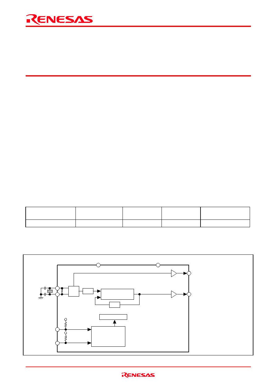
Block Diagram
Synthesizer
Mode Control
1/n
OSC
SSC Modulator
VDD
CLKOUT (12MHz typ.)
SSCCLKOUT (48MHz typ.)
GND
SEL0
XIN
XOUT
SEL1
1/m
R=100 k
R=100 k
R=1 M
HD151TS305RP
Rev.9.00 Jul. 07, 2004 page 2 of 9
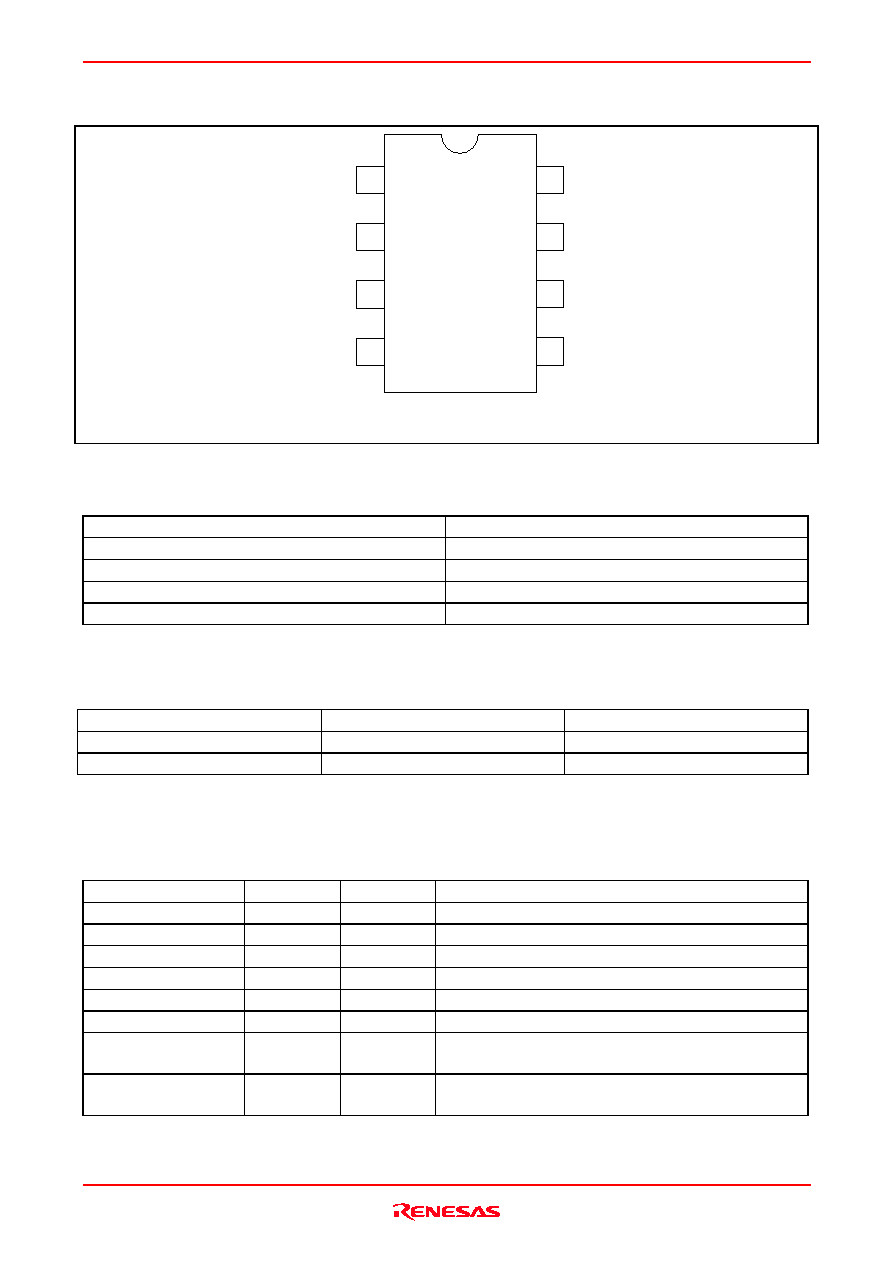
Pin Arrangement
(Top view)
8
SEL1
1
7
CLKOUT
6
SEL0
5
XOUT
SSCCLKOUT
2
VDD
3
GND
4
XIN
SSC Function Table
SEL1 :0
Spread Percentage
0 0
±
0.5%
0 1
±
1.5%
1 0
SSC OFF
1 1
±
0.25%
Note:
±
0.25% SSC is selected for default by internal pull-up resistors.
Clock Frequency Table
XIN(MHz)
SSCCLKOUT(MHz)
CLKOUT(MHz)
15
60
*1
15
*2
40
160
*1
40
*2
Notes: 1. With spread spectrum modulation.
2. Without spread spectrum modulation.
Pin Descriptions
Pin name
No.
Type
Description
GND
3
Ground
GND pin
VDD
2
Power
Power supplies pin. Normally 3.3 V.
CLKOUT
7
Output
Normally 3.3 V reference clock output.
SSCCLKOUT
1
Output
Spread spectrum modulated clock output.
XIN
4
Input
Oscillator input.
XOUT
5
Output
Oscillator output.
SEL0
6
Input
SSC mode select pin. LVCMOS level input.
Pull-up by internal resistor (100 k
).
SEL1
8
Input
SSC mode select pin. LVCMOS level input.
Pull≠up by internal resistor (100 k
).
HD151TS305RP
Rev.9.00 Jul. 07, 2004 page 3 of 9
Absolute Maximum Ratings
Item
Symbol
Ratings
Unit
Conditions
Supply voltage
VDD
≠0.5 to 4.6
V
Input voltage
V
I
≠0.5 to 4.6
V
Output voltage
*1
V
O
≠0.5 to VDD+0.5
V
Input clamp current
I
IK
≠50
mA
V
I
< 0
Output clamp current
I
OK
≠50
mA
V
O
< 0
Continuous output current
I
O
±50
mA
V
O
= 0 to VDD
Maximum power dissipation
at Ta = 55∞C (in still air)
0.7
W
Storage temperature
T
stg
≠65 to +150
∞C
Notes: Stresses beyond those listed under "absolute maximum ratings" may cause permanent damage to the device.
These are stress ratings only, and functional operation of the device at these or any other conditions beyond
those indicated under "recommended operating conditions" is not implied. Exposure to absolute maximum rated
conditions for extended periods may affect device reliability.
1. The input and output negative voltage ratings may be exceeded if the input and output clamp current ratings
are observed.
Recommended Operating Conditions
Item
Symbol
Min
Typ
Max
Unit
Conditions
Supply voltage
VDD
3.135
3.3
3.465
V
DC input signal voltage
≠0.3
--
VDD+0.3 V
High level input voltage
V
IH
2.0
--
VDD+0.3 V
Low level input voltage
V
IL
≠0.3
--
0.8
V
Operating temperature
T
a
0
--
70
∞C
Input clock duty cycle
45
50
55
%
DC Electrical Characteristics
Ta = 0 to 70∞C, VDD = 3.3 V±5%
Item
Symbol
Min
Typ
*1
Max
Unit
Test Conditions
Input low voltage
V
IL
--
--
0.8
V
Input high voltage
V
IH
2.0
--
--
V
--
--
±10
V
I
= 0 V or 3.465 V,
VDD = 3.465 V, XIN pin
Input current
I
I
--
--
±100
µA
V
I
= 0 V or 3.465 V, VDD = 3.465 V,
SEL0, SEL1 pins
Input slew rate
1
--
4
V / ns
20% ≠ 80%
Input capacitance
C
I
--
--
4
pF
SEL0, SEL1
Operating current
--
20
--
mA
XIN = 18 MHz, C
L
= 0 pF, VDD = 3.3 V
Note:
1. For conditions shown as Min or Max, use the appropriate value specified under recommended operating
conditions.
HD151TS305RP
Rev.9.00 Jul. 07, 2004 page 4 of 9
DC Electrical Characteristics / Clock Output & SSC Clock Output
Ta = 0 to 70∞C, VDD = 3.3 V±5%
Item
Symbol
Min
Typ
Max
Unit
Test Conditions
V
OH
3.1
--
--
V
I
OH
= ≠1 mA, VDD = 3.3 V
Output voltage
V
OL
--
--
50
mV
I
OL
= 1 mA, VDD = 3.3 V
I
OH
--
≠40
--
V
OH
= 1.5 V
Output current *
1
I
OL
--
40
--
mA
V
OL
= 1.5 V
Note:
1. Parameters are target of design. Not 100% tested in production.
AC Electrical Characteristics / Clock Output & SSC Clock Output
Ta = 25∞C, VDD = 3.3 V, C
L
= 15 pF
Item
Symbol
Min
Typ
Max
Unit
Test Conditions
Notes
--
| 250 |
| 300 |
SSCCLKOUT = 72MHz,
XIN = 18 MHz
SSC = 0%
SEL1:0 = 10
Fig1
--
| 250 |
| 300 |
SSCCLKOUT = 72MHz,
XIN = 18 MHz
SSC =
±
0.25%
SEL1:0 = 11
Fig1
Cycle to cycle jitter
*1, 2
t
CCS
--
| 250 |
| 300 |
ps
CLKOUT=18MHz
Fig1
70.4
--
73.6
SSCCLKOUT = 72MHz,
XIN = 18 MHz
SSC = 0%
SEL1:0 = 10
Output frequency
*1, 2
70.3
--
73.7
MHz
SSCCLKOUT = 72MHz,
XIN = 18 MHz
SSC=
±
0.25%
SEL1:0 = 11
Slew rate
*1
t
SL
0.8
--
--
V/ns
XIN = 18 MHz CLKOUT
0.4 V to 2.4 V
Clock duty cycle
*1
45
50
55
%
Output impedance
*1
--
40
--
Spread spectrum
modulation frequency
*1
--
33
--
KHz
SSCCLKOUT = 96MHz,
XIN = 24 MHz
Input clock frequency
15
--
40
MHz
Stabilization time
*1,3
--
--
2
ms
Note:
1. Parameters are target of design. Not 100% tested in production.
2. Cycle to cycle jitter and output frequency are included spread spectrum modulation.
3. Stabilization time is the time required for the integrated circuit to obtain phase lock of its input signal after
power up.
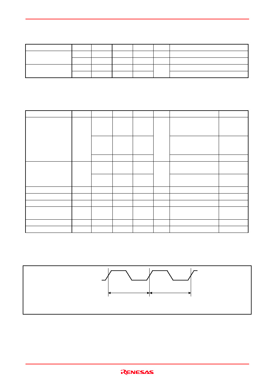
SSCCLKOUT
(or CLKOUT)
tcycle n
t = (tcycle n) - (tcycle n+1)
CCS
tcycle n+1
Figure 1 Cycle to cycle jitter
HD151TS305RP
Rev.9.00 Jul. 07, 2004 page 5 of 9
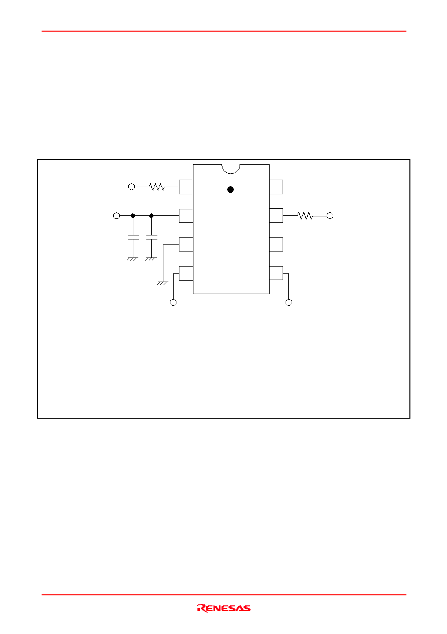
Application Information
1. Recommended Circuit Configuration
The power supply circuit of the optimal performance on the application of a system should refer to Fig. 2.
VDD decoupling is important to both reduce Jitter and EMI radiation.
The C1 decoupling capacitor should be placed, as close to the VDD pin as possible, otherwise the increased trace
inductance will negate its decoupling capability.
The C2 decoupling capacitor shown should be a tantalum type.
8
SEL1
1
7
CLKOUT
6
SEL0
5
SSCCLKOUT
2
VDD
3
GND
GND GND
4
XIN
XOUT
C1
R1
R2
C2
TS300 Series
(Crystal or
Reference input)
(Crystal or
Not connection)
Notes:
C1 = High frequency supply decoupling capacitor.
(0.1
µ
F recommended)
C2 = Low frequency supply decoupling capacitor.
(22
µ
F tantalum type recommended)
R1, R2 = Match value to line impedance.
(22
Reference value)
Figure 2 Recommended circuit configuration