 | –≠–ª–µ–∫—Ç—Ä–æ–Ω–Ω—ã–π –∫–æ–º–ø–æ–Ω–µ–Ω—Ç: HD404448 | –°–∫–∞—á–∞—Ç—å:  PDF PDF  ZIP ZIP |
Document Outline
- Description
- Features
- Ordering Information
- Pin Arrangement
- Pin Description
- Block Diagram
- Memory Map
- Functional Description
- Operating Modes
- Internal Oscillator Circuit
- Input/Output
- Prescalers
- Timers
- Serial Interface
- A/D Converter
- Notes on Mounting
- Programmable ROM
- Addressing Modes
- Absolute Maximum Ratings
- Electrical Characteristics
- Notes on ROM Out
- HD404448, HD404449 Option List

Regarding the change of names mentioned in the document, such as Hitachi
Electric and Hitachi XX, to Renesas Technology Corp.
The semiconductor operations of Mitsubishi Electric and Hitachi were transferred to Renesas
Technology Corporation on April 1st 2003. These operations include microcomputer, logic, analog
and discrete devices, and memory chips other than DRAMs (flash memory, SRAMs etc.)
Accordingly, although Hitachi, Hitachi, Ltd., Hitachi Semiconductors, and other Hitachi brand
names are mentioned in the document, these names have in fact all been changed to Renesas
Technology Corp. Thank you for your understanding. Except for our corporate trademark, logo and
corporate statement, no changes whatsoever have been made to the contents of the document, and
these changes do not constitute any alteration to the contents of the document itself.
Renesas Technology Home Page: http://www.renesas.com
Renesas Technology Corp.
Customer Support Dept.
April 1, 2003
To all our customers

Cautions
Keep safety first in your circuit designs!
1. Renesas Technology Corporation puts the maximum effort into making semiconductor products better
and more reliable, but there is always the possibility that trouble may occur with them. Trouble with
semiconductors may lead to personal injury, fire or property damage.
Remember to give due consideration to safety when making your circuit designs, with appropriate
measures such as (i) placement of substitutive, auxiliary circuits, (ii) use of nonflammable material or
(iii) prevention against any malfunction or mishap.
Notes regarding these materials
1. These materials are intended as a reference to assist our customers in the selection of the Renesas
Technology Corporation product best suited to the customer's application; they do not convey any
license under any intellectual property rights, or any other rights, belonging to Renesas Technology
Corporation or a third party.
2. Renesas Technology Corporation assumes no responsibility for any damage, or infringement of any
third-party's rights, originating in the use of any product data, diagrams, charts, programs, algorithms, or
circuit application examples contained in these materials.
3. All information contained in these materials, including product data, diagrams, charts, programs and
algorithms represents information on products at the time of publication of these materials, and are
subject to change by Renesas Technology Corporation without notice due to product improvements or
other reasons. It is therefore recommended that customers contact Renesas Technology Corporation
or an authorized Renesas Technology Corporation product distributor for the latest product information
before purchasing a product listed herein.
The information described here may contain technical inaccuracies or typographical errors.
Renesas Technology Corporation assumes no responsibility for any damage, liability, or other loss
rising from these inaccuracies or errors.
Please also pay attention to information published by Renesas Technology Corporation by various
means, including the Renesas Technology Corporation Semiconductor home page
(http://www.renesas.com).
4. When using any or all of the information contained in these materials, including product data, diagrams,
charts, programs, and algorithms, please be sure to evaluate all information as a total system before
making a final decision on the applicability of the information and products. Renesas Technology
Corporation assumes no responsibility for any damage, liability or other loss resulting from the
information contained herein.
5. Renesas Technology Corporation semiconductors are not designed or manufactured for use in a device
or system that is used under circumstances in which human life is potentially at stake. Please contact
Renesas Technology Corporation or an authorized Renesas Technology Corporation product distributor
when considering the use of a product contained herein for any specific purposes, such as apparatus or
systems for transportation, vehicular, medical, aerospace, nuclear, or undersea repeater use.
6. The prior written approval of Renesas Technology Corporation is necessary to reprint or reproduce in
whole or in part these materials.
7. If these products or technologies are subject to the Japanese export control restrictions, they must be
exported under a license from the Japanese government and cannot be imported into a country other
than the approved destination.
Any diversion or reexport contrary to the export control laws and regulations of Japan and/or the
country of destination is prohibited.
8. Please contact Renesas Technology Corporation for further details on these materials or the products
contained therein.

HD404449 Series
Rev. 6.0
Sept. 1998
Description
The HD404449 Series is a HMCS400-series microcomputer designed to increase program productivity
with large-capacity memory. Each microcomputer has four timers, two serial interfaces, A/D converter,
input capture circuit, 32-kHz oscillator for clock, and four low-power dissipation modes.
The HD404449 Series includes three chips: the HD404448 with 8-kword ROM; the HD404449 with 16-
kword ROM; and HD4074449 with 16-kword PROM (ZTAT
TM
version).
The HD4074449 is a PROM version (ZTAT
TM
microcomputer). A program can be written to the PROM by
a PROM writer, which can dramatically shorten system development periods and smooth the process from
debugging to mass production. (The ZTAT
TM
version is 27256-compatible.)
ZTAT
TM
: Zero Turn Around Time ZTAT is a trademark of Hitachi Ltd.
Features
∑
8,192-word
◊
10-bit ROM (HD404448)
16,384-word
◊
10-bit ROM (HD404449 and HD4074449)
∑
1,152-digit
◊
4-bit RAM
∑
64 I/O pins, including 10 high-current pins (15 mA, max)
∑
Four timer/counters
∑
Eight-bit input capture circuit
∑
Three timer outputs (including two PWM outputs)
∑
Two event counter inputs (including one double-edge function)
∑
Two clock-synchronous 8-bit serial interfaces
∑
A/D converter (4-channel
◊
8-bit)
∑
Built-in oscillators
Main clock: 4-MHz ceramic oscillator or crystal (an external clock is also possible)
Subclock: 32.768-kHz crystal
∑
Eleven interrupt sources
Four by external sources, including two double-edge function
Seven by internal sources

HD404449 Series
2
∑
Subroutine stack up to 16 levels, including interrupts
∑
Four low-power dissipation modes
Subactive mode
Standby mode
Watch mode
Stop mode
∑
One external input for transition from stop mode to active mode
∑
Instruction cycle time: 1
µ
s (f
OSC
= 4 MHz)
∑
Two operating modes
MCU mode (HD404448, HD404449)
MCU/PROM mode (HD4074449)
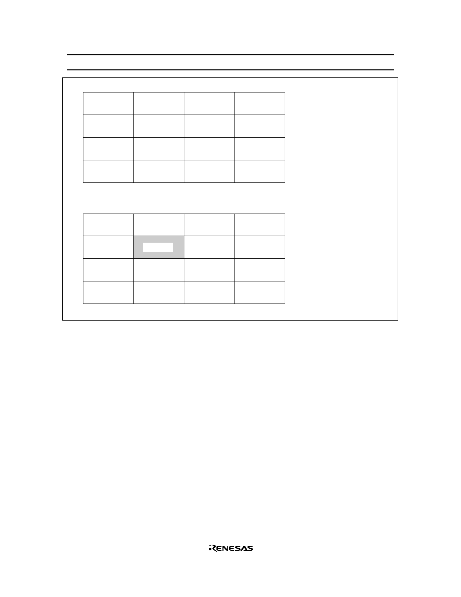
Ordering Information
Type
Product Name
Model Name
ROM (Words)
Package
Mask ROM
HD404448
HD404448H
8,192
80-pin plastic QFP (FP-80A)
HD404448TF
80-pin plastic QFP (TFP-80F)
HD404449
HD404449H
16,384
80-pin plastic QFP (FP-80A)
HD404449TF
80-pin plastic QFP (TFP-80F)
ZTAT
TM
HD4074449
HD4074449H
16,384
80-pin plastic QFP (FP-80A)
HD4074449TF
80-pin plastic QFP (TFP-80F)
HD404449 Series
3
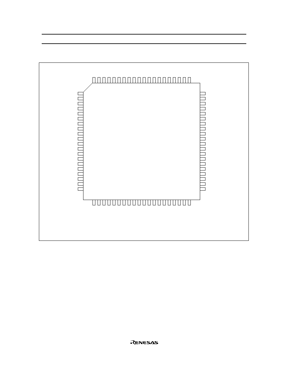
Pin Arrangement
FP-80A
TFP-80F
1
2
3
4
5
6
7
8
9
10
11
12
13
14
15
16
17
18
19
20
60
59
58
57
56
55
54
53
52
51
50
49
48
47
46
45
44
43
42
41
(Top view)
21
22
23
24
25
26
27
28
29
30
31
32
33
34
35
36
37
38
39
40
80
79
78
77
76
75
74
73
72
71
70
69
68
67
66
65
64
63
62
61
R8
3
R8
2
R8
1
R8
0
R7
3
R7
2
R7
1
R7
0
R6
3
R6
2
R6
1
R6
0
R5
3
/SO
2
R5
2
/SI
2
R5
1
/
SCK
2
R5
0
R4
3
/SO
1
R4
2
/SI
1
R4
1
/
SCK
1
R4
0
/EVND
AN
2
AN
3
AV
SS
TEST
OSC
1
OSC
2
RESET
X1
X2
GND
D
0
D
1
D
2
D
3
D
4
D
5
D
6
D
7
D
8
D
9
D
10
D
11
D
12
/
STOPC
D
13
/
INT
0
0
/
INT
1
R0
1
/INT
2
R0
2
/INT
3
R0
3
R1
0
R1
1
R1
2
R1
3
R2
0
R2
1
R2
2
R2
3
R3
0
/TOB
R3
1
/TOC
R3
2
/TOD
R3
3
/
EVNB
AN
1
AN
0
AV
CC
V
CC
RC
3
RC
2
RC
1
RC
0
RB
3
RB
2
RB
1
RB
0
RA
3
RA
2
RA
1
RA
0
R9
3
R9
2
R9
1
R9
0
R0

HD404449 Series
4
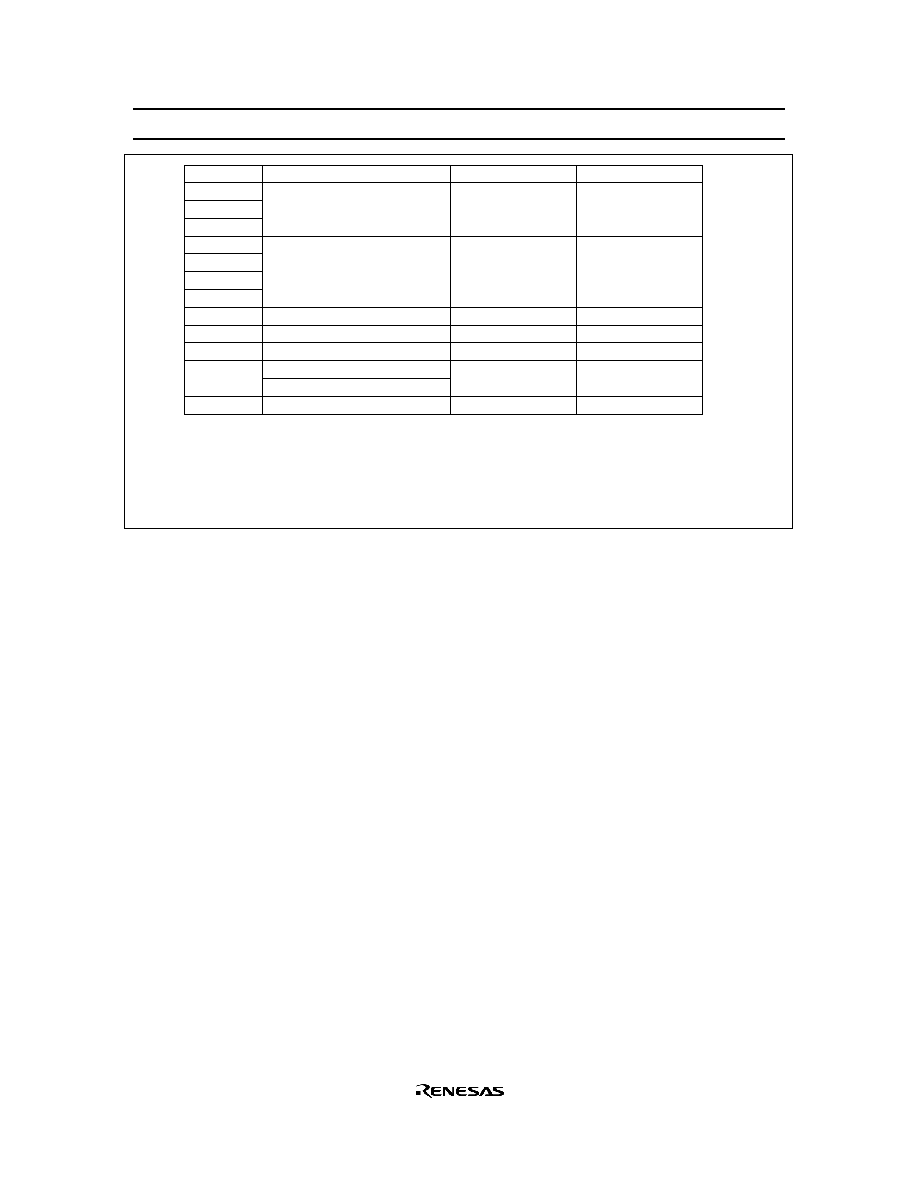
Pin Description
Item
Symbol
Pin Number I/O
Function
Power supply
V
CC
77
Applies power voltage
GND
10
Connected to ground
Test
TEST
4
I
Used for factory testing only: Connect this pin to V
CC
Reset
RESET
7
I
Resets the MCU
Oscillator
OSC
1
5
I
Input/output pins for the internal oscillator circuit:
Connect them to a ceramic oscillator, crystal, or
connect OSC
1
to an external oscillator circuit
OSC
2
6
O
X1
8
I
Used for a 32.768-kHz crystal for clock purposes. If
not to be used, fix the X1 pin to V
CC
and leave the X2
pin open.
X2
9
O
Port
D
0
≠D
11
11≠22
I/O
Input/output pins addressed by individual bits; pins
D
0
≠D
9
are high-current pins that can each supply up to
15 mA
D
12
, D
13
23, 24
I
Input pins addressable by individual bits
R0
0
≠RC
3
25≠76
I/O
Input/output pins addressable in 4-bit units
Interrupt
INT
0
,
INT
1
,
INT
2
, INT
3
24≠27
I
Input pins for external interrupts
Stop clear
STOPC
23
I
Input pin for transition from stop mode to active mode
Serial
SCK
1
,
SCK
2
42, 46
I/O
Serial clock input/output pin
interface
SI
1
, SI
2
43, 47
I
Serial receive data input pin
SO
1
, SO
2
44, 48
O
Serial transmit data output pin
Timer
TOB, TOC, TOD 37≠39
O
Timer output pins
EVNB
, EVND
40, 41
I
Event count input pins
A/D converter
AV
CC
78
Power pin for A/D converter: Connect it to the same
potential as V
CC
, as physically close to the V
CC
pin as
possible
AV
SS
3
Ground for AV
CC
: Connect it to the same potential as
GND, as physically close to the GND pin as possible
AN
0
≠AN
3
79, 80, 1, 2
I
Analog input pins for A/D converter
HD404449 Series
5
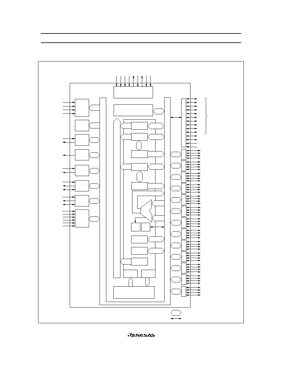
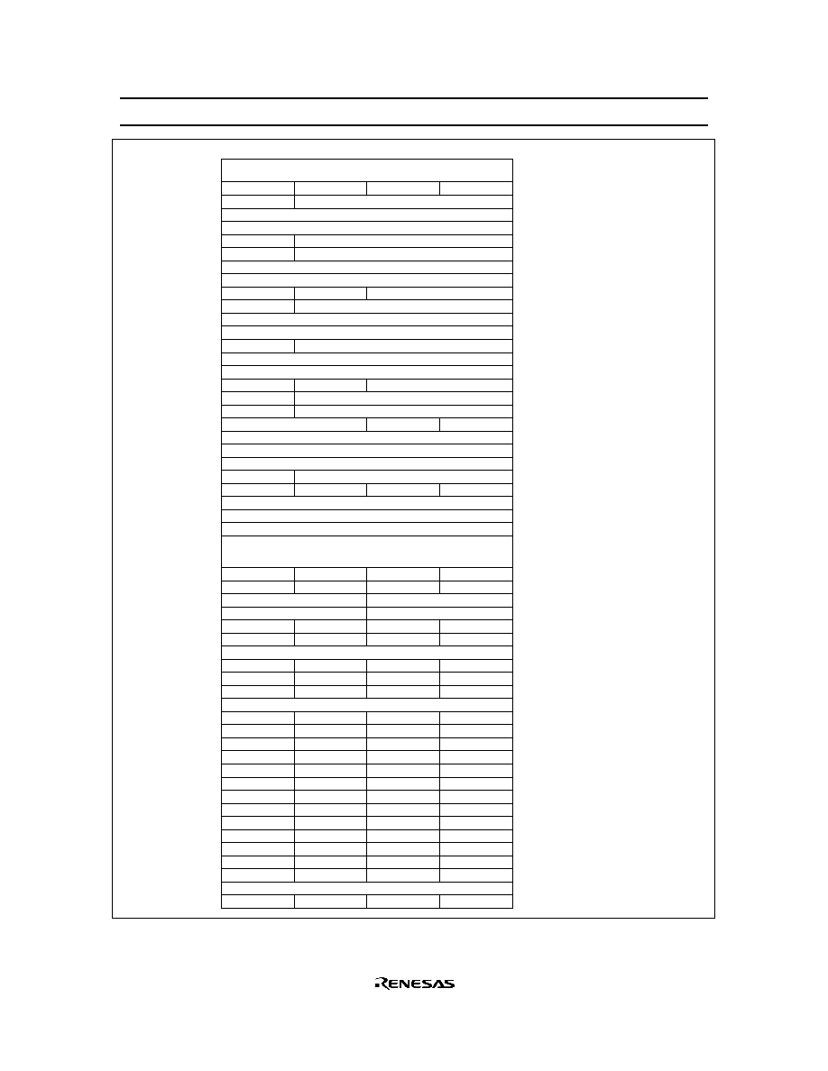
Block Diagram
System control
External
interrupt
Timer
A
Timer
B
Timer
C
Timer
D
Serial
interface
1
Serial
interface
2
A/D
converter
Internal data bus
Internal address bus
RAM
(1,152 4 bits)
W
(2 bits)
X
(4 bits)
Y
(4 bits)
SPX
(4 bits)
ST
(1 bit)
CA
(1 bit)
A
(4 bits)
B
(4 bits)
SP
(10 bits)
PC
(14 bits)
Instruction
decoder
CPU
R0
R0
R0
R0
R1
R1
R1
R1
R2
R2
R2
R2
R3
R3
R3
R3
R4
R4
R4
R4
R5
R5
R5
R5
R6
R6
R6
R6
R7
R7
R7
R7
R8
R8
R8
R8
R9
R9
R9
R9
RA
RA
RA
RA
RB
RB
RB
RB
RC
RC
RC
RC
: Data bus
: Signal line
RESET
TOC
EVND
TOD
INT
INT
INT
INT
SI
2
SO
2
SCK
2
AV
CC
AV
SS
AN
0
AN
1
AN
2
AN
3
R0 port
R1 port
R2 port
R3 port
R4 port
RC port
0
1
2
3
0
1
2
3
0
1
2
3
0
1
2
3
0
1
2
3
0
1
2
3
0
1
2
3
0
1
2
3
0
1
2
3
0
1
2
3
0
1
2
3
0
1
2
3
0
1
2
3
R5 port
R6 port
R7 port
R8 port
R9 port
RA port
RB port
SI
SO
SCK
ROM
(16,384
◊
10 bits)
(8,192
◊
10 bits)
D port
High current
pins
D
D
D
D
D
D
D
D
D
D
D
D
D
D
0
1
2
3
4
5
6
7
8
9
10
11
12
13
0
1
2
3
EVNB
TOB
1
1
1
SPY
(4 bits)
ALU
◊
TEST
STOPC
OSC
1
OSC
2
X1
X2
V
CC
GND
HD404449 Series
6
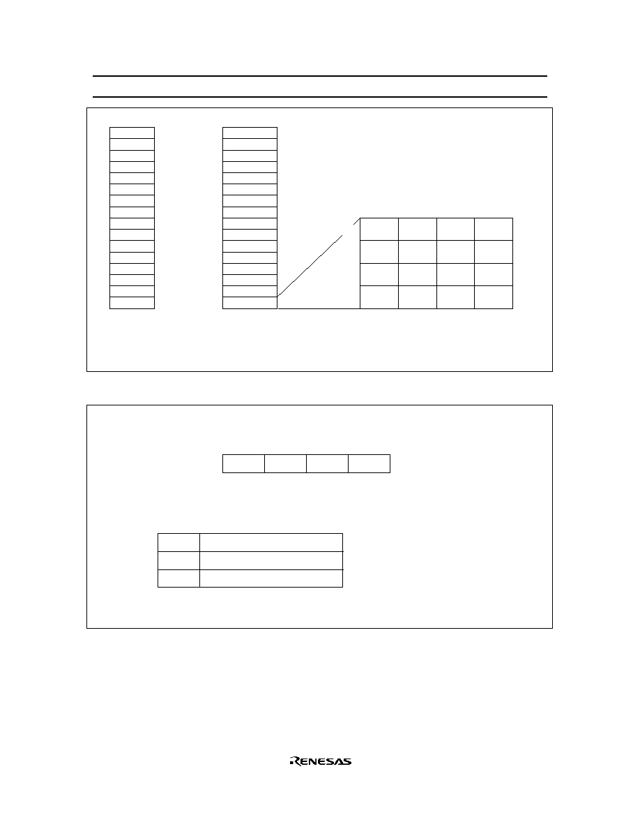
Memory Map
ROM Memory Map
The ROM memory map is shown in figure 1 and described below.
0
15
16
63
64
4,095
4,096
16,383
0
$000F
$0FFF
$1000
$1FFF
$2000
$3FFF
$0010
$003F
$0040
Vector address
Zero-page subroutine
(64 words)
Pattern
(4,096 words)
HD404448
Program
(8,192 words)
HD404449, HD4074449
Program
(16,384 words)
1
2
3
4
5
6
7
8
9
10
11
12
13
14
15
$0000
$0000
$0001
$0002
$0003
$0004
$0005
$0006
$0007
$0008
$0009
$000A
$000B
$000C
$000D
$000E
$000F
0
1
JMPL instruction
(Jump to RESET,
STOPC
routine)
JMPL instruction
(Jump to
INT
routine)
JMPL instruction
(Jump to timer A routine)
JMPL instruction
(Jump to timer B, INT routine)
JMPL instruction
(Jump to timer C, INT routine)
JMPL instruction
(Jump to timer D, A/D routine)
JMPL instruction
(Jump to
INT
routine)
JMPL instruction
(Jump to serial 1, serial 2 routine)
2
3
8,191
8,192
Figure 1 ROM Memory Map
Vector Address Area ($0000≠$000F): Reserved for JMPL instructions that branch to the start addresses
of the reset and interrupt routines. After MCU reset or an interrupt, program execution continues from the
vector address.
Zero-Page Subroutine Area ($0000≠$003F): Reserved for subroutines. The program branches to a
subroutine in this area in response to the CAL instruction.
Pattern Area ($0000≠$0FFF): Contains ROM data that can be referenced with the P instruction.
Program Area ($0000≠$1FFF (HD404448), $0000≠$3FFF (HD404449, HD4074449)): Used for
program coding.
RAM Memory Map
The MCU contains a 1,152-digit
◊
4-bit RAM area consisting of a memory register area, a data area, and a
stack area. In addition, an interrupt control bits area, special register area, and register flag area are mapped
onto the same RAM memory space as a RAM-mapped register area outside the above areas. The RAM
memory map is shown in figure 2 and described as follows.
HD404449 Series
7
A/D data register
Data
(464 digits)
V = 1
(bank = 1)
0
$000
$000
64
80
608
960
1023
$040
$050
4
5
6
7
0
3
12
13
14
15
8
9
10
11
16
17
32
35
18
19
20
63
$003
$004
$005
$006
$007
$008
$009
$00A
$00B
$00C
$00D
$00E
$00F
$010
$011
$012
$013
$014
$020
$023
$032
$033
$034
$035
$036
$037
$038
$03F
$00A
$00B
$00E
$00F
W
W
R/W
W
W
W
W
W
W
W
W
W
W
W
W
W
W
R
R
R
R
W
R/W
R/W
R/W
R/W
R/W
R/W
$090
$25F
58
54
55
$3C0
$260
RAM-mapped registers
Memory registers (MR)
Not used
Data (464 digits 2)
V = 0 (bank 0)
V = 1 (bank 1)
Data (144 digits)
Stack (64 digits)
Interrupt control bits area
Port mode register A
Serial mode register 1A
Serial data register 1 lower
Serial data register 1 upper
Timer mode register A
Timer mode register B1
Timer B
Miscellaneous register
Timer mode register C1
Timer C
Timer mode register B2
Timer mode register D2
Register flag area
Port R0 DCR
Port R1 DCR
Port R2 DCR
Port R3 DCR
Port D ≠D DCR
Port D ≠D DCR
Port D and D DCR
Not used
V register
0
3
4
7
8
11
Data
(464 digits)
V = 0
(bank = 0)
The data area has two banks:
bank 0 (V = 0) to bank 1 (V = 1)
10
11
14
15
Timer read register B lower
Timer read register B upper
Timer read register C lower
Timer read register C upper
Timer write register B lower
Timer write register B upper
Timer write register C lower
Timer write register C upper
R:
W:
R/W:
◊
$090
Read only
Write only
Read/Write
Note:
$011
$012
W
W
R
R
17
18
Timer read register D lower
Timer read register D upper
Timer write register D lower
Timer write register D upper
144
W
Timer mode register D1
R/W
R/W
Timer D
Timer mode register C2
21
$015
22
$016
R
A/D data register lower
23
$017
36
$024
37
$025
38
$026
39
$027
40
$028
41
$029
42
$02A
43
$02B
24
25
27
26
28
29
30
31
$018
$019
$01A
$01B
$01C
$01D
$01E
$01F
$3FF
A/D data register upper
Serial mode register 2A
Serial mode register 2B
Serial data register 2 lower
Serial data register 2 upper
R
W
W
W
W
W
60
44
45
46
47
Port mode register B
Port mode register C
Detection edge select register 1
Detection edge select register 2
Serial mode register 1B
System clock select register
Not used
Not used
Port R4 DCR
Port R5 DCR
Port R6 DCR
Port R7 DCR
W
W
W
W
W
W
W
W
W
W
W
W
W
$02C
$02D
$02E
$02F
$031
$030
53
48
49
50
51
52
Two registers are mapped
on the same area.
*
Not used
752
$2F0
Note
R/W
R/W
R/W
Not used
(PMRA)
(SM1A)
(SR1L)
(SR1U)
(TMA)
(TMB1)
(TRBL/TWBL)
(TRBU/TWBU)
(MIS)
(TMC1)
(TRCL/TWCL)
(TRCU/TWCU)
(TMD1)
(TRDL/TWDL)
(TRDU/TWDU)
(TMB2)
(TMC2)
(TMD2)
(AMR)
(ADRL)
(ADRU)
(SM2A)
(SM2B)
(SR2L)
(SR2U)
(PMRB)
(PMRC)
(SM1B)
(SSR)
(ESR1)
(ESR2)
(DCD0)
(DCD1)
(DCD2)
(DCR0)
(DCR1)
(DCR2)
(DCR3)
(DCR4)
(DCR5)
(DCR6)
(DCR7)
(DCR8)
(DCR9)
(DCRA)
(DCRB)
(DCRC)
R/W
R/W
Not used
Port R8 DCR
Port R9 DCR
Port RA DCR
Port RB DCR
Port RC DCR
59
57
56
$039
$03A
$03B
$03C
(TRBL)
(TRBU)
(TRCL)
(TRCU)
(TRDL)
(TRDU)
(TWBL)
(TWBU)
(TWCL)
(TWCU)
(TWDL)
(TWDU)
*
Figure 2 RAM Memory Map

HD404449 Series
8
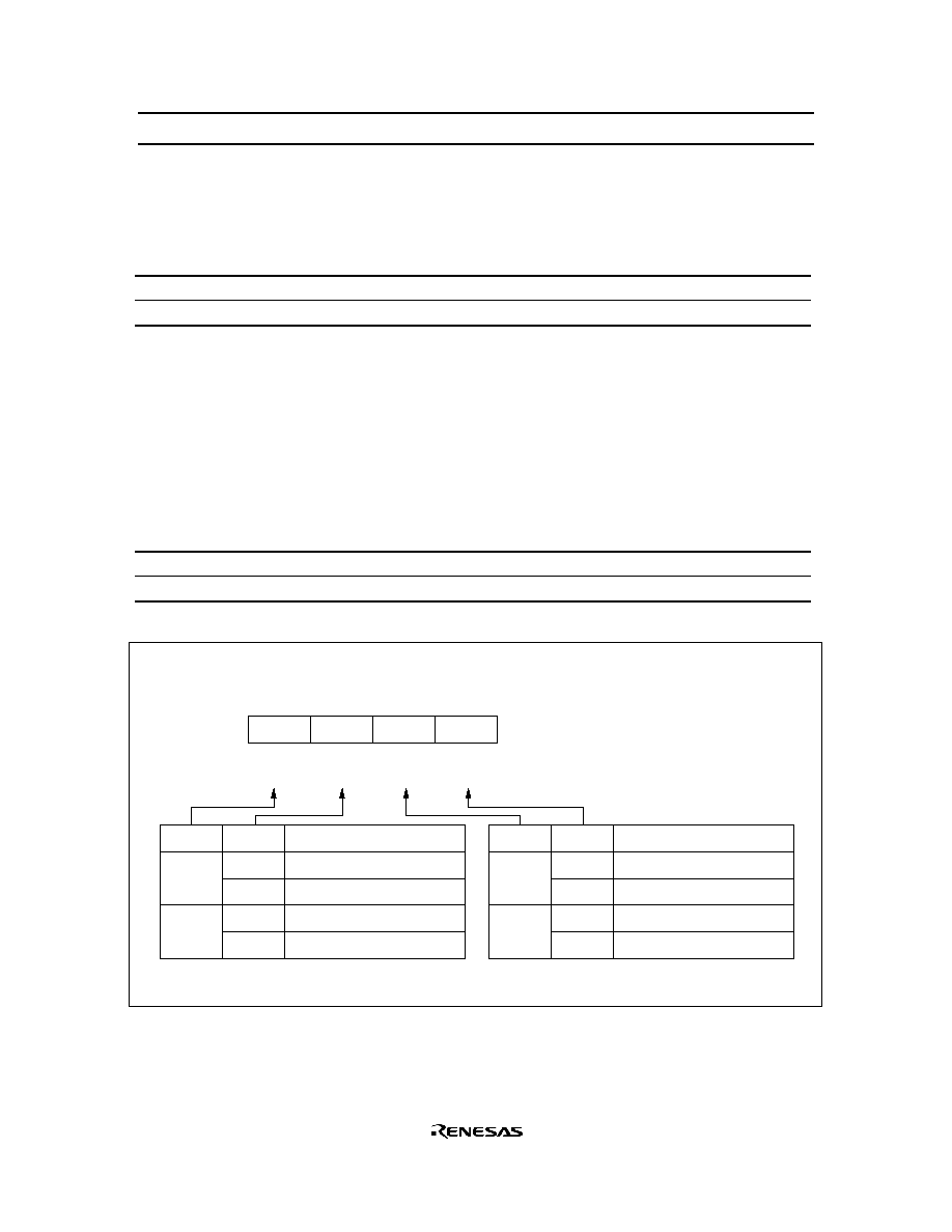
RAM-Mapped Register Area ($000≠$03F):
∑
Interrupt Control Bits Area ($000≠$003)
This area is used for interrupt control bits (figure 3). These bits can be accessed only by RAM bit
manipulation instructions (SEM/SEMD, REM/REMD, and TM/TMD). However, note that not all the
instructions can be used for each bit. Limitations on using the instructions are shown in figure 4.
∑
Special Function Register Area ($004≠$01F, $024≠$03F)
This area is used as mode registers and data registers for external interrupts, serial interface 1, serial
interface 2, timer/counters, A/D converter, and as data control registers for I/O ports. The structure is
shown in figures 2 and 5. These registers can be classified into three types: write-only (W), read-only
(R), and read/write (R/W). RAM bit manipulation instructions cannot be used for these registers.
∑
Register Flag Area ($020≠$023)
This area is used for the DTON, WDON, and other register flags and interrupt control bits (figure 3).
These bits can be accessed only by RAM bit manipulation instructions (SEM/SEMD, REM/REMD, and
TM/TMD). However, note that not all the instructions can be used for each bit. Limitations on using
the instructions are shown in figure 4.
Memory Register (MR) Area ($040≠$04F): Consisting of 16 addresses, this area (MR0≠MR15) can be
accessed by register-register instructions (LAMR and XMRA). The structure is shown in figure 6.
Data Area ($090≠$2EF): 464 digits from $090 to $25F have two banks, which can be selected by setting
the bank register (V: $03F). Before accessing this area, set the bank register to the required value (figure
7). The area from $260 to $2EF is accessed without setting the bank register.
Stack Area ($3C0≠$3FF): Used for saving the contents of the program counter (PC), status flag (ST), and
carry flag (CA) at subroutine call (CAL or CALL instruction) and for interrupts. This area can be used as a
16-level nesting subroutine stack in which one level requires four digits. The data to be saved and the save
conditions are shown in figure 6.
The program counter is restored by either the RTN or RTNI instruction, but the status and carry flags can
only be restored by the RTNI instruction. Any unused space in this area is used for data storage.
HD404449 Series
9
0
1
2
3
Bit 3
Bit 2
Bit 1
Bit 0
IMTA
(IM of timer A)
IFTA
(IF of timer A)
IM1
(IM of
INT
1
)
IF1
(IF of
INT
1
)
IMTC
(IM of timer C)
IFTC
(IF of timer C)
IMTB
(IM of timer B)
IFTB
(IF of timer B)
IMS1
(IM of serial
interface 1)
IFS1
(IF of serial
interface 1)
IMTD
(IM of timer D)
IFTD
(IF of timer D)
$000
$001
$002
$003
Interrupt control bits area
IM0
(IM of
INT
0
)
IF0
(IF of
INT
0
)
RSP
(Reset SP bit)
IE
(Interrupt
enable flag)
32
33
34
35
ICSF
(Input capture
status flag)
IM3
(IM of INT
3
)
IF3
(IF of INT
3
)
IM2
(IM of INT
2
)
IF2
(IF of INT
2
)
IMS2
(IM of serial
interface 2)
IFS2
(IF of serial
interface 2)
IMAD
(IM of A/D)
IFAD
(IF of A/D)
$020
$021
$022
$023
Register flag area
DTON
(Direct transfer
on flag)
ADSF
(A/D start flag)
WDON
(Watchdog
on flag)
LSON
(Low speed
on flag)
ICEF
(Input capture
error flag)
RAME
(RAM enable
flag)
Not used
IF:
IM:
IE:
SP:
Interrupt request flag
Interrupt mask
Interrupt enable flag
Stack pointer
Bit 3
Bit 2
Bit 1
Bit 0
Figure 3 Configuration of Interrupt Control Bits and Register Flag Areas
HD404449 Series
10
IE
IM
LSON
IF
ICSF
ICEF
RAME
RSP
WDON
ADSF
Not used
DTON
SEM/SEMD
REM/REMD
TM/TMD
Allowed
Allowed
Allowed
Not executed
Allowed
Allowed
Not executed
Allowed
Inhibited
Allowed
Not executed
Inhibited
Allowed
Inhibited
Allowed
Not executed in active mode
Allowed
Allowed
Used in subactive mode
Not executed
Not executed
Inhibited
Note: WDON is reset by MCU reset or by
STOPC
enable for stop mode cancellation.
The REM or REMD instuction must not be executed for ADSF during A/D conversion.
DTON is always reset in active mode.
If the TM or TMD instruction is executed for the inhibited bits or non-existing bits,
the value in ST becomes invalid.
Figure 4 Usage Limitations of RAM Bit Manipulation Instructions
HD404449 Series
11
$000
$003
PMRA $004
SM1A $005
SR1L $006
SR1U $007
TMA $008
TMB1 $009
TRBL/TWBL $00A
TRBU/TWBU $00B
MIS $00C
TMC1 $00D
TRCL/TWCL $00E
TRCU/TWCU $00F
TMD1 $010
TRDL/TWDL $011
TRDU/TWDU $012
TMB2 $013
TMC2 $014
TMD2 $015
AMR $016
ADRL $017
ADRU $018
SM2A $01B
SM2B $01C
SR2L $01D
SR2U $01E
$020
$023
PMRB $024
PMRC $025
ESR1 $026
ESR2 $027
SM1B $028
SSR $029
DCD0 $02C
DCD1 $02D
DCD2 $02E
DCR0 $030
DCR1 $031
DCR2 $032
DCR3 $033
DCR4 $034
DCR5 $035
DCR6 $036
DCR7 $037
DCR8 $038
DCR9 $039
DCRA $03A
DCRB $03B
DCRC $03C
V $03F
Bit 3
Bit 2
Bit 1
Interrupt control bits area
R5
2
/SI
2
R5
3
/SO
2
R4
3
/SO
1
R4
2
/SI
1
Serial transmit clock speed selection 1
Serial data register 1 (lower digit)
Serial data register 1 (upper digit)
*
1
*
2
Clock source selection (timer A)
Clock source selection (timer B)
Timer B register (lower digit)
Timer B register (upper digit)
*
3
R4
3
/SO
1
PMOS control
Interrupt frame period selection
*
2
Clock source selection (timer C)
Timer C register (lower digit)
Timer C register (upper digit)
*
2
Clock source selection (timer D)
Timer D register (lower digit)
Timer D register (upper digit)
Not used
Not used
Timer-B output mode selection
Not used
Timer-C output mode selection
Timer-D output mode selection
*
4
Not used
*
5
Analog channel selection
A/D data register (lower digit)
A/D data register (upper digit)
R5
1
/
SCK
2
Serial transmit clock speed selection 2
Register flag area
Not used
INT
3
detection edge selection
INT
2
detection edge selection
EVND detection edge selection
Not used
Not used
*
8
*
9
*
10
*
11
Not used
Port D
3
DCR
Port D
2
DCR
Port D
1
DCR
Port D
0
DCR
Port D
7
DCR
Port D
6
DCR
Port D
5
DCR
Port D
4
DCR
Port D
11
DCR
Port D
10
DCR
Port D
9
DCR
Port D
8
DCR
Not used
Port R0
3
DCR
Port R1
3
DCR
Port R2
3
DCR
Port R3
3
DCR
Port R4
3
DCR
Port R5
3
DCR
Port R6
3
DCR
Port R7
3
DCR
Not used
Not used
Not used
R0
2
/INT
3
R0
1
/INT
2
R0
0
/
INT
1
D
13
/
INT
0
D
12
/
STOPC
R4
0
/EVND
R3
3
/
EVNB
R4
1
/
SCK
1
Bit 0
Not used
Not used
R5
3
/SO
2
PMOS control
*
6
*
7
Serial data register 2 (lower digit)
Serial data register 2 (upper digit)
Not used
Not used
*
12
Not used
Port R8
3
DCR
Port R9
3
DCR
Port RA
3
DCR
Port RB
3
DCR
Port RC
3
DCR
Port R0
2
DCR
Port R1
2
DCR
Port R2
2
DCR
Port R3
2
DCR
Port R4
2
DCR
Port R5
2
DCR
Port R6
2
DCR
Port R7
2
DCR
Port R8
2
DCR
Port R9
2
DCR
Port RA
2
DCR
Port RB
2
DCR
Port RC
2
DCR
Port R0
1
DCR
Port R1
1
DCR
Port R2
1
DCR
Port R3
1
DCR
Port R4
1
DCR
Port R5
1
DCR
Port R6
1
DCR
Port R7
1
DCR
Port R8
1
DCR
Port R9
1
DCR
Port RA
1
DCR
Port RB
1
DCR
Port RC
1
DCR
Port R0
0
DCR
Port R1
0
DCR
Port R2
0
DCR
Port R3
0
DCR
Port R4
0
DCR
Port R5
0
DCR
Port R6
0
DCR
Port R7
0
DCR
Port R8
0
DCR
Port R9
0
DCR
Port RA
0
DCR
Port RB
0
DCR
Port RC
0
DCR
Notes:
1. Timer-A/time-base
2. Auto-reload on/off
3. Pull-up MOS control
4. Input capture selection
5. A/D conversion time
6. SO
2
ouput control in idle states
7. Serial clock source selection 2
8. SO
1
output level control in idle states
9. Serial clock source selection 1
10. 32-kHz oscillation stop
11. 32-kHz oscillation division ratio
12. System clock selection
13. Bank 0, 1 selection
Not used
*
13
Figure 5 Special Function Register Area
HD404449 Series
12
Memory registers
64
65
66
67
68
69
70
71
73
74
75
76
77
78
79
72
$040
$041
$042
$043
$044
$045
$046
$047
$048
$049
$04A
$04B
$04C
$04D
$04E
$04F
960
$3C0
1023
$3FF
MR(0)
MR(1)
MR(2)
MR(3)
MR(4)
MR(5)
MR(6)
MR(7)
MR(8)
MR(9)
Level 16
Level 15
Level 14
Level 13
Level 12
Level 11
Level 10
Level 9
Level 8
Level 7
Level 6
Level 5
Level 4
Level 3
Level 2
Level 1
MR(10)
MR(11)
MR(12)
MR(13)
MR(14)
MR(15)
PC
PC
PC
PC
PC
PC
PC
PC
PC
PC
PC
PC
ST
PC
CA
PC
10
3
13
9
6
2
12
8
5
1
11
7
4
0
Bit 3
Bit 2
Bit 1
Bit 0
$3FC
$3FD
$3FE
$3FF
1020
1021
1022
1023
PC ≠PC :
ST: Status flag
CA: Carry flag
Program counter
13
Stack area
0
Figure 6 Configuration of Memory Registers and Stack Area, and Stack Position
Bit
Initial value
Read/Write
Bit name
3
--
--
Not used
2
--
--
Not used
0
0
R/W
V0
1
--
--
Not used
V0
0
1
Bank area selection
Bank 0 is selected
Bank 1 is selected
Note: After reset, the value in the bank register is 0, and therefore bank 0 is
selected.
Bank register (V: $03F)
Figure 7 Bank Register (V)
HD404449 Series
13
Functional Description
Registers and Flags
The MCU has nine registers and two flags for CPU operations. They are shown in figure 8 and described
below.
3
0
3
0
3
0
3
0
3
0
3
0
0
0
0
13
9
5
1
(B)
(A)
(W)
(X)
(Y)
(SPX)
(SPY)
(CA)
(ST)
(PC)
(SP)
1
1
1
1
Accumulator
B register
W register
X register
Y register
SPX register
SPY register
Carry
Status
Program counter
Initial value: 0,
no R/W
Stack pointer
Initial value: $3FF, no R/W
0
0
Initial value: Undefined, R/W
Initial value: Undefined, R/W
Initial value: Undefined, R/W
Initial value: Undefined, R/W
Initial value: Undefined, R/W
Initial value: Undefined, R/W
Initial value: Undefined, R/W
Initial value: Undefined, R/W
Initial value: 1, no R/W
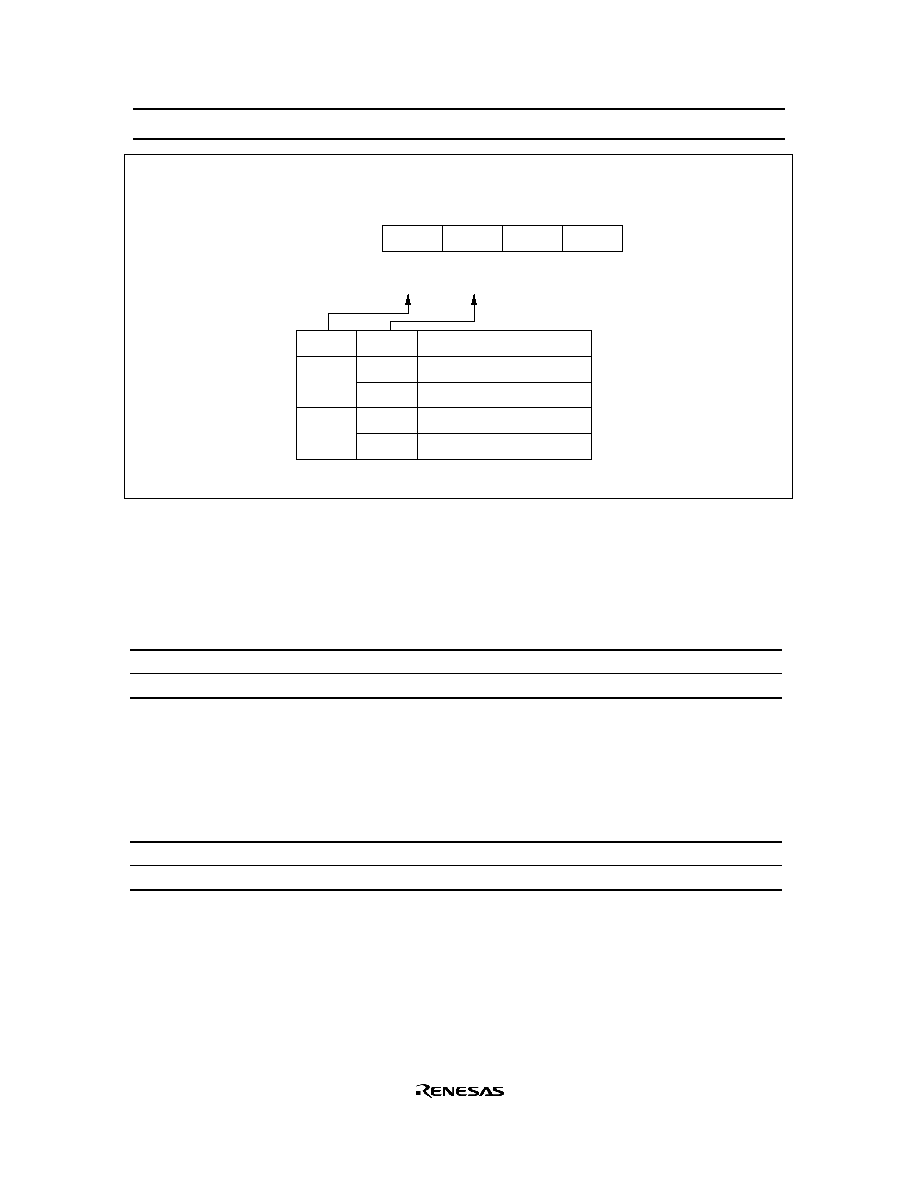
Figure 8 Registers and Flags
Accumulator (A), B Register (B): Four-bit registers used to hold the results from the arithmetic logic unit
(ALU) and transfer data between memory, I/O, and other registers.
W Register (W), X Register (X), Y Register (Y): Two-bit (W) and four-bit (X and Y) registers used for
indirect RAM addressing. The Y register is also used for D-port addressing.

HD404449 Series
14
SPX Register (SPX), SPY Register (SPY): Four-bit registers used to supplement the X and Y registers.
Carry Flag (CA): One-bit flag that stores any ALU overflow generated by an arithmetic operation. CA is
affected by the SEC, REC, ROTL, and ROTR instructions. A carry is pushed onto the stack during an
interrupt and popped from the stack by the RTNI instruction--but not by the RTN instruction.
Status Flag (ST): One-bit flag that latches any overflow generated by an arithmetic or compare
instruction, not-zero decision from the ALU, or result of a bit test. ST is used as a branch condition of the
BR, BRL, CAL, and CALL instructions. The contents of ST remain unchanged until the next arithmetic,
compare, or bit test instruction is executed, but become 1 after the BR, BRL, CAL, or CALL instruction is
read, regardless of whether the instruction is executed or skipped. The contents of ST are pushed onto the
stack during an interrupt and popped from the stack by the RTNI instruction--but not by the RTN
instruction.
Program Counter (PC): 14-bit binary counter that points to the ROM address of the instruction being
executed.
Stack Pointer (SP): Ten-bit pointer that contains the address of the stack area to be used next. The SP is
initialized to $3FF by MCU reset. It is decremented by 4 when data is pushed onto the stack, and
incremented by 4 when data is popped from the stack. The top four bits of the SP are fixed at 1111, so a
stack can be used up to 16 levels.
The SP can be initialized to $3FF in another way: by resetting the RSP bit with the REM or REMD
instruction.
Reset
The MCU is reset by inputting a high-level voltage to the RESET pin. At power-on or when stop mode is
cancelled, RESET must be high for at least one t
RC
to enable the oscillator to stabilize. During operation,
RESET must be high for at least two instruction cycles.
Initial values after MCU reset are listed in table 1.

HD404449 Series
15
Table 1
Initial Values After MCU Reset
Item
Abbr.
Initial
Value
Contents
Program counter
(PC)
$0000
Indicates program execution point from start
address of ROM area
Status flag
(ST)
1
Enables conditional branching
Stack pointer
(SP)
$3FF
Stack level 0
Interrupt
flags/mask
Interrupt enable flag
(IE)
0
Inhibits all interrupts
Interrupt request flag
(IF)
0
Indicates there is no interrupt request
Interrupt mask
(IM)
1
Prevents (masks) interrupt requests
I/O
Port data register
(PDR)
All bits 1
Enables output at level 1
Data control register
(DCD0≠
DCD2)
All bits 0
Turns output buffer off (to high impedance)
(DCR0≠
DCRC)
All bits 0
Port mode register A
(PMRA)
0000
Refer to description of port mode register A
Port mode register B
(PMRB)
- 000
Refer to description of port mode register B
Port mode register C
(PMRC)
0000
Refer to description of port mode register C
Detection edge select
register 1
(ESR1)
0000
Disables edge detection
Detection edge select
register 2
(ESR2)
00 - -
Disables edge detection
Timer/
counters,
serial
interface
Timer mode register A
(TMA)
0000
Refer to description of timer mode register A
Timer mode register B1
(TMB1)
0000
Refer to description of timer mode register B1
Timer mode register B2
(TMB2)
- - 00
Refer to description of timer mode register B2
Timer mode register C1
(TMC1)
0000
Refer to description of timer mode register C1
Timer mode register C2
(TMC2)
- 000
Refer to description of timer mode register C2
Timer mode register D1
(TMD1)
0000
Refer to description of timer mode register D1
Timer mode register D2
(TMD2)
0000
Refer to description of timer mode register D2
Serial mode register 1A
(SM1A)
0000
Refer to description of serial mode register 1A
Serial mode register 1B
(SM1B)
- - 00
Refer to description of serial mode register 1B
Serial mode register 2A
(SM2A)
0000
Refer to description of serial mode register 2A
Serial mode register 2B
(SM2B)
- 000
Refer to description of serial mode register 2B
Prescaler S
(PSS)
$000
--
Prescaler W
(PSW)
$00
--

HD404449 Series
16
Item
Abbr.
Initial
Value
Contents
Timer/
counters,
serial
interface
Timer counter A
(TCA)
$00
--
Timer counter B
(TCB)
$00
--
Timer counter C
(TCC)
$00
--
Timer counter D
(TCD)
$00
--
Timer write register B
(TWBU,
TWBL)
$X0
--
Timer write register C
(TWCU,
TWCL)
$X0
--
Timer write register D
(TWDU,
TWDL)
$X0
--
Octal counter
000
--
A/D
A/D mode register
(AMR)
00 - 0
Refer to description of A/D mode register
Bit register Low speed on flag
(LSON)
0
Refer to description of operating modes
Watchdog timer on flag
(WDON) 0
Refer to description of timer C
A/D start flag
(ADSF)
0
Refer to description of A/D converter
Direct transfer on flag
(DTON)
0
Refer to description of operating modes
Input capture status flag
(ICSF)
0
Refer to description of timer D
Input capture error flag
(ICEF)
0
Refer to description of timer D
Others
Miscellaneous register
(MIS)
0000
Refer to description of operating modes, and
oscillator circuit
System clock select
register bits 2≠0
(SSR2≠
SSR0)
00 -
Refer to description of operating modes, and
oscillator circuit
Bank register
(V)
- - - 0
Refer to description of RAM memory map
Notes: 1. The statuses of other registers and flags after MCU reset are shown in the following table.
2. X indicates invalid value. ≠ indicates that the bit does not exist.

HD404449 Series
17
Item
Abbr.
Status After
Cancellation of Stop
Mode by
STOPC
Input
Status After
Cancellation of Stop
Mode by MCU Reset
Status After all Other
Types of Reset
Carry flag
(CA)
Pre-stop-mode values are not guaranteed;
values must be initialized by program
Pre-stop-mode values
are not guaranteed;
values must be
initialized by program
Accumulator
(A)
B register
(B)
W register
(W)
X/SPX register
(X/SPX)
Y/SPY register
(Y/SPY)
Serial data register (SRL, SRU)
A/D data register
(ADRL,
ADRU)
RAM
Pre-stop-mode values are retained
RAM enable flag
(RAME)
1
0
0
Port mode register
1 bit 2
(PMRC12)
Pre-stop-mode values
are retained
0
0
System clock
select register bit 3
(SSR3)
Interrupts
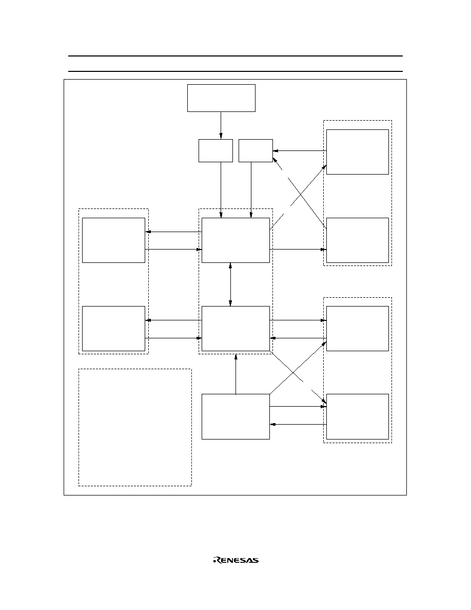
The MCU has 11 interrupt sources: four external signals (
INT
0
,
INT
1
,
INT
2
, INT
3
), four timer/counters
(timers A, B, C, and D), two serial interfaces (serial 1, serial 2), and A/D converter.
An interrupt request flag (IF), interrupt mask (IM), and vector address are provided for each interrupt
source, and an interrupt enable flag (IE) controls the entire interrupt process.
Some vector addresses are shared by two different interrupts. They are timer B and INT
2
, timer C and
INT
3
, timer D and A/D converter, and serial interface 1 and serial interface 2. So the type of request that
has occurred must be checked at the beginning of interrupt processing.
Interrupt Control Bits and Interrupt Processing: Locations $000 to $003 and $022 to $023 in RAM are
reserved for the interrupt control bits which can be accessed by RAM bit manipulation instructions.
The interrupt request flag (IF) cannot be set by software. MCU reset initializes the interrupt enable flag
(IE) and the IF to 0 and the interrupt mask (IM) to 1.
A block diagram of the interrupt control circuit is shown in figure 9, interrupt priorities and vector
addresses are listed in table 2, and interrupt processing conditions for the 11 interrupt sources are listed in
table 3.

HD404449 Series
18
An interrupt request occurs when the IF is set to 1 and the IM is set to 0. If the IE is 1 at that point, the
interrupt is processed. A priority programmable logic array (PLA) generates the vector address assigned to
that interrupt source.
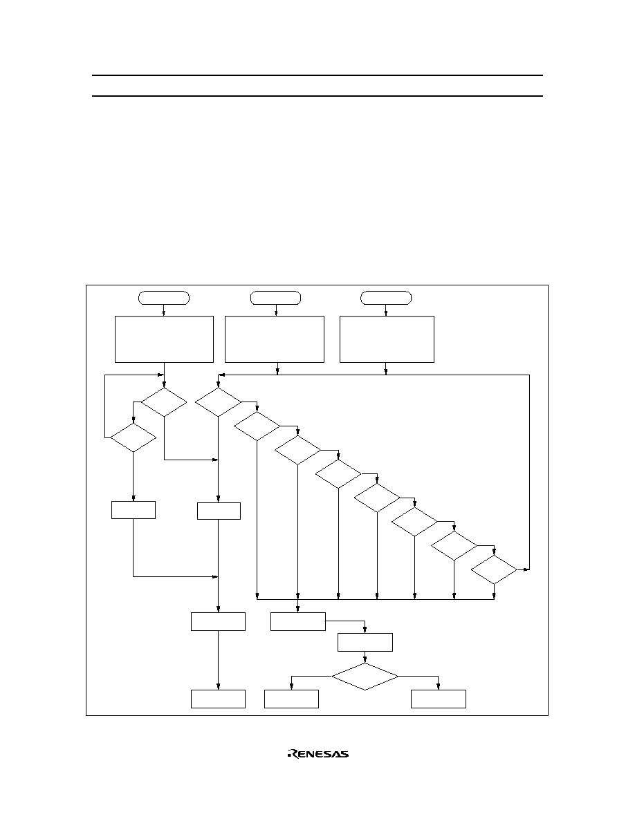
The interrupt processing sequence is shown in figure 10 and an interrupt processing flowchart is shown in
figure 11. After an interrupt is acknowledged, the previous instruction is completed in the first cycle. The
IE is reset in the second cycle, the carry, status, and program counter values are pushed onto the stack
during the second and third cycles, and the program jumps to the vector address to execute the instruction
in the third cycle.
Program the JMPL instruction at each vector address, to branch the program to the start address of the
interrupt program, and reset the IF by a software instruction within the interrupt program.
Table 2
Vector Addresses and Interrupt Priorities
Reset/Interrupt
Priority
Vector Address
RESET,
STOPC*
--
$0000
INT
0
1
$0002
INT
1
2
$0004
Timer A
3
$0006
Timer B, INT
2
4
$0008
Timer C, INT
3
5
$000A
Timer D, A/D
6
$000C
Serial 1, Serial 2
7
$000E
Note:
*
The
STOPC
interrupt request is valid only in stop mode
HD404449 Series
19
IE
IF0
IM0
IF1
IM1
IFTA
IMTA
IFTB
IMTB
IFTC
IMTC
IFTD
IMTD
$ 000,0
$ 000,2
$ 000,3
$ 001,0
$ 001,1
$ 001,2
$ 001,3
$ 002,0
$ 002,1
$ 002,2
$ 002,3
$ 003,0
$ 003,1
Sequence control
∑ Push PC/CA/ST
∑ Reset IE
∑ Jump to vector
address
Priority control logic
Vector
address
Note: $m,n is RAM address $m, bit number n.
$ 003,2
$ 003,3
INT
0
interrupt
INT
1
interrupt
Timer A interrupt
Timer B interrupt
Timer C interrupt
Timer D interrupt
Serial 1 interrupt
IF2
IM2
IF3
IM3
IF
A/D
IM
A/D
$ 022,0
$ 022,1
$ 022,2
$ 022,3
$ 023,0
$ 023,1
IFS2
IMS2
$ 023,2
$ 023,3
INT
2
interrupt
INT
3
interrupt
A/D interrupt
Serial 2 interrupt
IFS1
IMS1
Figure 9 Interrupt Control Circuit
HD404449 Series
20
Table 3
Interrupt Processing and Activation Conditions
Interrupt Source
Interrupt
Control Bit
INT
0
INT
1
Timer A
Timer B or
INT
2
Timer C or
INT
3
Timer D or
A/D
Serial 1 or
Serial 2
IE
1
1
1
1
1
1
1
IF0
.
IM0
1
0
0
0
0
0
0
IF1
.
IM1
*
1
0
0
0
0
0
IFTA
.
IMTA
*
*
1
0
0
0
0
IFTB
.
IMTB
+ IF2
.
IM2
*
*
*
1
0
0
0
IFTC
.
IMTC
+ IF3
.
IM3
*
*
*
*
1
0
0
IFTD
.
IMTD
+ IFAD
.
IMAD
*
*
*
*
*
1
0
IFS1
.
IMS1
+ IFS2
.
IMS2
*
*
*
*
*
*
1
Note:
Bits marked
*
can be either 0 or 1. Their values have no effect on operation.
Instruction cycles
1
2
3
4
5
6
Instruction
execution
*
IE reset
Interrupt
acceptance
Execution of JMPL
instruction at vector address
Execution of
instruction at
start address
of interrupt
routine
Vector address
generation
Note:
*
The stack is accessed and the IE reset after the instruction
is executed, even if it is a two-cycle instruction.
Stacking
Figure 10 Interrupt Processing Sequence
HD404449 Series
21
Power on
RESET = 1?
Reset MCU
Interrupt
request?
Execute instruction
PC (PC) + 1
PC $0002
PC $0004
PC $0006
PC $0008
PC $000A
PC $000E
IE = 1?
Accept interrupt
IE 0
Stack (PC)
Stack (CA)
Stack (ST)
INT
0
interrupt?
INT
1
interrupt?
Timer-A
interrupt?
Timer-B/INT
2
interrupt?
No
Yes
No
Yes
No
Yes
Yes
Yes
Yes
Yes
Yes
No
No
No
No
(Serial 1, serial 2 interrupt)
PC $000C
Timer-D/A-D
interrupt?
Yes
No
No
Timer-C/INT
3
interrupt?
Figure 11 Interrupt Processing Flowchart
HD404449 Series
22
Interrupt Enable Flag (IE: $000, Bit 0): Controls the entire interrupt process. It is reset by the interrupt
processing and set by the RTNI instruction, as listed in table 4.
Table 4
Interrupt Enable Flag (IE: $000, Bit 0)
IE
Interrupt Enabled/Disabled
0
Disabled
1
Enabled
External Interrupts (
INT
0
,
INT
1
, INT
2
, INT
3
): Four external interrupt signals.
External Interrupt Request Flags (IF0, IF1, IF2, IF3: $000, $001, $022): IF0 and IF1 are set at the
falling edge of signals input to
INT
0
and
INT
1
, and IF2 and IF3 are set at the rising or falling edge of signals
input to INT
2
and INT
3
, as listed in table 5. The INT
2
and INT
3
interrupt edges are selected by the detection
edge select registers (ESR1, ESR2: $026, $027) as shown in figures 12 and 13.
Table 5
External Interrupt Request Flags (IF0≠IF3: $000, $001, $022)
IF0≠IF3
Interrupt Request
0
No
1
Yes
Bit
Initial value
Read/Write
Bit name
3
0
W
ESR13
2
0
W
ESR12
0
0
W
ESR10
1
0
W
ESR11
Detection edge selection register 1 (ESR1: $026)
ESR11
0
1
ESR10
0
1
0
1
INT
2
detection edge
No detection
Falling-edge detection
Rising-edge detection
Double-edge detection
*
ESR13
0
1
ESR12
0
1
0
1
INT
3
detection edge
No detection
Falling-edge detection
Rising-edge detection
Double-edge detection
*
Note:
*
Both falling and rising edges are detected.
Figure 12 Detection Edge Selection Register 1 (ESR1)
HD404449 Series
23
Bit
Initial value
Read/Write
Bit name
3
0
W
ESR23
2
0
W
ESR22
0
--
--
Not used
1
--
--
Not used
Detection edge selection register 2 (ESR2: $027)
ESR23
0
1
ESR22
0
1
0
1
EVND detection edge
No detection
Falling-edge detection
Rising-edge detection
Double-edge detection
*
Note:
*
Both falling and rising edges are detected.
Figure 13 Detection Edge Selection Register 2 (ESR2)
External Interrupt Masks (IM0, IM1, IM2, IM3: $000, $001, $022): Prevent (mask) interrupt requests
caused by the corresponding external interrupt request flags, as listed in table 6.
Table 6
External Interrupt Masks (IM0≠1M3: $000, $001, $022)
IM0≠IM3
Interrupt Request
0
Enabled
1
Disabled (Masked)
Timer A Interrupt Request Flag (IFTA: $001, Bit 2): Set by overflow output from timer A, as listed in
table 7.
Table 7
Timer A Interrupt Request Flag (IFTA: $001, Bit 2)
IFTA
Interrupt Request
0
No
1
Yes

HD404449 Series
24
Timer A Interrupt Mask (IMTA: $001, Bit 3): Prevents (masks) an interrupt request caused by the
timer A interrupt request flag, as listed in table 8.
Table 8
Timer A Interrupt Mask (IMTA: $001, Bit 3)
IMTA
Interrupt Request
0
Enabled
1
Disabled (Masked)
Timer B Interrupt Request Flag (IFTB: $002, Bit 0): Set by overflow output from timer B, as listed in
table 9.
Table 9
Timer B Interrupt Request Flag (IFTB: $002, Bit 0)
IFTB
Interrupt Request
0
No
1
Yes
Timer B Interrupt Mask (IMTB: $002, Bit 1): Prevents (masks) an interrupt request caused by the
timer B interrupt request flag, as listed in table 10.
Table 10
Timer B Interrupt Mask (IMTB: $002, Bit 1)
IMTB
Interrupt Request
0
Enabled
1
Disabled (Masked)
Timer C Interrupt Request Flag (IFTC: $002, Bit 2): Set by overflow output from timer C, as listed in
table 11.
Table 11
Timer C Interrupt Request Flag (IFTC: $002, Bit 2)
IFTC
Interrupt Request
0
No
1
Yes

HD404449 Series
25
Timer C Interrupt Mask (IMTC: $002, Bit 3): Prevents (masks) an interrupt request caused by the
timer C interrupt request flag, as listed in table 12.
Table 12
Timer C Interrupt Mask (IMTC: $002, Bit 3)
IMTC
Interrupt Request
0
Enabled
1
Disabled (Masked)
Timer D Interrupt Request Flag (IFTD: $003, Bit 0): Set by overflow output from timer D, or by the
rising or falling edge of signals input to EVND when the input capture function is used, as listed in table
13.
Table 13
Timer D Interrupt Request Flag (IFTD: $003, Bit 0)
IFTD
Interrupt Request
0
No
1
Yes
Timer D Interrupt Mask (IMTD: $003, Bit 1): Prevents (masks) an interrupt request caused by the
timer D interrupt request flag, as listed in table 14.
Table 14
Timer D Interrupt Mask (IMTD: $003, Bit 1)
IMTD
Interrupt Request
0
Enabled
1
Disabled (Masked)
Serial Interrupt Request Flags (IFS1: $003, Bit 2; IFS2: $023, Bit 2) Set when data transfer is
completed or when data transfer is suspended, as listed in table 15.
Table 15
Serial Interrupt Request Flag (IFS1: $003, Bit 2; IFS2: $023, Bit 2)
IFS1, IFS2
Interrupt Request
0
No
1
Yes

HD404449 Series
26
Serial Interrupt Masks (IMS1: $003, Bit 3; IMS2: $023, Bit 3): Prevents (masks) an interrupt request
caused by the serial interrupt request flag, as listed in table 16.
Table 16
Serial Interrupt Mask (IMS1: $003, Bit 3; IMS2: $023, Bit 3)
IMS1, IMS2
Interrupt Request
0
Enabled
1
Disabled (Masked)
A/D Interrupt Request Flag (IFAD: $023, Bit 0): Set at the completion of A/D conversion, as listed in
table 17.
Table 17
A/D Interrupt Request Flag (IFAD: $023, Bit 0)
IFAD
Interrupt Request
0
No
1
Yes
A/D Interrupt Mask (IMAD: $023, Bit 1): Prevents (masks) an interrupt request caused by the A/D
interrupt request flag, as listed in table 18.
Table 18
A/D Interrupt Mask (IMAD: $023, Bit 1)
IMAD
Interrupt Request
0
Enabled
1
Disabled (Masked)

HD404449 Series
27
Operating Modes
The MCU has five operating modes as shown in table 19. The operations in each mode are listed in tables
20 and 21. Transitions between operating modes are shown in figure 14.
Active Mode: All MCU functions operate according to the clock generated by the system oscillators OSC
1
and OSC
2
.
Table 19
Operating Modes and Clock Status
Mode Name
Active
Standby
Stop
Watch
Subactive
*
2
Activation method
RESET
cancellation,
interrupt
request,
STOPC
cancellation in
stop mode,
STOP/SBY
instruction in
subactive mode
(when direct
transfer is
selected)
SBY instruction
STOP
instruction when
TMA3 = 0
STOP
instruction when
TMA3 = 1
INT
0
or timer A
interrupt request
from watch
mode
Status System
oscillator
OP
OP
Stopped
Stopped
Stopped
Subsystem
oscillator
OP
OP
OP
*
1
OP
OP
Cancellation
method
RESET input,
STOP/SBY
instruction
RESET input,
interrupt request
RESET input,
STOPC
input in
stop mode
RESET input,
INT
0
or timer A
interrupt request
RESET input,
STOP/SBY
instruction
Note:
OP implies in operation
1. Operating or stopping the oscillator can be selected by setting bit 3 of the system clock select
register (SSR: $029).
2. Subactive mode is an optional function; specify it on the function option list.

HD404449 Series
28
Table 20
Operations in Low-Power Dissipation Modes
Function
Stop Mode
Watch Mode
Standby Mode
Subactive Mode
*
2
CPU
Reset
Retained
Retained
OP
RAM
Retained
Retained
Retained
OP
Timer A
Reset
OP
OP
OP
Timer B
Reset
Stopped
OP
OP
Timer C
Reset
Stopped
OP
OP
Timer D
Reset
Stopped
OP
OP
Serial 1, 2
Reset
Stopped
*
3
OP
OP
A/D
Reset
Stopped
OP
Stopped
I/O
Reset
*
1
Retained
Retained
OP
Note:
OP implies in operation
1. Output pins are at high impedance.
2. Subactive mode is an optional function specified on the function option list.
3. Transmission/reception is activated if a clock is input in external clock mode. However, all
interrupts stop.
Table 21
I/O Status in Low-Power Dissipation Modes
Output
Input
Standby mode,
watch mode
Stop mode
Active mode,
subactive mode
D
0
≠D
11
Retained
High impedance
Input enabled
D
12
≠D
13
--
--
Input enabled
R0≠RC
Retained or output of
peripheral functions
High impedance
Input enabled
HD404449 Series
29
Reset by
RESET input or
by watchdog timer
f
OSC
:
f
X
:
¯
CPU
:
¯
CLK
:
¯
PER
:
Oscillate
Oscillate
Stop
f
cyc
f
cyc
f
OSC
:
f
X
:
¯
CPU
:
¯
CLK
:
¯
PER
:
Oscillate
Oscillate
Stop
f
W
f
cyc
f
OSC
:
f
X
:
¯
CPU
:
¯
CLK
:
¯
PER
:
Oscillate
Oscillate
f
cyc
f
cyc
f
cyc
f
OSC
:
f
X
:
¯
CPU
:
¯
CLK
:
¯
PER
:
Oscillate
Oscillate
f
cyc
f
W
f
cyc
f
OSC
:
f
X
:
¯
CPU
:
¯
CLK
:
¯
PER
:
Stop
Oscillate
f
SUB
f
W
f
SUB
f
OSC
:
f
X
:
¯
CPU
:
¯
CLK
:
¯
PER
:
Stop
Stop
Stop
Stop
Stop
f
OSC
:
f
X
:
¯
CPU
:
¯
CLK
:
¯
PER
:
Stop
Oscillate
Stop
f
W
Stop
f
OSC
:
f
X
:
¯
CPU
:
¯
CLK
:
¯
PER
:
Stop
Oscillate
Stop
f
W
Stop
Standby mode
Stop mode
(TMA3 = 0, SSR3 = 1)
Watch mode
Subactive
mode
(TMA3 = 1)
(TMA3 = 1, LSON = 0)
(TMA3 = 1, LSON = 1)
SBY
Interrupt
SBY
Interrupt
STOP
INT
0
,
timer A
*
1
STOP
*
4
*
2
*
3
1. Interrupt source
2. STOP/SBY (DTON = 1, LSON = 0)
3. STOP/SBY (DTON = 0, LSON = 0)
4. STOP/SBY (DTON = Don't care, LSON = 1)
f
OSC
:
f
X
:
f
cyc
:
f
SUB
:
f
W
:
LSON:
DTON:
Main oscillation frequency
Suboscillation frequency
for time-base
f
OSC
/4
f
X
/8 or f
X
/4
(software selectable)
f
X
/8
System clock
Clock for time-base
Clock for other
peripheral functions
Low speed on flag
Direct transfer on flag
Active
mode
Notes:
¯
CPU
:
¯
CLK
:
¯
PER
:
f
OSC
:
f
X
:
¯
CPU
:
¯
CLK
:
¯
PER
:
Stop
Oscillate
Stop
Stop
Stop
(TMA3 = 0, SSR3 = 0)
RESET1
RESET2
RAME = 0
RAME = 1
INT
0
,
timer A
*
1
(TMA3 = 0)
STOP
STOPC
STOPC
STOP
Figure 14 MCU Status Transitions
HD404449 Series
30
Standby Mode: In standby mode, the oscillators continue to operate, but the clocks related to instruction
execution stop. Therefore, the CPU operation stops, but all RAM and register contents are retained, and the
D or R port status, when set to output, is maintained. Peripheral functions such as interrupts, timers, and
serial interface continue to operate. The power dissipation in this mode is lower than in active mode
because the CPU stops.
The MCU enters standby mode when the SBY instruction is executed in active mode.
Standby mode is terminated by a RESET input or an interrupt request. If it is terminated by RESET input,
the MCU is reset as well. After an interrupt request, the MCU enters active mode and executes the next
instruction after the SBY instruction. If the interrupt enable flag is 1, the interrupt is then processed; if it is
0, the interrupt request is left pending and normal instruction execution continues. A flowchart of
operation in standby mode is shown in figure 15.
Standby
Oscillator: Active
Peripheral clocks: Active
All other clocks: Stop
No
Yes
No
Yes
No
Yes
No
Yes
No
Yes
No
Yes
Yes
(SBY
only)
Watch
Oscillator: Stop
Suboscillator: Active
Peripheral clocks: Stop
All other clocks: Stop
Restart
processor clocks
Reset MCU
Execute
next instruction
Accept interrupt
Restart
processor clocks
No
Yes
IF = 1,
IM = 0, and
IE = 1?
RESET = 1?
IF0 ∑
IM0
= 1?
IF1 ∑
IM1
= 1?
IFTA ∑
IMTA
= 1?
IFTB ∑
IMTB
+ IF2 ∑
IM2
= 1?
IFTC ∑
IMTC
+ IF3 ∑
IM3
= 1?
IFTD ∑
IMTD
+ IFAD ∑
IMAD
= 1?
No
Yes
IFS1∑
IMS1
+ IFS2 ∑
IMS2
= 1?
No
Stop
Oscillator: Stop
Suboscillator: Active/Stop
Peripheral clocks: Stop
All other clocks: Stop
RESET = 1?
STOPC
= 0?
RAME = 1
RAME = 0
Yes
Yes
No
No
Execute
next instruction
(SBY
only)
(SBY
only)
(SBY
only)
(SBY
only)
Figure 15 MCU Operation Flowchart
HD404449 Series
31
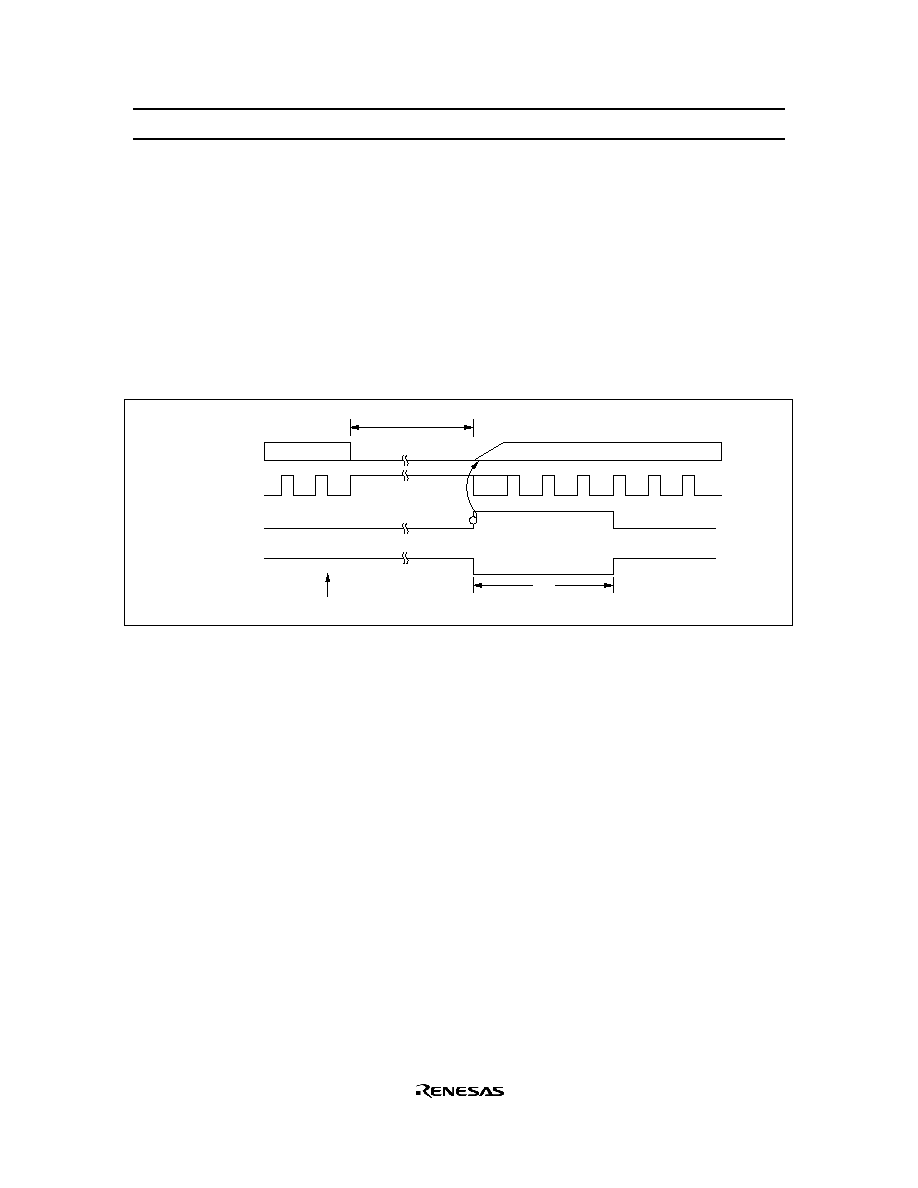
Stop Mode: In stop mode, all MCU operations stop and RAM data is retained. Therefore, the power
dissipation in this mode is the least of all modes. The OSC
1
and OSC
2
oscillator stops. Operation of the
X1 and X2 oscillator can be selected by setting bit 3 of the system clock select register (SSR: $029;
operating: SSR3 = 0, stop: SSR3 = 1) (figure 26). The MCU enters stop mode if the STOP instruction is
executed in active mode when bit 3 of timer mode register A (TMA: $008) is set to 0 (TMA3 = 0) (figure
41).
Stop mode is terminated by a RESET input or a
STOPC input as shown in figure 16. RESET or STOPC
must be applied for at least one t
RC
to stabilize oscillation (refer to the AC Characteristics section). When
the MCU restarts after stop mode is cancelled, all RAM contents before entering stop mode are retained,
but the accuracy of the contents of the accumulator, B register, W register, X/SPX register, Y/SPY register,
carry flag, and serial data register cannot be guaranteed.
,
Stop mode
Oscillator
Internal
clock
STOP instruction execution
t
res
t
RC
(stabilization period)
t
res
RESET
STOPC
Figure 16 Timing of Stop Mode Cancellation
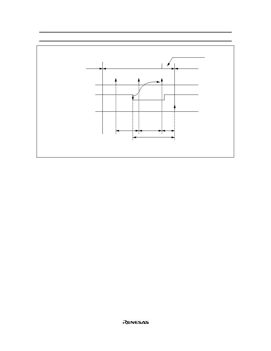
Watch Mode: In watch mode, the clock function (timer A) using the X1 and X2 oscillator operates but
other function operations stop. Therefore, the power dissipation in this mode is the second least to stop
mode, and this mode is convenient when only clock display is used. In this mode, the OSC
1
and OSC
2
oscillator stops, but the X1 and X2 oscillator operates. The MCU enters watch mode if the STOP
instruction is executed in active mode when TMA3 = 1, or if the STOP or SBY instruction is executed in
subactive mode.
Watch mode is terminated by a RESET input or a timer-A/
INT
0
interrupt request. For details of RESET
input, refer to the Stop Mode section. When terminated by a timer-A/
INT
0
interrupt request, the MCU
enters active mode if LSON is 0, or subactive mode if LSON is 1. After an interrupt request is generated,
the time required to enter active mode is t
RC
for a timer A interrupt, and T
X
(where T + t
RC
< T
X
< 2T + t
RC
)
for an
INT
0
interrupt, as shown in figure 17.
Operation during mode transition is the same as that at standby mode cancellation (figure 15).
HD404449 Series
32
Active mode
Watch mode
Active mode
Oscillation
stabilization period
Interrupt strobe
INT
Interrupt request
generation
(During the transition
from watch mode to
active mode only)
0
T
T
t
RC
Tx
T:
t :
RC
Interrupt frame length
Oscillation stabilization period
Figure 17 Interrupt Frame
Subactive Mode: The OSC
1
and OSC
2
oscillator stops and the MCU operates with a clock generated by
the X1 and X2 oscillator. In this mode, functions other than A/D conversion operate. However, because
the operating clock is slow, the power dissipation becomes low, next to watch mode.
The CPU instruction execution speed can be selected as 244
µ
s or 122
µ
s by setting bit 2 (SSR2) of the
system clock select register (SSR: $029). Note that the SSR2 value must be changed in active mode. If the
value is changed in subactive mode, the MCU may malfunction.
When the STOP or SBY instruction is executed in subactive mode, the MCU enters either watch or active
mode, depending on the statuses of the low speed on flag (LSON: $020, bit 0) and the direct transfer on
flag (DTON: $020, bit 3).
Subactive mode is an optional function that the user must specify on the function option list.
Interrupt Frame: In watch and subactive modes, ¯
CLK
is applied to timer A and the
INT
0
circuit. Prescaler
W and timer A operate as the time-base and generate the timing clock for the interrupt frame. Three
interrupt frame lengths (T) can be selected by setting the miscellaneous register (MIS: $00C) (figure 18).
In watch and subactive modes, the timer-A/
INT
0
interrupt is generated synchronously with the interrupt
frame. The interrupt request is generated synchronously with the interrupt strobe timing except during
transition to active mode. The falling edge of the
INT
0
signal is input asynchronously with the interrupt
frame timing, but it is regarded as input synchronously with the second interrupt strobe clock after the
falling edge. An overflow and interrupt request in timer A is generated synchronously with the interrupt
strobe timing.

HD404449 Series
33
Bit
Initial value
Read/Write
Bit name
3
0
W
MIS3
2
0
W
MIS2
0
0
W
MIS0
1
0
W
MIS1
Miscellaneous register (MIS: $00C)
MIS1
0
MIS0
T
*
1
0
0.24414 ms
t
RC
*
1
0.12207 ms
0.24414 ms
*
2
7.8125 ms
62.5 ms
Oscillation circuit conditions
External clock input
Ceramic oscillator or crystal
0
1
1
1
0
1
15.625 ms
125 ms
Not used
--
Notes: 1.
2.
The values of T and t
RC
are applied when a 32.768-kHz crystal oscillator is used.
The value is applied only when direct transfer operation is used.
Buffer control.
Refer to figure 38.
MIS3
MIS2
Figure 18 Miscellaneous Register (MIS)
Direct Transition from Subactive Mode to Active Mode: Available by controlling the direct transfer on
flag (DTON: $020, bit 3) and the low speed on flag (LSON: $020, bit 0). The procedures are described
below:
∑
Set LSON to 0 and DTON to 1 in subactive mode.
∑
Execute the STOP or SBY instruction.
∑
The MCU automatically enters active mode from subactive mode after waiting for the MCU internal
processing time and oscillation stabilization time (Figure 19).
Notes: 1. The DTON flag ($020, bit 3) can be set only in subactive mode. It is always reset in active
mode.
2. The transition time (T
D
) from subactive mode to active mode:
t
RC
< T
D
< T + t
RC
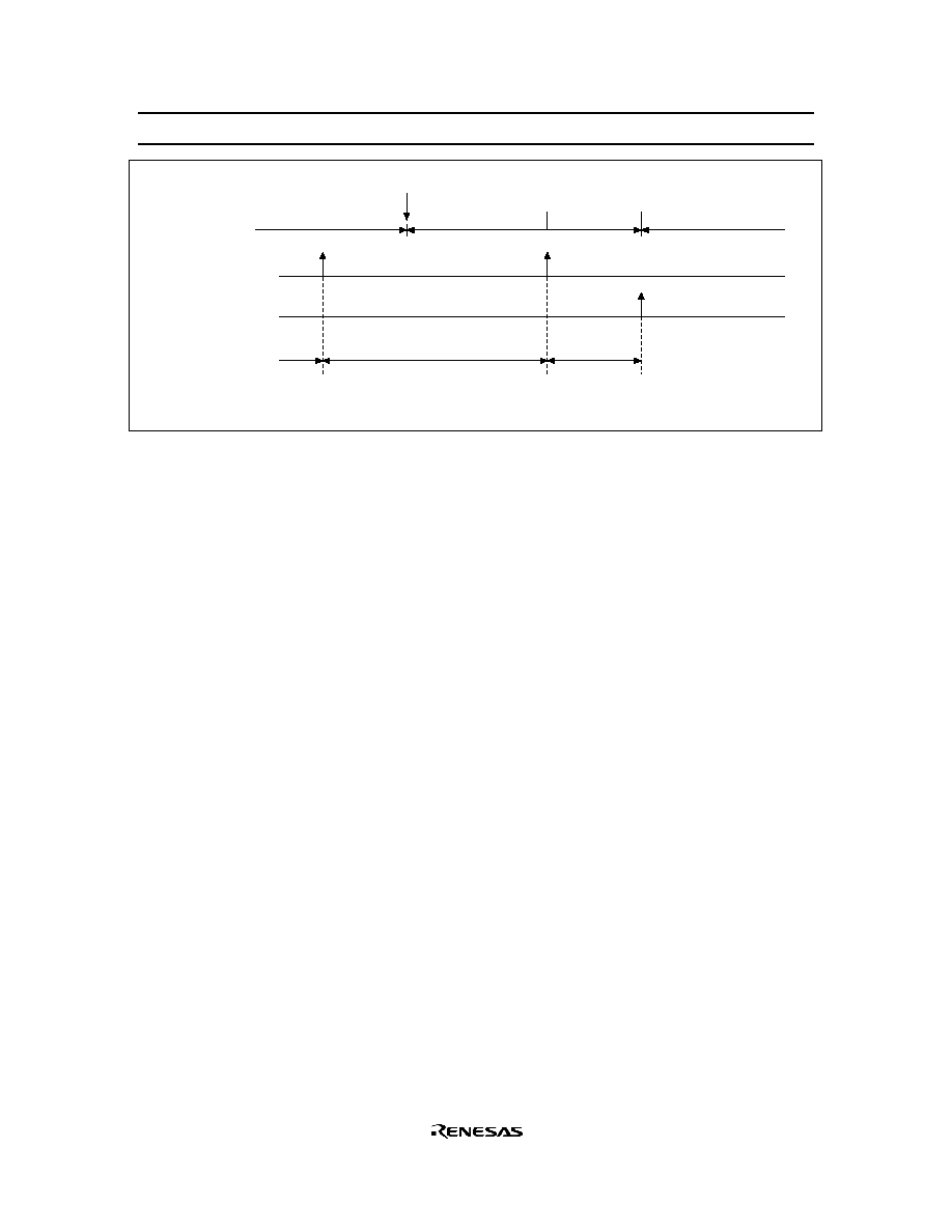
HD404449 Series
34
Subactive mode
Interrupt strobe
Direct transfer
completion timing
MCU internal
processing period
Oscillation
stabilization
time
Active mode
T
t
RC
T:
t :
RC
STOP/SBY instruction execution
(Set LSON = 0, DTON = 1)
Interrupt frame length
Oscillation stabilization period
Figure 19 Direct Transition Timing
Stop Mode Cancellation by
STOPC : The MCU enters active mode from stop mode by a STOPC input
as well as by RESET. In either case, the MCU starts instruction execution from the starting address
(address 0) of the program. However, the value of the RAM enable flag (RAME: $021, bit 3) differs
between cancellation by
STOPC and by RESET. When stop mode is cancelled by RESET, RAME = 0;
when cancelled by
STOPC, RAME = 1. RESET can cancel all modes, but STOPC is valid only in stop
mode;
STOPC input is ignored in other modes. Therefore, when the program requires to confirm that stop
mode has been cancelled by
STOPC (for example, when the RAM contents before entering stop mode are
used after transition to active mode), execute the TEST instruction on the RAM enable flag (RAME) at the
beginning of the program.
MCU Operation Sequence: The MCU operates in the sequences shown in figures 20 to 22. It is reset by
an asynchronous RESET input, regardless of its status.
The low-power mode operation sequence is shown in figure 22. With the IE flag cleared and an interrupt
flag set together with its interrupt mask cleared, if a STOP/SBY instruction is executed, the instruction is
cancelled (regarded as an NOP) and the following instruction is executed. Before executing a STOP/SBY
instruction, make sure all interrupt flags are cleared or all interrupts are masked.

HD404449 Series
35
Power on
RESET = 1 ?
RAME = 0
Reset MCU
MCU
operation
cycle
No
Yes
Figure 20 MCU Operating Sequence (Power On)
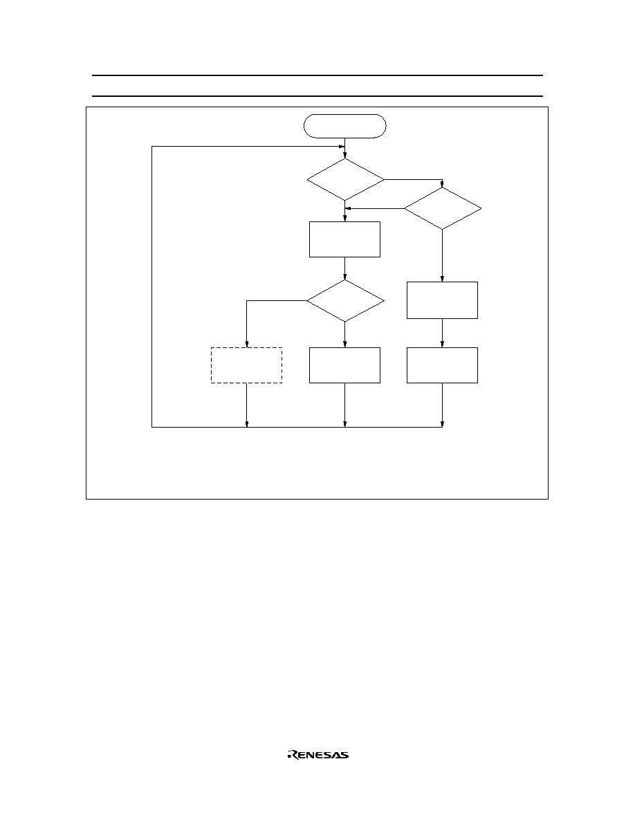
HD404449 Series
36
MCU operation
cycle
IF = 1?
Instruction
execution
SBY/STOP
instruction?
PC Next
location
PC Vector
address
Low-power mode
operation cycle
IE 0
Stack (PC),
(CA),
(ST)
IM = 0 and
IE = 1?
Yes
No
No
Yes
Yes
No
IF:
IM:
IE:
PC:
CA:
ST:
Interrupt request flag
Interrupt mask
Interrupt enable flag
Program counter
Carry flag
Status flag
Figure 21 MCU Operating Sequence (MCU Operation Cycle)
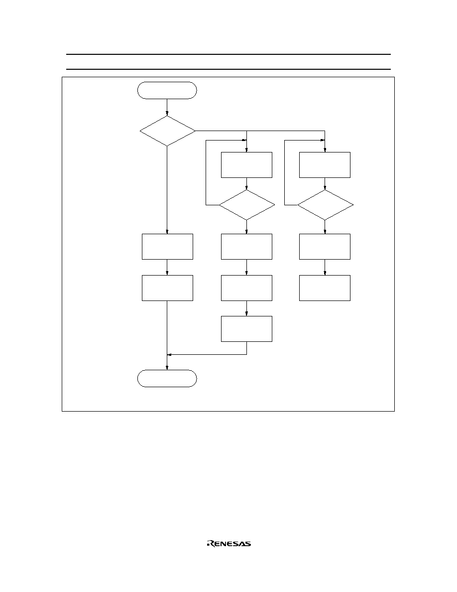
HD404449 Series
37
Low-power mode
operation cycle
IF = 1 and
IM = 0?
Hardware NOP
execution
PC Next
Iocation
MCU operation
cycle
Standby/Watch
mode
IF = 1 and
IM = 0?
Hardware NOP
execution
PC Next
Iocation
Instruction
execution
Stop mode
No
Yes
No
Yes
Note:
*
For IF and IM operation, refer to figure 15.
STOPC
= 0?
RAME = 1
Reset MCU
No
Yes
*
Figure 22 MCU Operating Sequence (Low-Power Mode Operation)
Note:
When the MCU is in watch mode or subactive mode, if the high level period before the falling edge
of
INT
0
is shorter than the interrupt frame,
INT
0
is not detected. Also, if the low level period after
the falling edge of
INT
0
is shorter than the interrupt frame,
INT
0
is not detected.
Edge detection is shown in figure 23. The level of the
INT
0
signal is sampled by a sampling clock.
When this sampled value changes to low from high, a falling edge is detected.
In figure 24, the level of the
INT
0
signal is sampled by an interrupt frame. In (a) the sampled value
is low at point A, and also low at point B. Therefore, a falling edge is not detected. In (b), the
sampled value is high at point A, and also high at point B. A falling edge is not detected in this
case either.
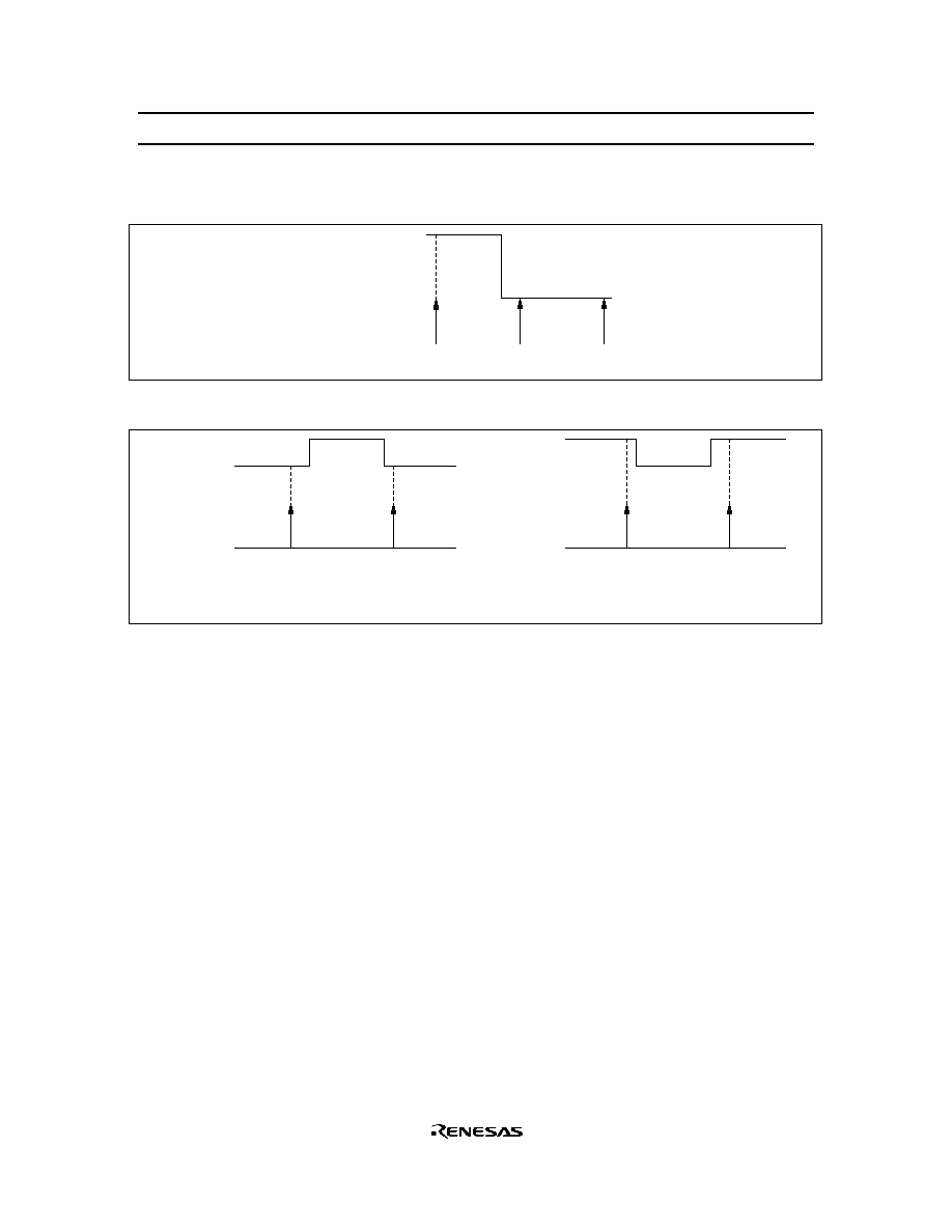
HD404449 Series
38
When the MCU is in watch mode or subactive mode, keep the high level and low level period of
INT
0
longer than interrupt frame.
High
Low
Low
INT
Sampling
0
Figure 23 Edge Detection
A: Low
B: Low
INT
Interrupt
frame
0
A: High
B: High
INT
Interrupt
frame
0
(a) High level period
(b) Low level period
Figure 24 Sampling Example
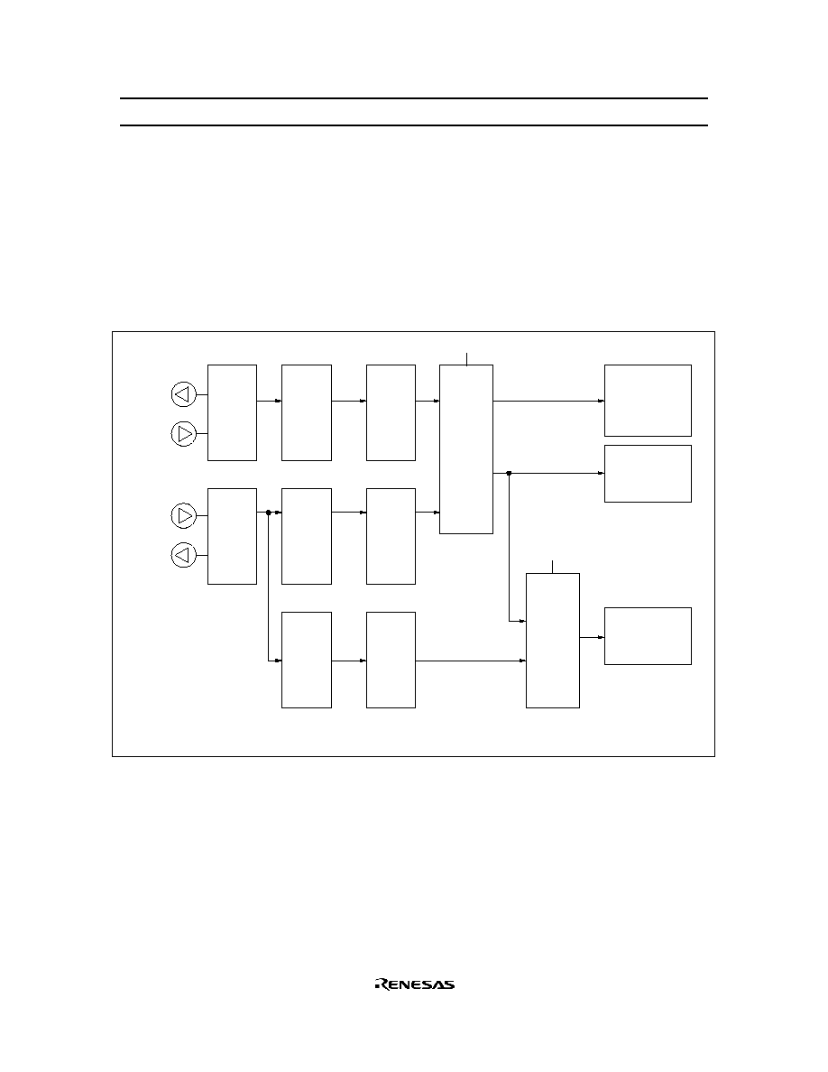
HD404449 Series
39
Internal Oscillator Circuit
A block diagram of the clock generation circuit is shown in figure 25. As shown in table 22, a ceramic
oscillator or crystal oscillator can be connected to OSC
1
and OSC
2
, and a 32.768-kHz oscillator can be
connected to X1 and X2. The system oscillator can also be operated by an external clock. Bit 1 (SSR1) of
the system clock select register (SSR: $029) must be selected according to the frequency of the oscillator
connected to OSC
1
and OSC
2
(figure 26).
Note:
If the system clock select register (SSR: $029) setting does not match the oscillator frequency,
subsystems using the 32.768-kHz oscillation will malfunction.
OSC
2
OSC
1
X1
X2
System
oscillator
Sub-
system
oscillator
1/4
division
circuit
Timing
generator
circuit
System
clock
selection
CPU with ROM,
RAM, registers,
flags, and I/O
Peripheral
function
interrupt
Time-base
interrupt
Time-base
clock
selection
1/8 or 1/4
division
circuit
Note
Timing
generator
circuit
Timing
generator
circuit
1/8
division
circuit
f
W
f
SUB
t
subcyc
LSON
TMA3
f
cyc
t
cyc
f
OSC
f
X
t
Wcyc
¯
CPU
¯
PER
¯
CLK
Note: 1/8 or 1/4 division ratio can be selected by setting bit 2 of the system
clock select register (SSR: $029).
Figure 25 Clock Generation Circuit

HD404449 Series
40
Bit
Initial value
Read/Write
Bit name
3
0
W
SSR3
2
0
W
SSR2
0
--
--
Not used
1
0
W
SSR1
System clock select register (SSR: $029)
System clock selection
0.4 to 1.0 MHz
1.6 to 4.0 MHz
SSR1
0
1
0
1
ratio selection
f
SUB
= f
X
/8
f
SUB
= f
X
/4
SSR3
0
1
32-kHz oscillation stop
Oscillation operates in stop mode
Oscillation stops in stop mode
32-kHz oscillation division
SSR2
Figure 26 System Clock Select Register
GND
D
0
GND
X2
X1
RESET
OSC
2
OSC
1
TEST
AV
SS
Figure 27 Typical Layouts of Crystal and Ceramic Oscillator
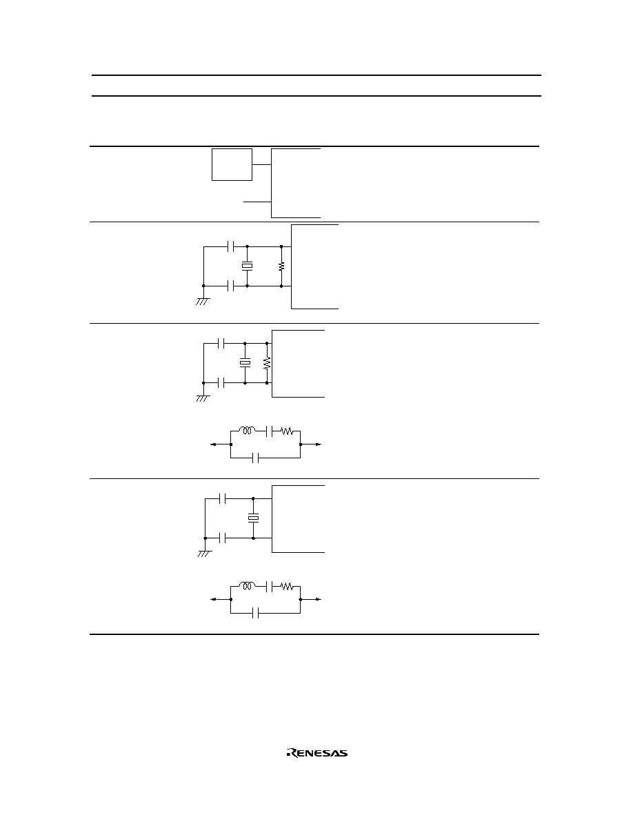
HD404449 Series
41
Table 22
Oscillator Circuit Examples
Circuit Configuration
Circuit Constants
External clock
operation
External
oscillator
OSC
Open
1
OSC
2
Ceramic oscillator
(OSC
1
, OSC
2
)
OSC
2
C
1
2
C
OSC
1
R
f
Ceramic
oscillator
GND
Ceramic oscillator: CSA4.00MG (Murata)
R
f
= 1 M
±
20%
C
1
= C
2
= 30 pF
±
20%
Crystal oscillator
(OSC
1
, OSC
2
)
C
1
2
C
Crystal
oscillator
GND
L
S
C
R
S
C
0
f
R
OSC
1
OSC
2
OSC
2
OSC
1
R
f
= 1 M
±
20%
C
1
= C
2
= 10≠22 pF
±
20%
Crystal: Equivalent to circuit shown below
C
0
= 7 pF max
R
S
= 100
max
Crystal oscillator
(X1, X2)
X1
C
1
2
C
X2
Crystal
oscillator
GND
L
S
C
R
S
C
0
X1
X2
Ceramic: 32.768 kHz: MX38T
(Nippon Denpa Kogyo)
C
1
= C
2
= 20 pF
±
20%
R
S
: 14 k
C
0
: 1.5 pF
Notes: 1. Since the circuit constants change depending on the crystal or ceramic resonator and stray
capacitance of the board, the user should consult with the crystal or ceramic oscillator
manufacturer to determine the circuit parameters.
2. Wiring among OSC
1
, OSC
2
, X1, X2,
and elements should be as short as possible, and must not
cross other wiring (see figure 27).
3. If the 32.768-kHz crystal oscillator is not used, the X1
pin must be fixed to GND and X2
must be
open.

HD404449 Series
42
Input/Output
The MCU has 64 input/output pins (D
0
≠D
11
, R0
0
≠RC
3
) and 2 input pins (D
12
, D
13
). The features are
described below.
∑
10 pins (D
0
≠D
9
) are high-current input/output pins.
∑
The D
12
, D
13
, R0
0
≠R0
2
, and R3
0
≠R5
3
input/output pins are multiplexed with peripheral function pins
such as for the timers or serial interface. For these pins, the peripheral function setting is done prior to
the D or R port setting. Therefore, when a peripheral function is selected for a pin, the pin function and
input/output selection are automatically switched according to the setting.
∑
Input or output selection for input/output pins and port or peripheral function selection for multiplexed
pins are set by software.
∑
Peripheral function output pins are CMOS output pins. Only the R4
3
/SO
1
and R5
3
/SO
2
pins can be set to
NMOS open-drain output by software.
∑
In stop mode, the MCU is reset, and therefore peripheral function selection is cancelled. Input/output
pins are in high-impedance state.
∑
Each input/output pin has a built-in pull-up MOS, which can be individually turned on or off by
software.
I/O buffer configuration is shown in figure 28, programmable I/O circuits are listed in table 23, and I/O pin
circuit types are shown in table 24.
Table 23
Programmable I/O Circuits
MIS3 (Bit 3 of MIS)
0
1
DCD, DCR
0
1
0
1
PDR
0
1
0
1
0
1
0
1
CMOS buffer
PMOS
--
--
--
On
--
--
--
On
NMOS
--
--
On
--
--
--
On
--
Pull-up MOS
--
--
--
--
--
On
--
On
Note:
-- indicates off status.
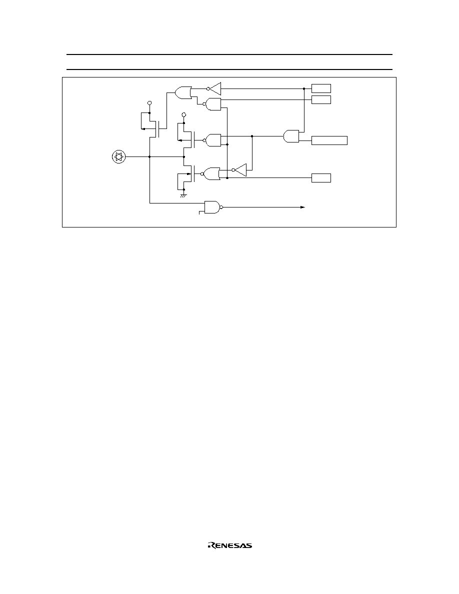
HD404449 Series
43
MIS3
Input control signal
V
CC
Pull-up
MOS
DCD, DCR
PDR
Input data
V
CC
HLT
Pull-up control signal
Buffer control signal
Output data
Figure 28 I/O Buffer Configuration
HD404449 Series
44
Table 24
Circuit Configurations of I/O Pins
I/O Pin Type
Circuit
Pins
Input/output pins
V
CC
V
CC
Pull-up control signal
Buffer control
signal
Output data
Input data
HLT
MIS3
DCD, DCR
PDR
Input control signal
D
0
≠D
11
, R0
0
≠R0
3
R1
0
≠R1
3
,
R2
0
≠R2
3
R3
0
≠R3
3
,
R4
0
≠R4
2
R5
0
≠R5
2
,
R6
0
≠R6
3
R7
0
≠R7
3
,
R8
0
≠R8
3
R9
0
≠R9
3
,
RA
0
≠RA
3
RB
0
≠RB
3
,
RC
0
≠RC
3
V
CC
V
CC
Pull-up control signal
Buffer control
signal
Output data
Input data
HLT
MIS3
DCR
PDR
Input control signal
MIS2, SM2B2
R4
3
,
R5
3
Input pins
Input data
Input control signal
D
12
, D
13
Peripheral
function pins
Input/ output
pins
V
CC
V
CC
Pull-up control signal
Output data
Input data
HLT
MIS3
SCK
,
1
SCK
2
SCK ,
1
SCK
2
SCK
1
,
SCK
2
Output pins
V
CC
V
CC
Pull-up control signal
PMOS control
signal
Output data
HLT
MIS3
SO ,
MIS2, SM2B2
1
SO
2
SO
1
, SO
2
V
CC
V
CC
Pull-up control signal
Output data
HLT
MIS3
TOB, TOC, TOD
TOB, TOC, TOD

HD404449 Series
45
I/O Pin Type
Circuit
Pins
Input pins
V
CC
Input data
SI
1
, SI
2
,,
INT
1
, etc
HLT
MIS3
PDR
SI
1
, SI
2
,
INT
1
,
INT
2
, INT
3
,
EVNB
, EVND
Input data
INT
,
STOPC
0
INT
0
,
STOPC
Notes: 1. The MCU is reset in stop mode, and peripheral function selection is cancelled. The
HLT
signal
becomes low, and input/output pins enter high-impedance state.
2. The
HLT
signal is 1 in watch and subactive modes.
D Port (D
0
≠D
13
): Consist of 12 input/output pins and 2 input pins addressed by one bit. D
0
≠D
11
are high-
current I/O pins, and D
12
and D
13
are input-only pins.
Pins D
0
≠D
11
are set by the SED and SEDD instructions, and reset by the RED and REDD instructions.
Output data is stored in the port data register (PDR) for each pin. All pins D
0
≠D
13
are tested by the TD and
TDD instructions.
The on/off statuses of the output buffers are controlled by D-port data control registers (DCD0≠DCD2:
$02C≠$02E) that are mapped to memory addresses (figure 29).
Pins D
12
and D
13
are multiplexed with peripheral function pins
STOPC and I
NT
0
, respectively. The
peripheral function modes of these pins are selected by bits 2 and 3 (PMRC2, PMRC3) of port mode
register C (PMRC: $025) (figure 30).
R Ports (R0
0
≠RC
3
): 52 input/output pins addressed in 4-bit units. Data is input to these ports by the LAR
and LBR instructions, and output from them by the LRA and LRB instructions. Output data is stored in the
port data register (PDR) for each pin. The on/off statuses of the output buffers of the R ports are controlled
by R-port data control registers (DCR0≠DCRC: $030≠$03C) that are mapped to memory addresses (figure
29).
Pins R0
0
≠R0
2
are multiplexed with peripheral pins
I NT
1
≠INT
3
, respectively. The peripheral function modes
of these pins are selected by bits 0≠2 (PMRB0≠PMRB2) of port mode register B (PMRB: $024) (figure
31).
Pins R3
0
≠R3
2
are multiplexed with peripheral pins TOB, TOC, and TOD, respectively. The peripheral
function modes of these pins are selected by bits 0 and 1 (TMB20, TMB21) of timer mode register B2
(TMB2: $013), bits 0≠2 (TMC20≠TMC22) of timer mode register C2 (TMC2: $014), and bits 0≠3
(TMD20≠TMD23) of timer mode register D2 (TMD2: $015) (figures 32, 33, and 34).
Pins R3
3
and R4
0
are multiplexed with peripheral pins
EVNB and EVND, respectively. The peripheral
function modes of these pins are selected by bits 0 and 1 (PMRC0, PMRC1) of port mode register C
(PMRC: $025) (figure 30).
Pins R4
1
≠R4
3
are multiplexed with peripheral pins
SCK
1
, SI
1
, and SO
1
, respectively. The peripheral
function modes of these pins are selected by bit 3 (SM1A3) of serial mode register 1A (SM1A: $005), and
bits 0 and 1 (PMRA0, PMRA1) of port mode register A (PMRA: $004), as shown in figures 35 and 36.

HD404449 Series
46
Ports R5
1
≠R5
3
are multiplexed with peripheral function pins
SCK
2
,
SI
2
, SO
2
, respectively. The function
modes of these pins can be selected by individual pins, by 2A setting bit 3 (SM2A3) of serial mode register
2A (SM2A: $01B), and bits 2 and 3 (PMRA2, PMRA3) of port mode register A (PMRA: $004) (figures 36
and 37).
Pull-Up MOS Transistor Control: A program-controlled pull-up MOS transistor is provided for each
input/output pin other than input-only pins D
12
and D
13
. The on/off status of all these transistors is
controlled by bit 3 (MIS3) of the miscellaneous register (MIS: $00C), and the on/off status of an individual
transistor can also be controlled by the port data register (PDR) of the corresponding pin--enabling on/off
control of that pin alone (table 23 and figure 38).
The on/off status of each transistor and the peripheral function mode of each pin can be set independently.
How to Deal with Unused I/O Pins: I/O pins that are not needed by the user system (floating) must be
connected to V
CC
to prevent LSI malfunctions due to noise. These pins must either be pulled up to V
CC
by
their pull-up MOS transistors or by resistors of about 100 k
.

HD404449 Series
47
Bit
Initial value
Read/Write
Bit name
3
0
W
DCD03,
2
0
W
DCD02,
0
0
W
DCD00,
1
0
W
DCD01,
DCD0, DCD1
Data control register
DCD13 DCD12
DCD10
DCD11
Bit
Initial value
Read/Write
Bit name
3
0
W
DCD23
2
0
W
DCD22
0
0
W
DCD20
1
0
W
DCD21
DCD2
(DCD0 to 2: $02C to $02E)
(DCR0 to C: $030 to $03C)
Bit
Initial value
Read/Write
Bit name
Correspondence between ports and DCD/DCR bits
0
1
DCD0
DCD1
DCD2
DCR0
DCR1
DCR2
DCR3
DCR4
DCR5
DCR6
DCR7
DCR8
DCR9
DCRA
DCRB
DCRC
Off (high-impedance)
On
3
0
W
DCR03≠
2
0
W
DCR02≠
0
0
W
DCR00≠
1
0
W
DCR01≠
DCRC3
DCRC2
DCRC0
DCRC1
DCR0 to DCRC
All Bits
CMOS Buffer On/Off Selection
Register Name
D
3
D
7
D
11
R0
3
R1
3
R2
3
R3
3
R4
3
R5
3
R6
3
R7
3
R8
3
R9
3
RA
3
RB
3
RC
3
Bit 3
D
2
D
6
D
10
R0
2
R1
2
R2
2
R3
2
R4
2
R5
2
R6
2
R7
2
R8
2
R9
2
RA
2
RB
2
RC
2
Bit 2
D
1
D
5
D
9
R0
1
R1
1
R2
1
R3
1
R4
1
R5
1
R6
1
R7
1
R8
1
R9
1
RA
1
RB
1
RC
1
Bit 1
D
0
D
4
D
8
R0
0
R1
0
R2
0
R3
0
R4
0
R5
0
R6
0
R7
0
R8
0
R9
0
RA
0
RB
0
RC
0
Bit 0
Figure 29 Data Control Registers (DCD, DCR)

HD404449 Series
48
Bit
Initial value
Read/Write
Bit name
3
0
W
PMRC3
2
0
W
PMRC2
*
0
0
W
PMRC0
1
0
W
PMRC1
Port mode register C (PMRC: $025)
PMRC0
0
1
R3
3
PMRC1
0
1
R4
0
/EVND mode selection
R4
0
EVND
R3
3
/
EVNB
mode selection
EVNB
PMRC2
0
1
D
12
STOPC
PMRC3
0
1
D
13
D
13
/
INT
0
mode selection
INT
0
D
12
/
STOPC
mode selection
Note:
*
PMRC2 is reset to 0 only by RESET input. When
STOPC
is input in stop
mode, PMRC2 is not reset but retains its value.
Figure 30 Port Mode Register C (PMRC )

HD404449 Series
49
Bit
Initial value
Read/Write
Bit name
3
--
--
Not used
2
0
W
PMRB2
0
0
W
PMRB0
1
0
W
PMRB1
PMRB0
0
1
R0
0
/
INT
1
mode selection
R0
0
INT
1
Port mode register B (PMRB: $024)
PMRB1
0
1
R0
1
/INT
2
mode selection
R0
1
INT
2
PMRB2
0
1
R0
2
/INT
3
mode selection
R0
2
INT
3
Figure 31 Port Mode Register B (PMRB)
Bit
Initial value
Read/Write
Bit name
3
--
--
Not used
2
--
--
Not used
0
0
R/W
TMB20
1
0
R/W
TMB21
Timer mode register B2 (TMB2: $013)
TMB21
0
1
TMB20
0
1
0
1
R3
0
/TOB mode selection
R3
0
TOB
TOB
TOB
R3
0
port
Toggle output
0 output
1 output
Figure 32 Timer Mode Register B2 (TMB2)
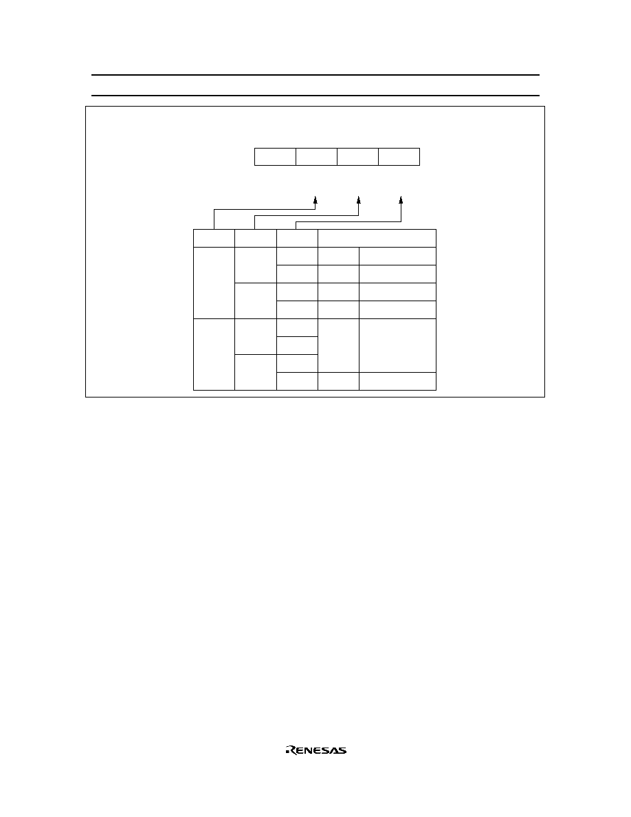
HD404449 Series
50
Bit
Initial value
Read/Write
Bit name
3
--
--
Not used
2
0
R/W
TMC22
0
0
R/W
TMC20
1
0
R/W
TMC21
Timer mode register C2 (TMC2: $014)
TMC22
TMC20
0
1
0
1
0
1
0
1
TMC21
0
1
0
1
0
1
R3
1
/TOC mode selection
R3
1
TOC
TOC
TOC
--
TOC
R3
1
port
Toggle output
0 output
1 output
Inhibited
PWM output
Figure 33 Timer Mode Register C2 (TMC2)
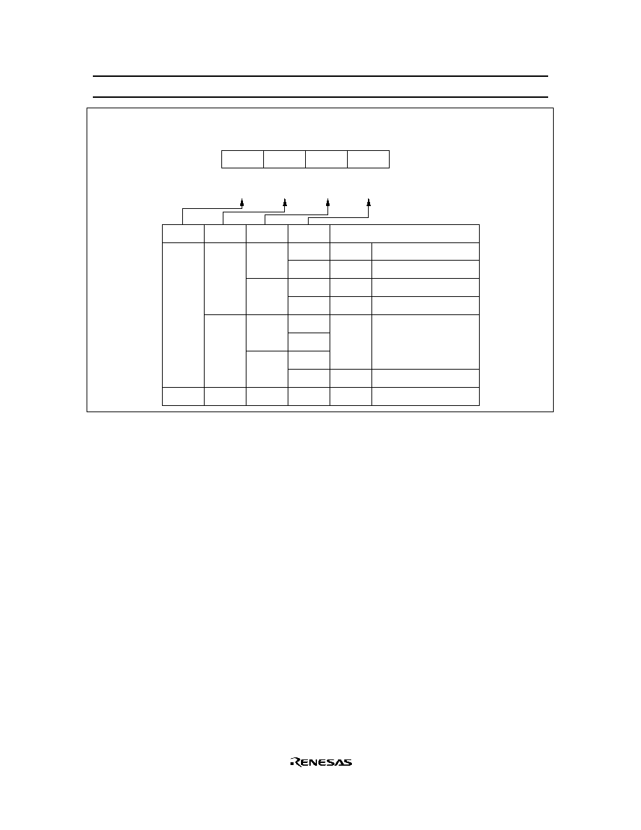
HD404449 Series
51
Bit
Initial value
Read/Write
Bit name
3
0
R/W
TMD23
2
0
R/W
TMD22
0
0
R/W
TMD20
1
0
R/W
TMD21
Timer mode register D2 (TMD2: $015)
TMD22
TMD20
0
1
0
1
0
1
0
1
TMD21
0
1
0
1
0
1
R3
2
/TOD mode selection
R3
2
TOD
TOD
TOD
--
TOD
R3
2
R3
2
port
Toggle output
0 output
1 output
Inhibited
PWM output
Input capture (R3
2
port)
TMD23
0
1
Don't care
Don't care
Don't care
Figure 34 Timer Mode Register D2 (TMD2)
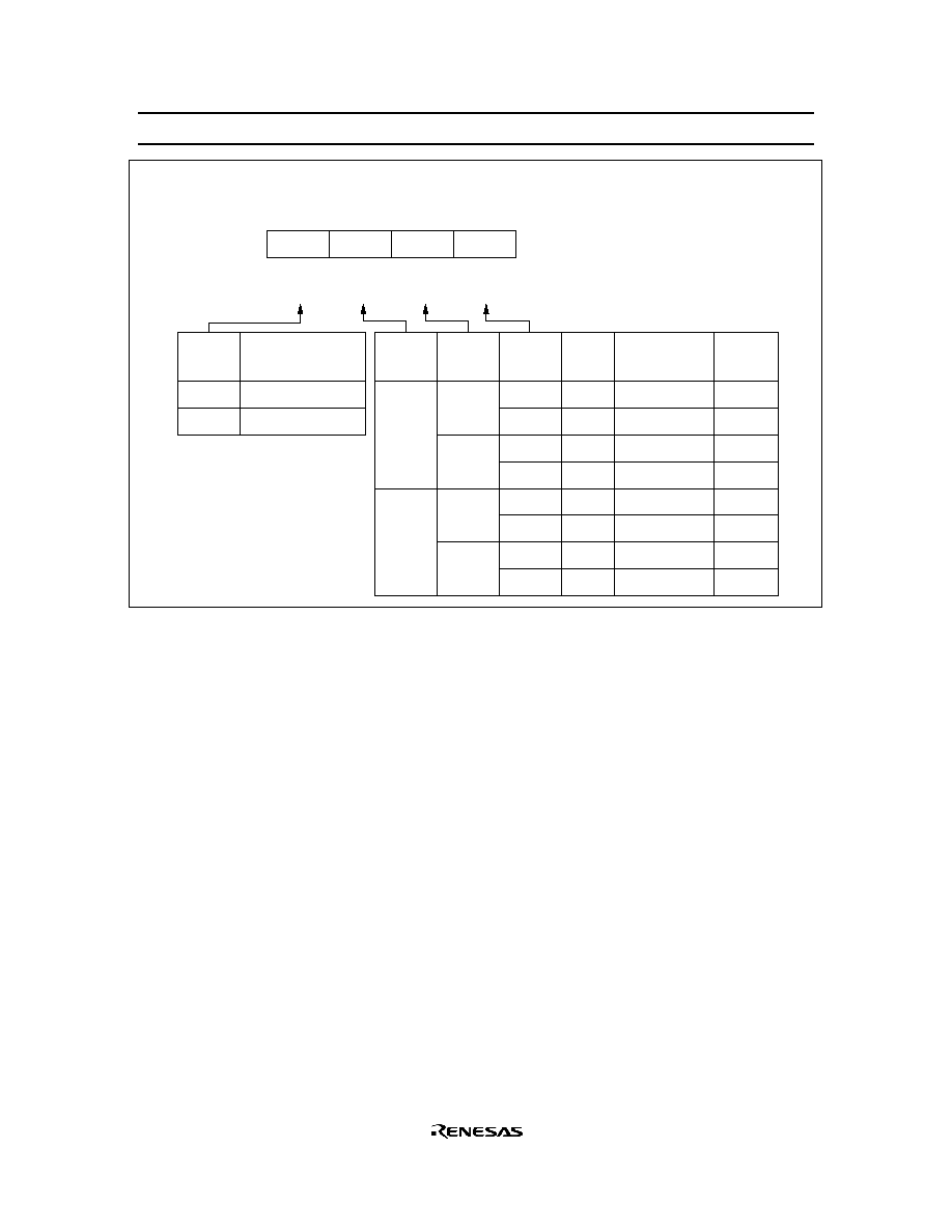
HD404449 Series
52
Bit
Initial value
Read/Write
Bit name
3
0
W
SM1A3
2
0
W
SM1A2
0
0
W
SM1A0
1
0
W
SM1A1
Serial mode register 1A (SM1A: $005)
0
1
0
1
0
1
0
1
0
1
0
1
0
1
Output
Output
Output
Output
Output
Output
Output
Input
Prescaler
Prescaler
Prescaler
Prescaler
Prescaler
Prescaler
System clock
External clock
˜
2048
˜
512
˜
128
˜
32
˜
8
˜
2
--
--
Prescaler
division
ratio
SM1A2
SM1A0
SM1A1
Clock source
SM1A3
0
1
R4
1
/
SCK
1
mode selection
SCK
1
R4
1
SCK
1
Figure 35 Serial Mode Register 1A (SM1A)
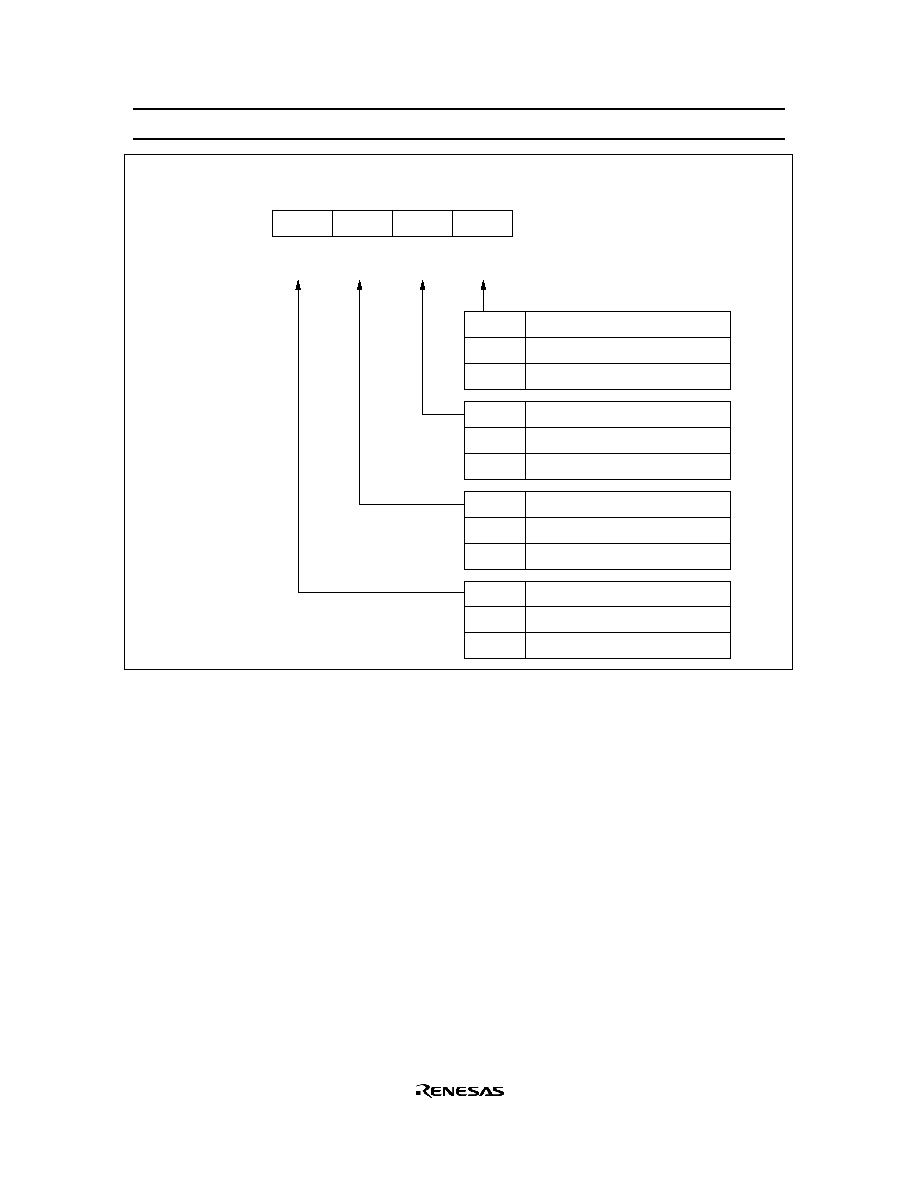
HD404449 Series
53
PMRA0
0
1
R4
3
/SO
1
mode selection
R4
3
SO
1
Bit
Initial value
Read/Write
Bit name
3
0
W
PMRA3
2
0
W
PMRA2
0
0
W
PMRA0
1
0
W
PMRA1
Port mode register A (PMRA: $004)
PMRA2
0
1
R5
3
/SO
2
mode selection
R5
3
SO
2
PMRA3
0
1
R5
2
/SI
2
mode selection
R5
2
SI
2
PMRA1
0
1
R4
2
/SI
1
mode selection
R4
2
SI
1
Figure 36 Port Mode Register A (PMRA)
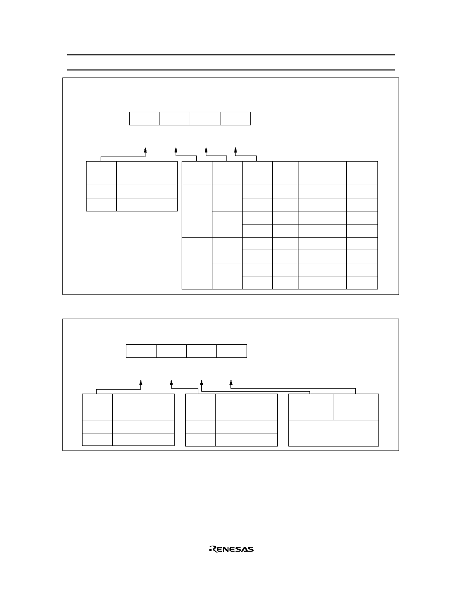
HD404449 Series
54
Bit
Initial value
Read/Write
Bit name
3
0
W
SM2A3
2
0
W
SM2A2
0
0
W
SM2A0
1
0
W
SM2A1
Serial mode register 2A (SM2A: $01B)
0
1
0
1
0
1
0
1
0
1
0
1
0
1
Output
Output
Output
Output
Output
Output
Output
Input
Prescaler
Prescaler
Prescaler
Prescaler
Prescaler
Prescaler
System clock
External clock
˜
2048
˜
512
˜
128
˜
32
˜
8
˜
2
--
--
Prescaler
division
ratio
SM2A2
SM2A0
SM2A1
Clock source
SM2A3
0
1
R5
1
/
SCK
2
mode selection
SCK
2
R5
1
SCK
2
Figure 37 Serial Mode Register 2A (SM2A)
Bit
Initial value
Read/Write
Bit name
3
0
W
MIS3
2
0
W
MIS2
0
0
W
MIS0
1
0
W
MIS1
MIS2
CMOS buffer
on/off selection
for pin R4
3
/SO
1
Miscellaneous register (MIS: $00C)
0
1
On
Off
Refer to figure 18 in the
operation modes section.
t
RC
selection.
MIS3
0
1
Pull-up MOS
on/off selection
Off
On
MIS1
MIS0
Figure 38 Miscellaneous Register (MIS)
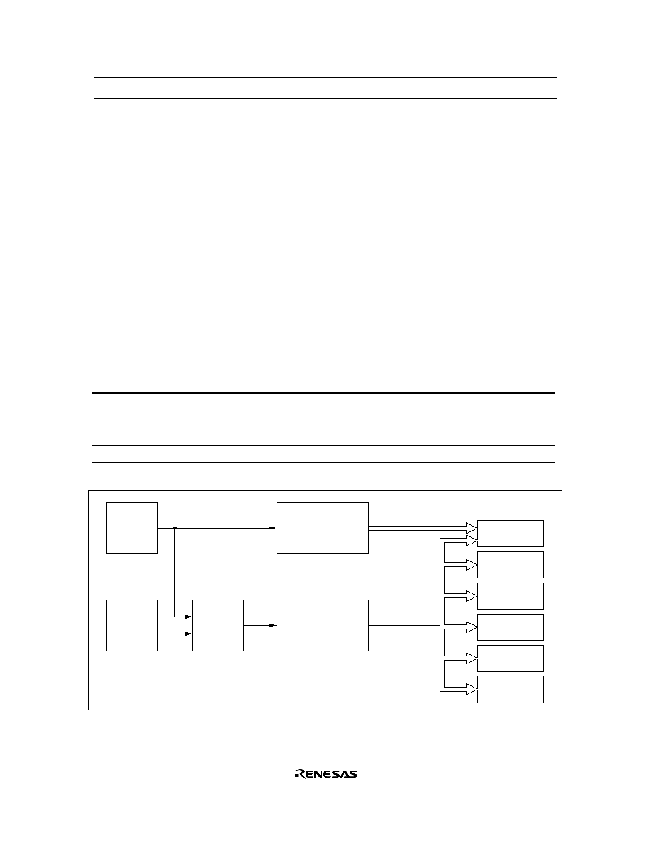
HD404449 Series
55
Prescalers
The MCU has the following two prescalers, S and W.
The prescaler operating conditions are listed in table 25, and the prescaler output supply is shown in figure
39. The timer A≠D input clocks except external events and the serial transmit clock except the external
clock are selected from the prescaler outputs, depending on corresponding mode registers.
Prescaler Operation
Prescaler S: 11-bit counter that inputs a system clock signal. After being reset to $000 by MCU reset,
prescaler S divides the system clock. Prescaler S keeps counting, except in stop, watch, and subactive
modes and at MCU reset.
Prescaler W: Five-bit counter that inputs the X1 input clock signal (32-kHz crystal oscillation) divided by
eight. After being reset to $00 by MCU reset, prescaler W divides the input clock. Prescaler W can be
reset by software.
Table 25
Prescaler Operating Conditions
Prescaler
Input Clock
Reset Conditions
Stop Conditions
Prescaler S
System clock (in active
and standby mode),
Subsystem clock (in
subactive mode)
MCU reset
MCU reset, stop mode,
watch mode
Prescaler W
32-kHz crystal oscillation
Software
MCU reset, stop mode
Subsystem
clock
Prescaler W
System
clock
Prescaler S
Clock
selector
Timer A
Timer B
Timer C
Timer D
Serial 1
Serial 2
f /8
X
f /4 or
X
f /8
X
Figure 39 Prescaler Output Supply

HD404449 Series
56
Timers
The MCU has four timer/counters (A to D).
∑
Timer A: Free-running timer
∑
Timer B: Multifunction timer
∑
Timer C: Multifunction timer
∑
Timer D: Multifunction timer
Timer A is an 8-bit free-running timer. Timers B≠D are 8-bit multifunction timers, whose functions are
listed in table 26. The operating modes are selected by software.
Table 26
Timer Functions
Functions
Timer A
Timer B
Timer C
Timer D
Clock source
Prescaler S
Available
Available
Available
Available
Prescaler W
Available
--
--
--
External event
--
Available
--
Available
Timer functions
Free-running
Available
Available
Available
Available
Time-base
Available
--
--
--
Event counter
--
Available
--
Available
Reload
--
Available
Available
Available
Watchdog
--
--
Available
--
Input capture
--
--
--
Available
Timer outputs
Toggle
--
Available
Available
Available
0 output
--
Available
Available
Available
1 output
--
Available
Available
Available
PWM
--
--
Available
Available
Note:
-- means not available.
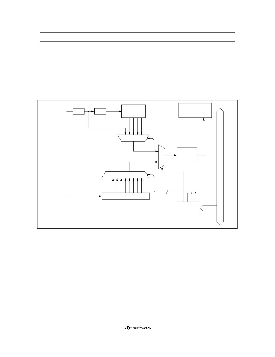
HD404449 Series
57
Timer A
Timer A Functions: Timer A has the following functions.
∑
Free-running timer
∑
Clock time-base
The block diagram of timer A is shown in figure 40.
1/4
1/2
32.768-kHz
oscillator
System
clock
Prescaler W
(PSW)
Selector
Selector
Prescaler S (PSS)
Selector
Internal data bus
Timer A interrupt
request flag
(IFTA)
Clock
Overflow
Timer
counter A
(TCA)
Timer mode
register A
(TMA)
3
2 f
1/2 tw
cyc
f
tw
cyc
¯
PER
2
4
8
32
128
512
1024
2048
˜ ˜ ˜ ˜ ˜ ˜ ˜ ˜
2
8
16
32
˜ ˜ ˜ ˜
W
W
Figure 40 Timer A Block Diagram
Timer A Operations:
∑
Free-running timer operation: The input clock for timer A is selected by timer mode register A (TMA:
$008).
Timer A is reset to $00 by MCU reset and incremented at each input clock. If an input clock is applied
to timer A after it has reached $FF, an overflow is generated, and timer A is reset to $00. The overflow
sets the timer A interrupt request flag (IFTA: $001, bit 2). Timer A continues to be incremented after
reset to $00, and therefore it generates regular interrupts every 256 clocks.
∑
Clock time-base operation: Timer A is used as a clock time-base by setting bit 3 (TMA3) of timer
mode register A (TMA: $008) to 1. The prescaler W output is applied to timer A, and timer A
generates interrupts at the correct timing based on the 32.768-kHz crystal oscillation. In this case,
prescaler W and timer A can be reset to $00 by software.
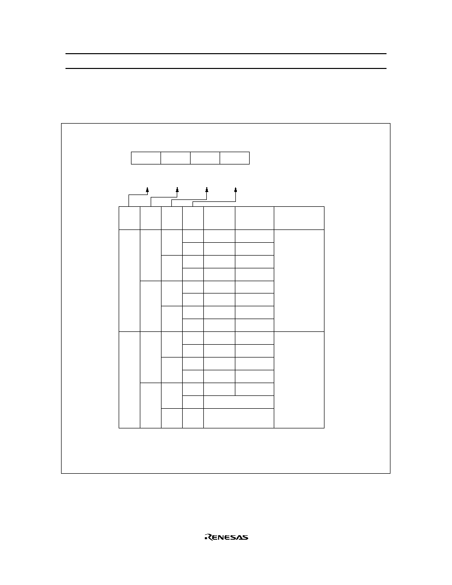
HD404449 Series
58
Registers for Timer A Operation: Timer A operating modes are set by the following registers.
∑
Timer mode register A (TMA: $008): Four-bit write-only register that selects timer A's operating mode
and input clock source as shown in figure 41.
Bit
Initial value
Read/Write
Bit name
3
0
W
TMA3
2
0
W
TMA2
0
0
W
TMA0
1
0
W
TMA1
Timer mode register A (TMA: $008)
0
0
1
0
0
1
0
1
0
1
0
1
0
1
0
1
0
1
PSS
PSS
PSS
PSS
PSS
PSS
PSS
PSS
PSW
PSW
PSW
PSW
PSW
Operating mode
Timer A mode
TMA3
TMA1
TMA2
TMA0
Source
prescaler
2048t
cyc
1024t
cyc
512t
cyc
128t
cyc
32t
cyc
8t
cyc
4t
cyc
2t
cyc
Input clock
frequency
0
1
1
32t
Wcyc
16t
Wcyc
8t
Wcyc
2t
Wcyc
1/2t
Wcyc
Time-base
mode
0
0
1
1
0
1
1
Inhibited
PSW and TCA reset
Don't
care
Notes: 1.
2.
3.
t
Wcyc
= 244.14
µ
s (when a 32.768-kHz crystal oscillator is used)
Timer counter overflow output period (seconds) = input clock period (seconds)
◊
256.
The division ratio must not be modified during time-base mode operation, otherwise
an overflow cycle error will occur.
Figure 41 Timer Mode Register A (TMA)
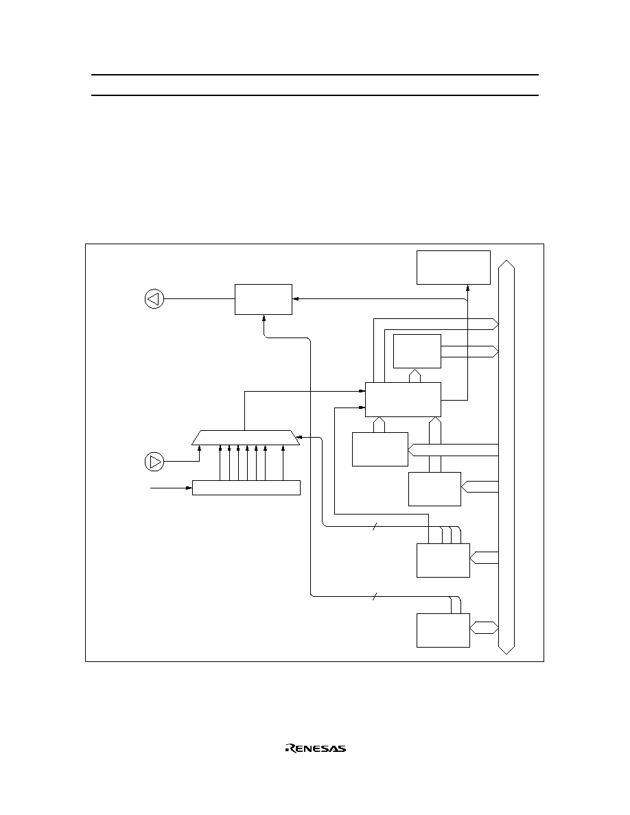
HD404449 Series
59
Timer B
Timer B Functions: Timer B has the following functions.
∑
Free-running/reload timer
∑
External event counter
∑
Timer output operation (toggle, 0, and 1 outputs)
The block diagram of timer B is shown in figure 42.
System
clock
EVNB
TOB
Timer output control
Selector
Prescaler S (PSS)
Clock
Timer read register BU (TRBU)
Timer read
register BL
(TRBL)
Timer counter B
(TCB)
Timer write
register BU
(TWBU)
Timer write
register BL
(TWBL)
Timer mode
register B1
(TMB1)
Timer mode
register B2
(TMB2)
Timer B interrupt
request flag
(IFTB)
¯
PER
3
2
Internal data bus
2
4
8
32
128
512
2048
˜ ˜ ˜ ˜ ˜ ˜
˜
Free-running/
Reload control
Overflow
Timer output
control logic
Figure 42 Timer B Block Diagram

HD404449 Series
60
Timer B Operations:
∑
Free-running/reload timer operation: The free-running/reload operation, input clock source, and
prescaler division ratio are selected by timer mode register B1 (TMB1: $009).
Timer B is initialized to the value set in timer write register B (TWBL: $00A, TWBU: $00B) by
software and incremented by one at each clock input. If an input clock is applied to timer B after it has
reached $FF, an overflow is generated. In this case, if the reload timer function is enabled, timer B is
initialized to its initial value set in timer write register B; if the free-running timer function is enabled,
the timer is initialized to $00 and then incremented again.
The overflow sets the timer B interrupt request flag (IFTB: $002, bit 0). IFTB is reset by software or
MCU reset. Refer to figure 3 and table 1 for details.
∑
External event counter operation: Timer B is used as an external event counter by selecting external
event input as the input clock source. In this case, pin R3
3
/
EVNB must be set to EVNB by port mode
register C (PMRC: $025).
Timer B is incremented by one at each falling edge of signals input to pin
EVNB. Other operations are
basically the same as the free-running/ reload timer operation.
∑
Timer output operation: The following three output modes can be selected for timer B by setting timer
mode register B2 (TMB2: $013).
Toggle
0 output
1 output
By selecting the timer output mode, pin R3
0
/TOB is set to TOB. The output from TOB is reset low by
MCU reset.
Toggle output: When toggle output mode is selected, the output level is inverted if a clock is input
after timer B has reached $FF. By using this function and reload timer function, clock signals can
be output at a required frequency for the buzzer. The output waveform is shown in figure 43.
0 output: When 0 output mode is selected, the output level is pulled low if a clock is input after
timer B has reached $FF. Note that this function must be used only when the output level is high.
1 output: When 1 output mode is selected, the output level is set high if a clock is input after timer
B has reached $FF. Note that this function must be used only when the output level is low.
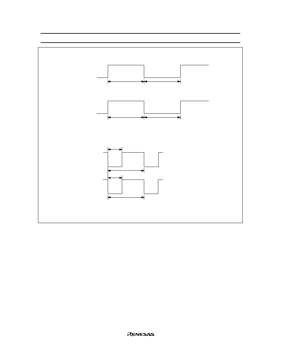
HD404449 Series
61
T (N + 1)
T 256
T
T (256 ≠ N)
TMC13 = 0
The waveform is always fixed low when N = $FF.
T:
N:
◊
◊
◊
TMC13 = 1
Input clock period to counter (figures 52 and 59)
The value of the timer write register
Note:
TMD13 = 0
TMD13 = 1
256 clock cycles
256 clock cycles
Free-running timer
Toggle output waveform (timers B, C, and D)
PWM output waveform (timers C and D)
(256 ≠ N) clock cycles (256 ≠ N) clock cycles
Reload timer
Figure 43 Timer Output Waveform
Registers for Timer B Operation: By using the following registers, timer B operation modes are selected
and the timer B count is read and written.
Timer mode register B1 (TMB1: $009)
Timer mode register B2 (TMB2: $013)
Timer write register B (TWBL: $00A, TWBU: $00B)
Timer read register B (TRBL: $00A, TRBU: $00B)
Port mode register C (PMRC: $025)
∑
Timer mode register B1 (TMB1: $009): Four-bit write-only register that selects the free-
running/reload timer function, input clock source, and the prescaler division ratio as shown in figure 44.
It is reset to $0 by MCU reset.
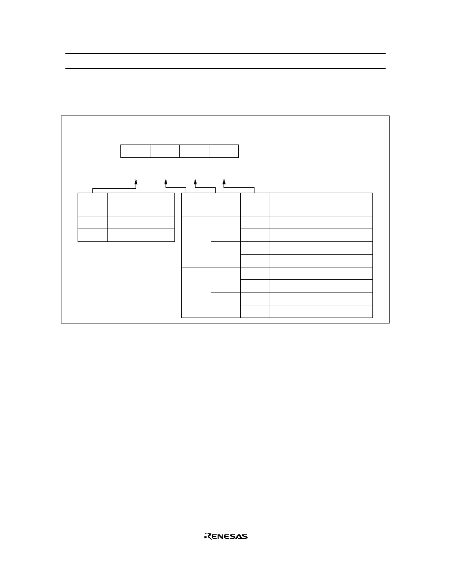
HD404449 Series
62
Writing to this register is valid from the second instruction execution cycle after the execution of the
previous timer mode register B1 write instruction. Setting timer B's initialization by writing to timer
write register B (TWBL: $00A, TWBU: $00B) must be done after a mode change becomes valid.
Bit
Initial value
Read/Write
Bit name
3
0
W
TMB13
2
0
W
TMB12
0
0
W
TMB10
1
0
W
TMB11
Timer mode register B1 (TMB1: $009)
0
1
0
1
0
1
0
1
0
1
0
1
0
1
2048t
cyc
512t
cyc
128t
cyc
32t
cyc
8t
cyc
4t
cyc
2t
cyc
TMB12
TMB10
TMB11
Input clock period and input
clock source
R3
3
/
EVNB
(External event input)
TMB13
0
1
Free-running/reload
timer selection
Free-running timer
Reload timer
Figure 44 Timer Mode Register B1 (TMB1)
∑
Timer mode register B2 (TMB2: $013): Two-bit read/write register that selects the timer B output
mode as shown in figure 45. It is reset to $0 by MCU reset.
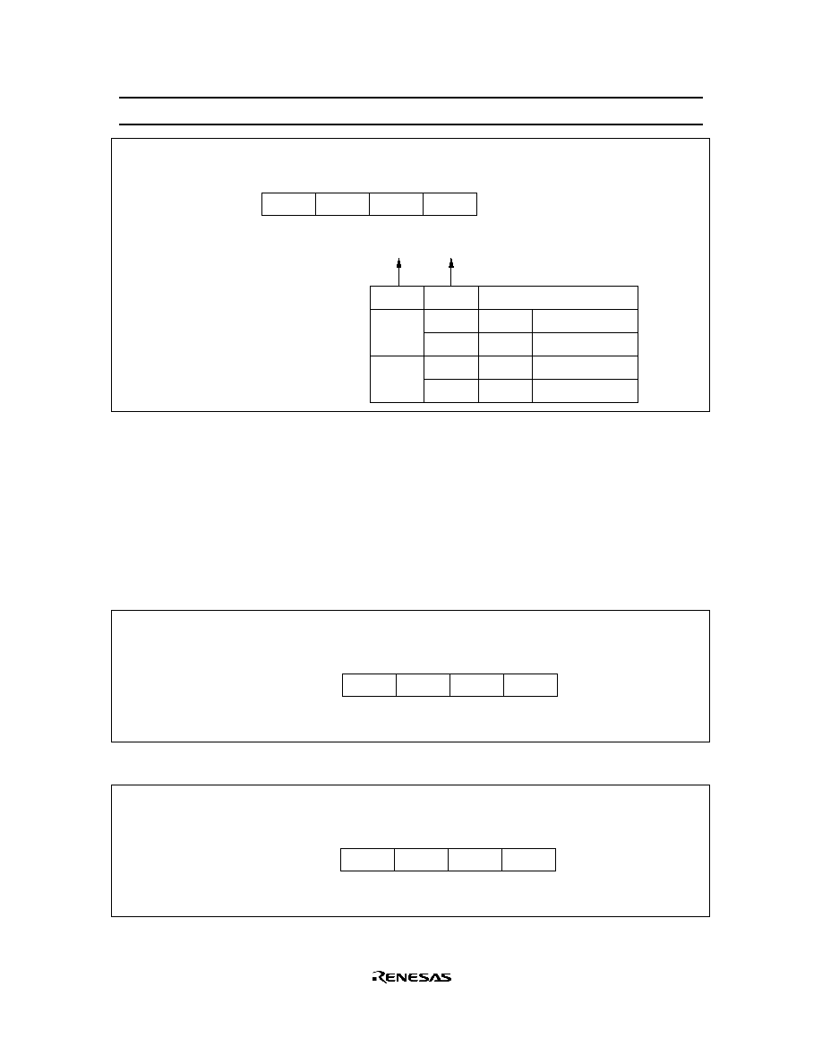
HD404449 Series
63
Bit
Initial value
Read/Write
Bit name
3
--
--
Not used
2
--
--
Not used
0
0
R/W
TMB20
1
0
R/W
TMB21
Timer mode register B2 (TMB2: $013)
TMB21
0
1
TMB20
0
1
0
1
R3
0
/TOB mode selection
R3
0
TOB
TOB
TOB
R3
0
port
Toggle output
0 output
1 output
Figure 45 Timer Mode Register B2 (TMB2)
∑
Timer write register B (TWBL: $00A, TWBU: $00B): Write-only register consisting of the lower digit
(TWBL) and the upper digit (TWBU) as shown in figures 46 and 47. The lower digit is reset to $0 by
MCU reset, but the upper digit value is invalid.
Timer B is initialized by writing to timer write register B (TWBL: $00A, TWBU: $00B). In this case,
the lower digit (TWBL) must be written to first, but writing only to the lower digit does not change the
timer B value. Timer B is initialized to the value in timer write register B at the same time the upper
digit (TWBU) is written to. When timer write register B is written to again and if the lower digit value
needs no change, writing only to the upper digit initializes timer B.
Bit
Initial value
Read/Write
Bit name
3
0
W
TWBL3
2
0
W
TWBL2
0
0
W
TWBL0
1
0
W
TWBL1
Timer write register B (lower digit) (TWBL: $00A)
Figure 46 Timer Write Register B Lower Digit (TWBL)
Bit
Initial value
Read/Write
Bit name
3
Undefined
W
TWBU3
2
Undefined
W
TWBU2
0
Undefined
W
TWBU0
1
Undefined
W
TWBU1
Timer write register B (upper digit) (TWBU: $00B)
Figure 47 Timer Write Register B Upper Digit (TWBU)

HD404449 Series
64
∑
Timer read register B (TRBL: $00A, TRBU: $00B): Read-only register consisting of the lower digit
(TRBL) and the upper digit (TRBU) that holds the count of the timer B upper digit (figures 48 and 49).
The upper digit (TRBU) must be read first. At this time, the count of the timer B upper digit is
obtained, and the count of the timer B lower digit is latched to the lower digit (TRBL). After this, by
reading TRBL, the count of timer B when TRBU is read can be obtained.
Bit
Initial value
Read/Write
Bit name
3
Undefined
R
TRBL3
2
Undefined
R
TRBL2
0
Undefined
R
TRBL0
1
Undefined
R
TRBL1
Timer read register B (lower digit) (TRBL: $00A)
Figure 48 Timer Read Register B Lower Digit (TRBL)
Bit
Initial value
Read/Write
Bit name
3
Undefined
R
TRBU3
2
Undefined
R
TRBU2
0
Undefined
R
TRBU0
1
Undefined
R
TRBU1
Timer read register B (upper digit) (TRBU: $00B)
Figure 49 Timer Read Register B Upper Digit (TRBU)
∑
Port mode register C (PMRC: $025): Write-only register that selects R3
3
/
EVNB pin function as shown
in figure 50. It is reset to $0 by MCU reset.
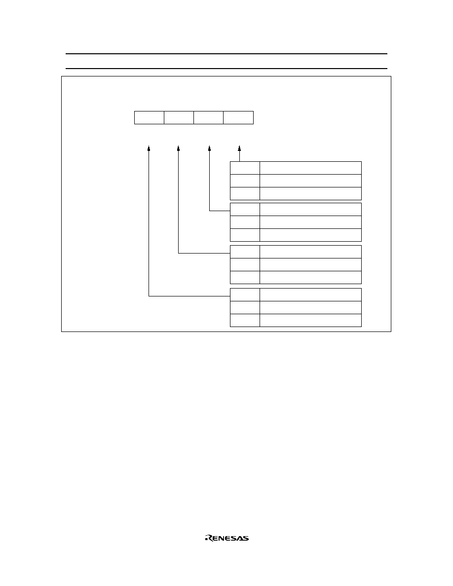
HD404449 Series
65
Bit
Initial value
Read/Write
Bit name
3
0
W
PMRC3
2
0
W
PMRC2
0
0
W
PMRC0
1
0
W
PMRC1
PMRC1
0
1
R4
0
/EVND mode selection
R4
0
EVND
Port mode register C (PMRC: $025)
PMRC0
0
1
R3
3
/
EVNB
mode selection
R3
3
EVNB
PMRC3
0
1
D
13
/
INT
0
mode selection
D
13
INT
0
PMRC2
0
1
D
12
/
STOPC
mode selection
D
12
STOPC
Figure 50 Port Mode Register C (PMRC)
Timer C
Timer C Functions: Timer C has the following functions.
∑
Free-running/reload timer
∑
Watchdog timer
∑
Timer output operation (toggle, 0, 1, and PWM outputs)
The block diagram of timer C is shown in figure 51.
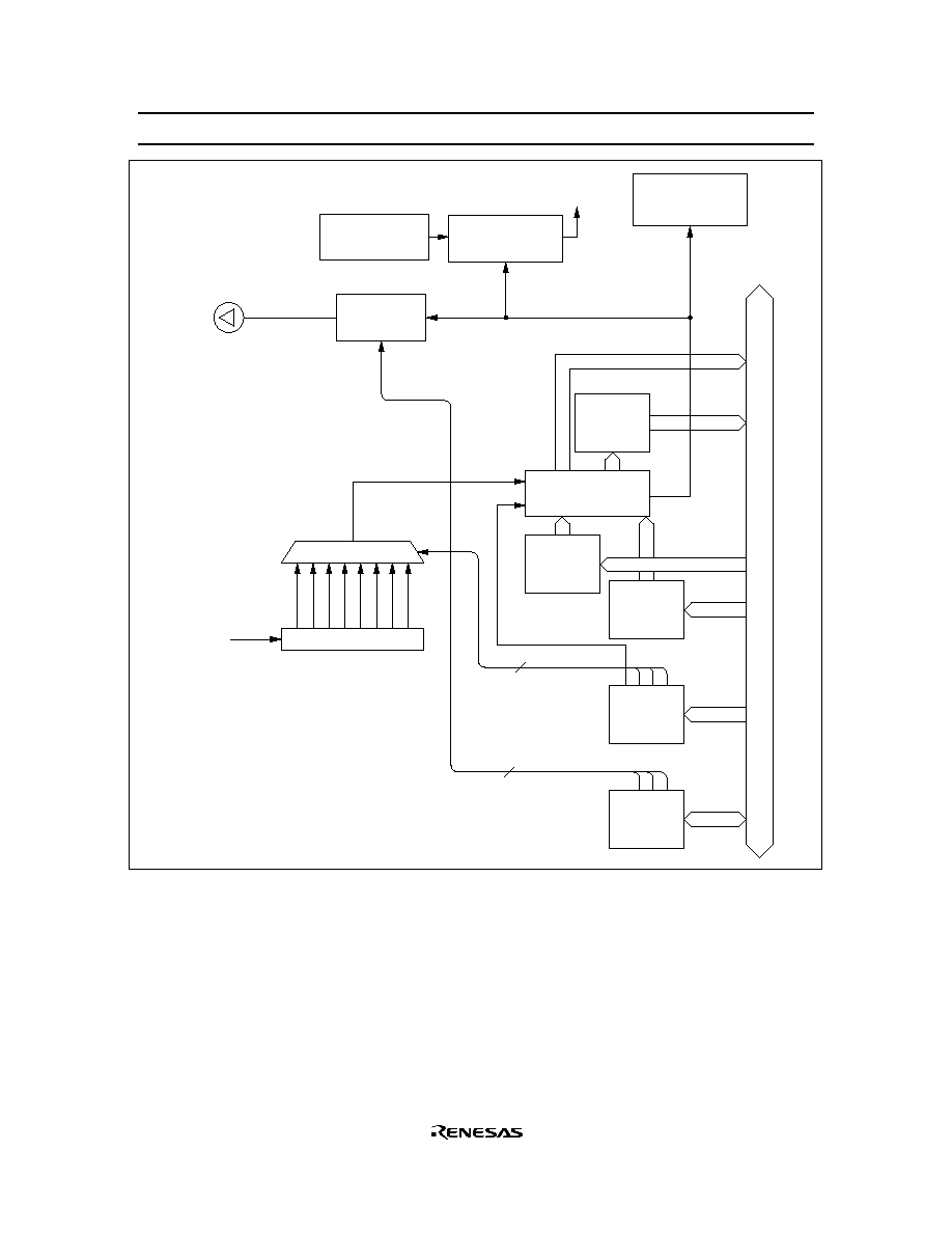
HD404449 Series
66
Watchdog on
flag (WDON)
System
reset signal
Timer C interrupt
request flag
(IFTC)
Timer output
control logic
Timer read register CU (TRCU)
Timer output
control
Timer read
register CL
(TRCL)
Clock
Timer counter C
(TCC)
Selector
System
clock
Prescaler S (PSS)
Overflow
Internal data bus
Timer write
register CU
(TWCU)
Timer write
register CL
(TWCL)
Timer mode
register C1
(TMC1)
Timer mode
register C2
(TMC2)
Free-running
/Reload control
Watchdog timer
control logic
TOC
¯
PER
˜
2
˜
4
˜
8
˜
32
˜
128
˜
512
˜
1024
˜
2048
3
3
Figure 51 Timer C Block Diagram
Timer C Operations:
∑
Free-running/reload timer operation: The free-running/reload operation, input clock source, and
prescaler division ratio are selected by timer mode register C1 (TMC1: $00D).
Timer C is initialized to the value set in timer write register C (TWCL: $00E, TWCU: $00F) by
software and incremented by one at each clock input. If an input clock is applied to timer C after it has
reached $FF, an overflow is generated. In this case, if the reload timer function is enabled, timer C is
initialized to its initial value set in timer write register C; if the free-running timer function is enabled,
the timer is initialized to $00 and then incremented again.

HD404449 Series
67
The overflow sets the timer C interrupt request flag (IFTC: $002, bit 2). IFTC is reset by software or
MCU reset. Refer to figure 3 and table 1 for details.
∑
Watchdog timer operation: Timer C is used as a watchdog timer for detecting out-of-control program
routines by setting the watchdog on flag (WDON: $020, bit 1) to 1. If a program routine runs out of
control and an overflow is generated, the MCU is reset. Program run can be controlled by initializing
timer C by software before it reaches $FF.
∑
Timer output operation: The following four output modes can be selected for timer C by setting timer
mode register C2 (TMC2: $014).
Toggle
0 output
1 output
PWM output
By selecting the timer output mode, pin R3
1
/TOC is set to TOC. The output from TOC is reset low by
MCU reset.
Toggle output: The operation is basically the same as that of timer-B's toggle output.
0 output: The operation is basically the same as that of timer-B's 0 output.
1 output: The operation is basically the same as that of timer-B's 1 output.
PWM output: When PWM output mode is selected, timer C provides the variable-duty pulse output
function. The output waveform differs depending on the contents of timer mode register C1
(TMC1: $00D) and timer write register C (TWCL: $00E, TWCU: $00F). The output waveform is
shown in figure 43.
Registers for Timer C Operation: By using the following registers, timer C operation modes are selected
and the timer C count is read and written.
Timer mode register C1 (TMC1: $00D)
Timer mode register C2 (TMC2: $014)
Timer write register C (TWCL: $00E, TWCU: $00F)
Timer read register C (TRCL: $00E, TRCU: $00F)
∑
Timer mode register C1 (TMC1: $00D): Four-bit write-only register that selects the free-
running/reload timer function, input clock source, and prescaler division ratio as shown in figure 52. It
is reset to $0 by MCU reset.
Writing to this register is valid from the second instruction execution cycle after the execution of the
previous timer mode register C1 write instruction. Setting timer C's initialization by writing to timer
write register C (TWCL: $00E, TWCU: $00F) must be done after a mode change becomes valid.
∑
Timer mode register C2 (TMC2: $014): Three-bit read/write register that selects the timer C output
mode as shown in figure 53. It is reset to $0 by MCU reset.
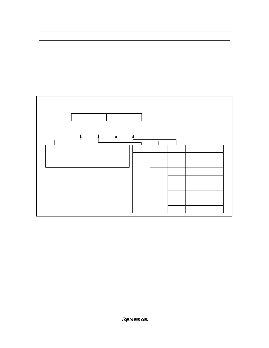
HD404449 Series
68
∑
Timer write register C (TWCL: $00E, TWCU: $00F): Write-only register consisting of a lower digit
(TWCL) and an upper digit (TWCU) as shown in figures 54 and 55. The operation of timer write
register C is basically the same as that of timer write register B (TWBL: $00A, TWBU: $00B).
∑
Timer read register C (TRCL: $00E, TRCU: $00F): Read-only register consisting of a lower digit
(TRCL) and an upper digit (TRCU) that holds the count of the timer C upper digit as shown in figures
56 and 57. The operation of timer read register C is basically the same as that of timer read register B
(TRBL: $00A, TRBU: $00B).
Bit
Initial value
Read/Write
Bit name
3
0
W
TMC13
2
0
W
TMC12
0
0
W
TMC10
1
0
W
TMC11
Timer mode register C1 (TMC1: $00D)
0
1
0
1
0
1
0
1
0
1
0
1
0
1
2048t
cyc
1024t
cyc
512t
cyc
128t
cyc
32t
cyc
8t
cyc
4t
cyc
2t
cyc
TMC12
TMC10
TMC11
TMC13
0
1
Free-running/reload timer selection
Free-running timer
Reload timer
Input clock period
Figure 52 Timer Mode Register C1 (TMC1)
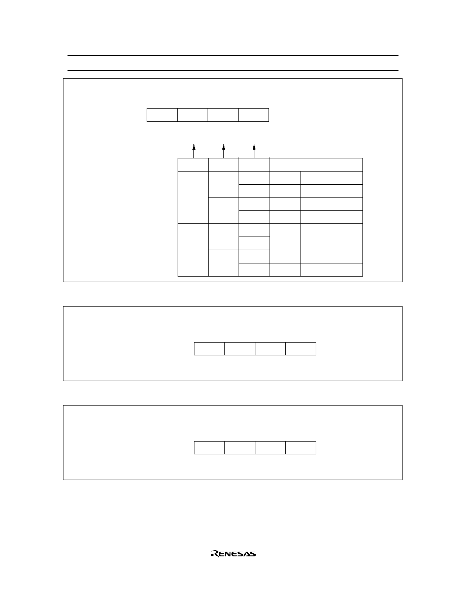
HD404449 Series
69
Bit
Initial value
Read/Write
Bit name
3
--
--
Not used
2
0
R/W
TMC22
0
0
R/W
TMC20
1
0
R/W
TMC21
Timer mode register C2 (TMC2: $014)
TMC22
0
TMC21
R3
1
/TOC mode selection
R3
1
TOC
TOC
TOC
--
TOC
R3
1
port
Toggle output
0 output
1 output
Inhibited
PWM output
TMC20
0
1
0
1
0
1
0
1
0
1
1
0
1
Figure 53 Timer Mode Register C2 (TMC2)
Bit
Initial value
Read/Write
Bit name
3
0
W
TWCL3
2
0
W
TWCL2
0
0
W
TWCL0
1
0
W
TWCL1
Timer write register C (lower digit) (TWCL: $00E)
Figure 54 Timer Write Register C Lower Digit (TWCL)
Bit
Initial value
Read/Write
Bit name
3
Undefined
W
TWCU3
2
Undefined
W
TWCU2
0
Undefined
W
TWCU0
1
Undefined
W
TWCU1
Timer write register C (upper digit) (TWCU: $00F)
Figure 55 Timer Write Register C Upper Digit (TWCU)

HD404449 Series
70
Bit
Initial value
Read/Write
Bit name
3
Undefined
R
TRCL3
2
Undefined
R
TRCL2
0
Undefined
R
TRCL0
1
Undefined
R
TRCL1
Timer read register C (lower digit) (TRCL: $00E)
Figure 56 Timer Read Register C Lower Digit (TRCL)
Bit
Initial value
Read/Write
Bit name
3
Undefined
R
TRCU3
2
Undefined
R
TRCU2
0
Undefined
R
TRCU0
1
Undefined
R
TRCU1
Timer read register C (upper digit) (TRCU: $00F)
Figure 57 Timer Read Register C Upper Digit (TRCU)
Timer D
Timer D Functions: Timer D has the following functions.
∑
Free-running/reload timer
∑
External event counter
∑
Timer output operation (toggle, 0, 1, and PWM outputs)
∑
Input capture timer
The block diagram for each operation mode of timer D is shown in figures 58 (A) and (B).
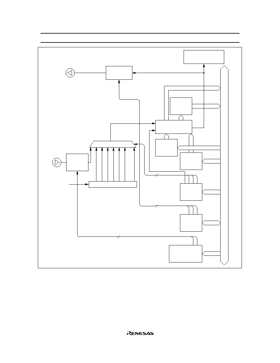
HD404449 Series
71
Timer D interrupt
request flag (IFTD)
Timer output
control logic
Timer read
register DU (TRDU)
Timer output
control
Timer read
register DL
(TRDL)
Clock
Timer counter D
(TCD)
Selector
System
clock
Prescaler S (PSS)
Overflow
Internal data bus
Timer write
register DU
(TWDU)
Timer write
register DL
(TWDL)
Timer mode
register D1
(TMD1)
Timer mode
register D2
(TMD2)
Free-running/
Reload control
TOD
Edge
detection
logic
Edge detection
selection register
2 (ESR2)
Edge detection control
¯
PER
2
3
3
˜
2
˜
4
˜
8
˜
32
˜
128
˜
512
˜
2048
EVND
Figure 58 (A) Timer D Block Diagram (Free-Running/Reload Timer)
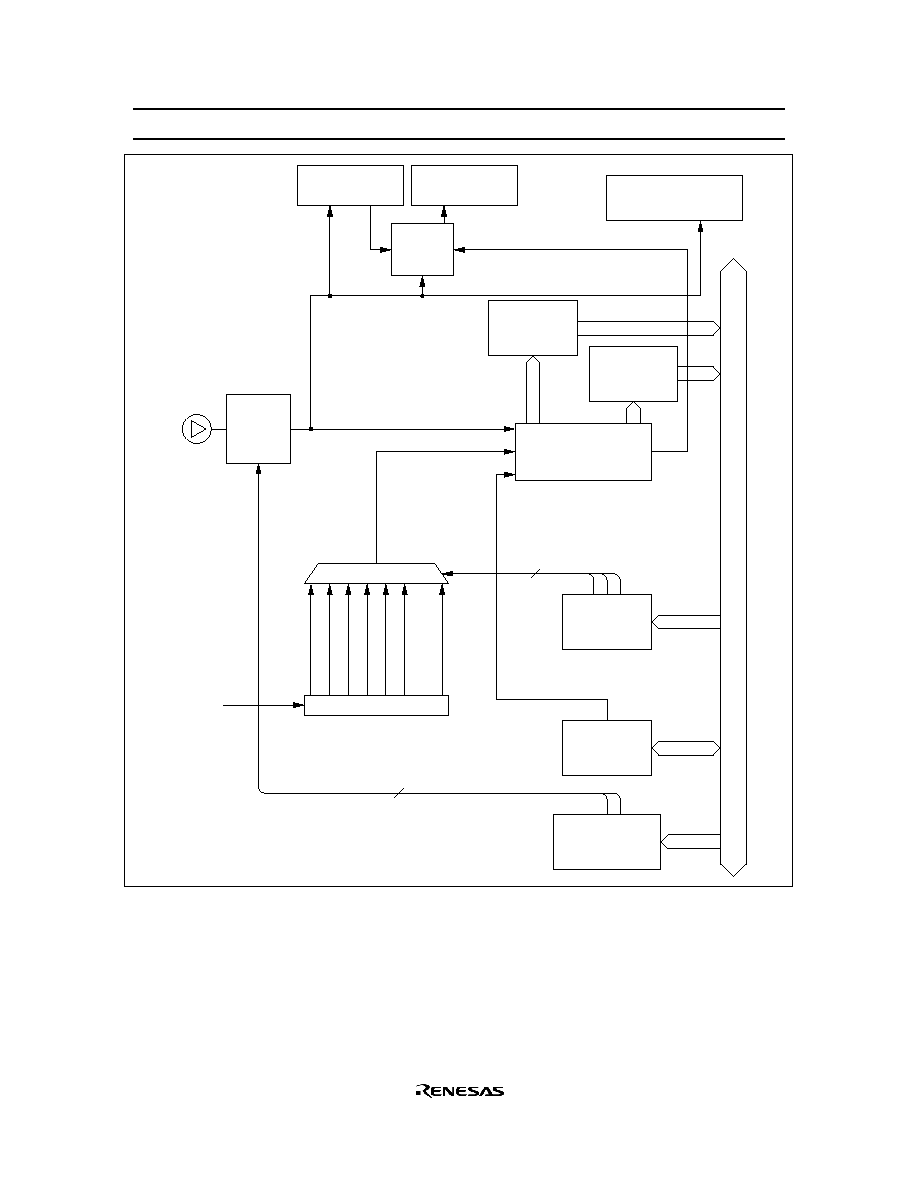
HD404449 Series
72
Selector
˜
2
˜
4
˜
8
˜
32
˜
128
˜
512
˜
2048
3
2
PER
¯
Input capture
status flag (ICSF)
Input capture
error flag (ICEF)
Timer D interrupt
request flag (IFTD)
Error
control
logic
Edge
detection
logic
Timer read
register DU
(TRDU)
Timer read
register DL
(TRDL)
Read signal
Clock
Timer counter D
(TCD)
Overflow
System
clock
Edge detection control
Prescaler S (PSS)
Input capture
timer control
Timer mode
register D1
(TMD1)
Timer mode
register D2
(TMD2)
Edge detection
selection register
2 (ESR2)
EVND
Internal data bus
Figure 58 (B) Timer D Block Diagram (Input Capture Timer)

HD404449 Series
73
Timer D Operations:
∑
Free-running/reload timer operation: The free-running/reload operation, input clock source, and
prescaler division ratio are selected by timer mode register D1 (TMD1: $010).
Timer D is initialized to the value set in timer write register D (TWDL: $011, TWDU: $012) by
software and incremented by one at each clock input. If an input clock is applied to timer D after it has
reached $FF, an overflow is generated. In this case, if the reload timer function is enabled, timer D is
initialized to its initial value set in timer write register D; if the free-running timer function is enabled,
the timer is initialized to $00 and then incremented again.
The overflow sets the timer D interrupt request flag (IFTD: $003, bit 0). IFTD is reset by software or
MCU reset. Refer to figure 3 and table 1 for details.
∑
External event counter operation: Timer D is used as an external event counter by selecting the
external event input as an input clock source. In this case, pin R4
0
/EVND must be set to EVND by port
mode register C (PMRC: $025).
Either falling or rising edge, or both falling and rising edges of input signals can be selected as the
external event detection edge by detection edge select register 2 (ESR2: $027). When both rising and
falling edges detection is selected, the time between the falling edge and rising edge of input signals
must be 2t
cyc
or longer.
Timer D is incremented by one at each detection edge selected by detection edge select register 2
(ESR2: $027). The other operation is basically the same as the free-running/reload timer operation.
∑
Timer output operation: The following four output modes can be selected for timer D by setting timer
mode register D2 (TMD2: $015).
Toggle
0 output
1 output
PWM output
By selecting the timer output mode, pin R3
2
/TOD is set to TOD. The output from TOD is reset low by
MCU reset.
Toggle output: The operation is basically the same as that of timer-B's toggle output.
0 output: The operation is basically the same as that of timer-B's 0 output.
1 output: The operation is basically the same as that of timer-B's 1 output.
PWM output: The operation is basically the same as that of timer-C's PWM output.
∑
Input capture timer operation: The input capture timer counts the clock cycles between trigger edges
input to pin EVND.
Either falling or rising edge, or both falling and rising edges of input signals can be selected as the
trigger input edge by detection edge select register 2 (ESR2: $027).

HD404449 Series
74
When a trigger edge is input to EVND, the count of timer D is written to timer read register D (TRDL:
$011, TRDU: $012), and the timer D interrupt request flag (IFTD: $003, bit 0) and the input capture
status flag (ICSF: $021, bit 0) are set. Timer D is reset to $00, and then incremented again. While
ICSF is set, if a trigger input edge is applied to timer D, or if timer D generates an overflow, the input
capture error flag (ICEF: $021, bit 1) is set. ICSF and ICEF are reset to 0 by MCU reset or by writing
0.
By selecting the input capture operation, pin R3
2
/TOD is set to R3
2
and timer D is reset to $00.
Registers for Timer D Operation: By using the following registers, timer D operation modes are selected
and the timer D count is read and written.
Timer mode register D1 (TMD1: $010)
Timer mode register D2 (TMD2: $015)
Timer write register D (TWDL: $011, TWDU: $012)
Timer read register D (TRDL: $011, TRDU: $012)
Port mode register C (PMRC: $025)
Detection edge select register 2 (ESR2: $027)
∑
Timer mode register D1 (TMD1: $010): Four-bit write-only register that selects the free-
running/reload timer function, input clock source, and the prescaler division ratio as shown in figure 59.
It is reset to $0 by MCU reset.
Writing to this register is valid from the second instruction execution cycle after the execution of the
previous timer mode register D1 (TMD1: $010) write instruction. Setting timer D's initialization by
writing to timer write register D (TWDL: $011, TWDU: $012) must be done after a mode change
becomes valid.
When selecting the input capture timer operation, select the internal clock as the input clock source.
∑
Timer mode register D2 (TMD2: $015): Four-bit read/write register that selects the timer D output
mode and input capture operation as shown in figure 60. It is reset to $0 by MCU reset.

HD404449 Series
75
Bit
Initial value
Read/Write
Bit name
3
0
W
TMD13
2
0
W
TMD12
0
0
W
TMD10
1
0
W
TMD11
Timer mode register D1 (TMD1: $010)
0
1
0
1
0
1
0
1
0
1
0
1
0
1
2048t
cyc
512t
cyc
128t
cyc
32t
cyc
8t
cyc
4t
cyc
2t
cyc
TMD12
TMD10
TMD11
Input clock period and
input clock source
R4
0
/EVND (External event input)
TMD13
0
1
Free-running/reload timer selection
Free-running timer
Reload timer
Figure 59 Timer Mode Register D1 (TMD1)
∑
Timer write register D (TWDL: $011, TWDU: $012): Write-only register consisting of a lower digit
(TWDL) and an upper digit (TWDU) as shown in figures 61 and 62. The operation of timer write
register D is basically the same as that of timer write register B (TWBL: $00A, TWBU: $00B).
∑
Timer read register D (TRDL: $011, TRDU: $012): Read-only register consisting of a lower digit
(TRDL) and an upper digit (TRDU) as shown in figures 63 and 64. The operation of timer read register
D is basically the same as that of timer read register B (TRBL: $00A, TRBU: $00B).
When the input capture timer operation is selected and if the count of timer D is read after a trigger is
input, either the lower or upper digit can be read first.
∑
Port mode register C (PMRC: $025): Write-only register that selects R4
0
/EVND pin function as shown
in figure 50. It is reset to $0 by MCU reset.
∑
Detection edge select register 2 (ESR2: $027): Write-only register that selects the detection edge of
signals input to pin EVND as shown in figure 65. It is reset to $0 by MCU reset.
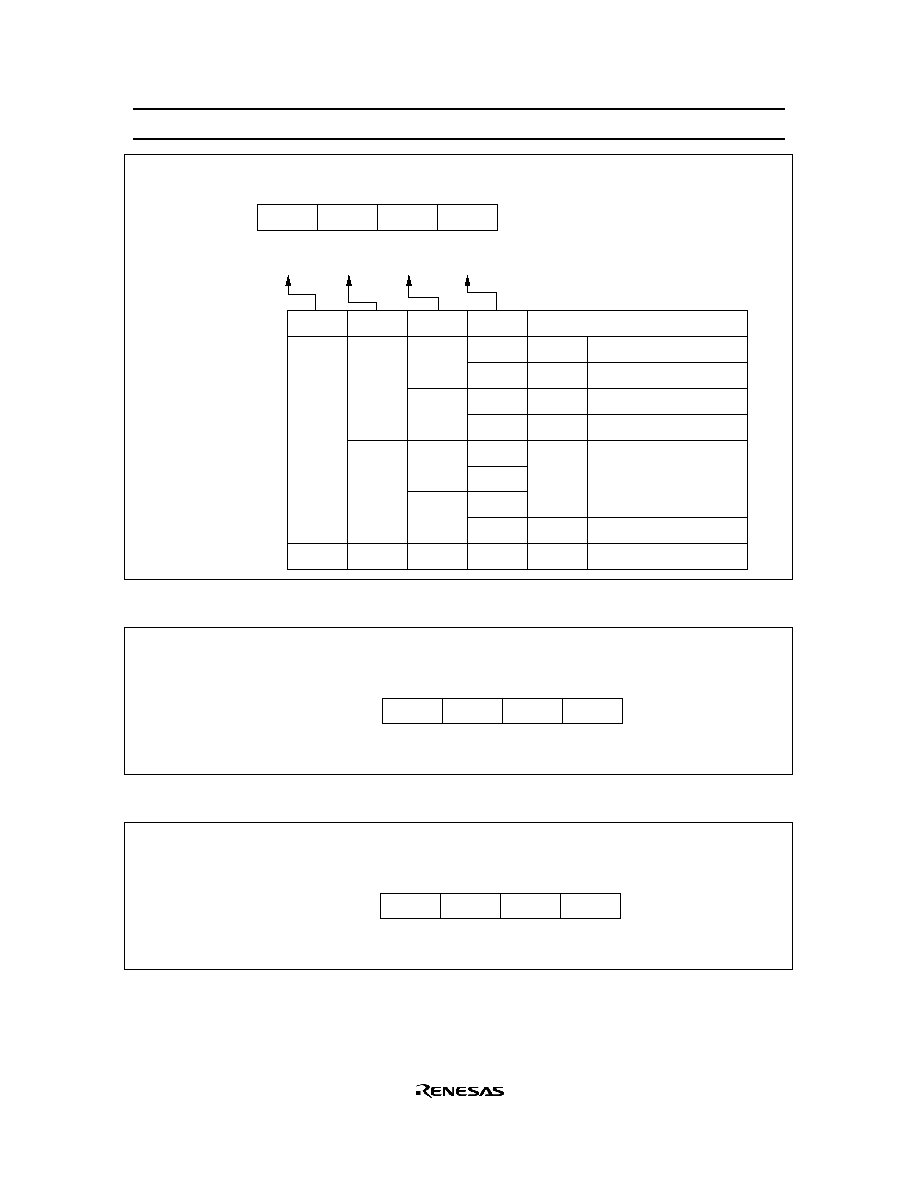
HD404449 Series
76
Bit
Initial value
Read/Write
Bit name
3
0
R/W
TMD23
2
0
R/W
TMD22
0
0
R/W
TMD20
1
0
R/W
TMD21
Timer mode register D2 (TMD2: $015)
TMD22
TMD20
0
1
0
1
0
1
0
1
TMD21
0
1
0
1
0
1
R3
2
/TOD mode selection
R3
2
TOD
TOD
TOD
--
TOD
R3
2
R3
2
port
Toggle output
0 output
1 output
Inhibited
PWM output
Input capture (R3
2
port)
TMD23
0
1
Don't care
Don't care
Don't care
Figure 60 Timer Mode Register D2 (TMD2)
Bit
Initial value
Read/Write
Bit name
3
0
W
TWDL3
2
0
W
TWDL2
0
0
W
TWDL0
1
0
W
TWDL1
Timer write register D (lower digit) (TWDL: $011)
Figure 61 Timer Write Register D Lower Digit (TWDL)
Bit
Initial value
Read/Write
Bit name
3
Undefined
W
TWDU3
2
Undefined
W
TWDU2
0
Undefined
W
TWDU0
1
Undefined
W
TWDU1
Timer write register D (upper digit) (TWDU: $012)
Figure 62 Timer Write Register D Upper Digit (TWDU)
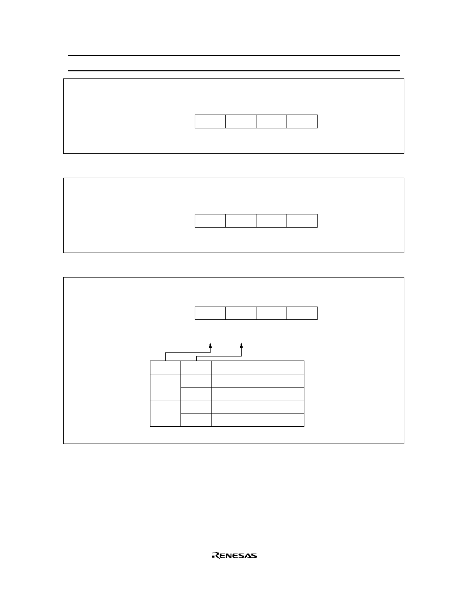
HD404449 Series
77
Bit
Initial value
Read/Write
Bit name
3
Undefined
R
TRDL3
2
Undefined
R
TRDL2
0
Undefined
R
TRDL0
1
Undefined
R
TRDL1
Timer read register D (lower digit) (TRDL: $011)
Figure 63 Timer Read Register D Lower Digit (TRDL)
Bit
Initial value
Read/Write
Bit name
3
Undefined
R
TRDU3
2
Undefined
R
TRDU2
0
Undefined
R
TRDU0
Timer read register D (upper digit) (TRDU: $012)
1
Undefined
R
TRDU1
Figure 64 Timer Read Register D Upper Digit (TRDU)
Bit
Initial value
Read/Write
Bit name
3
0
W
ESR23
2
0
W
ESR22
0
--
--
Not used
1
--
--
Not used
Detection edge register 2 (ESR2: $027)
ESR23
0
1
ESR22
0
1
0
1
EVND detection edge
No detection
Falling-edge detection
Rising-edge detection
Double-edge detection
*
Note:
*
Both falling and rising edges are detected.
Figure 65 Detection Edge Select Register 2 (ESR2)
Notes on Use
When using the timer output as PWM output, note the following point. From the update of the timer write
register until the occurrence of the overflow interrupt, the PWM output differs from the period and duty
settings, as shown in table 27. The PWM output should therefore not be used until after the overflow
interrupt following the update of the timer write register. After the overflow, the PWM output will have the
set period and duty cycle.
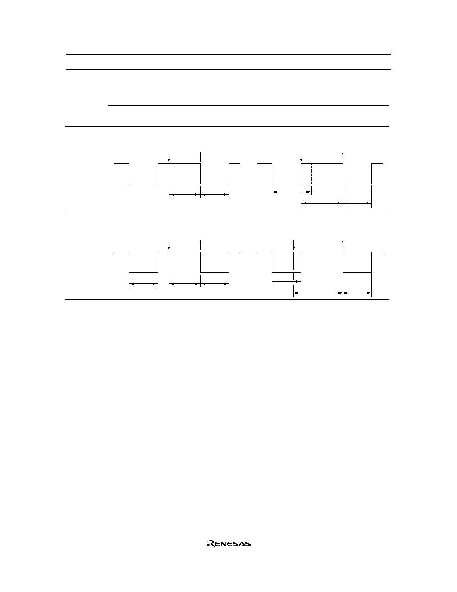
HD404449 Series
78
Table 27
PWM Output Following Update of Timer Write Register
PWM Output
Mode
Timer Write Register is Updated during
High PWM Output
Timer Write Register is Updated during
Low PWM Output
Free running
Timer write
register
updated to
value N
Interrupt
request
T
◊
(255 ≠ N) T
◊
(N + 1)
Timer write
register
updated to
value N
Interrupt
request
T
◊
(N' + 1)
T
◊
(255 ≠ N)
T
◊
(N + 1)
Reload
Timer write
register
updated to
value N
Interrupt
request
T
T
◊
(255 ≠ N)
T
Timer write
register
updated to
value N
Interrupt
request
T
T
◊
(255 ≠ N)
T

HD404449 Series
79
Serial Interface
The MCU has two channels of serial interface. The transfer and receive start instructions differ according
to the serial interface channel, but other functions are the same. The serial interface serially transfers or
receives 8-bit data, and includes the following features.
∑
Multiple transmit clock sources
External clock
Internal prescaler output clock
System clock
∑
Output level control in idle states
Five registers, an octal counter, and a multiplexer are also configured for serial interfaces 1 and 2 as
follows.
Serial interface 1
∑
Serial data register 1 (SR1L: $006, SR1U: $007)
∑
Serial mode register 1A (SM1A: $005)
∑
Serial mode register 1B (SM1B: $028)
∑
Port mode register A (PMRA: $004)
∑
Miscellaneous register (MIS: $00C)
∑
Octal counter (OC)
∑
Selector
Serial interface 2
∑
Serial data register 2 (SR2L: $01D, SR2U: $01E)
∑
Serial mode register 2A (SM2A: $01B)
∑
Serial mode register 2B (SM2B: $01C)
∑
Port mode register A (PMRA: $004)
∑
Octal counter (OC)
∑
Selector
The block diagram of serial interfaces 1 and 2 are shown in figure 66.
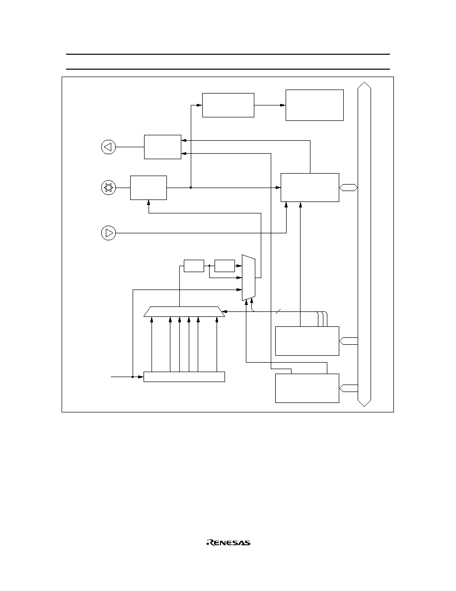
HD404449 Series
80
Selector
Prescaler S (PSS)
˜
2
˜
8
˜
32
˜
128
˜
512
˜
2048
Selector
I/O control
logic
Idle control
logic
Octal counter
(OC1, OC2)
Serial interrupt
request flag
(IFS1, IFS2)
Clock
Serial data
register (SR1L/U,
SR2L/U)
Serial mode register
1A, 2A (SM1A,
SM2A)
Serial mode register
1B, 2B (SM1B,
SM2B)
Transfer
control
SO , SO
SCK
,
SCK
SI , SI
System
clock
Internal data bus
3
¯
PER
1/2
1/2
2
1
2
1
2
1
Figure 66 Serial Interfaces 1 and 2 Block Diagram
Serial Interface Operation
Selecting and Changing the Operating Mode: Tables 28 (A) and 28 (B) list the serial interfaces'
operating modes. To select an operating mode, use one of these combinations of port mode register A
(PMRA: $004), serial mode register 1A (SM1A: $005), and serial mode register 2A (SM2A: $01B)
settings; to change the operating mode of serial interface 1, always initialize the serial interface internally
by writing data to serial mode register 1A; and to change the operating mode of serial interface 2, always
initialize the serial interface internally by writing data to serial mode register 2A. Note that serial interface

HD404449 Series
81
1 is initialized by writing data to serial mode register 1A, and serial interface 2 is initialized by writing data
to serial mode register 2A. Refer to the following section Registers for Serial Interface for details.
Pin Setting: The R4
1
/
SCK
1
pin is controlled by writing data to serial mode register 1A (SM1A: $005).
The R5
1
/
SCK
2
pin is controlled by writing data to serial mode register 2A (SM2A: $01B). Pins R4
2
/SI
1
,
R4
3
/SO
1
, R5
2
/SI
2
,
and R5
3
/SO
2
are controlled by writing data to port mode register A (PMRA: $004). Refer
to the following section Registers for Serial Interface for details.
Transmit Clock Source Setting: The transmit clock source of serial interface 1 is set by writing data to
serial mode register 1A (SM1A: $005) and serial mode register 1B (SM1B: $028). The transmit clock
source of serial interface 2 is set by writing data to serial mode register 2A (SM2A: $01B) and serial mode
register 2B (SM2B: $01C). Refer to the following section Registers for Serial Interface for details.
Data Setting: Transmit data of serial interface 1 is set by writing data to serial data register 1 (SR1L:
$006, SR1U: $007). Transmit data of serial interface 2 is set by writing data to serial data register 2
(SR2L: $01D, SR2U: $01E). Receive data of serial interface 1 is obtained by reading the contents of serial
data register 1. Receive data of serial interface 2 is obtained by reading the contents of serial data register
2. The serial data is shifted by each serial interface transmit clock and is input from or output to an external
system.
The output level of the SO
1
and SO
2
pins is invalid until the first data of each serial interface is output after
MCU reset, or until the output level control in idle states is performed.
Transfer Control: Serial interface 1 is activated by the STS instruction. Serial interface 2 is activated by
a dummy read of serial mode register 2A (SM2A: $01B), which will be referred to as SM2A read. The
octal counter is reset to 000 by the STS instruction (serial interface 2 is SM2A read), and it increments at
the rising edge of the transmit clock for each serial interface. When the eighth transmit clock signal is
input or when serial transmission/reception is discontinued, the octal counter is reset to 000, the serial 1
interrupt request flag (IFS1: $003, bit 2) for serial interface 1 and serial 2 interrupt request flag (IFS2:
$023, bit 2) for serial interface 2 are set, and the transfer stops.
When the prescaler output is selected as the transmit clock of serial interface 1, the transmit clock
frequency is selected as 4t
cyc
to 8192t
cyc
by setting bits 0 to 2 (SM1A0≠SM1A2) of serial mode register 1A
(SM1A: $005) and bit 0 (SM1B0) of serial mode register 1B (SM1B: $028) as listed in table 29. When the
prescaler output is selected as the transmit clock of serial interface 2, the transmit clock frequency is
selected as 4t
cyc
to 8192t
cyc
by setting bits 0 to 2 (SM2A0≠ SM2A2) of serial mode register 2A (SM2A:
$01B) and bit 0 (SM2B0) of serial mode register 2B (SM2B: $01C).
Note:
To start serial interface 2, simply read serial mode register 2A by using the instruction that
compares serial mode register 2A (SM2A: $01B) with the accumulator.
Serial mode register 2A (SM2A: $01B) is a read-only register, so $0 can be read.

HD404449 Series
82
Table 28 (A)
Serial Interface 1 Operating Modes
SM1A
PMRA
Bit 3
Bit 1
Bit 0
Operating Mode
1
0
0
Continuous clock output mode
1
Transmit mode
1
0
Receive mode
1
Transmit/receive mode
Table 28 (B)
Serial Interface 2 Operating Modes
SM2A
PMRA
Bit 3
Bit 3
Bit 2
Operating Mode
1
0
0
Continuous clock output mode
1
Transmit mode
1
0
Receive mode
1
Transmit/receive mode
Table 29
Serial Transmit Clock (Prescaler Output)
SM1B/
SM2B
SM1A/ SM2A
Bit 0
Bit 2
Bit 1
Bit 0
Prescaler Division Ratio
Transmit Clock Frequency
0
0
0
0
˜
2048
4096t
cyc
1
˜
512
1024t
cyc
1
0
˜
128
256t
cyc
1
˜
32
64t
cyc
1
0
0
˜
8
16t
cyc
1
˜
2
4t
cyc
1
0
0
0
˜
4096
8192t
cyc
1
˜
1024
2048t
cyc
1
0
˜
256
512t
cyc
1
˜
64
128t
cyc
1
0
0
˜
16
32t
cyc
1
˜
4
8t
cyc
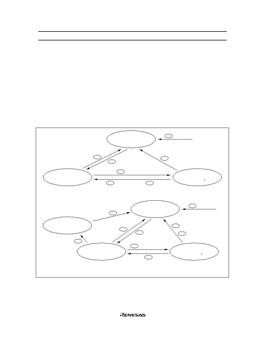
HD404449 Series
83
Operating States: The serial interface has the following operating states; transitions between them are
shown in figure 67.
STS wait state (serial interface 2 is in SM2A read wait state)
Transmit clock wait state
Transfer state
Continuous clock output state (only in internal clock mode)
The operation state of serial interface 2 is the same as serial interface 1 except that the STS instruction of
serial interface 1 changes to SM2A read. The following shows the operation state of serial interface 1.
∑
STS wait state: The serial interface enters STS wait state by MCU reset (00, 10 in figure 67). In STS
wait state, serial interface 1 is initialized and the transmit clock is ignored. If the STS instruction is then
executed (01, 11), serial interface 1 enters transmit clock wait state.
STS wait state
(Octal counter = 000,
transmit clock disabled)
Transmit clock wait state
(Octal counter = 000)
Transfer state
(Octal counter = 000)
MCU reset
00
SM1A write
04
STS instruction
01
Transmit clock
02
8 transmit clocks
03
STS instruction (IFS 1)
05
SM1A write (IFS 1)
06
External clock mode
STS wait state
(Octal counter = 000,
transmit clock disabled)
Transmit clock wait state
(Octal counter = 000)
Transfer state
(Octal counter = 000)
SM1A write
14
STS instruction
11
Transmit clock
12
15
STS instruction (IFS 1)
8 transmit clocks
13
Internal clock mode
Continuous clock output state
(PMRA 0, 1 = 00)
SM1A write
18
Transmit clock 17
16
Note: Refer to the Operating States section for the corresponding encircled numbers.
MCU reset
10
SM1A write (IFS 1)
Figure 67 Serial Interface State Transitions
∑
Transmit clock wait state: Transmit clock wait state is the period between the STS execution and the
falling edge of the first transmit clock. In transmit clock wait state, input of the transmit clock (02, 12)
increments the octal counter, shifts serial data register 1 (SR1L: $006, SR1U: $007), and enters the

HD404449 Series
84
serial interface in transfer state. However, note that if continuous clock output mode is selected in
internal clock mode, the serial interface does not enter transfer state but enters continuous clock output
state (17).
The serial interface enters STS wait state by writing data to serial mode register 1A (SM1A: $005) (04,
14) in transmit clock wait state.
∑
Transfer state: Transfer state is the period between the falling edge of the first clock and the rising edge
of the eighth clock. In transfer state, the input of eight clocks or the execution of the STS instruction
sets the octal counter to 000, and the serial interface enters another state. When the STS instruction is
executed (05, 15), transmit clock wait state is entered. When eight clocks are input, transmit clock wait
state is entered (03) in external clock mode, and STS wait state is entered (13) in internal clock mode.
In internal clock mode, the transmit clock stops after outputting eight clocks.
In transfer state, writing data to serial mode register 1A (SM1A: $005) (06, 16) initializes serial
interface 1, and STS wait state is entered.
If the state changes from transfer to another state, the serial 1 interrupt request flag (IFS1: $003, bit 2) is
set by the octal counter that is reset to 000.
∑
Continuous clock output state (only in internal clock mode): Continuous clock output state is entered
only in internal clock mode. In this state, the serial interface does not transmit/receive data but only
outputs the transmit clock from the
SCK
1
pin.
When bits 0 and 1 (PMRA0, PMRA1) of port mode register A (PMRA: $004) are 00 in transmit clock
wait state and if the transmit clock is input (17), the serial interface enters continuous clock output state.
If serial mode register 1A (SM1A: $005) is written to in continuous clock output mode (18), STS wait
state is entered.
Output Level Control in Idle States: When serial interface 1 is in STS instruction wait state and when
serial interface 2 is in SM2A read wait state and transmit clock state, the output of each serial output pin,
SO
1
and SO
2
,
can be controlled by setting bit 1 (SM1B1) of serial mode register 1B (SM1B: $028) to 0 or 1,
or bit 1 (SM2B1) of serial mode register 2B (SM2B: $01C) to 0 or 1. The output level control example of
serial interface 1 is shown in figure 68. Note that the output level cannot be controlled in transfer state.
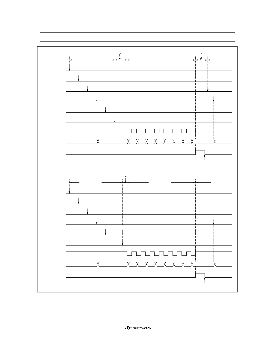
HD404449 Series
85
,
State
MCU reset
PMRA write
SM1A write
SM1B write
SR1L, SR1U
write
STS instruction
SCK
1
pin (input)
SO
1
pin
IFS1
STS wait state
Transmit clock
wait state
Transfer state
Transmit clock
wait state
STS wait state
Port selection
External clock selection
Output level control in
idle states
Dummy write for
state transition
Output level control in
idle states
Data write for transmission
Undefined
LSB
MSB
Flag reset at transfer completion
External clock mode
State
MCU reset
PMRA write
SM1A write
SM1B write
SR1L, SR1U
write
STS instruction
SCK
1
pin (input)
SO
1
pin
IFS1
STS wait state
Transfer state
Transmit clock
wait state
STS wait state
Port selection
Internal clock selection
Output level control in
idle states
Data write for transmission
Output level control in
idle states
Undefined
LSB
MSB
Flag reset at transfer completion
Internal clock mode
Figure 68 Example of Serial Interface 1 Operation Sequence

HD404449 Series
86
Transmit Clock Error Detection (In External Clock Mode): Each serial interface will malfunction if a
spurious pulse caused by external noise conflicts with a normal transmit clock during transfer. A transmit
clock error of this type can be detected as shown in figure 69.
If more than eight transmit clocks are input in transfer state, at the eighth clock including a spurious pulse
by noise, the octal counter reaches 000, the serial 1 interrupt request flag (IFS1: $003, bit 2) is set, and
transmit clock wait state is entered. At the falling edge of the next normal clock signal, the transfer state is
entered. After the transfer is completed and IFS1 is reset, writing to serial mode register 1A (SM1A: $005)
changes the state from transfer to STS wait. At this time serial interface 1 is in the transfer state, and the
serial 1 interrupt request flag (IFS1: $003, bit 2) is set again, and therefore the error can be detected. The
same applies to serial interface 2.
Notes on Use:
∑
Initialization after writing to registers: If port mode register A (PMRA: $004) is written to in transmit
clock wait state or in transfer state, the serial interface must be initialized by writing to serial mode
register 1A (SM1A: $005) and serial mode register 2A (SM2A: $01B) again.
∑
Serial 1 interrupt request flag (IFS1: $003, bit 2) and serial 2 interrupt request flag (IFS2: $023, bit 2)
set: For serial interface 1, if the state is changed from transfer state to another by writing to serial mode
register 1A (SM1A: $005) or executing the STS instruction during the first low pulse of the transmit
clock, the serial 1 interrupt request flag (IFS1: $003, bit 2) is not set. In the same way for serial
interface 2, if the state is changed from transfer state to another by writing to serial mode register 2A
(SM2A: $01B) or by executing the STS instruction during the first low pulse of the transmit clock, the
serial 2 interrupt request flag (IFS2: $023, bit 2) is not set. To set the serial 1 interrupt request flag
(IFS1: $003, bit 2), a serial mode register 1A (SM1A: $005) write or STS instruction execution must be
programmed to be executed after confirming that the
SCK
1
pin is at 1, that is, after executing the input
instruction to port R4. To set the serial 2 interrupt request flag (IFS2: $023, bit 2), a serial mode
register 2A (SM2A: $01B) write or SM2A instruction execution must be programmed to be executed
after confirming that the
SCK
2
pin is at 1, that is, after executing the input instruction to port R5.
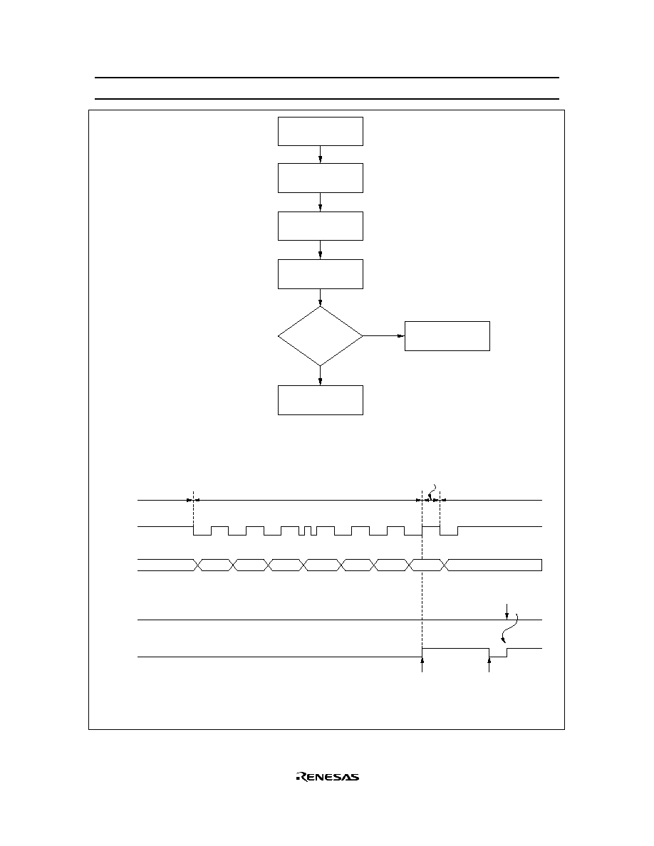
HD404449 Series
87
Transfer completion
(IFS1 1)
Interrupts inhibited
IFS1 0
SM1A write
IFS1 = 1
Transmit clock
error processing
Normal
termination
Yes
No
Transmit clock error detection flowchart
Transmit clock error detection procedures
State
Transmit clock
wait state
Transfer state
Transfer state
Transmit clock wait state
Noise
Transfer state has been
entered by the transmit clock
error. When SM1A is written,
IFS1 is set.
Flag set because octal
counter reaches 000.
Flag reset at
transfer completion.
SM1A
write
1
2
3
4
5
6
7
8
SCK
pin
(input)
IFS1
1
Figure 69 Transmit Clock Error Detection

HD404449 Series
88
Registers for Serial Interface
The serial interface operation is selected, and serial data is read and written by the following registers.
For serial interface 1
∑
Serial mode register 1A (SM1A: $005)
∑
Serial mode register 1B (SM1B: $028)
∑
Serial data register 1
(SR1L: $006, SR1U: $007)
∑
Port mode register A (PMRA: $004)
∑
Miscellaneous register (MIS: $00C)
For serial interface 2
∑
Serial mode register 2A (SM2A: $01B)
∑
Serial mode register 2B (SM2B: $01C)
∑
Serial data register 2
(SR2L: $01D, SR2U: $01E)
∑
Port mode register A (PMRA: $004)
Serial Mode Register 1A (SM1A: $005): This register has the following functions (figure 70).
∑
R4
1
/
SCK
1
pin function selection
∑
Serial interface 1 transmit clock selection
∑
Serial interface 1 prescaler division ratio selection
∑
Serial interface 1 initialization
Serial mode register 1A (SM1A: $005) is a 4-bit write-only register. It is reset to $0 by MCU reset.
A write signal input to serial mode register 1A (SM1A: $005) discontinues the input of the transmit clock
to serial data register 1 (SR1L: $006, SR1U: $007) and the octal counter, and the octal counter is reset to
000. Therefore, if a write is performed during data transfer, the serial 1 interrupt request flag (IFS1: $003,
bit 2) is set.
Written data is valid from the second instruction execution cycle after the write operation, so the STS
instruction must be executed at least two cycles after that.
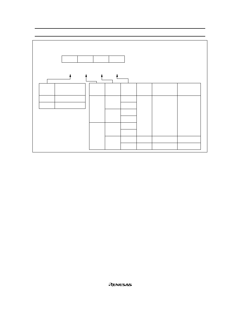
HD404449 Series
89
Bit
Initial value
Read/Write
Bit name
3
0
W
SM1A3
2
0
W
SM1A2
0
0
W
SM1A0
1
0
W
SM1A1
Serial mode register 1A (SM1A: $005)
0
1
0
1
0
1
0
1
0
1
0
1
0
1
SM1A2
SM1A0
SM1A1
SM1A3
0
1
R4
1
/
SCK
1
mode selection
R4
1
SCK
1
SCK
1
Output
Output
Input
Clock source
Prescaler
System clock
External clock
--
--
Prescaler
division ratio
Refer to
table 29
Figure 70 Serial Mode Register 1A (SM1A)
Serial Mode Register 1B (SM1B: $028): This register has the following functions (figure 71).
∑
Serial interface 1 prescaler division ratio selection
∑
Serial interface 1 output level control in idle states
Serial mode register 1B (SM1B: $028) is a 2-bit write-only register. It cannot be written during data
transfer.
By setting bit 0 (SM1B0) of this register, the serial interface 1 prescaler division ratio is selected. Only bit
0 (SM1B0) can be reset to 0 by MCU reset. By setting bit 1 (SM1B1), the output level of the SO
1
pin is
controlled in idle states of serial interface 1. The output level changes at the same time that SM1B1 is
written to.

HD404449 Series
90
Bit
Initial value
Read/Write
Bit name
3
--
--
Not used
2
--
--
Not used
0
0
W
SM1B0
1
Undefined
W
SM1B1
SM1B0
0
1
Transmit clock division ratio
Prescaler output divided by 2
Prescaler output divided by 4
Serial mode register 1B (SM1B: $028)
SM1B1
0
1
Output level control in idle states
Low level
High level
Figure 71 Serial Mode Register 1B (SM1B)
Serial Data Register 1 (SR1L: $006, SR1U: $007): This register has the following functions (figures 72
and 73)
∑
Serial interface 1 transmission data write and shift
∑
Serial interface 1 receive data shift and read
Writing data in this register is output from the SO
1
pin, LSB first, synchronously with the falling edge of
the transmit clock; data is input, LSB first, through the SI
1
pin at the rising edge of the transmit clock.
Input/output timing is shown in figure 74.
Data cannot be read or written during serial data transfer. If a read/write occurs during transfer, the
accuracy of the resultant data cannot be guaranteed.
Bit
Initial value
Read/Write
Bit name
3
Undefined
R/W
SR13
2
Undefined
R/W
SR12
0
Undefined
R/W
SR10
1
Undefined
R/W
SR11
Serial data register 1 (lower digit) (SR1L: $006)
Figure 72 Serial Data Register 1 (SR1L)
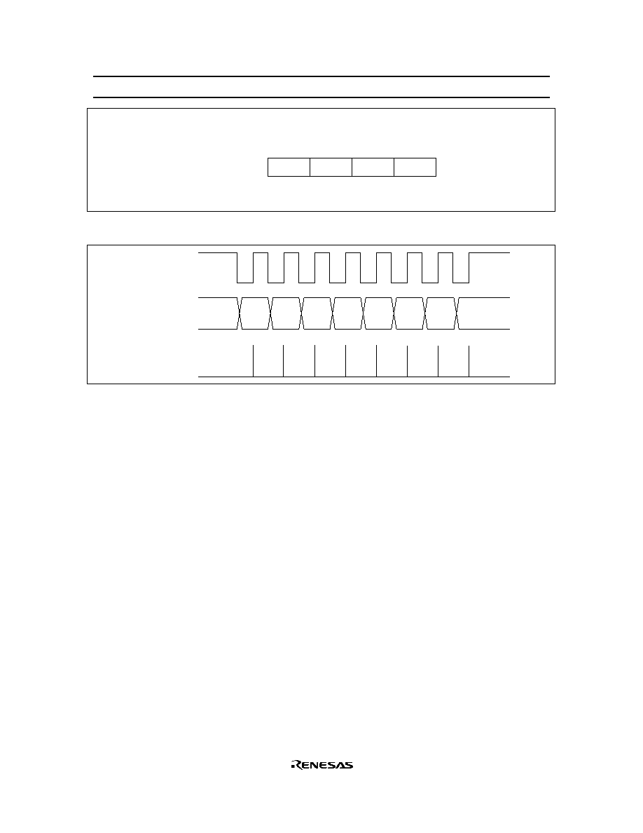
HD404449 Series
91
Bit
Initial value
Read/Write
Bit name
3
Undefined
R/W
SR17
2
Undefined
R/W
SR16
0
Undefined
R/W
SR14
1
Undefined
R/W
SR15
Serial data register 1 (upper digit) (SR1U: $007)
Figure 73 Serial Data Register 1 (SR1U)
LSB
MSB
1
2
3
4
5
6
7
8
Transmit clock
Serial output
data
Serial input data
latch timing
Figure 74 Serial Interface Output Timing
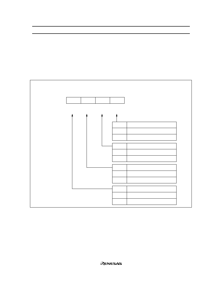
HD404449 Series
92
Port Mode Register A (PMRA: $004): This register has the following functions (figure 75).
∑
R4
2
/SI
1
pin function selection
∑
R4
3
/SO
1
pin function selection
∑
R5
2
/SI
2
pin function selection
∑
R5
3
/SO
2
pin function selection
Port mode register A (PMRA: $004) is a 4-bit write-only register, and is reset to $0 by MCU reset.
Bit
Initial value
Read/Write
Bit name
3
0
W
PMRA3
2
0
W
PMRA2
0
0
W
PMRA0
1
0
W
PMRA1
Port mode register A (PMRA: $004)
PMRA2
0
1
R5
3
/SO
2
mode selection
R5
3
SO
2
PMRA3
0
1
R5
2
/SI
2
mode selection
R5
2
SI
2
PMRA0
0
1
R4
3
/SO
1
mode selection
R4
3
SO
1
PMRA1
0
1
R4
2
/SI
1
mode selection
R4
2
SI
1
Figure 75 Port Mode Register A (PMRA)

HD404449 Series
93
Miscellaneous Register (MIS: $00C): This register has the following functions (figure 76).
∑
R4
3
/SO
1
pin PMOS control
Miscellaneous register (MIS: $00C) is a 4-bit write-only register and is reset to $0 by MCU reset.
Bit
Initial value
Read/Write
Bit name
3
0
W
MIS3
2
0
W
MIS2
0
0
W
MIS0
1
0
W
MIS1
Miscellaneous register (MIS: $00C)
MIS1
0
1
MIS0
0
1
0
1
t
RC
0.12207 ms
0.24414 ms
*
7.8125 ms
62.5 ms
Not used
MIS2
0
1
R4
3
/SO
1
PMOS on/off selection
On
Off
MIS3
0
1
Pull-up MOS on/off selection
Off
On
Note:
*
This value is valid only for direct transfer operation.
Figure 76 Miscellaneous Register (MIS)
Serial Mode Register 2A (SM2A: $01B): This register has the following functions (figure 77).
∑
R5
1
/
SCK
2
pin function selection
∑
Serial interface 2 transmit clock selection
∑
Serial interface 2 prescaler division ratio selection
∑
Serial interface 2 initialization
Serial mode register 2A (SM2A: $01B) is a 4-bit write-only register. It is reset to $0 by MCU reset.
A write signal input to serial mode register 2A (SM2A: $01B) discontinues the input of the transmit clock
to serial data register 2 (SR2L: $01D, SR1U: $01E) and the octal counter, and the octal counter is reset to

HD404449 Series
94
000. Therefore, if a write is performed during data transfer, the serial 2 interrupt request flag (IFS2: $023,
bit 2) is set.
Written data is valid from the second instruction execution cycle after the write operation, so the SM2A
read instruction must be executed at least two cycles after that.
Bit
Initial value
Read/Write
Bit name
3
0
W
SM2A3
2
0
W
SM2A2
0
0
W
SM2A0
1
0
W
SM2A1
Serial mode register 2A (SM2A: $01B)
0
1
0
1
0
1
0
1
0
1
0
1
0
1
SM2A2
SM2A0
SM2A1
SM2A3
0
1
R5
1
/
SCK
2
mode selection
R5
1
SCK
2
SCK
2
Output
Output
Input
Clock source
Prescaler
System clock
External clock
--
--
Prescaler
division ratio
Refer to
table 29
Figure 77 Serial Mode Register 2A (SM2A)
Serial Mode Register 2B (SM2B: $01C): This register has the following functions (figure 78).
∑
Serial interface 2 prescaler division ratio selection
∑
Serial interface 2 output level control in idle states
∑
R5
3
/SO
2
pin PMOS control
Serial mode register 2B (SM2B: $01C) is a 3-bit write-only register. It cannot be written during serial
interface 2 data transfer. Bit 0 (SM2B0) and bit 2 (SM2B2) is reset to $0 by MCU reset.
By setting bit 0 (SM2B0) of this register, the serial interface 2 prescaler division ratio of serial interface 2 is
selected. By resetting bit 1 (SM2B1), the output level of the SO
2
pin is controlled in idle states of serial
interface 2. The output level changes at the same time that SM2B1 is written to.
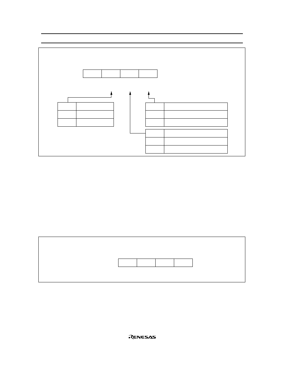
HD404449 Series
95
Bit
Initial value
Read/Write
Bit name
3
--
--
Not used
2
0
W
SM2B2
0
0
W
SM2B0
1
Undefined
W
SM2B1
SM2B0
0
1
Transmit clock division ratio
Prescaler output divided by 2
Prescaler output divided by 4
Serial mode register 2B (SM2B: $01C)
SM2B2
0
1
R5
3
/SO
2
PMOS
On
Off
SM2B1
0
1
Output level control in idle states
Low level
High level
Figure 78 Serial Mode Register 2B (SM2B)
Serial Data Register 2 (SR2L: $01D, SR2U: $01E): This register has the following functions (figures 79
and 80).
∑
Serial interface 2 transmission data write and shift
∑
Serial interface 2 receive data shift and read
Writing data in this register is output from the SO
2
pin, LSB first, synchronously with the falling edge of
the transmit clock; data is input, LSB first, through the SI
2
pin at the rising edge of the transmit clock.
Data cannot be read or written during serial data transfer. If a read/write occurs during transfer, the
accuracy of the resultant data cannot be guaranteed.
Bit
Initial value
Read/Write
Bit name
3
Undefined
R/W
SR23
2
Undefined
R/W
SR22
0
Undefined
R/W
SR20
1
Undefined
R/W
SR21
Serial data register 2 (lower digit) (SR2L: $01D)
Figure 79 Serial Data Register 2 (SR2L)
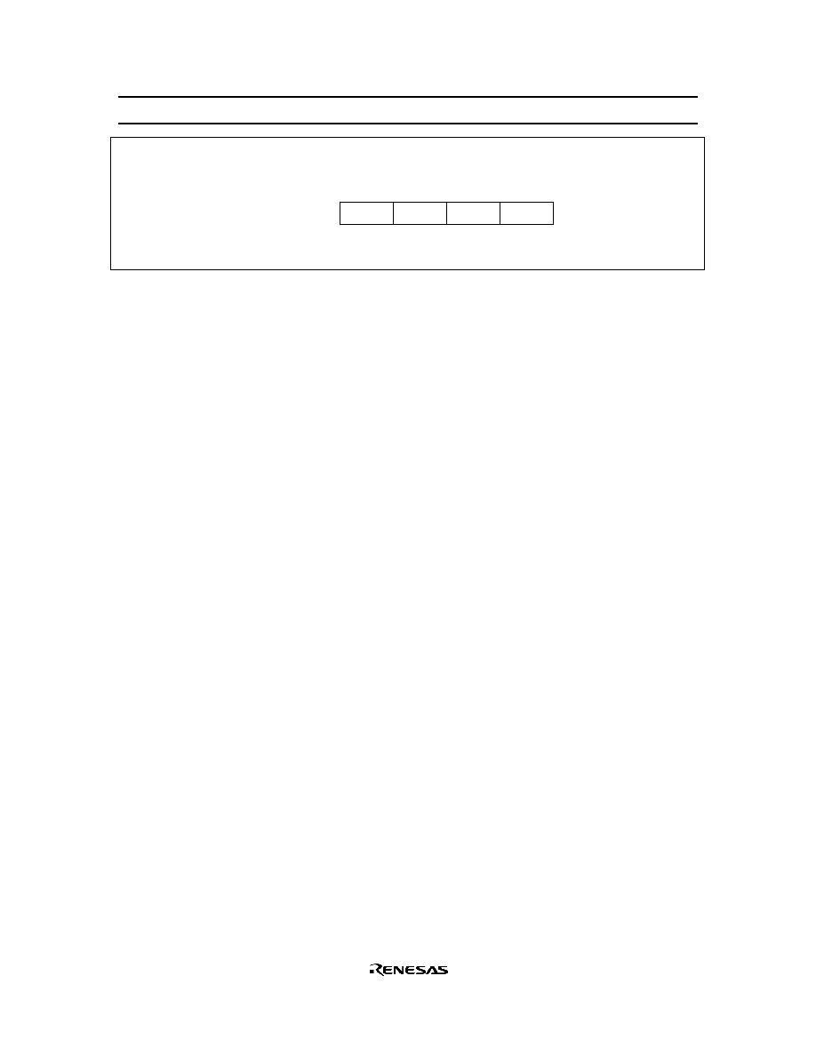
HD404449 Series
96
Bit
Initial value
Read/Write
Bit name
3
Undefined
R/W
SR27
2
Undefined
R/W
SR26
0
Undefined
R/W
SR24
1
Undefined
R/W
SR25
Serial data register 2 (upper digit) (SR2U: $01E)
Figure 80 Serial Data Register 2 (SR2U)
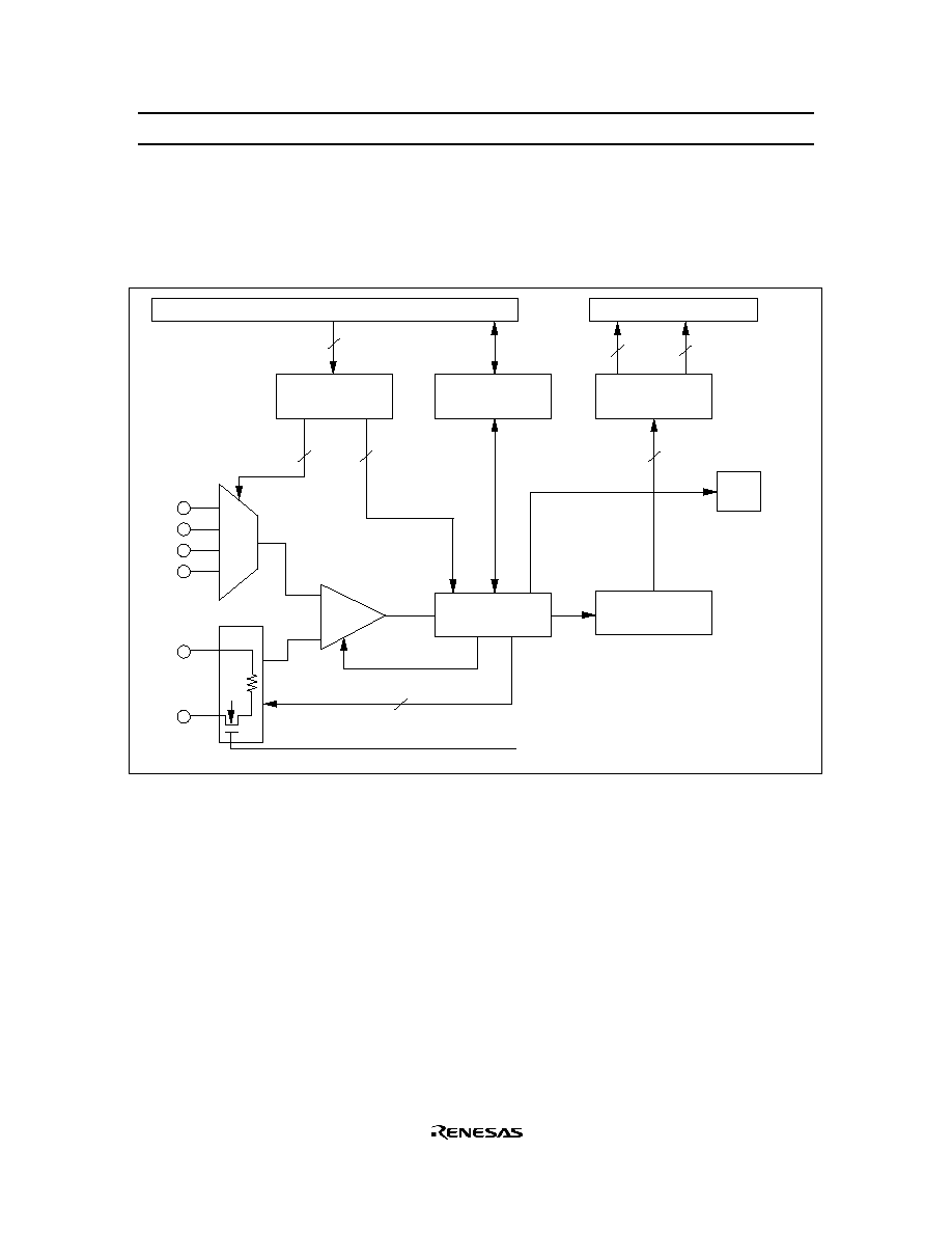
HD404449 Series
97
A/D Converter
The MCU has a built-in A/D converter that uses a sequential comparison method with a resistor ladder. It
can measure four analog inputs with 8-bit resolution. As shown in the block diagram of figure 81, the A/D
converter has a 4-bit A/D mode register, a 1-bit A/D start flag, and a 4-bit plus 4-bit A/D data register.
Internal bus line (S2)
A/D mode register
(AMR)
A/D start flag
(ADSF)
A/D data register
(ADRU, ADRL)
IFAD
Internal bus line (S1)
Encoder
Control logic
COMP
Selector
D/A
Operating mode signal (set to 0 in stop mode,
watch mode, and subactive mode)
4
4
4
8
2
2
AN
0
AN
1
AN
2
AN
3
AV
CC
AV
SS
+
≠
8
A/D interrupt
request flag
Figure 81 A/D Converter Block Diagram
A/D Mode Register (AMR: $016): Four-bit write-only register which selects the A/D conversion period
and indicates analog input pin information. Bit 0 of the A/D mode register selects the A/D conversion
period, and bits 2 and 3 select a channel, as shown in figure 82.
A/D Start Flag (ADSF: $020, Bit 2): One-bit flag that initiates A/D conversion when set to 1. At the
completion of A/D conversion, the converted data is stored in the A/D data register and the A/D start flag is
cleared. Refer to figure 86.
A/D Data Register (ADRL: $017, ADRU: $018): Eight-bit read-only register consisting of a 4-bit lower
digit and 4-bit upper digit. This register is not cleared by reset. After the completion of A/D conversion,
the resultant eight-bit data is held in this register until the start of the next conversion (figures 83, 84, and
85).

HD404449 Series
98
Note on Use: Use the SEM and SEMD instructions to write data to the A/D start flag (ADSF: $020, bit 2),
but make sure that the A/D start flag is not written to during A/D conversion. Data read from the A/D data
register (ADRL: $017, ADRU: $018) during A/D conversion cannot be guaranteed.
The A/D converter does not operate in the stop, watch, and subactive modes because of the OSC clock.
During these low-power dissipation modes, current through the resistor ladder is cut off to decrease the
power input.
Bit
Initial value
Read/Write
Bit name
3
0
W
AMR3
2
0
W
AMR2
0
0
W
AMR0
1
--
--
Not used
A/D mode register (AMR: $016)
AMR0
0
1
Conversion time
34t
cyc
67t
cyc
AMR3
0
0
1
1
AMR2
0
1
0
1
Analog input selection
AN
0
AN
1
AN
2
AN
3
Figure 82 A/D Mode Register (AMR)
3
2
1
0
MSB
LSB
3
2
1
0
Bit 0
Bit 7
ADRU: $018
ADRL: $017
Figure 83 A/D Data Registers
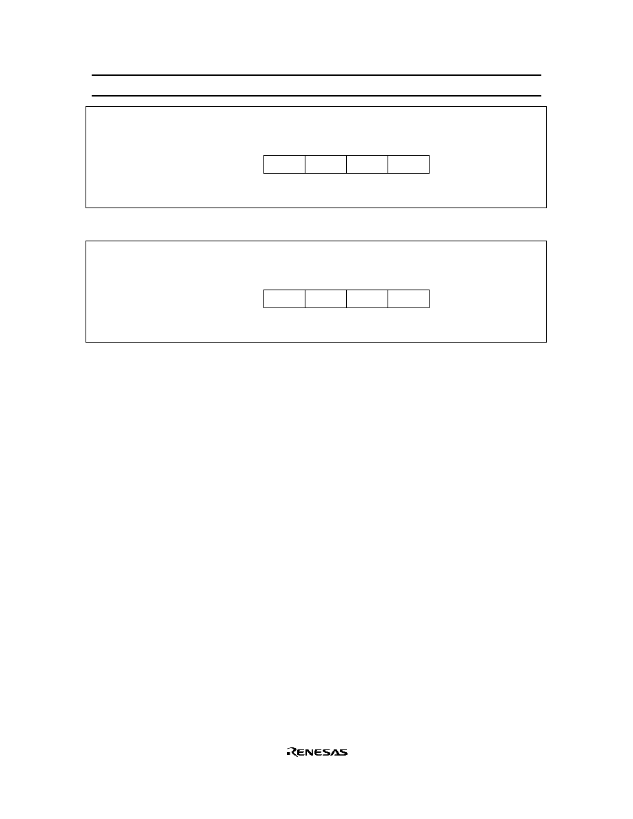
HD404449 Series
99
Bit
Initial value
Read/Write
Bit name
3
0
R
ADRL3
2
0
R
ADRL2
0
0
R
ADRL0
1
0
R
ADRL1
A/D data register (lower digit) (ADRL: $017)
Figure 84 A/D Data Register Lower Digit (ADRL)
Bit
Initial value
Read/Write
Bit name
A/D data register (upper digit) (ADRU: $018)
2
0
R
ADRU2
1
0
R
ADRU1
0
0
R
ADRU0
3
1
R
ADRU3
Figure 85 A/D Data Register Upper Digit (ADRU)
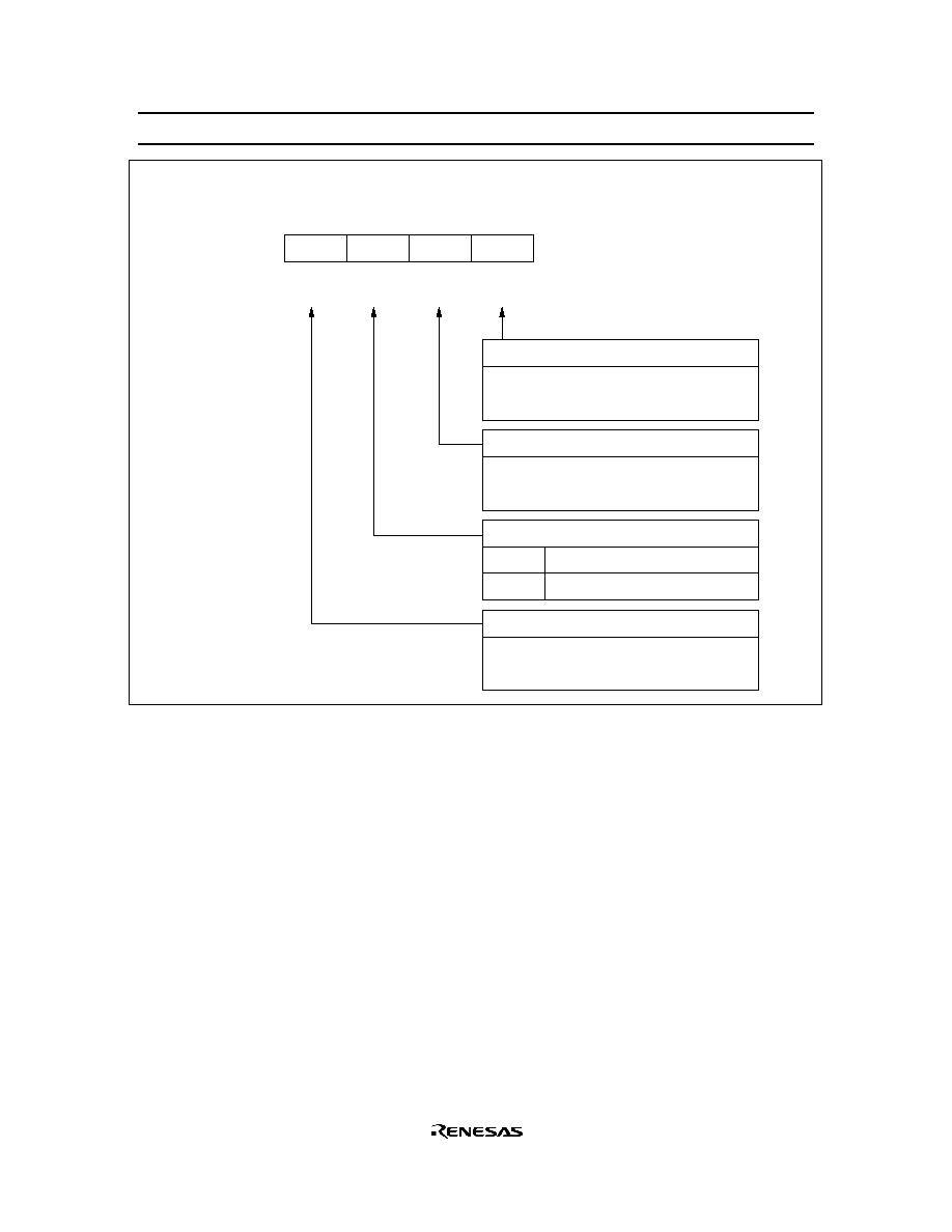
HD404449 Series
100
Bit
Initial value
Read/Write
Bit name
3
0
R/W
DTON
2
0
R/W
ADSF
0
0
R/W
LSON
1
0
R/W
WDON
A/D start flag (ADSF: $020, bit 2)
1
0
ADSF (A/D start flag)
A/D conversion started
A/D conversion completed
Refer to the description of operating
modes
DTON
Refer to the description of timers
WDON
Refer to the description of operating
modes
LSON
Figure 86 A/D Start Flag (ADSF)
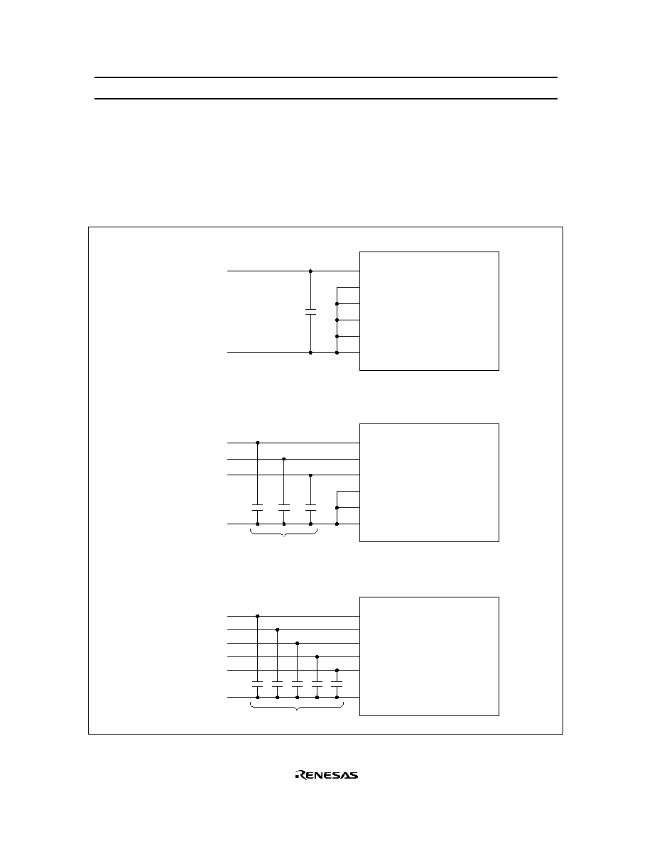
HD404449 Series
101
Notes on Mounting
Assemble all parts including the HD404449 Series on a board, noting the points described below.
1. Connect layered ceramic type capacitors (about 0.1
µ
F) between AV
CC
and AV
SS
, between V
CC
and
GND, and between used analog pins and AV
SS
.
2. Connect unused analog pins to AV
SS
.
AV
AN
AN
AN
AN
AV
CC
SS
0
1
2
3
AV
AN
AN
AN
AN
AV
CC
SS
0
1
2
3
AV
AN
AN
AN
AN
AV
CC
SS
0
1
2
3
∑ When not using an A/D converter
V
GND
CC
V
GND
CC
V
GND
CC
∑ When using pins AN
0
and AN
1
but not using AN
2
and AN
3
∑ When using all analog pins
0.1
µ
F 3
◊
0.1
µ
F 5
◊
0.1
µ
F
Figure 87 Example of Connections (1)
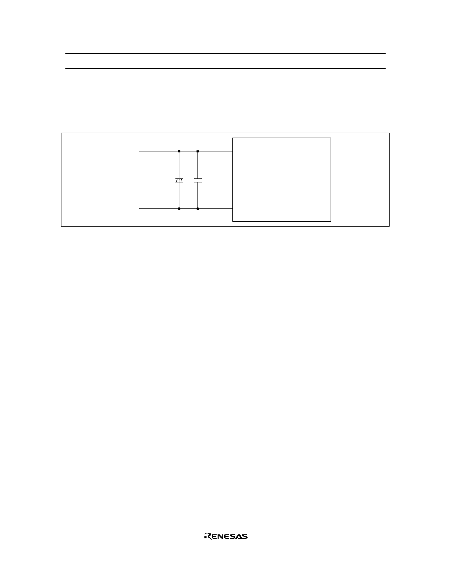
HD404449 Series
102
Between the V
CC
and GND lines, connect capacitors designed for use in ordinary power supply circuits.
An example connection is described in figure 88.
No resistors can be inserted in series in the power supply circuit, so the capacitors should be connected in
parallel. The capacitors are a large capacitance C
1
and a small capacitance C
2
.
V
GND
CC
V
GND
CC
C
1
C
2
Figure 88 Example of Connections (2)

HD404449 Series
103
Programmable ROM (HD4074449)
The HD4074449 is a ZTAT
TM
microcomputer with built-in PROM that can be programmed in PROM
mode.
PROM Mode Pin Description
MCU Mode
PROM Mode
MCU Mode
PROM Mode
Pin No. Pin Name
I/O
Pin Name
I/O
Pin No.
Pin Name
I/O
Pin Name
I/O
1
AN
2
I
31
R1
2
I/O
A
7
I
2
AN
3
I
32
R1
3
I/O
A
8
I
3
AV
SS
GND
33
R2
0
I/O
A
0
I
4
TEST
I
TEST
I
34
R2
1
I/O
A
10
I
5
OSC
1
I
V
CC
35
R2
2
I/O
A
11
I
6
OSC
2
O
36
R2
3
I/O
A
12
I
7
RESET
I
RESET
I
37
R3
0
/TOB
I/O
8
X1
I
GND
38
R3
1
/TOC
I/O
9
X2
O
39
R3
2
/TOD
I/O
10
GND
GND
40
R3
3
/
EVNB
I/O
11
D
0
I/O
CE
I
41
R4
0
/EVND
I/O
12
D
1
I/O
OE
I
42
R4
1
/
SCK
1
I/O
13
D
2
I/O
V
CC
43
R4
2
/SI
1
I/O
14
D
3
I/O
V
CC
44
R4
3
/SO
1
I/O
15
D
4
I/O
45
R5
0
I/O
16
D
5
I/O
46
R5
1
/
SCK
2
I/O
17
D
6
I/O
47
R5
2
/SI
2
I/O
18
D
7
I/O
48
R5
3
/SO
2
I/O
19
D
8
I/O
49
R6
0
I/O
A
1
I
20
D
9
I/O
50
R6
1
I/O
A
2
I
21
D
10
I/O
A
13
I
51
R6
2
I/O
A
3
I
22
D
11
I/O
A
14
I
52
R6
3
I/O
A
4
I
23
D
12
/
STOPC
I
A
9
I
53
R7
0
I/O
O
0
I/O
24
D
13
/
INT
0
I
V
PP
54
R7
1
I/O
O
1
I/O
25
R0
0
/
INT
1
I/O
M
0
I
55
R7
2
I/O
O
2
I/O
26
R0
1
/INT
2
I/O
M
1
I
56
R7
3
I/O
O
3
I/O
27
R0
2
/INT
3
I/O
57
R8
0
I/O
O
4
I/O
28
R0
3
I/O
58
R8
1
I/O
O
5
I/O
29
R1
0
I/O
A
5
I
59
R8
2
I/O
O
6
I/O
30
R1
1
I/O
A
6
I
60
R8
3
I/O
O
7
I/O

HD404449 Series
104
MCU Mode
PROM Mode
MCU Mode
PROM Mode
Pin No. Pin Name
I/O
Pin Name
I/O
Pin No.
Pin Name
I/O
Pin Name
I/O
61
R9
0
I/O
O
4
I/O
71
RB
2
I/O
62
R9
1
I/O
O
3
I/O
72
RB
3
I/O
63
R9
2
I/O
O
2
I/O
73
RC
0
I/O
64
R9
3
I/O
O
1
I/O
74
RC
1
I/O
65
RA
0
I/O
O
0
I/O
75
RC
2
I/O
66
RA
1
I/O
V
CC
76
RC
3
I/O
67
RA
2
I/O
77
V
CC
V
CC
68
RA
3
I/O
78
AV
CC
V
CC
69
RB
0
I/O
79
AN
0
I
70
RB
1
I/O
80
AN
1
I
Notes: 1. I/O: Input/output pin, I: Input pin, O: Output pin
2. Each of O
0
≠O
4
has two pins; before using, each pair must be connected together.

HD404449 Series
105
Programming the Built-In PROM
The MCU's built-in PROM is programmed in PROM mode. PROM mode is set by pulling
TEST, M
0
, and
M
1
low, and RESET high as shown in figure 89. In PROM mode, the MCU does not operate, but it can be
programmed in the same way as any other commercial 27256-type EPROM using a standard PROM
programmer and an 80-to-28-pin socket adapter. Recommended PROM programmers and socket adapters
of the HD4074449 are listed in table 31.
Since an HMCS400-series instruction is ten bits long, the HMCS400-series MCU has a built-in conversion
circuit to enable the use of a general-purpose PROM programmer. This circuit splits each instruction into
five lower bits and five upper bits that are read from or written to consecutive addresses. This means that
if, for example, 16 kwords of built-in PROM are to be programmed by a general-purpose PROM
programmer, a 32-kbyte address space ($0000≠$7FFF) must be specified.
Warnings
1. Always specify addresses $0000 to $7FFF when programming with a PROM programmer. If address
$8000 or higher is accessed, the PROM may not be programmed or verified correctly. Set all data in
unused addresses to $FF.
Note that the plastic-package version cannot be erased or reprogrammed.
2. Make sure that the PROM programmer, socket adapter, and LSI are aligned correctly (their pin 1
positions match), otherwise overcurrents may damage the LSI. Before starting programming, make
sure that the LSI is firmly fixed in the socket adapter and the socket adapter is firmly fixed onto the
programmer.
3. PROM programmers have two voltages (V
PP
): 12.5 V and 21 V. Remember that ZTAT
TM
devices
require a V
PP
of 12.5 V--the 21-V setting will damage them. 12.5 V is the Intel 27256 setting.
Programming and Verification
The built-in PROM of the MCU can be programmed at high speed without risk of voltage stress or damage
to data reliability.
Programming and verification modes are selected as listed in table 30.
For details of PROM programming, refer to the following section, Notes on PROM Programming.
Table 30
PROM Mode Selection
Pin
Mode
CE
OE
V
PP
O
0
≠O
7
Programming
Low
High
V
PP
Data input
Verification
High
Low
V
PP
Data output
Programming inhibited
High
High
V
PP
High impedance

HD404449 Series
106
Table 31
Recommended PROM Programmers and Socket Adapters
PROM Programmer
Socket Adapter
Manufacturer
Model Name
Manufacturer
Package
Model Name
DATA I/O Corp.
121B
29B
Hitachi
FP-80A
HS444ESH01H
TFP-80F
HS4449ESN01H
AVAL Corp.
PKW-1000
Hitachi
FP-80A
HS444ESH01H
TFP-80F
HS4449ESN01H
Address
A
0
to A
14
Data
O
0
to O
7
OE
CE
V
CC
V
CC
V
PP
AV
CC
GND
V
CC
V
CC
O
0
to O
7
A
0
to A
14
OE
CE
V
PP
RESET
TEST
M
0
M
1
AV
SS
V
CC
OSC
1
D
2
D
3
RA
1
X1
HD4074449
Figure 89 PROM Mode Connections
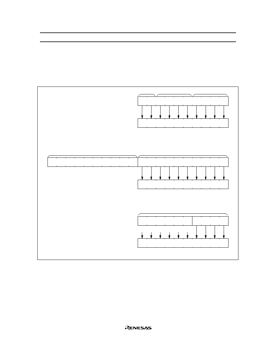
HD404449 Series
107
Addressing Modes
RAM Addressing Modes
The MCU has three RAM addressing modes, as shown in figure 90 and described below.
AP
9
AP
0
W
1
Y
0
W register
X register
Y register
RAM address
Register Direct Addressing
AP
9
AP
0
RAM address
Direct Addressing
d
9
d
0
2nd word of Instruction
Opcode
1st word of Instruction
AP
9
AP
0
RAM address
Memory Register Addressing
m
3
Opcode
Instruction
0
0
0
1
0
0
AP
8
AP
7
AP
AP
5
AP
4
6
AP
3
AP
2
AP
1
AP
AP
AP
AP
AP
AP
AP
AP
8
7
6
5
4
3
2
1
d
8
d
7
d
6
d
5
d
4
d
3
d
2
d
1
AP
8
AP
7
AP
6
AP
5
AP
4
AP
3
AP
2
AP
1
W
0
X
3
X
2
X
1
X
0
Y
3
Y
2
Y
1
m
2
m
1
m
0
Figure 90 RAM Addressing Modes
Register Indirect Addressing Mode: The contents of the W, X, and Y registers (10 bits in total) are used
as a RAM address. When the area from $090 to $25F is used, a bank must be selected by the bank register
(V: $03F).
Direct Addressing Mode: A direct addressing instruction consists of two words. The first word contains
the opcode, and the contents of the second word (10 bits) are used as a RAM address.

HD404449 Series
108
Memory Register Addressing Mode: The memory registers (MR), which are located in 16 addresses
from $040 to $04F, are accessed with the LAMR and XMRA instructions.
ROM Addressing Modes and the P Instruction
The MCU has four ROM addressing modes, as shown in figure 91 and described below.
Direct Addressing Mode: A program can branch to any address in the ROM memory space by executing
the JMPL, BRL, or CALL instruction. Each of these instructions replaces the 14 program counter bits
(PC
13
≠PC
0
) with 14-bit immediate data.
Current Page Addressing Mode: The MCU has 64 pages of ROM with 256 words per page. A program
can branch to any address in the current page by executing the BR instruction. This instruction replaces the
eight low-order bits of the program counter (PC
7
≠PC
0
) with eight-bit immediate data. If the BR instruction
is on a page boundary (address 256n + 255), executing that instruction transfers the PC contents to the next
physical page, as shown in figure 93. This means that the execution of the BR instruction on a page
boundary will make the program branch to the next page.
Note that the HMCS400-series cross macroassembler has an automatic paging feature for ROM pages.
Zero-Page Addressing Mode: A program can branch to the zero-page subroutine area located at $0000≠
$003F by executing the CAL instruction. When the CAL instruction is executed, 6 bits of immediate data
are placed in the six low-order bits of the program counter (PC
5
≠PC
0
), and 0s are placed in the eight high-
order bits (PC
13
≠PC
6
).
Table Data Addressing Mode: A program can branch to an address determined by the contents of four-
bit immediate data, the accumulator, and the B register by executing the TBR instruction.
P Instruction: ROM data addressed in table data addressing mode can be referenced with the P instruction
as shown in figure 92. If bit 8 of the ROM data is 1, eight bits of ROM data are written to the accumulator
and the B register. If bit 9 is 1, eight bits of ROM data are written to the R1 and R2 port output registers.
If both bits 8 and 9 are 1, ROM data is written to the accumulator and the B register, and also to the R1 and
R2 port output registers at the same time.
The P instruction has no effect on the program counter.
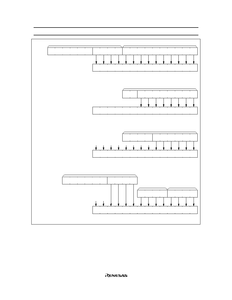
HD404449 Series
109
d
9
d
8
d
7
d
6
d
5
d
4
d
3
d
2
d
1
d
0
2nd word of instruction
Opcode
1st word of instruction
[JMPL]
[BRL]
[CALL]
PC
9
PC
8
PC
7
PC
6
PC
5
PC
4
PC
3
PC
2
PC
1
PC
0
PC
PC
PC
PC
10
11
12
13
Program counter
Direct Addressing
Zero Page Addressing
d
5
d
4
d
3
d
2
d
1
d
0
Instruction
[CAL]
Opcode
PC
9
8
PC
7
6
PC
5
4
PC
3
PC
1
PC
0
PC
PC
10
11
12
13
Program counter
0
0
0
0
0
0
0
0
PC
PC
PC
PC
PC
PC
2
B
1
B
0
A
3
A
2
A
1
A
0
Accumulator
Program counter
Table Data Addressing
PC
9
PC
8
PC
7
PC
6
PC
5
PC
4
PC
3
PC
2
PC
1
PC
0
PC
PC
PC
10
11
12
13
B
2
B
3
B register
p
3
p
0
[TBR]
Instruction
Opcode
0
0
p
2
p
1
PC
Opcode
b
7
b
6
b
5
b
4
b
3
b
2
b
1
b
0
Instruction
PC
9
0
PC
PC
PC
11
12
13
Program counter
Current Page Addressing
[BR]
PC
10
7
PC
6
PC
5
PC
4
PC
3
PC
2
PC
1
PC
PC
8
PC
p
0
p
1
p
2
p
3
Figure 91 ROM Addressing Modes
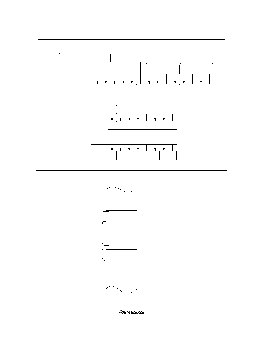
HD404449 Series
110
B
1
B
0
A
3
A
2
A
1
A
0
Accumulator
Referenced ROM address
Address Designation
RA
9
RA
8
RA
7
RA
6
RA
5
RA
4
RA
3
RA
2
RA
1
RA
0
RA
RA
RA
10
11
12
13
B
2
B
3
B register
0
0
p
3
p
0
[P]
Instruction
Opcode
p
2
p
1
RA
RO
9
RO
0
RO
8
RO
7
RO
6
RO
5
RO
4
RO
3
RO
2
RO
1
B
B
B
B
A
A
A
A
3
2
1
0
3
2
1
0
If RO = 1
8
Accumulator, B register
ROM data
Pattern Output
RO
9
ROM data
R2
R2
R2
R2
R1
R1 R1
R1
3
2
1
0
3
2
1
0
If RO = 1
9
Output registers R1, R2
RO
0
RO
8
RO
7
RO
6
RO
5
RO
4
RO
3
RO
2
RO
1
Figure 92 P Instruction
BR AAA
AAA NOP
256 (n ≠ 1) + 255
256n
BR AAA
BR BBB
256n + 254
256n + 255
256 (n + 1)
BBB NOP
Figure 93 Branching when the Branch Destination is on a Page Boundary

HD404449 Series
111
Absolute Maximum Ratings
Item
Symbol
Value
Unit
Notes
Supply voltage
V
CC
≠0.3 to +7.0
V
Programming voltage
V
PP
≠0.3 to +14.0
V
1
Pin voltage
V
T
≠0.3 to (V
CC
+ 0.3) V
Total permissible input current
I
o
100
mA
2
Total permissible output current
≠
I
o
50
mA
3
Maximum input current
I
o
4
mA
4, 5
30
mA
4, 6
Maximum output current
≠I
o
4
mA
7, 8
Operating temperature
T
opr
≠20 to +75
∞
C
Storage temperature
T
stg
≠55 to +125
∞
C
Notes: Permanent damage may occur if these absolute maximum ratings are exceeded. Normal opera-tion
must be under the conditions stated in the electrical characteristics tables. If these conditions are
exceeded, the LSI may malfunction or its reliability may be affected.
1. Applies to D
13
(V
PP
) of the HD4074449.
2. The total permissible input current is the total of input currents simultaneously flowing in from all
the I/O pins to ground.
3. The total permissible output current is the total of output currents simultaneously flowing out from
V
CC
to all I/O pins.
4. The maximum input current is the maximum current flowing from each I/O pin to ground.
5. Applies to D
10
, D
11
, and
R0≠RC.
6. Applies to D
0
≠D
9
.
7. The maximum output current is the maximum current flowing out from V
CC
to each I/O pin.
8. Applies to D
0
≠D
11
and R0≠RC.

HD404449 Series
112
Electrical Characteristics
DC Characteristics (HD404448, HD404449: V
CC
= 2.7 to 6.0 V, GND = 0 V, T
a
= ≠20
∞
C to +75
∞
C;
HD4074449: V
CC
= 2.7 to 5.5 V, GND = 0 V, T
a
= ≠20
∞
C to +75
∞
C, unless otherwise specified)
Item
Symbol
Pin(s)
Min
Typ
Max
Unit
Test Condition
Notes
Input high
voltage
V
IH
RESET,
STOPC
,
INT
0
,
INT
1
, INT
2
,
INT
3
,
SCK
1
, SI
1
,
SCK
2
, SI
2
,
EVNB
,
EVND
0.9V
CC
--
V
CC
+ 0.3
V
--
OSC
1
V
CC
≠ 0.3
--
V
CC
+ 0.3
V
External clock
operation
Input low
voltage
V
IL
RESET,
STOPC
,
INT
0
,
INT
1
, INT
2
,
INT
3
,
SCK
1
, SI
1
,
SCK
2
, SI
2
,
EVNB
,
EVND
≠0.3
--
0.1V
CC
V
--
OSC
1
≠0.3
--
0.3
V
External clock
operation
Output high
voltage
V
OH
SCK
1
, SO
1
,
SCK
2
, SO
2
,
TOB, TOC, TOD
V
CC
≠ 1.0
--
--
V
≠I
OH
= 0.5 mA
Output low
voltage
V
OL
SCK
1
, SO
1
,
SCK
2
, SO
2
,
TOB, TOC, TOD
--
--
0.4
V
I
OL
= 0.4 mA
I/O leakage
current
| I
IL
|
RESET,
STOPC
,
INT
0
,
INT
1
, INT
2
,
INT
3
,
SCK
1
, SI
1
,
SCK
2
, SI
2
, SO
1
,
SO
2
,
EVNB
,
EVND, OSC
1
,
TOB, TOC, TOD
--
--
1.0
µ
A
V
in
= 0 V to V
CC
1
Current
dissipation
in active
mode
I
CC1
V
CC
--
5
9
mA
V
CC
= 5.0 V,
f
OSC
= 4 MHz
2
I
CC2
V
CC
--
0.6
1.8
mA
V
CC
= 3.0 V,
f
OSC
= 800 kHz
2

HD404449 Series
113
Item
Symbol
Pin(s)
Min
Typ
Max
Unit
Test Condition
Notes
Current dissipation
in standby mode
I
SBY1
V
CC
--
1.2
3
mA
V
CC
= 5.0 V,
f
OSC
= 4 MHz
3
I
SBY2
V
CC
--
0.2
0.7
mA
V
CC
= 3.0 V,
f
OSC
= 800 kHz
3
Current dissipation
in subactive mode
I
SUB
V
CC
--
35
70
µ
A
V
CC
= 3.0 V,
32-kHz oscillator
4
--
70
150
µ
A
V
CC
= 3.0 V,
32-kHz oscillator
5
Current dissipation
in watch mode
I
WTC
V
CC
--
8
15
µ
A
V
CC
= 3.0 V,
32-kHz oscillator
6
Current dissipation
in stop mode
I
STOP
V
CC
--
1
10
µ
A
V
CC
= 3.0 V,
no 32-kHz oscillator
6
Stop mode retaining
voltage
V
STOP
V
CC
2
--
--
V
No 32-kHz oscillator
7
Notes: 1. Output buffer current is excluded.
2. I
CC1
and I
CC2
are the source currents when no I/O current is flowing while the MCU is in reset
state.
Test conditions:
MCU:
Reset
Pins:
RESET at V
CC
(V
CC
≠ 0.3 V to V
CC
)
TEST
at V
CC
(V
CC
≠ 0.3 V to V
CC
)
3. I
SBY1
and I
SBY2
are the source currents when no I/O current is flowing while the MCU timer is
operating.
Test conditions:
MCU:
I/O reset
Serial interface stopped
Standby mode
Pins:
RESET at GND (0 V to 0.3 V)
TEST
at V
CC
(V
CC
≠ 0.3 V to V
CC
)
4. Applies to HD404448 and HD404449.
5. Applies to HD4074449.
6. These are the source currents when no I/O current is flowing.
Test conditions:
Pins:
RESET at GND (0 V to 0.3 V)
TEST
at V
CC
(V
CC
≠ 0.3 V to V
CC
)
D
13
(V
PP
) at V
CC
(V
CC
≠ 0.3 V to V
CC
) for the HD4074449
7. RAM data retention.

HD404449 Series
114
I/O Characteristics for Standard Pins (HD404448, HD404449: V
CC
= 2.7 to 6.0 V, GND = 0 V, T
a
= ≠
20
∞
C to +75
∞
C; HD4074449: V
CC
= 2.7 to 5.5 V, GND = 0 V, T
a
= ≠20
∞
C to +75
∞
C, unless otherwise
specified)
Item
Symbol
Pin(s)
Min
Typ
Max
Unit
Test Condition
Notes
Input high
voltage
V
IH
D
10
≠D
13
,
R0≠RC
0.7V
CC
--
V
CC
+ 0.3 V
--
Input low
voltage
V
IL
D
10
≠D
13
,
R0≠RC
≠0.3
--
0.3V
CC
V
--
Output high
voltage
V
OH
D
10
, D
11
,
R0≠RC
V
CC
≠ 1.0 --
--
V
≠I
OH
= 0.5 mA
Output low
voltage
V
OL
D
10
, D
11
,
R0≠RC
--
--
0.4
V
I
OL
= 0.4 mA
I/O leakage
current
I
IL
D
10
≠D
13
,
R0≠RC
--
--
1
µ
A
V
in
= 0 V to V
CC
1, 2
D
10
≠D
12
,
R0≠RC
--
--
1
µ
A
V
in
= 0 V to V
CC
1, 3
D
13
--
--
1
µ
A
V
in
= V
CC
≠ 0.3 V to V
CC
1, 3
D
13
--
--
20
µ
A
V
in
= 0 V to 0.3 V
1, 3
Pull-up MOS
current
≠I
PU
D
10
, D
11
,
R0≠RC
5
30
90
µ
A
V
CC
= 3.0 V,
V
in
= 0 V
Notes: 1. Output buffer current is excluded.
2. Applies to HD404448 and HD404449.
3. Applies to HD4074449.

HD404449 Series
115
I/O Characteristics for High-Current Pins (HD404448, HD404449: V
CC
= 2.7 to 6.0 V, GND = 0 V, T
a
= ≠20
∞
C to +75
∞
C; HD4074449: V
CC
= 2.7 to 5.5 V, GND = 0 V, T
a
= ≠20
∞
C to +75
∞
C, unless otherwise
specified)
Item
Symbol
Pin(s)
Min
Typ
Max
Unit
Test Condition
Notes
Input high voltage
V
IH
D
0
≠D
9
0.7V
CC
--
V
CC
+ 0.3 V
--
Input low voltage
V
IL
D
0
≠D
9
≠0.3
--
0.3V
CC
V
--
Output high voltage
V
OH
D
0
≠D
9
V
CC
≠ 1.0 --
--
V
≠I
OH
= 0.5 mA
Output low voltage
V
OL
D
0
≠D
9
--
--
0.4
V
I
OL
= 0.4 mA
--
--
2.0
V
I
OL
= 15 mA,
V
CC
4.5 V
I/O leakage current
I
IL
D
0
≠D
9
--
--
1
µ
A
V
in
= 0 V to V
CC
1
Pull-up MOS current ≠I
PU
D
0
≠D
9
5
30
90
µ
A
V
CC
= 3.0 V,
V
in
= 0 V
Notes: 1. Output buffer current is excluded.
A/D Converter Characteristics (HD404448, HD404449: V
CC
= 2.7 to 6.0 V, GND = 0 V, T
a
= ≠20
∞
C to
+75
∞
C; HD4074449: V
CC
= 2.7 to 5.5 V, GND = 0 V, T
a
= ≠20
∞
C to +75
∞
C, unless otherwise specified)
Item
Symbol
Pin(s)
Min
Typ
Max
Unit
Test Condition
Notes
Analog power
voltage
AV
CC
AV
CC
V
CC
≠ 0.3 V
CC
V
CC
+ 0.3 V
--
1
Analog input
voltage
AV
in
AN
0
≠AN
3
AV
SS
--
AV
CC
V
--
Current between
AV
CC
and AV
SS
I
AD
--
--
50
150
µ
A
V
CC
= AV
CC
= 5.0 V
Analog input
capacitance
CA
in
AN
0
≠AN
3
--
15
--
pF
--
Resolution
--
--
8
8
8
Bit
Number of inputs
--
--
0
--
4
Channel
--
Absolute accuracy --
--
--
--
±
2.0
LSB
T
a
= 25
∞
C,
V
CC
= 4.5 V to 5.5 V
Conversion time
--
--
34
--
67
t
cyc
--
Input impedance
--
AN
0
≠AN
3
1
--
--
M
f
OSC
= 1 MHz,
V
in
= 0 V
Note:
1. AV
CC
2.7 V

HD404449 Series
116
AC Characteristics (HD404448, HD404449: V
CC
= 2.7 to 6.0 V, GND = 0 V, T
a
= ≠20
∞
C to +75
∞
C;
HD4074449: V
CC
= 2.7 to 5.5 V, GND = 0 V, T
a
= ≠20
∞
C to +75
∞
C, unless otherwise specified)
Item
Symbol
Pin(s)
Min Typ
Max Unit
Test Condition
Notes
Clock oscillation
frequency
f
OSC
OSC
1
, OSC
2
0.4
4.0
MHz
1/4 division
1
X1, X2
--
32.768 --
kHz
--
Instruction cycle
time
t
cyc
--
1.0
--
10
µ
s
--
1
t
subcyc
--
--
244.14 --
µ
s
32-kHz oscillator,
1/8 division
--
122.07 --
µ
s
32-kHz oscillator,
1/4 division
Oscillation
stabilization time
(ceramic)
t
RC
OSC
1
, OSC
2
--
--
7.5
ms
--
2
Oscillation
stabilization time
(crystal)
t
RC
OSC
1
, OSC
2
--
--
40
ms
HD404448, HD404449
V
CC
=3.0 to 6.0V
HD4074449
V
CC
=3.5 to 5.5V
2
--
--
60
ms
--
2
X1, X2
--
--
3
s
T
a
= ≠10
∞
C to +60
∞
C
3
External clock high
width
t
CPH
OSC
1
105 --
--
ns
--
4
External clock low
width
t
CPL
OSC
1
105 --
--
ns
--
4
External clock rise
time
t
CPr
OSC
1
--
--
20
ns
--
4
External clock fall
time
t
CPf
OSC
1
--
--
20
ns
--
4
INT
0
≠INT
3
,
EVNB
,
EVND high widths
t
IH
INT
0
≠INT
3
,
EVNB
, EVND
2
--
--
t
cyc
/
t
subcyc
--
5
INT
0
≠INT
3
,
EVNB
,
EVND low widths
t
IL
INT
0
≠INT
3
,
EVNB
, EVND
2
--
--
t
cyc
/
t
subcyc
--
5
RESET high width t
RSTH
RESET
2
--
--
t
cyc
--
6
STOPC
low width
t
STPL
STOPC
1
--
--
t
RC
--
7
RESET fall time
t
RSTf
RESET
--
--
20
ms
--
6
STOPC
rise time
t
STPr
STOPC
--
--
20
ms
--
7

HD404449 Series
117
Item
Symbol
Pin(s)
Min
Typ
Max
Unit
Test Condition
Notes
Input capacitance
C
in
All pins except D
13
--
--
15
pF
f = 1 MHz, V
in
= 0 V
D
13
--
--
15
pF
HD404448,
HD404449:
f = 1 MHz,
V
in
= 0 V
--
--
180
pF
HD4074449:
f = 1 MHz,
V
in
= 0 V
Notes: 1. If the 32.768-kHz oscillator is used for the subsystem oscillator, f
OSC
must be set as 0.4 MHz
f
OSC
1.0 MHz or 1.6 MHz
f
OSC
4.0 MHz, and bit 1 of the system clock selector register (SSR:
$029) must be set to 0 or 1, respectively.
2. The oscillation stabilization time is the period required for the oscillator to stabilize after V
CC
reaches 2.7 V at power-on, or after RESET input goes high or
STOPC
input goes low when stop
mode is cancelled. At power-on or when stop mode is cancelled, RESET or
STOPC
must be
input for at least t
RC
to ensure the oscillation stabilization time. If using a ceramic oscillator,
contact its manufacturer to determine what stabilization time is required, since it will depend on
the circuit constants and stray capacitances. Set bits 0 and 1 (MIS0, MIS1) of the miscellaneous
register (MIS: $00C) according to the system oscillation of the oscillation stabilization time.
3. The oscillation stabilization time is the period required for the oscillator to stabilize after V
CC
reaches 2.7 V at power-on, or after RESET input goes high or
STOPC
input goes low when the
32-kHz oscillator stops in stop mode and stop mode is cancelled. If using a crystal oscillator,
contact its manufacturer to determine what stabilization time is required, since it will depend on
the circuit constants and stray capacitances.
4. Refer to figure 94.
5. Refer to figure 95. The t
cyc
unit applies when the MCU is in standby or active mode. The t
subcyc
unit applies when the MCU is in watch or subactive mode.
6. Refer to figure 96.
7. Refer to figure 97.

HD404449 Series
118
Serial Interface Timing Characteristics (HD404448, HD404449: V
CC
= 2.7 to 6.0 V, GND = 0 V, T
a
= ≠
20
∞
C to +75
∞
C; HD4074449: V
CC
= 2.7 to 5.5 V, GND = 0 V, T
a
= ≠20
∞
C to +75
∞
C, unless otherwise
specified)
During Transmit Clock Output
Item
Symbol Pin
Min
Typ
Max
Unit
Test Condition
Note
Transmit clock cycle
time
t
Scyc
SCK
1
,
SCK
2
1.0
--
--
t
cyc
Load shown in figure 99
1
Transmit clock high
width
t
SCKH
SCK
1
,
SCK
2
0.5
--
--
t
Scyc
Load shown in figure 99
1
Transmit clock low
width
t
SCKL
SCK
1
,
SCK
2
0.5
--
--
t
Scyc
Load shown in figure 99
1
Transmit clock rise time t
SCKr
SCK
1
,
SCK
2
--
--
200
ns
Load shown in figure 99
1
Transmit clock fall time
t
SCKf
SCK
1
,
SCK
2
--
--
200
ns
Load shown in figure 99
1
Serial output data delay
time
t
DSO
SO
1
, SO
2
--
--
500
ns
Load shown in figure 99
1
Serial input data setup
time
t
SSI
SI
1
, SI
2
300
--
--
ns
--
1
Serial input data hold
time
t
HSI
SI
1
, SI
2
300
--
--
ns
--
1
Note:
1. Refer to figure 98.
During Transmit Clock Input
Item
Symbol Pin
Min
Typ
Max
Unit
Test Condition
Note
Transmit clock cycle
time
t
Scyc
SCK
1
,
SCK
2
1.0
--
--
t
cyc
--
1
Transmit clock high
width
t
SCKH
SCK
1
,
SCK
2
0.5
--
--
t
Scyc
--
1
Transmit clock low
width
t
SCKL
SCK
1
,
SCK
2
0.5
--
--
t
Scyc
--
1
Transmit clock rise time t
SCKr
SCK
1
,
SCK
2
--
--
200
ns
--
1
Transmit clock fall time
t
SCKf
SCK
1
,
SCK
2
--
--
200
ns
--
1
Serial output data delay
time
t
DSO
SO
1
, SO
2
--
--
500
ns
Load shown in figure 99
1
Serial input data setup
time
t
SSI
SI
1
, SI
2
300
--
--
ns
--
1
Serial input data hold
time
t
HSI
SI
1
, SI
2
300
--
--
ns
--
1
Note:
1. Refer to figure 98.
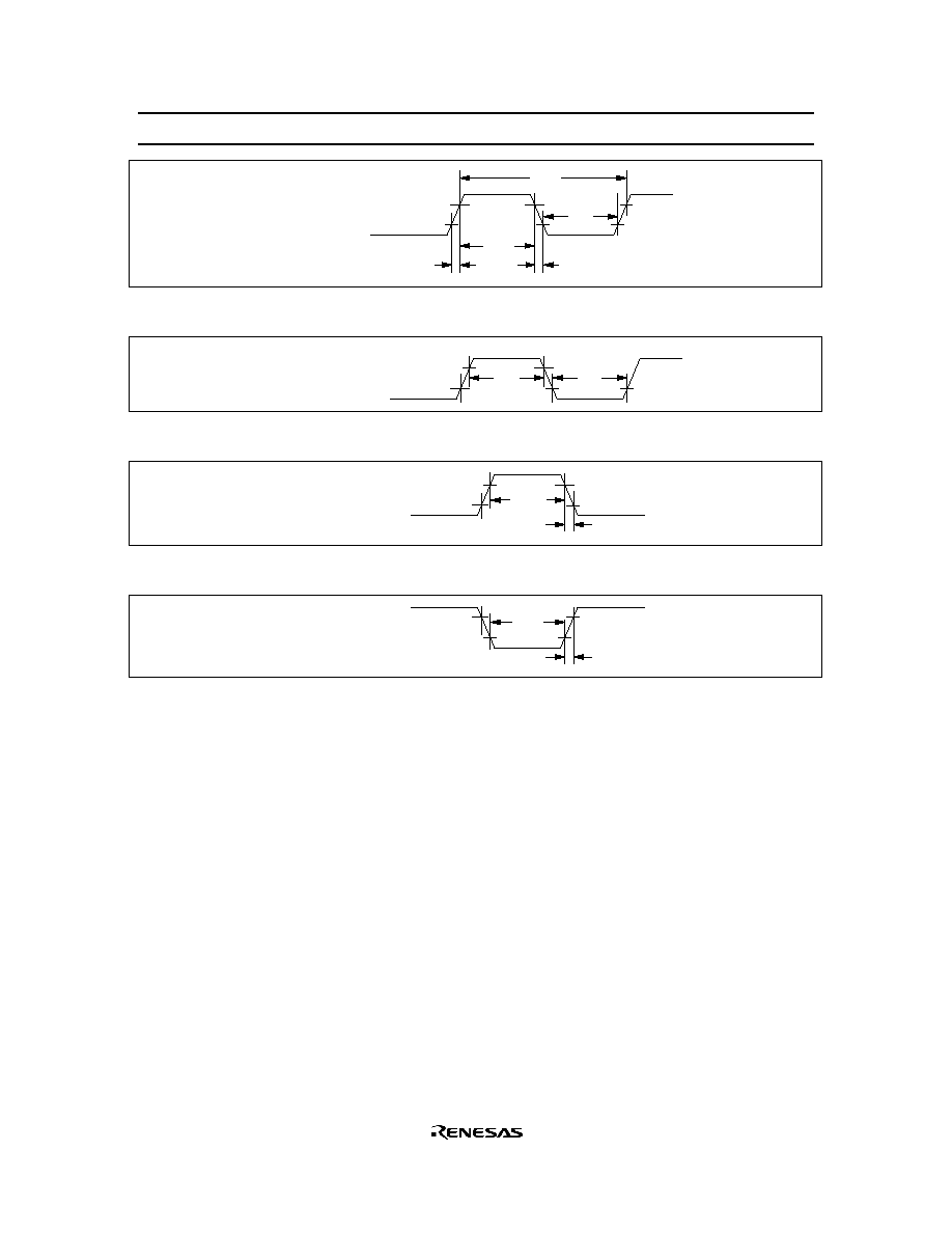
HD404449 Series
119
t
CPr
t
CPf
V
CC
≠ 0.3 V
0.3 V
OSC
1
t
CPH
t
CPL
1/f
CP
Figure 94 External Clock Timing
0.9V
CC
0.1V
CC
INT
0
to INT
3
,
EVNB
, EVND
t
IH
t
IL
Figure 95 Interrupt Timing
RESET
t
RSTf
t
RSTH
0.9V
CC
0.1V
CC
Figure 96 Reset Timing
t
STPr
t
STPL
0.9V
CC
0.1V
CC
STOPC
Figure 97
STOPC Timing
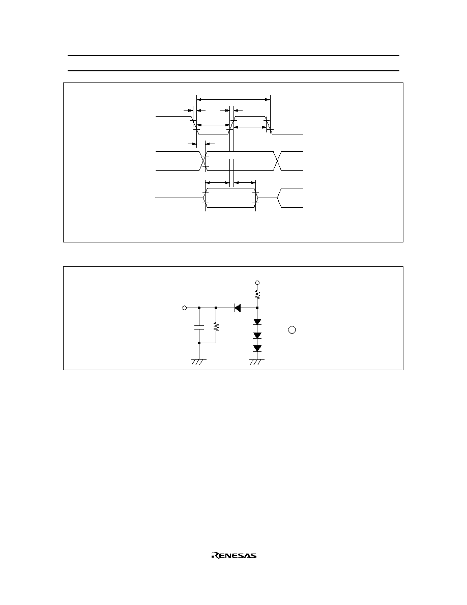
HD404449 Series
120
0.9V
CC
0.1V
CC
t
DSO
t
SCKf
t
SCKL
t
SSI
t
HSI
t
Scyc
t
SCKr
0.4 V
V ≠ 0.5 V
CC
V ≠ 2.0 V (0.9V )
*
CC
0.4 V (0.1V )
*
SCK
Note:
*
V
CC
≠ 2.0 V and 0.4 V are the threshold voltages for transmit clock output, and
0.9V
CC
and 0.1V
CC
are the threshold voltages for transmit clock input.
CC
CC
t
SCKH
1
SCK
2
SO
1
SO
2
SI
1
SI
2
Figure 98 Serial Interface Timing
R
L
= 2.6 k
V
CC
1S2074 H
or equivalent
R =
12 k
Test
point
C =
30 pF
Figure 99 Timing Load Circuit
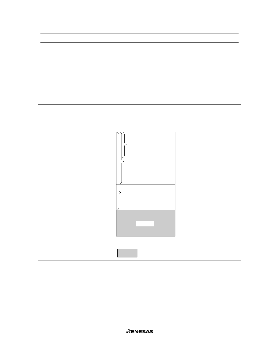
HD404449 Series
121
Notes on ROM Out
Please pay attention to the following items regarding ROM out.
On ROM out, fill the ROM area indicated below with 1s to create the same data size as a 16-kword version
(HD404449). A 16-kword data size is required to change ROM data to mask manufacturing data since the
program used is for a16-kword version.
This limitation applies when using an EPROM or a data base.
Vector address
Zero-page subroutine
(64 words)
Pattern & program
(8,192 words)
Not used
ROM 8-kword version:
HD404448
Address $2000≠$3FFF
$0000
$000F
$0010
$003F
$0040
$1FFF
$2000
$3FFF
Fill this area with 1s
HD404449 Series
122
HD404448, HD404449 Option List
Please check off the appropriate applications and enter the necessary information.
3. ROM code media
Date of order
Customer
Department
Name
ROM code name
LSI number
HD40444
EPROM:
Ceramic oscillator
Crystal oscillator
External clock
f = MHz
f = MHz
f = MHz
4. Oscillator for OSC1 and OSC2
The upper bits and lower bits are mixed together. The upper five bits and lower five bits
are programmed to the same EPROM in alternating order (i.e., LULULU...).
EPROM: The upper bits and lower bits are separated. The upper five bits and lower five bits are
programmed to different EPROMS.
HD404448
HD404449
8-kword
16-kword
1. ROM size
FP-80A
TFP-80F
6. Package
Please specify the first type below (the upper bits and lower bits are mixed together), when using
the EPROM on-package microcomputer type (including ZTATTM version).
Used
Not used
5. Stop mode
With 32-kHz CPU operation, with time-base for clock
Without 32-kHz CPU operation, with time-base for clock
Without 32-kHz CPU operation, without time-base
2. Optional Functions
Note:
*
Options marked with an asterisk require a subsystem crystal oscillator (X1, X2).
*
*

HD404449 Series
123
Cautions
1. Hitachi neither warrants nor grants licenses of any rights of Hitachi's or any third party's patent,
copyright, trademark, or other intellectual property rights for information contained in this document.
Hitachi bears no responsibility for problems that may arise with third party's rights, including
intellectual property rights, in connection with use of the information contained in this document.
2. Products and product specifications may be subject to change without notice. Confirm that you have
received the latest product standards or specifications before final design, purchase or use.
3. Hitachi makes every attempt to ensure that its products are of high quality and reliability. However,
contact Hitachi's sales office before using the product in an application that demands especially high
quality and reliability or where its failure or malfunction may directly threaten human life or cause risk
of bodily injury, such as aerospace, aeronautics, nuclear power, combustion control, transportation,
traffic, safety equipment or medical equipment for life support.
4. Design your application so that the product is used within the ranges guaranteed by Hitachi particularly
for maximum rating, operating supply voltage range, heat radiation characteristics, installation
conditions and other characteristics. Hitachi bears no responsibility for failure or damage when used
beyond the guaranteed ranges. Even within the guaranteed ranges, consider normally foreseeable
failure rates or failure modes in semiconductor devices and employ systemic measures such as fail-
safes, so that the equipment incorporating Hitachi product does not cause bodily injury, fire or other
consequential damage due to operation of the Hitachi product.
5. This product is not designed to be radiation resistant.
6. No one is permitted to reproduce or duplicate, in any form, the whole or part of this document without
written approval from Hitachi.
7. Contact Hitachi's sales office for any questions regarding this document or Hitachi semiconductor
products.
Copyright © Hitachi, Ltd., 1998. All rights reserved. Printed in Japan.