Document Outline
- Description
- Features
- Ordering Information
- Cautions about operation
- List of Functions
- Pin Arrangement
- Pin Description
- Block Diagram
- Memory Map
- Functional Description
- Operating Modes
- Internal Oscillator Circuit
- Input/Output
- Prescalers
- Timers
- Serial Interface
- A/D Converter
- DTMF Generation Circuit
- LCD Controller/Driver
- ZTAT Microcomputer with Built-in Programmable PROM
- Programmable ROM
- PROM Mode Pin Functions
- Programming Electrical Characteristics
- Addressing Modes
- Instruction Set
- Absolute Maximum Ratings
- Electrical Characteristics
- Notes on ROM Out
- HD404028R/HD4046212R/HD404629R Option List

Regarding the change of names mentioned in the document, such as Hitachi
Electric and Hitachi XX, to Renesas Technology Corp.
The semiconductor operations of Mitsubishi Electric and Hitachi were transferred to Renesas
Technology Corporation on April 1st 2003. These operations include microcomputer, logic, analog
and discrete devices, and memory chips other than DRAMs (flash memory, SRAMs etc.)
Accordingly, although Hitachi, Hitachi, Ltd., Hitachi Semiconductors, and other Hitachi brand
names are mentioned in the document, these names have in fact all been changed to Renesas
Technology Corp. Thank you for your understanding. Except for our corporate trademark, logo and
corporate statement, no changes whatsoever have been made to the contents of the document, and
these changes do not constitute any alteration to the contents of the document itself.
Renesas Technology Home Page: http://www.renesas.com
Renesas Technology Corp.
Customer Support Dept.
April 1, 2003
To all our customers

Cautions
Keep safety first in your circuit designs!
1.
Renesas Technology Corporation puts the maximum effort into making semiconductor products better and more reliable, but
there is always the possibility that trouble may occur with them. Trouble with semiconductors may lead to personal injury, fire
or property damage.
Remember to give due consideration to safety when making your circuit designs, with appropriate measures such as (i)
placement of substitutive, auxiliary circuits, (ii) use of nonflammable material or (iii) prevention against any malfunction or
mishap.
Notes regarding these materials
1.
These materials are intended as a reference to assist our customers in the selection of the Renesas Technology Corporation
product best suited to the customer's application; they do not convey any license under any intellectual property rights, or any
other rights, belonging to Renesas Technology Corporation or a third party.
2.
Renesas Technology Corporation assumes no responsibility for any damage, or infringement of any third-party's rights,
originating in the use of any product data, diagrams, charts, programs, algorithms, or circuit application examples contained in
these materials.
3.
All information contained in these materials, including product data, diagrams, charts, programs and algorithms represents
information on products at the time of publication of these materials, and are subject to change by Renesas Technology
Corporation without notice due to product improvements or other reasons. It is therefore recommended that customers contact
Renesas Technology Corporation or an authorized Renesas Technology Corporation product distributor for the latest product
information before purchasing a product listed herein.
The information described here may contain technical inaccuracies or typographical errors.
Renesas Technology Corporation assumes no responsibility for any damage, liability, or other loss rising from these
inaccuracies or errors.
Please also pay attention to information published by Renesas Technology Corporation by various means, including the
Renesas Technology Corporation Semiconductor home page (http://www.renesas.com).
4.
When using any or all of the information contained in these materials, including product data, diagrams, charts, programs, and
algorithms, please be sure to evaluate all information as a total system before making a final decision on the applicability of
the information and products. Renesas Technology Corporation assumes no responsibility for any damage, liability or other
loss resulting from the information contained herein.
5.
Renesas Technology Corporation semiconductors are not designed or manufactured for use in a device or system that is used
under circumstances in which human life is potentially at stake. Please contact Renesas Technology Corporation or an
authorized Renesas Technology Corporation product distributor when considering the use of a product contained herein for
any specific purposes, such as apparatus or systems for transportation, vehicular, medical, aerospace, nuclear, or undersea
repeater use.
6.
The prior written approval of Renesas Technology Corporation is necessary to reprint or reproduce in whole or in part these
materials.
7.
If these products or technologies are subject to the Japanese export control restrictions, they must be exported under a license
from the Japanese government and cannot be imported into a country other than the approved destination.
Any diversion or reexport contrary to the export control laws and regulations of Japan and/or the country of destination is
prohibited.
8.
Please contact Renesas Technology Corporation for further details on these materials or the products contained therein.

HD404629R Series
AS Microcomputer Incorporating a DTMF Generator Circuit
ADE-202-048D
Rev.5.0
Sept. 1999
Description
The HD404629R Series is part of the HMCS400-Series microcomputers designed to increase program
productivity and also incorporate large-capacity memory. Each microcomputer has a high precision dual-
tone multifrequency (DTMF) generator, LCD controller/driver, A/D converter, input capture circuit, 32-
kHz oscillator for clock, and four low-power dissipation modes.
The HD404629R Series includes four chips: the HD404628R with 8-kword ROM; the HD4046212R with
12-kword ROM; the HD404629R with 16-kword ROM; the HD4074629 with 16-kword PROM.
A program can be written to the PROM by a PROM writer, which can dramatically shorten system
development periods and smooth the process from debugging to mass production.
Features
�
1,876-digit
�
4-bit RAM
�
44 I/O pins, including 10 high-current pins (15 mA, max.) and 20 pins multiplexed with LCD segment
pins
�
Four timer/counters
�
8-bit input capture circuit
�
Three timer outputs (including two PWM out-puts)
�
Two event counter inputs (including one double-edge function)
�
Clock-synchronous 8-bit serial interface
�
A/D converter (4 channels
�
8 bits)
�
LCD controller/driver (52 segments
�
4 commons)
�
On-chip DTMF generator
�
Built-in oscillators
Main clock: 4-MHz ceramic (an external clock is also possible)
Subclock: 32.768-kHz crystal
�
Eleven interrupt sources
Five by external sources, including three double-edge functions
Six by internal sources
�
Subroutine stack up to 16 levels, including interrupts

HD404629R Series
2
�
Four low-power dissipation modes
Subactive mode
Standby mode
Watch mode
Stop mode
�
One external input for transition from stop mode to active mode
�
Instruction cycle time (min.): 1
�
s (f
OSC
= 4 MHz)
�
Operation voltage
V
CC
= 2.7 V to 6.0 V (HD404629R)
V
CC
= 2.7 V to 5.5 V (HD4074629)
�
Two operating modes
MCU mode
MCU/PROM mode (HD4074629 only)

HD404629R Series
3
Ordering Information
Type
Product Name
Model Name
ROM (Words)
Package
Mask ROM
HD404628R
HD404628RH
8,192
100-pin plastic QFP
(FP-100B)
HD404628RFS
100-pin plastic QFP
(FP-100A)
HD404628RTF
100-pin plastic TQFP
(TFP-100B)
HD4046212R
HD4046212RH
12,288
100-pin plastic QFP
(FP-100B)
HD4046212RFS
100-pin plastic QFP
(FP-100A)
HD4046212RTF
100-pin plastic TQFP
(TFP-100B)
HD404629R
HD404629RH
16,384
100-pin plastic QFP
(FP-100B)
HD404629RFS
100-pin plastic QFP
(FP-100A)
HD404629RTF
100-pin plastic TQFP
(TFP-100B)
ZTAT
TM
HD4074629
HD4074629H
16,384
100-pin plastic QFP
(FP-100B)
HD4074629FS
100-pin plastic QFP
(FP-100A)
HD4074629TF
100-pin plastic TQFP
(TFP-100B)
ZTAT
TM
: Zero Turn Around Time ZTAT is a trademark of Hitachi Ltd.
Cautions about operaton!
Like the ZTAT
TM
HD4074629 and the HD404629 Series, the HD404629R Series has been verified to fully
meet the standard electrical characteristics described in the data sheet or other related documents. However,
due to differences in the manufacturing process, the type of built-in ROMs used, and internal wiring
patterns, the HD404629R Series has different power factors, operating margins, and noise margins.
Therefore, you should test both of your systems incorporating the ZTAT
TM
and mask ROM versions. When
your system is modified to use an HD404629R Series in place of a conventional chip, you should also
perform a similar evaluation test to verify performance of your new system.

HD404629R Series
4
List of Functions
Product name
HD404628R
HD4046212R
HD404629R
HD4074629
ROM (Words)
8,192
12,288
16,384
16,384 PROM
RAM (Digits)
1,876
I/O
44 (max)
Large-current I/O pins
10 (Sink 15 mA max)
LCD segment multiplexed pins
20
Timer / Counter
4
Input capture
8 bit
�
1
Timer output
3 (PWM output possible for 2)
Event input
2 (edge selection possible for 1)
Serial interface
1 (8-bit syncronous)
DTMF generation circuit
Available
A/D converter
8 bit
�
4 channels
LCD controller / driver circuit
Max. 52 seg
�
4 com
Interrupts
External
5 (edge selection possible for 3)
Internal
6
Low-Power Dissipation Mode
4
Stop mode
Available
Watch mode
Available
Standby mode
Available
Subactive mode
Available
Main Oscillator
Ceramic oscillation
400 kHz, 800 kHz, 2 MHz, 4 MHz
Crystal oscillation
400 kHz, 800 kHz, 2 MHz, 4 MHz
--
Sub oscillator
Crystal oscillation
32.768 kHz
Minimum instruction execution time
1
�
s (f
OSC
= 4 MHz)
Operating voltage (V)
2.7 to 6.0
2.7 to 5.5
Package
100-pin plastic QFP (FP-100B)
100-pin plastic QFP (FP-100A)
100-pin plastic TQFP (TFP-100B)
Guaranteed operation temperature
(�C)
�20 to +75

HD404629R Series
5
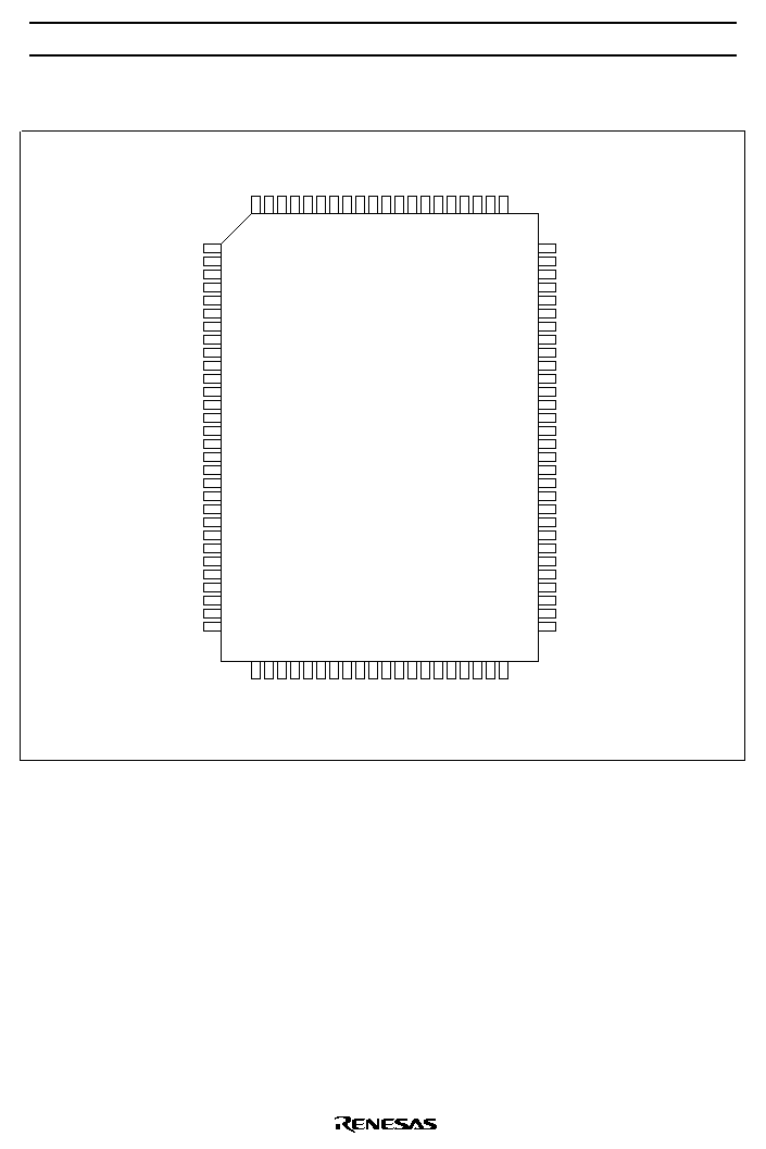
Pin Arrangement
FP-100B
TFP-100B
AV
AN
AN
AN
AN
AV
TEST
OSC
OSC
RESET
X1
X2
GND
D
D
D
D
D
D
D
D
D
D
D /
STOPC
D
11
/
INT
0
CC
1
2
3
SS
1
2
0
1
2
3
4
5
6
7
8
9
10
SEG38
SEG37
SEG36
SEG35
SEG34
SEG33
SEG32
SEG31
SEG30
SEG29
SEG28
SEG27
SEG26
SEG25
SEG24
SEG23
SEG22
SEG21
R7 /SEG20
R7 /SEG19
R7 /SEG18
R7 /SEG17
R6 /SEG16
R6 /SEG15
R6 /SEG14
3
2
1
0
3
2
1
R0 /
INT
R0 /INT
R0 /INT
R0 /INT
R1 /TOB
R1 /TOC
R1 /TOD
R1 /
EVNB
R2 /EVND
R2 /
SCK
R2 /SI
R2 /SO
R3 /SEG1
R3 /SEG2
R3 /SEG3
R3 /SEG4
R4 /SEG5
R4 /SEG6
R4 /SEG7
R4 /SEG8
R5 /SEG9
R5 /SEG10
R5 /SEG11
R5 /SEG12
R6 /SEG13
0
1
2
3
0
1
2
3
0
1
0
1
2
3
0
1
2
3
0
1
2
3
0
VT
TONER
TONEC
V
V
V
V
COM4
COM3
COM2
COM1
SEG52
SEG51
SEG50
SEG49
SEG48
SEG47
SEG46
SEG45
SEG44
SEG43
SEG42
SEG41
SEG40
SEG39
CC
3
2
1
1
2
3
4
5
6
7
8
9
10
11
12
13
14
15
16
17
18
19
20
21
22
23
24
25
75
74
73
72
71
70
69
68
67
66
65
64
63
62
61
60
59
58
57
56
55
54
53
52
51
1
2
3
4
2
3
Top view
0
26
27
28
29
30
31
32
33
34
35
36
37
38
39
40
41
42
43
44
45
46
47
48
49
50
100
95
94
93
92
91
90
89
88
87
86
85
84
83
82
81
80
79
78
77
76
99
98
97
96
ref
HD404629R Series
6
Pin Arrangement
FP-100A
TONER
VT
AV
AN
AN
AN
AN
AV
TEST
OSC
OSC
RESET
X1
X2
GND
D
D
D
D
D
D
D
D
D
D
D /
STOPC
D /
INT
R0 /
INT
R0 /INT
R0 /INT
SEG41
SEG40
SEG39
SEG38
SEG37
SEG36
SEG35
SEG34
SEG33
SEG32
SEG31
SEG30
SEG29
SEG28
SEG27
SEG26
SEG25
SEG24
SEG23
SEG22
SEG21
R7 /SEG20
R7 /SEG19
R7 /SEG18
R7 /SEG17
R6 /SEG16
R6 /SEG15
R6 /SEG14
R6 /SEG13
R5 /SEG12
3
2
1
0
3
2
1
0
3
R0 /INT
R1 /TOB
R1 /TOC
R1 /TOD
R1 /
EVNB
R2 /EVND
R2 /
SCK
R2 /SI
R2 /SO
R3 /SEG1
R3 /SEG2
R3 /SEG3
R3 /SEG4
R4 /SEG5
R4 /SEG6
R4 /SEG7
R4 /SEG8
R5 /SEG9
R5 /SEG10
R5 /SEG11
TONEC
V
V
V
V
COM4
COM3
COM2
COM1
SEG52
SEG51
SEG50
SEG49
SEG48
SEG47
SEG46
SEG45
SEG44
SEG43
SEG42
1
2
3
4
5
6
7
8
9
10
11
12
13
14
15
16
17
18
19
20
21
22
23
24
25
26
27
28
29
30
80
79
78
77
76
75
74
73
72
71
70
69
68
67
66
65
64
63
62
61
60
59
58
57
56
55
54
53
52
51
31
32
33
34
35
36
37
38
39
40
41
42
43
44
45
46
47
48
49
50
100
99
98
97
96
95
94
93
92
91
90
89
88
87
86
85
84
83
82
81
0
1
2
3
4
5
6
7
8
9
0
1
2
3
0
1
2
10
4
3
0
1
2
3
0
1
2
3
0
1
2
3
0
1
2
3
0
1
2
CC
3
2
1
11
ref
CC
0
1
2
3
SS
1
2

HD404629R Series
7
Pin Description
Pin Number
Item
Symbol
FP-100B
TFP-100B
FP-100A
I/O
Function
Power
V
CC
97
99
Applies power voltage
supply
GND
13
15
Connected to ground
Test
TEST
7
9
I
Used for factory testing only: Connect this pin
to V
CC
Reset
RESET
10
12
I
Resets the MCU
Oscillato
r
OSC
1
8
10
I
Input/output pins for the internal oscillator
circuit:
OSC
2
9
11
O
Connect them to a ceramic oscillator ,crystal
oscillator or connect OSC
1
to an external
oscillator
curcuit
X1
11
13
I
Used for a 32.768-kHz crystal for clock
purposes.
X2
12
14
O
If not to be used, fix the X1 pin to V
CC
and
leave
the X2 pin open.
Port
D
0
�D
9
14�23
16�25
I/O
Input/output pins addressed by individual bits;
pins D
0
�D
9
are high-current pins that can each
supply up to 15 mA
D
10
, D
11
24, 25
26, 27
I
Input pins addressable by individual bits
R0
0
�R7
3
26�57
28�59
I/O
Input/output pins addressable in 4-bit units
Interrupt
INT
0
,
INT
1
,
INT
2
�INT
4
25�29
27�31
I
Input pins for external interrupts
Stop clear
STOPC
24
26
I
Input pin for transition from stop mode to active
mode
Serial
SCK
35
37
I/O
Serial interface clock input/output pin
interface
SI
36
38
I
Serial interface receive data input pin
SO
37
39
O
Serial interface transmit data output pin
Timer
TOB, TOC,
TOD
30�32
32�34
O
Timer output pins
EVNB
, EVND
33, 34
35, 36
I
Event count input pins
LCD
V
1
, V
2
, V
3
94�96
96�98
Power pins for LCD controller/driver; may be left
open during operation since they are connected by
internal voltage division resistors.
Voltage conditions are: V
CC
V
1
V
2
V
3
GND
COM1�COM4
90�93
92�95
O
Common signal pins for LCD
SEG1�SEG52
38�89
40�91
O
Segment signal pins for LCD

HD404629R Series
8
Pin Number
Item
Symbol
FP-100B
TFP-100B
FP-100A
I/O
Function
A/D
converter
AV
CC
1
3
Power pin for A/D converter: Connect it to the same
potential as V
CC
, as physically close to the V
CC
pin as
possible
AV
SS
6
8
Ground for AV
CC
: Connect it to the same potential
as GND, as physically close to the GND pin as
possible
AN
0
�AN
3
2�5
4�7
I
Analog input pins for A/D converter
DTMF
TONER
99
1
O
Output pin for DTMF row signals
TONEC
98
100
O
Output pin for DTMF column signals
VT
ref
100
2
Reference voltage pin for DTMF signals.
Voltage conditions are: V
CC
VT
ref
GND

HD404629R Series
9
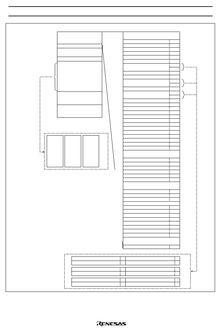
Block Diagram
: High current pins
RESET
TEST
STOP
C
OSC
1
OSC
2
X1
X2
V
CC
GND
HMCS400 CPU
ROM
RAM
Timer A
8-bit free-running timer
Timer B
8-bit free-running / reload timer
D
0
D
1
D
2
D
3
D
4
D
5
D
6
D
7
D
8
D
9
D
10
D
11
R4
0
R4
1
R4
2
R4
3
R0
0
R0
1
R0
2
R0
3
R1
0
R1
1
R1
2
R1
3
R2
0
R2
1
R2
2
R2
3
R3
0
R3
1
R3
2
R3
3
R5
0
R5
1
R5
2
R5
3
TOC
EVNB
TOB
AVcc
AVss
AN0
AN1
AN2
AN3
V
1
V
2
V
3
COM1
COM2
COM3
COM4
SEG1
SEG2
SEG3
SEG52
A/D converter
4 channels x 8 bits
External interrupt
control circuit
INT
0
INT
1
INT2
INT3
INT4
R6 Port
R5 Port
R4 Port
R3 Port
R2 Port
R1 Port
R0 Port
D Port
R7 Port
R6
0
R6
1
R6
2
R6
3
R7
0
R7
1
R7
2
R7
3
EVND
TOD
Clock-synchronous
8-bit serial interface
SCK
SI
SO
LCD controller / driver
circuit
52 segments x 4 commons
to
DTMF
generation circuit
VT
ref
TONER
TONEC
Timer C
8-bit free-running / reload timer
Timer D
8-bit free-running / reload timer

HD404629R Series
10
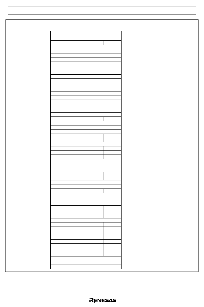
Memory Map
ROM Memory Map
The ROM memory map is shown in figure 1 and described below.
$000F
$0FFF
$3FFF
$003F
Vector address
(16 words)
Zero-page subroutine
(64 words)
Pattern
(4,096 words)
HD404628R
Program
(8,192 words)
$0000
$0000
$0001
$0002
$0003
$0004
$0005
$0006
$0007
$0008
$0009
$000A
$000B
$000C
$000D
$000E
$000F
JMPL instruction
(jump to RESET,
STOPC
routine)
JMPL instruction
(jump to
INT
routine)
0
JMPL instruction
(jump to timer A routine)
JMPL instruction
(jump to timer B, INT routine)
2
JMPL instruction
(jump to timer C, INT routine)
3
JMPL instruction
(jump to timer D, INT routine)
4
JMPL instruction
(jump to
INT
routine)
1
JMPL instruction
(jump to A/D, serial routine)
$1FFF
$2FFF
HD4046212R
Program
(12,288 words)
HD404629R, HD4074629
Program
(16,384 words)
$0010
$0040
$1000
$2000
$3000
ROM address
ROM address
Figure 1 ROM Memory Map
Vector Address Area ($0000�$000F): Reserved for JMPL instructions that branch to the start addresses
of the reset and interrupt routines. After MCU reset or an interrupt, program execution continues from the
vector address.
Zero-Page Subroutine Area ($0000�$003F): Reserved for subroutines. The program branches to a
subroutine in this area in response to the CAL instruction.
Pattern Area ($0000�$0FFF): Contains ROM data that can be referenced with the P instruction.
Program Area ($0000�$1FFF: HD404628R; $0000�$2FFF: HD4046212R; $0000�$3FFF;
HD404629R, HD4074629): Used for program coding.

HD404629R Series
11
RAM Memory Map
The MCU contains a 1,876-digit
�
4-bit RAM area consisting of a memory register area, an LCD data area,
a data area, and a stack area. In addition, an interrupt control bits area, special register area, and register
flag area are mapped onto the same RAM memory space as a RAM-mapped register area outside the above
areas. The RAM memory map is shown in figure 2 and described below.
RAM-Mapped Register Area ($000�$03F):
�
Interrupt Control Bits Area ($000�$003)
This area is used for interrupt control bits (figure 3). These bits can be accessed only by RAM bit
manipulation instructions (SEM/SEMD, REM/REMD, and TM/TMD). However, note that not all the
instructions can be used for each bit. Limitations on using the instructions are shown in figure 4.
�
Special Function Register Area ($004�$01F, $024�$03F)
This area is used as mode registers and data registers for external interrupts, serial interface,
timer/counters, LCD, A/D converter, and as data control registers for I/O ports. The structure is shown
in figures 2 and 5. These registers can be classified into three types: write-only (W), read-only (R), and
read/write (R/W). The SEM, SEMD, REM, and REMD instructions can be used for the LCD control
register (LCR: $01B), but RAM bit manipulation instructions cannot be used for other registers.
�
Register Flag Area ($020�$023)
�
This area is used for the DTON, WDON, and other register flags and interrupt control bits (figure 3).
These bits can be accessed only by RAM bit manipulation instructions (SEM/SEMD, REM/REMD, and
TM/TMD). However, note that not all the instructions can be used for each bit. Limitations on using
the instructions are shown in figure 4.
HD404629R Series
12
A/D mode register (AMR)
Data
(464 digits)
V = 1
(bank = 1)
$000
$000
$040
$050
$003
$004
$005
$006
$007
$008
$009
$00A
$00B
$00C
$00D
$00E
$00F
$010
$011
$012
$013
$014
$020
$023
$032
$033
$034
$035
$036
$037
$038
$03F
$00A
$00B
$00E
$00F
W
W
R/W
W
W
W
W
W
W
W
W
W
W
W
W
W
W
R
R
R
R
W
R/W
R/W
R/W
R/W
R/W
R/W
$090
$25F
$3C0
$260
RAM-mapped register area
Memory registers (10 digits)
LCD display area (52 digits)
Not used
Data (464 digits 3)
V = 0 (bank 0)
V = 1 (bank 1)
V = 2 (bank 2)
Data (352 digits)
Stack (64 digits)
Interrupt control bits area
Port mode register A (PMRA)
Serial mode register A (SMRA)
Serial data register lower (SRL)
Serial data register upper (SRU)
Timer mode register A (TMA)
Timer mode register B1 (TMB1)
Timer B (TRBL/TWBL)
(TRBU/TWBU)
Miscellaneous register (MIS)
Timer mode register C1 (TMC1)
Timer C (TRCL/TWCL)
(TRCU/TWCU)
Timer mode register B2 (TMB2)
Timer mode register D2 (TMD2)
Register flag area
Port R0 DCR (DCR0)
Port R1 DCR (DCR1)
Port R2 DCR (DCR2)
Port R3 DCR (DCR3)
Port D
0
�D
3
DCR (DCD0)
Port D
4
�D
7
DCR (DCD1)
Port D
8
and D
9
DCR (DCD2)
Not used
V register (V)
Data
(464 digits)
V = 0
(bank = 0)
The data area has three banks:
bank 0 (V = 0) to bank 2 (V = 2).
Two registers are mapped
on the same area.
10
11
14
15
Timer read register B lower (TRBL)
Timer read register B upper (TRBU)
Timer read register C lower (TRCL)
Timer read register C upper (TRCU)
Timer write register B lower (TWBL)
Timer write register B upper (TWBU)
Timer write register C lower (TWCL)
Timer write register C upper (TWCU)
R:
W:
R/W:
�
$090
Read only
Write only
Read/write
Data
(464 digits)
V = 2
(bank = 2)
Notes: 1.
2.
$011
$012
W
W
R
R
17
18
Timer read register D lower (TRDL)
Timer read register D upper (TRDU)
Timer write register D lower (TWDL)
Timer write register D upper (TWDU)
$084
W
Timer mode register D1 (TMD1)
R/W
R/W
Timer D (TRDL/TWDL)
(TRDU/TWDU)
Timer mode register C2 (TMC2)
$015
$016
R
A/D data register lower (ADRL)
$017
$024
$025
$026
$027
$028
$029
$02A
$02B
$018
$019
$01A
$01B
$01C
$01D
$01E
$01F
$3FF
A/D data register upper (ADRU)
LCD control register (LCR)
LCD mode register (LMR)
LCD output register 1 (LOR1)
LCD output register 2 (LOR2)
LCD output register 3 (LOR3)
R
W
W
W
W
W
W
W
W
Port mode register B (PMRB)
Port mode register C (PMRC)
Detection edge select register 1 (ESR1)
Detection edge select register 2 (ESR2)
Serial mode register B (SMRB)
System clock select register (SSR)
Not used
Not used
Port R4 DCR (DCR4)
Port R5 DCR (DCR5)
Port R6 DCR (DCR6)
Port R7 DCR (DCR7)
W
W
W
W
W
W
W
W
$03E
$02C
$02D
$02E
$02F
$031
$030
R/W
R/W
R/W
TG mode register (TGM)
TG control register (TGC)
W
W
*
2
*
1
RAM address
RAM address
Figure 2 RAM Memory Map

HD404629R Series
13
Bit 3
Bit 2
Bit 1
Bit 0
IMTA
(IM of timer A)
IFTA
(IF of timer A)
IM1
(IM of
INT
1
)
IF1
(IF of
INT
1
)
IMTC
(IM of timer C)
IFTC
(IF of timer C)
IMTB
(IM of timer B)
IFTB
(IF of timer B)
IMAD
(IM of A/D)
IFAD
(IF of A/D)
IMTD
(IM of timer D)
IFTD
(IF of timer D)
$000
$001
$002
$003
Interrupt control bits area
IM0
(IM of
INT
0
)
IF0
(IF of
INT
0
)
RSP
(Reset SP bit)
IE
(Interrupt
enable flag)
ICSF
(Input capture
status flag)
IM3
(IM of INT
3
)
IF3
(IF of INT
3
)
IM2
(IM of INT
2
)
IF2
(IF of INT
2
)
IMS
(IM of serial
interface)
IFS
(IF of serial
interface)
IM4
(IM of INT
4
)
IF4
(IF of INT
4
)
$020
$021
$022
$023
Register flag area
DTON
(Direct transfer
on flag)
ADSF
(A/D start flag)
WDON
(Watchdog
on flag)
LSON
(Low speed
on flag)
ICEF
(Input capture
error flag)
RAME
(RAM enable
flag)
Not used
IF:
IM:
IE:
SP:
Interrupt request flag
Interrupt mask
Interrupt enable flag
Stack pointer
Bit 3
Bit 2
Bit 1
Bit 0
Figure 3 Configuration of Interrupt Control Bits and Register Flag Areas
IE
IM
LSON
IF
ICSF
ICEF
RAME
RSP
WDON
ADSF
Not used
DTON
SEM/SEMD
REM/REMD
TM/TMD
Allowed
Allowed
Allowed
Not executed
Allowed
Allowed
Not executed
Allowed
Inhibited
Allowed
Not executed
Inhibited
Allowed
Inhibited
Allowed
Not executed in active mode
Allowed
Allowed
Used in subactive mode
Not executed
Not executed
Inhibited
Note: WDON is reset by MCU reset or by
STOPC
enable for stop mode cancellation.
The REM or REMD instuction must not be executed for ADSF during A/D conversion.
DTON is always reset in active mode.
If the TM or TMD instruction is executed for the inhibited bits or non-existing bits,
the value in ST becomes invalid.
Figure 4 Usage Limitations of RAM Bit Manipulation Instructions
HD404629R Series
14
$000
$003
PMRA $004
SMRA $005
SRL $006
SRU $007
TMA $008
TMB1 $009
TRBL/TWBL $00A
TRBU/TWBU $00B
MIS $00C
TMCI $00D
TRCL/TWCL $00E
TRCU/TWCU $00F
TMDI $010
TRDL/TWDL $011
TRDU/TWDU $012
TMB2 $013
TMC2 $014
TMD2 $015
AMR $016
ADRL $017
ADRU $018
TGM $019
TGC $01A
LCR $01B
LMR $01C
LOR1 $01D
LOR2 $01E
LOR3 $01F
$020
$023
PMRB $024
PMRC $025
ESR1 $026
ESR2 $027
SMRB $028
SSR $029
DCD0 $02C
DCD1 $02D
DCD2 $02E
DCR0 $030
DCR1 $031
DCR2 $032
DCR3 $033
DCR4 $034
DCR5 $035
DCR6 $036
DCR7 $037
V $03F
Bit 3
Bit 2
Bit 1
Interrupt control bits area
Not used
Not used
R2
2
/SI
R2
3
/SO
Serial transmit clock speed selection
Serial data register (lower digit)
Serial data register (upper digit)
Clock source setting (timer A)
Clock source setting (timer B)
Timer B register (lower digit)
Timer B register (upper digit)
R23/SO PMOS control
Interrupt frame period selection
Clock source setting (timer C)
Timer C register (lower digit)
Timer C register (upper digit)
Clock source setting (timer D)
Timer D register (lower digit)
Timer D register (upper digit)
Not used
Not used
Timer-B output mode selection
Not used
Timer-C output mode setting
Timer-D output mode setting
Not used
Analog channel selection
A/D data register (lower digit)
A/D data register (upper digit)
Not used
LCD duty cycle selection
LCD input clock source selection
R3
3
/SEG4
R4
3
/SEG8
Not used
R3
2
/SEG3
R4
2
/SEG7
R7/SEG17�20
R3
1
/SEG2
R4
1
/SEG6
R6/SEG13�16
R3
0
/SEG1
R4
0
/SEG5
R5/SEG9�12
Register flag area
R0
1
/INT
2
R2
0
/EVND
INT
2
detection edge selection
INT
4
detection edge selection
INT
3
detection edge selection
EVND detection edge selection
Not used
Not used
Not used
Port D
3
DCR
Port D
7
DCR
Not used
Port D
2
DCR
Port D
6
DCR
Not used
Port D
1
DCR
Port D
5
DCR
Port D
9
DCR
Port D
0
DCR
Port D
4
DCR
Port D
8
DCR
Not used
Port R0
3
DCR
Port R1
3
DCR
Port R2
3
DCR
Port R3
3
DCR
Port R4
3
DCR
Port R5
3
DCR
Port R6
3
DCR
Port R7
3
DCR
Port R0
2
DCR
Port R1
2
DCR
Port R2
2
DCR
Port R3
2
DCR
Port R4
2
DCR
Port R5
2
DCR
Port R6
2
DCR
Port R7
2
DCR
Port R0
1
DCR
Port R1
1
DCR
Port R2
1
DCR
Port R3
1
DCR
Port R4
1
DCR
Port R5
1
DCR
Port R6
1
DCR
Port R7
1
DCR
Port R0
0
DCR
Port R1
0
DCR
Port R2
0
DCR
Port R3
0
DCR
Port R4
0
DCR
Port R5
0
DCR
Port R6
0
DCR
Port R7
0
DCR
Not used
Not used
Not used
Bank 0 to bank 2 selection
1.
2.
3.
4.
5.
6.
7.
8.
9.
10.
11.
12.
13.
14.
R0
2
/INT
3
D
10
/
STOPC
R0
3
/INT
4
D
11
/
INT
0
R0
0
/
INT
1
R1
3
/
EVNB
R2
1
/
SCK
Bit 0
Clock select
1
*
2
*
3
*
2
*
2
*
4
*
5
*
8
*
9
*
10
*
11
*
12
*
13
*
14
*
Timer-A/time-base
Auto-reload on/off
Pull-up MOS control
Input capture selection
A/D conversion time
TONEC output control
TONER output control
Display on/off in watch mode
LCD power switch
LCD display on/off
SO idle H/L setting
Transmit clock source selection
32-kHz oscillation stop setting
32-kHz oscillation division ratio
Notes:
TONEC output frequency
TONER output frequency
DTMF enable
Not used
6
*
7
*
RAM address
Figure 5 Special Function Register Area

HD404629R Series
15
Memory Register (MR) Area ($040�$04F): Consisting of 16 addresses, this area (MR0�MR15) can be
accessed by register-register instructions (LAMR and XMRA). The structure is shown in figure 6.
Memory registers
$040
$041
$042
$043
$044
$045
$046
$047
$048
$049
$04A
$04B
$04C
$04D
$04E
$04F
$3C0
$3FF
MR(0)
MR(1)
MR(2)
MR(3)
MR(4)
MR(5)
MR(6)
MR(7)
MR(8)
MR(9)
Level 16
Level 15
Level 14
Level 13
Level 12
Level 11
Level 10
Level 9
Level 8
Level 7
Level 6
Level 5
Level 4
Level 3
Level 2
Level 1
MR(10)
MR(11)
MR(12)
MR(13)
MR(14)
MR(15)
PC
PC
PC
PC
PC
PC
PC
PC
PC
PC
PC
PC
ST
PC
CA
PC
10
3
13
9
6
2
12
8
5
1
11
7
4
0
Bit 3
Bit 2
Bit 1
Bit 0
PC �PC :
ST: Status flag
CA: Carry flag
Program counter
13
Stack area
0
$3FC
$3FD
$3FE
$3FF
Figure 6 Configuration of Memory Registers and Stack Area, and Stack Position

HD404629R Series
16
LCD Data Area ($050�$083): Used for storing 52-digit LCD data which is automatically output to LCD
segments as display data. Data 1 lights the corresponding LCD segment; data 0 extinguishes it. Refer to
the LCD description for details.
Data Area ($090�$3BF): 464 digits from $090 to $25F have three banks, which can be selected by setting
the bank register (V: $03F). Before accessing this area, set the bank register to the required value (figure
7). The area from $260 to $3BF is accessed without setting the bank register.
Bit
Initial value
Read/Write
Bit name
3
--
--
Not used
2
--
--
Not used
0
0
R/W
V0
1
0
R/W
V1
V1
0
1
V0
0
1
0
1
Bank area selection
Bank 0 is selected
Bank 1 is selected
Bank 2 is selected
Not Used
Note: After reset, the value in the bank register is 0, and therefore bank 0 is
selected. If V1 = 1 and V0 = 1, no bank is selected, and the operation is not
guaranteed.
Bank register (V: $03F)
Figure 7 Bank Register (V)
Stack Area ($3C0�$3FF): Used for saving the contents of the program counter (PC), status flag (ST), and
carry flag (CA) at subroutine call (CAL or CALL instruction) and for interrupts. This area can be used as a
16-level nesting subroutine stack in which one level requires four digits. The data to be saved and the save
conditions are shown in figure 6.
The program counter is restored by either the RTN or RTNI instruction, but the status and carry flags can
only be restored by the RTNI instruction. Any unused space in this area is used for data storage.
HD404629R Series
17
Functional Description
Registers and Flags
The MCU has nine registers and two flags for CPU operations. They are shown in figure 8 and described
below.
3
0
3
0
3
0
3
0
3
0
3
0
0
0
0
13
9
5
1
(B)
(A)
(W)
(X)
(Y)
(SPX)
(SPY)
(CA)
(ST)
(PC)
(SP)
1
1
1
1
Accumulator
B register
W register
X register
Y register
SPX register
SPY register
Carry
Status
Program counter
Initial value: $0000,
R/W not possible
Stack pointer
Initial value: $3FF, R/W not possible
0
0
Initial value: Undefined, R/W
Initial value: Undefined, R/W
Initial value: Undefined, R/W
Initial value: Undefined, R/W
Initial value: Undefined, R/W
Initial value: Undefined, R/W
Initial value: Undefined, R/W
Initial value: Undefined, R/W
Initial value: 1, R/W not possible
Figure 8 Registers and Flags
Accumulator (A) and B Register (B): A and B are 4-bit registers, and are used to hold the results of ALU
(arithmetic and logical unit) operations and to transfer data between memory, I/O ports, and other registers.
W Register (W), X Register (X), and Y Register (Y): W is a 2-bit register and X and Y are 4-bit
registers. These registers are used in RAM register indirect addressing. The Y register is also used in D port
addressing.

HD404629R Series
18
SPX Register (SPX) and SPY Register (SPY): The SPX and SPY registers are 4-bit registers used to
supplement the X and Y registers.
Carry Flag (CA): CA is a 1-bit flag that stores ALU overflow generated by an arithmetic operation. CA is
set to 1 when an overflow is generated, and is cleared to 0 after operations in which no overflow occurred.
CA is also affected by the carry set/carry clear instructions (SEC and REC), and by the rotate with carry
instructions (ROTL and ROTR).
During interrupt handling, CA is saved on the stack, and is restored from the stack by the RTNI instruction.
Status Flag (ST): ST is a 1-bit flag that stores the results of arithmetic instructions, compare instructions,
and bit test instructions, and is used as the branch condition for the BR, BRL, CAL, and CALL conditional
branch instructions.
The contents of the ST flag are held until the next arithmetic, compare, bit test, or conditional branch
instruction is executed. After the execution of a conditional branch instruction, the value of ST is set to 1
without regard to the condition.
During interrupt handling, ST is saved on the stack, and is restored from the stack by the RTNI instruction.
Program Counter (PC): The PC is a 14-bit counter that indicates the ROM address of the next instruction
the CPU will execute.
Stack Pointer (SP): The SP is a 10-bit register that indicates the RAM address of the next stack frame in
the stack area.
The SP is initialized to $3FF by a reset. The SP is decremented by 4 by a subroutine call or by interrupt
handling, and is incremented by 4 when the saved data has been restored by a return instruction.
The upper 4 bits of the SP are fixed at 1111; the maximum number of stack levels is thus 16.
In addition to the reset method described above, the SP can also be initialized to $3FF by clearing the reset
stack pointer (RSP) in the interrupt control bits area with a RAM bit manipulation instruction, i.e., REM or
REMD.
Reset
The MCU is reset by inputting a high-level voltage to the RESET pin. At power-on or when stop mode is
cancelled, RESET must be high for at least one t
RC
to enable the oscillator to stabilize. During operation,
RESET must be high for at least two instruction cycles.
Initial values after MCU reset are listed in table 1.

HD404629R Series
19
Table 1 Initial Values After MCU Reset
Item
Abbr.
Initial
Value
Contents
Program
counter
(PC)
$0000
Indicates program execution point from start
address of ROM area
Status flag
(ST)
1
Enables conditional branching
Stack pointer
(SP)
$3FF
Stack level 0
Interrupt
Interrupt enable flag
(IE)
0
Inhibits all interrupts
flags/mask
Interrupt request flag
(IF)
0
Indicates there is no interrupt request
Interrupt mask
(IM)
1
Prevents (masks) interrupt requests
I/O
Port data register
(PDR)
All bits 1
Enables output at level 1
Data control register
(DCD0,
DCD1)
All bits 0
Turns output buffer off (to high impedance)
(DCD2)
- - 00
(DCR0,
�DCR7)
All bits 0
Port mode register A
(PMRA)
- - 00
Refer to description of port mode register A
Port mode register B
(PMRB)
0000
Refer to description of port mode register B
Port mode register C
bits 3, 1, 0
(PMRC3,
PMRC1,
PMRC0)
000
Refer to description of port mode register C
Detection edge select
register 1
(ESR1)
0000
Disables edge detection
Detection edge select
register 2
(ESR2)
0000
Disables edge detection
Timer/
Timer mode register A
(TMA)
0000
Refer to description of timer mode register A
counters,
Timer mode register B1
(TMB1)
0000
Refer to description of timer mode register B1
serial
Timer mode register B2
(TMB2)
- - 00
Refer to description of timer mode register B2
interface
Timer mode register C1
(TMC1)
0000
Refer to description of timer mode register C1
Timer mode register C2
(TMC2)
- 000
Refer to description of timer mode register C2
Timer mode register D1
(TMD1)
0000
Refer to description of timer mode register D1
Timer mode register D2
(TMD2)
0000
Refer to description of timer mode register D2
Serial mode register A
(SMRA)
0000
Refer to description of serial mode register A
Serial mode register B
(SMRB)
- - X0
Refer to description of serial mode register B
Prescaler S
(PSS)
$000
--
Prescaler W
(PSW)
$00
--
Timer counter A
(TCA)
$00
--
Timer counter B
(TCB)
$00
--
Timer counter C
(TCC)
$00
--
Timer counter D
(TCD)
$00
--

HD404629R Series
20
Table 1 Initial Values After MCU Reset (cont)
Item
Abbr.
Initial
Value
Contents
Timer/
counters,
Timer write register B
(TWBU,
TWBL)
$X0
--
serial
interface
Timer write register C
(TWCU,
TWCL)
$X0
--
Timer write register D
(TWDU,
TWDL)
$X0
--
Octal counter
(OC)
000
--
A/D
A/D mode register
(AMR)
00 - 0
Refer to description of A/D mode register
A/D data register
(ADRL,
ADRU)
$80
Refer to description of A/D data register
LCD
LCD control register
(LCR)
- 000
Refer to description of LCD control register
LCD mode register
(LMR)
0000
Refer to description of LCD duty-cycle/clock
control register
LCD output register 1
(LOR1)
0000
Sets R-port/LCD segment pins to R port mode
LCD output register 2
(LOR2)
0000
LCD output register 3
(LOR3)
- 000
DTMF
Tone generator mode
register
(TGM)
0000
Refer to description of tone generator mode
register
Tone generator control
register
(TGC)
000 -
Refer to description of tone generator control
register
Bit registers
Low speed on flag
(LSON)
0
Refer to description of operating modes
Watchdog timer on flag
(WDON)
0
Refer to description of timer C
A/D start flag
(ADSF)
0
Refer to description of A/D converter
Direct transfer on flag
(DTON)
0
Refer to description of operating modes
Input capture status flag
(ICSF)
0
Refer to description of timer D
Input capture error flag
(ICEF)
0
Refer to description of timer D
Others
Miscellaneous register
(MIS)
0000
Refer to description of operating modes, I/O, and
serial interface
System clock select
register
(SSR)
0000
Refer to description of operating modes,
oscillation circuits, and DTMF generator
Bank register
(V)
- - 00
Refer to description of RAM memory map
Notes: 1. The statuses of other registers and flags after MCU reset are shown in the following table.
2. X indicates invalid value. � indicates that the bit does not exist.

HD404629R Series
21
Item
Abbr.
Status After Cancel-
lation of Stop Mode by
STOPC
Input
Status After Cancel-
lation of Stop Mode by
RESET Input
Status After all Other Types
of Reset
Carry flag
(CA)
Pre-stop-mode values are not guaranteed;
Pre-MCU-reset values
Accumulator
(A)
values must be initialized by program
are not guaranteed; val-
B register
(B)
ues must be initialized by
W register
(W)
program
X/SPX register
(X/SPX)
Y/SPY register
(Y/SPY)
Serial data register
(SRL, SRU)
RAM
Pre-stop-mode values are retained
RAM enable flag
(RAME)
1
0
0
Port mode
register C bit 2
(PMRC2)
Pre-stop-mode
values are retained
0
0
System clock
select register bit 3
(SSR3)
Interrupts
The MCU has 11 interrupt sources: five external signals (
INT
0
,
INT
1
, INT
2
�INT
4
), four timer/ counters
(timers A, B, C, and D), serial interface, and A/D converter.
An interrupt request flag (IF), interrupt mask (IM), and vector address are provided for each interrupt
source, and an interrupt enable flag (IE) controls the entire interrupt process.
Some vector addresses are shared by two different interrupts. They are timer B and INT
2
, timer C and
INT
3
, timer D and INT
4
, and A/D converter and serial interface interrupts. So the type of request that has
occurred must be checked at the beginning of interrupt processing.
Interrupt Control Bits and Interrupt Processing: Locations $000 to $003 and $022 to $023 in RAM are
reserved for the interrupt control bits which can be accessed by RAM bit manipulation instructions.
The interrupt request flag (IF) cannot be set by software. MCU reset initializes the interrupt enable flag
(IE) and the IF to 0 and the interrupt mask (IM) to 1.
A block diagram of the interrupt control circuit is shown in figure 9, interrupt priorities and vector
addresses are listed in table 2, and interrupt processing conditions for the 11 interrupt sources are listed in
table 3.
An interrupt request occurs when the IF is set to 1 and the IM is set to 0. If the IE is 1 at that point, the
interrupt is processed. A priority programmable logic array (PLA) generates the vector address assigned to
that interrupt source.
The interrupt processing sequence is shown in figure 10 and an interrupt processing flowchart is shown in
figure 11. After an interrupt is acknowledged, the previous instruction is completed in the first cycle. The
IE is reset in the second cycle, the carry, status, and program counter values are pushed onto the stack

HD404629R Series
22
during the second and third cycles, and the program jumps to the vector address to execute the instruction
in the third cycle.
Program the JMPL instruction at each vector address, to branch the program to the start address of the
interrupt program, and reset the IF by a software instruction within the interrupt program.
Table 2 Vector Addresses and Interrupt Priorities
Reset/Interrupt
Priority
Vector Address
RESET,
STOPC*
--
$0000
INT
0
1
$0002
INT
1
2
$0004
Timer A
3
$0006
Timer B, INT
2
4
$0008
Timer C, INT
3
5
$000A
Timer D, INT
4
6
$000C
A/D, Serial
7
$000E
Note:
* The
STOPC
interrupt request is valid only in
stop mode.

HD404629R Series
23
IE
IFO
IMO
IF1
IM1
IFTA
IMTA
IFTB
IMTB
IFTC
IMTC
IFTD
IMTD
$ 000,0
$ 000,2
$ 000,3
$ 001,0
$ 001,1
$ 001,2
$ 001,3
$ 002,0
$ 002,1
$ 002,2
$ 002,3
$ 003,0
$ 003,1
Priority controller
Vector
address
Note: $m,n is RAM address $m, bit number n.
IFAD
IMAD
$ 003,2
$ 003,3
INT
0
interrupt
INT
1
interrupt
Timer A interrupt
Timer B interrupt
Timer C interrupt
Timer D interrupt
A/D interrupt
IF2
IM2
IF3
IM3
IF4
IM4
$ 022,0
$ 022,1
$ 022,2
$ 022,3
$ 023,0
$ 023,1
IFS
IMS
$ 023,2
$ 023,3
INT
2
interrupt
INT
3
interrupt
INT
4
interrupt
Serial interrupt
Interrupt request
Figure 9 Interrupt Control Circuit

HD404629R Series
24
Table 3 Interrupt Processing and Activation Conditions
Interrupt Source
Interrupt
Cuntrol Bit
INT
0
INT
1
Timer A
Timer B or
INT
2
Timer C or
INT
3
Timer D or
INT
4
A/D or
Serial
IE
1
1
1
1
1
1
1
IF0 .
IM0
1
0
0
0
0
0
0
IF1 .
IM1
*
1
0
0
0
0
0
IFTA .
IMTA
*
*
1
0
0
0
0
IFTB .
IMTB
+ IF2
.
IM2
*
*
*
1
0
0
0
IFTC .
IMTC
+ IF3
.
IM3
*
*
*
*
1
0
0
IFTD .
IMTD
+ IF4
.
IM4
*
*
*
*
*
1
0
IFAD .
IMAD
+ IFS
.
IMS
*
*
*
*
*
*
1
Note:
Bits marked * can be either 0 or 1. Their values have no effect on operation.
Instruction cycles
1
2
3
4
5
6
Instruction
execution
IE reset
Interrupt
acceptance
Execution of JMPL
instruction at vector address
Execution of
instruction at
start address
of interrupt
routine
Vector address
generation
Note:
*
*
Stacking
The stack is accessed and the IE reset after the instruction
is executed, even if it is a 2-cycle instruction.
Figure 10 Interrupt Processing Sequence

HD404629R Series
25
Power on
RESET = 1?
Reset MCU
Interrupt
request?
Execute instruction
PC (PC) + 1
PC $0002
PC $0004
PC $0006
PC $0008
PC $000A
PC $000E
IE = 1?
Accept interrupt
IE 0
Stack (PC)
Stack (CA)
Stack (ST)
INT
0
interrupt?
INT
1
interrupt?
Timer-A
interrupt?
Timer-B/INT
2
interrupt?
No
Yes
No
Yes
No
Yes
Yes
Yes
Yes
Yes
Yes
No
No
No
No
(A/D, serial interrupt)
PC $000C
Timer-D/INT
4
interrupt?
Yes
No
No
Timer-C/INT
3
interrupt?
Figure 11 Interrupt Processing Flowchart

HD404629R Series
26
Interrupt Enable Flag (IE: $000, Bit 0): Controls the entire interrupt process. It is reset by the interrupt
processing and set by the RTNI instruction, as listed in table 4.
Table 4 Interrupt Enable Flag (IE: $000, Bit 0)
IE
Interrupt
Enabled/Disabled
0
Disabled
1
Enabled
External Interrupts (
INT
0
,
INT
1
, INT
2
�INT
4
): Five external interrupt signals.
External Interrupt Request Flags (IF0�IF4: $000, $001, $022, $023): IF0 and IF1 are set at the falling
edge of signals input to
INT
0
and
INT
1
, and IF2�IF4 are set at the rising or falling edge of signals input to
INT
2
�INT
4
, as listed in table 5. The INT
2
�INT
4
interrupt edges are selected by the detection edge select
registers (ESR1, ESR2: $026, $027) as shown in figures 12 and 13.
Table 5 External Interrupt Request Flags (IF0�IF4: $000, $001, $022, $023)
IF0�IF4
Interrupt Request
0
No
1
Yes
Bit
Initial value
Read/Write
Bit name
3
0
W
ESR13
2
0
W
ESR12
0
0
W
ESR10
1
0
W
ESR11
Detection edge selection register 1 (ESR1: $026)
ESR11
0
1
ESR10
0
1
0
1
INT
2
detection edge
No detection
Falling-edge detection
Rising-edge detection
Double-edge detection
ESR13
0
1
ESR12
0
1
0
1
INT
3
detection edge
No detection
Falling-edge detection
Rising-edge detection
Double-edge detection
Note: Both falling and rising edges are detected.
*
*
*
Figure 12 Detection Edge Selection Register 1 (ESR1)

HD404629R Series
27
Bit
Initial value
Read/Write
Bit name
3
0
W
ESR23
2
0
W
ESR22
0
0
W
ESR20
1
0
W
ESR21
Detection edge selection register 2 (ESR2: $027)
ESR21
0
1
ESR20
0
1
0
1
INT
4
detection edge
No detection
Falling-edge detection
Rising-edge detection
Double-edge detection
ESR23
0
1
ESR22
0
1
0
1
EVND detection edge
No detection
Falling-edge detection
Rising-edge detection
Double-edge detection
Note: Both falling and rising edges are detected.
*
*
*
Figure 13 Detection Edge Selection Register 2 (ESR2)
External Interrupt Masks (IM0�IM4: $000, $001, $022, $023): Prevent (mask) interrupt requests
caused by the corresponding external interrupt request flags, as listed in table 6.
Table 6 External Interrupt Masks (IM0�IM4: $000, $001, $022, $023)
IM0�IM4
Interrupt Request
0
Enabled
1
Disabled (masked)
Timer A Interrupt Request Flag (IFTA: $001, Bit 2): Set by overflow output from timer A, as listed in
table 7.
Table 7 Timer A Interrupt Request Flag (IFTA: $001, Bit 2)
IFTA
Interrupt Request
0
No
1
Yes

HD404629R Series
28
Timer A Interrupt Mask (IMTA: $001, Bit 3): Prevents (masks) an interrupt request caused by the
timer A interrupt request flag, as listed in table 8.
Table 8 Timer A Interrupt Mask (IMTA: $001, Bit 3)
IMTA
Interrupt Request
0
Enabled
1
Disabled (masked)
Timer B Interrupt Request Flag (IFTB: $002, Bit 0): Set by overflow output from timer B, as listed in
table 9.
Table 9 Timer B Interrupt Request Flag (IFTB: $002, Bit 0)
IFTB
Interrupt Request
0
No
1
Yes
Timer B Interrupt Mask (IMTB: $002, Bit 1): Prevents (masks) an interrupt request caused by the
timer B interrupt request flag, as listed in table 10.
Table 10 Timer B Interrupt Mask (IMTB: $002, Bit 1)
IMTB
Interrupt Request
0
Enabled
1
Disabled (masked)
Timer C Interrupt Request Flag (IFTC: $002, Bit 2): Set by overflow output from timer C, as listed in
table 11.
Table 11 Timer C Interrupt Request Flag (IFTC: $002, Bit 2)
IFTC
Interrupt Request
0
No
1
Yes

HD404629R Series
29
Timer C Interrupt Mask (IMTC: $002, Bit 3): Prevents (masks) an interrupt request caused by the
timer C interrupt request flag, as listed in table 12.
Table 12 Timer C Interrupt Mask (IMTC: $002, Bit 3)
IMTC
Interrupt Request
0
Enabled
1
Disabled (masked)
Timer D Interrupt Request Flag (IFTD: $003, Bit 0): Set by overflow output from timer D, or by the
rising or falling of signals input to EVND when the input capture function is used, as listed in table 13.
Table 13 Timer D Interrupt Request Flag (IFTD: $003, Bit 0)
IFTD
Interrupt Request
0
No
1
Yes
Timer D Interrupt Mask (IMTD: $003, Bit 1): Prevents (masks) an interrupt request caused by the
timer D interrupt request flag, as listed in table 14.
Table 14 Timer D Interrupt Mask (IMTD: $003, Bit 1)
IMTD
Interrupt Request
0
Enabled
1
Disabled (masked)
Serial Interrupt Request Flag (IFS: $023, Bit 2): Set when data transfer is completed or when data
transfer is suspended, as listed in table 15.
Table 15 Serial Interrupt Request Flag (IFS: $023, Bit 2)
IFS
Interrupt Request
0
No
1
Yes

HD404629R Series
30
Serial Interrupt Mask (IMS: $023, Bit 3): Prevents (masks) an interrupt request caused by the serial
interrupt request flag, as listed in table 16.
Table 16 Serial Interrupt Mask (IMS: $023, Bit 3)
IMS
Interrupt Request
0
Enabled
1
Disabled (masked)
A/D Interrupt Request Flag (IFAD: $003, Bit 2): Set at the completion of A/D conversion, as listed in
table 17.
Table 17 A/D Interrupt Request Flag (IFAD: $003, Bit 2)
IFAD
Interrupt Request
0
No
1
Yes
A/D Interrupt Mask (IMAD: $003, Bit 3): Prevents (masks) an interrupt request caused by the A/D
interrupt request flag, as listed in table 18.
Table 18 A/D Interrupt Mask (IMAD: $003, Bit 3)
IMAD
Interrupt Request
0
Enabled
1
Disabled (masked)

HD404629R Series
31
Operating Modes
The MCU has five operating modes as shown in table 19. The operations in each mode are listed in tables
20 and 21. Transitions between operating modes are shown in figure 14.
Active Mode: All MCU functions operate according to the clock generated by the system oscillator OSC
1
and OSC
2
.
Table 19 Operating Modes and Clock Status
Mode Name
Active
Standby
Stop
Watch
Subactive
*
2
Activation
method
RESET
cancellation,
interrupt
request,
STOPC
cancellation
in stop mode,
STOP/SBY
instruction in
subactive mode
(when direct
transfer is
selected)
SBY
instruction
STOP
instruction
when
TMA3 = 0
STOP
instruction
when
TMA3 = 1
INT
0
or timer A
interrupt request
from watch
mode
Status
System
oscillator
OP
OP
Stopped
Stopped
Stopped
Subsystem
oscillator
OP
OP
OP*1
OP
OP
Cancellation
method
RESET input,
STOP/SBY
instruction
RESET input,
interrupt
request
RESET input,
STOPC
input
in stop mode
RESET input,
INT
0
or timer A
interrupt
request
RESET input,
STOP/SBY
instruction
Notes:
OP implies in operation.
1. Operating or stopping the oscillator can be selected by setting bit 3 of the system clock select
register (SSR: $029).
2. Subactive mode is an optional function; specify it on the function option list.

HD404629R Series
32
Table 20 Operations in Low-Power Dissipation Modes
Function
Stop Mode
Watch Mode
Standby Mode
Subactive Mode
*2
CPU
Reset
Retained
Retained
OP
RAM
Retained
Retained
Retained
OP
Timer A
Reset
OP
OP
OP
Timer B
Reset
Stopped
OP
OP
Timer C
Reset
Stopped
OP
OP
Timer D
Reset
Stopped
OP
OP
Serial interface
Reset
Stopped
*3
OP
OP
A/D
Reset
Stopped
OP
Stopped
LCD
Reset
OP
*4
OP
OP
DTMF
Reset
Reset
Stopped
Reset
I/O
Reset
*1
Retained
Retained
OP
Notes: OP implies in operation.
1.
Output pins are at high impedance.
2.
Subactive mode is an optional function specified on the function option list.
3.
Transmission/Reception is activated if a clock is input in external clock mode. However,
interrupts stop.
4.
When a 32-kHz clock source is used.
Table 21 I/O Status in Low-Power Dissipation Modes
Output
Input
Standby Mode,
Watch Mode
Stop Mode
Active Mode,
Subactive Mode
D
0
�D
9
Retained
High impedance
Input enabled
D
10
�D
11
--
--
Input enabled
R0�R7
Retained or output
of peripheral functions
High impedance
Input enabled

HD404629R Series
33
Reset by
RESET input or
by watchdog timer
f
OSC
:
f
X
:
�
CPU
:
�
CLK
:
�
PER
:
Oscillate
Oscillate
Stop
f
cyc
f
cyc
f
OSC
:
f
X
:
�
CPU
:
�
CLK
:
�
PER
:
Oscillate
Oscillate
Stop
f
W
f
cyc
f
OSC
:
f
X
:
�
CPU
:
�
CLK
:
�
PER
:
Oscillate
Oscillate
f
cyc
f
cyc
f
cyc
f
OSC
:
f
X
:
�
CPU
:
�
CLK
:
�
PER
:
Oscillate
Oscillate
f
cyc
f
W
f
cyc
f
OSC
:
f
X
:
�
CPU
:
�
CLK
:
�
PER
:
Stop
Oscillate
f
SUB
f
W
f
SUB
f
OSC
:
f
X
:
�
CPU
:
�
CLK
:
�
PER
:
Stop
Stop
Stop
Stop
Stop
f
OSC
:
f
X
:
�
CPU
:
�
CLK
:
�
PER
:
Stop
Oscillate
Stop
f
W
Stop
f
OSC
:
f
X
:
�
CPU
:
�
CLK
:
�
PER
:
Stop
Oscillate
Stop
f
W
Stop
Standby mode
Stop mode
(TMA3 = 0, SSR3 = 1)
Watch mode
Subactive
mode
(TMA3 = 1)
(TMA3 = 1, LSON = 0)
(TMA3 = 1, LSON = 1)
SBY
Interrupt
SBY
Interrupt
STOP
INT
0
,
timer A
*
STOP
1. Interrupt source
2. STOP/SBY (DTON = 1, LSON = 0)
3. STOP/SBY (DTON = 0, LSON = 0)
4. STOP/SBY (DTON = Don't care, LSON = 1)
f
OSC
:
f
X
:
f
cyc
:
f
SUB
:
f
W
:
LSON:
DTON:
Main oscillation frequency
Suboscillation frequency
for time-base
f
OSC
/4
f
X
/8 or f
X
/4
(software selectable)
f
X
/8
CPU operating clock
Timer A operating clock
Clock for peripheral
functions (except timer A)
Low speed on flag
Direct transfer on flag
Active
mode
Notes:
�
CPU
:
�
CLK
:
�
PER
:
f
OSC
:
f
X
:
�
CPU
:
�
CLK
:
�
PER
:
Stop
Oscillate
Stop
Stop
Stop
(TMA3 = 0, SSR3 = 0)
RESET1
RESET2
RAME = 0
RAME = 1
INT
0
,
timer A
(TMA3 = 0)
STOP
STOPC
STOPC
STOP
1
*
2
*
3
*
1
*
4
Figure 14 MCU Status Transitions

HD404629R Series
34
Standby Mode: In standby mode, the oscillators continue to operate, but the clocks related to instruction
execution stop. Therefore, the CPU operation stops, but all RAM and register contents are retained, and the
D or R port status, when set to output, is maintained. Peripheral functions such as interrupts, timers, and
serial interface continue to operate. The power dissipation in this mode is lower than in active mode
because the CPU stops.
The MCU enters standby mode when the SBY instruction is executed in active mode.
Standby mode is terminated by a RESET input or an interrupt request. If it is terminated by RESET input,
the MCU is reset as well. After an interrupt request, the MCU enters active mode and executes the next
instruction after the SBY instruction. If the interrupt enable flag is 1, the interrupt is then processed; if it is
0, the interrupt request is left pending and normal instruction execution continues. A flowchart of
operation in standby mode is shown in figure 15.
Standby mode
No
Yes
No
Yes
No
Yes
*
1
No
Yes
No
Yes
*
1
No
Yes
*
1
Yes
*
1
Watch mode
System clock
oscillator started
System clock
oscillator started
System reset
Interrupts
enabled
No
Yes
IF = 1,
IM = 0,
IE = 1?
RESET = 1?
IF0 �
IM0
= 1?
IF1 �
IM1
= 1?
IFTA �
IMTA
= 1?
IFTB �
IMTB
+ IF2 �
IM2
= 1?
IFTC �
IMTC
+ IF3 �
IM3
= 1?
IFTD �
IMTD
+ IF4 �
IM4
= 1?
No
Yes
*
1
IFAD �
IMAD
+ IFS �
IMS
= 1?
No
Stop mode
RESET = 1?
STOPC
= 0?
RAME = 1
RAME = 0
Yes
Yes
No
No
Next instruction
execution
Next instruction
execution
Note: 1. Only when clearing from standby mode
Figure 15 MCU Operation Flowchart

HD404629R Series
35
Stop Mode: In stop mode, all MCU operations stop and RAM data is retained. Therefore, the power
dissipation in this mode is the least of all modes. The OSC
1
and OSC
2
oscillator stops. For the X1 and X2
oscillator to operate or stop can be selected by setting bit 3 of the system clock select register (SSR: $029;
operating: SSR3 = 0, stop: SSR3 = 1) (figure 27). The MCU enters stop mode if the STOP instruction is
executed in active mode when bit 3 of timer mode register A (TMA: $008) is set to 0 (TMA3 = 0) (figure
44).
Stop mode is terminated by a RESET input or a
STOPC input as shown in figure 16. RESET or STOPC
must be applied for at least one t
RC
to stabilize oscillation (refer to the AC Characteristics section). When
the MCU restarts after stop mode is cancelled, all RAM contents before entering stop mode are retained,
but the accuracy of the contents of the accumulator, B register, W register, X/SPX register, Y/SPY register,
carry flag, and serial data register cannot be guaranteed.
,
Stop mode
Oscillator
Internal
clock
STOP instruction execution
(at least equal to oscillator stabilization time t
RC
)
t
res
RESET
STOPC
Figure 16 Timing of Stop Mode Cancellation
Watch Mode: In watch mode, the clock function (timer A) using the X1 and X2 oscillator and the LCD
function operate, but other function operations stop. Therefore, the power dissipation in this mode is the
second least to stop mode, and this mode is convenient when only clock display is used. In this mode, the
OSC
1
and OSC
2
oscillator stops, but the X1 and X2 oscillator operates. The MCU enters watch mode if the
STOP instruction is executed in active mode when TMA3 = 1, or if the STOP or SBY instruction is
executed in subactive mode.
Watch mode is terminated by a RESET input or a timer-A/
INT
0
interrupt request. For details of RESET
input, refer to the Stop Mode section. When terminated by a timer-A/
INT
0
interrupt request, the MCU
enters active mode if LSON = 0, or subactive mode if LSON = 1. After an interrupt request is generated,
the time required to enter active mode is t
RC
for a timer A interrupt, and T
X
(where T + t
RC
< T
X
< 2T + t
RC
)
for an
INT
0
interrupt, as shown in figures 17 and 18.
Operation during mode transition is the same as that at standby mode cancellation (figure 15).

HD404629R Series
36
Subactive Mode: The OSC
1
and OSC
2
oscillator stops and the MCU operates with a clock generated by
the X1 and X2 oscillator. In this mode, functions except the A/D conversion operate. However, because
the operating clock is slow, the power dissipation becomes low, next to watch mode.
The CPU instruction execution speed can be selected as 244
�
s or 122
�
s by setting bit 2 (SSR2) of the
system clock select register (SSR: $029). Note that the SSR2 value must be changed in active mode. If the
value is changed in subactive mode, the MCU may malfunction.
When the STOP or SBY instruction is executed in subactive mode, the MCU enters either watch or active
mode, depending on the statuses of the low speed on flag (LSON: $020, bit 0) and the direct transfer on
flag (DTON: $020, bit 3).
Subactive mode is an optional function that the user must specify on the function option list.
Interrupt Frame: In watch and subactive modes,
CLK
is applied to timer A and the
INT
0
I
circuit.
Prescaler W and timer A operate as the time-base and generate the timing clock for the interrupt frame.
Three interrupt frame lengths (T) can be selected by setting the miscellaneous register (MIS: $00C) (figure
18).
In watch and subactive modes, the timer-A/
INT
0
interrupt is generated synchronously with the interrupt
frame. The interrupt request is generated synchronously with the interrupt strobe timing except during
transition to active mode. The falling edge of the
INT
0
signal is input asynchronously with the interrupt
frame timing, but it is regarded as input synchronously with the second interrupt strobe clock after the
falling edge. An overflow and interrupt request in timer A is generated synchronously with the interrupt
strobe timing.

HD404629R Series
37
t
RC
T
T
X
T
T:
t :
Interrupt frame period
Oscillation stabilization period
RC
(During the transition
from watch mode to
active mode only)
Interrupt strobe
INT
0
Interrupt request
generation
Active mode
Watch mode
Active mode
Oscillation
stabilization period
Note: If the time from the fall of the
INT
0
signal until the interrrupt is accepted
and active mode is entered is designated Tx, then Tx will be in the
following range:
T + t
RC
T
x
2T + t
RC
Figure 17 Interrupt Frame

HD404629R Series
38
Direct Transition from Subactive Mode to Active Mode: Available by controlling the direct transfer on
flag (DTON: $020, bit 3) and the low speed on flag (LSON: $020, bit 0). The procedures are described
below:
�
Set LSON to 0 and DTON to 1 in subactive mode.
�
Execute the STOP or SBY instruction.
�
The MCU automatically enters active mode from subactive mode after waiting for the MCU internal
processing time and oscillation stabilization time (figure 19).
Notes: 1. The DTON flag can be set only in subactive mode. It is always reset in active mode.
2. The transition time (T
D
) from subactive mode to active mode:
t
RC
< T
D
< T + t
RC
Bit
Initial value
Read/Write
Bit name
3
0
W
MIS3
2
0
W
MIS2
0
0
W
MIS0
1
0
W
MIS1
Miscellaneous register (MIS: $00C)
MIS1
0
MIS0
T
*
0
0.24414 ms
t
RC
0.12207 ms
0.24414 ms
7.8125 ms
31.25 ms
Oscillation circuit conditions
External clock input
Ceramic oscillator
Crystal oscillator
0
1
1
1
0
1
15.625 ms
62.5 ms
Not used
Not used
--
Notes: 1.
2.
Values of T and t
RC
when a 32.768-kHz crystal oscillator is used to pins x1 and x2.
The value is applied only when direct transfer operation is used.
Buffer control.
Refer to figure 41.
MIS3
MIS2
1
*
1
*
2
Figure 18 Miscellaneous Register (MIS)
Subactive mode
Interrupt strobe
Direct transfer
completion timing
MCU internal
processing time
Oscillation
stabilization
time
Active mode
T
T
t
RC
T:
t :
T :
RC
D
D
STOP/SBY instruction execution
(Set LSON = 0, DTON = 1)
Interrupt frame length
Oscillation stabilization period
Direct transition time
Figure 19 Direct Transition Timing

HD404629R Series
39
Stop Mode Cancellation by
STOPC
: The MCU enters active mode from stop mode by inputting
STOPC as well as by RESET. In either case, the MCU starts instruction execution from the starting
address (address 0) of the program. However, the value of the RAM enable flag (RAME: $021, bit 3)
differs between cancellation by
STOPC and by RESET. When stop mode is cancelled by RESET, RAME
= 0; when cancelled by
STOPC, RAME = 1. RESET can cancel all modes, but STOPC is valid only in
stop mode;
STOPC input is ignored in other modes. Therefore, when the program requires to confirm that
stop mode has been cancelled by
STOPC (for example, when the RAM contents before entering stop mode
is used after transition to active mode), execute the TEST instruction to the RAM enable flag (RAME) at
the beginning of the program.
MCU Operation Sequence: The MCU operates in the sequence shown in figures 20 to 22. It is reset by
an asynchronous RESET input, regardless of its status.
The low-power mode operation sequence is shown in figure 22. With the IE flag cleared and an interrupt
flag set together with its interrupt mask cleared, if a STOP/SBY instruction is executed, the instruction is
cancelled (regarded as an NOP) and the following instruction is executed. Before executing a STOP/SBY
instruction, make sure all interrupt flags are cleared or all interrupts are masked.
Power on
RESET = 1 ?
RAME = 0
Reset MCU
MCU
operation
cycle
No
Yes
Figure 20 MCU Operating Sequence (Power On)

HD404629R Series
40
MCU operation
cycle
IF = 1?
Instruction
execution
SBY/STOP
instruction?
PC Next
location
PC Vector
address
Low-power mode
operation cycle
IE 0
Stack (PC),
(CA),
(ST)
IM = 0 and
IE = 1?
Yes
No
No
Yes
Yes
No
IF:
IM:
IE:
PC:
CA:
ST:
Interrupt request flag
Interrupt mask
Interrupt enable flag
Program counter
Carry flag
Status flag
Figure 21 MCU Operating Sequence (MCU Operation Cycle)

HD404629R Series
41
STOP/SBY
instruction
IF = 1 and
IM = 0?
Hardware NOP
execution
PC (PC)+1
PC (PC)+1
MCU operation
cycle
Standby/watch
mode
IF = 1 and
IM = 0?
Hardware NOP
execution
Instruction
execution
Stop mode
No
Yes
IE = 0
Yes
No
Yes
Note:
*
Refer to figure 15, Flowchart for Exiting Low Power Modes,
for IF and IM operation.
STOPC
= 0?
RAME = 1
Reset MCU
No
No
Yes
*
Interrupt
service routine
Figure 22 MCU Operating Sequence (Low-Power Mode Operation)

HD404629R Series
42
Notes: 1. When watch or subactive mode on HD404629R Series/HD4074629 is used and the LCD
function is off in that mode, the watch mode or subactive mode current is larger, and
consequently the following settings should be made.
Perform the following writes in the order shown before the transition to watch mode (before
execution of the STOP instruction):
Write $0 to LCR
Write $3 to LMR
Also, when returning to active mode from watch mode or subactive mode, perform the
following writes in the order shown:
Write a value appropriate to the conditions of use to LMR
Write a value appropriate to the conditions of use to LCR
A sample programming flowchart for the above procedures is shown in figure 23.
.
.
.
LMR
LCR
.
.
.
Initialization routine
Include these
operations
.
.
.
LCR = $0
LMR = $3
.
.
.
Main routine
STOP instruction
Watch mode
Or transition to
subactive mode
.
.
.
LMR
LCR
.
.
.
Set
appropriate
values for
active mode
INT
or timer A
interrupt processing
routine
0
After the MCU enters active mode again
Set
appropriate
values for
active mode
Figure 23 Programming Flowchart (LCD Display Off in Watch or Subactive Mode)

HD404629R Series
43
Notes: 2. When the MCU is in watch mode or subactive mode, if the high level period before the falling
edge of
I NT
0
is shorter than the interrupt frame,
I NT
0
is not detected. Also, if the low level
period after the falling edge of
I NT
0
is shorter than the interrupt frame,
I NT
0
is not detected.
Edge detection is shown in figure 24. The level of the
INT
0
signal is sampled by a sampling
clock. When this sampled value changes to low from high, a falling edge is detected.
In figure 25, the level of the
I NT
0
signal is sampled by an interrupt frame. In (a) the sampled
value is low at point A, and also low at point B. Therefore, a falling edge is not detected. In
(b), the sampled value is high at point A, and also high at point B. A falling edge is not detected
in this case either.
When the MCU is in watch mode or subactive mode, keep the high level and low level period of
INT
0
longer than interrupt frame.
High
Low
INT
Sampling
0
Low
Figure 24 Edge Detection
A: Low
B: Low
INT
Interrupt
frame
0
A: High
B: High
INT
Interrupt
frame
0
(a) High level period
(b) Low level period
Figure 25 Sampling Example

HD404629R Series
44
Internal Oscillator Circuit
A block diagram of the clock generation circuit is shown in figure 26. As shown in table 22, a ceramic
oscillator can be connected to OSC
1
and OSC
2
, and a 32.768-kHz oscillator can be connected to X1 and
X2. The system oscillator can also be operated by an external clock. Bit 0 and 1 (SSR1) of the system
clock select register (SSR: $029) must be set according to the frequency of the oscillator connected to
OSC
1
and OSC
2
(figure 27).
Note:
If the system clock select register (SSR: $029) setting does not match the oscillator frequency,
DTMF generator and subsystems using the 32.768-kHz oscillation will malfunction.
OSC
2
OSC
1
X1
X2
System
clock
oscillator
Sub-
system
clock
oscillator
1/4
division
circuit
Timing
generation
circuit
System
clock
selection
circuit
CPU with ROM,
RAM, registers,
flags, and I/O
Internal
Peripheral
module
interrupts
(other than timer A)
Timer A
interrupt
Clock
Time-base
clock
selection
circuit
1/8 or 1/4
division
circuit
Timing
generator
circuit
Timing
generation
circuit
1/8
division
circuit
f
W
f
SUB
t
subcyc
LSON
TMA3 bit
f
cyc
t
cyc
f
OSC
f
X
t
Wcyc
�
CPU
�
PER
�
CLK
Note:
*
*
1/8 or 1/4 division ratio can be selected by setting bit 2 of the system
clock select register (SSR: $029).
Figure 26 Clock Generation Circuit

HD404629R Series
45
Bit
Initial value
Read/Write
Bit name
3
0
W
SSR3
2
0
W
SSR2
0
0
W
SSR0
1
0
W
SSR1
System clock select register (SSR: $029)
SSR2
0
1
ratio selection
f
SUB
= f
X
/8
f
SUB
= f
X
/4
SSR3
0
1
32-kHz oscillation stop
Oscillation operates in stop mode
Oscillation stops in stop mode
32-kHz oscillation division
SSR1
0
0
1
1
System clock selection
400 kHz
800 kHz
2 MHz
4 MHz
SSR0
0
1
0
1
Note: SSR3 is cleared only by a RESET input. SSR3 will not be cleared by a
STOPC
input during
stop mode, and will retain its value.
SSR3 will also not be cleared upon entering stop mode.
Figure 27 System Clock Select Register (SSR)
D
0
GND
X2
X1
RESET
OSC
2
OSC
1
TEST
AV
SS
GND
Figure 28 Typical Layouts of Crystal and Ceramic Oscillator

HD404629R Series
46
Table 22 Oscillator Circuit Examples
Circuit Configuration
Circuit Constants
External clock
operation
External
oscillator
OSC
Open
1
OSC
2
--
Ceramic oscillator
(OSC1, OSC2)
OSC
2
C
1
2
C
OSC
1
R
f
Ceramic
oscillator
GND
Ceramic oscillator: CSB400P22 (Murata)
CSB400P (Murata)
Rf = 1 M
�
20%
C1 = C2 = 220 pF
�
5%
Ceramic oscillator: CSB800J122 (Murata),
CSB800J (Murata)
Rf = 1 M
�
20%
C1 = C2 = 220 pF
�
5%
Ceramic oscillator: CSA2.00MG (Murata)
Rf = 1 M
�
20%
C1 = C2 = 30 pF
�
20%
Ceramic oscillator: CSA4.00MG (Murata)
Rf = 1 M
�
20%
C1 = C2 = 30 pF
�
20%
Crystal oscillator
(OSC1, OSC
2
)
OSC
1
C
1
2
C
OSC
2
Crystal
oscillator
GND
L
S
C
R
S
R
f
C
0
OSC
1
OSC
2
Rf = 1 M
�
20%
C1 = C2 = 10 to 22pF
�
20%
Crystal : Equivalent circuit at left
C0 =7pF max
Rs = 100
max
f = 400kHz, 800kHz, 2MHz, 4MHz
Crystal oscillator
(X1, X2)
X1
C
1
2
C
X2
Crystal
oscillator
GND
L
S
C
R
S
C
0
X1
X2
Crystal oscillator: 32.768 kHz: MX38T
(Nippon Denpa)
C
1
= C
2
= 20 pF
�
20%
R
S
: 14 k
C
0
: 1.5 pF

HD404629R Series
47
Notes: 1. Circuit constants differ by the different types of crystal oscillators, ceramic oscillators, and with
the stray capacitance of the board, so consult the manufacturer of the oscillator to determine the
circuit parameters.
2. The wiring between the OSC
1
, OSC
2
(X1 and X2 pins), and the other elements should be as
short as possible, and must not cross other wiring. Refer to figure 28.
3. If not using a 32.768-kHz crystal oscillator, fix the X1 pin to V
CC
and leave the X2 pin open.
Input/Output
The MCU has 42 input/output pins (D
0
�D
9
, R0
0
�R7
3
) and 2 input pins (D
10
, D
11
). The features are
described below.
�
Ten pins (D
0
�D
9
) are high-current input/output pins.
�
The D
10
and D
11
, and R0
0
�R7
3
input/output pins are multiplexed with peripheral function pins such as
for the timers or serial interface. For these pins, the peripheral function setting is done prior to the D or
R port setting. Therefore, when a peripheral function is selected for a pin, the pin function and
input/output selection are automatically switched according to the setting.
�
Input or output selection for input/output pins and port or peripheral function selection for multiplexed
pins are set by software.
�
Peripheral function output pins are CMOS output pins. Only the R2
3
/SO pin can be set to NMOS open-
drain output by software.
�
In stop mode, the MCU is reset, and therefore peripheral function selection is cancelled. Input/output
pins are in high-impedance state.
�
Each input/output pin has a built-in pull-up MOS, which can be individually turned on or off by
software.
I/O buffer configuration is shown in figure 29, programmable I/O circuits are listed in table 23, and I/O pin
circuit types are shown in table 24.
Table 23 Programmable I/O Circuits
MIS3 (bit 3 of MIS)
0
1
DCD, DCR
0
1
0
1
PDR
0
1
0
1
0
1
0
1
CMOS buffer
PMOS
--
--
--
On
--
--
--
On
NMOS
--
--
On
--
--
--
On
--
Pull-up MOS
--
--
--
--
--
On
--
On
Note:
-- indicates off status.

HD404629R Series
48
MIS3
Input control signal
V
CC
Pull-up
MOS
DCD, DCR
PDR
Input data
V
CC
HLT
Pull-up control signal
Buffer control signal
Output data
Figure 29 I/O Buffer Configuration
Table 24 Circuit Configurations of I/O Pins
I/O Pin Type
Circuit
Pins
Input/output pins
V
CC
V
CC
Pull-up control signal
Buffer control
signal
Output data
Input data
HLT
MIS3
DCD, DCR
PDR
Input control signal
D
0
� D
9
R0
0
�R0
3
R1
0
�R1
3
R2
0
�R2
2
R3
0
�R3
3
R4
0
�R4
3
R5
0
�R5
3
R6
0
�R6
3
R7
0
�R7
3
V
CC
V
CC
Pull-up control signal
Buffer control
signal
Output data
Input data
HLT
MIS3
DCR
PDR
Input control signal
MIS2
R2
3
Input pins
Input data
Input control signal
D
10
, D
11

HD404629R Series
49
Table 24 Circuit Configurations of I/O Pins (cont)
I/O Pin Type
Circuit
Pins
Peripheral
function
pins
Input/output
pins
V
CC
V
CC
Pull-up control signal
Output data
Input data
HLT
MIS3
SCK
SCK
SCK
Output pins
V
CC
V
CC
Pull-up control signal
PMOS control
signal
Output data
HLT
MIS3
SO
MIS2
SO
V
CC
V
CC
Pull-up control signal
Output data
HLT
MIS3
TOB, TOC, TOD
TOB, TOC, TOD
Input pins
Input data
SI,
INT
1
, etc
V
CC
HLT
MIS3
PDR
SI,
INT
1
, INT
2
,
INT
3
, INT
4
,
EVNB
, EVND
Input data
INT
0
,
STOPC
INT
0
,
STOPC
Notes: 1. The MCU is reset in stop mode, and peripheral function selection is cancelled. The
HLT
signal
becomes low, and input/output pins enter high-impedance state.
2. The
HLT
signal is 1 in watch and subactive modes.

HD404629R Series
50
D Port (D
0
�D
11
): Consist of 10 input/output pins and 2 input pins addressed by one bit. D
0
�D
9
are high-
current I/O pins, and D
10
and D
11
are input-only pins.
Pins D
0
�D
9
are set by the SED and SEDD instructions, and reset by the RED and REDD instructions.
Output data is stored in the port data register (PDR) for each pin. All pins D
0
�D
11
are tested by the TD and
TDD instructions.
The on/off statuses of the output buffers are controlled by D-port data control registers (DCD0�DCD2:
$02C�$02E) that are mapped to memory addresses (figure 30).
Pins D
10
and D
11
are multiplexed with peripheral function pins
S T OP C and I NT
0
, respectively. The
peripheral function modes of these pins are selected by bits 2 and 3 (PMRC2, PMRC3) of port mode
register C (PMRC: $025) (figure 31).
R Ports (R0
0
�R7
3
): 32 input/output pins addressed in 4-bit units. Data is input to these ports by the LAR
and LBR instructions, and output from them by the LRA and LRB instructions. Output data is stored in the
port data register (PDR) for each pin. The on/off statuses of the output buffers of the R ports are controlled
by R-port data control registers (DCR0�DCR7: $030�$037) that are mapped to memory addresses (figure
30).
Pins R0
0
�R0
3
are multiplexed with peripheral pins
INT
1
�INT
4
, respectively. The peripheral function
modes of these pins are selected by bits 0�3 (PMRB0�PMRB3) of port mode register B (PMRB: $024)
(figure 32).
Pins R1
0
�R1
2
are multiplexed with peripheral pins TOB, TOC, and TOD, respectively. The peripheral
function modes of these pins are selected by bits 0 and 1 (TMB20, TMB21) of timer mode register B2
(TMB2: $013), bits 0�2 (TMC20�TMC22) of timer mode register C2 (TMC2: $014), and bits 0�3
(TMD20�TMD23) of timer mode register D2 (TMD2: $015) (figures 33, 34, and 35).
Pins R1
3
and R2
0
are multiplexed with peripheral pins
EVNB and EVND, respectively. The peripheral
function modes of these pins are selected by bits 0 and 1 (PMRC0, PMRC1) of port mode register C
(PMRC: $025) (figure 31).
Pins R2
1
�R2
3
are multiplexed with peripheral pins
SCK, SI, and SO, respectively. The peripheral function
modes of these pins are selected by bit 3 (SMRA3) of serial mode register A (SMRA: $005), and bits 0 and
1 (PMRA0, PMRA1) of port mode register A (PMRA: $004), as shown in figures 36 and 37.
Ports R3 and R4 are multiplexed with segment pins SEG1�SEG8, respectively. The function modes of
these pins can be selected by individual pins, by setting LCD output registers 1 and 2 (LOR1, LOR2: $01D,
$01F) (figures 38 and 39).
Ports R5�R7 are multiplexed with segment pins SEG9�SEG20, respectively. The function modes of these
pins can be selected in 4-pin units by setting LCD output register 3 (LOR3: $01F) (figure 40).

HD404629R Series
51
Bit
Initial value
Read/Write
Bit name
3
0
W
DCD03,
2
0
W
DCD02,
0
0
W
DCD00,
1
0
W
DCD01,
DCD0, DCD1
Data control register
(DCD0 to 2: $02C to $02E)
(DCR0 to 7: $030 to $037)
DCD13
DCD12
DCD10
DCD11
Bit
Initial value
Read/Write
Bit name
3
--
--
Not used
2
--
--
Not used
0
0
W
DCD20
1
0
W
DCD21
DCD2
Bit
Initial value
Read/Write
Bit name
3
0
W
DCR03�
2
0
W
DCR02�
0
0
W
DCR00�
1
0
W
DCR01�
DCR0 to DCR7
DCR73
DCR72
DCR70
DCR71
All Bits
CMOS Buffer On/Off Selection
0
Off (high-impedance)
1
On
Correspondence between ports and DCD/DCR bits
Register Name
Bit 3
Bit 2
Bit 1
Bit 0
DCD0
D
3
D
2
D
1
D
0
DCD1
D
7
D
6
D
5
D
4
DCD2
--
--
D
9
D
8
DCR0
R0
3
R0
2
R0
1
R0
0
DCR1
R1
3
R1
2
R1
1
R1
0
DCR2
R2
3
R2
2
R2
1
R2
0
DCR3
R3
3
R3
2
R3
1
R3
0
DCR4
R4
3
R4
2
R4
1
R4
0
DCR5
R5
3
R5
2
R5
1
R5
0
DCR6
R6
3
R6
2
R6
1
R6
0
DCR7
R7
3
R7
2
R7
1
R7
0
Figure 30 Data Control Registers (DCD, DCR)

HD404629R Series
52
Bit
Initial value
Read/Write
Bit name
3
0
W
PMRC3
2
0
W
PMRC2
0
0
W
PMRC0
1
0
W
PMRC1
Port mode register C (PMRC: $025)
PMRC0
0
1
R1
3
PMRC1
0
1
R2
0
/EVND mode selection
R2
0
EVND
R1
3
/
EVNB
mode selection
EVNB
PMRC2
0
1
D
10
STOPC
PMRC3
0
1
D
11
D
11
/
INT
0
mode selection
INT
0
D
10
/
STOPC
mode selection
Note:
PMRC2 is reset to 0 only by RESET input. When
STOPC
is input in stop
mode, PMRC2 is not reset but retains its value.
*
*
Figure 31 Port Mode Register C (PMRC)
Bit
Initial value
Read/Write
Bit name
3
0
W
PMRB3
2
0
W
PMRB2
0
0
W
PMRB0
1
0
W
PMRB1
PMRB0
0
1
R0
0
/
INT
1
mode selection
R0
0
INT
1
Port mode register B (PMRB: $024)
PMRB1
0
1
R0
1
/INT
2
mode selection
R0
1
INT
2
PMRB2
0
1
R0
2
/INT
3
mode selection
R0
2
INT
3
PMRB3
0
1
R0
3
/INT
4
mode selection
R0
3
INT
4
Figure 32 Port Mode Register B (PMRB)

HD404629R Series
53
Bit
Initial value
Read/Write
Bit name
3
--
--
Not used
2
--
--
Not used
0
0
R/W
TMB20
1
0
R/W
TMB21
Timer mode register B2 (TMB2: $013)
TMB21
0
1
TMB20
0
1
0
1
R1
0
/TOB mode selection
R1
0
TOB
TOB
TOB
R1
0
port
Toggle output
0 output
1 output
Figure 33 Timer Mode Register B2 (TMB2)
Bit
Initial value
Read/Write
Bit name
3
--
--
Not used
2
0
R/W
TMC22
0
0
R/W
TMC20
1
0
R/W
TMC21
Timer mode register C2 (TMC2: $014)
TMC22
TMC20
0
1
0
1
0
1
0
1
TMC21
0
1
0
1
0
1
R1
1
/TOC mode selection
R1
1
TOC
TOC
TOC
--
TOC
R1
1
port
Toggle output
0 output
1 output
Not Used
PWM output
Figure 34 Timer Mode Register C2 (TMC2)

HD404629R Series
54
Bit
Initial value
Read/Write
Bit name
3
0
R/W
TMD23
2
0
R/W
TMD22
0
0
R/W
TMD20
1
0
R/W
TMD21
Timer mode register D2 (TMD2: $015)
TMD22
TMD20
0
1
0
1
0
1
0
1
TMD21
0
1
0
1
0
1
R1
2
/TOD mode selection
R1
2
TOD
TOD
TOD
--
TOD
R1
2
R1
2
port
Toggle output
0 output
1 output
Not used
PWM output
Input capture (R1
2
port)
TMD23
0
1
!
!
!
!
: Don't care
Figure 35 Timer Mode Register D2 (TMD2)
Bit
Initial value
Read/Write
Bit name
3
0
W
SMRA3
2
0
W
SMRA2
0
0
W
SMRA0
1
0
W
SMRA1
Serial mode register A (SMRA: $005)
0
1
0
1
0
1
0
1
0
1
0
1
0
1
Output
Output
Output
Output
Output
Output
Output
Input
Prescaler
Prescaler
Prescaler
Prescaler
Prescaler
Prescaler
System clock
External clock
�
2048
�
512
�
128
�
32
�
8
�
2
--
--
Prescaler
division
ratio
SMRA2
SMRA0
SMRA1
Clock source
SMRA3
0
1
R2
1
/
SCK
mode selection
SCK
R2
1
SCK
Figure 36 Serial Mode Register A (SMRA)

HD404629R Series
55
Bit
Initial value
Read/Write
Bit name
3
--
--
Not used
2
--
--
Not used
0
0
W
PMRA0
1
0
W
PMRA1
PMRA0
0
1
R2
3
/SO mode selection
R2
3
SO
Port mode register A (PMRA: $004)
PMRA1
0
1
R2
2
/SI mode selection
R2
2
SI
Figure 37 Port Mode Register A (PMRA)
Bit
Initial value
Read/Write
Bit name
3
0
W
LOR13
2
0
W
LOR12
0
0
W
LOR10
1
0
W
LOR11
LCD output register 1 (LOR1: $01D)
LOR12
0
1
R3
2
/SEG3 mode selection
R3
2
SEG3
LOR13
0
1
R3
3
/SEG4 mode selection
R3
3
SEG4
LOR10
0
1
R3
0
/SEG1 mode selection
R3
0
SEG1
LOR11
0
1
R3
1
/SEG2 mode selection
R3
1
SEG2
Figure 38 LCD Output Register 1 (LOR1)

HD404629R Series
56
Bit
Initial value
Read/Write
Bit name
3
0
W
LOR23
2
0
W
LOR22
0
0
W
LOR20
1
0
W
LOR21
LCD output register 2 (LOR2: $01E)
LOR21
0
1
R4
1
/SEG6 mode selection
R4
1
SEG6
LOR20
0
1
R4
0
/SEG5 mode selection
R4
0
SEG5
LOR22
0
1
R4
2
/SEG7 mode selection
R4
2
SEG7
LOR23
0
1
R4
3
/SEG8 mode selection
R4
3
SEG8
Figure 39 LCD Output Register 2 (LOR2)
Bit
Initial value
Read/Write
Bit name
3
--
--
Not used
2
0
W
LOR32
0
0
W
LOR30
1
0
W
LOR31
LCD output register 3 (LOR3: $01F)
LOR31
0
1
R6
0
/SEG13�R6
3
/SEG16 mode selection
R6
0
to R6
3
SEG13�SEG16
LOR30
0
1
R5
0
/SEG9�R5
3
/SEG12 mode selection
R5
0
to R5
3
SEG9�SEG12
LOR32
0
1
R7
0
/SEG17�R7
3
/SEG20 mode selection
R7
0
to R7
3
SEG17�SEG20
Figure 40 LCD Output Register 3 (LOR3)

HD404629R Series
57
Pull-Up MOS Transistor Control: A program-controlled pull-up MOS transistor is provided for each
input/output pin other than input-only pins D
10
and D
11
. The on/off status of all these transistors is
controlled by bit 3 (MIS3) of the miscellaneous register (MIS: $00C), and the on/off status of an individual
transistor can also be controlled by the port data register (PDR) of the corresponding pin--enabling on/off
control of that pin alone (table 23 and figure 41).
The on/off status of each transistor and the peripheral function mode of each pin can be set independently.
How to Deal with Unused I/O Pins: I/O pins that are not needed by the user system (floating) must be
connected to V
CC
to prevent LSI malfunctions due to noise. These pins must either be pulled up to V
CC
by
their pull-up MOS transistors or by resistors of about 100 k
.
Bit
Initial value
Read/Write
Bit name
3
0
W
MIS3
2
0
W
MIS2
0
0
W
MIS0
1
0
W
MIS1
MIS2
CMOS buffer
on/off selection
for pin R2
3
/SO
Miscellaneous register (MIS: $00C)
0
1
On
Off
Refer to figure 18 in the
operation modes section.
t
RC
selection.
MIS3
0
1
Pull-up MOS
on/off selection
Off
On
MIS1
MIS0
Figure 41 Miscellaneous Register (MIS)

HD404629R Series
58
Prescalers
The MCU has the following two prescalers, S and W.
The prescalers operating conditions are listed in table 25, and the prescalers output supply is shown in
figure 42. The timers A�D input clocks except external events, the serial transmit clock except the external
clock, and the LCD circuit operating clock are selected from the prescaler outputs, depending on
corresponding mode registers.
Prescaler Operation
Prescaler S: 11-bit counter that inputs the system clock signal. After being reset to $000 by MCU reset,
prescaler S divides the system clock. Prescaler S keeps counting, except in watch and subactive modes and
at MCU reset.
Prescaler W: Five-bit counter that inputs the X1 input clock signal (32-kHz crystal oscillation) divided by
eight. After being reset to $00 by MCU reset, prescaler W divides the input clock. Prescaler W can be
reset by software.
Table 25 Prescaler Operating Conditions
Prescaler
Input Clock
Reset Conditions
Stop Conditions
Prescaler S
System clock (in active and standby mode),
Subsystem clock (in subactive mode)
MCU reset
MCU reset,
stop mode,
watch mode
Prescaler W
32-kHz crystal oscillation
MCU reset,
software
MCU reset,
stop mode
Subsystem
clock
Prescaler W
LCD
Timer A
Timer B
Timer C
Timer D
Serial
System
clock
Prescaler S
Clock
selector
Figure 42 Prescaler Output Supply

HD404629R Series
59
Timers
The MCU has four timer/counters (A to D).
�
Timer A: Free-running timer
�
Timer B: Multifunction timer
�
Timer C: Multifunction timer
�
Timer D: Multifunction timer
Timer A is an 8-bit free-running timer. Timers B�D are 8-bit multifunction timers, whose functions are
listed in table 26. The operating modes are selected by software.
Table 26 Timer Functions
Functions
Timer A
Timer B
Timer C
Timer D
Clock
Prescaler S
Available
Available
Available
Available
source
Prescaler W
Available
--
--
--
External event
--
Available
--
Available
Timer
Free-running
Available
Available
Available
Available
functions
Time-base
Available
--
--
--
Event counter
--
Available
--
Available
Reload
--
Available
Available
Available
Watchdog
--
--
Available
--
Input capture
--
--
--
Available
Timer
Toggle
--
Available
Available
Available
outputs
0 output
--
Available
Available
Available
1 output
--
Available
Available
Available
PWM
--
--
Available
Available
Note:
-- implies not available.
Timer A
Timer A Functions: Timer A has the following functions.
�
Free-running timer
�
Clock time-base
The block diagram of timer A is shown in figure 43.

HD404629R Series
60
1/4
1/2
32.768-kHz
oscillator
System
clock
Prescaler W
(PSW)
Selector
Selector
Prescaler S (PSS)
Selector
Internal data bus
Timer A interrupt
request flag
(IFTA)
Clock
Overflow
Timer
counter A
(TCA)
Timer mode
register A
(TMA)
3
2 f
1/2 tw
cyc
f
tw
cyc
�
PER
2
4
8
32
128
512
1024
2048
� � � � � � � �
2
8
16
32
� � � �
W
W
Data bus
Clock line
Signal line
Figure 43 Block Diagram of Timer A
Timer A Operations:
�
Free-running timer operation: The input clock for timer A is selected by timer mode register A (TMA:
$008).
�
Timer A is reset to $00 by MCU reset and
incremented at each input clock. If an input clock is applied to timer A after it has reached
�
$FF, an overflow is generated, and timer A is reset to $00. The overflow sets the timer A interrupt
request flag (IFTA: $001, bit 2). Timer A continues to be incremented after reset to $00, and therefore
it generates regular interrupts every 256 clocks.
�
Clock time-base operation: Timer A is used as a clock time-base by setting bit 3 (TMA3) of timer
mode register A (TMA: $008) to 1. The prescaler W output is applied to timer A, and timer A
generates interrupts at the correct timing based on the 32.768-kHz crystal oscillation. In this case,
prescaler W and timer A can be reset to $00 by software.
Registers for Timer A Operation: Timer A operating modes are set by the following registers.
�
Timer mode register A (TMA: $008): Four-bit write-only register that selects timer A's operating mode
and input clock source as shown in figure 44.

HD404629R Series
61
Bit
Initial value
Read/Write
Bit name
3
0
W
TMA3
2
0
W
TMA2
0
0
W
TMA0
1
0
W
TMA1
Timer mode register A (TMA: $008)
0
0
1
0
0
1
0
1
0
1
0
1
0
1
0
1
0
1
X
PSS
PSS
PSS
PSS
PSS
PSS
PSS
PSS
PSW
PSW
PSW
PSW
--
Operating mode
Timer A mode
TMA3
TMA1
TMA2
TMA0
Source
prescaler
2048t
cyc
1024t
cyc
512t
cyc
128t
cyc
32t
cyc
8t
cyc
4t
cyc
2t
cyc
Input clock
frequency
0
1
1
32t
Wcyc
16t
Wcyc
8t
Wcyc
2t
Wcyc
1/2t
Wcyc
Time-base
mode
0
0
1
1
0
1
1
--
--
X : Don't care
Note: 1.
2.
3.
4.
t
Wcyc
= 244.14
�
s (when a 32.768-kHz crystal oscillator is used)
Timer counter overflow output period (seconds) = input clock period (seconds)
�
256.
If PSW of TCA reset is selected while the LCD is operating, LCD operation halts (power switch
goes off and all SEG and COM pins are grounded).
When an LCD is connected for display, the PSW and TCA reset periods must be set in the
program to the minimum.
The division ratio must not be modified during time-base mode operation, otherwise an overflow
cycle error will occur.
Not used
Reset PSW and TCA
Figure 44 Timer Mode Register A (TMA)
Timer B
Timer B Functions: Timer B has the following functions.
�
Free-running/reload timer
�
External event counter
�
Timer output operation (toggle, 0, and 1 outputs)

HD404629R Series
62
The block diagram of timer B is shown in figure 45.
2
3
4
4
4
Timer B ineterrupt
request flag
(IFTB)
(TCBL)
(TCBU)
Timer read
register BU
(TRBU)
Internal data bus
Timer read
register BL
(TRBL)
Timer counter B
Timer counter B
(TWBL)
(TWBU)
Free-runnning/Reload control
Timer mode
register B1
(TMB1)
Timer output
control
Timer mode
register B2
(TMB2)
Data bus
Clock line
Signal line
Selector
Overflow
Prescaler S
(PSS)
System
clock
�
2
�
4
�
8
�
32
�
128
�
512
�
2048
Timer output
control logic
TOB
EVNB
PER
Figure 45 Block Diagram of Timer B

HD404629R Series
63
Timer B Operations:
�
Free-running/reload timer operation: The free-running/reload operation, input clock source, and
prescaler division ratio are selected by timer mode register B1 (TMB1: $009).
Timer B is initialized to the value set in timer write register B (TWBL: $00A, TWBU: $00B) by
software and incremented by one at each clock input. If an input clock is applied to timer B after it has
reached $FF, an overflow is generated. In this case, if the reload timer function is enabled, timer B is
initialized to its initial value set in timer write register B; if the free-running timer function is enabled,
the timer is initialized to $00 and then incremented again.
The overflow sets the timer B interrupt request flag (IFTB: $002, bit 0). IFTB is reset by software or
MCU reset. Refer to figure 3 and table 1 for details.
�
External event counter operation: Timer B is used as an external event counter by selecting external
event input as input clock source. In this case, pin R1
3
/
EVNB must be set to EVNB by port mode
register C (PMRC: $025).
Timer B is incremented by one at each falling edge of signals input to pin
EVNB. The other operation
is basically the same as the free-running/reload timer operation.
�
Timer output operation: The following three output modes can be selected for timer B by setting timer
mode register B2 (TMB2: $013).
Toggle
0 output
1 output
By selecting the timer output mode, pin R1
0
/TOB is set to TOB. The output from TOB is reset low by
MCU reset.
Toggle output: When toggle output mode is selected, the output level is inverted if a clock is input
after timer B has reached $FF. By using this function and reload timer function, clock signals can
be output at a required frequency for the buzzer. The output waveform is shown in figure 46.
0 output: When 0 output mode is selected, the output level is pulled low if a clock is input after
timer B has reached $FF. Note that this function must be used only when the output level is high.
1 output: When 1 output mode is selected, the output level is set high if a clock is input after timer
B has reached $FF. Note that this function must be used only when the output level is low.

HD404629R Series
64
T (N + 1)
T 256
T
T (256 � N)
TMC13 = 0
The waveform is always fixed low when N = $FF.
T:
N:
�
�
�
TMC13 = 1
Input clock period to counter (figures 52 and 60)
The value of the timer write register
Note:
TMD13 = 0
TMD13 = 1
256 clock cycles
256 clock cycles
Free-running timer
Toggle output waveform (timers B, C, and D)
PWM output waveform (timers C and D)
(256 � N) clock cycles (256 � N) clock cycles
Reload timer
Figure 46 Timer Output Waveform
HD404629R Series
65
Registers for Timer B Operation: By using the following registers, timer B operation modes are selected
and the timer B count is read and written.
Timer mode register B1 (TMB1: $009)
Timer mode register B2 (TMB2: $013)
Timer write register B (TWBL: $00A, TWBU: $00B)
Timer read register B (TRBL: $00A, TRBU: $00B)
Port mode register C (PMRC: $025)
�
Timer mode register B1 (TMB1: $009):
Four-bit write-only register that selects the free-running/reload timer function, input clock source, and
the prescaler division ratio as shown in figure 47. It is reset to $0 by MCU reset.
Writing to this register is valid from the second instruction execution cycle after the execution of the
previous timer mode register B1 write instruction. Setting timer B's initialization by writing to timer
write register B (TWBL: $00A, TWBU: $00B) must be done after a mode change becomes valid.
Bit
Initial value
Read/Write
Bit name
3
0
W
TMB13
2
0
W
TMB12
0
0
W
TMB10
1
0
W
TMB11
Timer mode register B1 (TMB1: $009)
0
1
0
1
0
1
0
1
0
1
0
1
0
1
2048t
cyc
512t
cyc
128t
cyc
32t
cyc
8t
cyc
4t
cyc
2t
cyc
TMB12
TMB10
TMB11
Input clock period and input
clock source
R1
3
/
EVNB
(external event input)
TMB13
0
1
Free-running/reload
timer selection
Free-running timer
Reload timer
Figure 47 Timer Mode Register B1 (TMB1)

HD404629R Series
66
Bit
Initial value
Read/Write
Bit name
3
--
--
Not used
2
--
--
Not used
0
0
R/W
TMB20
1
0
R/W
TMB21
Timer mode register B2 (TMB2: $013)
TMB21
0
1
TMB20
0
1
0
1
R1
0
/TOB mode selection
R1
0
TOB
TOB
TOB
R1
0
port
Toggle output
0 output
1 output
Figure 48 Timer Mode Register B2 (TMB2)
�
Timer mode register B2 (TMB2: $013): Two-bit read/write register that selects the timer B output
mode as shown in figure 48. It is reset to $0 by MCU reset.
�
Timer write register B (TWBL: $00A, TWBU: $00B): Write-only register consisting of the lower digit
(TWBL) and the upper digit (TWBU) as shown in figures 49 and 50. The lower digit is reset to $0 by
MCU reset, but the upper digit value is invalid.
Timer B is initialized by writing to timer write register B. In this case, the lower digit (TWBL) must be
written to first, but writing only to the lower digit does not change the timer B value. Timer B is
initialized to the value in timer write register B at the same time the upper digit (TWBU) is written to.
When timer write register B is written to again and if the lower digit value needs no change, writing
only to the upper digit initializes timer B.
Bit
Initial value
Read/Write
Bit name
3
0
W
TWBL3
2
0
W
TWBL2
0
0
W
TWBL0
1
0
W
TWBL1
Timer write register B (lower digit) (TWBL: $00A)
Figure 49 Timer Write Register B Lower Digit (TWBL)
Bit
Initial value
Read/Write
Bit name
3
Undefined
W
TWBU3
2
Undefined
W
TWBU2
0
Undefined
W
TWBU0
1
Undefined
W
TWBU1
Timer write register B (upper digit) (TWBU: $00B)
Figure 50 Timer Write Register B Upper Digit (TWBU)
�
Timer read register B (TRBL: $00A, TRBU: $00B): Read-only register consisting of the lower digit
(TRBL) and the upper digit (TRBU) that holds the count of the timer B upper digit (figures 51 and 52).

HD404629R Series
67
The upper digit (TRBU) must be read first. At this time, the count of the timer B upper digit is
obtained, and the count of the timer B lower digit is latched to the lower digit (TRBL). After this, by
reading TRBL, the count of timer B when TRBU is read can be obtained.
Bit
Initial value
Read/Write
Bit name
3
Undefined
R
TRBL3
2
Undefined
R
TRBL2
0
Undefined
R
TRBL0
1
Undefined
R
TRBL1
Timer read register B (lower digit) (TRBL: $00A)
Figure 51 Timer Read Register B Lower Digit (TRBL)
Bit
Initial value
Read/Write
Bit name
3
Undefined
R
TRBU3
2
Undefined
R
TRBU2
0
Undefined
R
TRBU0
1
Undefined
R
TRBU1
Timer read register B (upper digit) (TRBU: $00B)
Figure 52 Timer Read Register B Upper Digit (TRBU)
�
Port mode register C (PMRC: $025): Write-only register that selects R1
3
/
EVNB pin function as shown
in figure 53. It is reset to $0 by MCU reset.
Bit
Initial value
Read/Write
Bit name
3
0
W
PMRC3
2
0
W
PMRC2
0
0
W
PMRC0
1
0
W
PMRC1
PMRC1
0
1
R2
0
/EVND mode selection
R2
0
EVND
Port mode register C (PMRC: $025)
PMRC0
0
1
R1
3
/
EVNB
mode selection
R1
3
EVNB
PMRC3
0
1
D
11
/
INT
0
mode selection
D
11
INT
0
PMRC2
0
1
D
10
/
STOPC
mode selection
D
10
STOPC
Figure 53 Port Mode Register C (PMRC)

HD404629R Series
68
Timer C
Timer C Functions: Timer C has the following functions.
�
Free-running/reload timer
�
Watchdog timer
�
Timer output operation (toggle, 0, 1, and PWM outputs)
The block diagram of timer C is shown in figure 54.
(TWCL)
(TWCU)
�
2
�
4
�
8
�
32
�
128
�
512
�
1024
� PER
3
3
4
4
4
TOC
�
2048
(TCCL)
(TCCU)
System reset signal
Watchdog on
flag
(WDON)
Timer output
control logic
System
clock
Prescalers
(PSS)
Watchdog timer
control logic
Timer C
interrupt request
flag
(IFTC)
Timer read
register CL
(TRCL)
Timer read
register CU
(TRCU)
Timer counter C
Timer write register C
Timer mode
register C1
(TMC1)
Timer output
control
Timer mode
register C2
(TMC2)
Selector
Free-running/reload control
Internal data bus
Data bus
Clock line
Signal line
Figure 54 Block Diagram of Timer C

HD404629R Series
69
Timer C Operations:
�
Free-running/reload timer operation: The free-running/reload operation, input clock source, and
prescaler division ratio are selected by timer mode register C1 (TMC1: $00D).
Timer C is initialized to the value set in timer write register C (TWCL: $00E, TWCU: $00F) by
software and incremented by one at each clock input. If an input clock is applied to timer C after it has
reached $FF, an overflow is generated. In this case, if the reload timer function is enabled, timer C is
initialized to its initial value set in timer write register C; if the free-running timer function is enabled,
the timer is initialized to $00 and then incremented again.
The overflow sets the timer C interrupt request flag (IFTC: $002, bit 2). IFTC is reset by software or
MCU reset. Refer to figure 3 and table 1 for details.
�
Watchdog timer operation: Timer C is used as a watchdog timer for detecting out-of-control program
routines by setting the watchdog on flag (WDON: $020, bit 1) to 1. If a program routine runs out of
control and an overflow is generated, the MCU is reset. Program run can be controlled by initializing
timer C by software before it reaches $FF.
�
Timer output operation: The following four output modes can be selected for timer C by setting timer
mode register C2 (TMC2: $014).
Toggle
0 output
1 output
PWM output
By selecting the timer output mode, pin R1
1
/TOC is set to TOC. The output from TOC is reset low by
MCU reset.
Toggle output: The operation is basically the same as that of timer-B's toggle output.
0 output: The operation is basically the same as that of timer-B's 0 output.
1 output: The operation is basically the same as that of timer-B's 1 output.
PWM output: When PWM output mode is selected, timer C provides the variable-duty pulse output
function. The output waveform differs depending on the contents of timer mode register C1
(TMC1: $00D) and timer write register C (TWCL: $00E, TWCU: $00F). The output waveform is
shown in figure 46.

HD404629R Series
70
Registers for Timer C Operation: By using the following registers, timer C operation modes are selected
and the timer C count is read and written.
Timer mode register C1 (TMC1: $00D)
Timer mode register C2 (TMC2: $014)
Timer write register C (TWCL: $00E, TWCU: $00F)
Timer read register C (TRCL: $00E, TRCU: $00F)
�
Timer mode register C1 (TMC1: $00D): Four-bit write-only register that selects the free-running/reload
timer function, input clock source, and the prescaler division ratio as shown in
figure 55. It is reset to $0 by MCU reset.
Writing to this register is valid from the second instruction execution cycle after the execution of the
previous timer mode register C1 write instruction. Setting timer C's initialization by writing to timer
write register C (TWCL: $00E, TWCU: $00F) must be done after a mode change becomes valid.
Bit
Initial value
Read/Write
Bit name
3
0
W
TMC13
2
0
W
TMC12
0
0
W
TMC10
1
0
W
TMC11
Timer mode register C1 (TMC1: $00D)
0
1
0
1
0
1
0
1
0
1
0
1
0
1
2048t
cyc
1024t
cyc
512t
cyc
128t
cyc
32t
cyc
8t
cyc
4t
cyc
2t
cyc
TMC12
TMC10
TMC11
TMC13
0
1
Free-running/reload timer selection
Free-running timer
Reload timer
Input clock period
Figure 55 Timer Mode Register C1 (TMC1)
�
Timer mode register C2 (TMC2: $014): Three-bit read/write register that selects the timer C output
mode as shown in figure 56. It is reset to $0 by MCU reset.
�
Timer write register C (TWCL: $00E, TWCU: $00F): Write-only register consisting of the lower digit
(TWCL) and the upper digit (TWCU). The operation of timer write register C is basically the same as
that of timer write register B (TWBL: $00A, TWBU: $00B).
�
Timer read register C (TRCL: $00E, TRCU: $00F): Read-only register consisting of the lower digit
(TRCL) and the upper digit (TRCU) that holds the count of the timer C upper digit. The operation of
timer read register C is basically the same as that of timer read register B (TRBL: $00A, TRBU: $00B).
HD404629R Series
71
Bit
Initial value
Read/Write
Bit name
3
--
--
Not used
2
0
R/W
TMC22
0
0
R/W
TMC20
1
0
R/W
TMC21
Timer mode register C2 (TMC2: $014)
TMC22
0
TMC21
R1
1
/TOC mode selection
R1
1
TOC
TOC
TOC
--
TOC
R1
1
port
Toggle output
0 output
1 output
Not used
PWM output
TMC20
0
1
0
1
0
1
0
1
0
1
1
0
1
Figure 56 Timer Mode Register C2 (TMC2)
Bit
Initial value
Read/Write
Bit name
3
0
W
TWCL3
2
0
W
TWCL2
0
0
W
TWCL0
1
0
W
TWCL1
Timer write register C (lower digit) (TWCL: $00E)
Figure 57 Timer Write Register C Lower Digit (TWCL)
Bit
Initial value
Read/Write
Bit name
3
Undefined
W
TWCU3
2
Undefined
W
TWCU2
0
Undefined
W
TWCU0
1
Undefined
W
TWCU1
Timer write register C (upper digit) (TWCU: $00F)
Figure 58 Timer Write Register C Upper Digit (TWCU)

HD404629R Series
72
Bit
Initial value
Read/Write
Bit name
3
Undefined
R
TRCL3
2
Undefined
R
TRCL2
0
Undefined
R
TRCL0
1
Undefined
R
TRCL1
Timer read register C (lower digit) (TRCL: $00E)
Figure 59 Timer Read Register C Lower Digit (TRCL)
Bit
Initial value
Read/Write
Bit name
3
Undefined
R
TRCU3
2
Undefined
R
TRCU2
0
Undefined
R
TRCU0
1
Undefined
R
TRCU1
Timer read register C (upper digit) (TRCU: $00F)
Figure 60 Timer Read Register C Upper Digit (TRCU)

HD404629R Series
73
Timer D
Timer D Functions: Timer D has the following functions.
�
Free-running/reload timer
�
External event counter
�
Timer output operation (toggle, 0, 1, and PWM outputs)
�
Input capture timer
The block diagram for each operation mode of timer D is shown in figures 61 and 62.
Timer D Operations:
�
Free-running/reload timer operation: The free-running/reload operation, input clock source, and
prescaler division ratio are selected by timer mode register D1 (TMD1: $010).
Timer D is initialized to the value set in timer write register D (TWDL: $011, TWDU: $012) by
software and incremented by one at each clock input. If an input clock is applied to timer D after it has
reached $FF, an overflow is generated. In this case, if the reload timer function is enabled, timer D is
initialized to its initial value set in timer write register D; if the free-running timer function is enabled,
the timer is initialized to $00 and then incremented again.
The overflow sets the timer D interrupt request flag (IFTD: $003, bit 0). IFTD is reset by software or
MCU reset. Refer to figure 3 and table 1 for details.
�
External event counter operation: Timer D is used as an external event counter by selecting the
external event input as an input clock source. In this case, pin R2
0
/EVND must be set to EVND by port
mode register C (PMRC: $025).
Either falling or rising edge, or both falling and rising edges of input signals can be selected as the
external event detection edge by detection edge select register 2 (ESR2: $027). When both rising and
falling edges detection is selected, the time between the falling edge and rising edge of input signals
must be 2t
cyc
or longer.
Timer D is incremented by one at each detection edge selected by detection edge select register 2
(ESR2: $027). The other operation is basically the same as the free-running/reload timer operation.
Timer output operation: The following four output modes can be selected for timer D by setting timer
mode register D2 (TMD2: $015).
Toggle
0 output
1 output
PWM output
By selecting the timer output mode, pin R1
2
/TOD is set to TOD. The output from TOD is reset low by
MCU reset.
Toggle output: The operation is basically the same as that of timer-B's toggle output.
0 output: The operation is basically the same as that of timer-B's 0 output.

HD404629R Series
74
1 output: The operation is basically the same as that of timer-B's 1 output.
PWM output: The operation is basically the same as that of timer-C's PWM output.
�
Input capture timer operation: The input capture timer counts the clock cycles between trigger edges
input to pin EVND.
Either falling or rising edge, or both falling and rising edges of input signals can be selected as the
trigger input edge by detection edge select register 2 (ESR2: $027).
When a trigger edge is input to EVND, the count of timer D is written to timer read register D (TRDL:
$011, TRDU: $012), and the timer D interrupt request flag (IFTD: $003, bit 0) and the input capture
status flag (ICSF: $021, bit 0) are set. Timer D is reset to $00, and then incremented again. While
ICSF is set, if a trigger input edge is applied to timer D, or if timer D generates an overflow, the input
capture error flag (ICEF: $021, bit 1) is set. ICSF and ICEF are reset to 0 by MCU reset or by writing
0.
By selecting the input capture operation, pin R1
2
/TOD is set to R1
2
and timer D is reset to $00.

HD404629R Series
75
(TWDL)
(TWDU)
�
2
�
4
�
8
�
32
�
128
�
512
�
2048
2
3
3
4
4
4
TOD
�PER
Timer read register
DU (TRDU)
Prescaler S (PSS)
Selector
Timer mode
register D1
(TMD1)
Edge detection
logic
EVND
System
clock
Edge detection
control
Data bus
Clock line
Signal line
Edge detection
selection register
2 (ESR2)
Timer output
control logic
Timer mode
register D2
(TMD2)
Timer write register D
F
ree-r
unning/reload control
Timer read
register DL
(TRDL)
Timer D interrupt
request flag
(IFTD)
Inter
nal data b
us
(TCDL)
(TCDU)
Timer counter D
Figure 61 Block Diagram of Timer D (Free-Running/Reload Timer)

HD404629R Series
76
2
3
4
4
EVND
Input capture
status flag
(ICSF)
Input capture
error flag
(ICEF)
Timer D interrupt
request flag
(IFTD)
Error control
logic
Read signal
Edge detection
logic
System
clock
Prescaler S (PSS)
Selector
Timer read register D
Timer counter D
(TRDL)
(TRDU)
(TCDL)
(TCDU)
Input capture
timer control
Overflow
Internal data bus
Timer mode
register D2
(TMD2)
Data bus
Clock line
Signal line
Edge
detection
control
Edge detection
selection register
2 (ESR2)
Time mode
register D1
(TMD1)
�
2
�
4
�
8
�
32
�
128
�
512
�
2048
�PER
Figure 62 Block Diagram of Timer D (Input Capture Timer)
Registers for Timer D Operation: By using the following registers, timer D operation modes are selected
and the timer D count is read and written.
Timer mode register D1 (TMD1: $010)
Timer mode register D2 (TMD2: $015)
Timer write register D (TWDL: $011, TWDU: $012)
Timer read register D (TRDL: $011, TRDU: $012)

HD404629R Series
77
Port mode register C (PMRC: $025)
Detection edge select register 2 (ESR2: $027)
�
Timer mode register D1 (TMD1: $010): Four-bit write-only register that selects the free-running/reload
timer function, input clock source, and the prescaler division ratio as shown in figure 63. It is reset to
$0 by MCU reset.
Writing to this register is valid from the second instruction execution cycle after the execution of the
previous timer mode register D1 (TMD1: $010) write instruction. Setting timer D's initialization by
writing to timer write register D (TWDL: $011, TWDU: $012) must be done after a mode change
becomes valid.
When selecting the input capture timer operation, select the internal clock as the input clock source.
Bit
Initial value
Read/Write
Bit name
3
0
W
TMD13
2
0
W
TMD12
0
0
W
TMD10
1
0
W
TMD11
Timer mode register D1 (TMD1: $010)
0
1
0
1
0
1
0
1
0
1
0
1
0
1
2048t
cyc
512t
cyc
128t
cyc
32t
cyc
8t
cyc
4t
cyc
2t
cyc
TMD12
TMD10
TMD11
Input clock period and
input clock source
R2
0
/EVND
(external event input)
TMD13
0
1
Free-running/reload timer selection
Free-running timer
Reload timer
Figure 63 Timer Mode Register D1 (TMD1)
�
Timer mode register D2 (TMD2: $015): Four-bit read/write register that selects the timer D output
mode and input capture operation as shown in figure 64. It is reset to $0 by MCU reset.
�
Timer write register D (TWDL: $011, TWDU: $012): Write-only register consisting of the lower digit
(TWDL) and the upper digit (TWDU). The operation of timer write register D is basically the same as
that of timer write register B (TWBL: $00A, TWBU: $00B).
�
Timer read register D (TRDL: $011, TRDU: $012): Read-only register consisting of the lower digit
(TRDL) and the upper digit (TRDU). The operation of timer read register D is basically the same as
that of timer read register B (TRBL: $00A, TRBU: $00B).
When the input capture timer operation is selected and if the count of timer D is read after a trigger is
input, either the lower or upper digit can be read first.

HD404629R Series
78
�
Port mode register C (PMRC: $025): Write-only register that selects R2
0
/EVND pin function as shown
in figure 53. It is reset to $0 by MCU reset.
�
Detection edge select register 2 (ESR2: $027): Write-only register that selects the detection edge of
signals input to pin EVND as shown in figure 69. It is reset to $0 by MCU reset.
Bit
Initial value
Read/Write
Bit name
3
0
R/W
TMD23
2
0
R/W
TMD22
0
0
R/W
TMD20
1
0
R/W
TMD21
Timer mode register D2 (TMD2: $015)
TMD22
TMD20
0
1
0
1
0
1
0
1
TMD21
0
1
0
1
0
1
R1
2
/TOD mode selection
R1
2
TOD
TOD
TOD
--
TOD
R1
2
R1
2
port
Toggle output
0 output
1 output
Not used
PWM output
Input capture (R1
2
port)
TMD23
0
1
!
!
!
!
: Don't care
Figure 64 Timer Mode Register D2 (TMD2)
Bit
Initial value
Read/Write
Bit name
3
0
W
TWDL3
2
0
W
TWDL2
0
0
W
TWDL0
1
0
W
TWDL1
Timer write register D (lower digit) (TWDL: $011)
Figure 65 Timer Write Register D Lower Digit (TWDL)

HD404629R Series
79
Bit
Initial value
Read/Write
Bit name
3
Undefined
W
TWDU3
2
Undefined
W
TWDU2
0
Undefined
W
TWDU0
1
Undefined
W
TWDU1
Timer write register D (upper digit) (TWDU: $012)
Figure 66 Timer Write Register D Upper Digit (TWDU)
Bit
Initial value
Read/Write
Bit name
3
Undefined
R
TRDL3
2
Undefined
R
TRDL2
0
Undefined
R
TRDL0
1
Undefined
R
TRDL1
Timer read register D (lower digit) (TRDL: $011)
Figure 67 Timer Read Register D Lower Digit (TRDL)
Bit
Initial value
Read/Write
Bit name
3
Undefined
R
TRDU3
2
Undefined
R
TRDU2
0
Undefined
R
TRDU0
Timer read register D (upper digit) (TRDU: $012)
1
Undefined
R
TRDU1
Figure 68 Timer Read Register D Upper Digit (TRDU)

HD404629R Series
80
Bit
Initial value
Read/Write
Bit name
3
0
W
ESR23
2
0
W
ESR22
0
0
W
ESR20
1
0
W
ESR21
Detection edge register 2 (ESR2: $027)
ESR21
0
1
ESR20
0
1
0
1
INT
4
detection edge
No detection
Falling-edge detection
Rising-edge detection
Double-edge detection
ESR23
0
1
ESR22
0
1
0
1
EVND detection edge
No detection
Falling-edge detection
Rising-edge detection
Double-edge detection
Note: Both falling and rising edges are detected.
*
*
*
Figure 69 Detection Edge Select Register 2 (ESR2)

HD404629R Series
81
Note on Use
When using the timer output as PWM output, note the following point. From the update of the timer write
register untill the occurrence of the overflow interrupt, the PWM output differs from the period and duty
settings, as shown in table 27. The PWM output should therefore not be used until after the overflow
interrupt following the update of the timer write register. After the overflow, the PWM output will have the
set period and duty cycle.
Table 27 PWM Output Following Update of Timer Write Register
PWM Output
Mode
Timer Write Register is Updated
during High PWM Output
Timer Write Register is Updated
during Low PWM Output
Free
running
Timer write
register
rewrite (set
value is N)
Timer write
register
rewrite (set
value is N)
Interrupt request
generated
Interrupt request
generated
T
�
(255 � N) T
�
(N + 1)
T
�
(N' + 1)
T
�
(255 � N)
T
�
(N + 1)
Reload
Timer write
register
rewrite (set
value is N)
Timer write
register
rewrite (set
value is N)
Interrupt request
generated
Interrupt request
generated
T
T
�
(255 � N)
T
T
T
�
(255 � N)
T

HD404629R Series
82
Serial Interfaces
The serial interface serially transfers and receives 8-bit data, and includes the following features.
�
Multiple transmit clock sources
External clock
Internal prescaler output clock
System clock
�
Output level control in idle states
Five registers, an octal counter, and a multiplexer are also configured for the serial interface as follows.
Serial data register (SRL: $006, SRU: $007)
Serial mode register A (SMRA: $005)
Serial mode register B (SMRB: $028)
Miscellaneous register (MIS: $00C)
Octal counter (OC)
Selector
The block diagram of the serial interface is shown in figure 70.

HD404629R Series
83
�
2
�
8
�
32
�
128
SO
SCK
SI
System
clock
�
PER
�
512
�
2048
1/2
1/2
Serial interrupt
request flag
(IFS)
Octal counter
(OC)
Idle control
logic
I/O control
logic
Clock
Transfer
control
Data bus
Clock line
Signal line
Serial mode register
A
(SMRA)
Serial mode register
B
(SMRB)
Serial data
register
(SRL/U)
Internal data bus
Selector
Selector
Prescalers (PSS)
Figure 70 Block Diagram of Serial Interface

HD404629R Series
84
Serial Interface Operation
Selecting and Changing the Operating Mode: Table 28 lists the serial interface's operating modes. To
select an operating mode, use one of these combinations of port mode register A (PMRA: $004) and serial
mode register A (SMRA: $005) settings; to change the operating mode, always initialize the serial interface
internally by writing data to serial mode register A. Note that the serial interface is initialized by writing
data to serial mode register A. Refer to the following Serial Mode Register A section for details.
Pin Setting: The R2
1
/
SCK pin is controlled by writing data to serial mode register A (SMRA: $005). The
R2
2
/SI and R2
3
/SO pins are controlled by writing data to port mode register A (PMRA: $004). Refer to the
following Registers for Serial Interface section for details.
Transmit Clock Source Setting: The transmit clock source is set by writing data to serial mode register A
(SMRA: $005) and serial mode register B (SMRB: $028). Refer to the following Registers for Serial
Interface section for details.
Data Setting: Transmit data is set by writing data to the serial data register (SRL: $006, SRU: $007).
Receive data is obtained by reading the contents of the serial data register. The serial data is shifted by the
transmit clock and is input from or output to an external system.
The output level of the SO pin is invalid until the first data is output after MCU reset, or until the output
level control in idle states is performed.
Table 28 Serial Interface Operating Modes
SMRA
PMRA
Bit 3
Bit 1
Bit 0
Operating Mode
1
0
0
Continuous clock output mode
1
Transmit mode
1
0
Receive mode
1
Transmit/receive mode
Transfer Control: The serial interface is activated by the STS instruction. The octal counter is reset to
000 by this instruction, and it increments at the rising edge of the transmit clock. When the eighth transmit
clock signal is input or when serial transmission/receive is discontinued, the octal counter is reset to 000,
the serial interrupt request flag (IFS: $023, bit 2) is set, and the transfer stops.
When the prescaler output is selected as the transmit clock, the transmit clock frequency is selected as 4t
cyc
to 8192t
cyc
by setting bits 2 to 0 (SMRA2� SMRA0) of serial mode register A (SMRA: $005) and bit 0
(SMRB0) of serial mode register B (SMRB: $028) as listed in table 29.
HD404629R Series
85
Table 29 Serial Transmit Clock (Prescaler Output)
SMRB
SMRA
Bit 0
Bit 2
Bit 1
Bit 0
Prescaler Division Ratio
Transmit Clock Frequency
0
0
0
0
�
2048
4096t
cyc
1
�
512
1024t
cyc
1
0
�
128
256t
cyc
1
�
32
64t
cyc
1
0
0
�
8
16t
cyc
1
�
2
4t
cyc
1
0
0
0
�
4096
8192t
cyc
1
�
1024
2048t
cyc
1
0
�
256
512t
cyc
1
�
64
128t
cyc
1
0
0
�
16
32t
cyc
1
�
4
8t
cyc
Operating States: The serial interface has the following operating states; transitions between them are
shown in figure 71.
STS wait state
Transmit clock wait state
Transfer state
Continuous clock output state (only in internal clock mode)
�
STS wait state: The serial interface enters STS wait state by MCU reset (00, 10 in figure 71). In STS
wait state, the serial interface is initialized and the transmit clock is ignored. If the STS instruction is
then executed (01, 11), the serial interface enters transmit clock wait state.
�
Transmit clock wait state: Transmit clock wait state is between the STS execution and the falling edge
of the first transmit clock. In transmit clock wait state, input of the transmit clock (02, 12) increments
the octal counter, shifts the serial data register, and enters the serial interface in transfer state. However,
note that if continuous clock output mode is selected in internal clock mode, the serial interface does not
enter transfer state but enters continuous clock output state (17).
The serial interface enters STS wait state by writing data to serial mode register A (SMRA: $005) (04,
14) in transmit clock wait state.
�
Transfer state: Transfer state is between the falling edge of the first clock and the rising edge of the
eighth clock. In transfer state, the input of eight clocks or the execution of the STS instruction sets the
octal counter to 000, and the serial interface enters another state. When the STS instruction is executed
(05, 15), transmit clock wait state is entered. When eight clocks are input, transmit clock wait state is
entered (03) in external clock mode, and STS wait state is entered (13) in internal clock mode. In
internal clock mode, the transmit clock stops after outputting eight clocks.

HD404629R Series
86
In transfer state, writing data to serial mode register A (SMRA: $005) (06, 16) initializes the serial
interface, and STS wait state is entered.
If the state changes from transfer to another state, the serial interrupt request flag (IFS: $023, bit 2) is set
by the octal counter that is reset to 000.
�
Continuous clock output state (only in internal clock mode): Continuous clock output state is entered
only in internal clock mode. In this state, the serial interface does not transmit/
receive data but only outputs the transmit clock from the
SCK pin.
When bits 1 and 0 (PMRA1, PMRA0) of port mode register A (PMRA: $004) are 00 in transmit clock
wait state and if the transmit clock is input (17), the serial interface enters continuous clock output state.
If serial mode register A (SMRA: $005) is written to in continuous clock output mode (18), STS wait
state is entered.
STS wait state
(Octal counter = 000,
transmit clock disabled)
Transmit clock wait state
(Octal counter = 000)
Transfer state
(Octal counter = 000)
MCU reset
00
SMRA write
04
STS instruction
01
Transmit clock
02
8 transmit clocks
03
STS instruction (IFS 1)
05
SMRA write (IFS 1)
06
External clock mode
STS wait state
(Octal counter = 000,
transmit clock disabled)
Transmit clock wait state
(Octal counter = 000)
Transfer state
(Octal counter = 000)
SMRA write
14
STS instruction
11
Transmit clock
12
15
STS instruction (IFS 1)
8 transmit clocks
13
Internal clock mode
Continuous clock output state
(PMRA 0, 1 = 00)
SMRA write
18
Transmit clock 17
16
Note: Refer to the Operating States section for the corresponding encircled numbers.
MCU reset
10
SMRA write (IFS 1)
Figure 71 Serial Interface State Transitions
Output Level Control in Idle States: In idle states, that is, STS wait state and transmit clock wait state,
the output level of the SO pin can be controlled by setting bit 1 (SMRB1) of serial mode register B (SMRB:
$028) to 0 or 1. The output level control example is shown in figure 72. Note that the output level cannot
be controlled in transfer state.

HD404629R Series
87
,
State
MCU reset
PMRA write
SMRA write
SMRB write
SRL, SRU write
STS instruction
SCK
pin (input)
SO pin
IFS
Idle
Idle
Idle
Idle
STS wait state
Transmit clock
wait state
Transfer state
Transmit clock
wait state
STS wait state
Port selection
External clock selection
Output level control in
idle states
Dummy write for
state transition
Output level control in
idle states
Data write for transmission
Undefined
LSB
MSB
Flag reset at transfer completion
External clock mode
State
MCU reset
PMRA write
SMRA write
SMRB write
SRL, SRU write
STS instruction
SCK
pin (output)
SO pin
IFS
STS wait state
Transfer state
Transmit clock
wait state
STS wait state
Port selection
Internal clock selection
Output level control in
idle states
Data write for transmission
Output level control in
idle states
Undefined
LSB
MSB
Flag reset at transfer completion
Internal clock mode
Figure 72 Example of Serial Interface Operation Sequence

HD404629R Series
88
Transmit Clock Error Detection (In External Clock Mode): The serial interface will malfunction if a
spurious pulse caused by external noise conflicts with a normal transmit clock during transfer. A transmit
clock error of this type can be detected as shown in figure 73.
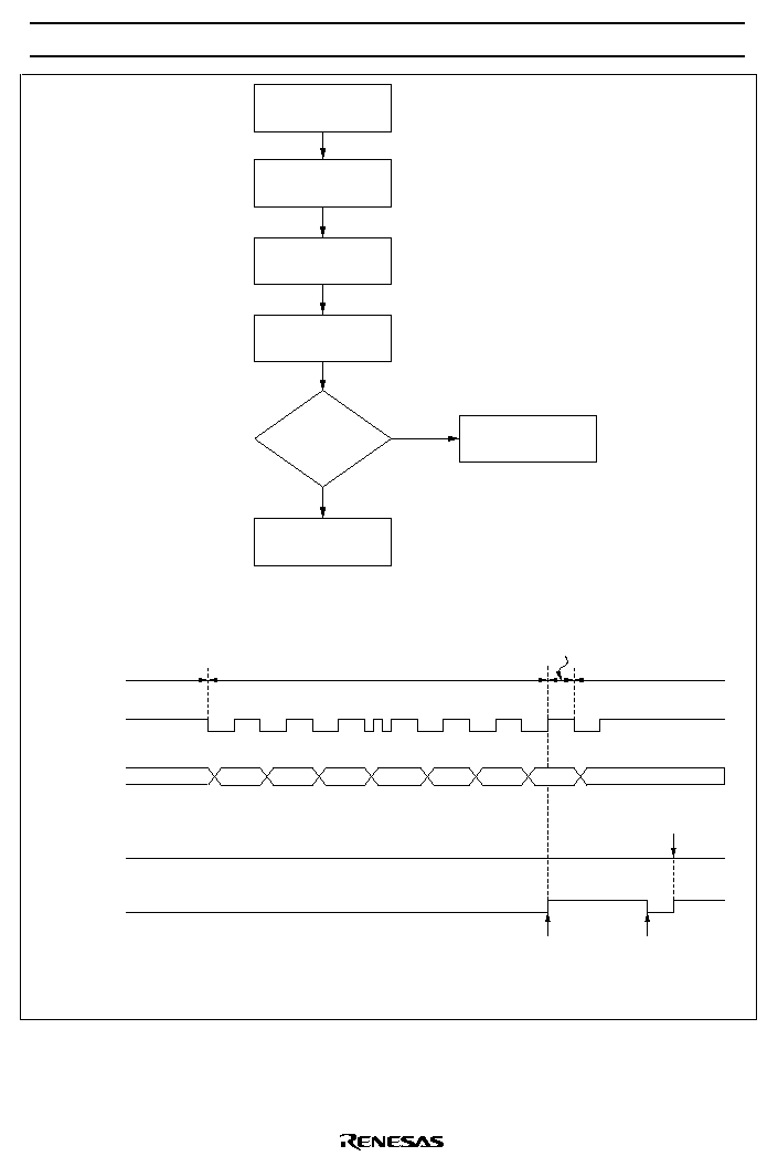
HD404629R Series
89
Transfer completion
(IFS 1)
Interrupts inhibited
IFS 0
SMRA write
IFS = 1?
Transmit clock
error processing
Normal
termination
Yes
No
Transmit clock error detection flowchart
,
Transmit clock error detection procedure
State
SCK
pin (input)
Transmit clock
wait state
Transfer state
Transfer state
Transmit clock wait state
Noise
Transfer state has been
entered by the transmit clock
error. When SMRA is written,
IFS is set.
Flag set because octal
counter reaches 000
Flag reset at
transfer completion
SMRA write
IFS
1
2
3
4
5
6
7
8
Figure 73 Transmit Clock Error Detection

HD404629R Series
90
If more than eight transmit clocks are input in transfer state, at the eighth clock including a spurious pulse
by noise, the octal counter reaches 000, the serial interrupt request flag (IFS: $023, bit 2) is set, and
transmit clock wait state is entered. At the falling edge of the next normal clock signal, the transfer state is
entered. After the transfer completion processing is performed and IFS is reset, writing to serial mode
register A (SMRA: $005) changes the state from transfer to STS wait. At this time IFS is set again, and
therefore the error can be detected.
Notes on Use:
�
Initialization after writing to registers: If port mode register A (PMRA: $004) is written to in transmit
clock wait state or in transfer state, the serial interface must be initialized by writing to serial mode
register A (SMRA: $005) again.
�
Serial interrupt request flag (IFS: $023, bit 2) set: If the state is changed from transfer to another by
writing to serial mode register A (SMRA: $005) or executing the STS instruction during the first low
pulse of the transmit clock, the serial interrupt request flag is not set. To set the serial interrupt request
flag, serial mode register A write or STS instruction execution must be programmed to be executed after
confirming that the
SCK pin is at 1, that is, after executing the input instruction to port R2.
Registers for Serial Interface
The serial interface operation is selected, and serial data is read and written by the following registers.
Serial Mode Register A (SMRA: $005)
Serial Mode Register B (SMRB: $028)
Serial Data Register (SRL: $006, SRU: $007)
Port Mode Register A (PMRA: $004)
Miscellaneous Register (MIS: $00C)
Serial Mode Register A (SMRA: $005): This register has the following functions (figure 74).
R2
1
/
SCK pin function selection
Transfer clock selection
Prescaler division ratio selection
Serial interface initialization
Serial mode register A (SMRA: $005) is a 4-bit write-only register. It is reset to $0 by MCU reset.
A write signal input to serial mode register A (SMRA: $005) discontinues the input of the transmit clock to
the serial data register and octal counter, and the octal counter is reset to 000. Therefore, if a write is
performed during data transfer, the serial interrupt request flag (IFS: $023, bit 2) is set.
Written data is valid from the second instruction execution cycle after the write operation, so the STS
instruction must be executed at least two cycles after that.
HD404629R Series
91
Bit
Initial value
Read/Write
Bit name
3
0
W
SMRA3
2
0
W
SMRA2
0
0
W
SMRA0
1
0
W
SMRA1
Serial mode register A (SMRA: $005)
0
1
0
1
0
1
0
1
0
1
0
1
0
1
SMRA2
SMRA0
SMRA1
SMRA3
0
1
R2
1
/
SCK
mode selection
R2
1
SCK
Output
Output
Input
Clock source
--
--
Prescaler
division ratio
Refer to
table 29
SCK
Prescaler
System clock
External clock
Figure 74 Serial Mode Register A (SMRA)
Serial Mode Register B (SMRB: $028): This register has the following functions (figure 75).
Prescaler division ratio selection
Output level control in idle states
Serial mode register B is a 2-bit write-only register. It cannot be written during data transfer.
By setting bit 0 (SMRB0) of this register, the prescaler division ratio is selected. Only bit 0 (SMRB0) can
be reset to 0 by MCU reset. By setting bit 1 (SMRB1), the output level of the SO pin is controlled in idle
states. The output level changes at the same time that SMRB1 is written to.
HD404629R Series
92
Bit
Initial value
Read/Write
Bit name
3
--
--
Not used
2
--
--
Not used
0
0
W
SMRB0
1
Undefined
W
SMRB1
SMRB0
0
1
Transmit clock division ratio
Prescaler output divided by 2
Prescaler output divided by 4
Serial mode register B (SMRB: $028)
SMRB1
0
1
Output level control in idle states
Low level
High level
Figure 75 Serial Mode Register B (SMRB)
Serial Data Register (SRL: $006, SRU: $007): This register has the following functions (figures 76 and
77).
Transmission data write and shift
Receive data shift and read
Writing data in this register is output from the SO pin, LSB first, synchronously with the falling edge of the
transmit clock; data is input, LSB first, through the SI pin at the rising edge of the transmit clock.
Input/output timing is shown in figure 78.
Data cannot be read or written during serial data transfer. If a read/write occurs during transfer, the
accuracy of the resultant data cannot be guaranteed.
Bit
Initial value
Read/Write
Bit name
3
Undefined
R/W
SR3
2
Undefined
R/W
SR2
0
Undefined
R/W
SR0
1
Undefined
R/W
SR1
Serial data register (lower digit) (SRL: $006)
Figure 76 Serial Data Register (SRL)

HD404629R Series
93
Bit
Initial value
Read/Write
Bit name
3
Undefined
R/W
SR7
2
Undefined
R/W
SR6
0
Undefined
R/W
SR4
1
Undefined
R/W
SR5
Serial data register (upper digit) (SRU: $007)
Figure 77 Serial Data Register (SRU)
LSB
MSB
1
2
3
4
5
6
7
8
Transmit clock
Serial output
data
Serial input data
latch timing
Figure 78 Serial Interface Output Timing
Port Mode Register A (PMRA: $004): This register has the following functions (figure 79).
R2
2
/SI pin function selection
R2
3
/SO pin function selection
Port mode register A (PMRA: $004) is a 2-bit write-only register, and is reset to $0 by MCU reset.
Bit
Initial value
Read/Write
Bit name
3
--
--
Not used
2
--
--
Not used
0
0
W
PMRA0
1
0
W
PMRA1
PMRA0
0
1
R2
3
/SO mode selection
R2
3
SO
Port mode register A (PMRA: $004)
PMRA1
0
1
R2
2
/SI mode selection
R2
2
SI
Figure 79 Port Mode Register A (PMRA)

HD404629R Series
94
Miscellaneous Register (MIS: $00C): This register has the following function (figure 80).
R2
3
/SO pin PMOS control
Miscellaneous register (MIS: $00C) is a 4-bit write-only register and is reset to $0 by MCU reset.
Bit
Initial value
Read/Write
Bit name
3
0
W
MIS3
2
0
W
MIS2
0
0
W
MIS0
1
0
W
MIS1
Miscellaneous register (MIS: $00C)
MIS1
0
1
MIS0
0
1
0
1
t
RC
0.12207 ms
0.24414 ms
7.8125 ms
31.25 ms
Not used
MIS2
0
1
R2
3
/SO PMOS on/off selection
On
Off
MIS3
0
1
Pull-up MOS on/off selection
Off
On
Figure 80 Miscellaneous Register (MIS)
A/D Converter
The MCU has a built-in A/D converter that uses a successive approximation method with a resistor ladder.
It can measure four analog inputs with 8-bit resolution. As shown in the block diagram of figure 81, the
A/D converter has a 4-bit A/D mode register, a 1-bit A/D start flag, and a 4-bit plus 4-bit A/D data register.

HD404629R Series
95
2
AN
0
AN
1
AN
2
AN
3
AV
CC
AV
SS
�
+
A/D interrupt request flag
(IFAD)
A/D mode register
(AMR)
Encoder
Conversion time
control
Off in stop, watch,
and subactive
modes
A/D control
logic
A/D start flag
(ADSF)
Data bus
Signal line
Resistance ladder
A/D data register
(ADR)
Internal data bus
Selector
COMP
Figure 81 Block Diagram of A/D Converter
A/D Mode Register (AMR: $016): Four-bit write-only register which selects the A/D conversion period
and indicates analog input pin information. Bit 0 of the A/D mode register selects the A/D conversion
period, and bits 3 and 2 select a channel, as shown in figure 82.

HD404629R Series
96
Bit
Initial value
Read/Write
Bit name
3
0
W
AMR3
2
0
W
AMR2
0
0
W
AMR0
1
--
--
Not used
A/D mode register (AMR: $016)
AMR0
0
1
Conversion time
34t
cyc
67t
cyc
AMR3
0
0
1
1
AMR2
0
1
0
1
Analog input selection
AN
0
AN
1
AN
2
AN
3
Figure 82 A/D Mode Register (AMR)
A/D Data Register (ADRL: $017, ADRU: $018): Eight-bit read-only register consisting of a 4-bit lower
digit and 4-bit upper digit. This register is not cleared by reset. After the completion of A/D conversion,
the resultant eight-bit data is held in this register until the start of the next conversion (figures 83, 84, and
85).
3
2
1
0
MSB
LSB
3
2
1
0
Bit 0
Bit 7
ADRU: $018
ADRL: $017
Figure 83 A/D Data Registers (ADRU, ADRL)

HD404629R Series
97
Bit
Initial value
Read/Write
Bit name
3
0
R
ADRL3
2
0
R
ADRL2
0
0
R
ADRL0
1
0
R
ADRL1
A/D data register (lower digit) (ADRL: $017)
Figure 84 A/D Data Register Lower Digit (ADRL)
Bit
Initial value
Read/Write
Bit name
A/D data register (upper digit) (ADRU: $018)
2
0
R
ADRU2
1
0
R
ADRU1
0
0
R
ADRU0
3
1
R
ADRU3
Figure 85 A/D Data Register Upper Digit (ADRU)
A/D Start Flag (ADSF: $020, Bit 2): One-bit flag that initiates A/D conversion when set to 1. At the
completion of A/D conversion, the converted data is stored in the A/D data register and the A/D start flag is
cleared. Refer to figure 86.
Bit
Initial value
Read/Write
Bit name
3
0
R/W
DTON
2
0
R/W
ADSF
0
0
R/W
LSON
1
0
R/W
WDON
A/D start flag (ADSF: $020, bit 2)
1
0
ADSF (A/D start flag)
A/D conversion started
A/D conversion completed
Refer to the description of operating
modes
DTON
Refer to the description of timers
WDON
Refer to the description of operating
modes
LSON
Figure 86 A/D Start Flag (ADSF)

HD404629R Series
98
Note on Use: Use the SEM and SEMD instructions to write data to the A/D start flag (ADSF: $020, bit 2),
but make sure that the A/D start flag is not written to during A/D conversion. Data read from the A/D data
register (ADRL: $017, ADRU: $018) during A/D conversion cannot be guaranteed.
The A/D converter does not operate in the stop, watch, and subactive modes because of the OSC clock.
During these low-power dissipation modes, current through the resistor ladder is cut off to decrease the
power input.
DTMF Generation Circuit
The MCU provides a dual-tone multifrequency (DTMF) generation circuit. The DTMF signal consists of
two sine waves to access the switching system.
Figure 87 shows the DTMF keypad and frequencies. Each key enables tones to be generated corresponding
to each frequency. Figure 88 shows a block diagram of the DTMF circuit.
The OSC clock (400 kHz, 800 kHz, 2 MHz, or 4 MHz) is changed into four clock signals through the
division circuit (
1/2
,
1/5
, and 1/10). The DTMF circuit uses one of the four clock signals, which is
selected by the system clock select register (SSR: $029) depending on the OSC clock frequency. The
DTMF circuit has transformed programmable dividers, sine wave counters, and control registers.
The DTMF generation circuit is controlled by the following three registers.
1
2
3
A
4
5
6
B
7
8
9
C
*
0
#
D
R1 (697 Hz)
R2 (770 Hz)
R3 (852 Hz)
R4 (941 Hz)
C1 (1,209 Hz)
C2 (1,336 Hz)
C3 (1,477 Hz)
C4 (1,633 Hz)
Figure 87 DTMF Keypad and Frequencies

HD404629R Series
99
Sine wave
counter D/A
Transforma-
tion program
divider
Feedback
Sine wave
counter D/A
Transforma-
tion program
divider
Feedback
TONER
VT
ref
TONEC
TONER output control
TONEC output control
1/2
1/5
1/10
f
OSC
Tone generator
control register
(TGC)
System clock
selection register
(SSR)
400 kHz
2
2
2
Selector
Tone generator
mode register
(TGM)
Internal data bus
800 kHz
2 MHz
4 MHz
400 kHz
Data bus
Clock line
Signal line
Figure 88 Block Diagram of DTMF Circuit
HD404629R Series
100
Tone Generator Mode Register (TGM: $019): Four-bit write-only register, which controls output
frequencies as shown in figure 89, and is reset to $0 by MCU reset.
Bit
Initial value
Read/Write
Bit name
3
0
W
TGM3
2
0
W
TGM2
0
0
W
TGM0
1
0
W
TGM1
Tone generator mode register (TGM: $019)
TGM3
0
0
1
1
TGM2
0
1
0
1
TONEC output frequencies
f
C1
(1,209 Hz)
f
C2
(1,336 Hz)
f
C3
(1,477 Hz)
f
C4
(1,633 Hz)
TGM1
0
0
1
1
TGM0
0
1
0
1
TONER output frequencies
f
R1
(697 Hz)
f
R2
(770 Hz)
f
R3
(852 Hz)
f
R4
(941 Hz)
Figure 89 Tone Generator Mode Register (TGM)
Tone Generator Control Register (TGC: $01A): Three-bit write-only register, which controls the
start/stop of the DTMF signal output as shown in figure 90, and is reset to $0 by MCU reset. TONER and
TONEC output can be independently controlled by bits 3 and 2 (TGC3, TGC2), and the DTMF circuit is
controlled by bit 1 (TGC1) of this register.
Bit
Initial value
Read/Write
Bit name
3
0
W
TGC3
2
0
W
TGC2
0
--
--
Not used
1
0
W
TGC1
Tone generator control register (TGC: $01A)
TGC1
0
1
DTMF enable bit
DTMF disable
DTMF enable
TGC2
0
1
TONER output control (row)
No output
TONER output (active)
TGC3
0
1
TONEC output control (column)
No output
TONEC output (active)
Figure 90 Tone Generator Control Register (TGC)

HD404629R Series
101
System Clock Select Register (SSR: $029): Four-bit write-only register. This register must be set to the
value specified in figure 91 depending on the frequency of the oscillator connected to the OSC
1
and OSC
2
pins. Note that if the combination of the oscillation frequency and the value in this register is different
from that specified in figure 91, the DTMF output frequencies will differ from the correct frequencies as
listed in figure 89.
Bit
Initial value
Read/Write
Bit name
3
0
W
SSR3
2
0
W
SSR2
0
0
W
SSR0
1
0
W
SSR1
System clock select register (SSR: $029)
SSR1
0
0
1
1
System clock selection
400 kHz
800 kHz
2 MHz
4 MHz
SSR0
0
1
0
1
SSR2
0
1
ratio selection
f
SUB
= f
X
/8
f
SUB
= f
X
/4
SSR3
0
1
32-kHz oscillation stop
Oscillation operates in stop mode
Oscillation stops in stop mode
32-kHz oscillation division
Note: SSR3 is cleared only by a RESET input. SSR3 will not be cleared by a
STOPC
input during stop
mode, and will retain its value. SSR3 will also not be cleared upon entering stop mode.
Figure 91 System Clock Select Register (SSR)

HD404629R Series
102
DTMF Output: The sine waves of the row-group and column-group are individually converted in the D/A
conversion circuit which provides a high-precision ladder resistance. The DTMF output pins (TONER,
TONEC) transmit the sine waves of the row-group and column-group, respectively.
Figure 92 shows the tone output equivalent circuit. Figure 93 shows the output waveform. One cycle of
this wave consists of 32 slots. Therefore, the output waveform is stable with little distortion. Table 30 lists
the frequency deviation of the MCU from standard DTMF signals.
Table 30 Frequency Deviation of the MCU from Standard DTMF
Standard DTMF (Hz)
MCU (Hz)
Deviation from Standard (%)
R1
697
694.44
�0.37
R2
770
769.23
�0.10
R3
852
851.06
�0.11
R4
941
938.97
�0.22
C1
1,209
1,212.12
0.26
C2
1,336
1,333.33
�0.20
C3
1,477
1,481.48
0.30
C4
1,633
1,639.34
0.39
Note:
This frequency deviation value does not include the frequency deviation due to the oscillator
element. Also note that in this case the ratio of the high level and low level widths in the oscillator
waveform due to the oscillator element will be 50%:50%.
VT
GND
ref
Switch control
TONER
TONEC
Figure 92 Tone Output Equivalent Circuit

HD404629R Series
103
VT
GND
ref
1 2 3 4 5 6 7 8 9 10 11 12 13 14 15 16 17 18 19 20 21 22 23 24 25 26 27 28 29 30 31 32
Time slot
Figure 93 Waveform of Tone Output

HD404629R Series
104
LCD Controller/Driver
The MCU has an LCD controller and driver which drive 4 common signal pins and 52 segment pins. The
controller consists of a RAM area in which display data is stored, a display control register (LCR: $01B),
and a duty-cycle/clock-control register (LMR: $01C) (figure 94).
Four duty cycles and the LCD clock are programmable, and a built-in dual-port RAM ensures that display
data can be automatically transmitted to the segment signal pins without program intervention. If a 32-kHz
oscillation clock is selected as the LCD clock source, the LCD can even be used in watch mode, in which
the system clock stops.
Internal LCD power supply switch
52
2
2
4
4
3
LCD mode
register
(LMR)
2
V
CC
V
1
V
2
V
3
GND
COM1
COM2
COM3
COM4
SEG1
SEG4
SEG5
SEG8
SEG9
SEG20
SEG21
SEG52
CL0
CL1
CL2
CL3
Note: Pin function switching circuit
LCD power supply
control circuit
Common
signal
output
circuit
LCD control
register
(LCR)
LCD output
register 1
(LOR1)
LCD output
register 2
(LOR2)
LCD output
register 3
(LOR3)
Dual-port
display RAM
(52 digits)
Display
control
Display data
Duty
selection
Clock
Internal data bus
Segment
signal
output
circuit
Selector
Data bus
Clock line
Signal line
Pin
control
Figure 94 Block Diagram of Liquid Crystal Display Control System

HD404629R Series
105
LCD Data Area and Segment Data ($050�$083): As shown in figure 95, each bit of the storage area
corresponds to one of four duty cycles. If data is written to an area corresponding to a certain duty cycle, it
is automatically output to the corresponding segments as display data.
$060
$061
$062
$063
$064
$065
$066
$067
$068
$069
COM4
COM3
COM2
COM1
Bit 3
Bit 2
Bit 1
Bit 0
$050
$051
$052
$053
$054
$055
$056
$057
$058
$059
$05A
$05B
$05C
$05D
$05E
$05F
SEG1
SEG2
SEG3
SEG4
SEG5
SEG6
SEG7
SEG8
SEG9
SEG10
SEG11
SEG12
SEG13
SEG14
SEG15
SEG16
SEG1
SEG2
SEG3
SEG4
SEG5
SEG6
SEG7
SEG8
SEG9
SEG10
SEG11
SEG12
SEG13
SEG14
SEG15
SEG16
SEG1
SEG2
SEG3
SEG4
SEG5
SEG6
SEG7
SEG8
SEG9
SEG10
SEG11
SEG12
SEG13
SEG14
SEG15
SEG16
SEG1
SEG2
SEG3
SEG4
SEG5
SEG6
SEG7
SEG8
SEG9
SEG10
SEG11
SEG12
SEG13
SEG14
SEG15
SEG16
Bit 3
Bit 2
Bit 1
Bit 0
$06A
$06B
$06C
$06D
$06E
$06F
$070
$071
$072
$073
$074
$075
$076
$077
$078
$079
SEG27
SEG28
SEG29
SEG30
SEG31
SEG32
SEG33
SEG34
SEG35
SEG36
SEG37
SEG38
SEG39
SEG40
SEG41
SEG42
$07A
$07B
$07C
$07D
$07E
$07F
$080
$081
$082
$083
COM4
COM3
COM2
COM1
SEG20
SEG21
SEG22
SEG23
SEG24
SEG25
SEG26
SEG43
SEG44
SEG45
SEG46
SEG47
SEG48
SEG49
SEG50
SEG51
SEG52
SEG17
SEG18
SEG19
SEG20
SEG21
SEG22
SEG23
SEG24
SEG25
SEG26
SEG17
SEG18
SEG19
SEG20
SEG21
SEG22
SEG23
SEG24
SEG25
SEG26
SEG17
SEG18
SEG19
SEG20
SEG21
SEG22
SEG23
SEG24
SEG25
SEG26
SEG17
SEG18
SEG19
SEG27
SEG28
SEG29
SEG30
SEG31
SEG32
SEG33
SEG34
SEG35
SEG36
SEG37
SEG38
SEG39
SEG40
SEG41
SEG42
SEG43
SEG44
SEG45
SEG46
SEG47
SEG48
SEG49
SEG50
SEG51
SEG52
SEG27
SEG28
SEG29
SEG30
SEG31
SEG32
SEG33
SEG34
SEG35
SEG36
SEG37
SEG38
SEG39
SEG40
SEG41
SEG42
SEG43
SEG44
SEG45
SEG46
SEG47
SEG48
SEG49
SEG50
SEG51
SEG52
SEG27
SEG28
SEG29
SEG30
SEG31
SEG32
SEG33
SEG34
SEG35
SEG36
SEG37
SEG38
SEG39
SEG40
SEG41
SEG42
SEG43
SEG44
SEG45
SEG46
SEG47
SEG48
SEG49
SEG50
SEG51
SEG52
RAM
address
RAM
address
Figure 95 Configuration of LCD RAM Area (for Dual-Port RAM)
HD404629R Series
106
LCD Control Register (LCR: $01B): Three-bit write-only register which controls LCD blanking, on/off
switching of the liquid-crystal display's power supply division resistor, and display in watch and subactive
modes, as shown in figure 96.
�
Blank/display
Blank: Segment signals are turned off, regardless of LCD RAM data setting.
Display: LCD RAM data is output as segment signals.
�
Power switch on/off
Off: The power switch is off.
On: The power switch is on and V1 is V
CC
.
�
Watch/subactive mode display
Off: In watch and subactive modes, all common and segment pins are grounded and the liquid-crystal
power switch is turned off.
On: In watch and subactive modes, LCD RAM data is output as segment signals.
Bit
Initial value
Read/Write
Bit name
3
--
--
Not used
2
0
W
LCR2
0
0
W
LCR0
1
0
W
LCR1
LCD display control register (LCR: $01B)
LCR1
0
1
Power switch on/off
Off
On
LCR0
0
1
Blank/display
Blank
Display
0
1
Display on/off selection in
watch and subactive modes
LCR2
Off
On
Figure 96 LCD Control Register (LCR)
HD404629R Series
107
LCD Duty-Cycle/Clock Control Register (LMR: $01C): Four-bit write-only register which selects the
display duty cycle and LCD clock source, as shown in figure 97. The dependence of frame
frequency on duty cycle is listed in table 31.
Bit
Initial value
Read/Write
Bit name
3
0
W
LMR3
2
0
W
LMR2
0
0
W
LMR0
1
0
W
LMR1
LCD duty cycle/clock control register (LMR: $01C)
LMR3
LMR2
Input clock source selection
LMR1
0
0
1
1
LMR0
0
1
0
1
Duty cycle selection
1/4 duty
1/3 duty
1/2 duty
Static
CL0 (32.768-kHz
�
duty/64: when
32.768-kHz oscillation is used)
0
1
1
1
0
1
CL1 (f
OSC
�
duty cycle/1024)
CL2 (f
OSC
�
duty cycle/8192)
CL3 (refer to table 31)
0
0
Figure 97 LCD Duty-Cycle/Clock Control Register (LMR)

HD404629R Series
108
Table 31 LCD Frame Frequencies for Different Duty Cycles
Frame Frequencies
Duty Cycle
LMR3
LMR2
f
OSC
=
400 kHz
f
OSC
=
800 kHZ
f
OSC
=
2 MHz
f
OSC
=
4 MHz
Static
0
0
CL0
512 Hz
1
CL1
390.6 Hz
781.3 Hz
1953 Hz
3906 Hz
1
0
CL2
48.8 Hz
97.7 Hz
244.1 Hz
488.3 Hz
1
CL3*
24.4 Hz
48.8 Hz
122.1 Hz
244.1 Hz
64 Hz
1/2
0
0
CL0
256 Hz
1
CL1
195.3 Hz
390.6 Hz
976.6 Hz
1953 Hz
1
0
CL2
24.4 Hz
48.8 Hz
122.1 Hz
244.1 Hz
1
CL3*
12.2 Hz
24.4 Hz
61 Hz
122.1 Hz
32 Hz
1/3
0
0
CL0
170.7 Hz
1
CL1
130.2 Hz
260.4 Hz
651 Hz
1302 Hz
1
0
CL2
16.3 Hz
32.6 Hz
81.4 Hz
162.8 Hz
1
CL3*
8.1 Hz
16.3 Hz
40.7 Hz
81.4 Hz
21.3 Hz
1/4
0
0
CL0
128 Hz
1
CL1
97.7 Hz
195.3 Hz
488.3 Hz
976.6 Hz
1
0
CL2
12.2 Hz
24.4 Hz
61 Hz
122.1 Hz
1
CL3*
6.1 Hz
12.2 Hz
30.5 Hz
61 Hz
16 Hz
Note: * The division ratio depends on the value of bit 3 of timer mode register A (TMA).
Upper value: When TMA3 = 0, CL3 = f
OSC
�
duty cycle/16384.
Lower value: When TMA3 = 1, CL3 = 32.768 kHz
�
duty cycle/512.

HD404629R Series
109
LCD Output Register 1 (LOR1: $01D): Write-only register used to specify ports R3
0
�R3
3
as pins SEG1�
SEG4 by individual pins (figure 98).
Bit
Initial value
Read/Write
Bit name
3
0
W
LOR13
2
0
W
LOR12
0
0
W
LOR10
1
0
W
LOR11
LCD output register 1 (LOR1: $01D)
LOR10
0
1
R3
0
/SEG1 mode selection
R3
0
SEG1
LOR11
0
1
R3
1
/SEG2 mode selection
R3
1
SEG2
LOR12
0
1
R3
2
/SEG3 mode selection
R3
2
SEG3
LOR13
0
1
R3
3
/SEG4 mode selection
R3
3
SEG4
Figure 98 LCD Output Register 1 (LOR1)
LCD Output Register 2 (LOR2: $01E): Write-only register used to specify ports R4
0
�R4
3
as pins SEG5�
SEG8 by individual pins (figure 99).
Bit
Initial value
Read/Write
Bit name
3
0
W
LOR23
2
0
W
LOR22
0
0
W
LOR20
1
0
W
LOR21
LCD output register 2 (LOR2: $01E)
LOR20
0
1
R4
0
/SEG5 mode selection
R4
0
SEG5
LOR21
0
1
R4
1
/SEG6 mode selection
R4
1
SEG6
LOR22
0
1
R4
2
/SEG7 mode selection
R4
2
SEG7
LOR23
0
1
R4
3
/SEG8 mode selection
R4
3
SEG8
Figure 99 LCD Output Register 2 (LOR2)

HD404629R Series
110
LCD Output Register 3 (LOR3: $01F): Write-only register used to specify ports R5�R7 as pins SEG9�
SEG20 in 4-pin units (figure 100).
Bit
Initial value
Read/Write
Bit name
3
--
--
Not used
2
0
W
LOR32
0
0
W
LOR30
1
0
W
LOR31
LCD output register 3 (LOR3: $01F)
LOR30
0
1
R5
0
/SEG9�R5
3
/SEG12 mode selection
R5
0
-R5
3
SEG9�SEG12
LOR31
0
1
R6
0
/SEG13�R6
3
/SEG16 mode selection
R6
0
-R6
3
SEG13�SEG16
LOR32
0
1
R7
0
/SEG17�R7
3
/SEG20 mode selection
R7
0
-R7
3
SEG17�SEG20
Figure 100 LCD Output Register 3 (LOR3)
Large Liquid-Crystal Panel Drive and V
LCD
: To drive a large-capacity LCD, decrease the resistance of
the built-in division resistors by attaching external resistors in parallel, as shown in figure 101.
The size of these resistors cannot be simply calculated from the LCD load capacitance because the matrix
configuration of the LCD complicates the paths of charge/discharge currents flowing through the
capacitors--the resistance will also vary with lighting conditions. This size must be determined by trial-
and-error, taking into account the power dissipation of the device using the LCD, but a resistance of 1 to 10
k
would usually be suitable. (Another effective method is to attach capacitors of 0.1 to 0.3
�
F.)
Always turn off the power switch (set bit 1 of the LCR to 0) before changing the liquid-crystal drive
voltage (V
LCD
).
HD404629R Series
111
52
2
3
4
52
52
52
V
CC
V
2
V
3
GND
V
1
COM1
SEG1
to
SEG52
V
CC
V
2
V
3
GND
V
1
COM1
COM2
SEG1
to
SEG52
V
CC
V
2
V
3
GND
V
1
COM1
to
COM3
SEG1
to
SEG52
V
CC
V
2
V
3
GND
V
1
COM1
to
COM4
SEG1
to
SEG52
V
CC
V
LCD
V
CC
V
LCD
V
CC
V
LCD
V
CC
V
LCD
R
R
R
V (V )
CC 1
V
2
V
3
GND
R
R
R
V (V )
CC 1
V
2
V
3
GND
C
C
C
6-digit LCD
with sign
.
13-digit LCD
17-digit LCD
with sign
26-digit LCD
.
.
.
Static drive
1/2 duty, 1/2 bias drive
1/3 duty, 1/3 bias drive
1/4 duty, 1/3 bias drive
V V GND
CC
LCD
1
Figure 101 LCD Connection Examples

HD404629R Series
112
ZTAT
TM
Microcomputer with Built-in programmable ROM
Programming of Built-in programmable ROM
The MCU can stop its function as an MCU in PROM mode for programming the built-in PROM.
PROM mode is set up by setting the
TEST, M
0
, and
M
1
terminals to "Low" level and the RESET terminal
to "High" level.
Writing and reading specifications of the PROM are the same as those for the commercial EPROM27256.
Using a socket adapter for specific use of each product, programming is possible with a general-purpose
PROM writer.
Since an instruction of the HMCS400 series is 10 bits long, a conversion circuit is incorporated to adapt the
general-purpose PROM writer. This circuit splits each instruction into five lower bits and five higher bits
to write from or read to two addresses. This enables use of a general-purpose PROM. For instance, to
write to a 16kword of built-in PROM with a general-purpose PROM writer, specify 32kbyte address
($0000-$7FFF).
Notes:
1. When programming with a PROM writer, set up each ROM size to the address given in table b. If it is
programmed erroneously to an address given in Table 33 or later, check of writing of PROM may
become impossible. Particularly, caution should be exercised in the case of a plastic package since
reprogramming is impossible with it. Set the data in unused addresses to $FF.
2. If the indexes of the PROM writer socket, socket adapter and product are not aligned precisely, the
product may break down due to overcurrent. Be sure to check that they are properly set to the writer
before starting the writing process.
3. Two levels of program voltages (V
PP
) are available for the PROM: 12.5 V and 21 V. Our product
employs a V
PP
of 12.5 V. If a voltage of 21 V is applied, permanent breakdown of the product will
result. The V
PP
of 12.5 V is obtained for the PROM writer by setting it according to the Intel 27258
specifications.
Writing/verification
Programming of the built-in program ROM employs a high speed programming method. With this method,
high speed writing is effected without voltage stress to the device or without damaging the reliability of the
written data.
For precautions for PROM writing procedure, refer to section 2, "Characteristics of ZTAT
TM
Microcomputer's Built-in Programmable ROM and precautions for its Applications."

HD404629R Series
113
Table 32 Selection of Mode
Mode
CE
OE
V
PP
O
0
�O
7
Writing
"Low"
"High"
V
PP
Data input
Verification
"High"
"Low"
V
PP
Data output
Prohibition of programming
"High"
"High"
V
PP
High impedance
Table 33 PROM Writer Program Address
ROM size
Address
8k
$0000~$3FFF
12k
$0000~$5FFF
16k
$0000~$7FFF

HD404629R Series
114
Programmable ROM (HD4074629)
The HD4074629 is a ZTAT
TM
microcomputer with built-in PROM that can be programmed in PROM
mode.
PROM Mode Pin Description
Pin No.
MCU Mode
PROM Mode
Pin No.
MCU Mode
PROM Mode
FP-100B
TFP-100B
FP-100A
Pin
Name
I/O
Pin
Name
I/O
FP-100B
TFP-100B
FP-100A
Pin
Name
I/O
Pin
Name
I/O
1
3
AV
CC
V
CC
24
26
D
10
/
STOPC
I/O
A
9
I
2
4
AN
0
I
25
27
D
11
/
INT
0
I/O
V
PP
3
5
AN
1
I
26
28
R0
0
/
INT
1
I/O
GND
4
6
AN
2
I
27
29
R0
1
/INT
2
I/O
GND
5
7
AN
3
I
28
30
R0
2
/INT
3
I/O
6
8
AV
SS
GND
29
31
R0
3
/INT
4
I/O
7
9
TEST
I
GND
30
32
R1
0
/TOB
I/O
A
5
I
8
10
OSC
1
I
V
CC
31
33
R1
1
/TOC
I/O
A
6
I
9
11
OSC
2
O
32
34
R1
2
/TOD
I/O
A
7
I
10
12
RESET
I
V
CC
33
35
R1
3
/
EVNB
I/O
A
8
I
11
13
X1
I
GND
34
36
R2
0
/EVND
I/O
A
0
I
12
14
X2
O
35
37
R2
1
/
SCK
I/O
A
10
I
13
15
GND
GND
36
38
R2
2
/SI
I/O
A
11
I
14
16
D
0
I/O
CE
I
37
39
R2
3
/SO
I/O
A
12
I
15
17
D
1
I/O
OE
I
38
40
R3
0
/SEG1
I/O
A
13
I
16
18
D
2
I/O
V
CC
39
41
R3
1
/SEG2
I/O
A
14
I
17
19
D
3
I/O
V
CC
40
42
R3
2
/SEG3
I/O
O
0
I/O
18
20
D
4
I/O
41
43
R3
3
/SEG4
I/O
O
1
I/O
19
21
D
5
I/O
42
44
R4
0
/SEG5
I/O
O
2
I/O
20
22
D
6
I/O
43
45
R4
1
/SEG6
I/O
O
3
I/O
21
23
D
7
I/O
44
46
R4
2
/SEG7
I/O
O
4
I/O
22
24
D
8
I/O
45
47
R4
3
/SEG8
I/O
O
5
I/O
23
25
D
9
I/O
46
48
R5
0
/SEG9
I/O
O
6
I/O
Notes on next page.

HD404629R Series
115
PROM Mode Pin Description (cont)
Pin No.
MCU Mode
PROM Mode
Pin No.
MCU Mode
PROM Mode
FP-100B
TFP-100B
FP-100A
Pin
Name
I/O
Pin
Name
I/O
FP-100B
TFP-100B
FP-100A
Pin
Name
I/O
Pin
Name
I/O
47
49
R5
1
/SEG10 I/O
O
7
I/O
74
76
SEG37
O
48
50
R5
2
/SEG11 I/O
O
4
I/O
75
77
SEG38
O
49
51
R5
3
/SEG12 I/O
O
3
I/O
76
78
SEG39
O
50
52
R6
0
/SEG13 I/O
O
2
I/O
77
79
SEG40
O
51
53
R6
1
/SEG14 I/O
O
1
I/O
78
80
SEG41
O
52
54
R6
2
/SEG15 I/O
O
0
I/O
79
81
SEG42
O
53
55
R6
3
/SEG16 I/O
V
CC
80
82
SEG43
O
54
56
R7
0
/SEG17 I/O
A
1
I
81
83
SEG44
O
55
57
R7
1
/SEG18 I/O
A
2
I
82
84
SEG45
O
56
58
R7
2
/SEG19 I/O
A
3
I
83
85
SEG46
O
57
59
R7
3
/SEG20 I/O
A
4
I
84
86
SEG47
O
58
60
SEG21
O
85
87
SEG48
O
59
61
SEG22
O
86
88
SEG49
O
60
62
SEG23
O
87
89
SEG50
O
61
63
SEG24
O
88
90
SEG51
O
62
64
SEG25
O
89
91
SEG52
O
63
65
SEG26
O
90
92
COM1
O
64
66
SEG27
O
91
93
COM2
O
65
67
SEG28
O
92
94
COM3
O
66
68
SEG29
O
93
95
COM4
O
67
69
SEG30
O
94
96
V
1
68
70
SEG31
O
95
97
V
2
69
71
SEG32
O
96
98
V
3
70
72
SEG33
O
97
99
V
CC
V
CC
71
73
SEG34
O
98
100
TONEC
O
72
74
SEG35
O
99
1
TONER
O
73
75
SEG36
O
100
2
VT
ref
Notes: 1. I/O: Input/output pin, I: Input pin, O: Output pin
2. Each of O
0
�O
4
has two pins; before using, each pair must be connected together.

HD404629R Series
116
PROM Mode Pin Functions
V
PP
: Applies the programming voltage (12.5 V
�
0.3 V) to the built-in PROM.
CE: Inputs a control signal to enable PROM programming and verification.
OE
: Inputs a data output control signal for verification.
A
0
�A
14
: Act as address input pins of the built-in PROM.
O
0
�O
7
: Act as data bus input pins of the built-in PROM. Each of O
0
�O
4
has two pins; before using these
pins, connect each pair together.
M
0
,
M
1
, RESET,
TEST: Used to set PROM mode. The MCU is set to the PROM mode by pulling M
0
,
M
1
, and
TEST low, and RESET high.
Other Pins (FP-100B/FP-100A): Connect pins 1/3 (AV
CC
), 8/10 (OSC
1
), 16/18 (D
2
), 17/19 (D
3
), 53/55
(R6
3
/SEG16), and 97/99 (V
CC
) to V
CC
, and pins 6/8 (AV
SS
) and 11/13 (X1) to GND. Leave other pins
open.
$0000
Vector address
Zero-page subroutine
(64 words)
Pattern
(4,096 words)
Program
(16,384 words)
$0001
$001F
$0080
$007F
$2000
$1FFF
$0020
$7FFF
Bit 4
Bit 8
Bit 3
Bit 7
Bit 2
Bit 6
Bit 1
Bit 5
Bit 0
Bit 9
Upper three bits are not to be used
(fill them with 111)
Upper 5 bits
Lower 5 bits
$0000
$000F
$0010
$003F
$0040
$3FFF
$0000
$0001
$0002
$0003
$0004
$0005
$0006
$0007
$0008
$0009
$000A
$000B
$000C
$000D
$000E
$000F
JMPL instruction
(jump to RESET,
STOPC
routine)
JMPL instruction
(jump to
INT
0
routine)
JMPL instruction
(jump to timer A routine)
JMPL instruction
(jump to timer B, INT
2
routine)
JMPL instruction
(jump to
INT
1
routine)
JMPL instruction
(jump to timer C, INT
3
routine)
JMPL instruction
(jump to timer D, INT
4
routine)
.
.
.
.
.
.
.
.
.
JMPL instruction
(jump to A/D, serial routine)
$0FFF
$1000
1
1
1
1
1
1
Figure 102 Memory Map in PROM Mode

HD404629R Series
117
Start
Verification OK?
Set programming/verification modes
V = 12.5
�
0.3 V, V = 6.0
�
0.25 V
PP
CC
Address = 0
n = 0
n + 1 n
Program t =1 ms
�
5%
PW
Program t = 3n ms
OPW
Last address?
n < 25?
Yes
No
No
No
Address + 1 Address
Yes
Set read mode
V = 5.0
�
0.5 V, V = V
�
0.6 V
CC
PP
CC
All addresses
read?
End
Fail
No
Yes
Yes
Figure 103 Flowchart of High-Speed Programming

HD404629R Series
118
Programming Electrical Characteristics
DC Characteristics (V
CC
= 6.0 V
�
0.25 V, V
PP
= 12.5 V
�
0.3 V, T
a
= 25
�
C
�
5
�
C, unless otherwise
specified)
Item
Symbol
Pin(s)
Min
Typ
Max
Unit
Test Condition
Input high
V
IH
O
0
�O
7
, A
0
�A
14
,
2.2
--
V
CC
+ 0.3
V
voltage level
OE
,
CE
Input low
V
IL
O
0
�O
7
, A
0
�A
14
,
�0.3
--
0.8
V
voltage level
OE
,
CE
Output high
V
OH
O
0
�O
7
2.4
--
--
V
I
OH
= �200
�
A
voltage level
Output low
V
OL
O
0
�O
7
--
--
0.4
V
I
OL
= 1.6 mA
voltage level
Input leakage
I
IL
O
0
�O
7
, A
0
�A
14
,
--
--
2
�
A
V
in
= 5.25 V/0.5 V
current
OE
,
CE
V
CC
current
I
CC
--
--
30
mA
V
PP
current
I
PP
--
--
40
mA
AC Characteristics (V
CC
= 6.0 V
�
0.25 V, V
PP
= 12.5 V
�
0.3 V, T
a
= 25
�
C
�
5
�
C, unless otherwise
specified)
Item
Symbol
Min
Typ
Max
Unit
Test Condition
Address setup time
t
AS
2
--
--
�
s
See figure 108
OE
setup time
t
OES
2
--
--
�
s
Data setup time
t
DS
2
--
--
�
s
Address hold time
t
AH
0
--
--
�
s
Data hold time
t
DH
2
--
--
�
s
Data output disable time
t
DF
--
--
130
ns
V
PP
setup time
t
VPS
2
--
--
�
s
Program pulse width
t
PW
0.95
1.0
1.05
ms
CE
pulse width during
t
OPW
2.85
--
78.75
ms
overprogramming
V
CC
setup time
t
VCS
2
--
--
�
s
Data output delay time
t
OE
0
--
500
ns

HD404629R Series
119
Address
Data
Data in Stable
Data out Valid
V
PP
V
PP
V
CC
GND
GND
V
CC
CE
OE
t
AS
t
DS
t
VPS
t
VCS
t
DH
t
PW
t
OPW
t
OES
t
OE
t
AH
t
DF
Programming
Verification
Input pulse level: 0.8 V to 2.2 V
Input rise/fall time: 20 ns
Input timing reference levels: 1.0 V, 2.0 V
Output timing reference levels: 0.8 V, 2.0 V
Figure 104 PROM Programming/Verification Timing

HD404629R Series
120
Notes on PROM Programming
Principles of Programming/Erasure: A memory cell in a ZTATTM microcomputer is the same as an
EPROM cell; it is programmed by applying a high voltage between its control gate and drain to inject hot
electrons into its floating gate. These electrons are stable, surrounded by an energy barrier formed by an
SiO
2
film. The change in threshold voltage of a memory cell with a charged floating gate makes the
corresponding bit appear as 0; a cell whose floating gate is not charged appears as a 1 bit (figure 105).
The charge in a memory cell may decrease with time. This decrease is usually due to one of the following
causes:
�
Ultraviolet light excites electrons, allowing them to escape. This effect is the basis of the erasure
principle.
�
Heat excites trapped electrons, allowing them to escape.
�
High voltages between the control gate and drain may erase electrons.
If the oxide film covering a floating gate is defective, the electron erasure rate will be greater. However,
electron erasure does not often occur because defective devices are detected and removed at the testing
stage.
Control gate
Floating gate
Drain
SiO
2
Source
N
N
+
+
Control gate
Floating gate
Drain
SiO
2
Source
N
N
+
+
Erasure (1)
Write (0)
Figure 105 Cross-Sections of a PROM Cell
PROM Programming: PROM memory cells must be programmed under specific voltage and timing
conditions. The higher the programming voltage V
PP
and the longer the programming pulse t
PW
is applied,
the more electrons are injected into the floating gates. However, if V
PP
exceeds specifications, the pn
junctions may be permanently damaged. Pay particular attention to overshooting in the PROM
programmer. In addition, note that negative voltage noise will produce a parasitic transistor effect that may
reduce breakdown voltages.
The ZTATTM microcomputer is electrically connected to the PROM programmer by a socket adapter.
Therefore, note the following points:
�
Check that the socket adapter is firmly mounted on the PROM programmer.
�
Do not touch the socket adapter or the LSI
during the programming. Touching them may affect the quality of the contacts, which will cause
programming errors.

HD404629R Series
121
PROM Reliability after Programming: In general, semiconductor devices retain their reliability,
provided that some initial defects can be excluded. These initial defects can be detected and rejected by
screening. Baking devices under high-temperature conditions is one method of screening that can rapidly
eliminate data-hold defects in memory cells. (Refer to the previous Principles of Programming/Erasure
section.)
ZTATTM microcomputer devices are extremely reliable because they have been subjected to such a
screening method during the wafer fabrication process, but Hitachi recommends that each device be
exposed to 150
�
C at one atmosphere for at least 48 hours after it is programmed, to ensure its best
performance. The recommended screening procedure is shown in figure 106.
Note:
If programming errors occur continuously during PROM programming, suspend programming and
check for problems in the PROM programmer or socket adapter. If programming verification
indicates errors in programming or after high-temperature exposure, please inform Hitachi.
Note: Exposure time is measured from when the temperature in the heater reaches 150�C.
Programming, verification
Exposure to high temperature, without power
150�C � 10�C, 48 h
+8 h
0 h
�
*
*
Program read check
V = 4.5 V or 5.5 V
CC
Figure 106 Recommended Screening Procedure

HD404629R Series
122
Addressing Modes
RAM Addressing Modes
The MCU has three RAM addressing modes, as shown in figure 107 and described below.
Register Indirect Addressing Mode: The contents of the W, X, and Y registers (10 bits in total) are used
as a RAM address.
Direct Addressing Mode: A direct addressing instruction consists of two words. The first word contains
the opcode, and the contents of the second word (10 bits) are used as a RAM address.
Memory Register Addressing Mode: The memory registers (MR), which are located in 16 addresses from
$040 to $04F, are accessed with the LAMR and XMRA instructions.
AP
9
AP
0
W
1
Y
0
W register
X register
Y register
RAM address
Register Direct Addressing
AP
9
AP
0
RAM address
Direct Addressing
d
9
d
0
2nd word of Instruction
Opcode
1st word of Instruction
AP
9
AP
0
RAM address
Memory Register Addressing
m
3
Opcode
Instruction
0
0
0
1
0
0
AP
8
AP
7
AP
AP
5
AP
4
6
AP
3
AP
2
AP
1
AP
AP
AP
AP
AP
AP
AP
AP
8
7
6
5
4
3
2
1
d
8
d
7
d
6
d
5
d
4
d
3
d
2
d
1
AP
8
AP
7
AP
6
AP
5
AP
4
AP
3
AP
2
AP
1
W
0
X
3
X
2
X
1
X
0
Y
3
Y
2
Y
1
m
2
m
1
m
0
Figure 107 RAM Addressing Modes

HD404629R Series
123
ROM Addressing Modes and the P Instruction
The MCU has four ROM addressing modes, as shown in figure 108 and described below.
Direct Addressing Mode: A program can branch to any address in the ROM memory space by executing
the JMPL, BRL, or CALL instruction. Each of these instructions replaces the 14 program counter bits
(PC
13
�PC
0
) with 14-bit immediate data.
Current Page Addressing Mode: The MCU has 64 pages of ROM with 256 words per page. A program
can branch to any address in the current page by executing the BR instruction. This instruction replaces the
eight low-order bits of the program counter (PC
7
�PC
0
) with eight-bit immediate data. If the BR instruction
is on a page boundary (address 256n + 255), executing that instruction transfers the PC contents to the next
physical page, as shown in figure 105. This means that the execution of the BR instruction on a page
boundary will make the program branch to the next page.
Note that the HMCS400-series cross macroassembler has an automatic paging feature for ROM pages.
Zero-Page Addressing Mode: A program can branch to the zero-page subroutine area located at $0000�
$003F by executing the CAL instruction. When the CAL instruction is executed, 6 bits of immediate data
are placed in the six low-order bits of the program counter (PC
5
�PC
0
), and 0s are placed in the eight high-
order bits (PC
13
�PC
6
).
Table Data Addressing Mode: A program can branch to an address determined by the contents of four-bit
immediate data, the accumulator, and the B register by executing the TBR instruction.
P Instruction: ROM data addressed in table data addressing mode can be referenced with the P instruction
as shown in figure 109. If bit 8 of the ROM data is 1, eight bits of ROM data are written to the accumulator
and the B register. If bit 9 is 1, eight bits of ROM data are written to the R1 and R2 port output registers. If
both bits 8 and 9 are 1, ROM data is written to the accumulator and the B register, and also to the R1 and
R2 port output registers at the same time.
The P instruction has no effect on the program counter.
HD404629R Series
124
d
9
d
8
d
7
d
6
d
5
d
4
d
3
d
2
d
1
d
0
2nd word of instruction
Opcode
1st word of instruction
[JMPL]
[BRL]
[CALL]
PC
9
PC
8
PC
7
PC
6
PC
5
PC
4
PC
3
PC
2
PC
1
PC
0
PC
PC
PC
PC
10
11
12
13
Program counter
Direct Addressing
Zero Page Addressing
d
5
d
4
d
3
d
2
d
1
d
0
Instruction
[CAL]
Opcode
PC
9
8
PC
7
6
PC
5
4
PC
3
PC
1
PC
0
PC
PC
10
11
12
13
Program counter
0
0
0
0
0
0
0
0
PC
PC
PC
PC
PC
PC
2
B
1
B
0
A
3
A
2
A
1
A
0
Accumulator
Program counter
Table Data Addressing
PC
9
PC
8
PC
7
PC
6
PC
5
PC
4
PC
3
PC
2
PC
1
PC
0
PC
PC
PC
10
11
12
13
B
2
B
3
B register
p
3
p
0
[TBR]
Instruction
Opcode
0
0
p
2
p
1
PC
Opcode
b
7
b
6
b
5
b
4
b
3
b
2
b
1
b
0
Instruction
PC
9
0
PC
PC
PC
11
12
13
Program counter
Current Page Addressing
[BR]
PC
10
7
PC
6
PC
5
PC
4
PC
3
PC
2
PC
1
PC
PC
8
PC
p
0
p
1
p
2
p
3
Figure 108 ROM Addressing Modes
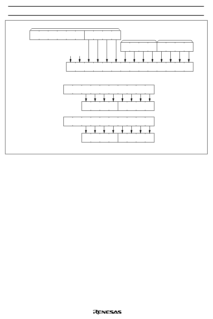
HD404629R Series
125
B
1
B
0
A
3
A
2
A
1
A
0
Accumulator
Referenced ROM address
Address Designation
RA
9
RA
8
RA
7
RA
6
RA
5
RA
4
RA
3
RA
2
RA
1
RA
0
RA
RA
RA
10
11
12
13
B
2
B
3
B register
0
0
p
3
p
0
[P]
Instruction
Opcode
p
2
p
1
RA
RO
9
RO
0
RO
8
RO
7
RO
6
RO
5
RO
4
RO
3
RO
2
RO
1
B
B
B
B
A
A
A
A
3
2
1
0
3
2
1
0
If RO = 1
8
Accumulator, B register
ROM data
Pattern Output
RO
9
ROM data
R2
3
If RO = 1
9
Output registers R1, R2
R2
2
R2
1
R2
0
R1
3
R1
2
R1
1
R1
0
RO
0
RO
8
RO
7
RO
6
RO
5
RO
4
RO
3
RO
2
RO
1
Figure 109 P Instruction
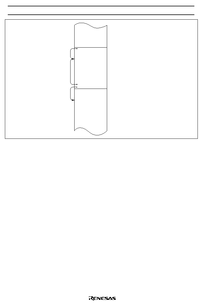
HD404629R Series
126
BR AAA
AAA NOP
256 (n � 1) + 255
256n
BR AAA
BR BBB
256n + 254
256n + 255
256 (n + 1)
BBB NOP
Figure 110 Branching when the Branch Destination is on a Page Boundary

HD404629R Series
127
Instruction Set
The MCU has 101 instructions, classified into the following 10 groups:
�
Immediate instructions
�
Register-to-register instructions
�
RAM addressing instructions
�
RAM register instructions
�
Arithmetic instructions
�
Compare instructions
�
RAM bit manipulation instructions
�
ROM addressing instructions
�
Input/output instructions
�
Control instructions
The functions of these instructions are listed in tables 34 to 43, and an opcode map is shown in table 44.
Table 34 Immediate Instructions
Words/
Operation Mnemonic
Operation
Code
Function
Status Cycles
Load A from
LAI i
1
0
0
0
1
1
i
3
i
2
i
1
i
0
i
A
1/1
immediate
Load B from
LBI i
1
0
0
0
0
0
i
3
i
2
i
1
i
0
i
B
1/1
immediate
Load memory
LMID i,d
0
1
1
0
1
0
i
3
i
2
i
1
i
0
i
M
2/2
from
d
9
d
8
d
7
d
6
d
5
d
4
d
3
d
2
d
1
d
0
immediate
Load memory
LMIIY i
1
0
1
0
0
1
i
3
i
2
i
1
i
0
i
M,
NZ
1/1
from immediate,
Y + 1
Y
increment Y

HD404629R Series
128
Table 35 Register-Register Instructions
Words/
Operation Mnemonic
Operation
Code
Function
Status Cycles
Load A
LAB
0
0
0
1
0
0
1
0
0
0
B
A
1/1
from B
Load B
LBA
0
0
1
1
0
0
1
0
0
0
A
B
1/1
from A
Load A
LAW
*
0
1
0
0
0
0
0
0
0
0
W
A
2/2
*
from W
0
0
0
0
0
0
0
0
0
0
Load A
LAY
0
0
1
0
1
0
1
1
1
1
Y
A
1/1
from Y
Load A
LASPX
0
0
0
1
1
0
1
0
0
0
SPX
A
1/1
from SPX
Load A
LASPY
0
0
0
1
0
1
1
0
0
0
SPY
A
1/1
from SPY
Load A
LAMR m
1
0
0
1
1
1
m
3
m
2
m
1
m
0
MR (m)
A
1/1
from MR
Exchange
XMRA m
1
0
1
1
1
1
m
3
m
2
m
1
m
0
MR (m)
A
1/1
MR and A
Note:
*
Although the LAW and LWA instructions require an operand ($000) in the second word, the
assembler generates it automatically and thus there is no need to specify it explicitly.

HD404629R Series
129
Table 36 RAM Address Instructions
Words/
Operation Mnemonic
Operation
Code
Function
Status Cycles
Load W from
LWI i
0
0
1
1
1
1
0
0
i
1
i
0
i
W
1/1
immediate
Load X from
LXI i
1
0
0
0
1
0
i
3
i
2
i
1
i
0
i
X
1/1
immediate
Load Y from
LYI i
1
0
0
0
0
1
i
3
i
2
i
1
i
0
i
Y
1/1
immediate
Load W
LWA
0
1
0
0
0
1
0
0
0
0
A
W
2/2
*
from A
0
0
0
0
0
0
0
0
0
0
Load X
LXA
0
0
1
1
1
0
1
0
0
0
A
X
1/1
from A
Load Y
LYA
0
0
1
1
0
1
1
0
0
0
A
Y
1/1
from A
Increment Y
IY
0
0
0
1
0
1
1
1
0
0
Y + 1
Y
NZ
1/1
Decrement Y
DY
0
0
1
1
0
1
1
1
1
1
Y � 1
Y
NB
1/1
Add A to Y
AYY
0
0
0
1
0
1
0
1
0
0
Y + A
Y
OVF
1/1
Subtract A
SYY
0
0
1
1
0
1
0
1
0
0
Y � A
Y
NB
1/1
from Y
Exchange X
XSPX
0
0
0
0
0
0
0
0
0
1
X
SPX
1/1
and SPX
Exchange Y
XSPY
0
0
0
0
0
0
0
0
1
0
Y
SPY
1/1
and SPY
Exchange X
XSPXY
0
0
0
0
0
0
0
0
1
1
X
SPX,
1/1
and SPX,
Y
SPY
Y and SPY
Note:
*
Although the LAW and LWA instructions require an operand ($000) in the second word, the
assembler generates it automatically and thus there is no need to specify it explicitly.

HD404629R Series
130
Table 37 RAM Register Instructions
Operation
Mnemonic
Operation Code
Function
Status
Words/
Cycles
Load A from
memory
LAM
0
0
1
0
0
1
0
0
0
0
M
A
1/1
LAMX
0
0
1
0
0
1
0
0
0
1
M
A,
X
SPX
LAMY
0
0
1
0
0
1
0
0
1
0
M
A,
Y
SPY
LAMXY
0
0
1
0
0
1
0
0
1
1
M
A,
X
SPX,
Y
SPY
Load A from
memory
LAMD d
0
d
9
1
d
8
1
d
7
0
d
6
0
d
5
1
d
4
0
d
3
0
d
2
0
d
1
0
d
0
M
A
2/2
Load B from
memory
LBM
0
0
0
1
0
0
0
0
0
0
M
B
1/1
LBMX
0
0
0
1
0
0
0
0
0
1
M
B,
X
SPX
LBMY
0
0
0
1
0
0
0
0
1
0
M
B,
Y
SPY
LBMXY
0
0
0
1
0
0
0
0
1
1
M
B,
X
SPX,
Y
SPY
Load memory
from A
LMA
0
0
1
0
0
1
0
1
0
0
A
M
1/1
LMAX
0
0
1
0
0
1
0
1
0
1
A
M,
X
SPX
LMAY
0
0
1
0
0
1
0
1
1
0
A
M,
Y
SPY
LMAXY
0
0
1
0
0
1
0
1
1
1
A
M,
X
SPX,
Y
SPY
Load memory
from A
LMAD d
0
d
9
1
d
8
1
d
7
0
d
6
0
d
5
1
d
4
0
d
3
0
d
2
0
d
1
0
d
0
A
M
2/2

HD404629R Series
131
Table 37 RAM Register Instructions (cont)
Operation
Mnemonic
Operation Code
Function
Status
Words/
Cycles
Load memory
from A,
increment Y
LMAIY
0
0
0
1
0
1
0
0
0
0
A
M,
Y + 1
Y
NZ
1/1
LMAIYX
0
0
0
1
0
1
0
0
0
1
A
M,
Y + 1
Y,
X
SPX
Load memory
from A,
decrement Y
LMADY
0
0
1
1
0
1
0
0
0
0
A
M,
Y � 1
Y
NB
1/1
LMADYX
0
0
1
1
0
1
0
0
0
1
A
M,
Y � 1
Y,
X
SPX
Exchange
memory
and A
XMA
0
0
1
0
0
0
0
0
0
0
M
A
1/1
XMAX
0
0
1
0
0
0
0
0
0
1
M
A,
X
SPX
XMAY
0
0
1
0
0
0
0
0
1
0
M
A,
Y
SPY
XMAXY
0
0
1
0
0
0
0
0
1
1
M
A,
X
SPX,
Y
SPY
Exchange
memory
and A
XMAD d
0
d
9
1
d
8
1
d
7
0
d
6
0
d
5
0
d
4
0
d
3
0
d
2
0
d
1
0
d
0
M
A
2/2
Exchange
memory
and B
XMB
0
0
1
1
0
0
0
0
0
0
M
B
1/1
XMBX
0
0
1
1
0
0
0
0
0
1
M
B,
X
SPX
XMBY
0
0
1
1
0
0
0
0
1
0
M
B,
Y
SPY
XMBXY
0
0
1
1
0
0
0
0
1
1
M
B,
X
SPX,
Y
SPY

HD404629R Series
132
Table 38 Arithmetic Instructions
Words/
Operation Mnemonic Operation
Code
Function
Status
Cycles
Add immediate to AI i
1
0
1
0
0
0
i
3
i
2
i
1
i
0
A + i
A
OVF
1/1
A
Increment B
IB
0
0
0
1
0
0
1
1
0
0
B + 1
B
NZ
1/1
Decrement B
DB
0
0
1
1
0
0
1
1
1
1
B � 1
B
NB
1/1
Decimal
DAA
0
0
1
0
1
0
0
1
1
0
1/1
adjust for addition
Decimal
DAS
0
0
1
0
1
0
1
0
1
0
1/1
adjust for
subtraction
Negate A
NEGA
0
0
0
1
1
0
0
0
0
0
A
+ 1
A
1/1
Complement
COMB
0
1
0
1
0
0
0
0
0
0
B
B
1/1
B
Rotate right A
ROTR
0
0
1
0
1
0
0
0
0
0
1/1
with carry
Rotate left A
ROTL
0
0
1
0
1
0
0
0
0
1
1/1
with carry
Set carry
SEC
0
0
1
1
1
0
1
1
1
1
1
CA
1/1
Reset carry
REC
0
0
1
1
1
0
1
1
0
0
0
CA
1/1
Test carry
TC
0
0
0
1
1
0
1
1
1
1
CA
1/1
Add A to memory
AM
0
0
0
0
0
0
1
0
0
0
M + A
A
OVF
1/1
Add A to memory
AMD d
0
1
0
0
0
0
1
0
0
0
M + A
A
OVF
2/2
d
9
d
8
d
7
d
6
d
5
d
4
d
3
d
2
d
1
d
0
Add A to memory
AMC
0
0
0
0
0
1
1
0
0
0
M + A + CA
A OVF
1/1
with carry
OVF
CA
Add A to memory
AMCD d
0
1
0
0
0
1
1
0
0
0
M + A + CA
A OVF
2/2
with carry
d
9
d
8
d
7
d
6
d
5
d
4
d
3
d
2
d
1
d
0
OVF
CA
Subtract A
SMC
0
0
1
0
0
1
1
0
0
0
M � A �
CA
A NB
1/1
from memory
NB
CA
with carry
Subtract A
SMCD d
0
1
1
0
0
1
1
0
0
0
M � A �
CA
A NB
2/2
from memory
d
9
d
8
d
7
d
6
d
5
d
4
d
3
d
2
d
1
d
0
NB
CA
with carry
OR A and B
OR
0
1
0
1
0
0
0
1
0
0
A
B
A
1/1

HD404629R Series
133
Table 38 Arithmetic Instructions (cont)
Words/
Operation Mnemonic
Operation
Code
Function
Status Cycles
AND memory
ANM
0
0
1
0
0
1
1
1
0
0
A
M
A
NZ
1/1
with A
AND memory
ANMD d
0
1
1
0
0
1
1
1
0
0
A
M
A
NZ
2/2
with A
d
9
d
8
d
7
d
6
d
5
d
4
d
3
d
2
d
1
d
0
OR memory
ORM
0
0
0
0
0
0
1
1
0
0
A
M
A
NZ
1/1
with A
OR memory
ORMD d
0
1
0
0
0
0
1
1
0
0
A
M
A
NZ
2/2
with A
d
9
d
8
d
7
d
6
d
5
d
4
d
3
d
2
d
1
d
0
EOR memory
EORM
0
0
0
0
0
1
1
1
0
0
A
M
A
NZ 1/1
with A
EOR memory
EORMD d
0
1
0
0
0
1
1
1
0
0
A
M
A
NZ 2/2
with A
d
9
d
8
d
7
d
6
d
5
d
4
d
3
d
2
d
1
d
0

HD404629R Series
134
Table 39 Compare Instructions
Words/
Operation Mnemonic
Operation
Code
Function
Status Cycles
Immediate not
INEM i
0
0
0
0
1
0
i
3
i
2
i
1
i
0
i
M
NZ
1/1
equal to
memory
Immediate not
INEMD i, d
0
1
0
0
1
0
i
3
i
2
i
1
i
0
i
M
NZ
2/2
equal to
d
9
d
8
d
7
d
6
d
5
d
4
d
3
d
2
d
1
d
0
memory
A not equal to
ANEM
0
0
0
0
0
0
0
1
0
0
A
M
NZ
1/1
memory
A not equal to
ANEMD d
0
1
0
0
0
0
0
1
0
0
A
M
NZ
2/2
memory
d
9
d
8
d
7
d
6
d
5
d
4
d
3
d
2
d
1
d
0
B not equal to
BNEM
0
0
0
1
0
0
0
1
0
0
B
M
NZ
1/1
memory
Y not equal to
YNEI i
0
0
0
1
1
1
i
3
i
2
i
1
i
0
Y
i
NZ
1/1
immediate
Immediate
ILEM i
0
0
0
0
1
1
i
3
i
2
i
1
i
0
i
M
NB
1/1
less or equal
to memory
Immediate
ILEMD i, d
0
1
0
0
1
1
i
3
i
2
i
1
i
0
i
M
NB
2/2
less or equal
d
9
d
8
d
7
d
6
d
5
d
4
d
3
d
2
d
1
d
0
to memory
A less or
ALEM
0
0
0
0
0
1
0
1
0
0
A
M
NB
1/1
equal to
memory
A less or
ALEMD d
0
1
0
0
0
1
0
1
0
0
A
M
NB
2/2
equal to
d
9
d
8
d
7
d
6
d
5
d
4
d
3
d
2
d
1
d
0
memory
B less or
BLEM
0
0
1
1
0
0
0
1
0
0
B
M
NB
1/1
equal to
memory
A less or
ALEI i
1
0
1
0
1
1
i
3
i
2
i
1
i
0
A
i
NB
1/1
equal to
immediate

HD404629R Series
135
Table 40 RAM Bit Manipulation Instructions
Words/
Operation Mnemonic
Operation
Code
Function
Status
Cycles
Set memory bit
SEM n
0
0
1
0
0
0
0
1
n
1
n
0
i
M (n)
1/1
Set memory bit
SEMD n,d
0
1
1
0
0
0
0
1
n
1
n
0
i
M (n)
2/2
d
9
d
8
d
7
d
6
d
5
d
4
d
3
d
2
d
1
d
0
Reset memory
REM n
0
0
1
0
0
0
1
0
n
1
n
0
0
M (n)
1/1
bit
Reset memory
REMD n,d
0
1
1
0
0
0
1
0
n
1
n
0
0
M (n)
2/2
bit
d
9
d
8
d
7
d
6
d
5
d
4
d
3
d
2
d
1
d
0
Test memory bit
TM n
0
0
1
0
0
0
1
1
n
1
n
0
M (n)
1/1
Test memory bit
TM n,d
0
1
1
0
0
0
1
1
n
1
n
0
M (n)
2/2
d
9
d
8
d
7
d
6
d
5
d
4
d
3
d
2
d
1
d
0
Table 41 ROM Addressing Instructions
Words/
Operation Mnemonic
Operation
Code
Function
Status Cycles
Branch on
BR b
1
1
b
7
b
6
b
5
b
4
b
3
b
2
b
1
b
0
1
1/1
status 1
Long branch
BRL u
0
1
0
1
1
1
p
3
p
2
p
1
p
0
1
2/2
on status 1
d
9
d
8
d
7
d
6
d
5
d
4
d
3
d
2
d
1
d
0
Long jump
JMPL u
0
1
0
1
0
1
p
3
p
2
p
1
p
0
2/2
unconditionally d
9
d
8
d
7
d
6
d
5
d
4
d
3
d
2
d
1
d
0
Subroutine jump
CAL a
0
1
1
1
a
5
a
4
a
3
a
2
a
1
a
0
1
1/2
on status 1
Long subroutine
CALL u
0
1
0
1
1
0
p
3
p
2
p
1
p
0
1
2/2
jump on status 1
d
9
d
8
d
7
d
6
d
5
d
4
d
3
d
2
d
1
d
0
Table branch
TBR p
0
0
1
0
1
1
p
3
p
2
p
1
p
0
1
1/1
Return from
RTN
0
0
0
0
0
1
0
0
0
0
1/3
subroutine
Return from
RTNI
0
0
0
0
0
1
0
0
0
1
1
IE,
ST
1/3
interrupt
carry restored

HD404629R Series
136
Table 42 Input/Output Instructions
Words/
Operation Mnemonic
Operation
Code
Function
Status Cycles
Set discrete
SED
0
0
1
1
1
0
0
1
0
0
1
D (Y)
1/1
I/O latch
Set discrete
SEDD m
1
0
1
1
1
0
m
3
m
2
m
1
m
0
1
D (m)
1/1
I/O latch
direct
Reset
RED
0
0
0
1
1
0
0
1
0
0
0
D (Y)
1/1
discrete I/O latch
Reset
REDD m
1
0
0
1
1
0
m
3
m
2
m
1
m
0
0
D (m)
1/1
discrete I/O latch
direct
Test discrete I/O
TD
0
0
1
1
1
0
0
0
0
0
D (Y)
1/1
latch
Test discrete I/O
TDD m
1
0
1
0
1
0
m
3
m
2
m
1
m
0
D (m)
1/1
latch direct
Load A
LAR m
1
0
0
1
0
1
m
3
m
2
m
1
m
0
R (m)
A
1/1
from R-port
register
Load B
LBR m
1
0
0
1
0
0
m
3
m
2
m
1
m
0
R (m)
B
1/1
from R-port
register
Load R-port
LRA m
1
0
1
1
0
1
m
3
m
2
m
1
m
0
A
R (m)
1/1
register
from A
Load R-port
LRB m
1
0
1
1
0
0
m
3
m
2
m
1
m
0
B
R (m)
1/1
register
from B
Pattern
P p
0
1
1
0
1
1
p
3
p
2
p
1
p
0
1/2
generation

HD404629R Series
137
Table 40 Control Instructions
Words/
Operation Mnemonic
Operation
Code
Function
Status Cycles
No operation
NOP
0
0
0
0
0
0
0
0
0
0
1/1
Start serial
STS
0
1
0
1
0
0
1
0
0
0
1/1
Standby
SBY
0
1
0
1
0
0
1
1
0
0
1/1
mode/Watch
mode
*
Stop mode/
STOP
0
1
0
1
0
0
1
1
0
1
1/1
Watch mode
Note:
*
Only on return from subactive mode.

HD404629R Series
138
Table 44 Opcode Map
R8
L
H
R9
0
1
2
3
4
5
6
7
8
9
A
B
C
D
E
F
0
1
2
3
4
5
6
7
8
9
A
B
C
D
E
F
LBI i(4)
LYI i(4)
LXI i(4)
LAI i(4)
LBR m(4)
LAR m(4)
REDD m(4)
LAMR m(4)
AI i(4)
LMIIY i(4)
TDD m(4)
ALEI i(4)
LRB m(4)
LRA m(4)
SEDD m(4)
XMRA m(4)
0
0
1
1-word/2-cycle
instruction
1-word/3-cycle
instruction
RAM direct address
instruction
(2-word/2-cycle)
2-word/2-cycle
instruction
0
1
2
3
4
5
6
7
8
9
A
B
C
D
E
F
NOP
XSPX
XSPY XSPXY ANEM
AM
ORM
LBM(XY)
BNEM
LAB
IB
LMAIY(X)
AYY
LASPY
IY
RTN
RTNI
ALEM
AMC
EORM
NEGA
RED
LASPX
TC
INEM i(4)
ILEM i(4)
YNEI i(4)
XMA(XY)
LAM(XY)
SEM n(2)
LMA(XY)
REM n(2)
SMC
TM n(2)
ANM
ROTR
DAA
DAS
LAY
ROTL
DB
DY
SEC
LBA
LYA
REC
LXA
BLEM
SYY
SED
XMB(XY)
LMADY(X)
TD
LWI i(2)
TBR p(4)

HD404629R Series
139
Table 44 Opcode Map (cont)
R8
L
H
R9
0
1
2
3
4
5
6
7
8
9
A
B
C
D
E
F
0
1
2
3
4
5
6
7
8
9
A
B
C
D
E
F
1
0
1
1-word/2-cycle
instruction
1-word/3-cycle
instruction
RAM direct address
instruction
(2-word/2-cycle)
2-word/2-cycle
instruction
0
1
2
3
4
5
6
7
8
9
A
B
C
D
E
F
LAW
ANEMD
AMD
ORMD
LWA
ALEMD
AMCD
EORMD
COMB
OR
STS
SBY
STOP
INEMD i(4)
ILEMD i(4)
JMPL p(4)
CALL p(4)
BRL p(4)
XMAD
LAMD
SEMD n(2)
LMAD
REMD n(2)
SMCD
TMD n(2)
ANMD
LMID i(4)
CAL a(6)
BR b(8)
P p(4)
HD404629R Series
140
Absolute Maximum Ratings
Item
Symbol
Value
Unit
Notes
Supply voltage
V
CC
�0.3 to +7.0
V
Programming voltage
V
PP
�0.3 to +14.0
V
1
Pin voltage
V
T
�0.3 to (V
CC
+ 0.3)
V
Total permissible input current
I
o
100
mA
2
Total permissible output current
�
I
o
50
mA
3
Maximum input current
I
o
4
mA
4, 5
30
mA
4, 6
Maximum output current
�I
o
4
mA
7, 8
Operating temperature
T
opr
�20 to +75
�
C
Storage temperature
T
stg
�55 to +125
�
C
Notes: Permanent damage may occur if these absolute maximum ratings are exceeded. Normal
operation must be under the conditions stated in the electrical characteristics tables. If these
conditions are exceeded, the LSI may malfunction or its reliability may be affected.
1. Applies to D
11
(V
PP
) of the HD4074629.
2. The total permissible input current is the total of input currents simultaneously flowing in from all
the I/O pins to ground.
3. The total permissible output current is the total of output currents simultaneously flowing out from
V
CC
to all I/O pins.
4. The maximum input current is the maximum current flowing from each I/O pin to ground.
5. Applies to R0�R7.
6. Applies to D
0
�D
9
.
7. The maximum output current is the maximum current flowing out from V
CC
to each I/O pin.
8. Applies to D
0
�D
9
and R0�R7.

HD404629R Series
141
Electrical Characteristics
DC Characteristics (HD404628R, HD4046212R, HD404629R: V
CC
= 2.7 to 6.0 V, GND = 0 V,
T
a
= �20
�
C to +75
�
C; HD4074629: V
C C
= 2.7 to 5.5 V, GND = 0 V, T
a
= �20
�
C to +75
�
C,
unless otherwise specified)
Item
Symbol
Pin(s)
Min
Typ
Max
Unit
Test Condition
Notes
Input high
voltage
V
IH
RESET,
SCK
,
SI,
INT
0
,
INT
1
INT
2
, INT
3
,
INT
4
,
STOPC
,
EVNB
, EVND
0.9V
CC
--
V
CC
+ 0.3
V
--
OSC
1
V
CC
� 0.3
--
V
CC
+ 0.3
V
External clock
operation
Input low
voltage
V
IL
RESET,
SCK
,
SI,
INT
0
,
INT
1
,
INT
2
, INT
3
,
INT
4
,
STOPC
,
EVNB
, EVND
�0.3
--
0.1V
CC
V
--
OSC
1
�0.3
--
0.3
V
External clock
operation
Output high
voltage
V
OH
SCK
, SO, TOB,
TOC, TOD
V
CC
� 1.0
--
--
V
�I
OH
= 0.5 mA
Output low
voltage
V
OL
SCK
, SO, TOB,
TOC, TOD
--
--
0.4
V
I
OL
= 0.4 mA
I/O leakage
current
I
I L
RESET,
SCK
,
SI,
INT
0
,
INT
1
,
INT
2
, INT
3
,
INT
4
,
STOPC
,
EVNB
, EVND,
OSC
1
, TOB,
TOC, TOD, SO
--
--
1.0
�
A
V
in
= 0 V to V
CC
1
Current
dissipation in
active mode
I
CC1
V
CC
(HD404628R,
HD4046212R,
HD404629R)
--
2.5
5.0
mA
V
CC
= 5.0 V,
f
OSC
= 4 MHz
2, 4
V
CC
(HD4074629)
--
5
9
I
CC2
V
CC
(HD404628R,
HD4046212R,
HD404629R)
--
0.3
0.9
mA
V
CC
= 3.0 V,
f
OSC
= 800 kHz
2, 4
V
CC
(HD4074629)
--
0.6
1.8
Current
dissipation in
standby mode
I
SBY1
V
CC
(HD404628R,
HD4046212R,
HD404629R)
--
1.0
2.0
mA
V
CC
= 5.0 V,
f
OSC
= 4 MHz,
LCD on
3, 4
V
CC
(HD4074629)
--
1.2
3
I
SBY2
V
CC
--
0.2
0.7
mA
V
CC
= 3.0 V,
f
OSC
= 800 kHz,
LCD on
3, 4
Notes on next page.

HD404629R Series
142
DC Characteristics (HD404628R, HD4046212R, HD404629R: V
CC
= 2.7 to 6.0 V, GND = 0 V,
T
a
= �20
�
C to +75
�
C; HD4074629: V
C C
= 2.7 to 5.5 V, GND = 0 V, T
a
= �20
�
C to +75
�
C,
unless otherwise specified) (cont)
Item
Symbol
Pin(s)
Min
Typ
Max
Unit
Test Condition
Notes
Current
dissipation in
subactive mode
I
SUB
V
CC
--
25
70
�
A
HD404628R,
HD4046212R,
HD404629R:
V
CC
= 3.0 V,
LCD on
32-kHz oscillator
4
--
70
150
�
A
HD4074629:
V
CC
= 3.0 V,
LCD on
32-kHz oscillator
4
Current
dissipation in
I
WTC1
V
CC
(HD404628R,
HD4046212R,
HD404629R)
--
15
40
�
A
V
CC
= 3.0 V,
LCD on
32-kHz oscillator
4
V
CC
(HD4074629)
--
18
40
watch mode
I
WTC2
V
CC
(HD404628R,
HD4046212R,
HD404629R)
--
5
10
�
A
V
CC
= 3.0 V,
LCD off
32-kHz oscillator
4
V
CC
(HD4074629)
--
8
15
Current
dissipation in
stop mode
I
STOP
V
CC
(HD404628R,
HD4046212R,
HD404629R)
--
0.5
5
�
A
V
CC
= 3.0 V,
No 32-kHz oscillator
4
V
CC
(HD4074629)
--
1
10
Stop mode
retaining voltage
V
STOP
V
CC
2
--
--
V
No 32-kHz
oscillator
5
Notes:
1. Output buffer current is excluded.
2. I
CC1
and I
CC2
are the source currents when no I/O current is flowing while the MCU is in reset state.
Test conditions:
MCU:
Reset
Pins:
RESET at V
CC
(V
CC
� 0.3 V to V
CC
)
TEST
at V
CC
(V
CC
� 0.3 V to V
CC
)
3. I
SBY1
and I
SBY2
are the source currents when no I/O current is flowing while the MCU timer is operating.
Test conditions:
MCU:
I/O reset
Serial interface stopped
DTMF stopped
Standby mode
Pins:
RESET at GND (0 V to 0.3 V)
TEST
at V
CC
(V
CC
� 0.3 V to V
CC
)
4. These are the source currents when no I/O current is flowing.
Test conditions:
Pins:
RESET at GND (0 V to 0.3 V)
TEST
at V
CC
(V
CC
� 0.3 V to V
CC
)
D
11
(V
PP
) at V
CC
(V
CC
� 0.3 V to V
CC
) for the HD4074629
5. The required voltage for RAM data retention.

HD404629R Series
143
I/O Characteristics for Standard Pins (HD404628R, HD4046212R, HD404629R: V
CC
= 2.7 to 6.0 V,
GND = 0 V, T
a
= �20
�
C to +75
�
C; HD4074629: V
CC
= 2.7 to 5.5 V, GND = 0 V, T
a
= �20
�
C to +75
�
C,
unless otherwise specified)
Item
Symbol
Pin(s)
Min
Typ
Max
Unit
Test Condition
Notes
Input high
voltage
V
IH
D
10
, D
11
,
R0�R7
0.7V
CC
--
V
CC
+ 0.3
V
--
Input low
voltage
V
IL
D
10
,
D
11
,
R0�R7
�0.3
--
0.3V
CC
V
--
Output high
voltage
V
OH
R0�R7
V
CC
� 1.0
--
--
V
�I
OH
= 0.5 mA
Output low
voltage
V
OL
R0�R7
--
--
0.4
V
I
OL
= 0.4 mA
I/O leakage
I
I L
D
10
, R0�R7
--
--
1
�
A
V
in
= 0 V to V
CC
1
current
D
11
--
--
1
�
A
HD404628R,
HD4046212R,
HD404629R:
V
in
= 0 V to V
CC
1
--
--
1
�
A
HD4074629:
V
in
= V
CC
� 0.3 V
to V
CC
1
--
--
20
�
A
HD4074629:
V
in
= 0 V to 0.3 V
1
Pull-up MOS
current
�I
PU
R0�R7
5
30
90
�
A
V
CC
= 3.0 V,
V
in
= 0 V
Note: 1. Output buffer current is excluded.

HD404629R Series
144
I/O Characteristics for High-Current Pins (HD404628R, HD4046212R, HD404629R: V
CC
= 2.7 to
6.0 V, GND = 0 V, T
a
= �20
�
C to +75
�
C; HD4074629: V
CC
= 2.7 to 5.5 V, GND = 0 V, T
a
= �20
�
C to
+75
�
C, unless otherwise specified)
Item
Symbol
Pin(s)
Min
Typ
Max
Unit
Test Condition
Notes
Input high
voltage
V
IH
D
0
�D
9
0.7V
CC
--
V
CC
+ 0.3
V
--
Input low
voltage
V
IL
D
0
�D
9
�0.3
--
0.3V
CC
V
--
Output high
voltage
V
OH
D
0
�D
9
V
CC
� 1.0
--
--
V
�I
OH
= 0.5 mA
Output low
V
OL
D
0
�D
9
--
--
0.4
V
I
OL
= 0.4 mA
voltage
--
--
2.0
V
I
OL
= 15 mA,
V
CC
= 4.5 V to 6.0 V
1
I/O leakage
current
I
I L
D
0
�D
9
--
--
1
�
A
V
in
= 0 V to V
CC
2
Pull-up MOS
current
�I
PU
D
0
�D
9
5
30
90
�
A
V
CC
= 3 V,
V
in
= 0 V
Note:
1. The test condition of HD4074629 is V
CC
= 4.5 V to 5.5 V.
2. Output buffer current is excluded.
LCD Circuit Characteristics (HD404628R, HD4046212R, HD404629R: V
CC
= 2.7 to 6.0 V, GND =
0 V, T
a
= �20
�
C to +75
�
C; HD4074629: V
CC
= 2.7 to 5.5 V, GND = 0 V, T
a
= �20
�
C to +75
�
C, unless
otherwise specified)
Item
Symbol
Pin(s)
Min
Typ
Max
Unit
Test Condition
Notes
Segment driver
voltage drop
V
DS
SEG1�SEG52
--
--
0.6
V
I
PD
= 3
�
A
1
Common driver
voltage drop
V
DC
COM1�COM4
--
--
0.3
V
I
PD
= 3
�
A
1
LCD power
supply division
resistance
R
W
--
(HD404628R,
HD4046212R,
HD404629R)
50
300
900
k
Between V
1
and
GND
--
(HD4074629)
100
300
900
--
LCD voltage
V
LCD
V
1
2.7
--
V
CC
V
--
2
Notes: 1. V
DS
and V
DC
are the voltage drops from power supply pins V
1
, V
2
, V
3
, and GND to each segment
pin and each common pin, respectively.
2. When V
LCD
is supplied from an external source, the following relations must be retained:
V
CC
V
1
V
2
V
3
GND

HD404629R Series
145
DTMF Characteristics (HD404628R, HD4046212R, HD404629R: V
CC
= 2.7 to 6.0 V, GND = 0 V,
T
a
= �20
�
C to +75
�
C; HD4074629: V
CC
= 2.7 to 5.5 V, GND = 0 V, T
a
= �20
�
C to +75
�
C, unless
otherwise specified)
Item
Symbol
Pin
Min
Typ
Max
Unit
Test Condition
Notes
Tone output
voltage (1)
V
OR
TONER
500
660
--
mV
rms
VT
ref
� GND = 2.0 V,
R
L
= 100 k
1
Tone output
voltage (2)
V
OC
TONEC
520
690
--
mV
rms
VT
ref
� GND = 2.0 V,
R
L
= 100 k
1
Tone output
distortion
%
DIS
--
--
3
7
%
Short circuit
between TONER
and TONEC,
R
L
= 100 k
2
Tone output
ratio
dB
CR
--
--
2.5
--
dB
Short circuit
between TONER
and TONEC,
R
L
= 100 k
2
Notes: 1. See figure 106.
2. See figure 107.
3. 400 kHz, 800 kHz, 2 MHz, or 4 MHz can be used as the operating frequency (f
OSC
).
HD404629R Series
146
A/D Converter Characteristics (HD404628R, HD4046212R, HD404629R: V
CC
= 2.7 to 6.0 V,
GND = 0 V, T
a
= �20
�
C to +75
�
C; HD4074629: V
CC
= 2.7 to 5.5 V, GND = 0 V, T
a
= �20
�
C to +75
�
C,
unless otherwise specified)
Item
Symbol
Pin(s)
Min
Typ
Max
Unit
Test Condition
Notes
Analog power
voltage
AV
CC
AV
CC
V
CC
� 0.3
V
CC
V
CC
+ 0.3
V
AV
CC
2.7 V
Analog input
voltage
AV
in
AN
0
�AN
3
AV
SS
--
AV
CC
V
--
Current between
AV
CC
and AV
SS
I
A D
--
(HD404628R,
HD4046212R,
HD404629R)
--
--
250
�
A
V
CC
= AV
CC
= 5.0 V
--
(HD4074629)
--
50
150
Analog input
capacitance
CA
in
AN
0
�AN
3
--
15
--
pF
--
Resolution
--
--
8
8
8
Bit
--
Number of inputs
--
--
0
--
4
Chan-
nel
--
Absolute accuracy
--
--
--
--
�
2.0
LSB
T
a
= 25
�
C,
V
CC
= 4.5�5.5 V
Conversion time
--
--
34
--
67
t
cyc
--
Input impedance
--
AN
0
�AN
3
1
--
--
M
f
OSC
= 1 MHz,
V
in
= 0.0 V

HD404629R Series
147
AC Characteristics (HD404628R, HD4046212R, HD404629R: V
CC
= 2.7 to 6.0 V, GND = 0 V,
T
a
= �20
�
C to +75
�
C; HD4074629: V
C C
= 2.7 to 5.5 V, GND = 0 V, T
a
= �20
�
C to +75
�
C,
unless otherwise specified)
Item
Symbol
Pin(s)
Min
Typ
Max
Unit
Test Condition
Notes
Clock oscillation
f
OSC
OSC
1
, OSC
2
--
400
--
kHz
1/4 division
1
frequency
--
800
--
kHz
1/4 division
1
--
2
--
MHz
1/4 division
1
--
4
--
MHz
1/4 division;
HD404628,
HD4046212,
HD404629:
V
CC
= 3.0 to 6.0 V
1
X1, X2
--
32.768
--
kHz
--
Instruction cycle
t
cyc
--
--
10
--
�
s
f
OSC
= 400 kHz
time
--
5
--
�
s
f
OSC
= 800 kHz
--
2
--
�
s
f
OSC
= 2 MHz
--
1
--
�
s
f
OSC
= 4 MHz;
HD404628,
HD4046212,
HD404629:
V
CC
= 3.0 to 6.0 V
t
subcyc
--
--
244.14
--
�
s
32-kHz oscillator,
1/8 division
--
122.07
--
�
s
32-kHz oscillator,
1/4 division
Oscillation
t
RC
OSC
1
, OSC
2
--
--
7.5
ms
Ceramic oscillator
2
stabilization time
OSC
1
, OSC
2
(HD404628R,
HD4046212R,
HD404629R)
--
--
30
ms
Crystal oscillator
V
CC
= 3.0 to 6.0 V
2
X1, X2
--
--
3
s
T
a
= �10
�
C to
+60
�
C
3
External clock
t
CPH
OSC
1
1100
--
--
ns
f
OSC
= 400 kHz
4
high width
550
--
--
ns
f
OSC
= 800 kHz
4
215
--
--
ns
f
OSC
= 2 MHz
4
105
--
--
ns
f
OSC
= 4 MHz
4
External clock
t
CPL
OSC
1
1100
--
--
ns
f
OSC
= 400 kHz
4
low width
550
--
--
ns
f
OSC
= 800 kHz
4
215
--
--
ns
f
OSC
= 2 MHz
4
105
--
--
ns
f
OSC
= 4 MHz
4
External clock
t
CPr
OSC
1
--
--
150
ns
f
OSC
= 400 kHz
4
rise time
--
--
75
ns
f
OSC
= 800 kHz
4
--
--
35
ns
f
OSC
= 2 MHz
4
--
--
20
ns
f
OSC
= 4 MHz
4
Notes on next page.

HD404629R Series
148
AC Characteristics (HD404628R, HD4046212R, HD404629R: V
CC
= 2.7 to 6.0 V, GND = 0 V, T
a
=
�20
�
C to +75
�
C; HD4074629: V
CC
= 2.7 to 5.5 V, GND = 0 V, T
a
= �20
�
C to +75
�
C, unless otherwise
specified) (cont)
Item
Symbol
Pin(s)
Min
Typ
Max
Unit
Test Condition
Notes
External clock
t
CPf
OSC
1
--
--
150
ns
f
OSC
= 400 kHz
4
fall time
--
--
75
ns
f
OSC
= 800 kHz
4
--
--
35
ns
f
OSC
= 2 MHz
4
--
--
20
ns
f
OSC
= 4 MHz
4
INT
0
�INT
4
,
EVNB
,
EVND high widths
t
I H
INT
0
�INT
4
,
EVNB
, EVND
2
--
--
t
cyc
/
t
subcyc
--
5
INT
0
�INT
4
,
EVNB
,
EVND low widths
t
I L
INT
0
�INT
4
,
EVNB
, EVND
2
--
--
t
cyc
/
t
subcyc
--
5
RESET high width
t
RSTH
RESET
2
--
--
t
cyc
--
6
STOPC
low width
t
STPL
STOPC
1
--
--
t
RC
--
7
RESET fall time
t
RSTf
RESET
--
--
20
ms
--
6
STOPC
rise time
t
STPr
STOPC
--
--
20
ms
--
7
Input capacitance
C
in
All pins
except D
11
--
--
15
pF
f = 1 MHz
V
in
= 0 V,
D
11
--
--
15
pF
HD404628R,
HD4046212R,
HD404629R:
f = 1 MHz,
V
in
= 0 V
--
--
180
pF
HD4074629:
f = 1 MHz,
V
in
= 0 V
Notes: 1. Be sure to set system clock selection register (SSR) bits SSR1 and SSR0 to match the system
clock oscillator frequency.
2. Applies to voltage ranges V
CC
= 3.5 to 5.5 V for the HD4074629.
3. There are three oscillator stabilization times.
(1) At power on, the time between the point where V
CC
reaches 2.7 V and the point where
oscillation has stabilized.
(2) At clearing stop mode, the time between the point where the RESET pin reaches the high
level and the point where oscillation has stabilized.
(3) At clearing stop mode, the time between the point where the
STOPC
pin reaches the low level
and the point where oscillation has stabilized.
At power on or when stop mode is cleared, RESET or
STOPC
must be input for at least t
RC
to
ensure the oscillation stabilization time.
Since the oscillator stabilization time will depend on circuit constants and stray capacitances,
determine the oscillator by consulting with the oscillator's manufacturer.
Be sure to set miscellaneous register (MIS) bits MIS1 and MIS0 to match the system clock
oscillator stabilization time.
4. Refer to figure 108.
5. Refer to figure 109. The t
cyc
unit applies when the MCU is in standby or active mode.
The t
subcyc
unit applies when the MCU is in watch or subactive mode.
6. Refer to figure 110.
7. Refer to figure 111.

HD404629R Series
149
Serial Interface Timing Characteristics (HD404628R, HD4046212R, HD404629R: V
CC
= 2.7 to 6.0 V,
GND = 0 V, T
a
= �20
�
C to +75
�
C; HD4074629: V
CC
= 2.7 to 5.5 V, GND = 0 V, T
a
= �20
�
C to +75
�
C,
unless otherwise specified)
During Transmit Clock Output
Item
Symbol
Pin
Min
Typ
Max
Unit
Test Condition
Notes
Transmit clock cycle time
t
Scyc
SCK
1.0
--
--
t
cyc
Load shown in
figure 113
1
Transmit clock high width
t
SCKH
SCK
0.5
--
--
t
Scyc
Load shown in
figure 113
1
Transmit clock low width
t
SCKL
SCK
0.5
--
--
t
Scyc
Load shown in
figure 113
1
Transmit clock rise time
t
SCKr
SCK
--
--
200
ns
Load shown in
figure 113
1
Transmit clock fall time
t
SCKf
SCK
--
--
200
ns
Load shown in
figure 113
1
Serial output data
delay time
t
DSO
SO
--
--
500
ns
Load shown in
figure 113
1
Serial input data
setup time
t
SSI
SI
300
--
--
ns
--
1
Serial input data
hold time
t
HSI
SI
300
--
--
ns
--
1
Note: 1. Refer to figure 112.
During Transmit Clock Input
Item
Symbol
Pin
Min
Typ
Max
Unit
Test Condition
Notes
Transmit clock cycle time
t
Scyc
SCK
1.0
--
--
t
cyc
--
1
Transmit clock high width
t
SCKH
SCK
0.5
--
--
t
Scyc
--
1
Transmit clock low width
t
SCKL
SCK
0.5
--
--
t
Scyc
--
1
Transmit clock rise time
t
SCKr
SCK
--
--
200
ns
--
1
Transmit clock fall time
t
SCKf
SCK
--
--
200
ns
--
1
Serial output data
delay time
t
DSO
SO
--
--
500
ns
Load shown in
figure 113
1
Serial input data
setup time
t
SSI
SI
300
--
--
ns
--
1
Serial input data
hold time
t
HSI
SI
300
--
--
ns
--
1
Note: 1. Refer to figure 112.
HD404629R Series
150
GND
R = 100 k
L
TONEC
TONER
R = 100 k
L
Figure 111 Tone Output Load Circuit
GND
R = 100 k
L
TONEC
TONER
Figure 112 Distortion and dB
CR
Load Circuit
t
CPr
t
CPf
V
CC
� 0.3 V
0.3 V
OSC
1
t
CPH
t
CPL
1/f
CP
Figure 113 External Clock Timing
0.9V
CC
0.1V
CC
INT
0
to INT
4
,
EVNB
, EVND
t
IH
t
IL
Figure 114 Interrupt Timing

HD404629R Series
151
RESET
t
RSTf
t
RSTH
0.9V
CC
0.1V
CC
Figure 115 Reset Timing
t
STPr
t
STPL
0.9V
CC
0.1V
CC
STOPC
Figure 116
STOPC Timing
0.9V
CC
0.1V
CC
t
DSO
t
SCKf
t
SCKL
t
SSI
t
HSI
t
Scyc
t
SCKr
0.4 V
V � 1.0 V
CC
V � 1.0 V (0.9V )
CC
0.4 V (0.1V )
SCK
SO
SI
Note: V
CC
� 1.0 V and 0.4 V are the threshold voltages for transmit clock output, and
0.9V
CC
and 0.1V
CC
are the threshold voltages for transmit clock input.
CC
CC
t
SCKH
*
*
*
Figure 117 Serial Interface Timing

HD404629R Series
152
R
L
= 2.6 k
V
CC
1S2074 H
or equivalent
R =
12 k
Test
point
C =
30 pF
Figure 118 Timing Load Circuit
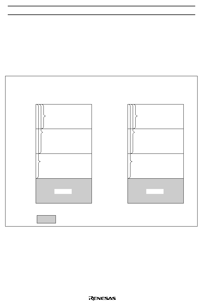
HD404629R Series
153
Notes on ROM Out
Please pay attention to the following items regarding ROM out.
On ROM out, fill the ROM area indicated below with 1s to create the same data size as a 16-kword version
(HD404629R). A 16-kword data size is required to change ROM data to mask manufacturing data since the
program used is for a 16-kword version.
This limitation applies when using an EPROM or a data base.
Vector address
Zero-page subroutine
(64 words)
Pattern & program
(8,192 words)
Not used
Vector address
Zero-page subroutine
(64 words)
Pattern & program
(12,288 words)
Not used
ROM 8-kword version:
HD404628R
Address $2000�$3FFF
ROM 12-kword version:
HD4046212R
Address $3000�$3FFF
$0000
$000F
$0010
$003F
$0040
$1FFF
$2000
$3FFF
$0000
$000F
$0010
$003F
$0040
$2FFF
$3000
$3FFF
Fill this area with 1s

HD404629R Series
154
HD404628R/HD4046212R/ HD404629R Option List
Please check off the appropriate applications and enter the necessary information.
Date of order
/
/
Customer
Department
Name
ROM code name
LSI number
(Hitachi entry)
1. ROM Size
HD404628R
8-kword
HD4046212R
12-kword
HD404629R
16-kword
2. Optional Functions
*
With 32-kHz CPU operation, with time-base for clock
*
Without 32-kHz CPU operation, with time-base for clock
Without 32-kHz CPU operation, without time-base for clock
Note: * Options marked with an asterisk require a subsystem crystal oscillator (X1, X2).
3. ROM Code Data Type
Please specify the first type below (the upper bits and lower bits are mixed together), when using the
EPROM on-package microcomputer type (including ZTAT
TM
version).
The upper bits and lower bits are mixed together. The upper five bits and lower five bits are programmed to the
same EPROM in alternating order (i.e., LULULU...).
The upper bits and lower bits are separated. The upper five bits and lower five bits are programmed to different
EPROMs.
4. System Oscillator (OSC1 and OSC2)
Ceramic oscillator
f =
MHz
Crystal oscillator
f =
MHz
External clock
f =
MHz
5. Stop Mode
Used
Not used
6. Package
FP-100A
FP-100B
TFP-100B

HD404629R Series
155
Cautions
1. Hitachi neither warrants nor grants licenses of any rights of Hitachi's or any third party's patent,
copyright, trademark, or other intellectual property rights for information contained in this document.
Hitachi bears no responsibility for problems that may arise with third party's rights, including
intellectual property rights, in connection with use of the information contained in this document.
2. Products and product specifications may be subject to change without notice. Confirm that you have
received the latest product standards or specifications before final design, purchase or use.
3. Hitachi makes every attempt to ensure that its products are of high quality and reliability. However,
contact Hitachi's sales office before using the product in an application that demands especially high
quality and reliability or where its failure or malfunction may directly threaten human life or cause risk
of bodily injury, such as aerospace, aeronautics, nuclear power, combustion control, transportation,
traffic, safety equipment or medical equipment for life support.
4. Design your application so that the product is used within the ranges guaranteed by Hitachi particularly
for maximum rating, operating supply voltage range, heat radiation characteristics, installation
conditions and other characteristics. Hitachi bears no responsibility for failure or damage when used
beyond the guaranteed ranges. Even within the guaranteed ranges, consider normally foreseeable
failure rates or failure modes in semiconductor devices and employ systemic measures such as fail-
safes, so that the equipment incorporating Hitachi product does not cause bodily injury, fire or other
consequential damage due to operation of the Hitachi product.
5. This product is not designed to be radiation resistant.
6. No one is permitted to reproduce or duplicate, in any form, the whole or part of this document without
written approval from Hitachi.
7. Contact Hitachi's sales office for any questions regarding this document or Hitachi semiconductor
products.