Document Outline
- Description
- Features
- Cautions about operation
- Ordering Information
- List of Functions
- Pin Arrangement
- Pad Arrangement
- Pad Coordinates
- Pad Arrangement
- Pad Coordinates
- Pin Description
- Block Diagram
- Memory Map
- Functional Description
- Operating Modes
- Internal Oscillator Circuit
- System Clock Gear Function
- Input/Output
- Prescalers
- Timers
- Serial Interface
- A/D Converter
- LCD Circuit
- Buzzer Output Circuit
- ZTAT Microcomputer with Built-in Programmable PROM
- Writing/Verification
- Programmable ROM
- Addressing Modes
- Instruction Set
- Absolute Maximum Ratings
- Electrical Characteristics
- Package Dimensions
- Note on ROM Ordering
- Option List
- Cautions

Regarding the change of names mentioned in the document, such as Hitachi
Electric and Hitachi XX, to Renesas Technology Corp.
The semiconductor operations of Mitsubishi Electric and Hitachi were transferred to Renesas
Technology Corporation on April 1st 2003. These operations include microcomputer, logic, analog
and discrete devices, and memory chips other than DRAMs (flash memory, SRAMs etc.)
Accordingly, although Hitachi, Hitachi, Ltd., Hitachi Semiconductors, and other Hitachi brand
names are mentioned in the document, these names have in fact all been changed to Renesas
Technology Corp. Thank you for your understanding. Except for our corporate trademark, logo and
corporate statement, no changes whatsoever have been made to the contents of the document, and
these changes do not constitute any alteration to the contents of the document itself.
Renesas Technology Home Page: http://www.renesas.com
Renesas Technology Corp.
Customer Support Dept.
April 1, 2003
To all our customers

Cautions
Keep safety first in your circuit designs!
1.
Renesas Technology Corporation puts the maximum effort into making semiconductor products better and more reliable, but
there is always the possibility that trouble may occur with them. Trouble with semiconductors may lead to personal injury, fire
or property damage.
Remember to give due consideration to safety when making your circuit designs, with appropriate measures such as (i)
placement of substitutive, auxiliary circuits, (ii) use of nonflammable material or (iii) prevention against any malfunction or
mishap.
Notes regarding these materials
1.
These materials are intended as a reference to assist our customers in the selection of the Renesas Technology Corporation
product best suited to the customer's application; they do not convey any license under any intellectual property rights, or any
other rights, belonging to Renesas Technology Corporation or a third party.
2.
Renesas Technology Corporation assumes no responsibility for any damage, or infringement of any third-party's rights,
originating in the use of any product data, diagrams, charts, programs, algorithms, or circuit application examples contained in
these materials.
3.
All information contained in these materials, including product data, diagrams, charts, programs and algorithms represents
information on products at the time of publication of these materials, and are subject to change by Renesas Technology
Corporation without notice due to product improvements or other reasons. It is therefore recommended that customers contact
Renesas Technology Corporation or an authorized Renesas Technology Corporation product distributor for the latest product
information before purchasing a product listed herein.
The information described here may contain technical inaccuracies or typographical errors.
Renesas Technology Corporation assumes no responsibility for any damage, liability, or other loss rising from these
inaccuracies or errors.
Please also pay attention to information published by Renesas Technology Corporation by various means, including the
Renesas Technology Corporation Semiconductor home page (http://www.renesas.com).
4.
When using any or all of the information contained in these materials, including product data, diagrams, charts, programs, and
algorithms, please be sure to evaluate all information as a total system before making a final decision on the applicability of
the information and products. Renesas Technology Corporation assumes no responsibility for any damage, liability or other
loss resulting from the information contained herein.
5.
Renesas Technology Corporation semiconductors are not designed or manufactured for use in a device or system that is used
under circumstances in which human life is potentially at stake. Please contact Renesas Technology Corporation or an
authorized Renesas Technology Corporation product distributor when considering the use of a product contained herein for
any specific purposes, such as apparatus or systems for transportation, vehicular, medical, aerospace, nuclear, or undersea
repeater use.
6.
The prior written approval of Renesas Technology Corporation is necessary to reprint or reproduce in whole or in part these
materials.
7.
If these products or technologies are subject to the Japanese export control restrictions, they must be exported under a license
from the Japanese government and cannot be imported into a country other than the approved destination.
Any diversion or reexport contrary to the export control laws and regulations of Japan and/or the country of destination is
prohibited.
8.
Please contact Renesas Technology Corporation for further details on these materials or the products contained therein.

HD404889/HD404899/HD404878/
HD404868 Series
Low-Voltage AS Microcomputers with On-Chip LCD Circuit
ADE-202-075D (O)
Rev. 5.0
Feb. 2000
Description
The HD404889, HD404899, and HD404868 Series comprise low-voltage, 4-bit single-chip
microcomputers with a variety of on-chip supporting functions that include an LCD circuit, A/D converter,
multifunctional timers, and large-current I/O pins. These devices are suitable for system and display panel
control in a wide range of applications, including pagers, remote controllers, and home appliances equipped
with an LCD display.
The HD404878 Series comprises low-voltage, 4-bit single-chip microcomputers with no on-chip A/D
converter.
Each series is equipped with a 32.768 kHz sub-resonator for realtime clock use, providing a time counting
facility, and a variety of low-power modes to reduce current drain.
The HD4074889, HD4074899, and HD4074869 are ZTATTM microcomputers with on-chip PROM that
drastically shortens development time and ensures a smooth transition from debugging to mass production.
(The PROM programming specifications are the same as for the 27256 type.)
ZTAT
TM
: Zero Turn-Around Time. ZTAT
TM
is a trademark of Hitachi, Ltd.
Features
�
46 I/O pins (HD404889/HD404899/HD404878 Series)
41 I/O pins (HD404868 Series)
Large-current I/O pins (source: 10 mA max.):4
Large-current I/O pins (sink: 15 mA max.): 8 (HD404889/HD404899/HD404878 Series)
6 (HD404868 Series)
LCD segment multiplexed pins:16
Analog input multiplexed pins: 6 (HD404889 and HD404899 Series)
4 (HD404868 Series)

HD404889/HD404899/HD404878/HD404868 Series
2
�
Four Timer/counters
8-bit timer: 2 (HD404889/HD404899/HD404878 Series)
1 (HD404868 Series)
16-bit timer:1 (Can also be used as two 8-bit timer)
�
8-bit input capture circuit (HD404889/HD404899/HD404878 Series)
�
Two timer outputs (including PWM out-put)
�
Two event counter inputs (edge-programmable) (HD404889/HD404899/HD404878 Series)
One event counter input (edge-programmable) (HD404868 Series)
�
Clock-synchronous 8-bit serial interface
�
A/D converter
6 channels
�
8-bit (HD404889 Series)
6 channels
�
10-bit (HD404899 Series)
4 channels
�
10-bit (HD404868 Series)
�
LCD controller/driver (32 segments
�
4 commons) (HD404889/HD404899/HD404878 Series)
(24 segments
�
4 commons) (HD404868 Series)
�
On-chip oscillators
Main clock (ceramic resonator, crystal resonator, or external clock operation possible)
Sub-clock (32.768 kHz crystal resonator)
�
Interrupts
External: 3 (including one edge-programmable)
Internal : 6 (HD404889 and HD404899 Series)
: 5 (HD404878 and HD404868 Series)
�
Subroutine stack up to 16 levels, including interrupts
�
Four Low-power dissipation modes
�
Module standby (timers, serial interface, A/D converter)
�
System clock division software switching (1/4 or 1/32)
�
Inputs for return from stop mode (wakeup): 4
�
Instruction execution time
Min. 0.89
�
s (f
OSC
= 4.5 MHz)
�
Operation voltage
1.8 V to 5.5 V
Cautions about operation!
�
Electrical properties presented on the data sheet for the mask ROM and ZTAT
TM
versions will surely
and sufficiently satisfy the standard values. However, real capabilities, operation margin, noise margin,
and other properties may vary depending on differences of manufacturing processes, internal wiring
patterns, etc. Therefore, it is requested for users to carry out an evaluation test for each product on an
actual system under the same conditions to see its operation.
�
Memory register, data area, and stack area values are unstable immediately after power is turned on.
They must be initialized before use.

HD404889/HD404899/HD404878/HD404868 Series
3
Ordering Information
HD404889 Series
Type
Product Name
Model Name
ROM (Words)
RAM (Digits)
Package
Mask ROM HD404888
HD404888H
8,192
1,344
80-pin plastic QFP
(FP-80A)
HD404888TE
80-pin plastic TQFP
(TFP-80C)
HD4048812
HD4048812H
12,288
80-pin plastic QFP
(FP-80A)
HD4048812TE
80-pin plastic TQFP
(TFP-80C)
HD404889
HD404889H
16,384
80-pin plastic QFP
(FP-80A)
HD404889TE
80-pin plastic TQFP
(TFP-80C)
HCD404889
HCD404889
Chip
*
2
ZTAT
TM
HD4074889
HD4074889H
16,384
80-pin plastic QFP
*
1
(FP-80A)
HD4074889TE
80-pin plastic TQFP
*
1
(TFP-80C)
Notes: 1. ZTAT
TM
chip shipment is not supported.
2. The specifications of shipped chips differ from those of the package product. Please contact our
sales staff for details.

HD404889/HD404899/HD404878/HD404868 Series
4
HD404899 Series
Type
Product Name
Model Name
ROM (Words)
RAM (Digits)
Package
Mask ROM HD404898
HD404898H
8,192
1,344
80-pin plastic QFP
(FP-80A)
HD404898TE
80-pin plastic TQFP
(TFP-80C)
HD4048912
HD4048912H
12,288
80-pin plastic QFP
(FP-80A)
HD4048912TE
80-pin plastic TQFP
(TFP-80C)
HD404899
HD404899H
16,384
80-pin plastic QFP
(FP-80A)
HD404899TE
80-pin plastic TQFP
(TFP-80C)
HCD404899
HCD404899
Chip
*
2
ZTAT
TM
HD4074899
HD4074899H
16,384
80-pin plastic QFP
*
1
(FP-80A)
HD4074899TE
80-pin plastic TQFP
*
1
(TFP-80C)
Notes: 1. ZTAT
TM
chip shipment is not supported.
2. The specifications of shipped chips differ from those of the package product. Please contact our
sales staff for details. In planning stage.
HD404878 Series
Type
Product Name
Model Name
ROM (Words)
RAM (Digits)
Package
Mask ROM HD404874
HD404874H
4,096
880
80-pin plastic QFP
(FP-80A)
HD404874TE
80-pin plastic TQFP
(TFP-80C)
HD404878
HD404878H
8,192
80-pin plastic QFP
(FP-80A)
HD404878TE
80-pin plastic TQFP
(TFP-80C)
HCD404878
HCD404878
Chip
*
2
ZTAT
TM
HD4074889 or HD4074899 is used.
*
1
Notes: 1. ZTAT
TM
chip shipment is not supported.
2. The specifications of shipped chips differ from those of the package product. Please contact our
sales staff for details. In planning stage.
HD404889/HD404899/HD404878/HD404868 Series
5
HD404868 Series
Type
Product Name
Model Name
ROM (Words)
RAM (Digits)
Package
Mask ROM HD404864
HD404864H
4,096
408
64-pin plastic QFP
(FP-64A)
HD404864S
64-pin plastic DILP
(DP-64S)
HD404868
HD404868H
8,192
64-pin plastic QFP
(FP-64A)
HD404868S
64-pin plastic DILP
(DP-64S)
HCD404868
HCD404868
Chip
*
1
ZTAT
TM
HD4074869
HD4074869H
16,384
64-pin plastic QFP
(FP-64A)
HD4074869S
64-pin plastic DILP
(DP-64S)
Note: 1. In planning stage

HD404889/HD404899/HD404878/HD404868 Series
6
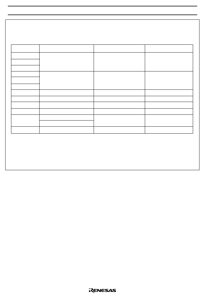
List of Functions
Product Name
HD404888
HD4048812
HD404889
HCD404889
ROM (words)
8,192
12,288
16,384
RAM (digit)
1,344
I/O
46 (max)
Large-current I/O pins
4 (source, 10 mA max), 8 (sink, 15 mA max)
LCD segment multiplexed pins
16
Analog input multiplexed pins
6
Timer/counter
16-bit timer: 1 (Can also be used as two 8-bit timer),
8-bit timer: 2
Input capture
8 bit
�
1
Timer output
2 (PWM output possible)
Event input
2 (edge selection possible)
Serial interface
1 (8-bit synchronous)
A/D converter
8 bits
�
6 channels
LCD circuit
Max. 32 seg
�
4 com
Interrupt sources
External
3 (edge selection possible for 1)
Internal
6
Low-power modes
4
Stop mode
O
Watch mode
O
Standby mode
O
Subactive mode
O
Module standby
O
System clock division software switching
O
Main oscillator
Ceramic oscillation
O
Crystal oscillation
O
Sub-oscillator
Crystal oscillation
O (32.768kHz)
Minimum instruction execution time
0.89
�
s(f
OSC
=4.5MHz)
Operating voltage (V)
1.8 to 5.5
Package
80-pin plastic QFP (FP-80A)
80-pin plastic TQFP (TFP-80C)
Chip
Guaranteed operation temperature(
�
C)
�20 to +75
+75

HD404889/HD404899/HD404878/HD404868 Series
7
Product Name
HD4074889
HD404898
HD4048912
HD404899
ROM (words)
16,384PROM
8,192
12,288
16,384
RAM (digit)
1,344
I/O
46 (max)
Large-current I/O pins
4 (source, 10 mA max), 8 (sink, 15 mA max)
LCD segment multiplexed pins
16
Analog input multiplexed pins
6
Timer/counter
16-bit timer: 1 (Can also be used as two 8-bit timer),
8-bit timer: 2
Input capture
8 bit
�
1
Timer output
2 (PWM output possible)
Event input
2 (edge selection possible)
Serial interface
1 (8-bit synchronous)
A/D converter
8 bits
�
6
channels
10 bits
�
6 channels
LCD circuit
Max. 32 seg
�
4 com
Interrupt sources
External
3 (edge selection possible for 1)
Internal
6
Low-power modes
4
Stop mode
O
Watch mode
O
Standby mode
O
Subactive mode
O
Module standby
O
System clock division software switching
O
Main oscillator
Ceramic oscillation
O
Crystal oscillation
O
Sub-oscillator
Crystal oscillation
O (32.768kHz)
Minimum instruction execution time
0.89
�
s(f
OSC
=4.5MHz)
Operating voltage (V)
2.0 to 5.5
1.8 to 5.5
Package
80-pin plastic QFP (FP-80A) 80-pin plastic TQFP (TFP-80C)
Guaranteed operation temperature(
�
C)
�20 to +75

HD404889/HD404899/HD404878/HD404868 Series
8
Product Name
HD40C4899
HD4074899
HD404874
HD404878
ROM (words)
16,384
16,384PROM
4,096
8,192
RAM (digit)
1,344
880
I/O
46 (max)
Large-current I/O pins
4 (source, 10 mA max), 8 (sink, 15 mA max)
LCD segment multiplexed pins
16
Analog input multiplexed pins
6
--
Timer/counter
16-bit timer: 1 (Can also be used as two 8-bit timer),
8-bit timer: 2
Input capture
8 bit
�
1
Timer output
2 (PWM output possible)
Event input
2 (edge selection possible)
Serial interface
1 (8-bit synchronous)
A/D converter
10 bits
�
6 channels
--
LCD circuit
Max. 32 seg
�
4 com
Interrupt sources
External
3 (edge selection possible for 1)
Internal
6
5
Low-power modes
4
Stop mode
O
Watch mode
O
Standby mode
O
Subactive mode
O
Module standby
O
System clock division software switching
O
Main oscillator
Ceramic oscillation
O
Crystal oscillation
O
Sub-oscillator
Crystal oscillation
O (32.768kHz)
Minimum instruction execution time
0.89
�
s(f
OSC
=4.5MHz)
Operating voltage (V)
1.8 to 5.5
2.0 to 5.5
1.8 to 5.5
Package
Chip
80-pin plastic QFP (FP-80A)
80-pin plastic TQFP (TFP-80C)
Guaranteed operation temperature(
�
C)
+75
�20 to +75
HD404889/HD404899/HD404878/HD404868 Series
9
Product Name
HCD404878
HD404864
HD404868
HD4074869
ROM (words)
8,192
4,096
8,192
16,384PROM
RAM (digit)
880
408
I/O
46 (max)
41 (max)
Large-current I/O pins
4 (source,
10 mA max),
8 (sink,
15 mA max)
4 (source, 10 mA max), 6 (sink, 15 mA max)
LCD segment multiplexed pins
16
Analog input multiplexed pins
--
4
Timer/counter
16-bit timer: 1
(Can also be
used as two
8-bit timer),
8-bit timer: 2
16-bit timer: 1 (Can also be used as two 8-bit
timer), 8-bit timer: 1
Input capture
8 bit
�
1
--
Timer output
2 (PWM output possible)
Event input
2 (edge
selection
possible)
1 (edge selection possible)
Serial interface
1 (8-bit synchronous)
A/D converter
--
10 bits
�
4 channels
LCD circuit
Max. 32 seg
�
4 com
Max. 24 seg
�
4 com
Interrupt sources
External
3 (edge selection possible for 1)
Internal
5
Low-power modes
4
Stop mode
O
Watch mode
O
Standby mode
O
Subactive mode
O
Module standby
O
System clock division software switching
O
Main oscillator
Ceramic oscillation
O
Crystal oscillation
O
Sub-oscillator
Crystal oscillation
O (32.768kHz)
Minimum instruction execution time
0.89
�
s(f
OSC
=4.5MHz)
Operating voltage (V)
1.8 to 5.5
2.0 to 5.5
Package
Chip
64-pin plastic QFP (FP-64A)
64-pin plastic DILP (DP-64S)
Guaranteed operation temperature(
�
C)
+75
�20 to +75
HD404889/HD404899/HD404878/HD404868 Series
10
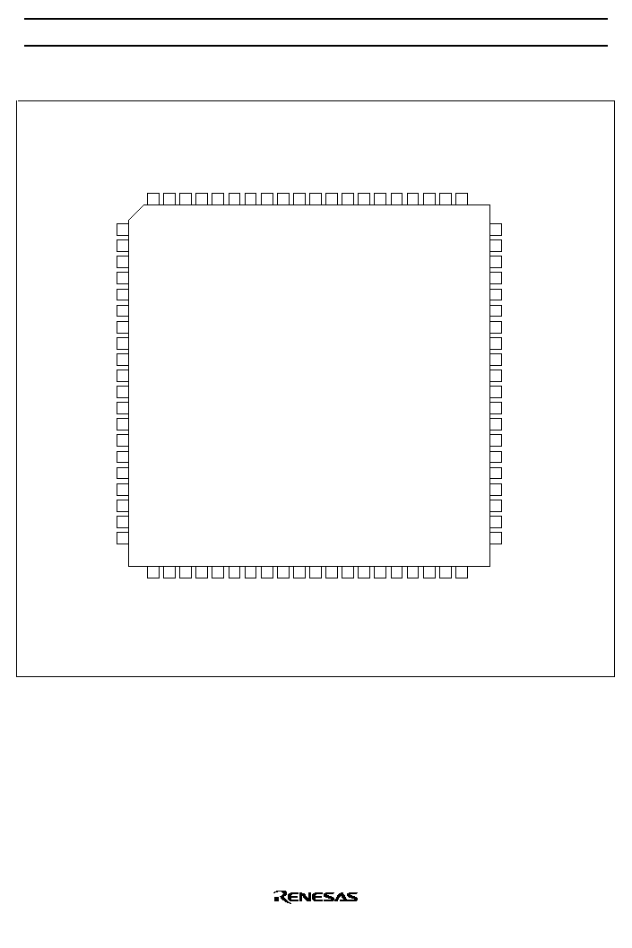
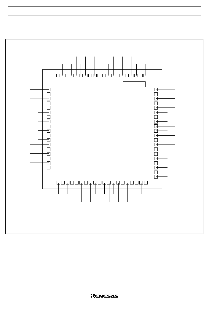
Pin Arrangement
AVcc
R7
0
/AN
0
R7
1
/AN
1
R7
2
/AN
2
R7
3
/AN
3
R8
0
/AN
4
R8
1
/AN
5
AVss
TEST
OSC
1
OCS
2
GND
X2
X1
RESET
Vcc
D
0
/
INT
0
D
1
/INT
1
D
2
D
3
D
4
D
5
D
6
D
7
D
8
D
9
D
10
D
11
R0
0
/
WU
0
R0
1
/
WU
1
R0
2
/
WU
2
R0
3
/
WU
3
R1
0
/EVNB
R1
1
/EVND
R1
2
/BUZZ
R1
3
/TOB
R2
0
/TOC
R2
1
/
SCK
R2
2
/SI/SO
R2
3
SEG20
SEG19
SEG18
SEG17
R6
3
/SEG16
R6
2
/SEG15
R6
1
/SEG14
R6
0
/SEG13
R5
3
/SEG12
R5
2
/SEG11
R5
1
/SEG10
R5
0
/SEG9
R4
3
/SEG8
R4
2
/SEG7
R4
1
/SEG6
R4
0
/SEG5
R3
3
/SEG4
R3
2
/SEG3
R3
1
/SEG2
R3
0
/SEG1
V
0
V
1
V
2
V
3
COM4
COM3
COM2
COM1
SEG32
SEG31
SEG30
SEG29
SEG28
SEG27
SEG26
SEG25
SEG24
SEG23
SEG22
SEG21
1
2
3
4
5
6
7
8
9
10
11
12
13
14
15
16
17
18
19
20
21
22
23
24
25
26
27
28
29
30
31
32
33
34
35
36
37
38
39
40
80
79
78
77
76
75
74
73
72
71
70
69
68
67
66
65
64
63
62
61
60
59
58
57
56
55
54
53
52
51
50
49
48
47
46
45
44
43
42
41
FP-80A
TFP-80C
(Top View)
HD404889/HD404899 Series
HD404889/HD404899/HD404878/HD404868 Series
11
NC
R7
0
R7
1
R7
2
R7
3
R8
0
R8
1
NC
TEST
OSC
1
OSC
2
GND
X2
X1
RESET
Vcc
D
0
/
INT
0
D
1
/INT
1
D
2
D
3
D
4
D
5
D
6
D
7
D
8
D
9
D
10
D
11
R0
0
/
WU
0
R0
1
/
WU
1
R0
2
/
WU
2
R0
3
/
WU
3
R1
0
/EVNB
R1
1
/EVND
R1
2
/BUZZ
R1
3
/TOB
R2
0
/TOC
R2
1
/
SCK
R2
2
/SI/SO
R2
3
SEG20
SEG19
SEG18
SEG17
R6
3
/SEG16
R6
2
/SEG15
R6
1
/SEG14
R6
0
/SEG13
R5
3
/SEG12
R5
2
/SEG11
R5
1
/SEG10
R5
0
/SEG9
R4
3
/SEG8
R4
2
/SEG7
R4
1
/SEG6
R4
0
/SEG5
R3
3
/SEG4
R3
2
/SEG3
R3
1
/SEG2
R3
0
/SEG1
V
0
V
1
V
2
V
3
COM4
COM3
COM2
COM1
SEG32
SEG31
SEG30
SEG29
SEG28
SEG27
SEG26
SEG25
SEG24
SEG23
SEG22
SEG21
1
2
3
4
5
6
7
8
9
10
11
12
13
14
15
16
17
18
19
20
21
22
23
24
25
26
27
28
29
30
31
32
33
34
35
36
37
38
39
40
80
79
78
77
76
75
74
73
72
71
70
69
68
67
66
65
64
63
62
61
60
59
58
57
56
55
54
53
52
51
50
49
48
47
46
45
44
43
42
41
FP-80A
TFP-80C
(Top View)
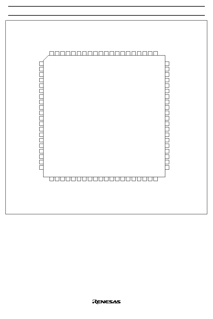
HD404878 Series

HD404889/HD404899/HD404878/HD404868 Series
12
HD404868 Series
R70/AN0
R71/AN1
R72/AN2
R73/AN3
TEST
OSC1
OSC2
GND
X2
X1
RESET
Vcc
D0/
INT
0
D1/INT1
D2
D3
D4
D5
D6
D7
D8
D9
R00/
WU
0
R01/
WU
1
R02/
WU
2
R10/EVNB
R11
R12/BUZZ
R13/TOB
R20/TOC
R21/
SCK
R22/SI/SO
R62/SEG15
R61/SEG14
R60/SEG13
R53/SEG12
R52/SEG11
R51/SEG10
R50/SEG9
R43/SEG8
R42/SEG7
R41/SEG6
R40/SEG5
R33/SEG4
R32/SEG3
R31/SEG2
R30/SEG1
R23
V1
V2
V3
COM4
COM3
COM2
COM1
SEG24
SEG23
SEG22
SEG21
SEG20
SEG19
SEG18
SEG17
R63/SEG16
1
2
3
4
5
6
7
8
9
10
11
12
13
14
15
16
17
18
19
20
21
22
23
24
25
26
27
28
29
30
31
32
64
63
62
61
60
59
58
57
56
55
54
53
52
51
50
49
48
47
46
45
44
43
42
41
40
39
38
37
36
35
34
33
FP-64A
(Top View)
COM1
COM2
COM3
COM4
V3
V2
V1
R70/AN0
R71/AN1
R72/AN2
R73/AN3
TEST
OSC1
OSC2
GND
X2
X1
RESET
Vcc
D0/
INT
0
D1/INT1
D2
D3
D4
D5
D6
D7
D8
D9
R00/
WU
0
R01/
WU
1
R02/
WU
2
1
2
3
4
5
6
7
8
9
10
11
12
13
14
15
16
17
18
19
20
21
22
23
24
25
26
27
28
29
30
31
32
64
63
62
61
60
59
58
57
56
55
54
53
52
51
50
49
48
47
46
45
44
43
42
41
40
39
38
37
36
35
34
33
SEG24
SEG23
SEG22
SEG21
SEG20
SEG19
SEG18
SEG17
R63/SEG16
R62/SEG15
R61/SEG14
R60/SEG13
R53/SEG12
R52/SEG11
R51/SEG10
R50/SEG9
R43/SEG8
R42/SEG7
R41/SEG6
R40/SEG5
R33/SEG4
R32/SEG3
R31/SEG2
R30/SEG1
R23
R22/SI/SO
R21/
SCK
R20/TOC
R13/TOB
R12/BUZZ
R11
R10/EVNB
DP-64S
(Top View)

HD404889/HD404899/HD404878/HD404868 Series
13
Pad Arrangement
HCD404889, HCD404899
2
4
6
8
10
12
14
16
18
20
1
3
5
7
9
11
13
15
17
19
21
23
25
27
29
31
33
35
37
39
22
24
26
28
30
32
34
36
38
40
80
78
76
74
72
70
68
66
64
62
79
77
75
73
71
69
67
65
63
61
60
58
56
54
52
50
48
46
44
42
59
57
55
53
51
49
47
45
43
41
Model Name
Model Name: HD404889 (HCD404889)
HD404899 (HCD404899)

HD404889/HD404899/HD404878/HD404868 Series
14
Pad Coordinates
HCD404889, HCD404899
Chip size (X
�
Y):
Coordinates:
Home point position:
Pad size (X
�
Y):
Chip thickness:
4.63
�
4.77 (mm)
Pad center
Chip center
90
�
90 (
�
m)
280 (
�
m)
Chip center
(X=0,Y=0)
Y
X
Mold
Coodinates
Coodinates
Pad No.
Pad name
X (
�
m)
Y (
�
m)
Pad No.
Pad name
X (
�
m)
Y (
�
m)
1
AV
CC
�2129
1779
41
R30/SEG1
2129
�1787
2
R70/AN0
�2129
1589
42
R31/SEG2
2129
�1616
3
R71/AN1
�2129
1417
43
R32/SEG3
2129
�1445
4
R72/AN2
�2129
1246
44
R33/SEG4
2129
�1273
5
R73/AN3
�2129
1074
45
R40/SEG5
2129
�1102
6
R80/AN4
�2129
903
46
R41/SEG6
2129
�973
7
R81/AN5
�2129
732
47
R42/SEG7
2129
�759
8
AV
SS
�2129
506
48
R43/SEG8
2129
�588
9
TEST
�2129
103
49
R50/SEG9
2129
�417
10
OSC1
�2129
�68
50
R51/SE10
2129
�245
11
OSC2
�2129
�240
51
R52/SEG11
2129
�74
12
GND
�2129
�434
52
R53/SEG12
2129
98
13
X2
�2129
�605
53
R60/SEG13
2129
269
14
X1
�2129
�776
54
R61/SEG14
2129
440
15
RESETN
�2129
�948
55
R62/SEG15
2129
612
16
V
CC
�2129
�1119
56
R63/SEG16
2129
783
17
D0/INT0N
�2129
�1290
57
SEG17
2129
954
18
D1/INT1
�2129
�1462
58
SEG18
2129
1126
19
D2
�2129
�1633
59
SEG19
2129
1297
20
D3
�2129
�1804
60
SEG20
2129
1477
21
D4
�1677
�2199
61
SEG21
1588
2199
22
D5
�1506
�2199
62
SEG22
1407
2199
23
D6
�1335
�2199
63
SEG23
1236
2199
24
D7
�1163
�2199
64
SEG24
1064
2199
25
D8
�992
�2199
65
SEG25
893
2199
26
D9
�821
�2199
66
SEG26
722
2199
27
D10
�649
�2199
67
SEG27
550
2199
28
D11
�478
�2199
68
SEG28
379
2199
29
R00/WU0N
�307
�2199
69
SEG29
208
2199
30
R01/WU1N
�135
�2199
70
SEG30
36
2199
31
R02/WU2N
36
�2199
71
SEG31
�135
2199
32
R03/WU3N
208
�2199
72
SEG32
�307
2199
33
R10/EVNB
379
�2199
73
COM1
�478
2199
34
R11/EVND
550
�2199
74
COM2
�649
2199
35
R12/BUZZ
722
�2199
75
COM3
�821
2199
36
R13/TOB
893
�2199
76
COM4
�992
2199
37
R20/TOC
1064
�2199
77
V3
�1163
2199
38
R21/SCKN
1236
�2199
78
V2
�1335
2199
39
R22/Si/SO
1407
�2199
79
V1
�1506
2199
40
R23
1588
�2199
80
V0
�1677
2199
HD404889/HD404899/HD404878/HD404868 Series
15
Pad Arrangement
HCD404878
1
2
3
4
5
6
7
8
9
10
11
12
13
14
15
16
17
18
19
20
21
22
23
24
25
26
27
28
29
30
31
32
33
34
35
36
37
38
78
77
76
75
74
73
72
71
70
69
68
67
66
65
64
63
62
61
60
59
58
57
56
55
54
53
52
51
50
49
48
47
46
45
44
43
42
41
40
39
Model Name
Model Name: HD404878 (HCD404878)

HD404889/HD404899/HD404878/HD404868 Series
16
Pad Coordinates
HCD404878
Chip size (X
�
Y):
Coordinates:
Home point position:
Pad size (X
�
Y):
Chip thickness:
4.13
�
4.26 (mm)
Pad center
Chip center
90
�
90 (
�
m)
280 (
�
m)
Y
Chip center
(X=0,Y=0)
X
Mold
Coodinates
Coodinates
Pad No.
Pad name
X (
�
m)
Y (
�
m)
Pad No.
Pad name
X (
�
m)
Y (
�
m)
1
R70
�1879
1446
40
R31/SEG2
1879
�1405
2
R71
�1879
1280
41
R32/SEG3
1879
�1239
3
R72
�1879
1114
42
R33/SEG4
1879
�1072
4
R73
�1879
948
43
R40/SEG5
1879
�906
5
R80
�1879
781
44
R41/SEG6
1879
�740
6
R81
�1879
615
45
R42/SEG7
1879
�573
7
TEST
�1879
449
46
R43/SEG8
1879
�407
8
OSC1
�1879
282
47
R50/SEG9
1879
�241
9
OSC2
�1879
116
48
R51/SE10
1879
�74
10
GND
�1879
�73
49
R52/SEG11
1879
92
11
X2
�1879
�239
50
R53/SEG12
1879
258
12
X1
�1879
�406
51
R60/SEG13
1879
425
13
RESETN
�1879
�572
52
R61/SEG14
1879
591
14
V
CC
�1879
�738
53
R62/SEG15
1879
757
15
D0/INT0N
�1879
�905
54
R63/SEG16
1879
924
16
D1/INT1
�1879
�1071
55
SEG17
1879
1087
17
D2
�1879
�1237
56
SEG18
1879
1246
18
D3
�1879
�1404
57
SEG19
1879
1405
19
D4
�1654
�1943
58
SEG20
1879
1564
20
D5
�1488
�1943
59
SEG21
1509
1943
21
D6
�1322
�1943
60
SEG22
1351
1943
22
D7
�1155
�1943
61
SEG23
1192
1943
23
D8
�989
�1943
62
SEG24
1033
1943
24
D9
�823
�1943
63
SEG25
874
1943
25
D10
�656
�1943
64
SEG26
716
1943
26
D11
�490
�1943
65
SEG27
557
1943
27
R00/WU0N
�324
�1943
66
SEG28
398
1943
28
R01/WU1N
�158
�1943
67
SEG29
239
1943
29
R02/WU2N
9
�1943
68
SEG30
81
1943
30
R03/WU3N
175
�1943
69
SEG31
�78
1943
31
R10/EVNB
341
�1943
70
SEG32
�237
1943
32
R11/EVND
508
�1943
71
COM1
�411
1943
33
R12/BUZZ
674
�1943
72
COM2
�570
1943
34
R13/TOB
840
�1943
73
COM3
�728
1943
35
R20/TOC
1007
�1943
74
COM4
�887
1943
36
R21/SCKN
1173
�1943
75
V3
�1038
1943
37
R22/Si/SO
1339
�1943
76
V2
�1194
1943
38
R23
1506
�1943
77
V1
�1351
1943
39
R30/SEG1
1879
�1571
78
V0
�1507
1943
HD404889/HD404899/HD404878/HD404868 Series
17
Pin Description
HD404889/HD404899/HD404878 Series
Pin Number
Item
Symbol
FP-80A
TFP-80C
I/O
Function
Power supply
V
CC
16
--
Apply the power supply voltage to this pin.
GND
12
--
Connect to ground.
Test
TEST
9
Input
Not for use by the user application. Connect to GND
potential.
Reset
RESET
15
Input
Used to reset the MCU.
Oscillation
OSC
1
10
Input
Internal oscillator input/output pins. Connect a ceramic
resonator, crystal resonator, or external
OSC
2
11
Output
oscillator circuit.
X1
14
Input
Realtime clock oscillator input/output pins. Connect a
32.768 kHz crystal. If 32.768 kHz
X2
13
Output
crystal oscillation is not used, fix the
�
1 pin to V
CC
and
leave the
�
2 pin open.
Port
D
0
�D
11
17�28
I/O
I/O pins addressed bit by bit. D
0
to D
3
are large-current
source pins (max. 10 mA), and D
4
to D
11
are large-
current sink pins (max. 15 mA).
R0
0
�R6
3
R7
0
�R8
1
29�56, 2�7
I/O
I/O pins, addressed in 4-bit units.
Interrupt
INT
0
,INT
1
17,18
Input
External interrupt input pins
Wakeup
WU
0
�
WU
3
29�32
Input
Input pins used for transition from stop mode to active
mode.
Serial interface
SCK
38
I/O
Serial interface clock I/O pin
SI
39
Input
Serial interface receive data input pin
SO
39
Output
Serial interface transmit data output pin
Timer
TOB,TOC
36,37
Output
Timer output pins
EVNB,EVND
33,34
Input
Event count input pins
LCD
V
0
�V
3
80�77
--
LCD driver power supply pins. The on-chip power
supply dividing resistor can be disconnected by
software. Power supply conditions are:
V
CC
V
1
V
2
V
3
GND.
COM1�COM4
73�76
Output
LCD common signal pins
SEG1�SEG32
41�72
Output
LCD segment signal pins
A/D converter
*
1
AV
CC
1
--
A/D converter power supply pin. Connect as close as
possible to the V
CC
pin so as to be at the same potential
as V
CC
.
AV
SS
8
--
Ground pin for AV
CC
. Connect as close as possible to
the GND pin so as to be at the same potential as GND.
AN
0
�AN
5
2�7
Input
A/D converter analog input pins
Buzzer output
BUZZ
35
Output
Timer overflow toggle output or divided system clock
output pin
Other
NC
1, 8
*
2
--
Connect to ground potential.
Notes: 1. Applies to HD404889 and HD404899 series.
2. Applies to HD404878 series.

HD404889/HD404899/HD404878/HD404868 Series
18
HD404868 Series
Pin Number
Item
Symbol
FP-64A
DP-64S
I/O
Function
Power supply
V
CC
12
19
--
Apply the power supply voltage to this pin.
GND
8
15
--
Connect to ground.
Test
TEST
5
12
Input
Not for use by the user application. Connect to
GND potential.
Reset
RESET
11
18
Input
Used to reset the MCU.
Oscillation
OSC
1
6
13
Input
Internal oscillator input/output pins. Connect a
ceramic resonator, crystal resonator, or external
OSC
2
7
14
Output
oscillator circuit.
X1
10
17
Input
Realtime clock oscillator input/output pins. Connect
a 32.768 kHz crystal. If 32.768 kHz
X2
9
16
Output
crystal oscillation is not used, fix the
�
1 pin to V
CC
and leave the
�
2 pin open.
Port
D
0
�D
9
13�22
20�29
I/O
I/O pins addressed bit by bit. D
0
to D
3
are large-
current source pins (max. 10 mA), and D
4
to D
9
are
large-current sink pins (max. 15 mA).
R0
0
�R0
2
R1
0
�R6
3
R7
0
�R7
3
23�25
26�49
1�4
30�32
33�56
8�11
I/O
I/O pins, addressed in 4-bit units.
Interrupt
INT
0
,INT
1
13,14
20, 21
Input
External interrupt input pins
Wakeup
WU
0
�
WU
2
23�25
30�32
Input
Input pins used for transition from stop mode to
active mode.
Serial interface
SCK
31
38
I/O
Serial interface clock I/O pin
SI
32
39
Input
Serial interface receive data input pin
SO
32
39
Output
Serial interface transmit data output pin
Timer
TOB,TOC
29, 30
36, 37
Output
Timer output pins
EVNB
26
33
Input
Event count input pins
LCD
V
1
�V
3
64�62
7�5
--
LCD driver power supply pins. The on-chip power
supply dividing resistor can be disconnected by
software. Power supply conditions are:
V
CC
V
1
V
2
V
3
GND.
COM1�COM4
58�61
1�4
Output
LCD common signal pins
SEG1�SEG24
34�57
41�64
Output
LCD segment signal pins
A/D converter
AN
0
�AN
3
1�4
8�11
Input
A/D converter analog input pins
Buzzer output
BUZZ
28
35
Output
Timer overflow toggle output or divided system
clock output pin

HD404889/HD404899/HD404878/HD404868 Series
19
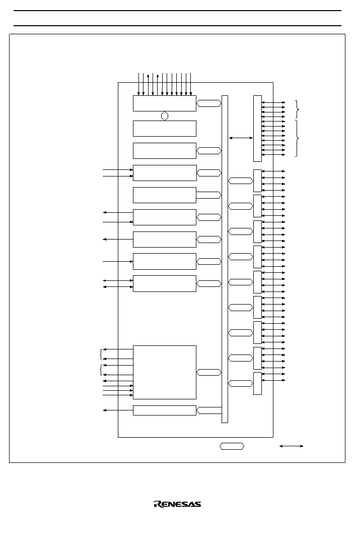
Block DiagramG
INT
0
INT
1
TOB
EVNB
TOC
EVND
SCK
SI/SO
AVcc
AN
0
AN
1
AN
2
AN
3
AN
4
AN
5
AVss
SEG1
to
SEG32
COM1
to
COM4
V0
V1
V2
V3
BUZZ
HMCS400 CPU
HD404889/HD404899 Series
ROM
RAM
P-MOS large-
current buffer
N-MOS large-
current buffer
External interrupt
control circuit
8-bit timer A
8-bit timer B
8-bit timer C
8-bit timer D
Synchronous
serial interface
A/D converter
8-bit
�
6 channels
(HD404889 Series)
10-bit
�
6 channels
(HD404899 Series)
LCD circuit
32-segment
�
4 common
Buzzer output circuit
RESET
TEST
OSC1
OSC2
X1
X2
Vcc
GND
WU
0
WU
1
WU
2
WU
3
D Port
R0 Port
R1 Port
R2 Port
R3 Port
R4 Port
R5 Port
R6 Port
R7 Port
R8 Port
D
0
D
1
D
2
D
3
D
4
D
5
D
6
D
7
D
8
D
9
D
10
D
11
R0
0
R0
1
R0
2
R0
3
R1
0
R1
1
R1
2
R1
3
R2
0
R2
1
R2
2
R2
3
R3
0
R3
1
R3
2
R3
3
R4
0
R4
1
R4
2
R4
3
R5
0
R5
1
R5
2
R5
3
R6
0
R6
1
R6
2
R6
3
R7
0
R7
1
R7
2
R7
3
R8
0
R8
1
: Data bus
: Signal line
HD404889/HD404899/HD404878/HD404868 Series
20
INT
0
INT
1
TOB
EVNB
TOC
EVND
SCK
SI/SO
SEG1
to
SEG32
COM1
to
COM4
V0
V1
V2
V3
BUZZ
HMCS400 CPU
ROM
RAM
P-MOS large-
current buffer
N-MOS large-
current buffer
External interrupt
control circuit
8-bit timer A
8-bit timer B
8-bit timer C
8-bit timer D
Clock-synchronous
8-bit serial interface
LCD circuit
32-segment
�
4 common
Buzzer output circuit
RESET
TEST
OSC1
OSC2
X1
X2
Vcc
GND
WU
0
WU
1
WU
2
WU
3
D Port
R0 Port
R1 Port
R2 Port
R3 Port
R4 Port
R5 Port
R6 Port
R7 Port
R8 Port
D
0
D
1
D
2
D
3
D
4
D
5
D
6
D
7
D
8
D
9
D
10
D
11
R0
0
R0
1
R0
2
R0
3
R1
0
R1
1
R1
2
R1
3
R2
0
R2
1
R2
2
R2
3
R3
0
R3
1
R3
2
R3
3
R4
0
R4
1
R4
2
R4
3
R5
0
R5
1
R5
2
R5
3
R6
0
R6
1
R6
2
R6
3
R7
0
R7
1
R7
2
R7
3
R8
0
R8
1
: Data bus
: Signal line
HD404878 Series

HD404889/HD404899/HD404878/HD404868 Series
21
RESET
TEST
OSC
1
OSC
2
X1
X2
V
CC
GND
WU
0
WU
1
WU
2
HMCS400 CPU
ROM
RAM
8-bit timer A
8-bit timer C
8-bit timer B
D
0
D
1
D
2
D
3
D
4
D
5
D
6
D
7
D
8
D
9
D Port
R0
0
R0
1
R0
2
R1
0
R1
1
R1
2
R1
3
R2
0
R2
1
R2
2
R2
3
R3
0
R3
1
R3
2
R3
3
TOC
EVNB
TOB
P-MOS large-
current buffer
N-MOS large-
current buffer
AN
0
AN
1
AN
2
AN
3
A/D converter
4 channels
�
10-bit
External interrupt control circuit
INT
0
INT
1
R6
0
R6
1
R6
2
R6
3
R7
0
R7
1
R7
2
R7
3
Clock-synchronous 8-bit serial interface
SCK
SI/SO
LCD circuit
24-segment
�
4 common
SEG1
SEG24
COM1
COM4
V
1
V
2
V
3
Buzzer output circuit
BUZZ
R4
0
R4
1
R4
2
R4
3
R5
0
R5
1
R5
2
R5
3
~
~
~~
R0 Port
R1 Port
R2 Port
R4 Port
R5 Port
R6 Port
R7 Port
R3 Port
HD404868 Series

HD404889/HD404899/HD404878/HD404868 Series
22
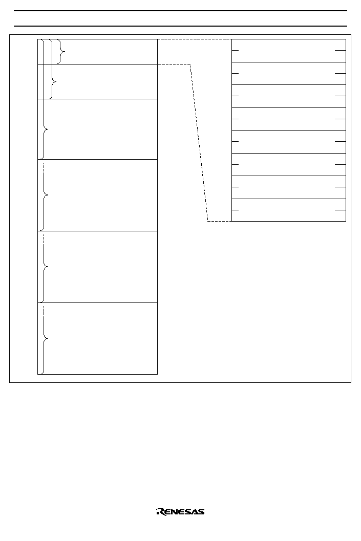
Memory Map
ROM Memory Map
The ROM memory map is shown in figure 1 and is described below.
Vector address area ($0000 to $000F): When an MCU reset or interrupt handling is performed, the
program is executed from the vector address. A JMPL instruction should be used to branch to the start
address of the reset routine or the interrupt routine.
Zero page subroutine area ($0000 to $003F):A branch can be made to a subroutine in the area $0000 to
$003F with the CAL instruction.
Pattern area ($0000 to $0FFF): ROM data in the area $0000 to $0FFF can be referenced as pattern data
with the P instruction.
Program area ($0000 to $0FFF(HD404874, HD404864)), ($0000 to $1FFF (HD404888, HD404898,
HD404878, HD404868, HCD404878)), ($0000 to $2FFF (HD4048812, HD4048912)), ($0000 to $3FFF
(HD404889, HD404899, HCD404889, HCD404899, HD4074899, HD4074889, HD4074869))
HD404889/HD404899/HD404878/HD404868 Series
23
$0000
$000F
$003F
$0FFF
$1FFF
$3FFF
$2FFF
Vector addresses
(16 words)
Zero page subroutine area
(64 words)
HD404874/HD404864
pattern/program area
(4,096 words)
HD404888/HD404898/HD404878/
HD404868/HCD404878
pattern/program area
(8,192 words)
HD4048812/HD4048912
pattern/program area
(12,288 words)
HD404889/HD4074889/
HD404899/HD4074899/HD4074869/
HCD404889/HCD404899
pattern/program area
(16,384 words)
$0000
$0001
$0002
$0003
$0004
$0005
$0006
$0007
$0008
$0009
$000A
$000B
$000C
$000D
$000E
$000F
JMPL instruction
(Jump to reset routine)
JMPL instruction
(Jump to
WU
0
to
WU
3
routine)
JMPL instruction
(Jump to
INT
0
routine)
JMPL instruction
(Jump to INT
1
routine)
JMPL instruction
(Jump to timer A routine)
JMPL instruction
(Jump to timer B/timer D routine)
JMPL instruction
(Jump to timer C routine)
JMPL instruction
(Jump to A/D or serial interface routine)
Figure 1 ROM Memory Map
RAM Memory Map
The MCU has on-chip RAM comprising a memory register area, LCD data area, data area, and stack area.
In addition to these areas, an interrupt control bit area, special register area, and register flag area are
mapped onto RAM memory space as a RAM-mapped register area.The RAM memory map is shown in
figure 2 and described below.
Memory register, LCD data area, data area, and stack area values are unstable immediately after
power is turned on. They must be initialized before use.

HD404889/HD404899/HD404878/HD404868 Series
24
Speed Select Reg.
Miscellaneous Reg.
Edge Select Reg.
Port Mode Reg.0
Port Mode Reg.1
Port Mode Reg.2
Port Mode Reg.3
Port Mode Reg.4
Module Standby Reg.1
Module Standby Reg.2
Timer Mode Reg.A
Timer Mode Reg.B1
Timer Mode Reg.B2
Timer Mode Reg.C1
Timer Mode Reg.C2
Timer Mode Reg.D1
Timer Mode Reg.D2
Serial Mode Reg.1
Serial Mode Reg.2
Serial Data Reg.Lower
Serial Data Reg.Upper
A/D Mode reg.
A/D Data Reg.Lower
A/D Data Reg.Upper
LCD Control Reg.
LCD Mode Reg.
Buzzer Mode Reg.
Port D
0
~D
3
DCR
Port D
4
~D
7
DCR
Port D
8
~D
11
DCR
Port R0 DCR
Port R1 DCR
Port R2 DCR
Port R3 DCR
Port R4 DCR
Port R5 DCR
Port R6 DCR
Port R7 DCR
Port R8 DCR
Vreg.
$000
$03F
$040
$04F
$050
$06F
$070
$08F
$090
$38F
$390
$25F
$260
$3BF
$3C0
$3FF
RAM-mapped
register area
HD404889 Series
Memory register (MR) area
(16 digits)
LCD data area
(32 digits)
Data (464 digits)
Stack area
(64 digits)
Interrupt control bit area
Not used
W
W
W
W
W
W
W
W
W
W
W
W
W
R/W
R/W
W
W
R/W
R/W
W
W
R/W
R/W
W
W
R/W
R/W
W
R
R
W
W
W
W
W
W
W
W
W
W
W
W
W
W
W
R/W
Timer-B
Timer-C
Timer-D
Not used
Register flag area
Not used
Not used
Not used
Not used
$000
$001
$002
$003
$004
$005
$006
$007
$008
$009
$00A
$00B
$00C
$00D
$00E
$00F
$010
$011
$012
$013
$014
$015
$016
$017
$018
$019
$01A
$01B
$01C
$01D
$01E
$01F
$020
$021
$022
$023
$024
$025
$026
$027
$028
$029
$02A
$02B
$02C
$02D
$02E
$02F
$030
$031
$032
$033
$034
$035
$036
$037
$038
$039
$03A
$03B
$03C
$03D
$03E
$03F
Timer Read Reg.B Lower
(TRBL)
R
Timer Write Reg.B Lower
(TWBL)
W
Timer Read Reg.B Upper
(TRBU)
R
Timer Write Reg.B Upper
(TWBU) W
Timer Read Reg.C Lower
(TRCL)
R
Timer Write Reg.C Lower
(TWCL)
W
Timer Read Reg.C Upper
(TRCU)
R
Timer Write Reg.C Upper
(TWCU) W
Timer Read Reg.D Lower
(TRDL)
R
Timer Write Reg.D Lower
(TWDL)
W
Timer Read Reg.D Upper
(TRDU)
R
Timer Write Reg.D Upper
(TWDU) W
$012
$013
$016
$017
$01A
$01B
*
Not used
Not used
V = 0 (bank = 0)
Data (464 digits)
V = 1 (bank = 1)
Data (304 digits)
(SSR)
(MIS)
(ESR)
(PMR0)
(PMR1)
(PMR2)
(PMR3)
(PMR4)
(MSR1)
(MSR2)
(TMA)
(TMB1)
(TMB2)
(TRBL/TWBL)
(TRBU/TWBU)
(TMC1)
(TMC2)
(TRCL/TWCL)
(TRCU/TWCU)
(TMD1)
(TMD2)
(TRDL/TWDL)
(TRDU/TWDU)
(SMR1)
(SMR2)
(SRL)
(SRU)
(AMR)
(ADRL)
(ADRU)
(LCR)
(LMR)
(BMR)
(DCD0)
(DCD1)
(DCD2)
(DCR0)
(DCR1)
(DCR2)
(DCR3)
(DCR4)
(DCR5)
(DCR6)
(DCR7)
(DCR8)
(V)
Notes: R : Read
W : Write
R/W : Read/Write
*Two registers are mapped onto the
same address ($012, $013, $016,
$017, $01A, $01B).
*
Figure 2 RAM Memory Map
HD404889/HD404899/HD404878/HD404868 Series
25
Speed Select Reg.
Miscellaneous Reg.
Edge Select Reg.
Port Mode Reg.0
Port Mode Reg.1
Port Mode Reg.2
Port Mode Reg.3
Port Mode Reg.4
Module Standby Reg.1
Module Standby Reg.2
Timer Mode Reg.A
Timer Mode Reg.B1
Timer Mode Reg.B2
Timer Mode Reg.C1
Timer Mode Reg.C2
Timer Mode Reg.D1
Timer Mode Reg.D2
Serial Mode Reg.1
Serial Mode Reg.2
Serial Data Reg.Lower
Serial Data Reg.Upper
A/D Mode reg.
A/D Data Reg.Lower
A/D Data Reg.Middle
A/D Data Reg.Upper
LCD Control Reg.
LCD Mode Reg.
Buzzer Mode Reg.
Port D
0
~D
3
DCR
Port D
4
~D
7
DCR
Port D
8
~D
11
DCR
Port R0 DCR
Port R1 DCR
Port R2 DCR
Port R3 DCR
Port R4 DCR
Port R5 DCR
Port R6 DCR
Port R7 DCR
Port R8 DCR
Vreg.
$000
$03F
$040
$04F
$050
$06F
$070
$08F
$090
$38F
$390
$25F
$260
$3BF
$3C0
$3FF
RAM-mapped
register area
HD404899 Series
Memory register (MR) area
(16 digits)
LCD data area
(32 digits)
Data (464 digits)
Stack area
(64 digits)
Interrupt control bit area
Not used
W
W
W
W
W
W
W
W
W
W
W
W
W
R/W
R/W
W
W
R/W
R/W
W
W
R/W
R/W
W
W
R/W
R/W
W
R
R
R
W
W
W
W
W
W
W
W
W
W
W
W
W
W
W
R/W
Timer-B
Timer-C
Timer-D
Not used
Register flag area
Not used
Not used
Not used
$000
$001
$002
$003
$004
$005
$006
$007
$008
$009
$00A
$00B
$00C
$00D
$00E
$00F
$010
$011
$012
$013
$014
$015
$016
$017
$018
$019
$01A
$01B
$01C
$01D
$01E
$01F
$020
$021
$022
$023
$024
$025
$026
$027
$028
$029
$02A
$02B
$02C
$02D
$02E
$02F
$030
$031
$032
$033
$034
$035
$036
$037
$038
$039
$03A
$03B
$03C
$03D
$03E
$03F
Timer Read Reg.B Lower
(TRBL)
R
Timer Write Reg.B Lower
(TWBL)
W
Timer Read Reg.B Upper
(TRBU)
R
Timer Write Reg.B Upper
(TWBU) W
Timer Read Reg.C Lower
(TRCL)
R
Timer Write Reg.C Lower
(TWCL)
W
Timer Read Reg.C Upper
(TRCU)
R
Timer Write Reg.C Upper
(TWCU) W
Timer Read Reg.D Lower
(TRDL)
R
Timer Write Reg.D Lower
(TWDL)
W
Timer Read Reg.D Upper
(TRDU)
R
Timer Write Reg.D Upper
(TWDU) W
$012
$013
$016
$017
$01A
$01B
*
Not used
Not used
V = 0 (bank = 0)
Data (464 digits)
V = 1 (bank = 1)
Data (304 digits)
(SSR)
(MIS)
(ESR)
(PMR0)
(PMR1)
(PMR2)
(PMR3)
(PMR4)
(MSR1)
(MSR2)
(TMA)
(TMB1)
(TMB2)
(TRBL/TWBL)
(TRBU/TWBU)
(TMC1)
(TMC2)
(TRCL/TWCL)
(TRCU/TWCU)
(TMD1)
(TMD2)
(TRDL/TWDL)
(TRDU/TWDU)
(SMR1)
(SMR2)
(SRL)
(SRU)
(AMR)
(ADRL)
(ADRM)
(ADRU)
(LCR)
(LMR)
(BMR)
(DCD0)
(DCD1)
(DCD2)
(DCR0)
(DCR1)
(DCR2)
(DCR3)
(DCR4)
(DCR5)
(DCR6)
(DCR7)
(DCR8)
(V)
Notes: R : Read
W : Write
R/W : Read/Write
*Two registers are mapped onto the
same address ($012, $013, $016,
$017, $01A, $01B).
*
Figure 2 RAM Memory Map (cont)
HD404889/HD404899/HD404878/HD404868 Series
26
Speed Select Reg.
Miscellaneous Reg.
Edge Select Reg.
Port Mode Reg.0
Port Mode Reg.1
Port Mode Reg.2
Port Mode Reg.3
Port Mode Reg.4
Module Standby Reg.1
Module Standby Reg.2
Timer Mode Reg.A
Timer Mode Reg.B1
Timer Mode Reg.B2
Timer Mode Reg.C1
Timer Mode Reg.C2
Timer Mode Reg.D1
Timer Mode Reg.D2
Serial Mode Reg.1
Serial Mode Reg.2
Serial Data Reg.Lower
Serial Data Reg.Upper
LCD Control Reg.
LCD Mode Reg.
Buzzer Mode Reg.
Port D
0
~D
3
DCR
Port D
4
~D
7
DCR
Port D
8
~D
11
DCR
Port R0 DCR
Port R1 DCR
Port R2 DCR
Port R3 DCR
Port R4 DCR
Port R5 DCR
Port R6 DCR
Port R7 DCR
Port R8 DCR
$000
$03F
$040
$04F
$050
$06F
$070
$08F
$090
$38F
$390
$3BF
$3C0
$3FF
RAM-mapped
register area
HD404878 Series
Memory register (MR) area
(16 digits)
LCD data area
(32 digits)
Data (768 digits)
Stack area
(64 digits)
Interrupt control bit area
Not used
W
W
W
W
W
W
W
W
W
W
W
W
W
R/W
R/W
W
W
R/W
R/W
W
W
R/W
R/W
W
W
R/W
R/W
W
W
W
W
W
W
W
W
W
W
W
W
W
W
W
Timer-B
Timer-C
Timer-D
Not used
Register flag area
Not used
Not used
Not used
Not used
$000
$001
$002
$003
$004
$005
$006
$007
$008
$009
$00A
$00B
$00C
$00D
$00E
$00F
$010
$011
$012
$013
$014
$015
$016
$017
$018
$019
$01A
$01B
$01C
$01D
$01E
$01F
$020
$021
$022
$023
$024
$025
$026
$027
$028
$029
$02A
$02B
$02C
$02D
$02E
$02F
$030
$031
$032
$033
$034
$035
$036
$037
$038
$039
$03A
$03B
$03C
$03D
$03E
$03F
Timer Read Reg.B Lower
(TRBL)
R
Timer Write Reg.B Lower
(TWBL)
W
Timer Read Reg.B Upper
(TRBU)
R
Timer Write Reg.B Upper
(TWBU) W
Timer Read Reg.C Lower
(TRCL)
R
Timer Write Reg.C Lower
(TWCL)
W
Timer Read Reg.C Upper
(TRCU)
R
Timer Write Reg.C Upper
(TWCU) W
Timer Read Reg.D Lower
(TRDL)
R
Timer Write Reg.D Lower
(TWDL)
W
Timer Read Reg.D Upper
(TRDU)
R
Timer Write Reg.D Upper
(TWDU) W
$012
$013
$016
$017
$01A
$01B
Not used
Not used
(SSR)
(MIS)
(ESR)
(PMR0)
(PMR1)
(PMR2)
(PMR3)
(PMR4)
(MSR1)
(MSR2)
(TMA)
(TMB1)
(TMB2)
(TRBL/TWBL)
(TRBU/TWBU)
(TMC1)
(TMC2)
(TRCL/TWCL)
(TRCU/TWCU)
(TMD1)
(TMD2)
(TRDL/TWDL)
(TRDU/TWDU)
(SMR1)
(SMR2)
(SRL)
(SRU)
(LCR)
(LMR)
(BMR)
(DCD0)
(DCD1)
(DCD2)
(DCR0)
(DCR1)
(DCR2)
(DCR3)
(DCR4)
(DCR5)
(DCR6)
(DCR7)
(DCR8)
Notes: R : Read
W : Write
R/W : Read/Write
*Two registers are mapped onto the
same address ($012, $013, $016,
$017, $01A, $01B).
*
Figure 2 RAM Memory Map (cont)
HD404889/HD404899/HD404878/HD404868 Series
27
$030
$031
$032
$033
$034
$035
$036
$037
$038
$039
$03A
$03B
$03C
$03D
$03E
$03F
$000
$001
$002
$003
$004
$005
$006
$007
$008
$009
$00A
$00B
$00C
$00D
$00E
$00F
$010
$011
$012
$013
$014
$015
$016
$017
$018
$019
$01A
$01B
$01C
$01D
$01E
$01F
$020
$021
$022
$023
$024
$025
$026
$027
$028
$029
$02A
$02B
$02C
$02D
$02E
$02F
Speed Select Reg.
Miscellaneous Reg.
Edge Select Reg.
Port Mode Reg.0
Port Mode Reg.1
Port Mode Reg.2
Port Mode Reg.3
Port Mode Reg.4
Module Standby Reg.1
Module Standby Reg.2
Timer Mode Reg.A
Timer Mode Reg.B1
Timer Mode Reg.B2
Timer B
Timer Mode Reg.C1
Timer Mode Reg.C2
Timer C
LCD Control Reg.
LCD Mode Reg.
Buzzer Mode Reg.
Port D
0
�D
3
DCR
Port D
4
�D
7
DCR
Port D
8
�D
9
DCR
Port R0 DCR
Port R1 DCR
Port R2 DCR
Port R3 DCR
Port R4 DCR
Port R5 DCR
Port R6 DCR
Port R7 DCR
Interrupt control bit area
Register flag area
(SSR)
(MIS)
(ESR)
(PMR0)
(PMR1)
(PMR2)
(PMR3)
(PMR4)
(MSR1)
(MSR2)
(TMA)
(TMB1)
(TMB2)
(TRBL/TWBL)
(TRBU/TWBU)
(TMC1)
(TMC2)
(TRCL/TWCL)
(TRCU/TWCU)
(SMR1)
(SMR2)
(SRL)
(SRU)
(AMR)
(ADRL)
(ADRM)
(ADRU)
(LCR)
(LMR)
(BMR)
(DCD0)
(DCD1)
(DCD2)
(DCR0)
(DCR1)
(DCR2)
(DCR3)
(DCR4)
(DCR5)
(DCR6)
(DCR7)
(TWBL)
(TWBU)
(TWCL)
(TWCU)
RAM-mapped
register area
Memory register (MR) area
(16 digits)
LCD data area
(24 digits)
Data
(304 digits)
Stack area
(64 digits)
Serial Mode Reg.1
Serial Mode Reg.2
Serial Mode Reg.Lower
Serial Mode Reg.Upper
A/D Mode reg.
A/D Data Reg.Lower
A/D Data Reg.Middle
A/D Data Reg.Upper
$012
$013
$016
$017
Timer Read Reg.B Lower
Timer Read Reg.B Upper
Timer Read Reg.C Lower
Timer Read Reg.C Upper
(TRBL)
(TRBU)
(TRCL)
(TRCU)
Timer Write Reg.B Lower
Timer Write Reg.B Upper
Timer Write Reg.C Lower
Timer Write Reg.C Upper
: Read
: Write
: Read/Write
R
W
R/W
*Two registers are mapped
onto the same address
($012, $013, $016, $017).
Notes:
$000
$03F
$040
$04F
$050
$067
$068
$08F
$090
$1BF
$1C0
$3BF
$3C0
$3FF
Not used
Not used
R
R
R
R
W
W
W
W
W
W
W
W
W
W
W
W
W
W
W
W
W
R/W
R/W
W
W
R/W
R/W
W
W
R/W
R/W
W
R
R
R
W
W
W
W
W
W
W
W
W
W
W
W
W
W
Not used
Not used
Not used
Not used
Not used
HD404868 Series
*
Figure 2 RAM Memory Map (cont)

HD404889/HD404899/HD404878/HD404868 Series
28
RAM-mapped register area ($000 to $03F):
�
Interrupt control bit area ($000 to $003)
This area consists of bits used for interrupt control. Its configuration is shown in figure 3. Individual
bits can only be accessed by RAM bit manipulation instructions (SEM/SEMD, REM/REMD,
TM/TMD). There are restrictions on access to certain bits. The individual bits and instruction
restrictions are shown in figure 4.
�
Special register area ($004 to $01F, $024 to $03F)
This area comprises mode registers and data registers for external interrupts, the serial interface, timers,
LCD, A/D converter, etc., and I/O pin data control registers. Its configuration is shown in figures 2 and
5. These registers are of three kinds: write-only (W), read-only (R), and read/write (R/W). The
SEM/SEMD and REM/REMD instructions can be used on the LCD control register (LCR: $02C) and
the third bit of buzzer mode register (BMR3: $02E, 3), but RAM bit manipulation instructions cannot
be used on the other registers.
�
Register flag area ($020 to $023)
This area consists of the DTON and WDON flags and interrupt control bits. Its configuration is shown
in figure 3. Individual bits can only be accessed by RAM bit manipulation instructions (SEM/SEMD,
REM/REMD, TM/TMD). There are restrictions on access to certain bits. The individual bits and
instruction restrictions are shown in figure 4.
Memory register (MR) area ($040 to $04F):
In this data area, the 16 memory register digits (MR(0) to MR(15)) can also be accessed by the register-
register instructions LAMR and XMRA. The configuration of this area is shown in figure 6.
LCD data area: $050 to $06F (HD404889/HD404899/HD404878 Series)
$050 to $067 (HD404868 Series)
This 32-digit data area stores data to be displayed on an LCD. Data written in this area is automatically
outputed to segments as display data. "1" data indicates "on" and "0" data "off" (see the section of the LCD
circuit for details).
Data area: $090 to $38F (HD404889/HD404899/HD404878 Series)
$090 to $1BF (HD404868 Series)
For the 464 digits from $090 to $25F, the bank can be switched according to the value of the bank register
(V: $03F) (figure 7). The bank register value must always be set when accessing the area from $090 to
$25F. The data area from $260 to $38F can be addressed without a bank register setting.
Stack area ($3C0 to $3FF):
This is the stack area used to save the contents of the program counter (PC), status flag (ST), and carry flag
(CA) when a subroutine call (CAL or CALL instruction) or interrupt handling is performed. As four digits
are used for one level, the area can be used as a subroutine stack with a maximum of 16 levels. The saved
data and saved status information are shown in figure 6. The program counter is restored by the RTN and
RTNI instructions. The status and carry flags are restored by the RTNI instruction, but are not affected by
the RTN instruction. Any part of the area not used for saving can be used as a data area.
HD404889/HD404899/HD404878/HD404868 Series
29
Bit 3
IMWU
*
1
(
WU
0
to
WU
3
interrupt mask)
IM1
(INT
1
interrupt mask)
IMTB
(Timer B interrupt
mask)
IMAD
*
3
(A/D converter
interrupt mask)
RAM address
$000
$001
$002
$003
Notes: 1.
WU
0
to
WU
2
interrupt mask in the HD404868 Series
2.
WU
0
to
WU
2
interrupt request flag in the HD404868 Series
3. Applies to the HD404889, HD404899, and HD404868 Series.
4. Applies to the HD404889, HD404899, and HD404878 Series.
Bit 2
IFWU
*
2
(
WU
0
to
WU
3
interrupt request flag)
IF1
(INT
1
interrupt
request flag)
IFTB
(Timer B interrupt
request flag)
IFAD
*
3
(A/D converter interrupt
request flag)
Bit 1
RSP
(Stack pointer reset)
IM0
(
INT
0
interrupt
mask)
IMTA
(Timer A interrupt
mask)
IMTC
(Timer C interrupt
mask)
Bit 0
IE
(Interrupt enable flag)
IF0
(
INT
0
interrupt
request flag)
IFTA
(Timer A interrupt
request flag)
IFTC
(Timer C interrupt
request flag)
DTON
(DTON flag)
GEF
(Gear enable flag)
IMTD
*
4
(Timer D interrupt mask)
IMS
(Serial interrupt
mask)
$020
$021
$022
$023
ADSF
*
3
(A/D start flag)
Not used
IFTD
*
4
(Timer D interrupt
request flag)
IFS
(Serial interrupt
request flag)
WDON
(Watchdog on flag)
ICEF
(Input capture error
flag)
Not used
Not used
LSON
(Low speed on flag)
ICSF
(Input capture status
flag)
Not used
Not used
IF
IM
IE
SP
: Interrupt Request Flag
: Interrupt Mask
: Interrupt Enable Flag
: Stack Pointer
Figure 3 Interrupt Control Bit and Register Flag Area Configuration
HD404889/HD404899/HD404878/HD404868 Series
30
IE
IM
LSON
IF
ICSF
ICEF
GEF
RSP
WDON
ADSF
*
DTON
Not Used
SEM/SEMD
Allowed
Not executed
Not executed
Allowed
Allowed
Not executed in active mode
Used in subactive mode
Not executed
Allowed
Allowed
Allowed
Not executed
Inhibited
Allowed
Not executed
Allowed
Allowed
Allowed
Allowed
Inhibited
Inhibited
Inhibited
Allowed
Allowed
Inhibited
REM/REMD
TM/TMD
Bits in the interrupt control bit area and register flag area can be set and reset by the SEM or SEMD
instruction and the REM or REMD instruction, and tested by the TM or TMD instruction. They are not
affected by any other instructions.
The following restrictions apply to individual bits.
The WDON bit is reset only by stop mode clearance by means of an MCU reset.
Do not use the REM or REMD instruction on the ADSF bit during A/D conversion.
The DTON bit is always in the reset state in active mode.
If the TM or TMD instruction is used on a bit for which its use is prohibited, or on a nonexistent
bit, the status flag value will be undetermined.
*
Applies to HD404889, HD404899, and HD404868 Series.
Notes :
Figure 4 Instruction Restrictions
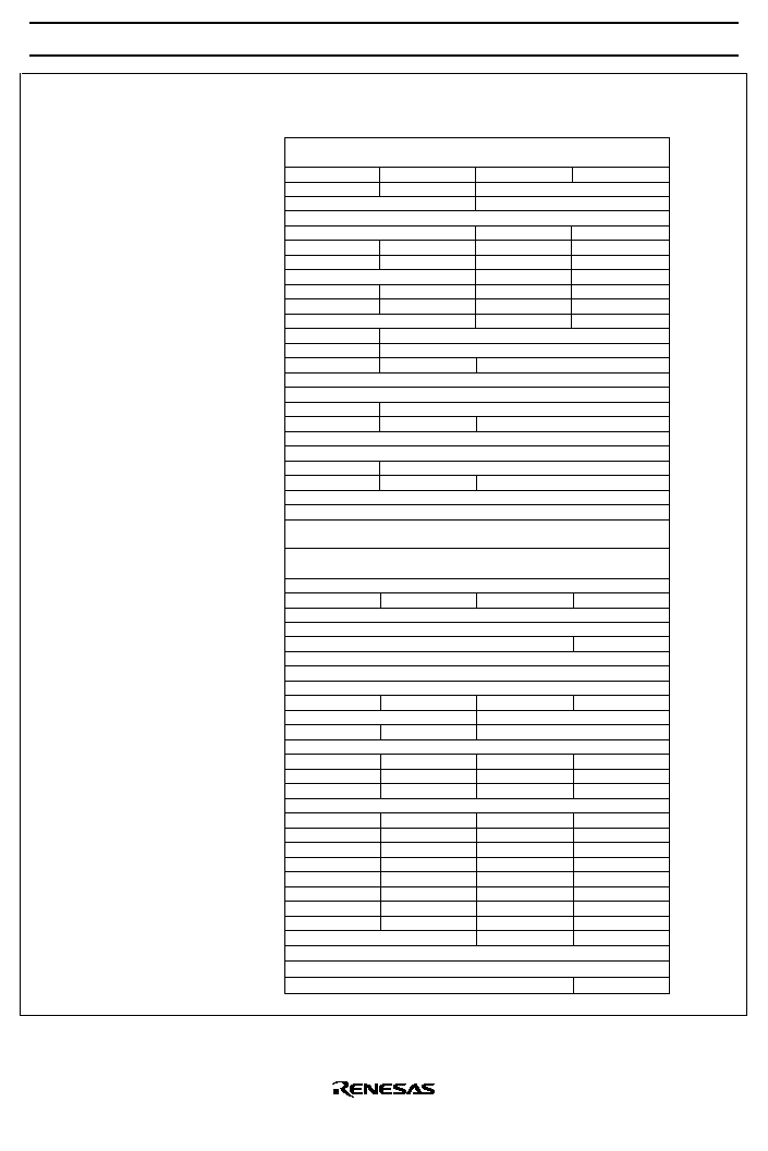
HD404889/HD404899/HD404878/HD404868 Series
31
RAM address
HD404889 Series
Bit 3
Bit 2
Bit 1
Bit 0
$000
$003
$004
$005
$006
$007
$008
$009
$00A
$00B
$00C
$00D
$00E
$00F
$010
$011
$012
$013
$014
$015
$016
$017
$018
$019
$01A
$01B
$01C
$01F
$020
$023
$024
$025
$026
$027
$028
$029
$02A
$02B
$02C
$02D
$02E
$02F
$030
$031
$032
$033
$034
$035
$036
$037
$038
$039
$03A
$03B
$03C
$03D
$03E
$03F
SSR
MIS
ESR
PMR0
PMR1
PMR2
PMR3
PMR4
MSR1
MSR2
TMA
TMB1
TMB2
TRBL/TWBL
TRBU/TWBU
TMC1
TMC2
TRCL/TWCL
TRCU/TWCU
TMD1
TMD2
TRDL/TWDL
TRDU/TWDU
SMR1
SMR2
SRL
SRU
AMR
ADRL
ADRU
LCR
LMR
BMR
DCD0
DCD1
DCD2
DCR0
DCR1
DCR2
DCR3
DCR4
DCR5
DCR6
DCR7
DCR8
V
Interrupt control bit area
32 kHz oscillation stop setting
32 kHz frequency division
ratio selection
System clock selection
System clock frequency
division ratio switching
Pull-up MOS control
Interrupt frame period selection
INT1 edge detection selection
D
1
/INT
1
D
0
/
INT
0
R0
3
/
WU
3
R1
3
/TOB
R0
2
/
WU
2
R1
2
/BUZZ
R0
1
/
WU
1
R1
1
/EVND
R0
0
/
WU
0
R1
0
/EVNB
R2
2
/SI/SO
R2
1
/
SCK
R2
0
/TOC
R6/SEG13~16
R5/SEG9~12
R4/SEG5~8
R3/SEG1~4
Timer D clock on/off
Timer C clock on/off
Timer B lock on/off
A/D clock on/off
Serial clock on/off
Timer A clock source selection
Timer B clock source selection
Timer C clock source selection
Reload on/off
Reload on/off
Timer B output mode setting
Timer C output mode selection
EVNB edge detection selection
EVND edge detection selection
Timer B register (lower)
Timer B register (upper)
Timer C register (lower)
Timer C register (upper)
Timer D register (lower)
Timer D register (upper)
Serial data register (lower)
Serial data register (upper)
A/D data register (lower)
A/D data register (upper)
Timer D clock source selection
Reload on/off
Input capture selection
Register flag area
Serial transfer clock speed selection
R2
2
/SI/SO PMOS control
SO idle H/L setting
Analog channel selection
A/D conversion time
Power supply dividing
resistor switch
Realtime clock mode
display selection
On-chip power supply switch
Display on/off
Input clock selection
Duty selection
Clock output on/off
Buzzer/clock selection
Buzzer/clock source selection
PortD
3
DCR
PortD
2
DCR
PortD
1
DCR
PortD
0
DCR
PortR0
3
DCR
PortR0
2
DCR
PortR0
1
DCR
PortR0
0
DCR
PortR1
3
DCR
PortR1
2
DCR
PortR1
1
DCR
PortR1
0
DCR
PortR2
3
DCR
PortR2
2
DCR
PortR2
1
DCR
PortR2
0
DCR
PortR3
3
DCR
PortR3
2
DCR
PortR3
1
DCR
PortR3
0
DCR
PortR4
3
DCR
PortR4
2
DCR
PortR4
1
DCR
PortR4
0
DCR
PortR5
3
DCR
PortR5
2
DCR
PortR5
1
DCR
PortR5
0
DCR
PortR6
3
DCR
PortR6
2
DCR
PortR6
1
DCR
PortR6
0
DCR
PortR7
3
DCR
PortR7
2
DCR
PortR7
1
DCR
PortR7
0
DCR
PortR8
1
DCR
PortR8
0
DCR
PortD
7
DCR
PortD
6
DCR
PorD
5
DCR
PortD
4
DCR
PortD
11
DCR
PortD
10
DCR
PortD
9
DCR
PortD
8
DCR
Bank setting
Not used
Not used
Not used
Not used
Not used
Not used
Not used
Not used
Not used
Not used
Not used
Not used
Not used
Not used
Not used
Not used
Not used
TimerA/Timer base
Not used
Not used
Not used
Figure 5 Special Function Register Area

HD404889/HD404899/HD404878/HD404868 Series
32
RAM address
HD404899 Series
Bit 3
Bit 2
Bit 1
Bit 0
$000
$003
$004
$005
$006
$007
$008
$009
$00A
$00B
$00C
$00D
$00E
$00F
$010
$011
$012
$013
$014
$015
$016
$017
$018
$019
$01A
$01B
$01C
$01F
$020
$023
$024
$025
$026
$027
$028
$029
$02A
$02B
$02C
$02D
$02E
$02F
$030
$031
$032
$033
$034
$035
$036
$037
$038
$039
$03A
$03B
$03C
$03D
$03E
$03F
SSR
MIS
ESR
PMR0
PMR1
PMR2
PMR3
PMR4
MSR1
MSR2
TMA
TMB1
TMB2
TRBL/TWBL
TRBU/TWBU
TMC1
TMC2
TRCL/TWCL
TRCU/TWCU
TMD1
TMD2
TRDL/TWDL
TRDU/TWDU
SMR1
SMR2
SRL
SRU
AMR
ADRL
ADRM
ADRU
LCR
LMR
BMR
DCD0
DCD1
DCD2
DCR0
DCR1
DCR2
DCR3
DCR4
DCR5
DCR6
DCR7
DCR8
V
Interrupt control bit area
32 kHz oscillation stop setting
32 kHz frequency division
ratio selection
System clock selection
System clock frequency
division ratio switching
Pull-up MOS control
Interrupt frame period selection
INT1 edge detection selection
D
1
/INT
1
D
0
/
INT
0
R0
3
/
WU
3
R1
3
/TOB
R0
2
/
WU
2
R1
2
/BUZZ
R0
1
/
WU
1
R1
1
/EVND
R0
0
/
WU
0
R1
0
/EVNB
R2
2
/SI/SO
R2
1
/
SCK
R2
0
/TOC
R6/SEG13~16
R5/SEG9~12
R4/SEG5~8
R3/SEG1~4
Timer D clock on/off
Timer C clock on/off
Timer B lock on/off
A/D clock on/off
Serial clock on/off
Timer A clock source selection
Timer B clock source selection
Timer C clock source selection
Reload on/off
Reload on/off
Timer B output mode setting
Timer C output mode selection
EVNB edge detection selection
EVND edge detection selection
Timer B register (lower)
Timer B register (upper)
Timer C register (lower)
Timer C register (upper)
Timer D register (lower)
Timer D register (upper)
Serial data register (lower)
Serial data register (upper)
A/D data register (middle)
A/D data register (upper)
Timer D clock source selection
Reload on/off
Input capture selection
Register flag area
Serial transfer clock speed selection
R2
2
/SI/SO PMOS control
SO idle H/L setting
Analog channel selection
A/D conversion time
Power supply dividing
resistor switch
Realtime clock mode
display selection
On-chip power supply switch
Display on/off
Input clock selection
Duty selection
Clock output on/off
Buzzer/clock selection
Buzzer/clock source selection
PortD
3
DCR
PortD
2
DCR
PortD
1
DCR
PortD
0
DCR
PortR0
3
DCR
PortR0
2
DCR
PortR0
1
DCR
PortR0
0
DCR
PortR1
3
DCR
PortR1
2
DCR
PortR1
1
DCR
PortR1
0
DCR
PortR2
3
DCR
PortR2
2
DCR
PortR2
1
DCR
PortR2
0
DCR
PortR3
3
DCR
PortR3
2
DCR
PortR3
1
DCR
PortR3
0
DCR
PortR4
3
DCR
PortR4
2
DCR
PortR4
1
DCR
PortR4
0
DCR
PortR5
3
DCR
PortR5
2
DCR
PortR5
1
DCR
PortR5
0
DCR
PortR6
3
DCR
PortR6
2
DCR
PortR6
1
DCR
PortR6
0
DCR
PortR7
3
DCR
PortR7
2
DCR
PortR7
1
DCR
PortR7
0
DCR
PortR8
1
DCR
PortR8
0
DCR
PortD
7
DCR
PortD
6
DCR
PorD
5
DCR
PortD
4
DCR
PortD
11
DCR
PortD
10
DCR
PortD
9
DCR
PortD
8
DCR
Bank setting
Not used
Not used
Not used
Not used
A/D data register (lower)
Not used
Not used
Not used
Not used
Not used
Not used
Not used
Not used
Not used
Not used
Not used
Not used
Not used
TimerA/Timer base
Not used
Not used
Not used
Figure 5 Special Function Register Area (cont)

HD404889/HD404899/HD404878/HD404868 Series
33
RAM address
HD404878 Series
Bit 3
Bit 2
Bit 1
Bit 0
$000
$003
$004
$005
$006
$007
$008
$009
$00A
$00B
$00C
$00D
$00E
$00F
$010
$011
$012
$013
$014
$015
$016
$017
$018
$019
$01A
$01B
$01C
$01F
$020
$023
$024
$025
$026
$027
$028
$029
$02A
$02B
$02C
$02D
$02E
$02F
$030
$031
$032
$033
$034
$035
$036
$037
$038
$039
$03A
$03B
$03C
$03D
$03E
$03F
SSR
MIS
ESR
PMR0
PMR1
PMR2
PMR3
PMR4
MSR1
MSR2
TMA
TMB1
TMB2
TRBL/TWBL
TRBU/TWBU
TMC1
TMC2
TRCL/TWCL
TRCU/TWCU
TMD1
TMD2
TRDL/TWDL
TRDU/TWDU
SMR1
SMR2
SRL
SRU
LCR
LMR
BMR
DCD0
DCD1
DCD2
DCR0
DCR1
DCR2
DCR3
DCR4
DCR5
DCR6
DCR7
DCR8
Interrupt control bit area
32 kHz oscillation stop setting
32 kHz frequency division
ratio selection
System clock selection
System clock frequency
division ratio switching
Pull-up MOS control
Interrupt frame period selection
INT1 edge detection selection
D
1
/INT
1
D
0
/
INT
0
R0
3
/
WU
3
R1
3
/TOB
R0
2
/
WU
2
R1
2
/BUZZ
R0
1
/
WU
1
R1
1
/EVND
R0
0
/
WU
0
R1
0
/EVNB
R2
2
/SI/SO
R2
1
/
SCK
R2
0
/TOC
R6/SEG13~16
R5/SEG9~12
R4/SEG5~8
R3/SEG1~4
Timer D clock on/off
Timer C clock on/off
Timer B lock on/off
Serial clock on/off
Timer A clock source selection
Timer B clock source selection
Timer C clock source selection
Reload on/off
Reload on/off
Timer B output mode setting
Timer C output mode selection
EVNB edge detection selection
EVND edge detection selection
Timer B register (lower)
Timer B register (upper)
Timer C register (lower)
Timer C register (upper)
Timer D register (lower)
Timer D register (upper)
Serial data register (lower)
Serial data register (upper)
Timer D clock source selection
Reload on/off
Input capture selection
Register flag area
Serial transfer clock speed selection
R2
2
/SI/SO PMOS control
SO idle H/L setting
Power supply dividing
resistor switch
Realtime clock mode
display selection
On-chip power supply switch
Display on/off
Input clock selection
Duty selection
Clock output on/off
Buzzer/clock selection
Buzzer/clock source selection
PortD
3
DCR
PortD
2
DCR
PortD
1
DCR
PortD
0
DCR
PortR0
3
DCR
PortR0
2
DCR
PortR0
1
DCR
PortR0
0
DCR
PortR1
3
DCR
PortR1
2
DCR
PortR1
1
DCR
PortR1
0
DCR
PortR2
3
DCR
PortR2
2
DCR
PortR2
1
DCR
PortR2
0
DCR
PortR3
3
DCR
PortR3
2
DCR
PortR3
1
DCR
PortR3
0
DCR
PortR4
3
DCR
PortR4
2
DCR
PortR4
1
DCR
PortR4
0
DCR
PortR5
3
DCR
PortR5
2
DCR
PortR5
1
DCR
PortR5
0
DCR
PortR6
3
DCR
PortR6
2
DCR
PortR6
1
DCR
PortR6
0
DCR
PortR7
3
DCR
PortR7
2
DCR
PortR7
1
DCR
PortR7
0
DCR
PortR8
1
DCR
PortR8
0
DCR
PortD
7
DCR
PortD
6
DCR
PorD
5
DCR
PortD
4
DCR
PortD
11
DCR
PortD
10
DCR
PortD
9
DCR
PortD
8
DCR
Not used
Not used
Not used
Not used
Not used
Not used
Not used
Not used
Not used
Not used
Not used
Not used
Not used
Not used
Not used
Not used
Not used
TimerA/Timer base
Not used
Not used
Not used
Figure 5 Special Function Register Area (cont)
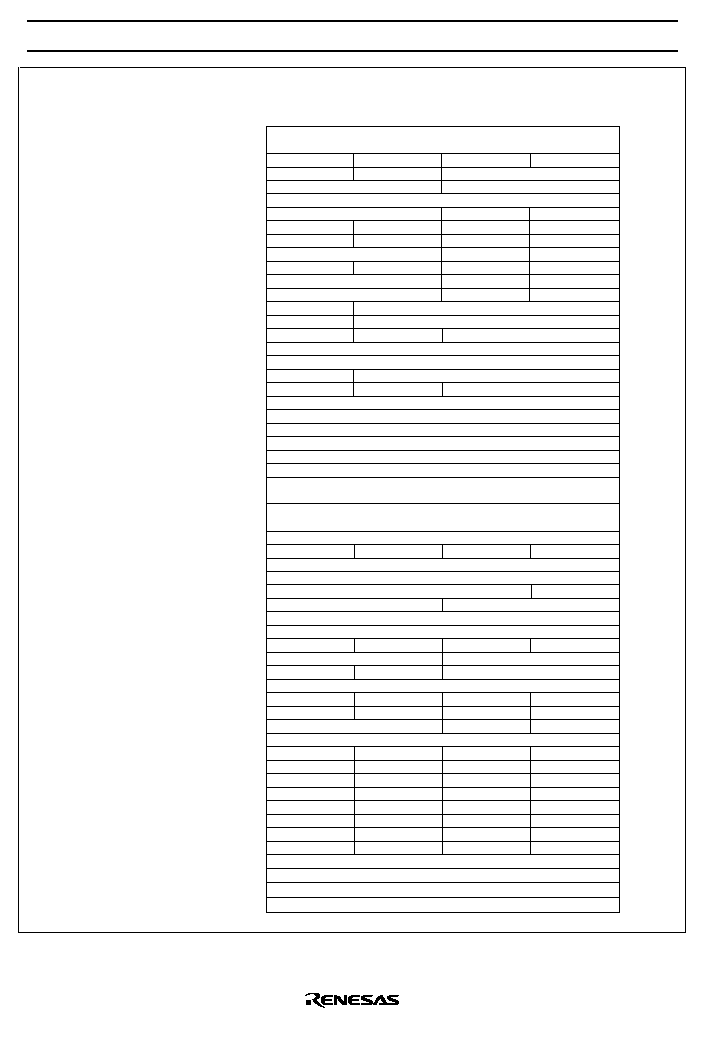
HD404889/HD404899/HD404878/HD404868 Series
34
RAM address
HD404868 Series
Bit 3
Bit 2
Bit 1
Bit 0
$000
$003
$004
$005
$006
$007
$008
$009
$00A
$00B
$00C
$00D
$00E
$00F
$010
$011
$012
$013
$014
$015
$016
$017
$018
$019
$01A
$01B
$01C
$01F
$020
$023
$024
$025
$026
$027
$028
$029
$02A
$02B
$02C
$02D
$02E
$02F
$030
$031
$032
$033
$034
$035
$036
$037
$038
$039
$03A
$03B
$03C
$03D
$03E
$03F
SSR
MIS
ESR
PMR0
PMR1
PMR2
PMR3
PMR4
MSR1
MSR2
TMA
TMB1
TMB2
TRBL/TWBL
TRBU/TWBU
TMC1
TMC2
TRCL/TWCL
TRCU/TWCU
SMR1
SMR2
SRL
SRU
AMR
ADRL
ADRM
ADRU
LCR
LMR
BMR
DCD0
DCD1
DCD2
DCR0
DCR1
DCR2
DCR3
DCR4
DCR5
DCR6
DCR7
Interrupt control bit area
32 kHz oscillation stop setting
32 kHz frequency division
ratio selection
System clock selection
System clock frequency
division ratio switching
Pull-up MOS control
Interrupt frame period selection
INT1 edge detection selection
D
1
/INT
1
D
0
/
INT
0
Not used
R1
3
/TOB
R0
2
/
WU
2
R1
2
/BUZZ
R0
1
/
WU
1
Not used
R0
0
/
WU
0
R1
0
/EVNB
R2
2
/SI/SO
R2
1
/
SCK
R2
0
/TOC
R6/SEG13~16
R5/SEG9~12
R4/SEG5~8
R3/SEG1~4
Timer C clock on/off
Timer B lock on/off
A/D clock on/off
Serial clock on/off
Timer A clock source selection
Timer B clock source selection
Timer C clock source selection
Reload on/off
Reload on/off
Timer C output mode selection
EVNB edge detection selection
Timer B register (lower)
Timer B register (upper)
Timer C register (lower)
Timer C register (upper)
Not used
Not used
Serial data register (lower)
Serial data register (upper)
A/D data register (middle)
A/D data register (upper)
Not used
Register flag area
Serial transfer clock speed selection
R2
2
/SI/SO PMOS control
SO idle H/L setting
Analog channel selection
A/D conversion time
Power supply dividing
resistor switch
Realtime clock mode
display selection
On-chip power supply switch
Display on/off
Input clock selection
Duty selection
Clock output on/off
Buzzer/clock selection
Buzzer/clock source selection
PortD
3
DCR
PortD
2
DCR
PortD
1
DCR
PortD
0
DCR
Not used
PortR0
2
DCR
PortR0
1
DCR
PortR0
0
DCR
PortR1
3
DCR
PortR1
2
DCR
PortR1
1
DCR
PortR1
0
DCR
PortR2
3
DCR
PortR2
2
DCR
PortR2
1
DCR
PortR2
0
DCR
PortR3
3
DCR
PortR3
2
DCR
PortR3
1
DCR
PortR3
0
DCR
PortR4
3
DCR
PortR4
2
DCR
PortR4
1
DCR
PortR4
0
DCR
PortR5
3
DCR
PortR5
2
DCR
PortR5
1
DCR
PortR5
0
DCR
PortR6
3
DCR
PortR6
2
DCR
PortR6
1
DCR
PortR6
0
DCR
PortR7
3
DCR
PortR7
2
DCR
PortR7
1
DCR
PortR7
0
DCR
PortD
7
DCR
PortD
6
DCR
PorD
5
DCR
PortD
4
DCR
Not used
PortD
9
DCR
PortD
8
DCR
Not used
Not used
Not used
Not used
A/D data register (lower)
Not used
Not used
Not used
Not used
Not used
Not used
Not used
Not used
Timer B output mode selection
Not used
Not used
Not used
Not used
Not used
TimerA/Timer base
Not used
Not used
Not used
Figure 5 Special Function Register Area (cont)
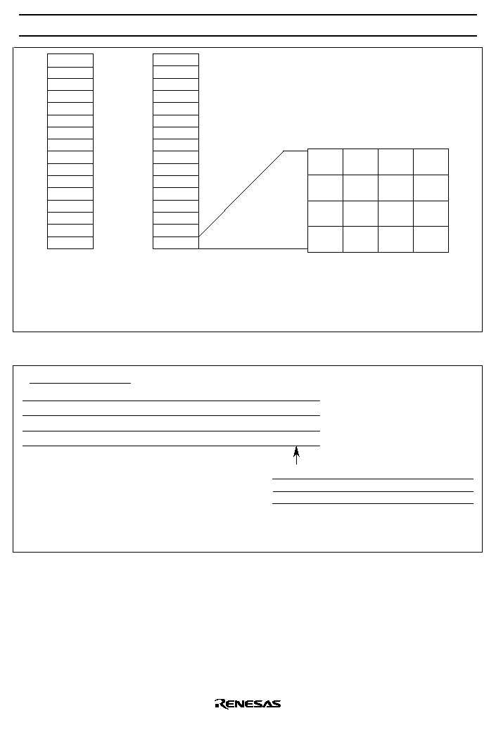
HD404889/HD404899/HD404878/HD404868 Series
35
MR (0)
MR (1)
MR (2)
MR (3)
MR (4)
MR (5)
MR (6)
MR (7)
MR (8)
MR (9)
MR (10)
MR (11)
MR (12)
MR (13)
MR (14)
MR (15)
$040
$041
$042
$043
$044
$045
$046
$047
$048
$049
$04A
$04B
$04C
$04D
$04E
$04F
Level
Level
Level
Level
Level
Level
Level
Level
Level
Level
Level
Level
Level
Level
Level
Level
ST
PC
10
CA
PC
3
PC
13
PC
9
PC
6
PC
2
PC
12
PC
8
PC
5
PC
1
PC
11
PC
7
PC
4
PC
0
$3FC
$3FD
$3FE
$3FF
1020
1021
1022
1023
Bit 3
Bit 2
Bit 1
Bit 0
$3FF
1,023
960
$3C0
(a) Memory registers
(b) Stack area
16
15
14
13
12
11
10
9
8
7
6
5
4
3
2
1
PC
13
to PC
0
: Program counter
ST
: Status flag
CA
: Carry flag
Figure 6 Configuration of Memory Registers and Stack Area, and Stack Position
Bit
Read/Write
Initial value on reset
Bit name
3
--
--
Not Used
2
--
--
Not Used
1
--
--
Not Used
0
R/W
0
V0
V0
0
1
Bank 0 is selected
Bank 1 is selected
Bank area selection
Bank register (V: $03F)
Note: After reset, the value in the bank register is 0, and therefore bank 0 is selected.
Applies to HD404889 and HD404899 Series.
Figure 7 Bank Register (V)
HD404889/HD404899/HD404878/HD404868 Series
36
Functional Description
Registers and Flags
The MCU has nine registers and two flags for CPU operations. they are shown in figure 8 and described
below.
Accumulator
B register
W register
X register
Y register
SPX register
SPY register
Carry flag
Status flag
Initial value: Undefined, R/W
Initial value: Undefined, R/W
Initial value: Undefined, R/W
Initial value: Undefined, R/W
Initial value: Undefined, R/W
Initial value: Undefined, R/W
Initial value: Undefined, R/W
Initial value: Undefined, R/W
Initial value: 1, no R/W
Program counter
Initial value: $0000,
no R/W
Stack pointer
Initial value: $3FF, no R/W
3
0
(A)
3
0
(B)
1
0
(W)
3
0
(X)
3
0
(Y)
3
0
(SPX)
3
0
(SPY)
0
(CA)
0
(ST)
13
0
(PC)
5
0
(SP)
9
1
1
1
1
Figure 8 Registers and Flags
Accumulator (A) and B register (B):
The accumulator and B register are 4-bit registers used to hold the result of an ALU operation, and for data
transfer to or from memory, an I/O area, or another register.

HD404889/HD404899/HD404878/HD404868 Series
37
W register (W), X register (X) and Y register (Y):
The W register is a 2-bit register, and the X and Y registers are 4-bit registers, used for RAM register
indirect addressing. The Y register is also used for D port addressing.
SPX register (SPX) and SPY register (SPY):
The SPX and SPY registers are 4-bit registers used as X register and Y register auxiliary registers,
respectively.
Carry flag (CA):
This flag holds ALU overflow when an arithmetic/logic instruction is executed. It is also affected by the
SEC, REC, ROTL, and ROTR instructions. The contents of the carry flag are saved to the stack when
interrupt handling is performed, and are restored from the stack by the RTNI instruction (but are not
affected by the RTN instruction).
Status flag (ST):
This flag holds ALU overflow when an arithmetic/logic or compare instruction is executed, and the result
of an ALU non-zero or bit test instruction. It is used as the branch condition for the BR, BRL, CAL, and
CALL instructions. The status flag is a latch-type flag, and does not change until the next arithmetic/logic,
compare, or bit test instruction is executed. After a BR, BRL, CAL, or CALL instruction, the status flag is
set to 1 regardless of whether the instruction is executed or skipped. The contents of the status flag are
saved to the stack when interrupt handling is performed, and are restored from the stack by the RTNI
instruction (but are not affected by the RTN instruction).
Program counter (PC):
This is a 14-bit binary counter that holds ROM address information.
Stack pointer (SP):
The stack pointer is a 10-bit register that holds the address of the next save space in the stack area. The
stack pointer is initialized to $3FF by an MCU reset. The stack pointer is decremented by 4 each time data
is saved, and incremented by 4 each time data is restored. The upper 4 bits of the stack pointer are fixed at
1111, so that a maximum of 16 stack levels can be used.
There are two ways in which the stack pointer is initialized to $3FF: by an MCU reset as mentioned above,
or by resetting the RSP bit with the REM or REMD instruction.
Reset
An MCU reset is performed by driving the
RESET pin low. At power-on, and when subactive mode,
watch mode, or stop mode is cleared,
RESET should be input for at least tRC to provide the oscillation
settling time for the oscillator.In other cases, the MCU is reset by inputting
RESET for at least two
instruction cycles.
Table 1 shows the areas initialized by an MCU reset, and their initial values.

HD404889/HD404899/HD404878/HD404868 Series
38
Table 1 (1) Initial Values after MCU Reset
Item
Abbr.
Initial
value
Contents
Program counter
(PC)
$0000
Program executed from ROM start address
Status flag
(ST)
1
Branching by conditional branch instruction enabled
Stack pointer
(SP)
$3FF
Stack level is 0
Interrupt
Interrupt enable flag
(IE)
0
All interrupts disabled
flags/ mask Interrupt request flag
(IF)
0
No interrupt requests
Interrupt mask
(IM)
1
Interrupt requests masked
I/O
Port data register
(PDR)
All bits 1 "1" level output possible
Data control registers
(DCD0 to 2) All bits 0 Output buffer off (high impedance)
Data control registers
(DCR0 to 7,
DCR80,
DCR81)
All bits 0
Port mode register 0
(PMR0)
--00
See port mode register 0 section
Port mode register 1
(PMR1)
0000
See port mode register 1 section
Port mode register 2
(PMR2)
0000
See port mode register 2 section
Port mode register 3
(PMR3)
0000
See port mode register 3 section
Port mode register 4
(PMR4)
0000
See port mode register 4 section
Edge detection select
register
(ESR)
--00
See edge detection select register section
Timers
Timer mode register A
(TMA)
0000
See timer mode register A section
Timer mode register B1
(TMB1)
0000
See timer mode register B1 section
Timer mode register B2
(TMB2)
-000
See timer mode register B2 section
Timer mode register C1
(TMC1)
0000
See timer mode register C1 section
Timer mode register C2
(TMC2)
-0--
See timer mode register C2 section
Timer mode register D1
(TMD1)
0000
See timer mode register D1 section
Timer mode register D2
(TMD2)
-000
See timer mode register D2 section
Prescaler S
(PSS)
$000
Prescaler W
(PSW)
$00
Timer/counter A
(TCA)
$00
Timer/counter B
(TCB)
$00
Timer/counter C
(TCC)
$00
Timer/counter D
(TCD)
$00
Timer write register B
(TWBU,L)
$X0
Timer write register C
(TWCU,L)
$X0
Timer write register D
(TWDU,L)
$X0
HD404889/HD404899/HD404878/HD404868 Series
39
Table 1 (1) (cont) Initial Values after MCU Reset
Item
Abbr.
Initial
value
Contents
Serial
Serial mode register 1
(SMR1)
0000
See serial mode register 1 section
interface
Serial mode register 2
(SMR2)
-0X-
See serial mode register 2 section
Serial data register
(SRU,L)
$XX
Octal counter
000
A/D
A/D mode register
(AMR)
0000
See A/D mode register section
converter
A/D data register
(HD404889 Series)
(ADRU,L)
$7F
See A/D data register section
A/D data register
(HD404899 Series)
(ADRU,M,L) $1FF
See A/D data register section
LCD
LCD control register
(LCR)
0000
See LCD control register section
LCD mode register
(LMR)
0000
See LCD duty/clock control register section
Bit
Low speed on flag
(LSON)
0
See low-power mode section
registers
Watchdog timer on flag
(WDON)
0
See timer C section
A/D start flag
(ADSF)
0
See A/D converter section
Direct transfer on flag
(DTON)
0
See low-power mode section
Input capture status flag
(ICSF)
0
See timer D section
Input capture error flag
(ICEF)
0
See timer D section
Gear enable flag
(GEF)
0
See system clock gear function
Others
Miscellaneous register
(MIS)
0-00
See low-power mode and input/output sections
System clock select
register
(SSR)
0000
See low-power mode and oscillator circuit sections
Module standby register 1
(MSR1)
-000
See timer section
Module standby register 2
(MSR2)
--00
See serial interface and A/D converter sections
Buzzer mode register
(BMR)
0000
See Buzzer mode register section
Notes: 1. The state of registers and flags other than those listed above after an MCU reset is shown in
table 1 (2).
2. X: Indicates invalid value, - indicates that the bit does not exist.

HD404889/HD404899/HD404878/HD404868 Series
40
Table 1 (2) Initial Values after MCU Reset
Item
Abbr.
After Stop Mode Clearance by
WU
0
to
WU
3
Input
After Other MCU Reset
Carry flag
(CA)
Retain value immediately prior to
Value immediately prior to MCU reset is not
Accumulator
(A)
entering stop mode
guaranteed. Must be initialized by program.
B register
(B)
W register
(W)
X/SPX register (X/SPX)
Y/SPY register (Y/SPY)
RAM
Interrupts
There are a total of nine interrupt sources, comprising wakeup input (
WU
0
to
WU
3
), external interrupts
(
INT
0
, INT
1
), timer/counter (timer A, timer B, timer C, timer D) interrupts, a serial interface interrupt, and
an A/D converter interrupt.
Each interrupt source is provided with an interrupt request flag, interrupt mask, and vector address, used for
storing and controlling interrupt requests. In addition, an interrupt enable flag is provided to control
interrupts as a whole.
Of the interrupt sources, timers B and D share the same vector address, and the A/D converter and serial
interface also share the same vector address. Software must therefore determine which of the interrupt
sources is requesting an interrupt at the start of interrupt handling.
Interrupt control bits and interrupt handling:
The interrupt control bits are mapped onto RAM addresses $000 to $003 and $022 to $023, and can be
accessed by RAM bit manipulation instructions. However, the interrupt request flags (IF) cannot be set by
software. When the MCU is reset, the interrupt enable flag (IE) and interrupt request flags (IF) are
initialized to 0, and the interrupt masks (IM) are initialized to 1.
Figure 9 shows a block diagram of the interrupt control circuit, table 2 shows interrupt priorities and vector
addresses, and table 3 lists the conditions for executing interrupt handling for each of the nine kinds of
interrupt source. When the interrupt request flag is set to 1 and the interrupt mask is cleared to 0, an
interrupt is requested. If the interrupt enable flag is set to 1 at this time, interrupt handling is started. The
vector address corresponding to the interrupt source is generated by the priority control circuit.
The interrupt handling sequence is shown in figure 10, and the interrupt handling flowchart in figure 11.
When an interrupt is accepted, execution of the previous instruction is completed in the first cycle. In the
second cycle, the interrupt enable flag (IE) is reset. In the second and third cycles, the contents of the carry
flag, status flag, and program counter are saved on the stack. In the third cycle, a jump is made to the
vector address and instruction execution is resumed from that address.

HD404889/HD404899/HD404878/HD404868 Series
41
In each vector address area, a JMPL instruction should be written that branches to the start address of the
interrupt routine. In the interrupt routine, the interrupt request flag that caused interrupt handling must be
reset by software.
Table 2
Vector Addresses and Interrupt Priorities
Interrupt Source
Priority
Vector Address
RESET
--
$0000
WU
0
to
WU
3
1
$0002
INT
0
2
$0004
INT
1
3
$0006
Timer A
4
$0008
Timer B, D
5
$000A
Timer C
6
$000C
Serial interface, A/D converter
7
$000E

HD404889/HD404899/HD404878/HD404868 Series
42
$000,2
$000,3
IFWU
IMWU
$001,0
$001,1
IF0
IM0
$001,2
$001,3
IF1
IM1
$002,0
$002,1
IFTA
IMTA
$002,2
$002,3
IFTB
IMTB
$003,0
$003,1
IFTC
IMTC
$003,2
$003,3
IFAD
IMAD
$000,0
I/E
$023,2
$023,3
IFS
IMS
$022,2
$022,3
IFTD
IMTD
(
WU
0
to
WU
3
interrupt)
(
INT
0
interrupt)
(INT
1
interrupt)
(Timer A interrupt)
(Timer B interrupt)
(Timer C interrupt)
(A/D interrupt)
Priority
control circuit
Interrupt
request
Vector address
(Timer D interrupt)
(Serial interrupt)
Figure 9 Block Diagram of Interrupt Control Circuit
HD404889/HD404899/HD404878/HD404868 Series
43
Table 3
Interrupt Processing and Activation Conditions
Interrupt Source
Interrupt Control Bit
WU
0
to
WU
3
INT
0
INT
1
Timer A
Timer B or
Timer D
Timer C
A/D or
Serial
IE
1
1
1
1
1
1
1
IFWU�
IMWU
1
0
0
0
0
0
0
IF0�
IM0
*
1
0
0
0
0
0
IF1�
IM1
*
*
1
0
0
0
0
IFTA�
IMTA
*
*
*
1
0
0
0
IFTB�
IMTB
+IFTD�
IMTD
*
*
*
*
1
0
0
IFTC�
IMTC
*
*
*
*
*
1
0
IFAD�
IMAD
+IFS�
IMS
*
*
*
*
*
*
1
Note: * Operation is not affected whether the value is 0 or 1.
1
2
3
4
5
6
Instruction
execution*
Interrupt
acceptance
Save to stack
IE reset
Execution of JMPL instruction
at vector address
Save to stack
Vector address
generated
Execution of
instruction at
start address of
interrupt routine
Instruction cycle
Note: The stack is accessed and the IE reset after the instruction is executed, even if it is a 2cycle instruction.
Figure 10 Interrupt Sequence
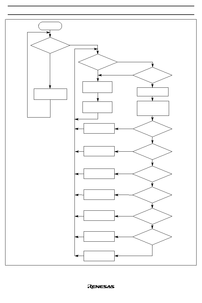
HD404889/HD404899/HD404878/HD404868 Series
44
Power ON
RESET
="0"?
Yes
No
Yes
Yes
No
No
No
No
No
No
No
Yes
Yes
Yes
Yes
Yes
Yes
Reset MCU
Interrupt request?
Execute instruction
PC
(PC)+1
PC
$0002
PC
$0004
PC
$0006
PC
$0008
PC
$000A
PC
$000C
PC
$000E
IE="1"?
Accept interrupt
IE
"0"
Stack
(PC)
Stack
(CA)
Stack
(ST)
WU
0
~
WU
3
interrupt?
INT
0
interrupt?
INT
1
interrupt?
Timer A interrupt?
Timer B, timer D
interrupt?
Timer C interrupt?
(A/D, serial interrupt)
Figure 11 Interrupt Handling Flowchart

HD404889/HD404899/HD404878/HD404868 Series
45
Interrupt enable flag (IE: $000,0):
The interrupt enable flag controls interrupt enabling/disabling of all interrupt requests as shown in table 4.
The interrupt enable flag is reset by interrupt handling and set by the RTNI instruction.
Table 4
Interrupt Enable Flag (IE: $000,0)
Interrupt Enable Flag(IE)
Interrupt Enabling/Disabling
0
Interrupts disabled
1
Interrupts enabled
Wakeup interrupt request flag (IFWU: $000,2):
The wakeup interrupt request flag (IFWU) is set by the detection of a falling edge in
WU
0
to
WU
3
input in
active mode, subactive mode,watch mode, or standby mode. In stop mode, when a falling edge is detected
at the wakeup pin, the MCU waits for the oscillation settling time, then switches to active mode. The
wakeup interrupt request flag (IFWU) is not set in this case.
Wakeup interrupt mask (IMWU: $000,3):
This bit masks an interrupt request by the wakeup interrupt request flag.
Bit
Read/Write
Initial value on reset
Bit name
3
--
--
--
2
--
--
--
1
W
0
ESR1
0
W
0
ESR0
ESR1
ESR0
0
1
0
1
Not detected
Falling edge detection
Rising edge detection
Both rising and falling edge detection
INT
1
edge detect
Edge detection select register (ESR: $006)
0
1
Figure 12 Edge Detection Select Register (ESR)

HD404889/HD404899/HD404878/HD404868 Series
46
External interrupt request flags (IF0, IF1: $001):
IF0 is set by a falling edge in the
INT
0
input, and IF1 is set by a rising edge, falling edge, or both edges in
the INT
1
input (table 5).
Interrupt edge selection is performed by means of the edge detection select register (ESR: $006) (figure
12).
Table 5
External Interrupt Request Flags (IF0, IF1: $001)
External Interrupt Request Flags
(IF0, IF1)
Interrupt Request
0
No external interrupt request
1
External interrupt request generated
External interrupt masks (IM0, IM1: $001):
These bits mask interrupt requests by the external interrupt request flags (table 6).
Table 6
External Interrupt Mask (IM: $001)
External Interrupt Masks
(IM0, IM1)
Interrupt Request
0
External interrupt request enabled
1
External interrupt request masked (held pending)
Timer A interrupt request flag (IFTA: $002,0):
The timer A interrupt request flag is set by timer A overflow output (table 7).
Table 7
Timer A Interrupt Request Flag (IFTA: $002,0)
Timer A Interrupt Request
Flag(IFTA)
Interrupt Request
0
No timer A interrupt request
1
Timer A interrupt request generated
Timer A interrupt mask (IMTA: $002,1):
This bit masks an interrupt request by the timer A interrupt request flag (table 8).
Table 8
Timer A Interrupt Mask (IMTA: $002,1)
Timer A Interrupt Mask (IMTA)
Interrupt Request
0
Timer A interrupt request enabled
1
Timer A interrupt request masked (held pending)

HD404889/HD404899/HD404878/HD404868 Series
47
Timer B interrupt request flag (IFTB: $002,2):
The timer B interrupt request flag is set by timer B overflow output (table 9).
Table 9
Timer B Interrupt Request Flag (IFTB: $002,2)
Timer B Interrupt Request Flag
(IFTB)
Interrupt Request
0
No timer B interrupt request
1
Timer B interrupt request generated
Timer B interrupt mask (IMTB: $002,3):
This bit masks an interrupt request by the timer B interrupt request flag (table 10).
Table 10
Timer B Interrupt Mask (IMTB: $002,3)
Timer B Interrupt Mask (IMTB)
Interrupt Request
0
Timer B interrupt request enabled
1
Timer B interrupt request masked (held pending)
Timer C interrupt request flag (IFTC: $003,0):
The timer C interrupt request flag is set by timer C overflow output (table 11).
Table 11
Timer C Interrupt Request Flag (IFTC: $003,0)
Timer C Interrupt Request Flag
(IFTC)
Interrupt Request
0
No timer C interrupt request
1
Timer C interrupt request generated (held pending)
Timer C interrupt mask (IMTC: $003,1):
This bit masks an interrupt request by the timer C interrupt request flag (table 12).
Table 12
Timer C Interrupt Mask (IMTC: $003,1)
Timer C Interrupt Mask (IMTC)
Interrupt Request
0
Timer C interrupt request enabled
1
Timer C interrupt request masked (held pending)

HD404889/HD404899/HD404878/HD404868 Series
48
Timer D interrupt request flag (IFTD: $022,2): (Applies to HD404889, HD404899, and HD404878
Series)
The timer D interrupt request flag is set by timer D overflow output, or by an EVND input edge when used
as an input capture timer (table 13).
Table 13
Timer D Interrupt Request Flag (IFTD: $022,2)
Timer D Interrupt Request Flag
(IFTD)
Interrupt Request
0
No timer D interrupt request
1
Timer D interrupt request generated
Timer D interrupt mask (IMTD: $022,3): (Applies to HD404889, HD404899, and HD404878 Series)
This bit masks an interrupt request by the timer D interrupt request flag (table 14).
Table 14
Timer D Interrupt Mask (IMTD: $022,3)
Timer D Interrupt Mask (IMTD)
Interrupt Request
0
Timer D interrupt request enabled
1
Timer D interrupt request masked (held pending)
Serial interrupt request flag (IFS: $023,2):
The serial interrupt request flag is set on completion of serial data transfer, or if data transfer is halted
midway (table 15).
Table 15
Serial Interrupt Request Flag (IFS: $023,2)
Serial Interrupt Request Flag (IFS) Interrupt Request
0
No serial interrupt request
1
Serial interrupt request generated
Serial interrupt mask (IMS: $023,3):
This bit masks an interrupt request by the serial interrupt request flag (table 16).
Table 16
Serial Interrupt Mask (IMS: $023,3)
Serial Interrupt Mask (IMS)
Interrupt Request
0
Serial interrupt request enabled
1
Serial interrupt request masked (held pending)
HD404889/HD404899/HD404878/HD404868 Series
49
A/D interrupt request flag (IFAD: $003,2): (Applies to HD404889, HD404899, and HD404868 Series)
The A/D interrupt request flag is set on completion of A/D conversion (table 17).
Table 17
A/D Interrupt Request Flag (IFAD: $003,2)
A/D Interrupt Request Flag (IFAD) Interrupt Request
0
No A/D interrupt request
1
A/D interrupt request generated
A/D interrupt mask (IMAD: $003,3): (Applies to HD404889, HD404899, and HD404868 Series)
This bit masks an interrupt request by the A/D interrupt request flag (table 18).
Table 18
A/D Interrupt Mask (IMAD: $003,3)
Serial Interrupt Mask (IMAD)
Interrupt Request
0
A/D interrupt request enabled
1
A/D interrupt request masked (held pending)

HD404889/HD404899/HD404878/HD404868 Series
50
Operating Modes
The five operating modes shown in table 19 can be used for the MCU.
The function of each mode is shown in table 20, and the state transition diagram among each mode in
figure 13.
Table 19
Operating Modes and Clock Status
Mode Name
Active
Standby
Stop
Watch
Subactive*
2
Activation method
RESET
cancellation,
interrupt
request,
WU
0
to
WU
3
input
in stop mode
STOP/SBY
instruction in
subactive
mode (when
direct
transfer is
selected)
SBY
instruction
STOP
instruction
when
TMA3 = 0
STOP
instruction
when
TMA3 = 1
INT
0
/timer A
or
WU
0
to
WU
3
interrupt
request in
watch mode
Status
System oscillator
OP
OP
Stopped
Stopped
Stopped
Subsystem oscillator
OP
OP
OP *
1
OP
OP
Cancellation method
RESET
input,
STOP/SBY
instruction
RESET
input,
interrupt
request
RESET
input,
WU
0
to
WU
3
input
RESET
input,
INT
0
/timer A
or
WU
0
to
WU
3
interrupt
request
RESET
input,
STOP/SBY
instruction
Notes: OP: implies in operation.
1. Operating or stopping the oscillator can be selected by setting bit 3 of the system clock select
register (SSR: $004)
2. Subactive mode is an optional function; specify it on the fnction option list.
HD404889/HD404899/HD404878/HD404868 Series
51
Table 20
Operation in Low-Power Dissipation Modes
Function
Stop Mode
Watch mode
Standby Mode
Subactive Mode*
3
CPU
Retained
Retained
Retained
OP
RAM
Retained
Retained
Retained
OP
Timer A
Stopped
OP
OP
OP
Timer B
Stopped
Stopped
OP
OP
Timer C
Stopped
Stopped
OP
OP
Timer D *
4
Stopped
Stopped
OP
OP
Serial interface
Stopped *
1
Stopped *
1
OP
OP
A/D *
5
Stopped
Stopped
OP
Stopped
LCD
Stopped
OP *
2
OP
OP
I/O
Retained
Retained
Retained
OP
Notes: OP: implies in operation.
1. Transmission/Reception is activated if a clock is input in external clock mode. However,
interrupts stop.
2. When a 32 kHz clock source is used.
3. Subactive mode is an optional function specified on the function option list.
4. Applies to HD404889, HD404899, and HD404878 Series.
5. Applies to HD404889, HD404899, and HD404868 Series.

HD404889/HD404899/HD404878/HD404868 Series
52
Reset by
RESET
pin
input or
watchdog timer
Reset
(TMA3=0)
(TMA3=1)
Timer A,
WU
0
to
WU
3
or
INT
0
interrupt
Standby mode
Active mode
SBY
instruction
interrupt
SBY
instruction
interrupt
STOP
instruction
(TMA3=1,LSON=0)
(TMA3=1,LSON=1)
f
osc
:
fx
:
fcyc
:
fw
:
f
SUB
:
�
CPU
:
�
CLK
:
�
PER
:
LSON
:
DTON
:
TMA3
:
Main oscillator frequency
Sub-oscillator frequency
(for realtime clock)
f
OSC
/32 or fOSC/4 (selected by
software)
fx/8
fx/8 or fx/4 (selected by software)
System clock
Clock for realtime clock
Peripheral function clock
Low speed on flag
Direct transfer on flag
Timer mode register A bit3
Timer A,
WU
0
~
WU
3
or
INT
0
interrupt
WU
0
to
WU
3
STOP
instruction
WU
0
to
WU
3
STOP
instruction
STOP
instruction
Stop mode
(TMA3=0,SSR3=0,LSON=0)
(TMA3=0,SSR3=1,LSON=0)
Subactive mode
*4
*2
*3
*1
DTON
1
0
Don't care
0
Transition Condition
STOP/SBY instruction
STOP/SBY instruction
STOP/SBY instruction
STOP/SBY instruction
LSON
0
0
1
0
*1
*2
*3
*4
TMA3
1
1
1
0
Watch mode
f
osc
fx
�
CPU
�
CLK
�
PER
: Stop
: Stop
: Stop
: Stop
: Stop
f
osc
fx
�
CPU
�
CLK
�
PER
: Active
: Active
: fcyc
: fcyc
: fcyc
f
osc
fx
�
CPU
�
CLK
�
PER
: Stop
: Active
: Stop
: Stop
: Stop
f
osc
fx
�
CPU
�
CLK
�
PER
: Active
: Active
: Stop
: fcyc
: fcyc
f
osc
fx
�
CPU
�
CLK
�
PER
: Stop
: Active
: f
SUB
: fw
: f
SUB
f
osc
fx
�
CPU
�
CLK
�
PER
: Active
: Active
: fcyc
: fw
: fcyc
f
osc
fx
�
CPU
�
CLK
�
PER
: Active
: Active
: Stop
: fw
: fcyc
f
osc
fx
�
CPU
�
CLK
�
PER
: Stop
: Active
: Stop
: fw
: Stop
f
osc
fx
�
CPU
�
CLK
�
PER
: Stop
: Active
: Stop
: fw
: Stop
Figure 13 MCU Status Transitions

HD404889/HD404899/HD404878/HD404868 Series
53
Active mode:
In active mode all functions operate. In this mode, the MCU operates on clocks generated by the OSC
1
and
OSC
2
oscillator circuits.
Standby mode:
In standby mode the oscillators continue to operate but clocks relating to instruction execution halt. As a
result, CPU operation stops, and registers, RAM, and the D port/R port set for output retain their state
immediately prior to entering standby mode. Interrupts, timers, the serial interface, and other peripheral
functions continue to operate.
Power consumption is lower than in active mode due to the halting of the CPU.
The MCU is switched to standby mode by executing the SBY instruction in active mode. Standby mode is
cleared by
RESET input or an interrupt request. When standby mode is cleared by RESET input, an MCU
reset is performed. When standby mode is cleared by an interrupt request, the MCU enters active mode
and executes a instruction following the SBY instruction. After executing the instruction, if the interrupt
enable flag is set to 1, interrupt handling is executed; if the interrupt enable flag is cleared to 0, the interrupt
request is held pending and normal instruction execution is continued.
MCU operation flowchart is shown in figure 14.

HD404889/HD404899/HD404878/HD404868 Series
54
Stop mode
System clock
oscillator started
System reset
Next Instruction
execution
System clock
oscillator started
Interrupts
enabled
IFWU�
IMWU
=1?
IF0�
IM0
= 1?
IF1�
IM1
= 1?
IFTA �
IMTA
= 1?
IFTB �
IMTB
+
IFTD�
IMTD
=
1?
IFTC�
IMTC
= 1?
IFAD�
IMAD
+
IFS�
IMS
= 1?
IF = 1,
IM = 0,
IE = 1?
No
No
Yes
Yes
Yes
Yes*
No
No
No
No
No
No
Yes
Only when clearing from standby mode
Note:
Standby mode
Watch mode
RESET
=0?
Yes*
Yes*
Yes*
Yes
No
No
Yes
Yes
No
RESET
=0?
NOP
System clock
oscillator started
Next Instruction
execution
WU
0
to
WU
3
= ?
Figure 14 MCU Operation Flowchart

HD404889/HD404899/HD404878/HD404868 Series
55
Stop mode:
In stop mode, all MCU function stop except that states prior to entry into stop mode are retained. This
mode thus has the lowest power consumption of all operating mode.
In stop mode, the OSC
1
and OSC
2
oscillators stop. Bit 3 (SSR3) of the system clock select register (SSR:
$004) (figure 24) can be used to select the active (= 0) or stopped (= 1) state for the X1 and X2 oscillators.
The MCU is switched to stop mode by executing a STOP instruction while bit 3 (TMA3) of timer mode
register A (TMA: $00F) is cleared to 0 in active mode. Stop mode is cleared by
RESET or WU
0
to
WU
3
input. When stop mode is cleared by
RESET, the RESET signal should be input for at least the oscillation
settling time (tRC) (see "AC Characteristics") shown in figure 15. Then, the MCU is initialized and starts
instruction execution from the start (address 0) of the program.
When the MCU detects a falling edge at
WU
0
to
WU
3
in stop mode, it automatically waits for the
oscillation settling time, then switches to active mode. After the transition to active mode, the MCU
resumes program execution from the instruction following the STOP instruction.
If stop mode is cleared by wakeup input, RAM data and registers retain their values prior to entering stop
mode.
Stop mode
Oscillator
Internal clock
RESET
STOP instruction executed
t
res
(At least oscillation settling time (t
RC
))
Figure 15 Timing Chart for Clearing Stop Mode by RESET Input
Note:
If stop mode is cleared by wakeup input when an external clock is used as the system clock
(OSC1), the subclock should not be stopped in stop mode.
Watch mode:
In watch mode, the realtime clock function (timer A) and LCD function using the X1 and X2 oscillators
operate, but other functions stop. This mode thus has the second lowest power consumption after stop
mode, and is useful for performing realtime clock display only.
In watch mode, the OSC
1
and OSC
2
oscillators stop but the X1 and X2 oscillators continue to operate.
The MCU is switched to watch mode by executing a STOP instruction while TMA3 = 1 in active mode, or
by executing a STOP/SBY instruction in subactive mode.

HD404889/HD404899/HD404878/HD404868 Series
56
Watch mode is cleared by
RESET input or an INT
0
,timer A or
WU
0
to
WU
3
interrupt request. For
RESET
input, refer to the section on stop mode. When watch mode is cleared by an
INT
0
,timer A or
WU
0
to
WU
3
interrupt request, the mode transition depends on the value of the LSON bit: the MCU enters active mode if
LSON = 0, and enters subactive mode if LSON = 1. In the case of a transition to active mode, interrupt
request generation is delayed to secure the oscillation settling time: the delay is the tRC set time for the
timer A interrupt, and, for the
INT
0
interrupt or
WU
0
to
WU
3
interrupt, Tx (T + t
RC
< Tx < 2T + t
RC
) if bit 1
and 0 (MIS1, MIS0) of the miscellaneous register are set to 00, or Tx (t
RC
< Tx < T + t
RC
) if MIS1 and
MIS0 are set to 01 or 10 (figures 16 and 17). Other operations when the transition is made are the same as
when watch mode is cleared (figure 14).
Subactive mode:
In subactive mode, the OSC
1
and OSC
2
oscillator circuits stop and the MCU operates on clocks generated
by the X1 and X2 oscillator circuits. In this mode, functions other than the A/D converter operate, but
since the operating clocks are slow, power consumption is the lowest after watch mode.
A CPU instruction processing speed of 244
�
s or 122
�
s can be selected according to whether bit 2 (SSR2)
of the system clock select register (SSR: $004) is set to 1 or cleared to 0. The value of the SSR2 bit should
be changed (0
1 or 1
0) only in active mode. If the value is changed in subactive mode, the MCU may
operate incorrectly.
Subactive mode is cleared by executing a STOP/SBY instruction. A transition is then made to either watch
mode or active mode according to the value of the low speed on flag (LSON: $020,0) and the direct
transfer on flag (DTON: $020,3).
Subactive mode is a function option, and should be specified in the function option list.
Interrupt frame:
In watch mode and subactive mode, �
CLK
is supplied to the timer A,
WU
0
to
WU
3
, and
INT
0
acceptance
circuits. Prescaler W and timer A operate as time bases, and generate interrupt frame timing. Either of two
values can be selected for the interrupt frame period, T, by means of the miscellaneous register (MIS: $005)
(figure 17).
In watch mode and subactive mode, the timing for generation of timer A,
INT
0
and
WU
0
to
WU
3
interrupts
is synchronized with the interrupt frame. Except for the case of an active mode transition, the interrupt
strobe timing is used for interrupt request generation. Timer A generates overflow and interrupt requests at
the interrupt strobe timing.
HD404889/HD404899/HD404878/HD404868 Series
57
Watch mode
Oscillation
stabilization
period
Active mode
Active mode
Interrupt
strobe
INT
0
Interrupt
request generation
T
T
T
t
RC
T
X
T: Interrupt frame period
t
RC
: Oscillation stabilization period
Only in case of
transition to active
mode
Note: If the time from the fall of the
INT
0
or
WU
0
to
WU
3
signal until the interrupt is accepted and
active mode is entered and is designated T
X
, then T
X
will be in the following range :
T+t
RC
T
X
2T+t
RC
(MIS1, MIS0=00)
t
RC
T
X
T+t
RC
(MIS1, MIS0=01 or 10)
Figure 16 Interrupt Frame
Miscellaneous Register (MIS: $005)
Bit
Read/Write
Reset
Bit name
3
W
0
MIS3
2
1
W
0
MIS1
0
W
0
MIS0
Interrupt Frame
period T(
ms
)*1
Oscillation Settling
Time t
RC
(
ms
)*1
MIS1
MIS0
0
1
0
1
0
1
0.24414
3.90625
3.90625
0.12207(0.24414)*
2
7.8125
31.25
Oscillator Circuit
Condition
External clock input
Ceramic resonator
Crystal resonator
Not used
Notes: 1. T and t
RC
values are for use of a 32.768 kHz crystal oscillator at the X1-X2 pins.
2. This value applies only in case of direct transition operation.
Buffer control
See section 3,
Input/Output,
and Figure 33
Figure 17 Miscellaneous Register (MIS)

HD404889/HD404899/HD404878/HD404868 Series
58
Direct transition from subactive to active mode:
A direct transition can be made from subactive mode to active mode by controlling the direct transfer on
flag (DTON: $020,3) and low speed on flag (LSON: $020,0). The procedure is shown below.
(a) Set LSON = 0 and DTON = 1 in subactive mode.
(b) Execute a STOP or SBY instruction.
(c) After the lapse of the MCU internal processing time and the oscillation settling time, the MCU
automatically switches from subactive mode to active mode (figure 18).
Notes: 1. The DTON flag ($020,3) can be set in only subactive mode. It is always in the reset state in
active mode.
2. The condition for transition time T
D
from the subactive mode to active mode is as follows:
t
RC
< T
D
< T + t
RC
.
Subactive mode
STOP/SBY
instruction execution
MCU internal
processing time
Oscillation
stabilization time
Active mode
(Set LSON =0, DTON =1)
Interrupt strobe
Direct transition
completion timing
T
T
D
t
RC
T: Interrupt frame period
t
RC
: Oscillation settling time
T
D
: Direct transition time
Figure 18 Direct Transition Timing
MCU operation sequence:
The MCU operates in accordance with the flowchart shown in figure 19.
RESET input is asynchronous
input, and the MCU immediately enters the reset state upon
RESET input, regardless of its current state.
In the low-power mode operation sequence, if a STOP/SBY instruction is executed while the IE flag is
cleared and the interrupt flag is set, releasing the relevant interrupt mask, the STOP/SBY instruction is
canceled (regarded as NOP) and the next instruction is executed. Therefore, when executing a STOP/SBY
instruction, all interrupt flags must be cleared, or interrupts masked, beforehand.

HD404889/HD404899/HD404878/HD404868 Series
59
Yes
Yes
Yes
Yes
No
No
No
No
IF=1
IM=0
IE=0
IF=1
IM=0
STOP/SBY
instruction
Standby/watch mode
Stop Mode
WU
0
~
WU
3
=
Hardware NOP
Execution
Hardware NOP
Execution
Clearing Standby
watch mode
PC
(PC)+1
PC
(PC)+1
MCU
Operation Cycle
Note: See figure 14, MCU Operation Flowchart, for IF and IM operation.
Interrupt handling
routine
Instruction
Execution
Instruction
Execution
Clearing Stop
mode
NOP
PC
(PC)+2
Figure 19 MCU Operating Sequence (Low-Power Mode Operation)

HD404889/HD404899/HD404878/HD404868 Series
60
Usage notes:
In watch mode and subactive mode, an interrupt will not be detected correctly if the
INT
0
or
WU
0
to
WU
3
high or low-level period is shorter than the interrupt frame period.
The MCU's edge sensing method is shown in figure 20. The MCU samples the
I NT
0
and
WU
0
to
WU
3
signals at regular intervals, and if consecutive sampled values change from high to low, it determines that a
falling edge has been generated.
Interrupt detection errors occur since this sampling is performed at the interrupt frame period. If the high-
level period of the
INT
0
or
WU
0
to
WU
3
signal is within an interrupt frame, as shown in figure 21 (a), the
signal will be low at point A and point B, with the result that the falling edge will not be recognized.
Similarly, If the low-level period of the
INT
0
or
WU
0
to
WU
3
signal is within an interrupt frame, as shown
in figure 21 (b), the signal will be high at point A and point B, with the result that the falling edge will not
be recognized.
In watch mode and subactive mode, therefore, ensure that the high-level and low-level periods of the
INT
0
and
WU
0
to
WU
3
signals is at least as long as the interrupt frame period.
INT
0
or
WU
0
to
WU
3
Sampling
High
Low
Low
Figure 20 Edge Sensing Method
INT
0
or
WU
0
to
WU
3
Interrupt frame
Point A: Low
Point B: Low
INT
0
or
WU
0
to
WU
3
Interrupt frame
Point A: High
Point B: High
(a) High-level mode
(b) Low-level mode
Figure 21 Sampling Examples
HD404889/HD404899/HD404878/HD404868 Series
61
Internal Oscillator Circuit
Figure 22 shows the clock pulse generator circuit. As shown in table 21, a ceramic oscillator or crystal
oscillator can be connected to OSC1 and OSC2, and a 32.768 kHz crystal oscillator can be connected to X1
and X2. External clock operation is possible for the system oscillator. Set bit 1 (SSR1) of the system clock
select register (SSR: $004) according to the frequency of the oscillator connected to OSC1 and OSC2
(figure 24).
Note:
If the setting of bit 1 in the system clock select register does not match the frequency of the system
oscillator, the subsystem using 32.768 kHz oscillation will not operate correctly.
OSC
1
X1
LSON
System
clock
selection
circuit
OSC
2
System
oscillator
1/4 or 1/32
division
circuit*
Timing
generation
circuit
f
OSC
f
cyc
t
cyc
X2
Sub
system
clock
oscillator
1/8 or 1/4
division
circuit*
Timing
generator
circuit
f
x
f
SUB
t
subcyc
1/8
division
circuit
Timing
generation
circuit
f
W
t
wcyc
�
CPU
�
PER
CPU
�ROM
�RAM
� Registers, flags
�I/O
Peripheral
functions
Interrupts
TMA3 bit
Timer A
interrupts
Time
base
clock
selection
circuit
�
CLK
Notes: The division ratio can be selected by setting bit 0 or bit 2 in the system clock select register
(SSR:$004).
Figure 22 Clock Pulse Generator Circuit

HD404889/HD404899/HD404878/HD404868 Series
62
System Clock Gear Function
The MCU has a built-in system clock gear function that allows the system clock divided by 4 or by 32 to be
selected by software for the instruction execution time. Efficient power consumption can be achieved by
operating at the divided-by-4 rate when high-speed processing is needed, and at the divided-by-32 rate at
the other times. Figure 23 shows the system clock conversion method.
System clock conversion from division-by-4 to division-by-32 is performed as follows. First, make the
division-by-32 setting (SSR0 write), then set the gear enable flag (GEF: $021,3). This flag is used to
distinguish between gear conversion and a transition to standby mode. Next, execute an SBY instruction.
When the gear enable flag is not set, standby mode is entered; when this flag is set, gear conversion mode
is entered. In this case a transition is made to standby mode for the duration of the gear conversion, but
after the synchronization time has elapsed, a transition is made automatically to active mode. As soon as
the transition is made to active mode, the gear enable flag is reset.
The same procedure is used for conversion from division-by-32 to division-by-4.
Clear all interrupts, then disable interrupts, before carrying out gear conversion. Incorrect operation may
result if an interrupt is generated during gear conversion.
HD404889/HD404899/HD404878/HD404868 Series
63
Division-by-32 setting (SSR0 = 1)
Set gear enable flag
Execute SBY instruction
Execute next instruction
Synchronization time
Division-by-4 setting (SSR0 = 0)
Set gear enable flag
Execute SBY instruction
Execute next instruction
Synchronization time
Figure 23 System Clock Division Ratio Conversion Flowchart
HD404889/HD404899/HD404878/HD404868 Series
64
System clock select register (SSR: $004)
Note:
*
If the subsystem clock is not used, this bit must be set to 1 following power-on and reset.
If it is set to 0 (the initial value), malfunctioning may occur in the stop mode.
Bit
Read/Write
Initial value on reset
Bit name
3
W
0
SSR3
*
2
W
0
SSR2
1
W
0
SSR1
0
W
0
SSR0
System clock division ratio switch
0
1
Division-by-4 (f
cyc
- f
OSC
/4)
Division-by-32 (f
cyc
- f
OSC
/32)
System clock division ratio switch
0
1
f
osc
=0.4�1.0MHz
f
osc
=1.6�4.5MHz
Subsystem clock division ratio switch
0
1
f
SUB
=fx/8
f
SUB
=fx/4
Subsystem clock stop setting
0
1
Subsystem clock operates in stop mode
Subsystem clock stops in stop mode
Figure 24 System Clock Select Register
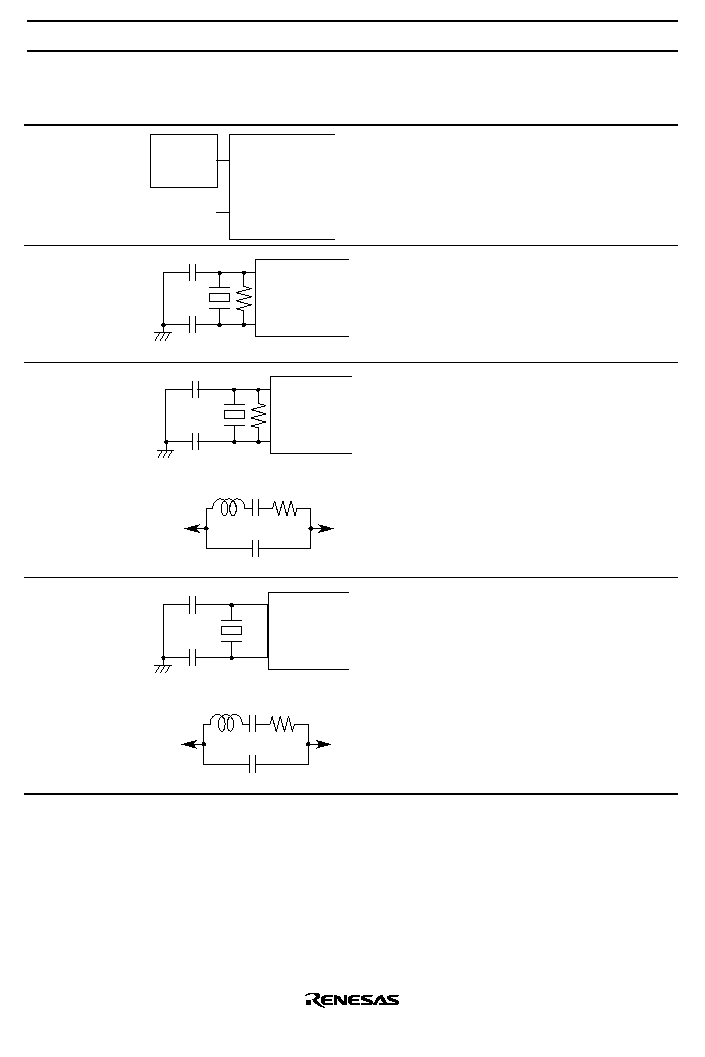
HD404889/HD404899/HD404878/HD404868 Series
65
Table 21
Oscillator Circuit Examples
Circuit Structure
Circuit Constants
External clock
operation
External
oscillator
OSC
1
OSC
2
Open
Ceramic oscillator
(OSC
1
, OSC
2
)
OSC
1
OSC
2
C
1
C
2
R
f
GND
Ceramic
oscillator
Ceramic oscillator: CSA4.00MG (Murata)
R
f
=1M
�
20%
C
1
=C
2
=30pF
�
20%
Crystal oscillator
(OSC
1
, OSC
2
)
OSC
1
OSC
2
C
1
C
2
R
f
GND
Crystal
oscillator
OSC
1
OSC
2
L
C
S
C
0
R
S
R
f
=1M
�
20%
C
1
=C
2
=10�22pF
�
20%
Crystal: Equivalent circuit at left
C
0
=7pFmax.
R
S
=100
max.
Crystal oscillator
(X1, X2)
X1
X2
C
1
C
2
GND
Crystal
oscillator
X1
X2
L
C
S
C
0
R
S
Crystal: 32.768 kHz: MX38T (Nihon Denpa
Kogyo)
C
1
=C
2
=20pF
�
20%
R
S
=14k
C
0
=1.5pF
Notes: 1. With a crystal or ceramic oscillator, circuit constants will differ depending on the resonator, stray
capacitance in the interconnecting circuit, and other factors. Suitable constants should be
determined in consultation with the resonator manufacturer.
2. Make the connections between the OSC
1
and OSC
2
pins (X1 and X2 pins) and external
components as short as possible, and ensure that no other lines cross these lines (see layout
example in figure 25).
3. When 32.768 kHz crystal oscillation is not used, fix the X1 pin at V
CC
and leave the X2 pin open.
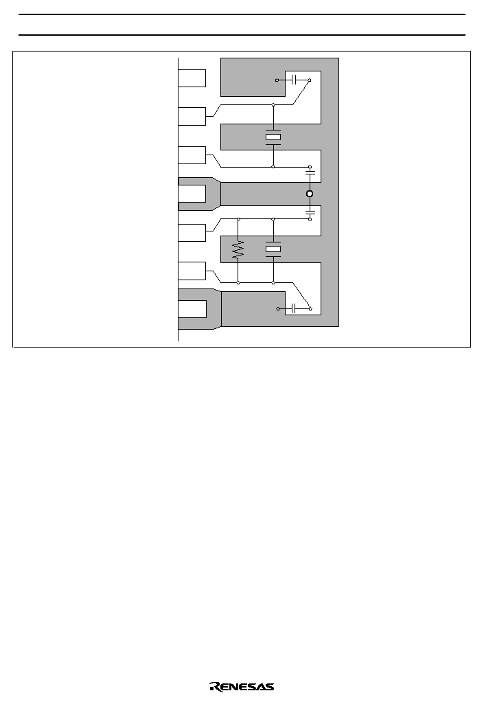
HD404889/HD404899/HD404878/HD404868 Series
66
RESET
X1
X2
GND
OSC
2
OSC
1
TEST
GND
Figure 25 Typical Layouts of Crystal and Ceramic Oscillator
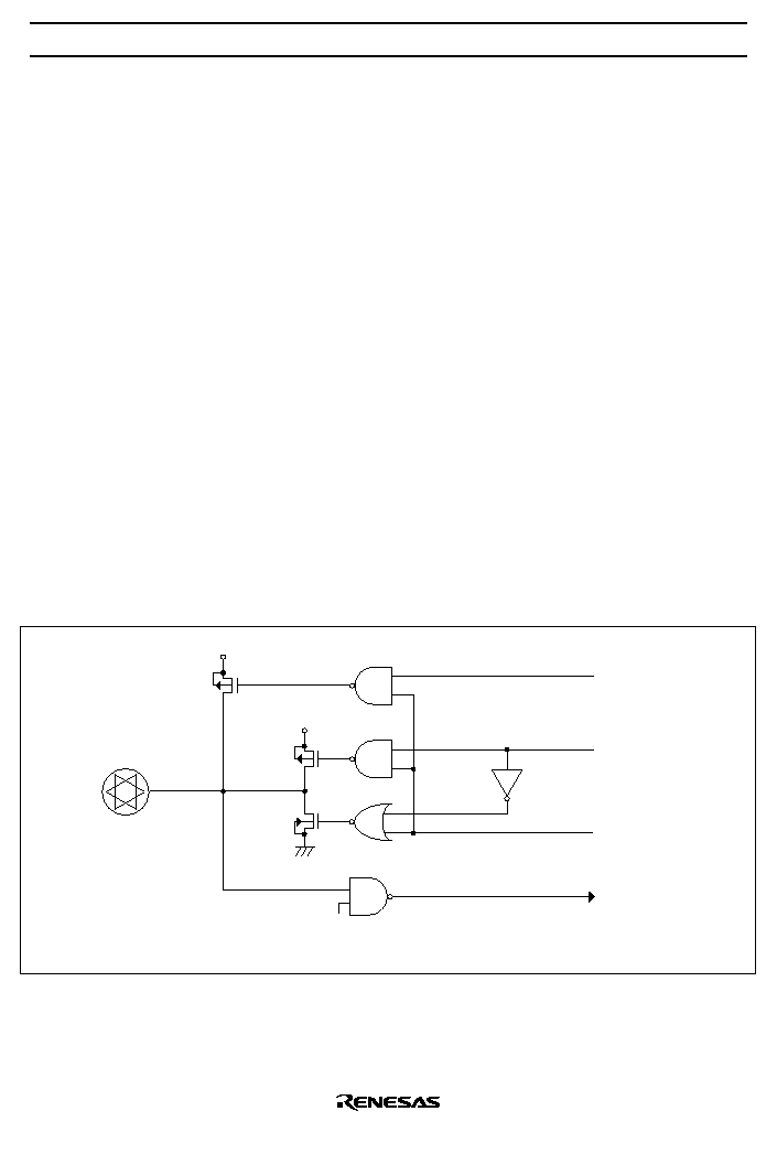
HD404889/HD404899/HD404878/HD404868 Series
67
Input/Output
The MCU has 46 input/output pins (D
0
to D
11
, R0 to R7, R8
0
, and R8
1
) in the HD404889, HD404899, and
HD404878 Series, or 41 input/output pins (D
0
to D
9
, R0
0
, R0
1
, R0
2
, and R1 to R7) in the HD404868 Series.
The features of these pins are described below.
�
The four pins D
0
to D
3
are source large-current (10 mA max.) I/O pins.
�
The eight pins D
4
to D
11
are sink large-current (15 mA max.) I/O pins.
�
I/O pins comprise pins (D
0
, D
1
, R
0
, R
1
, R2
0
to R2
2
, R3 to R7, R8
0
, and R8
1
) that also have a peripheral
function (timer, serial interface, etc.). With these pins, the peripheral function setting has priority over
the D port or R port pin setting. When a peripheral function setting has been made for a pin, the pin
function and input/output mode will be switched automatically in accordance with that setting.
�
Selection of input or output for I/O pins, or selection of the port or peripheral function for pins
multiplexed as peripheral function pins, is performed by the program.
�
All output of the peripheral function pins are CMOS outputs. The SO pin and R2
2
port pin can be
designated as NMOS open-drain output by the program.
�
A reset clears peripheral function selection. And since the data control registers (DCD, DCR) are also
reset, input/output pins go to the high-impedance state.
�
Each I/O pin has a built-in pull-up MOS that can be turned on and off individually by the program.
Figure 26 shows the I/O buffer configuration, and table 22 shows I/O pin circuit configuration control by
the program.
Table 23 shows the circuit configuration of each I/O pin.
pull-up
MOS
Pull-up control signal
Buffer control signal
Output data
Input data
V
CC
PMOS
NMOS
Input control signal
MIS3
DCD, DCR
PDR
V
CC
Figure 26 I/O Pin Circuit Configuration

HD404889/HD404899/HD404878/HD404868 Series
68
Table 22
Programmable I/O Circuits
MIS3 (bit 3 of MIS)
0
1
DCD,DCR
0
1
0
1
PDR
0
1
0
1
0
1
0
1
CMOS buffer
PMOS
--
--
--
ON
--
--
--
ON
NMOS
--
--
ON
--
--
--
ON
--
pull-up MOS
--
--
--
--
--
ON
--
ON
Note:
-- : OFF
Table 23 Circuit Configurations of I/O Pins
Type
Circuit Configuration
Pins
I/O pins
V
CC
V
CC
Input control signal
MIS3
DCD, DCR
PDR
Pull-up control signal
Buffer control signal
Output data
Input data
D
0
-D
11
R0
0
-R0
3
R1
0
-R1
3
R2
0
, R2
1
, R2
3
R3
0
-R3
3
R4
0
-R4
3
R5
0
-R5
3
R6
0
-R6
3
R7
0
-R7
3
R8
0
-R8
1
V
CC
V
CC
Input control signal
MIS3
DCR
PDR
Pull-up control signal
Buffer control signal
Output data
Input data
SMR22
R2
2
Perip-
heral
function
pins
I/O pins
V
CC
V
CC
MIS3
PDR
Pull-up control signal
I/O control signal
Output data
Input data
SCK
SCK
SCK
Note:
In a reset, since the I/O control registers are reset, input/output pins go to the high-impedance state
and peripheral function selections are cleared.

HD404889/HD404899/HD404878/HD404868 Series
69
Table 23
Circuit Configurations of I/O Pins (cont)
Type
Circuit Configuration
Pins
Perip-
heral
function
pins
Output
pins
V
CC
V
CC
MIS3
PDR
Pull-up control signal
PMOS control signal
Output data
SMR22
SO
SO
V
CC
V
CC
MIS3
PDR
Pull-up control signal
Output data
TOB, TOC, BUZZ
TOB, TOC,
BUZZ
Input
pins
RESET
Input data
RESET
V
CC
MIS3
PDR
WU
0
�
WU
3
etc.
WU
0
-
WU
3
,
INT
0
, INT
1
,
EVNB,
EVND, SI
V
CC
MIS3
PDR
A/D input
Input control signal
AN
0
-AN
5
*
Notes: In a reset, since the I/O control registers are reset, input/output pins go to the high-impedance state
and peripheral function selections are cleared.
*
Applies to HD404889, HD404899, and HD404868 Series.

HD404889/HD404899/HD404878/HD404868 Series
70
D Port
The D port consists of 12 I/O pins (10 I/O pins in the HD404868 Series) that are addressed bit-by-bit.
Ports D
0
to D
3
are source large-current I/O pins, and ports D
4
to D
11
(ports D
4
to D
9
in the HD404868
Series) are sink large-current I/O pins.
The D port can be set and reset by the SED and RED instructions or the SEDD and REDD instructions.
Output data is stored in the port data register (PDR) for each pin. The entire D port can be tested by the TD
or TDD instruction.
The D port output buffer is turned on and off by the D port data control registers (DCD0 to DCD2: $030 to
$032). The DCD registers are mapped onto memory addresses (figure 27).
Ports D
0
and D
1
are multiplexed as interrupt input pins
INT
0
and INT
1
, respectively. Setting as interrupt
pins is performed by bits 0 and 1 (PMR00, PMR01) of port mode register 0 (PMR0: $008) (figure 28).

HD404889/HD404899/HD404878/HD404868 Series
71
Data control registers
Note:
*
Applies to HD404889, HD404899, and HD404878 Series
(DCD0�2 : $030�$032)
(DCR0�8 : $034�$03C)
Register Name
DCD0�DCD2
DCR0�DCR8
Bit
Read/Write
Reset
Bit name
Read/Write
Reset
Bit name
3
W
0
DCD03�DCD23
W
0
DCR03�DCR73
2
W
0
DCD02�DCD22
W
0
DCR02�DCR72
1
W
0
DCD01�DCD21
W
0
DCR01�DCR81
0
W
0
DCD00�DCD20
W
0
DCR00�DCR80
All bits
0
1
CMOS buffer off (high impedance)
CMOS buffer active
CMOS buffer control
Register Name
DCD0
DCD1
DCD2
DCR0
DCR1
DCR2
DCR3
DCR4
DCR5
DCR6
DCR7
DCR8
Bit 3
D
3
D
7
D
11
*
R0
3
*
R1
3
R2
3
R3
3
R4
3
R5
3
R6
3
R7
3
Bit 2
D
2
D
6
D
10
*
R0
2
R1
2
R2
2
R3
2
R4
2
R5
2
R6
2
R7
2
Bit 1
D
1
D
5
D
9
R0
1
R1
1
R2
1
R3
1
R4
1
R5
1
R6
1
R7
1
R8
1
*
Bit 0
D
0
D
4
D
8
R0
0
R1
0
R2
0
R3
0
R4
0
R5
0
R6
0
R7
0
R8
0
*
Correspondence between each bit of DCD and DCR and ports
Figure 27 Data Control Registers (DCD, DCR)

HD404889/HD404899/HD404878/HD404868 Series
72
R Port
The R port consists of 34 I/O pins (31 I/O pins in the HD404868 Series) that are addressed in 4-bit units.
Input can be performed by means of the LAR and LBR instructions, and output by means of the LRA and
LRB instructions. Output data is stored in the port data register (PDR) for each pin.
The R port output buffer is turned on and off by the R port data control registers (DCR0 to DCR8: $034 to
$03C). The DCR registers are mapped onto memory addresses (figure 27).
Ports R0
0
to R0
3
are multiplexed as wakeup input pins
WU
0
to
WU
3
, respectively. Setting of these pins as
peripheral function pins is performed by port mode register 1 (PMR1: $009) (figure 29).
Ports R1
0
and R1
1
are multiplexed as peripheral function pins EVNB and EVND, respectively. Setting of
these pins as peripheral function pins is performed by bits 0 and 1 (PMR20, PMR21) of port mode register
2 (PMR2: $00A) (figure 30).
Ports R1
2
to R1
3
and R2
0
are multiplexed as peripheral function pins BUZZ, TOB, and TOC, respectively.
Setting of these pins as peripheral function pins is performed by bits 2 and 3 (PMR22, PMR23) of port
mode register 2 (PMR2: $00A) and bit 0 (PMR30) of port mode register 3 (PMR3: $00B)(figures 30 and
31).
Ports R2
1
and R2
2
are multiplexed as peripheral function pins
SCK and SI/SO, respectively. Setting of
these pins as peripheral function pins is performed by bits 1 to 3 (PMR31 to PMR33) of port mode register
3 (PMR3: $00B) (figure 31).
Ports R3 to R6 are multiplexed as peripheral function pins SEG1 to SEG16, respectively. Setting of these
pins as segment pins is performed every 4 pins in 4-bit units by port mode register 4 (PMR4: $00C) (figure
32).
Ports R7
0
to R7
3
and R8
0
to R8
1
also function as peripheral function pins AN
0
to AN
5
(HD404889,
HD404899, and HD404868 series only). Peripheral function pin setting of these pins is performed using
bits 1 to 3 (AMR
1
to AMR
3
) of the A/D mode register (AMR :$028). (See Figure 74 in A/D Converter.)
HD404889/HD404899/HD404878/HD404868 Series
73
Port mode register 0 (PMR0: $008)
Bit
Read/Write
Initial value on reset
Bit name
3
Not used
2
Not used
1
W
0
PMR01
0
W
0
PMR00
PMR00
0
1
D
0
/
INT
0
pin mode selection
D
0
INT
0
PMR01
0
1
D
1
/INT
1
pin mode selection
D
1
INT
1
Figure 28 Port Mode Register 0 (PMR0: $008)

HD404889/HD404899/HD404878/HD404868 Series
74
R0
0
/
WU
0
pin mode selection
R0
0
WU
0
Bit
Read/Write
Initial value on reset
Bit name
3
W
0
PMR13
*
PMR13
0
1
R0
3
/
WU
3
pin mode selection
R0
3
WU
3
2
W
0
PMR12
PMR12
0
1
R0
2
/
WU
2
pin mode selection
R0
2
WU
2
1
W
0
PMR11
PMR11
0
1
R0
1
/
WU
1
pin mode selection
R0
1
WU
1
0
W
0
PMR10
PMR10
0
1
Port mode register 1 (PMR1: $009)
Note:
*
Applies to HD404889, HD404899, and HD404878 Series
Figure 29 Port Mode Register 1 (PMR1: $009)
HD404889/HD404899/HD404878/HD404868 Series
75
R1
0
/EVNB pin mode selection
R1
0
EVNB
Bit
Read/Write
Initial value on reset
Bit name
3
W
0
PMR23
PMR23
0
1
R1
3
/TOB pin mode selection
R1
3
TOB
2
W
0
PMR22
PMR22
0
1
R1
2
/BUZZ pin mode selection
R1
2
BUZZ
1
W
0
PMR21
*
PMR21
0
1
R1
1
/EVND pin mode selection
R1
1
EVND
0
W
0
PMR20
PMR20
0
1
Port mode register 2 (PMR2: $00A)
Note:
*
Applies to HD404889, HD404899, and HD404878 Series
Figure 30 Port Mode Register 2 (PMR2: $00A)
HD404889/HD404899/HD404878/HD404868 Series
76
R2
0
/TOC pin mode selection
R2
0
TOC
Bit
Read/Write
Initial value on reset
Bit name
3
W
0
PMR33
2
W
0
PMR32
PMR32
0
1
PMR33
0
1
R2
2
/SI/SO pin mode selection
R2
2
SI
SO
1
W
0
PMR31
PMR31
0
1
R2
1
/
SCK
pin mode selection
R2
1
SCK
0
W
0
PMR30
PMR30
0
1
Port mode register 3 (PMR3: $00B)
: Don't care
Figure 31 Port Mode Register 3 (PMR3: $00B)
HD404889/HD404899/HD404878/HD404868 Series
77
R3/SEG1 to SEG4 pin mode selection
R3
SEG1�4
Bit
Read/Write
Initial value on reset
Bit name
3
W
0
PMR43
PMR43
0
1*
R6/SEG13 to SEG16 pin mode selection
R6
SEG13�16
2
W
0
PMR42
PMR42
0
1*
R5/SEG9 to SEG12 pin mode selection
R5
SEG9�12
1
W
0
PMR41
PMR41
0
1*
R4/SEG5 to SEG8 pin mode selection
R4
SEG5�8
0
W
0
PMR40
PMR40
0
1*
Port mode register 4 (PMR4: $00C)
* : When use as a segment output pin, write its port data register (PDR) to '0'
Figure 32 Port Mode Register 4 (PMR4: $00C)
Pull-Up MOS Control
Program-controllable pull-ups MOS are incorporated in all I/O pins.
On/off control of all pull-ups MOS is performed by bit 3 (MIS3) of the miscellaneous register (MIS: $005)
and the port data register (PDR) for each pin, enabling the pull-up MOS to be turned on or off
independently for each pin (table 22, figure 33).
Except for analog input multiplexed pins, the pull-up MOS on/off setting can be made independent of the
setting as an on-chip supporting module pin.

HD404889/HD404899/HD404878/HD404868 Series
78
Bit
Read/Write
Initial value on reset
Bit name
3
W
0
MIS3
2
--
--
--
1
W
0
MIS1
0
W
0
MIS0
t
RC
selection
(See figure 17 in the
Operating Modes section)
Miscellaneous register (MIS: $005)
MIS3
0
1
pull-up MOS control
All pull-ups MOS off
pull-up MOS active
Figure 33 Miscellaneous Register (MIS:$005)
Handling of I/O Pins Not Used by User System
If I/O pins that are not used by the user system are left floating, they may generate noise that can result in
chip malfunctions. Therefore, the pin potential must be fixed.
In this case, pull the pins up to V
CC
with the built-in pull-up MOS or with an external resistor of
approximately 100 k
.

HD404889/HD404899/HD404878/HD404868 Series
79
Prescalers
The MCU has the following two prescalers, S and W.
The operating conditions for each prescaler are shown in table 24, and the output supply destinations in
figure 34.
Timer A to D input clocks other than external events, serial transfer clocks other than external clocks, and
the LCD circuit operating clock are selected from the prescaler outputs in accordance with the respective
mode register.
Prescaler Operation
Prescaler S (PSS):
Prescaler S is an 11-bit counter that has the system clock as input. When the MCU is reset, prescaler S is
reset to $000, then divides the system clock. Prescaler S operation is stopped by a reset by the MCU, and
in stop mode and watch mode. It does not stop in any other modes.
Prescaler W (PSW):
Prescaler W is a counter that has a clock divided from the X1 input (32 kHz crystal oscillation) as input.
When the MCU is reset, prescaler W is reset to $00, then divides the input clock. Prescaler W can also be
reset by software.
Table 24
Prescaler Operating Conditions
Prescaler
Input Clock
Reset Conditions
Stop Conditions
Prescaler S
System clock in active and
standby modes, Subsystem
clock in subactive mode
MCU reset, Stop mode
clearance
MCU reset, Stop mode,
Watch mode
Prescaler W
Clock obtained by division-
by-8 of 32.768 kHz
oscillation by subsystem
clock oscillator
MCU reset, Software*
MCU reset, Stop mode
Note:
If bits TMA3 to TMA1 in timer mode register A (TMA) are all set to 1, PSW is cleared to $00.
HD404889/HD404899/HD404878/HD404868 Series
80
Prescaler W
System
clock
Prescaler S
Clock
selector
LCD controller
driver circuit
Subsystem
clock
Serial
interface
Timer D
Timer C
Timer B
Timer A
Figure 34 Prescaler Output Destinations

HD404889/HD404899/HD404878/HD404868 Series
81
Timers
The MCU incorporates four timers, A to D, in the HD404889, HD404899, and HD404878 Series, or three
timers, A to C, in the HD404868 Series.
�
Timer A: Free-running timer
�
Timer B: Multifunctional timer
�
Timer C: Multifunctional timer
�
Timer D: Multifunctional timer
Timer A is an 8-bit free-running timer. Timers B, C, and D are 8-bit multifunctional timers; Each one of
their have the functions shown in table 25 and their operating mode can be set by the program.
Table 25
Timer Functions
Functios
Timer A
Timer B
Timer C
Timer D
Clock source
Prescaler S
Available
Available
Available
Available
Prescaler W
Available
--
--
--
External event
--
Available
--
Available
Timer functions Free-running
Available
Available
Available
Available
Time-base
Available
--
--
--
Event counter
--
Available
--
Available
Reload
--
Available
Available
Available
Watchdog
--
--
Available
--
Input Capture
--
--
--
Available
Timer outputs
Toggle
--
Available
Available
--
PWM
--
Available
Available
--
Note:
-- implies not available
Timer A
Timer A Functions
Timer A has the following functions.
�
Free-running timer
�
Realtime clock time base
The block diagram of timer A is shown in figure 35.

HD404889/HD404899/HD404878/HD404868 Series
82
1/4
1/2
32.768-kHz
oscillator
System
clock
Data bus
Clock line
Signal line
Prescaler W
(PSW)
Selector
Selector
Prescaler S (PSS)
Selector
Internal data bus
Timer A interrupt
request flag
(IFTA)
Clock
Overflow
Timer
counter A
(TCA)
Timer mode
register A
(TMA)
3
2 f
1/2 t
Wcyc
f
t
Wcyc
�
PER
2
4
8
32
128
512
1024
2048
� � � � � � � �
2
8
16
32
� � � �
W
W
Figure 35 Timer A Block Diagram
Timer A Operation
Free-running timer operation:
The timer A input clock is selected by timer mode register A (TMA: $00F).
Timer A is reset to $00 by an MCU reset, and counts up each time the input clock is input. When the input
clock is input after the timer A value reaches $FF, overflow output is generated, and the timer A value
becomes $00. The generated overflow output sets the timer A interrupt request flag (IFTA: $002,0). Timer
A continues counting up after the count value returns to $00, so that an interrupt is generated regularly
every 256 input clock cycles.
Realtime clock time base operation:
Timer A can be used as the realtime clock time base by setting bit 3 (TMA3) of timer mode register A to 1.
As the prescaler W output is input to timer/counter A, interrupts are generated with accurate timing using
the 32.768 kHz crystal oscillator as the basic clock.
When timer A is used as the realtime clock time base, prescaler W and timer/counter A can be reset to $00
by the program.

HD404889/HD404899/HD404878/HD404868 Series
83
Timer A Register
Timer A operation is set by means of the following register.
Timer mode register A (TMA: $00F):
Timer mode register A (TMA: $00F) is a 4-bit write-only register. Timer A operation and input clock
selection are set as shown in figure 36.

HD404889/HD404899/HD404878/HD404868 Series
84
Bit
Read/Write
Initial value on reset
Bit name
3
W
0
TMA3
2
W
0
TMA2
1
W
0
TMA1
0
W
0
TMA0
TMA3
0
1
TMA2
0
1
1
0
TMA1
0
1
1
0
1
0
0
1
TMA0
0
1
0
1
0
1
0
1
0
1
0
1
0
1
*
Source prescaler
PSS
PSS
PSS
PSS
PSS
PSS
PSS
PSS
PSW
PSW
PSW
PSW
PSW
Input clock period
2,048 t
cyc
1,024 t
cyc
512 t
cyc
128 t
cyc
32 t
cyc
8 t
cyc
4 t
cyc
2 t
cyc
32 t
wcyc
16 t
wcyc
8 t
wcyc
2 t
wcyc
1/2 t
wcyc
Operating mode
Timer A
mode
Time base
mode
Timer mode register A (TMA: $00F)
Not Used
PSW, TCA reset
*
: Don't care
Notes: 1. t
wcyc
= 244.14
�
s (using 32.768 kHz crystal oscillator)
2. Timer/counter overflow output period (s) = input clock period (s)
�
256.
3. If PSW and TCA reset is selected during LCD, the LCD enters the halt state
(power switch off). Therefore, to provide continuous LCD the PSW and TCA
reset interval must be minimized by the program.
4. The division ratio must not be changed while time base mode is being used, as this
will result in an error in the overflow period.
Figure 36 Timer Mode Register A (TMA)
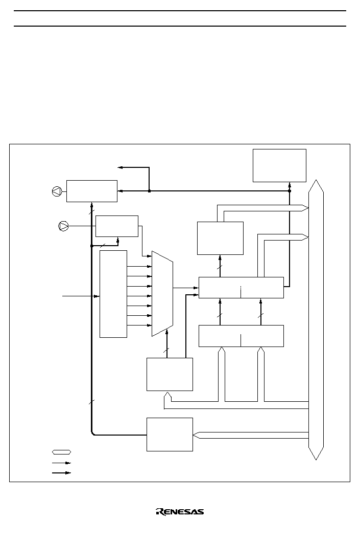
HD404889/HD404899/HD404878/HD404868 Series
85
Timer B
Timer B Functions: Timer B has the following functions.
�
Free-running/reload timer
�
External event counter
�
Timer output operation (toggle output, PWM output)
The block diagram of timer B is shown in figure 37.
3
1
2
3
4
4
4
Timer B ineterrupt
request flag
(IFTB)
(TCBL)
(TCBU)
Timer read
register BU
(TRBU)
Internal data bus
Timer read
register BL
(TRBL)
Timer counter B
Timer write register B
(TWBL)
(TWBU)
Free-runnning/Reload control
Timer mode
register B1
(TMB1)
Timer mode
register B2
(TMB2)
Data bus
Clock line
Signal line
Selector
Overflow
Prescaler S
(PSS)
System
clock
�
2
�
4
�
8
�
32
�
128
�
512
�
2048
Timer output
control logic
Timer C clock source
Edge detection
logic
TOB
EVNB
�
PER
Figure 37 Timer B Block Diagram

HD404889/HD404899/HD404878/HD404868 Series
86
Timer B Operation
�
Free-running/reload timer:
Free-running/reload timer operation, the input clock source, and the prescaler division ratio are selected
by means of timer mode register B1 (TMB1).
Timer B is initialized to the value written to timer write register B (TWBL, TWBU) by software, and
counts up by 1 each time the input clock is input. When the input clock is input after the timer B value
reaches $FF, overflow output is generated. Timer B is then set to the value in timer write register B if
the reload timer function is selected, or to $00 if the free-running timer function is selected, and starts
counting up again.
Overflow output sets the timer B interrupt request flag (IFTB). This flag is reset by the program or by
an MCU reset.
For details, see figure 3, Interrupt Control Bit and Register Flag Area Configuration, and table 1, Initial
Values after MCU Reset.
�
External event counter operation:
When external event input is designated for the input clock, timer B operates as an external event
counter. When external event input is used, the R1
0
/EVNB pin is designated as the EVNB pin by port
mode register 2 (PMR2).
The external event detected edge for timer B can be designated as a falling edge, rising edge, or both
falling and rising edges in the input signal by means of timer mode register B2 (TMB2). If both falling
and rising edges are selected, the input signal falling and rising edge interval should be at least 2tcyc.
Timer B counts up by 1 each time a falling edge is detected in the signal input at the EVNB pin. Other
operations are the same as for the free-running/reload timer function.
�
Timer output operation:
With timer B, the R13/TOB pin is designated as the TOB pin by the setting of bit 3 of port mode
register 2 (PMR2), and toggle waveform output or PWM waveform output can be selected by timer
mode register B2 (TMB2).
Toggle output:
With toggle output, the output level is changed upon input of the next clock pulse after the timer B
value reaches $FF. Use of this function in combination with the reload timer allows a clock signal
with any period to be output, enabling it to be used as buzzer output. The output waveform is
shown in figure 38 (1).
PWM output:
With PWM output, variable-duty pulses are output. The output waveform is as shown in figure 38
(2), according to the contents of timer mode register B1 (TMB1) and timer write register B (TWBL,
TWBU). When the waveform is output with bit 3 (TMB13) of timer mode register B1 cleared to 0,
the write to timer write register B to change the duty is effective from the next frame, whereas if the
waveform is output with the TMB13 bit set to 1 (reload setting), the next frame is output
immediately after the timer write register write.
�
Module standby:
With timer B, the supply of the system clock to the timer/counter can be halted by setting bit 0 of
module standby register 1 (MSR1: $00D) to 1. In the module standby state, the mode register value is
retained but the counter value is not guaranteed.
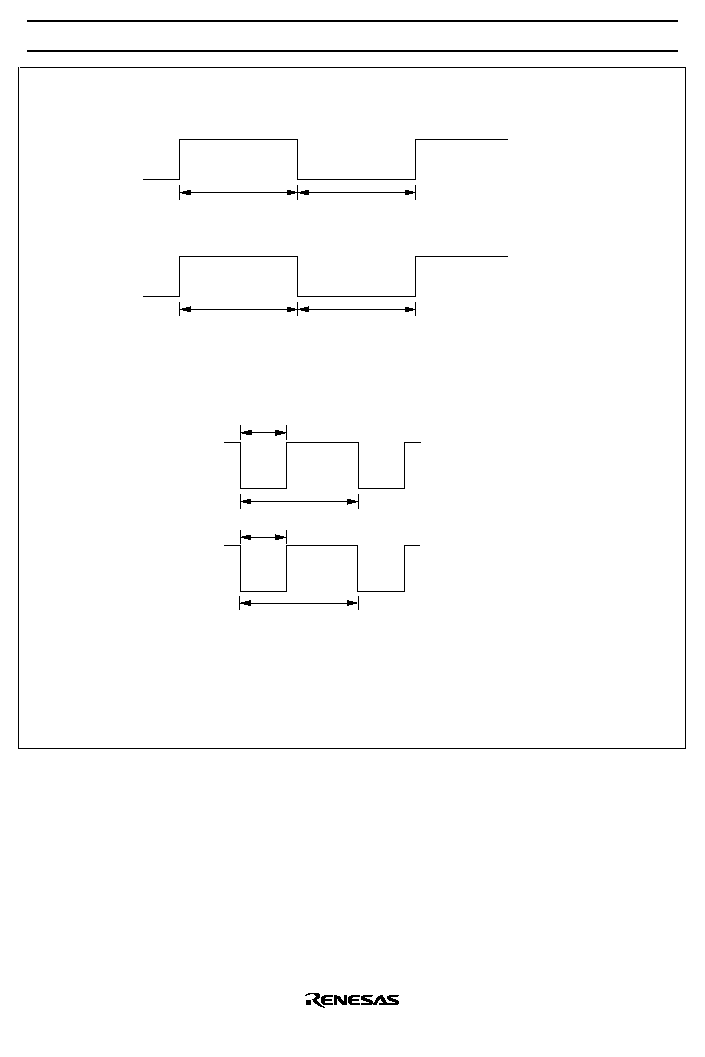
HD404889/HD404899/HD404878/HD404868 Series
87
(1) Toggle output waveform (timer B, timer C)
(2) PWM output waveform (timer B, timer C)
(
)
256 clock periods
256 clock periods
Free-running timer
(256 � N)
clock periods
(256 � N)
clock periods
Reload timer
T (N + 1)
T 256
T
T (256 � N)
TMB13 = 0
(free-running timer)
�
�
�
TMB13 = 1
(reload timer)
Notes:
T: Counter input clock period
The clock input source and division ratio are controlled by
timer mode register B1 and timer mode register C1.
N: Value in timer write register B or timer write register C
When N = 255 (= $FF), PWM output is always fixed at the timer low level.)
Figure 38 Timer Output Waveforms

HD404889/HD404899/HD404878/HD404868 Series
88
Timer B Registers
Timer B operation setting and timer B value reading/writing is controlled by the following registers.
Timer mode register B1 (TMB1: $010)
Timer mode register B2 (TMB2: $011)
Timer write register B (TWBL: $012, TWBU: $013)
Timer read register B (TRBL: $012, TRBU: $013)
Port mode register 2 (PMR2: $00A)
Module standby register 1 (MSR1: $00D)
�
Timer mode register B1 (TMB1: $010):
Timer mode register B1 (TMB1) is a 4-bit write-only register, used to select free-running/reload timer
operation and the input clock as shown in figure 39.
Timer mode register B1 (TMB1) is reset to $0 by an MCU reset:
A modification of timer mode register B1 (TMB1) becomes effective after execution of two instructions
following the timer mode register B1 (TMB1) write instruction. The program must provide for timer B
initialization by writing to timer write register B (TWBL, TWBU) to be executed after the post-
modification mode has become effective.
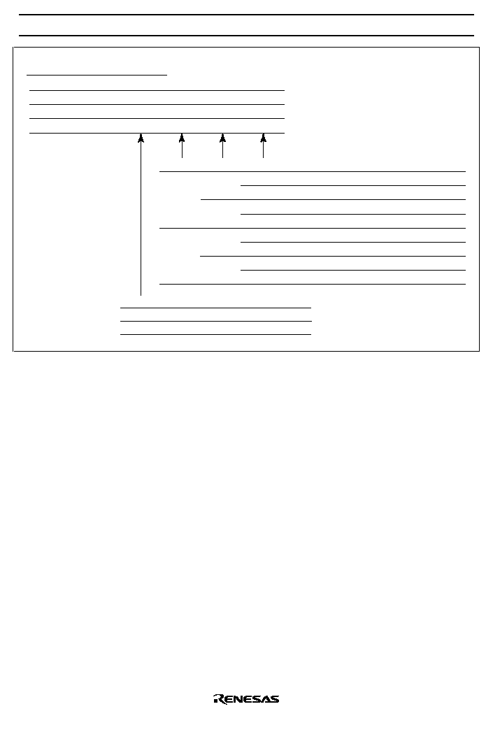
HD404889/HD404899/HD404878/HD404868 Series
89
3
W
0
TMB13
2
W
0
TMB12
1
W
0
TMB11
0
W
0
TMB10
Bit
Read/Write
Initial value on reset
Bit name
0
1
TMB12
TMB11
TMB10
0
1
0
1
0
1
0
1
0
1
Input clock period and input clock source
1
2,048 t
cyc
512 t
cyc
128 t
cyc
32 t
cyc
8 t
cyc
4 t
cyc
2 t
cyc
R1
0
/EVNB (external event input)
0
TMB13
0
1
Free-running/reload timer
Free-running timer
Reload timer
Timer mode register B1 (TMB1: $010)
Figure 39 Timer Mode Register B1 (TMB1)
�
Timer mode register B2 (TMB2: $011):
Timer mode register B2 (TMB2) is a 3-bit write-only register, used to select the timer B output mode
and EVNB pin detected edge as shown in figure 40.
Timer mode register B2 (TMB2) is reset to $0 by an MCU reset.

HD404889/HD404899/HD404878/HD404868 Series
90
TMB20
0
1
0
1
EVNB pin detected edge
Not detected
Falling edge detection
Rising edge detection
Both rising and falling edge detection
TMB22
0
1
Timer B output waveform
Toggle output
PWM output
TMB21
0
1
Timer mode register B2 (TMB2: $011)
Bit
Read/Write
Initial value on reset
Bit name
3
--
--
--
2
W
0
TMB22
1
W
0
TMB21
0
W
0
TMB20
Figure 40 Timer Mode Register B2 (TMB2)
�
Timer write register B (TWBL: $012, TWBU:$013):
Timer write register B (TWBL, TWBU) is a write-only register composed of a lower digit (TWBL) and
an upper digit (TWBU) (figures 41 and 42).
The lower digit (TWBL) of timer write register B is reset to $0 by an MCU reset, while the upper digit
(TWBU) is undetermined.
Timer B can be initialized by writing to timer write register B (TWBL, TWBU). To write the data, first
write the lower digit (TWBL). The lower digit write does not change the timer B value. Next, write the
upper digit (TWBU). Timer B is then initialized to the timer write register B (TWBL, TWBU) value.
When writing to timer write register B (TWBL, TWBU) from the second time onward, if it is not
necessary to change the lower digit (TWBL) reload value, timer B initialization is completed by the
upper digit write alone.
3
W
0
TWBL3
2
W
0
TWBL2
1
W
0
TWBL1
0
W
0
TWBL0
Timer write register B (lower) (TWBL: $012)
Bit
Read/Write
Initial value on reset
Bit name
Figure 41 Timer Write Register B (Lower) (TWBL)

HD404889/HD404899/HD404878/HD404868 Series
91
3
W
Undetermined
TWBU3
2
W
Undetermined
TWBU2
1
W
Undetermined
TWBU1
0
W
Undetermined
TWBU0
Timer write register B (upper) (TWBU: $013)
Bit
Read/Write
Initial value on reset
Bit name
Figure 42 Timer Write Register B (Upper) (TWBU)
�
Timer read register B (TRBL: $012, TRBU: $013):
Timer read register B (TRBL, TRBU) is a read-only register composed of a lower digit (TRBL) and an
upper digit (TRBU) from which the value of the upper digit of timer B is read directly (figures 43 and
44).
First, read the upper digit (TRBU) of timer read register B. The current value of the timer B upper digit
is read and, at the same time, the value of the timer B lower digit is latched in the lower digit (TRBL) of
timer read register B. The timer B value is obtained when the upper digit (TRBU) of timer read register
B is read by reading the lower digit (TRBL) of timer read register B.
3
R
Undetermined
TRBL3
2
R
Undetermined
TRBL2
1
R
Undetermined
TRBL1
0
R
Undetermined
TRBL0
Timer read register B (lower) (TRBL: $012)
Bit
Read/Write
Initial value on reset
Bit name
Figure 43 Timer Read Register B (Lower) (TRBL)
Bit
Read/Write
Initial value on reset
Bit name
3
R
Undetermined
TRBU3
2
R
Undetermined
TRBU2
1
R
Undetermined
TRBU1
0
R
Undetermined
TRBU0
Timer read register B (upper) (TRBU: $013)
Figure 44 Timer Read Register B (Upper) (TRBU)
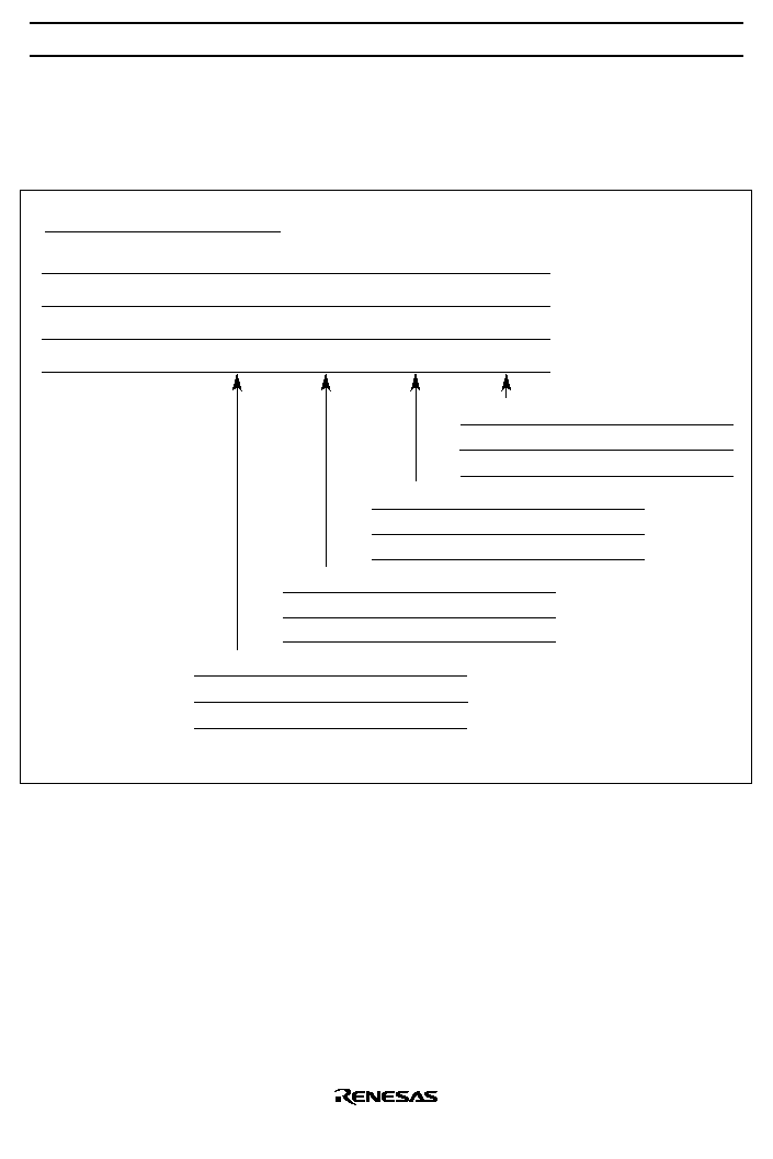
HD404889/HD404899/HD404878/HD404868 Series
92
�
Port mode register 2 (PMR2: $00A):
Port mode register 2 (PMR2) is a write-only register used to set the function of the R1
0
/EVNB and
R1
3
/TOB pins as shown in figure 45.
Port mode register 2 (PMR2) is reset to $0 by an MCU reset.
R1
0
/EVNB pin mode selection
R1
0
EVNB
Bit
Read/Write
Initial value on reset
Bit name
3
W
0
PMR23
PMR23
0
1
R1
3
/TOB pin mode selection
R1
3
TOB
2
W
0
PMR22
PMR22
0
1
R1
2
/BUZZ pin mode selection
R1
2
BUZZ
1
W
0
PMR21
*
PMR21
0
1
R1
1
/EVND pin mode selection
R1
1
EVND
0
W
0
PMR20
PMR20
0
1
Port mode register 2 (PMR2: $00A)
Note:
*
Applies to HD404889, HD404899, and HD404878 Series
Figure 45 Port Mode Register 2 (PMR2: $00A)
�
Module standby register 1 (MSR1: $00D):
Module standby register 1 (MSR1) is a write-only register used to designate supply or stopping of the
clock to timer B as shown in figure 46.
Module standby register 1 (MSR1) is reset to $0 by an MCU reset.

HD404889/HD404899/HD404878/HD404868 Series
93
Timer B clock supply control
Supplied
Stopped
Bit
Read/Write
Initial value on reset
Bit name
3
--
--
--
2
W
0
MSR12
1
W
0
MSR11
MSR11
0
1
Timer C clock supply control
Supplied
Stopped
0
W
0
MSR10
MSR10
0
1
MSR12
0
1
Timer D clock supply control
Supplied
Stopped
Module standby register 1 (MSR1: $00D)
Figure 46 Module Standby Register 1 (MSR1)

HD404889/HD404899/HD404878/HD404868 Series
94
Timer C
Timer C Functions:Timer : C has the following functions.
�
Free-running/reload timer
�
Watchdog timer
�
Timer output operation (toggle output, PWM output)
The block diagram of timer C is shown in figure 47.

HD404889/HD404899/HD404878/HD404868 Series
95
(TWCL)
(TWCU)
�
2
�
4
�
8
�
32
�
128
�
512
� PER
3
4
4
4
TOC
�
2048
(TCCL)
(TCCU)
System reset signal
Watchdog on
flag
(WDON)
Timer output
control logic
Timer B
overflow
System
clock
Prescaler
(PSS)
Watchdog timer
control logic
Timer C
interrupt request
flag
(IFTC)
Timer read
register CL
(TRCL)
Timer read
register CU
(TRCU)
Overflow
Timer counter C
Timer write register C
Timer mode
register C1
(TMC1)
Timer output
control
Timer mode
register C2
(TMC2)
Selector
Free-running/reload control
Internal data bus
Data bus
Clock line
Signal line
Figure 47 Timer C Block Diagram

HD404889/HD404899/HD404878/HD404868 Series
96
Timer C Operation
�
Free-running/reload timer:
Free-running/reload timer operation, the input clock source, and the prescaler division ratio are selected
by means of timer mode register C1 (TMC1).
Timer C is initialized to the value written to timer write register C (TWCL, TWCU) by software, and
counts up by 1 each time the input clock is input. When the input clock is input after the timer C value
reaches $FF, overflow output is generated. Timer C is then set to the value in timer write register C
(TWCL, TWCU) if the reload timer function is selected, or to $00 if the free-running timer function is
selected, and starts counting up again.
Overflow output sets the timer C interrupt request flag (IFTC). This flag is reset by the program or by
an MCU reset.
For details, see figure 3, Interrupt Control Bit and Register Flag Area Configuration, and table 1, Initial
Values after MCU Reset.
�
16-bit timer operation:
When timer B overflow flag is selected as the clock source, timer C can be used as a 16-bit timer that
counts the timer B clock source pulses. In this case, since the timer B and timer C free-running/reload
settings are independent, the settings should be made to suit the purpose.
�
Watchdog timer operation:
By using the timer C overflow output, timer C can be used as a watchdog timer for detecting program
runaway. The watchdog timer is enabled when the watchdog on flag (WDON) is set to 1, and generates
an MCU reset when timer C overflows. Usually, timer C initialization is performed by the program
before the timer C value reaches $FF, so controlling program runaway.
�
Timer output operation:
With timer C, the R2
0
/TOC pin is designated as the TOC pin by setting bit 0 of port mode register 3
(PMR3) to 1, and toggle waveform output or PWM waveform output can be selected by timer mode
register C2 (TMC2).
Toggle output
The operation is similar to that for timer B toggle output.
PWM output
The operation is similar to that for timer B PWM output.
�
Module standby:
The operation is similar to that for timer B module standby.

HD404889/HD404899/HD404878/HD404868 Series
97
Timer C Registers
Timer C operation setting and timer C value reading/writing is controlled by the following registers.
Timer mode register C1 (TMC1: $014)
Timer mode register C2 (TMC2: $015)
Timer write register C (TWCL: $016, TWCU: $017)
Timer read register C (TRCL: $016, TRCU: $017)
Port mode register 3 (PMR3: $00B)
Module standby register 1 (MSR1: $00D)
�
Timer mode register C1 (TMC1: $014):
Timer mode register C1 (TMC1) is a 4-bit write-only register, used to select free-running/reload timer
operation, the input clock, and the prescaler division ratio as shown in figure 48.
Timer mode register C1 (TMC1) is reset to $0 by an MCU reset.
A modification of timer mode register C1 (TMC1) becomes effective after execution of two instructions
following the timer mode register C1 (TMC1) write instruction. The program must provide for timer C
initialization by writing to timer write register C (TWCL, TWCU) to be executed after the post-
modification mode has become effective.

HD404889/HD404899/HD404878/HD404868 Series
98
3
W
0
TMC13
2
W
0
TMC12
1
W
0
TMC11
0
W
0
TMC10
Timer mode register C1 (TMC1: $014)
TMC12
TMC11
TMC10
Input clock period
2,048 t
cyc
512 t
cyc
128 t
cyc
32 t
cyc
8 t
cyc
4 t
cyc
2 t
cyc
Timer B overflow
0
1
0
1
0
1
0
1
0
1
0
1
0
1
TMC13
0
1
Bit
Read/Write
Initial value on reset
Bit name
Free-running/reload timer
Free-running timer
Reload timer
Figure 48 Timer Mode Register C1 (TMC1)

HD404889/HD404899/HD404878/HD404868 Series
99
�
Timer mode register C2 (TMC2: $015):
Timer mode register C2 (TMC2) is a 1-bit write-only register, used to select the timer C output mode as
shown in figure 49.
Timer mode register C2 (TMC2) is reset to $0 by an MCU reset.
3
--
--
--
2
W
0
TMC22
TMC22
0
1
1
--
--
--
0
--
--
--
Timer mode register C2 (TMC2: $015)
Bit
Read/Write
Initial value on reset
Bit name
Timer C output waveform
Toggle output
PWM output
Figure 49 Timer Mode Register C2 (TMC2)
�
Timer write register C (TWCL: $016, TWCU: $017):
Timer write register C (TWCL, TWCU) is a write-only register composed of a lower digit (TWCL) and
an upper digit (TWCU) (figures 50 and 51).
Timer write register C (TWCL, TWCU) operation is similar to that for timer write register B (TWBL,
TWBU).
Timer write register C (lower) (TWCL: $016)
3
W
0
TWCL3
2
W
0
TWCL2
1
W
0
TWCL1
0
W
0
TWCL0
Bit
Read/Write
Initial value on reset
Bit name
Figure 50 Timer Write Register C (Lower) (TWCL)

HD404889/HD404899/HD404878/HD404868 Series
100
Timer write register C (upper) (TWCU: $017)
Bit
Read/Write
Initial value on reset
Bit name
3
W
Undetermined
TWCU3
2
W
Undetermined
TWCU2
1
W
Undetermined
TWCU1
0
W
Undetermined
TWCU0
Figure 51 Timer Write Register C (Upper) (TWCU)
�
Timer read register C (TRCL: $016, TRCU: $017):
Timer read register C (TRCL, TRCU) is a read-only register composed of a lower digit (TRCL) and an
upper digit (TRCU) from which the value of the upper digit of timer C is read directly (figures 52 and
53).
Timer read register C (TRCL, TRCU) operation is similar to that for timer read register B (TRBL,
TRBU).
Timer read register C (upper) (TRCL: $016)
Bit
Read/Write
Initial value on reset
Bit name
3
R
Undetermined
TRCL3
2
R
Undetermined
TRCL2
1
R
Undetermined
TRCL1
0
R
Undetermined
TRCL0
Figure 52 Timer Read Register C (Lower) (TRCL)
Timer read register C (upper) (TRCU: $017)
Bit
Read/Write
Initial value on reset
Bit name
3
R
Undetermined
TRCU3
2
R
Undetermined
TRCU2
1
R
Undetermined
TRCU1
0
R
Undetermined
TRCU0
Figure 53 Timer Read Register C (Upper) (TRCU)
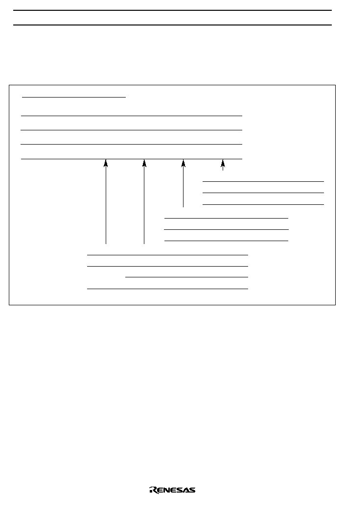
HD404889/HD404899/HD404878/HD404868 Series
101
�
Port mode register 3 (PMR3: $00B):
Port mode register 3 (PMR3) is a write-only register used to set the function of the R2
0
/TOC pin as
shown in figure 54.
Port mode register 3 (PMR3) is reset to $0 by an MCU reset.
R2
0
/TOC pin mode selection
R2
0
TOC
Bit
Read/Write
Initial value on reset
Bit name
3
W
0
PMR33
2
W
0
PMR32
PMR32
0
1
PMR33
0
1
R2
2
/SI/SO pin mode selection
R2
2
SI
SO
1
W
0
PMR31
PMR31
0
1
R2
1
/
SCK
pin mode selection
R2
1
SCK
0
W
0
PMR30
PMR30
0
1
Port mode register 3 (PMR3: $00B)
: Don't care
Figure 54 Port Mode Register 3 (PMR3)
�
Module standby register 1 (MSR1: $00D):
Module standby register 1 (MSR1) is a write-only register used to designate supply or stopping of the
clock to timer C as shown in figure 46.
Module standby register 1 (MSR1) is reset to $0 by an MCU reset.

HD404889/HD404899/HD404878/HD404868 Series
102
Timer D (HD404889/HD404899/HD404878 Series)
Timer D functions : Timer D has the following functions.
�
Free-running/reload timer
�
External event counter
�
Input capture timer
Block diagrams of timer D in different operating modes are shown in figures 55-1 and 55-2.

HD404889/HD404899/HD404878/HD404868 Series
103
(TWDL)
(TWDU)
�
2
�
4
�
8
�
32
�
128
�
512
�
2048
2
3
4
4
4
�PER
Timer read register
DU (TRDU)
Prescaler S (PSS)
Selector
Edge detection
logic
EVND
System
clock
Edge detection
control
Data bus
Clock line
Signal line
Timer mode
register D2
(TMD2)
Timer write register D
Free-running/
reload control
Timer read
register DL
(TRDL)
Timer D interrupt
request flag
(IFTD)
Internal data bus
Overflow
(TCDL)
(TCDU)
Timer counter D
Timer mode
register D1
(TMD1)
Figure 55-1 Timer D Block Diagram (Reload Timer and Event Counter Modes)

HD404889/HD404899/HD404878/HD404868 Series
104
2
3
3
4
4
EVND
Input capture
status flag
(ICSF)
Input capture
error flag
(ICEF)
Timer D interrupt
request flag
(IFTD)
Read signal
Edge detection
logic
System
clock
Prescaler S (PSS)
Selector
Timer read register D
Timer counter D
(TRDL)
(TRDU)
(TCDL)
(TCDU)
Input capture
timer control
Internal data bus
Timer mode
register D2
(TMD2)
Data bus
Clock line
Signal line
Time mode
register D1
(TMD1)
�
2
�
4
�
8
�
32
�
128
�
512
�
2048
�PER
Overflow
Figure 55-2 Timer D Block Diagram (Input Capture Timer Mode)

HD404889/HD404899/HD404878/HD404868 Series
105
Timer D Operation
�
Free-running/reload timer:
Free-running/reload timer operation, the input clock source, and the prescaler division ratio are selected
by means of timer mode register D1 (TMD1).
Timer D is initialized to the value written to timer write register D (TWDL, TWDU) by software, and
counts up by 1 each time the input clock is input. When the input clock is input after the timer D value
reaches $FF, overflow output is generated. Timer D is then set to the value in timer write register D
(TWDL, TWDU) if the reload timer function is selected, or to $00 if the free-running timer function is
selected, and starts counting up again.
Overflow output sets the timer D interrupt request flag (IFTD). This flag is reset by the program or by
an MCU reset. For details, see figure 3, Interrupt Control Bit and Register Flag Area Configuration,
and table 1, Initial Values after MCU Reset.
�
External event counter operation:
When external event input is designated for the input clock, timer D operates as an external event
counter. When external event input is used, the R1
1
/EVND pin is designated as the EVND pin by port
mode register 2 (PMR2).
The external event detected edge for timer D can be designated as a falling edge, rising edge, or both
falling and rising edges in the input signal by means of timer mode register D2 (TMD2). If both falling
and rising edges are selected, the input signal falling and rising edge interval should be at least 2tcyc.
Timer D counts up by 1 each time the edge selected by timer mode register D2 (TMD2) is detected.
Other operations are the same as for the free-running/reload timer function.
�
Input capture timer operation:
The input capture timer function is used to measure the time between trigger input edges input at the
EVND pin.
The trigger input edge can be designated as a falling edge, rising edge, or both falling and rising edges
by means of timer mode register D2 (TMD2).
When a trigger input edge is detected at the EVND pin, the current timer D value is stored in timer read
register D (TRDL, TRDU), and the timer D interrupt request flag (IFTD) and input capture status flag
(ICSF) are set. At the same time, timer D is reset to $00 and continues counting up.
If the next trigger input edge is input while the input capture status flag (ICSF) is set, or if timer D
overflows, the input capture error flag (ICEF) is set.
The input capture status flag (ICSF) and input capture error flag (ICEF) are reset to 0 by an MCU reset
or by writing 0 to them.
When timer D is set to operate as an input capture timer, it is reset to $00.

HD404889/HD404899/HD404878/HD404868 Series
106
Timer D Registers: Timer D operation setting and timer D value reading/writing is controlled by the
following registers.
Timer mode register D1 (TMD1: $018)
Timer mode register D2 (TMD2: $019)
Timer write register D (TWDL: $01A, TWDU: $01B)
Timer read register D (TRDL: $01A, TRDU: $01B)
Port mode register 2 (PMR2: $00A)
Module standby register 1 (MSR1: $00D)
�
Timer mode register D1 (TMD1: $018):
Timer mode register D1 (TMD1) is a 4-bit write-only register, used to select free-running/reload timer
operation, the input clock, and the prescaler division ratio as shown in figure 56.
Timer mode register D1 (TMD1) is reset to $0 by an MCU reset.
A modification of timer mode register D1 (TMD1) becomes effective after execution of two
instructions following the timer mode register D1 (TMD1) write instruction. The program must provide
for timer D initialization by writing to timer write register D (TWDL, TWDU) to be executed after the
post-modification mode has become effective.
When timer D is set to operate as an input capture timer, an internal clock should be set as the input
clock.

HD404889/HD404899/HD404878/HD404868 Series
107
3
W
0
TMD13
2
W
0
TMD12
1
W
0
TMD11
0
W
0
TMD10
Bit
Read/Write
Initial value on reset
Bit name
0
1
TMD12
TMD11
TMD10
0
1
0
1
0
1
0
1
0
1
Input clock period and input clock source
1
2,048 t
cyc
512 t
cyc
128 t
cyc
32 t
cyc
8 t
cyc
4 t
cyc
2 t
cyc
R11/EVND (external event input)
0
TMD13
0
1
Free-running/reload timer
Free-running timer
Reload timer
Timer mode register D1 (TMD1: $018)
Figure 56 Timer Mode Register D1 (TMD1)
�
Timer mode register D2 (TMD2: $019):
Timer mode register D2 (TMD2) is a 3-bit write-only register, used to select the EVND pin detected
edge and input capture operation as shown in figure 57.
Timer mode register D2 (TMD2) is reset to $0 by an MCU reset.

HD404889/HD404899/HD404878/HD404868 Series
108
TMD21
TMD20
0
1
0
1
0
1
EVND pin detected edge
Not detected
Falling edge detection
Rising edge detection
Both rising and falling edge detection
TMD22
0
1
Input capture setting
Free-running/reload timer
Input capture timer
Bit
Read/Write
Initial value on reset
Bit name
3
--
--
--
2
W
0
TMD22
1
W
0
TMD21
0
W
0
TMD20
Timer mode register D2 (TMD2: $019)
Figure 57 Timer Mode Register D2 (TMD2)
�
Timer write register D (TWDL: $01A, TWDU: $01B):
Timer write register D (TWDL, TWDU) is a write-only register composed of a lower digit (TWDL) and
an upper digit (TWDU) (figures 58 and 59).
Timer write register D (TWDL, TWDU) operation is similar to that for timer write register B (TWBL,
TWBU).
Bit
Read/Write
Initial value on reset
Bit name
3
W
0
TWDL3
2
W
0
TWDL2
1
W
0
TWDL1
0
W
0
TWDL0
Timer write register D (lower) (TWDL: $01A)
Figure 58 Timer Write Register D (Lower) (TWDL)

HD404889/HD404899/HD404878/HD404868 Series
109
Bit
Read/Write
Initial value on reset
Bit name
3
W
Undetermined
TWDU3
2
W
Undetermined
TWDU2
1
W
Undetermined
TWDU1
0
W
Undetermined
TWDU0
Timer write register D (upper) (TWDU: $01B)
Figure 59 Timer Write Register D (Upper) (TWDU)
�
Timer read register D (TRDL: $01A, TRDU: $01B):
Timer read register D (TRDL, TRDU) is a read-only register composed of a lower digit (TRDL) and an
upper digit (TRDU) (figures 60 and 61).
Timer read register D (TRDL, TRDU) operation is similar to that for timer read register B (TRBL,
TRBU).
In the input capture timer operating mode, when the timer D value is read after trigger input, it does not
matter whether the lower or upper digit is read first.
Bit
Read/Write
Initial value on reset
Bit name
3
R
Undetermined
TRDL3
2
R
Undetermined
TRDL2
1
R
Undetermined
TRDL1
0
R
Undetermined
TRDL0
Timer read register D (lower) (TRDL: $01A)
Figure 60 Timer Read Register D (Lower) (TRDL)
Bit
Read/Write
Initial value on reset
Bit name
3
R
Undetermined
TRDU3
2
R
Undetermined
TRDU2
1
R
Undetermined
TRDU1
0
R
Undetermined
TRDU0
Timer read register D (upper) (TRDU: $01B)
Figure 61 Timer Read Register D (Upper) (TRDU)

HD404889/HD404899/HD404878/HD404868 Series
110
�
Port mode register 2 (PMR2: $00A):
Port mode register 2 (PMR2) is a write-only register used to set the R1
1
/EVND pin function as shown in
figure 45.
Port mode register 2 (PMR2) is reset to $0 by an MCU reset.
�
Module standby register 1 (MSR1: $00D):
Module standby register 1 (MSR1) is a write-only register used to designate supply or stopping of the
clock to timer D as shown in figure 46.
Module standby register 1 (MSR1) is reset to $0 by an MCU reset.

HD404889/HD404899/HD404878/HD404868 Series
111
Serial Interface
The serial interface serially transfers and receives 8-bit data, and includes the following features.
�
Multiple transmit clock sources
External clock
Internal prescaler output clock
System clock
�
Output level control in idle states
Five registers, an octal counter, and a multiplexer are also configured for the serial interface as follows.
�
Serial data register (SRL: $026, SRU: $027)
�
Serial mode register 1 (SMR1: $024)
�
Serial mode register 2 (SMR2: $025)
�
Port mode register 3 (PMR3: $00B)
�
Octal counter (OC)
�
Selector
The block diagram of the serial interface is shown in figure 62.

HD404889/HD404899/HD404878/HD404868 Series
112
�
2
�
8
�
32
�
128
SI/SO
SCK
System
clock
�
PER
�
512
�
2048
1/2
1/2
Serial interrupt
request flag
(IFS)
Octal counter
(OC)
Idle control
logic
I/O control
logic
Clock
Transfer
control
Data bus
Clock line
Signal line
Serial mode
register 1
(SMR1)
Serial mode
register 2
(SMR2)
Serial data
register
(SRL/U)
Internal data bus
Selector
Selector
PrescalerS (PSS)
2
4
Figure 62 Serial Interface Block Diagram
HD404889/HD404899/HD404878/HD404868 Series
113
Serial Interface Operation
Selecting and changing serial interface operating mode:
The operating modes that can be selected for the serial interface are shown in table 26. The combination of
port mode register 3 (PMR3) values should be selected from this table. When the serial interface operating
mode is changed, the serial interface internal state must be initialized by writing to serial mode register 1
(SMR1).
Note : The serial interface is initialized by writing to serial mode register 1 (SMR1: $024). See serial
mode register 1 for details.
Table 26
Serial Interface Operating Modes
PMR3
Serial interface operating mode
Bit3
Bit2
Bit1
0
*
1
Clock continuous output mode
1
0
1
Receive mode
1
1
1
Transmit mode
*: Don't care
Serial interface pin setting:
The R2
1
/
SCK pin and R2
2
/SI/SO pin are set by writing data to port mode register 3 (PMR3). See serial
interface registers for details.
Serial clock source setting:
The serial clock is set by writing data to serial mode register 1 (SMR1). See serial interface registers for
details.
Serial data setting:
Transmit serial data is set by writing data to the serial data register (SRL, SRU).
Receive serial data is obtained by reading the serial data register (SRL, SRU). Serial data is shifted by
means of the serial clock to perform input/output from/to an external device.
The output level of the SO pin is undetermined until the first data is output after a reset by the MCU, or
until high/low control is performed in the idle state.
Transfer control:
Serial interface operation is started by an STS instruction. The octal counter is reset to 000 by the STS
instruction, and is incremented by 1 on each rise of the serial clock. When 8 serial clock pulses have been
input, or if data transmission/reception is suspended midway, the octal counter is reset to 000, the serial
interrupt request flag (IFS) is set, and transfer is terminated.
The serial clock is selected by means of serial mode register 1 (SMR1). See figure 66.

HD404889/HD404899/HD404878/HD404868 Series
114
Serial interface operating states:
The serial interface has the operating states shown in figure 63 in external clock mode and internal clock
mode.
STS instruction wait state
Serial clock wait state
Transfer state
Clock continuous output state (internal clock mode only)
�
STS instruction wait state
Upon MCU reset ((00) and (10) in figure 63), the serial interface enters the STS instruction wait state.
In the STS instruction wait state, the internal state of the serial interface is initialized. Even if the serial
clock is input at this time, the serial interface will not operate. When the STS instruction is executed
((01), (11)), the serial interface enters the serial clock wait state.
�
Serial clock wait state
The serial clock wait state is the interval from STS instruction execution until the first serial clock
falling edge. When the serial clock is input in the serial clock wait state ((02), (12)), the octal counter
begins counting, the contents of the serial data register (SRL) begin shifting, and the serial interface
enters the transfer state. However, if clock continuous output mode is selected in internal clock mode,
the serial interface enters the clock continuous output state ((17)) instead of the transfer state.
If a write to serial mode register 1 (SMR1) is performed in the serial clock wait state, the serial interface
enters the STS instruction wait state ((04), (14)).
�
Transfer state
The transfer state is the interval from the first serial clock falling edge until the eighth serial clock rising
edge. In the transfer state, if an STS instruction is executed or if eight serial clocks have been input, the
octal counter is cleared to 000, and the serial interface makes a state transition. If an STS instruction is
executed ((05), (15)), the serial interface enters the serial clock wait state. After eight serial clocks have
been input, the serial interface enters the serial clock wait state ((03)) when in external clock mode, and
enters the STS instruction wait state ((13)) when in internal clock mode.
In internal clock mode, the serial clock stops after output of eight clocks.
If a write to serial mode register 1 (SMR1) is performed in the transfer state ((06), (16)), the serial
interface is initialized and enters the STS instruction wait state.
When the serial interface switches from the transfer state to another state, the octal counter is reset to
000 and the serial interrupt request flag (IFS) is set.
�
Clock continuous output state (internal clock mode only)
In the clock continuous output state, no receive or transmit operation is performed, and the serial clock
is only output from the
SCK pin. It is therefore effective in internal clock mode.
If the serial clock is input ((17)) when bit 3 (PMR33) of port mode register 3 (PMR3) is cleared to 0 and
the serial interface is in the serial clock wait state, a transition is made to the clock continuous output
state.
If a write to serial mode register 1 (SMR1) is performed in the clock continuous output state ((18)), the
serial interface enters the STS instruction wait state.
HD404889/HD404899/HD404878/HD404868 Series
115
STS instruction wait state
(octal counter ="000",
serial clock disabled)
MCU reset (00)
Serial clock wait state
(octal counter ="000")
Transfer state
(octal counter
"000")
SMR1 write (14)
STS instruction (11)
Serial clock (12)
serial clocks (03)
STS instruction (05)
(IFS
"1")
STS instruction (15)
(IFS
"1")
External clock mode
STS instruction wait state
(octal counter ="000",
serial clock disabled)
Serial clock wait state
(octal counter ="000")
Transfer state
(octal counter
"000")
SMR1 write (04)
STS instruction (01)
Serial clock (02)
SMR1 write (06)
(IFS
"1")
8 serial clocks (13)
SMR1 write (16)
(IFS
"1")
MCU reset (10)
Serial clock (17)
SMR1 write (18)
Clock continuous output state
(PMR33 ="0")
Internal clock mode
( ) Refer to the text for details on the circled numbers in the figure.
8
Figure 63 Serial Interface Operating States

HD404889/HD404899/HD404878/HD404868 Series
116
Idle high/low control:
When the serial interface is in the STS instruction wait state or the serial clock wait state (i.e. when idle),
the output level of the SO pin can be set arbitrarily by software. Idle high/low control is performed by
writing the output level to bit 1 (SMR21) of serial mode register 2 (SMR2).
An example of idle high/low control is shown in figure 64. Idle high/low control cannot be performed in
the transfer state.

HD404889/HD404899/HD404878/HD404868 Series
117
State
SCK
pin (input)
SO pin
IFS
MSB
LSB
Undefined
Idle
Idle
Idle
Idle
Idle H/L setting
Dummy write to
cause state transition
Port setting
STS wait state
Serial clock
wait state
Transfer state
STS wait state
Serial clock
wait state
External clock setting
Idle H/L setting
(Flag reset by transfer
completion processing)
MCU reset
PMR3 write
SMR1 write
SMR2 write
SRL, SRU write
STS instruction
State
SCK
pin (output)
SO pin
IFS
MSB
LSB
Undefined
Idle H/L setting
Port setting
STS wait state
Serial clock
wait state
Transfer state
STS wait state
(Flag reset by transfer
completion processing)
MCU reset
PMR3 write
SMR1 write
SMR2 write
SRL, SRU write
STS instruction
(2) Internal clock mode
(1) External clock mode
External clock setting
Transmit data write
Transmit data write
Idle H/L setting
Figure 64 Examples of Serial Interface Operation Sequence

HD404889/HD404899/HD404878/HD404868 Series
118
Serial clock error detection (external clock mode):
The serial interface will operate incorrectly in the transfer state if external noise results in unnecessary
pulses being added to the serial clock. Serial clock error detection in such cases is carried out as shown in
figure 65.
If more than eight serial clock pulses are input due to external noise while in the transfer state, at the eighth
clock pulse (including any external noise pulses), the octal counter is cleared to 000 and the serial interrupt
request flag (IFS) is set. At the same time, the serial interface exits the transfer state and enters the serial
clock wait state, but returns to the transfer state at the next regular clock pulse falling edge.
Meanwhile, in the interrupt handling routine, transfer end processing is performed, the serial interrupt
request flag is reset, and a dummy write is performed into serial mode register 1 (SMR1). The serial
interface then returns to the STS wait state, and the serial interrupt request flag (IFS) is set again. It is
therefore possible to detect a serial clock error by testing the serial interrupt request flag after the dummy
write to serial mode register 1.
Usage notes:
�
Initialization after register modification
If a port mode register 3 (PMR3) write is performed in the serial clock wait state or transfer state, a
serial mode register 1 (SMR1) write should be performed again to initialize the serial interface.
�
Serial interrupt request flag (IFS:$023, 2) setting
If a serial mode register 1 (SMR1) write or STS instruction is executed during the first low-level
interval of the serial clock in the transfer state, the serial interrupt request flag (IFS) will not be set. To
ensure that the serial interrupt request flag (IFS) is properly set in this case, programming is required to
make sure that the
SCK pin is in the 1 state (by executing an input instruction for the R2 port) before
executing a serial mode register 1 (SMR1) write or an STS instruction.

HD404889/HD404899/HD404878/HD404868 Series
119
Transfer end
(IFS
"1")
Disable interrupts
IFS
"0"
SMR1 write
IFS=1?
Normal termination
Serial clock
error processing
(1) Serial clock error detection flowchart
Serial clock
wait state
Transfer state
Serial clock
wait state
Transfer state
(Noise)
State
SCK
pin
(input)
SMR1
write
IFS
1
2
3
4
5
6
7
8
(2) Serial clock error detection sequence
Flag set by octal
counter reaching
000
Flag reset by transfer
end processing
Yes
No
Because the serial
interface returns to
the transfer state, a
write to SMR1
resets IFS.
Figure 65 Example of Serial Clock Error Detection

HD404889/HD404899/HD404878/HD404868 Series
120
Serial Interface Registers
Serial interface operation setting and serial data reading/writing is controlled by the following registers.
Serial mode register 1 (SMR1: $024)
Serial mode register 2 (SMR2: $025)
Serial data register (SRL: $026, SRU: $027)
Port mode register 3 (PMR3: $00B)
Module standby register 2 (MSR2: $00E)
Serial mode register 1 (SMR1: $024):
Serial mode register 1 (SMR1) has the following functions. See figure 66.
�
Serial clock selection
�
Prescaler division ratio selection
�
Serial interface initialization
The serial mode register 1 (SMR1) is a 4-bit write-only register, and is reset to $0 by an MCU reset.
A write to serial mode register 1 (SMR1) halts the supply of the serial clock to the serial data register (SRL,
SRU) and the octal counter, and resets the octal counter to 000. Therefore, if serial mode register 1
(SMR1) is written to during serial interface operation, data transmission/reception will be suspended and
the serial interrupt request flag (IFS) will be set.
A modification of serial mode register 1 (SMR1) becomes effective after execution of two instructions
following the serial mode register 1 (SMR1) write instruction. The program must therefore provide for the
STS instruction to be executed two cycles after the instruction that writes to serial mode register 1 (SMR1).

HD404889/HD404899/HD404878/HD404868 Series
121
Serial mode register 1 (SMR1: $024)
SMR13 SMR12 SMR11 SMR10
SCK
pin
Serial clock
source
Serial clock
(PSS division ratio
�
2 or 4)
Serial clock
cycle
0
1
0
1
0
1
0
1
0
1
0
1
0
1
0
1
0
1
0
1
0
1
0
1
0
1
0
1
1
0
Output
Output
Output
Output
Output
Output
Output
Input
Output
Output
Output
Output
Output
Output
Output
Input
PSS
PSS
PSS
PSS
PSS
PSS
System clock
External clock
PSS
PSS
PSS
System clock
External clock
PSS
PSS
PSS
(
�
PER
/2048)
�
2
(
�
PER
/512)
�
2
(
�
PER
/128)
�
2
(
�
PER
/32)
�
2
(
�
PER
/8)
�
2
(
�
PER
/2)
�
2
�
PER
(
�
PER
/2048)
�
4
(
�
PER
/512)
�
4
(
�
PER
/128)
�
4
(
�
PER
/32)
�
4
(
�
PER
/8)
�
4
(
�
PER
/2)
�
4
�
PER
4096 tcyc
1024 tcyc
256 tcyc
64 tcyc
16 tcyc
4 tcyc
tcyc
8192 tcyc
2048 tcyc
512 tcyc
128 tcyc
32 tcyc
8 tcyc
tcyc
Bit
Read/Write
Initial value on reset
Bit name
3
W
0
SMR13
2
W
0
SMR12
1
W
0
SMR11
0
W
0
SMR10
Figure 66 Serial Mode Register 1 (SMR1)
Serial mode register 2 (SMR2: $025):
Serial mode register 2 (SMR2) has the following functions. See figure 67.
�
R2
2
/SI/SO pin PMOS control
�
Idle high/low control
Serial mode register 2 (SMR2) is a 2-bit write-only register. The register value cannot be modified in the
transfer state.
Bit 2 (SMR22) of serial mode register 2 (SMR2) controls the on/off status of the R2
2
/SI/SO pin PMOS.
The bit 2 (SMR22) only is reset to 0 by an MCU reset.
HD404889/HD404899/HD404878/HD404868 Series
122
Bit 1 (SMR21) of serial mode register 2 (SMR2) performs SO pin high/low control in the idle state. The
SO pin changes at the same time as the high/low write.
SMR21
0
1
R2
2
/SI/SO pin output buffer control
PMOS active
PMOS off (NMOS open-drain output)
SMR22
0
1
Idle high/low control
SO pin set to low-level output in idle state
SO pin set to high-level output in idle state
Serial mode register 2 (SMR2: $025)
Bit
Read/Write
Initial value on reset
Bit name
3
--
--
--
2
W
0
SMR22
1
W
undeternined
SMR21
0
--
--
Figure 67 Serial Mode Register 2 (SMR2)
Serial data register (SRL: $026, SRU: $027):
The serial data register (SRL, SRU) has the following functions. See figures 68 and 69.
�
Transmit data write and shift operations
�
Receive data shift and read operations
The data written to the serial data register (SRL, SRU) is output LSB-first from the SO pin in
synchronization with the falling edge of the serial clock.
External data input LSB-first from the SI pin is latched in synchronization with the rising edge of the serial
clock. Figure 70 shows the serial clock and data input/output timing chart.
Writing and reading of the serial data register (SRL, SRU) must be performed only after data
transmission/reception is completed. The data contents are not guaranteed if a read or write is performed
during data transmission or reception.
HD404889/HD404899/HD404878/HD404868 Series
123
Serial data register (lower) (SRL: $026)
3
R/W
Undetermined
SR3
2
SR2
1
SR1
0
SR0
R/W
R/W
R/W
Undetermined Undetermined Undetermined
Bit
Read/Write
Initial value on reset
Bit name
Figure 68 Serial Data Register (SRL)
Serial data register (upper) (SRU: $027)
3
R/W
Undetermined
SR7
2
SR6
1
SR5
0
SR4
R/W
R/W
R/W
Undetermined Undetermined Undetermined
Bit
Read/Write
Initial value on reset
Bit name
Figure 69 Serial Data Register (SRU)
1
2
3
4
5
6
7
8
Serial
clock
Serial output
data
Serial input
data latch
timing
LSB
MSB
Figure 70 Serial Interface Input/Output Timing Chart

HD404889/HD404899/HD404878/HD404868 Series
124
Port mode register 3 (PMR3: $00B):
Port mode register 3 (PMR3) has the following functions. See figure 71.
�
R2
1
/
SCK pin selection
�
R2
2
/SI/SO pin selection
Port mode register 3 (PMR3) is a 4-bit write-only register used to select serial interface pin settings as
shown in figure 71. It is reset to $0 by an MCU reset.
R2
0
/TOC pin mode selection
PMR30
R2
1
/
SCK
pin mode selection
PMR31
0
1
R2
0
TOC
0
1
R2
1
SCK
PMR33 PMR32
0
1
*
0
1
R2
2
/SI/SO pin mode selection
R2
2
SI
SO
*
: Don't care
Port mode register 3 (PMR3: $00B)
Bit
Read/Write
Initial value on reset
Bit name
3
W
0
PMR33
2
W
0
PMR32
1
W
0
PMR31
0
W
0
PMR30
Figure 71 Port Mode Register 3 (PMR3)

HD404889/HD404899/HD404878/HD404868 Series
125
Module standby register 2 (MSR2: $00E):
Module standby register 2 (MSR2) is a write-only register used to designate supply or stopping of the clock
to the serial interface as shown in figure 72.
Module standby register 2 (MSR2) is reset to $0 by an MCU reset.
Serial clock supply control
Supplied
Stopped
MSR20
A/D clock supply control
Supplied
Stopped
MSR21
0
1
0
1
Module standby register 2 (MSR2: $00E)
Bit
Read/Write
Initial value on reset
Bit name
3
--
--
--
2
--
--
--
1
W
0
MSR21
0
W
0
MSR20
Figure 72 Module Standby Register 2 (MSR2)
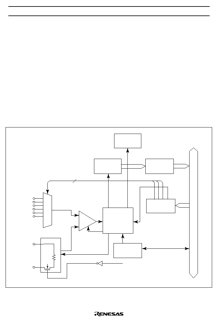
HD404889/HD404899/HD404878/HD404868 Series
126
A/D Converter
HD404889 Series
The MCU has a built-in successive approximation type A/D converter using a resistance ladder method,
capable of digital conversion of six analog inputs with an 8-bit resolution. The A/D converter block
diagram is shown in figure 73.
The A/D converter comprises the following four registers.
�
A/D mode register (AMR: $028)
�
A/D start flag (ADSF: $020,2)
�
A/D data register (ADRL: $02A, ADRU: $02B)
�
Module standby register 2 (MSR2: $00E)
Note : Address $029 is a reserved register, and should not be read or written to.
Interrupt flag
(IFAD)
Encoder
A/D data
register
(ADRU, ADRL)
Internal data bus
Selector
Conversion time control
A/D
start flag
(ADSF)
COMP
Reference
voltage
Reference
voltage control
R7
0
/AN
0
R7
1
/AN
1
R7
2
/AN
2
R7
3
/AN
3
R8
0
/AN
4
R8
1
/AN
5
+
�
A/D
control
logic
A/D mode
register
(AMR)
AV
CC
AV
SS
D/A
3
Operating mode signal (set to 1 in
stop, watch, and subactive modes,
and during module standby)
Figure 73 A/D Converter Block Diagram
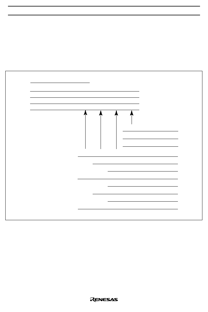
HD404889/HD404899/HD404878/HD404868 Series
127
A/D mode register (AMR: $028):
The A/D mode register is a 4-bit write-only register that shows the A/D converter speed setting and
information on the analog input pin specification. The A/D conversion time is selected by bit 0, and the
channel by bits 1, 2, and 3 (figure 74).
A/D start flag (ADSF: $020,2):
A/D conversion is started by writing 1 to the A/D start flag. When conversion ends, the converted data is
placed in the A/D data register and the A/D start flag is cleared at the same time. (figure 75).
Bit
Read/Write
Initial value on reset
Bit name
3
W
0
AMR3
2
W
0
AMR2
1
W
0
AMR1
0
W
0
AMR0
Analog input channel selection
No selection
AN0
AN1
AN2
AN3
AN4
AN5
AMR1
*
0
1
0
1
0
1
AMR2
0
1
0
1
AMR3
0
1
AMR0
0
1
A/D conversion time
65 t
cyc
125 t
cyc
A/D mode register (AMR: $028)
*
: Don't care
Figure 74 A/D Mode Register (AMR)
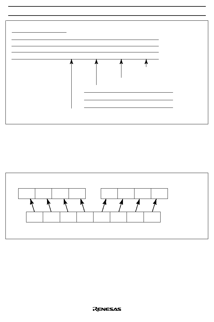
HD404889/HD404899/HD404878/HD404868 Series
128
Bit
Read/Write
Initial value on reset
Bit name
3
R/W
0
DTON
2
R/W
0
ADSF
1
R/W
0
WDON
0
R/W
0
LSON
A/D start flag (ADSF: $020,2)
1
0
DTON (see low-power mode section)
WDON (see timer section)
LSON (see low-power mode section)
A/D start flag (ADSF)
A/D conversion starts
Indicates end of A/D conversion
Figure 75 A/D Start Flag (ADSF)
A/D data register (ADRL: $02A, ADRU: $02B):
The A/D data register is a read-only register consisting of a lower and upper 4 bits. This register is not
cleared by a reset. Also, data read during A/D conversion is not guaranteed. At the end of A/D conversion,
the resulting 8-bit data is stored in this register, and is held until the next conversion operation starts
(figures 76, 77, and 78).
MSB
LSB
bit7
bit0
Conversion result
ADRU : $02B
ADRL : $02A
3 2 1 0
3 2 1 0
Figure 76 A/D Data Register
HD404889/HD404899/HD404878/HD404868 Series
129
Bit
Read/Write
Initial value on reset
Bit name
3
R
1
ADRL3
2
R
1
ADRL2
1
R
1
ADRL1
0
R
1
ADRL0
A/D data register-lower (ADRL: $02A)
Figure 77 A/D Data Register-Lower (ADRL)
Bit
Read/Write
Initial value on reset
Bit name
3
R
0
ADRU3
2
R
1
ADRU2
1
R
1
ADRU1
0
R
1
ADRU0
A/D data register-upper (ADRU: $02B)
Figure 78 A/D Data Register-Upper (ADRU)
Module standby register 2 (MSR2: $00E):
Writing 1 to bit 1 of module standby register 2 stops the supply of the system clock to the A/D module and
cuts the current (I
AD
) flowing in the ladder resistor.
Usage notes:
�
Use the SEM or SEMD instruction to write to the A/D start flag (ADSF).
�
Do not write to the ADSF during A/D conversion.
�
Data in the A/D data register is undetermined during A/D conversion.
�
As the A/D converter operates on a clock from OSC, it stops in stop mode, watch mode, and subactive
mode. The current flowing in the A/D converter ladder resistor is also cut in these low-power modes to
reduce power consumption.
�
When an analog input pin is selected by the A/D mode register, the pull-up MOS for that pin is
disabled.

HD404889/HD404899/HD404878/HD404868 Series
130
A/D Converter
HD404899/HD404868 Series
The MCU has a built-in successive approximation type A/D converter using a resistance ladder method,
capable of digital conversion of six analog inputs (four analog inputs in the HD404868 Series) with a 10-bit
resolution. The A/D converter block diagram is shown in figures 79-1 and 79-2.
The A/D converter comprises the following four registers.
�
A/D mode register (AMR: $028)
�
A/D start flag (ADSF: $020,2)
�
A/D data register (ADRL: $029, ADRM: $02A, ADRU: $02B)
�
Module standby register 2 (MSR2: $00E)
Interrupt flag
(IFAD)
Encoder
A/D data
register
(ADRU, ADRM, ADRL)
Internal data bus
Selector
Conversion time control
A/D
start flag
(ADSF)
COMP
Reference
voltage
Reference
voltage control
R7
0
/AN
0
R7
1
/AN
1
R7
2
/AN
2
R7
3
/AN
3
R8
0
/AN
4
R8
1
/AN
5
+
�
A/D
control
logic
A/D mode
register
(AMR)
AV
CC
AV
SS
D/A
3
Operating mode signal (set to 1 in
stop, watch, and subactive modes,
and during module standby)
Figure 79-1 A/D Converter Block Diagram (HD404899 Series)
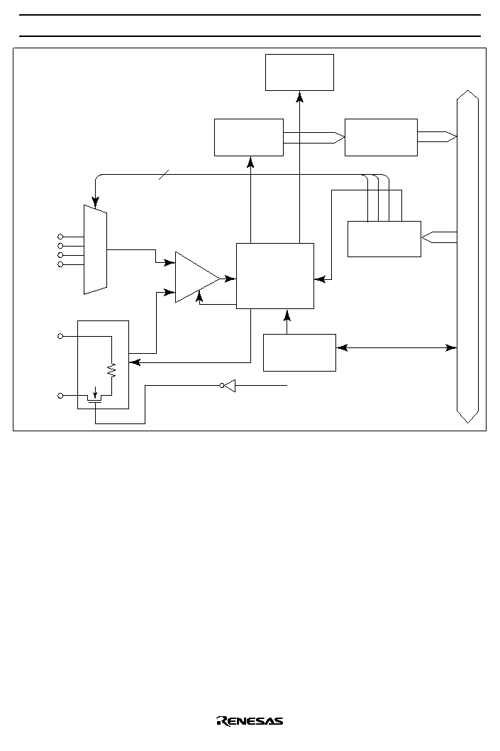
HD404889/HD404899/HD404878/HD404868 Series
131
Interrupt flag
(IFAD)
Encoder
A/D data
register
(ADRU, ADRM, ADRL)
Internal data bus
Selector
Conversion time control
A/D
start flag
(ADSF)
COMP
Reference
voltage
Reference
voltage control
R7
0
/AN
0
R7
1
/AN
1
R7
2
/AN
2
R7
3
/AN
3
+
�
A/D
control
logic
A/D mode
register
(AMR)
V
CC
GND
D/A
3
Operating mode signal (set to 1 in
stop, watch, and subactive modes,
and during module standby)
Figure 79-2 A/D Converter Block Diagram (HD404868 Series)

HD404889/HD404899/HD404878/HD404868 Series
132
A/D mode register (AMR: $028):
The A/D mode register is a 4-bit write-only register that shows the A/D converter speed setting and
information on the analog input pin specification. The A/D conversion time is selected by bit 0, and the
channel by bits 1, 2, and 3 (figure 80).
A/D start flag (ADSF: $020,2):
A/D conversion is started by writing 1 to the A/D start flag. When conversion ends, the converted data is
placed in the A/D data register and the A/D start flag is cleared at the same time. (figure 81).
Bit
Read/Write
Initial value on reset
Bit name
3
W
0
AMR3
2
W
0
AMR2
1
W
0
AMR1
0
W
0
AMR0
Analog input channel selection
No selection
AN0
AN1
AN2
AN3
AN4
*
AN5
*
AMR1
0
1
0
1
0
1
AMR2
0
1
0
1
AMR3
0
1
AMR0
0
1
A/D conversion time
65 t
cyc
125 t
cyc
A/D mode register (AMR: $028)
Note:
*
Applies to HD404899 Series.
Figure 80 A/D Mode Register (AMR)
HD404889/HD404899/HD404878/HD404868 Series
133
Bit
Read/Write
Initial value on reset
Bit name
3
R/W
0
DTON
2
R/W
0
ADSF
1
R/W
0
WDON
0
R/W
0
LSON
A/D start flag (ADSF: $020,2)
1
0
DTON (see low-power mode section)
WDON (see timer section)
LSON (see low-power mode section)
A/D start flag (ADSF)
A/D conversion starts
Indicates end of A/D conversion
Figure 81 A/D Start Flag (ADSF)
A/D data register (ADRL: $029, ADRM: $02A, ADRU: $02B):
The A/D data register is a read-only register consisting of a middle and upper 4 bits. This register is not
cleared by a reset. Also, data read during A/D conversion is not guaranteed. At the end of A/D conversion,
the resulting 10-bit data is stored in this register, and is held until the next conversion operation starts
(figures 82, 83, 84 and 85).
MSB
LSB
bit9
bit0
Conversion result
ADRU : $02B
ADRM : $02A
3 2 1 0
3 2 1 0
ADRL : $029
3
2
Figure 82 A/D Data Register
HD404889/HD404899/HD404878/HD404868 Series
134
Bit
Read/Write
Initial value on reset
Bit name
3
R
1
ADRL3
2
R
1
ADRL2
1
--
--
Not used
0
--
--
Not used
A/D data register-lower (ADRL: $029)
Figure 83 A/D Data Register-Lower (ADRL)
Bit
Read/Write
Initial value on reset
Bit name
3
R
1
ADRM3
2
R
1
ADRM2
1
R
1
ADRM1
0
R
1
ADRM0
A/D data register-middle (ADRM: $02A)
Figure 84 A/D Data Register-Middle (ADRM)
Bit
Read/Write
Initial value on reset
Bit name
3
R
0
ADRU3
2
R
1
ADRU2
1
R
1
ADRU1
0
R
1
ADRU0
A/D data register-upper (ADRU: $02B)
Figure 85 A/D Data Register-Upper (ADRU)
Module standby register 2 (MSR2: $00E):
Writing 1 to bit 1 of module standby register 2 stops the supply of the system clock to the A/D module and
cuts the current (I
AD
) flowing in the ladder resistor.
Usage notes:
�
Use the SEM or SEMD instruction to write to the A/D start flag (ADSF).
�
Do not write to the ADSF during A/D conversion.
�
Data in the A/D data register is undetermined during A/D conversion.

HD404889/HD404899/HD404878/HD404868 Series
135
�
As the A/D converter operates on a clock from OSC, it stops in stop mode, watch mode, and subactive
mode. The current flowing in the A/D converter ladder resistor is also cut in these low-power modes to
reduce power consumption.
�
When an analog input pin is selected by the A/D mode register, the pull-up MOS for that pin is
disabled.

HD404889/HD404899/HD404878/HD404868 Series
136
LCD Circuit
The MCU incorporates a controller and driver that drive four common signal pins and 32 segment pins (24
segment pins in the HD404868 Series). The controller unit consists of a RAM unit that stores the display
data, a display control register (LCR), and a duty/clock control register (LMR) (figures 86-1 and 86-2).
The LCD circuit allows four different duties and LCD clocks to be controlled by the program, and also
incorporates dual-port RAM, enabling display data to be transferred to the segment signal pins
automatically without program processing. If the 32 kHz oscillator clock is designated as the LCD clock
source, LCD display is also possible in watch mode in which the system clock stops.
HD404889/HD404899/HD404878/HD404868 Series
137
Common
signal
output
circuit
Segment
signal
output
circuit
Internal LCD power supply switch
32
2
Duty selection
Selector
LCD display
control register
(LCR)
Dual-port
display RAM
(32 digits)
LCD display
mode register
(LMR)
2
COM1
COM2
COM3
COM4
V
1
V
2
V
3
SEG17 to SEG32
LCD input clocks
Display data
2
Display
control
Port mode
register 4
(PMR4)
4
Pin control
SEG1 to SEG4
SEG9 to SEG12
SEG5 to SEG8
Clock
V
CC
LCD power supply control circuit
Internal data bus
Data bus
Clock line
Signal line
V
0
SEG13 to SEG16
Pin function switching circuit
Note:
Figure 86-1 LCD Circuit Block Diagram (HD404889/HD404899/HD404878 Series)
HD404889/HD404899/HD404878/HD404868 Series
138
Common
signal
output
circuit
Segment
signal
output
circuit
Internal LCD power supply switch
24
2
Duty selection
Selector
LCD display
control register
(LCR)
Dual-port
display RAM
(24 digits)
LCD display
mode register
(LMR)
2
COM1
COM2
COM3
COM4
V
1
V
2
V
3
SEG17 to SEG24
LCD input clocks
Display data
2
Display
control
Port mode
register 4
(PMR4)
4
Pin control
SEG1 to SEG4
SEG9 to SEG12
SEG5 to SEG8
Clock
V
CC
LCD power supply control circuit
Internal data bus
Data bus
Clock line
Signal line
SEG13 to SEG16
Pin function switching circuit
Note:
Figure 86-2 LCD Circuit Block Diagram (HD404868 Series)
HD404889/HD404899/HD404878/HD404868 Series
139
LCD data area and segment data: $050 to $06F (HD404889/HD404899/HD404878 Series)
$050 to $067 (HD404868 Series)
Figures 87-1 and 87-2 show the LCD RAM area configuration. Each bit of the storage area corresponds to
one of four duties. When data is written to the area corresponding to a particular duty, it is automatically
output to the segment as display data.
$050
$051
$052
$053
$054
$055
$056
$057
$058
$059
$05A
$05B
$05C
$05D
$05E
$05F
bit3
bit2
bit1
bit0
SEG1
SEG2
SEG3
SEG4
SEG5
SEG6
SEG7
SEG8
SEG9
SEG10
SEG11
SEG12
SEG13
SEG14
SEG15
SEG16
SEG1
SEG2
SEG3
SEG4
SEG5
SEG6
SEG7
SEG8
SEG9
SEG10
SEG11
SEG12
SEG13
SEG14
SEG15
SEG16
SEG1
SEG2
SEG3
SEG4
SEG5
SEG6
SEG7
SEG8
SEG9
SEG10
SEG11
SEG12
SEG13
SEG14
SEG15
SEG16
SEG1
SEG2
SEG3
SEG4
SEG5
SEG6
SEG7
SEG8
SEG9
SEG10
SEG11
SEG12
SEG13
SEG14
SEG15
SEG16
COM4
COM3
COM2
COM1
SEG17
SEG18
SEG19
SEG20
SEG21
SEG22
SEG23
SEG24
SEG25
SEG26
SEG27
SEG28
SEG29
SEG30
SEG31
SEG32
COM4
COM3
$060
$061
$062
$063
$064
$065
$066
$067
$068
$069
$06A
$06B
$06C
$06D
$06E
$06F
bit3
bit2
bit1
bit0
COM2
COM1
SEG17
SEG18
SEG19
SEG20
SEG21
SEG22
SEG23
SEG24
SEG25
SEG26
SEG27
SEG28
SEG29
SEG30
SEG31
SEG32
SEG17
SEG18
SEG19
SEG20
SEG21
SEG22
SEG23
SEG24
SEG25
SEG26
SEG27
SEG28
SEG29
SEG30
SEG31
SEG32
SEG17
SEG18
SEG19
SEG20
SEG21
SEG22
SEG23
SEG24
SEG25
SEG26
SEG27
SEG28
SEG29
SEG30
SEG31
SEG32
Figure 87-1 LCD RAM Area Configuration (Using Dual-Port RAM)
(HD404889/HD404899/HD404878 Series)
$050
$051
$052
$053
$054
$055
$056
$057
$058
$059
$05A
$05B
$05C
$05D
$05E
$05F
bit3
bit2
bit1
bit0
SEG1
SEG2
SEG3
SEG4
SEG5
SEG6
SEG7
SEG8
SEG9
SEG10
SEG11
SEG12
SEG13
SEG14
SEG15
SEG16
SEG1
SEG2
SEG3
SEG4
SEG5
SEG6
SEG7
SEG8
SEG9
SEG10
SEG11
SEG12
SEG13
SEG14
SEG15
SEG16
SEG1
SEG2
SEG3
SEG4
SEG5
SEG6
SEG7
SEG8
SEG9
SEG10
SEG11
SEG12
SEG13
SEG14
SEG15
SEG16
SEG1
SEG2
SEG3
SEG4
SEG5
SEG6
SEG7
SEG8
SEG9
SEG10
SEG11
SEG12
SEG13
SEG14
SEG15
SEG16
COM4
COM3
COM2
COM1
SEG17
SEG18
SEG19
SEG20
SEG21
SEG22
SEG23
SEG24
COM4
COM3
$060
$061
$062
$063
$064
$065
$066
$067
bit3
bit2
bit1
bit0
COM2
COM1
SEG17
SEG18
SEG19
SEG20
SEG21
SEG22
SEG23
SEG24
SEG17
SEG18
SEG19
SEG20
SEG21
SEG22
SEG23
SEG24
SEG17
SEG18
SEG19
SEG20
SEG21
SEG22
SEG23
SEG24
Figure 87-2 LCD RAM Area Configuration (Using Dual-Port RAM) (HD404868 Series)

HD404889/HD404899/HD404878/HD404868 Series
140
LCD control register (LCR: $02C):
The LCD control register is a 4-bit write-only register that controls LCD blanking, the on/off state of the
LCD power switch, display in watch mode and subactive mode, and disconnection of the LCD power
supply dividing resistor, as shown in figure 88.
Individual bit in this register can be set and reset by bit manipulation instructions.
�
Display on/off control
Off: Segment signals are in the off state, regardless of LCD RAM data.
On: LCD RAM data is output as segment signals.
�
Built-in power switch on/off control
Off: The built-in LCD power switch is off.
On: The built-in LCD power switch is on. If V0 and V1 are shorted externally, V1 goes to the V
CC
level.
�
LCD display in watch mode and subactive mode
Off: In watch mode and subactive mode, all common and segment pins are fixed at GND potential.
The built-in LCD power switch is off.
On: In watch mode and subactive mode, LCD RAM data is output as segment signals.
�
LCD power supply dividing resistor switch on/off control
Off: The built-in LCD power supply dividing resistor is disconnected.
On: The built-in LCD power supply dividing resistor is connected.
HD404889/HD404899/HD404878/HD404868 Series
141
Bit
Read/Write
Initial value on reset
Bit name
3
W
0
LCR3
2
W
0
LCR2
1
W
0
LCR1
0
W
0
LCR0
0
1
LCR0
LCD control register (LCR: $02C)
0
1
Built-in LCD power switch on/off control
Off
On
LCR1
0
1
Watch mode/subactive mode LCD display
Off
On
LCR2
0
1
LCD power supply dividing resistor
On
Off
LCR3
LCD on/off control
Off
On
Figure 88 LCD Control Register (LCR)
HD404889/HD404899/HD404878/HD404868 Series
142
LCD duty/clock control register (LMR: $02D):
The LCD duty/clock control register is a 4-bit write-only register used to set four kinds of display duty ratio
and LCD reference clock (figure 89). Table 27 shows the LCD frame frequencies for each duty setting.
Bit
Read/Write
Initial value on reset
Bit name
3
W
0
LMR3
2
W
0
LMR2
1
W
0
LMR1
0
W
0
LMR0
LCD duty/clock control register (LMR: $02D)
LMR1
LMR0
0
1
0
1
0
1
Duty factor
1/4
1/3
1/2
1 (static drive)
LMR3
0
1
LMR2
0
1
0
1
LCD circuit clock
CL0=32.768kHz
�
Duty/128
CL1=32.768kHz
�
Duty/256
CL2=
�
PER
�
Duty/256
When TMA3 = 0, CL3 =
�
PER
�
Duty/2048
When TMA3 = 1, CL3 = 32.768 kHz
�
Duty/512
Figure 89 LCD Duty/Clock Control Register (LMR)

HD404889/HD404899/HD404878/HD404868 Series
143
Table 27
LCD Frame Frequencies for Each Duty Setting
Frame Period
Duty
LMR3 LMR2
fosc=400kHz
fosc=800kHz
fosc=2.0MHz
fosc=4.0MHz
Division
by 4
Division
by 32
Division
by 4
Division
by 32
Division
by 4
Division
by 32
Division
by 4
Division
by 32
0
0
CL0
256Hz
1
CL1
128Hz
Static
0
CL2
390.6Hz 48.8Hz
781.3Hz 97.7Hz
1953Hz
244.1Hz 3906Hz
488.3Hz
1
1
CL3* 48.8Hz
6.1Hz
97.7Hz
12.2Hz
244.1Hz 30.5Hz
488.3Hz 61.0Hz
64Hz
0
0
CL0
128Hz
1
CL1
64Hz
1/2
0
CL2
195.3Hz 24.4Hz
390.6Hz 48.8Hz
976.6Hz 122.1Hz 1953Hz
244.1Hz
1
1
CL3* 24.4Hz
3.1Hz
48.8Hz
6.1Hz
122.1Hz 15.3Hz
244.1Hz 30.5Hz
32Hz
0
0
CL0
85.3Hz
1
CL1
42.7Hz
1/3
0
CL2
130.1Hz 16.3Hz
260.2Hz 32.5Hz
650Hz
81.3Hz
1301Hz
162.6Hz
1
1
CL3* 16.3Hz
2.0Hz
32.5Hz
4.1Hz
81.3Hz
10.2Hz
162.6Hz 20.3Hz
21.3Hz
0
0
CL0
64Hz
1
CL1
32Hz
1/4
0
CL2
97.7HZ
12.2Hz
195.3Hz 24.4Hz
488.3Hz 61.0Hz
976.6Hz 122.1Hz
1
1
CL3* 12.2Hz
1.5Hz
24.4Hz
3.1Hz
61.0Hz
7.6Hz
122.1Hz 15.3Hz
16Hz

HD404889/HD404899/HD404878/HD404868 Series
144
Port mode register 4 (PMR4: $00C):
Port mode register 4 (PMR4) is a 4-bit write-only register that enables the R3 to R6 port pins to be
switched to SEG1 to SEG16 pin functions in 4-port units (figure 90).
0
1
*
R3
SEG1�4
R3/SEG1 to SEG4 pin mode selection
PMR40
0
1
*
R4
SEG5�8
0
1
*
R5
SEG9�12
R4/SEG5 to SEG8 pin mode selection
PMR41
R5/SEG9 to SEG12 pin mode selection
PMR42
0
1
*
R6
SEG13�16
R6/SEG13 to SEG16 pin mode selection
PMR43
Bit
Read/Write
Initial value on reset
Bit name
3
W
0
PMR43
2
W
0
PMR42
1
W
0
PMR41
0
W
0
PMR40
Port mode register 4 (PMR4: $00C)
Note:
*
When use as a segment output pin, write its port data resister (PDR) to "0"
Figure 90 Port Mode Register 4 (PMR4: $00C)
HD404889/HD404899/HD404878/HD404868 Series
145
LCD drive voltage (V
LCD
):
Example of LCD drive power supply wiring are shown in figures 91-1 and 91-2. The LCD drive voltage
(V
LCD
) should be within the following range.
2.2
V
LCD
V
CC
(V)
If the LCD drive voltage is applied from off-chip, connect the V0 pin to V
CC
and turn the LCD power
switch (LCD control register) off. (HD404889/HD404899/HD404878 Series)
When the power supply voltage is used as the LCD drive voltage, the V0 and V1 pins should be shorted.
(HD404889/HD404899/HD404878 Series)
V
CC
V
CC
V
0
V
1
V
2
V
3
GND
COM1
SEG1
to
SEG32
Static drive (power supply voltage used for V
LCD
)
4-digit LCD
1
32
V
CC
V
CC
V
0
V
1
V
2
V
3
GND
COM1
COM2
SEG1
to
SEG32
2
8-digit LCD
1/2 duty, 1/2 bias drive (power supply voltage used for V
LCD
)
V
CC
V
0
V
1
V
2
V
3
GND
COM1
to
COM3
SEG1
to
SEG32
V
CC
1/3 duty, 1/3 bias drive (external power supply used for V
LCD
)
3
32
10-digit signed LCD
V
CC
V
0
V
1
V
2
V
3
GND
COM1
to
COM4
SEG1
to
SEG32
V
CC
1/4 duty, 1/3 bias drive (external power supply used for V
LCD
)
4
32
16-digit LCD
V
LCD
V
LCD
32
Figure 91-1 Examples of LCD Wiring (HD404889/HD404899/HD404878 Series)

HD404889/HD404899/HD404878/HD404868 Series
146
V
CC
V
CC
V
1
V
2
V
3
GND
COM1
SEG1
to
SEG24
Static drive (power supply voltage used for V
LCD
)
3-digit LCD
1
24
V
CC
V
CC
V
1
V
2
V
3
GND
COM1
COM2
SEG1
to
SEG24
2
6-digit LCD
8-digit LCD
1/2 duty, 1/2 bias drive (power supply voltage used for V
LCD
)
V
CC
V
1
V
2
V
3
GND
COM1
to
COM3
SEG1
to
SEG24
V
CC
1/3 duty, 1/3 bias drive (external power supply used for V
LCD
)
3
24
V
CC
V
1
V
2
V
3
GND
COM1
to
COM4
SEG1
to
SEG24
V
CC
1/4 duty, 1/3 bias drive (external power supply used for V
LCD
)
4
24
12-digit LCD
V
LCD
V
LCD
24
Figure 91-2 Examples of LCD Wiring (HD404868 Series)
Large LCD panel drive:
If the capacitance of the driven LCD is large, the value of the divided resistance should be reduced by
dividing the resistance in parallel with the built-in divided resistor (see figures 92-1 and 92-2).
As an LCD has a matrix structure, the path of the charge/discharge current flowing to the load capacitance
is complicated. Moreover, the current varies depending on the illumination state, so that it is not possible
to determine the resistance values simply from the LCD load capacitance. The resistance values must
therefore be determined experimentally in accordance with the power consumption requirement of the
equipment, including the LCD. (Adding capacitors C with a value of 0.1 to 0.3
�
F is also effective).
A value of 1 k
to 10 k
is normally set for R.
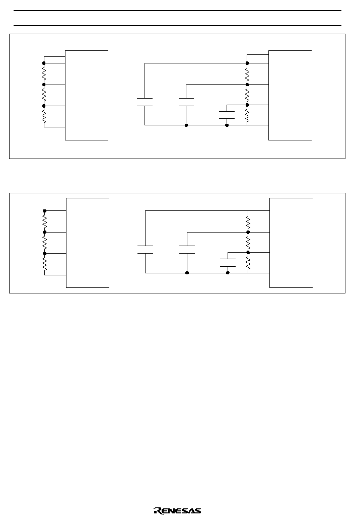
HD404889/HD404899/HD404878/HD404868 Series
147
V0(V
CC
)
V1
V2
V3
GND
R
R
R
C
R
C
C
R
R
V0(V
CC
)
V1
V2
V3
GND
Figure 92-1 Large LCD Panel Drive (Using Power Supply Voltage for V
LCD
)
(HD404889/HD404899/HD404878 Series)
V1
V2
V3
GND
R
R
R
C
R
C
C
R
R
V1
V2
V3
GND
Figure 92-2 Large LCD Panel Drive (Using Power Supply Voltage for V
LCD
) (HD404868 Series)
Usage Notes
When R3
0
/SEG1 to R6
0
/SEG16 pins are used as segment output pins, write their port data register (PDR) to
"0".

HD404889/HD404899/HD404878/HD404868 Series
148
Buzzer Output Circuit
Buzzer Output Circuit Functions: The buzzer output circuit has the following functions.
�
Timer overflow toggle output
�
System clock divided clock pulse output
The block diagram of the buzzer output circuit is shown in figure 93.
Buzzer Output Circuit Operation
�
Timer overflow toggle output operation
The timer overflow toggle output operation setting is made by bits 1 and 2 of the buzzer mode register
(BMR) and bit 2 of port mode register 2 (PMR2). By clearing bit 2 of the buzzer mode register (BMR)
to 0, selecting timer B or timer C overflow by bit 1, and setting bit 2 of port mode register 2 (PMR2) to
1, a toggle waveform is output from the BUZZ pin with overflow as the trigger.
�
System clock divided clock pulse output
The system clock divided clock pulse output operation setting is made by bits 0 to 3 of the buzzer mode
register (BMR) and bit 2 of port mode register 2 (PMR2). Bit 2 of the buzzer mode register (BMR) is
set to 1, the system clock division ratio is selected by bits 0 and 1, and bit 2 of port mode register 2
(PMR2) is set to 1. Clock pulses are output by setting bit 3 of the buzzer mode register (BMR) to 1. If
bit 3 of the buzzer mode register (BMR) is cleared to 0, the BUZZ pin goes low.
The clock pulse width is fixed without regard to the timing set by bit 3 of the buzzer mode register
(BMR), and careful coordination with software is necessary with regard to the number of output pulses.
After a clock pulse modification is made, clock pulses should not be output until 4tcyc after the
modifying instruction.
Only a bit manipulation instruction can be used on bit 3 of the buzzer mode register (BMR).
Buzzer Output Circuit Registers
Buzzer output circuit operation setting is performed by the following registers.
Buzzer mode register (BMR: $02E)
Port mode register 2 (PMR2: $00A)
Buzzer mode register (BMR: $02E):
The buzzer mode register (BMR) is a 4-bit write-only register used to set toggle output by timer overflow
and system clock divided clock pulse output as shown in figure 94.
Bit 3 of the buzzer mode register (BMR) can only accessed by a bit manipulation instruction.
The buzzer mode register (BMR) is reset to $0 by an MCU reset.
HD404889/HD404899/HD404878/HD404868 Series
149
Port mode register 2 (PMR2: $00A):
Port mode register 2 (PMR2) is a 4-bit write-only register used to switch the R1
2
/BUZZ pin function as
shown in figure 30.
Port mode register 2 (PMR2) is reset to $0 by an MCU reset.
BUZZ
Timer B
overflow
�
PER
1/2
(toggle)
Synchro-
nization
circuit
Buzzer
mode
register
Selector
Internal data bus
Data bus
Clock line
Signal line
1/2
1/3
1/4
Selector
Selector
Timer C
overflow
Figure 93 Buzzer Output Circuit
HD404889/HD404899/HD404878/HD404868 Series
150
Bit
Read/Write
Initial value on reset
Bit name
3
W
0
BMR3
2
W
0
BMR2
1
W
0
BMR1
0
W
0
BMR0
Buzzer mode register (BMR: $02E)
BMR2
0
1
BMR1 BMR0
BUZZ pin output
0
*
Division by
2 of timer B overflow
Division by
2 of timer C overflow
1
*
0
�PER clock
0
1
�PER/2clock
0
�PER/3clock
�PER/4clock
1
1
0
Stopped (low level)
Output
1
Clock output control (enabled when BMR2 = 1, bit manipulation instruction)
*
: Don't care
Figure 94 Buzzer Mode Register (BMR)

HD404889/HD404899/HD404878/HD404868 Series
151
ZTAT
TM
Microcomputer with Built-in Programmable ROM
1. Precautions for use of ZTAT
TM
microcomputer with built-in programmable ROM
(1) Precautions for writing to programmable ROM built in ZTAT
TM
microcomputer
In the ZTAT
TM
microcomputer with built-in plastic mold one-time programmable ROM, incomplete
electrical connection between the PROM writer and socket adapter causes writing errors and, makes the
computer unoperatable. To enhance the writing efficiency, attention should be paid to the following points:
(a) Make sure that the socket adapter is firmly fixed to the PROM writer and connected electrically with
each other (neither opened nor shorted), before starting the writing process.
(b) To secure the electrical connection between the contact pin and IC lead, make sure that there is no
foreign substance on the contact pin of the socket adapter, which may cause improper electrical
connection.
(c) When inserting the IC, be careful to protect the IC lead from bending in order to secure the electrical
connection between the contact pin and IC lead. If the lead is bent, correct the bending and insert it
again.
(d) If any trouble is noticed during a blank check to be performed to prevent erroneous writing due to
improper electrical connection, carry out the writing process again according to above steps (a), (b), and
(c).
(e) During the writing process, do not touch the socket adapter and IC to prevent erroneous writing.
(f) To write continuously in the IC, follow steps (a), (b), (c), (d) and (e).
(g) If a writing error recurs, or the rate of writing errors occur frequently, stop writing and check the PROM
writer, socket adapter, etc. for defects.
(h) If any problem is noticed in the written program or in the program after being left at a high temperature,
consult our technical staff.
(2) Precautions when new PROM writer, socket adapter or IC is used
When a new PROM writer, socket adapter or IC is employed, breakdown of the IC may occur or its writing
may become impossible because the noise, overshoot, timing or other electrical characteristics may be
inconsistent with the assured IC writing characteristics. To avoid such troubles, check the following points
before starting the writing process.
(a) To ensure stable writing operation, check that the V
CC
of the power supplied to the PROM writer,
power source current capacity of V
PP
, and current consumption at the time of writing to IC are provided
with sufficient margin.
(b) To prevent breakdown of the IC, check that the power source voltage between GND-V
CC
and GND-
V
PP
, and overshoot or undershoot of the power source at the connecting terminal of the socket adapter
are within the ratings. Particularly, if the overshoot or undershoot exceeds the maximum rating, the p-n
connection may be damaged, leading to permanent breakdown. If overshoot or undershoot occurs,
recheck the power source damping resistance of capacity.
(c) To prevent breakdown of the IC and for stable writing and reading operation, insert the IC into the
socket adapter and check the power noise between the GND-V
CC
and GND-V
PP
near the IC connecting

HD404889/HD404899/HD404878/HD404868 Series
152
terminal. If power source noise is noticed, insert an appropriate capacitor between the GND power
sources depending on the noise generated. In case of high frequency noise , insert a capacitor of low
inductance.
(d) For stable writing and reading operation, insert the IC into the socket adapter and check the input
waveform, timing and noise near the R/W, CS, address and data terminals. Particularly, since recent
ICs have increased in speed, caution should be exercised against the noise to the power source or
address due to crosstalk from the output data terminal. To avoid these problems, inserting a low
inductance capacitor between the GND and power source or inserting a damping resistance to the output
data terminal is effective.
(e) Particularly, when a multiple PROM writer is used, perform above items (a), (b), (c), and (d) assuming
all ICs inserted into the socket adapter.
(f) In the case of a multiple PROM writer, when an unacceptable result is noticed during a blank check
performed to prevent erroneous writing due to improper electrical connection of the power source, etc.,
rewriting is impossible unless every writing process can be stopped. Therefore, the potential increases
due to erroneous writing because of improper connection. Be sure to check the electrical connection
between the PROM writer and socket adapter and IC.
(g) If any abnormality is noticed while checking a written program, consult our technical staff.
2. Programming of Built-in programmable ROM
The MCU can stop its function as an MCU in PROM mode for programming the built-in PROM.
PROM mode is set by driving the
RESET, M
0
, and
M
1
pins low (or by driving the
RESET and M
0
pins low
in the HD4074869), and driving the TEST pin to the V
PP
level.
Writing and reading specifications of the PROM are the same as those for the commercial EPROM27256.
Using a socket adapter for specific use of each product, programming is possible with a general-purpose
PROM writer.
Since an instruction of the HMCS400 series is 10 bits long, a conversion circuit is incorporated to adapt the
general-purpose PROM writer. This circuit splits each instruction into five lower bits and five higher bits
to write from or read to two addresses. This enables use of a general-purpose PROM. For instance, to
write to a 16kword of built-in PROM writer with a general-purpose PROM, specify 32kbyte address
($0000-$7FFF). An example of PROM memory map is shown in figure 95.
Notes:
1. When programming with a PROM writer, set up each ROM size to the address given in table 30. If it is
programmed erroneously to an address given in table 30 or later, check of writing of PROM may
become impossible. Particularly, caution should be exercised in the case of a plastic package since
reprogramming is impossible with it. Set the data in unused addresses to $FF.
2. If the indexes of the PROM writer socket, socket adapter and product are not aligned precisely, the
product may break down due to overcurrent. Be sure to check that they are properly set to the writer
before starting the writing process.

HD404889/HD404899/HD404878/HD404868 Series
153
3. Two levels of program voltages (V
PP
) are available for the PROM: 12.5V and 21V. Our product
employs a V
PP
of 12.5V. If a voltage of 21V is applied, permanent breakdown of the product will
result. The V
PP
of 12.5V is obtained for the PROM writer by setting it according to the Intel 27258
specifications.
Table 28
Socket Adapters
Package
Model Name
Manufacturer
FP-80A
Please ask Hitachi service section.
TFP-80C
Please ask Hitachi service section.
FP-64A
Please ask Hitachi service section.
DP-64S
Please ask Hitachi service section.
Writing/verification
Programming of the built-in program ROM employs a high speed programming method. With this method,
high speed writing is effected without voltage stress to the device or without damaging the reliability of the
written data.
A basic programming flow chart is shown in figure 96 and a timing chart in figure 97.
For precautions for PROM writing procedure, refer to Section 2, "Characteristics of ZTAT
TM
Microcomputer's Built-in Programmable ROM and precautions for its Applications."
Table 29
Selection of Mode
Mode
CE
OE
V
PP
O
0
to O
4
Writing
"Low"
"High"
V
PP
Data input
Verification
"High"
"Low"
V
PP
Data output
Prohibition of programming
"High"
"High"
V
PP
High impedance
Table 30
PROM Writer Program Address
ROM size
Address
8k
$0000~$3FFF
12k
$0000~$5FFF
16k
$0000~$7FFF

HD404889/HD404899/HD404878/HD404868 Series
154
Programmable Rom (HD4074889, HD4074899, HD4074869)
The HD4074889, HD4074899, and HD4074869 are a ZTAT
TM
microcomputers with built-in PROM that
can be programmed in PROM mode.
PROM Mode Pin Description
HD4074889, HD4074899
Pin No.
MCU Mode
PROM Mode
Pin No.
MCU Mode
PROM Mode
FP-80A
TFP-80C
Pin Name
I/O
Pin Name
I/O
FP-80A
TFP-80C
Pin Name
I/O
Pin Name
I/O
1
AV
CC
--
V
CC
--
41
R3
0
/SEG1
I/O
A
1
I
2
R7
0
/AN0
I/O
V
CC
--
42
R3
1
/SEG2
I/O
A
2
I
3
R7
1
/AN1
I/O
V
CC
--
43
R3
2
/SEG3
I/O
A
3
I
4
R7
2
/AN2
I/O
44
R3
3
/SEG4
I/O
A
4
I
5
R7
3
/AN3
I/O
45
R4
0
/SEG5
I/O
O
0
I/O
6
R8
0
/AN4
I/O
46
R4
1
/SEG6
I/O
O
1
I/O
7
R8
1
/AN5
I/O
47
R4
2
/SEG7
I/O
O
2
I/O
8
AV
SS
--
GND
--
48
R4
3
/SEG8
I/O
O
3
I/O
9
TEST
I
V
PP
--
49
R5
0
/SEG9
I/O
O
4
I/O
10
OSC1
I
V
CC
--
50
R5
1
/SEG10
I/O
O
4
I/O
11
OSC2
O
51
R5
2
/SEG11
I/O
O
3
I/O
12
GND
--
GND
--
52
R5
3
/SEG12
I/O
O
2
I/O
13
X2
O
53
R6
0
/SEG13
I/O
O
1
I/O
14
X1
I
GND
--
54
R6
1
/SEG14
I/O
O
0
I/O
15
RESET
I
RESET
I
55
R6
2
/SEG15
I/O
16
V
CC
--
V
CC
--
56
R6
3
/SEG16
I/O
17
D
0
/
INT
0
I/O
A
0
I
57
SEG17
O
18
D
1
/INT
1
I/O
58
SEG18
O
19
D
2
I/O
A
5
I
59
SEG19
O
20
D
3
I/O
A
6
I
60
SEG20
O
21
D
4
I/O
A
7
I
61
SEG21
O
22
D
5
I/O
A
8
I
62
SEG22
O
23
D
6
I/O
A
9
I
63
SEG23
O
24
D
7
I/O
A
10
I
64
SEG24
O
25
D
8
I/O
A
11
I
65
SEG25
O
26
D
9
I/O
A
12
I
66
SEG26
O
27
D
10
I/O
A
13
I
67
SEG27
O
28
D
11
I/O
A
14
I
68
SEG28
O
29
R0
0
/
WU
0
I/O
V
CC
--
69
SEG29
O
30
R0
1
/
WU
1
I/O
70
SEG30
O
31
R0
2
/
WU
2
I/O
71
SEG31
O
32
R0
3
/
WU
3
I/O
72
SEG32
O
33
R1
0
/EVNB
I/O
73
COM1
O
34
R1
1
/EVND
I/O
M0
I
74
COM2
O
35
R1
2
/BUZZ
I/O
M1
I
75
COM3
O
36
R1
3
/TOB
I/O
CE
I
76
COM4
O
37
R2
0
/TOC
I/O
77
V3
--
38
R2
1
/
SCK
I/O
OE
I
78
V2
--
39
R2
2
/SI/SO
I/O
XM0
O
79
V1
--
V
CC
--
40
R2
3
I/O
XM1
O
80
V0
--
V
CC
--
HD404889/HD404899/HD404878/HD404868 Series
155
HD4074869
Pin No.
MCU Mode
PROM Mode
Pin No.
MCU Mode
PROM Mode
FP-64A
DP-64S
Pin Name
I/O
Pin Name
I/O
FP-64A
DP-64S
Pin Name
I/O
Pin Name
I/O
1
8
R7
0
/AN0
I/O
V
CC
--
33
40
R2
3
I/O
A
14
I
2
9
R7
1
/AN1
I/O
V
CC
--
34
41
R3
0
/SEG1
I/O
A
1
I
3
10
R7
2
/AN2
I/O
35
42
R3
1
/SEG2
I/O
A
2
I
4
11
R7
3
/AN3
I/O
36
43
R3
2
/SEG3
I/O
A
3
I
5
12
TEST
I
V
PP
--
37
44
R3
3
/SEG4
I/O
A
4
I
6
13
OSC1
I
V
CC
--
38
45
R4
0
/SEG5
I/O
O
0
I/O
7
14
OSC2
O
39
46
R4
1
/SEG6
I/O
O
1
I/O
8
15
GND
--
GND
--
40
47
R4
2
/SEG7
I/O
O
2
I/O
9
16
X2
O
41
48
R4
3
/SEG8
I/O
O
3
I/O
10
17
X1
I
GND
--
42
49
R5
0
/SEG9
I/O
O
4
I/O
11
18
RESET
I
RESET
I
43
50
R5
1
/SEG10
I/O
O
4
I/O
12
19
V
CC
--
V
CC
--
44
51
R5
2
/SEG11
I/O
O
3
I/O
13
20
D
0
/
INT
0
I/O
A
0
I
45
52
R5
3
/SEG12
I/O
O
2
I/O
14
21
D
1
/INT
1
I/O
46
53
R6
0
/SEG13
I/O
O
1
I/O
15
22
D
2
I/O
A
5
I
47
54
R6
1
/SEG14
I/O
O
0
I/O
16
23
D
3
I/O
A
6
I
48
55
R6
2
/SEG15
I/O
17
24
D
4
I/O
A
7
I
49
56
R6
3
/SEG16
I/O
18
25
D
5
I/O
A
8
I
50
57
SEG17
O
19
26
D
6
I/O
A
9
I
51
58
SEG18
O
20
27
D
7
I/O
A
10
I
52
59
SEG19
O
21
28
D
8
I/O
A
11
I
53
60
SEG20
O
22
29
D
9
I/O
A
12
I
54
61
SEG21
O
23
30
R0
0
/
WU
0
I/O
V
CC
--
55
62
SEG22
O
24
31
R0
1
/
WU
1
I/O
56
63
SEG23
O
25
32
R0
2
/
WU
2
I/O
57
64
SEG24
O
26
33
R1
0
/EVNB
I/O
58
1
COM1
O
27
34
R1
1
I/O
A
13
I
59
2
COM2
O
28
35
R1
2
/BUZZ
I/O
M0
I
60
3
COM3
O
29
36
R1
3
/TOB
I/O
CE
I
61
4
COM4
O
30
37
R2
0
/TOC
I/O
XM1
O
62
5
V
3
--
31
38
R2
1
/
SCKN
I/O
OE
I
63
6
V
2
--
32
39
R2
2
/SI/SO
I/O
XM0
O
64
7
V
1
--
V
CC
--
Notes: 1. I/O: I/O pin, I: Input-only pin, O: Output-only pin
2. As there are two each of pins O
0
to O
4
, the respective pairs should be shorted.
3. Unused data pins (O
5
to O
7
) on the PROM programmer side should be handled as shown below
on the socket.
V
CC
O
5
, O
6
, O
7
4. Pin A
9
should be handled as shown below on the socket.
V
CC
HD4074889
HD4074899
HD4074869
Writer side
A
9

HD404889/HD404899/HD404878/HD404868 Series
156
2. Pin Functions in PROM Mode
V
PP
:
Applies the on-chip PROM programming voltage (12.5 V
�
0.3 V).
CE:
Inputs a control signal to set the on-chip PROM to the write/verify enabled state.
OE:
Inputs a data output control signal during verification.
A
0
to A
14
:
On-chip PROM address input pins.
O
0
to O
4
:
On-chip PROM data bus I/O pins.
As there are two each of pins O
0
to O
4
, the respective pairs should be shorted.
M
0
,
M
1
,
RESET, TEST:
PROM mode setting pins. PROM mode is set by driving the
M
0
,
M
1
, and
RESET pins low (or by driving
the
M
0
, and
RESET pins low in the HD4074869), and driving the TEST pin to the V
PP
level.
Other pins:
V
CC
, AV
CC
, R7
0
/AN
0
, R7
1
/AN
1
, OSC
1
, V
0
, and V
1
should be connected to V
CC
potential.
GND, AV
SS
, and X1 should be connected to GND potential.
Other pins should be left open.

HD404889/HD404899/HD404878/HD404868 Series
157
$0000
1
1
1
1
1
1
Vector address
Zero-page subroutine
(64 words)
Pattern
(4,096 words)
Program
(16,384 words)
$0001
$001F
$0080
$007F
$2000
$1FFF
$0020
$7FFF
Bit 4
Bit 8
Bit 3
Bit 7
Bit 2
Bit 6
Bit 1
Bit 5
Bit 0
Bit 9
Upper three bits are not to be used
(fill them with 111)
Upper 5 bits
Lower 5 bits
$0000
$000F
$0010
$003F
$0040
$3FFF
$0000
$0001
$0002
$0003
$0004
$0005
$0006
$0007
$0008
$0009
$000A
$000B
$000C
$000D
$000E
$000F
JMPL instruction
(jump to
RESET
routine)
JMPL instruction
(jump to
WU
0
to
WU
3
JMPL instruction
(jump to
INT
1
routine)
JMPL instruction
(jump to timer A routine)
JMPL instruction
(jump to
INT
0
routine)
JMPL instruction
(jump to timer B, timer D routine)
JMPL instruction
(jump to timer C routine)
.
.
.
.
.
.
.
.
.
JMPL instruction
(jump to A/D, serial routine)
$0FFF
$1000
Figure 95 Memory Map in PROM Mode
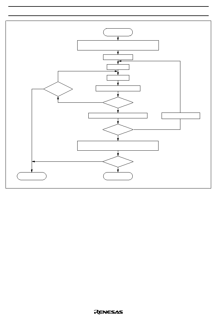
HD404889/HD404899/HD404878/HD404868 Series
158
Start
Set Prog./Verify Mode
V
PP
=12.5
�
0.3V, V
CC
=6.0
�
0.25V
Address=0
n=0
n+1
n
Program t
PW
= 1ms
�
5%
Verify
Go
Program t
OPW
= 3nms
Last
Address?
Yes
No
NoGo
Set Read Mode
V
CC
=5.0
�
0.5V, V
PP
=V
CC
�
0.6V
Read
All Address
Go
End
Address + 1
Address
Yes
n<S
No
S=25
NoGo
Fail
Figure 96 Flowchart of High-Speed Programming

HD404889/HD404899/HD404878/HD404868 Series
159
Programming Electrical Characteristics
DC Characteristics (V
CC
= 6V
�
0.25V, V
PP
= 12.5V
�
0.3V, V
SS
= 0V, T
a
= 25
�
C
�
5
�
C, unless
otherwise specified)
Item
Symbol
Test Conditions
min
typ
max
Unit
Input high voltage
O
0
to O
4
,A
0
to A
14
,
OE
,
CE
V
IH
2.2
--
V
CC
+0.3 V
Input low voltage
O
0
to O
4
,A
0
to A
14
,
OE
,
CE
V
IL
�0.3
--
0.8
V
Output high voltage
O
0
to O
4
V
OH
I
OH
=�200
�
A
2.4
--
--
V
Output low voltage
O
0
to O
4
V
OL
I
OL
=1.6mA
--
--
0.4
V
Input leakage current O
0
to O
4
,A
0
to A
14
,
OE
,
CE
I
IL
V
in
=5.25V/0.5V
--
--
2
�
A
V
CC
current
I
CC
--
--
30
mA
V
PP
current
I
PP
--
--
40
mA
AC Characteristics (V
CC
= 6V
�
0.25V, V
PP
= 12.5V
�
0.3V, T
a
= 25
�
C
�
5
�
C, unless otherwise
specified)
Item
Symbol
Test Conditions
min
typ
max
Unit
Address setup time
t
AS
2
--
--
�
s
OE
setup time
t
OES
2
--
--
�
s
Data setup time
t
DS
2
--
--
�
s
Address hold time
t
AH
0
--
--
�
s
Data hold time
t
DH
2
--
--
�
s
Data output disable time
t
DF
See figure 89
--
--
130
ns
V
PP
setup time
t
VPS
2
--
--
�
s
Program pulse width
t
PW
0.95
1.0
1.05
ms
CE
pulse width during overprogramming
t
OPW
2.85
--
78.75
ms
V
CC
setup time
t
VCS
2
--
--
�
s
Data output delay time
t
OE
0
--
500
ns
Notes: Input pulse level: 0.8 V to 2.2 V
Input rise/fall times:
20ns
Input timing reference levels: 1.0 V, 2.0 V
Output timing reference levels: 0.8 V, 2.0 V
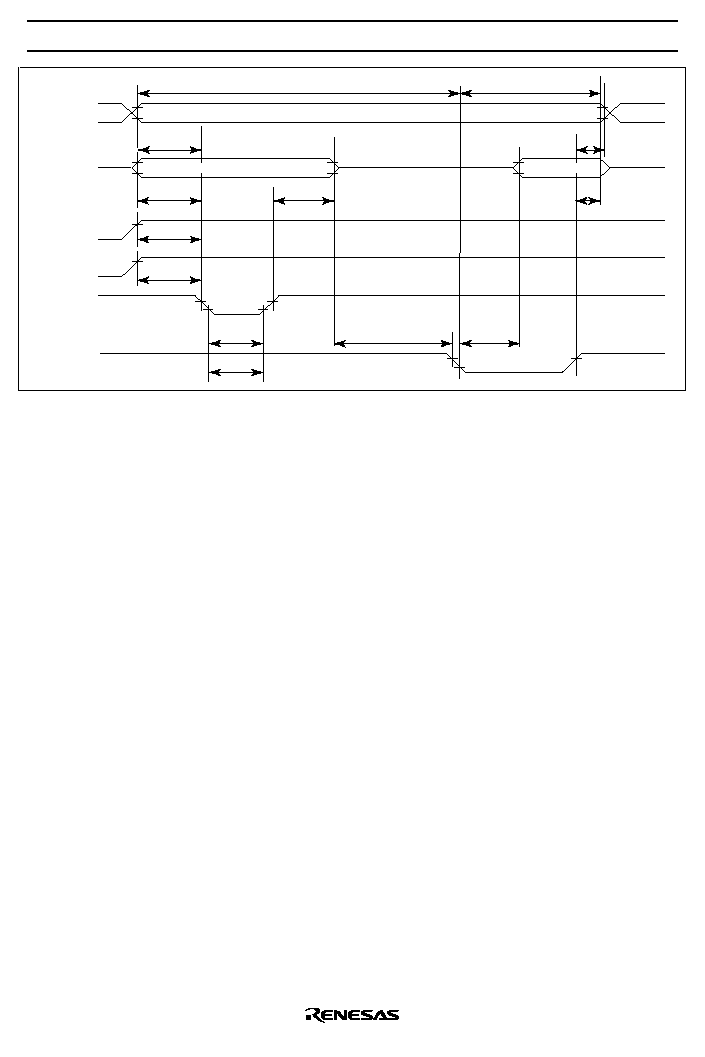
HD404889/HD404899/HD404878/HD404868 Series
160
Write
Verify
Address
Data
V
PP
V
CC
V
CC
V
PP
V
CC
GND
CE
OE
Data In Stable
Data Out Valid
t
AS
t
DS
t
DH
t
DF
t
AH
t
PW
t
OES
t
OE
t
OPW
t
VPS
t
VCS
Figure 97 PROM Write/Verify Timing

HD404889/HD404899/HD404878/HD404868 Series
161
Notes on PROM Programming
Principles of Programming/Erasure: A memory cell in a ZTATTM microcomputer is the same as an
EPROM cell; it is programmed by applying a high voltage between its control gate and drain to inject hot
electrons into its floating gate. These electrons are stable, surrounded by an energy barrier formed by an
SiO
2
film. The change in threshold voltage of a memory cell with a charged floating gate makes the
corresponding bit appear as 0; a cell whose floating gate is not charged appears as a 1 bit (figure 98).
The charge in a memory cell may decrease with time. This decrease is usually due to one of the following
causes:
�
Ultraviolet light excites electrons, allowing them to escape. This effect is the basis of the erasure
principle.
�
Heat excites trapped electrons, allowing them to escape.
�
High voltages between the control gate and drain may erase electrons.
If the oxide film covering a floating gate is defective, the electron erasure rate will be greater. However,
electron erasure does not often occur because defective devices are detected and removed at the testing
stage.
Control gate
Floating gate
Drain
SiO
2
Source
N
N
+
+
Control gate
Floating gate
Drain
SiO
2
Source
N
N
+
+
Erasure (1)
Write (0)
Figure 98 Cross-Sections of a PROM Cell
PROM Programming: PROM memory cells must be programmed under specific voltage and timing
conditions. The higher the programming voltage V
PP
and the longer the programming pulse t
PW
is applied,
the more electrons are injected into the floating gates. However, if V
PP
exceeds specifications, the pn
junctions may be permanently damaged. Pay particular attention to overshooting in the PROM
programmer. In addition, note that negative voltage noise will produce a parasitic transistor effect that may
reduce breakdown voltages.
The ZTATTM microcomputer is electrically connected to the PROM programmer by a socket adapter.
Therefore, note the following points:
�
Check that the socket adapter is firmly mounted on the PROM programmer.
�
Do not touch the socket adapter or the LSI during the programming. Touching them may affect the
quality of the contacts, which will cause programming errors.

HD404889/HD404899/HD404878/HD404868 Series
162
PROM Reliability after Programming: In general, semiconductor devices retain their reliability,
provided that some initial defects can be excluded. These initial defects can be detected and rejected by
screening. Baking devices under high-temperature conditions is one method of screening that can rapidly
eliminate data-hold defects in memory cells. (Refer to the previous Principles of Programming/Erasure
section.)
ZTATTM microcomputer devices are extremely reliable because they have been subjected to such a
screening method during the wafer fabrication process, but Hitachi recommends that each device be
exposed to 150
�
C at one atmosphere for at least 48 hours after it is programmed, to ensure its best
performance. The recommended screening procedure is shown in figure 99.
Note:
If programming errors occur continuously during PROM programming, suspend programming and
check for problems in the PROM programmer or socket adapter. If programming verification
indicates errors in programming or after high-temperature exposure, please inform Hitachi.
Note: Exposure time is measured from when the temperature in the heater reaches 150
�
C.
Programming, verification
Exposure to high temperature, without power
150
�
C
�
10
�
C, 48 h
+8 h
0 h
�
*
Program read check
V = 4.5 V or 5.5 V
CC
Figure 99 Recommended Screening Procedure

HD404889/HD404899/HD404878/HD404868 Series
163
Addressing Modes
RAM Addressing Modes
The MCU has three RAM addressing modes, as shown in figure 100 and described below.
Register Indirect Addressing Mode: The contents of the W, X, and Y registers (10 bits in total) are used
as a RAM address.
Direct Addressing Mode: A direct addressing instruction consists of two words. The first word contains
the opcode, and the contents of the second word (10 bits) are used as a RAM address.
Memory Register Addressing Mode: The memory registers (MR), which are located in 16 addresses from
$040 to $04F, are accessed with the LAMR and XMRA instructions.
AP
9
AP
0
W
1
Y
0
W register
X register
Y register
RAM address
Register Indirect Addressing
AP
9
AP
0
RAM address
Direct Addressing
d
9
d
0
2nd word of Instruction
Opcode
1st word of Instruction
AP
9
AP
0
RAM address
Memory Register Addressing
m
3
Opcode
Instruction
0
0
0
1
0
0
AP
8
AP
7
AP
AP
5
AP
4
6
AP
3
AP
2
AP
1
AP
AP
AP
AP
AP
AP
AP
AP
8
7
6
5
4
3
2
1
d
8
d
7
d
6
d
5
d
4
d
3
d
2
d
1
AP
8
AP
7
AP
6
AP
5
AP
4
AP
3
AP
2
AP
1
W
0
X
3
X
2
X
1
X
0
Y
3
Y
2
Y
1
m
2
m
1
m
0
Figure 100 RAM Addressing Modes

HD404889/HD404899/HD404878/HD404868 Series
164
ROM Addressing Modes and the P Instruction
The MCU has four ROM addressing modes, as shown in figure 101 and described below.
Direct Addressing Mode: A program can branch to any address in the ROM memory space by executing
the JMPL, BRL, or CALL instruction. Each of these instructions replaces the 14 program counter bits
(PC
13
�PC
0
) with 14-bit immediate data.
Current Page Addressing Mode: The MCU has 64 pages of ROM with 256 words per page. A program
can branch to any address in the current page by executing the BR instruction. This instruction replaces the
eight low-order bits of the program counter (PC
7
�PC
0
) with eight-bit immediate data. If the BR instruction
is on a page boundary (address 256n + 255), executing that instruction transfers the PC contents to the next
physical page, as shown in figure 103. This means that the execution of the BR instruction on a page
boundary will make the program branch to the next page.
Note that the HMCS400-series cross assembler has an automatic paging feature for ROM pages.
Zero-Page Addressing Mode: A program can branch to the zero-page subroutine area located at $0000�
$003F by executing the CAL instruction. When the CAL instruction is executed, 6 bits of immediate data
are placed in the six low-order bits of the program counter (PC
5
�PC
0
), and 0s are placed in the eight high-
order bits (PC
13
�PC
6
).
Table Data Addressing Mode: A program can branch to an address determined by the contents of four-bit
immediate data, the accumulator, and the B register by executing the TBR instruction.
P Instruction: ROM data addressed in table data addressing mode can be referenced with the P instruction
as shown in figure 102. If bit 8 of the ROM data is 1, eight bits of ROM data are written to the accumulator
and the B register. If bit 9 is 1, eight bits of ROM data are written to the R1 and R2 port output registers. If
both bits 8 and 9 are 1, ROM data is written to the accumulator and the B register, and also to the R1 and
R2 port output registers at the same time.
The P instruction has no effect on the program counter.
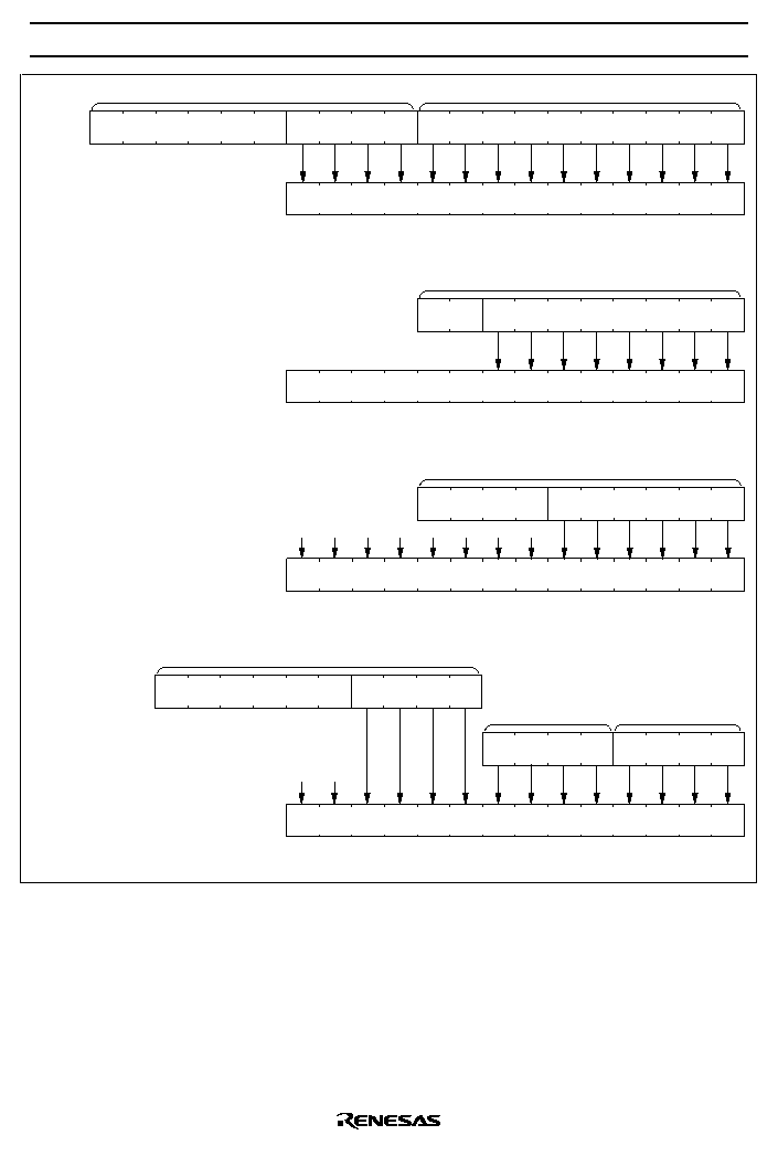
HD404889/HD404899/HD404878/HD404868 Series
165
d
9
d
8
d
7
d
6
d
5
d
4
d
3
d
2
d
1
d
0
2nd word of instruction
Opcode
1st word of instruction
[JMPL]
[BRL]
[CALL]
PC
9
PC
8
PC
7
PC
6
PC
5
PC
4
PC
3
PC
2
PC
1
PC
0
PC
PC
PC
PC
10
11
12
13
Program counter
Direct Addressing
Zero Page Addressing
d
5
d
4
d
3
d
2
d
1
d
0
Instruction
[CAL]
Opcode
PC
9
8
PC
7
6
PC
5
4
PC
3
PC
1
PC
0
PC
PC
10
11
12
13
Program counter
0
0
0
0
0
0
0
0
PC
PC
PC
PC
PC
PC
2
B
1
B
0
A
3
A
2
A
1
A
0
Accumulator
Program counter
Table Data Addressing
PC
9
PC
8
PC
7
PC
6
PC
5
PC
4
PC
3
PC
2
PC
1
PC
0
PC
PC
PC
10
11
12
13
B
2
B
3
B register
p
3
p
0
[TBR]
Instruction
Opcode
0
0
p
2
p
1
PC
Opcode
b
7
b
6
b
5
b
4
b
3
b
2
b
1
b
0
Instruction
PC
9
0
PC
PC
PC
11
12
13
Program counter
Current Page Addressing
[BR]
PC
10
7
PC
6
PC
5
PC
4
PC
3
PC
2
PC
1
PC
PC
8
PC
p
0
p
1
p
2
p
3
Figure 101 ROM Addressing Modes
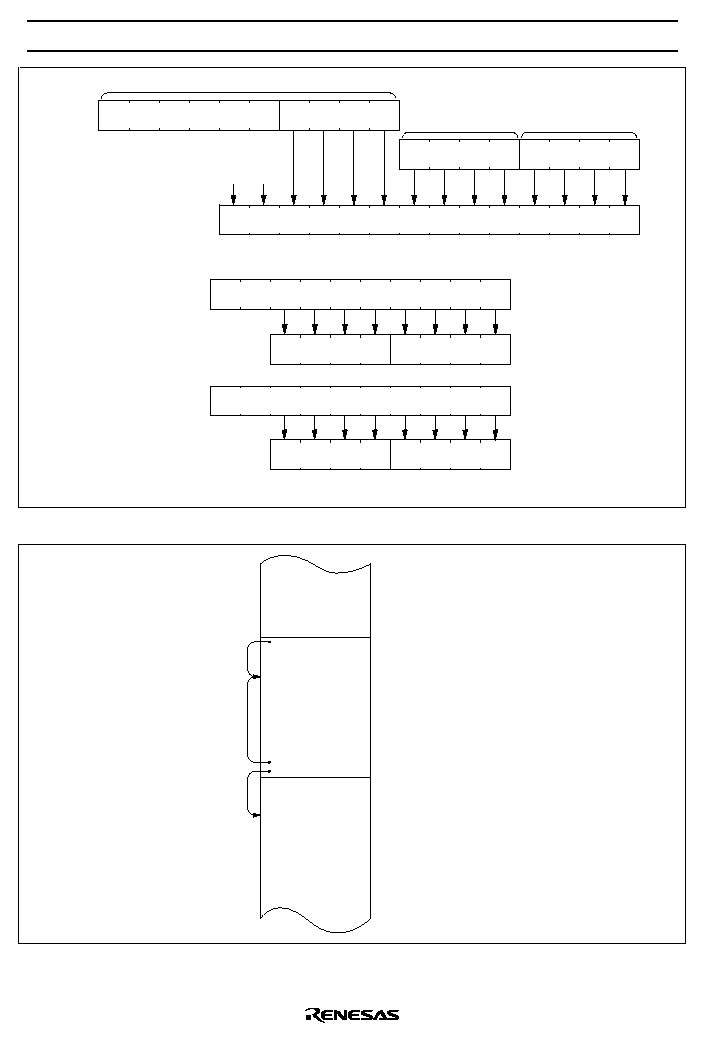
HD404889/HD404899/HD404878/HD404868 Series
166
B
1
B
0
A
3
A
2
A
1
A
0
Accumulator
Referenced ROM address
Address Designation
RA
9
RA
8
RA
7
RA
6
RA
5
RA
4
RA
3
RA
2
RA
1
RA
0
RA
RA
RA
10
11
12
13
B
2
B
3
B register
0
0
p
3
p
0
[P]
Instruction
Opcode
p
2
p
1
RA
RO
9
RO
0
RO
8
RO
7
RO
6
RO
5
RO
4
RO
3
RO
2
RO
1
B
B
B
B
A
A
A
A
3
2
1
0
3
2
1
0
If RO = 1
8
Accumulator, B register
ROM data
Pattern Output
RO
9
ROM data
R2
3
R2
2
R2
1
R2
0
R1
3
R1
2
R1
1
R1
0
If RO = 1
9
Output registers R1, R2
RO
0
RO
8
RO
7
RO
6
RO
5
RO
4
RO
3
RO
2
RO
1
Figure 102 P Instruction
BR AAA
AAA NOP
256 (n � 1) + 255
256n
BR AAA
BR BBB
256n + 254
256n + 255
256 (n + 1)
BBB NOP
Figure 103 Branching when the Branch Destination is on a Page Boundary

HD404889/HD404899/HD404878/HD404868 Series
167
Instruction Set
The MCU Series has 101 instructions, classified into the following 10 groups:
�
Immediate instructions
�
Register-to-register instructions
�
RAM addressing instructions
�
RAM register instructions
�
Arithmetic instructions
�
Compare instructions
�
RAM bit manipulation instructions
�
ROM addressing instructions
�
Input/output instructions
�
Control instructions
The functions of these instructions are listed in tables 31 to 40, and an opcode map is shown in table 41.
Table 31
Immediate Instructions
Operation
Mnemonic
Operation Code
Function
Status
Words/
Cycles
Load A from immediate
LAI i
1
0
0
0
1
1 i
3
i
2
i
1
i
0
i
A
1/1
Load B from immediate
LBI i
1
0
0
0
0
0 i
3
i
2
i
1
i
0
i
B
1/1
Load memory from
immediate
LMID i,d
0
1
1
0
1
0 i
3
i
2
i
1
i
0
d
9
d
8
d
7
d
6
d
5
d
4
d
3
d
2
d
1
d
0
i
M
2/2
Load memory from
immediate, increment Y
LMIIY i
1
0
1
0
0
1 i
3
i
2
i
1
i
0
i
M, Y + 1
Y
NZ
1/1

HD404889/HD404899/HD404878/HD404868 Series
168
Table 32
Register-Register Instructions
Operation
Mnemonic
Operation Code
Function
Status
Words/
Cycles
Load A from B
LAB
0
0
0
1
0
0 1
0
0
0
B
A
1/1
Load B from A
LBA
0
0
1
1
0
0 1
0
0
0
A
B
1/1
Load A from W
LAW
0
1
0
0
0
0 0
0
0
0
0
0
0
0
0
0 0
0
0
0
W
A
2/2*
Load A from Y
LAY
0
0
1
0
1
0 1
1
1
1
Y
A
1/1
Load A from SPX
LASPX
0
0
0
1
1
0 1
0
0
0
SPX
A
1/1
Load A from SPY
LASPY
0
0
0
1
0
1 1
0
0
0
SPY
A
1/1
Load A from MR
LAMR m
1
0
0
1
1
1 m
3
m
2
m
1
m
0
MR (m)
A
1/1
Exchange MR and A
XMRA m
1
0
1
1
1
1 m
3
m
2
m
1
m
0
MR (m)
A
1/1
Note:
The assembler automatically provides an operand for the second word of the LAW instruction.
Table 33
RAM Address Instructions
Operation
Mnemonic
Operation Code
Function
Status
Words/
Cycles
Load W from immediate
LWI i
0
0
1
1
1
1 0
0
i
1
i
0
i
W
1/1
Load X from immediate
LXI i
1
0
0
0
1
0 i
3
i
2
i
1
i
0
i
X
1/1
Load Y from immediate
LYI i
1
0
0
0
0
1 i
3
i
2
i
1
i
0
i
Y
1/1
Load W from A
LWA
0
1
0
0
0
1 0
0
0
0
0
0
0
0
0
0 0
0
0
0
A
W
2/2*
Load X from A
LXA
0
0
1
1
1
0 1
0
0
0
A
X
1/1
Load Y from A
LYA
0
0
1
1
0
1 1
0
0
0
A
Y
1/1
Increment Y
IY
0
0
0
1
0
1 1
1
0
0
Y + 1
Y
NZ
1/1
Decrement Y
DY
0
0
1
1
0
1 1
1
1
1
Y � 1
Y
NB
1/1
Add A to Y
AYY
0
0
0
1
0
1 0
1
0
0
Y + A
Y
OVF
1/1
Subtract A from Y
SYY
0
0
1
1
0
1 0
1
0
0
Y � A
Y
NB
1/1
Exchange X and SPX
XSPX
0
0
0
0
0
0 0
0
0
1
X
SPX
1/1
Exchange Y and SPY
XSPY
0
0
0
0
0
0 0
0
1
0
Y
SPY
1/1
Exchange X and SPX,
Y and SPY
XSPXY
0
0
0
0
0
0 0
0
1
1
X
SPX,Y
SPY
1/1
Note:
The assembler automatically provides an operand for the second word of the LWA instruction.

HD404889/HD404899/HD404878/HD404868 Series
169
Table 34
RAM Register Instructions
Operation
Mnemonic
Operation Code
Function
Status
Words/
Cycles
Load A from memory
LAM
0
0
1
0
0
1 0
0
0
0
M
A
1/1
LAMX
0
0
1
0
0
1 0
0
0
1
M
A
X
SPX
LAMY
0
0
1
0
0
1 0
0
1
0
M
A
Y
SPY
LAMXY
0
0
1
0
0
1 0
0
1
1
M
A
X
SPX, Y
SPY
Load A from memory
LAMD d
0
1
1
0
0
1 0
0
0
0
d
9
d
8
d
7
d
6
d
5
d
4
d
3
d
2
d
1
d
0
M
A
2/2
Load B from memory
LBM
0
0
0
1
0
0 0
0
0
0
M
B
1/1
LBMX
0
0
0
1
0
0 0
0
0
1
M
B
X
SPX
LBMY
0
0
0
1
0
0 0
0
1
0
M
B
Y
SPY
LBMXY
0
0
0
1
0
0 0
0
1
1
M
B
X
SPX, Y
SPY
Load memory from A
LMA
0
0
1
0
0
1 0
1
0
0
A
M
1/1
LMAX
0
0
1
0
0
1 0
1
0
1
A
M
X
SPX
LMAY
0
0
1
0
0
1 0
1
1
0
A
M
Y
SPY
LMAXY
0
0
1
0
0
1 0
1
1
1
A
M
X
SPX, Y
SPY
Load memory from A
LMAD d
0
1
1
0
0
1 0
1
0
0
d
9
d
8
d
7
d
6
d
5
d
4
d
3
d
2
d
1
d
0
A
M
2/2
Load memory from A,
increment Y
LMAIY
0
0
0
1
0
1 0
0
0
0
A
M, Y + 1
Y
NZ
1/1
LMAIYX
0
0
0
1
0
1 0
0
0
1
A
M, Y + 1
Y
X
SPX
Load memory from A,
decrement Y
LMADY
0
0
1
1
0
1 0
0
0
0
A
M, Y � 1
Y
NB
1/1
LMADYX
0
0
1
1
0
1 0
0
0
1
A
M, Y � 1
Y
X
SPX

HD404889/HD404899/HD404878/HD404868 Series
170
Table 34
RAM Register Instructions (cont)
Operation
Mnemonic
Operation Code
Function
Status
Words/
Cycles
Exchange memory
and A
XMA
0
0
1
0
0
0 0
0
0
0
M
A
1/1
XMAX
0
0
1
0
0
0 0
0
0
1
M
A
X
SPX
XMAY
0
0
1
0
0
0 0
0
1
0
M
A
Y
SPY
XMAXY
0
0
1
0
0
0 0
0
1
1
M
A
X
SPX, Y
SPY
Exchange memory
and A
XMAD d
0
1
1
0
0
0 0
0
0
0
d
9
d
8
d
7
d
6
d
5
d
4
d
3
d
2
d
1
d
0
M
A
2/2
Exchange memory
and B
XMB
0
0
1
1
0
0 0
0
0
0
M
B
1/1
XMBX
0
0
1
1
0
0 0
0
0
1
M
B
X
SPX
XMBY
0
0
1
1
0
0 0
0
1
0
M
B
Y
SPY
XMBXY
0
0
1
1
0
0 0
0
1
1
M
B
X
SPX, Y
SPY
HD404889/HD404899/HD404878/HD404868 Series
171
Table 35
Arithmetic Instructions
Operation
Mnemonic
Operation Code
Function
Status
Words/
Cycles
Add immediate to A
AI i
1
0
1
0
0
0 i
3
i
2
i
1
i
0
A + i
A
OVF
1/1
Increment B
IB
0
0
0
1
0
0 1
1
0
0
B + 1
B
NZ
1/1
Decrement B
DB
0
0
1
1
0
0 1
1
1
1
B � 1
B
NB
1/1
Decimal adjust for
addition
DAA
0
0
1
0
1
0 0
1
1
0
1/1
Decimal adjust for
subtraction
DAS
0
0
1
0
1
0 1
0
1
0
1/1
Negate A
NEGA
0
0
0
1
1
0 0
0
0
0
A
+ 1
A
1/1
Complement B
COMB
0
1
0
1
0
0 0
0
0
0
B
B
1/1
Rotate right A with carry
ROTR
0
0
1
0
1
0 0
0
0
0
1/1
Rotate left A with carry
ROTL
0
0
1
0
1
0 0
0
0
1
1/1
Set carry
SEC
0
0
1
1
1
0 1
1
1
1
1
CA
1/1
Reset carry
REC
0
0
1
1
1
0 1
1
0
0
0
CA
1/1
Test carry
TC
0
0
0
1
1
0 1
1
1
1
CA
1/1
Add A to memory
AM
0
0
0
0
0
0 1
0
0
0
M + A
A
OVF
1/1
Add A to memory
AMD d
0
1
0
0
0
0 1
0
0
0
d
9
d
8
d
7
d
6
d
5
d
4
d
3
d
2
d
1
d
0
M + A
A
OVF
2/2
Add A to memory with
carry
AMC
0
0
0
0
0
1 1
0
0
0
M + A + CA
A
OVF
CA
OVF
1/1
Add A to memory with
carry
AMCD d
0
1
0
0
0
1 1
0
0
0
d
9
d
8
d
7
d
6
d
5
d
4
d
3
d
2
d
1
d
0
M + A + CA
A
OVF
CA
OVF
2/2
Subtract A from memory
with carry
SMC
0
0
1
0
0
1 1
0
0
0
M � A �
CA
A
NB
CA
NB
1/1
Subtract A from memory
with carry
SMCD d
0
1
1
0
0
1 1
0
0
0
d
9
d
8
d
7
d
6
d
5
d
4
d
3
d
2
d
1
d
0
M � A �
CA
A
NB
CA
NB
2/2
OR A and B
OR
0
1
0
1
0
0 0
1
0
0
A
B
A
1/1
AND memory with A
ANM
0
0
1
0
0
1 1
1
0
0
A
M
A
NZ
1/1
AND memory with A
ANMD d
0
1
1
0
0
1 1
1
0
0
d
9
d
8
d
7
d
6
d
5
d
4
d
3
d
2
d
1
d
0
A
M
A
NZ
2/2
OR memory with A
ORM
0
0
0
0
0
0 1
1
0
0
A
M
A
NZ
1/1
OR memory with A
ORMD d
0
1
0
0
0
0 1
1
0
0
d
9
d
8
d
7
d
6
d
5
d
4
d
3
d
2
d
1
d
0
A
M
A
NZ
2/2
EOR memory with A
EORM
0
0
0
0
0
1 1
1
0
0
A
M
A
NZ
1/1
EOR memory with A
EORMD d
0
1
0
0
0
1 1
1
0
0
d
9
d
8
d
7
d
6
d
5
d
4
d
3
d
2
d
1
d
0
A
M
A
NZ
2/2

HD404889/HD404899/HD404878/HD404868 Series
172
Table 36
Compare Instructions
Operation
Mnemonic
Operation Code
Function
Status
Words/
Cycles
Immediate not equal to
memory
INEM i
0
0
0
0
1
0 i
3
i
2
i
1
i
0
i
M
NZ
1/1
Immediate not equal to
memory
INEMD i,d
0
1
0
0
1
0 i
3
i
2
i
1
i
0
d
9
d
8
d
7
d
6
d
5
d
4
d
3
d
2
d
1
d
0
i
M
NZ
2/2
A not equal to memory
ANEM
0
0
0
0
0
0 0
1
0
0
A
M
NZ
1/1
A not equal to memory
ANEMD d
0
1
0
0
0
0 0
1
0
0
d
9
d
8
d
7
d
6
d
5
d
4
d
3
d
2
d
1
d
0
A
M
NZ
2/2
B not equal to memory
BNEM
0
0
0
1
0
0 0
1
0
0
B
M
NZ
1/1
Y not equal to immediate
YNEI i
0
0
0
1
1
1 i
3
i
2
i
1
i
0
Y
i
NZ
1/1
Immediate less than or
equal to memory
ILEM i
0
0
0
0
1
1 i
3
i
2
i
1
i
0
i
M
NB
1/1
Immediate less than or
equal to memory
ILEMD i,d
0
1
0
0
1
1 i
3
i
2
i
1
i
0
d
9
d
8
d
7
d
6
d
5
d
4
d
3
d
2
d
1
d
0
i
M
NB
2/2
A less than or equal to
memory
ALEM
0
0
0
0
0
1 0
1
0
0
A
M
NB
1/1
A less than or equal to
memory
ALEMD d
0
1
0
0
0
1 0
1
0
0
d
9
d
8
d
7
d
6
d
5
d
4
d
3
d
2
d
1
d
0
A
M
NB
2/2
B less than or equal to
memory
BLEM
0
0
1
1
0
0 0
1
0
0
B
M
NB
1/1
A less than or equal to
immediate
ALEI i
1
0
1
0
1
1 i
3
i
2
i
1
i
0
A
i
NB
1/1
Table 37
RAM Bit Manipulation Instructions
Operation
Mnemonic
Operation Code
Function
Status
Words/
Cycles
Set memory bit
SEM n
0
0
1
0
0
0 0
1
n
1
n
0
i
M (n)
1/1
Set memory bit
SEMD n,d
0
1
1
0
0
0 0
1
n
1
n
0
d
9
d
8
d
7
d
6
d
5
d
4
d
3
d
2
d
1
d
0
i
M (n)
2/2
Reset memory bit
REM n
0
0
1
0
0
0 1
0
n
1
n
0
0
M (n)
1/1
Reset memory bit
REMD n,d
0
1
1
0
0
0 1
0
n
1
n
0
d
9
d
8
d
7
d
6
d
5
d
4
d
3
d
2
d
1
d
0
0
M (n)
2/2
Test memory bit
TM n
0
0
1
0
0
0 1
1
n
1
n
0
M (n)
1/1
Test memory bit
TM n,d
0
1
1
0
0
0 1
1
n
1
n
0
d
9
d
8
d
7
d
6
d
5
d
4
d
3
d
2
d
1
d
0
M (n)
2/2

HD404889/HD404899/HD404878/HD404868 Series
173
Table 38
ROM Address Instructions
Operation
Mnemonic
Operation Code
Function
Status
Words/
Cycles
Branch on status 1
BR b
1
1
b
7
b
6
b
5
b
4
b
3
b
2
b
1
b
0
1
1/1
Long branch on status 1
BRL u
0
1
0
1
1
1 p
3
p
2
p
1
p
0
d
9
d
8
d
7
d
6
d
5
d
4
d
3
d
2
d
1
d
0
1
2/2
Long jump
unconditionally
JMPL u
0
1
0
1
0
1 p
3
p
2
p
1
p
0
d
9
d
8
d
7
d
6
d
5
d
4
d
3
d
2
d
1
d
0
2/2
Subroutine jump on
status 1
CAL a
0
1
1
1
a
5
a
4
a
3
a
2
a
1
a
0
1
1/2
Long subroutine jump
on status 1
CALL u
0
1
0
1
1
0 p
3
p
2
p
1
p
0
d
9
d
8
d
7
d
6
d
5
d
4
d
3
d
2
d
1
d
0
1
2/2
Table branch
TBR p
0
0
1
0
1
1 p
3
p
2
p
1
p
0
1
1/1
Return from subroutine
RTN
0
0
0
0
0
1 0
0
0
0
1/3
Return from interrupt
RTNI
0
0
0
0
0
1 0
0
0
1
1
IE,
carry restored
ST
1/1
Table 39
Input/Output Instructions
Operation
Mnemonic
Operation Code
Function
Status
Words/
Cycles
Set discrete I/O latch
SED
0
0
1
1
1
0 0
1
0
0
1
D (Y)
1/1
Set discrete I/O latch
direct
SEDD m
1
0
1
1
1
0 m
3
m
2
m
1
m
0
1
D (m)
1/1
Reset discrete I/O latch
RED
0
0
0
1
1
0 0
1
0
0
0
D (Y)
1/1
Reset discrete I/O latch
direct
REDD m
1
0
0
1
1
0 m
3
m
2
m
1
m
0
0
D (m)
1/1
Test discrete I/O latch
TD
0
0
1
1
1
0 0
0
0
0
D (Y)
1/1
Test discrete I/O latch
direct
TDD m
1
0
1
0
1
0 m
3
m
2
m
1
m
0
D (m)
1/1
Load A from R-port
register
LAR m
1
0
0
1
0
1 m
3
m
2
m
1
m
0
R (m)
A
1/1
Load B from R-port
register
LBR m
1
0
0
1
0
0 m
3
m
2
m
1
m
0
R (m)
B
1/1
Load R-port register
from A
LRA m
1
0
1
1
0
1 m
3
m
2
m
1
m
0
A
R (m)
1/1
Load R-port register
from B
LRB m
1
0
1
1
0
0 m
3
m
2
m
1
m
0
B
R (m)
1/1
Pattern generation
P p
0
1
1
0
1
1 p
3
p
2
p
1
p
0
1/2

HD404889/HD404899/HD404878/HD404868 Series
174
Table 40
Control Instructions
Operation
Mnemonic
Operation Code
Function
Status
Words/
Cycles
No operation
NOP
0
0
0
0
0
0 0
0
0
0
1/1
Start serial
STS
0
1
0
1
0
0 1
0
0
0
1/1
Standby mode/watch mode*
SBY
0
1
0
1
0
0 1
1
0
0
1/1
Stop mode/watch mode
STOP
0
1
0
1
0
0 1
1
0
1
1/1
Note:
Only after a transition from subactive mode.
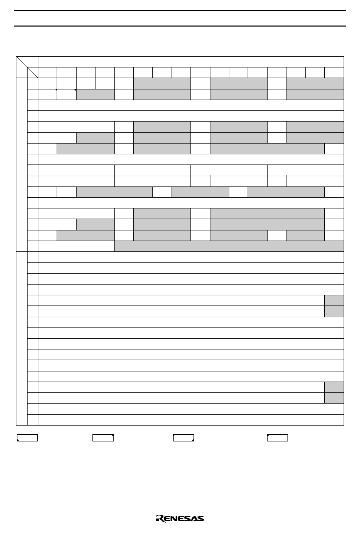
HD404889/HD404899/HD404878/HD404868 Series
175
Table 41
Opcode Map
R8
L
H
R9
0
1
2
3
4
5
6
7
8
9
A
B
C
D
E
F
0
1
2
3
4
5
6
7
8
9
A
B
C
D
E
F
LBI i(4)
LYI i(4)
LXI i(4)
LAI i(4)
LBR m(4)
LAR m(4)
REDD m(4)
LAMR m(4)
AI i(4)
LMIIY i(4)
TDD m(4)
ALEI i(4)
LRB m(4)
LRA m(4)
SEDD m(4)
XMRA m(4)
0
0
1
1-word/2-cycle
instruction
1-word/3-cycle
instruction
RAM direct address
instruction
(2-word/2-cycle)
2-word/2-cycle
instruction
0
1
2
3
4
5
6
7
8
9
A
B
C
D
E
F
NOP
XSPX
XSPY XSPXY ANEM
AM
ORM
LBM(XY)
BNEM
LAB
IB
LMAIY(X)
AYY
LASPY
IY
RTN
RTNI
ALEM
AMC
EORM
NEGA
RED
LASPX
TC
INEM i(4)
ILEM i(4)
YNEI i(4)
XMA(XY)
LAM(XY)
SEM n(2)
LMA(XY)
REM n(2)
SMC
TM n(2)
ANM
ROTR
DAA
DAS
LAY
ROTL
DB
DY
SEC
LBA
LYA
REC
LXA
BLEM
SYY
SED
XMB(XY)
LMADY(X)
TD
LWI i(2)
TBR p(4)

HD404889/HD404899/HD404878/HD404868 Series
176
Table 41
Opcode Map (cont)
R8
L
H
R9
0
1
2
3
4
5
6
7
8
9
A
B
C
D
E
F
0
1
2
3
4
5
6
7
8
9
A
B
C
D
E
F
1
0
1
1-word/2-cycle
instruction
1-word/3-cycle
instruction
RAM direct address
instruction
(2-word/2-cycle)
2-word/2-cycle
instruction
0
1
2
3
4
5
6
7
8
9
A
B
C
D
E
F
LAW
ANEMD
AMD
ORMD
LWA
ALEMD
AMCD
EORMD
COMB
OR
STS
SBY
STOP
INEMD i(4)
ILEMD i(4)
JMPL p(4)
CALL p(4)
BRL p(4)
XMAD
LAMD
SEMD n(2)
LMAD
REMD n(2)
SMCD
TMD n(2)
ANMD
LMID i(4)
CAL a(6)
BR b(8)
P p(4)

HD404889/HD404899/HD404878/HD404868 Series
177
Absolute Maximum Ratings
Item
Symbol
Value
Unit
Notes
Power supply voltage
V
CC
�0.3 to +7.0
V
Programming voltage
V
PP
�0.3 to +14.0
V
1
Pin voltage
V
T
�0.3 to V
CC
+0.3
V
Allowable input current (total)
l
0
100
mA
2
Allowable output current (total)
�
l
0
50
mA
3
Allowable input current (per pin)
l
0
4
mA
4,5
30
mA
4,6
Allowable output current (per pin)
�l
0
4
mA
7,8
20
mA
7,9
Operating temperature
Topr
�20 to +75
�
C
10
Storage temperature
Tstg
�55 to +125
�
C
11
Notes: Permanent damage may occur if these maximum ratings are exceeded. Normal operation must be
under the conditions stated in the electrical characteristics tables. If these conditions are exceeded,
the LSI may malfunction or its reliability may be affected.
1. Applies to the HD4074889, HD4074899, and HD4074869 TEST (V
PP
) pin.
2. The allowable input current (total) is the sum of all currents flowing from I/O pins to ground at the
same time.
3. The allowable output current (total) is the sum of all currents flowing from V
CC
to I/O pins.
4. The allowable input current (per pin) is the maximum current allowed to flow from any one I/O pin
to ground.
5. Applies to pins D
0
to D
3
and R0 to R8.
6. Applies to pins D
4
to D
11
.
7. The allowable output current (per pin) is the maximum current allowed to flow from V
CC
to any
one I/O pin.
8. Applies to pins D
4
to D
11
and R0 to R8.
9. Applies to pins D
0
to D
3
.
10. The operating temperature indicates the temperature range in which power can be supplied to
the LSI (voltage Vcc shown in the electrical characteristics tables can be applied).
11. In the case of chips, the storage specification differs from that of the package products. Please
consult your Hitachi sales representative for details.

HD404889/HD404899/HD404878/HD404868 Series
178
Electrical Characteristics
DC Characteristics (HD404888, HD4048812, HD404889, HD404898, HD4048912, HD404899,
HD404874, HD404878, HD404864, HD404868: V
CC
=1.8V to 5.5V, GND=0V, T
a
=�20
�
C to +75
�
C;
HCD404889, HCD404899, HCD404878: V
CC
=1.8V to 5.5V, GND=0V, Ta=+75
�
C; HD4074889,
HD4074899, HD4074869: V
C C
=2.0V to 5.5V, GND=0V, T
a
=�20
�
C to +75
�
C, unless otherwise
specified)
Item
Symbol Pins
min.
typ. max.
Unit Test conditions
Notes
Input high
voltage
V
IH
RESET
,
SCK
, SI,
INT
0
,INT
1
,
WU
0
to
WU
3
,
EVNB, EVND
0.90V
CC
--
V
CC
+0.3 V
OSC
1
V
CC
�0.3 --
V
CC
+0.3 V
External clock
operation
Input low
voltage
V
IL
RESET
,
SCK
, SI,
INT
0
,INT
1
,
WU
0
to
WU
3
,
EVNB, EVND
�0.3
--
0.10V
CC
V
OSC
1
�0.3
--
0.3
V
External clock
operation
Output high
voltage
V
OH
SCK
,SO, BUZZ, TOB,
TOC
V
CC
�0.5 --
--
V
�I
OH
=0.3mA
Output low
voltage
V
OL
SCK
,SO, BUZZ, TOB,
TOC
--
--
0.4
V
I
OL
=0.4mA
I/O leakage
current
| I
IL
|
RESET
,
SCK
, SI,
INT
0
,
INT
1
,
WU
0
to
WU
3
, EVNB,
EVND, OSC
1
, TOB, TOC,
SO, BUZZ
--
--
1
�
A
V
in
=0V to V
CC
1
Active mode
l
CC1
V
CC
--
3.0
5.0
mA
V
CC
=5V, f
OSC
=4MHz 2
current
dissipation
l
CC2
--
0.4
1.0
mA
V
CC
=3V,
f
OSC
=800kHz
2
Standby mode
current
dissipation
l
SBY1
V
CC
--
1.0
2.0
mA
V
CC
=5V,
f
OSC
=4MHz,
LCD on
3
l
SBY2
--
0.3
0.6
mA
V
CC
=3V,
f
OSC
=800kHz LCD
on
3
Subactive
mode current
dissipation
l
SUB
V
CC
(HD404888, HD4048812,
HD404889, HCD404889,
HD404898, HD4048912,
HD404899, HCD404899,
HD404874, HD404878,
HCD404878, HD404864,
HD404868)
--
35
60
�
A
V
CC
= 3V, LCD on,
32 kHz oscillator
used
4,5
V
CC
(HD4074889,
HD4074899, HD4074869)
--
70
120
�
A
4,5

HD404889/HD404899/HD404878/HD404868 Series
179
Item
Symbol Pins
min.
typ. max.
Unit
Test Conditions
Notes
Watch mode
current dissipation
l
WTC1
V
CC
--
15
30
�
A
V
CC
= 3 V, LCD on,
32 kHz oscillator used
4,5
l
WTC2
V
CC
--
5
8
�
A
V
CC
= 3 V, LCD off,
32 kHz oscillator used
5
Stop mode current
dissipation
l
STOP
V
CC
--
--
5
�
A
V
CC
= 3 V, no 32 kHz
oscillator
5
Stop mode
retention voltage
V
STOP
V
CC
1.5
--
--
V
no 32 kHz oscillator
6
Notes: 1. Excludes output buffer current.
2. Power supply current when the MCU is in the reset state and there are no I/O currents.
Test Conditions MCU State
�
Reset state
Pin States
�
RESET
, TEST: At ground
3. Power supply current when the on-chip timers are operating and there are no I/O currents.
Test Conditions MCU State
�
I/O: Same as reset state
�
Standby mode
�
f
cyc
= f
OSC
/4
Pin States
�
RESET
: At V
CC
�
TEST: At ground
�
D
0
to D
11
, R
0
to R
8
: At V
CC
4. Applies when the LCD power supply dividing resistor is connected.
5. Power supply current when there are no I/O currents.
Test Conditions Pin States
�
RESET
: At V
CC
�
TEST: At ground
�
D
0
to D
11
, R
0
to R
8
: At V
CC
6. Voltage needed to retain RAM data.

HD404889/HD404899/HD404878/HD404868 Series
180
I/O Characteristics for Standard Pins (HD404888, HD4048812, HD404889, HD404898, HD4048912,
HD404899, HD404874, HD404878, HD404864, HD404868: V
CC
=1.8V to 5.5V, GND=0V, T
a
=�20
�
C to
+75
�
C; HCD404889, HCD404899, HCD404878: V
C C
=1.8V to 5.5V, GND=0V, Ta=+75
�
C;
HD4074889, HD4074899, HD4074869: V
CC
=2.0V to 5.5V, GND=0V, T
a
=�20
�
C to +75
�
C, unless
otherwise specified)
Item
Symbol
Pins
min.
typ. max.
Unit
Test conditions
Notes
Input high voltage
V
IH
R0 to R8
0.7V
CC
--
V
CC
+0.3
V
1
R0 to R7
2
Input low voltage
V
IL
R0 to R8
�0.3
--
0.3V
CC
V
1
R0 to R7
2
Output high voltage
V
OH
R0 to R8
V
CC
�0.5
--
--
V
�I
OH
=0.3mA
1
R0 to R7
2
Output low voltage
V
OL
R0 to R8
--
--
0.4
V
I
OL
=0.4mA
1
R0 to R7
2
I/O leakage current
| I
IL
|
R0 to R8
--
--
1
�
A
V
IN
=0V to V
CC
1, 3
R0 to R7
2, 3
MOS pull-up current
�I
PU
R0 to R8
10
50
150
�
A
V
CC
=3V, V
IN
=0V
1
R0 to R7
2
Notes: 1. Applies to the HD404889, HD404899, and HD404878 Series.
2. Applies to the HD404868 Series.
3. Excludes the current flowing in the output buffer.
HD404889/HD404899/HD404878/HD404868 Series
181
I/O Characteristics for High-Current Pins (HD404888, HD4048812, HD404889, HD404898,
HD4048912, HD404899, HD404874, HD404878, HD404864, HD404868: V
CC
=1.8V to 5.5V, GND=0V,
T
a
=�20
�
C to +75
�
C; HCD404889, HCD404899, HCD404878: V
CC
=1.8V to 5.5V, GND=0V,
Ta=+75
�
C; HD4074889, HD4074899, HD4074869: V
CC
=2.0V to 5.5V, GND=0V, T
a
=�20
�
C to +75
�
C,
unless otherwise specified)
Item
Symbol
Pins
min.
typ. max.
Unit
Test conditions
Notes
Input high voltage
V
IH
D
0
to D
11
0.7V
CC
--
V
CC
+0.3
V
1
D
0
to D
9
2
Input low voltage
V
IL
D
0
to D
11
�0.3
--
0.3V
CC
V
1
D
0
to D
9
2
Output high voltage
V
OH
D
4
to D
11
V
CC
�0.5
--
--
V
�I
OH
=0.3mA
1
D
4
to D
9
2
D
0
to D
3
V
CC
�2.0
--
--
V
�I
OH
=10mA,
V
CC
=4.5 to 5.5V
Output low voltage
V
OL
D
0
to D
3
--
--
0.4
V
I
OL
=0.4mA
D
4
to D
11
--
--
2.0
V
I
OL
=15mA
1
D
4
to D
9
V
CC
=4.5V to 5.5V
2
I/O leakage current
| I
IL
|
D
0
to D
11
--
--
1
�
A
V
IN
=0V to V
CC
1, 3
D
0
to D
9
2, 3
MOS pull-up current
�I
PU
D
0
to D
11
10
50
150
�
A
V
CC
=3V, V
IN
=0V
1
D
0
to D
9
2
Notes: 1. Applies to the HD404889, HD404899, and HD404878 Series.
2. Applies to the HD404868 Series.
3. Excludes the current flowing in the output buffer.
HD404889/HD404899/HD404878/HD404868 Series
182
LCD Circuit Characteristics (HD404888, HD4048812, HD404889, HD404898, HD4048912,
HD404899, HD404874, HD404878, HD404864, HD404868: V
CC
=1.8V to 5.5V, GND=0V, T
a
= �20
�
C to
+75
�
C; HCD404889, HCD404899, HCD404878: V
C C
=1.8V to 5.5V, GND=0V, Ta=+75
�
C;
HD4074889, HD4074899, HD4074869: V
CC
=2.0V to 5.5V, GND=0V, T
a
=�20
�
C to +75
�
C, unless
otherwise specified)
Item
Symbol
Pins
min.
typ. max.
Unit
Test conditions
Notes
Segment driver voltage
drop
V
DS
SEG1 to
SEG32
--
--
0.6
V
I
d
=3
�
A
V
1
=2.7 to 5.5V
1, 2
SEG1 to
SEG24
1, 3
Common driver voltage
drop
V
DC
COM1 to
COM4
--
--
0.3
V
I
d
=3
�
A
V
1
=2.7 to 5.5V
1
LCD power supply
dividing resistance
R
W
50
300
900
k
V
1
-GND
LCD voltage
V
LCD
V
1
2.2
--
V
CC
V
4, 5
Notes: 1. The voltage drop from power supply pins V
1
, V
2
, V
3
, and GND to each segment pin or each
common pin.
2. Applies to the HD404889, HD404899, and HD404878 Series.
3. Applies to the HD404868 Series.
4. In the HD404889, HD404899, and HD404878 Series, when V
LCD
is supplied by the internal power
supply, V
0
and V
1
should be shorted. When V
LCD
is supplied by an external power supply, the
relationship V
CC
V
LCD
2.2 V should be maintained. In this case, the V
0
pin should be fixed at
V
CC
.
5. In the HD404868 Series, when V
LCD
is supplied by an external power supply, the relationship V
CC
V
LCD
2.2 V should be maintained.

HD404889/HD404899/HD404878/HD404868 Series
183
A/D Converter Characteristics (HD404888, HD4048812, HD404889: V
CC
=1.8V to 5.5V, GND=0V,
T
a
=�20
�
C to +75
�
C; HCD404889: V
CC
=1.8V to 5.5V, GND=0V, Ta=+75
�
C; HD4074889: V
CC
=2.0V to
5.5V, GND=0V, T
a
=�20
�
C to +75
�
C, unless otherwise specified)
Item
Symbol
Pins
min.
typ. max.
Unit
Test conditions
Notes
Analog power supply
voltage
AV
CC
AV
CC
V
CC
�0.3
V
CC
V
CC
+0.3
V
1
Analog input voltage
AV
in
AN
0
to AN
5
AV
SS
--
AV
CC
V
AV
CC
-AV
SS
current
I
AD
--
--
500
�
A
V
CC
=AV
CC
=5.0V
Analog input
capacitance
CA
in
AN
0
to AN
5
--
15
--
pF
Resolution
--
8
--
bit
Number of inputs
0
--
6
channel
Absolute accuracy
--
--
�
2.0
LSB
V
CC
=AV
CC
=2.7V to
5.5V
--
--
�
3.0
LSB
V
CC
=AV
CC
=1.8V to
2.7V
2
Conversion time
65
--
125
t
cyc
Input impedance
AN
0
to AN
5
1
--
--
M
Notes: 1. Connect to the V
CC
pin when the A/D converter is not used. The AV
CC
setting ranges are 1.8
V
AV
CC
5.5V (HD404888, HD4048812, HD404889, HCD404889) and 2.0V
AV
CC
5.5V
(HD4074889)
2. The conversion time is 125tcyc.

HD404889/HD404899/HD404878/HD404868 Series
184
(HD404898, HD4048912, HD404899: V
CC
=1.8V to 5.5V, GND=0V, T
a
=�20
�
C to +75
�
C;
HCD404899: V
CC
=1.8V to 5.5V, GND=0V, Ta=+75
�
C;
HD4074899: V
CC
=2.0V to 5.5V, GND=0V, T
a
=�20
�
C to +75
�
C, unless otherwise specified)
Item
Symbol
Pins
min.
typ. max.
Unit
Test conditions
Notes
Analog power supply
voltage
AV
CC
AV
CC
V
CC
�0.3
V
CC
V
CC
+0.3
V
1
Analog input voltage
AV
in
AN
0
to AN
5
AV
SS
--
AV
CC
V
AV
CC
-AV
SS
current
I
AD
--
--
500
�
A
V
CC
=AV
CC
=5.0V
Analog input
capacitance
CA
in
AN
0
to AN
5
--
15
--
pF
Resolution
--
10
--
bit
Number of inputs
0
--
6
channel
Conversion time
125
--
--
t
cyc
V
CC
= AV
CC
= 1.8 V to
less than 2.0 V
2
65
--
125
t
cyc
V
CC
=AV
CC
=2.0 V to
5.5V
Absolute accuracy
--
--
�
4.0
LSB
Input impedance
AN
0
to AN
5
1
--
--
M
Notes: 1. Connect to the V
CC
pin when the A/D converter is not used. The AV
CC
setting ranges are 1.8
V
AV
CC
5.5V (HD404898, HD4048912, HD404899, HCD404899) and 2.0V
AV
CC
5.5V
(HD4074899)
2. Applies to HD404898, HD4048912, HD404899, and HCD404899.
(HD404864, HD404868: V
CC
=1.8V to 5.5V, GND=0V, T
a
=�20
�
C to +75
�
C; HD4074869: V
CC
=2.0V to
5.5V, GND=0V, T
a
=�20
�
C to +75
�
C)
Item
Symbol
Pins
min.
typ. max.
Unit
Test conditions
Notes
Analog input voltage
AV
in
AN
0
to AN
3
GND
--
V
CC
V
Analog input
capacitance
CA
in
AN
0
to AN
3
--
15
--
pF
Resolution
--
10
--
bit
Number of inputs
0
--
4
channel
Absolute accuracy
--
--
�
4.0
LSB
Conversion time
125
--
--
t
cyc
V
CC
= 1.8 V to less
than 2.0 V
1
65
--
125
t
cyc
V
CC
= 2.0 V to 5.5V
Input impedance
AN
0
to AN
3
1
--
--
M
Note: 1. Applies to HD404864 and HD404868.
HD404889/HD404899/HD404878/HD404868 Series
185
AC Characteristics (HD404888, HD4048812, HD404889, HD404898, HD4048912, HD404899,
HD404874, HD404878, HD404864, HD404868: V
CC
=1.8V to 5.5V, GND=0V, T
a
=�20
�
C to +75
�
C;,
HCD404889, HCD404899, HCD404878: V
CC
=1.8V to 5.5V, GND=0V, Ta=+75
�
C; HD4074889,
HD4074899, HD4074869: V
C C
=2.0V to 5.5V, GND=0V, T
a
=�20
�
C to +75
�
C, unless otherwise
specified)
Item
Symbol Pins
min. typ.
max.
Unit
Test conditions
Notes
Clock oscillation
f
OSC
OSC
1
, OSC
2
0.4
--
4.5
MHz
Division by 4
1
frequency
X1,X2
--
32.768 --
kHz
Instruction cycle time
t
cyc
0.89 --
10
�
s
Division by 4
t
subcyc
--
244.14 --
�
s
32 kHz oscillator used,
division by 8
--
122.07 --
�
s
32 kHz oscillator used,
division by 4
Oscillation settling
time(external clock and
ceramic oscillator)
t
RC
OSC
1
, OSC
2
--
--
7.5
ms
2
Oscillation settling
t
RC
OSC
1
, OSC
2
--
--
30
ms
V
CC
=2.0 to 5.5V
2
time(crystal oscillator)
X1,X2
--
--
2
s
T
a
=�10 to +60
�
C
2
External clock high-
level width
t
CPH
OSC
1
105
--
--
ns
f
OSC
=4MHZ
3
External clock low-
level width
t
CPL
OSC
1
105
--
--
ns
f
OSC
=4MHZ
3
External clock rise time t
CPr
OSC
1
--
--
20
ns
f
OSC
=4MHZ
3
External clock fall time
t
CPf
OSC
1
--
--
20
ns
f
OSC
=4MHZ
3
INT
0
to INT
1
,
EVNB,EVND,
WU
0
to
WU
3
high-level width
t
IH
INT
0
to INT
1
,
EVNB,EVND,
WU
0
to
WU
3
2
--
--
t
cyc
/t
subcyc
4
INT
0
to INT
1
,
EVNB,EVND,
WU
0
to
WU
3
low-level width
t
IL
INT
0
to INT
1
,
EVNB,EVND,
WU
0
to
WU
3
2
--
--
t
cyc
/t
subcyc
4
RESET
low-level width t
RSTL
RESET
2
--
--
t
cyc
5
RESET
rise time
t
RSTr
RESET
--
--
20
ms
5
Input capacitance
C
in
All input pins except
TEST
--
--
15
pF
f=1MHz,V
in
=0V
TEST
(HD404888, HD4048812,
HD404889, HCD404889,
HD404899, HD404898,
HD4048912,
HCD404899, HD404874,
HD404878, HCD404878,
HD404864, HD404868)
--
--
15
pF
TEST
(HD4074889,
HD4074899,
HD4074869)
--
--
40
pF

HD404889/HD404899/HD404878/HD404868 Series
186
Notes: 1. When the subsystem oscillator (32.768 kHz crystal oscillation) is used, use within the range
0.4 MHz
f
OSC
1.0 MHz or 1.6 MHz
f
OSC
4.5 MHz. The SSR1 bit of the system clock select
register (SSR) should be set to 0 and 1, respectively.
2. The oscillation settling time is defined as follows:
(1)
The time required for the oscillation to settle after V
CC
has reached min. at power-on.
(2)
The time required for the oscillation to settle after
RESET
input has gone low when stop
mode is cleared.
To ensure enough time for the oscillation to settle at power-on hold the
RESET
input low for at
least time t
RC
. The oscillation settling time will depend on the circuit constants and stray
capacitance. The resonator should be determined in consultation with the resonator
manufacturer. With regard to the system clock (OSC
1
, OSC
2
), bits MIS1 and MIS0 in the
miscellaneous register (MIS) should be set according to the oscillation settling time of the
resonator used.
3. See figure 104.
4. See figure 105.
5. See figure 106.
Serial Interface Timing Characteristics (HD404888, HD4048812, HD404889, HD404898, HD4048912,
HD404899, HD404874, HD404878, HD404864, HD404868: V
CC
=1.8V to 5.5V, GND=0V, T
a
=�20
�
C to
+75
�
C;, HCD404889, HCD404899, HCD404878: V
CC
=1.8V to 5.5V, GND=0V, Ta=+75
�
C;
HD4074889, HD4074899, HD4074869: V
CC
=2.0V to 5.5V, GND=0V, T
a
=�20
�
C to +75
�
C, unless
otherwise specified)
Item
Symbol
Pins
min.
typ. max.
Unit
Test conditions
Notes
Serial clock cycle time
t
Scyc
SCK
1
--
--
t
cyc
See load in figure 108 1
Serial clock high-level
width
t
SCKH
SCK
0.4
--
--
t
Scyc
See load in figure 108 1
Serial clock low-level
width
t
SCKL
SCK
0.4
--
--
t
Scyc
See load in figure 108 1
Serial clock rise time
t
SC Kr
SCK
--
--
100
ns
See load in figure 108 1
Serial clock fall time
t
SCKf
SCK
--
--
100
ns
See load in figure 108 1
Serial output data
delay time
t
DSO
SO
--
--
300
ns
See load in figure 108 1
Serial input data setup
time
t
SSI
SI
200
--
--
ns
1
Serial input data hold
time
t
HSI
SI
200
--
--
ns
1

HD404889/HD404899/HD404878/HD404868 Series
187
During Serial Clock Input
Item
Symbol
Pins
min.
typ. max.
Unit
Test conditions
Notes
Serial clock cycle time
t
Scyc
SCK
1
--
--
t
cyc
1
Serial clock high-level
width
t
SCKH
SCK
0.4
--
--
t
Scyc
1
Serial clock low-level
width
t
SCKL
SCK
0.4
--
--
t
Scyc
1
Serial clock rise time
t
SC Kr
SCK
--
--
100
ns
1
Serial clock fall time
t
SCKf
SCK
--
--
100
ns
1
Serial output data
delay time
t
DSO
SO
--
--
300
ns
See load in figure 108 1
Serial input data setup
time
t
SSI
SI
200
--
--
ns
1
Serial input data hold
time
t
HSI
SI
200
--
--
ns
1
Note:
1. See
figure
107.
1/f
CP
0.3V
V
CC
-0.3V
t
CPL
t
CPH
t
CPr
t
CPf
OSC
1
Figure 104 External Clock Input Waveform
0.9V
CC
0.1V
CC
t
IH
t
IL
INT
0
, INT
1
, EVNB, EVND,
WU
0
to
WU
3
Figure 105 Interrupt Timing

HD404889/HD404899/HD404878/HD404868 Series
188
0.9V
CC
0.1V
CC
t
RSTL
t
RSTr
RESET
Figure 106 Reset Timing
SCK
SO
SI
t
SCK
f
V
CC
�0.5V(0.9V
CC
)*
0.4V(0.1V
CC
)*
t
Scyc
t
SCKr
t
SCKL
t
DOS
t
t
SCKH
t
HSI
t
SSI
V
CC
�0.5V
0.4V
0.9V
CC
0.1V
CC
Note : V
CC
�0.5V and 0.4V are the voltages during serial clock output.
0.9 V
CC
and 0.1 V
CC
are the voltages during serial clock input.
Figure 107 Serial Interface Timing
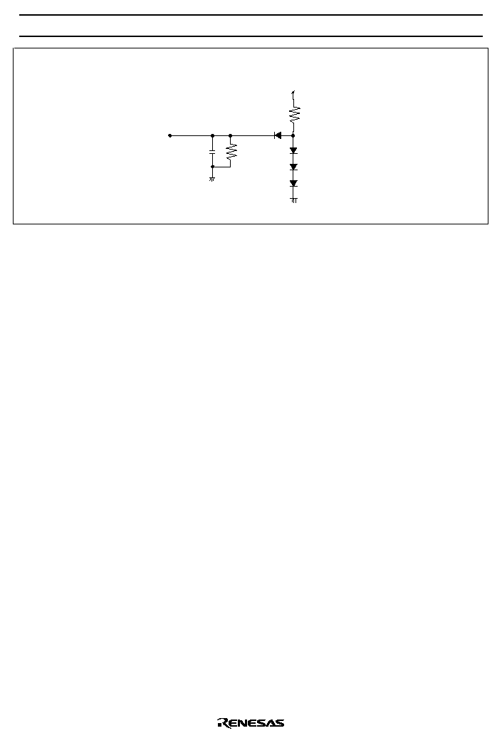
HD404889/HD404899/HD404878/HD404868 Series
189
V
CC
Test point
R
1
=2.6k
R=12k
C=30pF
1S2074(H)
or equivalent
Figure 108 Timing Load Circuit
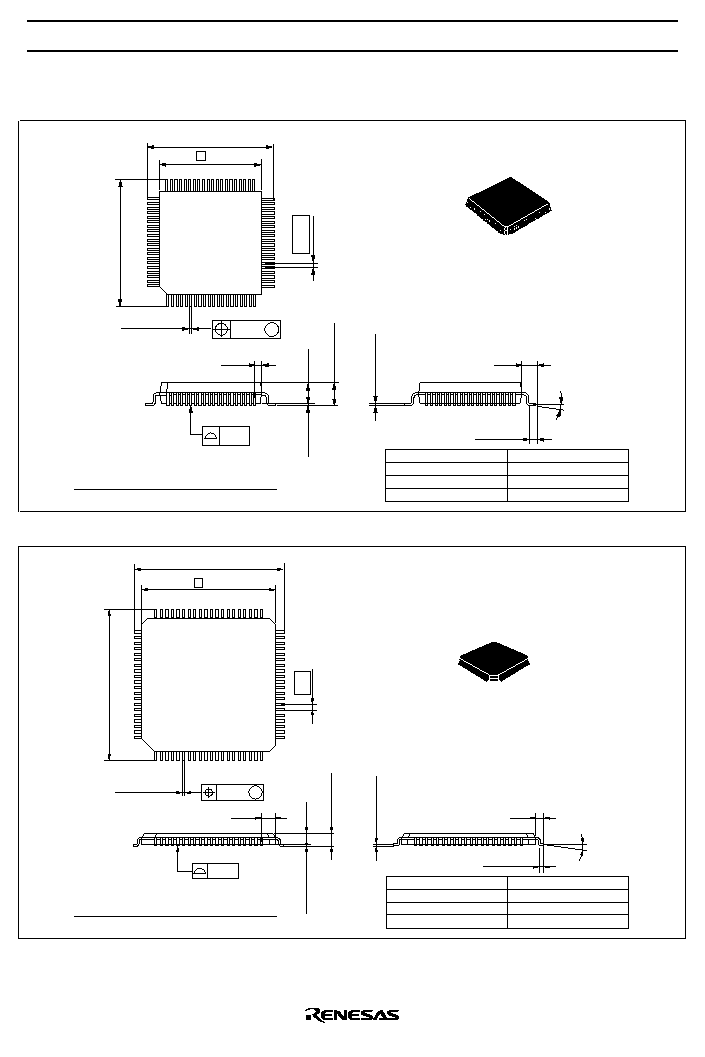
HD404889/HD404899/HD404878/HD404868 Series
190
Package Dimensions
Hitachi Code
JEDEC
EIAJ
Weight (reference value)
FP-80A
--
Conforms
1.2 g
Unit: mm
*Dimension including the plating thickness
Base material dimension
60
0
�
� 8
�
0.10
0.12 M
17.2
�
0.3
41
61
80
1
20
40
21
17.2
�
0.3
*0.32
�
0.08
0.65
3.05 Max
1.6
0.8
�
0.3
14
2.70
*0.17
�
0.05
0.10
+0.15 �
0.10
0.83
0.30
�
0.06
0.15
�
0.04
Hitachi Code
JEDEC
EIAJ
Weight (reference value)
TFP-80C
--
Conforms
0.4 g
Unit: mm
*Dimension including the plating thickness
Base material dimension
0.10
M
0.10
0.5
�
0.1
0
�
� 8
�
1.20 Max
14.0
�
0.2
0.5
12
14.0
�
0.2
60
41
1
20
80
61
21
40
*0.17
�
0.05
1.0
*0.22
�
0.05
0.10
�
0.10
1.00
1.25
0.20
�
0.04
0.15
�
0.04
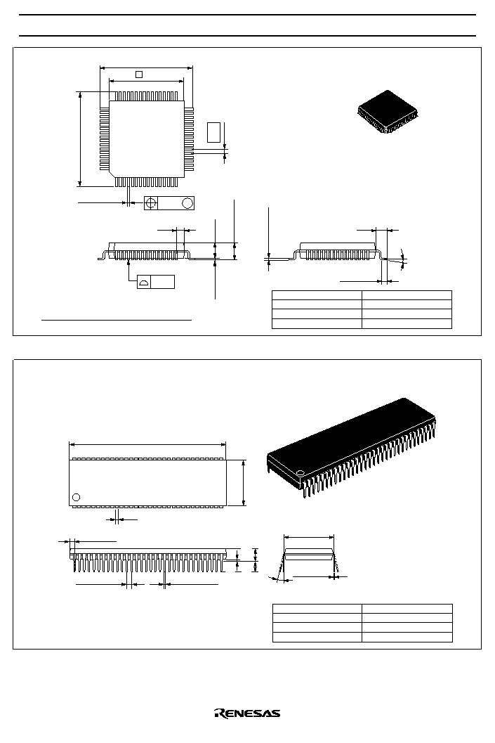
HD404889/HD404899/HD404878/HD404868 Series
191
Hitachi Code
JEDEC
EIAJ
Weight (reference value)
FP-64A
--
Conforms
1.2 g
Unit: mm
*Dimension including the plating thickness
Base material dimension
0.10
0.15 M
17.2
�
0.3
48
33
49
64
1
16
32
17
17.2
�
0.3
0.35
�
0.06
0.8
3.05 Max
14
2.70
0
�
� 8
�
1.6
0.8
�
0.3
*0.17
�
0.05
0.10
+0.15 �
0.10
1.0
*0.37
�
0.08
0.15
�
0.04
Hitachi Code
JEDEC
EIAJ
Weight (reference value)
DP-64S
--
Conforms
8.8 g
Unit: mm
0.25
+ 0.11
� 0.05
0
�
� 15
�
1.78
�
0.25
0.48
�
0.10
0.51 Min
2.54 Min
5.08 Max
19.05
57.6
58.5 Max
1.0
1
33
32
64
17.0
18.6 Max
1.46 Max
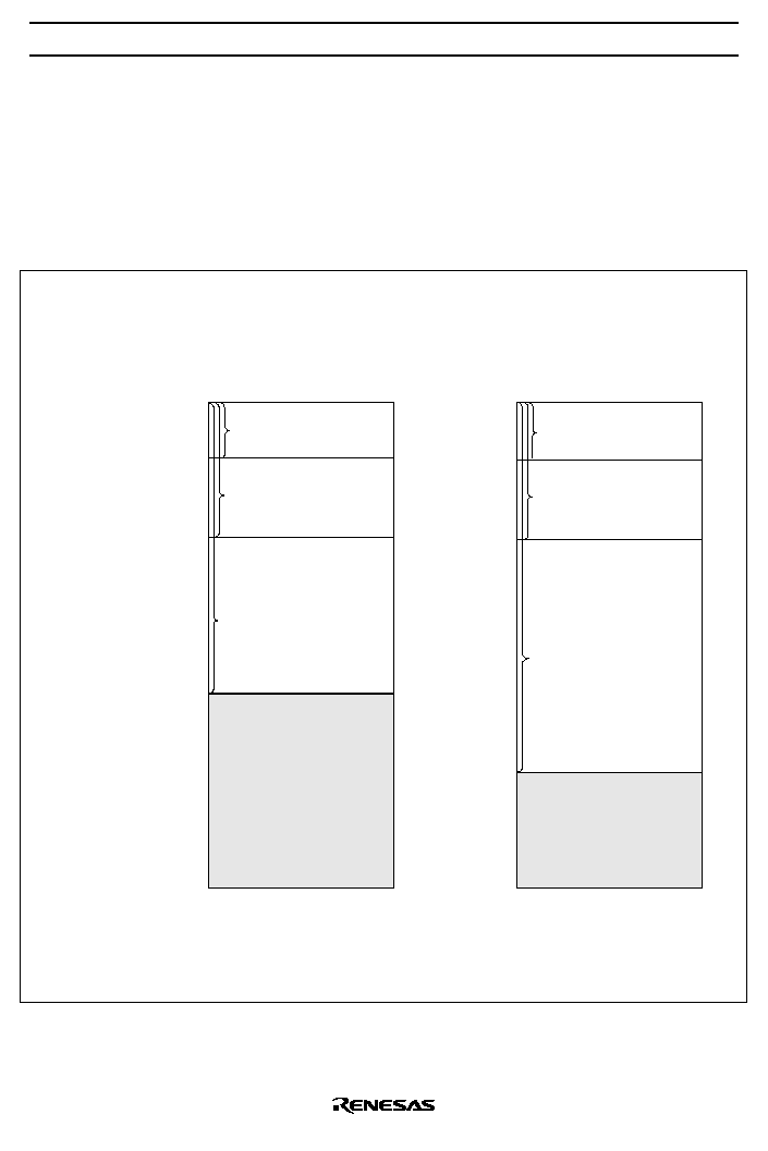
HD404889/HD404899/HD404878/HD404868 Series
192
Note on ROM Ordering
Please note the following when ordering HD404888, HD4048812, HD404898 or HD4048912 ROM.
When ordering ROM, please fill the "Not used" areas below with all-1 data, to give the same amount of
data as for the 16-kwords version (HD404889, HD404899). The program that converts ROM data to mask
drawing data is the same as that used for the 16-kwords version, and therefore the same amount of data is
necessary. This applies both to orders using EPROM and orders using data transmission.
Vector addresses
Program and pattern
area (8,192 words)
Vector addresses
Zero page
subroutine area
(64 words)
Zero page
subroutine area
(64 words)
Program and pattern
area (12,288 words)
Not used
Not used
8-kword ROM
version: HD404888, HD404898
Write all-1 data to addresses
$2000 to $3FFF.
12-kword ROM version:
HD4048812, HD4048912
Write all-1 data to addresses
$3000 to $3FFF.
$0000
$000F
$0010
$003F
$0040
$1FFF
$2000
$3FFF
$3FFF
$0000
$000F
$0010
$003F
$0040
$2FFF
$3000
Note : Write all-1 data in shaded areas.
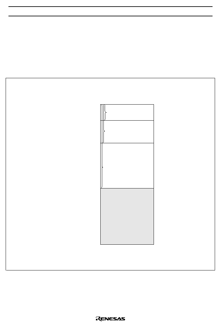
HD404889/HD404899/HD404878/HD404868 Series
193
Note on ROM Ordering
Please note the following when ordering HD404874 or HD404864 ROM.
When ordering ROM, please fill the "Not used" areas below with all-1 data, to give the same amount of
data as for the 8-kwords version (HD404878, HD404868). The program that converts ROM data to mask
drawing data is the same as that used for the 8-kwords version, and therefore the same amount of data is
necessary. This applies both to orders using EPROM and orders using data transmission.
Vector addresses
Program and pattern
area (4,096 words)
Zero page
subroutine area
(64 words)
Not used
4-kword ROM
version: HD404874, HD404864
Write all-1 data to addresses
$1000 to $1FFF.
$0000
$000F
$0010
$003F
$0040
$0FFF
$1000
$1FFF
Note : Write all-1 data in shaded areas.

HD404889/HD404899/HD404878/HD404868 Series
194
Option List HD404888, HD4048812, HD404889, HCD404889
Please check off the appropriate applications and enter the necessary information.
Date of order
Year
Month
Day
Customer
Department
Name
ROM code name
LSI number (Hitachi entry)
1. ROM Size
HD404888
8 kwords
HD4048812
12 kwords
HD404889
16 kwords
HCD404889
16 kwords
2. Function Options
*
32 kHz CPU operation, realtime clock time base
*
No 32 kHz CPU operation, realtime clock time base
No 32 kHz CPU operation, no realtime clock time base
Note: When an asterisked item is selected, "crystal resonator" is necessary for subsystem oscillator (X1
X2).
3. ROM Code Data Organization
For a microcomputer with EPROM mounted (including a ZTATTM microcomputer), specify the combined upper/lower
type.
Combined lower/upper type
�
Both the lower 5 data bits (L) and the upper 5 data bits (U) are written to a single EPROM in the order LULULU...
Separate lower/upper type
�
The lower 5 data bits (L) and upper 5 data bits (U) are written to separate EPROMs respectively.
4. System Oscillator (OSC1-OSC2)
Ceramic oscillator
f =
MHz
Crystal oscillator
f =
MHz
External clock
f =
MHz

HD404889/HD404899/HD404878/HD404868 Series
195
5. Subsystem Oscillator (X1 X2)
6. Stop Mode
7. Package
Not used
--
Yes (used)
FP-80A
Crystal resonator
f = 32.768 kHz
No (not used)
TFP-80C
Chip
Note:
The specifications of shipped chips differ from those of the package product. Please contact our
sales staff for details.
HD404889/HD404899/HD404878/HD404868 Series
196
Option List HD404898, HD4048912, HD404899, HCD404899
Please check off the appropriate applications and enter the necessary information.
Date of order
Year
Month
Day
Customer
Department
Name
ROM code name
LSI number (Hitachi entry)
1. ROM Size
HD404898
8 kwords
HD4048912
12 kwords
HD404899
16 kwords
HCD404899
16 kwords
2. Function Options
*
32 kHz CPU operation, realtime clock time base
*
No 32 kHz CPU operation, realtime clock time base
No 32 kHz CPU operation, no realtime clock time base
Note: When an asterisked item is selected, "crystal resonator" is necessary for subsystem oscillator (X1
X2).
3. ROM Code Data Organization
For a microcomputer with EPROM mounted (including a ZTATTM microcomputer), specify the combined upper/lower
type.
Combined lower/upper type
�
Both the lower 5 data bits (L) and the upper 5 data bits (U) are written to a single EPROM in the order LULULU...
Separate lower/upper type
�
The lower 5 data bits (L) and upper 5 data bits (U) are written to separate EPROMs respectively.
4. System Oscillator (OSC1-OSC2)
Ceramic oscillator
f =
MHz
Crystal oscillator
f =
MHz
External clock
f =
MHz

HD404889/HD404899/HD404878/HD404868 Series
197
5. Subsystem Oscillator (X1 X2)
6. Stop Mode
7. Package
Not used
--
Yes (used)
FP-80A
Crystal resonator
f = 32.768 kHz
No (not used)
TFP-80C
Chip
Note:
The specifications of shipped chips differ from those of the package product. Please contact our
sales staff for details.

HD404889/HD404899/HD404878/HD404868 Series
198
Option List HD404874, HD404878, HCD404878
Please check off the appropriate applications and enter the necessary information.
Date of order
Year
Month
Day
Customer
Department
Name
ROM code name
LSI number (Hitachi entry)
1. ROM Size
HD404874
4 kwords
HD404878
8 kwords
HCD404878
8 kwords
2. Function Options
*
32 kHz CPU operation, realtime clock time base
*
No 32 kHz CPU operation, realtime clock time base
No 32 kHz CPU operation, no realtime clock time base
Note: When an asterisked item is selected, "crystal resonator" is necessary for subsystem oscillator (X1 X2).
3. ROM Code Data Organization
For a microcomputer with EPROM mounted (including a ZTATTM microcomputer), specify the combined upper/lower
type.
Combined lower/upper type
�
Both the lower 5 data bits (L) and the upper 5 data bits (U) are written to a single EPROM in the order LULULU...
Separate lower/upper type
�
The lower 5 data bits (L) and upper 5 data bits (U) are written to separate EPROMs respectively.
4. System Oscillator (OSC1-OSC2)
Ceramic oscillator
f =
MHz
Crystal oscillator
f =
MHz
External clock
f =
MHz
5. Subsystem Oscillator (X1 X2)
6. Stop Mode
7. Package
Not used
--
Yes (used)
FP-80A
Crystal resonator
f = 32.768 kHz
No (not used)
TFP-80C
Chip
Note:
The specifications of shipped chips differ from those of the package product. Please contact our
sales staff for details.
HD404889/HD404899/HD404878/HD404868 Series
199
Option List HD404864, HD404868
Please check off the appropriate applications and enter the necessary information.
Date of order
Year
Month
Day
Customer
Department
Name
ROM code name
LSI number (Hitachi entry)
1. ROM Size
HD404864
4 kwords
HD404868
8 kwords
2. Function Options
*
32 kHz CPU operation, realtime clock time base
*
No 32 kHz CPU operation, realtime clock time base
No 32 kHz CPU operation, no realtime clock time base
Note: When an asterisked item is selected, "crystal resonator" is necessary for subsystem oscillator (X1
X2).
3. ROM Code Data Organization
For a microcomputer with EPROM mounted (including a ZTATTM microcomputer), specify the combined upper/lower
type.
Combined lower/upper type
�
Both the lower 5 data bits (L) and the upper 5 data bits (U) are written to a single EPROM in the order LULULU...
Separate lower/upper type
�
The lower 5 data bits (L) and upper 5 data bits (U) are written to separate EPROMs respectively.
4. System Oscillator (OSC1-OSC2)
Ceramic oscillator
f =
MHz
Crystal oscillator
f =
MHz
External clock
f =
MHz
5. Subsystem Oscillator (X1 X2)
6. Stop Mode
7. Package
Not used
--
Yes (used)
FP-64A
Crystal resonator
f = 32.768 kHz
No (not used)
DP-64S

HD404889/HD404899/HD404878/HD404868 Series
200
Cautions
1. Hitachi neither warrants nor grants licenses of any rights of Hitachi's or any third party's patent,
copyright, trademark, or other intellectual property rights for information contained in this document.
Hitachi bears no responsibility for problems that may arise with third party's rights, including
intellectual property rights, in connection with use of the information contained in this document.
2. Products and product specifications may be subject to change without notice. Confirm that you have
received the latest product standards or specifications before final design, purchase or use.
3. Hitachi makes every attempt to ensure that its products are of high quality and reliability. However,
contact Hitachi's sales office before using the product in an application that demands especially high
quality and reliability or where its failure or malfunction may directly threaten human life or cause risk
of bodily injury, such as aerospace, aeronautics, nuclear power, combustion control, transportation,
traffic, safety equipment or medical equipment for life support.
4. Design your application so that the product is used within the ranges guaranteed by Hitachi particularly
for maximum rating, operating supply voltage range, heat radiation characteristics, installation
conditions and other characteristics. Hitachi bears no responsibility for failure or damage when used
beyond the guaranteed ranges. Even within the guaranteed ranges, consider normally foreseeable
failure rates or failure modes in semiconductor devices and employ systemic measures such as fail-
safes, so that the equipment incorporating Hitachi product does not cause bodily injury, fire or other
consequential damage due to operation of the Hitachi product.
5. This product is not designed to be radiation resistant.
6. No one is permitted to reproduce or duplicate, in any form, the whole or part of this document without
written approval from Hitachi.
7. Contact Hitachi's sales office for any questions regarding this document or Hitachi semiconductor
products.