 | –≠–ª–µ–∫—Ç—Ä–æ–Ω–Ω—ã–π –∫–æ–º–ø–æ–Ω–µ–Ω—Ç: HD49334AF | –°–∫–∞—á–∞—Ç—å:  PDF PDF  ZIP ZIP |

Rev.1.0, Apr 20, 2004, page 1 of 22
HD49334AF/AHF
CDS/PGA & 10-bit A/D Converter
REJ03F0105-0100Z
Rev.1.0
Apr 20, 2004
Description
The HD49334AF/AHF is a CMOS IC that provides CDS-PGA analog processing (CDS/PGA) suitable for CCD camera
digital signal processing systems together with a 10-bit A/D converter in a single chip.
Functions
∑ Correlated double sampling
∑ PGA
∑ Offset compensation
∑ Serial interface control
∑ 10-bit ADC
∑ Operates using only the 3 V voltage
∑ Corresponds to switching mode of power dissipation and operating frequency
Power dissipation: 120 mW (Typ), maximum frequency: 36 MHz (HD49334AHF)
Power dissipation: 60 mW (Typ), maximum frequency: 25 MHz (HD49334AF)
∑ ADC direct input mode
∑ QFP 48-pin package
Features
∑ Suppresses low-frequency noise output from CCD by the S/H type correlated double sampling.
∑ The S/H response frequency characteristics for the reference level can be adjusted using values of external parts and
registers.
∑ High sensitivity is achieved due to the high S/N ratio and a wide coverage provided by a PG amplifier.
∑ Feedback is used to compensate and reduce the DC offsets including the output DC offset due to PGA gain change
and the CCD offset in the CDS (correlated double sampling) amplifier input.
∑ PGA, standby mode, etc., is achieved via a serial interface.
∑ High precision is provided by a 10-bit-resolution A/D converter.
HD49334AF/AHF
Rev.1.0, Apr 20, 2004, page 2 of 22
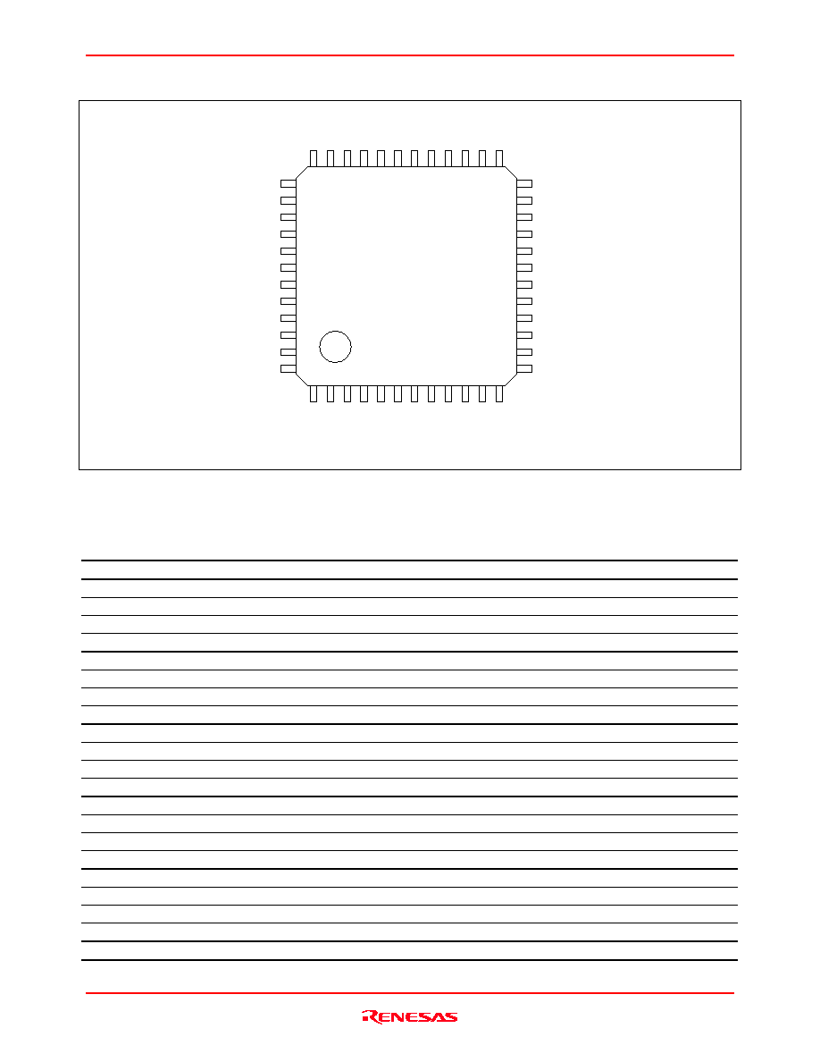
Pin Arrangement
ADCIN
AV
SS
NC
AV
DD
BIAS
BLKC
CDSIN
BLKFB
BLKSH
AV
DD
AV
SS
AV
SS
NC
D0
D1
D2
D3
D4
D5
D6
D7
D8
D9
NC
36 35
27
34 33 32 31 30 29 28
26 25
1 2
10
3 4 5 6 7 8 9
11 12
24
23
22
21
20
19
18
17
16
15
14
13
37
38
39
40
41
42
43
44
45
46
47
48
(Top view)
NC
NC
SPSIG
SPBLK
OBP
PBLK
DV
DD
DV
DD
ADCLK
DV
SS
DV
SS
DRDV
DD
VRM
VRT
VRB
NC
DV
SS
OEB
DV
DD
DV
DD
DV
SS
CS
SDATA
SCK
Pin Description
Pin No.
Symbol
Description
I/O
Analog(A) or
Digital(D)
1
NC
No connection pin
--
--
2 to 11
D0 to D9
Digital output
O
D
12
NC
No connection pin
--
--
13 DRDV
DD
Output buffer power supply (3 V)
--
D
14 DV
SS
Digital ground (0 V)
--
D
15 DV
SS
Digital ground (0 V)
--
D
16
ADCLK
ADC conversion clock input pin
I
D
17 DV
DD
Digital power supply (3 V)
--
D
18 DV
DD
Digital power supply (3 V)
--
D
19
PBLK
Preblanking input pin
I
D
20
OBP
Optical black pulse input pin
I
D
21
SPBLK
Black level sampling clock input pin
I
D
22
SPSIG
Signal level sampling clock input pin
I
D
23
NC
No connection pin
--
--
24
NC
No connection pin
--
--
25 AV
SS
Analog ground (0 V)
--
A
26 AV
SS
Analog ground (0 V)
--
A
27 AV
DD
Analog power supply (3 V)
--
A
28
BLKSH
Black level S/H pin
--
A
29
BLKFB
Black level FB pin
--
A
30 CDSIN
CDS
input
pin
I
A
31
BLKC
Black level C pin
--
A
HD49334AF/AHF
Rev.1.0, Apr 20, 2004, page 3 of 22
Pin Description (cont.)
Pin No.
Symbol
Description
I/O
Analog(A) or
Digital(D)
32
BIAS
Internal bias pin
Connect a 33 k
resistor between BIAS and AV
SS
.
-- A
33 AV
DD
Analog power supply (3 V)
--
A
34
NC
No connection pin
--
--
35 AV
SS
Analog ground (0 V)
--
A
36 ADCIN
ADC
input
pin
--
A
37
VRM
Reference voltage pin 1
Connect a 0.1
µ
F ceramic capacitor between VRM and AV
SS
.
-- A
38
VRT
Reference voltage pin 3
Connect a 0.1
µ
F ceramic capacitor between VRT and AV
SS
.
-- A
39
VRB
Reference voltage pin 2
Connect a 0.1
µ
F ceramic capacitor between VRB and AV
SS
.
-- A
40
NC
No connection pin
--
--
41 DV
SS
Digital ground (0 V)
--
D
42 OEB
*
1
Digital output enable pin
--
D
43 DV
DD
Digital power supply (3 V)
--
D
44 DV
DD
Digital power supply (3 V)
--
D
45 DV
SS
Digital ground (0 V)
--
D
46
CS
Serial interface control input pin
I
D
47
SDATA
Serial data input pin
I
D
48
SCK
Serial clock input pin
I
D
Note: 1. With pull-down resistor.
HD49334AF/AHF
Rev.1.0, Apr 20, 2004, page 4 of 22
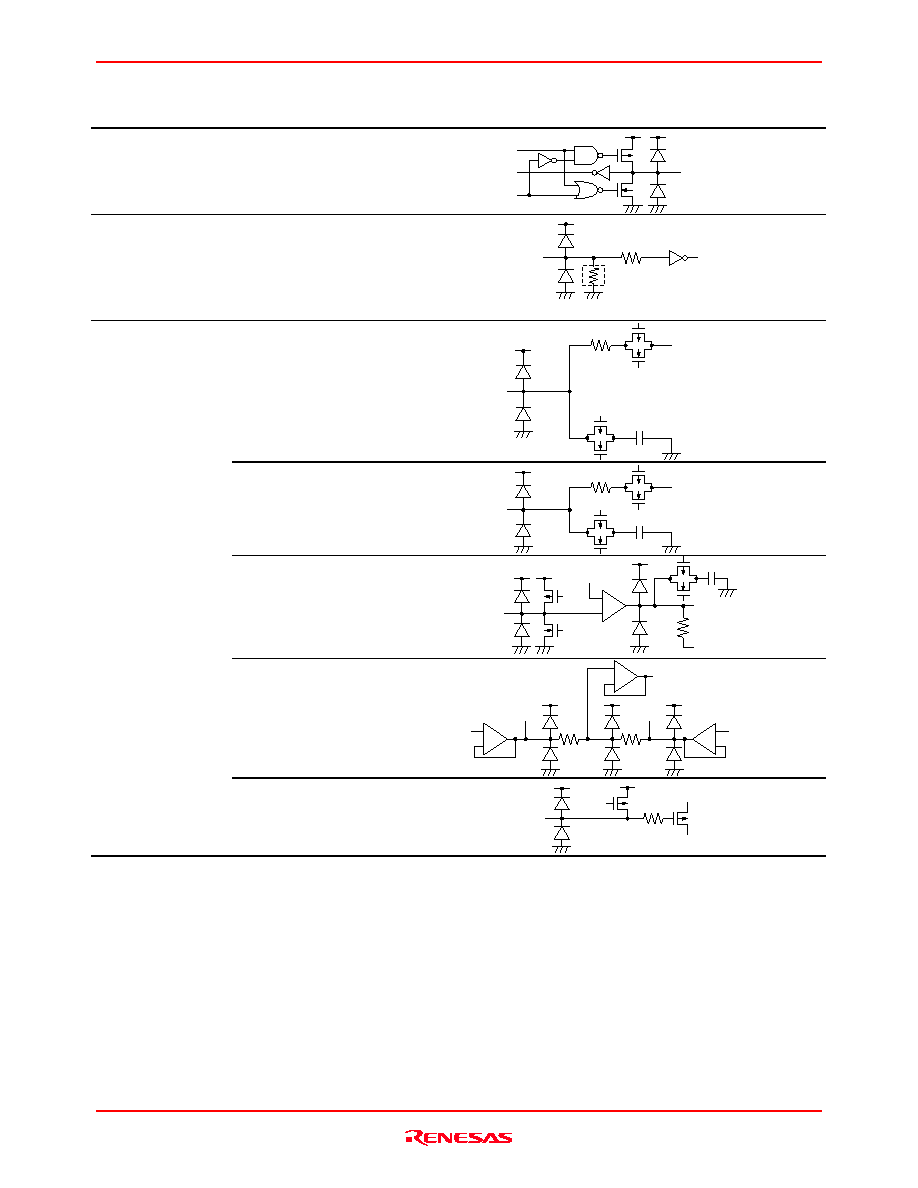
Input/Output Equivalent Circuit
Pin Name
Equivalent Circuit
Digital output
D0 to D9
DIN
DV
DD
STBY
Digital
output
Digital input
ADCLK, OBP,
SPBLK, SPSIG,
CS, SCK, SDATA,
PBLK, OEB
*1
Digital
input
DV
DD
Note: Only OEB is pulled down to about 70 k
.
CDSIN
CDSIN
Internally
connected
to VRT
AV
DD
ADCIN
ADCIN
Internally
connected
to VRM
AV
DD
BLKSH, BLKFB,
BLKC
BLKFB
AV
DD
BLKSH
BLKC
-
+
VRT, VRM, VRB
-
+
-
+
-
+
VRT
VRB
AV
DD
VRM
Analog
BIAS
BIAS
AV
DD

HD49334AF/AHF
Rev.1.0, Apr 20, 2004, page 5 of 22
Block Diagram
33
34
32
43
45
44
17
27
26
28
29
35
2
3
4
5
6
7
8
42
9
19
18
16
31
10-bit
ADC
OEB
VRB
VRM
VRT
OBP
ADCIN
CDSIN
CDS
PGA
BLKSH
26
PBLK
28
BLKC
D9
D8
D7
D6
D5
D4
D3
D2
D1
D0
DC offset
compensation
circuit
BLKFB
CS
SDATA
SCK
Serial
interface
BIAS
Bias
generator
Timing
generator
19
18
16
ADCLK
SPBLK
SPSIG
DV
DD
DRDV
DD
AV
SS
AV
DD
19
DV
SS
Output latch circuit
HD49334AF/AHF
Rev.1.0, Apr 20, 2004, page 6 of 22
Internal Functions
Functional Description
∑ CDS input
CCD low-frequency noise is suppressed by CDS (correlated double sampling).
The signal level is clamped at 14 LSB to 76 LSB by resister during the OB period. *
1
Gain can be adjusted using 8 bits of register (0.132 dB steps) within the range from ≠2.36 dB to 31.40 dB. *
2
∑ ADC input
The center level of the input signal is clamped at 512 LSB (Typ).
Gain can be adjusted using 8 bits of register (0.01784 times steps) within the range from 0.57 times (≠4.86 dB)
to 5.14 times (14.22 dB). *
1
∑ Automatic offset calibration of PGA and ADC
∑ DC offset compensation feedback for CCD and CDS
∑ Pre-blanking
CDS input operation is protected by separating it from the large input signal.
Digital output is set at clamp level by resister.
∑ Digital output enable function
Notes: 1. It is not
covered by warranty when 14LSB settings
2. Full-scale digital output is defined as 0 dB (one time) when 1 V is input.
Operating Description
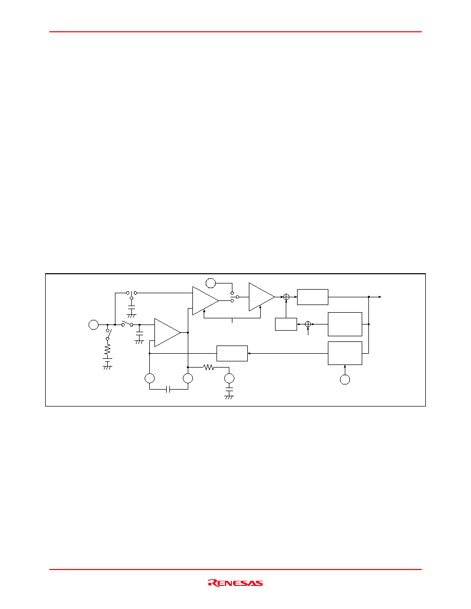
Figure 1 shows CDS/PGA + ADC function block.
Offset
calibration
logic
DC offset
feedback
logic
DAC
C3
CDS
AMP
PG
AMP
CDSIN
BLKFB
BLKSH
Gain setting
(register)
Clamp data
(register)
OBP
SH
AMP
BLKC
C4
C2
C1
VRT
Current
DAC
10-bit
ADC
D0 to D9
ADCIN
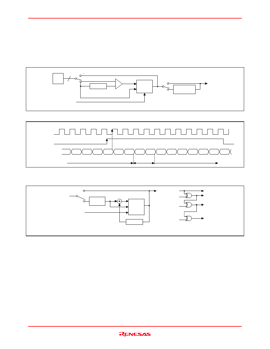
Figure 1 HD49334AF/AHF Functional Block Diagram
1. CDS (Correlated Double Sampling) Circuit
The CDS circuit extracts the voltage differential between the black level and a signal including the black level. The
black level is directly sampled at C1 by using the SPBLK pulse, buffered by the SHAMP, then provided to the
CDSAMP.
The signal level is directly sampled at C2 by using the SPSIG pulse, and provided to CDSAMP (see figure 1). The
difference between these two signal levels is extracted by the CDSAMP, which also operates as a programmable
gain amplifier at the previous stage. The CDS input is biased with VRT (2 V) during the SPBLK pulse validation
period. During the PBLK period, the above sampling and bias operation are paused.
HD49334AF/AHF
Rev.1.0, Apr 20, 2004, page 7 of 22
2. PGA Circuit
The PGAMP is the programmable gain amplifier for the latter stage. The PGAMP and the CDSAMP set the gain
using 8 bits of register.
The equation below shows how the gain changes when register value N is from 0 to 255.
In CDSIN mode: Gain = (≠2.36 dB + 0.132 dB)
◊ N (LOG linear).
In ADCIN mode: Gain = (0.57 times + 0.00446 times)
◊ N (linear).
Full-scale digital output is defined as 0 dB (one time) when 1 V is input.
3. Automatic Offset Calibration Function and Black-Level Clamp Data Setting
The DAC DC voltage added to the output of the PGAMP is adjusted by automatic offset calibration.
The data, which cancels the output offset of the PGAMP and the input offset of the ADC, and the clamp data (14
LSB to 76 LSB) set by register are added and input to the DAC.
The automatic offset calibration starts automatically after the RESET mode set by register 1 is cancelled and
terminates after 40000 clock cycles (when fclk = 20 MHz, 2 ms).
4. DC Offset Compensation Feedback Function
Feedback is done to set the black signal level input during the OB period to the DC standard, and all offsets
(including the CCD offset and the CDSAMP offset) are compensated for.
The offset from the ADC output is calculated during the OB period, and SHAMP feedback capacitor C3 is charged
by the current DAC (see figure 1).
The open-loop differential gain (
Gain/H) per 1 H of the feedback loop is given by the following equation. 1H is
the one cycle of the OBP.
Gain/
H = 0.078/(fclk
◊
C3) (fclk: ADCLK frequency, C3: SHAMP external feedback capacitor)
Example: When fclk = 20 MHz and C3 = 1.0
µ
F,
Gain/
H = 0.0039
When the PGAMP gain setting is changed, the high-speed lead-in operation state is entered, and the feedback loop
gain is increased by a multiple of N. Loop gain multiplication factor N can be selected from 4 times, 8 times, 16
times, or 32 times by changing the register settings (see table 1). Note that the open-loop differential gain
(
Gain/H) must be one or lower. If it is two or more, oscillation occurs.
The time from the termination of high-speed lead-in operation to the return of normal loop gain operation can be
selected from 1 H, 2 H, 4 H, or 8 H. If the offset error is over 32 LSB, the high-speed lead-in operation continues,
and when the offset error is 32 LSB or less, the operation returns to the normal loop-gain operation after 1 H, 2 H, 4
H, or 8 H depending on the register settings. See table 2.
Table 1
Loop Gain Multiplication Factor during
High-Speed Lead-In Operation
Table 2
High-Speed Lead-In Operation
Cancellation Time
HGain-Nsel
(register settings)
Multiplication
Factor N
HGstop-Hsel
(register settings)
Cancellation
Time
[0]
L
H
L
H
[1]
L
H
H
L
4
32
16
8
[0]
L
H
L
H
[1]
L
H
H
L
1 H
8 H
4 H
2 H
5. Pre-Blanking Function
During the PBLK input period, the CDS input operation is separated and protected from the large input signal. The
ADC digital output is fixed to clamp data (14 to 76 LSB).

HD49334AF/AHF
Rev.1.0, Apr 20, 2004, page 8 of 22
6. ADC Digital Output Control Function
The ADC digital output includes the functions output enable, code conversion, and test mode. Tables 3, 4 and 5
show the output functions and the codes.
Table 3
ADC Digital Output Functions
Operating Mode
ADC Digital Output
Low-power wait state
Output Hi-Z
Normal operation
Pre-blanking
Normal operation
Pre-blanking
Test mode
Hi-Z
Hi-Z
Same as in table 4.
D9 is inverted in table 4.
D8 to D0 are inverted in table 4.
D9 to D0 are inverted in table 4.
Output code is set up to Clamp Level.
Same as in table 5.
D9 is inverted in table 5.
D8 to D0 are inverted in table 5.
D9 to D0 are inverted in table 5.
Output code is set up to Clamp Level.
Notes:
1. STBY, TEST, LINV, and MINV are set by register.
2. Mode setting for the OEB and the PBLK are done by external input pins.
3. The polarity of the PBLK pin when the register setting is SPinv is low.
X
X
H
H
H
H
L
H
H
H
H
L
X
X
X
X
H
L
H
L
L
L
H
H
H
H
L
L
L
L
H
H
H
H
L
L
L
L
H
H
H
H
L
L
L
L
H
H
H
H
L
L
L
L
H
H
X
X
L
H
L
H
X
L
H
L
H
X
L
H
L
H
X
X
L
L
H
H
X
L
L
H
H
X
L
L
H
H
X
X
L
H
X
X
X
L
H
X
H
L
H
L
STBY
D9
OEB
D0
D1
D2
D3
D4
D5
D6
D7
D8
PBLK
MINV
LINV
TEST0
TEST1
Table 4
ADC Output Code
D1
H
L
L
H
H
L
L
L
H
H
D0
H
L
H
L
H
L
L
H
L
H
D2
L
H
H
H
H
L
H
H
H
H
D7
L
L
L
L
H
L
H
H
H
H
D5
L
L
L
L
H
L
H
H
H
H
D4
L
L
L
L
H
L
H
H
H
H
D3
L
L
L
L
H
L
H
H
H
H
D6
L
L
L
L
H
L
H
H
H
H
D8
L
L
L
L
H
L
H
H
H
H
D9
L
L
L
L
L
H
H
H
H
H
Output Pin
Output
codes
Steps
3
4
5
6
511
512
1020
1021
1022
1023
Table 5
ADC Output Code (TEST1)
D8
L
L
L
L
H
H
L
L
L
L
D9
L
L
L
L
L
H
H
H
H
H
Output Pin
Output
codes
Steps
3
4
5
6
511
512
1020
1021
1022
1023
D1
H
H
H
L
L
L
H
H
L
L
D0
L
L
H
H
L
L
L
H
H
L
D2
L
H
H
H
L
L
L
L
L
L
D7
L
L
L
L
L
L
L
L
L
L
D5
L
L
L
L
L
L
L
L
L
L
D4
L
L
L
L
L
L
L
L
L
L
D3
L
L
L
L
L
L
L
L
L
L
D6
L
L
L
L
L
L
L
L
L
L
HD49334AF/AHF
Rev.1.0, Apr 20, 2004, page 9 of 22
7. Adjustment of Black-Level S/H Response Frequency Characteristics
The CR time constant that is used for sampling/hold (S/H) at the black level can be adjusted by changing the
register settings, as shown in table 6.
Table 6
SHSW CR Time Constant Setting
L
[0]
2.20 nsec
(72 MHz)
2.30 nsec
(69 MHz)
L
[1]
L
[2]
L
2.51 nsec
(63 MHz)
2.64 nsec
(60 MHz)
2.93 nsec
(54 MHz)
3.11 nsec
(51 MHz)
3.52 nsec
(45 MHz)
3.77 nsec
(42 MHz)
[3]
H
[0]
L
[1]
L
[2]
L
[3]
L
[0]
H
[1]
L
[2]
L
[3]
H
[0]
H
[1]
L
[2]
L
[3]
L
[0]
L
[1]
H
[2]
L
[3]
H
[0]
L
[1]
H
[2]
L
[3]
L
[0]
H
[1]
H
[2]
L
[3]
H
[0]
H
[1]
H
[2]
L
[3]
L
[0]
SHSW-fsel (Register setting)
4.40 nsec
(36 MHz)
4.80 nsec
(33 MHz)
L
[1]
L
[2]
H
CR Time Constant (Typ)
(cutoff frequency conversion)
5.87 nsec
(27 MHz)
6.60 nsec
(24 MHz)
8.80 nsec
(18 MHz)
10.6 nsec
(15 MHz)
17.6 nsec
(9 MHz)
26.4 nsec
(6 MHz)
[3]
H
[0]
L
[1]
L
[2]
H
[3]
L
[0]
H
[1]
L
[2]
H
[3]
H
[0]
H
[1]
L
[2]
H
[3]
L
[0]
L
[1]
H
[2]
H
[3]
H
[0]
L
[1]
H
[2]
H
[3]
L
[0]
H
[1]
H
[2]
H
[3]
H
[0]
H
[1]
H
[2]
H
[3]
BLKC
C4
31
The SHAMP frequency characteristics can be adjusted by changing the register settings
and the C4 value of the external 31st pin.
The settings are shown in table 7.
Values other than those shown in the table 7 cannot be used.
8.
SHSW-fsel (Register setting)
CR Time Constant (Typ)
(cutoff frequency conversion)
Table 7
SHAMP Frequency Characteristics Setting
49 MHz
15000 pF
(620 pF)
24 MHz
27000 pF
(820 pF)
32 MHz
22000 pF
(750 pF)
SHA-fsel (Register setting)
LoPwr
(Register setting)
Note: Upper line
Middle line
Lower line
: SHAMP cutoff frequency (Typ)
: Standard value of C4 (maximum value is not defined)
: Minimum value of C4 (do not set below this value)
56 MHz
18000 pF
(360 pF)
116 MHz
10000 pF
(270 pF)
"Lo"
"Hi"
75 MHz
13000 pF
(300 pF)
H
[0]
L
[1]
L
[0]
H
[1]
H
[0]
H
[1]

HD49334AF/AHF
Rev.1.0, Apr 20, 2004, page 10 of 22
Timing Chart
Figure 2 shows the timing chart when CDSIN and ADCIN input modes are used.
0
1
2
9
10
11
N+1
N+2
N+9
N+10
N+11
N
N
-9
N
-8
N
-1
N
CDSIN
SPBLK
SPSIG
ADCLK
D0 to D9
N+2
N+8
N+9
N+10
N+11
N
-8
N
-9
N
-1
ADCIN
ADCLK
D0 to D9
N
N+1
N
N+1
N
-10
∑ When CDSIN input mode is used
Note: The phases of SPBLK and SPSIG are those when the serial data SPinv bit is set to low.
∑ When ADCIN input mode is used
~
Figure 2 Output Timing Chart when CDSIN and ADCIN Input Modes are Used
∑ The ADC output (D0 to D9) is output at the rising edge of the ADCLK in both modes.
∑ Pipe-line delay is ten clock cycles when CDSIN is used and nine when ADCIN is used.
∑ In ADCIN input mode, the input signal is sampled at the rising edge of the ADCLK.
HD49334AF/AHF
Rev.1.0, Apr 20, 2004, page 11 of 22
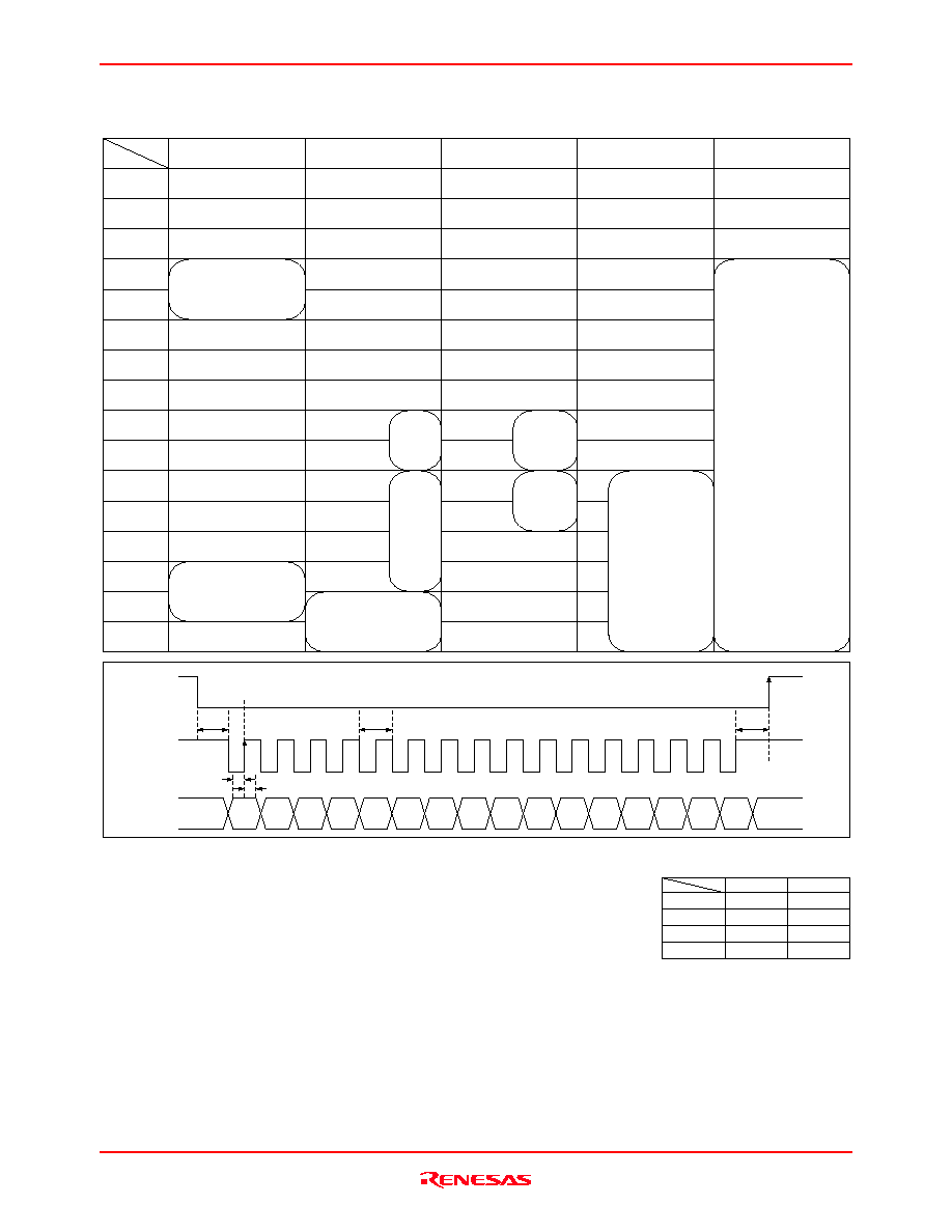
Detailed Timing Specifications
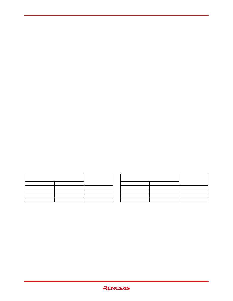
Detailed Timing Specifications when CDSIN Input Mode is Used
Figure 3 shows the detailed timing specifications when the CDSIN input mode is used, and table 8 shows each timing
specification.
Note:
Black
level
Signal
level
D0 to D9
1. When serial data Spinv bit is set to low. (When the Spinv bit is set to high, the polarities
of the SPBLK and the SPSIG are inverted.)
CDSIN
SPBLK
Vth
(2)
(3)
SPSIG
ADCLK
(7)
Vth
Vth
(8)
(9)
(10)
(4)
(1)
(5)
(6)
Figure 3 Detailed Timing Chart when CDSIN Input Mode is Used
Table 8
Timing Specifications when the CDSIN Input Mode is Used
No. Timing
Symbol
Min
Typ Max
Unit
(1)
Black-level signal fetch time
t
CDS1
-- (1.5)
-- ns
(2)
SPBLK low period *
1
t
CDS2
Typ
◊
0.8
1/4f
CLK
Typ
◊
1.2
ns
(3)
Signal-level fetch time
t
CDS3
-- (1.5)
-- ns
(4)
SPSIG low period *
1
t
CDS4
Typ
◊
0.8
1/4f
CLK
Typ
◊
1.2
ns
(5)
SPBLK rising to SPSIG rising time *
1
t
CDS5
Typ
◊
0.85
1/2f
CLK
Typ
◊
1.15
ns
(6)
SPSIG rising to ADCLK rising inhibition time *
1
t
CDS6
1
5
11
ns
(7), (8) ADCLK t
WH
min./t
WL
min.
t
CDS7, 8
11
--
--
ns
(9)
ADCLK rising to digital output hold time
t
CHLD9
3
7
--
ns
(10)
ADCLK rising to digital output delay time
t
COD10
--
16
24
ns
Note: 1. SPBLK and SPSIG polarities when serial data Spinv bit is set to low.
OBP Detailed Timing Specifications
Figure 4 shows the OBP detailed timing specifications.
The OB period is from the fifth to the twelfth clock cycle after the OB pulse is input. The average of the black signal
level is taken for eight input cycles during the OB period and becomes the clamp level (DC standard).
CDSIN
OBP
Note:
OB pulse > 2 clock cycles
When serial data OBPinv bit is set to low
(When the OBPinv is set to high, the polarity of the OBP is inverted.)
OB period *
1
1. Shifts
±1 clock cycle depending on the OBP input timing.
N
N+1
N+5
N+12
N+13
This edge is used, when OBP pulse-width period is clamp-on.
Figure 4 OBP Detailed Timing Specifications
HD49334AF/AHF
Rev.1.0, Apr 20, 2004, page 12 of 22
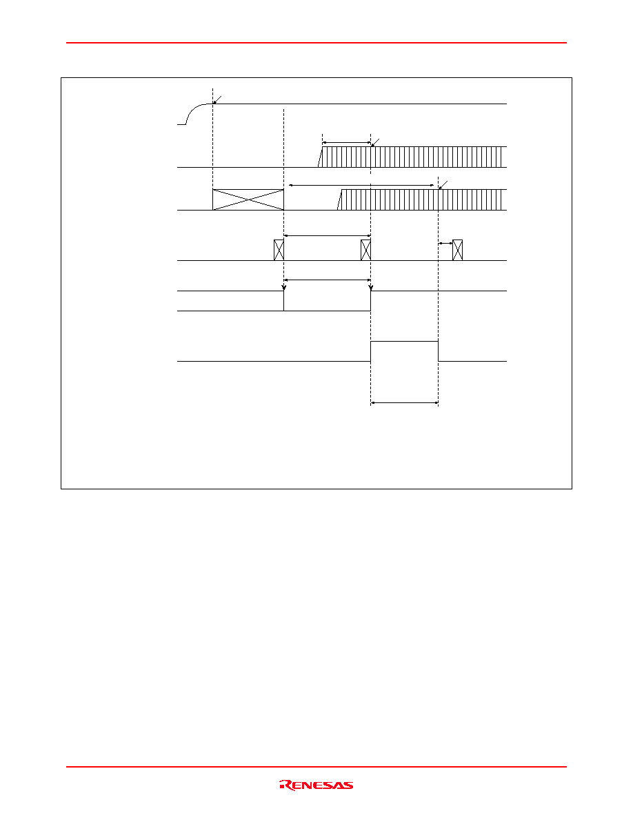
Detailed Timing Specifications at Pre-Blanking
Figure 5 shows the pre-blanking detailed timing specifications.
Digital output
(D0 to D9)
ADC
data
Clamp level
ADC
data
PBLK
t
PBLK
ADCLK
◊ 2 clocks
ADCLK
◊ 10 clocks
(shifts one clock cycle depending
on the PBLK input timing)
When serial data SPinv bit is set to low
(When the SPinv is set to high, the PBLK polarity is inverted.)
Vth
V
OL
V
OH
Figure 5 Detailed Timing Specifications at Pre-Blanking
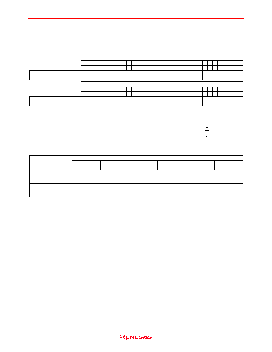
Detailed Timing Specifications when ADCIN Input Mode is Used
Figure 6 shows the detailed timing chart when ADCIN input mode is used, and table 9 shows each timing specification.
ADCIN
(1)
ADCLK
D0 to D9
(2)
Vth
V
DD
/2
(3)
(5)
(4)
Figure 6 Detailed Timing Chart when ADCIN Input Mode is Used
Table 9
Timing Specifications when ADCIN Input Mode is Used
No. Timing
Symbol
Min
Typ Max
Unit
(1)
Signal fetch time
t
ADC1
-- (6)
-- ns
(2), (3)
ADCLK t
WH
min./t
WL
min.
t
ADC2, 3
Typ
◊
0.85
1/2f
ADCLK
Typ
◊
1.15
ns
(4)
ADCLK rising to digital output hold time
t
AHLD4
10
14.5 --
ns
(5)
ADCLK rising to digital output delay time
t
AOD5
--
23.5 31.5
ns
Detailed Timing Specifications for Digital Output-Enable Control
Figure 7 shows the detailed timing specifications for digital output enable control. When the OEB pin is set to high,
output disable mode is entered, and the output state becomes High-Z.
Digital output
(D0 to D9)
OEB
t
LZ
t
ZL
t
HZ
t
ZH
DV
DD
/2
DV
DD
/2
DV
DD
2 k
10 pF
DV
DD
DV
SS
DV
SS
V
OL
t
LZ
, t
ZL
measurement load
t
HZ
, t
ZH
measurement load
V
OH
Vth
DV
SS
10 pF
2 k
DV
SS
Figure 7 Detailed Timing Specifications for Digital Output Enable Control
HD49334AF/AHF
Rev.1.0, Apr 20, 2004, page 13 of 22
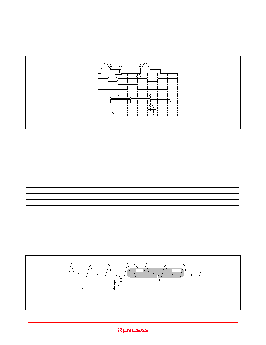
Serial Interface Specifications
DI 00 (LSB)
Low
DI 01
Low
Low
High
Low
Low
Resister 2
Resister 0
Resister 4 to 7
Test Mode (can not be used)
Resister 3
Resister 1
Low
Low
High
High
Low
Low to High
Low to High
High
High
DI 02
DI 03
DI 04
DI 05
DI 06
DI 07
DI 08
DI 09
DI 10
DI 11
DI 12
DI 13
DI 14
DI 15 (MSB)
HGstop-Hsel [1]
HGain-Nsel [0]
SHA-fsel [0] (LSB)
SHA-fsel [1] (MSB)
SHSW-fsel [0] (LSB)
SHSW-fsel [1]
SHSW-fsel [2]
SHSW-fsel [3] (MSB)
Clamp-level [3]
Clamp-level [2]
Clamp-level [1]
Low: Normal operation mode
High: Sleep mode
SLP
Low: Normal operation mode
High: Standby mode
STBY
Low: CDSIN input mode
High: ADCIN input mode
CSEL
Clamp-level [0] (LSB)
C-Bias off
Clamp-level [4] (MSB)
Gray code [0] (TEST1)
Gray code [1]
Ave_4H
HGstop-Hsel [0]
PGA gain setting (LSB)
PGA gain setting
PGA gain setting
PGA gain setting
PGA gain setting
PGA gain setting
Output mode setting (LINV)
Output mode setting (MINV)
Output mode setting (TEST0)
PGA gain setting
PGA gain setting (MSB)
OBPinv, OBP inversion
Low_PWR
SPinv,
SPSIG/SPBLK/PBLK inversion
Low: Reset mode
High: Normal operation mode
RESET
HGain-Nsel [1]
SHSW
frequency
character-
istics
switching
SHAMP
frequency
character-
istics
switching
Table 10
Serial Data Function List
Cannot
be used.
All low
Cannot
be used.
All low
Cannot
be used.
All low
High-speed
lead-in
cancellation
time
High-speed
lead-in
gain
multiplication
Cannot
be used.
Cannot be used.
Timing Specifications
SCK
CS
SDATA
DI
00
DI
01
DI
02
DI
03
DI
04
DI
05
DI
06
DI
07
DI
08
DI
09
DI
10
DI
11
DI
12
DI
13
DI
14
DI
15
Latches SDATA
at SCK rising edge
Data is determined
at CS rising edge
t
INT
1
t
ho
t
su
t
INT
2
f
SCK
Figure 8 Serial Interface Timing Specifications
t
su
t
ho
t
INT
1, 2
f
SCK
50 ns
50 ns
50 ns
Min
5 MHz
Max
Gray_test [2]
0
Gray_test [0]
Gray_test [1]
0
0
1
1
0
Notes: 1.
2.
3.
4.
5.
6.
7.
8.
2 byte continuous communications.
SDATA is latched at SCK rising edge.
Insert 16 clocks of SCK while CS is low.
Data is invalid if data transmission is aborted during transmission.
The gain conversion table differs in the CDSIN input mode and the ADCIN input mode.
STBY: Reference voltage generator circuit is in the operating state.
SLP: All circuits are in the sleep state.
This bit is used for the IC testing, and cannot be used by the user.
The use of this address is prohibited.
Circuit current and the frequency characteristic are switched.
Data = 0: 36 MHz guarantee
Data = 1: 25 MHz guarantee
HD49334AF/AHF
Rev.1.0, Apr 20, 2004, page 14 of 22
Explanation of Serial Data of CDS Part
Serial data of CDS part has the following functions.
∑ PGA gain (D5 to D12 of register 0)
Details are referred to page 5 block diagram.
At CDS_in mode: ≠2.36 dB + 0.132 dB
◊
N (Log linear)
At ADC_in mode: 0.57 times + 0.01784 times
◊
N (Times linear)
: Full-scale digital output is defined as 0 dB when 1 V is input.
Above PGA gain definition means input signal 1 Vp-p to CDS_in, and set N = 18 (correspond 2.36 dB), and then
PGA outputs the 2 V full-range, and also ADC out puts the full code (1023).
This mean offset gain of PGA has 6 dB ≠ 2.36 dB = 3.64 dB, therefore it should be decided that how much dB add
on.
(1) Level dia explain
CDS
PGA
0 dB when set N = 18 which correspond to 2.36 dB
ADC
(2) Level dia on the circuit
CDS
PGA
3.64 dB + 0.132 dB
◊ N
(CDS = 0 dB)
ADC
2 V
1023
(1.0 V)
(1.0 V)
(2.0 V)
(1023)
Figure 9 Level Dia of PGA
∑ CSEL (D15 of register 0)
Data = 0: Select CDSIN
Data = 1: Select ADCIN
Address
STD1[7:0] (L)
STD2[15:8] (H)
1
1
1
1
0
0
0
1
D4
D3
D2
D1
D0 D15 D14 D13 D12 D11 D10 D9
D8
SHA_fsel
test_I2
SHSW_fsel
test0
MINV
LINV
STBY
SLP
∑ SLP and STBY (D3, D4 of register 1)
SLP:
Stop the all circuit. Consumption current of CDS part is less than 10
µA.
Start up from offset calibration when recover is needed.
STBY: Only the standard voltage generating circuit is operated. Consumption current of CDS part is about 3 mA.
Allow 50 H time for feedback clamp is stabilized until recover.
∑ Output mode (D5 to D7 of register 1 and D4 of register 3)
It is a test mode. Combination details are table 3 to 5. Normally set to all 0.
∑ SHA-fsel (D8 to D9 of register 1)
It is a LPF switching of SH amplifier. Frequency characteristics are referred to page 9. To get rough idea, set the
double cut off frequency point with using.
∑ SHSW-fsel (D10 to D13 of register 1)
It is a time constant which sampling the black level of SH amplifier. Frequency characteristics are referred to page
9. To get rough idea, set the double cut off frequency point with using. S/N changes by this data, so find the
appropriate point with set data to up/down.
HD49334AF/AHF
Rev.1.0, Apr 20, 2004, page 15 of 22
∑ Clamp (D3 to D7 of register 2)
Determine the OB part level with digital code of ADC output.
Clamp level = setting data
◊
2 + 14
Default data is 9 = 32 LSB.
∑ HGstop-Hsel, HGain-Nsel (D8 to D11 of register 2)
Determine the lead-in speed of OB clamp. Details are referred to page 7. PGA gain need to be changed for switch
the high speed leading mode. Transfer the gain +1/≠1 to previous field, its switch to high speed leading mode.
∑ Low_PWR (D12 of register 2)
Switch circuit current and frequency characteristic.
Data = 0: 36 MHz guarantee
Data = 1: 25 MHz guarantee
∑ SPinv (D13 of register 2)
SPSIG/SPBLK/PBLK input signal inverted switching.
Data = 1: Normal
Data = 0: Inverted
∑ Reset (D15 of register 2)
Software reset.
Data = 1: Normal
Data = 0: Reset
Offset calibration should be done when starting up with using this bit. Details are referred to page 19.
∑ C_Bias_off (D3 of register 3)
Center bias is turned off in ADCIN mode.
Data = 0: Normally on
Data = 1: Off
∑ Ave_4H (D6 of register 3)
Clamp detection data is averaged 4H.
Data = 0: 1H
Data = 1: Averaged 4H
Differential Code and Gray Code (D4 to D5 and D7 to D9 of register 3)
∑ Gray code (D4 to D5 of register 3)
DC output code can be change to following type.
Gray Code [1]
Gray Code [0]
Output Code
0 0 Binary
code
0 1 Gray
code
1
0
Differential encoded binary
1
1
Differential encoded gray
∑ Serial data setting items (D7 to D9 of register 3)
Setting Bit
Setting Contents
Gray_test[0]
Gray_test[1]
Standard data output timing control signal
(Refer to the following table)
Gray_test[2]
ADCLK polar with OBP. (Lo
Positive edge, HI
Negative edge)
∑ Standard data output timing
Gray_test[1] Gray_test[0] Standard Data Output Timing
Low Low Third
and
fourth
Low
High
Fourth and fifth
High
Low
Fifth and sixth
High High Sixth
and
seventh
HD49334AF/AHF
Rev.1.0, Apr 20, 2004, page 16 of 22
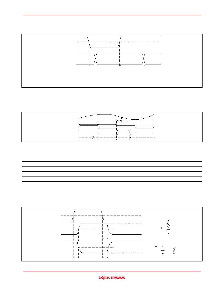
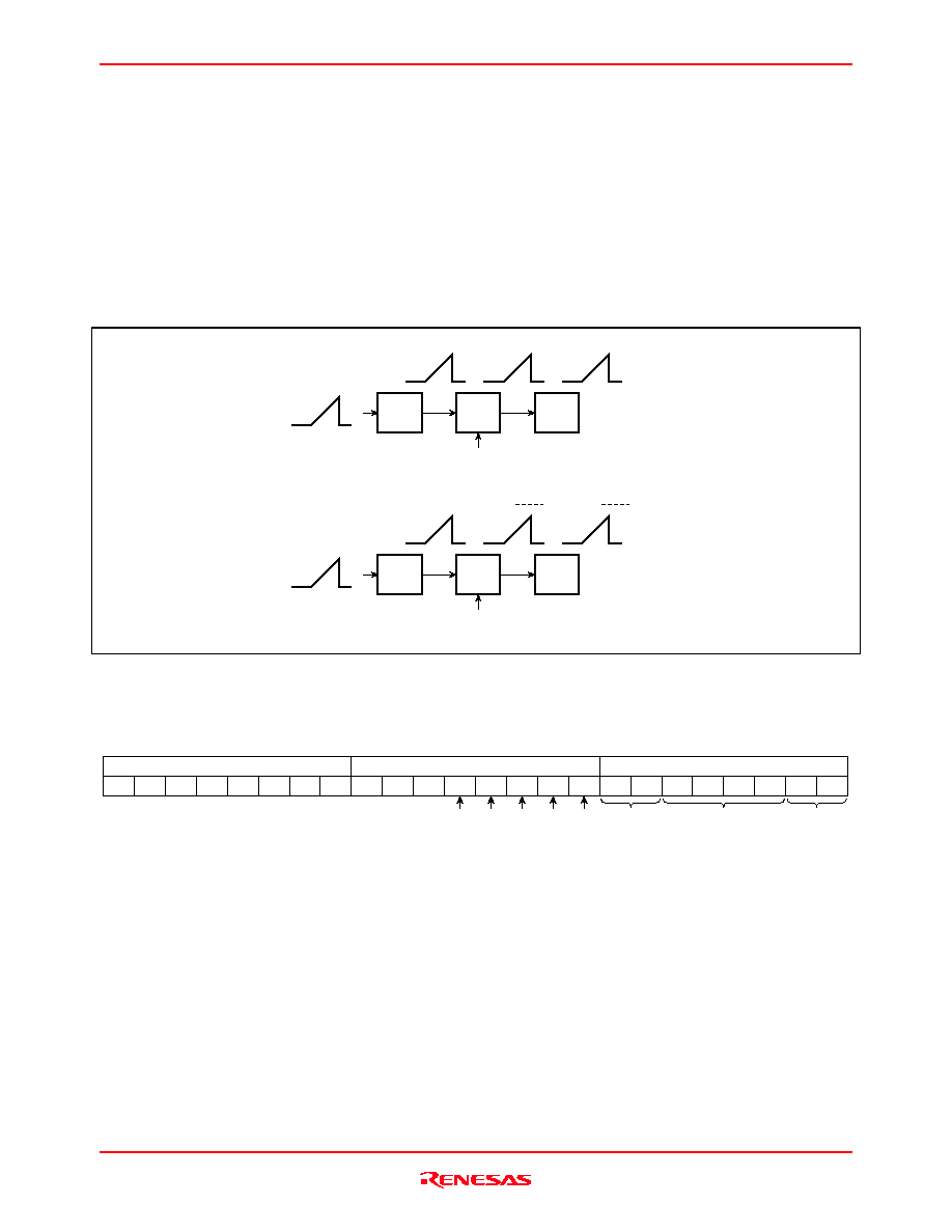
Ripple (pseudo outline made by quantized error) occurres on the point which swithing the ADC output multiple bit in
parallel. When switching the several of ADC output at the same time, ripple (pseudo outline caused by miss
quantization) occurs to the image.
Differential code and gray code are recommended for this countermeasure.
Figure 10 indicates circuit block. When luminance signal changes are smoothly, the number of bit of switching digital
output bit can be reduced and easily to reduce the ripple using this function.
This function is especially effective for longer the settings of sensor more than clk = 30 kHz, and ADC output.
Figure 11 indicates the timing specifications.
ADC
10
Differential SW(D5)
Carry bit
round
+
-
Gray SW(D4)
Standard data
control signal
(D9,D8,D7)
Standard
data
selector
10-bit
output
2clk_DL
Gray
Binary
conversion
Figure 10 Differential Code, Gray Code Circuit
1
ADCLK
OBP
Digital output
(Beginning edge of OBP and standard edge of ADCLK should be exept ±5 ns)
(In case of select the positive edge of ADCLK with D8)
(In case of select the positive polar)
Differential data
Standard
data
Differential data
2
3
4
5
6
7
8
9
10
11
Figure 11 Differential Code Timing Specifications
To use differential code, complex circuit is necessary at DSP side.
(1) Differential coded
From ADC
Standard data
control signal
Carry bit
round
2clk_DL
Standard
data
selector
D9
D9
D8
D7
D0
D8
D7
D0
Gray
Binary
(2) Gray
Binary conversion
Figure 12 Complex Circuit Example
HD49334AF/AHF
Rev.1.0, Apr 20, 2004, page 17 of 22
Absolute Maximum Ratings
(Ta = 25
∞C)
Item Symbol
Ratings
Unit
Power supply voltage
V
DD
(max) 4.1
V
Analog input voltage
V
IN
(max)
≠0.3 to AV
DD
+0.3
V
Digital input voltage
V
I
(max)
≠0.3 to DV
DD
+0.3
V
Operating temperature
Topr
≠10 to +75
∞C
Power dissipation
Pt(max)
400
mW
Storage temperature
Tstg
≠55 to +125
∞C
Power supply voltage range
Vopr
2.7 to 3.3
V
Notes: 1. V
DD
indicates AV
DD
and DV
DD
.
2.
AV
DD
and DV
DD
must be commonly connected outside the IC. When they are separated by a noise filter, the
potential difference must be 0.3 V or less at power on, and 0.1 V or less during operation.
Electrical Characteristics
(Unless othewide specified, Ta = 25∞C, AV
DD
= 3.0 V, DV
DD
= 3.0 V, and R
BIAS
= 33 k
)
∑ Items Common to CDSIN and ADCIN Input Modes
Item Symbol
Min
Typ
Max
Unit
Test
Conditions
Remarks
Power supply voltage
range
V
DD
2.7 3.0
3.3 V
f
CLK
hi
20 --
36 MHz
LoPwr
=
low
HD49334AHF
Conversion frequency
f
CLK
low
5.5
--
25
MHz
LoPwr = high
HD49334AF
V
IH
DV
DD
3.0
2.0
◊
-- DV
DD
V
V
IL
0
--
DV
DD
3.0
0.8
◊
V
Digital input pins
other than CS,
SCK and SDATA
V
IH2
DV
DD
3.0
2.25
◊
-- DV
DD
V
Digital input voltage
V
IL2
0
--
DV
DD
3.0
0.6
◊
V
CS, SCK, SDATA
V
OH
DV
DD
≠0.5
--
--
V
I
OH
= ≠1 mA
Digital output voltage
V
OL
--
-- 0.5
V I
OL
= +1 mA
I
IH
--
-- 50
µ
A V
IH
= 3.0 V
I
IH2
--
-- 250
µ
A V
IH
= 3.0 V
Digital input current
I
IL
≠50 -- --
µ
A V
IL
= 0 V
I
OZH
--
-- 50
µ
A V
OH
= V
DD
Digital output current
I
OZL
≠50
-- --
µ
A V
OL
= 0 V
ADC
resolution RES
10 10
10 bit
ADC integral linearity
INL
--
(3)
--
LSBp-p
f
CLK
= 25 MHz
ADC differential linearity+ DNL+
--
0.3
0.9
LSB
f
CLK
= 25 MHz
*1
ADC differential linearity≠ DNL≠
≠0.9
≠0.3
--
LSB
f
CLK
= 25 MHz
*1
Sleep current
I
SLP
≠100 0 100
µ
A
Digital input pin is
set to 0 V, output
pin is open
Standby current
I
STBY
--
3
5
mA Digital I/O pin is set
to 0 V
t
HZ
--
-- 100 ns
t
LZ
--
-- 100 ns
t
ZH
--
-- 100 ns
Digital output Hi-Z
delay time
t
ZL
--
-- 100 ns
R
L
= 2 k
,
C
L
= 10 pF
See figure 7
Notes: 1. Differential linearity is the calculated difference in linearity errors between adjacent codes.
2. Values within parentheses ( ) are for reference.

HD49334AF/AHF
Rev.1.0, Apr 20, 2004, page 18 of 22
Electrical Characteristics (cont.)
(Unless othewide specified, Ta = 25∞C, AV
DD
= 3.0 V, DV
DD
= 3.0 V, and R
BIAS
= 33 k
)
∑ Items for CDSIN Input Mode
Item Symbol
Min
Typ
Max
Unit
Test
Conditions
Remarks
Consumption current (1)
I
DD1
-- 45.0
54.5 mA
f
CLK
= 36 MHz
CDSIN mode
LoPwr = low
Consumption current (2)
I
DD2
-- 23.5
31.0 mA
f
CLK
= 25 MHz
CDSIN mode
LoPwr = high
CCD offset tolerance range
V
CCD
(≠100)
-- (100) mV
Timing specifications (1)
t
CDS1
-- (1.5) -- ns
Timing specifications (2)
t
CDS2
Typ
◊
0.8
1/4f
CLK
Typ
◊
1.2
ns
Timing specifications (3)
t
CDS3
-- (1.5) -- ns
Timing specifications (4)
t
CDS4
Typ
◊
0.8
1/4f
CLK
Typ
◊
1.2
ns
Timing specifications (5)
t
CDS5
Typ
◊
0.85
1/2f
CLK
Typ
◊
1.15
ns
Timing specifications (6)
t
CDS6
1 5 9
ns
Timing specifications (7)
t
CDS7
11 -- -- ns
Timing specifications (8)
t
CDS8
11 -- -- ns
Timing specifications (9)
t
CHLD9
3
7
--
ns
Timing specifications (10)
t
COD10
-- 16 24
ns
C
L
= 10 pF
See table 8
CLP(00) --
(14)
--
LSB
CLP(09) --
(32)
--
LSB
Clamp level
CLP(31) --
(76)
--
LSB
PGA(0) ≠4.4 ≠2.4 ≠0.4
dB
PGA(63) 4.1
6.1
8.1
dB
PGA(127) 12.5
14.5
16.5
dB
PGA(191) 21.0
23.0
25.0
dB
PGA gain at CDS input
PGA(255) 29.3
31.3
33.3
dB
Note : Values within parentheses ( ) are for reference.
∑ Items for ADCIN Input Mode
Item Symbol
Min
Typ
Max
Unit
Test
Conditions
Remarks
Consumption current (3)
I
DD3
-- 30.0
38.0
mA
f
CLK
= 36 MHz
ADCIN mode
LoPwr = low
Consumption current (4)
I
DD4
-- 17.0
21.5
mA
f
CLK
= 25 MHz
ADCIN mode
LoPwr = high
Timing specifications (11)
t
ADC1
-- (6) -- ns
Timing specifications (12)
t
ADC2
Typ
◊
0.85
1/2f
ADCLK
Typ
◊
1.15
ns
Timing specifications (13)
t
ADC3
Typ
◊
0.85
1/2f
ADCLK
Typ
◊
1.15
ns
Timing specifications (14)
t
AHLD4
10 14.5 -- ns
Timing specifications (15)
t
AOD5
-- 23.5
31.5 ns
C
L
= 10 pF
See table 9
Input current at ADC input
IIN
CIN
≠110 -- 110
µ
A V
IN
= 1.0 V to 2.0 V
Clamp level at ADC input
OF2
--
(512)
--
LSB
GSL(0) 0.45 0.57 0.72 Times
GSL(63) 1.36
1.71 2.16
Times
GSL(127) 2.26
2.85
3.59
Times
GSL(191) 3.18
4.00
5.04
Times
PGA gain at ADC input
GSL(255) 4.06
5.12
6.45
Times
Note : Values within parentheses ( ) are for reference.
HD49334AF/AHF
Rev.1.0, Apr 20, 2004, page 19 of 22
Operation Sequence at Power On
RESET bit
RESET = "Low"
(RESET mode)
V
DD
OBP
High-speed pulse is the right phase
OBP is the right phase
SPBLK
SPSIG
ADCLK
etc.
OBP is started within this period
HD49334AF/AHF
serial data transfer
RESET = "High"
(RESET cancellation)
Must be stable within the operating
power supply voltage range
Start control
of TG and
camera DSP
(1) Register 2 setting
(2) Register 2 setting
(3) Register 0 and 1 settings
(4) Please perform an offset calibration in the period which avoided PBLK of V.
: Set all bits in register 2 to the usage condition, and set the RESET bit to low.
: Cancel the RESET mode by setting the register 2 RESET bit to high.
Do not change other register 2 settings. Offset calibration starts automatically.
: After the offset calibration is terminated, set registers 0 and 1.
(2) Register 2 setting
(1) Register 2 setting
(3) Registers 0
and 1 settings
0 ms
or more
1 ms or more
2 ms or more
2 ms or more
Prohibition
period
Ends after
40000 clock cycles
Automatic offset
calibration
The following describes the above serial data transfer. For details on registers 0, 1, and 2, refer to table 10.
(4)Offset calibration
(automatically starts
after RESET
cancellation)
HD49334AF/AHF
Rev.1.0, Apr 20, 2004, page 20 of 22
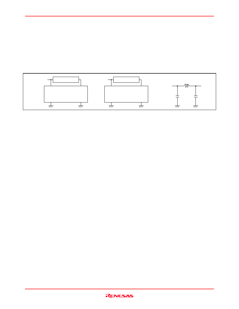
Notice for Use
1. Careful handling is necessary to prevent damage due to static electricity.
2. This product has been developed for consumer applications, and should not be used in non-consumer applications.
3. As this IC is sensitive to power line noise, the ground impedance should be kept as small as possible. Also, to
prevent latchup, a ceramic capacitor of 0.1 µF or more and an electrolytic capacitor of 10 µF or more should be
inserted between the ground and power supply.
4. Common connection of AV
DD
and DV
DD
should be made off-chip. If AV
DD
and DV
DD
are isolated by a noise filter,
the phase difference should be 0.3 V or less at power-on and 0.1 V or less during operation.
5. If a noise filter is necessary, make a common connection after passage through the filter, as shown in the figure
below.
HD49334AF/AHF
AV
SS
DV
SS
AV
DD
DV
DD
Noise filter
Analog
+3.0V
HD49334AF/AHF
DV
SS
AV
SS
DV
DD
AV
DD
100
µH
0.01
µF
Noise filter
Example of noise filter
Digital
+3.0V
0.01
µF
6. Connect AV
SS
and DV
SS
off-chip using a common ground. If there are separate analog system and digital system
set grounds, connect to the analog system.
7. When V
DD
is specified in the data sheet, this indicates AV
DD
and DV
DD
.
8. No Connection (NC) pins are not connected inside the IC, but it is recommended that they be connected to power
supply or ground pins or left open to prevent crosstalk in adjacent analog pins.
9. To ensure low thermal resistance of the package, a Cu-type lead material is used. As this material is less tolerant of
bending than Fe-type lead material, careful handling is necessary.
10. The infrared reflow soldering method should be used to mount the chip. Note that general heating methods such as
solder dipping cannot be used.
11. Serial communication should not be performed during the effective video period, since this will result in degraded
picture quality. Also, use of dedicated ports is recommended for the SCK and SDATA signals used in the
HD49330AF. If ports are to be shared with another IC, picture quality should first be thoroughly checked.
12. At power-on, automatic adjustment of the offset voltage generated from PGA, ADC, etc., must be implemented in
accordance with the power-on operating sequence (see page 19).

HD49334AF/AHF
Rev.1.0, Apr 20, 2004, page 21 of 22
Example of Recommended External Circuit
R11 100
R12 100
R13 100
R10 100
C18
0.1
C19
0.1
C17
0.1
L1
47
µ
∑ At CDS Input
Notes: 1. For C4, see table 5.
2. For C3, see page 8 "DC Offset Compensation Feedback Function".
Unit: R:
C: F
23
26
27
28
29
30
31
32
33
34
C4*
1
C14 0.1
R15 33 k
C15 0.1
35
36
25
11
10
9
8
7
6
5
4
3
2
1
12
16 15 14 13
17
18
19
20
21
22
24
38
45 46 47 48
44
43
42
41
40
39
37
Serial data input
GND
from
Timing generator
from CCD out
Note: External circuit is same as above except for ADC input.
3.0 V
3.0 V
to
Camera
signal
processor
to
Camera
signal
processor
C21
0.1
C22
0.1
C18
0.1
C19
0.1
C17
0.1
C21
0.1
C22
0.1
C1
1
µ C3*
2
1
µ
C10
0.1
C11
0.1
C12
0.1
C11
0.1
C12
0.1
R15 33 k
C16
47/6
C21
47/6
L2
47
µ
R14 100
HD49334AF/AHF
(CDS/PGA+ADC)
L1
47
µ
∑ At ADC Input
23
26
27
28
29
30
31
32
33
34
C15 0.1
35
36
25
11
10
9
8
7
6
5
4
3
2
1
12
16 15 14 13
17
18
19
20
21
22
24
38
45 46 47 48
44
43
42
41
40
39
37
Serial data input
GND
from
Timing generator
C14 0.1
C2 2.2/16
C16
47/6
C21
47/6
L2
47
µ
HD49334AF/AHF
(CDS/PGA+ADC)
+
-
AV
SS
AV
SS
AV
DD
BLKSH
BLKFB
CDSIN
BLKC
BIAS
AV
DD
NC
AV
SS
ADCIN
NC
D9
D8
D7
D6
D5
D4
D3
D2
D1
D0
NC
NC
NC
SPSIG
SPBLK
OBP
PBLK
DV
DD
DV
DD
ADCLK
DV
SS
DV
SS
DRDV
DD
VRM
VRT
VRB
NC
DV
SS
OEB
DV
DD
DV
DD
DV
SS
CS
SDATA
SCK
AV
SS
AV
SS
AV
DD
BLKSH
BLKFB
CDSIN
BLKC
BIAS
AV
DD
NC
AV
SS
ADCIN
NC
D9
D8
D7
D6
D5
D4
D3
D2
D1
D0
NC
NC
NC
SPSIG
SPBLK
OBP
PBLK
DV
DD
DV
DD
ADCLK
DV
SS
DV
SS
DRDV
DD
VRM
VRT
VRB
NC
DV
SS
OEB
DV
DD
DV
DD
DV
SS
CS
SDATA
SCK
with ADC input
HD49334AF/AHF
Rev.1.0, Apr 20, 2004, page 22 of 22
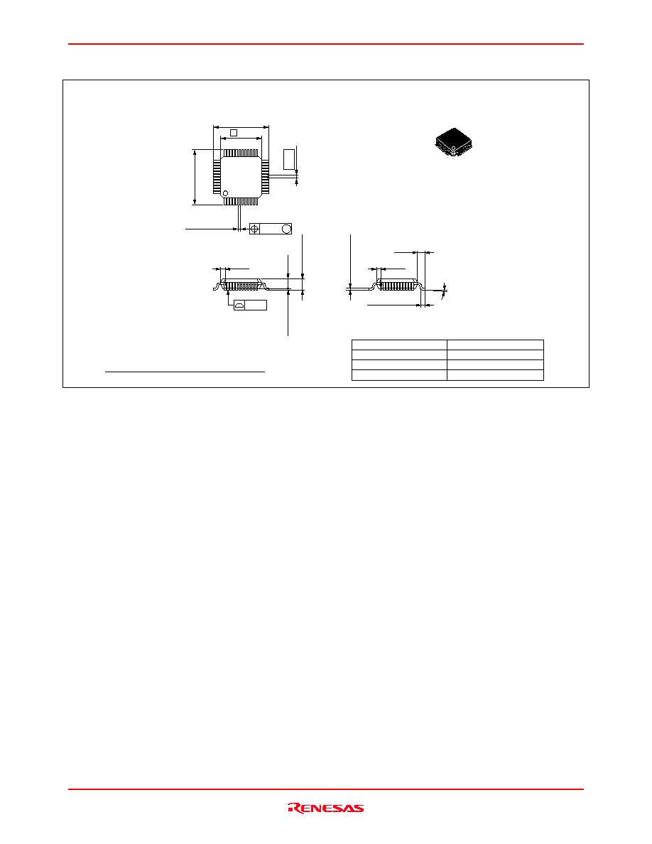
Package Dimensions
Package Code
JEDEC
JEITA
Mass (reference value)
FP-48C
--
Conforms
0.2 g
*Dimension including the plating thickness
Base material dimension
9.0 ± 0.2
7.0
*0.21 ± 0.05
0.08
36
25
1
12
37
48
24
13
0.5
9.0 ± 0.2
0.10
1.00
0∞ ≠ 8∞
0.50 ± 0.10
*0.17 ± 0.05
1.70 Max
M
0.75
0.75
0.19 ± 0.04
1.40
0.15 ± 0.04
0.13
+0.09 ≠0.05
As of January, 2003
Unit: mm

Keep safety first in your circuit designs!
1. Renesas Technology Corp. puts the maximum effort into making semiconductor products better and more reliable, but there is always the possibility that trouble
may occur with them. Trouble with semiconductors may lead to personal injury, fire or property damage.
Remember to give due consideration to safety when making your circuit designs, with appropriate measures such as (i) placement of substitutive, auxiliary
circuits, (ii) use of nonflammable material or (iii) prevention against any malfunction or mishap.
Notes regarding these materials
1. These materials are intended as a reference to assist our customers in the selection of the Renesas Technology Corp. product best suited to the customer's
application; they do not convey any license under any intellectual property rights, or any other rights, belonging to Renesas Technology Corp. or a third party.
2. Renesas Technology Corp. assumes no responsibility for any damage, or infringement of any third-party's rights, originating in the use of any product data,
diagrams, charts, programs, algorithms, or circuit application examples contained in these materials.
3. All information contained in these materials, including product data, diagrams, charts, programs and algorithms represents information on products at the time of
publication of these materials, and are subject to change by Renesas Technology Corp. without notice due to product improvements or other reasons. It is
therefore recommended that customers contact Renesas Technology Corp. or an authorized Renesas Technology Corp. product distributor for the latest product
information before purchasing a product listed herein.
The information described here may contain technical inaccuracies or typographical errors.
Renesas Technology Corp. assumes no responsibility for any damage, liability, or other loss rising from these inaccuracies or errors.
Please also pay attention to information published by Renesas Technology Corp. by various means, including the Renesas Technology Corp. Semiconductor
home page (http://www.renesas.com).
4. When using any or all of the information contained in these materials, including product data, diagrams, charts, programs, and algorithms, please be sure to
evaluate all information as a total system before making a final decision on the applicability of the information and products. Renesas Technology Corp. assumes
no responsibility for any damage, liability or other loss resulting from the information contained herein.
5. Renesas Technology Corp. semiconductors are not designed or manufactured for use in a device or system that is used under circumstances in which human life
is potentially at stake. Please contact Renesas Technology Corp. or an authorized Renesas Technology Corp. product distributor when considering the use of a
product contained herein for any specific purposes, such as apparatus or systems for transportation, vehicular, medical, aerospace, nuclear, or undersea repeater
use.
6. The prior written approval of Renesas Technology Corp. is necessary to reprint or reproduce in whole or in part these materials.
7. If these products or technologies are subject to the Japanese export control restrictions, they must be exported under a license from the Japanese government and
cannot be imported into a country other than the approved destination.
Any diversion or reexport contrary to the export control laws and regulations of Japan and/or the country of destination is prohibited.
8. Please contact Renesas Technology Corp. for further details on these materials or the products contained therein.
Sales Strategic Planning Div. Nippon Bldg., 2-6-2, Ohte-machi, Chiyoda-ku, Tokyo 100-0004, Japan
http://www.renesas.com
Renesas Technology America, Inc.
450 Holger Way, San Jose, CA 95134-1368, U.S.A
Tel: <1> (408) 382-7500 Fax: <1> (408) 382-7501
Renesas Technology Europe Limited.
Dukes Meadow, Millboard Road, Bourne End, Buckinghamshire, SL8 5FH, United Kingdom
Tel: <44> (1628) 585 100, Fax: <44> (1628) 585 900
Renesas Technology Europe GmbH
Dornacher Str. 3, D-85622 Feldkirchen, Germany
Tel: <49> (89) 380 70 0, Fax: <49> (89) 929 30 11
Renesas Technology Hong Kong Ltd.
7/F., North Tower, World Finance Centre, Harbour City, Canton Road, Hong Kong
Tel: <852> 2265-6688, Fax: <852> 2375-6836
Renesas Technology Taiwan Co., Ltd.
FL 10, #99, Fu-Hsing N. Rd., Taipei, Taiwan
Tel: <886> (2) 2715-2888, Fax: <886> (2) 2713-2999
Renesas Technology (Shanghai) Co., Ltd.
26/F., Ruijin Building, No.205 Maoming Road (S), Shanghai 200020, China
Tel: <86> (21) 6472-1001, Fax: <86> (21) 6415-2952
Renesas Technology Singapore Pte. Ltd.
1, Harbour Front Avenue, #06-10, Keppel Bay Tower, Singapore 098632
Tel: <65> 6213-0200, Fax: <65> 6278-8001
RENESAS SALES OFFICES
© 2004. Renesas Technology Corp., All rights reserved. Printed in Japan.
Colophon .1.0