 | –≠–ª–µ–∫—Ç—Ä–æ–Ω–Ω—ã–π –∫–æ–º–ø–æ–Ω–µ–Ω—Ç: HD6413002 | –°–∫–∞—á–∞—Ç—å:  PDF PDF  ZIP ZIP |

Regarding the change of names mentioned in the document, such as Hitachi
Electric and Hitachi XX, to Renesas Technology Corp.
The semiconductor operations of Mitsubishi Electric and Hitachi were transferred to Renesas
Technology Corporation on April 1st 2003. These operations include microcomputer, logic, analog
and discrete devices, and memory chips other than DRAMs (flash memory, SRAMs etc.)
Accordingly, although Hitachi, Hitachi, Ltd., Hitachi Semiconductors, and other Hitachi brand
names are mentioned in the document, these names have in fact all been changed to Renesas
Technology Corp. Thank you for your understanding. Except for our corporate trademark, logo and
corporate statement, no changes whatsoever have been made to the contents of the document, and
these changes do not constitute any alteration to the contents of the document itself.
Renesas Technology Home Page: http://www.renesas.com
Renesas Technology Corp.
Customer Support Dept.
April 1, 2003
To all our customers

Cautions
Keep safety first in your circuit designs!
1.
Renesas Technology Corporation puts the maximum effort into making semiconductor products better and more reliable, but
there is always the possibility that trouble may occur with them. Trouble with semiconductors may lead to personal injury, fire
or property damage.
Remember to give due consideration to safety when making your circuit designs, with appropriate measures such as (i)
placement of substitutive, auxiliary circuits, (ii) use of nonflammable material or (iii) prevention against any malfunction or
mishap.
Notes regarding these materials
1.
These materials are intended as a reference to assist our customers in the selection of the Renesas Technology Corporation
product best suited to the customer's application; they do not convey any license under any intellectual property rights, or any
other rights, belonging to Renesas Technology Corporation or a third party.
2.
Renesas Technology Corporation assumes no responsibility for any damage, or infringement of any third-party's rights,
originating in the use of any product data, diagrams, charts, programs, algorithms, or circuit application examples contained in
these materials.
3.
All information contained in these materials, including product data, diagrams, charts, programs and algorithms represents
information on products at the time of publication of these materials, and are subject to change by Renesas Technology
Corporation without notice due to product improvements or other reasons. It is therefore recommended that customers contact
Renesas Technology Corporation or an authorized Renesas Technology Corporation product distributor for the latest product
information before purchasing a product listed herein.
The information described here may contain technical inaccuracies or typographical errors.
Renesas Technology Corporation assumes no responsibility for any damage, liability, or other loss rising from these
inaccuracies or errors.
Please also pay attention to information published by Renesas Technology Corporation by various means, including the
Renesas Technology Corporation Semiconductor home page (http://www.renesas.com).
4.
When using any or all of the information contained in these materials, including product data, diagrams, charts, programs, and
algorithms, please be sure to evaluate all information as a total system before making a final decision on the applicability of
the information and products. Renesas Technology Corporation assumes no responsibility for any damage, liability or other
loss resulting from the information contained herein.
5.
Renesas Technology Corporation semiconductors are not designed or manufactured for use in a device or system that is used
under circumstances in which human life is potentially at stake. Please contact Renesas Technology Corporation or an
authorized Renesas Technology Corporation product distributor when considering the use of a product contained herein for
any specific purposes, such as apparatus or systems for transportation, vehicular, medical, aerospace, nuclear, or undersea
repeater use.
6.
The prior written approval of Renesas Technology Corporation is necessary to reprint or reproduce in whole or in part these
materials.
7.
If these products or technologies are subject to the Japanese export control restrictions, they must be exported under a license
from the Japanese government and cannot be imported into a country other than the approved destination.
Any diversion or reexport contrary to the export control laws and regulations of Japan and/or the country of destination is
prohibited.
8.
Please contact Renesas Technology Corporation for further details on these materials or the products contained therein.

Hitachi Microcomputer
H8/3002
HD6413002
Hardware Manual
ADE-602-066

Preface
The H8/3002 is a high-performance single-chip microcontroller that integrates system supporting
functions together with an H8/300H CPU core.
The H8/300H CPU has a 32-bit internal architecture with sixteen 16-bit general registers, and a
concise, optimized instruction set designed for speed. It can address a 16-Mbyte linear address
space.
The on-chip system supporting functions include RAM, a 16-bit integrated timer unit (ITU), a
programmable timing pattern controller (TPC), a watchdog timer (WDT), two serial
communication interfaces (SCI), an A/D converter, I/O ports, a direct memory access controller
(DMAC), a refresh controller, and other facilities.
The address space is divided into eight areas. The data bus width and access cycle length can be
selected independently in each area, simplifying the connection of different types of memory. Four
operating modes (modes 1 to 4) are provided, offering a choice of initial data bus width and
address space size.
With these features, the H8/3002 can be used to implement compact, high-performance systems
easily.
This manual describes the H8/3002 hardware. For details of the instruction set, refer to the
H8/300H Series Programming Manual.

Contents
Section 1
Overview
.....................................................................................................
1
1.1
Overview ........................................................................................................................
1
1.2
Block Diagram................................................................................................................
5
1.3
Pin Description ...............................................................................................................
6
1.3.1
Pin Arrangement .............................................................................................
6
1.3.2
Pin Functions ..................................................................................................
8
1.4
Pin Functions .................................................................................................................. 12
Section 2
CPU
............................................................................................................... 17
2.1
Overview ........................................................................................................................ 17
2.1.1
Features........................................................................................................... 17
2.1.2
Differences from H8/300 CPU ....................................................................... 18
2.2
CPU Operating Modes.................................................................................................... 19
2.3
Address Space................................................................................................................. 20
2.4
Register Configuration.................................................................................................... 21
2.4.1
Overview......................................................................................................... 21
2.4.2
General Registers............................................................................................ 22
2.4.3
Control Registers ............................................................................................ 23
2.4.4
Initial CPU Register Values ............................................................................ 24
2.5
Data Formats................................................................................................................... 25
2.5.1
General Register Data Formats....................................................................... 25
2.5.2
Memory Data Formats .................................................................................... 26
2.6
Instruction Set ................................................................................................................. 28
2.6.1
Instruction Set Overview ................................................................................ 28
2.6.2
Instructions and Addressing Modes................................................................ 29
2.6.3
Tables of Instructions Classified by Function ................................................ 30
2.6.4
Basic Instruction Formats ............................................................................... 40
2.6.5
Notes on Use of Bit Manipulation Instructions .............................................. 41
2.7
Addressing Modes and Effective Address Calculation .................................................. 41
2.7.1
Addressing Modes .......................................................................................... 41
2.7.2
Effective Address Calculation ........................................................................ 44
2.8
Processing States ............................................................................................................ 48
2.8.1
Overview......................................................................................................... 48
2.8.2
Program Execution State ................................................................................ 49
2.8.3
Exception-Handling State ............................................................................... 49
2.8.4
Exception-Handling Sequences ...................................................................... 51
2.8.5
Bus-Released State ......................................................................................... 52
2.8.6
Reset State ...................................................................................................... 52
2.8.7
Power-Down State .......................................................................................... 52

2.9
Basic Operational Timing ............................................................................................... 53
2.9.1
Overview......................................................................................................... 53
2.9.2
On-Chip Memory Access Timing................................................................... 53
2.9.3
On-Chip Supporting Module Access Timing ................................................. 55
2.9.4
Access to External Address Space.................................................................. 56
Section 3
MCU Operating Modes
........................................................................... 57
3.1
Overview ........................................................................................................................ 57
3.1.1
Operating Mode Selection .............................................................................. 57
3.1.2
Register Configuration.................................................................................... 58
3.2
Mode Control Register (MDCR) .................................................................................... 59
3.3
System Control Register (SYSCR)................................................................................. 60
3.4
Operating Mode Descriptions......................................................................................... 62
3.4.1
Mode 1 ............................................................................................................ 62
3.4.2
Mode 2 ............................................................................................................ 62
3.4.3
Mode 3 ............................................................................................................ 62
3.4.4
Mode 4 ............................................................................................................ 62
3.5
Pin Functions in Each Operating Mode.......................................................................... 63
3.6
Memory Map in Each Operating Mode.......................................................................... 63
Section 4
Exception Handling
.................................................................................. 65
4.1
Overview ........................................................................................................................ 65
4.1.1
Exception Handling Types and Priority.......................................................... 65
4.1.2
Exception Handling Operation ....................................................................... 65
4.1.3
Exception Vector Table................................................................................... 66
4.2
Reset
........................................................................................................................ 67
4.2.1
Overview......................................................................................................... 67
4.2.2
Reset Sequence ............................................................................................... 67
4.2.3
Interrupts after Reset....................................................................................... 69
4.3
Interrupts ........................................................................................................................ 70
4.4
Trap Instruction............................................................................................................... 71
4.5
Stack Status after Exception Handling ........................................................................... 71
4.6
Notes on Stack Usage ..................................................................................................... 72
Section 5
Interrupt Controller
................................................................................... 73
5.1
Overview ........................................................................................................................ 73
5.1.1
Features........................................................................................................... 73
5.1.2
Block Diagram................................................................................................ 74
5.1.3
Pin Configuration............................................................................................ 75
5.1.4
Register Configuration.................................................................................... 75

5.2
Register Descriptions...................................................................................................... 76
5.2.1
System Control Register (SYSCR)................................................................. 76
5.2.2
Interrupt Priority Registers A and B (IPRA, IPRB) ....................................... 77
5.2.3
IRQ Status Register (ISR) .............................................................................. 84
5.2.4
IRQ Enable Register (IER) ............................................................................. 85
5.2.5
IRQ Sense Control Register (ISCR) ............................................................... 86
5.3
Interrupt Sources............................................................................................................. 87
5.3.1
External Interrupts .......................................................................................... 87
5.3.2
Internal Interrupts ........................................................................................... 88
5.3.3
Interrupt Vector Table ..................................................................................... 88
5.4
Interrupt Operation ......................................................................................................... 91
5.4.1
Interrupt Handling Process ............................................................................. 91
5.4.2
Interrupt Sequence .......................................................................................... 96
5.4.3
Interrupt Response Time................................................................................. 97
5.5
Usage Notes .................................................................................................................... 98
5.5.1
Contention between Interrupt and Interrupt-Disabling Instruction ................ 98
5.5.2
Instructions that Inhibit Interrupts .................................................................. 99
5.5.3
Interrupts during EEPMOV Instruction Execution ........................................ 99
5.5.4
Usage Notes .................................................................................................... 99
Section 6
Bus Controller
............................................................................................ 103
6.1
Overview ........................................................................................................................ 103
6.1.1
Features........................................................................................................... 103
6.1.2
Block Diagram................................................................................................ 104
6.1.3
Input/Output Pins............................................................................................ 105
6.1.4
Register Configuration.................................................................................... 105
6.2
Register Descriptions...................................................................................................... 106
6.2.1
Bus Width Control Register (ABWCR) ......................................................... 106
6.2.2
Access State Control Register (ASTCR) ........................................................ 107
6.2.3
Wait Control Register (WCR)......................................................................... 108
6.2.4
Wait State Control Enable Register (WCER) ................................................. 109
6.2.5
Bus Release Control Register (BRCR)........................................................... 110
6.3
Operation ........................................................................................................................ 112
6.3.1
Area Division.................................................................................................. 112
6.3.2
Chip Select Signals ......................................................................................... 114
6.3.3
Data Bus.......................................................................................................... 115
6.3.4
Bus Control Signal Timing ............................................................................. 116
6.3.5
Wait Modes ..................................................................................................... 124
6.3.6
Interconnections with Memory (Example) ..................................................... 130
6.3.7
Bus Arbiter Operation..................................................................................... 132
6.4
Usage Notes .................................................................................................................... 135

6.4.1
Connection to Dynamic RAM and Pseudo-Static RAM ................................ 135
6.4.2
Register Write Timing .................................................................................... 135
6.4.3
BREQ Input Timing........................................................................................ 137
Section 7
Refresh Controller
.................................................................................... 139
7.1
Overview ........................................................................................................................ 139
7.1.1
Features........................................................................................................... 139
7.1.2
Block Diagram................................................................................................ 140
7.1.3
Input/Output Pins............................................................................................ 141
7.1.4
Register Configuration.................................................................................... 141
7.2
Register Descriptions...................................................................................................... 142
7.2.1
Refresh Control Register (RFSHCR) ............................................................. 142
7.2.2
Refresh Timer Control/Status Register (RTMCSR) ....................................... 145
7.2.3
Refresh Timer Counter (RTCNT)................................................................... 147
7.2.4
Refresh Time Constant Register (RTCOR) .................................................... 147
7.3
Operation ........................................................................................................................ 148
7.3.1
Area Division.................................................................................................. 148
7.3.2
DRAM Refresh Control.................................................................................. 149
7.3.3
Pseudo-Static RAM Refresh Control.............................................................. 164
7.3.4
Interval Timing ............................................................................................... 169
7.4
Interrupt Source .............................................................................................................. 175
7.5
Usage Notes .................................................................................................................... 175
Section 8
DMA Controller
........................................................................................ 179
8.1
Overview ........................................................................................................................ 179
8.1.1
Features........................................................................................................... 179
8.1.2
Block Diagram................................................................................................ 180
8.1.3
Functional Overview ...................................................................................... 181
8.1.4
Input/Output Pins............................................................................................ 182
8.1.5
Register Configuration.................................................................................... 182
8.2
Register Descriptions (1) (Short Address Mode) ........................................................... 184
8.2.1
Memory Address Registers (MAR)................................................................ 185
8.2.2
I/O Address Registers (IOAR)........................................................................ 186
8.2.3
Execute Transfer Count Registers (ETCR) .................................................... 186
8.2.4
Data Transfer Control Registers (DTCR) ....................................................... 188
8.3
Register Descriptions (2) (Full Address Mode).............................................................. 192
8.3.1
Memory Address Registers (MAR)................................................................ 192
8.3.2
I/O Address Registers (IOAR)........................................................................ 192
8.3.3
Execute Transfer Count Registers (ETCR) .................................................... 193
8.3.4
Data Transfer Control Registers (DTCR) ....................................................... 195
8.4
Operation ........................................................................................................................ 201

8.4.1
Overview......................................................................................................... 201
8.4.2
I/O Mode......................................................................................................... 203
8.4.3
Idle Mode........................................................................................................ 205
8.4.4
Repeat Mode ................................................................................................... 208
8.4.5
Normal Mode.................................................................................................. 211
8.4.6
Block Transfer Mode ...................................................................................... 214
8.4.7
DMAC Activation .......................................................................................... 219
8.4.8
DMAC Bus Cycle........................................................................................... 221
8.4.9
Multiple-Channel Operation ........................................................................... 227
8.4.10
External Bus Requests, Refresh Controller, and DMAC................................ 229
8.4.11
NMI Interrupts and DMAC ............................................................................ 230
8.4.12
Aborting a DMA Transfer .............................................................................. 231
8.4.13
Exiting Full Address Mode............................................................................. 232
8.4.14
DMAC States in Reset State, Standby Modes, and Sleep Mode.................... 233
8.5
Interrupts ........................................................................................................................ 234
8.6
Usage Notes .................................................................................................................... 235
8.6.1
Note on Word Data Transfer........................................................................... 235
8.6.2
DMAC Self-Access ........................................................................................ 235
8.6.3
Longword Access to Memory Address Registers .......................................... 235
8.6.4
Note on Full Address Mode Setup.................................................................. 235
8.6.5
Note on Activating DMAC by Internal Interrupts.......................................... 236
8.6.6
NMI Interrupts and Block Transfer Mode ...................................................... 237
8.6.7
Memory and I/O Address Register Values ..................................................... 238
8.6.8
Bus Cycle when Transfer is Aborted .............................................................. 238
Section 9
I/O Ports
....................................................................................................... 239
9.1
Overview ........................................................................................................................ 239
9.2
Port 4
........................................................................................................................ 242
9.2.1
Overview......................................................................................................... 242
9.2.2
Register Descriptions...................................................................................... 243
9.2.3
Pin Functions in Each Mode........................................................................... 245
9.2.4
Input Pull-Up Transistors................................................................................ 246
9.3
Port 6
........................................................................................................................ 247
9.3.1
Overview......................................................................................................... 247
9.3.2
Register Descriptions...................................................................................... 247
9.3.3
Pin Functions .................................................................................................. 249
9.4
Port 7
........................................................................................................................ 249
9.4.1
Overview......................................................................................................... 249
9.4.2
Register Description ....................................................................................... 250

9.5
Port 8
........................................................................................................................ 251
9.5.1
Overview......................................................................................................... 251
9.5.2
Register Descriptions...................................................................................... 251
9.5.3
Pin Functions .................................................................................................. 253
9.6
Port 9
........................................................................................................................ 254
9.6.1
Overview......................................................................................................... 254
9.6.2
Register Descriptions...................................................................................... 254
9.6.3
Pin Functions .................................................................................................. 256
9.7
Port A
........................................................................................................................ 258
9.7.1
Overview......................................................................................................... 258
9.7.2
Register Descriptions...................................................................................... 259
9.7.3
Pin Functions .................................................................................................. 261
9.8
Port B
........................................................................................................................ 269
9.8.1
Overview......................................................................................................... 269
9.8.2
Register Descriptions...................................................................................... 269
9.8.3
Pin Functions .................................................................................................. 271
Section 10
16-Bit Integrated Timer Unit (ITU)
..................................................... 277
10.1
Overview ........................................................................................................................ 277
10.1.1
Features........................................................................................................... 277
10.1.2
Block Diagrams .............................................................................................. 280
10.1.3
Input/Output Pins............................................................................................ 285
10.1.4
Register Configuration.................................................................................... 286
10.2
Register Descriptions...................................................................................................... 289
10.2.1
Timer Start Register (TSTR) .......................................................................... 289
10.2.2
Timer Synchro Register (TSNC) .................................................................... 290
10.2.3
Timer Mode Register (TMDR)....................................................................... 292
10.2.4
Timer Function Control Register (TFCR) ...................................................... 295
10.2.5
Timer Output Master Enable Register (TOER) .............................................. 297
10.2.6
Timer Output Control Register (TOCR)......................................................... 300
10.2.7
Timer Counters (TCNT) ................................................................................. 301
10.2.8
General Registers (GRA, GRB) ..................................................................... 302
10.2.9
Buffer Registers (BRA, BRB) ........................................................................ 303
10.2.10
Timer Control Registers (TCR) ...................................................................... 304
10.2.11
Timer I/O Control Register (TIOR)................................................................ 306
10.2.12
Timer Status Register (TSR)........................................................................... 308
10.2.13
Timer Interrupt Enable Register (TIER)......................................................... 311
10.3
CPU Interface ................................................................................................................. 313
10.3.1
16-Bit Accessible Registers ............................................................................ 313
10.3.2
8-Bit Accessible Registers .............................................................................. 315

10.4
Operation ........................................................................................................................ 317
10.4.1
Overview......................................................................................................... 317
10.4.2
Basic Functions............................................................................................... 318
10.4.3
Synchronization .............................................................................................. 328
10.4.4
PWM Mode .................................................................................................... 330
10.4.5
Reset-Synchronized PWM Mode ................................................................... 334
10.4.6
Complementary PWM Mode.......................................................................... 337
10.4.7
Phase Counting Mode..................................................................................... 347
10.4.8
Buffering......................................................................................................... 349
10.4.9
ITU Output Timing ......................................................................................... 356
10.5
Interrupts ........................................................................................................................ 358
10.5.1
Setting of Status Flags .................................................................................... 358
10.5.2
Clearing of Status Flags.................................................................................. 360
10.5.3
Interrupt Sources and DMA Controller Activation ........................................ 361
10.6
Usage Notes .................................................................................................................... 362
Section 11
Programmable Timing Pattern Controller
......................................... 377
11.1
Overview ........................................................................................................................ 377
11.1.1
Features........................................................................................................... 377
11.1.2
Block Diagram................................................................................................ 378
11.1.3
TPC Pins ......................................................................................................... 379
11.1.4
Registers ......................................................................................................... 380
11.2
Register Descriptions...................................................................................................... 381
11.2.1
Port A Data Direction Register (PADDR) ...................................................... 381
11.2.2
Port A Data Register (PADR) ......................................................................... 381
11.2.3
Port B Data Direction Register (PBDDR) ...................................................... 382
11.2.4
Port B Data Register (PBDR) ......................................................................... 382
11.2.5
Next Data Register A (NDRA)....................................................................... 383
11.2.6
Next Data Register B (NDRB) ....................................................................... 385
11.2.7
Next Data Enable Register A (NDERA) ........................................................ 387
11.2.8
Next Data Enable Register B (NDERB)......................................................... 388
11.2.9
TPC Output Control Register (TPCR)............................................................ 389
11.2.10
TPC Output Mode Register (TPMR).............................................................. 392
11.3
Operation ........................................................................................................................ 394
11.3.1
Overview......................................................................................................... 394
11.3.2
Output Timing................................................................................................. 395
11.3.3
Normal TPC Output........................................................................................ 396
11.3.4
Non-Overlapping TPC Output........................................................................ 398
11.3.5
TPC Output Triggering by Input Capture....................................................... 400
11.4
Usage Notes .................................................................................................................... 401
11.4.1
Operation of TPC Output Pins........................................................................ 401
11.4.2
Note on Non-Overlapping Output .................................................................. 401

Section 12
Watchdog Timer
........................................................................................ 403
12.1
Overview ........................................................................................................................ 403
12.1.1
Features........................................................................................................... 403
12.1.2
Block Diagram................................................................................................ 404
12.1.3
Pin Configuration............................................................................................ 404
12.1.4
Register Configuration.................................................................................... 405
12.2
Register Descriptions...................................................................................................... 406
12.2.1
Timer Counter (TCNT)................................................................................... 406
12.2.2
Timer Control/Status Register (TCSR)........................................................... 407
12.2.3
Reset Control/Status Register (RSTCSR) ...................................................... 409
12.2.4
Notes on Register Access ............................................................................... 411
12.3
Operation ........................................................................................................................ 413
12.3.1
Watchdog Timer Operation............................................................................. 413
12.3.2
Interval Timer Operation ................................................................................ 414
12.3.3
Timing of Setting of Overflow Flag (OVF).................................................... 415
12.3.4
Timing of Setting of Watchdog Timer Reset Bit (WRST) ............................. 416
12.4
Interrupts ........................................................................................................................ 417
12.5
Usage Notes .................................................................................................................... 417
Section 13
Serial Communication Interface
........................................................... 419
13.1
Overview ........................................................................................................................ 419
13.1.1
Features........................................................................................................... 419
13.1.2
Block Diagram................................................................................................ 421
13.1.3
Input/Output Pins............................................................................................ 422
13.1.4
Register Configuration.................................................................................... 422
13.2
Register Descriptions...................................................................................................... 423
13.2.1
Receive Shift Register (RSR) ......................................................................... 423
13.2.2
Receive Data Register (RDR)......................................................................... 423
13.2.3
Transmit Shift Register (TSR) ........................................................................ 424
13.2.4
Transmit Data Register (TDR) ....................................................................... 424
13.2.5
Serial Mode Register (SMR) .......................................................................... 425
13.2.6
Serial Control Register (SCR) ........................................................................ 429
13.2.7
Serial Status Register (SSR) ........................................................................... 433
13.2.8
Bit Rate Register (BRR) ................................................................................. 437
13.3
Operation ........................................................................................................................ 446
13.3.1
Overview......................................................................................................... 446
13.3.2
Operation in Asynchronous Mode.................................................................. 448
13.3.3
Multiprocessor Communication ..................................................................... 457
13.3.4
Synchronous Operation .................................................................................. 464
13.4
SCI Interrupts.................................................................................................................. 473
13.5
Usage Notes .................................................................................................................... 474

Section 14
A/D Converter
............................................................................................ 479
14.1
Overview ........................................................................................................................ 479
14.1.1
Features........................................................................................................... 479
14.1.2
Block Diagram................................................................................................ 480
14.1.3
Input Pins ........................................................................................................ 481
14.1.4
Register Configuration.................................................................................... 482
14.2
Register Descriptions...................................................................................................... 483
14.2.1
A/D Data Registers A to D (ADDRA to ADDRD) ........................................ 483
14.2.2
A/D Control/Status Register (ADCSR) .......................................................... 484
14.2.3
A/D Control Register (ADCR) ....................................................................... 487
14.3
CPU Interface ................................................................................................................. 488
14.4
Operation ........................................................................................................................ 489
14.4.1
Single Mode (SCAN = 0) ............................................................................... 489
14.4.2
Scan Mode (SCAN = 1).................................................................................. 491
14.4.3
Input Sampling and A/D Conversion Time .................................................... 493
14.4.4
External Trigger Input Timing........................................................................ 494
14.5
Interrupts ........................................................................................................................ 495
14.6
Usage Notes .................................................................................................................... 495
Section 15
RAM
............................................................................................................. 501
15.1
Overview ........................................................................................................................ 501
15.1.1
Block Diagram................................................................................................ 501
15.1.2
Register Configuration.................................................................................... 502
15.2
System Control Register (SYSCR)................................................................................. 502
15.3
Operation ........................................................................................................................ 503
Section 16
Clock Pulse Generator
............................................................................. 505
16.1
Overview ........................................................................................................................ 505
16.1.1
Block Diagram................................................................................................ 505
16.2
Oscillator Circuit ............................................................................................................ 506
16.2.1
Connecting a Crystal Resonator ..................................................................... 506
16.2.2
External Clock Input....................................................................................... 508
16.3
Duty Adjustment Circuit................................................................................................. 511
16.4
Prescalers ........................................................................................................................ 511
Section 17
Power-Down State
.................................................................................... 513
17.1
Overview ........................................................................................................................ 513
17.2
Register Configuration.................................................................................................... 514
17.2.1
System Control Register (SYSCR)................................................................. 514

17.3
Sleep Mode ..................................................................................................................... 516
17.3.1
Transition to Sleep Mode................................................................................ 516
17.3.2
Exit from Sleep Mode..................................................................................... 516
17.4
Software Standby Mode ................................................................................................. 517
17.4.1
Transition to Software Standby Mode ............................................................ 517
17.4.2
Exit from Software Standby Mode ................................................................. 517
17.4.3
Selection of Waiting Time for Exit from Software Standby Mode ................ 518
17.4.4
Sample Application of Software Standby Mode ............................................ 519
17.4.5
Note................................................................................................................. 519
17.5
Hardware Standby Mode ................................................................................................ 520
17.5.1
Transition to Hardware Standby Mode........................................................... 520
17.5.2
Exit from Hardware Standby Mode................................................................ 520
17.5.3
Timing for Hardware Standby Mode.............................................................. 520
Section 18
Electrical Characteristics
........................................................................ 521
18.1
Absolute Maximum Ratings ........................................................................................... 521
18.2
Electrical Characteristics ................................................................................................ 522
18.2.1
DC Characteristics .......................................................................................... 522
18.2.2
AC Characteristics .......................................................................................... 532
18.2.3
A/D Conversion Characteristics ..................................................................... 539
18.3
Operational Timing......................................................................................................... 540
18.3.1
Bus Timing ..................................................................................................... 540
18.3.2
Refresh Controller Bus Timing....................................................................... 544
18.3.3
Control Signal Timing .................................................................................... 549
18.3.4
Clock Timing .................................................................................................. 551
18.3.5
TPC and I/O Port Timing................................................................................ 551
18.3.6
ITU Timing ..................................................................................................... 552
18.3.7
SCI Input/Output Timing................................................................................ 553
18.3.8
DMAC Timing................................................................................................ 554

Appendix A
Instruction Set
............................................................................................ 557
A.1
Instruction List................................................................................................................ 557
A.2
Operation Code Map....................................................................................................... 572
A.3
Number of States Required for Execution...................................................................... 575
Appendix B
Register Field
............................................................................................. 584
B.1
Register Addresses and Bit Names................................................................................. 584
B.2
Register Descriptions...................................................................................................... 593
Appendix C
I/O Port Block Diagrams
........................................................................ 662
C.1
Port 4 Block Diagram ..................................................................................................... 662
C.2
Port 6 Block Diagrams.................................................................................................... 663
C.3
Port 7 Block Diagram ..................................................................................................... 666
C.4
Port 8 Block Diagrams.................................................................................................... 667
C.5
Port 9 Block Diagrams.................................................................................................... 670
C.6
Port A Block Diagrams................................................................................................... 673
C.7
Port B Block Diagrams ................................................................................................... 676
Appendix D
Pin States
..................................................................................................... 680
D.1
Port States in Each Mode................................................................................................ 680
D.2
Pin States at Reset........................................................................................................... 682
Appendix E
Timing of Transition to and Recovery
from Hardware Standby Mode
.............................................................. 685
Appendix F
Package Dimensions
................................................................................ 686

Section 1 Overview
1.1 Overview
The H8/3002 is a microcontroller (MCU) that integrates system supporting functions together
with an H8/300H CPU core having an original Hitachi architecture.
The H8/300H CPU has a 32-bit internal architecture with sixteen 16-bit general registers, and a
concise, optimized instruction set designed for speed. It can address a 16-Mbyte linear address
space. Its instruction set is upward-compatible at the object-code level with the H8/300 CPU,
enabling easy porting of software from the H8/300 Series.
The on-chip system supporting functions include RAM, a 16-bit integrated timer unit (ITU), a
programmable timing pattern controller (TPC), a watchdog timer (WDT), two serial
communication interfaces (SCI), an A/D converter, I/O ports, a direct memory access controller
(DMAC), a refresh controller, and other facilities. Four MCU operating modes offer a choice of
data bus width and address space size.
Table 1-1 summarizes the H8/3002 features.
Table 1-1 Features
Feature
Description
CPU
Upward-compatible with the H8/300 CPU at the object-code level
General-register machine
∑ Sixteen 16-bit general registers
(also useable as sixteen 8-bit registers or eight 32-bit registers)
High-speed operation
∑ Maximum clock rate: 17 MHz
∑ Add/subtract: 118 ns
∑ Multiply/divide: 824 ns
Two CPU operating modes
∑ Normal mode (64-kbyte address space, not available in the H8/3002)
∑ Advanced mode (16-Mbyte address space)
Instruction features
∑ 8/16/32-bit data transfer, arithmetic, and logic instructions
∑ Signed and unsigned multiply instructions (8 bits
◊
8 bits, 16 bits
◊
16 bits)
∑ Signed and unsigned divide instructions (16 bits ˜ 8 bits, 32 bits ˜ 16 bits)
∑ Bit accumulator function
∑ Bit manipulation instructions with register-indirect specification of bit positions
1

Table 1-1 Features (cont)
Feature
Description
Memory
RAM: 512 bytes
Interrupt
∑ Seven external interrupt pins: NMI, IRQ
0
to IRQ
5
controller
∑ 30 internal interrupts
∑ Three selectable interrupt priority levels
Bus controller
∑ Address space can be partitioned into eight areas, with independent bus
specifications in each area
∑ Chip select output available for areas 0 to 3
∑ 8-bit access or 16-bit access selectable for each area
∑ Two-state or three-state access selectable for each area
∑ Selection of four wait modes
∑ Bus arbitration function
DRAM refresh
∑ Directly connectable to 16-bit-wide DRAM
∑ CAS-before-RAS refresh
∑ Self-refresh mode selectable
Pseudo-static RAM refresh
∑ Self-refresh mode selectable
Usable as an interval timer
Short address mode
∑ Maximum four channels available
∑ Selection of I/O mode, idle mode, or repeat mode
∑ Can be activated by compare match/input capture A interrupts from ITU
channels 0 to 3, SCI transmit-data-empty and receive-data-full interrupts, or
external requests
Full address mode
∑ Maximum two channels available
∑ Selection of normal mode or block transfer mode
∑ Can be activated by compare match/input capture A interrupts from ITU
channels 0 to 3, external requests, or auto-request
Refresh
controller
DMA controller
(DMAC)
2

Table 1-1 Features (cont)
Feature
Description
∑ Five 16-bit timer channels, capable of processing up to 12 pulse outputs or 10
pulse inputs
∑ 16-bit timer counter (channels 0 to 4)
∑ Two multiplexed output compare/input capture pins (channels 0 to 4)
∑ Operation can be synchronized (channels 0 to 4)
∑ PWM mode available (channels 0 to 4)
∑ Phase counting mode available (channel 2)
∑ Buffering available (channels 3 and 4)
∑ Reset-synchronized PWM mode available (channels 3 and 4)
∑ Complementary PWM mode available (channels 3 and 4)
∑ DMAC can be activated by compare match/input capture A interrupt
(channels 0 to 3)
∑ Maximum 16-bit pulse output, using ITU as time base
∑ Up to four 4-bit pulse output groups (or one 16-bit group, or two 8-bit groups)
∑ Non-overlap mode available
∑ Output data can be transferred by DMAC
Watchdog
∑ Reset signal can be generated by overflow
timer (WDT),
∑ Reset signal can be output externally
1 channel
∑ Usable as an interval timer
Serial
∑ Selection of asynchronous or synchronous mode
communication
∑ Full duplex: can transmit and receive simultaneously
interface (SCI),
∑ On-chip baud-rate generator
2 channels
A/D converter
∑ Resolution: 10 bits
∑ Eight channels, with selection of single or scan mode
∑ Variable analog conversion voltage range
∑ Sample-and-hold function
∑ Can be externally triggered
I/O ports
∑ 38 input/output pins
∑ 8 input-only pins
16-bit integrated
timer unit (ITU)
Programmable
timing pattern
controller (TPC)
3

Table 1-1 Features (cont)
Feature
Description
Operating modes Four MCU operating modes
Address Address Initial
Bus
Max.
Bus
Mode
Space
Pins
Width
Width
Mode 1
1 Mbyte
A
0
to A
19
8 bits
16 bits
Mode 2
1 Mbyte
A
0
to A
19
16 bits
16 bits
Mode 3
16 Mbyte
A
0
to A
23
8 bits
16 bits
Mode 4
16 Mbyte
A
0
to A
23
16 bits
16 bits
∑ Sleep mode
∑ Software standby mode
∑ Hardware standby mode
Other features
∑ On-chip clock oscillator
Product lineup
Model
Package
Power Supply Voltage
HD6413002F
5 V ±10%
HD6413002VF
2.7 V to 5.5 V
HD6413002TF
5 V ±10%
HD6413002VTF
2.7 V to 5.5 V
HD6413002FP
5 V ±10%
HD6413002VFP
2.7 V to 5.5 V
Power-down
state
4
100-pin QFP
(FP-100B)
100-pin TQFP
(TFP-100B)
100-pin QFP
(FP-100A)
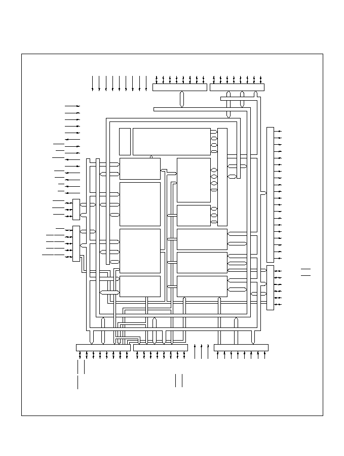
1.2 Block Diagram
Figure 1-1 shows an internal block diagram.
Figure 1-1 Block Diagram
V
CC
V
CC
V
CC
V
SS
V
SS
V
SS
V
SS
V
SS
V
SS
Data bus (upper)
Data bus (lower)
Address bus
D
15
D
14
D
13
D
12
D
11
D
10
D
9
D
8
P4
7
/D
7
P4
6
/D
6
P4
5
/D
5
P4
4
/D
4
P4
3
/D
3
P4
2
/D
2
P4
1
/D
1
P4
0
/D
0
Data bus
Port 4
Port 9
Address bus
A
19
A
18
A
17
A
16
A
15
A
14
A
13
A
12
A
11
A
10
A
9
A
8
A
7
A
6
A
5
A
4
A
3
A
2
A
1
A
0
P9
5
/SCK
1
/IRQ
5
P9
4
/SCK
0
/IRQ
4
P9
3
/RxD
1
P9
2
/RxD
0
P9
1
/TxD
1
P9
0
/TxD
0
P7
7
/AN
7
P7
6
/AN
6
P7
5
/AN
5
P7
4
/AN
4
P7
3
/AN
3
P7
3
/AN
2
P7
1
/AN
1
P7
0
/AN
0
Port 7
V
REF
AV
CC
AV
SS
PA
7
/TP
7
/TIOCB
2
/A
20
PA
6
/TP
6
/TIOCA
2
/A
21
PA
5
/TP
5
/TIOCB
1
/A
22
PA
4
/TP
4
/TIOCA
1
/A
23
PA
3
/TP
3
/TIOCB
0
/TCLKD
PA
2
/TP
2
/TIOCA
0
/TCLKC
PA
1
/TP
1
/TEND
1
/TCLKB
PA
0
/TP
0
/TEND
0
/TCLKA
Port A
PB
7
/TP
15
/DREQ
1
/ADTRG
PB
6
/TP
14
/DREQ
0
PB
5
/TP
13
/TOCXB
4
PB
4
/TP
12
/TOCXA
4
PB
3
/TP
11
/TIOCB
4
PB
2
/TP
10
/TIOCA
4
PB
1
/TP
9
/TIOCB
3
PB
0
/TP
8
/TIOCA
3
Port B
Port 8
Port 6
P8
4
/CS
0
P8
3
/CS
1
/IRQ
3
P8
2
/CS
2
/IRQ
2
P8
1
/CS
3
/IRQ
1
P8
0
/RFSH/IRQ
0
P6
2
/BACK
P6
1
/BREQ
P6
0
/WAIT
MD
2
MD
1
MD
0
EXTAL
XTAL
¯
STBY
RES
RESO
NMI
LWR
HWR
RD
AS
H8/300H CPU
Clock
osc.
Interrupt controller
RAM
512 bytes
16-bit
integrated
timer unit
(ITU)
Programmable
timing pattern
controller (TPC)
DMA controller
(DMAC)
Serial communication
interface
(SCI) 2 channels
◊
Bus controller
A/D converter
Watchdog timer
(WDT)
Refresh
controller
5
1.3 Pin Description
1.3.1 Pin Arrangement
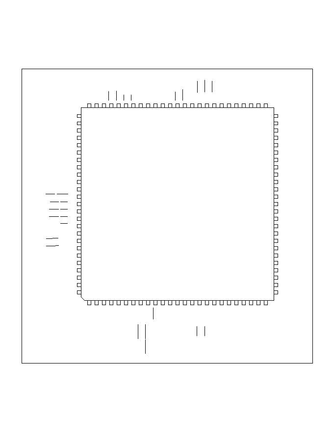
Figure 1-2 shows the pin arrangement of the H8/3002's FP-100B, TFP-100B package.
Figure 1-2 Pin Arrangement (FP-100B, TFP-100B, Top View)
1
2
3
4
5
6
7
8
9
10
11
12
13
14
15
16
17
18
19
20
21
22
23
24
25
76
77
78
79
80
81
82
83
84
85
86
87
88
89
90
91
92
93
94
95
96
97
98
99
100
50
49
48
47
46
45
44
43
42
41
40
39
38
37
36
35
34
33
32
31
30
29
28
27
26
75
74
73
72
71
70
69
68
67
66
65
64
63
62
61
60
59
58
57
56
55
54
53
52
51
V
CC
TIOCA
3
/TP
8
/PB
0
TIOCB
3
/TP
9
/PB
1
TIOCA
4
/TP
10
/PB
2
TIOCB
4
/TP
11
/PB
3
TOCXA
4
/TP
12
/PB
4
TOCXB
4
/TP
13
/PB
5
DREQ
0
/TP
14
/PB
6
ADTRG/DREQ
1
/TP
15
/PB
7
RESO
V
SS
TxD
0
/P9
0
TxD
1
/P9
1
RxD
0
/P9
2
RxD
1
/P9
3
IRQ
4
/SCK
0
/P9
4
IRQ
5
/SCK
1
/P9
5
D
0
/P4
0
D
1
/P4
1
D
2
/P4
2
D
3
/P4
3
V
SS
D
4
/P4
4
D
5
/P4
5
D
6
/P4
6
MD
2
MD
1
MD
0
LWR
HWR
RD
AS
V
CC
XTAL
EXTAL
V
SS
NMI
RES
STBY
¯
P6
2
/BACK
P6
1
/BREQ
P6
0
/WAIT
V
SS
A
19
A
18
A
17
A
16
A
15
A
14
AV
CC
V
REF
AN
0
/P7
0
AN
1
/P7
1
AN
2
/P7
2
AN
3
/P7
3
AN
4
/P7
4
AN
5
/P7
5
AN
6
/P7
6
AN
7
/P7
7
AV
SS
IRQ
0
/RFSH/P8
0
IRQ
1
/CS
3
/P8
1
IRQ
2
/CS
2
/P8
2
IRQ
3
/CS
1
/P8
3
CS
0
/P8
4
V
SS
TCLKA/TEND
0
/TP
0
/PA
0
TCLKB/TEND
1
/TP
1
/PA
1
TCLKC/TIOCA
0
/TP
2
/PA
2
TCLKD/TIOCB
0
/TP
3
/PA
3
A
23
/TIOCA
1
/TP
4
/PA
4
A
22
/TIOCB
1
/TP
5
/PA
5
A
21
/TIOCA
2
/TP
6
/PA
6
A
20
/TIOCB
2
/TP
7
/PA
7
Top view
(FP-100B, TFP-100B)
A
13
A
12
A
11
A
10
A
9
A
8
V
SS
A
7
A
6
A
5
A
4
A
3
A
2
A
1
A
0
V
CC
D
15
D
14
D
13
D
12
D
11
D
10
D
9
D
8
P4
7
/D
7
6
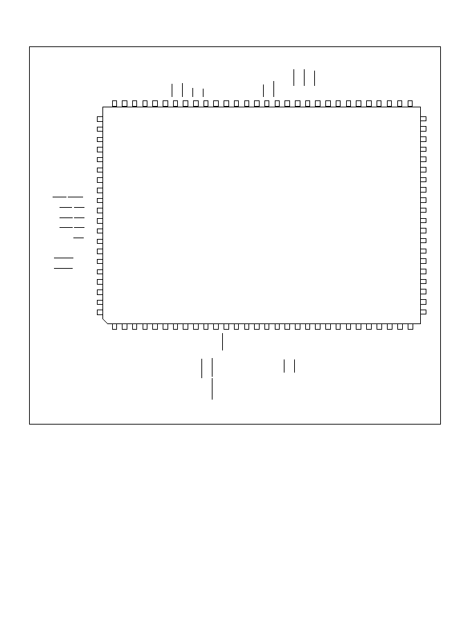
Figure 1-3 shows the pin arrangement of the H8/3002's FP-100A package.
Figure 1-3 Pin Arrangement (FP-100A, TopView)
7
1
2
3
4
5
6
7
8
9
10
11
12
13
14
15
16
17
18
19
20
21
22
23
24
25
26
27
28
29
30
81
82
83
84
85
86
87
88
89
90
91
92
93
94
95
96
97
98
99
100
50
49
48
47
46
45
44
43
42
41
40
39
38
37
36
35
34
33
32
31
80
79
78
77
76
75
74
73
72
71
70
69
68
67
66
65
64
63
62
61
60
59
58
57
56
55
54
53
52
51
A
21
/TIOCA
2
/TP
6
/PA
6
A
20
/TIOCB
2
/TP
7
/PA
7
V
CC
TIOCA
3
/TP
8
/PB
0
TIOCB
3
/TP
9
/PB
1
TIOCA
4
/TP
10
/PB
2
TIOCB
4
/TP
11
/PB
3
TOCXA
4
/TP
12
/PB
4
TOCXB
4
/TP
13
/PB
5
DREQ
0
/TP
14
/PB
6
ADTRG/DREQ
1
/TP
15
/PB
7
RESO
V
SS
TxD
0
/P9
0
TxD
1
/P9
1
RxD
0
/P9
2
RxD
1
/P9
3
IRQ
4
/SCK
0
/P9
4
IRQ
5
/SCK
1
/P9
5
D
0
/P4
0
D
1
/P4
1
D
2
/P4
2
D
3
/P4
3
V
SS
D
4
/P4
4
D
5
/P4
5
D
6
/P4
6
D
7
/P4
7
D
8
D
9
P7
0
/AN
0
V
REF
AV
CC
MD
2
MD
1
MD
0
LWR
HWR
RD
AS
V
CC
XTAL
EXTAL
V
SS
NMI
RES
STBY
¯
P6
2
/BACK
P6
1
/BREQ
P6
0
/WAIT
V
SS
A
19
A
18
A
17
A
16
A
15
A
14
A
13
A
12
AN
1
/P7
1
AN
2
/P7
2
AN
3
/P7
3
AN
4
/P7
4
AN
5
/P7
5
AN
6
/P7
6
AN
7
/P7
7
AV
SS
IRQ
0
/RFSH/P8
0
IRQ
1
/CS
3
/P8
1
IRQ
2
/CS
2
/P8
2
IRQ
3
/CS
1
/P8
3
CS
0
/P8
4
V
SS
TCLKA/TEND
0
/TP
0
/PA
0
TCLKB/TEND
1
/TP
1
/PA
1
TCLKC/TIOCA
0
/TP
2
/PA
2
TCLKD/TIOCB
0
/TP
3
/PA
3
A
23
/TIOCA
1
/TP
4
/PA
4
A
22
/TIOCB
1
/TP
5
/PA
5
Top view
(FP-100A)
A
11
A
10
A
9
A
8
V
SS
A
7
A
6
A
5
A
4
A
3
A
2
A
1
A
0
V
CC
D
15
D
14
D
13
D
12
D
11
D
10

1.3.2 Pin Functions
Pin Assignments in Each Mode: Table 1-2 lists the pin assignments in each mode.
Table 1-2 Pin Assignments in Each Mode
Pin No.
Pin Name
FP-100B,
TFP-100B FP-100A Mode 1
Mode 2
Mode 3
Mode 4
1
3
VCC
VCC
VCC
VCC
2
4
PB0/TP8/TIOCA3
PB0/TP8/TIOCA3
PB0/TP8/TIOCA3
PB0/TP8/TIOCA3
3
5
PB1/TP9/TIOCB3
PB1/TP9/TIOCB3
PB1/TP9/TIOCB3
PB1/TP9/TIOCB3
4
6
PB2/TP10/TIOCA4
PB2/TP10/TIOCA4
PB2/TP10/TIOCA4
PB2/TP10/TIOCA4
5
7
PB3/TP11/TIOCB4
PB3/TP11/TIOCB4
PB3/TP11/TIOCB4
PB3/TP11/TIOCB4
6
8
PB4/TP12/TOCXA4
PB4/TP12/TOCXA4
PB4/TP12/TOCXA4
PB4/TP12/TOCXA4
7
9
PB5/TP13/TOCXB4
PB5/TP13/TOCXB4
PB5/TP13/TOCXB4
PB5/TP13/TOCXB4
8
10
PB6/TP14/DREQ0
PB6/TP14/DREQ0
PB6/TP14/DREQ0
PB6/TP14/DREQ0
9
11
PB7/TP15/DREQ1/
ADTRG
PB7/TP15/DREQ1/
ADTRG
PB7/TP15/DREQ1/
ADTRG
PB7/TP15/DREQ1/
ADTRG
10
12
RESO
RESO
RESO
RESO
11
13
VSS
VSS
VSS
VSS
12
14
P90/TxD0
P90/TxD0
P90/TxD0
P90/TxD0
13
15
P91/TxD1
P91/TxD1
P91/TxD1
P91/TxD1
14
16
P92/RxD0
P92/RxD0
P92/RxD0
P92/RxD0
15
17
P93/RxD1
P93/RxD1
P93/RxD1
P93/RxD1
16
18
P94/SCK0/IRQ4
P94/SCK0/IRQ4
P94/SCK0/IRQ4
P94/SCK0/IRQ4
17
19
P95/SCK1/IRQ5
P95/SCK1/IRQ5
P95/SCK1/IRQ5
P95/SCK1/IRQ5
18
20
P40/D0
*
1
P40/D0
*
2
P40/D0
*
1
P40/D0
*
2
19
21
P41/D1
*
1
P41/D1
*
2
P41/D1
*
1
P41/D1
*
2
20
22
P42/D2
*
1
P42/D2
*
2
P42/D2
*
1
P42/D2
*
2
21
23
P43/D3
*
1
P43/D3
*
2
P43/D3
*
1
P43/D3
*
2
22
24
VSS
VSS
VSS
VSS
23
25
P44/D4
*
1
P44/D4
*
2
P44/D4
*
1
P44/D4
*
2
24
26
P45/D5
*
1
P45/D5
*
2
P45/D5
*
1
P45/D5
*
2
25
27
P46/D6
*
1
P46/D6
*
2
P46/D6
*
1
P46/D6
*
2
26
28
P47/D7
*
1
P47/D7
*
2
P47/D7
*
1
P47/D7
*
2
Notes: 1. In modes 1 and 3 the P4
0
to P4
7
functions of pins P4
0
/D
0
to P4
7
/D
7
are selected after a reset,
but they can be changed by software.
2. In modes 2 and 4 the D
0
to D
7
functions of pins P4
0
/D
0
to D4
7
/D
7
are selected after a reset, but
they can be changed by software.
8

Table 1-2 Pin Assignments in Each Mode (cont)
Pin No.
Pin Name
FP-100B,
TFP-100B FP-100A Mode 1
Mode 2
Mode 3
Mode 4
27
29
D8
D8
D8
D8
28
30
D9
D9
D9
D9
29
31
D10
D10
D10
D10
30
32
D11
D11
D11
D11
31
33
D12
D12
D12
D12
32
34
D13
D13
D13
D13
33
35
D14
D14
D14
D14
34
36
D15
D15
D15
D15
35
37
VCC
VCC
VCC
VCC
36
38
A0
A0
A0
A0
37
39
A1
A1
A1
A1
38
40
A2
A2
A2
A2
39
41
A3
A3
A3
A3
40
42
A4
A4
A4
A4
41
43
A5
A5
A5
A5
42
44
A6
A6
A6
A6
43
45
A7
A7
A7
A7
44
46
VSS
VSS
VSS
VSS
45
47
A8
A8
A8
A8
46
48
A9
A9
A9
A9
47
49
A10
A10
A10
A10
48
50
A11
A11
A11
A11
49
51
A12
A12
A12
A12
50
52
A13
A13
A13
A13
51
53
A14
A14
A14
A14
52
54
A15
A15
A15
A15
53
55
A16
A16
A16
A16
54
56
A17
A17
A17
A17
55
57
A18
A18
A18
A18
56
58
A19
A19
A19
A19
9

Table 1-2 Pin Assignments in Each Mode (cont)
Pin No.
Pin Name
FP-100B,
TFP-100B FP-100A Mode 1
Mode 2
Mode 3
Mode 4
57
59
VSS
VSS
VSS
VSS
58
60
P60/
WAIT
P60/
WAIT
P60/
WAIT
P60/
WAIT
59
61
P61/
BREQ
P61/
BREQ
P61/
BREQ
P61/
BREQ
60
62
P62/
BACK
P62/
BACK
P62/
BACK
P62/
BACK
61
63
¯
¯
¯
¯
62
64
STBY
STBY
STBY
STBY
63
65
RES
RES
RES
RES
64
66
NMI
NMI
NMI
NMI
65
67
VSS
VSS
VSS
VSS
66
68
EXTAL
EXTAL
EXTAL
EXTAL
67
69
XTAL
XTAL
XTAL
XTAL
68
70
VCC
VCC
VCC
VCC
69
71
AS
AS
AS
AS
70
72
RD
RD
RD
RD
71
73
HWR
HWR
HWR
HWR
72
74
LWR
LWR
LWR
LWR
73
75
MD0
MD0
MD0
MD0
74
76
MD1
MD1
MD1
MD1
75
77
MD2
MD2
MD2
MD2
76
78
AVCC
AVCC
AVCC
AVCC
77
79
VREF
VREF
VREF
VREF
78
80
P70/AN0
P70/AN0
P70/AN0
P70/AN0
79
81
P71/AN1
P71/AN1
P71/AN1
P71/AN1
80
82
P72/AN2
P72/AN2
P72/AN2
P72/AN2
81
83
P73/AN3
P73/AN3
P73/AN3
P73/AN3
82
84
P74/AN4
P74/AN4
P74/AN4
P74/AN4
83
85
P75/AN5
P75/AN5
P75/AN5
P75/AN5
84
86
P76/AN6
P76/AN6
P76/AN6
P76/AN6
85
87
P77/AN7
P77/AN7
P77/AN7
P77/AN7
10

Table 1-2 Pin Assignments in Each Mode (cont)
Pin No.
Pin Name
FP-100B,
TFP-100B FP-100A Mode 1
Mode 2
Mode 3
Mode 4
86
88
AVSS
AVSS
AVSS
AVSS
87
89
P80/
RFSH
/IRQ0
P80/
RFSH
/IRQ0
P80/
RFSH
/IRQ0
P80/
RFSH
/IRQ0
88
90
P81/CS3/IRQ1
P81/CS3/IRQ1
P81/CS3/IRQ1
P81/CS3/IRQ1
89
91
P82/CS2/IRQ2
P82/CS2/IRQ2
P82/CS2/IRQ2
P82/CS2/IRQ2
90
92
P83/CS1/IRQ3
P83/CS1/IRQ3
P83/CS1/IRQ3
P83/CS1/IRQ3
91
93
P84/CS0
P84/CS0
P84/CS0
P84/CS0
92
94
VSS
VSS
VSS
VSS
93
95
PA0/TP0/TEND0/TCLKA PA0/TP0/TEND0/TCLKA PA0/TP0/TEND0/TCLKA PA0/TP0/TEND0/TCLKA
94
96
PA1/TP1/TEND1/TCLKB PA1/TP1/TEND1/TCLKB PA1/TP1/TEND1/TCLKB PA1/TP1/TEND1/TCLKB
95
97
PA2/TP2/TIOCA0/TCLKC PA2/TP2/TIOCA0/TCLKC PA2/TP2/TIOCA0/TCLKC PA2/TP2/TIOCA0/TCLKC
96
98
PA3/TP3/TIOCB0/TCLKD PA3/TP3/TIOCB0/TCLKD PA3/TP3/TIOCB0/TCLKD PA3/TP3/TIOCB0/TCLKD
97
99
PA4/TP4/TIOCA1
PA4/TP4/TIOCA1
PA4/TP4/TIOCA1/A23
PA4/TP4/TIOCA1/A23
98
100
PA5/TP5/TIOCB1
PA5/TP5/TIOCB1
PA5/TP5/TIOCB1/A22
PA5/TP5/TIOCB1/A22
99
1
PA6/TP6/TIOCA2
PA6/TP6/TIOCA2
PA6/TP6/TIOCA2/A21
PA6/TP6/TIOCA2/A21
100
2
PA7/TP7/TIOCB2
PA7/TP7/TIOCB2
A20
A20
11

1.4 Pin Functions
Table 1-3 summarizes the pin functions.
Table 1-3 Pin Functions
Pin No.
FP-100B,
Type
Symbol
TFP-100B
FP-100A
I/O
Name and Function
Power
V
CC
1, 35, 68
3, 37, 70
Input
Power: For connection to the power supply.
Connect all V
CC
pins to the system power supply.
V
SS
11, 22, 44,
13, 24, 46, Input
Ground: For connection to ground (0 V).
57, 65, 92
59, 67, 94
Connect all V
SS
pins to the 0-V system power
supply.
Clock
XTAL
67
69
Input
For connection to a crystal resonator.
For examples of crystal resonator and external
clock input, see section 16, Clock Pulse
Generator.
EXTAL
66
68
Input
For connection to a crystal resonator or input
of an external clock signal. For examples of
crystal resonator and external clock input,
see section 16, Clock Pulse Generator.
¯
61
63
Output
System clock: Supplies the system clock to
external devices
Operating
MD
2
to MD
0
75 to 73
77 to 75
Input
Mode 2 to 0: For setting the operating
mode, as follows. Inputs at these pins must
not be changed during operation.
MD
2
MD
1
MD
0
Operating Mode
0
0
0
--
0
0
1
Mode 1
0
1
0
Mode 2
0
1
1
Mode 3
1
0
0
Mode 4
1
0
1
--
1
1
0
--
1
1
1
--
12

Table 1-3 Pin Functions (cont)
Pin No.
FP-100B,
Type
Symbol
TFP-100B
FP-100A
I/O
Name and Function
System
RES
63
65
Input
Reset input: When driven low, this pin
control
resets control the H8/3002
RESO
10
12
Output
Reset output: Outputs the reset signal
generated by the watchdog timer to external
devices.
STBY
62
64
Input
Standby: When driven low, this pin forces a
transition to hardware standby mode
BREQ
59
61
Input
Bus request: Used by an external bus
master to request the bus right from the
H8/3002
BACK
60
62
Output
Bus request acknowledge: Indicates that
the bus has been granted to an external bus
master
Interrupts
NMI
64
66
Input
Nonmaskable interrupt: Requests a
nonmaskable interrupt
IRQ
5
to
17, 16,
19, 18
Input
Interrupt request 5 to 0: Maskable
IRQ
0
90 to 87
92 to 89
interrupt request pins
Address
Modes A
19
to 56 to 45,
58 to 47
Output
Address bus: Outputs address signals
bus
1 and 2 A
0
43 to 36
45 to38
Modes A
23
to 100 to 97,
99, 100,
3 and 4 A
0
56 to 45,
1, 2,
43 to 36
58 to 47
45 to 38
Data bus
D
15
to D
0
34 to 23,
36 to 25
Input/
Data bus: Bidirectional data bus
21 to 18
23 to 20
output
Bus control
CS
3
to CS
0
91 to 88
90 to 93
Output
Chip select: Select signals for areas 3 to 0
AS
69
71
Output
Address strobe: Goes low to indicate valid
address output on the address bus
RD
70
72
Output
Read: Goes low to indicate reading from the
external address space
HWR
71
73
Output
High write: Goes low to indicate writing to
the external address space; indicates valid
data on the upper data bus (D
15
to D
8
).
LWR
72
74
Output
Low write: Goes low to indicate writing to
the external address space; indicates valid
data on the lower data bus (D
7
to D
0
).
WAIT
58
60
Input
Wait: Requests insertion of wait states in
bus cycles during access to the external
address space
13

Table 1-3 Pin Functions (cont)
Pin No.
FP-100B,
Type
Symbol
TFP-100B
FP-100A
I/O
Name and Function
Refresh
RFSH
87
89
Output
Refresh: Indicates a refresh cycle
controller
CS
3
88
90
Output
Row address strobe
RAS
: Row address
strobe signal for DRAM connected to area 3
RD
70
72
Output
Column address strobe
CAS
: Column
address strobe signal for DRAM connected
to area 3; used with 2
WE
DRAM.
Write enable: Write enable signal for DRAM
connected to area 3; used with 2
CAS
DRAM.
HWR
71
73
Output
Upper write: Write enable signal for DRAM
connected to area 3; used with 2
WE
DRAM.
Upper column address strobe: Column
address strobe signal for DRAM connected
to area 3; used with 2
CAS
DRAM.
LWR
72
74
Output
Lower write: Write enable signal for DRAM
connected to area 3; used with 2
WE
DRAM.
Lower column address strobe: Column
address strobe signal for DRAM connected
to area 3; used with 2
CAS
DRAM.
DREQ
1
,
9, 8
11, 10
Input
DMA request 1 and 0: DMAC activation
DREQ
0
requests
TEND
1
,
94, 93
96, 95
Output
Transfer end 1 and 0: These signals indicate
TEND
0
that the DMAC has ended a data transfer
TCLKD to
96 to 93
98 to 95
Input
Clock input D to A: External clock inputs
TCLKA
TIOCA
4
to
4, 2, 99,
6, 4, 1,
Input/
Input capture/output compare A4 to A0:
TIOCA
0
97, 95
99, 97
output
GRA4 to GRA0 output compare or input
capture, or PWM output
TIOCB
4
to
5, 3, 100,
7, 5, 2,
Input/
Input capture/output compare B4 to B0:
TIOCB
0
98, 96
100, 98
output
GRB4 to GRB0 output compare or input
capture, or PWM output
TOCXA
4
6
8
Output
Output compare XA4: PWM output
TOCXB
4
7
9
Output
Output compare XB4: PWM output
14

Table 1-3 Pin Functions (cont)
Pin No.
FP-100B,
Type
Symbol
TFP-100B
FP-100A
I/O
Name and Function
Programmable
TP
15
to
9 to 2,
11 to 4
Output
TPC output 15 to 0: Pulse output
timing pattern
TP
0
100 to 93
2 to 95
controller (TPC)
Serial com-
TxD
1
,
13, 12
15, 14
Output
Transmit data (channels 0 and 1): SCI data
munication TxD
0
output
interface (SCI)
RxD
1
,
15, 14
17, 16
Input
Receive data (channels 0 and 1): SCI data
RxD
0
input
SCK
1
,
17, 16
19, 18
Input/
Serial clock (channels 0 and 1): SCI clock
SCK
0
output
input/output
A/D
AN
7
to AN
0
85 to 78
45 to 38
Input
Analog 7 to 0: Analog input pins
converter
ADTRG
9
11
Input
A/D trigger: External trigger input for starting
A/D conversion
AV
CC
76
78
Input
Power supply pin for the A/D converter.
Connect to the system power supply when
not using the A/D converter.
AV
SS
86
88
Input
Ground pin for the A/D converter. Connect to
system ground (0 V).
V
REF
77
79
Input
Reference voltage input pin for the A/D
converter. Connect to the system power
supply when not using the A/D converter.
I/O ports
P4
7
to P4
0
26 to 23,
28 to 25
Input/
Port 4: Eight input/output pins. The
21 to 18
23 to 20
output
direction of each pin can be selected in the
port 4 data direction register (P4DDR).
P6
2
to P6
0
60 to 58
62 to 60
Input/
Port 6: Three input/output pins. The direction
output
of each pin can be selected in the port 6 data
direction register (P6DDR).
P7
7
to P7
0
85 to 78
87 to 80
Input
Port 7: Eight input pins
P8
4
to P8
0
91 to 87
93 to 89
Input/
Port 8: Five input/output pins. The direction
output
of each pin can be selected in the port 8 data
direction register (P8DDR).
15

Table 1-3 Pin Functions (cont)
Pin No.
FP-100B,
Type
Symbol
TFP-100B
FP-100A
I/O
Name and Function
I/O ports
P9
5
to P9
0
17 to 12
19 to 14
Input/
Port 9: Six input/output pins. The direction
output
of each pin can be selected in the port 9
data direction register (P9DDR).
PA
7
to PA
0
100 to 93
2, 1,
Input/
Port A: Eight input/output pins. The direction
100 to 95
output
of each pin can be selected in the port A
data direction register (PADDR).
PB
7
to PB
0
9 to 2
11 to 4
Input/
Port B: Eight input/output pins. The direction
output
of each pin can be selected in the port B
data direction register (PBDDR).
16

Section 2 CPU
2.1 Overview
The H8/300H CPU is a high-speed central processing unit with an internal 32-bit architecture that
is upward-compatible with the H8/300 CPU. The H8/300H CPU has sixteen 16-bit general
registers, can address a 16-Mbyte linear address space, and is ideal for realtime control.
2.1.1 Features
The H8/300H CPU has the following features.
∑
Upward compatibility with H8/300 CPU
Can execute H8/300 series object programs
∑
General-register architecture
Sixteen 16-bit general registers (also usable as sixteen 8-bit registers or eight 32-bit registers)
∑
Sixty-two basic instructions
-- 8/16/32-bit arithmetic and logic instructions
-- Multiply and divide instructions
-- Powerful bit-manipulation instructions
∑
Eight addressing modes
-- Register direct [Rn]
-- Register indirect [@ERn]
-- Register indirect with displacement [@(d:16, ERn) or @(d:24, ERn)]
-- Register indirect with post-increment or pre-decrement [@ERn+ or @≠ERn]
-- Absolute address [@aa:8, @aa:16, or @aa:24]
-- Immediate [#xx:8, #xx:16, or #xx:32]
-- Program-counter relative [@(d:8, PC) or @(d:16, PC)]
-- Memory indirect [@@aa:8]
∑
16-Mbyte linear address space
17

∑
High-speed operation
-- All frequently-used instructions execute in two to four states
-- Maximum clock frequency:
17 MHz
-- 8/16/32-bit register-register add/subtract: 118 ns
-- 8
◊
8-bit register-register multiply:
824 ns
-- 16 ˜ 8-bit register-register divide:
824 ns
-- 16
◊
16-bit register-register multiply:
1,294 ns
-- 32 ˜ 16-bit register-register divide:
1,294 ns
∑
Two CPU operating modes
-- Normal mode (not available in H8/3002)
-- Advanced mode
∑
Low-power mode
Transition to power-down state by SLEEP instruction
2.1.2 Differences from H8/300 CPU
In comparison to the H8/300 CPU, the H8/300H has the following enhancements.
∑
More general registers
Eight 16-bit registers have been added.
∑
Expanded address space
-- Advanced mode supports a maximum 16-Mbyte address space.
-- Normal mode supports the same 64-kbyte address space as the H8/300 CPU.
∑
Enhanced addressing
The addressing modes have been enhanced to make effective use of the 16-Mbyte address
space.
∑
Enhanced instructions
-- Data transfer, arithmetic, and logic instructions can operate on 32-bit data.
-- Signed multiply/divide instructions and other instructions have been added.
18
2.2 CPU Operating Modes
The H8/300H CPU has two operating modes: normal and advanced. Normal mode supports a
maximum 64-kbyte address space. Advanced mode supports up to 16 Mbytes. See figure 2-1.
The H8/3002 uses only advanced mode.
Figure 2-1 CPU Operating Modes
CPU operating modes
Normal mode
Advanced mode
*
Maximum 64 kbytes, program
and data areas combined
Maximum 16 Mbytes, program
and data areas combined
Note: Normal mode is not available in the H8/3002 .
*
19

2.3 Address Space
The maximum address space of the H8/300H CPU is 16 Mbytes. The H8/3002 has two operating
modes (MCU modes), one providing a 1-Mbyte address space, the other supporting the full
16 Mbytes.
Figure 2-2 shows the H8/3002's address ranges. For further details see section 3.6, Memory Map
in Each Operating Mode.
The 1-Mbyte operating mode uses 20-bit addressing. The upper 4 bits of effective addresses are
ignored.
Figure 2-2 Memory Map
H'00000
H'FFFFF
H'000000
H'FFFFFF
a. 1-Mbyte mode
b. 16-Mbyte mode
20
2.4 Register Configuration
2.4.1 Overview
The H8/300H CPU has the internal registers shown in figure 2-3. There are two types of registers:
general registers and control registers.
Figure 2-3 CPU Registers
ER0
ER1
ER2
ER3
ER4
ER5
ER6
ER7
E0
E1
E2
E3
E4
E5
E6
E7
R0H
R1H
R2H
R3H
R4H
R5H
R6H
R7H
R0L
R1L
R2L
R3L
R4L
R5L
R6L
R7L
0
7
0
7
0
15
(SP)
23
0
PC
7
CCR
6 5 4 3 2 1 0
I UI H U N Z V C
General Registers (ERn)
Control Registers (CR)
Legend
SP:
PC:
CCR:
I:
UI:
H:
U:
N:
Z:
V:
C:
Stack pointer
Program counter
Condition code register
Interrupt mask bit
User bit or interrupt mask bit
Half-carry flag
User bit
Negative flag
Zero flag
Overflow flag
Carry flag
21

2.4.2 General Registers
The H8/300H CPU has eight 32-bit general registers. These general registers are all functionally
alike and can be used without distinction between data registers and address registers. When a
general register is used as a data register, it can be accessed as a 32-bit, 16-bit, or 8-bit register.
When the general registers are used as 32-bit registers or as address registers, they are designated
by the letters ER (ER0 to ER7).
The ER registers divide into 16-bit general registers designated by the letters E (E0 to E7) and R
(R0 to R7). These registers are functionally equivalent, providing a maximum sixteen 16-bit
registers. The E registers (E0 to E7) are also referred to as extended registers.
The R registers divide into 8-bit general registers designated by the letters RH (R0H to R7H) and
RL (R0L to R7L). These registers are functionally equivalent, providing a maximum sixteen 8-bit
registers.
Figure 2-4 illustrates the usage of the general registers. The usage of each register can be selected
independently.
Figure 2-4 Usage of General Registers
∑ Address registers
∑ 32-bit registers
∑ 16-bit registers
∑ 8-bit registers
ER registers
ER0 to ER7
E registers
(extended registers)
E0 to E7
R registers
R0 to R7
RH registers
R0H to R7H
RL registers
R0L to R7L
22
General register ER7 has the function of stack pointer (SP) in addition to its general-register
function, and is used implicitly in exception handling and subroutine calls. Figure 2-5 shows the
stack.
Figure 2-5 Stack
2.4.3 Control Registers
The control registers are the 24-bit program counter (PC) and the 8-bit condition code register
(CCR).
Program Counter (PC): This 24-bit counter indicates the address of the next instruction the CPU
will execute. The length of all CPU instructions is 2 bytes (one word) or a multiple of 2 bytes, so
the least significant PC bit is ignored. When an instruction is fetched, the least significant PC bit is
regarded as 0.
Condition Code Register (CCR): This 8-bit register contains internal CPU status information,
including the interrupt mask bit (I) and half-carry (H), negative (N), zero (Z), overflow (V), and
carry (C) flags.
Bit 7--Interrupt Mask Bit (I): Masks interrupts other than NMI when set to 1. NMI is accepted
regardless of the I bit setting. The I bit is set to 1 at the start of an exception-handling sequence.
Bit 6--User Bit or Interrupt Mask Bit (UI): Can be written and read by software using the
LDC, STC, ANDC, ORC, and XORC instructions. This bit can also be used as an interrupt mask
bit. For details see section 5, Interrupt Controller.
Free area
Stack area
SP (ER7)
23

Bit 5--Half-Carry Flag (H): When the ADD.B, ADDX.B, SUB.B, SUBX.B, CMP.B, or NEG.B
instruction is executed, this flag is set to 1 if there is a carry or borrow at bit 3, and cleared to 0
otherwise. When the ADD.W, SUB.W, CMP.W, or NEG.W instruction is executed, the H flag is
set to 1 if there is a carry or borrow at bit 11, and cleared to 0 otherwise. When the ADD.L,
SUB.L, CMP.L, or NEG.L instruction is executed, the H flag is set to 1 if there is a carry or
borrow at bit 27, and cleared to 0 otherwise.
Bit 4--User Bit (U): Can be written and read by software using the LDC, STC, ANDC, ORC,
and XORC instructions.
Bit 3--Negative Flag (N): Indicates the most significant bit (sign bit) of data.
Bit 2--Zero Flag (Z): Set to 1 to indicate zero data, and cleared to 0 to indicate non-zero data.
Bit 1--Overflow Flag (V): Set to 1 when an arithmetic overflow occurs, and cleared to 0 at other
times.
Bit 0--Carry Flag (C): Set to 1 when a carry occurs, and cleared to 0 otherwise. Used by:
∑
Add instructions, to indicate a carry
∑
Subtract instructions, to indicate a borrow
∑
Shift and rotate instructions, to store the value shifted out of the end bit
The carry flag is also used as a bit accumulator by bit manipulation instructions.
Some instructions leave flag bits unchanged. Operations can be performed on CCR by the LDC,
STC, ANDC, ORC, and XORC instructions. The N, Z, V, and C flags are used by conditional
branch (Bcc) instructions.
For the action of each instruction on the flag bits, see appendix A.1, Instruction List. For the I and
UI bits, see section 5, Interrupt Controller.
2.4.4 Initial CPU Register Values
In reset exception handling, PC is initialized to a value loaded from the vector table, and the I bit
in CCR is set to 1. The other CCR bits and the general registers are not initialized. In particular,
the stack pointer (ER7) is not initialized. The stack pointer must therefore be initialized by an
MOV.L instruction executed immediately after a reset.
24
2.5 Data Formats
The H8/300H CPU can process 1-bit, 4-bit (BCD), 8-bit (byte), 16-bit (word), and 32-bit
(longword) data. Bit-manipulation instructions operate on 1-bit data by accessing bit n (n = 0, 1,
2, ..., 7) of byte operand data. The DAA and DAS decimal-adjust instructions treat byte data as
two digits of 4-bit BCD data.
2.5.1 General Register Data Formats
Figures 2-6 and 2-7 show the data formats in general registers.
Figure 2-6 General Register Data Formats (1)
7
RnH
RnL
RnH
RnL
RnH
RnL
1-bit data
1-bit data
4-bit BCD data
4-bit BCD data
Byte data
Byte data
6 5 4 3 2 1 0
7
0
Don't care
7 6 5 4 3 2 1 0
7
0
Don't care
Don't care
7
0
4 3
Lower digit
Upper digit
7
4 3
Lower digit
Upper digit
Don't care
0
7
0
Don't care
MSB
LSB
Don't care
7
0
MSB
LSB
Data Type
Data Format
General
Register
25

Figure 2-7 General Register Data Formats (2)
2.5.2 Memory Data Formats
Figure 2-8 shows the data formats on memory. The H8/300H CPU can access word data and
longword data on memory, but word or longword data must begin at an even address. If an
attempt is made to access word or longword data at an odd address, no address error occurs but
the least significant bit of the address is regarded as 0, so the access starts at the preceding
address. This also applies to instruction fetches.
Rn
En
ERn
Word data
Word data
Longword data
15
0
MSB
LSB
General
Register
Data Type
Data Format
15
0
MSB
LSB
31
16
MSB
15
0
LSB
Legend
ERn:
En:
Rn:
RnH:
RnL:
MSB:
LSB:
General register
General register E
General register R
General register RH
General register RL
Most significant bit
Least significant bit
26
Figure 2-8 Memory Data Formats
When ER7 (SP) is used as an address register to access the stack, the operand size should be word
size or longword size.
7
6
5
4
3
2
1
0
Address L
Address L
LSB
MSB
MSB
LSB
7
0
MSB
LSB
1-bit data
Byte data
Word data
Longword data
Address
Data Type
Data Format
Address 2M
Address 2M + 1
Address 2N
Address 2N + 1
Address 2N + 2
Address 2N + 3
27

2.6 Instruction Set
2.6.1 Instruction Set Overview
The H8/300H CPU has 62 types of instructions, which are classified in table 2-1.
Table 2-1 Instruction Classification
Function
Instruction
Types
Data transfer
MOV, PUSH
*
1
, POP
*
1
, MOVTPE
*
2
, MOVFPE
*
2
3
Arithmetic operations
ADD, SUB, ADDX, SUBX, INC, DEC, ADDS, SUBS, DAA, DAS,
18
MULXU, DIVXU, MULXS, DIVXS, CMP, NEG, EXTS, EXTU
Logic operations
AND, OR, XOR, NOT
4
Shift operations
SHAL, SHAR, SHLL, SHLR, ROTL, ROTR, ROTXL, ROTXR
8
Bit manipulation
BSET, BCLR, BNOT, BTST, BAND, BIAND, BOR, BIOR, BXOR,
14
BIXOR, BLD, BILD, BST, BIST
Branch
Bcc
*
3
, JMP, BSR, JSR, RTS
5
System control
TRAPA, RTE, SLEEP, LDC, STC, ANDC, ORC, XORC, NOP
9
Block data transfer
EEPMOV
1
Total 62 types
Notes: 1. POP.W Rn is identical to MOV.W @SP+, Rn.
PUSH.W Rn is identical to MOV.W Rn, @≠SP.
POP.L ERn is identical to MOV.L @SP+, Rn.
PUSH.L ERn is identical to MOV.L Rn, @≠SP.
2. Not available in the H8/3002.
3. Bcc is a generic branching instruction.
28

2.6.2 Instructions and Addressing Modes
Table 2-2 indicates the instructions available in the H8/300H CPU.
Table 2-2 Instructions and Addressing Modes
Addressing Modes
@
@
@
@
(d:16, (d:24, @ERn+/ @
@
@
(d:8, (d:16, @@
Function
Instruction
#xx
Rn
@ERn ERn)
ERn)
@≠ERn aa:8
aa:16
aa:24 PC)
PC)
aa:8
--
MOV
BWL BWL BWL
BWL
BWL
BWL
B
BWL
BWL
--
--
--
--
POP, PUSH
--
--
--
--
--
--
--
--
--
--
--
--
WL
MOVFPE, --
--
--
--
--
--
--
B
--
--
--
--
--
MOVTPE
ADD, CMP
BWL BWL --
--
--
--
--
--
--
--
--
--
--
SUB
WL
BWL --
--
--
--
--
--
--
--
--
--
--
ADDX, SUBX B
B
--
--
--
--
--
--
--
--
--
--
--
ADDS, SUBS --
L
--
--
--
--
--
--
--
--
--
--
--
INC, DEC
--
BWL --
--
--
--
--
--
--
--
--
--
--
DAA, DAS
--
B
--
--
--
--
--
--
--
--
--
--
--
DIVXU,
--
BW
--
--
--
--
--
--
--
--
--
--
--
MULXS,
MULXU,
DIVXS
NEG
--
BWL --
--
--
--
--
--
--
--
--
--
--
EXTU, EXTS
--
WL
--
--
--
--
--
--
--
--
--
--
--
Logic AND,
OR,
BWL BWL --
--
--
--
--
--
--
--
--
--
--
operations XOR
NOT
--
BWL --
--
--
--
--
--
--
--
--
--
--
Shift instructions
--
BWL --
--
--
--
--
--
--
--
--
--
--
Bit manipulation
--
B
B
--
--
--
B
--
--
--
--
--
--
Branch
Bcc, BSR
--
--
--
--
--
--
--
--
--
--
--
JMP, JSR
--
--
--
--
--
--
--
--
--
--
RTS
--
--
--
--
--
--
--
--
--
--
--
--
TRAPA
--
--
--
--
--
--
--
--
--
--
--
--
RTE
--
--
--
--
--
--
--
--
--
--
--
--
SLEEP
--
--
--
--
--
--
--
--
--
--
--
--
LDC
B
B
W
W
W
W
--
W
W
--
--
--
--
STC
--
B
W
W
W
W
--
W
W
--
--
--
--
ANDC, ORC, B
--
--
--
--
--
--
--
--
--
--
--
--
XORC
NOP
--
--
--
--
--
--
--
--
--
--
--
--
Block data transfer
--
--
--
--
--
--
--
--
--
--
--
--
BW
Legend
B:
Byte
W: Word
L:
Longword
Data
transfer
Arithmetic
operations
System
control
29

2.6.3 Tables of Instructions Classified by Function
Tables 2-3 to 2-10 summarize the instructions in each functional category. The operation notation
used in these tables is defined next.
Operation Notation
Rd
General register (destination)
*
Rs
General register (source)
*
Rn
General register
*
ERn
General register (32-bit register or address register)
(EAd)
Destination operand
(EAs)
Source operand
CCR
Condition code register
N
N (negative) flag of CCR
Z
Z (zero) flag of CCR
V
V (overflow) flag of CCR
C
C (carry) flag of CCR
PC
Program counter
SP
Stack pointer
#IMM
Immediate data
disp
Displacement
+
Addition
≠
Subtraction
◊
Multiplication
˜
Division
AND logical
OR logical
Exclusive OR logical
Move
¨
NOT (logical complement)
:3/:8/:16/:24
3-, 8-, 16-, or 24-bit length
Note:
*
General registers include 8-bit registers (R0H to R7H, R0L to R7L), 16-bit registers (R0 to
R7, E0 to E7), and 32-bit data or address registers (ER0 to ER7).
30

Table 2-3 Data Transfer Instructions
Instruction
Size
*
Function
MOV
B/W/L
(EAs)
Rd, Rs
(EAd)
Moves data between two general registers or between a general register
and memory, or moves immediate data to a general register.
MOVFPE
B
(EAs)
Rd
Cannot be used in the H8/3002.
MOVTPE
B
Rs
(EAs)
Cannot be used in the H8/3002.
POP
W/L
@SP+
Rn
Pops a general register from the stack. POP.W Rn is identical to MOV.W
@SP+, Rn. Similarly, POP.L ERn is identical to MOV.L @SP+, ERn.
PUSH
W/L
Rn
@≠SP
Pushes a general register onto the stack. PUSH.W Rn is identical to MOV.W
Rn, @≠SP. Similarly, PUSH.L ERn is identical to MOV.L ERn, @≠SP.
Note:
*
Size refers to the operand size.
B: Byte
W: Word
L:
Longword
31

Table 2-4 Arithmetic Operation Instructions
Instruction
Size
*
Function
B/W/L
Rd ± Rs
Rd, Rd ± #IMM
Rd
Performs addition or subtraction on data in two general registers, or on
immediate data and data in a general register. (Immediate byte data cannot
be subtracted from data in a general register. Use the SUBX or ADD
instruction.)
B
Rd ± Rs ± C
Rd, Rd ± #IMM ± C
Rd
Performs addition or subtraction with carry or borrow on data in two general
registers, or on immediate data and data in a general register.
B/W/L
Rd ± 1
Rd, Rd ± 2
Rd
Increments or decrements a general register by 1 or 2. (Byte operands can
be incremented or decremented by 1 only.)
L
Rd ± 1
Rd, Rd ± 2
Rd, Rd ± 4
Rd
Adds or subtracts the value 1, 2, or 4 to or from data in a 32-bit register.
B
Rd decimal adjust
Rd
Decimal-adjusts an addition or subtraction result in a general register by
referring to CCR to produce 4-bit BCD data.
MULXU
B/W
Rd
◊
Rs
Rd
Performs unsigned multiplication on data in two general registers: either
8 bits
◊
8 bits
16 bits or 16 bits
◊
16 bits
32 bits.
MULXS
B/W
Rd
◊
Rs
Rd
Performs signed multiplication on data in two general registers: either
8 bits
◊
8 bits
16 bits or 16 bits
◊
16 bits
32 bits.
Note:
*
Size refers to the operand size.
B: Byte
W: Word
L:
Longword
ADDX,
SUBX
INC,
DEC
ADD,
SUB
ADDS,
SUBS
DAA,
DAS
32

Table 2-4 Arithmetic Operation Instructions (cont)
Instruction
Size
*
Function
DIVXU
B/W
Rd ˜ Rs
Rd
Performs unsigned division on data in two general registers: either
16 bits ˜ 8 bits
8-bit quotient and 8-bit remainder or 32 bits ˜ 16 bits
16-bit quotient and 16-bit remainder.
DIVXS
B/W
Rd ˜ Rs
Rd
Performs signed division on data in two general registers: either
16 bits ˜ 8 bits
8-bit quotient and 8-bit remainder, or 32 bits ˜ 16 bits
16-bit quotient and 16-bit remainder.
CMP
B/W/L
Rd ≠ Rs, Rd ≠ #IMM
Compares data in a general register with data in another general register or
with immediate data, and sets CCR according to the result.
NEG
B/W/L
0 ≠ Rd
Rd
Takes the two's complement (arithmetic complement) of data in a general
register.
EXTS
W/L
Rd (sign extension)
Rd
Extends byte data in the lower 8 bits of a 16-bit register to word data, or
extends word data in the lower 16 bits of a 32-bit register to longword data,
by extending the sign bit.
EXTU
W/L
Rd (zero extension)
Rd
Extends byte data in the lower 8 bits of a 16-bit register to word data, or
extends word data in the lower 16 bits of a 32-bit register to longword data,
by padding with zeros.
Note:
*
Size refers to the operand size.
B: Byte
W: Word
L:
Longword
33

Table 2-5 Logic Operation Instructions
Instruction
Size
*
Function
AND
B/W/L
Rd
Rs
Rd, Rd
#IMM
Rd
Performs a logical AND operation on a general register and another general
register or immediate data.
OR
B/W/L
Rd
Rs
Rd, Rd
#IMM
Rd
Performs a logical OR operation on a general register and another general
register or immediate data.
XOR
B/W/L
Rd
Rs
Rd, Rd
#IMM
Rd
Performs a logical exclusive OR operation on a general register and another
general register or immediate data.
NOT
B/W/L
¨ Rd
Rd
Takes the one's complement of general register contents.
Note:
*
Size refers to the operand size.
B: Byte
W: Word
L:
Longword
Table 2-6 Shift Instructions
Instruction
Size
*
Function
B/W/L
Rd (shift)
Rd
Performs an arithmetic shift on general register contents.
B/W/L
Rd (shift)
Rd
Performs a logical shift on general register contents.
B/W/L
Rd (rotate)
Rd
Rotates general register contents.
B/W/L
Rd (rotate)
Rd
Rotates general register contents through the carry bit.
Note:
*
Size refers to the operand size.
B: Byte
W: Word
L:
Longword
SHAL,
SHAR
SHLL,
SHLR
ROTL,
ROTR
ROTXL,
ROTXR
34

Table 2-7 Bit Manipulation Instructions
Instruction
Size
*
Function
BSET
B
1
(<bit-No.> of <EAd>)
Sets a specified bit in a general register or memory operand to 1. The bit
number is specified by 3-bit immediate data or the lower 3 bits of a general
register.
BCLR
B
0
(<bit-No.> of <EAd>)
Clears a specified bit in a general register or memory operand to 0. The bit
number is specified by 3-bit immediate data or the lower 3 bits of a general
register.
BNOT
B
¨ (<bit-No.> of <EAd>)
(<bit-No.> of <EAd>)
Inverts a specified bit in a general register or memory operand. The bit
number is specified by 3-bit immediate data or the lower 3 bits of a general
register.
BTST
B
¨ (<bit-No.> of <EAd>)
Z
Tests a specified bit in a general register or memory operand and sets or
clears the Z flag accordingly. The bit number is specified by 3-bit immediate
data or the lower 3 bits of a general register.
BAND
B
C
(<bit-No.> of <EAd>)
C
ANDs the carry flag with a specified bit in a general register or memory
operand and stores the result in the carry flag.
BIAND
B
C
[¨ (<bit-No.> of <EAd>)]
C
ANDs the carry flag with the inverse of a specified bit in a general register or
memory operand and stores the result in the carry flag.
The bit number is specified by 3-bit immediate data.
Note:
*
Size refers to the operand size.
B: Byte
35

Table 2-7 Bit Manipulation Instructions (cont)
Instruction
Size
*
Function
BOR
B
C
(<bit-No.> of <EAd>)
C
ORs the carry flag with a specified bit in a general register or memory
operand and stores the result in the carry flag.
BIOR
B
C
[¨ (<bit-No.> of <EAd>)]
C
ORs the carry flag with the inverse of a specified bit in a general register or
memory operand and stores the result in the carry flag.
The bit number is specified by 3-bit immediate data.
BXOR
B
C
(<bit-No.> of <EAd>)
C
Exclusive-ORs the carry flag with a specified bit in a general register or
memory operand and stores the result in the carry flag.
BIXOR
B
C
[¨ (<bit-No.> of <EAd>)]
C
Exclusive-ORs the carry flag with the inverse of a specified bit in a general
register or memory operand and stores the result in the carry flag.
The bit number is specified by 3-bit immediate data.
BLD
B
(<bit-No.> of <EAd>)
C
Transfers a specified bit in a general register or memory operand to the
carry flag.
BILD
B
¨ (<bit-No.> of <EAd>)
C
Transfers the inverse of a specified bit in a general register or memory
operand to the carry flag.
The bit number is specified by 3-bit immediate data.
BST
B
C
(<bit-No.> of <EAd>)
Transfers the carry flag value to a specified bit in a general register or
memory operand.
BIST
B
C
¨ (<bit-No.> of <EAd>)
Transfers the inverse of the carry flag value to a specified bit in a general
register or memory operand.
The bit number is specified by 3-bit immediate data.
Note:
*
Size refers to the operand size.
B: Byte
36

Table 2-8 Branching Instructions
Instruction
Size
Function
Bcc
--
Branches to a specified address if a specified condition is true. The
branching conditions are listed below.
Mnemonic
Description
Condition
BRA (BT)
Always (true)
Always
BRN (BF)
Never (false)
Never
BHI
High
C
Z = 0
BLS
Low or same
C
Z = 1
Bcc (BHS)
Carry clear (high or same)
C = 0
BCS (BLO)
Carry set (low)
C = 1
BNE
Not equal
Z = 0
BEQ
Equal
Z = 1
BVC
Overflow clear
V = 0
BVS
Overflow set
V = 1
BPL
Plus
N = 0
BMI
Minus
N = 1
BGE
Greater or equal
N
V = 0
BLT
Less than
N
V = 1
BGT
Greater than
Z
(N
V) = 0
BLE
Less or equal
Z
(N
V) = 1
JMP
--
Branches unconditionally to a specified address
BSR
--
Branches to a subroutine at a specified address
JSR
--
Branches to a subroutine at a specified address
RTS
--
Returns from a subroutine
37

Table 2-9 System Control Instructions
Instruction
Size
*
Function
TRAPA
--
Starts trap-instruction exception handling
RTE
--
Returns from an exception-handling routine
SLEEP
--
Causes a transition to the power-down state
LDC
B/W
(EAs)
CCR
Moves the source operand contents to the condition code register. The
condition code register size is one byte, but in transfer from memory, data is
read by word access.
STC
B/W
CCR
(EAd)
Transfers the CCR contents to a destination location. The condition code
register size is one byte, but in transfer to memory, data is written by word
access.
ANDC
B
CCR
#IMM
CCR
Logically ANDs the condition code register with immediate data.
ORC
B
CCR
#IMM
CCR
Logically ORs the condition code register with immediate data.
XORC
B
CCR
#IMM
CCR
Logically exclusive-ORs the condition code register with immediate data.
NOP
--
PC + 2
PC
Only increments the program counter.
Note:
*
Size refers to the operand size.
B: Byte
W: Word
38

Table 2-10 Block Transfer Instruction
Instruction
Size
Function
EEPMOV.B
--
if R4L
0 then
repeat
@ER5+
@ER6+, R4L ≠ 1
R4L
until
R4L = 0
else next;
EEPMOV.W --
if R4
0 then
repeat
@ER5+
@ER6+, R4 ≠ 1
R4
until
R4 = 0
else next;
Transfers a data block according to parameters set in general registers R4L
or R4, ER5, and ER6.
R4L or R4: Size of block (bytes)
ER5:
Starting source address
ER6:
Starting destination address
Execution of the next instruction begins as soon as the transfer is
completed.
39

2.6.4 Basic Instruction Formats
The H8/300H instructions consist of 2-byte (1-word) units. An instruction consists of an operation
field (OP field), a register field (r field), an effective address extension (EA field), and a condition
field (cc).
Operation Field: Indicates the function of the instruction, the addressing mode, and the operation
to be carried out on the operand. The operation field always includes the first 4 bits of the
instruction. Some instructions have two operation fields.
Register Field: Specifies a general register. Address registers are specified by 3 bits, data
registers by 3 bits or 4 bits. Some instructions have two register fields. Some have no register
field.
Effective Address Extension: Eight, 16, or 32 bits specifying immediate data, an absolute
address, or a displacement. A 24-bit address or displacement is treated as 32-bit data in which the
first 8 bits are 0 (H'00).
Condition Field: Specifies the branching condition of Bcc instructions.
Figure 2-9 shows examples of instruction formats.
Figure 2-9 Instruction Formats
op
NOP, RTS, etc.
op
rn
rm
op
rn
rm
EA (disp)
Operation field only
ADD.B Rn, Rm, etc.
Operation field and register fields
MOV.B @(d:16, Rn), Rm
Operation field, register fields, and effective address extension
BRA d:8
Operation field, effective address extension, and condition field
op
cc
EA (disp)
40

2.6.5 Notes on Use of Bit Manipulation Instructions
The BSET, BCLR, BNOT, BST, and BIST instructions read a byte of data, modify a bit in the
byte, then write the byte back. Care is required when these instructions are used to access registers
with write-only bits, or to access ports.
The BCLR instruction can be used to clear flags in the on-chip registers. In an interrupt-handling
routine, for example, if it is known that the flag is set to 1, it is not necessary to read the flag
ahead of time.
2.7 Addressing Modes and Effective Address Calculation
2.7.1 Addressing Modes
The H8/300H CPU supports the eight addressing modes listed in table 2-11. Each instruction uses
a subset of these addressing modes. Arithmetic and logic instructions can use the register direct
and immediate modes. Data transfer instructions can use all addressing modes except program-
counter relative and memory indirect. Bit manipulation instructions use register direct, register
indirect, or absolute (@aa:8) addressing mode to specify an operand, and register direct (BSET,
BCLR, BNOT, and BTST instructions) or immediate (3-bit) addressing mode to specify a bit
number in the operand.
Table 2-11 Addressing Modes
No.
Addressing Mode
Symbol
1
Register direct
Rn
2
Register indirect
@ERn
3
Register indirect with displacement
@(d:16, ERn)/@(d:24, ERn)
4
Register indirect with post-increment
@ERn+
Register indirect with pre-decrement
@≠ERn
5
Absolute address
@aa:8/@aa:16/@aa:24
6
Immediate
#xx:8/#xx:16/#xx:32
7
Program-counter relative
@(d:8, PC)/@(d:16, PC)
8
Memory indirect
@@aa:8
41

1 Register Direct--Rn: The register field of the instruction code specifies an 8-, 16-, or 32-bit
register containing the operand. R0H to R7H and R0L to R7L can be specified as 8-bit registers.
R0 to R7 and E0 to E7 can be specified as 16-bit registers. ER0 to ER7 can be specified as 32-bit
registers.
2 Register Indirect--@ERn: The register field of the instruction code specifies an address
register (ERn), the lower 24 bits of which contain the address of the operand.
3 Register Indirect with Displacement--@(d:16, ERn) or @(d:24, ERn): A 16-bit or 24-bit
displacement contained in the instruction code is added to the contents of an address register
(ERn) specified by the register field of the instruction, and the lower 24 bits of the sum specify the
address of a memory operand. A 16-bit displacement is sign-extended when added.
4 Register Indirect with Post-Increment or Pre-Decrement--@ERn+ or @≠ERn:
∑
Register indirect with post-increment--@ERn+
The register field of the instruction code specifies an address register (ERn) the lower 24 bits
of which contain the address of a memory operand. After the operand is accessed, 1, 2, or 4 is
added to the address register contents (32 bits) and the sum is stored in the address register.
The value added is 1 for byte access, 2 for word access, or 4 for longword access. For word or
longword access, the register value should be even.
∑
Register indirect with pre-decrement--@≠ERn
The value 1, 2, or 4 is subtracted from an address register (ERn) specified by the register field
in the instruction code, and the lower 24 bits of the result become the address of a memory
operand. The result is also stored in the address register. The value subtracted is 1 for byte
access, 2 for word access, or 4 for longword access. For word or longword access, the
resulting register value should be even.
5 Absolute Address--@aa:8, @aa:16, or @aa:24: The instruction code contains the absolute
address of a memory operand. The absolute address may be 8 bits long (@aa:8), 16 bits long
(@aa:16), or 24 bits long (@aa:24). For an 8-bit absolute address, the upper 16 bits are all
assumed to be 1 (H'FFFF). For a 16-bit absolute address the upper 8 bits are a sign extension. A
24-bit absolute address can access the entire address space. Table 2-12 indicates the accessible
address ranges.
42

Table 2-12 Absolute Address Access Ranges
Absolute
Address
1-Mbyte Modes
16-Mbyte Modes
8 bits (@aa:8)
H'FFF00 to H'FFFFF
H'FFFF00 to H'FFFFFF
(1048320 to 1048575)
(16776960 to 16777215)
16 bits (@aa:16)
H'00000 to H'07FFF,
H'000000 to H'007FFF,
H'F8000 to H'FFFFF
H'FF8000 to H'FFFFFF
(0 to 32767, 1015808 to 1048575)
(0 to 32767, 16744448 to 16777215)
24 bits (@aa:24)
H'00000 to H'FFFFF
H'000000 to H'FFFFFF
(0 to 1048575)
(0 to 16777215)
6 Immediate--#xx:8, #xx:16, or #xx:32: The instruction code contains 8-bit (#xx:8), 16-bit
(#xx:16), or 32-bit (#xx:32) immediate data as an operand.
The instruction codes of the ADDS, SUBS, INC, and DEC instructions contain immediate data
implicitly. The instruction codes of some bit manipulation instructions contain 3-bit immediate
data specifying a bit number. The TRAPA instruction code contains 2-bit immediate data
specifying a vector address.
7 Program-Counter Relative--@(d:8, PC) or @(d:16, PC): This mode is used in the Bcc and
BSR instructions. An 8-bit or 16-bit displacement contained in the instruction code is sign-
extended to 24 bits and added to the 24-bit PC contents to generate a 24-bit branch address. The
PC value to which the displacement is added is the address of the first byte of the next instruction,
so the possible branching range is ≠126 to +128 bytes (≠63 to +64 words) or ≠32766 to +32768
bytes (≠16383 to +16384 words) from the branch instruction. The resulting value should be an
even number.
8 Memory Indirect--@@aa:8: This mode can be used by the JMP and JSR instructions. The
instruction code contains an 8-bit absolute address specifying a memory operand. This memory
operand contains a branch address. The memory operand is accessed by longword access. The
first byte of the memory operand is ignored, generating a 24-bit branch address. See figure 2-10.
The upper bits of the 8-bit absolute address are assumed to be 0 (H'0000), so the address range is
0 to 255 (H'000000 to H'0000FF). Note that the first part of this range is also the exception vector
area. For further details see section 5, Interrupt Controller.
43

Figure 2-10 Memory-Indirect Branch Address Specification
When a word-size or longword-size memory operand is specified, or when a branch address is
specified, if the specified memory address is odd, the least significant bit is regarded as 0. The
accessed data or instruction code therefore begins at the preceding address. See section 2.5.2,
Memory Data Formats.
2.7.2 Effective Address Calculation
Table 2-13 explains how an effective address is calculated in each addressing mode. In the
1-Mbyte operating modes the upper 4 bits of the calculated address are ignored in order to
generate a 20-bit effective address.
Specified by @aa:8
Reserved
Branch address
44
Table 2-13 Effective Address Calculation
Addressing Mode and
Instruction Format
No.
Effective Address Calculation
Effective Address
Register direct (Rn)
1
Operand is general
register contents
op
rm
rn
Register indirect (@ERn)
2
op
r
General register contents
31
0
23
0
Register indirect with displacement
@(d:16, ERn)/@(d:24, ERn)
3
op
r
General register contents
31
0
23
0
disp
Sign extension
disp
Register indirect with post-increment
or pre-decrement
4
General register contents
31
0
23
0
1, 2, or 4
op
r
General register contents
31
0
23
0
1, 2, or 4
op
r
1 for a byte operand, 2 for a word
operand, 4 for a longword operand
Register indirect with post-increment
@ERn+
Register indirect with pre-decrement
@≠ERn
45
Table 2-13 Effective Address Calculation (cont)
Addressing Mode and
Instruction Format
No.
Effective Address Calculation
Effective Address
Absolute address
@aa:8
5
op
Program-counter relative
@(d:8, PC) or @(d:16, PC)
7
0
23
0
abs
23
0
87
@aa:16
op
abs
23
0
16
15
H'FFFF
Sign
extension
@aa:24
op
23
0
abs
Immediate
#xx:8, #xx:16, or #xx:32
6
Operand is immediate data
op
disp
23
0
PC contents
disp
op
IMM
Sign
extension
46
Table 2-13 Effective Address Calculation (cont)
Addressing Mode and
Instruction Format
No.
Effective Address Calculation
Effective Address
Memory indirect
@@aa:8
8
op
23
0
abs
23
0
87
H'0000
Memory contents
31
0
abs
Legend
r, rm, rn:
op:
disp:
IMM:
abs:
Register field
Operation field
Displacement
Immediate data
Absolute address
47
2.8 Processing States
2.8.1 Overview
The H8/300H CPU has five processing states: the program execution state, exception-handling
state, power-down state, reset state, and bus-released state. The power-down state includes sleep
mode, software standby mode, and hardware standby mode. Figure 2-11 classifies the processing
states. Figure 2-13 indicates the state transitions.
Figure 2-11 Processing States
Processing states
Program execution state
Bus-released state
Reset state
Power-down state
The CPU executes program instructions in sequence
A transient state in which the CPU executes a hardware sequence
(saving PC and CCR, fetching a vector, etc.) in response to a reset,
interrupt, or other exception
The external bus has been released in response to a bus request
signal from a bus master other than the CPU
The CPU and all on-chip supporting modules are initialized and halted
The CPU is halted to conserve power
Sleep mode
Software standby mode
Hardware standby mode
Exception-handling state
48

2.8.2 Program Execution State
In this state the CPU executes program instructions in normal sequence.
2.8.3 Exception-Handling State
The exception-handling state is a transient state that occurs when the CPU alters the normal
program flow due to a reset, interrupt, or trap instruction. The CPU fetches a starting address from
the exception vector table and branches to that address. In interrupt and trap exception handling
the CPU references the stack pointer (ER7) and saves the program counter and condition code
register.
Types of Exception Handling and Their Priority: Exception handling is performed for resets,
interrupts, and trap instructions. Table 2-14 indicates the types of exception handling and their
priority. Trap instruction exceptions are accepted at all times in the program execution state.
Table 2-14 Exception Handling Types and Priority
Priority
Type of Exception Detection Timing
Start of Exception Handling
High
Reset
Synchronized with clock
Exception handling starts immediately
when
RES
changes from low to high
Interrupt
End of instruction
When an interrupt is requested,
execution or end of
exception handling starts at the end of
exception handling
*
the current instruction or current
exception-handling sequence
Trap instruction
When TRAPA instruction
Exception handling starts when a trap
Low
is executed
(TRAPA) instruction is executed
Note:
*
Interrupts are not detected at the end of the ANDC, ORC, XORC, and LDC instructions, or
immediately after reset exception handling.
Figure 2-12 classifies the exception sources. For further details about exception sources, vector
numbers, and vector addresses, see section 4, Exception Handling, and section 5, Interrupt
Controller.
49
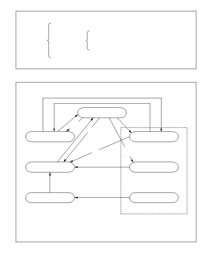
Figure 2-12 Classification of Exception Sources
Figure 2-13 State Transitions
Exception
sources
Reset
Interrupt
Trap instruction
External interrupts
Internal interrupts (from on-chip supporting modules)
Bus-released state
Exception-handling state
Reset state
Program execution state
Sleep mode
Software standby mode
Hardware standby mode
Power-down state
End of bus release
Bus request
End of bus
release
Bus
request
End of
exception
handling
Exception
Interrupt
SLEEP
instruction
with SSBY = 0
SLEEP instruction
with SSBY = 1
NMI, IRQ , IRQ ,
or IRQ interrupt
STBY
RES
= high, = low
RES
= high
0
1
2
*
1
*
2
Notes: 1.
2.
From any state except hardware standby mode, a transition to the reset state occurs
whenever goes low.
From any state, a transition to hardware standby mode occurs when goes low.
RES
STBY
50
2.8.4 Exception-Handling Sequences
Reset Exception Handling: Reset exception handling has the highest priority. The reset state is
entered when the
RES signal goes low. Reset exception handling starts after that, when RES
changes from low to high. When reset exception handling starts the CPU fetches a start address
from the exception vector table and starts program execution from that address. All interrupts,
including NMI, are disabled during the reset exception-handling sequence and immediately after it
ends.
Interrupt Exception Handling and Trap Instruction Exception Handling: When these
exception-handling sequences begin, the CPU references the stack pointer (ER7) and pushes the
program counter and condition code register on the stack. Next, if the UE bit in the system control
register (SYSCR) is set to 1, the CPU sets the I bit in the condition code register to 1. If the UE bit
is cleared to 0, the CPU sets both the I bit and the UI bit in the condition code register to 1. Then
the CPU fetches a start address from the exception vector table and execution branches to that
address.
Figure 2-14 shows the stack after the exception-handling sequence.
Figure 2-14 Stack Structure after Exception Handling
SP≠4
SP≠3
SP≠2
SP≠1
SP (ER7)
Before exception
handling starts
SP (ER7)
SP+1
SP+2
SP+3
SP+4
After exception
handling ends
Stack area
CCR
PC
Even
address
Pushed on stack
Legend
CCR:
SP:
Condition code register
Stack pointer
Notes: 1.
2.
PC is the address of the first instruction executed after the return from the
exception-handling routine.
Registers must be saved and restored by word access or longword access,
starting at an even address.
51

2.8.5 Bus-Released State
In this state the bus is released to a bus master other than the CPU, in response to a bus request.
The bus masters other than the CPU are the DMA controller, the refresh controller, and an
external bus master. While the bus is released, the CPU halts except for internal operations.
Interrupt requests are not accepted. For details see section 6.3.7, Bus Arbiter Operation
2.8.6 Reset State
When the
RES input goes low all current processing stops and the CPU enters the reset state. The
I bit in the condition code register is set to 1 by a reset. All interrupts are masked in the reset state.
Reset exception handling starts when the
RES signal changes from low to high.
The reset state can also be entered by a watchdog timer overflow. For details see section 12,
Watchdog Timer.
2.8.7 Power-Down State
In the power-down state the CPU stops operating to conserve power. There are three modes: sleep
mode, software standby mode, and hardware standby mode.
Sleep Mode: A transition to sleep mode is made if the SLEEP instruction is executed while the
SSBY bit is cleared to 0 in the system control register (SYSCR). CPU operations stop
immediately after execution of the SLEEP instruction, but the contents of CPU registers are
retained.
Software Standby Mode: A transition to software standby mode is made if the SLEEP
instruction is executed while the SSBY bit is set to 1 in SYSCR. The CPU and clock halt and all
on-chip supporting modules stop operating. The on-chip supporting modules are reset, but as long
as a specified voltage is supplied the contents of CPU registers and on-chip RAM are retained.
The I/O ports also remain in their existing states.
Hardware Standby Mode: A transition to hardware standby mode is made when the
STBY input
goes low. As in software standby mode, the CPU and all clocks halt and the on-chip supporting
modules are reset, but as long as a specified voltage is supplied, on-chip RAM contents are
retained.
For further information see section 17, Power-Down State.
52
2.9 Basic Operational Timing
2.9.1 Overview
The H8/300H CPU operates according to the system clock (¯). The interval from one rise of the
system clock to the next rise is referred to as a "state." A memory cycle or bus cycle consists of
two or three states. The CPU uses different methods to access on-chip memory, the on-chip
supporting modules, and the external address space. Access to the external address space can be
controlled by the bus controller.
2.9.2 On-Chip Memory Access Timing
On-chip memory is accessed in two states. The data bus is 16 bits wide, permitting both byte and
word access. Figure 2-15 shows the on-chip memory access cycle. Figure 2-16 indicates the pin
states.
Figure 2-15 On-Chip Memory Access Cycle
T state
Bus cycle
Internal address bus
Internal read signal
Internal data bus
(read access)
Internal write signal
Internal data bus
(write access)
¯
1
T state
2
Read data
Address
Write data
53
Figure 2-16 Pin States during On-Chip Memory Access
T
, , ,
AS
¯
1
T
2
Address bus
D to D
15
0
RD HWR LWR
High
Address
High impedance
54
2.9.3 On-Chip Supporting Module Access Timing
The on-chip supporting modules are accessed in three states. The data bus is 8 or 16 bits wide,
depending on the register being accessed. Figure 2-17 shows the on-chip supporting module
access timing. Figure 2-18 indicates the pin states.
Figure 2-17 Access Cycle for On-Chip Supporting Modules
Address bus
Internal read signal
Internal data bus
Internal write signal
Address
Internal data bus
¯
T state
Bus cycle
1
T state
2
T state
3
Read
access
Write
access
Write data
Read data
55
Figure 2-18 Pin States during Access to On-Chip Supporting Modules
2.9.4 Access to External Address Space
The external address space is divided into eight areas (areas 0 to 7). Bus-controller settings
determine whether each area is accessed via an 8-bit or 16-bit bus, and whether it is accessed in
two or three states. For details see section 6, Bus Controller.
Address
T
, , ,
AS
¯
1
T
2
Address bus
D to D
15
0
RD HWR LWR
High
High impedance
T
3
56

Section 3 MCU Operating Modes
3.1 Overview
3.1.1 Operating Mode Selection
The H8/3002 has four operating modes (modes 1 to 4) that are selected by the mode pins (MD
2
to
MD
0
) as indicated in table 3-1. The input at these pins determines the size of the address space
and the initial bus mode.
Table 3-1 Operating Mode Selection
Mode Pins
Description
Operating Mode
MD
2
MD
1
MD
0
Address Space
Initial Bus Mode
*
1
On-Chip RAM
--
0
0
0
--
--
--
Mode 1
0
0
1
1 Mbyte
8 bits
Enabled
*
2
Mode 2
0
1
0
1 Mbyte
16 bits
Enabled
*
2
Mode 3
0
1
1
16 Mbytes
8 bits
Enabled
*
2
Mode 4
1
0
0
16 Mbytes
16 bits
Enabled
*
2
--
1
0
1
--
--
--
--
1
1
0
--
--
--
--
1
1
1
--
--
--
Notes: 1. In all modes, an 8-bit or 16-bit data bus can be selected on a per-area basis by settings
made in the area bus width control register (ABWCR). For details see section 6, Bus
Controller.
2. If the RAME in SYSCR is cleared to 0, these addresses become external addresses.
For the address space size there are two choices: 1 Mbyte or 16 Mbytes. The external data bus is
either 8 or 16 bits wide depending on the settings in the area bus width control register (ABWCR).
If 8-bit access is selected for all areas, the external data bus is 8 bits wide. For details see
section 6, Bus Controller.
Modes 1 to 4 are externally expanded modes that enable access to external memory and peripheral
devices. Modes 1 and 2 support a maximum address space of 1 Mbyte. Modes 3 and 4 support a
maximum address space of 16 Mbytes.
The H8/3002 can only be used in modes 1 to 4. The inputs at the mode pins must select one of
these four modes. The inputs at the mode pins must not be changed during operation.
57

3.1.2 Register Configuration
The H8/3002 has a mode control register (MDCR) that indicates the inputs at the mode pins
(MD
2
to MD
0
), and a system control register (SYSCR). Table 3-2 summarizes these registers.
Table 3-2 Registers
Address
*
Name
Abbreviation
R/W
Initial Value
H'FFF1
Mode control register
MDCR
R
Undetermined
H'FFF2
System control register
SYSCR
R/W
H'0B
Note:
*
The lower 16 bits of the address are indicated.
58

3.2 Mode Control Register (MDCR)
MDCR is an 8-bit read-only register that indicates the current operating mode of the H8/3002.
Bits 7 and 6--Reserved: These bits cannot be modified and are always read as 1.
Bits 5 to 3--Reserved: These bits cannot be modified and are always read as 0.
Bits 2 to 0--Mode Select 2 to 0 (MDS2 to MDS0): These bits indicate the logic levels at pins
MD
2
to MD
0
(the current operating mode). MDS2 to MDS0 correspond to MD
2
to MD
0
. MDS2
to MDS0 are read-only bits. The mode pin (MD
2
to MD
0
) levels are latched when MDCR is read.
Bit
Initial value
Read/Write
7
--
1
--
6
--
1
--
5
--
0
--
4
--
0
--
3
--
0
--
0
MDS0
--
R
*
2
MDS2
--
R
1
MDS1
--
R
*
*
Reserved bits
Mode select 2 to 0
Bits indicating the current
operating mode
Reserved bits
Note: Determined by pins MD to MD .
*
2
0
59

3.3 System Control Register (SYSCR)
SYSCR is an 8-bit register that controls the operation of the H8/3002.
Bit 7--Software Standby (SSBY): Enables transition to software standby mode. (For further
information about software standby mode see section 17, Power-Down State.)
When software standby mode is exited by an external interrupt, this bit remains set to 1. To clear
this bit, write 0.
Bit 7
SSBY
Description
0
SLEEP instruction causes transition to sleep mode
(Initial value)
1
SLEEP instruction causes transition to software standby mode
Bit
Initial value
Read/Write
7
SSBY
0
R/W
6
STS2
0
R/W
5
STS1
0
R/W
4
STS0
0
R/W
3
UE
1
R/W
0
RAME
1
R/W
2
NMIEG
0
R/W
1
--
1
--
Software standby
Enables transition to software standby mode
User bit enable
Selects whether to use the UI bit in CCR
as a user bit or an interrupt mask bit
NMI edge select
Selects the valid edge
of the NMI input
Reserved bit
RAM enable
Enables or
disables
on-chip RAM
Standby timer select 2 to 0
These bits select the waiting time at
recovery from software standby mode
60

Bits 6 to 4--Standby Timer Select (STS2 to STS0): These bits select the length of time the CPU
and on-chip supporting modules wait for the internal clock oscillator to settle when software
standby mode is exited by an external interrupt. Set these bits so that the waiting time will be at
least 8 ms at the system clock rate. For further information about waiting time selection, see
section 17.4.3, Selection of Oscillator Waiting Time after Exit from Software Standby Mode.
Bit 6
Bit 5
Bit 4
STS2
STS1
STS0
Description
0
0
0
Waiting time = 8192 states
(Initial value)
0
0
1
Waiting time = 16384 states
0
1
0
Waiting time = 32768 states
0
1
1
Waiting time = 65536 states
1
0
--
Waiting time = 131072 states
1
1
--
Illegal setting
Bit 3--User Bit Enable (UE): Selects whether to use the UI bit in the condition code register as a
user bit or an interrupt mask bit.
Bit 3
UE
Description
0
UI bit in CCR is used as an interrupt mask bit
1
UI bit in CCR is used as a user bit
(Initial value)
Bit 2--NMI Edge Select (NMIEG): Selects the valid edge of the NMI input.
Bit 2
NMIEG
Description
0
An interrupt is requested at the falling edge of NMI
(Initial value)
1
An interrupt is requested at the rising edge of NMI
Bit 1--Reserved: This bit cannot be modified and is always read as 1.
Bit 0--RAM Enable (RAME): Enables or disables the on-chip RAM. The RAME bit is
initialized by the rising edge of the RES signal. It is not initialized in software standby mode.
Bit 0
RAME
Description
0
On-chip RAM is disabled
1
On-chip RAM is enabled
(Initial value)
61

3.4 Operating Mode Descriptions
3.4.1 Mode 1
Address pins A
19
to A
0
are enabled, permitting access to a maximum 1-Mbyte address space. The
initial bus mode after a reset is 8 bits, with 8-bit access to all areas. If at least one area is
designated for 16-bit access in ABWCR, the bus mode switches to 16 bits.
3.4.2 Mode 2
Address pins A
19
to A
0
are enabled, permitting access to a maximum 1-Mbyte address space. The
initial bus mode after a reset is 16 bits, with 16-bit access to all areas. If all areas are designated
for 8-bit access in ABWCR, the bus mode switches to 8 bits.
3.4.3 Mode 3
Address pins A
23
to A
0
are enabled, permitting access to a maximum 16-Mbyte address space.
The initial bus mode after a reset is 8 bits, with 8-bit access to all areas. If at least one area is
designated for 16-bit access in ABWCR, the bus mode switches to 16 bits. A
23
to A
21
are valid
when 0 is written in bits 7 to 5 of the bus release control register (BRCR).
3.4.4 Mode 4
Address pins A
23
to A
0
are enabled, permitting access to a maximum 16-Mbyte address space.
The initial bus mode after a reset is 16 bits, with 16-bit access to all areas. If all areas are
designated for 8-bit access in ABWCR, the bus mode switches to 8 bits. A
23
to A
21
are valid
when 0 is written in bits 7 to 5 of BRCR.
62

3.5 Pin Functions in Each Operating Mode
The pin functions of ports 4 and A vary depending on the operating mode. Table 3-3 indicates
their functions in each operating mode.
Table 3-3 Pin Functions in Each Mode
Port
Mode 1
Mode 2
Mode 3
Mode 4
Port 4
P4
7
to P4
0
*
1
D
7
to D
0
*
1
P4
7
to P4
0
*
1
D
7
to D
0
*
1
Port A
PA
7
to PA
4
PA
7
to PA
4
A
23
to A
20
*
2
A
23
to A
20
*
2
Notes: 1. Initial state. The bus mode can be switched by settings in ABWCR.
These pins function as P4
7
to P4
0
in 8-bit bus mode, and as D
7
to
D
0
in 16-bit bus mode.
2. A
20
is always an address output pin. A
23
to A
21
become valid when
0 is written in bits 7 to 5 of BRCR; initially, they function as PA
4
to
PA
6
.
3.6 Memory Map in Each Operating Mode
Figure 3-1 shows a memory map for modes 1 to 4. The address space is divided into eight areas.
The initial bus mode differs between modes 1 and 2, and also between modes 3 and 4. The address
locations of the on-chip RAM and on-chip registers differ between the 1-Mbyte modes (modes 1
and 2) and 16-Mbyte modes (modes 3 and 4). The address range specifiable by the CPU in its
8- and 16-bit absolute addressing modes (@aa:8 and @aa:16) also differs.
63
Figure 3-1 Memory Map in Each Operating Mode
Modes 1 and 2 (1-Mbyte modes)
Modes 3 and 4 (16-Mbyte modes)
Vector table
External address space
External address
space
Vector table
External address
space
Area 0
Area 1
Area 2
Area 3
Area 4
Area 5
Area 6
Area 7
8-bit
absolute
addresses
External address
space
8-bit
absolute
addresses
Area 0
Area 1
Area 2
Area 3
Area 4
Area 5
Area 6
Area 7
H'00000
H'07FFF
H'1FFFF
H'20000
H'3FFFF
H'40000
H'5FFFF
H'60000
H'7FFFF
H'80000
H'9FFFF
H'A0000
H'BFFFF
H'C0000
H'DFFFF
H'E0000
H'F8000
H'FFD0F
H'FFD10
H'FFF00
H'FFF0F
H'FFF10
H'FFF1B
H'FFF1C
F'FFFFF
H'1FFFFF
H'200000
H'3FFFFF
H'400000
H'5FFFFF
H'600000
H'7FFFFF
H'800000
H'9FFFFF
H'A00000
H'BFFFFF
H'C00000
H'DFFFFF
H'E00000
H'FF8000
H'FFFD0F
H'FFFD10
H'FFFF00
H'FFFF0F
H'FFFF10
H'FFFF1B
H'FFFF1C
H'FFFFFF
H'000000
H'007FFF
16-bit
absolute
addresses
16-bit
absolute
addresses
16-bit
absolute
addresses
16-bit
absolute
addresses
Note:
*
External addresses can be accessed by clearing the RAME bit to 0 in SYSCR.
On-chip registers
On-chip RAM
*
On-chip registers
On-chip RAM
*
64

Section 4 Exception Handling
4.1 Overview
4.1.1 Exception Handling Types and Priority
As table 4-1 indicates, exception handling may be caused by a reset, trap instruction, or interrupt.
Exception handling is prioritized as shown in table 4-1. If two or more exceptions occur
simultaneously, they are accepted and processed in priority order. Trap instruction exceptions are
accepted at all times in the program execution state.
Table 4-1 Exception Types and Priority
Priority Exception Type
Start of Exception Handling
High
Reset
Starts immediately after a low-to-high transition at the
RES
pin
Interrupt
Interrupt requests are handled when execution of the current
instruction or handling of the current exception is completed
Low
Trap instruction (TRAPA) Started by execution of a trap instruction (TRAPA)
4.1.2 Exception Handling Operation
Exceptions originate from various sources. Trap instructions and interrupts are handled as follows.
1.
The program counter (PC) and condition code register (CCR) are pushed onto the stack.
2.
The CCR interrupt mask bit is set to 1.
3.
A vector address corresponding to the exception source is generated, and program execution
starts from that address.
For a reset exception, steps 2 and 3 above are carried out.
65

4.1.3 Exception Vector Table
The exception sources are classified as shown in figure 4-1. Different vectors are assigned to
different exception sources. Table 4-2 lists the exception sources and their vector addresses.
Figure 4-1 Exception Sources
Table 4-2 Exception Vector Table
Exception Source
Vector Number
Vector Address
*
1
Reset
0
H'0000 to H'0003
Reserved for system use
1
H'0004 to H'0007
2
H'0008 to H'000B
3
H'000C to H'000F
4
H'0010 to H'0013
5
H'0014 to H'0017
6
H'0018 to H'001B
External interrupt (NMI)
7
H'001C to H'001F
Trap instruction (4 sources)
8
H'0020 to H'0023
9
H'0024 to H'0027
10
H'0028 to H'002B
11
H'002C to H'002F
External interrupt IRQ
0
12
H'0030 to H'0033
External interrupt IRQ
1
13
H'0034 to H'0037
External interrupt IRQ
2
14
H'0038 to H'003B
External interrupt IRQ
3
15
H'003C to H'003F
External interrupt IRQ
4
16
H'0040 to H'0043
External interrupt IRQ
5
17
H'0044 to H'0047
Reserved for system use
18
H'0048 to H'004B
19
H'004C to H'004F
Internal interrupts
*
2
20
H'0050 to H'0053
to
to
60
H'00F0 to H'00F3
Notes: 1. Lower 16 bits of the address.
2. For the internal interrupt vectors, see section 5.3.3, Interrupt Vector Table.
Exception
sources
∑ Reset
∑ Interrupts
∑ Trap instruction
External interrupts:
Internal interrupts:
NMI, IRQ to IRQ
30 interrupts from on-chip
supporting modules
0 5
66

4.2 Reset
4.2.1 Overview
A reset is the highest-priority exception. When the
RES pin goes low, all processing halts and the
H8/3002 enters the reset state. A reset initializes the internal state of the CPU and the registers of
the on-chip supporting modules. Reset exception handling begins when the
RES pin changes from
low to high.
The H8/3002 can also be reset by overflow of the watchdog timer. For details see section 12,
Watchdog Timer.
4.2.2 Reset Sequence
The H8/3002 enters the reset state when the
RES pin goes low.
To ensure that the H8/3002 is reset, hold the
RES pin low for at least 20 ms at power-up. To reset
the H8/3002 during operation, hold the
RES pin low for at least 10 system clock (¯) cycles. See
appendix D.2, Pin States at Reset, for the states of the pins in the reset state.
When the
RES pin goes high after being held low for the necessary time, the H8/3002 starts reset
exception handling as follows.
∑
The internal state of the CPU and the registers of the on-chip supporting modules are
initialized, and the I bit is set to 1 in CCR.
∑
The contents of the reset vector address (H'0000 to H'0003) are read, and program execution
starts from the address indicated in the vector address.
Figure 4-2 shows the reset sequence in modes 1 and 3. Figure 4-3 shows the reset sequence in
modes 2 and 4.
67

Figure 4-2 Reset Sequence (Modes 1 and 3)
¯
Address
bus
RES
RD
HWR
D to D
15
8
Vector fetch
Internal
processing
Prefetch of
first program
instruction
(1), (3), (5), (7)
(2), (4), (6), (8)
(9)
(10)
Note: After a reset, the wait-state controller inserts three wait states in every bus cycle.
Address of reset vector: (1) = H'00000, (3) = H'00001, (5) = H'00002, (7) = H'00003
Start address (contents of reset vector)
Start address
First instruction of program
High
(1)
(3)
(5)
(7)
(9)
(2)
(4)
(6)
(8)
(10)
LWR
,
68
Figure 4-3 Reset Sequence (Modes 2 and 4)
4.2.3 Interrupts after Reset
If an interrupt is accepted after a reset but before the stack pointer (SP) is initialized, PC and CCR
will not be saved correctly, leading to a program crash. To prevent this, all interrupt requests,
including NMI, are disabled immediately after a reset. The first instruction of the program is
always executed immediately after the reset state ends. This instruction should initialize the stack
pointer (example: MOV.L #xx:32, SP).
¯
Address bus
RES
RD
HWR
D to D
15
0
Vector fetch
Internal
processing
Prefetch of first
program instruction
(1), (3)
(2), (4)
(5)
(6)
Note: After a reset, the wait-state controller inserts three wait states in every bus cycle.
High
LWR
,
Address of reset vector: (1) = H'00000, (3) = H'00002
Start address (contents of reset vector)
Start address
First instruction of program
(2)
(4)
(3)
(1)
(5)
(6)
69

4.3 Interrupts
Interrupt exception handling can be requested by seven external sources (NMI, IRQ
0
to IRQ
5
) and
30 internal sources in the on-chip supporting modules. Figure 4-4 classifies the interrupt sources
and indicates the number of interrupts of each type.
The on-chip supporting modules that can request interrupts are the watchdog timer (WDT),
refresh controller, 16-bit integrated timer-pulse unit (ITU), DMA controller (DMAC), serial
communication interface (SCI), and A/D converter. Each interrupt source has a separate vector
address.
NMI is the highest-priority interrupt and is always accepted. Interrupts are controlled by the
interrupt controller. The interrupt controller can assign interrupts other than NMI to two priority
levels, and arbitrate between simultaneous interrupts. Interrupt priorities are assigned in interrupt
priority registers A and B (IPRA and IPRB) in the interrupt controller.
For details on interrupts see section 5, Interrupt Controller.
Figure 4-4 Interrupt Sources and Number of Interrupts
Interrupts
External interrupts
Internal interrupts
NMI (1)
IRQ to IRQ (6)
WDT (1)
Refresh controller (1)
ITU (15)
DMAC (4)
SCI (8)
A/D converter (1)
*
1
*
2
Notes: Numbers in parentheses are the number of interrupt sources.
1.
2.
When the watchdog timer is used as an interval timer, it generates an interrupt
request at every counter overflow.
When the refresh controller is used as an interval timer, it generates an interrupt
request at compare match.
0 5
70
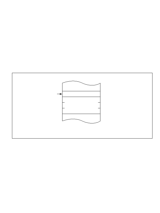
4.4 Trap Instruction
Trap instruction exception handling starts when a TRAPA instruction is executed. If the UE bit is
set to 1 in the system control register (SYSCR), the exception handling sequence sets the I bit to 1
in CCR. If the UE bit is 0, the I and UI bits are both set to 1. The TRAPA instruction fetches a
start address from a vector table entry corresponding to a vector number from 0 to 3, which is
specified in the instruction code.
4.5 Stack Status after Exception Handling
Figure 4-5 shows the stack after completion of trap instruction exception handling and interrupt
exception handling.
Figure 4-5 Stack after Completion of Exception Handling
SP
PC
Note: In modes 1 and 2 only 20 PC bits are valid; the upper 4 bits are ignored.
CCR
71
4.6 Notes on Stack Usage
When accessing word data or longword data, the H8/3002 regards the lowest address bit as 0. The
stack should always be accessed by word access or longword access, and the value of the stack
pointer (SP, ER7) should always be kept even. Use the following instructions to save registers:
PUSH.W Rn (or MOV.W Rn, @≠SP)
PUSH.L ERn (or MOV.L ERn, @≠SP)
Use the following instructions to restore registers:
POP.W Rn
(or MOV.W @SP+, Rn)
POP.L ERn
(or MOV.L @SP+, ERn)
Setting SP to an odd value may lead to a malfunction. Figure 4-6 shows an example of what
happens when the SP value is odd.
Figure 4-6 Operation when SP Value is Odd
TRAPA instruction executed
CCR
Legend
CCR:
PC:
R1L:
SP:
SP
PC
RIL
PC
SP
SP
MOV. B RIL, @-ER7
SP set to H'FFFEFF
Data saved above SP
CCR contents lost
Condition code register
Program counter
General register R1L
Stack pointer
Note: The diagram illustrates modes 3 and 4.
H'FFFEFA
H'FFFEFB
H'FFFEFC
H'FFFEFD
H'FFFEFF
72

Section 5 Interrupt Controller
5.1 Overview
5.1.1 Features
The interrupt controller has the following features:
∑
Interrupt priority registers (IPRs) for setting interrupt priorities
Interrupts other than NMI can be assigned to two priority levels on a module-by-module basis
in interrupt priority registers A and B (IPRA and IPRB).
∑
Three-level masking by the I and UI bits in the CPU condition code register (CCR)
∑
Independent vector addresses
All interrupts are independently vectored; the interrupt service routine does not have to
identify the interrupt source.
∑
Seven external interrupt pins
NMI has the highest priority and is always accepted; either the rising or falling edge can be
selected. For each of IRQ
0
to IRQ
5
, sensing of the falling edge or level sensing can be
selected independently.
73

5.1.2 Block Diagram
Figure 5-1 shows a block diagram of the interrupt controller.
Figure 5-1 Interrupt Controller Block Diagram
ISCR
IER
IPRA, IPRB
.
.
.
OVF
TME
ADI
ADIE
.
.
.
.
.
.
.
CPU
CCR
I
UI
UE
SYSCR
ISCR:
IER:
ISR:
IPRA:
IPRB:
SYSCR:
NMI
input
IRQ input
IRQ input
section ISR
Interrupt controller
Priority
decision logic
Interrupt
request
Vector
number
IRQ sense control register
IRQ enable register
IRQ status register
Interrupt priority register A
Interrupt priority register B
System control register
Legend
74

5.1.3 Pin Configuration
Table 5-1 lists the interrupt pins.
Table 5-1 Interrupt Pins
Name
Abbreviation
I/O
Function
Nonmaskable interrupt
NMI
Input
Nonmaskable interrupt, rising edge or
falling edge selectable
External interrupt request 5 to 0
IRQ
5
to IRQ
0
Input
Maskable interrupts, falling edge or
level sensing selectable
5.1.4 Register Configuration
Table 5-2 lists the registers of the interrupt controller.
Table 5-2 Interrupt Controller Registers
Address
*
1
Name
Abbreviation
R/W
Initial Value
H'FFF2
System control register
SYSCR
R/W
H'0B
H'FFF4
IRQ sense control register
ISCR
R/W
H'00
H'FFF5
IRQ enable register
IER
R/W
H'00
H'FFF6
IRQ status register
ISR
R/(W)
*
2
H'00
H'FFF8
Interrupt priority register A
IPRA
R/W
H'00
H'FFF9
Interrupt priority register B
IPRB
R/W
H'00
Notes: 1. Lower 16 bits of the address.
2. Only 0 can be written, to clear flags.
75
5.2 Register Descriptions
5.2.1 System Control Register (SYSCR)
SYSCR is an 8-bit readable/writable register that controls software standby mode, selects the
action of the UI bit in CCR, selects the NMI edge, and enables or disables the on-chip RAM.
Only bits 3 and 2 are described here. For the other bits, see section 3.3, System Control Register
(SYSCR).
SYSCR is initialized to H'0B by a reset and in hardware standby mode. It is not initialized in
software standby mode.
Bit
Initial value
Read/Write
7
SSBY
0
R/W
6
STS2
0
R/W
5
STS1
0
R/W
4
STS0
0
R/W
3
UE
1
R/W
0
RAME
1
R/W
2
NMIEG
0
R/W
1
--
1
--
Software standby
Standby timer
select 2 to 0
User bit enable
Selects whether to use the UI bit in
CCR as a user bit or interrupt mask bit
NMI edge select
Selects the NMI input edge
Reserved bit
RAM enable
76

Bit 3--User Bit Enable (UE): Selects whether to use the UI bit in CCR as a user bit or an
interrupt mask bit.
Bit 3
UE
Description
0
UI bit in CCR is used as interrupt mask bit
1
UI bit in CCR is used as user bit
(Initial value)
Bit 2--NMI Edge Select (NMIEG): Selects the NMI input edge.
Bit 2
NMIEG
Description
0
Interrupt is requested at falling edge of NMI input
(Initial value)
1
Interrupt is requested at rising edge of NMI input
5.2.2 Interrupt Priority Registers A and B (IPRA, IPRB)
IPRA and IPRB are 8-bit readable/writable registers that control interrupt priority.
77
Interrupt Priority Register A (IPRA): IPRA is an 8-bit readable/writable register in which
interrupt priority levels can be set.
IPRA is initialized to H'00 by a reset and in hardware standby mode.
Bit
Initial value
Read/Write
7
IPRA7
0
R/W
6
IPRA6
0
R/W
5
IPRA5
0
R/W
4
IPRA4
0
R/W
3
IPRA3
0
R/W
0
IPRA0
0
R/W
2
IPRA2
0
R/W
1
IPRA1
0
R/W
Priority level A7
Selects the priority level of IRQ interrupt requests
Priority level A3
Selects the priority level of WDT and
refresh controller interrupt requests
Priority level A2
Selects the priority level of
ITU channel 0 interrupt requests
Priority level A1
Selects the priority level
of ITU channel 1
interrupt requests
Priority
level A0
Selects the
priority level
of ITU
channel 2
interrupt
requests
Selects the priority level of IRQ interrupt requests
Priority level A6
Selects the priority level of IRQ and IRQ interrupt requests
Priority level A5
Selects the priority level of IRQ and IRQ
interrupt requests
Priority level A4
0
1
2
3
4
5
78

Bit 7--Priority Level A7 (IPRA7): Selects the priority level of IRQ
0
interrupt requests.
Bit 7
IPRA7
Description
0
IRQ
0
interrupt requests have priority level 0 (low priority)
(Initial value)
1
IRQ
0
interrupt requests have priority level 1 (high priority)
Bit 6--Priority Level A6 (IPRA6): Selects the priority level of IRQ
1
interrupt requests.
Bit 6
IPRA6
Description
0
IRQ
1
interrupt requests have priority level 0 (low priority)
(Initial value)
1
IRQ
1
interrupt requests have priority level 1 (high priority)
Bit 5--Priority Level A5 (IPRA5): Selects the priority level of IRQ
2
and IRQ
3
interrupt
requests.
Bit 5
IPRA5
Description
0
IRQ
2
and IRQ
3
interrupt requests have priority level 0 (low priority)
(Initial value)
1
IRQ
2
and IRQ
3
interrupt requests have priority level 1 (high priority)
Bit 4--Priority Level A4 (IPRA4): Selects the priority level of IRQ
4
and IRQ
5
interrupt
requests.
Bit 4
IPRA4
Description
0
IRQ
4
and IRQ
5
interrupt requests have priority level 0 (low priority)
(Initial value)
1
IRQ
4
and IRQ
5
interrupt requests have priority level 1 (high priority)
79

Bit 3--Priority Level A3 (IPRA3): Selects the priority level of WDT and refresh controller
interrupt requests.
Bit 3
IPRA3
Description
0
WDT and refresh controller interrupt requests have priority level 0
(Initial value)
(low priority)
1
WDT and refresh controller interrupt requests have priority level 1 (high priority)
Bit 2--Priority Level A2 (IPRA2): Selects the priority level of ITU channel 0 interrupt requests.
Bit 2
IPRA2
Description
0
ITU channel 0 interrupt requests have priority level 0 (low priority)
(Initial value)
1
ITU channel 0 interrupt requests have priority level 1 (high priority)
Bit 1--Priority Level A1 (IPRA1): Selects the priority level of ITU channel 1 interrupt requests.
Bit 1
IPRA1
Description
0
ITU channel 1 interrupt requests have priority level 0 (low priority)
(Initial value)
1
ITU channel 1 interrupt requests have priority level 1 (high priority)
Bit 0--Priority Level A0 (IPRA0): Selects the priority level of ITU channel 2 interrupt requests.
Bit 0
IPRA0
Description
0
ITU channel 2 interrupt requests have priority level 0 (low priority)
(Initial value)
1
ITU channel 2 interrupt requests have priority level 1 (high priority)
80

Interrupt Priority Register B (IPRB): IPRB is an 8-bit readable/writable register in which
interrupt priority levels can be set.
IPRB is initialized to H'00 by a reset and in hardware standby mode.
Bit
Initial value
Read/Write
7
IPRB7
0
R/W
6
IPRB6
0
R/W
5
IPRB5
0
R/W
4
--
0
R/W
3
IPRB3
0
R/W
0
--
0
R/W
2
IPRB2
0
R/W
1
IPRB1
0
R/W
Priority level B7
Selects the priority level of ITU channel 3 interrupt requests
Priority level B3
Selects the priority level of SCI
channel 0 interrupt requests
Priority level B2
Selects the priority level of
SCI channel 1 interrupt requests
Priority level B1
Selects the priority level
of A/D converter
interrupt request
Reserved bit
Selects the priority level of ITU channel 4 interrupt requests
Priority level B6
Selects the priority level of DMAC interrupt requests
(channels 0 and 1)
Priority level B5
Reserved bit
81

Bit 7--Priority Level B7 (IPRB7): Selects the priority level of ITU channel 3 interrupt requests.
Bit 7
IPRB7
Description
0
ITU channel 3 interrupt requests have priority level 0 (low priority)
(Initial value)
1
ITU channel 3 interrupt requests have priority level 1 (high priority)
Bit 6--Priority Level B6 (IPRB6): Selects the priority level of ITU channel 4 interrupt requests.
Bit 6
IPRB6
Description
0
ITU channel 4 interrupt requests have priority level 0 (low priority)
(Initial value)
1
ITU channel 4 interrupt requests have priority level 1 (high priority)
Bit 5--Priority Level B5 (IPRB5): Selects the priority level of DMAC interrupt requests
(channels 0 and 1).
Bit 5
IPRB5
Description
0
DMAC interrupt requests (channels 0 and 1) have priority level 0
(Initial value)
(low priority)
1
DMAC interrupt requests (channels 0 and 1) have priority level 1 (high priority)
Bit 4--Reserved: This bit can be written and read, but it does not affect interrupt priority.
82

Bit 3--Priority Level B3 (IPRB3): Selects the priority level of SCI channel 0 interrupt requests.
Bit 3
IPRB3
Description
0
SCI0 interrupt requests have priority level 0 (low priority)
(Initial value)
1
SCI0 interrupt requests have priority level 1 (high priority)
Bit 2--Priority Level B2 (IPRB2): Selects the priority level of SCI channel 1 interrupt requests.
Bit 2
IPRB2
Description
0
SCI1 interrupt requests have priority level 0 (low priority)
(Initial value)
1
SCI1 interrupt requests have priority level 1 (high priority)
Bit 1--Priority Level B1 (IPRB1): Selects the priority level of A/D converter interrupt requests.
Bit 1
IPRB1
Description
0
A/D converter interrupt requests have priority level 0 (low priority)
(Initial value)
1
A/D converter interrupt requests have priority level 1 (high priority)
Bit 0--Reserved: This bit can be written and read, but it does not affect interrupt priority.
83

5.2.3 IRQ Status Register (ISR)
ISR is an 8-bit readable/writable register that indicates the status of IRQ
0
to IRQ
5
interrupt
requests.
ISR is initialized to H'00 by a reset and in hardware standby mode.
Bits 7 and 6--Reserved: These bits cannot be modified and are always read as 0.
Bits 5 to 0--IRQ
5
to IRQ
0
Flags (IRQ5F to IRQ0F): These bits indicate the status of IRQ
5
to
IRQ
0
interrupt requests.
Bits 5 to 0
IRQ5F to IRQ0F
Description
0
[Clearing conditions]
(Initial value)
0 is written in IRQnF after reading the IRQnF flag when IRQnF = 1.
IRQnSC = 0, IRQn input is high, and interrupt exception handling is carried out.
IRQnSC = 1 and IRQn interrupt exception handling is carried out.
1
[Setting conditions]
IRQnSC = 0 and IRQn input is low.
IRQnSC = 1 and IRQn input changes from high to low.
Note: n = 5 to 0
Bit
Initial value
Read/Write
7
--
0
--
These bits indicate IRQ to IRQ interrupt request status
Note: Only 0 can be written, to clear flags.
*
6
--
0
--
5
IRQ5F
0
R/(W)
*
4
IRQ4F
0
R/(W)
*
3
IRQ3F
0
R/(W)
*
2
IRQ2F
0
R/(W)
*
1
IRQ1F
0
R/(W)
*
0
IRQ0F
0
R/(W)
*
5
0
IRQ to IRQ flags
5
0
Reserved bits
84

5.2.4 IRQ Enable Register (IER)
IER is an 8-bit readable/writable register that enables or disables IRQ
0
to IRQ
5
interrupt requests.
IER is initialized to H'00 by a reset and in hardware standby mode.
Bits 7 and 6--Reserved: These bits can be written and read, but they do not enable or disable
interrupts.
Bits 5 to 0--IRQ
5
to IRQ
0
Enable (IRQ5E to IRQ0E): These bits enable or disable IRQ
5
to
IRQ
0
interrupts.
Bits 5 to 0
IRQ5E to IRQ0E
Description
0
IRQ
5
to IRQ
0
interrupts are disabled
(Initial value)
1
IRQ
5
to IRQ
0
interrupts are enabled
Bit
Initial value
Read/Write
7
--
0
R/W
These bits enable or disable IRQ to IRQ interrupts
6
--
0
R/W
5
IRQ5E
0
R/W
4
IRQ4E
0
R/W
3
IRQ3E
0
R/W
2
IRQ2E
0
R/W
1
IRQ1E
0
R/W
0
IRQ0E
0
R/W
5
0
IRQ to IRQ enable
5
0
Reserved bits
85

5.2.5 IRQ Sense Control Register (ISCR)
ISCR is an 8-bit readable/writable register that selects level sensing or falling-edge sensing of the
inputs at pins IRQ
5
to IRQ
0
.
ISCR is initialized to H'00 by a reset and in hardware standby mode.
Bits 7 and 6--Reserved: These bits can be written and read, but they do not select level or
falling-edge sensing.
Bits 5 to 0--IRQ
5
to IRQ
0
Sense Control (IRQ5SC to IRQ0SC): These bits select whether
interrupts IRQ
5
to IRQ
0
are requested by level sensing of pins IRQ
5
to IRQ
0
, or by falling-edge
sensing.
Bits 5 to 0
IRQ5SC to IRQ0SC
Description
0
Interrupts are requested when IRQ
5
to IRQ
0
inputs are low
(Initial value)
1
Interrupts are requested by falling-edge input at IRQ
5
to IRQ
0
Bit
Initial value
Read/Write
7
--
0
R/W
These bits select level sensing or falling-edge sensing for
IRQ to IRQ interrupts
6
--
0
R/W
5
IRQ5SC
0
R/W
4
IRQ4SC
0
R/W
3
IRQ3SC
0
R/W
2
IRQ2SC
0
R/W
1
IRQ1SC
0
R/W
0
IRQ0SC
0
R/W
5
0
IRQ to IRQ sense control
5
0
Reserved bits
86
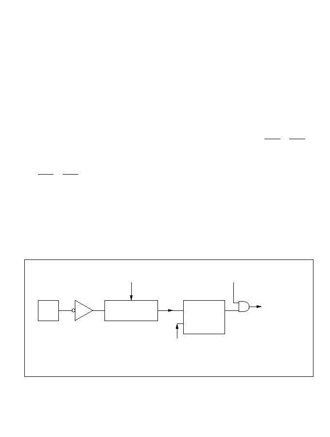
5.3 Interrupt Sources
The interrupt sources include external interrupts (NMI, IRQ
0
to IRQ
5
) and 30 internal interrupts.
5.3.1 External Interrupts
There are seven external interrupts: NMI, and IRQ
0
to IRQ
5
. Of these, NMI, IRQ
0
, IRQ
1
, and
IRQ
2
can be used to exit software standby mode.
NMI: NMI is the highest-priority interrupt and is always accepted, regardless of the states of the
I and UI bits in CCR. The NMIEG bit in SYSCR selects whether an interrupt is requested by the
rising or falling edge of the input at the NMI pin. NMI interrupt exception handling has vector
number 7.
IRQ
0
to IRQ
5
Interrupts: These interrupts are requested by input signals at pins IRQ
0
to IRQ
5
.
The IRQ
0
to IRQ
5
interrupts have the following features.
∑
ISCR settings can select whether an interrupt is requested by the low level of the input at pins
IRQ
0
to IRQ
5
, or by the falling edge.
∑
IER settings can enable or disable the IRQ
0
to IRQ
5
interrupts. Interrupt priority levels can be
assigned by four bits in IPRA (IPRA7 to IPRA4).
∑
The status of IRQ
0
to IRQ
5
interrupt requests is indicated in ISR. The ISR flags can be
cleared to 0 by software.
Figure 5-2 shows a block diagram of interrupts IRQ
0
to IRQ
5
.
Figure 5-2 Block Diagram of Interrupts IRQ
0
to IRQ
5
input
Edge/level
sense circuit
IRQnSC
IRQnF
S
R
Q
IRQnE
IRQn interrupt
request
Clear signal
IRQn
Note: n = 5 to 0
87

Figure 5-3 shows the timing of the setting of the interrupt flags (IRQnF).
Figure 5-3 Timing of Setting of IRQnF
Interrupts IRQ
0
to IRQ
5
have vector numbers 12 to 17. These interrupts are detected regardless of
whether the corresponding pin is set for input or output. When using a pin for external interrupt
input, clear its DDR bit to 0 and do not use the pin for chip select output, refresh output, or SCI
input or output.
5.3.2 Internal Interrupts
Thirty internal interrupts are requested from the on-chip supporting modules.
∑
Each on-chip supporting module has status flags for indicating interrupt status, and enable
bits for enabling or disabling interrupts.
∑
Interrupt priority levels can be assigned in IPRA and IPRB.
∑
ITU and SCI interrupt requests can activate the DMAC, in which case no interrupt request is
sent to the interrupt controller, and the I and UI bits are disregarded.
5.3.3 Interrupt Vector Table
Table 5-3 lists the interrupt sources, their vector addresses, and their default priority order. In the
default priority order, smaller vector numbers have higher priority. The priority of interrupts other
than NMI can be changed in IPRA and IPRB. The priority order after a reset is the default order
shown in table 5-3.
¯
IRQn
IRQnF
input pin
Note: n = 5 to 0
88

Table 5-3 Interrupt Sources, Vector Addresses, and Priority
Vector
Interrupt Source
Origin
Number
Vector Address
*
IPR
Priority
NMI
External pins
7
H'001C to H'001F
--
High
IRQ
0
12
H'0030 to H'0033
IPRA7
IRQ
1
13
H'0034 to H0037
IPRA6
IRQ
2
14
H'0038 to H'003B
IPRA5
IRQ
3
15
H'003C to H'003F
IRQ
4
16
H'0040 to H'0043
IPRA4
IRQ
5
17
H'0044 to H'0047
Reserved
--
18
H'0048 to H'004B
19
H'004C to H'004F
WOVI (interval timer)
Watchdog timer
20
H'0050 to H'0053
IPRA3
CMI (compare match)
Refresh controller
21
H'0054 to H'0057
Reserved
--
22
H'0058 to H'005B
23
H'005C to H'005F
IMIA0 (compare match/input
ITU channel 0
24
H'0060 to H'0063
IPRA2
capture A0)
IMIB0 (compare match/input
25
H'0064 to H'0067
capture B0)
OVI0 (overflow 0)
26
H'0068 to H'006B
Reserved
--
27
H'006C to H'006F
IMIA1 (compare match/input
ITU channel 1
28
H'0070 to H'0073
IPRA1
capture A1)
IMIB1 (compare match/input
29
H'0074 to H'0077
capture B1)
OVI1 (overflow 1)
30
H'0078 to H'007B
Reserved
--
31
H'007C to H'007F
IMIA2 (compare match/input
ITU channel 2
32
H'0080 to H'0083
IPRA0
capture A2)
IMIB2 (compare match/input
33
H'0084 to H'0087
capture B2)
OVI2 (overflow 2)
34
H'0088 to H'008B
Reserved
--
35
H'008C to H'008F
Low
Note:
*
Lower 16 bits of the address.
89

Table 5-3 Interrupt Sources, Vector Addresses, and Priority (cont)
Vector
Interrupt Source
Origin
Number
Vector Address
*
IPR
Priority
IMIA3 (compare match/input
ITU channel 3
36
H'0090 to H'0093
IPRB7 High
capture A3)
IMIB3 (compare match/input
37
H'0094 to H'0097
capture B3)
OVI3 (overflow 3)
38
H'0098 to H'009B
Reserved
--
39
H'009C to H'009F
IMIA4 (compare match/input
ITU channel 4
40
H'00A0 to H'00A3
IPRB6
capture A4)
IMIB4 (compare match/input
41
H'00A4 to H'00A7
capture B4)
OVI4 (overflow 4)
42
H'00A8 to H'00AB
Reserved
--
43
H'00AC to H'00AF
DEND0A
DMAC
44
H'00B0 to H'00B3
IPRB5
DEND0B
45
H'00B4 to H'00B7
DEND1A
46
H'00B8 to H'00BB
DEND1B
47
H'00BC to H'00BF
Reserved
--
48
H'00C0 to H'00C3 --
49
H'00C4 to H'00C7
50
H'00C8 to H'00CB
51
H'00CC to H'00CF
ERI0 (receive error 0)
SCI channel 0
52
H'00D0 to H'00D3 IPRB3
RXI0 (receive data full 0)
53
H'00D4 to H'00D7
TXI0 (transmit data empty 0)
54
H'00D8 to H'00DB
TEI0 (transmit end 0)
55
H'00DC to H'00DF
ERI1 (receive error 1)
SCI channel 1
56
H'00E0 to H'00E3
IPRB2
RXI1 (receive data full 1)
57
H'00E4 to H'00E7
TXI1 (transmit data empty 1)
58
H'00E8 to H'00EB
TEI1 (transmit end 1)
59
H'00EC to H'00EF
ADI (A/D end)
A/D
60
H'00F0 to H'00F3
IPRB1 Low
Note:
*
Lower 16 bits of the address.
90

5.4 Interrupt Operation
5.4.1 Interrupt Handling Process
The H8/3002 handles interrupts differently depending on the setting of the UE bit. When UE = 1,
interrupts are controlled by the I bit. When UE = 0, interrupts are controlled by the I and UI bits.
Table 5-4 indicates how interrupts are handled for all setting combinations of the UE, I, and
UI bits.
NMI interrupts are always accepted except in the reset and hardware standby states. IRQ
interrupts and interrupts from the on-chip supporting modules have their own enable bits.
Interrupt requests are ignored when the enable bits are cleared to 0.
Table 5-4 UE, I, and UI Bit Settings and Interrupt Handling
SYSCR
CCR
UE
I
UI
Description
1
0
--
All interrupts are accepted. Interrupts with priority level 1 have higher
priority.
1
--
No interrupts are accepted except NMI.
0
0
--
All interrupts are accepted. Interrupts with priority level 1 have higher
priority.
1
0
NMI and interrupts with priority level 1 are accepted.
1
No interrupts are accepted except NMI.
UE = 1: Interrupts IRQ
0
to IRQ
5
and interrupts from the on-chip supporting modules can all be
masked by the I bit in the CPU's CCR. Interrupts are masked when the I bit is set to 1, and
unmasked when the I bit is cleared to 0. Interrupts with priority level 1 have higher priority.
Figure 5-4 is a flowchart showing how interrupts are accepted when UE = 1.
91
Figure 5-4 Process Up to Interrupt Acceptance when UE = 1
Program execution state
Interrupt requested?
NMI
No
Yes
No
Yes
No
Priority level 1?
No
IRQ
0
Yes
No
IRQ
1
Yes
ADI
Yes
No
IRQ
0
Yes
No
IRQ
1
Yes
ADI
Yes
No
I = 0
Yes
Save PC and CCR
Branch to interrupt
service routine
Pending
Yes
I 1
Read vector address
92

∑
If an interrupt condition occurs and the corresponding interrupt enable bit is set to 1, an
interrupt request is sent to the interrupt controller.
∑
When the interrupt controller receives one or more interrupt requests, it selects the highest-
priority request, following the IPR interrupt priority settings, and holds other requests
pending. If two or more interrupts with the same IPR setting are requested simultaneously, the
interrupt controller follows the priority order shown in table 5-3.
∑
The interrupt controller checks the I bit. If the I bit is cleared to 0, the selected interrupt
request is accepted. If the I bit is set to 1, only NMI is accepted; other interrupt requests are
held pending.
∑
When an interrupt request is accepted, interrupt exception handling starts after execution of
the current instruction has been completed.
∑
In interrupt exception handling, PC and CCR are saved to the stack area. The PC value that is
saved indicates the address of the first instruction that will be executed after the return from
the interrupt service routine.
∑
Next the I bit is set to 1 in CCR, masking all interrupts except NMI.
∑
The vector address of the accepted interrupt is generated, and the interrupt service routine
starts executing from the address indicated by the contents of the vector address.
UE = 0: The I and UI bits in the CPU's CCR and the IPR bits enable three-level masking of IRQ
0
to IRQ
5
interrupts and interrupts from the on-chip supporting modules.
∑
Interrupt requests with priority level 0 are masked when the I bit is set to 1, and are unmasked
when the I bit is cleared to 0.
∑
Interrupt requests with priority level 1 are masked when the I and UI bits are both set to 1,
and are unmasked when either the I bit or the UI bit is cleared to 0.
For example, if the interrupt enable bits of all interrupt requests are set to 1, IPRA is set to
H'20, and IPRB is set to H'00 (giving IRQ
2
and IRQ
3
interrupt requests priority over other
interrupts), interrupts are masked as follows:
a. If I = 0, all interrupts are unmasked (priority order: NMI > IRQ
2
> IRQ
3
>IRQ
0
...).
b. If I = 1 and UI = 0, only NMI, IRQ
2
, and IRQ
3
are unmasked.
c. If I = 1 and UI = 1, all interrupts are masked except NMI.
93
Figure 5-5 shows the transitions among the above states.
Figure 5-5 Interrupt Masking State Transitions (Example)
Figure 5-6 is a flowchart showing how interrupts are accepted when UE = 0.
∑
If an interrupt condition occurs and the corresponding interrupt enable bit is set to 1, an
interrupt request is sent to the interrupt controller.
∑
When the interrupt controller receives one or more interrupt requests, it selects the highest-
priority request, following the IPR interrupt priority settings, and holds other requests
pending. If two or more interrupts with the same IPR setting are requested simultaneously, the
interrupt controller follows the priority order shown in table 5-3.
∑
The interrupt controller checks the I bit. If the I bit is cleared to 0, the selected interrupt
request is accepted regardless of its IPR setting, and regardless of the UI bit. If the I bit is set
to 1 and the UI bit is cleared to 0, only NMI and interrupts with priority level 1 are accepted;
interrupt requests with priority level 0 are held pending. If the I bit and UI bit are both set to
1, only NMI is accepted; all other interrupt requests are held pending.
∑
When an interrupt request is accepted, interrupt exception handling starts after execution of
the current instruction has been completed.
∑
In interrupt exception handling, PC and CCR are saved to the stack area. The PC value that is
saved indicates the address of the first instruction that will be executed after the return from
the interrupt service routine.
∑
The I and UI bits are set to 1 in CCR, masking all interrupts except NMI.
∑
The vector address of the accepted interrupt is generated, and the interrupt service routine
starts executing from the address indicated by the contents of the vector address.
All interrupts are
unmasked
Only NMI, IRQ , and
IRQ are unmasked
Exception handling,
or I 1, UI 1
a.
b.
2
3
All interrupts are
masked except NMI
c.
UI 0
I 0
Exception handling,
or UI 1
I 0
I 1, UI 0
94
Figure 5-6 Process Up to Interrupt Acceptance when UE = 0
Program execution state
Interrupt requested?
NMI
No
Yes
No
Yes
No
Priority level 1?
No
IRQ
0
Yes
No
IRQ
1
Yes
ADI
Yes
No
IRQ
0
Yes
No
IRQ
1
Yes
ADI
Yes
No
I = 0
Yes
No
I = 0
Yes
UI = 0
Yes
No
Save PC and CCR
I 1, UI 1
Pending
Branch to interrupt
service routine
Read vector address
95
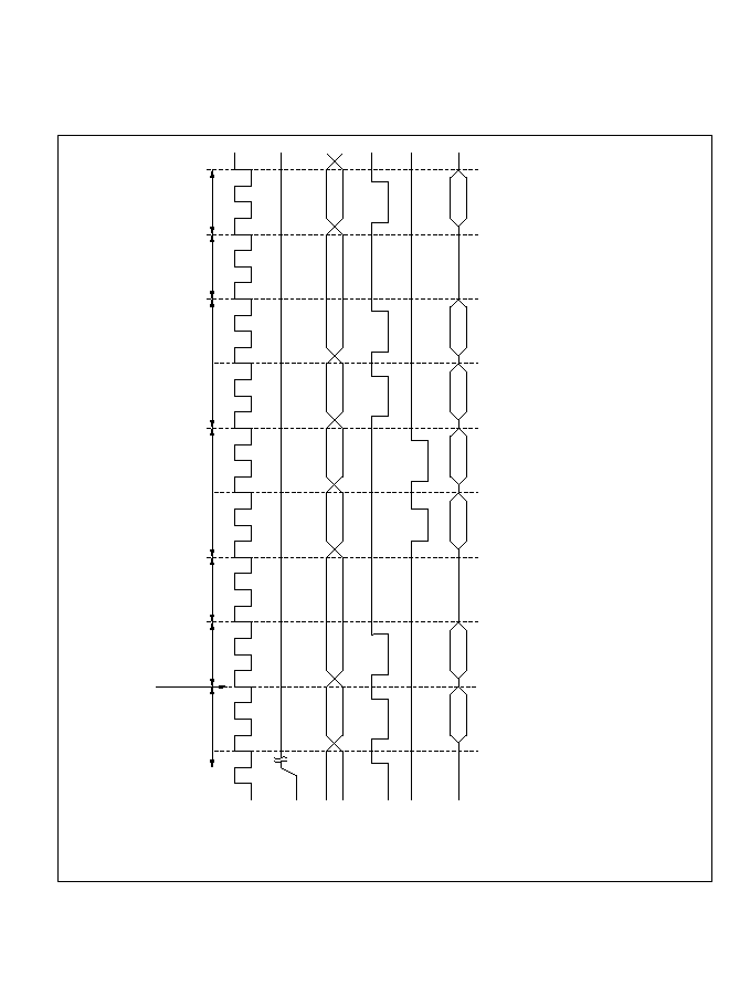
5.4.2 Interrupt Sequence
Figure 5-7 shows the interrupt sequence in mode 2 when the program code and stack are in an
external memory area accessed in two states via a 16-bit bus.
Figure 5-7 Interrupt Sequence (Mode 2, Two-State Access,
Stack in External Memory)
¯
Address
bus
Interrupt
request
signal
RD
HWR
D to D
15
0
(1)
(2), (4)
(3)
(5)
(7)
Note: Mode 2, with program code and stack in external memory area accessed in two states via 16-bit bus.
LWR
,
Interrupt level
decision and wait
for end of instruction
Interrupt accepted
Instruction
prefetch
Internal
processing
Stack
Vector fetch
Internal
processing
Prefetch of
interrupt
service routine
instruction
High
Instruction prefetch address (not executed;
return address, same as PC contents)
Instruction code (not executed)
Instruction prefetch address (not executed)
SP ≠ 2
SP ≠ 4
(6), (8)
(9), (11)
(10), (12)
(13)
(14)
PC and CCR saved to stack
Vector address
Starting address of interrupt service routine (contents of
vector address)
Starting address of interrupt service routine; (13) = (10), (12)
First instruction of interrupt service routine
(1)
(2)
(3)
(4)
(5)
(6)
(7)
(8)
(9)
(10)
(11)
(12)
(13)
(14)
96

5.4.3 Interrupt Response Time
Table 5-5 indicates the interrupt response time from the occurrence of an interrupt request until
the first instruction of the interrupt service routine is executed.
Table 5-5 Interrupt Response Time
External Memory
8-Bit Bus
16-Bit Bus
No. Item
2 States
3 States
2 States
3 States
1
Interrupt priority decision
2
*
1
2
*
1
2
*
1
2
*
1
2
*
1
2
Maximum number of states
1 to 23
1 to 27
1 to 31
*
4
1 to 23
1 to 25
*
4
until end of current instruction
3
Saving PC and CCR to stack
4
8
12
*
4
4
6
*
4
4
Vector fetch
4
8
12
*
4
4
6
*
4
5
Instruction prefetch
*
2
4
8
12
*
4
4
6
*
4
6
Internal processing
*
3
4
4
4
4
4
Total
19 to 41
31 to 57
43 to 73
19 to 41
25 to 49
Notes: 1. 1 state for internal interrupts.
2. Prefetch after the interrupt is accepted and prefetch of the first instruction in the interrupt
service routine.
3. Internal processing after the interrupt is accepted and internal processing after prefetch.
4. The number of states increases if wait states are inserted in external memory access.
On-Chip
Memory
97
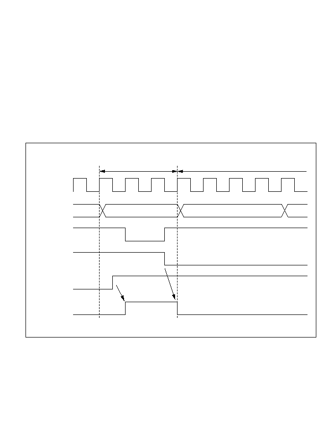
5.5 Usage Notes
5.5.1 Contention between Interrupt and Interrupt-Disabling Instruction
When an instruction clears an interrupt enable bit to 0 to disable the interrupt, the interrupt is not
disabled until after execution of the instruction is completed. If an interrupt occurs while a BCLR,
MOV, or other instruction is being executed to clear its interrupt enable bit to 0, at the instant
when execution of the instruction ends the interrupt is still enabled, so its interrupt exception
handling is carried out. If a higher-priority interrupt is also requested, however, interrupt exception
handling for the higher-priority interrupt is carried out, and the lower-priority interrupt is ignored.
This also applies to the clearing of an interrupt flag.
Figure 5-8 shows an example in which an IMIEA bit is cleared to 0 in the ITU.
Figure 5-8 Contention between Interrupt and Interrupt-Disabling Instruction
This type of contention will not occur if the interrupt is masked when the interrupt enable bit or
flag is cleared to 0.
IMIA exception handling
TIER write cycle by CPU
¯
TIER address
Internal
address bus
Internal
write signal
IMIEA
IMIA
IMFA interrupt
signal
98

5.5.2 Instructions that Inhibit Interrupts
The LDC, ANDC, ORC, and XORC instructions inhibit interrupts. When an interrupt occurs,
after determining the interrupt priority, the interrupt controller requests a CPU interrupt. If the
CPU is currently executing one of these interrupt-inhibiting instructions, however, when the
instruction is completed the CPU always continues by executing the next instruction.
5.5.3 Interrupts during EEPMOV Instruction Execution
The EEPMOV.B and EEPMOV.W instructions differ in their reaction to interrupt requests.
When the EEPMOV.B instruction is executing a transfer, no interrupts are accepted until the
transfer is completed, not even NMI.
When the EEPMOV.W instruction is executing a transfer, interrupt requests other than NMI are
not accepted until the transfer is completed. If NMI is requested, NMI exception handling starts at
a transfer cycle boundary. The PC value saved on the stack is the address of the next instruction.
Programs should be coded as follows to allow for NMI interrupts during EEPMOV.W execution:
L1:
EEPMOV.W
MOV.W R4,R4
BNE L1
5.5.4 Usage Notes
The IRQnF flag specification calls for the flag to be cleared by writing 0 to it after it has been read
while set to 1. However, it is possible for the IRQnF flag to be cleared by mistake simply by
writing 0 to it, irrespective of whether it has been read while set to 1, with the result that interrupt
exception handling is not executed. This will occur when the following conditions are met.
1. Setting conditions
(1) Multiple external interrupts (IRQa, IRQb) are being used.
(2) Different clearing methods are being used: clearing by writing 0 for the IRQaF flag, and
clearing by hardware for the IRQbF flag.
(3) A bit-manipulation instruction is used on the IRQ status register for clearing the IRQaF flag,
or else ISR is read as a byte unit, the IRQaF flag bit is cleard, and the values read in the other
bits are written as a byte unit.
2. Generation conditions
(1) A read of the ISR register is executed to clear the IRQaF flag while it is set to1, then the
99
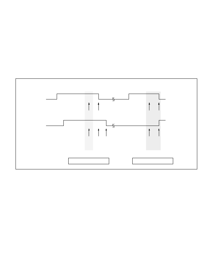
IRQbF flag is cleared by the execution of interrupt exception handling.
(2) When the IRQaF flag is cleared, there is contention with IRQb generation (IRQaF flag
setting). (IRQbF was 0 when ISR was read to clear the IRQaF flag, but IRQbF is set to 1
before ISR is written to.)
If the above setting conditions (1) to (3) and generation conditions (1) and (3) are all fulfilled,
when the ISR write in generation condition (2) is performed the IRQbF flag will be cleared
inadvertently, and interrupt exception handling will not be executed.
However, this inadvertent clearing of the IRQbF flag will not occur if 0 is written to this flag even
once between generation conditions (1) and (2).
Figure 5-9 IRQnF Flag when Interrupt Exception Handling is not Executed
Either of the methods shown below should be used to prevent this problem.
Method 1
When clearing the IRQaF flag, read ISR as a byte unit instead of using a bit-manipulation
instruction, and write a byte value that clears the IRQaF flag to 0 and sets the other bits to 1.
Example: When a = 0
MOV.B @ISR, R0L
MOV.B #HFE, R0L
MOV.B R0L, @ISR
100
TIER write cycle by CPU
1 read 0 written
1 read 0 written
1 read
IRQaF
IRQbF
0
written
IRQb
executed
1 read 0 written
IMIA exception handling
Generation condition (1)
Generation condition (2)
(Inadvertent clearing)

Method 2
Perform dummy processing within the IRQb interrupt exception handling routine to clear the
IRQbF flag.
Example: When b = 1
IRQB
MOV.B #HFD, R0L
MOV.B R0L, @ISR
.
.
.
101

102

Section 6 Bus Controller
6.1 Overview
The H8/3002 has an on-chip bus controller that divides the address space into eight areas and can
assign different bus specifications to each. This enables different types of memory to be connected
easily.
A bus arbitration function of the bus controller controls the operation of the DMA controller
(DMAC) and refresh controller. The bus controller can also release the bus to an external device.
6.1.1 Features
Features of the bus controller are listed below.
∑
Independent settings for address areas 0 to 7
-- 128-kbyte areas in 1-Mbyte modes; 2-Mbyte areas in 16-Mbyte modes.
-- Chip select signals (CS
0
to CS
3
) can be output for areas 0 to 3.
-- Areas can be designated for 8-bit or 16-bit access.
-- Areas can be designated for two-state or three-state access.
∑
Four wait modes
-- Programmable wait mode, pin auto-wait mode, and pin wait modes 0 and 1 can be
selected.
-- Zero to three wait states can be inserted automatically.
∑
Bus arbitration function
-- A built-in bus arbiter grants the bus right to the CPU, DMAC, refresh controller, or an
external bus master.
103
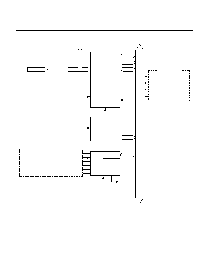
6.1.2 Block Diagram
Figure 6-1 shows a block diagram of the bus controller.
Figure 6-1 Block Diagram of Bus Controller
0
CS
to
3
CS
ABWCR
ASTCR
WCER
WCR
BRCR
BACK
BREQ
WAIT
Internal
address bus
Area
decoder
Bus control
circuit
Wait-state
controller
Bus arbiter
Internal data bus
Bus mode control signal
Bus size control signal
Access state control signal
Wait request signal
CPU bus request signal
DMAC bus request signal
Refresh controller bus request signal
CPU bus acknowledge signal
DMAC bus acknowledge signal
Refresh controller bus acknowledge signal
Legend
ABWCR:
ASTCR:
WCER:
WCR:
BRCR:
Bus width control register
Access state control register
Wait state controller enable register
Wait control register
Bus release control register
Internal signals
Internal signals
104

6.1.3 Input/Output Pins
Table 6-1 summarizes the bus controller's input/output pins.
Table 6-1 Bus Controller Pins
Name
Abbreviation
I/O
Function
Chip select 0 to 3
CS
0
to CS
3
Output
Strobe signals selecting areas 0 to 3
Address strobe
AS
Output
Strobe signal indicating valid address output on the
address bus
Read
RD
Output
Strobe signal indicating reading from the external
address space
High write
HWR
Output
Strobe signal indicating writing to the external
address space, with valid data on the upper data
bus (D
15
to D
8
)
Low write
LWR
Output
Strobe signal indicating writing to the external
address space, with valid data on the lower data
bus (D
7
to D
0
)
Wait
WAIT
Input
Wait request signal for access to external three-
state-access areas
Bus request
BREQ
Input
Request signal for releasing the bus to an external
device
Bus acknowledge
BACK
Output
Acknowledge signal indicating the bus is released
to an external device
6.1.4 Register Configuration
Table 6-2 summarizes the bus controller's registers.
Table 6-2 Bus Controller Registers
Initial Value
Address
*
Name
R/W
Modes 1 & 3 Modes 2 & 4
H'FFEC
Bus width control register
ABWCR
R/W
H'FF
H'00
H'FFED
Access state control register
ASTCR
R/W
H'FF
H'FF
H'FFEE
Wait control register
WCR
R/W
H'F3
H'F3
H'FFEF
Wait state controller enable register
WCER
R/W
H'FF
H'FF
H'FFF3
Bus release control register
BRCR
R/W
H'FE
H'FE
Note:
*
Lower 16 bits of the address.
Abbrevi-
ation
105

6.2 Register Descriptions
6.2.1 Bus Width Control Register (ABWCR)
ABWCR is an 8-bit readable/writable register that selects 8-bit or 16-bit access for each area.
When ABWCR contains H'FF (selecting 8-bit access for all areas), the H8/3002 operates in 8-bit
bus mode: the upper data bus (D
15
to D
8
) is valid, and port 4 is an input/output port. When at least
one bit is cleared to 0 in ABWCR, the H8/3002 operates in 16-bit bus mode with a 16-bit data bus
(D
15
to D
0
). In modes 1 and 3, ABWCR is initialized to H'FF by a reset and in hardware standby
mode. In modes 2 and 4, ABWCR is initialized to H'00 by a reset and in hardware standby mode.
ABWCR is not initialized in software standby mode.
Bits 7 to 0--Area 7 to 0 Bus Width Control (ABW7 to ABW0): These bits select 8-bit access
or 16-bit access to the corresponding address areas.
Bits 7 to 0
ABW7 to ABW0
Description
0
Areas 7 to 0 are 16-bit access areas
1
Areas 7 to 0 are 8-bit access areas
ABWCR specifies the bus width of external memory areas. The bus width of on-chip memory and
registers is fixed and does not depend on ABWCR settings.
Bit
Read/Write
7
ABW7
1
0
R/W
6
ABW6
1
0
R/W
5
ABW5
1
0
R/W
4
ABW4
1
0
R/W
3
ABW3
1
0
R/W
0
ABW0
1
0
R/W
2
ABW2
1
0
R/W
1
ABW1
1
0
R/W
Bits selecting bus width for each area
Initial
value
Modes 1, 3
Modes 2, 4
106

6.2.2 Access State Control Register (ASTCR)
ASTCR is an 8-bit readable/writable register that selects whether each area is accessed in two
states or three states.
ASTCR is initialized to H'FF by a reset and in hardware standby mode. It is not initialized in
software standby mode.
Bits 7 to 0--Area 7 to 0 Access State Control (AST7 to AST0): These bits select whether the
corresponding area is accessed in two or three states.
Bits 7 to 0
AST7 to AST0
Description
0
Areas 7 to 0 are accessed in two states
1
Areas 7 to 0 are accessed in three states
(Initial value)
ASTCR specifies the number of states in which external areas are accessed. On-chip memory and
registers are accessed in a fixed number of states that does not depend on ASTCR settings.
Bit
Initial value
Read/Write
7
AST7
1
R/W
6
AST6
1
R/W
5
AST5
1
R/W
4
AST4
1
R/W
3
AST3
1
R/W
0
AST0
1
R/W
2
AST2
1
R/W
1
AST1
1
R/W
Bits selecting number of states for access to each area
107

6.2.3 Wait Control Register (WCR)
WCR is an 8-bit readable/writable register that selects the wait mode for the wait-state controller
(WSC) and specifies the number of wait states.
WCR is initialized to H'F3 by a reset and in hardware standby mode. It is not initialized in
software standby mode.
Bits 7 to 4--Reserved: These bits cannot be modified and are always read as 1.
Bits 3 and 2--Wait Mode Select 1 and 0 (WMS1/0): These bits select the wait mode.
Bit 3
Bit 2
WMS1
WMS0
Description
0
0
Programmable wait mode
(Initial value)
1
No wait states inserted by wait-state controller
1
0
Pin wait mode 1
1
Pin auto-wait mode
Bit
Initial value
Read/Write
7
--
1
--
6
--
1
--
5
--
1
--
4
--
1
--
3
WMS1
0
R/W
0
WC0
1
R/W
2
WMS0
0
R/W
1
WC1
1
R/W
Wait count 1/0
These bits select the
number of wait states
inserted
Reserved bits
Wait mode select 1/0
These bits select the wait mode
108
Bits 1 and 0--Wait Count 1 and 0 (WC1/0): These bits select the number of wait states inserted
in access to external three-state-access areas.
Bit 1
Bit 0
WC1
WC0
Description
0
0
No wait states inserted by wait-state controller
1
1 state inserted
1
0
2 states inserted
1
3 states inserted
(Initial value)
6.2.4 Wait State Control Enable Register (WCER)
WCER is an 8-bit readable/writable register that enables or disables wait-state control of external
three-state-access areas by the wait-state controller.
WCER is initialized to H'FF by a reset and in hardware standby mode. It is not initialized in
software standby mode.
Bits 7 to 0--Wait-State Controller Enable 7 to 0 (WCE7 to WCE0): These bits enable or
disable wait-state control of external three-state-access areas.
Bits 7 to 0
WCE7 to WCE0
Description
0
Wait-state control disabled (pin wait mode 0)
1
Wait-state control enabled
(Initial value)
Bit
Initial value
Read/Write
7
WCE7
1
R/W
6
WCE6
1
R/W
5
WCE5
1
R/W
4
WCE4
1
R/W
3
WCE3
1
R/W
0
WCE0
1
R/W
2
WCE2
1
R/W
1
WCE1
1
R/W
Wait state controller enable 7 to 0
These bits enable or disable wait-state control
109

6.2.5 Bus Release Control Register (BRCR)
BRCR is an 8-bit readable/writable register that enables address output on bus lines A
23
to A
21
and enables or disables release of the bus to an external device.
BRCR is initialized to H'FE by a reset and in hardware standby mode. It is not initialized in
software standby mode.
Bit 7--Address 23 Enable (A23E): Enables PA
4
to be used as the A
23
address output pin.
Writing 0 in this bit enables A
23
address output from PA
4
. In modes other than 3 and 4 this bit
cannot be modified and PA
4
has its ordinary input/output functions.
Bit 7
A23E
Description
0
PA
4
is the A
23
address output pin
1
PA
4
is the PA
4
/TP
4
/TIOCA
1
input/output pin
(Initial value)
Bit
Initial value
7
A23E
1
--
R/W
6
A22E
1
--
R/W
5
A21E
1
--
R/W
4
--
1
--
--
3
--
1
--
--
0
BRLE
0
R/W
R/W
2
--
1
--
--
1
--
1
--
--
Bus release enable
Enables or disables
release of the bus
to an external device
Address 23 to 21 enable
Reserved bits
These bits enable PA to
PA to be used for A to
A address output
6
4
23
21
Modes 1, 2
Modes 3, 4
Read/
Write
110

Bit 6--Address 22 Enable (A22E): Enables PA
5
to be used as the A
22
address output pin.
Writing 0 in this bit enables A
22
address output from PA
5
. In modes other than 3 and 4 this bit
cannot be modified and PA
5
has its ordinary input/output functions.
Bit 6
A22E
Description
0
PA
5
is the A
22
address output pin
1
PA
5
is the PA
5
/TP
5
/TIOCB
1
input/output pin
(Initial value)
Bit 5--Address 21 Enable (A21E): Enables PA
6
to be used as the A
21
address output pin.
Writing 0 in this bit enables A
21
address output from PA
6
. In modes other than 3 and 4 this bit
cannot be modified and PA
6
has its ordinary input/output functions.
Bit 5
A21E
Description
0
PA
6
is the A
21
address output pin
1
PA
6
is the PA
6
/TP6/TIOCA
2
input/output pin
(Initial value)
Bits 4 to 1--Reserved: These bits cannot be modified and are always read as 1.
Bit 0--Bus Release Enable (BRLE): Enables or disables release of the bus to an external device.
Bit 0
BRLE
Description
0
The bus cannot be released to an external device;
BREQ
and
BACK
(Initial value)
can be used as input/output pins
1
The bus can be released to an external device
111

6.3 Operation
6.3.1 Area Division
The external address space is divided into areas 0 to 7. Each area has a size of 128 kbytes in the
1-Mbyte modes, or 2 Mbytes in the 16-Mbyte modes. Figure 6-2 shows a general view of the
memory map.
Figure 6-2 Access Area Map for Modes 1 to 4
H'00000
H'1FFFF
H'20000
H'3FFFF
H'40000
H'5FFFF
H'60000
H'7FFFF
H'80000
H'9FFFF
H'A0000
H'BFFFF
H'C0000
H'DFFFF
H'E0000
H'000000
H'1FFFFF
H'200000
H'3FFFFF
H'400000
H'5FFFFF
H'600000
H'7FFFFF
H'800000
H'9FFFFF
H'A00000
H'BFFFFF
H'C00000
H'DFFFFF
H'E00000
Area 0 (128 kbytes)
Area 1 (128 kbytes)
Area 2 (128 kbytes)
Area 3 (128 kbytes)
Area 4 (128 kbytes)
Area 5 (128 kbytes)
Area 6 (128 kbytes)
Area 7 (128 kbytes)
On-chip RAM
External address space
On-chip registers
* *
1, 2
*
1
Area 7 (2 Mbytes)
On-chip RAM
External address space
On-chip registers
* *
1, 2
Area 0 (2 Mbytes)
Area 1 (2 Mbytes)
Area 2 (2 Mbytes)
Area 3 (2 Mbytes)
Area 4 (2 Mbytes)
Area 5 (2 Mbytes)
Area 6 (2 Mbytes)
a. 1-Mbyte modes (modes 1 and 2)
b. 16-Mbyte modes (modes 3 and 4)
Notes:
The on-chip RAM and on-chip registers have a fixed bus width and are accessed in a fixed
number of states.
When the RAME bit is cleared to 0 in SYSCR, this area conforms to the specifications of area 7.
The 12-byte external address space conforms to the specifications of area 7.
1.
2.
3.
*
1
*
3
*
3
H'FFFFF
H'FFFFFF
112

Chip select signals (CS
0
to CS
3
) can be output for each area. The bus specifications for each area
can be selected in ABWCR, ASTCR, WCER, and WCR as shown in table 6-3.
Table 6-3 Bus Specifications
ABWCR ASTCR WCER
WCR
Bus Specifications
Bus Access
ABWn
ASTn
WCEn
WMS1
WMS0
Width
States
Wait Mode
0
0
--
--
--
16
2
Disabled
1
0
--
--
16
3
Pin wait mode 0
1
0
0
16
3
Programmable wait mode
1
16
3
Disabled
1
0
16
3
Pin wait mode 1
1
16
3
Pin auto-wait mode
1
0
--
--
--
8
2
Disabled
1
0
--
--
8
3
Pin wait mode 0
1
0
0
8
3
Programmable wait mode
1
8
3
Disabled
1
0
8
3
Pin wait mode 1
1
8
3
Pin auto-wait mode
Note: n = 0 to 7
113
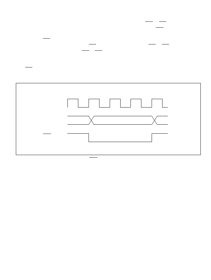
6.3.2 Chip Select Signals
For each of areas 0 to 3, the H8/3002 can output a chip select signal (CS
0
to CS
3
) that goes low to
indicate when the area is selected. Figure 6-3 shows the output timing of a CSn signal (n = 0 to 3).
Output of the CS
n
signal is enabled or disabled in the data direction register (DDR) of the
corresponding port. A reset leaves pin CS
0
in the output state and pins CS
1
to CS
3
in the input
state. To output chip select signals CS
1
to CS
3
, the corresponding DDR bits must be set to 1.
For details see section 9, I/O Ports.
The CS
n
signals are decoded from the address signals. They can be used as chip select signals for
SRAM and other devices.
Figure 6-3 CS
n
Output Timing (n = 0 to 3)
Address
bus
n
T
T
T
1
2
3
External address in area n
¯
CS
114

6.3.3 Data Bus
The H8/3002 allows either 8-bit access or 16-bit access to be designated for each of areas 0 to 7.
An 8-bit-access area uses the upper data bus (D
15
to D
8
). A 16-bit-access area uses both the upper
data bus (D
15
to D
8
) and lower data bus (D
7
to D
0
).
In read access the
RD signal applies without distinction to both the upper and lower data bus. In
write access the
HWR signal applies to the upper data bus, and the LWR signal applies to the
lower data bus.
Table 6-4 indicates how the two parts of the data bus are used under different access conditions.
Table 6-4 Access Conditions and Data Bus Usage
Access Read/
Valid
Upper Data Bus
Lower Data Bus
Area
Size
Write
Address Strobe
(D
15
to D
8
)
(D
7
to D
0
)
--
Read
--
RD
Valid
Invalid
Write
--
HWR
Undetermined data
Byte
Read
Even
RD
Valid
Invalid
Odd
Invalid
Valid
Write
Even
HWR
Valid
Undetermined data
Odd
LWR
Undetermined data
Valid
Word
Read
--
RD
Valid
Valid
Write
--
HWR
,
LWR
Valid
Valid
Note: Undetermined data means that unpredictable data is output.
Invalid means that the bus is in the input state and the input is ignored.
8-bit-access
area
16-bit-access
area
115
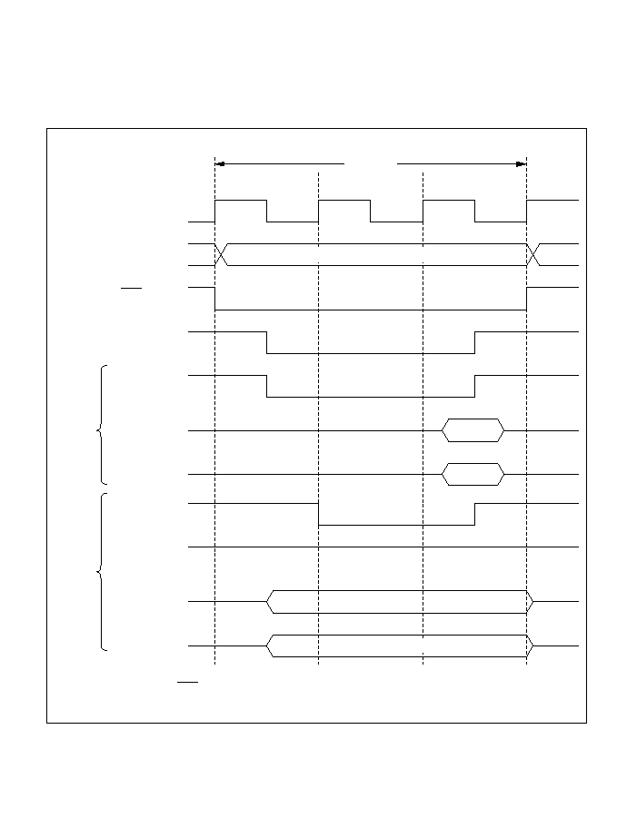
6.3.4 Bus Control Signal Timing
8-Bit, Three-State-Access Areas: Figure 6-4 shows the timing of bus control signals for an 8-bit,
three-state-access area. The upper address bus (D
15
to D
8
) is used to access these areas. The
LWR
pin is always high. Wait states can be inserted.
Figure 6-4 Bus Control Signal Timing for 8-Bit, Three-State-Access Area
¯
Address bus
CS
AS
RD
D to D
D to D
HWR
LWR
D to D
D to D
n
15 8
7 0
15 8
7 0
T
1
T
2
T
3
Read
access
Write
access
Bus cycle
External address in area n
Valid
Invalid
High
Valid
Undetermined data
Note: n = 7 to 0 (but for CS , n = 3 to 0)
n
116
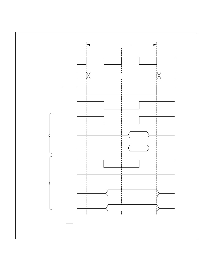
8-Bit, Two-State-Access Areas: Figure 6-5 shows the timing of bus control signals for an 8-bit,
two-state-access area. The upper address bus (D
15
to D
8
) is used to access these areas. The
LWR
pin is always high. Wait states cannot be inserted.
Figure 6-5 Bus Control Signal Timing for 8-Bit, Two-State-Access Area
¯
Address bus
CS
AS
RD
D to D
D to D
HWR
LWR
D to D
D to D
15 8
7 0
15 8
7 0
n
T
1
T
2
Read
access
Write
access
High
Bus cycle
External address in area n
Valid
Invalid
Valid
Undetermined data
Note: n = 7 to 0 (but for CS , n = 3 to 0)
n
117
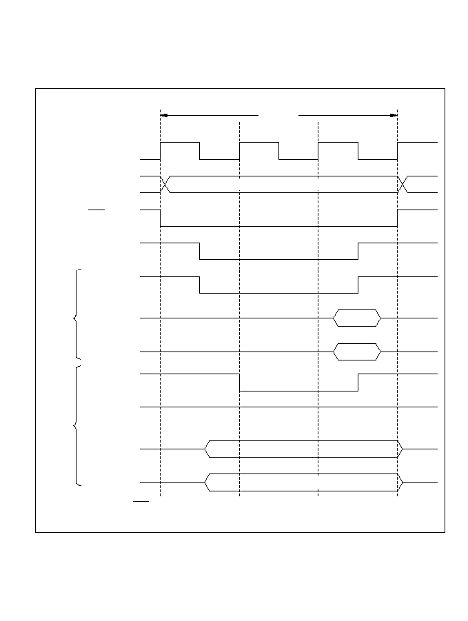
16-Bit, Three-State-Access Areas: Figures 6-6 to 6-8 show the timing of bus control signals for a
16-bit, three-state-access area. In these areas, the upper address bus (D
15
to D
8
) is used to access
even addresses and the lower address bus (D
7
to D
0
) is used to access odd addresses. Wait states
can be inserted.
Figure 6-6 Bus Control Signal Timing for 16-Bit, Three-State-Access Area (1)
(Byte Access to Even Address)
¯
Address bus
CS
AS
RD
D to D
D to D
HWR
LWR
D to D
D to D
n
15 8
7 0
15 8
7 0
T
1
T
2
T
3
Read
access
Write
access
Bus cycle
Even external address in area n
Valid
Invalid
Valid
Undetermined data
High
Note: n = 7 to 0 (but for CS , n = 3 to 0)
n
118
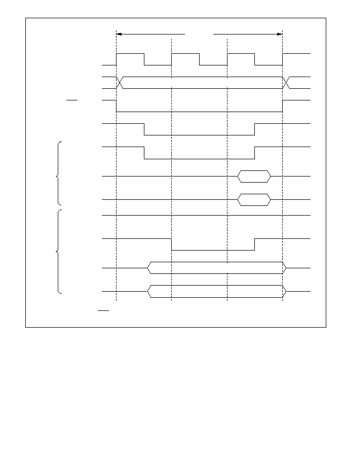
Figure 6-7 Bus Control Signal Timing for 16-Bit, Three-State-Access Area (2)
(Byte Access to Odd Address)
¯
Address bus
CS
AS
RD
D to D
D to D
HWR
LWR
D to D
D to D
n
15 8
7 0
15 8
7 0
T
1
T
2
T
3
Read
access
Write
access
Bus cycle
Odd external address in area n
Invalid
Valid
Undetermined data
Valid
High
Note: n = 7 to 0 (but for CS , n = 3 to 0)
n
119
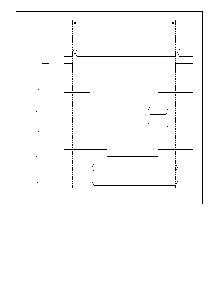
Figure 6-8 Bus Control Signal Timing for 16-Bit, Three-State-Access Area (3)
(Word Access)
¯
Address bus
CS
AS
RD
D to D
D to D
HWR
LWR
D to D
D to D
n
15 8
7 0
15 8
7 0
T
1
T
2
T
3
Read
access
Bus cycle
External address in area n
Valid
Valid
Valid
Valid
Write
access
Note: n = 7 to 0 (but for CS , n = 3 to 0)
n
120
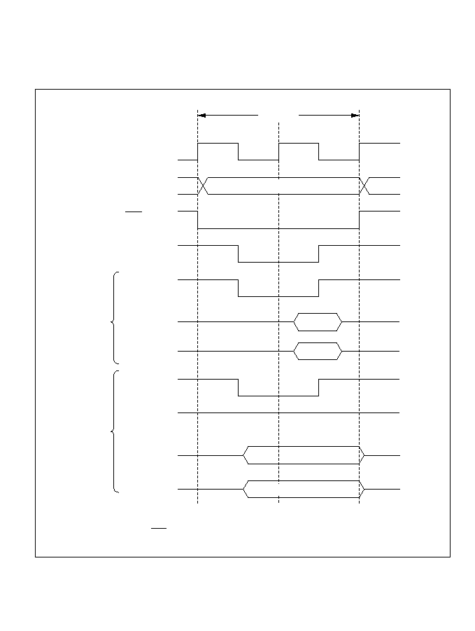
16-Bit, Two-State-Access Areas: Figures 6-9 to 6-11 show the timing of bus control signals for a
16-bit, two-state-access area. In these areas, the upper address bus (D
15
to D
8
) is used to access
even addresses and the lower address bus (D
7
to D
0
) is used to access odd addresses. Wait states
cannot be inserted.
Figure 6-9 Bus Control Signal Timing for 16-Bit, Two-State-Access Area (1)
(Byte Access to Even Address)
¯
Address bus
CS
AS
RD
D to D
D to D
HWR
LWR
D to D
D to D
15 8
7 0
15 8
7 0
n
T
1
T
2
Read
access
Write
access
Valid
Undetermined data
High
Valid
Invalid
Bus cycle
Even external address in area n
Note: n = 7 to 0 (but for CS , n = 3 to 0)
n
121
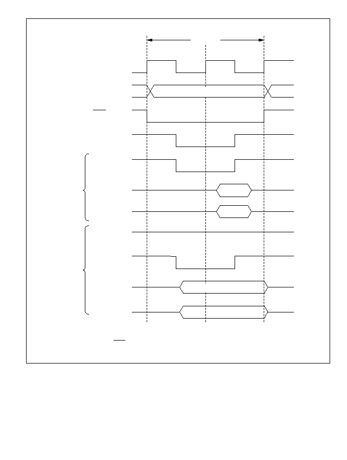
Figure 6-10 Bus Control Signal Timing for 16-Bit, Two-State-Access Area (2)
(Byte Access to Odd Address)
¯
Address bus
CS
AS
RD
D to D
D to D
HWR
LWR
D to D
D to D
15 8
7 0
15 8
7 0
n
T
1
T
2
Read
access
Invalid
Valid
High
Bus cycle
Odd external address in area n
Write
access
Undetermined data
Valid
Note: n = 7 to 0 (but for CS , n = 3 to 0)
n
122
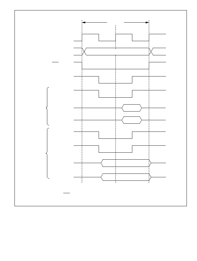
Figure 6-11 Bus Control Signal Timing for 16-Bit, Two-State-Access Area (3)
(Word Access)
¯
Address bus
CS
AS
RD
D to D
D to D
HWR
LWR
D to D
D to D
15 8
7 0
15 8
7 0
n
T
1
T
2
Read
access
Write
access
Valid
Valid
Valid
Valid
Bus cycle
External address in area n
Note: n = 7 to 0 (but for CS , n = 3 to 0)
n
123

6.3.5 Wait Modes
Four wait modes can be selected for each area as shown in table 6-5.
Table 6-5 Wait Mode Selection
ASTCR
WCER
WCR
ASTn Bit WCEn Bit WMS1 Bit WMS0 Bit
WSC Control
Wait Mode
0
--
--
--
Disabled
No wait states
1
0
--
--
Disabled
Pin wait mode 0
1
0
0
Enabled
Programmable wait mode
1
Enabled
No wait states
1
0
Enabled
Pin wait mode 1
1
Enabled
Pin auto-wait mode
Note: n = 7 to 0
The ASTn and WCEn bits can be set independently for each area. Bits WMS1 and WMS0 apply
to all areas. All areas for which WSC control is enabled operate in the same wait mode.
124
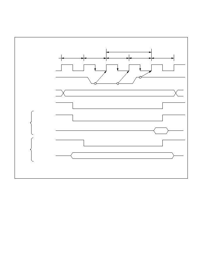
Pin Wait Mode 0: The wait state controller is disabled. Wait states can only be inserted by
WAIT
pin control. During access to an external three-state-access area, if the
WAIT pin is low at the fall
of the system clock (¯) in the T
2
state, a wait state (T
W
) is inserted. If the
WAIT pin remains low,
wait states continue to be inserted until the
WAIT signal goes high. Figure 6-12 shows the timing.
Figure 6-12 Pin Wait Mode 0
¯
pin
Address bus
Data bus
AS
RD
HWR
Data bus
,
LWR
T
1
T
2
T
W
T
W
T
3
Inserted by signal
Write data
*
*
*
Read data
Read
access
Write
access
External address
WAIT
WAIT
Note: Arrows indicate time of sampling of the pin.
*
WAIT
125

Pin Wait Mode 1: In all accesses to external three-state-access areas, the number of wait states
(T
W
) selected by bits WC1 and WC0 are inserted. If the
WAIT pin is low at the fall of the system
clock (¯) in the last of these wait states, an additional wait state is inserted. If the
WAIT pin
remains low, wait states continue to be inserted until the
WAIT signal goes high.
Pin wait mode 1 is useful for inserting four or more wait states, or for inserting different numbers
of wait states for different external devices.
If the wait count is 0, this mode operates in the same way as pin wait mode 0.
Figure 6-13 shows the timing when the wait count is 1 (WC1 = 0, WC0 = 1) and one additional
wait state is inserted by
WAIT input.
Figure 6-13 Pin Wait Mode 1
Address bus
Data bus
AS
RD
HWR
,
LWR
T
1
T
2
T
W
T
W
T
3
Write data
*
Read data
*
Read
access
Write
access
Note: Arrows indicate time of sampling of the pin.
*
WAIT
¯
pin
WAIT
Data bus
External address
Write data
Inserted by
wait count
Inserted by
signal
WAIT
126
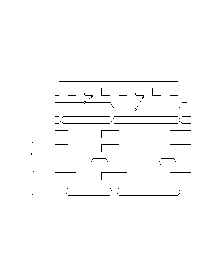
Pin Auto-Wait Mode: If the
WAIT pin is low, the number of wait states (T
W
) selected by bits
WC1 and WC0 are inserted.
In pin auto-wait mode, if the
WAIT pin is low at the fall of the system clock (¯) in the T
2
state,
the number of wait states (T
W
) selected by bits WC1 and WC0 are inserted. No additional wait
states are inserted even if the
WAIT pin remains low. Pin auto-wait mode can be used for an easy
interface to low-speed memory, simply by routing the chip select signal to the
WAIT pin.
Figure 6-14 shows the timing when the wait count is 1.
Figure 6-14 Pin Auto-Wait Mode
¯
Address bus
Data bus
AS
RD
HWR
Data bus
,
LWR
T
1
T
2
T
3
T
1
T
2
T
W
T
3
*
*
Read data
Read data
Write data
Write data
Read
access
Write
access
Note: Arrows indicate time of sampling of the pin.
*
WAIT
External address
External address
WAIT
RS
,
127

Programmable Wait Mode: The number of wait states (T
W
) selected by bits WC1 and WC0 are
inserted in all accesses to external three-state-access areas. Figure 6-15 shows the timing when the
wait count is 1 (WC1 = 0, WC0 = 1).
Figure 6-15 Programmable Wait Mode
T
1
T
2
T
W
T
3
¯
Address bus
AS
RD
HWR
,
Data bus
Data bus
External address
Read data
Write data
Read
access
Write
access
LWR
128

Example of Wait State Control Settings: A reset initializes ASTCR and WCER to H'FF and
WCR to H'F3, selecting programmable wait mode and three wait states for all areas. Software can
select other wait modes for individual areas by modifying the ASTCR, WCER, and WCR settings.
Figure 6-16 shows an example of wait mode settings.
Figure 6-16 Wait Mode Settings (Example)
7
6
5
4
3
2
1
0
0
0
--
0
0
--
0
1
--
0
1
--
1
0
0
1
0
0
1
1
1
1
1
1
Bit:
ASTCR H'0F:
WCER H'33:
WCR H'F3:
Area 0
Area 1
Area 2
Area 3
Area 4
Area 5
Area 6
Area 7
3-state-access area,
programmable wait mode
3-state-access area,
programmable wait mode
3-state-access area,
pin wait mode 0
3-state-access area,
pin wait mode 0
2-state-access area,
no wait states inserted
2-state-access area,
no wait states inserted
2-state-access area,
no wait states inserted
2-state-access area,
no wait states inserted
Note: Wait states cannot be inserted in areas designated for two-state access by ASTCR.
129
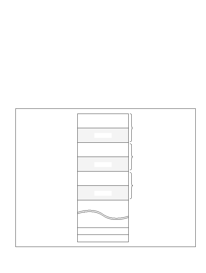
6.3.6 Interconnections with Memory (Example)
For each area, the bus controller can select two- or three-state access and an 8- or 16-bit data bus
width. In three-state-access areas, wait states can be inserted in a variety of modes, simplifying the
connection of both high-speed and low-speed devices.
Figure 6-18 shows an example of interconnections between the H8/3002 and memory. Figure 6-17
shows a memory map for this example.
A 256-kword
◊
16-bit EPROM is connected to area 0. This device is accessed in three states via a
16-bit bus.
Two 32-kword
◊
8-bit SRAM devices (SRAM1 and SRAM2) are connected to area 1. These
devices are accessed in two states via a 16-bit bus.
One 32-kword
◊
8-bit SRAM (SRAM3) is connected to area 2. This device is accessed via an
8-bit bus, using three-state access with an additional wait state inserted in pin auto-wait mode.
Figure 6-17 Memory Map (Example)
H'000000
H'03FFFF
H'1FFFFF
H'200000
H'20FFFF
H'210000
H'3FFFFF
H'FFFFFF
On-chip RAM
On-chip registers
Area 0
16-bit, three-state-access area
Area 1
16-bit, two-state-access area
EPROM
Not used
SRAM 1, 2
Not used
SRAM 3
Not used
H'5FFFFF
H'407FFF
H'400000
Area 2
8-bit, three-state-access area
(one pin auto-wait state)
130
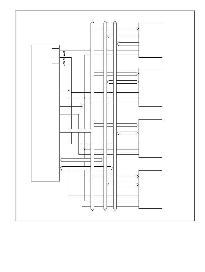
Figure 6-18 External-Bus-Released State (Two-State-Access Area, During Read Cycle)
131
EPROM
A to A
I/O to I/O
I/O to I/O
CE
OE
18
15
7
0
8
0
A to A
19 1
SRAM1 (even addresses)
A to A
I/O to I/O
CS
OE
WE
14
7
0
0
A to A
15 1
SRAM2 (odd addresses)
A to A
I/O to I/O
CS
OE
WE
14
7
0
0
A to A
15 1
SRAM3
A to A
I/O to I/O
CS
OE
WE
14
7
0
0
A to A
14 0
H8/3002
CS
CS
CS
0
1
2
WAIT
RD
HWR
LWR
A to A
23 0
D to D
D to D
15 8
7 0

6.3.7 Bus Arbiter Operation
The bus controller has a built-in bus arbiter that arbitrates between different bus masters. There
are four bus masters: the CPU, DMA controller (DMAC), refresh controller, and an external bus
master. When a bus master has the bus right it can carry out read, write, or refresh access. Each
bus master uses a bus request signal to request the bus right. At fixed times the bus arbiter
determines priority and uses a bus acknowledge signal to grant the bus to a bus master, which can
then operate using the bus.
The bus arbiter checks whether the bus request signal from a bus master is active or inactive, and
returns an acknowledge signal to the bus master if the bus request signal is active. When two or
more bus masters request the bus, the highest-priority bus master receives an acknowledge signal.
The bus master that receives an acknowledge signal can continue to use the bus until the
acknowledge signal is deactivated.
The bus master priority order is:
(High)
External bus master > refresh controller > DMAC > CPU
(Low)
The bus arbiter samples the bus request signals and determines priority at all times, but it does not
always grant the bus immediately, even when it receives a bus request from a bus master with
higher priority than the current bus master. Each bus master has certain times at which it can
release the bus to a higher-priority bus master.
CPU: The CPU is the lowest-priority bus master. If the DMAC, refresh controller, or an external
bus master requests the bus while the CPU has the bus right, the bus arbiter transfers the bus right
to the bus master that requested it. The bus right is transferred at the following times:
∑
The bus right is transferred at the boundary of a bus cycle. If word data is accessed by two
consecutive byte accesses, however, the bus right is not transferred between the two byte
accesses.
∑
If another bus master requests the bus while the CPU is performing internal operations, such
as executing a multiply or divide instruction, the bus right is transferred immediately. The
CPU continues its internal operations.
∑
If another bus master requests the bus while the CPU is in sleep mode, the bus right is
transferred immediately.
132

DMAC: When the DMAC receives an activation request, it requests the bus right from the bus
arbiter. If the DMAC is bus master and the refresh controller or an external bus master requests
the bus, the bus arbiter transfers the bus right from the DMAC to the bus master that requested the
bus. The bus right is transferred at the following times.
The bus right is transferred when the DMAC finishes transferring 1 byte or 1 word. A DMAC
transfer cycle consists of a read cycle and a write cycle. The bus right is not transferred between
the read cycle and the write cycle.
There is a priority order among the DMAC channels. For details see section 8.4.9, Multiple-
Channel Operation.
Refresh Controller: When a refresh cycle is requested, the refresh controller requests the bus
right from the bus arbiter. When the refresh cycle is completed, the refresh controller releases the
bus. For details see section 7, Refresh Controller.
External Bus Master: When the BRLE bit is set to 1 in BRCR, the bus can be released to an
external bus master. The external bus master has highest priority, and requests the bus right from
the bus arbiter by driving the
BREQ signal low. Once the external bus master gets the bus, it keeps
the bus right until the
BREQ signal goes high. While the bus is released to an external bus master,
the H8/3002 holds the address bus and data bus control signals (
AS, RD, HWR, and LWR) in the
high-impedance state, and holds the
BACK pin in the low output state.
The bus arbiter samples the
BREQ pin at the rise of the system clock (¯). If BREQ is low, the bus
is released to the external bus master at the appropriate opportunity. The
BREQ signal should be
held low until the
BACK signal goes low.
When the
BREQ pin is high in two consecutive samples, the BACK signal is driven high to end
the bus-release cycle.
133
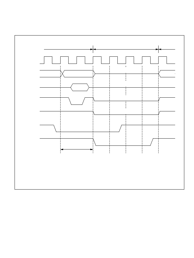
Figure 6-19 shows the timing when the bus right is requested by an external bus master during a
read cycle in a two-state-access area. There is a minimum interval of two states from when the
BREQ signal goes low until the bus is released.
Figure 6-19 Interconnections with Memory (Example)
¯
Data bus
(D to D )
AS
HWR
BREQ
BACK
RD
,
LWR
,
15 0
T
1
T
2
Address
2
1
3
4
5
6
High
CPU cycles
External bus released
CPU cycles
Minimum 2 cycles
High-impedance
High-impedance
High-impedance
High-impedance
1
2
3
4, 5
6
Low signal is sampled at rise of T state.
signal goes low at end of CPU read cycle, releasing bus right to external bus master.
pin continues to be sampled while bus is released to external bus master.
High signal is sampled twice consecutively.
signal goes high, ending bus-release cycle.
BREQ
BREQ
BREQ
BREQ
BACK
1
Address
bus
134
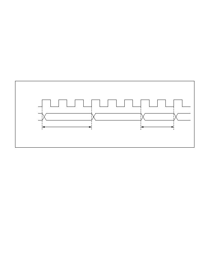
6.4 Usage Notes
6.4.1 Connection to Dynamic RAM and Pseudo-Static RAM
A different bus control signal timing applies when dynamic RAM or pseudo-static RAM is
connected to area 3. For details see section 7, Refresh Controller.
6.4.2 Register Write Timing
ABWCR, ASTCR, and WCER Write Timing: Data written to ABWCR, ASTCR, or WCER
takes effect starting from the next bus cycle. Figure 6-20 shows the timing when an instruction
fetched from area 0 changes area 0 from three-state access to two-state access.
Figure 6-20 ASTCR Write Timing
¯
T
1
T
2
T
3
T
1
T
2
T
3
T
1
T
2
ASTCR address
3-state access to area 0
2-state access
to area 0
Address
bus
135
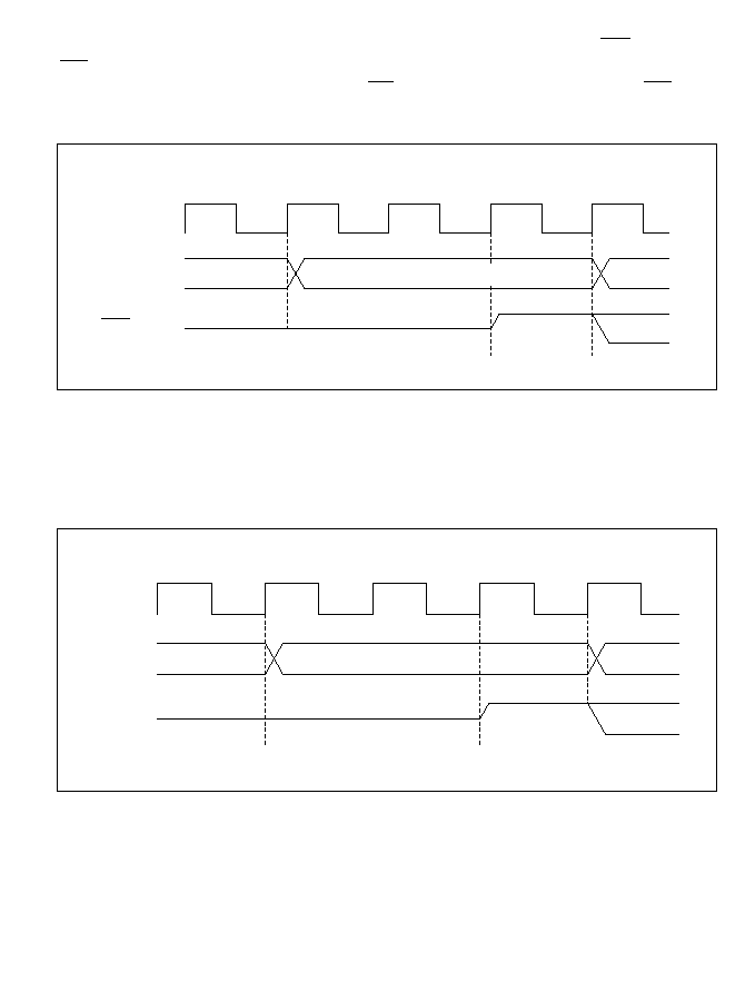
DDR Write Timing: Data written to a data direction register (DDR) to change a CS
n
pin from
CS
n
output to generic input, or vice versa, takes effect starting from the T
3
state of the DDR write
cycle. Figure 6-21 shows the timing when the CS
1
pin is changed from generic input to CS
1
output.
Figure 6-21 DDR Write Timing
BRCR Write Timing: Data written to switch between A
23
, A
22
, or A
21
output and generic input
or output takes effect starting from the T
3
state of the BRCR write cycle. Figure 6-22 shows the
timing when a pin is changed from generic input to A
23
, A
22
, or A
21
output.
Figure 6-22 BRCR Write Timing
¯
CS
1
T
1
T
2
T
3
P8DDR address
High impedance
Address
bus
T
1
T
2
T
3
¯
Address
bus
A to A
21
23
BRCR address
High impedance
136
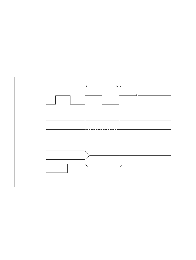
6.4.3
BREQ Input Timing
After driving the
BREQ pin low, hold it low until BACK goes low. If BREQ returns to the high
level before
BACK goes low, the bus arbiter may operate incorrectly.
To terminate the external-bus-released state, hold the
BREQ signal high for at least three states.
If
BREQ is high for too short an interval, the bus arbiter may operate incorrectly.
∑
If contention occurs between a transition to software standby mode and a bus request from an
external bus master, the bus may be released for one state just before the transition to
software standby mode (see figure 6-23). When using software standby mode, clear the
BRLE bit to 0 in BRCR before executing the SLEEP instruction.
Figure 6-23 Contention between Bus-Released State and Software Standby Mode
137
¯
BREQ
Address
bus
strobe
BACK
Software standby mode
Bus-released state

138

Section 7 Refresh Controller
7.1 Overview
The H8/3002 has an on-chip refresh controller that enables direct connection of 16-bit-wide
DRAM or pseudo-static RAM (PSRAM).
DRAM or pseudo-static RAM can be directly connected to area 3 of the external address space.
A maximum 128 kbytes can be connected in modes 1 and 2 (1-Mbyte modes). A maximum
2 Mbytes can be connected in modes 3 and 4 (16-Mbyte modes).
Systems that do not need to refresh DRAM or pseudo-static RAM can use the refresh controller as
an 8-bit interval timer.
7.1.1 Features
The refresh controller can be used for one of three functions: DRAM refresh control, pseudo-static
RAM refresh control, or interval timing. Features of the refresh controller are listed below.
Features as a DRAM Refresh Controller
∑
Enables direct connection of 16-bit-wide DRAM
∑
Selection of 2
CAS or 2WE mode
∑
Selection of 8-bit or 9-bit column address multiplexing for DRAM address input
Examples:
-- 1-Mbit DRAM: 8-bit row address
◊
8-bit column address
-- 4-Mbit DRAM: 9-bit row address
◊
9-bit column address
-- 4-Mbit DRAM: 10-bit row address
◊
8-bit column address
∑
CAS-before-RAS refresh control
∑
Software-selectable refresh interval
∑
Software-selectable self-refresh mode
∑
Wait states can be inserted
Features as a Pseudo-Static RAM Refresh Controller
∑
RFSH signal output for refresh control
∑
Software-selectable refresh interval
∑
Software-selectable self-refresh mode
∑
Wait states can be inserted
139

Features as an Interval Timer
∑
Refresh timer counter (RTCNT) can be used as an 8-bit up-counter
∑
Selection of seven counter clock sources: ¯/2, ¯/8, ¯/32, ¯/128, ¯/512, ¯/2048, ¯/4096
∑
Interrupts can be generated by compare match between RTCNT and the refresh time constant
register (RTCOR)
7.1.2 Block Diagram
Figure 7-1 shows a block diagram of the refresh controller.
Figure 7-1 Block Diagram of Refresh Controller
¯/2, ¯/8, ¯/32,
¯/128, ¯/512,
¯/2048, ¯/4096
RTCNT
RTCOR
RTMCSR
RFSHCR
Legend
RTCNT:
RTCOR:
RTMCSR:
RFSHCR:
Refresh signal
Clock selector
Comparator
CMI interrupt
Bus interface
Internal data bus
Module data bus
Refresh timer counter
Refresh time constant register
Refresh timer control/status register
Refresh control register
Control logic
140

7.1.3 Input/Output Pins
Table 7-1 summarizes the refresh controller's input/output pins.
Table 7-1 Refresh Controller Pins
Signal
Pin
Name
Abbr.
I/O
Function
RFSH
Refresh
RFSH
Output
Goes low during refresh cycles; used
to refresh DRAM and PSRAM
HWR
Upper write/upper column
UW
/
UCAS
Output
Connects to the
UW
pin of 2
WE
address strobe
DRAM or
UCAS
pin of 2
CAS
DRAM
LWR
Lower write/lower column
LW
/
LCAS
Output
Connects to the
LW
pin of 2
WE
DRAM
address strobe
or
LCAS
pin of 2
CAS
DRAM
RD
Column address strobe/
CAS
/
WE
Output
Connects to the
CAS
pin of 2
WE
write enable
DRAM or
WE
pin of 2
CAS
DRAM
CS
3
Row address strobe
RAS
Output
Connects to the
RAS
pin of DRAM
7.1.4 Register Configuration
Table 7-2 summarizes the refresh controller's registers.
Table 7-2 Refresh Controller Registers
Address
*
Name
Abbreviation
R/W
Initial Value
H'FFAC
Refresh control register
RFSHCR
R/W
H'02
H'FFAD
Refresh timer control/status register
RTMCSR
R/W
H'07
H'FFAE
Refresh timer counter
RTCNT
R/W
H'00
H'FFAF
Refresh time constant register
RTCOR
R/W
H'FF
Note:
*
Lower 16 bits of the address.
141
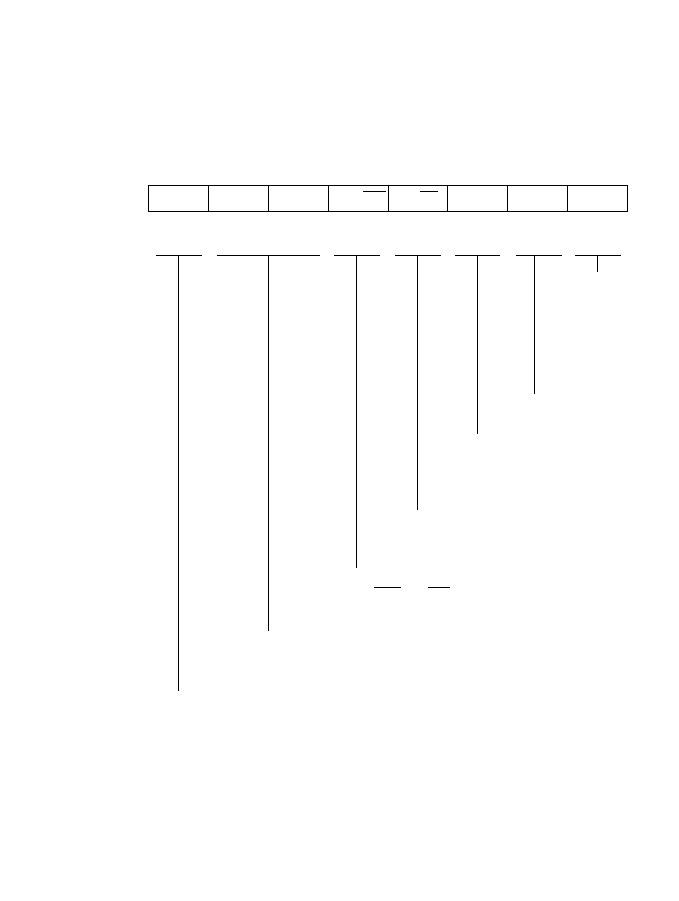
7.2 Register Descriptions
7.2.1 Refresh Control Register (RFSHCR)
RFSHCR is an 8-bit readable/writable register that selects the operating mode of the refresh
controller.
RFSHCR is initialized to H'02 by a reset and in hardware standby mode.
Bit
Initial value
Read/Write
7
SRFMD
0
R/W
6
PSRAME
0
R/W
5
DRAME
0
R/W
4
CAS/WE
0
R/W
3
M9/M8
0
R/W
0
RCYCE
0
R/W
2
RFSHE
0
R/W
1
--
1
--
Self-refresh mode
Selects self-refresh mode
PSRAM enable and DRAM enable
These bits enable or disable connection of pseudo-static RAM and DRAM
Strobe mode select
Selects 2CAS or 2WE strobing of DRAM
Address multiplex mode select
Selects the number of column address bits
Refresh pin enable
Enables refresh signal output
from the refresh pin
Refresh cycle
enable
Enables or
disables
insertion of
refresh cycles
Reserved bit
142

Bit 7--Self-Refresh Mode (SRFMD): Specifies DRAM or pseudo-static RAM self-refresh
during software standby mode. When PSRAME = 1 and DRAME = 0, after the SRFMD bit is set
to 1, pseudo-static RAM can be self-refreshed when the H8/3002 enters software standby mode.
When PSRAME = 0 and DRAME = 1, after the SRFMD bit is set to 1, DRAM can be self-
refreshed when the H8/3002 enters software standby mode. In either case, the normal access state
resumes on exit from software standby mode.
Bit 7
SRFMD Description
0
DRAM or PSRAM self-refresh is disabled in software standby mode
(Initial value)
1
DRAM or PSRAM self-refresh is enabled in software standby mode
Bit 6--PSRAM Enable (PSRAME) and Bit 5--DRAM Enable (DRAME): These bits enable
or disable connection of pseudo-static RAM and DRAM to area 3 of the external address space.
When DRAM or pseudo-static RAM is connected, the bus cycle and refresh cycle of area 3
consist of three states, regardless of the setting in the access state control register (ASTCR). If
AST3 = 0 in ASTCR, wait states cannot be inserted.
When the PSRAME or DRAME bit is set to 1, bits 0, 2, 3, and 4 in RFSHCR and registers
RTMCSR, RTCNT, and RTCOR are write-disabled, except that the CMF flag in RTMCSR can be
cleared by writing 0.
Bit 6
Bit 5
PSRAME
DRAME
Description
0
0
Can be used as an interval timer
(Initial value)
(DRAM and PSRAM cannot be directly connected)
1
DRAM can be directly connected
1
0
PSRAM can be directly connected
1
Illegal setting
143

Bit 4--Strobe Mode Select (CAS/
WE): Selects 2CAS or 2WE mode. The setting of this bit is
valid when PSRAME = 0 and DRAME = 1. This bit is write-disabled when the PSRAME or
DRAME bit is set to 1.
Bit 4
CAS/
WE
Description
0
2
WE
mode
(Initial value)
1
2
CAS
mode
Bit 3--Address Multiplex Mode Select (M9/
M8): Selects 8-bit or 9-bit column addressing.
The setting of this bit is valid when PSRAME = 0 and DRAME = 1. This bit is write-disabled
when the PSRAME or DRAME bit is set to 1.
Bit 3
M9/
M8
Description
0
8-bit column address mode
(Initial value)
1
9-bit column address mode
Bit 2--Refresh Pin Enable (RFSHE): Enables or disables refresh signal output from the
RFSH pin. This bit is write-disabled when the PSRAME or DRAME bit is set to 1.
Bit 2
RFSHE
Description
0
Refresh signal output at the
RFSH
pin is disabled
(Initial value)
(the
RFSH
pin can be used as a generic input/output port)
1
Refresh signal output at the
RFSH
pin is enabled
Bit 1--Reserved: This bit cannot be modified and is always read as 1.
Bit 0--Refresh Cycle Enable (RCYCE): Enables or disables insertion of refresh cycles.
The setting of this bit is valid when PSRAME = 1 or DRAME = 1.This bit cannot be written to
when the PSRAME bit or DRAME bit is set to 1. When PSRAME = 0 and DRAME = 0, refresh
cycles are not inserted regardless of the setting of this bit.
Bit 0
RCYCE
Description
0
Refresh cycles are disabled
(Initial value)
1
Refresh cycles are enabled for area 3
144

7.2.2 Refresh Timer Control/Status Register (RTMCSR)
RTMCSR is an 8-bit readable/writable register that selects the clock source for RTCNT. It also
enables or disables interrupt requests when the refresh controller is used as an interval timer.
Bits 7 and 6 are initialized by a reset and in standby mode. Bits 5 to 3 are initialized by a reset and
in hardware standby mode, but retain their previous values on transition to software standby
mode.
Bit 7--Compare Match Flag (CMF): This status flag indicates that the RTCNT and RTCOR
values have matched.
Bit 7
CMF
Description
0
[Clearing condition]
Cleared by reading CMF when CMF = 1, then writing 0 in CMF
1
[Setting condition]
When RTCNT = RTCOR
Bit
Initial value
Read/Write
7
CMF
0
R/(W)
6
CMIE
0
R/W
5
CKS2
0
R/W
4
CKS1
0
R/W
3
CKS0
0
R/W
0
--
1
--
2
--
1
--
1
--
1
--
Compare match flag
Status flag indicating that RTCNT has matched RTCOR
Reserved bits
Clock select 2 to 0
These bits select an
internal clock source
for input to RTCNT
Note: Only 0 can be written, to clear the flag.
*
*
Compare match interrupt enable
Enables or disables the CMI interrupt requested by CMF
145

Bit 6--Compare Match Interrupt Enable (CMIE): Enables or disables the CMI interrupt
requested when the CMF flag is set to 1 in RTMCSR. The CMIE bit is always cleared to 0 when
PSRAME = 1 or DRAME = 1.
Bit 6
CMIE
Description
0
The CMI interrupt requested by CMF is disabled
(Initial value)
1
The CMI interrupt requested by CMF is enabled
Bits 5 to 3--Clock Select 2 to 0 (CKS2 to CKS0): These bits select an internal clock source for
input to RTCNT. When used for refresh control, the refresh controller outputs a refresh request at
periodic intervals determined by compare match between RTCNT and RTCOR. When used as an
interval timer, the refresh controller generates CMI interrupts at periodic intervals determined by
compare match. These bits are write-disabled when the PSRAME bit or DRAME bit is set to 1.
Bit 5
Bit 4
Bit 3
CKS2
CKS1
CKS0
Description
0
0
0
Clock input is disabled
(Initial value)
1
¯/2 clock source
1
0
¯/8 clock source
1
¯/32 clock source
1
0
0
¯/128 clock source
1
¯/512 clock source
1
0
¯/2048 clock source
1
¯/4096 clock source
Bits 2 to 0--Reserved: These bits cannot be modified and are always read as 1.
146

7.2.3 Refresh Timer Counter (RTCNT)
RTCNT is an 8-bit readable/writable up-counter.
RTCNT is an up-counter that is incremented by an internal clock selected by bits CKS2 to CKS0
in RTMCSR. When RTCNT matches RTCOR (compare match), the CMF flag is set to 1 and
RTCNT is cleared to H'00.
RTCNT is write-disabled when the PSRAME bit or DRAME bit is set to 1. RTCNT is initialized
to H'00 by a reset and in standby mode.
7.2.4 Refresh Time Constant Register (RTCOR)
RTCOR is an 8-bit readable/writable register that determines the interval at which RTCNT is
cleared.
RTCOR and RTCNT are constantly compared. When their values match, the CMF flag is set to 1
in RTMCSR, and RTCNT is simultaneously cleared to H'00.
RTCOR is write-disabled when the PSRAME bit or DRAME bit is set to 1. RTCOR is initialized
to H'FF by a reset and in hardware standby mode. In software standby mode it retains its previous
value.
Bit
Initial value
Read/Write
7
0
R/W
6
0
R/W
5
0
R/W
4
0
R/W
3
0
R/W
0
0
R/W
2
0
R/W
1
0
R/W
Bit
Initial value
Read/Write
7
1
R/W
6
1
R/W
5
1
R/W
4
1
R/W
3
1
R/W
0
1
R/W
2
1
R/W
1
1
R/W
147

7.3 Operation
7.3.1 Area Division
One of three functions can be selected for the H8/3002 refresh controller: interfacing to
DRAM connected to area 3, interfacing to pseudo-static RAM connected to area 3, or interval
timing. Table 7-3 summarizes the register settings when these three functions are used.
Table 7-3 Refresh Controller Settings
Usage
Register Settings
DRAM Interface
PSRAM Interface
Interval Timer
RFSHCR
SRFMD
Selects self-refresh mode
Cleared to 0
PSRAME
Cleared to 0
Set to 1
Cleared to 0
DRAME
Set to 1
Cleared to 0
Cleared to 0
CAS/
WE
Selects 2
CAS
or --
--
2
WE
mode
M9/
M8
Selects column
--
--
addressing mode
RFSHE
Selects
RFSH
signal output
Cleared to 0
RCYCE
Selects insertion of refresh cycles
--
RTCOR
Refresh interval setting
Interrupt interval setting
RTMCSR
CKS2 to CKS0
CMF
Set to 1 when RTCNT = RTCOR
CMIE
Cleared to 0
Enables or disables
interrupt requests
P8DDR
P8
1
DDR
Set to 1 (CS
3
output)
Set to 0 or 1
ABWCR
ABW3
Cleared to 0
--
--
DRAM Interface: To set up area 3 for connection to 16-bit-wide DRAM, initialize RTCOR,
RTMCSR, and RFSHCR in that order, clearing bit PSRAME to 0 and setting bit DRAME to 1.
Set bit P8
1
DDR to 1 in the port 8 data direction register (P8DDR) to enable CS
3
output. In
ABWCR, make area 3 a 16-bit-access area.
Pseudo-Static RAM Interface: To set up area 3 for connection to pseudo-static RAM, initialize
RTCOR, RTMCSR, and RFSHCR in that order, setting bit PSRAME to 1 and clearing bit
DRAME to 0. Set bit P8
1
DDR to 1 in P8DDR to enable CS
3
output.
148
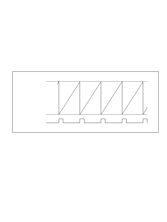
Interval Timer: When PSRAME = 0 and DRAME = 0, the refresh controller operates as an
interval timer. After setting RTCOR, select an input clock in RTMCSR and set the CMIE bit to 1.
CMI interrupts will be requested at compare match intervals determined by RTCOR and bits
CKS2 to CKS0 in RTMCSR.
When setting RTCOR, RTMCSR, and RFSHCR, make sure that PSRAME = 0 and DRAME = 0.
Writing is disabled when either of these bits is set to 1.
7.3.2 DRAM Refresh Control
Refresh Request Interval and Refresh Cycle Execution: The refresh request interval is
determined by the settings of RTCOR and bits CKS2 to CKS0 in RTMCSR. Figure 7-2 illustrates
the refresh request interval.
Figure 7-2 Refresh Request Interval (RCYCE = 1)
Refresh requests are generated at regular intervals as shown in figure 7-2, but the refresh cycle is
not actually executed until the refresh controller gets the bus right.
Table 7-4 summarizes the relationship among area 3 settings, DRAM read/write cycles, and
refresh cycles.
RTCOR
H'00
RTCNT
Refresh request
149
Table 7-4 Area 3 Settings, DRAM Access Cycles, and Refresh Cycles
Area 3 Settings
Read/Write Cycle by CPU or DMAC
Refresh Cycle
2-state-access area
∑ 3 states
∑ 3 states
(AST3 = 0)
∑ Wait states cannot be inserted
∑ Wait states cannot be inserted
3-state-access area
∑ 3 states
∑ 3 states
(AST3 = 1)
∑ Wait states can be inserted
∑ Wait states can be inserted
To insert refresh cycles, set the RCYCE bit to 1 in RFSHCR. Figure 7-3 shows the state
transitions for execution of refresh cycles.
When the first refresh request occurs after exit from the reset state or standby mode, the refresh
controller does not execute a refresh cycle, but goes into the refresh request pending state. Note
this point when using a DRAM that requires a refresh cycle for initialization.
When a refresh request occurs in the refresh request pending state, the refresh controller acquires
the bus right, then executes a refresh cycle. If another refresh request occurs during execution of
the refresh cycle, it is ignored.
Figure 7-3 State Transitions for Refresh Cycle Execution
Refresh
request
*
Refresh
request
*
Exit from reset or standby mode
Refresh request pending state
Requesting bus right
Executing refresh cycle
Refresh request
Refresh request
Bus granted
End of refresh
cycle
Note:
A refresh request is ignored if it occurs while the refresh controller is requesting the
bus right or executing a refresh cycle.
*
*
150
Address Multiplexing: Address multiplexing depends on the setting of the M9/
M8 bit in
RFSHCR, as described in table 7-5. Figure 7-4 shows the address output timing. Address output is
multiplexed only in area 3.
Table 7-5 Address Multiplexing
Address Pins
A
23
to A
10
A
9
A
8
A
7
A
6
A
5
A
4
A
3
A
2
A
1
A
0
Address signals during row
A
23
to A
10
A
9
A
8
A
7
A
6
A
5
A
4
A
3
A
2
A
1
A
0
address output
M9/
M8
= 0 A
23
to A
10
A
9
A
9
A
16
A
15
A
14
A
13
A
12
A
11
A
10
A
0
M9/
M8
= 1 A
23
to A
10
A
18
A
17
A
16
A
15
A
14
A
13
A
12
A
11
A
10
A
0
Figure 7-4 Multiplexed Address Output (Example without Wait States)
Address signals during
column address output
¯
A to A , A
A to A
23 9 0
8 1
T
1
T
2
T
3
A to A
Row address
8 1
A to A
Column address
16 9
A to A , A
23 9 0
Address
bus
¯
A to A , A
A to A
23 10 0
9 1
T
1
T
2
T
3
A to A
Row address
9 1
A to A
Column address
18 10
A to A , A
23 10 0
Address
bus
a. M9/ = 0
M8
b. M9/ = 1
M8
151
2
CAS and 2WE Modes: The CAS/WE bit in RFSHCR can select two control modes for 16-bit-
wide DRAM: one using
UCAS and LCAS; the other using UW and LW. These DRAM pins
correspond to H8/3002 pins as shown in table 7-6.
Table 7-6 DRAM Pins and H8/3002 Pins
DRAM Pin
H8/3002 Pin
CAS/
WE
= 0 (2
WE
mode)
CAS/
WE
= 1 (2
CAS
mode)
HWR
UW
UCAS
LWR
LW
LCAS
RD
CAS
WE
CS
3
RAS
RAS
Figure 7-5 (1) shows the interface timing for 2
WE DRAM. Figure 7-5 (2) shows the interface
timing for 2
CAS DRAM.
¯
( )
CS
RAS
3
( )
RD
CAS
( )
HWR
UW
( )
LWR
LW
RFSH
AS
Read cycle
Write cycle
Refresh cycle
*
Row
Column
Row
Column
Area 3 top address
Note: 16-bit access
*
Address
bus
152
Figure 7-5 DRAM Control Signal Output Timing (1) (2
WE Mode)
Figure 7-5 DRAM Control Signal Output Timing (2) (2
CAS Mode)
Refresh Cycle Priority Order: When there are simultaneous bus requests, the priority order is:
(High)
External bus master > refresh controller > DMA controller > CPU
(Low)
For details see section 6.3.7, Bus Arbiter Operation.
Wait State Insertion: When bit AST3 is set to 1 in ASTCR, bus controller settings can cause
wait states to be inserted into bus cycles and refresh cycles. For details see section 6.3.5, Wait
Modes.
¯
( )
CS
RAS
3
( )
HWR
UCAS
( )
LWR
LCAS
( )
RD
WE
RFSH
AS
Read cycle
Write cycle
Refresh cycle
*
Row
Column
Row
Column
Area 3 top address
Note: 16-bit access
*
Address
bus
153

Self-Refresh Mode: Some DRAM devices have a self-refresh function. After the SRFMD bit is
set to 1 in RFSHCR, when a transition to software standby mode occurs, the
CAS and RAS
outputs go low in that order so that the DRAM self-refresh function can be used. On exit from
software standby mode, the
CAS and RAS outputs both go high.
Table 7-7 shows the pin states in software standby mode. Figure 7-6 shows the signal output
timing.
Table 7-7 Pin States in Software Standby Mode (1) (PSRAME = 0, DRAME = 1)
Software Standby Mode
SRFMD = 0
SRFMD = 1 (self-refresh mode)
Signal
CAS/
WE
= 0
CAS/
WE
= 1
CAS/
WE
= 0
CAS/
WE
= 1
HWR
High-impedance
High-impedance
High
Low
LWR
High-impedance
High-impedance
High
Low
RD
High-impedance
High-impedance
Low
High
CS
3
High
High
Low
Low
RFSH
High
High
Low
Low
154
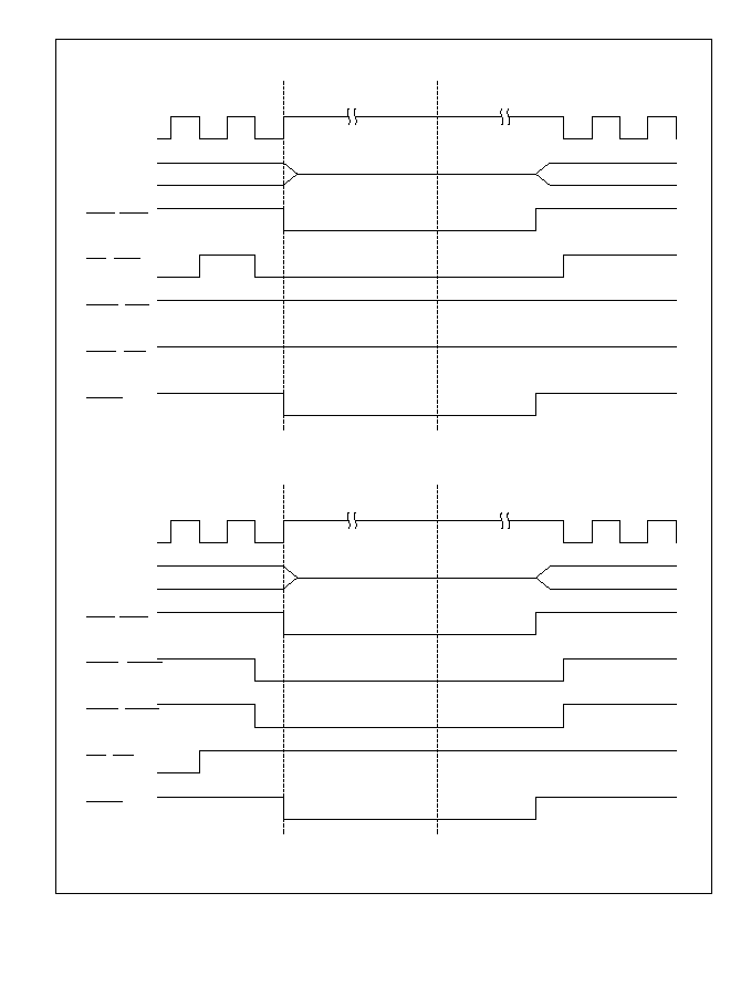
Figure 7-6 Signal Output Timing in Self-Refresh Mode (PSRAME = 0, DRAME = 1)
¯
CS (RAS)
RD (CAS)
HWR (UW)
LWR (LW)
RFSH
3
High
High
CS (RAS)
HWR (UCAS)
LWR (LCAS)
RD (WE)
RFSH
3
Software
standby mode
High-impedance
Oscillator
settling time
a. 2 mode (SRFMD = 1)
b. 2 mode (SRFMD = 1)
Software
standby mode
High-impedance
Oscillator
settling time
WE
CAS
Address
bus
¯
Address
bus
155
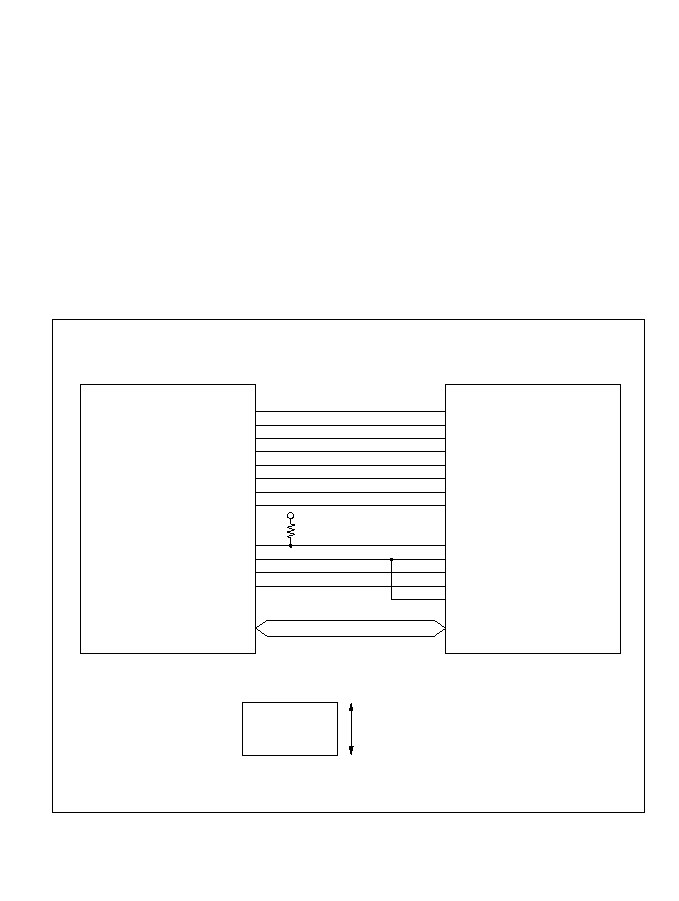
Operation in Power-Down State: The refresh controller operates in sleep mode. It does not
operate in hardware standby mode. In software standby mode RTCNT is initialized, but RFSHCR,
RTMCSR bits 5 to 3, and RTCOR retain their settings prior to the transition to software standby
mode.
Example 1: Connection to 2
WE 1-Mbit DRAM (1-Mbyte Mode): Figure 7-7 shows typical
interconnections to a 2
WE 1-Mbit DRAM, and the corresponding address map. Figure 7-8 shows
a setup procedure to be followed by a program for this example. After power-up the DRAM must
be refreshed to initialize its internal state. Initialization takes a certain length of time, which can be
measured by using an interrupt from another timer module, or by counting the number of times
RTMCSR bit 7 (CMF) is set. Note that no refresh cycle is executed for the first refresh request
after exit from the reset state or standby mode (the first time the CMF flag is set; see figure 7-3).
When using this example, check the DRAM device characteristics carefully and use a procedure
that fits them.
H8/3002
A
A
A
A
A
A
A
A
8
7
6
5
4
3
2
1
CS
RD
HWR
LWR
3
D to D
0
15
A
A
A
A
A
A
A
A
7
6
5
4
3
2
1
0
RAS
CAS
UW
LW
OE
I/O to I/O
15
0
H'60000
H'7FFFF
a. Interconnections (example)
DRAM area
Area 3 (1-Mbyte mode)
b. Address map
2 1-Mbit DRAM with
16-bit organization
WE
◊
156

Figure 7-7 Interconnections and Address Map for 2
WE 1-Mbit DRAM (Example)
Figure 7-8 Setup Procedure for 2
WE 1-Mbit DRAM (1-Mbyte Mode)
Set area 3 for 16-bit access
Set P8 DDR to 1 for output
Set RTCOR
Set bits CKS2 to CKS0 in RTMCSR
Write H'23 in RFSHCR
Wait for DRAM to be initialized
DRAM can be accessed
CS
1
3
157

Example 2: Connection to 2
WE 4-Mbit DRAM (16-Mbyte Mode): Figure 7-9 shows typical
interconnections to a single 2
WE 4-Mbit DRAM, and the corresponding address map. Figure 7-10
shows a setup procedure to be followed by a program for this example.
The DRAM in this example has 10-bit row addresses and 8-bit column addresses. Its address area
is H'600000 to H'67FFFF.
Figure 7-9 Interconnections and Address Map for 2
WE 4-Mbit DRAM (Example)
A
A
A
A
A
A
A
A
8
7
6
5
4
3
2
1
CS
RD
HWR
LWR
3
D to D
0
15
A
A
A
A
A
A
A
A
7
6
5
4
3
2
1
0
RAS
CAS
UW
LW
OE
I/O to I/O
15
0
A
A
18
17
A
A
9
8
H'600000
H'67FFFF
H'680000
H'7FFFFF
H8/3002
2 4-Mbit DRAM with 10-bit
row address, 8-bit column address,
and 16-bit organization
a. Interconnections (example)
b. Address map
DRAM area
Not used
Area 3 (16-Mbyte mode)
WE
◊
158

Figure 7-10 Setup Procedure for 2
WE 4-Mbit DRAM with 10-Bit Row Address and
8-Bit Column Address (16-Mbyte Mode)
Set area 3 for 16-bit access
Set P8 DDR to 1 for output
Set RTCOR
Set bits CKS2 to CKS0 in RTMCSR
Write H'23 in RFSHCR
Wait for DRAM to be initialized
DRAM can be accessed
CS
1
3
159
Example 3: Connection to 2
CAS 4-Mbit DRAM (16-Mbyte Mode): Figure 7-11 shows typical
interconnections to a single 2
CAS 4-Mbit DRAM, and the corresponding address map.
Figure 7-12 shows a setup procedure to be followed by a program for this example.
The DRAM in this example has 9-bit row addresses and 9-bit column addresses. Its address area
is H'600000 to H'67FFFF.
Figure 7-11 Interconnections and Address Map for 2
CAS 4-Mbit DRAM (Example)
A
A
A
A
A
A
A
A
A
9
8
7
6
5
4
3
2
1
CS
HWR
LWR
RD
3
D to D
0
A
A
A
A
A
A
A
A
A
8
7
6
5
4
3
2
1
0
RAS
UCAS
LCAS
WE
OE
I/O to I/O
15
0
15
H'600000
H'67FFFF
H'680000
H'7FFFFF
H8/3002
2 4-Mbit DRAM with 9-bit
row address, 9-bit column address,
and 16-bit organization
CAS
◊
a. Interconnections (example)
b. Address map
DRAM area
Not used
Area 3 (16-Mbyte mode)
160
Figure 7-12 Setup Procedure for 2
CAS 4-Mbit DRAM with 9-Bit Row Address and
9-Bit Column Address (16-Mbyte Mode)
Set area 3 for 16-bit access
Set P8 DDR to 1 for output
Set RTCOR
Set bits CKS2 to CKS0 in RTMCSR
Write H'3B in RFSHCR
Wait for DRAM to be initialized
DRAM can be accessed
CS
1
3
161
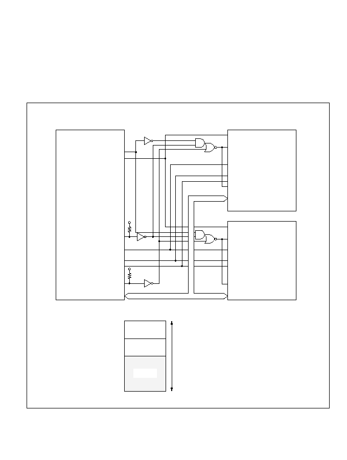
Example 4: Connection to Two 4-Mbit DRAM Chips (16-Mbyte Mode): Figure 7-13 shows
an example of interconnections to two 2
CAS 4-Mbit DRAM chips, and the corresponding address
map. Up to four DRAM chips can be connected to area 3 by decoding upper address bits A
19
and A
20
.
Figure 7-14 shows a setup procedure to be followed by a program for this example. The DRAM
in this example has 9-bit row addresses and 9-bit column addresses. Both chips must be refreshed
simultaneously, so the
RFSH pin must be used.
Figure 7-13 Interconnections and Address Map for Multiple 2
CAS 4-Mbit DRAM Chips
(Example)
H'600000
H'67FFFF
H'680000
H'6FFFFF
H'700000
H'7FFFFF
A to A
RAS
UCAS
LCAS
WE
OE
I/O to I/O
15
0
8
0
No. 1
A to A
RAS
UCAS
LCAS
I/O to I/O
15
0
8
0
No. 2
WE
OE
A
A to A
19
9 1
CS
HWR
LWR
RD
RFSH
3
D to D
15 0
H8/3002
2 4-Mbit DRAM with 9-bit
row address, 9-bit column
address, and 16-bit organization
a. Interconnections (example)
b. Address map
No. 1
DRAM area
No. 2
DRAM area
Not used
Area 3 (16-Mbyte mode)
CAS
◊
162
Figure 7-14 Setup Procedure for Multiple 2
CAS 4-Mbit DRAM Chips with 9-Bit
Row Address and 9-Bit Column Address (16-Mbyte Mode)
Set area 3 for 16-bit access
Set P8 DDR to 1 for CS output
1
3
Set RTCOR
Set bits CKS2 to CKS0 in RTMCSR
Write H'3F in RFSHCR
Wait for DRAM to be initialized
DRAM can be accessed
163
7.3.3 Pseudo-Static RAM Refresh Control
Refresh Request Interval and Refresh Cycle Execution: The refresh request interval is
determined as in a DRAM interface, by the settings of RTCOR and bits CKS2 to CKS0 in
RTMCSR. The numbers of states required for pseudo-static RAM read/write cycles and refresh
cycles are the same as for DRAM (see table 7-4). The state transitions are as shown in figure 7-3.
Pseudo-Static RAM Control Signals: Figure 7-15 shows the control signals for pseudo-static
RAM read, write, and refresh cycles.
Figure 7-15 Pseudo-Static RAM Control Signal Output Timing
¯
CS
RD
HWR
LWR
RFSH
AS
3
Read cycle
Write cycle
*
Refresh cycle
Area 3 top address
Note: 16-bit access
*
Address
bus
164

Refresh Cycle Priority Order: When there are simultaneous bus requests, the priority order is:
(High)
External bus master > refresh controller > DMA controller > CPU
(Low)
For details see section 6.3.7, Bus Arbiter Operation.
Wait State Insertion: When bit AST3 is set to 1 in ASTCR, the wait state controller (WSC) can
insert wait states into bus cycles and refresh cycles. For details see section 6.3.5, Wait Modes.
Self-Refresh Mode: Some pseudo-static RAM devices have a self-refresh function. After the
SRFMD bit is set to 1 in RFSHCR, when a transition to software standby mode occurs, the
H8/3002's CS
3
output goes high and its
RFSH output goes low so that the pseudo-static RAM
self-refresh function can be used. On exit from software standby mode, the
RFSH output goes
high.
Table 7-8 shows the pin states in software standby mode. Figure 7-16 shows the signal output
timing.
Table 7-8 Pin States in Software Standby Mode (2) (PSRAME = 1, DRAME = 0)
Software Standby Mode
Signal
SRFMD = 0
SRFMD = 1 (self-refresh mode)
CS
3
High
High
RD
High-impedance
High-impedance
HWR
High-impedance
High-impedance
LWR
High-impedance
High-impedance
RFSH
High
Low
165
Figure 7-16 Signal Output Timing in Self-Refresh Mode (PSRAME = 1, DRAME = 0)
Operation in Power-Down State: The refresh controller operates in sleep mode. It does not
operate in hardware standby mode. In software standby mode RTCNT is initialized, but RFSHCR,
RTMCSR bits 5 to 3, and RTCOR retain their settings prior to the transition to software standby
mode.
¯
CS
RD
HWR
LWR
RFSH
3
High
Software standby mode
Oscillator
settling time
High-impedance
High-impedance
High-impedance
High-impedance
Address
bus
166
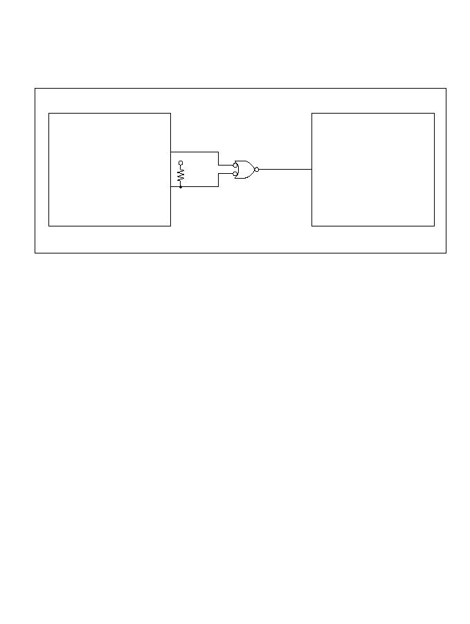
Example: Pseudo-static RAM may have separate
OE and RFSH pins, or these may be combined
into a single
OE/RFSH pin. Figure 7-17 shows an example of a circuit for generating an
OE/RFSH signal. Check the device characteristics carefully, and design a circuit that fits them.
Figure 7-18 shows a setup procedure to be followed by a program.
Figure 7-17 Interconnection to Pseudo-Static RAM with
OE/RFSH Signal (Example)
H8/3002
PSRAM
RD
RFSH
OE RFSH
/
167
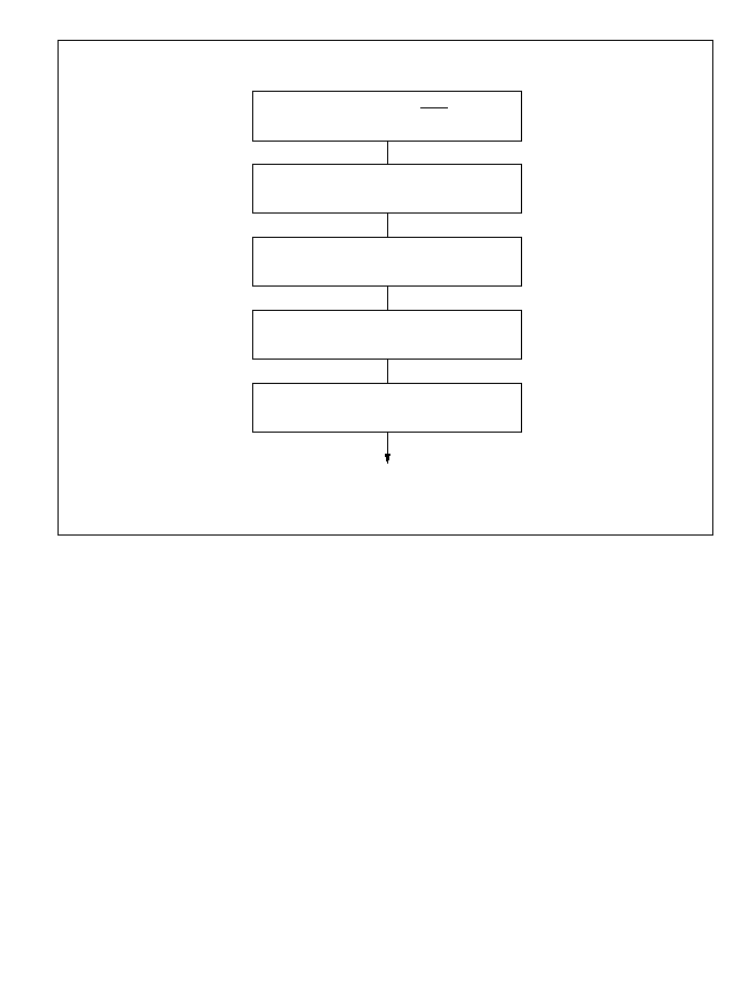
Figure 7-18 Setup Procedure for Pseudo-Static RAM
Set P8 DDR to 1 for CS output
1
3
Set RTCOR
Set bits CKS2 to CKS0 in RTMCSR
Write H'47 in RFSHCR
Wait for PSRAM to be initialized
PSRAM can be accessed
168
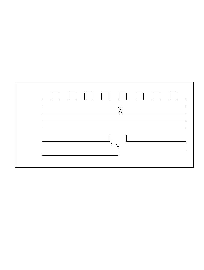
7.3.4 Interval Timing
To use the refresh controller as an interval timer, clear the PSRAME and DRAME both to 0. After
setting RTCOR, select a clock source with bits CKS2 to CKS0 in RTMCSR, and set the CMIE bit
to 1.
Timing of Setting of Compare Match Flag and Clearing by Compare Match: The CMF flag
in RTCSR is set to 1 by a compare match signal output when the RTCOR and RTCNT values
match. The compare match signal is generated in the last state in which the values match (when
RTCNT is updated from the matching value to a new value). Accordingly, when RTCNT and
RTCOR match, the compare match signal is not generated until the next counter clock pulse.
Figure 7-19 shows the timing.
Figure 7-19 Timing of Setting of CMF Flag
Operation in Power-Down State: The interval timer function operates in sleep mode. It does not
operate in hardware standby mode. In software standby mode RTCNT and RTMCSR bits 7 and 6
are initialized, but RTMCSR bits 5 to 3 and RTCOR retain their settings prior to the transition to
software standby mode.
¯
RTCNT
RTCOR
CMF flag
N
H'00
N
Compare
match signal
169
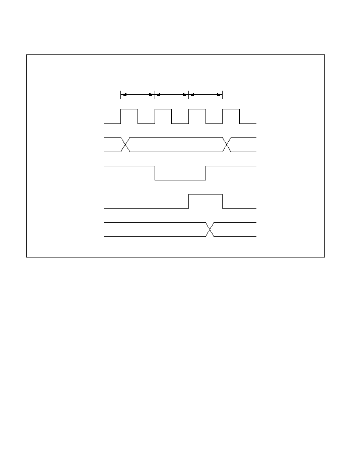
Contention between RTCNT Write and Counter Clear: If a counter clear signal occurs in the
T
3
state of an RTCNT write cycle, clearing of the counter takes priority and the write is not
performed. See figure 7-20.
Figure 7-20 Contention between RTCNT Write and Clear
¯
Address bus
RTCNT
T
1
T
2
T
3
RTCNT address
N
H'00
RTCNT write cycle by CPU
Internal
write signal
Counter
clear signal
170
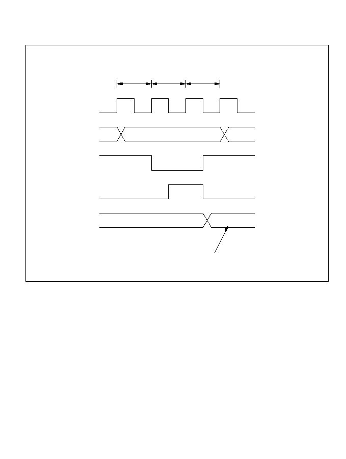
Contention between RTCNT Write and Increment: If an increment pulse occurs in the T
3
state
of an RTCNT write cycle, writing takes priority and RTCNT is not incremented. See figure 7-21.
Figure 7-21 Contention between RTCNT Write and Increment
T
1
T
2
T
3
RTCNT address
N
M
¯
Address bus
RTCNT
RTCNT write cycle by CPU
Internal
write signal
RTCNT
input clock
Counter write data
171
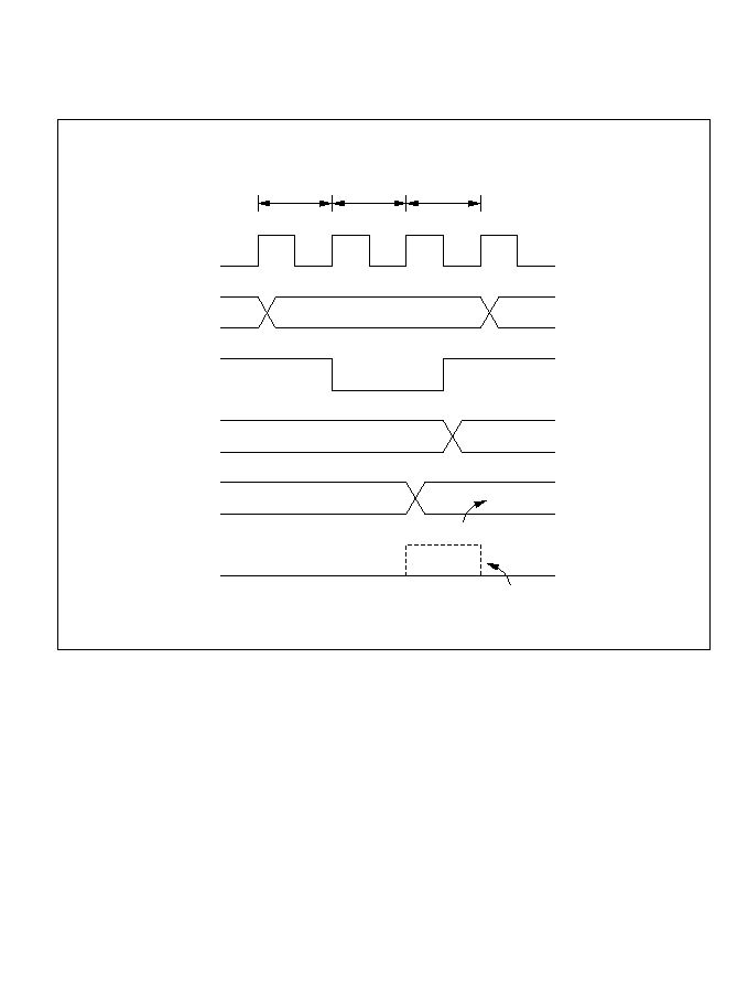
Contention between RTCOR Write and Compare Match: If a compare match occurs in the T
3
state of an RTCOR write cycle, writing takes priority and the compare match signal is inhibited.
See figure 7-22.
Figure 7-22 Contention between RTCOR Write and Compare Match
RTCNT Operation at Internal Clock Source Switchover: Switching internal clock sources may
cause RTCNT to increment, depending on the switchover timing. Table 7-9 shows the relation
between the time of the switchover (by writing to bits CKS2 to CKS0) and the operation of
RTCNT.
The RTCNT input clock is generated from the internal clock source by detecting the falling edge
of the internal clock. If a switchover is made from a high clock source to a low clock source, as in
case No. 3 in table 7-9, the switchover will be regarded as a falling edge, an RTCNT clock pulse
will be generated, and RTCNT will be incremented.
T
1
T
2
T
3
RTCOR address
N
M
N
N + 1
¯
Address bus
RTCNT
RTCOR
RTCOR write cycle by CPU
Internal
write signal
Compare
match signal
Inhibited
RTCOR write data
172
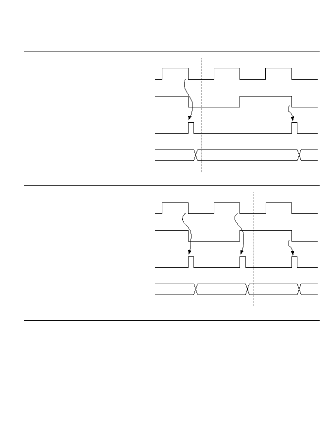
Table 7-9 Internal Clock Switchover and RTCNT Operation
CKS2 to CKS0
No.
Write Timing
RTCNT Operation
1
Low
low switchover
*
1
2
Low
high switchover
*
2
Notes: 1. Including switchovers from a low clock source to the halted state, and from the halted
state to a low clock source.
2. Including switchover from the halted state to a high clock source.
Old clock
source
New clock
source
RTCNT
N
N + 1
CKS bits rewritten
RTCNT
clock
Old clock
source
New clock
source
RTCNT
N
N + 1
CKS bits rewritten
N + 2
RTCNT
clock
173
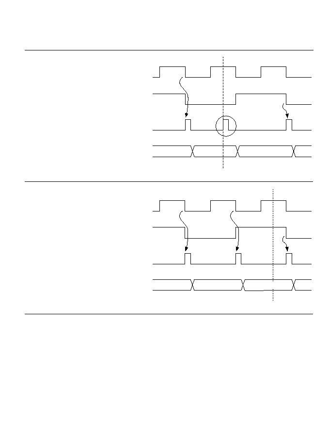
Table 7-9 Internal Clock Switchover and RTCNT Operation (cont)
CKS2 to CKS0
No.
Write Timing
RTCNT Operation
3
High
low switchover
*
1
4
High
high switchover
Notes: 1. Including switchover from a high clock source to the halted state.
2. The switchover is regarded as a falling edge, causing RTCNT to increment.
Old clock
source
New clock
source
RTCNT
clock
RTCNT
N
N + 1
CKS bits rewritten
N + 2
*
2
Old clock
source
New clock
source
RTCNT
clock
RTCNT
N
N + 1
CKS bits rewritten
N + 2
174

7.4 Interrupt Source
Compare match interrupts (CMI) can be generated when the refresh controller is used as an
interval timer. Compare match interrupt requests are masked/unmasked with the CMIE bit of
RTMCSR.
7.5 Usage Notes
When using the DRAM or pseudo-static RAM refresh function, note the following points:
∑
With the refresh controller, if directly connected DRAM or PSRAM is disconnected*, the
P8
0
/
RFSH/IRQ
0
pin and the P8
1
/
CS
3
/
IRQ
1
pin may both become low-level outputs
simultaneously.
Note: * When the DRAM enable bit (DRAME) or PSRAM enable bit (PSRAME) in the refresh
control register (RFSHCR) is cleared to 0 after being set to 1.
Figure 7-23 Operation when DRAM/PSRAM Connection is Switched
175
Address bus
Area 3 start address
P8
0
/RFSH/IRQ
0
P8
1
/CS
3
/IRQ
1
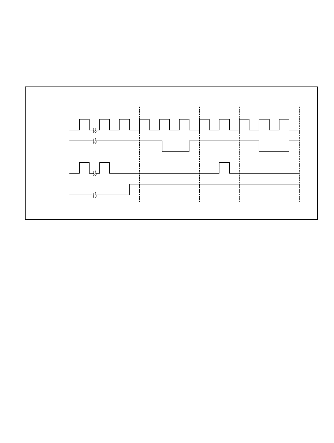
∑
Refresh cycles are not executed while the bus is released, during software standby mode, and
when a bus cycle is greatly prolonged by insertion of wait states. When these conditions
occur, other means of refreshing are required.
∑
If refresh requests occur while the bus is released, the first request is held and one refresh
cycle is executed after the bus-released state ends. Figure 7-24 shows the bus cycles in this
case.
Figure 7-24 Refresh Cycles when Bus is Released
176
¯
RFSH
BACK
Refresh
request
Bus-released state
Refresh cycle
CPU cycle
Refresh cycle
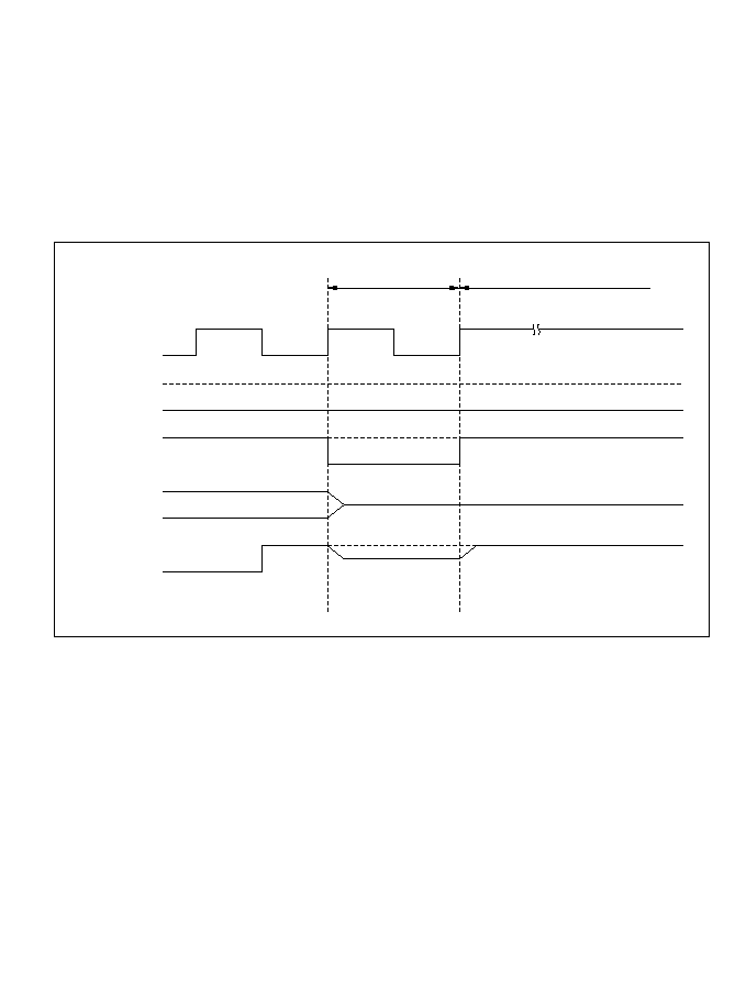
∑
If a bus cycle is prolonged by insertion of wait states, the first refresh request is held, as in the
bus-released state.
∑
If contention occurs between a transition to software standby mode and a bus request from an
external bus master, the bus may be released for one state just before the transition to
software standby mode (see figure 7-25). When using software standby mode, clear the
BRLE bit to 0 in BRCR before executing the SLEEP instruction.
If similar contention occurs in a transition to self-refresh mode, strobe waveforms may not be
output correctly. This can also be prevented by clearing the BRLE bit to 0 in BRCR.
Figure 7-25 Contention between Bus-Released State and Software Standby Mode
177
¯
Strobe
BREQ
BACK
Bus-released state
Software standby mode
Address
bus

Section 8 DMA Controller
8.1 Overview
The H8/3002 has an on-chip DMA controller (DMAC) that can transfer data on up to four
channels.
8.1.1 Features
DMAC features are listed below.
∑
Selection of short address mode or full address mode
Short address mode
-- 8-bit source address and 24-bit destination address, or vice versa
-- Maximum four channels available
-- Selection of I/O mode, idle mode, or repeat mode
Full address mode
-- 24-bit source and destination addresses
-- Maximum two channels available
-- Selection of normal mode or block transfer mode
∑
Directly addressable 16-Mbyte address space
∑
Selection of byte or word transfer
∑
Activation by internal interrupts, external requests, or auto-request (depending on transfer
mode)
-- 16-bit integrated timer unit (ITU) compare match/input capture interrupts (four)
-- Serial communication interface (SCI) transmit-data-empty/receive-data-full interrupts
-- External requests
-- Auto-request
179

8.1.2 Block Diagram
Figure 8-1 shows a DMAC block diagram.
Figure 8-1 Block Diagram of DMAC
IMIA0
IMIA1
IMIA2
IMIA3
TXI0
RXI0
DREQ0
DREQ1
TEND0
TEND1
DEND0A
DEND0B
DEND1A
DEND1B
DTCR0A
DTCR0B
DTCR1A
DTCR1B
Control logic
Data buffer
Address buffer
Arithmetic-logic unit
MAR0A
MAR0B
MAR1A
MAR1B
IOAR0A
IOAR0B
IOAR1A
IOAR1B
ETCR0A
ETCR0B
ETCR1A
ETCR1B
Internal address bus
Internal
interrupts
Interrupt
signals
External
requests
Internal data bus
Module data bus
Legend
DTCR:
MAR:
IOAR:
ETCR:
Data transfer control register
Memory address register
I/O address register
Execute transfer count register
Channel
0A
Channel
0B
Channel
1A
Channel
1B
Channel
0
Channel
1
180

8.1.3 Functional Overview
Table 8-1 gives an overview of the DMAC functions.
Table 8-1 DMAC Functional Overview
Address
Reg. Length
Destina-
Transfer Mode
Activation
Source tion
∑ Compare match/input 24
8
capture A interrupts
from ITU channels
0 to 3
∑ Transmit-data-empty
interrupt from SCI
channel 0
∑ Receive-data-full 8
24
interrupt from SCI
channel 0
∑ External request
∑ Auto-request
24
24
∑ External request
∑ Compare match/
24
24
input capture A
interrupts from ITU
channels 0 to 3
∑ External request
I/O mode
∑ Transfers one byte or one word
per request
∑ Increments or decrements the
memory address by 1 or 2
∑ Executes 1 to 65,536 transfers
Idle mode
∑ Transfers one byte or one word
per request
∑ Holds the memory address fixed
∑ Executes 1 to 65,536 transfers
Repeat mode
∑ Transfers one byte or one word
per request
∑ Increments or decrements the
memory address by 1 or 2
∑ Executes a specified number (1 to
255) of transfers, then returns to
the initial state and continues
Normal mode
∑ Auto-request
-- Retains the transfer request
internally
-- Executes a specified number
(1 to 65,536) of transfers
continuously
-- Selection of burst mode or
cycle-steal mode
∑ External request
-- Transfers one byte or one word
per request
-- Executes 1 to 65,536 transfers
Block transfer
∑ Transfers one block of a specified
size per request
∑ Executes 1 to 65,536 transfers
∑ Allows either the source or
destination to be a fixed block
area
∑ Block size can be 1 to 255 bytes
or words
Short
address
mode
Full
address
mode
181

8.1.4 Input/Output Pins
Table 8-2 lists the DMAC pins.
Table 8-2 DMAC Pins
Abbrevia-
Input/
Channel
Name
tion
Output
Function
0
DMA request 0
DREQ
0
Input
External request for DMAC channel 0
Transfer end 0
TEND
0
Output
Transfer end on DMAC channel 0
1
DMA request 1
DREQ
1
Input
External request for DMAC channel 1
Transfer end 1
TEND
1
Output
Transfer end on DMAC channel 1
Note: External requests cannot be made to channel A in short address mode.
8.1.5 Register Configuration
Table 8-3 lists the DMAC registers.
182

Table 8-3 DMAC Registers
Channel
Address
*
Name
Abbreviation
R/W
Initial Value
0
H'FF20
Memory address register 0AR
MAR0AR
R/W
Undetermined
H'FF21
Memory address register 0AE
MAR0AE
R/W
Undetermined
H'FF22
Memory address register 0AH
MAR0AH
R/W
Undetermined
H'FF23
Memory address register 0AL
MAR0AL
R/W
Undetermined
H'FF26
I/O address register 0A
IOAR0A
R/W
Undetermined
H'FF24
Execute transfer count register 0AH
ETCR0AH
R/W
Undetermined
H'FF25
Execute transfer count register 0AL
ETCR0AL
R/W
Undetermined
H'FF27
Data transfer control register 0A
DTCR0A
R/W
H'00
H'FF28
Memory address register 0BR
MAR0BR
R/W
Undetermined
H'FF29
Memory address register 0BE
MAR0BE
R/W
Undetermined
H'FF2A
Memory address register 0BH
MAR0BH
R/W
Undetermined
H'FF2B
Memory address register 0BL
MAR0BL
R/W
Undetermined
H'FF2E
I/O address register 0B
IOAR0B
R/W
Undetermined
H'FF2C
Execute transfer count register 0BH
ETCR0BH
R/W
Undetermined
H'FF2D
Execute transfer count register 0BL
ETCR0BL
R/W
Undetermined
H'FF2F
Data transfer control register 0B
DTCR0B
R/W
H'00
1
H'FF30
Memory address register 1AR
MAR1AR
R/W
Undetermined
H'FF31
Memory address register 1AE
MAR1AE
R/W
Undetermined
H'FF32
Memory address register 1AH
MAR1AH
R/W
Undetermined
H'FF33
Memory address register 1AL
MAR1AL
R/W
Undetermined
H'FF36
I/O address register 1A
IOAR1A
R/W
Undetermined
H'FF34
Execute transfer count register 1AH
ETCR1AH
R/W
Undetermined
H'FF35
Execute transfer count register 1AL
ETCR1AL
R/W
Undetermined
H'FF37
Data transfer control register 1A
DTCR1A
R/W
H'00
H'FF38
Memory address register 1BR
MAR1BR
R/W
Undetermined
H'FF39
Memory address register 1BE
MAR1BE
R/W
Undetermined
H'FF3A
Memory address register 1BH
MAR1BH
R/W
Undetermined
H'FF3B
Memory address register 1BL
MAR1BL
R/W
Undetermined
H'FF3E
I/O address register 1B
IOAR1B
R/W
Undetermined
H'FF3C
Execute transfer count register 1BH
ETCR1BH
R/W
Undetermined
H'FF3D
Execute transfer count register 1BL
ETCR1BL
R/W
Undetermined
H'FF3F
Data transfer control register 1B
DTCR1B
R/W
H'00
Note:
*
The lower 16 bits of the address are indicated.
183

8.2 Register Descriptions (1) (Short Address Mode)
In short address mode, transfers can be carried out independently on channels A and B. Short
address mode is selected by bits DTS2A and DTS1A in data transfer control register A (DTCRA)
as indicated in table 8-4.
Table 8-4 Selection of Short and Full Address Modes
Bit 2
Bit 1
Channel
DTS2A
DTS1A
Description
0
1
1
DMAC channel 0 operates as one channel in full address mode
Other than above
DMAC channels 0A and 0B operate as two independent channels
in short address mode
1
1
1
DMAC channel 1 operates as one channel in full address mode
Other than above
DMAC channels 1A and 1B operate as two independent channels
in short address mode
184
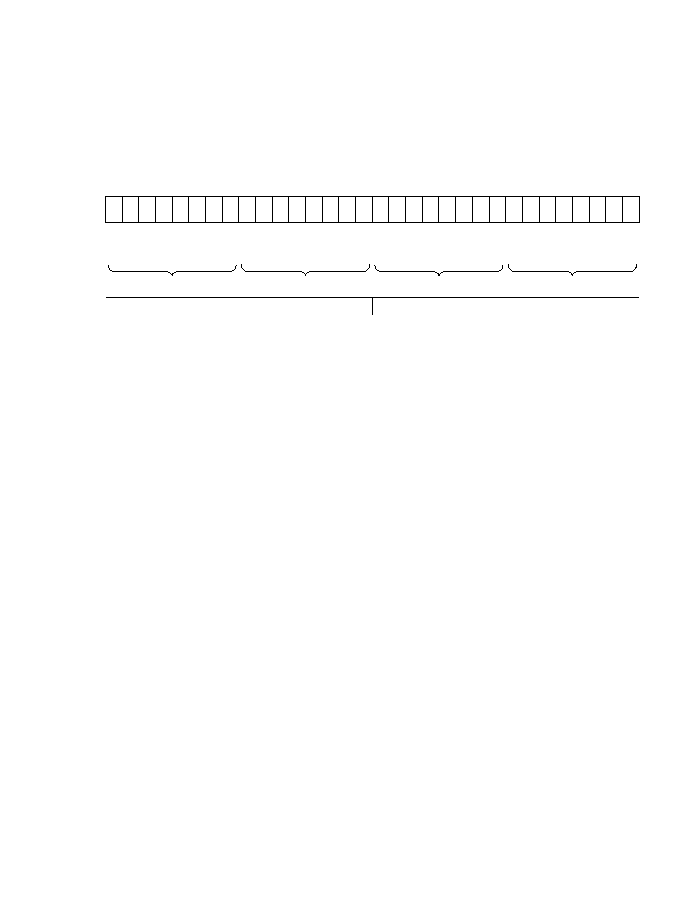
8.2.1 Memory Address Registers (MAR)
A memory address register (MAR) is a 32-bit readable/writable register that specifies a source or
destination address. The transfer direction is determined automatically from the activation source.
An MAR consists of four 8-bit registers designated MARR, MARE, MARH, and MARL. All bits
of MARR are reserved: they cannot be modified and always read 1.
An MAR functions as a source or destination address register depending on how the DMAC is
activated: as a destination address register if activation is by a receive-data-full interrupt from the
serial communication interface (SCI)
channel 0
, and as a source address register otherwise.
The MAR value is incremented or decremented each time one byte or word is transferred,
automatically updating the source or destination memory address. For details, see section 8.2.4,
Data Transfer Control Registers (DTCR).
The MARs are not initialized by a reset or in standby mode.
Bit
Initial value
Read/Write
31
1
--
Source or destination address
30
1
--
29
1
--
28
1
--
27
1
--
26
1
--
25
1
--
24
1
--
23
R/W
22
R/W
21
R/W
20
R/W
19
R/W
18
R/W
17
R/W
16
R/W
15
R/W
14
R/W
13
R/W
12
R/W
11
R/W
10
R/W
9
R/W
8
R/W
7
R/W
6
R/W
5
R/W
4
R/W
3
R/W
2
R/W
1
R/W
0
R/W
MARR
MARE
MARH
MARL
Undetermined
185

8.2.2 I/O Address Registers (IOAR)
An I/O address register (IOAR) is an 8-bit readable/writable register that specifies a source or
destination address. The IOAR value is the lower 8 bits of the address. The upper 16 address bits
are all 1 (H'FFFF).
An IOAR functions as a source or destination address register depending on how the DMAC is
activated: as a source address register if activation is by a receive-data-full interrupt from the SCI
channel 0
, and as a destination address register otherwise.
The IOAR value is held fixed. It is not incremented or decremented when a transfer is executed.
The IOARs are not initialized by a reset or in standby mode.
8.2.3 Execute Transfer Count Registers (ETCR)
An execute transfer count register (ETCR) is a 16-bit readable/writable register that specifies the
number of transfers to be executed. These registers function in one way in I/O mode and idle
mode, and another way in repeat mode.
∑
I/O mode and idle mode
In I/O mode and idle mode, ETCR functions as a 16-bit counter. The count is decremented by
1 each time one transfer is executed. The transfer ends when the count reaches H'0000.
Bit
Initial value
Read/Write
7
R/W
6
R/W
5
R/W
4
R/W
3
R/W
0
R/W
2
R/W
1
R/W
Source or destination address
Undetermined
Bit
Initial value
Read/Write
14
R/W
12
R/W
10
R/W
8
R/W
6
R/W
0
R/W
4
R/W
2
R/W
Transfer counter
Undetermined
15
R/W
13
R/W
11
R/W
9
R/W
7
R/W
1
R/W
5
R/W
3
R/W
186
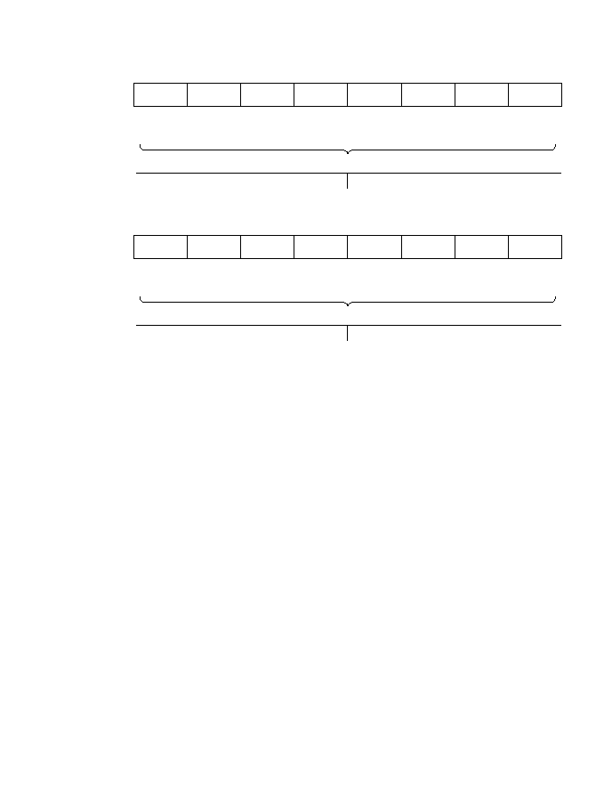
∑
Repeat mode
In repeat mode, ETCRH functions as an 8-bit transfer counter and ETCRL holds the initial
transfer count. ETCRH is decremented by 1 each time one transfer is executed. When ETCRH
reaches H'00, the value in ETCRL is reloaded into ETCRH and the same operation is repeated.
The ETCRs are not initialized by a reset or in standby mode.
Bit
Initial value
Read/Write
7
R/W
6
R/W
5
R/W
4
R/W
3
R/W
0
R/W
2
R/W
1
R/W
Undetermined
Transfer counter
ETCRH
Bit
Initial value
Read/Write
7
R/W
6
R/W
5
R/W
4
R/W
3
R/W
0
R/W
2
R/W
1
R/W
Undetermined
Initial count
ETCRL
187

8.2.4 Data Transfer Control Registers (DTCR)
A data transfer control register (DTCR) is an 8-bit readable/writable register that controls the
operation of one DMAC channel.
The DTCRs are initialized to H'00 by a reset and in standby mode.
Bit 7--Data Transfer Enable (DTE): Enables or disables data transfer on a channel. When the
DTE bit is set to 1, the channel waits for a transfer to be requested, and executes the transfer when
activated as specified by bits DTS2 to DTS0. When DTE is 0, the channel is disabled and does not
accept transfer requests. DTE is set to 1 by reading the register when DTE is 0, then writing 1.
Bit 7
DTE
Description
0
Data transfer is disabled. In I/O mode or idle mode, DTE is cleared to 0
(Initial value)
when the specified number of transfers have been completed.
1
Data transfer is enabled
If DTIE is set to 1, a CPU interrupt is requested when DTE is cleared to 0.
Bit
Initial value
Read/Write
7
DTE
0
R/W
6
DTSZ
0
R/W
5
DTID
0
R/W
4
RPE
0
R/W
3
DTIE
0
R/W
0
DTS0
0
R/W
2
DTS2
0
R/W
1
DTS1
0
R/W
Data transfer enable
Enables or disables
data transfer
Data transfer interrupt enable
Enables or disables the CPU interrupt
at the end of the transfer
Data transfer select
These bits select the data
transfer activation source
Data transfer size
Selects byte or
word size
Data transfer
increment/decrement
Selects whether to
increment or decrement
the memory address
register
Repeat enable
Selects repeat
mode
188

Bit 6--Data Transfer Size (DTSZ): Selects the data size of each transfer.
Bit 6
DTSZ
Description
0
Byte-size transfer
(Initial value)
1
Word-size transfer
Bit 5--Data Transfer Increment/Decrement (DTID): Selects whether to increment or
decrement the memory address register (MAR) after a data transfer in I/O mode or repeat mode.
Bit 5
DTID
Description
0
MAR is incremented after each data transfer
(Initial value)
∑ If DTSZ = 0, MAR is incremented by 1 after each transfer
∑ If DTSZ = 1, MAR is incremented by 2 after each transfer
1
MAR is decremented after each data transfer
∑ If DTSZ = 0, MAR is decremented by 1 after each transfer
∑ If DTSZ = 1, MAR is decremented by 2 after each transfer
MAR is not incremented or decremented in idle mode.
Bit 4--Repeat Enable (RPE): Selects whether to transfer data in I/O mode, idle mode, or repeat
mode.
Bit 4
Bit 3
RPE
DTIE
Description
0
0
I/O mode
(Initial value)
1
1
0
Repeat mode
1
Idle mode
Operations in these modes are described in sections 8.4.2, I/O Mode, 8.4.3, Idle Mode, and 8.4.4,
Repeat Mode.
189

Bit 3--Data Transfer Interrupt Enable (DTIE): Enables or disables the CPU interrupt (DEND)
requested when the DTE bit is cleared to 0.
Bit 3
DTIE
Description
0
The DEND interrupt requested by DTE is disabled
(Initial value)
1
The DEND interrupt requested by DTE is enabled
Bits 2 to 0--Data Transfer Select (DTS2, DTS1, DTS0): These bits select the data transfer
activation source. Some of the selectable sources differ between channels A and B.
Channel A
Bit 2
Bit 1
Bit 0
DTS2A
DTS1A
DTS0A
Description
0
0
0
Compare match/input capture A interrupt from ITU
(Initial value)
channel 0
1
Compare match/input capture A interrupt from ITU channel 1
1
0
Compare match/input capture A interrupt from ITU channel 2
1
Compare match/input capture A interrupt from ITU channel 3
1
0
0
Transmit-data-empty interrupt from SCI channel 0
1
Receive-data-full interrupt from SCI channel 0
1
--
*
Transfer in full address mode
Note:
*
See section 8.3.4, Data Transfer Control Register (DTCR).
190

Channel B
Bit 2
Bit 1
Bit 0
DTS2B
DTS1B
DTS0B
Description
0
0
0
Compare match/input capture A interrupt from ITU
(Initial value)
channel 0
1
Compare match/input capture A interrupt from ITU channel 1
1
0
Compare match/input capture A interrupt from ITU channel 2
1
Compare match/input capture A interrupt from ITU channel 3
1
0
0
Transmit-data-empty interrupt from SCI channel 0
1
Receive-data-full interrupt from SCI channel 0
1
0
Falling edge of
DREQ
input
1
Low level of
DREQ
input
The same internal interrupt can be selected as an activation source for two or more channels at
once. In that case the channels are activated in a priority order, highest-priority channel first. For
the priority order, see section 8.4.9, Multiple-Channel Operation.
When a channel is enabled (DTE = 1), its selected DMAC activation source cannot generate a
CPU interrupt.
191
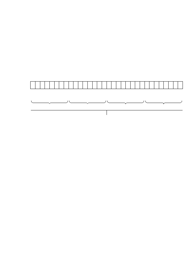
8.3 Register Descriptions (2) (Full Address Mode)
In full address mode the A and B channels operate together. Full address mode is selected as
indicated in table 8-4.
8.3.1 Memory Address Registers (MAR)
A memory address register (MAR) is a 32-bit readable/writable register. MARA functions as the
source address register of the transfer, and MARB as the destination address register.
An MAR consists of four 8-bit registers designated MARR, MARE, MARH, and MARL. All bits
of MARR are reserved: they cannot be modified and always read 1.
The MAR value is incremented or decremented each time one byte or word is transferred,
automatically updating the source or destination memory address. For details, see section 8.3.4,
Data Transfer Control Registers (DTCR).
The MARs are not initialized by a reset or in standby mode.
8.3.2 I/O Address Registers (IOAR)
The I/O address registers (IOARs) are not used in full address mode.
Bit
Initial value
Read/Write
31
1
--
Source or destination address
30
1
--
29
1
--
28
1
--
27
1
--
26
1
--
25
1
--
24
1
--
23
R/W
22
R/W
21
R/W
20
R/W
19
R/W
18
R/W
17
R/W
16
R/W
15
R/W
14
R/W
13
R/W
12
R/W
11
Undetermined
R/W
10
R/W
9
R/W
8
R/W
7
R/W
6
R/W
5
R/W
4
R/W
3
R/W
2
R/W
1
R/W
0
R/W
MARR
MARE
MARH
MARL
192

8.3.3 Execute Transfer Count Registers (ETCR)
An execute transfer count register (ETCR) is a 16-bit readable/writable register that specifies the
number of transfers to be executed. The functions of these registers differ between normal mode
and block transfer mode.
∑
Normal mode
ETCRA
ETCRB: Is not used in normal mode.
In normal mode ETCRA functions as a 16-bit transfer counter. The count is decremented by 1
each time one transfer is executed. The transfer ends when the count reaches H'0000. ETCRB is
not used.
Bit
Initial value
Read/Write
14
R/W
12
R/W
10
R/W
8
R/W
6
R/W
0
R/W
4
R/W
2
R/W
Transfer counter
Undetermined
15
R/W
13
R/W
11
R/W
9
R/W
7
R/W
1
R/W
5
R/W
3
R/W
193
∑
Block transfer mode
ETCRA
ETCRB
In block transfer mode, ETCRAH functions as an 8-bit block size counter. ETCRAL holds the
initial block size. ETCRAH is decremented by 1 each time one byte or word is transferred. When
the count reaches H'00, ETCRAH is reloaded from ETCRAL. Blocks consisting of an arbitrary
number of bytes or words can be transferred repeatedly by setting the same initial block size value
in ETCRAH and ETCRAL.
In block transfer mode ETCRB functions as a 16-bit block transfer counter. ETCRB is
decremented by 1 each time one block is transferred. The transfer ends when the count reaches
H'0000.
The ETCRs are not initialized by a reset or in standby mode.
Bit
Initial value
Read/Write
7
R/W
6
R/W
5
R/W
4
R/W
3
R/W
0
R/W
2
R/W
1
R/W
Undetermined
Block size counter
ETCRAH
Bit
Initial value
Read/Write
7
R/W
6
R/W
5
R/W
4
R/W
3
R/W
0
R/W
2
R/W
1
R/W
Undetermined
Initial block size
ETCRAL
Bit
Initial value
Read/Write
14
R/W
12
R/W
10
R/W
8
R/W
6
R/W
0
R/W
4
R/W
2
R/W
Block transfer counter
Undetermined
15
R/W
13
R/W
11
R/W
9
R/W
7
R/W
1
R/W
5
R/W
3
R/W
194
8.3.4 Data Transfer Control Registers (DTCR)
The data transfer control registers (DTCRs) are 8-bit readable/writable registers that control the
operation of the DMAC channels. A channel operates in full address mode when bits DTS2A and
DTS1A are both set to 1 in DTCRA. DTCRA and DTCRB have different functions in full address
mode.
DTCRA
DTCRA is initialized to H'00 by a reset and in standby mode.
Bit
Initial value
Read/Write
7
DTE
0
R/W
6
DTSZ
0
R/W
5
SAID
0
R/W
4
SAIDE
0
R/W
3
DTIE
0
R/W
0
DTS0A
0
R/W
2
DTS2A
0
R/W
1
DTS1A
0
R/W
Data transfer enable
Enables or disables
data transfer
Enables or disables the
CPU interrupt at the end
of the transfer
Data transfer size
Selects byte or
word size
Source address
increment/decrement
Data transfer select
2A and 1A
These bits must both be
set to 1
Data transfer
interrupt enable
Source address increment/
decrement enable
These bits select whether
the source address register
(MARA) is incremented,
decremented, or held fixed
during the data transfer
Selects block
transfer mode
Data transfer
select 0A
195

Bit 7--Data Transfer Enable (DTE): Together with the DTME bit in DTCRB, this bit enables or
disables data transfer on the channel. When the DTME and DTE bits are both set to 1, the channel
is enabled. If auto-request is specified, data transfer begins immediately. Otherwise, the channel
waits for transfers to be requested. When the specified number of transfers have been completed,
the DTE bit is automatically cleared to 0. When DTE is 0, the channel is disabled and does not
accept transfer requests. DTE is set to 1 by reading the register when DTE is 0, then writing 1.
Bit 7
DTE
Description
0
Data transfer is disabled (DTE is cleared to 0 when the specified number (Initial value)
of transfers have been completed)
1
Data transfer is enabled
If DTIE is set to 1, a CPU interrupt is requested when DTE is cleared to 0.
Bit 6--Data Transfer Size (DTSZ): Selects the data size of each transfer.
Bit 6
DTSZ
Description
0
Byte-size transfer
(Initial value)
1
Word-size transfer
Bit 5--Source Address Increment/Decrement (SAID) and Bit 4--Source Address
Increment/Decrement Enable (SAIDE): These bits select whether the source address register
(MARA) is incremented, decremented, or held fixed during the data transfer.
Bit 5
Bit 4
SAID
SAIDE
Description
0
0
MARA is held fixed
(Initial value)
1
MARA is incremented after each data transfer
∑ If DTSZ = 0, MARA is incremented by 1 after each transfer
∑ If DTSZ = 1, MARA is incremented by 2 after each transfer
1
0
MARA is held fixed
1
MARA is decremented after each data transfer
∑ If DTSZ = 0, MARA is decremented by 1 after each transfer
∑ If DTSZ = 1, MARA is decremented by 2 after each transfer
196

Bit 3--Data Transfer Interrupt Enable (DTIE): Enables or disables the CPU interrupt (DEND)
requested when the DTE bit is cleared to 0.
Bit 3
DTIE
Description
0
The DEND interrupt requested by DTE is disabled
(Initial value)
1
The DEND interrupt requested by DTE is enabled
Bits 2 and 1--Data Transfer Select 2A and 1A (DTS2A, DTS1A): A channel operates in full
address mode when DTS2A and DTS1A are both set to 1.
Bit 0--Data Transfer Select 0A (DTS0A): Selects normal mode or block transfer mode.
Bit 0
DTS0A
Description
0
Normal mode
(Initial value)
1
Block transfer mode
Operations in these modes are described in sections 8.4.5, Normal Mode, and 8.4.6, Block
Transfer Mode.
197

DTCRB
DTCRB is initialized to H'00 by a reset and in standby mode.
Bit 7--Data Transfer Master Enable (DTME): Together with the DTE bit in DTCRA, this bit
enables or disables data transfer. When the DTME and DTE bits are both set to 1, the channel is
enabled. When an NMI interrupt occurs DTME is cleared to 0, suspending the transfer so that the
CPU can use the bus. The suspended transfer resumes when DTME is set to 1 again. For further
information on operation in block transfer mode, see section 8.6.6, NMI Interrupts and Block
Transfer Mode.
DTME is set to 1 by reading the register while DTME = 0, then writing 1.
Bit 7
DTME
Description
0
Data transfer is disabled (DTME is cleared to 0 when an NMI interrupt
(Initial value)
occurs)
1
Data transfer is enabled
Bit
Initial value
Read/Write
7
DTME
0
R/W
6
--
0
R/W
5
DAID
0
R/W
4
DAIDE
0
R/W
3
TMS
0
R/W
0
DTS0B
0
R/W
2
DTS2B
0
R/W
1
DTS1B
0
R/W
Data transfer master enable
Enables or disables data
transfer, together with
the DTE bit, and is cleared
to 0 by an interrupt
Reserved bit
Destination address
increment/decrement
Data transfer select
2B to 0B
These bits select the data
transfer activation source
Transfer mode select
Destination address
increment/decrement enable
These bits select whether
the destination address
register (MARB) is incremented,
decremented, or held fixed
during the data transfer
Selects whether the
block area is the source
or destination in block
transfer mode
198

Bit 6--Reserved: Although reserved, this bit can be written and read.
Bit 5--Destination Address Increment/Decrement (DAID) and Bit 4--Destination Address
Increment/Decrement Enable (DAIDE): These bits select whether the destination address
register (MARB), is incremented, decremented, or held fixed during the data transfer.
Bit 5
Bit 4
DAID
DAIDE
Description
0
0
MARB is held fixed
(Initial value)
1
MARB is incremented after each data transfer
∑ If DTSZ = 0, MARB is incremented by 1 after each data transfer
∑ If DTSZ = 1, MARB is incremented by 2 after each data transfer
1
0
MARB is held fixed
1
MARB is decremented after each data transfer
∑ If DTSZ = 0, MARB is decremented by 1 after each data transfer
∑ If DTSZ = 1, MARB is decremented by 2 after each data transfer
Bit 3--Transfer Mode Select (TMS): Selects whether the source or destination is the block area
in block transfer mode.
Bit 3
TMS
Description
0
Destination is the block area in block transfer mode
(Initial value)
1
Source is the block area in block transfer mode
199

Bits 2 to 0--Data Transfer Select (DTS2B, DTS1B, DTS0B): These bits select the data transfer
activation source. The selectable activation sources differ between normal mode and block
transfer mode.
Normal mode
Bit 2
Bit 1
Bit 0
DTS2B
DTS1B
DTS0B
Description
0
0
0
Auto-request (burst mode)
(Initial value)
1
Cannot be used
1
0
Auto-request (cycle-steal mode)
1
Cannot be used
1
0
0
Cannot be used
1
Cannot be used
1
0
Falling edge of
DREQ
1
Low level input at
DREQ
Block transfer mode
Bit 2
Bit 1
Bit 0
DTS2B DTS1B DTS0B Description
0
0
0
Compare match/input capture A interrupt from ITU channel 0 (Initial value)
1
Compare match/input capture A interrupt from ITU channel 1
1
0
Compare match/input capture A interrupt from ITU channel 2
1
Compare match/input capture A interrupt from ITU channel 3
1
0
0
Cannot be used
1
Cannot be used
1
0
Falling edge of
DREQ
1
Cannot be used
The same internal interrupt can be selected to activate two or more channels. The channels are
activated in a priority order, highest priority first. For the priority order, see section 8.4.9,
Multiple-Channel Operation.
200

8.4 Operation
8.4.1 Overview
Table 8-5 summarizes the DMAC modes.
Table 8-5 DMAC Modes
Transfer Mode
Activation
Notes
Short address
Compare match/input
mode
capture A interrupt from
ITU channels 0 to 3
SCI channel 0
transmit-data-empty
and receive-data-full
interrupts
External request
Normal mode
Auto-request
External request
Block transfer mode
Compare match/input
capture A interrupt from
ITU channels 0 to 3
External request
A summary of operations in these modes follows.
I/O Mode: One byte or word is transferred per request. A designated number of these transfers
are executed. A CPU interrupt can be requested at completion of the designated number of
transfers. One 24-bit address and one 8-bit address are specified. The transfer direction is
determined automatically from the activation source.
Idle Mode: One byte or word is transferred per request. A designated number of these transfers
are executed. A CPU interrupt can be requested at completion of the designated number of
transfers. One 24-bit address and one 8-bit address are specified. The addresses are held fixed.
The transfer direction is determined automatically from the activation source.
Repeat Mode: One byte or word is transferred per request. A designated number of these
transfers are executed. When the designated number of transfers are completed, the initial address
and counter value are restored and operation continues. No CPU interrupt is requested. One 24-bit
address and one 8-bit address are specified. The transfer direction is determined automatically
from the activation source.
Full address
mode
∑ Up to four channels
can operate
independently
∑ Only the B channels
support external
requests
∑ A and B channels are
paired; up to two
channels are
available
∑ Burst mode or cycle-
steal mode can be
selected for auto-
requests
I/O mode
Idle mode
Repeat mode
201

Normal Mode :
∑
Auto-request
The DMAC is activated by register setup alone, and continues executing transfers until the
designated number of transfers have been completed. A CPU interrupt can be requested at
completion of the transfers. Both addresses are 24-bit addresses.
-- Cycle-steal mode
The bus is released to another bus master after each byte or word is transferred.
-- Burst mode
Unless requested by a higher-priority bus master, the bus is not released until the
designated number of transfers have been completed.
∑
External request
One byte or word is transferred per request. A designated number of these transfers are
executed. A CPU interrupt can be requested at completion of the designated number of
transfers. Both addresses are 24-bit addresses.
Block Transfer Mode: One block of a specified size is transferred per request. A designated
number of block transfers are executed. At the end of each block transfer, one address is restored
to its initial value. When the designated number of blocks have been transferred, a CPU interrupt
can be requested. Both addresses are 24-bit addresses.
202

8.4.2 I/O Mode
I/O mode can be selected independently for each channel.
One byte or word is transferred at each transfer request in I/O mode. A designated number of
these transfers are executed. One address is specified in the memory address register (MAR), the
other in the I/O address register (IOAR). The direction of transfer is determined automatically
from the activation source. The transfer is from the address specified in IOAR to the address
specified in MAR if activated by an SCI
channel 0
receive-data-full interrupt, and from the
address specified in MAR to the address specified in IOAR otherwise.
Table 8-6 indicates the register functions in I/O mode.
Table 8-6 Register Functions in I/O Mode
Function
Activated by
SCI Receive-
Data-Full Other
Register
Interrupt
Activation
Initial Setting
Operation
Destination
Source
Destination or
Incremented or
address address
source
address
decremented
register
register
once per transfer
Source
Destination Source or
Held fixed
address address
destination
register
register
address
Transfer counter
Number of
Decremented
transfers
once per
transfer until
H'0000 is
reached and
transfer ends
Legend
MAR:
Memory address register
IOAR: I/O address register
ETCR: Execute transfer count register
MAR and IOAR specify the source and destination addresses. MAR specifies a 24-bit source or
destination address, which is incremented or decremented as each byte or word is transferred.
IOAR specifies the lower 8 bits of a fixed address. The upper 16 bits are all 1s. IOAR is not
incremented or decremented.
Figure 8-2 illustrates how I/O mode operates.
23
0
MAR
All 1s
IOAR
23
0
15
0
ETCR
7
203
Figure 8-2 Operation in I/O Mode
The transfer count is specified as a 16-bit value in ETCR. The ETCR value is decremented by 1 at
each transfer. When the ETCR value reaches H'0000, the DTE bit is cleared and the transfer ends.
If the DTIE bit is set to 1, a CPU interrupt is requested at this time. The maximum transfer count
is 65,536, obtained by setting ETCR to H'0000.
Transfers can be requested (activated) by compare match/input capture A interrupts from ITU
channels 0 to 3, SCI
channel 0
transmit-data-empty and receive-data-full interrupts, and external
request signals.
For the detailed settings see section 8.2.4, Data Transfer Control Registers (DTCR).
Address T
Address B
Transfer
Legend
L = initial setting of MAR
N = initial setting of ETCR
Address T = L
Address B = L + (≠1) ∑ (2 ∑ N ≠ 1)
DTID
IOAR
1 byte or word is
transferred per request
DTSZ
204
Figure 8-3 shows a sample setup procedure for I/O mode.
Figure 8-3 I/O Mode Setup Procedure (Example)
8.4.3 Idle Mode
Idle mode can be selected independently for each channel.
One byte or word is transferred at each transfer request in idle mode. A designated number of
these transfers are executed. One address is specified in the memory address register (MAR), the
other in the I/O address register (IOAR). The direction of transfer is determined automatically
from the activation source. The transfer is from the address specified in IOAR to the address
specified in MAR if activated by an SCI
channel 0
receive-data-full interrupt, and from the
address specified in MAR to the address specified in IOAR otherwise.
Table 8-7 indicates the register functions in idle mode.
Set source and
destination addresses
Set transfer count
Read DTCR
Set DTCR
I/O mode
I/O mode setup
1
2
3
4
1.
2.
3.
4.
Set the source and destination addresses
in MAR and IOAR. The transfer direction is
determined automatically from the activation
source.
Set the transfer count in ETCR.
Read DTCR while the DTE bit is cleared to 0.
Set the DTCR bits as follows.
Select the DMAC activation source with bits
DTS2 to DTS0.
Set or clear the DTIE bit to enable or disable
the CPU interrupt at the end of the transfer.
Clear the RPE bit to 0 to select I/O mode.
Select MAR increment or decrement with the
DTID bit.
Select byte size or word size with the DTSZ bit.
Set the DTE bit to 1 to enable the transfer.
∑
∑
∑
∑
∑
∑
205
Table 8-7 Register Functions in Idle Mode
Function
Activated by
SCI Receive-
Data-Full Other
Register
Interrupt
Activation
Initial Setting
Operation
Destination
Source
Destination or
Held fixed
address address
source
address
register
register
Source
Destination Source or
Held fixed
address address
destination
register
register
address
Transfer counter
Number of
Decremented
transfers
once per
transfer until
H'0000 is
reached and
transfer ends
Legend
MAR:
Memory address register
IOAR: I/O address register
ETCR: Execute transfer count register
MAR and IOAR specify the source and destination addresses. MAR specifies a 24-bit source or
destination address. IOAR specifies the lower 8 bits of a fixed address. The upper 16 bits are all
1s. MAR and IOAR are not incremented or decremented.
Figure 8-4 illustrates how idle mode operates.
Figure 8-4 Operation in Idle Mode
23
0
MAR
All 1s
IOAR
23
0
15
0
ETCR
7
Transfer
1 byte or word is
transferred per request
IOAR
MAR
206
The transfer count is specified as a 16-bit value in ETCR. The ETCR value is decremented by 1 at
each transfer. When the ETCR value reaches H'0000, the DTE bit is cleared, the transfer ends, and
a CPU interrupt is requested. The maximum transfer count is 65,536, obtained by setting ETCR to
H'0000.
Transfers can be requested (activated) by compare match/input capture A interrupts from ITU
channels 0 to 3, SCI transmit-data-empty and receive-data-full interrupts, and external request
signals.
For the detailed settings see section 8.2.4, Data Transfer Control Registers (DTCR).
Figure 8-5 shows a sample setup procedure for idle mode.
Figure 8-5 Idle Mode Setup Procedure (Example)
Set source and
destination addresses
Set transfer count
Read DTCR
Set DTCR
Idle mode
Idle mode setup
1
2
3
4
1.
2.
3.
4.
Set the source and destination addresses
in MAR and IOAR. The transfer direction is deter-
mined automatically from the activation source.
Set the transfer count in ETCR.
Read DTCR while the DTE bit is cleared to 0.
Set the DTCR bits as follows.
Select the DMAC activation source with bits
DTS2 to DTS0.
Set the DTIE and RPE bits to 1 to select idle mode.
Select byte size or word size with the DTSZ bit.
Set the DTE bit to 1 to enable the transfer.
∑
∑
∑
∑
207

8.4.4 Repeat Mode
Repeat mode is useful for cyclically transferring a bit pattern from a table to the programmable
timing pattern controller (TPC) in synchronization, for example, with ITU compare match. Repeat
mode can be selected for each channel independently.
One byte or word is transferred per request in repeat mode, as in I/O mode. A designated number
of these transfers are executed. One address is specified in the memory address register (MAR),
the other in the I/O address register (IOAR). At the end of the designated number of transfers,
MAR and ETCR are restored to their original values and operation continues. The direction of
transfer is determined automatically from the activation source. The transfer is from the address
specified in IOAR to the address specified in MAR if activated by an SCI receive-data-full
interrupt, and from the address specified in MAR to the address specified in IOAR otherwise.
Table 8-8 indicates the register functions in repeat mode.
Table 8-8 Register Functions in Repeat Mode
Function
Activated by
SCI Receive-
Data-Full Other
Register
Interrupt
Activation Initial Setting
Operation
Destination
Source
Destination or
Incremented or
address
address
source address decremented at
register
register
each transfer until
ETCRH reaches
H'0000, then restored
to initial value
Source Destination
Source
or
Held
fixed
address address
destination
register
register
address
Transfer counter
Number of
Decremented once
transfers
per transfer unti
H'0000 is reached,
then reloaded from
ETCRL
Initial transfer count
Number of
Held fixed
transfers
Legend
MAR:
Memory address register
IOAR: I/O address register
ETCR: Execute transfer count register
23
0
MAR
All 1s
IOAR
23
0
7
0
ETCRH
7
7
0
ETCRL
208
In repeat mode ETCRH is used as the transfer counter while ETCRL holds the initial transfer
count. ETCRH is decremented by 1 at each transfer until it reaches H'00, then is reloaded from
ETCRL. MAR is also restored to its initial value, which is calculated from the DTSZ and DTID
bits in DTCR. Specifically, MAR is restored as follows:
MAR
MAR ≠ (≠1)
DTID
∑ 2
DTSZ
∑ ETCRL
ETCRH and ETCRL should be initially set to the same value.
In repeat mode transfers continue until the CPU clears the DTE bit to 0. After DTE is cleared to 0,
if the CPU sets DTE to 1 again, transfers resume from the state at which DTE was cleared. No
CPU interrupt is requested.
As in I/O mode, MAR and IOAR specify the source and destination addresses. MAR specifies a
24-bit source or destination address. IOAR specifies the lower 8 bits of a fixed address. The upper
16 bits are all 1s. IOAR is not incremented or decremented.
Figure 8-6 illustrates how repeat mode operates.
Figure 8-6 Operation in Repeat Mode
Address T
Address B
Transfer
1 byte or word is
transferred per request
Legend
L = initial setting of MAR
N = initial setting of ETCRH and ETCRL
Address T = L
Address B = L + (≠1) ∑ (2 ∑ N ≠ 1)
DTID
DTSZ
IOAR
209
The transfer count is specified as an 8-bit value in ETCRH and ETCRL. The maximum transfer
count is 255, obtained by setting both ETCRH and ETCRL to H'FF.
Transfers can be requested (activated) by compare match/input capture A interrupts from ITU
channels 0 to 3, SCI transmit-data-empty and receive-data-full interrupts, and external request
signals.
For the detailed settings see section 8.2.4, Data Transfer Control Registers (DTCR).
Figure 8-7 shows a sample setup procedure for repeat mode.
Figure 8-7 Repeat Mode Setup Procedure (Example)
Set source and
destination addresses
Set transfer count
Read DTCR
Set DTCR
Repeat mode
Repeat mode
1
2
3
4
1.
2.
3.
4.
Set the source and destination addresses in MAR
and IOAR. The transfer direction is determined
automatically from the activation source.
Set the transfer count in both ETCRH and ETCRL.
Read DTCR while the DTE bit is cleared to 0.
Select byte size or word size with the DTSZ bit.
Set the DTE bit to 1 to enable the transfer.
∑
∑
∑
∑
∑
Select the DMAC activation source with bits
DTS2 to DTS0.
Clear the DTIE bit to 0 and set the RPE bit to 1
to select repeat mode.
Select MAR increment or decrement with the DTID bit.
Set the DTCR bits as follows.
210

8.4.5 Normal Mode
In normal mode the A and B channels are combined. One byte or word is transferred per request.
A designated number of these transfers are executed. Addresses are specified in MARA and
MARB. Table 8-9 indicates the register functions in I/O mode.
Table 8-9 Register Functions in Normal Mode
Register
Function
Initial Setting
Operation
Source address
Source address
Incremented or
register
decremented once per
transfer, or held fixed
Destination Destination Incremented
or
address register
address
decremented once per
transfer, or held fixed
Transfer counter
Number of
Decremented once per
transfers
transfer
Legend
MARA:
Memory address register A
MARB:
Memory address register B
ETCRA: Execute transfer count register A
The source and destination addresses are both 24-bit addresses. MARA specifies the source
address. MARB specifies the destination address. MARA and MARB can be independently
incremented, decremented, or held fixed as data is transferred.
The transfer count is specified as a 16-bit value in ETCRA. The ETCRA value is decremented by
1 at each transfer. When the ETCRA value reaches H'0000, the DTE bit is cleared and the transfer
ends. If the DTIE bit is set, a CPU interrupt is requested at this time. The maximum transfer count
is 65,536, obtained by setting ETCRA to H'0000.
Figure 8-8 illustrates how normal mode operates.
23
0
MARA
15
0
ETCRA
23
0
MARB
211
Figure 8-8 Operation in Normal Mode
Transfers can be requested (activated) by an external request or auto-request. An auto-requested
transfer is activated by the register settings alone. The designated number of transfers are executed
automatically. Either cycle-steal or burst mode can be selected. In cycle-steal mode the DMAC
releases the bus temporarily after each transfer. In burst mode the DMAC keeps the bus until the
transfers are completed, unless there is a bus request from a higher-priority bus master.
For the detailed settings see section 8.3.4, Data Transfer Control Registers (DTCR).
Address T
Address B
Transfer
Legend
L
L
N
T
B
T
B
SAID
DAID
Address T
Address B
A
B
A
A
B
B
= initial setting of MARA
= initial setting of MARB
= initial setting of ETCRA
= L
= L + SAIDE ∑ (≠1) ∑ (2 ∑ N ≠ 1)
= L
= L + DAIDE ∑ (≠1) ∑ (2 ∑ N ≠ 1)
A
A
B
B
DTSZ
DTSZ
A
A
B
B
212
Figure 8-9 shows a sample setup procedure for normal mode.
Figure 8-9 Normal Mode Setup Procedure (Example)
1.
2.
3.
4.
5.
6.
7.
8.
9.
Set the initial source address in MARA.
Set the initial destination address in MARB.
Set the transfer count in ETCRA.
Set the DTCRB bits as follows.
Set the DTCRA bits as follows.
Read DTCRB with DTME cleared to 0.
Normal mode
Normal mode
Set initial source address
Set initial destination address
Set transfer count
Set DTCRB (1)
Set DTCRA (1)
Read DTCRB
Set DTCRB (2)
Read DTCRA
Set DTCRA (2)
1
2
3
4
5
6
7
8
9
∑
∑
∑
∑
∑
∑
∑
∑
Clear the DTME bit to 0.
Set the DAID and DAIDE bits to select whether
MARB is incremented, decremented, or held fixed.
Select the DMAC activation source with bits
DTS2B to DTS0B.
Clear the DTE bit to 0.
Select byte or word size with the DTSZ bit.
Set the SAID and SAIDE bits to select whether
MARA is incremented, decremented, or held fixed.
Set or clear the DTIE bit to enable or disable the
CPU interrupt at the end of the transfer.
Clear the DTS0A bit to 0 and set the DTS2A
and DTS1A bits to 1 to select normal mode.
Set the DTME bit to 1 in DTCRB.
Read DTCRA with DTE cleared to 0.
Set the DTE bit to 1 in DTCRA to enable the transfer.
Note:
*
Carry out settings 1 to 9 with the DEND interrupt masked in the CPU. If an NMI
interrupt occurs during the setup procedure, it may clear the DTME bit to 0,
in which case the transfer will not start.
213
8.4.6 Block Transfer Mode
In block transfer mode the A and B channels are combined. One block of a specified size is
transferred per request. A designated number of block transfers are executed. Addresses are
specified in MARA and MARB. The block area address can be either held fixed or cycled.
Table 8-10 indicates the register functions in block transfer mode.
Table 8-10 Register Functions in Block Transfer Mode
Register
Function
Initial Setting
Operation
Source address
Source address
Incremented or
register
decremented once per
transfer, or held fixed
Destination Destination Incremented
or
address register
address
decremented once per
transfer, or held fixed
Block size counter Block size
Decremented once per
transfer until H'00 is
reached, then reloaded
from ETCRAL
Initial block size
Block size
Held fixed
Block transfer
Number of block
Decremented once per
counter
transfers
block transfer until H'0000
is reached and the
transfer ends
Legend
MARA:
Memory address register A
MARB:
Memory address register B
ETCRA: Execute transfer count register A
ETCRB: Execute transfer count register B
The source and destination addresses are both 24-bit addresses. MARA specifies the source
address. MARB specifies the destination address. MARA and MARB can be independently
incremented, decremented, or held fixed as data is transferred. One of these registers operates as a
block area register: even if it is incremented or decremented, it is restored to its initial value at the
end of each block transfer. The TMS bit in DTCRB selects whether the block area is the source or
destination.
23
0
MARA
7
0
ETCRAH
7
0
ETCRAL
23
0
MARB
15
0
ETCRB
214

If M (1 to 255) is the size of the block transferred at each request and N (1 to 65,536) is the
number of blocks to be transferred, then ETCRAH and ETCRAL should initially be set to M and
ETCRB should initially be set to N.
Figure 8-10 illustrates how block transfer mode operates. In this figure, bit TMS is cleared to 0,
meaning the block area is the destination.
Figure 8-10 Operation in Block Transfer Mode
T
B
Transfer
Legend
L
L
M
N
T
B
T
B
Address T
M bytes or words are
transferred per request
Address B
A
A
Block 1
Block N
B
B
Block area
Block 2
= initial setting of MARA
= initial setting of MARB
= initial setting of ETCRAH and ETCRAL
= initial setting of ETCRB
= L
= L + SAIDE ∑ (≠1) ∑ (2 ∑ M ≠ 1)
= L
= L + DAIDE ∑ (≠1) ∑ (2 ∑ M ≠ 1)
A
A
B
B
A
B
A
A
B
B
SAID
DAID
DTSZ
DTSZ
215

When activated by a transfer request, the DMAC executes a burst transfer. During the transfer
MARA and MARB are updated according to the DTCR settings, and ETCRAH is decremented.
When ETCRAH reaches H'00, it is reloaded from ETCRAL to restore the initial value. The
memory address register of the block area is also restored to its initial value, and ETCRB is
decremented. If ETCRB is not H'0000, the DMAC then waits for the next transfer request.
ETCRAH and ETCRAL should be initially set to the same value.
The above operation is repeated until ETCRB reaches H'0000, at which point the DTE bit is
cleared to 0 and the transfer ends. If the DTIE bit is set to 1, a CPU interrupt is requested at this
time.
Figure 8-11 shows examples of a block transfer with byte data size when the block area is the
destination. In (a) the block area address is cycled. In (b) the block area address is held fixed.
Transfers can be requested (activated) by compare match/input capture A interrupts from ITU
channels 0 to 3, and by external request signals.
For the detailed settings see section 8.3.4, Data Transfer Control Registers (DTCR).
216
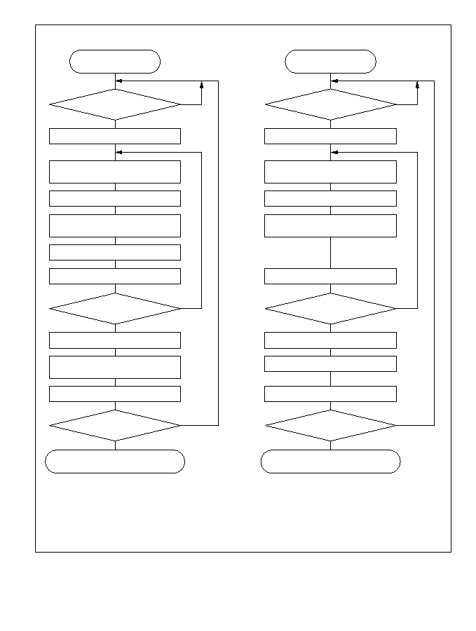
Figure 8-11 Block Transfer Mode Flowcharts (Examples)
Start
(DTE = DTME = 1)
Transfer requested?
Get bus
MARA = MARA + 1
Read from MARA address
Write to MARB address
MARB = MARB + 1
ETCRAH = ETCRAH ≠ 1
ETCRAH = H'00
Release bus
Clear DTE to 0 and end transfer
ETCRAH = ETCRAL
MARB = MARB ≠ ETCRAL
ETCRB = ETCRB ≠ 1
ETCRB = H'0000
Start
(DTE = DTME = 1)
Transfer requested?
Get bus
MARA = MARA + 1
Read from MARA address
Write to MARB address
ETCRAH = ETCRAH ≠ 1
ETCRAH = H'00
Release bus
Clear DTE to 0 and end transfer
ETCRB = ETCRB ≠ 1
ETCRB = H'0000
ETCRAH = ETCRAL
No
No
No
Yes
Yes
Yes
No
No
No
Yes
Yes
Yes
a. DTSZ = TMS = 0
SAID = DAID = 0
SAIDE = DAIDE = 1
b. DTSZ = TMS = 0
SAID = 0
SAIDE = 1
DAIDE = 0
217

Figure 8-12 shows a sample setup procedure for block transfer mode.
Figure 8-12 Block Transfer Mode Setup Procedure (Example)
1.
2.
3.
4.
5.
6.
7.
8.
9.
10.
Block transfer mode
1
2
3
4
5
6
7
8
9
10
Set source address
Set destination address
Set block transfer count
Set block size
Set DTCRB (1)
Set DTCRA (1)
Read DTCRB
Set DTCRB (2)
Read DTCRA
Set DTCRA (2)
Block transfer mode
Set the source address in MARA.
Set the destination address in MARB.
Set the block transfer count in ETCRB.
Set the block size (number of bytes or words)
in both ETCRAH and ETCRAL.
Set the DTCRB bits as follows.
Set the DTCRA bits as follows.
∑
∑
∑
∑
∑
∑
∑
∑
∑
Clear the DTME bit to 0.
Set the DAID and DAIDE bits to select whether
MARB is incremented, decremented, or held fixed.
Set or clear the TMS bit to make the block area
the source or destination.
Select the DMAC activation source with bits
DTS2B to DTS0B.
Clear the DTE to 0.
Select byte size or word size with the DTSZ bit.
Set the SAID and SAIDE bits to select whether
MARA is incremented, decremented, or held fixed.
Set or clear the DTIE bit to enable or disable the
CPU interrupt at the end of the transfer.
Set bits DTS2A to DTS0A all to 1 to select
block transfer mode.
Read DTCRB with DTME cleared to 0.
Set the DTME bit to 1 in DTCRB.
Read DTCRA with DTE cleared to 0.
Set the DTE bit to 1 in DTCRA to enable
the transfer.
Note:
*
Carry out settings 1 to 10 with the DEND interrupt masked in the CPU.If an NMI
interrupt occurs during the setup procedure, it may clear the DTME bit to 0,
in which case the transfer will not start.
218

8.4.7 DMAC Activation
The DMAC can be activated by an internal interrupt, external request, or auto-request. The
available activation sources differ depending on the transfer mode and channel as indicated in
table 8-11.
Table 8-11 DMAC Activation Sources
Short Address Mode
Channels Channels
Activation Source
0A and 1A
0B and 1B
Normal
Block
IMIA0
◊
IMIA1
◊
IMIA2
◊
IMIA3
◊
TXI0
◊
◊
RXI0
◊
◊
External Falling
edge
◊
requests
of
DREQ
Low input at
◊
◊
DREQ
Auto-request
◊
◊
◊
Activation by Internal Interrupts: When an interrupt request is selected as a DMAC activation
source and the DTE bit is set to 1, that interrupt request is not sent to the CPU. It is not possible
for an interrupt request to activate the DMAC and simultaneously generate a CPU interrupt.
When the DMAC is activated by an interrupt request, the interrupt request flag is cleared
automatically. If the same interrupt is selected to activate two or more channels, the interrupt
request flag is cleared when the highest-priority channel is activated, but the transfer request is
held pending on the other channels in the DMAC, which are activated in their priority order.
Full Address Mode
Internal
interrupts
219

Activation by External Request: If an external request (
DREQ pin) is selected as an activation
source, the
DREQ pin becomes an input pin and the corresponding TEND pin becomes an output
pin, regardless of the port data direction register (DDR) settings. The
DREQ input can be level-
sensitive or edge-sensitive.
In short address mode and normal mode, an external request operates as follows. If edge sensing is
selected, one byte or word is transferred each time a high-to-low transition of the
DREQ input is
detected. If the next edge is input before the transfer is completed, the next transfer may not be
executed. If level sensing is selected, the transfer continues while
DREQ is low, until the transfer
is completed. The bus is released temporarily after each byte or word has been transferred,
however. If the
DREQ input goes high during a transfer, the transfer is suspended after the current
byte or word has been transferred. When
DREQ goes low, the request is held internally until one
byte or word has been transferred. The
TEND signal goes low during the last write cycle.
In block transfer mode, an external request operates as follows. Only edge-sensitive transfer
requests are possible in block transfer mode. Each time a high-to-low transition of the
DREQ
input is detected, a block of the specified size is transferred. The
TEND signal goes low during the
last write cycle in each block.
Activation by Auto-Request: The transfer starts as soon as enabled by register setup, and
continues until completed. Cycle-steal mode or burst mode can be selected.
In cycle-steal mode the DMAC releases the bus temporarily after transferring each byte or word.
Normally, DMAC cycles alternate with CPU cycles.
In burst mode the DMAC keeps the bus until the transfer is completed, unless there is a higher-
priority bus request. If there is a higher-priority bus request, the bus is released after the current
byte or word has been transferred.
220
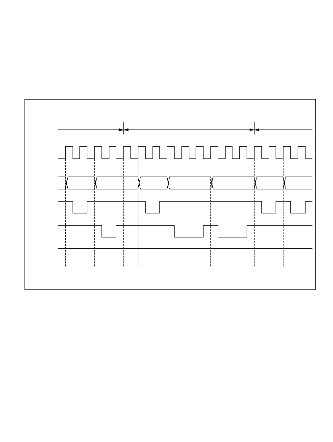
8.4.8 DMAC Bus Cycle
Figure 8-13 shows an example of the timing of the basic DMAC bus cycle. This example shows a
word-size transfer from a 16-bit two-state access area to an 8-bit three-state access area. When the
DMAC gets the bus from the CPU, after one dead cycle (T
d
), it reads from the source address and
writes to the destination address. During these read and write operations the bus is not released
even if there is another bus request. DMAC cycles comply with bus controller settings in the same
way as CPU cycles.
Figure 8-13 DMA Transfer Bus Timing (Example)
¯
RD
HWR
LWR
T
1
T
2
T
1
T
2
T
d
T
1
T
2
T
1
T
2
T
3
T
1
T
2
T
3
T
1
T
2
T
1
T
2
CPU cycle
DMAC cycle (word transfer)
CPU cycle
Source
address
Destination address
Address
bus
221
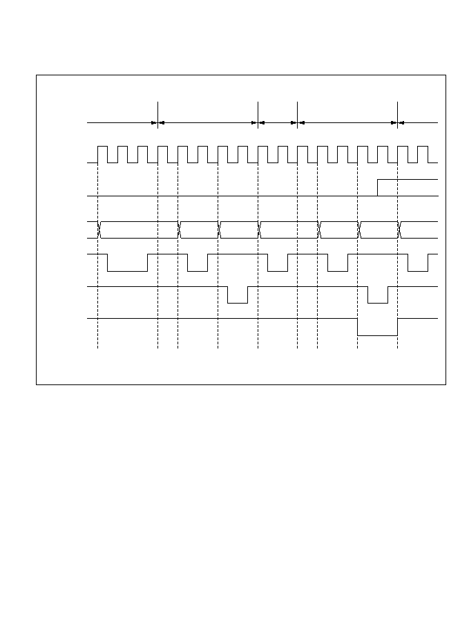
Figure 8-14 shows the timing when the DMAC is activated by low input at a
DREQ pin. This
example shows a word-size transfer from a 16-bit two-state access area to another 16-bit two-state
access area. The DMAC continues the transfer while the
DREQ pin is held low.
Figure 8-14 Bus Timing of DMA Transfer Requested by Low
DREQ Input
¯
DREQ
RD
HWR
TEND
T
1
T
2
T
3
T
d
T
1
T
2
T
1
T
2
T
1
T
2
T
d
T
1
T
2
T
1
T
2
T
1
T
2
LWR
,
CPU cycle
DMAC cycle
CPU cycle
DMAC cycle
(last transfer cycle)
CPU cycle
Source
address
Destination
address
Source
address
Destination
address
Address
bus
222

Figure 8-15 shows an auto-requested burst-mode transfer. This example shows a transfer of three
words from a 16-bit two-state access area to another 16-bit two-state access area.
Figure 8-15 Burst DMA Bus Timing
When the DMAC is activated from a
DREQ pin there is a minimum interval of four states from
when the transfer is requested until the DMAC starts operating. The
DREQ pin is not sampled
during the time between the transfer request and the start of the transfer. In short address mode
and normal mode, the pin is next sampled at the end of the read cycle. In block transfer mode, the
pin is next sampled at the end of one block transfer.
T
1
T
2
T
1
T
2
T
1
T
2
T
1
T
2
T
1
T
2
T
1
T
2
T
1
T
2
T
1
T
2
¯
RD
CPU cycle
DMAC cycle
Source
address
Destination
address
CPU cycle
T
d
Address
bus
HWR
LWR
,
223
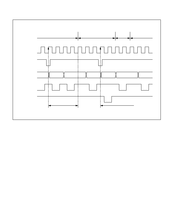
Figure 8-16 shows the timing when the DMAC is activated by the falling edge of DREQ in
normal mode.
Figure 8-16 Timing of DMAC Activation by Falling Edge of
DREQ in Normal Mode
¯
DREQ
RD
HWR
T
2
T
1
T
2
T
1
T
2
T
d
T
1
T
2
T
1
T
2
T
1
T
2
T
d
T
1
T
2
LWR
,
CPU cycle
DMAC cycle
CPU
cycle
DMAC cycle
Minimum 4 states
Next sampling point
Address
bus
224
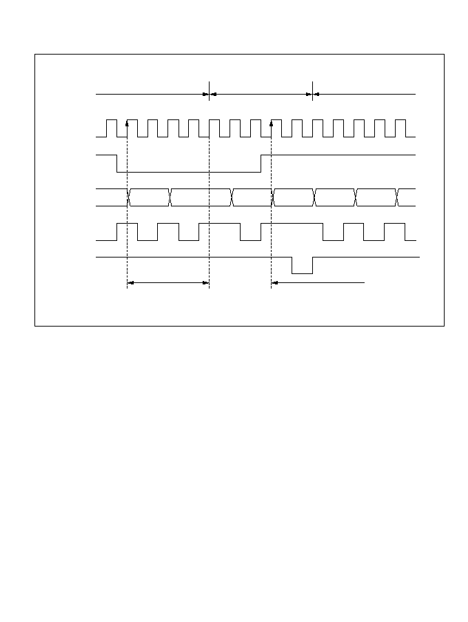
Figure 8-17 shows the timing when the DMAC is activated by level-sensitive low
DREQ input in
normal mode.
Figure 8-17 Timing of DMAC Activation by Low
DREQ Level in Normal Mode
¯
DREQ
RD
HWR LWR
,
T
2
T
1
T
2
T
1
T
2
T
d
T
1
T
2
T
1
T
2
T
1
T
2
T
1
T
2
T
1
CPU cycle
DMAC cycle
CPU cycle
Minimum 4 states
Next sampling point
Address
bus
225

Figure 8-18 shows the timing when the DMAC is activated by the falling edge of
DREQ in block
transfer mode.
Figure 8-18 Timing of DMAC Activation by Falling Edge of
DREQ in Block Transfer
Mode
¯
DREQ
RD
HWR
TEND
T
1
T
2
T
1
T
2
T
1
T
2
T
1
T
2
T
1
T
2
T
1
T
2
T
d
T
1
T
2
DMAC cycle
DMAC cycle
CPU cycle
Next sampling
Minimum 4 states
End of 1 block transfer
LWR
,
Address
bus
226

8.4.9 Multiple-Channel Operation
The DMAC channel priority order is: channel 0 > channel 1 and channel A > channel B.
Table 8-12 shows the complete priority order.
Table 8-12 Channel Priority Order
Short Address Mode
Full Address Mode
Priority
Channel 0A
Channel 0
High
Channel 0B
Channel 1A
Channel 1
Channel 1B
Low
Multiple-Channel Operation: If transfers are requested on two or more channels simultaneously,
or if a transfer on one channel is requested during a transfer on another channel, the DMAC
operates as follows.
∑
When a transfer is requested, the DMAC requests the bus right. When it gets the bus right, it
starts a transfer on the highest-priority channel at that time.
∑
Once a transfer starts on one channel, requests to other channels are held pending until that
channel releases the bus.
∑
After each transfer in short address mode, and each externally-requested or cycle-steal
transfer in normal mode, the DMAC releases the bus and returns to step 1. After releasing the
bus, if there is a transfer request for another channel, the DMAC requests the bus again.
∑
After completion of a burst-mode transfer, or after transfer of one block in block transfer
mode, the DMAC releases the bus and returns to step 1. If there is a transfer request for a
higher-priority channel or a bus request from a higher-priority bus master, however, the
DMAC releases the bus after completing the transfer of the current byte or word. After
releasing the bus, if there is a transfer request for another channel, the DMAC requests the
bus again.
227
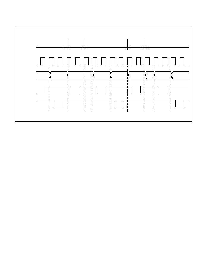
Figure 8-19 shows the timing when channel 0A is set up for I/O mode and channel 1 for burst
mode, and a transfer request for channel 0A is received while channel 1 is active.
Figure 8-19 Timing of Multiple-Channel Operations in the Same Group
¯
RD
T
1
T
2
T
1
T
2
T
d
T
1
T
2
T
1
T
2
T
1
T
2
T
d
T
1
T
2
T
1
T
2
DMAC cycle
(channel 1)
CPU
cycle
DMAC cycle
(channel 0A)
CPU
cycle
DMAC cycle
(channel 1)
Address
bus
HWR
LWR
,
228
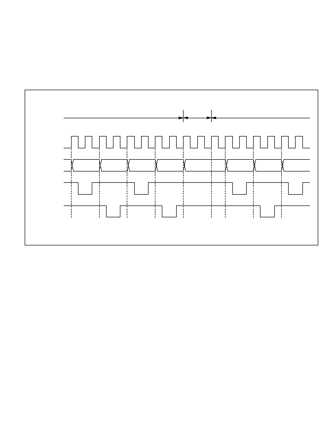
8.4.10 External Bus Requests, Refresh Controller, and DMAC
During a DMA transfer, if the bus right is requested by an external bus request signal (
BREQ) or
by the refresh controller, the DMAC releases the bus after completing the transfer of the current
byte or word. If there is a transfer request at this point, the DMAC requests the bus right again.
Figure 8-20 shows an example of the timing of insertion of a refresh cycle during a burst transfer
on channel 0.
Figure 8-20 Bus Timing of Refresh Controller and DMAC
¯
RD
HWR LWR
,
T
1
T
2
T
1
T
2
T
1
T
2
T
1
T
2
T
1
T
2
T
d
T
1
T
2
T
1
T
2
T
1
T
2
DMAC cycle (channel 0)
DMAC cycle (channel 0)
Refresh
cycle
Address
bus
229
8.4.11 NMI Interrupts and DMAC
NMI interrupts do not affect DMAC operations in short address mode.
If an NMI interrupt occurs during a transfer in full address mode, the DMAC suspends operations.
In full address mode, a channel is enabled when its DTE and DTME bits are both set to 1. NMI
input clears the DTME bit to 0. After transferring the current byte or word, the DMAC releases
the bus to the CPU. In normal mode, the suspended transfer resumes when the CPU sets the
DTME bit to 1 again. Check that the DTE bit is set to 1 and the DTME bit is cleared to 0 before
setting the DTME bit to 1.
Figure 8-21 shows the procedure for resuming a DMA transfer in normal mode on channel 0 after
the transfer was halted by NMI input.
Figure 8-21 Procedure for Resuming a DMA Transfer Halted by NMI (Example)
For information about NMI interrupts in block transfer mode, see section 8.6.6, NMI Interrupts
and Block Transfer Mode.
Resuming DMA transfer
in normal mode
DTE = 1
DTME = 0
Set DTME to 1
DMA transfer continues
End
1.
2.
Check that DTE = 1 and DTME = 0.
Read DTCRB while DTME = 0,
then write 1 in the DTME bit.
2
No
Yes
1
230

8.4.12 Aborting a DMA Transfer
When the DTE bit in an active channel is cleared to 0, the DMAC halts after transferring the
current byte or word. The DMAC starts again when the DTE bit is set to 1. In full address mode,
the DTME bit can be used for the same purpose. Figure 8-22 shows the procedure for aborting a
DMA transfer by software.
Figure 8-22 Procedure for Aborting a DMA Transfer
DMA transfer abort
Set DTCR
DMA transfer aborted
1
1. Clear the DTE bit to 0 in DTCR.
To avoid generating an interrupt when
aborting a DMA transfer, clear the DTIE
bit to 0 simultaneously.
231
8.4.13 Exiting Full Address Mode
Figure 8-23 shows the procedure for exiting full address mode and initializing the pair of
channels. To set the channels up in another mode after exiting full address mode, follow the setup
procedure for the relevant mode.
Figure 8-23 Procedure for Exiting Full Address Mode (Example)
Exiting full address mode
Halt the channel
Initialize DTCRB
Initialize DTCRA
Initialized and halted
1
2
3
1.
2.
3.
Clear the DTE bit to 0 in DTCRA, or wait
for the transfer to end and the DTE bit
to be cleared to 0.
Clear all DTCRB bits to 0.
Clear all DTCRA bits to 0.
232
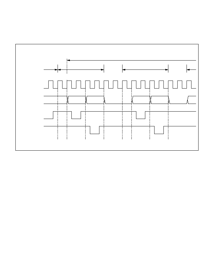
8.4.14 DMAC States in Reset State, Standby Modes, and Sleep Mode
When the chip is reset or enters hardware or software standby mode, the DMAC is initialized.
DMAC operations continue in sleep mode. Figure 8-24 shows the timing of a cycle-steal transfer
in sleep mode.
Figure 8-24 Timing of Cycle-Steal Transfer in Sleep Mode
¯
RD
HWR LWR
,
2
T
d
T
T
2
1
T
2
T
d
T
1
T
2
T
1
T
2
T
1
T
CPU cycle
DMAC cycle
DMAC cycle
Sleep mode
Address
bus
d
T
233
8.5 Interrupts
The DMAC generates only DMA-end interrupts. Table 8-13 lists the interrupts and their priority.
Table 8-13 DMAC Interrupts
Description
Interrupt
Short Address Mode
Full Address Mode
Interrupt Priority
DEND0A
End of transfer on channel 0A
End of transfer on
High
channel 0
DEND0B
End of transfer on channel 0B
--
DEND1A
End of transfer on channel 1A
End of transfer on
channel 1
DEND1B
End of transfer on channel 1B
--
Low
Each interrupt is enabled or disabled by the DTIE bit in the corresponding data transfer control
register (DTCR). Separate interrupt signals are sent to the interrupt controller.
The interrupt priority order among channels is channel 0 > channel 1 and channel A > channel B.
Figure 8-25 shows the DMA-end interrupt logic. An interrupt is requested whenever DTE = 0 and
DTIE = 1.
Figure 8-25 DMA-End Interrupt Logic
The DMA-end interrupt for the B channels (DENDB) is unavailable in full address mode. The
DTME bit does not affect interrupt operations.
DTE
DTIE
DMA-end interrupt
234

8.6 Usage Notes
8.6.1 Note on Word Data Transfer
Word data cannot be accessed starting at an odd address. When word-size transfer is selected, set
even values in the memory and I/O address registers (MAR and IOAR).
8.6.2 DMAC Self-Access
The DMAC itself cannot be accessed during a DMAC cycle. DMAC registers cannot be specified
as source or destination addresses.
8.6.3 Longword Access to Memory Address Registers
A memory address register can be accessed as longword data at the MARR address.
Example
MOV.L
#LBL, ER0
MOV.L
ER0, @MARR
Four byte accesses are performed. Note that the CPU may release the bus between the second byte
(MARE) and third byte (MARH).
Memory address registers should be written and read only when the DMAC is halted.
8.6.4 Note on Full Address Mode Setup
Full address mode is controlled by two registers: DTCRA and DTCRB. Care must be taken to
prevent the B channel from operating in short address mode during the register setup. The enable
bits (DTE and DTME) should not be set to 1 until the end of the setup procedure.
235
8.6.5 Note on Activating DMAC by Internal Interrupts
When using an internal interrupt to activate the DMAC, make sure that the interrupt selected as
the activating source does not occur during the interval after it has been selected but before the
DMAC has been enabled. The on-chip supporting module that will generate the interrupt should
not be activated until the DMAC has been enabled. If the DMAC must be enabled while the on-
chip supporting module is active, follow the procedure in figure 8-26.
Figure 8-26 Procedure for Enabling DMAC while On-Chip Supporting
Module is Operating (Example)
If the DTE bit is set to 1 but the DTME bit is cleared to 0, the DMAC is halted and the selected
activating source cannot generate a CPU interrupt. If the DMAC is halted by an NMI interrupt, for
example, the selected activating source cannot generate CPU interrupts. To terminate DMAC
operations in this state, clear the DTE bit to 0 to allow CPU interrupts to be requested. To continue
DMAC operations, carry out steps 2 and 4 in figure 8-26 before and after setting the DTME bit
to 1.
Enabling of DMAC
Selected interrupt
requested?
Interrupt hand-
ling by CPU
Clear selected interrupt's
enable bit to 0
Enable DMAC
Set selected interrupt's
enable bit to 1
1
2
3
4
1.
2.
3.
4.
While the DTE bit is cleared to 0,
interrupt requests are sent to the
CPU.
Clear the interrupt enable bit to 0
in the interrupt-generating on-chip
supporting module.
Enable the DMAC.
Enable the DMAC-activating
interrupt.
DMAC operates
Yes
No
236

When an ITU interrupt activates the DMAC, make sure the next interrupt does not occur before
the DMA transfer ends. If one ITU interrupt activates two or more channels, make sure the next
interrupt does not occur before the DMA transfers end on all the activated channels. If the next
interrupt occurs before a transfer ends, the channel or channels for which that interrupt was
selected may fail to accept further activation requests.
8.6.6 NMI Interrupts and Block Transfer Mode
If an NMI interrupt occurs in block transfer mode, the DMAC operates as follows.
∑
When the NMI interrupt occurs, the DMAC finishes transferring the current byte or word,
then clears the DTME bit to 0 and halts. The halt may occur in the middle of a block.
It is possible to find whether a transfer was halted in the middle of a block by checking the
block size counter. If the block size counter does not have its initial value, the transfer was
halted in the middle of a block.
∑
If the transfer is halted in the middle of a block, the activating interrupt flag is cleared to 0.
The activation request is not held pending.
∑
While the DTE bit is set to 1 and the DTME bit is cleared to 0, the DMAC is halted and does
not accept activating interrupt requests. If an activating interrupt occurs in this state, the
DMAC does not operate and does not hold the transfer request pending internally. Neither is a
CPU interrupt requested.
For this reason, before setting the DTME bit to 1, first clear the enable bit of the activating
interrupt to 0. Then, after setting the DTME bit to 1, set the interrupt enable bit to 1 again.
See section 8.6.5, Note on Activating DMAC by Internal Interrupts.
∑
When the DTME bit is set to 1, the DMAC waits for the next transfer request. If it was halted
in the middle of a block transfer, the rest of the block is transferred when the next transfer
request occurs. Otherwise, the next block is transferred when the next transfer request occurs.
237
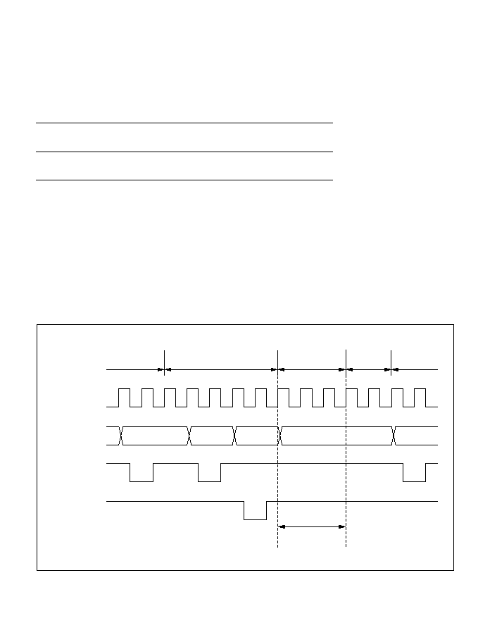
8.6.7 Memory and I/O Address Register Values
Table 8-14 indicates the address ranges that can be specified in the memory and I/O address
registers (MAR and IOAR).
Table 8-14 Address Ranges Specifiable in MAR and IOAR
1-Mbyte Mode
16-Mbyte Mode
MAR
H'00000 to H'FFFFF
H'000000 to H'FFFFFF
(0 to 1048575)
(0 to 16777215)
IOAR
H'FFF00 to H'FFFFF
H'FFFF00 to H'FFFFFF
(1048320 to 1048575)
(16776960 to 16777215)
Note: MAR bits 23 to 20 are ignored in 1-Mbyte mode.
8.6.8 Bus Cycle when Transfer is Aborted
When a transfer is aborted by clearing the DTE bit or suspended by an NMI that clears the DTME
bit, if this halts a channel for which the DMAC has a transfer request pending internally, a dead
cycle may occur. This dead cycle does not update the halted channel's address register or counter
value. Figure 8-27 shows an example in which an auto-requested transfer in cycle-steal mode on
channel 0 is aborted by clearing the DTE bit in channel 0.
Figure 8-27 Bus Timing at Abort of DMA Transfer in Cycle-Steal Mode
¯
Address bus
RD
HWR
,
LWR
CPU cycle
DMAC cycle
CPU cycle
DMAC
cycle
CPU cycle
DTE bit is
cleared
T
1
T
2
T
d
T
1
T
2
T
1
T
2
T
1
T
2
T
3
T
d
T
d
T
1
T
2
238

Section 9 I/O Ports
9.1 Overview
The H8/3002 has six input/output ports (ports 4, 6, 8, 9, A, and B) and one input port (port 7).
Table 9-1 summarizes the port functions. The pins in each port are multiplexed as shown in
table 9-1.
Each port has a data direction register (DDR) for selecting input or output, and a data register
(DR) for storing output data. In addition to these registers, port 4 has an input pull-up control
register (PCR) for switching input pull-up transistors on and off.
Ports 4, 6, and 8 can drive one TTL load and a 90-pF capacitive load. Ports 9, A, and B can drive
one TTL load and a 30-pF capacitive load. Ports 4, 6, and 8 to B can drive a darlington pair.
Port B can drive LEDs (with 10-mA current sink). Pins P8
2
to P8
0
, PA
7
to PA
0
, and PB
3
to PB
0
have Schmitt-trigger input circuits.
For block diagrams of the ports see appendix C, I/O Port Block Diagrams.
239

Table 9-1 Port Functions
Port
Description
Pins
Mode 1
Mode 2
Mode 3
Mode 4
Port 4
∑ 8-bit I/O port
P4
7
to P4
0
/D
7
to D
0
Data input/output (D
7
to D
0
) and 8-bit
∑ Input pull-up
generic input/output
8-bit bus mode: generic input/output
16-bit bus mode: data input/output
Port 6
∑ 3-bit I/O port
P6
2
/
BACK
Bus control signal input/output
P6
1
/
BREQ
(
BACK
,
BREQ
,
WAIT
) and 3-bit
P6
0
/
WAIT
generic input/output
Port 7
∑ 8-bit input port
P7
7
to P7
0
/AN
7
to AN
0
Analog input (AN
7
to AN
0
) to A/D
converter, and 8-bit generic input
Port 8
∑ 5-bit I/O port
P8
4
/CS
0
DDR = 0: generic input
∑
DDR = 1 (reset value): CS
0
output
P8
3
/CS
1
/IRQ
3
IRQ
3
to IRQ
1
input, CS
1
to CS
3
P8
2
/CS
2
/IRQ
2
output, and generic input
P8
1
/CS
3
/IRQ
1
DDR = 0 (reset value): generic input
DDR = 1: CS
1
to CS
3
output
P8
0
/
RFSH
/IRQ
0
IRQ
0
input,
RFSH
output, and
generic input/output
Port 9
∑ 6-bit I/O port
P9
5
/SCK
1
/IRQ
5
Input and output (SCK
1
, SCK
0
, RxD
1
,
P9
4
/SCK
0
/IRQ
4
RxD
0
, TxD
1
, TxD
0
) for serial
P9
3
/RxD
1
communication interfaces 0 and 1
P9
2
/RxD
0
(SCI0/1), IRQ
5
and IRQ
4
input, and
P9
1
/TxD
1
6-bit generic input/output
P9
0
/TxD
0
P8
2
to P8
0
have
Schmitt inputs
240

Table 9-1 Port Functions (cont)
Port
Description
Pins
Mode 1
Mode 2
Mode 3
Mode 4
Port A
∑ 8-bit I/O port
PA
7
/TP
7
/TIOCB
2
/A
20
Output (TP
7
) from Address output
∑ Schmitt inputs
programmable
(A
20
)
timing pattern
controller (TPC),
input or output
(TIOCB
2
) for 16-bit
integrated timer
unit (ITU), and
generic input/output
PA
6
/TP
6
/TIOCA
2
/A
21
TPC output
TPC output
PA
5
/TP
5
/TIOCB
1
/A
22
(TP
6
to TP
4
), ITU
(TP
6
to TP
4
),
PA
4
/TP
4
/TIOCA
1
/A
23
input and output
ITU input and
(TIOCA
2
, TIOCB
1
, output (TIOCA
2
,
TIOCA
1
), and
TIOCB
1
, TIOCA
1
),
generic input/
address output
output
(A
23
to A
21
), and
generic input/output
PA
3
/TP
3
/TIOCB
0
/TCLKD
TPC output (TP
3
to TP
0
), output
PA
2
/TP
2
/TIOCA
0
/TCLKC
(TEND
1
, TEND
0
) from DMA
PA
1
/TP
1
/TEND
1
/TCLKB
controller (DMAC), ITU input and output
PA
0
/TP
0
/TEND
0
/TCLKA
(TCLKD, TCLKC, TCLKB, TCLKA,
TIOCB
0
, TIOCA
0
), and generic
input/output
Port B
∑ 8-bit I/O port
PB
7
/TP
15
/DREQ
1
/
ADTRG
TPC output (TP
15
to TP
8
), DMAC input
∑ Can drive LEDs
PB
6
/TP
14
/DREQ
0
(DREQ
1
, DREQ
0
), external trigger
∑ PB
3
to PB
0
PB
5
/TP
13
/TOCXB
4
input (
ADTRG
) to A/D converter, ITU
have Schmitt
PB
4
/TP
12
/TOCXA
4
input and output (TOCXB
4
, TOCXA
4
,
inputs
PB
3
/TP
11
/TIOCB
4
TIOCB
4
, TIOCA
4
, TIOCB
3
, TIOCA
3
),
PB
2
/TP
10
/TIOCA
4
and 8-bit generic input/output
PB
1
/TP
9
/TIOCB
3
PB
0
/TP
8
/TIOCA
3
241

9.2 Port 4
9.2.1 Overview
Port 4 is an 8-bit input/output port with the pin configuration shown in figure 9-1. The pin
functions differ between the 8-bit and 16-bit bus modes.
When the bus width control register (ABWCR) designates areas 0 to 7 all as 8-bit-access areas,
the H8/3002 operates in 8-bit bus mode and port 4 is a generic input/output port. When at least
one of areas 0 to 7 is designated as a 16-bit-access area, the H8/3002 operates in 16-bit bus mode
and port 4 becomes the lower data bus.
Port 4 has software-programmable built-in pull-up transistors.
Pins in port 4 can drive one TTL load and a 90-pF capacitive load. They can also drive a
darlington transistor pair.
Figure 9-1 Port 4 Pin Configuration
Port 4
P4 /D
P4 /D
P4 /D
P4 /D
P4 /D
P4 /D
P4 /D
P4 /D
7
6
5
4
3
2
1
0
7
6
5
4
3
2
1
0
P4 (input/output)
P4 (input/output)
P4 (input/output)
P4 (input/output)
P4 (input/output)
P4 (input/output)
P4 (input/output)
P4 (input/output)
7
6
5
4
3
2
1
0
D (input/output)
D (input/output)
D (input/output)
D (input/output)
D (input/output)
D (input/output)
D (input/output)
D (input/output)
7
6
5
4
3
2
1
0
Port 4 pins
8-bit bus mode
16-bit bus mode
Notes: 1.
2.
Initial state in modes 1 and 3.
Initial state in modes 2 and 4.
*
1
*
2
242

9.2.2 Register Descriptions
Table 9-2 summarizes the registers of port 4.
Table 9-2 Port 4 Registers
Address
*
Name
Abbreviation
R/W
Initial Value
H'FFC5
Port 4 data direction register
P4DDR
W
H'00
H'FFC7
Port 4 data register
P4DR
R/W
H'00
H'FFDA
Port 4 input pull-up control register
P4PCR
R/W
H'00
Note:
*
Lower 16 bits of the address.
Port 4 Data Direction Register (P4DDR): P4DDR is an 8-bit write-only register that can select
input or output for each pin in port 4.
8-Bit Bus Mode: When all areas are designated as 8-bit-access areas, selecting 8-bit bus mode,
port 4 functions as a generic input/output port. A pin in port 4 becomes an output pin if the
corresponding P4DDR bit is set to 1, and an input pin if this bit is cleared to 0.
16-Bit Bus Mode: When at least one area is designated as a 16-bit-access area, selecting 16-bit
bus mode, port 4 functions as the lower data bus.
P4DDR is a write-only register. Its value cannot be read. All bits return 1 when read.
P4DDR is initialized to H'00 by a reset and in hardware standby mode. In software standby mode
it retains its previous setting.
ABWCR and P4DDR are not initialized in software standby mode. When port 4 functions as a
generic input/output port, if a P4DDR bit is set to 1, the corresponding pin maintains its output
state in software standby mode.
Bit
Initial value
Read/Write
7
P4 DDR
0
W
Port 4 data direction 7 to 0
These bits select input or output for port 4 pins
7
6
P4 DDR
0
W
6
5
P4 DDR
0
W
5
4
P4 DDR
0
W
4
3
P4 DDR
0
W
3
2
P4 DDR
0
W
2
1
P4 DDR
0
W
1
0
P4 DDR
0
W
0
243

Port 4 Data Register (P4DR): P4DR is an 8-bit readable/writable register that stores data for
pins P4
7
to P4
0
.
When a bit in P4DDR is set to 1, if port 4 is read the value of the corresponding P4DR bit is
returned directly, regardless of the actual state of the pin. When a bit in P4DDR is cleared to 0, if
port 4 is read the corresponding pin level is read. This applies in both 8-bit and 16-bit bus modes.
P4DR is initialized to H'00 by a reset and in hardware standby mode. In software standby mode it
retains its previous setting.
Port 4 Input Pull-Up Control Register (P4PCR): P4PCR is an 8-bit readable/writable register
that controls the MOS input pull-up transistors in port 4.
In 8-bit bus mode, when a P4DDR bit is cleared to 0 (selecting generic input), if the
corresponding P4PCR bit is set to 1, the input pull-up transistor is turned on.
P4PCR is initialized to H'00 by a reset and in hardware standby mode. In software standby mode
it retains its previous setting.
Bit
Initial value
Read/Write
7
P4
0
R/W
Port 4 data 7 to 0
These bits store data for port 4 pins
7
6
P4
0
R/W
6
5
P4
0
R/W
5
4
P4
0
R/W
4
3
P4
0
R/W
3
2
P4
0
R/W
2
1
P4
0
R/W
1
0
P4
0
R/W
0
Bit
Initial value
Read/Write
7
P4 PCR
0
R/W
Port 4 input pull-up control 7 to 0
These bits control input pull-up transistors built into port 4
7
6
P4 PCR
0
R/W
6
5
P4 PCR
0
R/W
5
4
P4 PCR
0
R/W
4
3
P4 PCR
0
R/W
3
2
P4 PCR
0
R/W
2
1
P4 PCR
0
R/W
1
0
P4 PCR
0
R/W
0
244
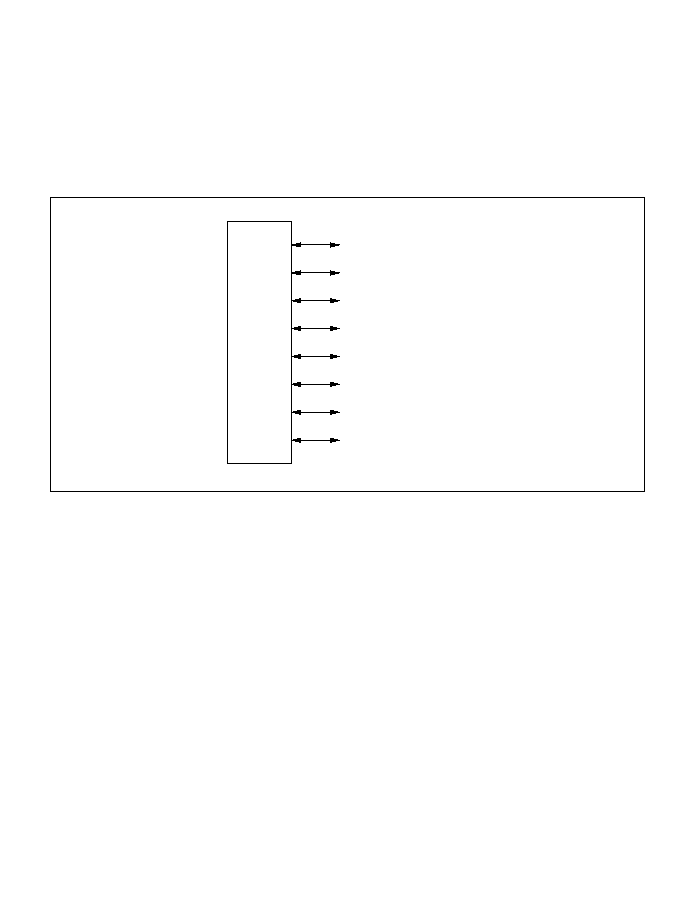
9.2.3 Pin Functions in Each Mode
The functions of port 4 differ depending on whether 8-bit or 16-bit bus mode is selected by
ABWCR settings. The pin functions in each mode are described below.
8-Bit Bus Mode: Input or output can be selected separately for each pin in port 4. A pin becomes
an output pin if the corresponding P4DDR bit is set to 1 and an input pin if this bit is cleared to 0.
Figure 9-2 shows the pin functions in 8-bit bus mode. This is the initial state in modes 1 and 3.
Figure 9-2 Pin Functions in 8-Bit Bus Mode (Port 4)
16-Bit Bus Mode: The input/output settings in P4DDR are ignored. Port 4 automatically becomes
a bidirectional data bus. Figure 9-3 shows the pin functions in 16-bit bus mode. This is the initial
state in modes 2 and 4.
Port 4
P4 (input/output)
P4 (input/output)
P4 (input/output)
P4 (input/output)
P4 (input/output)
P4 (input/output)
P4 (input/output)
P4 (input/output)
7
6
5
4
3
2
1
0
245

Figure 9-3 Pin Functions in 16-Bit Bus Mode (Port 4)
9.2.4 Input Pull-Up Transistors
Port 4 has built-in MOS input pull-up transistors that can be controlled by software. These input
pull-up transistors can be used in 8-bit bus mode. They can be turned on and off individually.
In 8-bit bus mode, when a P4PCR bit is set to 1 and the corresponding P4DDR bit is cleared to 0,
the input pull-up transistor is turned on.
The input pull-up transistors are turned off by a reset and in hardware standby mode. In software
standby mode they retain their previous state.
Table 9-3 summarizes the states of the input pull-ups in the 8-bit and 16-bit bus modes.
Table 9-3 Input Pull-Up Transistor States (Port 4)
Hardware Software
Mode
Reset
Standby Mode
Standby Mode
Other Modes
8-bit bus mode
Off
Off
On/off
On/off
16-bit bus mode
Off
Off
Legend
Off:
The input pull-up transistor is always off.
On/off: The input pull-up transistor is on if P4PCR = 1 and P4DDR = 0. Otherwise, it is off.
Port 4
D (input/output)
D (input/output)
D (input/output)
D (input/output)
D (input/output)
D (input/output)
D (input/output)
D (input/output)
7
6
5
4
3
2
1
0
246

9.3 Port 6
9.3.1 Overview
Port 6 is a 3-bit input/output port that is also used for input and output of bus control signals
(
BACK, BREQ, and WAIT). Port 6 has the same set of pin functions in all operating modes.
Figure 9-4 shows the pin configuration of port 6.
Pins in port 6 can drive one TTL load and a 90-pF capacitive load. They can also drive a
darlington transistor pair.
Figure 9-4 Port 6 Pin Configuration
9.3.2 Register Descriptions
Table 9-4 summarizes the registers of port 6.
Table 9-4 Port 6 Registers
Address
*
Name
Abbreviation
R/W
Initial Value
H'FFC9
Port 6 data direction register
P6DDR
W
H'80
H'FFCB
Port 6 data register
P6DR
R/W
H'80
Note:
*
Lower 16 bits of the address.
Port 6
P6 (input/output)/
P6 (input/output)/
P6 (input/output)/
2
1
0
BACK
BREQ
WAIT
(output)
(input)
(input)
Port 6 pins
247

Port 6 Data Direction Register (P6DDR): P6DDR is an 8-bit write-only register that can select
input or output for each pin in port 6.
A pin in port 6 becomes an output pin if the corresponding P6DDR bit is set to 1, and an input pin
if this bit is cleared to 0. Bits 7 to 3 are reserved.
P6DDR is a write-only register. Its value cannot be read. All bits return 1 when read.
P6DDR is initialized to H'80 by a reset and in hardware standby mode. In software standby mode
it retains its previous setting. If a P6DDR bit is set to 1, the corresponding pin maintains its output
state in software standby mode.
Port 6 Data Register (P6DR): P6DR is an 8-bit readable/writable register that stores data for
pins P6
2
to P6
0
.
When a bit in P6DDR is set to 1, if port 6 is read the value of the corresponding P6DR bit is
returned directly. When a bit in P6DDR is cleared to 0, if port 6 is read the corresponding pin
level is read. In this case bit 7 reads 1 and bits 6 to 3 have undetermined values. Bits 7 to 3 are
reserved. Bits 6 to 3 can be written and read, but they cannot be used for port input or output.
Bit 7 cannot be modified and always reads 1.
P6DR is initialized to H'80 by a reset and in hardware standby mode. In software standby mode it
retains its previous setting.
Bit
Initial value
Read/Write
7
--
1
--
6
P6 DDR
0
W
6
5
P6 DDR
0
W
5
4
P6 DDR
0
W
4
3
P6 DDR
0
W
3
2
P6 DDR
0
W
2
1
P6 DDR
0
W
1
0
P6 DDR
0
W
0
Reserved bits
Port 6 data direction 2 to 0
These bits select input or
output for port 6 pins
Bit
Initial value
Read/Write
7
--
1
--
6
P6
0
R/W
6
5
P6
0
R/W
5
4
P6
0
R/W
4
3
P6
0
R/W
3
2
P6
0
R/W
2
1
P6
0
R/W
1
0
P6
0
R/W
0
Reserved bits
Port 6 data 2 to 0
These bits store data
for port 6 pins
248
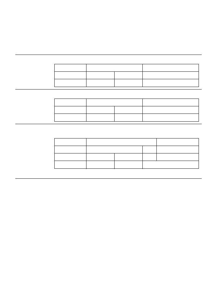
9.3.3 Pin Functions
The port 6 pins are also used for
BACK output and BREQ and WAIT input. Table 9-5 describes
the selection of pin functions.
Table 9-5 Port 6 Pin Functions
Pin
Pin Functions and Selection Method
P6
2
/
BACK
Bit BRLE in BRCR and bit P6
2
DDR select the pin function as follows
BRLE
0
1
P6
2
DDR
0
1
--
Pin function
P6
2
input
P6
2
output
BACK
output
P6
1
/
BREQ
Bit BRLE in BRCR and bit P6
1
DDR select the pin function as follows
BRLE
0
1
P6
1
DDR
0
1
--
Pin function
P6
1
input
P6
1
output
BREQ
input
P6
0
/
WAIT
Bits WCE7 to WCE0 in WCER, bit WMS1 in WCR, and bit P6
0
DDR select the
pin function as follows
WCER
All 1s
Not all 1s
WMS1
0
1
--
P6
0
DDR
0
1
0
*
0
*
Pin function
P6
0
input
P6
0
output
WAIT
input
Note:
*
Do not set bit P6
0
DDR to 1.
9.4 Port 7
9.4.1 Overview
Port 7 is an 8-bit input port that is also used for analog input to the A/D converter. Port 7 has the
same set of pin functions in all operating modes. Figure 9-5 shows the pin configuration of port 7.
249
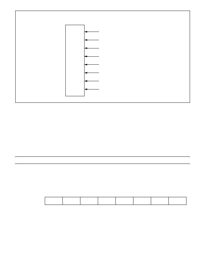
Figure 9-5 Port 7 Pin Configuration
9.4.2 Register Description
Table 9-6 summarizes the port 7 register. Port 7 is an input-only port, so it has no data direction
register.
Table 9-6 Port 7 Register
Address
*
Name
Abbreviation
R/W
Initial Value
H'FFCE
Port 7 data register
P7DR
R
Undetermined
Note:
*
Lower 16 bits of the address.
Port 7 Data Register (P7DR)
When port 7 is read, the pin levels are always read.
Port 7
P7 (input)/AN (input)
P7 (input)/AN (input)
P7 (input)/AN (input)
P7 (input)/AN (input)
P7 (input)/AN (input)
P7 (input)/AN (input)
P7 (input)/AN (input)
P7 (input)/AN (input)
7
6
5
4
3
2
1
0
7
6
5
4
3
2
1
0
Port 7 pins
Bit
Initial value
Read/Write
0
P7
--
R
*
Note: Determined by pins P7 to P7 .
*
0
1
P7
--
R
*
1
2
P7
--
R
*
2
3
P7
--
R
*
3
4
P7
--
R
*
4
5
P7
--
R
*
5
6
P7
--
R
*
6
7
P7
--
R
*
7
7
0
250
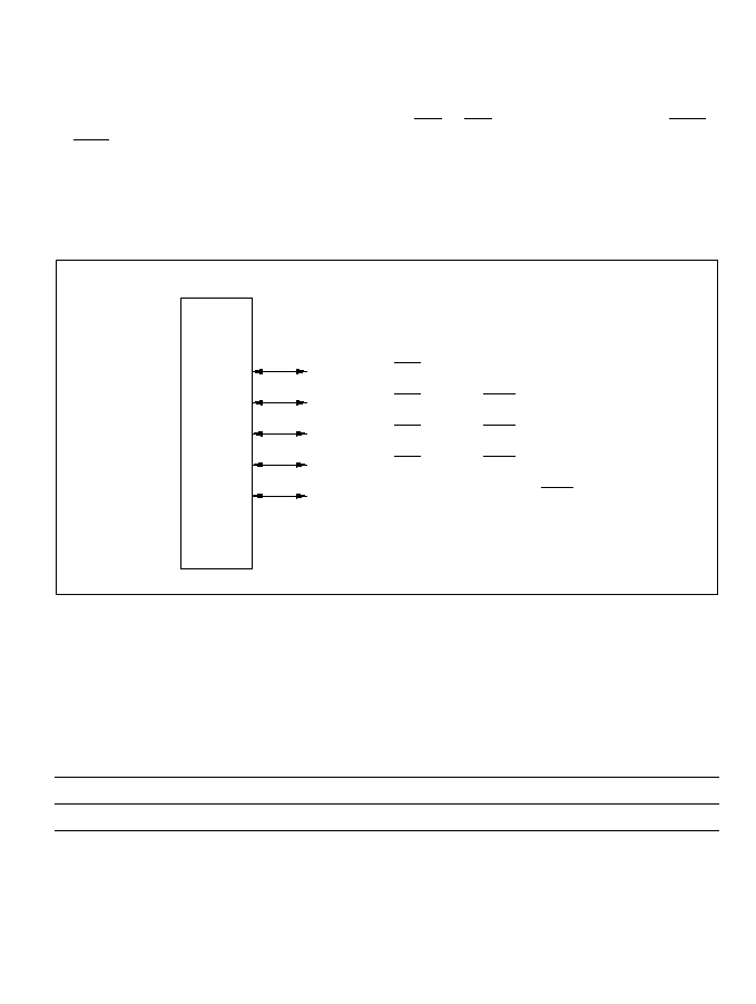
9.5 Port 8
9.5.1 Overview
Port 8 is a 5-bit input/output port that is also used for CS
3
to CS
0
output,
RFSH output, and IRQ
3
to IRQ
0
input. Port 8 has the same set of pin functions in all operating modes. Figure 9-6 shows
the pin configuration of port 8.
Pins in port 8 can drive one TTL load and a 90-pF capacitive load. They can also drive a
darlington transistor pair. Pins P8
2
to P8
0
have Schmitt-trigger inputs.
Figure 9-6 Port 8 Pin Configuration
9.5.2 Register Descriptions
Table 9-7 summarizes the registers of port 8.
Table 9-7 Port 8 Registers
Address
*
Name
Abbreviation
R/W
Initial Value
H'FFCD
Port 8 data direction register
P8DDR
W
H'F0
H'FFCF
Port 8 data register
P8DR
R/W
H'E0
Note:
*
Lower 16 bits of the address.
Port 8
P8 (input)/CS (output)
P8 (input)/CS (output)/IRQ (input)
P8 (input)/CS (output)/IRQ (input)
P8 (input)/CS (output)/IRQ (input)
P8 (input/output)/
4
3
2
1
0
0
1
2
3
Port 8 pins
RFSH
(output)/IRQ (input)
0
3
2
1
251

Port 8 Data Direction Register (P8DDR): P8DDR is an 8-bit write-only register that can select
input or output for each pin in port 8.
When bits in P8DDR bit are set to 1, P8
4
to P8
1
become CS
0
to CS
3
output pins and P8
0
becomes
a generic output pin. When bits in P8DDR are cleared to 0, the corresponding pins become input
pins.
P8DDR is a write-only register. Its value cannot be read. All bits return 1 when read.
P8DDR is initialized to H'F0 by a reset and in hardware standby mode. In software standby mode
it retains its previous setting. If a P8DDR bit is set to 1, the corresponding pin maintains its output
state in software standby mode.
Port 8 Data Register (P8DR): P8DR is an 8-bit readable/writable register that stores data for
pins P8
4
to P8
0
.
When a bit in P8DDR is set to 1, if port 8 is read the value of the corresponding P8DR bit is
returned directly. When a bit in P8DDR is cleared to 0, if port 8 is read the corresponding pin
level is read.
Bits 7 to 5 are reserved. They cannot be modified and always read 1.
P8DR is initialized to H'E0 by a reset and in hardware standby mode. In software standby mode it
retains its previous setting.
Bit
Initial value
Read/Write
7
--
1
--
6
--
1
--
5
--
1
--
4
P8 DDR
1
W
4
3
P8 DDR
0
W
3
2
P8 DDR
0
W
2
1
P8 DDR
0
W
1
0
P8 DDR
0
W
0
Reserved bits
Port 8 data direction 4 to 0
These bits select input or
output for port 8 pins
Bit
Initial value
Read/Write
7
--
1
--
6
--
1
--
5
--
1
--
4
P8
0
R/W
4
3
P8
0
R/W
3
2
P8
0
R/W
2
1
P8
0
R/W
1
0
P8
0
R/W
0
Reserved bits
Port 8 data 4 to 0
These bits store data
for port 8 pins
252

9.5.3 Pin Functions
The port 8 pins are also used for CS
3
to CS
0
and
RFSH output and IRQ
3
to IRQ
0
input.
Table 9-8 describes the selection of pin functions.
Table 9-8 Port 8 Pin Functions
Pin
Pin Functions and Selection Method
P8
4
/CS
0
Bit P8
4
DDR selects the pin function as follows
P8
4
DDR
0
1
Pin function
P8
4
input
CS
0
output
P8
3
/CS
1
/IRQ
3
Bit P8
3
DDR selects the pin function as follows
P8
3
DDR
0
1
Pin function
P8
3
input
CS
1
output
IRQ
3
input
P8
2
/CS
2
/IRQ
2
Bit P8
2
DDR selects the pin function as follows
P8
2
DDR
0
1
Pin function
P8
2
input
CS
2
output
IRQ
2
input
P8
1
/CS
3
/IRQ
1
Bit P8
1
DDR selects the pin function as follows
P8
1
DDR
0
1
Pin function
P8
1
input
CS
3
output
IRQ
1
input
P8
0
/
RFSH
/IRQ
0
Bit RFSHE in RFSHCR and bit P8
0
DDR select the pin function as follows
RFSHE
0
1
P8
0
DDR
0
1
--
Pin function
P8
0
input
P8
0
output
RFSH
output
IRQ
0
input
253
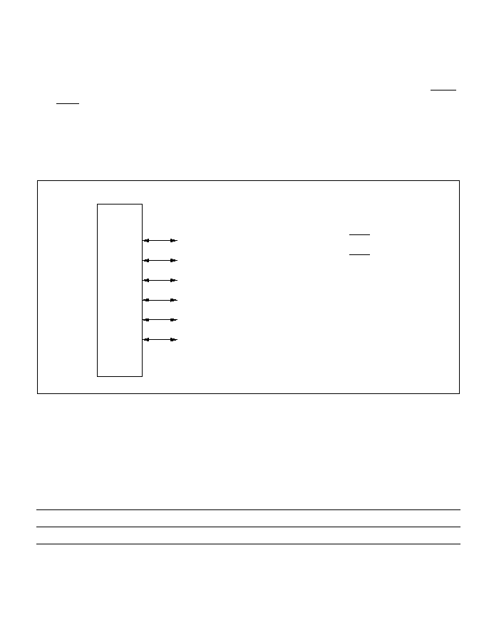
9.6 Port 9
9.6.1 Overview
Port 9 is a 6-bit input/output port that is also used for input and output (TxD
0
, TxD
1
, RxD
0
, RxD
1
,
SCK
0
, SCK
1
) by serial communication interface channels 0 and 1 (SCI0 and SCI1), and for IRQ
5
and IRQ
4
input. Port 9 has the same set of pin functions in all operating modes. Figure 9-7 shows
the pin configuration of port 9.
Pins in port 9 can drive one TTL load and a 30-pF capacitive load. They can also drive a
darlington transistor pair.
Figure 9-7 Port 9 Pin Configuration
9.6.2 Register Descriptions
Table 9-9 summarizes the registers of port 9.
Table 9-9 Port 9 Registers
Address
*
Name
Abbreviation
R/W
Initial Value
H'FFD0
Port 9 data direction register
P9DDR
W
H'C0
H'FFD2
Port 9 data register
P9DR
R/W
H'C0
Note:
*
Lower 16 bits of the address.
Port 9
P9 (input/output)/SCK
P9 (input/output)/SCK
P9 (input/output)/RxD (input)
P9 (input/output)/RxD (input)
P9 (input/output)/TxD (output)
P9 (input/output)/TxD (output)
5
4
3
2
1
0
Port 9 pins
1
0
(input/output)/IRQ (input)
(input/output)/IRQ (input)
5
4
1
0
1
0
254

Port 9 Data Direction Register (P9DDR): P9DDR is an 8-bit write-only register that can select
input or output for each pin in port 9.
A pin in port 9 becomes an output pin if the corresponding P9DDR bit is set to 1, and an input pin
if this bit is cleared to 0.
P9DDR is a write-only register. Its value cannot be read. All bits return 1 when read.
P9DDR is initialized to H'C0 by a reset and in hardware standby mode. In software standby mode
it retains its previous setting. If a P9DDR bit is set to 1, the corresponding pin maintains its output
state in software standby mode.
Port 9 Data Register (P9DR): P9DR is an 8-bit readable/writable register that stores data for
pins P9
5
to P9
0
.
When a bit in P9DDR is set to 1, if port 9 is read the value of the corresponding P9DR bit is
returned directly. When a bit in P9DDR is cleared to 0, if port 9 is read the corresponding pin
level is read.
Bits 7 and 6 are reserved. They cannot be modified and always read 1.
P9DR is initialized to H'C0 by a reset and in hardware standby mode. In software standby mode it
retains its previous setting.
Bit
Initial value
Read/Write
7
--
1
--
6
--
1
--
5
P9 DDR
0
W
4
P9 DDR
0
W
4
3
P9 DDR
0
W
3
2
P9 DDR
0
W
2
1
P9 DDR
0
W
1
0
P9 DDR
0
W
0
Reserved bits
Port 9 data direction 5 to 0
These bits select input or
output for port 9 pins
5
Bit
Initial value
Read/Write
7
--
1
--
6
--
1
--
5
P9
5
0
R/W
4
P9
0
R/W
4
3
P9
0
R/W
3
2
P8
0
R/W
2
1
P9
0
R/W
1
0
P9
0
R/W
0
Reserved bits
Port 9 data 5 to 0
These bits store data
for port 9 pins
255
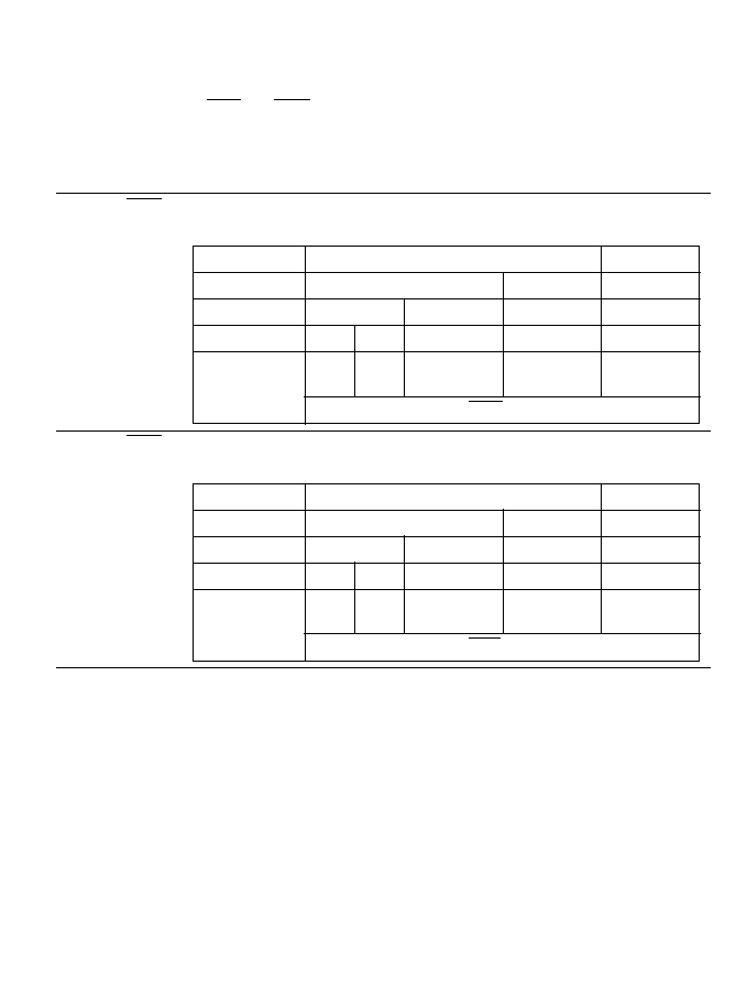
9.6.3 Pin Functions
The port 9 pins are also used for SCI0 and SCI1 input and output (TxD
0
, RxD
0
, SCK
0
, TxD
1
,
RxD
1
, SCK
1
), and for IRQ
5
and IRQ
4
input. Table 9-10 describes the selection of pin functions.
Table 9-10 Port 9 Pin Functions
Pin
Pin Functions and Selection Method
P9
5
/SCK
1
/IRQ
5
Bit C/
A
in SMR of SCI1, bits CKE0 and CKE1 in SCR of SCI1, and bit P9
5
DDR
select the pin function as follows
CKE1
0
1
C/
A
0
1
--
CKE0
0
1
--
--
P9
5
DDR
0
1
--
--
--
Pin function
P9
5
P9
5
SCK
1
output
SCK
1
output
SCK
1
input
input output
IRQ
5
input
P9
4
/SCK
0
/IRQ
4
Bit C/
A
in SMR of SCI0, bits CKE0 and CKE1 in SCR of SCI0, and bit P9
4
DDR
select the pin function as follows
CKE1
0
1
C/
A
0
1
--
CKE0
0
1
--
--
P9
4
DDR
0
1
--
--
--
Pin function
P9
4
P9
4
SCK
0
output
SCK
0
output
SCK
0
input
input output
IRQ
4
input
256

Table 9-10 Port 9 Pin Functions (cont)
Pin
Pin Functions and Selection Method
P9
3
/RxD
1
Bit RE in SCR of SCI1 and bit P9
3
DDR select the pin function as follows
RE
0
1
P9
3
DDR
0
1
--
Pin function
P9
3
input
P9
3
output
RxD
1
input
P9
2
/RxD
0
Bit RE in SCR of SCI0 and bit P9
2
DDR select the pin function as follows
RE
0
1
P9
2
DDR
0
1
--
Pin function
P9
2
input
P9
2
output
RxD
0
input
P9
1
/TxD
1
Bit TE in SCR of SCI1 and bit P9
1
DDR select the pin function as follows
TE
0
1
P9
1
DDR
0
1
--
Pin function
P9
1
input
P9
1
output
TxD
1
output
P9
0
/TxD
0
Bit TE in SCR of SCI0 and bit P9
0
DDR select the pin function as follows
TE
0
1
P9
0
DDR
0
1
--
Pin function
P9
0
input
P9
0
output
TxD
0
output
257
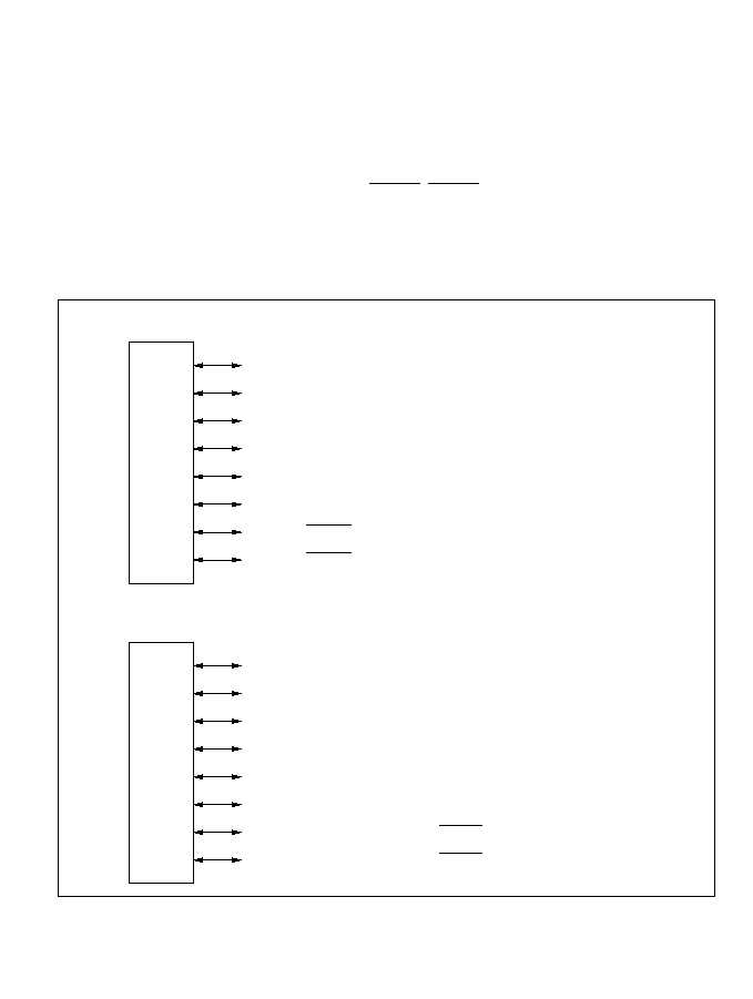
9.7 Port A
9.7.1 Overview
Port A is an 8-bit input/output port that is also used for address output (A
23
to A
20
), output
(TP
7
to TP
0
) from the programmable timing pattern controller (TPC), input and output (TIOCB
2
,
TIOCA
2
, TIOCB
1
, TIOCA
1
, TIOCB
0
, TIOCA
0
, TCLKD, TCLKC, TCLKB, TCLKA) by the
16-bit integrated timer unit (ITU), and output (TEND
1
, TEND
0
) from the DMA controller
(DMAC). Figure 9-8 shows the pin configuration of port A.
Pins in port A can drive one TTL load and a 30-pF capacitive load. They can also drive a
darlington transistor pair. Port A has Schmitt-trigger inputs.
Figure 9-8 Port A Pin Configuration (1)
Port A
PA /TP /TIOCB /A
PA /TP /TIOCA /A
PA /TP /TIOCB /A
PA /TP /TIOCA /A
PA /TP /TIOCB /TCLKD
PA /TP /TIOCA /TCLKC
PA /TP /TEND /TCLKB
PA /TP /TEND /TCLKA
7
6
5
4
3
2
1
0
Port A pins
7
6
5
4
3
2
1
0
1
0
Port A
PA (input/output)/TP (output)/TIOCB (input/output)
PA (input/output)/TP (output)/TIOCA (input/output)
PA (input/output)/TP (output)/TIOCB (input/output)
7
6
5
4
3
2
1
0
Modes 1 and 2
PA (input/output)/TP (output)/TIOCA (input/output)
PA (input/output)/TP (output)/TIOCB (input/output)/TCLKD (input)
PA (input/output)/TP (output)/TIOCA (input/output)/TCLKC (input)
PA (input/output)/TP (output)/TEND (output)/TCLKB (input)
PA (input/output)/TP (output)/TEND (output)/TCLKA (input)
7
6
5
4
3
2
1
0
2
2
1
1
0
0
1
0
2
2
1
1
0
0
20
21
22
23
258
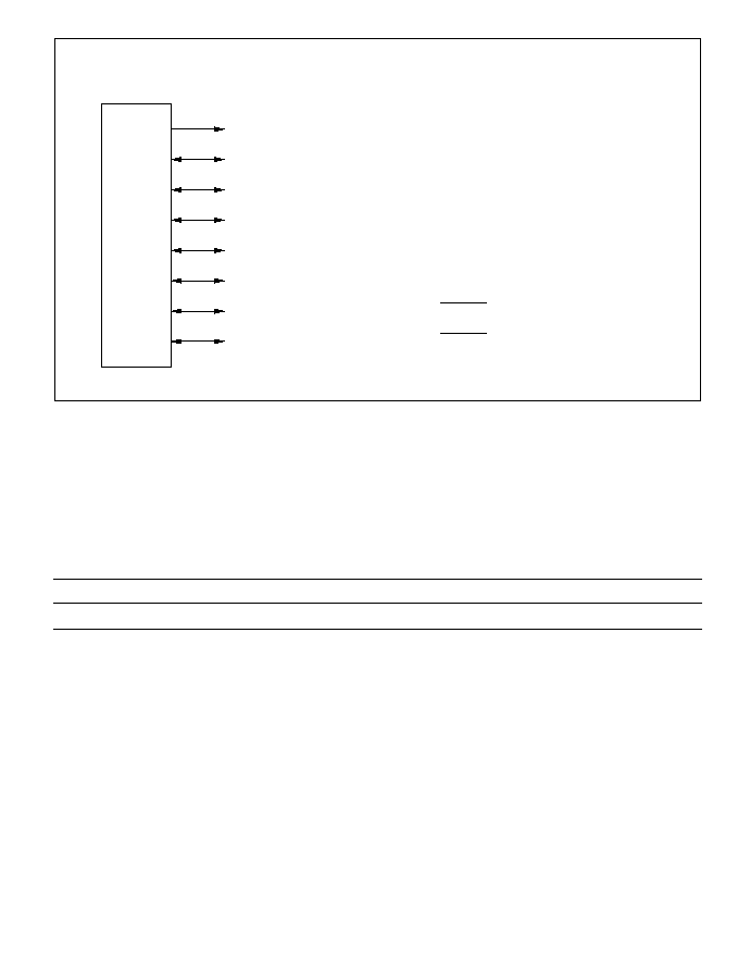
Figure 9-8 Port A Pin Configuration (2)
9.7.2 Register Descriptions
Table 9-11 summarizes the registers of port A.
Table 9-11 Port A Registers
Address
*
Name
Abbreviation
R/W
Initial Value
H'FFD1
Port A data direction register
PADDR
W
H'00
H'FFD3
Port A data register
PADR
R/W
H'00
Note:
*
Lower 16 bits of the address.
Port A
A (output)
PA (input/output)/TP (output)/TIOCA (input/output)/A (output)
PA (input/output)/TP (output)/TIOCB (input/output)/A (output)
6
5
4
3
2
1
0
Modes 3 and 4
PA (input/output)/TP (output)/TIOCA (input/output)/A (output)
PA (input/output)/TP (output)/TIOCB (input/output)/TCLKD (input)
PA (input/output)/TP (output)/TIOCA (input/output)/TCLKC (input)
PA (input/output)/TP (output)/TEND (output)/TCLKB (input)
PA (input/output)/TP (output)/TEND (output)/TCLKA (input)
6
5
4
3
2
1
0
2
1
1
0
0
1
0
20
21
22
23
259

Port A Data Direction Register (PADDR): PADDR is an 8-bit write-only register that can select
input or output for each pin in port A.
A pin in port A becomes an output pin if the corresponding PADDR bit is set to 1, and an input
pin if this bit is cleared to 0. In modes 3and 4, PA
7
functions as an address output pin regardless of
the PA7DDR setting.
PADDR is a write-only register. Its value cannot be read. All bits return 1 when read.
PADDR is initialized to H'00 by a reset and in hardware standby mode. In software standby mode
it retains its previous setting. If a PADDR bit is set to 1, the corresponding pin maintains its output
state in software standby mode.
Port A Data Register (PADR): PADR is an 8-bit readable/writable register that stores data for
pins PA
7
to PA
0
.
When a bit in PADDR is set to 1, if port A is read the value of the corresponding PADR bit is
returned directly. When a bit in PADDR is cleared to 0, if port A is read the corresponding pin
level is read.
PADR is initialized to H'00 by a reset and in hardware standby mode. In software standby mode it
retains its previous setting.
Bit
Initial value
Read/Write
0
PA
0
R/W
0
1
PA
0
R/W
1
2
PA
0
R/W
2
3
PA
0
R/W
3
4
PA
0
R/W
4
5
PA
0
R/W
5
6
PA
0
R/W
6
7
PA
0
R/W
7
Port A data direction 7 to 0
These bits select input or output for port A pins
Bit
Initial value
Read/Write
0
PA
0
R/W
0
1
PA
0
R/W
1
2
PA
0
R/W
2
3
PA
0
R/W
3
4
PA
0
R/W
4
5
PA
0
R/W
5
6
PA
0
R/W
6
7
PA
0
R/W
7
Port A data 7 to 0
These bits store data for port A pins
260

9.7.3 Pin Functions
The port A pins are also used for TPC output (TP
7
to TP
0
), ITU input/output
(TIOCB
2
to TIOCB
0
, TIOCA
2
to TIOCA
0
), ITU input (TCLKD, TCLKC, TCLKB, TCLKA),
DMAC output (TEND
1
, TEND
0
), and address output (A
23
to A
20
). Table 9-12 describes the
selection of pin functions.
Table 9-12 Port A Pin Functions (cont)
Pin
Pin Functions and Selection Method
PA
7
/TP
7
/
The mode setting, ITU channel 2 settings (bit PWM2 in TMDR and bits
TIOCB
2
/A
20
IOB2 to IOB0 in TIOR2), bit NDER7 in NDERA, and bit PA
7
DDR in PADDR
select the pin function as follows
Mode
1, 2
3, 4
ITU channel 2
(1) in table
settings
below
(2) in table below
--
PA
7
DDR
--
0
1
1
--
NDER7
--
--
0
1
--
Pin function
TIOCB
2
PA
7
PA
7
TP
7
A
20
output
input
output
output
output
TIOCB
2
input
*
Note:
*
TIOCB
2
input when IOB2 = 1 and PWM2 = 0.
ITU channel 2
settings
(2)
(1)
(2)
IOB2
0
1
IOB1
0
0
1
--
IOB0
0
1
--
--
261

Table 9-12 Port A Pin Functions (cont)
Pin
Pin Functions and Selection Method
PA
6
/TP
6
/
The mode setting, bit A21E in BRCR, ITU channel 2 settings (bit PWM2 in
TIOCA
2
/A
21
TMDR and bits IOA2 to IOA0 in TIOR2), bit NDER6 in NDERA, and bit
PA
6
DDR in PADDR select the pin function as follows
Mode
1, 2
ITU channel 2
(1) in table
settings
below
(2) in table below
PA
6
DDR
--
0
1
1
NDER6
--
--
0
1
Pin function TIOCA
2
output
PA
6
PA
6
TP
6
input
output
output
TIOCA
2
input
*
Mode
3, 4
A21E
0
1
ITU channel 2
--
(1) in table
settings
below
(2) in table below
PA
6
DDR
--
--
0
1
1
NDER6
--
--
--
0
1
Pin function
A
21
TIOCA
2
PA
6
PA
6
TP
6
output
output
input
output
output
TIOCA
2
input
*
Note:
*
TIOCA
2
input when IOA2 = 1.
ITU channel 2
settings
(2)
(1)
(2)
(1)
PWM2
0
1
IOA2
0
1
--
IOA1
0
0
1
--
--
IOA0
0
1
--
--
--
262
Table 9-12 Port A Pin Functions (cont)
Pin
Pin Functions and Selection Method
PA
5
/TP
5
The mode setting, bit A22E in BRCR, ITU channel 1 settings (bit PWM1 in
TIOCB
1
/A
22
TMDR and bits IOB2 to IOB0 in TIOR1), bit NDER5 in NDERA, and bit
PA
5
DDR in PADDR select the pin function as follows
Mode
1, 2
ITU channel 1
(1) in table
settings
below
(2) in table below
PA
5
DDR
--
0
1
1
NDER5
--
--
0
1
Pin function TIOCB
1
output
PA
5
PA
5
TP
5
input
output
output
TIOCB
1
input
*
Mode
3, 4
A22E
0
1
ITU channel 1
--
(1) in table
settings
below
(2) in table below
PA
5
DDR
--
--
0
1
1
NDER5
--
--
--
0
1
Pin function
A
22
TIOCB
1
PA
5
PA
5
TP
5
output
output
input
output
output
TIOCB
1
input
*
Note:
*
TIOCB
1
input when IOB2 = 1 and PWM1 = 0.
ITU channel 1
settings
(2)
(1)
(2)
IOB2
0
1
IOB1
0
0
1
--
IOB0
0
1
--
--
263

Table 9-12 Port A Pin Functions (cont)
Pin
Pin Functions and Selection Method
PA
4
/TP
4
/
The mode setting, bit A23E in BRCR, ITU channel 1 settings (bit PWM1 in
TIOCA
1
/A
23
TMDR and bits IOA2 to IOA0 in TIOR1), bit NDER4 in NDERA, and bit
PA
4
DDR in PADDR select the pin function as follows
Mode
1, 2
ITU channel 1
(1) in table
settings
below
(2) in table below
PA
4
DDR
--
0
1
1
NDER4
--
--
0
1
Pin function TIOCA
1
output
PA
4
PA
4
TP
4
input
output
output
TIOCA
1
input
*
Mode
3, 4
A23E
0
1
ITU channel 1
--
(1) in table
settings
below
(2) in table below
PA
4
DDR
--
--
0
1
1
NDER4
--
--
--
0
1
Pin function
A
23
TIOCA
1
PA
4
PA
4
TP
4
output
output
input
output
output
TIOCA
1
input
*
Note:
*
TIOCA
1
input when IOA2 = 1.
ITU channel 1
settings
(2)
(1)
(2)
(1)
PWM1
0
1
IOA2
0
1
--
IOA1
0
0
1
--
--
IOA0
0
1
--
--
--
264
Table 9-12 Port A Pin Functions (cont)
Pin
Pin Functions and Selection Method
PA
3
/TP
3
/
ITU channel 0 settings (bit PWM0 in TMDR and bits IOB2 to IOB0 in TIOR0),
TIOCB
0
/TCLKD
bits TPSC2 to TPSC0 in timer control registers 4 to 0 (TCR4 to TCR0), bit
NDER3 in NDERA, and bit PA
3
DDR in PADDR select the pin function as
follows
ITU channel 0
(1)in table
settings
below
(2) in table below
PA
3
DDR
--
0
1
1
NDER3
--
--
0
1
Pin function TIOCB
0
output PA
3
PA
3
TP
3
input
output
output
TIOCB
0
input
*
1
TCLKD input
*
2
Notes: 1. TIOCB
0
input when IOB2 = 1 and PWM0 = 0.
2. TCLKD input when TPSC2 = TPSC1 = TPSC0 = 1 in any of TCR4
to TCR0.
ITU channel 0
settings
(2)
(1)
(2)
IOB2
0
1
IOB1
0
0
1
--
IOB0
0
1
--
--
265

Table 9-12 Port A Pin Functions (cont)
Pin
Pin Functions and Selection Method
PA
2
/TP
2
/
ITU channel 0 settings (bit PWM0 in TMDR and bits IOA2 to IOA0 in TIOR0),
TIOCA
0
/TCLKC
bits TPSC2 to TPSC0 in TCR4 to TCR0, bit NDER2 in NDERA, and bit
PA
2
DDR in PADDR select the pin function as follows
ITU channel 0
(1) in table
settings
below
(2) in table below
PA
2
DDR
--
0
1
1
NDER2
--
--
0
1
Pin function TIOCA
0
output
PA
2
PA
2
TP
2
input
output
output
TIOCA
0
input
*
1
, TCLKC input
*
2
Notes: 1. TIOCA
0
input when IOA2 = 1.
2. TCLKC input when TPSC2 = TPSC1 = 1 and TPSC0 = 0 in any of
TCR4 to TCR0.
ITU channel 0
settings
(2)
(1)
(2)
(1)
PWM0
0
1
IOA2
0
1
--
IOA1
0
0
1
--
--
IOA0
0
1
--
--
--
266

Table 9-12 Port A Pin Functions (cont)
Pin
Pin Functions and Selection Method
PA
1
/TP
1
DMAC channel 1 settings (bits DTS2/1/0A and DTS2/1/0B in DTCR1A and
TCLKB/TEND
1
DTCR1B), bit NDER1 in NDERA, and bit PA
1
DDR in PADDR select the pin
function as follows
DMAC channel 1
(1) in table
settings
below
(2)in table below
PA
1
DDR
--
0
1
1
NDER1
--
--
0
1
Pin function TEND
1
output
PA
1
PA
1
TP
1
input
output
output
TCLKB input
*
Note:
*
TCLKB input when MDF = 1 in TMDR, or when TPSC2 = 1,
TPSC1 = 0, and TPSC0 = 1 in any of TCR4 to TCR0.
DMAC channel 1
settings
(2)
(1)
(2)
(1)
(2)
(1)
DTS2A, DTS1A
Not both 1
Both 1
DTS0A
--
0
0
1
1
1
DTS2B
0
1
1
0
1
0
1
1
DTS1B
--
0
1
--
--
--
0
1
267
Table 9-12 Port A Pin Functions (cont)
Pin
Pin Functions and Selection Method
PA
0
/TP
0
DMAC channel 0 settings (bits DTS2/1/0A and DTS2/1/0B in DTCR0A and
TCLKA/TEND
0
DTCR0B), bit NDER0 in NDERA, and bit PA
0
DDR in PADDR select the pin
function as follows
DMAC channel 0
(1) in table
settings
below
(2)in table below
PA
0
DDR
--
0
1
1
NDER0
--
--
0
1
Pin function TEND
0
output
PA
0
PA
0
TP
0
input
output
output
TCLKA input
*
Note:
*
TCLKA input when MDF = 1 in TMDR, or when TPSC2 = 1,
TPSC1 = 0, and TPSC0 = 0 in any of TCR4 to TCR0.
DMAC channel 0
settings
(2)
(1)
(2)
(1)
(2)
(1)
DTS2A, DTS1A
Not both 1
Both 1
DTS0A
--
0
0
1
1
1
DTS2B
0
1
1
0
1
0
1
1
DTS1B
--
0
1
--
--
--
0
1
268

9.8 Port B
9.8.1 Overview
Port B is an 8-bit input/output port that is also used for TPC output (TP
15
to TP
8
), ITU
input/output (TIOCB
4
, TIOCB
3
, TIOCA
4
, TIOCA
3
), ITU output (TOCXB
4
, TOCXA
4
), DMAC
input (DREQ
1
, DREQ
0
), and
ADTRG input to the A/D converter. Port B has the same set of pin
functions in all operating modes. Figure 9-9 shows the pin configuration of port B.
Pins in port B can drive one TTL load and a 30-pF capacitive load. They can also drive a LED or
a darlington transistor pair. Pins PB
3
to PB
0
have Schmitt-trigger inputs.
Figure 9-9 Port B Pin Configuration
9.8.2 Register Descriptions
Table 9-13 summarizes the registers of port B.
Table 9-13 Port B Registers
Address
*
Name
Abbreviation
R/W
Initial Value
H'FFD4
Port B data direction register
PBDDR
W
H'00
H'FFD6
Port B data register
PBDR
R/W
H'00
Note:
*
Lower 16 bits of the address.
Port B
PB (input/output)/TP (output)/DREQ (input)/ (input)
PB (input/output)/TP (output)/DREQ (input)
PB (input/output)/TP (output)/TOCXB (output)
PB (input/output)/TP (output)/TOCXA (output)
7
6
5
4
3
2
1
0
Port B pins
15
14
13
12
11
10
9
8
1
0
4
4
PB (input/output)/TP (output)/TIOCB (input/output)
PB (input/output)/TP (output)/TIOCA (input/output)
PB (input/output)/TP (output)/TIOCB (input/output)
PB (input/output)/TP (output)/TIOCA (input/output)
4
4
3
3
ADTRG
269

Port B Data Direction Register (PBDDR): PBDDR is an 8-bit write-only register that can select
input or output for each pin in port B.
A pin in port B becomes an output pin if the corresponding PBDDR bit is set to 1, and an input
pin if this bit is cleared to 0.
PBDDR is a write-only register. Its value cannot be read. All bits return 1 when read.
PBDDR is initialized to H'00 by a reset and in hardware standby mode. In software standby mode
it retains its previous setting. If a PBDDR bit is set to 1, the corresponding pin maintains its output
state in software standby mode.
Port B Data Register (PBDR): PBDR is an 8-bit readable/writable register that stores data for
pins PB
7
to PB
0
.
When a bit in PBDDR is set to 1, if port B is read the value of the corresponding PBDR bit is
returned directly. When a bit in PBDDR is cleared to 0, if port B is read the corresponding pin
level is read.
PBDR is initialized to H'00 by a reset and in hardware standby mode. In software standby mode it
retains its previous setting.
Bit
Initial value
Read/Write
7
PB DDR
0
W
Port B data direction 7 to 0
These bits select input or output for port B pins
7
6
PB DDR
0
W
6
5
PB DDR
0
W
5
4
PB DDR
0
W
4
3
PB DDR
0
W
3
2
PB DDR
0
W
2
1
PB DDR
0
W
1
0
PB DDR
0
W
0
Bit
Initial value
Read/Write
0
PB
0
R/W
0
1
PB
0
R/W
1
2
PB
0
R/W
2
3
PB
0
R/W
3
4
PB
0
R/W
4
5
PB
0
R/W
5
6
PB
0
R/W
6
7
PB
0
R/W
7
Port B data 7 to 0
These bits store data for port B pins
270
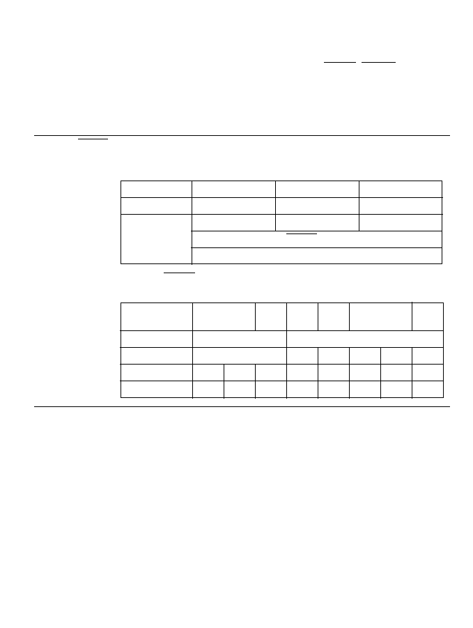
9.8.3 Pin Functions
The port B pins are also used for TPC output (TP
15
to TP
8
), ITU input/output (TIOCB
4
, TIOCB
3
,
TIOCA
4
, TIOCA
3
) and output (TOCXB
4
, TOCXA
4
), DMAC input (DREQ
1
, DREQ
0
), and
ADTRG input. Table 9-14 describes the selection of pin functions.
Table 9-14 Port B Pin Functions
Pin
Pin Functions and Selection Method
PB
7
/TP
15
/DREQ
1
/ DMAC channel 1 settings (bits DTS2/1/0A and DTS2/1/0B in DTCR1A and
ADTRG
DTCR1B), bit TRGE in ADCR, bit NDER15 in NDERB, and bit PB
7
DDR in
PBDDR select the pin function as follows
PB
7
DDR
0
1
1
NDER15
--
0
1
Pin function
PB
7
input
PB
7
output
TP
15
output
DREQ
1
input
*
1
ADTRG
input
*
2
Notes: 1. DREQ
1
input under DMAC channel 1 settings (1) in the table below.
2.
ADTRG
input when TRGE = 1.
DMAC channel
1 settings
(2)
(1)
(2)
(1)
(2)
(1)
DTS2A, DTS1A
Not both 1
Both 1
DTS0A
--
0
0
1
1
1
DTS2B
0
1
1
0
1
0
1
1
DTS1B
--
0
1
--
--
--
0
1
271
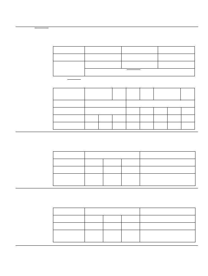
Table 9-14 Port B Pin Functions (cont)
Pin
Pin Functions and Selection Method
PB
6
/TP
14
/DREQ
0
DMAC channel 0 settings (bits DTS2/1/0A and DTS2/1/0B in DTCR0A and
DTCR0B), bit NDER14 in NDERB, and bit PB
6
DDR in PBDDR select the pin
function as follows
PB
6
DDR
0
1
1
NDER14
--
0
1
Pin function
PB
6
input
PB
6
output
TP
14
output
DREQ
0
input
*
Note:
*
DREQ
0
input under DMAC channel 0 settings (1) in the table below.
DMAC channel
0 settings
(2)
(1)
(2)
(1)
(2)
(1)
DTS2A, DTS1A
Not both 1
Both 1
DTS0A
--
0
0
1
1
1
DTS2B
0
1
1
0
1
0
1
1
DTS1B
--
0
1
--
--
--
0
1
PB
5
/TP
13
/TOCXB
4
ITU channel 4 settings (bit CMD1 in TFCR and bit EXB4 in TOER), bit
NDER13 in NDERB, and bit PB
5
DDR in PBDDR select the pin function as
follows
EXB4, CMD1
Not both 1
Both 1
PB
5
DDR
0
1
1
--
NDER13
--
0
1
--
Pin function
PB
5
PB
5
TP
13
TOCXB
4
output
input
output
output
PB
4
/TP
12
/TOCXA
4
ITU channel 4 settings (bit CMD1 in TFCR and bit EXA4 in TOER), bit
NDER12 in NDERB, and bit PB
4
DDR in PBDDR select the pin function as
follows
EXA4, CMD1
Not both 1
Both 1
PB
4
DDR
0
1
1
--
NDER12
--
0
1
--
Pin function
PB
4
PB
4
TP
12
TOCXA
4
output
input
output
output
272

Table 9-14 Port B Pin Functions (cont)
Pin
Pin Functions and Selection Method
PB
3
/TP
11
/TIOCB
4
ITU channel 4 settings (bit PWM4 in TMDR, bit CMD1 in TFCR, bit EB4 in
TOER, and bits IOB2 to IOB0 in TIOR4), bit NDER11 in NDERB, and bit
PB
3
DDR in PBDDR select the pin function as follows
ITU channel 4
settings
(1) in table below
(2) in table below
PB
3
DDR
--
0
1
1
NDER11
--
--
0
1
Pin function
TIOCB
4
output
PB
3
PB
3
TP
11
input
output
output
TIOCB
4
input
*
Note:
*
TIOCB
4
input when CMD1 = PWM4 = 0 and IOB2 = 1.
ITU channel 4
settings
(2)
(2)
(1)
(2)
(1)
EB4
0
1
CMD1
--
0
1
IOB2
--
0
0
0
1
--
IOB1
--
0
0
1
--
--
IOB0
--
0
1
--
--
--
273
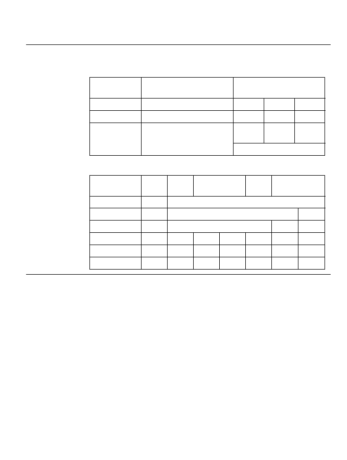
Table 9-14 Port B Pin Functions (cont)
Pin
Pin Functions and Selection Method
PB
2
/TP
10
/TIOCA
4
ITU channel 4 settings (bit CMD1 in TFCR, bit EA4 in TOER, bit PWM4 in
TMDR, and bits IOA2 to IOA0 in TIOR4), bit NDER10 in NDERB, and bit
PB
2
DDR in PBDDR select the pin function as follows
ITU channel 4
settings
(1) in table below
(2) in table below
PB
2
DDR
--
0
1
1
NDER10
--
--
0
1
Pin function
TIOCA
4
output
PB
2
PB
2
TP
10
input
output
output
TIOCA
4
input
*
Note:
*
TIOCA
4
input when CMD1 = PWM4 = 0 and IOA2 = 1.
ITU channel 4
settings
(2)
(2)
(1)
(2)
(1)
EA4
0
1
CMD1
--
0
1
PWM4
--
0
1
--
IOA2
--
0
0
0
1
--
--
IOA1
--
0
0
1
--
--
--
IOA0
--
0
1
--
--
--
--
274
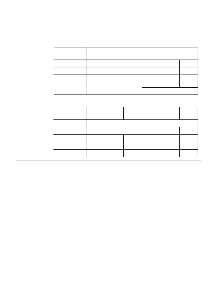
Table 9-14 Port B Pin Functions (cont)
Pin
Pin Functions and Selection Method
PB
1
/TP
9
/TIOCB
3
ITU channel 3 settings (bit PWM3 in TMDR, bit CMD1 in TFCR, bit EB3 in
TOER, and bits IOB2 to IOB0 in TIOR3), bit NDER9 in NDERB, and bit
PB
1
DDR in PBDDR select the pin function as follows
ITU channel 3
settings
(1) in table below
(2) in table below
PB
1
DDR
--
0
1
1
NDER9
--
--
0
1
Pin function
TIOCB
3
output
PB
1
PB
1
TP
9
input
output
output
TIOCB
3
input
*
Note:
*
TIOCB
3
input when CMD1 = PWM3 = 0 and IOB2 = 1.
ITU channel 3
settings
(2)
(2)
(1)
(2)
(1)
EB3
0
1
CMD1
--
0
1
IOB2
--
0
0
0
1
--
IOB1
--
0
0
1
--
--
IOB0
--
0
1
--
--
--
275

Table 9-14 Port B Pin Functions (cont)
Pin
Pin Functions and Selection Method
PB
0
/TP
8
/TIOCA
3
ITU channel 3 settings (bit CMD1 in TFCR, bit EA3 in TOER, bit PWM3 in
TMDR, and bits IOA2 to IOA0 in TIOR3), bit NDER8 in NDERB, and bit
PB
0
DDR in PBDDR select the pin function as follows
ITU channel 3
settings
(1) in table below
(2) in table below
PB
0
DDR
--
0
1
1
NDER8
--
--
0
1
Pin function
TIOCA
3
output
PB
0
PB
0
TP
8
input
output
output
TIOCA
3
input
*
Note:
*
TIOCA
3
input when CMD1 = PWM3 = 0 and IOA2 = 1.
ITU channel 3
settings
(2)
(2)
(1)
(2)
(1)
EA3
0
1
CMD1
--
0
1
PWM3
--
0
1
--
IOA2
--
0
0
0
1
--
--
IOA1
--
0
0
1
--
--
--
IOA0
--
0
1
--
--
--
--
276

Section 10 16-Bit Integrated Timer Unit (ITU)
10.1 Overview
The H8/3002 has a built-in 16-bit integrated timer unit (ITU) with five 16-bit timer channels.
10.1.1 Features
ITU features are listed below.
∑
Capability to process up to 12 pulse outputs or 10 pulse inputs
∑
Ten general registers (GRs, two per channel) with independently-assignable output compare
or input capture functions
∑
Selection of eight counter clock sources for each channel:
Internal clocks: ¯, ¯/2, ¯/4, ¯/8
External clocks: TCLKA, TCLKB, TCLKC, TCLKD
∑
Five operating modes selectable in all channels:
-- Waveform output by compare match
Selection of 0 output, 1 output, or toggle output (only 0 or 1 output in channel 2)
-- Input capture function
Rising edge, falling edge, or both edges (selectable)
-- Counter clearing function
Counters can be cleared by compare match or input capture
-- Synchronization
Two or more timer counters (TCNTs) can be preset simultaneously, or cleared
simultaneously by compare match or input capture. Counter synchronization enables
synchronous register input and output.
277

-- PWM mode
PWM output can be provided with an arbitrary duty cycle. With synchronization, up to
five-phase PWM output is possible
∑
Phase counting mode selectable in channel 2
Two-phase encoder output can be counted automatically.
∑
Three additional modes selectable in channels 3 and 4
-- Reset-synchronized PWM mode
If channels 3 and 4 are combined, three-phase PWM output is possible with three pairs of
complementary waveforms.
-- Complementary PWM mode
If channels 3 and 4 are combined, three-phase PWM output is possible with three pairs of
non-overlapping complementary waveforms.
-- Buffering
Input capture registers can be double-buffered. Output compare registers can be updated
automatically.
∑
High-speed access via internal 16-bit bus
The 16-bit timer counters, general registers, and buffer registers can be accessed at high speed
via a 16-bit bus.
∑
Fifteen interrupt sources
Each channel has two compare match/input capture interrupts and an overflow interrupt. All
interrupts can be requested independently.
∑
Activation of DMA controller (DMAC)
Four of the compare match/input capture interrupts from channels 0 to 3 can start the DMAC.
∑
Output triggering of programmable pattern controller (TPC)
Compare match/input capture signals from channels 0 to 3 can be used as TPC output
triggers.
278

Table 10-1 summarizes the ITU functions.
Table 10-1 ITU Functions
Item
Channel 0
Channel 1
Channel 2
Channel 3
Channel 4
Clock sources
Internal clocks: ¯, ¯/2, ¯/4, ¯/8
External clocks: TCLKA, TCLKB, TCLKC, TCLKD, selectable independently
General registers
GRA0, GRB0
GRA1, GRB1
GRA2, GRB2
GRA3, GRB3
GRA4, GRB4
(output compare/input
capture registers)
Buffer registers
--
--
--
BRA3, BRB3
BRA4, BRB4
Input/output pins
TIOCA
0
,
TIOCA
1
,
TIOCA
2
,
TIOCA
3
,
TIOCA
4
,
TIOCB
0
TIOCB
1
TIOCB
2
TIOCB
3
TIOCB
4
Output pins
--
--
--
--
TOCXA
4
,
TOCXB
4
Counter
clearing
function
GRA0/GRB0 GRA1/GRB1 GRA2/GRB2 GRA3/GRB3 GRA4/GRB4
compare compare compare compare compare
match or
match or
match or
match or
match or
input capture
input capture
input capture
input capture
input capture
0
1
Toggle
--
Input capture function
Synchronization
PWM mode
Reset-synchronized --
--
--
PWM mode
Complementary PWM
--
--
--
mode
Phase counting mode
--
--
--
--
Buffering
--
--
--
DMAC activation
GRA0 compare GRA1 compare GRA2 compare GRA3 compare --
match or
match or
match or
match or
input capture
input capture
input capture
input capture
Interrupt sources
Three sources
Three sources
Three sources
Three sources
Three sources
∑ Compare ∑ Compare ∑ Compare ∑ Compare ∑ Compare
match/input match/input match/input match/input match/input
capture A0
capture A1
capture A2
capture A3
capture A4
∑ Compare ∑ Compare ∑ Compare ∑ Compare ∑ Compare
match/input match/input match/input match/input match/input
capture B0
capture B1
capture B2
capture B3
capture B4
∑ Overflow
∑ Overflow
∑ Overflow
∑ Overflow
∑ Overflow
Legend
: Available
--: Not available
Compare
match output
279
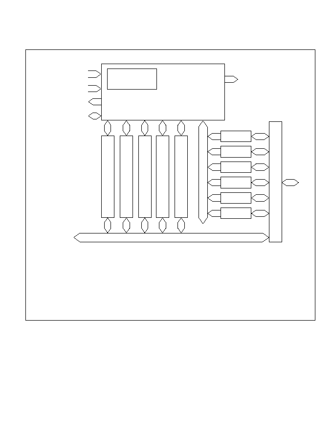
10.1.2 Block Diagrams
ITU Block Diagram (Overall): Figure 10-1 is a block diagram of the ITU.
Figure 10-1 ITU Block Diagram (Overall)
16-bit timer channel 4
16-bit timer channel 3
16-bit timer channel 2
16-bit timer channel 1
16-bit timer channel 0
Module data bus
Bus interface
On-chip data bus
IMIA0 to IMIA4
IMIB0 to IMIB4
OVI0 to OVI4
TCLKA to TCLKD
¯, ¯/2, ¯/4, ¯/8
TOCXA
4
, TOCXB
4
Clock selector
Control logic
TIOCA
0
to TIOCA
4
TIOCB
0
to TIOCB
4
TOER
TOCR
TSTR
TSNC
TMDR
TFCR
TOER:
TOCR:
TSTR:
TSNC:
TMDR:
TFCR:
Legend
Timer output master enable register (8 bits)
Timer output control register (8 bits)
Timer start register (8 bits)
Timer synchro register (8 bits)
Timer mode register (8 bits)
Timer function control register (8 bits)
280
Block Diagram of Channels 0 and 1: ITU channels 0 and 1 are functionally identical. Both have
the structure shown in figure 10-2.
Figure 10-2 Block Diagram of Channels 0 and 1 (for Channel 0)
Clock selector
Comparator
Control logic
TCLKA to TCLKD
¯, ¯/2, ¯/4, ¯/8
TIOCA
0
TIOCB
0
IMIA0
IMIB0
OVI0
TCNT
GRA
GRB
TCR
TIOR
TIER
TSR
Module data bus
Legend
TCNT:
GRA, GRB:
TCR:
TIOR:
TIER:
TSR:
Timer counter (16 bits)
General registers A and B (input capture/output compare registers) (16 bits 2)
Timer control register (8 bits)
Timer I/O control register (8 bits)
Timer interrupt enable register (8 bits)
Timer status register (8 bits)
◊
281

Block Diagram of Channel 2: Figure 10-3 is a block diagram of channel 2. This is the channel
that provides only 0 output and 1 output.
Figure 10-3 Block Diagram of Channel 2
Clock selector
Comparator
Control logic
TCLKA to TCLKD
¯, ¯/2, ¯/4, ¯/8
TIOCA
2
TIOCB
2
IMIA2
IMIB2
OVI2
TCNT2
GRA2
GRB2
TCR2
TIOR2
TIER2
TSR2
Module data bus
Legend
TCNT2:
GRA2, GRB2:
TCR2:
TIOR2:
TIER2:
TSR2:
Timer counter 2 (16 bits)
General registers A2 and B2 (input capture/output compare registers)
(16 bits 2)
Timer control register 2 (8 bits)
Timer I/O control register 2 (8 bits)
Timer interrupt enable register 2 (8 bits)
◊
Timer status register 2 (8 bits)
282

Block Diagrams of Channels 3 and 4: Figure 10-4 is a block diagram of channel 3. Figure 10-5
is a block diagram of channel 4.
Figure 10-4 Block Diagram of Channel 3
TCNT3
BRA3
Legend
TCNT3:
GRA3, GRB3:
BRA3, BRB3:
TCR3:
TIOR3:
TIER3:
TSR3:
Timer counter 3 (16 bits)
General registers A3 and B3 (input capture/output compare registers)
(16 bits 2)
Buffer registers A3 and B3 (input capture/output compare buffer registers)
(16 bits 2)
Timer control register 3 (8 bits)
Clock selector
Comparator
Control logic
GRA3
BRB3
GRB3
TCR3
TIOR3
TIER3
TSR3
TCLKA to
TCLKD
¯, ¯/2,
¯/4, ¯/8
TIOCA
3
TIOCB
3
Module data bus
◊
IMIA3
IMIB3
OVI3
Timer I/O control register 3 (8 bits)
Timer interrupt enable register 3 (8 bits)
Timer status register 3 (8 bits)
◊
283
Figure 10-5 Block Diagram of Channel 4
TCNT4
BRA4
Legend
TCNT4:
GRA4, GRB4:
BRA4, BRB4:
TCR4:
TIOR4:
TIER4:
TSR4:
Timer counter 4 (16 bits)
General registers A4 and B4 (input capture/output compare registers)
(16 bits 2)
Buffer registers A4 and B4 (input capture/output compare buffer registers)
(16 bits 2)
Timer control register 4 (8 bits)
Clock selector
Comparator
Control logic
GRA4
BRB4
GRB4
TCR4
TIOR4
TIER4
TSR4
Module data bus
◊
TCLKA to
TCLKD
¯, ¯/2,
¯/4, ¯/8
Timer I/O control register 4 (8 bits)
Timer interrupt enable register 4 (8 bits)
Timer status register 4 (8 bits)
◊
TOCXA
4
TOCXB
4
TIOCA
4
TIOCB
4
IMIA4
IMIB4
OVI4
284

10.1.3 Input/Output Pins
Table 10-2 summarizes the ITU pins.
Table 10-2 ITU Pins
Abbre-
Input/
Channel
Name
viation
Output
Function
Common
Clock input A
TCLKA
Input
External clock A input pin
(phase-A input pin in phase counting mode)
Clock input B
TCLKB
Input
External clock B input pin
(phase-B input pin in phase counting mode)
Clock input C
TCLKC
Input
External clock C input pin
Clock input D
TCLKD
Input
External clock D input pin
0
Input capture/output TIOCA
0
Input/
GRA0 output compare or input capture pin
compare A0
output
PWM output pin in PWM mode
Input capture/output TIOCB
0
Input/
GRB0 output compare or input capture pin
compare B0
output
1
Input capture/output TIOCA
1
Input/
GRA1 output compare or input capture pin
compare A1
output
PWM output pin in PWM mode
Input capture/output TIOCB
1
Input/
GRB1 output compare or input capture pin
compare B1
output
2
Input capture/output TIOCA
2
Input/
GRA2 output compare or input capture pin
compare A2
output
PWM output pin in PWM mode
Input capture/output TIOCB
2
Input/
GRB2 output compare or input capture pin
compare B2
output
3
Input capture/output TIOCA
3
Input/
GRA3 output compare or input capture pin
compare A3
output
PWM output pin in PWM mode, comple-
mentary PWM mode, or reset-synchronized
PWM mode
Input capture/output TIOCB
3
Input/
GRB3 output compare or input capture pin
compare B3
output
PWM output pin in complementary PWM
mode or reset-synchronized PWM mode
4
Input capture/output TIOCA
4
Input/
GRA4 output compare or input capture pin
compare A4
output
PWM output pin in PWM mode, comple-
mentary PWM mode, or reset-synchronized
PWM mode
Input capture/output TIOCB
4
Input/
GRB4 output compare or input capture pin
compare B4
output
PWM output pin in complementary PWM
mode or reset-synchronized PWM mode
Output compare XA4 TOCXA
4
Output
PWM output pin in complementary PWM
mode or reset-synchronized PWM mode
Output compare XB4 TOCXB
4
Output
PWM output pin in complementary PWM
mode or reset-synchronized PWM mode
285

10.1.4 Register Configuration
Table 10-3 summarizes the ITU registers.
Table 10-3 ITU Registers
Abbre-
Initial
Channel
Address
*
1
Name
viation
R/W
Value
Common
H'FF60
Timer start register
TSTR
R/W
H'E0
H'FF61
Timer synchro register
TSNC
R/W
H'E0
H'FF62
Timer mode register
TMDR
R/W
H'80
H'FF63
Timer function control register
TFCR
R/W
H'C0
H'FF90
Timer output master enable register
TOER
R/W
H'FF
H'FF91
Timer output control register
TOCR
R/W
H'FF
0
H'FF64
Timer control register 0
TCR0
R/W
H'80
H'FF65
Timer I/O control register 0
TIOR0
R/W
H'88
H'FF66
Timer interrupt enable register 0
TIER0
R/W
H'F8
H'FF67
Timer status register 0
TSR0
R/(W)
*
2
H'F8
H'FF68
Timer counter 0 (high)
TCNT0H
R/W
H'00
H'FF69
Timer counter 0 (low)
TCNT0L
R/W
H'00
H'FF6A
General register A0 (high)
GRA0H
R/W
H'FF
H'FF6B
General register A0 (low)
GRA0L
R/W
H'FF
H'FF6C
General register B0 (high)
GRB0H
R/W
H'FF
H'FF6D
General register B0 (low)
GRB0L
R/W
H'FF
1
H'FF6E
Timer control register 1
TCR1
R/W
H'80
H'FF6F
Timer I/O control register 1
TIOR1
R/W
H'88
H'FF70
Timer interrupt enable register 1
TIER1
R/W
H'F8
H'FF71
Timer status register 1
TSR1
R/(W)
*
2
H'F8
H'FF72
Timer counter 1 (high)
TCNT1H
R/W
H'00
H'FF73
Timer counter 1 (low)
TCNT1L
R/W
H'00
H'FF74
General register A1 (high)
GRA1H
R/W
H'FF
H'FF75
General register A1 (low)
GRA1L
R/W
H'FF
H'FF76
General register B1 (high)
GRB1H
R/W
H'FF
H'FF77
General register B1 (low)
GRB1L
R/W
H'FF
Notes: 1. The lower 16 bits of the address are indicated.
2. Only 0 can be written, to clear flags.
286

Table 10-3 ITU Registers (cont)
Abbre-
Initial
Channel
Address
*
1
Name
viation
R/W
Value
2
H'FF78
Timer control register 2
TCR2
R/W
H'80
H'FF79
Timer I/O control register 2
TIOR2
R/W
H'88
H'FF7A
Timer interrupt enable register 2
TIER2
R/W
H'F8
H'FF7B
Timer status register 2
TSR2
R/(W)
*
2
H'F8
H'FF7C
Timer counter 2 (high)
TCNT2H
R/W
H'00
H'FF7D
Timer counter 2 (low)
TCNT2L
R/W
H'00
H'FF7E
General register A2 (high)
GRA2H
R/W
H'FF
H'FF7F
General register A2 (low)
GRA2L
R/W
H'FF
H'FF80
General register B2 (high)
GRB2H
R/W
H'FF
H'FF81
General register B2 (low)
GRB2L
R/W
H'FF
3
H'FF82
Timer control register 3
TCR3
R/W
H'80
H'FF83
Timer I/O control register 3
TIOR3
R/W
H'88
H'FF84
Timer interrupt enable register 3
TIER3
R/W
H'F8
H'FF85
Timer status register 3
TSR3
R/(W)
*
2
H'F8
H'FF86
Timer counter 3 (high)
TCNT3H
R/W
H'00
H'FF87
Timer counter 3 (low)
TCNT3L
R/W
H'00
H'FF88
General register A3 (high)
GRA3H
R/W
H'FF
H'FF89
General register A3 (low)
GRA3L
R/W
H'FF
H'FF8A
General register B3 (high)
GRB3H
R/W
H'FF
H'FF8B
General register B3 (low)
GRB3L
R/W
H'FF
H'FF8C
Buffer register A3 (high)
BRA3H
R/W
H'FF
H'FF8D
Buffer register A3 (low)
BRA3L
R/W
H'FF
H'FF8E
Buffer register B3 (high)
BRB3H
R/W
H'FF
H'FF8F
Buffer register B3 (low)
BRB3L
R/W
H'FF
Notes: 1. The lower 16 bits of the address are indicated.
2. Only 0 can be written, to clear flags.
287

Table 10-3 ITU Registers (cont)
Abbre-
Initial
Channel
Address
*
1
Name
viation
R/W
Value
4
H'FF92
Timer control register 4
TCR4
R/W
H'80
H'FF93
Timer I/O control register 4
TIOR4
R/W
H'88
H'FF94
Timer interrupt enable register 4
TIER4
R/W
H'F8
H'FF95
Timer status register 4
TSR4
R/(W)
*
2
H'F8
H'FF96
Timer counter 4 (high)
TCNT4H
R/W
H'00
H'FF97
Timer counter 4 (low)
TCNT4L
R/W
H'00
H'FF98
General register A4 (high)
GRA4H
R/W
H'FF
H'FF99
General register A4 (low)
GRA4L
R/W
H'FF
H'FF9A
General register B4 (high)
GRB4H
R/W
H'FF
H'FF9B
General register B4 (low)
GRB4L
R/W
H'FF
H'FF9C
Buffer register A4 (high)
BRA4H
R/W
H'FF
H'FF9D
Buffer register A4 (low)
BRA4L
R/W
H'FF
H'FF9E
Buffer register B4 (high)
BRB4H
R/W
H'FF
H'FF9F
Buffer register B4 (low)
BRB4L
R/W
H'FF
Notes: 1. The lower 16 bits of the address are indicated.
2. Only 0 can be written, to clear flags.
288

10.2 Register Descriptions
10.2.1 Timer Start Register (TSTR)
TSTR is an 8-bit readable/writable register that starts and stops the timer counter (TCNT) in
channels 0 to 4.
TSTR is initialized to H'E0 by a reset and in standby mode.
Bits 7 to 5--Reserved: These bits cannot be modified and are always read as 1.
Bit 4--Counter Start 4 (STR4): Starts and stops timer counter 4 (TCNT4).
Bit 4
STR4
Description
0
TCNT4 is halted
(Initial value)
1
TCNT4 is counting
Bit 3--Counter Start 3 (STR3): Starts and stops timer counter 3 (TCNT3).
Bit 3
STR3
Description
0
TCNT3 is halted
(Initial value)
1
TCNT3 is counting
Bit 2--Counter Start 2 (STR2): Starts and stops timer counter 2 (TCNT2).
Bit 2
STR2
Description
0
TCNT2 is halted
(Initial value)
1
TCNT2 is counting
Bit
Initial value
Read/Write
7
--
1
--
6
--
1
--
5
--
1
--
4
STR4
0
R/W
3
STR3
0
R/W
2
STR2
0
R/W
1
STR1
0
R/W
0
STR0
0
R/W
Reserved bits
Counter start 4 to 0
These bits start and
stop TCNT4 to TCNT0
289

Bit 1--Counter Start 1 (STR1): Starts and stops timer counter 1 (TCNT1).
Bit 1
STR1
Description
0
TCNT1 is halted
(Initial value)
1
TCNT1 is counting
Bit 0--Counter Start 0 (STR0): Starts and stops timer counter 0 (TCNT0).
Bit 0
STR0
Description
0
TCNT0 is halted
(Initial value)
1
TCNT0 is counting
10.2.2 Timer Synchro Register (TSNC)
TSNC is an 8-bit readable/writable register that selects whether channels 0 to 4 operate
independently or synchronously. Channels are synchronized by setting the corresponding bits to 1.
TSNC is initialized to H'E0 by a reset and in standby mode.
Bits 7 to 5--Reserved:These bits cannot be modified and are always read as 1.
Bit 4--Timer Sync 4 (SYNC4): Selects whether channel 4 operates independently or
synchronously.
Bit 4
SYNC4
Description
0
Channel 4's timer counter (TCNT4) operates independently
(Initial value)
TCNT4 is preset and cleared independently of other channels
1
Channel 4 operates synchronously
TCNT4 can be synchronously preset and cleared
Bit
Initial value
Read/Write
7
--
1
--
6
--
1
--
5
--
1
--
4
SYNC4
0
R/W
3
SYNC3
0
R/W
2
SYNC2
0
R/W
1
SYNC1
0
R/W
0
SYNC0
0
R/W
Reserved bits
Timer sync 4 to 0
These bits synchronize
channels 4 to 0
290

Bit 3--Timer Sync 3 (SYNC3): Selects whether channel 3 operates independently or
synchronously.
Bit 3
SYNC3
Description
0
Channel 3's timer counter (TCNT3) operates independently
(Initial value)
TCNT3 is preset and cleared independently of other channels
1
Channel 3 operates synchronously
TCNT3 can be synchronously preset and cleared
Bit 2--Timer Sync 2 (SYNC2): Selects whether channel 2 operates independently or
synchronously.
Bit 2
SYNC2
Description
0
Channel 2's timer counter (TCNT2) operates independently
(Initial value)
TCNT2 is preset and cleared independently of other channels
1
Channel 2 operates synchronously
TCNT2 can be synchronously preset and cleared
Bit 1--Timer Sync 1 (SYNC1): Selects whether channel 1 operates independently or
synchronously.
Bit 1
SYNC1
Description
0
Channel 1's timer counter (TCNT1) operates independently
(Initial value)
TCNT1 is preset and cleared independently of other channels
1
Channel 1 operates synchronously
TCNT1 can be synchronously preset and cleared
Bit 0--Timer Sync 0 (SYNC0): Selects whether channel 0 operates independently or
synchronously.
Bit 0
SYNC0
Description
0
Channel 0's timer counter (TCNT0) operates independently
(Initial value)
TCNT0 is preset and cleared independently of other channels
1
Channel 0 operates synchronously
TCNT0 can be synchronously preset and cleared
291

10.2.3 Timer Mode Register (TMDR)
TMDR is an 8-bit readable/writable register that selects PWM mode for channels 0 to 4. It also
selects phase counting mode and the overflow flag (OVF) setting conditions for channel 2.
TMDR is initialized to H'80 by a reset and in standby mode.
Bit 7--Reserved:This bit cannot be modified and is, always read as 1.
Bit 6--Phase Counting Mode Flag (MDF): Selects whether channel 2 operates normally or in
phase counting mode.
Bit 6
MDF
Description
0
Channel 2 operates normally
(Initial value)
1
Channel 2 operates in phase counting mode
Bit
Initial value
Read/Write
7
--
1
--
6
MDF
0
R/W
5
FDIR
0
R/W
4
PWM4
0
R/W
3
PWM3
0
R/W
0
PWM0
0
R/W
2
PWM2
0
R/W
1
PWM1
0
R/W
Reserved bit
PWM mode 4 to 0
These bits select PWM
mode for channels 4 to 0
Phase counting mode flag
Selects phase counting mode for channel 2
Flag direction
Selects the setting condition for the overflow
flag (OVF) in timer status register 2 (TSR2)
292

When MDF is set to 1 to select phase counting mode, TCNT2 operates as an up/down-counter and
pins TCLKA and TCLKB become counter clock input pins. TCNT2 counts both rising and falling
edges of TCLKA and TCLKB, and counts up or down as follows.
Counting Direction
Down-Counting
Up-Counting
TCLKA pin
High
Low
Low
High
TCLKB pin
Low
High
High
Low
In phase counting mode channel 2 operates as above regardless of the external clock edges
selected by bits CKEG1 and CKEG0 and the clock source selected by bits TPSC2 to TPSC0 in
TCR2. Phase counting mode takes precedence over these settings.
The counter clearing condition selected by the CCLR1 and CCLR0 bits in TCR2 and the compare
match/input capture settings and interrupt functions of TIOR2, TIER2, and TSR2 remain effective
in phase counting mode.
Bit 5--Flag Direction (FDIR): Designates the setting condition for the OVF flag in TSR2. The
FDIR designation is valid in all modes in channel 2.
Bit 5
FDIR
Description
0
OVF is set to 1 in TSR2 when TCNT2 overflows or underflows
(Initial value)
1
OVF is set to 1 in TSR2 when TCNT2 overflows
Bit 4--PWM Mode 4 (PWM4): Selects whether channel 4 operates normally or in PWM mode.
Bit 4
PWM4
Description
0
Channel 4 operates normally
(Initial value)
1
Channel 4 operates in PWM mode
When bit PWM4 is set to 1 to select PWM mode, pin TIOCA4 becomes a PWM output pin. The
output goes to 1 at compare match with GRA4, and to 0 at compare match with GRB4.
If complementary PWM mode or reset-synchronized PWM mode is selected by bits CMD1 and
CMD0 in TFCR, the CMD1 and CMD0 setting takes precedence and the PWM4 setting is
ignored.
293

Bit 3--PWM Mode 3 (PWM3): Selects whether channel 3 operates normally or in PWM mode.
Bit 3
PWM3
Description
0
Channel 3 operates normally
(Initial value)
1
Channel 3 operates in PWM mode
When bit PWM3 is set to 1 to select PWM mode, pin TIOCA3 becomes a PWM output pin. The
output goes to 1 at compare match with GRA3, and to 0 at compare match with general register
B3 (GRB3).
If complementary PWM mode or reset-synchronized PWM mode is selected by bits CMD1 and
CMD0 in TFCR, the CMD1 and CMD0 setting takes precedence and the PWM3 setting is
ignored.
Bit 2--PWM Mode 2 (PWM2): Selects whether channel 2 operates normally or in PWM mode.
Bit 2
PWM2
Description
0
Channel 2 operates normally
(Initial value)
1
Channel 2 operates in PWM mode
When bit PWM2 is set to 1 to select PWM mode, pin TIOCA2 becomes a PWM output pin. The
output goes to 1 at compare match with GRA2, and to 0 at compare match with GRB2.
Bit 1--PWM Mode 1 (PWM1): Selects whether channel 1 operates normally or in PWM mode.
Bit 1
PWM1
Description
0
Channel 1 operates normally
(Initial value)
1
Channel 1 operates in PWM mode
When bit PWM1 is set to 1 to select PWM mode, pin TIOCA1 becomes a PWM output pin. The
output goes to 1 at compare match with GRA1, and to 0 at compare match with GRB1.
294

Bit 0--PWM Mode 0 (PWM0): Selects whether channel 0 operates normally or in PWM mode.
Bit 0
PWM0
Description
0
Channel 0 operates normally
(Initial value)
1
Channel 0 operates in PWM mode
When bit PWM0 is set to 1 to select PWM mode, pin TIOCA0 becomes a PWM output pin. The
output goes to 1 at compare match with GRA0, and to 0 at compare match with GRB0.
10.2.4 Timer Function Control Register (TFCR)
TFCR is an 8-bit readable/writable register that selects complementary PWM mode, reset-
synchronized PWM mode, and buffering for channels 3 and 4.
TFCR is initialized to H'C0 by a reset and in standby mode.
Bits 7 and 6--Reserved: These bits cannot be modified and are always read as 1.
Bit
Initial value
Read/Write
7
--
1
--
6
--
1
--
5
CMD1
0
R/W
4
CMD0
0
R/W
3
BFB4
0
R/W
0
BFA3
0
R/W
2
BFA4
0
R/W
1
BFB3
0
R/W
Reserved bits
Combination mode 1/0
These bits select complementary
PWM mode or reset-synchronized
PWM mode for channels 3 and 4
Buffer mode B4 and A4
These bits select buffering of
general registers (GRB4 and
GRA4) by buffer registers
(BRB4 and BRA4) in channel 4
Buffer mode B3 and A3
These bits select buffering
of general registers (GRB3
and GRA3) by buffer
registers (BRB3 and BRA3)
in channel 3
295

Bits 5 and 4--Combination Mode 1 and 0 (CMD1, CMD0): These bits select whether channels
3 and 4 operate in normal mode, complementary PWM mode, or reset-synchronized PWM mode.
Bit 5
Bit 4
CMD1
CMD0
Description
0
0
Channels 3 and 4 operate normally
(Initial value)
1
1
0
Channels 3 and 4 operate together in complementary PWM mode
1
Channels 3 and 4 operate together in reset-synchronized PWM mode
Before selecting reset-synchronized PWM mode or complementary PWM mode, halt the timer
counter or counters that will be used in these modes.
When these bits select complementary PWM mode or reset-synchronized PWM mode, they take
precedence over the setting of the PWM mode bits (PWM4 and PWM3) in TMDR. Settings of
timer sync bits SYNC4 and SYNC3 in TSNC are valid in complementary PWM mode and reset-
synchronized PWM mode, however. When complementary PWM mode is selected, channels 3
and 4 must not be synchronized (do not set bits SYNC3 and SYNC4 both to 1 in TSNC).
Bit 3--Buffer Mode B4 (BFB4): Selects whether GRB4 operates normally in channel 4, or
whether GRB4 is buffered by BRB4.
Bit 3
BFB4
Description
0
GRB4 operates normally
(Initial value)
1
GRB4 is buffered by BRB4
Bit 2--Buffer Mode A4 (BFA4): Selects whether GRA4 operates normally in channel 4, or
whether GRA4 is buffered by BRA4.
Bit 2
BFA4
Description
0
GRA4 operates normally
(Initial value)
1
GRA4 is buffered by BRA4
296

Bit 1--Buffer Mode B3 (BFB3): Selects whether GRB3 operates normally in channel 3, or
whether GRB3 is buffered by BRB3.
Bit 1
BFB3
Description
0
GRB3 operates normally
(Initial value)
1
GRB3 is buffered by BRB3
Bit 0--Buffer Mode A3 (BFA3): Selects whether GRA3 operates normally in channel 3, or
whether GRA3 is buffered by BRA3.
Bit 0
BFA3
Description
0
GRA3 operates normally
(Initial value)
1
GRA3 is buffered by BRA3
10.2.5 Timer Output Master Enable Register (TOER)
TOER is an 8-bit readable/writable register that enables or disables output settings for channels 3
and 4.
TOER is initialized to H'FF by a reset and in standby mode.
Bits 7 and 6--Reserved: These bits cannot be modified and are always read as 1.
Bit
Initial value
Read/Write
7
--
1
--
6
--
1
--
5
EXB4
1
R/W
4
EXA4
1
R/W
3
EB3
1
R/W
0
EA3
1
R/W
2
EB4
1
R/W
1
EA4
1
R/W
Reserved bits
Master enable TOCXA
4
, TOCXB
4
These bits enable or disable output
settings for pins TOCXA
4
and TOCXB
4
Master enable TIOCA
3
, TIOCB
3
, TIOCA
4
, TIOCB
4
These bits enable or disable output settings for pins
TIOCA
3
, TIOCB
3
, TIOCA
4
, and TIOCB
4
297

Bit 5--Master Enable TOCXB
4
(EXB4): Enables or disables ITU output at pin TOCXB
4
.
Bit 5
EXB4
Description
0
TOCXB
4
output is disabled regardless of TFCR settings (TOCXB
4
operates as a generic
input/output pin).
If XTGD = 0, EXB4 is cleared to 0 when input capture A occurs in channel 1.
1
TOCXB
4
is enabled for output according to TFCR settings
(Initial value)
Bit 4--Master Enable TOCXA
4
(EXA4): Enables or disables ITU output at pin TOCXA
4
.
Bit 4
EXA4
Description
0
TOCXA
4
output is disabled regardless of TFCR settings (TOCXA
4
operates as a generic
input/output pin).
If XTGD = 0, EXA4 is cleared to 0 when input capture A occurs in channel 1.
1
TOCXA
4
is enabled for output according to TFCR settings
(Initial value)
Bit 3--Master Enable TIOCB
3
(EB3): Enables or disables ITU output at pin TIOCB
3
.
Bit 3
EB3
Description
0
TIOCB
3
output is disabled regardless of TIOR3 and TFCR settings (TIOCB
3
operates as
a generic input/output pin).
If XTGD = 0, EB3 is cleared to 0 when input capture A occurs in channel 1.
1
TIOCB
3
is enabled for output according to TIOR3 and TFCR settings
(Initial value)
298

Bit 2--Master Enable TIOCB
4
(EB4): Enables or disables ITU output at pin TIOCB
4
.
Bit 2
EB4
Description
0
TIOCB
4
output is disabled regardless of TIOR4 and TFCR settings (TIOCB
4
operates as
a generic input/output pin).
If XTGD = 0, EB4 is cleared to 0 when input capture A occurs in channel 1.
1
TIOCB
4
is enabled for output according to TIOR4 and TFCR settings
(Initial value)
Bit 1--Master Enable TIOCA
4
(EA4): Enables or disables ITU output at pin TIOCA
4
.
Bit 1
EA4
Description
0
TIOCA
4
output is disabled regardless of TIOR4, TMDR, and TFCR settings (TIOCA
4
operates as a generic input/output pin).
If XTGD = 0, EA4 is cleared to 0 when input capture A occurs in channel 1.
1
TIOCA
4
is enabled for output according to TIOR4, TMDR, and
(Initial value)
TFCR settings
Bit 0--Master Enable TIOCA
3
(EA3): Enables or disables ITU output at pin TIOCA
3
.
Bit 0
EA3
Description
0
TIOCA
3
output is disabled regardless of TIOR3, TMDR, and TFCR settings (TIOCA
3
operates as a generic input/output pin).
If XTGD = 0, EA3 is cleared to 0 when input capture A occurs in channel 1.
1
TIOCA
3
is enabled for output according to TIOR3, TMDR, and
(Initial value)
TFCR settings
299

10.2.6 Timer Output Control Register (TOCR)
TOCR is an 8-bit readable/writable register that selects externally triggered disabling of output in
complementary PWM mode and reset-synchronized PWM mode, and inverts the output levels.
The settings of the XTGD, OLS4, and OLS3 bits are valid only in complementary PWM mode
and reset-synchronized PWM mode. These settings do not affect other modes.
TOCR is initialized to H'FF by a reset and in standby mode.
Bits 7 to 5--Reserved: These bits cannot be modified and are always read as 1.
Bit 4--External Trigger Disable (XTGD): Selects externally triggered disabling of ITU output
in complementary PWM mode and reset-synchronized PWM mode.
Bit 4
XTGD
Description
0
Input capture A in channel 1 is used as an external trigger signal in complementary PWM
mode and reset-synchronized PWM mode.
When an external trigger occurs, bits 5 to 0 in TOER are cleared to 0, disabling ITU
output.
1
External triggering is disabled
(Initial value)
Bit
Initial value
Read/Write
7
--
1
--
6
--
1
--
5
--
1
--
4
XTGD
1
R/W
3
--
1
--
0
OLS3
1
R/W
2
--
1
--
1
OLS4
1
R/W
Reserved bits
Output level select 3, 4
These bits select output
levels in complementary
PWM mode and reset-
synchronized PWM mode
External trigger disable
Selects externally triggered disabling of output in
complementary PWM mode and reset-synchronized
PWM mode
Reserved bits
300

Bits 3 and 2--Reserved: These bits cannot be modified and are always read as 1.
Bit 1--Output Level Select 4 (OLS4): Selects output levels in complementary PWM mode and
reset-synchronized PWM mode.
Bit 1
OLS4
Description
0
TIOCA
3
, TIOCA
4
, and TIOCB
4
outputs are inverted
1
TIOCA
3
, TIOCA
4
, and TIOCB
4
outputs are not inverted
(Initial value)
Bit 0--Output Level Select 3 (OLS3): Selects output levels in complementary PWM mode and
reset-synchronized PWM mode.
Bit 0
OLS3
Description
0
TIOCB
3
, TOCXA
4
, and TOCXB
4
outputs are inverted
1
TIOCB
3
, TOCXA
4
, and TOCXB
4
outputs are not inverted
(Initial value)
10.2.7 Timer Counters (TCNT)
TCNT is a 16-bit counter. The ITU has five TCNTs, one for each channel.
Channel
Abbreviation
Function
0
TCNT0
Up-counter
1
TCNT1
2
TCNT2
Phase counting mode: up/down-counter
Other modes: up-counter
3
TCNT3
4
TCNT4
Each TCNT is a 16-bit readable/writable register that counts pulse inputs from a clock source. The
clock source is selected by bits TPSC2 to TPSC0 in TCR.
Bit
Initial value
Read/Write
14
0
R/W
12
0
R/W
10
0
R/W
8
0
R/W
6
0
R/W
0
0
R/W
4
0
R/W
2
0
R/W
15
0
R/W
13
0
R/W
11
0
R/W
9
0
R/W
7
0
R/W
1
0
R/W
5
0
R/W
3
0
R/W
Complementary PWM mode: up/down-counter
Other modes: up-counter
301

TCNT0 and TCNT1 are up-counters. TCNT2 is an up/down-counter in phase counting mode and
an up-counter in other modes. TCNT3 and TCNT4 are up/down-counters in complementary PWM
mode and up-counters in other modes.
TCNT can be cleared to H'0000 by compare match with GRA or GRB or by input capture to GRA
or GRB (counter clearing function) in the same channel.
When TCNT overflows (changes from H'FFFF to H'0000), the OVF flag is set to 1 in the timer
status register (TSR) of the corresponding channel.
When TCNT underflows (changes from H'0000 to H'FFFF), the OVF flag is set to 1 in TSR of the
corresponding channel.
The TCNTs are linked to the CPU by an internal 16-bit bus and can be written or read by either
word access or byte access.
Each TCNT is initialized to H'0000 by a reset and in standby mode.
10.2.8 General Registers (GRA, GRB)
The general registers are 16-bit registers. The ITU has 10 general registers, two in each channel.
Channel
Abbreviation
Function
0
GRA0, GRB0
Output compare/input capture register
1
GRA1, GRB1
2
GRA2, GRB2
3
GRA3, GRB3
4
GRA4, GRB4
A general register is a 16-bit readable/writable register that can function as either an output
compare register or an input capture register. The function is selected by settings in TIOR.
When a general register is used as an output compare register, its value is constantly compared
with the TCNT value. When the two values match (compare match), the IMFA or IMFB flag is set
to 1 in TSR. Compare match output can be selected in TIOR.
Output compare/input capture register; can be buffered by buffer
registers BRA and BRB
Bit
Initial value
Read/Write
14
1
R/W
12
1
R/W
10
1
R/W
8
1
R/W
6
1
R/W
0
1
R/W
4
1
R/W
2
1
R/W
15
1
R/W
13
1
R/W
11
1
R/W
9
1
R/W
7
1
R/W
1
1
R/W
5
1
R/W
3
1
R/W
302

When a general register is used as an input capture register, rising edges, falling edges, or both
edges of an external input capture signal are detected and the current TCNT value is stored in the
general register. The corresponding IMFA or IMFB flag in TSR is set to 1 at the same time. The
valid edge or edges of the input capture signal are selected in TIOR.
TIOR settings are ignored in PWM mode, complementary PWM mode, and reset-synchronized
PWM mode.
General registers are linked to the CPU by an internal 16-bit bus and can be written or read by
either word access or byte access.
General registers are initialized to the output compare function (with no output signal) by a reset
and in standby mode. The initial value is H'FFFF.
10.2.9 Buffer Registers (BRA, BRB)
The buffer registers are 16-bit registers. The ITU has four buffer registers, two each in channels 3
and 4.
Channel
Abbreviation
Function
3
BRA3, BRB3
Used for buffering
4
BRA4, BRB4
∑ When the corresponding GRA or GRB functions as an output
compare register, BRA or BRB can function as an output compare
buffer register: the BRA or BRB value is automatically transferred
to GRA or GRB at compare match
∑ When the corresponding GRA or GRB functions as an input
capture register, BRA or BRB can function as an input capture
buffer register: the GRA or GRB value is automatically transferred
to BRA or BRB at input capture
A buffer register is a 16-bit readable/writable register that is used when buffering is selected.
Buffering can be selected independently by bits BFB4, BFA4, BFB3, and BFA3 in TFCR.
The buffer register and general register operate as a pair. When the general register functions as an
output compare register, the buffer register functions as an output compare buffer register. When
the general register functions as an input capture register, the buffer register functions as an input
capture buffer register.
Bit
Initial value
Read/Write
14
1
R/W
12
1
R/W
10
1
R/W
8
1
R/W
6
1
R/W
0
1
R/W
4
1
R/W
2
1
R/W
15
1
R/W
13
1
R/W
11
1
R/W
9
1
R/W
7
1
R/W
1
1
R/W
5
1
R/W
3
1
R/W
303
The buffer registers are linked to the CPU by an internal 16-bit bus and can be written or read by
either word or byte access.
Buffer registers are initialized to H'FFFF by a reset and in standby mode.
10.2.10 Timer Control Registers (TCR)
TCR is an 8-bit register. The ITU has five TCRs, one in each channel.
Channel
Abbreviation
Function
0
TCR0
1
TCR1
2
TCR2
3
TCR3
4
TCR4
Each TCR is an 8-bit readable/writable register that selects the timer counter clock source, selects
the edge or edges of external clock sources, and selects how the counter is cleared.
TCR is initialized to H'80 by a reset and in standby mode.
Bit 7--Reserved: This bit cannot be modified and is always read as 1.
TCR controls the timer counter. The TCRs in all channels are
functionally identical. When phase counting mode is selected in
channel 2, the settings of bits CKEG1 and CKEG0 and TPSC2 to
TPSC0 in TCR2 are ignored.
Bit
Initial value
Read/Write
7
--
1
--
6
CCLR1
0
R/W
5
CCLR0
0
R/W
4
CKEG1
0
R/W
3
CKEG0
0
R/W
0
TPSC0
0
R/W
2
TPSC2
0
R/W
1
TPSC1
0
R/W
Timer prescaler 2 to 0
These bits select the
counter clock
Reserved bit
Clock edge 1/0
These bits select external clock edges
Counter clear 1/0
These bits select the counter clear source
304

Bits 6 and 5--Counter Clear 1/0 (CCLR1, CCLR0): These bits select how TCNT is cleared.
Bit 6
Bit 5
CCLR1
CCLR0
Description
0
0
TCNT is not cleared
(Initial value)
1
TCNT is cleared by GRA compare match or input capture
*
1
1
0
TCNT is cleared by GRB compare match or input capture
*
1
1
Synchronous clear: TCNT is cleared in synchronization with other
synchronized timers
*
2
Notes: 1. TCNT is cleared by compare match when the general register functions as an output
compare register, and by input capture when the general register functions as an input
capture register.
2. Selected in TSNC.
Bits 4 and 3--Clock Edge 1/0 (CKEG1, CKEG0): These bits select external clock input edges
when an external clock source is used.
Bit 4
Bit 3
CKEG1
CKEG0
Description
0
0
Count rising edges
(Initial value)
1
Count falling edges
1
--
Count both edges
When channel 2 is set to phase counting mode, bits CKEG1 and CKEG0 in TCR2 are ignored.
Phase counting takes precedence.
305

Bits 2 to 0--Timer Prescaler 2 to 0 (TPSC2 to TPSC0): These bits select the counter clock
source.
Bit 2
Bit 1
Bit 0
TPSC2
TPSC1
TPSC0
Function
0
0
0
Internal clock: ¯
(Initial value)
1
Internal clock: ¯/2
1
0
Internal clock: ¯/4
1
Internal clock: ¯/8
1
0
0
External clock A: TCLKA input
1
External clock B: TCLKB input
1
0
External clock C: TCLKC input
1
External clock D: TCLKD input
When bit TPSC2 is cleared to 0 an internal clock source is selected, and the timer counts only
falling edges. When bit TPSC2 is set to 1 an external clock source is selected, and the timer
counts the edge or edges selected by bits CKEG1 and CKEG0.
When channel 2 is set to phase counting mode (MDF = 1 in TMDR), the settings of bits TPSC2 to
TPSC0 in TCR2 are ignored. Phase counting takes precedence.
10.2.11 Timer I/O Control Register (TIOR)
TIOR is an 8-bit register. The ITU has five TIORs, one in each channel.
Channel
Abbreviation
Function
0
TIOR0
1
TIOR1
2
TIOR2
3
TIOR3
4
TIOR4
TIOR controls the general registers. Some functions differ in PWM
mode. TIOR3 and TIOR4 settings are ignored when complementary
PWM mode or reset-synchronized PWM mode is selected in
channels 3 and 4.
306

Each TIOR is an 8-bit readable/writable register that selects the output compare or input capture
function for GRA and GRB, and specifies the functions of the TIOCA and TIOCB pins. If the
output compare function is selected, TIOR also selects the type of output. If input capture is
selected, TIOR also selects the edge or edges of the input capture signal.
TIOR is initialized to H'88 by a reset and in standby mode.
Bit 7--Reserved: This bit cannot be modified and is always read as 1.
Bits 6 to 4--I/O Control B2 to B0 (IOB2 to IOB0): These bits select the GRB function.
Bit 6
Bit 5
Bit 4
IOB2
IOB1
IOB0
Function
0
0
0
No output at compare match
(Initial value)
1
0 output at GRB compare match
*
1
1
0
1 output at GRB compare match
*
1
1
Output toggles at GRB compare match
(1 output in channel 2)
*
1,
*
2
1
0
0
GRB captures rising edge of input
1
GRB captures falling edge of input
1
0
GRB captures both edges of input
1
Notes: 1. After a reset, the output is 0 until the first compare match.
2. Channel 2 output cannot be toggled by compare match. This setting selects 1 output
instead.
Bit
Initial value
Read/Write
7
--
1
--
6
IOB2
0
R/W
5
IOB1
0
R/W
4
IOB0
0
R/W
3
--
1
--
0
IOA0
0
R/W
2
IOA2
0
R/W
1
IOA1
0
R/W
I/O control A2 to A0
These bits select GRA
functions
Reserved bit
I/O control B2 to B0
These bits select GRB functions
Reserved bit
GRB is an output
compare register
GRB is an input
capture register
307

Bit 3--Reserved: This bit cannot be modified and is always read as 1.
Bits 2 to 0--I/O Control A2 to A0 (IOA2 to IOA0): These bits select the GRA function.
Bit 2
Bit 1
Bit 0
IOA2
IOA1
IOA0
Function
0
0
0
No output at compare match
(Initial value)
1
0 output at GRA compare match
*
1
1
0
1 output at GRA compare match
*
1
1
Output toggles at GRA compare match
(1 output in channel 2)
*
1,
*
2
1
0
0
GRA captures rising edge of input
1
GRA captures falling edge of input
1
0
GRA captures both edges of input
1
Notes: 1. After a reset, the output is 0 until the first compare match.
2. Channel 2 output cannot be toggled by compare match. This setting selects 1 output
instead.
10.2.12 Timer Status Register (TSR)
TSR is an 8-bit register. The ITU has five TSRs, one in each channel.
Channel
Abbreviation
Function
0
TSR0
Indicates input capture, compare match, and overflow status
1
TSR1
2
TSR2
3
TSR3
4
TSR4
GRA is an output
compare register
GRA is an input
capture register
308

Each TSR is an 8-bit readable/writable register containing flags that indicate TCNT overflow or
underflow and GRA or GRB compare match or input capture. These flags are interrupt sources
and generate CPU interrupts if enabled by corresponding bits in TIER.
TSR is initialized to H'F8 by a reset and in standby mode.
Bits 7 to 3--Reserved: These bits cannot be modified and are always read as 1.
Bit 2--Overflow Flag (OVF): This status flag indicates TCNT overflow or underflow.
Bit 2
OVF
Description
0
[Clearing condition]
(Initial value)
Read OVF when OVF = 1, then write 0 in OVF
1
[Setting condition]
TCNT overflowed from H'FFFF to H'0000, or underflowed from H'0000 to H'FFFF
*
Notes:
*
TCNT underflow occurs when TCNT operates as an up/down-counter. Underflow occurs
only under the following conditions:
1. Channel 2 operates in phase counting mode (MDF = 1 in TMDR)
2. Channels 3 and 4 operate in complementary PWM mode (CMD1 = 1 and CMD0 = 0 in
TFCR)
Bit
Initial value
Read/Write
7
--
1
--
6
--
1
--
5
--
1
--
4
--
1
--
3
--
1
--
*
2
OVF
0
R/(W)
Reserved bits
Note: Only 0 can be written, to clear the flag.
*
*
1
IMFB
0
R/(W)
*
0
IMFA
0
R/(W)
Overflow flag
Status flag indicating
overflow or underflow
Input capture/compare match flag B
Status flag indicating GRB compare
match or input capture
Input capture/compare match flag A
Status flag indicating GRA compare
match or input capture
309

Bit 1--Input Capture/Compare Match Flag B (IMFB): This status flag indicates GRB
compare match or input capture events.
Bit 1
IMFB
Description
0
[Clearing condition]
(Initial value)
Read IMFB when IMFB = 1, then write 0 in IMFB
1
[Setting conditions]
TCNT = GRB when GRB functions as an output compare register.
TCNT value is transferred to GRB by an input capture signal, when GRB functions as
an input capture register.
Bit 0--Input Capture/Compare Match Flag A (IMFA): This status flag indicates GRA
compare match or input capture events.
Bit 0
IMFA
Description
0
[Clearing condition]
(Initial value)
Read IMFA when IMFA = 1, then write 0 in IMFA.
DMAC activated by IMIA interrupt (channels 0 to 3 only).
1
[Setting conditions]
TCNT = GRA when GRA functions as an output compare register.
TCNT value is transferred to GRA by an input capture signal, when GRA functions
as an input capture register.
310
10.2.13 Timer Interrupt Enable Register (TIER)
TIER is an 8-bit register. The ITU has five TIERs, one in each channel.
Channel
Abbreviation
Function
0
TIER0
Enables or disables interrupt requests.
1
TIER1
2
TIER2
3
TIER3
4
TIER4
Each TIER is an 8-bit readable/writable register that enables and disables overflow interrupt
requests and general register compare match and input capture interrupt requests.
TIER is initialized to H'F8 by a reset and in standby mode.
Bits 7 to 3--Reserved: These bits cannot be modified and are always read as 1.
Bit
Initial value
Read/Write
7
--
1
--
6
--
1
--
5
--
1
--
4
--
1
--
3
--
1
--
2
OVIE
0
R/W
1
IMIEB
0
R/W
0
IMIEA
0
R/W
Reserved bits
Overflow interrupt enable
Enables or disables OVF
interrupts
Input capture/compare match
interrupt enable B
Enables or disables IMFB interrupts
Input capture/compare match
interrupt enable A
Enables or disables IMFA
interrupts
311

Bit 2--Overflow Interrupt Enable (OVIE): Enables or disables the interrupt requested by the
OVF flag in TSR when OVF is set to 1.
Bit 2
OVIE
Description
0
OVI interrupt requested by OVF is disabled
(Initial value)
1
OVI interrupt requested by OVF is enabled
Bit 1--Input Capture/Compare Match Interrupt Enable B (IMIEB): Enables or disables the
interrupt requested by the IMFB flag in TSR when IMFB is set to 1.
Bit 1
IMIEB
Description
0
IMIB interrupt requested by IMFB is disabled
(Initial value)
1
IMIB interrupt requested by IMFB is enabled
Bit 0--Input Capture/Compare Match Interrupt Enable A (IMIEA): Enables or disables the
interrupt requested by the IMFA flag in TSR when IMFA is set to 1.
Bit 0
IMIEA
Description
0
IMIA interrupt requested by IMFA is disabled
(Initial value)
1
IMIA interrupt requested by IMFA is enabled
312
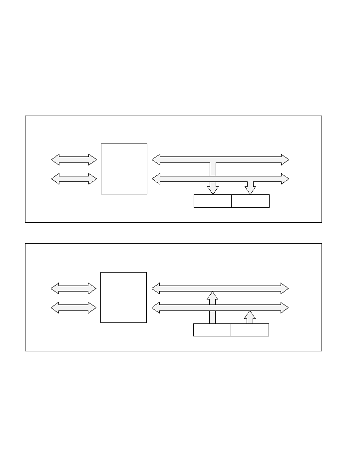
10.3 CPU Interface
10.3.1 16-Bit Accessible Registers
The timer counters (TCNTs), general registers A and B (GRAs and GRBs), and buffer registers A
and B (BRAs and BRBs) are 16-bit registers, and are linked to the CPU by an internal 16-bit data
bus. These registers can be written or read a word at a time, or a byte at a time.
Figures 10-6 and 10-7 show examples of word access to a timer counter (TCNT). Figures 10-8,
10-9, 10-10, and 10-11 show examples of byte access to TCNTH and TCNTL.
Figure 10-6 Access to Timer Counter (CPU Writes to TCNT, Word)
Figure 10-7 Access to Timer Counter (CPU Reads TCNT, Word)
On-chip data bus
CPU
H
L
Bus interface
H
L
Module
data bus
TCNTH
TCNTL
On-chip data bus
CPU
H
L
Bus interface
H
L
Module
data bus
TCNTH
TCNTL
313
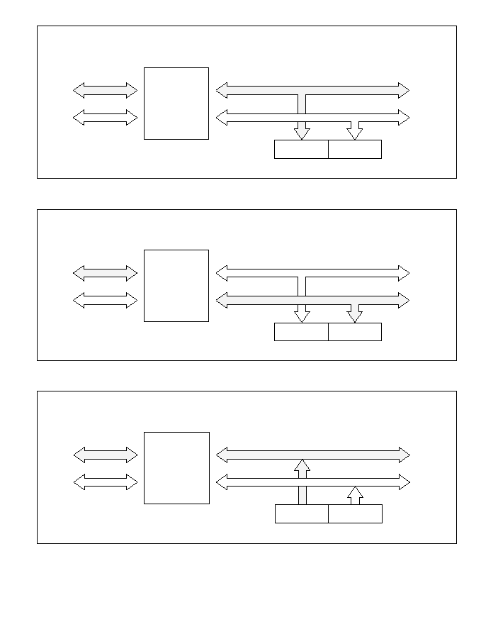
Figure 10-8 Access to Timer Counter (CPU Writes to TCNT, Upper Byte)
Figure 10-9 Access to Timer Counter (CPU Writes to TCNT, Lower Byte)
Figure 10-10 Access to Timer Counter (CPU Reads TCNT, Upper Byte)
On-chip data bus
CPU
H
L
Bus interface
H
L
Module
data bus
TCNTH
TCNTL
On-chip data bus
CPU
H
L
Bus interface
H
L
Module
data bus
TCNTH
TCNTL
On-chip data bus
CPU
H
L
Bus interface
H
L
Module
data bus
TCNTH
TCNTL
314
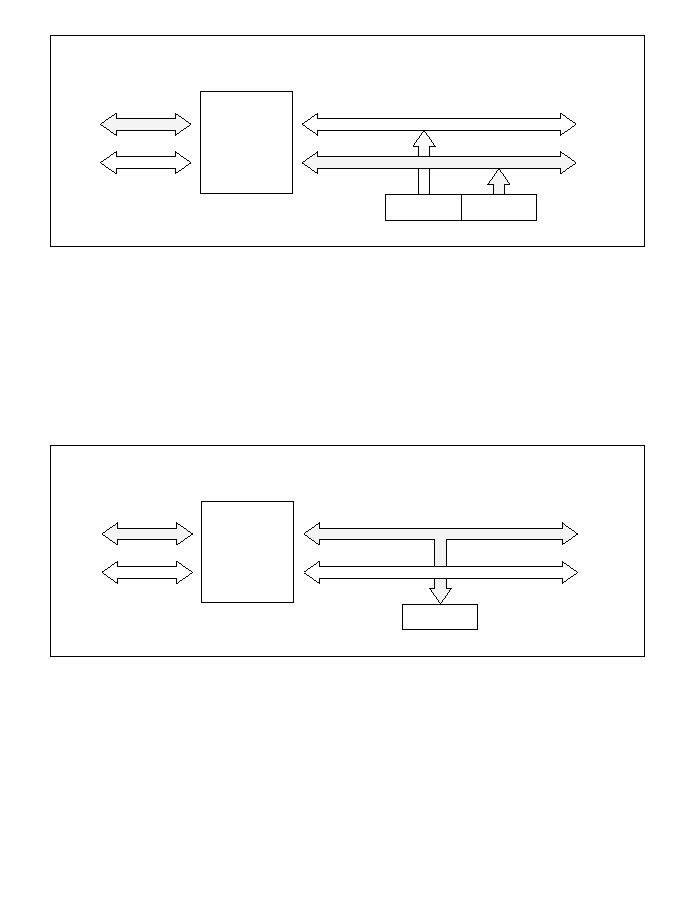
Figure 10-11 Access to Timer Counter (CPU Reads TCNT, Lower Byte)
10.3.2 8-Bit Accessible Registers
The registers other than the timer counters, general registers, and buffer registers are 8-bit
registers. These registers are linked to the CPU by an internal 8-bit data bus.
Figures 10-12 and 10-13 show examples of byte read and write access to a TCR.
If a word-size data transfer instruction is executed, two byte transfers are performed.
Figure 10-12 TCR Access (CPU Writes to TCR)
On-chip data bus
CPU
H
L
Bus interface
H
L
Module
data bus
TCNTH
TCNTL
On-chip data bus
CPU
H
L
Bus interface
H
L
Module
data bus
TCR
315
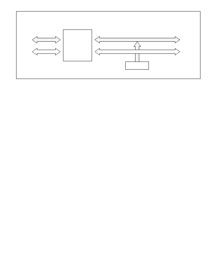
Figure 10-13 TCR Access (CPU Reads TCR)
On-chip data bus
CPU
H
L
Bus interface
H
L
Module
data bus
TCR
316

10.4 Operation
10.4.1 Overview
A summary of operations in the various modes is given below.
Normal Operation: Each channel has a timer counter and general registers. The timer counter
counts up, and can operate as a free-running counter, periodic counter, or external event counter.
General registers A and B can be used for input capture or output compare.
Synchronous Operation: The timer counters in designated channels are preset synchronously.
Data written to the timer counter in any one of these channels is simultaneously written to the
timer counters in the other channels as well. The timer counters can also be cleared synchronously
if so designated by the CCLR1 and CCLR0 bits in the TCRs.
PWM Mode: A PWM waveform is output from the TIOCA pin. The output goes to 1 at compare
match A and to 0 at compare match B. The duty cycle can be varied from 0% to 100% depending
on the settings of GRA and GRB. When a channel is set to PWM mode, its GRA and GRB
automatically become output compare registers.
Reset-Synchronized PWM Mode: Channels 3 and 4 are paired for three-phase PWM output with
complementary waveforms. (The three phases are related by having a common transition point.)
When reset-synchronized PWM mode is selected GRA3, GRB3, GRA4, and GRB4 automatically
function as output compare registers, TIOCA3, TIOCB3, TIOCA4, TOCXA4, TIOCB4, and
TOCXB4 function as PWM output pins, and TCNT3 operates as an up-counter. TCNT4 operates
independently, and is not compared with GRA4 or GRB4.
Complementary PWM Mode: Channels 3 and 4 are paired for three-phase PWM output with
non-overlapping complementary waveforms. When complementary PWM mode is selected
GRA3, GRB3, GRA4, and GRB4 automatically function as output compare registers, and
TIOCA3, TIOCB3, TIOCA4, TOCXA4, TIOCB4, and TOCXB4 function as PWM output pins.
TCNT3 and TCNT4 operate as up/down-counters.
Phase Counting Mode: The phase relationship between two clock signals input at TCLKA and
TCLKB is detected and TCNT2 counts up or down accordingly. When phase counting mode is
selected TCLKA and TCLKB become clock input pins and TCNT2 operates as an up/down-
counter.
317

Buffering :
∑
If the general register is an output compare register
When compare match occurs the buffer register value is transferred to the general register.
∑
If the general register is an input capture register
When input capture occurs the TCNT value is transferred to the general register, and the
previous general register value is transferred to the buffer register.
∑
Complementary PWM mode
The buffer register value is transferred to the general register when TCNT3 and TCNT4
change counting direction.
∑
Reset-synchronized PWM mode
The buffer register value is transferred to the general register at GRA3 compare match.
10.4.2 Basic Functions
Counter Operation: When one of bits STR0 to STR4 is set to 1 in the timer start register
(TSTR), the timer counter (TCNT) in the corresponding channel starts counting. The counting can
be free-running or periodic.
∑
Sample setup procedure for counter
Figure 10-14 shows a sample procedure for setting up a counter.
318
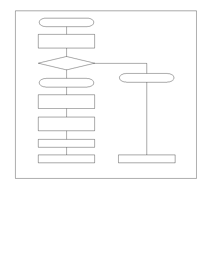
Figure 10-14 Counter Setup Procedure (Example)
1.
Set bits TPSC2 to TPSC0 in TCR to select the counter clock source. If an external clock
source is selected, set bits CKEG1 and CKEG0 in TCR to select the desired edge(s) of the
external clock signal.
2.
For periodic counting, set CCLR1 and CCLR0 in TCR to have TCNT cleared at GRA
compare match or GRB compare match.
3.
Set TIOR to select the output compare function of GRA or GRB, whichever was selected in
step 2.
4.
Write the count period in GRA or GRB, whichever was selected in step 2.
5.
Set the STR bit to 1 in TSTR to start the timer counter.
Counter setup
Select counter clock
Type of counting?
Periodic counting
Select counter clear source
Select output compare
register function
Set period
Start counter
Free-running counting
Start counter
Periodic counter
Free-running counter
1
2
3
4
5
5
No
Yes
319
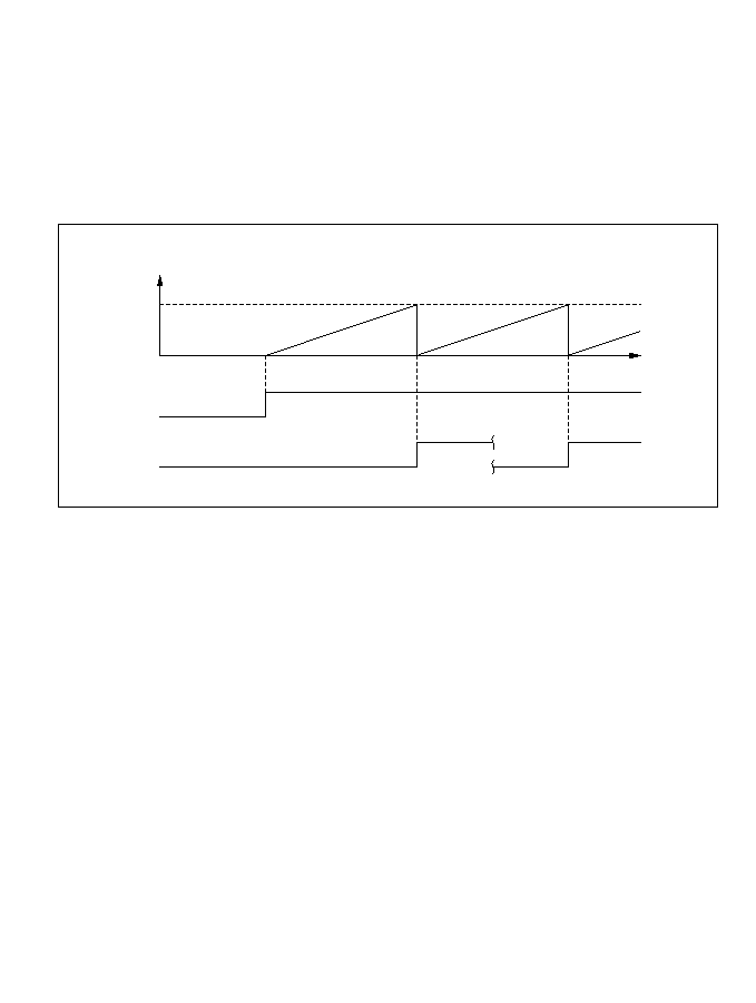
∑
Free-running and periodic counter operation
A reset leaves the counters (TCNTs) in ITU channels 0 to 4 all set as free-running counters. A
free-running counter starts counting up when the corresponding bit in TSTR is set to 1. When
the count overflows from H'FFFF to H'0000, the OVF flag is set to 1 in TSR. If the
corresponding OVIE bit is set to 1 in TIER, a CPU interrupt is requested. After the overflow,
the counter continues counting up from H'0000. Figure 10-15 illustrates free-running
counting.
Figure 10-15 Free-Running Counter Operation
When a channel is set to have its counter cleared by compare match, in that channel TCNT
operates as a periodic counter. Select the output compare function of GRA or GRB, set bit
CCLR1 or CCLR0 in TCR to have the counter cleared by compare match, and set the count
period in GRA or GRB. After these settings, the counter starts counting up as a periodic
counter when the corresponding bit is set to 1 in TSTR. When the count matches GRA or
GRB, the IMFA or IMFB flag is set to 1 in TSR and the counter is cleared to H'0000. If the
corresponding IMIEA or IMIEB bit is set to 1 in TIER, a CPU interrupt is requested at this
time. After the compare match, TCNT continues counting up from H'0000. Figure 10-16
illustrates periodic counting.
TCNT value
H'FFFF
H'0000
STR0 to
STR4 bit
OVF
Time
320

Figure 10-16 Periodic Counter Operation
∑
TCNT count timing
-- Internal clock source
Bits TPSC2 to TPSC0 in TCR select the system clock (¯) or one of three internal clock
sources obtained by prescaling the system clock (¯/2, ¯/4, ¯/8).
Figure 10-17 shows the timing.
Figure 10-17 Count Timing for Internal Clock Sources
TCNT value
GR
H'0000
STR bit
IMF
Time
Counter cleared by general
register compare match
¯
TCNT input
TCNT
Internal
clock
N ≠ 1
N
N + 1
321

-- External clock source
Bits TPSC2 to TPSC0 in TCR select an external clock input pin (TCLKA to TCLKD),
and its valid edge or edges are selected by bits CKEG1 and CKEG0. The rising edge,
falling edge, or both edges can be selected.
The pulse width of the external clock signal must be at least 1.5 system clocks when a
single edge is selected, and at least 2.5 system clocks when both edges are selected.
Shorter pulses will not be counted correctly.
Figure 10-18 shows the timing when both edges are detected.
Figure 10-18 Count Timing for External Clock Sources (when Both Edges are Detected)
¯
TCNT input
TCNT
External
clock input
N ≠ 1
N
N + 1
322
Waveform Output by Compare Match: In ITU channels 0, 1, 3, and 4, compare match A or B
can cause the output at the TIOCA or TIOCB pin to go to 0, go to 1, or toggle. In channel 2 the
output can only go to 0 or go to 1.
∑
Sample setup procedure for waveform output by compare match
Figure 10-19 shows a sample procedure for setting up waveform output by compare match.
Figure 10-19 Setup Procedure for Waveform Output by Compare Match (Example)
∑
Examples of waveform output
Figure 10-20 shows examples of 0 and 1 output. TCNT operates as a free-running counter, 0
output is selected for compare match A, and 1 output is selected for compare match B. When
the pin is already at the selected output level, the pin level does not change.
Output setup
Select waveform
output mode
Set output timing
Start counter
Waveform output
Select the compare match output mode (0, 1, or
toggle) in TIOR. When a waveform output mode
is selected, the pin switches from its generic input/
output function to the output compare function
(TIOCA or TIOCB). An output compare pin outputs
Set a value in GRA or GRB to designate the
compare match timing.
Set the STR bit to 1 in TSTR to start the timer
counter.
1
2
3
0 until the first compare match occurs.
1.
2.
3.
323
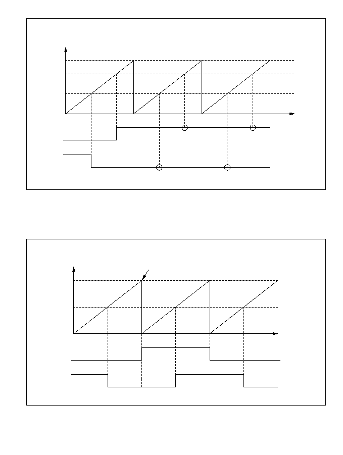
Figure 10-20 0 and 1 Output (Examples)
Figure 10-21 shows examples of toggle output. TCNT operates as a periodic counter, cleared
by compare match B. Toggle output is selected for both compare match A and B.
Figure 10-21 Toggle Output (Example)
Time
H'FFFF
GRB
TIOCB
TIOCA
GRA
No change
No change
No change
No change
1 output
0 output
TCNT value
H'0000
GRB
TIOCB
TIOCA
GRA
TCNT value
Time
Counter cleared by compare match with GRB
Toggle
output
Toggle
output
H'0000
324

∑
Output compare timing
The compare match signal is generated in the last state in which TCNT and the general
register match (when TCNT changes from the matching value to the next value). When the
compare match signal is generated, the output value selected in TIOR is output at the output
compare pin (TIOCA or TIOCB). When TCNT matches a general register, the compare
match signal is not generated until the next counter clock pulse.
Figure 10-22 shows the output compare timing.
Figure 10-22 Output Compare Timing
Input Capture Function: The TCNT value can be captured into a general register when a
transition occurs at an input capture/output compare pin (TIOCA or TIOCB). Capture can take
place on the rising edge, falling edge, or both edges. The input capture function can be used to
measure pulse width or period.
∑
Sample setup procedure for input capture
Figure 10-23 shows a sample procedure for setting up input capture.
N + 1
N
N
¯
TCNT input
clock
TCNT
GR
Compare
match signal
TIOCA,
TIOCB
325
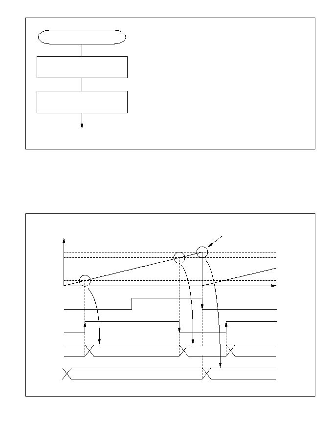
Figure 10-23 Setup Procedure for Input Capture (Example)
∑
Examples of input capture
Figure 10-24 illustrates input capture when the falling edge of TIOCB and both edges of
TIOCA are selected as capture edges. TCNT is cleared by input capture into GRB.
Figure 10-24 Input Capture (Example)
Input selection
Select input-capture input
Start counter
Input capture
Set TIOR to select the input capture function of a
general register and the rising edge, falling edge,
or both edges of the input capture signal. Clear the
port data direction bit to 0 before making these
TIOR settings.
Set the STR bit to 1 in TSTR to start the timer
counter.
1
2
1.
2.
H'0005
H'0180
Time
H'0180
H'0160
H'0005
H'0000
TIOCB
TIOCA
GRA
GRB
Counter cleared by TIOCB
input (falling edge)
TCNT value
H'0160
326

∑
Input capture signal timing
Input capture on the rising edge, falling edge, or both edges can be selected by settings in
TIOR. Figure 10-25 shows the timing when the rising edge is selected. The pulse width of the
input capture signal must be at least 1.5 system clocks for single-edge capture, and 2.5 system
clocks for capture of both edges.
Figure 10-25 Input Capture Signal Timing
N
N
¯
Input-capture input
Internal input
capture signal
TCNT
GRA, GRB
327
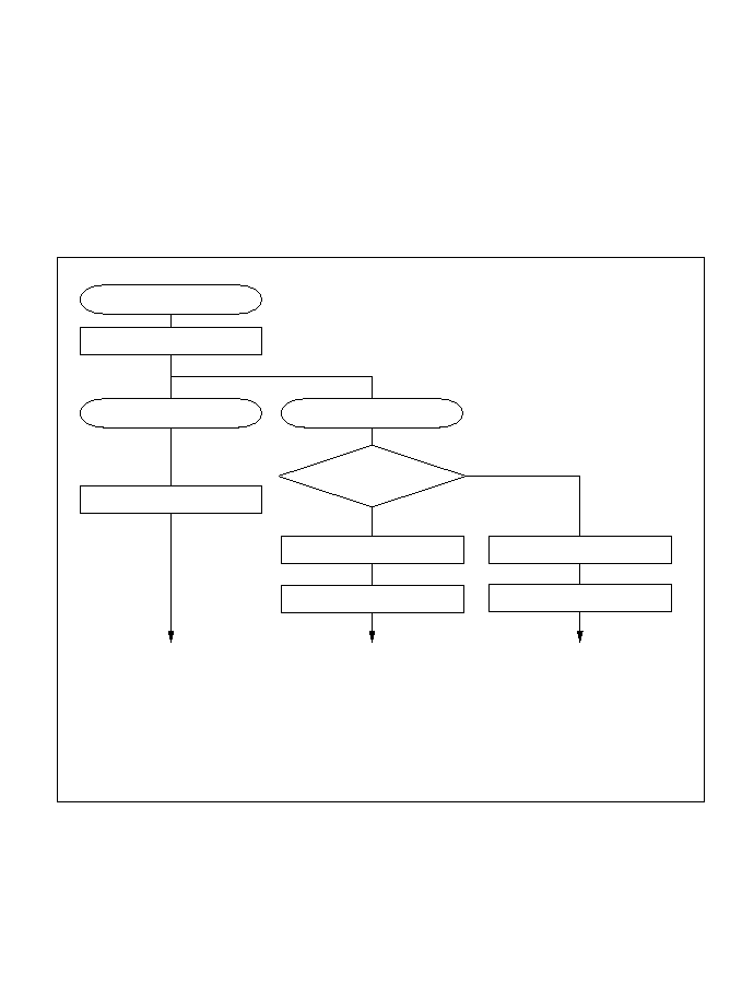
10.4.3 Synchronization
The synchronization function enables two or more timer counters to be synchronized by writing
the same data to them simultaneously (synchronous preset). With appropriate TCR settings, two or
more timer counters can also be cleared simultaneously (synchronous clear). Synchronization
enables additional general registers to be associated with a single time base. Synchronization can
be selected for all channels (0 to 4).
Sample Setup Procedure for Synchronization: Figure 10-26 shows a sample procedure for
setting up synchronization.
Figure 10-26 Setup Procedure for Synchronization (Example)
Setup for synchronization
Synchronous preset
Set the SYNC bits to 1 in TSNC for the channels to be synchronized.
When a value is written in TCNT in one of the synchronized channels, the same value is
simultaneously written in TCNT in the other channels (synchronized preset).
1.
2.
2
3
1
5
4
5
Select synchronization
Synchronous preset
Write to TCNT
Synchronous clear
Clearing
synchronized to this
channel?
Select counter clear source
Start counter
Counter clear
Synchronous clear
Start counter
Select counter clear source
Yes
No
Set the CCLR1 or CCLR0 bit in TCR to have the counter cleared by compare match or input capture.
Set the CCLR1 and CCLR0 bits in TCR to have the counter cleared synchronously.
Set the STR bits in TSTR to 1 to start the synchronized counters.
3.
4.
5.
328
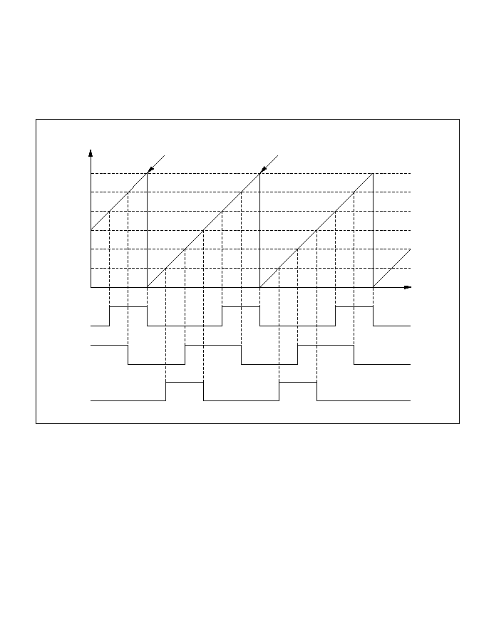
Example of Synchronization: Figure 10-27 shows an example of synchronization. Channels 0, 1,
and 2 are synchronized, and are set to operate in PWM mode. Channel 0 is set for counter clearing
by compare match with GRB0. Channels 1 and 2 are set for synchronous counter clearing. The
timer counters in channels 0, 1, and 2 are synchronously preset, and are synchronously cleared by
compare match with GRB0. A three-phase PWM waveform is output from pins TIOCA
0
,
TIOCA
1
, and TIOCA
2
. For further information on PWM mode, see section 10.4.4, PWM Mode.
Figure 10-27 Synchronization (Example)
TIOCA
2
Time
TIOCA
1
TIOCA
0
GRA2
GRA1
GRB2
GRA0
GRB1
GRB0
Value of TCNT0 to TCNT2
Cleared by compare match with GRB0
H'0000
329

10.4.4 PWM Mode
In PWM mode GRA and GRB are paired and a PWM waveform is output from the TIOCA pin.
GRA specifies the time at which the PWM output changes to 1. GRB specifies the time at which
the PWM output changes to 0. If either GRA or GRB is selected as the counter clear source, a
PWM waveform with a duty cycle from 0% to 100% is output at the TIOCA pin. PWM mode can
be selected in all channels (0 to 4).
Table 10-4 summarizes the PWM output pins and corresponding registers. If the same value is set
in GRA and GRB, the output does not change when compare match occurs.
Table 10-4 PWM Output Pins and Registers
Channel
Output Pin
1 Output
0 Output
0
TIOCA
0
GRA
0
GRB0
1
TIOCA
1
GRA
1
GRB1
2
TIOCA
2
GRA
2
GRB2
3
TIOCA
3
GRA
3
GRB3
4
TIOCA
4
GRA
4
GRB4
330
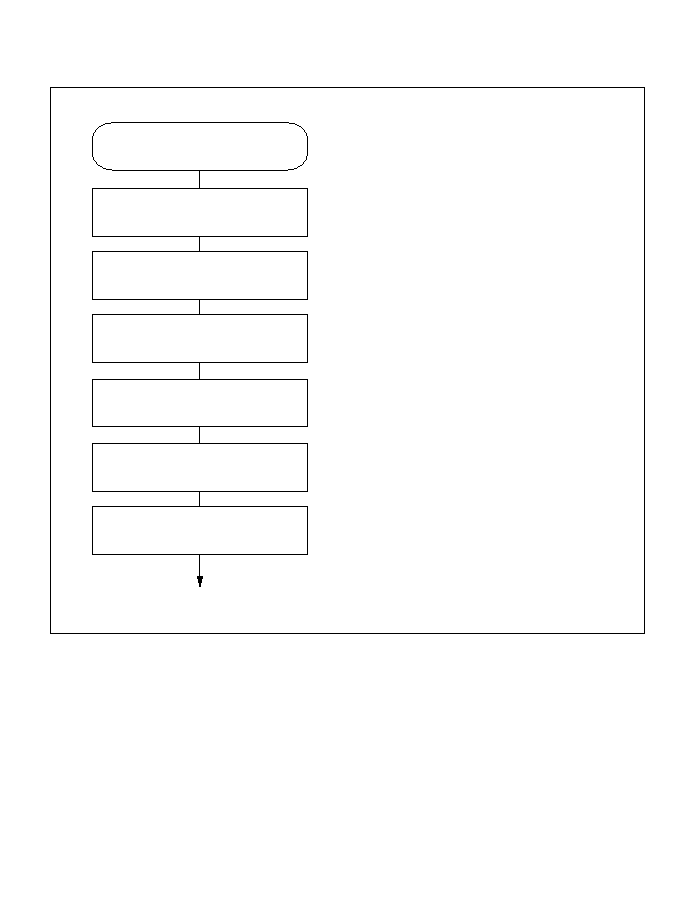
Sample Setup Procedure for PWM Mode: Figure 10-28 shows a sample procedure for setting
up PWM mode.
Figure 10-28 Setup Procedure for PWM Mode (Example)
PWM mode
1. Set bits TPSC2 to TPSC0 in TCR to
select the counter clock source. If an
external clock source is selected, set
bits CKEG1 and CKEG0 in TCR to
select the desired edge(s) of the
external clock signal.
PWM mode
Select counter clock
1
Select counter clear source
2
Set GRA
3
Set GRB
4
Select PWM mode
5
Start counter
6
2. Set bits CCLR1 and CCLR0 in TCR
to select the counter clear source.
3. Set the time at which the PWM
waveform should go to 1 in GRA.
4. Set the time at which the PWM
waveform should go to 0 in GRB.
5. Set the PWM bit in TMDR to select
PWM mode. When PWM mode is
selected, regardless of the TIOR
contents, GRA and GRB become
output compare registers specifying
the times at which the PWM output
goes to 1 and 0. The TIOCA pin
automatically becomes the PWM
output pin. The TIOCB pin conforms
to the settings of bits IOB1 and IOB0
in TIOR. If TIOCB output is not
desired, clear both IOB1 and IOB0 to 0.
6. Set the STR bit to 1 in TSTR to start
the timer counter.
331
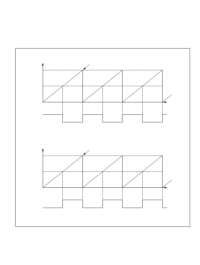
Examples of PWM Mode: Figure 10-29 shows examples of operation in PWM mode. In PWM
mode TIOCA becomes an output pin. The output goes to 1 at compare match with GRA, and to 0
at compare match with GRB.
In the examples shown, TCNT is cleared by compare match with GRA or GRB. Synchronized
operation and free-running counting are also possible.
Figure 10-29 PWM Mode (Example 1)
TCNT value
Counter cleared by compare match with GRA
Time
GRA
GRB
TIOCA
a. Counter cleared by GRA
TCNT value
Counter cleared by compare match with GRB
Time
GRB
GRA
TIOCA
b. Counter cleared by GRB
H'0000
H'0000
332
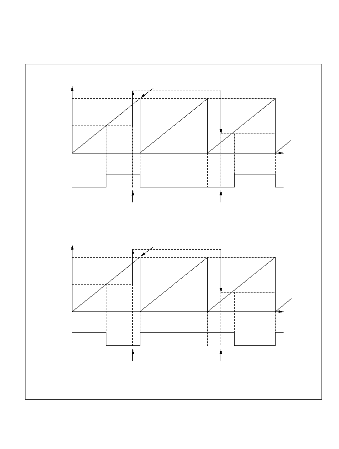
Figure 10-30 shows examples of the output of PWM waveforms with duty cycles of 0% and
100%. If the counter is cleared by compare match with GRB, and GRA is set to a higher value
than GRB, the duty cycle is 0%. If the counter is cleared by compare match with GRA, and GRB
is set to a higher value than GRA, the duty cycle is 100%.
Figure 10-30 PWM Mode (Example 2)
TCNT value
Counter cleared by compare match with GRB
Time
GRB
GRA
TIOCA
a. 0% duty cycle
TCNT value
Counter cleared by compare match with GRA
Time
GRA
GRB
TIOCA
b. 100% duty cycle
Write to GRA
Write to GRA
Write to GRB
Write to GRB
H'0000
H'0000
333

10.4.5 Reset-Synchronized PWM Mode
In reset-synchronized PWM mode channels 3 and 4 are combined to produce three pairs of
complementary PWM waveforms, all having one waveform transition point in common.
When reset-synchronized PWM mode is selected TIOCA
3
, TIOCB
3
, TIOCA
4
, TOCXA
4
, TIOCB
4
,
and TOCXB
4
automatically become PWM output pins, and TCNT3 functions as an up-counter.
Table 10-5 lists the PWM output pins. Table 10-6 summarizes the register settings.
Table 10-5 Output Pins in Reset-Synchronized PWM Mode
Channel
Output Pin
Description
3
TIOCA
3
PWM output 1
TIOCB
3
PWM output 1¥ (complementary waveform to PWM output 1)
4
TIOCA
4
PWM output 2
TOCXA
4
PWM output 2¥ (complementary waveform to PWM output 2)
TIOCB
4
PWM output 3
TOCXB
4
PWM output 3¥ (complementary waveform to PWM output 3)
Table 10-6 Register Settings in Reset-Synchronized PWM Mode
Register
Setting
TCNT3
Initially set to H'0000
TCNT4
Not used (operates independently)
GRA3
Specifies the count period of TCNT3
GRB3
Specifies a transition point of PWM waveforms output from TIOCA
3
and TIOCB
3
GRA4
Specifies a transition point of PWM waveforms output from TIOCA
4
and TOCXA
4
GRB4
Specifies a transition point of PWM waveforms output from TIOCB
4
and TOCXB
4
334
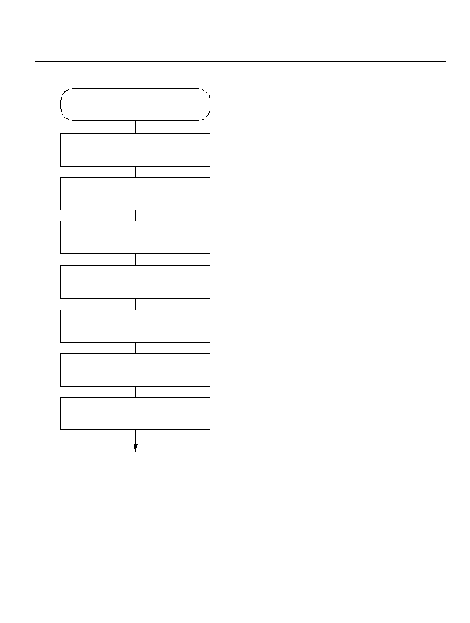
Sample Setup Procedure for Reset-Synchronized PWM Mode: Figure 10-31 shows a sample
procedure for setting up reset-synchronized PWM mode.
Figure 10-31 Setup Procedure for Reset-Synchronized PWM Mode (Example)
Reset-synchronized PWM mode
1. Clear the STR3 bit in TSTR to 0 to
halt TCNT3. Reset-synchronized
PWM mode must be set up while
TCNT3 is halted.
Reset-synchronized PWM mode
Stop counter
1
Select counter clock
2
Select counter clear source
3
Select reset-synchronized
PWM mode
4
Set TCNT
5
Set general registers
6
2. Set bits TPSC2 to TPSC0 in TCR to
select the counter clock source for
channel 3. If an external clock source
is selected, select the external clock
edge(s) with bits CKEG1 and CKEG0
in TCR.
3. Set bits CCLR1 and CCLR0 in TCR3
to select GRA3 compare match as
the counter clear source.
4. Set bits CMD1 and CMD0 in TFCR to
select reset-synchronized PWM mode.
TIOCA
3
, TIOCB
3
, TIOCA
4
, TIOCB
4
,
TOCXA
4
, and TOCXB
4
automatically
become PWM output pins.
5. Preset TCNT3 to H'0000. TCNT4
need not be preset.
Start counter
7
6. GRA3 is the waveform period register.
Set the waveform period value in
GRA3. Set transition times of the
PWM output waveforms in GRB3,
GRA4, and GRB4. Set times within
the compare match range of TCNT3.
X GRA3 (X: setting value)
7. Set the STR3 bit in TSTR to 1 to start
TCNT3.
335

Example of Reset-Synchronized PWM Mode: Figure 10-32 shows an example of operation in
reset-synchronized PWM mode. TCNT3 operates as an up-counter in this mode. TCNT4 operates
independently, detached from GRA4 and GRB4. When TCNT3 matches GRA3, TCNT3 is
cleared and resumes counting from H'0000. The PWM outputs toggle at compare match of
TCNT3 with GRB3, GRA4, and GRB4, respectively, and all toggle when the counter is cleared.
Figure 10-32 Operation in Reset-Synchronized PWM Mode (Example, OLS3 = OLS4 = 1)
For the settings and operation when reset-synchronized PWM mode and buffer mode are both
selected, see section 10.4.8, Buffering.
TCNT3 value
Counter cleared at compare match with GRA3
Time
GRA3
GRB3
GRA4
GRB4
H'0000
TIOCA
3
TIOCB
3
TIOCA
4
TOCXA
4
TIOCB
4
TOCXB
4
336

10.4.6 Complementary PWM Mode
In complementary PWM mode channels 3 and 4 are combined to output three pairs of
complementary, non-overlapping PWM waveforms.
When complementary PWM mode is selected TIOCA
3
, TIOCB
3
, TIOCA
4
, TOCXA
4
, TIOCB
4
,
and TOCXB
4
automatically become PWM output pins, and TCNT3 and TCNT4 function as
up/down-counters.
Table 10-7 lists the PWM output pins. Table 10-8 summarizes the register settings.
Table 10-7 Output Pins in Complementary PWM Mode
Channel
Output Pin
Description
3
TIOCA
3
PWM output 1
TIOCB
3
PWM output 1¥ (non-overlapping complementary waveform to PWM
output 1)
4
TIOCA
4
PWM output 2
TOCXA
4
PWM output 2¥ (non-overlapping complementary waveform to PWM
output 2)
TIOCB
4
PWM output 3
TOCXB
4
PWM output 3¥ (non-overlapping complementary waveform to PWM
output 3)
Table 10-8 Register Settings in Complementary PWM Mode
Register
Setting
TCNT3
Initially specifies the non-overlap margin (difference to TCNT4)
TCNT4
Initially set to H'0000
GRA3
Specifies the upper limit value of TCNT3 minus 1
GRB3
Specifies a transition point of PWM waveforms output from TIOCA
3
and TIOCB
3
GRA4
Specifies a transition point of PWM waveforms output from TIOCA
4
and TOCXA
4
GRB4
Specifies a transition point of PWM waveforms output from TIOCB
4
and TOCXB
4
337
Setup Procedure for Complementary PWM Mode: Figure 10-33 shows a sample procedure for
setting up complementary PWM mode.
Figure 10-33 Setup Procedure for Complementary PWM Mode (Example)
Complementary PWM mode
1. Clear bits STR3 and STR4 to 0 in
TSTR to halt the timer counters.
Complementary PWM mode must be
set up while TCNT3 and TCNT4 are
halted.
Complementary PWM mode
Stop counting
1
Select counter clock
2
Select complementary
PWM mode
3
Set TCNTs
4
Set general registers
5
Start counters
6
2. Set bits TPSC2 to TPSC0 in TCR to
select the same counter clock source
for channels 3 and 4. If an external
clock source is selected, select the
external clock edge(s) with bits
CKEG1 and CKEG0 in TCR. Do not
select any counter clear source
with bits CCLR1 and CCLR0 in TCR.
3. Set bits CMD1 and CMD0 in TFCR
to select complementary PWM mode.
TIOCA
3
, TIOCB
3
, TIOCA
4
, TIOCB
4
,
TOCXA
4
, and TOCXB
4
automatically
become PWM output pins.
4. Clear TCNT4 to H'0000. Set the
non-overlap margin in TCNT3. Do not
set TCNT3 and TCNT4 to the same
value.
5. GRA3 is the waveform period
register. Set the upper limit value of
TCNT3 minus 1 in GRA3. Set
transition times of the PWM output
waveforms in GRB3, GRA4, and
GRB4. Set times within the compare
match range of TCNT3 and TCNT4.
T
X (X: initial setting of GRB3,
GRA4, or GRB4. T: initial setting of
TCNT3)
6. Set bits STR3 and STR4 in TSTR to
1 to start TCNT3 and TCNT4.
Note: After exiting complementary PWM mode, to resume operating in complementary
PWM mode, follow the entire setup procedure from step 1 again.
338
Clearing Procedure for Complementary PWM Mode: Figure 10-34 shows the steps to clear
complementary PWM mode.
Figure 10-34 Clearing Procedure for Complementary PWM Mode
339
Clear complementary
PWM mode
Stop counter operation
1
2
1.
2.
Clear bit CMD1 bit of TFCR to 0 to set
channels 3 and 4 to normal operating mode.
After setting channels 3 and 4 to normal
operating mode, wait at least one counter
clock period, then clear bits STR3 and
STR4 of TSTR to 0 to stop counter operation
of TCNT3 andTCNT4.
Complementary PWM mode
Normal operating mode

Examples of Complementary PWM Mode: Figure 10-35 shows an example of operation in
complementary PWM mode. TCNT3 and TCNT4 operate as up/down-counters, counting down
from compare match between TCNT3 and GRA3 and counting up from the point at which
TCNT4 underflows. During each up-and-down counting cycle, PWM waveforms are generated by
compare match with general registers GRB3, GRA4, and GRB4. Since TCNT3 is initially set to a
higher value than TCNT4, compare match events occur in the sequence TCNT3, TCNT4, TCNT4,
TCNT3.
Figure 10-35 Operation in Complementary PWM Mode (Example 1, OLS3 = OLS4 = 1)
TCNT3 and
TCNT4 values
Down-counting starts at compare
match between TCNT3 and GRA3
Time
GRA3
GRB3
GRA4
GRB4
H'0000
TIOCA
3
TIOCB
3
TIOCA
4
TOCXA
4
TIOCB
4
TOCXB
4
TCNT3
TCNT4
Up-counting starts when
TCNT4 underflows
340

Figure 10-36 shows examples of waveforms with 0% and 100% duty cycles (in one phase) in
complementary PWM mode. In this example the outputs change at compare match with GRB3, so
waveforms with duty cycles of 0% or 100% can be output by setting GRB3 to a value larger than
GRA3. The duty cycle can be changed easily during operation by use of the buffer registers. For
further information see section 10.4.8, Buffering.
Figure 10-36 Operation in Complementary PWM Mode (Example 2, OLS3 = OLS4 = 1)
TCNT3 and
TCNT4 values
Time
GRA3
GRB3
TIOCA
3
TIOCB
3
0% duty cycle
a. 0% duty cycle
TCNT3 and
TCNT4 values
Time
GRA3
GRB3
TIOCA
3
TIOCB
3
100% duty cycle
b. 100% duty cycle
H'0000
H'0000
341
In complementary PWM mode, TCNT3 and TCNT4 overshoot and undershoot at the transitions
between up-counting and down-counting. The setting conditions for the IMFA bit in channel 3
and the OVF bit in channel 4 differ from the usual conditions. In buffered operation the buffer
transfer conditions also differ. Timing diagrams are shown in figures 10-37 and 10-38.
Figure 10-37 Overshoot Timing
TCNT3
GRA3
IMFA
Buffer transfer
signal (BR to GR)
GR
N ≠ 1
N
N + 1
N
N ≠ 1
N
Set to 1
Flag not set
No buffer transfer
Buffer transfer
342
Figure 10-38 Undershoot Timing
In channel 3, IMFA is set to 1 only during up-counting. In channel 4, OVF is set to 1 only when
an underflow occurs. When buffering is selected, buffer register contents are transferred to the
general register at compare match A3 during up-counting, and when TCNT4 underflows.
General Register Settings in Complementary PWM Mode: When setting up general registers
for complementary PWM mode or changing their settings during operation, note the following
points.
∑
Initial settings
Do not set values from H'0000 to T ≠ 1 (where T is the initial value of TCNT3). After the
counters start and the first compare match A3 event has occurred, however, settings in this
range also become possible.
∑
Changing settings
Use the buffer registers. Correct waveform output may not be obtained if a general register is
written to directly.
∑
Cautions on changes of general register settings
Figure 10-39 shows six correct examples and one incorrect example.
TCNT4
OVF
Buffer transfer
signal (BR to GR)
GR
H'0001
H'0000
H'FFFF
H'0000
Set to 1
Flag not set
No buffer transfer
Buffer transfer
Underflow
Overflow
343
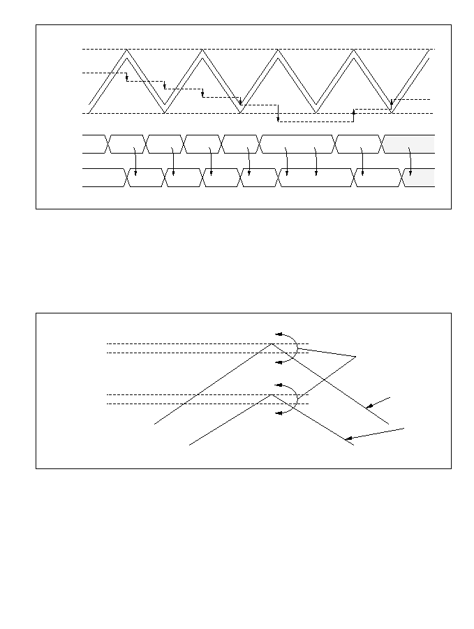
Figure 10-39 Changing a General Register Setting by Buffer Transfer (Example 1)
-- Buffer transfer at transition from up-counting to down-counting
If the general register value is in the range from GRA3 ≠ T + 1 to GRA3, do not transfer a
buffer register value outside this range. Conversely, if the general register value is outside
this range, do not transfer a value within this range. See figure 10-40.
Figure 10-40 Changing a General Register Setting by Buffer Transfer (Caution 1)
GRA3
GR
H'0000
BR
GR
Not allowed
GRA3 + 1
GRA3
GRA3 ≠ T + 1
GRA3 ≠ T
Illegal changes
TCNT3
TCNT4
344
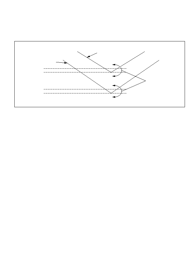
-- Buffer transfer at transition from down-counting to up-counting
If the general register value is in the range from H'0000 to T ≠ 1, do not transfer a buffer
register value outside this range. Conversely, when a general register value is outside this
range, do not transfer a value within this range. See figure 10-41.
Figure 10-41 Changing a General Register Setting by Buffer Transfer (Caution 2)
T
T ≠ 1
H'0000
H'FFFF
Illegal changes
TCNT3
TCNT4
345

-- General register settings outside the counting range (H'0000 to GRA3)
Waveforms with a duty cycle of 0% or 100% can be output by setting a general register to
a value outside the counting range. When a buffer register is set to a value outside the
counting range, then later restored to a value within the counting range, the counting
direction (up or down) must be the same both times. See figure 10-42.
Figure 10-42 Changing a General Register Setting by Buffer Transfer (Example 2)
Settings can be made in this way by detecting GRA3 compare match or TCNT4
underflow before writing to the buffer register. They can also be made by using GRA3
compare match to activate the DMAC.
0% duty cycle
100% duty cycle
Write during down-counting
Write during up-counting
GRA3
GR
H'0000
Output pin
Output pin
BR
GR
346

10.4.7 Phase Counting Mode
In phase counting mode the phase difference between two external clock inputs (at the TCLKA
and TCLKB pins) is detected, and TCNT2 counts up or down accordingly.
In phase counting mode, the TCLKA and TCLKB pins automatically function as external clock
input pins and TCNT2 becomes an up/down-counter, regardless of the settings of bits TPSC2 to
TPSC0, CKEG1, and CKEG0 in TCR2. Settings of bits CCLR1, CCLR0 in TCR2, and settings in
TIOR2, TIER2, TSR2, GRA2, and GRB2 are valid. The input capture and output compare
functions can be used, and interrupts can be generated.
Phase counting is available only in channel 2.
Sample Setup Procedure for Phase Counting Mode: Figure 10-43 shows a sample procedure
for setting up phase counting mode.
Figure 10-43 Setup Procedure for Phase Counting Mode (Example)
Phase counting mode
Select phase counting mode
Select flag setting condition
Start counter
1
2
3
Phase counting mode
1.
2.
3.
Set the MDF bit in TMDR to 1 to select
phase counting mode.
Select the flag setting condition with
the FDIR bit in TMDR.
Set the STR2 bit to 1 in TSTR to start
the timer counter.
347
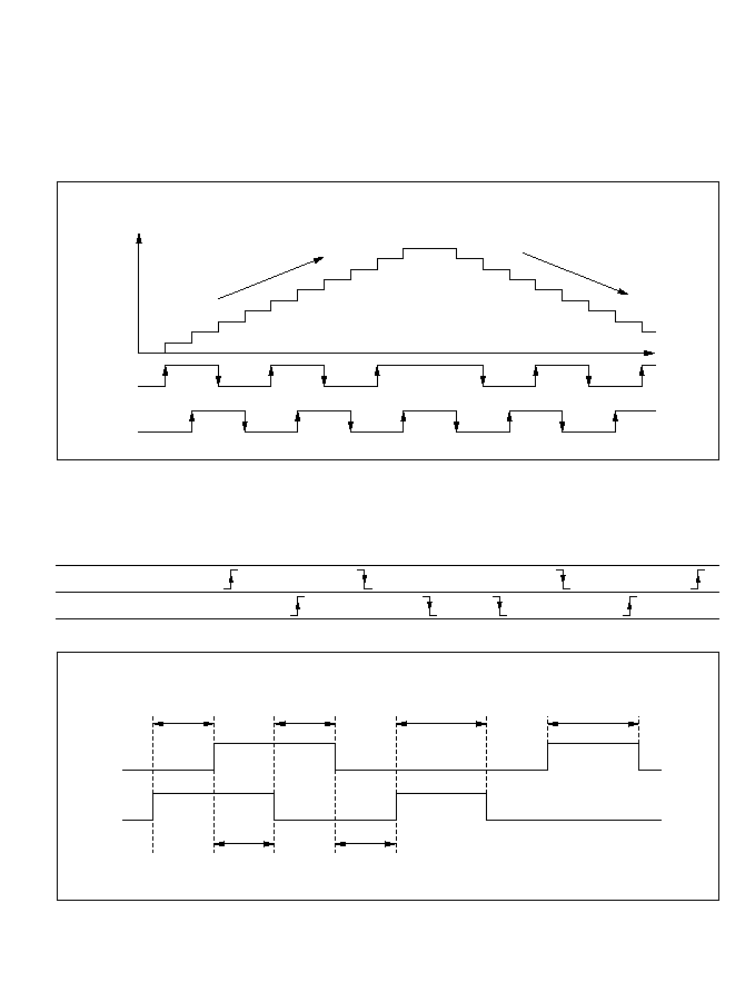
Example of Phase Counting Mode: Figure 10-44 shows an example of operations in phase
counting mode. Table 10-9 lists the up-counting and down-counting conditions for TCNT2.
In phase counting mode both the rising and falling edges of TCLKA and TCLKB are counted.
The phase difference between TCLKA and TCLKB must be at least 1.5 states, the phase overlap
must also be at least 1.5 states, and the pulse width must be at least 2.5 states. See figure 10-45.
Figure 10-44 Operation in Phase Counting Mode (Example)
Table 10-9 Up/Down Counting Conditions
Counting Direction
Up-Counting
Down-Counting
TCLKB
High
Low
High
Low
TCLKA
Low
High
Low
High
Figure 10-45 Phase Difference, Overlap, and Pulse Width in Phase Counting Mode
TCNT2 value
Counting up
Counting down
Time
TCLKB
TCLKA
TCLKA
TCLKB
Phase
difference
Phase
difference
Pulse width
Pulse width
Overlap
Overlap
Phase difference and overlap:
Pulse width:
at least 1.5 states
at least 2.5 states
348
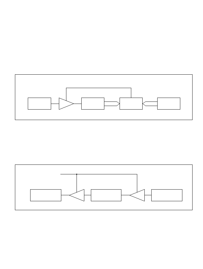
10.4.8 Buffering
Buffering operates differently depending on whether a general register is an output compare
register or an input capture register, with further differences in reset-synchronized PWM mode
and complementary PWM mode. Buffering is available only in channels 3 and 4. Buffering
operations under the conditions mentioned above are described next.
∑
General register used for output compare
The buffer register value is transferred to the general register at compare match. See
figure 10-46.
Figure 10-46 Compare Match Buffering
∑
General register used for input capture
The TCNT value is transferred to the general register at input capture. The previous general
register value is transferred to the buffer register.
See figure 10-47.
Figure 10-47 Input Capture Buffering
Compare match signal
Comparator
TCNT
GR
BR
Input capture signal
BR
GR
TCNT
349
∑
Complementary PWM mode
The buffer register value is transferred to the general register when TCNT3 and TCNT4
change counting direction. This occurs at the following two times:
-- When TCNT3 matches GRA3
-- When TCNT4 underflows
∑
Reset-synchronized PWM mode
The buffer register value is transferred to the general register at compare match A3.
Sample Buffering Setup Procedure: Figure 10-48 shows a sample buffering setup procedure.
Figure 10-48 Buffering Setup Procedure (Example)
Buffering
Select general register functions
Set buffer bits
Start counters
Buffered operation
1
1.
2.
3.
2
3
Set TIOR to select the output compare or input
capture function of the general registers.
Set bits BFA3, BFA4, BFB3, and BFB4 in TFCR
to select buffering of the required general registers.
Set the STR bits to 1 in TSTR to start the timer
counters.
350
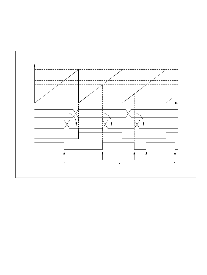
Examples of Buffering: Figure 10-49 shows an example in which GRA is set to function as an
output compare register buffered by BRA, TCNT is set to operate as a periodic counter cleared by
GRB compare match, and TIOCA and TIOCB are set to toggle at compare match A and B.
Because of the buffer setting, when TIOCA toggles at compare match A, the BRA value is
simultaneously transferred to GRA. This operation is repeated each time compare match A occurs.
Figure 10-50 shows the transfer timing.
Figure 10-49 Register Buffering (Example 1: Buffering of Output Compare Register)
GRB
H'0250
H'0200
H'0100
H'0000
BRA
GRA
TIOCB
TIOCA
TCNT value
Counter cleared by compare match B
Time
Toggle
output
Toggle
output
Compare match A
H'0200
H'0250
H'0100
H'0200
H'0100
H'0200
H'0200
351

Figure 10-50 Compare Match and Buffer Transfer Timing (Example)
¯
TCNT
BR
GR
Compare
match signal
Buffer transfer
signal
n
n + 1
n
N
N
352

Figure 10-51 shows an example in which GRA is set to function as an input capture register
buffered by BRA, and TCNT is cleared by input capture B. The falling edge is selected as the
input capture edge at TIOCB. Both edges are selected as input capture edges at TIOCA. Because
of the buffer setting, when the TCNT value is captured into GRA at input capture A, the previous
GRA value is simultaneously transferred to BRA. Figure 10-52 shows the transfer timing.
Figure 10-51 Register Buffering (Example 2: Buffering of Input Capture Register)
H'0180
H'0160
H'0005
H'0000
TIOCB
TOICA
GRA
BRA
GRB
H'0005
H'0160
H'0005
H'0180
TCNT value
Counter cleared by
input capture B
Time
Input capture A
H'0160
353

Figure 10-52 Input Capture and Buffer Transfer Timing (Example)
¯
TCNT
GR
BR
TIOC pin
Input capture
signal
n
n + 1
N
n
M
N + 1
N
n
M
m
n
M
354
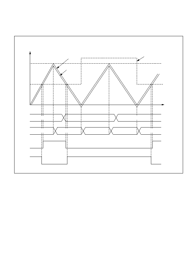
Figure 10-53 shows an example in which GRB3 is buffered by BRB3 in complementary PWM
mode. Buffering is used to set GRB3 to a higher value than GRA3, generating a PWM waveform
with 0% duty cycle. The BRB3 value is transferred to GRB3 when TCNT3 matches GRA3, and
when TCNT4 underflows.
Figure 10-53 Register Buffering (Example 4: Buffering in Complementary PWM Mode)
TCNT3 and
TCNT4 values
Time
GRA3
H'0999
H'0000
TCNT3
TCNT4
GRB3
H'1FFF
BRB3
GRB3
TIOCA
3
TIOCB
3
H'0999
H'0999
H'0999
H'1FFF
H'0999
H'1FFF
H'1FFF
H'0999
355
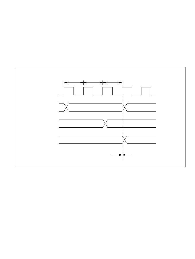
10.4.9 ITU Output Timing
The ITU outputs from channels 3 and 4 can be disabled by bit settings in TOER or by an external
trigger, or inverted by bit settings in TOCR.
Timing of Enabling and Disabling of ITU Output by TOER: In this example an ITU output is
disabled by clearing a master enable bit to 0 in TOER. An arbitrary value can be output by
appropriate settings of the data register (DR) and data direction register (DDR) of the
corresponding input/output port. Figure 10-54 illustrates the timing of the enabling and disabling
of ITU output by TOER.
Figure 10-54 Timing of Disabling of ITU Output by Writing to TOER (Example)
¯
Address
TOER
ITU output pin
TOER address
Timer output
I/O port
Generic input/output
ITU output
T
1
T
2
T
3
356
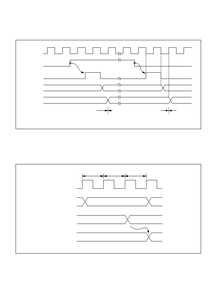
Timing of Disabling of ITU Output by External Trigger: If the XTGD bit is cleared to 0 in
TOCR in reset-synchronized PWM mode or complementary PWM mode, when an input capture
A signal occurs in channel 1, the master enable bits are cleared to 0 in TOER, disabling ITU
output. Figure 10-55 shows the timing.
Figure 10-55 Timing of Disabling of ITU Output by External Trigger (Example)
Timing of Output Inversion by TOCR: The output levels in reset-synchronized PWM mode and
complementary PWM mode can be inverted by inverting the output level select bits (OLS4 and
OLS3) in TOCR. Figure 10-56 shows the timing.
Figure 10-56 Timing of Inverting of ITU Output Level by Writing to TOCR (Example)
¯
TIOCA
1
pin
TOER
ITU output
I/O port
ITU output
I/O port
Generic
input/output
Generic
input/output
ITU output
ITU output
Input capture
signal
ITU output
pins
N
N
H'C0
H'C0
N: Arbitrary setting (H'C1 to H'FF)
¯
Address
TOCR
ITU output pin
TOCR address
Inverted
T
1
T
2
T
3
357

10.5 Interrupts
The ITU has two types of interrupts: input capture/compare match interrupts, and overflow
interrupts.
10.5.1 Setting of Status Flags
Timing of Setting of IMFA and IMFB at Compare Match: IMFA and IMFB are set to 1 by a
compare match signal generated when TCNT matches a general register (GR). The compare
match signal is generated in the last state in which the values match (when TCNT is updated from
the matching count to the next count). Therefore, when TCNT matches a general register, the
compare match signal is not generated until the next timer clock input. Figure 10-57 shows the
timing of the setting of IMFA and IMFB.
Figure 10-57 Timing of Setting of IMFA and IMFB by Compare Match
¯
TCNT
GR
IMF
IMI
TCNT input
clock
Compare
match signal
N
N + 1
N
358

Timing of Setting of IMFA and IMFB by Input Capture: IMFA and IMFB are set to 1 by an
input capture signal. The TCNT contents are simultaneously transferred to the corresponding
general register. Figure 10-58 shows the timing.
Figure 10-58 Timing of Setting of IMFA and IMFB by Input Capture
Timing of Setting of Overflow Flag (OVF): OVF is set to 1 when TCNT overflows from
H'FFFF to H'0000 or underflows from H'0000 to H'FFFF. Figure 10-59 shows the timing.
Input capture
signal
N
N
¯
IMF
TCNT
GR
IMI
359

Figure 10-59 Timing of Setting of OVF
10.5.2 Clearing of Status Flags
If the CPU reads a status flag while it is set to 1, then writes 0 in the status flag, the status flag is
cleared. Figure 10-60 shows the timing.
Figure 10-60 Timing of Clearing of Status Flags
Overflow
signal
H'FFFF
H'0000
¯
TCNT
OVF
OVI
¯
Address
IMF, OVF
TSR write cycle
TSR address
T
1
T
2
T
3
360

10.5.3 Interrupt Sources and DMA Controller Activation
Each ITU channel can generate a compare match/input capture A interrupt, a compare match/input
capture B interrupt, and an overflow interrupt. In total there are 15 interrupt sources, all
independently vectored. An interrupt is requested when the interrupt request flag and interrupt
enable bit are both set to 1.
The priority order of the channels can be modified in interrupt priority registers A and B (IPRA
and IPRB). For details see section 5, Interrupt Controller.
Compare match/input capture A interrupts in channels 0 to 3 can activate the DMA controller
(DMAC). When the DMAC is activated a CPU interrupt is not requested.
Table 10-10 lists the interrupt sources.
Table 10-10 ITU Interrupt Sources
Interrupt DMAC
Channel
Source
Description
Activatable
Priority
*
0
IMIA0
Compare match/input capture A0
Yes
High
IMIB0
Compare match/input capture B0
No
OVI0
Overflow 0
No
1
IMIA1
Compare match/input capture A1
Yes
IMIB1
Compare match/input capture B1
No
OVI1
Overflow 1
No
2
IMIA2
Compare match/input capture A2
Yes
IMIB2
Compare match/input capture B2
No
OVI2
Overflow 2
No
3
IMIA3
Compare match/input capture A3
Yes
IMIB3
Compare match/input capture B3
No
OVI3
Overflow 3
No
4
IMIA4
Compare match/input capture A4
No
IMIB4
Compare match/input capture B4
No
OVI4
Overflow 4
No
Low
Note:
*
The priority immediately after a reset is indicated. Inter-channel priorities can be changed
by settings in IPRA and IPRB.
361
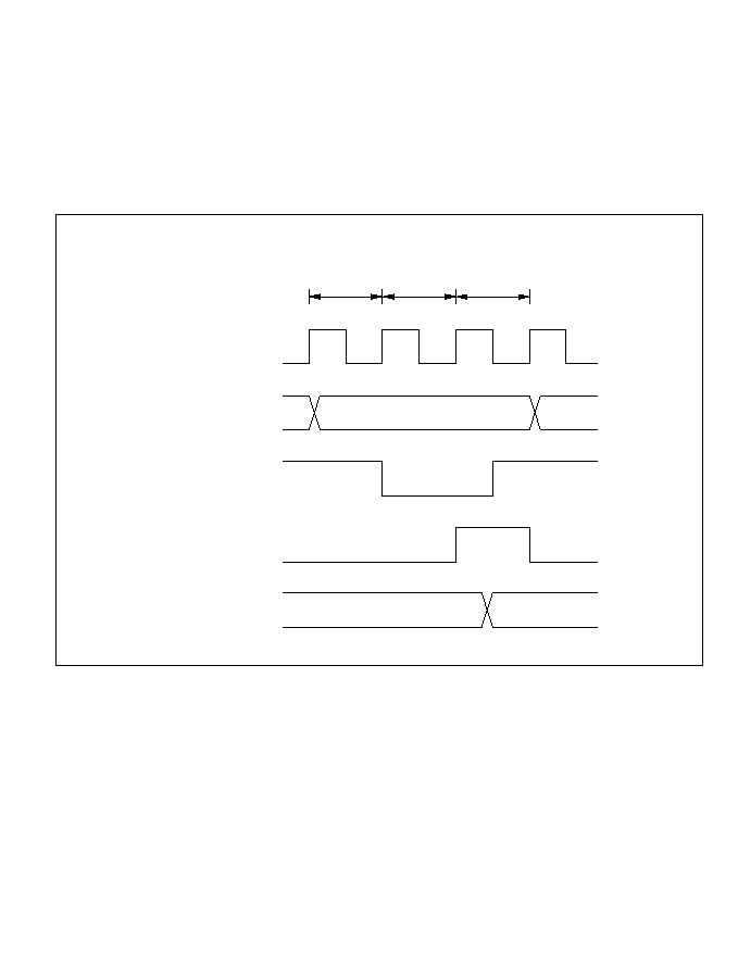
10.6 Usage Notes
This section describes contention and other matters requiring special attention during ITU
operations.
Contention between TCNT Write and Clear: If a counter clear signal occurs in the T
3
state of a
TCNT write cycle, clearing of the counter takes priority and the write is not performed. See
figure 10-61.
Figure 10-61 Contention between TCNT Write and Clear
¯
Address
Internal write signal
Counter clear signal
TCNT
TCNT write cycle
TCNT address
N
H'0000
T
1
T
2
T
3
362
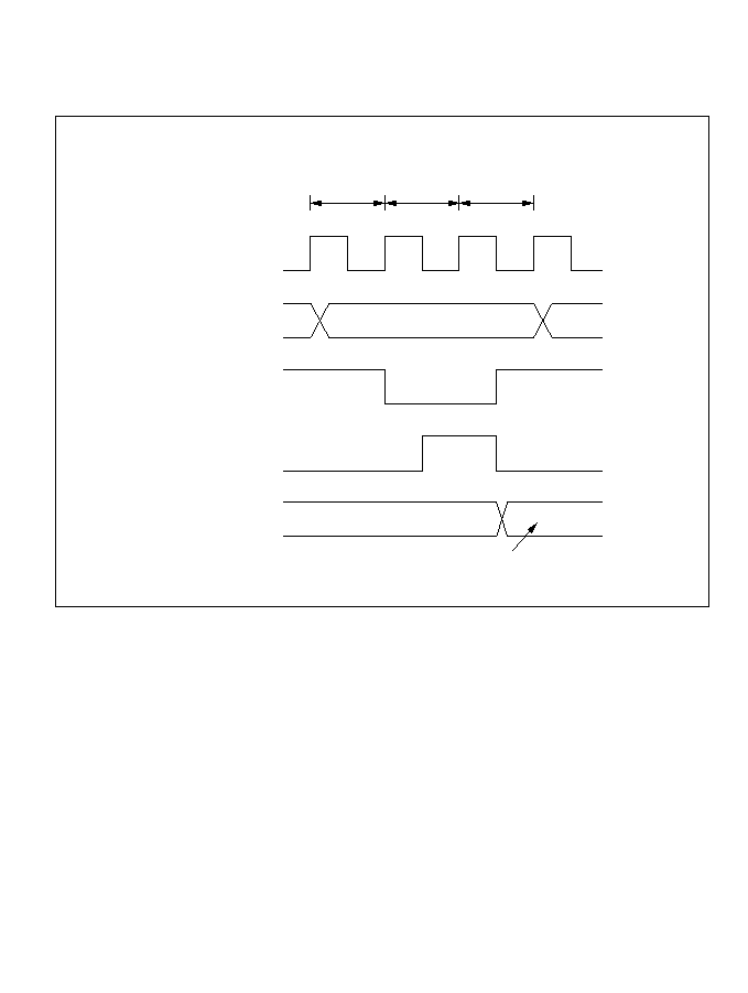
Contention between TCNT Word Write and Increment: If an increment pulse occurs in the T
3
state of a TCNT word write cycle, writing takes priority and TCNT is not incremented. See
figure 10-62.
Figure 10-62 Contention between TCNT Word Write and Increment
¯
Address
Internal write signal
TCNT input clock
TCNT
N
TCNT address
M
TCNT write data
TCNT word write cycle
T
1
T
2
T
3
363

Contention between TCNT Byte Write and Increment: If an increment pulse occurs in the T
2
or T
3
state of a TCNT byte write cycle, writing takes priority and TCNT is not incremented. The
TCNT byte that was not written retains its previous value. See figure 10-63, which shows an
increment pulse occurring in the T
2
state of a byte write to TCNTH.
Figure 10-63 Contention between TCNT Byte Write and Increment
¯
Address
Internal write signal
TCNT input clock
TCNTH
TCNTL
TCNTH byte write cycle
T
1
T
2
T
3
N
TCNTH address
M
TCNT write data
X
X
X + 1
364
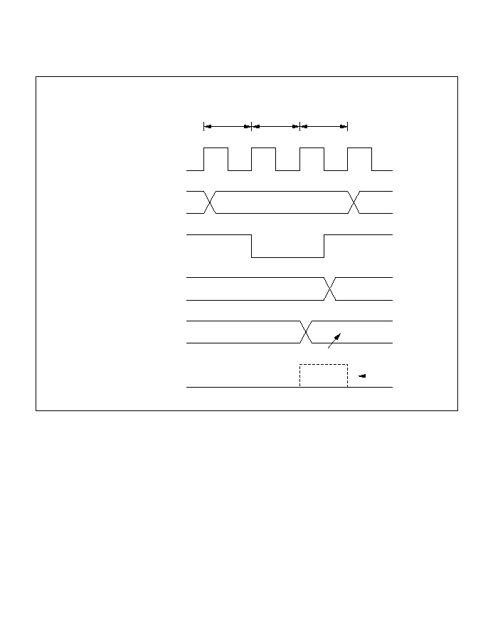
Contention between General Register Write and Compare Match: If a compare match occurs
in the T
3
state of a general register write cycle, writing takes priority and the compare match
signal is inhibited. See figure 10-64.
Figure 10-64 Contention between General Register Write and Compare Match
¯
Address
Internal write signal
TCNT
GR
Compare match signal
General register write cycle
T
1
T
2
T
3
N
GR address
M
N
N + 1
General register write data
Inhibited
365
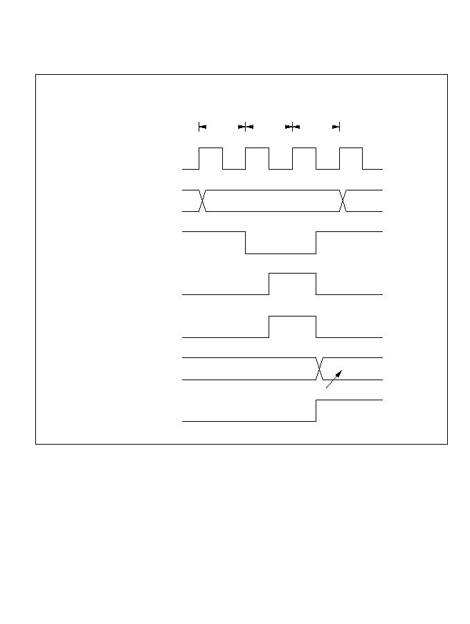
Contention between TCNT Write and Overflow or Underflow: If an overflow occurs in the T
3
state of a TCNT write cycle, writing takes priority and the counter is not incremented. OVF is
set to 1.The same holds for underflow. See figure 10-65.
Figure 10-65 Contention between TCNT Write and Overflow
¯
Address
Internal write signal
TCNT input clock
Overflow signal
TCNT
OVF
H'FFFF
TCNT address
M
TCNT write data
TCNT write cycle
T
1
T
2
T
3
366
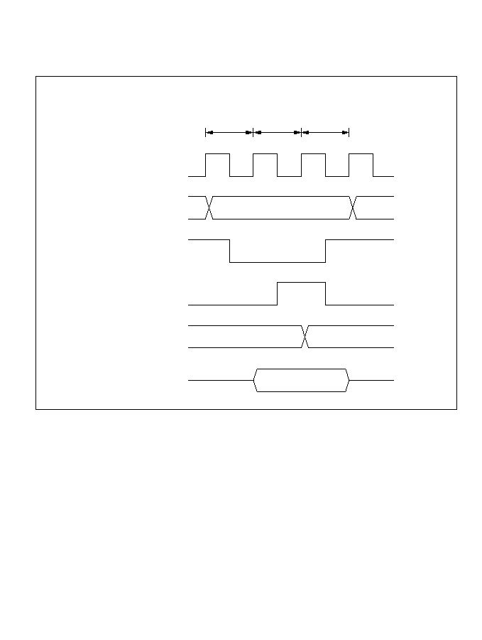
Contention between General Register Read and Input Capture: If an input capture signal
occurs during the T
3
state of a general register read cycle, the value before input capture is read.
See figure 10-66.
Figure 10-66 Contention between General Register Read and Input Capture
¯
Address
Internal read signal
Input capture signal
GR
Internal data bus
GR address
X
General register read cycle
T
1
T
2
T
3
X
M
367

Contention between Counter Clearing by Input Capture and Counter Increment: If an input
capture signal and counter increment signal occur simultaneously, the counter is cleared according
to the input capture signal. The counter is not incremented by the increment signal. The value
before the counter is cleared is transferred to the general register. See figure 10-67.
Figure 10-67 Contention between Counter Clearing by Input Capture and
Counter Increment
¯
Input capture signal
Counter clear signal
TCNT input clock
TCNT
GR
N
N
H'0000
368
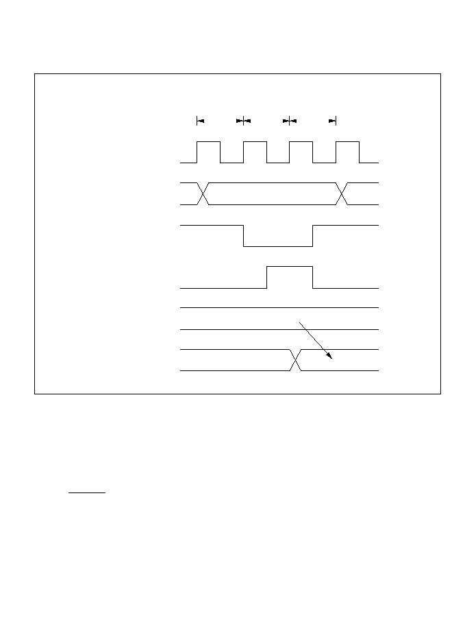
Contention between General Register Write and Input Capture: If an input capture signal
occurs in the T
3
state of a general register write cycle, input capture takes priority and the write to
the general register is not performed. See figure 10-68.
Figure 10-68 Contention between General Register Write and Input Capture
Note on Waveform Period Setting: When a counter is cleared by compare match, the counter is
cleared in the last state at which the TCNT value matches the general register value, at the time
when this value would normally be updated to the next count. The actual counter frequency is
therefore given by the following formula:
f =
(f: counter frequency. ¯: system clock frequency. N: value set in general register.)
¯
Address
Internal write signal
Input capture signal
TCNT
GR
M
GR address
General register write cycle
T
1
T
2
T
3
M
¯
(N + 1)
369
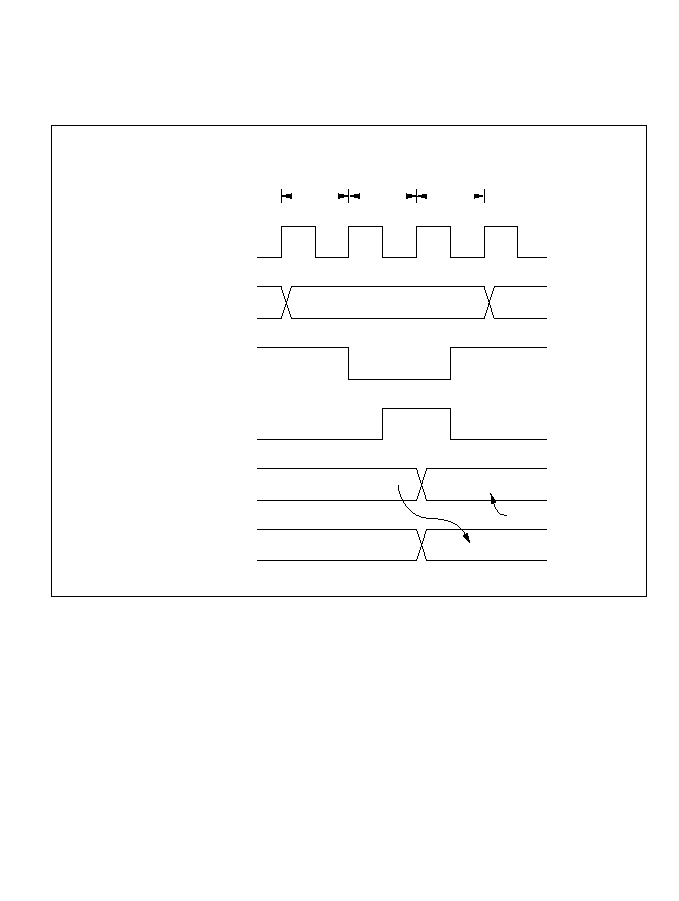
Contention between Buffer Register Write and Input Capture: If a buffer register is used for
input capture buffering and an input capture signal occurs in the T
3
state of a write cycle, input
capture takes priority and the write to the buffer register is not performed.
See figure 10-69.
Figure 10-69 Contention between Buffer Register Write and Input Capture
¯
Address
Internal write signal
Input capture signal
GR
BR
BR address
Buffer register write cycle
T
1
T
2
T
3
N
X
M
N
TCNT value
370

Note on Synchronous Preset: When channels are synchronized, if a TCNT value is modified by
byte write access, all 16 bits of all synchronized counters assume the same value as the counter
that was addressed.
(Example) When channels 2 and 3 are synchronized
Note on Setup of Reset-Synchronized PWM Mode and Complementary PWM Mode: When
setting bits CMD1 and CMD0 in TFCR, take the following precautions:
∑
Write to bits CMD1 and CMD0 only when TCNT3 and TCNT4 are stopped.
∑
Do not switch directly between reset-synchronized PWM mode and complementary PWM
mode. First switch to normal mode (by clearing bit CMD1 to 0), then select reset-
synchronized PWM mode or complementary PWM mode.
∑ Byte write to channel 2 or byte write to channel 3
TCNT2
TCNT3
W
Y
X
Z
TCNT2
TCNT3
A
A
X
X
TCNT2
TCNT3
Y
Y
A
A
TCNT2
TCNT3
W
Y
X
Z
TCNT2
TCNT3
A
A
B
B
∑ Word write to channel 2 or word write to channel 3
Upper byte Lower byte
Upper byte Lower byte
Upper byte Lower byte
Upper byte Lower byte
Upper byte Lower byte
Write A to upper byte
of channel 2
Write A to lower byte
of channel 3
Write AB word to
channel 2 or 3
371

ITU Operating Modes
T
able 10-1
1 (a) ITU Operating Modes (Channel 0)
Register Settings
TSNC
TMDR
TFCR
T
OCR
T
OER
TIOR0
TCR0
Reset-
Comple-
Synchro-
Output
Synchro-
mentary nized
Buffer-
Level
Master
Clear
Clock
Operating Mode
nization
MDF
FDIR
PWM
PWM
PWM
ing
XTGD
Select
Enable
IOA
IOB
Select
Select
Synchronous preset
SYNC0 = 1
--
--
----
--
--
--
--
PWM mode
--
--
PWM0 = 1
--
--
--
--
--
--
--
*
Output compare A
--
--
PWM0 = 0
--
--
--
--
--
--
IOA2 = 0
Other bits
unrestricted
Output compare B
----
----
--
--
--
--
IOB2 = 0
Other bits
unrestricted
Input capture A
--
--
PWM0 = 0
--
--
--
--
--
--
IOA2 = 1
Other bits
unrestricted
Input capture B
--
--
PWM0 = 0
--
--
--
--
--
--
IOB2 = 1
Other bits
unrestricted
Counter By
compare
----
----
--
--
--
--
CCLR1 = 0
clearing
match/input
CCLR0 = 1
capture A
By compare
----
----
--
--
--
--
CCLR1 = 1
match/input
CCLR0 = 0
capture B
Syn-
SYNC0 = 1
--
--
----
--
--
--
--
CCLR1 = 1
chronous
CCLR0 = 1
clear
Legend:
Setting available (valid). -- Setting does not af
fect this mode.
Note:
*
The input capture function cannot be used in PWM mode. If compare match A and compare match B occur simultaneously
, the compare
match signal is inhibited.
372

T
able 10-1
1 (b) ITU Operating Modes (Channel 1)
Register Settings
TSNC
TMDR
TFCR
T
OCR
T
OER
TIOR1
TCR1
Reset-
Comple-
Synchro-
Output
Synchro-
mentary nized
Buffer-
Level
Master
Clear
Clock
Operating Mode
nization
MDF
FDIR
PWM
PWM
PWM
ing
XTGD
Select
Enable
IOA
IOB
Select
Select
Synchronous preset
SYNC1 = 1
--
--
----
--
--
--
--
PWM mode
--
--
PWM1 = 1
--
--
--
--
--
--
--
*
1
Output compare A
--
--
PWM1 = 0
--
--
--
--
--
--
IOA2 = 0
Other bits
unrestricted
Output compare B
----
----
--
--
--
--
IOB2 = 0
Other bits
unrestricted
Input capture A
--
--
PWM1 = 0
--
--
--
*
2
--
--
IOA2 = 1
Other bits
unrestricted
Input capture B
--
--
PWM1 = 0
--
--
--
--
--
--
IOB2 = 1
Other bits
unrestricted
Counter By
compare
----
----
--
--
--
--
CCLR1 = 0
clearing
match/input
CCLR0 = 1
capture A
By compare
----
----
--
--
--
--
CCLR1 = 1
match/input
CCLR0 = 0
capture B
Syn-
SYNC1 = 1
--
--
----
--
--
--
--
CCLR1 = 1
chronous
CCLR0 = 1
clear
Legend:
Setting available (valid). -- Setting does not af
fect this mode.
Notes:
1.
The input capture function cannot be used in PWM mode. If compare match A and compare match B occur simultaneously
, the
compare match signal is inhibited.
2.
V
alid only when channels 3 and 4 are operating in complementary PWM mode or reset-synchronized PWM mode.
373

T
able 10-1
1 (c) ITU Operating Modes (Channel 2)
Register Settings
TSNC
TMDR
TFCR
T
OCR
T
OER
TIOR2
TCR2
Reset-
Comple-
Synchro-
Output
Synchro-
mentary nized
Buffer-
Level
Master
Clear
Clock
Operating Mode
nization
MDF
FDIR
PWM
PWM
PWM
ing
XTGD
Select
Enable
IOA
IOB
Select
Select
Synchronous preset
SYNC2 = 1
--
----
--
--
--
--
PWM mode
--
PWM2 = 1
--
--
--
--
--
--
--
*
Output compare A
--
PWM2 = 0
--
--
--
--
--
--
IOA2 = 0
Other bits
unrestricted
Output compare B
--
----
--
--
--
--
IOB2 = 0
Other bits
unrestricted
Input capture A
--
PWM2 = 0
--
--
--
--
--
--
IOA2 = 1
Other bits
unrestricted
Input capture B
--
PWM2 = 0
--
--
--
--
--
--
IOB2 = 1
Other bits
unrestricted
Counter By
compare
--
----
--
--
--
--
CCLR1 = 0
clearing
match/input
CCLR0 = 1
capture A
By compare
--
----
--
--
--
--
CCLR1 = 1
match/input
CCLR0 = 0
capture B
Syn-
SYNC2 = 1
--
----
--
--
--
--
CCLR1 = 1
chronous
CCLR0 = 1
clear
Phase counting
MDF = 1
----
--
--
--
--
--
mode
Legend:
Setting available (valid). -- Setting does not af
fect this mode.
Note:
*
The input capture function cannot be used in PWM mode. If compare match A and compare match B occur simultaneously
, the compare
match signal is inhibited.
374

T
able 10-1
1 (d) ITU Operating Modes (Channel 3)
Register Settings
TSNC
TMDR
TFCR
T
OCR
T
O
ER
TIOR3
TCR3
Comple-
Reset-
Output
Synchro-
mentary Synchro-
Level
Master
Clear
Clock
Operating Mode
nization
MDF
FDIR
PWM
PWM
nized PWM
Buffering
XTGD
Select
Enable
IOA
IOB
Select
Select
Synchronous preset
SYNC3 = 1
--
--
*
3
----
*
1
PWM mode
--
--
PWM3 = 1
CMD1 = 0
CMD1 = 0
----
--
*
2
Output compare A
--
--
PWM3 = 0
CMD1 = 0
CMD1 = 0
----
IOA2 = 0
Other bits
unrestricted
Output compare B
----
CMD1 = 0
CMD1 = 0
----
IOB2 = 0
Other bits
unrestricted
Input capture A
--
--
PWM3 = 0
CMD1 = 0
CMD1 = 0
--
--
EA3 ignored
IOA2 = 1
Other bits
Other bits
unrestricted
unrestricted
Input capture B
--
--
PWM3 = 0
CMD1 = 0
CMD1 = 0
--
--
EA3 ignored
IOA2 = 1
Other bits
Other bits
unrestricted
unrestricted
Counter By
compare
----
Illegal setting:
*
4
----
*
1
CCLR1 = 0
clearing
match/input
CMD1 = 1
CCLR0 = 1
capture A
CMD0 = 0
By compare
----
CMD1 = 0
CMD1 = 0
----
*
1
CCLR1 = 1
match/input
CCLR0 = 0
capture B
Syn-
SYNC3 = 1
--
--
Illegal setting:
----
*
1
CCLR1 = 1
chronous
CMD1 = 1
CCLR0 = 1
clear
CMD0 = 0
Complementary
*
3
--
--
--
CMD1 = 1
CMD1 = 1
*
6
--
--
CCLR1 = 0
*
5
PWM mode
CMD0 = 0
CMD0 = 0
CCLR0 = 0
Reset-synchronized
--
--
--
CMD1 = 1
CMD1 = 1
*
6
--
--
CCLR1 = 0
PWM mode
CMD0 = 1
CMD0 = 1
CCLR0 = 1
Buf
fering
----
BF
A3 = 1
--
--
*
1
(BRA)
Other bits
unrestricted
Buf
fering
----
BFB3 = 1
--
--
*
1
(BRB)
Other bits
unrestricted
Legend:
Setting available (valid). -- Setting does not af
fect this mode.
Notes:
1.
Master enable bit settings are valid only during waveform output.
2.
The input capture function cannot be used in PWM mode. If compare match A and compare match B occur simultaneously
, the compa
re match signal is inhibited.
3.
Do not set both channels 3 and 4 for synchronous operation when complementary PWM mode is selected.
4.
The counter cannot be cleared by input capture A when reset-synchronized PWM mode is selected.
5.
In complementary PWM mode, select the same clock source for channels 3 and 4.
6.
Use the input capture A function in channel 1.
375

T
able 10-1
1 (e) ITU Operating Modes (Channel 4)
Register Settings
TSNC
TMDR
TFCR
T
OCR
T
O
ER
TIOR4
TCR4
Comple-
Reset-
Output
Synchro-
mentary Synchro-
Level
Master
Clear
Clock
Operating Mode
nization
MDF
FDIR
PWM
PWM
nized PWM
Buffering
XTGD
Select
Enable
IOA
IOB
Select
Select
Synchronous preset
SYNC4 = 1
--
--
*
3
----
*
1
PWM mode
--
--
PWM4 = 1
CMD1 = 0
CMD1 = 0
----
--
*
2
Output compare A
--
--
PWM4 = 0
CMD1 = 0
CMD1 = 0
----
IOA2 = 0
Other bits
unrestricted
Output compare B
----
CMD1 = 0
CMD1 = 0
----
IOB2 = 0
Other bits
unrestricted
Input capture A
--
--
PWM4 = 0
CMD1 = 0
CMD1 = 0
--
--
EA4 ignored
IOA2 = 1
Other bits
Other bits
unrestricted
unrestricted
Input capture B
--
--
PWM4 = 0
CMD1 = 0
CMD1 = 0
--
--
EB4 ignored
IOB2 = 1
Other bits
Other bits
unrestricted
unrestricted
Counter By
compare
----
Illegal setting:
*
4
----
*
1
CCLR1 = 0
clearing
match/input
CMD1 = 1
CCLR0 = 1
capture A
CMD0 = 0
By compare
----
Illegal setting:
*
4
----
*
1
CCLR1 = 1
match/input
CMD1 = 1
CCLR0 = 0
capture B
CMD0 = 0
Syn-
SYNC4 = 1
--
--
Illegal setting:
*
4
----
*
1
CCLR1 = 1
chronous
CMD1 = 1
CCLR0 = 1
clear
CMD0 = 0
Complementary
*
3
--
--
--
CMD1 = 1
CMD1 = 1
--
--
CCLR1 = 0
*
5
PWM mode
CMD0 = 0
CMD0 = 0
CCLR0 = 0
Reset-synchronized
--
--
--
CMD1 = 1
CMD1 = 1
----
*
6
*
6
PWM mode
CMD0 = 1
CMD0 = 1
Buf
fering
----
BF
A4 = 1
--
--
*
1
(BRA)
Other bits
unrestricted
Buf
fering
----
BFB4 = 1
--
--
*
1
(BRB)
Other bits
unrestricted
Legend:
Setting available (valid). -- Setting does not af
fect this mode.
Notes:
1.
Master enable bit settings are valid only during waveform output.
2.
The input capture function cannot be used in PWM mode. If compare match A and compare match B occur simultaneously
, the compa
re match signal is inhibited.
3.
Do not set both channels 3 and 4 for synchronous operation when complementary PWM mode is selected.
4.
When reset-synchronized PWM mode is selected, TCNT4 operates independently and the counter clearing function is available. W
a
veform output is not af
fected.
5.
In complementary PWM mode, select the same clock source for channels 3 and 4.
6.
TCR4 settings are valid in reset-synchronized PWM mode, but TCNT4 operates independently
, without af
fecting waveform output.
376

Section 11 Programmable Timing Pattern Controller
11.1 Overview
The H8/3002 has a built-in programmable timing pattern controller (TPC) that provides pulse
outputs by using the 16-bit integrated timer unit (ITU) as a time base. The TPC pulse outputs are
divided into 4-bit groups (group 3 to group 0) that can operate simultaneously and independently.
11.1.1 Features
TPC features are listed below.
∑
16-bit output data
Maximum 16-bit data can be output. TPC output can be enabled on a bit-by-bit basis.
∑
Four output groups
Output trigger signals can be selected in 4-bit groups to provide up to four different 4-bit
outputs.
∑
Selectable output trigger signals
Output trigger signals can be selected for each group from the compare-match signals of four
ITU channels.
∑
Non-overlap mode
A non-overlap margin can be provided between pulse outputs.
∑
Can operate together with the DMA controller (DMAC)
The compare-match signals selected as trigger signals can activate the DMAC for sequential
output of data without CPU intervention.
377
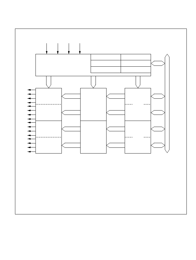
11.1.2 Block Diagram
Figure 11-1 shows a block diagram of the TPC.
Figure 11-1 TPC Block Diagram
PADDR
NDERA
TPMR
PBDDR
NDERB
TPCR
Internal
data bus
TP
TP
TP
TP
TP
TP
TP
TP
TP
TP
TP
TP
TP
TP
TP
TP
15
14
13
12
11
10
9
8
7
6
5
4
3
2
1
0
Control logic
ITU compare match signals
Pulse output
pins, group 3
PBDR
PADR
Legend
TPMR:
TPCR:
NDERB:
NDERA:
PBDDR:
PADDR:
NDRB:
NDRA:
PBDR:
PADR:
Pulse output
pins, group 2
Pulse output
pins, group 1
Pulse output
pins, group 0
TPC output mode register
TPC output control register
Next data enable register B
Next data enable register A
Port B data direction register
Port A data direction register
Next data register B
Next data register A
Port B data register
Port A data register
NDRB
NDRA
378

11.1.3 TPC Pins
Table 11-1 summarizes the TPC output pins.
Table 11-1 TPC Pins
Name
Symbol
I/O
Function
TPC output 0
TP
0
Output
Group 0 pulse output
TPC output 1
TP
1
Output
TPC output 2
TP
2
Output
TPC output 3
TP
3
Output
TPC output 4
TP
4
Output
Group 1 pulse output
TPC output 5
TP
5
Output
TPC output 6
TP
6
Output
TPC output 7
TP
7
Output
TPC output 8
TP
8
Output
Group 2 pulse output
TPC output 9
TP
9
Output
TPC output 10
TP
10
Output
TPC output 11
TP
11
Output
TPC output 12
TP
12
Output
Group 3 pulse output
TPC output 13
TP
13
Output
TPC output 14
TP
14
Output
TPC output 15
TP
15
Output
379

11.1.4 Registers
Table 11-2 summarizes the TPC registers.
Table 11-2 TPC Registers
Address
*
1
Name
Abbreviation
R/W
Initial Value
H'FFD1
Port A data direction register
PADDR
W
H'00
H'FFD3
Port A data register
PADR
R/(W)
*
2
H'00
H'FFD4
Port B data direction register
PBDDR
W
H'00
H'FFD6
Port B data register
PBDR
R/(W)
*
2
H'00
H'FFA0
TPC output mode register
TPMR
R/W
H'F0
H'FFA1
TPC output control register
TPCR
R/W
H'FF
H'FFA2
Next data enable register B
NDERB
R/W
H'00
H'FFA3
Next data enable register A
NDERA
R/W
H'00
H'FFA5/
Next data register A
NDRA
R/W
H'00
H'FFA7
*
3
H'FFA4
Next data register B
NDRB
R/W
H'00
H'FFA6
*
3
Notes: 1. Lower 16 bits of the address.
2. Bits used for TPC output cannot be written.
3. The NDRA address is H'FFA5 when the same output trigger is selected for TPC output
groups 0 and 1 by settings in TPCR. When the output triggers are different, the NDRA
address is H'FFA7 for group 0 and H'FFA5 for group 1. Similarly, the address of NDRB
is H'FFA4 when the same output trigger is selected for TPC output groups 2 and 3 by
settings in TPCR. When the output triggers are different, the NDRB address is H'FFA6
for group 2 and H'FFA4 for group 3.
380

11.2 Register Descriptions
11.2.1 Port A Data Direction Register (PADDR)
PADDR is an 8-bit write-only register that selects input or output for each pin in port A.
Port A is multiplexed with pins TP
7
to TP
0
. Bits corresponding to pins used for TPC output must
be set to 1. For further information about PADDR, see section 9.7, Port A.
11.2.2 Port A Data Register (PADR)
PADR is an 8-bit readable/writable register that stores TPC output data for groups 0 and 1, when
these TPC output groups are used.
For further information about PADR, see section 9.7, Port A.
Bit
Initial value
Read/Write
7
PA DDR
0
W
Port A data direction 7 to 0
These bits select input or
output for port A pins
7
6
PA DDR
0
W
6
5
PA DDR
0
W
5
4
PA DDR
0
W
4
3
PA DDR
0
W
3
2
PA DDR
0
W
2
1
PA DDR
0
W
1
0
PA DDR
0
W
0
Bit
Initial value
Read/Write
0
PA
0
R/(W)
0
1
PA
0
R/(W)
1
2
PA
0
R/(W)
2
3
PA
0
R/(W)
3
4
PA
0
R/(W)
4
5
PA
0
R/(W)
5
6
PA
0
R/(W)
6
7
PA
0
R/(W)
7
Port A data 7 to 0
These bits store output data
for TPC output groups 0 and 1
*
*
*
*
*
*
*
*
Note: Bits selected for TPC output by NDERA settings become read-only bits.
*
381

11.2.3 Port B Data Direction Register (PBDDR)
PBDDR is an 8-bit write-only register that selects input or output for each pin in port B.
Port B is multiplexed with pins TP
15
to TP
8
. Bits corresponding to pins used for TPC output must
be set to 1. For further information about PBDDR, see section 9.8, Port B.
11.2.4 Port B Data Register (PBDR)
PBDR is an 8-bit readable/writable register that stores TPC output data for groups 2 and 3, when
these TPC output groups are used.
For further information about PBDR, see section 9.8, Port B.
Bit
Initial value
Read/Write
7
PB DDR
0
W
Port B data direction 7 to 0
These bits select input or
output for port B pins
7
6
PB DDR
0
W
6
5
PB DDR
0
W
5
4
PB DDR
0
W
4
3
PB DDR
0
W
3
2
PB DDR
0
W
2
1
PB DDR
0
W
1
0
PB DDR
0
W
0
Bit
Initial value
Read/Write
0
PB
0
R/(W)
0
1
PB
0
R/(W)
1
2
PB
0
R/(W)
2
3
PB
0
R/(W)
3
4
PB
0
R/(W)
4
5
PB
0
R/(W)
5
6
PB
0
R/(W)
6
7
PB
0
R/(W)
7
Port B data 7 to 0
These bits store output data
for TPC output groups 2 and 3
*
*
*
*
*
*
*
*
Note: Bits selected for TPC output by NDERB settings become read-only bits.
*
382

11.2.5 Next Data Register A (NDRA)
NDRA is an 8-bit readable/writable register that stores the next output data for TPC output groups
1 and 0 (pins TP
7
to TP
0
). During TPC output, when an ITU compare match event specified in
TPCR occurs, NDRA contents are transferred to the corresponding bits in PADR. The address of
NDRA differs depending on whether TPC output groups 0 and 1 have the same output trigger or
different output triggers.
NDRA is initialized to H'00 by a reset and in hardware standby mode. It is not initialized in
software standby mode.
Same Trigger for TPC Output Groups 0 and 1: If TPC output groups 0 and 1 are triggered by
the same compare match event, the NDRA address is H'FFA5. The upper 4 bits belong to group 1
and the lower 4 bits to group 0. Address H'FFA7 consists entirely of reserved bits that cannot be
modified and always read 1.
Address H'FFA5
Address H'FFA7
Bit
Initial value
Read/Write
7
NDR7
0
R/W
6
NDR6
0
R/W
5
NDR5
0
R/W
4
NDR4
0
R/W
3
NDR3
0
R/W
2
NDR2
0
R/W
1
NDR1
0
R/W
0
NDR0
0
R/W
Next data 3 to 0
These bits store the next output
data for TPC output group 0
Next data 7 to 4
These bits store the next output
data for TPC output group 1
Bit
Initial value
Read/Write
0
--
1
--
1
--
1
--
2
--
1
--
3
--
1
--
4
--
1
--
5
--
1
--
6
--
1
--
7
--
1
--
Reserved bits
383

Different Triggers for TPC Output Groups 0 and 1: If TPC output groups 0 and 1 are triggered
by different compare match events, the address of the upper 4 bits of NDRA (group 1) is H'FFA5
and the address of the lower 4 bits (group 0) is H'FFA7. Bits 3 to 0 of address H'FFA5 and bits 7
to 4 of address H'FFA7 are reserved bits that cannot be modified and always read 1.
Address H'FFA5
Address H'FFA7
Bit
Initial value
Read/Write
7
NDR7
0
R/W
6
NDR6
0
R/W
5
NDR5
0
R/W
4
NDR4
0
R/W
3
--
1
--
2
--
1
--
1
--
1
--
0
--
1
--
Reserved bits
Next data 7 to 4
These bits store the next output
data for TPC output group 1
Bit
Initial value
Read/Write
7
--
1
--
6
--
1
--
5
--
1
--
4
--
1
--
3
NDR3
0
R/W
2
NDR2
0
R/W
1
NDR1
0
R/W
0
NDR0
0
R/W
Next data 3 to 0
These bits store the next output
data for TPC output group 0
Reserved bits
384

11.2.6 Next Data Register B (NDRB)
NDRB is an 8-bit readable/writable register that stores the next output data for TPC output groups
3 and 2 (pins TP
15
to TP
8
). During TPC output, when an ITU compare match event specified in
TPCR occurs, NDRB contents are transferred to the corresponding bits in PBDR. The address of
NDRB differs depending on whether TPC output groups 2 and 3 have the same output trigger or
different output triggers.
NDRB is initialized to H'00 by a reset and in hardware standby mode. It is not initialized in
software standby mode.
Same Trigger for TPC Output Groups 2 and 3: If TPC output groups 2 and 3 are triggered by
the same compare match event, the NDRB address is H'FFA4. The upper 4 bits belong to group 3
and the lower 4 bits to group 2. Address H'FFA6 consists entirely of reserved bits that cannot be
modified and always read 1.
Address H'FFA4
Address H'FFA6
Bit
Initial value
Read/Write
7
NDR15
0
R/W
6
NDR14
0
R/W
5
NDR13
0
R/W
4
NDR12
0
R/W
3
NDR11
0
R/W
2
NDR10
0
R/W
1
NDR9
0
R/W
0
NDR8
0
R/W
Next data 11 to 8
These bits store the next output
data for TPC output group 2
Next data 15 to 12
These bits store the next output
data for TPC output group 3
Bit
Initial value
Read/Write
7
NDR15
0
R/W
6
NDR14
0
R/W
5
NDR13
0
R/W
4
NDR12
0
R/W
3
NDR11
0
R/W
2
NDR10
0
R/W
1
NDR9
0
R/W
0
NDR8
0
R/W
Next data 11 to 8
These bits store the next output
data for TPC output group 2
Next data 15 to 12
These bits store the next output
data for TPC output group 3
Bit
Initial value
Read/Write
0
--
1
--
1
--
1
--
2
--
1
--
3
--
1
--
4
--
1
--
5
--
1
--
6
--
1
--
7
--
1
--
Reserved bits
385

Different Triggers for TPC Output Groups 2 and 3: If TPC output groups 2 and 3 are triggered
by different compare match events, the address of the upper 4 bits of NDRB (group 3) is H'FFA4
and the address of the lower 4 bits (group 2) is H'FFA6. Bits 3 to 0 of address H'FFA4 and bits 7
to 4 of address H'FFA6 are reserved bits that cannot be modified and always read 1.
Address H'FFA4
Address H'FFA6
Bit
Initial value
Read/Write
7
NDR15
0
R/W
6
NDR14
0
R/W
5
NDR13
0
R/W
4
NDR12
0
R/W
3
--
1
--
2
--
1
--
1
--
1
--
0
--
1
--
Reserved bits
Next data 15 to 12
These bits store the next output
data for TPC output group 3
Bit
Initial value
Read/Write
7
--
1
--
6
--
1
--
5
--
1
--
4
--
1
--
3
NDR11
0
R/W
2
NDR10
0
R/W
1
NDR9
0
R/W
0
NDR8
0
R/W
Next data 11 to 8
These bits store the next output
data for TPC output group 2
Reserved bits
386

11.2.7 Next Data Enable Register A (NDERA)
NDERA is an 8-bit readable/writable register that enables or disables TPC output groups 1 and 0
(TP
7
to TP
0
) on a bit-by-bit basis.
If a bit is enabled for TPC output by NDERA, then when the ITU compare match event selected
in the TPC output control register (TPCR) occurs, the NDRA value is automatically transferred to
the corresponding PADR bit, updating the output value. If TPC output is disabled, the bit value is
not transferred from NDRA to PADR and the output value does not change.
NDERA is initialized to H'00 by a reset and in hardware standby mode. It is not initialized in
software standby mode.
Bits 7 to 0--Next Data Enable 7 to 0 (NDER7 to NDER0): These bits enable or disable TPC
output groups 1 and 0 (TP
7
to TP
0
) on a bit-by-bit basis.
Bits 7 to 0
NDER7 to NDER0
Description
0
TPC outputs TP
7
to TP
0
are disabled
(Initial value)
(NDR7 to NDR0 are not transferred to PA
7
to PA
0
)
1
TPC outputs TP
7
to TP
0
are enabled
(NDR7 to NDR0 are transferred to PA
7
to PA
0
)
Bit
Initial value
Read/Write
0
NDER0
0
R/W
1
NDER1
0
R/W
2
NDER2
0
R/W
3
NDER3
0
R/W
4
NDER4
0
R/W
5
NDER5
0
R/W
6
NDER6
0
R/W
7
NDER7
0
R/W
Next data enable 7 to 0
These bits enable or disable
TPC output groups 1 and 0
387

11.2.8 Next Data Enable Register B (NDERB)
NDERB is an 8-bit readable/writable register that enables or disables TPC output groups 3 and 2
(TP
15
to TP
8
) on a bit-by-bit basis.
If a bit is enabled for TPC output by NDERB, then when the ITU compare match event selected in
the TPC output control register (TPCR) occurs, the NDRB value is automatically transferred to
the corresponding PBDR bit, updating the output value. If TPC output is disabled, the bit value is
not transferred from NDRB to PBDR and the output value does not change.
NDERB is initialized to H'00 by a reset and in hardware standby mode. It is not initialized in
software standby mode.
Bits 7 to 0--Next Data Enable 15 to 8 (NDER15 to NDER8): These bits enable or disable TPC
output groups 3 and 2 (TP
15
to TP
8
) on a bit-by-bit basis.
Bits 7 to 0
NDER15 to NDER8
Description
0
TPC outputs TP
15
to TP
8
are disabled
(Initial value)
(NDR15 to NDR8 are not transferred to PB
7
to PB
0
)
1
TPC outputs TP
15
to TP
8
are enabled
(NDR15 to NDR8 are transferred to PB
7
to PB
0
)
Bit
Initial value
Read/Write
0
NDER8
0
R/W
1
NDER9
0
R/W
2
NDER10
0
R/W
3
NDER11
0
R/W
4
NDER12
0
R/W
5
NDER13
0
R/W
6
NDER14
0
R/W
7
NDER15
0
R/W
Next data enable 15 to 8
These bits enable or disable
TPC output groups 3 and 2
388

11.2.9 TPC Output Control Register (TPCR)
TPCR is an 8-bit readable/writable register that selects output trigger signals for TPC outputs on a
group-by-group basis.
TPCR is initialized to H'FF by a reset and in hardware standby mode. It is not initialized in
software standby mode.
Bit
Initial value
Read/Write
7
G3CMS1
1
R/W
6
G3CMS0
1
R/W
5
G2CMS1
1
R/W
4
G2CMS0
1
R/W
3
G1CMS1
1
R/W
0
G0CMS0
1
R/W
2
G1CMS0
1
R/W
1
G0CMS1
1
R/W
Group 3 compare
match select 1 and 0
These bits select
the compare match
event that triggers
TPC output group 3
(TP to TP )
Group 2 compare
match select 1 and 0
These bits select
the compare match
event that triggers
TPC output group 2
(TP to TP )
Group 1 compare
match select 1 and 0
These bits select
the compare match
event that triggers
TPC output group 1
(TP to TP )
Group 0 compare
match select 1 and 0
These bits select
the compare match
event that triggers
TPC output group 0
(TP to TP )
15
12
11
8
7
4
3
0
389

Bits 7 and 6--Group 3 Compare Match Select 1 and 0 (G3CMS1, G3CMS0): These bits
select the compare match event that triggers TPC output group 3 (TP
15
to TP
12
).
Bit 7
Bit 6
G3CMS1
G3CMS0
Description
0
0
TPC output group 3 (TP
15
to TP
12
) is triggered by compare match in ITU
channel 0
1
TPC output group 3 (TP
15
to TP
12
) is triggered by compare match in ITU
channel 1
1
0
TPC output group 3 (TP
15
to TP
12
) is triggered by compare match in ITU
channel 2
1
TPC output group 3 (TP
15
to TP
12
) is triggered by
(Initial value)
compare match in ITU channel 3
Bits 5 and 4--Group 2 Compare Match Select 1 and 0 (G2CMS1, G2CMS0): These bits
select the compare match event that triggers TPC output group 2 (TP
11
to TP
8
).
Bit 5
Bit 4
G2CMS1
G2CMS0
Description
0
0
TPC output group 2 (TP
11
to TP
8
) is triggered by compare match in ITU
channel 0
1
TPC output group 2 (TP
11
to TP
8
) is triggered by compare match in ITU
channel 1
1
0
TPC output group 2 (TP
11
to TP
8
) is triggered by compare match in ITU
channel 2
1
TPC output group 2 (TP
11
to TP
8
) is triggered by
(Initial value)
compare match in ITU channel 3
390

Bits 3 and 2--Group 1 Compare Match Select 1 and 0 (G1CMS1, G1CMS0): These bits
select the compare match event that triggers TPC output group 1 (TP
7
to TP
4
).
Bit 3
Bit 2
G1CMS1
G1CMS0
Description
0
0
TPC output group 1 (TP
7
to TP
4
) is triggered by compare match in ITU
channel 0
1
TPC output group 1 (TP
7
to TP
4
) is triggered by compare match in ITU
channel 1
1
0
TPC output group 1 (TP
7
to TP
4
) is triggered by compare match in ITU
channel 2
1
TPC output group 1 (TP
7
to TP
4
) is triggered by
(Initial value)
compare match in ITU channel 3
Bits 1 and 0--Group 0 Compare Match Select 1 and 0 (G0CMS1, G0CMS0): These bits
select the compare match event that triggers TPC output group 0 (TP
3
to TP
0
).
Bit 1
Bit 0
G0CMS1
G0CMS0
Description
0
0
TPC output group 0 (TP
3
to TP
0
) is triggered by compare match in ITU
channel 0
1
TPC output group 0 (TP
3
to TP
0
) is triggered by compare match in ITU
channel 1
1
0
TPC output group 0 (TP
3
to TP
0
) is triggered by compare match in ITU
channel 2
1
TPC output group 0 (TP
3
to TP
0
) is triggered by
(Initial value)
compare match in ITU channel 3
391

11.2.10 TPC Output Mode Register (TPMR)
TPMR is an 8-bit readable/writable register that selects normal or non-overlapping TPC output for
each group.
The output trigger period of a non-overlapping TPC output waveform is set in general register B
(GRB) in the ITU channel selected for output triggering. The non-overlap margin is set in general
register A (GRA). The output values change at compare match A and B. For details see
section 11.3.4, Non-Overlapping TPC Output.
TPMR is initialized to H'F0 by a reset and in hardware standby mode. It is not initialized in
software standby mode.
Bits 7 to 4--Reserved: These bits cannot be modified and are always read as 1.
Bit
Initial value
Read/Write
7
--
1
--
6
--
1
--
5
--
1
--
4
--
1
--
3
G3NOV
0
R/W
0
G0NOV
0
R/W
2
G2NOV
0
R/W
1
G1NOV
0
R/W
Group 3 non-overlap
Selects non-overlapping TPC
output for group 3 (TP to TP )
Reserved bits
Group 2 non-overlap
Selects non-overlapping TPC
output for group 2 (TP to TP )
Group 1 non-overlap
Selects non-overlapping TPC
output for group 1 (TP to TP )
Group 0 non-overlap
Selects non-overlapping TPC
output for group 0 (TP to TP )
15
12
11
8
7
4
3
0
392

Bit 3--Group 3 Non-Overlap (G3NOV): Selects normal or non-overlapping TPC output for
group 3 (TP
15
to TP
12
).
Bit 3
G3NOV
Description
0
Normal TPC output in group 3 (output values change at
(Initial value)
compare match A in the selected ITU channel)
1
Non-overlapping TPC output in group 3 (independent 1 and 0 output at
compare match A and B in the selected ITU channel)
Bit 2--Group 2 Non-Overlap (G2NOV): Selects normal or non-overlapping TPC output for
group 2 (TP
11
to TP
8
).
Bit 2
G2NOV
Description
0
Normal TPC output in group 2 (output values change at
(Initial value)
compare match A in the selected ITU channel)
1
Non-overlapping TPC output in group 2 (independent 1 and 0 output at
compare match A and B in the selected ITU channel)
Bit 1--Group 1 Non-Overlap (G1NOV): Selects normal or non-overlapping TPC output for
group 1 (TP
7
to TP
4
).
Bit 1
G1NOV
Description
0
Normal TPC output in group 1 (output values change at
(Initial value)
compare match A in the selected ITU channel)
1
Non-overlapping TPC output in group 1 (independent 1 and 0 output at
compare match A and B in the selected ITU channel)
Bit 0--Group 0 Non-Overlap (G0NOV): Selects normal or non-overlapping TPC output for
group 0 (TP
3
to TP
0
).
Bit 0
G0NOV
Description
0
Normal TPC output in group 0 (output values change at
(Initial value)
compare match A in the selected ITU channel)
1
Non-overlapping TPC output in group 0 (independent 1 and 0 output at
compare match A and B in the selected ITU channel)
393
11.3 Operation
11.3.1 Overview
When corresponding bits in PADDR or PBDDR and NDERA or NDERB are set to 1, TPC output
is enabled. The TPC output initially consists of the corresponding PADR or PBDR contents.
When a compare-match event selected in TPCR occurs, the corresponding NDRA or NDRB bit
contents are transferred to PADR or PBDR to update the output values.
Figure 11-2 illustrates the TPC output operation. Table 11-3 summarizes the TPC operating
conditions.
Figure 11-2 TPC Output Operation
Table 11-3 TPC Operating Conditions
NDER
DDR
Pin Function
0
0
Generic input port
1
Generic output port
1
0
Generic input port (but software cannot write to the DR bit, and when compare
match occurs, the NDR bit value is transferred to the DR bit)
1
TPC pulse output
Sequential output of up to 16-bit patterns is possible by writing new output data to NDRA and
NDRB before the next compare match. For information on non-overlapping operation, see
section 11.3.4, Non-Overlapping TPC Output.
DDR
NDER
Q
Q
TPC output pin
DR
NDR
C
Q
D
Q
D
Internal
data bus
Output trigger signal
394
11.3.2 Output Timing
If TPC output is enabled, NDRA/NDRB contents are transferred to PADR/PBDR and output when
the selected compare match event occurs. Figure 11-3 shows the timing of these operations for the
case of normal output in groups 2 and 3, triggered by compare match A.
Figure 11-3 Timing of Transfer of Next Data Register Contents and Output (Example)
¯
TCNT
GRA
Compare
match A signal
NDRB
PBDR
TP to TP
8
15
N
N
n
m
m
N + 1
n
n
395
11.3.3 Normal TPC Output
Sample Setup Procedure for Normal TPC Output: Figure 11-4 shows a sample procedure for
setting up normal TPC output.
Figure 11-4 Setup Procedure for Normal TPC Output (Example)
Normal TPC output
Set next TPC output data
Compare match?
No
Yes
Set next TPC output data
ITU setup
Port and
TPC setup
ITU setup
10
11
9
1.
2.
3.
4.
5.
6.
7.
8.
9.
10.
11.
Set TIOR to make GRA an output compare
register (with output inhibited).
Set the TPC output trigger period.
Select the counter clock source with bits
TPSC2 to TPSC0 in TCR. Select the counter
clear source with bits CCLR1 and CCLR0.
Enable the IMFA interrupt in TIER.
The DMAC can also be set up to transfer
data to the next data register.
Set the initial output values in the DR bits
of the input/output port pins to be used for
TPC output.
Set the DDR bits of the input/output port
pins to be used for TPC output to 1.
Set the NDER bits of the pins to be used for
TPC output to 1.
Select the ITU compare match event to be
used as the TPC output trigger in TPCR.
Set the next TPC output values in the NDR bits.
Set the STR bit to 1 in TSTR to start the
timer counter.
At each IMFA interrupt, set the next output
values in the NDR bits.
1
2
3
4
5
6
7
8
Select GR functions
Set GRA value
Select counting operation
Select interrupt request
Start counter
Set initial output data
Select port output
Enable TPC output
Select TPC output trigger
396
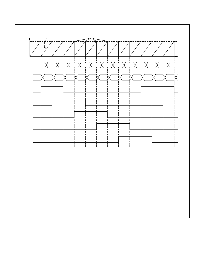
Example of Normal TPC Output (Example of Five-Phase Pulse Output): Figure 11-5 shows
an example in which the TPC is used for cyclic five-phase pulse output.
Figure 11-5 Normal TPC Output Example (Five-Phase Pulse Output)
GRA
H'0000
NDRB
PBDR
TP
15
TP
14
TP
13
TP
12
TP
11
∑
∑
∑
∑
Time
80
TCNT
TCNT value
C0
40
60
20
30
10
18
08
88
80
C0
Compare match
The ITU channel to be used as the output trigger channel is set up so that GRA is an output compare
register and the counter will be cleared by compare match A. The trigger period is set in GRA.
The IMIEA bit is set to 1 in TIER to enable the compare match A interrupt.
H'F8 is written in PBDDR and NDERB, and bits G3CMS1, G3CMS0, G2CMS1, and G2CMS0 are set in
TPCR to select compare match in the ITU channel set up in step 1 as the output trigger.
Output data H'80 is written in NDRB.
The timer counter in this ITU channel is started. When compare match A occurs, the NDRB contents
are transferred to PBDR and output. The compare match/input capture A (IMFA) interrupt service routine
writes the next output data (H'C0) in NDRB.
Five-phase overlapping pulse output (one or two phases active at a time) can be obtained by writing
H'40, H'60, H'20, H'30, H'10, H'18, H'08, H'88... at successive IMFA interrupts. If the DMAC is set for
activation by this interrupt, pulse output can be obtained without loading the CPU.
00
80
C0
40
60
20
30
10
18
08
88
80
C0
40
397
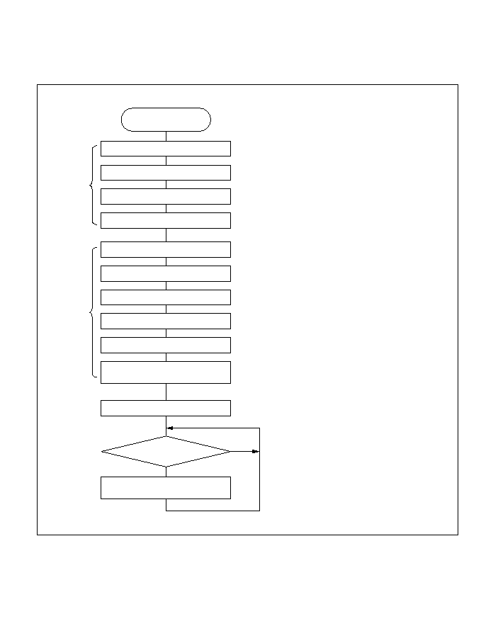
11.3.4 Non-Overlapping TPC Output
Sample Setup Procedure for Non-Overlapping TPC Output: Figure 11-6 shows a sample
procedure for setting up non-overlapping TPC output.
Figure 11-6 Setup Procedure for Non-Overlapping TPC Output (Example)
Non-overlapping
TPC output
Set next TPC output data
Compare match A?
No
Yes
Set next TPC output data
Start counter
ITU setup
Port and
TPC setup
ITU setup
Set initial output data
Set up TPC output
Enable TPC transfer
Select TPC transfer trigger
Select non-overlapping groups
1
2
3
4
12
10
11
5
6
7
8
9
1.
2.
3.
4.
5.
6.
7.
8.
9.
10.
11.
12.
Set TIOR to make GRA and GRB output
compare registers (with output inhibited).
Set the TPC output trigger period in GRB
and the non-overlap margin in GRA.
Select the counter clock source with bits
TPSC2 to TPSC0 in TCR. Select the counter
clear source with bits CCLR1 and CCLR0.
Enable the IMFA interrupt in TIER.
The DMAC can also be set up to transfer
data to the next data register.
Set the initial output values in the DR bits
of the input/output port pins to be used for
TPC output.
Set the DDR bits of the input/output port pins
to be used for TPC output to 1.
Set the NDER bits of the pins to be used for
TPC output to 1.
In TPCR, select the ITU compare match
event to be used as the TPC output trigger.
In TPMR, select the groups that will operate
in non-overlap mode.
Set the next TPC output values in the NDR
bits.
Set the STR bit to 1 in TSTR to start the timer
counter.
At each IMFA interrupt, write the next output
value in the NDR bits.
Select GR functions
Set GR values
Select counting operation
Select interrupt requests
398
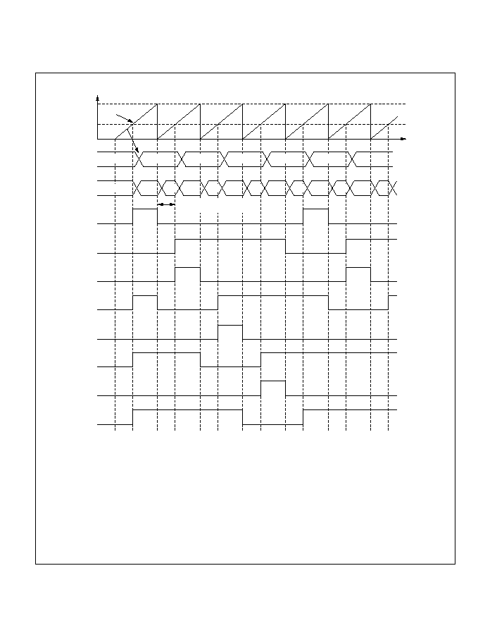
Example of Non-Overlapping TPC Output (Example of Four-Phase Complementary Non-
Overlapping Output): Figure 11-7 shows an example of the use of TPC output for four-phase
complementary non-overlapping pulse output.
Figure 11-7 Non-Overlapping TPC Output Example (Four-Phase Complementary
Non-Overlapping Pulse Output)
GRB
H'0000
NDRB
PBDR
TP
15
TP
14
TP
13
TP
12
TP
11
TP
10
TP
9
TP
8
Time
95
00
65
95
59
56
95
65
05
65
41
59
50
56
14
95
05
65
TCNT
period is set in GRB. The non-overlap margin is set in GRA. The IMIEA bit is set to 1 in TIER to enable
IMFA interrupts.
TCNT value
Non-overlap margin
The ITU channel to be used as the output trigger channel is set up so that GRA and GRB are output
compare registers and the counter will be cleared by compare match B. The TPC output trigger
∑
∑
∑
∑
The timer counter in this ITU channel is started. When compare match B occurs, outputs change from
1 to 0. When compare match A occurs, outputs change from 0 to 1 (the change from 0 to 1 is delayed
by the value of GRA). The IMFA interrupt service routine writes the next output data (H'65) in NDRB.
Four-phase complementary non-overlapping pulse output can be obtained by writing H'59, H'56, H'95...
at successive IMFA interrupts. If the DMAC is set for activation by this interrupt, pulse output can be
obtained without loading the CPU.
GRA
H'FF is written in PBDDR and NDERB, and bits G3CMS1, G3CMS0, G2CMS1, and G2CMS0 are set in
TPCR to select compare match in the ITU channel set up in step 1 as the output trigger. Bits G3NOV
and G2NOV are set to 1 in TPMR to select non-overlapping output. Output data H'95 is written in NDRB.
399
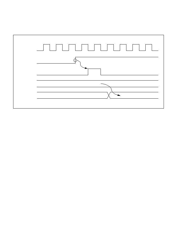
11.3.5 TPC Output Triggering by Input Capture
TPC output can be triggered by ITU input capture as well as by compare match. If GRA functions
as an input capture register in the ITU channel selected in TPCR, TPC output will be triggered by
the input capture signal. Figure 11-8 shows the timing.
Figure 11-8 TPC Output Triggering by Input Capture (Example)
¯
TIOC pin
Input capture
signal
NDR
DR
N
N
M
400
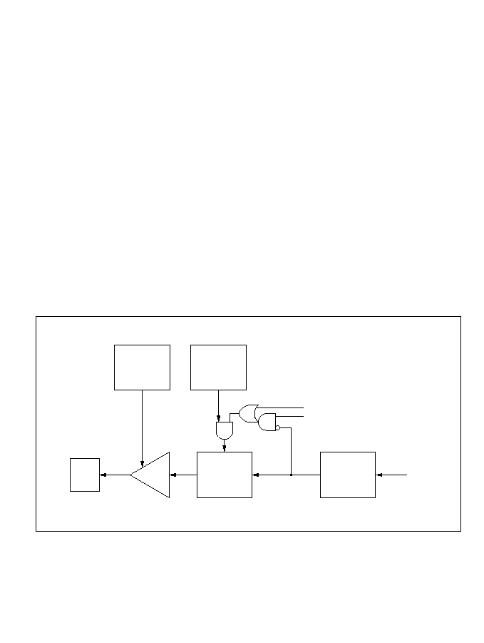
11.4 Usage Notes
11.4.1 Operation of TPC Output Pins
TP
0
to TP
15
are multiplexed with ITU, DMAC, address bus, and other pin functions. When ITU,
DMAC, or address output is enabled, the corresponding pins cannot be used for TPC output. The
data transfer from NDR bits to DR bits takes place, however, regardless of the usage of the pin.
Pin functions should be changed only under conditions in which the output trigger event will not
occur.
11.4.2 Note on Non-Overlapping Output
During non-overlapping operation, the transfer of NDR bit values to DR bits takes place as
follows.
1.
NDR bits are always transferred to DR bits at compare match A.
2.
At compare match B, NDR bits are transferred only if their value is 0. Bits are not transferred
if their value is 1.
Figure 11-9 illustrates the non-overlapping TPC output operation.
Figure 11-9 Non-Overlapping TPC Output
DDR
NDER
Q
Q
TPC output pin
DR
NDR
C
Q
D
Q
D
Compare match A
Compare match B
Internal
data bus
401
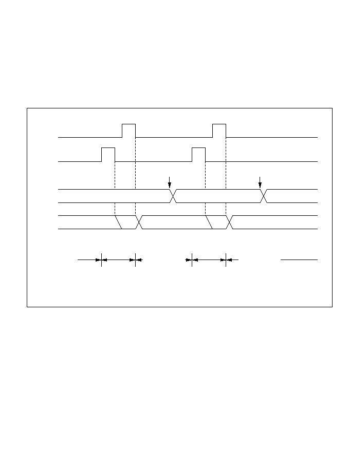
Therefore, 0 data can be transferred ahead of 1 data by making compare match B occur before
compare match A. NDR contents should not be altered during the interval from compare match B
to compare match A (the non-overlap margin).
This can be accomplished by having the IMFA interrupt service routine write the next data in
NDR, or by having the IMFA interrupt activate the DMAC. The next data must be written before
the next compare match B occurs.
Figure 11-10 shows the timing relationships.
Figure 11-10 Non-Overlapping Operation and NDR Write Timing
Compare
match A
Compare
match B
NDR write
NDR
NDR write
DR
0/1 output
0/1 output
0 output
0 output
Do not write
to NDR in this
interval
Do not write
to NDR in this
interval
Write to NDR
in this interval
Write to NDR
in this interval
402

Section 12 Watchdog Timer
12.1 Overview
The H8/3002 has an on-chip watchdog timer (WDT). The WDT has two selectable functions: it
can operate as a watchdog timer to supervise system operation, or it can operate as an interval
timer. As a watchdog timer, it generates a reset signal for the H8/3002 chip if a system crash
allows the timer counter (TCNT) to overflow before being rewritten. In interval timer operation,
an interval timer interrupt is requested at each TCNT overflow.
12.1.1 Features
WDT features are listed below.
∑
Selection of eight counter clock sources
¯/2, ¯/32, ¯/64, ¯/128, ¯/256, ¯/512, ¯/2048, or ¯/4096
∑
Interval timer option
∑
Timer counter overflow generates a reset signal or interrupt.
The reset signal is generated in watchdog timer operation. An interval timer interrupt is
generated in interval timer operation.
∑
Watchdog timer reset signal resets the entire H8/3002 internally, and can also be output
externally.
The reset signal generated by timer counter overflow during watchdog timer operation resets
the entire H8/3002 internally. An external reset signal can be output from the
RESO pin to
reset other system devices simultaneously.
403
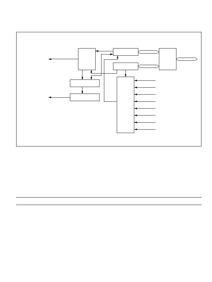
12.1.2 Block Diagram
Figure 12-1 shows a block diagram of the WDT.
Figure 12-1 WDT Block Diagram
12.1.3 Pin Configuration
Table 12-1 describes the WDT output pin.
Table 12-1 WDT Pin
Name
Abbreviation
I/O
Function
Reset output
RESO
Output
*
External output of the watchdog timer reset signal
Note:
*
Open-drain output.
¯/2
¯/32
¯/64
¯/128
¯/256
¯/512
¯/2048
¯/4096
TCNT
TCSR
RSTCSR
Reset control
Interrupt signal
Reset
(internal, external)
(interval timer)
Interrupt
control
Overflow
Clock
Clock
selector
Read/
write
control
Internal
data bus
Internal clock sources
Legend
TCNT:
TCSR:
RSTCSR:
Timer counter
Timer control/status register
Reset control/status register
404

12.1.4 Register Configuration
Table 12-2 summarizes the WDT registers.
Table 12-2 WDT Registers
Address
*
1
Write
*
2
Read
Name
Abbreviation
R/W
Initial Value
H'FFA8
H'FFA8
Timer control/status register
TCSR
R/(W)
*
3
H'18
H'FFA9
Timer counter
TCNT
R/W
H'00
H'FFAA
H'FFAB
Reset control/status register
RSTCSR
R/(W)
*
3
H'3F
Notes: 1. Lower 16 bits of the address.
2. Write word data starting at this address.
3. Only 0 can be written in bit 7, to clear the flag.
405

12.2 Register Descriptions
12.2.1 Timer Counter (TCNT)
TCNT is an 8-bit readable and writable* up-counter.
When the TME bit is set to 1 in TCSR, TCNT starts counting pulses generated from an internal
clock source selected by bits CKS2 to CKS0 in TCSR. When the count overflows (changes from
H'FF to H'00), the OVF bit is set to 1 in TCSR. TCNT is initialized to H'00 by a reset and when
the TME bit is cleared to 0.
Note: * TCNT is write-protected by a password. For details see section 12.2.4, Notes on Register
Access.
Bit
Initial value
Read/Write
7
0
R/W
6
0
R/W
5
0
R/W
4
0
R/W
3
0
R/W
0
0
R/W
2
0
R/W
1
0
R/W
406

12.2.2 Timer Control/Status Register (TCSR)
TCSR is an 8-bit readable and writable
*1
register. Its functions include selecting the timer mode
and clock source.
Bits 7 to 5 are initialized to 0 by a reset and in standby mode. Bits 2 to 0 are initialized to 0 by a
reset. In software standby mode bits 2 to 0 are not initialized, but retain their previous values.
Notes: 1. TCSR is write-protected by a password. For details see section 12.2.4, Notes on
Register Access.
2. Only 0 can be written, to clear the flag.
Bit
Initial value
Read/Write
7
OVF
0
R/(W)
6
WT/IT
0
R/W
5
TME
0
R/W
4
--
1
--
3
--
1
--
0
CKS0
0
R/W
2
CKS2
0
R/W
1
CKS1
0
R/W
Overflow flag
Status flag indicating overflow
Clock select
These bits select the
TCNT clock source
Timer mode select
Selects the mode
Timer enable
Selects whether TCNT runs or halts
Reserved bits
*
2
407

Bit 7--Overflow Flag (OVF): This status flag indicates that the timer counter has overflowed
from H'FF to H'00.
Bit 7
OVF
Description
0
[Clearing condition]
Cleared by reading OVF when OVF = 1, then writing 0 in OVF
(Initial value)
1
[Setting condition]
Set when TCNT changes from H'FF to H'00
Bit 6--Timer Mode Select (WT/
IT): Selects whether to use the WDT as a watchdog timer or
interval timer. If used as an interval timer, the WDT generates an interval timer interrupt request
when TCNT overflows. If used as a watchdog timer, the WDT generates a reset signal when
TCNT overflows.
Bit 6
WT/
IT
Description
0
Interval timer: requests interval timer interrupts
(Initial value)
1
Watchdog timer: generates a reset signal
Bit 5--Timer Enable (TME): Selects whether TCNT runs or is halted.
Bit 5
TME
Description
0
TCNT is initialized to H'00 and halted
(Initial value)
1
TCNT is counting
Bits 4 and 3--Reserved: These bits cannot be modified and are always read as 1.
408

Bits 2 to 0--Clock Select 2 to 0 (CKS2/1/0): These bits select one of eight internal clock
sources, obtained by prescaling the system clock (¯), for input to TCNT.
Bit 2
Bit 1
Bit 0
CKS2
CKS1
CKS0
Description
0
0
0
¯/2
(Initial value)
1
¯/32
1
0
¯/64
1
¯/128
1
0
0
¯/256
1
¯/512
1
0
¯/2048
1
¯/4096
12.2.3 Reset Control/Status Register (RSTCSR)
RSTCSR is an 8-bit readable and writable
*1
register that indicates when a reset signal has been
generated by watchdog timer overflow, and controls external output of the reset signal.
Bits 7 and 6 are initialized by input of a reset signal at the
RES pin. They are not initialized by
reset signals generated by watchdog timer overflow.
Notes: 1. RSTCSR is write-protected by a password. For details see section 12.2.4, Notes on
Register Access.
2. Only 0 can be written in bit 7, to clear the flag.
Bit
Initial value
Read/Write
7
WRST
0
R/(W)
6
RSTOE
0
R/W
5
--
1
--
4
--
1
--
3
--
1
--
0
--
1
--
2
--
1
--
1
--
1
--
*
Watchdog timer reset
Indicates that a reset signal has been generated
Reserved bits
Reset output enable
Enables or disables external output of the reset signal
2
409

Bit 7--Watchdog Timer Reset (WRST): During watchdog timer operation, this bit indicates that
TCNT has overflowed and generated a reset signal. This reset signal resets the entire H8/3002
chip internally. If bit RSTOE is set to 1, this reset signal is also output (low) at the
RESO pin to
initialize external system devices.
Bit 7
WRST
Description
0
[Clearing condition]
(1)Cleared to 0 by reset signal input at
RES
pin
(Initial value)
(2)Cleared by reading WRST when WRST=1, then writing 0 in WRST
1
[Setting condition]
Set when TCNT overflow generates a reset signal during watchdog timer operation
Bit 6--Reset Output Enable (RSTOE): Enables or disables external output at the
RESO pin of
the reset signal generated if TCNT overflows during watchdog timer operation.
Bit 6
RSTOE
Description
0
Reset signal is not output externally
(Initial value)
1
Reset signal is output externally
Bits 5 to 0--Reserved: These bits cannot be modified and are always read as 1.
410

12.2.4 Notes on Register Access
The watchdog timer's TCNT, TCSR, and RSTCSR registers differ from other registers in being
more difficult to write. The procedures for writing and reading these registers are given below.
Writing to TCNT and TCSR: These registers must be written by a word transfer instruction.
They cannot be written by byte instructions. Figure 12-2 shows the format of data written to
TCNT and TCSR. TCNT and TCSR both have the same write address. The write data must be
contained in the lower byte of the written word. The upper byte must contain H'5A (password for
TCNT) or H'A5 (password for TCSR). This transfers the write data from the lower byte to TCNT
or TCSR.
Figure 12-2 Format of Data Written to TCNT and TCSR
15
8 7
0
H'5A
Write data
Address
H'FFA8
*
15
8 7
0
H'A5
Write data
Address
H'FFA8
*
TCNT write
TCSR write
Note: Lower 16 bits of the address.
*
411

Writing to RSTCSR: RSTCSR must be written by a word transfer instruction. It cannot be
written by byte transfer instructions. Figure 12-3 shows the format of data written to RSTCSR. To
write 0 in the WRST bit, the write data must have H'A5 in the upper byte and H'00 in the lower
byte. The H'00 in the lower byte clears the WRST bit in RSTCSR to 0. To write to the RSTOE bit,
the upper byte must contain H'5A and the lower byte must contain the write data. Writing this
word transfers a write data value into the RSTOE bit.
Figure 12-3 Format of Data Written to RSTCSR
Reading TCNT, TCSR, and RSTCSR: These registers are read like other registers. Byte access
instructions can be used. The read addresses are H'FFA8 for TCSR, H'FFA9 for TCNT, and
H'FFAB for RSTCSR, as listed in table 12-3.
Table 12-3 Read Addresses of TCNT, TCSR, and RSTCSR
Address
*
Register
H'FFA8
TCSR
H'FFA9
TCNT
H'FFAB
RSTCSR
Note:
*
Lower 16 bits of the address.
15
8 7
0
H'A5
H'00
Address
H'FFAA
*
15
8 7
0
H'5A
Write data
Address
H'FFAA
*
Writing 0 in WRST bit
Writing to RSTOE bit
Note: Lower 16 bits of the address.
*
412
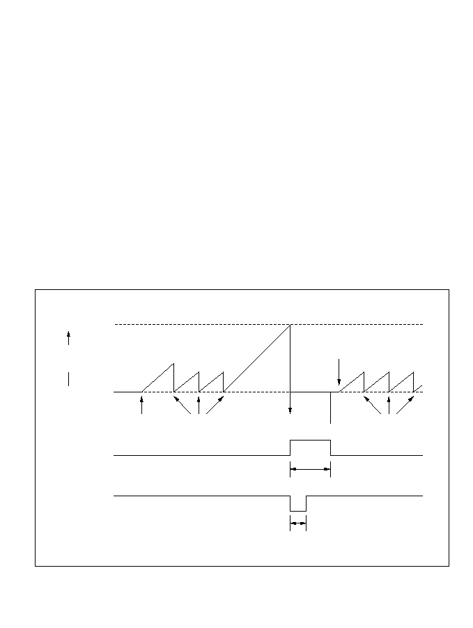
12.3 Operation
Operations when the WDT is used as a watchdog timer and as an interval timer are described
below.
12.3.1 Watchdog Timer Operation
Figure 12-4 illustrates watchdog timer operation. To use the WDT as a watchdog timer, set the
WT/
IT and TME bits to 1 in TCSR. Software must prevent TCNT overflow by rewriting the
TCNT value (normally by writing H'00) before overflow occurs. If TCNT fails to be rewritten and
overflows due to a system crash etc., the H8/3002 is internally reset for a duration of 518 states.
The watchdog reset signal can be externally output from the
RESO pin to reset external system
devices. The reset signal is output externally for 132 states. External output can be enabled or
disabled by the RSTOE bit in RSTCSR.
A watchdog reset has the same vector as a reset generated by input at the
RES pin. Software can
distinguish a
RES reset from a watchdog reset by checking the WRST bit in RSTCSR.
If a
RES reset and a watchdog reset occur simultaneously, the RES reset takes priority.
Figure 12-4 Watchdog Timer Operation
H'FF
H'00
RESO
WDT overflow
Start
H'00 written
in TCNT
Reset
TME set to 1
H'00 written
in TCNT
Internal
reset signal
518 states
132 states
TCNT count
value
OVF = 1
413
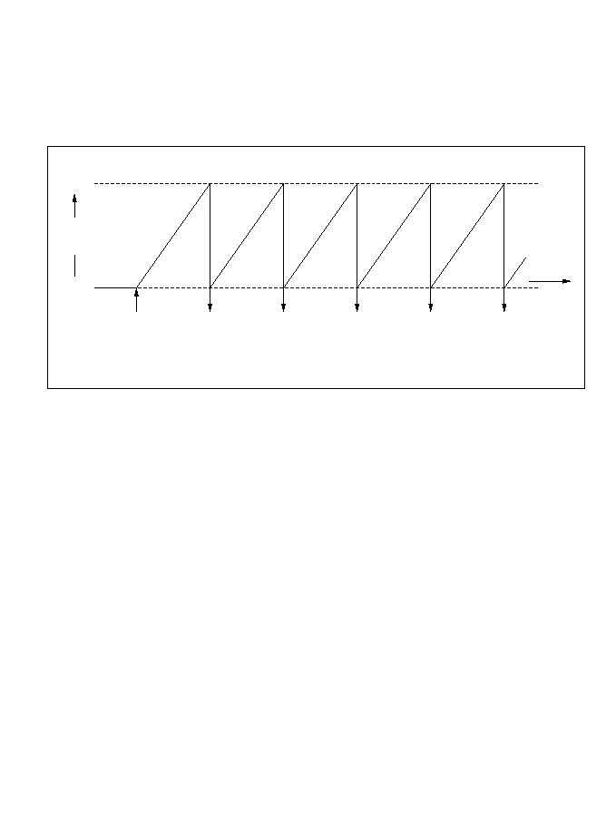
12.3.2 Interval Timer Operation
Figure 12-5 illustrates interval timer operation. To use the WDT as an interval timer, clear bit
WT/
IT to 0 and set bit TME to 1 in TCSR. An interval timer interrupt request is generated at each
TCNT overflow. This function can be used to generate interval timer interrupts at regular
intervals.
Figure 12-5 Interval Timer Operation
TCNT
count value
Time t
Interval
timer
interrupt
Interval
timer
interrupt
Interval
timer
interrupt
Interval
timer
interrupt
WT/ = 0
TME = 1
IT
H'FF
H'00
414
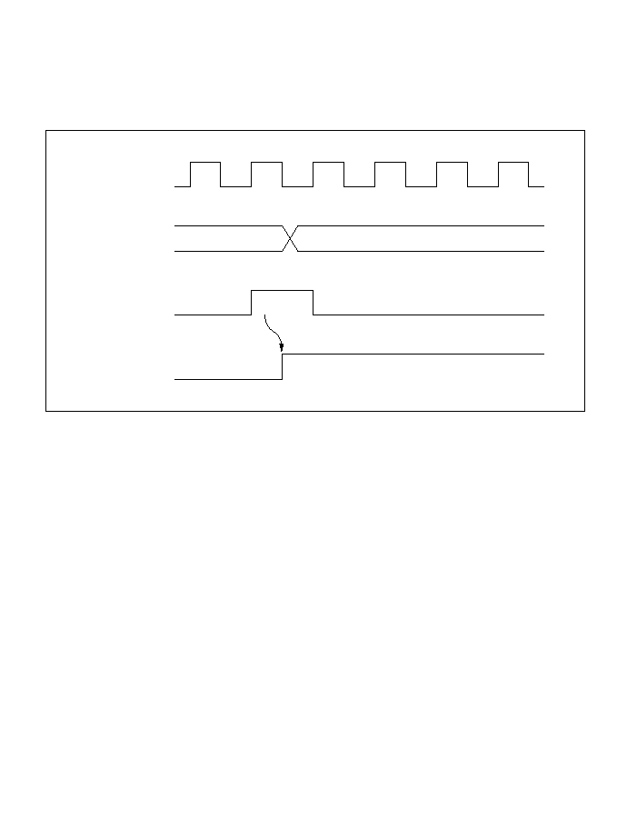
12.3.3 Timing of Setting of Overflow Flag (OVF)
Figure 12-6 shows the timing of setting of the OVF flag in TCSR. The OVF flag is set to 1 when
TCNT overflows. At the same time, a reset signal is generated in watchdog timer operation, or an
interval timer interrupt is generated in interval timer operation.
Figure 12-6 Timing of Setting of OVF
¯
TCNT
Overflow signal
OVF
H'FF
H'00
415
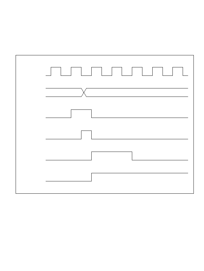
12.3.4 Timing of Setting of Watchdog Timer Reset Bit (WRST)
The WRST bit in RSTCSR is valid when bits WT/
IT and TME are both set to 1 in TCSR.
Figure 12-7 shows the timing of setting of WRST and the internal reset timing. The WRST bit is
set to 1 when TCNT overflows and OVF is set to 1. At the same time an internal reset signal is
generated for the entire H8/3002 chip. This internal reset signal clears OVF to 0, but the WRST
bit remains set to 1. The reset routine must therefore clear the WRST bit.
Figure 12-7 Timing of Setting of WRST Bit and Internal Reset
¯
TCNT
Overflow signal
OVF
WRST
H'FF
H'00
WDT internal
reset
416
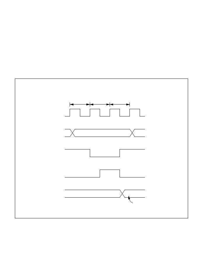
12.4 Interrupts
During interval timer operation, an overflow generates an interval timer interrupt (WOVI). The
interval timer interrupt is requested whenever the OVF bit is set to 1 in TCSR.
12.5 Usage Notes
Contention between TCNT Write and Increment: If a timer counter clock pulse is generated
during the T
3
state of a write cycle to TCNT, the write takes priority and the timer count is not
incremented. See figure 12-8.
Figure 12-8 Contention between TCNT Write and Increment
Changing CKS2 to CKS0 Values: Halt TCNT by clearing the TME bit to 0 in TCSR before
changing the values of bits CKS2 to CKS0.
¯
TCNT
TCNT
N
M
Counter write data
T
3
T
2
T
1
Write cycle: CPU writes to TCNT
Internal write
signal
TCNT input
clock
417

418

Section 13 Serial Communication Interface
13.1 Overview
The H8/3002 has a serial communication interface (SCI) with two independent channels. Both
channels are functionally identical. The SCI can communicate in asynchronous mode or
synchronous mode, and has a multiprocessor communication function for serial communication
among two or more processors.
13.1.1 Features
SCI features are listed below.
∑
Selection of asynchronous or synchronous mode for serial communication
a.
Asynchronous mode
Serial data communication is synchronized one character at a time. The SCI can communicate
with a universal asynchronous receiver/transmitter (UART), asynchronous communication
interface adapter (ACIA), or other chip that employs standard asynchronous serial
communication. It can also communicate with two or more other processors using the
multiprocessor communication function. There are twelve selectable serial data
communication formats.
-- Data length:
7 or 8 bits
-- Stop bit length:
1 or 2 bits
-- Parity bit:
even, odd, or none
-- Multiprocessor bit:
1 or 0
-- Receive error detection: parity, overrun, and framing errors
-- Break detection:
by reading the RxD level directly when a framing error occurs
b.
Synchronous mode
Serial data communication is synchronized with a clock signal. The SCI can communicate
with other chips having a synchronous communication function. There is one serial data
communication format.
-- Data length:
8 bits
-- Receive error detection: overrun errors
419

∑
Full duplex communication
The transmitting and receiving sections are independent, so the SCI can transmit and receive
simultaneously. The transmitting and receiving sections are both double-buffered, so serial
data can be transmitted and received continuously.
∑
Built-in baud rate generator with selectable bit rates
∑
Selectable transmit/receive clock sources: internal clock from baud rate generator, or external
clock from the SCK pin.
∑
Four types of interrupts
Transmit-data-empty, transmit-end, receive-data-full, and receive-error interrupts are
requested independently. The transmit-data-empty and receive-data-full interrupts can
activate the DMA controller (DMAC) to transfer data.
420
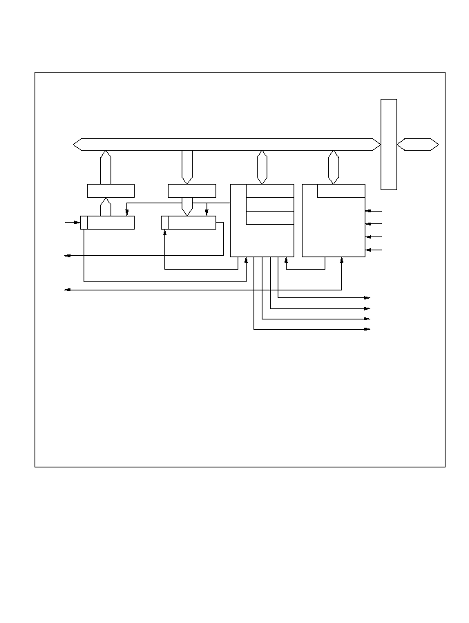
13.1.2 Block Diagram
Figure 13-1 shows a block diagram of the SCI.
Figure 13-1 SCI Block Diagram
RxD
TxD
SCK
RDR
RSR
TDR
TSR
SSR
SCR
SMR
BRR
Module data bus
Bus interface
Internal
data bus
Transmit/
receive control
Baud rate
generator
¯
¯/4
¯/16
¯/64
Clock
Parity generate
Parity check
TEI
TXI
RXI
ERI
Legend
External clock
RSR:
RDR:
TSR:
TDR:
SMR:
SCR:
SSR:
BRR:
Receive shift register
Receive data register
Transmit shift register
Transmit data register
Serial mode register
Serial control register
Serial status register
Bit rate register
421

13.1.3 Input/Output Pins
The SCI has serial pins for each channel as listed in table 13-1.
Table 13-1 SCI Pins
Channel
Name
Abbreviation
I/O
Function
0
Serial clock pin
SCK
0
Input/output
SCI
0
clock input/output
Receive data pin
RxD
0
Input
SCI
0
receive data input
Transmit data pin
TxD
0
Output
SCI
0
transmit data output
1
Serial clock pin
SCK
1
Input/output
SCI
1
clock input/output
Receive data pin
RxD
1
Input
SCI
1
receive data input
Transmit data pin
TxD
1
Output
SCI
1
transmit data output
13.1.4 Register Configuration
The SCI has internal registers as listed in table 13-2. These registers select asynchronous or
synchronous mode, specify the data format and bit rate, and control the transmitter and receiver
sections.
Table 13-2 Registers
Channel
Address
*
1
Name
Abbreviation
R/W
Initial Value
0
H'FFB0
Serial mode register
SMR
R/W
H'00
H'FFB1
Bit rate register
BRR
R/W
H'FF
H'FFB2
Serial control register
SCR
R/W
H'00
H'FFB3
Transmit data register
TDR
R/W
H'FF
H'FFB4
Serial status register
SSR
R/(W)
*
2
H'84
H'FFB5
Receive data register
RDR
R
H'00
1
H'FFB8
Serial mode register
SMR
R/W
H'00
H'FFB9
Bit rate register
BRR
R/W
H'FF
H'FFBA
Serial control register
SCR
R/W
H'00
H'FFBB
Transmit data register
TDR
R/W
H'FF
H'FFBC
Serial status register
SSR
R/(W)
*
2
H'84
H'FFBD
Receive data register
RDR
R
H'00
Notes: 1. Lower 16 bits of the address.
2. Only 0 can be written, to clear flags.
422

13.2 Register Descriptions
13.2.1 Receive Shift Register (RSR)
RSR is the register that receives serial data.
The SCI loads serial data input at the RxD pin into RSR in the order received, LSB (bit 0) first,
thereby converting the data to parallel data. When 1 byte has been received, it is automatically
transferred to RDR. The CPU cannot read or write RSR directly.
13.2.2 Receive Data Register (RDR)
RDR is the register that stores received serial data.
When the SCI finishes receiving 1 byte of serial data, it transfers the received data from RSR into
RDR for storage. RSR is then ready to receive the next data. This double buffering allows data to
be received continuously.
RDR is a read-only register. Its contents cannot be modified by the CPU. RDR is initialized to
H'00 by a reset and in standby mode.
Bit
Initial value
Read/Write
7
--
6
--
5
--
4
--
3
--
0
--
2
--
1
--
Bit
Initial value
Read/Write
7
0
R
6
0
R
5
0
R
4
0
R
3
0
R
0
0
R
2
0
R
1
0
R
423

13.2.3 Transmit Shift Register (TSR)
TSR is the register that transmits serial data.
The SCI loads transmit data from TDR into TSR, then transmits the data serially from the TxD
pin, LSB (bit 0) first. After transmitting one data byte, the SCI automatically loads the next
transmit data from TDR into TSR and starts transmitting it. If the TDRE flag is set to 1 in SSR,
however, the SCI does not load the TDR contents into TSR. The CPU cannot read or write TSR
directly.
13.2.4 Transmit Data Register (TDR)
TDR is an 8-bit register that stores data for serial transmission.
When the SCI detects that TSR is empty, it moves transmit data written in TDR from TDR into
TSR and starts serial transmission. Continuous serial transmission is possible by writing the next
transmit data in TDR during serial transmission from TSR.
The CPU can always read and write TDR. TDR is initialized to H'FF by a reset and in standby
mode.
Bit
Initial value
Read/Write
7
--
6
--
5
--
4
--
3
--
0
--
2
--
1
--
Bit
Initial value
Read/Write
7
1
R/W
6
1
R/W
5
1
R/W
4
1
R/W
3
1
R/W
0
1
R/W
2
1
R/W
1
1
R/W
424

13.2.5 Serial Mode Register (SMR)
SMR is an 8-bit register that specifies the SCI serial communication format and selects the clock
source for the baud rate generator.
The CPU can always read and write SMR. SMR is initialized to H'00 by a reset and in standby
mode.
Bit
Initial value
Read/Write
7
C/A
0
R/W
6
CHR
0
R/W
5
PE
0
R/W
4
O/E
0
R/W
3
STOP
0
R/W
0
CKS0
0
R/W
2
MP
0
R/W
1
CKS1
0
R/W
Communication mode
Selects asynchronous or synchronous mode
Clock select 1/0
These bits select the
baud rate generator's
clock source
Character length
Selects character length in asynchronous mode
Parity enable
Selects whether a parity bit is added
Parity mode
Selects even or odd parity
Stop bit length
Selects the stop bit length
Multiprocessor mode
Selects the multiprocessor
function
425

Bit 7--Communication Mode (C/
A): Selects whether the SCI operates in asynchronous or
synchronous mode.
Bit 7
C/
A
Description
0
Asynchronous mode
(Initial value)
1
Synchronous mode
Bit 6--Character Length (CHR): Selects 7-bit or 8-bit data length in asynchronous mode. In
synchronous mode the data length is 8 bits regardless of the CHR setting.
Bit 6
CHR
Description
0
8-bit data
(Initial value)
1
7-bit data
*
Note:
*
When 7-bit data is selected, the MSB (bit 7) in TDR is not transmitted.
Bit 5--Parity Enable (PE): In asynchronous mode, this bit enables or disables the addition of a
parity bit to transmit data, and the checking of the parity bit in receive data. In synchronous mode
the parity bit is neither added nor checked, regardless of the PE setting.
Bit 5
PE
Description
0
Parity bit not added or checked
(Initial value)
1
Parity bit added and checked
*
Note:
*
When PE is set to 1, an even or odd parity bit is added to transmit data according to the
even or odd parity mode selected by the O/
E
bit, and the parity bit in receive data is
checked to see that it matches the even or odd mode selected by the O/
E
bit.
426

Bit 4--Parity Mode (O/
E): Selects even or odd parity. The O/E bit setting is valid in
asynchronous mode when the PE bit is set to 1 to enable the adding and checking of a parity bit.
The O/
E setting is ignored in synchronous mode, or when parity adding and checking is disabled
in asynchronous mode.
Bit 4
O/
E
Description
0
Even parity
*
1
(Initial value)
1
Odd parity
*
2
Notes: 1. When even parity is selected, the parity bit added to transmit data makes an even
number of 1s in the transmitted character and parity bit combined. Receive data must
have an even number of 1s in the received character and parity bit combined.
2. When odd parity is selected, the parity bit added to transmit data makes an odd number
of 1s in the transmitted character and parity bit combined. Receive data must have an
odd number of 1s in the received character and parity bit combined.
Bit 3--Stop Bit Length (STOP): Selects one or two stop bits in asynchronous mode. This setting
is used only in asynchronous mode. In synchronous mode no stop bit is added, so the STOP bit
setting is ignored.
Bit 3
STOP
Description
0
One stop bit
*
1
(Initial value)
1
Two stop bits
*
2
Notes: 1. One stop bit (with value 1) is added at the end of each transmitted character.
2. Two stop bits (with value 1) are added at the end of each transmitted character.
In receiving, only the first stop bit is checked, regardless of the STOP bit setting. If the second
stop bit is 1 it is treated as a stop bit. If the second stop bit is 0 it is treated as the start bit of the
next incoming character.
427

Bit 2--Multiprocessor Mode (MP): Selects a multiprocessor format. When a multiprocessor
format is selected, parity settings made by the PE and O/
E bits are ignored. The MP bit setting is
valid only in asynchronous mode. It is ignored in synchronous mode.
For further information on the multiprocessor communication function, see section 13.3.3,
Multiprocessor Communication Function.
Bit 2
MP
Description
0
Multiprocessor function disabled
(Initial value)
1
Multiprocessor format selected
Bits 1 and 0--Clock Select 1 and 0 (CKS1/0): These bits select the clock source of the on-chip
baud rate generator. Four clock sources are available: ¯, ¯/4, ¯/16, and ¯/64.
For the relationship between the clock source, bit rate register setting, and baud rate, see
section 13.2.8, Bit Rate Register.
Bit 1
Bit 0
CKS1
CKS0
Description
0
0
¯
(Initial value)
0
1
¯/4
1
0
¯/16
1
1
¯/64
428

13.2.6 Serial Control Register (SCR)
SCR enables the SCI transmitter and receiver, enables or disables serial clock output in
asynchronous mode, enables or disables interrupts, and selects the transmit/receive clock source.
The CPU can always read and write SCR. SCR is initialized to H'00 by a reset and in standby
mode.
Bit
Initial value
Read/Write
7
TIE
0
R/W
6
RIE
0
R/W
5
TE
0
R/W
4
RE
0
R/W
3
MPIE
0
R/W
0
CKE0
0
R/W
2
TEIE
0
R/W
1
CKE1
0
R/W
Transmit interrupt enable
Enables or disables transmit-data-empty interrupts (TXI)
Clock enable 1/0
These bits select the
SCI clock source
Receive interrupt enable
Enables or disables receive-data-full interrupts (RXI) and
receive-error interrupts (ERI)
Transmit enable
Enables or disables the transmitter
Receive enable
Enables or disables the receiver
Multiprocessor interrupt enable
Enables or disables multiprocessor
interrupts
Transmit end interrupt enable
Enables or disables transmit-
end interrupts (TEI)
429

Bit 7--Transmit Interrupt Enable (TIE): Enables or disables the transmit-data-empty interrupt
(TXI) requested when the TDRE flag in SSR is set to 1 due to transfer of serial transmit data from
TDR to TSR.
Bit 7
TIE
Description
0
Transmit-data-empty interrupt request (TXI) is disabled
*
(Initial value)
1
Transmit-data-empty interrupt request (TXI) is enabled
Note:
*
TXI interrupt requests can be cleared by reading the value 1 from the TDRE flag, then
clearing it to 0; or by clearing the TIE bit to 0.
Bit 6--Receive Interrupt Enable (RIE): Enables or disables the receive-data-full interrupt
(RXI) requested when the RDRF flag is set to 1 in SSR due to transfer of serial receive data from
RSR to RDR; also enables or disables the receive-error interrupt (ERI).
Bit 6
RIE
Description
0
Receive-end (RXI) and receive-error (ERI) interrupt requests are disabled (Initial value)
1
Receive-end (RXI) and receive-error (ERI) interrupt requests are enabled
Note:
*
RXI and ERI interrupt requests can be cleared by reading the value 1 from the RDRF, FER,
PER, or ORER flag, then clearing it to 0; or by clearing the RIE bit to 0.
Bit 5--Transmit Enable (TE): Enables or disables the start of SCI serial transmitting operations.
Bit 5
TE
Description
0
Transmitting disabled
*
1
(Initial value)
1
Transmitting enabled
*
2
Notes: 1. The TDRE bit is locked at 1 in SSR.
2. In the enabled state, serial transmitting starts when the TDRE bit in SSR is cleared to 0
after writing of transmit data into TDR. Select the transmit format in SMR before setting
the TE bit to 1.
430

Bit 4--Receive Enable (RE): Enables or disables the start of SCI serial receiving operations.
Bit 4
RE
Description
0
Receiving disabled
*
1
(Initial value)
1
Receiving enabled
*
2
Notes: 1. Clearing the RE bit to 0 does not affect the RDRF, FER, PER, and ORER flags. These
flags retain their previous values.
2. In the enabled state, serial receiving starts when a start bit is detected in asynchronous
mode, or serial clock input is detected in synchronous mode. Select the receive format
in SMR before setting the RE bit to 1.
Bit 3--Multiprocessor Interrupt Enable (MPIE): Enables or disables multiprocessor interrupts.
The MPIE setting is valid only in asynchronous mode, and only if the MP bit is set to 1 in SMR.
The MPIE setting is ignored in synchronous mode or when the MP bit is cleared to 0.
Bit 3
MPIE
Description
0
Multiprocessor interrupts are disabled (normal receive operation)
(Initial value)
[Clearing conditions]
The MPIE bit is cleared to 0.
MPB = 1 in received data.
1
Multiprocessor interrupts are enabled
*
Receive-data-full interrupts (RXI), receive-error interrupts (ERI), and setting of the RDRF,
FER, and ORER status flags in SSR are disabled until data with the multiprocessor bit
set to 1 is received.
Note:
*
The SCI does not transfer receive data from RSR to RDR, does not detect receive errors,
and does not set the RDRF, FER, and ORER flags in SSR. When it receives data in which
MPB = 1, the SCI sets the MPB bit to 1 in SSR, automatically clears the MPIE bit to 0,
enables RXI and ERI interrupts (if the RIE bit is set to 1 in SCR), and allows the FER and
ORER flags to be set.
431

Bit 2--Transmit-End Interrupt Enable (TEIE): Enables or disables the transmit-end interrupt
(TEI) requested if TDR does not contain new transmit data when the MSB is transmitted.
Bit 2
TEIE
Description
0
Transmit-end interrupt requests (TEI) are disabled
*
(Initial value)
1
Transmit-end interrupt requests (TEI) are enabled
*
Note:
*
TEI interrupt requests can be cleared by reading the value 1 from the TDRE flag in SSR,
then clearing the TDRE flag to 0, thereby also clearing the TEND flag to 0; or by clearing
the TEIE bit to 0.
Bits 1 and 0--Clock Enable 1 and 0 (CKE1/0): These bits select the SCI clock source and
enable or disable clock output from the SCK pin. Depending on the settings of CKE1 and CKE0,
the SCK pin can be used for generic input/output, serial clock output, or serial clock input.
The CKE0 setting is valid only in asynchronous mode, and only when the SCI is internally
clocked (CKE1 = 0). The CKE0 setting is ignored in synchronous mode, or when an external
clock source is selected (CKE1 = 1). Select the SCI operating mode in SMR before setting the
CKE1 and CKE0 bits. For further details on selection of the SCI clock source, see table 13-9 in
section 13.3, Operation.
Bit 1
Bit 0
CKE1
CKE0
Description
0
0
Asynchronous mode
Internal clock, SCK pin available for generic
input/output
*
1
Synchronous mode
Internal clock, SCK pin used for serial clock output
*
1
0
1
Asynchronous mode
Internal clock, SCK pin used for clock output
*
2
Synchronous mode
Internal clock, SCK pin used for serial clock output
1
0
Asynchronous mode
External clock, SCK pin used for clock input
*
3
Synchronous mode
External clock, SCK pin used for serial clock input
1
1
Asynchronous mode
External clock, SCK pin used for clock input
*
3
Synchronous mode
External clock, SCK pin used for serial clock input
Notes: 1. Initial value
2. The output clock frequency is the same as the bit rate.
3. The input clock frequency is 16 times the bit rate.
432

13.2.7 Serial Status Register (SSR)
SSR is an 8-bit register containing multiprocessor bit values, and status flags that indicate SCI
operating status.
Bit
Initial value
Read/Write
7
TDRE
1
R/(W)
6
RDRF
0
R/(W)
5
ORER
0
R/(W)
4
FER
0
R/(W)
3
PER
0
R/(W)
0
MPBT
0
R/W
2
TEND
1
R
1
MPB
0
R
Transmit data register empty
Status flag indicating that transmit data has been transferred from TDR into
TSR and new data can be written in TDR
Multiprocessor
bit transfer
Value of multi-
processor bit to
be transmitted
Receive data register full
Status flag indicating that data has been received and stored in RDR
Overrun error
Status flag indicating detection of a receive overrun error
Framing error
Status flag indicating detection of a receive
framing error
Parity error
Status flag indicating detection of
a receive parity error
Transmit end
Status flag indicating end of
transmission
*
Note: Only 0 can be written, to clear the flag.
*
*
*
*
*
Multiprocessor bit
Stores the received
multiprocessor bit value
433

The CPU can always read and write SSR, but cannot write 1 in the TDRE, RDRF, ORER, PER,
and FER flags. These flags can be cleared to 0 only if they have first been read while set to 1. The
TEND and MPB flags are read-only bits that cannot be written.
SSR is initialized to H'84 by a reset and in standby mode.
Bit 7--Transmit Data Register Empty (TDRE): Indicates that the SCI has loaded transmit data
from TDR into TSR and the next serial transmit data can be written in TDR.
Bit 7
TDRE
Description
0
TDR contains valid transmit data
[Clearing conditions]
Software reads TDRE while it is set to 1, then writes 0.
The DMAC writes data in TDR.
1
TDR does not contain valid transmit data
(Initial value)
[Setting conditions]
The chip is reset or enters standby mode.
The TE bit in SCR is cleared to 0.
TDR contents are loaded into TSR, so new data can be written in TDR.
Bit 6--Receive Data Register Full (RDRF): Indicates that RDR contains new receive data.
Bit 6
RDRF
Description
0
RDR does not contain new receive data
(Initial value)
[Clearing conditions]
The chip is reset or enters standby mode.
Software reads RDRF while it is set to 1, then writes 0.
The DMAC reads data from RDR.
1
RDR contains new receive data
[Setting condition]
When serial data is received normally and transferred from RSR to RDR.
Note: The RDR contents and RDRF flag are not affected by detection of receive errors or by
clearing of the RE bit to 0 in SCR. They retain their previous values. If the RDRF flag is still
set to 1 when reception of the next data ends, an overrun error occurs and receive data is
lost.
434

Bit 5--Overrun Error (ORER): Indicates that data reception ended abnormally due to an
overrun error.
Bit 5
ORER
Description
0
Receiving is in progress or has ended normally
(Initial value)
*
1
[Clearing conditions]
The chip is reset or enters standby mode.
Software reads ORER while it is set to 1, then writes 0.
1
A receive overrun error occurred
*
2
[Setting condition]
Reception of the next serial data ends when RDRF = 1.
Notes: 1. Clearing the RE bit to 0 in SCR does not affect the ORER flag, which retains its
previous value.
2. RDR continues to hold the receive data before the overrun error, so subsequent receive
data is lost. Serial receiving cannot continue while the ORER flag is set to 1. In
synchronous mode, serial transmitting is also disabled.
Bit 4--Framing Error (FER): Indicates that data reception ended abnormally due to a framing
error in asynchronous mode.
Bit 4
FER
Description
0
Receiving is in progress or has ended normally
(Initial value)
*
1
[Clearing conditions]
The chip is reset or enters standby mode.
Software reads FER while it is set to 1, then writes 0.
1
A receive framing error occurred
*
2
[Setting condition]
The stop bit at the end of receive data is checked and found to be 0.
Notes: 1. Clearing the RE bit to 0 in SCR does not affect the FER flag, which retains its previous
value.
2. When the stop bit length is 2 bits, only the first bit is checked. The second stop bit is not
checked. When a framing error occurs the SCI transfers the receive data into RDR but
does not set the RDRF flag. Serial receiving cannot continue while the FER flag is set
to 1. In synchronous mode, serial transmitting is also disabled.
435

Bit 3--Parity Error (PER): Indicates that data reception ended abnormally due to a parity error
in asynchronous mode.
Bit 3
PER
Description
0
Receiving is in progress or has ended normally
*
1
(Initial value)
[Clearing conditions]
The chip is reset or enters standby mode.
Software reads PER while it is set to 1, then writes 0.
1
A receive parity error occurred
*
2
[Setting condition]
The number of 1s in receive data, including the parity bit, does not match the even or
odd parity setting of O/
E
in SMR.
Notes: 1. Clearing the RE bit to 0 in SCR does not affect the PER flag, which retains its previous
value.
2. When a parity error occurs the SCI transfers the receive data into RDR but does not set
the RDRF flag. Serial receiving cannot continue while the PER flag is set to 1. In
synchronous mode, serial transmitting is also disabled.
Bit 2--Transmit End (TEND): Indicates that when the last bit of a serial character was
transmitted TDR did not contain new transmit data, so transmission has ended. The TEND flag is
a read-only bit and cannot be written.
Bit 2
TEND
Description
0
Transmission is in progress
[Clearing conditions]
Software reads TDRE while it is set to 1, then writes 0 in the TDRE flag.
The DMAC writes data in TDR.
1
End of transmission
(Initial value)
[Setting conditions]
The chip is reset or enters standby mode.
The TE bit is cleared to 0 in SCR.
TDRE is 1 when the last bit of a serial character is transmitted.
436

Bit 1--Multiprocessor Bit (MPB): Stores the value of the multiprocessor bit in receive data
when a multiprocessor format is used in asynchronous mode. MPB is a read-only bit and cannot
be written.
Bit 1
MPB
Description
0
Multiprocessor bit value in receive data is 0
*
(Initial value)
1
Multiprocessor bit value in receive data is 1
Note:
*
If the RE bit is cleared to 0 when a multiprocessor format is selected, MPB retains its
previous value.
Bit 0--Multiprocessor Bit Transfer (MPBT): Stores the value of the multiprocessor bit added to
transmit data when a multiprocessor format is selected for transmitting in asynchronous mode.
The MPBT setting is ignored in synchronous mode, when a multiprocessor format is not selected,
or when the SCI is not transmitting.
Bit 0
MPBT
Description
0
Multiprocessor bit value in transmit data is 0
(Initial value)
1
Multiprocessor bit value in transmit data is 1
13.2.8 Bit Rate Register (BRR)
BRR is an 8-bit register that, together with the CKS1 and CKS0 bits in SMR that select the baud
rate generator clock source, determines the serial communication bit rate.
The CPU can always read and write BRR. BRR is initialized to H'FF by a reset and in standby
mode. The two SCI channels have independent baud rate generator control, so different values can
be set in the two channels.
Table 13-3 shows examples of BRR settings in asynchronous mode. Table 13-4 shows examples
of BRR settings in synchronous mode.
Bit
Initial value
Read/Write
7
1
R/W
6
1
R/W
5
1
R/W
4
1
R/W
3
1
R/W
0
1
R/W
2
1
R/W
1
1
R/W
437

Table 13-3 Examples of Bit Rates and BRR Settings in Asynchronous Mode
¯ (MHz)
2
2.097152
2.4576
3
Bit Rate
Error
Error
Error
Error
(bits/s)
n
N
(%)
n
N
(%)
n
N
(%)
n
N
(%)
110
1
141
0.03
1
148
≠0.04
1
174
≠0.26
1
212
0.03
150
1
103
0.16
1
108
0.21
1
127
0.00
1
155
0.16
300
0
207
0.16
0
217
0.21
0
255
0.00
1
77
0.16
600
0
103
0.16
0
108
0.21
0
127
0.00
0
155
0.16
1200
0
51
0.16
0
54
≠0.70
0
63
0.00
0
77
0.16
2400
0
25
0.16
0
26
1.14
0
31
0.00
0
38
0.16
4800
0
12
0.16
0
13
≠2.48
0
15
0.00
0
19
≠2.34
9600
0
6
≠6.99
0
6
≠2.48
0
7
0.00
0
9
≠2.34
19200
0
2
8.51
0
2
13.78
0
3
0.00
0
4
≠2.34
31250
0
1
0.00
0
1
4.86
0
1
22.88
0
2
0.00
38400
0
1
≠18.62
0
1
≠14.67
0
1
0.00
--
--
--
¯ (MHz)
3.6864
4
4.9152
5
Bit Rate
Error
Error
Error
Error
(bits/s)
n
N
(%)
n
N
(%)
n
N
(%)
n
N
(%)
110
2
64
0.70
2
70
0.03
2
86
0.31
2
88
≠0.25
150
1
191
0.00
1
207
0.16
1
255
0.00
2
64
0.16
300
1
95
0.00
1
103
0.16
1
127
0.00
1
129
0.16
600
0
191
0.00
0
207
0.16
0
255
0.00
1
64
0.16
1200
0
95
0.00
0
103
0.16
0
127
0.00
0
129
0.16
2400
0
47
0.00
0
51
0.16
0
63
0.00
0
64
0.16
4800
0
23
0.00
0
25
0.16
0
31
0.00
0
32
≠1.36
9600
0
11
0.00
0
12
0.16
0
15
0.00
0
15
1.73
19200
0
5
0.00
0
6
≠6.99
0
7
0.00
0
7
1.73
31250
--
--
--
0
3
0.00
0
4
≠1.70
0
4
0.00
38400
0
2
0.00
0
2
8.51
0
3
0.00
0
3
1.73
438

Table 13-3 Examples of Bit Rates and BRR Settings in Asynchronous Mode (cont)
¯ (MHz)
6
6.144
7.3728
8
Bit Rate
Error
Error
Error
Error
(bits/s)
n
N
(%)
n
N
(%)
n
N
(%)
n
N
(%)
110
2
106
≠0.44
2
108
0.08
2
130
≠0.07
2
141
0.03
150
2
77
0.16
2
79
0.00
2
95
0.00
2
103
0.16
300
1
155
0.16
1
159
0.00
1
191
0.00
1
207
0.16
600
1
77
0.16
1
79
0.00
1
95
0.00
1
103
0.16
1200
0
155
0.16
0
159
0.00
0
191
0.00
0
207
0.16
2400
0
77
0.16
0
79
0.00
0
95
0.00
0
103
0.16
4800
0
38
0.16
0
39
0.00
0
47
0.00
0
51
0.16
9600
0
19
≠2.34
0
19
0.00
0
23
0.00
0
25
0.16
19200
0
9
≠2.34
0
9
0.00
0
11
0.00
0
12
0.16
31250
0
5
0.00
0
5
2.40
0
6
5.33
0
7
0.00
38400
0
4
≠2.34
0
4
0.00
0
5
0.00
0
6
≠6.99
¯ (MHz)
9.8304
10
12
12.288
Bit Rate
Error
Error
Error
Error
(bits/s)
n
N
(%)
n
N
(%)
n
N
(%)
n
N
(%)
110
2
174
≠0.26
2
177
≠0.25
2
212
0.03
2
217
0.08
150
2
127
0.00
2
129
0.16
2
155
0.16
2
159
0.00
300
1
255
0.00
2
64
0.16
2
77
0.16
2
79
0.00
600
1
127
0.00
1
129
0.16
1
155
0.16
1
159
0.00
1200
0
255
0.00
1
64
0.16
1
77
0.16
1
79
0.00
2400
0
127
0.00
0
129
0.16
0
155
0.16
0
159
0.00
4800
0
63
0.00
0
64
0.16
0
77
0.16
0
79
0.00
9600
0
31
0.00
0
32
≠1.36
0
38
0.16
0
39
0.00
19200
0
15
0.00
0
15
1.73
0
19
≠2.34
0
19
0.00
31250
0
9
≠1.70
0
9
0.00
0
11
0.00
0
11
2.40
38400
0
7
0.00
0
7
1.73
0
9
≠2.34
0
9
0.00
439

Table 13-3 Examples of Bit Rates and BRR Settings in Asynchronous Mode (cont)
¯ (MHz)
14
14.7456
16
Bit Rate
Error
Error
Error
(bits/s)
n
N
(%)
n
N
(%)
n
N
(%)
110
2
248
≠0.17
3
64
0.70
3
70
0.03
150
2
181
0.16
2
191
0.00
2
207
0.16
300
2
90
0.16
2
95
0.00
2
103
0.16
600
1
181
0.16
1
191
0.00
1
207
0.16
1200
1
90
0.16
1
95
0.00
1
103
0.16
2400
0
181
0.16
0
191
0.00
0
207
0.16
4800
0
90
0.16
0
95
0.00
0
103
0.16
9600
0
45
≠0.93
0
47
0.00
0
51
0.16
19200
0
22
≠0.93
0
23
0.00
0
25
0.16
31250
0
13
0.00
0
14
≠1.70
0
15
0.00
38400
0
10
3.57
0
11
0.00
0
12
0.16
440

Table 13-4 Examples of Bit Rates and BRR Settings in Synchronous Mode
¯ (MHz)
2
4
8
10
16
n
N
n
N
n
N
n
N
n
N
110
3
70
--
--
--
--
--
--
--
--
250
2
124
2
249
3
124
--
--
3
249
500
1
249
2
124
2
249
--
--
3
124
1 k
1
124
1
249
2
124
--
--
2
249
2.5 k
0
199
1
99
1
199
1
249
2
99
5 k
0
99
0
199
1
99
1
124
1
199
10 k
0
49
0
99
0
199
0
249
1
99
25 k
0
19
0
39
0
79
0
99
0
159
50 k
0
9
0
19
0
39
0
49
0
79
100 k
0
4
0
9
0
19
0
24
0
39
250 k
0
1
0
3
0
7
0
9
0
15
500 k
0
0
*
0
1
0
3
0
4
0
7
1 M
0
0
*
0
1
--
--
0
3
2 M
0
0
*
--
--
0
1
2.5 M
--
--
0
0
*
--
--
4 M
0
0
*
Note: Settings with an error of 1% or less are recommended.
Legend
Blank: No setting available
--:
Setting possible, but error occurs
*
:
Continuous transmit/receive not possible
The BRR setting is calculated as follows:
Asynchronous mode:
N =
◊
10
6
≠ 1
Synchronous mode:
N =
◊
10
6
≠ 1
B: Bit rate (bits/s)
N: BRR setting for baud rate generator (0
N
255)
¯: System clock frequency (MHz)
n: Baud rate generator clock source (n = 0, 1, 2, 3)
(For the clock sources and values of n, see the following table.)
Bit Rate
(bits/s)
¯
64
◊
2
2n≠1
◊
B
¯
8
◊
2
2n≠1
◊
B
441

SMR Settings
n
Clock Source
CKS1
CKS0
0
¯
0
0
1
¯/4
0
1
2
¯/16
1
0
3
¯/64
1
1
The bit rate error in asynchronous mode is calculated as follows.
Error (%) =
≠1
◊
100
¯
◊
10
6
(N + 1)
◊
B
◊
64
◊
2
2n≠1
442

Table 13-5 indicates the maximum bit rates in asynchronous mode for various system clock
frequencies. Tables 13-6 and 13-7 indicate the maximum bit rates with external clock input.
Table 13-5 Maximum Bit Rates for Various Frequencies (Asynchronous Mode)
Settings
¯ (MHz)
Maximum Bit Rate (bits/s)
n
N
2
62500
0
0
2.097152
65536
0
0
2.4576
76800
0
0
3
93750
0
0
3.6864
115200
0
0
4
125000
0
0
4.9152
153600
0
0
5
156250
0
0
6
187500
0
0
6.144
192000
0
0
7.3728
230400
0
0
8
250000
0
0
9.8304
307200
0
0
10
312500
0
0
12
375000
0
0
12.288
384000
0
0
14
437500
0
0
14.7456
460800
0
0
16
500000
0
0
443

Table 13-6 Maximum Bit Rates with External Clock Input (Asynchronous Mode)
¯ (MHz)
External Input Clock (MHz)
Maximum Bit Rate (bits/s)
2
0.5000
31250
2.097152
0.5243
32768
2.4576
0.6144
38400
3
0.7500
46875
3.6864
0.9216
57600
4
1.0000
62500
4.9152
1.2288
76800
5
1.2500
78125
6
1.5000
93750
6.144
1.5360
96000
7.3728
1.8432
115200
8
2.0000
125000
9.8304
2.4576
153600
10
2.5000
156250
12
3.0000
187500
12.288
3.0720
192000
14
3.5000
218750
14.7456
3.6864
230400
16
4.0000
250000
444

Table 13-7 Maximum Bit Rates with External Clock Input (Synchronous Mode)
¯ (MHz)
External Input Clock (MHz)
Maximum Bit Rate (bits/s)
2
0.3333
333333.3
4
0.6667
666666.7
6
1.0000
1000000.0
8
1.3333
1333333.3
10
1.6667
1666666.7
12
2.0000
2000000.0
14
2.3333
2333333.3
16
2.6667
2666666.7
445

13.3 Operation
13.3.1 Overview
The SCI has an asynchronous mode in which characters are synchronized individually, and a
synchronous mode in which communication is synchronized with clock pulses. Serial
communication is possible in either mode. Asynchronous or synchronous mode and the
communication format are selected in SMR, as shown in table 13-8. The SCI clock source is
selected by the C/
A bit in SMR and the CKE1 and CKE0 bits in SCR, as shown in table 13-9.
Asynchronous Mode
∑
Data length is selectable: 7 or 8 bits.
∑
Parity and multiprocessor bits are selectable. So is the stop bit length (1 or 2 bits). These
selections determine the communication format and character length.
∑
In receiving, it is possible to detect framing errors, parity errors, overrun errors, and the break
state.
∑
An internal or external clock can be selected as the SCI clock source.
-- When an internal clock is selected, the SCI operates using the on-chip baud rate generator,
and can output a serial clock signal with a frequency matching the bit rate.
-- When an external clock is selected, the external clock input must have a frequency
16 times the bit rate. (The on-chip baud rate generator is not used.)
Synchronous Mode
∑
The communication format has a fixed 8-bit data length.
∑
In receiving, it is possible to detect overrun errors.
∑
An internal or external clock can be selected as the SCI clock source.
-- When an internal clock is selected, the SCI operates using the on-chip baud rate generator,
and outputs a serial clock signal to external devices.
-- When an external clock is selected, the SCI operates on the input serial clock. The on-chip
baud rate generator is not used.
446

Table 13-8 SMR Settings and Serial Communication Formats
SCI Communication Format
Multi-
Stop
Bit 7
Bit 6
Bit 2
Bit 5
Bit 3
Data
processor
Parity
Bit
C/
A
CHR
MP
PE
STOP
Mode
Length
Bit
Bit
Length
0
0
0
0
0
8-bit data
Absent
Absent
1 bit
0
0
0
0
1
2 bits
0
0
0
1
0
Present
1 bit
0
0
0
1
1
2 bits
0
1
0
0
0
7-bit data
Absent
1 bit
0
1
0
0
1
2 bits
0
1
0
1
0
Present
1 bit
0
1
0
1
1
2 bits
0
0
1
--
0
8-bit data
Present
Absent
1 bit
0
0
1
--
1
2 bits
0
1
1
--
0
7-bit data
1 bit
0
1
1
--
1
2 bits
1
--
--
--
--
Synchronous 8-bit
data
Absent
None
mode
Table 13-9 SMR and SCR Settings and SCI Clock Source Selection
SMR
SCR Settings
Bit 7
Bit 1
Bit 0
C/
A
CKE1 CKE0
Mode
Clock Source
SCK Pin Function
0
0
0
Asynchronous mode
Internal
SCI does not use the SCK pin
0
0
1
Outputs a clock with frequency
matching the bit rate
0
1
0
External
0
1
1
1
0
0
Synchronous mode
Internal
Outputs the serial clock
1
0
1
1
1
0
External
Inputs the serial clock
1
1
1
SMR Settings
Asynchronous
mode
Asynchronous
mode (multi-
processor
format)
SCI Transmit/Receive Clock
Inputs a clock with frequency
16 times the bit rate
447

13.3.2 Operation in Asynchronous Mode
In asynchronous mode each transmitted or received character begins with a start bit and ends with
a stop bit. Serial communication is synchronized one character at a time.
The transmitting and receiving sections of the SCI are independent, so full duplex communication
is possible. The transmitter and receiver are both double buffered, so data can be written and read
while transmitting and receiving are in progress, enabling continuous transmitting and receiving.
Figure 13-2 shows the general format of asynchronous serial communication. In asynchronous
serial communication the communication line is normally held in the mark (high) state. The SCI
monitors the line and starts serial communication when the line goes to the space (low) state,
indicating a start bit. One serial character consists of a start bit (low), data (LSB first), parity bit
(high or low), and stop bit (high), in that order.
When receiving in asynchronous mode, the SCI synchronizes at the falling edge of the start bit.
The SCI samples each data bit on the eighth pulse of a clock with a frequency 16 times the bit
rate. Receive data is latched at the center of each bit.
Figure 13-2 Data Format in Asynchronous Communication (Example: 8-Bit Data with
Parity and 2 Stop Bits)
Serial data
0
1
1
1
Idle (mark) state
1
D0
D1
D2
D3
D4
D5
D6
D7
0/1
(LSB)
(MSB)
Start
bit
Transmit or receive data
Parity
bit
Stop
bit
One unit of data (character or frame)
1 bit
7 bits or 8 bits
1 bit or
no bit
1 bit or
2 bits
448

Communication Formats: Table 13-10 shows the 12 communication formats that can be selected
in asynchronous mode. The format is selected by settings in SMR.
Table 13-10 Serial Communication Formats (Asynchronous Mode)
1
2
3
4
5
6
7
8
9
10
11
12
8-bit data
STOP
8-bit data
8-bit data
8-bit data
7-bit data
7-bit data
7-bit data
7-bit data
8 bit data
8 bit data
7-bit data
7-bit data
S
S
S
S
S
S
S
S
S
S
S
S
STOP
STOP
P
STOP
P
STOP
STOP
STOP STOP
STOP
STOP STOP
STOP
P
P
MPB
STOP STOP
STOP
MPB
MPB
MPB
STOP STOP
Legend
S:
STOP:
P:
MPB:
Start bit
Stop bit
Parity bit
Multiprocessor bit
CHR
PE
MP
STOP
SMR Settings
0
0
0
0
1
1
1
1
0
0
1
1
0
0
1
1
0
0
1
1
--
--
--
--
0
0
0
0
0
0
0
0
1
1
1
1
0
1
0
1
0
1
0
1
0
1
0
1
Serial Communication Format and Frame Length
STOP
449
Clock: An internal clock generated by the on-chip baud rate generator or an external clock input
from the SCK pin can be selected as the SCI transmit/receive clock. The clock source is selected
by the C/
A bit in SMR and bits CKE1 and CKE0 in SCR. See table 13-9.
When an external clock is input at the SCK pin, it must have a frequency equal to 16 times the
desired bit rate.
When the SCI operates on an internal clock, it can output a clock signal at the SCK pin. The
frequency of this output clock is equal to the bit rate. The phase is aligned as in figure 13-3 so that
the rising edge of the clock occurs at the center of each transmit data bit.
Figure 13-3 Phase Relationship between Output Clock and Serial Data
(Asynchronous Mode)
Transmitting and Receiving Data
SCI Initialization (Asynchronous Mode): Before transmitting or receiving, clear the TE and RE
bits to 0 in SCR, then initialize the SCI as follows.
When changing the communication mode or format, always clear the TE and RE bits to 0 before
following the procedure given below. Clearing TE to 0 sets the TDRE flag to 1 and initializes
TSR. Clearing RE to 0, however, does not initialize the RDRF, PER, FER, and ORER flags and
RDR, which retain their previous contents.
When an external clock is used, the clock should not be stopped during initialization or
subsequent operation. SCI operation becomes unreliable if the clock is stopped.
Figure 13-4 is a sample flowchart for initializing the SCI.
0
D0
D1
D2
D3
D4
D5
D6
D7
0/1
1
1
1 frame
450
Figure 13-4 Sample Flowchart for SCI Initialization
Clear TE and RE bits
to 0 in SCR
Transmitting or receiving
No
Yes
1.
2.
3.
4.
Select the communication format in SMR.
Write the value corresponding to the bit rate in BRR.
This step is not necessary when an external clock is used.
Select communication
format in SMR
1
Set value in BRR
2
3
Set TE or RE bit to 1 in SCR
Set RIE, TIE, TEIE, and
MPIE bits as necessary
4
1 bit interval
elapsed?
Wait
Wait for at least the interval required to transmit or receive
1 bit, then set the TE or RE bit to 1 in SCR. Set the RIE,
TIE, TEIE, and MPIE bits as necessary. Setting the TE
or RE bit enables the SCI to use the TxD or RxD pin.
Start of initialization
Set CKE1 and CKE0 bits
in SCR (leaving TE and
RE bits cleared to 0)
Select the clock source in SCR. Clear the RIE, TIE, TEIE,
MPIE, TE, and RE bits to 0. If clock output is selected in
asynchronous mode, clock output starts immediately after
the setting is made in SCR.
Note: In simultaneous transmit/receive operations,
the TE and RE bits should be set to 1 or cleared to
0 simultaneously.
451
Transmitting Serial Data (Asynchronous Mode): Figure 13-5 shows a sample flowchart for
transmitting serial data and indicates the procedure to follow.
Figure 13-5 Sample Flowchart for Transmitting Serial Data
Start transmitting
Read TDRE flag in SSR
TDRE = 1?
Write transmit data
in TDR and clear TDRE
flag to 0 in SSR
All data
transmitted?
End
1
2
3
No
Yes
No
Yes
SCI initialization: the transmit data output function
of the TxD pin is selected automatically.
SCI status check and transmit data write: read SSR,
check that the TDRE flag is 1, then write transmit data
in TDR and clear the TDRE flag to 0.
Read TEND flag in SSR
TEND = 1?
No
Yes
Output break
signal?
No
Yes
Clear TE bit to 0 in SCR
4
1.
2.
3.
4.
Clear DR bit to 0,
set DDR bit to 1
Initialize
To continue transmitting serial data: after checking
that the TDRE flag is 1, indicating that data can be
written, write data in TDR, then clear the TDRE
flag to 0. When the DMAC is activated by a transmit-
-data-empty interrupt request (TXI) to write data in TDR,
the TDRE flag is checked and cleared automatically.
To output a break signal at the end of serial transmission:
set the DDR bit to 1 and clear the DR bit to 0
(DDR and DR are I/O port registers), then clear the
TE bit to 0 in SCR.
452
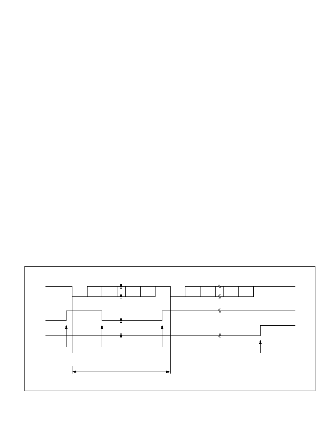
In transmitting serial data, the SCI operates as follows.
∑
The SCI monitors the TDRE flag in SSR. When the TDRE flag is cleared to 0 the SCI
recognizes that TDR contains new data, and loads this data from TDR into TSR.
∑
After loading the data from TDR into TSR, the SCI sets the TDRE flag to 1 and starts
transmitting. If the TIE bit is set to 1 in SCR, the SCI requests a transmit-data-empty interrupt
(TXI) at this time.
Serial transmit data is transmitted in the following order from the TxD pin:
-- Start bit:
One 0 bit is output.
-- Transmit data:
7 or 8 bits are output, LSB first.
-- Parity bit or multiprocessor bit: One parity bit (even or odd parity) or one multiprocessor
bit is output. Formats in which neither a parity bit nor a
multiprocessor bit is output can also be selected.
-- Stop bit:
One or two 1 bits (stop bits) are output.
-- Mark state:
Output of 1 bits continues until the start bit of the next
transmit data.
∑
The SCI checks the TDRE flag when it outputs the stop bit. If the TDRE flag is 0, the SCI
loads new data from TDR into TSR, outputs the stop bit, then begins serial transmission of
the next frame. If the TDRE flag is 1, the SCI sets the TEND flag to 1 in SSR, outputs the
stop bit, then continues output of 1 bits in the mark state. If the TEIE bit is set to 1 in SCR, a
transmit-end interrupt (TEI) is requested at this time.
Figure 13-6 shows an example of SCI transmit operation in asynchronous mode.
Figure 13-6 Example of SCI Transmit Operation in Asynchronous Mode
(8-Bit Data with Parity and 1 Stop Bit)
1
Start
bit
0
D0
D1
D7
0/1
Stop
bit
1
Data
Parity
bit
Start
bit
0
D0
D1
D7
0/1
Stop
bit
1
Data
Parity
bit
1
Idle (mark)
state
TDRE
TEND
TXI
interrupt
request
TXI interrupt handler
writes data in TDR and
clears TDRE flag to 0
TXI
interrupt
request
1 frame
TEI interrupt request
453
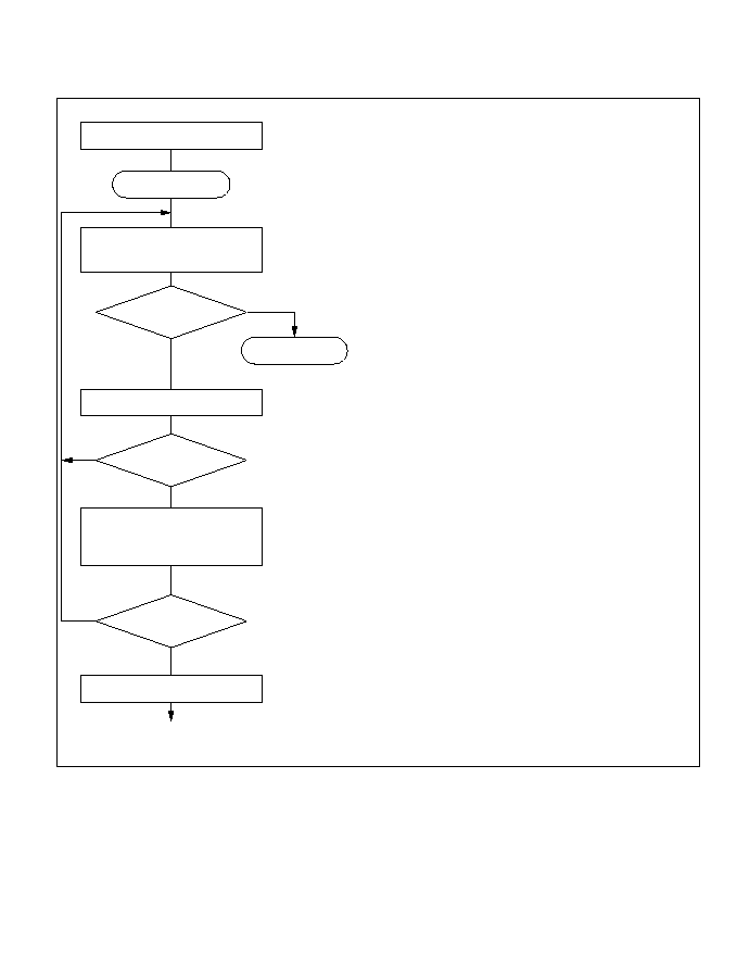
Receiving Serial Data (Asynchronous Mode): Figure 13-7 shows a sample flowchart for
receiving serial data and indicates the procedure to follow.
Figure 13-7 Sample Flowchart for Receiving Serial Data (1)
Start receiving
Read RDRF flag in SSR
RDRF = 1?
Read receive data
from RDR, and clear
RDRF flag to 0 in SSR
PER FER
ORER = 1?
Clear RE bit to 0 in SCR
Finished
receiving?
End
Error handling
(continued on next page)
1
4
No
Yes
Yes
No
No
Yes
1.
2, 3.
4.
5.
SCI initialization: the receive data function of
the RxD pin is selected automatically.
Receive error handling and break
detection: if a receive error occurs, read the
ORER, PER, and FER flags in SSR to identify
the error. After executing the necessary error
handling, clear the ORER, PER, and FER
flags all to 0. Receiving cannot resume if any
of the ORER, PER, and FER flags remains
set to 1. When a framing error occurs, the
RxD pin can be read to detect the break state.
SCI status check and receive data read: read
SSR, check that RDRF is set to 1, then read
receive data from RDR and clear the RDRF
flag to 0. Notification that the RDRF flag has
changed from 0 to 1 can also be given by the
RXI interrupt.
To continue receiving serial data: check the
RDRF flag, read RDR, and clear the RDRF
flag to 0 before the stop bit of the current
frame is received. If the DMAC is activated
by an RXI interrupt to read the RDR value,
the RDRF flag is cleared automatically.
Read ORER, PER,
and FER flags in SSR
2
5
Initialize
3
454
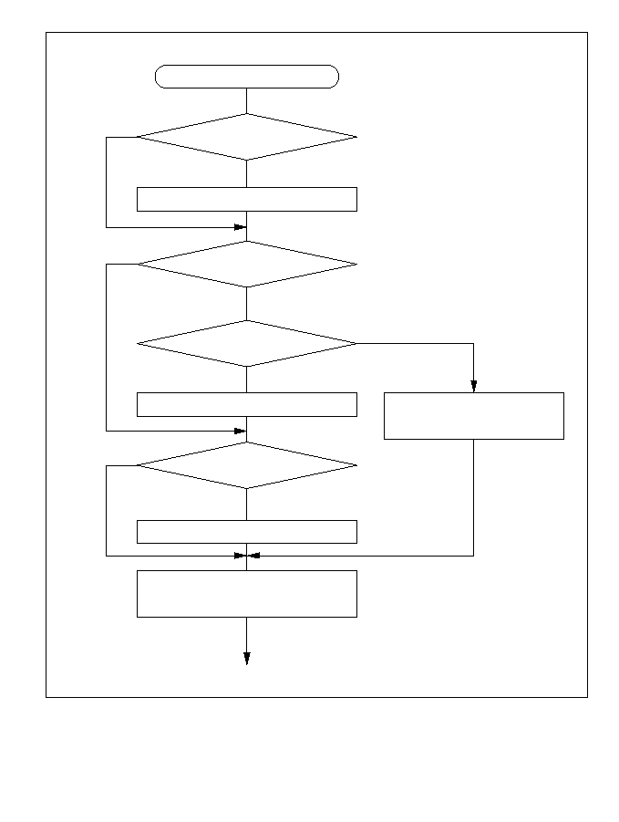
Figure 13-7 Sample Flowchart for Receiving Serial Data (2)
No
No
No
No
Yes
Yes
Yes
Yes
Framing error handling
PER = 1?
ORER = 1?
Overrun error handling
FER = 1?
Break?
Error handling
Parity error handling
Clear ORER, PER, and
FER flags to 0 in SSR
Clear RE bit to 0 in SCR
End
3
455

In receiving, the SCI operates as follows.
∑
The SCI monitors the receive data line. When it detects a start bit, the SCI synchronizes
internally and starts receiving.
∑
Receive data is stored in RSR in order from LSB to MSB.
∑
The parity bit and stop bit are received.
After receiving, the SCI makes the following checks:
-- Parity check:
The number of 1s in the receive data must match the even or odd parity
setting of the O/
E bit in SMR.
-- Stop bit check: The stop bit value must be 1. If there are two stop bits, only the first stop
bit is checked.
-- Status check:
The RDRF flag must be 0 so that receive data can be transferred from
RSR into RDR.
If these checks all pass, the RDRF flag is set to 1 and the received data is stored in RDR. If one of
the checks fails (receive error), the SCI operates as indicated in table 13-11.
Note: When a receive error occurs, further receiving is disabled. In receiving, the RDRF flag is
not set to 1. Be sure to clear the error flags to 0.
∑
When the RDRF flag is set to 1, if the RIE bit is set to 1 in SCR, a receive-data-full interrupt
(RXI) is requested. If the ORER, PER, or FER flag is set to 1 and the RIE bit in SCR is also
set to 1, a receive-error interrupt (ERI) is requested.
Table 13-11 Receive Error Conditions
Receive Error
Abbreviation
Condition
Data Transfer
Overrun error
ORER
Receiving of next data ends
Receive data not transferred
while RDRF flag is still set to
from RSR to RDR
1 in SSR
Framing error
FER
Stop bit is 0
Receive data transferred
from RSR to RDR
Parity error
PER
Parity of receive data differs
Receive data transferred
from even/odd parity setting
from RSR to RDR
in SMR
456
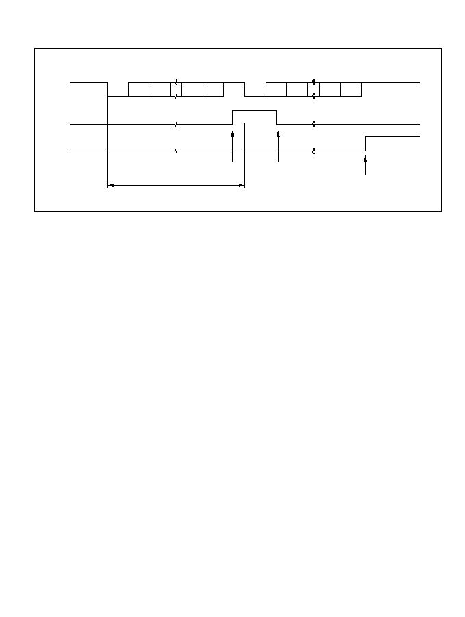
Figure 13-8 shows an example of SCI receive operation in asynchronous mode.
Figure 13-8 Example of SCI Receive Operation (8-Bit Data with Parity and One Stop Bit)
13.3.3 Multiprocessor Communication
The multiprocessor communication function enables several processors to share a single serial
communication line. The processors communicate in asynchronous mode using a format with an
additional multiprocessor bit (multiprocessor format).
In multiprocessor communication, each receiving processor is addressed by an ID. A serial
communication cycle consists of an ID-sending cycle that identifies the receiving processor, and a
data-sending cycle. The multiprocessor bit distinguishes ID-sending cycles from data-sending
cycles.
The transmitting processor starts by sending the ID of the receiving processor with which it wants
to communicate as data with the multiprocessor bit set to 1. Next the transmitting processor sends
transmit data with the multiprocessor bit cleared to 0.
Receiving processors skip incoming data until they receive data with the multiprocessor bit set
to 1. When they receive data with the multiprocessor bit set to 1, receiving processors compare the
data with their IDs. The receiving processor with a matching ID continues to receive further
incoming data. Processors with IDs not matching the received data skip further incoming data
until they again receive data with the multiprocessor bit set to 1. Multiple processors can send and
receive data in this way.
Figure 13-9 shows an example of communication among different processors using a
multiprocessor format.
1
Start
bit
0
D0
D1
D7
0/1
Stop
bit
1
Data
Parity
bit
Start
bit
0
D0
D1
D7
0/1
Stop
bit
1
Data
Parity
bit
1
Idle (mark)
state
RDRF
FER
RXI
request
1 frame
Framing error,
ERI request
RXI interrupt handler
reads data in RDR and
clears RDRF flag to 0
457
Communication Formats: Four formats are available. Parity-bit settings are ignored when a
multiprocessor format is selected. For details see table 13-10.
Clock: See the description of asynchronous mode.
Figure 13-9 Example of Communication among Processors using Multiprocessor Format
(Sending Data H'AA to Receiving Processor A)
Transmitting
processor
Receiving
processor A
Serial communication line
Receiving
processor B
Receiving
processor C
Receiving
processor D
(ID = 01)
(ID = 02)
(ID = 03)
(ID = 04)
Serial data
H'01
H'AA
(MPB = 1)
(MPB = 0)
ID-sending cycle: receiving
processor address
Data-sending cycle:
data sent to receiving
processor specified by ID
Legend
MPB: Multiprocessor bit
458
Transmitting and Receiving Data
Transmitting Multiprocessor Serial Data: Figure 13-10 shows a sample flowchart for
transmitting multiprocessor serial data and indicates the procedure to follow.
Figure 13-10 Sample Flowchart for Transmitting Multiprocessor Serial Data
No
No
No
No
Yes
Yes
Yes
Yes
Initialize
Start transmitting
Read TDRE flag in SSR
TDRE = 1?
Write transmit data in
TDR and set MPBT bit in SSR
Clear TDRE flag to 0
All data transmitted?
Read TEND flag in SSR
TEND = 1?
1
2
3
4
1.
2.
3.
4.
SCI initialization: the transmit data
output function of the TxD pin is
selected automatically.
SCI status check and transmit data
write: read SSR, check that the TDRE
flag is 1, then write transmit
data in TDR. Also set the MPBT flag to
0 or 1 in SSR. Finally, clear the TDRE
flag to 0.
To continue transmitting serial data:
after checking that the TDRE flag is 1,
indicating that data can be
written, write data in TDR, then clear
the TDRE flag to 0. When the DMAC
is activated by a transmit-data-empty
interrupt request (TXI) to write data in
TDR, the TDRE flag is checked and
cleared automatically.
To output a break signal at the end of
serial transmission: set the DDR bit to
1 and clear the DR bit to 0 (DDR and
DR are I/O port registers), then clear
the TE bit to 0 in SCR.
Output break signal?
Clear DR bit to 0, set DDR bit to 1
Clear TE bit to 0 in SCR
End
459

In transmitting serial data, the SCI operates as follows.
∑
The SCI monitors the TDRE flag in SSR. When the TDRE flag is cleared to 0 the SCI
recognizes that TDR contains new data, and loads this data from TDR into TSR.
∑
After loading the data from TDR into TSR, the SCI sets the TDRE flag to 1 and starts
transmitting. If the TIE bit in SCR is set to 1, the SCI requests a transmit-data-empty interrupt
(TXI) at this time.
Serial transmit data is transmitted in the following order from the TxD pin:
-- Start bit:
One 0 bit is output.
-- Transmit data:
7 or 8 bits are output, LSB first.
-- Multiprocessor bit: One multiprocessor bit (MPBT value) is output.
-- Stop bit:
One or two 1 bits (stop bits) are output.
-- Mark state:
Output of 1 bits continues until the start bit of the next transmit data.
∑
The SCI checks the TDRE flag when it outputs the stop bit. If the TDRE flag is 0, the SCI
loads data from TDR into TSR, outputs the stop bit, then begins serial transmission of the
next frame. If the TDRE flag is 1, the SCI sets the TEND flag in SSR to 1, outputs the stop
bit, then continues output of 1 bits in the mark state. If the TEIE bit is set to 1 in SCR, a
transmit-end interrupt (TEI) is requested at this time.
Figure 13-11 shows an example of SCI transmit operation using a multiprocessor format.
Figure 13-11 Example of SCI Transmit Operation (8-Bit Data with Multiprocessor Bit and
One Stop Bit)
1
Start
bit
0
D0
D1
D7
0/1
Stop
bit
1
Data
Multi-
processor
bit
Start
bit
0
D0
D1
D7
0/1
Stop
bit
1
Data
1
Idle (mark)
state
TDRE
TEND
TXI
request
TXI interrupt handler
writes data in TDR and
clears TDRE flag to 0
TXI
request
1 frame
TEI request
Serial
data
Multi-
processor
bit
460
Receiving Multiprocessor Serial Data: Figure 13-12 shows a sample flowchart for receiving
multiprocessor serial data and indicates the procedure to follow.
Figure 13-12 Sample Flowchart for Receiving Multiprocessor Serial Data (1)
Initialize
Start receiving
Read RDRF flag in SSR
RDRF = 1?
Read receive data from RDR
Read ORER and FER flags in SSR
FER ORER = 1
Read RDRF flag in SSR
RDRF = 1?
Read receive data from RDR
Finished receiving?
Clear RE bit to 0 in SCR
Error handling
(continued on next page)
End
1
2
4
5
1.
2.
3.
4.
5.
SCI initialization: the receive data function
of the RxD pin is selected automatically.
ID receive cycle: set the MPIE bit to 1 in SCR.
SCI status check and ID check: read SSR,
check that the RDRF flag is set to 1, then read
data from RDR and compare with the
processor's own ID. If the ID does not match,
set the MPIE bit to 1 again and clear the
RDRF flag to 0. If the ID matches, clear the
RDRF flag to 0.
SCI status check and data receiving: read
SSR, check that the RDRF flag is set to 1,
then read data from RDR.
Receive error handling and break detection:
if a receive error occurs, read the
ORER and FER flags in SSR to identify the error.
After executing the necessary error handling,
clear the ORER and FER flags both to 0.
Receiving cannot resume while either the ORER
or FER flag remains set to 1. When a framing
error occurs, the RxD pin can be read to detect
the break state.
Yes
Yes
Yes
No
Yes
Yes
No
No
No
3
Set MPIE bit to 1 in SCR
Read ORER and FER flags in SSR
Yes
FER
O
RER = 1
Own ID?
No
No
461
Figure 13-12 Sample Flowchart for Receiving Multiprocessor Serial Data (2)
No
No
Yes
No
Yes
Yes
Error handling
ORER = 1?
Overrun error handling
FER = 1?
Break?
Framing error handling
Clear ORER, PER, and FER
flags to 0 in SSR
Clear RE bit to 0 in SCR
End
5
462

Figure 13-13 shows an example of SCI receive operation using a multiprocessor format.
Figure 13-13 Example of SCI Receive Operation (8-Bit Data with Multiprocessor Bit and
One Stop Bit)
1
Start
bit
0
D0
D1
D7
1
Stop
bit
1
Data (ID1)
MPB
Start
bit
0
D0
D1
D7
0
Stop
bit
1
Data (data1)
MPB
1
Idle (mark)
state
MPIE
RDRF
RDR value
ID1
RXI request
(multiprocessor
interrupt)
MPB detection
MPIE = 0
MPB detection
MPIE = 0
RXI handler reads
RDR data and clears
RDRF flag to 0
Not own ID, so
MPIE bit is set
to 1 again
No RXI request,
RDR not updated
a. Own ID does not match data
1
Start
bit
0
D0
D1
D7
1
Stop
bit
1
Data (ID2)
MPB
Start
bit
0
D0
D1
D7
0
Stop
bit
1
Data (data2)
MPB
1
Idle (mark)
state
MPIE
RDRF
RDR value
ID2
RXI request
(multiprocessor
interrupt)
RXI interrupt handler
reads RDR data and
clears RDRF flag to 0
Own ID, so receiving
continues, with data
received by RXI
interrupt handler
MPIE bit is set
to 1 again
b. Own ID matches data
Data 2
463

13.3.4 Synchronous Operation
In synchronous mode, the SCI transmits and receives data in synchronization with clock pulses.
This mode is suitable for high-speed serial communication.
The SCI transmitter and receiver share the same clock but are otherwise independent, so full
duplex communication is possible. The transmitter and receiver are also double buffered, so
continuous transmitting or receiving is possible by reading or writing data while transmitting or
receiving is in progress.
Figure 13-14 shows the general format in synchronous serial communication.
Figure 13-14 Data Format in Synchronous Communication
In synchronous serial communication, each data bit is placed on the communication line from one
falling edge of the serial clock to the next. Data is guaranteed valid at the rise of the serial clock.
In each character, the serial data bits are transmitted in order from LSB (first) to MSB (last). After
output of the MSB, the communication line remains in the state of the MSB. In synchronous mode
the SCI receives data by synchronizing with the rise of the serial clock.
Communication Format: The data length is fixed at 8 bits. No parity bit or multiprocessor bit
can be added.
Clock: An internal clock generated by the on-chip baud rate generator or an external clock input
from the SCK pin can be selected by clearing or setting the CKE1 bit in SCR. See table 13-9.
When the SCI operates on an internal clock, it outputs the clock signal at the SCK pin. Eight clock
pulses are output per transmitted or received character. When the SCI is not transmitting or
receiving, the clock signal remains in the high state.
Serial clock
Serial data
Bit 0
Bit 1
Bit 2
Bit 3
Bit 4
Bit 5
Bit 6
Bit 7
LSB
MSB
Don't care
Don't care
One unit (character or frame) of serial data
Transfer direction
*
*
Note: High except in continuous transmitting or receiving
*
464

Transmitting and Receiving Data
SCI Initialization (Synchronous Mode): Before transmitting or receiving, clear the TE and RE
bits to 0 in SCR, then initialize the SCI as follows.
When changing the communication mode or format, always clear the TE and RE bits to 0 before
following the procedure given below. Clearing the TE bit to 0 sets the TDRE flag to 1 and
initializes TSR. Clearing the RE bit to 0, however, does not initialize the RDRF, PER, FER, and
ORE flags and RDR, which retain their previous contents.
Figure 13-15 is a sample flowchart for initializing the SCI.
Figure 13-15 Sample Flowchart for SCI Initialization
Clear TE and RE
bits to 0 in SCR
1 bit interval
elapsed?
Start transmitting or receiving
No
Yes
1.
2.
3.
4.
Select the clock source in SCR. Clear the RIE, TIE, TEIE,
MPIE, TE, and RE bits to 0.
Select the communication format in SMR.
Write the value corresponding to the bit rate in BRR.
This step is not necessary when an external clock is used.
1
2
Set RIE, TIE, TEIE, MPIE,
CKE1, and CKE0 bits in SCR
(leaving TE and RE bits
cleared to 0)
3
Set TE or RE to 1 in SCR
Set RIE, TIE, TEIE, and
MPIE bits as necessary
4
Wait
Wait for at least the interval required to transmit or receive
one bit, then set the TE or RE bit to 1 in SCR. Also set
the RIE, TIE, TEIE, and MPIE bits as necessary.
Setting the TE or RE bit enables the SCI to use the
TxD or RxD pin.
Start of initialization
Set value in BRR
Select communication
format in SMR
Note: In simultaneous transmit/receive operations,
the TE and RE bits should be set to 1 or cleared to
0 simultaneously.
465
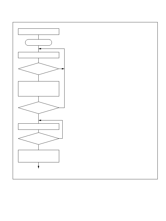
Transmitting Serial Data (Synchronous Mode): Figure 13-16 shows a sample flowchart for
transmitting serial data and indicates the procedure to follow.
Figure 13-16 Sample Flowchart for Serial Transmitting
Start transmitting
Read TDRE flag in SSR
TDRE = 1?
Write transmit data in
TDR and clear TDRE flag
to 0 in SSR
End
1
2
3
No
Yes
No
Yes
SCI initialization: the transmit data output function
of the TxD pin is selected automatically.
SCI status check and transmit data write: read SSR,
check that the TDRE flag is 1, then write transmit
data in TDR and clear the TDRE flag to 0.
Read TEND flag in SSR
No
Yes
1.
2.
3.
Initialize
Clear TE bit to 0 in SCR
To continue transmitting serial data: after checking
that the TDRE flag is 1, indicating that data can be
written, write data in TDR, then clear the TDRE flag
to 0. When the DMAC is activated by a transmit-
data-empty interrupt request (TXI) to write data in
TDR, the TDRE flag is checked and cleared
automatically.
All data
transmitted?
TEND = 1?
466

In transmitting serial data, the SCI operates as follows.
∑
The SCI monitors the TDRE flag in SSR. When the TDRE flag is cleared to 0 the SCI
recognizes that TDR contains new data, and loads this data from TDR into TSR.
∑
After loading the data from TDR into TSR, the SCI sets the TDRE flag to 1 and starts
transmitting. If the TIE bit is set to 1 in SCR, the SCI requests a transmit-data-empty interrupt
(TXI) at this time.
If clock output is selected, the SCI outputs eight serial clock pulses. If an external clock
source is selected, the SCI outputs data in synchronization with the input clock. Data is output
from the TxD pin in order from LSB (bit 0) to MSB (bit 7).
∑
The SCI checks the TDRE flag when it outputs the MSB (bit 7). If the TDRE flag is 0, the
SCI loads data from TDR into TSR and begins serial transmission of the next frame. If the
TDRE flag is 1, the SCI sets the TEND flag to 1 in SSR, and after transmitting the MSB,
holds the TxD pin in the MSB state. If the TEIE bit in SCR is set to 1, a transmit-end
interrupt (TEI) is requested at this time.
∑
After the end of serial transmission, the SCK pin is held in a constant state.
467

Figure 13-17 shows an example of SCI transmit operation.
Figure 13-17 Example of SCI Transmit Operation
Transmit
direction
Serial clock
Serial data
TDRE
TEND
Bit 0
Bit 1
Bit 7
Bit 0
Bit 1
Bit 6
Bit 7
TXI interrupt handler
writes data in TDR
and clears TDRE
flag to 0
TXI
request
TXI
request
TEI
request
1 frame
468

Receiving Serial Data: Figure 13-18 shows a sample flowchart for receiving serial data and
indicates the procedure to follow. When switching from asynchronous mode to synchronous
mode, make sure that the ORER, PER, and FER flags are cleared to 0. If the FER or PER flag is
set to 1 the RDRF flag will not be set and both transmitting and receiving will be disabled.
Figure 13-18 Sample Flowchart for Serial Receiving (1)
Start receiving
Read RDRF flag in SSR
Read receive data
from RDR, and clear
RDRF flag to 0 in SSR
Read ORER flag in SSR
Clear RE bit to 0 in SCR
End
Error handling
1
4
5
No
Yes
Yes
No
Yes
3
1.
2, 3.
4.
5.
SCI initialization: the receive data function of
the RxD pin is selected automatically.
Receive error handling: if a receive error
occurs, read the ORER flag in SSR, then after
executing the necessary error handling, clear
the ORER flag to 0. Neither transmitting nor
receiving can resume while the ORER flag
remains set to 1.
SCI status check and receive data read: read
SSR, check that the RDRF flag is set to 1,
then read receive data from RDR and clear
the RDRF flag to 0. Notification that the RDRF
flag has changed from 0 to 1 can also be
given by the RXI interrupt.
To continue receiving serial data: check the
RDRF flag, read RDR, and clear the RDRF
flag to 0 before the MSB (bit 7) of the current
frame is received. If the DMAC is activated
by a receive-data-full interrupt request (RXI)
to read RDR, the RDRF flag is cleared
automatically.
Initialize
No
RDRF = 1?
ORER = 1?
Finished
receiving?
2
469

Figure 13-18 Sample Flowchart for Serial Receiving (2)
In receiving, the SCI operates as follows.
∑
The SCI synchronizes with serial clock input or output and initializes internally.
∑
Receive data is stored in RSR in order from LSB to MSB.
After receiving the data, the SCI checks that the RDRF flag is 0 so that receive data can be
transferred from RSR to RDR. If this check passes, the RDRF flag is set to 1 and the received
data is stored in RDR. If the check does not pass (receive error), the SCI operates as indicated
in table 13-11.
∑
After setting the RDRF flag to 1, if the RIE bit is set to 1 in SCR, the SCI requests a receive-
data-full interrupt (RXI). If the ORER flag is set to 1 and the RIE bit in SCR is also set to 1,
the SCI requests a receive-error interrupt (ERI).
3
End
Error handling
Overrun error handling
Clear ORER flag to 0 in SSR
470
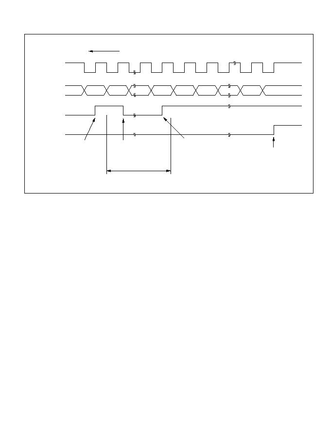
Figure 13-19 shows an example of SCI receive operation.
Figure 13-19 Example of SCI Receive Operation
Transmitting and Receiving Serial Data Simultaneously (Synchronous Mode): Figure 13-20
shows a sample flowchart for transmitting and receiving serial data simultaneously and indicates
the procedure to follow.
Serial clock
Serial data
Bit 7
Bit 0
Bit 7
Bit 0
Bit 1
Bit 6
Bit 7
RXI
request
Receive direction
RDRF
ORER
RXI interrupt handler
reads data in RDR and
clears RDRF flag to 0
RXI
request
Overrun error,
ERI request
1 frame
471
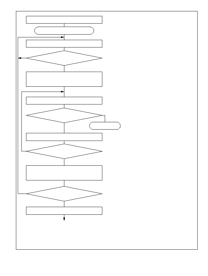
Figure 13-20 Sample Flowchart of Simultaneous Serial Transmit and Receive Operations
No
Yes
No
Yes
Yes
No
Yes
No
Initialize
Start transmitting and receiving
Read TDRE flag in SSR
TDRE = 1?
Write transmit data in TDR and
clear TDRE flag to 0 in SSR
RDRF = 1?
Read RDRF flag in SSR
Read receive data from RDR
and clear RDRF flag to 0 in SSR
Read ORER flag in SSR
ORER = 1?
End of transmitting and
receiving?
1
2
5
3
1.
2.
3.
4.
5.
SCI initialization: the transmit data
output function of the TxD pin and
receive data input function of the
RxD pin are selected, enabling
simultaneous transmitting and
receiving.
SCI status check and transmit
data write: read SSR, check that
the TDRE flag is 1, then write
transmit data in TDR and clear
the TDRE flag to 0.
Error handling
Note:
*
When switching from transmitting or receiving to simultaneous
transmitting and receiving, clear the TE and RE bits both to 0,
then set the TE and RE bits both to 1 simultaneously.
Clear TE and RE bits to 0 in SCR
End
Notification that the TDRE flag has
changed from 0 to 1 can also be
given by the TXI interrupt.
Receive error handling: if a receive
error occurs, read the ORER flag in
SSR, then after executing the neces-
sary error handling, clear the ORER
flag to 0.
Neither transmitting nor receiving
can resume while the ORER flag
remains set to 1.
SCI status check and receive
data read: read SSR, check that
the RDRF flag is 1, then read
receive data from RDR and clear
the RDRF flag to 0. Notification
that the RDRF flag has changed
from 0 to 1 can also be given
by the RXI interrupt.
To continue transmitting and
receiving serial data: check the
RDRF flag, read RDR, and clear
the RDRF flag to 0 before the
MSB (bit 7) of the current frame
is received. Also check that
the TDRE flag is set to 1, indicat-
ing that data can be written, write
data in TDR, then clear the TDRE
flag to 0 before the MSB (bit 7) of
the current frame is transmitted.
When the DMAC is activated by
a transmit-data-empty interrupt
request (TXI) to write data in TDR,
the TDRE flag is checked and
cleared automatically. When the
DMAC is activated by a receive-
data-full interrupt request (RXI) to
read RDR, the RDRF flag is
cleared automatically.
4
472

13.4 SCI Interrupts
The SCI has four interrupt request sources: TEI (transmit-end interrupt), ERI (receive-error
interrupt), RXI (receive-data-full interrupt), and TXI (transmit-data-empty interrupt). Table 13-12
lists the interrupt sources and indicates their priority. These interrupts can be enabled and disabled
by the TIE, TEIE, and RIE bits in SCR. Each interrupt request is sent separately to the interrupt
controller.
The TXI interrupt is requested when the TDRE flag is set to 1 in SSR. The TEI interrupt is
requested when the TEND flag is set to 1 in SSR. The TXI interrupt request can activate the
DMAC to transfer data. Data transfer by the DMAC automatically clears the TDRE flag to 0. The
TEI interrupt request cannot activate the DMAC.
The RXI interrupt is requested when the RDRF flag is set to 1 in SSR. The ERI interrupt is
requested when the ORER, PER, or FER flag is set to 1 in SSR. The RXI interrupt request can
activate the DMAC to transfer data. Data transfer by the DMAC automatically clears the RDRF
flag to 0. The ERI interrupt request cannot activate the DMAC.
The DMAC can be activated by interrupts from SCI channel 0.
Table 13-12 SCI Interrupt Sources
Interrupt
Description
Priority
ERI
Receive error (ORER, FER, or PER)
High
RXI
Receive data register full (RDRF)
TXI
Transmit data register empty (TDRE)
TEI
Transmit end (TEND)
Low
473

13.5 Usage Notes
Note the following points when using the SCI.
TDR Write and TDRE Flag: The TDRE flag in SSR is a status flag indicating the loading of
transmit data from TDR into TSR. The SCI sets the TDRE flag to 1 when it transfers data from
TDR to TSR.
Data can be written into TDR regardless of the state of the TDRE flag. If new data is written in
TDR when the TDRE flag is 0, the old data stored in TDR will be lost because this data has not
yet been transferred to TSR. Before writing transmit data in TDR, be sure to check that the TDRE
flag is set to 1.
Simultaneous Multiple Receive Errors: Table 13-13 indicates the state of SSR status flags when
multiple receive errors occur simultaneously. When an overrun error occurs the RSR contents are
not transferred to RDR, so receive data is lost.
Table 13-13 SSR Status Flags and Transfer of Receive Data
Receive Data
Transfer
RDRF
ORER
FER
PER
RSR
RDR
Receive Errors
1
1
0
0
◊
Overrun error
0
0
1
0
Framing error
0
0
0
1
Parity error
1
1
1
0
◊
Overrun error + framing error
1
1
0
1
◊
Overrun error + parity error
0
0
1
1
Framing error + parity error
1
1
1
1
◊
Overrun error + framing error + parity error
Notes:
: Receive data is transferred from RSR to RDR.
◊
Receive data is not transferred from RSR to RDR.
SSR Status Flags
474

Break Detection and Processing: Break signals can be detected by reading the RxD pin directly
when a framing error (FER) is detected. In the break state the input from the RxD pin consists of
all 0s, so the FER flag is set and the parity error flag (PER) may also be set. In the break state the
SCI receiver continues to operate, so if the FER flag is cleared to 0 it will be set to 1 again.
Sending a Break Signal: When the TE bit is cleared to 0 the TxD pin becomes an I/O port, the
level and direction (input or output) of which are determined by DR and DDR bits. This feature
can be used to send a break signal.
After the serial transmitter is initialized, the DR value substitutes for the mark state until the TE
bit is set to 1 (the TxD pin function is not selected until the TE bit is set to 1). The DDR and DR
bits should therefore both be set to 1 beforehand.
To send a break signal during serial transmission, clear the DR bit to 0, then clear the TE bit to 0.
When the TE bit is cleared to 0 the transmitter is initialized, regardless of its current state, so the
TxD pin becomes an output port outputting the value 0.
Receive Error Flags and Transmitter Operation (Synchronous Mode Only): When a receive
error flag (ORER, PER, or FER) is set to 1 the SCI will not start transmitting, even if the TDRE
flag is cleared to 0. Be sure to clear the receive error flags to 0 when starting to transmit. Note that
clearing the RE bit to 0 does not clear the receive error flags to 0.
Receive Data Sampling Timing in Asynchronous Mode and Receive Margin: In asynchronous
mode the SCI operates on a base clock with 16 times the bit rate frequency. In receiving, the SCI
synchronizes internally with the fall of the start bit, which it samples on the base clock. Receive
data is latched at the rising edge of the eighth base clock pulse. See figure 13-21.
475
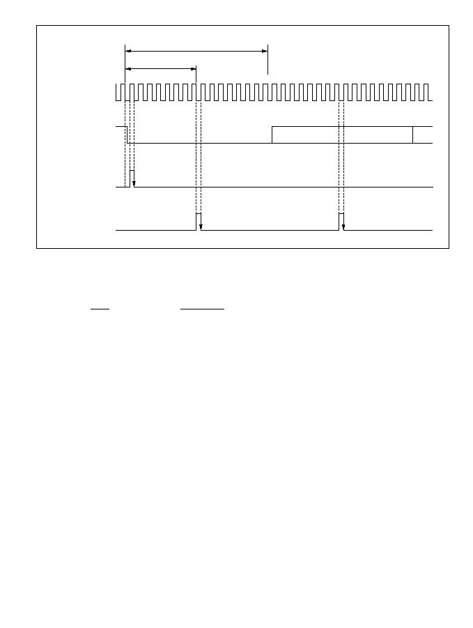
Figure 13-21 Receive Data Sampling Timing in Asynchronous Mode
The receive margin in asynchronous mode can therefore be expressed as in equation (1).
...................(1)
M: Receive margin (%)
N: Ratio of clock frequency to bit rate (N = 16)
D: Clock duty cycle (D = 0 to 1.0)
L: Frame length (L = 9 to 12)
F: Absolute deviation of clock frequency
From equation (1), if F = 0 and D = 0.5 the receive margin is 46.875%, as given by equation (2).
D = 0.5, F = 0
M = [0.5 ≠ 1/(2
◊
16)]
◊
100%
= 46.875%.................................................................................................(2)
This is a theoretical value. A reasonable margin to allow in system designs is 20% to 30%.
Internal
base clock
Receive data
(RxD)
Synchronization
sampling timing
Data sampling
timing
0
7
15 0
7
15 0
D
0
D
1
8 clocks
16 clocks
Start bit
M = | (0.5 ≠ ) ≠ (L ≠ 0.5) F ≠ (1 + F) | 100%
1
2N
| D ≠ 0.5 |
N
◊
476
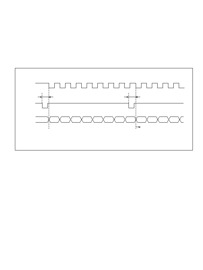
Restrictions on Usage of DMAC
To have the DMAC read RDR, be sure to select the SCI receive-data-full interrupt (RXI) as the
activation source with bits DTS2 to DTS0 in DTCR.
Restrictions in Synchronous Mode: When data transmission is performed using an external
clock source as the serial clock, an interval of at least 5 states is necessary between clearing the
TDRE bit in SSR and the start (falling edge) of the first transmit clock pulse corresponding to
each frame (figure 13-22). This interval is also necessary when performing continuous
transmission. If this condition is not satisfied, an operation error may occur.
Figure 13-22 Transmission in Synchronous Mode (Example)
SCK
TDRE
TXD
t
*
X0
X1
X2
X3
X4
X5
X6
X7
Y0
Continuous transmission
Note:
*
Make sure that t is at least 5 states.
Y1
Y2
Y3
t
*
477

478

Section 14 A/D Converter
14.1 Overview
The H8/3002 includes a 10-bit successive-approximations A/D converter with a selection of up to
eight analog input channels.
14.1.1 Features
A/D converter features are listed below.
∑
10-bit resolution
∑
Eight input channels
∑
Selectable analog conversion voltage range
The analog voltage conversion range can be programmed by input of an analog reference
voltage at the V
REF
pin.
∑
High-speed conversion
Conversion time: maximum 7.9 µs per channel (with 17 MHz system clock)
∑
Two conversion modes
Single mode: A/D conversion of one channel
Scan mode: continuous conversion on one to four channels
∑
Four 16-bit data registers
A/D conversion results are transferred for storage into data registers corresponding to the
channels.
∑
Sample-and-hold function
∑
A/D conversion can be externally triggered
∑
A/D interrupt requested at end of conversion
At the end of A/D conversion, an A/D end interrupt (ADI) can be requested.
479

14.1.2 Block Diagram
Figure 14-1 shows a block diagram of the A/D converter.
Figure 14-1 A/D Converter Block Diagram
Module data bus
Bus interface
On-chip
data bus
ADDRA
ADDRB
ADDRC
ADDRD
ADCSR
ADCR
Successive-
approximations register
10-bit D/A
AV
V
AV
CC
REF
SS
Analog
multi-
plexer
AN
AN
AN
AN
AN
AN
AN
AN
0
1
2
3
4
5
6
7
Sample-and-
hold circuit
Comparator
+
≠
Control circuit
ADTRG
¯/8
¯/16
ADI
interrupt
signal
Legend
ADCR:
ADCSR:
ADDRA:
ADDRB:
ADDRC:
ADDRD:
A/D control register
A/D control/status register
A/D data register A
A/D data register B
A/D data register C
A/D data register D
480

14.1.3 Input Pins
Table 14-1 summarizes the A/D converter's input pins. The eight analog input pins are divided
into two groups: group 0 (AN
0
to AN
3
), and group 1 (AN
4
to AN
7
). AV
CC
and AV
SS
are the
power supply for the analog circuits in the A/D converter. V
REF
is the A/D conversion reference
voltage.
Table 14-1 A/D Converter Pins
Abbrevi-
Pin Name
ation
I/O
Function
Analog power supply pin
AV
CC
Input
Analog power supply
Analog ground pin
AV
SS
Input
Analog ground and reference voltage
Reference voltage pin
V
REF
Input
Analog reference voltage
Analog input pin 0
AN
0
Input
Group 0 analog inputs
Analog input pin 1
AN
1
Input
Analog input pin 2
AN
2
Input
Analog input pin 3
AN
3
Input
Analog input pin 4
AN
4
Input
Group 1 analog inputs
Analog input pin 5
AN
5
Input
Analog input pin 6
AN
6
Input
Analog input pin 7
AN
7
Input
A/D external trigger input pin
ADTRG
Input
External trigger input for starting A/D conversion
481

14.1.4 Register Configuration
Table 14-2 summarizes the A/D converter's registers.
Table 14-2 A/D Converter Registers
Address
*
1
Name
Abbreviation
R/W
Initial Value
H'FFE0
A/D data register A (high)
ADDRAH
R
H'00
H'FFE1
A/D data register A (low)
ADDRAL
R
H'00
H'FFE2
A/D data register B (high)
ADDRBH
R
H'00
H'FFE3
A/D data register B (low)
ADDRBL
R
H'00
H'FFE4
A/D data register C (high)
ADDRCH
R
H'00
H'FFE5
A/D data register C (low)
ADDRCL
R
H'00
H'FFE6
A/D data register D (high)
ADDRDH
R
H'00
H'FFE7
A/D data register D (low)
ADDRDL
R
H'00
H'FFE8
A/D control/status register
ADCSR
R/(W)
*
2
H'00
H'FFE9
A/D control register
ADCR
R/W
H'7E
Notes: 1. Lower 16 bits of the address
2. Only 0 can be written in bit 7, to clear the flag.
482

14.2 Register Descriptions
14.2.1 A/D Data Registers A to D (ADDRA to ADDRD)
The four A/D data registers (ADDRA to ADDRD) are 16-bit read-only registers that store the
results of A/D conversion.
An A/D conversion produces 10-bit data, which is transferred for storage into the A/D data
register corresponding to the selected channel. The upper 8 bits of the result are stored in the
upper byte of the A/D data register. The lower 2 bits are stored in the lower byte. Bits 5 to 0 of an
A/D data register are reserved bits that always read 0. Table 14-3 indicates the pairings of analog
input channels and A/D data registers.
The CPU can always read and write the A/D data registers. The upper byte can be read directly,
but the lower byte is read through a temporary register (TEMP). For details see section 14.3, CPU
Interface.
The A/D data registers are initialized to H'0000 by a reset and in standby mode.
Table 14-3 Analog Input Channels and A/D Data Registers
Analog Input Channel
Group 0
Group 1
A/D Data Register
AN
0
AN
4
ADDRA
AN
1
AN
5
ADDRB
AN
2
AN
6
ADDRC
AN
3
AN
7
ADDRD
Bit
ADDRn
Initial value
14
AD8
0
R
12
AD6
0
R
10
AD4
0
R
8
AD2
0
R
6
AD0
0
R
0
--
0
R
4
--
0
R
2
--
0
R
15
AD9
0
R
13
AD7
0
R
11
AD5
0
R
9
AD3
0
R
7
AD1
0
R
1
--
0
R
5
--
0
R
3
--
0
R
A/D conversion data
10-bit data giving an
A/D conversion result
Reserved bits
Read/Write
(n = A to D)
483

14.2.2 A/D Control/Status Register (ADCSR)
ADCSR is an 8-bit readable/writable register that selects the mode and controls the A/D converter.
ADCSR is initialized to H'00 by a reset and in standby mode.
Bit
Initial value
Read/Write
7
ADF
0
R/(W)
6
ADIE
0
R/W
5
ADST
0
R/W
4
SCAN
0
R/W
3
CKS
0
R/W
0
CH0
0
R/W
2
CH2
0
R/W
1
CH1
0
R/W
*
Note: Only 0 can be written, to clear the flag.
*
A/D end flag
Indicates end of A/D conversion
A/D interrupt enable
Enables and disables A/D end interrupts
A/D start
Starts or stops A/D conversion
Scan mode
Selects single mode or scan mode
Clock select
Selects the A/D conversion time
Channel select 2 to 0
These bits select analog
input channels
484

Bit 7--A/D End Flag (ADF): Indicates the end of A/D conversion.
Bit 7
ADF
Description
0
[Clearing condition]
(Initial value)
Cleared by reading ADF while ADF = 1, then writing 0 in ADF
1
[Setting conditions]
Single mode: A/D conversion ends
Scan mode: A/D conversion ends in all selected channels
Bit 6--A/D Interrupt Enable (ADIE): Enables or disables the interrupt (ADI) requested at the
end of A/D conversion.
Bit 6
ADIE
Description
0
A/D end interrupt request (ADI) is disabled
(Initial value)
1
A/D end interrupt request (ADI) is enabled
Bit 5--A/D Start (ADST): Starts or stops A/D conversion. The ADST bit remains set to 1 during
A/D conversion. It can also be set to 1 by external trigger input at the
ADTRG pin.
Bit 5
ADST
Description
0
A/D conversion is stopped
(Initial value)
1
Single mode: A/D conversion starts; ADST is automatically cleared to 0 when conversion
ends.
Scan mode: A/D conversion starts and continues, cycling among the selected channels,
until ADST is cleared to 0 by software, by a reset, or by a transition to standby mode.
485

Bit 4--Scan Mode (SCAN): Selects single mode or scan mode. For further information on
operation in these modes, see section 14.4, Operation. Clear the ADST bit to 0 before switching
the conversion mode.
Bit 4
SCAN
Description
0
Single mode
(Initial value)
1
Scan mode
Bit 3--Clock Select (CKS): Selects the A/D conversion time. Clear the ADST bit to 0 before
switching the conversion time.
Bit 3
CKS
Description
0
Conversion time = 266 states (maximum)
(Initial value)
1
Conversion time = 134 states (maximum)
Bits 2 to 0--Channel Select 2 to 0 (CH2 to CH0): These bits and the SCAN bit select the analog
input channels. Clear the ADST bit to 0 before changing the channel selection.
Group
Selection
Channel Selection
Description
CH2
CH1
CH0
Single Mode
Scan Mode
0
0
0
AN
0
(Initial value)
AN
0
1
AN
1
AN
0
, AN
1
1
0
AN
2
AN
0
to AN
2
1
AN
3
AN
0
to AN
3
1
0
0
AN
4
AN
4
1
AN
5
AN
4
, AN
5
1
0
AN
6
AN
4
to AN
6
1
AN
7
AN
4
to AN
7
486

14.2.3 A/D Control Register (ADCR)
ADCR is an 8-bit readable/writable register that enables or disables external triggering of A/D
conversion. ADCR is initialized to H'7F by a reset and in standby mode.
Bit 7--Trigger Enable (TRGE): Enables or disables external triggering of A/D conversion.
Bit 7
TRGE
Description
0
A/D conversion cannot be externally triggered
(Initial value)
1
A/D conversion starts at the falling edge of the external trigger signal (
ADTRG
)
Bits 6 to 0--Reserved: These bits cannot be modified and are always read as 1.
Bit
Initial value
Read/Write
7
TRGE
0
R/W
6
--
1
--
5
--
1
--
4
--
1
--
3
--
1
--
0
--
1
--
2
--
1
--
1
--
1
--
Trigger enable
Enables or disables external triggering of A/D conversion
Reserved bits
487

14.3 CPU Interface
ADDRA to ADDRD are 16-bit registers, but they are connected to the CPU by an 8-bit data bus.
Therefore, although the upper byte can be be accessed directly by the CPU, the lower byte is read
through an 8-bit temporary register (TEMP).
An A/D data register is read as follows. When the upper byte is read, the upper-byte value is
transferred directly to the CPU and the lower-byte value is transferred into TEMP. Next, when the
lower byte is read, the TEMP contents are transferred to the CPU.
When reading an A/D data register, always read the upper byte before the lower byte. It is possible
to read only the upper byte, but if only the lower byte is read, incorrect data may be obtained.
Figure 14-2 shows the data flow for access to an A/D data register.
Figure 14-2 A/D Data Register Access Operation (Reading H'AA40)
Upper-byte read
Bus interface
Module data bus
CPU
(H'AA)
ADDRnH
(H'AA)
ADDRnL
(H'40)
Lower-byte read
Bus interface
Module data bus
CPU
(H'40)
ADDRnH
(H'AA)
ADDRnL
(H'40)
TEMP
(H'40)
TEMP
(H'40)
(n = A to D)
(n = A to D)
488

14.4 Operation
The A/D converter operates by successive approximations with 10-bit resolution. It has two
operating modes: single mode and scan mode.
14.4.1 Single Mode (SCAN = 0)
Single mode should be selected when only one A/D conversion on one channel is required. A/D
conversion starts when the ADST bit is set to 1 by software, or by external trigger input. The
ADST bit remains set to 1 during A/D conversion and is automatically cleared to 0 when
conversion ends.
When conversion ends the ADF bit is set to 1. If the ADIE bit is also set to 1, an ADI interrupt is
requested at this time. To clear the ADF flag to 0, first read ADCSR, then write 0 in ADF.
When the mode or analog input channel must be switched during analog conversion, to prevent
incorrect operation, first clear the ADST bit to 0 in ADCSR to halt A/D conversion. After making
the necessary changes, set the ADST bit to 1 to start A/D conversion again. The ADST bit can be
set at the same time as the mode or channel is changed.
Typical operations when channel 1 (AN
1
) is selected in single mode are described next.
Figure 14-3 shows a timing diagram for this example.
1.
Single mode is selected (SCAN = 0), input channel AN
1
is selected (CH2 = CH1 = 0,
CH0 = 1), the A/D interrupt is enabled (ADIE = 1), and A/D conversion is started
(ADST = 1).
2.
When A/D conversion is completed, the result is transferred into ADDRB. At the same time
the ADF flag is set to 1, the ADST bit is cleared to 0, and the A/D converter becomes idle.
3.
Since ADF = 1 and ADIE = 1, an ADI interrupt is requested.
4.
The A/D interrupt handling routine starts.
5.
The routine reads ADCSR, then writes 0 in the ADF flag.
6.
The routine reads and processes the conversion result (ADDRB).
7.
Execution of the A/D interrupt handling routine ends. After that, if the ADST bit is set to 1,
A/D conversion starts again and steps 2 to 7 are repeated.
489
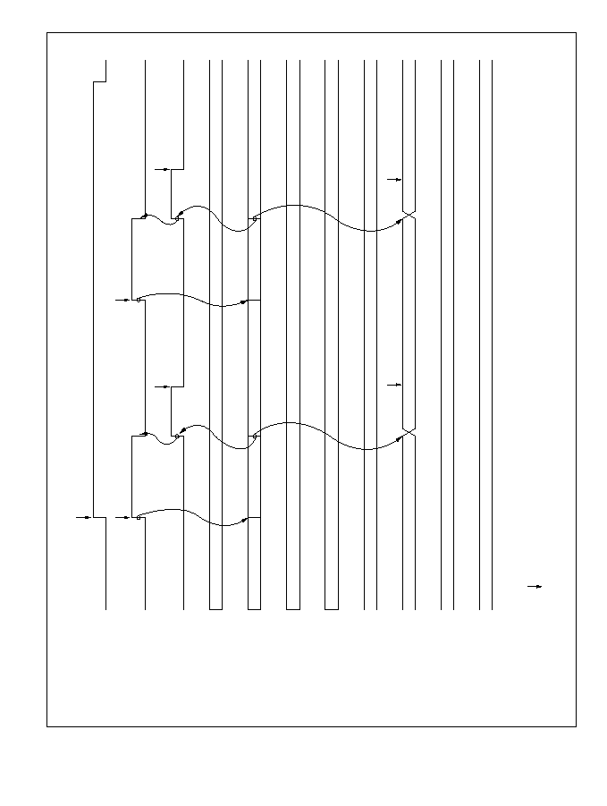
Figure 14-3 Example of A/D Converter Operation (Single Mode, Channel 1 Selected)
ADIE
ADST
ADF
State of channel 0
(AN )
Set
Set
Set
Clear
Clear
Idle
Idle
Idle
Idle
A/D conversion
A/D conversion
Idle
Read conversion result
A/D conversion result
Read conversion result
A/D conversion result
(2)
Note: V
ertical arrows ( ) indicate instructions executed by software.
0
1
2
3
A/D conversion
starts
*
*
*
*
*
(2)
(1)
(1)
*
ADDRA
ADDRB
ADDRC
ADDRD
State of channel 1
(AN )
State of channel 2
(AN )
State of channel 3
(AN )
Idle
490

14.4.2 Scan Mode (SCAN = 1)
Scan mode is useful for monitoring analog inputs in a group of one or more channels. When the
ADST bit is set to 1 by software or external trigger input, A/D conversion starts on the first
channel in the group (AN
0
when CH2 = 0, AN
4
when CH2 = 1). When two or more channels are
selected, after conversion of the first channel ends, conversion of the second channel (AN
1
or
AN
5
) starts immediately. A/D conversion continues cyclically on the selected channels until the
ADST bit is cleared to 0. The conversion results are transferred for storage into the A/D data
registers corresponding to the channels.
When the mode or analog input channel selection must be changed during analog conversion, to
prevent incorrect operation, first clear the ADST bit to 0 in ADCSR to halt A/D conversion. After
making the necessary changes, set the ADST bit to 1. A/D conversion will start again from the
first channel in the group. The ADST bit can be set at the same time as the mode or channel
selection is changed.
Typical operations when three channels in group 0 (AN
0
to AN
2
) are selected in scan mode are
described next. Figure 14-4 shows a timing diagram for this example.
1.
Scan mode is selected (SCAN = 1), scan group 0 is selected (CH2 = 0), analog input channels
AN
0
to AN
2
are selected (CH1 = 1, CH0 = 0), and A/D conversion is started (ADST = 1).
2.
When A/D conversion of the first channel (AN
0
) is completed, the result is transferred into
ADDRA. Next, conversion of the second channel (AN
1
) starts automatically.
3.
Conversion proceeds in the same way through the third channel (AN
2
).
4.
When conversion of all selected channels (AN
0
to AN
2
) is completed, the ADF flag is set to 1
and conversion of the first channel (AN
0
) starts again. If the ADIE bit is set to 1, an ADI
interrupt is requested at this time.
5.
Steps 2 to 4 are repeated as long as the ADST bit remains set to 1. When the ADST bit is
cleared to 0, A/D conversion stops. After that, if the ADST bit is set to 1, A/D conversion
starts again from the first channel (AN
0
).
491
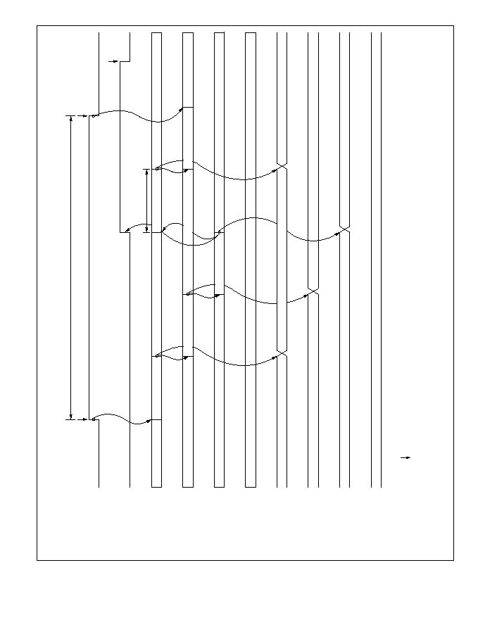
Figure 14-4 Example of A/D Converter Operation (Scan Mode,
Channels AN
0
to AN
2
Selected)
ADST
ADF
State of channel 0
(AN )
0
1
2
3
Continuous
A/D conversion
Set
Clear
*
1
Clear
*
1
Idle
A/D conversion
Idle
Idle
Idle
A/D conversion
Idle
A/D conversion
Idle
A/D conversion
Idle
A/D conversion
Idle
Idle
T
ransfer
A/D conversion result
A/D conversion result
A/D conversion result
A/D conversion result
1.
2.
A/D conversion time
Notes:
*
2
(1)
(4)
(2)
(5)
*
1
(3)
(1)
(4)
(2)
(3)
ADDRA
ADDRB
ADDRC
ADDRD
State of channel 1
(AN )
State of channel 2
(AN )
State of channel 3
(AN )
V
ertical arrows ( ) indicate instructions executed by software.
Data currently being converted is ignored.
492

14.4.3 Input Sampling and A/D Conversion Time
The A/D converter has a built-in sample-and-hold circuit. The A/D converter samples the analog
input at a time t
D
after the ADST bit is set to 1, then starts conversion. Figure 14-5 shows the A/D
conversion timing. Table 14-4 indicates the A/D conversion time.
As indicated in figure 14-5, the A/D conversion time includes t
D
and the input sampling time. The
length of t
D
varies depending on the timing of the write access to ADCSR. The total conversion
time therefore varies within the ranges indicated in table 14-4.
In scan mode, the values given in table 14-4 apply to the first conversion. In the second and
subsequent conversions the conversion time is fixed at 256 states when CKS = 0 or 128 states
when CKS = 1.
Figure 14-5 A/D Conversion Timing
¯
Address bus
Write signal
Input sampling
timing
ADF
(1)
(2)
t
D
t
SPL
t
CONV
Legend
(1):
(2):
t :
t :
t :
D
SPL
CONV
ADCSR write cycle
ADCSR address
Synchronization delay
Input sampling time
A/D conversion time
493

Table 14-4 A/D Conversion Time (Single Mode)
CKS = 0
CKS = 1
Symbol
Min
Typ
Max
Min
Typ
Max
Synchronization delay
t
D
10
--
17
6
--
9
Input sampling time
t
SPL
--
80
--
--
40
--
A/D conversion time
t
CONV
259
--
266
131
--
134
Note: Values in the table are numbers of states.
14.4.4 External Trigger Input Timing
A/D conversion can be externally triggered. When the TRGE bit is set to 1 in ADCR, external
trigger input is enabled at the
ADTRG pin. A high-to-low transition at the ADTRG pin sets the
ADST bit to 1 in ADCSR, starting A/D conversion. Other operations, in both single and scan
modes, are the same as if the ADST bit had been set to 1 by software. Figure 14-6 shows the
timing.
Figure 14-6 External Trigger Input Timing
¯
ADTRG
Internal trigger
signal
ADST
A/D conversion
494

14.5 Interrupts
The A/D converter generates an interrupt (ADI) at the end of A/D conversion. The ADI interrupt
request can be enabled or disabled by the ADIE bit in ADCSR.
14.6 Usage Notes
When using the A/D converter, note the following points:
1.
Analog Input Voltage Range: During A/D conversion, the voltages input to the analog input
pins should be in the range AV
SS
AN
n
V
REF
.
2.
Relationships of AV
CC
and AV
SS
to V
CC
and V
SS
: AV
CC
, AV
SS
, V
CC
, and V
SS
should be
related as follows: AV
SS
= V
SS
. AV
CC
and AV
SS
must not be left open, even if the A/D
converter is not used.
3.
V
REF
Programming Range: The reference voltage input at the V
REF
pin should be in the
range V
REF
AV
CC
.
Failure to observe points 1, 2, and 3 above may degrade chip reliability.
4.
Note on Board Design: In board layout, separate the digital circuits from the analog circuits
as much as possible. Particularly avoid layouts in which the signal lines of digital circuits
cross or closely approach the signal lines of analog circuits. Induction and other effects may
cause the analog circuits to operate incorrectly, or may adversely affect the accuracy of A/D
conversion.
The analog input signals (AN
0
to AN
7
), analog reference voltage (V
REF
), and analog supply
voltage (AV
CC
) must be separated from digital circuits by the analog ground (AV
SS
). The
analog ground (AV
SS
) should be connected to a stable digital ground (V
SS
) at one point on
the board.
5.
Note on Noise: To prevent damage from surges and other abnormal voltages at the analog
input pins (AN
0
to AN
7
) and analog reference voltage pin (V
REF
), connect a protection circuit
like the one in figure 14-7 between AV
CC
and AV
SS
. The bypass capacitors connected to
AV
CC
and V
REF
and the filter capacitors connected to AN
0
to AN
7
must be connected to
AV
SS
. If filter capacitors like the ones in figure 14-7 are connected, the voltage values input
to the analog input pins (AN
0
to AN
7
) will be smoothed, which may give rise to error. Error
can also occur if A/D conversion is frequently performed in scan mode so that the current that
charges and discharges the capacitor in the sample-and-hold circuit of the A/D converter
becomes greater than that input to the analog input pins via input impedance Rin. The circuit
constants should therefore be selected carefully.
495
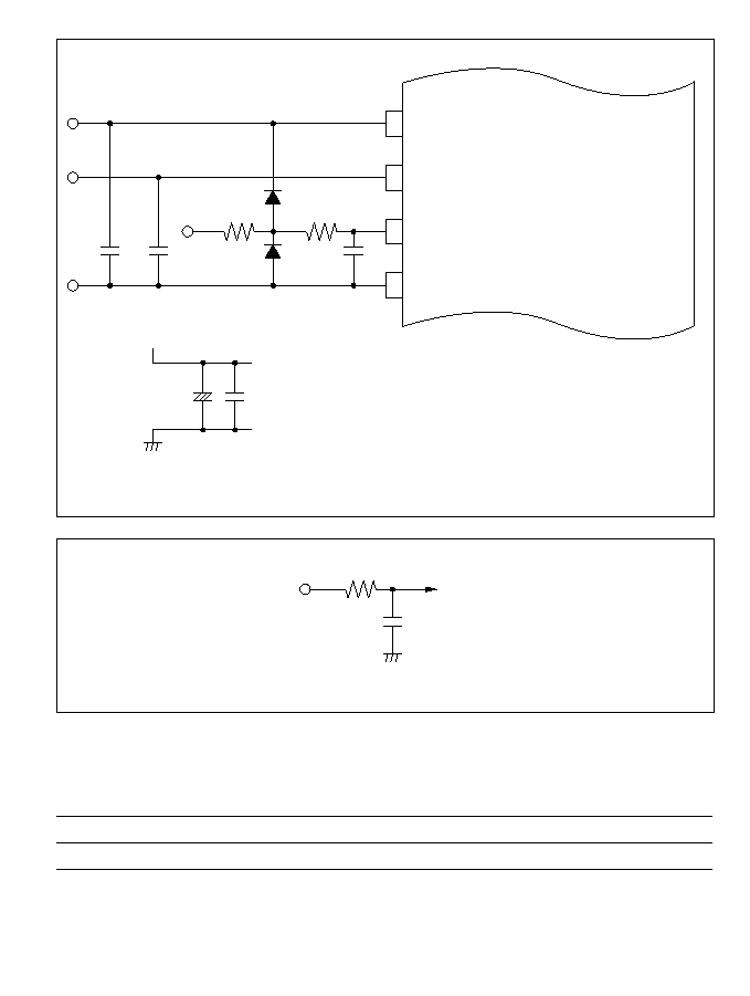
Figure 14-7 Example of Analog Input Protection Circuit
Figure 14-8 Analog Input Pin Equivalent Circuit
Table 14-5 Analog Input Pin Ratings
Item
min
max
Unit
Analog input capacitance
--
20
pF
Allowable signal-source impedance
--
10
*
k
Note:
*
When V
CC
= 4.0 V to 5.5 V and
¯
12 MHz.
Note: Numeric values are approximate, except in table 14-5.
496
AV
CC
*
1
*
1
V
REF
AN
0
to AN
7
AV
SS
Notes: 1.
2. Rin: input impedance
Rin
*
2
100
0.1 µF
0.01 µF
10 µF
20 pF
To A/D converter
AN
0
to AN
7
10 k

6.
A/D Conversion Accuracy Definitions: A/D conversion accuracy in the H8/3002 is defined as
follows:
∑
Resolution:..................Digital output code length of A/D converter
∑
Offset error: ................Deviation from ideal A/D conversion characteristic of analog input
voltage required to raise digital output from minimum voltage value
0000000000 to 0000000001 (figure 14-10)
∑
Full-scale error:...........Deviation from ideal A/D conversion characteristic of analog input
voltage required to raise digital output from 1111111110 to 1111111111
(figure 14-10)
∑
Quantization error:......Intrinsic error of the A/D converter; 1/2 LSB (figure 14-9)
∑
Nonlinearity error: ......Deviation from ideal A/D conversion characteristic in range from zero
volts to full scale, exclusive of offset error, full-scale error, and
quantization error.
∑
Absolute accuracy:......Deviation of digital value from analog input value, including offset
error, full-scale error, quantization error, and nonlinearity error.
Figure 14-9 A/D Converter Accuracy Definitions (1)
497
111
110
101
100
011
010
001
000
1/8 2/8 3/8 4/8 5/8 6/8 7/8 FS
Quantization error
Analog input
voltage
Digital
output
Ideal A/D conversion
characteristic
Figure 14-10 A/D Converter Accuracy Definitions (2)
7.
Allowable Signal-Source Impedance: The analog inputs of the H8/3002 are designed to
assure accurate conversion of input signals with a signal-source impedance not exceeding 10
k
. The reason for this rating is that it enables the input capacitor in the sample-and-hold
circuit in the A/D converter to charge within the sampling time. If the sensor output
impedance exceeds 10 k
, charging may be inadequate and the accuracy of A/D conversion
cannot be guaranteed.
If a large external capacitor is provided in single mode, then the internal 10-k
input
resistance becomes the only significant load on the input. In this case the impedance of the
signal source is not a problem.
A large external capacitor, however, acts as a low-pass filter. This may make it impossible to
track analog signals with high dv/dt (e.g. a variation of 5 mV/µs) (figure 14-11). To convert
high-speed analog signals or to use scan mode, insert a low-impedance buffer.
8.
Effect on Absolute Accuracy: Attaching an external capacitor creates a coupling with ground,
so if there is noise on the ground line, it may degrade absolute accuracy. The capacitor must
be connected to an electrically stable ground, such as AV
SS
.
If a filter circuit is used, be careful of interference with digital signals on the same board, and
make sure the circuit does not act as an antenna.
498
FS
Offset error
Nonlinearity
error
Actual A/D conversion
characteristic
Analog input
voltage
Digital
output
Ideal A/D
conversion
characteristic
Full-scale
error
Figure 14-11 Analog Input Circuit (Example)
499
Equivalent circuit of
A/D converter
H8/3002
20 pF
Cin =
15 pF
10 k
Up to 10 k
Low-pass
filter
C to 0.1
µ
F
Sensor output impedance
Sensor
input
Section 15 RAM
15.1 Overview
The H8/3002 has 512 bytes of on-chip static RAM. The RAM is connected to the CPU by a 16-bit
data bus. The CPU accesses both byte data and word data in two states, enabling rapid data
transfer.
The on-chip RAM is assigned to addresses H'FFD10 to H'FFF0F in modes 1 and 2, and addresses
H'FFFD10 to H'FFFF0F in modes 3 and 4. The RAM enable bit (RAME) in the system control
register (SYSCR) can enable or disable the on-chip RAM.
15.1.1 Block Diagram
Figure 15-1 shows a block diagram of the on-chip RAM.
Figure 15-1 RAM Block Diagram
H'FD10
H'FD12
*
*
H'FF0E
*
H'FD11
H'FD13
*
*
H'FF0F
*
On-chip data bus (upper 8 bits)
On-chip data bus (lower 8 bits)
Bus interface
On-chip RAM
Even addresses
Odd addresses
Note: Lower 16 bits of the address
*
501
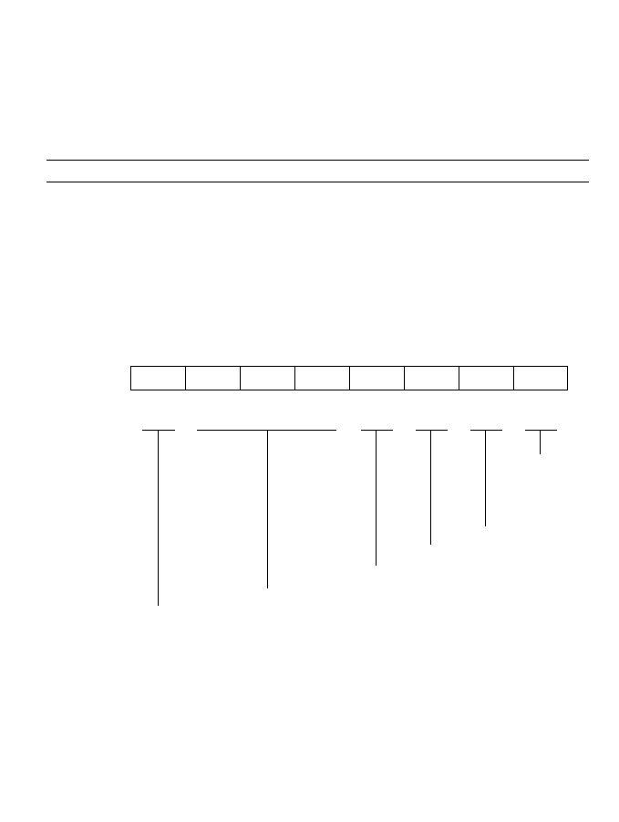
15.1.2 Register Configuration
The on-chip RAM is controlled by SYSCR. Table 15-1 gives the address and initial value of
SYSCR.
Table 15-1 RAM Control Register
Address
*
Name
Abbreviation
R/W
Initial Value
H'FFF2
System control register
SYSCR
R/W
H'0B
Note:
*
Lower 16 bits of the address
15.2 System Control Register (SYSCR)
502
Bit
Initial value
Read/Write
7
SSBY
0
R/W
6
STS2
0
R/W
5
STS1
0
R/W
4
STS0
0
R/W
3
UE
1
R/W
2
NMIEG
0
R/W
1
--
1
--
0
RAME
1
R/W
Software standby
Standby timer select 2 to 0
User bit enable
NMI edge select
Reserved bit
RAM enable bit
Enables or
disables
on-chip RAM

One function of SYSCR is to enable or disable access to the on-chip RAM. The on-chip RAM is
enabled or disabled by the RAME bit in SYSCR. For details about the other bits, see section 3.3,
System Control Register.
B
it 0--RAM Enable (RAME): Enables or disables the on-chip RAM. The RAME bit is
initialized at the rising edge of the input at the
RES pin. It is not initialized in software standby
mode.
Bit 0
RAME
Description
0
On-chip RAM is disabled
1
On-chip RAM is enabled
(Initial value)
15.3 Operation
When the RAME bit is set to 1, accesses to addresses H'FFD10 to H'FFF0F in modes 1 and 2, and
to addresses H'FFFD10 to H'FFFF0F in modes 3 and 4, are directed to the on-chip RAM. When
the RAME bit is cleared to 0, the off-chip address space is accessed.
Since the on-chip RAM is connected to the CPU by an internal 16-bit data bus, it can be written
and read by word access. It can also be written and read by byte access. Byte data is accessed in
two states using the upper 8 bits of the data bus. Word data starting at an even address is accessed
in two states using all 16 bits of the data bus.
503

504
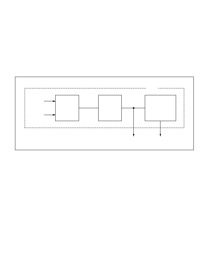
Section 16 Clock Pulse Generator
16.1 Overview
The H8/3002 has a built-in clock pulse generator (CPG) that generates the system clock (¯) and
other internal clock signals (¯/2 to ¯/4096). The clock pulse generator consists of an oscillator
circuit, a duty adjustment circuit, and prescalers.
16.1.1 Block Diagram
Figure 16-1 shows a block diagram of the clock pulse generator.
Figure 16-1 Block Diagram of Clock Pulse Generator
XTAL
EXTAL
CPG
¯
¯/2 to ¯/4096
Oscillator
Duty
adjustment
circuit
Prescalers
505
16.2 Oscillator Circuit
Clock pulses can be supplied by connecting a crystal resonator, or by input of an external clock
signal.
16.2.1 Connecting a Crystal Resonator
Circuit Configuration: A crystal resonator can be connected as in the example in figure 16-2.
The damping resistance Rd should be selected according to table 16-1. An AT-cut parallel-
resonance crystal should be used.
Figure 16-2 Connection of Crystal Resonator (Example)
Table 16-1 Damping Resistance Value
Frequency (MHz)
2
4
8
10
12
16
17
Rd (
)
1 k
500
200
0
0
0
0
Crystal Resonator: Figure 16-3 shows an equivalent circuit of the crystal resonator. The crystal
resonator should have the characteristics listed in table 16-2.
Figure 16-3 Crystal Resonator Equivalent Circuit
EXTAL
XTAL
C
L1
C
L2
C = C = 10 pF to 22 pF
L1 L2
R
d
XTAL
L
Rs
C
L
C
O
EXTAL
AT-cut parallel-resonance type
506
Table 16-2 Crystal Resonator Parameters
Frequency (MHz)
2
4
8
10
12
16
17
Rs max (
)
500
120
80
70
60
50
40
Co (pF)
7 pF max
Use a crystal resonator with a frequency equal to the system clock frequency (¯).
Notes on Board Design: When a crystal resonator is connected, the following points should be
noted:
Other signal lines should be routed away from the oscillator circuit to prevent induction from
interfering with correct oscillation. See figure 16-4.
When the board is designed, the crystal resonator and its load capacitors should be placed as close
as possible to the XTAL and EXTAL pins.
Figure 16-4 Example of Incorrect Board Design
XTAL
EXTAL
C
L2
C
L1
H8/3002
Avoid
Signal A
Signal B
507
16.2.2 External Clock Input
Circuit Configuration: An external clock signal can be input as shown in the examples in
figure 16-5. In example b, the clock should be held high in standby mode.
If the XTAL pin is left open, the stray capacitance should not exceed 10 pF.
Figure 16-5 External Clock Input (Examples)
EXTAL
XTAL
EXTAL
XTAL
74HC04
External clock input
Open
External clock input
a. XTAL pin left open
b. Complementary clock input at XTAL pin
508
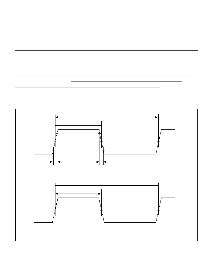
External Clock:The external clock frequency should be equal to the system clock frequency (¯).
Table 16-3 and figure 16-6 indicate the clock timing.
Table 16-3 Clock Timing
V
CC
= 2.7 to 5.5 V
V
CC
= 5.0 V ± 10%
Item
Symbol
Min
Max
Min
Max
Unit Test Conditions
External clock rise
t
EXr
--
10
--
5
ns
Figure 16-6
time
External clock fall
t
EXf
--
10
--
5
ns
time
--
30
70
30
70
%
¯
5 MHz
40
60
40
60
%
¯ < 5 MHz
--
40
60
40
60
%
Figure 16-6 External Clock Input Timing
EXTAL
t
EXr
t
EXf
a
V
CC
◊
0.5
t
cyc
¯
b
V
CC
◊
0.5
t
cyc
External clock
input duty (a/t
cyc
)
¯
clock duty
(b/t
cyc
)
Figure
16-6
509
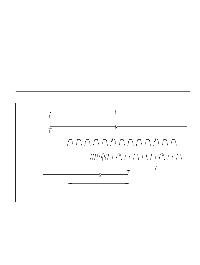
Table 16≠4 shows the external clock output stabilization delay time, and figure 16≠7 shows the
timing for the external clock output stabilization delay time. The oscillator and duty correction
circuit have the function of regulating the waveform of the external clock input to the EXTAL pin.
When the specified clock signal is input to the EXTAL pin, internal clock signal output is
confirmed after the elapse of the external clock output stabilization delay time (t
DEXT
). As clock
signal output is not confirmed during the t
DEXT
period, the reset signal should be driven low and
the reset state maintained during this time.
Table 16≠4 External Clock Output Stabilization Delay Time
Conditions: V
CC
= 2.7 to 5.5 V, AV
CC
= 2.7 to 5.5 V, V
SS
= AV
SS
= 0 V
Item
Symbol
Min
Max
Unit
Notes
External clock output stabilization
t
DEXT
*
500
--
µs
Figure 16-7
delay time
Note:
*
t
DEXT
includes a 10 t
cyc
RES
pulse width (t
RESW
).
Figure 16-7 External Clock Output Stabilization Delay Time
510
V
CC
STBY
EXTAL
¯
RES
t
DEXT
*
Note:
*
t
DEXT
includes a 10 t
cyc
RES
pulse width (t
RESW
).
2.7 V
V
IH

16.3 Duty Adjustment Circuit
When the oscillator frequency is 5 MHz or higher, the duty adjustment circuit adjusts the duty
cycle of the clock signal from the oscillator to generate the system clock (¯).
16.4 Prescalers
The prescalers divide the system clock (¯) to generate internal clocks (¯/2 to ¯/4096).
511

Section 17 Power-Down State
17.1 Overview
The H8/3002 has a power-down state that greatly reduces power consumption by halting CPU
functions. The power-down state includes the following three modes:
∑
Sleep mode
∑
Software standby mode
∑
Hardware standby mode
Table 17-1 indicates the methods of entering and exiting these power-down modes and the status
of the CPU and on-chip supporting modules in each mode.
Table 17-1 Power-Down State
State
Entering CPU
Refresh
Supporting
I/O
Exiting
Mode
Conditions
Clock
CPU
Registers DMAC Controller
Functions
RAM
Ports
Conditions
Sleep SLEEP
instruc- Active
Halted
Held
Active
Active
Active
Held
Held
∑ Interrupt
mode
tion executed
∑
RES
while SSBY = 0
∑
STBY
in SYSCR
Software
SLEEP
instruc-
Halted
Halted
Held
Halted
Halted Halted Held
Held
∑ NMI
standby
tion executed
and
and
and
∑ IRQ
0
to IRQ
2
mode
while SSBY = 1
reset
held
*
1
reset
∑
RES
in SYSCR
∑
STBY
Hardware Low input at
Halted
Halted
Undeter-
Halted Halted
Halted
Held
*
2
High ∑
STBY
standby
STBY
pin
mined
and and
and
impedance ∑
RES
mode
reset
reset
reset
Notes: 1. RTCNT and bits 7 and 6 of RTMCSR are initialized. Other bits and registers hold their previous states.
2. The RAME bit must be cleared to 0 in SYSCR before the transition from the program execution state to hardware
standby mode.
Legend
SYSCR: System control register
SSBY:
Software standby bit
513
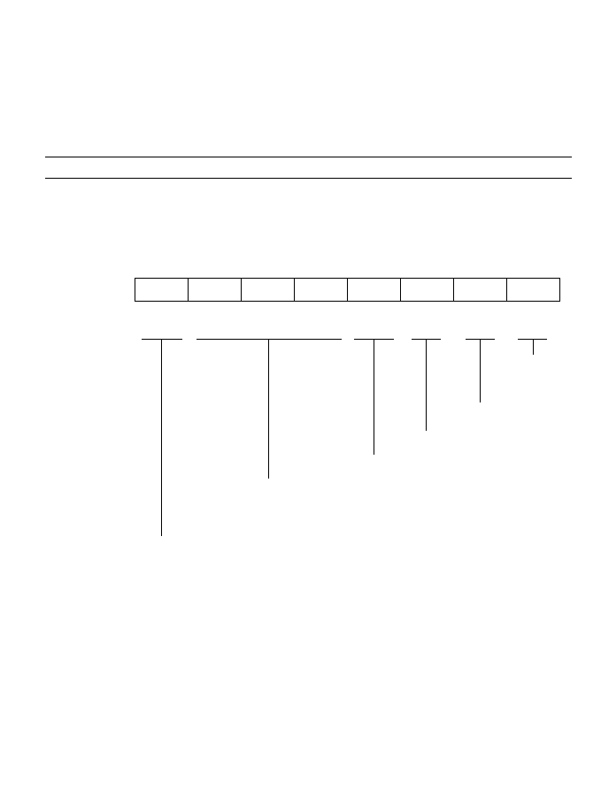
17.2 Register Configuration
The H8/3002's system control register (SYSCR) controls the power-down state. Table 17-2
summarizes this register.
Table 17-2 Control Register
Address
*
Name
Abbreviation
R/W
Initial Value
H'FFF2
System control register
SYSCR
R/W
H'0B
Note:
*
Lower 16 bits of the address.
17.2.1 System Control Register (SYSCR)
SYSCR is an 8-bit readable/writable register. Bit 7 (SSBY) and bits 6 to 4 (STS2 to STS0) control
the power-down state. For information on the other SYSCR bits, see section 3.3, System Control
Register.
Bit
Initial value
Read/Write
7
SSBY
0
R/W
6
STS2
0
R/W
5
STS1
0
R/W
4
STS0
0
R/W
3
UE
1
R/W
0
RAME
1
R/W
2
NMIEG
0
R/W
1
--
1
--
Software standby
Enables transition to
software standby mode
RAM enable
Standby timer select 2 to 0
These bits select the
waiting time at exit from
software standby mode
User bit enable
NMI edge select
Reserved bit
514

Bit 7--Software Standby (SSBY): Enables transition to software standby mode. When software
standby mode is exited by an external interrupt, this bit remains set to 1 after the return to normal
operation. To clear this bit, write 0.
Bit 7
SSBY
Description
0
SLEEP instruction causes transition to sleep mode
(Initial value)
1
SLEEP instruction causes transition to software standby mode
Bits 6 to 4--Standby Timer Select (STS2 to STS0): These bits select the length of time the CPU
and on-chip supporting modules wait for the clock to settle when software standby mode is exited
by an external interrupt. If the clock is generated by a crystal resonator, set these bits according to
the clock frequency so that the waiting time will be at least 8 ms. See table 17-3. If an external
clock is used, any setting is permitted.
Bit 6
Bit 5
Bit 4
STS2
STS1
STS0
Description
0
0
0
Waiting time = 8192 states
(Initial value)
1
Waiting time = 16384 states
1
0
Waiting time = 32768 states
1
Waiting time = 65536 states
1
0
--
Waiting time = 131072 states
1
--
Illegal setting
515

17.3 Sleep Mode
17.3.1 Transition to Sleep Mode
When the SSBY bit is cleared to 0 in SYSCR, execution of the SLEEP instruction causes a
transition from the program execution state to sleep mode. Immediately after executing the
SLEEP instruction the CPU halts, but the contents of its internal registers are retained. The DMA
controller (DMAC), refresh controller, and on-chip supporting modules do not halt in sleep mode.
17.3.2 Exit from Sleep Mode
Sleep mode is exited by an interrupt, or by input at the
RES or STBY pin.
Exit by Interrupt: An interrupt terminates sleep mode and causes a transition to the interrupt
exception handling state. Sleep mode is not exited by an interrupt source in an on-chip supporting
module if the interrupt is disabled in the on-chip supporting module. Sleep mode is not exited by
an interrupt other than NMI if the interrupt is masked in the CPU.
Exit by
RES Input: Low input at the RES pin exits from sleep mode to the reset state.
Exit by
STBY Input: Low input at the STBY pin exits from sleep mode to hardware standby
mode.
516

17.4 Software Standby Mode
17.4.1 Transition to Software Standby Mode
To enter software standby mode, execute the SLEEP instruction while the SSBY bit is set to 1 in
SYSCR.
In software standby mode, current dissipation is reduced to an extremely low level because the
CPU, clock, and on-chip supporting modules all halt. The DMAC and on-chip supporting
modules are reset. As long as the specified voltage is supplied, however, CPU register contents
and on-chip RAM data are retained. The settings of the I/O ports and refresh controller* are also
held.
Note: * RTCNT and bits 7 and 6 of RTMCSR are initialized. Other bits and registers hold their
previous states.
17.4.2 Exit from Software Standby Mode
Software standby mode can be exited by input of an external interrupt at the NMI, IRQ
0
, IRQ
1
, or
IRQ
2
pin, or by input at the
RES or STBY pin.
Exit by Interrupt: When an NMI, IRQ
0
, IRQ
1
, or IRQ
2
interrupt request signal is received, the
clock oscillator begins operating. After the oscillator settling time selected by bits STS2 to STS0
in SYSCR, stable clock signals are supplied to the entire H8/3002 chip, software standby mode
ends, and interrupt exception handling begins. Software standby mode is not exited if the interrupt
enable bits of interrupts IRQ
0
, IRQ
1
, and IRQ
2
are cleared to 0, or if these interrupts are masked
in the CPU.
Exit by
RES Input: When the RES input goes low, the clock oscillator starts and clock pulses are
supplied immediately to the entire H8/3002 chip. The
RES signal must be held low long enough
for the clock oscillator to stabilize. When
RES goes high, the CPU starts reset exception handling.
Exit by
STBY Input: Low input at the STBY pin causes a transition to hardware standby mode.
517

17.4.3 Selection of Waiting Time for Exit from Software Standby Mode
Bits STS2 to STS0 in SYSCR should be set as follows.
Crystal Resonator: Set STS2 to STS0 so that the waiting time (for the clock to stabilize) is at
least 8 ms. Table 17-3 indicates the waiting times that are selected by STS2 to STS0 settings at
various system clock frequencies.
External Clock: Any value may be set.
Table 17-3 Clock Frequency and Waiting Time for Clock to Settle
Waiting
STS2 STS1 STS0 Time
16 MHZ 12 MHz 10 MHz 8 MHz
6 MHz
4 MHz
2 MHz
Unit
0
0
0
8192 0.51
0.65
0.8
1.0
1.3
2.0
4.1
ms
states
0
0
1
16384 1.0
1.3
1.6
2.0
2.7
4.1
8.2
states
0
1
0
32768 2.0
2.7
3.3
4.1
5.5
8.2
16.4
states
0
1
1
65536 4.1
5.5
6.6
8.2
10.9
16.4
32.8
states
1
0
--
131072 8.2
10.9
13.1
16.4
21.8
32.8
65.5
states
1
1
--
Illegal setting
: Recommended setting
518
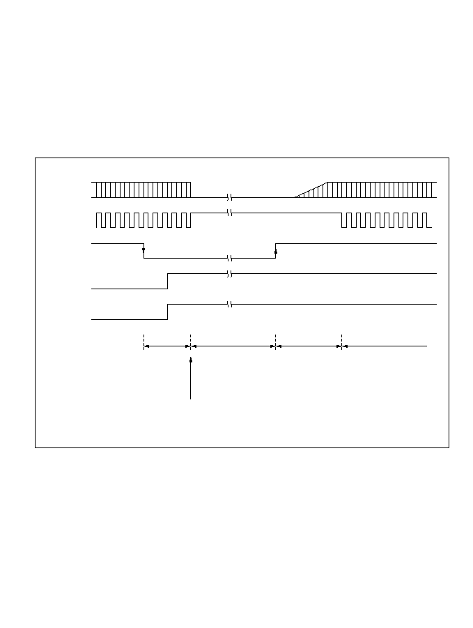
17.4.4 Sample Application of Software Standby Mode
Figure 17-1 shows an example in which software standby mode is entered at the fall of NMI and
exited at the rise of NMI.
With the NMI edge select bit (NMIEG) cleared to 0 in SYSCR (selecting the falling edge), an
NMI interrupt occurs. Next the NMIEG bit is set to 1 (selecting the rising edge) and the SSBY bit
is set to 1; then the SLEEP instruction is executed to enter software standby mode.
Software standby mode is exited at the next rising edge of the NMI signal.
Figure 17-1 NMI Timing for Software Standby Mode (Example)
17.4.5 Note
The I/O ports retain their existing states in software standby mode. If a port is in the high output
state, its output current is not reduced.
¯
NMI
NMIEG
SSBY
NMI interrupt
handler
NMIEG = 1
SSBY = 1
Software standby
mode (power-
down state)
Oscillator
settling time
(t
osc2
)
SLEEP
instruction
NMI exception
handling
Clock
oscillator
519

17.5 Hardware Standby Mode
17.5.1 Transition to Hardware Standby Mode
Regardless of its current state, the chip enters hardware standby mode whenever the
STBY pin
goes low. Hardware standby mode reduces power consumption drastically by halting all functions
of the CPU, DMAC, refresh controller, and on-chip supporting modules. All modules are reset
except the on-chip RAM. As long as the specified voltage is supplied, on-chip RAM data is
retained. I/O ports are placed in the high-impedance state.
Clear the RAME bit to 0 in SYSCR before
STBY goes low to retain on-chip RAM data.
The inputs at the mode pins (MD2 to MD0) should not be changed during hardware standby
mode.
17.5.2 Exit from Hardware Standby Mode
Hardware standby mode is exited by inputs at the
STBY and RES pins. While RES is low, when
STBY goes high, the clock oscillator starts running. RES should be held low long enough for the
clock oscillator to settle. When
RES goes high, reset exception handling begins, followed by a
transition to the program execution state.
17.5.3 Timing for Hardware Standby Mode
Figure 17-2 shows the timing relationships for hardware standby mode. To enter hardware standby
mode, first drive
RES low, then drive STBY low. To exit hardware standby mode, first drive
STBY high, wait for the clock to settle, then bring RES from low to high.
Figure 17-2 Hardware Standby Mode Timing
RES
STBY
Clock
oscillator
Oscillator
settling time
Reset
exception
handling
520

Section 18 Electrical Characteristics
18.1 Absolute Maximum Ratings
Table 18-1 lists the absolute maximum ratings.
Table 18-1 Absolute Maximum Ratings
I
tem
Symbol
Value
Unit
Power supply voltage
V
CC
≠0.3 to +7.0
V
Input voltage (except port 7)
V
in
≠0.3 to V
CC
+0.3
V
Input voltage (port 7)
V
in
≠0.3 to AV
CC
+0.3
V
Reference voltage
V
REF
≠0.3 to AV
CC
+0.3
V
Analog power supply voltage
AV
CC
≠0.3 to +7.0
V
Analog input voltage
V
AN
≠0.3 to AV
CC
+0.3
V
Operating temperature
T
opr
Regular specifications: ≠20 to +75
∞C
Wide-range specifications: ≠40 to +85
∞C
Storage temperature
T
stg
≠55 to +125
∞C
Caution: Permanent damage to the chip may result if absolute maximum ratings are exceeded.
521

18.2 Electrical Characteristics
18.2.1 DC Characteristics
Table 18-2 lists the DC characteristics. Table 18-3 lists the permissible output currents.
Table 18-2 DC Characteristics
Conditions: V
CC
= 5.0 V ± 10%, AV
CC
= 5.0 V ± 10%, V
REF
= 4.5 V to AV
CC
,
V
SS
= AV
SS
= 0 V*, T
a
= ≠20∞C to +75∞C (regular specifications),
T
a
= ≠40∞C to +85∞C (wide-range specifications)
Item
Symbol
Min
Typ
Max
Unit Test Conditions
V
T
≠
1.0
--
--
V
V
T
+
--
--
V
CC
◊
0.7 V
V
T
+
≠ V
T
≠
0.4
--
--
V
Input high
RES
,
STBY
, V
IH
V
CC
≠ 0.7 --
V
CC
+ 0.3 V
voltage
NMI, MD
2
to
MD
0
EXTAL
V
CC
◊
0.7 --
V
CC
+ 0.3 V
Port 7
2.0
--
AV
CC
+ 0.3 V
Ports 4, 6, 9,
2.0
--
V
CC
+ 0.3 V
P8
3
, P8
4
,
PB
4
to PB
7
,
D
15
to D
8
Input low
RES
,
STBY
, V
IL
≠0.3
--
0.5
V
voltage
MD
2
to MD
0
NMI, EXTAL,
≠0.3
--
0.8
V
ports 4, 6, 7,
9, P8
3
, P8
4
,
PB
4
to PB
7
,
D
15
to D
8
All output pins V
OH
V
CC
≠ 0.5 --
--
V
I
OH
= ≠200 µA
(except
RESO
)
3.5
--
--
V
I
OH
= ≠1mz
Output low
All output pins V
OL
--
--
0.4
V
I
OL
= 1.6 mA
voltage
(except
RESO
)
Port B,
--
--
1.0
V
I
OL
= 10 mA
A
19
to A
0
RESO
--
--
0.4
V
I
OL
= 2.6 mA
Note:
*
If the A/D converter is not used, do not leave the AV
CC
, AV
SS
, and V
REF
pins open.
Connect AV
CC
and V
REF
to V
CC
, and connect AV
SS
to V
SS
.
Output high
voltage
Schmitt
Port A,
trigger input P8
0
to P8
2
,
voltages
PB
0
to PB
3
522

Table 18-2 DC Characteristics (cont)
Conditions: V
CC
= 5.0 V ± 10%, AV
CC
= 5.0 V ± 10%, V
REF
= 4.5 V to AV
CC
,
V
SS
= AV
SS
= 0 V
*1
, T
a
= ≠20∞C to +75∞C (regular specifications),
T
a
= ≠40∞C to +85∞C (wide-range specifications)
Item
Symbol
Min
Typ
Max
Unit
Test Conditions
Input leakage
STBY
, NMI,
|I
in
|
--
--
1.0
µA
V
in
= 0.5 to
current
RES
,
V
CC
≠ 0.5 V
MD
2
to MD
0
Port 7
--
--
1.0
µA
V
in
= 0.5 to
AV
CC
≠ 0.5 V
Ports 4, 6,
|I
TS1
|
--
--
1.0
µA
V
in
= 0.5 to
8 to B, A
19
to V
CC
≠ 0.5 V
A
0
, D
15
to D
8
RESO
--
--
10.0
µA
V
in
= 0.5 to
V
CC
≠ 0.5 V
Input pull-up Port 4
≠I
P
50
--
300
µA
V
in
= 0 V
current
NMI
C
in
--
--
50
pF
All input pins
--
--
15
except NMI
I
CC
*
4
--
45
70
mA
f = 16 MHz
--
53
85
f = 17 MHz
Sleep mode
--
30
50
mA
f = 16 MHz
--
38
63
f = 17 MHz
--
0.01
5.0
µA
T
a
50∞C
--
--
20.0
50∞C < T
a
Analog power
During A/D
AI
CC
--
1.2
2.0
mA
supply current
conversion
Idle
--
0.01
5.0
µA
Reference During
A/D
AI
CC
--
0.3
0.6
mA V
REF
= 5.0 V
current
conversion
Idle
--
0.01
5.0
µA
RAM standby voltage
V
RAM
2.0
--
--
V
Notes: 1. If the A/D converter is not used, do not leave the AV
CC
, AV
SS
, and V
REF
pins open.
Connect AV
CC
and V
REF
to V
CC
, and connect AV
SS
to V
SS
.
2. Current dissipation values are for V
IHmin
= V
CC
≠ 0.5 V and V
ILmax
= 0.5 V with all output
pins unloaded and the on-chip pull-up transistors in the off state.
3. The values are for V
RAM
V
CC
< 4.5 V, V
IHmin
= V
CC
◊
0.9, and V
ILmax
= 0.3 V.
4. When 16 MHz, I
CC
depends on f as follows:
I
CC max
= 5.0 (mA) + 4.06 (mA/MHz)
◊
f [normal mode]
I
CC max
= 5.0 (mA) + 2.81 (mA/MHz)
◊
f [sleep mode]
I
CC typ
= 5.0 (mA) + 2.50 (mA/MHz)
◊
f [normal mode]
I
CC typ
= 5.0 (mA) + 1.56 (mA/MHz)
◊
f [sleep mode]
Current Normal
dissipation
*
2
operation
Input
capacitance
Three-state
leakage
current
(off state)
V
in
= 0 V
f = 1 MHz
T
a
= 25∞C
Standby
mode
*
3
523

Table 18-2 DC Characteristics (cont)
Conditions: V
CC
= 2.7 V to 5.5 V, AV
CC
= 2.7 V to 5.5 V, V
REF
= 2.7 V to AV
CC
,
V
SS
= AV
SS
= 0 V*, T
a
= ≠20∞C to +75∞C (regular specifications),
T
a
= ≠40∞C to +85∞C (wide-range specifications)
Item
Symbol
Min
Typ
Max
Unit Test Conditions
Schmitt Port
A,
V
T
≠
V
CC
◊
0.2
--
--
V
V
T
+
--
--
V
CC
◊
0.7
V
V
T
+
≠ V
T
≠
V
CC
◊
0.07 --
--
V
Input high
RES
,
STBY
, V
IH
V
CC
◊
0.9
--
V
CC
+ 0.3
V
voltage
NMI, MD
2
to
MD
0
EXTAL
V
CC
◊
0.7
--
V
CC
+ 0.3
V
Port 7
V
CC
◊
0.7
--
AV
CC
+ 0.3 V
Ports 4, 6, 9,
V
CC
◊
0.7
--
V
CC
+ 0.3
V
P8
3
, P8
4
,
PB
4
to PB
7
,
D
15
to D
8
Note:
*
If the A/D converter is not used, do not leave the AV
CC
, AV
SS
, and V
REF
pins open.
Connect AV
CC
and V
REF
to V
CC
, and connect AV
SS
to V
SS
.
Schmitt Port
A,
trigger input P8
0
to P8
2
,
voltages
PB
0
to PB
3
524

Table 18-2 DC Characteristics (cont)
Conditions: V
CC
= 2.7 V to 5.5 V, AV
CC
= 2.7 V to 5.5 V, V
REF
= 2.7 V to AV
CC
,
V
SS
= AV
SS
= 0 V*, T
a
= ≠20∞C to +75∞C (regular specifications),
T
a
= ≠40∞C to +85∞C (wide-range specifications)
Item
Symbol
Min
Typ
Max
Unit
Test Conditions
Input low
RES
,
STBY
, V
IL
≠0.3
--
V
CC
◊
0.1 V
voltage
MD
2
to MD
0
≠0.3
--
V
CC
◊
0.2 V
V
CC
< 4.0 V
0.8
V
V
CC
=
4.0 to 5.5 V
All output pins V
OH
V
CC
≠ 0.5 --
--
V
I
OH
= ≠200 µA
(except
RESO
)
V
CC
≠ 1.0 --
--
V
V
CC
4.5 V
I
OH
= ≠1 mA
3.5
--
--
V
4.5 V< VCC
5.5 V
IOH = ≠1 mA
Output low
All output pins V
OL
--
--
0.4
V
I
OL
= 1.6 mA
voltage
(except
RESO
)
Port B,
--
--
1.0
V
V
CC
4 V
A
19
to A
0
I
OL
= 5 mA,
4 V < V
CC
5.5 V
I
OL
= 10 mA
RESO
--
--
0.4
V
I
OL
= 1.6 mA
Input leakage
STBY
, NMI,
|I
in
|
--
--
1.0
µA
V
in
= 0.5 to
current
RES
, V
CC
≠ 0.5 V
MD
2
to MD
0
Port 7
--
--
1.0
µA
V
in
= 0.5 to
AV
CC
≠ 0.5 V
Ports 4, 6,
|I
TS1
|
--
--
1.0
µA
V
in
= 0.5 to
8 to B, A
19
to V
CC
≠ 0.5 V
A
0
, D
15
to D
8
RESO
--
--
10.0
µA
Input pull-up Port 4
≠I
P
10
--
300
µA
V
CC
= 2.7 V to
current
5.5 V,
V
in
= 0 V
Note:
*
If the A/D converter is not used, do not leave the AV
CC
, AV
SS
, and V
REF
pins open.
Connect AV
CC
and V
REF
to V
CC
, and connect AV
SS
to V
SS
.
525
Output high
voltage
NMI, EXTAL,
ports 4, 6, 7, 9,
P8
3
, P8
4
PB
4
to PB
7
,
D
15
to D
8
Three-state
leakage
current
(off state)

Table 18-2 DC Characteristics (cont)
Conditions: V
CC
= 2.7 V to 5.5 V, AV
CC
= 2.7 V to 5.5 V, V
REF
= 2.7 V to AV
CC
,
V
SS
= AV
SS
= 0 V
*1
, T
a
= ≠20∞C to +75∞C (regular specifications),
T
a
= ≠40∞C to +85∞C (wide-range specifications)
Item
Symbol
Min
Typ
Max
Unit Test Conditions
NMI
C
in
--
--
50
pF
All input pins
--
--
15
except NMI
Current Normal
I
CC
*
4
--
25
31.8
mA
f = 8 MHz
dissipation
*
2
operation
(5.0 V)
(5.5 V)
Sleep mode
--
15
23.0
mA
f = 8 MHz
(5.0 V)
(5.5 V)
--
0.01
5.0
µA
T
a
50∞C
--
--
20.0
µA
50∞C < T
a
AI
CC
--
1.0
2.0
mA
AV
CC
= 3.0 V
--
1.2
--
mA
AV
CC
= 5.0 V
Idle
--
0.01
5.0
µA
AI
CC
--
0.2
0.4
mA
V
REF
= 3.0 V
--
0.3
--
mA
V
REF
= 5.0 V
Idle
--
0.01
5.0
µA
RAM standby voltage
V
RAM
2.0
--
--
V
Notes: 1. If the A/D converter is not used, do not leave the AV
CC
, AV
SS
, and V
REF
pins open.
Connect AV
CC
and V
REF
to V
CC
, and connect AV
SS
to V
SS
.
2. Current dissipation values are for V
IHmin
= V
CC
≠ 0.5 V and V
ILmax
= 0.5 V with all output
pins unloaded and the on-chip pull-up transistors in the off state.
3. The values are for V
RAM
V
CC
< 2.7 V, V
IHmin
= V
CC
◊
0.9, and V
ILmax
= 0.3 V.
4. I
CC
depends on V
CC
and f as follows:
I
CCmax
= 1.0 (mA) + 0.7 (mA/MHz ∑ V)
◊
V
CC
◊
f [normal mode]
I
CCmax
= 1.0 (mA) + 0.5 (mA/MHz ∑ V)
◊
V
CC
◊
f [sleep mode]
Input
capacitance
V
in
= 0 V
f = 1 MHz
T
a
= 25∞C
Analog power During A/D
supply current
conversion
Reference During
A/D
current
conversion
Standby
mode
*
3
526

Table 18-2 DC Characteristics (cont)
Conditions: V
CC
= 3.0 V to 5.5 V, AV
CC
= 3.0 V to 5.5 V, V
REF
= 3.0 V to AV
CC
,
V
SS
= AV
SS
= 0 V*, T
a
= ≠20∞C to +75∞C (regular specifications),
T
a
= ≠40∞C to +85∞C (wide-range specifications)
Item
Symbol
Min
Typ
Max
Unit Test Conditions
V
T
≠
V
CC
◊
0.2
--
--
V
V
T
+
--
--
V
CC
◊
0.7 V
V
T
+
≠ V
T
≠
V
CC
◊
0.07
--
--
V
Input high
RES
,
STBY
, V
IH
V
CC
◊
0.9
--
V
CC
+ 0.3 V
voltage
NMI, MD
2
to
MD
0
EXTAL
V
CC
◊
0.7
--
V
CC
+ 0.3 V
Port 7
V
CC
◊
0.7
--
AV
CC
+ 0.3 V
Ports 4, 6, 7,
V
CC
◊
0.7
--
V
CC
+ 0.3 V
P8
3
, P8
4
,
PB
4
to PB
7
,
D
15
to D
8
Input low
RES
,
STBY
, V
IL
≠0.3
--
V
CC
◊
0.1 V
voltage
MD
2
to MD
0
NMI, EXTAL,
≠0.3
--
V
CC
◊
0.2 V
V
CC
< 4 V
ports 4, 6, 7, 9,
P8
3
, P8
4
,
PB
4
to PB
7
,
D
15
to D
8
All output pins V
OH
V
CC
≠ 0.5
--
--
V
I
OH
= ≠200 µA
(except
RESO
)
V
CC
≠ 1.0
--
--
V
V
CC
4.5 V
I
OH
= ≠1 mA
3.5
--
--
V
4.5 V< VCC
5.5V
I
OH
= ≠1 mA
Note:
*
If the A/D converter is not used, do not leave the AV
CC
, AV
SS
, and V
REF
pins open.
Connect AV
CC
and V
REF
to V
CC
, and connect AV
SS
to V
SS
.
Output high
voltage
Schmitt
Port A,
trigger input P8
0
to P8
2
,
voltages
PB
0
to PB
3
≠0.3
--
0.8
V
4 V
V
CC
5.5 V
527

Table 18-2 DC Characteristics (cont)
Conditions: V
CC
= 3.0 V to 5.5 V, AV
CC
= 3.0 V to 5.5 V, V
REF
= 3.0 V to AV
CC
,
V
SS
= AV
SS
= 0 V
*1
, T
a
= ≠20∞C to +75∞C (regular specifications),
T
a
= ≠40∞C to +85∞C (wide-range specifications)
Item
Symbol
Min
Typ
Max
Unit
Test Conditions
Output low
All output pins V
OL
--
--
0.4
V
I
OL
= 1.6 mA
voltage
(except
RESO
)
Port B,
--
--
1.0
V
V
CC
4 V, I
OL
= 5 mA,
A
19
to A
0
4 V < V
CC
5.5 V,
I
OL
= 10 mA
RESO
--
--
0.4
V
I
OL
= 1.6 mA
Input leakage
STBY
, NMI,
|I
in
|
--
--
1.0
µA
V
in
= 0.5 to
current
RES
,
V
CC
≠ 0.5 V
MD
2
to MD
0
Port 7
--
--
1.0
µA
V
in
= 0.5 to AV
CC
≠ 0.5 V
Ports 4, 6,
|I
TS1
|
--
--
1.0
µA
V
in
= 0.5 to V
CC
≠ 0.5 V
8 to B, A
19
to
A
0
, D
15
to D
8
RESO
--
--
10.0
µA
Input pull-up Port 4
≠I
P
10
--
300
µA
V
CC
= 3.0 V to 5.5 V
current
V
in
= 0 V
NMI
C
in
--
--
50
pF
All input pins
--
--
15
except NMI
Current
Normal I
CC
*
4
--
30
39.5
mA
f = 10 MHz
dissipation
*
2
operation
(5.0 V) (5.5 V)
Sleep mode
--
20
28.5
mA
f = 10 MHz
(5.0 V) (5.5 V)
--
0.01
5.0
µA
T
a
50∞C
--
--
20.0
µA
50∞C < T
a
Notes: 1. If the A/D converter is not used, do not leave the AV
CC
, AV
SS
, and V
REF
pins open.
Connect AV
CC
and V
REF
to V
CC
, and connect AV
SS
to V
SS
.
2. Current dissipation values are for V
IHmin
= V
CC
≠ 0.5 V and V
ILmax
= 0.5 V with all output
pins unloaded and the on-chip pull-up transistors in the off state.
3. The values are for V
RAM
V
CC
< 3.0 V, V
IHmin
= V
CC
◊
0.9, and V
ILmax
= 0.3 V.
4. I
CC
depends on V
CC
and f as follows:
I
CC max
= 1.0 (mA) + 0.7 (mA/MHz ∑ V)
◊
V
CC
◊
f [normal mode]
I
CC max
= 1.0 (mA) + 0.5 (mA/MHz ∑ V)
◊
V
CC
◊
f [sleep mode]
Input
capacitance
Three-state
leakage
current
(off state)
V
in
= 0 V, f = 1 MHz,
T
a
= 25∞C
Standby
mode
*
3
528

Table 18-2 DC Characteristics (cont)
Conditions: V
CC
= 3.0 V to 5.5 V, AV
CC
= 3.0 V to 5.5 V, V
REF
= 3.0 V to AV
CC
,
V
SS
= AV
SS
= 0 V
*
, T
a
= ≠20∞C to +75∞C (regular specifications),
T
a
= ≠40∞C to +85∞C (wide-range specifications)
Item
Symbol
Min
Typ
Max
Unit Test Conditions
AI
CC
--
1.0
2.0
mA
AV
CC
= 3.0 V
--
1.2
--
mA
AV
CC
= 5.0 V
Idle
--
0.01
5.0
µA
AI
CC
--
0.2
0.4
mA
V
REF
= 3.0 V
--
0.3
--
mA
V
REF
= 5.0 V
Idle
--
0.01
5.0
µA
RAM standby voltage
V
RAM
2.0
--
--
V
Notes: 1. If the A/D converter is not used, do not leave the AV
CC
, AV
SS
, and V
REF
pins open.
Connect AV
CC
and V
REF
to V
CC
, and connect AV
SS
to V
SS
.
Analog power
During A/D
supply current
conversion
Reference During
A/D
current
conversion
529

Table 18-3 Permissible Output Currents
Conditions: V
CC
= 2.7 V to 5.5 V, AV
CC
= 2.7 V to 5.5 V, V
REF
= 2.7 V to AV
CC
,
V
SS
= AV
SS
= 0 V, T
a
= ≠20∞C to +75∞C (regular specifications),
T
a
= ≠40∞C to +85∞C (wide-range specifications)
Item
Symbol
Min
Typ
Max
Unit
Port B, A
19
to A
0
I
OL
--
--
10
mA
Other output pins
--
--
2.0
mA
Permissible output
Total of 28 pins including
I
OL
--
--
80
mA
low current (total)
port B and A
19
to A
0
Total of all output pins,
--
--
120
mA
including the above
Permissible output
All output pins
I
OH
--
--
2.0
mA
high current (per pin)
Permissible output
Total of all output pins
I
OH
--
--
40
mA
high current (total)
Notes: 1. To protect chip reliability, do not exceed the output current values in table 18-3.
2. When driving a darlington pair or LED, always insert a current-limiting resistor in the
output line, as shown in figures 18-1 and 18-2.
Permissible output
low current (per pin)
530
Figure 18-1 Darlington Pair Drive Circuit (Example)
Figure 18-2 LED Drive Circuit (Example)
H8/3002
LED
600
Port B
H8/3002
Port
2 k
Darlington pair
531

18.2.2 AC Characteristics
Bus timing parameters are listed in table 18-4. Refresh controller bus timing parameters are listed
in table 18-5. Control signal timing parameters are listed in table 18-6. Timing parameters of the
on-chip supporting modules are listed in table 18-7.
Table 18-4 Bus Timing (1)
Condition A:
V
CC
= 2.7 V to 5.5 V, AV
CC
= 2.7 V to 5.5 V, V
REF
= 2.7 V to AV
CC
,
V
SS
= AV
SS
= 0 V, ¯ = 2 MHz to 8 MHz, T
a
= ≠20∞C to +75∞C (regular specifications),
T
a
= ≠40∞C to +85∞C (wide-range specifications)
Condition B:
V
CC
= 3.0 V to 5.5 V, AV
CC
= 3.0 V to 5.5 V, V
REF
= 3.0 V to AV
CC
,
V
SS
= AV
SS
= 0 V, ¯ = 2 MHz to 10 MHz, T
a
= ≠20∞C to +75∞C (regular specifications),
T
a
= ≠40∞C to +85∞C (wide-range specifications)
Condition C:
V
CC
= 5.0 V ± 10%, AV
CC
= 5.0 V ± 10%, V
REF
= 4.5 V to AV
CC
,
V
SS
= AV
SS
= 0 V, ¯ = 2 MHz to 16 MHz, T
a
= ≠20∞C to +75∞C (regular specifications),
T
a
= ≠40∞C to +85∞C (wide-range specifications)
Condition D:
V
CC
= 5.0 V ± 10%, AV
CC
= 5.0 V ± 10%, V
REF
= 4.5 V to AV
CC
,
V
SS
= AV
SS
= 0 V, ¯ = 2 MHz to 17 MHz, T
a
= ≠20∞C to +75∞C (regular specifications),
T
a
= ≠40∞C to +85∞C (wide-range specifications)
Condition A Condition B Condition C
Condition D
8 MHz
10 MHz
16 MHz
17 MHz
Item Symbol
Min
Max
Min
Max
Min
Max
Min
Max
Unit
Clock cycle time
t
CYC
125
500
100
500
62.5
500
58.8
500
ns
Clock low pulse width
t
CL
40
--
30
--
20
--
17
--
t
cyc
Clock high pulse width
t
CH
40
--
30
--
20
--
17
--
Clock rise time
t
CR
--
20
--
15
--
10
--
10
ns
Clock fall time
t
CF
--
20
--
15
--
10
--
10
Address delay time
t
AD
--
60
--
50
--
30
--
25
Address hold time
t
AH
25
--
20
--
10
--
10
--
Address strobe delay
t
ASD
--
60
--
40
--
30
--
25
time
Write strobe delay time
t
WSD
--
60
--
50
--
30
--
25
Strobe delay time
t
SD
--
60
--
50
--
30
--
25
Write data strobe pulse t
WSW1
*
85
--
60
--
35
--
34.8
--
width 1
Write data strobe pulse t
WSW2
*
150
--
110
--
65
--
66.2
--
width 2
Address setup time 1
t
AS1
20
--
15
--
10
--
10
--
Address setup time 2
t
AS2
80
--
65
--
40
--
38
--
Read data setup time
t
RDS
50
--
35
--
20
--
15
--
Read data hold time
t
RDH
0
--
0
--
0
--
0
--
Test
Conditions
Figure 18-4,
Figure 18-5
532

Table 18-4 Bus Timing (cont)
Condition A: V
CC
= 2.7 V to 5.5 V, AV
CC
= 2.7 V to 5.5 V, V
REF
= 2.7 V to AV
CC
,
V
SS
= AV
SS
= 0 V, ¯ = 2 MHz to 8 MHz, T
a
= ≠20∞C to +75∞C (regular
specifications), T
a
= ≠40∞C to +85∞C (wide-range specifications)
Condition B: V
CC
= 3.0 V to 5.5 V, AV
CC
= 3.0 V to 5.5 V, V
REF
= 3.0 V to AV
CC
,
V
SS
= AV
SS
= 0 V, ¯ = 2 MHz to 10 MHz, T
a
= ≠20∞C to +75∞C (regular
specifications), T
a
= ≠40∞C to +85∞C (wide-range specifications)
Condition C: V
CC
= 5.0 V ± 10%, AV
CC
= 5.0 V ± 10%, V
REF
= 4.5 V to AV
CC
,
V
SS
= AV
SS
= 0 V, ¯ = 2 MHz to 16 MHz, T
a
= ≠20∞C to +75∞C (regular
specifications), T
a
= ≠40∞C to +85∞C (wide-range specifications)
Condition D: V
CC
= 5.0 V ± 10%, AV
CC
= 5.0 V ± 10%, V
REF
= 4.5 V to AV
CC
,
V
SS
= AV
SS
= 0 V, ¯ = 2 MHz to 17 MHz, T
a
= ≠20∞C to +75∞C (regular
specifications), T
a
= ≠40∞C to +85∞C (wide-range specifications)
Condition A Condition B Condition C Condition D
8 MHz
10 MHz
16 MHz
17 MHz
Item Symbol
Min
Max
Min
Max
Min
Max
Min
Max
Unit
Write data delay time
t
WDD
--
75
--
75
--
60
--
55
ns
Write data setup time 1
t
WDS1
60
--
65
--
35
--
10
--
Write data setup time 2
t
WDS2
15
--
10
--
5
--
-10
--
Write data hold time
t
WDH
25
--
20
--
20
--
20
--
Read data access
t
ACC1
*
--
110
--
100
--
55
--
54.2
time 1
Read data access
t
ACC2
*
--
230
--
200
--
115
--
113
time 2
Read data access
t
ACC3
*
--
55
--
50
--
25
--
22.8
time 3
Read data access
t
ACC4
*
--
160
--
150
--
85
--
86.6
time 4
Precharge time
t
PCH
*
85
--
60
--
40
--
37.8
--
Wait setup time
t
WTS
40
--
40
--
25
--
25
-- ns Figure 18-6
Wait hold time
t
WTH
10
--
10
--
5
--
5
--
Bus request setup time
t
BRQS
40
--
40
--
40
--
40
--
ns Figure 18-18
Bus acknowledge
t
BACD1
--
60
--
50
--
30
--
30
delay time 1
Bus acknowledge
t
BACD2
--
60
--
50
--
30
--
30
delay time 2
Bus-floating time
t
BZD
--
70
--
70
--
40
--
40
Note is on next page.
Test
Conditions
Figure 18-4,
Figure 18-5
533

Note:
*
At 8 MHz (condition A), the times below depend as indicated on the clock cycle time.
t
ACC1
= 1.5
◊
t
CYC
≠ 78 (ns)
t
WSW1
= 1.0
◊
t
CYC
≠ 40 (ns)
t
ACC2
= 2.5
◊
t
CYC
≠ 83 (ns)
t
WSW2
= 1.5
◊
t
CYC
≠ 38 (ns)
t
ACC3
= 1.0
◊
t
CYC
≠ 70 (ns)
t
PCH
= 1.0
◊
t
CYC
≠ 40 (ns)
t
ACC4
= 2.0
◊
t
CYC
≠ 90 (ns)
At 10 MHz (condition B), the times below depend as indicated on the clock cycle time.
t
ACC1
= 1.5
◊
t
CYC
≠ 50 (ns)
t
WSW1
= 1.0
◊
t
CYC
≠ 40 (ns)
t
ACC2
= 2.5
◊
t
CYC
≠ 50 (ns)
t
WSW2
= 1.5
◊
t
CYC
≠ 40 (ns)
t
ACC3
= 1.0
◊
t
CYC
≠ 50 (ns)
t
PCH
= 1.0
◊
t
CYC
≠ 40 (ns)
t
ACC4
= 2.0
◊
t
CYC
≠ 50 (ns)
At 16 MHz (condition C), the times below depend as indicated on the clock cycle time.
t
ACC1
= 1.5
◊
t
CYC
≠ 39 (ns)
t
WSW1
= 1.0
◊
t
CYC
≠ 28 (ns)
t
ACC2
= 2.5
◊
t
CYC
≠ 41 (ns)
t
WSW2
= 1.5
◊
t
CYC
≠ 28 (ns)
t
ACC3
= 1.0
◊
t
CYC
≠ 38 (ns)
t
PCH
= 1.0
◊
t
CYC
≠ 23 (ns)
t
ACC4
= 2.0
◊
t
CYC
≠ 40 (ns)
At 17 MHz (condition D), the times below depend as indicated on the clock cycle time.
t
ACC1
= 1.5
◊
t
CYC
≠ 34 (ns)
t
WSW1
= 1.0
◊
t
CYC
≠ 24 (ns)
t
ACC2
= 2.5
◊
t
CYC
≠ 34 (ns)
t
WSW2
= 1.5
◊
t
CYC
≠ 22 (ns)
t
ACC3
= 1.0
◊
t
CYC
≠ 36 (ns)
t
PCH
= 1.0
◊
t
CYC
≠ 21 (ns)
t
ACC4
= 2.0
◊
t
CYC
≠ 31 (ns)
534

Table 18-5 Refresh Controller Bus Timing
Condition A:
V
CC
= 2.7 V to 5.5 V, AV
CC
= 2.7 V to 5.5 V, V
REF
= 2.7 V to AV
CC
,
V
SS
= AV
SS
= 0 V, ¯ = 2 MHz to 8 MHz, T
a
= ≠20∞C to +75∞C (regular specifications),
T
a
= ≠40∞C to +85∞C (wide-range specifications)
Condition B:
V
CC
= 3.0 V to 5.5 V, AV
CC
= 3.0 V to 5.5 V, V
REF
= 3.0 V to AV
CC
,
V
SS
= AV
SS
= 0 V, ¯ = 2 MHz to 8 MHz, T
a
= ≠20∞C to +75∞C (regular specifications),
T
a
= ≠40∞C to +85∞C (wide-range specifications)
Condition C:
V
CC
= 5.0 V ± 10%, AV
CC
= 5.0 V ± 10%, V
REF
= 4.5 V to AVCC,
V
SS
= AV
SS
= 0 V, ¯ = 2 MHz to 16 MHz, T
a
= ≠20∞C to +75∞C (regular specifications),
T
a
= ≠40∞C to +85∞C (wide-range specifications)
Condition D:
V
CC
= 5.0 V ± 10%, AV
CC
= 5.0 V ± 10%, V
REF
= 4.5 V to AV
CC
,
V
SS
= AV
SS
= 0 V, ¯ = 2 MHz to 17 MHz, T
a
= ≠20∞C to +75∞C (regular specifications),
T
a
= ≠40∞C to +85∞C (wide-range specifications)
Condition A
Condition B
Condition C Condition D
8 MHz
10 MHz
16 MHz
17MHz
Item Symbol Min
Max
Min
Max
Min
Max
Min
Max Unit
RAS
delay time 1
t
RAD1
--
60
--
50
--
30
--
30
ns
RAS
delay time 2
t
RAD2
--
60
--
50
--
30
--
30
RAS
delay time 3
t
RAD3
--
60
--
50
--
30
--
30
Row address hold time
*
t
RAH
25
--
20
--
15
--
16.4
--
RAS
precharge time
*
t
RP
85
--
70
--
40
--
42.8
--
CAS
to
RAS
precharge t
CRP
85
--
70
--
40
--
42.8
--
time
*
CAS
pulse width
t
CAS
110
--
85
--
40
--
35
--
RAS
access time
*
t
RAC
--
160
--
150
--
85
--
76.6
Address access time
t
AA
--
105
--
75
--
55
--
45
CAS
access time
t
CAC
--
50
--
50
--
25
--
27.8
Write data setup time 3
t
WDS3
75
--
50
--
40
--
10
--
CAS
setup time
*
t
CSR
20
--
15
--
15
--
11.4
--
Read strobe delay time
t
RSD
--
60
--
50
--
30
--
30
Note:
*
At 8 MHz (condition A), the times below depend as indicated on the clock cycle time.
t
RAH
= 0.5
◊
t
CYC
≠ 38 (ns) t
CAC
= 1.0
◊
t
CYC
≠ 75 (ns) t
RAC
= 2.0
◊
t
CYC
≠ 90 (ns)
t
CSR
= 0.5
◊
t
CYC
≠ 43 (ns) t
RP
= t
CRP
= 1.0
◊
t
CYC
≠ 40 (ns)
At 10 MHz (condition B), the times below depend as indicated on the clock cycle time.
t
RAH
= 0.5
◊
t
CYC
≠ 30 (ns) t
CAC
= 1.0
◊
t
CYC
≠ 50 (ns) t
RAC
= 2.0
◊
t
CYC
≠ 50 (ns)
t
CSR
= 0.5
◊
t
CYC
≠ 35 (ns) t
RP
= t
CRP
= 1.0
◊
t
CYC
≠ 30 (ns)
At 16 MHz (condition C), the times below depend as indicated on the clock cycle time.
t
RAH
= 0.5
◊
t
CYC
≠ 16 (ns) t
CAC
= 1.0
◊
t
CYC
≠ 38 (ns) t
RAC
= 2.0
◊
t
CYC
≠ 40 (ns)
t
CSR
= 0.5
◊
t
CYC
≠ 16 (ns) t
RP
= t
CRP
= 1.0
◊
t
CYC
≠ 23 (ns)
At 17 MHz (condition D), the times below depend as indicated on the clock cycle time.
t
RAH
= 0.5
◊
t
CYC
≠ 13 (ns) t
CAC
= 1.0
◊
t
CYC
≠ 31 (ns) t
RAC
= 2.0
◊
t
CYC
≠ 41 (ns)
t
CSR
= 0.5
◊
t
CYC
≠ 18 (ns) t
RP
= t
CRP
= 1.0
◊
t
CYC
≠ 16 (ns)
Test
Conditions
Figure 18-7
to
Figure 18-13
535

Table 18-6 Control Signal Timing
Condition A:
V
CC
= 2.7 V to 5.5 V, AV
CC
= 2.7 V to 5.5 V, V
REF
= 2.7 V to AV
CC
,
V
SS
= AV
SS
= 0 V, ¯ = 2 MHz to 8 MHz, T
a
= ≠20∞C to +75∞C (regular specifications),
T
a
= ≠40∞C to +85∞C (wide-range specifications)
Condition B:
V
CC
= 3.0 V to 5.5 V, AV
CC
= 3.0 V to 5.5 V, V
REF
= 3.0 V to AV
CC
,
V
SS
= AV
SS
= 0 V, ¯ = 2 MHz to 10 MHz, T
a
= ≠20∞C to +75∞C (regular specifications),
T
a
= ≠40∞C to +85∞C (wide-range specifications)
Condition C:
V
CC
= 5.0 V ± 10%, AV
CC
= 5.0 V ± 10%, V
REF
= 4.5 V to AV
CC
,
V
SS
= AV
SS
= 0 V, ¯ = 2 MHz to 16 MHz, T
a
= ≠20∞C to +75∞C (regular specifications),
T
a
= ≠40∞C to +85∞C (wide-range specifications)
Condition D:
V
CC
= 5.0 V ± 10%, AV
CC
= 5.0 V ± 10%, V
REF
= 4.5 V to AV
CC
,
V
SS
= AV
SS
= 0 V, ¯ = 2 MHz to 17 MHz, T
a
= ≠20∞C to +75∞C (regular specifications),
T
a
= ≠40∞C to +85∞C (wide-range specifications)
Condition A
Condition B
Condition C
Condition D
8 MHz
10 MHz
16 MHz
17 MHz
Item
Symbol Min
Max
Min
Max
Min
Max
Min
Max Unit
RES
setup time
t
RESS
200
--
200
--
200
--
200
≠
ns
Figure 18-15
RES
pulse width
t
RESW
10
--
10
--
10
--
10
≠
t
CYC
RESO
output delay
t
RESD
--
100
--
100
--
100
≠
100
ns
Figure 18-16
time
RESO
output pulse
t
RESOW
132
--
132
--
132
--
132
≠
t
CYC
width
NMI setup time
t
NMIS
150
--
150
--
150
--
150
≠
ns
Figure 18-17
(NMI, IRQ
5
to IRQ
0
)
NMI hold time
t
NMIH
10
--
10
--
10
--
10
≠
ns
(NMI, IRQ
5
to IRQ
0
)
Interrupt pulse width
t
NMIW
200
--
200
--
200
--
200
≠
ns
(NMI, IRQ
2
to IRQ
0
when exiting software
standby mode)
Clock oscillator settling t
OSC1
20
--
20
--
20
--
20
≠
ms
Figure 18-19
time at reset (crystal)
Clock oscillator settling t
OSC2
8
--
8
--
8
--
8
≠
ms
Figure 17-1
time in software standby
(crystal)
Test
Conditions
536

Table 18-7 Timing of On-Chip Supporting Modules
Condition A:
V
CC
= 2.7 V to 5.5 V, AV
CC
= 2.7 V to 5.5 V, V
REF
= 2.7 V to AV
CC
,
V
SS
= AV
SS
= 0 V, ¯ = 2 MHz to 8 MHz, T
a
= ≠20∞C to +75∞C (regular specifications),
T
a
= ≠40∞C to +85∞C (wide-range specifications)
Condition B:
V
CC
= 3.0 V to 5.5 V, AV
CC
= 3.0 V to 5.5 V, V
REF
= 3.0 V to AV
CC
,
V
SS
= AV
SS
= 0 V, ¯ = 2 MHz to 10 MHz, T
a
= ≠20∞C to +75∞C (regular specifications),
T
a
= ≠40∞C to +85∞C (wide-range specifications)
Condition C:
V
CC
= 5.0 V ± 10%, AV
CC
= 5.0 V ± 10%, V
REF
= 4.5 V to AV
CC
,
V
SS
= AV
SS
= 0 V, ¯ = 2 MHz to 16 MHz, T
a
= ≠20∞C to +75∞C (regular specifications),
T
a
= ≠40∞C to +85∞C (wide-range specifications)
Condition D:
V
CC
= 5.0 V ± 10%, AV
CC
= 5.0 V ± 10%, V
REF
= 4.5 V to AV
CC
,
V
SS
= AV
SS
= 0 V, ¯ = 2 MHz to 17 MHz, T
a
= ≠20∞C to +75∞C (regular specifications),
T
a
= ≠40∞C to +85∞C (wide-range specifications)
Condition A
Condition B Condition C Condition D
8 MHz
10 MHz
16 MHz
17 MHz
Item
Symbol Min
Max
Min
Max
Min
Max
Min
Max Unit
DMAC
DREQ
setup t
DRQS
40
--
40
--
30
--
30
≠
ns
Figure 18-27
time
DREQ
hold t
DRQH
10
--
10
--
10
--
10
≠
time
TEND
delay t
TED1
--
100
--
100
--
50
≠
50
Figure 18-25,
time 1
Figure 18-26
TEND
delay t
TED2
--
100
--
100
--
50
≠
50
time 2
ITU
Timer output
t
TOCD
--
100
--
100
--
100
≠
100
ns
Figure 18-21
delay time
Timer input
t
TICS
50
--
50
--
50
--
50
≠
setup time
Timer clock
t
TCKS
50
--
50
--
50
--
50
≠
Figure 18-22
input setup time
Single t
TCKWH
1.5
--
1.5
--
1.5
--
1.5
≠
t
CYC
edge
t
TCKWL
Both 2.5
--
2.5
--
2.5
--
2.5
≠
edges
SCI
Asyn-
t
SCYC
4
--
4
--
4
--
4
≠
Figure 18-23
chronous
Syn-
t
SCYC
6
--
6
--
6
--
6
≠
chronous
Input clock rise t
SCKr
--
1.5
--
1.5
--
1.5
≠
1.5
time
Input clock fall t
SCKf
--
1.5
--
1.5
--
1.5
≠
1.5
time
Input clock
t
SCKW
0.4
0.6
0.4
0.6
0.4
0.6
0.4
0.6 t
SCYC
pulse width
Test
Conditions
Timer
clock
pulse
width
Input
clock
cycle
537

Table 18-7 Timing of On-Chip Supporting Modules (cont)
Condition A:
V
CC
= 2.7 V to 5.5 V, AV
CC
= 2.7 V to 5.5 V, V
REF
= 2.7 V to AV
CC
,
V
SS
= AV
SS
= 0 V, ¯ = 2 MHz to 8 MHz, T
a
= ≠20∞C to +75∞C (regular specifications),
T
a
= ≠40∞C to +85∞C (wide-range specifications)
Condition B:
V
CC
= 3.0 V to 5.5 V, AV
CC
= 3.0 V to 5.5 V, V
REF
= 3.0 V to AV
CC
,
V
SS
= AV
SS
= 0 V, ¯ = 2 MHz to 10 MHz, T
a
= ≠20∞C to +75∞C (regular specifications),
T
a
= ≠40∞C to +85∞C (wide-range specifications)
Condition C:
V
CC
= 5.0 V ± 10%, AV
CC
= 5.0 V ± 10%, V
REF
= 4.5 V to AV
CC
,
V
SS
= AV
SS
= 0 V, ¯ = 2 MHz to 16 MHz, T
a
= ≠20∞C to +75∞C (regular specifications),
T
a
= ≠40∞C to +85∞C (wide-range specifications)
Condition D:
V
CC
= 5.0 V ± 10%, AV
CC
= 5.0 V ± 10%, V
REF
= 4.5 V to AV
CC
,
V
SS
= AV
SS
= 0 V, ¯ = 2 MHz to 17 MHz, T
a
= ≠20∞C to +75∞C (regular specifications),
T
a
= ≠40∞C to +85∞C (wide-range specifications)
Condition A
Condition B
Condition C
Condition D
8 MHz
10 MHz
16 MHz
17 MHz
Item
Symbol Min
Max
Min
Max
Min
Max
Min
Max Unit
SCI
Transmit data
t
TXD
--
100
--
100
--
100
≠
100
ns
Figure 18-24
delay time
Receive data
t
RXS
100
--
100
--
100
--
100
≠
setup time
(synchronous)
Clock t
RXH
100
--
100
--
100
--
100
≠
input
Clock
0
--
0
--
0
--
0
≠
output
Output data
t
PWD
--
100
--
100
--
100
≠
100
ns
Figure 18-20
delay time
Input data
t
PRS
50
--
50
--
50
--
50
≠
setup time
(synchronous)
Input data
t
PRH
50
--
50
--
50
--
50
≠
hold time
(synchronous)
Figure 18-3 Output Load Circuit
C
R
H
5 V
R
L
H8/3002
output pin
C = 90 pF: ports 4, 6, 8,
A to A , D to D ,
¯, , , ,
C = 30 pF: ports 9, A, B
Input/output timing measurement levels
∑ Low: 0.8 V
∑ High: 2.0 V
R = 2.4 k
R = 12 k
L
H
AS RD HWR LWR
19
0
15
8
Test
Conditions
Ports
and
TPC
Receive
data hold
time (syn-
chronous)
538

18.2.3 A/D Conversion Characteristics
Table 18-8 lists the A/D conversion characteristics.
Table 18-8 A/D Converter Characteristics
Condition A:
V
CC
= 2.7 V to 5.5 V, AV
CC
= 2.7 V to 5.5 V, V
REF
= 2.7 V to AV
CC
,
V
SS
= AV
SS
= 0 V, ¯ = 2 MHz to 8 MHz, T
a
= ≠20∞C to +75∞C (regular specifications),
T
a
= ≠40∞C to +85∞C (wide-range specifications)
Condition B:
V
CC
= 3.0 V to 5.5 V, AV
CC
= 3.0 V to 5.5 V, V
REF
= 3.0 V to AV
CC
,
V
SS
= AV
SS
= 0 V, ¯ = 2 MHz to 10 MHz, T
a
= ≠20∞C to +75∞C (regular specifications),
T
a
= ≠40∞C to +85∞C (wide-range specifications)
Condition C:
V
CC
= 5.0 V ± 10%, AV
CC
= 5.0 V ± 10%, V
REF
= 4.5 V to AV
CC
,
V
SS
= AV
SS
= 0 V, ¯ = 2 MHz to 16 MHz, T
a
= ≠20∞C to +75∞C (regular specifications),
T
a
= ≠40∞C to +85∞C (wide-range specifications)
Condition D:
V
CC
= 5.0 V ± 10%, AV
CC
= 5.0 V ± 10%, V
REF
= 4.5 V to AV
CC
,
V
SS
= AV
SS
= 0 V, ¯ = 2 MHz to 17 MHz, T
a
= ≠20∞C to +75∞C (regular specifications),
T
a
= ≠40∞C to +85∞C (wide-range specifications)
Condition A
Condition B
Condition C
Condition D
8 MHz
10 MHz
16 MHz
17 MHz
Item
Min Typ Max Min Typ Max Min Typ Max Min Typ Max
Unit
Resolution
10
10
10
10
10
10
10
10
10
10
10
10
bits
Conversion time
--
--
16.8 --
--
13.4 --
--
8.4
--
--
7.8
µs
Analog input
--
--
20
--
--
20
--
--
20
--
--
20
pF
capacitance
--
--
10
*
1
--
--
10
*
1
--
--
10
*
3
--
--
10
*
3
k
--
--
5
*
2
5
*
5
--
--
5
*
4
--
--
5
*
4
10
Nonlinearity error
--
--
±6.0 --
--
±6.0 --
--
±3.0 --
--
±3.0
LSB
Offset error
--
--
±4.0 --
--
±4.0 --
--
±2.0 --
--
±2.0
LSB
Full-scale error
--
--
±4.0 --
--
±4.0 --
--
±2.0 --
--
±2.0
LSB
Quantization error
--
--
±0.5 --
--
±0.5 --
--
±0.5 --
--
±0.5
LSB
Absolute accuracy
--
--
±8.0 --
--
±8.0 --
--
±4.0 --
--
±4.0
LSB
Notes: 1. The value is for 4.0
AV
CC
5.5.
2. The value is for 2.7
AV
CC
< 4.0.
3. The value is for ¯
12 MHz.
4. The value is for ¯ > 12 MHz.
5. The value is for 3.0
AV
CC
< 4.0
Permissible signal-
source impedance
539

18.3 Operational Timing
This section shows timing diagrams.
18.3.1 Bus Timing
Bus timing is shown as follows:
∑
Basic bus cycle: two-state access
Figure 18-4 shows the timing of the external two-state access cycle.
∑
Basic bus cycle: three-state access
Figure 18-5 shows the timing of the external three-state access cycle.
∑
Basic bus cycle: three-state access with one wait state
Figure 18-6 shows the timing of the external three-state access cycle with one wait state
inserted.
540
Figure 18-4 Basic Bus Cycle: Two-State Access
T
1
T
2
t
CYC
t
CH
t
CL
t
AD
t
CF
t
CR
t
AS1
t
AS1
t
ASD
t
ACC3
t
ASD
t
ACC3
t
ACC1
t
ASD
t
AS1
t
WDD
t
WDS1
t
WSW1
t
SD
t
AH
t
PCH
t
SD
t
AH
t
PCH
t
RDH
t
RDS
t
PCH
t
SD
t
AH
t
WDH
3
to A
0
S
to
CS
S
D
ad)
5
to D
0
ad)
WR
,
LWR
rite)
5
to D
0
rite)
3
0
541
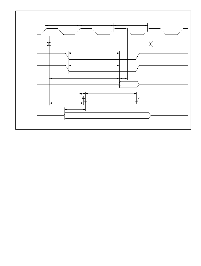
Figure 18-5 Basic Bus Cycle: Three-State Access
T
1
T
2
T
3
t
ACC4
t
ACC4
t
ACC2
t
WSW2
t
WSD
t
AS2
t
WDS2
¯
A
23
to A
0
AS
RD
(read)
D
15
to D
0
(read)
HWR
,
LWR
(write)
D
15
to D
0
(write)
t
RDS
542
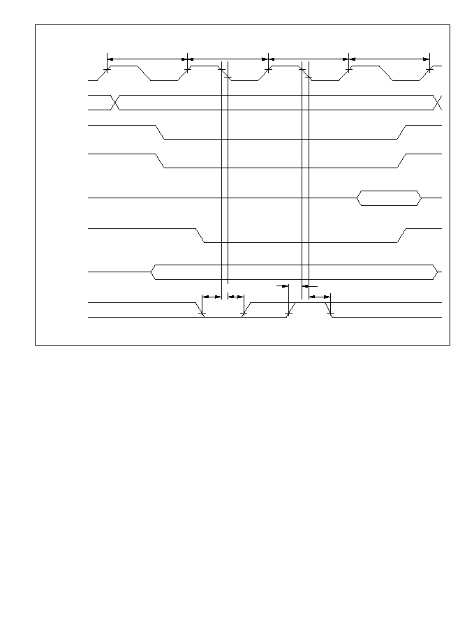
Figure 18-6 Basic Bus Cycle: Three-State Access with One Wait State
T
1
T
2
T
W
T
3
t
WTS
t
WTS
t
WTH
¯
A
23
to A
0
AS
RD
(read)
D
15
to D
0
(read)
HWR
,
LWR
(write)
D
15
to D
0
(write)
WAIT
t
WTH
543

18.3.2 Refresh Controller Bus Timing
Refresh controller bus timing is shown as follows:
∑
DRAM bus timing
Figures 18-7 to 18-12 show the DRAM bus timing in each operating mode.
∑
PSRAM bus timing
Figures 18-13 and 18-14 show the pseudo-static RAM bus timing in each operating mode.
Figure 18-7 DRAM Bus Timing (Read/Write): Three-State Access
-- 2
WE Mode --
¯
A
9
to A
1
AS
CS3
(
RAS
)
RD
(
CAS
)
HWR
(
UW
),
LWR
(
LW
)
(read)
HWR
(
UW
),
LWR
(
LW
)
(write)
RFSH
D
15
to D
0
(read)
D
15
to D
0
(write)
T
1
T
2
T
3
t
AD
t
AD
t
RAH
t
RAD1
t
AS1
t
ASD
t
AS1
t
RAC
t
ASD
t
AA
t
CAC
t
RAD3
t
RP
t
SD
t
CRP
t
SD
t
WDH
*
*
t
RDS
t
RDH
t
WDS3
t
CAS
Note:
*
Stipulation from earliest
CS3
and
RD
negate timing.
544
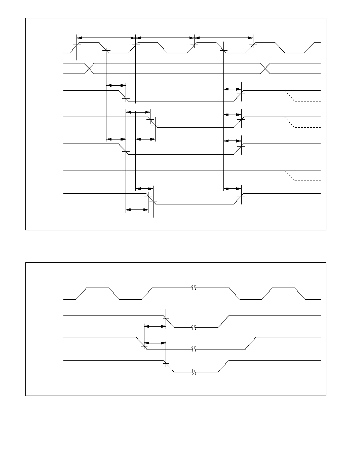
Figure 18-8 DRAM Bus Timing (Refresh Cycle): Three-State Access
-- 2
WE Mode --
Figure 18-9 DRAM Bus Timing (Self-Refresh Mode)
-- 2
WE Mode --
¯
A
9
to A
1
AS
CS3
(
RAS
)
RD
(
CAS
)
HWR
(
UW
),
LWR
(
LW
)
RFSH
T
1
T
2
T
3
t
ASD
t
CSR
t
ASD
t
RAD2
t
RAD2
t
CSR
t
RAD3
t
SD
t
RAD3
t
SD
¯
CS3
(
RAS
)
RD
(
CAS
)
RFSH
t
CSR
t
CSR
545
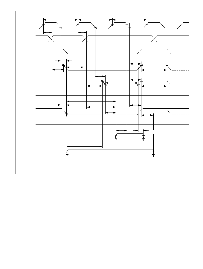
Figure 18-10 DRAM Bus Timing (Read/Write): Three-State Access
-- 2
CAS Mode --
)
T
1
T
2
T
3
t
AD
t
AD
t
RAH
t
RAD1
t
AS1
t
ASD
t
AS1
t
AA
t
RAC
t
ASD
t
CAC
t
WDS3
t
RDS
t
WDH
t
RDH
*
t
SD
t
SD
t
RAD3
t
CRP
t
RP
t
CAS
RFSH
¯
A
9
to A
1
AS
CS3
(
RAS
HWR
(
UCAS
),
LWR
(
LCAS
)
RD
(
WE
)
(read)
RD
(
WE
)
(write)
D
15
to D
0
(read)
(write)
D
15
to D
0
Note:
*
Stipulation from earliest
CS3
and
RD
negate timing.
546
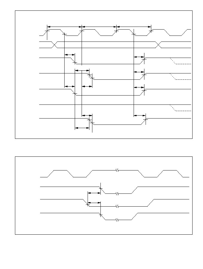
Figure 18-11 DRAM Bus Timing (Refresh Cycle): Three-State Access
-- 2
CAS Mode --
Figure 18-12 DRAM Bus Timing (Self-Refresh Mode)
-- 2
CAS Mode --
¯
A
9
to A
1
AS
CS3
(
RAS
)
RD
(
WE
)
HWR
(
UCAS
),
LWR
(
LCAS
)
RFSH
T
1
T
2
T
3
t
ASD
t
CSR
t
ASD
t
RAD2
t
RAD2
t
CSR
t
RAD3
t
SD
t
RAD3
t
SD
t
CSR
t
CSR
UCAS
¯
CS3
(
RAS
)
HWR
LWR
(
(
),
RFSH
LCAS
)
547
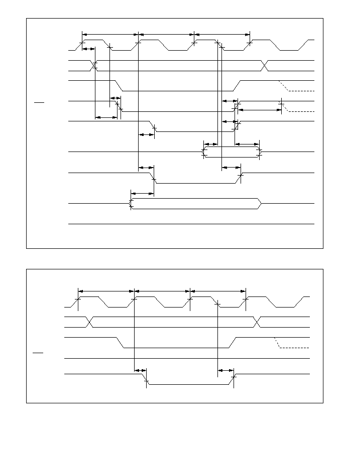
Figure 18-13 PSRAM Bus Timing (Read/Write): Three-State Access
Figure 18-14 PSRAM Bus Timing (Refresh Cycle): Three-State Access
¯
A
23
to A
0
AS
CS
3
RD
(read)
D
15
to D
0
(read)
HWR
,
LWR
(write)
D
15
to D
0
(write)
RFSH
t
AD
T
2
T
3
t
RAD1
t
AS1
t
RSD
t
WSD
t
WDS2
t
RAD3
t
RP
t
RDH
*
t
SD
t
RDS
t
SD
T
1
Note:
*
Stipulation from earliest
CS3
and
RD
negate timing.
¯
A
23
to A
0
AS
CS
3
,
HWR
,
LWR
,
RD
RFSH
T
2
T
3
T
1
t
RAD2
t
RAD3
548

18.3.3 Control Signal Timing
Control signal timing is shown as follows:
∑
Reset input timing
Figure 18-15 shows the reset input timing.
∑
Reset output timing
Figure 18-16 shows the reset output timing.
∑
Interrupt input timing
Figure 18-17 shows the input timing for NMI and IRQ
5
to IRQ
0
.
∑
Bus-release mode timing
Figure 18-18 shows the bus-release mode timing.
Figure 18-15 Reset Input Timing
Figure 18-16 Reset Output Timing
¯
RES
t
RESS
t
RESS
t
RESW
¯
RESO
t
RESD
t
RESOW
t
RESD
549
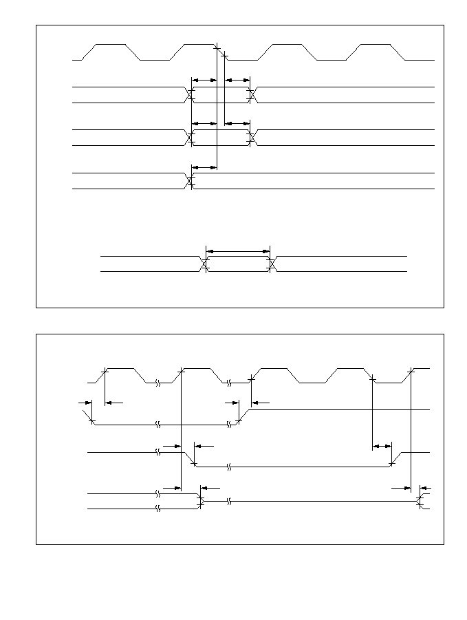
Figure 18-17 Interrupt Input Timing
Figure 18-18 Bus-Release Mode Timing
¯
NMI
IRQ
IRQ
E
L
t
NMIS
t
NMIH
t
NMIS
t
NMIH
t
NMIS
t
NMIW
NMI
IRQ
j
IRQ
: Edge-sensitive
IRQ
: Level-sensitive
IRQ
(i = 0 to 5)
E
L
i
i
IRQ
(j = 0 to 2)
BREQ
BACK
¯
A
23
to A
0
,
AS
,
RD
,
HWR
,
LWR
t
BRQS
t
BRQS
t
BACD1
t
BZD
t
BACD2
t
BZD
550

18.3.4 Clock Timing
Clock timing is shown as follows:
∑
Oscillator settling timing
Figure 18-19 shows the oscillator settling timing.
Figure 18-19 Oscillator Settling Timing
18.3.5 TPC and I/O Port Timing
TPC and I/O port timing is shown as follows.
Figure 18-20 TPC and I/O Port Input/Output Timing
¯
V
CC
STBY
RES
t
OSC1
t
OSC1
T
1
T
2
T
3
¯
Port 4,
6 to B
(read)
Port 4,6,
8 to B
(write)
t
PRS
t
PRH
t
PWD
551

18.3.6 ITU Timing
ITU timing is shown as follows:
∑
ITU input/output timing
Figure 18-21 shows the ITU input/output timing.
∑
ITU external clock input timing
Figure 18-22 shows the ITU external clock input timing.
Figure 18-21 ITU Input/Output Timing
Figure 18-22 ITU Clock Input Timing
¯
Output
compare
*
1
Input
capture
*
2
t
TOCD
t
TICS
Notes: 1. TIOCA0 to TIOCA4, TIOCB0 to TIOCB4, TOCXA4, TOCXB4
2. TIOCA0 to TIOCA4, TIOCB0 to TIOCB4
¯
t
TCKS
t
TCKS
t
TCKWH
t
TCKWL
TCLKA to
TCLKD
552
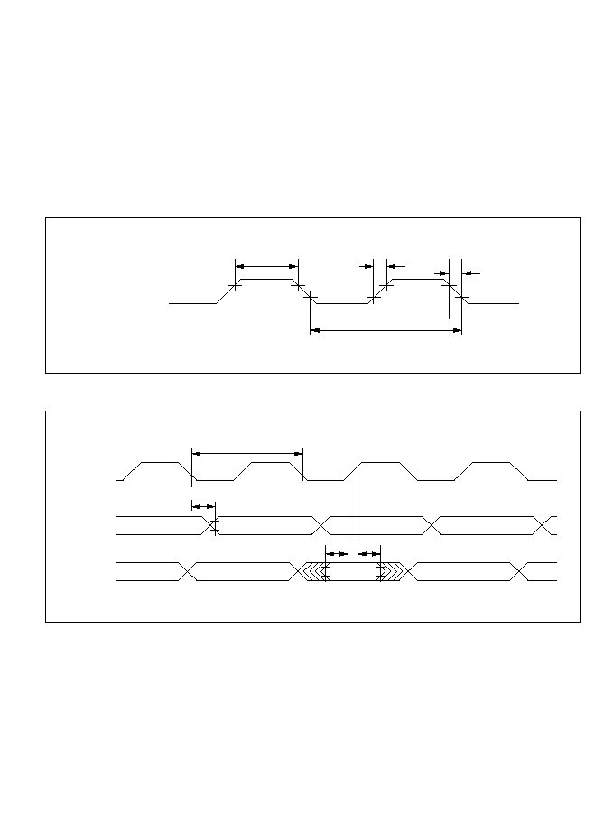
18.3.7 SCI Input/Output Timing
SCI timing is shown as follows:
∑
SCI input clock timing
Figure 18-23 shows the SCI input clock timing.
∑
SCI input/output timing (synchronous mode)
Figure 18-24 shows the SCI input/output timing in synchronous mode.
Figure 18-23 SCK Input Clock Timing
Figure 18-24 SCI Input/Output Timing in Synchronous Mode
SCK0, SCK1
t
SCKW
t
SCYC
t
SCKr
t
SCKf
t
SCYC
t
TXD
t
RXS
t
RXH
SCK0, SCK1
TxD0, TxD1
(transmit
data)
RxD0, RxD1
(receive
data)
553
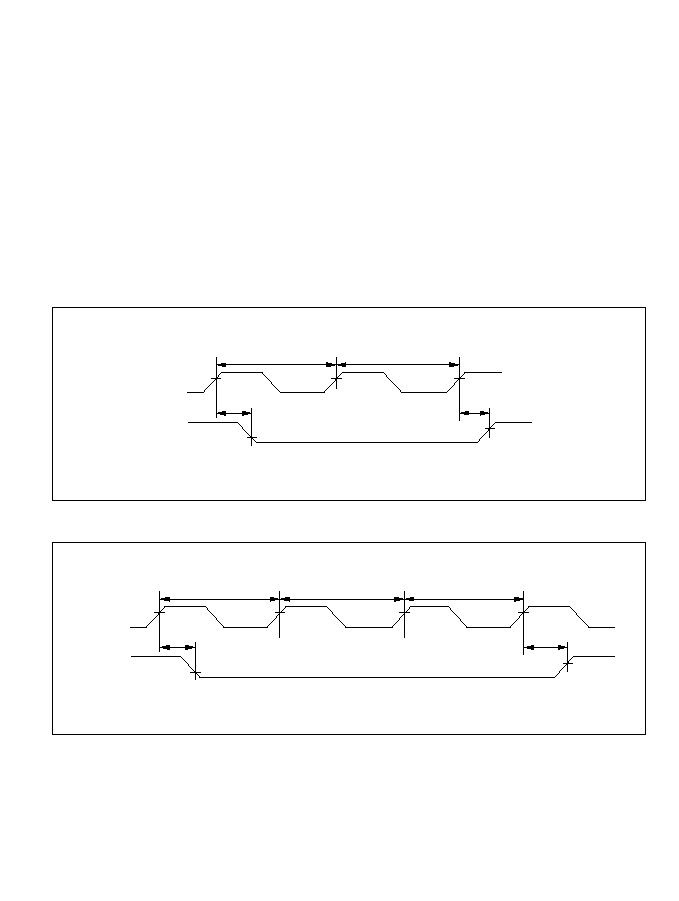
18.3.8 DMAC Timing
DMAC timing is shown as follows.
∑
DMAC
TEND output timing for 2 state access
Figure 18-25 shows the DMAC
TEND output timing for 2 state access.
∑
DMAC
TEND output timing for 3 state access
Figure 18-26 shows the DMAC
TEND output timing for 3 state access.
∑
DMAC
DREQ input timing
Figure 18-27 shows DMAC
DREQ input timing.
Figure 18-25 DMAC
TEND Output Timing/2 State Access
Figure 18-26 DMAC
TEND Output Timing/3 State Access
T
1
T
2
t
TED1
t
TED2
¯
TEND
T
1
T
2
T
3
t
TED1
t
TED2
¯
TEND
554
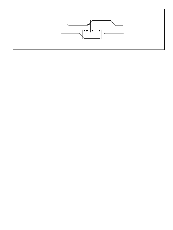
Figure 18-27 DMAC
DREQ Input Timing
t
DRQH
t
DRQS
¯
DREQ
555

556

Appendix A Instruction Set
A.1 Instruction List
Operand Notation
Symbol
Description
Rd
General destination register
Rs
General source register
Rn
General register
ERd
General destination register (address register or 32-bit register)
ERs
General source register (address register or 32-bit register)
ERn
General register (32-bit register)
(EAd)
Destination operand
(EAs)
Source operand
PC
Program counter
SP
Stack pointer
CCR
Condition code register
N
N (negative) flag in CCR
Z
Z (zero) flag in CCR
V
V (overflow) flag in CCR
C
C (carry) flag in CCR
disp
Displacement
Transfer from the operand on the left to the operand on the right, or transition from
the state on the left to the state on the right
+
Addition of the operands on both sides
≠
Subtraction of the operand on the right from the operand on the left
◊
Multiplication of the operands on both sides
˜
Division of the operand on the left by the operand on the right
Logical AND of the operands on both sides
Logical OR of the operands on both sides
Exclusive logical OR of the operands on both sides
¨
NOT (logical complement)
( ), < >
Contents of operand
Note: General registers include 8-bit registers (R0H to R7H and R0L to R7L) and 16-bit registers
(R0 to R7 and E0 to E7).
557

Condition Code Notation
Symbol
Description
§
Changed according to execution result
*
Undetermined (no guaranteed value)
0
Cleared to 0
1
Set to 1
--
Not affected by execution of the instruction
Varies depending on conditions, described in notes
558

Table A-1 Instruction Set
1.
Data transfer instructions
Condition Code
Mnemonic
Operation
I
H
N
Z
V
C
MOV.B #xx:8, Rd
B
#xx:8
Rd8
2
-- --
§
§
0
--
2
MOV.B Rs, Rd
B
Rs8
Rd8
2
-- --
§
§
0
--
2
MOV.B @ERs, Rd
B
@ERs
Rd8
2
-- --
§
§
0
--
4
MOV.B @(d:16, ERs),
B
@(d:16, ERs)
Rd8
4
-- --
§
§
0
--
6
Rd
MOV.B @(d:24, ERs),
B
@(d:24, ERs)
Rd8
8
-- --
§
§
0
--
10
Rd
MOV.B @ERs+, Rd
B
@ERs
RD8 2
-- --
§
§
0
--
6
ERs32+1
ERs32
MOV.B @aa:8, Rd
B
@aa:8
Rd8
2
-- --
§
§
0
--
4
MOV.B @aa:16, Rd
B
@aa:16
Rd8
4
-- --
§
§
0
--
6
MOV.B @aa:24, Rd
B
@aa:24
Rd8
6
-- --
§
§
0
--
8
MOV.B Rs, @ERd
B
Rs8
@ERd
2
-- --
§
§
0
--
4
MOV.B Rs, @(d:16,
B
Rs8
@(d:16, ERd)
4
-- --
§
§
0
--
6
ERd)
MOV.B Rs, @(d:24,
B
Rs8
@(d:24, ERd)
8
-- --
§
§
0
--
10
ERd)
MOV.B Rs, @≠ERd
B
ERd32≠1
ERd32
2
-- --
§
§
0
--
6
Rs8
@ERd
MOV.B Rs, @aa:8
B
Rs8
@aa:8
2
-- --
§
§
0
--
4
MOV.B Rs, @aa:16
B
Rs8
@aa:16
4
-- --
§
§
0
--
6
MOV.B Rs, @aa:24
B
Rs8
@aa:24
6
-- --
§
§
0
--
8
MOV.W #xx:16, Rd
W
#xx:16
Rd16
4
-- --
§
§
0
--
4
MOV.W Rs, Rd
W
Rs16
Rd16
2
-- --
§
§
0
--
2
MOV.W @ERs, Rd
W
@ERs
Rd16
2
-- --
§
§
0
--
4
MOV.W @(d:16, ERs),
W
@(d:16, ERs)
Rd16
4
-- --
§
§
0
--
6
Rd
MOV.W @(d:24, ERs),
W
@(d:24, ERs)
Rd16
8
-- --
§
§
0
--
10
Rd
MOV.W @ERs+, Rd
W
@ERs
Rd16
2
-- --
§
§
0
--
6
ERs32+2
@ERd32
MOV.W @aa:16, Rd
W
@aa:16
Rd16
4
-- --
§
§
0
--
6
#xx
Rn
@ERn
@(d, ERn)
@≠ERn/@ERn+
@aa
@(d, PC)
@@aa
--
Addressing Mode and
Instruction Length (bytes)
Normal
No. of
States
*
1
Advanced
Operand Size
559

Table A-1 Instruction Set (cont)
Condition Code
Mnemonic
Operation
I
H
N
Z
V
C
MOV.W @aa:24, Rd
W
@aa:24
Rd16
6
-- --
§
§
0
--
8
MOV.W Rs, @ERd
W
Rs16
@ERd
2
-- --
§
§
0
--
4
MOV.W Rs, @(d:16,
W
Rs16
@(d:16, ERd)
4
-- --
§
§
0
--
6
ERd)
MOV.W Rs, @(d:24,
W
Rs16
@(d:24, ERd)
8
-- --
§
§
0
--
10
ERd)
MOV.W Rs, @≠ERd
W
ERd32≠2
ERd32
2
-- --
§
§
0
--
6
Rs16
@ERd
MOV.W Rs, @aa:16
W
Rs16
@aa:16
4
-- --
§
§
0
--
6
MOV.W Rs, @aa:24
W
Rs16
@aa:24
6
-- --
§
§
0
--
8
MOV.L #xx:32, ERd
L
#xx:32
ERd32
6
-- --
§
§
0
--
6
MOV.L ERs, ERd
L
ERs32
ERd32
2
-- --
§
§
0
--
2
MOV.L @ERs, ERd
L
@ERs
ERd32
4
-- --
§
§
0
--
8
MOV.L @(d:16, ERs),
L
@(d:16, ERs)
ERd32
6
-- --
§
§
0
--
10
ERd
MOV.L @(d:24, ERs),
L
@(d:24, ERs)
ERd32
10
-- --
§
§
0
--
14
ERd
MOV.L @ERs+, ERd
L
@ERs
ERd32
4
-- --
§
§
0
--
10
ERs32+4
ERs32
MOV.L @aa:16, ERd
L
@aa:16
ERd32
6
-- --
§
§
0
--
10
MOV.L @aa:24, ERd
L
@aa:24
ERd32
8
-- --
§
§
0
--
12
MOV.L ERs, @ERd
L
ERs32
@ERd
4
-- --
§
§
0
--
8
MOV.L ERs, @(d:16,
L
ERs32
@(d:16, ERd)
6
-- --
§
§
0
--
10
ERd)
MOV.L ERs, @(d:24,
L
ERs32
@(d:24, ERd)
10
-- --
§
§
0
--
14
ERd)
MOV.L ERs, @≠ERd
L
ERd32≠4
ERd32
4
-- --
§
§
0
--
10
ERs32
@ERd
MOV.L ERs, @aa:16
L
ERs32
@aa:16
6
-- --
§
§
0
--
10
MOV.L ERs, @aa:24
L
ERs32
@aa:24
8
-- --
§
§
0
--
12
POP.W Rn
W
@SP
Rn16
2
-- --
§
§
0
--
6
SP+2
SP
POP.L ERn
L
@SP
ERn32
4
-- --
§
§
0
--
10
SP+4
SP
#xx
Rn
@ERn
@(d, ERn)
@≠ERn/@ERn+
@aa
@(d, PC)
@@aa
--
Addressing Mode and
Instruction Length (bytes)
Normal
No. of
States
*
1
Advanced
Operand Size
560
Table A-1 Instruction Set (cont)
Condition Code
Mnemonic
Operation
I
H
N
Z
V
C
PUSH.W Rn
W
SP≠2
SP
2
-- --
§
§
0
--
6
Rn16
@SP
PUSH.L ERn
L
SP≠4
SP
4
-- --
§
§
0
--
10
ERn32
@SP
MOVFPE @aa:16,
B
Cannot be used in the
4
Cannot be used in the H8/3002
Rd
H8/3002
MOVTPE Rs,
B
Cannot be used in the
4
Cannot be used in the H8/3002
@aa:16
H8/3002
2.
Arithmetic instructions
Condition Code
Mnemonic
Operation
I
H
N
Z
V
C
ADD.B #xx:8, Rd
B
Rd8+#xx:8
Rd8
2
--
§
§
§
§
§
2
ADD.B Rs, Rd
B
Rd8+Rs8
Rd8
2
--
§
§
§
§
§
2
ADD.W #xx:16, Rd
W
Rd16+#xx:16
Rd16
4
-- (1)
§
§
§
§
4
ADD.W Rs, Rd
W
Rd16+Rs16
Rd16
2
-- (1)
§
§
§
§
2
ADD.L #xx:32, ERd
L
ERd32+#xx:32
6
-- (2)
§
§
§
§
6
ERd32
ADD.L ERs, ERd
L
ERd32+ERs32
2
-- (2)
§
§
§
§
2
ERd32
ADDX.B #xx:8, Rd
B
Rd8+#xx:8 +C
Rd8
2
--
§
§
(3)
§
§
2
ADDX.B Rs, Rd
B
Rd8+Rs8 +C
Rd8
2
--
§
§
(3)
§
§
2
ADDS.L #1, ERd
L
ERd32+1
ERd32
2
-- -- -- -- -- --
2
ADDS.L #2, ERd
L
ERd32+2
ERd32
2
-- -- -- -- -- --
2
ADDS.L #4, ERd
L
ERd32+4
ERd32
2
-- -- -- -- -- --
2
INC.B Rd
B
Rd8+1
Rd8
2
-- --
§
§
§
--
2
INC.W #1, Rd
W
Rd16+1
Rd16
2
-- --
§
§
§
--
2
INC.W #2, Rd
W
Rd16+2
Rd16
2
-- --
§
§
§
--
2
#xx
Rn
@ERn
@(d, ERn)
@≠ERn/@ERn+
@aa
@(d, PC)
@@aa
--
Addressing Mode and
Instruction Length (bytes)
Normal
No. of
States
*
1
Advanced
Operand Size
#xx
Rn
@ERn
@(d, ERn)
@≠ERn/@ERn+
@aa
@(d, PC)
@@aa
--
Addressing Mode and
Instruction Length (bytes)
Normal
No. of
States
*
1
Advanced
Operand Size
561

T
I
able A-1 Instruction Set (cont)
Condition Code
Mnemonic
Operation
I
H
N
Z
V
C
INC.L #1, ERd
L
ERd32+1
ERd32
2
-- --
§
§
§
--
2
INC.L #2, ERd
L
ERd32+2
ERd32
2
-- --
§
§
§
--
2
DAA Rd
B
Rd8 decimal adjust
2
--
*
§
§
*
--
2
Rd8
SUB.B Rs, Rd
B
Rd8≠Rs8
Rd8
2
--
§
§
§
§
§
2
SUB.W #xx:16, Rd
W
Rd16≠#xx:16
Rd16
4
-- (1)
§
§
§
§
4
SUB.W Rs, Rd
W
Rd16≠Rs16
Rd16
2
-- (1)
§
§
§
§
2
SUB.L #xx:32, ERd
L
ERd32≠#xx:32
6
-- (2)
§
§
§
§
6
ERd32
SUB.L ERs, ERd
L
ERd32≠ERs32
2
-- (2)
§
§
§
§
2
ERd32
SUBX.B #xx:8, Rd
B
Rd8≠#xx:8≠C
Rd8
2
--
§
§
(3)
§
§
2
SUBX.B Rs, Rd
B
Rd8≠Rs8≠C
Rd8
2
--
§
§
(3)
§
§
2
SUBS.L #1, ERd
L
ERd32≠1
ERd32
2
-- -- -- -- -- --
2
SUBS.L #2, ERd
L
ERd32≠2
ERd32
2
-- -- -- -- -- --
2
SUBS.L #4, ERd
L
ERd32≠4
ERd32
2
-- -- -- -- -- --
2
DEC.B Rd
B
Rd8≠1
Rd8
2
-- --
§
§
§
--
2
DEC.W #1, Rd
W
Rd16≠1
Rd16
2
-- --
§
§
§
--
2
DEC.W #2, Rd
W
Rd16≠2
Rd16
2
-- --
§
§
§
--
2
DEC.L #1, ERd
L
ERd32≠1
ERd32
2
-- --
§
§
§
--
2
DEC.L #2, ERd
L
ERd32≠2
ERd32
2
-- --
§
§
§
--
2
DAS.Rd
B
Rd8 decimal adjust
2
--
*
§
§
*
--
2
Rd8
MULXU. B Rs, Rd
B
Rd8
◊
Rs8
Rd16 2
-- -- -- -- -- --
14
(unsigned multiplication)
MULXU. W Rs, ERd
W
Rd16
◊
Rs16
ERd32 2
-- -- -- -- -- --
22
(unsigned multiplication)
MULXS. B Rs, Rd
B
Rd8
◊
Rs8
Rd16 4
-- --
§
§
-- --
16
(signed multiplication)
MULXS. W Rs, ERd
W
Rd16
◊
Rs16
ERd32 4
-- --
§
§
-- --
24
(signed multiplication)
DIVXU. B Rs, Rd
B
Rd16
˜
Rs8
Rd16 2
-- -- (6) (7) -- --
14
(RdH: remainder,
RdL: quotient)
(unsigned division)
#xx
Rn
@ERn
@(d, ERn)
@≠ERn/@ERn+
@aa
@(d, PC)
@@aa
--
Addressing Mode and
Instruction Length (bytes)
Normal
No. of
States
*
1
Advanced
Operand Size
562

Table A-1 Instruction Set (cont)
Condition Code
Mnemonic
Operation
I
H
N
Z
V
C
DIVXU. W Rs, ERd
W
ERd32
˜
Rs16
ERd32 2
-- -- (6) (7) -- --
22
(Ed: remainder,
Rd: quotient)
(unsigned division)
DIVXS. B Rs, Rd
B
Rd16
˜
Rs8
Rd16 4
-- -- (8) (7) -- --
16
(RdH: remainder,
RdL: quotient)
(signed division)
DIVXS. W Rs, ERd
W
ERd32
˜
Rs16
ERd32 4
-- -- (8) (7) -- --
24
(Ed: remainder,
Rd: quotient)
(signed division)
CMP.B #xx:8, Rd
B
Rd8≠#xx:8
2
--
§
§
§
§
§
2
CMP.B Rs, Rd
B
Rd8≠Rs8
2
--
§
§
§
§
§
2
CMP.W #xx:16, Rd
W
Rd16≠#xx:16
4
-- (1)
§
§
§
§
4
CMP.W Rs, Rd
W
Rd16≠Rs16
2
-- (1)
§
§
§
§
2
CMP.L #xx:32, ERd
L
ERd32≠#xx:32
6
-- (2)
§
§
§
§
6
CMP.L ERs, ERd
L
ERd32≠ERs32
2
-- (2)
§
§
§
§
2
NEG.B Rd
B
0≠Rd8
Rd8
2
--
§
§
§
§
§
2
NEG.W Rd
W
0≠Rd16
Rd16
2
--
§
§
§
§
§
2
NEG.L ERd
L
0≠ERd32
ERd32
2
--
§
§
§
§
§
2
EXTU.W Rd
W
0
(<bits 15 to 8>
2
-- --
0
§
0
--
2
of Rd16)
EXTU.L ERd
L
0
(<bits 31 to 16>
2
-- --
0
§
0
--
2
of Rd32)
EXTS.W Rd
W
(<bit 7> of Rd16)
2
-- --
§
§
0
--
2
(<bits 15 to 8> of Rd16)
EXTS.L ERd
L
(<bit 15> of Rd32)
2
-- --
§
§
0
--
2
(<bits 31 to 16> of
ERd32)
#xx
Rn
@ERn
@(d, ERn)
@≠ERn/@ERn+
@aa
@(d, PC)
@@aa
--
Addressing Mode and
Instruction Length (bytes)
Normal
No. of
States
*
1
Advanced
Operand Size
563

Table A-1 Instruction Set (cont)
3.
Logic instructions
Condition Code
Mnemonic
Operation
I
H
N
Z
V
C
AND.B #xx:8, Rd
B
Rd8
#xx:8
Rd8
2
-- --
§
§
0
--
2
AND.B Rs, Rd
B
Rd8
Rs8
Rd8
2
-- --
§
§
0
--
2
AND.W #xx:16, Rd
W
Rd16
#xx:16
Rd16
4
-- --
§
§
0
--
4
AND.W Rs, Rd
W
Rd16
Rs16
Rd16
2
-- --
§
§
0
--
2
AND.L #xx:32, ERd
L
ERd32
#xx:32
ERd32
6
-- --
§
§
0
--
6
AND.L ERs, ERd
L
ERd32
ERs32
ERd32
4
-- --
§
§
0
--
4
OR.B #xx:8, Rd
B
Rd8
#xx:8
Rd8
2
-- --
§
§
0
--
2
OR.B Rs, Rd
B
Rd8
Rs8
Rd8
2
-- --
§
§
0
--
2
OR.W #xx:16, Rd
W
Rd16
#xx:16
Rd16
4
-- --
§
§
0
--
4
OR.W Rs, Rd
W
Rd16
Rs16
Rd16
2
-- --
§
§
0
--
2
OR.L #xx:32, ERd
L
ERd32
#xx:32
ERd32
6
-- --
§
§
0
--
6
OR.L ERs, ERd
L
ERd32
ERs32
ERd32
4
-- --
§
§
0
--
4
XOR.B #xx:8, Rd
B
Rd8
#xx:8
Rd8
2
-- --
§
§
0
--
2
XOR.B Rs, Rd
B
Rd8
Rs8
Rd8
2
-- --
§
§
0
--
2
XOR.W #xx:16, Rd
W
Rd16
#xx:16
Rd16
4
-- --
§
§
0
--
4
XOR.W Rs, Rd
W
Rd16
Rs16
Rd16
2
-- --
§
§
0
--
2
XOR.L #xx:32, ERd
L
ERd32
#xx:32
ERd32
6
-- --
§
§
0
--
6
XOR.L ERs, ERd
L
ERd32
ERs32
ERd32
4
-- --
§
§
0
--
4
NOT.B Rd
B
¨ Rd8
Rd8
2
-- --
§
§
0
--
2
NOT.W Rd
W
¨ Rd16
Rd16
2
-- --
§
§
0
--
2
NOT.L ERd
L
¨ Rd32
Rd32
2
-- --
§
§
0
--
2
#xx
Rn
@ERn
@(d, ERn)
@≠ERn/@ERn+
@aa
@(d, PC)
@@aa
--
Addressing Mode and
Instruction Length (bytes)
Normal
No. of
States
*
1
Advanced
Operand Size
564
Table A-1 Instruction Set (cont)
4.
Shift instructions
Condition Code
Mnemonic
Operation
I
H
N
Z
V
C
SHAL.B Rd
B
2
-- --
§
§
§
§
2
SHAL.W Rd
W
2
-- --
§
§
§
§
2
SHAL.L ERd
L
2
-- --
§
§
§
§
2
SHAR.B Rd
B
2
-- --
§
§
0
§
2
SHAR.W Rd
W
2
-- --
§
§
0
§
2
SHAR.L ERd
L
2
-- --
§
§
0
§
2
SHLL.B Rd
B
2
-- --
§
§
0
§
2
SHLL.W Rd
W
2
-- --
§
§
0
§
2
SHLL.L ERd
L
2
-- --
§
§
0
§
2
SHLR.B Rd
B
2
-- --
§
§
0
§
2
SHLR.W Rd
W
2
-- --
§
§
0
§
2
SHLR.L ERd
L
2
-- --
§
§
0
§
2
ROTXL.B Rd
B
2
-- --
§
§
0
§
2
ROTXL.W Rd
W
2
-- --
§
§
0
§
2
ROTXL.L ERd
L
2
-- --
§
§
0
§
2
ROTXR.B Rd
B
2
-- --
§
§
0
§
2
ROTXR.W Rd
W
2
-- --
§
§
0
§
2
ROTXR.L ERd
L
2
-- --
§
§
0
§
2
ROTL.B Rd
B
2
-- --
§
§
0
§
2
ROTL.W Rd
W
2
-- --
§
§
0
§
2
ROTL.L ERd
L
2
-- --
§
§
0
§
2
ROTR.B Rd
B
2
-- --
§
§
0
§
2
ROTR.W Rd
W
2
-- --
§
§
0
§
2
ROTR.L ERd
L
2
-- --
§
§
0
§
2
#xx
Rn
@ERn
@(d, ERn)
@≠ERn/@ERn+
@aa
@(d, PC)
@@aa
--
Addressing Mode and
Instruction Length (bytes)
Normal
No. of
States
*
1
Advanced
Operand Size
MSB
LSB
0
C
C
MSB
LSB
MSB
LSB
0
C
0
C
MSB
LSB
C
MSB
LSB
C
MSB
LSB
C
MSB
LSB
C
MSB
LSB
565

Table A-1 Instruction Set (cont)
5.
Bit manipulation instructions
Condition Code
Mnemonic
Operation
I
H
N
Z
V
C
BSET #xx:3, Rd
B
(#xx:3 of Rd8)
1
2
-- -- -- -- -- --
2
BSET #xx:3, @ERd
B
(#xx:3 of @ERd)
1
4
-- -- -- -- -- --
8
BSET #xx:3, @aa:8
B
(#xx:3 of @aa:8)
1
4
-- -- -- -- -- --
8
BSET Rn, Rd
B
(Rn8 of Rd8)
1
2
-- -- -- -- -- --
2
BSET Rn, @ERd
B
(Rn8 of @ERd)
1
4
-- -- -- -- -- --
8
BSET Rn, @aa:8
B
(Rn8 of @aa:8)
1
4
-- -- -- -- -- --
8
BCLR #xx:3, Rd
B
(#xx:3 of Rd8)
0
2
-- -- -- -- -- --
2
BCLR #xx:3, @ERd
B
(#xx:3 of @ERd)
0
4
-- -- -- -- -- --
8
BCLR #xx:3, @aa:8
B
(#xx:3 of @aa:8)
0
4
-- -- -- -- -- --
8
BCLR Rn, Rd
B
(Rn8 of Rd8)
0
2
-- -- -- -- -- --
2
BCLR Rn, @ERd
B
(Rn8 of @ERd)
0
4
-- -- -- -- -- --
8
BCLR Rn, @aa:8
B
(Rn8 of @aa:8)
0
4
-- -- -- -- -- --
8
BNOT #xx:3, Rd
B
(#xx:3 of Rd8)
2
-- -- -- -- -- --
2
¨ (#xx:3 of Rd8)
BNOT #xx:3, @ERd
B
(#xx:3 of @ERd)
4
-- -- -- -- -- --
8
¨ (#xx:3 of @ERd)
BNOT #xx:3, @aa:8
B
(#xx:3 of @aa:8)
4
-- -- -- -- -- --
8
¨ (#xx:3 of @aa:8)
BNOT Rn, Rd
B
(Rn8 of Rd8)
2
-- -- -- -- -- --
2
¨ (Rn8 of Rd8)
BNOT Rn, @ERd
B
(Rn8 of @ERd)
4
-- -- -- -- -- --
8
¨ (Rn8 of @ERd)
BNOT Rn, @aa:8
B
(Rn8 of @aa:8)
4
-- -- -- -- -- --
8
¨ (Rn8 of @aa:8)
BTST #xx:3, Rd
B
¨ (#xx:3 of Rd8)
Z
2
-- -- --
§
-- --
2
BTST #xx:3, @ERd
B
¨ (#xx:3 of @ERd)
Z
4
-- -- --
§
-- --
6
BTST #xx:3, @aa:8
B
¨ (#xx:3 of @aa:8)
Z
4
-- -- --
§
-- --
6
BTST Rn, Rd
B
¨ (Rn8 of @Rd8)
Z
2
-- -- --
§
-- --
2
BTST Rn, @ERd
B
¨ (Rn8 of @ERd)
Z
4
-- -- --
§
-- --
6
BTST Rn, @aa:8
B
¨ (Rn8 of @aa:8)
Z
4
-- -- --
§
-- --
6
BLD #xx:3, Rd
B
(#xx:3 of Rd8)
C
2
-- -- -- -- --
§
2
#xx
Rn
@ERn
@(d, ERn)
@≠ERn/@ERn+
@aa
@(d, PC)
@@aa
--
Addressing Mode and
Instruction Length (bytes)
Normal
No. of
States
*
1
Advanced
Operand Size
566

Table A-1 Instruction Set (cont)
Condition Code
Mnemonic
Operation
I
H
N
Z
V
C
BLD #xx:3, @ERd
B
(#xx:3 of @ERd)
C
4
-- -- -- -- --
§
6
BLD #xx:3, @aa:8
B
(#xx:3 of @aa:8)
C
4
-- -- -- -- --
§
6
BILD #xx:3, Rd
B
¨ (#xx:3 of Rd8)
C
2
-- -- -- -- --
§
2
BILD #xx:3, @ERd
B
¨ (#xx:3 of @ERd)
C
4
-- -- -- -- --
§
6
BILD #xx:3, @aa:8
B
¨ (#xx:3 of @aa:8)
C
4
-- -- -- -- --
§
6
BST #xx:3, Rd
B
C
(#xx:3 of Rd8)
2
-- -- -- -- -- --
2
BST #xx:3, @REd
B
C
(#xx:3 of @ERd)
4
-- -- -- -- -- --
8
BST #xx:3, @aa:8
B
C
(#xx:3 of @aa:8)
4
-- -- -- -- -- --
8
BIST #xx:3, Rd
B
¨ C
(#xx:3 of Rd8)
2
-- -- -- -- -- --
2
BIST #xx:3, @ERd
B
¨ C
(#xx:3 of @ERd24)
4
-- -- -- -- -- --
8
BIST #xx:3, @aa:8
B
¨ C
(#xx:3 of @aa:8)
4
-- -- -- -- -- --
8
BAND #xx:3, Rd
B
C
(#xx:3 of Rd8)
C
2
-- -- -- -- --
§
2
BAND #xx:3, @ERd
B
C
(#xx:3 of @ERd24)
C
4
-- -- -- -- --
§
6
BAND #xx:3, @aa:8
B
C
(#xx:3 of @aa:8)
C
4
-- -- -- -- --
§
6
BIAND #xx:3, Rd
B
C
¨ (#xx:3 of Rd8)
C
2
-- -- -- -- --
§
2
BIAND #xx:3, @ERd
B
C
¨ (#xx:3 of @ERd24)
C
4
-- -- -- -- --
§
6
BIAND #xx:3, @aa:8
B
C
¨ (#xx:3 of @aa:8)
C
4
-- -- -- -- --
§
6
BOR #xx:3, Rd
B
C
(#xx:3 of Rd8)
C
2
-- -- -- -- --
§
2
BOR #xx:3, @ERd
B
C
(#xx:3 of @ERd24)
C
4
-- -- -- -- --
§
6
BOR #xx:3, @aa:8
B
C
(#xx:3 of @aa:8)
C
4
-- -- -- -- --
§
6
BIOR #xx:3, Rd
B
C
¨ (#xx:3 of Rd8)
C
2
-- -- -- -- --
§
2
BIOR #xx:3, @ERd
B
C
¨ (#xx:3 of @ERd24)
C
4
-- -- -- -- --
§
6
BIOR #xx:3, @aa:8
B
C
¨ (#xx:3 of @aa:8)
C
4
-- -- -- -- --
§
6
BXOR #xx:3, Rd
B
C
(#xx:3 of Rd8)
C
2
-- -- -- -- --
§
2
BXOR #xx:3, @ERd
B
C
(#xx:3 of @ERd24)
C
4
-- -- -- -- --
§
6
BXOR #xx:3, @aa:8
B
C
(#xx:3 of @aa:8)
C
4
-- -- -- -- --
§
6
BIXOR #xx:3, Rd
B
C
¨ (#xx:3 of Rd8)
C
2
-- -- -- -- --
§
2
BIXOR #xx:3, @ERd
B
C
¨ (#xx:3 of @ERd24)
C
4
-- -- -- -- --
§
6
BIXOR #xx:3, @aa:8
B
C
¨ (#xx:3 of @aa:8)
C
4
-- -- -- -- --
§
6
#xx
Rn
@ERn
@(d, ERn)
@≠ERn/@ERn+
@aa
@(d, PC)
@@aa
--
Addressing Mode and
Instruction Length (bytes)
Normal
No. of
States
*
1
Advanced
Operand Size
567

Table A-1 Instruction Set (cont)
6.
Branching instructions
Condition Code
Mnemonic
Operation
I
H
N
Z
V
C
BRA d:8 (BT d:8)
--
Always
2
-- -- -- -- -- --
4
BRA d:16 (BT d:16)
--
4
-- -- -- -- -- --
6
BRN d:8 (BF d:8)
--
Never
2
-- -- -- -- -- --
4
BRN d:16 (BF d:16)
--
4
-- -- -- -- -- --
6
BHI d:8
--
C
Z = 0
2
-- -- -- -- -- --
4
BHI d:16
--
4
-- -- -- -- -- --
6
BLS d:8
--
C
Z = 1
2
-- -- -- -- -- --
4
BLS d:16
--
4
-- -- -- -- -- --
6
BCC d:8 (BHS d:8)
--
C = 0
2
-- -- -- -- -- --
4
BCC d:16 (BHS d:16)
--
4
-- -- -- -- -- --
6
BCS d:8 (BLO d:8)
--
C = 1
2
-- -- -- -- -- --
4
BCS d:16 (BLO d:16)
--
4
-- -- -- -- -- --
6
BNE d:8
--
Z = 0
2
-- -- -- -- -- --
4
BNE d:16
--
4
-- -- -- -- -- --
6
BEQ d:8
--
Z = 1
2
-- -- -- -- -- --
4
BEQ d:16
--
4
-- -- -- -- -- --
6
BVC d:8
--
V = 0
2
-- -- -- -- -- --
4
BVC d:16
--
4
-- -- -- -- -- --
6
BVS d:8
--
V = 1
2
-- -- -- -- -- --
4
BVS d:16
--
4
-- -- -- -- -- --
6
BPL d:8
--
N = 0
2
-- -- -- -- -- --
4
BPL d:16
--
4
-- -- -- -- -- --
6
BMI d:8
--
N = 1
2
-- -- -- -- -- --
4
BMI d:16
--
4
-- -- -- -- -- --
6
BGE d:8
--
N
V = 0
2
-- -- -- -- -- --
4
BGE d:16
--
4
-- -- -- -- -- --
6
BLT d:8
--
N
V = 1
2
-- -- -- -- -- --
4
BLT d:16
--
4
-- -- -- -- -- --
6
BGT d:8
--
2
-- -- -- -- -- --
4
BGT d:16
--
4
-- -- -- -- -- --
6
#xx
Rn
@ERn
@(d, ERn)
@≠ERn/@ERn+
@aa
@(d, PC)
@@aa
--
Addressing Mode and
Instruction Length (bytes)
Normal
No. of
States
*
1
Advanced
Operand Size
Z
(N
V)
= 0
If condition
is true then
PC
PC+d else
next;
568

Table A-1 Instruction Set (cont)
Condition Code
Mnemonic
Operation
I
H
N
Z
V
C
BLE d:8
--
2
-- -- -- -- -- --
4
BLE d:16
--
4
-- -- -- -- -- --
6
JMP @ERn
--
PC
ERn
2
-- -- -- -- -- --
4
JMP @aa:24
--
PC
aa:24
4
-- -- -- -- -- --
6
JMP @@aa:8
--
PC
@aa:8
2
-- -- -- -- -- --
8
10
BSR d:8
--
PC
@≠SP
2
-- -- -- -- -- --
6
8
PC
PC+d:8
BSR d:16
--
PC
@≠SP
4
-- -- -- -- -- --
8
10
PC
PC+d:16
JSR @ERn
--
PC
@≠SP
2
-- -- -- -- -- --
6
8
PC
@ERn
JSR @aa:24
--
PC
@≠SP
4
-- -- -- -- -- --
8
10
PC
@aa:24
JSR @@aa:8
--
PC
@≠SP
2
-- -- -- -- -- --
8
12
PC
@aa:8
RTS
--
PC
@SP+
2
-- -- -- -- -- --
8
10
#xx
Rn
@ERn
@(d, ERn)
@≠ERn/@ERn+
@aa
@(d, PC)
@@aa
--
Addressing Mode and
Instruction Length (bytes)
Normal
No. of
States
*
1
Advanced
Operand Size
Z
(N
V)
= 1
Branch
Condition
If condition
is true then
PC
PC+d else
next;
569

Table A-1 Instruction Set (cont)
7.
System control instructions
Condition Code
Mnemonic
Operation
I
H
N
Z
V
C
TRAPA #x:2
--
PC
@≠SP
2
-- -- -- -- -- --
14
16
CCR
@≠SP
<vector>
PC
RTE
--
CCR
@SP+
§
§
§
§
§
§
10
PC
@SP+
SLEEP
--
Transition to power-
-- -- -- -- -- --
2
down state
LDC #xx:8, CCR
B
#xx:8
CCR
2
§
§
§
§
§
§
2
LDC Rs, CCR
B
Rs8
CCR
2
§
§
§
§
§
§
2
LDC @ERs, CCR
W
@ERs
CCR
4
§
§
§
§
§
§
6
LDC @(d:16, ERs),
W
@(d:16, ERs)
CCR
6
§
§
§
§
§
§
8
CCR
LDC @(d:24, ERs),
W
@(d:24, ERs)
CCR
10
§
§
§
§
§
§
12
CCR
LDC @ERs+, CCR
W
@ERs
CCR
4
§
§
§
§
§
§
8
ERs32+2
ERs32
LDC @aa:16, CCR
W
@aa:16
CCR
6
§
§
§
§
§
§
8
LDC @aa:24, CCR
W
@aa:24
CCR
8
§
§
§
§
§
§
10
STC CCR, Rd
B
CCR
Rd8
2
-- -- -- -- -- --
2
STC CCR, @ERd
W
CCR
@ERd
4
-- -- -- -- -- --
6
STC CCR, @(d:16,
W
CCR
@(d:16, ERd)
6
-- -- -- -- -- --
8
ERd)
STC CCR, @(d:24,
W
CCR
@(d:24, ERd)
10
-- -- -- -- -- --
12
ERd)
STC CCR, @≠ERd
W
ERd32≠2
ERd32
4
-- -- -- -- -- --
8
CCR
@ERd
STC CCR, @aa:16
W
CCR
@aa:16
6
-- -- -- -- -- --
8
STC CCR, @aa:24
W
CCR
@aa:24
8
-- -- -- -- -- --
10
ANDC #xx:8, CCR
B
CCR
#xx:8
CCR
2
§
§
§
§
§
§
2
ORC #xx:8, CCR
B
CCR
#xx:8
CCR
2
§
§
§
§
§
§
2
XORC #xx:8, CCR
B
CCR
#xx:8
CCR
2
§
§
§
§
§
§
2
NOP
--
PC
PC+2
2
-- -- -- -- -- --
2
#xx
Rn
@ERn
@(d, ERn)
@≠ERn/@ERn+
@aa
@(d, PC)
@@aa
--
Addressing Mode and
Instruction Length (bytes)
Normal
No. of
States
*
1
Advanced
Operand Size
570

Table A-1 Instruction Set (cont)
8.
Block transfer instructions
Condition Code
Mnemonic
Operation
I
H
N
Z
V
C
EEPMOV. B
--
if R4L
0 then
4
-- -- -- -- -- --
8+
repeat @R5
@R6
4n
*
2
R5+1
R5
R6+1
R6
R4L≠1
R4L
until
R4L=0
else next
EEPMOV. W
--
if R4
0 then
4
-- -- -- -- -- --
8+
repeat @R5
@R6
4n
*
2
R5+1
R5
R6+1
R6
R4L≠1
R4
until
R4=0
else next
Notes: 1. The number of states is the number of states required for execution when the instruction and its
operands are located in on-chip memory. For other cases see section A.3, Number of States
Required for Execution.
2. n is the value set in register R4L or R4.
(1)
Set to 1 when a carry or borrow occurs at bit 11; otherwise cleared to 0.
(2)
Set to 1 when a carry or borrow occurs at bit 27; otherwise cleared to 0.
(3)
Retains its previous value when the result is zero; otherwise cleared to 0.
(4)
Set to 1 when the adjustment produces a carry; otherwise retains its previous value.
(5)
The number of states required for execution of an instruction that transfers data in
synchronization with the E clock is variable.
(6)
Set to 1 when the divisor is negative; otherwise cleared to 0.
(7)
Set to 1 when the divisor is zero; otherwise cleared to 0.
(8)
Set to 1 when the quotient is negative; otherwise cleared to 0.
#xx
Rn
@ERn
@(d, ERn)
@≠ERn/@ERn+
@aa
@(d, PC)
@@aa
--
Addressing Mode and
Instruction Length (bytes)
Normal
No. of
States
*
1
Advanced
Operand Size
571

572
AH
AL
0123
4567
89
A
B
C
D
E
F
0
1
2
3
4
5
6
7
8
9
A
B
C
D
E
F
NOP
BRA
MULXU
BSET
BRN
DIVXU
BNOT
STC
BHI
MULXU
BCLR
LDC
BLS
DIVXU
BTST
ORC
OR.B
BCC
RTS
OR
XORC
XOR.B
BCS
BSR
XOR
BOR
BIOR
BXOR
BIXOR
BAND
BIAND
ANDC
AND.B
BNE
RTE
AND
LDC
BEQ
TRAPA
BLD
BILD
BST
BIST
BVC
MOV
MOV
BPL
JMP
BMI
EEPMOV
ADDX
SUBX
BGT
JSR
BLE
MOV
ADD
ADDX
CMP
SUBX
OR
XOR
AND
MOV
Table A≠2 Operation Code Map (1)
Instruction when most significant bit of BH is 0.
Instruction when most significant bit of BH is 1.
Instruction code:
Table A.2
(2)
Table A.2
(2)
Table A.2
(2)
Table A.2
(2)
Table A.2
(2)
BVS
BLT
BGE
BSR
Table A.2
(2)
Table A.2
(2)
Table A.2
(2)
Table A.2
(2)
Table A.2
(2)
Table A.2
(2)
Table A.2
(2)
Table A.2
(2)
Table A.2
(2)
Table A.2
(2)
Table A.2
(3)
1st byte
2nd byte
AH
BH
AL
BL
ADD
SUB
MOV
CMP
MOV.B
A.2 Operation Code Map
573
AH AL
BH
0123
4567
89
A
B
C
D
E
F
01
0A
0B
0F
10
11
12
13
17
1A
1B
1F
58
79
7A
MOV
INC
ADDS
DAA
DEC
SUBS
DAS
BRA
MOV
MOV
BHI
CMP
CMP
LDC/STC
BCC
OR
OR
BPL
BGT
Table A≠2 Operation Code Map (2)
Instruction code:
BVS
SLEEP
BVC
BGE
Table A.2
(3)
Table A.2
(3)
Table A.2
(3)
ADD
MOV
SUB
CMP
BNE
AND
AND
INC
EXTU
DEC
BEQ
INC
EXTU
DEC
BCS
XOR
XOR
SHLL
SHLR
ROTXL
ROTXR
NOT
BLS
SUB
SUB
BRN
ADD
ADD
INC
EXTS
DEC
BLT
INC
EXTS
DEC
BLE
SHAL
SHAR
ROTL
ROTR
NEG
BMI
1st byte
2nd byte
AH
BH
AL
BL
SUBS
ADDS
SHLL
SHLR
ROTXL
ROTXR
NOT
SHAL
SHAR
ROTL
ROTR
NEG

574
AH
ALBH
BLCH
C
0123
4567
89
A
B
C
D
E
F
01406
01C05
01D05
01F06
7Cr06
7Cr07
7Dr06
7Dr07
7Eaa6
7Eaa7
7Faa6
7Faa7
MULXS
BSET
BSET
BSET
BSET
DIVXS
BNOT
BNOT
BNOT
BNOT
MULXS
BCLR
BCLR
BCLR
BCLR
DIVXS
BTST
BTST
BTST
BTST
OR
XOR
BOR
BIOR
BXOR
BIXOR
BAND
BIAND
AND
BLD
BILD
BST
BIST
Table A≠2 Operation Code Map (3)
Instruction when most significant bit of DH is 0.
Instruction when most significant bit of DH is 1.
Instruction code:
*
*
*
*
*
*
*
*
1
1
1
1
2
2
2
2
BOR
BIOR
BXOR
BIXOR
BAND
BIAND
BLD
BILD
BST
BIST
Notes:
1.
2.
r is the register designation field.
aa is the absolute address field.
1st byte
2nd byte
AH
BH
AL
BL
3rd byte
CH
DH
CL
DL
4th byte
LDC
STC
LDC
LDC
LDC
STC
STC
STC

A.3 Number of States Required for Execution
The tables in this section can be used to calculate the number of states required for instruction
execution by the H8/300H CPU. Table A-3 indicates the number of instruction fetch, data
read/write, and other cycles occurring in each instruction. Table A-2 indicates the number of states
required per cycle according to the bus size. The number of states required for execution of an
instruction can be calculated from these two tables as follows:
Number of states = I
◊
S
I
+ J
◊
S
J
+ K
◊
S
K
+ L
◊
S
L
+ M
◊
S
M
+ N
◊
S
N
Examples of Calculation of Number of States Required for Execution
Examples: Advanced mode, stack located in external address space, on-chip supporting modules
accessed with 8-bit bus width, external devices accessed in three states with one wait state and
16-bit bus width.
BSET #0, @FFFFC7:8
From table A-4, I = L = 2 and J = K = M = N = 0
From table A-3, S
I
= 4 and S
L
= 3
Number of states = 2
◊
4 + 2
◊
3 = 14
JSR @@30
From table A-4, I = J = K = 2 and L = M = N = 0
From table A-3, S
I
= S
J
= S
K
= 4
Number of states = 2
◊
4 + 2
◊
4 + 2
◊
4 = 24
575

Table A-3 Number of States per Cycle
Access Conditions
External Device
8-Bit Bus
16-Bit Bus
On-Chip 8-Bit
16-Bit 2-State 3-State 2-State 3-State
Cycle
Memory
Bus
Bus
Access
Access
Access
Access
Instruction fetch
S
I
2
6
3
4
6 + 2m
2
3 + m
Branch address read
S
J
Stack operation
S
K
Byte data access
S
L
3
2
3 + m
Word data access
S
M
6
4
6 + 2m
Internal operation
S
N
1
Legend
m: Number of wait states inserted into external device access
On-Chip Sup-
porting Module
576

Table A-4 Number of Cycles per Instruction
Instruction Branch
Stack
Byte Data Word Data Internal
Fetch
Addr. Read Operation Access
Access
Operation
Instruction Mnemonic
I
J
K
L
M
N
ADD
ADD.B #xx:8, Rd
1
ADD.B Rs, Rd
1
ADD.W #xx:16, Rd
2
ADD.W Rs, Rd
1
ADD.L #xx:32, ERd
3
ADD.L ERs, ERd
1
ADDS
ADDS #1/2/4, ERd
1
ADDX
ADDX #xx:8, Rd
1
ADDX Rs, Rd
1
AND
AND.B #xx:8, Rd
1
AND.B Rs, Rd
1
AND.W #xx:16, Rd
2
AND.W Rs, Rd
1
AND.L #xx:32, ERd
3
AND.L ERs, ERd
2
ANDC
ANDC #xx:8, CCR
1
BAND
BAND #xx:3, Rd
1
BAND #xx:3, @ERd
2
1
BAND #xx:3, @aa:8
2
1
Bcc
BRA d:8 (BT d:8)
2
BRN d:8 (BF d:8)
2
BHI d:8
2
BLS d:8
2
BCC d:8 (BHS d:8)
2
BCS d:8 (BLO d:8)
2
BNE d:8
2
BEQ d:8
2
BVC d:8
2
BVS d:8
2
BPL d:8
2
BMI d:8
2
BGE d:8
2
BLT d:8
2
BGT d:8
2
BLE d:8
2
577

Table A-4 Number of Cycles per Instruction (cont)
Instruction Branch
Stack
Byte Data Word Data Internal
Fetch
Addr. Read Operation Access
Access
Operation
Instruction Mnemonic
I
J
K
L
M
N
Bcc
BRA d:16 (BT d:16)
2
2
BRN d:16 (BF d:16)
2
2
BHI d:16
2
2
BLS d:16
2
2
BCC d:16 (BHS d:16)
2
2
BCS d:16 (BLO d:16)
2
2
BNE d:16
2
2
BEQ d:16
2
2
BVC d:16
2
2
BVS d:16
2
2
BPL d:16
2
2
BMI d:16
2
2
BGE d:16
2
2
BLT d:16
2
2
BGT d:16
2
2
BLE d:16
2
2
BCLR
BCLR #xx:3, Rd
1
BCLR #xx:3, @ERd
2
2
BCLR #xx:3, @aa:8
2
2
BCLR Rn, Rd
1
BCLR Rn, @ERd
2
2
BCLR Rn, @aa:8
2
2
BIAND
BIAND #xx:3, Rd
1
BIAND #xx:3, @ERd
2
1
BIAND #xx:3, @aa:8
2
1
BILD
BILD #xx:3, Rd
1
BILD #xx:3, @ERd
2
1
BILD #xx:3, @aa:8
2
1
BIOR
BIOR #xx:8, Rd
1
BIOR #xx:8, @ERd
2
1
BIOR #xx:8, @aa:8
2
1
BIST
BIST #xx:3, Rd
1
BIST #xx:3, @ERd
2
2
BIST #xx:3, @aa:8
2
2
BIXOR
BIXOR #xx:3, Rd
1
BIXOR #xx:3, @ERd
2
1
BIXOR #xx:3, @aa:8
2
1
BLD
BLD #xx:3, Rd
1
BLD #xx:3, @ERd
2
1
BLD #xx:3, @aa:8
2
1
578

Table A-4 Number of Cycles per Instruction (cont)
Instruction Branch
Stack
Byte Data Word Data Internal
Fetch
Addr. Read Operation Access
Access
Operation
Instruction Mnemonic
I
J
K
L
M
N
BNOT
BNOT #xx:3, Rd
1
BNOT #xx:3, @ERd
2
2
BNOT #xx:3, @aa:8
2
2
BNOT Rn, Rd
1
BNOT Rn, @ERd
2
2
BNOT Rn, @aa:8
2
2
BOR
BOR #xx:3, Rd
1
BOR #xx:3, @ERd
2
1
BOR #xx:3, @aa:8
2
1
BSET
BSET #xx:3, Rd
1
BSET #xx:3, @ERd
2
2
BSET #xx:3, @aa:8
2
2
BSET Rn, Rd
1
BSET Rn, @ERd
2
2
BSET Rn, @aa:8
2
2
BSR
BSR d:8
Normal
*
1
2
1
Advanced
2
2
BSR d:16
Normal
*
1
2
1
2
Advanced
2
2
2
BST
BST #xx:3, Rd
1
BST #xx:3, @ERd
2
2
BST #xx:3, @aa:8
2
2
BTST
BTST #xx:3, Rd
1
BTST #xx:3, @ERd
2
1
BTST #xx:3, @aa:8
2
1
BTST Rn, Rd
1
BTST Rn, @ERd
2
1
BTST Rn, @aa:8
2
1
BXOR
BXOR #xx:3, Rd
1
BXOR #xx:3, @ERd
2
1
BXOR #xx:3, @aa:8
2
1
CMP
CMP.B #xx:8, Rd
1
CMP.B Rs, Rd
1
CMP.W #xx:16, Rd
2
CMP.W Rs, Rd
1
CMP.L #xx:32, ERd
3
CMP.L ERs, ERd
1
DAA
DAA Rd
1
DAS
DAS Rd
1
579

Table A-4 Number of Cycles per Instruction (cont)
Instruction Branch
Stack
Byte Data Word Data Internal
Fetch
Addr. Read Operation Access
Access
Operation
Instruction Mnemonic
I
J
K
L
M
N
DEC
DEC.B Rd
1
DEC.W #1/2, Rd
1
DEC.L #1/2, ERd
1
DIVXS
DIVXS.B Rs, Rd
2
12
DIVXS.W Rs, ERd
2
20
DIVXU
DIVXU.B Rs, Rd
1
12
DIVXU.W Rs, ERd
1
20
EEPMOV
EEPMOV.B
2
2n + 2
*
2
EEPMOV.W
2
2n + 2
*
2
EXTS
EXTS.W Rd
1
EXTS.L ERd
1
EXTU
EXTU.W Rd
1
EXTU.L ERd
1
INC
INC.B Rd
1
INC.W #1/2, Rd
1
INC.L #1/2, ERd
1
JMP
JMP @ERn
2
JMP @aa:24
2
2
JMP @@aa:8 Normal
*
1
2
1
2
Advanced 2
2
2
JSR
JSR @ERn
Normal
*
1
2
1
Advanced 2
2
JSR @aa:24
Normal
*
1
2
1
2
Advanced 2
2
2
JSR @@aa:8 Normal
*
1
2
1
1
Advanced 2
2
2
LDC
LDC #xx:8, CCR
1
LDC Rs, CCR
1
LDC @ERs, CCR
2
1
LDC @(d:16, ERs), CCR 3
1
LDC @(d:24, ERs), CCR 5
1
LDC @ERs+, CCR
2
1
2
LDC @aa:16, CCR
3
1
LDC @aa:24, CCR
4
1
580

Table A-4 Number of Cycles per Instruction (cont)
Instruction Branch
Stack
Byte Data Word Data Internal
Fetch
Addr. Read Operation Access
Access
Operation
Instruction Mnemonic
I
J
K
L
M
N
MOV
MOV.B #xx:8, Rd
1
MOV.B Rs, Rd
1
MOV.B @ERs, Rd
1
1
MOV.B @(d:16, ERs), Rd 2
1
MOV.B @(d:24, ERs), Rd 4
1
MOV.B @ERs+, Rd
1
1
2
MOV.B @aa:8, Rd
1
1
MOV.B @aa:16, Rd
2
1
MOV.B @aa:24, Rd
3
1
MOV.B Rs, @ERd
1
1
MOV.B Rs, @(d:16, ERd) 2
1
MOV.B Rs, @(d:24, ERd) 4
1
MOV.B Rs, @≠ERd
1
1
2
MOV.B Rs, @aa:8
1
1
MOV.B Rs, @aa:16
2
1
MOV.B Rs, @aa:24
3
1
MOV.W #xx:16, Rd
2
MOV.W Rs, Rd
1
MOV.W @ERs, Rd
1
1
MOV.W @(d:16, ERs), Rd 2
1
MOV.W @(d:24, ERs), Rd 4
1
MOV.W @ERs+, Rd
1
1
2
MOV.W @aa:16, Rd
2
1
MOV.W @aa:24, Rd
3
1
MOV.W Rs, @ERd
1
1
MOV.W Rs, @(d:16, ERd) 2
1
MOV.W Rs, @(d:24, ERd) 4
1
MOV.W Rs, @≠ERd
1
1
2
MOV.W Rs, @aa:16
2
1
MOV.W Rs, @aa:24
3
1
MOV.L #xx:32, ERd
3
MOV.L ERs, ERd
1
MOV.L @ERs, ERd
2
2
MOV.L @(d:16, ERs), ERd 3
2
MOV.L @(d:24, ERs), ERd 5
2
MOV.L @ERs+, ERd
2
2
2
MOV.L @aa:16, ERd
3
2
MOV.L @aa:24, ERd
4
2
MOV.L ERs, @ERd
2
2
MOV.L ERs, @(d:16, ERd) 3
2
MOV.L ERs, @(d:24, ERd) 5
2
MOV.L ERs, @≠ERd
2
2
2
MOV.L ERs, @aa:16
3
2
MOV.L ERs, @aa:24
4
2
581

Table A-4 Number of Cycles per Instruction (cont)
Instruction Branch
Stack
Byte Data Word Data Internal
Fetch
Addr. Read Operation Access
Access
Operation
Instruction Mnemonic
I
J
K
L
M
N
MOVFPE
MOVFPE @aa:16, Rd
*
3
2
1
MOVTPE
MOVTPE Rs, @aa:16
*
3
2
1
MULXS
MULXS.B Rs, Rd
2
12
MULXS.W Rs, ERd
2
20
MULXU
MULXU.B Rs, Rd
1
12
MULXU.W Rs, ERd
1
20
NEG
NEG.B Rd
1
NEG.W Rd
1
NEG.L ERd
1
NOP
NOP
1
NOT
NOT.B Rd
1
NOT.W Rd
1
NOT.L ERd
1
OR
OR.B #xx:8, Rd
1
OR.B Rs, Rd
1
OR.W #xx:16, Rd
2
OR.W Rs, Rd
1
OR.L #xx:32, ERd
3
OR.L ERs, ERd
2
ORC
ORC #xx:8, CCR
1
POP
POP.W Rn
1
1
2
POP.L ERn
2
2
2
PUSH
PUSH.W Rn
1
1
2
PUSH.L ERn
2
2
2
ROTL
ROTL.B Rd
1
ROTL.W Rd
1
ROTL.L ERd
1
ROTR
ROTR.B Rd
1
ROTR.W Rd
1
ROTR.L ERd
1
ROTXL
ROTXL.B Rd
1
ROTXL.W Rd
1
ROTXL.L ERd
1
ROTXR
ROTXR.B Rd
1
ROTXR.W Rd
1
ROTXR.L ERd
1
RTE
RTE
2
2
2
582

Table A-4 Number of Cycles per Instruction (cont)
Instruction Branch
Stack
Byte Data Word Data Internal
Fetch
Addr. Read Operation Access
Access
Operation
Instruction Mnemonic
I
J
K
L
M
N
RTS
RTS
Normal
*
1
2
1
2
Advanced 2
2
2
SHAL
SHAL.B Rd
1
SHAL.W Rd
1
SHAL.L ERd
1
SHAR
SHAR.B Rd
1
SHAR.W Rd
1
SHAR.L ERd
1
SHLL
SHLL.B Rd
1
SHLL.W Rd
1
SHLL.L ERd
1
SHLR
SHLR.B Rd
1
SHLR.W Rd
1
SHLR.L ERd
1
SLEEP
SLEEP
1
STC
STC CCR, Rd
1
STC CCR, @ERd
2
1
STC CCR, @(d:16, ERd) 3
1
STC CCR, @(d:24, ERd) 5
1
STC CCR, @≠ERd
2
1
2
STC CCR, @aa:16
3
1
STC CCR, @aa:24
4
1
SUB
SUB.B Rs, Rd
1
SUB.W #xx:16, Rd
2
SUB.W Rs, Rd
1
SUB.L #xx:32, ERd
3
SUB.L ERs, ERd
1
SUBS
SUBS #1/2/4, ERd
1
SUBX
SUBX #xx:8, Rd
1
SUBX Rs, Rd
1
TRAPA
TRAPA #x:2 Normal
*
1
2
1
2
4
Advanced 2
2
2
4
XOR
XOR.B #xx:8, Rd
1
XOR.B Rs, Rd
1
XOR.W #xx:16, Rd
2
XOR.W Rs, Rd
1
XOR.L #xx:32, ERd
3
XOR.L ERs, ERd
2
XORC
XORC #xx:8, CCR
1
Notes: 1. Normal mode is not available in the H8/3002.
2. n is the value set in register R4L or R4. The source and destination are accessed n + 1 times each.
3. Not available in the H8/3002.
583

Appendix B Internal I/O Register
B.1 Addresses
Data
Address Register Bus
(low)
Name
Width
Bit 7
Bit 6
Bit 5
Bit 4
Bit 3
Bit 2
Bit 1
Bit 0
Module Name
H'1C
H'1D
H'1E
H'1F
H'20
MAR0AR
8
H'21
MAR0AE
8
H'22
MAR0AH
8
H'23
MAR0AL
8
H'24
ETCR0AH 8
H'25
ETCR0AL
8
H'26
IOAR0A
8
H'27
DTCR0A
8
DTE
DTSZ
DTID
RPE
DTIE
DTS2A
DTS1A
DTS0A
Short
address
mode
DTE
DTSZ
SAID
SAIDE
DTIE
DTS2A
DTS1A
DTS0A
Full
address
mode
H'28
MAR0BR
8
H'29
MAR0BE
8
H'2A
MAR0BH
8
H'2B
MAR0BL
8
H'2C
ETCR0BH 8
H'2D
ETCR0BL
8
H'2E
IOAR0B
8
H'2F
DTCR0B
8
DTE
DTSZ
DTID
RPE
DTIE
DTS2B
DTS1B
DTS0B
Short
address
mode
DTME
--
DAID
DAIDE
TMS
DTS2B
DTS1B
DTS0B
Full
address
mode
Legend
DMAC: DMA controller
(Continued on next page)
DMAC
channel 0A
DMAC
channel 0B
Bit Names
584

(Continued from preceding page)
Data
Address Register Bus
(low)
Name
Width
Bit 7
Bit 6
Bit 5
Bit 4
Bit 3
Bit 2
Bit 1
Bit 0
Module Name
H'30
MAR1AR
8
H'31
MAR1AE
8
H'32
MAR1AH
8
H'33
MAR1AL
8
H'34
ETCR1AH 8
H'35
ETCR1AL
8
H'36
IOAR1A
8
H'37
DTCR1A
8
DTE
DTSZ
DTID
RPE
DTIE
DTS2A
DTS1A
DTS0A
Short
address
mode
DTE
DTSZ
SAID
SAIDE
DTIE
DTS2A
DTS1A
DTS0A
Full
address
mode
H'38
MAR1BR
8
H'39
MAR1BE
8
H'3A
MAR1BH
8
H'3B
MAR1BL
8
H'3C
ETCR1BH 8
H'3D
ETCR1BL
8
H'3E
IOAR1B
8
H'3F
DTCR1B
8
DTE
DTSZ
DTID
RPE
DTIE
DTS2B
DTS1B
DTS0B
Short
address
mode
DTME
--
DAID
DAIDE
TMS
DTS2B
DTS1B
DTS0B
Full
address
mode
Legend
DMAC: DMA controller
(Continued on next page)
Bit Names
DMAC
channel 1A
DMAC
channel 1B
585

(Continued from preceding page)
Data
Address Register Bus
(low)
Name
Width
Bit 7
Bit 6
Bit 5
Bit 4
Bit 3
Bit 2
Bit 1
Bit 0
Module Name
H'40
--
--
--
--
--
--
--
--
--
H'41
--
--
--
--
--
--
--
--
--
H'42
--
--
--
--
--
--
--
--
--
H'43
--
--
--
--
--
--
--
--
--
H'44
--
--
--
--
--
--
--
--
--
H'45
--
--
--
--
--
--
--
--
--
H'46
--
--
--
--
--
--
--
--
--
H'47
--
--
--
--
--
--
--
--
--
H'48
--
--
--
--
--
--
--
--
--
H'49
--
--
--
--
--
--
--
--
--
H'4A
--
--
--
--
--
--
--
--
--
H'4B
--
--
--
--
--
--
--
--
--
H'4C
--
--
--
--
--
--
--
--
--
H'4D
--
--
--
--
--
--
--
--
--
H'4E
--
--
--
--
--
--
--
--
--
H'4F
--
--
--
--
--
--
--
--
--
H'50
--
--
--
--
--
--
--
--
--
H'51
--
--
--
--
--
--
--
--
--
H'52
--
--
--
--
--
--
--
--
--
H'53
--
--
--
--
--
--
--
--
--
H'54
--
--
--
--
--
--
--
--
--
H'55
--
--
--
--
--
--
--
--
--
H'56
--
--
--
--
--
--
--
--
--
H'57
--
--
--
--
--
--
--
--
--
H'58
--
--
--
--
--
--
--
--
--
H'59
--
--
--
--
--
--
--
--
--
H'5A
--
--
--
--
--
--
--
--
--
H'5B
--
--
--
--
--
--
--
--
--
H'5C
--
--
--
--
--
--
--
--
--
H'5D
--
--
--
--
--
--
--
--
--
H'5E
--
--
--
--
--
--
--
--
--
H'5F
--
--
--
--
--
--
--
--
--
(Continued on next page)
Bit Names
586

(Continued from preceding page)
Data
Address Register Bus
(low)
Name
Width
Bit 7
Bit 6
Bit 5
Bit 4
Bit 3
Bit 2
Bit 1
Bit 0
Module Name
H'60
TSTR
8
--
--
--
STR4
STR3
STR2
STR1
STR0
H'61
TSNC
8
--
--
--
SYNC4
SYNC3
SYNC2
SYNC1
SYNC0
H'62
TMDR
8
--
MDF
FDIR
PWM4
PWM3
PWM2
PWM1
PWM0
H'63
TFCR
8
--
--
CMD1
CMD0
BFB4
BFA4
BFB3
BFA3
H'64
TCR0
8
--
CCLR1
CCLR0
CKEG1 CKEG0 TPSC2
TPSC1
TPSC0
H'65
TIOR0
8
--
IOB2
IOB1
IOB0
--
IOA2
IOA1
IOA0
H'66
TIER0
8
--
--
--
--
--
OVIE
IMIEB
IMIEA
H'67
TSR0
8
--
--
--
--
--
OVF
IMFB
IMFA
H'68
TCNT0H
16
H'69
TCNT0L
H'6A
GRA0H
16
H'6B
GRA0L
H'6C
GRB0H
16
H'6D
GRB0L
H'6E
TCR1
8
--
CCLR1
CCLR0
CKEG1 CKEG0 TPSC2
TPSC1
TPSC0
H'6F
TIOR1
8
--
IOB2
IOB1
IOB0
--
IOA2
IOA1
IOA0
H'70
TIER1
8
--
--
--
--
--
OVIE
IMIEB
IMIEA
H'71
TSR1
8
--
--
--
--
--
OVF
IMFB
IMFA
H'72
TCNT1H
16
H'73
TCNT1L
H'74
GRA1H
16
H'75
GRA1L
H'76
GRB1H
16
H'77
GRB1L
H'78
TCR2
8
--
CCLR1
CCLR0
CKEG1 CKEG0 TPSC2
TPSC1
TPSC0
H'79
TIOR2
8
--
IOB2
IOB1
IOB0
--
IOA2
IOA1
IOA0
H'7A
TIER2
8
--
--
--
--
--
OVIE
IMIEB
IMIEA
H'7B
TSR2
8
--
--
--
--
--
OVF
IMFB
IMFA
H'7C
TCNT2H
16
H'7D
TCNT2L
H'7E
GRA2H
16
H'7F
GRA2L
H'80
GRB2H
16
H'81
GRB2L
Legend
ITU: 16-bit integrated timer unit
(Continued on next page)
Bit Names
ITU
(all channels)
ITU channel 0
ITU channel 1
ITU channel 2
587

(Continued from preceding page)
Data
Address Register Bus
(low)
Name
Width
Bit 7
Bit 6
Bit 5
Bit 4
Bit 3
Bit 2
Bit 1
Bit 0
Module Name
H'82
TCR3
8
--
CCLR1
CCLR0
CKEG1 CKEG0 TPSC2
TPSC1
TPSC0
H'83
TIOR3
8
--
IOB2
IOB1
IOB0
--
IOA2
IOA1
IOA0
H'84
TIER3
8
--
--
--
--
--
OVIE
IMIEB
IMIEA
H'85
TSR3
8
--
--
--
--
--
OVF
IMFB
IMFA
H'86
TCNT3H
16
H'87
TCNT3L
H'88
GRA3H
16
H'89
GRA3L
H'8A
GRB3H
16
H'8B
GRB3L
H'8C
BRA3H
16
H'8D
BRA3L
H'8E
BRB3H
16
H'8F
BRB3L
H'90
TOER
8
--
--
EXB4
EXA4
EB3
EB4
EA4
EA3
H'91
TOCR
8
--
--
--
XTGD
--
--
OLS4
OLS3
H'92
TCR4
8
--
CCLR1
CCLR0
CKEG1 CKEG0 TPSC2
TPSC1
TPSC0
H'93
TIOR4
8
--
IOB2
IOB1
IOB0
--
IOA2
IOA1
IOA0
H'94
TIER4
8
--
--
--
--
--
OVIE
IMIEB
IMIEA
H'95
TSR4
8
--
--
--
--
--
OVF
IMFB
IMFA
H'96
TCNT4H
16
H'97
TCNT4L
H'98
GRA4H
16
H'99
GRA4L
H'9A
GRB4H
16
H'9B
GRB4L
H'9C
BRA4H
16
H'9D
BRA4L
H'9E
BRB4H
16
H'9F
BRB4L
Legend
ITU: 16-bit integrated timer unit
(Continued on next page)
Bit Names
ITU channel 3
ITU
(all channels)
ITU channel 4
588

(Continued from preceding page)
Data
Address Register Bus
(low)
Name
Width
Bit 7
Bit 6
Bit 5
Bit 4
Bit 3
Bit 2
Bit 1
Bit 0
Module Name
H'A0
TPMR
8
--
--
--
--
G3NOV G2NOV G1NOV G0NOV
TPC
H'A1
TPCR
8
G3CMS1 G3CMS0 G2CMS1 G2CMS0 G1CMS1 G1CMS0 G0CMS1 G0CMS0
H'A2
NDERB
8
NDER15 NDER14 NDER13 NDER12 NDER11 NDER10 NDER9 NDER8
H'A3
NDERA
8
NDER7 NDER6 NDER5 NDER4 NDER3 NDER2 NDER1 NDER0
H'A4
NDRB
*
1
8
NDR15
NDR14
NDR13
NDR12
NDR11
NDR10
NDR9
NDR8
8
NDR15
NDR14
NDR13
NDR12
--
--
--
--
H'A5
NDRA
*
1
8
NDR7
NDR6
NDR5
NDR4
NDR3
NDR2
NDR1
NDR0
8
NDR7
NDR6
NDR5
NDR4
--
--
--
--
H'A6
NDRB
*
1
8
--
--
--
--
--
--
--
--
8
--
--
--
--
NDR11
NDR10
NDR9
NDR8
H'A7
NDRA
*
1
8
--
--
--
--
--
--
--
--
8
--
--
--
--
NDR3
NDR2
NDR1
NDR0
H'A8
TCSR
*
2
8
OVF
WT/
IT
TME
--
--
CKS2
CKS1
CKS0
WDT
H'A9
TCNT
*
2
8
H'AA
--
--
--
--
--
--
--
--
--
H'AB
RSTCSR
*
3
8
WRST
RSTOE --
--
--
--
--
--
H'AC
RFSHCR
8
SRFMD PSRAME DRAME CAS/
WE
M9/
M8
RFSHE --
RCYCE
H'AD
RTMCSR
8
CMF
CMIE
CKS2
CKS1
CKS0
--
--
--
H'AE
RTCNT
8
H'AF
RTCOR
8
H'B0
SMR
8
C
/A
CHR
PE
O
/E
STOP
MP
CKS1
CKS0
SCI channel 0
H'B1
BRR
8
H'B2
SCR
8
TIE
RIE
TE
RE
MPIE
TEIE
CKE1
CKE0
H'B3
TDR
8
H'B4
SSR
8
TDRE
RDRF
ORER
FER
PER
TEND
MPB
MPBT
H'B5
RDR
8
H'B6
--
--
--
--
--
--
--
--
--
H'B7
Notes:
1.
The address depends on the output trigger setting.
2. For write access to TCSR and TCNT, see section 12.2.4, Notes on Register Access.
3. For write access to RSTCSR, see section 12.2.4, Notes on Register Access.
Legend
TPC:
Programmable timing pattern controller
WDT: Watchdog timer
SCI:
Serial communication interface
(Continued on next page)
Bit Names
Refresh
controller
589

(Continued from preceding page)
Data
Address Register Bus
(low)
Name
Width
Bit 7
Bit 6
Bit 5
Bit 4
Bit 3
Bit 2
Bit 1
Bit 0
Module Name
H'B8
SMR
8
C/
A
CHR
PE
O/
E
STOP
MP
CKS1
CKS0
SCI channel 1
H'B9
BRR
8
H'BA
SCR
8
TIE
RIE
TE
RE
MPIE
TEIE
CKE1
CKE0
H'BB
TDR
8
H'BC
SSR
8
TDRE
RDRF
ORER
FER
PER
TEND
MPB
MPBT
H'BD
RDR
8
H'BE
--
--
--
--
--
--
--
--
--
H'BF
H'C0
--
--
--
--
--
--
--
--
--
H'C1
--
--
--
--
--
--
--
--
--
H'C2
--
--
--
--
--
--
--
--
--
H'C3
--
--
--
--
--
--
--
--
--
H'C4
--
--
--
--
--
--
--
--
--
H'C5
P4DDR
8
P4
7
DDR P4
6
DDR P4
5
DDR P4
4
DDR P4
3
DDR P4
2
DDR P4
1
DDR P4
0
DDR
Port 4
H'C6
--
--
--
--
--
--
--
--
--
H'C7
P4DR
8
P4
7
P4
6
P4
5
P4
4
P4
3
P4
2
P4
1
P4
0
Port 4
H'C8
--
--
--
--
--
--
--
--
--
H'C9
P6DDR
8
--
P6
6
DDR P6
5
DDR P6
4
DDR P6
3
DDR P6
2
DDR P6
1
DDR P6
0
DDR
Port 6
H'CA
--
--
--
--
--
--
--
--
--
H'CB
P6DR
8
--
P6
6
P6
5
P6
4
P6
3
P6
2
P6
1
P6
0
Port 6
H'CC
--
--
--
--
--
--
--
--
--
H'CD
P8DDR
8
--
--
--
P8
4
DDR P8
3
DDR P8
2
DDR P8
1
DDR P8
0
DDR
Port 8
H'CE
P7DR
8
P7
7
P7
6
P7
5
P7
4
P7
3
P7
2
P7
1
P7
0
Port 7
H'CF
P8DR
8
--
--
--
P8
4
P8
3
P8
2
P8
1
P8
0
Port 8
H'D0
P9DDR
8
--
--
P9
5
DDR P9
4
DDR P9
3
DDR P9
2
DDR P9
1
DDR P9
0
DDR
Port 9
H'D1
PADDR
8
PA
7
DDR PA
6
DDR PA
5
DDR PA
4
DDR PA
3
DDR PA
2
DDR PA
1
DDR PA
0
DDR
Port A
H'D2
P9DR
8
--
--
P9
5
P9
4
P9
3
P9
2
P9
1
P9
0
Port 9
H'D3
PADR
8
PA
7
PA
6
PA
5
PA
4
PA
3
PA
2
PA
1
PA
0
Port A
H'D4
PBDDR
8
PB
7
DDR PB
6
DDR PB
5
DDR PB
4
DDR PB
3
DDR PB
2
DDR PB
1
DDR PB
0
DDR
Port B
H'D5
--
--
--
--
--
--
--
--
--
H'D6
PBDR
8
PB
7
PB
6
PB
5
PB
4
PB
3
PB
2
PB
1
PB
0
Port B
H'D7
--
--
--
--
--
--
--
--
--
Legend
SCI: Serial communication interface
(Continued on next page)
Bit Names
590

(Continued from preceding page)
Data
Address Register Bus
(low)
Name
Width
Bit 7
Bit 6
Bit 5
Bit 4
Bit 3
Bit 2
Bit 1
Bit 0
Module Name
H'D8
--
--
--
--
--
--
--
--
--
H'D9
--
--
--
--
--
--
--
--
--
H'DA
P4PCR
8
P4
7
PCR P4
6
PCR P4
5
PCR P4
4
PCR P4
3
PCR P4
2
PCR P4
1
PCR P4
0
PCR
Port 4
H'DB
--
--
--
--
--
--
--
--
--
H'DC
--
--
--
--
--
--
--
--
--
H'DD
--
--
--
--
--
--
--
--
--
H'DE
--
--
--
--
--
--
--
--
--
H'DF
--
--
--
--
--
--
--
--
--
H'E0
ADDRAH
8
AD9
AD8
AD7
AD6
AD5
AD4
AD3
AD2
A/D
H'E1
ADDRAL
8
AD1
AD0
--
--
--
--
--
--
H'E2
ADDRBH
8
AD9
AD8
AD7
AD6
AD5
AD4
AD3
AD2
H'E3
ADDRBL
8
AD1
AD0
--
--
--
--
--
--
H'E4
ADDRCH
8
AD9
AD8
AD7
AD6
AD5
AD4
AD3
AD2
H'E5
ADDRCL
8
AD1
AD0
--
--
--
--
--
--
H'E6
ADDRDH
8
AD9
AD8
AD7
AD6
AD5
AD4
AD3
AD2
H'E7
ADDRDL
8
AD1
AD0
--
--
--
--
--
--
H'E8
ADCSR
8
ADF
ADIE
ADST
SCAN
CKS
CH2
CH1
CH0
H'E9
ADCR
8
TRGE
--
--
--
--
--
--
--
H'EA
--
--
--
--
--
--
--
--
--
H'EB
--
--
--
--
--
--
--
--
--
H'EC
ABWCR
8
ABW7
ABW6
ABW5
ABW4
ABW3
ABW2
ABW1
ABW0
Bus controller
H'ED
ASTCR
8
AST7
AST6
AST5
AST4
AST3
AST2
AST1
AST0
H'EE
WCR
8
--
--
--
--
WMS1
WMS0
WC1
WC0
H'EF
WCER
8
WCE7
WCE6
WCE5
WCE4
WCE3
WCE2
WCE1
WCE0
Legend
A/D: A/D converter
(Continued on next page)
Bit Names
591

(Continued from preceding page)
Data
Address Register Bus
(low)
Name
Width
Bit 7
Bit 6
Bit 5
Bit 4
Bit 3
Bit 2
Bit 1
Bit 0
Module Name
H'F0
--
--
--
--
--
--
--
--
--
H'F1
MDCR
8
--
--
--
--
--
MDS2
MDS1
MDS0
System control
H'F2
SYSCR
8
SSBY
STS2
STS1
STS0
UE
NMIEG
--
RAME
H'F3
BRCR
8
A23E
A22E
A21E
--
--
--
--
BRLE
Bus controller
H'F4
ISCR
8
--
--
IRQ5SC IRQ4SC IRQ3SC IRQ2SC IRQ1SC IRQ0SC
I
H'F5
IER
8
--
--
IRQ5E
IRQ4E
IRQ3E
IRQ2E
IRQ1E
IRQ0E
H'F6
ISR
8
--
--
IRQ5F
IRQ4F
IRQ3F
IRQ2F
IRQ1F
IRQ0F
H'F7
--
--
--
--
--
--
--
--
--
H'F8
IPRA
8
IPRA7
IPRA6
IPRA5
IPRA4
IPRA3
IPRA2
IPRA1
IPRA0
H'F9
IPRB
8
IPRB7
IPRB6
IPRB5
--
IPRB3
IPRB2
IPRB1
--
H'FA
--
--
--
--
--
--
--
--
--
H'FB
--
--
--
--
--
--
--
--
--
H'FC
H'FD
--
--
--
--
--
--
--
--
--
H'FE
--
--
--
--
--
--
--
--
--
H'FF
--
--
--
--
--
--
--
--
--
Bit Names
Interrupt
controller
Interrupt
controller
592
B.2 Function
TSTR Timer Start Register
H'60
ITU (all channels)
Register
name
Address to which
the register is mapped
Name of on-chip
supporting
module
Register
acronym
Bit
numbers
Initial bit
values
Names of the
bits. Dashes
(--) indicate
reserved bits.
Full name
of bit
Descriptions
of bit settings
Read only
Write only
Read and write
R
W
R/W
Possible types of access
Bit
Initial value
Read/Write
7
--
1
--
6
--
1
--
5
--
1
--
4
STR4
0
R/W
3
STR3
0
R/W
0
STR0
0
R/W
2
STR2
0
R/W
1
STR1
0
R/W
Counter start 0
0
TCNT0 is halted
1
TCNT0 is counting
Counter start 3
0
TCNT3 is halted
1
TCNT3 is counting
Counter start 1
0
TCNT1 is halted
1
TCNT1 is counting
Counter start 2
0
TCNT2 is halted
1
TCNT2 is counting
Counter start 4
0
TCNT4 is halted
1
TCNT4 is counting
593
MAR0A R/E/H/L--Memory Address Register 0A R/E/H/L
H'20, H'21,
DMAC0
H'22, H'23
Bit
Initial value
Read/Write
30
1
--
28
1
--
26
1
--
24
1
--
22
R/W
16
R/W
20
R/W
18
R/W
31
1
--
29
1
--
27
1
--
25
1
--
23
R/W
17
R/W
21
R/W
19
R/W
MAR0AR
Source or destination address
MAR0AE
Bit
Initial value
Read/Write
14
R/W
12
R/W
10
R/W
8
R/W
6
R/W
0
R/W
4
R/W
2
R/W
15
R/W
13
R/W
11
R/W
9
R/W
7
R/W
1
R/W
5
R/W
3
R/W
MAR0AH
MAR0AL
Undetermined
Undetermined
Undetermined
594

ETCR0A H/L--Execute Transfer Count Register 0A H/L
H'24, H'25
DMAC0
∑
Short address mode
I/O mode and idle mode
Repeat mode
Bit
Initial value
Read/Write
7
R/W
6
R/W
5
R/W
4
R/W
3
R/W
0
R/W
2
R/W
1
R/W
Undetermined
Transfer counter
ETCR0AH
Bit
Initial value
Read/Write
7
R/W
6
R/W
5
R/W
4
R/W
3
R/W
0
R/W
2
R/W
1
R/W
Undetermined
Initial count
ETCR0AL
Bit
Initial value
Read/Write
14
R/W
12
R/W
10
R/W
8
R/W
6
R/W
0
R/W
4
R/W
2
R/W
Transfer counter
Undetermined
15
R/W
13
R/W
11
R/W
9
R/W
7
R/W
1
R/W
5
R/W
3
R/W
595

ETCR0A H/L--Execute Transfer Count Register 0A H/L
H'24, H'25
DMAC0
(cont)
∑
Full address mode
Normal mode
Block transfer mode
Bit
Initial value
Read/Write
14
R/W
12
R/W
10
R/W
8
R/W
6
R/W
0
R/W
4
R/W
2
R/W
Transfer counter
Undetermined
15
R/W
13
R/W
11
R/W
9
R/W
7
R/W
1
R/W
5
R/W
3
R/W
Bit
Initial value
Read/Write
7
R/W
6
R/W
5
R/W
4
R/W
3
R/W
0
R/W
2
R/W
1
R/W
Undetermined
Block size counter
ETCR0AH
Bit
Initial value
Read/Write
7
R/W
6
R/W
5
R/W
4
R/W
3
R/W
0
R/W
2
R/W
1
R/W
Undetermined
Initial block size
ETCR0AL
596

IOAR0A--I/O Address Register 0A
H'26
DMAC0
Bit
Initial value
Read/Write
7
R/W
6
R/W
5
R/W
4
R/W
3
R/W
0
R/W
2
R/W
1
R/W
Short address mode:
Full address mode:
Undetermined
source or destination address
not used
597
DTCR0A--Data Transfer Control Register 0A
H'27
DMAC0
∑
Short address mode
Bit
Initial value
Read/Write
7
DTE
0
R/W
6
DTSZ
0
R/W
5
DTID
0
R/W
4
RPE
0
R/W
3
DTIE
0
R/W
0
DTS0A
0
R/W
2
DTS2A
0
R/W
1
DTS1A
0
R/W
Data transfer enable
0
Data transfer is disabled
1
Data transfer is enabled
Data transfer size
0
Byte-size transfer
1
Word-size transfer
Data transfer increment/decrement
0
Incremented:
1
Decremented:
Data transfer select 2A to 0A
DTS2A
Data transfer interrupt enable
0
Interrupt requested by DTE bit is disabled
1
Interrupt requested by DTE bit is enabled
0
1
Data Transfer Activation Source
Compare match/input capture A interrupt from ITU channel 0
Compare match/input capture A interrupt from ITU channel 1
Compare match/input capture A interrupt from ITU channel 2
Compare match/input capture A interrupt from ITU channel 3
SCI0 transmit-data-empty interrupt
SCI0 receive-data-full interrupt
Transfer in full address mode
Bit 2
DTS1A
0
1
0
1
Bit 1
DTS0A
0
1
0
1
0
1
≠
Bit 0
Repeat enable
Description
I/O mode
Repeat mode
Idle mode
RPE
0
1
DTIE
0
1
0
1
If DTSZ = 0, MAR is incremented by 1 after each transfer
If DTSZ = 1, MAR is incremented by 2 after each transfer
If DTSZ = 0, MAR is decremented by 1 after each transfer
If DTSZ = 1, MAR is decremented by 2 after each transfer
598
DTCR0A--Data Transfer Control Register 0A
H'27
DMAC0
(cont)
∑
Full address mode
Bit
Initial value
Read/Write
7
DTE
0
R/W
6
DTSZ
0
R/W
5
SAID
0
R/W
4
SAIDE
0
R/W
3
DTIE
0
R/W
0
DTS0A
0
R/W
2
DTS2A
0
R/W
1
DTS1A
0
R/W
Data transfer enable
0
Data transfer is disabled
1
Data transfer is enabled
Source address increment/decrement
Source address increment/decrement enable
Data transfer interrupt enable
Data transfer select 0A
0
Normal mode
1
Block transfer mode
Data transfer select 2A and 1A
Set both bits to 1
Data transfer size
0
Byte-size transfer
1
Word-size transfer
Description
MARA is held fixed
MARA is held fixed
Decremented:
0
1
0
1
0
1
SAID
Bit 5
SAIDE
Bit 4
Incremented:
0
Interrupt request by DTE bit is disabled
1
Interrupt request by DTE bit is enabled
If DTSZ = 0, MARA is decremented by 1 after each transfer
If DTSZ = 1, MARA is decremented by 2 after each transfer
If DTSZ = 0, MARA is incremented by 1 after each transfer
If DTSZ = 1, MARA is incremented by 2 after each transfer
599
MAR0B R/E/H/L--Memory Address Register 0B R/E/H/L
H'28, H'29,
DMAC0
H'2A, H'2B
Bit
Initial value
Read/Write
30
1
--
28
1
--
26
1
--
24
1
--
22
R/W
16
R/W
20
R/W
18
R/W
31
1
--
29
1
--
27
1
--
25
1
--
23
R/W
17
R/W
21
R/W
19
R/W
MAR0BR
Source or destination address
MAR0BE
Bit
Initial value
Read/Write
14
R/W
12
R/W
10
R/W
8
R/W
6
R/W
0
R/W
4
R/W
2
R/W
15
R/W
13
R/W
11
R/W
9
R/W
7
R/W
1
R/W
5
R/W
3
R/W
MAR0BH
MAR0BL
Undetermined
Undetermined
Undetermined
600
ETCR0B H/L--Execute Transfer Count Register 0B H/L
H'2C, H'2D
DMAC0
∑
Short address mode
I/O mode and idle mode
Repeat mode
Bit
Initial value
Read/Write
14
R/W
12
R/W
10
R/W
8
R/W
6
R/W
0
R/W
4
R/W
2
R/W
Transfer counter
Undetermined
15
R/W
13
R/W
11
R/W
9
R/W
7
R/W
1
R/W
5
R/W
3
R/W
Bit
Initial value
Read/Write
7
R/W
6
R/W
5
R/W
4
R/W
3
R/W
0
R/W
2
R/W
1
R/W
Undetermined
Transfer counter
ETCR0BH
Bit
Initial value
Read/Write
7
R/W
6
R/W
5
R/W
4
R/W
3
R/W
0
R/W
2
R/W
1
R/W
Undetermined
Initial count
ETCR0BL
601
ETCR0B H/L--Execute Transfer Count Register 0B H/L
H'2C, H'2D
DMAC0
(cont)
∑
Full address mode
Normal mode
Block transfer mode
IOAR0B--I/O Address Register 0B
H'2E
DMAC0
Bit
Initial value
Read/Write
14
R/W
12
R/W
10
R/W
8
R/W
6
R/W
0
R/W
4
R/W
2
R/W
Not used
Undetermined
15
R/W
13
R/W
11
R/W
9
R/W
7
R/W
1
R/W
5
R/W
3
R/W
Bit
Initial value
Read/Write
14
R/W
12
R/W
10
R/W
8
R/W
6
R/W
0
R/W
4
R/W
2
R/W
Block transfer counter
Undetermined
15
R/W
13
R/W
11
R/W
9
R/W
7
R/W
1
R/W
5
R/W
3
R/W
Bit
Initial value
Read/Write
7
R/W
6
R/W
5
R/W
4
R/W
3
R/W
0
R/W
2
R/W
1
R/W
Short address mode:
Full address mode:
Undetermined
source or destination address
not used
602
DTCR0B--Data Transfer Control Register 0B
H'2F
DMAC0
∑
Short address mode
Bit
Initial value
Read/Write
7
DTE
0
R/W
6
DTSZ
0
R/W
5
DTID
0
R/W
4
RPE
0
R/W
3
DTIE
0
R/W
0
DTS0B
0
R/W
2
DTS2B
0
R/W
1
DTS1B
0
R/W
Data transfer enable
0
Data transfer is disabled
1
Data transfer is enabled
Data transfer size
0
Byte-size transfer
1
Word-size transfer
Data transfer increment/decrement
0
Incremented:
1
Decremented:
Data transfer select 2B to 0B
DTS2B
Data transfer interrupt enable
0
Interrupt requested by DTE bit is disabled
1
Interrupt requested by DTE bit is enabled
0
1
Data Transfer Activation Source
Compare match/input capture A interrupt from ITU channel 0
Compare match/input capture A interrupt from ITU channel 1
Compare match/input capture A interrupt from ITU channel 2
Compare match/input capture A interrupt from ITU channel 3
SCI0 transmit-data-empty interrupt
SCI0 receive-data-full interrupt
Falling edge of input
Bit 2
DTS1B
0
1
0
1
Bit 1
DTS0B
0
1
0
1
0
1
Bit 0
Repeat enable
Description
I/O mode
Repeat mode
Idle mode
RPE
0
1
DTIE
0
1
0
1
0
Low level of input
1
DREQ
DREQ
If DTSZ = 0, MAR is incremented by 1 after each transfer
If DTSZ = 1, MAR is incremented by 2 after each transfer
If DTSZ = 0, MAR is decremented by 1 after each transfer
If DTSZ = 1, MAR is decremented by 2 after each transfer
603

DTCR0B--Data Transfer Control Register 0B
H'2F
DMAC0
∑
Full address mode
Bit
Initial value
Read/Write
7
DTME
0
R/W
6
--
0
R/W
5
DAID
0
R/W
4
DAIDE
0
R/W
3
TMS
0
R/W
0
DTS0B
0
R/W
2
DTS2B
0
R/W
1
DTS1B
0
R/W
Data transfer master enable
0
Data transfer is disabled
1
Data transfer is enabled
Destination address increment/decrement
Destination address increment/decrement enable
Description
MARB is held fixed
MARB is held fixed
Decremented:
0
1
0
1
0
1
DAID
Bit 5
DAIDE
Bit 4
Incremented:
Transfer mode select
0
Destination is the block area in block transfer mode
1
Source is the block area in block transfer mode
Data transfer select 2B to 0B
DTS2B
0
1
Normal Mode
Auto-request
(burst mode)
Not available
Auto-request
(cycle-steal mode)
Not available
Not available
Not available
Falling edge of
Bit 2
DTS1B
0
1
0
1
Bit 1
DTS0B
0
1
0
1
0
1
Bit 0
0
Low level input at
1
Data Transfer Activation Source
Block Transfer Mode
Compare match/input capture
A from ITU channel 0
Compare match/input capture
A from ITU channel 1
Compare match/input capture
A from ITU channel 2
Compare match/input capture
A from ITU channel 3
Not available
Not available
Falling edge of
Not available
DREQ
DREQ
DREQ
If DTSZ = 0, MARB is incremented by 1 after each transfer
If DTSZ = 1, MARB is incremented by 2 after each transfer
If DTSZ = 0, MARB is decremented by 1 after each transfer
If DTSZ = 1, MARB is decremented by 2 after each transfer
604

MAR1A R/E/H/L--Memory Address Register 1A R/E/H/L
H'30, H'31,
DMAC1
H'32, H'33
Bit
Initial value
Read/Write
30
1
--
28
1
--
26
1
--
24
1
--
22
R/W
16
R/W
20
R/W
18
R/W
31
1
--
29
1
--
27
1
--
25
1
--
23
R/W
17
R/W
21
R/W
19
R/W
MAR1AR
MAR1AE
Bit
Initial value
Read/Write
14
R/W
12
R/W
10
R/W
8
R/W
6
R/W
0
R/W
4
R/W
2
R/W
15
R/W
13
R/W
11
R/W
9
R/W
7
R/W
1
R/W
5
R/W
3
R/W
MAR1AH
MAR1AL
Undetermined
Undetermined
Undetermined
Note: Bit functions are the same as for DMAC0.
605

ETCR1A H/L--Execute Transfer Count Register 1A H/L
H'34, H'35
DMAC1
IOAR1A--I/O Address Register 1A
H'36
DMAC1
Bit
Initial value
Read/Write
14
R/W
12
R/W
10
R/W
8
R/W
6
R/W
0
R/W
4
R/W
2
R/W
15
R/W
13
R/W
11
R/W
9
R/W
7
R/W
1
R/W
5
R/W
3
R/W
Note: Bit functions are the same as for DMAC0.
Undetermined
Bit
Initial value
Read/Write
7
R/W
6
R/W
5
R/W
4
R/W
3
R/W
0
R/W
2
R/W
1
R/W
Undetermined
Bit
Initial value
Read/Write
7
R/W
6
R/W
5
R/W
4
R/W
3
R/W
0
R/W
2
R/W
1
R/W
Undetermined
ETCR1AH
ETCR1AL
Bit
Initial value
Read/Write
7
R/W
6
R/W
5
R/W
4
R/W
3
R/W
0
R/W
2
R/W
1
R/W
Undetermined
Note: Bit functions are the same as for DMAC0.
606
DTCR1A--Data Transfer Control Register 1A
H'37
DMAC1
∑
Short address mode
∑
Full address mode
MAR1B R/E/H/L--Memory Address Register 1B R/E/H/L
H'38, H'39,
DMAC1
H'3A, H'3B
Bit
Initial value
Read/Write
7
DTE
0
R/W
6
DTSZ
0
R/W
5
SAID
0
R/W
4
SAIDE
0
R/W
3
DTIE
0
R/W
0
DTS0A
0
R/W
2
DTS2A
0
R/W
1
DTS1A
0
R/W
Bit
Initial value
Read/Write
7
DTE
0
R/W
6
DTSZ
0
R/W
5
SAID
0
R/W
4
SAIDE
0
R/W
3
DTIE
0
R/W
0
DTS0A
0
R/W
2
DTS2A
0
R/W
1
DTS1A
0
R/W
Note: Bit functions are the same as for DMAC0.
Bit
Initial value
Read/Write
30
1
--
28
1
--
26
1
--
24
1
--
22
R/W
16
R/W
20
R/W
18
R/W
31
1
--
29
1
--
27
1
--
25
1
--
23
R/W
17
R/W
21
R/W
19
R/W
MAR1BR
MAR1BE
Bit
Initial value
Read/Write
14
R/W
12
R/W
10
R/W
8
R/W
6
R/W
0
R/W
4
R/W
2
R/W
15
R/W
13
R/W
11
R/W
9
R/W
7
R/W
1
R/W
5
R/W
3
R/W
MAR1BH
MAR1BL
Undetermined
Undetermined
Undetermined
Note: Bit functions are the same as for DMAC0.
607

ETCR1B H/L--Execute Transfer Count Register 1B H/L
H'3C, H'3D
DMAC1
IOAR1B--I/O Address Register 1B
H'3E
DMAC1
Bit
Initial value
Read/Write
14
R/W
12
R/W
10
R/W
8
R/W
6
R/W
0
R/W
4
R/W
2
R/W
15
R/W
13
R/W
11
R/W
9
R/W
7
R/W
1
R/W
5
R/W
3
R/W
Note: Bit functions are the same as for DMAC0.
Undetermined
Bit
Initial value
Read/Write
7
R/W
6
R/W
5
R/W
4
R/W
3
R/W
0
R/W
2
R/W
1
R/W
Undetermined
Bit
Initial value
Read/Write
7
R/W
6
R/W
5
R/W
4
R/W
3
R/W
0
R/W
2
R/W
1
R/W
Undetermined
ETCR1BH
ETCR1BL
Bit
Initial value
Read/Write
7
R/W
6
R/W
5
R/W
4
R/W
3
R/W
0
R/W
2
R/W
1
R/W
Undetermined
Note: Bit functions are the same as for DMAC0.
608

DTCR1B--Data Transfer Control Register 1B
H'3F
DMAC1
∑
Short address mode
∑
Full address mode
Bit
Initial value
Read/Write
7
DTE
0
R/W
6
DTSZ
0
R/W
5
DTID
0
R/W
4
RPE
0
R/W
3
DTIE
0
R/W
0
DTS0B
0
R/W
2
DTS2B
0
R/W
1
DTS1B
0
R/W
Bit
Initial value
Read/Write
7
DTME
0
R/W
6
--
0
R/W
5
DAID
0
R/W
4
DAIDE
0
R/W
3
TMS
0
R/W
0
DTS0B
0
R/W
2
DTS2B
0
R/W
1
DTS1B
0
R/W
Note: Bit functions are the same as for DMAC0.
609
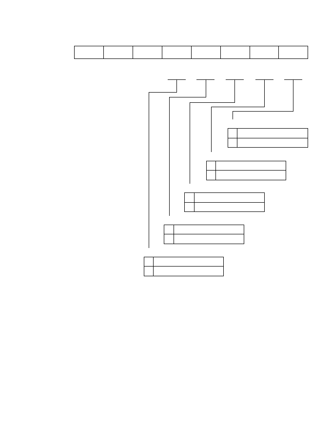
TSTR--Timer Start Register
H'60
ITU (all channels)
Bit
Initial value
Read/Write
7
--
1
--
6
--
1
--
5
--
1
--
4
STR4
0
R/W
3
STR3
0
R/W
0
STR0
0
R/W
2
STR2
0
R/W
1
STR1
0
R/W
Counter start 0
0
TCNT0 is halted
1
TCNT0 is counting
Counter start 3
0
TCNT3 is halted
1
TCNT3 is counting
Counter start 1
0
TCNT1 is halted
1
TCNT1 is counting
Counter start 2
0
TCNT2 is halted
1
TCNT2 is counting
Counter start 4
0
TCNT4 is halted
1
TCNT4 is counting
610
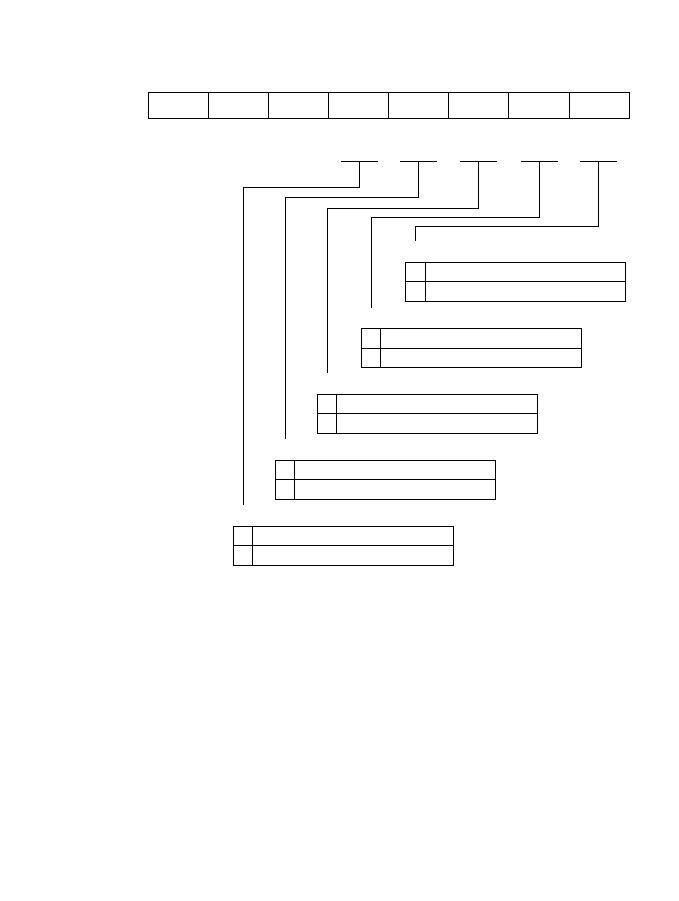
TSNC--Timer Synchro Register
H'61
ITU (all channels)
Bit
Initial value
Read/Write
7
--
1
--
6
--
1
--
5
--
1
--
4
SYNC4
0
R/W
3
SYNC3
0
R/W
0
SYNC0
0
R/W
2
SYNC2
0
R/W
1
SYNC1
0
R/W
Timer sync 0
0
TCNT0 operates independently
1
TCNT0 is synchronized
Timer sync 3
0
TCNT3 operates independently
1
TCNT3 is synchronized
Timer sync 1
0
TCNT1 operates independently
1
TCNT1 is synchronized
Timer sync 2
0
TCNT2 operates independently
1
TCNT2 is synchronized
Timer sync 4
0
TCNT4 operates independently
1
TCNT4 is synchronized
611
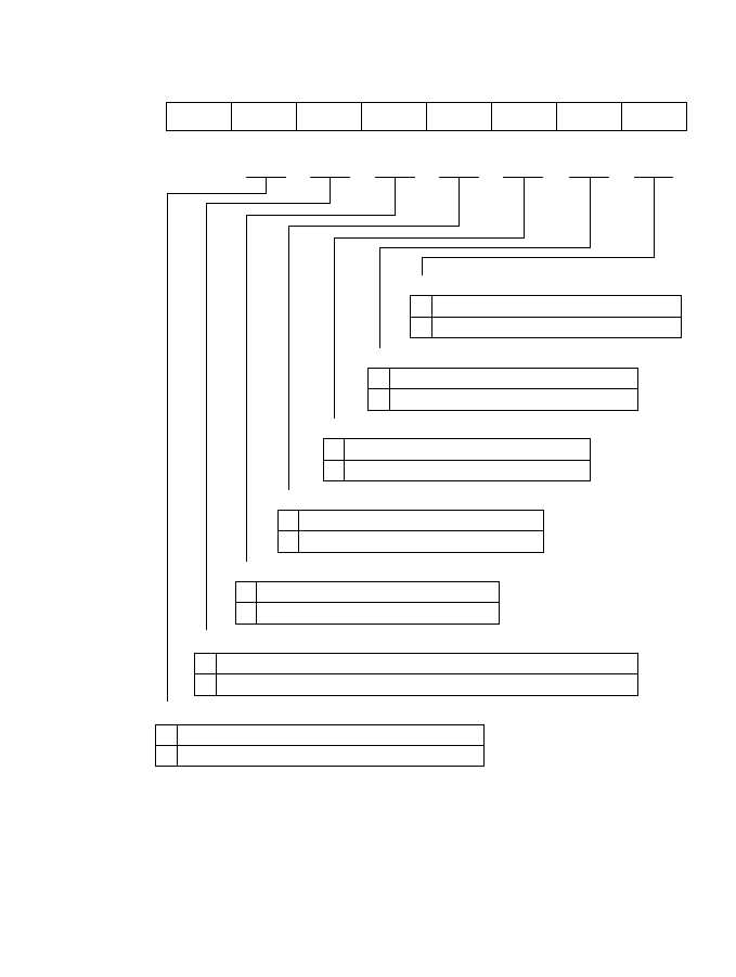
TMDR--Timer Mode Register
H'62
ITU (all channels)
Bit
Initial value
Read/Write
7
--
1
--
6
MDF
0
R/W
5
FDIR
0
R/W
4
PWM4
0
R/W
3
PWM3
0
R/W
0
PWM0
0
R/W
2
PWM2
0
R/W
1
PWM1
0
R/W
PWM mode 0
0
Channel 0 operates normally
1
Channel 0 operates in PWM mode
PWM mode 3
0
Channel 3 operates normally
1
Channel 3 operates in PWM mode
PWM mode 1
0
Channel 1 operates normally
1
Channel 1 operates in PWM mode
PWM mode 2
0
Channel 2 operates normally
1
Channel 2 operates in PWM mode
PWM mode 4
0
Channel 4 operates normally
1
Channel 4 operates in PWM mode
Flag direction
0
OVF is set to 1 in TSR2 when TCNT2 overflows or underflows
1
OVF is set to 1 in TSR2 when TCNT2 overflows
Phase counting mode flag
0
Channel 2 operates normally
1
Channel 2 operates in phase counting mode
612
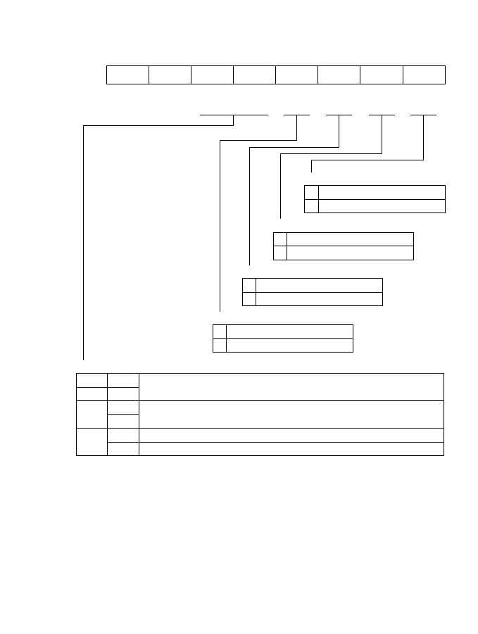
TFCR--Timer Function Control Register
H'63
ITU (all channels)
Bit
Initial value
Read/Write
7
--
1
--
6
--
1
--
5
CMD1
0
R/W
4
CMD0
0
R/W
3
BFB4
0
R/W
0
BFA3
0
R/W
2
BFA4
0
R/W
1
BFB3
0
R/W
Buffer mode A3
0
GRA3 operates normally
1
GRA3 is buffered by BRA3
Buffer mode B4
0
GRB4 operates normally
1
GRB4 is buffered by BRB4
Buffer mode B3
0
GRB3 operates normally
1
GRB3 is buffered by BRB3
Buffer mode A4
0
GRA4 operates normally
1
GRA4 is buffered by BRA4
Combination mode 1 and 0
Channels 3 and 4 operate normally
Channels 3 and 4 operate together in complementary PWM mode
Channels 3 and 4 operate together in reset-synchronized PWM mode
Bit 5
0
1
Bit 4
0
1
0
1
Operating Mode of Channels 3 and 4
CMD1 CMD0
613
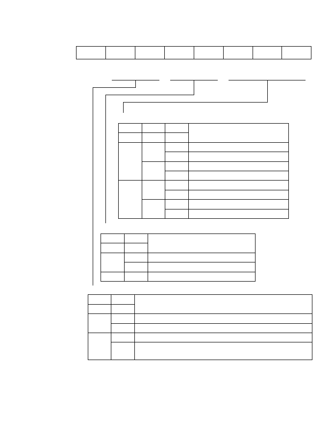
TCR0--Timer Control Register 0
H'64
ITU0
Bit
Initial value
Read/Write
7
--
1
--
6
CCLR1
0
R/W
5
CCLR0
0
R/W
4
CKEG1
0
R/W
3
CKEG0
0
R/W
0
TPSC0
0
R/W
2
TPSC2
0
R/W
1
TPSC1
0
R/W
Timer prescaler 2 to 0
Clock edge 1 and 0
Counter clear 1 and 0
TCNT is not cleared
TCNT is cleared by GRB compare match or input capture
Synchronous clear:
Bit 6
0
1
Bit 5
0
0
1
TCNT Clear Source
CCLR1 CCLR0
TCNT is cleared by GRA compare match or input capture
1
Rising edges counted
Both edges counted
Bit 4
0
1
Bit 3
0
--
Counted Edges of External Clock
CKEG1 CKEG0
Falling edges counted
1
TPSC2
1
TCNT Clock Source
Internal clock: ¯
Internal clock: ¯/2
Internal clock: ¯/4
Internal clock: ¯/8
External clock A: TCLKA input
External clock B: TCLKB input
External clock C: TCLKC input
Bit 2
TPSC1
0
1
0
1
Bit 1
TPSC0
0
1
0
1
0
1
Bit 0
0
External clock D: TCLKD input
1
0
TCNT is cleared in synchronization
with other synchronized timers
614
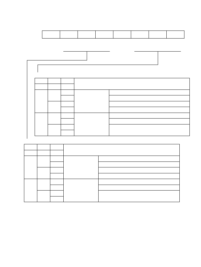
TIOR0--Timer I/O Control Register 0
H'65
ITU0
Bit
Initial value
Read/Write
7
--
1
--
6
IOB2
0
R/W
5
IOB1
0
R/W
4
IOB0
0
R/W
3
--
1
--
0
IOA0
0
R/W
2
IOA2
0
R/W
1
IOA1
0
R/W
I/O control A2 to A0
IOA2
1
GRA Function
GRA is an output
compare register
GRA is an input
capture register
IOA1
0
1
0
1
Bit 1
IOA0
0
1
0
1
0
1
Bit 0
0
1
0
Bit 2
No output at compare match
0 output at GRA compare match
*
1
1 output at GRA compare match
*
1
Output toggles at GRA compare match
*
1,
*
2
GRA captures rising edge of input
GRA captures falling edge of input
GRA captures both edges of input
I/O control B2 to B0
IOB2
1
GRB Function
GRB is an output
compare register
GRB is an input
capture register
IOB1
0
1
0
1
Bit 5
IOB0
0
1
0
1
0
1
Bit 4
0
1
0
Bit 6
No output at compare match
Notes: 1. After a reset, the output is 0 until the first compare match.
2. Channel 2 output cannot be toggled by compare match.
This setting selects 1output instead.
0 output at GRB compare match
*
1
1 output at GRB compare match
*
1
Output toggles at GRB compare match
*
1,
*
2
GRB captures rising edge of input
GRB captures falling edge of input
GRB captures both edges of input
615
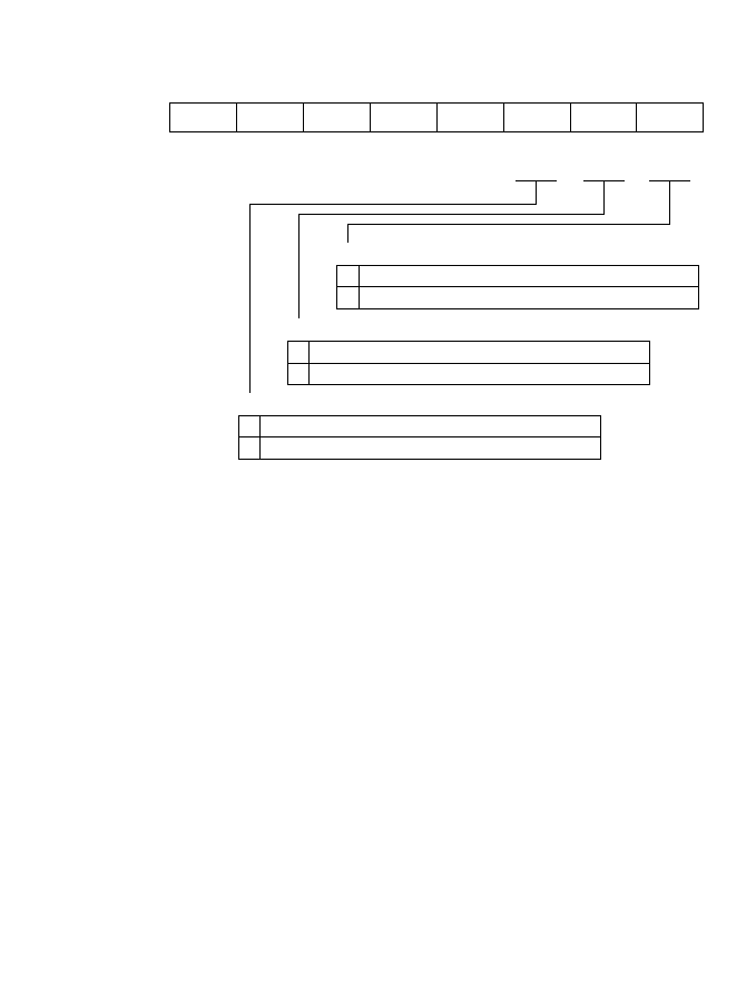
TIER0--Timer Interrpt Enable Register 0
H'66
ITU0
Bit
Initial value
Read/Write
7
--
1
--
6
--
1
--
5
--
1
--
4
--
1
--
3
--
1
--
0
IMIEA
0
R/W
2
OVIE
0
R/W
1
IMIEB
0
R/W
Input capture/compare match interrupt enable A
0
IMIA interrupt requested by IMFA flag is disabled
1
IMIA interrupt requested by IMFA flag is enabled
Input capture/compare match interrupt enable B
0
IMIB interrupt requested by IMFB flag is disabled
1
IMIB interrupt requested by IMFB flag is enabled
Overflow interrupt enable
0
OVI interrupt requested by OVF flag is disabled
1
OVI interrupt requested by OVF flag is enabled
616

TSR0--Timer Status Register 0
H'67
ITU0
Bit
Initial value
Read/Write
7
--
1
--
6
--
1
--
5
--
1
--
4
--
1
--
3
--
1
--
0
IMFA
0
R/(W)
2
OVF
0
R/(W)
1
IMFB
0
R/(W)
Input capture/compare match flag A
0
[Clearing condition]
Overflow flag
*
*
*
Read IMFA when IMFA = 1, then write 0 in IMFA
DMAC activated by IMIA interrupt (channels 0 to 3 only).
1
[Setting conditions]
TCNT = GRA when GRA functions as an output compare
register.
TCNT value is transferred to GRA by an input capture
signal, when GRA functions as an input capture register.
Input capture/compare match flag B
0
[Clearing condition]
Read IMFB when IMFB = 1, then write 0 in IMFB
1
[Setting conditions]
TCNT = GRB when GRB functions as an output compare
register.
TCNT value is transferred to GRB by an input capture
signal, when GRB functions as an input capture register.
0
[Clearing condition]
Read OVF when OVF = 1, then write 0 in OVF
1
[Setting condition]
TCNT overflowed from H'FFFF to H'0000
Note: Only 0 can be written, to clear the flag.
*
617

CNT0--Timer Counter 0 H/L
H'68, H'69
ITU0
GRA0 H/L--General Register A0 H/L
H'6A, H'6B
ITU0
GRB0 H/L--General Register B0 H/L
H'6C, H'6D
ITU0
TCR1--Timer Control Register 1
H'6E
ITU1
Bit
Initial value
Read/Write
14
0
R/W
12
0
R/W
10
0
R/W
8
0
R/W
6
0
R/W
0
0
R/W
4
0
R/W
2
0
R/W
Up-counter
15
0
R/W
13
0
R/W
11
0
R/W
9
0
R/W
7
0
R/W
1
0
R/W
5
0
R/W
3
0
R/W
Bit
Initial value
Read/Write
14
1
R/W
12
1
R/W
10
1
R/W
8
1
R/W
6
1
R/W
0
1
R/W
4
1
R/W
2
1
R/W
Output compare or input capture register
15
1
R/W
13
1
R/W
11
1
R/W
9
1
R/W
7
1
R/W
1
1
R/W
5
1
R/W
3
1
R/W
Bit
Initial value
Read/Write
14
1
R/W
12
1
R/W
10
1
R/W
8
1
R/W
6
1
R/W
0
1
R/W
4
1
R/W
2
1
R/W
Output compare or input capture register
15
1
R/W
13
1
R/W
11
1
R/W
9
1
R/W
7
1
R/W
1
1
R/W
5
1
R/W
3
1
R/W
Bit
Initial value
Read/Write
7
--
1
--
6
CCLR1
0
R/W
5
CCLR0
0
R/W
4
CKEG1
0
R/W
3
CKEG0
0
R/W
0
TPSC0
0
R/W
2
TPSC2
0
R/W
1
TPSC1
0
R/W
Note: Bit functions are the same as for ITU0.
618

TCR1--Timer Control Register 1
H'6E
ITU1
TIERI--Timer Interrupt Enable Register 1
H'70
ITU1
TSR1--Timer Status Register 1
H'71
ITU1
TCNT1 H/L--Timer Counter 1 H/L
H'72,H'73
ITU1
Bit
Initial value
Read/Write
7
--
1
--
6
IOB2
0
R/W
5
IOB1
0
R/W
4
IOB0
0
R/W
3
--
1
--
0
IOA0
0
R/W
2
IOA2
0
R/W
1
IOA1
0
R/W
Note: Bit functions are the same as for ITU0.
Bit
Initial value
Read/Write
7
--
1
--
6
--
1
--
5
--
1
--
4
--
1
--
3
--
1
--
0
IMIEA
0
R/W
2
OVIE
0
R/W
1
IMIEB
0
R/W
Note: Bit functions are the same as for ITU0.
Bit
Initial value
Read/Write
7
--
1
--
6
--
1
--
5
--
1
--
4
--
1
--
3
--
1
--
0
IMFA
0
R/(W)
2
OVF
0
R/(W)
1
IMFB
0
R/(W)
Notes:
*
*
*
*
Bit functions are the same as for ITU0.
Only 0 can be written, to clear the flag.
Bit
Initial value
Read/Write
14
0
R/W
12
0
R/W
10
0
R/W
8
0
R/W
6
0
R/W
0
0
R/W
4
0
R/W
2
0
R/W
15
0
R/W
13
0
R/W
11
0
R/W
9
0
R/W
7
0
R/W
1
0
R/W
5
0
R/W
3
0
R/W
Note: Bit functions are the same as for ITU0.
619

GRA1 H/L--General Register A 1 H/L
H'74,H'75
ITU1
GRB1 H/L--General Register B 1 H/L
H'76,H'77
ITU1
TCR2--Timer Control Register 2
H'78
ITU2
Bit
Initial value
Read/Write
14
1
R/W
12
1
R/W
10
1
R/W
8
1
R/W
6
1
R/W
0
1
R/W
4
1
R/W
2
1
R/W
15
1
R/W
13
1
R/W
11
1
R/W
9
1
R/W
7
1
R/W
1
1
R/W
5
1
R/W
3
1
R/W
Note: Bit functions are the same as for ITU0.
Bit
Initial value
Read/Write
14
1
R/W
12
1
R/W
10
1
R/W
8
1
R/W
6
1
R/W
0
1
R/W
4
1
R/W
2
1
R/W
15
1
R/W
13
1
R/W
11
1
R/W
9
1
R/W
7
1
R/W
1
1
R/W
5
1
R/W
3
1
R/W
Note: Bit functions are the same as for ITU0.
Bit
Initial value
Read/Write
7
--
1
--
6
CCLR1
0
R/W
5
CCLR0
0
R/W
4
CKEG1
0
R/W
3
CKEG0
0
R/W
0
TPSC0
0
R/W
2
TPSC2
0
R/W
1
TPSC1
0
R/W
Notes:
Bit functions are the same as for ITU0.
When channel 2 is used in phase counting mode, the counter clock source selection by
bits CKEG1 and CKEG0 and TPSC2 to TPSC0 is ignored.
1.
2.
620

TIOR2--Timer I/O Control Register 2
H'79F
ITU2
Bit
Initial value
Read/Write
7
--
1
--
6
IOB2
0
R/W
5
IOB1
0
R/W
4
IOB0
0
R/W
3
--
1
--
0
IOA0
0
R/W
2
IOA2
0
R/W
1
IOA1
0
R/W
Note: Bit functions are the same as for ITU0.
621

TIER2 H/L--Timer Interrupt Enable Register 2
H'7A
ITU2
TSR2--Timer Status Register 2
H'7B
ITU2
TCNT2 H/L--Timer Counter 2 H/L
H'7C, H'7D
ITU2
Bit
Initial value
Read/Write
7
--
1
--
6
--
1
--
5
--
1
--
4
--
1
--
3
--
1
--
0
IMIEA
0
R/W
2
OVIE
0
R/W
1
IMIEB
0
R/W
Note: Bit functions are the same as for ITU0.
Bit
Initial value
Read/Write
7
--
1
--
6
--
1
--
5
--
1
--
4
--
1
--
3
--
1
--
0
IMFA
0
R/(W)
2
OVF
0
R/(W)
1
IMFB
0
R/(W)
Overflow flag
0
[Clearing condition]
*
*
*
Read OVF when OVF = 1, then write 0 in OVF
1
[Setting condition]
TCNT overflowed from H'FFFF to H'0000 or underflowed from
H'0000 to H'FFFF
Bit functions are the
same as for ITU0.
Note: Only 0 can be written, to clear the flag.
*
Bit
Initial value
Read/Write
14
0
R/W
12
0
R/W
10
0
R/W
8
0
R/W
6
0
R/W
0
0
R/W
4
0
R/W
2
0
R/W
Phase counting mode:
Other modes:
15
0
R/W
13
0
R/W
11
0
R/W
9
0
R/W
7
0
R/W
1
0
R/W
5
0
R/W
3
0
R/W
up/down counter
up-counter
622

GRA2 H/L--General Register A2 H/L
H'7E, H'7F
ITU2
GRB2 H/L--General Register B2 H/L
H'80, H'81
ITU2
TCR3--Timer Control Register 3
H'82
ITU3
TIOR3--Timer I/O Control Register 3
H'83
ITU3
Bit
Initial value
Read/Write
14
1
R/W
12
1
R/W
10
1
R/W
8
1
R/W
6
1
R/W
0
1
R/W
4
1
R/W
2
1
R/W
15
1
R/W
13
1
R/W
11
1
R/W
9
1
R/W
7
1
R/W
1
1
R/W
5
1
R/W
3
1
R/W
Note: Bit functions are the same as for ITU0.
Bit
Initial value
Read/Write
14
1
R/W
12
1
R/W
10
1
R/W
8
1
R/W
6
1
R/W
0
1
R/W
4
1
R/W
2
1
R/W
15
1
R/W
13
1
R/W
11
1
R/W
9
1
R/W
7
1
R/W
1
1
R/W
5
1
R/W
3
1
R/W
Note: Bit functions are the same as for ITU0.
Bit
Initial value
Read/Write
7
--
1
--
6
CCLR1
0
R/W
5
CCLR0
0
R/W
4
CKEG1
0
R/W
3
CLEG0
0
R/W
0
TPSC0
0
R/W
2
TPSC2
0
R/W
1
TPSC1
0
R/W
Note: Bit functions are the same as for ITU0.
Bit
Initial value
Read/Write
7
--
1
--
6
IOB2
0
R/W
5
IOB1
0
R/W
4
IOB0
0
R/W
3
--
1
--
0
IOA0
0
R/W
2
IOA2
0
R/W
1
IOA1
0
R/W
Note: Bit functions are the same as for ITU0.
623
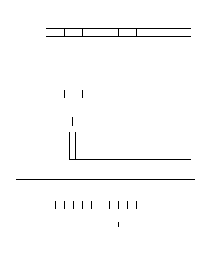
TIER2--Timer Interrupt Enable Register 3
H'84
ITU3
TSR3--Timer Status Register 3
H'85
ITU3
TCNT3 H/L--Timer Counter 3 H/L
H'86, H'87
ITU3
Bit
Initial value
Read/Write
7
--
1
--
6
--
1
--
5
--
1
--
4
--
1
--
3
--
1
--
0
IMIEA
0
R/W
2
OVIE
0
R/W
1
IMIEB
0
R/W
Note: Bit functions are the same as for ITU0.
Bit
Initial value
Read/Write
7
--
1
--
6
--
1
--
5
--
1
--
4
--
1
--
3
--
1
--
0
IMFA
0
R/(W)
2
OVF
0
R/(W)
1
IMFB
0
R/(W)
*
*
*
Overflow flag
0
[Clearing condition]
Read OVF when OVF = 1, then write 0 in OVF
1
[Setting condition]
TCNT overflowed from H'FFFF to H'0000 or underflowed from
H'0000 to H'FFFF
Bit functions are the
same as for ITU0
Note: Only 0 can be written, to clear the flag.
*
Bit
Initial value
Read/Write
14
0
R/W
12
0
R/W
10
0
R/W
8
0
R/W
6
0
R/W
0
0
R/W
4
0
R/W
2
0
R/W
Complementary PWM mode:
Other modes:
15
0
R/W
13
0
R/W
11
0
R/W
9
0
R/W
7
0
R/W
1
0
R/W
5
0
R/W
3
0
R/W
up/down counter
up-counter
624

GRA3 H/L--General Register A3 H/L
H'88,H'89
ITU3
GRB3 H/L--General Register B3 H/L
H'8A,H'8B
ITU3
BRA3 H/L--Buffer Register A3 H/L
H'8C, H'8D
ITU3
BRB3 H/L--Buffer Register B3 H/L
H'8E, H'8F
ITU3
Bit
Initial value
Read/Write
14
1
R/W
12
1
R/W
10
1
R/W
8
1
R/W
6
1
R/W
0
1
R/W
4
1
R/W
2
1
R/W
Output compare or input capture register (can be buffered)
15
1
R/W
13
1
R/W
11
1
R/W
9
1
R/W
7
1
R/W
1
1
R/W
5
1
R/W
3
1
R/W
Bit
Initial value
Read/Write
14
1
R/W
12
1
R/W
10
1
R/W
8
1
R/W
6
1
R/W
0
1
R/W
4
1
R/W
2
1
R/W
Output compare or input capture register (can be buffered)
15
1
R/W
13
1
R/W
11
1
R/W
9
1
R/W
7
1
R/W
1
1
R/W
5
1
R/W
3
1
R/W
Bit
Initial value
Read/Write
14
1
R/W
12
1
R/W
10
1
R/W
8
1
R/W
6
1
R/W
0
1
R/W
4
1
R/W
2
1
R/W
Used to buffer GRA
15
1
R/W
13
1
R/W
11
1
R/W
9
1
R/W
7
1
R/W
1
1
R/W
5
1
R/W
3
1
R/W
Bit
Initial value
Read/Write
14
1
R/W
12
1
R/W
10
1
R/W
8
1
R/W
6
1
R/W
0
1
R/W
4
1
R/W
2
1
R/W
Used to buffer GRB
15
1
R/W
13
1
R/W
11
1
R/W
9
1
R/W
7
1
R/W
1
1
R/W
5
1
R/W
3
1
R/W
625
TOER--Timer Output Enable Register
H'90
ITU (all channels)
Bit
Initial value
Read/Write
7
--
1
--
6
--
1
--
5
EXB4
1
R/W
4
EXA4
1
R/W
3
EB3
1
R/W
0
EA3
1
R/W
2
EB4
1
R/W
1
EA4
1
R/W
Master enable TIOCA3
0
TIOCA output is disabled regardless of TIOR3, TMDR, and TFCR settings
1
TIOCA is enabled for output according to TIOR3, TMDR, and TFCR settings
Master enable TIOCB3
0
TIOCB output is disabled regardless of TIOR3 and TFCR settings
1
TIOCB is enabled for output according to TIOR3 and TFCR settings
Master enable TIOCA4
0
TIOCA output is disabled regardless of TIOR4, TMDR, and TFCR settings
1
TIOCA is enabled for output according to TIOR4, TMDR, and TFCR settings
Master enable TIOCB4
0
TIOCB output is disabled regardless of TIOR4 and TFCR settings
1
TIOCB is enabled for output according to TIOR4 and TFCR settings
Master enable TOCXA4
0
TOCXA output is disabled regardless of TFCR settings
1
TOCXA is enabled for output according to TFCR settings
Master enable TOCXB4
0
TOCXB output is disabled regardless of TFCR settings
1
TOCXB is enabled for output according to TFCR settings
4
4
4
4
3
3
4
4
4
4
3
3
626
TOCR--Timer Output Control Register
H'91
ITU (all channels)
Bit
Initial value
Read/Write
7
--
1
--
6
--
1
--
5
--
1
--
4
1
R/W
3
--
1
--
0
OLS3
1
R/W
2
--
1
--
1
OLS4
1
R/W
Output level select 3
0
TIOCB , TOCXA , and TOCXB outputs are inverted
1
TIOCB , TOCXA , and TOCXB outputs are not inverted
Output level select 4
0
TIOCA , TIOCA , and TIOCB outputs are inverted
1
TIOCA , TIOCA , and TIOCB outputs are not inverted
External trigger disable
0
Input capture A in channel 1 is used as an external trigger signal in
reset-synchronized PWM mode and complementary PWM mode
1
External triggering is disabled
XTGD
Note:
*
When an external trigger occurs, bits 5 to 0 in TOER are cleared to 0, disabling ITU
output.
3
3
3
3
4
4
4
4
4
4
4
4
*
627

TCR4--Timer Control Register 4
H'92
ITU4
TIOR4--Timer I/O Control Register 4
H'93
ITU4
TIER4--Timer Interrupt Enable Register 4
H'94
ITU4
TSR4--Timer Status Register 4
H'95
ITU4
Bit
Initial value
Read/Write
7
--
1
--
6
CCLR1
0
R/W
5
CCLR0
0
R/W
4
CKEG1
0
R/W
3
CKEG0
0
R/W
0
TPSC0
0
R/W
2
TPSC2
0
R/W
1
TPSC1
0
R/W
Note: Bit functions are the same as for ITU0.
Bit
Initial value
Read/Write
7
--
1
--
6
IOB2
0
R/W
5
IOB1
0
R/W
4
IOB0
0
R/W
3
--
1
--
0
IOA0
0
R/W
2
IOA2
0
R/W
1
IOA1
0
R/W
Note: Bit functions are the same as for ITU0.
Bit
Initial value
Read/Write
7
--
1
--
6
--
1
--
5
--
1
--
4
--
1
--
3
--
1
--
0
IMIEA
0
R/W
2
OVIE
0
R/W
1
IMIEB
0
R/W
Note: Bit functions are the same as for ITU0.
Bit
Initial value
Read/Write
7
--
1
--
6
--
1
--
5
--
1
--
4
--
1
--
3
--
1
--
0
IMFA
0
R/(W)
2
OVF
0
R/(W)
1
IMFB
0
R/(W)
*
*
*
Notes:
*
Bit functions are the same as for ITU3.
Only 0 can be written, to clear the flag.
628

TCNT4 H/L--Timer Counter 4 H/L
H'96, H'97
ITU4
GRA4 H/L--General Register A4 H/L
H'98, H'99
ITU4
GRB4 H/L--General Register B4 H/L
H'9A, H'9B
ITU4
BRA4 H/L--Buffer Register A4 H/L
H'9C, H'9D
ITU4
Bit
Initial value
Read/Write
14
0
R/W
12
0
R/W
10
0
R/W
8
0
R/W
6
0
R/W
0
0
R/W
4
0
R/W
2
0
R/W
15
0
R/W
13
0
R/W
11
0
R/W
9
0
R/W
7
0
R/W
1
0
R/W
5
0
R/W
3
0
R/W
Note: Bit functions are the same as for ITU3.
Bit
Initial value
Read/Write
14
1
R/W
12
1
R/W
10
1
R/W
8
1
R/W
6
1
R/W
0
1
R/W
4
1
R/W
2
1
R/W
15
1
R/W
13
1
R/W
11
1
R/W
9
1
R/W
7
1
R/W
1
1
R/W
5
1
R/W
3
1
R/W
Note: Bit functions are the same as for ITU3.
Bit
Initial value
Read/Write
14
1
R/W
12
1
R/W
10
1
R/W
8
1
R/W
6
1
R/W
0
1
R/W
4
1
R/W
2
1
R/W
15
1
R/W
13
1
R/W
11
1
R/W
9
1
R/W
7
1
R/W
1
1
R/W
5
1
R/W
3
1
R/W
Note: Bit functions are the same as for ITU3.
Bit
Initial value
Read/Write
14
1
R/W
12
1
R/W
10
1
R/W
8
1
R/W
6
1
R/W
0
1
R/W
4
1
R/W
2
1
R/W
15
1
R/W
13
1
R/W
11
1
R/W
9
1
R/W
7
1
R/W
1
1
R/W
5
1
R/W
3
1
R/W
Note: Bit functions are the same as for ITU3.
629
BRB4 H/L--Buffer Register B4 H/L
H'9E, H'9F
ITU4
TPMR--TPC Output Mode Register
H'A0
TPC
Bit
Initial value
Read/Write
14
1
R/W
12
1
R/W
10
1
R/W
8
1
R/W
6
1
R/W
0
1
R/W
4
1
R/W
2
1
R/W
15
1
R/W
13
1
R/W
11
1
R/W
9
1
R/W
7
1
R/W
1
1
R/W
5
1
R/W
3
1
R/W
Note: Bit functions are the same as for ITU3.
Bit
Initial value
Read/Write
7
--
1
--
6
--
1
--
5
--
1
--
4
--
1
--
3
G3NOV
0
R/W
0
G0NOV
0
R/W
2
G2NOV
0
R/W
1
G1NOV
0
R/W
Group 3 non-overlap
0
Normal TPC output in group 3.
Output values change at compare match A in the selected ITU channel.
1
Non-overlapping TPC output in group 3, controlled by compare match
A and B in the selected ITU channel
Group 2 non-overlap
0
Normal TPC output in group 2.
Output values change at compare match A in the selected ITU channel.
1
Non-overlapping TPC output in group 2, controlled by compare match
A and B in the selected ITU channel
Group 1 non-overlap
0
Normal TPC output in group 1.
Output values change at compare match A in the selected ITU channel.
1
Non-overlapping TPC output in group 1, controlled by compare match
A and B in the selected ITU channel
Group 0 non-overlap
0
Normal TPC output in group 0.
Output values change at compare match A in the selected ITU channel.
1
Non-overlapping TPC output in group 0, controlled by compare match
A and B in the selected ITU channel
630
TPCR--TPC Output Control Register
H'A1
TPC
Bit
Initial value
Read/Write
7
G3CMS1
1
R/W
6
G3CMS0
1
R/W
5
G2CMS1
1
R/W
4
G2CMS0
1
R/W
3
G1CMS1
1
R/W
0
G0CMS0
1
R/W
2
G1CMS0
1
R/W
1
G0CMS1
1
R/W
Group 3 compare match select 1 and 0
TPC output group 3 (TP to TP ) is triggered by compare match in ITU channel 0
TPC output group 3 (TP to TP ) is triggered by compare match in ITU channel 2
TPC output group 3 (TP to TP ) is triggered by compare match in ITU channel 3
Bit 7
0
1
Bit 6
0
0
1
ITU Channel Selected as Output Trigger
G3CMS1 G3CMS0
TPC output group 3 (TP to TP ) is triggered by compare match in ITU channel 1
1
15
15
15
15
12
12
12
12
Group 2 compare match select 1 and 0
TPC output group 2 (TP to TP ) is triggered by compare match in ITU channel 0
TPC output group 2 (TP to TP ) is triggered by compare match in ITU channel 2
TPC output group 2 (TP to TP ) is triggered by compare match in ITU channel 3
Bit 5
0
1
Bit 4
0
0
1
ITU Channel Selected as Output Trigger
G2CMS1 G2CMS0
TPC output group 2 (TP to TP ) is triggered by compare match in ITU channel 1
1
11
11
11
11
8
8
8
8
Group 1 compare match select 1 and 0
TPC output group 1 (TP to TP ) is triggered by compare match in ITU channel 0
TPC output group 1 (TP to TP ) is triggered by compare match in ITU channel 2
TPC output group 1 (TP to TP ) is triggered by compare match in ITU channel 3
Bit 3
0
1
Bit 2
0
0
1
ITU Channel Selected as Output Trigger
G1CMS1 G1CMS0
TPC output group 1 (TP to TP ) is triggered by compare match in ITU channel 1
1
7
7
7
7
4
4
4
4
Group 0 compare match select 1 and 0
TPC output group 0 (TP to TP ) is triggered by compare match in ITU channel 0
TPC output group 0 (TP to TP ) is triggered by compare match in ITU channel 2
TPC output group 0 (TP to TP ) is triggered by compare match in ITU channel 3
Bit 1
0
1
Bit 0
0
0
1
ITU Channel Selected as Output Trigger
G0CMS1 G0CMS0
TPC output group 0 (TP to TP ) is triggered by compare match in ITU channel 1
1
3
3
3
3
0
0
0
0
631

NDERB--Next Data Enable Register B
H'A2
TPC
NDERA--Next Data Enable Register A
H'A3
TPC
Bit
Initial value
Read/Write
7
NDER15
0
R/W
6
NDER14
0
R/W
5
NDER13
0
R/W
4
NDER12
0
R/W
3
NDER11
0
R/W
0
NDER8
0
R/W
2
NDER10
0
R/W
1
NDER9
0
R/W
Next data enable 15 to 8
TPC outputs TP to TP are disabled
(NDR15 to NDR8 are not transferred to PB to PB )
TPC outputs TP to TP are enabled
(NDR15 to NDR8 are transferred to PB to PB )
Bits 7 to 0
0
1
Description
NDER15 to NDER8
15
15
8
8
7
7
0
0
Bit
Initial value
Read/Write
7
NDER7
0
R/W
6
NDER6
0
R/W
5
NDER5
0
R/W
4
NDER4
0
R/W
3
NDER3
0
R/W
0
NDER0
0
R/W
2
NDER2
0
R/W
1
NDER1
0
R/W
Next data enable 7 to 0
TPC outputs TP to TP are disabled
(NDR7 to NDR0 are not transferred to PA to PA )
TPC outputs TP to TP are enabled
(NDR7 to NDR0 are transferred to PA to PA )
Bits 7 to 0
0
1
Description
NDER7 to NDER0
7
7
0
0
7
7
0
0
632

NDRB--Next Data Register B
H'A4/H'A6
TPC
∑
Same output trigger for TPC output groups 2 and 3
Address H'FFA4
Address H'FFA6
∑
Different output triggers for TPC output groups 2 and 3
Address H'FFA4
Address H'FFA6
Bit
Initial value
Read/Write
7
NDR15
0
R/W
6
NDR14
0
R/W
5
NDR13
0
R/W
4
NDR12
0
R/W
3
NDR11
0
R/W
0
NDR8
0
R/W
2
NDR10
0
R/W
1
NDR9
0
R/W
Store the next output data for
TPC output group 3
Store the next output data for
TPC output group 2
Bit
Initial value
Read/Write
7
--
1
--
6
--
1
--
5
--
1
--
4
--
1
--
3
--
1
--
0
--
1
--
2
--
1
--
1
--
1
--
Bit
Initial value
Read/Write
7
NDR15
0
R/W
6
NDR14
0
R/W
5
NDR13
0
R/W
4
NDR12
0
R/W
3
--
1
--
0
--
1
--
2
--
1
--
1
--
1
--
Store the next output data for
TPC output group 3
Bit
Initial value
Read/Write
7
--
1
--
6
--
1
--
5
--
1
--
4
--
1
--
3
NDR11
0
R/W
0
NDR8
0
R/W
2
NDR10
0
R/W
1
NDR9
0
R/W
Store the next output data for
TPC output group 2
633

NDRA--Next Data Register A
H'A5/H'A7
TPC
∑
Same output trigger for TPC output groups 0 and 1
Address H'FFA5
Address H'FFA7
∑
Different output triggers for TPC output groups 0 and 1
Address H'FFA5
Address H'FFA7
Bit
Initial value
Read/Write
7
NDR7
0
R/W
6
NDR6
0
R/W
5
NDR5
0
R/W
4
NDR4
0
R/W
3
NDR3
0
R/W
0
NDR0
0
R/W
2
NDR2
0
R/W
1
NDR1
0
R/W
Store the next output data for
TPC output group 1
Store the next output data for
TPC output group 0
Bit
Initial value
Read/Write
7
--
1
--
6
--
1
--
5
--
1
--
4
--
1
--
3
--
1
--
0
--
1
--
2
--
1
--
1
--
1
--
Bit
Initial value
Read/Write
7
NDR7
0
R/W
6
NDR6
0
R/W
5
NDR5
0
R/W
4
NDR4
0
R/W
3
--
1
--
0
--
1
--
2
--
1
--
1
--
1
--
Store the next output data for
TPC output group 1
Bit
Initial value
Read/Write
7
--
1
--
6
--
1
--
5
--
1
--
4
--
1
--
3
NDR3
0
R/W
0
NDR0
0
R/W
2
NDR2
0
R/W
1
NDR1
0
R/W
Store the next output data for
TPC output group 0
634

TCSR--Timer Control/Status Register
H'A8
WDT
Bit
Initial value
Read/Write
7
OVF
0
R/(W)
6
WT/
0
R/W
5
TME
0
R/W
4
--
1
--
3
--
1
--
0
CKS0
0
R/W
2
CKS2
0
R/W
1
CKS1
0
R/W
Overflow flag
Timer mode select
IT
0
[Clearing condition]
Read OVF when OVF = 1, then write 0 in OVF
1
[Setting condition]
TCNT changes from H'FF to H'00
0
Interval timer: requests interval timer interrupts
1
Watchdog timer: generates a reset signal
Clock select 2 to 0
0
1
¯/2
¯/32
¯/64
¯/128
¯/256
¯/512
¯/2048
0
1
0
1
0
1
0
1
0
1
0
¯/4096
1
Timer enable
0
Timer disabled
∑
1
Timer enabled
TCNT is initialized to H'00 and halted
∑ TCNT is counting
Note: Only 0 can be written, to clear the flag.
*
*
635

TCNT--Timer Counter
H'A9 (read),
WDT
H'A8 (write)
RSTCSR--Reset Control/Status Register
H'AB (read),
WDT
H'AA (write)
Bit
Initial value
Read/Write
7
0
R/W
6
0
R/W
5
0
R/W
4
0
R/W
3
0
R/W
0
0
R/W
2
0
R/W
1
0
R/W
Count value
Bit
Initial value
Read/Write
7
WRST
0
R/(W)
6
RSTOE
0
R/W
5
--
1
--
4
--
1
--
3
--
1
--
0
--
1
--
2
--
1
--
1
--
1
--
Reset output enable
0
Reset signal is not output externally
1
Reset signal is output externally
Watchdog timer reset
0
[Clearing condition]
Reset signal input at pin.
Reading WRST when WRST=1, then writing 0 in WRST.
1
[Setting condition]
TCNT overflow generates a reset signal
Note: Only 0 can be written in bit 7, to clear the flag.
*
*
RES
636

RFSHCR--Refresh Control Register
H'AC
Refresh controller
Bit
Initial value
Read/Write
7
SRFMD
0
R/W
6
PSRAME
0
R/W
5
DRAME
0
R/W
4
CAS/
0
R/W
3
M9/
0
R/W
0
RCYCE
0
R/W
2
RFSHE
0
R/W
1
--
1
--
Self-refresh mode
0
DRAM or PSRAM self-refresh is disabled in software standby mode
1
DRAM or PSRAM self-refresh is enabled in software standby mode
Refresh cycle enable
Refresh pin enable
PSRAM enable, DRAM enable
0
Refresh cycles are disabled
1
Refresh cycles are enabled for area 3
Address multiplex mode select
0
8-bit column address mode
1
9-bit column address mode
WE
M8
Strobe mode select
0
1
0
2 mode
1
2 mode
Can be used as an interval timer
(DRAM and PSRAM cannot be directly connected)
PSRAM can be directly connected
Illegal setting
Bit 6
0
1
Bit 5
0
0
1
RAM Interface
PSRAME DRAME
DRAM can be directly connected
1
Refresh signal output at the pin is disabled
Refresh signal output at the pin is enabled
RFSH
RFSH
WE
CAS
637
RTMCSR--Refresh Timer Control/Status Register
H'AD
Refresh controller
Bit
Initial value
Read/Write
7
CMF
0
R/(W)
6
CMIE
0
R/W
5
CKS2
0
R/W
4
CKS1
0
R/W
3
CKS0
0
R/W
0
--
1
--
2
--
1
--
1
--
1
--
Compare match flag
Compare match interrupt enable
0
[Clearing condition]
Read CMF when CMF = 1, then write 0 in CMF
1
[Setting condition]
RTCNT = RTCOR
Note: Only 0 can be written, to clear the flag.
*
0
The CMI interrupt requested by CMF is disabled
1
The CMI interrupt requested by CMF is enabled
Clock select 2 to 0
CKS2
Counter Clock Source
CKS1
Bit 4
CKS0
Bit 3
Bit 5
0
1
Clock input is disabled
¯/2
¯/8
¯/32
¯/128
¯/512
¯/2048
0
1
0
1
0
1
0
1
0
1
0
¯/4096
1
*
638
RTCNT--Refresh Timer Counter
H'AE
Refresh controller
RTCOR--Refresh Time Constant Register
H'AF
Refresh controller
Bit
Initial value
Read/Write
7
0
R/W
6
0
R/W
5
0
R/W
4
0
R/W
3
0
R/W
0
0
R/W
2
0
R/W
1
0
R/W
Count value
Bit
Initial value
Read/Write
7
1
R/W
6
1
R/W
5
1
R/W
4
1
R/W
3
1
R/W
0
1
R/W
2
1
R/W
1
1
R/W
Interval at which RTCNT is cleared
639

SMR--Serial Mode Register
H'B0
SCI0
Bit
Initial value
Read/Write
7
C/
0
R/W
6
CHR
0
R/W
5
PE
0
R/W
3
STOP
0
R/W
0
CKS0
0
R/W
2
MP
0
R/W
1
CKS1
0
R/W
Parity enable
Clock select 1 and 0
CKS1
Clock Source
CKS0
Bit 0
Bit 1
0
1
¯ clock
¯/4 clock
¯/16 clock
¯/64 clock
0
0
1
1
A
7
O/
0
R/W
E
0
Parity bit is not added or checked
1
Parity bit is added and checked
Parity mode
0
Even parity
1
Odd parity
Stop bit length
Multiprocessor mode
0
Multiprocessor function disabled
1
Multiprocessor format selected
0
One stop bit
1
Two stop bits
Character length
0
8-bit data
1
7-bit data
Communication mode
0
Asynchronous mode
1
Synchronous mode
640

BRR--Bit Rate Register
H'B1
SCI0
Bit
Initial value
Read/Write
7
1
R/W
6
1
R/W
5
1
R/W
4
1
R/W
3
1
R/W
0
1
R/W
2
1
R/W
1
1
R/W
Serial communication bit rate setting
641
SCR--Serial Control Register
H'B2
SCI0
Bit
Initial value
Read/Write
7
TIE
0
R/W
6
RIE
0
R/W
5
TE
0
R/W
4
RE
0
R/W
3
MPIE
0
R/W
0
CKE0
0
R/W
2
TEIE
0
R/W
1
CKE1
0
R/W
Transmit interrupt enable
0
Transmit-data-empty interrupt request (TXI) is disabled
1
Transmit-data-empty interrupt request (TXI) is enabled
Receive interrupt enable
0
Receive-end (RXI) and receive-error (ERI) interrupt requests are disabled
1
Receive-end (RXI) and receive-error (ERI) interrupt requests are enabled
Transmit enable
Clock enable 1 and 0
CKE1
Multiprocessor interrupt enable
0
1
Clock Selection and Output
Asynchronous mode
Synchronous mode
Asynchronous mode
Synchronous mode
Asynchronous mode
Synchronous mode
Asynchronous mode
Bit 1
CKE0
0
1
0
1
Bit 0
Receive enable
Synchronous mode
0
Multiprocessor interrupts are disabled (normal receive operation)
1
Multiprocessor interrupts are enabled
0
Transmitting is disabled
1
Transmitting is enabled
Transmit-end interrupt enable
0
Transmitting is disabled
1
Transmitting is enabled
0
Transmit-end interrupt requests (TEI) are disabled
1
Transmit-end interrupt requests (TEI) are enabled
Internal clock, SCK pin available for generic
input/output
Internal clock, SCK pin used for serial clock output
Internal clock, SCK pin used for clock output
Internal clock, SCK pin used for serial clock output
External clock, SCK pin used for clock input
External clock, SCK pin used for serial clock input
External clock, SCK pin used for clock input
External clock, SCK pin used for serial clock input
642

TDR--Transmit Data Register
H'B3
SCI0
Bit
Initial value
Read/Write
7
1
R/W
6
1
R/W
5
1
R/W
4
1
R/W
3
1
R/W
0
1
R/W
2
1
R/W
1
1
R/W
Serial transmit data
643

SSR--Serial Status Register
H'B4
SCI0
Bit
Initial value
Read/Write
7
TDRE
1
R/(W)
6
RDRF
0
R/(W)
5
ORER
0
R/(W)
4
FER
0
R/(W)
3
PER
0
R/(W)
0
MPBT
0
R/W
2
TEND
1
R
1
MPB
0
R
Transmit end
0
[Clearing conditions]
1
[Setting conditions]
Reset or transition to standby mode.
TE is cleared to 0 in SCR. TDRE is 1 when
last bit of 1-byte serial character is transmitted.
*
*
*
*
*
Multiprocessor bit transfer
Read TDRE when TDRE = 1, then write 0 in TDRE.
The DMAC writes data in TDR.
Multiprocessor bit
Parity error
0
[Clearing conditions]
1
[Setting condition]
Parity error: (parity of receive data does not
match parity setting of O/ bit in SMR)
Reset or transition to standby mode.
Read PER when PER = 1, then write 0 in
PER.
E
Framing error
0
[Clearing conditions]
1
[Setting condition]
Framing error (stop bit is 0)
Reset or transition to standby mode.
Read FER when FER = 1, then write 0
in FER.
Overrun error
0
[Clearing conditions]
1
[Setting condition]
Overrun error (reception of next serial data
ends when RDRF = 1)
Reset or transition to standby mode.
Read ORER when ORER = 1, then write 0 in
ORER.
Receive data register full
0
[Clearing conditions]
1
[Setting condition]
Serial data is received normally and transferred
from RSR to RDR
Reset or transition to standby mode.
Read RDRF when RDRF = 1, then write 0 in
RDRF.
The DMAC reads data from RDR.
Transmit data register empty
0
[Clearing conditions]
1
[Setting conditions]
Reset or transition to standby mode.
TE is 0 in SCR
Data is transferred from TDR to TSR, enabling new
data to be written in TDR.
Read TDRE when TDRE = 1, then write 0 in TDRE.
The DMAC writes data in TDR.
0
Multiprocessor bit value in
receive data is 0
1
Multiprocessor bit value in
receive data is 1
0
Multiprocessor bit value in
transmit data is 0
1
Multiprocessor bit value in
transmit data is 1
Note: Only 0 can be written, to clear the flag.
*
644

RDR--Receive Data Register
H'B5
SCI0
SMR--Serial Mode Register
H'B8
SCI1
BRR--Bit Rate Register
H'B9
SCI1
SCR--Serial Control Register
H'BA
SCI1
Bit
Initial value
Read/Write
7
0
R
6
0
R
5
0
R
4
0
R
3
0
R
0
0
R
2
0
R
1
0
R
Serial receive data
Bit
Initial value
Read/Write
7
C/
0
R/W
6
CHR
0
R/W
5
PE
0
R/W
4
O/
0
R/W
3
STOP
0
R/W
0
CKS0
0
R/W
2
MP
0
R/W
1
CKS1
0
R/W
Note: Bit functions are the same as for SCI0.
A
E
Bit
Initial value
Read/Write
7
1
R/W
6
1
R/W
5
1
R/W
4
1
R/W
3
1
R/W
0
1
R/W
2
1
R/W
1
1
R/W
Note: Bit functions are the same as for SCI0.
Bit
Initial value
Read/Write
7
TIE
0
R/W
6
RIE
0
R/W
5
TE
0
R/W
4
RE
0
R/W
3
MPIE
0
R/W
0
CKE0
0
R/W
2
TEIE
0
R/W
1
CKE1
0
R/W
Note: Bit functions are the same as for SCI0.
645

TDR--Transmit Data Register
H'BB
SCI1
SSR--Serial Status Register
H'BC
SCI1
RDR--Receive Data Register
H'BD
SCI1
Bit
Initial value
Read/Write
7
1
R/W
6
1
R/W
5
1
R/W
4
1
R/W
3
1
R/W
0
1
R/W
2
1
R/W
1
1
R/W
Note: Bit functions are the same as for SCI0.
Bit
Initial value
Read/Write
7
TDRE
1
R/(W)
6
RDRF
0
R/(W)
5
ORER
0
R/(W)
4
FER
0
R/(W)
3
PER
0
R/(W)
0
MPBT
0
R/W
2
TEND
1
R
1
MPB
0
R
*
*
*
*
*
Notes:
*
Bit functions are the same as for SCI0.
Only 0 can be written, to clear the flag.
Bit
Initial value
Read/Write
7
0
R
6
0
R
5
0
R
4
0
R
3
0
R
0
0
R
2
0
R
1
0
R
Note: Bit functions are the same as for SCI0.
646
P4DDR--Port 4 Data Direction Register
H'C5
Port 4
P4DR--Port 4 Data Register
H'C7
Port 4
P6DDR--Port 6 Data Direction Register
H'C9
Port 6
Bit
Initial value
Read/Write
7
P4 DDR
0
W
7
6
P4 DDR
0
W
6
5
P4 DDR
0
W
5
4
P4 DDR
0
W
4
3
P4 DDR
0
W
3
2
P4 DDR
0
W
2
1
P4 DDR
0
W
1
0
P4 DDR
0
W
0
Port 4 input/output select
0
Generic input pin
1
Generic output pin
Bit
Initial value
Read/Write
7
P4
0
R/W
7
6
P4
0
R/W
6
5
P4
0
R/W
5
4
P4
0
R/W
4
3
P4
0
R/W
3
2
P4
0
R/W
2
1
P4
0
R/W
1
0
P4
0
R/W
0
Data for port 4 pins
Bit
Initial value
Read/Write
7
--
1
--
6
P6 DDR
0
W
6
5
P6 DDR
0
W
5
4
P6 DDR
0
W
4
3
P6 DDR
0
W
3
2
P6 DDR
0
W
2
1
P6 DDR
0
W
1
0
P6 DDR
0
W
0
Port 6 input/output select
0
Generic input
1
Generic output
647
P6DR--Port 6 Data Register
H'CB
Port 6
P8DDR--Port 8 Data Direction Register
H'CD
Port 8
P7DR--Port 7 Data Register
H'CE
Port 7
Bit
Initial value
Read/Write
7
--
1
--
6
P6
0
R/W
6
5
P6
0
R/W
5
4
P6
0
R/W
4
3
P6
0
R/W
3
2
P6
0
R/W
2
1
P6
0
R/W
1
0
P6
0
R/W
0
Data for port 6 pins
Bit
Initial value
Read/Write
7
--
1
--
6
--
1
--
5
--
1
--
4
P8 DDR
1
W
4
3
P8 DDR
0
W
3
2
P8 DDR
0
W
2
1
P8 DDR
0
W
1
0
P8 DDR
0
W
0
Port 8 input/output select
Port 8 input/output select
0
Generic input
1
Generic output
0
Generic input
1
output
CS
Bit
Initial value
Read/Write
0
P7
--
R
*
Note: Determined by pins P7 to P7 .
*
0
1
P7
--
R
*
1
2
P7
--
R
*
2
3
P7
--
R
*
3
4
P7
--
R
*
4
5
P7
--
R
*
5
6
P7
--
R
*
6
7
P7
--
R
*
7
Data for port 7 pins
7
0
648

P8DR--Port 8 Data Register
H'CF
Port 8
P9DDR--Port 9 Data Direction Register
H'D0
Port 9
PADDR--Port A Data Direction Register
H'D1
Port A
Bit
Initial value
Read/Write
7
--
1
--
6
--
1
--
5
--
1
--
4
P8
0
R/W
4
3
P8
0
R/W
3
2
P8
0
R/W
2
1
P8
0
R/W
1
0
P8
0
R/W
0
Data for port 8 pins
Bit
Initial value
Read/Write
7
--
1
--
6
--
1
--
5
P9 DDR
0
W
5
4
P9 DDR
0
W
4
3
P9 DDR
0
W
3
2
P9 DDR
0
W
2
1
P9 DDR
0
W
1
0
P9 DDR
0
W
0
Port 9 input/output select
0
Generic input
1
Generic output
Bit
7
PA DDR
0
W
1
--
7
6
PA DDR
0
W
0
W
6
5
PA DDR
0
W
0
W
5
4
PA DDR
0
W
0
W
4
3
PA DDR
0
W
0
W
3
2
PA DDR
0
W
0
W
2
1
PA DDR
0
W
0
W
1
0
PA DDR
0
W
0
W
0
Port A input/output select
0
Generic input
1
Generic output
Initial value
Read/Write
Initial value
Read/Write
Modes
1, 2
Modes
3, 4
649

P9DR--Port 9 Data Register
H'D2
Port 9
PADR--Port A Data Register
H'D3
Port A
PBDDR--Port B Data Direction Register
H'D4
Port B
Bit
Initial value
Read/Write
7
--
1
--
6
--
1
--
5
P9
0
R/W
4
P9
0
R/W
4
3
P9
0
R/W
3
2
P9
0
R/W
2
1
P9
0
R/W
1
0
P9
0
R/W
0
Data for port 9 pins
5
Bit
Initial value
Read/Write
0
PA
0
R/W
0
1
PA
0
R/W
1
2
PA
0
R/W
2
3
PA
0
R/W
3
4
PA
0
R/W
4
5
PA
0
R/W
5
6
PA
0
R/W
6
7
PA
0
R/W
7
Data for port A pins
Bit
Initial value
Read/Write
7
PB DDR
0
W
7
6
PB DDR
0
W
6
5
PB DDR
0
W
5
4
PB DDR
0
W
4
3
PB DDR
0
W
3
2
PB DDR
0
W
2
1
PB DDR
0
W
1
0
PB DDR
0
W
0
Port B input/output select
0
Generic input
1
Generic output
650
PBDR--Port B Data Register
H'D6
Port B
P4PCR--Port 4 Input Pull-Up Control Register
H'DA
Port 4
ADDRA H/L--A/D Data Register A H/L
H'E0, H'E1
A/D
Bit
Initial value
Read/Write
0
PB
0
R/W
0
1
PB
0
R/W
1
2
PB
0
R/W
2
3
PB
0
R/W
3
4
PB
0
R/W
4
5
PB
0
R/W
5
6
PB
0
R/W
6
7
PB
0
R/W
7
Data for port B pins
Bit
Initial value
Read/Write
7
P4 PCR
0
R/W
7
6
P4 PCR
0
R/W
6
5
P4 PCR
0
R/W
5
4
P4 PCR
0
R/W
4
3
P4 PCR
0
R/W
3
2
P4 PCR
0
R/W
2
1
P4 PCR
0
R/W
1
0
P4 PCR
0
R/W
0
Port 4 input pull-up control 7 to 0
0
Input pull-up transistor is off
1
Input pull-up transistor is on
Note: Valid when the corresponding P4DDR bit is cleared to 0 (designating generic input).
Bit
Initial value
Read/Write
14
AD8
0
R
12
AD6
0
R
10
AD4
0
R
8
AD2
0
R
6
AD0
0
R
0
--
0
R
4
--
0
R
2
--
0
R
15
AD9
0
R
13
AD7
0
R
11
AD5
0
R
9
AD3
0
R
7
AD1
0
R
1
--
0
R
5
--
0
R
3
--
0
R
A/D conversion data
10-bit data giving an
A/D conversion result
ADDRAH
ADDRAL
651
ADDRB H/L--A/D Data Register B H/L
H'E2, H'E3
A/D
ADDRC H/L--A/D Data Register C H/L
H'E4, H'E5
A/D
ADDRD H/L--A/D Data Register D H/L
H'E6, H'E7
A/D
Bit
Initial value
Read/Write
14
AD8
0
R
12
AD6
0
R
10
AD4
0
R
8
AD2
0
R
6
AD0
0
R
0
--
0
R
4
--
0
R
2
--
0
R
15
AD9
0
R
13
AD7
0
R
11
AD5
0
R
9
AD3
0
R
7
AD1
0
R
1
--
0
R
5
--
0
R
3
--
0
R
ADDRBH
ADDRBL
A/D conversion data
10-bit data giving an
A/D conversion result
Bit
Initial value
Read/Write
14
AD8
0
R
12
AD6
0
R
10
AD4
0
R
8
AD2
0
R
6
AD0
0
R
0
--
0
R
4
--
0
R
2
--
0
R
15
AD9
0
R
13
AD7
0
R
11
AD5
0
R
9
AD3
0
R
7
AD1
0
R
1
--
0
R
5
--
0
R
3
--
0
R
ADDRCH
ADDRCL
A/D conversion data
10-bit data giving an
A/D conversion result
Bit
Initial value
Read/Write
14
AD8
0
R
12
AD6
0
R
10
AD4
0
R
8
AD2
0
R
6
AD0
0
R
0
--
0
R
4
--
0
R
2
--
0
R
15
AD9
0
R
13
AD7
0
R
11
AD5
0
R
9
AD3
0
R
7
AD1
0
R
1
--
0
R
5
--
0
R
3
--
0
R
ADDRDH
ADDRDL
A/D conversion data
10-bit data giving an
A/D conversion result
652

ADCR--A/D Control Register
H'E9
A/D
Bit
Initial value
Read/Write
7
TRGE
0
R/W
6
--
1
--
5
--
1
--
4
--
1
--
3
--
1
--
0
--
1
--
2
--
1
--
1
--
1
--
Trigger enable
0
A/D conversion cannot be externally triggered
1
A/D conversion starts at the fall of the external trigger signal ( )
ADTRG
653
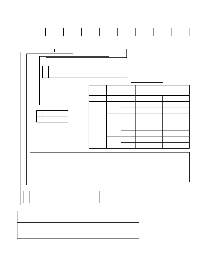
ADCSR--A/D Control/Status Register
H'E8
A/D
Bit
Initial value
Read/Write
7
ADF
0
R/(W)
6
ADIE
0
R/W
5
ADST
0
R/W
4
SCAN
0
R/W
3
CKS
0
R/W
0
CH0
0
R/W
2
CH2
0
R/W
1
CH1
0
R/W
*
Note: Only 0 can be written, to clear flag.
*
Channel select 2 to 0
CH2
1
Single Mode
AN
AN
AN
AN
AN
AN
AN
CH1
0
1
0
1
Channel
Selection
CH0
0
1
0
1
0
1
0
1
0
0
1
2
3
4
5
6
AN
7
Scan Mode
AN
AN , AN
AN to AN
AN to AN
AN
AN , AN
AN to AN
0
0
0
0
4
4
4
AN to AN
4
1
5
2
3
6
7
Description
Group
Selection
A/D end flag
A/D interrupt enable
A/D start
Clock select
Scan mode
0
[Clearing condition]
Read ADF while ADF = 1, then write 0 in ADF
1
[Setting conditions]
Single mode:
Scan mode:
0
A/D end interrupt request is disabled
1
A/D end interrupt request is enabled
0
A/D conversion is stopped
1
Single mode:
Scan mode:
0
Single mode
1
Scan mode
0
Conversion time = 266 states (maximum)
1
Conversion time = 134 states (maximum)
A/D conversion ends
A/D conversion ends in all selected channels
A/D conversion starts; ADST is automatically cleared to 0 when
conversion ends
A/D conversion starts and continues, cycling among the selected
channels, until ADST is cleared to 0 by software, by a reset, or by a
transition to standby mode
654
ABWCR--Bus Width Control Register
H'EC
Bus controller
ASTCR--Access State Control Register
H'ED
Bus controller
Bit
Read/Write
7
ABW7
1
0
R/W
6
ABW6
1
0
R/W
5
ABW5
1
0
R/W
4
ABW4
1
0
R/W
3
ABW3
1
0
R/W
0
ABW0
1
0
R/W
2
ABW2
1
0
R/W
1
ABW1
1
0
R/W
Initial
value
Mode 1, 3
Mode 2, 4
Area 7 to 0 bus width control
Areas 7 to 0 are 16-bit access areas
Areas 7 to 0 are 8-bit access areas
Bits 7 to 0
0
1
Bus Width of Access Area
AWB7 to AWB0
Bit
Initial value
Read/Write
7
AST7
1
R/W
6
AST6
1
R/W
5
AST5
1
R/W
4
AST4
1
R/W
3
AST3
1
R/W
0
AST0
1
R/W
2
AST2
1
R/W
1
AST1
1
R/W
Area 7 to 0 access state control
Areas 7 to 0 are two-state access areas
Areas 7 to 0 are three-state access areas
Bits 7 to 0
0
1
Number of States in Access Cycle
AST7 to AST0
655

WCR--Wait Control Register
H'EE
Bus controller
WCER--Wait Controller Enable Register
H'EF
Bus controller
Bit
Initial value
Read/Write
7
--
1
--
6
--
1
--
5
--
1
--
4
--
1
--
3
WMS1
0
R/W
0
WC0
1
R/W
2
WMS0
0
R/W
1
WC1
1
R/W
Wait count 1 and 0
WC1
Number of Wait States
WC0
Bit 0
Bit 1
0
1
No wait states inserted by
wait-state controller
1 state inserted
2 states inserted
3 states inserted
0
0
1
1
Wait mode select 1 and 0
WMS1
Wait Mode
WMS0
Bit 2
Bit 3
0
1
Programmable wait mode
No wait states inserted by
wait-state controller
Pin wait mode 1
Pin auto-wait mode
0
0
1
1
Bit
Initial value
Read/Write
7
WCE7
1
R/W
6
WCE6
1
R/W
5
WCE5
1
R/W
4
WCE4
1
R/W
3
WCE3
1
R/W
0
WCE0
1
R/W
2
WCE2
1
R/W
1
WCE1
1
R/W
Wait state controller enable 7 to 0
0
Wait-state control is disabled (pin wait mode 0)
1
Wait-state control is enabled
656
MDCR--Mode Control Register
H'F1
System control
Bit
Initial value
Read/Write
7
--
1
--
6
--
1
--
5
--
0
--
4
--
0
--
3
--
0
--
0
MDS0
--
R
*
2
MDS2
--
R
1
MDS1
--
R
*
*
Note: Determined by the state of the mode pins (MD to MD ).
*
Mode select 2 to 0
2
0
MD
2
0
Operating mode
--
Mode 1
Mode 2
Mode 3
Bit 2
MD
1
0
1
Bit 1
MD
0
0
1
0
1
Bit 0
1
Mode 4
--
--
--
0
1
0
1
0
1
657
SYSCR--System Control Register
H'F2
System control
Bit
Initial value
Read/Write
7
SSBY
0
R/W
6
STS2
0
R/W
5
STS1
0
R/W
4
STS0
0
R/W
3
UE
1
R/W
0
RAME
1
R/W
2
NMIEG
0
R/W
1
--
1
--
Software standby
0
SLEEP instruction causes transition to sleep mode
1
SLEEP instruction causes transition to software standby mode
Standby timer select 2 to 0
STS2
0
1
Standby Timer
Waiting time = 8192 states
Waiting time = 16384 states
Waiting time = 32768 states
Waiting time = 65536 states
Waiting time = 131072 states
Illegal setting
Bit 6
STS1
0
1
0
1
Bit 5
STS0
0
1
0
1
--
Bit 4
RAM enable
0
On-chip RAM is disabled
1
On-chip RAM is enabled
NMI edge select
0
An interrupt is requested at the falling edge of NMI
1
An interrupt is requested at the rising edge of NMI
User bit enable
0
CCR bit 6 (UI) is used as an interrupt mask bit
1
CCR bit 6 (UI) is used as a user bit
--
658
BRCR--Bus Release Control Register
H'F3
Bus controller
ISCR--IRQ Sense Control Register
H'F4
Interrupt controller
IER--IRQ Enable Register
H'F5
Interrupt controller
7
A23E
1
--
1
R/W
6
A22E
1
--
1
R/W
5
A21E
1
--
1
R/W
4
--
1
--
1
--
3
--
1
--
1
--
0
BRLE
0
R/W
0
R/W
2
--
1
--
1
--
1
--
1
--
1
--
Bus release enable
0
The bus cannot be released to an external device
1
The bus can be released to an external device
Bit
Initial value
Read/Write
Initial value
Read/Write
Modes
1, 2
Modes
3, 4
Address 23 to 21 enable
0
Address output
1
Other input/output
Bit
Initial value
Read/Write
7
--
0
R/W
6
--
0
R/W
5
IRQ5SC
0
R/W
4
IRQ4SC
0
R/W
3
IRQ3SC
0
R/W
2
IRQ2SC
0
R/W
1
IRQ1SC
0
R/W
0
IRQ0SC
0
R/W
IRQ to IRQ sense control
0
Interrupts are requested when IRQ to IRQ inputs are low
1
Interrupts are requested by falling-edge input at IRQ to IRQ
5
0
5
5
0
0
Bit
Initial value
Read/Write
7
--
0
R/(W)
6
--
0
R/(W)
5
IRQ5E
0
R/(W)
4
IRQ4E
0
R/(W)
3
IRQ3E
0
R/(W)
2
IRQ2E
0
R/(W)
1
IRQ1E
0
R/(W)
0
IRQ0E
0
R/(W)
IRQ to IRQ enable
0
IRQ to IRQ interrupts are disabled
1
IRQ to IRQ interrupts are enabled
5
0
5
5
0
0
659

ISR--IRQ Status Register
H'F6
Interrupt controller
Bit
Initial value
Read/Write
7
--
0
--
6
--
0
--
5
IRQ5F
0
R/(W)
*
4
IRQ4F
0
R/(W)
*
3
IRQ3F
0
R/(W)
*
2
IRQ2F
0
R/(W)
*
1
IRQ1F
0
R/(W)
*
0
IRQ0F
0
R/(W)
*
IRQ to IRQ flags
Bits 5 to 0
0
1
Setting and Clearing Conditions
IRQ5F to IRQ0F
[Clearing conditions]
Read IRQnF when IRQnF = 1, then write 0 in IRQnF.
IRQnSC = 0, input is high, and interrupt exception
handling is carried out.
IRQnSC = 1 and IRQn interrupt exception handling is
carried out.
[Setting conditions]
IRQnSC = 0 and input is low.
IRQnSC = 1 and input changes from high to low.
(n = 5 to 0)
IRQn
IRQn
IRQn
5
0
Note: Only 0 can be written, to clear the flag.
*
660
IPRA--Interrupt Priority Register A
H'F8
Interrupt controller
∑
Interrupt sources controlled by each bit
Bit 7
Bit 6
Bit 5
Bit 4
Bit 3
Bit 2
Bit 1
Bit 0
IPRA7
IPRA6
IPRA5
IPRA4
IPRA3
IPRA2
IPRA1
IPRA0
Interrupt IRQ
0
IRQ
1
IRQ
2
, IRQ
4
,
WDT,
ITU ITU ITU
source
IRQ
3
IRQ
5
Refresh
chan-
chan-
chan-
con-
nel 0
nel 1
nel 2
troller
IPRB--Interrupt Priority Register B
H'F9
Interrupt controller
∑
Interrupt sources controlled by each bit
Bit 7
Bit 6
Bit 5
Bit 4
Bit 3
Bit 2
Bit 1
Bit 0
IPRB7
IPRB6
IPRB5
--
IPRB3
IPRB2
IPRB1
--
Interrupt
ITU ITU DMAC
--
SCI SCI A/D --
source
chan-
chan-
chan-
chan-
con-
nel 3
nel 4
nel 0
nel 1
verter
Bit
Initial value
Read/Write
7
IPRA7
0
R/W
6
IPRA6
0
R/W
5
IPRA5
0
R/W
4
IPRA4
0
R/W
3
IPRA3
0
R/W
0
IPRA0
0
R/W
2
IPRA2
0
R/W
1
IPRA1
0
R/W
Priority level A7 to A0
0
Priority level 0 (low priority)
1
Priority level 1 (high priority)
Bit
Initial value
Read/Write
7
IPRB7
0
R/W
6
IPRB6
0
R/W
5
IPRB5
0
R/W
4
--
0
R/W
3
IPRB3
0
R/W
0
--
0
R/W
2
IPRB2
0
R/W
1
IPRB1
0
R/W
Priority level B7 to B5, B3 to B1
0
Priority level 0 (low priority)
1
Priority level 1 (high priority)
Reserved bits
661
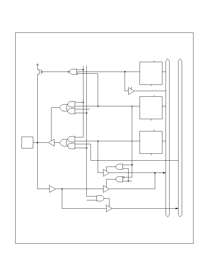
Appendix C I/O Port Block Diagrams
C.1 Port 4 Block Diagram
Figure C-1 Port 4 Block Diagram
P4
n
RP4P
RP4
WP4
WP4D
WP4P
Reset
Reset
Reset
Q
D
R
C
P4 PCR
n
Q
D
R
C
P4 DDR
n
Q
D
R
C
P4 DR
n
WP4P:
RP4P:
WP4D:
WP4:
RP4:
n = 0 to 7
Write to P4PCR
Read P4PCR
Write to P4DDR
Write to port 4
Read port 4
8-bit bus mode
16-bit bus mode
Write to external
address
Read external
address
Internal data bus (upper)
Internal data bus (lower)
662
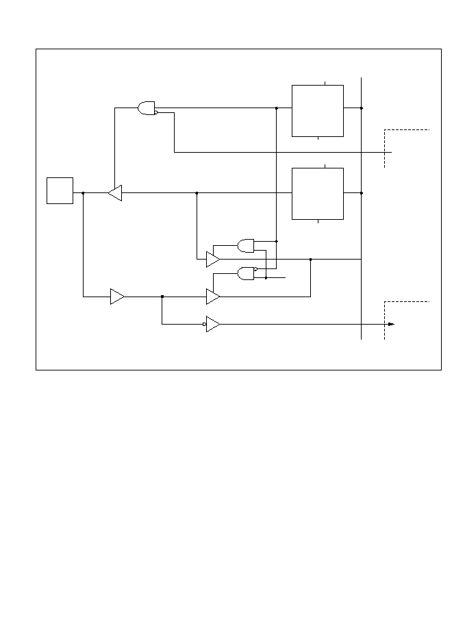
C.2 Port 6 Block Diagrams
Figure C-2 (a) Port 6 Block Diagram (Pin P6
0
)
WP6D:
WP6:
RP6:
Write to P6DDR
Write to port 6
Read port 6
RP6
input
WP6D
Reset
Q
D
R
C
P6 DDR
0
WP6
Reset
Q
D
R
C
P6 DR
0
P6
0
Internal data bus
Bus controller
WAIT
input
enable
Bus controller
WAIT
663
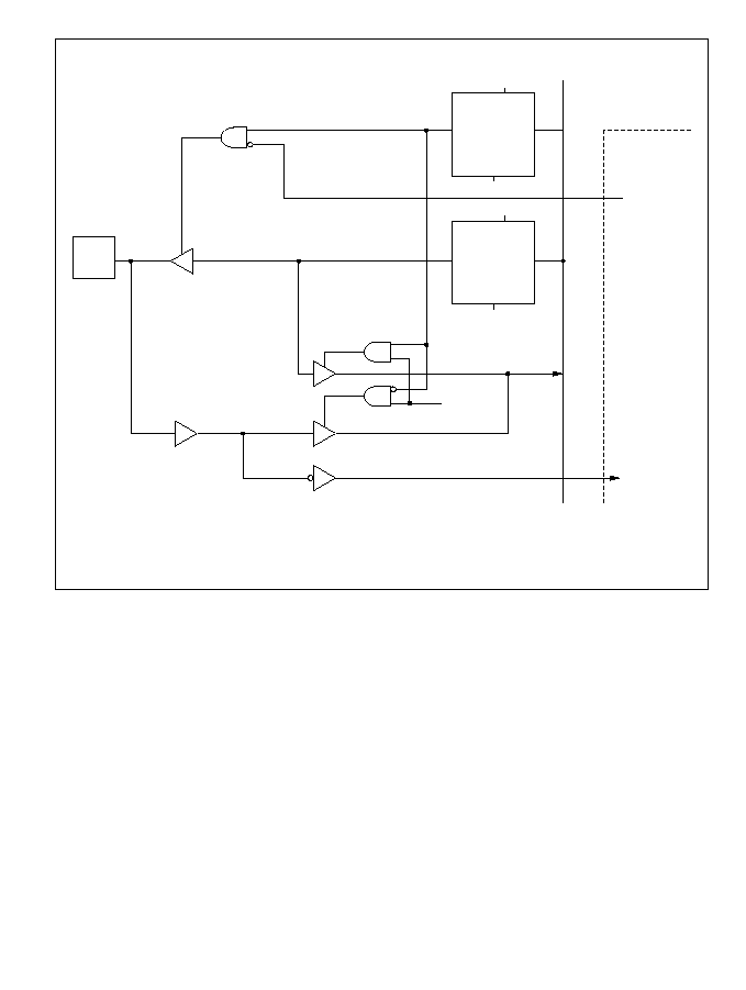
Figure C-2 (b) Port 6 Block Diagram (Pin P6
1
)
P6
1
WP6D:
WP6:
RP6:
Write to P6DDR
Write to port 6
Read port 6
WP6D
Reset
Q
D
R
C
P6 DDR
1
WP6
Reset
Q
D
R
C
P6 DR
1
RP6
Internal data bus
Bus
controller
Bus release
enable
BREQ input
664

Figure C-2 (c) Port 6 Block Diagram (Pin P6
2
)
WP6D
Reset
Q
D
R
C
P6 DDR
2
WP6
Reset
Q
D
R
C
P6 DR
2
RP6
P6
2
WP6D:
WP6:
RP6:
Write to P6DDR
Write to port 6
Read port 6
Internal data bus
Bus controller
Bus release
enable
BACK
output
665
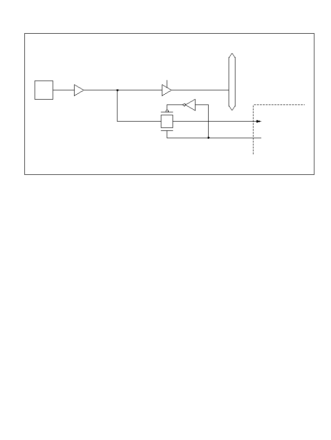
C.3 Port 7 Block Diagram
Figure C-3 Port 7 Block Diagram (Pin P7
n
)
P7
n
RP7
RP7: Read port 7
n = 0 to 7
Internal data bus
A/D converter
Analog input
Input enable
666
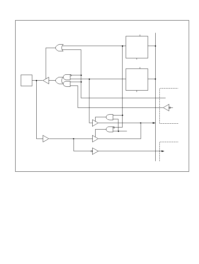
C.4 Port 8 Block Diagrams
Figure C-4 (a) Port 8 Block Diagram (Pin P8
0
)
P8
0
RP8
WP8D
Reset
Q
D
R
C
P8 DDR
0
WP8
Reset
Q
D
R
C
P8 DR
0
WP8D:
WP8:
RP8:
Write to P8DDR
Write to port 8
Read port 8
Internal data bus
Refresh
controller
Output
enable
Interrupt
controller
0
RFSH
output
IRQ
input
667

Figure C-4 (b) Port 8 Block Diagram (Pins P8
1
, P8
2
, P8
3
)
P8
n
WP8D
Reset
Q
D
R
C
P8 DDR
n
WP8
Reset
Q
D
R
C
P8 DR
n
RP8
WP8D
WP8:
RP8:
n = 1 to 3
Write to P8DDR
Write to port 8
Read port 8
Internal data bus
Bus controller
output
Interrupt
controller
IRQ
IRQ
IRQ
CS
CS
CS
1
2
3
1
2
3
input
668
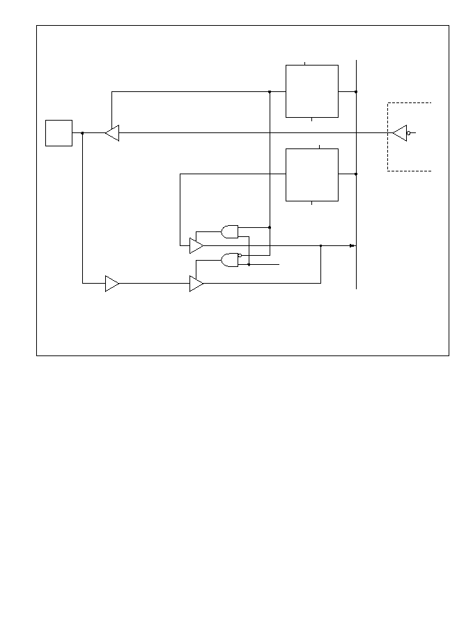
Figure C-4 (c) Port 8 Block Diagram (Pin P8
4
)
P8
4
WP8D
Reset
Q
D
S
C
P8 DDR
4
WP8
Reset
Q
D
R
C
P8 DR
4
RP8
WP8D:
WP8:
RP8:
Write to P8DDR
Write to port 8
Read port 8
Internal data bus
Bus controller
output
0
CS
669
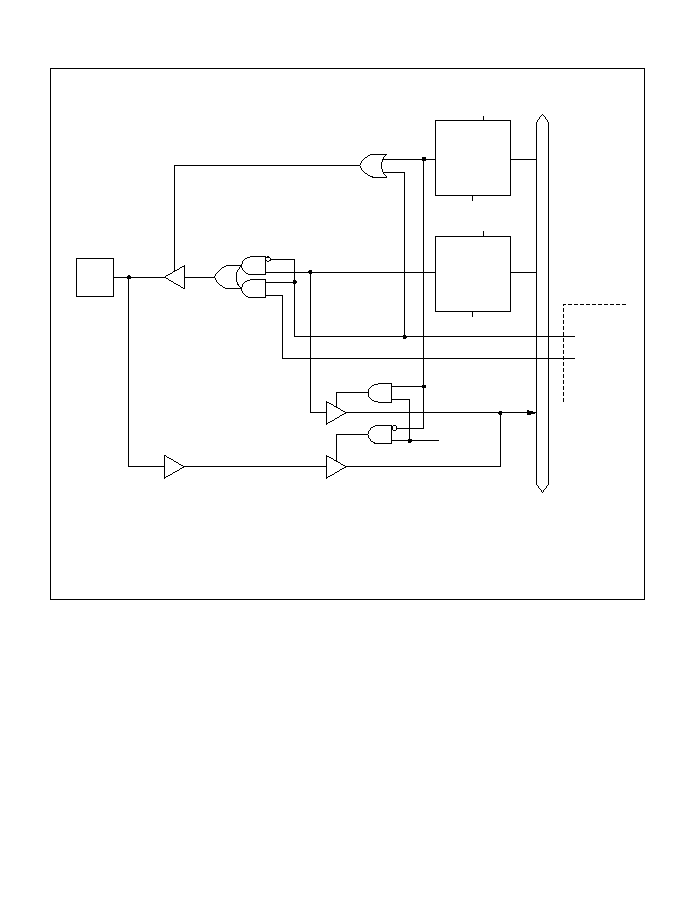
C.5 Port 9 Block Diagrams
Figure C-5 (a) Port 9 Block Diagram (Pins P9
0
, P9
1
)
WP9D:
WP9:
RP9:
n = 0 and 1
Write to P9DDR
Write to port 9
Read port 9
P9
n
RP9
WP9D
Reset
Q
D
R
C
P9 DDR
n
WP9
Reset
Q
D
R
C
P9 DR
n
Internal data bus
SCI
Output
enable
Serial
transmit
data
670

Figure C-5 (b) Port 9 Block Diagram (Pins P9
2
, P9
3
)
WP9D:
WP9:
RP9:
n = 2 and 3
Write to P9DDR
Write to port 9
Read port 9
P9
n
WP9D
Reset
Q
D
R
C
P9 DDR
n
WP9
Reset
Q
D
R
C
P9 DR
n
RP9
Internal data bus
Input enable
Serial receive
data
SCI
671

Figure C-5 (c) Port 9 Block Diagram (Pins P9
4
, P9
5
)
WP9D:
WP9:
RP9:
n = 4 and 5
Write to P9DDR
Write to port 9
Read port 9
WP9D
Reset
Q
D
R
C
P9 DDR
n
WP9
Reset
Q
D
R
C
P9 DR
n
RP9
P9
n
Internal data bus
SCI
Clock input
enable
Clock output
enable
Clock output
Clock input
Interrupt
controller
or
input
IRQ
4
IRQ
5
672
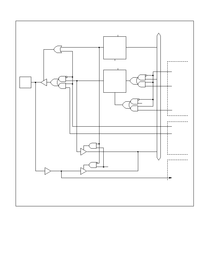
C.6 Port A Block Diagrams
Figure C-6 (a) Port A Block Diagram (Pins PA
0
, PA
1
)
WPAD:
WPA:
RPA:
n = 0 and 1
Write to PADDR
Write to port A
Read port A
PA
n
WPAD
Reset
Q
D
R
C
PA DDR
n
Reset
Q
D
R
C
PA DR
n
RPA
WPA
Internal data bus
TPC
output
enable
TPC
Next data
Output
trigger
Output
enable
Transfer
end output
DMA controller
Counter
clock input
ITU
673
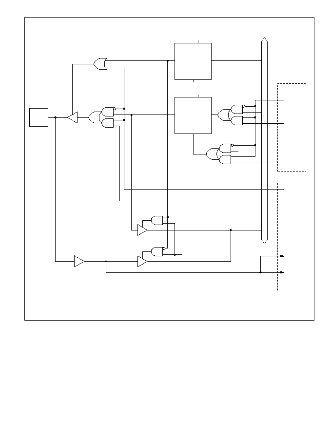
Figure C-6 (b) Port A Block Diagram (Pins PA
2
, PA
3
)
WPAD:
WPA:
RPA:
n = 2 and 3
Write to PADDR
Write to port A
Read port A
PA
n
RPA
WPA
WPAD
Reset
Q
D
R
C
PA DDR
n
Reset
Q
D
R
C
PA DR
n
Internal data bus
TPC
output
enable
TPC
Next
data
Output
trigger
Output
enable
Compare
match
output
Input
capture
Counter
clock
input
ITU
674

Figure C-6 (c) Port A Block Diagram (Pins PA
4
to PA
7
)
WPAD:
WPA:
RPA:
n = 4 to 7
Write to PADDR
Write to port A
Read port A
RPA
WPA
WPAD
Reset
Q
D
R
C
PA DDR
n
Reset
Q
D
R
C
PA DR
n
PA
n
Internal data bus
TPC
output
enable
TPC
Next
data
Output
trigger
Output
enable
Compare
match
output
Input
capture
ITU
Internal address bus
Software standby
External bus released
Address output enable
Mode 3, 4
*
Note: The PA address output enable signal is always 1 in modes 3 and 4.
*
7
675
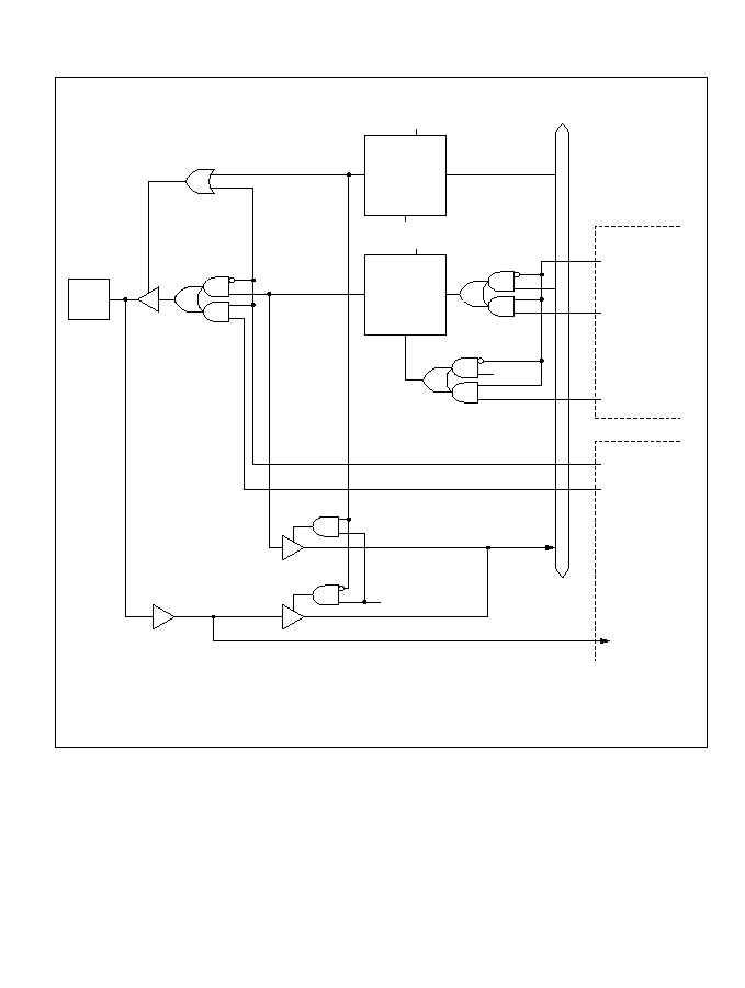
C.7 Port B Block Diagrams
Figure C-7 (a) Port B Block Diagram (Pins PB
0
to PB
3
)
PB
n
WPBD:
WPB:
RPB:
n = 0 to 3
Write to PBDDR
Write to port B
Read port B
Reset
Q
D
R
C
PB DDR
n
WPBD
Reset
Q
D
R
C
PB DR
n
WPB
RPB
Internal data bus
TPC output
enable
TPC
Next data
Output trigger
Output enable
Compare
match output
Input
capture
ITU
676
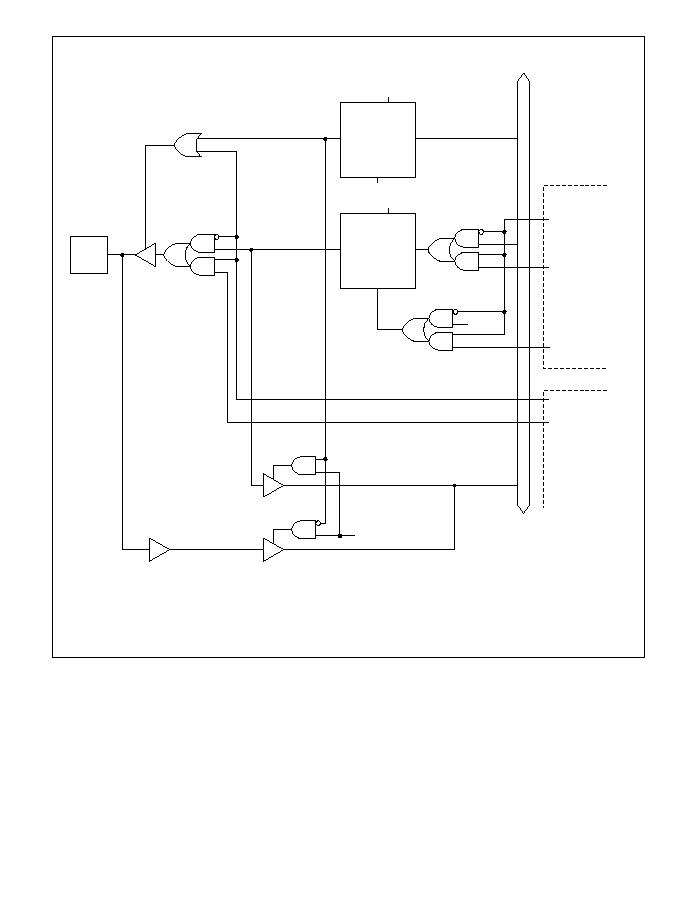
Figure C-7 (b) Port B Block Diagram (Pins PB
4
, PB
5
)
PB
n
WPBD:
WPB:
RPB:
n = 4 and 5
Write to PBDDR
Write to port B
Read port B
WPB
RPB
Reset
Q
D
R
C
PB DDR
n
WPBD
Reset
Q
D
R
C
PB DR
n
Internal data bus
TPC output
enable
Next data
Output trigger
Output enable
Compare
match output
TPC
ITU
677
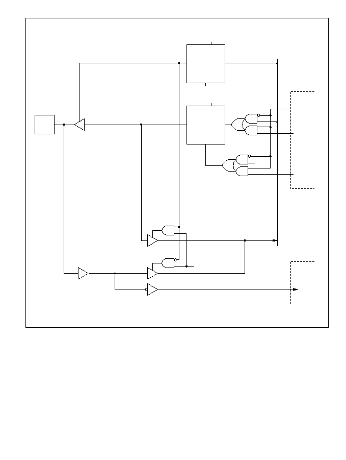
Figure C-7 (c) Port B Block Diagram (Pin PB
6
)
PB
6
WPBD
Reset
Reset
Q
D
R
C
PB DDR
Q
D
R
C
PB DR
6
RPB
WPB
DMAC
DREQ
0
input
TPC
WPBD:
WPB:
RPB:
Write to PBDDR
Write to port B
Read port B
TPC
output
enable
Next data
Output
trigger
Internal data bus
6
678

Figure C-7 (d) Port B Block Diagram (Pin PB
7
)
PB
7
WPBD
Reset
Reset
Q
D
R
C
PB DDR
Q
D
R
C
PB DR
7
RPB
WPB
DMAC
TPC
WPBD:
WPB:
RPB:
Write to PBDDR
Write to port B
Read port B
TPC
output
enable
Next data
Output
trigger
Internal data bus
7
ADTRG
input
A/D converter
DREQ
1
input
679

Appendix D Pin States
D.1 Port States in Each Mode
Table D-1 Port States
Hardware Software
Bus-
Program
Pin Reset
Standby
Standby
Released
Execution
Name
Mode
State Mode
Mode
Mode
Sleep
Mode
¯
--
Clock output T
H
Clock output Clock output
RESO
--
T
*
2
T
T
T
RESO
A
19
to A
0
1 to 4
L
T
T
T
A
19
to A
0
D
15
to D
8
1 to 4
T
T
T
T
D
15
to D
0
AS
,
RD
,
1 to 4
H
T
T
T
AS
,
RD
,
HWR
,
LWR
HWR
,
LWR
P4
7
to P4
0
1 to 4
8-bit bus
T
T
keep
keep
I/O port
D
7
to D
0
16-bit bus
T
T
D
7
to D
0
P6
0
1 to 4
T
T
keep
keep
I/O port
*
1
WAIT
P6
1
1 to 4
T
T
(BRLE = 0) T
I/O port
keep
BREQ
(BRLE = 1)
T
P6
2
1 to 4
T
T
(BRLE = 0)
I/O port
keep
L
(BRLE = 0)
(BRLE = 1)
or
BACK
H
(BRLE = 1)
P7
7
to P7
0
1 to 4
T
T
T
T
Input port
Note:
*
1
Do not set the DDR bit to 1.
*
2
Low output only when WDT overflow causes a reset.
Legend
H:
High
L:
Low
T:
High-impedance state
keep: Input pins are in the high-impedance state; output pins maintain their previous state.
DDR: Data direction register bit
680

Table D-1 Port States (cont)
Hardware Software
Bus-
Program
Pin Reset
Standby
Standby
Released
Execution
Name
Mode
State
Mode
Mode Mode
Sleep
Mode
P8
0
1 to 4
T
T
(RFSHE = 0)
(RFSHE = 0)
I/O port
keep
keep
(RFSHE = 0)
(RFSHE = 1)
(RFSHE = 1)
or
RFSH
RFSH
H
(RFSHE = 1)
P8
3
to P8
1
1 to 4
T
T
(DDR = 0)
keep
Input port
T
(DDR = 0) or
(DDR = 1)
CS
3
to CS
1
H
(DDR = 1)
P8
4
1 to 4
L
T
(DDR = 0)
keep
Input port
T
(DDR = 0)
(DDR = 1)
or CS
0
L
(DDR = 1)
P9
5
to P9
0
1 to 4
T
T
keep
keep
I/O port
PA
3
to PA
0
1 to 4
T
T
keep
keep
I/O port
PA
6
to PA
4
1, 2
T
T
keep
keep
I/O port
3, 4
T
T
I/O port
*
1
I/O port
*
2
A
23
, A
22
, A
21
(A23E/A22E/
A21E = 0)
or I/O port
(A23E/A22E/
A21E = 1)
PA
7
1, 2
T
T
keep
keep
I/O port
3, 4
T
T
I/O port
*
1
I/O port
*
2
A
20
PB
7
to PB
0
1 to 4
T
T
keep
keep
I/O port
Notes: 1. The pin state depends on the DDR bit.
2. The pin state depends on the ITU output enable and DDR bits.
Legend
H:
High
L:
Low
T:
High-impedance state
keep: Input pins are in the high-impedance state; output pins maintain their previous state.
DDR: Data direction register bit
681
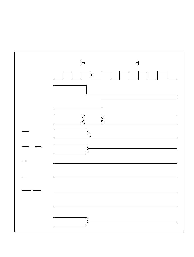
D.2 Pin States at Reset
Reset in T
1
State: Figure D-1 is a timing diagram for the case in which
RES goes low during the
T
1
state of an external memory access cycle. As soon as
RES goes low, all ports are initialized to
the input state.
AS, RD, HWR, and LWR go high, and the data bus goes to the high-impedance
state. The address bus is initialized to the low output level 0.5 state after the low level of
RES is
sampled. Sampling of
RES takes place at the fall of the system clock (¯).
Figure D-1 Reset during Memory Access (Reset during T
1
State)
Access to external address
¯
Address bus
CS
CS to CS
AS
RD (read access)
HWR, LWR
Data bus
I/O port
0
3
1
RES
(write access)
(write access)
H'000000
High impedance
High impedance
High impedance
High
High
High
Internal
reset signal
T
1
T
2
T
3
682
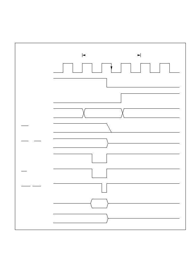
Reset in T
2
State: Figure D-2 is a timing diagram for the case in which
RES goes low during the
T
2
state of an external memory access cycle. As soon as
RES goes low, all ports are initialized to
the input state.
AS, RD, HWR, and LWR go high, and the data bus goes to the high-impedance
state. The address bus is initialized to the low output level 0.5 state after the low level of
RES is
sampled. The same timing applies when a reset occurs during a wait state (T
W
).
Figure D-2 Reset during Memory Access (Reset during T
2
State)
¯
Address bus
CS
CS to CS
RD (read access)
HWR, LWR
Data bus
I/O port
0
3
1
RES
AS
H'000000
High impedance
High impedance
High impedance
Internal
reset signal
Access to external address
T
1
T
2
T
3
(write access)
(write access)
683

Reset in T
3
State: Figure D-3 is a timing diagram for the case in which
RES goes low during the
T
3
state of an external memory access cycle. As soon as
RES goes low, all ports are initialized to
the input state.
AS, RD, HWR, and LWR go high, and the data bus goes to the high-impedance
state. The address bus outputs are held during the T
3
state.The same timing applies when a reset
occurs in the T
2
state of an access cycle to a two-state-access area.
Figure D-3 Reset during Memory Access (Reset during T
3
State)
¯
Address bus
CS
CS to CS
RD (read access)
HWR, LWR
Data bus
I/O port
0
3
1
RES
AS
High impedance
High impedance
High impedance
Internal
reset signal
Access to external address
T
1
T
2
T
3
(write access)
(write access)
H'000000
684

Appendix E Timing of Transition to and Recovery from
Hardware Standby Mode
Timing of Transition to Hardware Standby Mode
(1) To retain RAM contents with the RAME bit set to 1 in SYSCR, drive the
RES signal low 10
system clock cycles before the
STBY signal goes low, as shown below. RES must remain low
until
STBY goes low (minimum delay from STBY low to RES high: 0 ns).
(2) To retain RAM contents with the RAME bit cleared to 0 in SYSCR, or when RAM contents
do not need to be retained,
RES does not have to be driven low as in (1).
Timing of Recovery from Hardware Standby Mode: Drive the
RES signal low approximately
100 ns before
STBY goes high.
t
1
10t
CYC
t
2
0 ns
STBY
RES
STBY
RES
t
100 ns
t
OSC
685
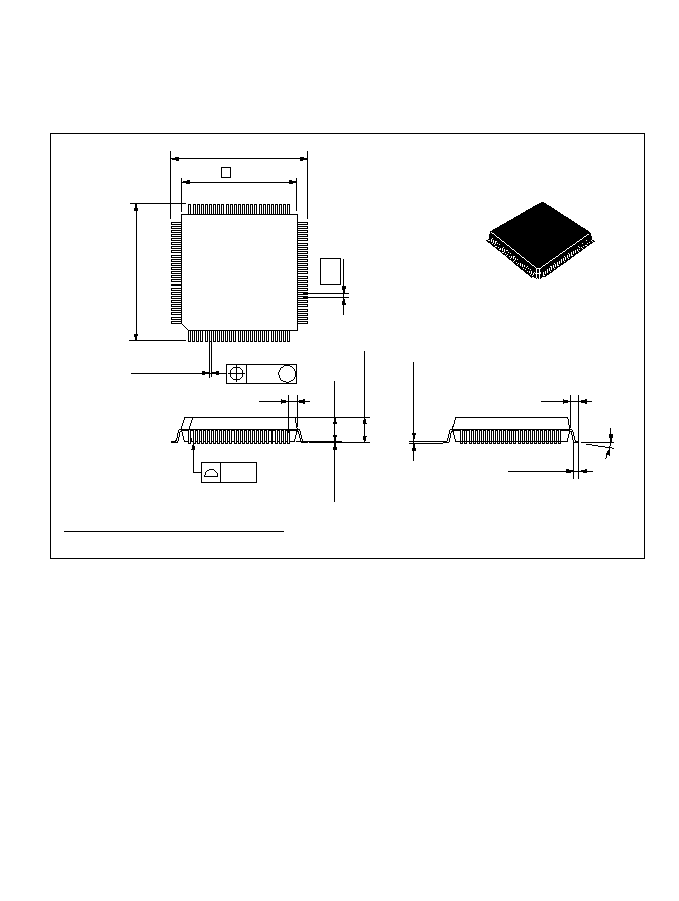
Appendix F Package Dimensions
Figures F-1, F-2 and F-3 show the H8/3002 package dimensions.
Unit: mm
Figure F-1 Package Dimensions (FP-100B)
0.10
16.0
±
0.3
1.0
0.5
±
0.2
16.0
±
0.3
3.05 Max
75
51
50
26
1
25
76
100
14
0
∞
≠ 8
∞
0.5
0.08 M
0.22
±
0.05
2.70
0.17
±
0.05
0.12
+0.13 ≠0.12
1.0
0.20
±
0.04
0.15
±
0.04
Dimension including the plating thickness
Base material dimension
686
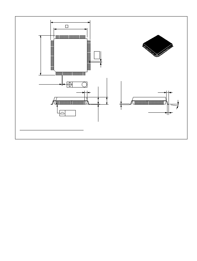
Unit: mm
Figure F-2 Package Dimensions (TFP-100B)
0.10
16.0
±
0.3
1.0
0.5
±
0.2
16.0
±
0.3
3.05 Max
75
51
50
26
1
25
76
100
14
0
∞
≠ 8
∞
0.5
0.08 M
0.22
±
0.05
2.70
0.17
±
0.05
0.12
+0.13 ≠0.12
1.0
0.20
±
0.04
0.15
±
0.04
Dimension including the plating thickness
Base material dimension
687
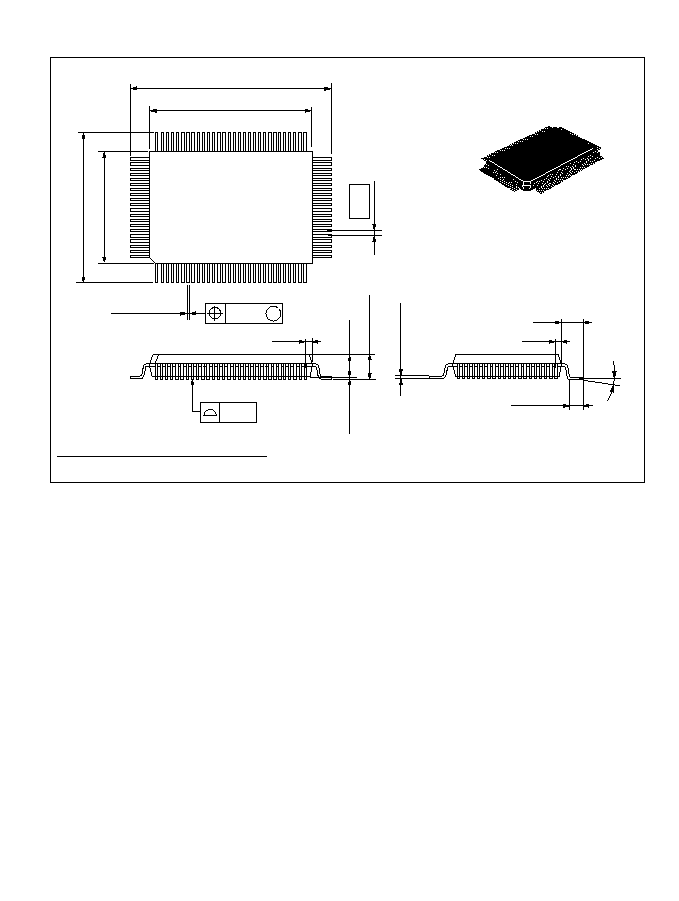
Unit: mm
Figure F-3 Package Dimensions (FP-100A)
688
0.13 M
0
∞
≠ 10
∞
0.32
±
0.08
0.17
±
0.05
3.10 Max
1.2
±
0.2
24.8
±
0.4
20
80
51
50
31
30
1
100
81
18.8
±
0.4
14
0.15
0.65
2.70
2.4
0.20
+0.10 ≠0.20
0.58
0.83
0.30
±
0.06
0.15
±
0.04
Dimension including the plating thickness
Base material dimension