 | –≠–ª–µ–∫—Ç—Ä–æ–Ω–Ω—ã–π –∫–æ–º–ø–æ–Ω–µ–Ω—Ç: HD6417616 | –°–∫–∞—á–∞—Ç—å:  PDF PDF  ZIP ZIP |
Document Outline
- Cover
- Cautions
- Preface
- Contents
- Section 1 Overview
- 1.1 Features of SuperH Microcomputer with On-Chip Ethernet Controller
- 1.2Block Diagram
- 1.3 Pin Description
- 1.3.1 Pin Arrangement
- 1.3.2 Pin Functions
- 1.3.3 Pin Multiplexing
- 1.4 Processing States
- Section 2 CPU
- 2.1 Register Configuration
- 2.1.1 General Registers
- 2.1.2 Control Registers
- 2.1.3 System Registers
- 2.1.4 DSP Registers
- 2.1.5 Notes on Guard Bits and Overflow Treatment
- 2.1.6 Initial Values of Registers
- 2.2 Data Formats
- 2.2.1 Data Format in Registers
- 2.2.2 Data Formats in Memory
- 2.2.3 Immediate Data Format
- 2.2.4 DSP Type Data Formats
- 2.2.5 DSP Type Instructions and Data Formats
- 2.3 CPU Core Instruction Features
- 2.4 Instruction Formats
- 2.4.1 CPU Instruction Addressing Modes
- 2.4.2 DSP Data Addressing
- 2.4.3 Instruction Formats for CPU Instructions
- 2.4.4 Instruction Formats for DSP Instructions
- 2.5 Instruction Set
- 2.5.1 CPU Instruction Set
- 2.5.2 DSP Data Transfer Instruction Set
- 2.5.3 DSP Operation Instruction Set
- 2.5.4 Various Operation Instructions
- 2.6 Usage Notes
- 2.6.1 When not using DSP instructions
- 2.6.2 When executing a combination of double-precision multiplication or double-precision product-sum operation (CPU instruc
- Section 3 Oscillator Circuits and Operating Modes
- 3.1 Overview
- 3.2 On-Chip Clock Pulse Generator and Operating Modes
- 3.2.1 Clock Pulse Generator
- 3.2.2 lock Operating Mode Settings
- 3.2.3 Connecting a Crystal Resonator
- 3.2.4 External Clock Input
- 3.2.5 Operating Frequency Selection by Register
- 3.2.6 lock Modes and Frequency Ranges
- 3.2.7 Notes on Board Design
- 3.3 Bus Width of the CS0 Area
- Section 4 Exception Handling
- 4.1 Overview
- 4.1.1 Types of Exception Handling and Priority Order
- 4.1.2 Exception Handling Operations
- 4.1.3 Exception Vector Table
- 4.2 Resets
- 4.2.1 Types of Resets
- 4.2.2 Power-On Reset
- 4.2.3 Manual Reset
- 4.3 Address Errors
- 4.3.1 Sources of Address Errors
- 4.3.2 Address Error Exception Handling
- 4.4 Interrupts
- 4.4.1 Interrupt Sources
- 4.4.2 Interrupt Priority Levels
- 4.4.3 Interrupt Exception Handling
- 4.5 Exceptions Triggered by Instructions
- 4.5.1 Instruction-Triggered Exception Types
- 4.5.2 Trap Instructions
- 4.5.3 Illegal Slot Instructions
- 4.5.4 General Illegal Instructions
- 4.6 When Exception Sources Are Not Accepted
- 4.6.1 Immediately after a Delayed Branch Instruction
- 4.6.2 Immediately after an Interrupt-Disabled Instruction
- 4.6.3 Instructions in Repeat Loops
- 4.7 Stack Status after Exception Handling
- 4.8 Usage Notes
- 4.8.1 Value of Stack Pointer (SP)
- 4.8.2 Value of Vector Base Register (VBR)
- 4.8.3 Address Errors Caused by Stacking of Address Error Exception Handling
- 4.8.4 Manual Reset during Register Access
- Section 5 Interrupt Controller (INTC)
- 5.1 Overview
- 5.1.1 Features
- 5.1.2 Block Diagram
- 5.1.3 Pin Configuration
- 5.1.4 Register Configuration
- 5.2 Interrupt Sources
- 5.2.1 NMI Interrupt
- 5.2.2 User Break Interrupt
- 5.2.3 H-UDI Interrupt
- 5.2.4 IRL Interrupts
- 5.2.5 IRQ Interrupts
- 5.2.6 On-chip Peripheral Module Interrupts
- 5.2.7 Interrupt Exception Vectors and Priority Order
- 5.3 Register Descriptions
- 5.3.1 Interrupt Priority Level Setting Register A (IPRA)
- 5.3.2 Interrupt Priority Level Setting Register B (IPRB)
- 5.3.3 Interrupt Priority Level Setting Register C (IPRC)
- 5.3.4 Interrupt Priority Level Setting Register D (IPRD)
- 5.3.5 Interrupt Priority Level Setting Register E (IPRE)
- 5.3.6 Vector Number Setting Register WDT (VCRWDT)
- 5.3.7 Vector Number Setting Register A (VCRA)
- 5.3.8 Vector Number Setting Register B (VCRB)
- 5.3.9 Vector Number Setting Register C (VCRC)
- 5.3.10 Vector Number Setting Register D (VCRD)
- 5.3.11 Vector Number Setting Register E (VCRE)
- 5.3.12 Vector Number Setting Register F (VCRF)
- 5.3.13 Vector Number Setting Register G (VCRG)
- 5.3.14 Vector Number Setting Register H (VCRH)
- 5.3.15 Vector Number Setting Register I (VCRI)
- 5.3.16 Vector Number Setting Register J (VCRJ)
- 5.3.17 Vector Number Setting Register K (VCRK)
- 5.3.18 Vector Number Setting Register L (VCRL)
- 5.3.19 Vector Number Setting Register M (VCRM)
- 5.3.20 Vector Number Setting Register N (VCRN)
- 5.3.21 Vector Number Setting Register O (VCRO)
- 5.3.22 Vector Number Setting Register P (VCRP)
- 5.3.23 Vector Number Setting Register Q (VCRQ)
- 5.3.24 Vector Number Setting Register R (VCRR)
- 5.3.25 Vector Number Setting Register S (VCRS)
- 5.3.26 Vector Number Setting Register T (VCRT)
- 5.3.27 Vector Number Setting Register U (VCRU)
- 5.3.28 Interrupt Control Register (ICR)
- 5.3.29 IRQ Control/Status Register (IRQCSR)
- 5.4 Interrupt Operation
- 5.4.1 Interrupt Sequence
- 5.4.2 Stack State after Interrupt Exception Handling
- 5.5 Interrupt Response Time
- 5.6 Sampling of Pins IRL3 ÖIRL0
- 5.7 Usage Notes
- Section 6 User Break Controller (UBC)
- 6.1 Overview
- 6.1.1 Features
- 6.1.2 Block Diagram
- 6.1.3 Register Configuration
- 6.2 Register Descriptions
- 6.2.1 Break Address Register A (BARA)
- 6.2.2 Break Address Mask Register A (BAMRA)
- 6.2.3 Break Bus Cycle Register A (BBRA)
- 6.2.4 Break Address Register B (BARB)
- 6.2.5 Break Address Mask Register B (BAMRB)
- 6.2.6 Break Bus Cycle Register B (BBRB)
- 6.2.7 Break Address Register C (BARC)
- 6.2.8 Break Address Mask Register C (BAMRC)
- 6.2.9 Break Data Register C (BDRC)
- 6.2.10 Break Data Mask Register C (BDMRC)
- 6.2.11 Break Bus Cycle Register C (BBRC)
- 6.2.12 Break Execution Times Register C (BETRC)
- 6.2.13 Break Address Register D (BARD)
- 6.2.14 Break Address Mask Register D (BAMRD)
- 6.2.15 Break Data Register D (BDRD)
- 6.2.16 Break Data Mask Register D (BDMRD)
- 6.2.17 Break Bus Cycle Register D (BBRD)
- 6.2.18 Break Execution Times Register D (BETRD)
- 6.2.19 Break Control Register (BRCR)
- 6.2.20 Branch Flag Registers (BRFR)
- 6.2.21 Branch Source Registers (BRSR)
- 6.2.22 Branch Destination Registers (BRDR)
- 6.3 Operation
- 6.3.1 User Break Operation Sequence
- 6.3.2 Instruction Fetch Cycle Break
- 6.3.3 Data Access Cycle Break
- 6.3.4 Saved Program Counter (PC)Value
- 6.3.5 X Memory Bus or Y Memory Bus Cycle Break
- 6.3.6 Sequential Break
- 6.3.7 PC Traces
- 6.3.8 Examples of Use
- 6.3.9 Usage Notes
- Section 7 Bus State Controller (BSC)
- 7.1 Overview
- 7.1.1 Features
- 7.1.2 Block Diagram
- 7.1.3 Pin Configuration
- 7.1.4 Register Configuration
- 7.1.5 Address Map
- 7.2 Register Descriptions
- 7.2.1 Bus Control Register 1 (BCR1)
- 7.2.2 Bus Control Register 2 (BCR2)
- 7.2.3 Bus Control Register 3 (BCR3)
- 7.2.4 Wait Control Register 1 (WCR1)
- 7.2.5 Wait Control Register 2 (WCR2)
- 7.2.6 Wait Control Register 3 (WCR3)
- 7.2.7 Individual Memory Control Register (MCR)
- 7.2.8 Refresh Timer Control/Status Register (RTCSR)
- 7.2.9 Refresh Timer Counter (RTCNT)
- 7.2.10 Refresh Time Constant Register (RTCOR)
- 7.3 Access Size and Data Alignment
- 7.3.1 Connection to Ordinary Devices
- 7.3.2 Connection to Little-Endian Devices
- 7.4 Accessing Ordinary Space
- 7.4.1 Basic Timing
- 7.4.2 Wait State Control
- 7.4.3 CS Assertion Period Extension
- 7.5 Synchronous DRAM Interface
- 7.5.1 Synchronous DRAM Direct Connection
- 7.5.2 Address Multiplexing
- 7.5.3 Burst Reads
- 7.5.4 Single Reads
- 7.5.5 Single Writes
- 7.5.6 Burst Write Mode
- 7.5.7 Bank Active Function
- 7.5.8 Refreshes
- 7.5.9 Overlap Between Auto Precharge Cycle (Tap)and Next Access
- 7.5.10 Power-On Sequence
- 7.5.11 64 Mbit Synchronous DRAM (2 Mword Ä 32-bit)Connection
- 7.6 DRAM Interface
- 7.6.1 DRAM Direct Connection
- 7.6.2 Address Multiplexing
- 7.6.3 Basic Timing
- 7.6.4 Wait State Control
- 7.6.5 Burst Access
- 7.6.6 EDO Mode
- 7.6.7 DRAM Single Transfer
- 7.6.8 Refreshing
- 7.6.9 Power-On Sequence
- 7.7 Burst ROM Interface
- 7.8 Idles between Cycles
- 7.9 Bus Arbitration
- 7.10 Additional Items
- 7.10.1 Resets
- 7.10.2 Access as Viewed from CPU,DMAC or E-DMAC
- 7.10.3 STATS1 and STATS0 Pins
- 7.10.4 BUSHiZ Specification
- 7.11 Usage Notes
- 7.11.1 Normal Space Access after Synchronous DRAM Write when Using DMAC
- 7.11.2 When Using I Ä :E Ä Clock Ratio of 1 :1,8-Bit Bus Width,and External Wait Input
- 7.11.3 When connecting external device to synchronous DRAM
- Section 8 Cache
- 8.1 Introduction
- 8.1.1 Register Configuration
- 8.2 Register Description
- 8.2.1 Cache Control Register (CCR)
- 8.3Address Space and the Cache
- 8.4 Cache Operation
- 8.4.1 Cache Reads
- 8.4.2 Write Access
- 8.4.3 Cache-Through Access
- 8.4.4 The TAS Instruction
- 8.4.5 Pseudo-LRU and Cache Replacement
- 8.4.6 Cache Initialization
- 8.4.7 Associative Purges
- 8.4.8 Cache Flushing
- 8.4.9 Data Array Access
- 8.4.10 Address Array Access
- 8.5 Cache Use
- 8.5.1 Initialization
- 8.5.2 Purge of Specific Lines
- 8.5.3 Cache Data Coherency
- 8.5.4 Two-Way Cache Mode
- 8.6 Usage Notes
- 8.6.1 Standby
- 8.6.2 Cache Control Register
- Section 9 Ethernet Controller (EtherC)
- 9.1 Overview
- 9.1.1 Features
- 9.1.2 Configuration
- 9.1.3 Pin Configuration
- 9.1.4 Ethernet Controller Register Configuration
- 9.2 Register Descriptions
- 9.2.1 EtherC Mode Register (ECMR)
- 9.2.2 EtherC Status Register (ECSR)
- 9.2.3 EtherC Interrupt Permission Register (ECSIPR)
- 9.2.4 PHY Interface Register (PIR)
- 9.2.5 MAC Address High Register (MAHR)
- 9.2.6 MAC Address Low Register (MALR)
- 9.2.7 Receive Frame Length Register (RFLR)
- 9.2.8 PHY Interface Status Register (PSR)
- 9.2.9 Transmit Retry Over Counter Register (TROCR)
- 9.2.10 Single Collision Detect Counter Register (SCDCR)
- 9.2.11 Delay Collision Detect Counter Register (CDCR)
- 9.2.12 Lost Carrier Counter Register (LCCR)
- 9.2.13 Carrier Not Detect Counter Register (CNDCR)
- 9.2.14 Illegal Frame Length Counter Register (IFLCR)
- 9.2.15 CRC Error Frame Counter Register (CEFCR)
- 9.2.16 Frame Receive Error Counter Register (FRECR )
- 9.2.17 Too-Short Frame Receive Counter Register (TSFRCR)
- 9.2.18 Too-Long Frame Receive Counter Register (TLFRCR )
- 9.2.19 Residual-Bit Frame Counter Register (RFCR)
- 9.2.20 Multicast Address Frame Counter Register (MAFCR)
- 9.3 Operation
- 9.3.1 Transmission
- 9.3.2 Reception
- 9.3.3 MII Frame Timing
- 9.3.4 Accessing MII Registers
- 9.3.5 Magic Packet Detection
- 9.3.6 CPU Operating Mode and Ethernet Controller Operation
- 9.3.7 CAM Match Signal Input Function
- 9.4 Connection to PHY-LSI
- Section 10 Ethernet Controller Direct Memory Access Controller (E-DMAC)
- 10.1 Overview
- 10.1.1 Features
- 10.1.2 Configuration
- 10.1.3 Descriptor Management System
- 10.1.4 Register Configuration
- 10.2 Register Descriptions
- 10.2.1 E-DMAC Mode Register (EDMR)
- 10.2.2 E-DMAC Transmit Request Register (EDTRR)
- 10.2.3 E-DMAC Receive Request Register (EDRRR)
- 10.2.4 Transmit Descriptor List Address Register (TDLAR)
- 10.2.5 Receive Descriptor List Address Register (RDLAR)
- 10.2.6 EtherC/E-DMAC Status Register (EESR)
- 10.2.7 EtherC/E-DMAC Status Interrupt Permission Register (EESIPR)
- 10.2.8 Transmit/Receive Status Copy Enable Register (TRSCER)
- 10.2.9 Receive Missed-Frame Counter Register (RMFCR)
- 10.2.10 Transmit FIFO Threshold Register (TFTR)
- 10.2.11 FIFO Depth Register (FDR)
- 10.2.12 Receiver Control Register (RCR)
- 10.2.13 E-DMAC Operation Control Register (EDOCR)
- 10.2.14 Receiving-Buffer Write Address Register (RBWAR)
- 10.2.15 Receiving-Descriptor Fetch Address Register (RDFAR)
- 10.2.16 Transmission-Buffer Read Address Register (TBRAR)
- 10.2.17 Transmission-Descriptor Fetch Address Register (TDFAR)
- 10.3Operation
- 10.3.1 Descriptor List and Data Buffers
- 10.3.2 Transmission
- 10.3.3 Reception
- 10.3.4 Multi-Buffer Frame Transmit/Receive Processing
- Section 11 Direct Memory Access Controller (DMAC)
- 11.1 Overview
- 11.1.1 Features
- 11.1.2 Block Diagram
- 11.1.3 Pin Configuration
- 11.1.4 Register Configuration
- 11.2 Register Descriptions
- 11.2.1 DMA Source Address Registers 0 and 1 (SAR0,SAR1)
- 11.2.2 DMA Destination Address Registers 0 and 1 (DAR0,DAR1)
- 11.2.3 DMA Transfer Count Registers 0 and 1 (TCR0,TCR1)
- 11.2.4 DMA Channel Control Registers 0 and 1 (CHCR0,CHCR1)
- 11.2.5 DMA Vector Number Registers 0 and 1 (VCRDMA0,VCRDMA1)
- 11.2.6 DMA Request/Response Selection Control Registers 0 and 1 (DRCR0,DRCR1)
- 11.2.7 DMA Operation Register (DMAOR)
- 11.3 Operation
- 11.3.1 DMA Transfer Flow
- 11.3.2 DMA Transfer Requests
- 11.3.3 Channel Priorities
- 11.3.4 DMA Transfer Types
- 11.3.5 Number of Bus Cycles
- 11.3.6 DMA Transfer Request Acknowledge Signal Output Timing
- 11.3.7 DREQn Pin Input Detection Timing
- 11.3.8 DMA Transfer End
- 11.3.9 BH Pin Output Timing
- 11.4 Usage Examples
- 11.4.1 Example of DMA Data Transfer Between SCIF and External Memory
- 11.5 Usage Notes
- Section 12 16-Bit Free-Running Timer (FRT)
- 12.1 Overview
- 12.1.1 Features
- 12.1.2 Block Diagram
- 12.1.3 Pin Configuration
- 12.1.4 Register Configuration
- 12.2 Register Descriptions
- 12.2.1 Free-Running Counter (FRC)
- 12.2.2 Output Compare Registers A and B (OCRA and OCRB)
- 12.2.3 Input Capture Register (FICR)
- 12.2.4 Timer Interrupt Enable Register (TIER)
- 12.2.5 Free-Running Timer Control/Status Register (FTCSR)
- 12.2.6 Timer Control Register (TCR)
- 12.2.7 Timer Output Compare Control Register (TOCR)
- 12.3 CPU Interface
- 12.4Operation
- 12.4.1 FRC Count Timing
- 12.4.2 Output Timing for Output Compare
- 12.4.3 FRC Clear Timing
- 12.4.4 Input Capture Input Timing
- 12.4.5 Input Capture Flag (ICF)Setting Timing
- 12.4.6 Output Compare Flag (OCFA,OCFB)Setting Timing
- 12.4.7 Timer Overflow Flag (OVF)Setting Timing
- 12.5 Interrupt Sources
- 12.6 Example of FRT Use
- 12.7 Usage Notes
- 12.7.1 Contention between FRC Write and Clear
- 12.7.2 Contention between FRC Write and Increment
- 12.7.3 Contention between OCR Write and Compare Match
- 12.7.4 Internal Clock Switching and Counter Operation
- 12.7.5 Timer Output (FTOA,FTOB)
- Section 13 Watchdog Timer (WDT)
- 13.1 Overview
- 13.1.1 Features
- 13.1.2 Block Diagram
- 13.1.3 Pin Configuration
- 13.1.4 Register Configuration
- 13.2 Register Descriptions
- 13.2.1 Watchdog Timer Counter (WTCNT)
- 13.2.2 Watchdog Timer Control/Status Register (WTCSR)
- 13.2.3 Reset Control/Status Register (RSTCSR)
- 13.2.4 Notes on Register Access
- 13.3 Operation
- 13.3.1 Operation in Watchdog Timer Mode
- 13.3.2 Operation in Interval Timer Mode
- 13.3.3 Operation when Standby Mode is Cleared
- 13.3.4 Timing of Overflow Flag (OVF)Setting
- 13.3.5 Timing of Watchdog Timer Overflow Flag (WOVF)Setting
- 13.4Usage Notes
- 13.4.1 Contention between WTCNT Write and Increment
- 13.4.2 Changing CKS2 to CKS0 Bit Values
- 13.4.3 Switching between Watchdog Timer Mode and Interval Timer Mode
- 13.4.4 System Reset with WDTOVF
- 13.4.5 Internal Reset in Watchdog Timer Mode
- Section 14 Serial Communication Interface with FIFO (SCIF)
- 14.1 Overview
- 14.1.1 Features
- 14.1.2 Block Diagrams
- 14.1.3 Pin Configuration
- 14.1.4 Register Configuration
- 14.2 Register Descriptions
- 14.2.1 Receive Shift Register (SCRSR)
- 14.2.2 Receive FIFO Data Register (SCFRDR)
- 14.2.3 Transmit Shift Register (SCTSR)
- 14.2.4 Transmit FIFO Data Register (SCFTDR)
- 14.2.5 Serial Mode Register (SCSMR)
- 14.2.6 Serial Control Register (SCSCR)
- 14.2.7 Serial Status 1 Register (SC1SSR)
- 14.2.8 Serial Status 2 Register (SC2SSR)
- 14.2.9 Bit Rate Register (SCBRR)
- 14.2.10 FIFO Control Register (SCFCR)
- 14.2.11 FIFO Data Count Register (SCFDR)
- 14.2.12 FIFO Error Register (SCFER)
- 14.2.13 IrDA Mode Register (SCIMR)
- 14.3 Operation
- 14.3.1 Overview
- 14.3.2 Operation in Asynchronous Mode
- 14.3.3 Multiprocessor Communication Function
- 14.3.4 Operation in Synchronous Mode
- 14.3.5 Use of Transmit/Receive FIFO Buffers
- 14.3.6 Operation in IrDA Mode
- 14.4 SCIF Interrupt Sources and the DMAC
- 14.5 Usage Notes
- Section 15 Serial I/O with FIFO (SIOF)
- 15.1 Overview
- 15.2 Register Configuration
- 15.2.1 Receive Shift Register (SIRSR)
- 15.2.2 Receive Data Register (SIRDR)
- 15.2.3 Transmit Shift Register (SITSR)
- 15.2.4 Transmit Data Register (SITDR)
- 15.2.5 Serial Control Register (SICTR)
- 15.2.6 Serial Status Register (SISTR)
- 15.2.7 Receive Control Data Register (SIRCDR)
- 15.2.8 Transmit Control Data Register (SITCDR)
- 15.2.9 FIFO Control Register (SIFCR)
- 15.2.10 FIFO Data Count Register (SIFDR)
- 15.3 Operation
- 15.3.1 Input when TRMD =0 in SIFCR
- 15.3.2 Output when TRMD =0 in SIFCR
- 15.3.3 Output when TRMD =1 in SIFCR
- 15.4 SIOF Interrupt Sources and DMAC
- Section 16 Serial I/O (SIO)
- 16.1 Overview
- 16.2 Register Configuration
- 16.2.1 Receive Shift Register (SIRSR)
- 16.2.2 Receive Data Register (SIRDR)
- 16.2.3 Transmit Shift Register (SITSR)
- 16.2.4 Transmit Data Register (SITDR)
- 16.2.5 Serial Control Register (SICTR)
- 16.2.6 Serial Status Register (SISTR)
- 16.3 Operation
- 16.3.1 Input
- 16.3.2 Output
- 16.4 SIO Interrupt Sources and DMAC
- Section 17 16-Bit Timer Pulse Unit (TPU)
- 17.1 Overview
- 17.1.1 Features
- 17.1.2 Block Diagram
- 17.1.3 Pin Configuration
- 17.1.4 Register Configuration
- 17.2 Register Descriptions
- 17.2.1 Timer Control Register (TCR)
- 17.2.2 Timer Mode Register (TMDR)
- 17.2.3 Timer I/O Control Register (TIOR)
- 17.2.4 Timer Interrupt Enable Register (TIER)
- 17.2.5 Timer Status Register (TSR)
- 17.2.6 Timer Counter (TCNT)
- 17.2.7 Timer General Register (TGR)
- 17.2.8 Timer Start Register (TSTR)
- 17.2.9 Timer Synchronous Register (TSYR)
- 17.3Interface to Bus Master
- 17.3.1 16-Bit Registers
- 17.3.2 8-Bit Registers
- 17.4 Operation
- 17.4.1 Overview
- 17.4.2 Basic Functions
- 17.4.3 Synchronous Operation
- 17.4.4 Buffer Operation
- 17.4.5 PWM Modes
- 17.4.6 Phase Counting Mode
- 17.5 Interrupts
- 17.5.1 Interrupt Sources and Priorities
- 17.5.2 DMAC Activation
- 17.6 Operation Timing
- 17.6.1 Input/Output Timing
- 17.6.2 Interrupt Signal Timing
- 17.7 Usage Notes
- 17.8 Usage Notes
- 17.8.1 Clearing Flags in TSR0 to TSR2
- 17.8.2 DMA Transfer by TPU0
- Section 18 Hitachi User Debug Interface (H-UDI)
- 18.1 Overview
- 18.1.1 Features
- 18.1.2 H-UDI Block Diagram
- 18.1.3 Pin Configuration
- 18.1.4 Register Configuration
- 18.2 External Signals
- 18.2.1 Test Clock (TCK)
- 18.2.2 Test Mode Select (TMS)
- 18.2.3 Test Data Input (TDI)
- 18.2.4 Test Data Output (TDO)
- 18.2.5 Test Reset (TRST )
- 18.3 Register Descriptions
- 18.3.1 Instruction Register (SDIR)
- 18.3.2 Status Register (SDSR)
- 18.3.3 Data Register (SDDR)
- 18.3.4 Bypass Register (SDBPR)
- 18.3.5 Boundary scan register (SDBSR)
- 18.3.6 ID code register (SDIDR)
- 18.4 Operation
- 18.4.1 TAP Controller
- 18.4.2 H-UDI Interrupt and Serial Transfer
- 18.4.3 H-UDI Reset
- 18.5 Boundary Scan
- 18.5.1 Supported Instructions
- 18.5.2 Notes on Use
- 18.6 Usage Notes
- Section 19 Pin Function Controller (PFC)
- 19.1 Overview
- 19.2 Register Configuration
- 19.3 Register Descriptions
- 19.3.1 Port A Control Register (PACR)
- 19.3.2 Port A I/O Register (PAIOR)
- 19.3.3 Port B Control Registers (PBCR,PBCR2)
- 19.3.4 Port B I/O Register (PBIOR)
- Section 20 I/O Ports
- 20.1 Overview
- 20.2 Port A
- 20.2.1 Register Configuration
- 20.2.2 Port A Data Register (PADR)
- 20.3 Port B
- 20.3.1 Register Configuration
- 20.3.2 Port B Data Register (PBDR)
- Section 21 Power-Down Modes
- 21.1 Overview
- 21.1.1 Power-Down Modes
- 21.1.2 Register
- 21.2 Register Descriptions
- 21.2.1 Standby Control Register 1 (SBYCR1)
- 21.2.2 Standby Control Register 2 (SBYCR2)
- 21.3 Sleep Mode
- 21.3.1 Transition to Sleep Mode
- 21.3.2 Canceling Sleep Mode
- 21.4 Standby Mode
- 21.4.1 Transition to Standby Mode
- 21.4.2 Canceling Standby Mode
- 21.4.3 Standby Mode Cancellation by NMI Interrupt
- 21.4.4 Clock Pause Function
- 21.4.5 Notes on Standby Mode
- 21.5 Module Standby Function
- 21.5.1 Transition to Module Standby Function
- 21.5.2 Clearing the Module Standby Function
- Section 22 Electrical Characteristics
- 22.1 Absolute Maximum Ratings
- 22.2 DC Characteristics
- 22.3 AC Characteristics
- 22.3.1 Clock Timing
- 22.3.2 Control Signal Timing
- 22.3.3 Bus Timing
- 22.3.4 Direct Memory Access Controller Timing
- 22.3.5 Free-Running Timer Timing
- 22.3.6 Serial Communication Interface Timing
- 22.3.7 Watchdog Timer Timing
- 22.3.8 Serial I/O with FIFO /Serial I/O Timing
- 22.3.9 Hitachi User Debug Interface Timing
- 22.3.10 I/O Port Timing
- 22.3.11 Ethernet Controller Timing
- 22.3.12 STATS,BH ,and BUSHiZ Signal Timing
- 22.4 AC Characteristic Test Conditions
- Appendix A On-Chip Peripheral Module Registers
- Appendix B Pin States
- B.1 Pin States in Reset,Power-Down State,and Bus-Released State
- Appendix C Product Lineup
- Appendix D Package Dimensions
- Colophon

Regarding the change of names mentioned in the document, such as Hitachi
Electric and Hitachi XX, to Renesas Technology Corp.
The semiconductor operations of Mitsubishi Electric and Hitachi were transferred to Renesas
Technology Corporation on April 1st 2003. These operations include microcomputer, logic, analog
and discrete devices, and memory chips other than DRAMs (flash memory, SRAMs etc.)
Accordingly, although Hitachi, Hitachi, Ltd., Hitachi Semiconductors, and other Hitachi brand
names are mentioned in the document, these names have in fact all been changed to Renesas
Technology Corp. Thank you for your understanding. Except for our corporate trademark, logo and
corporate statement, no changes whatsoever have been made to the contents of the document, and
these changes do not constitute any alteration to the contents of the document itself.
Renesas Technology Home Page: http://www.renesas.com
Renesas Technology Corp.
Customer Support Dept.
April 1, 2003
To all our customers

Cautions
Keep safety first in your circuit designs!
1.
Renesas Technology Corporation puts the maximum effort into making semiconductor products better and more reliable, but
there is always the possibility that trouble may occur with them. Trouble with semiconductors may lead to personal injury, fire
or property damage.
Remember to give due consideration to safety when making your circuit designs, with appropriate measures such as (i)
placement of substitutive, auxiliary circuits, (ii) use of nonflammable material or (iii) prevention against any malfunction or
mishap.
Notes regarding these materials
1.
These materials are intended as a reference to assist our customers in the selection of the Renesas Technology Corporation
product best suited to the customer's application; they do not convey any license under any intellectual property rights, or any
other rights, belonging to Renesas Technology Corporation or a third party.
2.
Renesas Technology Corporation assumes no responsibility for any damage, or infringement of any third-party's rights,
originating in the use of any product data, diagrams, charts, programs, algorithms, or circuit application examples contained in
these materials.
3.
All information contained in these materials, including product data, diagrams, charts, programs and algorithms represents
information on products at the time of publication of these materials, and are subject to change by Renesas Technology
Corporation without notice due to product improvements or other reasons. It is therefore recommended that customers contact
Renesas Technology Corporation or an authorized Renesas Technology Corporation product distributor for the latest product
information before purchasing a product listed herein.
The information described here may contain technical inaccuracies or typographical errors.
Renesas Technology Corporation assumes no responsibility for any damage, liability, or other loss rising from these
inaccuracies or errors.
Please also pay attention to information published by Renesas Technology Corporation by various means, including the
Renesas Technology Corporation Semiconductor home page (http://www.renesas.com).
4.
When using any or all of the information contained in these materials, including product data, diagrams, charts, programs, and
algorithms, please be sure to evaluate all information as a total system before making a final decision on the applicability of
the information and products. Renesas Technology Corporation assumes no responsibility for any damage, liability or other
loss resulting from the information contained herein.
5.
Renesas Technology Corporation semiconductors are not designed or manufactured for use in a device or system that is used
under circumstances in which human life is potentially at stake. Please contact Renesas Technology Corporation or an
authorized Renesas Technology Corporation product distributor when considering the use of a product contained herein for
any specific purposes, such as apparatus or systems for transportation, vehicular, medical, aerospace, nuclear, or undersea
repeater use.
6.
The prior written approval of Renesas Technology Corporation is necessary to reprint or reproduce in whole or in part these
materials.
7.
If these products or technologies are subject to the Japanese export control restrictions, they must be exported under a license
from the Japanese government and cannot be imported into a country other than the approved destination.
Any diversion or reexport contrary to the export control laws and regulations of Japan and/or the country of destination is
prohibited.
8.
Please contact Renesas Technology Corporation for further details on these materials or the products contained therein.

Hitachi SuperHTM RISC engine
SH7616
HD6417616
Hardware Manual
ADE-602-243
Rev. 1.0
3/5/03
Hitachi, Ltd.

Cautions
1. Hitachi neither warrants nor grants licenses of any rights of Hitachi's or any third party's
patent, copyright, trademark, or other intellectual property rights for information contained in
this document. Hitachi bears no responsibility for problems that may arise with third party's
rights, including intellectual property rights, in connection with use of the information
contained in this document.
2. Products and product specifications may be subject to change without notice. Confirm that you
have received the latest product standards or specifications before final design, purchase or
use.
3. Hitachi makes every attempt to ensure that its products are of high quality and reliability.
However, contact Hitachi's sales office before using the product in an application that
demands especially high quality and reliability or where its failure or malfunction may directly
threaten human life or cause risk of bodily injury, such as aerospace, aeronautics, nuclear
power, combustion control, transportation, traffic, safety equipment or medical equipment for
life support.
4. Design your application so that the product is used within the ranges guaranteed by Hitachi
particularly for maximum rating, operating supply voltage range, heat radiation characteristics,
installation conditions and other characteristics. Hitachi bears no responsibility for failure or
damage when used beyond the guaranteed ranges. Even within the guaranteed ranges,
consider normally foreseeable failure rates or failure modes in semiconductor devices and
employ systemic measures such as fail-safes, so that the equipment incorporating Hitachi
product does not cause bodily injury, fire or other consequential damage due to operation of
the Hitachi product.
5. This product is not designed to be radiation resistant.
6. No one is permitted to reproduce or duplicate, in any form, the whole or part of this document
without written approval from Hitachi.
7. Contact Hitachi's sales office for any questions regarding this document or Hitachi
semiconductor products.

Preface
The SH7616 is a microprocessor that integrates peripheral functions necessary for system
configuration with a 32-bit internal architecture SH2-DSP CPU as its core.
The SH7616's on-chip peripheral functions include a cache memory, an interrupt controller,
timers, an ethernet controller (EtherC), DSP, a serial communication interface with FIFO (SCIF),
a USB function module, a user break controller (UBC), a bus state controller (BSC), a direct
memory access cntroller (DMAC), and I/O ports, making it ideal for use as a microcomputer in
electronic devices that require high speed together with low power consumption.
Intended Readership: This manual is intended for users undertaking the design of an application
system using the SH7616. Readers using this manual require a basic
knowledge of electrical circuits, logic circuits, and microcomputers.
Purpose:
The purpose of this manual is to give users an understanding of the hardware
functions and electrical characteristics of the SH7616. Details of execution
instructions can be found in the SH-1, SH-2, SH-DSP Programming Manual,
which should be read in conjunction with the present manual.
Using this Manual:
∑
For an overall understanding of the SH7616's functions
Follow the Table of Contents. This manual is broadly divided into sections on the CPU, system
control functions, peripheral functions, and electrical characteristics.
∑
For a detailed understanding of CPU functions
Refer to the separate publication SH-1, SH-2, SH-DSP Programming Manual.
Note on bit notation: Bits are shown in high-to-low order from left to right.
Related Material: The latest information is available at our Web Site. Please make sure that you
have the most up-to-date information available.
http://www.hitachisemiconductor.com/

User's Manuals on the SH7616:
Manual Title
ADE No.
SH7616 Hardware Manual
This manual
SH-1, SH-2, SH-DSP Programming Manual
ADE-602-085
Users manuals for development tools:
Manual Title
ADE No.
C/C++ Complier, Assembler, Optimized Linkage Editor User's Manual
ADE-702-304
Simulator Debugger Users Manual
ADE-702-266
Hitachi Embedded Workshop Users Manual
ADE-702-275
Application Note:
Manual Title
ADE No.
C/C++ Complier
ADE-502-046

i
Contents
Section 1
Overview
...........................................................................................................
1
1.1
Features of SuperH Microcomputer with On-Chip Ethernet Controller ...........................
1
1.2 Block
Diagram...................................................................................................................
13
1.3 Pin
Description ..................................................................................................................
14
1.3.1 Pin
Arrangement ..................................................................................................
14
1.3.2 Pin
Functions........................................................................................................
15
1.3.3 Pin
Multiplexing ...................................................................................................
21
1.4 Processing
States ...............................................................................................................
27
Section 2
CPU
.....................................................................................................................
31
2.1 Register
Configuration ......................................................................................................
31
2.1.1 General
Registers..................................................................................................
31
2.1.2 Control
Registers..................................................................................................
33
2.1.3 System
Registers ..................................................................................................
36
2.1.4 DSP
Registers .......................................................................................................
37
2.1.5
Notes on Guard Bits and Overflow Treatment.....................................................
40
2.1.6
Initial Values of Registers ....................................................................................
40
2.2 Data
Formats......................................................................................................................
41
2.2.1
Data Format in Registers......................................................................................
41
2.2.2
Data Formats in Memory......................................................................................
41
2.2.3
Immediate Data Format........................................................................................
42
2.2.4
DSP Type Data Formats .......................................................................................
42
2.2.5
DSP Type Instructions and Data Formats ............................................................
44
2.3
CPU Core Instruction Features..........................................................................................
48
2.4 Instruction
Formats............................................................................................................
52
2.4.1
CPU Instruction Addressing Modes .....................................................................
52
2.4.2
DSP Data Addressing ...........................................................................................
56
2.4.3
Instruction Formats for CPU Instructions ............................................................
62
2.4.4
Instruction Formats for DSP Instructions.............................................................
66
2.5 Instruction
Set....................................................................................................................
72
2.5.1
CPU Instruction Set..............................................................................................
73
2.5.2
DSP Data Transfer Instruction Set .......................................................................
89
2.5.3
DSP Operation Instruction Set .............................................................................
93
2.5.4
Various Operation Instructions ............................................................................
96
2.6 Usage
Notes ....................................................................................................................... 105
2.6.1
When not using DSP instructions......................................................................... 105
2.6.2
When executing a combination of double-precision multiplication or
double-precision product-sum operation (CPU instruction) and DSP
computing instruction ........................................................................................... 105

ii
Section 3 Oscillator Circuits and Operating Modes
.................................................. 107
3.1 Overview............................................................................................................................ 107
3.2
On-Chip Clock Pulse Generator and Operating Modes .................................................... 107
3.2.1
Clock Pulse Generator.......................................................................................... 107
3.2.2
Clock Operating Mode Settings ........................................................................... 109
3.2.3
Connecting a Crystal Resonator ........................................................................... 112
3.2.4
External Clock Input ............................................................................................ 113
3.2.5
Operating Frequency Selection by Register ......................................................... 114
3.2.6
Clock Modes and Frequency Ranges ................................................................... 122
3.2.7
Notes on Board Design ........................................................................................ 123
3.3
Bus Width of the CS0 Area ............................................................................................... 124
Section 4 Exception Handling
.......................................................................................... 125
4.1 Overview............................................................................................................................ 125
4.1.1
Types of Exception Handling and Priority Order ................................................ 125
4.1.2
Exception Handling Operations ........................................................................... 127
4.1.3
Exception Vector Table........................................................................................ 128
4.2 Resets................................................................................................................................. 131
4.2.1
Types of Resets .................................................................................................... 131
4.2.2 Power-On
Reset.................................................................................................... 131
4.2.3 Manual
Reset........................................................................................................ 132
4.3 Address
Errors ................................................................................................................... 132
4.3.1
Sources of Address Errors.................................................................................... 132
4.3.2
Address Error Exception Handling ...................................................................... 134
4.4 Interrupts............................................................................................................................ 135
4.4.1 Interrupt
Sources .................................................................................................. 135
4.4.2
Interrupt Priority Levels ....................................................................................... 136
4.4.3
Interrupt Exception Handling ............................................................................... 136
4.5
Exceptions Triggered by Instructions................................................................................ 137
4.5.1
Instruction-Triggered Exception Types................................................................ 137
4.5.2 Trap
Instructions .................................................................................................. 137
4.5.3
Illegal Slot Instructions ........................................................................................ 138
4.5.4
General Illegal Instructions .................................................................................. 138
4.6
When Exception Sources Are Not Accepted..................................................................... 139
4.6.1
Immediately after a Delayed Branch Instruction.................................................. 139
4.6.2
Immediately after an Interrupt-Disabled Instruction............................................ 139
4.6.3
Instructions in Repeat Loops................................................................................ 140
4.7
Stack Status after Exception Handling .............................................................................. 141
4.8 Usage
Notes ....................................................................................................................... 142
4.8.1
Value of Stack Pointer (SP).................................................................................. 142
4.8.2
Value of Vector Base Register (VBR) ................................................................. 142
4.8.3
Address Errors Caused by Stacking of Address Error Exception Handling ........ 142
4.8.4
Manual Reset during Register Access ................................................................. 142

iii
Section 5 Interrupt Controller (INTC)
........................................................................... 143
5.1 Overview............................................................................................................................ 143
5.1.1 Features ................................................................................................................ 143
5.1.2 Block
Diagram...................................................................................................... 143
5.1.3 Pin
Configuration ................................................................................................. 145
5.1.4 Register
Configuration ......................................................................................... 145
5.2 Interrupt
Sources................................................................................................................ 146
5.2.1 NMI
Interrupt ....................................................................................................... 147
5.2.2
User Break Interrupt ............................................................................................. 147
5.2.3 H-UDI
Interrupt.................................................................................................... 147
5.2.4 IRL
Interrupts ....................................................................................................... 147
5.2.5 IRQ
Interrupts ...................................................................................................... 148
5.2.6
On-chip Peripheral Module Interrupts.................................................................. 152
5.2.7
Interrupt Exception Vectors and Priority Order ................................................... 152
5.3 Register
Descriptions......................................................................................................... 159
5.3.1
Interrupt Priority Level Setting Register A (IPRA) ............................................. 159
5.3.2
Interrupt Priority Level Setting Register B (IPRB).............................................. 160
5.3.3
Interrupt Priority Level Setting Register C (IPRC).............................................. 161
5.3.4
Interrupt Priority Level Setting Register D (IPRD) ............................................. 162
5.3.5
Interrupt Priority Level Setting Register E (IPRE) .............................................. 163
5.3.6
Vector Number Setting Register WDT (VCRWDT) ........................................... 164
5.3.7
Vector Number Setting Register A (VCRA)........................................................ 165
5.3.8
Vector Number Setting Register B (VCRB) ....................................................... 166
5.3.9
Vector Number Setting Register C (VCRC) ........................................................ 166
5.3.10 Vector Number Setting Register D (VCRD)........................................................ 167
5.3.11 Vector Number Setting Register E (VCRE) ........................................................ 168
5.3.12 Vector Number Setting Register F (VCRF) ......................................................... 169
5.3.13 Vector Number Setting Register G (VCRG)........................................................ 170
5.3.14 Vector Number Setting Register H (VCRH)........................................................ 171
5.3.15 Vector Number Setting Register I (VCRI)........................................................... 172
5.3.16 Vector Number Setting Register J (VCRJ) .......................................................... 173
5.3.17 Vector Number Setting Register K (VCRK)........................................................ 174
5.3.18 Vector Number Setting Register L (VCRL) ........................................................ 175
5.3.19 Vector Number Setting Register M (VCRM) ...................................................... 176
5.3.20 Vector Number Setting Register N (VCRN)........................................................ 177
5.3.21 Vector Number Setting Register O (VCRO)........................................................ 178
5.3.22 Vector Number Setting Register P (VCRP) ......................................................... 179
5.3.23 Vector Number Setting Register Q (VCRQ)........................................................ 180
5.3.24 Vector Number Setting Register R (VCRR) ........................................................ 181
5.3.25 Vector Number Setting Register S (VCRS) ......................................................... 182
5.3.26 Vector Number Setting Register T (VCRT) ........................................................ 183
5.3.27 Vector Number Setting Register U (VCRU)........................................................ 184
5.3.28 Interrupt Control Register (ICR) .......................................................................... 187

iv
5.3.29 IRQ Control/Status Register (IRQCSR) .............................................................. 188
5.4 Interrupt
Operation ............................................................................................................ 190
5.4.1 Interrupt
Sequence................................................................................................ 190
5.4.2
Stack State after Interrupt Exception Handling.................................................... 192
5.5
Interrupt Response Time.................................................................................................... 192
5.6
Sampling of Pins
IRL3≠IRL0............................................................................................ 194
5.7 Usage
Notes ....................................................................................................................... 195
Section 6 User Break Controller (UBC)
........................................................................ 199
6.1 Overview............................................................................................................................ 199
6.1.1 Features ................................................................................................................ 199
6.1.2 Block
Diagram...................................................................................................... 200
6.1.3 Register
Configuration ......................................................................................... 201
6.2 Register
Descriptions......................................................................................................... 203
6.2.1
Break Address Register A (BARA) ..................................................................... 203
6.2.2
Break Address Mask Register A (BAMRA)........................................................ 204
6.2.3
Break Bus Cycle Register A (BBRA) .................................................................. 205
6.2.4
Break Address Register B (BARB)...................................................................... 207
6.2.5
Break Address Mask Register B (BAMRB) ........................................................ 208
6.2.6
Break Bus Cycle Register B (BBRB) .................................................................. 209
6.2.7
Break Address Register C (BARC)...................................................................... 211
6.2.8
Break Address Mask Register C (BAMRC) ........................................................ 212
6.2.9
Break Data Register C (BDRC) ........................................................................... 214
6.2.10 Break Data Mask Register C (BDMRC).............................................................. 215
6.2.11 Break Bus Cycle Register C (BBRC) .................................................................. 217
6.2.12 Break Execution Times Register C (BETRC)...................................................... 218
6.2.13 Break Address Register D (BARD) ..................................................................... 219
6.2.14 Break Address Mask Register D (BAMRD)........................................................ 220
6.2.15 Break Data Register D (BDRD) ........................................................................... 222
6.2.16 Break Data Mask Register D (BDMRD).............................................................. 223
6.2.17 Break Bus Cycle Register D (BBRD) .................................................................. 225
6.2.18 Break Execution Times Register D (BETRD) ..................................................... 226
6.2.19 Break Control Register (BRCR) .......................................................................... 227
6.2.20 Branch Flag Registers (BRFR) ............................................................................ 233
6.2.21 Branch Source Registers (BRSR) ........................................................................ 234
6.2.22 Branch Destination Registers (BRDR) ................................................................ 235
6.3 Operation ........................................................................................................................... 236
6.3.1
User Break Operation Sequence .......................................................................... 236
6.3.2
Instruction Fetch Cycle Break.............................................................................. 237
6.3.3
Data Access Cycle Break ..................................................................................... 238
6.3.4
Saved Program Counter (PC) Value .................................................................... 239
6.3.5
X Memory Bus or Y Memory Bus Cycle Break .................................................. 239
6.3.6 Sequential
Break .................................................................................................. 240

v
6.3.7 PC
Traces.............................................................................................................. 241
6.3.8
Examples of Use................................................................................................... 243
6.3.9 Usage
Notes.......................................................................................................... 248
Section 7 Bus State Controller (BSC)
............................................................................ 251
7.1 Overview............................................................................................................................ 251
7.1.1 Features ................................................................................................................ 251
7.1.2 Block
Diagram...................................................................................................... 253
7.1.3 Pin
Configuration ................................................................................................. 254
7.1.4 Register
Configuration ......................................................................................... 256
7.1.5 Address
Map ........................................................................................................ 257
7.2 Register
Descriptions......................................................................................................... 259
7.2.1
Bus Control Register 1 (BCR1)............................................................................ 259
7.2.2
Bus Control Register 2 (BCR2)............................................................................ 262
7.2.3
Bus Control Register 3 (BCR3)............................................................................ 263
7.2.4
Wait Control Register 1 (WCR1) ......................................................................... 265
7.2.5
Wait Control Register 2 (WCR2) ......................................................................... 267
7.2.6
Wait Control Register 3 (WCR3) ......................................................................... 269
7.2.7
Individual Memory Control Register (MCR)....................................................... 270
7.2.8
Refresh Timer Control/Status Register (RTCSR) ................................................ 274
7.2.9
Refresh Timer Counter (RTCNT) ........................................................................ 276
7.2.10 Refresh Time Constant Register (RTCOR).......................................................... 277
7.3
Access Size and Data Alignment ...................................................................................... 277
7.3.1
Connection to Ordinary Devices .......................................................................... 277
7.3.2
Connection to Little-Endian Devices ................................................................... 279
7.4
Accessing Ordinary Space ................................................................................................. 280
7.4.1 Basic
Timing ........................................................................................................ 280
7.4.2
Wait State Control ................................................................................................ 285
7.4.3
CS Assertion Period Extension ............................................................................ 289
7.5
Synchronous DRAM Interface .......................................................................................... 290
7.5.1
Synchronous DRAM Direct Connection.............................................................. 290
7.5.2 Address
Multiplexing ........................................................................................... 292
7.5.3 Burst
Reads .......................................................................................................... 294
7.5.4 Single
Reads ......................................................................................................... 299
7.5.5 Single
Writes ........................................................................................................ 301
7.5.6
Burst Write Mode ................................................................................................. 302
7.5.7
Bank Active Function........................................................................................... 305
7.5.8 Refreshes .............................................................................................................. 315
7.5.9
Overlap Between Auto Precharge Cycle (Tap) and Next Access ........................ 318
7.5.10 Power-On
Sequence ............................................................................................. 319
7.5.11 64 Mbit Synchronous DRAM (2 Mword
◊
32 Bit) Connection........................... 321
7.6 DRAM
Interface ................................................................................................................ 322
7.6.1
DRAM Direct Connection.................................................................................... 322

vi
7.6.2 Address
Multiplexing ........................................................................................... 323
7.6.3 Basic
Timing ........................................................................................................ 324
7.6.4
Wait State Control ................................................................................................ 325
7.6.5 Burst
Access ......................................................................................................... 327
7.6.6 EDO
Mode............................................................................................................ 330
7.6.7
DRAM Single Transfer ........................................................................................ 334
7.6.8 Refreshing ............................................................................................................ 335
7.6.9 Power-On
Sequence ............................................................................................. 337
7.7
Burst ROM Interface ......................................................................................................... 337
7.8
Idles between Cycles ......................................................................................................... 341
7.9 Bus
Arbitration .................................................................................................................. 342
7.9.1 Master
Mode ........................................................................................................ 347
7.10 Additional
Items ................................................................................................................ 348
7.10.1 Resets.................................................................................................................... 348
7.10.2 Access as Viewed from CPU, DMAC or E-DMAC ............................................ 349
7.10.3 STATS1 and STATS0 Pins.................................................................................. 350
7.10.4
BUSHiZ Specification.......................................................................................... 351
7.11 Usage
Notes ....................................................................................................................... 351
7.11.1 Normal Space Access after Synchronous DRAM Write when Using DMAC .... 351
7.11.2 When Using If : Ef Clock Ratio of 1 : 1, 8-Bit Bus Width,
and External Wait Input........................................................................................ 354
7.11.3 When connecting external device to synchronous DRAM .................................. 354
Section 8 Cache
.................................................................................................................... 355
8.1 Introduction........................................................................................................................ 355
8.1.1 Register
Configuration ......................................................................................... 356
8.2 Register
Description .......................................................................................................... 356
8.2.1
Cache Control Register (CCR) ............................................................................. 356
8.3
Address Space and the Cache............................................................................................ 358
8.4 Cache
Operation ................................................................................................................ 359
8.4.1 Cache
Reads ......................................................................................................... 359
8.4.2 Write
Access ........................................................................................................ 361
8.4.3 Cache-Through
Access ........................................................................................ 364
8.4.4
The TAS Instruction ............................................................................................. 364
8.4.5
Pseudo-LRU and Cache Replacement.................................................................. 364
8.4.6 Cache
Initialization .............................................................................................. 366
8.4.7 Associative
Purges................................................................................................ 366
8.4.8 Cache
Flushing ..................................................................................................... 367
8.4.9
Data Array Access................................................................................................ 367
8.4.10 Address Array Access .......................................................................................... 368
8.5 Cache
Use .......................................................................................................................... 369
8.5.1 Initialization.......................................................................................................... 369
8.5.2
Purge of Specific Lines ........................................................................................ 370

vii
8.5.3
Cache Data Coherency ......................................................................................... 370
8.5.4
Two-Way Cache Mode ........................................................................................ 371
8.6 Usage
Notes ....................................................................................................................... 372
8.6.1 Standby ................................................................................................................. 372
8.6.2
Cache Control Register ........................................................................................ 372
Section 9 Ethernet Controller (EtherC)
......................................................................... 373
9.1 Overview............................................................................................................................ 373
9.1.1 Features ................................................................................................................ 373
9.1.2 Configuration........................................................................................................ 374
9.1.3 Pin
Configuration ................................................................................................. 376
9.1.4
Ethernet Controller Register Configuration ......................................................... 377
9.2 Register
Descriptions......................................................................................................... 378
9.2.1
EtherC Mode Register (ECMR) ........................................................................... 378
9.2.2
EtherC Status Register (ECSR)............................................................................ 381
9.2.3
EtherC Interrupt Permission Register (ECSIPR) ................................................. 382
9.2.4
PHY Interface Register (PIR) .............................................................................. 383
9.2.5
MAC Address High Register (MAHR)................................................................ 384
9.2.6
MAC Address Low Register (MALR) ................................................................. 385
9.2.7
Receive Frame Length Register (RFLR).............................................................. 386
9.2.8
PHY Interface Status Register (PSR) ................................................................... 387
9.2.9
Transmit Retry Over Counter Register (TROCR)................................................ 388
9.2.10 Single Collision Detect Counter Register (SCDCR)............................................ 389
9.2.11 Delay Collision Detect Counter Register (CDCR) .............................................. 390
9.2.12 Lost Carrier Counter Register (LCCR) ................................................................ 391
9.2.13 Carrier Not Detect Counter Register (CNDCR) .................................................. 392
9.2.14 Illegal Frame Length Counter Register (IFLCR) ................................................. 393
9.2.15 CRC Error Frame Counter Register (CEFCR) ..................................................... 394
9.2.16 Frame Receive Error Counter Register (FRECR ) ............................................... 395
9.2.17 Too-Short Frame Receive Counter Register (TSFRCR)...................................... 396
9.2.18 Too-Long Frame Receive Counter Register (TLFRCR )..................................... 397
9.2.19 Residual-Bit Frame Counter Register (RFCR) .................................................... 398
9.2.20 Multicast Address Frame Counter Register (MAFCR)........................................ 399
9.3 Operation ........................................................................................................................... 400
9.3.1 Transmission ........................................................................................................ 400
9.3.2 Reception.............................................................................................................. 402
9.3.3
MII Frame Timing................................................................................................ 404
9.3.4
Accessing MII Registers ...................................................................................... 406
9.3.5
Magic Packet Detection........................................................................................ 409
9.3.6
CPU Operating Mode and Ethernet Controller Operation ................................... 410
9.3.7
CAM Match Signal Input Function...................................................................... 411
9.4
Connection to PHY-LSI .................................................................................................... 413

viii
Section 10 Ethernet Controller Direct Memory Access Controller
(E-DMAC)
........................................................................................................ 415
10.1 Overview............................................................................................................................ 415
10.1.1 Features ................................................................................................................ 415
10.1.2 Configuration........................................................................................................ 416
10.1.3 Descriptor Management System .......................................................................... 417
10.1.4 Register
Configuration ......................................................................................... 417
10.2 Register
Descriptions......................................................................................................... 419
10.2.1 E-DMAC Mode Register (EDMR) ...................................................................... 419
10.2.2 E-DMAC Transmit Request Register (EDTRR).................................................. 420
10.2.3 E-DMAC Receive Request Register (EDRRR) ................................................... 421
10.2.4 Transmit Descriptor List Address Register (TDLAR) ......................................... 422
10.2.5 Receive Descriptor List Address Register (RDLAR) .......................................... 423
10.2.6 EtherC/E-DMAC Status Register (EESR) ........................................................... 424
10.2.7 EtherC/E-DMAC Status Interrupt Permission Register (EESIPR)...................... 430
10.2.8 Transmit/Receive Status Copy Enable Register (TRSCER)................................ 435
10.2.9 Receive Missed-Frame Counter Register (RMFCR) ........................................... 436
10.2.10 Transmit FIFO Threshold Register (TFTR) ......................................................... 437
10.2.11 FIFO Depth Register (FDR) ................................................................................. 439
10.2.12 Receiver Control Register (RCR) ........................................................................ 440
10.2.13 E-DMAC Operation Control Register (EDOCR) ................................................ 441
10.2.14 Receiving-Buffer Write Address Register (RBWAR) ......................................... 442
10.2.15 Receiving-Descriptor Fetch Address Register (RDFAR) .................................... 443
10.2.16 Transmission-Buffer Read Address Register (TBRAR) ...................................... 444
10.2.17 Transmission-Descriptor Fetch Address Register (TDFAR) ............................... 445
10.3 Operation ........................................................................................................................... 446
10.3.1 Descriptor List and Data Buffers.......................................................................... 446
10.3.2 Transmission ........................................................................................................ 452
10.3.3 Reception.............................................................................................................. 454
10.3.4 Multi-Buffer Frame Transmit/Receive Processing .............................................. 456
Section 11 Direct Memory Access Controller (DMAC)
.......................................... 459
11.1 Overview............................................................................................................................ 459
11.1.1 Features ................................................................................................................ 459
11.1.2 Block
Diagram...................................................................................................... 461
11.1.3 Pin
Configuration ................................................................................................. 462
11.1.4 Register
Configuration.......................................................................................... 463
11.2 Register
Descriptions......................................................................................................... 464
11.2.1 DMA Source Address Registers 0 and 1 (SAR0, SAR1) .................................... 464
11.2.2 DMA Destination Address Registers 0 and 1 (DAR0, DAR1)............................ 464
11.2.3 DMA Transfer Count Registers 0 and 1 (TCR0, TCR1)...................................... 465
11.2.4 DMA Channel Control Registers 0 and 1 (CHCR0, CHCR1) ............................. 466
11.2.5 DMA Vector Number Registers 0 and 1 (VCRDMA0, VCRDMA1) ................. 470

ix
11.2.6 DMA Request/Response Selection Control Registers 0 and 1
(DRCR0, DRCR1)................................................................................................ 471
11.2.7 DMA Operation Register (DMAOR) ................................................................... 473
11.3 Operation ........................................................................................................................... 475
11.3.1 DMA Transfer Flow ............................................................................................. 475
11.3.2 DMA Transfer Requests....................................................................................... 477
11.3.3 Channel
Priorities ................................................................................................. 481
11.3.4 DMA Transfer Types ........................................................................................... 484
11.3.5 Number of Bus Cycles.......................................................................................... 494
11.3.6 DMA Transfer Request Acknowledge Signal Output Timing ............................. 494
11.3.7 DREQn Pin Input Detection Timing .................................................................... 505
11.3.8 DMA Transfer End............................................................................................... 511
11.3.9
BH Pin Output Timing ......................................................................................... 512
11.4 Usage
Examples ................................................................................................................ 513
11.4.1 Example of DMA Data Transfer Between SCIF and External Memory.............. 513
11.5 Usage
Notes ....................................................................................................................... 514
Section 12 16-Bit Free-Running Timer (FRT)
............................................................ 517
12.1 Overview............................................................................................................................ 517
12.1.1 Features ................................................................................................................ 517
12.1.2 Block
Diagram...................................................................................................... 518
12.1.3 Pin
Configuration ................................................................................................. 519
12.1.4 Register
Configuration ......................................................................................... 519
12.2 Register
Descriptions......................................................................................................... 520
12.2.1 Free-Running Counter (FRC)............................................................................... 520
12.2.2 Output Compare Registers A and B (OCRA and OCRB).................................... 520
12.2.3 Input Capture Register (FICR) ............................................................................. 521
12.2.4 Timer Interrupt Enable Register (TIER) .............................................................. 521
12.2.5 Free-Running Timer Control/Status Register (FTCSR)....................................... 522
12.2.6 Timer Control Register (TCR) ............................................................................. 524
12.2.7 Timer Output Compare Control Register (TOCR) .............................................. 525
12.3 CPU
Interface .................................................................................................................... 526
12.4 Operation ........................................................................................................................... 529
12.4.1 FRC Count Timing ............................................................................................... 529
12.4.2 Output Timing for Output Compare..................................................................... 530
12.4.3 FRC Clear Timing ................................................................................................ 530
12.4.4 Input Capture Input Timing.................................................................................. 531
12.4.5 Input Capture Flag (ICF) Setting Timing ............................................................. 532
12.4.6 Output Compare Flag (OCFA, OCFB) Setting Timing ....................................... 532
12.4.7 Timer Overflow Flag (OVF) Setting Timing ....................................................... 533
12.5 Interrupt
Sources................................................................................................................ 534
12.6 Example of FRT Use ......................................................................................................... 534
12.7 Usage
Notes ....................................................................................................................... 535

x
12.7.1 Contention between FRC Write and Clear ........................................................... 535
12.7.2 Contention between FRC Write and Increment ................................................... 535
12.7.3 Contention between OCR Write and Compare Match ......................................... 536
12.7.4 Internal Clock Switching and Counter Operation ................................................ 537
12.7.5 Timer Output (FTOA, FTOB).............................................................................. 539
Section 13 Watchdog Timer (WDT)
.............................................................................. 541
13.1 Overview............................................................................................................................ 541
13.1.1 Features ................................................................................................................ 541
13.1.2 Block
Diagram...................................................................................................... 542
13.1.3 Pin
Configuration ................................................................................................. 542
13.1.4 Register
Configuration ......................................................................................... 543
13.2 Register
Descriptions......................................................................................................... 543
13.2.1 Watchdog Timer Counter (WTCNT) ................................................................... 543
13.2.2 Watchdog Timer Control/Status Register (WTCSR) ........................................... 544
13.2.3 Reset Control/Status Register (RSTCSR) ............................................................ 545
13.2.4 Notes on Register Access ..................................................................................... 546
13.3 Operation ........................................................................................................................... 548
13.3.1 Operation in Watchdog Timer Mode ................................................................... 548
13.3.2 Operation in Interval Timer Mode ....................................................................... 550
13.3.3 Operation when Standby Mode is Cleared ........................................................... 550
13.3.4 Timing of Overflow Flag (OVF) Setting.............................................................. 551
13.3.5 Timing of Watchdog Timer Overflow Flag (WOVF) Setting.............................. 551
13.4 Usage
Notes ....................................................................................................................... 552
13.4.1 Contention between WTCNT Write and Increment ............................................ 552
13.4.2 Changing CKS2 to CKS0 Bit Values ................................................................... 552
13.4.3 Switching between Watchdog Timer Mode and Interval Timer Mode................ 552
13.4.4 System Reset with
WDTOVF .............................................................................. 553
13.4.5 Internal Reset in Watchdog Timer Mode ............................................................. 553
Section 14 Serial Communication Interface with FIFO (SCIF)
............................ 555
14.1 Overview............................................................................................................................ 555
14.1.1 Features ................................................................................................................ 555
14.1.2 Block
Diagrams.................................................................................................... 557
14.1.3 Pin
Configuration ................................................................................................. 558
14.1.4 Register
Configuration ......................................................................................... 559
14.2 Register
Descriptions......................................................................................................... 560
14.2.1 Receive Shift Register (SCRSR).......................................................................... 560
14.2.2 Receive FIFO Data Register (SCFRDR).............................................................. 560
14.2.3 Transmit Shift Register (SCTSR) ........................................................................ 561
14.2.4 Transmit FIFO Data Register (SCFTDR) ............................................................ 561
14.2.5 Serial Mode Register (SCSMR) ........................................................................... 561
14.2.6 Serial Control Register (SCSCR) ......................................................................... 564

xi
14.2.7 Serial Status 1 Register (SC1SSR) ....................................................................... 568
14.2.8 Serial Status 2 Register (SC2SSR) ....................................................................... 573
14.2.9 Bit Rate Register (SCBRR).................................................................................. 575
14.2.10 FIFO Control Register (SCFCR).......................................................................... 583
14.2.11 FIFO Data Count Register (SCFDR) ................................................................... 585
14.2.12 FIFO Error Register (SCFER).............................................................................. 586
14.2.13 IrDA Mode Register (SCIMR) ............................................................................. 586
14.3 Operation ........................................................................................................................... 588
14.3.1 Overview .............................................................................................................. 588
14.3.2 Operation in Asynchronous Mode........................................................................ 590
14.3.3 Multiprocessor Communication Function............................................................ 602
14.3.4 Operation in Synchronous Mode.......................................................................... 610
14.3.5 Use of Transmit/Receive FIFO Buffers ............................................................... 620
14.3.6 Operation in IrDA Mode ...................................................................................... 623
14.4 SCIF Interrupt Sources and the DMAC ............................................................................ 627
14.5 Usage
Notes ....................................................................................................................... 628
Section 15 Serial I/O with FIFO (SIOF)
....................................................................... 633
15.1 Overview............................................................................................................................ 633
15.1.1 Features ................................................................................................................ 633
15.2 Register
Configuration ...................................................................................................... 635
15.2.1 Receive Shift Register (SIRSR) ........................................................................... 635
15.2.2 Receive Data Register (SIRDR)........................................................................... 636
15.2.3 Transmit Shift Register (SITSR).......................................................................... 636
15.2.4 Transmit Data Register (SITDR).......................................................................... 637
15.2.5 Serial Control Register (SICTR) .......................................................................... 638
15.2.6 Serial Status Register (SISTR) ............................................................................. 641
15.2.7 Receive Control Data Register (SIRCDR) ........................................................... 644
15.2.8 Transmit Control Data Register (SITCDR).......................................................... 644
15.2.9 FIFO Control Register (SIFCR) ........................................................................... 645
15.2.10 FIFO Data Count Register (SIFDR)..................................................................... 649
15.3 Operation ........................................................................................................................... 650
15.3.1 Input when TRMD = 0 in SIFCR ......................................................................... 650
15.3.2 Output when TRMD = 0 in SIFCR ...................................................................... 653
15.3.3 Output when TRMD = 1 in SIFCR ...................................................................... 657
15.4 SIOF Interrupt Sources and DMAC .................................................................................. 659
Section 16 Serial I/O (SIO)
............................................................................................... 661
16.1 Overview............................................................................................................................ 661
16.1.1 Features ................................................................................................................ 661
16.2 Register
Configuration ...................................................................................................... 664
16.2.1 Receive Shift Register (SIRSR) ........................................................................... 665
16.2.2 Receive Data Register (SIRDR) ........................................................................... 665

xii
16.2.3 Transmit Shift Register (SITSR).......................................................................... 666
16.2.4 Transmit Data Register (SITDR).......................................................................... 666
16.2.5 Serial Control Register (SICTR) .......................................................................... 667
16.2.6 Serial Status Register (SISTR) ............................................................................. 669
16.3 Operation ........................................................................................................................... 671
16.3.1 Input...................................................................................................................... 671
16.3.2 Output ................................................................................................................... 672
16.4 SIO Interrupt Sources and DMAC .................................................................................... 675
Section 17 16-Bit Timer Pulse Unit (TPU)
.................................................................. 677
17.1 Overview............................................................................................................................ 677
17.1.1 Features ................................................................................................................ 677
17.1.2 Block
Diagram...................................................................................................... 680
17.1.3 Pin
Configuration ................................................................................................. 681
17.1.4 Register
Configuration ......................................................................................... 682
17.2 Register
Descriptions......................................................................................................... 683
17.2.1 Timer Control Register (TCR) ............................................................................. 683
17.2.2 Timer Mode Register (TMDR) ............................................................................ 687
17.2.3 Timer I/O Control Register (TIOR) ..................................................................... 689
17.2.4 Timer Interrupt Enable Register (TIER) .............................................................. 696
17.2.5 Timer Status Register (TSR) ................................................................................ 698
17.2.6 Timer Counter (TCNT) ........................................................................................ 701
17.2.7 Timer General Register (TGR) ............................................................................ 702
17.2.8 Timer Start Register (TSTR)................................................................................ 702
17.2.9 Timer Synchronous Register (TSYR) .................................................................. 703
17.3 Interface to Bus Master...................................................................................................... 704
17.3.1 16-Bit
Registers.................................................................................................... 704
17.3.2 8-Bit
Registers...................................................................................................... 704
17.4 Operation ........................................................................................................................... 706
17.4.1 Overview .............................................................................................................. 706
17.4.2 Basic
Functions .................................................................................................... 707
17.4.3 Synchronous
Operation ........................................................................................ 713
17.4.4 Buffer
Operation .................................................................................................. 715
17.4.5 PWM
Modes ........................................................................................................ 719
17.4.6 Phase Counting Mode .......................................................................................... 724
17.5 Interrupts............................................................................................................................ 729
17.5.1 Interrupt Sources and Priorities............................................................................ 729
17.5.2 DMAC
Activation ................................................................................................ 730
17.6 Operation
Timing .............................................................................................................. 731
17.6.1 Input/Output
Timing ............................................................................................ 731
17.6.2 Interrupt Signal Timing ........................................................................................ 735
17.7 Usage
Notes ....................................................................................................................... 738
17.8 Usage
Notes ....................................................................................................................... 748

xiii
17.8.1 Clearing Flags in TSR0 to TSR2.......................................................................... 748
17.8.2 DMA Transfer by TPU0 ...................................................................................... 748
Section 18 Hitachi User Debug Interface (H-UDI)
................................................... 749
18.1 Overview............................................................................................................................ 749
18.1.1 Features ................................................................................................................ 749
18.1.2 H-UDI Block Diagram ......................................................................................... 750
18.1.3 Pin
Configuration ................................................................................................. 751
18.1.4 Register
Configuration ......................................................................................... 751
18.2 External
Signals ................................................................................................................. 752
18.2.1 Test Clock (TCK) ................................................................................................. 752
18.2.2 Test Mode Select (TMS) ...................................................................................... 752
18.2.3 Test Data Input (TDI) ........................................................................................... 752
18.2.4 Test Data Output (TDO) ...................................................................................... 752
18.2.5 Test Reset (TRST)................................................................................................ 753
18.3 Register
Descriptions......................................................................................................... 753
18.3.1 Instruction Register (SDIR).................................................................................. 753
18.3.2 Status Register (SDSR) ........................................................................................ 755
18.3.3 Data Register (SDDR).......................................................................................... 756
18.3.4 Bypass Register (SDBPR).................................................................................... 756
18.3.5 Boundary scan register (SDBSR) ......................................................................... 756
18.3.6 ID code register (SDIDR) .................................................................................... 768
18.4 Operation ........................................................................................................................... 769
18.4.1 TAP
Controller ..................................................................................................... 769
18.4.2 H-UDI Interrupt and Serial Transfer .................................................................... 770
18.4.3 H-UDI
Reset ......................................................................................................... 773
18.5 Boundary
Scan................................................................................................................... 773
18.5.1 Supported
Instructions.......................................................................................... 773
18.5.2 Notes on Use ........................................................................................................ 774
18.6 Usage
Notes ....................................................................................................................... 775
Section 19 Pin Function Controller (PFC)
.................................................................... 779
19.1 Overview............................................................................................................................ 779
19.2 Register
Configuration ...................................................................................................... 781
19.3 Register
Descriptions......................................................................................................... 781
19.3.1 Port A Control Register (PACR).......................................................................... 781
19.3.2 Port A I/O Register (PAIOR) ............................................................................... 784
19.3.3 Port B Control Registers (PBCR, PBCR2) .......................................................... 785
19.3.4 Port B I/O Register (PBIOR)................................................................................ 791
Section 20 I/O Ports
............................................................................................................ 793
20.1 Overview............................................................................................................................ 793
20.2 Port
A................................................................................................................................. 793

xiv
20.2.1 Register
Configuration ......................................................................................... 794
20.2.2 Port A Data Register (PADR) .............................................................................. 794
20.3 Port
B ................................................................................................................................. 795
20.3.1 Register
Configuration ......................................................................................... 795
20.3.2 Port B Data Register (PBDR)............................................................................... 796
Section 21 Power-Down Modes
...................................................................................... 797
21.1 Overview............................................................................................................................ 797
21.1.1 Power-Down
Modes ............................................................................................. 797
21.1.2 Register................................................................................................................. 798
21.2 Register
Descriptions......................................................................................................... 799
21.2.1 Standby Control Register 1 (SBYCR1)................................................................ 799
21.2.2 Standby Control Register 2 (SBYCR2)................................................................ 801
21.3 Sleep
Mode ........................................................................................................................ 803
21.3.1 Transition to Sleep Mode ..................................................................................... 803
21.3.2 Canceling Sleep Mode.......................................................................................... 803
21.4 Standby
Mode.................................................................................................................... 803
21.4.1 Transition to Standby Mode ................................................................................. 803
21.4.2 Canceling Standby Mode ..................................................................................... 805
21.4.3 Standby Mode Cancellation by NMI Interrupt .................................................... 805
21.4.4 Clock Pause Function ........................................................................................... 806
21.4.5 Notes on Standby Mode ....................................................................................... 809
21.5 Module Standby Function.................................................................................................. 809
21.5.1 Transition to Module Standby Function............................................................... 809
21.5.2 Clearing the Module Standby Function................................................................ 809
Section 22 Electrical Characteristics
.............................................................................. 811
22.1 Absolute Maximum Ratings.............................................................................................. 811
22.2 DC
Characteristics ............................................................................................................. 812
22.3 AC
Characteristics ............................................................................................................. 814
22.3.1 Clock
Timing........................................................................................................ 815
22.3.2 Control Signal Timing.......................................................................................... 819
22.3.3 Bus
Timing ........................................................................................................... 821
22.3.4 Direct Memory Access Controller Timing........................................................... 859
22.3.5 Free-Running Timer Timing ................................................................................ 860
22.3.6 Serial Communication Interface Timing.............................................................. 862
22.3.7 Watchdog Timer Timing ...................................................................................... 865
22.3.8 Serial I/O with FIFO / Serial I/O Timing ............................................................. 866
22.3.9 Hitachi User Debug Interface Timing .................................................................. 869
22.3.10 I/O Port Timing .................................................................................................... 870
22.3.11 Ethernet Controller Timing .................................................................................. 872
22.3.12 STATS,
BH, and BUSHiZ Signal Timing........................................................... 875
22.4 AC Characteristic Test Conditions .................................................................................... 877

xv
Appendix A On-Chip Peripheral Module Registers
.................................................. 879
A.1 Addresses........................................................................................................................... 879
Appendix B Pin States
........................................................................................................ 897
B.1
Pin States in Reset, Power-Down State, and Bus-Released State ..................................... 897
Appendix C Product Lineup
............................................................................................. 901
Appendix D Package Dimensions
................................................................................... 902

xvi

1
Section 1 Overview
1.1
Features of SuperH Microcomputer with On-Chip Ethernet
Controller
The SH7616 is a CMOS single-chip microcontroller that integrates a high-speed CPU core using
an original Hitachi architecture with supporting functions required for an Ethernet system.
The CPU has a RISC (Reduced Instruction Set Computer) type instruction set. The CPU basically
operates at a rate of one instruction per cycle, offering a great improvement in instruction
execution speed. In addition, the 32-bit internal architecture provides improved data processing
power, and DSP functions have also been enhanced with the implementation of extended Harvard
architecture DSP data bus functions. With this CPU, it has become possible to assemble low-cost,
high-performance/high-functionality systems even for applications such as realtime control, which
could not previously be handled by microcontrollers because of their high-speed processing
requirements. The SH7616 also includes a maximum 4-kbyte cache, for greater CPU processing
power when accessing external memory.
The SH7616 is equipped with a media access controller (MAC) conforming to the IEEE802.3u
standard, and an Ethernet controller that includes a media independent interface (MII) standard
unit, enabling 10/100 Mbps LAN connection. Supporting functions necessary for system
configuration are also provided, including RAM, timers, a serial communication interface with
FIFO (SCIF), interrupt controller (INTC), and I/O ports.
To improve the efficiency of frame transmission/reception, the processing power of the DMAC for
the Ethernet controller is improved and the FIFO for the DMAC has 2 kbytes. A CAM match
signal input function is provided for systems that require multiple MAC addresses. In serial I/O
with three channels, one operates with the FIFO for better data processing power when connected
to the codec.

2
Table 1.1
Features
Item
Specifications
CPU
∑
Original Hitachi architecture
∑
32-bit internal architecture
∑
General register machine
Sixteen 32-bit general registers
Six 32-bit control registers (including 3 added for DSP use)
Ten 32-bit system registers
∑
RISC (Reduced Instruction Set Computer) type instruction set
Fixed 16-bit instruction length for improved code efficiency
Load-store architecture (basic operations are executed between
registers)
Delayed branch instructions reduce pipeline disruption during
branches
C-oriented instruction set
∑
Instruction execution time: One instruction per cycle (16.0 ns/instruction at
62.5 MHz operation)
∑
Address space: Architecture supports 4 Gbytes
∑
On-chip multiplier: Multiply operations (32 bits
◊
32 bits
64 bits) and
multiply-and-accumulate operations (32 bits
◊
32 bits + 64 bits
64 bits)
executed in two to four cycles
∑
Five-stage pipeline

3
Table 1.1
Features (cont)
Item
Specifications
DSP
∑
DSP engine
Multiplier
Arithmetic logic unit (ALU)
Shifter
DSP registers
∑
Multiplier
16 bits
◊
16 bits
32 bits
Single-cycle multiplier
∑
DSP registers
Two 40-bit data registers
Six 32-bit data registers
Modulo register (MOD, 32 bits) added to control registers
Repeat counter (RC) added to status register (SR)
Repeat start register (RS, 32 bits) and repeat end register (RE, 32 bits)
added to control registers
∑
DSP data bus
Extended Harvard architecture
Simultaneous access to two data buses and one instruction bus
∑
Parallel processing
Maximum of four parallel processes
ALU operations, multiplication, and two loads or stores
∑
Address processors
Two address processors
Address operations to access two memories
∑
DSP data addressing modes
Increment and index
Each with or without modulo addressing
∑
Repeat control: Zero-overhead repeat (loop) control
∑
Instruction set
16-bit length (in case of load or store only)
32-bit length (including ALU operations and multiplication)
Added SuperH microcontroller instructions for accessing DSP registers
∑
Fifth and last pipeline stage is DSP stage

4
Table 1.1
Features (cont)
Item
Specifications
Cache
∑
Mixed instruction/data type cache
∑
Maximum of 4 kbytes
∑
4-way set-associative type
∑
16-byte line length
∑
64 cache tag entries
∑
16-byte write-back buffer
∑
Selection of write-through or write-back mode for data writes
∑
LRU replacement algorithm
∑
Can also be used as 2-kbyte cache and 2-kbyte RAM (2-way cache mode)
∑
Mixed instruction/data cache, instruction cache, or data cache mode can
be set
∑
1-cycle reads, 2-cycle writes (in write-back mode)
Interrupt controller
(INTC)
∑
16 priority levels can be set
∑
On-chip supporting module interrupt vector numbers can be set
∑
41 internal interrupt sources
∑
The E-DMAC interrupt (EINT) is input to the INTC as the OR of 22 EtherC
and E-DMAC interrupt sources (max.). Thus, from the viewpoint of the
INTC, there is one EtherC/E-DMAC interrupt source.
∑
Five external interrupt pins (NMI,
IRL0
to
IRL3
)
15 external interrupt sources (encoded input) can also be selected for pins
IRL0
to
IRL3
(IRL interrupts)
∑
IRL interrupt vector number setting can also be selected (selection of auto
vector or external vector)
∑
Provision for IRQ interrupt setting (low-level, rising-edge, falling-edge,
both-edge detection)

5
Table 1.1
Features (cont)
Item
Specifications
User break
controller (UBC),
4 channels
(A, B, C, D)
∑
Interrupt generation based on independent or sequential conditions for
channels A, B, C, D
Three sequential setting patterns: A
B
C
D, B
C
D,
C
D
∑
Settable break conditions: Address, data (channels C and D only), bus
master (CPU/DMAC), bus cycle (instruction fetch/data access), read/write,
operand cycle (byte/word/longword)
∑
User break interrupt generated on occurrence of break condition
∑
Processing can be stopped before or after instruction execution in
instruction fetch cycle
∑
Break with specification of number of executions (channels C and D only)
Settable number of executions: max. 2
12
≠ 1 (4095)
∑
PC trace function
Branch source/branch destination can be traced in branch instruction fetch
(max. 8 addresses (4 pairs))

6
Table 1.1
Features (cont)
Item
Specifications
Bus state controller
(BSC)
∑
Address space divided into five areas (CS0 to CS4, max. linear 32 Mbytes
each)
Memory types such as DRAM, synchronous DRAM, burst ROM, can
be specified for each area
Two synchronous DRAM spaces (CS2, CS3); CS3 also supports
DRAM
Bus width (8, 16, 32 bits) can be selected for each area
Wait state insertion control for each area
Control signal output for each area
Endian can be set for CS2 and CS4
∑
Cache
Cache area/cache-through area selection by access address
Selection of write-through or write-back mode
∑
Refresh functions
CAS
-before-
RAS
refreshing (auto refreshing) or self-refreshing
Refresh interval settable by means of refresh counter and clock select
setting
Concentrated refreshing according to refresh count setting
(1, 2, 4, 6, 8)
Refresh request output possible (REFOUT)
∑
Direct DRAM interface
Multiplexed row address/column address output
Fast page mode burst transfer and continuous access when reading
EDO mode
TP cycle generation to secure
RAS
precharge time
∑
Direct synchronous DRAM interface
Multiplexed row address/column address output
Bank-active mode (valid for CS3 only)
Selection of burst read/single write mode or burst read/burst write
mode
∑
Bus arbitration (
BRLS
,
BGR
)
∑
Refresh counter can be used as interval timer
Interrupt request generated on compare match (CMI interrupt request
signal)

7
Table 1.1
Features (cont)
Item
Specifications
Direct memory
access controller
(DMAC),
2 channels
∑
4-Gbyte address space, maximum 16M (16,777,216) transfers
∑
Selection of 8-bit, 16-bit, 32-bit, or 16-byte transfer data length
∑
Parallel execution of CPU instruction processing and DMA operation
possible in case of cache hit
∑
Selection of dual address or single address mode
Single address (data transfer rate of one transfer unit in one bus cycle)
Dual address (data transfer rate of one transfer unit in two bus cycles)
When synchronous DRAM is connected, 16-byte continuous read
continuous write transfer is possible (dual)
∑
When SDRAM is connected, clocked single-address transfer is possible at
rates up to 31.25 MHz
∑
Cycle stealing or burst transfer
∑
Relative channel priorities can be set (fixed mode/round robin mode)
∑
DMA transfer is possible for the following devices:
External memory, on-chip memory, on-chip supporting modules
(excluding DMAC, BSC, UBC, cache, E-DMAC, EtherC)
∑
External requests, DMA transfer requests from on-chip supporting
modules, auto requests
∑
Interrupt request (DEIn) can be issued to CPU at end of data transfer
∑
DACK used for DREQ sampling (however, there is always one overrun as
there is one acceptance before first DACK)
On-chip RAM
∑
4-kbyte X-RAM
∑
4-kbyte Y-RAM
Ethernet controller
direct memory
access controller
(E-DMAC),
2 channels
∑
Transfer possible between EtherC and external memory/on-chip memory
∑
16-byte burst transfer possible
∑
Single address transfer
∑
Chain block transfer
∑
32-bit transfer data width
∑
4-Gbyte address space
∑
Data transfer possible from across byte boundaries in transmission
∑
Each transmit and receive FIFO includes 2 kbytes

8
Table 1.1
Features (cont)
Item
Specifications
Ethernet controller
(EtherC)
∑
MAC (Media Access Control) functions
Data frame assembly/disassembly (IEEE802.3-compliant frames)
CSMA/CD link management (collision avoidance, processing in case
of collision)
CRC processing
Supports full-duplex transmission/reception
Transmitting and receiving short and long packets
∑
Compatible with MII (Media Independent Interface) standard
Converts 8-bit stream data from MAC level to MII nibble stream (4 bits)
Station management (STA) functions
18 TTL-level signals
Variable transfer rate: 10/100 Mbps
∑
Magic PacketTM
*
(with WOL (Wake On LAN) output)
∑
CAM match signal input function
Serial communi-
cation interface
with FIFO (SCIF),
2 channels
∑
Asynchronous mode
Data length: 7 or 8 bits
Stop bit length: 1 or 2
Parity: Even, odd, or none
Receive error detection: Parity errors, framing errors, overrun errors
Break detection
∑
Synchronous mode
One serial communication format (8-bit data length)
Receive error detection: Overrun errors
∑
IrDA mode (conforming to IrDA 1.0)
∑
Simultaneous transmission/reception (full-duplex) capability
Half-duplex communication used for IrDA communication
∑
Built-in dedicated baud rate generator allows selection of bit rate
∑
Built-in 16-stage transmit and receive FIFOs enable high-speed,
continuous communication
∑
Internal or external (SCK) transmit/receive clock source
Note:
*
Magic Packet is a registered trademark of Advanced Micro Devices, Inc.

9
Table 1.1
Features (cont)
Item
Specifications
Serial communi-
cation interface
with FIFO (SCIF),
2 channels
∑
Four interrupt sources
Transmit FIFO data empty
Break
Receive FIFO data full
Receive error
∑
Built-in modem control functions (
RTS
,
CTS
)
∑
Detection of transmit and receive FIFO register data quantity and number
of receive FIFO register transmit data errors
∑
Timeout error (DR) can be detected during reception
Serial I/O with FIFO
(SIOF)
∑
Full-duplex operation (independent transmit and receive registers, and
independent transmit and receive clocks)
∑
Transmit and receive FIFO for primary data/transmit and receive buffer for
control data (enabling continuous transmission/reception)
∑
Interval transfer mode and continuous transfer mode
∑
Choice of 8- or 16-bit data length
∑
Data transfer communication by means of polling or interrupts
∑
Choice of MSB- or LSB-first transfer for data I/O
Serial I/O (SIO),
2 channels
∑
Full-duplex operation (independent transmit and receive registers, and
independent transmit and receive clocks)
∑
Transmit/receive ports with double-buffer structure (enabling continuous
transmission/reception)
∑
Interval transfer mode and continuous transfer mode
∑
Choice of 8- or 16-bit data length
∑
Data transfer communication by means of polling or interrupts
∑
MSB-first transfer between SIO and data I/O

10
Table 1.1
Features (cont)
Item
Specifications
Hitachi user debug
interface (H-UDI)
∑
Conforms to IEEE1149.1 standard
Five test signals (TCK, TDI, TDO, TMS,
TRST
)
TAP controller
Instruction register
Data register
Bypass register
∑
Test mode that conforms to the IEEE1149.1 standard
Standard instructions: BYPASS, SAMPLE/PRELOAD, and EXTEST
Optional instructions: CLAMP, HIGHZ, and IDCODE
∑
H-UDI interrupt
H-UDI interrupt request to INTC
∑
Reset hold
Timer pulse unit
(TPU), 3 channels
∑
Maximum 8-pulse input/output
∑
Total of eight timer general registers (TGR) (four for channel 0, two each
for channels 1 and 2)
Waveform output by compare match: Selection of 0, 1, or toggle output
Input capture function: Selection of rising-edge, falling-edge, or both-
edge detection
Counter clear operation: Counter clearing possible by compare match
or input capture
Synchronous operation: Multiple timer counters (TCNT) can be written
to simultaneously; simultaneous clearing by compare match and input
capture possible; simultaneous register input/output possible by
counter synchronous operation
PWM mode: Any PWM output duty can be set; maximum 7-phase
PWM output possible by combination with synchronous operation
∑
Buffer operation settable for channel 0
Input capture register double-buffering possible
Automatic rewriting of output compare register possible
∑
Phase counting mode settable independently for channels 1 and 2
Two-phase encoder pulse up/down-count possible
∑
13 interrupt sources
For channel 0, four compare match/input capture dual-function
interrupts and one overflow interrupt can be requested independently
For channels 1 and 2, two compare match/input capture dual-function
interrupts, one overflow interrupt, and one underflow interrupt can be
requested independently

11
Table 1.1
Features (cont)
Item
Specifications
16-bit free-running
timer (FRT),
1 channel
∑
Choice of four counter input clocks
Three internal clocks (P
/8, P
/32, P
/128)
External clock (enabling external event counting)
∑
Two independent comparators (allowing generation of two waveform
outputs)
∑
Input capture (choice of rising edge or falling edge)
∑
Counter clear specification
Counter value can be cleared by compare match A
∑
Four interrupt sources
Two compare match sources (OCIA, OCIB)
One input capture source (ICI)
One overflow source (OVI)
Watchdog timer
(WDT), 1 channel
∑
Can be switched between watchdog timer mode and interval timer mode
∑
Internal reset, external signal (
WDTOVF
), or interrupt generated on count
overflow
∑
Used when standby mode is cleared or the clock frequency is changed,
and in clock pause mode
∑
Selection of eight counter input clocks
Clock pulse
generator (CPG)
∑
Built-in clock pulse generator
∑
Selection of crystal or external clock as clock source
∑
Built-in clock-multiplication PLL circuits
∑
Built-in PLL circuit for phase synchronization between external clock and
internal clock
∑
CPU/DSP core clock (I
), peripheral module clock (P
), and external
interface clock (E
) frequencies can be scaled independently

12
Table 1.1
Features (cont)
Item
Specifications
System controller
(SYSC)
∑
Selection of seven operating mode settings, three power-down modes
∑
Operating modes
Control the method of clock generation (PLL ON/OFF) and clock
division ratio
∑
Power-down mode
Sleep mode: CPU functions halted
Standby mode: All functions halted
Module standby function: Operation of FRT, SCIF, DMAC, UBC, DSP,
TPU, and SIO on-chip supporting modules is halted selectively
I/O ports
∑
29 input/output ports
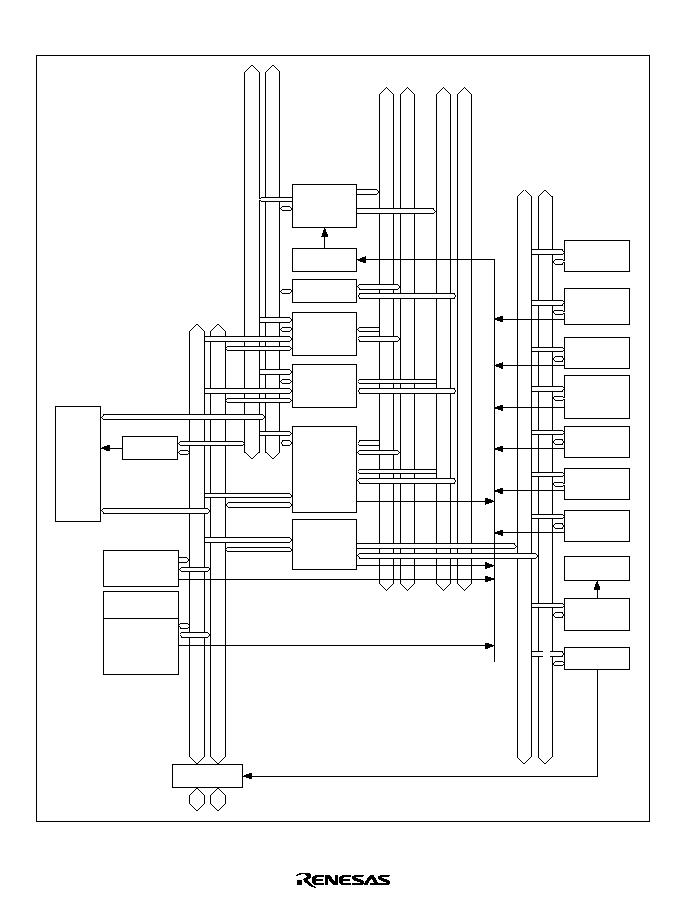
13
1.2
Block Diagram
CPU
X-RAM
Y-RAM
Bus state
controller
User break
controller
Interrupt
controller
Cache
address
array/data
array
DSP
Direct
memory access
controller
Ethernet
controller
direct memory
access
controller
Ethernet
controller
External bus
interface
Cache
controller
Hitachi user
debug
interface
Serial
I/O
Timer
pulse unit
Watchdog
timer
Clock pulse
generator
Free-running
timer
Serial
communication
interface
with FIFO
System
controller
Cache address bus
Internal address bus
Internal address bus
Peripheral address bus
Internal address bus
32-bit internal data bus
32-bit cache data bus
16-bit internal data bus
16-bit internal data bus
I/O ports
16-bit peripheral data bus
Serial I/O
with FIFO
Figure 1.1 Block Diagram of SH7616

14
1.3
Pin Description
1.3.1
Pin Arrangement
Figure 1.2 shows the pin arrangement.
156
155
154
153
152
151
150
149
148
147
146
145
144
143
142
141
140
139
138
137
136
135
134
133
132
131
130
129
128
127
126
125
124
123
122
121
120
119
118
117
116
115
114
113
112
111
110
109
108
107
106
105
PB11/SRS2/
CTS
/STATS0
PVCC
PB12/SRCK2/
RTS
/STATS1
PB13/TXD1
PB14/RXD1
PB15/SCK1
VSS
VSS
BGR
VCC
VCC
BRLS
DACK0
DACK1
DREQ0
DREQ1
BH
BUSHiZ
CS4
CS3
CS2
CS1
CS0
RD/
WR
VCC
BS
VSS
REFOUT
RD
CKE
CAS0
CAS1
CAS2
CAS3
DQMLL/
WE0
DQMLU/
WE1
DQMUL/
WE2
DQMUU/
WE3
CAS
/
OE
RAS
VCC
WAIT
VSS
VSS
VSS
A24
VCC
VCC
A23
A22
A21
A20
1
2
3
4
5
6
7
8
9
10
11
12
13
14
15
16
17
18
19
20
21
22
23
24
25
26
27
28
29
30
31
32
33
34
35
36
37
38
39
40
41
42
43
44
45
46
47
48
49
50
51
52
IRL3
IRL2
IRL1
IRL0
NMI
ASEMODE
*
VSS
RES
PLLVSS
PLLCAP2
PLLCAP1
PLLVCC
MD4
MD3
MD2
MD1
MD0
VCC
EXTAL
VSS
XTAL
VCC
CKIO
CKPREQ
/CKM
CKPACK
VSS
IVECF
TDO
TDI
TCK
TMS
TRST
VCC
D0
VSS
D1
D2
D3
D4
D5
D6
VCC
D7
D8
VSS
D9
D10
D11
D12
VCC
D13
VSS
A19
A18
A17
VSS
A16
VCC
A15
A14
A13
A12
A11
A10
A9
VSS
A8
VCC
A7
A6
A5
A4
A3
A2
A1
VCC
A0
VSS
VSS
D31
VCC
D30
D29
D28
D27
D26
D25
VSS
D24
VCC
VCC
D23
D22
D21
D20
VSS
VSS
D19
VCC
D18
D17
D16
D15
D14
104
103
102
101
100
99
98
97
96
95
94
93
92
91
90
89
88
87
86
85
84
83
82
81
80
79
78
77
76
75
74
73
72
71
70
69
68
67
66
65
64
63
62
61
60
59
58
57
56
55
54
53
157
158
159
160
161
162
163
164
165
166
167
168
169
170
171
172
173
174
175
176
177
178
179
180
181
182
183
184
185
186
187
188
189
190
191
192
193
194
195
196
197
198
199
200
201
202
203
204
205
206
207
208
PVSS
TIOCA1/SRXD2/PB10
TCLKC/TIOCB1/STCK2/PB9
TIOCA2/STS2/PB8
TCLKD/TIOCB2/STXD2/PB7
SCK2/SRCK1/PB6
RXD2/SRS1/PB5
TXD2/SRXD1/PB4
TIOCA0/STCK1/PB3
TIOCB0/STS1/PB2
PVCC
TCLKA/TIOCC0/STXD1/PB1
PVSS
WOL/TCLKB/TIOCD0/PB0
SRCK0/PA13
SRS0/PA12
SRXD0/PA11
STCK0/PA10
STS0/PA9
STXD0/PA8
WDTOVF
/PA7
FTCI/PA6
PVCC
FTI/PA5
PVSS
FTOA/PA4
FTOB/CKPO
LNKSTA/PA2
EXOUT/PA1
PA0/CAMSEN
RXER
RXDV
COL
CRS
PVSS
RXCLK
PVCC
ERXD0
ERXD1
ERXD2
ERXD3
MDIO
MDC
PVCC
TXCLK
PVSS
TXEN
ETXD0
ETXD1
ETXD2
ETXD3
TXER
FP-208C
(Top view)
Body size
Height
Pin pitch
Note:
*
When doing debugging using the E10A emulator, this pin is used for mode switching. It should be connected to Vss
when using the E10A emulator and connected to Vcc when using a normal user system.
28
◊
28
1.7
0.5
(mm)
(mm)
(mm)
Figure 1.2 SH7616 Pin Arrangement (FP-208C)

15
1.3.2
Pin Functions
Table 1.2
Pin Functions
Type
Symbol
I/O
Name
Function
Power
V
CC
Input
Power
For connection to the power supply.
Connect all V
CC
pins to the system power
supply. The chip will not operate if there
are any open pins
V
SS
Input
Ground
For connection to ground. Connect all
V
SS
pins to the system ground. The chip
will not operate if there are any open pins
PV
CC
Input
I/O circuit power
Power supply for the I/O circuits
PV
SS
Input
I/O circuit
ground
Ground for the I/O circuits
Clock
XTAL
Output
Crystal input/
output pin
For connection to a crystal resonator
EXTAL
Input
For connection to a crystal resonator, or
used as external clock input pin
CKIO
I/O
System clock
input/output
pin
Used as the external clock input or
internal clock output pin
CKPREQ
/
CKM
Input
Clock pause
request input
Used as the clock pause request pin for
changing the frequency of the clock input
from the CKIO pin, or halting the clock
CKPACK
Output
Clock pause
acknowledge
signal
Indicates that the chip is in the clock
pause state (standby state) internally
CKPO
Output
On-chip
peripheral clock
(P
) output
Outputs the on-chip peripheral clock (P
)
PLLCAP1
Input
PLL capacitance
connection pins
Connects capacitance for operation of
PLL circuit 1
PLLCAP2
Input
Connects capacitance for operation of
PLL circuit 2
PLLV
CC
Input
PLL power
PLL oscillator power supply
PLLV
SS
Input
PLL ground
PLL oscillator ground

16
Table 1.2
Pin Functions (cont)
Type
Symbol
I/O
Name
Function
System
control
RES
Input
Reset
When
RES
= 0 and NMI = 1, the chip
enters the power-on reset state. When
RES
= 0 and NMI = 0, the chip enters the
manual reset state
WDTOVF
Output
Watchdog
timer overflow
Counter overflow signal output in
watchdog timer mode
BGR
Output
Bus grant
Indicates that the bus has been released
to an external device. The device that
output the
BRLS
signal recognizes that
the bus has been acquired when it
receives the
BGR
signal
BRLS
Input
Bus release
Driven low when an external device
requests release of the bus
Operating
mode
MD0≠MD4
Input
Mode setting
The operating mode is specified by the
levels at these pins
Interrupts
NMI
Input
Nonmaskable
interrupt
Inputs the nonmaskable interrupt request
signal
IRL3
≠
IRL0
Input
External
interrupt
request input
0 to 3
These pins input maskable interrupt
request signals
IVECF
Output
Interrupt
vector fetch
cycle
Indicates an external vector read cycle
Bus control
BS
Output
Bus cycle
start
Signal indicating the start of a bus cycle
Asserted every data cycle in burst
transfer
CS4
≠
CS0
Output
Chip select
0 to 4
Chip select signals indicating the area
being accessed
WAIT
Input
Wait
Wait state request signal
RD
Output
Read
Strobe signal indicating a read cycle
RAS
Output
Row address
strobe
DRAM/synchronous DRAM RAS signal

17
Table 1.2
Pin Functions (cont)
Type
Symbol
I/O
Name
Function
Bus control
CAS
Output
Column
address strobe
Synchronous DRAM CAS signal
OE
Output
Output enable
EDO DRAM output enable signal
Used in access in RAS down mode
DQMUU/
WE3
Output
Highest byte
access
SRAM/synchronous DRAM highest byte
select signal
DQMUL/
WE2
Output
Second byte
access
SRAM/synchronous DRAM second byte
select signal
DQMLU/
WE1
Output
Third byte
access
SRAM/synchronous DRAM third byte
select signal
DQMLL/
WE0
Output
Lowest byte
access
SRAM/synchronous DRAM lowest byte
select signal
CAS3
Output
Column address
strobe 3
DRAM highest byte select signal
CAS2
Output
Column address
strobe 2
DRAM second byte select signal
CAS1
Output
Column address
strobe 1
DRAM third byte select signal
CAS0
Output
Column address
strobe 0
DRAM lowest byte select signal
CKE
Output
Clock enable
Synchronous DRAM clock enable signal
REFOUT
Output
Refresh out
Signal requesting refresh execution
when the bus is released
RD/
WR
Output
Read/write
DRAM/synchronous DRAM write signal
BUSHiZ
Input
Bus high
impedance
Signal used in combination with WAIT
signal to place bus and strobe signals in
the high-impedance state without the
ending bus cycle
BH
Output
Burst hint
Asserted at the start of a DMA burst,
negated one bus cycle before the end of
the burst
STATS0, 1
Output
Status
CPU, DMAC, and E-DMAC status
information

18
Table 1.2
Pin Functions (cont)
Type
Symbol
I/O
Name
Function
Bus control
A24≠A0
Output
Address bus
Address output
D31≠D0
I/O
Data bus
Data input/output
H-UDI
TCK
Input
Test clock
Test clock input
TMS
Input
Test mode
select
Test mode select input signal
TDI
Input
Test data input
Serial data input
TDO
Output
Test data output
Serial data output
TRST
Input
Test reset
Test reset input signal
ASEMODE
*
Input
ASE mode input
ASE mode/user mode select signal
Ethernet
controller
TX-CLK
Input
Transmitter
clock
TX-EN, ETXD0≠3, TX-ER timing
reference signal
(EtherC)
RX-CLK
Input
Receive clock
RX-DV, ERXD0≠3, RX-ER timing
reference signal
TX-EN
Output
Transmit enable
Signal indicating that transmit data on
ETXD0≠3 is ready
ETXD0≠3
Output
Transmit data
0≠3
4-bit receive data
TX-ER
Output
Transmit error
Signal sending error status to another
port
RX-DV
Input
Receive data
enable
Indicates that enable receive data on
ERXD0≠3 exist
ERXD0≠3
Input
Receive data
0≠3
4-bit receive data
RX-ER
Input
Receive error
Reports error state that occurred during
transfer of frame data
CRS
Input
Carrier sense
Carrier detection notification signal
COL
Input
Collision
Collision detection signal
MDC
Output
Management
data clock
Reference clock signal for information
transfer by MDIO
MDIO
I/O
Management
data input/output
Bidirectional signal for exchanging
management information between STA
and PHY
Note:
*
When carrying out debugging using the E10A emulator, this pin is used for mode switching.
It should be connected to V
SS
when using the E10A emulator and connected to V
CC
when
using a normal user system. When a boundary scan test is performed with the H-UDI, user
mode must be used. A boundary scan test cannot be performed in ASE mode.

19
Table 1.2
Pin Functions (cont)
Type
Symbol
I/O
Name
Function
Ethernet
LNKSTA
Input
Link status
Link status input from PHY
controller
(EtherC)
EXOUT
Output
General-purpose
external output
General-purpose external output pin
WOL
Output
Wake on LAN
Signal indicating detection of a Magic
Packet
CAMSEN
Input
CAM sense
CAM sense signal
Direct
memory
access
controller
DACK0, 1
Output
DMAC
channel 0, 1
acknowledge
These pins output receiving a DMA
transfer request to an external device
(DMAC)
DREQ0, 1
Input
DMAC
channel 0, 1
request
Pins that input DMA transfer requests
from an external device
Serial com-
munication
interface with
TXD1, 2
Output
Transmit data
output channel
1, 2
SCIF channel 1 and 2 transmit data
output pins
FIFO (SCIF)
RXD1, 2
Input
Receive data
output channel
1, 2
SCIF channel 1 and 2 receive data input
pins
SCK1, 2
I/O
Serial clock
input/output
channel 1, 2
SCIF clock input/output pins
RTS
Output
Transmit
request
SCIF channel 1 transmit request output
pin
CTS
Input
Transmit enable
SCIF channel 1 transmit enable input pin
Timer pulse
unit (TPU)
TCLKA
TCLKB
TCLKC
TCLKD
Input
TPU timer clock
input A, B, C, D
Pins that input an external clock to the
TPU counter
TIOCA0
TIOCB0
TIOCC0
TIOCD0
I/O
TPU input
capture/output
compare
(channel 0)
Channel 0 input capture input/
output compare output/PWM output pins
TIOCA1
TIOCB1
I/O
TPU input
capture/output
compare
(channel 1)
Channel 1 input capture input/
output compare output/PWM output pins

20
Table 1.2
Pin Functions (cont)
Type
Symbol
I/O
Name
Function
Timer pulse
unit (TPU)
TIOCA2
TIOCB2
I/O
TPU input
capture/output
compare
(channel 2)
Channel 2 input capture input/output
compare output/PWM output pins
16-bit
free-running
FTCI
Input
Counter clock
input
FRC counter clock input pin
timer (FRT)
FTOA
Output
Output compare
A output
Output compare A output pin
FTOB
Output
Output compare
B output
Output compare B output pin
FTI
Input
Input capture
input
Input capture input pin
Serial I/O
with FIFO
SRXD0
Input
Serial receive
data input 0
Serial receive data input ports
(SIOF)
SRCK0
Input
Serial receive
clock input 0
Serial receive clock ports
SRS0
Input
Serial receive
synchronization
clock input 0
Serial receive synchronization input
ports
STXD0
Output
Serial transmit
data output 0
Serial data output ports
STCK0
Input
Serial transmit
clock input 0
Serial transmit clock ports
STS0
I/O
Serial transmit
synchronization
clock
input/output
0
Serial transmit synchronization
input/output ports
Serial I/O
(SIO)
SRXD1, 2
Input
Serial receive
data input 1, 2
Serial receive data input ports
SRCK1, 2
Input
Serial receive
clock input 1, 2
Serial receive clock ports
SRS1, 2
Input
Serial receive
synchronization
input 1, 2
Serial receive synchronization input
ports
STXD1, 2
Output
Serial transmit
data output 1, 2
Serial data output ports
STCK1, 2
Input
Serial transmit
clock input 1, 2
Serial transmit clock ports
STS1, 2
I/O
Serial transmit
synchronization
input/output 1, 2
Serial transmit synchronization
input/output ports

21
Table 1.2
Pin Functions (cont)
Type
Symbol
I/O
Name
Function
I/O ports
PA0≠PA13
*
I/O
General port
General input/output port pins
Input or output can be specified bit by bit
PB0≠PB15
I/O
General port
General input/output port pins
Input or output can be specified bit by bit
Note:
*
PA3 cannot be used; CKPO is valid instead.
1.3.3
Pin Multiplexing
Table 1.3
Pin Multiplexing
No.
Function 1
Function 2
Function 3
Function 4
Type
12
PLLV
CC
Clocks
9
PLLV
SS
11
PLLCAP1
10
PLLCAP2
19
EXTAL
21
XTAL
23
CKIO
24
CKPREQ
/CKM
25
CKPACK
9 pins
8
RES
System control
13
MD4
14
MD3
15
MD2
16
MD1
17
MD0
6 pins
5
NMI
Interrupts
1
IRL3
2
IRL2
3
IRL1
4
IRL0
27
IVECF
6 pins

22
Table 1.3
Pin Multiplexing (cont)
No.
Function 1
Function 2
Function 3
Function 4
Type
131
BS
Bus control
138
CS4
137
CS3
136
CS2
135
CS1
134
CS0
148
BGR
145
BRLS
115
WAIT
128
RD
117
RAS
118
CAS
/
OE
119
DQMUU/
WE3
120
DQMUL/
WE2
121
DQMLU/
WE1
122
DQMLL/
WE0
123
CAS3
124
CAS2
125
CAS1
126
CAS0
127
CKE
129
REFOUT
133
RD/
WR
139
BUSHiZ
140
BH
25 pins

23
Table 1.3
Pin Multiplexing (cont)
No.
Function 1
Function 2
Function 3
Function 4
Type
111
A24
Address bus
108
A23
107
A22
106
A21
105
A20
104
A19
103
A18
102
A17
100
A16
98
A15
97
A14
96
A13
95
A12
94
A11
93
A10
92
A9
90
A8
88
A7
87
A6
86
A5
85
A4
84
A3
83
A2
82
A1
80
A0
25 pins

24
Table 1.3
Pin Multiplexing (cont)
No.
Function 1
Function 2
Function 3
Function 4
Type
77
D31
Data bus
75
D30
74
D29
73
D28
72
D27
71
D26
70
D25
68
D24
65
D23
64
D22
63
D21
62
D20
59
D19
57
D18
56
D17
55
D16
54
D15
53
D14
51
D13
49
D12
48
D11
47
D10
46
D9
44
D8
43
D7
41
D6
40
D5
39
D4
38
D3
37
D2
36
D1
34
D0
32 pins

25
Table 1.3
Pin Multiplexing (cont)
No.
Function 1
Function 2
Function 3
Function 4
Type
30
TCK
H-UDI
31
TMS
29
TDI
28
TDO
32
TRST
6
ASEMODE
*
6 pins
201
TX-CLK
EtherC
192
RX-CLK
203
TX-EN
5 V I/O compatibility
207
ETXD3
206
ETXD2
205
ETXD1
204
ETXD0
208
TX-ER
188
RX-DV
197
ERXD3
196
ERXD2
195
ERXD1
194
ERXD0
187
RX-ER
190
CRS
189
COL
199
MDC
198
MDIO
18 pins
143
DACK1
DMAC
144
DACK0
141
DREQ1
142
DREQ0
4 pins
Note:
*
When carrying out debugging using the E10A emulator, this pin is used for mode switching.
It should be connected to V
SS
when using the E10A emulator (ASE mode). When using the
chip in the normal user system, and not using the E10A emulator (user mode), connect this
pin to V
CC
. When a boundary scan test is performed with the H-UDI, user mode must be
used. A boundary scan test cannot be performed in ASE mode.

26
Table 1.3
Pin Multiplexing (cont)
No.
Function 1
[00]
*
Function 2
[01]
*
Function 3
[10]
*
Function 4
[11]
*
Type
151
PB15
SCK1
Port B
152
PB14
RXD1
SCIF, SIO, TPU
153
PB13
TXD1
154
PB12
SRCK2
RTS
STATS1
5 V I/O compatibility
156
PB11
SRS2
CTS
STATS0
158
PB10
SRXD2
TIOCA1
159
PB9
STCK2
TIOCB1/TCLKC
160
PB8
STS2
TIOCA2
161
PB7
STXD2
TIOCB2/TCLKD
162
PB6
SRCK1
SCK2
163
PB5
SRS1
RXD2
164
PB4
SRXD1
TXD2
165
PB3
STCK1
TIOCA0
166
PB2
STS1
TIOCB0
168
PB1
STXD1
TIOCC0/TCLKA
170
PB0
TIOCD0/TCLKB
WOL
16 pins
171
PA13
SRCK0
Port A
172
PA12
SRS0
SIOF, FRT, WDT,
173
PA11
SRXD0
EtherC
174
PA10
STCK0
5 V I/O compatibility
175
PA9
STS0
176
PA8
STXD0
177
WDTOVF
PA7
178
PA6
FTCI
180
PA5
FTI
182
PA4
FTOA
183
CKPO
FTOB
184
PA2
LNKSTA
185
PA1
EXOUT
186
PA0
CAMSEN
14 pins
Note:
*
Figures in square brackets indicate the settings of the mode bits (MD0, MD1) in the PFC in
order to select the multiplex functions in port A [0:13] and port B [0:15].
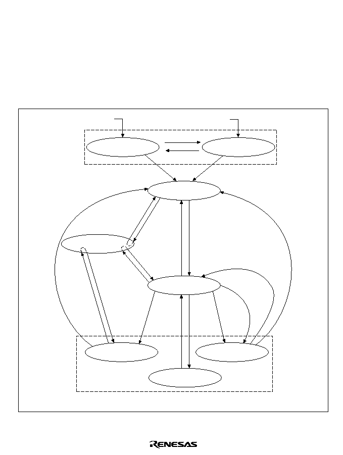
27
WDTOVF
:
In a reset, this pin becomes an output pin.
When used for general input/output, attention must be paid to the polarity of
this pin.
1.4
Processing States
State Transitions: The CPU has five processing states: the reset state, exception handling state,
bus-released state, program execution state, and power-down state. Figure 1.3 shows the state
transitions.
RST
= 0, NMI = 1
RST
= 1,
NMI = 0
RST
= 1,
NMI = 1
Interrupt or DMA
address error
NMI interrupt
End of
exception
handling
Bus
request
Exception
Bus request
cleared
Bus request
received
Bus request
cleared
SLEEP
instruction
(SBY = 0)
SLEEP
instruction
(SBY = 1)
From any state when
RES
= 0 and NMI = 1
From any state when
RES
= 0 and NMI = 0
Reset states
Power-down state
Note:
*
clock pause function
Bus request
received
Bus request
cleared
RST
= 0, NMI = 0
MSTP
bit
cleared
MSTP
bit set
Bus-released state
Exception-handling state
Manual reset state
Power-on reset state
Program execution state
Sleep mode
Standby mode
Module standby
SBY bit set and
CKPREQ
= 0
*
CKPREQ
= 1
*
Figure 1.3 Processing State Transitions

28
Reset State: In this state, the CPU is reset. The reset state is entered when the
RES pin goes low.
The power-on reset state is entered if the NMI pin is high, and the manual reset state is entered if
the NMI pin is low.
Exception Handling State: The exception handling state is a transient state that occurs when the
CPU alters the normal programming flow dues to a reset, interrupt, or other exception handling
source.
In the case of a reset, the CPU fetches the execution start address as the initial value of the
program counter (PC) from the exception vector table, and the initial value of the stack pointer
(SP), stores these values, branches to the start address, and begins program execution at that
address.
In the case of an interrupt, etc., the CPU references the SP and saves the PC and status register
(SR) in the stack area. It fetches the start address of the exception service routine from the
exception vector table, branches to that address, and begins program execution.
Subsequently, the processing state is the program execution state.
Program Execution State: In the program execution state the CPU executes program instructions
in normal sequence.
Power-Down State: In the power-down state the CPU stops operating to conserve power. The
power-down state is entered by executing a SLEEP instruction. The power-down state includes
two modes--sleep mode and standby mode--and a module standby function.
Bus-Released State: In the bus-released state, the CPU releases the bus to a device that has
requested it.
Power-Down State: In addition to the normal program execution state, another CPU processing
state called the power-down state is provided. In this state, CPU operation is halted and power
consumption is reduced. The power-down state includes two modes--sleep mode and standby
mode--and a module standby function.
∑
Sleep Mode
A transition to sleep mode is made if the SLEEP instruction is executed while the standby bit
(SBY) is cleared to 0 in standby control register 1 (SBYCR1). In sleep mode CPU operations
stop but data in the CPU's internal registers and in on-chip cache memory and on-chip RAM is
retained. The functions of the on-chip supporting modules do not stop.

29
∑
Standby Mode
A transition to standby mode is made if the SLEEP instruction is executed while SBY is set to
1 in SBYCR1. In standby mode the CPU, the on-chip modules, and the oscillator all stop.
When entering standby mode, the DMAC's DMA master enable bit should be cleared to 0.
Also, the cache should be turned off before entering this mode. The contents of the cache and
on-chip RAM are not retained in this mode.
Standby mode is exited by means of a reset or an external NMI interrupt. When standby mode
is exited, the normal program execution state is entered via the exception handling state after
the elapse of the oscillation settling time.
If a transition is made to standby mode using the clock pause function, it is possible to change
the frequency of the CKIO pin input clock, or to stop the clock itself. When SBY in SBYCR1
is set to 1 and a low level is applied to the
CKPREQ/CKM pin, a transition is made to standby
mode and a low level is output from the
CKPACK pin. The clock can then be stopped, or its
frequency changed.
On-chip supporting module states and pin states are the same as in the normal standby mode
entered by means of the SLEEP instruction. A transition to the program execution state is
made by applying a high level to the
CKPREQ/CKM pin.
In this mode the oscillator is halted, greatly reducing power consumption.
∑
Module Standby Function
A module standby function is provided for the following on-chip supporting modules: the
direct memory access controller (DMAC), DSP, 16-bit free-running timer (FRT), serial
communication interface with FIFO (SCIF), serial I/O with FIFO (SIOF), serial I/O (SIO), user
break controller (UBC), and timer pulse unit (TPU). A module standby function is not
supported for the Ethernet controller (EtherC) or the Ethernet direct memory access controller
(E-DMAC).
Setting one of module stop bits 11 to 3 and 1 (MSTP11 to MSTP3, MSTP1) to 1 in the standby
control register (SBYCR1/2) stops the clock supply to the corresponding on-chip supporting
module. Use of this function enables power consumption to be reduced.
The module standby function is cleared by clearing the corresponding MSTP bit to 0.
DSP instructions must not be used when the DSP has been placed in the module standby state.
When using the DMAC module standby function, the direct memory access controller's DMA
master enable bit should be cleared to 0.

30
Table 1.4
Power-Down State
State
Mode
Entering
Conditions
Clock
CPU
On-chip
Supporting
Modules
CPU
Registers
On-Chip
Cache or
On-Chip
RAM
Exiting
Conditions
Sleep
mode
Executing
SLEEP
instruction
while SBY bit
is cleared in
SBYCR1
Operating
Halted
Operating
Held
Held
1. Interrupt
2. DMA address
error
3. Power-on reset
4. Manual reset
Standby
mode
Executing
SLEEP
instruction
while SBY
bit is set in
SBYCR1
Halted
Halted
Halted and
initialized
*
1
Held
Undefined
1. NMI interrupt
2. Power-on reset
3. Manual reset
Module
standby
function
Setting
MSTP bit
corresponding
to individual
module
Operating
Operating
(DSP
halted)
Clock supply
to specified
module
halted,
module
initialized
*
2
Held
Held
1. Clearing MSTP
bit
2. Power-on reset
3. Manual reset
Notes:
*
1 Depends on individual supporting module or pin.
*
2 DMAC and DSP registers and specified module interrupt vectors retain their set values.

31
Section 2 CPU
2.1
Register Configuration
The register set consists of sixteen 32-bit general registers, six 32-bit control registers and ten 32-
bit system registers.
This chip is upwardly compatible with the SH-1, SH-2 on the object code level. For this reason,
several registers have been added to the previous SuperH microcontroller registers. The added
registers are the three control registers: repeat start register (RS), repeat end register (RE), and
modulo register (MOD) and the six system registers: DSP status register (DSR), and A0, A1, X0,
X1, Y0 and Y1 among the DSP data registers.
The general registers are used in the same manner as the SH-1, SH-2 with regard to SuperH
microcontroller-type instructions. With regard to DSP type instructions, they are used as address
and index registers for accessing memory.
2.1.1
General Registers
There are 16 general registers (Rn) numbered R0≠R15, which are 32 bits in length. General
registers are used for data processing and address calculation.
With SuperH microcomputer type instructions, R0 is also used as an index register. Several
instructions are limited to use of R0 only. R15 is used as the hardware stack pointer (SP). Saving
and recovering the status register (SR) and program counter (PC) in exception processing is
accomplished by referencing the stack using R15.
With DSP type instructions, eight of the 16 general registers are used for the addressing of X, Y
data memory and data memory (single data) using the I bus.
R4, R5 are used as an X address register (Ax) for X memory accesses, and R8 is used as an X
index register (Ix). R6, R7 are used as a Y address register (Ay) for Y memory accesses, and R9 is
used as a Y index register (Iy). R2, R3, R4, R5 are used as a single data address register (As) for
accessing single data using the I bus, and R8 is used as a single data index register (Is).
DSP type instructions can simultaneously access X and Y data memory. There are two groups of
address pointers for designating X and Y data memory addresses.
Figure 2.1 shows the general registers.

32
R0
*
1
R1
R2, [As]
*
3
R3, [As]
*
3
R4, [As, Ax]
*
3
R5, [As, Ax]
*
3
R6, [Ay]
*
3
R7, [Ay]
*
3
R8, [Ix, Is]
*
3
R9, [Iy]
*
3
R10
R11
R12
R13
R14
R15, SP
*
2
0
31
R0 also functions as an index register in the indirect indexed register
addressing mode and indirect indexed GBR addressing mode. In some
instructions, only the R0 functions as a source register or destination register.
R15 functions as a hardware stack pointer (SP) during exception processing.
Used as memory address registers, memory index registers with DSP type
instructions.
Notes:
*
1
*
2
*
3
Figure 2.1 General Register Configuration
With the assembler, symbol names are used for R2, R3 ... R9. If it is wished to use a name that
makes clear the role of a register for DSP type instructions, a different register name (alias) can be
used. This is written in the following manner for the assembler.
Ix:
.REG (R8)

33
The name Ix is an alias for R8. The other aliases are assigned as follows:
Ax0:
.REG (R4)
Ax1:
.REG (R5)
Ix:
.REG (R8)
Ay0:
.REG (R6)
Ay1:
.REG (R7)
Iy:
.REG (R9)
As0:
.REG (R4)
defined when an alias is required for single data transfer
As1:
.REG (R5)
defined when an alias is required for single data transfer
As2:
.REG (R2)
defined when an alias is required for single data transfer
As3:
.REG (R3)
defined when an alias is required for single data transfer
Is:
.REG (R8)
defined when an alias is required for single data transfer
2.1.2
Control Registers
The six 32-bit control registers consist of the status register (SR), repeat start register (RS), repeat
end register (RE), global base register (GBR), vector base register (VBR), and modulo register
(MOD).
The SR register indicates processing states.
The GBR register functions as a base address for the indirect GBR addressing mode, and is used
for such as on-chip peripheral module register data transfers.
The VBR register functions as the base address of the exception processing vector area (including
interrupts).
The RS and RE registers are used for program repeat (loop) control. The repeat count is
designated in the SR register repeat counter (RC), the repeat start address in the RS register, and
the repeat end address in the RE register. However, note that the address values stored in the RS
and RE registers are not necessarily always the same as the physical start and end address values
of the repeat.
The MOD register is used for modulo addressing to buffer the repeat data. The modulo addressing
designation is made by DMX or DMY, the modulo end address (ME) is designated in the upper 16
bits of the MOD register, and the modulo start address (MS) is designated in the lower 16 bits.
Note that the DMX and DMY bits cannot simultaneously designate modulo addressing. Modulo
addressing is possible with X and Y data transfer instructions (MOVX, MOVY). It is not possible
with single data transfer instructions (MOVS).

34
Figure 2.2 shows the control registers. Table 2.1 indicates the SR register bits.
S T
I3 I2 I1 I0 RF1 RF0
Q
M
DMX
DMY
0000
0000
RC
31 28 27
16 15 12 11
10
9 8 7
4
3
2
1 0
Status register (SR)
Repeat start register (RS)
Repeat end register (RE)
Global base register (GBR)
Vector base register (VBR)
Modulo register (MOD)
ME: Modulo end address
MS: Modulo start address
31
31
31
31
31
0
0
0
0
0
16 15
RS
RE
GBR
VBR
ME
MS
Figure 2.2 Control Register Configuration

35
Table 2.1
SR Register Bits
Bit
Name (Abbreviation)
Function
27≠16
Repeat counter (RC)
Designate the repeat count (2≠4095) for repeat (loop)
control
11
Y pointer usage modulo
addressing designation
(DMY)
1: modulo addressing mode becomes valid for Y
memory address pointer, Ay (R6, R7)
10
X pointer usage modulo
addressing designation
(DMX)
1: modulo addressing mode becomes valid for X
memory address pointer, Ax (R4, R5)
9
M bit
Used by the DIV0S/U, DIV1 instructions
8
Q bit
Used by the DIV0S/U, DIV1 instructions
7≠4
Interrupt request mask
(I3≠I0)
Indicate the receive level of an interrupt request (0 to
15)
3≠2
Repeat flags (RF1, RF0)
Used in zero overhead repeat (loop) control. Set as
below for an SETRC instruction
For 1 step repeat 00 RE--RS=≠4
For 2 step repeat 01 RE--RS=≠2
For 3 step repeat 11 RE--RS=0
For 4 steps or more 10 RE--RS>0
1
Saturation arithmetic bit
(S)
Used with MAC instructions and DSP instructions
1: Designates saturation arithmetic (prevents
overflows)
0
T bit
For MOVT, CMP/cond, TAS, TST, BT, BT/S, BF,
BF/S, SETT, CLRT and DT instructions,
0: represents false
1: represents true
For ADDV/ADDC, SUBV/SUBC, DIV0U/DIV0S, DIV1,
NEGC, SHAR/SHAL, SHLR/SHLL, ROTR/ROTL and
ROTCR/ROTCL instructions,
1: represents occurrence of carry, borrow, overflow or
underflow
31≠28
15≠12
0 bit
0: 0 is always read out; write a 0

36
There are dedicated load/store instructions for accessing the RS, RE and MOD registers. For
example, the RS register is accessed as follows.
LDC
Rm,RS;
Rm
RS
LDC.L
@Rm+,RS;
(Rm)
RS,Rm+4
Rm
STC
RS,Rn;
RS
Rn
STC.L
RS,@-Rn;
Rn-4
Rn,RS
(Rn)
The following instructions set addresses in the RS, RE registers for zero overhead repeat control:
LDRS
@(disp,PC);
disp
◊
2 + PC
RS
LDRE
@(disp,PC);
disp
◊
2 + PC
RE
The GBR register and VBR register are the same as the previous SuperH microprocessor registers.
An RC counter and four control bits (DMX bit, DMY bit, RF1 bit, RF0 bit) have been added to
the SR register. The RS, RE and MOD registers are new registers.
2.1.3
System Registers
System registers consist of four 32-bit registers: high and low multiply and accumulate registers
(MACH and MACL), the procedure register (PR), and the program counter (PC). The MACH and
MACL store the results of multiplication or multiply and accumulate operations*. The PR stores
the return address from the subroutine procedure. The PC indicates the address of the program in
execution; it controls the flow of the processing. The PC indicates the fourth byte after the
instruction currently being executed. These registers are the same as those in the SuperH
microprocessor.
Note:
These are used only when executing an instruction that was supported by SH-1 and SH-2.
They are not used for newly added multiplication instructions (PMULS).
MACL
PR
PC
MACH
31
0
0
0
31
31
Multiply and accumulate
register high (MACH)
Multiply and accumulate
register low (MACL)
Procedure register (PR)
Program counter (PC)
Figure 2.3 System Register Configuration

37
In addition, among the DSP unit usage registers (DSP registers) described in 2.1.4 DSP Registers,
the DSP status register (DSR) and the five registers A0, X0, X1, Y0 and Y1 of the eight data
registers are treated as system registers. Among these, the A0 is a 40-bit register, but when data is
output from the A0 register, the guard bit section (A0G) is disregarded; when data is input to the
A0 register, the MSB of the data is copied into the guard bit section (A0G).
2.1.4
DSP Registers
The DSP unit has eight data registers and one control register as its DSP registers.
The DSP data registers are comprised of the two 40-bit registers A0 and A1, and the six 32-bit
registers M0, M1, X0, X1, Y0 and Y1. The A0 and A1 registers have the 8-bit guard bits A0G and
A1G, respectively.
The DSP data registers are used for the transfer and processing of the DSP data of DSP instruction
operands. There are three types of instructions that access DSP data registers: those for DSP data
processing, and those for X or Y data transfer processing.
The control register is the 32-bit DSP status register (DSR) that represents operation results. The
DSR register has bits that represent operation results, a signed greater than bit (GT), a zero bit (Z),
a negative value bit (N), an overflow bit (V), a DSP status bit (DC: DSP condition), and a status
selection bit (CS: condition select) for controlling DC bit setting.
The DC bit represents one status flag and is very similar to the SuperH microprocessor CPU core
T bit. For conditional DSP type instructions, DSP data processing execution is controlled in
accordance with the DC bit. This control is related to execution in the DSP unit only, and only
DSP registers are updated. It bears no relation to address calculation or such SuperH
microprocessor CPU core execution instructions as load/store instructions. The control bits CS
(bits 2 to 0) designate the status for setting the DC bit.
DSP type instructions are comprised of unconditional DSP type instructions and conditional DSP
type instructions. The status and DC bits are updated in unconditional DSP type data processing,
with the exception of the PMULS, MOVX, MOVY and MOVS instructions. Conditional DSP
type instructions are executed according to the status of the DC bit, but regardless of whether or
not they are executed, the DSR register is not updated.
Figure 2.4 shows the DSP registers. The DSR register bit functions are shown in table 2.2.

38
39
32 31
0
A0G
A1G
A0
A1
M0
M1
X0
X1
Y0
Y1
DSP data registers
DSP status register (DSR)
GT Z N
V CS[2:0] DC
8
7
6
5
4
3 2 1
0
31
Figure 2.4 DSP Register Configuration

39
Table 2.2
DSR Register Bits
Bit
Name (Abbreviation)
Function
31≠8
Reserved bits
0: Always read out; always use 0 as a write value
7
Signed greater than bit
(GT)
Indicates that the operation result is positive
(excepting 0), or that operand 1 is greater than
operand 2
1: Operation result is positive, or operand 1 is greater
6
Zero bit (Z)
Indicates that the operation result is zero (0), or that
operand 1 is equal to operand 2
1: Operation result is zero (0), or equivalence
5
Negative bit (N)
Indicates that the operation result is negative, or that
operand 1 is smaller than operand 2
1: Operation result is negative, or operand 1 is
smaller
4
Overflow bit (V)
Indicates that the operation result has overflowed
1: Operation result has overflowed
3≠1
Status selection bits (CS) Designate the mode for selecting the operation result
status set in the DC bit
Do not set either 110 or 111
000: Carry/borrow mode
001: Negative value mode
010: Zero mode
011: Overflow mode
100: Signed greater mode
101: Signed above mode
0
DSP status bit (DC)
Sets the status of the operation result in the mode
designated by the CS bits
0: Designated mode status not realized (unrealized)
1: Designated mode status realized

40
2.1.5
Notes on Guard Bits and Overflow Treatment
DSP unit data operations are fundamentally performed as 32-bit, but these operations are always
executed with a 40-bit length including the 8-bit guard section. When the guard bit section does
not match the value of the 32-bit section MSB, the operation result is treated as an overflow. In
this case, the N bit indicates the correct status of the operation result regardless of the existence or
not of an overflow. This is so even if the destination operand is a 32-bit length register. The 8-bit
section guard bits are always presupposed and each status flag is updated.
When place overflows occur so that the correct result cannot be displayed even when the guard
bits are used, the N flag cannot indicate the correct status.
2.1.6
Initial Values of Registers
Table 2.3 lists the values of the registers after reset.
Table 2.3
Initial Values of Registers
Classification
Register
Initial Value
General registers
R0≠R14
Undefined
R15 (SP)
Value of the SP in the vector address table
Control registers
SR
Bits I3≠I0 are 1111 (H'F), the reserved bits, RC, DMY,
and DMX are 0, and other bits are undefined
RS
RE
Undefined
GBR
Undefined
VBR
H'00000000
MOD
Undefined
System registers
MACH, MACL, PR
Undefined
PC
Value of the PC in the vector address table
DSP registers
A0, A0G, A1, A1G, M0,
M1, X0, X1, Y0, Y1
Undefined
DSR
H'00000000

41
2.2
Data Formats
2.2.1
Data Format in Registers
Register operand data size is always longword (32 bits). When loading data from memory into a
register, if the memory operand is a byte (8 bits) or a word (16 bits), it is sign-extended into a
longword, then loaded into the register.
31
0
Longword
Figure 2.5 Register Data Format
2.2.2
Data Formats in Memory
These formats are classified into bytes, words, and longwords.
Place byte data in any address, word data from 2n addresses, and longword data from 4n
addresses. An address error will occur if accesses are made from any other boundary. In such
cases, the access results cannot be guaranteed. In particular, the stack area referred to by the
hardware stack pointer (SP, R15) stores the program counter (PC) and status register (SR) as
longwords, so establish the hardware stack pointer so that a 4n value will always result.
To enable sharing of the processor accessing memory in little-endian mode and memory, the CS2,
4 space (area 2, 4) has a function that allows access in little-endian mode. The order of byte data
differs between little-endian mode and normal big-endian mode.
31
0
15
23
7
Byte
Byte
Byte
Byte
Word
Word
Address 2n
Address 4n
Longword
Address m
Address m + 2
Address m + 1
Address m + 3
Big endian
31
0
15
23
7
Byte
Byte
Byte
Byte
Word
Word
Address 2n
Address 4n
Longword
Address m + 3
Address m + 1
Address m + 2
Address m
Little endian
Figure 2.6 Data Formats in Memory

42
2.2.3
Immediate Data Format
Byte immediate data is placed in an instruction code.
With the MOV, ADD, and CMP/EQ instructions, immediate data is sign-extended and operated in
registers as longword data. Immediate data accessed by the TST, AND, OR, and XOR instructions
is zero-extended and handled as longword data. Consequently, AND instructions with immediate
data always clear the upper 24 bits of the destination register.
Word or longword immediate data is not located in the instruction code; it should be placed in a
memory table. Use an immediate data transfer instruction (MOV) to refer the memory table using
the PC relative addressing mode with displacement.
2.2.4
DSP Type Data Formats
This chip has three different types of data format that correspond to various instructions. These are
the fixed-point data format, the integer data format, and the logical data format.
The DSP type fixed-point data format has a binary point fixed between bits 31 and 30. There are
three types: with guard bits, without guard bits, and multiplication input; each with different valid
bit lengths and value ranges.
The DSP type integer data format has a binary point fixed between bits 16 and 15. There are three
types: with guard bits, without guard bits, and shift amount; each with different valid bit lengths
and value ranges. The shift amount of the arithmetic shift (PSHA) has a 7 bit range and can
express values from ≠64 to +63, but the actual valid values are from ≠32 to +32. In the same
manner, the shift amount of the logical shift has a 6 bit range, but the actual valid values are from
≠16 to +16.
The DSP type logical data format does not have a decimal point.
The data format and valid data length are determined by the instructions and DSP registers.
Figure 2.7 shows the three DSP type data formats and binary point positions. The SuperH type
data format is also shown for reference.
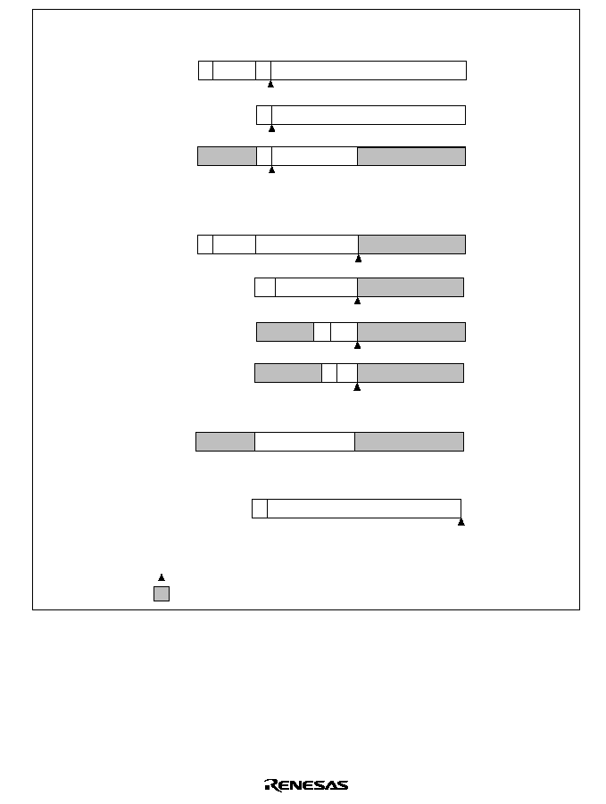
43
S
S
S
S
S
S
S
S
(16 bits)
DSP logical data
SuperH integer (word)
(Reference)
DSP integer data
DSP fixed decimal
point data
With guard bits
No guard bits
Multiplication input
With guard bits
No guard bits
Arithmetic shift (PSHA)
Logical shift (PSHL)
39
39
39
39
32
32
31
31
31
31
31
31
31
31
31
22
21
0
0
0
0
0
0
0
0
0
≠2
8
to +2
8
≠ 2
≠31
≠1 to +1 ≠ 2
≠31
≠1 to +1 ≠ 2
≠15
≠2
23
to +2
23
≠1
≠2
15
to +2
15
≠1
≠32 to +32
≠16 to +16
≠2
31
to +2
31
≠1
16 15
16
16
16
16
16
15
15
15
15
15
: Sign bit
S
: Binary decimal point
: Unrelated to processing (ignored)
30
30
30
Figure 2.7 DSP Type Data Formats

44
2.2.5
DSP Type Instructions and Data Formats
The DSP data format and valid data length are determined by DSP type instructions and DSP
registers. There are three types of instructions that access DSP data registers, DSP data processing,
X, Y data transfer processing, and single data transfer processing instructions.
DSP Data Processing: The guard bits (bits 39≠32) are valid when the A0 and A1 registers are
used as source registers in DSP fixed-point data processing. When any registers other than A0, A1
(e.i., M0, M1, X0, X1, Y0, Y1 registers) are used as source registers, the sign-extended part of that
register data becomes the bits 39 to 32 data. When the A0 and A1 registers are used as destination
registers, the guard bits (bits 39≠32) are valid. When any registers other than A0, A1 are used as
destination registers, bits 39 to 32 of the result data are disregarded.
Processing for DSP integer data is the same as the DSP fixed-point data processing. However, the
lower word (the lower 16 bits, bits 15≠0) of the source register is disregarded. The lower word of
the destination register is cleared to 0.
In DSP logical data processing, the upper word (the upper 16 bits, bits 31≠16) of the source
register is valid. The lower word and the guard bits of the A0, A1 registers are disregarded. The
upper word of the destination register is valid. The lower word and the guard bits of the A0, A1
registers are cleared to 0.
X, Y Data Transfers: The MOVX.W and MOVY.W instructions access X, Y memory via the
16-bit X, Y data buses. The data loaded into registers and data stored from registers is always the
upper word (the upper 16 bits, bits 31≠16).
When loading, the MOVX.W instruction loads X memory, with the X0 and X1 registers as the
destination registers. The MOVY.W instruction loads Y memory, with the Y0 and Y1 registers as
the destination registers. Data is stored in the upper word of the register; the lower word is cleared
to 0.
The upper word data of the A0, A1 registers can be stored in X or Y memory with these data
transfer instructions, but storing is not possible from any other registers. The guard bits and the
lower word of the A0, A1 registers are disregarded.
Single Data Transfers: The MOVS.W and MOVS.L instructions can access any memory via the
data bus (CDB). All DSP registers are connected to the CDB bus, and they can become source or
destination registers during data transfers. The two data transfer modes are word and longword.
In word mode, data is loaded to and stored in the upper word of the DSP register, with the
exception of the A0G, A1G registers. In longword mode, data is loaded to and stored in the 32 bits
of the DSP register, with the exception of the A0G, A1G registers. The A0G, A1G registers can be
treated as independent registers during single data transfers. The load/store data length for the
A0G, A1G registers is 8 bits.

45
If DSP registers are used as source registers in word mode, when data is stored from any registers
other than A0G, A1G, the data in the upper word of the register is transferred. In the case of the
A0, A1 registers, the guard bits are disregarded. When the A0G, A1G registers are the source
registers in word mode, only 8 bits of the data are stored from the registers; the upper bits are sign-
extended.
If the DSP registers are used as destination registers in word mode, the load is to the upper word of
the register, with the exception of A0G, A1G. When data is loaded to any register other than A0G,
A1G, the lower word of the register is cleared to 0. In the case of the A0, A1 registers, the data
sign is extended and stored in the guard bits; the lower word is cleared to 0. When the A0G, A1G
registers are the destination registers in word mode, the least significant 8 bits of the data are
loaded into the registers; the A0, A1 registers are not zero cleared but retain their previous values.
If the DSP registers are used as source registers in longword mode, when data is stored from any
registers other than A0G, A1G, the 32 bits (data) of the register are transferred. When the A0, A1
registers are used as the source registers the guard bits are disregarded. When the A0G, A1G
registers are the source registers in longword mode, only 8 bits of the data are stored from the
registers; the upper bits are sign-extended.
If the DSP registers are used as destination registers in longword mode, the load is to the 32 bits of
the register, with the exception of A0G, A1G. In the case of the A0, A1 registers, the data sign is
extended and stored in the guard bits. When the A0G, A1G registers are the destination registers in
longword mode, the least significant 8 bits of the data are loaded into the registers; the A0, A1
registers are not zero cleared but retain their previous values.
Tables 2.4 and 2.5 indicate the register data formats for DSP instructions. Some registers cannot
be accessed by certain instructions. For example, the PMULS instruction can designate the A1
register as a source register but cannot designate A0 as such. Refer to the instruction explanations
for details.
Figure 2.8 shows the relationship between the buses and the DSP registers during transfers.

46
Table 2.4
Source Register Data Formats for DSP Instructions
Guard Bits
Register Bits
Register
Instruction
39≠32
31≠16
15≠0
A0, A1
DSP
operation
Fixed decimal,
PDMSB,
PSHA
40-bit data
Integer
24-bit data
--
Logic, PSHL,
PMULS
--
16-bit data
Data
transfer
MOVX.W,
MOVY.W,
MOVS.W
MOVS.L
32-bit data
A0G, A1G
Data
MOVS.W
Data
--
--
transfer
MOVS.L
X0, X1, Y0,
Y1, M0, M1
DSP
operation
Fixed decimal,
PDMSB,
PSHA
Sign
*
32-bit data
Integer
16-bit data
--
Logic, PSHL,
PMULS
--
Data
MOVS.W
transfer
MOVS.L
32-bit data
Note:
*
The sign is extended and stored in the ALU's guard bits.

47
Table 2.5
Destination Register Data Formats for DSP Instructions
Guard Bits
Register Bits
Register
Instruction
39≠32
31≠16
15≠0
A0, A1
DSP
operation
Fixed
decimal,
PSHA,
PMULS
(Sign extend)
40-bit result
Integer,
PDMSB
24-bit result
Clear to 0
Logic, PSHL
Clear to 0
16-bit result
Data transfer
MOVS.W
Sign extend
MOVS.L
32-bit data
A0G, A1G
Data transfer
MOVS.W
Data
Not updated
Not updated
MOVS.L
X0, X1, Y0,
Y1, M0, M1
DSP
operation
Fixed
decimal,
PSHA,
PMULS
--
32-bit result
Integer, logic,
PDMSB,
PSHL
16-bit result
Clear to 0
Data transfer
MOVX.W,
MOVY.W,
MOVS.W
MOVS.L
32-bit data

48
39
32
31
0
A0G
A1G
A0
A1
M0
M1
X0
X1
Y0
Y1
DSR
CDB
XDB
YDB
MOVS.W,
MOVS.L
32 bits
16 bits
16 bits
16 bits
32 bits
MOVX.W,
MOVY.W
MOVS.W,
MOVS.L
16
8 bits
7
0
[7:0]
Figure 2.8 DSP Register-Bus Relationship during Data Transfers
2.3
CPU Core Instruction Features
The CPU core instructions are RISC type. The characteristics are as follows.
16-Bit Fixed Length: All instructions are 16 bits long, increasing program code efficiency.
One Instruction per Cycle: The microprocessor can execute basic instructions in one cycle using
the pipeline system. One state equals 16.0 ns when operating at 62.5 MHz.
Data Length: Longword is the basic data length for all operations. Memory can be accessed in
bytes, words, or longwords. Byte or word data accessed from memory is sign-extended and
handled as longword data. Immediate data is sign-extended for arithmetic operations or zero-
extended for logic operations. It also is handled as longword data.

49
Table 2.6
Sign Extension of Word Data
SH7616 CPU
Description
Example of Conventional CPU
MOV.W @(disp,PC),R1
ADD
R1,R0
........
.DATA.W H'1234
Data is sign-extended to 32
bits, and R1 becomes
H'00001234. It is next operated
upon by an ADD instruction
ADD.W #H'1234,R0
Note:
@(disp, PC) accesses the immediate data.
Load-Store Architecture: Basic operations are executed between registers. For operations that
involve memory access, data is loaded to the registers and executed (load-store architecture).
However, Instructions such as AND manipulating bits, are executed directly in memory.
Delayed Branches: Such instructions as unconditional branches are delayed branch instructions.
In the case of delayed branch instructions, the branch occurs after execution of the instruction
immediately following the delayed branch instruction (slot instruction). This reduces pipeline
disruption during branching.
The branching operation of the delayed branch occurs after execution of the slot instruction.
However, with the exception of such branch operations as register updating, execution of
instructions is performed with the order of delayed branch instruction, then delayed slot
instruction.
For example, even if the contents of a register storing a branch destination address are modified by
a delayed slot, the branch destination address will still be the contents of the register before the
modification.
Table 2.7
Delayed Branch Instructions
SH7616 CPU
Description
Example of Conventional CPU
BRA TRGET
ADD R1,R0
Executes an ADD before
branching to TRGET
ADD.W R1,R0
BRA TRGET
Multiplication/Multiply-Accumulate Operation: 16
◊
16
32 multiplications execute in one
to three cycles, and 16
◊
16 + 64
64 multiply-accumulate operations execute in two to three
cycles. 32
◊
32
64 multiplications and 32
◊
32 + 64
64 multiply-accumulate operations
execute in two to four cycles.

50
T Bit: The T bit in the status register (SR) changes according to the result of a comparison, and
conditional branches occur in accordance with its true or false status. The number of instructions
modifying the T bit is kept to a minimum to improve the processing speed.
Table 2.8
T Bit
SH7616 CPU
Description
Example of Conventional CPU
CMP/GE
R1,R0
BT
TRGET0
BF
TRGET1
T bit is set when R0
R1.
The program branches to TRGET0
when R0
R1.
The program branches to TRGET1
when R0 < R1
CMP.W R1,R0
BGE
TRGET0
BLT
TRGET1
ADD
#≠1,R0
CMP/EQ #0,R0
BT
TRGET
T bit is not changed by ADD. T bit
is set when R0 = 0. The program
branches when R0 = 0
SUB.W #1,R0
BEQ TRGET
Immediate Data: Byte immediate data resides in instruction code. Word or longword immediate
data is not input in instruction codes but is stored in a memory table. An immediate data transfer
instruction (MOV) accesses the memory table using the PC relative addressing mode with
displacement.
Table 2.9
Immediate Data Accessing
Classification
SH7616 CPU
Example of Conventional CPU
8-bit immediate
MOV
#H'12,R0
MOV.B
#H'12,R0
16-bit immediate
MOV.W
@(disp,PC),R0
........
.DATA.W H'1234
MOV.W
#H'1234,R0
32-bit immediate
MOV.L
@(disp,PC),R0
........
.DATA.L H'12345678
MOV.L
#H'12345678,R0
Note:
@(disp, PC) accesses the immediate data.

51
Absolute Address: When data is accessed by absolute address, the value already in the absolute
address is placed in the memory table. Loading the immediate data when the instruction is
executed transfers that value to the register and the data is accessed in the indirect register
addressing mode.
Table 2.10
Absolute Address Accessing
Classification
SH7616 CPU
Example of Conventional CPU
Absolute address
MOV.L
@(disp,PC),R1
MOV.B
@R1,R0
........
.DATA.L H'12345678
MOV.B @H'12345678,R0
16-Bit/32-Bit Displacement: When data is accessed by 16-bit or 32-bit displacement, the pre-
existing displacement value is placed in the memory table. Loading the immediate data when the
instruction is executed transfers that value to the register and the data is accessed in the indirect
indexed register addressing mode.
Table 2.11
Displacement Accessing
Classification
SH7616 CPU
Example of Conventional CPU
16-bit displacement
MOV.W
@(disp,PC),R0
MOV.W
@(R0,R1),R2
........
.DATA.W H'1234
MOV.W
@(H'1234,R1),R2

52
2.4
Instruction Formats
2.4.1
CPU Instruction Addressing Modes
The addressing modes and effective address calculation for instructions executed by the CPU core
are listed in table 2.12.
Table 2.12
CPU Instruction Addressing Modes and Effective Addresses
Addressing
Mode
Instruction
Format
Effective Addresses Calculation
Equation
Direct register
addressing
Rn
The effective address is register Rn
(The operand is the contents of register Rn)
--
Indirect register
addressing
@Rn
The effective address is the content of register
Rn
Rn
Rn
Rn
Post-increment
indirect register
addressing
@Rn+
The effective address is the content of register
Rn. A constant is added to the content of Rn after
the instruction is executed. 1 is added for a byte
operation, 2 for a word operation, and 4 for a
longword operation
Rn
Rn
1/2/4
+
Rn + 1/2/4
Rn
(After the
instruction
executes)
Byte: Rn + 1
Rn
Word: Rn + 2
Rn
Longword: Rn + 4
Rn
Pre-decrement
indirect register
addressing
@≠Rn
The effective address is the value obtained by
subtracting a constant from Rn. 1 is subtracted
for a byte operation, 2 for a word operation, and
4 for a longword operation
Rn
1/2/4
Rn ≠ 1/2/4
≠
Rn ≠ 1/2/4
Byte: Rn ≠ 1
Rn
Word: Rn ≠ 2
Rn
Longword: Rn ≠ 4
Rn (Instruction
executed with Rn
after calculation)
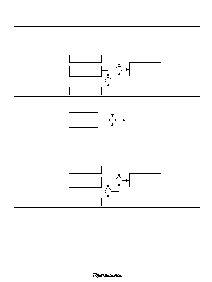
53
Table 2.12
CPU Instruction Addressing Modes and Effective Addresses (cont)
Addressing
Mode
Instruction
Format
Effective Addresses Calculation
Equation
Indirect register
addressing
with
displacement
@(disp:4,
Rn)
The effective address is Rn plus a 4-bit
displacement (disp). The value of disp is zero-
extended, and remains the same for a byte
operation, is doubled for a word operation, and is
quadrupled for a longword operation
Rn
1/2/4
+
◊
disp
(zero-extended)
Rn
+ disp
◊
1/2/4
Byte: Rn + disp
Word: Rn + disp
◊
2
Longword: Rn +
disp
◊
4
Indirect indexed
register
addressing
@(R0, Rn) The effective address is the Rn value plus R0
Rn
R0
Rn + R0
+
Rn + R0
Indirect GBR
addressing with
displacement
@(disp:8,
GBR)
The effective address is the GBR value plus an
8-bit displacement (disp). The value of disp is
zero-extended, and remains the same for a byte
operation, is doubled for a word operation, and
is quadrupled for a longword operation
GBR
1/2/4
+
◊
disp
(zero-extended)
GBR
+ disp
◊
1/2/4
Byte: GBR + disp
Word: GBR + disp
◊
2
Longword: GBR +
disp
◊
4
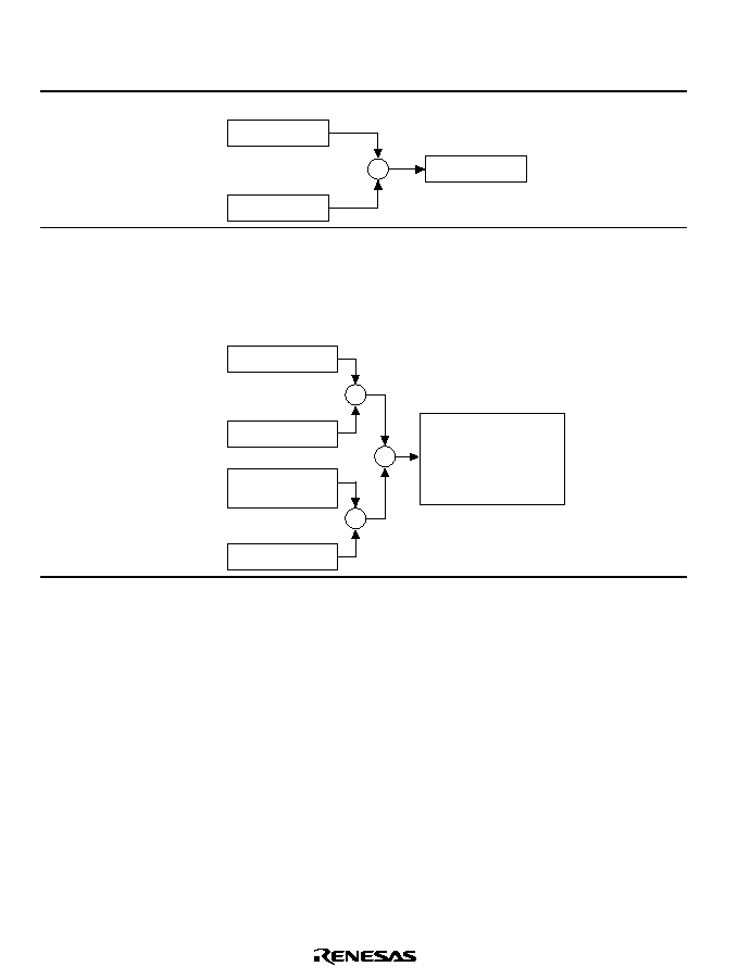
54
Table 2.12
CPU Instruction Addressing Modes and Effective Addresses (cont)
Addressing
Mode
Instruction
Format
Effective Addresses Calculation
Equation
Indirect
indexed GBR
addressing
@(R0,
GBR)
The effective address is the GBR value plus the R0
GBR
R0
GBR + R0
+
GBR + R0
PC relative
addressing
with
displacement
@(disp:8,
PC)
The effective address is the PC value plus an
8-bit displacement (disp). The value of disp is zero-
extended, is doubled for a word operation, and is
quadrupled for a longword operation. For a
longword operation, the lowest two bits of the PC
value are masked
PC
H'FFFFFFFC
+
2/4
◊
&
(for longword)
disp
(zero-extended)
PC + disp
◊
2
or
PC&H'FFFFFFFC
+ disp
◊
4
Word: PC + disp
◊
2
Longword: PC &
H'FFFFFFFC +
disp
◊
4
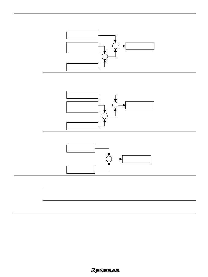
55
Table 2.12
CPU Instruction Addressing Modes and Effective Addresses (cont)
PC relative
addressing
disp:8
The effective address is the PC value sign-extended
with an 8-bit displacement (disp), doubled, and
added to the PC value
PC
2
+
◊
disp
(sign-extended)
PC + disp
◊
2
PC + disp
◊
2
disp:12
The effective address is the PC value sign-extended
with a 12-bit displacement (disp), doubled, and
added to the PC value
PC
2
+
◊
disp
(sign-extended)
PC + disp
◊
2
PC + disp
◊
2
Rn
The effective address is the register PC value plus
Rn
PC
Rn
+
PC + Rn
PC + Rn
Immediate
addressing
#imm:8
The 8-bit immediate data (imm) for the TST, AND,
OR, and XOR instructions are zero-extended
--
#imm:8
The 8-bit immediate data (imm) for the MOV, ADD,
and CMP/EQ instructions are sign-extended
--
#imm:8
The 8-bit immediate data (imm) for the TRAPA
instruction is zero-extended and is quadrupled
--

56
2.4.2
DSP Data Addressing
There are two different kinds of memory accesses with DSP instructions. One type is with the X,
Y data transfer instructions (MOVX.W, MOVY.W), and the other is with the single data transfer
instructions (MOVS.W, MOVS.L). The data addressing differs between these two types of
instructions. Table 2.13 shows a summary of the data transfer instructions.
Table 2.13
Overview of Data Transfer Instructions
Classification
X, Y Data Transfer Processing
(MOVX.W, MOVY.W)
Single Data Transfer Processing
(MOVS.W, MOVS.L)
Address registers
Ax: R4, R5; Ay: R6, R7
As: R2, R3, R4, R5
Index registers
Ix: R8, Iy: R9
Is: R8
Addressing
Nop/Inc(+2)/index addition: post-
update
Nop/Inc(+2,+4)/index addition: post-
update
--
Dec(≠2,≠4): pre-update
Modulo addressing
Possible
Not possible
Data bus
XDB, YDB
CDB
Data length
16 bit (word)
16 bit/32 bit (word/longword)
Bus contention
None
Yes
Memory
X, Y data memory
All memory spaces
Source registers
Dx, Dy: A0, A1
Ds: A0/A1, M0/M1, X0/X1, Y0/Y1,
A0G, A1G
Destination registers
Dx: X0/X1; Dy: Y0/Y1
Ds: A0/A1, M0/M1, X0/X1, Y0/Y1,
A0G, A1G
X, Y Data Addressing: Among the DSP instructions, the MOVX.W and MOVY.W instructions
can be used to simultaneously access X, Y data memory. The DSP instructions have two address
pointers for simultaneous accessing of X, Y data memory. Only pointer addressing is possible with
DSP instructions; there is no immediate addressing. The address registers are divided into two; the
R4, R5 registers become the X memory address register (Ax), and the R6, R7 registers become the
Y memory address register (Ay). The following three types of addressing exist with X, Y data
transfer instructions.
1. Non-updated address registers: The Ax, Ay registers are address pointers. They are not
updated.
2. Add index registers: The Ax, Ay registers are address pointers. The Ix, Iy register values are
added to them, respectively, after the data transfer (post-update).
3. Increment address registers: The Ax, Ay registers are address pointers. The value +2 is added
to each of them after the data transfer (post-update).
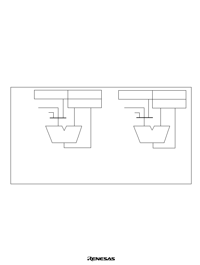
57
Each of the address pointers has an index register. The R8 register becomes the index register (Ix)
of the X memory address register (Ax), and the R9 register becomes the index register (Iy) of the
Y memory address register (Ay).
The X, Y data transfer instructions are processed in word lengths. X, Y data memory is accessed
in 16 bit lengths. This is why the increment processing adds 2 to the address registers. In order to
decrement, set ≠2 in the index register and designate add index register addressing. During X, Y
data addressing, only bits 1 to 15 of the address pointer are valid. Always write a 0 to bit 0 of the
address pointer and the index register during X, Y data addressing.
Figure 2.9 shows the X, Y data transfer addressing. When X memory and Y memory are accessed
using the X, Y bus, the upper word of Ax (R4 or R5) and Ay (R6 or R7) is ignored. The result of
@Ay+ and @Ay+Iy is stored in the lower word of Ay, and the upper word retains its original
value.
ALU
AU
*
R8[Ix]
R4[Ax]
R5[Ax]
R9[Iy]
R6[Ay]
R7[Ay]
+2 (INC)
+2 (INC)
+0 (No update)
+0 (No update)
Notes:
All three addressing methods (increment, index register addition (Ix, Iy), and
no update) are post-updating methods. To decrement the address pointer, set
the index register to ≠2 or ≠4.
*
Adder added for DSP addressing.
Figure 2.9 X, Y Data Transfer Addressing

58
Single Data Addressing: Among the DSP instructions, the single data transfer instructions
(MOVS.W and MOVS.L) are used to either load data into DSP registers or to store it from them.
With these instructions, the registers R2 to R5 are used as address registers (As) for the single data
transfers.
The four following data addressing instructions exist for single data transfer instructions.
1. Non-updated address registers: The As registers are address pointers. They are not updated.
2. Add index registers: The As registers are address pointers. The Is register values are added to
them after the data transfer (post-update).
3. Increment address registers: The As registers are address pointers. The value +2 or +4 is added
after the data transfer (post-update).
4. Decrement address registers: The As registers are address pointers. The value ≠2 or ≠4 is added
(+2 or +4 is subtracted) before the data transfer (pre-update).
The address pointer (As) uses the R8 register as an index register (Is).
Figure 2.10 shows the single data transfer addressing.
ALU
R8[Is]
R4[As]
R5[As]
+2/+4 (INC)
+0 (No update)
Note: There are four addressing methods (no update, index register addition (Is),
increment, and decrement). Index register addition and increment are
post-updating methods. Decrement is a pre-updating method.
R3[As]
R2[As]
≠2/≠4 (DEC)
31
31
0
31
0
0
MAB
CAB
Figure 2.10 Single Data Transfer Addressing

59
Modulo Addressing: The chip has a modulo addressing mode, just as other DSPs do. Address
registers are updated in the same manner as with other modes. When the address pointer value
becomes the same as a previously established modulo end address, the address pointer becomes
the modulo start address.
Modulo addressing is valid only with X, Y data transfer instructions (MOVX.W, MOVY.W).
When the DMX bit of the SR register is set, the X address register enters modulo addressing
mode; when the DMY bit of the SR register is set, the Y address register does so. Modulo
addressing is valid only for either the X or the Y address register; it is not possible to make them
both modulo addressing mode at the same time. Therefore, do not simultaneously set the DMX
and DMY. If they happen to be set at the same time, only the DMY side is valid.
The MOD register is used to designate the start and end addresses of the modulo address area; it
stores the MS (modulo start) and ME (modulo end). An example of MOD register (MS, ME)
usage is indicated below.
MOV.L ModAddr,Rn;
Rn=ModEnd, ModStart
LDC Rn,MOD;
ME=ModEnd, MS=ModStart
ModAddr:
.DATA.W
mEnd;
ModEnd
.DATA.W mStart;
ModStart
ModStart:
.DATA
:
ModEnd:
.DATA
Designate the start and end addresses in MS and ME, and then set the DMX or DMY bit to 1. The
contents of the address register are compared with ME. If they match ME, the start address MS is
stored in the address register. The lower 16 bits of the address register are compared with ME. The
maximum modulo size is 64 kbytes. This is sufficient for X, Y data memory accesses. Figure 2.11
shows a block diagram of modulo addressing.
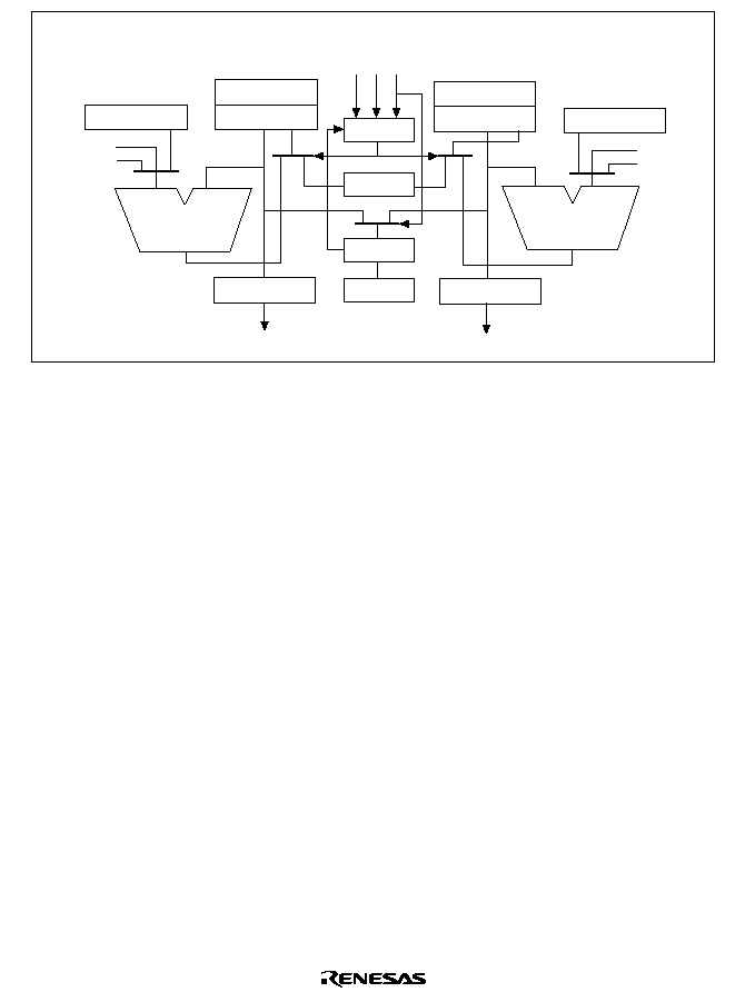
60
Instruction (MOVX/MOVY)
DMX
CONT
MS
CMP
ME
ALU
AU
ABx
ABy
R4[Ax]
R6[Ay]
R5[Ax]
R7[Ay]
R8[Ix]
R9[Iy]
DMY
31
0
0
0
0
1
1
16
16
15
15
15
31
31
31
+2
+0
+2
+0
15
15
1
1
XAB
YAB
15
Figure 2.11 Modulo Addressing
An example of modulo addressing is indicated below:
MS=H'E008; ME=H'E00C; R4=H'1000E008;
DMX=1; DMY=0;
(sets modulo addressing for address register Ax (R4, R5))
The R4 register changes as follows due to the above settings.
R4: H'1000E008
Inc.
R4: H'1000E00A
Inc.
R4: H'1000E00C
Inc.
R4: H'1000E008
(becomes the modulo start address because the modulo end
address occurred)
Data is placed so that the upper 16 bits of the modulo start and end addresses become identical.
This is so because the modulo start address replaces only the lower 15 bits of the address register,
excepting bit 0.
Note:
When using add index with DSP data addressing, there are cases where the value is
exceeded without the address pointer matching the ME. In such cases, the address pointer
does not return to the modulo start address. Bit 0 is disregarded not only for modulo
addressing, but also during X, Y data addressing, so always write 0 to the 0 bits of the
address pointer, index register, MS, and ME.

61
DSP Addressing Operation: The DSP addressing operation in the item stage (EX) of the
pipeline, including modulo addressing, is indicated below.
if ( Operation is MOVX.W MOVY.W ) {
ABx=Ax; ABy=Ay;
/* memory access cycle uses ABx and ABy. The addresses to be used have
not been updated */
/* Ax is one of R4,5 */
if ( DMX==0 || DMX==1 && DMY==1 )} Ax=Ax+(+2 or R8[Ix} or +0);
/* Inc,Index,Not-Update */
else if (!not-update) Ax=modulo( Ax, (+2 or R8[Ix]) );
/* Ay is one of R6,7 */
if ( DMY==0 ) Ay=Ay+(+2 or R9[Iy] or +0; /* Inc,Index,Not-Update */
else if (! not-update) Ay=modulo( Ay, (+2 or R9[Iy]) );
}
else if ( Operation is MOVS.W or MOVS.L ) {
if ( Addressing is Nop, Inc, Add-index-reg ) {
MAB=As;
/* memory access cycle uses MAB. The address to be used has not been
updated */
/* As is one of R2≠5 */
As=As+(+2 or +4 or R8[Is] or +0); /* Inc.Index,Not-Update */
else { /* Decrement, Pre-update */
/* As is one of R2≠5 */
As=As+(≠2 or ≠4);
MAB=As;
/* memory access cycle uses MAB. The address to be used has been updated
*/
}
/* The value to be added to the address register depends on addressing
operations.
For example, (+2 or R8[Ix] or +0) means that
+2:
if operation is increment
R8[Ix}:
if operation is add-index-reg
+0:
if operation is not-update
*/

62
function modulo ( AddrReg, Index ) {
if ( AdrReg[15:0]==ME ) AdrReg[15:0]=MS;
else AdrReg=AdrReg+Index;
return AddrReg;
}
2.4.3
Instruction Formats for CPU Instructions
The instruction format of instructions executed by the CPU core and the meanings of the source
and destination operands are indicated below. The meaning of the operand depends on the
instruction code. The symbols are used as follows:
∑
xxxx: Instruction code
∑
mmmm: Source register
∑
nnnn: Destination register
∑
iiii: Immediate data
∑
dddd: Displacement

63
Table 2.14
Instruction Formats for CPU Instructions
Instruction Formats
Source Operand
Destination
Operand
Example
0 format
xxxx
xxxx
xxxx
xxxx
15
0
--
--
NOP
n format
xxxx
xxxx
xxxx
nnnn
15
0
--
nnnn
: Direct
register
MOVT Rn
Control register or
system register
nnnn
: Direct
register
STS MACH,Rn
Control register or
system register
nnnn
: Indirect pre-
decrement register
STC.L SR,@-Rn
m format
xxxx
mmmm
xxxx
xxxx
15
0
mmmm
: Direct
register
Control register or
system register
LDC Rm,SR
mmmm
: Indirect post-
increment register
Control register or
system register
LDC.L @Rm+,SR
mmmm
: Indirect
register
--
JMP @Rm
mmmm
: PC relative
using Rm
--
BRAF Rm

64
Table 2.14
Instruction Formats for CPU Instructions (cont)
Instruction Formats
Source Operand
Destination
Operand
Example
nm format
mmmm
: Direct
register
nnnn
: Direct
register
ADD Rm,Rn
nnnn
xxxx
xxxx
15
0
mmmm
mmmm
: Direct
register
nnnn
: Indirect
register
MOV.L Rm,@Rn
mmmm
: Indirect post-
increment register
(multiply/
accumulate)
nnnn
: Indirect post-
increment register
(multiply/
accumulate)
*
MACH, MACL
MAC.W
@Rm+,@Rn+
mmmm
: Indirect post-
increment register
nnnn
: Direct
register
MOV.L @Rm+,Rn
mmmm
: Direct
register
nnnn
: Indirect pre-
decrement register
MOV.L Rm,@-Rn
mmmm
: Direct
register
nnnn
: Indirect
indexed register
MOV.L
Rm,@(R0,Rn)
md format
xxxx
dddd
15
0
mmmm
xxxx
mmmmdddd
: indirect
register with
displacement
R0 (Direct register) MOV.B
@(disp,Rm),R0
nd4 format
dddd
nnnn
xxxx
15
0
xxxx
R0 (Direct register)
nnnndddd
: Indirect
register with
displacement
MOV.B
R0,@(disp,Rn)
nmd format
nnnn
xxxx
dddd
15
0
mmmm
mmmm
: Direct
register
nnnndddd
: Indirect
register with
displacement
MOV.L
Rm,@(disp,Rn)
mmmmdddd
: Indirect
register
with displacement
nnnn
: Direct
register
MOV.L
@(disp,Rm),Rn

65
Table 2.14
Instruction Formats for CPU Instructions (cont)
Instruction Formats
Source Operand
Destination
Operand
Example
d format
dddd
xxxx
15
0
xxxx
dddd
dddddddd
: Indirect
GBR with
displacement
R0 (Direct register) MOV.L
@(disp,GBR),R0
R0(Direct register)
dddddddd
: Indirect
GBR with
displacement
MOV.L
R0,@(disp,GBR)
dddddddd: PC
relative with
displacement
R0 (Direct register) MOVA
@(disp,PC),R0
dddddddd
: PC
relative
--
BF label
d12 format
dddd
xxxx
15
0
dddd
dddd
dddddddddddd
:
PC relative
--
BRA label
(label=disp+PC)
nd8 format
dddd
nnnn
xxxx
15
0
dddd
dddddddd: PC
relative with
displacement
nnnn
: Direct
register
MOV.L
@(disp,PC),Rn
i format
iiiiiiii:
Immediate
Indirect indexed
GBR
AND.B
#imm,@(R0,GBR)
i i i i
xxxx
15
0
xxxx
i i i i
iiiiiiii
:
Immediate
R0 (Direct register) AND #imm,R0
iiiiiiii:
Immediate
--
TRAPA #imm
ni format
nnnn
i i i i
xxxx
15
0
i i i i
iiiiiiii
:
Immediate
nnnn
: Direct
register
ADD #imm,Rn
Note:
*
In multiply/accumulate instructions,
nnnn
is the source register.

66
2.4.4
Instruction Formats for DSP Instructions
New instructions have been added for digital signal processing. The new instructions are divided
into the two following types.
1. Memory and DSP register double, single data transfer instructions (16 bit length)
2. Parallel processing instructions processed by the DSP unit (32 bit length)
Figure 2.12 shows each of the instruction formats.
CPU core
instructions
0 0 0 0
to
1 1 1 0
Double data
transfer instructions
Single data
transfer instructions
Parallel processing
instructions
B field
A field
A field
A field
1 1 1 1 0 0
1 1 1 1 0 1
1 1 1 1 1 0
15
15
15
15
0
0
0
0
31
10
10
9
9
16
26 25
Figure 2.12 Instruction Formats for DSP Instructions
Double, Single Data Transfer Instructions: Table 2.15 indicates the data formats for double data
transfer instructions, and table 2.16 indicates the data formats for single data transfer instructions.

67
Table 2.15
Instruction Formats for Double Data Transfers
Category
Mnemonic
15
14
13
12
11
10
9
8
X memory
NOPX
1
1
1
1
0
0
0
data transfers
MOVX.W
@Ax,Dx
MOVX.W
@Ax+,Dx
MOVX.W
@Ax+Ix,Dx
Ax
MOVX.W
Da,@Ax
MOVX.W
Da,@Ax+
MOVX.W
Da,@Ax+Ix
Y memory
NOPY
1
1
1
1
0
0
0
data transfers
MOVY.W
@Ay,Dy
MOVY.W
@Ay+,Dy
MOVY.W
@Ay+Iy,Dy
Ay
MOVY.W
Da,@Ay
MOVY.W
Da,@Ay+
MOVY.W
Da,@Ay+Iy
Table 2.15
Instruction Formats for Double Data Transfers (cont)
Category
Mnemonic
7
6
5
4
3
2
1
0
X memory
NOPX
0
0
0
0
data transfers
MOVX.W
@Ax,Dx
MOVX.W
@Ax+,Dx
MOVX.W
@Ax+Ix,Dx
Dx
0
0
1
1
1
0
1
MOVX.W
Da,@Ax
MOVX.W
Da,@Ax+
MOVX.W
Da,@Ax+Ix
Da
1
0
1
1
1
0
1
Y memory
NOPY
0
0
0
0
data transfers
MOVY.W
@Ay,Dy
MOVY.W
@Ay+,Dy
MOVY.W
@Ay+Iy,Dy
Dy
0
0
1
1
1
0
1
MOVY.W
Da,@Ay
MOVY.W
Da,@Ay+
MOVY.W
Da,@Ay+Iy
Da
1
0
1
1
1
0
1
Ax: 0=R4, 1=R5 Ay: 0=R6, 1=R7 Dx: 0=X0, 1=X1 Dy: 0=Y0, 1=Y1 Da: 0=A0, 1=A1

68
Table 2.16
Instruction Formats for Single Data Transfers
Category
Mnemonic
15
14
13
12
11
10
9
8
Single data
transfer
MOVS.W
@≠As,Ds
MOVS.W
@As,Ds
MOVS.W
@As+,Ds
MOVS.W
@As+Is,Ds
1
1
1
1
0
1
As
0: R4
1: R5
2: R2
MOVS.W
Ds,@-As
MOVS.W
Ds,@As
MOVS.W
Ds,@As+
MOVS.W
Ds,@As+Is
3: R3
MOVS.L
@≠As,Ds
MOVS.L
@As,Ds
MOVS.L
@As+,Ds
MOVS.L
@As+Is,Ds
MOVS.L
Ds,@-As
MOVS.L
Ds,@As
MOVS.L
Ds,@As+
MOVS.L
Ds,@As+Is
Table 2.16
Instruction Formats for Single Data Transfers (cont)
Category
Mnemonic
7
6
5
4
3
2
1
0
Single data
transfer
MOVS.W
@≠As,Ds
MOVS.W
@As,Ds
MOVS.W
@As+,Ds
MOVS.W
@As+Is,Ds
Ds
0: (
*
)
1: (
*
)
2: (
*
)
3: (
*
)
0
0
1
1
0
1
0
1
0
0
MOVS.W
Ds,@-As
MOVS.W
Ds,@As
MOVS.W
Ds,@As+
MOVS.W
Ds,@As+Is
4: (
*
)
5: A1
6: (
*
)
7: A0
0
0
1
1
0
1
0
1
1
MOVS.L
@≠As,Ds
MOVS.L
@As,Ds
MOVS.L
@As+,Ds
MOVS.L
@As+Is,Ds
8: X0
9: X1
A: Y0
B: Y1
0
0
1
1
0
1
0
1
1
0
MOVS.L
Ds,@-As
MOVS.L
Ds,@As
MOVS.L
Ds,@As+
MOVS.L
Ds,@As+Is
C: M0
D: A1G
E: M1
F: A0G
0
0
1
1
0
1
0
1
1
Note:
*
System reserved code

69
Parallel Processing Instructions: The parallel processing instructions allow for more efficient
execution of digital signal processing using the DSP unit. They are 32 bit length, allowing
simultaneously in parallel four processes, ALU operations, multiplications or 2 data transfers.
The parallel processing instructions are divided into A fields and B fields. The A field defines data
transfer instructions; the B field defines ALU operation instructions and multiplication
instructions. These instructions can be defined independently, the processes can be independent,
and furthermore, they can be executed simultaneously in parallel. Table 2.17 indicates the A field
parallel data transfer instructions, and table 2.18 indicates the B field ALU operation instructions
and multiplication instructions. A fields instruction is the same as double data transfers in table
2.15.
Table 2.17
A Field Parallel Data Transfer Instructions
Category
Mnemonic
31
30
29
28
27
26
25
24
23
X memory
NOPX
1
1
1
1
1
0
0
0
data
transfers
MOVX.W
@Ax,Dx
MOVX.W
@Ax+,Dx
MOVX.W
@Ax+Ix,Dx
Ax
Dx
MOVX.W
Da,@Ax
MOVX.W
Da,@Ax+
MOVX.W
Da,@Ax+Ix
Da
Y memory
NOPY
0
data
transfers
MOVY.W
@Ay,Dy
MOVY.W
@Ay+,Dy
MOVY.W
@Ay+Iy,Dy
Ay
MOVY.W
Da,@Ay
MOVY.W
Da,@Ay+
MOVY.W
Da,@Ay+Iy

70
Table 2.17
A Field Parallel Data Transfer Instructions (cont)
Category
Mnemonic
22
21
20
19
18
17
16
15≠0
X memory
NOPX
0
0
0
B field
data
transfers
MOVX.W
@Ax,Dx
MOVX.W
@Ax+,Dx
MOVX.W
@Ax+Ix,Dx
0
0
1
1
1
0
1
MOVX.W
Da,@Ax
MOVX.W
Da,@Ax+
MOVX.W
Da,@Ax+Ix
1
0
1
1
1
0
1
Y memory
NOPY
0
0
0
0
data
transfers
MOVY.W
@Ay,Dy
MOVY.W
@Ay+,Dy
MOVY.W
@Ay+Iy,Dy
Dy
0
0
1
1
1
0
1
MOVY.W
Da,@Ay
MOVY.W
Da,@Ay+
MOVY.W
Da,@Ay+Iy
Da
1
0
1
1
1
0
1
Ax: 0=R4, 1=R5 Ay: 0=R6, 1=R7 Dx: 0=X0, 1=X1 Dy: 0=Y0, 1=Y1 Da: 0=A0, 1=A1

71
Table 2.18
B Field ALU Operation Instructions, Multiplication Instructions
Category
Mnemonic
14 13 12
10
9
8 7 6 5 4 3 2 1
0
15
Dz
0 0 0
0 0 0
≠16
lmm
+16
≠ 32
lmm
+32
0
1
0
Se
Sf
Sx
Sy
Dg
Du
0 0 0
0 0 1
0 1 0
0
0 1 1
1
0 1 1
0
1 0
0
0
0
0
Dz
0: (
*
1
)
1: (
*
1
)
2: (
*
1
)
3: (
*
1
)
4: (
*
1
)
5: A1
6: (
*
1
)
7: A0
8: X0
9: X1
A: Y0
B: Y1
C: M0
D: (
*
1
)
E: M1
F: (
*
1
)
0
0
0
1
0
0
0
0
1
1
0
1
0
1
0
0
1
0
1
0
1
1
1
1
1
1
1
0
0
1
1
1
0
0
1
1
1
1 0:X0
1:X1
2:Y0
3:A1
0:X0
1:X1
2:A0
3:A1
0:X0
0:Y0
1:Y1
2:X0
3:A1
0:Y0 0:M0
1:Y0
1:Y1 1:M1
2:A0
2:M0 2:A0
3:A1
3:M1 3:A1
0 1 0
PSHL #lmm, Dz
PSHA #lmm, Dz
PMULS Se, Sf, Dg
Reserved
Reserved
Reserved
Reserved
Reserved
Reserved
PABS Sx, Dz
PRND Sx, Dz
PRND Sy, Dz
PABS Sy, Dz
Reserved
PSUBC Sx, Sy, Dz
PADDC Sx, Sy, Dz
PCMP Sx, Sy
PSUB Sx, Sy, Du
PMULS Se, Sf, Dg
PADD Sx, Sy, Du
PMULS Se, Sf, Dg
Imm. shift
Six
operand
parallel
instruction
Three
operand
instructions
31≠27
25≠16
26
1
0
A field
11
0
0
1
72
Table 2.18
B Field ALU Operation Instructions, Multiplication Instructions (cont)
Category
Mnemonic
14 13 12
10
9
8
7 6 5 4 3 2 1 0
15
1 1
0
0
0
0
1
0
0
1
1
1
0
0
1
0
1
0
0
1
1
1
0
0
0
1
1
0
0
1
1
1
0
0
1
1
1
0
0
1
1
1
0
0
0
1
1
0
0
1
1
1
0
0
1
if cc
1
0 *
0
0
1
0
0
1
1
1
Reserved
Reserved
Reserved
Reserved
*
2
Reserved
(if cc) PSHL Sx, Sy, Dz
(if cc) PSHA Sx, Sy, Dz
(if cc) PSUB Sx, Sy, Dz
(if cc) PADD Sx, Sy, Dz
(if cc) PAND Sx, Sy, Dz
(if cc) PXOR Sx, Sy, Dz
(if cc) POR Sx, Sy, Dz
(if cc) PDEC Sx, Dz
(if cc) PDEC Sy, Dz
(if cc) PINC Sx, Dz
(if cc) PINC Sy, Dz
(if cc) PCLR Dz
(if cc) PDMSB Sx, Dz
(if cc) PDMSB Sy, Dz
(if cc) PNEG Sx, Dz
(if cc) PNEG Sy, Dz
(if cc) PCOPY Sx, Dz
(if cc) PCOPY Sy, Dz
(if cc) PSTS MACH, Dz
(if cc) PSTS MACL, Dz
(if cc) PLDS Dz, MACL
(if cc) PLDS Dz, MACH
Conditional
three
operand
instructions
0
0
if cc
10:DCT
11:DCF
01:
Uncon-
dition
31≠27
25≠16
26
1
11
1
0
A field
Notes:
*
1 System reserved code
*
2 (if cc): DCT (DC bit true), DCF (DC bit false), or none (unconditional instruction)
* : Don't care
2.5
Instruction Set
The instructions are divided into three groups: CPU instructions executed by the CPU core, DSP
data transfer instructions executed by the DSP unit, and DSP operation instructions. There are a
number of CPU instructions for supporting the DSP functions. The instruction set is explained
below in terms of each of the three groups.

73
2.5.1
CPU Instruction Set
Table 2.19 lists the CPU instructions by classification.
Table 2.19
Classification of CPU Instructions
Classification Types
Operation
Code
Function
No. of
Instructions
Data transfer
5
MOV
Data transfer, immediate data transfer, peripheral
module data transfer, structure data transfer
39
MOVA
Effective address transfer
MOVT
T bit transfer
SWAP
Swap of upper and lower bytes
XTRCT
Extraction of the middle of registers connected
Arithmetic
21
ADD
Binary addition
33
operations
ADDC
Binary addition with carry
ADDV
Binary addition with overflow
CMP/cond Comparison
DIV1
Division
DIV0S
Initialization of signed division
DIV0U
Initialization of unsigned division
DMULS
Signed double-length multiplication
DMULU
Unsigned double-length multiplication
DT
Decrement and test
EXTS
Sign extension
EXTU
Zero extension
MAC
Multiply/accumulate, double-length
multiply/accumulate operation
MUL
Double-length multiply operation
MULS
Signed multiplication
MULU
Unsigned multiplication
NEG
Negation
NEGC
Negation with borrow
SUB
Binary subtraction
SUBC
Binary subtraction with borrow
SUBV
Binary subtraction with underflow

74
Table 2.19
Classification of CPU Instructions (cont)
Classification Types
Operation
Code
Function
No. of
Instructions
Logic
6
AND
Logical AND
14
operations
NOT
Bit inversion
OR
Logical OR
TAS
Memory test and bit set
TST
Logical AND and T bit set
XOR
Exclusive OR
Shift
10
ROTCL
One-bit left rotation with T bit
14
ROTCR
One-bit right rotation with T bit
ROTL
One-bit left rotation
ROTR
One-bit right rotation
SHAL
One-bit arithmetic left shift
SHAR
One-bit arithmetic right shift
SHLL
One-bit logical left shift
SHLLn
n-bit logical left shift
SHLR
One-bit logical right shift
SHLRn
n-bit logical right shift
Branch
9
BF
Conditional branch, conditional branch with delay
(Branch when T = 0)
11
BT
Conditional branch, conditional branch with delay
(Branch when T = 1)
BRA
Unconditional branch
BRAF
Unconditional branch
BSR
Branch to subroutine procedure
BSRF
Branch to subroutine procedure
JMP
Unconditional branch
JSR
Branch to subroutine procedure
RTS
Return from subroutine procedure

75
Table 2.19
Classification of CPU Instructions (cont)
Classification Types
Operation
Code
Function
No. of
Instructions
System
14
CLRMAC MAC register clear
71
control
CLRT
T bit clear
LDC
Load to control register
LDRE
Load to repeat end register
LDRS
Load to repeat start register
LDS
Load to system register
NOP
No operation
RTE
Return from exception processing
SETRC
Repeat count setting
SETT
T bit set
SLEEP
Shift into power-down mode
STC
Storing control register data
STS
Storing system register data
TRAPA
Trap exception handling
Total:65
182

76
The instruction codes, operation, and execution states of the CPU instructions are listed by
classification with the formats listed in below.
Instruction
Instruction Code
Operation
Execution
Cycles
T Bit
Indicated by mnemonic
Explanation of Symbols
OP.Sz SRC, DEST
OP: Operation code
Sz: Size
SRC: Source
DEST: Destination
Rm: Source register
Rn: Destination register
imm: Immediate data
disp: Displacement
*
2
Indicated in MSB
LSB order
Explanation of Symbols
mmmm: Source register
nnnn: Destination register
0000: R0
0001: R1
.........
1111: R15
iiii: Immediate data
dddd: Displacement
Indicates summary of
operation
Explanation of Symbols
,
: Transfer direction
(xx): Memory operand
M/Q/T: Flag bits in the SR
&: Logical AND of each bit
|: Logical OR of each bit
^: Exclusive OR of each bit
~: Logical NOT of each bit
<<n: n-bit left shift
>>n: n-bit right shift
Value when
no wait
states are
inserted
*
1
Value of T bit
after
instruction is
executed
Explanation of
Symbols
--: No change
Notes:
*
1 Instruction execution cycles: The execution cycles shown in the table are minimums.
The actual number of cycles may be increased when (1) contention occurs between
instruction fetches and data access, or (2) when the destination register of the load
instruction (memory
register) and the register used by the next instruction are the
same.
*
2 Depending on the instruction's operand size, scaling is
◊
1,
◊
2, or
◊
4. For details, see
the
SH-1/SH-2/SH-DSP Programming Manual.

77
Table 2.20
Data Transfer Instructions
Instruction
Instruction Code
Operation
Cycles
T Bit
MOV
#imm,Rn
1110nnnniiiiiiii
imm
Sign extension
Rn
1
--
MOV.W
@(disp,PC),Rn
1001nnnndddddddd
(disp
◊
2 + PC)
Sign
extension
Rn
1
--
MOV.L
@(disp,PC),Rn
1101nnnndddddddd
(disp
◊
4 + PC)
Rn
1
--
MOV
Rm,Rn
0110nnnnmmmm0011
Rm
Rn
1
--
MOV.B
Rm,@Rn
0010nnnnmmmm0000
Rm
(Rn)
1
--
MOV.W
Rm,@Rn
0010nnnnmmmm0001
Rm
(Rn)
1
--
MOV.L
Rm,@Rn
0010nnnnmmmm0010
Rm
(Rn)
1
--
MOV.B
@Rm,Rn
0110nnnnmmmm0000
(Rm)
Sign extension
Rn
1
--
MOV.W
@Rm,Rn
0110nnnnmmmm0001
(Rm)
Sign extension
Rn
1
--
MOV.L
@Rm,Rn
0110nnnnmmmm0010
(Rm)
Rn
1
--
MOV.B
Rm,@≠Rn
0010nnnnmmmm0100
Rn≠1
Rn, Rm
(Rn)
1
--
MOV.W
Rm,@≠Rn
0010nnnnmmmm0101
Rn≠2
Rn, Rm
(Rn)
1
--
MOV.L
Rm,@≠Rn
0010nnnnmmmm0110
Rn≠4
Rn, Rm
(Rn)
1
--
MOV.B
@Rm+,Rn
0110nnnnmmmm0100
(Rm)
Sign extension
Rn,Rm + 1
Rm
1
--
MOV.W
@Rm+,Rn
0110nnnnmmmm0101
(Rm)
Sign extension
Rn,Rm + 2
Rm
1
--
MOV.L
@Rm+,Rn
0110nnnnmmmm0110
(Rm)
Rn,Rm + 4
Rm
1
--
MOV.B
R0,@(disp,Rn)
10000000nnnndddd
R0
(disp + Rn)
1
--
MOV.W
R0,@(disp,Rn)
10000001nnnndddd
R0
(disp
◊
2 + Rn)
1
--
MOV.L
Rm,@(disp,Rn)
0001nnnnmmmmdddd
Rm
(disp
◊
4 + Rn)
1
--
MOV.B
@(disp,Rm),R0
10000100mmmmdddd
(disp + Rm)
Sign
extension
R0
1
--
MOV.W
@(disp,Rm),R0
10000101mmmmdddd
(disp
◊
2 + Rm)
Sign
extension
R0
1
--
MOV.L
@(disp,Rm),Rn
0101nnnnmmmmdddd
(disp
◊
4 + Rm)
Rn
1
--
MOV.B
Rm,@(R0,Rn)
0000nnnnmmmm0100
Rm
(R0 + Rn)
1
--
MOV.W
Rm,@(R0,Rn)
0000nnnnmmmm0101
Rm
(R0 + Rn)
1
--

78
Table 2.20
Data Transfer Instructions (cont)
Instruction
Instruction Code
Operation
Cycles
T Bit
MOV.L
Rm,@(R0,Rn)
0000nnnnmmmm0110
Rm
(R0 + Rn)
1
--
MOV.B
@(R0,Rm),Rn
0000nnnnmmmm1100
(R0 + Rm)
Sign
extension
Rn
1
--
MOV.W
@(R0,Rm),Rn
0000nnnnmmmm1101
(R0 + Rm)
Sign
extension
Rn
1
--
MOV.L
@(R0,Rm),Rn
0000nnnnmmmm1110
(R0 + Rm)
Rn
1
--
MOV.B
R0,@(disp,GBR)
11000000dddddddd
R0
(disp + GBR)
1
--
MOV.W
R0,@(disp,GBR)
11000001dddddddd
R0
(disp
◊
2 + GBR)
1
--
MOV.L
R0,@(disp,GBR)
11000010dddddddd
R0
(disp
◊
4 + GBR)
1
--
MOV.B
@(disp,GBR),R0
11000100dddddddd
(disp + GBR)
Sign
extension
R0
1
--
MOV.W
@(disp,GBR),R0
11000101dddddddd
(disp
◊
2 + GBR)
Sign
extension
R0
1
--
MOV.L
@(disp,GBR),R0
11000110dddddddd
(disp
◊
4 + GBR)
R0
1
--
MOVA
@(disp,PC),R0
11000111dddddddd
disp
◊
4 + PC
R0
1
--
MOVT
Rn
0000nnnn00101001
T
Rn
1
--
SWAP.B Rm,Rn
0110nnnnmmmm1000
Rm
Swap the bottom
two bytes
Rn
1
--
SWAP.W Rm,Rn
0110nnnnmmmm1001
Rm
Swap upper and
lower words
Rn
1
--
XTRCT
Rm,Rn
0010nnnnmmmm1101
Rm: Middle 32 bits of
Rn
Rn
1
--

79
Table 2.21
Arithmetic Instructions
Instruction
Instruction Code
Operation
Cycles
T Bit
ADD
Rm,Rn
0011nnnnmmmm1100
Rn + Rm
Rn
1
--
ADD
#imm,Rn
0111nnnniiiiiiii
Rn + imm
Rn
1
--
ADDC
Rm,Rn
0011nnnnmmmm1110
Rn + Rm + T
Rn,
Carry
T
1
Carry
ADDV
Rm,Rn
0011nnnnmmmm1111
Rn + Rm
Rn,
Overflow
T
1
Overflow
CMP/EQ
#imm,R0
10001000iiiiiiii
If R0 = imm, 1
T
1
Comparison
result
CMP/EQ
Rm,Rn
0011nnnnmmmm0000
If Rn = Rm, 1
T
1
Comparison
result
CMP/HS
Rm,Rn
0011nnnnmmmm0010
If Rn
Rm with
unsigned data, 1
T
1
Comparison
result
CMP/GE
Rm,Rn
0011nnnnmmmm0011
If Rn
Rm with signed
data, 1
T
1
Comparison
result
CMP/HI
Rm,Rn
0011nnnnmmmm0110
If Rn > Rm with
unsigned data, 1
T
1
Comparison
result
CMP/GT
Rm,Rn
0011nnnnmmmm0111
If Rn > Rm with signed
data, 1
T
1
Comparison
result
CMP/PL
Rn
0100nnnn00010101
If Rn > 0, 1
T
1
Comparison
result
CMP/PZ
Rn
0100nnnn00010001
If Rn
0, 1
T
1
Comparison
result
CMP/STR Rm,Rn
0010nnnnmmmm1100
If Rn and Rm contain
an identical byte,
1
T
1
Comparison
result
DIV1
Rm,Rn
0011nnnnmmmm0100
Single-step division
(Rn/Rm)
1
Calculation
result
DIV0S
Rm,Rn
0010nnnnmmmm0111
MSB of Rn
Q, MSB
of Rm
M, M ^ Q
T
1
Calculation
result
DIV0U
0000000000011001
0
M/Q/T
1
0

80
Table 2.21
Arithmetic Instructions (cont)
Instruction
Instruction Code
Operation
Cycles
T Bit
DMULS.L Rm,Rn
0011nnnnmmmm1101
Signed operation of Rn
◊
Rm
MACH, MACL
32
◊
32
64 bits
2 to 4
*
--
DMULU.L Rm,Rn
0011nnnnmmmm0101
Unsigned operation of
Rn
◊
Rm
MACH,
MACL 32
◊
32
64 bits
2 to 4
*
--
DT
Rn
0100nnnn00010000
Rn ≠ 1
Rn, when Rn
is 0, 1
T
When Rn is nonzero,
0
T
1
Comparison
result
EXTS.B
Rm,Rn
0110nnnnmmmm1110
A byte in Rm is sign-
extended
Rn
1
--
EXTS.W
Rm,Rn
0110nnnnmmmm1111
A word in Rm is sign-
extended
Rn
1
--
EXTU.B
Rm,Rn
0110nnnnmmmm1100
A byte in Rm is zero-
extended
Rn
1
--
EXTU.W
Rm,Rn
0110nnnnmmmm1101
A word in Rm is zero-
extended
Rn
1
--
MAC.L
@Rm+,@Rn+
0000nnnnmmmm1111
Signed operation of
(Rn)
◊
(Rm) + MAC
MAC 32
◊
32 + 64
64 bits
3/(2 to 4)
*
--
MAC.W
@Rm+,@Rn+
0100nnnnmmmm1111
Signed operation of
(Rn)
◊
(Rm) + MAC
MAC 16
◊
16 + 64
64 bits
3/(2)
*
--
MUL.L
Rm,Rn
0000nnnnmmmm0111
Rn
◊
Rm
MACL, 32
◊
32
32 bits
2 to 4
*
--
MULS.W
Rm,Rn
0010nnnnmmmm1111
Signed operation of Rn
◊
Rm
MAC 16
◊
16
32 bits
1 to 3
*
--
MULU.W
Rm,Rn
0010nnnnmmmm1110
Unsigned operation of
Rn
◊
Rm
MAC 16
◊
16
32 bits
1 to 3
*
--
NEG
Rm,Rn
0110nnnnmmmm1011
0≠Rm
Rn
1
--
NEGC
Rm,Rn
0110nnnnmmmm1010
0≠Rm≠T
Rn,
Borrow
T
1
Borrow

81
Table 2.21
Arithmetic Instructions (cont)
Instruction
Instruction Code
Operation
Cycles
T Bit
SUB
Rm,Rn
0011nnnnmmmm1000
Rn≠Rm
Rn
1
--
SUBC
Rm,Rn
0011nnnnmmmm1010
Rn≠Rm≠T
Rn,
Borrow
T
1
Borrow
SUBV
Rm,Rn
0011nnnnmmmm1011
Rn≠Rm
Rn,
Underflow
T
1
Underflow
Note:
*
The normal number of execution cycles. The number in parentheses is the number of
execution cycles in the case of contention with preceding or following instructions.
Table 2.22
Logic Operation Instructions
Instruction
Instruction Code
Operation
Cycles
T Bit
AND
Rm,Rn
0010nnnnmmmm1001
Rn & Rm
Rn
1
--
AND
#imm,R0
11001001iiiiiiii
R0 & imm
R0
1
--
AND.B
#imm,@(R0,GBR)
11001101iiiiiiii
(R0 + GBR) & imm
(R0 + GBR)
3
--
NOT
Rm,Rn
0110nnnnmmmm0111
~Rm
Rn
1
--
OR
Rm,Rn
0010nnnnmmmm1011
Rn | Rm
Rn
1
--
OR
#imm,R0
11001011iiiiiiii
R0 | imm
R0
1
--
OR.B
#imm,@(R0,GBR)
11001111iiiiiiii
(R0 + GBR) | imm
(R0 + GBR)
3
--
TAS.B
@Rn
0100nnnn00011011
If (Rn) is 0, 1
T,
1
MSB of (Rn)
4
Test
result
TST
Rm,Rn
0010nnnnmmmm1000
Rn & Rm, if the result is
0, 1
T
1
Test
result
TST
#imm,R0
11001000iiiiiiii
R0 & imm, if the result is
0, 1
T
1
Test
result
TST.B
#imm,@(R0,GBR)
11001100iiiiiiii
(R0 + GBR) & imm, if the
result is 0, 1
T
3
Test
result
XOR
Rm,Rn
0010nnnnmmmm1010
Rn ^ Rm
Rn
1
--
XOR
#imm,R0
11001010iiiiiiii
R0 ^ imm
R0
1
--
XOR.B
#imm,@(R0,GBR)
11001110iiiiiiii
(R0 + GBR) ^ imm
(R0 + GBR)
3
--

82
Table 2.23
Shift Instructions
Instruction
Instruction Code
Operation
Cycles
T Bit
ROTL
Rn
0100nnnn00000100
T
Rn
MSB
1
MSB
ROTR
Rn
0100nnnn00000101
LSB
Rn
T
1
LSB
ROTCL
Rn
0100nnnn00100100
T
Rn
T
1
MSB
ROTCR
Rn
0100nnnn00100101
T
Rn
T
1
LSB
SHAL
Rn
0100nnnn00100000
T
Rn
0
1
MSB
SHAR
Rn
0100nnnn00100001
MSB
Rn
T
1
LSB
SHLL
Rn
0100nnnn00000000
T
Rn
0
1
MSB
SHLR
Rn
0100nnnn00000001
0
Rn
T
1
LSB
SHLL2
Rn
0100nnnn00001000
Rn<<2
Rn
1
--
SHLR2
Rn
0100nnnn00001001
Rn>>2
Rn
1
--
SHLL8
Rn
0100nnnn00011000
Rn<<8
Rn
1
--
SHLR8
Rn
0100nnnn00011001
Rn>>8
Rn
1
--
SHLL16 Rn
0100nnnn00101000
Rn<<16
Rn
1
--
SHLR16 Rn
0100nnnn00101001
Rn>>16
Rn
1
--

83
Table 2.24
Branch Instructions
Instruction
Instruction Code
Operation
Cycles
T Bit
BF
label
10001011dddddddd
If T = 0, disp
◊
2 + PC
PC,
if T = 1, nop
3/1
*
--
BF/S
label
10001111dddddddd
Delayed branch, if T = 0, disp
◊
2
+ PC
PC, if T = 1, nop
2/1
*
--
BT
label
10001001dddddddd
If T = 1, disp
◊
2 + PC
PC,
if T = 0, nop
3/1
*
--
BT/S
label
10001101dddddddd
Delayed branch,
if T = 1, disp
◊
2 + PC
PC,
if T = 0, nop
2/1
*
--
BRA
label
1010dddddddddddd
Delayed branch,
disp
◊
2 + PC
PC
2
--
BRAF
Rm
0000mmmm00100011
Delayed branch, Rm + PC
PC
2
--
BSR
label
1011dddddddddddd
Delayed branch, PC
PR,
disp
◊
2 + PC
PC
2
--
BSRF
Rm
0000mmmm00000011
Delayed branch,
PC
PR, Rm + PC
PC
2
--
JMP
@Rm
0100mmmm00101011
Delayed branch, Rm
PC
2
--
JSR
@Rm
0100mmmm00001011
Delayed branch,
PC
PR, Rm
PC
2
--
RTS
0000000000001011
Delayed branch, PR
PC
2
--
Note:
*
One state when it does not branch.

84
Table 2.25
System Control Instructions
Instruction
Instruction Code
Operation
Cycles
T Bit
CLRMAC
0000000000101000
0
MACH, MACL
1
--
CLRT
0000000000001000
0
T
1
0
LDC
Rm,SR
0100mmmm00001110
Rm
SR
1
LSB
LDC
Rm,GBR
0100mmmm00011110
Rm
GBR
1
--
LDC
Rm,VBR
0100mmmm00101110
Rm
VBR
1
--
LDC
Rm,MOD
0100mmmm01011110
Rm
MOD
1
--
LDC
Rm,RE
0100mmmm01111110
Rm
RE
1
--
LDC
Rm,RS
0100mmmm01101110
Rm
RS
1
--
LDC.L
@Rm+,SR
0100mmmm00000111
(Rm)
SR, Rm + 4
Rm
3
LSB
LDC.L
@Rm+,GBR
0100mmmm00010111
(Rm)
GBR, Rm + 4
Rm
3
--
LDC.L
@Rm+,VBR
0100mmmm00100111
(Rm)
VBR, Rm + 4
Rm
3
--
LDC.L
@Rm+,MOD
0100mmmm01010111
(Rm)
MOD, Rm + 4
Rm
3
--
LDC.L
@Rm+,RE
0100mmmm01110111
(Rm)
RE, Rm + 4
Rm
3
--
LDC.L
@Rm+,RS
0100mmmm01100111
(Rm)
RS, Rm + 4
Rm
3
--
LDRE
@(disp,PC)
10001110dddddddd
disp
◊
2 + PC
RE
1
--
LDRS
@(disp,PC)
10001100dddddddd
disp
◊
2 + PC
RS
1
--
LDS
Rm,MACH
0100mmmm00001010
Rm
MACH
1
--
LDS
Rm,MACL
0100mmmm00011010
Rm
MACL
1
--
LDS
Rm,PR
0100mmmm00101010
Rm
PR
1
--
LDS
Rm,DSR
0100mmmm01101010
Rm
DSR
1
--
LDS
Rm,A0
0100mmmm01111010
Rm
A0
1
--
LDS
Rm,X0
0100mmmm10001010
Rm
X0
1
--
LDS
Rm,X1
0100mmmm10011010
Rm
X1
1
--
LDS
Rm,Y0
0100mmmm10101010
Rm
Y0
1
--
LDS
Rm,Y1
0100mmmm10111010
Rm
Y1
1
--
LDS.L
@Rm+,MACH
0100mmmm00000110
(Rm)
MACH,
Rm + 4
Rm
1
--
LDS.L
@Rm+,MACL
0100mmmm00010110
(Rm)
MACL,
Rm + 4
Rm
1
--
LDS.L
@Rm+,PR
0100mmmm00100110
(Rm)
PR, Rm + 4
Rm
1
--

85
Table 2.25
System Control Instructions (cont)
Instruction
Instruction Code
Operation
Cycles
T Bit
LDS.L
@Rm+,DSR
0100mmmm01100110
(Rm)
DSR, Rm + 4
Rm
1
--
LDS.L
@Rm+,A0
0100mmmm01110110
(Rm)
A0, Rm + 4
Rm
1
--
LDS.L
@Rm+,X0
0100mmmm10000110
(Rm)
X0, Rm + 4
Rm
1
--
LDS.L
@Rm+,X1
0100mmmm10010110
(Rm)
X1, Rm + 4
Rm
1
--
LDS.L
@Rm+,Y0
0100mmmm10100110
(Rm)
Y0, Rm + 4
Rm
1
--
LDS.L
@Rm+,Y1
0100mmmm10110110
(Rm)
Y1, Rm + 4
Rm
1
--
NOP
0000000000001001
No operation
1
--
RTE
0000000000101011
Delayed branch,
stack area
PC/SR
4
LSB
SETRC
Rm
0100mmmm00010100
RE≠RS operation result
(repeat status)
RF1, RF0
Rm[11:0]
RC (SR[27:16])
1
--
SETRC
#imm
10000010iiiiiiii
RE≠RS operation result
(repeat status)
RF1, RF0
imm
RC (SR[23:16]),
0
SR[27:24]
1
1
SETT
0000000000011000
1
T
1
1
SLEEP
0000000000011011
Sleep
3
*
--
STC
SR,Rn
0000nnnn00000010
SR
Rn
1
--
STC
GBR,Rn
0000nnnn00010010
GBR
Rn
1
--
STC
VBR,Rn
0000nnnn00100010
VBR
Rn
1
--
STC
MOD,Rn
0000nnnn01010010
MOD
Rn
1
--
STC
RE,Rn
0000nnnn01110010
RE
Rn
1
--
STC
RS,Rn
0000nnnn01100010
RS
Rn
1
--
STC.L
SR,@≠Rn
0100nnnn00000011
Rn≠4
Rn, SR
(Rn)
2
--
STC.L
GBR,@≠Rn
0100nnnn00010011
Rn≠4
Rn, GBR
(Rn)
2
--
STC.L
VBR,@≠Rn
0100nnnn00100011
Rn≠4
Rn, VBR
(Rn)
2
--
STC.L
MOD,@≠Rn
0100nnnn01010011
Rn≠4
Rn, MOD
(Rn)
2
--
STC.L
RE,@≠Rn
0100nnnn01110011
Rn≠4
Rn, RE
(Rn)
2
--
STC.L
RS,@≠Rn
0100nnnn01100011
Rn≠4
Rn, RS
(Rn)
2
--

86
Table 2.25
System Control Instructions (cont)
Instruction
Instruction Code
Operation
Cycles
T Bit
STS
MACH,Rn
0000nnnn00001010
MACH
Rn
1
--
STS
MACL,Rn
0000nnnn00011010
MACL
Rn
1
--
STS
PR,Rn
0000nnnn00101010
PR
Rn
1
--
STS
DSR,Rn
0000nnnn01101010
DSR
Rn
1
--
STS
A0,Rn
0000nnnn01111010
A0
Rn
1
--
STS
X0,Rn
0000nnnn10001010
X0
Rn
1
--
STS
X1,Rn
0000nnnn10011010
X1
Rn
1
--
STS
Y0,Rn
0000nnnn10101010
Y0
Rn
1
--
STS
Y1,Rn
0000nnnn10111010
Y1
Rn
1
--
STS.L
MACH,@≠Rn
0100nnnn00000010
Rn≠4
Rn, MACH
(Rn)
1
--
STS.L
MACL,@≠Rn
0100nnnn00010010
Rn≠4
Rn, MACL
(Rn)
1
--
STS.L
PR,@≠Rn
0100nnnn00100010
Rn≠4
Rn, PR
(Rn)
1
--
STS.L
DSR,@≠Rn
0100nnnn01100010
Rn≠4
Rn, DSR
(Rn)
1
--
STS.L
A0,@≠Rn
0100nnnn01110010
Rn≠4
Rn, A0
(Rn)
1
--
STS.L
X0,@≠Rn
0100nnnn10000010
Rn≠4
Rn, X0
(Rn)
1
--
STS.L
X1,@≠Rn
0100nnnn10010010
Rn≠4
Rn, X1
(Rn)
1
--
STS.L
Y0,@≠Rn
0100nnnn10100010
Rn≠4
Rn, Y0
(Rn)
1
--
STS.L
Y1,@≠Rn
0100nnnn10110010
Rn≠4
Rn, Y1
(Rn)
1
--
TRAPA
#imm
11000011iiiiiiii
PC/SR
stack area, (imm
◊
4 + VBR)
PC
8
--
Note:
*
The number of execution cycles before the chip enters sleep mode.

87
Precautions Concerning the Number of Instruction Execution Cycles: The execution cycles
listed in the tables are minimum values. In practice, the number of execution cycles increases
under such conditions as 1) when the instruction fetch is in contention with a data access, 2) when
the destination register of a load instruction (memory
register) is the same as the register used
by the next instruction, 3) when the branch destination address of a branch instruction is a 4n + 2
address.
CPU Instructions That Support DSP Functions: A number of system control instructions have
been added to the CPU core instructions to support DSP functions. The RS, RE and MOD
registers have been added to support repeat control and modulo addressing, and the repeat counter
(RC) has been added to the status register (SR). The LDC and STC instructions have been added
in order to access the aforementioned. The LDS and STS instructions have been added in order to
access the DSP registers DSR, A0, X0, X1, Y0 and Y1.
The SETRC instruction has been added to set the repeat counter (RC, bits 27 to 16) and repeat
flags (RF1, RF0, bits 3 and 2) of the SR register. When the SETRC instruction operand is
immediate, the 8-bit immediate data is stored in bits 23 to 16 of the SR register and bits 27 to 24
are cleared to 0. When the operand is a register, bits 11 to 0 (12 bits) of the register are stored in
bits 27 to 16 of the SR register. Additionally, the status of 1 instruction repeat (00), 2 instruction
repeat (01), 3 instruction repeat (11) or 4 instruction or greater repeat (10) is set from the RS and
RE set values.
In addition to the LDC instruction, the LDRS and LDRE instructions have been added for
establishing the repeat start and repeat end addresses in the RS and RE registers.
The added instructions are listed in table 2.26.

88
Table 2.26
Added CPU Instructions
Instruction
Code
Operation
Cycles
T Bit
LDC
Rm,MOD
0100mmmm01011110
Rm
MOD
1
--
LDC
Rm,RE
0100mmmm01111110
Rm
RE
1
--
LDC
Rm,RS
0100mmmm01101110
Rm
RS
1
--
LDC.L
@Rm+,MOD
0100mmmm01010111
(Rm)
MOD,Rm+4
Rm
3
--
LDC.L
@Rm+,RE
0100mmmm01110111
(Rm)
RE,Rm+4
Rm
3
--
LDC.L
@Rm+,RS
0100mmmm01100111
(Rm)
RS,Rm+4
Rm
3
--
STC
MOD,Rn
0000nnnn01010010
MOD
Rn
1
--
STC
RE,Rn
0000nnnn01110010
RE
Rn
1
--
STC
RS,Rn
0000nnnn01100010
RS
Rn
1
--
STC.L
MOD,@-Rn
0100nnnn01010011
Rn≠4
Rn,MOD
(Rn)
2
--
STC.L
RE,@-Rn
0100nnnn01110011
Rn≠4
Rn,RE
(Rn)
2
--
STC.L
RS,@-Rn
0100nnnn01100011
Rn≠4
Rn,RS
(Rn)
2
--
LDS
Rm,DSR
0100mmmm01101010
Rm
DSR
1
--
LDS.L
@Rm+,DSR
0100mmmm01100110
(Rm)
DSR,Rm+4
Rm
1
--
LDS
Rm,A0
0100mmmm01111010
Rm
A0
1
--
LDS.L
@Rm+,A0
0100mmmm01110110
(Rm)
A0,Rm+4
Rm
1
--
LDS
Rm,X0
0100mmmm10001010
Rm
X0
1
--
LDS.L
@Rm+,X0
0100mmmm10000110
(Rm)
X0,Rm+4
Rm
1
--
LDS
Rm,X1
0100mmmm10011010
Rm
X1
1
--
LDS.L
@Rm+,X1
0100mmmm10010110
(Rm)
X1,Rm+4
Rm
1
--
LDS
Rm,Y0
0100mmmm10101010
Rm
Y0
1
--
LDS.L
@Rm+,Y0
0100mmmm10100110
(Rm)
Y0,Rm+4
Rm
1
--
LDS
Rm,Y1
0100mmmm10111010
Rm
Y1
1
--
LDS.L
@Rm+,Y1
0100mmmm10110110
(Rm)
Y1,Rm+4
Rm
1
--
STS
DSR,Rn
0000nnnn01101010
DSR
Rn
1
--
STS.L
DSR,@-Rn
0100nnnn01100010
Rn≠4
Rn,DSR
(Rn)
1
--
STS
A0,Rn
0000nnnn01111010
A0
Rn
1
--
STS.L
A0,@-Rn
0100nnnn01110010
Rn≠4
Rn,A0
(Rn)
1
--
STS
X0,Rn
0000nnnn10001010
X0
Rn
1
--
STS.L
X0,@-Rn
0100nnnn10000010
Rn≠4
Rn,X0
(Rn)
1
--
STS
X1,Rn
0000nnnn10011010
X1
Rn
1
--

89
Table 2.26
Added CPU Instructions (cont)
Instruction
Code
Operation
Cycles
T Bit
STS.L
X1,@-Rn
0100nnnn10010010
Rn≠4
Rn,X1
(Rn)
1
--
STS
Y0,Rn
0000nnnn10101010
Y0
Rn
1
--
STS.L
Y0,@-Rn
0100nnnn10100010
Rn≠4
Rn,Y0
(Rn)
1
--
STS
Y1,Rn
0000nnnn10111010
Y1
Rn
1
--
STS.L
Y1,@-Rn
0100nnnn10110010
Rn≠4
Rn,Y1
(Rn)
1
--
SETRC
Rm
0100mmmm00010100
Rm[11:0]
RC (SR[27:16]) 1
--
SETRC
#imm
10000010iiiiiiii
imm
RC(SR[23:16]),
0
SR[27:24]
1
--
LDRS
@(disp,PC)
10001100dddddddd
disp
◊
2+PC
RS
1
--
LDRE
@(disp,PC)
10001110dddddddd
disp
◊
2+PC
RE
1
--
2.5.2
DSP Data Transfer Instruction Set
Table 2.27 lists the DSP data transfer instructions by classification.
Table 2.27
Classification of DSP Data Transfer Instructions
Classification
Types
Operation
Code
Function
No. of
Instructions
Double data
4
NOPX
X memory no operation
14
transfer
MOVX
X memory data transfer
instructions
NOPY
Y memory no operation
MOVY
Y memory data transfer
Single data
transfer
instructions
1
MOVS
Single data transfer
16
Total: 5
Total: 30
The data transfer instructions are divided into two groups, double data transfers and single data
transfers. Double data transfers can be combined with DSP operation instructions to perform DSP
parallel processing. The parallel processing instructions are 32 bit length, and the double data
transfer instructions are incorporated into their A fields. Double data transfers that are not parallel
processing instructions are 16 bit length, as are the single data transfer instructions.
The X memory and Y memory can be accessed simultaneously in parallel in double data transfers.
One instruction each is designated from among the X and Y memory data accesses. The Ax

90
pointer is used to access X memory; the Ay pointer is used to access Y memory. Double data
transfers can only access X, Y memory.
Single data transfers can be accessed from any area. Single data transfers use the Ax pointer and
two other pointers as an As pointer.
Table 2.28
Double Data Transfer Instructions (X Memory Data)
Instruction
Operation
Code
Cycles
DC Bit
NOPX
No Operation
1111000*0*0*00**
1
--
MOVX.W
@Ax,Dx
(Ax)
MSW of Dx,0
LSW of Dx
111100A*D*0*01**
1
--
MOVX.W
@Ax+,Dx
(Ax)
MSW of Dx,0
LSW of
Dx,Ax+2
Ax
111100A*D*0*10**
1
--
MOVX.W
@Ax+Ix,Dx
(Ax)
MSW of Dx,0
LSW of
Dx,Ax+Ix
Ax
111100A*D*0*11**
1
--
MOVX.W
Da,@Ax
MSW of Da
(Ax)
111100A*D*1*01**
1
--
MOVX.W
Da,@Ax+
MSW of Da
(Ax),Ax+2
Ax
111100A*D*1*10**
1
--
MOVX.W
Da,@Ax+Ix
MSW of Da
(Ax),Ax+Ix
Ax
111100A*D*1*11**
1
--
Table 2.29
Double Data Transfer Instructions (Y Memory Data)
Instruction
Operation
Code
Cycles
DC Bit
NOPY
No Operation
111100*0*0*0**00
1
--
MOVY.W
@Ay,Dy
(Ay)
MSW of Dy,0
LSW of Dy
111100*A*D*0**01
1
--
MOVY.W
@Ay+,Dy
(Ay)
MSW of Dy,0
LSW of Dy,
Ay+2
Ay
111100*A*D*0**10
1
--
MOVY.W
@Ay+Iy,Dy
(Ay)
MSW of Dy,0
LSW of Dy,
Ay+Iy
Ay
111100*A*D*0**11
1
--
MOVY.W
Da,@Ay
MSW of Da
(Ay)
111100*A*D*1**01
1
--
MOVY.W
Da,@Ay+
MSW of Da
(Ay),Ay+2
Ay
111100*A*D*1**10
1
--
MOVY.W
Da,@Ay+Iy
MSW of Da
(Ay),Ay+Iy
Ay
111100*A*D*1**11
1
--

91
Table 2.30
Single Data Transfer Instructions
Instruction
Operation
Code
Cycles
DC Bit
MOVS.W
@-As,Ds
As≠2
As,(As)
MSW of
Ds,0
LSW of Ds
111101AADDDD0000
1
--
MOVS.W @As,Ds
(As)
MSW of Ds,0
LSW of
Ds
111101AADDDD0100
1
--
MOVS.W @As+,Ds
(As)
MSW of Ds,0
LSW of
Ds, As+2
As
111101AADDDD1000
1
--
MOVS.W
@As+Ix,Ds
(As)
MSW of Ds,0
LSW of
Ds, As+Ix
As
111101AADDDD1100
1
--
MOVS.W
Ds,@-As
As≠2
As,MSW of Ds
(As)
*
111101AADDDD0001
1
--
MOVS.W Ds,@As
MSW of Ds
(As)
*
111101AADDDD0101
1
--
MOVS.W Ds,@As+
MSW of Ds
(As)
*
,As+2
As
111101AADDDD1001
1
--
MOVS.W
Ds,@As+Is
MSW of Ds
(As)
*
,As+Is
As
111101AADDDD1101
1
--
MOVS.L
@-As,Ds
As≠4
As,(As)
Ds
111101AADDDD0010
1
--
MOVS.L @As,Ds
(As)
Ds
111101AADDDD0110
1
--
MOVS.L @As+,Ds
(As)
Ds,As+4
As
111101AADDDD1010
1
--
MOVS.L
@As+Is,Ds
(As)
Ds,As+Is
As
111101AADDDD1110
1
--
MOVS.L Ds,
@-As
As≠4
As,Ds
(As)
*
111101AADDDD0011
1
--
MOVS.L Ds,@As
Ds
(As)
*
111101AADDDD0111
1
--
MOVS.L Ds,@As+
Ds
(As)
*
,As+4
As
111101AADDDD1011
1
--
MOVS.L
Ds,@As+Is
Ds
(As)
*
,As+Is
As
111101AADDDD1111
1
--
Note:
*
When guard bit registers A0G and A1G are specified for the source operand Ds, data is
sign-extended before being transferred.

92
Table 2.31 shows the correspondence between the DSP data transfer operands and registers. CPU
core registers are used as pointer addresses indicating memory addresses.
Table 2.31
Correspondence between DSP Data Transfer Operands and Registers
SH (CPU Core) Registers
Oper-
and
R0
R1
R2
(As2)
R3
(As3)
R4
(Ax0)
(As0)
R5
(Ax1)
(As0)
R6
(Ay0)
R7
(Ay1)
R8
(Ix)
(Is)
R9
(Iy)
Ax
--
--
--
--
Yes
Yes
--
--
--
--
Ix (Is)
--
--
--
--
--
--
--
--
Yes
--
Dx
--
--
--
--
--
--
--
--
--
--
Ay
--
--
--
--
--
--
Yes
Yes
--
--
Iy
--
--
--
--
--
--
--
--
--
Yes
Dy
--
--
--
--
--
--
--
--
--
--
Da
--
--
--
--
--
--
--
--
--
--
As
--
--
Yes
Yes
Yes
Yes
--
--
--
--
Ds
--
--
--
--
--
--
--
--
--
--
Oper-
DSP Registers
and
X0
X1
Y0
Y1
M0
M1
A0
A1
A0G
A1G
Ax
--
--
--
--
--
--
--
--
--
--
Ix (Is)
--
--
--
--
--
--
--
--
--
--
Dx
Yes
Yes
--
--
--
--
--
--
--
--
Ay
--
--
--
--
--
--
--
--
--
--
Iy
--
--
--
--
--
--
--
--
--
--
Dy
--
--
Yes
Yes
--
--
--
--
--
--
Da
--
--
--
--
--
--
Yes
Yes
--
--
As
--
--
--
--
--
--
--
--
--
--
Ds
Yes
Yes
Yes
Yes
Yes
Yes
Yes
Yes
Yes
Yes
Note:
Yes indicates that the register can be set.

93
2.5.3
DSP Operation Instruction Set
DSP operation instructions are digital signal processing instructions processed by the DSP unit.
These instructions use 32-bit instruction codes, and multiple instructions are executed in parallel.
The instruction codes are divided into an A field and a B field; parallel data transfer instructions
are designated in the A field, and single or double data operation instructions are designated in the
B field. Instructions can be independently designated and execution can also be carried out
independently. A parallel data transfer instruction designated in the A field is exactly the same as a
double data transfer instruction.
The B field data operation instructions are divided into three groups: double data operation
instructions, conditional single data operation instructions, and unconditional single data operation
instructions. Table 2.32 lists the instruction formats of the DSP operation instructions. Each of the
operands can be independently selected from the DSP registers. Table 2.33 shows the
correspondence between the DSP operation instruction operands and registers.
Table 2.32
DSP Operation Instruction Formats
Classification
Instruction Forms
Instruction
Double data operation instructions
(6 operands)
ALUop. Sx, Sy, Du
MLTop. Se, Sf, Dg
PADD PMULS,
PSUB PMULS
Conditional single data
operation instructions
3 operands
ALUop. Sx, Sy, Dz
DCT ALUop. Sx, Sy, Dz
DCF ALUop. Sx, Sy, Dz
PADD, PAND, POR,
PSHA, PSHL, PSUB,
PXOR
2 operands
ALUop. Sx, Dz
DCT ALUop. Sx, Dz
DCF ALUop. Sx, Dz
ALUop. Sy, Dz
DCT ALUop. Sy, Dz
DCF ALUop. Sy, Dz
PCOPY, PDEC, PDMSB,
PINC, PLDS, PSTS,
PNEG
1 operand
ALUop. Dz
DCT ALUop. Dz
DCF ALUop. Dz
PCLR, PSHA #imm,
PSHL #imm
Unconditional single data
operation instructions
3 operands
ALUop. Sx, Sy, Du
MLTop. Se, Sf, Dg
PADDC, PSUBC, PMULS
2 operands
ALUop. Sx, Dz
ALUop. Sy, Dz
ALUop. Sx, Sy
PCMP, PABS, PRND
1 operand
ALUop. Dz
PSHA #imm,
PSHL #imm

94
Table 2.33
Correspondence between DSP Instruction Operands and Registers
ALU and BPU Instructions
Multiplication Instructions
Register
Sx
Sy
Dz
Du
Se
Sf
Dg
A0
Yes
--
Yes
Yes
--
--
Yes
A1
Yes
--
Yes
Yes
Yes
Yes
Yes
M0
--
Yes
Yes
--
--
--
Yes
M1
--
Yes
Yes
--
--
--
Yes
X0
Yes
--
Yes
Yes
Yes
Yes
--
X1
Yes
--
Yes
--
Yes
--
--
Y0
--
Yes
Yes
Yes
Yes
Yes
--
Y1
--
Yes
Yes
--
--
Yes
--
When writing parallel instructions, write the B field instructions first, then write the A field
instructions:
PADD A0,M0,A0 PMULS X0,Y0,M0 MOVX.W @R4+,X0 MOVY.W @R6+,Y0[;]
DCF PINC X1,A1 MOVX.W A0,@R5+R8 MOVY.W @R7+,Y0[;]
PCMP X1,M0 MOVX.W @R4+R8 [NOPY][;]
Text in brackets ([]) can be omitted. The no operation instructions NOPX and NOPY can be
omitted. Semicolons (;) are used to demarcate instruction lines, but can be omitted. If semicolons
are used, the space after the semicolon can be used for comments.
The individual status codes (DC, N, Z, V, GT) of the DSR register are always updated by
unconditional ALU operation instructions and shift operation instructions. Conditional instructions
do not update the status codes, even if the conditions have been met. Multiplication instructions
also do not update the status codes. DC bit definitions are determined by the specifications of the
CS bits in the DSR register.
Table 2.34 lists the DSP operation instructions by classification.

95
Table 2.34
Classification of DSP Instructions
Classification
Instruction
Types
Operation
Code
Function
No. of In-
structions
ALU
arith-
ALU fixed decimal
point operation
11
PABS
Absolute value
operation
28
metic
instructions
PADD
Addition
opera-
tion
PADD
PMULS
Addition and signed
multiplication
instruc-
PADDC
Addition with carry
tions
PCLR
Clear
PCMP
Compare
PCOPY
Copy
PNEG
Invert sign
PSUB
Subtraction
PSUB
PMULS
Subtraction and signed
multiplication
PSUBC
Subtraction with borrow
ALU integer
operation
2
PDEC
Decrement
12
instructions
PINC
Increment
MSB detection
instruction
1
PDMSB
MSB detection
6
Rounding operation
instruction
1
PRND
Rounding
2
ALU logical operation
3
PAND
Logical AND
9
instructions
POR
Logical OR
PXOR
Logical exclusive OR
Fixed decimal point
multiplication instruction
1
PMULS
Signed multiplication
1
Shift
Arithmetic shift
operation instruction
1
PSHA
Arithmetic shift
4
Logical shift
operation instruction
1
PSHL
Logical shift
4
System control instructions
2
PLDS
System register load
12
PSTS
Store from system
register
Total 23
Total 78

96
2.5.4
Various Operation Instructions
ALU Arithmetic Operation Instructions: Tables 2.35≠2.44 list various operation instructions.
Table 2.35
ALU Fixed Point Operation Instructions
Instruction
Operation
Code
Cycles
DC Bit
PABS Sx,Dz
If Sx
0,Sx
Dz
If Sx<0,0≠ Sx
Dz
111110**********
10001000xx00zzzz
1
Update
PABS Sy,Dz
If Sy
0,Sy
Dz
If Sy<0,0≠Sy
Dz
111110**********
1010100000yyzzzz
1
Update
PADD Sx,Sy,Dz
Sx+Sy
Dz
111110**********
10110001xxyyzzzz
1
Update
DCT PADD
Sx,Sy,Dz
if DC=1,Sx+Sy
Dz if 0,nop
111110**********
10110010xxyyzzzz
1
--
DCF PADD
Sx,Sy,Dz
if DC=0,Sx+Sy
Dz if 1,nop
111110**********
10110011xxyyzzzz
1
--
PADD Sx,Sy,Du
PMULS Se,Sf,Dg
Sx+Sy
Du
MSW of Se
◊
MSW of
Sf
Dg
111110**********
0111eeffxxyygguu
1
Update
PADDC Sx,Sy,Dz
Sx+Sy+DC
Dz
111110**********
10110000xxyyzzzz
1
Update
PCLR Dz
H'00000000
Dz
111110**********
100011010000zzzz
1
Update
DCT PCLR Dz
if DC=1,H'00000000
Dz
if 0,nop
111110**********
100011100000zzzz
1
--
DCF PCLR Dz
if DC=0,H'00000000
Dz
if 1,nop
111110**********
100011110000zzzz
1
--
PCMP Sx,Sy
Sx≠Sy
111110**********
10000100xxyy0000
1
Update
PCOPY Sx,Dz
Sx
Dz
111110**********
11011001xx00zzzz
1
Update
PCOPY Sy,Dz
Sy
Dz
111110**********
1111100100yyzzzz
1
Update
DCT PCOPY
Sx,Dz
if DC=1,Sx
Dz if 0,nop
111110**********
11011010xx00zzzz
1
--

97
Table 2.35
ALU Fixed Point Operation Instructions (cont)
Instruction
Operation
Code
Cycles
DC Bit
DCT PCOPY
Sy,Dz
if DC=1,Sy
Dz if 0,nop
111110**********
1111101000yyzzzz
1
--
DCF PCOPY
Sx,Dz
if DC=0,Sx
Dz if 1,nop
111110**********
11011011xx00zzzz
1
--
DCF PCOPY
Sy,Dz
if DC=0,Sy
Dz if 1,nop
111110**********
1111101100yyzzzz
1
--
PNEG Sx,Dz
0≠Sx
Dz
111110**********
11001001xx00zzzz
1
Update
PNEG Sy,Dz
0≠Sy
Dz
111110**********
1110100100yyzzzz
1
Update
DCT PNEG Sx,Dz
if DC=1,0≠Sx
Dz
if 0,nop
111110**********
11001010xx00zzzz
1
--
DCT PNEG Sy,Dz
if DC=1,0≠Sy
Dz
if 0,nop
111110**********
1110101000yyzzzz
1
--
DCF PNEG Sx,Dz
if DC=0,0≠Sx
Dz
if 1,nop
111110**********
11001011xx00zzzz
1
--
DCF PNEG Sy,Dz
if DC=0,0≠Sy
Dz
if 1,nop
111110**********
1110101100yyzzzz
1
--
PSUB Sx,Sy,Dz
Sx≠Sy
Dz
111110**********
10100001xxyyzzzz
1
Update
DCT PSUB
Sx,Sy,Dz
if DC=1,Sx≠Sy
Dz if 0,nop
111110**********
10100010xxyyzzzz
1
--
DCF PSUB
Sx,Sy,Dz
if DC=0,Sx≠Sy
Dz if 1,nop
111110**********
10100011xxyyzzzz
1
--
PSUB Sx,Sy,Du
PMULS Se,Sf,Dg
Sx≠Sy
Du
MSW of Se
◊
MSW of
Sf
Dg
111110**********
0110eeffxxyygguu
1
Update
PSUBC Sx,Sy,Dz
Sx≠Sy≠DC
Dz
111110**********
10100000xxyyzzzz
1
Update

98
Table 2.36
ALU Integer Operation Instructions
Instruction
Operation
Code
Cycles
DC Bit
PDEC Sx,Dz
MSW of Sx ≠ 1
MSW of
Dz, clear LSW of Dz
111110**********
10001001xx00zzzz
1
Update
PDEC Sy,Dz
MSW of Sy ≠ 1
MSW of
Dz, clear LSW of Dz
111110**********
1010100100yyzzzz
1
Update
DCT PDEC Sx,Dz
If DC=1, MSW of Sx ≠ 1
MSW of Dz, clear LSW of
Dz; if 0, nop
111110**********
10001010xx00zzzz
1
--
DCT PDEC Sy,Dz
If DC=1, MSW of Sy ≠ 1
MSW of Dz, clear LSW of
Dz; if 0, nop
111110**********
1010101000yyzzzz
1
--
DCF PDEC Sx,Dz
If DC=0, MSW of Sx ≠ 1
MSW of Dz, clear LSW of
Dz; if 1, nop
111110**********
10001011xx00zzzz
1
--
DCF PDEC Sy,Dz
If DC=0, MSW of Sy ≠ 1
MSW of Dz, clear LSW of
Dz; if 1, nop
111110**********
1010101100yyzzzz
1
--
PINC Sx,Dz
MSW of Sx + 1
MSW of
Dz, clear LSW of Dz
111110**********
10011001xx00zzzz
1
Update
PINC Sy,Dz
MSW of Sy + 1
MSW of
Dz, clear LSW of Dz
111110**********
1011100100yyzzzz
1
Update
DCT PINC Sx,Dz
If DC=1, MSW of Sx + 1
MSW of Dz, clear LSW of
Dz; if 0, nop
111110**********
10011010xx00zzzz
1
--
DCT PINC Sy,Dz
If DC=1, MSW of Sy + 1
MSW of Dz, clear LSW of
Dz; if 0, nop
111110**********
1011101000yyzzzz
1
--
DCF PINC Sx,Dz
If DC=0, MSW of Sx + 1
MSW of Dz, clear LSW of
Dz; if 1, nop
111110**********
10011011xx00zzzz
1
--
DCF PINC Sy,Dz
If DC=0, MSW of Sy + 1
MSW of Dz, clear LSW of
Dz; if 1, nop
111110**********
1011101100yyzzzz
1
--

99
Table 2.37
MSB Detection Instructions
Instruction
Operation
Code
Cycles
DC Bit
PDMSB Sx,Dz
Sx data MSB position
MSW of Dz, clear LSW of
Dz
111110**********
10011101xx00zzzz
1
Update
PDMSB Sy,Dz
Sy data MSB position
MSW of Dz, clear LSW of
Dz
111110**********
1011110100yyzzzz
1
Update
DCT PDMSB
Sx,Dz
If DC=1, Sx data MSB
position
MSW of Dz,
clear LSW of Dz; if 0, nop
111110**********
10011110xx00zzzz
1
--
DCT PDMSB
Sy,Dz
If DC=1, Sy data MSB
position
MSW of Dz,
clear LSW of Dz; if 0, nop
111110**********
1011111000yyzzzz
1
--
DCF PDMSB
Sx,Dz
If DC=0, Sx data MSB
position
MSW of Dz,
clear LSW of Dz; if 1, nop
111110**********
10011111xx00zzzz
1
--
DCF PDMSB
Sy,Dz
If DC=0, Sy data MSB
position
MSW of Dz,
clear LSW of Dz; if 1, nop
111110**********
1011111100yyzzzz
1
--
Table 2.38
Rounding Operation Instructions
Instruction
Operation
Code
Cycles
DC Bit
PRND Sx,Dz
Sx+H'00008000
Dz
clear LSW of Dz
111110**********
10011000xx00zzzz
1
Update
PRND Sy,Dz
Sy+H'00008000
Dz
clear LSW of Dz
111110**********
1011100000yyzzzz
1
Update

100
Table 2.39
ALU Logical Operation Instructions
Instruction
Operation
Code
Cycles
DC Bit
PAND Sx,Sy,Dz
Sx & Sy
Dz, clear LSW
of Dz
111110**********
10010101xxyyzzzz
1
Update
DCT PAND
Sx,Sy,Dz
If DC=1, Sx & Sy
Dz,
clear LSW of Dz; if 0, nop
111110**********
10010110xxyyzzzz
1
--
DCF PAND
Sx,Sy,Dz
If DC=0, Sx & Sy
Dz,
clear LSW of Dz; if 1, nop
111110**********
10010111xxyyzzzz
1
--
POR Sx,Sy,Dz
Sx | Sy
Dz, clear LSW of
Dz
111110**********
10110101xxyyzzzz
1
Update
DCT POR
Sx,Sy,Dz
If DC=1, Sx | Sy
Dz,
clear LSW of Dz; if 0, nop
111110**********
10110110xxyyzzzz
1
--
DCF POR
Sx,Sy,Dz
If DC=0, Sx | Sy
Dz,
clear LSW of Dz; if 1, nop
111110**********
10110111xxyyzzzz
1
--
PXOR Sx,Sy,Dz
Sx ^ Sy
Dz, clear LSW
of Dz
111110**********
10100101xxyyzzzz
1
Update
DCT PXOR
Sx,Sy,Dz
If DC=1, Sx ^ Sy
Dz,
clear LSW of Dz; if 0, nop
111110**********
10100110xxyyzzzz
1
--
DCF PXOR
Sx,Sy,Dz
If DC=0, Sx ^ Sy
Dz,
clear LSW of Dz; if 1, nop
111110**********
10100111xxyyzzzz
1
--
Table 2.40
Fixed Point Multiplication Instructions
Instruction
Operation
Code
Cycles
DC Bit
PMULS Se,Sf,Dg
MSW of Se
◊
MSW of
Sf
Dg
111110**********
0100eeff0000gg00
1
--

101
Table 2.41
Arithmetic Shift Operation Instructions
Instruction
Operation
Code
Cycles
DC Bit
PSHA Sx,Sy,Dz
if Sy
0,Sx<<Sy
Dz
if Sy<0,Sx>>Sy
Dz
111110**********
10010001xxyyzzzz
1
Update
DCT PSHA
Sx,Sy,Dz
if DC=1 &
Sy
0,Sx<<Sy
Dz
if DC=1 &
Sy<0,Sx>>Sy
Dz
if DC=0,nop
111110**********
10010010xxyyzzzz
1
--
DCF PSHA
Sx,Sy,Dz
if DC=0 &
Sy
0,Sx<<Sy
Dz
if DC=0 &
Sy<0,Sx>>Sy
Dz
if DC=1,nop
111110**********
10010011xxyyzzzz
1
--
PSHA #imm,Dz
if imm
0,Dz<<imm
Dz
if imm<0,Dz>>imm
Dz
111110**********
00010iiiiiiizzzz
1
Update

102
Table 2.42
Logical Shift Operation Instructions
Instruction
Operation
Code
Cycles
DC Bit
PSHL Sx,Sy,Dz
if Sy
0,Sx<<Sy
Dz, clear
LSW of Dz
if Sy<0,Sx>>Sy
Dz, clear
LSW of Dz
111110**********
10000001xxyyzzzz
1
Update
DCT PSHL
Sx,Sy,Dz
if DC=1 &
Sy
0,Sx<<Sy
Dz, clear
LSW of Dz
if DC=1 &
Sy<0,Sx>>Sy
Dz, clear
LSW of Dz
if DC=0,nop
111110**********
10000010xxyyzzzz
1
--
DCF PSHL
Sx,Sy,Dz
if DC=0 &
Sy
0,Sx<<Sy
Dz, clear
LSW of Dz
if DC=0 &
Sy<0,Sx>>Sy
Dz, clear
LSW of Dz
if DC=1,nop
111110**********
10000011xxyyzzzz
1
--
PSHL #imm,Dz
if imm
0,Dz<<imm
Dz,
clear LSW of Dz
if imm<0,Dz>>imm
Dz,
clear LSW of Dz
111110**********
00000iiiiiiizzzz
1
Update

103
Table 2.43
System Control Instructions
Instruction
Operation
Code
Cycles
DC Bit
PLDS
Dz,MACH
Dz
MACH
111110**********
111011010000zzzz
1
--
PLDS
Dz,MACL
Dz
MACL
111110**********
111111010000zzzz
1
--
DCT PLDS
Dz,MACH
if DC=1,Dz
MACH
if 0,nop
111110**********
111011100000zzzz
1
--
DCT PLDS
Dz,MACL
if DC=1,Dz
MACL
if 0,nop
111110**********
111111100000zzzz
1
--
DCF PLDS
Dz,MACH
if DC=0,Dz
MACH
if 1,nop
111110**********
111011110000zzzz
1
--
DCF PLDS
Dz,MACL
if DC=0,Dz
MACL
if 1,nop
111110**********
111111110000zzzz
1
--
PSTS
MACH,Dz
MACH
Dz
111110**********
110011010000zzzz
1
--
PSTS
MACL,Dz
MACL
Dz
111110**********
110111010000zzzz
1
--
DCT PSTS
MACH,Dz
if DC=1,MACH
Dz
if 0,nop
111110**********
110011100000zzzz
1
--
DCT PSTS
MACL,Dz
if DC=1,MACL
Dz
if 0,nop
111110**********
110111100000zzzz
1
--
DCF PSTS
MACH,Dz
if DC=0,MACH
Dz
if 1,nop
111110**********
110011110000zzzz
1
--
DCF PSTS
MACL,Dz
if DC=0,MACL
Dz
if 1,nop
111110**********
110111110000zzzz
1
--

104
When there are no data transfer instructions being processed simultaneously in parallel with DSP
operation instructions, it is possible to either write NOPX, NOPY instructions or to omit the
instructions. The instruction codes are the same regardless of whether the NOPX, NOPY
instructions are written or omitted. Table 2.44 gives some examples of NOPX and NOPY
instruction codes.
Table 2.44
NOPX and NOPY Instruction Codes
Instruction
Code
PADD X0, Y0, A0 MOVX.W @R4+, X0 MOVY.W @R6+R9, Y0
1111100000001011
1011000100000111
PADD X0, Y0, A0 NOPX MOVY.W @R6+R9, Y0
1111100000000011
1011000100000111
PADD X0, Y0, A0 NOPX NOPY
1111100000000000
1011000100000111
PADD X0, Y0, A0 NOPX
1111100000000000
1011000100000111
PADD X0, Y0, A0
1111100000000000
1011000100000111
MOVX.W @R4+, X0 MOVY.W @R6+R9, Y0
1111000000001011
MOVX.W @R4+, X0 NOPY
1111000000001000
MOVS.W @R4+, X0
1111010010001000
NOPX MOVY.W @R6+R9, Y0
1111000000000011
MOVY.W @R6+R9, Y0
1111000000000011
NOPX NOPY
1111000000000000
NOP
0000000000001001

105
2.6
Usage Notes
2.6.1
When not using DSP instructions
When DSP instructions are not used, execute the following dummy instruction in the initialization
section of application software in order to reduce the operating current.
PCLR A0
: Clear the A0 register.
PSHA #5, A0
: 5 bit shift to left.
2.6.2
When executing a combination of double-precision multiplication or double-
precision product-sum operation (CPU instruction) and DSP computing
instruction
When double-precision multiplication (MUL.L, DMULU.L, DMULS.L) or double-precision
product-sum operation (MAC.L) in CPU instructions is executed in combination with DSP
computing instruction (when the following conditions 1 and 2 are met simultaneously), a
malfunction may occur in the instructions indicated in 2-b.
1. Execution of instructions from the internal memory or cache.
2. Execution of the following instruction strings in the order of a, b and c.
a. Double-precision multiplication (MUL.L, DMULU.L, DMULS.L) or double-precision
product-sum operation (MAC.L)
b. DSP computing instruction excluding PMULS, PSTS and PLDS
c. Execution of PMLS, PSTS or PLDS instruction
The above caution also applies when there is a delayed jump instruction immediately before the
above 2-a, and the instruction 2-a is in a delayed slot, and the instructions 2-b and 2-c are
described continuously at the jump destination.
To prevent the malfunction, take one of the following measures.
1
Do not execute the instruction string described in the above condition 2.
2. When the instruction string described in the above condition 2 exists on the instruction code
and if no problem is caused by switching instructions b and c, switch the locations of
instructions b and c.
3. When the instruction string described in the above condition 2 exists on the instruction code
and if a problem is caused by switching instructions b and c, insert one or more NOP
instructions or CPU instructions that are not related to the multiplier.

106

107
Section 3 Oscillator Circuits and Operating Modes
3.1
Overview
Operation of the on-chip clock pulse generator, and CS0 area bus width specification, are
controlled by the operating mode pins. A crystal resonator or external clock can be selected as the
clock source.
3.2
On-Chip Clock Pulse Generator and Operating Modes
3.2.1
Clock Pulse Generator
A block diagram of the on-chip clock pulse generator circuit is shown in figure 3.1.
CAP1
CKIO
MD2
MD0
MD1
CKPACK
*
Oscillator
On/Off
PLL circuit 1
PLL circuit 2
◊
1,
◊
2,
◊
4
CAP2
EXTAL
XTAL
CKPREQ
/CKM
Clock mode control circuit
DIVP
1/1
1/2
1/4
Note: See section 21.4.4, Clock Pause Function.
E
External interface
clock
I
CPU/DSP core
clock
P
Peripheral module
clock
The relationship between the
internal clock frequencies is:
I
E
P
.
Maximum frequencies are:
I
, E
62.5 MHz, P
31.25 MHz.
DIVE
1/1
1/2
1/4
DIVM
1/1
1/2
1/4
system clock
Figure 3.1 Block Diagram of Clock Pulse Generator Circuit

108
Pin Configuration: Table 3.1 lists the functions relating to the pins relating to the oscillator
circuit.
Table 3.1
Pin Configuration
Pin Name
I/O
Function
CKIO
I/O
External clock input pin or internal clock output pin
XTAL
O
Connects to the crystal resonator
EXTAL
I
Connects to the crystal resonator or to the external clock input when
using PLL circuit 2
CAP1
I
Connects to capacitance for operating PLL circuit 1
CAP2
I
Connects to capacitance for operating PLL circuit 2
MD0
I
The level applied to these pins specifies the clock mode
MD1
I
MD2
I
CKPREQ
/CKM
I
Used as the clock pause request pin, or specifies operation of the crystal
resonator
CKPACK
O
Clock pause function
PLL Circuit 1: PLL circuit 1 eliminates phase differences between external clocks and clocks
supplied internally within the chip. In high-speed operation, the phase difference between the
reference clocks and operating clocks in the chip directly affects the interface margin with
peripheral devices
.
On-chip PLL circuit 1 is provided to eliminate this effect.
PLL Circuit 2: PLL circuit 2 either leaves unchanged, doubles, or quadruples the frequency of
clocks provided from the crystal resonator or the EXTAL pin external clock input for the chip
operating frequency
.
The frequency modification register sets the clock frequency multiplication
factor.

109
3.2.2
Clock Operating Mode Settings
Table 3.2 lists the functions and operation of clock modes 0 to 6.
Table 3.2
Operating Modes
Clock Mode
Function/Operation
Clock Source
0
PLL circuits 1 and 2 operate. A clock is output with the same
phase (with the same frequency as E¯) as the internal clocks
(I¯, E¯, P¯) from the CKIO pin
PLL circuits 1 and 2 can be switched between the operating
and halted states by means of control bits in the frequency
modification register (FMR). The CKIO pin can also be placed
in the high-impedance state
Normally, mode 0 should be used.
Crystal resonator/
external clock input
1
PLL circuits 1 and 2 operate. A clock (with the same
frequency as E¯) 1/4 ¯ cycle in advance of the chip's internal
system clock ¯ is output from the CKIO pin.
PLL circuits 1 and 2 can be switched between the operating
and halted states by means of control bits in the frequency
modification register (FMR). The CKIO pin can also be placed
in the high-impedance state. However, clock phase shifting is
not performed when PLL circuit 1 is halted.
Normally, mode 0 should be used.
2
Only PLL circuit 2 operates. The clock from PLL circuit 2 is
output from the CKIO pin (having the same frequency as the
E¯). As PLL circuit 1 does not operate, phases are not
matched in this mode
PLL circuit 2 can be switched between the operating and
halted states by means of a control bit in the frequency
modification register (FMR). The CKIO pin can also be placed
in the high-impedance state
3
Only PLL circuit 2 operates. The CKIO pin is high-impedance
PLL circuit 2 can be switched between the operating and
halted states by means of a control bit in the frequency
modification register (FMR)
4
Only PLL circuit 1 operates. Operate PLL circuit 1 when
operating with synchronization of the phases of the clock
input from the CKIO pin and the internal clocks (I¯, E¯, P¯).
PLL circuit 2 does not operate in this mode
PLL circuit 1 can be switched between the operating and
halted states by means of a control bit in the frequency
modification register (FMR)
External clock input

110
Table 3.2
Operating Modes (cont)
Clock Mode
Function/Operation
Clock Source
5
Only PLL circuit 1 operates. Operate PLL circuit 1 when
operating with a 1/4
cycle lag of the clock input from the
CKIO pin and the internal clocks (I¯, E¯, P¯) with respect to
system clock ¯. PLL circuit 2 does not operate in this mode
PLL circuit 1 can be switched between the operating and
halted states by means of control bits in the frequency
modification register (FMR). However, clock phase shifting is
not performed when PLL circuit 1 is halted.
Normally, mode 4 should be used.
External clock input
6
PLL circuits 1 and 2 do not operate. Set this mode when a
clock having a frequency equal to that of clocks the clock
input from the CKIO pin is used
The internal clock frequency can be changed in each clock mode (see section 3.2.5, Operating
Frequency Selection by Register).
In clock modes 4 to 6, the frequency of the clock input from the CKIO pin can be changed, or the
clock can be stopped (see section 21.4.4, Clock Pause Function).
Table 3.3 lists the relationship between pins MD2 to MD0 and the clock operating mode. Do not
switch the MD2≠MD0 pins while they are operating. Switching will cause operating errors.

111
Table 3.3
Clock Mode Pin Settings and States
Pin
Clock
Mode
MD2
MD1
MD0
CKPREQ
/
CKM
EXTAL
XTAL
CKIO
0
0
0
0
0
Clock input
Open
Output/high
1
Crystal
oscillation
Crystal
oscillation
impedance
1
0
0
1
0
Clock input
Open
Output/high
1
Crystal
oscillation
Crystal
oscillation
impedance
2
0
1
0
0
Clock input
Open
Output/high
1
Crystal
oscillation
Crystal
oscillation
impedance
3
0
1
1
0
Clock input
Open
High
1
Crystal
oscillation
Crystal
oscillation
impedance
4
1
0
0
*
Open
Open
Clock input
5
1
0
1
Open
Open
Clock input
6
1
1
0
Open
Open
Clock input
Notes: Do not use in combinations other than those listed.
*
In clock modes 4, 5, and 6,
CKPREQ
/CKM functions as the clock pause request pin.
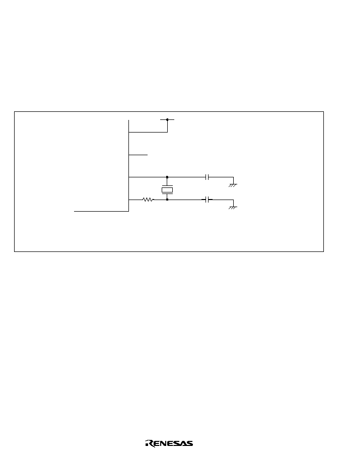
112
3.2.3
Connecting a Crystal Resonator
Connecting a Crystal Resonator: Figure 3.2 shows an example of crystal resonator connection.
The values of damping resistance R and load capacitances CL1 and CL2 should be decided after
investigating the components in collaboration with the manufacturer of the crystal oscillator to be
used. The crystal resonator should be an AT-cut parallel-oscillator type. Place the crystal resonator
and its load capacitors as close as possible to the XTAL and EXTAL pins.
Other signal lines should be routed away from the oscillator circuit to prevent induction from
interfering with correct oscillation.
High level
Notes: 1. The CKIO pin is an output in clock modes 0,1, and 2. In mode 3, it is high impedance.
2. The values for CL1, CL2, and the damping resistance should be determined after
consultation with the crystal resonator manufacturer.
CL1
R
CKPREQ
/CKM
CKIO
EXTAL
XTAL
Output or high
impedance
CL2
Figure 3.2 Example of Crystal Oscillator Connection
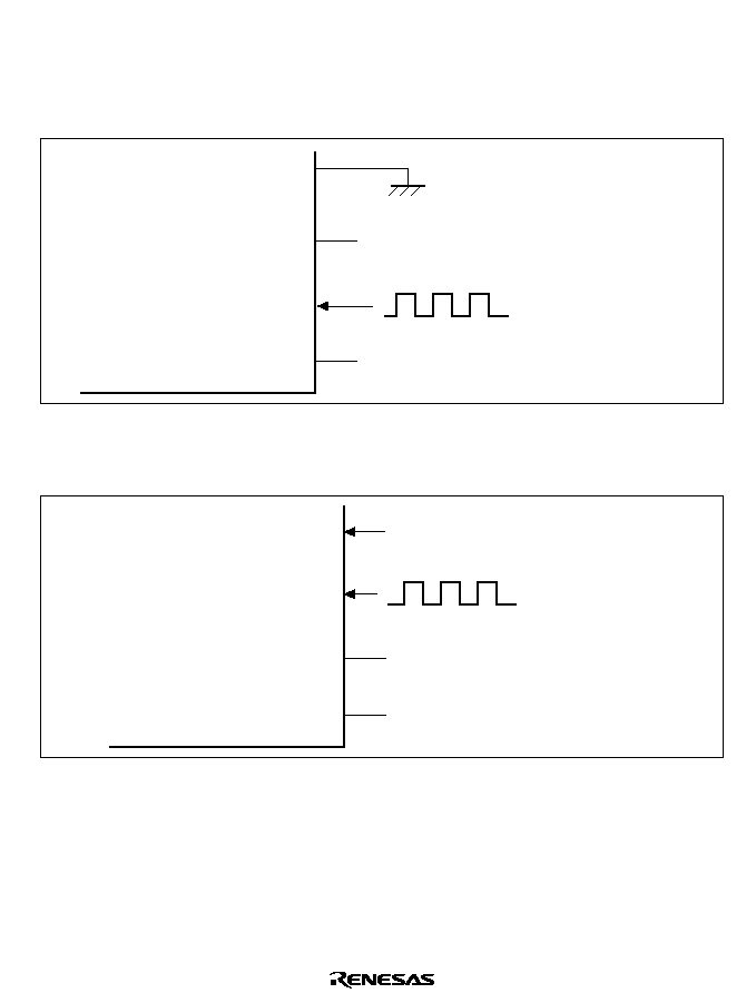
113
3.2.4
External Clock Input
An external clock is input from the EXTAL pin or the CKIO pin, depending on the clock mode.
Clock Input from EXTAL Pin: This method can be used in clock modes 0, 1, 2, and 3.
CKPREQ
/CKM
CKIO
EXTAL
XTAL
Output or
high-impedance
The CKIO pin is an output
in clock modes 0, 1, and 2,
and is high-impedance in
clock mode 3.
Open
External Clock Input
Ground level
Figure 3.3 External Clock Input Method
Clock Input from CKIO Pin: This method can be used in clock modes 4, 5, and 6.
CKPREQ
/CKM
CKIO
EXTAL
XTAL
Open
External Clock Input
Open
The
CKPREQ
/CKM pin is the clock
pause request input pin.
Figure 3.4 External Clock Input Method

114
3.2.5
Operating Frequency Selection by Register
Using the frequency modification register (FMR), it is possible to specify the operating frequency
division ratio for the internal clocks (I
, E
, P
). The internal clock frequency is determined under
the control of PLL circuits 1 and 2 and dividers DIVM, DIVE, and DIVP.
Frequency Modification Register (FMR): The frequency modification register is initialized only
by a power-on reset via the
RES pin, and not by an internal reset resulting from WDT overflow.
Its initial value depends on the settings of pins MD2≠MD0. Table 3.4 shows the relationship
between the MD2≠MD0 pin combinations and the initial value of the frequency modification
register.
Table 3.4
Relationship between Clock Mode Pin Settings and Initial Value of Frequency
Modification Register
Clock Mode
MD2
MD1
MD0
Initial Value
Mode 0
0
0
0
H'00
Mode 1
0
0
1
Mode 2
0
1
0
H'40
Mode 3
0
1
1
H'60
Mode 4
1
0
0
H'A6
Mode 5
1
0
1
Mode 6
1
1
0
H'E0
The register configuration is shown in table 3.5.
Table 3.5
Register Configuration
Name
Abbreviation
R/W
Initial Value
Address
Frequency modification register
FMR
R/W
See table 3.4
*
H'FFFFFE90
Note:
*
The initial value depends on the clock mode.

115
Bit:
7
6
5
4
3
2
1
0
PLL2ST
PLL1ST
CKIOST
--
FR3
FR2
FR1
FR0
Initial value:
--
--
--
0
0
--
--
0
R/W:
R/W
R/W
R/W
R
R/W
R/W
R/W
R/W
Bit 7--PLL2ST: Switching is possible in modes 0 to 3. In modes 4 to 6, PLL circuit 2 cannot be
used. In these modes, this bit always reads 1.
Bit 7: PLL2ST
Description
0
PLL circuit 2 used
1
PLL circuit 2 not used
Bit 6--PLL1ST: Switching is possible in modes 0, 1, 4, and 5. In modes 2, 3, and 6, PLL circuit 1
cannot be used. In these modes, this bit always reads 1.
Bit 6: PLL1ST
Description
0
PLL circuit 1 is used
1
PLL circuit 1 is not used
Bit 5--CKIOST: Setting is possible in modes 0 to 3. In modes 4 to 6, the CKIO pin is an input
pin. In these modes, this bit always reads 1.
Bit 5: CKIOST
Description
0
The CKIO pin outputs E
1
The CKIO pin is in the high-impedance state (Do not place CKIO in the high-
impedance state when PLL circuit 1 is operating)
Bit 4--Reserved: This bit is always read as 0. The write value should always be 0.
Bits 3 to 0--FR3 to FR0: The internal clock frequency and CKIO output frequency (modes 0≠2)
can be set by frequency setting bits FR3≠FR0. The values that can be set in bits FR3≠FR0 depend
on the mode and whether PLL circuit 1 and PLL circuit 2 are operating or halted. The following
tables show the values that can be set in FR3≠FR0, and the internal clock and CKIO output
frequency ratios, taking the external input clock frequency as 1.

116
∑
Modes 0 and 1
PLL circuits 1 and 2 operating
EXTAL input or crystal resonator used
FR3
FR2
FR1
FR0
I
E
P
CKIO
0
0
0
0
◊
4
◊
1
◊
1
◊
1
E
0
1
0
0
◊
4
◊
2
◊
1
◊
1
E
0
1
0
1
◊
4
◊
2
◊
2
◊
1
E
0
1
1
0
◊
4
◊
2
◊
2
◊
2
E
1
0
0
0
◊
4
◊
4
◊
1
◊
1
E
1
0
0
1
◊
4
◊
4
◊
2
◊
1
E
1
0
1
0
◊
4
◊
4
◊
2
◊
2
E
1
1
0
0
◊
4
◊
4
◊
4
◊
1
E
1
1
1
0
◊
4
◊
4
◊
4
◊
2
E
Note: Do not use combinations other than those shown above.
∑
Modes 0 to 3
PLL circuit 1 halted, PLL circuit 2 operating
EXTAL input or crystal resonator used
FR3
FR2
FR1
FR0
I
E
P
CKIO
0
0
0
0
◊
1
◊
1
◊
1
◊
1
E
0
1
0
1
◊
2
◊
2
◊
2
◊
1
E
0
1
1
0
◊
2
◊
2
◊
2
◊
2
E
1
1
0
0
◊
4
◊
4
◊
4
◊
1
E
1
1
1
0
◊
4
◊
4
◊
4
◊
2
E
Note: Do not use combinations other than those shown above.

117
∑
Modes 0 and 1
PLL circuit 1 operating, PLL circuit 2 halted
EXTAL input or crystal resonator used
FR3
FR2
FR1
FR0
I
E
P
CKIO
0
0
0
0
◊
4
◊
1
◊
1
◊
1
E
0
1
0
0
◊
4
◊
2
◊
1
◊
1
E
1
0
0
0
◊
4
◊
4
◊
1
◊
1
E
Note: Do not use combinations other than those shown above.
∑
Modes 4 and 5
PLL circuit 1 operating, PLL circuit 2 halted
CKIO input
FR3
FR2
FR1
FR0
I
E
P
CKIO
0
1
0
1
◊
2
◊
1
◊
1
◊
1/2
E
0
1
1
0
◊
2
◊
1
◊
1
◊
1
E
1
0
0
1
◊
2
◊
2
◊
1
◊
1/2
E
1
0
1
0
◊
2
◊
2
◊
1
◊
1
E
Note: Do not use combinations other than those shown above.

118
∑
Modes 0≠6
PLL circuits 1 and 2 halted
EXTAL input or crystal resonator used (modes 0≠3)
CKIO input (modes 4≠6)
FR3
FR2
FR1
FR0
I
E
P
CKIO
0
0
0
0
◊
1
◊
1/4
◊
1/4
◊
1/4
◊
1
0
1
0
0
◊
1
◊
1/2
◊
1/4
◊
1/4
◊
1
0
1
0
1
◊
1
◊
1/2
◊
1/2
◊
1/4
◊
1
0
1
1
0
◊
1
◊
1/2
◊
1/2
◊
1/2
◊
1
1
0
0
0
◊
1
◊
1
◊
1/4
◊
1/4
◊
1
1
0
0
1
◊
1
◊
1
◊
1/2
◊
1/4
◊
1
1
0
1
0
◊
1
◊
1
◊
1/2
◊
1/2
◊
1
1
1
0
0
◊
1
◊
1
◊
1
◊
1/4
◊
1
1
1
1
0
◊
1
◊
1
◊
1
◊
1/2
◊
1
1
1
1
1
◊
1
◊
1
◊
1
◊
1
◊
1
Note: Do not use combinations other than those shown above.
Frequency Change: When PLL circuit 1 or PLL circuit 2 becomes operational after modifying
the frequency modification register (including modification the frequency modification register in
the operating state), access the frequency modification register using the following procedure, and
noting the cautions listed below.
Frequency change procedure
∑
Set the on-chip watchdog timer (WDT) overflow time to secure the PLL circuit oscillation
settling time (CKS2≠CKS0 bits in WTCSR).
∑
Clear the WT/
IT and TME bit to 0 in WTCSR.
∑
Perform a read anywhere in an external memory area 0≠4 cache-through area.
∑
Change the frequency modification register to the target frequency, or change the
operating/halted state of the PLL circuits 1 and 2 (the clocks will stop temporarily inside the
chip).
∑
The oscillation circuits operate, and the clock is supplied to the WDT. This clock increments
the WDT.
∑
On WDT overflow, supply of a clock with the frequency set in frequency setting bits FR3≠FR0
begins. In this case, the OVF bit in WTSCR and the WOVF bit in RSTCSR are not set, an
interval timer interrupt (ITI) is not requested, and the
WDTOVF signal is not asserted.
Sample code for changing the frequency is shown below.

119
;
SH7616 frequency change
;
;
FMR
.equ
h'fffffe90
WTCSR
.equ h'fffffe80
RSTCSR .equ
h'fffffe83
PACR
.equ
h'fffffc80
XRAM
.equ
h'1000e000
.export _init_FMR
_init_FMR:
mov.l
#XRAM,r1
mov.l
r1,r5
mov.l
#FREQUENCY,r2
mov.l
#FREQUENCY_END,r3
program_move:
mov.w
@r2,r0
mov.w
r0,@r1
add
#2,r1
add
#2,r2
cmp/eq r2,r3
bf
program_move
nop
mov.l
#PACR,r1
mov.w
#h'0008,r0
mov.w
r0,@r1
MOV.L
#WTCSR,R1
MOV.W
#H'A51F,R2

120
MOV.L
#H'26200000,R3
MOV.L
#FMR,R4
jmp
@r5
nop
nop
nop
nop
nop
clock4_err:
bra
clock4_err
nop
nop
nop
nop
;
;
Main portion of frequency change code.
;
First copy this to XRAM and then run it in XRAM.
FREQUENCY:
;
<Watchdog timer control and status register setting>
;
Clear TME bit.
;
Clock input to WTCNT is
/16384
;
(Overflow frequency = 262.144 ms)
MOV.W
R2,@R1
;
<External cache through area read>
;
Cache through area of external member space 3: H'26200000
MOV.L
@R3,R0
;
<Frequency change register setting>
;
PLL circuit 1
Disabled.
;
PLL circuit 1
Enabled.
;
I¯ (
◊
4) = 62.5 MHz, E¯ (
◊
4) = 62.5 MHz,
;
P¯ (
◊
2) = 31.25 MHz, CKIO (E¯) = 62.5 MHz,
;
MOV
#H'4E,R0
;
PLL circuits 1 and 2
Enabled.

121
;
I¯ (
◊
4) = 62.5 MHz, E¯ (
◊
2) = 31.25 MHz,
;
P¯ (
◊
2 ) = 31.25 MHz, CKIO (E¯) = 31.25 MHz,
MOV
#H'0A,R0
;
PLL circuits 1 and 2
Enabled.
;
I¯ (
◊
4) = 62.5 MHz, E¯ (
◊
1) = 15.625 MHz,
;
P¯ (
◊
1) = 15.625 MHz, CKIO (E¯) = 15.625 MHz,
;
MOV
#H'08,R0
MOV.B
R0,@R4
rts
nop
FREQUENCY_END:
NOP
.END
Cautions
∑
The read from the external memory space 0≠4 cache-through area and the write to the
frequency modification register should be performed in on-chip X/Y memory. After reading
from the external memory space 0≠4 cache-through area, do not perform any write operations
in external memory spaces 0≠4 until the write to the frequency modification register.
∑
When the write access to the frequency modification register is executed, the WDT starts
automatically.
∑
Do not turn off the CKIO output when PLL circuit 1 is in the operating state.
∑
The CKIO output will be unstable until the PLL circuit stabilizes.
∑
When a frequency is modified, halt the on-chip DMAC (E-DMAC and DMAC) operation
before the frequency modification.
If PLL circuit 1 or PLL circuit 2 does not become operational after modifying the frequency
modification register (including modification in the operating state), it means that the above
procedure or cautions have not been properly observed. In this case, the WDT will not operate
even though the frequency modification register is modified.

122
3.2.6
Clock Modes and Frequency Ranges
The following table shows the operating modes and the associated frequency ranges for input
clocks.
Clock Input
PLL Circuit
Internal Clock
*
2,
*
3
Mode Pin
Input Frequency
Range (MHz)
PLL1 PLL2
I
(MH
Z
)
E
(MH
Z
)
P
(MH
Z
)
CKIO Output
(MHz)
0, 1
EXTAL or crystal
resonator
*
1
8≠15.625
On
On
8≠
62.5
8≠
62.5
8≠
31.25
8≠62.5
Off
On
8≠
62.5
8≠
62.5
8≠
31.25
8≠62.5
On
Off
8≠
62.5
8≠
15.625
8≠
15.625
8≠15.625
1≠31.25
Off
Off
1≠
31.25
1≠
31.25
1≠
31.25
1≠31.25
2
8≠15.625
Off
On
8≠
62.5
8≠
62.5
8≠
31.25
8≠62.5
1≠31.25
Off
1≠
31.25
1≠
31.25
1≠
31.25
1≠31.25
3
8≠15.625
On
8≠
62.5
8≠
62.5
8≠
31.25
--
1≠31.25
Off
1≠
31.25
1≠
31.25
1≠
31.25
4, 5
CKIO
16≠31.25
On
Off
16≠
62.5
16≠
31.25
16≠
31.25
--
1≠31.25
Off
1≠
31.25
1≠
31.25
1≠
31.25
6
1≠31.25
Off
1≠
31.25
1≠
31.25
1≠
31.25
Notes:
*
1 When a crystal resonator is used, set the frequency in the range of 8 to 15.625 MHz.
*
2 Set the frequency modification register so that the frequency of all internal clocks is 1
MHz or higher.
*
3 Use internal clock frequencies such that I
E
P
.
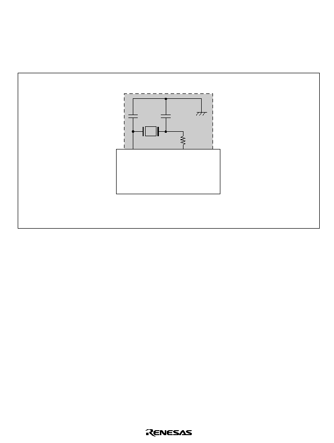
123
3.2.7
Notes on Board Design
When Using an External Crystal Oscillator: Place the crystal resonator, capacitors CL1 and
CL2, and damping resistor R close to the EXTAL and XTAL pins. To prevent induction from
interfering with correct oscillation, use a common grounding point for the capacitors connected to
the resonator, and do not locate a wiring pattern near these components.
Note: The values for CL1, CL2, and the damping resistance should be determined after
consultation with the crystal resonator manufacturer.
XTAL
EXTAL
R
CL2
CL1
Avoid crossing
signal lines
Figure 3.5 Points for Attention when Using Crystal Resonator
Bypass Capacitors: As far as possible, insert a laminated ceramic capacitor of 0.01 to 0.1 µF as a
bypass capacitor for each V
SS
/V
CC
pair. Mount the bypass capacitors as close as possible to the LSI
power supply pins, and use components with a frequency characteristic suitable for the LSI
operating frequency, as well as a suitable capacitance value.
V
SS
/V
CC
pairs
PLL system: 9-12
3 V digital system:
20-18, 26-22, 35-33, 45-42, 52-50, 60-58, 61-67, 69-66, 78-76, 79-81, 91-89,
101-99, 112-109, 113-110, 114-116, 130-132, 149-146, 150-147
5 V digital system:
157-155, 169-167, 181-179, 191-193, 202-200
124
When Using a PLL Oscillator Circuit: Keep the wiring short from the PLL V
CC
and V
SS
connection pattern to the power supply pins, and make the pattern width large, to minimize the
inductance component. Ground the oscillation stabilization capacitors C1 and C2 to V
SS
(PLL1)
and V
SS
(PLL2), respectively. Place C1 and C2 close to the CAP1 and CAP2 pins and do not
locate a wiring pattern in the vicinity.
CAP1
V
CC
(PLL)
V
CC
C1 = 470 pF
C2 = 470 pF
V
SS
CAP2
V
SS
(PLL)
Avoid crossing
signal lines
Power supply
Reference values
C1
C2
Figure 3.6 Points for Attention when Using PLL Oscillator Circuit
3.3
Bus Width of the CS0 Area
Pins MD3 and MD4 are used to specify the bus width of the CS0 area
.
The pin combination and
functions are listed in table 3.6. Do not switch the MD4 and MD3 pins while they are operating.
Switching them will cause operating errors.
Table 3.6
Bus Width of the CS0 Area
Pin
MD4
MD3
Function
0
0
8-bit bus width selected
0
1
16-bit bus width selected
1
0
32-bit bus width selected
1
1
Setting prohibited

125
Section 4 Exception Handling
4.1
Overview
4.1.1
Types of Exception Handling and Priority Order
Exception handling is initiated by four sources: resets, address errors, interrupts, and instructions
(table 4.1). When several exception sources occur simultaneously, they are accepted and processed
according to the priority order shown in table 4.1.

126
Table 4.1
Types of Exception Handling and Priority Order
Exception
Source
Priority
Reset
Power-on reset
High
Manual reset
Address
CPU address error
error
DMA address error (DMAC and E-DMAC)
Interrupt
NMI
User break
Hitachi user debug interface (H-UDI)
External interrupts (IRL1≠IRL15, IRQ0≠IRQ3 (set with
IRL3
,
IRL2
,
IRL1
,
IRL0
pins))
On-chip peripheral modules
Direct memory access controller (DMAC)
Watchdog timer (WDT)
Compare match interrupt (part of the bus
state controller)
Ethernet controller (EtherC) and Ethernet
controller direct memory access controller
(E-DMAC)
16-bit free-running timer (FRT)
Serial communication interface with FIFO
(SCIF)
16-bit timer pulse unit (TPU)
Serial I/O with FIFO (SIOF)
Serial I/O (SIO)
Instructions Trap instruction (TRAPA)
General illegal instructions (undefined code)
Illegal slot instructions (undefined code placed directly following a delayed
branch instruction
*
1
or instructions that rewrite the PC
*
2
)
Low
Notes:
*
1 Delayed branch instructions: JMP, JSR, BRA, BSR, RTS, RTE, BF/S, BT/S, BSRF,
BRAF
*
2 Instructions that rewrite the PC: JMP, JSR, BRA, BSR, RTS, RTE, BT, BF, TRAPA,
BF/S, BT/S, BSRF, BRAF

127
4.1.2
Exception Handling Operations
Exception handling sources are detected, and exception handling started, according to the timing
shown in table 4.2.
Table 4.2
Timing of Exception Source Detection and Start of Exception Handling
Exception Source
Timing of Source Detection and Start of Handling
Reset
Power-on reset
Starts when the NMI pin is high and the
RES
pin changes from
low to high
Manual reset
Starts when the NMI pin is low and the
RES
pin changes from
low to high
Address error
Detected when instruction is decoded and starts when the
previous executing instruction finishes executing
Interrupts
Detected when instruction is decoded and starts when the
previous executing instruction finishes executing
Instructions
Trap instruction
Starts from the execution of a TRAPA instruction
General illegal
instructions
Starts from the decoding of undefined code anytime except after
a delayed branch instruction (delay slot)
Illegal slot
instructions
Starts from the decoding of undefined code placed directly
following a delayed branch instruction (delay slot) or of an
instruction that rewrites the PC
When exception handling starts, the CPU operates as follows:
1. Exception handling triggered by reset
The initial values of the program counter (PC) and stack pointer (SP) are fetched from the
exception vector table (PC and SP are respectively addresses H'00000000 and H'00000004 for
a power-on reset and addresses H'00000008 and H'0000000C addresses for a manual reset).
See section 4.1.3, Exception Vector Table, for more information. 0 is then written to the vector
base register (VBR) and 1111 is written to the interrupt mask bits (I3≠I0) of the status register
(SR). The program begins running from the PC address fetched from the exception vector
table.
2. Exception handling triggered by address errors, interrupts, and instructions
SR and PC are saved to the stack address indicated by R15. For interrupt exception handling,
the interrupt priority level is written to the SR's interrupt mask bits (I3≠I0). For address error
and instruction exception handling, the I3≠I0 bits are not affected. The start address is then
fetched from the exception vector table and the program begins running from that address.

128
4.1.3
Exception Vector Table
Before exception handling begins, the exception vector table must be written in memory. The
exception vector table stores the start addresses of exception service routines. (The reset exception
table holds the initial values of PC and SP.)
All exception sources are given different vector numbers and vector table address offsets, from
which the vector table addresses are calculated. In exception handling, the start address of the
exception service routine is fetched from the exception vector table as indicated by the vector table
address.
Table 4.3 lists the vector numbers and vector table address offsets. Table 4.4 shows vector table
address calculations.
Table 4.3 (a) Exception Vector Table
Exception Source
Vector
Number
Vector Table Address
Offset
Vector Address
Power-on reset
PC
0
H'00000000≠H'00000003
Vector number
◊
4
SP
1
H'00000004≠H'00000007
Manual reset
PC
2
H'00000008≠H'0000000B
SP
3
H'0000000C≠H'0000000F
General illegal instruction
4
H'00000010≠H'00000013
VBR + (vector
(Reserved by system)
5
H'00000014≠H'00000017
number
◊
4)
Slot illegal instruction
6
H'00000018≠H'0000001B
(Reserved by system)
7
H'0000001C≠H'0000001F
8
H'00000020≠H'00000023
CPU address error
9
H'00000024≠H'00000027
DMA address error (DMAC and
E-DMAC)
10
*
5
H'00000028≠H'0000002B
Interrupt
NMI
11
H'0000002C≠H'0000002F
User break
12
H'00000030≠H'00000033
H-UDI
13
H'00000034≠H'00000037
(Reserved by system)
14
:
31
H'00000038≠H'0000003B
:
H'0000007C≠H'0000007F
Trap instruction (user vector)
32
:
63
H'00000080≠H'00000083
:
H'000000FC≠H'000000FF

129
Table 4.3 (b) Exception Processing Vector Table (IRQ Mode)
Exception Source
Vector
Number
Vector Table Address
Offset
Vector Addresses
Interrupt
IRQ0
64
*
2
H'00000100≠H'00000103
IRQ1
65
*
2
H'00000104≠H'00000107
IRQ2
66
*
2
H'00000108≠H'0000010B
IRQ3
67
*
2
H'0000010C≠H'0000010F
On-chip
peripheral
module
*
3
0
*
4
:
127
*
4
H'00000000≠H'00000003
:
H'000001FC≠H'000001FF
Table 4.3 (c) Exception Processing Vector Table (IRL Mode)
Exception Source
Vector
Number
Vector Table Address
Offset
Vector Addresses
Interrupt
IRL1
*
1
64
*
2
H'00000100≠H'00000103
VBR + (vector
IRL2
*
1
65
*
2
H'00000104≠H'00000107
number
◊
4)
IRL3
*
1
IRL4
*
1
66
*
2
H'00000108≠H'0000010B
IRL5
*
1
IRL6
*
1
67
*
2
H'0000010C≠H'0000010F
IRL7
*
1
IRL8
*
1
68
*
2
H'00000110≠H'00000113
IRL9
*
1
IRL10
*
1
69
*
2
H'00000114≠H'00000117
IRL11
*
1
IRL12
*
1
70
*
2
H'00000118≠H'0000011B
IRL13
*
1
IRL14
*
1
71
*
2
H'0000011C≠H'0000011F
IRL15
*
1
On-chip
peripheral
module
*
3
0
*
4
:
127
*
4
H'00000000≠H'00000003
:
H'000001FC≠H'000001FF
Notes:
*
1 When 1110 is input to the
IRL3
,
IRL2
,
IRL1
, and
IRL0
pins, an IRL1 interrupt results.
When 0000 is input, an IRL15 interrupt results.
*
2 External vector number fetches can be performed without using the auto-vector
numbers in this table.

130
*
3 The vector numbers and vector table address offsets for each on-chip peripheral
module interrupt are given table 5.4, Interrupt Exception Vectors and Priorities, in
section 5, Interrupt Controller.
*
4 Vector numbers are set in the on-chip vector number register. See section 5.3, Register
Descriptions, in section 5, Interrupt Controller, and section 11, Direct Memory Access
Controller, for more information.
*
5 The same vector number, 10, is generated for a DMAC DMA address error and an E-
DMAC DMA address error. (See table 4.3 (a).)
Both the address error flag (AE) in the DMAC's DMA operation register (DMAOR) and
the address error control bit (AEC) in the E-DMAC's E-DMAC operation control register
(EDOCR) must therefore be read in the exception service routine to determine which
DMA address error has occurred.
Table 4.4
Calculating Exception Vector Table Addresses
Exception Source
Vector Table Address Calculation
Power-on reset
Manual reset
(Vector table address) = (vector table address offset)
= (vector number)
◊
4
Other exception handling
(Vector table address) = VBR + (vector table address offset)
= VBR + (vector number)
◊
4
Note:
VBR: Vector base register
Vector table address offset: See table 4.3.
Vector number: See table 4.3.

131
4.2
Resets
4.2.1
Types of Resets
Resets have the highest priority of any exception source. There are two types of resets: manual
resets and power-on resets. As table 4.5 shows, both types of resets initialize the internal status of
the CPU. In power-on resets, all registers of the on-chip peripheral modules are initialized; in
manual resets, registers of all on-chip peripheral modules except the bus state controller (BSC),
user break controller (UBC), pin function controller (PFC), and frequency modification register
(FMR) are initialized. (Use the power-on reset when turning the power on.)
Table 4.5
Types of Resets
Conditions for
Transition to Reset Status
Internal Status
Type
NMI Pin
RES
Pin
CPU
On-Chip Peripheral Modules
Power-on reset
High
Low
Initialized
Initialized
Manual reset
Low
Low
Initialized
Initialized except for BSC, UBC,
PFC, and frequency modification
register (FMR)
4.2.2
Power-On Reset
When the NMI pin is high and the
RES pin is driven low, the device performs a power-on reset.
For a reliable reset, the
RES pin should be kept low for at least the duration of the oscillation
settling time (when the PLL circuit is halted) or for 20t
pcyc
(when the PLL circuit is running).
During a power-on reset, the CPU's internal state and all on-chip peripheral module registers are
initialized. See appendix B, Pin States, for the state of individual pins in the power-on reset state.
In a power-on reset, power-on reset exception handling starts when the NMI pin is kept high and
the
RES pin is first driven low for a set period of time and then returned to high. The CPU will
then operate as follows:
1. The initial value (execution start address) of the program counter (PC) is fetched from the
exception vector table.
2. The initial value of the stack pointer (SP) is fetched from the exception vector table.
3. The vector base register (VBR) is cleared to H'00000000 and the interrupt mask bits (I3≠I0) of
the status register (SR) are set to H'F (1111).
4. The values fetched from the exception vector table are set in the program counter (PC) and
stack pointer (SP), and the program begins executing.

132
4.2.3
Manual Reset
When the NMI pin is low and the
RES pin is driven low, the device executes a manual reset. For a
reliable reset, the
RES pin should be kept low for at least 20 clock cycles. During a manual reset,
the CPU's internal state is initialized. All on-chip peripheral module registers are initialized,
except for the bus state controller (BSC), user break controller (UBC), and pin function controller
(PFC) registers, and the frequency modification register (FMR). When the chip enters the manual
reset state in the middle of a bus cycle, manual reset exception handling does not start until the bus
cycle has ended. Thus, manual resets do not abort bus cycles. See appendix B, Pin States, for the
state of individual pins in the manual reset state.
In a manual reset, manual reset exception handling starts when the NMI pin is kept low and the
RES pin is first kept low for a set period of time and then returned to high. The CPU will then
operate in the same way as for a power-on reset.
4.3
Address Errors
4.3.1
Sources of Address Errors
Address errors occur when instructions are fetched or data read or written, as shown in table 4.6.

133
Table 4.6
Bus Cycles and Address Errors
Bus Cycle
Type
Bus
Master
Bus Cycle Description
Address Errors
Instruction CPU
Instruction fetched from even address
None (normal)
fetch
Instruction fetched from odd address
Address error
occurs
Instruction fetched from other than on-chip peripheral
module space
None (normal)
Instruction fetched from on-chip peripheral module
space
Address error
occurs
Data
CPU or
Word data accessed from even address
None (normal)
read/write
DMAC,
E-DMAC
Word data accessed from odd address
Address error
occurs
Longword data accessed from a longword boundary
None (normal)
Longword data accessed from other than a longword
boundary
Address error
occurs
Access of cache purge space, address array read/write
space, on-chip peripheral module space, or
synchronous DRAM mode setting space by PC-relative
addressing
Address error
occurs
Access of cache purge space, address array read/write
space, data array read/write space, on-chip peripheral
module space, or synchronous DRAM mode setting
space by a TAS.B instruction
Address error
occurs
Byte, word, or longword data accessed in on-chip
peripheral module space at addresses H'FFFFFC00 to
H'FFFFFCFF
None (normal)
Longword data accessed in on-chip peripheral module
space at addresses H'FFFFFE00 to H'FFFFFEFF
Address error
occurs
Word or byte data accessed in on-chip peripheral
module space at addresses H'FFFFFE00 to
H'FFFFFEFF
None (normal)
Byte data accessed in on-chip peripheral module space
at addresses H'FFFF0000 to H'FFFFF0FF or
H'FFFFFF00 to H'FFFFFFFF
Address error
occurs
Word or longword data accessed in on-chip peripheral
module space at addresses H'FFFF0000 to
H'FFFFF0FF or H'FFFFFF00 to H'FFFFFFFF
None (normal)
Notes: 1. Address errors do not occur during the synchronous DRAM mode register write cycle.
2. 16-byte DMAC transfers use longword accesses.

134
4.3.2
Address Error Exception Handling
When an address error occurs, address error exception handling begins after the end of the bus
cycle in which the error occurred and completion of the executing instruction. The CPU operates
as follows:
1. The status register (SR) is saved to the stack.
2. The program counter (PC) is saved to the stack. The PC value saved is the start address of the
instruction to be executed after the last instruction executed .
3. The exception service routine start address is fetched from the exception vector table entry that
corresponds to the address error that occurred, and the program starts executing from that
address. The jump that occurs is not a delayed branch.
Note:
The same vector number, 10, is generated for a DMAC DMA address error and an E-
DMAC DMA address error. (See table 4.3 (a).)
Both the address error flag (AE) in the DMAC's DMA operation register (DMAOR) and
the address error control bit (AEC) in the E-DMAC's E-DMAC operation control register
(EDOCR) must therefore be read in the exception service routine to determine which
DMA address error has occurred.

135
4.4
Interrupts
4.4.1
Interrupt Sources
Table 4.7 shows the sources that initiate interrupt exception handling. These are divided into NMI,
user breaks, H-UDI, IRL, IRQ, and on-chip peripheral modules.
Table 4.7
Types of Interrupt Sources
Type
Request Source
Number of Sources
NMI
NMI pin (external input)
1
User break
User break controller (UBC)
1
H-UDI
Hitachi user debug interface (H-UDI)
1
IRL
IRL1≠IRL15 (external input)
15
IRQ
IRQ0≠IRQ3 (external input)
4
On-chip peripheral module
Direct memory access controller (DMAC)
2
Ethernet controller (EtherC) and Ethernet
controller direct memory access controller
(E-DMAC)
1
16-bit free-running timer (FRT)
3
Watchdog timer (WDT)
1
Bus state controller (BSC)
1
Serial I/O with FIFO (SIOF)
4
Serial I/O (SIO)
4
Serial communication interface with FIFO
(SCIF)
4
16-bit timer pulse unit (TPU)
13
Each interrupt source is allocated a different vector number and vector table address offset. See
table 5.4, Interrupt Exception Vectors and Priority Order, in section 5, Interrupt Controller, for
more information.

136
4.4.2
Interrupt Priority Levels
The interrupt priority order is predetermined. When multiple interrupts occur simultaneously, the
interrupt controller (INTC) determines their relative priorities and begins exception handling
accordingly.
The priority order of interrupts is expressed as priority levels 0≠16, with priority 0 the lowest and
priority 16 the highest. The NMI interrupt has priority 16 and cannot be masked, so it is always
accepted. The user break interrupt priority level is 15 and IRL interrupts have priorities of 1≠15.
On-chip peripheral module interrupt priority levels can be set freely using the INTC's interrupt
priority level setting registers A≠E (IPRA≠IPRE) as shown in table 4.8. The priority levels that
can be set are 0≠15. Level 16 cannot be set. For more information on IPRA≠IPRE, see sections
5.3.1, Interrupt Priority Level Setting Register A (IPRA), to 5.3.5, Interrupt Priority Level Setting
Register E (IPRE).
Table 4.8
Interrupt Priority Order
Type
Priority Level Comment
NMI
16
Fixed priority level. Cannot be masked
User break
15
Fixed priority level
H-UDI
15
Fixed priority level
IRL
1≠15
Set with
IRL3
≠
IRL0
pins
IRQ
0≠15
Set with interrupt priority level setting register C
(IPRC)
On-chip peripheral module
0≠15
Set with interrupt priority level setting registers A, B,
D, and E (IPRA, IPRB, IPRD, IPRE)
4.4.3
Interrupt Exception Handling
When an interrupt occurs, its priority level is ascertained by the interrupt controller (INTC). NMI
is always accepted, but other interrupts are only accepted if they have a priority level higher than
the priority level set in the interrupt mask bits (I3≠I0) of the status register (SR).
When an interrupt is accepted, exception handling begins. In interrupt exception handling, the
CPU saves SR and the program counter (PC) to the stack. The priority level value of the accepted
interrupt is written to SR bits I3≠I0. For NMI, however, the priority level is 16, but the value set in
I3≠I0 is H'F (level 15). Next, the start address of the exception service routine is fetched from the
exception vector table for the accepted interrupt, that address is jumped to and execution begins.
For more information about interrupt exception handling, see section 5.4, Interrupt Operation.

137
4.5
Exceptions Triggered by Instructions
4.5.1
Instruction-Triggered Exception Types
Exception handling can be triggered by a trap instruction, general illegal instruction or illegal slot
instruction, as shown in table 4.9.
Table 4.9
Types of Exceptions Triggered by Instructions
Type
Source Instruction
Comment
Trap instruction
TRAPA
--
Illegal slot
instruction
Undefined code placed
immediately after a delayed
branch instruction (delay slot)
and instructions that rewrite the
PC
Delayed branch instructions: JMP, JSR,
BRA, BSR, RTS, RTE, BF/S, BT/S, BSRF,
BRAF
Instructions that rewrite the PC: JMP, JSR,
BRA, BSR, RTS, RTE, BT, BF, TRAPA,
BF/S, BT/S, BSRF, BRAF
General illegal
instruction
Undefined code anywhere
besides in a delay slot
--
4.5.2
Trap Instructions
When a TRAPA instruction is executed, trap instruction exception handling starts. The CPU
operates as follows:
1. The status register (SR) is saved to the stack.
2. The program counter (PC) is saved to the stack. The PC value saved is the start address of the
instruction to be executed after the TRAPA instruction.
3. The exception service routine start address is fetched from the exception vector table entry that
corresponds to the vector number specified by the TRAPA instruction. That address is jumped
to and the program starts executing. The jump that occurs is not a delayed branch.

138
4.5.3
Illegal Slot Instructions
An instruction placed immediately after a delayed branch instruction is said to be placed in a delay
slot. If the instruction placed in the delay slot is undefined code, illegal slot exception handling
begins when the undefined code is decoded. Illegal slot exception handling is also started when an
instruction that rewrites the program counter (PC) is placed in a delay slot. The exception handling
starts when the instruction is decoded. The CPU handles an illegal slot instruction as follows:
1. The status register (SR) is saved to the stack.
2. The program counter (PC) is saved to the stack. The PC value saved is the jump address of the
delayed branch instruction immediately before the undefined code or the instruction that
rewrites the PC.
3. The exception service routine start address is fetched from the exception vector table entry that
corresponds to the exception that occurred. That address is jumped to and the program starts
executing. The jump that occurs is not a delayed branch.
4.5.4
General Illegal Instructions
When undefined code placed anywhere other than immediately after a delayed branch instruction
(i.e., in a delay slot) is decoded, general illegal instruction exception handling starts. The CPU
handles general illegal instructions in the same way as illegal slot instructions. Unlike processing
of illegal slot instructions, however, the program counter value saved is the start address of the
undefined code.

139
4.6
When Exception Sources Are Not Accepted
When an address error or interrupt is generated after a delayed branch instruction or interrupt-
disabled instruction, it is sometimes not immediately accepted but is stored instead, as described in
table 4.10. When this happens, it will be accepted when an instruction for which exception
acceptance is possible is decoded.
Table 4.10
Exception Source Generation Immediately after a Delayed Branch Instruction
or Interrupt-Disabled Instruction
Exception Source
Point of Occurrence
Address Error
Interrupt
Immediately after a delayed branch instruction
*
1
Not accepted
Not accepted
Immediately after an interrupt-disabled instruction
*
2
Accepted
Not accepted
A repeat loop comprising up to three instructions (instruction
fetch cycle not generated)
First instruction or last three instructions in a repeat loop
containing four or more instructions
Not accepted
Not accepted
Fourth from last instruction in a repeat loop containing four
or more instructions
Accepted
Not accepted
Notes:
*
1 Delayed branch instructions: JMP, JSR, BRA, BSR, RTS, RTE, BF/S, BT/S, BSRF,
BRAF
*
2 Interrupt-disabled instructions: LDC, LDC.L, STC, STC.L, LDS, LDS.L, STS, STS.L
4.6.1
Immediately after a Delayed Branch Instruction
When an instruction placed immediately after a delayed branch instruction (delay slot) is decoded,
neither address errors nor interrupts are accepted. The delayed branch instruction and the
instruction located immediately after it (delay slot) are always executed consecutively, so no
exception handling occurs between the two.
4.6.2
Immediately after an Interrupt-Disabled Instruction
When an instruction immediately following an interrupt-disabled instruction is decoded, interrupts
are not accepted. Address errors are accepted.

140
4.6.3
Instructions in Repeat Loops
If a repeat loop comprises up to three instructions, neither exceptions nor interrupts are accepted.
If a repeat loop contains four or more instructions, neither exceptions nor interrupts are accepted
during the execution cycle of the first instruction or the last three instructions. If a repeat loop
contains four or more instructions, address errors only are accepted during the execution cycle of
the fourth from last instruction. For more information, see the SH-1/SH-2/SH-DSP Programming
Manual.
A. All interrupts and address errors are accepted.
B. Address errors only are accepted.
C. No interrupts or address errors are accepted.
When RC
1
When RC = 0
All interrupts and address errors are accepted.
(1) One instruction
A
B
C
A
instr0
instr1
instr2
Start (End):
(4) Four or more instructions
A
A or C (on return from instr n)
A
:
A
B
C
C
C
A
instr0
instr1
:
:
instr n-3
instr n-2
instr n-1
instr n
instr n+1
Start:
End:
(2) Two instructions
A
B
C
C
A
instr0
instr1
instr2
instr3
Start:
End:
(3) Three instructions
A
B
C
C
C
A
instr0
instr1
instr2
instr3
instr4
Start:
End:
Figure 4.1 Interrupt Acceptance Restrictions in Repeat Mode

141
4.7
Stack Status after Exception Handling
The status of the stack after exception handling ends is as shown in table 4.11.
Table 4.11
Stack Status after Exception Handling
Type
Stack Status
Address error
SP
Address of instruction after executed instruction
32 bits
SR
32 bits
Trap instruction
SP
Address of instruction after TRAPA instruction
32 bits
SR
32 bits
General illegal instruction SP
Start address of illegal instruction
32 bits
SR
32 bits
Interrupt
SP
Address of instruction after executed instruction
32 bits
SR
32 bits
Illegal slot instruction
SP
Jump destination address of delayed branch instruction 32 bits
SR
32 bits

142
4.8
Usage Notes
4.8.1
Value of Stack Pointer (SP)
The value of the stack pointer must always be a multiple of four, otherwise an address error will
occur when the stack is accessed during exception handling.
4.8.2
Value of Vector Base Register (VBR)
The value of the vector base register must always be a multiple of four, otherwise an address error
will occur when the vector table is accessed during exception handling.
4.8.3
Address Errors Caused by Stacking of Address Error Exception Handling
If the stack pointer value is not a multiple of four, an address error will occur during stacking of
the exception handling (interrupts, etc.). Address error exception handling will begin after the
original exception handling ends, but address errors will continue to occur. To ensure that address
error exception handling does not go into an endless loop, no address errors are accepted at that
point. This allows program control to be shifted to the address error exception service routine and
enables error handling to be carried out.
When an address error occurs during exception handling stacking, the stacking bus cycle (write) is
executed. In stacking of the status register (SR) and program counter (PC), the SP is decremented
by 4 for both, so the value of SP will not be a multiple of four after the stacking either. The
address value output during stacking is the SP value, so the address where the error occurred is
itself output. This means that the write data stacked will be undefined.
4.8.4
Manual Reset during Register Access
Do not initiate a manual reset during access of a bus state controller (BSC), user break controller
(UBC), or pin function controller (PFC) register, or the frequency modification register (FMR),
otherwise a write error may result.

143
Section 5 Interrupt Controller (INTC)
5.1
Overview
The interrupt controller (INTC) ascertains the priority order of interrupt sources and controls
interrupt requests to the CPU. The INTC has registers for setting the priority of each interrupt
which allow the user to set the order of priority in which interrupt requests are handled.
5.1.1
Features
The INTC has the following features:
∑
Sixteen interrupt priority levels can be set
By setting the five interrupt priority registers, the priorities of on-chip peripheral module
interrupts can be selected at 16 levels for different request sources.
∑
Vector numbers for on-chip peripheral module interrupt can be set
By setting the 24 vector number setting registers, the vector numbers of on-chip peripheral
module interrupts can be set to values from 0 to 127 for different request sources.
∑
The IRL interrupt vector number setting method can be selected: Either of two modes can be
selected by a register setting: auto-vector mode in which vector numbers are determined
internally, and external vector mode in which vector numbers are set externally.
∑
IRQ interrupt settings can be made (low level, rising-, falling-, or both-edge detection)
5.1.2
Block Diagram
Figure 5.1 shows a block diagram of the INTC.
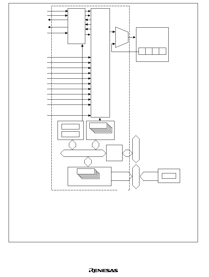
144
CPU
SR
Interrupt request
Com-
parator
Priority
decision
logic
(Interrupt request)
(Interrupt request)
(Interrupt request)
(Interrupt request)
(Interrupt request)
(Interrupt request)
(Interrupt request)
(Interrupt request)
(Interrupt request)
(Interrupt request)
(Interrupt request)
ICR
IRQCSR
IPRA≠IPRE
VCRWDT, VCRA≠VCRU
Module bus
Bus
interface
Internal bus
I3
I2
I1
I0
INTC
NMI
IR3
≠
IR0
A3≠A0
IVECF
D7≠D0
UBC
H-UDI
DMAC
FRT
WDT
REF
SCIF
TPU
SIO
E-DMAC
Input/
output
control
Vector
number
Vector
number
DMAC
Peripheral bus
VCRWDT
IPR
UBC:
User break controller
H-UDI: Hitachi user debug interface
DMAC: Direct memory access controller
FRT:
16-bit free-running timer
WDT:
Watchdog timer
REF:
Refresh request within bus state controller
SCIF:
Serial communication interface with FIFO
TPU:
16-bit timer pulse unit
SIO:
Serial I/O
SIOF:
Serial I/O with FIFO
E-DMAC:
Ethernet controller direct memory
access controller
EtherC:
Ethernet controller
ICR:
Interrupt control register
IRQCSR:
IRQ control/status register
IPRA≠IPRE:
Interrupt priority level setting
registers A≠E
VCRWDT:
Vector number setting register WDT
VCRA≠VCRU: Vector number setting registers A≠U
SR:
Status register
(Including EtherC
interrupt)
SIOF
Figure 5.1 INTC Block Diagram

145
5.1.3
Pin Configuration
Table 5.1 shows the INTC pin configuration.
Table 5.1
Pin Configuration
Name
Abbreviation
I/O
Function
Nonmaskable interrupt input pin
NMI
I
Input of nonmaskable interrupt request
signal
Level request interrupt input pins
IRL3
≠
IRL0
I
Input of maskable interrupt request
signals
Interrupt acceptance level output
pins
A3≠A0
O
In external vector mode, output an
interrupt level signal when an IRL/IRQ
interrupt is accepted
External vector fetch pin
IVECF
O
Indicates external vector read cycle
External vector number input pins
D7≠D0
I
Input external vector number
5.1.4
Register Configuration
The INTC has the 31 registers shown in table 5.2. These registers perform various INTC functions
including setting interrupt priority, and controlling external interrupt input signal detection.
Table 5.2
Register Configuration
Name
Abbr.
R/W
Initial
Value
Address
Access
Size
Interrupt priority register setting register A
IPRA
R/W
H'0000
H'FFFFFEE2
8, 16
Interrupt priority register setting register B
IPRB
R/W
H'0000
H'FFFFFE60
8, 16
Interrupt priority register setting register C
IPRC
R/W
H'0000
H'FFFFFEE6
8, 16
Interrupt priority register setting register D
IPRD
R/W
H'0000
H'FFFFFE40
8, 16
Interrupt priority register setting register E
IPRE
R/W
H'0000
H'FFFFFEC0
8, 16
Vector number setting register A
VCRA
R/W
H'0000
H'FFFFFE62
8, 16
Vector number setting register B
*
3
VCRB
R/W
H'0000
H'FFFFFE64
8, 16
Vector number setting register C
VCRC
R/W
H'0000
H'FFFFFE66
8, 16
Vector number setting register D
VCRD
R/W
H'0000
H'FFFFFE68
8, 16
Vector number setting register E
VCRE
R/W
H'0000
H'FFFFFE42
8, 16
Vector number setting register F
VCRF
R/W
H'0000
H'FFFFFE44
8, 16
Vector number setting register G
VCRG
R/W
H'0000
H'FFFFFE46
8, 16

146
Table 5.2
Register Configuration (cont)
Name
Abbr.
R/W
Initial
Value
Address
Access
Size
Vector number setting register H
VCRH
R/W
H'0000
H'FFFFFE48
8, 16
Vector number setting register I
VCRI
R/W
H'0000
H'FFFFFE4A
8, 16
Vector number setting register J
VCRJ
R/W
H'0000
H'FFFFFE4C
8, 16
Vector number setting register K
VCRK
R/W
H'0000
H'FFFFFE4E
8, 16
Vector number setting register L
VCRL
R/W
H'0000
H'FFFFFE 50 8, 16
Vector number setting register M
VCRM
R/W
H'0000
H'FFFFFE52
8, 16
Vector number setting register N
VCRN
R/W
H'0000
H'FFFFFE54
8, 16
Vector number setting register O
VCRO
R/W
H'0000
H'FFFFFE56
8, 16
Vector number setting register P
VCRP
R/W
H'0000
H'FFFFFEC2
8, 16
Vector number setting register Q
VCRQ
R/W
H'0000
H'FFFFFEC4
8, 16
Vector number setting register R
VCRR
R/W
H'0000
H'FFFFFEC6
8, 16
Vector number setting register S
VCRS
R/W
H'0000
H'FFFFFEC8
8, 16
Vector number setting register T
VCRT
R/W
H'0000
H'FFFFFECA 8, 16
Vector number setting register U
VCRU
R/W
H'0000
H'FFFFFECC 8, 16
Vector number setting register WDT
VCRWDT
R/W
H'0000
H'FFFFFEE4
8, 16
Vector number setting register DMA0
*
4
VCRDMA0 R/W
Undefined H'FFFFFFA0
32
Vector number setting register DMA1
*
4
VCRDMA1 R/W
Undefined H'FFFFFFA8
32
Interrupt control register
ICR
R/W
H'8000/
H'0000
*
1
H'FFFFFEE0
8, 16
IRQ control/status register
IRQCSR
R/W
*
2
H'FFFFFEE8
8, 16
Notes:
*
1 The value when the NMI pin is high is H'8000; when the NMI pin is low, it is H'0000.
*
2 When pins
IRL3
≠
IRL0
are high, bits 7≠4 in IRQCSR are set to 1. When pins
IRL3
≠
IRL0
are low, bits 7≠4 in IRQCSR are cleared to 0. The initial value of bits other than 7≠4 is
0.
*
3 In the SH7616, VCRB is a reserved register and must not be accessed.
*
4 See section 11, Direct Memory Access Controlle for more information on VCRDMA0,
and VCRDMA1.
5.2
Interrupt Sources
There are five types of interrupt sources: NMI, user breaks, H-UDI, IRL/IRQ and on-chip
peripheral modules. Each interrupt has a priority expressed as a priority level (0 to 16, with 0 the
lowest and 16 the highest). Giving an interrupt a priority level of 0 masks it.

147
5.2.1
NMI Interrupt
The NMI interrupt has priority 16 and is always accepted. Input at the NMI pin is detected by
edge. Use the NMI edge select bit (NMIE) in the interrupt control register (ICR) to select either
the rising or falling edge. NMI interrupt exception handling sets the interrupt mask level bits (I3≠
I0) in the status register (SR) to level 15.
5.2.2
User Break Interrupt
A user break interrupt has priority level 15 and occurs when the break condition set in the user
break controller (UBC) is satisfied. User break interrupt exception handling sets the interrupt mask
level bits (I3≠I0) in the status register (SR) to level 15. For more information about the user break
interrupt, see section 6, User Break Controller.
5.2.3
H-UDI Interrupt
The H-UDI interrupt has a priority level of 15, and is generated when an H-UDI interrupt
instruction is serially input. H-UDI interrupt exception processing sets the interrupt mask bits (I3≠
I0) in the status register (SR) to level 15. See section 18, Hitachi User Debug Interface, for details
of the H-UDI interrupt.
5.2.4
IRL Interrupts
IRL interrupts are requested by input from pins
IRL3≠IRL0. Fifteen interrupts, IRL15≠IRL1, can
be input externally via pins
IRL3≠IRL0. The priority levels of interrupts IRL15≠IRL0 are 15≠1,
respectively, and their vector numbers are 71≠64. Set the vector numbers with the interrupt vector
mode select (VECMD) bit of the interrupt control register (ICR) to enable external input. External
input of vector numbers consists of vector numbers 0≠127 from the external vector input pins
(D7≠D0). When an external vector is used, 0 is input to D7. Internal vectors are called auto-
vectors and vectors input externally are called external vectors. Table 5.3 lists IRL priority levels
and auto vector numbers.
When an IRL interrupt is accepted in external vector mode, the IRL interrupt level is output from
the interrupt acceptance level output pins (A3≠A0). The external vector fetch pin (
IVECF) is also
asserted. The external vector number is read from pins D7≠D0 at this time.
IRL interrupt exception processing sets the interrupt mask level bits (I3 to I0) in the status register
(SR) to the priority level value of the IRL interrupt that was accepted.

148
5.2.5
IRQ Interrupts
An IRQ interrupt is requested when the external interrupt vector mode select bit (EXIMD) of the
interrupt control register (ICR) is set to 1. An IRQ interrupt corresponds to input at one of pins
IRL3≠IRL0. Low-level sensing or rising/falling/both-edge sensing can be selected independently
for each pin by the IRQ sense select bits (IRQ31S≠IRQ00S) in the IRQ control/status register
(IRQCSR), and a priority level of 0 to 15 can be selected independently for each pin by means of
interrupt priority register C (IPRC). Set the interrupt vector mode select bit (VECMD) of the
interrupt control register (ICR) to enable external input of vector numbers. External vector
numbers are 0 to 127, and are input to the external vector input pins (D7≠D0) during the interrupt
vector fetch bus cycle. When an external vector is used, 0 is input to D7.
When an IRQ interrupt is accepted in external vector mode, the IRQ interrupt priority level is
output from the interrupt acceptance level output pins (A3≠A0). The external vector fetch signal
(
IVECF) is also asserted. The external vector number is read from signals D7≠D0 at this time.
IRQ interrupt exception processing sets the interrupt mask bits (I3≠I0) in the status register (SR) to
the priority level value of the IRQ interrupt that was accepted.
Table 5.3
IRL Interrupt Priority Levels and Auto-Vector Numbers
Pin
Priority
Vector
IRL3
IRL2
IRL1
IRL0
Level
Number
0
0
0
0
15
71
1
14
1
0
13
70
1
12
1
0
0
11
69
1
10
1
0
9
68
1
8
1
0
0
0
7
67
1
6
1
0
5
66
1
4
1
0
0
3
65
1
2
1
0
1
64
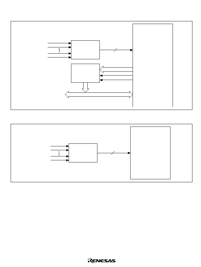
149
An example of connections for external vector mode interrupts is shown in figure 5.2, and an
example of connections for auto-vector mode interrupts in figure 5.3.
Chip
Priority
encoder
Interrupt
requests
Vector number
generator
circuit
4
IRL0
≠
IRL3
IRL0
≠
IRL3
D0≠D7
A0≠A3
IVECF
RD
D0≠D7
Figure 5.2 Example of Connections for External Vector Mode Interrupts
Chip
Priority
encoder
Interrupt
requests
4
IRL0
≠
IRL3
IRL0
≠
IRL3
Figure 5.3 Example of Connections for Auto-Vector Mode Interrupts
Figures 5.4 to 5.7 show the interrupt vector fetch cycle for the external vector mode. During this
cycle,
CS0≠CS4 stay high. A24≠A4 output undefined values. The WAIT pin is sampled, but
programmable waits are not valid.
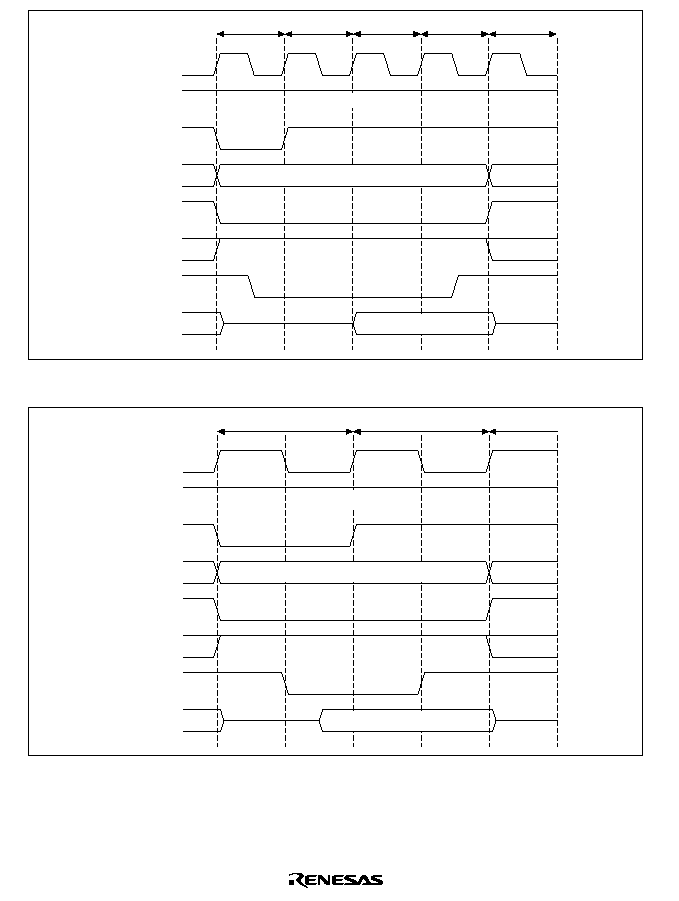
150
T1
CKIO
CS0
≠
CS4
BS
A3≠A0
IVECF
RD/
WR
RD
D7≠D0
T2
T3
T4
Vector number input
High
Accepted interrupt level
Figure 5.4 External Vector Fetch (I
: E
= 1 : 1)
T1
CKIO
CS0
≠
CS4
BS
A3≠A0
IVECF
RD/
WR
RD
D7≠D0
T2
High
Vector number input
Accepted interrupt level
Figure 5.5 External Vector Fetch (I
: E
1 : 1)

151
CKIO
CS0
≠
CS4
BS
A3≠A0
IVECF
RD/
WR
RD
D7≠D0
WAIT
T1
T2
T3
Tw
T4
Vector number input
Accepted interrupt level
High
Figure 5.6 External Vector Fetch (I
: E
= 1 : 1 (
WAIT Input))
CKIO
CS0
≠
CS4
BS
A3≠A0
IVECF
RD/
WR
RD
D7≠D0
WAIT
T1
Tw
T2
Accepted interrupt level
High
Vector number input
Figure 5.7 External Vector Fetch (I
: E
1 : 1 (
WAIT Input))

152
5.2.6
On-chip Peripheral Module Interrupts
On-chip peripheral module interrupts are interrupts generated by the following 9 on-chip
peripheral modules:
∑
Direct memory access controller (DMAC)
∑
Bus state controller (BSC)
∑
Watchdog timer (WDT)
∑
16-bit free-running timer (FRT)
∑
Ethernet controller direct memory access controller (E-DMAC) (Including EtherC interrupt)
∑
16-bit timer pulse unit (TPU)
∑
Serial communication interface with FIFO (SCIF)
∑
Serial I/O with FIFO (SIOF)
∑
Serial I/O (SIO)
A different interrupt vector is assigned to each interrupt source, so the exception service routine
does not have to decide which interrupt has occurred. Priority levels between 0 and 15 can be
assigned to individual on-chip peripheral modules in interrupt priority registers A, B, D, and E
(IPRA, IPRB, IPRD, IPRE). On-chip peripheral module interrupt exception handling sets the
interrupt mask level bits (I3≠I0) in the status register (SR) to the priority level value of the on-chip
peripheral module interrupt that was accepted.
5.2.7
Interrupt Exception Vectors and Priority Order
Table 5.4 lists interrupt sources and their vector numbers, vector table address offsets and interrupt
priorities.
Each interrupt source is allocated a different vector number and vector table address offset. Vector
table addresses are calculated from vector numbers and vector table address offsets. In interrupt
exception handling, the exception service routine start address is fetched from the vector table
entry indicated by the vector table address. See table 4.4, Calculating Exception Vector Table
Addresses, in section 4, Exception Handling, for more information on this calculation.
IRL interrupts IRL15≠IRL1 have interrupt priority levels of 15≠1, respectively. IRQ interrupt and
on-chip peripheral module interrupt priorities can be set freely between 0 and 15 for each module
by setting interrupt priority registers A≠E (IPRA≠IPRE). The ranking of interrupt sources for
IPRA≠IPRE, however, must be the order listed under Priority within IPR Setting Unit in table 5.4
and cannot be changed. A reset assigns priority level 0 to on-chip peripheral module interrupts. If
the same priority level is assigned to two or more interrupt sources and interrupts from those
sources occur simultaneously, their priority order is the default priority order indicated at the right
in table 5.4.

153
Table 5.4 (a) Interrupt Exception Vectors and Priority Order (IRL Mode)
Vectors
Interrupt
Priority
Priority
within
Interrupt Source
Vector
No.
Vector
Table
Address
Order
(Initial
Value)
IPR (Bit
Numbers)
IPR
Setting
Unit
VCR (Bit
Numbers)
Default
Priority
NMI
11
VBR +
16
--
--
--
High
User break
12
(vector No. 15
--
--
--
H-UDI
13
◊
4)
15
--
--
--
IRL15
*
4
71
*
1
15
--
--
--
IRL14
*
4
14
--
--
--
IRL13
*
4
70
*
1
13
--
--
--
IRL12
*
4
12
--
--
--
IRL11
*
4
69
*
1
11
--
--
--
IRL10
*
4
10
--
--
--
IRL9
*
4
68
*
1
9
--
--
--
IRL8
*
4
8
--
--
--
IRL7
*
4
67
*
1
7
--
--
--
IRL6
*
4
6
--
--
--
IRL5
*
4
66
*
1
5
--
--
--
IRL4
*
4
4
--
--
--
IRL3
*
4
65
*
1
3
--
--
--
IRL2
*
4
2
--
--
--
IRL1
*
4
64
*
1
1
--
--
--
DMAC0
Transfer
end
0≠127
*
2
15≠0 (0)
IPRA
(11≠8)
High
Low
VCRDMA0
(6≠0)
DMAC1
Transfer
end
0≠127
*
2
15≠0 (0)
High
Low
VCRDMA1
(6≠0)
Low

154
Table 5.4 (a) Interrupt Exception Vectors and Priority Order (IRL Mode) (cont)
Vectors
Interrupt
Priority
Priority
within
Interrupt Source
Vector
No.
Vector
Table
Address
Order
(Initial
Value)
IPR (Bit
Numbers)
IPR
Setting
Unit
VCR (Bit
Numbers)
Default
Priority
WDT
ITI
0≠127
*
2
VBR +
(vector No.
◊
4)
15≠0 (0)
IPRA
(7≠4)
High
Low
VCRWDT
(14≠8)
High
REF
*
3
CMI
0≠127
*
2
15≠0 (0)
High
Low
VCRWDT
(6≠0)
E-DMAC EINT
*
6
0≠127
*
2
15≠0 (0)
IPRB
High
VCRA (14≠8)
(15≠12)
Reserved
VCRB (14≠0)
*
5
Low
FRT
ICI
0≠127
*
2
15≠0 (0)
IPRB
High
VCRC (14≠8)
OCI
0≠127
*
2
(11≠8)
VCRC (6≠0)
OVI
0≠127
*
2
Low
VCRD (14≠8)
TPU0
TGI0A
0≠127
*
2
15≠0 (0)
IPRD
High
VCRE (14≠8)
TGI0B
0≠127
*
2
(15≠12)
VCRE (6≠0)
TGI0C
0≠127
*
2
VCRF (14≠8)
TGI0D
0≠127
*
2
VCRF (6≠0)
TCI0V
0≠127
*
2
Low
VCRG (14≠8)
TPU1
TGI1A
0≠127
*
2
15≠0 (0)
IPRD
High
VCRH (14≠8)
TGI1B
0≠127
*
2
(11≠8)
VCRH (6≠0)
TCI1V
0≠127
*
2
VCRI (14≠8)
TCI1U
0≠127
*
2
Low
VCRI (6≠0)
TPU2
TGI2A
0≠127
*
2
15≠0 (0)
IPRD
High
VCRJ (14≠8)
TGI2B
0≠127
*
2
(7≠4)
VCRJ (6≠0)
TCI2V
0≠127
*
2
VCRK (14≠8)
TCI2U
0≠127
*
2
Low
VCRK (6≠0)
Low

155
Table 5.4 (a) Interrupt Exception Vectors and Priority Order (IRL Mode) (cont)
Vectors
Interrupt
Priority
Priority
within
Interrupt Source
Vector
No.
Vector
Table
Address
Order
(Initial
Value)
IPR (Bit
Numbers)
IPR
Setting
Unit
VCR (Bit
Numbers)
Default
Priority
SCIF1
ERI1
0≠127
*
2
VBR +
15≠0 (0)
IPRD
High
VCRL (14≠8)
High
RXI1
0≠127
*
2
(vector No.
(3≠0)
VCRL (6≠0)
BRI1
0≠127
*
2
◊
4)
VCRM (14≠8)
TXI1
0≠127
*
2
Low
VCRM (6≠0)
SCIF2
ERI2
0≠127
*
2
15≠0 (0)
IPRE
High
VCRN (14≠8)
RXI2
0≠127
*
2
(15≠12)
VCRN (6≠0)
BRI2
0≠127
*
2
VCRO (14≠8)
TXI2
0≠127
*
2
Low
VCRO (6≠0)
SIOF
RERI0
0≠127
*
2
15≠0 (0)
IPRE
High
VCRP (14≠8)
TERI0
0≠127
*
2
(11≠8)
VCRP (6≠0)
RDFI0
0≠127
*
2
VCRQ (14≠8)
TDEI0
0≠127
*
2
Low
VCRQ (6≠0)
SIO1
RERI1
0≠127
*
2
15≠0 (0)
IPRE
High
VCRR (14≠8)
TERI1
0≠127
*
2
(7≠4)
VCRR (6≠0)
RDFI1
0≠127
*
2
VCRS (14≠8)
TDEI1
0≠127
*
2
Low
VCRS (6≠0)
SIO2
RERI2
0≠127
*
2
15≠0 (0)
IPRE
High
VCRT (14≠8)
TERI2
0≠127
*
2
(3≠0)
VCRT (6≠0)
RDFI2
0≠127
*
2
VCRU (14≠8)
TDEI2
0≠127
*
2
Low
VCRU (6≠0)
Reserved
128≠255 --
--
--
--
--
Low
Notes:
*
1 An external vector number fetch can be performed without using the auto-vector
numbers shown in this table. The external vector numbers are 0≠127.
*
2 Vector numbers are set in the on-chip vector number register.
*
3 REF is the refresh control unit within the bus state controller.
*
4 Set to IRL1≠IRL15 or IRQ0≠IRQ3 by the EXIMD bit in ICR.
*
5 In the SH7616, VCRB is a reserved register and must not be accessed.
*
6 The E-DMAC interrupt (EINT) is the OR of those of the 19 interrupt sources in the
EtherC/E-DMAC status register (EESR) that are enabled by the EtherC/E-DMAC status
interrupt permission register (EESIPR). As the three status bits in the EtherC status
register (ECSR) can be copied into the ECI bit in EESR as an interrupt source, EINT is
input to the INTC as the OR of a maximum of 22 interrupt sources.

156
Table 5.4 (b) Interrupt Exception Vectors and Priority Order (IRQ Mode)
Vectors
Interrupt
Priority
Priority
within
Interrupt Source
Vector
No.
Vector
Table
Address
Order
(Initial
Value)
IPR (Bit
Numbers)
IPR
Setting
Unit
VCR (Bit
Numbers)
Default
Priority
NMI
11
VBR +
16
--
--
--
High
User break
12
(vector No. 15
--
--
--
H-UDI
13
◊
4)
15
--
--
--
IRQ0
*
4
64
*
1
15≠0 (0)
IPRC
(15≠12)
--
--
IRQ1
*
4
65
*
1
15≠0 (0)
IPRC
(11≠8)
--
--
IRQ2
*
4
66
*
1
15≠0 (0)
IPRC
(7≠4)
--
--
IRQ3
*
4
67
*
1
15≠0 (0)
IPRC
(3≠0)
--
--
DMAC0
Transfer
end
0≠127
*
2
15≠0 (0)
IPRA
(11≠8)
High
Low
VCRDMA0
(6≠0)
DMAC1
Transfer
end
0≠127
*
2
15≠0 (0)
High
Low
VCRDMA1
(6≠0)
WDT
ITI
0≠127
*
2
15≠0 (0)
IPRA
(7≠4)
High
Low
VCRWDT
(14≠8)
REF
*
3
CMI
0≠127
*
2
15≠0 (0)
High
Low
VCRWDT
(6≠0)
Low

157
Table 5.4 (b) Interrupt Exception Vectors and Priority Order (IRQ Mode) (cont)
Vectors
Interrupt
Priority
Priority
within
Interrupt Source
Vector
No.
Vector
Table
Address
Order
(Initial
Value)
IPR (Bit
Numbers)
IPR
Setting
Unit
VCR (Bit
Numbers)
Default
Priority
E-DMAC EINT
*
6
0≠127
*
2
VBR +
15≠0 (0)
IPRB
High
VCRA (14≠8) High
(vector No.
(15≠12)
Reserved
◊
4)
VCRB
Low
(14≠0)
*
5
FRT
ICI
0≠127
*
2
15≠0 (0)
IPRB
High
VCRC (14≠8)
OCIA/B
0≠127
*
2
(11≠8)
VCRC (6≠0)
OVI
0≠127
*
2
Low
VCRD (14≠8)
TPU0
TGI0A
0≠127
*
2
15≠0 (0)
IPRD
High
VCRE (14≠8)
TGI0B
0≠127
*
2
(15≠12)
VCRE (6≠0)
TGI0C
0≠127
*
2
VCRF (14≠8)
TGI0D
0≠127
*
2
VCRF (6≠0)
TCI0V
0≠127
*
2
Low
VCRG (14≠8)
TPU1
TGI1A
0≠127
*
2
15≠0 (0)
IPRD
High
VCRH (14≠8)
TGI1B
0≠127
*
2
(11≠8)
VCRH (6≠0)
TCI1V
0≠127
*
2
VCRI (14≠8)
TCI1U
0≠127
*
2
Low
VCRI (6≠0)
TPU2
TGI2A
0≠127
*
2
15≠0 (0)
IPRD
High
VCRJ (14≠8)
TGI2B
0≠127
*
2
(7≠4)
VCRJ (6≠0)
TCI2V
0≠127
*
2
VCRK (14≠8)
TCI2U
0≠127
*
2
Low
VCRK (6≠0)
SCIF1
ERI1
0≠127
*
2
15≠0 (0)
IPRD
High
VCRL (14≠8)
RXI1
0≠127
*
2
(3≠0)
VCRL (6≠0)
BRI1
0≠127
*
2
VCRM (14≠8)
TXI1
0≠127
*
2
Low
VCRM (6≠0)
SCIF2
ERI2
0≠127
*
2
15≠0 (0)
IPRE
High
VCRN (14≠8)
RXI2
0≠127
*
2
(15≠12)
VCRN (6≠0)
BRI2
0≠127
*
2
VCRO (14≠8)
TXI2
0≠127
*
2
Low
VCRO (6≠0)
Low

158
Table 5.4 (b) Interrupt Exception Vectors and Priority Order (IRQ Mode) (cont)
Vectors
Interrupt
Priority
Priority
within
Interrupt Source
Vector
No.
Vector
Table
Address
Order
(Initial
Value)
IPR (Bit
Numbers)
IPR
Setting
Unit
VCR (Bit
Numbers)
Default
Priority
SIOF
RERI0
0≠127
*
2
VBR +
15≠0 (0)
IPRE
High
VCRP (14≠8) High
TERI0
0≠127
*
2
(vector No.
(11≠8)
VCRP (6≠0)
RDFI0
0≠127
*
2
◊
4)
VCRQ (14≠8)
TDEI0
0≠127
*
2
Low
VCRQ (6≠0)
SIO1
RERI1
0≠127
*
2
15≠0 (0)
IPRE
High
VCRR (14≠8)
TERI1
0≠127
*
2
(7≠4)
VCRR (6≠0)
RDFI1
0≠127
*
2
VCRS (14≠8)
TDEI1
0≠127
*
2
Low
VCRS (6≠0)
SIO2
RERI2
0≠127
*
2
15≠0 (0)
IPRE
High
VCRT (14≠8)
TERI2
0≠127
*
2
(3≠0)
VCRT (6≠0)
RDFI2
0≠127
*
2
VCRU (14≠8)
TDEI2
0≠127
*
2
Low
VCRU (6≠0)
Reserved
128≠255 --
--
--
--
--
Low
Notes:
*
1 An external vector number fetch can be performed without using the auto-vector
numbers shown in this table. The external vector numbers are 0≠127.
*
2 Vector numbers are set in the on-chip vector number register.
*
3 REF is the refresh control unit within the bus state controller.
*
4 Set to IRL1≠IRL15 or IRQ0≠IRQ3 by the EXIMD bit in ICR.
*
5 In the SH7616, VCRB is a reserved register and must not be accessed.
*
6 The E-DMAC interrupt (EINT) is the OR of those of the 19 interrupt sources in the
EtherC/E-DMAC status register (EESR) that are enabled by the EtherC/E-DMAC status
interrupt permission register (EESIPR). As the three status bits in the EtherC status
register (ECSR) can be copied into the ECI bit in EESR as an interrupt source, EINT is
input to the INTC as the OR of a maximum of 22 interrupt sources.

159
5.3
Register Descriptions
5.3.1
Interrupt Priority Level Setting Register A (IPRA)
Interrupt priority level setting register A (IPRA) is a 16-bit read/write register that assigns priority
levels from 0 to 15 to on-chip peripheral module interrupts. IPRA is initialized to H'0000 by a
reset. It is not initialized in standby mode. Unless otherwise specified, `reset' refers to both power-
on and manual resets throughout this manual.
Bit:
15
14
13
12
11
10
9
8
--
--
--
--
DMAC
IP3
DMAC
IP2
DMAC
IP1
DMAC
IP0
Initial value:
0
0
0
0
0
0
0
0
R/W:
R
R
R
R
R/W
R/W
R/W
R/W
Bit:
7
6
5
4
3
2
1
0
WDT
IP3
WDT
IP2
WDT
IP1
WDT
IP0
--
--
--
--
Initial value:
0
0
0
0
0
0
0
0
R/W:
R/W
R/W
R/W
R/W
R
R
R
R
Bits 15 to 12--Reserved: These bits are always read as 0. The write value should always be 0.
Bits 11 to 8--Direct Memory Access Controller (DMAC) Interrupt Priority Level 3 to 0
(DMACIP3≠DMACIP0): These bits set the direct memory access controller (DMAC) interrupt
priority level. There are four bits, so levels 0≠15 can be set. The same level is set for both two
DMAC channels. When interrupts occur simultaneously, channel 0 has priority.
Bits 7 to 4--Watchdog Timer (WDT) Interrupt Priority Level 3 to 0 (WDTIP3≠WDTIP0): These
bits set the watchdog timer (WDT) interrupt priority level and bus state controller (BSC) interrupt
priority level. There are four bits, so levels 0≠15 can be set. When WDT and BSC interrupts occur
simultaneously, the WDT interrupt has priority.
Bits 3 to 0--Reserved: These bits are always read as 0. The write value should always be 0.

160
5.3.2
Interrupt Priority Level Setting Register B (IPRB)
Interrupt priority level setting register B (IPRB) is a 16-bit read/write register that assigns priority
levels from 0 to 15 to on-chip peripheral module interrupts. IPRB is initialized to H'0000 by a
reset. It is not initialized in standby mode.
Bit:
15
14
13
12
11
10
9
8
E-DMAC
IP3
E-DMAC
IP2
E-DMAC
IP1
E-DMAC
IP0
FRTIP3
FRTIP2
FRTIP1
FRTIP0
Initial value:
0
0
0
0
0
0
0
0
R/W:
R/W
R/W
R/W
R/W
R/W
R/W
R/W
R/W
Bit:
7
6
5
4
3
2
1
0
--
--
--
--
--
--
--
--
Initial value:
0
0
0
0
0
0
0
0
R/W:
R
R
R
R
R
R
R
R
Bits 15 to 12--Ethernet Controller Direct Memory Access Controller (E-DMAC) Interrupt
Priority Level 3 to 0 (E-DMACIP3≠E-DMACIP0): These bits set the ethernet controller direct
memory access controller (E-DMAC) interrupt priority level. There are four bits, so levels 0≠15
can be set.
Bits 11 to 8--16-Bit Free-Running Timer (FRT) Interrupt Priority Level 3 to 0 (FRTIP3≠
FRTIP0): These bits set the 16-bit free-running timer (FRT) interrupt priority level. There are four
bits, so levels 0≠15 can be set.
Bits 7 to 0--Reserved: These bits are always read as 0. The write value should always be 0.

161
5.3.3
Interrupt Priority Level Setting Register C (IPRC)
Interrupt priority level setting register C (IPRC) is a 16-bit read/write register that sets the priority
levels (0≠15) of IRQ0≠IRQ3 interrupts. IPRC is initialized to H'0000 by a reset. It is not initialized
in standby mode.
Bit:
15
14
13
12
11
10
9
8
IRQ0IP3 IRQ0IP2 IRQ0IP1 IRQ0IP0 IRQ1IP3 IRQ1IP2 IRQ1IP1 IRQ1IP0
Initial value:
0
0
0
0
0
0
0
0
R/W:
R/W
R/W
R/W
R/W
R/W
R/W
R/W
R/W
Bit:
7
6
5
4
3
2
1
0
IRQ2IP3 IRQ2IP2 IRQ2IP1 IRQ2IP0 IRQ3IP3 IRQ3IP2 IRQ3IP1 IRQ3IP0
Initial value:
0
0
0
0
0
0
0
0
R/W:
R/W
R/W
R/W
R/W
R/W
R/W
R/W
R/W
Bits 15 to 0≠IRQ0 to IRQ3 Priority Level 3 to 0 (IRQnIP3≠IRQnIP0, n = 0≠3): These bits set the
IRQ0≠IRQ3 priority levels. There are four bits for each interrupt, so the value can be set between
0 and 15.

162
5.3.4
Interrupt Priority Level Setting Register D (IPRD)
Interrupt priority level setting register D (IPRD) is a 16-bit read/write register that sets the priority
levels (0≠15) of on-chip peripheral module interrupts. IPRD is initialized to H'0000 by a reset. It is
not initialized in standby mode.
Bit:
15
14
13
12
11
10
9
8
TPU0IP3 TPU0IP2 TPU0IP1 TPU0IP0 TPU1IP3 TPU1IP2 TPU1IP1 TPU1IP0
Initial value:
0
0
0
0
0
0
0
0
R/W:
R/W
R/W
R/W
R/W
R/W
R/W
R/W
R/W
Bit:
7
6
5
4
3
2
1
0
TPU2IP3 TPU2IP2 TPU2IP1 TPU2IP0 SCF1IP3 SCF1IP2 SCF1IP1 SCF1IP0
Initial value:
0
0
0
0
0
0
0
0
R/W:
R/W
R/W
R/W
R/W
R/W
R/W
R/W
R/W
Bits 15 to 4--16-Bit Timer Pulse Unit 0 to 2 (TPU0≠TPU2) Interrupt Priority Level 3 to 0
(TPUnIP3≠TPUnIP0, n = 0≠2): These bits set the 16-bit timer pulse unit 0 to 2 (TPU0≠TPU2)
interrupt priority levels. There are four bits for each interrupt, so the value can be set between 0
and 15.
Bits 3 to 0--Serial Communication Interface with FIFO 1 (SCIF1) Interrupt Priority Level 3 to 0
(SCF1IP3≠SCF1IP0): These bits set the serial communication interface with FIFO 1 (SCIF1)
interrupt priority level. There are four bits, so the value can be set between 0 and 15.

163
5.3.5
Interrupt Priority Level Setting Register E (IPRE)
Interrupt priority level setting register E (IPRE) is a 16-bit read/write register that sets the priority
levels (0≠15) of on-chip peripheral module interrupts. IPRE is initialized to H'0000 by a reset. It is
not initialized in standby mode.
Bit:
15
14
13
12
11
10
9
8
SCF2IP3 SCF2IP2 SCF2IP1 SCF2IP0 SIOFIP3 SIOFIP2 SIOFIP1 SIOFIP0
Initial value:
0
0
0
0
0
0
0
0
R/W:
R/W
R/W
R/W
R/W
R/W
R/W
R/W
R/W
Bit:
7
6
5
4
3
2
1
0
SIO1IP3 SIO1IP2 SIO1IP1 SIO1IP0 SIO2IP3 SIO2IP2 SIO2IP1 SIO2IP0
Initial value:
0
0
0
0
0
0
0
0
R/W:
R/W
R/W
R/W
R/W
R/W
R/W
R/W
R/W
Bits 15 to 12--Serial Communication Interface with FIFO 2 (SCIF2) Interrupt Priority Level 3 to
0 (SCF2IP3≠SCF2IP0): These bits set the serial communication interface with FIFO 2 (SCIF2)
interrupt priority levels. There are four bits, so the value can be set between 0 and 15.
Bits 11 to 8≠≠Serial I/O with FIFO (SIOF) Interrupt Priority Level 3 to 0 (SIOFIP3(SIOFIP0):
These bits set the serial I/O with FIFO (SIOF) interrupt priority levels. There are four bits, so the
value can be set between 0 and 15.
Bits 7 to 0--Serial I/O 1 to 2 (SIO1≠SIO2) Interrupt Priority Level 3 to 0 (SIOnIP3≠SIOnIP0, n =
0≠2): These bits set the serial I/O 0 to 2 (SIO0≠SIO2) interrupt priority levels. There are four bits
for each interrupt, so the value can be set between 0 and 15.
Table 5.5 shows the relationship between on-chip peripheral module interrupts and interrupt
priority level setting registers.

164
Table 5.5
Interrupt Request Sources and IPRA≠IPRE
Register
Bits 15 to 12
Bits 11 to 8
Bits 7 to 4
Bits 3 to 0
Interrupt priority level setting
register A
Reserved
DMAC0,
DMAC1
WDT, REF
Reserved
Interrupt priority level setting
register B
E-DMAC
FRT
Reserved
Reserved
Interrupt priority level setting
register C
IRQ0
IRQ1
IRQ2
IRQ3
Interrupt priority level setting
register D
TPU0
TPU1
TPU2
SCIF1
Interrupt priority level setting
register E
SCIF2
SIOF
SIO1
SIO2
As table 5.5 shows, between two and four on-chip peripheral modules are assigned to each
interrupt priority level setting register. Set the priority levels by setting the corresponding 4-bit
groups with values in the range of H'0 (0000) to H'F (1111). H'0 is interrupt priority level 0 (the
lowest); H'F is level 15 (the highest). When two on-chip peripheral modules are assigned to the
same bits (DMAC0 and DMAC1, or WDT and BSC refresh control unit), those two modules have
the same priority. A reset initializes IPRA≠IPRE to H'0000. They are not initialized in standby
mode.
5.3.6
Vector Number Setting Register WDT (VCRWDT)
Vector number setting register WDT (VCRWDT) is a 16-bit read/write register that sets the WDT
interval interrupt and BSC compare match interrupt vector numbers (0≠127). VCRWDT is
initialized to H'0000 by a reset. It is not initialized in standby mode.
Bit:
15
14
13
12
11
10
9
8
--
WITV6
WITV5
WITV4
WITV3
WITV2
WITV1
WITV0
Initial value:
0
0
0
0
0
0
0
0
R/W:
R
R/W
R/W
R/W
R/W
R/W
R/W
R/W
Bit:
7
6
5
4
3
2
1
0
--
BCMV6 BCMV5
BCMV4 BCMV3
BCMV2
BCMV1 BCMV0
Initial value:
0
0
0
0
0
0
0
0
R/W:
R
R/W
R/W
R/W
R/W
R/W
R/W
R/W
Bits 15 and 7--Reserved: These bits are always read as 0. The write value should always be 0.

165
Bits 14 to 8--Watchdog Timer (WDT) Interval Interrupt Vector Number 6 to 0 (WITV6≠
WITV0): These bits set the vector number for the interval interrupt (ITI) of the watchdog timer
(WDT). There are seven bits, so the value can be set between 0 and 127.
Bits 6 to 0--Bus State Controller (BSC) Compare Match Interrupt Vector Number 6 to 0
(BCMV6≠BCMV0): These bits set the vector number for the compare match interrupt (CMI) of
the bus state controller (BSC). There are seven bits, so the value can be set between 0 and 127.
5.3.7
Vector Number Setting Register A (VCRA)
Vector number setting register A (VCRA) is a 16-bit read/write register that sets the E-DMAC
interrupt vector numbers (0≠127). VCRA is initialized to H'0000 by a reset. It is not initialized in
standby mode.
Bit:
15
14
13
12
11
10
9
8
--
EINV6
EINV5
EINV4
EINV3
EINV2
EINV1
EINV0
Initial value:
0
0
0
0
0
0
0
0
R/W:
R
R/W
R/W
R/W
R/W
R/W
R/W
R/W
Bit:
7
6
5
4
3
2
1
0
--
--
--
--
--
--
--
--
Initial value:
0
0
0
0
0
0
0
0
R/W:
R
R
R
R
R
R
R
R
Bits 15 and 7 to 0--Reserved: These bits are always read as 0. The write value should always be
0.
Bits 14 to 8--Ethernet Controller Direct Memory Access Controller (E-DMAC) Interrupt Vector
Number 6 to 0 (EINV6≠EINV0): These bits set the vector number for ethernet controller direct
memory access controller (E-DMAC) interrupt (EINT). There are seven bits, so the value can be
set between 0 and 127.

166
5.3.8
Vector Number Setting Register B (VCRB)
Vector number setting register B (VCRB) is a 16-bit reserved register. Access to this register is
prohibited. VCRB is initialized to H'0000 by a reset. It is not initialized in standby mode.
Bit:
15
14
13
12
11
10
9
8
--
--
--
--
--
--
--
--
Initial value:
0
0
0
0
0
0
0
0
R/W:
R
R
R
R
R
R
R
R
Bit:
7
6
5
4
3
2
1
0
--
--
--
--
--
--
--
--
Initial value:
0
0
0
0
0
0
0
0
R/W:
R
R
R
R
R
R
R
R
5.3.9
Vector Number Setting Register C (VCRC)
Vector number setting register C (VCRC) is a 16-bit read/write register that sets the 16-bit free-
running timer (FRT) input-capture interrupt and output-compare interrupt vector numbers (0≠127).
VCRC is initialized to H'0000 by a reset. It is not initialized in standby mode.
Bit:
15
14
13
12
11
10
9
8
--
FICV6
FICV5
FICV4
FICV3
FICV2
FICV1
FICV0
Initial value:
0
0
0
0
0
0
0
0
R/W:
R
R/W
R/W
R/W
R/W
R/W
R/W
R/W
Bit:
7
6
5
4
3
2
1
0
--
FOCV6
FOCV5
FOCV4
FOCV3
FOCV2
FOCV1
FOCV0
Initial value:
0
0
0
0
0
0
0
0
R/W:
R
R/W
R/W
R/W
R/W
R/W
R/W
R/W
Bits 15 and 7--Reserved: These bits are always read as 0. The write value should always be 0.
Bits 14 to 8--16-Bit Free-Running Timer (FRT) Input-Capture Interrupt Vector Number 6 to 0
(FICV6≠FICV0): These bits set the vector number for the 16-bit free-running timer (FRT) input-
capture interrupt (ICI). There are seven bits, so the value can be set between 0 and 127.
Bits 6 to 0--16-Bit Free-Running Timer (FRT) Output-Compare Interrupt Vector Number 6 to 0
(FOCV6≠FOCV0): These bits set the vector number for the 16-bit free-running timer (FRT)
output-compare interrupt (OCI). There are seven bits, so the value can be set between 0 and 127.

167
5.3.10
Vector Number Setting Register D (VCRD)
Vector number setting register D (VCRD) is a 16-bit read/write register that sets the 16-bit free-
running timer (FRT) overflow interrupt vector number (0≠127). VCRD is initialized to H'0000 by
a reset. It is not initialized in standby mode.
Bit:
15
14
13
12
11
10
9
8
--
FOVV6
FOVV5
FOVV4
FOVV3
FOVV2
FOVV1
FOVV0
Initial value:
0
0
0
0
0
0
0
0
R/W:
R
R/W
R/W
R/W
R/W
R/W
R/W
R/W
Bit:
7
6
5
4
3
2
1
0
--
--
--
--
--
--
--
--
Initial value:
0
0
0
0
0
0
0
0
R/W:
R
R
R
R
R
R
R
R
Bits 15 and 7 to 0--Reserved: These bits are always read as 0. The write value should always be
0.
Bits 14 to 8--16-Bit Free-Running Timer (FRT) Overflow Interrupt Vector Number 6 to 0
(FOVV6≠FOVV0): These bits set the vector number for the 16-bit free-running timer (FRT)
overflow interrupt (OVI). There are seven bits, so the value can be set between 0 and 127.

168
5.3.11
Vector Number Setting Register E (VCRE)
Vector number setting register E (VCRE) is a 16-bit read/write register that sets the 16-bit timer
pulse unit 0 (TPU0) TGR0A and TGR0B input capture/compare match interrupt vector numbers
(0≠127).
VCRE is initialized to H'0000 by a reset. It is not initialized in standby mode.
Bit:
15
14
13
12
11
10
9
8
--
TG0AV6 TG0AV5 TG0AV4 TG0AV3 TG0AV2 TG0AV1 TG0AV0
Initial value:
0
0
0
0
0
0
0
0
R/W:
R
R/W
R/W
R/W
R/W
R/W
R/W
R/W
Bit:
7
6
5
4
3
2
1
0
--
TG0BV6 TG0BV5 TG0BV4 TG0BV3 TG0BV2 TG0BV1 TG0BV0
Initial value:
0
0
0
0
0
0
0
0
R/W:
R
R/W
R/W
R/W
R/W
R/W
R/W
R/W
Bits 15 and 7--Reserved: These bits are always read as 0. The write value should always be 0.
Bits 14 to 8--16-Bit Timer pulse unit 0 (TPU0) TGR0A Input Capture/Compare Match Interrupt
Vector Number 6 to 0 (TG0AV6≠TG0AV0): These bits set the vector number for the 16-bit timer
pulse unit 0 (TPU0) TGR0A input capture/compare match interrupt. There are seven bits, so the
value can be set between 0 and 127.
Bits 6 to 0--16-Bit Timer pulse unit 0 (TPU0) TGR0B Input Capture/Compare Match Interrupt
Vector Number 6 to 0 (TG0BV6≠TG0BV0): These bits set the vector number for the 16-bit timer
pulse unit 0 (TPU0) TGR0B input capture/compare match interrupt. There are seven bits, so the
value can be set between 0 and 127.

169
5.3.12
Vector Number Setting Register F (VCRF)
Vector number setting register F (VCRF) is a 16-bit read/write register that sets the 16-bit timer
pulse unit 0 (TPU0) TGR0C and TGR0D input capture/compare match interrupt vector numbers
(0≠127).
VCRF is initialized to H'0000 by a reset. It is not initialized in standby mode.
Bit:
15
14
13
12
11
10
9
8
--
TG0CV6 TG0CV5 TG0CV4 TG0CV3 TG0CV2 TG0CV1 TG0CV0
Initial value:
0
0
0
0
0
0
0
0
R/W:
R
R/W
R/W
R/W
R/W
R/W
R/W
R/W
Bit:
7
6
5
4
3
2
1
0
--
TG0DV6 TG0DV5 TG0DV4 TG0DV3 TG0DV2 TG0DV1 TG0DV0
Initial value:
0
0
0
0
0
0
0
0
R/W:
R
R/W
R/W
R/W
R/W
R/W
R/W
R/W
Bits 15 and 7--Reserved: These bits are always read as 0. The write value should always be 0.
Bits 14 to 8--16-Bit Timer pulse unit 0 (TPU0) TGR0C Input Capture/Compare Match Interrupt
Vector Number 6 to 0 (TG0CV6≠TG0CV0): These bits set the vector number for the 16-bit timer
pulse unit 0 (TPU0) TGR0C input capture/compare match interrupt. There are seven bits, so the
value can be set between 0 and 127.
Bits 6 to 0--16-Bit Timer pulse unit 0 (TPU0) TGR0D Input Capture/Compare Match Interrupt
Vector Number 6 to 0 (TG0DV6≠TG0DV0): These bits set the vector number for the 16-bit timer
pulse unit 0 (TPU0) TGR0D input capture/compare match interrupt. There are seven bits, so the
value can be set between 0 and 127.

170
5.3.13
Vector Number Setting Register G (VCRG)
Vector number setting register G (VCRG) is a 16-bit read/write register that sets the 16-bit timer
pulse unit 0 (TPU0) TCNT0 overflow interrupt vector number (0≠127).
VCRG is initialized to H'0000 by a reset. It is not initialized in standby mode.
Bit:
15
14
13
12
11
10
9
8
--
TC0VV6 TC0VV5 TC0VV4 TC0VV3 TC0VV2 TC0VV1 TC0VV0
Initial value:
0
0
0
0
0
0
0
0
R/W:
R
R/W
R/W
R/W
R/W
R/W
R/W
R/W
Bit:
7
6
5
4
3
2
1
0
--
--
--
--
--
--
--
--
Initial value:
0
0
0
0
0
0
0
0
R/W:
R
R
R
R
R
R
R
R
Bits 15 and 7 to 0--Reserved: These bits are always read as 0. The write value should always be
0.
Bits 14 to 8--16-Bit Timer pulse unit 0 (TPU0) TCNT0 Overflow Interrupt Vector Number 6 to 0
(TC0VV6≠TV0VV0): These bits set the vector number for the 16-bit timer pulse unit 0 (TPU0)
TCNT0 overflow interrupt. There are seven bits, so the value can be set between 0 and 127.

171
5.3.14
Vector Number Setting Register H (VCRH)
Vector number setting register H (VCRH) is a 16-bit read/write register that sets the 16-bit timer
pulse unit 1 (TPU1) TGR1A and TGR1B input capture/compare match interrupt vector numbers
(0≠127).
VCRH is initialized to H'0000 by a reset. It is not initialized in standby mode.
Bit:
15
14
13
12
11
10
9
8
--
TG1AV6 TG1AV5 TG1AV4 TG1AV3 TG1AV2 TG1AV1 TG1AV0
Initial value:
0
0
0
0
0
0
0
0
R/W:
R
R/W
R/W
R/W
R/W
R/W
R/W
R/W
Bit:
7
6
5
4
3
2
1
0
--
TG1BV6 TG1BV5 TG1BV4 TG1BV3 TG1BV2 TG1BV1 TG1BV0
Initial value:
0
0
0
0
0
0
0
0
R/W:
R
R/W
R/W
R/W
R/W
R/W
R/W
R/W
Bits 15 and 7--Reserved: These bits are always read as 0. The write value should always be 0.
Bits 14 to 8--16-Bit Timer pulse unit 1 (TPU1) TGR1A Input Capture/Compare Match Interrupt
Vector Number 6 to 0 (TG1AV6≠TG1AV0): These bits set the vector number for the 16-bit timer
pulse unit 1 (TPU1) TGR1A input capture/compare match interrupt. There are seven bits, so the
value can be set between 0 and 127.
Bits 6 to 0--16-Bit Timer pulse unit 1 (TPU1) TGR1B Input Capture/Compare Match Interrupt
Vector Number 6 to 0 (TG1BV6≠TG1BV0): These bits set the vector number for the 16-bit timer
pulse unit 1 (TPU1) TGR1B input capture/compare match interrupt. There are seven bits, so the
value can be set between 0 and 127.

172
5.3.15
Vector Number Setting Register I (VCRI)
Vector number setting register I (VCRI) is a 16-bit read/write register that sets the 16-bit timer
pulse unit 1 (TPU1) TCNT1 overflow/underflow interrupt vector numbers (0≠127).
VCRI is initialized to H'0000 by a reset. It is not initialized in standby mode.
Bit:
15
14
13
12
11
10
9
8
--
TC1VV6 TC1VV5 TC1VV4 TC1VV3 TC1VV2 TC1VV1 TC1VV0
Initial value:
0
0
0
0
0
0
0
0
R/W:
R
R/W
R/W
R/W
R/W
R/W
R/W
R/W
Bit:
7
6
5
4
3
2
1
0
--
TC1UV6 TC1UV5 TC1UV4 TC1UV3 TC1UV2 TC1UV1 TC1UV0
Initial value:
0
0
0
0
0
0
0
0
R/W:
R
R/W
R/W
R/W
R/W
R/W
R/W
R/W
Bits 15 and 7--Reserved: These bits are always read as 0. The write value should always be 0.
Bits 14 to 8--16-Bit Timer pulse unit 1 (TPU1) TCNT1 Overflow Interrupt Vector Number 6 to 0
(TC1VV6≠TC1VV0): These bits set the vector number for the 16-bit timer pulse unit 1 (TPU1)
TCNT1 overflow interrupt. There are seven bits, so the value can be set between 0 and 127.
Bits 6 to 0--16-Bit Timer pulse unit 1 (TPU1) TCNT1 Underflow Interrupt Vector Number 6 to 0
(TC1UV6≠TC1UV0): These bits set the vector number for the 16-bit timer pulse unit 1 (TPU1)
TCNT1 underflow interrupt. There are seven bits, so the value can be set between 0 and 127.

173
5.3.16
Vector Number Setting Register J (VCRJ)
Vector number setting register J (VCRJ) is a 16-bit read/write register that sets the 16-bit timer
pulse unit 2 (TPU2) TGR2A and TGR2B input capture/compare match interrupt vector numbers
(0≠127).
VCRJ is initialized to H'0000 by a reset. It is not initialized in standby mode.
Bit:
15
14
13
12
11
10
9
8
--
TG2AV6 TG2AV5 TG2AV4 TG2AV3 TG2AV2 TG2AV1 TG2AV0
Initial value:
0
0
0
0
0
0
0
0
R/W:
R
R/W
R/W
R/W
R/W
R/W
R/W
R/W
Bit:
7
6
5
4
3
2
1
0
--
TG2BV6 TG2BV5 TG2BV4 TG2BV3 TG2BV2 TG2BV1 TG2BV0
Initial value:
0
0
0
0
0
0
0
0
R/W:
R
R/W
R/W
R/W
R/W
R/W
R/W
R/W
Bits 15 and 7--Reserved: These bits are always read as 0. The write value should always be 0.
Bits 14 to 8--16-Bit Timer pulse unit 2 (TPU2) TGR2A Input Capture/Compare Match Interrupt
Vector Number 6 to 0 (TG2AV6≠TG2AV0): These bits set the vector number for the 16-bit timer
pulse unit 2 (TPU2) TGR2A input capture/compare match interrupt. There are seven bits, so the
value can be set between 0 and 127.
Bits 6 to 0--16-Bit Timer pulse unit 2 (TPU2) TGR2B Input Capture/Compare Match Interrupt
Vector Number 6 to 0 (TG2BV6≠TG2BV0): These bits set the vector number for the 16-bit timer
pulse unit 2 (TPU2) TGR2B input capture/compare match interrupt. There are seven bits, so the
value can be set between 0 and 127.

174
5.3.17
Vector Number Setting Register K (VCRK)
Vector number setting register K (VCRK) is a 16-bit read/write register that sets the 16-bit timer
pulse unit 2 (TPU2) TCNT2 overflow/underflow interrupt vector numbers (0≠127).
VCRK is initialized to H'0000 by a reset. It is not initialized in standby mode.
Bit:
15
14
13
12
11
10
9
8
--
TC2VV6 TC2VV5 TC2VV4 TC2VV3 TC2VV2 TC2VV1 TC2VV0
Initial value:
0
0
0
0
0
0
0
0
R/W:
R
R/W
R/W
R/W
R/W
R/W
R/W
R/W
Bit:
7
6
5
4
3
2
1
0
--
TC2UV6 TC2UV5 TC2UV4 TC2UV3 TC2UV2 TC2UV1 TC2UV0
Initial value:
0
0
0
0
0
0
0
0
R/W:
R
R/W
R/W
R/W
R/W
R/W
R/W
R/W
Bits 15 and 7--Reserved: These bits are always read as 0. The write value should always be 0.
Bits 14 to 8--16-Bit Timer pulse unit 2 (TPU2) TCNT2 Overflow Interrupt Vector Number 6 to 0
(TC2VV6≠TC2VV0): These bits set the vector number for the 16-bit timer pulse unit 2 (TPU2)
TCNT2 overflow interrupt. There are seven bits, so the value can be set between 0 and 127.
Bits 6 to 0--16-Bit Timer pulse unit 2 (TPU2) TCNT2 Underflow Interrupt Vector Number 6 to 0
(TC2UV6≠TC2UV0): These bits set the vector number for the 16-bit timer pulse unit 2 (TPU2)
TCNT2 underflow interrupt. There are seven bits, so the value can be set between 0 and 127.

175
5.3.18
Vector Number Setting Register L (VCRL)
Vector number setting register L (VCRL) is a 16-bit read/write register that sets the serial
communication interface with FIFO 1 (SCIF1) receive-error interrupt and receive-data-full/data-
ready interrupt vector numbers (0≠127).
VCRL is initialized to H'0000 by a reset. It is not initialized in standby mode.
Bit:
15
14
13
12
11
10
9
8
--
SER1V6 SER1V5 SER1V4 SER1V3 SER1V2 SER1V1 SER1V0
Initial value:
0
0
0
0
0
0
0
0
R/W:
R
R/W
R/W
R/W
R/W
R/W
R/W
R/W
Bit:
7
6
5
4
3
2
1
0
--
SRX1V6 SRX1V5 SRX1V4 SRX1V3 SRX1V2 SRX1V1 SRX1V0
Initial value:
0
0
0
0
0
0
0
0
R/W:
R
R/W
R/W
R/W
R/W
R/W
R/W
R/W
Bits 15 and 7--Reserved: These bits are always read as 0. The write value should always be 0.
Bits 14 to 8--Serial Communication Interface with FIFO 1 (SCIF1) Receive-Error Interrupt
Vector Number 6 to 0 (SER1V6≠SER1V0): These bits set the vector number for the serial
communication interface with FIFO 1 (SCIF1) receive-error interrupt. There are seven bits, so the
value can be set between 0 and 127.
Bits 6 to 0--Serial Communication Interface with FIFO 1 (SCIF1) Receive-Data-Full/Data-Ready
Interrupt Vector Number 6 to 0 (SRX1V6≠SRX1V0): These bits set the vector number for the
serial communication interface with FIFO 1 (SCIF1) receive-data-full/data-ready interrupt. There
are seven bits, so the value can be set between 0 and 127.

176
5.3.19
Vector Number Setting Register M (VCRM)
Vector number setting register M (VCRM) is a 16-bit read/write register that sets the serial
communication interface with FIFO 1 (SCIF1) break interrupt and transmit-data-empty interrupt
vector numbers (0≠127).
VCRM is initialized to H'0000 by a reset. It is not initialized in standby mode.
Bit:
15
14
13
12
11
10
9
8
--
SBR1V6 SBR1V5 SBR1V4 SBR1V3 SBR1V2 SBR1V1 SBR1V0
Initial value:
0
0
0
0
0
0
0
0
R/W:
R
R/W
R/W
R/W
R/W
R/W
R/W
R/W
Bit:
7
6
5
4
3
2
1
0
--
STX1V6 STX1V5 STX1V4 STX1V3 STX1V2 STX1V1 STX1V0
Initial value:
0
0
0
0
0
0
0
0
R/W:
R
R/W
R/W
R/W
R/W
R/W
R/W
R/W
Bits 15 and 7--Reserved: These bits are always read as 0. The write value should always be 0.
Bits 14 to 8--Serial Communication Interface with FIFO 1 (SCIF1) Break Interrupt Vector
Number 6 to 0 (SBR1V6≠SBR1V0): These bits set the vector number for the serial
communication interface with FIFO 1 (SCIF1) break interrupt. There are seven bits, so the value
can be set between 0 and 127.
Bits 6 to 0--Serial Communication Interface with FIFO 1 (SCIF1) Transmit-Data-Empty Interrupt
Vector Number 6 to 0 (STE1V6≠STE1V0): These bits set the vector number for the serial
communication interface with FIFO 1 (SCIF1) transmit-data-empty interrupt. There are seven bits,
so the value can be set between 0 and 127.

177
5.3.20
Vector Number Setting Register N (VCRN)
Vector number setting register N (VCRN) is a 16-bit read/write register that sets the serial
communication interface with FIFO 2 (SCIF2) receive-error interrupt and receive-data-full/data-
ready interrupt vector numbers (0≠127).
VCRN is initialized to H'0000 by a reset. It is not initialized in standby mode.
Bit:
15
14
13
12
11
10
9
8
--
SER2V6 SER2V5 SER2V4 SER2V3 SER2V2 SER2V1 SER2V0
Initial value:
0
0
0
0
0
0
0
0
R/W:
R
R/W
R/W
R/W
R/W
R/W
R/W
R/W
Bit:
7
6
5
4
3
2
1
0
--
SRX2V6 SRX2V5 SRX2V4 SRX2V3 SRX2V2 SRX2V1 SRX2V0
Initial value:
0
0
0
0
0
0
0
0
R/W:
R
R/W
R/W
R/W
R/W
R/W
R/W
R/W
Bits 15 and 7--Reserved: These bits are always read as 0. The write value should always be 0.
Bits 14 to 8--Serial Communication Interface with FIFO 2 (SCIF2) Receive-Error Interrupt
Vector Number 6 to 0 (SER2V6≠SER2V0): These bits set the vector number for the serial
communication interface with FIFO 2 (SCIF2) receive-error interrupt. There are seven bits, so the
value can be set between 0 and 127.
Bits 6 to 0--Serial Communication Interface with FIFO 2 (SCIF2) Receive-Data-Full/Data-Ready
Interrupt Vector Number 6 to 0 (SRX2V6≠SRX2V0): These bits set the vector number for the
serial communication interface with FIFO 2 (SCIF2) receive-data-full/data-ready interrupt. There
are seven bits, so the value can be set between 0 and 127.

178
5.3.21
Vector Number Setting Register O (VCRO)
Vector number setting register O (VCRO) is a 16-bit read/write register that sets the serial
communication interface with FIFO 2 (SCIF2) break interrupt and transmit-data-empty interrupt
vector numbers (0≠127).
VCRO is initialized to H'0000 by a reset. It is not initialized in standby mode.
Bit:
15
14
13
12
11
10
9
8
--
SBR2V6 SBR2V5 SBR2V4 SBR2V3 SBR2V2 SBR2V1 SBR2V0
Initial value:
0
0
0
0
0
0
0
0
R/W:
R
R/W
R/W
R/W
R/W
R/W
R/W
R/W
Bit:
7
6
5
4
3
2
1
0
--
STX2V6 STX2V5 STX2V4 STX2V3 STX2V2 STX2V1 STX2V0
Initial value:
0
0
0
0
0
0
0
0
R/W:
R
R/W
R/W
R/W
R/W
R/W
R/W
R/W
Bits 15 and 7--Reserved: These bits are always read as 0. The write value should always be 0.
Bits 14 to 8--Serial Communication Interface with FIFO 2 (SCIF2) Break Interrupt Vector
Number 6 to 0 (SBR2V6≠SBR2V0): These bits set the vector number for the serial
communication interface with FIFO 2 (SCIF2) break interrupt. There are seven bits, so the value
can be set between 0 and 127.
Bits 6 to 0--Serial Communication Interface with FIFO 2 (SCIF2) Transmit-Data-Empty Interrupt
Vector Number 6 to 0 (STE2V6≠STE2V0): These bits set the vector number for the serial
communication interface with FIFO 2 (SCIF2) transmit-data-empty interrupt. There are seven bits,
so the value can be set between 0 and 127.

179
5.3.22
Vector Number Setting Register P (VCRP)
Vector number setting register P (VCRP) is a 16-bit read/write register that sets the serial I/O with
FIFO (SIOF) receive overrun error interrupt and transmit underrun error interrupt vector numbers
(0≠127).
VCRP is initialized to H'0000 by a reset. It is not initialized in standby mode.
Bit:
15
14
13
12
11
10
9
8
--
RER0V6 RER0V5 RER0V4 RER0V3 RER0V2 RER0V1 RER0V0
Initial value:
0
0
0
0
0
0
0
0
R/W:
R
R/W
R/W
R/W
R/W
R/W
R/W
R/W
Bit:
7
6
5
4
3
2
1
0
--
TER0V6 TER0V5 TER0V4 TER0V3 TER0V2 TER0V1 TER0V0
Initial value:
0
0
0
0
0
0
0
0
R/W:
R
R/W
R/W
R/W
R/W
R/W
R/W
R/W
Bits 15 and 7--Reserved: These bits are always read as 0. The write value should always be 0.
Bits 14 to 8--Serial I/O with FIFO (SIOF) Receive Overrun Error Interrupt Vector Number 6 to 0
(RER0V6≠RER0V0): These bits set the vector number for the serial I/O with FIFO (SIOF) receive
overrun error interrupt. There are seven bits, so the value can be set between 0 and 127.
Bits 6 to 0--Serial I/O with FIFO (SIOF) Transmit Underrun Error Interrupt Vector Number 6 to
0 (TER0V6≠TER0V0): These bits set the vector number for the serial I/O with FIFO (SIOF)
transmit underrun error interrupt. There are seven bits, so the value can be set between 0 and 127.

180
5.3.23
Vector Number Setting Register Q (VCRQ)
Vector number setting register Q (VCRQ) is a 16-bit read/write register that sets the serial I/O
with FIFO (SIOF) receive-data-full interrupt and transmit-data-empty interrupt vector numbers (0≠
127).
VCRQ is initialized to H'0000 by a reset. It is not initialized in standby mode.
Bit:
15
14
13
12
11
10
9
8
--
RDF0V6 RDF0V5 RDF0V4 RDF0V3 RDF0V2 RDF0V1 RDF0V0
Initial value:
0
0
0
0
0
0
0
0
R/W:
R
R/W
R/W
R/W
R/W
R/W
R/W
R/W
Bit:
7
6
5
4
3
2
1
0
--
TDE0V6 TDE0V5 TDE0V4 TDE0V3 TDE0V2 TDE0V1 TDE0V0
Initial value:
0
0
0
0
0
0
0
0
R/W:
R
R/W
R/W
R/W
R/W
R/W
R/W
R/W
Bits 15 and 7--Reserved: These bits are always read as 0. The write value should always be 0.
Bits 14 to 8--Serial I/O with FIFO (SIOF) Receive-Data-Full Interrupt Vector Number 6 to 0
(RDF0V6≠RDF0V0): These bits set the vector number for the serial I/O with FIFO (SIOF)
receive-data-full interrupt. There are seven bits, so the value can be set between 0 and 127.
Bits 6 to 0--Serial I/O with FIFO (SIOF) Transmit-Data-Empty Interrupt Vector Number 6 to 0
(TDE0V6≠TDE0V0): These bits set the vector number for the serial I/O with FIFO (SIOF)
transmit-data-empty interrupt. There are seven bits, so the value can be set between 0 and 127.

181
5.3.24
Vector Number Setting Register R (VCRR)
Vector number setting register R (VCRR) is a 16-bit read/write register that sets the serial I/O 1
(SIO1) receive overrun error interrupt and transmit underrun error interrupt vector numbers (0≠
127).
VCRR is initialized to H'0000 by a reset. It is not initialized in standby mode.
Bit:
15
14
13
12
11
10
9
8
--
RER1V6 RER1V5 RER1V4 RER1V3 RER1V2 RER1V1 RER1V0
Initial value:
0
0
0
0
0
0
0
0
R/W:
R
R/W
R/W
R/W
R/W
R/W
R/W
R/W
Bit:
7
6
5
4
3
2
1
0
--
TER1V6 TER1V5 TER1V4 TER1V3 TER1V2 TER1V1 TER1V0
Initial value:
0
0
0
0
0
0
0
0
R/W:
R
R/W
R/W
R/W
R/W
R/W
R/W
R/W
Bits 15 and 7--Reserved: These bits are always read as 0. The write value should always be 0.
Bits 14 to 8--Serial I/O 1 (SIO1) Receive Overrun Error Interrupt Vector Number 6 to 0
(RER1V6≠RER1V0): These bits set the vector number for the serial I/O 1 (SIO1) receive overrun
error interrupt. There are seven bits, so the value can be set between 0 and 127.
Bits 6 to 0--Serial I/O 1 (SIO1) Transmit Underrun Error Interrupt Vector Number 6 to 0
(TER1V6≠TER1V0): These bits set the vector number for the serial I/O 1 (SIO1) transmit
underrun error interrupt. There are seven bits, so the value can be set between 0 and 127.

182
5.3.25
Vector Number Setting Register S (VCRS)
Vector number setting register S (VCRS) is a 16-bit read/write register that sets the serial I/O 1
(SIO1) receive-data-full interrupt and transmit-data-empty interrupt vector numbers (0≠127).
VCRS is initialized to H'0000 by a reset. It is not initialized in standby mode.
Bit:
15
14
13
12
11
10
9
8
--
RDF1V6 RDF1V5 RDF1V4 RDF1V3 RDF1V2 RDF1V1 RDF1V0
Initial value:
0
0
0
0
0
0
0
0
R/W:
R
R/W
R/W
R/W
R/W
R/W
R/W
R/W
Bit:
7
6
5
4
3
2
1
0
--
TDE1V6 TDE1V5 TDE1V4 TDE1V3 TDE1V2 TDE1V1 TDE1V0
Initial value:
0
0
0
0
0
0
0
0
R/W:
R
R/W
R/W
R/W
R/W
R/W
R/W
R/W
Bits 15 and 7--Reserved: These bits are always read as 0. The write value should always be 0.
Bits 14 to 8--Serial I/O 1 (SIO1) Receive-Data-Full Interrupt Vector Number 6 to 0 (RDF1V6≠
RDF1V0): These bits set the vector number for the serial I/O 1 (SIO1) receive-data-full interrupt.
There are seven bits, so the value can be set between 0 and 127.
Bits 6 to 0--Serial I/O 1 (SIO1) Transmit-Data-Empty Interrupt Vector Number 6 to 0 (TDE1V6≠
TDE1V0): These bits set the vector number for the serial I/O 1 (SIO1) transmit-data-empty
interrupt. There are seven bits, so the value can be set between 0 and 127.

183
5.3.26
Vector Number Setting Register T (VCRT)
Vector number setting register T (VCRT) is a 16-bit read/write register that sets the serial I/O 2
(SIO2) receive overrun error interrupt and transmit underrun error interrupt vector numbers (0≠
127).
VCRT is initialized to H'0000 by a reset. It is not initialized in standby mode.
Bit:
15
14
13
12
11
10
9
8
--
RER2V6 RER2V5 RER2V4 RER2V3 RER2V2 RER2V1 RER2V0
Initial value:
0
0
0
0
0
0
0
0
R/W:
R
R/W
R/W
R/W
R/W
R/W
R/W
R/W
Bit:
7
6
5
4
3
2
1
0
--
TER2V6 TER2V5 TER2V4 TER2V3 TER2V2 TER2V1 TER2V0
Initial value:
0
0
0
0
0
0
0
0
R/W:
R
R/W
R/W
R/W
R/W
R/W
R/W
R/W
Bits 15 and 7--Reserved: These bits are always read as 0. The write value should always be 0.
Bits 14 to 8--Serial I/O 2 (SIO2) Receive Overrun Error Interrupt Vector Number 6 to 0
(RER2V6≠RER2V0): These bits set the vector number for the serial I/O 2 (SIO2) receive overrun
error interrupt. There are seven bits, so the value can be set between 0 and 127.
Bits 6 to 0--Serial I/O 2 (SIO2) Transmit Underrun Error Interrupt Vector Number 6 to 0
(TER2V6≠TER2V0): These bits set the vector number for the serial I/O 2 (SIO2) transmit
underrun error interrupt. There are seven bits, so the value can be set between 0 and 127.

184
5.3.27
Vector Number Setting Register U (VCRU)
Vector number setting register U (VCRU) is a 16-bit read/write register that sets the serial I/O 2
(SIO2) receive-data-full interrupt and transmit-data-empty interrupt vector numbers (0≠127).
VCRU is initialized to H'0000 by a reset. It is not initialized in standby mode.
Bit:
15
14
13
12
11
10
9
8
--
RDF2V6 RDF2V5 RDF2V4 RDF2V3 RDF2V2 RDF2V1 RDF2V0
Initial value:
0
0
0
0
0
0
0
0
R/W:
R
R/W
R/W
R/W
R/W
R/W
R/W
R/W
Bit:
7
6
5
4
3
2
1
0
--
TDE2V6 TDE2V5 TDE2V4 TDE2V3 TDE2V2 TDE2V1 TDE2V0
Initial value:
0
0
0
0
0
0
0
0
R/W:
R
R/W
R/W
R/W
R/W
R/W
R/W
R/W
Bits 15 and 7--Reserved. These bits are always read as 0. The write value should always be 0.
Bits 14 to 8--Serial I/O 2 (SIO2) Receive-Data-Full Interrupt Vector Number 6 to 0 (RDF2V6≠
RDF2V0): These bits set the vector number for the serial I/O 2 (SIO2) receive-data-full interrupt.
There are seven bits, so the value can be set between 0 and 127.
Bits 6 to 0--Serial I/O 2 (SIO2) Transmit-Data-Empty Interrupt Vector Number 6 to 0 (TDE2V6≠
TDE2V0): These bits set the vector number for the serial I/O 2 (SIO2) transmit-data-empty
interrupt. There are seven bits, so the value can be set between 0 and 127.
Tables 5.6 and 5.7 show the relationship between on-chip peripheral module interrupts and
interrupt vector number setting registers.

185
Table 5.6
Interrupt Request Sources and Vector Number Setting Registers (1)
Bits
Register
14≠8
6≠0
Vector number setting register
WDT
Interval interrupt (WDT)
Compare-match interrupt
(BSC)
Vector number setting register A
E-DMAC interrupt (E-DMAC)
Reserved
Vector number setting register B
Reserved
Reserved
Vector number setting register C
Input-capture interrupt (FRT)
Output-compare interrupt
(FRT)
Vector number setting register D
Overflow interrupt (FRT)
Reserved
Vector number setting register E
Input capture/compare match
interrupt (TPU0/TGR0A)
Input capture/compare match
interrupt (TPU0/TGR0B)
Vector number setting register F
Input capture/compare match
interrupt (TPU0/TGR0C)
Input capture/compare match
interrupt (TPU0/TGR0D)
Vector number setting register G
Overflow interrupt
(TPU0/TCNT0)
Reserved
Vector number setting register H
Input capture/compare match
interrupt (TPU1/TGR1A)
Input capture/compare match
interrupt (TPU1/TGR1B)
Vector number setting register I
Overflow interrupt
(TPU1/TCNT1)
Underflow interrupt
(TPU1/TCNT1)
Vector number setting register J
Input capture/compare match
interrupt (TPU2/TGR2A)
Input capture/compare match
interrupt (TPU2/TGR2B)
Vector number setting register K
Overflow interrupt
(TPU2/TCNT2)
Underflow interrupt
(TPU2/TCNT2)
Vector number setting register L
Receive-error interrupt (SCIF1) Receive-data-full/data-ready
interrupt (SCIF1)
Vector number setting register M
Break interrupt (SCIF1)
Transmit-data-empty interrupt
(SCIF1)
Vector number setting register N
Receive-error interrupt (SCIF2) Receive-data-full/data-ready
interrupt (SCIF2)
Vector number setting register O
Break interrupt (SCIF2)
Transmit-data-empty interrupt
(SCIF2)
Vector number setting register P
Receive overrun error interrupt
(SIOF)
Transmit underrun error
interrupt (SIOF)
Vector number setting register Q
Receive-data-full interrupt
(SIOF)
Transmit-data-empty interrupt
(SIOF)

186
Table 5.6
Interrupt Request Sources and Vector Number Setting Registers (1) (cont)
Bits
Register
14≠8
6≠0
Vector number setting register R
Receive overrun error interrupt
(SIO1)
Transmit underrun error
interrupt (SIO1)
Vector number setting register S
Receive-data-full interrupt
(SIO1)
Transmit-data-empty interrupt
(SIO1)
Vector number setting register T
Receive overrun error interrupt
(SIO2)
Transmit underrun error
interrupt (SIO2)
Vector number setting register U
Receive-data-full interrupt
(SIO2)
Transmit-data-empty interrupt
(SIO2)
As table 5.6 shows, two on-chip peripheral module interrupts are assigned to each register. Set the
vector numbers by setting the corresponding 7-bit groups (bits 14 to 8 and bits 6 to 0) with values
in the range of H'00 (0000000) to H'7F (1111111). H'00 is vector number 0 (the lowest); H'7F is
vector number 127 (the highest). The vector table address is calculated by the following equation.
Vector table address = VBR + (vector number
◊
4)
A reset initializes a vector number setting register to H'0000. They are not initialized in standby
mode.
Table 5.7
Interrupt Request Sources and Vector Number Setting Registers (2)
Register
Setting Function
Vector number setting register DMA0
(VCRDMA0)
Channel 0 transfer end interrupt for DMAC
Vector number setting register DMA1
(VCRDMA1)
Channel 1 transfer end interrupt for DMAC
As shown in table 5.7 the vector numbers for direct memory access controller transfer-end
interrupts are set in VCRDMA0 and VCRDMA1. See sections 11, Direct Memory Access
Controller, for more details.

187
5.3.28
Interrupt Control Register (ICR)
ICR is a 16-bit register that sets the input signal detection mode of external interrupt input pin
NMI and indicates the input signal level at the NMI pin. It can also specify IRQ or IRL mode by
means of the External Interrupt Vector Mode Select bit. The IRQ/IRL interrupt vector number can
be selected for setting in accordance with either auto vector mode or external vector mode by
means of the Interrupt Vector Mode Select bit. ICR is initialized to H'8000 or H'0000 by a reset. It
is not initialized in standby mode.
Bit:
15
14
13
12
11
10
9
8
NMIL
--
--
--
--
--
--
NMIE
Initial value:
0/1
*
0
0
0
0
0
0
0
R/W:
R
R
R
R
R
R
R
R/W
Bit:
7
6
5
4
3
2
1
0
--
--
--
--
--
--
EXIMD
VECMD
Initial value:
0
0
0
0
0
0
0
0
R/W:
R
R
R
R
R
R
R/W
R/W
Note:
*
When NMI input is high: 1; when NMI input is low: 0
Bit 15--NMI Input Level (NMIL): Sets the level of the signal input at the NMI pin. This bit can
be read to determine the NMI pin level. This bit cannot be modified.
Bit 15: NMIL
Description
0
NMI input level is low
1
NMI input level is high
Bits 14 to 9--Reserved: These bits are always read as 0. The write value should always be 0.
Bit 8--NMI Edge Select (NMIE): Selects whether the falling or rising edge of the interrupt
request signal to the NMI pin is detected.
Bit 8: NMIE
Description
0
Interrupt request is detected on falling edge of NMI input (Initial value)
1
Interrupt request is detected on rising edge of NMI input
Bits 7 to 2--Reserved: These bits are always read as 0. The write value should always be 0.

188
Bit 1--External Interrupt Vector Mode Select (EXIMD): This bit selects IRQ mode or IRL mode.
In IRQ mode, each of signals
IRL3 to IRL0 functions as a separate interrupt source. In IRL mode,
these signals can specify interrupt priority levels 1 to 15.
Bit 1: EXIMD
Description
0
IRL mode
(Initial value)
1
IRQ mode
Bit 0--Interrupt Vector Mode Select (VECMD): This bit selects auto-vector mode or external
vector mode for IRL/IRQ interrupt vector number setting. In auto-vector mode, an internally
determined vector number is set. The IRL15 and IRL14 interrupt vector numbers are set to 71 and
the IRL1 vector number is set to 64. In external vector mode, a value between 0 and 127 can be
input as the vector number from the external vector number input pins (D7≠D0).
Bit 0: VECMD
Description
0
Auto vector mode, vector number automatically set internally
(Initial value)
1
External vector mode, vector number set by external input
5.3.29
IRQ Control/Status Register (IRQCSR)
The IRQ control/status register (IRQCSR) is a 16-bit register that sets the
IRL0≠IRL3 input signal
detection mode, indicates the input signal levels at pins
IRL0≠IRL3, and also indicates the IRQ
interrupt status. IRQCSR is initialized by a reset. It is not initialized in standby mode.
Bit:
15
14
13
12
11
10
9
8
IRQ31S IRQ30S IRQ21S IRQ20S IRQ11S IRQ10S IRQ01S IRQ00S
Initial value:
0
0
0
0
0
0
0
0
R/W:
R/W
R/W
R/W
R/W
R/W
R/W
R/W
R/W
Bit:
7
6
5
4
3
2
1
0
IRL3PS
IRL2PS IRL1PS
IRL0PS
IRQ3F
IRQ2F
IRQ1F
IRQ0F
Initial value:
0/1
0/1
0/1
0/1
0
0
0
0
R/W:
R
R
R
R
R/(W)
*
R/(W)
*
R/(W)
*
R/(W)
*
Note:
*
Only 0 can be written, to clear the flag (in case of edge detection).

189
Bits 15 to 8--IRQ Sense Select Bits (IRQ31S≠IRQ00S): These bits set the IRQ detection mode
for
IRL3≠IRL0.
Bit 15≠8:
IRQn1S
Bit 15≠8:
IRQn0S
Description
0
0
Low-level detection
(Initial value)
1
Rising-edge detection
1
0
Falling-edge detection
1
Both-edge detection
Note:
n = 0 to 3
Bits 7 to 4--IRL Pin Status Bits (IRL3PS≠IRL0PS): These bits indicate the
IRL3≠IRL0 pin status.
The
IRL3≠IRL0 pin levels can be ascertained by reading these bits. These bits cannot be modified.
Bit 7≠4: IRLnPS
Description
0
Low level is being input to pin
IRLn
1
High level is being input to pin
IRLn
Note:
n = 0 to 3
Bits 3 to 0--IRQ3 to IRQ0 Flags (IRQ3F≠IRQ0F): These bits indicate the IRQ3≠IRQ0 interrupt
request status.
Bit 3≠0:
IRQ3F≠IRQ0F
Detection Setting
Description
0
Level detection
There is no IRQn interrupt request
(Initial value)
[Clearing condition]
When
IRLn
input is high
Edge detection
An IRQn interrupt request has not been detected
(Initial value)
[Clearing conditions]
∑
When 0 is written to IRQnF after reading IRQnF = 1
∑
When an IRQn interrupt is accepted
1
Level detection
There is an IRQn interrupt request
[Setting condition]
When
IRLn
input is low
Edge detection
An IRQn interrupt request has been detected
[Setting condition]
When an
IRLn
input edge is detected
Note:
n = 0 to 3

190
5.4
Interrupt Operation
5.4.1
Interrupt Sequence
The sequence of operations in interrupt generation is described below and illustrated in figure 5.8.
1. The interrupt request sources send interrupt request signals to the interrupt controller.
2. The interrupt controller selects the highest-priority interrupt among the interrupt requests sent,
according to the priority levels set in interrupt priority level setting registers A to E (IPRA≠
IPRE). Lower-priority interrupts are held pending. If two or more of these interrupts have the
same priority level or if multiple interrupts occur within a single module, the interrupt with the
highest default priority or the highest priority within its IPR setting unit (as indicated in table
5.4) is selected.
3. The interrupt controller compares the priority level of the selected interrupt request with the
interrupt mask bits (I3≠I0) in the CPU's status register (SR). If the request priority level is
equal to or less than the level set in I3≠I0, the request is held pending. If the request priority
level is higher than the level in bits I3≠I0, the interrupt controller accepts the interrupt and
sends an interrupt request signal to the CPU.
4. The CPU detects the interrupt request sent from the interrupt controller when it decodes the
next instruction to be executed. Instead of executing the decoded instruction, the CPU starts
interrupt exception handling.
5. Status register (SR) and program counter (PC) are saved onto the stack.
6. The priority level of the accepted interrupt is copied to the interrupt mask level bits (I3 to I0) in
the status register (SR).
7. When external vector mode is specified for the IRL/IRQ interrupt, the vector number is read
from the external vector number input pins (D7≠D0).
8. The CPU reads the start address of the exception service routine from the exception vector
table entry for the accepted interrupt, jumps to that address, and starts executing the program
there. This jump is not a delayed branch.
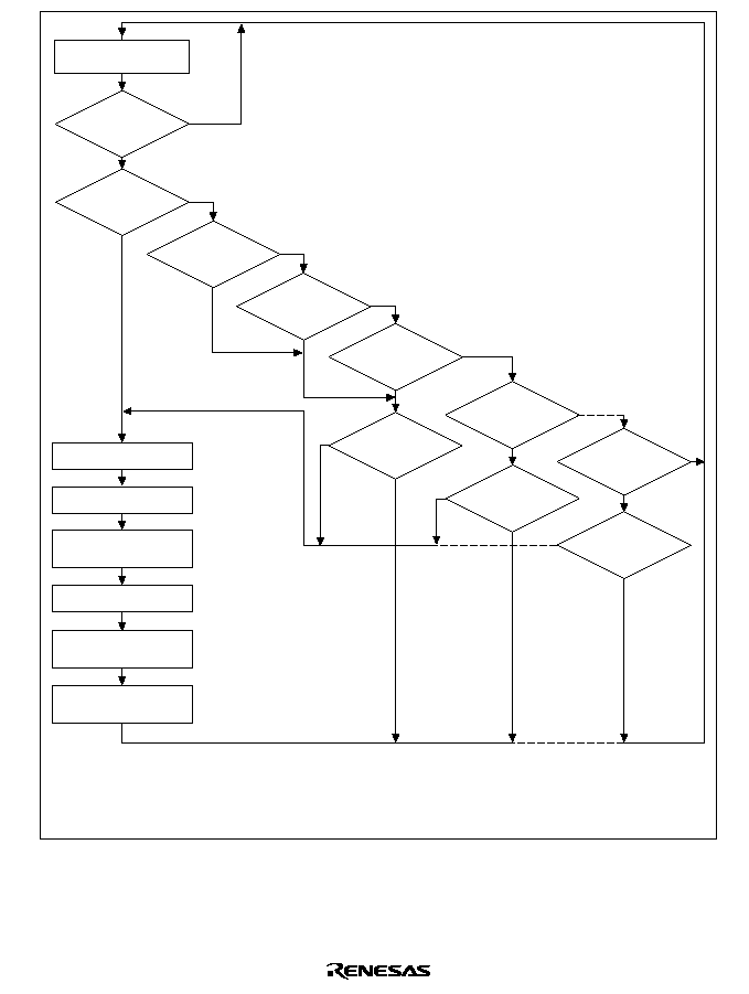
191
No
Yes
NMI?
No
Yes
User break?
No
Yes
No
H-UDI
interrupt?
Yes
Level 15
interrupt?
No
Yes
I3 to I0
level 14?
No
Yes
Level 14
interrupt?
No
Yes
Yes
I3 to I0
level 13?
No
Yes
Level 1
interrupt?
No
Yes
I3 to I0 =
level 0?
No
Program execution
state
Save SR to stack
Save PC to stack
Read vector number
*
Branch to exception
service routine
Interrupt
generated?
Copy accepted
interrupt level to I3≠I0
Read exception
vector table
I3≠I0: Status register interrupt mask bits.
Note:
*
The vector number is only read from an external source when an external vector number is
specified for the IRL/IRQ interrupt vector number.
Figure 5.8 Interrupt Sequence Flowchart
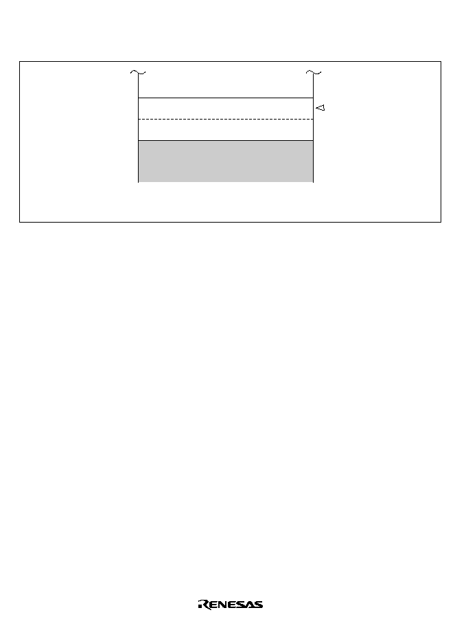
192
5.4.2
Stack State after Interrupt Exception Handling
The state of the stack after interrupt exception handling is completed is shown in figure 5.9.
Address
4n-8
4n-4
4n
PC
PC: Start address of return destination instruction (instruction after executing instruction)
SP
32 bits
32 bits
SR
Figure 5.9 Stack State after Interrupt Exception Handling
5.5
Interrupt Response Time
Table 5.8 shows the interrupt response time, which is the time from the occurrence of an interrupt
request until interrupt exception handling starts and fetching of the first instruction of the interrupt
service routine begins.

193
Table 5.8
Interrupt Response Time
Number of States
Peripheral Module
Item
NMI
IRL/IRQ
A
B
Notes
Compare identified
interrupt priority with SR
mask level
2.0
◊
Icyc
0.5
◊
Icyc
+ 1.0
◊
Ecyc
+ 1.5
◊
Pcyc
0.5
◊
Icyc
+ 1.0
◊
Pcyc
1.0
◊
Pcyc
Wait for completion of
sequence currently being
executed by CPU
X (
0)
X (
0)
X (
0)
X (
0)
The longest
sequence is for
interrupt or address-
error exception
handling (X = 4.0
◊
Icyc + m1 + m2 +
m3 + m4). If an
interrupt-making
instruction follows,
however, the time
may be even longer
during repeat
instruction
execution
Time from interrupt
exception handling (SR
and PC saves and vector
address fetch) until fetch of
first instruction of exception
service routine starts
5.0
◊
Icyc
+ m1 + m2
+ m3
5.0
◊
Icyc
+ m1 + m2
+ m3
5.0
◊
Icyc
+ m1 + m2
+ m3
5.0
◊
Icyc
+ m1 + m2
+ m3
Response time
Total: X + 7.0
◊
Icyc
+ m1 + m2
+ m3
X + 5.5
◊
Icyc
+ 1.0
◊
Ecyc
+ 1.5
◊
Pcyc
+ m1 + m2
+ m3
X + 5.5
◊
Icyc
+ 1.0
◊
Pcyc
+ m1 + m2
+ m3
X + 5.0
◊
Icyc
+ 1.0
◊
Pcyc
+ m1 + m2
+ m3
Minimum: 10
11
9.5
9
I
:E
:P
= 1:1:1
Maximum: 11 + 2 (m1
+ m2 + m3)
+ m4
19.5 + 2 (m1
+ m2 + m3)
+ m4
13.5 + 2 (m1
+ m2 + m3)
+ m4
13.0 + 2 (m1
+ m2 + m3)
+ m4
I
:E
:P
= 1:1/4:1/4
Notes: m1≠m4 are the number of states needed for the following memory accesses
m1: SR save (longword write)
m2: PC save (longword write)
m3: Vector address read (longword read)
m4: Fetch of first instruction of interrupt service routine
Icyc: I
cycle time
Ecyc: E
cycle time
Pcyc: P
cycle time
Peripheral modules A: DMAC, REF (BSC)
Peripheral modules B: WDT, FRT, TPU, SCIF, SIOF, SIO, E-DMAC
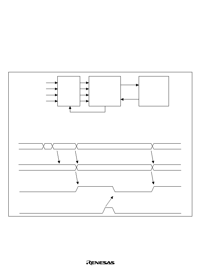
194
5.6
Sampling of Pins
IRL3≠IRL0
Signals on interrupt pins
IRL3 to IRL0 pass through the noise canceler before being sent by the
interrupt controller to the CPU as interrupt requests, as shown in figure 5.10. The noise canceler
cancels noise that changes in short cycles. The CPU samples the interrupt requests between
executing instructions. During this period, the noise canceler output changes according to the
noise-eliminated pin level, so the pin level must be held until the CPU samples it. This means that
interrupt sources generally must not be cleared inside interrupt routines.
When an external vector is fetched, the interrupt source can also be cleared when the external
vector fetch cycle is detected.
Interrupt acceptance
signal from CPU
Interrupt request
to CPU
Noise canceler
output
Cleared when interrupt is accepted
IRL3
≠
IRL0
pin level
1011 for
1 clock
due to
noise
Level 2 interrupt
Level 6 interrupt
1111
1111
1101
1001
1111
1101
1001
IRL0
IRL1
IRL2
IRL3
CPU
Interrupt
controller
Noise
canceler
Interrupt
request
Interrupt
accepted
Figure 5.10
IRL3≠IRL0 Pin Sampling

195
5.7
Usage Notes
1. Note on module standby execution
Do not execute module standby for modules that have the module standby function when the
possibility remains that an interrupt request may be output.
2. Notes on interrupt source clearing
A. When clearing external interrupt source
If interrupt source clearing is performed by writing to an IO address (external), the next
instruction will be executed before completion of the write operation because of the write
buffer. To ensure that the write operation is completed before the next instruction is
executed, synchronization is achieved when a read is performed from the same address
following the write.
a. When returning from interrupt handling by means of RTE instruction
When the RTE instruction is used to return from interrupt handling, as shown in figure
5.11, consider the cycles to be inserted between the read instruction for synchronization
and the RTE instruction, according to the set clock ratio (I
: E
: P
) and external bus
cycle.
IRL3--IRL0 should be negated at least 0.5 Icyc + 1.0 Ecyc + 1.5 Pcyc before next
interrupt acceptance becomes possible.
For example, if clock ratio I
: E
: P
is 4 : 2 : 2, at least 5.5 Icyc should be inserted.
b. When changing level during interrupt handling
When the SR value is changed by means of an LDC instruction and multiple
implementation of other interrupts is enabled, also, consider the cycles to be inserted
between the synchronization instruction and the LDC instruction as shown in figure
5.12, according to the set clock ratio (I
: E
: P
) and external bus cycle.
IRL3≠IRL0 should be negated at least 0.5 Icyc + 1.0 Ecyc + 1.5 Pcyc before next
interrupt acceptance becomes possible.
For example, if clock ratio I
: E
: P
is 4 : 2 : 2, at least 5.5 Icyc should be inserted.
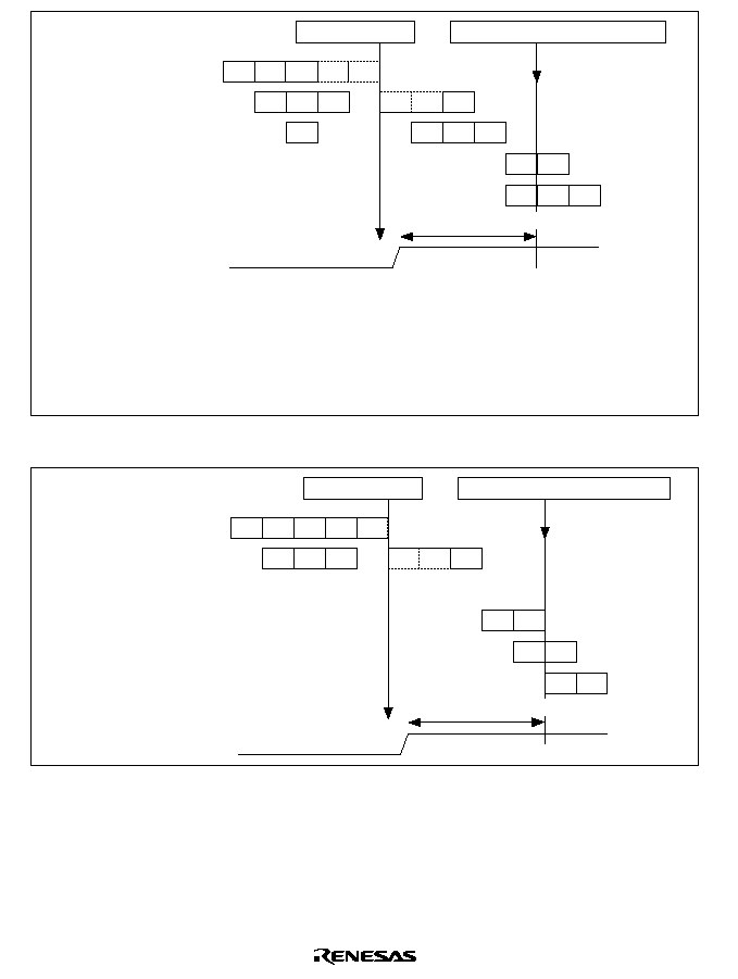
196
Interrupt clear instruction
External write
cycle
External read
cycle
Write completed
Next interrupt can be accepted
Synchronization instruction
RTE instruction
IRL3
≠
IRL0
Delay slot instruction
Interrupt return destination instruction
D
E
M
M
D
E
M
E
M
W
D
E
E
F
D
D
0.5Icyc + 1.0Ecyc + 1.5Pcyc
;
;
F: Instruction fetch ............... Instruction is fetched from memory in which program is stored
D: Instruction decode ........... Fetched instruction is decoded
E: Instruction execution ........ Data operation or address operation is performed in accordance
with result of decoding
M: Memory access ................ Memory data access is performed
W: Write-back ....................... Data read from memory is written to register
Figure 5.11 Pipeline Operation when Returning by Means of RTE Instruction
Interrupt clear instruction
External write
cycle
External read
cycle
Write completed
Next interrupt can be accepted
Synchronization instruction
∑
∑
∑
IRL3
≠
IRL0
LDC instruction
Interrupt disable instruction
Normal instruction
D
E
M
M
D
E
W
D
E
D
E
D
E
0.5Icyc + 1.0Ecyc + 1.5Pcyc
;
Figure 5.12 Pipeline Operation when Interrupts are Enabled by Means of SR Modification
When an interrupt source is cleared by the program, pipeline operation must be considered
to ensure that the same interrupt is not implemented again.

197
B. When clearing on-chip interrupt source
When an interrupt source is from an on-chip peripheral module, also, pipeline operation
must be considered to ensure that the same interrupt is not implemented again. An interval
of 0.5 Icyc + 1.0 Pcyc is required until an on-chip peripheral module interrupt is identified
by the CPU. Similarly, an interval of 0.5 Icyc + 1.0 Pcyc is also necessary to report the fact
that an interrupt request is no longer present.
a. When returning from interrupt handling by means of RTE instruction
When the RTE instruction is used to return from interrupt handling, as shown in figure
5.13, consider the cycles to be inserted between the read instruction for synchronization
and the RTE instruction, according to the set clock ratio (I
: E
: P
).
The on-chip peripheral interrupt signal should be negated at least 0.5 Icyc + 1.0 Pcyc
before next interrupt acceptance becomes possible.
For example, if clock ratio I
: E
: P
is 4 : 2 : 2, at least 2.5 Icyc should be inserted.
b. When changing level during interrupt handling
When the SR value is changed by means of an LDC instruction and multiple
implementation of other interrupts is enabled, consider the cycles to be inserted
between the synchronization instruction and the LDC instruction as shown in figure
5.14, according to the set clock ratio (I
: E
: P
).
The on-chip peripheral interrupt signal should be negated at least 0.5 Icyc + 1.0 Pcyc
before next interrupt acceptance becomes possible.
For example, if clock ratio I
: E
: P
is 4 : 2 : 2, at least 2.5 Icyc should be inserted.
Interrupt clear instruction
On-chip peripheral
write, min. 1 Icyc
Write completed
Next interrupt can be accepted
Synchronization instruction
RTE instruction
On-chip peripheral interrupt
Delay slot instruction
Interrupt return destination instruction
D
E
M
M
E
D
E
M
M
W
D
E
E
F
D
D
0.5Icyc + 1.0Pcyc
;;
;;
On-chip peripheral
read, min. 1 Icyc
Figure 5.13 Pipeline Operation when Returning by Means of RTE Instruction
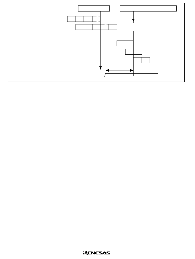
198
Interrupt clear instruction
On-chip peripheral
write, min. 1 Icyc
Write completed
Next interrupt can be accepted
Synchronization instruction
∑
∑
∑
On-chip peripheral interrupt
LDC instruction
Interrupt disable instruction
Normal instruction
D
E
M
M
D
E
W
D
E
D
E
D
E
0.5Icyc + 1.0Pcyc
;;
On-chip peripheral
read, min. 1 Icyc
Figure 5.14 Pipeline Operation when Interrupts are Enabled by Means of SR Modification
In the above figure, the stage in which the instruction fetch occurs cannot be specified
because of the mix of DSP instructions in this chip, so instruction fetch F is omitted in
most cases during pipeline operation.

199
Section 6 User Break Controller (UBC)
6.1
Overview
The user break controller (UBC) provides functions that simplify program debugging. When break
conditions are set in the UBC, a user break interrupt is generated according to the conditions of the
bus cycle generated by the CPU or on-chip DMAC (DMAC or E-DMAC).
This function makes it easy to design a sophisticated self-monitoring debugger, enabling programs
to be debugged with the chip alone, without using an in-circuit emulator.
6.1.1
Features
The UBC has the following features:
∑
The following can be set as break conditions:
Number of break channels: Four (channels A, B, C, and D)
User break interrupts can be generated on independent or sequential conditions for
channels A, B, C, and D.
Sequential break settings
∑
Channel A
channel B
channel C
channel D
∑
Channel B
channel C
channel D
∑
Channel C
channel D
1. Address: 32-bit masking capability, individual address setting possible (cache bus (CPU),
internal bus (DMAC, E-DMAC), X/Y bus)
2. Data (channels C and D only,): 32-bit masking capability, individual address setting
possible (cache bus (CPU), internal bus (DMAC, E-DMAC), X/Y bus)
3. Bus master: CPU cycle/on-chip DMAC (DMAC, E-DMAC) cycle
4. Bus cycle: Instruction fetch/data access
5. Read/write
6. Operand cycle: Byte/word/longword
∑
User break interrupt generation on occurrence of break condition
A user-written user break interrupt exception routine can be executed.
∑
Processing can be stopped before or after instruction execution in an instruction fetch cycle.
∑
Break with specification of number of executions (channels C and D only)
Settable number of executions: maximum 2
12
≠ 1 (4095)
∑
PC trace function
The branch source/branch destination can be traced when a branch instruction is fetched
(maximum 8 addresses (4 pairs)).
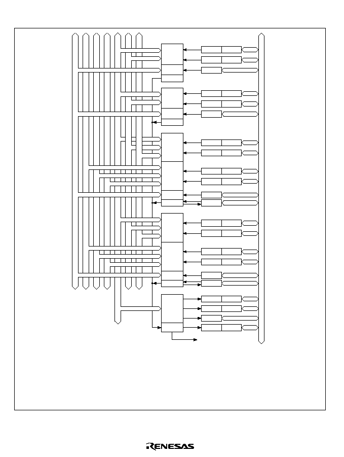
200
6.1.2
Block Diagram
Address
Access
Channel A
Address
Access
Channel B
Address
Data
Access
Channel C
Address
Data
Access
PC trace
Control
Channel D
BARAH
BARAL
BAMRAH BAMRAL
BBRA
BARBH
BARBL
BAMRBH BAMRBL
BARCH
BARCL
BAMRCH BAMRCL
BDRCH
BBRC
BETRC
BDRCL
BDMRCH BDMRCL
BARDH
BARDL
BAMRDH BAMRDL
BDRDH
BBRD
BETRD
BDRDL
BRSRH
BRSRL
BRDRH
BRDRL
BRFR
BRCRH
BRCRL
BDMRDH BDMRDL
BBRB
Access
Module data bus
Cache data bus
Internal data bus
X/Y data bus
Cache address bus
Internal address bus
X/Y address bus
Internal interrupt signal
Legend
BARAH/L:
Break address register AH/L
BAMRAH/L: Break address mask register AH/L
BBRA:
Break bus cycle register A
BARBH/L:
Break address register BH/L
BAMRBH/L: Break address mask register BH/L
BBRB:
Break bus cycle register B
BARCH/L:
Break address register CH/L
BAMRCH/L: Break address mask register CH/L
BDRCH/L:
Break data register CH/L
BDMRCH/L: Break data mask register CH/L
BBRC:
Break bus cycle register C
BETRC:
Break execution times register C
BARDH/L:
Break address register DH/L
BAMRDH/L: Break address mask register DH/L
BDRDH/L:
Break data register DH/L
BDMRDH/L: Break data mask register DH/L
BBRD:
Break bus cycle register D
BETRD:
Break execution times register D
BRCRH/L:
Break control register H/L
BRFR:
Branch flag register
BRSRH/L:
Branch source register H/L
BRDRH/L:
Branch destination register H/L
Figure 6.1 Block Diagram of User Break Controller

201
6.1.3
Register Configuration
Table 6.1
UBC Registers
Name
Abbre-
viation
R/W
Initial
Value
*
1
Address
Access Size
*
2
Break address register AH
BARAH
R/W
H'0000
H'FFFFFF00
16
32
Break address register AL
BARAL
R/W
H'0000
H'FFFFFF02
16
Break address mask register AH
BAMRAH
R/W
H'0000
H'FFFFFF04
16
32
Break address mask register AL
BAMRAL
R/W
H'0000
H'FFFFFF06
16
Break bus cycle register A
BBRA
R/W
H'0000
H'FFFFFF08
16, 32
Break address register BH
BARBH
R/W
H'0000
H'FFFFFF20
16
32
Break address register BL
BARBL
R/W
H'0000
H'FFFFFF22
16
Break address mask register BH
BAMRBH
R/W
H'0000
H'FFFFFF24
16
32
Break address mask register BL
BAMRBL
R/W
H'0000
H'FFFFFF26
16
Break bus cycle register B
BBRB
R/W
H'0000
H'FFFFFF28
16, 32
Break address register CH
BARCH
R/W
H'0000
H'FFFFFF40
16
32
Break address register CL
BARCL
R/W
H'0000
H'FFFFFF42
16
Break address mask register CH
BAMRCH
R/W
H'0000
H'FFFFFF44
16
32
Break address mask register CL
BAMRCL
R/W
H'0000
H'FFFFFF46
16
Break data register CH
BDRCH
R/W
H'0000
H'FFFFFF50
16
32
Break data register CL
BDRCL
R/W
H'0000
H'FFFFFF52
16
Break data mask register CH
BDMRCH
R/W
H'0000
H'FFFFFF54
16
32
Break data mask register CL
BDMRCL
R/W
H'0000
H'FFFFFF56
16
Break bus cycle register C
BBRC
R/W
H'0000
H'FFFFFF48
16, 32
Break execution times register C
BETRC
R/W
H'0000
H'FFFFFF58
16, 32
Break address register DH
BARDH
R/W
H'0000
H'FFFFFF60
16
32
Break address register DL
BARDL
R/W
H'0000
H'FFFFFF62
16
Break address mask register DH
BAMRDH
R/W
H'0000
H'FFFFFF64
16
32
Break address mask register DL
BAMRDL
R/W
H'0000
H'FFFFFF66
16
Break data register DH
BDRDH
R/W
H'0000
H'FFFFFF70
16
32
Break data register DL
BDRDL
R/W
H'0000
H'FFFFFF72
16
Break data mask register DH
BDMRDH
R/W
H'0000
H'FFFFFF74
16
32
Break data mask register DL
BDMRDL
R/W
H'0000
H'FFFFFF76
16

202
Table 6.1
UBC Registers (cont)
Name
Abbre-
viation
R/W
Initial
Value
*
1
Address
Access Size
*
2
Break bus cycle register D
BBRD
R/W
H'0000
H'FFFFFF68
16, 32
Break execution times register D
BETRD
R/W
H'0000
H'FFFFFF78
16, 32
Break control register H
BRCRH
R/W
H'0000
H'FFFFFF30
16
32
Break control register L
BRCRL
R/W
H'0000
H'FFFFFF32
16
Branch flag register
BRFR
R
*
3
H'FFFFFF10
16, 32
Branch source register H
BRSRH
R
Undefined H'FFFFFF14
16
32
Branch source register L
BRSRL
R
Undefined H'FFFFFF16
16
Branch destination register H
BRDRH
R
Undefined H'FFFFFF18
16
32
Branch destination register L
BRDRL
R
Undefined H'FFFFFF1A
16
Notes:
*
1 Initialized by a power-on reset. Value is retained in standby mode, and is undefined
after a manual reset.
*
2 Byte access cannot be used.
*
3 Bits SVF and DVF in BRFR are initialized by a power-on reset; the other bits in BRFR
are not initialized.

203
6.2
Register Descriptions
6.2.1
Break Address Register A (BARA)
BARAH
Bit:
15
14
13
12
11
10
9
8
BAA31
BAA30
BAA29
BAA28
BAA27
BAA26
BAA25
BAA24
Initial value:
0
0
0
0
0
0
0
0
R/W:
R/W
R/W
R/W
R/W
R/W
R/W
R/W
R/W
Bit:
7
6
5
4
3
2
1
0
BAA23
BAA22
BAA21
BAA20
BAA19
BAA18
BAA17
BAA16
Initial value:
0
0
0
0
0
0
0
0
R/W:
R/W
R/W
R/W
R/W
R/W
R/W
R/W
R/W
BARAL
Bit:
15
14
13
12
11
10
9
8
BAA15
BAA14
BAA13
BAA12
BAA11
BAA10
BAA9
BAA8
Initial value:
0
0
0
0
0
0
0
0
R/W:
R/W
R/W
R/W
R/W
R/W
R/W
R/W
R/W
Bit:
7
6
5
4
3
2
1
0
BAA7
BAA6
BAA5
BAA4
BAA3
BAA2
BAA1
BAA0
Initial value:
0
0
0
0
0
0
0
0
R/W:
R/W
R/W
R/W
R/W
R/W
R/W
R/W
R/W
Break address register A (BARA) consists of two 16-bit readable/writable registers: break address
register AH (BARAH) and break address register AL (BARAL). BARAH specifies the upper half
(bits 31 to 16) of the address used as a channel A break condition, and BARAL specifies the lower
half (bits 15 to 0). BARAH and BARAL are initialized to H'0000 by a power-on reset; after a
manual reset, their values are undefined.
BARAH Bits 15 to 0--Break Address A31 to A16 (BAA31 to BAA16): These bits store the upper
half (bits 31 to 16) of the address used as a channel A break condition.
BARAL Bits 15 to 0--Break Address A15 to A0 (BAA15 to BAA0): These bits store the lower
half (bits 15 to 0) of the address used as a channel A break condition.

204
6.2.2
Break Address Mask Register A (BAMRA)
BAMRAH
Bit:
15
14
13
12
11
10
9
8
BAMA31 BAMA30 BAMA29 BAMA28 BAMA27 BAMA26 BAMA25 BAMA24
Initial value:
0
0
0
0
0
0
0
0
R/W:
R/W
R/W
R/W
R/W
R/W
R/W
R/W
R/W
Bit:
7
6
5
4
3
2
1
0
BAMA23 BAMA22 BAMA21 BAMA20 BAMA19 BAMA18 BAMA17 BAMA16
Initial value:
0
0
0
0
0
0
0
0
R/W:
R/W
R/W
R/W
R/W
R/W
R/W
R/W
R/W
BAMRAL
Bit:
15
14
13
12
11
10
9
8
BAMA15 BAMA14 BAMA13 BAMA12 BAMA11 BAMA10 BAMA9
BAMA8
Initial value:
0
0
0
0
0
0
0
0
R/W:
R/W
R/W
R/W
R/W
R/W
R/W
R/W
R/W
Bit:
7
6
5
4
3
2
1
0
BAMA7
BAMA6
BAMA5
BAMA4
BAMA3
BAMA2
BAMA1
BAMA0
Initial value:
0
0
0
0
0
0
0
0
R/W:
R/W
R/W
R/W
R/W
R/W
R/W
R/W
R/W
Break address mask register A (BAMRA) consists of two 16-bit readable/writable registers: break
address mask register AH (BAMRAH) and break address mask register AL (BAMRAL).
BAMRAH specifies which bits of the break address set in BARAH are to be masked, and
BAMRAL specifies which bits of the break address set in BARAL are to be masked. BAMRAH
and BAMRAL are initialized to H'0000 by a power-on reset; after a manual reset, their values are
undefined.
BAMRAH Bits 15 to 0--Break Address Mask A31 to A16 (BAMA31 to BAMA16): These bits
specify whether or not corresponding channel A break address bits 31 to 16 (BAA31 to BAA16)
set in BARAH are to be masked.
BAMRAL Bits 15 to 0--Break Address Mask A15 to A0 (BAMA15 to BAMA0): These bits
specify whether or not corresponding channel A break address bits 15 to 0 (BAA15 to BAA0) set
in BARAL are to be masked.

205
Bit 31 to 0:
BAMAn
Description
0
Channel A break address bit BAAn is included in break condition (Initial value)
1
Channel A break address bit BAAn is masked, and not included in condition
Note:
n = 31 to 0
6.2.3
Break Bus Cycle Register A (BBRA)
Bit:
15
14
13
12
11
10
9
8
--
--
--
--
--
--
--
--
Initial value:
0
0
0
0
0
0
0
0
R/W:
R
R
R
R
R
R
R
R
Bit:
7
6
5
4
3
2
1
0
CPA1
CPA0
IDA1
IDA0
RWA1
RWA0
SZA1
SZA0
Initial value:
0
0
0
0
0
0
0
0
R/W:
R/W
R/W
R/W
R/W
R/W
R/W
R/W
R/W
Break bus cycle register A (BBRA) is a 16-bit readable/writable register that sets four channel A
break conditions: (1) CPU cycle/on-chip DMAC (DMAC, E-DMAC) cycle, (2) instruction
fetch/data access, (3) read/write, and (4) operand size. BBRA is initialized to H'0000 by a power-
on reset; after a manual reset, its value is undefined.
Bits 15 to 8--Reserved: These bits are always read as 0. The write value should always be 0.
Bits 7 and 6--CPU/DMAC, E-DMAC Cycle Select A (CPA1, CPA0): These bits specify whether
a CPU cycle, or a DMAC or E-DMAC cycle, is to be selected as the bus cycle used as a channel A
break condition.
Bit 7:
CPA1
Bit 6:
CPA0
Description
0
0
Channel A user break interrupt is not generated
(Initial value)
1
CPU cycle is selected as user break condition
1
0
DMAC or E-DMAC cycle is selected as user break condition
1
CPU, DMAC, or E-DMAC cycle is selected as user break condition

206
Bits 5 and 4--Instruction Fetch/Data Access Select A (IDA1, IDA0): These bits specify whether
an instruction fetch cycle or data access cycle is to be selected as the bus cycle used as a channel A
break condition.
Bit 5:
IDA1
Bit 4:
IDA0
Description
0
0
Channel A user break interrupt is not generated
(Initial value)
1
Instruction fetch cycle is selected as break condition
1
0
Data access cycle is selected as break condition
1
Instruction fetch cycle or data access cycle is selected as break condition
Bits 3 and 2--Read/Write Select A (RWA1, RWA0): These bits specify whether a read cycle or
write cycle is to be selected as the bus cycle used as a channel A break condition.
Bit 3:
RWA1
Bit 2:
RWA0
Description
0
0
Channel A user break interrupt is not generated
(Initial value)
1
Read cycle is selected as break condition
1
0
Write cycle is selected as break condition
1
Read cycle or write cycle is selected as break condition
Bits 1 and 0--Operand Size Select A (SZA1, SZA0): These bits select the operand size of the bus
cycle used as a channel A break condition.
Bit 1:
SZA1
Bit 0:
SZA0
Description
0
0
Operand size is not included in break conditions
(Initial value)
1
Byte access is selected as break condition
1
0
Word access is selected as break condition
1
Longword access is selected as break condition
Notes: When a break is to be executed on an instruction fetch, clear the SZA0 bit to 0. All
instructions are regarded as being accessed using word size (instruction fetches are always
performed as longword).
In the case of an instruction, the operand size is word; in the case of a CPU/DMAC, E-
DMAC data access, it is determined by the specified operand size. Note that the operand
size is not determined by the bus width of the space accessed.
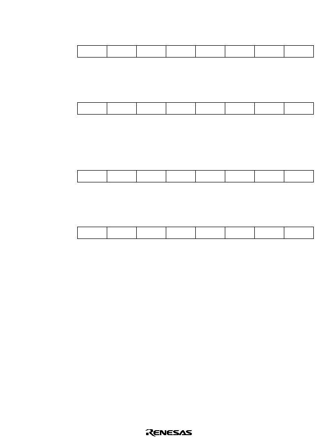
207
6.2.4
Break Address Register B (BARB)
BARBH
Bit:
15
14
13
12
11
10
9
8
BAB31
BAB30
BAB29
BAB28
BAB27
BAB26
BAB25
BAB24
Initial value:
0
0
0
0
0
0
0
0
R/W:
R/W
R/W
R/W
R/W
R/W
R/W
R/W
R/W
Bit:
7
6
5
4
3
2
1
0
BAB23
BAB22
BAB21
BAB20
BAB19
BAB18
BAB17
BAB16
Initial value:
0
0
0
0
0
0
0
0
R/W:
R/W
R/W
R/W
R/W
R/W
R/W
R/W
R/W
BARBL
Bit:
15
14
13
12
11
10
9
8
BAB15
BAB14
BAB13
BAB12
BAB11
BAB10
BAB9
BAB8
Initial value:
0
0
0
0
0
0
0
0
R/W:
R/W
R/W
R/W
R/W
R/W
R/W
R/W
R/W
Bit:
7
6
5
4
3
2
1
0
BAB7
BAB6
BAB5
BAB4
BAB3
BAB2
BAB1
BAB0
Initial value:
0
0
0
0
0
0
0
0
R/W:
R/W
R/W
R/W
R/W
R/W
R/W
R/W
R/W
Break address register B (BARB) consists of two 16-bit readable/writable registers: break address
register BH (BARBH) and break address register BL (BARBL). BARBH specifies the upper half
(bits 31 to 16) of the address used as a channel B break condition, and BARBL specifies the lower
half (bits 15 to 0). BARBH and BARBL are initialized to H'0000 by a power-on reset; after a
manual reset, their values are undefined.
BARBH Bits 15 to 0--Break Address B31 to B16 (BAB31 to BAB16): These bits store the upper
half (bits 31 to 16) of the address used as a channel B break condition.
BARBL Bits 15 to 0--Break Address B15 to B0 (BAB15 to BAB0): These bits store the lower
half (bits 15 to 0) of the address used as a channel B break condition.

208
6.2.5
Break Address Mask Register B (BAMRB)
BAMRBH
Bit:
15
14
13
12
11
10
9
8
BAMB31 BAMB30 BAMB29 BAMB28 BAMB27 BAMB26 BAMB25 BAMB24
Initial value:
0
0
0
0
0
0
0
0
R/W:
R/W
R/W
R/W
R/W
R/W
R/W
R/W
R/W
Bit:
7
6
5
4
3
2
1
0
BAMB23 BAMB22 BAMB21 BAMB20 BAMB19 BAMB18 BAMB17 BAMB16
Initial value:
0
0
0
0
0
0
0
0
R/W:
R/W
R/W
R/W
R/W
R/W
R/W
R/W
R/W
BAMRBL
Bit:
15
14
13
12
11
10
9
8
BAMB15 BAMB14 BAMB13 BAMB12 BAMB11 BAMB10 BAMB9
BAMB8
Initial value:
0
0
0
0
0
0
0
0
R/W:
R/W
R/W
R/W
R/W
R/W
R/W
R/W
R/W
Bit:
7
6
5
4
3
2
1
0
BAMB7
BAMB6
BAMB5
BAMB4
BAMB3
BAMB2
BAMB1
BAMB0
Initial value:
0
0
0
0
0
0
0
0
R/W:
R/W
R/W
R/W
R/W
R/W
R/W
R/W
R/W
Break address mask register B (BAMRB) consists of two 16-bit readable/writable registers: break
address mask register BH (BAMRBH) and break address mask register BL (BAMRBL).
BAMRBH specifies which bits of the break address set in BARBH are to be masked, and
BAMRBL specifies which bits of the break address set in BARBL are to be masked. BAMRBH
and BAMRBL are initialized to H'0000 by a power-on reset; after a manual reset, their values are
undefined.
BAMRBH Bits 15 to 0--Break Address Mask B31 to B16 (BAMB31 to BAMB16): These bits
specify whether or not corresponding channel B break address bits 31 to 16 (BAB31 to BAB16)
set in BARBH are to be masked.
BAMRBL Bits 15 to 0--Break Address Mask B15 to B0 (BAMB15 to BAMB0): These bits
specify whether or not corresponding channel B break address bits 15 to 0 (BAB15 to BAB0) set
in BARBL are to be masked.
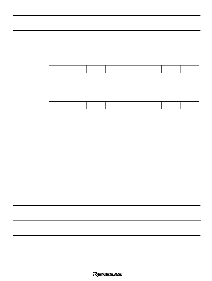
209
Bit 31 to 0:
BAMBn
Description
0
Channel B break address bit BABn is included in break condition (Initial value)
1
Channel B break address bit BABn is masked, and not included in condition
Note:
n = 31 to 0
6.2.6
Break Bus Cycle Register B (BBRB)
Bit:
15
14
13
12
11
10
9
8
--
--
--
--
--
--
--
--
Initial value:
0
0
0
0
0
0
0
0
R/W:
R
R
R
R
R
R
R
R
Bit:
7
6
5
4
3
2
1
0
CPB1
CPB0
IDB1
IDB0
RWB1
RWB0
SZB1
SZB0
Initial value:
0
0
0
0
0
0
0
0
R/W:
R/W
R/W
R/W
R/W
R/W
R/W
R/W
R/W
Break bus cycle register B (BBRB) is a 16-bit readable/writable register that sets four channel B
break conditions: (1) CPU cycle/on-chip DMAC (DMAC, E-DMAC) cycle, (2) instruction
fetch/data access, (3) read/write, and (4) operand size. BBRB is initialized to H'0000 by a power-
on reset; after a manual reset, its value is undefined.
Bits 15 to 8--Reserved: These bits are always read as 0. The write value should always be 0.
Bits 7 and 6--CPU/DMAC, E-DMAC Cycle Select B (CPB1, CPB0): These bits specify whether
a CPU cycle, or a DMAC or E-DMAC cycle, is to be selected as the bus cycle used as a channel B
break condition.
Bit 7:
CPB1
Bit 6:
CPB0
Description
0
0
Channel B user break interrupt is not generated
(Initial value)
1
CPU cycle is selected as user break condition
1
0
DMAC or E-DMAC cycle is selected as user break condition
1
CPU, DMAC, or E-DMAC cycle is selected as user break condition

210
Bits 5 and 4--Instruction Fetch/Data Access Select B (IDB1, IDB0): These bits specify whether
an instruction fetch cycle or data access cycle is to be selected as the bus cycle used as a channel B
break condition.
Bit 5:
IDB1
Bit 4:
IDB0
Description
0
0
Channel B user break interrupt is not generated
(Initial value)
1
Instruction fetch cycle is selected as break condition
1
0
Data access cycle is selected as break condition
1
Instruction fetch cycle or data access cycle is selected as break condition
Bits 3 and 2--Read/Write Select B (RWB1, RWB0): These bits specify whether a read cycle or
write cycle is to be selected as the bus cycle used as a channel B break condition.
Bit 3:
RWB1
Bit 2:
RWB0
Description
0
0
Channel B user break interrupt is not generated
(Initial value)
1
Read cycle is selected as break condition
1
0
Write cycle is selected as break condition
1
Read cycle or write cycle is selected as break condition
Bits 1 and 0--Operand Size Select B (SZB1, SZB0): These bits select the operand size of the bus
cycle used as a channel B break condition.
Bit 1:
SZB1
Bit 0:
SZB0
Description
0
0
Operand size is not included in break conditions
(Initial value)
1
Byte access is selected as break condition
1
0
Word access is selected as break condition
1
Longword access is selected as break condition
Notes: When a break is to be executed on an instruction fetch, clear the SZB0 bit to 0. All
instructions are regarded as being accessed using word size (instruction fetches are always
performed as longword).
In the case of an instruction, the operand size is word; in the case of a CPU/DMAC, E-
DMAC data access, it is determined by the specified operand size. Note that the operand
size is not determined by the bus width of the space accessed.

211
6.2.7
Break Address Register C (BARC)
BARCH
Bit:
15
14
13
12
11
10
9
8
BAC31
BAC30
BAC29
BAC28
BAC27
BAC26
BAC25
BAC24
Initial value:
0
0
0
0
0
0
0
0
R/W:
R/W
R/W
R/W
R/W
R/W
R/W
R/W
R/W
Bit:
7
6
5
4
3
2
1
0
BAC23
BAC22
BAC21
BAC20
BAC19
BAC18
BAC17
BAC16
Initial value:
0
0
0
0
0
0
0
0
R/W:
R/W
R/W
R/W
R/W
R/W
R/W
R/W
R/W
BARCL
Bit:
15
14
13
12
11
10
9
8
BAC15
BAC14
BAC13
BAC12
BAC11
BAC10
BAC9
BAC8
Initial value:
0
0
0
0
0
0
0
0
R/W:
R/W
R/W
R/W
R/W
R/W
R/W
R/W
R/W
Bit:
7
6
5
4
3
2
1
0
BAC7
BAC6
BAC5
BAC4
BAC3
BAC2
BAC1
BAC0
Initial value:
0
0
0
0
0
0
0
0
R/W:
R/W
R/W
R/W
R/W
R/W
R/W
R/W
R/W
Break address register C (BARC) consists of two 16-bit readable/writable registers: break address
register CH (BARCH) and break address register CL (BARCL). BARCH specifies the upper half
(bits 31 to 16) of the address used as a channel C break condition, and BARCL specifies the lower
half (bits 15 to 0). The address bus connected to the X/Y memory can also be specified as a break
condition by making a setting in the XYEC bit/XYSC bit in break bus cycle register C (BBRC).
When XYEC = 0, BAC31 to BAC0 specify the address. When XYEC = 1, the upper 16 bits
(BAC31 to BAC16) of BARC specify the X address bus, and the lower 16 bits (BAC15 to BAC0)
specify the Y address bus. BARCH and BARCL are initialized to H'0000 by a power-on reset;
after a manual reset, their values are undefined.

212
BARC Configuration
Upper 16 Bits
(BAC31 to BAC16)
Lower 16 Bits
(BAC15 to BAC0)
XYEC = 0
Address
Upper 16 bits of address bus
Lower 16 bits of address bus
XYEC = 1
X address
(when XYSC = 0)
X address
(XAB15 to XAB1)
*
--
Y address
(when XYSC = 1)
--
Y address
(YAB15 to YAB1)
*
Note:
*
As an X/Y bus access is always a word access, the values of XAB0 and YAB0 is not
included in the break condition.
6.2.8
Break Address Mask Register C (BAMRC)
BAMRCH
Bit:
15
14
13
12
11
10
9
8
BAMC31 BAMC30 BAMC29 BAMC28 BAMC27 BAMC26 BAMC25 BAMC24
Initial value:
0
0
0
0
0
0
0
0
R/W:
R/W
R/W
R/W
R/W
R/W
R/W
R/W
R/W
Bit:
7
6
5
4
3
2
1
0
BAMC23 BAMC22 BAMC21 BAMC20 BAMC19 BAMC18 BAMC17 BAMC16
Initial value:
0
0
0
0
0
0
0
0
R/W:
R/W
R/W
R/W
R/W
R/W
R/W
R/W
R/W
BAMRCL
Bit:
15
14
13
12
11
10
9
8
BAMC15 BAMC14 BAMC13 BAMC12 BAMC11 BAMC10 BAMC9
BAMC8
Initial value:
0
0
0
0
0
0
0
0
R/W:
R/W
R/W
R/W
R/W
R/W
R/W
R/W
R/W
Bit:
7
6
5
4
3
2
1
0
BAMC7
BAMC6
BAMC5
BAMC4
BAMC3
BAMC2
BAMC1
BAMC0
Initial value:
0
0
0
0
0
0
0
0
R/W:
R/W
R/W
R/W
R/W
R/W
R/W
R/W
R/W

213
Break address mask register C (BAMRC) consists of two 16-bit readable/writable registers: break
address mask register CH (BAMRCH) and break address mask register CL (BAMRCL).
BAMRCH specifies which bits of the break address set in BARCH are to be masked, and
BAMRCL specifies which bits of the break address set in BARCL are to be masked. Operation
also depends on bits XYEC and XYSC in BBRC as shown below.
BAMRC Configuration
Upper 16 Bits
(BAMC31 to BAMC16)
Lower 16 Bits
(BAMC15 to BAMC0)
XYEC = 0
Address
Upper 16 bits maskable
Lower 16 bits maskable
XYEC = 1
X address
(when XYSC = 0)
Maskable
--
Y address
(when XYSC = 1
--
Maskable
Bit 31 to 0:
BAMCn
Description
0
Channel C break address bit BACn is included in break condition (Initial value)
1
Channel C break address bit BACn is masked, and not included in condition
Note:
n = 31 to 0

214
6.2.9
Break Data Register C (BDRC)
BDRCH
Bit:
15
14
13
12
11
10
9
8
BDC31
BDC30
BDC29
BDC28
BDC27
BDC26
BDC25
BDC24
Initial value:
0
0
0
0
0
0
0
0
R/W:
R/W
R/W
R/W
R/W
R/W
R/W
R/W
R/W
Bit:
7
6
5
4
3
2
1
0
BDC23
BDC22
BDC21
BDC20
BDC19
BDC18
BDC17
BDC16
Initial value:
0
0
0
0
0
0
0
0
R/W:
R/W
R/W
R/W
R/W
R/W
R/W
R/W
R/W
BDRCL
Bit:
15
14
13
12
11
10
9
8
BDC15
BDC14
BDC13
BDC12
BDC11
BDC10
BDC9
BDC8
Initial value:
0
0
0
0
0
0
0
0
R/W:
R/W
R/W
R/W
R/W
R/W
R/W
R/W
R/W
Bit:
7
6
5
4
3
2
1
0
BDC7
BDC6
BDC5
BDC4
BDC3
BDC2
BDC1
BDC0
Initial value:
0
0
0
0
0
0
0
0
R/W:
R/W
R/W
R/W
R/W
R/W
R/W
R/W
R/W
Break data register C (BDRC) consists of two 16-bit readable/writable registers: break data
register CH (BDRCH) and break data register CL (BDRCL). BDRCH specifies the upper half
(bits 31 to 16) of the data used as a channel C break condition, and BDRCL specifies the lower
half (bits 15 to 0). The data bus connected to the X/Y memory can also be specified as a break
condition by making a setting in the XYEC bit/XYSC bit in break bus cycle register C (BBRC).
When XYEC = 1, the upper 16 bits (BDC31 to BDC16) of BDRC specify the X data bus, and the
lower 16 bits (BDC15 to BDC0) specify the Y data bus.

215
BDRC Configuration
Upper 16 Bits
(BDC31 to BDC16)
Lower 16 Bits
(BDC15 to BDC0)
XYEC = 0
Data
Upper 16 bits of data bus
Lower 16 bits of data bus
XYEC = 1
X data
(when XYSC = 0)
X data
(XDB15 to XDB0)
--
Y data
(when XYSC = 1)
--
Y data
(YDB15 to YDB0)
6.2.10
Break Data Mask Register C (BDMRC)
BDMRCH
Bit:
15
14
13
12
11
10
9
8
BDMC31 BDMC30 BDMC29 BDMC28 BDMC27 BDMC26 BDMC25 BDMC24
Initial value:
0
0
0
0
0
0
0
0
R/W:
R/W
R/W
R/W
R/W
R/W
R/W
R/W
R/W
Bit:
7
6
5
4
3
2
1
0
BDMC23 BDMC22 BDMC21 BDMC20 BDMC19 BDMC18 BDMC17 BDMC16
Initial value:
0
0
0
0
0
0
0
0
R/W:
R/W
R/W
R/W
R/W
R/W
R/W
R/W
R/W
BDMRCL
Bit:
15
14
13
12
11
10
9
8
BDMC15 BDMC14 BDMC13 BDMC12 BDMC11 BDMC10 BDMC9
BDMC8
Initial value:
0
0
0
0
0
0
0
0
R/W:
R/W
R/W
R/W
R/W
R/W
R/W
R/W
R/W
Bit:
7
6
5
4
3
2
1
0
BDMC7
BDMC6
BDMC5
BDMC4
BDMC3
BDMC2
BDMC1
BDMC0
Initial value:
0
0
0
0
0
0
0
0
R/W:
R/W
R/W
R/W
R/W
R/W
R/W
R/W
R/W
Break data mask register C (BDMRC) consists of two 16-bit readable/writable registers: break
data mask register CH (BDMRCH) and break data mask register CL (BDMRCL). BDMRCH
specifies which bits of the break data set in BDRCH are to be masked, and BDMRCL specifies
which bits of the break data set in BDRCL are to be masked. Operation also depends on bits

216
XYEC and XYSC in BBRC as shown below. BDMRCH and BDMRCL are initialized to H'0000
by a power-on reset; after a manual reset, their values are undefined.
BDMRC Configuration
Upper 16 Bits
(BDMC31 to BDMC16)
Lower 16 Bits
(BDMC15 to BDMC0)
XYEC = 0
Data
Upper 16 bits maskable
Lower 16 bits maskable
XYEC = 1
X data
(when XYSC = 0)
Maskable
--
Y data
(when XYSC = 1)
--
Maskable
Bit 31 to 0:
BDMCn
Description
0
Channel C break data bit BDCn is included in break condition
(Initial value)
1
Channel C break data bit BDCn is masked, and not included in condition
Notes: 1. n = 31 to 0
2. When including the data bus value in the break condition, specify the operand size.
3. When specifying byte size, and using odd-address data as a break condition, set the
value in bits 7 to 0 of BDRC and BDMRC. When using even-address data as a break
condition, set the value in bits 15 to 8. The unused 8 bits of these registers have no
effect on the break condition.

217
6.2.11
Break Bus Cycle Register C (BBRC)
Bit:
15
14
13
12
11
10
9
8
--
--
--
--
--
--
XYEC
XYSC
Initial value:
0
0
0
0
0
0
0
0
R/W:
R
R
R
R
R
R
R/W
R/W
Bit:
7
6
5
4
3
2
1
0
CPC1
CPC0
IDC1
IDC0
RWC1
RWC0
SZC1
SZC0
Initial value:
0
0
0
0
0
0
0
0
R/W:
R/W
R/W
R/W
R/W
R/W
R/W
R/W
R/W
Break bus cycle register C (BBRC) is a 16-bit readable/writable register that sets five channel C
break conditions: (1) internal bus (C-bus, I-bus)/X memory bus/Y memory bus), (2) CPU
cycle/on-chip DMAC (DMAC, E-DMAC) cycle, (3) instruction fetch/data access, (4) read/write,
and (5) operand size. BBRC is initialized to H'0000 by a power-on reset; after a manual reset, its
value is undefined.
Bits 15 to 10--Reserved: These bits are always read as 0. The write value should always be 0.
Bit 9--X/Y Memory Bus Enable C (XYEC): Selects whether the X/Y bus is used as a channel C
break condition.
Bit 9: XYEC
Description
0
Cache bus or internal bus is selected as condition for channel C address/data
(Initial value)
1
X/Y bus is selected as condition for channel C address/data
Bit 8--X Bus/Y Bus Select C (XYSC): Selects whether the X bus or the Y bus is used as a
channel C break condition. This bit is valid only when bit XYEC = 1.
Bit 8: XYSC
Description
0
X bus is selected as channel C break condition
(Initial value)
1
Y bus is selected as channel C break condition
The configuration of bits 7 to 0 is the same as for BBRA.

218
6.2.12
Break Execution Times Register C (BETRC)
Bit:
15
14
13
12
11
10
9
8
--
--
--
--
ETRC11 ETRC10
ETRC9
ETRC8
Initial value:
0
0
0
0
0
0
0
0
R/W:
R
R
R
R
R/W
R/W
R/W
R/W
Bit:
7
6
5
4
3
2
1
0
ETRC7
ETRC6
ETRC5
ETRC4
ETRC3
ETRC2
ETRC1
ETRC0
Initial value:
0
0
0
0
0
0
0
0
R/W:
R/W
R/W
R/W
R/W
R/W
R/W
R/W
R/W
When a channel C execution-times break condition is enabled (by setting the ETBEC bit in
BRCR), this 16-bit register specifies the number of times a channel C break condition occurs
before a user break interrupt is requested. The maximum value is 2
12
≠ 1 times. Each time a
channel C break condition occurs, the value in BETRC is decremented by 1. After the BETRC
value reaches H'0001, an interrupt is requested when a break condition next occurs.
As exceptions and interrupts cannot be accepted for instructions in a repeat loop comprising no
more than three instructions, BETRC is not decremented by the occurrence of a break condition
for an instruction in such a repeat loop (see 4.6, When Exception Sources Are Not Accepted).
Bits 15 to 12 are always read as 0, and should only be written with 0.
BETRC is initialized to H'0000 by a power-on reset.

219
6.2.13
Break Address Register D (BARD)
BARDH
Bit
15
14
13
12
11
10
9
8
BAD31
BAD30
BAD29
BAD28
BAD27
BAD26
BAD25
BAD24
Initial value
0
0
0
0
0
0
0
0
Read/Write
R/W
R/W
R/W
R/W
R/W
R/W
R/W
R/W
Bit
7
6
5
4
3
2
1
0
BAD23
BAD22
BAD21
BAD20
BAD19
BAD18
BAD17
BAD16
Initial value
0
0
0
0
0
0
0
0
Read/Write
R/W
R/W
R/W
R/W
R/W
R/W
R/W
R/W
BARDL
Bit
15
14
13
12
11
10
9
8
BAD15
BAD14
BAD13
BAD12
BAD11
BAD10
BAD9
BAD8
Initial value
0
0
0
0
0
0
0
0
Read/Write
R/W
R/W
R/W
R/W
R/W
R/W
R/W
R/W
Bit
7
6
5
4
3
2
1
0
BAD7
BAD6
BAD5
BAD4
BAD3
BAD2
BAD1
BAD0
Initial value
0
0
0
0
0
0
0
0
Read/Write
R/W
R/W
R/W
R/W
R/W
R/W
R/W
R/W
Break address register D (BARD) consists of two 16-bit readable/writable registers: break address
register DH (BARDH) and break address register DL (BARDL). BARDH specifies the upper half
(bits 31 to 16) of the address used as a channel D break condition, and BARDL specifies the lower
half (bits 15 to 0). The address bus connected to the X/Y memory can also be specified as a break
condition by making a setting in the XYED bit/XYSD bit in break bus cycle register D (BBRD).
When XYED = 0, BAD31 to BAD0 specify the address. When XYED = 1, the upper 16 bits
(BAD31 to BAD16) of BARD specify the X address bus, and the lower 16 bits (BAD15 to BAD0)
specify the Y address bus. BARDH and BARDL are initialized to H'0000 by a power-on reset;
after a manual reset, their values are undefined.

220
BARD Configuration
Upper 16 Bits
(BAD31 to BAD16)
Lower 16 Bits
(BAD15 to BAD0)
XYED = 0
Address
Upper 16 bits of address bus
Lower 16 bits of address bus
XYED = 1
X address
(when XYSD = 0)
X address
(XAB15 to XAB1)
*
--
Y address
(when XYSD = 1)
--
Y address
(YAB15 to YAB1)
*
Note:
*
As an X/Y bus access is always a word access, the values of XAB0 and YAB0 is not
included in the break condition.
6.2.14
Break Address Mask Register D (BAMRD)
BAMRDH
Bit:
15
14
13
12
11
10
9
8
BAMD31 BAMD30 BAMD29 BAMD28 BAMD27 BAMD26 BAMD25 BAMD24
Initial value:
0
0
0
0
0
0
0
0
R/W:
R/W
R/W
R/W
R/W
R/W
R/W
R/W
R/W
Bit:
7
6
5
4
3
2
1
0
BAMD23 BAMD22 BAMD21 BAMD20 BAMD19 BAMD18 BAMD17 BAMD16
Initial value:
0
0
0
0
0
0
0
0
R/W:
R/W
R/W
R/W
R/W
R/W
R/W
R/W
R/W
BAMRDL
Bit:
15
14
13
12
11
10
9
8
BAMD15 BAMD14 BAMD13 BAMD12 BAMD11 BAMD10 BAMD9
BAMD8
Initial value:
0
0
0
0
0
0
0
0
R/W:
R/W
R/W
R/W
R/W
R/W
R/W
R/W
R/W
Bit:
7
6
5
4
3
2
1
0
BAMD7
BAMD6
BAMD5
BAMD4
BAMD3
BAMD2
BAMD1
BAMD0
Initial value:
0
0
0
0
0
0
0
0
R/W:
R/W
R/W
R/W
R/W
R/W
R/W
R/W
R/W

221
Break address mask register D (BAMRD) consists of two 16-bit readable/writable registers: break
address mask register DH (BAMRDH) and break address mask register DL (BAMRDL).
BAMRDH specifies which bits of the break address set in BARDH are to be masked, and
BAMRDL specifies which bits of the break address set in BARDL are to be masked. Operation
also depends on bits XYED and XYSD in BBRD as shown below.
BAMRD Configuration
Upper 16 Bits
(BAMD31 to BAMD16)
Lower 16 Bits
(BAMD15 to BAMD0)
XYED = 0
Address
Upper 16 bits maskable
Lower 16 bits maskable
XYED = 1
X address
(when XYSD = 0)
Maskable
--
Y address
(when XYSD = 1)
--
Maskable
Bit 31 to 0:
BAMDn
Description
0
Channel D break address bit BADn is included in break condition (Initial value)
1
Channel D break address bit BADn is masked, and not included in condition
Note:
n = 31 to 0
222
6.2.15
Break Data Register D (BDRD)
BDRDH
Bit:
15
14
13
12
11
10
9
8
BDD31
BDD30
BDD29
BDD28
BDD27
BDD26
BDD25
BDD24
Initial value:
0
0
0
0
0
0
0
0
R/W:
R/W
R/W
R/W
R/W
R/W
R/W
R/W
R/W
Bit:
7
6
5
4
3
2
1
0
BDD23
BDD22
BDD21
BDD20
BDD19
BDD18
BDD17
BDD16
Initial value:
0
0
0
0
0
0
0
0
R/W:
R/W
R/W
R/W
R/W
R/W
R/W
R/W
R/W
BDRDL
Bit:
15
14
13
12
11
10
9
8
BDD15
BDD14
BDD13
BDD12
BDD11
BDD10
BDD9
BDD8
Initial value:
0
0
0
0
0
0
0
0
R/W:
R/W
R/W
R/W
R/W
R/W
R/W
R/W
R/W
Bit:
7
6
5
4
3
2
1
0
BDD7
BDD6
BDD5
BDD4
BDD3
BDD2
BDD1
BDD0
Initial value:
0
0
0
0
0
0
0
0
R/W:
R/W
R/W
R/W
R/W
R/W
R/W
R/W
R/W
Break data register D (BDRD) consists of two 16-bit readable/writable registers: break data
register DH (BDRDH) and break data register DL (BDRDL). BDRDH specifies the upper half
(bits 31 to 16) of the data used as a channel D break condition, and BDRDL specifies the lower
half (bits 15 to 0). The data bus connected to the X/Y memory can also be specified as a break
condition by making a setting in the XYED bit/XYSD bit in break bus cycle register D (BBRD).
When XYED = 1, the upper 16 bits (BDD31 to BDD16) of BDRD specify the X data bus, and the
lower 16 bits (BDD15 to BDD0) specify the Y data bus.

223
BDRD Configuration
Upper 16 Bits
(BDD31 to BDD16)
Lower 16 Bits
(BDD15 to BDD0)
XYED = 0
Data
Upper 16 bits of data bus
Lower 16 bits of data bus
XYED = 1
X data
(when XYSD = 0)
X data
(XDB15 to XDB0)
--
Y data
(when XYSD = 1)
--
Y data
(YDB15 to YDB0)
6.2.16
Break Data Mask Register D (BDMRD)
BDMRDH
Bit:
15
14
13
12
11
10
9
8
BDMD31 BDMD30 BDMD29 BDMD28 BDMD27 BDMD26 BDMD25 BDMD24
Initial value:
0
0
0
0
0
0
0
0
R/W:
R/W
R/W
R/W
R/W
R/W
R/W
R/W
R/W
Bit:
7
6
5
4
3
2
1
0
BDMD23 BDMD22 BDMD21 BDMD20 BDMD19 BDMD18 BDMD17 BDMD16
Initial value:
0
0
0
0
0
0
0
0
R/W:
R/W
R/W
R/W
R/W
R/W
R/W
R/W
R/W
BDMRDL
Bit:
15
14
13
12
11
10
9
8
BDMD15 BDMD14 BDMD13 BDMD12 BDMD11 BDMD10 BDMD9
BDMD8
Initial value:
0
0
0
0
0
0
0
0
R/W:
R/W
R/W
R/W
R/W
R/W
R/W
R/W
R/W
Bit:
7
6
5
4
3
2
1
0
BDMD7
BDMD6
BDMD5
BDMD4
BDMD3
BDMD2
BDMD1
BDMD0
Initial value:
0
0
0
0
0
0
0
0
R/W:
R/W
R/W
R/W
R/W
R/W
R/W
R/W
R/W
Break data mask register D (BDMRD) consists of two 16-bit readable/writable registers: break
data mask register DH (BDMRDH) and break data mask register DL (BDMRDL). BDMRDH
specifies which bits of the break data set in BDRDH are to be masked, and BDMRDL specifies
which bits of the break data set in BDRDL are to be masked. Operation also depends on bits

224
XYED and XYSD in BBRD as shown below. BDMRDH and BDMRDL are initialized to H'0000
by a power-on reset; after a manual reset, their values are undefined.
BDMRD Configuration
Upper 16 Bits
(BDMD31 to BDMD16)
Lower 16 Bits
(BDMD15 to BDMD0)
XYED = 0
Data
Upper 16 bits maskable
Lower 16 bits maskable
XYED = 1
X data
(when XYSD = 0)
Maskable
--
Y data
(when XYSD = 1)
--
Maskable
Bit 31 to 0:
BDMDn
Description
0
Channel D break data bit BDDn is included in break condition
(Initial value)
1
Channel D break data bit BDDn is masked, and not included in condition
Notes: 1. n = 31 to 0
2. When including the data bus value in the break condition, specify the operand size.
3. When specifying byte size, and using odd-address data as a break condition, set the
value in bits 7 to 0 of BDRD and BDMRD. When using even-address data as a break
condition, set the value in bits 15 to 8. The unused 8 bits of these registers have no
effect on the break condition.

225
6.2.17
Break Bus Cycle Register D (BBRD)
Bit:
15
14
13
12
11
10
9
8
--
--
--
--
--
--
XYED
XYSD
Initial value:
0
0
0
0
0
0
0
0
R/W:
R
R
R
R
R
R
R/W
R/W
Bit:
7
6
5
4
3
2
1
0
CPD1
CPD0
IDD1
IDD0
RWD1
RWD0
SZD1
SZD0
Initial value:
0
0
0
0
0
0
0
0
R/W:
R/W
R/W
R/W
R/W
R/W
R/W
R/W
R/W
Break bus cycle register D (BBRD) is a 16-bit readable/writable register that sets five channel D
break conditions: (1) internal bus (C-bus, I-bus)/X memory bus/Y memory bus), (2) CPU
cycle/on-chip DMAC (DMAC, E-DMAC) cycle, (3) instruction fetch/data access, (4) read/write,
and (5) operand size. BBRD is initialized to H'0000 by a power-on reset; after a manual reset, its
value is undefined.
Bits 15 to 10--Reserved: These bits are always read as 0. The write value should always be 0.
Bit 9--X/Y Memory Bus Enable D (XYED): Selects whether the X/Y bus is used as a channel D
break condition.
Bit 9: XYED
Description
0
Cache bus or internal bus is selected as condition for channel D address/data
(Initial value)
1
X/Y bus is selected as condition for channel D address/data
Bit 8--X Bus/Y Bus Select D (XYSD): Selects whether the X bus or the Y bus is used as a
channel D break condition. This bit is valid only when bit XYED = 1.
Bit 8: XYSD
Description
0
X bus is selected as channel D break condition
(Initial value)
1
Y bus is selected as channel D break condition
The configuration of bits 7 to 0 is the same as for BBRA.

226
6.2.18
Break Execution Times Register D (BETRD)
Bit:
15
14
13
12
11
10
9
8
--
--
--
--
ETRD11 ETRD10
ETRD9
ETRD8
Initial value:
0
0
0
0
0
0
0
0
R/W:
R
R
R
R
R/W
R/W
R/W
R/W
Bit:
7
6
5
4
3
2
1
0
ETRD7
ETRD6
ETRD5
ETRD4
ETRD3
ETRD2
ETRD1
ETRD0
Initial value:
0
0
0
0
0
0
0
0
R/W:
R/W
R/W
R/W
R/W
R/W
R/W
R/W
R/W
When a channel D execution-times break condition is enabled (by setting the ETBED bit in
BRCR), this 16-bit register specifies the number of times a channel D break condition occurs
before a user break interrupt is requested. The maximum value is 2
12
≠ 1 times. Each time a
channel D break condition occurs, the value in BETRD is decremented by 1. After the BETRD
value reaches H'0001, an interrupt is requested when a break condition next occurs.
As exceptions and interrupts cannot be accepted for instructions in a repeat loop comprising no
more than three instructions, BETRD is not decremented by the occurrence of a break condition
for an instruction in such a repeat loop (see 4.6, When Exception Sources Are Not Accepted).
Bits 15 to 12 are always read as 0, and should only be written with 0.
BETRD is initialized to H'0000 by a power-on reset.

227
6.2.19
Break Control Register (BRCR)
BRCRH
Bit:
15
14
13
12
11
10
9
8
CMFCA CMFPA
--
--
PCTE
PCBA
--
--
Initial value:
0
0
0
0
0
0
0
0
R/W:
R/W
R/W
R/W
R/W
R/W
R/W
R/W
R/W
Bit:
7
6
5
4
3
2
1
0
CMFCB CMFPB
--
SEQ1
SEQ0
PCBB
--
--
Initial value:
0
0
0
0
0
0
0
0
R/W:
R/W
R/W
R/W
R/W
R/W
R/W
R/W
R/W
BRCRL
Bit:
15
14
13
12
11
10
9
8
CMFCC CMFPC
ETBEC
--
DBEC
PCBC
--
--
Initial value:
0
0
0
0
0
0
0
0
R/W:
R/W
R/W
R/W
R/W
R/W
R/W
R/W
R/W
Bit:
7
6
5
4
3
2
1
0
CMFCD CMFPD
ETBED
--
DBED
PCBD
--
--
Initial value:
0
0
0
0
0
0
0
0
R/W:
R/W
R/W
R/W
R/W
R/W
R/W
R/W
R/W
The break control register (BRCR) is used to make the following settings:
1. Setting of independent channel mode or sequential condition mode for channels A, B, C, and D
2. Selection of pre- or post-instruction-execution break in case of an instruction fetch cycle
3. Selection of whether the data bus is to be included in the comparison conditions for channels C
and D
4. Selection of whether an execution-times break is to be set for channels C and D
5. Selection of whether a PC trace is to be executed
BRCR also contains flags that are set when a condition is satisfied. BRCR is initialized to
H'00000000 by a power-on reset; after a manual reset, its value is undefined.

228
Bit 31--CPU Condition Match Flag A (CMFCA): This flag is set to 1 when a CPU bus cycle
condition, among the break conditions set for channel A, is satisfied. This flag is not cleared to 0
(if the flag setting is to be checked again after it has once been set, the flag must be cleared by a
write).
Bit 31: CMFCA
Description
0
User break interrupt has not been generated by a channel A CPU cycle
condition
(Initial value)
1
User break interrupt has been generated by a channel A CPU cycle condition
Bit 30--DMAC Condition Match Flag A (CMFPA): This flag is set to 1 when an on-chip DMAC
bus cycle condition, among the break conditions set for channel A, is satisfied. This flag is not
cleared to 0 (if the flag setting is to be checked again after it has once been set, the flag must be
cleared by a write).
Bit 30: CMFPA
Description
0
User break interrupt has not been generated by a channel A on-chip DMAC
cycle condition
(Initial value)
1
User break interrupt has been generated by a channel A on-chip DMAC cycle
condition
Bits 29 and 28--Reserved: These bits are always read as 0. The write value should always be 0.
Bit 27--PC Trace Enable (PCTE): Selects whether a PC trace is to be executed.
Bit 27: PCTE
Description
0
PC trace is not executed
(Initial value)
1
PC trace is executed
Bit 26--PC Break Select A (PCBA): Selects whether a channel A instruction fetch cycle break is
effected before or after execution of the instruction.
Bit 26: PCBA
Description
0
Channel A instruction fetch cycle break is effected before instruction execution
(Initial value)
1
Channel A instruction fetch cycle break is effected after instruction execution
Bits 25 and 24--Reserved: These bits are always read as 0. The write value should always be 0.

229
Bit 23--CPU Condition Match Flag B (CMFCB): This flag is set to 1 when a CPU bus cycle
condition, among the break conditions set for channel B, is satisfied. This flag is not cleared to 0
(if the flag setting is to be checked again after it has once been set, the flag must be cleared by a
write).
Bit 23: CMFCB
Description
0
User break interrupt has not been generated by a channel B CPU cycle
condition
(Initial value)
1
User break interrupt has been generated by a channel B CPU cycle condition
Bit 22--DMAC Condition Match Flag B (CMFPB): This flag is set to 1 when an on-chip DMAC
bus cycle condition, among the break conditions set for channel B, is satisfied. This flag is not
cleared to 0 (if the flag setting is to be checked again after it has once been set, the flag must be
cleared by a write).
Bit 22: CMFPB
Description
0
User break interrupt has not been generated by a channel B on-chip DMAC
cycle condition
(Initial value)
1
User break interrupt has been generated by a channel B on-chip DMAC cycle
condition
Bit 21--Reserved: This bit is always read as 0. The write value should always be 0.
Bits 20 and 19--Sequence Condition Select (SEQ1, SEQ0): These bits select independent or
sequential conditions for channels A, B, C, and D.
Bit 20:
SEQ1
Bit 19:
SEQ0
Description
0
0
Comparison based on independent conditions for channels A, B, C, and D
(Initial value)
1
Channel C
D sequential condition; channels A and B independent
1
0
Channel B
C
D sequential condition; channel A independent
1
Channel A
B
C
D sequential condition

230
Bit 18--PC Break Select B (PCBB): Selects whether a channel B instruction fetch cycle break is
effected before or after execution of the instruction.
Bit 18: PCBB
Description
0
Channel B instruction fetch cycle break is effected before instruction execution
(Initial value)
1
Channel B instruction fetch cycle break is effected after instruction execution
Bits 17 and 16--Reserved: These bits are always read as 0. The write value should always be 0.
Bit 15--CPU Condition Match Flag C (CMFCC): This flag is set to 1 when a CPU bus cycle
condition, among the break conditions set for channel C, is satisfied. This flag is not cleared to 0
(if the flag setting is to be checked again after it has once been set, the flag must be cleared by a
write).
Bit 15: CMFCC
Description
0
User break interrupt has not been generated by a channel C CPU cycle
condition
(Initial value)
1
User break interrupt has been generated by a channel C CPU cycle condition
Bit 14--DMAC Condition Match Flag C (CMFPC): This flag is set to 1 when an on-chip DMAC
bus cycle condition, among the break conditions set for channel C, is satisfied. This flag is not
cleared to 0 (if the flag setting is to be checked again after it has once been set, the flag must be
cleared by a write).
Bit 14: CMFPC
Description
0
User break interrupt has not been generated by a channel C on-chip DMAC
cycle condition
(Initial value)
1
User break interrupt has been generated by a channel C on-chip DMAC cycle
condition
Bit 13--Execution-Times Break Enable C (ETBEC): Enables a channel C execution-times break
condition. When this bit is 1, a user break interrupt is generated when the number of break
conditions that have occurred equals the number of executions specified by the break execution
times register (BETRC).
Bit 13: ETBEC
Description
0
Channel C execution-times break condition is disabled
(Initial value)
1
Channel C execution-times break condition is enabled

231
Bit 12--Reserved: This bit is always read as 0. The write value should always be 0.
Bit 11--Data Break Enable C (DBEC): Selects whether a data bus condition is to be included in
the channel C break conditions.
Bit 11: DBEC
Description
0
Data bus condition is not included in channel C conditions
(Initial value)
1
Data bus condition is included in channel C conditions
Bit 10--PC Break Select C (PCBC): Selects whether a channel C instruction fetch cycle break is
effected before or after execution of the instruction.
Bit 10: PCBC
Description
0
Channel C instruction fetch cycle break is effected before instruction execution
(Initial value)
1
Channel C instruction fetch cycle break is effected after instruction execution
Bits 9 and 8--Reserved: These bits are always read as 0. The write value should always be 0.
Bit 7--CPU Condition Match Flag D (CMFCD): This flag is set to 1 when a CPU bus cycle
condition, among the break conditions set for channel D, is satisfied. This flag is not cleared to 0
(if the flag setting is to be checked again after it has once been set, the flag must be cleared by a
write).
Bit 7: CMFCD
Description
0
User break interrupt has not been generated by a channel D CPU cycle
condition
(Initial value)
1
User break interrupt has been generated by a channel D CPU cycle condition
Bit 6--DMAC Condition Match Flag D (CMFPD): This flag is set to 1 when a DMAC bus cycle
condition, among the break conditions set for channel D, is satisfied. This flag is not cleared to 0
(if the flag setting is to be checked again after it has once been set, the flag must be cleared by a
write).
Bit 6: CMFPD
Description
0
User break interrupt has not been generated by a channel D on-chip DMAC
cycle condition
(Initial value)
1
User break interrupt has been generated by a channel D on-chip DMAC cycle
condition

232
Bit 5--Execution-Times Break Enable D (ETBED): Enables a channel D execution-times break
condition. When this bit is 1, a user break interrupt is generated when the number of break
conditions that have occurred equals the number of executions specified by the break execution
times register (BETRD).
Bit 5: ETBED
Description
0
Channel D execution-times break condition is disabled
(Initial value)
1
Channel D execution-times break condition is enabled
Bit 4--Reserved: This bit is always read as 0. The write value should always be 0.
Bit 3--Data Break Enable D (DBED): Selects whether a data bus condition is to be included in the
channel D break conditions.
Bit 3: DBED
Description
0
Data bus condition is not included in channel D conditions
(Initial value)
1
Data bus condition is included in channel D conditions
Bit 2--PC Break Select D (PCBD): Selects whether a channel D instruction fetch cycle break is
effected before or after execution of the instruction.
Bit 2: PCBD
Description
0
Channel D instruction fetch cycle break is effected before instruction execution
(Initial value)
1
Channel D instruction fetch cycle break is effected after instruction execution
Bits 1 and 0--Reserved: These bits are always read as 0. The write value should always be 0.

233
6.2.20
Branch Flag Registers (BRFR)
Bit:
15
14
13
12
11
10
9
8
SVF
PID2
PID1
PID0
--
--
--
--
Initial value:
0
Undefined Undefined Undefined
0
0
0
0
R/W:
R
R
R
R
R
R
R
R
Bit:
7
6
5
4
3
2
1
0
DVF
--
--
--
--
--
--
--
Initial value:
0
0
0
0
0
0
0
0
R/W:
R
R
R
R
R
R
R
R
The branch flag registers (BRFR) comprise a set of four 16-bit read-only registers. The BRFR
registers contain flags indicating whether the actual branch addresses (in a branch instruction,
repeat, interrupt, etc.) have been saved in BRSR and BRDR, and a 3-bit pointer indicating the
number of cycles from fetch to execution of the last instruction executed. The BRFR registers
form a FIFO (first-in first-out) queue for PC trace use. The queue is shifted at each branch.
Bits SVF and DVF are initialized by a power-on reset, but bits PID2 to PID0 are not.
Bit 15--Source Verify Flag (SVF): Indicates whether the address and pointer that enable the
branch source address to be calculated have been stored in BRSR. This flag is set when the
instruction at the branch destination address is fetched, and reset when BRSR is read.
Bit 15: SVF
Description
0
BRSR value is invalid
(Initial value)
1
BRSR value is valid
Bits 14 to 12--PID2 to PID0: These bits comprise a pointer that indicates the instruction buffer
number of the instruction executed immediately before a branch occurred.
Bits 14 to 12:
PID2 to PID0
Description
Odd
PID indicates instruction buffer number
(Initial value)
Even
PID+2 indicates instruction buffer number
Bits 11 to 8, 6 to 0--Reserved: These bits are always read as 0. The write value should always be
0.

234
Bit 7--Destination Verify Flag (DVF): Indicates whether the branch source address has been
stored in BRDR. This flag is set when the instruction at the branch destination address is fetched,
and reset when BRDR is read.
Bit 7: DVF
Description
0
BRDR value is invalid
(Initial value)
1
BRDR value is valid
See the PC trace description for the method of executing a PC trace using the branch source
registers (BRSR), branch destination registers (BRDR), and branch flag registers (BRFR).
6.2.21
Branch Source Registers (BRSR)
BRSRH
Bit:
15
14
13
12
11
10
9
8
BSA31
BSA30
BSA29
BSA28
BSA27
BSA26
BSA25
BSA24
Initial value:
Undefined Undefined Undefined Undefined Undefined Undefined Undefined Undefined
R/W:
R
R
R
R
R
R
R
R
Bit:
7
6
5
4
3
2
1
0
BSA23
BSA22
BSA21
BSA20
BSA19
BSA18
BSA17
BSA16
Initial value:
Undefined Undefined Undefined Undefined Undefined Undefined Undefined Undefined
R/W:
R
R
R
R
R
R
R
R
BRSRL
Bit:
15
14
13
12
11
10
9
8
BSA15
BSA14
BSA13
BSA12
BSA11
BSA10
BSA9
BSA8
Initial value:
Undefined Undefined Undefined Undefined Undefined Undefined Undefined Undefined
R/W:
R
R
R
R
R
R
R
R
Bit:
7
6
5
4
3
2
1
0
BSA7
BSA6
BSA5
BSA4
BSA3
BSA2
BSA1
BSA0
Initial value:
Undefined Undefined Undefined Undefined Undefined Undefined Undefined Undefined
R/W:
R
R
R
R
R
R
R
R
The branch source registers (BRSR) comprise a set of four 32-bit read-only registers. The values
in these registers are used to calculate the address of the last instruction executed before a branch

235
when performing a PC trace. The BRSR registers form a FIFO (first-in first-out) queue for PC
trace use. The queue is shifted at each branch.
The BRSR registers are not initialized by a reset.
6.2.22
Branch Destination Registers (BRDR)
BRDRH
Bit:
15
14
13
12
11
10
9
8
BDA31
BDA30
BDA29
BDA28
BDA27
BDA26
BDA25
BDA24
Initial value:
Undefined Undefined Undefined Undefined Undefined Undefined Undefined Undefined
R/W:
R
R
R
R
R
R
R
R
Bit:
7
6
5
4
3
2
1
0
BDA23
BDA22
BDA21
BDA20
BDA19
BDA18
BDA17
BDA16
Initial value:
Undefined Undefined Undefined Undefined Undefined Undefined Undefined Undefined
R/W:
R
R
R
R
R
R
R
R
BRDRL
Bit:
15
14
13
12
11
10
9
8
BDA15
BDA14
BDA13
BDA12
BDA11
BDA10
BDA9
BDA8
Initial value:
Undefined Undefined Undefined Undefined Undefined Undefined Undefined Undefined
R/W:
R
R
R
R
R
R
R
R
Bit:
7
6
5
4
3
2
1
0
BDA7
BDA6
BDA5
BDA4
BDA3
BDA2
BDA1
BDA0
Initial value:
Undefined Undefined Undefined Undefined Undefined Undefined Undefined Undefined
R/W:
R
R
R
R
R
R
R
R
The branch destination registers (BRDR) comprise a set of four 32-bit read-only registers. These
registers store the branch destination fetch addresses used when performing a PC trace. The
BRDR registers form a FIFO (first-in first-out) queue for PC trace use. The queue is shifted at
each branch.
The BRDR registers are not initialized by a reset.

236
6.3
Operation
6.3.1
User Break Operation Sequence
The sequence of operations from setting of break conditions to user break interrupt exception
handling is described below.
1. Set the break address in the break address register (BARA/BARB/BARC/BARD), the bits to
be masked in the break address mask register (BAMRA/BAMRB/BAMRC/BAMRD), the
break bits in the break data register (BDRC/BDRD), and the data to be masked in the break
data mask register (BDMRC/BDMRD).
Set the break bus conditions in the break bus cycle register (BBRA/BBRB/BBRC/BBRD).
Make three settings--CPU cycle/on-chip DMAC cycle select, instruction fetch/data access
select, and read/write select--for each of BBRA, BBRB, BBRC, and BBRD. A user break
interrupt will not be generated for a channel for which any one of these settings is 00.
Set the respective conditions in the corresponding BRCR register bits.
2. When a set condition is satisfied, the UBC sends a user break interrupt request to the interrupt
controller (INTC). The CPU condition match flag (CMFCA/CMFCB/CMFCC/CMFCD) and
DMAC condition match flag (CMFPA/CMFPB/CMFPC/CMFPD) is also set for the matched
condition for the respective channel.
3. The INTC determines the priority of the user break interrupt. As the priority level of a user
break interrupt is 15, the interrupt is accepted if the level set in the interrupt mask bits (I3 to I0)
in the status register (SR) is 14 or less. If the level set in bits I3 to I0 is 15, the user break
interrupt is not accepted, but is held pending until it can be. For details of priority
determination, see section 5, Interrupt Controller (INTC).
4. If the user break interrupt is accepted after its priority is determined, the CPU begins user
break interrupt exception handling.
5. Whether a set condition is matched or not can be ascertained from the respective condition
match flag (CMFCA, CMFPA, CMFCB, CMFPB, CMFCC, CMFPC, CMFCD, or CMFPD).
These flags are set by a match with the set condition, but are not reset. Therefore, if the setting
of a particular flag is to be checked again, the flag must be cleared by writing 0.
When an execution-times break is specified for channel C or D, the CMFCC, CMFPC,
CMFCD, or CMFPD flag is set when the number of executions matches the number of
executions specified by BETRC or BETRD.

237
6.3.2
Instruction Fetch Cycle Break
1. If a CPU/instruction fetch/read/word setting is made in the break bus cycle register (BBRA,
BBRB, BBRC, or BBRD), a CPU instruction fetch cycle can be selected as a break condition.
In this case, it is possible to specify whether the break is to be effected before or after
execution of the relevant instruction by means of the PCBA/PCBB/PCBC/PCBD bit in the
break control register (BRCR).
2. In the case of an instruction for which pre-execution is set as the break condition, the break is
performed when it has been confirmed that the instruction has been fetched and is to be
executed. Consequently, a break cannot be set for an overrun-fetched instruction (an
instruction fetched but not executed in the event of a branch or interrupt transition). If a break
is set for the delay slot of a delayed branch instruction, or for the instruction following an
instruction for which interrupts are prohibited, such as LCD, an interrupt is generated before
execution of the next instruction at which interrupts are accepted.
3. With the post-execution condition, an interrupt is generated after execution of the instruction
set as the break condition, and before execution of the following instruction. As in 2 above, a
break cannot be set for an overrun-fetched instruction. If a break is set for a delayed branch
instruction, or for an instruction for which interrupts are prohibited, such as LCD, an interrupt
is generated before execution of the next instruction at which interrupts are accepted.
4. When an instruction fetch cycle is set for channel C or D, break data register C (BDRC) or
break data register D (BDRD) is ignored. Therefore, break data need not be set for an
instruction fetch cycle break.
5. When an instruction fetch cycle is set, the start address at which that instruction is located
should be set for the break. A break will not occur if a different address is set. Also, a break
will not occur if the address of the lower word of a 32-bit instruction is set.

238
6.3.3
Data Access Cycle Break
1. Memory cycles for which a CPU data access break can be set are memory cycles due to
instructions and stack operations and vector reads when exception handling is executed. A
CPU data access break cannot be set for a vector fetch cycle of an external vector interrupt, for
burst write of a synchronous DRAM, or for a dammy access cycle of a single read.
2. Table 6.2 shows the bits of the break address register and the address bus that are compared for
each operand size to determine whether a break condition has been matched.
Table 6.2
Data Access Cycle Address and Operand Size Comparison Conditions
Access Size
Compared Address Bits
Longword
Bits 31 to 2 of break address register compared with bits 31 to 2 of address
bus
Word
Bits 31 to 1 of break address register compared with bits 31 to 1 of address
bus
Byte
Bits 31 to 0 of break address register compared with bits 31 to 0 of address
bus
This means, for example, that if address H'00001003 is set without specifying a size condition,
bus cycles that satisfy the break conditions are as follows (assuming that all other conditions
are satisfied):
Longword access at address H'00001000
Word access at address H'00001002
Byte access at address H'00001003
3. When data value is included in break condition in channel C
When the data value is included in the break conditions, specify longword, word, or byte as the
operand size in break bus cycle register C (BBRC). When the data value is included in the
break conditions, a break interrupt is generated on a match of the address condition and the
data condition.
When byte data is specified, set the same data in the two bytes comprising bits 15 to 8 and bits
7 to 0 in break data register C (BDRC) and break data mask register C (BDMRC). If word or
byte is designated, bits 31 to 16 of BDRC and BDMRC are ignored.
Similar conditions apply when the data value is included in the break conditions for channel D.

239
6.3.4
Saved Program Counter (PC) Value
1. When instruction fetch (pre-instruction-execution) is set as break condition
The program counter (PC) value saved to the stack in user break interrupt exception handling
is the address of the instruction for which the break condition matched. In this case, the fetched
instruction is not executed, a user break interrupt being generated prior to its execution. If a
setting is made for an instruction following an instruction for which interrupts are prohibited,
the break is effected before execution of the next instruction at which interrupts are accepted,
so that the saved PC value is the address at which the break occurs.
2. When instruction fetch (post-instruction-execution) is set as break condition
The program counter (PC) value saved to the stack in user break interrupt exception handling
is the address of the next instruction to be executed after the instruction for which the break
condition matched. In this case, the fetched instruction is executed, and a user break interrupt
is generated before execution of the next instruction. However, if a setting is made for an
instruction for which interrupts are prohibited, the break is effected before execution of the
next instruction at which interrupts are accepted, so that the saved PC value is the address at
which the break occurs.
3. When data access (CPU/on-chip DMAC) is set as break condition
The value saved is the start address of the next instruction after the instruction for which
execution has been completed when user break exception handling is initiated.
When data access (CPU/on-chip DMAC) is set as a break condition, the point at which the
break is to be made cannot be specified. A break is effected before execution of the instruction
about to be fetched around the time of the break data access.
6.3.5
X Memory Bus or Y Memory Bus Cycle Break
A break condition for an X bus cycle or Y bus cycle can only be specified for channel C or D.
When XYEC in BBRC or XYED in BBRD is set to 1, break addresses and break data on the X
memory bus or Y memory bus are selected. Either the X memory bus or the Y memory bus must
be selected with the XYSC bit in BBRC or the XYSD bit in BBRD; the X and Y memory buses
cannot both be included in the break conditions at the same time. The break conditions are applied
to X memory bus cycles or Y memory bus cycles by setting the CPU bus master, data access
cycle, read or write access, and word operand size or no operand size specification.
When an X memory address is selected as a break condition, specify the X memory address in the
upper 16 bits of BARC and BAMRC or BARD and BAMRD; when a Y memory address is
selected, specify the Y memory address in the lower 16 bits of BARC and BAMRC or BARD and
BAMRD. The same method is used to specify X memory data or Y memory data for BDRC and
BDMRC or BDRD and BMRD.

240
6.3.6
Sequential Break
Channel C to Channel D: When SEQ1 in BRCR is set to 0 and SEQ0 is set to 1, a sequential
break occurs when the conditions are met for channel C and then channel D, in that order. This
causes the BRCR condition match flag for each channel to be set to 1.
If the break conditions for channels C and D are met at the same time, and the conditions had not
already been met for channel C, the conditions are considered to be met for channel C alone, in the
same manner as if the conditions were met for channel C first. Also, if the conditions for channel
C have already been met when the break conditions for channels C and D are met at the same
time, the conditions for channel D are considered to be met and a break occurs.
Channel B to Channel C to Channel D: When SEQ1 in BRCR is set to 1 and SEQ0 is set to 0, a
sequential break occurs when the conditions are met for channel B, channel C, and then channel
D, in that order. This causes the BRCR condition match flag for each channel to be set to 1.
If the break conditions for channels B and C are met at the same time, and the conditions had not
already been met for channel B, the conditions are considered to be met for channel B. Also, if the
conditions for channel B have already been met when the break conditions for channels B and C
are met at the same time, the conditions for channel C are considered to be met.
If the break conditions for channels C and D are met at the same time, and the conditions had not
already been met for channel C, the conditions are considered to be met for channel C. Also, if the
conditions for channel C have already been met when the break conditions for channels C and D
are met at the same time, the conditions for channel D are considered to be met and a break
occurs.
Channel A to Channel B to Channel C to Channel D: When SEQ1 in BRCR is set to 1 and
SEQ0 is set to 1, a sequential break occurs when the conditions are met for channel A, channel B,
channel C, and then channel D, in that order. This causes the BRCR condition match flag for each
channel to be set to 1.
If the break conditions for channels A and B are met at the same time, and the conditions had not
already been met for channel A, the conditions are considered to be met for channel A. Also, if the
conditions for channel A have already been met when the break conditions for channels A and B
are met at the same time, the conditions for channel B are considered to be met.
If the break conditions for channels B and C are met at the same time, and the conditions had not
already been met for channel B, the conditions are considered to be met for channel B. Also, if the
conditions for channel B have already been met when the break conditions for channels B and C
are met at the same time, the conditions for channel C are considered to be met.
If the break conditions for channels C and D are met at the same time, and the conditions had not
already been met for channel C, the conditions are considered to be met for channel C. Also, if the
conditions for channel C have already been met when the break conditions for channels C and D

241
are met at the same time, the conditions for channel D are considered to be met and a break
occurs.
However, if bus cycle conditions match for two of the channels included in the sequential
conditions, and if the bus cycle conditions (which is the first break condition for the adjacent
channel) have been specified as pre-execution break (PCB bit of BRCR set to 0) and (using the
break bus cycle register) instruction fetch, a break occurs and the BRCR condition match flag is
set to 1.
Bus X or bus Y may be selected in the sequential break setting, and it is also possible to set the
number of executions as a brake condition. For example, if an execution-times break is set for
channels C and D, a user break interrupt will be issued if, after the execution-times set for channel
set in BETRC has occurred, the execution-times condition set in BETRD for channel D is met.
6.3.7
PC Traces
1. A PC trace is started by setting the PC trace enable bit (PCTE) to 1 in BRCR. When a branch
(branch instruction, repeat, or interrupt) occurs the address that enables the branch source
address to be calculated and the branch destination address are stored in the branch source
register (BRSR) and branch destination register (BRDR). The address stored in BRDR is the
branch destination instruction fetch address. The address stored in BRSR is the last instruction
fetch address prior to the branch. A pointer indicating the relationship to the instruction
executed immediately before the branch is stored in the branch flag register (BRFR).
2. The address of the instruction executed immediately before the branch occurred can be
calculated from the address stored in BRSR and the pointer stored in BRFR. Designating the
address stored in BRSR as BSA, the pointer stored in BRFR as PID, and the address prior to
the branch as IA, then IA is found from the following equation:
IA = BSA ≠ 2
◊
PID
Caution is necessary if an interrupt (branch) occurs before the instruction at the branch
destination is executed. In the case illustrated in figure 6.2., the address of instruction "Exec",
executed immediately before the branch, is calculated from the equation IA = BSA ≠ 2
◊
PID.
However, if branch "branch" is a delayed branch instruction with a delay slot and the branch
destination is a 4n+2 address, branch destination address "Dest" specified by the branch
instruction is stored directly in BRSR. In this case, therefore, equation IA = BSA ≠ 2
◊
PID is
not applied, and PID is invalid. BSA is at a 4n+2 boundary in this case only, categorized as
shown in table 6.3.

242
Exec:
Dest:
Int:
branch Dest
instr;
Not executed
Interrupt
interrupt routine
Figure 6.2 When Interrupt Occurs before Branch Instruction Is Executed
Table 6.3
BSA Values Stored in Exception Handling before Execution of Branch
Destination Instruction
Branch
Branch Destination
(Dest)
BSA
Branch Source Address Calculable by Means
of BRSR and BRFR
Delay
4n
4n
Exec = IA = BSA ≠ 2
◊
PID
4n + 2
4n + 2
Dest = BSA
No delay
4n or 4n + 2
4n
Exec = IA = BSA ≠ 2
◊
PID
If PID is an odd number, the value incremented by 2 indicates the instruction buffer, but the
equations in the table do not take this into account. Therefore, the calculation can be performed
using the values of BSA stored in BRSR and PID stored in BRFR.
3. The location indicated by the address before branch occurrence, IA, differs according to the
kind of branch.
a. Branch instruction: Branch instruction address
b. Repeat loop: 2nd instruction from last in repeat loop
Repeat_Start: inst (1);
BRDR
inst(2);
:
inst (n-1);
Address calculated from BRSR and BRFR
Repeat End:
inst (n);
c. Interrupt: Instruction executed immediately before interrupt
The address of the first instruction in the interrupt routine is stored in BRDR.
In a repeat loop consisting of no more than three instructions, an instruction fetch cycle is not
generated. As the branch destination address is unknown, a PC trace cannot be performed.

243
4. BRSR, BRDR, and BRFR have a four-queue structure. When the stored address is read in a PC
trace, the read is performed from the head of the queue. Reads should be performed in the
order BRFR, BRSR, BRDR. After BRDR is read, the queue shifts by one. Use longword
access to read BRSR and BRDR.
6.3.8
Examples of Use
CPU Instruction Fetch Cycle Break Condition Settings
A. Register settings: BARA = H'00000404 / BAMRA = H'00000000 / BBRA = H'0054
BARB = H'00003080 / BAMRB = H'0000007F / BBRB = H'0054
BARC = H'00008010 / BAMRC = H'00000006 / BBRC = H'0054
BDRC = H'00000000 / BDMRC = H'00000000
BARD =H'0000FF04 / BAMRD = H'00000000 / BBRD = H'0054
BDRD = H'00000000 / BDMRD = H'00000000
BRCR = H'04000400
Set conditions:
All channels independent
Channel A: Address:
H'00000404; address mask: H'00000000
Bus cycle: CPU, instruction fetch (post-execution),
read (operand size not included in conditions)
Channel B: Address:
H'00003080; address mask: H'0000007F
Bus cycle: CPU, instruction fetch (pre-execution),
read (operand size not included in conditions)
Channel C: Address:
H'00008010; address mask: H'00000006
Data:
H'00000000; data mask: H'00000000
Bus cycle: CPU, instruction fetch (post-execution),
read (operand size not included in conditions)
Channel D: Address:
H'0000FF04; address mask: H'00000000
Data:
H'00000000; data mask: H'00000000
Bus cycle: CPU, instruction fetch (pre-execution),
read (operand size not included in conditions)
A user break interrupt is generated after execution of the instruction at address H'00000404,
before execution of instructions at addresses H'00003080 to H'000030FF, after execution of
instructions at addresses H'00008010 to H'00008016, or before execution of the instruction at
address H'0000FF04.
B. Register settings: BARA = H'00027128 / BAMRA = H'00000000 / BBRA = H'005A
BARB = H'00031415 / BAMRB = H'00000000 / BBRB = H'0054
BARC = H'00037226 / BAMRC = H'00000000 / BBRC = H'0056

244
BDRC = H'00000000 / BDMRC = H'00000000
BARD = H'0003722E / BAMRD = H'00000000 / BBRD = H'0056
BDRD = H'00000000 / BDMRD = H'00000000
BRCR = H'00080000
Set conditions:
Channels A and B independent, channel C
channel D sequential mode
Channel A: Address:
H'00027128; address mask: H'00000000
Bus cycle: CPU, instruction fetch (pre-execution), write, word
Channel B: Address:
H'00031415; address mask: H'00000000
Bus cycle: CPU, instruction fetch (pre-execution),
read (operand size not included in conditions)
Channel C: Address:
H'00037226; address mask: H'00000000
Data:
H'00000000; data mask: H'00000000
Bus cycle: CPU, instruction fetch (pre-execution), read, word
Channel D: Address:
H'0003722E; address mask: H'00000000
Data:
H'00000000; data mask: H'00000000
Bus cycle: CPU, instruction fetch (pre-execution), read, word
On channel A, a user break interrupt is not generated as an instruction fetch is not a write
cycle.
On channel B, a user break interrupt is not generated as an instruction fetch is performed on an
even address.
A user break interrupt is generated by a channel C and D sequential condition match before
execution of the instruction at address H'0003722E following execution of the instruction at
address H'00037226.
C. Register settings: BBRA = H'0000
BBRB = H'0000
BARC = H'00037226 / BAMRC = H'00000000 / BBRC = H'005A
BDRC = H'00000000 / BDMRC = H'00000000
BARD = H'0003722E / BAMRD = H'00000000 / BBRD = H'0056
BDRD = H'00000000 / BDMRD = H'00000000
BRCR = H'00080000
Set conditions:
Channels A and B independent, channel C
channel D sequential mode
Channel A: Not used
Channel B: Not used

245
Channel C: Address:
H'00037226; address mask: H'00000000
Data:
H'00000000; data mask: H'00000000
Bus cycle: CPU, instruction fetch (pre-execution), write, word
Channel D: Address:
H'0003722E; address mask: H'00000000
Data:
H'00000000; data mask: H'00000000
Bus cycle: CPU, instruction fetch (pre-execution), read, word
As the channel C break condition is a write cycle, the condition is not matched, and as the
sequential conditions are not satisfied, a user break interrupt is not generated.
D. Register settings: BBRA = H'0000
BARB = H'00000500 / BAMRB = H'00000000 / BBRB = H'0057
BARC = H'00000A00 / BAMRC = H'00000000 / BBRC = H'0057
BDRC = H'00000000 / BDMRC = H'00000000
BARD = H'00001000 / BAMRD = H'00000000 / BBRD = H'0057
BDRD = H'00000000 / BDMRD = H'00000000
BRCR = H'00102020 / BETRC = H'0005 / BETRD = H'000A
Channel A: Not used
Channel B: Address:
H'00000500; address mask: H'00000000
Data:
H'00000000; data mask: H'00000000
Bus cycle: CPU, instruction fetch (pre-execution), read, word
Channel C: Address:
H'00000A00; address mask: H'00000000
Data:
H'00000000; data mask: H'00000000
Bus cycle: CPU, instruction fetch (pre-execution), read, word
Execution-times break enabled (5 times)
Channel D: Address: H'00001000; address mask: H'00000000
Data:
H'00000000; data mask: H'00000000
Bus cycle: CPU, instruction fetch (pre-execution), read, word
Execution-times break enabled (10 times)
After the instruction at address H'0000500 is executed, and the instruction at address
H'00000A00 is executed five times, a user break interrupt is generated after the instruction at
address H'00001000 has been executed nine times, but before it is executed a tenth time.

246
CPU Data Access Cycle Break Condition Settings
Register settings: BARA = H'00123456 / BAMRA = H'00000000 / BBRA = H'0064
BARB = H'01000000 / BAMRB = H'00000000 / BBRB = H'0066
BARC = H'000ABCDE / BAMRC = H'000000FF / BBRC = H'006A
BDRC = H'0000A512 / BDMRC = H'00000000
BARD = H'1001E000 / BAMRD = H'FFFF0000 / BBRD = H'036A
BDRD = H'00004567 / BDMRD = H'00000000
BRCR = H'00000808
Set conditions:
All channels independent
Channel A: Address:
H'00123456; address mask: H'00000000
Bus cycle: CPU, data access, read (operand size not included
in conditions)
Channel B: Address:
H'01000000; address mask: H'00000000
Bus cycle: CPU, data access, read, word
Channel C: Address: H'000ABCDE; address mask: H'00000000
Data:
H'0000A512; data mask: H'00000000
Bus cycle: CPU, data access, write, word
Channel D: Y address: H'1001E000; address mask: H'FFFF0000
Data:
H'00004567; data mask: H'00000000
Bus cycle: CPU, data access, write, word
On channel A, a user break interrupt is generated by a longword read at address H'00123456, a
word read at address H'00123456, or a byte read at address H'00123456.
On channel B, a user break interrupt is generated by a word read at address H'01000000.
On channel C, a user break interrupt is generated when H'A512 is written by word access to an
address from H'000ABC00 to H'000ABCFE.
On channel D, a user break interrupt is generated when H'4567 is written by word access to
address H'1001E000 in Y memory space.

247
DMA Data Access Cycle Break Condition Settings
Register settings: BARA = H'00314156 / BAMRA = H'00000000 / BBRA = H'0094
BBRB = H'0000
BBRC = H'0000
BARD = H'00055555 / BAMRD = H'00000000 / BBRD = H'00A9
BDRD = H'00007878 / BDMRD = H'00000F0F
BRCR = H'00000008
Set conditions:
All channels independent
Channel A: Address:
H'00314156; address mask: H'00000000
Bus cycle: DMAC, instruction fetch, read (operand not
included in conditions)
Channel B: Not used
Channel C: Not used
Channel D: Address:
H'00055555; address mask: H'00000000
Data:
H'00007878; data mask: H'00000F0F
Bus cycle: DMAC, data access, write, byte
On channel A, a user break interrupt is not generated as an instruction fetch is not performed in
a DMAC cycle.
On channel D, a user break interrupt is generated when the DMAC writes H'7* (*: Don't care)
is written by byte access to address H'00055555.

248
6.3.9
Usage Notes
1. UBC registers can be read and written to only by the CPU.
2. Note the following concerning sequential break specifications:
a. As the CPU has a pipeline structure, the order of instruction fetch cycles and memory
cycles is determined by the pipeline. Therefore, a break will occur if channel condition
matches in the bus cycle order satisfy the sequential condition.
b. If, of the channels included in a sequential condition, the channel bus cycle conditions
constituting the first break conditions of adjacent channels are specified as a pre-execution
break (PCB bit cleared to 0 in BRCR) and an instruction fetch (designated by the break bus
cycle register), note that when the bus cycle conditions for the two channels are matched
simultaneously, a break is effected and the BRCR condition match flags are set to 1.
3. When changing a register setting, the written value normally becomes effective in three cycles.
In an on-chip memory fetch, two instructions are fetched simultaneously. If the fetch of the
second instruction has been set as a break condition, even if the break condition is changed by
modifying the relevant UBC registers immediately after the fetch of the first instruction, a user
break interrupt will still be generated prior to the second instruction. To fix a timing at which
the setting is definitely changed, the last register value written should be read with a dummy
access. The changed setting will be valid from this point on.
4. If a user break interrupt is generated by an instruction fetch condition match, and the condition
is matched again in the UBC during execution of the exception service routine, exception
handling for that break will be executed when the interrupt request mask value in SR becomes
14 or below. Therefore, when masking addresses and setting an instruction fetch/post-
execution condition to perform step-execution, ensure that an address match does not occur
during execution of the UBC's exception service routine.
5. Note the following when specifying an instruction in a repeat loop that includes a repeat
instruction as a break condition.
When an instruction in a repeat loop is specified as a break condition:
a. A break will not occur during execution of a repeat loop comprising no more than three
instructions.
b. When an execution-times break is set, an instruction fetch from memory will not occur
during execution of a repeat loop comprising no more than three instructions.
Consequently, the value in the break execution times register (BETRC or BETRD) will not
be decremented.
6. Do not execute a branch instruction immediately after reading a PC trace register (BRFR,
BRSR, or BRDR).

249
7. If CPU and DMAC bus cycles are set as break conditions when an execution-times break has
been set, BETR will only be decremented once even if CPU and DMAC condition matches
occur simultaneously.
8. UBC and H-UDI are used by the emulator. For this reason, the operation of UBC and H-UDI
may differ in some cases between the emulator and the actual device. If UBC and H-UDI are
not used on the user's system, no register setting should be performed.

250

251
Section 7 Bus State Controller (BSC)
7.1
Overview
The bus state controller (BSC) manages the address spaces and outputs control signals to allow
optimum memory accesses to the five spaces. This enables memories like DRAM, and SDRAM,
and peripheral chips, to be linked directly.
7.1.1
Features
The BSC has the following features:
∑
Address space is managed as five spaces
Maximum linear 32 Mbytes for each of the address spaces CS0 to CS4
Memory type (DRAM, synchronous DRAM, burst ROM, etc.) can be specified for each
space.
Bus width (8, 16, or 32 bits) can be selected for each space.
Wait state insertion can be controlled for each space.
Control signals are output for each space.
∑
Cache
Cache area and cache-through area can be selected by access address.
In cache access, in the event of a cache access miss 16 bytes are read consecutively in 4-
byte units to fill the cache. Write-through mode/write-back mode can be selected for
writes.
In cache-through access, access is performed according to access size.
∑
Refresh
Supports
CAS-before-RAS refresh (auto-refresh) and self-refresh.
Refresh interval can be set by the refresh counter and clock selection.
Intensive refreshing by means of refresh count setting (1, 2, 4, 6, or 8)
∑
Direct interface to DRAM
Row/column address multiplex output.
Burst transfer during reads, fast page mode for consecutive accesses.
TP cycle generation to secure
RAS precharge time.
EDO mode
∑
Direct interface to synchronous DRAM
Row/column address multiplex output.
Selection of burst read, single write mode or burst read, burst write mode
Bank active mode

252
∑
Bus arbitration
All resources are shared with the CPU, and use of the bus is granted on reception of a bus
release request from off-chip.
∑
Refresh counter can be used as an interval timer
Interrupt request generation on compare match (CMI interrupt request signal).
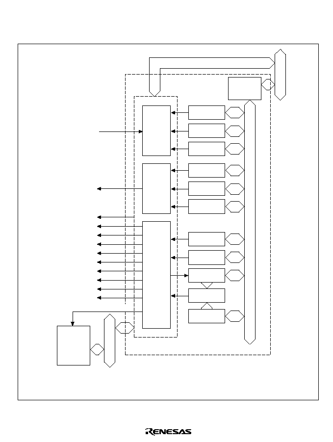
253
7.1.2
Block Diagram
Figure 7.1 shows a block diagram of the BSC.
Area
control
unit
MCR
BSC
RTCSR
RTCNT
RTCOR
Comparator
Memory
control
unit
WCR1
WCR2
WCR3
Wait
control
unit
WAIT
CS4
≠
CS0
BS
STATS1, 0
RD
CAS
RAS
RD/
WR
WE3
≠
WE0
CKE
REFOUT
IVECF
Interrupt
controller
Peripheral bus
Module bus
Internal bus
Bus
interface
WCR: Wait control register
RTCSR: Refresh timer control/status register
BCR: Bus control register
RTCNT: Refresh timer counter
MCR: Individual memory control register
RTCOR: Refresh time constant register
CMI interrupt request
BCR1
BCR2
BCR3
Figure 7.1 BSC Block Diagram

254
7.1.3
Pin Configuration
Table 7.1 shows the BSC pin configuration.
Table 7.1
Pin Configuration
Signal
I/O
With Bus
Released
Description
A24≠A0
O
Hi-Z
Address bus. 32 Mbytes of memory space can be specified with 25
bits
D31≠D0
I/O
Hi-Z
32-bit data bus. When reading or writing a 16-bit width area, use
D15≠D0; when reading or writing a 8-bit width area, use D7≠D0.
With 8-bit accesses that read or write a 32-bit width area, input and
output the data via the byte position determined by the lower
address bits of the 32-bit bus
BS
O
Hi-Z
Indicates start of bus cycle or monitor. With the basic interface
(device interfaces except for DRAM, synchronous DRAM), signal is
asserted for a single clock cycle simultaneous with address output.
The start of the bus cycle can be determined by this signal
CS0
≠
CS4
O
Hi-Z
Chip select.
CS3
is not asserted when the CS3 space is DRAM
space
RD/
WR
O
Hi-Z
Read/write signal. Signal that indicates access cycle direction
(read/write). Connected to
WE
pin when DRAM/synchronous
DRAM is connected
RAS
O
Hi-Z
RAS
pin for DRAM/synchronous DRAM
CAS
/
OE
O
Hi-Z
Open when using DRAM
Connected to
OE
pin when using EDO RAM
Connected to
CAS
pin when using synchronous DRAM
RD
O
Hi-Z
Read pulse signal (read data output enable signal). Normally,
connected to the device's
OE
pin; when there is an external data
buffer, the read cycle data can only be output when this signal is
low
WAIT
I
Don't care
Hardware wait input
BRLS
I
I
Bus release request input
BGR
O
O
Bus grant output
CKE
O
O
Synchronous DRAM clock enable control. Signal for supporting
synchronous DRAM self-refresh
IVECF
O
O
Interrupt vector fetch
DREQ0
I
I
DMA request 0
DACK0
O
O
DMA acknowledge 0

255
Table 7.1
Pin Configuration (cont)
Signal
I/O
With Bus
Released
Description
DREQ1
I
I
DMA request 1
DACK1
O
O
DMA acknowledge 1
REFOUT
O
O
Refresh execution request output when bus is released
DQMUU/
WE3
O
Hi-Z
When synchronous DRAM is used, connected to DQM pin for the
most significant byte (D31≠D24). For ordinary space, indicates
writing to the most significant byte
DQMUL/
WE2
O
Hi-Z
When synchronous DRAM is used, connected to DQM pin for the
second byte (D23≠D16). For ordinary space, indicates writing to the
second byte
DQMLU/
WE1
O
Hi-Z
When synchronous DRAM is used, connected to DQM pin for the
third byte (D15≠D8). For ordinary space, indicates writing to the
third byte
DQMLL/
WE0
O
Hi-Z
When synchronous DRAM is used, connected to DQM pin for the
least significant byte (D7≠D0). For ordinary space, indicates writing
to the least significant byte
CAS3
O
Hi-Z
When DRAM is used, connected to
CAS
pin for the most significant
byte (D31≠D24)
CAS2
O
Hi-Z
When DRAM is used, connected to
CAS
pin for the second byte
(D23≠D16)
CAS1
O
Hi-Z
When DRAM is used, connected to
CAS
pin for the third byte (D15≠
D8)
CAS0
O
Hi-Z
When DRAM is used, connected to
CAS
pin for the least significant
byte (D7≠D0)
STATS0, 1 O
O
Bus master identification 00: CPU
01: DMAC
10: E-DMAC
11: Other
BUSHIZ
I
I
Signal used in combination with
WAIT
signal to place bus and
strobe signals in the high-impedance state without the ending bus
cycle.
Note:
Hi-Z: High impedance

256
7.1.4
Register Configuration
The BSC has ten registers. These registers are used to control wait states, bus width, interfaces
with memories like DRAM, synchronous DRAM, and burst ROM, and DRAM and synchronous
DRAM refreshing. The register configurations are shown in table 7.2.
The size of the registers themselves is 16 bits. If read as 32 bits, the upper 16 bits are 0. In order to
prevent writing mistakes, 32-bit writes are accepted only when the value of the upper 16 bits of the
write data is H'A55A; no other writes are performed. Initialize the reserved bits.
Initialization Procedure: Do not access a space other than CS0 until the settings for the interface
to memory are completed.
Table 7.2
Register Configuration
Name
Abbr.
R/W
Initial Value Address
*
1
Access Size
Bus control register 1
BCR1
R/W
H'03F0
H'FFFFFFE0 16
*
2
, 32
Bus control register 2
BCR2
R/W
H'00FC
H'FFFFFFE4 16
*
2
, 32
Bus control register 3
BCR3
R/W
H'0F00
H'FFFFFFFC 16
*
2
, 32
Wait control register 1
WCR1
R/W
H'AAFF
H'FFFFFFE8 16
*
2
, 32
Wait control register 2
WCR2
R/W
H'000B
H'FFFFFFC0 16
*
2
, 32
Wait control register 3
WCR3
R/W
H'0000
H'FFFFFFC4 16
*
2
, 32
Individual memory control register
MCR
R/W
H'0000
H'FFFFFFEC 16
*
2
, 32
Refresh timer control/status register RTCSR
R/W
H'0000
H'FFFFFFF0 16
*
2
, 32
Refresh timer counter
RTCNT
R/W
H'0000
H'FFFFFFF4 16
*
2
, 32
Refresh time constant register
RTCOR
R/W
H'0000
H'FFFFFFF8 16
*
2
, 32
Notes:
*
1 This address is for 32-bit accesses; for 16-bit accesses add 2.
*
2 16-bit access is for read only.

257
7.1.5
Address Map
The address map, which has a memory space of 320 Mbytes, is divided into five spaces
.
The types
and data width of devices that can be connected are specified for each space
.
The overall space
address map is shown in table 7.3
.
Since the spaces of the cache area and the cache-through area
are actually the same, and the maximum memory space that can be connected is 160 Mbytes. This
means that when address H'20000000 is accessed in a program, the data accessed is actually in
H'00000000.
The chip has 16-kbyte RAM as on-chip memory. The on-chip RAM is divided into an X area and
a Y area, which can be accessed in parallel with the DSP instruction. See the SH-1/SH-2/SH-DSP
Programming Manual for more information.
There are several spaces for cache control. These include the associative purge space for cache
purges, address array read/write space for reading and writing addresses (address tags), and data
array read/write space for forced reads and writes of data arrays.
Table 7.3
Address Map
Address
Space
Memory
Size
H'00000000≠H'01FFFFFF
CS0 space, cache area
Ordinary space or burst
ROM
32 Mbytes
H'02000000≠H'03FFFFFF
CS1 space, cache area
Ordinary space
32 Mbytes
H'04000000≠H'05FFFFFF
CS2 space, cache area
Ordinary space or
synchronous DRAM
*
2
32 Mbytes
H'06000000≠H'07FFFFFF
CS3 space, cache area
Ordinary space,
synchronous DRAM
*
2
, or
DRAM
32 Mbytes
H'08000000≠H'09FFFFFF
CS4 space, cache area
Ordinary space (I/O
device)
32 Mbytes
H'0A000000≠H'0FFFFFFF
Reserved
*
1
H'10000000≠H'1000DFFF
Reserved
*
1
H'1000E000≠H'1000EFFF
On-chip X RAM area
8 kbytes
H'1000F000≠H'1001DFFF
Reserved
*
1
H'1001E000≠H'1001EFFF
On-chip Y RAM area
8 kbytes
H'1001F000≠H'1FFFFFFF
Reserved
*
1
H'20000000≠H'21FFFFFF
CS0 space, cache-through
area
Ordinary space or burst
ROM
32 Mbytes
H'22000000≠H'23FFFFFF
CS1 space, cache-through
area
Ordinary space
32 Mbytes

258
Table 7.3
Address Map (cont)
Address
Space
Memory
Size
H'24000000≠H'25FFFFFF
CS2 space, cache-through
area
Ordinary space or
synchronous DRAM
*
2
32 Mbytes
H'26000000≠H'27FFFFFF
CS3 space, cache-through
area
Ordinary space,
synchronous DRAM
*
2
, or
DRAM
32 Mbytes
H'28000000≠H'29FFFFFF
CS4 space, cache-through
area
Ordinary space (I/O
device)
32 Mbytes
H'2A000000≠H'3FFFFFFF
Reserved
*
1
H'40000000≠H'49FFFFFF
Associative purge space
160 Mbytes
H'4A000000≠H'5FFFFFFF
Reserved
*
1
H'60000000≠H'7FFFFFFF
Address array, read/write
space
512 Mbytes
H'80000000≠H'BFFFFFFF
Reserved
*
1
H'C0000000≠H'C0000FFF
Data array, read/write space
4 kbytes
H'C0001000≠H'DFFFFFFF Reserved
*
1
H'E0000000≠H'FFFEFFFF Reserved
*
1
H'FFFF0000≠H'FFFF0FFF For setting synchronous
DRAM mode
4 kbytes
H'FFFF1000≠H'FFFF7FFF Reserved
*
1
H'FFFF8000≠H'FFFF8FFF For setting synchronous
DRAM mode
4 kbytes
H'FFFFC000≠H'FFFFBFFF Reserved
*
1
H'FFFFFC00≠H'FFFFFFFF On-chip peripheral modules
Notes:
*
1 Do not access reserved spaces, as operation cannot be guaranteed.
*
2 Bank-active mode is not supported for CS2 space synchronous DRAM access; auto-
precharge mode is always used.
Bank-active mode is supported for CS3 space synchronous DRAM access.

259
7.2
Register Descriptions
7.2.1
Bus Control Register 1 (BCR1)
Bit:
15
14
13
12
11
10
9
8
--
A4LW1
A4LW0
A2EN
DIAN
BST
ROM
--
AHLW1 AHLW0
Initial value:
0
0
0
0
0
0
1
1
R/W:
R
R/W
R/W
R/W
R/W
R
R/W
R/W
Bit:
7
6
5
4
3
2
1
0
A1LW1
A1LW0
A0LW1
A0LW0
A4EN
DIAN
DRAM2
DRAM1 DRAM0
Initial value:
1
1
1
1
0
0
0
0
R/W:
R/W
R/W
R/W
R/W
R/W
R/W
R/W
R/W
Initialize the ENDIAN, BSTROM, PSHR, and DRAM2≠DRAM0 bits after a power-on reset, and
do not change their values thereafter. To change other bits by writing to them, write the same
value as they are initialized to. Do not access any space other than CS0 until the register
initialization ends.
Bit 15--Reserved: This bit is always read as 0. The write value should always be 0.
Bits 14 and 13--Long Wait Specification for Area 4 (A4LW1, A4LW0): From 3 to 14 wait cycles
are inserted in CS4 space accesses when the wait control bits (W41, W40) in wait control register
2 (WCR2) are set as long wait (i.e., are set to 11) (see table 7.4).
Bit 12--Endian Specification for Area 2 (A2ENDIAN): In big-endian format, the MSB of byte
data is the lowest byte address and byte data goes in order toward the LSB
.
For little-endian
format, the LSB of byte data is the lowest byte address and byte data goes in order toward the
MSB
.
When this bit is 1, the data is rearranged into little-endian format before transfer when the
CS2 space is read or written to. It is used when handling data with little-endian processors or
running programs written with conscious use of little-endian format.
Bit 12: A2ENDIAN
Description
0
Big-endian
(Initial value)
1
Little-endian

260
Bit 11--Area 0 Burst ROM Enable (BSTROM)
Bit 11: BSTROM
Description
0
Area 0 is accessed normally
(Initial value)
1
Area 0 is accessed as burst ROM
Bit 10--Reserved: This bit is always read as 0. The write value should always be 0.
Bits 9 and 8--Long Wait Specification for Areas 2 and 3 (AHLW1, AHLW0): When the basic
memory interface setting is made for CS2 and CS3, from 3 to 14 wait cycles are inserted in CS2 or
CS3 accesses when the bits specifying the respective area waits in the wait control bits (W21,
W20 or W31, W30) in wait control register 1 (WCR1) are set as long waits (i.e., are set to 11) (see
table 7.4).
Bits 7 and 6--Long Wait Specification for Area 1 (A1LW1, A1LW0): From 3 to 14 wait cycles
are inserted in area 1 accesses when the wait control bits (W11, W10) in wait control register 1
(WCR1) are set as long wait (i.e., are set to 11) (see table 7.4).
Bits 5 and 4--Long Wait Specification for Area 0 (A0LW1, A0LW0): When the basic memory
interface setting is made for CS0, from 3 to 14 wait cycles are inserted in CS0 accesses when the
wait control bits (W01, W00) in wait control register 1 (WCR1) are set as long wait (i.e., are set to
11) (see table 7.4).
Bit 3--Endian Specification for Area 4 (A4ENDIAN): In big-endian mode, the most significant
byte (MSB) is the lowest byte address, and byte data is aligned in order toward the least significant
byte (LSB). In little-endian mode, the LSB is the lowest byte address, and byte data is aligned in
order toward the MSB. When this bit is set to 1, data in read/write accesses to the CS4 space is
rearranged into little endian order before being transferred. This is used for data exchange with a
little-endian processor or when executing a program written with awareness of little-endian mode.
Bit 3: A4ENDIAN
Description
0
Big endian
(Initial value)
1
Little endian

261
Bits 2 to 0--Enable for DRAM and Other Memory (DRAM2≠DRAM0)
DRAM2
DRAM1
DRAM0
Description
0
0
0
CS2 and CS3 are ordinary spaces
(Initial value)
1
CS2 is ordinary space; CS3 is synchronous DRAM space
1
0
CS2 is ordinary space; CS3 is DRAM space
1
Reserved (do not set)
1
0
0
CS2 is synchronous DRAM space, CS3 is ordinary space
1
CS2 and CS3 are synchronous DRAM spaces
1
0
Reserved (do not set)
1
Reserved (do not set)
Table 7.4
Wait Values Corresponding to BCR1 and BCR3 Register Settings (All Spaces)
BCR3
BCR1
AnLW2
AnLW1
AnLW0
Wait Value
0
0
0
3 cycles inserted
1
4 cycles inserted
1
0
5 cycles inserted
1
6 cycles inserted
1
0
0
8 cycles inserted
1
10 cycles inserted
1
0
12 cycles inserted
1
14 cycles inserted
(Initial value)
Note:
n = 0 to 4
AHLW2, AHLW1, and AHLW0 are common to CS2 and CS3.

262
7.2.2
Bus Control Register 2 (BCR2)
Bit:
15
14
13
12
11
10
9
8
--
--
--
--
--
--
A4SZ1
A4SZ0
Initial value:
0
0
0
0
0
0
0
0
R/W:
R
R
R
R
R
R
R/W
R/W
Bit:
7
6
5
4
3
2
1
0
A3SZ1
A3SZ0
A2SZ1
A2SZ0
A1SZ1
A1SZ0
--
--
Initial value:
1
1
1
1
1
1
0
0
R/W:
R/W
R/W
R/W
R/W
R/W
R/W
R
R
Initialize BCR2 after a power-on reset and do not write to it thereafter. When writing to it, write
the same values as those the bits are initialized to. Do not access any space other than CS0 until
the register initialization ends.
The CS0 space bus size specification is set with pins MD4 and MD3. See section 3.3, CS0 Space
Bus Width of the CS0 Area, for details.
Bits 15 to 10--Reserved: These bits are always read as 0. The write value should always be 0.
Bits 9 and 8--Bus Size Specification for Area 4 (CS4) (A4SZ1, A4SZ0)
Bit 9: A4SZ1
Bit 8: A4SZ0
Description
0
0
Longword (32-bit) size
(Initial value)
1
Byte (8-bit) size
1
0
Word (16-bit) size
1
Longword (32-bit) size
Bits 7 and 6--Bus Size Specification for Area 3 (CS3) (A3SZ1, A3SZ0). Effective only when
ordinary space is set.
Bit 7: A3SZ1
Bit 6: A3SZ0
Description
0
0
Reserved (do not set)
1
Byte (8-bit) size
1
0
Word (16-bit) size
1
Longword (32-bit) size
(Initial value)

263
Bits 5 and 4--Bus Size Specification for Area 2 (CS2) (A2SZ1, A2SZ0): Effective only when
ordinary space is set.
Bit 5: A2SZ1
Bit 4: A2SZ0
Description
0
0
Reserved (do not set)
1
Byte (8-bit) size
1
0
Word (16-bit) size
1
Longword (32-bit) size
(Initial value)
Bits 3 and 2--Bus Size Specification for Area 1 (CS1) (A1SZ1, A1SZ0)
Bit 3: A1SZ1
Bit 2: A1SZ0
Description
0
0
Reserved (do not set)
1
Byte (8-bit) size
1
0
Word (16-bit) size
1
Longword (32-bit) size
(Initial value)
Bits 1 and 0--Reserved: These bits are always read as 0. The write value should always be 0.
7.2.3
Bus Control Register 3 (BCR3)
Bit:
15
14
13
12
11
10
9
8
--
--
--
--
A4LW2
AHLW2
A1LW2
A0LW2
Initial value:
0
0
0
0
1
1
1
1
R/W:
R
R
R
R
R/W
R/W
R/W
R/W
Bit:
7
6
5
4
3
2
1
0
DSWW1 DSWW0
--
--
--
BASEL
EDO
BWE
Initial value:
0
0
0
0
0
0
0
0
R/W:
R/W
R/W
R
R
R
R/W
R/W
R/W
Initialize the BASEL, EDO, and BWE bits after a power-on reset and do not write to them
thereafter. To change other bits by writing to them, write the same value as they are initialized to.
Do not access any space other than CS0 until the register initialization ends.
Bits 15 to 12--Reserved bits: These bits are always read as 0. The write value should always be 0.
Bits 11 to 8--Long Wait Specification for Areas 0 to 4 (AnLW2): When the basic memory
interface setting is made for CS n, from 3 to 14 wait cycles are inserted in CS n accesses,

264
according to the combination with the long wait specification bits (AnLW1 and AnLW0) in
BCR1, when the bits specifying the wait in the wait control register are set as long wait (i.e., are
set to 11). For a basic description of long waits, see section 7.2.1, Bus Control Register 1 (BCR1).
Bits 7 and 6--DMA Single-Write Wait (DSWW1, DSWW0): These bits determine the number of
wait states inserted between DACK assertion and
CASn assertion when writing to DRAM or EDO
RAM in DMA single address mode.
Bit 7: DSWW1
Bit 6: DSWW0
Description
0
0
0 waits
(Initial value)
1
1 wait
1
0
2 waits
1
Reserved (do not set)
Bits 5 to 3--Reserved bits: These bits are always read as 0. The write value should always be 0.
Bit 2--Number of Banks Specification when Using 64M Synchronous DRAM (BASEL): When
64M synchronous DRAM is specified by AMX2≠AMX0 in MCR, the number of banks can be
specified.
Bit 2: BASEL
Description
0
4 banks
(Initial value)
1
2 banks
Bit 1--EDO Mode Specification (EDO): Enables EDO mode to be specified when DRAM is
specified for CS3 space.
Bit 1: EDO
Description
0
High-speed page mode
(Initial value)
1
EDO mode
Bit 0--Synchronous DRAM Burst Write Specification (BWE): Enables burst write mode to be
specified when synchronous DRAM is specified for CS2 or CS3 space.
Bit 0: BWE
Description
0
Single write mode
(Initial value)
1
Burst write mode

265
7.2.4
Wait Control Register 1 (WCR1)
Bit:
15
14
13
12
11
10
9
8
IW31
IW30
IW21
IW20
IW11
IW10
IW01
IW00
Initial value:
1
0
1
0
1
0
1
0
R/W:
R/W
R/W
R/W
R/W
R/W
R/W
R/W
R/W
Bit:
7
6
5
4
3
2
1
0
W31
W30
W21
W20
W11
W10
W01
W00
Initial value:
1
1
1
1
1
1
1
1
R/W:
R/W
R/W
R/W
R/W
R/W
R/W
R/W
R/W
Do not access a space other than CS0 until the settings for register initialization are completed.
Bits 15 to 8--Idles between Cycles for Areas 3 to 0 (IW31≠IW00): These bits specify idle cycles
inserted between consecutive accesses to different CS spaces. Idles are used to prevent data
conflict between ROM or the like, which is slow to turn the read buffer off, and fast memories and
I/O interfaces. Even when access is to the same space, idle cycles must be inserted when a read
access is followed immediately by a write access. The idle cycles to be inserted comply with the
specification for the previously accessed space
.
The set values below show the minimum number
of idle cycles; more cycles than indicated by the Idles between Cycles setting may actually be
inserted.
IW31, IW21, IW11, IW01
IW30, IW20, IW10, IW00
Description
0
0
No idle cycle
1
One idle cycle inserted
1
0
Two idle cycles inserted
(
Initial value)
1
Four idle cycles inserted
Bits 7 to 0--Wait Control for Areas 3 to 0 (W31≠W00)
∑
When the CSn space is set as ordinary space, the number of CSn space waits can be specified
with Wn1 and Wn0.

266
W31, W21, W11, W01
W30, W20, W10, W00
Description
0
0
External wait input disabled without wait
1
External wait input enabled with one wait
1
0
External wait input enabled with two waits
1
Complies with the long wait specification of
bus control register 1, 3 (BCR1, BCR3).
External wait input is enabled (Initial value)
∑
When CS3 is DRAM, the number of
CAS assert cycles is specified by wait control bits W31
and W30
Bit 7: W31
Bit 6: W30
Description
0
0
1 cycle
1
2 cycles
1
0
3 cycles
1
Reserved (do not set)
When external wait mask bit A3WM in WCR2 is 0 and the number of
CAS assert cycles is set
to 2 or more, external wait input is enabled.
∑
When CS2 or CS3 is synchronous DRAM, CAS latency is specified by wait control bits W31
and W30, and W21 and W20, respectively
W31, W21
W30, W20
Description
0
0
1 cycle
1
2 cycles
1
0
3 cycles
1
4 cycles
(Initial value)
With synchronous DRAM, external wait input is ignored regardless of any setting.

267
7.2.5
Wait Control Register 2 (WCR2)
Bit:
15
14
13
12
11
10
9
8
A4WD1
A4WD0
--
A4WM
A3WM
A2WM
A1WM
A0WM
Initial value:
0
0
0
0
0
0
0
0
R/W:
R/W
R/W
R
R/W
R/W
R/W
R/W
R/W
Bit:
7
6
5
4
3
2
1
0
--
--
--
--
IW41
IW40
W41
W40
Initial value:
0
0
0
0
1
0
1
1
R/W:
R
R
R
R
R/W
R/W
R/W
R/W
Bits 15 and 14--Number of External Waits Specification for Area 4 (A4WD1, A4WD0): These
bits specify the number of cycles between acceptance of CS4 space external wait negation and
RD
or
WEn negation.
Bit 15: A4WD1
Bit 14: A4WD0
Description
0
0
1 cycle
(Initial value)
1
2 cycles
1
0
4 cycles
1
Reserved (do not set)
Bit 13--Reserved bit. This bit is always read as 0. The write value should always be 0.
Bits 12 to 8--External Wait Mask Specification for Areas 0 to 4 (A4WM≠A0WM): These bits
enable waits to be masked for CS spaces 0 to 4. When a value other than 00 is set in the wait
control bits for CS spaces 0 to 4 (W41≠W00), external wait input can be enabled, but the wait
input can be masked by setting these bits to 1. With synchronous DRAM, external wait input is
ignored regardless of the settings.

268
A4WM
A3WM
A2WM
A1WM
A0WM
W41
W31
W21
W11
W01
W40
W30
W20
W10
W00
Description
0
0
0
External wait input ignored
1
External wait input enabled
1
0
External wait input enabled
1
External wait input enabled
(Initial value)
1
Don't care
Don't care
External wait input ignored
Bits 7 to 4--Reserved bits: These bits are always read as 0. The write value should always be 0.
Bits 3 and 2--Idles between Cycles for Area 4 (IW41, IW40): These bits specify idle cycles
inserted between cycles in CS4 in the same way as for CS 0 to 3. The set values below show the
minimum number of idle cycles; more cycles than indicated by the Idles between Cycles setting
may actually be inserted.
Bit 3: IW41
Bit 2: IW40
Description
0
0
No idle cycle
1
One idle cycle inserted
1
0
Two idle cycles inserted
(Initial value)
1
Four idle cycles inserted
Bits 1 and 0--Wait Control for Area 4 (W41, W40): These bits specify waits for CS4 in the same
way as for areas 0 to 3.
Bit 1: W41
Bit 0: W40
Description
0
0
No wait. External wait input disabled without wait
1
One wait. External wait input enabled with one wait
1
0
Two waits. External wait input enabled with two waits
1
Complies with the long wait specification of bus control
registers 1 and 3 (BCR1, BCR3). External wait input is
enabled
(Initial value)

269
7.2.6
Wait Control Register 3 (WCR3)
Bit:
15
14
13
12
11
10
9
8
--
--
A4SW2
A4SW1
A4SW0
--
A4HW1 A4HW0
Initial value:
0
0
0
0
0
0
0
0
R/W:
R
R
R/W
R/W
R/W
R
R/W
R/W
Bit:
7
6
5
4
3
2
1
0
A3SHW1 A3SHW0 A2SHW1 A2SHW0 A1SHW1 A1SHW0 A0SHW1 A0SHW0
Initial value:
0
0
0
0
0
0
0
0
R/W:
R/W
R/W
R/W
R/W
R/W
R/W
R/W
R/W
Bits 15 and 14--Reserved bits: These bits are always read as 0. The write value should always be
0.
Bits 13 to 11--CS4 Address/
CS4 to RD/WEn Assertion (A4SW2≠A4SW0): These bits specify the
number of cycles from address/
CS4 output to RD/WEn assertion for the CS4 space.
Bit 13: A4SW2
Bit 12: A4SW1
Bit 11: A4SW0
Description
0
0
0
0.5 cycles
(Initial value)
1
1.5 cycles
1
0
3.5 cycles
1
5.5 cycles
1
0
0
7.5 cycles
1
Reserved (do not set)
1
0
Reserved (do not set)
1
Reserved (do not set)
Bit 10--Reserved bit: This bit is always read as 0. The write value should always be 0.
Bits 9 and 8--Area 4
RD/WEn Negation to Address/CS4 Hold (A4HW1, A4HW0): These bits
specify the number of cycles from
RD/WEn negation to address/CS4 hold for the CS4 space.
Bit 9: A4HW1
Bit 8: A4HW0
Description
0
0
0.5 cycle,
CS4
hold cycle = 0 cycles
(Initial value)
1
1.5 cycle,
CS4
hold cycle = 1 cycle
1
0
3.5 cycle,
CS4
hold cycle = 3 cycles
1
5.5 cycle,
CS4
hold cycle = 5 cycles

270
Bits 7 to 0--Area 3 to 0
CSn Assert Period Extension (A3SHW1≠A0SHW0): These bits specify
the number of cycles from address/
CSn output to RD/WEn assertion and from RD/WEn negation
to address/
CSn hold for areas 3 to 0.
A3SHW1
A2SHW1
A1SHW1
A0SHW1
A3SHW0
A2SHW0
A1SHW0
A0SHW0
Description
0
0
0.5 cycle,
CSn*
hold cycle = 0 cycles
(Initial value)
1
1.5 cycle,
CSn*
hold cycle = 1 cycle
1
0
2.5 cycle,
CSn*
hold cycle = 2 cycles
1
Reserved (do not set)
Note:
*
n = 0 to 3
7.2.7
Individual Memory Control Register (MCR)
Bit:
15
14
13
12
11
10
9
8
TRP0
RCD0
TRWL0
TRAS1
TRAS0
BE
RASD
TRWL1
Initial value:
0
0
0
0
0
0
0
0
R/W:
R/W
R/W
R/W
R/W
R/W
R/W
R/W
R/W
Bit:
7
6
5
4
3
2
1
0
AMX2
SZ
AMX1
AMX0
RFSH
RMODE
TRP1
RCD1
Initial value:
0
0
0
0
0
0
0
0
R/W:
R/W
R/W
R/W
R/W
R/W
R/W
R/W
R/W
The TRP1≠TRP0, RCD1≠RCD0, TRWL1≠TRWL0, TRAS1≠TRAS0, BE, RASD, AMX2≠AMX0
and SZ bits are initialized after a power-on reset. Do not write to them thereafter. When writing to
them, write the same values as they are initialized to. Do not access CS2 or CS3 until register
initialization is completed.
Bits 1 and 15--
RAS Precharge Time (TRP1, TRP0): When DRAM is connected, specifies the
minimum number of cycles after
RAS is negated before the next assert. When synchronous
DRAM is connected, specifies the minimum number of cycles after precharge until a bank active
command is output. See section 7.5, Synchronous DRAM Interface, for details.

271
Bit 1: TRP1
Bit 15: TRP0
Description
0
0
1 cycle
(Initial value)
1
2 cycles
1
0
Reserved (do not set)
1
Reserved (do not set)
Bits 0 and 14--
RAS-CAS Delay (RCD1, RCD0): When DRAM is connected, specifies the
number of cycles after
RAS is asserted before CAS is asserted. When synchronous DRAM is
connected, specifies the number of cycles after a bank active (ACTV) command is issued until a
read or write command (READ, READA, WRIT, WRITA) is issued.
Bit 0: RCD1
Bit 14: RCD0
Description
0
0
1 cycle
(Initial value)
1
2 cycles
1
0
3 cycles
1
Reserved (do not set)
Bits 8 and 13--Write-Precharge Delay (TRWL1, TRWL0): When the synchronous DRAM is not
in the bank active mode, this bit specifies the number of cycles after the write cycle before the
start-up of the auto-precharge. Based on this number of cycles, the timing at which the next active
command can be issued is calculated within the bus controller. In bank active mode, this bit
specifies the number of cycles before the precharge command is issued after the write command is
issued. This bit is ignored when memory other than synchronous DRAM is connected.
Bit 8: TRWL1
Bit 13: TRWL0
Description
0
0
1 cycle
(Initial value)
1
2 cycles
1
0
3 cycles
1
Reserved (do not set)
Bits 12 and 11--
CAS-Before-RAS Refresh RAS Assert Time (TRAS1, TRAS0): These bits
specify the
RAS assertion width when DRAM is connected.
Bit 12: TRAS1
Bit 11: TRAS0
Description
0
0
2 cycles
(Initial value)
1
3 cycles
1
0
4 cycles
1
5 cycles

272
After an auto-refresh command is issued, a bank active command is not issued for TRAS cycles,
regardless of the TRP bit setting. For synchronous DRAM, there is no
RAS assertion period, but
there is a limit for the time from the issue of a refresh command until the next access. This value is
set to observe this limit. Commands are not issued for TRAS cycles when self-refresh is cleared.
Bit 12: TRAS1
Bit 11: TRAS0
Description
0
0
3 cycles
(Initial value)
1
4 cycles
1
0
6 cycles
1
9 cycles
Bit 10--Burst Enable (BE)
Bit 10: BE
Description
0
Burst disabled
(Initial value)
1
High-speed page mode during DRAM and ED0 interfacing is enabled
.
Burst access conditions are as follows:
∑
Longword access, cache fill access, or DMAC 16-byte transfer, with 16-bit
bus width
∑
Cache fill access or DMAC 16-byte transfer, with 32-bit bus width
During synchronous DRAM access, burst operation is always enabled
regardless of this bit
Bit 9--Bank Active Mode (RASD)
Bit 9: RASD
Description
0
For DRAM,
RAS
is negated after access ends (normal operation)
For synchronous DRAM, a read or write is performed using auto-precharge
mode
.
The next access always starts with a bank active command
(Initial value)
1
For DRAM, after access ends
RAS
down mode is entered in which RAS is left
asserted. When using this mode with an external device connected which
performs writes other than to DRAM, see section 7.6.5, Burst Access
For synchronous DRAM, access ends in the bank active state. This is only
valid for area 3. When area 2 is synchronous DRAM, the mode is always auto-
precharge

273
Bits 7, 5, and 4--Address Multiplex (AMX2≠AMX0)
∑
For DRAM interface
Bit 7: AMX2
Bit 5: AMX1
Bit 4: AMX0
Description
0
0
0
8-bit column address DRAM
1
9-bit column address DRAM
1
0
10-bit column address DRAM
1
11-bit column address DRAM
1
0
0
Reserved (do not set)
1
Reserved (do not set)
1
0
Reserved (do not set)
1
Reserved (do not set)
∑
For synchronous DRAM interface
Bit 7: AMX2
Bit 5: AMX1
Bit 4: AMX0
Description
0
0
0
16-Mbit DRAM (1M
◊
16 bits), 64-Mbit
DRAM (2M
◊
32 bits)
*
2
1
16-Mbit DRAM (2M
◊
8 bits)
*
1
1
0
16-Mbit DRAM (4M
◊
4 bits)
*
1
1
4-Mbit DRAM (256k
◊
16 bits)
1
0
0
64-Mbit DRAM (4M
◊
16 bits)
1
64-Mbit DRAM (8M
◊
8 bits)
*
1
1
0
Reserved (do not set)
1
2-Mbit DRAM (128k
◊
16 bits)
Notes:
*
1 Reserved. Do not set when SZ bit in MCR is 0 (16-bit bus width).
*
2 See section 7.5.11 for the method of connection to a 64-Mbit DRAM with a 2M
◊
32-bit
configuration.
Bit 6--Memory Data Size (SZ): For synchronous DRAM and DRAM space, the data bus width of
BCR2 is ignored in favor of the specification of this bit.
Bit 6: SZ
Description
0
Word (16 bits)
(Initial value)
1
Longword (32 bits)

274
Bit 3--Refresh Control (RFSH): This bit determines whether or not the refresh operation of
DRAM/synchronous DRAM is performed
.
Bit 3: RFSH
Description
0
No refresh
(Initial value)
1
Refresh
Bit 2--Refresh Mode (RMODE): When the RFSH bit is 1, this bit selects normal refresh or self-
refresh. When the RFSH bit is 0, do not set this bit to 1. When the RFSH bit is 1, self-refresh
mode is entered immediately after the RMODE bit is set to 1. When the RFSH bit is 1 and this bit
is 0, a
CAS-before-RAS refresh or auto-refresh is performed at the interval set in the 8-bit interval
timer. When a refresh request occurs during an external area access, the refresh is performed after
the access cycle is completed. When set for self-refresh, self-refresh mode is entered immediately
unless the chip is in the middle of a synchronous DRAM area access, in which case self-refresh
mode is entered when the access ends. Refresh requests from the interval timer are ignored during
self-refresh.
Bit 2: RMODE
Description
0
Normal refresh
(Initial value)
1
Self-refresh
7.2.8
Refresh Timer Control/Status Register (RTCSR)
Bit:
15
14
13
12
11
10
9
8
--
--
--
--
--
--
--
--
Initial value:
0
0
0
0
0
0
0
0
R/W:
R
R
R
R
R
R
R
R
Bit:
7
6
5
4
3
2
1
0
CMF
CMIE
CKS2
CKS1
CKS0
RRC2
RRC1
RRC0
Initial value:
0
0
0
0
0
0
0
0
R/W:
R/W
R/W
R/W
R/W
R/W
R/W
R/W
R/W
Bits 15 to 8--Reserved: These bits are always read as 0. The write value should always be 0.

275
Bit 7--Compare Match Flag (CMF): This status flag, which indicates that the values of RTCNT
and RTCOR match, is set/cleared under the following conditions:
Bit 7: CMF
Description
0
[Clearing condition]
After RTCSR is read when CMF is 1, 0 is written in CMF
1
[Setting condition]
RTCNT = RTCOR
Bit 6--Compare Match Interrupt Enable (CMIE): Enables or disables an interrupt request caused
by the CMF bit of RTCSR when CMF is set to 1.
Bit 6: CMIE
Description
0
Interrupt request caused by CMF is disabled
(Initial value)
1
Interrupt request caused by CMF is enabled
Bits 5 to 3--Clock Select Bits (CKS2≠CKS0)
Bit 5: CKS2
Bit 4: CKS1
Bit 3: CKS0
Description
0
0
0
Count-up disabled
(Initial value)
1
P
/4
1
0
P
/16
1
P
/64
1
0
0
P
/256
1
P
/1024
1
0
P
/2048
1
P
/4096
Bits 2 to 0--Refresh Count (RRC2≠RRC0): These bits specify the number of consecutive
refreshes to be performed when the refresh timer counter (RTCNT) and refresh time constant
register (RTCOR) values match and a refresh request is issued.

276
Bit 2: RRC2
Bit 1: RRC1
Bit 0: RRC0
Description
0
0
0
1 refresh
(Initial value)
1
2 refreshes
1
0
4 refreshes
1
6 refreshes
1
0
0
8 refreshes
1
Reserved (do not set)
1
0
Reserved (do not set)
1
Reserved (do not set)
7.2.9
Refresh Timer Counter (RTCNT)
Bit:
15
14
13
12
11
10
9
8
--
--
--
--
--
--
--
--
Initial value:
0
0
0
0
0
0
0
0
R/W:
R
R
R
R
R
R
R
R
Bit:
7
6
5
4
3
2
1
0
Initial value:
0
0
0
0
0
0
0
0
R/W:
R/W
R/W
R/W
R/W
R/W
R/W
R/W
R/W
The 8-bit counter RTCNT counts up with input clocks. The clock select bit of RTCSR selects an
input clock. RTCNT values can always be read/written by the CPU. When RTCNT matches
RTCOR, RTCNT is cleared. Returns to 0 after it counts up to 255.
Bits 15 to 8--Reserved: These bits are always read as 0. The write value should always be 0.

277
7.2.10
Refresh Time Constant Register (RTCOR)
Bit:
15
14
13
12
11
10
9
8
--
--
--
--
--
--
--
--
Initial value:
0
0
0
0
0
0
0
0
R/W:
R
R
R
R
R
R
R
R
Bit:
7
6
5
4
3
2
1
0
Initial value:
0
0
0
0
0
0
0
0
R/W:
R/W
R/W
R/W
R/W
R/W
R/W
R/W
R/W
RTCOR is an 8-bit read/write register. The values of RTCOR and RTCNT are constantly
compared. When the values correspond, the compare match flag (CMF) in RTCSR is set and
RTCNT is cleared to 0. When the refresh bit (RFSH) in the individual memory control register
(MCR) is set to 1, a refresh request signal occurs. The refresh request signal is held until refresh
operation is actually performed. If the refresh request is not processed before the next match, the
previous request becomes ineffective.
When the CMIE bit in RTCSR is set to 1, an interrupt request is sent to the controller by this
match signal. The interrupt request is output continuously until the CMF bit in RTCSR is cleared.
When the CMF bit clears, it only affects the interrupt; the refresh request is not cleared by this
operation. When a refresh is performed and refresh requests are counted using interrupts, a refresh
can be set simultaneously with the interval timer interrupt.
Bits 15 to 8--Reserved: These bits are always read as 0. The write value should always be 0.
7.3
Access Size and Data Alignment
7.3.1
Connection to Ordinary Devices
Byte, word, and longword are supported as access units
.
Data is aligned based on the data width of
the device
.
Therefore, reading longword data from a byte-width device requires four read
operations
.
The bus state controller automatically converts data alignment and data length between
interfaces. An 8-bit, 16-bit, or 32-bit external device data width can be connected by using the
mode pins for the CS0 space, or by setting BCR2 for the CS1≠CS4 spaces. However, the data
width of devices connected to the respective spaces is specified statically, and the data width
cannot be changed for each access cycle. Figures 7.2 to 7.4 show the relationship between device
data widths and access units.
278
D31
7
0
D23
D15
D7
D0
15
8
7
0
7
0
7
0
7
0
A24≠A0
000000
000001
000002
000003
000000
000002
000000
Data input/output pin
Byte read/write of address 0
Byte read/write of address 1
Byte read/write of address 2
Byte read/write of address 3
Word read/write of address 0
Word read/write of address 2
Longword read/write of address 0
31
24
23
16
15
8
7
0
15
8
7
0
32-bit external device (ordinary)
Figure 7.2 32-Bit External Devices and Their Access Units
D15
7
0
D7
16-bit external device (ordinary)
D0
15
0
7
0
7
0
7
0
A24≠A0
000000
000001
000002
000003
000000
000002
000000
000002
Data input/output pin
Byte read/write of address 0
Byte read/write of address 1
Byte read/write of address 2
Byte read/write of address 3
Word read/write of address 0
Word read/write of address 2
Longword read/write of address 0
15
0
31
16
15
0
Figure 7.3 16-Bit External Devices and Their Access Units
D7
8-bit external device (ordinary)
7
0
D0
7
0
7
0
7
0
15
8
7
0
15
8
7
0
31
24
23
16
15
8
7
0
A24≠A0
000000
000001
000002
000003
000000
000001
000002
000003
000000
000001
000002
000003
Data input/output pin
Byte read/write of address 0
Byte read/write of address 1
Byte read/write of address 2
Byte read/write of address 3
Word read/write of address 0
Word read/write of address 2
Longword read/write of address 0
Figure 7.4 8-Bit External Devices and Their Access Units
279
7.3.2
Connection to Little-Endian Devices
The chip provides a conversion function in CS2, CS4 space for connection to and to maintain data
compatibility with devices that use little-endian format (in which the LSB is the 0 position in the
byte data lineup). When the endian specification bit of BCR1 is set to 1, CS2, CS4 space is little-
endian. The relationship between device data width and access unit for little-endian format is
shown in figures 7.5, 7.6, and 7.7. When sharing memory or the like with a little-endian bus
master, the SH7616 connects D31≠D24 to the least significant byte (LSB) of the other bus master
and D7≠D0 to the most significant byte (MSB), when the bus width is 32 bits. When the width is
16 bits, the SH7616 connects D15≠D8 to the least significant byte of the other bus master and D7≠
D0 to the most significant byte.
Only data conversion is supported by this function. For this reason, be careful not to place
program code or constants in the CS2, CS4 space. When this function is used, make sure that the
access unit is the same for writing and reading. For example, data written by longword access
should be read by longword access. If the read access unit is different from the write access unit,
an incorrect value will be read.
D31
7
0
7
0
7
0
D23
D15
32-bit external device (little-endian)
D7
D0
15
8
7
0
7
0
7
0
A24≠A0
000000
000001
000002
000003
000000
000002
000000
Data input/output pin
Byte read/write of address 0
Byte read/write of address 1
Byte read/write of address 2
Byte read/write of address 3
Word read/write of address 0
Word read/write of address 2
Longword read/write of address 0
15
8
7
0 15
8
23
16
31
24
Figure 7.5 32-Bit External Devices and Their Access Units
D15
7
0
D7
16-bit external device (little-endian)
D0
7
8
7
0
7
0
0
7
15
0
15
0
15
16
31
0
A24≠A0
000000
000001
000002
000003
000000
000002
000000
000002
Data input/output pin
Byte read/write of address 0
Byte read/write of address 1
Byte read/write of address 2
Byte read/write of address 3
Word read/write of address 0
Word read/write of address 2
Longword read/write of address 0
7
8
7
8
23
24
Figure 7.6 16-Bit External Devices and Their Access Units

280
D7
7
0
D0
7
0
7
0
7
0
7
0
15
8
7
0
15
8
7
0
15
8
23
16
31
24
A24≠A0
000000
000001
000002
000003
000000
000001
000002
000003
000000
000001
000002
000003
Data input/output pin
Byte read/write of address 0
Byte read/write of address 1
Byte read/write of address 2
Byte read/write of address 3
Word read/write of address 0
Word read/write of address 2
Longword read/write of address 0
8-bit external device (little-endian)
Figure 7.7 8-Bit External Devices and Their Access Units
7.4
Accessing Ordinary Space
7.4.1
Basic Timing
A strobe signal is output by ordinary space accesses of CS0≠CS4 spaces to provide primarily for
SRAM direct connections. Figure 7.8 shows the basic timing of ordinary space accesses. Ordinary
accesses without waits end in 2 cycles. The
BS signal is asserted for 1 cycle to indicate the start of
the bus cycle. The
CSn signal is negated by the fall of clock T2 to ensure the negate period. The
negate period is thus half a cycle when accessed at the minimum pitch.
The access size is not specified during a read. The correct access start address will be output to the
LSB of the address, but since no access size is specified, the read will always be 32 bits for 32-bit
devices and 16 bits for 16-bit devices. For writes, only the
WE signal of the byte that will be
written is asserted. For 32-bit devices,
WE3 specifies writing to a 4n address and WE0 specifies
writing to a 4n+3 address. For 16-bit devices,
WE1 specifies writing to a 2n address and WE0
specifies writing to a 2n+1 address. For 8-bit devices, only
WE0 is used.
When data buses are provided with buffers, the
RD signal must be used for data output in the read
direction. When RD/
WR signals do not perform accesses, the chip stays in read status, so there is
a danger of conflicts occurring with output when this is used to control the external data buffer.
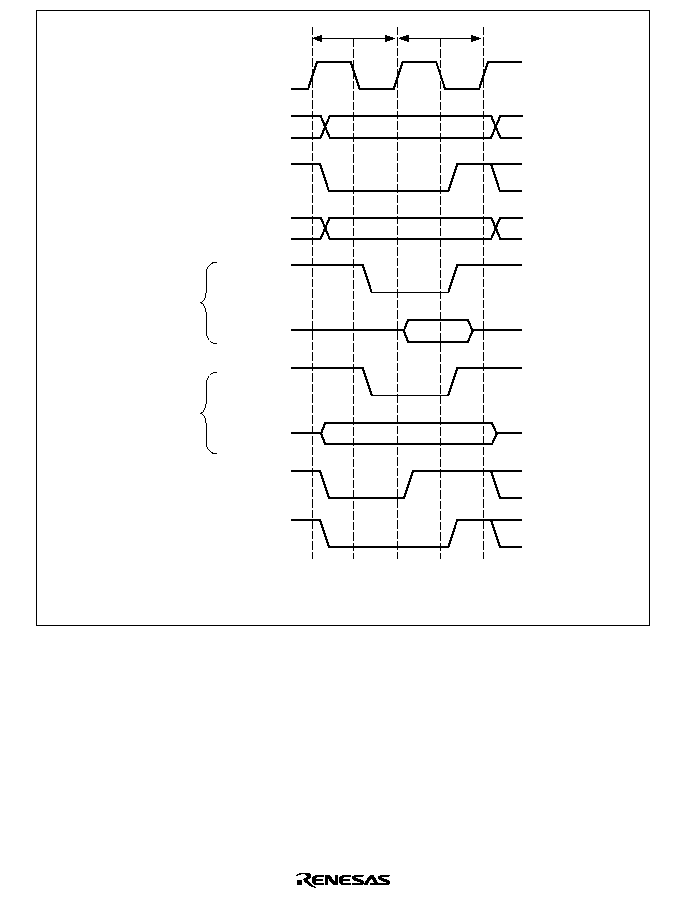
281
T1
T2
CKIO
A24≠A0
CSn
RD/
WR
RD
D31≠D0
WEn
D31≠D0
BS
DACKn
*
Read
Write
Note:
*
DACKn waveform when active-low is specified.
Figure 7.8 Basic Timing of Ordinary Space Access
When making a word or longword access with an 8-bit bus width, or a longword access with a 16-
bit bus width, the bus state controller performs multiple accesses.
When clock ratio I¯ : E¯ is other than 1 : 1, the basic timing shown in figure 7.8 is repeated, but
when clock ratio I
: E
is 1 : 1, burst access with no
CSn negate period is performed as shown in
figure 7.9.
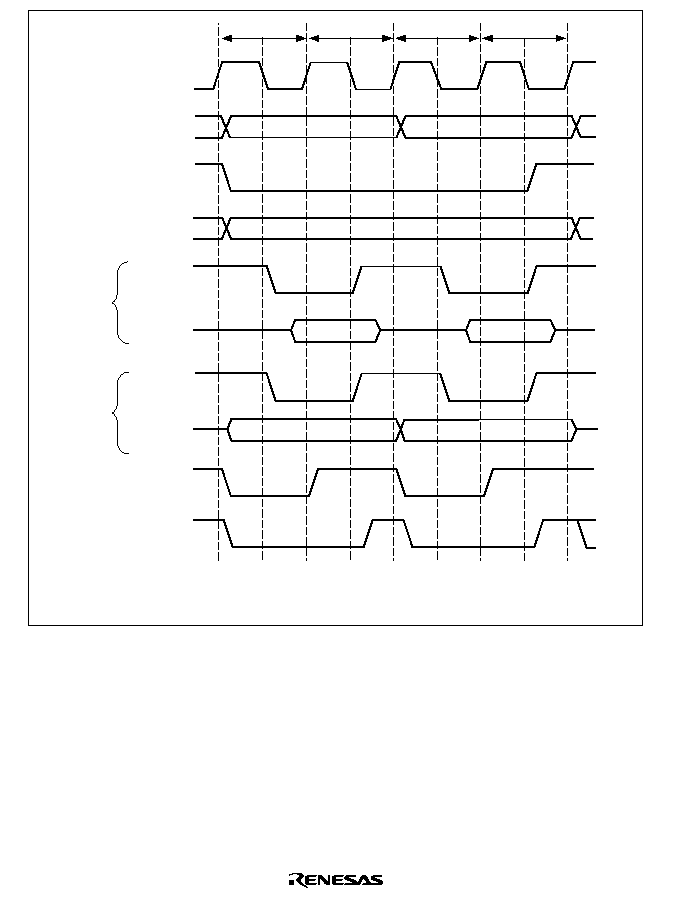
282
T1
T2
CKIO
A24≠A0
CSn
RD/
WR
RD
D15≠D0
WEn
D15≠D0
BS
DACKn
*
Read
Write
T1
T2
Note:
*
DACKn waveform when active-low is specified.
Figure 7.9 Timing of Longword Access in Ordinary Space Using 16-Bit Bus Width
(Clock Ratio I
: E
= 1 : 1)
Figure 7.10 shows an example of 32-bit data width SRAM connection, figure 7.11 an example of
16-bit data width SRAM connection, and figure 7.12 an example of 8-bit data width SRAM
connection.

283
A18
A2
CSn
RD
D31
D24
DQMUU/
WE3
D23
D16
DQMUL/
WE2
D15
D8
DQMLU/
WE1
D7
D0
DQMLL/
WE0
A16
A0
CS
OE
I/O7
I/O0
WE
Chip
128 k
◊
8-bit
SRAM
...
...
...
...
...
...
...
A16
A0
CS
OE
I/O7
I/O0
WE
...
...
...
...
A16
A0
CS
OE
I/O7
I/O0
WE
...
...
...
...
A16
A0
CS
OE
I/O7
I/O0
WE
...
...
...
...
...
...
...
...
...
...
...
Figure 7.10 Example of 32-Bit Data Width SRAM Connection
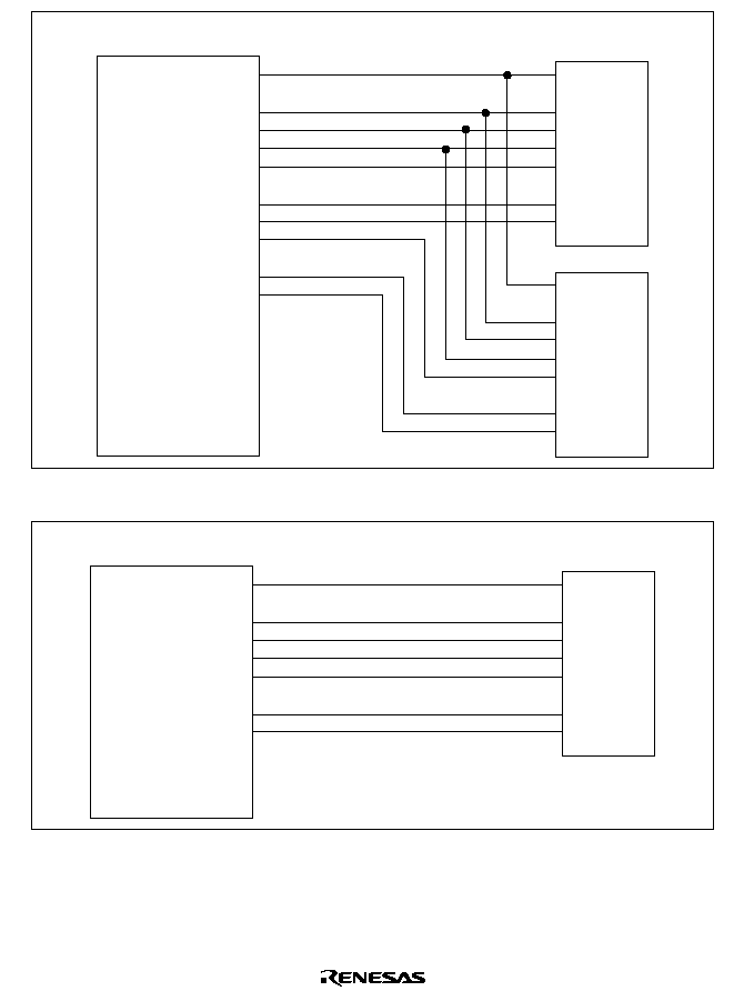
284
A17
A1
CSn
RD
D15
D8
DQMLU/
WE1
D7
D0
DQMLL/
WE0
A16
A0
CS
OE
I/O7
I/O0
WE
Chip
128 k
◊
8-bit
SRAM
...
...
...
...
...
...
...
A16
A0
CS
OE
I/O7
I/O0
WE
...
...
...
...
...
...
...
Figure 7.11 Example of 16-Bit Data Width SRAM Connection
A16
A0
CSn
RD
D7
D0
DQMLL/
WE0
A16
A0
CS
OE
I/O7
I/O0
WE
Chip
128 k
◊
8-bit
SRAM
...
...
...
...
...
...
...
...
Figure 7.12 Example of 8-Bit Data Width SRAM Connection

285
7.4.2
Wait State Control
The number of wait states inserted into ordinary space access states can be controlled using the
WCR1, WCR2, BCR1 and BCR3 register settings. When the Wn1 and Wn0 wait specification bits
in WCR1, WCR2 for the given CS space are 01 or 10, software waits are inserted according to the
wait specification. When Wn1 and Wn0 are 11, wait cycles are inserted according to the long wait
specification bit AnLW in BCR1, BCR3. The long wait specification in BCR1, BCR3 can be
made independently for CS0, CS1 and CS4 spaces, but the same value must be specified for CS2
and CS3 spaces. All WCR1 specifications are independent. By means of WCR1, WCR2, BCR1,
and BCR3, a Tw cycle is inserted as a wait cycle as long as the number of specified cycles at the
wait timing for ordinary access space shown in figure 7.13. The names of the control bits that
specify Tw for each CS space are shown in table 7.5.
T1
Tw
CKIO
A24≠A0
CSn
RD/
WR
RD
D31≠D0
WEn
D31≠D0
BS
DACKn
*
Read
Write
T2
Note:
*
DACKn waveform when active≠low is specified.
Figure 7.13 Wait Timing of Ordinary Space Access (Software Wait Only)

286
Table 7.5
CSn Spaces and Tw Specification Bits
BCR3
BCR1
WCR1
WCR2
Tw
CS0
A0LW2
A0LW1
A0LW0
W01
W00
--
--
0≠14
CS1
A1LW2
A1LW1
A2LW0
W11
W10
--
--
0≠14
CS2
AHLW2
AHLW1
AHLW0
W21
W20
--
--
0≠14
CS3
AHLW2
AHLW1
AHLW0
W31
W30
--
--
0≠14
CS4
A4LW2
A4LW1
A4LW0
--
--
W41
W40
0≠14
When a wait is specified by software using WCR1 and WCR2 (Wn1, Wn0), and the external wait
mask bit (AnWM) is cleared to 0 in WCR2, the wait input
WAIT signal from outside is sampled.
Figure 7.14 shows
WAIT signal sampling. A 2-cycle wait is specified as a software wait. The
sampling is performed when the Tw state shifts to the T2 state, so there is no effect even when the
WAIT signal is asserted in the T1 cycle or the first Tw cycle. The WAIT signal is sampled at the
clock fall.

287
T1
Tw
CKIO
A24≠A0
CSn
RD/
WR
RD
D31≠D0
WEn
D31≠D0
WAIT
BS
DACKn
*
Read
Write
Tw
Twx
T2
Wait states
from
WAIT
signal input
Note:
*
DACKn waveform when active-low is specified.
Figure 7.14 Wait State Timing of Ordinary Space Access
(Wait States from
WAIT Signal)
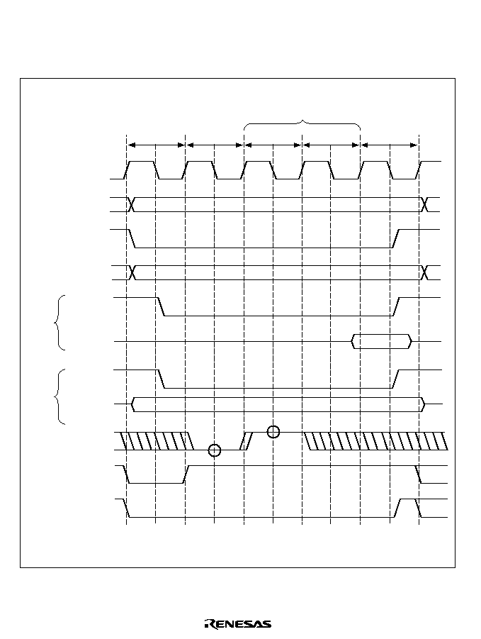
288
For the CS0≠CS3 spaces,
CSn, RD, and WEn are negated for one cycle after negation of the
external wait signal is accepted, as shown in figure 7.14. For the CS4 space, the number of cycles
before
CSn, RD, and WEn are negated after acceptance of external wait negation can be set as 1,
2, or 4 by means of bits A4WD1 and A4WD0 in WCR2. Figure 7.15 shows an example.
T1
Tw
CKIO
A24≠A0
CSn
RD/
WR
RD
D15≠D0
WEn
D15≠D0
WAIT
BS
DACKn
*
Read
Write
Twx
Twx
T2
Specified by A4WD1 and
A4WD0 in WCR2
(A4WD1, A4WD0 = 01)
Note:
*
DACKn waveform when active-low is specified.
Figure 7.15 Wait State Timing of Ordinary Space in CS4 Space
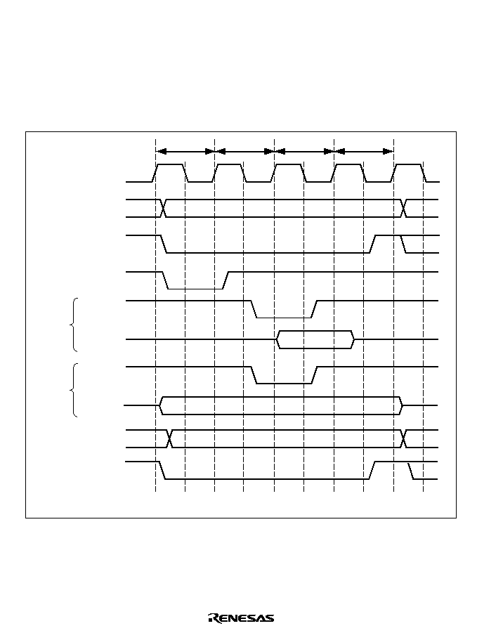
289
7.4.3
CS Assertion Period Extension
Idle cycles can be inserted to prevent extension of the
RD or WEn assertion period beyond the
length of the
CSn assertion period by setting control bits in WCR3. This allows for flexible
interfacing to external circuit. The timing is shown in figure 7.16. Th and Tf cycles are added
respectively before and after the ordinary cycle. Signals other than
RD and WEn are asserted in
this cycle, but
RD and WEn are not. In addition, data is extended up to the Tf cycle, which is
effective for devices with slow write operations.
CKIO
Address
CSn
BS
RD
Data
WEn
Data
Th
T1
T2
Tf
DACKn
*
RD/
WR
Read
Write
Note:
*
DACKn waveform when active-low is specified.
Figure 7.16
CS Assertion Period Extension Function

290
For the CS0≠CS4 spaces, For spaces CS0--CS4, Th and Tf can be set as follows.
Th
Tf
WCR3
CS0--3
0--2
0--2
AnSW1, AnSW0 (Th = Tf) n =0--3
CS4
0--7
0--5
Th: A4SW2--0
Tf: A4HW1--0
7.5
Synchronous DRAM Interface
7.5.1
Synchronous DRAM Direct Connection
Seven kinds of synchronous DRAM can be connected: 2-Mbit (128k
◊
16), 4-Mbit (256k
◊
16),
16-Mbit (1M
◊
16, 2M
◊
8, and 4M
◊
4), and 64-Mbit (4M
◊
16 and 8M
◊
8). This chip supports
64-Mbit synchronous DRAMs internally divided into two or four banks, and other synchronous
DRAMs internally divided into two banks. Since synchronous DRAM can be selected by the
CS
signal, CS2 and CS3 spaces can be connected using a common
RAS or other control signal.
When
the memory enable bits for DRAM and other memory (DRAM2≠DRAM0) in BCR1 are set to
001, CS2 is ordinary space and CS3 is synchronous DRAM space. When the DRAM2≠0 bits are
set to 100, CS2 is synchronous DRAM space and CS3 is ordinary space. When the bits are set to
101, both CS2 and CS3 are synchronous DRAM spaces.
Supported synchronous DRAM operating modes are burst read/single write mode (initial setting)
and burst read/burst write mode. The burst length depends on the data bus width, comprising 8
bursts for a 16-bit width, and 4 bursts for a 32-bit width. The data bus width is specified by the SZ
bit in MCR. Burst operation is always performed, so the burst enable (BE) bit in MCR is ignored.
Switching to burst write mode is performed by means of the BWE bit in BCR3.
Control signals for directly connecting synchronous DRAM are the
RAS, CAS/OE, RD/WR, CS2
or
CS3, DQMUU, DQMUL, DQMLU, DQMLL, and CKE signals
.
Signals other than
CS2 and
CS3 are common to every area, and signals other than CKE are valid and fetched only when CS2
or
CS3 is true
.
Therefore, synchronous DRAM can be connected in parallel in multiple areas.
CKE is negated (to the low level) only when a self-refresh is performed; otherwise it is always
asserted (to the high level).
Commands can be specified for synchronous DRAM using the
RAS, CAS/OE, RD/WR, and
certain address signals. These commands are NOP, auto-refresh (REF), self-refresh (SELF), all-
bank precharge (PALL), specific bank precharge (PRE), row address strobe/bank active (ACTV),
read (READ), read with precharge (READA), write (WRIT), write with precharge (WRITA), and
mode register write (MRS).
Bytes are specified using DQMUU, DQMUL, DQMLU, and DQMLL. The read/write is
performed on the byte whose DQM is low. For 32-bit data, DQMUU specifies 4n address access
and DQMLL specifies 4n + 3 address access. For 16-bit data, only DQMLU and DQMLL are

291
used. Figure 7.17 shows an example in which a 32-bit connection uses a 256k
◊
16 bit
synchronous DRAM. Figure 7.18 shows an example with a 16-bit connection.
A11
A2
CKIO
CKE
CSn
RAS
CAS
/
OE
RD/
WR
D31
D16
DQMUU/
WE3
DQMUL/
WE2
D15
D0
DQMLU/
WE1
DQMLL/
WE0
A9
A0
CLK
CKE
CS
RAS
CAS
WE
I/O15
I/O0
DQMU
DQML
Chip
256 k
◊
16-bit
synchronous
DRAM
...
...
...
...
...
...
...
...
A9
A0
CLK
CKE
CS
RAS
CAS
WE
I/O15
I/O0
DQMU
DQML
...
...
...
...
...
...
Figure 7.17 Synchronous DRAM 32-bit Device Connection
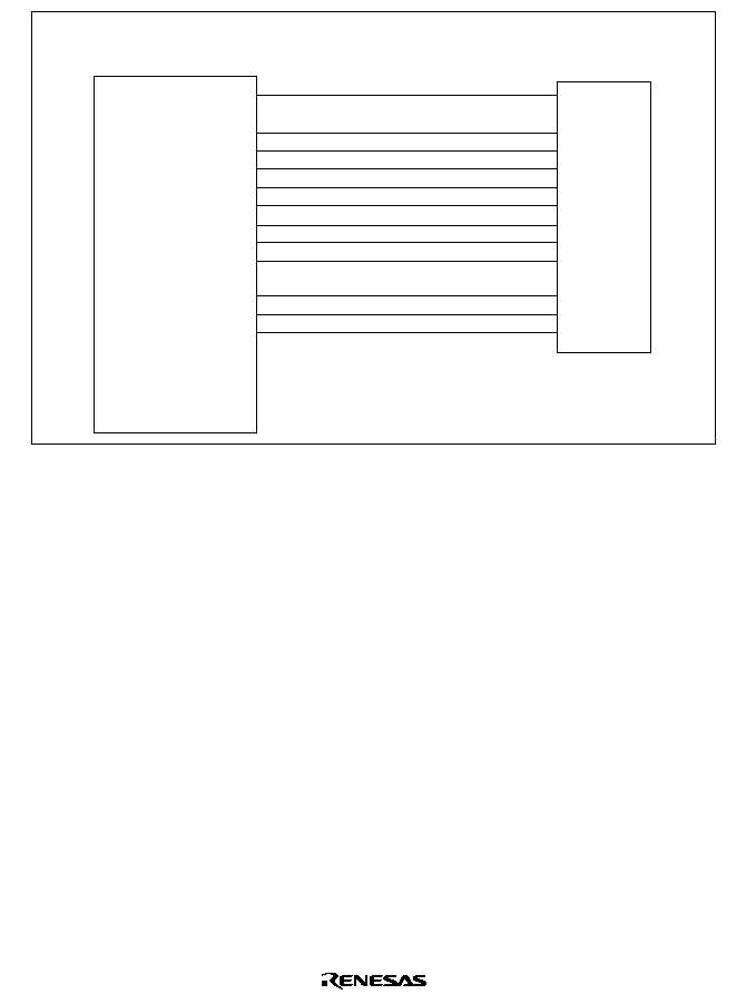
292
A10
A1
CKIO
CKE
CSn
RAS
CAS
/
OE
RD/
WR
D15
D0
DQMLU/
WE1
DQMLL/
WE0
A9
A0
CLK
CKE
CS
RAS
CAS
WE
I/O15
I/O0
DQMU
DQML
Chip
256 k
◊
16-bit
synchronous
DRAM
...
...
...
...
...
...
...
...
Figure 7.18 Synchronous DRAM 16-bit Device Connection
7.5.2
Address Multiplexing
Addresses are multiplexed according to the MCR's address multiplex specification bits AMX2≠
AMX0 and size specification bit SZ so that synchronous DRAMs can be connected to the SH7616
directly without an external multiplex circuit
.
Table 7.6 shows the relationship between the
multiplex specification bits and bit output to the address pins.
A24≠A16 always output the original value regardless of multiplexing.
When SZ = 0, the data width on the synchronous DRAM side is 16 bits and the LSB of the
device's address pins (A0) specifies word address. The A0 pin of the synchronous DRAM is thus
connected to the A1 pin of the SH7616, the rest of the connection proceeding in the same order,
beginning with the A1 pin to the A2 pin.
When SZ = 1, the data width on the synchronous DRAM side is 32 bits and the LSB of the
device's address pins (A0) specifies longword address. The A0 pin of the synchronous DRAM is
thus connected to the A2 pin of the SH7616, the rest of the connection proceeding in the same
order, beginning with the A1 pin to the A3 pin.

293
Table 7.6
SZ and AMX Bits and Address Multiplex Output
Setting
External Address Pins
SZ
AMX2 AMX1 AMX0
Output
Timing
A1≠A8
A9
A10
A11
A12
A13
A14
A15
1
0
0
0
Column
address
A1≠A8
A9
A10
A11
L/H
*
1
A21
*
2
A14
A15
Row
address
A9≠A16
A17
A18
A19
A20
A21
*
2
A22
A23
1
0
0
1
Column
address
A1≠A8
A9
A10
A11
L/H
*
1
A22
*
2
A14
A15
Row
address
A10≠A17 A18
A19
A20
A21
A22
*
2
A23
A24
1
0
1
0
Column
address
A1≠A8
A9
A10
A11
L/H
*
1
A23
*
2
A14
A15
Row
address
A11≠A18 A19
A20
A21
A22
A23
*
2
A24
A25
1
0
1
1
Column
address
A1≠A8
A9
L/H
*
1
A19
*
2
A12
A13
A14
A15
Row
address
A9≠A16
A17
A18
A19
*
2
A20
A21
A22
A23
1
1
0
0
Column
address
A1≠A8
A9
A10
A11
L/H
*
1
A13
A22
*
3
A23
*
2
Row
address
A9≠A16
A17
A18
A19
A20
A21
A22
*
3
A23
*
2
1
1
0
1
Column
address
A1≠A8
A9
A10
A11
L/H
*
1
A13
A23
*
3
A24
*
2
Row
address
A10≠A17 A18
A19
A20
A21
A22
A23
*
3
A24
*
2
1
1
1
1
Column
address
A1≠A8
A9
L/H
*
1
A18
*
2
A12
A13
A14
A15
Row
address
A9≠A16
A17
A17
A18
*
2
A20
A21
A22
A23
0
0
0
0
Column
address
A1≠A8
A9
A10
L/H
*
1
A20
*
2
A13
A14
A15
Row
address
A9≠A16
A17
A18
A19
A20
*
2
A21
A22
A23

294
Table 7.6
SZ and AMX Bits and Address Multiplex Output (cont)
Setting
External Address Pins
SZ
AMX2 AMX1 AMX0
Output
Timing
A1≠A8
A9
A10
A11
A12
A13
A14
A15
0
1
0
0
Column
address
A1≠A8
A9
A10
LH
*
1
A12
A21
*
3
A22
*
2
A15
Row
address
A9≠A16
A17
A18
A19
A20
A21
*
3
A22
*
2
A23
0
0
1
1
Column
address
A1≠A8
L/H
*
1
A18
*
2
A11
A12
A13
A14
A15
Row
address
A9≠A16
A17
A18
*
2
A19
A20
A21
A22
A23
0
1
1
1
Column
address
A1≠A8
L/H
*
1
A17
*
2
A11
A12
A13
A14
A15
Row
address
A9≠A16
A16
A17
*
2
A19
A20
A21
A22
A23
Notes: AMX2≠AMX0 setting 110 is reserved and must not be used. When SZ = 0, AMX2≠AMX0
settings 001, 010, and 101 are also reserved and must not be used.
*
1 L/H is a bit used to specify commands. It is fixed at L or H according to the access
mode.
*
2 Bank address specification.
*
3 Bank address specification when using four banks.
7.5.3
Burst Reads
Figure 7.19 (a) and (b) show the timing charts for burst reads. In the following example, 2
synchronous DRAMs of 256k
◊
16 bits are connected, the data width is 32 bits and the burst
length is 4. After a Tr cycle that performs ACTV command output, a READA command is issued
in the Tc cycle, read data is accepted in cycles Td1 to Td4, and the end of the read sequence is
waited for in the Tde cycle. One Tde cycle is issued when I¯ : E¯
1 : 1, and two cycles when I¯
: E¯ = 1 : 1. Tap is a cycle for waiting for the completion of the auto-precharge based on the
READA command within the synchronous DRAM. During this period, no new access commands
are issued to the same bank. Accesses of the other bank of the synchronous DRAM by another CS
space are possible. Depending on the TRP1, TRP0 specification in MCR, the chip determines the
number of Tap cycles and does not issue a command to the same bank during that period.
Figure 7.19 (a) and (b) show examples of the basic cycle. Because a slower synchronous DRAM is
connected, setting WCR1 and MCR bits can extend the cycle. The number of cycles from the
ACTV command output cycle Tr to the READA command output cycle Tc can be specified by
bits RCD1 and RCD0 in MCR. 00 specifies 1 cycle, 01 specifies 2 cycles, and 10 specifies 3
cycles. For 2 or 3 cycles, a NOP command issue cycle Trw for the synchronous DRAM is inserted
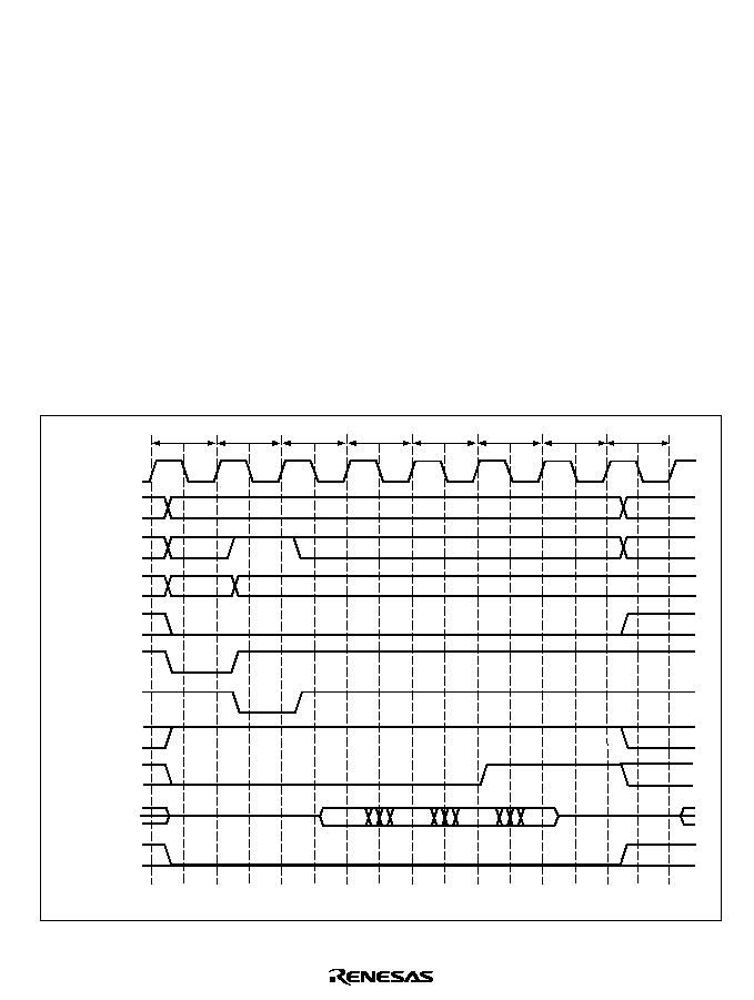
295
between the Tr cycle and the Tc cycle. The number of cycles between the READA command
output cycle Tc and the initial read data fetch cycle Td1 can be specified between 1 cycle and 4
cycles using the W21/W20 and W31/W30 bits in WCR1. The number of cycles at this time
corresponds to the number of CAS latency cycles of the synchronous DRAM. When 2 cycles or
more, a NOP command issue cycle Tw is inserted between the Tc cycle and the Td1 cycle. The
number of cycles in the precharge completion waiting cycle Tap is specified by bits TRP1 and
TRP0 in MCR. When CAS latency is 1, a Tap cycle comprising the number of cycles specified by
TRP1 and TRP0 is generated. When the CAS latency is 2 or more, a Tap cycle equal to the TRP
specification ≠ 1 is generated. During the Tap cycle, no commands other than NOP are issued to
the same bank. Figure 7.20 (a) and (b) show examples of burst read timing when RCD1/RCD0 is
01, W31/W30 is 01, and TRP1/TRP0 is 01.
When the data width is 16 bits, 8 burst cycles are required for a 16-byte data transfer. The data
fetch cycle goes from Td1 to Td8.
Synchronous DRAM CAS latency is up to 3 cycles, but the CAS latency of the bus state controller
can be specified up to 4. This is so that circuits containing latches can be installed between
synchronous DRAMs and the chip.
Tr
Tc
CKIO
A24≠A11
A10
A9≠A1
CS2
or
CS3
RAS
CAS
RD/
WR
DQMxx
D31≠D0
DACKn
*
Td1
Td2
Td3
Td4
Tde
Tap
Note:
*
DACKn waveform when active-low is specified.
Figure 7.19 (a) Basic Burst Read Timing (Auto-Precharge) I
: E
other than 1 : 1

296
Tr
Tc
CKIO
A24≠A11
A10
A9≠A1
CS2
or
CS3
RAS
CAS
RD/
WR
DQMxx
D31≠D0
DACKn
*
Td1
Td2
Td3
Td4
Tde
Tde
Tap
Note:
*
DACKn waveform when active-low is specified.
Figure 7.19 (b) Basic Burst Read Timing (Auto-Precharge) I
: E
= 1 : 1
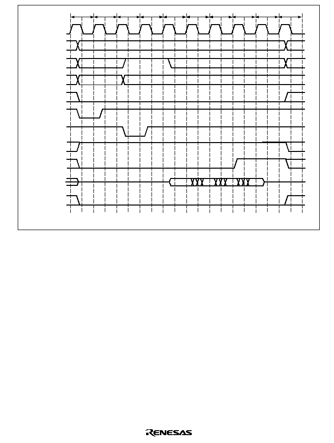
297
Tr
CKIO
A24≠A11
A10
A9≠A1
CS2
or
CS3
RAS
CAS
RD/
WR
DQMxx
D31≠D0
DACKn
*
TrW
Tc
Tw
Td1
Td2
Td3
Td4
Tde
Tap
Note:
*
DACKn waveform when active-low is specified.
Figure 7.20 (a) Burst Read Wait Specification Timing (Auto-Precharge)
I
: E
other than 1 : 1
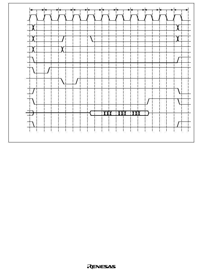
298
Tr
CKIO
A24≠A11
A10
A9≠A1
CS2
or
CS3
RAS
CAS
RD/
WR
DQMxx
D31≠D0
DACKn
*
TrW
Tc
Tw
Td1
Td2
Td3
Td4
Tde
Tde
Tap
Note:
*
DACKn waveform when active-low is specified.
Figure 7.20 (b) Burst Read Wait Specification Timing (Auto-Precharge) I
: E
= 1 : 1

299
7.5.4
Single Reads
When a cache area is accessed and there is a cache miss, the cache fill cycle is performed in 16-
byte units. This means that all the data read in the burst read is valid. On the other hand, when a
cache-through area is accessed the required data is a maximum length of 32 bits, and the
remaining 12 bytes are wasted. The same kind of wasted data access is produced when
synchronous DRAM is specified as the source in a DMA transfer by the DMAC and the transfer
unit is other than 16 bytes. Figure 7.21 (a) and (b) show the timings of a single address read.
Because the synchronous DRAM is set to the burst read mode, the read data output continues after
the required data is received. To avoid data conflict, an empty read cycle is performed from Td2 to
Td4 after the required data is read in Td1 and the device waits for the end of synchronous DRAM
operation.
When the data width is 16 bits, the number of burst transfers during a read is 8. Data is fetched in
cache-through and other DMA read cycles only in the Td1 and Td2 cycles (of the 8 cycles from
Td1 to Td8) for longword accesses, and only in the Td1 cycle for word or byte accesses.
Empty cycles tend to increase the memory access time, lower the program execution speed, and
lower the DMA transfer speed, so it is important to avoid accessing unnecessary cache-through
areas and to use data structures that enable 16-byte unit transfers by placing data on 16-byte
boundaries when performing DMA transfers that specify synchronous DRAM as the source.

300
Tr
Tc
CKIO
A24≠A11
A10
A9≠A1
CS2
or
CS3
RAS
CAS
RD/
WR
DQMxx
D31≠D0
DACKn
*
Td1
Td2
Td3
Td4
Tde
Tap
Note:
*
DACKn waveform when active-low is specified.
Figure 7.21 (a) Single Read Timing (Auto-Precharge) I
: E
other than 1 : 1
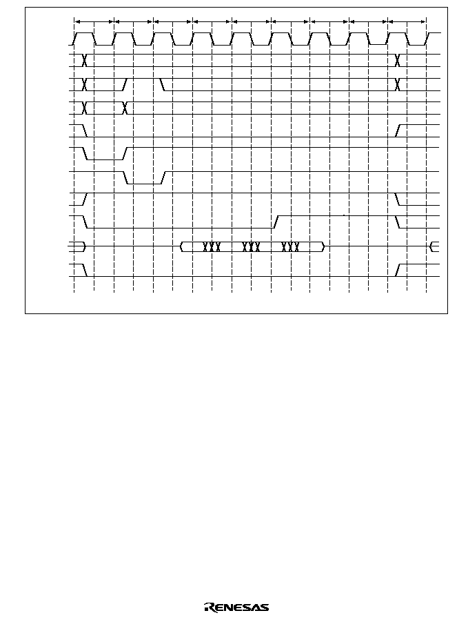
301
Tr
Tc
CKIO
A24≠A11
A10
A9≠A1
CS2
or
CS3
RAS
CAS
RD/
WR
DQMxx
D31≠D0
DACKn
*
Td1
Td2
Td3
Td4
Tde
Tde
Tap
Note:
*
DACKn waveform when active-low is specified.
Figure 7.21 (b) Single Read Timing (Auto-Precharge) I
: E
= 1 : 1
7.5.5
Single Writes
Synchronous DRAM writes are executed as single writes or burst writes according to the
specification by the BWE bit in BCR3. Figure 7.22 shows the basic timing chart for single write
accesses. After the ACTV command Tr, a WRITA command is issued in Tc to perform an auto-
precharge. In the write cycle, the write data is output simultaneously with the write command.
When writing with an auto-precharge, the bank is precharged after the completion of the write
command within the synchronous DRAM, so no command can be issued to that bank until the
precharge is completed. For that reason, besides a Tap cycle to wait for the precharge during read
accesses, a Trw1 cycle is added to wait until the precharge is started, and the issuing of any new
commands to the same bank is delayed during this period. The number of cycles in the Trw1 cycle
can be specified using the TRWL1 and TRWL0 bits in MCR.

302
Tr
Tc
CKIO
A24≠A11
A10
A9≠A1
CS2
or
CS3
RAS
CAS
RD/
WR
DQMxx
D31≠D0
DACKn
*
Trwl
Tap
Note:
*
DACKn waveform when active-low is specified.
Figure 7.22 Basic Single Write Cycle Timing (Auto-Precharge)
7.5.6
Burst Write Mode
Burst write mode can be selected by setting the BWE bit to 1 in BCR3. The basic timing charts for
burst write access is shown in figure 7.23 (a) and (b). This example assumes a 32-bit bus width
and a burst length of 4. In the burst write cycle, the WRITA command that performs auto-
precharge is issued in Tc1 following the ACTV command Tr cycle. The first 4 bytes of write data
are output simultaneously with the WRITA command in Tc1, and the remaining 12 bytes of data
are output consecutively in Tc2, Tc3, and Tc4. In a write with auto-precharge, as with a single
write, a Trw1 cycle that provides the waiting time until precharge is started is inserted after output
of the write data, followed by a Tap cycle for the precharge wait in a write access. The Trw1 and
Tap cycles can be set respectively in MCR by bits TRWL1 and TRWL0, and bits TRP1 and
TRP0.

303
When a single write is performed in burst write mode, the synchronous DRAM setting is for a
burst length of 4. After data is written in Tc1, empty writes are performed in Tc2, Tc3, and Tc4 by
driving the DQMxx signal high.
These empty cycles increase the memory access time and tend to reduce program execution speed
and DMA transfer speed. Therefore, unnecessary cache-through area accesses should be avoided,
and copy-back should be selected for the cache setting. Also, in DMA transfer, it is important to
use a data structure that allows transfer in 16-bit units.
Tr
Tc1
CKIO
A24≠A11
A10
A9≠A1
CS2
or
CS3
RAS
CAS
RD/
WR
DQMxx
D31≠D0
DACKn
*
Tc2
Tc3
Tc4
Trwl
Tap
Note:
*
DACKn waveform when active-low is specified.
Figure 7.23 (a) Basic Burst Write Timing (Auto-Precharge) I
: E
other than 1 : 1
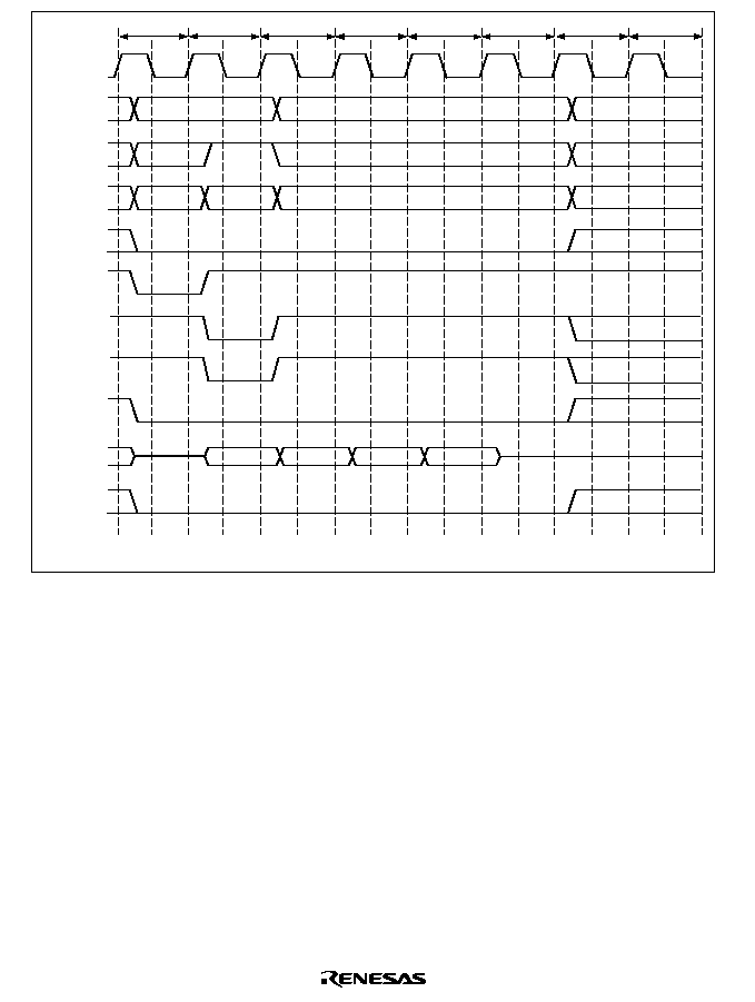
304
Tr
Tc1
CKIO
A24≠A11
A10
A9≠A1
CS2
or
CS3
RAS
CAS
RD/
WR
DQMxx
D31≠D0
DACKn
*
Tc2
Tc3
Tc4
Trwl
Tap
Tde
Note:
*
DACKn waveform when active-low is specified.
Figure 7.23 (b) Basic Burst Write Timing (Auto-Precharge) I
: E
= 1 : 1

305
7.5.7
Bank Active Function
A synchronous DRAM bank function is used to support high-speed accesses of the same row
address. When the RASD bit in MCR is set to 1, read/write accesses are performed using
commands without auto-precharge (READ, WRIT). In this case, even when the access is
completed, no precharge is performed. This function is not supported in the CS2 space. When the
bank active function is used, no precharge is performed when the access is completed. When
accessing the same row address in the same bank, a READ or WRIT command can be called
immediately without calling an ACTV command, just like the
RAS down mode of the DRAM's
high-speed page mode
.
Synchronous DRAM is divided into two banks,
so one row address in each
can stay active. When the next access is to a different row address, a PRE command is called first
to precharge the bank, and access is performed by an ACTV command and READ or WRIT
command in order, after the precharge is completed. With successive accesses to different row
addresses, the precharge is performed after the access request occurs, so the access time is longer.
When writing, performing an auto-precharge means that no command can be called for t
RWL
+
t
AP
cycles after a WRITA command is called. When the bank active mode is used, READ or
WRIT commands can be issued consecutively if the row address is the same. This shortens the
number of cycles by t
RWL
+ t
AP
for each write. The number of cycles between the issue of the
precharge command and the row address strobe command is determined by the TRP1, TRP0 in
MCR.
Whether execution is faster when the bank active mode is used or when basic access is used is
determined by the proportion of accesses to the same row address (P1) and the average number of
cycles from the end of one access to the next access (t
A
). When tA is longer than t
AP
, the delay
waiting for the precharge during a read becomes invisible. If t
A
is longer than t
RWL
+ t
AP
, the
delay waiting for the precharge also becomes invisible during writes. The difference between the
bank active mode and basic access speeds in these cases is the number of cycles between the start
of access and the issue of the read/write command: (t
RP
+ t
RCD
)
◊
(1 ≠ P1) and t
RCD
,
respectively.
The time that a bank can be kept active, t
RAS
, is limited. When the period will be provided by
program execution, and it is not assured that another row address will be accessed without a hit to
the cache, the synchronous DRAM must be set to auto-refresh and the refresh cycle must be set to
the maximum value t
RAS
or less. This enables the limit on the maximum active period for each
bank to be ensured. When auto-refresh is not being used, some measure must be taken in the
program to ensure that the bank does not stay active for longer than the prescribed period.
Figure 7.24 (a) and (b) show burst read cycles that is not an auto-precharge cycle, figure 7.25 (a)
and (b) show burst read cycles to a same row address, figure 7.26 (a) and (b) show burst read
cycles to different row addresses, figure 7.27 shows a write cycle without auto-precharge, figure
7.28 shows a write cycle to a same row address, and figure 7.29 shows a write cycle to different
row addresses.
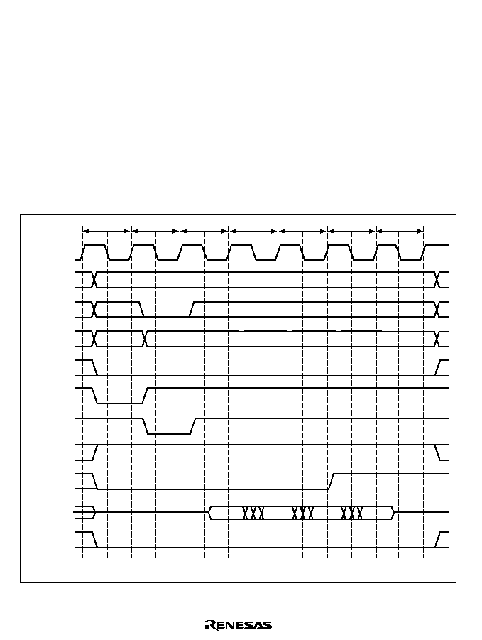
306
In figure 7.25, a cycle that does nothing, Tnop, is inserted before the Tc cycle that issues the
READ command. Synchronous DRAMs have a 2 cycle latency during reads for the DQMxx
signals that specify bytes. If the Tc cycle is performed immediately without inserting a Tnop
cycle, the DQMxx signal for the Td1 cycle data output cannot be specified. This is why the Tnop
cycle is inserted. When the CAS latency is 2 or more, however, the Tnop cycle is not inserted so
that timing requirements will be met even when a DQMxx signal is set after the Tc cycle.
When the bank active mode is set, the access will start with figure 7.24 or figure 7.27 and repeat
figure 7.25 or figure 7.28 for as long as the same row address continues to be accessed when only
accesses to the respective banks of the CS3 space are considered. Accesses to other CS spaces
during this period do not affect this operation. When an access occurs to a different row address
while the bank is active, figure 7.26 or figure 7.29 will be substituted for figures 7.25 and 7.28
after this is detected. Both banks will become inactive even in the bank active mode after the
refresh cycle ends or after the bus is released by bus arbitration.
Tr
Tc
CKIO
A24≠A11
A10
A9≠A1
CS3
RAS
CAS
RD
/WR
DQMxx
D31≠D0
DACKn
*
Td1
Td2
Td3
Td4
Tde
Note:
*
DACKn waveform when active-low is specified.
Figure 7.24 (a) Burst Read Timing (No Precharge) I
: E
other than 1 : 1

307
Tr
Tc
CKIO
A24≠A11
A10
A9≠A1
CS3
RAS
CAS
RD/
WR
DQMxx
D31≠D0
DACKn
*
Td1
Td2
Td3
Td4
Tde
Tde
Note:
*
DACKn waveform when active-low is specified.
Figure 7.24 (b) Burst Read Timing (No Precharge) I
: E
= 1 : 1
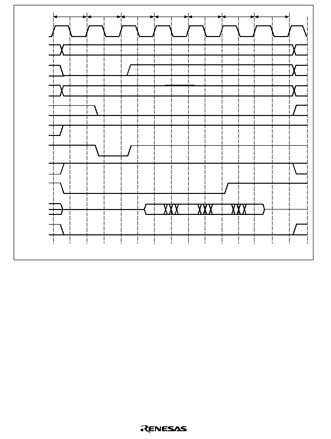
308
Tnop
CKIO
A24≠A11
A10
A9≠A1
CS3
RAS
CAS
RD/
WR
DQMxx
D31≠D0
DACKn
*
Tc
Td1
Td2
Td3
Td4
Tde
Note:
*
DACKn waveform when active-low is specified.
Figure 7.25 (a) Burst Read Timing (Bank Active, Same Row Address)
I
: E
other than 1 : 1
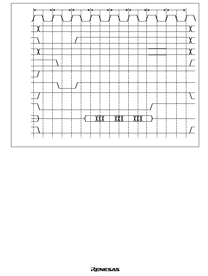
309
Tc
Tnop
CKIO
A24≠A11
A10
A9≠A1
CS3
RAS
CAS
RD/
WR
DQMxx
D31≠D0
DACKn
*
Td1
Td2
Td3
Td4
Tde
Tde
Note:
*
DACKn waveform when active-low is specified.
Figure 7.25 (b) Burst Read Timing (Bank Active, Same Row Address) I
: E
= 1 : 1
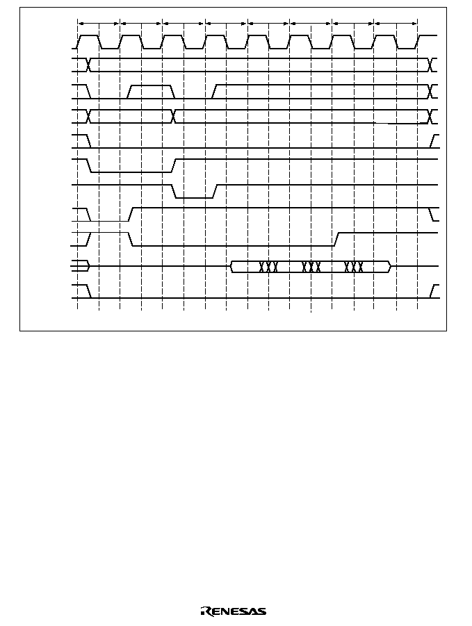
310
Tp
Tr
CKIO
A24≠A11
A10
A9≠A1
CS3
RAS
CAS
RD/
WR
DQMxx
D31≠D0
DACKn
*
Tc
Td1
Td2
Td3
Td4
Tde
Note:
*
DACKn waveform when active-low is specified.
Figure 7.26 (a) Burst Read Timing (Bank Active, Different Row Addresses)
I
: E
other than 1 : 1
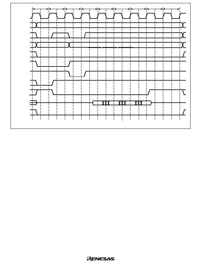
311
Tp
Tr
CKIO
A24
≠A11
A10
A9
≠A1
CS3
RAS
CAS
RD/
WR
DQMxx
D31≠D0
DACKn
*
Tc
Td1
Td2
Td3
Td4
Tde
Tde
Note:
*
DACKn waveform when active-low is specified.
Figure 7.26 (b) Burst Read Timing (Bank Active, Different Row Addresses) I
: E
= 1 : 1
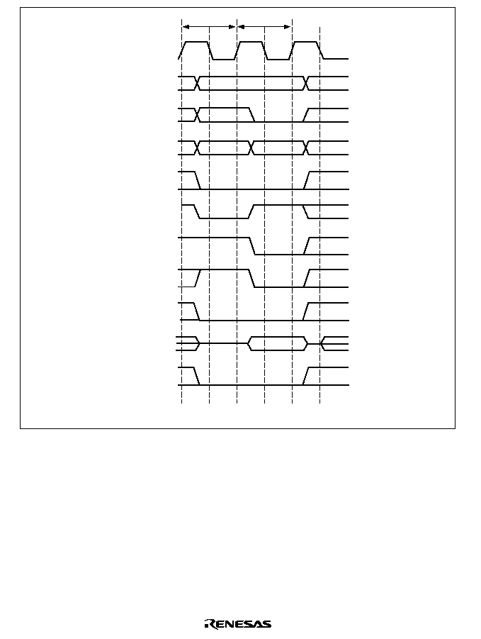
312
CKIO
A24≠A11
A10
A9≠A1
CS3
RAS
CAS
RD/
WR
DQMxx
D31≠D0
DACKn
*
Tr
Tc
Note:
*
DACKn waveform when active-low is specified.
Figure 7.27 Single Write Mode Timing (No Precharge)
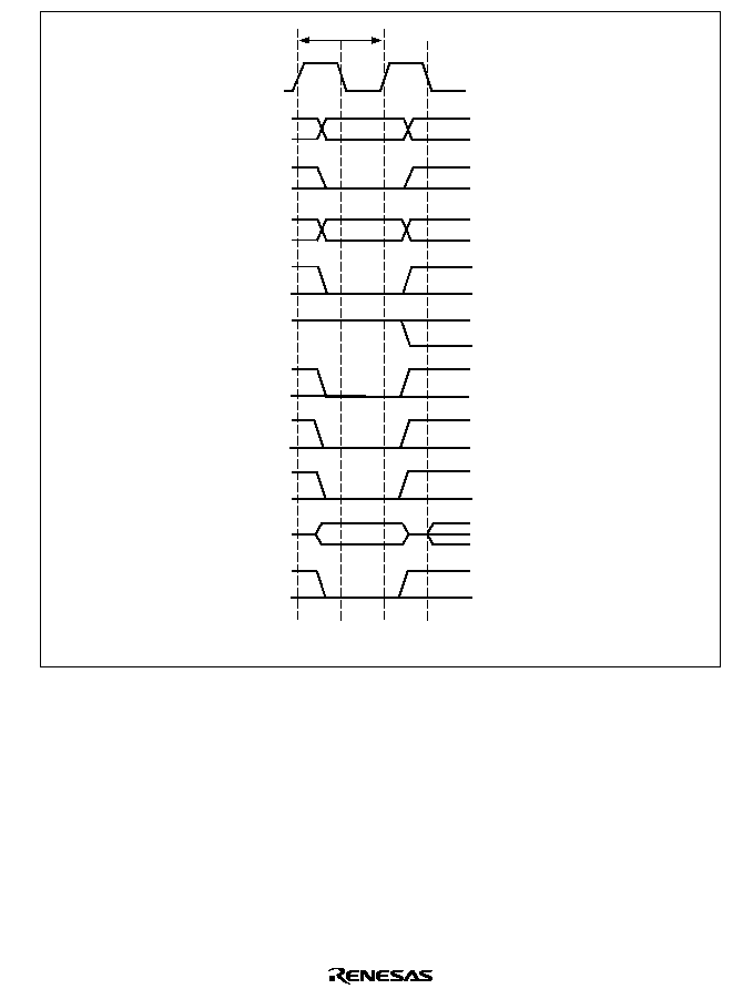
313
CKIO
A24≠A11
A10
A9≠A1
CS3
RAS
CAS
RD/
WR
DQMxx
D31≠D0
DACKn
*
Tc
Note:
*
DACKn waveform when active-low is specified.
Figure 7.28 Single Write Mode Timing (Bank Active, Same Row Address)

314
CKIO
A24≠A11
A10
A9≠A1
CS3
RAS
CAS
RD/
WR
DQMxx
D31≠D0
DACKn
*
Tp
Tr
Tc
Note:
*
DACKn waveform when active-low is specified.
Figure 7.29 Single Write Mode Timing (Bank Active, Different Row Addresses)

315
7.5.8
Refreshes
The bus state controller is equipped with a function to control refreshes of synchronous DRAM.
Auto-refreshes can be performed by setting the RMODE bit to 0 and the RFSH bit to 1 in MCR.
Consecutive refreshes can also be generated by setting the RRC2≠RRC0 bits in RTCSR. When the
synchronous DRAM is not accessed for a long period of time, set the RFSH bit and RMODE bit
both to 1 to generate self-refresh mode, which uses low power consumption to retain data.
Auto-Refresh: The number of refreshes set in the RRC2≠RRC0 bits in RTCSR are performed at
the interval determined by the input clock selected by the CKS2≠CKS0 bits in RTCSR and the
value set in RTCOR. Set the CKS2≠CKS0 bits and RTCOR so that the refresh interval
specifications of the synchronous DRAM being used are satisfied. First , set RTCOR, RTCNT,
and the RMODE and RFSH bits in MCR, then set the CKS2≠CKS0 and RRC2≠RRC0 bits in
RTCSR. When a clock is selected with the CKS2≠CKS0 bits, RTCNT starts counting up from the
value at that time. The RTCNT value is constantly compared to the RTCOR value, and when the
two values match, a refresh request is made, and the number of auto-refreshes set in RRC2≠RRC0
are performed. RTCNT is cleared to 0 at that time and the count up starts again. Figure 7.30 shows
the timing for the auto-refresh cycle.
First, a PALL command is issued during the Tp cycle to change all the banks from active to
precharge states. Then number of idle cycles equal to one less than the value set in TRP1 and
TRP0 are inserted, and a REF command is issued in the Trr cycle. After the Trr cycle, no new
commands are output for the number of cycles specified in the TRAS bit in MCR. The TRAS bit
must be set to satisfy the refresh cycle time specifications (active/active command delay time) of
the synchronous DRAM. When the set value of the TRP1 and TRP0 bits in MCR is 2 or more, an
NOP cycle is inserted between the Tp cycle and Trr cycle.
During a manual reset, no refresh request is issued, since there is no RTCNT count-up. To perform
a refresh properly, make the manual reset period shorter than the refresh cycle interval and set
RTCNT to (RTCOR ≠ 1) so that the refresh is performed immediately after the manual reset is
cleared.
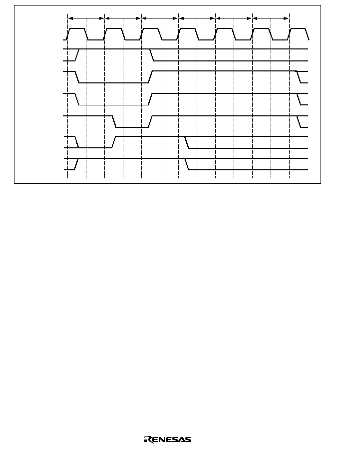
316
Tp
Trr
CKIO
A10
CS2
or
CS3
RAS
CAS
RD/
WR
DQMxx
Trc
Trc
Trc
Tre
Figure 7.30 Auto-Refresh Timing
Self-Refreshes: The self-refresh mode is a type of standby mode that produces refresh timing and
refresh addresses within the synchronous DRAM. It is started up by setting the RMODE and
RFSH bits to 1. The synchronous DRAM is in self-refresh mode when the CKE signal level is
low. During the self-refresh, the synchronous DRAM cannot be accessed. To clear the self-refresh,
set the RMODE bit to 0. After self-refresh mode is cleared, issuing of commands is prohibited for
the number of cycles specified in the TRAS1 and TRAS0 bits in MCR. Figure 7.31 shows the self-
refresh timing. Settings must be made so that self-refresh clearing and data retention are
performed correctly, and auto-refreshing is performed without delay at the correct intervals. When
self-refresh mode is entered while the synchronous DRAM is set for auto-refresh or when leaving
the standby mode with a manual reset or NMI, auto-refresh can be re-started if RFSH is 1 and
RMODE is 0 when the self-refresh mode is cleared. When time is required between clearing the
self-refresh mode and starting the auto-refresh mode, this time must be reflected in the initial
RTCNT setting. When the RTCNT value is set to RTCOR ≠ 1, the refresh can be started
immediately.
If the standby function of the chip is used to enter the standby mode after the self-refresh mode is
set, the self-refresh state continues; the self-refresh state will also be maintained after returning
from a standby using an NMI. A manual reset cannot be used to exit the self-refresh state either.
During a power-on reset, the bus state controller register is initialized, so the self-refresh state is
ended.

317
Refresh Requests and Bus Cycle Requests: When a refresh request occurs while a bus cycle is
executing, the refresh will not be executed until the bus cycle is completed. When a refresh request
occurs while the bus is released using the bus arbitration function, the refresh will not be executed
until the bus is recaptured. In the SH7616, the REFOUT pin is provided to send a signal
requesting the bus right during the wait for refreshing to be executed. REFOUT is asserted until
the bus is acquired. If RTCNT and RTCOR match and a new refresh request occurs while waiting
for the refresh to execute, the previous refresh request is erased. To make sure the refresh executes
properly, be sure that the bus cycle and bus capture do not exceed the refresh interval.
If a bus arbitration request occurs during a self-refresh, the bus is not released until the self-refresh
is cleared.
Tp
CKIO
CKE
A10
CS2
or
CS3
RAS
CAS
RD/
WR
DQMxx
Trr
Trc
Trc
Trc
Trc
Trc
Tre
Figure 7.31 Self-Refresh Timing
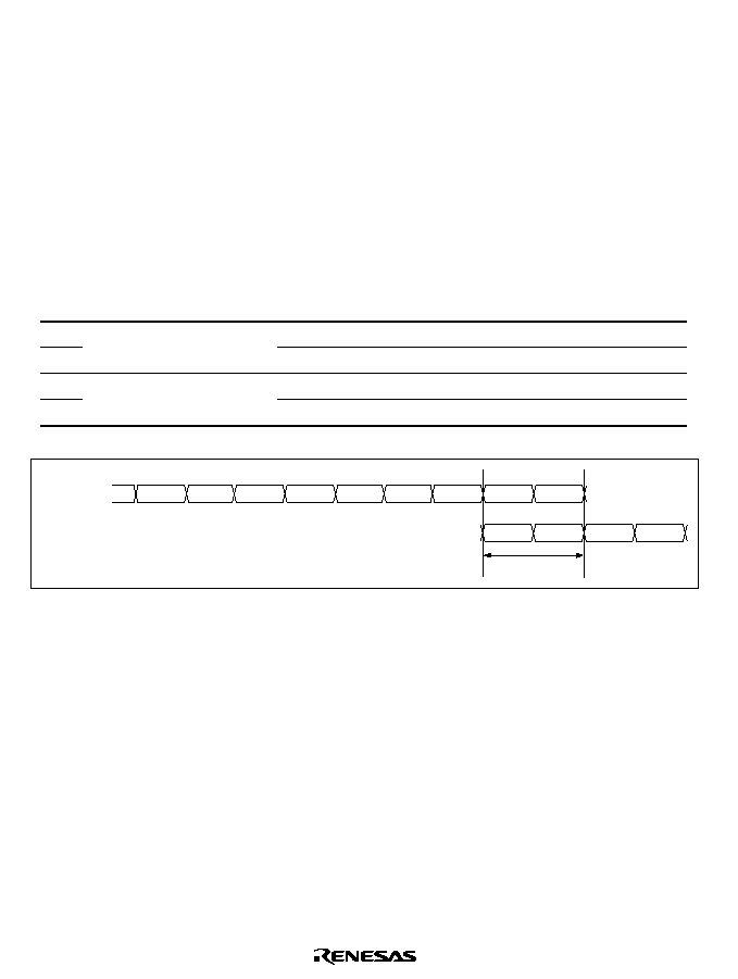
318
7.5.9
Overlap Between Auto Precharge Cycle (Tap) and Next Access
If the CPU and DMAC or E-DMAC are accessed sequentially and the first access is to SDRAM
and also in the auto precharge mode, the auto precharge cycle (Tap) of the first access may overlap
the second access if the second access is to a different memory space or to a different bank of the
same SDRAM. (Even if the second access is to the normal space, there may be an overlap with the
Tap cycle.) For this reason, it appears for the number of cycles of the second access as if access
takes place sooner (by the number of Tap cycles) than it actually does. Specific cases in which an
overlap occurs are listed in table 7.7. Also, figure 7.32 shows is a conceptual diagram of an
overlap that occurs when memory spaces CS2 and CS3 are connected to SDRAM (table 7.7, No.
3).
Table 7.7
Cases of Overlap Between Tap Cycle and Next Access
No.
First Access
Second Access
1
Space CS3, auto precharge
Access to different space among CS0, CS1, CS2, and CS3
2
mode
Access to different bank in CS3
3
Space CS2, auto precharge
Access to different space among CS0, CS1, CS2, and CS3
4
mode
Access to different bank in CS2
First access
to CS2 space
Tr
Tc
Td1
Td2
Td4
Tde
Tap
Tap
Td3
Tr
Tc
Td1
Td2
Overlap
Second
access to
CS3 space
Figure 7.32 Conceptual Diagram of Overlap (Conditions: SDRAM Connected to CS2 Space
(
RAS Precharge Time Set to 2 Cycles) and SDRAM Connected to CS3 Space)

319
7.5.10
Power-On Sequence
To use synchronous DRAM, the mode must first be set after the power is turned on. To properly
initialize the synchronous DRAM, the synchronous DRAM mode register must be written to after
the registers of the bus state controller have first been set. The synchronous DRAM mode register
is set using a combination of the
CS2 or CS3 signal and the RAS, CAS/OE, and RD/WR signals.
They fetch the value of the address signal at that time. If the value to be set is X, the bus state
controller operates by writing to address X + H'FFFF0000 or X + H'FFFF8000 from the CPU,
which allows the value X to be written to the synchronous DRAM mode register. Whether X +
H'FFFF0000 or X + H'FFFF8000 is used depends on the specifications of the synchronous
DRAM. Use a value in the range H'000 to H'FFF for X. Data is ignored at this time, but the mode
is written using word as the size.
Write any data in word size to the following addresses to select the burst read single write
supported by the chip, a CAS latency of 1 to 3, a sequential wrap type, and a burst length of 8 or 4
(depending on whether the width is 16 bits or 32 bits).
∑
Burst Read/Single Write
For 16 bits:
CAS latency 1
CAS latency 2
CAS latency 3
H'FFFF0426
H'FFFF0446
H'FFFF0466
(H'FFFF8426)
(H'FFFF8446)
(H'FFFF8466)
For 32 bits:
CAS latency 1
CAS latency 2
CAS latency 3
H'FFFF0848
H'FFFF0888
H'FFFF08C8
(H'FFFF8848)
(H'FFFF8888)
(H'FFFF88C8)
To set burst read, burst write, CAS latency 1 to 3, wrap-type sequential, and burst length 8 or 4
(depending on whether the width is 16 bits or 32 bits), arbitrary data is written to the following
addresses, using the word size.
∑
Burst Read/Burst Write
16-bit width:
CAS latency 1
CAS latency 2
CAS latency 3
H'FFFF0026
H'FFFF0046
H'FFFF0066
(H'FFFF8026)
(H'FFFF8046)
(H'FFFF8066)
32-bit width:
CAS latency 1
CAS latency 2
CAS latency 3
H'FFFF0048
H'FFFF0088
H'FFFF00C8
(H'FFFF8048)
(H'FFFF8088)
(H'FFFF80C8)
Figure 7.33 shows the mode register setting timing.
Writing to address X + H'FFFF0000 or X + H'FFFF8000 first issues an all-bank precharge
command (PALL), then issues eight dummy auto-refresh commands (REF) required for the
synchronous DRAM power-on sequence. Lastly, a mode register write command (MRS) is issued.
Three idle cycles are inserted between the all-bank precharge command and the first auto-refresh
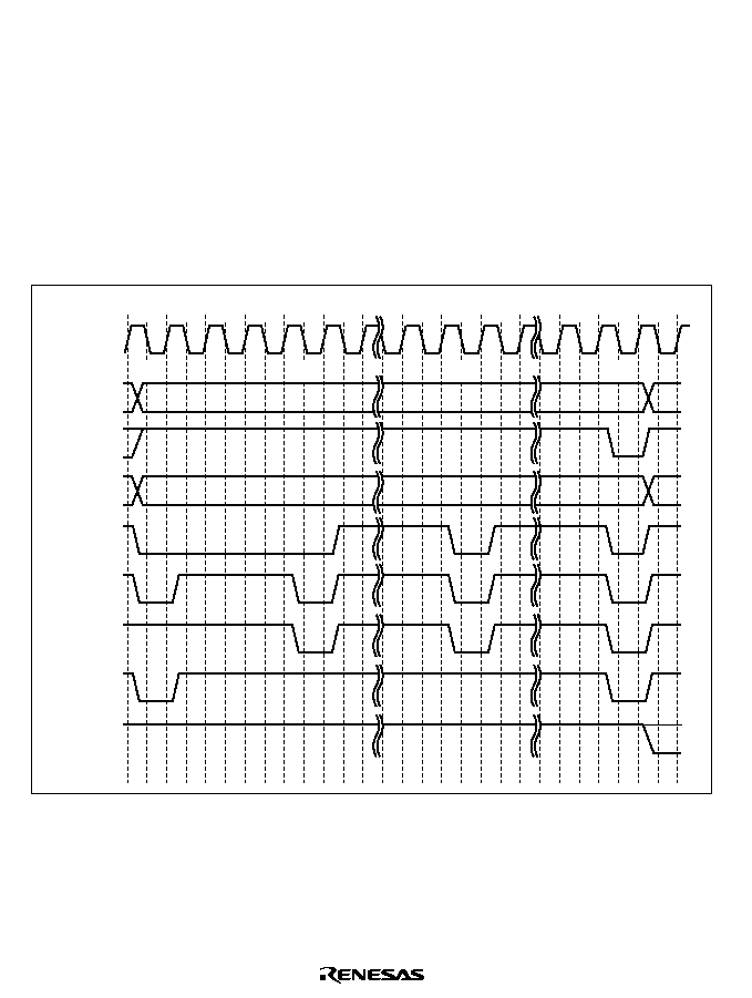
320
command, and eight idle cycles between auto-refresh commands, and between the eighth auto-
refresh command and the mode register write command, regardless of the MCR setting.
After writing to the synchronous DRAM mode register, perform a dummy read to each
synchronous DRAM bank before starting normal access. This will initialize the SH7616's internal
address comparator.
Synchronous DRAM requires a fixed idle time after powering on before the all-bank precharge
command is issued. Refer to the synchronous DRAM manual for the necessary idle time. When
the pulse width of the reset signal is longer than the idle time, the mode register may be set
immediately without problem. However, care is required if the pulse width of the reset signal is
shorter than the idle time.
Tp
Tpw
Tpw
Tpw
Trr
Trc
Trc
Trr
Trc
Trc
Tmw
CKIO
A24≠A11
A10
A9≠A1
CS2
or
CS3
RAS
CAS
RD/
WR
DQMxx
MRS
REF
REF
PALL
Figure 7.33 Synchronous DRAM Mode Write Timing

321
7.5.11
64 Mbit Synchronous DRAM (2 Mword
◊◊◊
◊
32-bit) Connection
64 Mbit Synchronous DRAM (
◊◊◊
◊
32-bit) Connection Example: Figure 7.34 shows an example
connection between the SH7616 and 64 Mbit synchronous DRAM (
◊
32-bit).
A22
A13
A12
A2
CKIO
CKE
CSn
RAS
CAS
/OE
RD/
WR
D31
D0
DQMUU/
WE3
DQMUL/
WE2
DQMLU/
WE1
DQMLL/
WE0
Chip
2 Mword
◊
32-bit SDRAM
A12
A11
A10
A0
CLK
CKE
CS
RAS
CAS
WE
I/O31
I/O0
DQMUU
DQMUL
DQMLU
DQMLL
Figure 7.34 64 Mbit Synchronous DRAM (2 Mword
◊◊◊
◊
32-bit) Connection Example
Bus Status Controller (BSC) Register Settings: Set the individual bits in the memory control
register (MCR) as follows.
MCR (bit 6) SZ = 1
MCR (bit 7) AMX2 = 0
MCR (bit 5) AMX1 = 0
MCR (bit 4) AMX0 = 0
Synchronous DRAM Mode Settings: To make mode settings for the synchronous DRAM, write
to address X+H'FFBF0000 or X+H'FFBF8000 from the CPU.. (X represents the setting value.)
Whether to use X+H'FFBF0000 or X+H'FFBF8000 determines on the synchronous DRAM used.
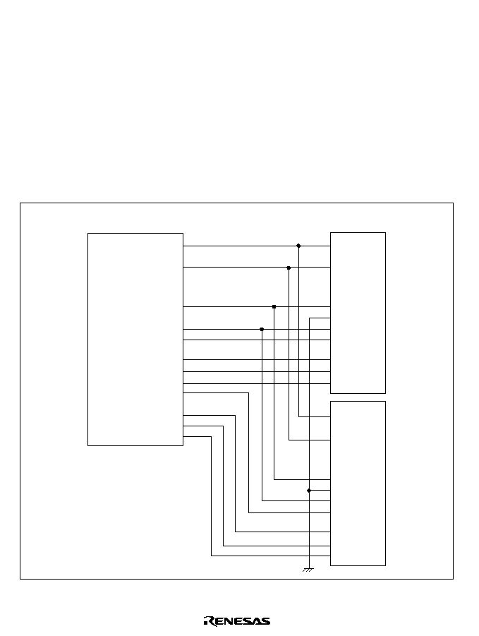
322
7.6
DRAM Interface
7.6.1
DRAM Direct Connection
When the DRAM and other memory enable bits (DRAM2≠DRAM0) in BCR1 are set to 010, the
CS3 space becomes DRAM space, and a DRAM interface function can be used to directly connect
DRAM.
The data width of an interface can be 16 or 32 bits (figures 7.35 and 7.36)
.
Two-CAS 16-bit
DRAMs can be connected, since
CAS is used to control byte access
.
The
RAS, CAS3≠CAS0, and
RD/
WR signals are used to connect the DRAM. When the data width is 16 bits, CAS3, and CAS2
are not used. In addition to ordinary read and write access, burst access using high-speed page
mode is also supported
.
A10
A2
D15
D0
RAS
RD/
WR
D31
D16
CAS3
CAS2
A8
A0
RAS
OE
WE
I/O15
I/O0
UCAS
LCAS
CAS1
CAS0
A8
A0
RAS
OE
WE
I/O15
I/O0
UCAS
LCAS
Chip
256k
◊
16-bit
DRAM
...
...
...
...
...
...
...
...
...
...
...
......
...
Figure 7.35 Example of DRAM Connection (32-Bit Data Width)
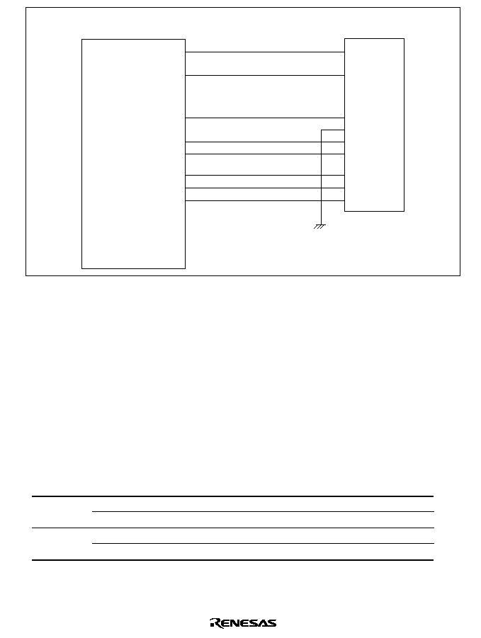
323
A9
A1
RAS
RD/
WR
D15
D0
CAS1
CAS0
A8
A0
RAS
OE
WE
I/O15
I/O0
UCAS
LCAS
Chip
256k
◊
16-bit
DRAM
...
...
...
...
...
...
...
...
Figure 7.36 Example of DRAM Connection (16-Bit Data Width)
7.6.2
Address Multiplexing
When the CS3 space is set to DRAM, addresses are always multiplexed. This allows DRAMs that
require multiplexing of row and column addresses to be connected directly without additional
address multiplexing circuits. There are four ways of multiplexing, which can be selected using
the AMX1≠AMX0 bits in MCR. Table 7.8 illustrates the relationship between the AMX1≠AMX0
bits and address multiplexing. Address multiplexing is performed on address output pins A15≠A1.
The original addresses are output to pins A24≠A16. During DRAM accesses, AMX2 is reserved,
so set it to 0.
Table 7.8
Relationship between AMX1≠AMX0 and Address Multiplexing
AMX1
AMX0
No. of Column
Address Bits
Row
Address Output
Column
Address Output
0
0
8 bits
A23≠A9
A15≠A1
1
9 bits
A24≠A10
A15≠A1
1
0
10 bits
A24≠A11
*
1
A15≠A1
1
11 bits
A24≠A12
*
2
A15≠A1
Notes:
*
1 Address output pin A15 is high.
*
2 Address output pins A15 and A14 are high.
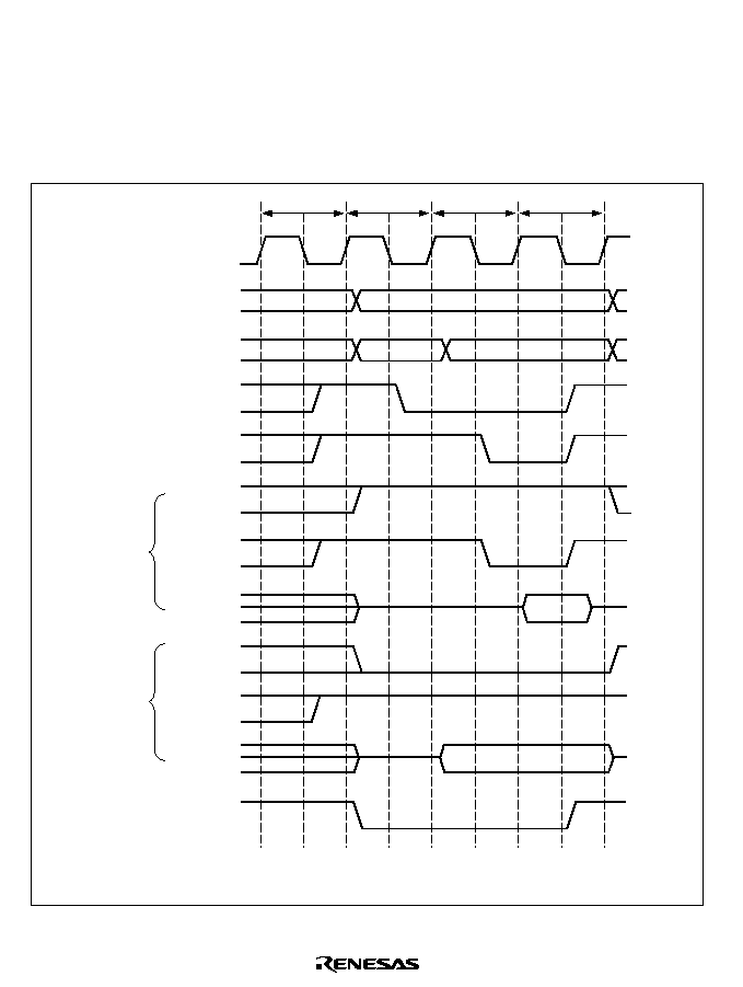
324
7.6.3
Basic Timing
The basic timing of a DRAM access is 3 cycles. Figure 7.37 shows the basic DRAM access
timing. Tp is the precharge cycle, Tr is the
RAS assert cycle, Tc1 is the CAS assert cycle, and Tc2
is the read data fetch cycle. When accesses are consecutive, the Tp cycle of the next access
overlaps the Tc2 cycle of the previous access, so accesses can be performed in a minimum of 3
cycles each.
Tp
Tr
CKIO
A24≠A16
A15≠A1
RAS
CASn
RD/
WR
RD
D31≠D0
RD/
WR
RD
D31≠D0
DACKn
*
Read
Write
Tc1
Tc2
Note:
*
DACKn waveform when active-low is specified.
Figure 7.37 Basic Access Timing

325
7.6.4
Wait State Control
When the clock frequency is raised, 1 cycle may not always be sufficient for all states to end, as in
basic access. Setting bits in WCR1, WCR2 and MCR enables the state to be lengthened. Figure
7.38 shows an example of lengthening a state using settings.
The Tp cycle (which ensures a sufficient
RAS precharge time) can be extended from 1 cycle to 2
cycles by insertion of a Tpw cycle by means of the TRP1, TRP0 bit in MCR. The number of
cycles between
RAS assert and CASn assert can be extended from 1 cycle to 3 cycles by inserting
a Trw cycle by means of the RCD1, RCD0 bit in MCR. The number of cycles from
CASn assert
to the end of access can be extended from 1 cycle to 3 cycles by setting the W31/W30 bits in
WCR1. When external wait mask bit A3WM in WCR2 is cleared to 0 and bits W31 and W30 in
WCR1 are set to a value other than 00, the external wait pin is also sampled, so the number of
cycles can be further increased. When bit A3WM in WCR2 is set to 1, external wait input is
ignored regardless of the setting of W31 and W30 in WCR1. Figure 7.39 shows the timing of wait
state control using the
WAIT pin.
In either case, when consecutive accesses occur, the Tp cycle access overlaps the Tc2 cycle of the
previous access. In DRAM access,
BS is not asserted, and so RAS, CASn, RD, etc., should be
used for
WAIT pin control.

326
Tp
Tpw
CKIO
A24≠A16
A15≠A1
RAS
CASn
RD/
WR
RD
D31≠D0
RD/
WR
RD
D31≠D0
DACKn
*
Read
Write
Note:
*
DACKn waveform when active-low is specified
Tr
Trw
Tc1
Tw
Tc2
Figure 7.38 Wait State Timing
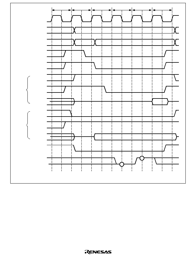
327
Tp
Tr
CKIO
A24≠A16
A15≠A1
RAS
CASn
RD/
WR
RD
D31≠D0
RD/
WR
RD
D31≠D0
DACKn
*
WAIT
Read
Write
Tc1
Tw
Twx
Tc2
Note:
*
DACKn waveform when active-low is specified
Figure 7.39 External Wait State Timing
7.6.5
Burst Access
In addition to the ordinary mode of DRAM access, in which row addresses are output at every
access and data is then accessed, DRAM also has a high-speed page mode for use when
continuously accessing the same row that enables fast access of data by changing only the column
address after the row address is output. Select ordinary access or high-speed page mode by setting
the burst enable bit (BE) in MCR. Figure 7.40 shows the timing of burst access in high-speed page
mode. When performing burst access, cycles can be inserted using the wait state control function.
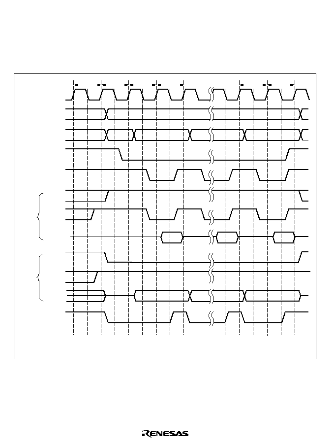
328
An address comparator is provided to detect matches of row addresses in burst mode. When this
function is used and the BE bit in MCR is set to 1, setting the MCR's RASD bit (which specifies
RAS down mode) to 1 places the SH7616 in RAS down mode, which leaves the RAS signal
asserted. The access timing in
RAS down mode is shown in figures 7.41 and 7.42. When RAS
down mode is used, the refresh cycle must be less than the maximum DRAM
RAS assert time
tRAS when the refresh cycle is longer than the tRAS maximum.
Tp
CKIO
A24≠A16
A15≠A1
RAS
CASn
RD/
WR
RD
D31≠D0
RD/
WR
RD
D31≠D0
DACKn
*
Read
Write
Tr
Tc1
Tc2
Tc1
Tc2
Note:
*
DACKn waveform when active-low is specified
Figure 7.40 Burst Access Timing
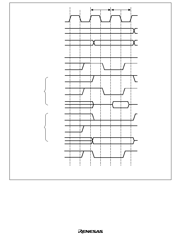
329
CKIO
A24≠A14
A13≠A1
RAS
CASn
RD/
WR
RD
D31≠D0
RD/
WR
RD
D31≠D0
DACKn
*
Read
Write
Tc1
Tc2
Note:
*
DACKn waveform when active-low is specified
Figure 7.41
RAS Down Mode Same Row Access Timing

330
Tp
Tr
CKIO
A24≠A16
A15≠A1
RAS
CASn
RD/
WR
RD
D31≠D0
RD/
WR
RD
D31≠D0
DACKn
*
Read
Write
Tc1
Tc2
Note:
*
DACKn waveform when active-low is specified
Figure 7.42
RAS Down Mode Different Row Access Timing
7.6.6
EDO Mode
In addition to the kind of DRAM in which data is output to the data bus only while the
CASn
signal is asserted in a data read cycle, there is another kind provided with an EDO mode in which,
while both
RAS and OE are asserted, once the CASn signal is asserted data is output to the data
bus until
CASn is next asserted, even though CASn is negated during this time.
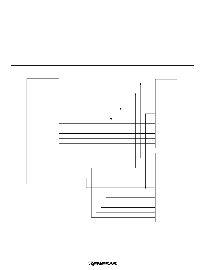
331
The EDO mode bit (EDO) in MCR allows selection of ordinary access/high-speed page mode
burst access or ordinary access/burst access using EDO mode. Since
OE control is performed in
EDO mode DRAM access, the
CAS and OE pins of the SH7616 must be connected to the OE pin
of the DRAM.
Ordinary access in EDO mode is shown in figure 7.45, and burst access in figure 7.46.
In EDO mode, in order to extend the timing for data output to the data bus in a read cycle until the
next assertion of
CASn, the DRAM access time can be increased by delaying the data latch timing
by 1/2 cycle, making it at the rise of the CKIO clock.
A8
A0
RAS
OE
WE
I/O15
I/O0
UCAS
LCAS
A8
A0
RAS
OE
WE
I/O15
I/O0
UCAS
LCAS
A10
A2
RAS
RD/
WR
D31
D16
CAS3
CAS2
D15
D0
CAS1
CAS0
CAS
/
OE
.
.
.
.
.
.
.
.
.
.
.
.
.
.
.
.
.
.
.
.
.
.
.
.
.
.
.
.
.
.
.
.
.
.
.
.
.
.
.
.
.
.
.
.
.
.
.
.
256 k
◊
16-bit
DRAM
Chip
Figure 7.43 Example of EDO DRAM Connection (32-Bit Data Width)
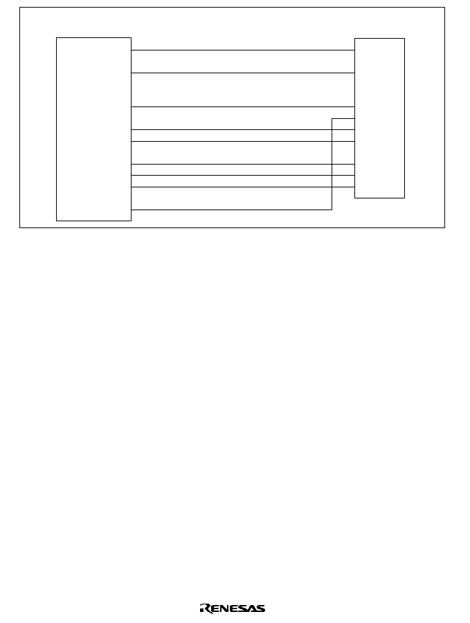
332
A8
A0
RAS
OE
WE
I/O15
I/O0
UCAS
LCAS
A9
A1
RAS
RD/
WR
D15
D0
CAS1
CAS0
CAS
/
OE
.
.
.
.
.
.
.
.
.
.
.
.
.
.
.
.
.
.
.
.
.
.
.
.
.
.
.
.
.
.
.
.
256 k
◊
16-bit
DRAM
Chip
Figure 7.44 Example of EDO DRAM Connection (16-Bit Data Width)
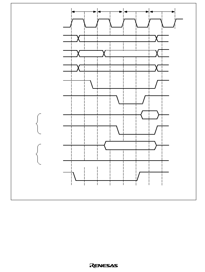
333
Tr
Tc1
CKIO
A24≠A16
A15≠A1
RD/
WR
RAS
CASn
D15≠D0
CAS
/
OE
D15≠D0
CAS
/
OE
DACKn
*
Read
Note:
*
DACKn waveform when active-low is specified
Write
Tc2
(Tpc)
Row address
Column address
Row address
High level
Figure 7.45 DRAM EDO Mode Ordinary Access Timing
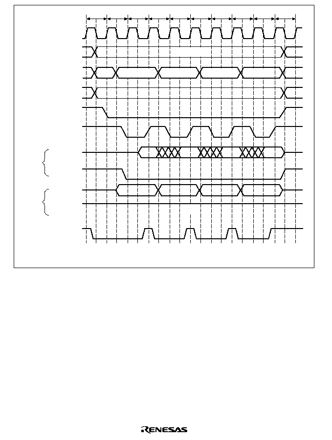
334
Tr
CKIO
A24≠A16
A15≠A1
RD/
WR
RAS
CASn
D15≠D0
CAS
/
OE
D15≠D0
CAS
/
OE
DACKn
*
Tc1
Tc2
Tc1
Tc2
Tc1
Tc2
Tc1
Tc2
(Tpc)
Read
Note:
*
DACKn waveform when active-low is specified
Write
Column address
Column address
Column address
Column address
Row
address
Row address
High
Figure 7.46 DRAM EDO Mode Burst Access Timing
7.6.7
DRAM Single Transfer
Wait states equivalent to the value set in bits DSWW1 and DSWW0 in BCR3 can be inserted
between DACKn assertion and
CASn assertion in a write in DMA single address transfer mode.
Inserting wait states allows the data setup time for external device memory. Figure 7.47 shows the
write cycle timing in DMA single transfer mode when DSWW1/DSWW0 = 01 and RASD = 1.
The DMA single transfer mode read cycle is the same as a CPU or DMA dual transfer mode read
cycle.
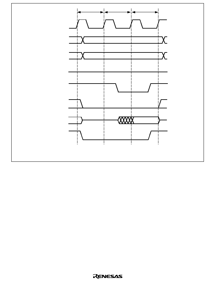
335
Tdsww
Tc1
CKIO
A24≠A16
A15≠A1
RAS
CASn
RD/
WR
D31≠D0
DACKn
*
Tc2
Low level
Note:
*
DACKn waveform when active-low is specified
Figure 7.47 DMA Single Transfer Mode Write Cycle Timing
(
RAS Down Mode, Same Row Address)
7.6.8
Refreshing
The bus state controller includes a function for controlling DRAM refreshing. Distributed
refreshing using a
CAS-before-RAS refresh cycle can be performed by clearing the RMODE bit to
0 and setting the RFSH bit to 1 in MCR. Consecutive refreshes can be generated by setting bits
RRC2≠RRC0 in RTCSR. If DRAM is not accessed for a long period, self-refresh mode, which
uses little power consumption for data retention, can be activated by setting both the RMODE and
RFSH bits to 1.
CAS-Before-RAS Refreshing: Refreshing is performed at intervals determined by the input clock
selected by bits CKS2≠CKS0 in RTCSR, and the value set in RTCOR. The RTCOR value and the
value of bits CKS2≠CKS0 in RTCSR should be set so as to satisfy the refresh interval
specification for the DRAM used. First make the settings for RTCOR, RTCNT, and the RMODE
and RFSH bits in MCR, then make the CKS2≠CKS0 and RRC2≠RRC0 settings in RTCSR. When
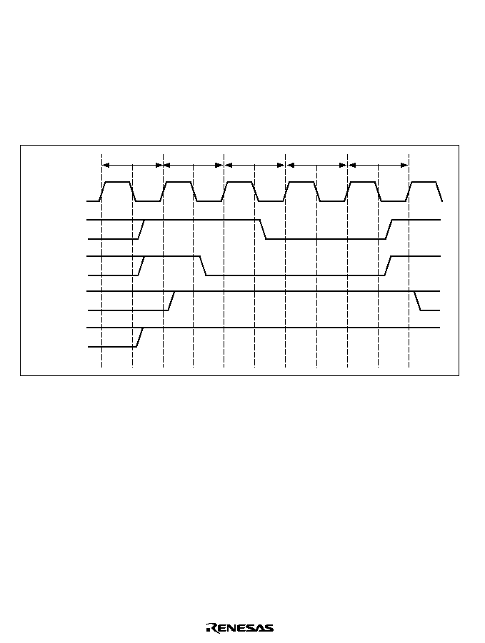
336
the clock is selected by CKS2≠CKS0, RTCNT starts counting up from the value at that time. The
RTCNT value is constantly compared with the RTCOR value, and when the two values match, a
refresh request is generated and the number of CAS-before-RAS refreshes set in bits RRC2≠RRC0
are performed. At the same time, RTCNT is cleared to zero and the count-up is restarted. Figure
7.48 shows the
CAS-before-RAS refresh cycle timing.
The number of RAS assert cycles in the refresh cycle is specified by bits TRAS1 and TRAS0 in
MCR. As with ordinary accesses, the specification of the
RAS precharge time in the refresh cycle
follows the setting of bits TRP1 and TRP0 in MCR.
Tp
Trr
CKIO
RAS
CASn
RD/
WR
RD
Trc1
Trc2
Tre
Figure 7.48 DRAM
CAS-before-RAS Refresh Cycle Timing
Self-Refreshing: A self-refresh is started by setting both the RMODE bit and the RFSH bit to 1.
During the self-refresh, DRAM cannot be accessed. Self-refreshing is cleared by clearing the
RMODE bit to 0. Self-refresh timing is shown in figure 7.49. Settings must be made so that self-
refresh clearing and data retention are performed correctly, and
CAS-before-RAS refreshing is
immediately performed at the correct intervals. When self-refreshing is started from the state in
which
CAS-before-RAS refreshing is set, or when exiting standby mode by means of a manual
reset or NMI, auto-refreshing is restarted if RFSH is set to 1 and RMODE is cleared to 0 when
self-refresh mode is cleared. If the transition from clearing of self-refresh mode to starting auto-
refresh takes time, this time should be taken into consideration when setting the initial value of
RTCNT. When the RTCNT value is set to RTCOR-1, the refresh can be started immediately.
After self-refreshing has been set, the self-refresh state continues even if the chip standby state is
entered using the chip's standby function. The self-refresh state is also maintained even after
recovery from standby mode by means of NMI input.

337
In the case of a power-on reset, the bus state controller's registers are initialized, and therefore the
self-refresh state is cleared.
Tp
Trr
CKIO
RAS
CASn
Trc1
Trc2
Trc2
Tre
Figure 7.49 DRAM Self-Refresh Cycle Timing
7.6.9
Power-On Sequence
When DRAM is used after the power is turned on, there is a requirement for a waiting period
during which accesses cannot be performed (100 µs or 200 µs minimum) followed by at least the
prescribed number of dummy
CAS-before-RAS refresh cycles (usually 8). The bus state controller
(BSC) does not perform any special operations for the power-on reset, so the required power-on
sequence must be implemented by the initialization program executed after a power-on reset.
7.7
Burst ROM Interface
Set the BSTROM bit in BCR1 to set the CS0 space for connection to burst ROM. The burst ROM
interface is used to permit fast access to ROMs that have the nibble access function. Figure 7.51
shows the timing of nibble accesses to burst ROM. Set for two wait cycles. The access is basically
the same as an ordinary access, but when the first cycle ends, only the address is changed. The
CS0 signal is not negated, enabling the next access to be conducted without the T1 cycle required
for ordinary space access. From the second time on, the T1 cycle is omitted, so access is 1 cycle
faster than ordinary accesses. Currently, the nibble access can only be used on 4-address ROM.
This function can only be utilized for word or longword reads to 8-bit ROM and longword reads to
16-bit ROM. Mask ROMs have slow access speeds and require 4 instruction fetches for 8-bit
widths and 16 accesses for cache filling. Limited support of nibble access was thus added to
alleviate this problem. When connecting to an 8-bit width ROM, a maximum of 4 consecutive
accesses are performed; when connecting to a 16-bit width ROM, a maximum of 2 consecutive
accesses are performed. Figure 7.50 shows the relationship between data width and access size.
For cache filling and DMAC 16-byte transfers, longword accesses are repeated 4 times.
338
When one or more wait states are set for a burst ROM access, the
WAIT pin is sampled. When the
burst ROM is set and 0 specified for waits, there are 2 access cycles from the second time on.
Figure 7.52 shows the timing.
T1
Tw
T2
Tw
T2
Tw
T2
Tw
T2
8-bit bus-width longword access
T1
Tw
T2
Tw
T2
8-bit bus-width word access
T1
Tw
T2
8-bit bus-width byte access
T1
Tw
T2
Tw
T2
16-bit bus-width longword access
T1
Tw
T2
16-bit bus-width word access
T1
Tw
T2
16-bit bus-width byte access
T1
Tw
T2
32-bit bus-width longword access
T1
Tw
T2
32-bit bus-width word access
T1
Tw
T2
32-bit bus-width byte access
Figure 7.50 Data Width and Burst ROM Access (1 Wait State)

339
T1
Tw1
CKIO
A24≠A0
CS0
RD/
WR
RD
D31≠D0
BS
DACKn
*
Tw2
T2
Tw1
Tw2
T2
Note:
*
DACKn waveform when active-low is specified.
Figure 7.51 Burst ROM Nibble Access (2 Wait States)

340
T1
T2
CKIO
A24≠A0
CS0
RD/
WR
RD
D31≠D0
BS
DACKn
*
T1'
T2
Note:
*
DACKn waveform when active-low is specified.
Figure 7.52 Burst ROM Nibble Access (No Wait States)

341
7.8
Idles between Cycles
Because operating frequencies have become high, when a read from a slow device is completed,
data buffers may not go off in time to prevent data conflicts with the next access. This lowers
device reliability and causes errors. To prevent this, a function has been added to avoid data
conflicts that memorizes the space and read/write state of the preceding access and inserts an idle
cycle in the access cycle for those cases in which problems are found to occur when the next
access starts up. The BSC checks whether a wait is to be inserted in two cases: if a read cycle is
followed immediately by a read access to a different CS space, and if a read access is followed
immediately by a write from the chip. When the chip is writing continuously, the data direction is
always from the chip to other memory, and there are no particular problems. Neither is there any
particular problem if the following read access is to the same CS space, since data is output from
the same data buffer. The number of idle cycles to be inserted into the access cycle when reading
from another CS space, or performing a write, after a read from the CS3 space, is specified by the
IW31 and IW30 bits in WCR1. Likewise, IW21 and IW20 specify the number of idle cycles after
CS2 reads, IW11 and IW10 specify the number after CS1 reads, and IW01 and IW00 specify the
number after CS0 reads. The number of idle cycles after a CS4 read is specified by the IW41 and
IW40 bits in WCR2. From 0, 1, 2, or 4 cycles can be specified. When there is already a gap
between accesses, the number of empty cycles is subtracted from the number of idle cycles before
insertion. When a write cycle is performed immediately after a read access, 1 idle cycle is inserted
even when 0 is specified for waits between access cycles.
When the chip shifts to a read cycle immediately after a write, the write data becomes high
impedance when the clock rises, but the
RD signal, which indicates read cycle data output enable,
is not asserted until the clock falls. The result is that no idles are inserted into the cycle.
When bus arbitration is being performed, an empty cycle is inserted for arbitration, so no is
inserted between cycles.
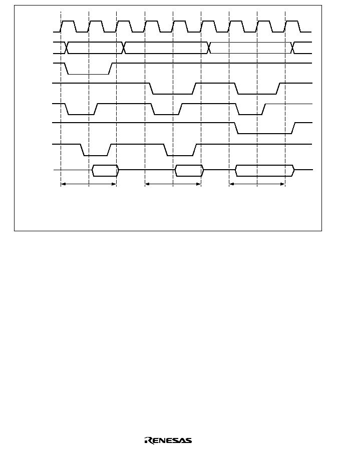
342
T1
T2
CKIO
A24≠A0
CSm
CSn
BS
RD/
WR
RD
D31≠D0
Twait
T1
T2
Twait
T1
T2
CSm space read
CSn space read
CSn space write
Specification of waits
between CSm accesses
(reading different spaces)
Specification of waits
between CSn accesses
(read followed by write)
Figure 7.53 Idles between Cycles
7.9
Bus Arbitration
The chip has a bus arbitration function that, when a bus release request is received from an
external device, releases the bus to that device after the bus cycle being executed is completed.
The chip keeps the bus under normal conditions and permits other devices to use the bus by
releasing it when they request its use.
In the following explanation, external devices requesting the bus are called slaves.
The chip has three internal bus masters, the CPU, the DMAC and the E-DMAC. When
synchronous DRAM or DRAM is connected and refresh control is performed, the refresh request
becomes a fourth master. In addition to these, there are also bus requests from external devices.
The priority for bus requests when they occur simultaneously is as follows.

343
Refresh request External device E-DMAC DMAC CPU
However, only one E-DMAC channel can hold the bus during one bus-mastership cycle.
The E-DMAC has two channels to handle both transmission and reception. Arbitration between
the channels is performed automatically within the E-DMAC module, with bus mastership
alternating between the transmit channel and the receive channel. For arbitration between the two
DMAC channels, either fixed priority mode or round robin mode can be selected by means of the
priority mode bit (PR) in the DMA operation register (DMAOR).
When the bus is being passed between slave and master, all bus control signals are negated before
the bus is released to prevent erroneous operation of the connected devices. When the bus is
transferred, also, the bus control signals begin bus driving from the negated state. The master and
slave passing the bus between them drive the same signal values, so output buffer conflict is
avoided. A pull-up resistance is required for the bus control signals to prevent malfunction caused
by external noise when they are at high impedance.
Bus permission is granted at the end of the bus cycle. When the bus is requested, the bus is
released immediately if there is no ongoing bus cycle. If there is a current bus cycle, the bus is not
released until the bus cycle ends. Even when a bus cycle does not appear to be in progress when
viewed from off-chip, it is not possible to determine immediately whether the bus has been
released by looking at
CSn or other control signals, since a bus cycle (such as wait insertion
between access cycles) may have been started internally. The bus cannot be released during burst
transfers for cache filling, DMAC 16-byte block transfers (16 + 16 = 32-byte transfers in dual
address mode), or E-DMAC 16-byte block transfers. Likewise, the bus cannot be released between
the read and write cycles of a TAS instruction. Arbitration is also not performed between multiple
bus cycles produced by a data width smaller than the access size, such as a longword access to an
8-bit data width memory. Bus arbitration is performed between external vector fetch, PC save, and
SR save cycles during interrupt handling, which are all independent accesses.
Because the CPU is connected to cache memory by a dedicated internal bus, cache memory can be
read even when the bus is being used by another bus master on the chip or externally. When
writing from the CPU, an external write cycle is produced. Since the internal bus that connects the
CPU, DMAC, and on-chip peripheral modules can operate in parallel to the external bus, both read
and write accesses from the CPU to on-chip peripheral modules and from the DMAC to on-chip
peripheral modules are possible even if the external bus is not held.
Figures 7.54 (a) and 7.54 (b) show the timing charts in the cases that bus requests occur
simultaneously from the E-DMAC, DMAC, and CPU. These cases are based on the following
settings:
∑
The CS2 and CS3 spaces are set for synchronous DRAM.
∑
The CAS latency is one cycle.

344
∑
The E-DMAC is enabled at both the transmitter and receiver (the buffer and descriptor use the
CS3 space).
∑
The DMAC is enabled in only one channel that is set to auto-request mode, cycle-steal mode,
and 16-byte dual-address transmission (CS2 space).
∑
Burst read and single write are set to synchronous DRAM.

345
CPU
DMAC
E-DMAC
CPU
CKIO
A24
≠
A0
CS0
RD
CS2
CS3
RAS
CAS
RD/
WR
D31
≠
D0
Figure 7.54 (a) Bus Arbitration Timing
(E-DMAC Read
DMAC 16-Byte Transmission
CPU Read)
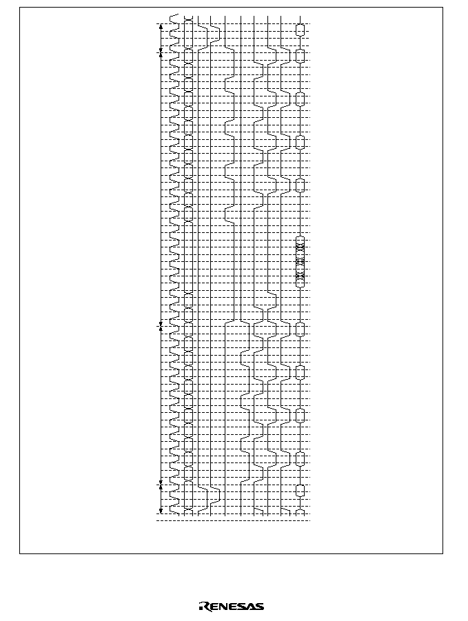
346
CPU
DMAC
E-DMAC
CPU
CKIO
A24
≠
A0
CS0
RD
CS2
CS3
RAS
CAS
RD/
WR
D31
≠
D0
Figure 7.54 (b) Bus Arbitration Timing
(E-DMAC Write
DMAC 16-Byte Transmission
CPU Read)

347
7.9.1
Master Mode
The chip keeps the bus unless it receives a bus request. When a bus release request (
BRLS)
assertion (low level) is received from an external device, buses are released and a bus grant (
BGR)
is asserted (low level) as soon as the bus cycle being executed is completed. When it receives a
negated (high level)
BRLS signal, indicating that the slave has released the bus, it negates the
BGR (to high level) and begins using the bus. When the bus is released, all output and I/O signals
related to the bus interface are changed to high impedance, except for the CKE signal for the
synchronous DRAM interface, the
BGR signal for bus arbitration, and DMA transfer control
signals DACK0 and DACK1.
When the DRAM has finished precharging, the bus is released. The synchronous DRAM also
issues a precharge command to the active bank. After this is completed, the bus is released.
The specific bus release sequence is as follows. First, the address bus and data bus become high
impedance synchronously with a rise of the clock. Half a cycle later, the bus use enable signal is
asserted synchronously with a fall of the clock. Thereafter the bus control signals (
BS, CSn, RAS,
CASn, WEn, RD, RD/WR) become high impedance at a rise of the clock. These bus control
signals are driven high at least 2 cycles before they become high impedance. Sampling for bus
request signals occurs at the clock fall.
The sequence when the bus is taken back from the slave is as follows. When the negation of
BRLS
is detected at a clock fall, high-level driving of the bus control signals starts half a cycle later. The
bus use enable signal is then negated at the next clock fall. The address bus and data bus are driven
starting at the next clock rise. The bus control signals are asserted and the bus cycle actually starts
from the same clock rise at which the address and data signals are driven, at the earliest. Figure
7.55 shows the timing of bus arbitration.
To reduce the overhead due to arbitration with a user-designed slave, a number of consecutive bus
accesses may be attempted. In this case, to insure dependable refreshing, the design must provide
for the slave to release the bus before it has held it for a period exceeding the refresh cycle. The
SH7616 is provided with the REFOUT pin to send a signal requesting the bus while refresh
execution is being kept waiting. REFOUT is asserted while refresh execution is being kept waiting
until the bus is acquired. When the external slave device receives this signal and releases the bus,
the bus is returned to the chip and refreshing can be executed.
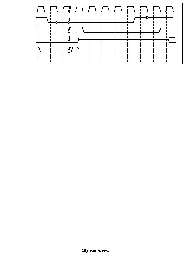
348
CKIO
BRLS
BGR
Address data
CSn
Other bus
control signals
Figure 7.55 Bus Arbitration
7.10
Additional Items
7.10.1
Resets
The bus state controller is completely initialized only in a power-on reset. All signals are
immediately negated, regardless of whether or not the chip is in the middle of a bus cycle. Signal
negation is simultaneous with turning the output buffer off. All control registers are initialized. In
standby mode, sleep mode, and a manual reset, no bus state controller control registers are
initialized. When a manual reset is performed, the currently executing bus cycle only is completed,
and then the chip waits for an access. When a cache-filling or DMAC/E-DMAC 16-byte transfer is
executing, the CPU, DMAC, or E-DMAC that is the bus master ends the access in a longword
unit, since the access request is canceled by the manual reset.This means that when a manual reset
is executed during a cache filling, the cache contents can no longer be guaranteed. During a
manual reset, the RTCNT does not count up, so no refresh request is generated, and a refresh cycle
is not initiated. To preserve the data of the DRAM and synchronous DRAM, the pulse width of the
manual reset must be shorter than the refresh interval.
The bus-release operation of this LSI during a manual reset is described below.
∑
BRLS signal is asserted before transition to manual reset state and continues to be asserted
during manual reset
In this LSI, the
BGR signal is continuously asserted to retain the bus-release state.
∑
BRLS signal is asserted before transition to manual reset state and negated during manual reset
In this LSI, the
BGR signal is negated to acquire the bus.
∑
BRLS signal is asserted during manual reset
In this LSI, the
BGR signal is not asserted until the manual reset is released.

349
7.10.2
Access as Viewed from CPU, DMAC or E-DMAC
The chip is internally divided into three buses: cache, internal, and peripheral. The CPU and cache
memory are connected to the cache bus, the DMAC, E-DMAC and bus state controller are
connected to the internal bus, and the low-speed peripheral devices and mode registers are
connected to the peripheral bus. On-chip memory other than cache memory and the user break
controller are connected to both the cache bus and the internal bus. The internal bus can be
accessed from the cache bus, but not the other way around. The peripheral bus can be accessed
from the internal bus, but not the other way around. This results in the following.
The DMAC can access on-chip memory other than cache memory, but cannot access cache
memory. When the DMAC causes a write to external memory, the external memory contents and
the cache contents may be different. When external memory contents are rewritten by a DMA
transfer, the cache memory must be purged by software if there is a possibility that the data for
that address is present in the cache.
When the CPU starts a read access, if the access is to a cache area, a cache search is first
performed. This takes one cycle. If there is data in the cache, it fetches it and completes the access.
If there is no data in the cache, a cache filling is performed via the internal bus, so four
consecutive longword reads occur. For misses that occur when byte or word operands are accessed
or branches occur to odd word boundaries (4n + 2 addresses), the filling is always performed by
longword accesses on the chip-external interface. In the cache-through area, the access is to the
actual access address. When the access is an instruction fetch, the access size is always longword.
For cache-through areas and on-chip peripheral module read cycles, after an extra cycle is added
to determine the cycle, the read cycle is started through the internal bus. Read data is sent to the
CPU through the cache bus.
When write cycles access the cache area, the cache is searched. When the data of the relevant
address is found, it is written here. The actual write occurs in parallel to this via the internal bus in
write-through mode. In write-back mode, the actual write is not performed until a replace
operation occurs for the relevant address. When the right to use the internal bus is held, the CPU is
notified that the write is completed without waiting for the end of the actual off-chip write. When
the right to use the internal bus is not held, as when it is being used by the DMAC or the like,
there is a wait until the bus is acquired before the CPU is notified of completion.
Accesses to cache-through areas and on-chip peripheral modules work the same as in the cache
area, except for the cache search and write.
Because the bus state controller has one level of write buffer, the internal bus can be used for
another access even when the chip-external bus cycle has not ended. After a write has been
performed to low-speed memory off the chip, performing a read or write with an on-chip
peripheral module enables an access to the on-chip peripheral module without having to wait for
the completion of the write to low-speed memory.
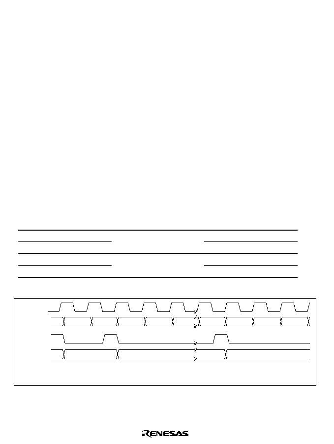
350
During reads, the CPU always has to wait for the end of the operation. To immediately continue
processing after checking that the write to the device of actual data has ended, perform a dummy
read access to the same address consecutively to check that the write has ended.
The bus state controller's write buffer functions in the same way during accesses from the DMAC.
A dual-address DMA transfer thus starts in the next read cycle without waiting for the end of the
write cycle. When both the source address and destination address of the DMA are external spaces
to the chip, however, it must wait until the completion of the previous write cycle before starting
the next read cycle.
The E-DMAC can perform access involving external memory, but not access involving any on-
chip memory or peripheral modules.
7.10.3
STATS1 and STATS0 Pins
The SH7616 has two pins, STATS1 and STATS0, to identify the bus master status. The signals
output from these pins show the external access status. Encoded output is provided for the
following categories: CPU (cache hit/cache disable), DMAC (external access only), E-DMAC,
and Others (refresh, internal access, etc..). All output is synchronized with the address signals.
The encoding patterns are shown in table 7.9, and the output timing in figure 7.56.
Table 7.9
Encoding Patterns
Identification
STATS1
STATS0
CPU
0
0
DMAC
1
E-DMAC
1
0
Others
1
CKIO
Address
CPU
CPU
E-DMAC
E-DMAC
E-DMAC G-DMAC G-DMAC G-DMAC
E-DMAC
STATS1, 0
00
10
01
CSn
Note: In on-chip I/O
on-chip RAM or on-chip I/O
memory transfers using the DMAC,
accesses to on-chip I/O and on-chip RAM are included in the "Others" category.
Figure 7.56 STATS Output Timing

351
7.10.4
BUSHiZ Specification
The
BUSHiZ pin is needed when the SH7616 is connected to a PCI controller via a PCI bridge,
and the PCI master and SH7616 share local memory on the SH7616 bus. By using this pin in
combination with the
WAIT pin, it is possible to place the bus and specific control signals in the
high-impedance state while keeping the SH7616's internal state halted. The conditions for
establishing the high-impedance state, the applicable pins, and the bus timing (figure 7.57) are
shown below. See the Application Note for an example of PCI bridge connection.
∑
High-impedance conditions: Not dependent on BCR settings etc. when
WAIT = L and
BUSHiZ = L
∑
Applicable pins: A[24:0], D[31:0],
CS3, RD/WR, RD, RAS, CAS/OE, DQMLL/WE0,
DQMLU/
WE1, DQMUL/WE2, DQMUU/WE3 (total of 66 pins)
CKIO
WAIT
BUSHiZ
Target pins
Period
Figure 7.57
BUSHiZ Bus Timing
1. Can be used when memory is shared by the CPU and an external device.
2. When
BUSHiZ is asserted after asserting WAIT, the CPU appears to release the bus.
3. When it becomes possible to access the shared memory,
BUSHiZ is negated.
4. When the data is ready,
WAIT is negated.
This procedure allows the CPU and an external device to share memory.
7.11
Usage Notes
7.11.1
Normal Space Access after Synchronous DRAM Write when Using DMAC
Negation of the DQMn/
WEn signal in a synchronous DRAM write and CSn assertion in an
immediately following normal space access both occur at the same rising edge of CKIO (figure
7.58). As there is a risk of an erroneous write to normal space in this case, when synchronous
DRAM or a high-speed device is connected to normal space, it is recommended that
CSn be
delayed on the system side.
Cases in which a synchronous DRAM write and normal space access occur consecutively are
shown in table 7.10.

352
Table 7.10
access sequence
Write to Synchronous DRAM
Normal Space Access
CPU
DMA
DMA
CPU
DMA
DMA
Note:
When an access by the CPU is performed immediately after a write by the CPU, internally
the accesses are not consecutive.
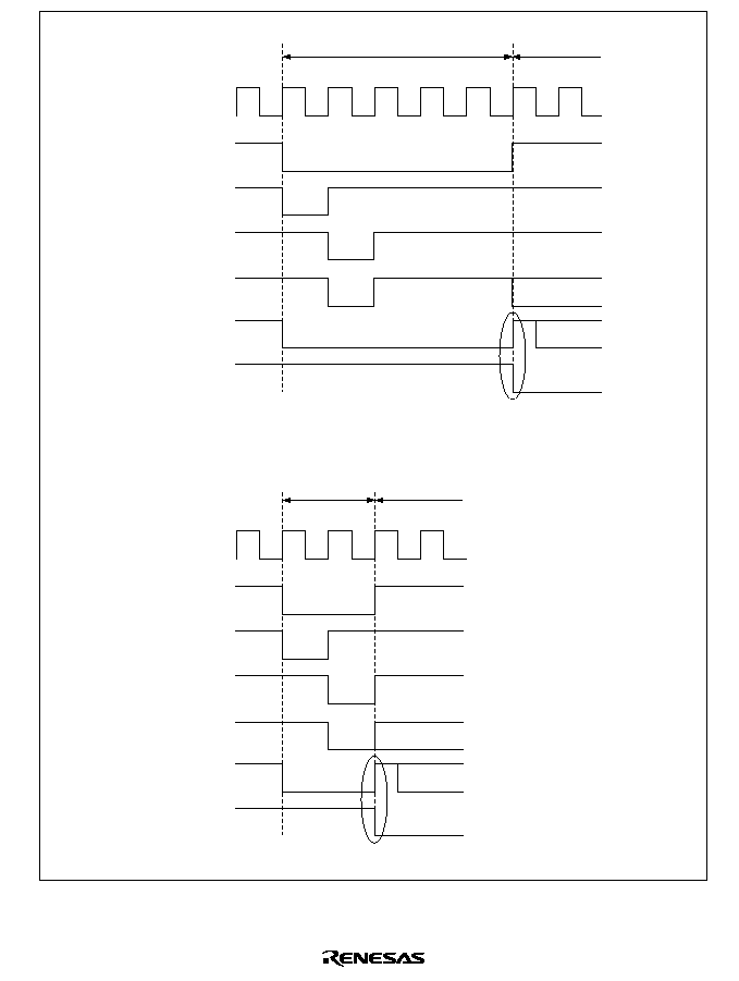
353
Tr
Tc1
Tc2
Tc3
Tc4
T1
CKIO
CS2
or
CS3
RAS
CAS
RD/
WR
DQM/
WEn
CSn
Tr
Tc1
T1
CKIO
CS2
or
CS3
RAS
CAS
RD/
WR
DQM/
WEn
CSn
(a) Burst write mode
(b) Single write mode
Synchronous DRAM write access
Synchronous DRAM
write access
Normal space
access
Normal space
access
Figure 7.58 Normal Space Access Immediately after Synchronous DRAM Write

354
7.11.2
When Using I
: E
Clock Ratio of 1 : 1, 8-Bit Bus Width, and External Wait Input
When using an I
: E
clock ratio of 1 : 1 and an 8-bit bus width, at least 1.5 address hold cycles
should be set.
Set a value other than the initial value in bits AnSHW1, AnSHW0, A4HW1, and A4HW0 for the
relevant space.
7.11.3
When connecting external device to synchronous DRAM
When connecting an external device to the synchronous DRAM, not only CSnN and DACKn but
also other instructions for the synchronous DRAM such as CSnN, RASN, CASN and RDWRN
must be recognized for the estimation of an access sequence.
In some cases, it is difficult to specify read and write cycles only with CSnN and DACKn.
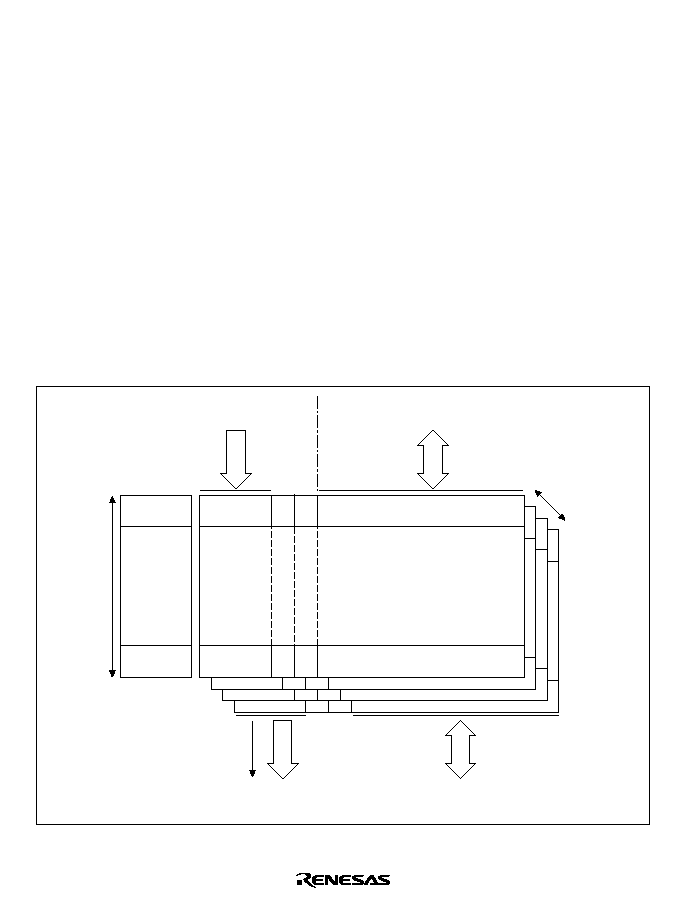
355
Section 8 Cache
8.1
Introduction
This chip incorporates 4 kbytes of four-way, mixed instruction/data type cache memory. This
memory can also be used as 2-kbyte RAM and 2 kbyte mixed instruction/data type cache memory
by making a setting in the cache control register (CCR) (two-way cache mode). CCR can specify
that either instructions or data do not use cache. Both write-through and write-back modes are
supported for cache operation.
Each line of cache memory consists of 16 bytes. Cache memory is always updated in line units.
Four 32-bit accesses are required to update a line. Since the number of entries is 64, the six bits
(A9 to A4) in each address determine the entry. A four-way set associative configuration is used,
so up to four different instructions/data can be stored in the cache even when entry addresses
match. To efficiently use four ways having the same entry address, replacement is provided based
on a pseudo-LRU (least-recently used) replacement algorithm.
The cache configuration is shown in figure 8.1, and addresses in figure 8.2.
64
entries
Internal
data bus
Internal
address bus
Tag address
match signal
Cache
data bus
Way 0
Way 1
Way 2
Way 3
Cache
address bus
Cache data array
Cache address array
Tag
address
LRU
information
Data (16 bytes/line)
U
V
V: Valid bit
U: Update bit
Figure 8.1 Cache Configuration

356
31
28
9
3
3
19
6
4
0
Byte address
in line
Entry address
Tag address
Access space
specification address
Address
Bit
Number of bits
Figure 8.2 Address Configuration
8.1.1
Register Configuration
Table 8.1 shows the cache register configuration.
Table 8.1
Register Configuration
Name
Abbrev.
R/W
Initial Value
Address
Cache control register
CCR
R/W
H'00
H'FFFFFE92
8.2
Register Description
8.2.1
Cache Control Register (CCR)
The cache control register (CCR) is used for cache control. CCR must be set and the cache must
be initialized before use. CCR is initialized to H'00 by a power-on reset or manual reset.
Bit:
7
6
5
4
3
2
1
0
W1
W0
WB
CP
TW
OD
ID
CE
Initial value:
0
0
0
0
0
0
0
0
R/W:
R/W
R/W
R/W
R/W
R/W
R/W
R/W
R/W
Bits 7 and 6--Way Specification Bit (W1, W0): W1 and W0 specify the way when an address
array is directly accessed by address specification.
Bit 7: W1
Bit 6: W0
Description
0
0
Way 0
(Initial value)
1
Way 1
1
0
Way 2
1
Way 3

357
Bit 5--Write-Back Bit (WB): Specifies the cache operation method when the cache area is
accessed.
Bit 5: WB
Description
0
Write-through
(Initial value)
1
Write-back
Bit 4--Cache Purge Bit (CP): When 1 is written to the CP bit, all cache entries and the valid bits,
and LRU information of all ways are initialized to 0. After initialization is completed, the CP bit
reverts to 0. The CP bit always reads 0.
Bit 4: CP
Description
0
Normal operation
(Initial value)
1
Cache purge
Note:
Always read 0.
Bit 3--Two-Way Mode (TW): TW is the two-way mode bit. The cache operates as a four-way set
associative cache when TW is 0 and as a two-way set associative cache and 2-kbyte RAM when
TW is 1. In the two-way mode, ways 2 and 3 are cache and ways 0 and 1 are RAM. Ways 0 and 1
are read or written by direct access of the data array according to address space specification.
Bit 3: TW
Description
0
Four-way mode
(Initial value)
1
Two-way mode
Bit 2--Data Replacement Disable Bit (OD): OD is the bit for disabling data replacement. When
this bit is 1, data fetched from external memory is not written to the cache even if there is a cache
miss. Cache data is, however, read or updated during cache hits. OD is valid only when CE is 1.
Bit 2: OD
Description
0
Normal operation
(Initial value)
1
Data not replaced even when cache miss occurs in data access

358
Bit 1--Instruction Replacement Disable Bit (ID): ID is the bit for disabling instruction
replacement. When this bit is 1, an instruction fetched from external memory is not written to the
cache even if there is a cache miss. Cache data is, however, read or updated during cache hits. ID
is valid only when CE is 1.
Bit 1: ID
Description
0
Normal operation
(Initial value)
1
Data not replaced even when cache miss occurs in instruction fetch
Bit 0--Cache Enable Bit (CE): CE is the cache enable bit. Cache can be used when CE is set to 1.
Bit 0: CE
Description
0
Cache disabled
(Initial value)
1
Cache enabled
8.3
Address Space and the Cache
The address space is divided into six partitions. The cache access operation is specified by
addresses. Table 8.2 lists the partitions and their cache operations. For more information on
address spaces, see section 7, Bus State Controller. Note that the spaces of the cache area and
cache-through area are the same.
Table 8.2
Address Space and Cache Operation
Addresses
A31≠A29
Partition
Cache Operation
000
Cache area
Cache is used when the CE bit in CCR is 1
001
Cache-through area
Cache is not used
010
Associative purge area
Cache line of the specified address is purged
(disabled)
011
Address array read/write area
Cache address array is accessed directly
110
Data array read/write area
Cache data array is accessed directly
111
I/O area
Cache is not used
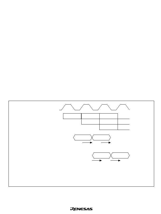
359
8.4
Cache Operation
8.4.1
Cache Reads
This section describes cache operation when the cache is enabled and data is read from the CPU.
One of the 64 entries is selected by the entry address part of the address output from the CPU on
the cache address bus. The tag addresses of ways 0 through 3 are compared to the tag address parts
of the addresses output from the CPU. When there is a way for which the tag address matches, this
is called a cache hit (when any one of the way tag addresses and the tag address of the address
output from the CPU match). In proper use, the tag addresses of each way differ from each other,
and the tag address of only one way will match. When none of the way tag addresses match, it is
called a cache miss. Tag addresses of entries with valid bits of 0 will not match in any case.
When a cache hit occurs, data is read from the data array of the way that was matched according to
the entry address, the byte address within the line, and the access data size, and is sent to the CPU.
The address output on the cache address bus is calculated in the CPU's instruction execution phase
and the results of the read are written during the CPU's write-back stage. The cache address bus
and cache data bus both operate as pipelines in concert with the CPU's pipeline structure. From
address comparison to data read requires 1 cycle; since the address and data operate as a pipeline,
consecutive reads can be performed at each cycle with no waits (figure 8.3).
EX
CPU pipeline stage
I
Cache address bus
Cache data bus
MA
WB
EX
Address A
Cache tag comparison
Address B
MA
EX
Address A
Data array read
Address B
EX: Instruction
execution
MA: Memory
access
WB: Write-back
Figure 8.3 Read Access in Case of a Cache Hit

360
When a cache miss occurs, the way for replacement is determined using the LRU information, and
the read address from the CPU is written in the address array for that way. Simultaneously, the
valid bit is set to 1. Since the 16 bytes of data for replacing the data array are simultaneously read,
the address on the cache address bus is output to the internal address bus and 4 longwords are read
consecutively. The access order is such that, for the address output to the internal address, the byte
address within the line is sequentially incremented by 4, so that the longword that contains the
address to be read from the cache comes last. The read data on the internal data bus is written
sequentially to the cache data array. One cycle after the last data is written to the cache data array,
it is also output to the cache data bus and the read data is sent to the CPU.
The internal address bus and internal data bus also function as pipelines, just like the cache bus
(figure 8.4).
Address A
MA
EX
EX
WB
MA
Data array write
Address B
Address A
+12
Address A
Address A
+8
Address A
+4
Address A
+4
Address A
+8
Address A
+12
Address A
Cache tag comparison
CPU
pipeline
stage
I
Cache
address
bus
Cache
data bus
Internal
address
bus
Internal
data bus
EX:
Instruction execution
MA: Memory access
WB: Write-back
Address A
Figure 8.4 Read Access in Case of a Cache Miss
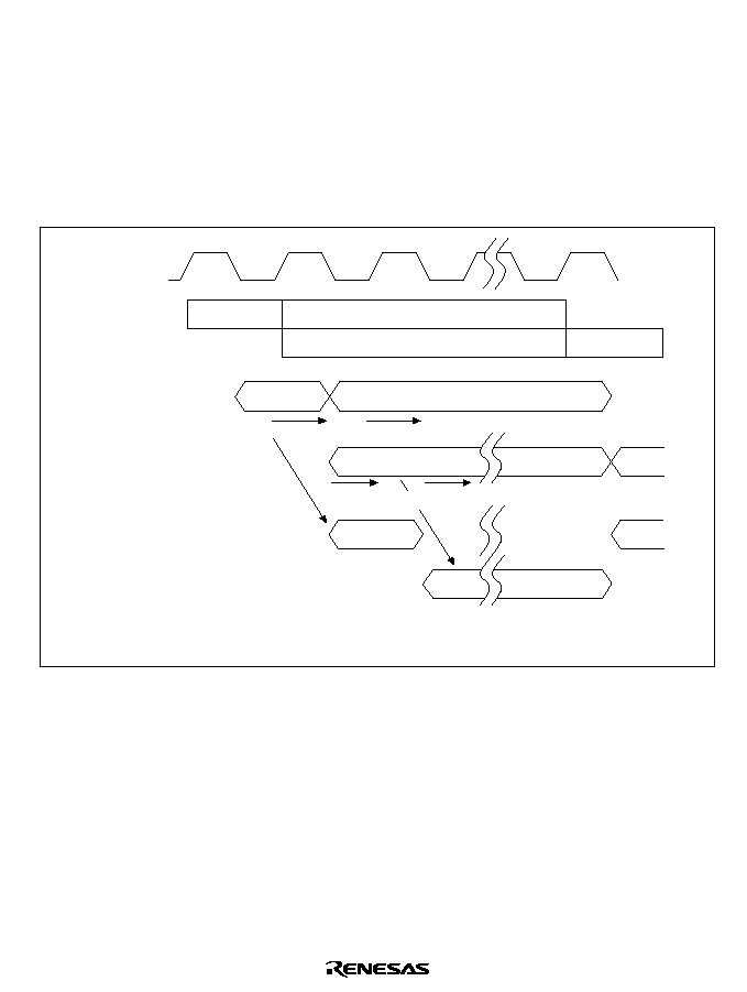
361
8.4.2
Write Access
Write-Through Mode: Writing to external memory is performed regardless of whether or not
there is a cache hit. The write address output to the cache address bus is used for comparison to the
tag address of the cache's address array. If they match, the write data output to the cache data bus
in the following cycle is written to the cache data array. If they do not match, nothing is written to
the cache data array. The write address is output to the internal address bus 1 cycle later than the
cache address bus. The write data is similarly output to the internal data bus 1 cycle later than the
cache data bus. The CPU waits until the writes on the internal buses are completed (figure 8.5).
Address A
CPU pipeline
stage
I
Cache
address bus
Cache
data bus
MA
EX
Internal
data bus
EX
MA
Address B
Address A
Address A
Address A
Address B
Address B
Internal
address bus
Cache tag comparison
Data array write
EX: Instruction execution
MA: Memory access
Figure 8.5 Write Access (Write-Through)
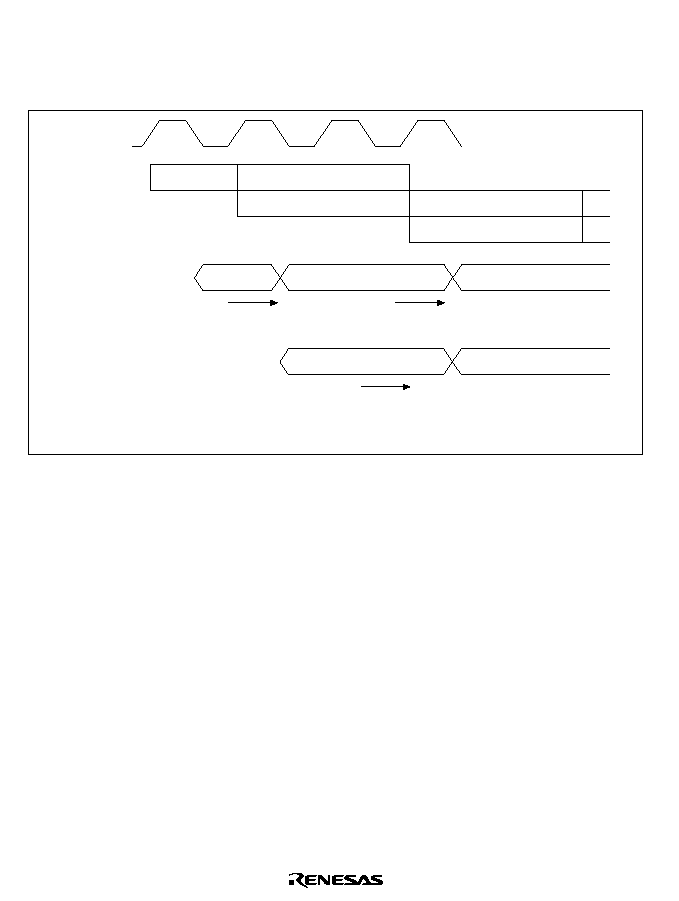
362
Write-Back Mode: When a cache hit occurs, the data is written to the data array of the matching
way according to the entry address, byte address in the line, and access data size, and the update
bit of that entry is set to 1. A write is performed only to the data array, not to external memory. A
write hit is completed in 2 cycles (figure 8.6).
EX
MA
EX
MA
EX
Address A
Address B
Address C
Address A
Address B
CPU pipeline
stage
I
Cache
address bus
Cache
data bus
EX: Instruction
execution
MA: Memory access
Cache tag comparison
Cache tag comparison
Data array write
Figure 8.6 Write Access in Case of a Cache Hit (Write-Back)
When a cache miss occurs, the way for replacement is determined using the LRU information, and
the write address from the CPU is written in the address array for that way. Simultaneously, the
valid bit and update bit are set to 1. Since the 16 bytes of data for replacing the data array are
simultaneously read when the data on the cache bus is written to the cache, the address on the
cache address bus is output to the internal address bus and 4 longwords are read consecutively.
The access order is such that, for the address output to the internal address, the byte address within
the line is sequentially incremented by 4, so that the longword that contains the address to be read
from the cache comes last. The read data on the internal data bus is written sequentially to the
cache data array.
The internal address bus and internal data bus also function as pipelines, just like the cache bus
(figure 8.7).
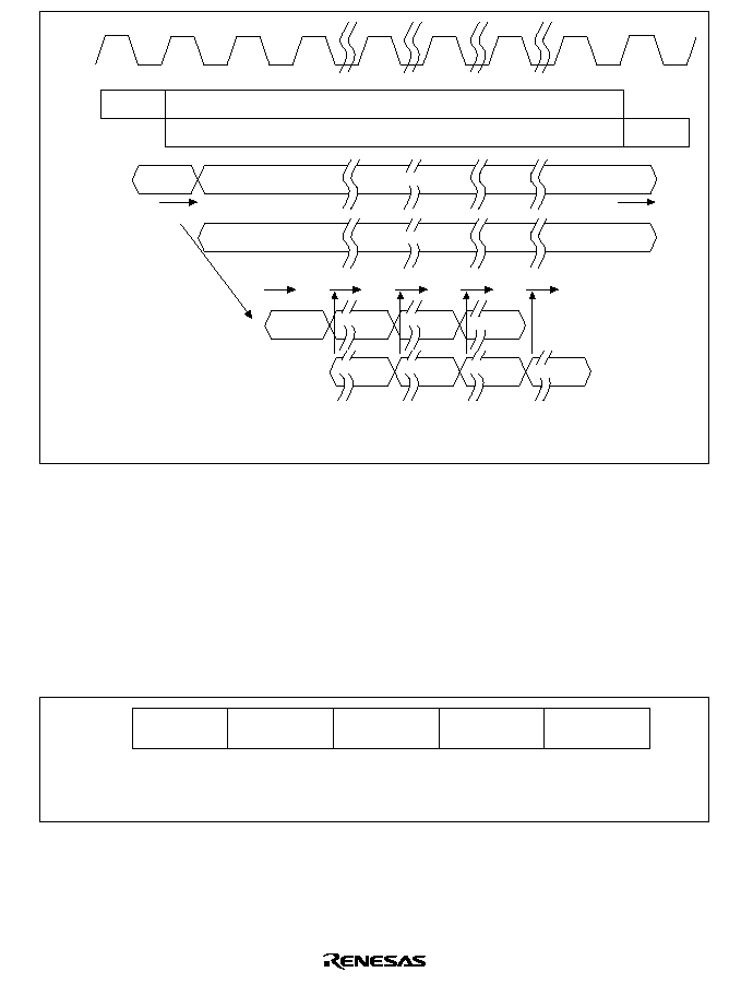
363
Address A
MA
EX
EX
MA
Cache tag comparison
Cache tag comparison
Data array write
Address A
Address A
+12
Address A
+8
Address A
+4
Address A
Address A
+12
Address A
+8
Address A
+4
Address B
Address A
CPU
pipeline
stage
I
Cache
address
bus
Cache
data bus
Internal
address
bus
EX: Instruction
execution
MA: Memory
access
Internal
data bus
Figure 8.7 Write Access in Case of a Cache Miss (Write-Back)
When the update bit of an entry to be replaced in write-back mode is 1, write-back to external
memory is necessary. To improve performance, the entry to be replaced is first transferred to the
write-back buffer, and fetching of the new entry into the cache is given priority over the write-
back. When the new entry has been fetched into the cache, the write-back buffer contents are
written back to external memory. The cache can be accessed during this write-back.
The write-back buffer can hold one cache line (16 bytes) of data and its address. The configuration
of the write-back buffer is shown in figure 8.8.
A (31≠4):
Address for write-back to external memory
Longwords 0≠3: One cache line of data for write-back to external memory
A (31≠4)
Longword 0
Longword 1
Longword 2
Longword 3
Figure 8.8 Write-Back Buffer Configuration
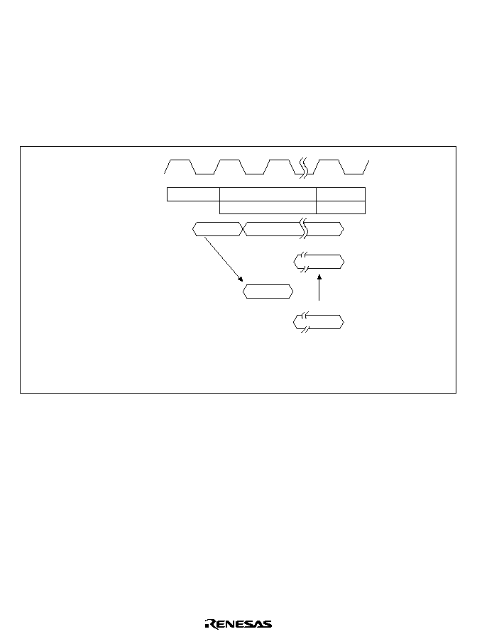
364
8.4.3
Cache-Through Access
When reading or writing a cache-through area, the cache is not accessed. Instead, the cache
address value is output to the internal address bus. For read operations, the read data output to the
internal data bus is fetched and output to the cache data bus, as shown in figure 8.9. The read of
the cache-through area is only performed on the address in question. For write operations, the
write data on the cache data bus is output to the internal data bus. Writes on the cache through area
are compared to the address tag; except for the fact that nothing is written to the data array, the
operation is the same as the write shown in figure 8.5.
EX
CPU
pipeline stage
I
Cache
address bus
Cache
data bus
Internal
address bus
Internal
data bus
MA
WB
EX
MA
Address A
Address A
Address B
Address A
Address A
EX: Instruction
execution
MA: Memory access
WB: Write-back
Figure 8.9 Reading Cache-Through Areas
8.4.4
The TAS Instruction
The TAS instruction reads data from memory, compares it to 0, reflects the result in the T bit of
the status register (SR), and sets the most significant bit to 1. It is an instruction that writes to the
same address. Accesses to the cache area are handled in the same way as ordinary data accesses.
8.4.5
Pseudo-LRU and Cache Replacement
When a cache miss occurs during a read, the data of the missed address is read from 1 line (16
bytes) of memory and replaced. It is therefore necessary to decide which of the four ways is to be
replaced. It can generally be expected that a way that has been infrequently used recently is also
unlikely to be used next. This algorithm for replacing ways is called the least recently used
replacement algorithm, or LRU. The hardware to implement it, however, is complex. For that

365
reason, this cache uses a pseudo-LRU replacement algorithm that keeps track of the order of way
access and replaces the oldest way.
Six bits of data are used as the LRU information. The bits indicate the access order for 2 ways, as
shown in figure 8.10. When the value is 1, access occurred in the direction of the appropriate
arrow in the figure. The direction of the arrow can be determined by reading the bit. Access to the
way to which all the arrows are pointing is the oldest, and that way becomes subject to
replacement. The access order is recorded in the LRU information bits, so the LRU information is
rewritten when a cache hit occurs during a read, when a cache hit occurs during a write, and when
replacement occurs after a cache miss. Table 8.3 shows the rewrite values; table 8.4 shows how
the way to be replaced is selected.
After a cache purge by means of the CP bit in CCR, all the LRU information is zeroized, so the
initial order of use is way 3
way 2
way 1
way 0. Thereafter, the way is selected according
to the order of access in the program. Since the replacement will not be correct if the LRU gets an
inappropriate value, the address array write function can be used to rewrite. When this is done, be
sure not to write a value other than 0 as the LRU information.
When the OD bit or ID bit in CCR is 1, cache replacement is not performed even if a cache miss
occurs during data read or instruction fetch. Instead of replacing, the missed address data is read
and directly transferred to the CPU.
The two-way mode of the cache set by CCR's TW bit can only be implemented by replacing ways
2 and 3. Comparisons of address array tag addresses are carried out on all four ways even in two-
way mode, so the valid bits of ways 1 and 0 must be cleared to 0 before beginning operation in
two-way mode.
Writing for the tag address and valid bit for cache replacement does not wait for the read from
memory to be completed. If a memory access is aborted due to a reset, etc., during replacement,
there will be a discrepancy between the cache contents and memory contents, so a purge must be
performed.
Way 0
Way 2
Way 1
Way 3
Bit 5
Bit 2
Bit 3
Bit 4
Bit 1
Bit 0
Figure 8.10 LRU Information and Access Sequence

366
Table 8.3
LRU Information after Update
Bit 5
Bit 4
Bit 3
Bit 2
Bit 1
Bit 0
Way 0
0
0
0
--
--
--
Way 1
1
--
--
0
0
--
Way 2
--
1
--
1
--
0
Way 3
--
--
1
--
1
1
Note:
--: Holds the value before update.
Table 8.4
Selection Conditions for Replaced Way
Bit 5
Bit 4
Bit 3
Bit 2
Bit 1
Bit 0
Way 0
1
1
1
--
--
--
Way 1
0
--
--
1
1
--
Way 2
--
0
--
0
--
1
Way 3
--
--
0
--
0
0
Note:
--: Don't care.
8.4.6
Cache Initialization
Purges of the entire cache area can only be carried out by writing 1 to the CP bit in CCR. Writing
1 to the CP bit initializes the valid bit of the address array, and all bits of the LRU information, to
0. Cache purges are completed in 1 cycle, but additional time is required for writing to CCR.
Always initialize the valid bit and LRU before enabling the cache.
When the cache is enabled, instructions are read from the cache even during writing to CCR. This
means that the prefetched instructions are read from the cache. To do a proper purge, write 0 to
CCR's CE bit, then disable the cache and purge. Since CCR's CE bit is cleared to 0 by a power-on
reset or manual reset, the cache can be purged immediately by a reset.
8.4.7
Associative Purges
Associative purges invalidate 1 line (16 bytes) corresponding to specific address contents when
the contents are in the cache.
When the contents of a shared address are rewritten by one CPU in a multiprocessor configuration
or a configuration in which the chip's internal E-DMAC (or DMAC) and CPU share memory, that
address must be invalidated in the cache of the other CPU if it is present there.
When writing to or reading the address obtained by adding H'40000000 to the address to be
purged, the valid bit of the entry storing the address prior to addition are initialized to 0.

367
16 bytes are purged in each write, so a purge of 256 bytes of consecutive areas can be
accomplished in 16 writes. Access sizes when associative purges are performed should be
longword. A purge of 1 line requires 2 cycles.
Also note that write-back (flushing) to the main memory is not performed if there is a dirty line in
the cache.
Tag address
010
Entry
address
--
31
9
3
0
19
6
3
4
28
Associative purge:
Address
Bit
Number of bits
Figure 8.11 Associative Purge Access
8.4.8
Cache Flushing
When the CPU rewrites the contents of a specific shared address in the cache by write-back in a
multiprocessor configuration or a configuration in which the chip's internal E-DMAC (or DMAC)
and CPU share memory, the rewritten data must be written back to the main memory, and the
cache contents invalidated, before the bus is granted by the CPU in the chip to another master
(external master, E-DMAC, or DMAC). The chip does not support an instruction or procedure for
flushing the contents of specific addresses, so in order to execute a cache flush it is necessary to
perform reads in a 4-kbyte space (cache area) other than the address space to be flushed from
cache, and intentionally create cache misses. For this purpose, cache accesses should be performed
every 16 bytes. By this means, write-backs are generated and the contents written to the cache by
the CPU in the chip are written back to the main memory, enabling flushing to be executed.
However, this method incurs an overhead consisting of the cache fill time due to read misses and
the time for rereading data to be left in the cache. Therefore, if the overhead due to use of the
write-back method is of concern when constructing a system in which a number of masters share
memory, the shared area should be made a cache-through area in order to maintain coherency.
8.4.9
Data Array Access
The cache data array can be read or written directly via the data array read/write area. Byte, word,
or longword access can be used on the data array. Data array accesses are completed in 1 cycle for
a read and 2 cycles for a write. Since only the cache bus is used, the operation can proceed in
parallel even when another master, such as the DMAC, is using the bus. The data array of way 0 is
mapped on H'C0000000 to H'C00003FF, way 1 on H'C0000400 to H'C00007FF, way 2 on
H'C0000800 to H'C0000BFF and way 3 on H'C0000C00 to H'C0000FFF. When the two-way
mode is being used, the area H'C0000000 to H'C00007FF is accessed as 2 kbytes of on-chip
RAM. When the cache is disabled, the area H'C0000000 to H'C0000FFF can be used as 4 kbytes
of on-chip RAM.

368
When the contents of the way being used as cache are rewritten using a data array access, the
contents of external memory and cache will not match, so this operation should be avoided.
Tag address
110
Entry
address
BA
W
31
28
9
10
11
12
3
0
19
Data
31
0
32
6
3
4
Data
Data array read/write:
BA: Byte address within line
W: Way specification
Address
Bit
Number of bits
Bit
Number of bits
Figure 8.12 Data Array Access
8.4.10
Address Array Access
The address array of the cache can be accessed so that the contents fetched to the cache can be
checked for purposes of program debugging or the like. The address array is mapped on
H'60000000 to H'600003FF. Since all of the ways are mapped to the same addresses, ways are
selected by rewriting the W1 and W0 bits in CCR. The address array can only be accessed in
longwords.
When the address array is read, the tag address, LRU information, and valid bit are output as data.
When the address array is written to, the tag address, and valid bit are written from the cache
address bus. The write address must therefore be calculated before the write is performed. LRU
information is written from the cache data bus, but 0 must always be written to prevent
malfunctions.
369
--
011
Entry
address
--
31
28
29
9
10
3
4
0
19
6
3
4
Tag address
--
Data
LRU
information
--
-- V
31
9
10
3
4
2
0
19
6
3
1 1 2
--
LRU
information
--
31
9
10
3
4
0
22
6
4
Data
Tag address
011
Entry
address
--
-- V
31
28
29
9
10
19
6
3
1 1 2
Address array read:
Address array write:
V: Valid bit
1
3
4
2
0
1
28
29
Address
Bit
Number of bits
Bit
Number of bits
Address
Bit
Number of bits
Bit
Number of bits
Figure 8.13 Address Array Access
8.5
Cache Use
8.5.1
Initialization
Cache memory is not initialized in a reset. Therefore, the cache must be initialized by software
before use. The cache is initialized by zeroizing all address array valid bits and LRU information.
The address array write function can be used to initialize each line, but it is simpler to initialize it
once by writing 1 to the CP bit in CCR. Figure 8.14 shows how to initialize the cache.
MOV.W #H'FE92, R1
MOV.B @R1, R0 ;
AND #H'FE, R0 ;
MOV.B #R0, @R1 ;
Cache disable
OR #H'10, R0
MOV.B R0, @R1 ;
Cache purge
OR #H'01, R0
MOV.B R0, R1 ;
Cache enable
Figure 8.14 Cache Initialization

370
8.5.2
Purge of Specific Lines
There is no snoop function (for monitoring data rewrites), so specific lines of cache must be
purged when the contents of cache memory and external memory differ as a result of an operation.
For instance, when a DMA transfer is performed to the cache area, cache lines corresponding to
the rewritten address area must be purged. All entries of the cache can be purged by setting the CP
bit in CCR to 1. However, it is efficient to purge only specific lines if only a limited number of
entries are to be purged.
An associative purge is used to purge specific lines. Since cache lines are 16 bytes long, purges are
performed in a 16-byte units. The four ways are checked simultaneously, and only lines holding
data corresponding to specified addresses are purged. When addresses do not match, the data at
the specified address is not fetched to the cache, so no purge occurs.
;
Purging 32 bytes from address R3
MOV.L #H'40000000, R0
XOR R1, R1
MOV.L R1, @(R0, R3)
ADD #16, R3
MOV.L R1, @(R0, R3)
Figure 8.15 Purging Specific Addresses
When it is troublesome to purge the cache after every DMA transfer, it is recommended that the
OD bit in CCR be set to 1 in advance. When the OD bit is 1, the cache operates as cache memory
only for instructions. However, when data is already fetched into cache memory, specific lines of
cache memory must be purged for DMA transfers.
8.5.3
Cache Data Coherency
The cache memory does not have a snoop function. This means that when data is shared with a
bus master other than the CPU, software must be used to ensure the coherency of data. For this
purpose, the cache-through area can be used, or a cache purge can be performed with program
logic using write-through.
When the cache-through area is to be used, the data shared by the bus masters is placed in the
cache-through area. This makes it easy to maintain data coherency, since access of the cache-
through area does not fetch data into the cache. When the shared data is accessed repeatedly and
the frequency of data rewrites is low, a lower access speed can adversely affect performance.
To purge the cache using program logic, the data updates are detected by the program flow and the
cache is then purged. For example, if the program inputs data from a disk, whenever reading of a
unit (such as a sector) is completed, the buffer address used for reading or the entire cache is

371
purged, thereby maintaining coherency. When data is to be exchanged between two processors,
only flags that provide mutual notification of completion of data preparation or completion of a
fetch are placed in the cache-through area. The data actually to be transferred is placed in the
cache area and the cache is purged before the first data read to maintain the coherency of the data.
When semaphores are used as the means of communication, data coherency can be maintained
even when the cache is not purged by utilizing the TAS instruction. Direct external access must
always be used for a TAS instruction read.
When the update unit is small, specific addresses can be purged, so only the relevant addresses are
purged. When the update unit is larger, it is faster to purge the entire cache rather than purging all
the addresses in order, and then read the data that previously existed in the cache again from
external memory.
When write-back is used, coherency can be maintained by executing write-backs (flushing) to
memory by means of intentional cache miss reads, but since executing flushing incurs an
overhead, use of write-through or accessing the cache-through area is recommended in a system in
which a number of masters share memory.
8.5.4
Two-Way Cache Mode
The 4-kbyte cache can be used as 2-kbyte RAM and 2-kbyte mixed instruction/data cache memory
by setting the TW bit in CCR to 1. Ways 2 and 3 become cache, and ways 0 and 1 become RAM.
Initialization is performed by writing 1 to the CP bit in CCR, in the same way as with 4 ways. The
valid bit, and LRU bits are cleared to 0.
When LRU information is initialized to zero, the initial order of use is way 3
way 2. Thereafter,
way 3 or way 2 is selected for replacement in accordance with the LRU information. The
conditions for updating the LRU information are the same as for four-way mode, except that the
number of ways is two.
When designated as 2-kbyte RAM, ways 0 and 1 are accessed by data array access. Figure 8.16
shows the address mapping.

372
H'C0000000
H'C00003FF
H'C0000400
H'C00007FF
Way 0
Way 1
H'00000000
H'FFFFFFFF
Figure 8.16 Address Mapping of 2-kbyte RAM in the Two-Way Mode
8.6
Usage Notes
8.6.1
Standby
Disable the cache before entering the standby mode for power-down operation. After returning
from standby, initialize the cache before use.
8.6.2
Cache Control Register
Changing the contents of CCR also changes cache operation. The chip makes full use of pipeline
operations, so it is difficult to synchronize access. For this reason, change the contents of the cache
control register simultaneously when disabling the cache or after the cache is disabled. After
changing the CCR contents, perform a CCR read.

373
Section 9 Ethernet Controller (EtherC)
9.1
Overview
The SH7616 has an on-chip Ethernet controller (EtherC) conforming to the IEEE802.3 MAC
(Media Access Control) layer standard. Connecting a physical-layer LSI (PHY-LSI) complying
with this standard enables the Ethernet controller (EtherC) to perform transmission and reception
of Ethernet/IEEE802.3 frames. The Ethernet controller is connected to dedicated transmit and
receive Ethernet DMACs (E-DMACs) in the SH7616, and carries out high-speed data transfer to
and from memory.
9.1.1
Features
The EtherC has the following features:
∑
Transmission and reception of Ethernet/IEEE802.3 frames
∑
Supports 10/100 Mbps transfer
∑
Supports full-duplex and half-duplex modes
∑
Conforms to IEEE802.3u standard MII (Media Independent Interface)
∑
Magic Packet detection and Wake On LAN (WOL) signal output
∑
CAM (Content Addressable Memory) match signal input function
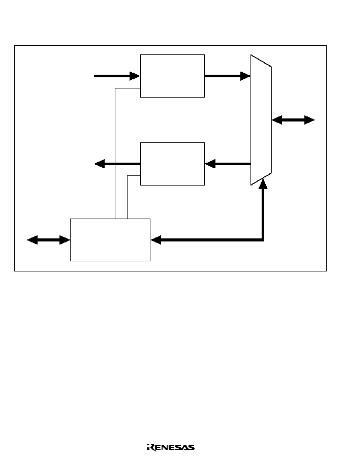
374
9.1.2
Configuration
Figure 9.1 shows the configuration of the Ethernet controller.
Transmit
controller
Receive
controller
Command status
interface
MII
Figure 9.1 Configuration of Ethernet Controller (EtherC)
Transmit Controller: Transmit data is stored in the transmit FIFO from memory via the transmit
E-DMAC. The transmit controller assembles this data into an Ethernet/IEEE802.3 frame, which it
outputs to the MII. After passing through the MII, the transmit data is sent onto the line by a PHY-
LSI. The main functions of the transmit controller are as follows:
∑
Frame assembly and transmission
∑
CRC calculation and provision to frames
∑
Data retransmission in case of a collision (up to 15 times)
∑
Compliant with MII in IEEE802.3u standard
∑
Byte-nibble conversion supporting PHY-LSI speed

375
Receive Controller: After a frame is received via the MII, the receive controller carries out
address information, frame length, CRC, and other checks, and the receive data is transferred to
memory by the receive E-DMAC. The main functions of the receive controller are as follows:
∑
Checking received frame format
∑
Checking receive frame CRC and frame length
∑
Transfer of own-address, multicast, or broadcast receive frames to memory
∑
Compliant with MII in IEEE802.3u standard
∑
Nibble-byte conversion supporting PHY-LSI speed
∑
Magic Packet monitoring
∑
CAM (Content Addressable Memory) match signal input function
Command/Status Interface: This interface provides various command/status registers to control
the EtherC, and performs access to PHY-LSI internal registers via the MII.

376
9.1.3
Pin Configuration
The EtherC has signal pins compatible with the 18-pin MII specified in the IEEE802.3u standard,
and three related signal pins to simplify connection to the PHY-LSI. The pin configuration are
shown in table 9.1.
Table 9.1
MII Pin Functions
Type
Abbre-
viation
Name
I/O
Function
MII
TX-CLK
Transmit clock
Input
TX-EN, ETXD0 to ETXD3, TX-ER timing
reference signal
RX-CLK
Receive clock
Input
RX-DV, ERXD0 to ERXD3, RX-ER timing
reference signal
TX-EN
Transmit enable
Output
Indicates that transmit data is ready on
ETXD0 to ETXD3
ETXD0≠
ETXD3
Transmit data (4-bit)
Output
4-bit transmit data
TX-ER
Transmit error
Output
Notifies PHY-LSI of error during transmission
RX-DV
Receive data valid
Input
Indicates that there is valid receive data on
ERXD0 to ERXD3
ERXD0≠
ERXD3
Receive data (4-bit)
Input
4-bit receive data
RX-ER
Receive error
Input
Identifies error state occurring during data
reception
CRS
Carrier detect
Input
Carrier detection signal
COL
Collision detect
Input
Collision detection signal
MDC
Management data
clock
Output
Reference clock signal for information
transfer via MDIO
MDIO
Management data
input/output
Input/
output
Bidirectional signal for exchange of
management information between STA and
PHY
Other
LNKSTA
Link status
Input
Inputs link status from PHY-LSI
EXOUT
General-purpose
external output
Output
External output pin
WOL
Wake-On-LAN
Output
Magic packet reception
CAMSEN
CAM input
Input
CAM match signal input function

377
9.1.4
Ethernet Controller Register Configuration
The Ethernet controller (EtherC) has the nineteen 32-bit registers shown in table 9.2.
Table 9.2
EtherC Registers
Name
Abbre-
viation
R/W
Initial Value
Address
EtherC mode register
ECMR
R/W
H'00000000
H'FFFFFD60
EtherC status register
ECSR
R/W
*
1
H'00000000
H'FFFFFD64
EtherC interrupt permission register
ECSIPR
R/W
H'00000000
H'FFFFFD68
PHY interface register
PIR
R/W
H'0000000X
H'FFFFFD6C
MAC address high register
MAHR
R/W
H'00000000
H'FFFFFD70
MAC address low register
MALR
R/W
H'00000000
H'FFFFFD74
Receive flame length register
RFLR
R/W
H'00000000
H'FFFFFD78
PHY status register
PSR
R
H'00000000
H'FFFFFD7C
Transmit retry over counter register
TROCR
R/W
*
2
H'00000000
H'FFFFFD80
Single Collision detect counter register
SCDCR
R/W
*
2
H'00000000
H'FFFFFDB4
Delay Collision detect counter register
CDCR
R/W
*
2
H'00000000
H'FFFFFD84
Lost carrier counter register
LCCR
R/W
*
2
H'00000000
H'FFFFFD88
Carrier not detect counter register
CNDCR
R/W
*
2
H'00000000
H'FFFFFD8C
Illegal frame length counter register
IFLCR
R/W
*
2
H'00000000
H'FFFFFD90
CRC error frame receive counter register
CEFCR
R/W
*
2
H'00000000
H'FFFFFD94
Frame receive error counter register
FRECR
R/W
*
2
H'00000000
H'FFFFFD98
Too-short frame receive counter register
TSFRCR
R/W
*
2
H'00000000
H'FFFFFD9C
Too-long frame receive counter register
TLFRCR
R/W
*
2
H'00000000
H'FFFFFDA0
Residual-bit frame counter register
RFCR
R/W
*
2
H'00000000
H'FFFFFDA4
Multicast address frame counter register
MAFCR
R/W
*
2
H'00000000
H'FFFFFDA8
Notes: 1. All registers must be accessed as 32-bit units.
2. Reserved bits in a register should only be written with 0.
3. The value read from a reserved bit is not guaranteed.
*
1 Individual bits are cleared by writing 1.
*
2 Cleared by a write to the register.

378
9.2
Register Descriptions
9.2.1
EtherC Mode Register (ECMR)
Bit:
31
30
29
. . .
19
18
17
16
--
--
--
. . .
--
--
--
--
Initial value:
0
0
0
. . .
0
0
0
0
R/W:
R
R
R
. . .
R
R
R
R
Bit:
15
14
13
12
11
10
9
8
--
--
--
PRCEF
--
--
MPDE
--
Initial value:
0
0
0
0
0
0
0
0
R/W:
R
R
R
R/W
R
R
R/W
R
Bit:
7
6
5
4
3
2
1
0
--
RE
TE
--
ILB
ELB
DM
PRM
Initial value:
0
0
0
0
0
0
0
0
R/W:
R
R/W
R/W
R
R/W
R/W
R/W
R/W
The EtherC mode register specifies the operating mode of the Ethernet controller. The settings in
this register are normally made in the initialization process following a reset.
Notes: Operation mode settings must not be changed while the transmitting and receiving
functions are enabled. To modify bits other than the ECMR's RE and TE bits, follow the
procedures below.
1. Return EtherC and E-DMAC to their initial state by means of the software reset bit
(SWR) in the E-DMAC mode register (EDMR), and make new settings.
2. Set the RE and TE bits to 0 to disable them before modifying bits. Since a frame may
be transmitted or received, wait for at least a maximum frame transfer time before
changing bits other than the RE and TE bits.
Bits 31 to 13--Reserved: These bits are always read as 0. The write value should always be 0.

379
Bit 12--Permit Receive CRC Error Frame (PRCEF): Specifies the treatment of a receive frame
containing a CRC error.
Bit 12: PRCEF
Description
0
Reception of a frame with a CRC error is treated as an error
(Initial value)
1
Reception of a frame with a CRC error is not treated as an error
Note:
When this bit is set to 1, the CRC error frame counter register (CEFCR: see section 9.2.14)
is not incremented when a CRC error is detected.
Bits 11 and 10--Reserved: These bits are always read as 0. The write value should always be 0.
Bit 9--Magic Packet Detection Enable (MPDE): Enables or disables Magic Packet detection by
hardware to allow activation from the Ethernet. When the Magic Packet is detected, it is reflected
to the EtherC status register and the WOL pin notifies peripheral LSIs that the Magic Packet has
been received.
Bit 9: MPDE
Description
0
Magic Packet detection is not enabled
(Initial value)
1
Magic Packet detection is enabled
Bits 8 and 7--Reserved: These bits are always read as 0. The write value should always be 0.
Bit 6--Receiver Enable (RE): Enables or disables the receiver.
Bit 6: RE
Description
0
Receiver is disabled
(Initial value)
1
Receiver is enabled
Note:
If a switch is made from the receiver-enabled state (RE = 1) to the receiver-disabled state
(RE = 0) while a frame is being received, the receiver will not be disabled until reception of
the frame is completed.
Bit 5--Transmitter Enable (TE): Enables or disables the transmitter.
Bit 5: TE
Description
0
Transmitter is disabled
(Initial value)
1
Transmitter is enabled
Note:
If a switch is made from the transmitter-enabled state (TE = 1) to the transmitter-disabled
state (TE = 0) while a frame is being transmitted, the transmitter will not be disabled until
transmission of the frame is completed.
Bit 4--Reserved: This bit is always read as 0. The write value should always be 0.

380
Bit 3--Internal Loop Back Mode (ILB): Specifies loopback mode in the EtherC.
Bit 3: ILB
Description
0
Normal data transmission/reception is performed
(Initial value)
1
Data loopback is performed inside the EtherC
Note:
A loopback mode specification can only be made with full-duplex transfer (DM = 1 in this
register).
Bit 2--External Loop Back Mode (ELB): The value in this register is output directly to the
SH7616's general-purpose external output pin (EXOUT). This is used for loopback mode
directives, etc., in the PHY-LSI, using the EXOUT pin.
Bit 2: ELB
Description
0
Low-level output from EXOUT pin
(Initial value)
1
High-level output from EXOUT pin
Note:
In order for PHY loopback to be implemented using this function, the PHY-LSI must have a
pin corresponding to the EXOUT pin.
Bit 1--Duplex Mode (DM): Specifies the EtherC transfer method.
Bit 1: DM
Description
0
Half-duplex transfer is specified
(Initial value)
1
Full-duplex transfer is specified
Note:
When internal loopback mode is specified (ILB = 1), full-duplex transfer (DM = 1) must be
used.
Bit 0--Promiscuous Mode (PRM): Setting this bit enables all Ethernet frames to be received.
Bit 0: PRM
Description
0
EtherC performs normal operation
(Initial value)
1
EtherC performs promiscuous mode operation
Note:
"All Ethernet frames" means all receivable frames, irrespective of differences or
enabled/disabled status (destination address, broadcast address, multicast bit, etc.).

381
9.2.2
EtherC Status Register (ECSR)
Bit:
31
30
29
. . .
11
10
9
8
--
--
--
. . .
--
--
--
--
Initial value:
0
0
0
. . .
0
0
0
0
R/W:
R
R
R
. . .
R
R
R
R
Bit:
7
6
5
4
3
2
1
0
--
--
--
--
--
LCHNG
MPD
ICD
Initial value:
0
0
0
0
0
0
0
0
R/W:
R
R
R
R
R
R/W
*
R/W
*
R/W
*
Note:
*
The flag is cleared by writing 1. Writing 0 does not affect the flag.
The EtherC status register shows the internal status of the EtherC. This status information can be
reported to the CPU by means of interrupts. Individual bits are cleared by writing 1 to them. For
bits that generate an interrupt, the interrupt can be enabled or disabled by means of the
corresponding bit in the EtherC status interrupt permission register (ECSIPR).
Bits 31 to 3--Reserved: These bits are always read as 0. The write value should always be 0.
Bit 2--LINK Signal Changed (LCHNG): Indicates that the LNKSTA signal input from the PHY-
LSI has changed from high to low, or from low to high. This bit is cleared by writing 1 to it.
Writing 0 to this bit has no effect.
Bit 2: LCHNG
Description
0
LNKSTA signal change has not been detected
(Initial value)
1
LNKSTA signal change (high-to-low or low-to-high) has been detected
Notes: 1. The current link status can be checked by referencing the LMON bit in the PHY
interface status register (PSR).
2. Signal variation may be detected when the LNKSTA function is selected by the port A
control register (PACR) of the pin function controller (PFC).
Bit 1--Magic Packet Detection (MPD): Indicates that a Magic Packet has been detected on the
line. This bit is cleared by writing 1 to it. Writing 0 to this bit has no effect.
Bit 1: MPD
Description
0
Magic Packet has not been detected
(Initial value)
1
Magic Packet has been detected

382
Bit 0--Illegal Carrier Detection (ICD): Indicates that PHY-LSI has detected an illegal carrier on
the line. This bit is cleared by writing 1 to it. Writing 0 to this bit has no effect.
Bit 0: ICD
Description
0
PHY-LSI has not detected an illegal carrier on the line
(Initial value)
1
PHY-LSI has detected an illegal carrier on the line
Note:
If a change in the signal input from the PHY-LSI occurs before the software recognition
period, the correct information may not be obtained. Refer to the timing specification for the
PHY-LSI used.
9.2.3
EtherC Interrupt Permission Register (ECSIPR)
Bit:
31
30
29
. . .
11
10
9
8
--
--
--
. . .
--
--
--
--
Initial value:
0
0
0
. . .
0
0
0
0
R/W:
R
R
R
. . .
R
R
R
R
Bit:
7
6
5
4
3
2
1
0
--
--
--
--
--
LCHNGIP MPDIP
ICDIP
Initial value:
0
0
0
0
0
0
0
0
R/W:
R
R
R
R
R
R/W
R/W
R/W
This register enables or disables the interrupt sources indicated by the EtherC status register. Each
bit in this register enables or disables the interrupt indicated by the corresponding bit in the EtherC
status register.
Bits 31 to 3--Reserved: These bits are always read as 0. The write value should always be 0.
Bit 2-- LINK Signal Changed Interrupt Permission (LCHNGIP): Controls interrupt notification
by the LINK Signal Changed bit.
Bit 2: LCHNGIP
Description
0
Interrupt notification by LCHNG bit in ECSR is disabled
(Initial value)
1
Interrupt notification by LCHNG bit in ECSR is enabled
Bit 1--Magic Packet Detection Interrupt Permission (MPDIP): Controls interrupt notification by
the Magic Packet Detection bit.
Bit 1: MPDIP
Description
0
Interrupt notification by MPD bit in ECSR is disabled
(Initial value)
1
Interrupt notification by MPD bit in ECSR is enabled
383
Bit 0--Illegal Carrier Detection Interrupt Permission (ICDIP): Controls interrupt notification by
the Illegal Carrier Detection bit.
Bit 0: ICDIP
Description
0
Interrupt notification by ICD bit in ECSR is disabled
(Initial value)
1
Interrupt notification by ICD bit in ECSR is enabled
9.2.4
PHY Interface Register (PIR)
Bit:
31
30
29
. . .
11
10
9
8
--
--
--
. . .
--
--
--
--
Initial value:
0
0
0
. . .
0
0
0
0
R/W:
R
R
R
. . .
R
R
R
R
Bit:
7
6
5
4
3
2
1
0
--
--
--
--
MDI
MDO
MMD
MDC
Initial value:
0
0
0
0
*
0
0
0
R/W:
R
R
R
R
R
R/W
R/W
R/W
Note:
*
Undefined
PIR provides a means of accessing PHY-LSI internal registers via the MII.
Bits 31 to 4--Reserved: These bits are always read as 0. The write value should always be 0.
Bit 3-- MII Management Data-In (MDI): Indicates the level of the MDIO pin.
Bit 2-- MII Management Data-Out (MDO): Outputs the value set to this bit by the MDIO pin
when the MMD bit is 1.
Bit 1-- MII Management Mode (MMD): Specifies the data read/write direction with respect to the
MII. Read direction is indicated by 0, and write direction by 1.
Bit 0-- MII Management Data Clock (MDC): Outputs the value set to this bit by the MDC pin
and supplies the MII with the management data clock.
For the method of accessing MII registers, see section 9.3.4, Accessing MII Registers.

384
9.2.5
MAC Address High Register (MAHR)
Bit:
31
30
29
28
27
26
25
24
MA47
MA46
MA45
MA44
MA43
MA42
MA41
MA40
Initial value:
0
0
0
0
0
0
0
0
R/W:
R/W
R/W
R/W
R/W
R/W
R/W
R/W
R/W
Bit:
23
22
21
20
19
18
17
16
MA39
MA38
MA37
MA36
MA35
MA34
MA33
MA32
Initial value:
0
0
0
0
0
0
0
0
R/W:
R/W
R/W
R/W
R/W
R/W
R/W
R/W
R/W
Bit:
15
14
13
12
11
10
9
8
MA31
MA30
MA29
MA28
MA27
MA26
MA25
MA24
Initial value:
0
0
0
0
0
0
0
0
R/W:
R/W
R/W
R/W
R/W
R/W
R/W
R/W
R/W
Bit:
7
6
5
4
3
2
1
0
MA23
MA22
MA21
MA20
MA19
MA18
MA17
MA16
Initial value:
0
0
0
0
0
0
0
0
R/W:
R/W
R/W
R/W
R/W
R/W
R/W
R/W
R/W
The upper 32 bits of the 48-bit MAC address are set in MARH. The setting in this register is
normally made in the initialization process after a reset.
Note:
The MAC address setting must not be changed while the transmitter and receiver are
enabled. First return the EtherC and E-DMAC modules to their initial state by means of
the SWR bit in the E-DMAC mode register (EDMR), then make the new setting.
Bits 31 to 0--MAC Address Bits 47 to 16 (MA47 to MA16): Used to set the upper 32 bits of the
MAC address.
Note:
If the MAC address to be set in the SH7616 is 01-23-45-67-89-AB (hexadecimal), the
value set in this register is H'01234567.

385
9.2.6
MAC Address Low Register (MALR)
Bit:
31
30
29
. . .
19
18
17
16
--
--
--
. . .
--
--
--
--
Initial value:
0
0
0
. . .
0
0
0
0
R/W:
R
R
R
R
R
R
R
Bit:
15
14
13
12
11
10
9
8
MA15
MA14
MA13
MA12
MA11
MA10
MA9
MA8
Initial value:
0
0
0
0
0
0
0
0
R/W:
R/W
R/W
R/W
R/W
R/W
R/W
R/W
R/W
Bit:
7
6
5
4
3
2
1
0
MA7
MA6
MA5
MA4
MA3
MA2
MA1
MA0
Initial value:
0
0
0
0
0
0
0
0
R/W:
R/W
R/W
R/W
R/W
R/W
R/W
R/W
R/W
The lower 16 bits of the 48-bit MAC address are set in MARL. The setting in this register is
normally made in the initialization process after a reset.
Note:
The MAC address setting must not be changed while the transmitter and receiver are
enabled. First return the EtherC and E-DMAC modules to their initial state by means of
the SWR bit in the E-DMAC mode register (EDMR), then make the new setting.
Bits 31 to 16--Reserved: These bits are always read as 0. The write value should always be 0.
Bits 15 to 0--MAC Address Bits 15 to 0 (MA15 to MA0): Used to set the lower 16 bits of the
MAC address.
Note:
If the MAC address to be set in the SH7616 is 01-23-45-67-89-AB (hexadecimal), the
value set in this register is H'000089AB.

386
9.2.7
Receive Frame Length Register (RFLR)
Bit:
31
30
29
. . .
19
18
17
16
--
--
--
. . .
--
--
--
--
Initial value:
0
0
0
. . .
0
0
0
0
R/W:
R
R
R
. . .
R
R
R
R
Bit:
15
14
13
12
11
10
9
8
--
--
--
--
RFL11
RFL10
RFL9
RFL8
Initial value:
0
0
0
0
0
0
0
0
R/W:
R
R
R
R
R/W
R/W
R/W
R/W
Bit:
7
6
5
4
3
2
1
0
RFL7
RFL6
RFL5
RFL4
RFL3
RFL2
RFL1
RFL0
Initial value:
0
0
0
0
0
0
0
0
R/W:
R/W
R/W
R/W
R/W
R/W
R/W
R/W
R/W
This register specifies the maximum frame length (in bytes) that can be received by the SH7616
Bits 31 to 12--Reserved: These bits are always read as 0. The write value should always be 0.
Bits 11 to 0--Receive Frame Length (RFL)
H'000≠H'5EE
1,518 bytes
H'5EF
1,519 bytes
H'5F0
1,520 bytes
.
.
.
.
.
.
H'7FF
2,047 bytes
H'800≠H'FFF
2,048 bytes
Notes: 1. The frame length refers to all fields from the destination address up to and including the
CRC data.
2. When data that exceeds the specified value is received, the part of the data that is
higher than the specified value is discarded.
Frame contents from the destination address up to and including the data are actually
transferred to memory. CRC data is not included in the transfer.

387
9.2.8
PHY Interface Status Register (PSR)
Bit:
31
30
29
. . .
11
10
9
8
--
--
--
. . .
--
--
--
--
Initial value:
0
0
0
. . .
0
0
0
0
R/W:
R
R
R
. . .
R
R
R
R
Bit:
7
6
5
4
3
2
1
0
--
--
--
--
--
--
--
LMON
Initial value:
0
0
0
0
0
0
0
0
R/W:
R
R
R
R
R
R
R
R
PSR enables interface signals from the PHY-LSI to be read.
Bits 31 to 1--Reserved: These bits are always read as 0. The write value should always be 0.
Bit 0-- Link Monitor (LMON): The link status can be read by connecting the LINK signal output
from the PHY-LSI. For information on the polarity, refer to the specifications for the PHY-LSI to
be connected.
Note: The LMON bit is set to 0 when the LNKSTA pin is at high level, and it is set to 1 when
the LNKSTA pin is at low level.

388
9.2.9
Transmit Retry Over Counter Register (TROCR)
Bit:
31
30
29
. . .
19
18
17
16
--
--
--
. . .
--
--
--
--
Initial value:
0
0
0
. . .
0
0
0
0
R/W:
R
R
R
. . .
R
R
R
R
Bit:
15
14
13
12
11
10
9
8
TROC15 TROC14 TROC13 TROC12 TROC11 TROC10 TROC9
TROC8
Initial value:
0
0
0
0
0
0
0
0
R/W:
R/W
R/W
R/W
R/W
R/W
R/W
R/W
R/W
Bit:
7
6
5
4
3
2
1
0
TROC7
TROC6
TROC5
TROC4
TROC3
TROC2
TROC1
TROC0
Initial value:
0
0
0
0
0
0
0
0
R/W:
R/W
R/W
R/W
R/W
R/W
R/W
R/W
R/W
TROCR is a 16-bit counter that indicates the number of frames that were unable to be transmitted
in 16 retransmission attempts. When 16 transmission attempts have failed, TROCR is incremented
by 1. When the value in this register reaches H'FFFF (65,535), the count is halted. The counter
value is cleared to 0 by a write to this register (the write value is immaterial).
Bits 31 to 16--Reserved: These bits are always read as 0. The write value should always be 0.
Bits 15 to 0--Transmit Retry Over Count 15 to 0 (TROC15 to TROC0): These bits indicate the
number of frames that were unable to be transmitted in 16 retransmission attempts.

389
9.2.10
Single Collision Detect Counter Register (SCDCR)
This register is a 32-bit counter that indicates the number of collisions on all lines from a start of
transmission. When the value in this register reaches H'FFFFFFFF, count-up is halted. The
counter's value is cleared to 0 by writing to this register. The value written is "don't care".
Bit:
31
30
29
28
27
26
25
24
COSDC31 COSDC30 COSDC29 COSDC28 COSDC27 COSDC26 COSDC25 COSDC24
Initial value:
0
0
0
0
0
0
0
0
R/W:
R/W
R/W
R/W
R/W
R/W
R/W
R/W
R/W
Bit:
23
22
21
20
19
18
17
16
COSDC23 COSDC22 COSDC21 COSDC20 COSDC19 COSDC18 COSDC17 COSDC16
Initial value:
0
0
0
0
0
0
0
0
R/W:
R/W
R/W
R/W
R/W
R/W
R/W
R/W
R/W
Bit:
15
14
13
12
11
10
9
8
COSDC15 COSDC14 COSDC13 COSDC12 COSDC11 COSDC10
COSDC9 COSDC8
Initial value:
0
0
0
0
0
0
0
0
R/W:
R/W
R/W
R/W
R/W
R/W
R/W
R/W
R/W
Bit:
7
6
5
4
3
2
1
0
COSDC7 COSDC6 COSDC5 COSDC4 COSDC3 COSDC2 COSDC1 COSDC0
Initial value:
0
0
0
0
0
0
0
0
R/W:
R/W
R/W
R/W
R/W
R/W
R/W
R/W
R/W
Bits 31 to 0≠≠ Collision Detect Count 31 to 0 (COSDC31 to COSDC0): These bits indicate the
number of collisions from a start of transmission.

390
9.2.11
Delay Collision Detect Counter Register (CDCR)
Bit:
31
30
29
. . .
19
18
17
16
--
--
--
. . .
--
--
--
--
Initial value:
0
0
0
. . .
0
0
0
0
R/W:
R
R
R
. . .
R
R
R
R
Bit:
15
14
13
12
11
10
9
8
COLDC15 COLDC14COLDC13 COLDC12COLDC11 COLDC10 COLDC9 COLDC8
Initial value:
0
0
0
0
0
0
0
0
R/W:
R/W
R/W
R/W
R/W
R/W
R/W
R/W
R/W
Bit:
7
6
5
4
3
2
1
0
COLDC7 COLDC6 COLDC5 COLDC4 COLDC3 COLDC2 COLDC1 COLDC0
Initial value:
0
0
0
0
0
0
0
0
R/W:
R/W
R/W
R/W
R/W
R/W
R/W
R/W
R/W
CDCR is a 16-bit counter that indicates the number of collisions that occurred on the line,
counting from a point 512 bits after the start of data transmission. When the value in this register
reaches H'FFFF (65,535), the count is halted. The counter value is cleared to 0 by a write to this
register (the write value is immaterial).
Bits 31 to 16--Reserved: These bits are always read as 0. The write value should always be 0.
Bits 15 to 0--Collision Detect Count 15 to 0 (COLDC15 to COLDC0): These bits indicate the
count of collisions from a point 512 bits after the start of data transmission.

391
9.2.12
Lost Carrier Counter Register (LCCR)
Bit:
31
30
29
. . .
19
18
17
16
--
--
--
. . .
--
--
--
--
Initial value:
0
0
0
. . .
0
0
0
0
R/W:
R
R
R
. . .
R
R
R
R
Bit:
15
14
13
12
11
10
9
8
LCC15
LCC14
LCC13
LCC12
LCC11
LCC10
LCC9
LCC8
Initial value:
0
0
0
0
0
0
0
0
R/W:
R/W
R/W
R/W
R/W
R/W
R/W
R/W
R/W
Bit:
7
6
5
4
3
2
1
0
LCC7
LCC6
LCC5
LCC4
LCC3
LCC2
LCC1
LCC0
Initial value:
0
0
0
0
0
0
0
0
R/W:
R/W
R/W
R/W
R/W
R/W
R/W
R/W
R/W
LCCR is a 16-bit counter that indicates the number of times the carrier was lost during data
transmission. When the value in this register reaches H'FFFF (65,535), the count is halted. The
counter value is cleared to 0 by a write to this register (the write value is immaterial).
Bits 31 to 16--Reserved: These bits are always read as 0. The write value should always be 0.
Bits 15 to 0--Lost Carrier Count 15 to 0 (LCC15 to LCC0): These bits indicate the number of
times the carrier was lost during data transmission.

392
9.2.13
Carrier Not Detect Counter Register (CNDCR)
Bit:
31
30
29
. . .
19
18
17
16
--
--
--
. . .
--
--
--
--
Initial value:
0
0
0
. . .
0
0
0
0
R/W:
R
R
R
. . .
R
R
R
R
Bit:
15
14
13
12
11
10
9
8
CNDC15 CNDC14 CNDC13 CNDC12 CNDC11 CNDC10 CNDC9
CNDC8
Initial value:
0
0
0
0
0
0
0
0
R/W:
R/W
R/W
R/W
R/W
R/W
R/W
R/W
R/W
Bit:
7
6
5
4
3
2
1
0
CNDC7
CNDC6
CNDC5
CNDC4
CNDC3
CNDC2
CNDC1
CNDC0
Initial value:
0
0
0
0
0
0
0
0
R/W:
R/W
R/W
R/W
R/W
R/W
R/W
R/W
R/W
CNDCR is a 16-bit counter that indicates the number of times the carrier could not be detected
while the preamble was being sent. When the value in this register reaches H'FFFF (65,535), the
count is halted. The counter value is cleared to 0 by a write to this register (the write value is
immaterial).
Bits 31 to 16--Reserved: These bits are always read as 0. The write value should always be 0.
Bits 15 to 0--Carrier Not Detect Count 15 to 0 (CNDC15 to CNDC0): These bits indicate the
number of times the carrier was not detected.

393
9.2.14
Illegal Frame Length Counter Register (IFLCR)
Bit:
31
30
29
. . .
19
18
17
16
--
--
--
. . .
--
--
--
--
Initial value:
0
0
0
. . .
0
0
0
0
R/W:
R
R
R
. . .
R
R
R
R
Bit:
15
14
13
12
11
10
9
8
IFLC15
IFLC14
IFLC13
IFLC12
IFLC11
IFLC10
IFLC9
IFLC8
Initial value:
0
0
0
0
0
0
0
0
R/W:
R/W
R/W
R/W
R/W
R/W
R/W
R/W
R/W
Bit:
7
6
5
4
3
2
1
0
IFLC7
IFLC6
IFLC5
IFLC4
IFLC3
IFLC2
IFLC1
IFLC0
Initial value:
0
0
0
0
0
0
0
0
R/W:
R/W
R/W
R/W
R/W
R/W
R/W
R/W
R/W
IFLCR is a 16-bit counter that indicates the number of times transmission of a packet with a frame
length of less than four bytes was attempted during data transmission. When the value in this
register reaches H'FFFF (65,535), the count is halted. The counter value is cleared to 0 by a write
to this register (the write value is immaterial).
Bits 31 to 16--Reserved: These bits are always read as 0. The write value should always be 0.
Bits 15 to 0--Illegal Frame Length Count 15 to 0 (IFLC15 to IFLC0): These bits indicate the
count of illegal frame length transmission attempts.

394
9.2.15
CRC Error Frame Counter Register (CEFCR)
Bit:
31
30
29
. . .
19
18
17
16
--
--
--
. . .
--
--
--
--
Initial value:
0
0
0
. . .
0
0
0
0
R/W:
R
R
R
. . .
R
R
R
R
Bit:
15
14
13
12
11
10
9
8
CEFC15 CEFC14 CEFC13 CEFC12 CEFC11 CEFC10
CEFC9
CEFC8
Initial value:
0
0
0
0
0
0
0
0
R/W:
R/W
R/W
R/W
R/W
R/W
R/W
R/W
R/W
Bit:
7
6
5
4
3
2
1
0
CEFC7
CEFC6
CEFC5
CEFC4
CEFC3
CEFC2
CEFC1
CEFC0
Initial value:
0
0
0
0
0
0
0
0
R/W:
R/W
R/W
R/W
R/W
R/W
R/W
R/W
R/W
CEFCR is a 16-bit counter that indicates the number of times a frame with a CRC error was
received. When the value in this register reaches H'FFFF (65,535), the count is halted. The counter
value is cleared to 0 by a write to this register (the write value is immaterial).
Bits 31 to 16--Reserved: These bits are always read as 0. The write value should always be 0.
Bits 15 to 0--CRC Error Frame Count 15 to 0 (CEFC15 to CEFC0): These bits indicate the count
of CRC error frames received.
Note:
When the Permit Receive CRC Error Frame bit (PRCEF) is set to 1 in the EtherC Mode
Register (ECMR), CEFCR is not incremented by reception of a frame with a CRC error.

395
9.2.16
Frame Receive Error Counter Register (FRECR )
Bit:
31
30
29
. . .
19
18
17
16
--
--
--
. . .
--
--
--
--
Initial value:
0
0
0
. . .
0
0
0
0
R/W:
R
R
R
. . .
R
R
R
R
Bit:
15
14
13
12
11
10
9
8
FREC15 FREC14 FREC13 FREC12 FREC11 FREC10
FREC9
FREC8
Initial value:
0
0
0
0
0
0
0
0
R/W:
R/W
R/W
R/W
R/W
R/W
R/W
R/W
R/W
Bit:
7
6
5
4
3
2
1
0
FREC7
FREC6
FREC5
FREC4
FREC3
FREC2
FREC1
FREC0
Initial value:
0
0
0
0
0
0
0
0
R/W:
R/W
R/W
R/W
R/W
R/W
R/W
R/W
R/W
FRECR is a 16-bit counter that indicates the number of frames input from the PHY-LSI for which
a receive error was indicated by the RX-ER pin. FRECR is incremented each time this pin
becomes active. When the value in this register reaches H'FFFF (65,535), the count is halted. The
counter value is cleared to 0 by a write to this register (the write value is immaterial).
Bits 31 to 16--Reserved: These bits are always read as 0. The write value should always be 0.
Bits 15 to 0--Frame Receive Error Count 15 to 0 (FREC15 to FREC0): These bits indicate the
count of errors during frame reception.

396
9.2.17
Too-Short Frame Receive Counter Register (TSFRCR)
Bit:
31
30
29
. . .
19
18
17
16
--
--
--
. . .
--
--
--
--
Initial value:
0
0
0
. . .
0
0
0
0
R/W:
R
R
R
. . .
R
R
R
R
Bit:
15
14
13
12
11
10
9
8
TSFC15 TSFC14 TSFC13 TSFC12 TSFC11 TSFC10
TSFC9
TSFC8
Initial value:
0
0
0
0
0
0
0
0
R/W:
R/W
R/W
R/W
R/W
R/W
R/W
R/W
R/W
Bit:
7
6
5
4
3
2
1
0
TSFC7
TSFC6
TSFC5
TSFC4
TSFC3
TSFC2
TSFC1
TSFC0
Initial value:
0
0
0
0
0
0
0
0
R/W:
R/W
R/W
R/W
R/W
R/W
R/W
R/W
R/W
TSFRCR is a 16-bit counter that indicates the number of frames of fewer than 64 bytes that have
been received. When the value in this register reaches H'FFFF (65,535), the count is halted. The
counter value is cleared to 0 by a write to this register (the write value is immaterial).
Bits 31 to 16--Reserved: These bits are always read as 0. The write value should always be 0.
Bits 15 to 0--Too-Short Frame Receive Count 15 to 0 (TSFC15 to TSFC0): These bits indicate
the count of frames received with a length of less than 64 bytes.

397
9.2.18
Too-Long Frame Receive Counter Register (TLFRCR )
Bit:
31
30
29
. . .
19
18
17
16
--
--
--
. . .
--
--
--
--
Initial value:
0
0
0
. . .
0
0
0
0
R/W:
R
R
R
. . .
R
R
R
R
Bit:
15
14
13
12
11
10
9
8
TLFC15 TLFC14 TLFC13 TLFC12 TLFC11 TLFC10
TLFC9
TLFC8
Initial value:
0
0
0
0
0
0
0
0
R/W:
R/W
R/W
R/W
R/W
R/W
R/W
R/W
R/W
Bit:
7
6
5
4
3
2
1
0
TLFC7
TLFC6
TLFC5
TLFC4
TLFC3
TLFC2
TLFC1
TLFC0
Initial value:
0
0
0
0
0
0
0
0
R/W:
R/W
R/W
R/W
R/W
R/W
R/W
R/W
R/W
TLFRCR is a 16-bit counter that indicates the number of frames received with a length exceeding
the value specified by the receive frame length register (RFLR). When the value in this register
reaches H'FFFF (65,535), the count is halted. The counter value is cleared to 0 by a write to this
register (the write value is immaterial).
Bits 31 to 16--Reserved: These bits are always read as 0. The write value should always be 0.
Bits 15 to 0--Too-Long Frame Receive Count 15 to 0 (TLFC15 to TLFC0): These bits indicate
the count of frames received with a length exceeding the value in RFLR.
Notes: If the value specified by RFLR is 1518 bytes, TLFRCR is incremented by reception of a
frame with a length of 1519 bytes or more.
TLFRCR is not incremented when a frame containing residual bits is received. In this
case, the reception of the frame is indicated in the residual-bit frame counter register
(RFCR).

398
9.2.19
Residual-Bit Frame Counter Register (RFCR)
Bit:
31
30
29
. . .
19
18
17
16
--
--
--
. . .
--
--
--
--
Initial value:
0
0
0
. . .
0
0
0
0
R/W:
R
R
R
. . .
R
R
R
R
Bit:
15
14
13
12
11
10
9
8
RFC15
RFC14
RFC13
RFC12
RFC11
RFC10
RFC9
RFC8
Initial value:
0
0
0
0
0
0
0
0
R/W:
R/W
R/W
R/W
R/W
R/W
R/W
R/W
R/W
Bit:
7
6
5
4
3
2
1
0
RFC7
RFC6
RFC5
RFC4
RFC3
RFC2
RFC1
RFC0
Initial value:
0
0
0
0
0
0
0
0
R/W:
R/W
R/W
R/W
R/W
R/W
R/W
R/W
R/W
RFCR is a 16-bit counter that indicates the number of frames received containing residual bits
(less than an 8-bit unit). When the value in this register reaches H'FFFF (65,535), the count is
halted. The counter value is cleared to 0 by a write to this register (the write value is immaterial).
Bits 31 to 16--Reserved: These bits are always read as 0. The write value should always be 0.
Bits 15 to 0--Residual-Bit Frame Count 15 to 0 (RFC15 to RFC0): These bits indicate the count
of frames received containing residual bits.

399
9.2.20
Multicast Address Frame Counter Register (MAFCR)
Bit:
31
30
29
. . .
19
18
17
16
--
--
--
. . .
--
--
--
--
Initial value:
0
0
0
. . .
0
0
0
0
R/W:
R
R
R
. . .
R
R
R
R
Bit:
15
14
13
12
11
10
9
8
MAFC15 MAFC14 MAFC13 MAFC12 MAFC11 MAFC10 MAFC9
MAFC8
Initial value:
0
0
0
0
0
0
0
0
R/W:
R/W
R/W
R/W
R/W
R/W
R/W
R/W
R/W
Bit:
7
6
5
4
3
2
1
0
MAFC7
MAFC6
MAFC5
MAFC4
MAFC3
MAFC2
MAFC1
MAFC0
Initial value:
0
0
0
0
0
0
0
0
R/W:
R/W
R/W
R/W
R/W
R/W
R/W
R/W
R/W
MAFCR is a 16-bit counter that indicates the number of frames received with a multicast address
specified. When the value in this register reaches H'FFFF (65,535), the count is halted. The
counter value is cleared to 0 by a write to this register (the write value is immaterial).
Bits 31 to 16--Reserved: These bits are always read as 0. The write value should always be 0.
Bits 15 to 0--Multicast Address Frame Count 15 to 0 (MAFC15 to MAFC0): These bits indicate
the count of multicast frames received.

400
9.3
Operation
When a transmit command is issued from the transmit E-DMAC, the EtherC starts transmission in
accordance with a predetermined transmission procedure. When the specified number of words
have been transferred, transmission of one frame is terminated.
When an own-address frame (including a broadcast frame) is received, the EtherC transfers the
frame to the receive E-DMAC while carrying out format checks. At the end of frame reception the
EtherC carries out a CRC check, completing reception of one frame.
Notes: 1. In actual EtherC operation, frame transmission and reception is performed
continuously in combination with the E-DMACs. For details of continuous operation,
see the description of E-DMAC operation.
2. The receive data transferred to memory by the receive data E-DMAC does not include
CRC data.
9.3.1
Transmission
The main transmit functions of the EtherC are as follows:
∑
Frame generation and transmission: Monitors the line status, then adds the preamble, SFD, and
CRC to the data to be transmitted, and sends it to the MII
∑
CRC generation: Generates the CRC for the data field, and adds it to the transmit frame
∑
Transmission retry: when a collision is detected in the collision window (during the
transmission of the 512-bit data that includes the preamble and SFD from the start of
transmission), transmission is retried up to 15 times based on the back-off algorithm
The state transitions of the EtherC transmitter are shown in figure 9.2.
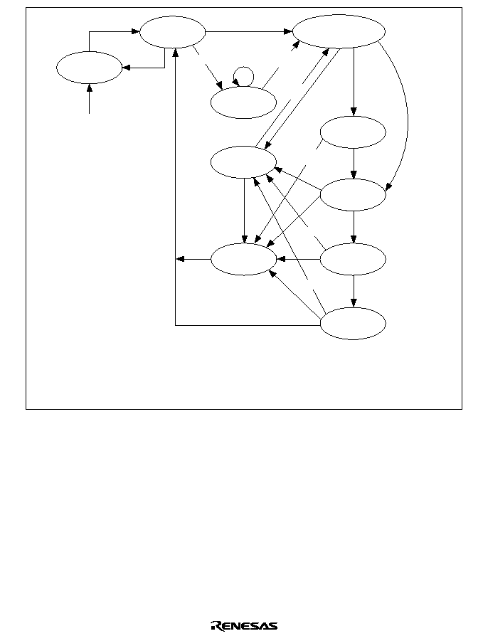
401
Reset
TE set
FDPX
FDPX
TE reset
Failure of 15
retransmission
attempts
or
collision after
512-bit time
Collision
Collision
Normal transmission
Carrier
detection
Carrier
detection
SFD
transmission
Data
transmission
CRC
transmission
Retransmission
processing
*
1
Carrier
detection
Start of transmission
(preamble transmission)
Idle
Carrier
non-detection
Carrier
non-detection
Carrier
detection
HDPX
HDPX
Retrans-
mission
initiation
Transmission
halted
Error
detection
Error
Error
Error
Error
notification
Notes:
*
1 Transmission retry processing includes both jam transmission that depends on collision detection and the
adjustment of transmission intervals based on the back-off algorithm.
*
2 Transmission is retried only when data of 512 bits or less (including the preamble and SFD) is transmitted.
When a collision is detected during the transmission of data greater than 512 bits, only jam is transmitted and
transmission based on the back-off algorithm is not retried.
Collision
*
2
Collision
*
2
Figure 9.2 EtherC Transmitter State Transitions
1. When the transmit enable (TE) bit is set, the transmitter enters the transmit idle state.
2. When a transmit request is issued by the transmit E-DMAC, the EtherC sends the preamble
after a transmission delay equivalent to the frame interval time.
Note:
If full-duplex transfer is selected, which does not require carrier detection, the preamble is
sent as soon as a transmit request is issued by the transmit E-DMAC.
3. The transmitter sends the SFD, data, and CRC sequentially. At the end of transmission, the
transmit E-DMAC generates a transmission complete interrupt (TC).
Note:
If a collision or the carrier-not-detected state occurs during data transmission, these are
reported as interrupt sources.

402
4. After waiting for the frame interval time, the transmitter enters the idle state, and if there is
more transmit data, continues transmitting.
9.3.2
Reception
The EtherC receiver separates a received frame into preamble, SFD, data, and CRC, and the fields
from DA (destination address) to the CRC data are transferred to the receive E-DMAC. The main
receive functions of the EtherC are as follows:
∑
Receive frame header check: Checks the preamble and SFD, and discards a frame with an
invalid pattern
∑
Receive frame data check: Checks the data length in the header, and reports an error status if
the data length is less than 64 bytes or greater than the specified number of bytes
∑
Receive CRC check: Performs a CRC check on the frame data field, and reports an error status
in the case of an abnormality
∑
Line status monitoring: Reports an error status if an illegal carrier is detected by means of the
fault detection signal from the PHY-LSI
∑
Magic Packet monitoring: Detects a Magic Packet from all receive frames
The state transitions of the EtherC receiver are shown in figure 9.3.
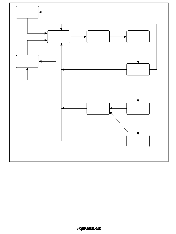
403
Reset
RE set
RE reset
SFD: Start frame delimiter
Note: The error frame also transmits data to the buffer.
Preamble
detection
Rx-DV negation
Promiscuous and other station
destination address
SFD
reception
Own destination
address
or broadcast
or multicast
or promiscuous
End of
reception
Error
notification
Receive
error
detection
Receive error
detection
Normal reception
Reception
halted
Illegal carrier
detection
Idle
Start of frame
reception
Destination
address
reception
Error
detection
Data
reception
CRC
reception
Wait for SFD
reception
Figure 9.3 EtherC Receiver State Transitions
1. When the receive enable (RE) bit is set, the receiver enters the receive idle state.
2. When an SFD (start frame delimiter) is detected after a receive packet preamble, the receiver
starts receive processing.
3. If the destination address matches the receiver's own address, or if broadcast or multicast
transmission or promiscuous mode is specified, the receiver starts data reception.
4. Following data reception, the receiver carries out a CRC check. The result is indicated as a
status bit in the descriptor after the frame data has been written to memory.
5. After one frame has been received, if the receive enable bit is set (RE = 1) in the EtherC mode
register, the receiver prepares to receive the next frame.
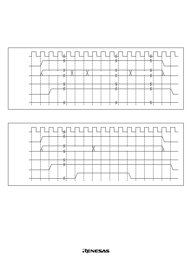
404
9.3.3
MII Frame Timing
Figures 9.4 (a) to (f) show the timing for various kinds of MII frames. The normal timing for
frame transmission is shown in figure 9.4 (a), the timing in the case of a collision during
transmission in figure 9.4 (b), and the timing in the case of an error during transmission in figure
9.4 (c). The normal timing for frame reception is shown in figure 9.4 (d), and the timing in the
case of errors during transmission in figures 9.4 (e) and (f).
TX-CLK
TX-EN
TXD3 ≠
TXD0
TX-ER
CRS
COL
SFD
Preamble
Data
CRC
Figure 9.4 (a) MII Frame Transmit Timing (Normal Transmission)
TX-CLK
TX-EN
TXD3 ≠
TXD0
TX-ER
CRS
COL
Preamble
JAM
Figure 9.4 (b) MII Frame Transmit Timing (Collision)
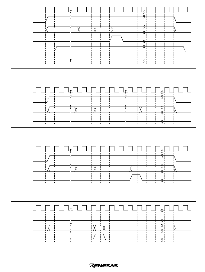
405
TX-CLK
TX-EN
TXD3 ≠
TXD0
TX-ER
CRS
COL
SFD
Preamble
Data
Figure 9.4 (c) MII Frame Transmit Timing (Transmit Error)
RX-CLK
RX-DV
RXD3 ≠
RXD0
RX-ER
Preamble
Data
CRC
SFD
Figure 9.4 (d) MII Frame Receive Timing (Normal Reception)
RX-CLK
RX-DV
RXD3 ≠
RXD0
RX-ER
Preamble
Data
XXXX
SFD
Figure 9.4 (e) MII Frame Receive Timing (Receive Error (1))
RX-CLK
RX-DV
RXD3 ≠
RXD0
RX-ER
XXXX
1110
XXXX
Figure 9.4 (f) MII Frame Receive Timing (Receive Error (2))

406
9.3.4
Accessing MII Registers
MII registers in the PHY-LSI are accessed via the SH7616's PHY interface register (PIR).
Connection is made as a serial interface in accordance with the MII frame format specified in
IEEE802.3u.
MII Management Frame Format: The format of an MII management frame is shown in figure
9.5. To access an MII register, a management frame is implemented by the program in accordance
with the procedures shown in MII Register Access Procedure.
Access Type
MII Management Frame
Item
Number of bits
Read
Write
PRE
32
1..1
1..1
ST
2
01
01
OP
2
10
01
PHYAD
5
00001
00001
REGAD
5
RRRRR
RRRRR
TA
2
Z0
10
DATA
16
D..D
D..D
IDLE
X
PRE:
32 consecutive 1s
ST:
Write of 01 indicating start of frame
OP:
Write of code indicating access type
PHYAD:
Write of 0001 if the PHY-LSI address is 1 (sequential write starting with the MSB).
This bit changes depending on the PHY-LSI address.
REGAD: Write of 0001 if the register address is 1 (sequential write starting with the MSB).
This bit changes depending on the PHY-LSI register address.
TA:
Time for switching data transmission source on MII interface
(a) Write: 10 written
(b) Read: Bus release (notation: Z0) performed
DATA:
16-bit data. Sequential write or read from MSB
(a) Write: 16-bit data write
(b) Read: 16-bit data read
IDLE:
Wait time until next MII management format input
(a) Write: Independent bus release (notation: X) performed
(b) Read: Bus already released in TA; control unnecessary
Figure 9.5 MII Management Frame Format
MII Register Access Procedure: The program accesses MII registers via the PHY interface
register (PIR). Access is implemented by a combination of 1-bit-unit data write, 1-bit-unit data
read, bus release, and independent bus release. Examples 1 through 4 below show the register
access timing. The timing will differ depending on the PHY-LSI type.
1. The MII register write procedure is shown in figure 9.6 (a).
2. The bus release procedure is shown in figure 9.6 (b).

407
3. The MII register read procedure is shown in figure 9.6 (c).
4. The independent bus release procedure is shown in figure 9.6 (d).
MDC
MDO
1-bit data write timing
relationship
(1) Write to PHY interface
register
MMD = 1
MDO = write data
MDC = 0
(2) Write to PHY interface
register
MMD = 1
MDO = write data
MDC = 1
(3) Write to PHY interface
register
MMD = 1
MDO = write data
MDC = 0
(1) (2)
(3)
Figure 9.6 (a) 1-Bit Data Write Flowchart
MDC
MDO
Bus release timing
relationship
(1) Write to PHY interface
register
MMD = 0
MDC = 0
(2) Write to PHY interface
register
MMD = 0
MDC = 1
(3) Write to PHY interface
register
MMD = 0
MDC = 0
(1) (2)
(3)
Figure 9.6 (b) Bus Release Flowchart (TA in Read in Figure 9.5)

408
1-bit data read timing
relationship
(1) Write to PHY interface
register
MMD = 0
MDC = 1
(2) Read from PHY
interface register read
MMD = 0
MMC = 1
MDI is read data
(3) Write to PHY interface
register
MMD = 0
MDC = 0
MDC
MDI
(1)
(3)
(2)
Figure 9.6 (c) 1-Bit Data Read Flowchart
Independent bus release
timing relationship
(1) Write to PHY interface
register
MMD = 0
MDC = 0
MDC
MDO
(1)
Figure 9.6 (d) Independent Bus Release Flowchart (IDLE in Write in Figure 9.5)

409
9.3.5
Magic Packet Detection
The EtherC has a Magic Packet detection function. This function provides a Wake-On-LAN
(WOL) facility that activates various peripheral devices connected to a LAN from the host device
or other source. This makes it possible to construct a system in which a peripheral device receives
a Magic Packet sent from the host device or other source, and activates itself. Further information
on Magic Packets can be found in the technical documentation published by AMD Corporation.
The procedure for using the WOL function with the SH7616 is as follows.
1. Disable interrupt source output by means of the various interrupt enable/mask registers.
2. Set the Magic Packet detection enable bit (MPDE) in the EtherC mode register (ECMR).
3. Set the Magic Packet detection interrupt enable bit (MPDIP) in the EtherC interrupt enable
register (ECSIPR) to the enable setting.
4. If necessary, set the CPU operating mode to sleep mode or set supporting functions to module
standby mode.
5. When a Magic Packet is detected, an interrupt is sent to the CPU. The WOL pin notifies
peripheral LSIs that the Magic Packet has been detected.
Notes: 1. When the Magic Packet is detected, data is stored in the receive FIFO by the broadcast
packet that has received data previously and the EtherC is notified of the receiving
status. To return to normal operation from the interrupt processing, initialize the EtherC
and E-DMAC by using the software reset bit (SWR) in the E-DMAC mode register
(EDMR).
2. With a Magic Packet, reception is performed regardless of the destination address. As a
result, this function is valid, and the WOL pin enabled, only in the case of a match with
the destination address specified by the format in the Magic Packet.

410
9.3.6
CPU Operating Mode and Ethernet Controller Operation
The SH7616 enables a low-power-consumption system to be constructed by selecting or
combining three functions: a module standby function that halts the operation of unnecessary on-
chip modules, a sleep mode that halts CPU functions, and a standby function that halts all the
chip's functions. Details of each operating mode are given in section 21, Power-Down State. Here,
features and points for attention when these functions are used in combination with the Ethernet
controller are described.
Sleep Mode: In sleep mode, the operation of the CPU and DSP is halted. The EtherC, on-chip
supporting functions, and external pins continue to operate. Recovery from sleep mode can be
carried out by means of an interrupt from the EtherC or a supporting module, or a reset. In order to
control external pins and the WOL pin by means of Magic Packet reception, the relevant pins must
be set beforehand.
Note:
In order to specify recovery by means of a magic packet, supporting function interrupt
sources should be masked before sleep mode is entered. See section 9.3.5, Magic Packet
Detection, for the setting procedure.
Standby Mode: In standby mode, the on-chip oscillation circuit is halted. Consequently, the clock
is not supplied to the EtherC, and interrupts from the EtherC and other supporting modules cannot
be reported. It is therefore not possible to restore normal operation by these means, and so the
WOL function cannot be used.
Notes: This mode can be selected to halt all functions including the EtherC. However, an NMI
interrupt, power-on reset, or manual reset is necessary in order to restore normal operation.
When the SH7616 has been placed in standby mode, the CPU, DSP, and bus state
controller are among the functions halted. When DRAM is connected, refreshing is also
halted, and therefore initialization of memory, etc., is necessary after recovery, in the same
way as in a reset.
Module Standby Mode: Module standby mode allows individual supporting modules to be run or
halted. However, due to the nature of its function, the operation of the EtherC cannot be stopped.
During normal operation, module standby mode can be used to halt unnecessary supporting
functions. The CPU and DSP continue to operate in this mode.
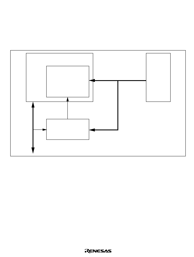
411
9.3.7
CAM Match Signal Input Function
The EtherC is equipped with a CAM (Content Addressable Memory) match signal input function.
A CAM circuit is externally connected to compare a destination address in a receive frame (see
figure 9.7). The EtherC receives the result of comparison of a destination address corresponding to
signals (RXD3 to RXD0) fetched from the MII as a signal from a CAMSEN pin and selects
whether the current frame is received or discarded.
SH7616
EtherC
CAMSEN
CAM logic
MII (RX-DV, RXD3 to RXD0)
PHY-LSI
Figure 9.7 CAM Circuit Connection
Table 9.3 shows types of frames received and discarded in the two states of the CAMSEN signal.
The CAM holds the MAC address besides this LSI. When the MAC address which is received
from the PHY-LSI is matched with the destination address held in the CAM, the CAMSEN signal
is asserted. The EtherC recognizes that the CAMSEN signal has been asserted then receives a
frame for the reception.
Some of the frame's data will have already been stored in the receive FIFO when the CAMSEN
signal is asserted. Therefore, when the E-DMAC is requested that the received data be discarded,
the E-DMAC discards the frame. The frame must be discarded before DMA transfer starts because
the E-DMAC starts transferring to main memory by DMA when at least 16 bytes of data is stored
in the receive FIFO. In this case, according to the MII receive signal timing, the RX-DV is
asserted and the CAMSEN signal must be asserted within 35 clock cycles of the start timing of a
destination address. The fact that the CAMSEN is asserted is reflected in the RFAR bit in the
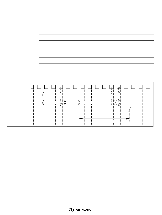
412
EtherC/E-DMAC status register (EESR) and this can be reflected as the write-back information of
the descriptor.
Table 9.3 Processing of Receive Frames
CAMSEN Input
Frame Type
Normal Mode
Promise-CAS Mode
Asserted
SH7616 MAC address
Discarded
Discarded
(address is
Broadcast address
Discarded
Discarded
matched)
Multicast address
Discarded
Discarded
CAM MAC addresses
Received
Discarded
Negated
SH7616 MAC address
Received
Received
(address is not
Broadcast address
Received
Received
matched)
Multicast address
Received
Received
CAM MAC addresses
Discarded
Received
RX-CLK
RX-DV
RXD3 to RXD0
CAMSEN
SFD
Preamble
Destination address
Within 35 clock cycles
Figure 9.8 CAM Signal Timing
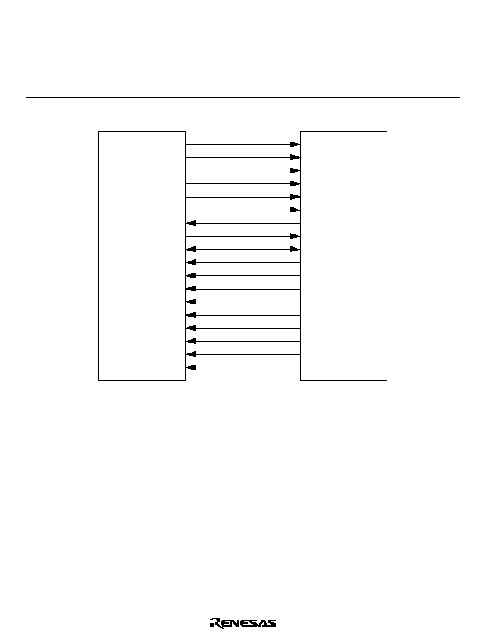
413
9.4
Connection to PHY-LSI
Figure 9.9 shows example of connection to an PHY-LSI AM79C873 (Advanced Micro Devices,
Inc). Figure 9.10 shows example of connection to a DP83843 (National Semiconductor
Corporation).
TX-ER
ETXD3
ETXD2
ETXD1
ETXD0
TX-EN
TX-CLK
MDC
MDIO
ERXD3
ERXD2
ERXD1
ERXD0
RX-CLK
CRS
COL
RX-DV
RX-ER
TXER
ETXD3
ETXD2
ETXD1
ETXD0
TXEN
TXCLK
MDC
MDIO
ERXD3
ERXD2
ERXD1
ERXD0
RXCLK
CRS
COL
RXDV
RXER
SH7616
AM79C873
MII (Media independent interface)
Figure 9.9 Example of Connection to AM79C873
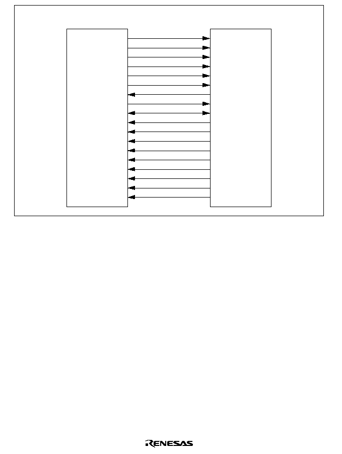
414
TX-ER
ETXD3
ETXD2
ETXD1
ETXD0
TX-EN
TX-CLK
MDC
MDIO
ERXD3
ERXD2
ERXD1
ERXD0
RX-CLK
CRS
COL
RX-DV
RX-ER
TX_ER
TXD3
TXD2
TXD1
TXD0
TX_EN
TX_CLK
MDC
MDIO
RXD3
RXD2
RXD1
RXD0
RX_CLK
CRS
COL
RX_DV
RX_ER
SH7616
DP83843
MII (Media independent interface)
Figure 9.10 Example of Connection to DP83843

415
Section 10 Ethernet Controller Direct Memory Access
Controller (E-DMAC)
10.1
Overview
The SH7616 has an on-chip two-channel direct memory access controller (E-DMAC) directly
connected to the Ethernet controller (EtherC). A large proportion of buffer management is
controlled by the E-DMAC itself using descriptors. This lightens the load on the CPU and enables
efficient data transfer control to be achieved.
10.1.1
Features
The E-DMAC has the following features:
∑
The load on the CPU is reduced by means of a descriptor management system
∑
Transmit/receive frame status information is indicated in descriptors
∑
Achieves efficient system bus utilization through the use of block transfer (16-byte units)
∑
Supports single-frame/multi-buffer operation
Note:
The E-DMAC cannot access peripheral modules.
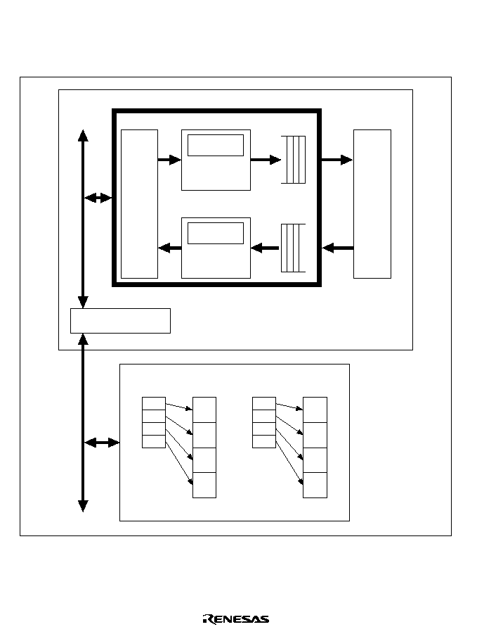
416
10.1.2
Configuration
Figure 10.1 shows the configuration of the E-DMAC, and the descriptors and transmit/receive
buffers in memory.
SH7616
E-DMAC
Internal
bus
interface
EtherC
Descriptor
information
Transmit DMAC
Descriptor
information
Receive DMAC
External bus interface
Tx FIFO
Rx FIFO
Transmit
descriptors
Transmit
buffer
Receive
descriptors
Receive
buffer
Memory
Figure 10.1 Configuration of E-DMAC, and Descriptors and Buffers

417
10.1.3
Descriptor Management System
The E-DMAC manages the transmit/receive buffers by means of corresponding transmit/receive
descriptor lists.
Transmission: The transmit E-DMAC fetches a transmit buffer address from the top of the
transmit descriptor list, and transfers the transmit data in the buffer to the transmit FIFO. If a
transmit directive follows in the descriptor, the E-DMAC reads the next descriptor and transfers
the data in the corresponding buffer to the transmit FIFO. In this way, continuous data
transmission can be carried out.
Reception: For each start of a receive DMA transfer, the receive E-DMAC fetches a receive
buffer address from the top of the receive descriptor list. When receive data is stored in the receive
FIFO, the E-DMAC transfers this data to the receive buffer. When reception of one frame is
finished, the E-DMAC performs a receive status write and fetches the receive buffer address from
the next descriptor. By repeating this sequence, consecutive frames can be received.
10.1.4
Register Configuration
The E-DMAC has the seventeen 32-bit registers shown in table 10.1.
Notes: 1. All registers must be accessed as 32-bit units.
2. Reserved bits in a register should only be written with 0.
3. The value read from a reserved bit is not guaranteed.

418
Table 10.1
E-DMAC Registers
Name
Abbre-
viation
R/W
Initial Value
Address
E-DMAC mode register
EDMR
R/W
H'00000000
H'FFFFFD00
E-DMAC transmit request register
EDTRR
R/W
H'00000000
H'FFFFFD04
E-DMAC receive request register
EDRRR
R/W
H'00000000
H'FFFFFD08
Transmit descriptor list address register
TDLAR
R/W
H'00000000
H'FFFFFD0C
Receive descriptor list address register
RDLAR
R/W
H'00000000
H'FFFFFD10
EtherC/E-DMAC status register
EESR
R/W
*
1
H'00000000
H'FFFFFD14
EtherC/E-DMAC status interrupt
permission register
EESIPR
R/W
H'00000000
H'FFFFFD18
Transmit/receive status copy enable
register
TRSCER
R/W
H'00000000
H'FFFFFD1C
Receive missed-frame counter register
RMFCR
R/W
*
2
H'00000000
H'FFFFFD20
Transmit FIFO threshold register
TFTR
R/W
H'00000000
H'FFFFFD24
FIFO depth register
FDR
R/W
H'00000000
H'FFFFFD28
Receiver control register
RCR
R/W
H'00000000
H'FFFFFD2C
E-DMAC operation control register
EDOCR
R/W
H'00000000
H'FFFFFD30
Receive buffer write address register
RBWAR
R
H'00000000
H'FFFFFD40
Receive descriptor fetch address register
RDFAR
R
H'00000000
H'FFFFFD44
Transmit buffer read address register
TBRAR
R
H'00000000
H'FFFFFD4C
Transmit descriptor fetch address register
TDFAR
R
H'00000000
H'FFFFFD50
Notes:
*
1 Individual bits are cleared by writing 1.
*
2 Cleared by reading the register.
419
10.2
Register Descriptions
10.2.1
E-DMAC Mode Register (EDMR)
The E-DMAC mode register specifies the operating mode of the E-DMAC. The settings in this
register are normally made in the initialization process following a reset.
Note:
Operating mode settings must not be changed while the transmitter and receiver are
enabled. To change the operating mode, first return the EtherC and E-DMAC modules to
their initial state by means of the software reset bit (SWR) in this register, then make new
settings.
Bit:
31
30
29
. . .
11
10
9
8
--
--
--
. . .
--
--
--
--
Initial value:
0
0
0
. . .
0
0
0
0
R/W:
R
R
R
. . .
R
R
R
R
Bit:
7
6
5
4
3
2
1
0
--
--
DL1
DL0
--
--
--
SWR
Initial value:
0
0
0
0
0
0
0
0
R/W:
R
R
R/W
R/W
R
R
R
R/W
Bits 31 to 6--Reserved: These bits are always read as 0. The write value should always be 0.
Bits 5 and 4--Descriptor Length 1, 0 (DL1, DL0): These bits specify the descriptor length,
Bit 5:
DL1
Bit 4:
DL0
Description
0
0
16 bytes
(Initial value)
1
32 bytes
1
0
64 bytes
1
Reserved (setting prohibited)
Bits 3 to 1--Reserved: These bits are always read as 0. The write value should always be 0.
Bit 0--Software Reset (SWR): The EtherC and E-DMAC can be initialized by software. These
bits should only be written with 0.

420
Bit 0: SWR
Description
0
EtherC and E-DMAC reset is cleared
(Initial value)
1
EtherC and E-DMAC are reset
Notes: 1. If the EtherC and E-DMAC are initialized by means of this register during data
transmission, etc., abnormal data may be sent onto the line.
2. The EtherC and E-DMAC are initialized in 16 internal clocks. Therefore, before
accessing registers in the EtherC and E-DMAC, 16 internal clocks must be waited for.
3. The E-DMAC's TDLAR, RDLAR, and RMFCRL registers are not initialized. All other
EtherC and E-DMAC registers are initialized.
10.2.2
E-DMAC Transmit Request Register (EDTRR)
The E-DMAC transmit request register issues transmit directives to the E-DMAC.
Bit:
31
30
29
. . .
11
10
9
8
--
--
--
. . .
--
--
--
--
Initial value:
0
0
0
. . .
0
0
0
0
R/W:
R
R
R
. . .
R
R
R
R
Bit:
7
6
5
4
3
2
1
0
--
--
--
--
--
--
--
TR
Initial value:
0
0
0
0
0
0
0
0
R/W:
R
R
R
R
R
R
R
R/W
Bits 31 to 1--Reserved: These bits are always read as 0. The write value should always be 0.
Bit 0--Transmit Request (TR): When 1 is written to this bit, the E-DMAC reads a descriptor, and
in the case of an active descriptor, transfers the data in the transmit buffer to the EtherC.
Bit 0: TR
Description
0
Transmission-halted state. Writing 0 does not stop transmission. Termination of
transmission is controlled by the active bit in the transmit descriptor
1
Start of transmission. The relevant descriptor is read and a frame is sent with
the transmit active bit set to 1
Note:
When transmission of one frame is completed, the next descriptor is read. If the transmit
descriptor active bit in this descriptor has the "active" setting, transmission is continued. If
the transmit descriptor active bit has the "inactive" setting, the TR bit is cleared and
operation of the transmit DMAC is halted.
421
10.2.3
E-DMAC Receive Request Register (EDRRR)
The E-DMAC receive request register issues receive directives to the E-DMAC.
Bit:
31
30
29
. . .
11
10
9
8
--
--
--
. . .
--
--
--
--
Initial value:
0
0
0
. . .
0
0
0
0
R/W:
R
R
R
. . .
R
R
R
R
Bit:
7
6
5
4
3
2
1
0
--
--
--
--
--
--
--
RR
Initial value:
0
0
0
0
0
0
0
0
R/W:
R
R
R
R
R
R
R
R/W
Bits 31 to 1--Reserved: These bits are always read as 0. The write value should always be 0.
Bit 0--Receive Request (RR): When 1 is written to this bit, the E-DMAC reads a descriptor, and
then transfers receive data to the buffer in response to receive requests from the EtherC.
Bit 0: RR
Description
0
After frame reception is completed, the receiver is disabled
1
A receive descriptor is read, and transfer is enabled
Notes: In order to receive a frame in response to a receive request, the receive descriptor active
bit in the receive descriptor must be set to "active" beforehand.
1. When the receive request bit is set, the E-DMAC reads the relevant receive descriptor.
2. If the receive descriptor active bit in the descriptor has the "active" setting, the E-DMAC
prepares for a receive request from the EtherC.
3. When one receive buffer of data has been received, the E-DMAC reads the next
descriptor and prepares to receive the next frame. If the receive descriptor active bit in
the descriptor has the "inactive" setting, the RR bit is cleared and operation of the
receive DMAC is halted.

422
10.2.4
Transmit Descriptor List Address Register (TDLAR)
TDLAR specifies the start address of the transmit descriptor list. Descriptors have a boundary
configuration in accordance with the descriptor length indicated by the DL bit in EDMR.
Bit:
31
30
29
28
27
26
25
24
TDLA31 TDLA30 TDLA29 TDLA28 TDLA27 TDLA26 TDLA25 TDLA24
Initial value:
0
0
0
0
0
0
0
0
R/W:
R/W
R/W
R/W
R/W
R/W
R/W
R/W
R/W
Bit:
23
22
21
20
19
18
17
16
TDLA23 TDLA22 TDLA21 TDLA20 TDLA19 TDLA18 TDLA17 TDLA16
Initial value:
0
0
0
0
0
0
0
0
R/W:
R/W
R/W
R/W
R/W
R/W
R/W
R/W
R/W
Bit:
15
14
13
12
11
10
9
8
TDLA15 TDLA14 TDLA13 TDLA12 TDLA11 TDLA10
TDLA9
TDLA8
Initial value:
0
0
0
0
0
0
0
0
R/W:
R/W
R/W
R/W
R/W
R/W
R/W
R/W
R/W
Bit:
7
6
5
4
3
2
1
0
TDLA7
TDLA6
TDLA5
TDLA4
TDLA3
TDLA2
TDLA1
TDLA0
Initial value:
0
0
0
0
0
0
0
0
R/W:
R/W
R/W
R/W
R/W
R/W
R/W
R/W
R/W
Bits 31 to 0--Transmit Descriptor Start Address 31 to 0 (TDLA31 to TDLA0) : These bits should
only be written with 0.
Notes: The lower bits are set as follows according to the specified descriptor length.
16-byte boundary: TDLA[3:0] = 0000
32-byte boundary: TDLA[4:0] = 00000
64-byte boundary: TDLA[5:0] = 000000
This register must not be written to during transmission. Modifications to this register
should only be made while transmission is disabled.

423
10.2.5
Receive Descriptor List Address Register (RDLAR)
RDLAR specifies the start address of the receive descriptor list. Descriptors have a boundary
configuration in accordance with the descriptor length indicated by the DL bit in EDMR.
Bit:
31
30
29
28
27
26
25
24
RDLA31 RDLA30 RDLA29 RDLA28 RDLA27 RDLA26 RDLA25 RDLA24
Initial value:
0
0
0
0
0
0
0
0
R/W:
R/W
R/W
R/W
R/W
R/W
R/W
R/W
R/W
Bit:
23
22
21
20
19
18
17
16
RDLA23 RDLA22 RDLA21 RDLA20 RDLA19 RDLA18 RDLA17 RDLA16
Initial value:
0
0
0
0
0
0
0
0
R/W:
R/W
R/W
R/W
R/W
R/W
R/W
R/W
R/W
Bit:
15
14
13
12
11
10
9
8
RDLA15 RDLA14 RDLA13 RDLA12 RDLA11 RDLA10 RDLA9
RDLA8
Initial value:
0
0
0
0
0
0
0
0
R/W:
R/W
R/W
R/W
R/W
R/W
R/W
R/W
R/W
Bit:
7
6
5
4
3
2
1
0
RDLA7
RDLA6
RDLA5
RDLA4
RDLA3
RDLA2
RDLA1
RDLA0
Initial value:
0
0
0
0
0
0
0
0
R/W:
R/W
R/W
R/W
R/W
R/W
R/W
R/W
R/W
Bits 31 to 0--Receive Descriptor Start Address 31 to 0 (RDLA31 to RDLA0)
Notes: The lower bits are set as follows according to the specified descriptor length.
16-byte boundary: RDLA[3:0] = 0000
32-byte boundary: RDLA[4:0] = 00000
64-byte boundary: RDLA[5:0] = 000000
Modifications made to this register during reception are invalid. This register should only
be modified while reception is disabled.

424
10.2.6
EtherC/E-DMAC Status Register (EESR)
EESR shows communication status information for both the E-DMAC and the EtherC. The
information in this register is reported in the form of interrupt sources. Individual bits are cleared
by writing 1 to them. Each bit can also be masked by means of the corresponding bit in the
EtherC/E-DMAC status interrupt permission register.
Bit:
31
30
29
28
27
26
25
24
--
--
--
--
--
--
--
RFCOF
Initial value:
0
0
0
0
0
0
0
0
R/W:
R
R
R
R
R
R
R
R/W
Bit:
23
22
21
20
19
18
17
16
--
ECI
TC
TDE
TFUF
FR
RDE
RFOF
Initial value:
0
0
0
0
0
0
0
0
R/W:
R
R
R/W
R/W
R/W
R/W
R/W
R/W
Bit:
15
14
13
12
11
10
9
8
--
--
--
ITF
CND
DLC
CD
TRO
Initial value:
0
0
0
0
0
0
0
0
R/W:
R
R
R
R/W
R/W
R/W
R/W
R/W
Bit:
7
6
5
4
3
2
1
0
RMAF
--
RFAR
RRF
RTLF
RTSF
PRE
CERF
Initial value:
0
0
0
0
0
0
0
0
R/W:
R/W
R
R/W
R/W
R/W
R/W
R/W
R/W
Bits 31 to 25--Reserved: These bits are always read as 0. The write value should always read as 0.
Bit 24--Receive Frame Counter Overflow (RFCOF): Indicates that the receive FIFO frame
counter has overflowed.

425
Bit 24: RFCOF
Description
0
Receive frame counter has not overflowed
(Initial value)
1
Receive frame counter overflow (interrupt source)
Note:
The receive FIFO in the E-DMAC can hold up to eight frames. If a ninth frame is received
when there are already eight frames in the receive FIFO, the receive frame counter
overflows and the ninth frame is discarded. Discarded frames are counted by the missed-
frame counter register. The eight frames in the receive FIFO are retained, and are
transferred to memory when DMA transfer becomes possible. When the frame counter
value falls below 8, another frame is received.
Bit 23--Reserved: These bits are always read as 0. The write value should always be 0.
Bit 22--EtherC States Register Interrupt (ECI): Indicates that an interrupt due to an EtherC status
register (ECSR) source has been detected.
Bit 22: ECI
Description
0
EtherC status interrupt source not detected
(Initial value)
1
EtherC status interrupt source detected (interrupt source)
Note:
EESR is a read-only register. When this register is cleared by a source in ECSR in the
EtherC, this bit is also cleared.
Bit 21--Frame Transmit Complete (TC): Indicates that all the data specified by the transmit
descriptor has been transmitted to the EtherC. The transfer status is written back to the relevant
descriptor. When 1-frame transmission is completed for 1-frame/1-buffer processing, or when the
last data in the frame is transmitted and the transmission descriptor valid bit (TACT) in the next
descriptor is not set for multiple-frame buffer processing, transmission is completed and this bit is
set to 1. After frame transmission, the E-DMAC writes the transmission status back to the
descriptor.
Bit 21: TC
Description
0
Transfer not complete, or no transfer directive
(Initial value)
1
Transfer complete (interrupt source)
Note:
As data is sent onto the line by the PHY-LSI from the EtherC via the MII, the actual
transmission completion time is longer.
Bit 20--Transmit Descriptor Exhausted (TDE): Indicates that the transmission descriptor valid bit
(TACT) in the descriptor is not set when the E-DMAC reads the transmission descriptor when the
previous descriptor is not the last one of the frame for multiple- buffer frame processing. As a
result, an incomplete frame may be transmitted.

426
Bit 20: TDE
Description
0
"1" transmit descriptor active bit (TACT) detected
(Initial value)
1
"0" transmit descriptor active bit (TACT) detected (interrupt source)
Note:
When transmission descriptor empty (TDE = 1) occurs, execute a software reset and initiate
transmission. In this case, the address that is stored in the transmit descriptor list address
register (TDLAR) is transmitted first.
Bit 19--Transmit FIFO Underflow (TFUF): Indicates that underflow has occurred in the transmit
FIFO during frame transmission. Incomplete data is sent onto the line.
Bit 19: TFUF
Description
0
Underflow has not occurred
(Initial value)
1
Underflow has occurred (interrupt source)
Note:
Whether E-DMAC operation continues or halts after underflow is controlled by the E-DMAC
operation control register (EDOCR).
Bit 18--Frame Received (FR): Indicates that a frame has been received and the receive descriptor
has been updated. This bit is set to 1 each time a frame is received.
Note:
The actual receive frame status is indicated in the receive status field in the descriptor.
Bit 18: FR
Description
0
Frame not received
(Initial value)
1
Frame received (interrupt source)
Bit 17--Receive Descriptor Exhausted (RDE): This bit is set if the receive descriptor active bit
(RACT) setting is "inactive" (RACT = 0) when the E-DMAC reads a receive descriptor.
Bit 17: RDE
Description
0
"1" receive descriptor active bit (RACT) detected
(Initial value)
1
"0" receive descriptor active bit (RACT) detected (interrupt source)
Note:
When receive descriptor empty (RDE = 1) occurs, receiving can be restarted by setting
RACT = 1 in the receive descriptor and initiating receiving.
Bit 16--Receive FIFO Overflow (RFOF): Indicates that the receive FIFO has overflowed during
frame reception.

427
Bit 16: RFOF
Description
0
Overflow has not occurred
(Initial value)
1
Overflow has occurred (interrupt source)
Notes: 1. If there are a number of receive frames in the receive FIFO, they will not be sent to
memory correctly. The status of the frame that caused the overflow is written back to
the receive descriptor.
2. Whether E-DMAC operation continues or halts after overflow is controlled by the E-
DMAC operation control register (EDOCR).
Bits 15 to 13--Reserved: These bits are always read as 0. The write value should always be 0.
Bit 12--Illegal Transmit Frame (ITF): Indicates that the transmit frame length specification is less
than four bytes.
Bit 12: ITF
Description
0
Normal transmit frame length
(Initial value)
1
Illegal transmit frame length (interrupt source)
Bit 11--Carrier Not Detect (CND): Indicates the carrier detection status.
Bit 11: CND
Description
0
A carrier is detected when transmission starts
(Initial value)
1
Carrier not detected (interrupt source)
Bit 10--Detect Loss of Carrier (DLC): Indicates that loss of the carrier has been detected during
frame transmission.
Bit 10: DLC
Description
0
Loss of carrier not detected
(Initial value)
1
Loss of carrier detected (interrupt source)
Bit 9--Collision Detect (CD): Indicates that a collision has been detected during frame
transmission.
Bit 9: CD
Description
0
Collision not detected
(Initial value)
1
Collision detected (interrupt source)

428
Bit 8--Transmit Retry Over (TRO): Indicates that a retry-over condition has occurred during
frame transmission. Total 16 transmission retries including 15 retries based on the back-off
algorithm are failed after the EtherC transmission starts.
Bit 8: TRO
Description
0
Transmit retry-over condition not detected
(Initial value)
1
Transmit retry-over condition detected (interrupt source)
Bit 7--Receive Multicast Address Frame (RMAF): Indicates that a multicast address frame has
been received.
Bit 7: RMAF
Description
0
Multicast address frame has not been received
(Initial value)
1
Multicast address frame has been received (interrupt source)
Bits 6--Reserved: This bit should only be written with 0.
Bit 5≠≠Receive Frame Discard Request Assertion (RFAR): Indicates that a frame discard request
has been asserted by the EtherC as a result of a signal from the CAM, however, it is not possible to
discard the frame in the E-DMAC.
Bit 5: RFAR
Description
0
Receive frame discard request assertion has not been received (Initial value)
1
Receive frame discard request assertion has been received (interrupt source)
Bit 4--Receive Residual-Bit Frame (RRF): Indicates that a residual-bit frame has been received.
Bit 4: RRF
Description
0
Residual-bit frame has not been received
(Initial value)
1
Residual-bit frame has been received (interrupt source)
Bit 3--Receive Too-Long Frame (RTLF): Indicates that a frame of 1519 bytes or longer has been
received.
Bit 3: RTLF
Description
0
Too-long frame has not been received
(Initial value)
1
Too-long frame has been received (interrupt source)
Bit 2--Receive Too-Short Frame (RTSF): Indicates that a frame of fewer than 64 bytes has been
received.

429
Bit 2: RTSF
Description
0
Too-short frame has not been received
(Initial value)
1
Too-short frame has been received (interrupt source)
Bit 1--PHY-LSI Receive Error (PRE): Indicates an error notification from the MII (PHY-LSI)
Bit 1: PRE
Description
0
PHY-LSI receive error not detected
(Initial value)
1
PHY-LSI receive error detected (interrupt source)
Bit 0--CRC Error on Received Frame (CERF): Indicates that a CRC error has been detected in the
received frame.
Bit 0: CERF
Description
0
CRC error not detected
(Initial value)
1
CRC error detected (interrupt source)

430
10.2.7
EtherC/E-DMAC Status Interrupt Permission Register (EESIPR)
EESIPR enables interrupts corresponding to individual bits in the EtherC/E-DMAC status register.
An interrupt is enabled by writing 1 to the corresponding bit. In the initial state, interrupts are not
enabled.
Bit:
31
30
29
28
27
26
25
24
--
--
--
--
--
--
--
RFCOFIP
Initial value:
0
0
0
0
0
0
0
0
R/W:
R
R
R
R
R
R
R
R/W
Bit:
23
22
21
20
19
18
17
16
--
ECIIP
TCIP
TDEIP
TFUFIP
FRIP
RDEIP
RFOFIP
Initial value:
0
0
0
0
0
0
0
0
R/W:
R
R/W
R/W
R/W
R/W
R/W
R/W
R/W
Bit:
15
14
13
12
11
10
9
8
--
--
--
ITFIP
CNDIP
DLCIP
CDIP
TROIP
Initial value:
0
0
0
0
0
0
0
0
R/W:
R
R
R
R/W
R/W
R/W
R/W
R/W
Bit:
7
6
5
4
3
2
1
0
RMAFIP
--
RFARIP
RRFIP
RTLFIP
RTSFIP
PREIP
CERFIP
Initial value:
0
0
0
0
0
0
0
0
R/W:
R/W
R
R/W
R/W
R/W
R/W
R/W
R/W
Bits 31 to 25--Reserved: These bits are always read as 0. The write value should always be 0.
Bit 24--Receive Frame Counter Overflow Interrupt Permission (RFCOFIP): Enables the receive
frame counter overflow interrupt.
Bit 24: RFCOFIP Description
0
Receive frame counter overflow interrupt is disabled
(Initial value)
1
Receive frame counter overflow interrupt is enabled

431
Bit 23--Reserved: This bit is always read as 0. The write value should always be 0.
Bit 22--EtherC Status Register Interrupt Permission (ECIP): Enables interrupts due to EtherC
status register sources.
Bit 22: ECIP
Description
0
EtherC status interrupts are disabled
(Initial value)
1
EtherC status interrupts are enabled
Bit 21--Frame Transmit Complete Interrupt Permission (TCIP): Enables the frame transmit
complete interrupt.
Bit 21: TCIP
Description
0
Frame transmit complete interrupt is disabled
(Initial value)
1
Frame transmit complete interrupt is enabled
Bit 20--Transmit Descriptor Exhausted Interrupt Permission (TDEIP): Enables the transmit
descriptor exhausted interrupt.
Bit 20: TDEIP
Description
0
Transmit descriptor exhausted interrupt is disabled
(Initial value)
1
Transmit descriptor exhausted interrupt is enabled
Bit 19--Transmit FIFO Underflow Interrupt Permission (TFUFIP): Enables the transmit FIFO
underflow interrupt.
Bit 19: TFUFIP
Description
0
Transmit FIFO underflow interrupt is disabled
(Initial value)
1
Transmit FIFO underflow interrupt is enabled
Bit 18--Frame Received Interrupt Permission (FRIP): Enables the frame received interrupt.
Bit 18: FRIP
Description
0
Frame received interrupt is disabled
(Initial value)
1
Frame received interrupt is enabled

432
Bit 17--Receive Descriptor Exhausted Interrupt Permission (RDEIP): Enables the receive
descriptor exhausted interrupt.
Bit 17: RDEIP
Description
0
Receive descriptor exhausted interrupt is disabled
(Initial value)
1
Receive descriptor exhausted interrupt is enabled
Bit 16--Receive FIFO Overflow Interrupt Permission (RFOFIP): Enables the receive FIFO
overflow interrupt.
Bit 16: RFOFIP
Description
0
Receive FIFO overflow interrupt is disabled
(Initial value)
1
Receive FIFO overflow interrupt is enabled
Bits 15 to 13--Reserved: These bits are always read as 0. The write value should always be 0.
Bit 12--Illegal Transmit Frame Interrupt Permission (ITFIP): Enables the illegal transmit frame
interrupt.
Bit 12: ITFIP
Description
0
Illegal transmit frame interrupt is disabled
(Initial value)
1
Illegal transmit frame interrupt is enabled
Bit 11--Carrier Not Detect Interrupt Permission (CNDIP): Enables the carrier not detect interrupt.
Bit 11: CNDIP
Description
0
Carrier not detect interrupt is disabled
(Initial value)
1
Carrier not detect interrupt is enabled
Bit 10--Detect Loss of Carrier Interrupt Permission (DLCIP): Enables the detect loss of carrier
interrupt.
Bit 10: DLCIP
Description
0
Detect loss of carrier interrupt is disabled
(Initial value)
1
Detect loss of carrier interrupt is enabled

433
Bit 9--Collision Detect Interrupt Permission (CDIP): Enables the collision detect interrupt.
Bit 9: CDIP
Description
0
Collision detect interrupt is disabled
(Initial value)
1
Collision detect interrupt is enabled
Bit 8--Transmit Retry Over Interrupt Permission (TROIP): Enables the transmit retry over
interrupt.
Bit 8: TROIP
Description
0
Transmit retry over interrupt is disabled
(Initial value)
1
Transmit retry over interrupt is enabled
Bit 7--Receive Multicast Address Frame Interrupt Permission (RMAFIP): Enables the receive
multicast address frame interrupt.
Bit 7: RMAFIP
Description
0
Receive multicast address frame interrupt is disabled
(Initial value)
1
Receive multicast address frame interrupt is enabled
Bits 6--Reserved: This bit is always read as 0. The write value should always be 0.
Bit 5≠≠Receive Frame Discard Request Assertion Interrupt Permission (RFARIP): Enables the
receive frame discard request assertion interrupt.
Bit 5: RFARIP
Description
0
Receive frame discard request assertion interrupt is disabled
(Initial value)
1
Receive frame discard request assertion interrupt is enabled
Bit 4--Receive Residual-Bit Frame Interrupt Permission (RRFIP): Enables the receive residual-bit
frame interrupt.
Bit 4: RRFIP
Description
0
Receive residual-bit frame interrupt is disabled
(Initial value)
1
Receive residual-bit frame interrupt is enabled
Bit 3--Receive Too-Long Frame Interrupt Permission (RTLFIP): Enables the receive too-long
frame interrupt.

434
Bit 3: RTLFIP
Description
0
Receive too-long frame interrupt is disabled
(Initial value)
1
Receive too-long frame interrupt is enabled
Bit 2--Receive Too-Short Frame Interrupt Permission (RTSFIP): Enables the receive too-short
frame interrupt.
Bit 2: RTSFIP
Description
0
Receive too-short frame interrupt is disabled
(Initial value)
1
Receive too-short frame interrupt is enabled
Bit 1--PHY-LSI Receive Error Interrupt Permission (PREIP): Enables the PHY-LSI receive error
interrupt.
Bit 1: PREIP
Description
0
PHY-LSI receive error interrupt is disabled
(Initial value)
1
PHY-LSI receive error interrupt is enabled
Bit 0--CRC Error on Received Frame Interrupt Permission (PREIP): Enables the CRC error on
received frame interrupt.
Bit 0: CERFIP
Description
0
CRC error on received frame interrupt is disabled
(Initial value)
1
CRC error on received frame interrupt is enabled

435
10.2.8
Transmit/Receive Status Copy Enable Register (TRSCER)
TRSCER specifies whether or not transmit and receive status information reported by bits in the
EtherC/E-DMAC status register is to be indicated in the corresponding descriptor. The bits in this
register correspond to EtherC/E-DMAC status register EESR[15 to 0]. When a bit is cleared to 0,
the transmit status (EESR[15 to 8]) is indicated in the TFE bit of the transmit descriptor, and the
receive status (EESR[7 to 0]) is indicated in the RFE bit of the receive descriptor. When a bit is set
to 1, the occurrence of the corresponding source is not indicated in the descriptor. After the chip is
reset, all bits are cleared to 0.
Bit:
31
30
29
. . .
19
18
17
16
--
--
--
. . .
--
--
--
--
Initial value:
0
0
0
. . .
0
0
0
0
R/W:
R
R
R
. . .
R
R
R
R
Bit:
15
14
13
12
11
10
9
8
--
--
--
ITFCE
CNDCE
DLCCE
CDCE
TROCE
Initial value:
0
0
0
0
0
0
0
0
R/W:
R
R
R
R/W
R/W
R/W
R/W
R/W
Bit:
7
6
5
4
3
2
1
0
RMAFCE
--
RFARCE RRFCE RTLFCE RTSFCE PRECE CERFCE
Initial value:
0
0
0
0
0
0
0
0
R/W:
R/W
R
R/W
R/W
R/W
R/W
R/W
R/W
For the corresponding bit sources, see section 10.2.6, EtherC/E-DMAC Status Register (EESR).

436
10.2.9
Receive Missed-Frame Counter Register (RMFCR)
RMFCR is a 16-bit counter that indicates the number of frames missed (discarded, and not
transferred to the receive buffer) during reception. When the receive FIFO overflows, the receive
frames in the FIFO are discarded. The number of frames discarded at this time are counted. When
the value in this register reaches H'FFFF (65,535), the count is halted. When this register is read,
the counter value is cleared to 0. Writes to this register have no effect.
Bit:
31
30
29
. . .
19
18
17
16
--
--
--
. . .
--
--
--
--
Initial value:
0
0
0
. . .
0
0
0
0
R/W:
R
R
R
. . .
R
R
R
R
Bit:
15
14
13
12
11
10
9
8
MFC15
MFC14
MFC13
MFC12
MFC11
MFC10
MFC9
MFC8
Initial value:
0
0
0
0
0
0
0
0
R/W:
R
R
R
R
R
R
R
R
Bit:
7
6
5
4
3
2
1
0
MFC7
MFC6
MFC5
MFC4
MFC3
MFC2
MFC1
MFC0
Initial value:
0
0
0
0
0
0
0
0
R/W:
R
R
R
R
R
R
R
R

437
10.2.10
Transmit FIFO Threshold Register (TFTR)
TFTR specifies the transmit FIFO threshold at which the first transmission is started. The actual
threshold is 4 times the set value. The EtherC starts transmission when the amount of data in the
transmit FIFO exceeds the number of bytes specified by this register, when the transmit FIFO is
full, or when 1-frame write is executed.
Note:
When setting this register, do so in the transmission-halt state.
Bit:
31
30
29
. . .
19
18
17
16
--
--
--
. . .
--
--
--
--
Initial value:
0
0
0
. . .
0
0
0
0
R/W:
R
R
R
. . .
R
R
R
R
Bit:
15
14
13
12
11
10
9
8
--
--
--
--
--
TFT10
TFT9
TFT8
Initial value:
0
0
0
0
0
0
0
0
R/W:
R
R
R
R
R
R/W
R/W
R/W
Bit:
7
6
5
4
3
2
1
0
TFT7
TFT6
TFT5
TFT4
TFT3
TFT2
TFT1
TFT0
Initial value:
0
0
0
0
0
0
0
0
R/W:
R/W
R/W
R/W
R/W
R/W
R/W
R/W
R/W
Bits 31 to 11--Reserved: These bits should only be written with 0.

438
Bits 10 to 0--Transmit FIFO Threshold 10 to 0 (TFT10 to TFT0)
Bits 10 to 0:
TFT
Description
H'00
Store-and-forward mode (transmission starts when one frame of data is written
or transmit FIFO is full)
(Initial value)
H'01
4 bytes
H'02
8 bytes
:
:
H'1F
124 bytes
H'20
128 bytes
:
:
H'3F
252 bytes
H'40
256 bytes
:
:
H'7F
508 bytes
H'80
512 bytes
:
:
H'FF
1023 bytes
H'100
1024 bytes
:
:
H'1FF
2047 bytes
H'200
2048 bytes
Note:
Note: When setting a transmit FIFO, the FIFO must be set to a smaller value than the
specified value of the FIFO's capacity.

439
10.2.11
FIFO Depth Register (FDR)
FDR specifies the depth (size) of the transmit and receive FIFOs.
Bit:
31
30
29
. . .
19
18
17
16
--
--
--
. . .
--
--
--
--
Initial value:
0
0
0
. . .
0
0
0
0
R/W:
R
R
R
. . .
R
R
R
R
Bit:
15
14
13
12
11
10
9
8
--
--
--
--
--
TFD2
TFD1
TFD0
Initial value:
0
0
0
0
0
0
0
0
R/W:
R
R
R
R
R
R/W
R/W
R/W
Bit:
7
6
5
4
3
2
1
0
--
--
--
--
--
RFD2
RFD1
RFD0
Initial value:
0
0
0
0
0
0
0
0
R/W:
R
R
R
R
R
R/W
R/W
R/W
Bits 31 to 11--Reserved: These bits are always read as 0. The write value should always be 0.
Bit 10 to 8--Transmit FIFO Depth (TFD): Specifies 256 bytes to 2 kbytes in 256-byte units as the
depth (size) of the transmit FIFO. The setting cannot be changed after transmission/reception has
started.
Bits 10 to 8: TFD2 to TFD0
Description
H'0
256 bytes
(Initial value)
H'1
512 bytes
:
:
H'7
2048 bytes
Bits 7 to 3--Reserved: These bits are always read as 0. The write value should always be 0.
Bit 2 to 0--Receive FIFO Depth (RFD): Specifies 256 bytes to 2 kbytes in 256-byte units as the
depth (size) of the receive FIFO. The actual FIFO depth is 256 times the set value. The setting
cannot be changed after transmission/reception has started.

440
Bits 2 to 0: RFD2 to RFD0
Description
H'0
256 bytes
(Initial value)
H'1
512 bytes
:
:
H'7
2048 bytes
10.2.12
Receiver Control Register (RCR)
RCR specifies the control method for the RE bit in ECMR when a frame is received.
Note:
When setting this register, do so in the receiving-halt state.
Bit:
31
30
29
. . .
11
10
9
8
--
--
--
. . .
--
--
--
--
Initial value:
0
0
0
. . .
0
0
0
0
R/W:
R
R
R
. . .
R
R
R
R
Bit:
7
6
5
4
3
2
1
0
--
--
--
--
--
--
--
RNC
Initial value:
0
0
0
0
0
0
0
0
R/W:
R
R
R
R
R
R
R
R/W
Bits 31 to 1--Reserved: These bits are always read as 0. The write value should always be 0.
Bit 0--Receive Enable Control (RNC)
Bit 0: RNC
Description
0
When reception of one frame is completed, the E-DMAC writes the receive
status into the descriptor and clears the RR bit in EDRRR
(Initial value)
1
When reception of one frame is completed, the E-DMAC writes the receive
status into the descriptor, reads the next descriptor, and prepares to receive
the next frame
*
Note:
*
This setting is normally used for continuous frame reception.

441
10.2.13
E-DMAC Operation Control Register (EDOCR)
EDOCR specifies the control methods used in E-DMAC operation.
Bit:
31
30
29
. . .
11
10
9
8
--
--
--
. . .
--
--
--
--
Initial value:
0
0
0
. . .
0
0
0
0
R/W:
R
R
R
. . .
R
R
R
R
Bit:
7
6
5
4
3
2
1
0
--
--
--
--
FEC
AEC
EDH
--
Initial value:
0
0
0
0
0
0
0
0
R/W:
R
R
R
R
R/W
R/W
R/W
R
Bits 31 to 4, and 0--Reserved: These bits are always read as 0. The write value should always be
0.
Bit 3--FIFO Error Control (FEC): Specifies E-DMAC operation when transmit FIFO underflow
or receive FIFO overflow occurs.
Bit 3: FEC
Description
0
E-DMAC operation continues when underflow or overflow occurs (Initial value)
1
E-DMAC operation halts when underflow or overflow occurs
Bit 2--Address Error Control (AEC): Indicates detection of an illegal memory address in an
attempted E-DMAC transfer.
Bit 2: AEC
Description
0
Illegal memory address not detected (normal operation)
(Initial value)
1
Illegal memory address detected. Can be cleared by writing 0
Note:
This error occurs if the memory address setting in the descriptor used by the E-DMAC is
illegal.
Bit 1--E-DMAC Halted (EDH): When the SH7616's NMI input pin is asserted, E-DMAC
operation is halted.
Bit 1: EDH
Description
0
The E-DMAC is operating normally
(Initial value)
1
The E-DMAC has been halted by NMI pin assertion. E-DMAC operation is
restarted by writing 0

442
Bits 0--Reserved: This bit is always read as 0. The write value should always be 0.
10.2.14
Receiving-Buffer Write Address Register (RBWAR)
This is the register for storing the buffer address to be written in the receiving buffer when the E-
DMAC writes data in the receiving buffer. Which addresses in the receiving buffer are processed
by the E-DMAC can be recognized by monitoring addresses displayed in this register.
Bit:
31
30
29
28
27
26
25
24
RBWA31 RBWA30 RBWA29 RBWA28 RBWA27 RBWA26 RBWA25 RBWA24
Initial value:
0
0
0
0
0
0
0
0
R/W:
R
R
R
R
R
R
R
R
Bit:
23
22
21
20
19
18
17
16
RBWA23 RBWA22 RBWA21 RBWA20 RBWA19 RBWA18 RBWA17 RBWA16
Initial value:
0
0
0
0
0
0
0
0
R/W:
R
R
R
R
R
R
R
R
Bit:
15
14
13
12
11
10
9
8
RBWA15 RBWA14 RBWA13 RBWA12 RBWA11 RBWA10 RBWA9 RBWA8
Initial value:
0
0
0
0
0
0
0
0
R/W:
R
R
R
R
R
R
R
R
Bit:
7
6
5
4
3
2
1
0
RBWA7 RBWA6 RBWA5 RBWA4 RBWA3 RBWA2 RBWA1 RBWA0
Initial value:
0
0
0
0
0
0
0
0
R/W:
R
R
R
R
R
R
R
R
Bits 31 to 0--Receiving-buffer write address (RBWA): This bit can only be read. Writing is
disabled.
Note:
The buffer write processing result from the E-DMAC and the value read by the register
may not be the same.

443
10.2.15
Receiving-Descriptor Fetch Address Register (RDFAR)
This is the register for storing the descriptor start address that is required when the E-DMAC
fetches descriptor information from the receiving descriptor . Which receiving descriptor
information is used for processing by the E-DMAC can be recognized by monitoring addresses
displayed in this register.
Bit:
31
30
29
28
27
26
25
24
RDFA31 RDFA30 RDFA29 RDFA28 RDFA27 RDFA26 RDFA25 RDFA24
Initial value:
0
0
0
0
0
0
0
0
R/W:
R
R
R
R
R
R
R
R
Bit:
23
22
21
20
19
18
17
16
RDFA23 RDFA22 RDFA21 RDFA20 RDFA19 RDFA18 RDFA17 RDFA16
Initial value:
0
0
0
0
0
0
0
0
R/W:
R
R
R
R
R
R
R
R
Bit:
15
14
13
12
11
10
9
8
RDFA15 RDFA14 RDFA13 RDFA12 RDFA11 RDFA10
RDFA9
RDFA8
Initial value:
0
0
0
0
0
0
0
0
R/W:
R
R
R
R
R
R
R
R
Bit:
7
6
5
4
3
2
1
0
RDFA7
RDFA6
RDFA5
RDFA4
RDFA3
RDFA2
RDFA1
RDFA0
Initial value:
0
0
0
0
0
0
0
0
R/W:
R
R
R
R
R
R
R
R
Bits 31 to 0--Receiving-descriptor fetch address (RDFA): This bit can only be read. Writing is
disabled.
Note:
The descriptor fetch processing result from the E-DMAC and the value read by the
register may not be the same.

444
10.2.16
Transmission-Buffer Read Address Register (TBRAR)
This is the register for storing the buffer address to be read in the transmission buffer when the E-
DMAC reads data from the transmission buffer. Which addresses in the transmission buffer are
processed by the E-DMAC can be recognized by monitoring addresses displayed in this register.
Bit:
31
30
29
28
27
26
25
24
TBRA31 TBRA30 TBRA29 TBRA28 TBRA27 TBRA26 TBRA25 TBRA24
Initial value:
0
0
0
0
0
0
0
0
R/W:
R
R
R
R
R
R
R
R
Bit:
23
22
21
20
19
18
17
16
TBRA23 TBRA22 TBRA21 TBRA20 TBRA19 TBRA18 TBRA17 TBRA16
Initial value:
0
0
0
0
0
0
0
0
R/W:
R
R
R
R
R
R
R
R
Bit:
15
14
13
12
11
10
9
8
TBRA15 TBRA14 TBRA13 TBRA12 TBRA11 TBRA10 TBRA9
TBRA8
Initial value:
0
0
0
0
0
0
0
0
R/W:
R
R
R
R
R
R
R
R
Bit:
7
6
5
4
3
2
1
0
TBRA7
TBRA6
TBRA5
TBRA4
TBRA3
TBRA2
TBRA1
TBRA0
Initial value:
0
0
0
0
0
0
0
0
R/W:
R
R
R
R
R
R
R
R
Bits 31 to 0--Transmission-buffer read address (TBRD): This bit can only be read. Writing is
disabled.
Note:
The buffer read processing result from the E-DMAC and the value read by the register
may not be the same.

445
10.2.17
Transmission-Descriptor Fetch Address Register (TDFAR)
This is the register for storing the descriptor start address that is required when the E-DMAC
fetches descriptor information from the transmission descriptor . Which transmission descriptor
information is used for processing by the E-DMAC can be recognized by monitoring addresses
displayed in this register.
Bit:
31
30
29
28
27
26
25
24
TDFA31 TDFA30 TDFA29 TDFA28 TDFA27 TDFA26 TDFA25 TDFA24
Initial value:
0
0
0
0
0
0
0
0
R/W:
R
R
R
R
R
R
R
R
Bit:
23
22
21
20
19
18
17
16
TDFA23 TDFA22 TDFA21 TDFA20 TDFA19 TDFA18 TDFA17 TDFA16
Initial value:
0
0
0
0
0
0
0
0
R/W:
R
R
R
R
R
R
R
R
Bit:
15
14
13
12
11
10
9
8
TDFA15 TDFA14 TDFA13 TDFA12 TDFA11 TDFA10
TDFA9
TDFA8
Initial value:
0
0
0
0
0
0
0
0
R/W:
R
R
R
R
R
R
R
R
Bit:
7
6
5
4
3
2
1
0
TDFA7
TDFA6
TDFA5
TDFA4
TDFA3
TDFA2
TDFA1
TDFA0
Initial value:
0
0
0
0
0
0
0
0
R/W:
R
R
R
R
R
R
R
R
Bits 31 to 0--Transmission-descriptor fetch address (TDFA): This bit can only be read. Writing is
disabled.
Note:
The descriptor fetch processing result from the E-DMAC and the value read by the
register may not be the same.

446
10.3
Operation
The E-DMAC is connected to the EtherC, and performs efficient transfer of transmit/receive data
between the EtherC and memory (buffers) without the intervention of the CPU. The E-DMAC
itself reads control information, including buffer pointers called descriptors, relating to the buffers.
The E-DMAC reads transmit data from the transmit buffer and writes receive data to the receive
buffer in accordance with this control information. By setting up a number of consecutive
descriptors (a descriptor list), it is possible to execute transmission and reception continuously.
10.3.1
Descriptor List and Data Buffers
Before starting transmission/reception, the communication program creates transmit and receive
descriptor lists in memory. The start addresses of these lists are then set in the transmit and receive
descriptor list start address registers.
Transmit Descriptor
Figure 10.2 shows the relationship between a transmit descriptor and the transmit buffer.
According to the specification in this descriptor, the relationship between the transmit frame and
transmit buffer can be defined as one frame/one buffer or one frame/multi-buffer.
Notes: 1. The descriptor's start address setting must be aligned with an address boundary that
corresponds with the descriptor's length as set by the E-DMAC mode register
(EDMR).
2. The transmit buffer's start address setting must be aligned with a longword boundary.
However, when SDRAM is connected, the setting must be aligned with a 16-byte
boundary.
Transmit descriptor
Transmit buffer
TACT
TDLE
TFP1
TFP0
TFE
TFS26 to TFS0
0
0
31
16
31
31 30 29 28 27 26
TD0
TDL
TD1
TBA
Padding (4 bytes)
TD2
Valid transmit data
Figure 10.2 Relationship between Transmit Descriptor and Transmit Buffer

447
Transmit Descriptor 0 (TD0): TD0 indicates the transmit frame status. The CPU and E-DMAC
use TD0 to report the frame transmission status.
Bit 31--Transmit Descriptor Active (TACT): Indicates that this descriptor is active. The CPU sets
this bit after transmit data has been transferred to the transmit buffer. The E-DMAC resets this bit
on completion of a frame transfer or when transmission is suspended.
Bit 31: TACT
Description
0
The transmit descriptor is invalid
Indicates that valid data has not been written to the transmit buffer by the CPU,
or this bit has been reset by a write-back operation on termination of E-DMAC
frame transfer processing (completion or suspension of transmission)
If this state is recognized in an E-DMAC descriptor read, the E-DMAC
terminates transmit processing and transmit operations cannot be continued (a
restart is necessary)
1
The transmit descriptor is valid
Indicates that valid data has been written to the transmit buffer by the CPU and
frame transfer processing has not yet been executed, or that frame transfer is
in progress
When this state is recognized in an E-DMAC descriptor read, the E-DMAC
continues with the transmit operation
Bit 30--Transmit Descriptor List Last (TDLE): Indicates that this descriptor is the last in the
transmit descriptor list. After completion of the corresponding buffer transfer, the E-DMAC
references the first descriptor. This specification is used to set a ring configuration for the transmit
descriptors.
Bit 30: TDLE
Description
0
This is not the last transmit descriptor list
1
This is the last transmit descriptor list
Bits 29 and 28--Transmit Frame Position 1, 0 (TFP1, TFP0): These two bits specify the
relationship between the transmit buffer and transmit frame.

448
Bit 29:
TFP1
Bit 28:
TFP0
Description
0
0
Frame transmission for transmit buffer indicated by this descriptor continues
(frame is not concluded)
1
Transmit buffer indicated by this descriptor contains end of frame (frame is
concluded)
1
0
Transmit buffer indicated by this descriptor is start of frame (frame is not
concluded)
1
Contents of transmit buffer indicated by this descriptor are equivalent to one
frame (one frame/one buffer)
Note:
In the preceding and following descriptors, a logically positive relationship must be
maintained between the settings of this bit and the TDLE bit.
Bit 27--Transmit Frame Error (TFE): Indicates that one or other bit of the transmit frame status
indicated by bits 26 to 0 is set. Whether or not the transmit frame status information is copied into
this bit is specified by the transmit/receive status copy enable register.
Bit 27: TFE
Description
0
No error during transmission
1
An error of some kind occurred during transmission (see bits 26 to 0)
Bits 26 to 0--Transmit Frame Status 26 to 0 (TFS26 to TFS0): These bits indicate the error status
during frame transmission.
∑
TFS26 to TFS5--Reserved
∑
TFS4--Illegal Transmit Frame (corresponds to ITF bit in EESR)
∑
TFS3--Carrier Not Detect (corresponds to CND bit in EESR)
∑
TFS2--Detect Loss of Carrier (corresponds to DLC bit in EESR)
∑
TFS1--Collision Detect (corresponds to CD bit in EESR)
∑
TFS0--Transmit Retry Over (corresponds to TRO bit in EESR)
Transmit Descriptor 1 (TD1): Specifies the transmit buffer length (maximum 64 kbytes).
Bits 31 to 16--Transmit Buffer Data Length (TDL): These bits specify the valid transfer byte
length in the corresponding transmit buffer.
Note: When the one frame/multi-buffer system is specified (TD0 and TFP = 10 or 00), the
transfer byte length specified in the descriptors at the start and midway can be set in byte
units.
Bits 15 to 0--Reserved: The bits are always read as 0. The write value should always be 0.

449
Transmit Descriptor 2 (TD2): Specifies the 32-bit transmit buffer start address.
Note: The transmit buffer's start address setting must be aligned with a longword boundary.
However, when SDRAM is connected, the setting must be aligned with a 16-byte
boundary.
Bits 31 to 0--Transmit Buffer Address (TBA)
Receive Descriptor
Figure 10.3 shows the relationship between a receive descriptor and the receive buffer. In frame
reception, the E-DMAC performs data rewriting up to a receive buffer 16-byte boundary,
regardless of the receive frame length. Finally, the actual receive frame length is reported in the
lower 16 bits of RD1 in the descriptor. Data transfer to the receive buffer is performed
automatically by the E-DMAC to give a one frame/one buffer or one frame/multi-buffer
configuration according to the size of one received frame.
Notes: 1. The descriptor's start address setting must be aligned with an address boundary that
corresponds with the descriptor's length as set by the E-DMAC mode register
(EDMR).
2. The receive buffer's start address setting must be aligned with a longword boundary.
However, when SDRAM is connected, the setting must be aligned with a 16-byte
boundary. Make the setting so that the size of the receive buffer is aligned with a 16-
byte boundary.
Example:
H'0500 (= 1280 bytes)
Receive descriptor
Receive buffer
RACT
RDLE
RFP1
RFP0
RFE
RFS 26 to RFS0
RD0
RBL
RDL
0
0
31
31 30 29 28
26
27
31
RD1
RBA
Padding (4 bytes)
RD2
Valid receive data
15 16
Figure 10.3 Relationship between Receive Descriptor and Receive Buffer

450
Receive Descriptor 0 (RD0): RD0 indicates the receive frame status. The CPU and E-DMAC use
RD0 to report the frame transmission status.
Bit 31--Receive Descriptor Active (RACT): Indicates that this descriptor is active. The E-DMAC
resets this bit after receive data has been transferred to the receive buffer. On completion of
receive frame processing, the CPU sets this bit to prepare for reception.
Bit 31: RACT
Description
0
The receive descriptor is invalid
Indicates that the receive buffer is not ready (access disabled by E-DMAC), or
this bit has been reset by a write-back operation on termination of E-DMAC
frame transfer processing (completion or suspension of reception)
If this state is recognized in an E-DMAC descriptor read, the E-DMAC
terminates receive processing and receive operations cannot be continued
Reception can be restarted by setting RACT to 1 and executing receive
initiation.
1
The receive descriptor is valid
Indicates that the receive buffer is ready (access enabled) and processing for
frame transfer from the FIFO has not been executed, or that frame transfer is in
progress
When this state is recognized in an E-DMAC descriptor read, the E-DMAC
continues with the receive operation
Bit 30--Receive Descriptor List Last (RDLE): Indicates that this descriptor is the last in the
receive descriptor list. After completion of the corresponding buffer transfer, the E-DMAC
references the first receive descriptor. This specification is used to set a ring configuration for the
receive descriptors.
Bit 30: RDLE
Description
0
This is not the last receive descriptor list
1
This is the last receive descriptor list (the next descriptor is inactive)

451
Bits 29 and 28--Receive Frame Position 1, 0 (RFP1, RFP0): These two bits specify the
relationship between the receive buffer and receive frame.
Bit 29:
RFP
Bit 28:
RFP
Description
0
0
Frame reception for receive buffer indicated by this descriptor continues
(frame is not concluded)
1
Receive buffer indicated by this descriptor contains end of frame (frame is
concluded)
1
0
Receive buffer indicated by this descriptor is start of frame (frame is not
concluded)
1
Contents of receive buffer indicated by this descriptor are equivalent to one
frame (one frame/one buffer)
Bit 27--Receive Frame Error (RFE): Indicates that one or other bit of the receive frame status
indicated by bits 26 to 0 is set. Whether or not the receive frame status information is copied into
this bit is specified by the transmit/receive status copy enable register.
Bit 27: RFE
Description
0
No error during reception
(Initial value)
1
An error of some kind occurred during reception (see bits 26 to 0)
Bits 26 to 0--Receive Frame Status 26 to 0 (RFS26 to RFS0): These bits indicate the error status
during frame reception.
∑
RFS26 to RFS10--Reserved
∑
RFS9--Receive FIFO Overflow (corresponds to RMAF bit in EESR)
∑
RFS8--Reserved
∑
RFS7--Receive Multicast Address Frame (corresponds to RMAF bit in EESR)
∑
RFS6--Reserved
∑
RSF5-- Receive Frame Discard Request Assertion (corresponds to RFAR bit in EESR)
∑
RFS4--Receive Residual-Bit Frame (corresponds to RRF bit in EESR)
∑
RFS3--Receive Too-Long Frame (corresponds to RTLF bit in EESR)
∑
RFS2--Receive Too-Short Frame (corresponds to RTSF bit in EESR)
∑
RFS1--PHY-LSI Receive Error (corresponds to PRE bit in EESR)
∑
RFS0--CRC Error on Received Frame (corresponds to CERF bit in EESR)

452
Receive Descriptor 1 (RD1): Specifies the receive buffer length (maximum 64 kbytes).
Bits 31 to 16--Receive Buffer Length (RBL): These bits specify the maximum transfer byte
length in the corresponding receive buffer.
Notes: The transfer byte length must align with a 16-byte boundary (bits 19 to 16 cleared to 0).
The maximum receive frame length with one frame per buffer is 1,514 bytes, excluding
the CRC data. Therefore, for the receive buffer length specification, a value of 1,520 bytes
(H'05F0) that takes account of a 16-byte boundary is set as the maximum receive frame
length.
Bits 15 to 0--Receive Data Length (RDL): These bits specify the data length of a receive frame
stored in the receive buffer.
Note:
The receive data transferred to the receive buffer does not include the 4-byte CRC data at
the end of the frame. The receive frame length is reported as the number of words (valid
data bytes) not including this CRC data.
Receive Descriptor 2 (RD2): Specifies the 32-bit receive buffer start address.
Note: The receive buffer's start address setting must be aligned with a longword boundary.
However, when SDRAM is connected, the setting must be aligned with a 16-byte
boundary.
Bits 31 to 0--Receive Buffer Address (RBA)
10.3.2
Transmission
When the transmitter is enabled and the transmit request bit (TR) is set in the E-DMAC transmit
request register (EDTRR), the E-DMAC reads the descriptor used last time from the transmit
descriptor list (in the initial state, the descriptor indicated by the transmission descriptor start
address register (TDLAR)). If the setting of the TACT bit in the read descriptor is "active," the E-
DMAC reads transmit frame data sequentially from the transmit buffer start address specified by
TD2, and transfers it to the EtherC. The EtherC creates a transmit frame and starts transmission to
the MII. After DMA transfer of data equivalent to the buffer length specified in the descriptor, the
following processing is carried out according to the TFP value.
1. TFP = 00 or 01 (frame continuation):
Descriptor write-back is performed after DMA transfer.
2. TFP = 01 or 11 (frame end):
Descriptor write-back is performed after completion of frame transmission.
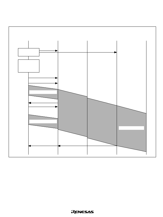
453
The E-DMAC continues reading descriptors and transmitting frames as long as the setting of the
TACT bit in the read descriptors is "active." When a descriptor with an "inactive" TACT bit is
read, the E-DMAC resets the transmit request bit (TR) in the transmit register and ends transmit
processing (EDTRR).
SH7616 + memory
Transmission flowchart
E-DMAC
EtherC
Ethernet
Transmit FIFO
EtherC/E-DMAC
initialization
Descriptor and
transmit
buffer setting
Transmit directive
Descriptor read
Descriptor write-back
Descriptor write-back
Transmission
completed
Descriptor read
Transmit data transfer
Transmit data transfer
Frame transmission
Figure 10.4 Sample Transmission Flowchart

454
10.3.3
Reception
When the receiver is enabled and the CPU sets the receive request bit (RR) in the E-DMAC
receive request register (EDRRR), the E-DMAC reads the descriptor following the previously
used one from the receive descriptor list (in the initial state, the descriptor indicated by the
transmission descriptor start address register (TDLAR)), and then enters the receive-standby state.
If the setting of the RACT bit is "active" and an own-address frame is received, the E-DMAC
transfers the frame to the receive buffer specified by RD2. If the data length of the received frame
is greater than the buffer length given by RD1, the E-DMAC performs write-back to the descriptor
when the buffer is full (RFP = 10 or 00), then reads the next descriptor. The E-DMAC then
continues to transfer data to the receive buffer specified by the new RD2. When frame reception is
completed, or if frame reception is suspended because of an error of some kind, the E-DMAC
performs write-back to the relevant descriptor (RFP = 11 or 01), and then ends the receive
processing. The E-DMAC then reads the next descriptor and enters the receive-standby state
again.
Note:
To receive frames continuously, the receive enable control bit (RNC) must be set to 1 in
the receive control register (RCR). After initialization, this bit is cleared to 0.
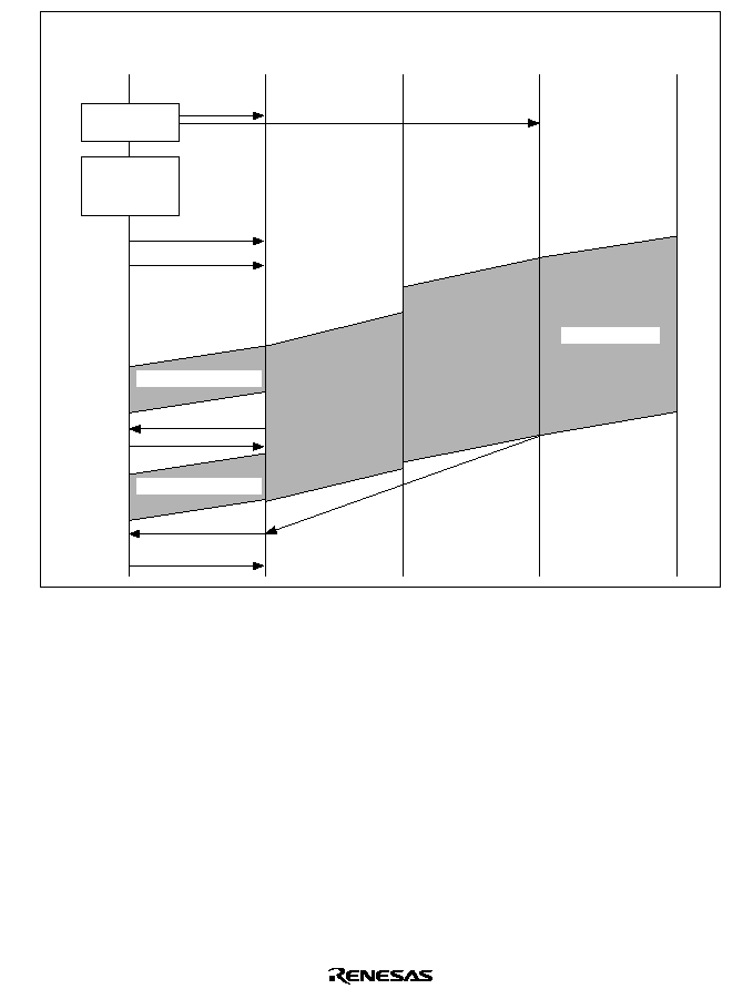
455
SH7616 + memory
Reception flowchart
E-DMAC
EtherC
Receive FIFO
Ethernet
EtherC/E-DMAC
initialization
Descriptor and
transmit
buffer setting
Reception
completed
Receive data transfer
Frame reception
Start of reception
Descriptor read
Descriptor write-back
Descriptor write-back
Descriptor read (preparation
for receiving next frame)
Descriptor read
Receive data transfer
Figure 10.5 Sample Reception Flowchart
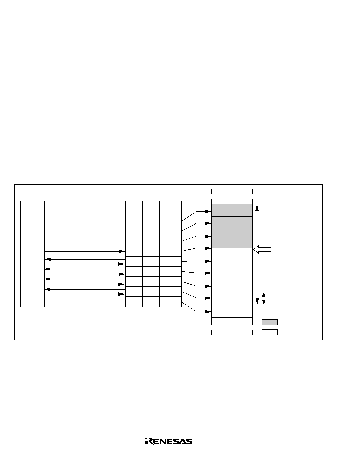
456
10.3.4
Multi-Buffer Frame Transmit/Receive Processing
Multi-Buffer Frame Transmit Processing: If an error occurs during multi-buffer frame
transmission, the processing shown in figure 10.6 is carried out.
Where the transmit descriptor is shown as inactive (TACT bit = 0) in the figure, buffer data has
already been transmitted normally, and where the transmit descriptor is shown as active (TACT bit
= 1), buffer data has not been transmitted. If a frame transmit error occurs in the first descriptor
part where the transmit descriptor is active (TACT bit = 1), transmission is halted, and the TACT
bit cleared to 0, immediately. The next descriptor is then read, and the position within the transmit
frame is determined on the basis of bits TFP1 and TFP0 (continuing [00] or end [01]). In the case
of a continuing descriptor, the TACT bit is cleared to 0, only, and the next descriptor is read
immediately. If the descriptor is the final descriptor, not only is the TACT bit cleared to 0, but
write-back is also performed to the TFE and TFS bits at the same time. Data in the buffer is not
transmitted between the occurrence of an error and write-back to the final descriptor. If error
interrupts are enabled in the EtherC/E-DMAC status interrupt permission register (EESIPR), an
interrupt is generated immediately after the final descriptor write-back.
0 0
0 0
0 0
1 0
1 0
1 0
1 0
1 0
1 1
1 0
0 0
0 0
0 0
0 0
0 0
0 0
0 1
1 0
E-DMAC
Inactivates TACT (changes 1 to 0)
Descriptor read
Descriptor read
Descriptor read
Descriptor read
Inactivates TACT
Inactivates TACT
Inactivates TACT
Inactivates TACT and writes TFE, TFS
Descriptors
One frame
Buffer
Transmitted data
Untransmitted data
Transmit error occurrence
Untransmitted
data is not
transmitted
after error
occurrence.
Descriptor
TA
C
T
TDLE
TFP1
TFP0
Figure 10.6 E-DMAC Operation after Transmit Error
Multi-Buffer Frame Receive Processing: If an error occurs during multi-buffer frame reception,
the processing shown in figure 10.7 is carried out.
Where the receive descriptor is shown as inactive (RACT bit = 0) in the figure, buffer data has
already been received normally, and where the receive descriptor is shown as active (RACT bit =
1), this indicates a buffer for which reception has not yet been performed. If a frame receive error
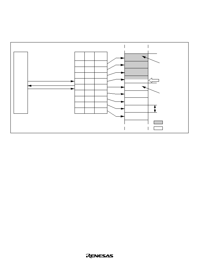
457
occurs in the first descriptor part where the RACT bit = 1 in the figure, reception is halted
immediately and a status write-back to the descriptor is performed.
If error interrupts are enabled in the EtherC/E-DMAC status interrupt permission register
(EESIPR), an interrupt is generated immediately after the write-back. If there is a new frame
receive request, reception is continued from the buffer after that in which the error occurred.
0 0
0 0
0 0
0 0
1 0
1 0
1 0
1 0
1 1
1 0
0 0
0 0
0 0
0 0
0 0
0 0
0 0
0 0
E-DMAC
Inactivates RACT and writes RFE, RFS
Descriptor read
Write-back
Descriptors
Buffer
Received data
Unreceived data
Receive error occurrence
:
:
:
:
:
Start of frame
New frame reception
continues from this buffer
RA
CT
RDLE
RFP1
RFP0
Figure 10.7 E-DMAC Operation after Receive Error

458

459
Section 11 Direct Memory Access Controller (DMAC)
11.1
Overview
A two-channel direct memory access controller (DMAC) is included on-chip. The DMAC can be
used in place of the CPU to perform high-speed data transfers between external devices equipped
with DACK (transfer request acknowledge signal), external memories, on-chip memory, and
memory-mapped external devices. Using the DMAC reduces the burden on the CPU and increases
the operating efficiency of the chip as a whole.
11.1.1
Features
The DMAC has the following features:
∑
Two channels
∑
Address space: Architecturally 4 Gbytes
∑
Choice of data transfer unit: Byte, word (2-byte), longword (4-byte) or 16-byte unit (In a 16-
byte transfer, four longword reads are executed, followed by four longword writes.)
∑
Maximum of 16,777,216 (16M) transfers
∑
In the event of a cache hit, CPU instruction processing and DMA operation can be executed in
parallel
∑
Single address mode transfers: Either the transfer source or transfer destination (peripheral
device) is accessed by a DACK signal (selectable) while the other is accessed by address. One
transfer unit of data is transferred in one bus cycle.
Possible transfer devices: External devices with DACK and memory-mapped external devices
(including external memory)
∑
Dual address mode transfer: Both the transfer source and transfer destination are accessed by
address. One transfer unit of data is transferred in two bus cycles.
Possible transfer devices:
Two external memories
External memory and memory-mapped external device
Two memory-mapped external devices
External memory and on-chip peripheral module (excluding DMAC, BSC, UBC, cache-
memory, E-DMAC, and EtherC)
Memory-mapped external device and on-chip peripheral module (excluding DMAC, BSC,
UBC, cache-memory, E-DMAC, and EtherC)
Two on-chip peripheral modules (excluding DMAC, BSC, UBC, cache-memory, E-
DMAC, and EtherC)
On-chip memory and memory-mapped external device
Two on-chip memories

460
On-chip memory and on-chip peripheral modules (excluding DMAC, BSC, UBC, cache-
memory, E-DMAC, and EtherC)
On-chip memory and external memory
∑
Transfer requests
External request: from the DREQn pins. Edge or level detection, and active-low or active-
high mode, can be specified for DREQn.
On-chip peripheral module requests: serial communication interface with FIFO (SCIF),
16-bit timer pulse unit (TPU), serial I/O with FIFO (SIOF), serial I/O (SIO)
Auto-request: the transfer request is generated automatically within the DMAC
∑
Choice of bus mode
Cycle steal mode
Burst mode
∑
Choice of channel priority order
Fixed mode
Round robin mode
∑
An interrupt request can be sent to the CPU on completion of data transfer
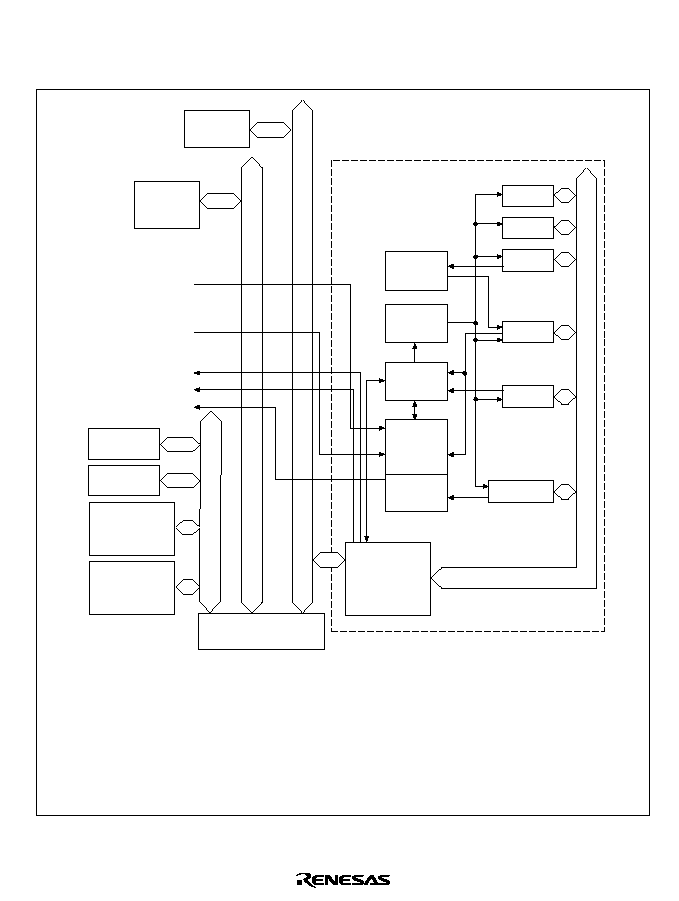
461
11.1.2
Block Diagram
Figure 11.1 shows the DMAC block diagram.
DREQn
On-chip peripheral
module request
DACKn
BH
DEIn
DMAC
On-chip
peripheral
module
On-chip
memory
Peripheral bus
External bus
External
ROM
External
RAM
External I/O
(memory
mapped)
External I/O
(with
acknowledge)
Bus controller
Iteration
control
Register
control
Start-up
control
Request
priority
control
Interrupt
control
Bus interface
DMAC module bus
SARn
DARn
TCRn
CHCRn
DMAOR
VCRDMAn
Internal bus
DMAOR:
SARn:
DARn:
TCRn:
CHCRn:
VCRDMAn:
DEIn:
On-chip peripheral module request:
BH
:
n:
DMA operation register
DMA source address register
DMA destination address register
DMA transfer count register
DMA channel control register
DMA vector number register
DMA transfer end interrupt request to CPU
Interrupt transfer request from on-chip SCIF, SIOF, SIO, TPU
Burst hint
0, 1
Figure 11.1 DMAC Block Diagram

462
11.1.3
Pin Configuration
Table 11.1 shows the DMAC pin configuration.
Table 11.1
Pin Configuration
Channel
Name
Symbol
I/O
Function
0
DMA transfer request
DREQ0
I
DMA transfer request input from external
device to channel 0
DMA transfer request
acknowledge
DACK0
O
DMA transfer request acknowledge output
from channel 0 to external device
1
DMA transfer request
DREQ1
I
DMA transfer request input from external
device to channel 1
DMA transfer request
acknowledge
DACK1
O
DMA transfer request acknowledge output
from channel 1 to external device
All
Burst hint
BH
O
Burst transfer in 16-byte transfer mode

463
11.1.4
Register Configuration
Table 11.2 summarizes the DMAC registers. The DMAC has a total of 13 registers. Each channel
has six control registers. One control register is shared by both channels.
Table 11.2
Register Configuration
Channel Name
Abbr.
R/W
Initial
Value Address
Access
Size
*
3
0
DMA source address register 0
SAR0
R/W
Undefined
H'FFFFFF80 32
DMA destination address
register 0
DAR0
R/W
Undefined
H'FFFFFF84 32
DMA transfer count register 0
TCR0
R/W
Undefined
H'FFFFFF88 32
DMA channel control register 0
CHCR0
R/(W)
*
1
H'00000000 H'FFFFFF8C 32
DMA vector number register 0
VCRDMA0 R/W
Undefined
H'FFFFFFA0 32
DMA request/response
selection control register 0
DRCR0
R/W
H'00
H'FFFFFE71 8
*
3
1
DMA source address register 1
SAR1
R/W
Undefined
H'FFFFFF90 32
DMA destination address
register 1
DAR1
R/W
Undefined
H'FFFFFF94 32
DMA transfer count register 1
TCR1
R/W
Undefined
H'FFFFFF98 32
DMA channel control register 1
CHCR1
R/(W)
*
1
H'00000000 H'FFFFFF9C 32
DMA vector number register 1
VCRDMA1 R/(W)
Undefined
H'FFFFFFA8 32
DMA request/response
selection control register 1
DRCR1
R/(W)
H'00
H'FFFFFE72 8
*
3
All
DMA operation register
DMAOR
R/(W)
*
2
H'00000000 H'FFFFFFB0 32
Notes:
*
1 Only 0 can be written to bit 1 of CHCR0 and CHCR1, after reading 1, to clear the flags.
*
2 Only 0 can be written to bits 1 and 2 of the DMAOR, after reading 1, to clear the flags.
*
3 Access DRCR0 and DRCR1 in byte units. Access all other registers in longword units.

464
11.2
Register Descriptions
11.2.1
DMA Source Address Registers 0 and 1 (SAR0, SAR1)
Bit:
31
30
29
...
3
2
1
0
...
Initial value:
--
--
--
...
--
--
--
--
R/W:
R/W
R/W
R/W
...
R/W
R/W
R/W
R/W
DMA source address registers 0 and 1 (SAR0 and SAR1) are 32-bit read/write registers that
specify the source address of a DMA transfer. During a DMA transfer, these registers indicate the
next source address. (In single-address mode, SAR is ignored in transfers from external devices
with DACK to memory-mapped external devices or external memory). In 16-byte unit transfers,
always set the value of the source address to a 16-byte boundary (16n address). Operation results
cannot be guaranteed if other values are used. Transmission in 16-byte units can be set only in
auto-request mode and at edge detection in external request mode. Values are retained in a reset, in
standby mode, and when the module standby function is used.
11.2.2
DMA Destination Address Registers 0 and 1 (DAR0, DAR1)
Bit:
31
30
29
...
3
2
1
0
...
Initial value:
--
--
--
...
--
--
--
--
R/W:
R/W
R/W
R/W
...
R/W
R/W
R/W
R/W
DMA destination address registers 0 and 1 (DAR0 and DAR1) are 32-bit read/write registers that
specify the destination address of a DMA transfer. During a DMA transfer, these registers indicate
the next destination address. (In single-address mode, DAR is ignored in transfers from memory-
mapped external devices or external memory to external devices with DACK). In 16-byte unit
transfers, always set the value of the source address to a 16-byte boundary (16n address).
Operation results cannot be guaranteed if other values are used. Transmission in 16-byte units can
be set only in auto-request mode and at edge detection in external request mode. Values are
retained in a reset, in standby mode, and when the module standby function is used.
If synchronous DRAM is accessed when performing 16-byte-unit transfer, a 16-byte boundary
(address 16n) value must be set for the destination address.

465
11.2.3
DMA Transfer Count Registers 0 and 1 (TCR0, TCR1)
Bit:
31
30
29
28
27
26
25
24
--
--
--
--
--
--
--
--
Initial value:
0
0
0
0
0
0
0
0
R/W:
R
R
R
R
R
R
R
R
Bit:
23
22
21
...
3
2
1
0
...
Initial value:
--
--
--
...
--
--
--
--
R/W:
R/W
R/W
R/W
...
R/W
R/W
R/W
R/W
DMA transfer count registers 0 and 1 (TCR0 and TCR1) are 32-bit read/write registers that
specify the DMA transfer count. The lower 24 of the 32 bits are valid. The value is written as 32
bits, including the upper eight bits. The number of transfers is 1 when the setting is H'00000001,
16,777,215 when the setting is H'00FFFFFF and 16, 777,216 (the maximum) when H'00000000 is
set. During a DMA transfer, these registers indicate the remaining transfer count.
Set the initial value as the write value in the upper eight bits. These bits always read 0. Values are
retained in a reset, in standby mode, and when the module standby function is used. For 16-byte
transfers, set the count to 4 times the number of transfers. Operation is not guaranteed if an
incorrect value is set.

466
11.2.4
DMA Channel Control Registers 0 and 1 (CHCR0, CHCR1)
Bit:
31
30
29
...
19
18
17
16
--
--
--
...
--
--
--
--
Initial value:
0
0
0
...
0
0
0
0
R/W:
R
R
R
...
R
R
R
R
Bit:
15
14
13
12
11
10
9
8
DM1
DM0
SM1
SM0
TS1
TS0
AR
AM
Initial value:
0
0
0
0
0
0
0
0
R/W:
R/W
R/W
R/W
R/W
R/W
R/W
R/W
R/W
Bit:
7
6
5
4
3
2
1
0
AL
DS
DL
TB
TA
IE
TE
DE
Initial value:
0
0
0
0
0
0
0
0
R/W:
R/W
R/W
R/W
R/W
R/W
R/W
R/(W)
*
R/W
Note:
Only 0 can be written, to clear the flag.
DMA channel control registers 0 and 1 (CHCR0 and CHCR1) are 32-bit read/write registers that
control the DMA transfer mode. They also indicate the DMA transfer status. Only the lower 16 of
the 32 bits are valid. They should be read and written as 32-bit values, including the upper 16 bits.
The registers are initialized to H'00000000 by a reset and in standby mode. Values are retained
during a module standby.
Bits 31 to 16--Reserved: These bits are always read as 0. The write value should always be 0.
Bits 15 and 14--Destination Address Mode Bits 1, 0 (DM1, DM0): Select whether the DMA
destination address is incremented, decremented or left fixed (in single address mode, DM1 and
DM0 are ignored when transfers are made from a memory-mapped external device, or external
memory to an external device with DACK). DM1 and DM0 are initialized to 00 by a reset and in
standby mode. Values are retained during a module standby.

467
Bit 15: DM1
Bit 14: DM0
Description
0
0
Fixed destination address
(Initial value)
1
Destination address is incremented (+1 for byte transfer size,
+2 for word transfer size, +4 for longword transfer size, +16
for 16-byte transfer size)
1
0
Destination address is decremented (≠1 for byte transfer size,
≠2 for word transfer size, ≠4 for longword transfer size, ≠16
for 16-byte transfer size)
1
Reserved (setting prohibited)
Bits 13 and 12--Source Address Mode Bits 1, 0 (SM1, SM0): Select whether the DMA source
address is incremented, decremented or left fixed. (In single address mode, SM1 and SM0 are
ignored when transfers are made from an external device with DACK to a memory-mapped
external device, or external memory.) For a 16-byte transfer, the address is incremented by +16
regardless of the SM1 and SM0 values. SM1 and SM0 are initialized to 00 by a reset and in
standby mode. Values are retained during a module standby.
Bit 13: SM1
Bit 12: SM0
Description
0
0
Fixed source address (+16 for 16-byte transfer size)
(Initial value)
1
Source address is incremented (+1 for byte transfer size, +2
for word transfer size, +4 for longword transfer size, +16 for
16-byte transfer size)
1
0
Source address is decremented (≠1 for byte transfer size, ≠2
for word transfer size, ≠4 for longword transfer size, +16 for
16-byte transfer size)
1
Reserved (setting prohibited)
Bits 11 and 10--Transfer Size Bits (TS1, TS0): Select the DMA transfer size. When 11 is set to
bits TS1 and TS0 (in the 16-byte unit), request mode is available only in auto-request mode and at
edge detection in external request mode. When 11 is set to bits TS1 and TS0 (in the 16-byte unit)
and level detection in external request mode and internal peripheral-module request mode are set,
system operations are not guaranteed. TS1 and TS0 are initialized to 00 by a reset and in standby
mode. Values are retained during a module standby.
Bit 11: TS1
Bit 10: TS0
Description
0
0
Byte unit
*
(initial value)
1
Word (2-byte) unit
1
0
Longword (4-byte) unit
1
16-byte unit (4 longword transfers)
Note:
*
The byte unit setting should not be used if a destination address has been set in internal
memory for the dual address mode.

468
Bit 9--Auto Request Mode Bit (AR): Selects either auto-request mode (in which transfer requests
are generated automatically within the DMAC) or a mode using external requests or requests from
on-chip peripheral modules (SCIF, TPU, SIOF, SIO). The AR bit is initialized to 0 by a reset and
in standby mode. Its value is retained during a module standby.
Bit 9: AR
Description
0
External/on-chip peripheral module request mode
(Initial value)
1
Auto-request mode
Bit 8--Acknowledge/Transfer Mode Bit (AM): In dual address mode, this bit selects whether the
DACKn signal is output during the data read cycle or write cycle. In single-address mode, it
selects whether to transfer data from memory to device or from device to memory. The AM bit is
initialized to 0 by a reset and in standby mode. Its value is retained during a module standby.
Bit 8: AM
Description
0
DACKn output in read cycle (dual address mode)/transfer from memory
to device (single address mode)
(Initial value)
1
DACKn output in write cycle (dual address mode)/transfer from device
to memory (single address mode)
Bit 7--Acknowledge Level Bit (AL): Selects whether the DACKn signal is an active-high signal
or an active-low signal. The AL bit is initialized to 0 by a reset and in standby mode. Its value is
retained during a module standby.
Bit 7: AL
Description
0
DACKn is an active-low signal
(Initial value)
1
DACKn is an active-high signal
Bit 6--DREQn Select Bit (DS): Selects the DREQn input detection used. When 0 (level detection)
is set to bit DS, set 0 (cycle-steal mode) to the transfer bus mode bit (TB). When 0 is set to bit DS
and 1 (burst mode) is set to bit TB, system operations are not guaranteed. The DS bit is initialized
to 0 by a reset and in standby mode. Its value is retained during a module standby.
Bit 6: DS
Description
0
Detected by level
(Initial value)
Can be set only in cycle-steal mode
1
Detected by edge

469
Bit 5--DREQn Level Bit (DL): Selects the DREQn input detection level. The DL bit is initialized
to 0 by a reset and in standby mode. Its value is retained during a module standby.
Bit 5: DL
Description
0
When DS is 0, DREQ is detected by low level; when DS is 1, DREQ is
detected at falling edge
(Initial value)
1
When DS is 0, DREQ is detected by high level; when DS is 1, DREQ is
detected at rising edge
Bit 4--Transfer Bus Mode Bit (TB): Selects the bus mode for DMA transfers. When 1 (burst
mode) is set to bit TB, set 1 (edge detection) to the DREQ select bit (DS). When 1 is set to bit TB
and 0 (level detection) is set to bit DS, system operations are not guaranteed. The TB bit is
initialized to 0 by a reset and in standby mode. Its value is retained during a module standby.
Bit 4: TB
Description
0
Cycle-steal mode
(Initial value)
1
Burst mode
Bit 3--Transfer Address Mode Bit (TA): Selects the DMA transfer address mode. The TA bit is
initialized to 0 by a reset and in standby mode. Its value is retained during a module standby.
Bit 3: TA
Description
0
Dual address mode
(Initial value)
1
Single address mode
Bit 2--Interrupt Enable Bit (IE): Determines whether or not to request a CPU interrupt at the end
of a DMA transfer. When the IE bit is set to 1, an interrupt (DEI) request is sent to the CPU when
the TE bit is set. The IE bit is initialized to 0 by a reset and in standby mode. Its value is retained
during a module standby.
Bit 2: IE
Description
0
Interrupt request disabled
(Initial value)
1
Interrupt request enabled
Bit 1--Transfer-End Flag Bit (TE): Indicates that the transfer has ended. When the value in the
DMA transfer count register (TCR) becomes 0, the DMA transfer ends normally and the TE bit is
set to 1. When TCR is not 0, the TE bit is not set if the transfer ends because of an NMI interrupt
or DMA address error, or because the DME bit in the DMA operation register (DMAOR) or the
DE bit was cleared. To clear the TE bit, read 1 from it and then write 0. When the TE bit is set,
setting the DE bit to 1 will not enable a transfer. The TE bit is initialized to 0 by a reset and in
standby mode. Its value is retained during a module standby.

470
Bit 1: TE
Description
0
DMA has not ended or was aborted
(Initial value)
Cleared by reading 1 from the TE bit and then writing 0
1
DMA has ended normally (by TCR = 0)
Bit 0--DMA Enable Bit (DE): Enables or disables DMA transfers. In auto-request mode, the
transfer starts when this bit or the DME bit in DMAOR is set to 1. The NMIF and AE bits in
DMAOR and the TE bit must be all set to 0. In external request mode or on-chip peripheral
module request mode, the transfer begins when the DMA transfer request is received from the
relevant device or on-chip peripheral module, provided this bit and the DME bit are set to 1. As
with the auto-request mode, the TE bit and the NMIF and AE bits in DMAOR must all be set to 0.
The transfer can be stopped by clearing this bit to 0. The DE bit is initialized to 0 by a reset and in
standby mode. Its value is retained during a module standby.
Bit 0: DE
Description
0
DMA transfer disabled
(Initial value)
1
DMA transfer enabled
11.2.5
DMA Vector Number Registers 0 and 1 (VCRDMA0, VCRDMA1)
Bit:
31
30
29
...
11
10
9
8
--
--
--
...
--
--
--
--
Initial value:
0
0
0
...
0
0
0
0
R/W:
R
R
R
...
R
R
R
R
Bit:
7
6
5
4
3
2
1
0
VC7
VC6
VC5
VC4
VC3
VC2
VC1
VC0
Initial value:
--
--
--
--
--
--
--
--
R/W:
R/W
R/W
R/W
R/W
R/W
R/W
R/W
R/W
DMA vector number registers 0 and 1 (VCRDMA0, VCRDMA1) are 32-bit read/write registers
that set the DMAC transfer-end interrupt vector number. Only the lower eight bits of the 32 are
valid. They are written as 32-bit values, including the upper 24 bits. Values are retained in a reset,
in standby mode, and when the module standby function is used.
Bits 31 to 8--Reserved: These bits are always read as 0. The write value should always be 0.

471
Bits 7 to 0--Vector Number Bits 7≠0 (VC7≠VC0): Set the interrupt vector numbers at the end of a
DMAC transfer. Interrupt vector numbers of 0≠127 can be set. When a transfer-end interrupt
occurs, the vector number is fetched and control is transferred to the specified interrupt handling
routine. The VC7≠VC0 bits retain their values in a reset and in standby mode. As the maximum
vector number is 127, 0 must always be written to VC7.
11.2.6
DMA Request/Response Selection Control Registers 0 and 1 (DRCR0, DRCR1)
Bit:
7
6
5
4
3
2
1
0
--
--
--
RS4
RS3
RS2
RS1
RS0
Initial value:
0
0
0
0
0
0
0
0
R/W:
R
R
R
R/W
R/W
R/W
R/W
R/W
DMA request/response selection control registers 0 and 1 (DRCR0, DRCR1) are 8-bit read/write
registers that set the DMAC transfer request source. They are written as 8-bit values. They are
initialized to H'00 by a reset, but retain their values in standby mode and a module standby.
Bits 7 to 5--Reserved: These bits are always read as 0. The write value should always be 0.
Bits 4 to 0--Resource Select Bits 4 to 0 (RS4≠RS0): Specify which transfer request to input to the
DMAC. Changing the transfer request source must be done when the DMA enable bit (DE) is 0.
See section 11.3.4, DMA Transfer Types, for the possible setting combinations.
Bits RS4 to RS0 are initialized to 001 by a reset.
Bit 4:
RS4
Bit 3:
RS3
Bit 2:
RS2
Bit 1:
RS1
Bit 0:
RS0
Description
0
0
0
0
0
DREQ (external request)
(Initial value)
1
Reserved (setting prohibited)
1
0
Reserved (setting prohibited)
1
Reserved (setting prohibited)
1
0
0
Reserved (setting prohibited)
1
SCIF channel 1 RXI (on-chip SCI with FIFO channel
1 receive-data-full interrupt request)
*
1
0
SCIF channel 1 TXI (on-chip SCI with FIFO channel
1 transmit-data-empty interrupt request)
*
1
1
1
Reserved (setting prohibited)

472
Bit 4:
RS4
Bit 3:
RS3
Bit 2:
RS2
Bit 1:
RS1
Bit 0:
RS0
Description
0
1
0
0
0
Reserved (setting prohibited)
1
SCIF channel 2 RXI (on-chip SCI with FIFO channel
2 receive-data-full interrupt request)
*
1
0
SCIF channel 2 TXI (on-chip SCI with FIFO channel
2 transmit-data-empty interrupt request)
*
1
Reserved (setting prohibited)
1
0
0
TPU TGI0A (TPU input capture channel 0A interrupt
request)
*
1
TPU TGI0B (TPU input capture channel 0B interrupt
request)
*
0
0
1
0
TPU TGI0C (TPU input capture channel 0C interrupt
request)
*
1
TPU TGI0D (TPU input capture channel 0D interrupt
request)
*
1
0
0
0
0
Reserved (setting prohibited)
1
SIOF RDFI (SIO with FIFO receive-data-full interrupt
request)
*
1
0
SIOF TDEI (SIO with FIFO transmit-data-empty
interrupt request)
*
1
Reserved (setting prohibited)
1
0
0
Reserved (setting prohibited)
1
SIO channel 1 RDFI (SIO channel 1 receive-data-
full interrupt request)
*
1
0
SIO channel 1 TDEI (SIO channel 1 transmit-data-
empty interrupt request)
*
1
Reserved (setting prohibited)
1
0
0
0
Reserved (setting prohibited)
1
SIO channel 2 RDFI (SIO channel 2 receive-data-
full interrupt request)
*
1
0
SIO channel 2 TDEI (SIO channel 2 transmit-data-
empty interrupt request)
*
1
Reserved (setting prohibited)
1
*
*
Reserved (setting prohibited)
Note:
*
When a transfer request is generated by an on-chip module, select cycle-steal as the bus
mode, dual transfer as the transfer mode, and falling edge detection for the DREQn setting.

473
11.2.7
DMA Operation Register (DMAOR)
Bit:
31
30
29
...
11
10
9
8
--
--
--
...
--
--
--
--
Initial value:
0
0
0
...
0
0
0
0
R/W:
R
R
R
...
R
R
R
R
Bit:
7
6
5
4
3
2
1
0
--
--
--
--
PR
AE
NMIF
DME
Initial value:
0
0
0
0
0
0
0
0
R/W:
R
R
R
R
R/W
R/(W)
*
R/(W)
*
R/W
Note:
*
Only 0 can be written, to clear the flag.
The DMA operation register (DMAOR) is a 32-bit read/write register that controls the DMA
transfer mode. It also indicates the DMA transfer status. Only the lower four of the 32 bits are
valid. DMAOR is written as a 32-bit value, including the upper 28 bits. DMAOR is initialized to
H'00000000 by a reset and in standby mode. It retains its value when the module standby function
is used.
Bits 31 to 4--Reserved: These bits are always read as 0. The write value should always be 0.
Bit 3--Priority Mode Bit (PR): Specifies whether a fixed channel priority order or round-robin
mode is to be used there are simultaneous transfer requests for multiple channels. It is initialized to
0 by a reset and in standby mode. It retains its value when the module standby function is used.
Bit 3: PR
Description
0
Fixed priority (channel 0 > channel 1)
(Initial value)
1
Round-robin (Top priority shifts to bottom after each transfer. The
priority for the first DMA transfer after a reset is channel 1 > channel 0)
Bit 2--Address Error Flag Bit (AE): This flag indicates that an address error has occurred in the
DMAC. When the AE bit is set to 1, DMA transfer cannot be enabled even if the DE bit in the
DMA channel control register (CHCR) is set to 1. To clear the AE bit, read 1 from it and then
write 0. Operation is performed up to the DMAC transfer being executed when the address error
occurred. AE is initialized to 0 by a reset and in standby mode. It retains its value when the
module standby function is used.

474
Bit 2: AE
Description
0
No DMAC address error
(Initial value)
To clear the AE bit, read 1 from it and then write 0
1
Address error by DMAC
Bit 1--NMI Flag Bit (NMIF): This flag indicates that an NMI interrupt has occurred. When the
NMIF bit is set to 1, DMA transfer cannot be enabled even if the DE bit in the DMA channel
control register (CHCR) and the DME bit are set to 1. To clear the NMIF bit, read 1 from it and
then write 0. Operation is completed up to the end of the DMAC transfer being executed when
NMI was input. When the NMI interrupt is input while the DMAC is not operating, the NMIF bit
is set to 1. The NMIF bit is initialized to 0 by a reset or in the standby mode. It retains its value
when the module standby function is used.
Bit 1: NMIF
Description
0
No NMIF interrupt
(Initial value)
To clear the NMIF bit, read 1 from it and then write 0
1
NMIF interrupt has occurred
Bit 0--DMA Master Enable Bit (DME): Enables or disables DMA transfers on all channels. A
DMA transfer becomes enabled when the DE bit in the CHCR and the DME bit are set to 1. For
this to be effective, the TE bit in CHCR and the NMIF and AE bits must all be 0. When the DME
bit is cleared, all channel DMA transfers are aborted. DME is initialized to 0 by a reset and in
standby mode. It retains its value when the module standby function is used.
Bit 0: DME
Description
0
DMA transfers disabled on all channels
(Initial value)
1
DMA transfers enabled on all channels

475
11.3
Operation
When there is a DMA transfer request, the DMAC starts the transfer according to the
predetermined channel priority; when the transfer-end conditions are satisfied, it ends the transfer.
Transfers can be requested in three modes: auto-request, external request, and on-chip module
request. A transfer can be in either single address mode or dual address mode. The bus mode can
be either burst or cycle-steal.
11.3.1
DMA Transfer Flow
After the DMA source address registers (SAR), DMA destination address registers (DAR), DMA
transfer count registers (TCR), DMA channel control registers (CHCR), DMA vector number
registers (VCRDMA), DMA request/response selection control registers (DRCR), and DMA
operation register (DMAOR) are initialized (initializing sets each register so that ultimately the
condition (DE = 1, DME = 1, TE = 0, NMIF = 0, AE = 0) is satisfied), the DMAC transfers data
according to the following procedure:
1. Checks to see if transfer is enabled (DE = 1, DME = 1, TE = 0, NMIF = 0, AE = 0)
2. When a transfer request occurs and transfer is enabled, the DMAC transfers 1 transfer unit of
data. (In auto-request mode, the transfer begins automatically after register initialization. The
TCR value will be decremented by 1.) The actual transfer flows vary depending on the address
mode and bus mode.
3. When the specified number of transfers have been completed (when TCR reaches 0), the
transfer ends normally. If the IE bit in CHCR is set to 1 at this time, a DEI interrupt request is
sent to the CPU.
4. When an address error occurs in the DMAC or an NMI interrupt is generated, the transfer is
aborted. Transfers are also aborted when the DE bit in CHCR or the DME bit in DMAOR is
changed to 0.
Figure 11.2 shows a flowchart illustrating this procedure.
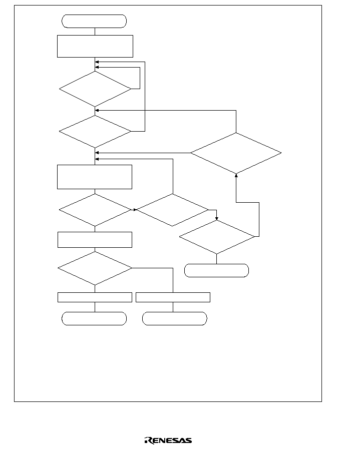
476
TCR = 0?
DE,
DME = 1 and NMIF,
AE, TE = 0?
Has a
transfer request been
generated?
*
1
Transfer aborted
Initial settings
(SAR, DAR, TCR, CHCR,
VCRDMA, DRCR, DMAOR)
Transfer
TCR-1
TCR,
SAR, and DAR updated
DEI interrupt request
(when IE = 1)
TE = 1
TE = 1
No
Yes
No
Yes
No
Yes
No
Yes
No
*
3
*
5
*
4
*
2
Start
End normally
End transfer
Yes
16-byte transfer
in progress?
NMIF = 1, or
AE = 1, or DE = 0, or
DME = 0?
NMIF = 1,
or AE = 1, or DE = 0,
or DME
= 0?
Bus
mode, transfer
request mode, DREQ detec-
tion method?
Notes:
*
1 In auto-request mode, the transfer will start when the NMIF, AE, and TE bits are all 0
and the DE and DME bits are then set to 1.
*
2 Cycle-steal mode.
*
3 In burst mode, DREQ = edge detection (external request), or auto-request mode in
burst mode.
*
4 16-byte transfer cycle in progress.
*
5 End of a 16-byte transfer cycle.
Figure 11.2 DMA Transfer Flow

477
11.3.2
DMA Transfer Requests
DMA transfer requests are usually generated in either the data transfer source or destination, but
they can also be generated by devices that are neither the source nor the destination. Transfers can
be requested in three modes: auto-request, external request, and on-chip peripheral module
request. The request mode is selected with the AR bit in DMA channel control registers 0 and 1
(CHCR0, CHCR1) and the RS0, RS1, RS2, RS3 and RS4 bits in DMA request/response selection
control registers 0 and 1 (DRCR0, DRCR1).
Table 11.3
Selecting the DMA Transfer Request Using the AR and RS Bits
CHCR
DRCR
AR
RS4
RS3
RS2
RS1
RS0
Request Mode
Resource Selection
0
0
0
0
0
0
Module request mode
DREQ (external request)
1
0
1
SCIF channel 1 RXI
1
0
SCIF channel 1 TXI
1
0
0
1
SCIF channel 2 RXI
1
0
SCIF channel 2 TXI
1
0
TPU TGI0A
1
TPU TGI0B
1
0
TPU TGI0C
1
TPU TGI0D
1
0
0
0
SIOF RDFI
1
0
SIOF TDEI
1
0
1
SIO channel 1 RDFI
1
0
SIO channel 1 TDEI
1
0
0
1
SIO channel 2 RDFI
1
0
SIO channel 2 TDEI
1
*
*
*
*
*
Auto-request mode
Note:
*
Don't care
Auto-Request Mode: When there is no transfer request signal from an external source (as in a
memory-to-memory transfer, the auto-request mode allows the DMAC to automatically generate a
transfer request signal internally. When the DE bits in CHCR0 and CHCR1 and the DME bit in
the DMA operation register (DMAOR) are set to 1, the transfer begins (so long as the TE bits in
CHCR0 and CHCR1 and the NMIF and AE bits in DMAOR are all 0).

478
External Request Mode: In this mode a transfer is started by a transfer request signal (DREQn)
from an external device. Choose one of the modes shown in table 11.4 according to the application
system. When DMA transfer is enabled (DE = 1, DME = 1, TE = 0, NMIF = 0, AE = 0), a transfer
is performed upon input of a DREQn signal.
Table 11.4
Selecting External Request Modes with the TA and AM Bits
CHCR
Transfer
TA
AM
Address Mode
Acknowledge Mode
Source
Destination
0
0
Dual address
mode
DACKn output in read
cycle
Any
*
Any
*
1
Dual address
mode
DACKn output in write
cycle
Any
*
Any
*
1
0
Single address
mode
Data transferred from
memory to device
External memory or
memory-mapped
external device
External device
with DACK
1
Single address
mode
Data transferred from
device to memory
External device
with DACK
External memory or
memory-mapped
external device
Note:
*
External memory, memory-mapped external device, and on-chip peripheral module
(excluding DMAC, BSC, UBC, cache memory, E-DMAC, and EtherC).
Choose to detect DREQn either by the falling edge or by level using the DS and DL bits in
CHCR0 and CHCR1 (DS = 0 is level detection, DS = 1 is edge detection; DL = 0 is active-low,
DL = 1 is active-high). The source of the transfer request does not have to be the data transfer
source or destination.
When 0 (level detection) is set to the DS bit of CHCR0 and CHCR1, set the TB bit to 0 (cycle-
steal mode) and set the TS1 and TS0 bits of CHCR0 and CHCR1 to either 00 (byte unit), 01 (word
unit), or 10 (long word unit).
When 0 is set to the DS bit of CHCR0 and CHCR1, when 1 (burst mode) is set to the TB bit of
CHCR0 and CHCR1, and when 11 (16 byte unit) is set to the TS1 and TS0 bits of CHCR1 and
CHCR1, operation is not guaranteed.

479
Table 11.5
Selecting the External Request Signal with the DS and DL Bits
CHCR
DS
DL
External Request
0
0
Low-level detection (can only be set in cycle-steal mode)
1
High-level detection (can only be set in cycle-steal mode)
1
0
Falling-edge detection
1
Rising-edge detection
On-Chip Module Request Mode: In this mode, transfers are started by a transfer request signal
(interrupt request signal) from an on-chip peripheral module. Transfer request signals include
SCIF, SIOF or SIO receive-data-full interrupts (RXI, RDFI), SCIF, SIOF or SIO transmit-data-
empty interrupts (TXI, TDEI), and TPU general registers (table 11.6). If DMA transfer is enabled
(DE = 1, DME = 1, TE = 0, NMIF = 0, AE = 0), DMA transfer starts upon input of a transfer
request signal.
When RXI or RDFI (transfer request due to an SCIF, SIOF or SIO receive-data-full condition) is
set as a transfer request, the transfer source must be the receive data register of the corresponding
module (SCFRDR or SIRDR). When TXI or TDEI (transfer request due to an SCIF, SIOF or SIO
transmit-data-empty condition) is set as a transfer request, the transfer destination must be the
transmit data register of the corresponding module (SCFTDR or SITDR).
These restrictions do not apply to TPU transfer requests.
When on-chip module request mode is used, an access size permitted by the peripheral module
register used as the transfer source or transfer destination must be set in bits TS1 and TS0 of
CHCR0 and CHCR1.

480
Table 11.6
Selecting On-Chip Peripheral Module Request Mode with the AR and RS Bits
AR
RS4
RS3
RS2
RS1
RS0
DMA Transfer
Request
Source
DMA
Transfer
Request
Signal
Transfer
Source
Transfer
Destina-
tion
Bus
Mode
DREQ
Setting
0
0
0
1
0
1
SCIF channel 1
receiver
RXI
SCFRDR1 Any
Cycle-
steal
Edge,
active-low
1
0
SCIF channel 1
transmitter
TXI
Any
SCFTDR1 Cycle-
steal
Edge,
active-low
1
0
0
1
SCIF channel 2
receiver
RXI
SCFRDR2 Any
Cycle-
steal
Edge,
active-low
1
0
SCIF channel 2
transmitter
TXI
Any
SCFTDR2 Cycle-
steal
Edge,
active-low
1
0
0
TPU channel
0A
TGI0A
Any
(excluding
on-chip
RAM)
Any
(excluding
on-chip
RAM)
Cycle-
steal
Edge,
active-low
1
TPU channel
0B
TGI0B
Any
(excluding
on-chip
RAM)
Any
(excluding
on-chip
RAM)
Cycle-
steal
Edge,
active-low
1
0
TPU channel
0C
TGI0C
Any
(excluding
on-chip
RAM)
Any
(excluding
on-chip
RAM)
Cycle-
steal
Edge,
active-low
1
TPU channel
0D
TGI0D
Any
(excluding
on-chip
RAM)
Any
(excluding
on-chip
RAM)
Cycle-
steal
Edge,
active-low
1
0
0
0
1
SIOF receiver
RDFI
SIRDR
Any
Cycle-
steal
Edge,
active-low
1
0
SIOF
transmitter
TDEI
Any
SITDR
Cycle-
steal
Edge,
active-low
1
0
1
SIO channel 1
receiver
RDFI
SIRDR1
Any
Cycle-
steal
Edge,
active-low
1
0
SIO channel 1
transmitter
TDEI
Any
SITDR1
Cycle-
steal
Edge,
active-low
1
0
0
1
SIO channel 2
receiver
RDFI
SIRDR2
Any
Cycle-
steal
Edge,
active-low
1
0
SIO channel 2
transmitter
TDEI
Any
SITDR2
Cycle-
steal
Edge,
active-low
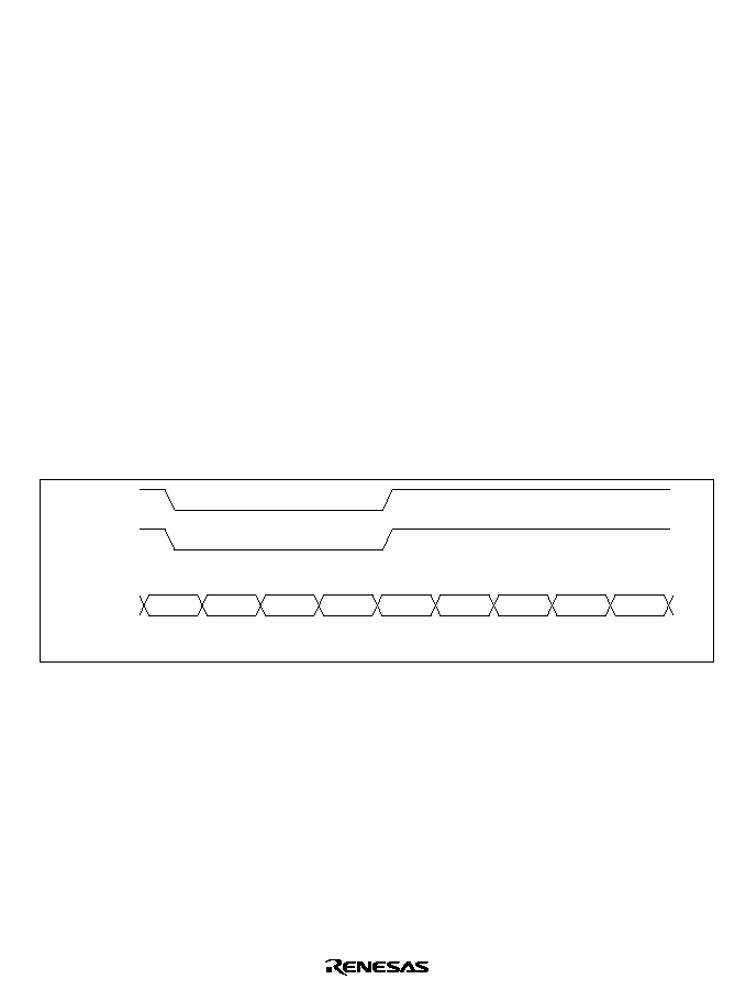
481
For outputting transfer request from the SCIF, SIOF, SIO, and TPU, the corresponding interrupt
enable bits must be set to output the interrupt signals. Note that transfer request signals from on-
chip peripheral modules (interrupt request signals) are sent not just to the DMAC but to the CPU
as well. When an on-chip peripheral module is specified as the transfer request source, set the
priority level values in the interrupt priority level registers (IPRC≠IPRE) of the interrupt controller
(INTC) at or below the levels set in the I3≠I0 bits of the CPU's status register so that the CPU
does not accept the interrupt request signal.
With the DMA transfer request signals in table 11.6, when DMA transfer is performed a DMA
transfer request (interrupt request) from any module will be cleared at the first transfer.
11.3.3
Channel Priorities
When the DMAC receives simultaneous transfer requests on two channels, it selects a channel
according to a predetermined priority order. There is a choice of two priority modes, fixed or
round-robin. The mode is selected by the priority bit, PR, in the DMA operation register
(DMAOR).
Fixed Priority Mode: In this mode, the relative channel priority levels are fixed. When PR is set
to 0, channel 0 has higher priority than channel 1. Figure 11.3 shows an example of a transfer in
burst mode.
CPU
Bus
cycle
DREQ1
DREQ0
CPU
CPU
Channel 0
source
Channel 0
destination
Channel 0
source
Channel 0
destination
Channel 1
source
Channel 1
destination
Figure 11.3 Fixed Mode DMA Transfer in Burst Mode
(Dual Address, DREQn Falling-Edge Detection)
In cycle-steal mode, once a channel 0 request is accepted, channel 1 requests are also accepted
until the next request is accepted, which makes more effective use of the bus cycle. If requests
come simultaneously for channel 0 and channel 1 when DMA operation is starting, the first is
transmitted with channel 0, and thereafter channel 1 and channel 0 transfers are performed
alternately.

482
CPU
Bus
cycle
DREQ1
DREQ0
CPU
CPU
CPU
CPU
Channel 0
source
Channel 1
source
Channel 0
source
Channel 0
destination
Channel 1
destination
Figure 11.4 Fixed Mode DMA Transfer in Cycle-Steal Mode
(Dual Address, DREQn Low-Level Detection)
Round-Robin Mode: Switches the priority of channel 0 and channel 1, shifting their ability to
receive transfer requests. Each time one transfer ends on one channel, the priority shifts to the
other channel. The channel on which the transfer just finished is assigned low priority. After reset,
channel 1 has higher priority than channel 0.
Figure 11.5 shows how the priority changes when channel 0 and channel 1 transfers are requested
simultaneously and another channel 0 transfer is requested after the first two transfers end. The
DMAC operates as follows:
1. Transfer requests are generated simultaneously to channels 1 and 0.
2. Channel 1 has the higher priority, so the channel 1 transfer begins first (channel 0 waits for
transfer).
3. When the channel 1 transfer ends, channel 1 becomes the lower-priority channel.
4. The channel 0 transfer begins.
5. When the channel 0 transfer ends, channel 0 becomes the lower-priority channel.
6. A channel 0 transfer is requested.
7. The channel 0 transfer begins.
8. When the channel 0 transfer ends, channel 0 is already the lower-priority channel, so the order
remains the same.
483
0
None
None
1. Requests occur
in channels
0 and 1
6. Request occurs
in channel 0
2. Channel 1
transfer starts
3. Channel 1
transfer ends
5. Channel 0
transfer ends
7. Channel 0
transfer starts
4. Channel 0
transfer starts
8. Channel 0
transfer ends
Priority
changes
1
>
0
0
>
1
1
>
0
1
>
0
Transfer requests
Waiting channel
DMAC operation
Channel priority order
Priority
changes
Priority
does not change
Waiting for
transfer request
Figure 11.5 Channel Priority in Round-Robin Mode

484
11.3.4
DMA Transfer Types
It can operate in single address mode or dual address mode, as defined by how many bus cycles
the DMAC takes to access the transfer source and transfer destination. The actual transfer
operation timing varies with the DMAC bus mode used: cycle-steal mode or burst mode. The
DMAC supports all the transfers shown in table 11.7.
Table 11.7
Supported DMA Transfers
Destination
Source
External
Device with
DACK
External
Memory
Memory-Mapped
External Device
On-Chip
Peripheral
Module
On-Chip
Memory
External device
with DACK
Not available
Single
Single
Not available Not available
External memory
Single
Dual
Dual
Dual
*
Dual
Memory-mapped
external device
Single
Dual
Dual
Dual
*
Dual
On-chip peripheral
module
Not available
Dual
*
Dual
*
Dual
*
Dual
*
On-chip memory
Not available
Dual
Dual
Dual
*
Dual
Single: Single address mode
Dual:
Dual address mode
Note:
*
Access size permitted by peripheral module register used as transfer source or transfer
destination (excluding DMAC, BSC, UBC, cache memory, E-DMAC, and EtherC).
Address Modes:
∑
Single Address Mode
In single address mode, both the transfer source and destination are external; one (selectable) is
accessed by a DACKn signal while the other is accessed by address. In this mode, the DMAC
performs the DMA transfer in one bus cycle by simultaneously outputting a transfer request
acknowledge DACKn signal to one external device to access it, while outputting an address to
the other end of the transfer. Figure 11.6 shows an example of a transfer between external
memory and external device with DACK. That data is written in external memory in the same
bus cycle while the external device outputs data to the data bus.
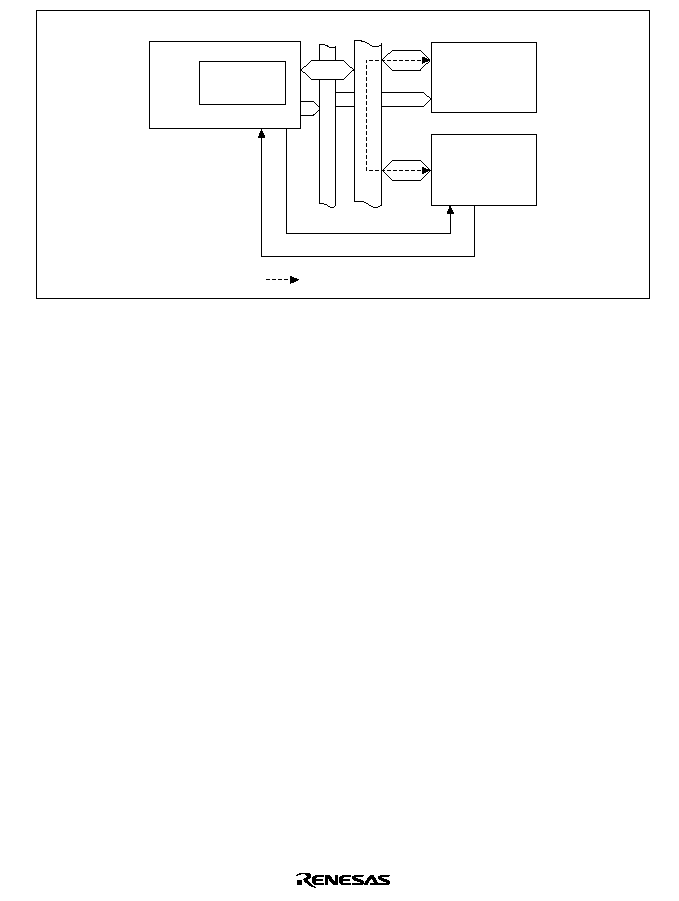
485
DMAC
DACKn
DREQn
External
memory
External device
with DACK
Chip
External address bus
: Data flow
External data bus
Figure 11.6 Data Flow in Single Address Mode
Two types of transfers are possible in single address mode: 1) transfers between external
devices with DACK and memory-mapped external devices; and 2) transfers between external
devices with DACK and external memory. For both of them, transfer must be requested by the
external request signal (DREQn). For the combination of the specifiable setting to perform
data transfer using an external request (DREQn), see table 11.9. Figure 11.7 shows the DMA
transfer timing for single address mode.
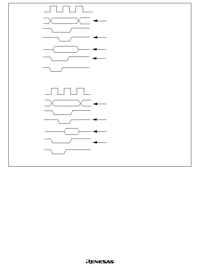
486
CKIO
A24≠A0
CS
D31≠D0
DACKn
BS
CKIO
A24≠A0
CS
D31≠D0
BS
DACKn
WE
RD
Address output to external
memory space
Write strobe signal to external
memory space
Data output from external
device with DACK
DACK signal (active low) to external
device with DACK
a. External device with DACK to external memory space
Address output to external
memory space
Data output from external
memory space
Read strobe signal to external
memory space
DACK signal (active low) to external
device with DACK
b. External memory space to external device with DACK
Figure 11.7 DMA Transfer Timing in Single Address Mode
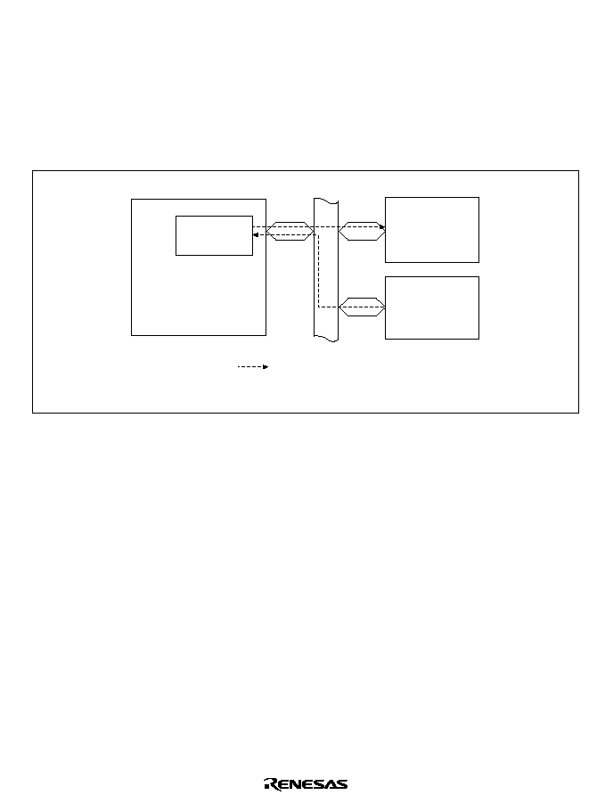
487
∑
Dual Address Mode
In dual address mode, both the transfer source and destination are accessed (selectable) by
address. The source and destination can be located externally or internally. The DMAC
accesses the source in the read cycle and the destination in the write cycle, so the transfer is
performed in two separate bus cycles. The transfer data is temporarily stored in the DMAC.
Figure 11.8 shows an example of a transfer between two external memories in which data is
read from one external memory in the read cycle and written to the other external memory in
the following write cycle.
DMAC
External
memory
External
memory
Chip
2
1
External data bus
: Data flow
1: Read cycle
2: Write cycle
Figure 11.8 Data Flow in Dual Address Mode
In dual address mode transfers, external memory and memory-mapped external devices can be
mixed without restriction. Specifically, this enables transfers between the following:
Transfer between external memory and external memory
Transfer between external memory and memory-mapped external device
Transfer between memory-mapped external device and memory-mapped external device
Transfer between external memory and on-chip peripheral module (excluding DMAC,
BSC, UBC, cache, E-DMAC, and EtherC)*
Transfer between memory-mapped external device and on-chip peripheral module
(excluding DMAC, BSC, UBC, cache, E-DMAC, and EtherC)*
Transfer between on-chip memory and on-chip memory
Transfer between on-chip memory and memory-mapped external device
Transfer between on-chip memory and on-chip peripheral module (excluding DMAC,
BSC, UBC, cache, E-DMAC, and EtherC)*
Transfer between on-chip memory and external memory
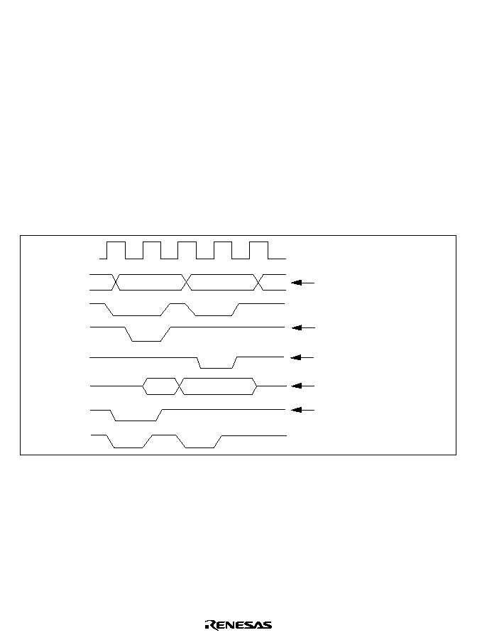
488
Transfer between on-chip peripheral module (excluding DMAC, BSC, UBC, cache, E-
DMAC, and EtherC) and on-chip peripheral module (excluding DMAC, BSC, UBC, cache,
E-DMAC, and EtherC)*
Note: * Access size permitted by peripheral module register used as transfer source or transfer
destination (excluding DMAC, BSC, UBC, cache, E-DMAC, and EtherC).
Transfer requests can be auto-request, external requests, or on-chip peripheral module requests.
If the transfer request source is the SCIF, SIOF or SIO, an SCIF, SIOF or SIO register,
respectively, must be the transfer destination or transfer source (see table 11.6). For the
combination of the specifiable setting to perform data transfer using an external request
(DREQn), see table 11.9. Dual address mode outputs DACKn in either the read cycle or write
cycle. The acknowledge/transfer mode bit (AM) of the DMA channel control registers 0 and 1
(CHCR0 and 1) specifies whether DACK is output in either the read cycle or the write cycle.
Figure 11.9 shows the DMA transfer timing in dual address mode.
CKIO
A24≠A0
CS
D31≠D0
DACKn
RD
WE
BS
Address output to
external memory space
Read strobe signal to
external memory space
Write strobe signal to
external memory space
I/O data of external
memory space
DMAC acknowledge signal
(active-low)
Figure 11.9 DMA Transfer Timing in Dual Address Mode
(External Memory Space
External Memory Space, DACKn Output in Read Cycle)
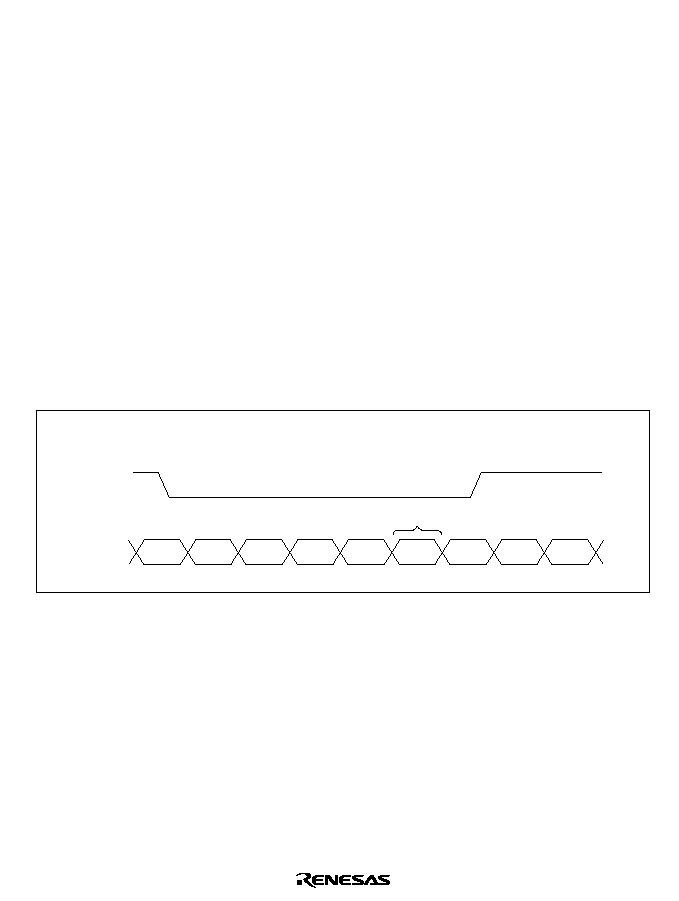
489
Bus Modes: There are two bus modes: cycle-steal and burst. Select the mode with the TB bits in
CHCR0 and CHCR1.
∑
Cycle-Steal Mode
In cycle-steal mode, the bus right is given to another bus master each time the DMAC
completes one transfer. When another transfer request occurs, the bus right is retrieved from
the other bus master and another transfer is performed for one transfer unit. When that transfer
ends, the bus right is passed to the other bus master. This is repeated until the transfer end
conditions are satisfied. (in the case of 16-byte transfer in dual address mode, the DMAC
continues to hold the bus)
Cycle-steal mode can be used with all categories of transfer destination, transfer source, and
transfer request source. (with the exception of transfers between on-chip peripheral modules)
The CPU may take the bus twice when an acknowledge signal is output during the write cycle
or in single address mode. Figure 11.10 shows an example of DMA transfer timing in cycle-
steal mode. The transfer conditions for the example in the figure are as shown below.
When the transfer request source is an external request mode with level detection in the cycle-
steal mode, set the TS1 and TS0 bits of CHCR0 and CHCR1 to either 00 (byte unit), 01 (word
unit), or 01 (longword unit). If the TS1 and TS0 bits of CHCR0 and CHCR1 are set to 11 (16-
byte transfer), operation is not guaranteed.
CPU
CPU
CPU
DMAC DMAC
CPU
DMAC
DMAC
CPU
DREQn
∑ Dual address mode
∑ DREQn level detection
Bus
cycle
Bus right returned to CPU
Read
Write
Read
Write
Figure 11.10 DMA Transfer Timing in Cycle-Steal Mode
(Dual Address Mode, DREQn Low Level Detection)
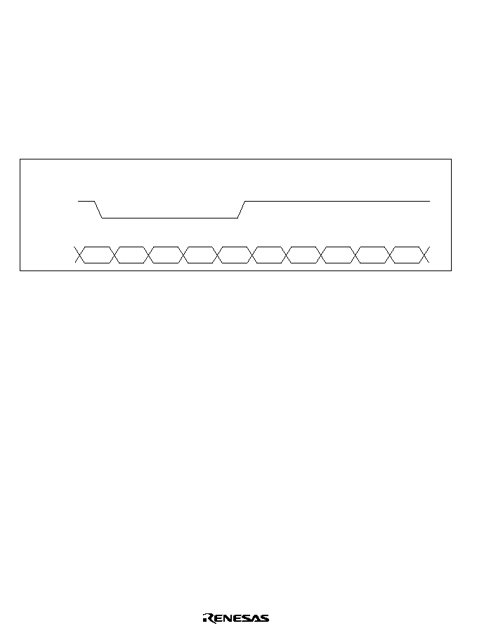
490
∑
Burst Mode
In burst mode, once the DMAC gets the bus, the transfer continues until the transfer end
condition is satisfied. When external request mode is used with level detection of the DREQ
pin, however, negating DREQ will pass the bus to the other bus master after completion of the
bus cycle of the DMAC that currently has an acknowledged request, even if the transfer end
conditions have not been satisfied. When the transfer request source is an on-chip peripheral
module, however, cycle-steal mode is always used.
Figure 11.11 shows an example of DMA transfer timing in burst mode. The transfer conditions
for the example in the figure are as shown below.
CPU
CPU
CPU
DMAC DMAC DMAC DMAC
CPU
DREQn
∑ Single address mode
∑ DREQn level detection
Bus
cycle
CPU
CPU
Figure 11.11 DMA Transfer Timing in Burst Mode (Single Address, DREQn Falling-Edge
Detection)
Refreshes cannot be performed during a burst transfer, so ensure that the number of transfers
satisfies the refresh request period when a memory requiring refreshing is used. When the transfer
request source is an external request (DREQn) in burst mode, set the DS bit of CHCR0 and
CHCR1 to 1 (edge detection). If the DS bits of CHCR0 and CHCR1 are set to 0 (level detection),
operation is not guaranteed.

491
Relationship of Request Modes and Bus Modes by DMA Transfer Category: Table 11.8
shows the relationship between request modes, bus modes, etc., by DMA transfer category.
Table 11.8
Relationship of Request Modes and Bus Modes by DMA Transfer Category
Address
Mode
Transfer Range
Request Mode
*
3
Bus
Mode
*
7
Transfer
Size (Byte)
Single
Between external memory and external
device with DACK
External
B/C
1/2/4/16
*
8
Between external device with DACK, and
memory mapped external device
External
B/C
1/2/4/16
*
8
Dual
Between external memories
External
B/C
1/2/4/16
*
8
Automatic
B/C
1/2/4/16
Internal peripheral
module
*
1
C
1/2/4
Between external memory and memory
External
B/C
1/2/4/16
*
8
mapped external device
Automatic
B/C
1/2/4/16
Internal peripheral
module
*
1
C
1/2/4
Between memory mapped external devices External
B/C
1/2/4/16
*
8
Automatic
B/C
1/2/4/16
Internal peripheral
module
*
1
C
1/2/4
Between external memory and internal
External
B/C
1/2/4
*
4
peripheral module
Automatic
B/C
1/2/4
*
4
Internal peripheral
module
*
2
C
1/2/4
*
4
Between memory mapped external device
External
B/C
1/2/4
*
4
and internal peripheral module
Automatic
B/C
1/2/4
*
4
Internal peripheral
module
*
2
C
1/2/4
*
4
Between internal memories
Automatic
B/C
1/2/4/16
Between internal memory and memory
External
B/C
1/2/4/16
*
8
mapped external device
*
5
Automatic
B/C
1/2/4/16
Internal peripheral
module
*
1
C
1/2/4

492
Table 11.8
Relationship of Request Modes and Bus Modes by DMA Transfer Category
(cont)
Address
Mode
Transfer Range
Request Mode
*
3
Bus
Mode
*
7
Transfer
Size (Byte)
Dual
Between internal memory and internal
Automatic
B/C
1/2/4
*
4
peripheral module
Internal peripheral
module
*
2
C
1/2/4
*
4
Between internal memory and external
External
B/C
1/2/4/16
*
8
memory
*
6
Automatic
B/C
1/2/4/16
Internal peripheral
module
*
1
C
1/2/4
Between internal peripheral modules
Automatic
B/C
1/2/4
*
4
Internal peripheral
module
*
2
C
1/2/4
*
4
Notes: B: Burst mode
C: Cycle steal mode
*
1 For on-chip peripheral module requests, do not specify SCIF, SIOF and SIO as a
transfer request source.
*
2 When the transfer request source is SCIF, SIOF or SIO, the transfer source or transfer
destination must be SCIF, SIOF and SIO, respectively.
*
3 When the request mode is set to internal peripheral module request, set the DS bit and
the DL bit of CHCR0 and CHCR1 to 1 and 0, respectively (detection at the falling edge
of DREQn). In addition, the bus mode can only be set to cycle-steal mode.
*
4 Specify the access size that is allowed by the internal peripheral-module registers,
which are a transfer source or a transfer destination.
*
5 When transferring data from internal memory to a memory mapped external device, set
DACKn to write-time output. When transferring from a memory mapped external device
to internal memory, set DACKn to read-time output.
*
6 When transferring data from internal memory to external memory, set DACKn to write-
time output. When transferring from external memory to internal memory, set DACKn to
read-time output.
*
7 When B (burst mode) is set in the external request mode, set the DS bits of CHCR0
and CHCR1 to 1 (edge detection). If they are set to 0 (level detection), operation cannot
be guaranteed.
*
8 Transfer in units of 16 bytes is enabled only when edge detection has been specified. If
transfer is attempted in units of 16 bytes when level detection has been specified,
operation cannot be guaranteed.
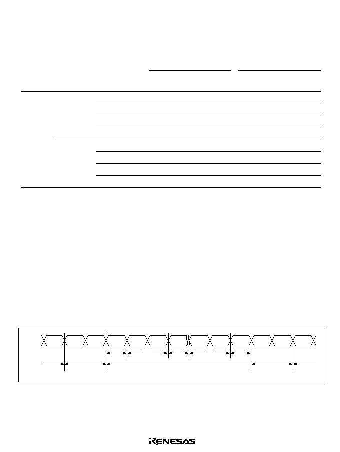
493
Table 11.9 shows the combinations of request mode, bus mode, and address mode that can be
specified in the external request mode.
Table 11.9
Combinations of Request Mode, Bus Mode, and Address Mode Specifiable in
the External Request Mode
Dual Address Mode
Single Address Mode
Request Mode
Burst
Mode
Cycle-Steal
Mode
Burst
Mode
Cycle-Steal
Mode
External
Level
Byte
--
O
--
O
request
detection
*
1
Word
--
O
--
O
Longword
--
O
--
O
16-byte unit
--
--
--
--
Edge
Byte
O
O
O
O
detection
*
2
Word
O
O
O
O
Longword
O
O
O
O
16-byte unit
O
O
O
O
Notes: O: Can be set
--: Cannot be set
*
1 The same for high-level and low-level detection.
*
2 The same for rising-edge detection and falling-edge detection.
Bus Mode and Channel Priority: When a given channel (1) is transferring in burst mode and
there is a transfer request to a channel (0) with a higher priority, the transfer of the channel with
higher priority (0) will begin immediately. When channel 0 is also operating in the burst mode, the
channel 1 transfer will continue as soon as the channel 0 transfer has completely finished. When
channel 0 is in cycle-steal mode, channel 1 will begin operating again after channel 0 completes
the transfer of one transfer unit, but the bus will then switch between the two in the order channel
1, channel 0, channel 1, channel 0. Since channel 1 is in burst mode, it will not give the bus to the
CPU. This example is illustrated in Figure 11.12.
Bus
state
CPU
DMAC ch1 DMAC ch1 DMAC ch0
DMAC ch0
DMAC ch1 DMAC ch1
DMAC ch1 DMAC ch1 DMAC ch0 DMAC ch1 DMAC ch1
CPU
ch1
ch0
ch0
ch1
ch0
CPU
DMAC ch1
Burst mode
DMAC ch1
Burst mode
DMAC ch1/ch0
bus right transfers
CPU
Figure 11.12 Bus Status when Multiple Channels are Operating
(when priority order is ch0 > ch1, ch1 is set to burst mode, and ch0 to cycle-steal mode)

494
11.3.5
Number of Bus Cycles
The number of states in the bus cycle when the DMAC is the bus master is controlled by the bus
state controller (BSC) just as it is when the CPU is the bus master. For details, see section 7, Bus
State Controller (BSC).
11.3.6
DMA Transfer Request Acknowledge Signal Output Timing
DMA transfer request acknowledge signal DACKn is output synchronous to the DMA address
output specified by the channel control register AM bit of the address bus. Normally, the
acknowledge signal becomes valid when DMA address output begins, and becomes invalid 0.5
cycles before the address output ends. (See figure 11.13.) The output timing of the acknowledge
signal varies with the settings of the connected memory space. The output timing of acknowledge
signals in the memory spaces is shown in figure 11.13.
Clock
DACKn
(Active high)
Address bus
CPU
DMAC
0.5 cycles
Figure 11.13 Example of DACKn Output Timing
Acknowledge Signal Output when External Memory Is Set as Ordinary Memory Space:
The timing at which the acknowledge signal is output is the same in the DMA read and write
cycles specified by the AM bit (figures 11.14 and 11.15). When DMA address output begins, the
acknowledge signal becomes valid; 0.5 cycles before address output ends, it becomes invalid. If a
wait is inserted in this period and address output is extended, the acknowledge signal is also
extended.
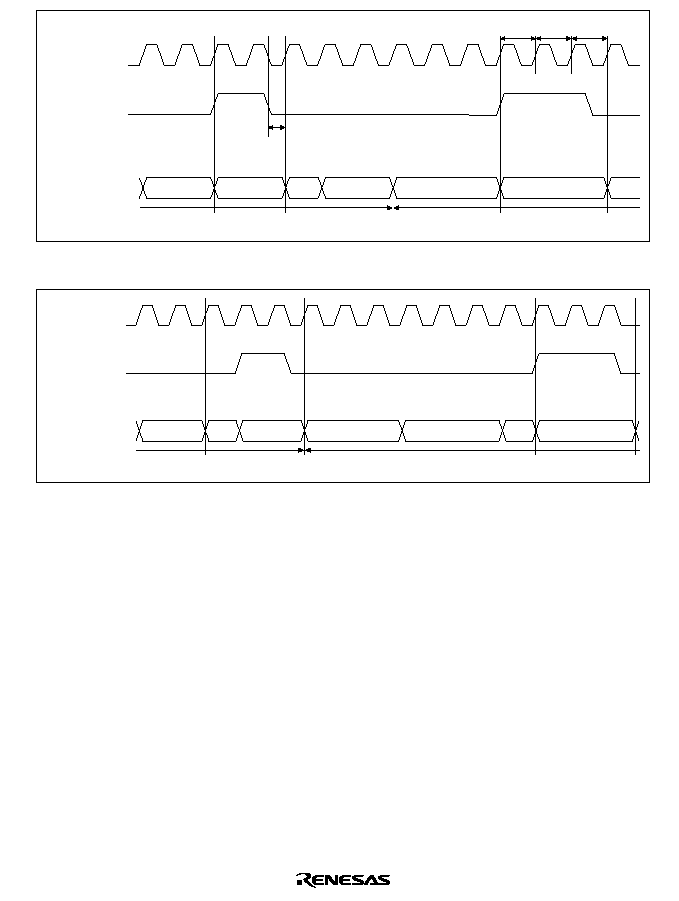
495
Clock
DACKn
(Active high)
Address
bus
CPU
DMAC
read
DMAC
write
Invalid
write
CPU
0.5 cycles
DMAC read
T
1
T
W
T
2
Basic timing
1 wait inserted
Figure 11.14 DACKn Output in Ordinary Space Accesses (AM = 0)
Clock
DACKn
(Active high)
Address
bus
DMAC
read
DMAC
write
Invalid
write
Invalid
write
CPU
DMAC read
Basic timing
1 wait inserted
DMAC write
Figure 11.15 DACKn Output in Ordinary Space Accesses (AM = 1)
In a longword access of a 16-bit external device (figure 11.16) or an 8-bit external device (figure
11.17), or a word access of an 8-bit external device (figure 11.18), the lower and upper addresses
are output 2 and 4 times in each DMAC access in order to align the data. For all of these
addresses, the acknowledge signal becomes valid simultaneous with the start of output and the
signal becomes invalid 0.5 cycles before the address output ends. When multiple addresses are
output in a single access to align data for synchronous DRAM, DRAM, or burst ROM, an
acknowledge signal is output to those addresses as well.
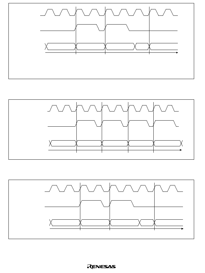
496
Clock
DACKn
(Active high)
Address
bus
CPU H
DMAC read H
DMAC read L
Invalid
write
DMAC write
Basic timing
*
1
*
2
Notes:
*
1 H: MSB side
*
2 L: LSB side
Figure 11.16 DACKn Output in Ordinary Space Accesses
(AM = 0, Longword Access to 16-Bit External Device)
Clock
DACKn
(Active high)
Address
bus
CPU
DMAC
read HH
DMAC
read HL
DMAC
read LH
DMAC
read LL
Basic timing
Figure 11.17 DACKn Output in Ordinary Space Accesses
(AM = 0, Longword Access to 8-Bit External Device)
Clock
DACKn
(Active high)
Address
bus
CPU
DMAC read H
DMAC read L
Invalid
write
DMAC write
Basic timing
Figure 11.18 DACKn Output in Ordinary Space Accesses
(AM = 0, Word Access to 8-Bit External Device)
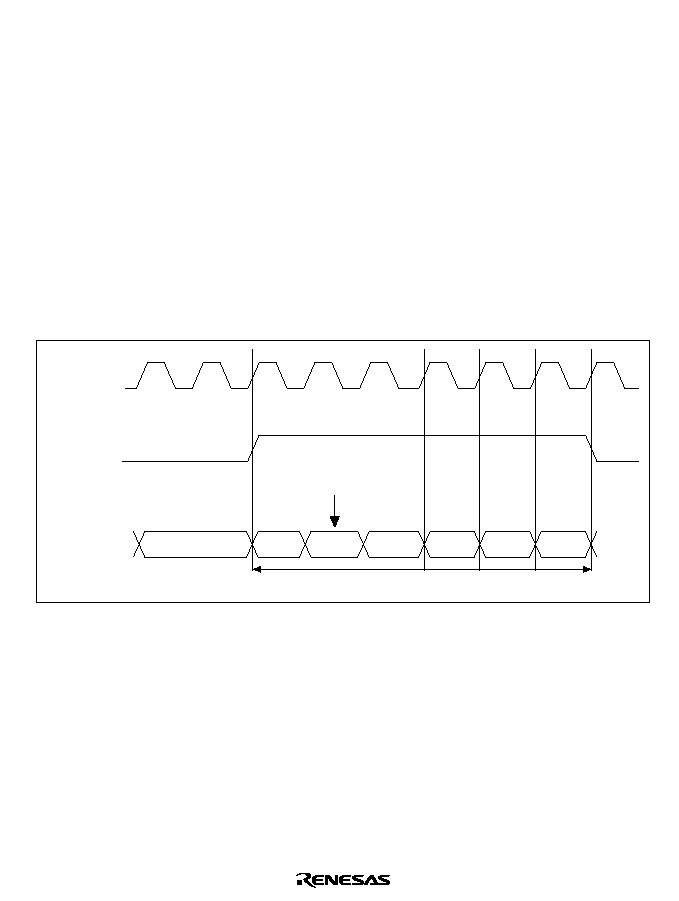
497
Acknowledge Signal Output when External Memory Is Set as Synchronous DRAM: When
external memory is set as synchronous DRAM, DACKn output becomes valid simultaneously
with the start of the DMA address, and becomes invalid when the address output ends.
When external memory is set as synchronous DRAM auto-precharge and AM = 0, the
acknowledge signal is output across the row address, read command, wait and read address of the
DMAC read (figure 11.19). Since the synchronous DRAM read has only burst mode, during a
single read an invalid address is output; the acknowledge signal, however, is output on the same
timing (figure 11.20). At this time, the acknowledge signal is extended until the write address is
output after the invalid read. A synchronous DRAM burst read is performed in the case of 16-byte
transfer. As 16-byte transfer is enabled only in auto-request mode and in external request mode
with edge detection, when using on-chip peripheral module requests or external request mode with
level detection, byte, word, or longword should be set as the transfer unit. Operation is not
guaranteed if a 16-byte unit is set when using on-chip peripheral module requests or external
request mode with level detection. When AM = 1, the acknowledge signal is output across the row
address and column address of the DMAC write (figure 11.21).
Clock
DACKn
(Active high)
Address
bus
CPU
DMAC read (basic timing)
Row
address
Read 1
Read 2
Read 3
Read 4
Read
command
Figure 11.19 DACKn Output in Synchronous DRAM Burst Read
(Auto-Precharge, AM = 0)
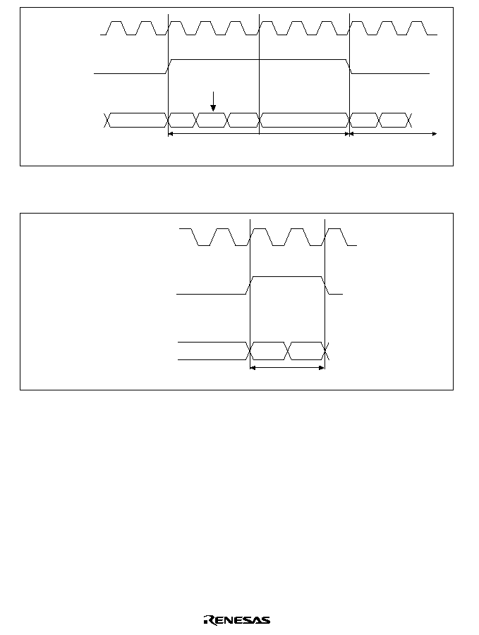
498
Clock
DACKn
(Active high)
Address
bus
CPU
Invalid read
DMAC read
(basic timing)
DMAC write
(basic timing)
Row
address
Column
address
Row
address
Read
Read
command
Figure 11.20 DACKn Output in Synchronous DRAM Single Read
(Auto-Precharge, AM = 0)
Clock
DACKn
(Active high)
Address
bus
DMAC write (basic timing)
Column
address
Row
address
Figure 11.21 DACKn Output in Synchronous DRAM Write
(Auto-Precharge, AM = 1)
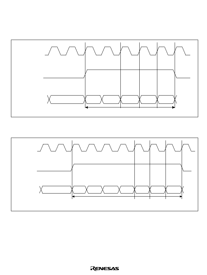
499
When external memory is set as bank active synchronous DRAM, during a burst read the
acknowledge signal is output across the read command, wait and read address when the row
address is the same as the previous address output (figure 11.22). When the row address is
different from the previous address, the acknowledge signal is output across the precharge, row
address, read command, wait and read address (figure 11.23).
Clock
DACKn
(Active high)
Address
bus
CPU
DMAC read (basic timing)
Read
command
Read 1
Read 2
Read 3
Read 4
Figure 11.22 DACKn Output in Synchronous DRAM Burst Read
(Bank Active, Same Row Address, AM = 0)
Clock
DACKn
(Active high)
Address
bus
CPU
DMAC read
(basic timing)
Pre-
charge
Read
command
Read 1 Read 2 Read 3 Read 4
Row
address
Figure 11.23 DACKn Output in Synchronous DRAM Burst Read
(Bank Active, Different Row Address, AM = 0)
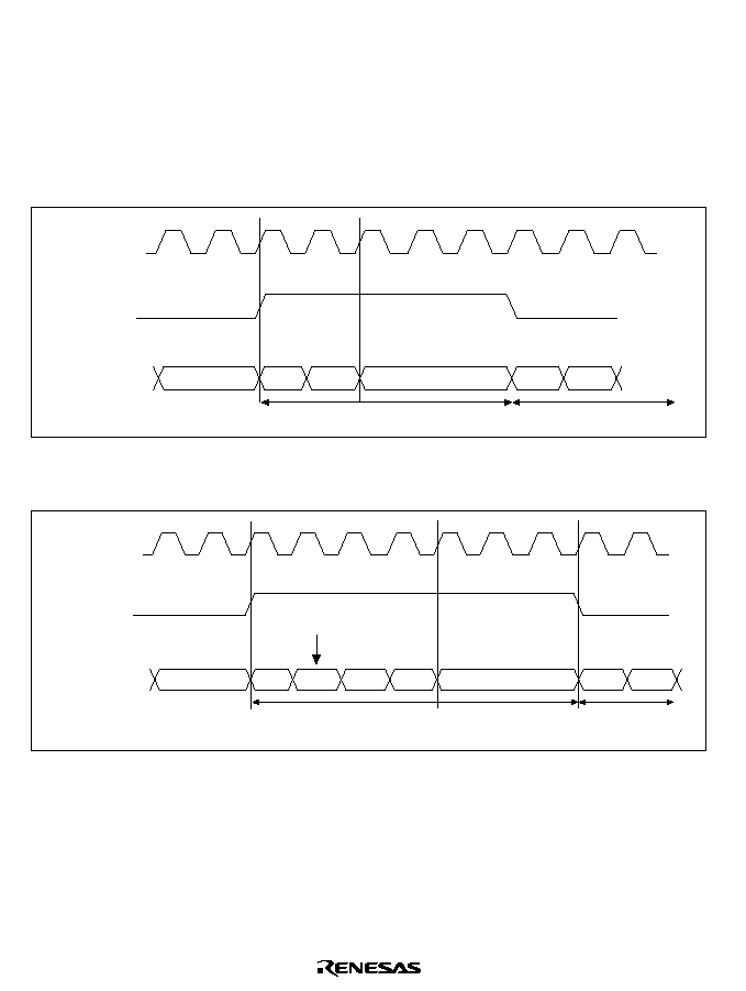
500
When external memory is set as bank active synchronous DRAM, during a single read the
acknowledge signal is output across the read command, wait and read address when the row
address is the same as the previous address output (figure 11.24). When the row address is
different from the previous address, the acknowledge signal is output across the precharge, row
address, read command, wait and read address (figure 11.25). Since the synchronous DRAM read
has only burst mode, during a single read an invalid address is output; the acknowledge signal is
output on the same timing. At this time, the acknowledge signal is extended until the write address
is output after the invalid read.
Clock
DACKn
(Active high)
Address
bus
CPU
Read
Invalid read
DMAC read (basic timing)
DMAC write (basic timing)
Read
command
Row
address
Column
address
Figure 11.24 DACKn Output in Synchronous DRAM Single Read
(Bank Active, Same Row Address, AM = 0)
Clock
DACKn
(Active high)
Address
bus
CPU
Invalid read
DMAC read
(basic timing)
DMAC write
(basic timing)
Row
address
Read
command
Row
address
Column
address
Pre-
charge
Read
Figure 11.25 DACKn Output in Synchronous DRAM Single Read
(Bank Active, Different Row Address, AM = 0)

501
When external memory is set as bank active synchronous DRAM, during a write the acknowledge
signal is output across the wait and column address when the row address is the same as the
previous address output (figure 11.26). When the row address is different from the previous
address, the acknowledge signal is output across the precharge, row address, wait and column
address (figure 11.27).
Clock
DACKn
(Active high)
Address
bus
DMAC write
(basic timing)
Column
address
Figure 11.26 DACKn Output in Synchronous DRAM Write
(Bank Active, Same Row Address, AM = 1)
Clock
DACKn
(Active high)
Address
bus
DMAC write
(basic timing)
Precharge
Row
address
Column
address
Figure 11.27 DACKn Output in Synchronous DRAM Write
(Bank Active, Different Row Address, AM = 1)
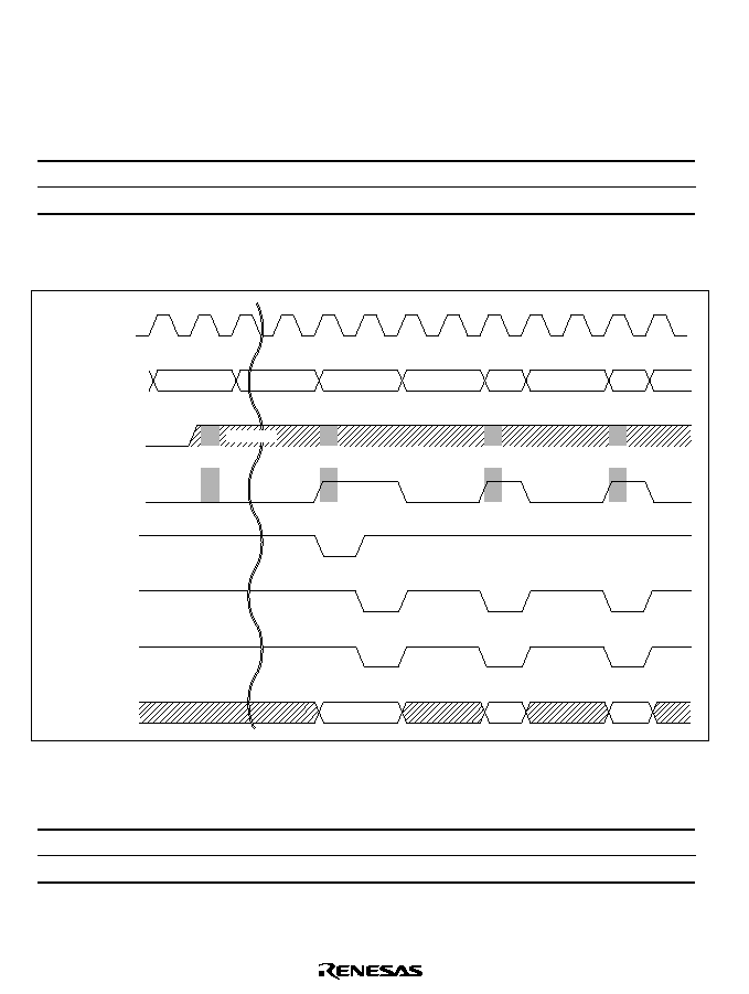
502
∑
Synchronous DRAM one-cycle write
When a one-cycle write is performed to synchronous DRAM, the DACKn signal is
synchronized with the rising edge of the clock. A request by the request signal is accepted
while the clock is high during DACKn output.
Transfer Width
Byte/Word/Longword
Transfer
*
1
DREQn Detection
Method
Level Detection
Transfer bus mode
Cycle-steal mode
*
2
DACKn output timing
Write DACK
Transfer address mode
Single mode
Bus cycle
Basic bus cycle
Notes:
*
1 Do not set a 16-byte unit; operation is not guaranteed if this setting is made.
*
2 Cycle-steal mode must be set when DREQ is level-detected.
Clock
Bus cycle
DREQn
(Active high)
DMAC1
DMAC2
DMAC3
DACK1
DACK3
DACK2
1st
acceptance
CPU
CPU
CPU
CPU
CPU
DACKn
(Active high)
CAS
RD/
WR
WEn
/DQMxx
RAS
Blind zone
. . . .
2nd
acceptance
3rd
acceptance
4th
acceptance
Figure 11.28 (a) Synchronous DRAM One-Cycle Write Timing
Transfer Width
Byte/Word/Longword
Transfer
DREQn Detection
Method
Edge Detection
*
Transfer bus mode
Burst mode
DACKn output timing
Write DACK
Transfer address mode
Single mode
Bus cycle
Basic bus cycle
Note:
*
Edge detection must be set when burst mode is selected as the transfer bus mode.
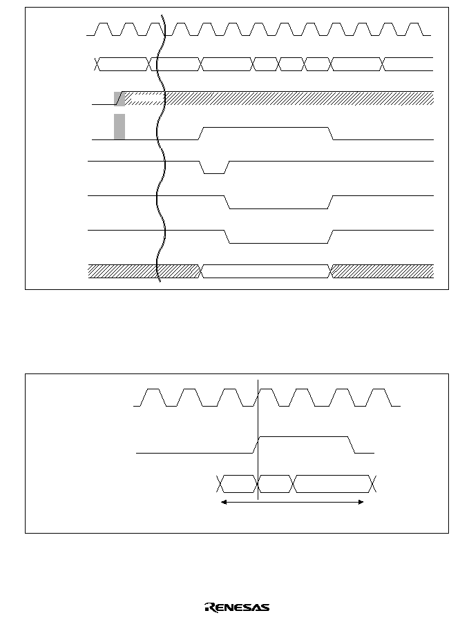
503
Clock
Bus cycle
DREQn
(Active high)
DMAC1
DMAC2 DMAC3 DMAC4
DACK1
DACK3
DACK4
DACK2
Acceptance
CPU
CPU
CPU
CPU
DACKn
(Active high)
CAS
RD/
WR
WEn
/DQMxx
RAS
. . . .
Blind zone
Figure 11.28 (b) Synchronous DRAM One-Cycle Write Timing
Acknowledge Signal Output when External Memory Is Set as DRAM: When external memory
is set as DRAM and a row address is output during a read or write, the acknowledge signal is
output across the row address and column address (figures 11.29≠11.31).
Clock
DACKn
(Active high)
Address
bus
DMAC read or write
(basic timing)
Precharge
Row
address
Column address
Figure 11.29 DACKn Output in Normal DRAM Accesses (AM = 0 or 1)
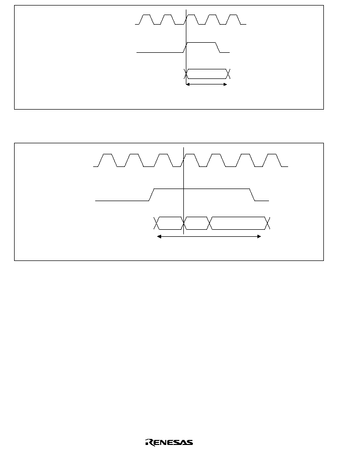
504
Clock
DACKn
(Active high)
Address
bus
DMAC read or write
(basic timing)
Column
address
Figure 11.30 DACKn Output in DRAM Burst Accesses
(Same Row Address, AM = 0 or 1)
Clock
DACKn
(Active high)
Address
bus
DMAC read or write
(basic timing)
Pre-
charge
Row
address
Column address
Figure 11.31 DACKn Output in DRAM Burst Accesses
(Different Row Address, AM = 0 or 1)
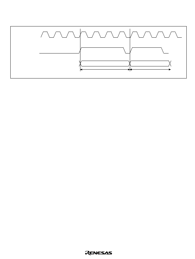
505
Acknowledge Signal Output When External Memory Is Set as Burst ROM: When external
memory is set as burst ROM, the acknowledge signal is output synchronous to the DMA address
(no dual writes allowed) (figure 11.32).
Clock
DACKn
(Active high)
Address
bus
DMAC (1 wait state)
DMAC cycle
DMAC cycle
Figure 11.32 DACKn Output in Nibble Accesses of Burst ROM
11.3.7
DREQn Pin Input Detection Timing
In external request mode, DREQn pin signals are usually detected at the falling edge of the clock
pulse (CKIO). When a request is detected, a DMAC bus cycle is produced four cycles later at the
earliest and a DMA transfer performed. After the request is detected, the timing of the next input
detection varies with the bus mode, address mode, DREQn input detection, and the memory
connected.
DREQn Pin Input Detection Timing in Cycle-Steal Mode: In cycle-steal mode, once a request
is detected from the DREQn pin, the request signal is not detected until DACKn signal output in
the next external bus cycle. In cycle-steal mode, request detection is performed from DACKn
signal output until a request is detected.
Once a request has been accepted, it cannot be canceled midway.
The timing from the detection of a request until the next time requests are detectable is shown
below.
∑
Cycle-Steal Mode Edge Detection
When transfer control is performed using edge detection, perform DREQn/DACKn
handshaking as shown in figure 11.33, and perform DREQn input control so that there is a
one-to-one relationship between DREQn and DACKn. Operation is not guaranteed if DREQn
is input before the corresponding DACKn is output.
If the DACKn signal is output a number of times, the first DACKn signal for the input DREQn
signal indicates the request acceptance start timing, and subsequently each clock edge is
sampled.
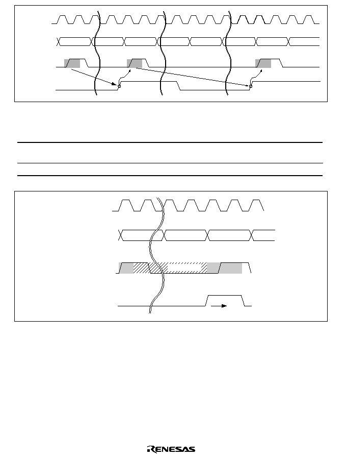
506
Clock
DMAC
DMAC
DMAC
DMAC
1st
acceptance
2nd
acceptance
3rd
acceptance
CPU
CPU
CPU
CPU
DACKn
(Active high)
Bus cycle
DREQn
(Rising-edge
detection)
Figure 11.33 DREQn/DACKn Handshaking
Transfer Width
Byte/Word/Longword
DREQn Detection
Method
Edge Detection
Transfer bus mode
Cycle-steal mode
DACKn output timing
Read DACK/write
DACK
Transfer address mode
Dual/single mode
Bus cycle
Basic bus cycle
Clock
Bus cycle
DREQn
(Active high)
DACKn
(Active high)
Requests acceptable
2nd
acceptance
1st
acceptance
CPU
CPU
DMAC
CPU
Blind zone
Figure 11.34 DREQn Pin Input Detection Timing in Cycle-Steal Mode with Edge Detection

507
Clock
Bus cycle
CPU
DMAC
H
DMAC
L
DACK
H
DACK
L
2nd
acceptance
CPU
DACKn
(Active high)
DREQn
(Active high)
1st
acceptance
Blind zone
Figure 11.35 When a16-Bit External Device is Connected (Edge Detection)
Clock
Bus cycle
CPU
DMAC
HH
DACK
HH
DACK
HL
DACK
LH
DACK
LL
DMAC
HL
DMAC
LH
DMAC
LL
1st
acceptance
2nd
acceptance
CPU
Blind zone
Blind zone
DACKn
(Active high)
DREQn
(Active high)
Figure 11.36 When an 8-Bit External Device is Connected (Edge Detection)
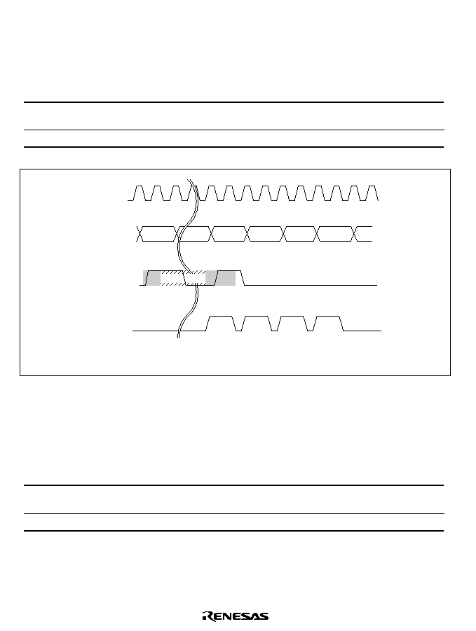
508
∑
Cycle-Steal Mode Edge Detection--16-Bit Transfer
With 16-byte transfer, the first request signal is the first transfer request, and the second
transfer request is accepted when the next request signal is accepted. The third and fourth
requests are accepted in the same way.
Transfer Width
16-Byte Transfer
DREQn Detection
Method
Edge Detection
Transfer bus mode
Cycle-steal mode
DACKn output timing
Read DACK/write
DACK
Transfer address mode
Dual/single mode
Bus cycle
Basic bus cycle
Clock
Bus cycle
CPU
CPU
DMAC
*
1
DMAC
*
2
DMAC
*
3
DMAC
*
4
DMA
1st
acceptance
2nd
acceptance
DACK
*
1
DACK
*
2
DACK
*
3
DACK
*
4
Blind zone
Note:
*
n is the nth 16-byte transfer.
DACKn
(Active high)
DREQn
(Active high)
Figure 11.37 DREQn Pin Input Detection Timing in Cycle-Steal Mode with Edge Detection
(16-Byte Transfer Setting)
∑
Cycle-Steal Mode Level Detection
In level detection mode, too, a request cannot be canceled once accepted.
Transfer Width
Byte/Word/Longword
*
DREQn Detection
Method
Level Detection
Transfer bus mode
Cycle-steal mode
DACKn output timing
Read DACK/write
DACK
Transfer address mode
Dual/single mode
Bus cycle
Basic bus cycle
Note:
*
Do not set a 16-byte unit; operation is not guaranteed if this setting is made.
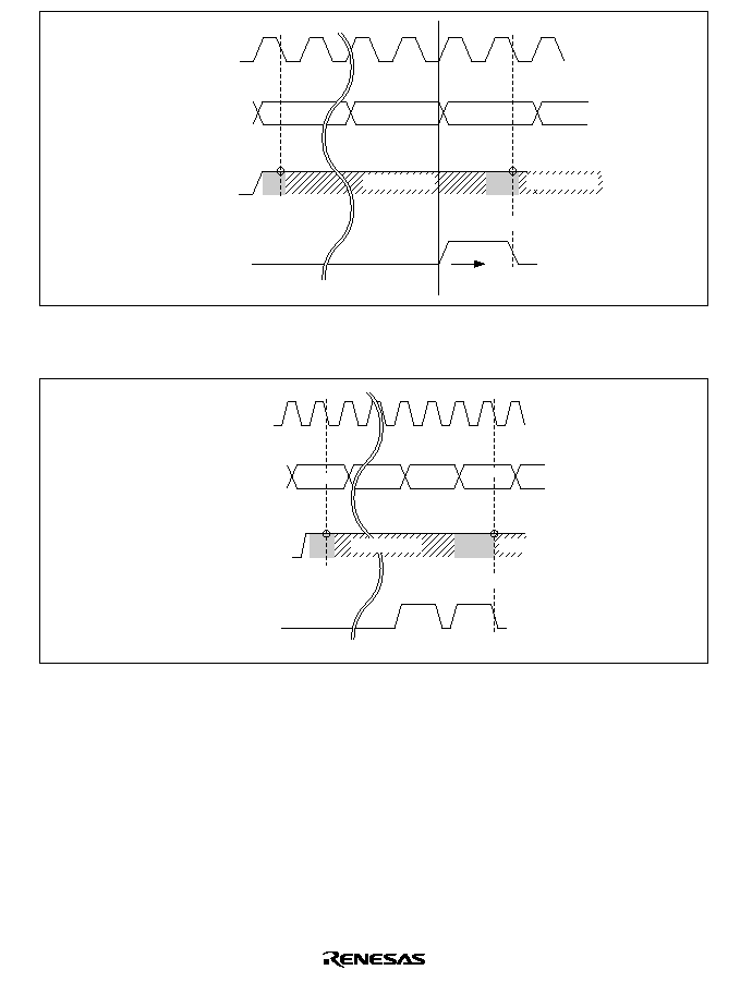
509
Clock
Bus cycle
Requests acceptable
1st
acceptance
CPU
CPU
DMAC
CPU
Blind zone
Blind zone
2nd
acceptance
DACKn
(Active high)
DREQn
(Active high)
Figure 11.38 DREQn Pin Input Detection Timing in Cycle-Steal Mode with Level Detection
(Byte/Word/Longword Setting)
Clock
Bus cycle
DMAC
H
DACK
H
DACK
L
1st
acceptance
CPU
Blind zone
Blind zone
2nd
acceptance
DMAC
L
CPU
DACKn
(Active high)
DREQn
(Active high)
Figure 11.39 When a 16-Bit External Device is Connected (Level Detection)
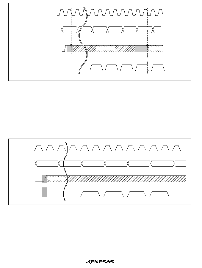
510
Clock
Bus cycle
DMAC
HH
DMAC
HL
DMAC
LH
DACK
HH
DACK
HL
DACK
LH
DACK
LL
1st
acceptance
CPU
DACKn
Blind zone
Blind zone
2nd
acceptance
DMAC
LL
CPU
(Active high)
DREQn
(Active high)
Figure 11.40 When an 8-Bit External Device is Connected (Level Detection)
DREQn Pin Input Detection Timing in Burst Mode: In burst mode, only edge detection is valid
for DREQn input. Operation is not guaranteed if level detection is set.
With edge detection of DREQn input, once a request is detected, DMA transfer continues until the
transfer end condition is satisfied, regardless of the state of the DREQn pin. Request detection is
not performed during this time. When the transfer start conditions are fulfilled after the end of
transfer, request detection is performed again every cycle.
Clock
DMAC1
DMAC2
CPU
CPU
CPU
DMAC3
DMAC4
DACKn
(Active high)
Blind zone
Acceptance
Bus cycle
Bus DREQn
(Active high)
Figure 11.41 DREQn Pin Input Detection Timing in Burst Mode with Edge Detection

511
11.3.8
DMA Transfer End
The DMA transfer ending conditions vary when channels end individually and when both
channels end together.
Conditions for Channels Ending Individually: When either of the following conditions is met,
the transfer will end in the relevant channel only:
The DMA transfer count register (TCR) value becomes 0.
The DMA enable bit (DE) of the DMA channel control register (CHCR) is cleared to 0.
∑
Transfer end when TCR = 0
When the TCR value becomes 0, the DMA transfer for that channel ends and the transfer-end
flag bit (TE) is set in CHCR. If the IE (interrupt enable) bit has already been set, a DMAC
interrupt (DEI) request is sent to the CPU. For 16-byte transfer, set the number of transfers
◊
4.
Operation is not guaranteed if an incorrect value is set.
A 16-byte transfer is valid only in auto-request mode or in external request mode with edge
detection. When using an external request with level detection or on-chip peripheral module
request, do not specify a 16-byte transfer.
∑
Transfer end when DE = 0 in CHCR
When the DMA enable bit (DE) in CHCR is cleared, DMA transfers in the affected channel
are halted. The TE bit is not set when this happens.
Conditions for Both Channels Ending Simultaneously: Transfers on both channels end when
either of the following conditions is met:
The NMIF (NMI flag) bit or AE (address error flag) bit in DMAOR is set to 1.
The DMA master enable (DME) bit is cleared to 0 in DMAOR.
∑
Transfer end when NMIF = 1 or AE = 1 in DMAOR
When an NMI interrupt or DMAC address error occurs and the NMIF or AE bit is set to 1 in
DMAOR, all channels stop their transfers. The DMA source address register (SAR),
destination address register (DAR), and transfer count register (TCR) are all updated by the
transfer immediately preceding the halt. When this transfer is the final transfer, TE = 1 and the
transfer ends. To resume transfer after NMI interrupt exception handling or address error
exception handling, clear the appropriate flag bit. When the DE bit is then set to 1, the transfer
on that channel will restart. To avoid this, keep its DE bit at 0. In dual address mode, DMA
transfer will be halted after the completion of the following write cycle even when the address
error occurs in the initial read cycle. SAR, DAR and TCR are updated by the final transfer.
∑
Transfer end when DME = 0 in DMAOR
Clearing the DME bit in DMAOR forcibly aborts the transfers on both channels at the end of
the current bus cycle. When the transfer is the final transfer, TE = 1 and the transfer ends.
512
11.3.9
BH Pin Output Timing
Purpose of New Specifications for
BH: When the SH7616 is connected to the PCI bus as an
external bus, Grew logic must be used externally because the SH7616 is not equipped with a PCI
bus interface.
The PCI bus uses burst transfer principally, and performance is poor if data is transferred in small
increments.
Due to these properties of the PCI bus, it is necessary to use Grew logic externally to compare the
present address and the next address and determine whether burst transfer is possible. However,
the size of the external Grew logic increases if address comparisons are required, and there is also
the possibility that delays may interfere with timing requirements.
The specifications for
BH have therefore been updated in order to solve these problems. Now if
burst transfer is possible using the present address this information is passed to the external Grew
logic. This provides enhanced support for PCI bus connections.
Register Settings When Using
BH Pin: BH is output from only when the 16-byte transfer mode
is selected using the DMAC built into the SH7616. However, it is not output when SDRAM or
DRAM are accessed. When using the 16-byte transfer mode, specify auto-request mode or the
external request mode with edge detection. If external request mode with level detection or on-
chip module request mode is specified, operation is not guaranteed.
To use
BH, the settings for the CHCR0 register or CHCR1 register in the on-chip DMAC of the
SH7616 must be as shown in figure 11.43.
BH is not output unless the settings for the CHCR0
register or CHCR1 register are as indicated in figure 11.42.
Bit
Bit name
Setting
Bit
Bit name
Setting
31
--
0
15
DM1
0
30
--
0
14
DM0
1
29
--
0
13
SM1
0
28
--
0
12
SM0
1
27
--
0
11
TS1
1
26
--
0
10
TS0
1
25
--
0
9
AR
*
24
--
0
8
AM
*
23
--
0
7
AL
*
22
--
0
6
DS
*
21
--
0
5
DL
*
20
--
0
4
TB
*
19
--
0
3
TA
*
18
--
0
2
IE
*
17
--
0
1
TE
*
16
--
0
0
DE
1
16-byte unit (four long words transferred)
Source address is incremented
Destination address is incremented
*
Don't care
DMA transfer
allowed
Figure 11.42 Register Settings When Using
BH

513
Summary of
BH Timing: Figure 11.43 is a summary of the BH output timing.
CPU
DMAC
read 0
DMAC
read 1
DMAC
read 2
DMAC
read 3
DMAC
write 0
DMAC
write 1
DMAC
write 2
DMAC
write 3
CPU
External
bus cycle
BH
Figure 11.43 Summary of
BH Output Timing
11.4
Usage Examples
11.4.1
Example of DMA Data Transfer Between SCIF and External Memory
In this example data received by the serial communication interface with FIFO (SCIF) is sent to
external memory using DMAC channel 1. Table 11.10 lists the transfer conditions and register
setting values.
Table 11.10 Transfer Conditions and Register Setting Values for Data Transfer Between
On-chip SCIF and External Memory
Transfer Condition
Register
Setting Value
Transfer source: SCFRDR1 in SCIF
SAR1
H'FFFFFCCC
Transfer destination: External memory (word space)
DAR1
Transfer destination address
Number of transfers: 64
TCR1
H'0040
Transfer destination address: Increment
CHCR1
H'4045
Transfer source address: Fixed
Bus mode: Cycle-steal
Transfer unit: Byte
DEI interrupt request at end of transfer DE = 1
Channel priority: Fixed (0 > 1) DME = 1
DMAOR
H'0001
Transfer request source (transfer request signal): SCIF
(RXI)
DRCR1
H'05
Note:
Make sure the SCIF settings have interrupts enabled and the appropriate CPU interrupt
level.

514
11.5
Usage Notes
1. DMA request/response selection control registers 0 and 1 (DRCR0 and DRCR1) should be
accessed in bytes. All other registers should be accessed in longword units.
2. Before rewriting the registers in the DMAC (CHCR0, CHCR1, DRCR0, DRCR1), first clear
the DE bit to 0 in the CHCR register for the specified channel, or clear the DME bit in
DMAOR to 0.
3. When the DMAC is not operating, the NMIF bit in DMAOR is set even when an NMI
interrupt is input.
4. The DMAC cannot access the cache memory.
5. Before changing the frequency or changing to standby mode, set the DME bit of DMAOR to 0
and stop operation of the DMAC.
6. Do not use the DMAC, BSC, UBC, E-DMAC, and EtherC for on-chip peripheral module
transfers.
7. Do not access the cache (address array, data array, associative purge area).
8. Note that when level detection of the request signal is used in single address mode, the request
signal may be detected before DACKn is output.
9. When E
exceeds 31.25 MHz, do not use transfer involving DACKn output on ordinary space
for word or longword access with an 8-bit bus width, or longword access with a 16-bit bus
width.
10. When DMA transfer is performed in response to a DMA transfer request signal from a
peripheral module, if clearing of the DMA transfer request signal from the peripheral module
by the DMA transfer is not completed before the next transfer request signal from that module,
subsequent DMA transfers may not be possible.
11. The following restrictions apply when using dual address mode for 16-byte transfer in cycle-
steal mode:
a. When external request and level detection are set, do not input DREQn during cycles in
which DACKn is not active after the start of DMA transfer.
b. When external request DREQ edge detection is set, if DREQn is input continuously the
DMAC continues to operate without insertion of a CPU cycle. (However, a CPU cycle
will begin if there is no request from DREQn.)

515
Bus cycle
Note:
*
In addition to CPU cycles, E-DMAC cycles may be inserted in some cases.
DACK output in read cycle
CPU CPU
CPU
CPU
DMA
(W)
DMA
(W)
DMA
(W)
DMA
(W)
DMA
(R)
DMA
(R)
DMA
(R)
DMA
(R)
DMA
(W)
DMA
(W)
DMA
(W)
DMA
(W)
DMA
(R)
DMA
(R)
DMA
(R)
DMA
(R)
CPU CPU
CPU
CPU
DMA
(W)
DMA
(W)
DMA
(W)
DMA
(W)
DMA
(R)
DMA
(R)
DMA
(R)
DMA
(R)
DMA
(W)
DMA
(W)
DMA
(W)
DMA
(W)
DMA
(R)
DMA
(R)
DMA
(R)
DMA
(R)
DACK output in write cycle
DACKn
(active high)
DREQn
(active high)
Bus cycle
DACKn
(active high)
DREQn
(active high)
*
*
12. When setting DMAC channel 0 to cycle-steal mode, and channel 1 to cycle-steel mode, dual
address mode or built-in peripheral module request, set the priority mode to priority order fixed
mode.
13. When SDRAM is connected, set the upper limit of external bus frequency in DMA single
address mode transfers to 31.25 MHz.
14. In the dual address mode, bits TS1 and TS0 (transfer size) in CHCR0 and CHCR1 should be
cleared to 00 (byte unit setting) if a destination address as been set in internal memory.

516

517
Section 12 16-Bit Free-Running Timer (FRT)
12.1
Overview
A single-channel, 16-bit free-running timer (FRT) is included on-chip. The FRT is based on a
16-bit free-running counter (FRC) and can output two types of independent waveforms. The FRT
can also measure the width of input pulses and the cycle of external clocks.
12.1.1
Features
The FRT has the following features:
∑
Choice of four counter input clocks
The counter input clock can be selected from three internal clocks (P
/8, P
/32, P
/128) and
an external clock (enabling external event counting).
∑
Two independent comparators
Two waveform outputs can be generated.
∑
Input capture
Choice of rising edge or falling edge
∑
Counter clear specification
The counter value can be cleared by compare match A.
∑
Four interrupt sources
Two compare match sources, one input capture source, and one overflow source can issue
requests independently.
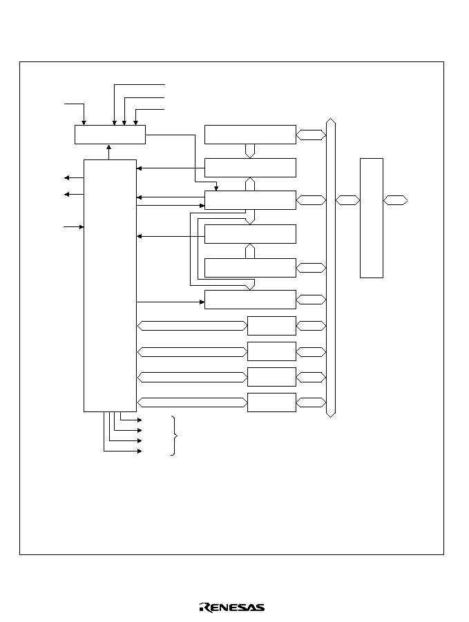
518
12.1.2
Block Diagram
Figure 12.1 shows a block diagram of the FRT.
FTI
/8
Internal clock
Internal
data bus
Module
data bus
/32
/128
ICI
Interrupt
signals
OCIA
OCIB
OVI
FTOB
FTOA
FTCI
Control
logic
Clock select
Clock
Compare
match A
Overflow
Clear
Compare
match B
Capture
OCRA (H/L)
Comparator A
FRC (H/L)
Comparator B
OCRB (H/L)
FICR (H/L)
FTCSR
TIER
TCR
TOCR
Bus interface
OCRA,B:
FRC:
FICR:
FTCSR:
TIER:
TCR:
TOCR:
Output compare registers A,B (16 bits)
Free-running counter (16 bits)
Input capture register (16 bits)
Free-running timer control/status register (8 bits)
Timer interrupt enable register (8 bits)
Timer control register (8 bits)
Timer output compare control register (8 bits)
Figure 12.1 FRT Block Diagram

519
12.1.3
Pin Configuration
Table 12.1 lists FRT I/O pins and their functions.
Table 12.1
Pin Configuration
Channel
Pin
I/O
Function
Counter clock input pin
FTCI
I
FRC counter clock input pin
Output compare A output pin
FTOA
O
Output pin for output compare A
Output compare B output pin
FTOB
O
Output pin for output compare B
Input capture input pin
FTI
I
Input pin for input capture
12.1.4
Register Configuration
Table 12.2 shows the FRT register configuration.
Table 12.2
Register Configuration
Register
Abbreviation
R/W
Initial
Value
Address
Timer interrupt enable register
TIER
R/W
H'01
HFFFFFE10
Free-running timer control/status register
FTCSR
R/(W)
*
1
H'00
HFFFFFE11
Free-running counter H
FRC H
R/W
H'00
HFFFFFE12
Free-running counter L
FRC L
R/W
H'00
HFFFFFE13
Output compare register A H
OCRA H
R/W
H'FF
HFFFFFE14
*
2
Output compare register A L
OCRA L
R/W
H'FF
HFFFFFE15
*
2
Output compare register B H
OCRB H
R/W
H'FF
HFFFFFE14
*
2
Output compare register B L
OCRB L
R/W
H'FF
HFFFFFE15
*
2
Timer control register
TCR
R/W
H'00
HFFFFFE16
Timer output compare control register
TOCR
R/W
H'E0
HFFFFFE17
Input capture register H
FICR H
R
H'00
HFFFFFE18
Input capture register L
FICR L
R
H'00
HFFFFFE19
Notes: Use byte-size access for all registers.
*
1 Bits 7 to 1 are read-only. The only value that can be written is a 0, which is used to
clear flags. Bit 0 can be read or written.
*
2 OCRA and OCRB have the same address. The OCRS bit in TOCR is used to switch
between them.

520
12.2
Register Descriptions
12.2.1
Free-Running Counter (FRC)
Bit:
15
14
13
...
3
2
1
0
...
Initial value:
0
0
0
...
0
0
0
0
R/W:
R/W
R/W
R/W
...
R/W
R/W
R/W
R/W
FRC is a 16-bit read/write register. It increments upon input of a clock. The input clock can be
selected using clock select bits 1 and 0 (CKS1, CKS0) in TCR. FRC can be cleared upon compare
match A.
When FRC overflows (H'FFFF
H'0000), the overflow flag (OVF) in FTCSR is set to 1. FRC
can be read or written to by the CPU, but because it is 16 bits long, data transfers involving the
CPU are performed via a temporary register (TEMP). See section 12.3, CPU Interface, for more
detailed information.
FRC is initialized to H'0000 by a reset, in standby mode, and when the module standby function is
used.
12.2.2
Output Compare Registers A and B (OCRA and OCRB)
Bit:
15
14
13
...
3
2
1
0
...
Initial value:
1
1
1
...
1
1
1
1
R/W:
R/W
R/W
R/W
...
R/W
R/W
R/W
R/W
OCR is composed of two 16-bit read/write registers (OCRA and OCRB). The contents of OCR are
always compared to the FRC value. When the two values are the same, the output compare flags
in FTCSR (OCFA and OCFB) are set to 1.
When the OCR and FRC values are the same (compare match), the output level values set in the
output level bits (OLVLA and OLVLB) are output to the output compare pins (FTOA and FTOB).
After a reset, FTOA and FTOB output 0 until the first compare match occurs.
Because OCR is a 16-bit register, data transfers involving the CPU are performed via a temporary
register (TEMP). See section 12.3, CPU Interface, for more detailed information.
OCR is initialized to H'FFFF by a reset, in standby mode, and when the module standby function
is used.

521
12.2.3
Input Capture Register (FICR)
Bit:
15
14
13
...
3
2
1
0
...
Initial value:
0
0
0
...
0
0
0
0
R/W:
R
R
R
...
R
R
R
R
FICR is a 16-bit read-only register. When a rising edge or falling edge of the input capture signal
(FTI pin) is detected, the current FRC value is transferred to FICR. At the same time, the input
capture flag (ICF) in FTCSR is set to 1. The edge of the input signal can be selected using the
input edge select bit (IEDG) in TCR.
Because FICR is a 16-bit register, data transfers involving the CPU are performed via a temporary
register (TEMP). See Section 12.3, CPU Interface, for more detailed information. To ensure that
the input capture operation is reliably performed, set the pulse width of the input capture input
signal to six system clocks (
) or more.
FICR is initialized to H'0000 by a reset, in standby mode, and when the module standby function
is used.
12.2.4
Timer Interrupt Enable Register (TIER)
Bit:
7
6
5
4
3
2
1
0
ICIE
--
--
--
OCIAE
OCIBE
OVIE
--
Initial value:
0
0
0
0
0
0
0
1
R/W:
R/W
R
R
R
R/W
R/W
R/W
R
TIER is an 8-bit read/write register that controls enabling of all interrupt requests. TIER is
initialized to H'01 by a reset, in standby mode, and when the module standby function is used.
Bit 7--Input Capture Interrupt Enable (ICIE): Selects enabling/disabling of the ICI interrupt
request when the input capture flag (ICF) in FTCSR is set to 1.
Bit 7: ICIE
Description
0
Interrupt request (ICI) caused by ICF disabled
(Initial value)
1
Interrupt request (ICI) caused by ICF enabled
Bits 6 to 4--Reserved: These bits are always read as 0. The write value should always be 0.

522
Bit 3--Output Compare Interrupt A Enable (OCIAE): Selects enabling/disabling of the OCIA
interrupt request when the output compare flag A (OCFA) in FTCSR is set to 1.
Bit 3: OCIAE
Description
0
Interrupt request (OCIA) caused by OCFA disabled
(Initial value)
1
Interrupt request (OCIA) caused by OCFA enabled
Bit 2--Output Compare Interrupt B Enable (OCIBE): Selects enabling/disabling of the OCIB
interrupt request when the output compare flag B (OCFB) in FTCSR is set to 1.
Bit 2: OCIBE
Description
0
Interrupt request (OCIB) caused by OCFB disabled
(Initial value)
1
Interrupt request (OCIB) caused by OCFB enabled
Bit 1--Timer Overflow Interrupt Enable (OVIE): Selects enabling/disabling of the OVI interrupt
request when the overflow flag (OVF) in FTCSR is set to 1.
Bit 1: OVIE
Description
0
Interrupt request (OVI) caused by OVF disabled
(initial value)
1
Interrupt request (OVI) caused by OVF enabled
Bit 0--Reserved: This bit is always read as 1. The write value should always be 1.
12.2.5
Free-Running Timer Control/Status Register (FTCSR)
Bit:
7
6
5
4
3
2
1
0
ICF
--
--
--
OCFA
OCFB
OVF
CCLRA
Initial value:
0
0
0
0
0
0
0
0
R/W:
R/(W)
*
R
R
R
R/(W)
*
R/(W)
*
R/(W)
*
R/W
Note:
*
For bits 7, and 3 to 1, the only value that can be written is 0 (to clear the flags).
FTCSR is an 8-bit register that selects counter clearing and controls interrupt request signals.
FTCSR is initialized to H'00 by a reset, in standby mode, and when the module standby function is
used. See section 12.4, Operation, for the timing.
Bit 7--Input Capture Flag (ICF): Status flag that indicates that the FRC value has been sent to
FICR by the input capture signal. This flag is cleared by software and set by hardware. It cannot
be set by software.

523
Bit 7: ICF
Description
0
[Clearing condition]
When ICF is read while set to 1, and then 0 is written to it
(Initial value)
1
[Setting condition]
When the FRC value is sent to FICR by the input capture signal
Bits 6 to 4--Reserved: These bits always read 0. The write value should always be 0.
Bit 3--Output Compare Flag A (OCFA): Status flag that indicates when the values of the FRC
and OCRA match. This flag is cleared by software and set by hardware. It cannot be set by
software.
Bit 3: OCFA
Description
0
[Clearing condition]
When OCFA is read while set to 1, and then 0 is written to it
(Initial value)
1
[Setting condition]
When the FRC value becomes equal to OCRA
Bit 2--Output Compare Flag B (OCFB): Status flag that indicates when the values of FRC and
OCRB match. This flag is cleared by software and set by hardware. It cannot be set by software.
Bit 2: OCFB
Description
0
[Clearing condition]
When OCFB is read while set to 1, and then 0 is written to it
(Initial value)
1
[Setting condition]
When the FRC value becomes equal to OCRB
Bit 1--Timer Overflow Flag (OVF): Status flag that indicates when FRC overflows (from H'FFFF
to H'0000). This flag is cleared by software and set by hardware. It cannot be set by software.
Bit 1: OVF
Description
0
[Clearing condition]
When OVF is read while set to 1, and then 0 is written to it
(Initial value)
1
[Setting condition]
When the FRC value changes from H'FFFF to H'0000

524
Bit 0--Counter Clear A (CCLRA): Selects whether or not to clear FRC on compare match A
(signal indicating match of FRC and OCRA).
Bit 0: CCLRA
Description
0
FRC clear disabled
(Initial value)
1
FRC cleared on compare match A
12.2.6
Timer Control Register (TCR)
Bit:
7
6
5
4
3
2
1
0
IEDG
--
--
--
--
--
CKS1
CKS0
Initial value:
0
0
0
0
0
0
0
0
R/W:
R/W
R
R
R
R
R
R/W
R/W
TCR is an 8-bit read/write register that selects the input edge for input capture and selects the
input clock for FRC. TCR is initialized to H'00 by a reset, in standby mode, and when the module
standby function is used.
Bit 7--Input Edge Select (IEDG): Selects whether to capture the input capture input (FTI) on the
falling edge or rising edge.
Bit 7: IEDG
Description
0
Input captured on falling edge
(Initial value)
1
Input captured on rising edge
Bits 6 to 2--Reserved: These bits are always read as 0. The write value should always be 0.
Bits 1 and 0--Clock Select (CKS1, CKS0): These bits select whether to use an external clock or
one of three internal clocks for input to FRC. The external clock is counted at the rising edge.
Bit 1: CKS1
Bit 0: CKS0
Description
0
0
Internal clock: count at
/8
(Initial value)
1
Internal clock: count at
/32
1
0
Internal clock: count at
/128
1
External clock: count at rising edge

525
12.2.7
Timer Output Compare Control Register (TOCR)
Bit:
7
6
5
4
3
2
1
0
--
--
--
OCRS
--
--
OLVLA
OLVLB
Initial value:
1
1
1
0
0
0
0
0
R/W:
R
R
R
R/W
R
R
R/W
R/W
TOCR is an 8-bit read/write register that selects the output level for output compare and controls
switching between access of output compare registers A and B. TOCR is initialized to H'E0 by a
reset, in standby mode, and when the module standby function is used.
Bits 7 to 5--Reserved: These bits are always read as 1. The write value should always be 1.
Bit 4--Output Compare Register Select (OCRS): OCRA and OCRB share the same address. The
OCRS bit controls which register is selected when reading/writing to this address. It does not
affect the operation of OCRA and OCRB.
Bit 4: OCRS
Description
0
OCRA register selected
(Initial value)
1
OCRB register selected
Bits 3 and 2--Reserved: These bits are always read as 0. The write value should always be 0.
Bit 1--Output Level A (OLVLA): Selects the level output to the output compare A output pin
upon compare match A (signal indicating match of FRC and OCRA).
Bit 1: OLVLA
Description
0
0 output on compare match A
(Initial value)
1
1 output on compare match A
Bit 0--Output Level B (OLVLB): Selects the level output to the output compare B output pin
upon compare match B (signal indicating match of FRC and OCRB).
Bit 0: OLVLB
Description
0
0 output on compare match B
(Initial value)
1
1 output on compare match B

526
12.3
CPU Interface
FRC, OCRA, OCRB, and FICR are 16-bit registers. The data bus width between the CPU and
FRT, however, is only 8 bits. Access of these three types of registers from the CPU therefore
needs to be performed via an 8-bit temporary register called TEMP.
The following describes how these registers are read from and written to:
∑
Writing to 16-bit Registers
The upper byte is written, which results in the upper byte of data being stored in TEMP. The
lower byte is then written, which results in 16 bits of data being written to the register when
combined with the upper byte value in TEMP.
∑
Reading from 16-bit Registers
The upper byte of data is read, which results in the upper byte value being transferred to the
CPU. The lower byte value is transferred to TEMP. The lower byte is then read, which results
in the lower byte value in TEMP being sent to the CPU.
When registers of these three types are accessed, two byte accesses should always be performed,
first to the upper byte, then the lower byte. If only the upper byte or lower byte is accessed, the
data will not be transferred properly.
Figure 12.2 and 12.3 show the flow of data when FRC is accessed. Other registers function in the
same way. When reading OCRA and OCRB, however, both upper and lower-byte data is
transferred directly to the CPU without passing through TEMP.

527
CPU
(H'AA)
upper
byte
Data bus within module
Bus interface
TEMP
(H'AA)
FRC H
( )
FRC L
( )
(Write to upper byte)
CPU
(H'55)
lower
byte
Data bus within module
Bus interface
TEMP
(H'AA)
FRC H
(H'AA)
FRC L
(H'55)
(Write to lower byte)
Figure 12.2 FRC Access Operation (CPU Writes H'AA55 to FRC)
528
CPU
(H'AA)
upper
byte
TEMP
(H'55)
FRC H
(H'AA)
FRC L
(H'55)
Data bus within module
Bus interface
(Read from upper byte)
CPU
(H'55)
lower
byte
TEMP
(H'AA)
FRC H
( )
FRC L
( )
Data bus within module
Bus interface
(Read from lower byte)
Figure 12.3 FRC Access Operation (CPU Reads H'AA55 from FRC)

529
12.4
Operation
12.4.1
FRC Count Timing
The FRC increments on clock input (internal or external).
Internal Clock Operation: Set the CKS1 and CKS0 bits in TCR to select which of the three
internal clocks created by dividing system clock
(
/8,
/32,
/128) is used. Figure 12.4 shows
the timing.
P
N ≠ 1
N
N + 1
Internal clock
FRC input
clock
FRC
Figure 12.4 Count Timing (Internal Clock Operation)
External Clock Operation: Set the CKS1 and CKS0 bits in TCR to select the external clock.
External clock pulses are counted on the rising edge. The pulse width of the external clock must be
at least 6 system clocks (
). A smaller pulse width will result in inaccurate operation. Figures 12.5
shows the timing.
N + 1
N
P
External clock
input pin
FRC input
clock
FRC
Figure 12.5 Count Timing (External Clock Operation)
530
12.4.2
Output Timing for Output Compare
When a compare match occurs, the output level set in the OLVL bit in TOCR is output from the
output compare output pins (FTOA, FTOB). Figure 12.6 shows the timing for output of output
compare A.
Clear
*
N
N
N
N
N + 1
N + 1
P
FRC
OCRA
Compare
match A
signal
OLVLA
Output
compare A
output pin
FTOA
Note:
*
Indicates instruction execution by software
Figure 12.6 Output Timing for Output Compare A
12.4.3
FRC Clear Timing
FRC can be cleared on compare match A. Figure 12.7 shows the timing.
P
Compare
match A
signal
FRC
N
H'0000
Figure 12.7 Compare Match A Clear Timing
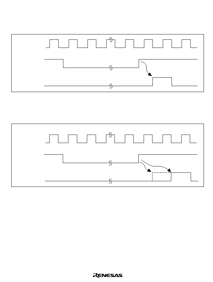
531
12.4.4
Input Capture Input Timing
Either the rising edge or falling edge can be selected for input capture input using the IEDG bit in
TCR. Figure 12.8 shows the timing when the rising edge is selected (IEDG = 1).
P
Input capture
input pin
Input capture
signal
Figure 12.8 Input Capture Signal Timing (Normal)
When the input capture signal is input when FICR is read (upper-byte read), the input capture
signal is delayed by one cycle of P
. Figure 12.9 shows the timing.
P
Input capture
input pin
Input capture
signal
FICR upper-byte read cycle
Figure 12.9 Input Capture Signal Timing (Input Capture Input when FICR is Read)
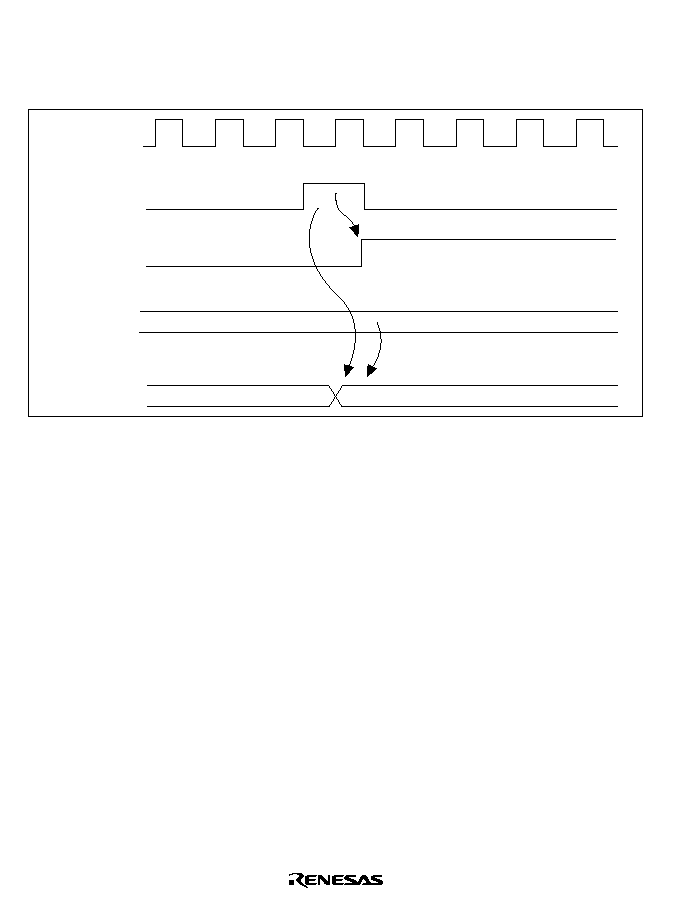
532
12.4.5
Input Capture Flag (ICF) Setting Timing
Input capture input sets the input capture flag (ICF) to 1 and simultaneously transfers the FRC
value to FICR. Figure 12.10 shows the timing.
P
Input capture
signal
ICF
FRC
FICR
N
N
Figure 12.10 ICF Setting Timing
12.4.6
Output Compare Flag (OCFA, OCFB) Setting Timing
The compare match signal output (when OCRA or OCRB matches the FRC value) sets output
compare flag OCFA or OCFB to 1. The compare match signal is generated in the last state in
which the values matched (at the timing for updating the count value that matched the FRC). After
OCRA or OCRB matches the FRC, no compare match is generated until the next increment
occurs. Figure 12.11 shows the timing for setting OCFA and OCFB.
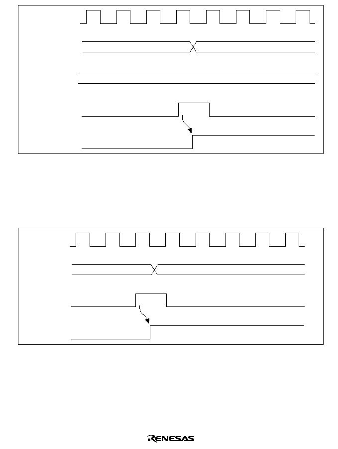
533
P
FRC
OCRA, OCRB
Compare match
signal
OCFA, OCFB
N + 1
N
N
Figure 12.11 OCF Setting Timing
12.4.7
Timer Overflow Flag (OVF) Setting Timing
FRC overflow (from H'FFFF to H'0000) sets the timer overflow flag (OVF) to 1. Figure 12.12
shows the timing.
P
FRC
Overflow
signal
OVF
H'0000
H'FFFF
Figure 12.12 OVF Setting Timing
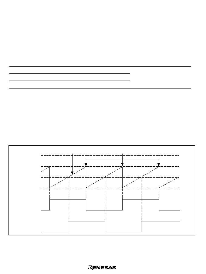
534
12.5
Interrupt Sources
There are four FRT interrupt sources of three types (ICI, OCIA/OCIB, and OVI). Table 12.3 lists
the interrupt sources and their priorities after a reset is cleared. The interrupt enable bits in TIER
are used to enable or disable the interrupt bits. Each interrupt request is sent to the interrupt
controller independently. See section 5, Interrupt Controller (INTC), for more information about
priorities and the relationship to interrupts other than those of the FRT.
Table 12.3
FRT Interrupt Sources and Priorities
Interrupt Source
Description
Priority
ICI
Interrupt by ICF
High
OCIA, OCIB
Interrupt by OCFA or OCFB
OVI
Interrupt by OVF
Low
12.6
Example of FRT Use
Figure 12.13 shows an example in which pulses with a 50% duty factor and arbitrary phase
relationship are output. The procedure is as follows:
1. Set the CCLRA bit in FTCSR to 1.
2. The OLVLA and OLVLB bits are inverted by software whenever a compare match occurs.
H'FFFF
OCRA
OCRB
H'0000
FTOA
FTOB
FRC
Counter clear
Figure 12.13 Example of Pulse Output
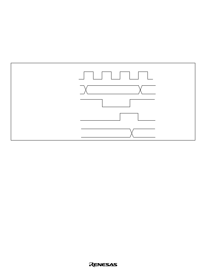
535
12.7
Usage Notes
Note that the following contention and operations occur when the FRT is operating:
12.7.1
Contention between FRC Write and Clear
When a counter clear signal is generated with the timing shown in figure 12.14 during the write
cycle for the lower byte of FRC, writing does not occur to the FRC, and the FRC clear takes
priority.
P
FRC lower-byte write cycle
Address
Internal write
signal
Counter clear
signal
FRC
FRC address
N
H'0000
Figure 12.14 Contention between FRC Write and Clear
12.7.2
Contention between FRC Write and Increment
When an increment occurs with the timing shown in figure 12.15 during the write cycle for the
lower byte of FRC, no increment is performed and the counter write takes priority.
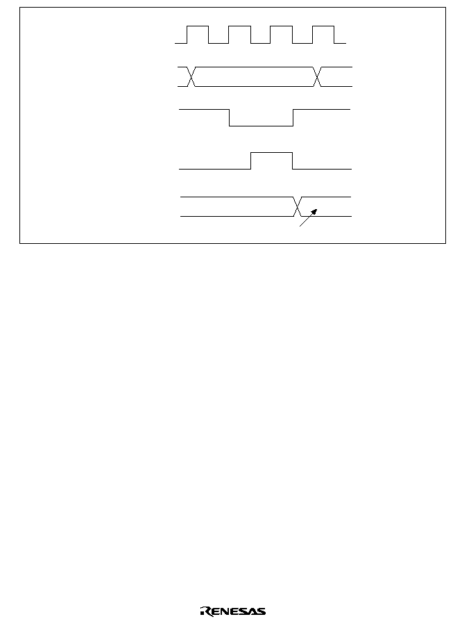
536
FRC
FRC address
N
M
Write data
P
FRC lower-byte write cycle
Address
Internal write
signal
FRC input
clock
Figure 12.15 Contention between FRC Write and Increment
12.7.3
Contention between OCR Write and Compare Match
When a compare match occurs with the timing shown in figure 12.16, during the write cycle for
the lower byte of OCRA or OCRB, the OCR write takes priority and the compare match signal is
disabled.
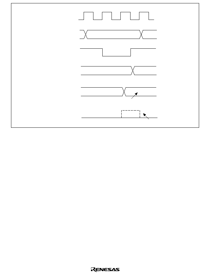
537
FRC
Compare match
signal
OCR
OCR address
N
M
N
N + 1
Write data
Disabled
P
FRC lower-byte write cycle
Address
Internal write
signal
Figure 12.16 Contention between OCR and Compare Match
12.7.4
Internal Clock Switching and Counter Operation
FRC will sometimes begin incrementing because of the timing of switching between internal
clocks. Table 12.4 shows the relationship between internal clock switching timing (CKS1 and
CKS0 bit rewrites) and FRC operation.
When an internal clock is used, the FRC clock is generated when the falling edge of an internal
clock (created by dividing the system clock (
)) is detected. When a clock is switched to high
before the switching and to low after switching, as shown in case 3 in table 12.4, the switchover is
considered a falling edge and an FRC clock pulse is generated, causing FRC to increment. FRC
may also increment when switching between an internal clock and an external clock.
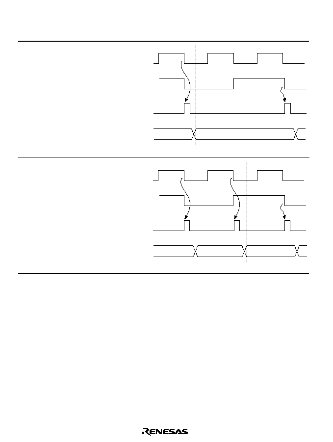
538
Table 12.4
Internal Clock Switching and FRC Operation
No.
Timing of Rewrite of
CKS1 and CKS0 Bits
FRC Operation
1
Low-to-low switch
Clock before
switching
Clock after
switching
FRC clock
FRC
N
N + 1
Rewrite of CKS bit
2
Low-to-high switch
N
N + 1
N + 2
Clock before
switching
Clock after
switching
FRC clock
FRC
Rewrite of CKS bit

539
Table 12.4
Internal Clock Switching and FRC Operation (cont)
No.
Timing of Rewrite of
CKS1 and CKS0 Bits
FRC Operation
3
High-to-low switch
N
N + 1
N + 2
Clock before
switching
Clock after
switching
FRC clock
FRC
Rewrite of CKS bit
4
High-to-high switch
N
N + 1
N + 2
Clock before
switching
Clock after
switching
FRC clock
FRC
Rewrite of CKS bit
Note:
Because the switchover is considered a falling edge, FRC starts counting up.
12.7.5
Timer Output (FTOA, FTOB)
During a power-on reset, the timer outputs (FTOA, FTOB) will be unreliable until the oscillation
stabilizes. The initial value is output after the oscillation settling time has elapsed.

540

541
Section 13 Watchdog Timer (WDT)
13.1
Overview
A single-channel watchdog timer (WDT) is provided on-chip for monitoring system operations. If
a system becomes uncontrolled and the timer counter overflows without being rewritten correctly
by the CPU, an overflow signal (
WDTOVF) is output externally. The WDT can simultaneously
generate an internal reset signal for the entire chip.
When this watchdog function is not needed, the WDT can be used as an interval timer. In the
interval timer operation, an interval timer interrupt is generated at each counter overflow. The
WDT is also used when recovering from standby mode, in modifying a clock frequency, and in
clock pause mode.
13.1.1
Features
The WDT includes the following features.
∑
Can be switched between watchdog timer mode and interval timer mode.
∑
WDTOVF output in watchdog timer mode
The
WDTOVF signal is output externally when the counter overflows, and a simultaneous
internal reset of the chip can also be selected (either a power-on reset or manual reset can be
specified).
∑
Interrupt generation in interval timer mode
An interval timer interrupt is generated when the counter overflows.
∑
Used when standby mode is cleared or the clock frequency is changed, and in clock pause
mode.
∑
Choice of eight counter input clocks
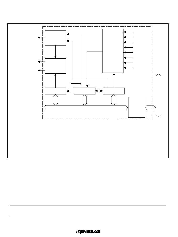
542
13.1.2
Block Diagram
Figure 13.1 shows a block diagram of the WDT.
/4
/128
/256
/512
/1024
/2048
/8192
/16384
Internal
clock
Clock
Overflow
Clock
select
Interrupt
control
Reset
control
RSTCSR
WTCNT
WTCSR
Module bus
Bus
interface
Interna bus
ITI
(Interrupt
request signal)
WDTOVF
Internal
reset signal
*
WDT
: See figure 3.1, Block Diagram of Clock Pulse Generator Circuit.
WTCSR:
Watchdog timer control/status register
WTCNT: Watchdog timer counter
RSTCSR: Reset control/status register
Note:
*
The internal reset signal can be generated by a register setting. The type of reset can
be selected (power-on or manual reset).
Figure 13.1 WDT Block Diagram
13.1.3
Pin Configuration
Table 13.1 shows the pin configuration.
Table 13.1
Pin Configuration
Pin
Abbreviation
I/O
Function
Watchdog timer overflow
WDTOVF
O
Outputs the counter overflow signal in
watchdog timer mode

543
13.1.4
Register Configuration
Table 13.2 summarizes the three WDT registers. They are used to select the clock, switch the
WDT mode, and control the reset signal.
Table 13.2
Register Configuration
Address
Name
Abbreviation
R/W
Initial Value
Write
*
1
Read
*
2
Watchdog timer
control/status register
WTCSR
R/(W)
*
3
H'18
H'FFFFFE80
H'FFFFFE80
Watchdog timer
counter
WTCNT
R/W
H'00
H'FFFFFE80
H'FFFFFE81
Reset control/status
register
RSTCSR
R/(W)
*
3
H'1D
H'FFFFFE82
H'FFFFFE83
Notes:
*
1 Write by word access. It cannot be written by byte or longword access.
*
2 Read by byte access. The correct value cannot be read by word or longword access.
*
3 Only 0 can be written in bit 7 to clear the flag.
13.2
Register Descriptions
13.2.1
Watchdog Timer Counter (WTCNT)
Bit:
7
6
5
4
3
2
1
0
Initial value:
0
0
0
0
0
0
0
0
R/W:
R/W
R/W
R/W
R/W
R/W
R/W
R/W
R/W
WTCNT is an 8-bit read/write register. The method of writing to WTCNT differs from that of
most other registers to prevent inadvertent rewriting. See section 13.2.4, Notes on Register Access,
for details. When the timer enable bit (TME) in the watchdog timer control/status register
(WTCSR) is set to 1, the watchdog timer counter starts counting pulses of an internal clock source
selected by clock select bits 2 to 0 (CKS2 to CKS0) in WTCSR. When the value of WTCNT
overflows (changes from H'FF to H'00), a watchdog timer overflow signal (
WDTOVF) or interval
timer interrupt (ITI) is generated, depending on the mode selected in the WT/
IT bit in WTCSR.
WTCNT is initialized to H'00 by a reset and when the TME bit is cleared to 0. It is not initialized
in standby mode, when the clock frequency is changed, or in clock pause mode.

544
13.2.2
Watchdog Timer Control/Status Register (WTCSR)
Bit:
7
6
5
4
3
2
1
0
OVF
WT/
IT
TME
--
--
CKS2
CKS1
CKS0
Initial value:
0
0
0
1
1
0
0
0
R/W:
R/(W)
*
R/W
R/W
R
R
R/W
R/W
R/W
Note:
*
Only 0 can be written in bit 7, to clear the flag.
The watchdog timer control/status register (WTCSR) is an 8-bit read/write register. The method of
writing to WTCSR differs from that of most other registers to prevent inadvertent rewriting. See
section 13.2.4, Notes on Register Access, for details. Its functions include selecting the timer
mode and clock source. Bits 7 to 5 are initialized to 000 by a reset, in standby mode, when the
clock frequency is changed, and in clock pause mode. Bits 2 to 0 are initialized to 000 by a reset,
but are not initialized in standby mode, when the clock frequency is changed, or in clock pause
mode.
Bit 7--Overflow Flag (OVF): Indicates that WTCNT has overflowed from H'FF to H'00 in
interval timer mode. It is not set in watchdog timer mode.
Bit 7: OVF
Description
0
No overflow of WTCNT in interval timer mode
(Initial value)
Cleared by reading OVF, then writing 0 in OVF
1
WTCNT overflow in interval timer mode
Bit 6--Timer Mode Select (WT/
IT): Selects whether to use the WDT as a watchdog timer or
interval timer. When WTCNT overflows, the WDT either generates an interval timer interrupt
(ITI) or generates a
WDTOVF signal, depending on the mode selected.
Bit 6: WT/
IT
Description
0
Interval timer mode: interval timer interrupt (ITI) request to the CPU
when WTCNT overflows
(Initial value)
1
Watchdog timer mode:
WDTOVF
signal output externally when WTCNT
overflows. Section 13.2.3, Reset Control/Status Register (RSTCSR),
describes in detail what happens when WTCNT overflows in watchdog
timer mode

545
Bit 5--Timer Enable (TME): Enables or disables the timer.
Bit 5: TME
Description
0
Timer disabled: WTCNT is initialized to H'00 and count-up stops
(Initial value)
1
Timer enabled: WTCNT starts counting. A
WDTOVF
signal or interrupt
is generated when WTCNT overflows
Bits 4 and 3--Reserved: These bits are always read as 1. The write value should always be 1.
Bits 2 to 0--Clock Select 2 to 0 (CKS2 to CKS0): These bits select one of eight internal clock
sources for input to WTCNT. The clock signals are obtained by dividing the frequency of the
system clock (
).
Description
Bit 2: CKS2 Bit 1: CKS1 Bit 0: CKS0 Clock Source
Overflow Interval
*
(
= 60 MHz)
0
0
0
/4 (Initial value)
17.0 µs
1
/128
544 µs
1
0
/256
1.1 ms
1
/512
2.2 ms
1
0
0
/1024
4.4 ms
1
/2048
8.7 ms
1
0
/8192
34.8 ms
1
/16384
69.6 ms
Note:
*
The overflow interval listed is the time from when the WTCNT begins counting at H'00 until
an overflow occurs.
13.2.3
Reset Control/Status Register (RSTCSR)
Bit:
7
6
5
4
3
2
1
0
WOVF
RSTE
RSTS
--
--
--
--
--
Initial value:
0
0
0
1
1
1
0
1
R/W:
R/(W)
*
R/W
R/W
R
R
R
R
R
Note:
*
Only 0 can be written in bit 7, to clear the flag.
RSTCSR is an 8-bit read/write register that controls output of the reset signal generated by
watchdog timer counter (WTCNT) overflow and selects the internal reset signal type. The method
of writing to RSTCSR differs from that of most other registers to prevent inadvertent rewriting.
See section 13.2.4, Notes on Register Access, for details. RSTCR is initialized to H'1D by input of

546
a reset signal from the
RES pin, but is not initialized by the internal reset signal generated by
overflow of the WDT. It is initialized to H'1D in standby mode, when the clock frequency is
changed, and in clock pause mode.
Bit 7--Watchdog Timer Overflow Flag (WOVF): Indicates that WTCNT has overflowed (from
H'FF to H'00) in watchdog timer mode. It is not set in interval timer mode.
Bit 7: WOVF
Description
0
No WTCNT overflow in watchdog timer mode
(Initial value)
Cleared by reading WOVF, then writing 0 in WOVF
1
Set by WTCNT overflow in watchdog timer mode
Bit 6--Reset Enable (RSTE): Selects whether to reset the chip internally if WTCNT overflows in
watchdog timer mode.
Bit 6: RSTE
Description
0
Not reset when WTCNT overflows
(Initial value)
LSI not reset internally, but WTCNT and WTCSR reset within WDT
1
Reset when WTCNT overflows
Bit 5--Reset Select (RSTS): Selects the type of internal reset generated if WTCNT overflows in
watchdog timer mode.
Bit 5: RSTS
Description
0
Power-on reset
(Initial value)
1
Manual reset
Bits 4 to 2, bit 0--Reserved: These bits are always read as 1. The write value should always be 1.
Bit 1-- Reserved: This bit is always read as 0. The write value should always be 0.
13.2.4
Notes on Register Access
The watchdog timer's WTCNT, WTCSR, and RSTCSR registers differ from other registers in that
they are more difficult to write. The procedures for writing and reading these registers are given
below.
Writing to WTCNT and WTCSR: These registers must be written by a word transfer
instruction. They cannot be written by byte or longword transfer instructions. WTCNT and
WTCSR both have the same write address. The write data must be contained in the lower byte of

547
the written word. The upper byte must be H'5A (for WTCNT) or H'A5 (for WTCSR) (figure 13.2).
This transfers the write data from the lower byte to WTCNT or WTCSR.
Writing to WTCNT
15
8 7
0
Address:
H'FFFFFE80
H'5A
Write data
Writing to WTCSR
15
8 7
0
Address:
H'FFFFFE80
H'A5
Write data
Figure 13.2 Writing to WTCNT and WTCSR
Writing to RSTCSR: RSTCSR must be written by a word access to address H'FFFFFE82. It
cannot be written by byte or longword transfer instructions. Procedures for writing 0 in WOVF
(bit 7) and for writing to RSTE (bit 6) and RSTS (bit 5) are different, as shown in figure 13.3. To
write 0 in the WOVF bit, the write data must be H'A5 in the upper byte and H'00 in the lower byte.
This clears the WOVF bit to 0. The RSTE and RSTS bits are not affected. To write to the RSTE
and RSTS bits, the upper byte must be H'5A and the lower byte must be the write data. The values
of bits 6 and 5 of the lower byte are transferred to the RSTE and RSTS bits, respectively. The
WOVF bit is not affected.
Writing 0 to the WOVF bit
15
8 7
0
Address:
H'FFFFFE82
H'A5
H'00
Writing to the RSTE and RSTS bits
15
8 7
0
Address:
H'FFFFFE82
H'5A
Write data
Figure 13.3 Writing to RSTCSR
Reading from WTCNT, WTCSR, and RSTCSR: WTCNT, WTCSR, and RSTCSR are read
like other registers. Use byte transfer instructions. The read addresses are H'FFFFFE80 for
WTCSR, H'FFFFFE81 for WTCNT, and H'FFFFFE83 for RSTCSR.

548
13.3
Operation
13.3.1
Operation in Watchdog Timer Mode
To use the WDT as a watchdog timer, set the WT/
IT and TME bits in WTCSR to 1. Software
must prevent WTCNT overflow by rewriting the WTCNT value (normally by writing H'00) before
overflow occurs. Thus, WTCNT will not overflow while the system is operating normally, but if
WTCNT fails to be rewritten and overflows occur due to a system crash or the like, a
WDTOVF
signal is output (figure 13.4). The
WDTOVF signal can be used to reset the system. The
WDTOVF signal is output for 512
clock cycles.
If the RSTE bit in RSTCSR is set to 1, a signal to reset the chip will be generated internally
simultaneously with the
WDTOVF signal when WTCNT overflows. Either a power-on reset or a
manual reset can be selected by the RSTS bit. The internal reset signal is output for 2048
clock
cycles.
If a reset due to the input signal from the
RES pin and a reset due to WDT overflow occur
simultaneously, the
RES reset takes priority and the WOVF bit in RSTCSR is cleared to 0.
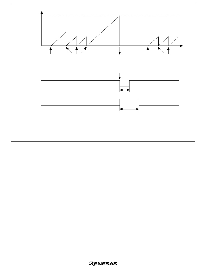
549
WOVF = 1
WTCNT value
Overflow
WT/
IT
= 1
TME = 1
WT/
IT
= 1
TME = 1
H'00 written
in WTCNT
H'00 written
in WTCNT
WDTOVF
and
internal reset generated
H'FF
H'00
512
clocks
2048
clocks
WDTOVF
signal
Internal
reset
signal
*
Time
WT/
IT
: Timer mode select bit
TME: Timer enable bit
Note:
*
Internal reset signal is generated only when the RSTE bit is set to 1.
Figure 13.4 Operation in Watchdog Timer Mode
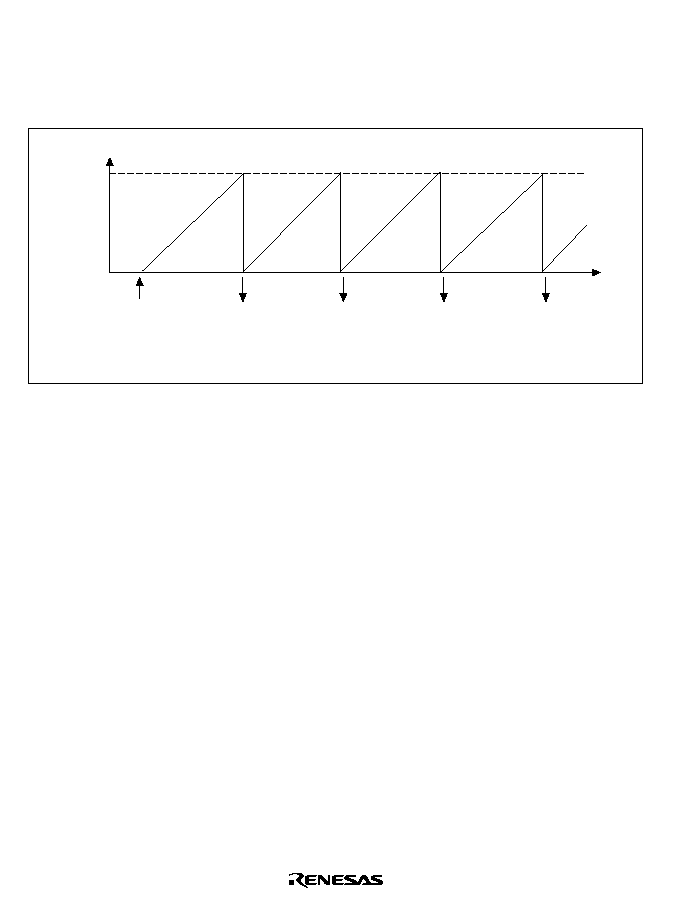
550
13.3.2
Operation in Interval Timer Mode
To use the WDT as an interval timer, clear WT/
IT to 0 and set TME to 1 in WTCSR. An interval
timer interrupt (ITI) is generated each time the watchdog timer counter (WTCNT) overflows. This
function can be used to generate interval timer interrupts at regular intervals (figure 13.5).
ITI
ITI
ITI
ITI
WTCNT value
Overflow
Overflow
Overflow
Overflow
WT/
IT
= 0
TME = 1
H'FF
H'00
Time
ITI: Interval timer interrupt request generation
Figure 13.5 Operation in Interval Timer Mode
13.3.3
Operation when Standby Mode is Cleared
The watchdog timer has a special function to clear standby mode with an NMI interrupt. When
using standby mode, set the WDT as described below.
Transition to Standby Mode: The TME bit in WTCSR must be cleared to 0 to stop the watchdog
timer counter before it enters standby mode. The chip cannot enter standby mode while the TME
bit is set to 1. Set bits CKS2 to CKS0 in WTCSR so that the counter overflow interval is equal to
or longer than the oscillation settling time. See section 22, Electrical Characteristics, for the
oscillation settling time.
Recovery from Standby Mode: When an NMI request signal is received in standby mode the
clock oscillator starts running and the watchdog timer starts counting at the rate selected by bits
CKS2 to CKS0 before standby mode was entered. When WTCNT overflows (changes from H'FF
to H'00) the system clock (
) is presumed to be stable and usable; clock signals are supplied to the
entire chip and standby mode ends.
For details on standby mode, see section 21, Power Down Modes.
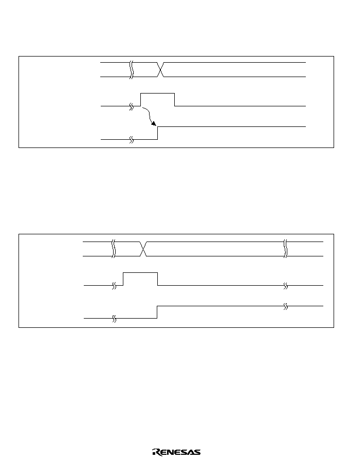
551
13.3.4
Timing of Overflow Flag (OVF) Setting
In interval timer mode, when WTCNT overflows, the OVF flag in WTCSR is set to 1 and an
interval timer interrupt (ITI) is requested (figure 13.6).
WTCNT
H'FF
H'00
Overflow signal
(internal signal)
OVF
Figure 13.6 Timing of OVF Setting
13.3.5
Timing of Watchdog Timer Overflow Flag (WOVF) Setting
When WTCNT overflows the WOVF flag in RSTCSR is set to 1 and a
WDTOVF signal is output.
When the RSTE bit is set to 1, WTCNT overflow enables an internal reset signal to be generated
for the entire chip (figure 13.7).
WTCNT
H'FF
H'00
Overflow signal
(internal signal)
WOVF
Figure 13.7 Timing of WOVF Setting

552
13.4
Usage Notes
13.4.1
Contention between WTCNT Write and Increment
If a count-up pulse is generated at the timing shown in figure 13.8 during a watchdog timer
counter (WTCNT) write cycle, the write takes priority and the timer counter is not incremented
(figure 13.8).
WTCNT address
Address
Internal write
signal
WTCNT input
clock
WTCNT
Counter write data
N
M
Figure 13.8 Contention between WTCNT Write and Increment
13.4.2
Changing CKS2 to CKS0 Bit Values
If the values of bits CKS2 to CKS0 are altered while the WDT is running, the count may
increment incorrectly. Always stop the watchdog timer (by clearing the TME bit to 0) before
changing the values of bits CKS2 to CKS0.
13.4.3
Switching between Watchdog Timer Mode and Interval Timer Mode
The WDT may not operate correctly if it is switched between watchdog timer mode and interval
timer mode while it is running.
To ensure correct operation, always stop the watchdog timer (by clearing the TME bit to 0) before
switching between watchdog timer mode and interval timer mode.

553
13.4.4
System Reset with
WDTOVF
If a
WDTOVF signal is input to the RES pin, the device cannot initialize correctly. Avoid logical
input of the
WDTOVF output signal to the RES input pin. To reset the entire system with the
WDTOVF signal, use the circuit shown in figure 13.9.
Reset input
Reset signal to
entire system
Chip
RES
WDTOVF
Figure 13.9 Example of Circuit for System Reset with
WDTOVF Signal
13.4.5
Internal Reset in Watchdog Timer Mode
If the RSTE bit is cleared to 0 in watchdog timer mode, the chip will not reset internally when a
WTCNT overflow occurs, but WTCNT and WTCSR in the WDT will reset.
When using sleep mode, do not use internal reset. Instead, use the
RES pin for resetting. (See
section13.4.4, System Reset with
WDTOVF.)
Internal reset can be used only when sleep mode is not used.

554

555
Section 14 Serial Communication Interface with FIFO
(SCIF)
14.1
Overview
The SH7616 is equipped with a two-channel serial communication interface with built-in FIFO
buffers (SCIF: SCI with FIFO). The SCIF can handle both asynchronous and synchronous serial
communication. A function is also provided for serial communication between processors
(multiprocessor communication function).
An on-chip Infrared Data Association (IrDA) interface based on the IrDA 1.0 system is also
provided, enabling infrared communication.
Sixteen-stage FIFO registers are provided for both transmission and reception, enabling fast,
efficient, and continuous communication.
14.1.1
Features
The SCIF has the following features:
∑
Choice of synchronous or asynchronous serial communication mode
Asynchronous mode
Serial data communication is executed using an asynchronous system in which
synchronization is achieved character by character. Serial data communication can be
carried out with standard asynchronous communication chips such as a Universal
Asynchronous Receiver/Transmitter (UART) or Asynchronous Communication Interface
Adapter (ACIA). A multiprocessor communication function is also provided that enables
serial data communication with a number of processors.
There is a choice of 12 serial data communication formats.
∑
Data length:
7 or 8 bits
∑
Stop bit length:
1 or 2 bits
∑
Parity:
Even/odd/none
∑
Multiprocessor bit:
1 or 0
∑
Receive error detection: Parity, overrun, and framing errors
∑
Automatic break detection

556
Synchronous mode
Serial data communication is synchronized with a clock. Serial data communication can be
carried out with other chips that have a synchronous communication function.
There is a single serial data communication format.
∑
Data length:
8 bits
∑
Receive error detection: Overrun errors
∑
IrDA 1.0 compliance
∑
Full-duplex communication capability
The transmitter and receiver are mutually independent, enabling transmission and reception to
be executed simultaneously. In addition, the transmitter and receiver both have a 16-stage
FIFO buffer structure, enabling continuous serial data transmission and reception.
(However, IrDA communication is carried out in half-duplex mode.)
∑
Built-in baud rate generator allows a choice of bit rates.
∑
Choice of transmit/receive clock source: internal clock from baud rate generator or external
clock from SCK pin
∑
Four interrupt sources
There are four interrupt sources--transmit-FIFO-data-empty, break, receive-FIFO-data-full,
and receive-error--that can issue requests independently. The transmit-FIFO-data-empty and
receive-FIFO-data-full interrupts can activate the on-chip DMAC to execute data transfer.
∑
When not in use, the SCIF can be stopped by halting its clock supply to reduce power
consumption.
∑
Choice of LSB-first or MSB-first mode
∑
In asynchronous mode, operation can be selected on a base clock of 4, 8, or 16 times the bit
rate.
∑
Built-in modem control functions (
RTS and CTS)
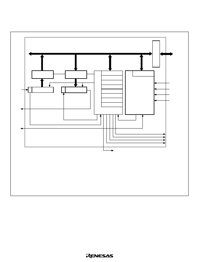
557
14.1.2
Block Diagrams
A block diagram of the SCIF is shown in figure 14.1, and a diagram of the IrDA block in figure
14.2.
Module data bus
SCFRDR
(16-stage)
SCFTDR
(16-stage)
SCRSR
RxD
TxD
SCK
SCTSR
SCFDR
SCFCR
SC1SSR
SC2SSR
SCSCR
SCSMR
SCFER
SCIMR
SCBRR
Parity generation
Parity check
Transmission/
reception control
Baud rate
generator
Clock
External clock
P
P
/4
P
/16
P
/64
BRI
IrDA/SCI switchover (to IrDA block)
TxI
RxI
ERI
SCIF
Legend
SCRSR:
Receive shift register
SCFRDR: Receive FIFO data register
SCTSR:
Transmit shift register
SCFTDR:
Transmit FIFO data register
SCSMR:
Serial mode register
SCSCR:
Serial control register
Bus interface
Internal
data bus
SC1SSR:
Serial status 1 register
SC2SSR:
Serial status 2 register
SCBRR:
Bit rate register
SCFCR:
FIFO control register
SCFDR:
FIFO data count register
SCFER:
FIFO error register
SCIMR:
IrDA mode register
Figure 14.1 Block Diagram of SCIF
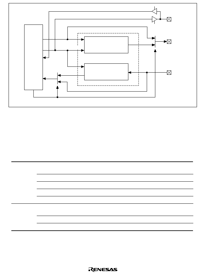
558
SCIF
IrDA/SCIF switchover
SCK
IrDA
TxD
TxD
RxD
RxD
Demodulation unit
Modulation unit
Clock input
Transmit clock
Figure 14.2 Diagram of IrDA Block
14.1.3
Pin Configuration
The SCIF has the serial pins shown in table 14.1.
Table 14.1
SCIF Pins
Channel
Name
Abbreviation
I/O
Function
1
Serial clock pin
SCK1
Input/
output
Clock input/output
Receive data pin
RxD1
Input
Receive data input
Transmit data pin
TxD1
Output
Transmit data output
Transmit request pin
RTS
Output
Transmit request
Transmit enable pin
CTS
Input
Transmit enable
2
Serial clock pin
SCK2
Input/
output
Clock input/output
Receive data pin
RxD2
Input
Receive data input
Transmit data pin
TxD2
Output
Transmit data output

559
14.1.4
Register Configuration
The SCIF has the internal registers shown in table 14.2. These registers are used to specify
asynchronous mode/synchronous mode and the IrDA communication mode, the data format and
the bit rate, and to perform transmitter/receiver control.
Table 14.2
SCIF Registers
Channel
Name
Abbre-
viation
R/W
Initial
Value
Address
Access
Size
1
Serial mode register
SCSMR1
R/W
H'00
H'FFFFFCC0 8
Bit rate register
SCBRR1
R/W
H'FF
H'FFFFFCC2 8
Serial control register
SCSCR1
R/W
H'00
H'FFFFFCC4 8
Transmit FIFO data register
SCFTDR1
W
--
H'FFFFFCC6 8
Serial status 1 register
SC1SSR1
R/(W)
*
H'0060
H'FFFFFCC8 16
Serial status 2 register
SC2SSR1
R/(W)
*
H'20
H'FFFFFCCA 8
Receive FIFO data register
SCFRDR1
R
Undefined H'FFFFFCCC 8
FIFO control register
SCFCR1
R/W
H'00
H'FFFFFCCE 8
FIFO data count register
SCFDR1
R
H'0000
H'FFFFFCD0 16
FIFO error register
SCFER1
R
H'0000
H'FFFFFCD2 16
IrDA mode register
SCIFMR1
R/W
H'00
H'FFFFFCD4 8
2
Serial mode register
SCSMR2
R/W
H'00
H'FFFFFCE0 8
Bit rate register
SCBRR2
R/W
H'FF
H'FFFFFCE2 8
Serial control register
SCSCR2
R/W
H'00
H'FFFFFCE4 8
Transmit FIFO data register
SCFTDR2
W
--
H'FFFFFCE6 8
Serial status 1 register
SC1SSR2
R/(W)
*
H'0060
H'FFFFFCE8 16
Serial status 2 register
SC2SSR2
R/(W)
*
H'20
H'FFFFFCEA 8
Receive FIFO data register
SCFRDR2
R
Undefined H'FFFFFCEC 8
FIFO control register
SCFCR2
R/W
H'00
H'FFFFFCEE 8
FIFO data count register
SCFDR2
R
H'0000
H'FFFFFCF0 16
FIFO error register
SCFER2
R
H'0000
H'FFFFFCF2 16
IrDA mode register
SCIMR2
R/W
H'00
H'FFFFFCF4 8
Note:
*
Only 0 can be written, to clear flags. Use byte access on registers with an access size of 8,
and word access on registers with an access size of 16.

560
14.2
Register Descriptions
With the exception of the IrDA mode register (SCIMR) and bits 6 to 3 (ICK3 to ICK0) of the
serial mode register (SCSMR), IrDA communication mode settings are the same as for
asynchronous mode.
14.2.1
Receive Shift Register (SCRSR)
Bit:
7
6
5
4
3
2
1
0
R/W:
--
--
--
--
--
--
--
--
The receive shift register (SCRSR) is the register used to receive serial data.
The SCIF sets serial data input from the RxD pin in SCRSR in the order received, starting with the
LSB (bit 0) or MSB (bit 7), and converts it to parallel data. When one byte of data has been
received, it is transferred to the receive FIFO data register (SCFRDR) automatically.
SCRSR cannot be read or written to directly.
14.2.2
Receive FIFO Data Register (SCFRDR)
Bit:
7
6
5
4
3
2
1
0
R/W:
R
R
R
R
R
R
R
R
The receive FIFO data register (SCFRDR) is a 16-stage FIFO register (8 bits per stage) that stores
received serial data.
When the SCIF has received one byte of serial data, it transfers the received data from SCRSR to
SCFRDR where it is stored, and completes the receive operation. SCRSR is then enabled for
reception, and consecutive receive operations can be performed until the receive FIFO data
register is full (16 data bytes).
SCFRDR is a read-only register, and cannot be written to.
If a read is performed when there is no receive data in the receive FIFO data register, an undefined
value will be returned. When the receive FIFO data register is full of receive data, subsequent
serial data is lost.

561
14.2.3
Transmit Shift Register (SCTSR)
Bit:
7
6
5
4
3
2
1
0
R/W:
--
--
--
--
--
--
--
--
The transmit shift register (SCTSR) is the register used to transmit serial data.
To perform serial data transmission, the SCIF first transfers transmit data from SCFTDR to
SCTSR, then sends the data to the TxD pin starting with the LSB (bit 0) or MSB (bit 7).
When transmission of one byte is completed, the next transmit data is transferred from SCFTDR
to SCTSR, and transmission started, automatically.
SCTSR cannot be read or written to directly.
14.2.4
Transmit FIFO Data Register (SCFTDR)
Bit:
7
6
5
4
3
2
1
0
R/W:
W
W
W
W
W
W
W
W
The transmit FIFO data register (SCFTDR) is a 16-stage FIFO register (8 bits per stage) that stores
data for serial transmission.
When the SCIF detects that SCTSR is empty, it transfers the transmit data written in SCFTDR to
SCTSR and starts serial transmission. Serial transmission is performed continuously until there is
no transmit data left in SCFTDR.
SCFTDR is a write-only register, and cannot be read.
The next data cannot be written when SCFTDR is filled with 16 bytes of transmit data. Data
written in this case is ignored.
14.2.5
Serial Mode Register (SCSMR)
Bit:
7
6
5
4
3
2
1
0
C/
A
CHR/
ICK3
PE/
ICK2
O/
E
/
ICK1
STOP/
ICK0
MP
CKS1
CKS0
Initial value:
0
0
0
0
0
0
0
0
R/W:
R/W
R/W
R/W
R/W
R/W
R/W
R/W
R/W

562
The serial mode register (SCSMR) is an 8-bit register used to set the SCIF's serial communication
format and select the baud rate generator clock source. In IrDA communication mode, it is used to
select the output pulse width.
SCSMR can be read or written to by the CPU at all times.
SCSMR is initialized to H'00 by a reset, by the module standby function, and in standby mode.
Bit 7--Communication Mode (C/
A): Selects asynchronous mode or synchronous mode as the
SCIF operating mode. In IrDA communication mode, this bit must be cleared to 0.
Bit 7: C/
A
Description
0
Asynchronous mode
(Initial value)
1
Synchronous mode
Bit 6--Character Length (CHR)/IrDA Clock Select 3 (ICK3): Selects 7 or 8 bits as the data length
in asynchronous mode. In synchronous mode, a fixed data length of 8 bits is used regardless of the
CHR setting,
Bit 6: CHR
Description
0
8-bit data
(Initial value)
1
7-bit data
*
Note:
*
When 7-bit data is selected, the MSB (bit 7) of the transmit FIFO data register (SCFTDR) is
not transmitted.
In IrDA communication mode, bit 6 is the IrDA clock select 3 (ICK3) bit, enabling appropriate
clock pulses to be generated according to its setting. See Pulse Width Selection, in section 14.3.6,
Operation in IrDA Mode, for details.
Bit 5--Parity Enable (PE)/IrDA Clock Select 2 (ICK2): In asynchronous mode, selects whether or
not parity bit addition is performed in transmission, and parity bit checking in reception. In
synchronous mode, parity bit addition and checking is not performed, regardless of the PE bit
setting.
Bit 5: PE
Description
0
Parity bit addition and checking disabled
(Initial value)
1
Parity bit addition and checking enabled
*
Note:
*
When the PE bit is set to 1, the parity (even or odd) specified by the O/
E
bit is added to
transmit data before transmission. In reception, the parity bit is checked for the parity (even
or odd) specified by the O/
E
bit.

563
In IrDA communication mode, bit 5 is the IrDA clock select 2 (ICK2) bit, enabling appropriate
clock pulses to be generated according to its setting. See Pulse Width Selection, in section 14.3.6,
Operation in IrDA Mode, for details.
Bit 4--Parity Mode (O/
E)/IrDA Clock Select 1 (ICK1): Selects either even or odd parity for use in
parity addition and checking. The O/
E bit setting is only valid when the PE bit is set to 1, enabling
parity bit addition and checking, in asynchronous mode. The O/
E bit setting is invalid in
synchronous mode, and when parity addition and checking is disabled in asynchronous mode.
Bit 4: O/
E
Description
0
Even parity
*
1
(Initial
value)
1
Odd parity
*
2
Notes:
*
1 When even parity is set, parity bit addition is performed in transmission so that the total
number of 1-bits in the transmit character plus the parity bit is even. In reception, a
check is performed to see if the total number of 1-bits in the receive character plus the
parity bit is even.
*
2 When odd parity is set, parity bit addition is performed in transmission so that the total
number of 1-bits in the transmit character plus the parity bit is odd. In reception, a check
is performed to see if the total number of 1-bits in the receive character plus the parity
bit is odd.
In IrDA communication mode, bit 4 is the IrDA clock select 1 (ICK1) bit, enabling appropriate
clock pulses to be generated according to its setting. See Pulse Width Selection, in section 14.3.6,
Operation in IrDA Mode, for details.
Bit 3--Stop Bit Length (STOP)/IrDA Clock Select 0 (ICK0): Selects 1 or 2 bits as the stop bit
length in asynchronous mode. The STOP bit setting is only valid in asynchronous mode. When
synchronous mode is set, the STOP bit setting is invalid since stop bits are not added.
Bit 3: STOP
Description
0
1 stop bit
*
1
(Initial value)
1
2 stop bits
*
2
Notes:
*
1 In transmission, a single 1-bit (stop bit) is added to the end of a transmit character
before it is sent.
*
2 In transmission, two 1-bits (stop bits) are added to the end of a transmit character
before it is sent.
In reception, only the first stop bit is checked, regardless of the STOP bit setting. If the second
stop bit is 1, it is treated as a stop bit; if it is 0, it is treated as the start bit of the next transmit
character.
In IrDA communication mode, bit 3 is the IrDA clock select 0 (ICK0) bit, enabling appropriate
clock pulses to be generated according to its setting. See Pulse Width Selection, in section 14.3.6,
Operation in IrDA Mode, for details.

564
Bit 2--Multiprocessor Mode (MP): Selects a multiprocessor format. When a multiprocessor
format is selected, the PE bit and O/
E bit parity settings are invalid. The MP bit setting is only
valid in asynchronous mode; it is invalid in synchronous mode and IrDA mode.
For details of the multiprocessor communication function, see section 14.3.3, Multiprocessor
Communication Function.
Bit 2: MP
Description
0
Multiprocessor function disabled
(Initial value)
1
Multiprocessor format selected
Bits 1 and 0--Clock Select 1 and 0 (CKS1, CKS0): These bits select the clock source for the built-
in baud rate generator. The clock source can be selected from P
, P
/4, P
/16, and P
/64,
according to the setting of bits CKS1 and CKS0.
For the relationship between the clock source, the bit rate register setting, and the baud rate, see
section 14.2.9, Bit Rate Register (SCBRR).
Bit 1:
CKS1
Bit 0:
CKS0
Description
0
0
P
clock
(Initial value)
1
P
/4 clock
1
0
P
/16 clock
1
P
/64 clock
Note:
P
= peripheral clock
14.2.6
Serial Control Register (SCSCR)
Bit:
7
6
5
4
3
2
1
0
TIE
RIE
TE
RE
MPIE
--
CKE1
CKE0
Initial value:
0
0
0
0
0
0
0
0
R/W:
R/W
R/W
R/W
R/W
R/W
R
R/W
R/W
The serial control register (SCSCR) performs enabling or disabling of SCIF transmit/receive
operations, serial clock output in asynchronous mode, and interrupt requests, and selection of the
transmit/receive clock source.
SCSCR can be read or written to by the CPU at all times.
SCSCR is initialized to H'00 by a reset, by the module standby function, and in standby mode.

565
Bit 7--Transmit Interrupt Enable (TIE): Enables or disables transmit-FIFO-data-empty interrupt
(TXI) request generation when, after serial transmit data is transferred from the transmit FIFO data
register (SCFTDR) to the transmit shift register (SCTSR), the number of data bytes in SCFTDR
falls to or below the transmit trigger set number, and the TDFE flag is set to 1 in the serial status 1
register (SC1SSR).
Bit 7: TIE
Description
0
Transmit-FIFO-data-empty interrupt (TXI) request disabled
*
(Initial value)
1
Transmit-FIFO-data-empty interrupt (TXI) request enabled
Note:
*
TXI interrupt requests can be cleared by writing transmit data exceeding the transmit trigger
set number to SCFTDR, reading 1 from the TDFE flag, then clearing it to 0, or by clearing
the TIE bit to 0. When transmit data is written to SCFTDR using the on-chip DMAC, the
TDFE flag is cleared automatically.
Bit 6--Receive Interrupt Enable (RIE): Enables or disables generation of a receive-FIFO-data-full
interrupt (RXI) request and receive-error interrupt (ERI) request when, after serial receive data is
transferred from the receive shift register (SCRSR) to the receive FIFO data register (SCFRDR),
the number of data bytes in SCFRDR reaches or exceeds the receive trigger set number, and the
RDF flag is set to 1 in SC1SSR.
Bit 6: RIE
Description
0
Receive-FIFO-data-full interrupt (RXI) request, receive-error interrupt (ERI)
request, and break interrupt (BRI) request disabled
*
(Initial value)
1
Receive-FIFO-data-full interrupt (RXI) request, receive-error interrupt (ERI)
request, and break interrupt (BRI) request enabled
Note:
*
RXI, ERI, and BRI interrupt requests can be cleared by reading 1 from the RDF or DR flag,
the FER, PER, ORER, or ER flag, or the BRK flag, then clearing the flag to 0, or by clearing
the RIE bit to 0. With the RDF flag, read receive data from SCFRDR until the number of
receive data bytes is less than the receive trigger set number, then read 1 from the RDF
flag and clear it to 0.
Bit 5--Transmit Enable (TE): Enables or disables the start of serial transmission by the SCIF.
Bit 5: TE
Description
0
Transmission disabled
*
1
(Initial
value)
1
Transmission enabled
*
2
Notes:
*
1 The TDRE flag in SC1SSR is fixed at 1.
*
2 Serial transmission is started when transmit data is written to SCFTDR in this state.
Serial mode register (SCSMR) and FIFO control register (SCFCR) settings must be
made, the transmission format decided, and the transmit FIFO reset, before the TE bit
is set to 1.

566
Bit 4--Receive Enable (RE): Enables or disables the start of serial reception by the SCIF.
Bit 4: RE
Description
0
Reception disabled
*
1
(Initial value)
1
Reception enabled
*
2
Notes:
*
1 Clearing the RE bit to 0 does not affect the RDF, DR, FER, PER, ORER, ER, and BRK
flags, which retain their states.
*
2 Serial reception is started in this state when a start bit is detected in asynchronous
mode or serial clock input is detected in synchronous mode.
SCSMR settings must be made to decide the reception format before setting the RE bit
to 1.
Bit 3--Multiprocessor Interrupt Enable (MPIE): Enables or disables multiprocessor interrupts.
The MPIE bit setting is only valid in asynchronous mode when the MP bit in SCSMR is set to 1.
The MPIE bit setting is invalid in synchronous mode and IrDA mode, and when the MP bit is 0.
Bit 3: MPIE
Description
0
Multiprocessor interrupts disabled (normal reception performed) (Initial value)
[Clearing conditions]
∑
When the MPIE bit is cleared to 0
∑
When data with MPB = 1 is received
1
Multiprocessor interrupts enabled
*
Receive interrupt (RXI) requests, receive-error interrupt (ERI) requests, and
setting of the RDF and FER in SC1SSR and ORER in SC2SSR are disabled
until data with the multiprocessor bit set to 1 is received.
Note:
*
Receive data transfer from SCRSR to SCFRDR, receive error detection, and setting of the
RDF and FER in SC1SSR and ORER flags in SC2SSR, is not performed. When receive
data with MPB = 1 is received, the MPB flag in SC2SSR is set to 1, the MPIE bit is cleared
to 0 automatically, and generation of RXI and ERI (when the RIE bit in SCSCR is set to 1)
and FER and ORER flag setting is enabled.
Bit 2--Reserved: This bit is always read as 0. The write value should always be 0.

567
Bits 1 and 0--Clock Enable 1 and 0 (CKE1, CKE0): These bits are used to select the SCIF clock
source and enable or disable clock output from the SCK pin. The combination of the CKE1 and
CKE0 bits determines whether the SCK pin functions as the serial clock output pin or the serial
clock input pin. The function of the SCK pin should be selected with the pin function controller
(PFC).
The setting of the CKE0 bit, however, is only valid for internal clock operation (CKE1 = 0) in
asynchronous mode. The CKE0 bit setting is invalid in synchronous mode and in the case of
external clock operation (CKE1 = 1). The CKE1 and CKE0 bits must be set before determining
the SCIF's operating mode with SCSMR.
For details of clock source selection, see table 14.9 in section 14.3, Operation.
Bit 1:
CKE1
Bit 0:
CKE0
Description
0
0
Asynchronous mode
Internal clock/SCK pin functions as input pin (input
signal ignored)
*
1
Synchronous mode
Internal clock/SCK pin functions as serial clock
output
*
1
1
Asynchronous mode
Internal clock/SCK pin functions as clock output
*
2
Synchronous mode
Internal clock/SCK pin functions as serial clock
output
1
*
4
Asynchronous mode
External clock/SCK pin functions as clock input
*
3
Synchronous mode
External clock/SCK pin functions as serial clock
input
Notes:
*
1 Initial value
*
2 Outputs a clock with a frequency of 16/8/4 times the bit rate.
*
3 Inputs a clock with a frequency of 16/8/4 times the bit rate.
*
4 Don't care

568
14.2.7
Serial Status 1 Register (SC1SSR)
Bit:
15
14
13
12
11
10
9
8
PER3
PER2
PER1
PER0
FER3
FER2
FER1
FER0
Initial value:
0
0
0
0
0
0
0
0
R/W:
R
R
R
R
R
R
R
R
Bit:
7
6
5
4
3
2
1
0
ER
TEND
TDFE
BRK
FER
PER
RDF
DR
Initial value:
0
1
1
0
0
0
0
0
R/W:
R/(W)
*
R
R/(W)
*
R/(W)
*
R
R
R/(W)
*
R/(W)
*
Note:
*
Only 0 can be written, to clear the flag.
The serial status 1 register (SC1SSR) is a 16-bit register in which the lower 8 bits consist of status
flags that indicate the operating status of the SCIF, and the upper 8 bits indicate the number of
receive errors in the data in the receive FIFO register.
SC1SSR can be read or written to at all times. However, 1 cannot be written to the ER, TDFE,
BRK, RDF, and DR status flags. Also note that in order to clear these flags to 0, they must first be
read as 1. The TEND, FER, and PER flags are read-only and cannot be modified.
SC1SSR is initialized to H'0084 by a reset, by the module standby function, and in standby mode.
Bits 15 to 12--Parity Error Count 3 to 0 (PER3 to PER0): These bits indicate the number of data
bytes in which a parity error occurred in the receive data in the receive FIFO data register.
These bits are cleared by reading all the receive data in the receive FIFO data register, or by
setting the RFRST bit to 1 in SCFCR and resetting the receive FIFO data register to the empty
state.
Bits 11 to 8--Framing Error Count 3 to 0 (FER3 to FER0): These bits indicate the number of data
bytes in which a framing error occurred in the receive data in the receive FIFO data register.
These bits are cleared by reading all the receive data in the receive FIFO data register, or by
setting the RFRST bit to 1 in SCFCR and resetting the receive FIFO data register to the empty
state.

569
Bit 7--Receive Error (ER)
Bit 7: ER
Description
0
Reception in progress, or reception has ended normally
*
1
(Initial value)
[Clearing conditions]
∑
In a reset or in standby mode
∑
When 0 is written to ER after reading ER = 1
1
A framing error, parity error, or overrun error occurred during reception
[Setting conditions]
∑
When the SCIF checks whether the stop bit at the end of the receive data is
1 when reception ends, and the stop bit is 0
*
2
∑
When, in reception, the number of 1-bits in the receive data plus the parity
bit does not match the parity setting (even or odd) specified by the O/
E
bit
in the serial mode register (SCSMR)
∑
When the next serial receive operation is completed while there are 16
receive data bytes in SCFRDR
Notes:
*
1 The ER flag is not affected and retains its previous state when the RE bit in SCSCR is
cleared to 0. When a framing error or parity error occurs, the receive data is still
transferred to SCFRDR, and reception is then halted or continued according to the
setting of the EI bit. When an overrun error occurs, the receive data is not transferred to
SCFRDR and reception cannot be continued.
*
2 In 2-stop-bit mode, only the first stop bit is checked for a value of 1; the second stop bit
is not checked.
Bit 6--Transmit End (TEND): Indicates that there is no valid data in SCFTDR when the last bit of
the transmit character is sent, and transmission has been ended.
Bit 6: TEND
Description
0
Transmission is in progress
[Clearing condition]
When data is written to SCFTDR while TE = 1
1
Transmission has been ended
(Initial value)
[Setting conditions]
∑
In a reset or in standby mode
∑
When the TE bit in SCSCR is 0
∑
When there is no transmit data in SCFTDR on transmission of the last bit of
a 1-byte serial transmit character

570
Bit 5--Transmit Data FIFO Empty (TDFE): Indicates that data has been transferred from the
transmit FIFO data register (SCFTDR) to the transmit shift register (SCTSR), the number of data
bytes in SCFTDR has fallen to or below the transmit trigger data number set by bits TTRG1 and
TTRG0 in the FIFO control register (SCFCR), and transmit data can be written to SCFTDR.
Bit 5: TDFE
Description
0
A number of transmit data bytes exceeding the transmit trigger set number
have been written to SCFTDR
[Clearing conditions]
∑
When transmit data exceeding the transmit trigger set number is written to
SCFTDR, and 0 is written to TDFE after reading TDFE = 1
∑
When transmit data exceeding the transmit trigger set number is written to
SCFTDR by the on-chip DMAC
1
The number of transmit data bytes in SCFTDR does not exceed the transmit
trigger set number
(Initial value)
[Setting conditions]
∑
In a reset or in standby mode
∑
When the number of SCFTDR transmit data bytes falls to or below the
transmit trigger set number as the result of a transmit operation
*
Note:
*
As SCFTDR is a 16-byte FIFO register, the maximum number of bytes that can be written
when TDFE = 0 is {16 ≠ (transmit trigger set number)}. Data written in excess of this will be
ignored. The number of data bytes in SCFTDR is indicated by the upper 8 bits of SCFDR.
Bit 4--Break Detect (BRK): Indicates that a receive data break signal has been detected.
Bit 4: BRK
Description
0
A break signal has not been received
(Initial value)
[Clearing conditions]
∑
In a reset or in standby mode
∑
When 0 is written to BRK after reading BRK = 1
1
A break signal has been received
[Setting condition]
When data with a framing error is received, and a framing error also occurs in
the next receive data (all space "0")
Note:
When a break is detected, transfer to SCFRDR of the receive data (H'00) following
detection is halted. When the break ends and the receive signal returns to mark "1", receive
data transfer is resumed.

571
Bit 3--Framing Error (FER): Indicates a framing error in the data read from the receive FIFO data
register (SCFRDR).
Bit 3: FER
Description
0
There is no framing error in the receive data read from SCFRDR (Initial value)
[Clearing conditions]
∑
In a reset or in standby mode
∑
When there is no framing error in SCFRDR read data
1
There is a framing error in the receive data read from SCFRDR
[Setting condition]
When there is a framing error in SCFRDR read data
Bit 2--Parity Error (PER): In asynchronous mode, indicates a parity error in the data read from
the receive FIFO data register (SCFRDR).
Bit 2: PER
Description
0
There is no parity error in the receive data read from SCFRDR
(Initial value)
[Clearing conditions]
∑
In a reset or in standby mode
∑
When there is no parity error in SCFRDR read data
1
There is a parity error in the receive data read from SCFRDR
[Setting condition]
When there is a parity error in SCFRDR read data
Bit 1--Receive Data Register Full (RDF): Indicates that the received data has been transferred to
the receive FIFO data register (SCFRDR), and the number of receive data bytes in SCFRDR is
equal to or greater than the receive trigger number set by bits RTRG1 and RTRG0 in the FIFO
control register (SCFCR).

572
Bit 1: RDF
Description
0
The number of receive data bytes in SCFRDR is less than the receive trigger
set number
(Initial value)
[Clearing conditions]
∑
In a reset or in standby mode
∑
When SCFRDR is read until the number of receive data bytes in SCFRDR
falls below the receive trigger set number, and 0 is written to RDF after
reading RDF = 1
∑
When SCFRDR is read by the on-chip DMAC until the number of receive
data bytes in SCFRDR falls below the receive trigger set number
1
The number of receive data bytes in SCFRDR is equal to or greater than the
receive trigger set number
[Setting condition]
When SCFRDR contains at least the receive trigger set number of receive data
bytes
Note:
SCFRDR is a 16-byte FIFO register. When RDF = 1, at least the receive trigger set number
of data bytes can be read. If all the data in SCFRDR is read and another read is performed,
the data value will be undefined. The number of receive data bytes in SCFRDR is indicated
by the lower 8 bits of SCFDR.
Bit 0--Receive Data Ready (DR): Indicates that there are fewer than the receive trigger set
number of data bytes in the receive FIFO data register (SCFRDR), and no further data has arrived
for at least 16 etu after the stop bit of the last data received.
Bit 0: DR
Description
0
Reception is in progress or has ended normally and there is no receive data
left in SCFRDR
(Initial value)
[Clearing conditions]
∑
In a reset or in standby mode
∑
When 0 is written to DR after all the remaining receive data has been
read
*
1
1
No further receive data has arrived, and SCFRDR contains fewer than the
receive trigger set number of data bytes
[Setting condition]
When SCFRDR contains fewer than the receive trigger set number of receive
data bytes, and no further data has arrived for at least 16 etu after the stop bit
of the last data received
*
2
Notes:
*
1 All remaining receive data should be read before clearing the DR flag.
*
2 Equivalent to 1.6 frames when using an 8-bit, 1-stop-bit format.
etu: Elementary time unit = sec/bit

573
14.2.8
Serial Status 2 Register (SC2SSR)
Bit:
7
6
5
4
3
2
1
0
TLM
RLM
N1
N0
MPB
MPBT
EI
ORER
Initial value:
0
0
1
0
0
0
0
0
R/W:
R/W
R/W
R/W
R/W
R
R/W
R/W
R/(W)
*
Note:
*
Only 0 can be written, to clear the flag.
The serial status 2 register (SC2SSR) is an 8-bit register.
SC2SSR can be read or written to at all times. However, 1 cannot be written to the ORER flag.
Also note that in order to clear this flag to 0, they must first be read as 1.
SC2SSR is initialized to H'20 by a reset, by the module standby function, and in standby mode.
Bit 7--Transmit LSB/MSB-First Select (TLM): Selects LSB-first or MSB-first mode in data
transmission.
Bit 7: TLM
Description
0
LSB-first transmission
(Initial value)
1
MSB-first transmission
Bit 6--Receive LSB/MSB-First Select (RLM): Selects LSB-first or MSB-first mode in data
reception.
Bit 6: RLM
Description
0
LSB-first reception
(Initial value)
1
MSB-first reception
Bits 5 and 4--Clock Bit Rate Ratio (N1, N0): These bits select the ratio of the base clock to the bit
rate.
Bit 5:
N1
Bit 4:
N0
Description
0
0
SCIF operates on base clock of 4 times the bit rate
1
SCIF operates on base clock of 8 times the bit rate
1
0
SCIF operates on base clock of 16 times the bit rate
(Initial value)
1
Setting prohibited

574
Bit 3--Multiprocessor bit (MPB): When reception is performed using a multiprocessor format in
asynchronous mode, MPB stores the multiprocessor bit in the receive data.
The MPB flag is read-only and cannot be modified.
Bit 3: MPB
Description
0
Data with a 0 multiprocessor bit has been received
*
(Initial value)
1
Data with a 1 multiprocessor bit has been received
Note:
*
Retains its previous state when the RE bit is cleared to 0 while using a multiprocessor
format.
Bit 2--Multiprocessor Bit Transfer (MPBT): When transmission is performed using a
multiprocessor format in asynchronous mode, MPBT stores the multiprocessor bit to be added to
the transmit data.
The MPBT bit setting is invalid in synchronous mode and IrDA mode, when a multiprocessor
format is not used, and when the operation is not transmission.
Bit 2: MPBT
Description
0
Data with a 0 multiprocessor bit is transmitted
(Initial value)
1
Data with a 1 multiprocessor bit is transmitted
Bit 1--Receive Data Error Ignore Enable (EI): Selects whether or not the receive operation is to
be continued when a framing error or parity error occurs in receive data (ER = 1).
Bit 1: EI
Description
0
Receive operation is halted when framing error or parity error occurs during
reception (ER = 1)
(Initial value)
1
Receive operation is continued when framing error or parity error occurs during
reception (ER = 1)
Note:
When EI = 0, only the last data in SCFRDR is treated as data containing an error. When EI
= 1, receive data is sent to SCFRDR even if it contains an error.

575
Bit 0--Overrun Error (ORER): Indicates that an overrun error occurred during reception, causing
abnormal termination.
Bit 0: ORER
Description
0
Reception in progress, or reception has ended normally
*
1
(Initial value)
[Clearing conditions]
∑
In a reset or in standby mode
∑
When 0 is written to ORER after reading ORER = 1
1
An overrun error occurred during reception
*
2
[Setting condition]
When the next serial receive operation is completed while there are 16 receive
data bytes in SCFRDR
Notes:
*
1 The ORER flag is not affected and retains its previous state when the RE bit in SCSCR
is cleared to 0.
*
2 The receive data prior to the overrun error is retained in SCFRDR, and the data
received subsequently is lost. Serial reception cannot be continued while the ORER flag
is set to 1. Also, serial transmission cannot be continued in synchronous mode.
14.2.9
Bit Rate Register (SCBRR)
Bit:
7
6
5
4
3
2
1
0
Initial value:
1
1
1
1
1
1
1
1
R/W:
R/W
R/W
R/W
R/W
R/W
R/W
R/W
R/W
The bit rate register (SCBRR) is an 8-bit register that sets the serial transmit/receive bit rate in
accordance with the baud rate generator operating clock selected by bits CKS1 and CKS0 in the
serial mode register (SCSMR).
SCBRR can be read or written to by the CPU at all times.
SCBRR is initialized to H'FF by a reset, by the module standby function, and in standby mode.
The SCBRR setting is found from the following equations.

576
Asynchronous mode:
N =
64
◊
2
2n≠1
◊
B
◊
10
6
≠ 1 (When operating on a base clock of 16 times the bit rate)
P
N =
32
◊
2
2n≠1
◊
B
◊
10
6
≠ 1 (When operating on a base clock of 8 times the bit rate)
P
N =
16
◊
2
2n≠1
◊
B
◊
10
6
≠ 1 (When operating on a base clock of 4 times the bit rate)
P
Synchronous mode:
N =
8
◊
2
2n≠1
◊
B
◊
10
6
≠ 1
P
Where B:
Bit rate (bits/s)
N:
SCBRR setting for baud rate generator (0
N
255)
P
: Peripheral module operating frequency (MHz)
n:
Baud rate generator input clock (n = 0, 1, 2, or 3)
(See the table below for the relation between n and the clock.)
SCSMR Settings
n
Clock
CKS1
CKS0
0
P
0
0
1
P
/4
1
2
P
/16
1
0
3
P
/64
1
The bit rate error in asynchronous mode is found from the following equations:
Error (%) =
(N + 1)
◊
B
◊
64
◊
2
2n≠1
≠ 1
◊
100
P
◊
10
6
(When operating on a base clock of 16 times the bit rate)
Error (%) =
(N + 1)
◊
B
◊
32
◊
2
2n≠1
≠ 1
◊
100
P
◊
10
6
(When operating on a base clock of 8 times the bit rate)
Error (%) =
(N + 1)
◊
B
◊
16
◊
2
2n≠1
≠ 1
◊
100
P
◊
10
6
(When operating on a base clock of 4 times the bit rate)

577
Table 14.3 shows sample SCBRR settings in asynchronous mode, and table 14.4 shows sample
SCBRR settings in synchronous mode. In both tables, the values are for operation on a base clock
of 16 times the bit rate.
Table 14.3
Examples of Bit Rates and SCBRR Settings in Asynchronous Mode
P
(MHz)
2
2.097152
2.4576
3
Bit Rate
(Bits/s)
n
N
Error
(%)
n
N
Error
(%)
n
N
Error
(%)
n
N
Error
(%)
110
1
141
0.03
1
148
≠0.04
1
174
≠0.26
1
212
0.03
150
1
103
0.16
1
108
0.21
1
127
0.00
1
155
0.16
300
0
207
0.16
0
217
0.21
0
255
0.00
1
77
0.16
600
0
103
0.16
0
108
0.21
0
127
0.00
0
155
0.16
1200
0
51
0.16
0
54
≠0.70
0
63
0.00
0
77
0.16
2400
0
25
0.16
0
26
1.14
0
31
0.00
0
38
0.16
4800
0
12
0.16
0
13
≠2.48
0
15
0.00
0
19
≠2.34
9600
0
6
≠6.99
0
6
≠2.48
0
7
0.00
0
9
≠2.34
19200
0
2
8.51
0
2
13.78
0
3
0.00
0
4
≠2.34
31250
0
1
0.00
0
1
4.86
0
1
22.88
0
2
0.00
38400
0
1
≠18.62
0
1
≠14.67
0
1
0.00
--
--
--

578
Table 14.3
Examples of Bit Rates and SCBRR Settings in Asynchronous Mode (cont)
P
(MHz)
3.6864
4
4.9152
5
Bit Rate
(Bits/s)
n
N
Error
(%)
n
N
Error
(%)
n
N
Error
(%)
n
N
Error
(%)
110
2
64
0.70
2
70
0.03
2
86
0.31
2
88
≠0.25
150
1
191
0.00
1
207
0.16
1
255
0.00
2
64
0.16
300
1
95
0.00
1
103
0.16
1
127
0.00
1
129
0.16
600
0
191
0.00
0
207
0.16
0
255
0.00
1
64
0.16
1200
0
95
0.00
0
103
0.16
0
127
0.00
0
129
0.16
2400
0
47
0.00
0
51
0.16
0
63
0.00
0
64
0.16
4800
0
23
0.00
0
25
0.16
0
31
0.00
0
32
≠1.36
9600
0
11
0.00
0
12
0.16
0
15
0.00
0
15
1.73
19200
0
5
0.00
0
6
≠6.99
0
7
0.00
0
7
1.73
31250
--
--
--
0
3
0.00
0
4
≠1.70
0
4
0.00
38400
0
2
0.00
0
2
8.51
0
3
0.00
0
3
1.73
P
(MHz)
6
6.144
7.37288
8
Bit Rate
(Bits/s)
n
N
Error
(%)
n
N
Error
(%)
n
N
Error
(%)
n
N
Error
(%)
110
2
106
≠0.44
2
108
0.08
2
130
≠0.07
2
141
0.03
150
2
77
0.16
2
79
0.00
2
95
0.00
2
103
0.16
300
1
155
0.16
1
159
0.00
1
191
0.00
1
207
0.16
600
1
77
0.16
1
79
0.00
1
95
0.00
1
103
0.16
1200
0
155
0.16
0
159
0.00
0
191
0.00
0
207
0.16
2400
0
77
0.16
0
79
0.00
0
95
0.00
0
103
0.16
4800
0
38
0.16
0
39
0.00
0
47
0.00
0
51
0.16
9600
0
19
≠2.34
0
19
0.00
0
23
0.00
0
25
0.16
19200
0
9
≠2.34
0
9
0.00
0
11
0.00
0
12
0.16
31250
0
5
0.00
0
5
2.40
0
6
5.33
0
7
0.00
38400
0
4
≠2.34
0
4
0.00
0
5
0.00
0
6
≠6.99

579
Table 14.3
Examples of Bit Rates and SCBRR Settings in Asynchronous Mode (cont)
P
(MHz)
9.8304
10
12
12.288
Bit Rate
(Bits/s)
n
N
Error
(%)
n
N
Error
(%)
n
N
Error
(%)
n
N
Error
(%)
110
2
174
≠0.26
2
177
≠0.25
2
212
0.03
2
217
0.08
150
2
127
0.00
2
129
0.16
2
155
0.16
2
159
0.00
300
1
255
0.00
2
64
0.16
2
77
0.16
2
79
0.00
600
1
127
0.00
1
129
0.16
1
155
0.16
1
159
0.00
1200
0
255
0.00
1
64
0.16
1
77
0.16
1
79
0.00
2400
0
127
0.00
0
129
0.16
0
155
0.16
0
159
0.00
4800
0
63
0.00
0
64
0.16
0
77
0.16
0
79
0.00
9600
0
31
0.00
0
32
≠1.36
0
38
0.16
0
39
0.00
19200
0
15
0.00
0
15
1.73
0
19
≠2.34
0
19
0.00
31250
0
9
≠1.70
0
9
0.00
0
11
0.00
0
11
2.40
38400
0
7
0.00
0
7
1.73
0
9
≠2.34
0
9
0.00
P
(MHz)
14.7456
16
30
Bit Rate
(Bits/s)
n
N
Error
(%)
n
N
Error
(%)
n
N
Error
(%)
110
3
64
0.70
3
70
0.03
3
132
0.13
150
2
191
0.00
2
207
0.16
3
97
≠0.35
300
2
95
0.00
2
103
0.16
2
194
0.16
600
1
191
0.00
1
207
0.16
2
97
≠0.35
1200
1
95
0.00
1
103
0.16
1
194
0.16
2400
0
191
0.00
0
207
0.16
1
97
≠0.35
4800
0
95
0.00
0
103
0.16
0
194
0.16
9600
0
47
0.00
0
51
0.16
0
97
≠0.35
19200
0
23
0.00
0
25
0.16
0
48
≠0.35
31250
0
14
≠1.70
0
15
0.00
0
29
0.00
38400
0
11
0.00
0
12
0.16
0
23
1.73

580
Table 14.4
Examples of Bit Rates and SCBRR Settings in Synchronous Mode
P
(MHz)
4
8
16
32
Bit Rate (Bits/s)
n
N
n
N
n
N
n
N
110
--
--
--
--
--
--
--
--
250
2
249
3
124
3
249
--
--
500
2
124
2
249
3
124
3
249
1 k
1
249
2
124
2
249
3
124
2.5 k
1
99
1
199
2
99
2
199
5 k
0
199
1
99
1
199
2
99
10 k
0
99
0
199
1
99
1
199
25 k
0
39
0
79
0
159
1
79
50 k
0
19
0
39
0
79
0
159
100 k
0
9
0
19
0
39
0
79
250 k
0
3
0
7
0
15
0
31
500 k
0
1
0
3
0
7
0
15
1 M
0
0
*
0
1
0
3
0
7
2 M
0
0
*
0
1
0
3
Note:
As far as possible, the setting should be made so that the error is within 1%.
Legend
Blank: No setting is available.
--:
A setting is available but error occurs.
*
Continuous transmission/reception is not possible.

581
Table 14.5 shows the maximum bit rate for various frequencies in asynchronous mode when using
the baud rate generator. Tables 14.6 and 14.7 show the maximum bit rates when using external
clock input.
Table 14.5
Maximum Bit Rate for Various Frequencies with Baud Rate Generator
(Asynchronous Mode)
Settings
P
(MHz)
Maximum Bit Rate (Bits/s)
n
N
2
62500
0
0
2.097152
65536
0
0
2.4576
76800
0
0
3
93750
0
0
3.6864
115200
0
0
4
125000
0
0
4.9152
153600
0
0
8
250000
0
0
9.8304
307200
0
0
12
375000
0
0
14.7456
460800
0
0
16
500000
0
0
19.66080
614400
0
0
20
625000
0
0
24
750000
0
0
24.57600
768000
0
0
28
896875
0
0
30
937500
0
0

582
Table 14.6
Maximum Bit Rate with External Clock Input (Asynchronous Mode)
P
(MHz)
External Input Clock (MHz)
Maximum Bit Rate (Bits/s)
2
0.5000
31250
2.097152
0.5243
32768
2.4576
0.6144
38400
3
0.7500
46875
3.6864
0.9216
57600
4
1.0000
62500
4.9152
1.2288
76800
8
2.0000
125000
9.8304
2.4576
153600
12
3.0000
187500
14.7456
3.6864
230400
16
4.0000
250000
30
7.5000
468750
Table 14.7
Maximum Bit Rate with External Clock Input (Synchronous Mode)
P
(MHz)
External Input Clock (MHz)
Maximum Bit Rate (Bits/s)
8
1.3333
1333333.3
16
2.6667
2666666.7
30
5.0
5000000.0

583
14.2.10
FIFO Control Register (SCFCR)
Bit:
7
6
5
4
3
2
1
0
RTRG1
RTRG0
TTRG1
TTRG0
MCE
TFRST
RFRST
LOOP
Initial value:
0
0
0
0
0
0
0
0
R/W:
R/W
R/W
R/W
R/W
R/W
R/W
R/W
R/W
The FIFO control register (SCFCR) performs data count resetting and trigger data number setting
for the transmit and receive FIFO registers, and also contains a loopback test enable bit.
SCFCR can be read or written to at all times.
SCFCR is initialized to H'00 by a reset, by the module standby function, and in standby mode.
Bits 7 and 6--Receive FIFO Data Number Trigger (RTRG1, RTRG0): These bits are used to set
the number of receive data bytes that sets the receive data full (RDF) flag in the serial status 1
register (SC1SSR).
The RDF flag is set when the number of receive data bytes in the receive FIFO data register
(SCFRDR) is equal to or greater than the trigger set number shown in the following table.
Bit 7: RTRG1
Bit 6: RTRG0
Receive Trigger Number
0
0
1
*
1
4
1
0
8
1
14
Note:
*
Initial value
Bits 5 and 4--Transmit FIFO Data Number Trigger (TTRG1, TTRG0): These bits are used to set
the number of remaining transmit data bytes that sets the transmit FIFO data register empty
(TDFE) flag in the serial status 1 register (SC1SSR).
The TDFE flag is set when the number of transmit data bytes in the transmit FIFO data register
(SCFTDR) is equal to or less than the trigger set number shown in the following table.

584
Bit 5: TTRG1
Bit 4: TTRG0
Transmit Trigger Number
0
0
8 (8)
*
1
4 (12)
1
0
2 (14)
1
1 (15)
Note:
*
Initial value. Figures in parentheses are the number of empty bytes in SCFTDR when the
flag is set.
Bit 3--Modem Control Enable (MCE): Enables or disables the
CTS and RTS modem control
signals.
Bit 3: MCE
Description
0
Modem signals disabled
*
(Initial value)
1
Modem signals enabled
Note:
*
CTS
is fixed at active-0 regardless of the input value, and
RTS
output is also fixed at 0.
Bit 2--Transmit FIFO Data Register Reset (TFRST): Invalidates the transmit data in the transmit
FIFO data register and resets it to the empty state.
Bit 2: TFRST
Description
0
Reset operation disabled
(Initial value)
1
Reset operation enabled
Note:
A reset operation is performed in the event of a reset, module standby, or in standby mode.
Bit 1--Receive FIFO Data Register Reset (RFRST): Invalidates the receive data in the receive
FIFO data register and resets it to the empty state.
Bit 1: RFRST
Description
0
Reset operation disabled
(Initial value)
1
Reset operation enabled
Note:
A reset operation is performed in the event of a reset, module standby, or in standby mode.
Bit 0--Loopback Test (LOOP): Internally connects the transmit output pin (TxD) and receive
input pin (RxD), enabling loopback testing.
Bit 0: LOOP
Description
0
Loopback test disabled
(Initial value)
1
Loopback test enabled

585
14.2.11
FIFO Data Count Register (SCFDR)
The FIFO data count register (SCFDR) is a 16-bit register that indicates the number of data bytes
stored in the transmit FIFO data register (SCFTDR) and receive FIFO data register (SCFRDR).
The upper 8 bits show the number of transmit data bytes in SCFTDR, and the lower 8 bits show
the number of receive data bytes in SCFRDR.
SCFDR can be read by the CPU at all times.
SCFDR is initialized to H'00 by a reset, by the module standby function, and in standby mode. It is
also initialized to H'00 by setting the TFRST and RFRST bits to 1 in SCFCR to reset SCFTDR
and SCFRDR to the empty state.
Upper 8 bits:
15
14
13
12
11
10
9
8
--
--
--
T4
T3
T2
T1
T0
Initial value:
0
0
0
0
0
0
0
0
R/W:
R
R
R
R
R
R
R
R
Bits 15 to 13--Reserved: These bits are always read as 0. The write value should always be 0.
Bits 12 to 8--Transmit FIFO Data Count 4 to 0 (T4 to T0): These bits show the number of
untransmitted data bytes in SCFTDR.
A value of H'00 indicates that there is no transmit data, and a value of H'10 indicates that
SCFTDR is full of transmit data. The value is cleared to H'00 by transmitting all the data, as well
as by the above initialization conditions.
Lower 8 bits:
7
6
5
4
3
2
1
0
--
--
--
R4
R3
R2
R1
R0
Initial value:
0
0
0
0
0
0
0
0
R/W:
R
R
R
R
R
R
R
R
Bits 7 to 5--Reserved: These bits are always read as 0. The write value should always be 0.
Bits 4 to 0--Receive FIFO Data Count 4 to 0 (R4 to R0): These bits show the number of receive
data bytes in SCFRDR.
A value of H'00 indicates that there is no receive data, and a value of H'10 indicates that SCFRDR
is full of receive data. The value is cleared to H'00 by reading all the receive data from SCFRDR,
as well as by the above initialization conditions.

586
14.2.12
FIFO Error Register (SCFER)
The FIFO error register (SCFER) indicates the data location at which a parity error or framing
error occurred in receive data stored in the receive FIFO data register (SCFRDR).
SCFER can be read at all times.
Upper 8 bits:
15
14
13
12
11
10
9
8
ED15
ED14
ED13
ED12
ED11
ED10
ED9
ED8
Initial value:
0
0
0
0
0
0
0
0
R/W:
R
R
R
R
R
R
R
R
Lower 8 bits:
7
6
5
4
3
2
1
0
ED7
ED6
ED5
ED4
ED3
ED2
ED1
ED0
Initial value:
0
0
0
0
0
0
0
0
R/W:
R
R
R
R
R
R
R
R
Bits 15 to 0--Error Data Flags 15 to 0 (ED15 to ED0): These flags indicate the data location in the
receive FIFO data register at which an error occurred. When data in the nth stage of the buffer
contains an error, the nth bit is set to 1. Note that this register is not cleared by setting the RFRST
bit to 1 in SCFCR.
Bits 15 to 0:
ED15 to ED0
Description
0
No parity or framing error in data in corresponding stage of register FIFO
(Initial value)
1
Parity or framing error present in data in corresponding stage of register FIFO
Note:
A reset operation is performed in the event of a reset, when the module standby function is
used, or in standby mode. These flags are also cleared by reading the data in which the
parity error or framing error occurred from SCFRDR.
14.2.13
IrDA Mode Register (SCIMR)
The IrDA mode register (SCIFMR) allows selection of the IrDA mode and the IrDA output pulse
width, and inversion of the IrDA receive data polarity.
SCIMR can be read and written to at all times.
SCIMR is initialized to H'00 by a reset, by the module standby function, and in standby mode.

587
Bit:
7
6
5
4
3
2
1
0
IRMOD
PSEL
RIVS
--
--
--
--
--
Initial value:
0
0
0
0
0
0
0
0
R/W:
R/W
R/W
R/W
R
R
R
R
R
Bit 7--IrDA Mode (IRMOD): Selects operation as an IrDA serial communication interface.
Bit 7: IRMOD
Description
0
Operation as SCIF is selected
(Initial value)
1
Operation as IrDA is selected
*
Note:
*
When operation as an IrDA interface is selected, bit 7 (C/
A
) of the serial mode register
(SCSMR) must be cleared to 0.
Bit 6--Output Pulse Width Select (PSEL): Selects either 3/16 of the bit length set by bits ICK3 to
ICK0 in the serial mode register (SCSMR), or 3/16 of the bit length corresponding to the selected
baud rate, as the IrDA output pulse width. The setting is shown together with bits 6 to 3 (ICK3 to
ICK0) of the serial mode register (SCSMR).
Serial Mode Register (SCSMR)
SCIMR
Bit 6:
ICK3
Bit 5:
ICK2
Bit 4:
ICK1
Bit 3:
ICK0
Bit 2:
PSEL
Description
ICK3
ICK2
ICK1
ICK0
1
Pulse width: 3/16 of bit length set in bits ICK3 to
ICK0
Don't
care
Don't
care
Don't
care
Don't
care
0
Pulse width: 3/16 of bit length set in SCBRR
(Initial value)
Note:
A fixed clock pulse signal, IRCLK, must be generated by multiplying the P
clock by 1/2 N +
2 (where N is determined by the value set in ICK3 to ICK0). For details, see section 14.3.6
Pulse Width Selection.
Bit 5--IrDA Receive Data Inverse (RIVS): Allows inversion of the receive data polarity to be
selected in IrDA communication.
Bit 5: RIVS
Description
0
Receive data polarity inverted in reception
(Initial value)
1
Receive data polarity not inverted in reception
Note:
Make the selection according to the characteristics of the IrDA modulation/demodulation
module.
Bits 4 to 0--Reserved: These bits are always read as 0. The write value should always be 0.

588
14.3
Operation
14.3.1
Overview
The SCIF can carry out serial communication in two modes: asynchronous mode in which
synchronization is achieved character by character, and synchronous mode in which
synchronization is achieved with clock pulses.
An IrDA block is also provided, enabling infrared communication conforming to IrDA 1.0 to be
executed by connecting an infrared transmission/reception unit.
Sixteen-stage FIFO buffers are provided for both transmission and reception, reducing the CPU
overhead and enabling fast, continuous communication to be performed.
Selection of asynchronous, synchronous, or IrDA mode and the transmission format is made by
means of the serial mode register (SCSMR) and IrDA mode register (SCIMR) as shown in table
14.8. The SCIF clock source is determined by a combination of the C/
A bit in SCSMR, the
IRMOD bit in SCIMR, and the CKE1 and CKE0 bits in the serial control register (SCSCR), as
shown in table 14.9.
∑
Asynchronous Mode
Data length: Choice of 7 or 8 bits
Choice of parity addition, multiprocessor bit addition, and addition of 1 or 2 stop bits (the
combination of these parameters determines the transmit/receive format and character
length)
Detection of framing, parity, and overrun errors, receive FIFO data full and receive data
ready conditions, and breaks, during reception
Detection of transmit FIFO data empty condition during transmission
Choice of internal or external clock as SCIF clock source
When internal clock is selected: The SCIF operates on a clock with a frequency of 16, 8, or
4 times the bit rate of the baud rate generator, and can output this operating clock.
When external clock is selected: A clock with a frequency of 16, 8, or 4 times the bit rate
must be input (the built-in baud rate generator is not used).
∑
Synchronous Mode
Transmit/receive format: Fixed 8-bit data
Detection of overrun errors during reception
Choice of internal or external clock as SCIF clock source
When internal clock is selected: The SCIF operates on the baud rate generator clock and
can output a serial clock to external devices.
When external clock is selected: The on-chip baud rate generator is not used, and the SCIF
operates on the input serial clock.

589
∑
IrDA Mode
IrDA 1.0 compliance
Data length: 8 bits
Stop bit length: 1 bit
Protection function to prevent receiver being affected during transmission
Clock source: Internal clock
Table 14.8
SCSMR and SCIMR Settings for Serial Transmit/Receive Format Selection
SCIMR
SCSMR Settings
SCIF Transmit/Receive Format
Bit 7:
IRMOD
Bit 7:
C/
A
Bit 6:
CHR
Bit 2:
MP
Bit 5:
PE
Bit 3:
STOP
Mode
Data
Length
MP Bit
Parity
Bit
Stop Bit
Length
0
0
0
0
0
0
Asynchronous 8-bit
Absent Absent 1 bit
1
mode
data
2 bits
1
0
Present 1 bit
1
2 bits
1
0
0
7-bit
Absent 1 bit
1
data
2 bits
1
0
Present 1 bit
1
2 bits
0
1
*
0
Asynchronous
mode (multi-
8-bit
data
Present Absent 1 bit
*
1
processor
format)
2 bits
1
*
0
7-bit
1 bit
*
1
data
2 bits
0
1
*
*
*
*
Synchronous
mode
8-bit
data
Absent Absent None
1
0
ICK3
ICK2
ICK1
ICK0
IrDA mode
8-bit
data
Absent Absent 1 bit
1
*
*
*
*
Setting
prohibited
--
--
--
--
Note:
An asterisk in the table means "Don't care."

590
Table 14.9
SCSMR and SCSCR Settings for SCIF Clock Source Selection
SCSMR
SCSCR Setting
SCIF Transmit/Receive Clock
Bit 7:
C/
A
Bit 1:
CKE1
Bit 0:
CKE0
Mode
Clock
Source
SCK Pin Function
0
0
0
Asynchronous
mode
Internal
SCIF does not use SCK pin
1
Outputs clock with frequency of
16/8/4 times bit rate
1
0
External
Inputs clock with frequency of 16/8/4
1
times bit rate
1
0
0
Synchronous
Internal
Outputs serial clock
1
mode
1
0
External
Inputs serial clock
1
14.3.2
Operation in Asynchronous Mode
In asynchronous mode, characters are sent or received, each preceded by a start bit indicating the
start of communication and followed by one or two stop bits indicating the end of communication.
Serial communication is thus carried out with synchronization established on a character-by-
character basis.
Inside the SCIF, the transmitter and receiver are independent units, enabling full-duplex
communication. Both the transmitter and the receiver also have a 16-stage FIFO buffer structure,
so that data can be read or written during transmission or reception, enabling continuous data
transfer.
Figure 14.3 shows the general format for asynchronous serial communication.
In asynchronous serial communication, the communication line is usually held in the mark state
(high level). The SCIF monitors the line, and when it goes to the space state (low level),
recognizes a start bit and starts serial communication.
One serial communication character consists of a start bit (low level), followed by data (LSB-first
or MSB-first order selectable), a parity bit or multiprocessor bit (high or low level), and finally
one or two stop bits (high level).
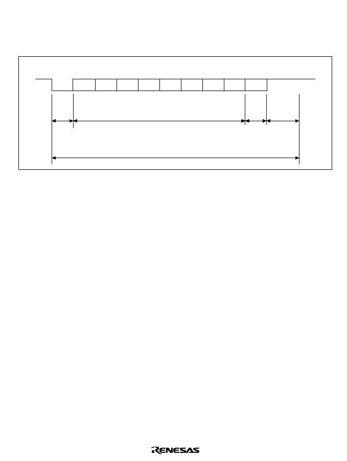
591
In asynchronous mode, the SCIF performs synchronization at the falling edge of the start bit in
reception. The SCIF samples the data on the eighth (fourth, second) pulse of a clock with a
frequency of 16 (8, 4) times the length of one bit, so that the transfer data is latched at the center of
each bit.
Serial
data
(LSB)
7 or 8 bits
One unit of transfer data (character or frame)
Parity
bit
1 bit,
or none
1 or
2 bits
1
1
0
D0
D1
D2
D3
D4
D5
D6
D7
0/1
1
1
Idle state (mark state)
Start
bit
1 bit
(MSB)
Transmit/receive data
Stop
bit(s)
Figure 14.3 Data Format in Asynchronous Communication
(Example with 8-Bit Data, Parity, Two Stop Bits, LSB-First Transfer)
Transmit/Receive Format: Table 14.10 shows the transmit/receive formats that can be used in
asynchronous mode. Any of 12 transmit/receive formats can be selected by means of settings in
the serial mode register (SCSMR).

592
Table 14.10
Serial Transmit/Receive Formats (Asynchronous Mode)
SCSMR Settings
Serial Transmit/Receive Format and Frame Length
CHR PE
MP
STOP
1
2
3
4
5
6
7
8
9
10
11
12
0
0
0
0
S
8-bit data
STOP
1
S
8-bit data
STOP STOP
1
0
S
8-bit data
P
STOP
1
S
8-bit data
P
STOP STOP
1
0
0
S
8-bit data
STOP
1
S
8-bit data
STOP STOP
1
0
S
7-bit data
P
STOP
1
S
7-bit data
P
STOP STOP
0
*
1
0
S
8-bit data
MPB STOP
*
1
S
8-bit data
MPB STOP STOP
1
*
0
S
7-bit data
MPB STOP
*
1
S
7-bit data
MPB STOP STOP
Note:
An asterisk in the table means "Don't care."
Legend
S:
Start bit
STOP: Stop bit
P:
Parity bit
MPB: Multiprocessor bit

593
Clock: Either an internal clock generated by the built-in baud rate generator or an external clock
input at the SCK pin can be selected as the SCI's serial clock, according to the setting of the C/
A
bit in SCSMR and the CKE1 and CKE0 bits in SCSCR. For details of SCIF clock source
selection, see table 14.9.
When an external clock is input at the SCK pin, the input clock frequency should be 16, 8, or 4
times the bit rate used.
When the SCIF is operated on an internal clock, the clock can be output from the SCK pin. The
frequency of the clock output in this case is 16, 8, or 4 times the bit rate.
Data Transmit/Receive Operations
∑
SCIF Initialization (Asynchronous Mode)
Before transmitting and receiving data, it is necessary to clear the TE and RE bits to 0 in
SCSCR, then initialize the SCIF as described below.
When the operating mode, communication format, etc., is changed, the TE and RE bits must be
cleared to 0 before making the change using the following procedure. When the TE bit is
cleared to 0, the transmit shift register (SCTSR) is initialized. Note that clearing the TE and RE
bits to 0 does not change the contents of the serial status 1 register (SC1SSR), the transmit
FIFO data register (SCFTDR), or the receive FIFO data register (SCFRDR). The TE bit should
not be cleared to 0 until all transmit data has been transmitted and the TEND flag has been set
in SC1SSR. It is possible to clear the TE bit to 0 during transmission, but the data being
transmitted will go to the high-impedance state after TE is cleared. Also, before starting
transmission by setting TE again, the TFRST bit should first be set to 1 in SCFCR to reset
SCFTDR.
When an external clock is used the clock should not be stopped during operation, including
initialization, since operation will be unreliable in this case.
Figure 14.4 shows a sample SCIF initialization flowchart.
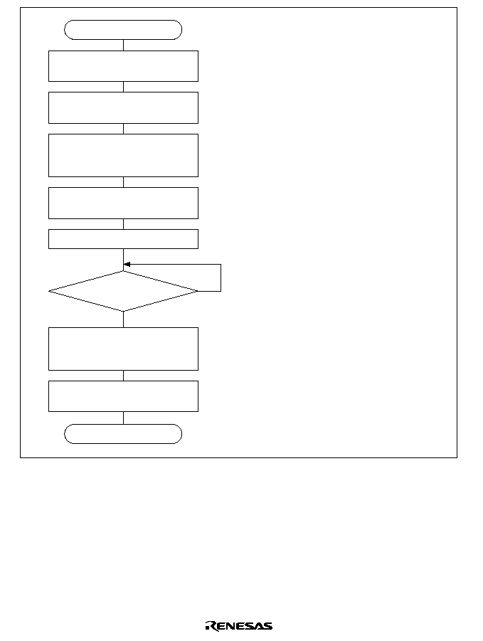
594
Initialization
Set TFRST and RFRST bits
to 1 in SCFCR
Set CKE1 and CKE0 bits
in SCSCR (leaving TE and
RE bits cleared to 0)
Set transmit/receive format
in SCSMR
Set value in SCBRR
1-bit interval elapsed?
Set RTRG1≠0 and TTRG1≠0 bits
in SCFCR, and clear TFRST
and RFRST bits to 0
Set TE or RE bit to 1 in SCSCR,
and set RIE, TIE, and MPIE bits
End
1
2
3
Clear TE and RE bits
to 0 in SCSCR
4
1. Set the clock selection in SCSCR.
Be sure to clear bits RIE, TIE, and
MPIE, and bits TE and RE, to 0.
When clock output is selected in
asynchronous mode, it is output
immediately after SCSCR settings are
made.
Select input or output for the SCK pin
with the PFC.
2. Set the transmit/receive format in
SCSMR.
When using IrDA mode, also set
SCIFMR.
3. Write a value corresponding to the bit
rate into the bit rate register (SCBRR).
(Not necessary if an external clock is
used.)
4. Wait at least one bit interval, then set
the TE bit or RE bit in SCSCR to 1.
Also set the RIE, TIE, and MPIE bits.
Setting the TE and RE bits enables
the TxD and RxD pins to be used.
When transmitting, the SCIF will go to
the mark state; when receiving, it will
go to the idle state, waiting for a start
bit.
Yes
No
Wait
Figure 14.4 Sample SCIF Initialization Flowchart
∑
Serial Data Transmission (Asynchronous Mode)
Figure 14.5 shows a sample flowchart for serial transmission.
Use the following procedure for serial data transmission after enabling the SCIF for
transmission.
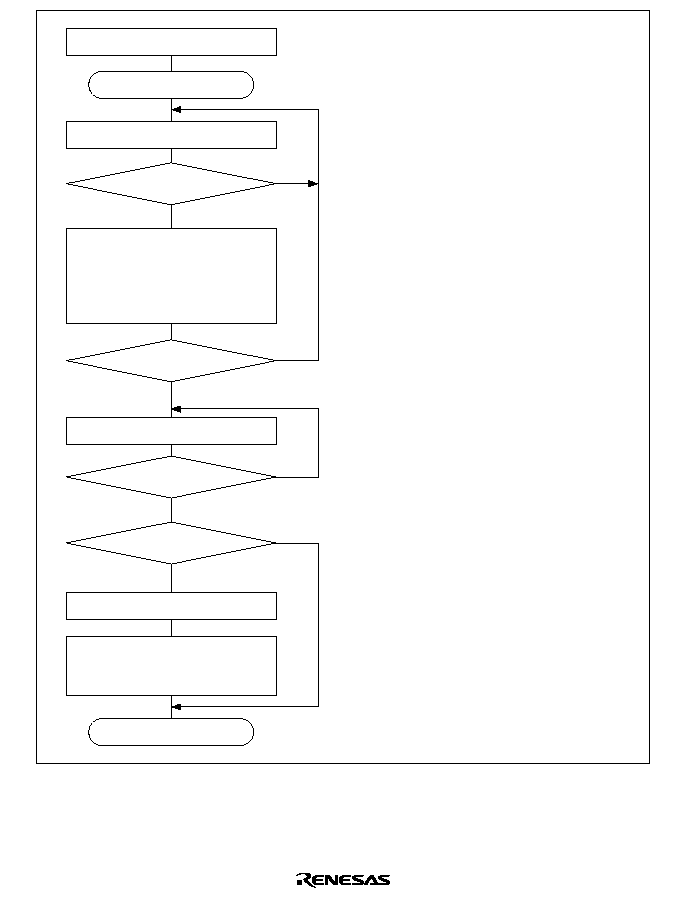
595
End of transmission
Read TDFE bit in SC1SSR
Write {16 ≠ (transmit trigger set
number)} bytes of transmit
data to SCFTDR, and clear
TDFE bit to 0 in SC1SSR after
reading TDFE = 1
TDFE = 1?
All data transmitted?
Read TEND bit in SC1SSR
TEND = 1?
Break output?
Clear DR to 0
Clear TE bit to 0 in SCSCR,
and set TxD pin as output
port with PFC
Start of transmission
Initialization
Yes
No
No
No
No
Yes
Yes
Yes
1
2
3
4
1. PFC initialization: Set the TxD pin, and
the SCK pin if necessary, with the PFC.
2. SCIF status check and transmit data
write: Read the serial status 1 register
(SC1SSR) and check that the TDFE bit is
set to 1, then write transmit data to the
transmit FIFO data register (SCFTDR)
and clear the TDFE bit to 0 after reading
TDFE = 1. The TEND bit is cleared
automatically when transmission is
started by writing transmit data.
The number of data bytes that can be
written is {16 ≠ (transmit trigger set
number)}.
3. Serial transmission continuation
procedure: To continue serial
transmission, read 1 from the TDFE bit to
confirm that writing is possible, then write
data to SCFTDR, and then clear the
TDFE bit to 0. (Checking and clearing of
the TDFE bit is automatic when the
DMAC is activated by a transmit-FIFO-
data-empty interrupt (TXI) request, and
data is written to SCFTDR.)
4. Break output at the end of serial
transmission: To output a break in serial
transmission, clear the port data register
(DR) to 0, then clear the TE bit to 0 in
SCSCR, and set the TxD pin as an output
port with the PFC.
In steps 2 and 3, the number of transmit data
bytes that can be written can be ascertained
from the number of transmit data bytes in
SCFTDR indicated in the upper 8 bits of the
FIFO data count register (SCFDR).
Figure 14.5 Sample Serial Transmission Flowchart

596
In serial transmission, the SCIF operates as described below.
1. When data is written to the transmit FIFO data register (SCFTDR), the SCIF transfers the data
to the transmit shift register (SCTSR), and starts transmitting. Check that the TDFE flag is set
to 1 in the serial status 1 register (SC1SSR) before writing transmit data to SCFTDR. The
number of data bytes that can be written is at least {16 ≠ (transmit trigger set number)}.
2. When data is transferred from SCFTDR to SCTSR and transmission is started, transmit
operations are performed continually until there is no transmit data left in SCFTDR. If the
number of data bytes in SCFTDR falls to or below the transmit trigger number set in the FIFO
control register (SCFCR) during transmission, the TDFE flag is set. If the TE bit setting in the
serial control register (SCSCR) is 1 at this time, a transmit-FIFO-data-empty interrupt (TXI) is
requested.
The serial transmit data is sent from the TxD pin in the following order.
a. Start bit: One 0-bit is output.
b. Transmit data: 8-bit or 7-bit data is output in LSB-first or MSB-first order according to the
setting of the TLM bit in SC2SSR.
c. Parity bit or multiprocessor bit: One parity bit (even or odd parity), or one multiprocessor
bit is output. (A format in which neither a parity bit nor a multiprocessor bit is output can
also be selected.)
d. Stop bit(s): One or two 1-bits (stop bits) are output.
e. Mark state: 1 is output continuously until the start bit that starts the next transmission is
sent.
3. The SCIF checks for transmit data in SCFTDR at the timing for sending the stop bit. If there is
data in SCFTDR, it is transferred to SCTSR, the stop bit is sent, and then serial transmission of
the next frame is started.
If there is no transmit data in SCFTDR, the TEND flag is set to 1 in the serial status 1 register
(SC1SSR), the stop bit is sent, and then the line goes to the mark state in which 1 is output
continuously.
Figure 14.6 shows an example of the operation for transmission in asynchronous mode.

597
Serial
data
1
0
D0
D1
D7
0/1
1
0
D0
D1
D7
0/1
1
1
TDFE
TEND
Start
bit
Data
Parity
bit
Stop
bit
Start
bit
Idle state
(mark state)
Data
Parity
bit
Stop
bit
TXI interrupt
request
Data written to SCFTDR
and TDFE flag cleared
to 0 by TXI interrupt handler
One frame
TXI interrupt
request
Figure 14.6 Example of Transmit Operation in Asynchronous Mode
(Example with 8-Bit Data, Parity, One Stop Bit, LSB-First Transfer)
4. When modem control is enabled, transmission can be stopped and restarted in accordance with
the
CTS input value. When CTS is set to 1, if transmission is in progress, the line goes to the
mark state after transmission of one frame. When
CTS is set to 0, the next transmit data is
output starting from the start bit.
Figure 14.7 shows an example of the operation when modem control is used.
Serial
data
0
D0
D1
D7
0/1
0
D0
D1
D7
0/1
CTS
Drive high at this point
before stop bit
Start
bit
Parity
bit
Stop
bit
Start
bit
Figure 14.7 Example of Operation Using Modem Control (
CTS)

598
∑
Serial Data Reception (Asynchronous Mode)
Figure 14.8 shows a sample flowchart for serial reception.
Use the following procedure for serial data reception after enabling the SCIF for reception.
1. PFC initialization: Set the RxD pin, and
the SCK pin if necessary, with the PFC.
2. Receive error handling and break
detection: Read ER, BRK, FER, PER,
and DR in SC1SSR, and ORER in
SC2SSR, to check whether a receive
error has occurred.
If a receive error has occurred, read the
ER, BRK, FER, PER, and DR flags in
SC1SSR and the ORER flag in SC2SSR
to identify the error. After performing the
appropriate error handling, ensure that
the ORER, BRK, DR, and ER bits are all
cleared to 0. Reception cannot be
resumed if the ORER bit is set to 1. The
setting of the EI bit in SC2SSR
determines whether reception is
continued or halted when any of
PER3≠0 or FER3≠0 is set to 1.
In the case of a framing error, a break
can be detected by reading the value of
the RxD pin.
3. SCIF status check and receive data
read: Read the serial status 1 register
(SC1SSR) and check that RDF = 1, then
read receive data from the receive FIFO
data register (SCFRDR) and clear the
RDF bit to 0. Transition of the RDF bit
from 0 to 1 can also be identified by
means of an RXI interrupt.
4. Serial reception continuation procedure:
To continue serial reception, read at
least the receive trigger set number of
data bytes from SCFRDR, and write 0 to
the RDF flag after reading 1 from it. The
number of receive data bytes in
SCFRDR can be ascertained by reading
the lower bits of the FIFO data count
register (SCFDR). (The RDF bit is
cleared automatically when the DMAC is
activated by an RXI interrupt and the
SCFRDR value is read.)
Initialization
Start of reception
Read ER, BRK, FER, PER,
and DR bits in SC1SSR, and
ORER bit in SC2SSR
ER
BRK
FER
PER
DR
ORER = 1?
Error handling
Read RDF flag in SC1SSR
RDF = 1?
Read receive data
from SCFRDR, and clear
RDF flag to 0 in SC1SSR
All data received?
Clear RE bit to 0 in SCSCR
End of reception
Yes
No
Yes
No
No
Yes
1
2
3
4
Figure 14.8 Sample Serial Reception Flowchart (1)
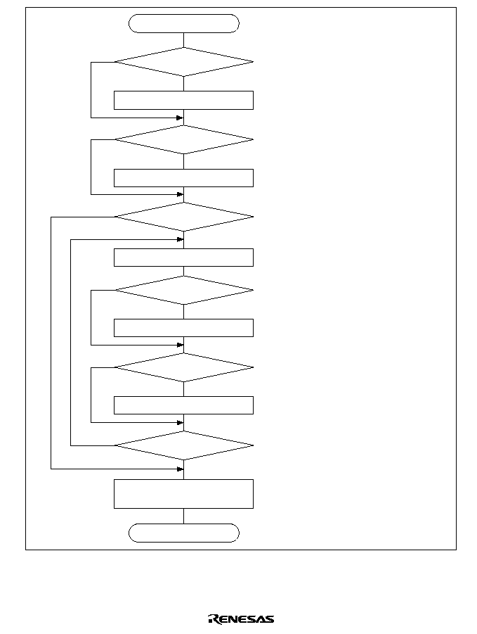
599
1. Whether a framing error or
parity error has occurred in the
receive data read from
SCFRDR can be ascertained
from the FER and PER bits in
SC1SSR.
2. When a break signal is
received, receive data is not
transferred to SCFRDR while
the BRK flag is set. However,
note that the H'00 break data
in which a framing error
occurred is stored as the last
data in SCFRDR.
Error handling
Overrun error handling
ORER = 1?
BRK = 1?
DR = 1?
FER = 1?
Framing error handling
PER = 1?
Parity error handling
All data read?
Clear ORER, BRK, DR, and
ER flags to 0
End
No
No
No
No
No
No
Yes
Yes
Yes
Yes
Yes
Yes
Clear RE bit to 0 in SCSCR
Read receive data from SCFRDR
1
2
Figure 14.8 Sample Serial Reception Flowchart (2)

600
In serial reception, the SCIF operates as described below.
1. The SCIF monitors the communication line, and if a 0 start bit is detected, performs internal
synchronization and starts reception.
2. The received data is stored in SCRSR in LSB-to-MSB order or MSB-to-LSB order according
to the setting of the RLM bit in SC2SSR.
3. The parity bit and stop bit are received.
After receiving these bits, the SCIF carries out the following checks.
a. Parity check: The SCIF checks whether the number of 1-bits in the receive data agrees with
the parity (even or odd) set in the O/
E bit in the serial mode register (SCSMR).
b. Stop bit check: The SCIF checks whether the stop bit is 1. If there are two stop bits, only
the first is checked.
c. Status check: The SCIF checks whether receive data can be transferred from the receive
shift register (SCRSR) to SCFRDR.
d. Break check: The SCIF checks that the BRK flag is 0, indicating no break.
If all the above checks are passed, the receive data is stored in SCFRDR. If a receive error is
detected in the error check, the operation is as shown in table 14.11.
Note:
No further receive operations can be performed when an overrun error has occurred. The
setting of the EI bit in SC2SSR determines whether reception is continued or halted when
a framing error or parity error occurs.
Also, as the RDF flag is not set to 1 when receiving, the error flags must be cleared to 0.
4. If the RIE bit setting in SCSCR is 1 when the RDF or DR flag is set to 1, a receive-FIFO-data-
full interrupt (RXI) is requested.
If the RIE bit setting in SCSCR is 1 when the ORER, PER, or FER flag is set to 1, a receive-
error interrupt (ERI) is requested.
If the RIE bit setting in SCSCR is 1 when the BRK flag is set to 1, a break-receive interrupt
(BRI) is requested.
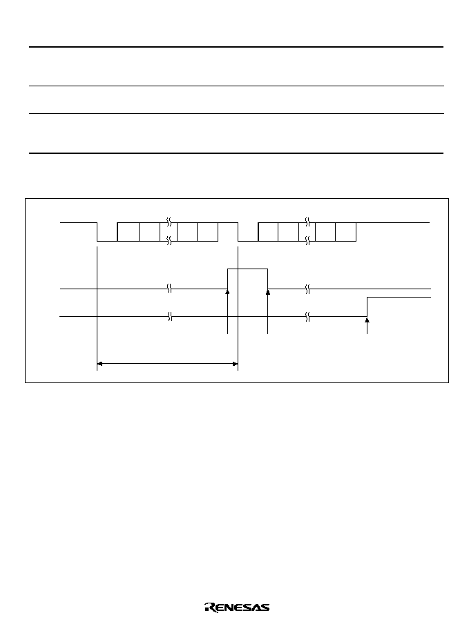
601
Table 14.11
Receive Error Conditions
Receive Error
Abbreviation
Condition
Data Transfer
Overrun error
ORER
Next serial receive operation is
completed while there are 16
receive data bytes in SCFRDR
Receive data is not transferred
from SCRSR to SCFRDR
Framing error
FER
Stop bit is 0
Receive data is transferred from
SCRSR to SCFRDR
Parity error
PER
Received data parity differs
from that (even or odd) set in
SCSMR
Receive data is transferred from
SCRSR to SCFRDR
Figure 14.9 shows an example of the operation for reception in asynchronous mode.
Serial
data
1
0
D0
D1
D7
0/1
1
0
D0
D1
D7
0/1
1
1
RDF
FER
Start
bit
Parity
bit
Stop
bit
Start
bit
Data
Data
Parity
bit
Stop
bit
Idle state
(mark state)
RXI interrupt
request
One frame
Data read and RDF
flag cleared to 0 by
RXI interrupt handler
ERI interrupt request
due to framing error
Figure 14.9 Example of SCIF Receive Operation
(Example with 8-Bit Data, Parity, One Stop Bit, LSB-First Transfer)
5. When modem control is enabled, the
RTS signal is output when SCFRDR is empty. When
RTS is 0, reception is possible. When RTS is 1, this indicates that SCFRDR is full and
reception is not possible.
Figure 14.10 shows an example of the operation when modem control is used.

602
Serial
data
0
D0
D1
D2
D7
0/1
0
1
RTS
Start
bit
Parity
bit
Start
bit
Figure 14.10 Example of Operation Using Modem Control (
RTS)
14.3.3
Multiprocessor Communication Function
The multiprocessor communication function performs serial communication using a
multiprocessor format, in which a multiprocessor bit is added to the transfer data, in asynchronous
mode. Use of this function enables data transfer to be performed among a number of processors
sharing a serial communication line.
When multiprocessor communication is carried out, each receiving station is addressed by a
unique ID code.
The serial communication cycle consists of two cycles: an ID transmission cycle which specifies
the receiving station, and a data transmission cycle. The multiprocessor bit is used to differentiate
between the ID transmission cycle and the data transmission cycle.
The transmitting station first sends the ID of the receiving station with which it wants to perform
serial communication as data with a 1 multiprocessor bit added. It then sends transmit data as data
with a 0 multiprocessor bit added.
The receiving stations skip the data until data with a 1 multiprocessor bit is sent. When data with a
1 multiprocessor bit is received, each receiving stations compares that data with its own ID. The
station whose ID matches then receives the data sent next. Stations whose ID does not match
continue to skip the data until data with a 1 multiprocessor bit is again received. In this way, data
communication is carried out among a number of processors.
Figure 14.11 shows an example of inter-processor communication using a multiprocessor format.
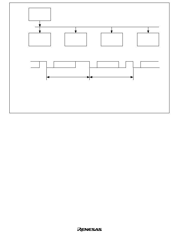
603
Transmitting
station
Receiving
station A
(ID = 01)
(ID = 02)
(ID = 03)
(ID = 04)
Serial communication line
Serial
data
ID transmission cycle:
Receiving station
specification
Data transmission cycle:
Data transmission
to receiving station
specified by ID
(MPB = 1)
(MPB = 0)
H'01
H'AA
Legend
MPB: Multiprocessor bit
Receiving
station B
Receiving
station C
Receiving
station D
Figure 14.11 Example of Inter-Processor Communication Using Multiprocessor Format
(Transmission of Data H'AA to Receiving Station A)
Transmit/Receive Formats: There are four transmit/receive formats. When the multiprocessor
format is specified, the parity bit specification is invalid. For details, see table 14.10.
Clock: See the section on asynchronous mode.
Data Transmit/Receive Operations
∑
SCI Initialization
See the section on asynchronous mode.
∑
Multiprocessor Serial Data Transmission
Figure 14.12 shows a sample flowchart for multiprocessor serial data transmission.
Use the following procedure for multiprocessor serial data transmission after enabling the
SCIF for transmission.
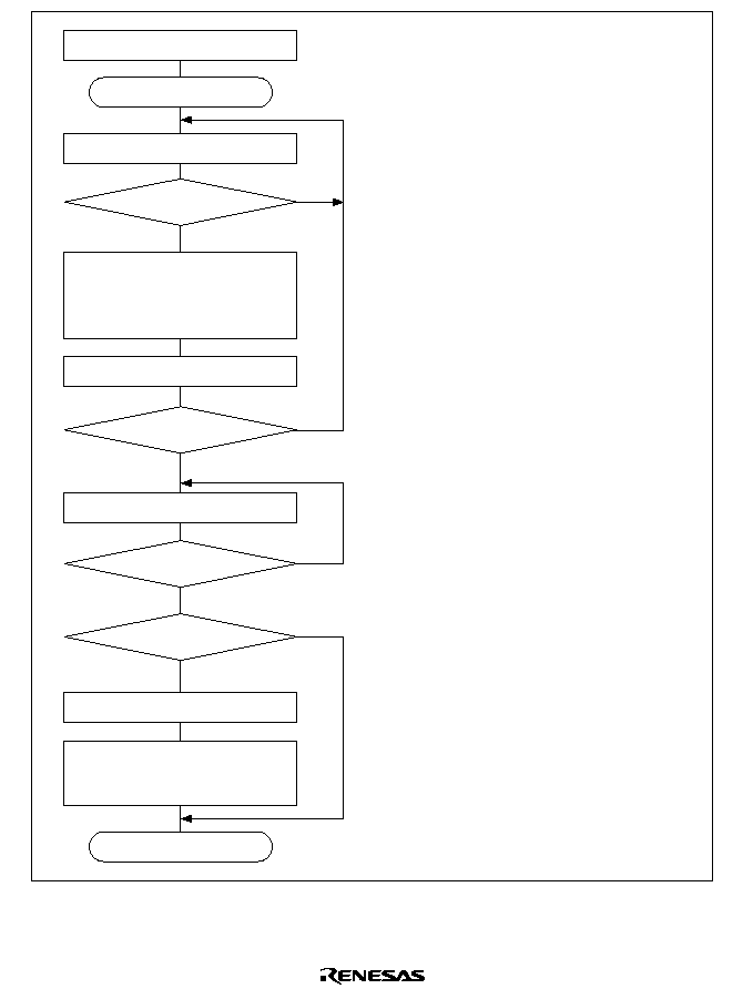
604
End of transmission
Read TDFE bit in SC1SSR
Write {16 ≠ (transmit trigger set
number)} bytes of transmit data
to SCFTDR, and set MPBT
in SC2SSR
TDFE = 1?
End of transmission?
Read TEND bit in SC2SSR
TEND = 1?
Break output?
Clear DR to 0
Clear TE bit to 0 in SCSCR,
and set TxD pin as output
port with PFC
Start of transmission
Initialization
Yes
No
No
No
No
Yes
Yes
Yes
1
2
3
4
1. PFC initialization: Set the TxD pin, and
the SCK pin if necessary, with the PFC.
2. SCIF status check and transmit data
write: Read the serial status 1 register
(SC1SSR) and check that the TDFE bit
is set to 1, then write transmit data to
the transmit FIFO data register
(SCFTDR). Set the MPBT bit to 0 or 1
in SC1SSR. Finally, clear the TDFE
and TEND flags to 0 after reading 1
from them.
The number of data bytes that can be
written is {16 ≠ (transmit trigger set
number)}.
3. Serial transmission continuation
procedure: To continue serial
transmission, read 1 from the TDFE bit
to confirm that writing is possible, then
write data to SCFTDR, and then clear
the TDFE bit to 0. (Checking and
clearing of the TDFE bit is automatic
when the DMAC is activated by a
transmit-FIFO-data-empty interrupt
(TXI) request, and data is written to
SCFTDR.)
4. Break output at the end of serial
transmission: To output a break in
serial transmission, clear the port data
register (DR) to 0, then clear the TE bit
to 0 in SCSCR, and set the TxD pin as
an output port with the PFC.
In steps 2 and 3, the number of transmit
data bytes that can be written can be
ascertained from the number of transmit
data bytes in SCFTDR indicated in the
upper 8 bits of the FIFO data count register
(SCFDR).
Clear TDFE and TEND flags to 0
Figure 14.12 Sample Multiprocessor Serial Transmission Flowchart

605
In serial transmission, the SCIF operates as described below.
1. When data is written to SCFTDR, the SCIF transfers the data to SCTSR and starts
transmitting. Check that the TDFE flag is set to 1 in SC1SSR before writing transmit data to
SCFTDR. The number of data bytes that can be written is at least {16 ≠ (transmit trigger set
number)}.
2. When data is transferred from SCFTDR to SCTSR and transmission is started, transmit
operations are performed continually until there is no transmit data left in SCFTDR. If the
number of data bytes in SCFTDR falls to or below the transmit trigger number set in SCFCR
during transmission, the TDFE flag is set to 1. If the TIE bit setting in SCSCR is 1 at this time,
a transmit-FIFO-data-empty interrupt (TXI) is requested.
The serial transmit data is sent from the TxD pin in the following order.
a. Start bit: One 0-bit is output.
b. Transmit data: 8-bit or 7-bit data is output in LSB-first or MSB-first order according to the
setting of the TLM bit in SC2SSR.
c. Multiprocessor bit: One multiprocessor bit (MPBT value) is output.
d. Stop bit(s): One or two 1-bits (stop bits) are output.
e. Mark state: 1 is output continuously until the start bit that starts the next transmission is
sent.
3. The SCIF checks for transmit data in SCFTDR at the timing for sending the stop bit. If there is
data in SCFTDR, it is transferred to SCTSR, the stop bit is sent, and then serial transmission of
the next frame is started.
If there is no transmit data in SCFTDR, the TEND flag is set to 1 in SC1SSR, the stop bit is
sent, and then the line goes to the mark state in which 1 is output continuously.
Figure 14.13 shows an example of SCIF operation for transmission using a multiprocessor
format.

606
Serial
data
1
0
D0
D1
D7
0/1
1
0
D0
D1
D7
0/1
1
1
TDFE
TEND
TXI interrupt
request
Start
bit
Data
Multi-
proces-
sor bit
Multi-
proces-
sor bit
Stop
bit
Start
bit
Stop
bit
Idle state
(mark state)
Data written to SCFTDR
and TDFE flag cleared
to 0 by TXI interrupt handler
TXI interrupt
request
One frame
Figure 14.13 Example of SCIF Transmit Operation
(Example with 8-Bit Data, Multiprocessor Bit, One Stop Bit, LSB-First Transfer)
∑
Multiprocessor Serial Data Reception
Figure 14.14 shows a sample flowchart for multiprocessor serial reception.
Use the following procedure for multiprocessor serial data reception after enabling the SCIF
for reception.
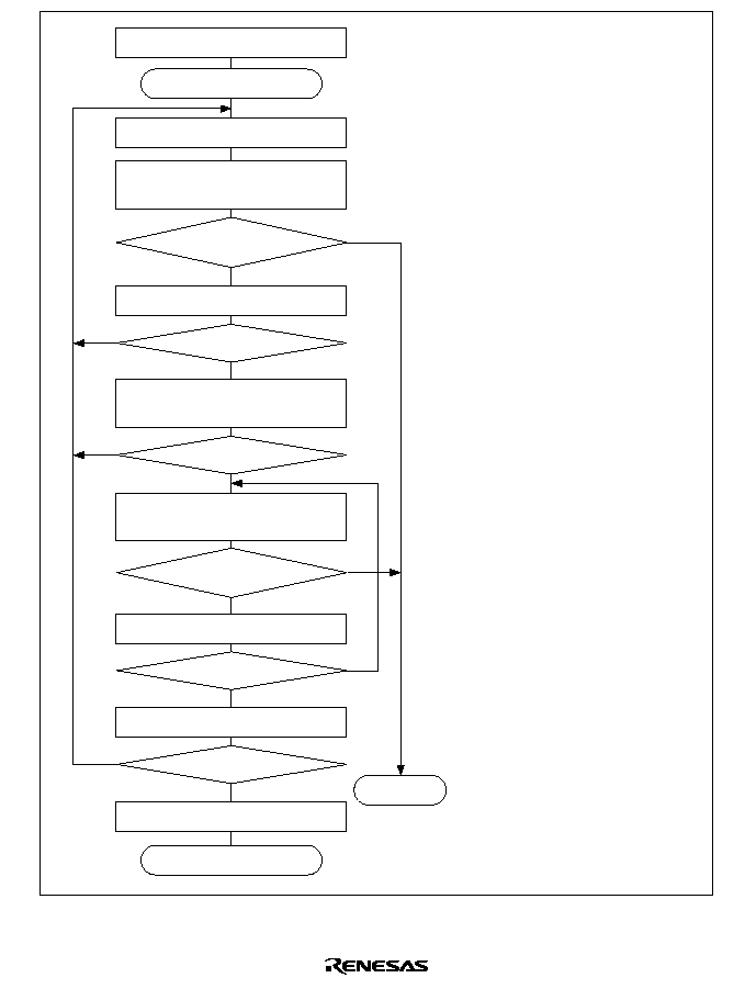
607
1. PFC initialization: Set the RxD pin,
and the SCK pin if necessary, with
the PFC.
2. ID reception cycle: Set the MPIE bit to
1 in SCSCR.
3. SCIF status check, ID reception and
comparison: Read SC1SSR and
check that the RDF bit is set to 1,
then read the receive data in the
receive FIFO data register (SCFRDR)
and compare it with this station's ID.
If the data is not this station's ID, set
the MPIE bit to 1 again, and clear the
RDF bit to 0.
If the data is this station's ID, clear
the RDF bit to 0.
4. Receive error handling and break
detection: Read the ER, BRK, FER,
and DR flags in SC1SSR and the
ORER flag in SC2SSR to check
whether a receive error has occurred.
If a receive error has occurred, read
the ER, BRK, FER, and DR flags in
SC1SSR and the ORER flag in
SC2SSR to identify the error. After
performing the appropriate error
handling, ensure that ER, BRK, DR,
and ORER are all cleared to 0. The
setting of the EI bit in SC2SSR
determines whether reception is
continued or halted when the ORER
bit is set to 1. In the case of a framing
error, a break can be detected by
reading the value of the RxD pin.
5. SCIF status check and receive data
read: Read the serial status 1 register
(SC1SSR) and check that RDF = 1,
then read receive data from the
receive FIFO data register
(SCFRDR).
Start of reception
Set MPIE bit to 1 in SCSCR
Read ER, BRK, FER, and DR bits in
SC1SSR, and ORER bit in SC2SSR
Initialization
BRK
DR
ER
ORER = 1?
Read RDF flag in SC1SSR
RDF = 1?
Read receive data from SCFRDR,
and clear RDF flag to 0 in SC1SSR
This station's ID?
Read BRK and DR bits in SC1SSR,
and ER bit in SC2SSR
BRK
DR
ER = 1?
Read RDF flag in SC1SSR
RDF = 1?
Read receive data from SCFRDR
All data received?
Clear RE bit to 0 in SCSCR
End of reception
Error handling
Yes
Yes
No
Yes
Yes
No
No
No
Yes
Yes
No
No
1
2
3
4
5
Figure 14.14 Sample Multiprocessor Serial Reception Flowchart (1)
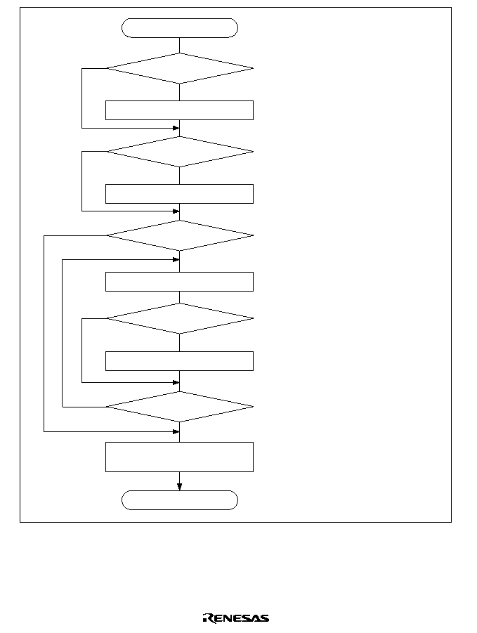
608
1. Whether a framing error has
occurred in the receive data read
from SCFRDR can be ascertained
from the FER bit in SC1SSR.
2. When a break signal is received,
receive data is not transferred to
SCFRDR while the BRK flag is
set. However, note that the last
data in SCFRDR is H'00 and the
break data in which a framing
error occurred is stored. However,
note that the H'00 break data in
which a framing error occurred is
stored as the last data in
SCFRDR.
Error handling
Clear RE bit to 0 in SCSCR
Overrun error handling
Read receive data from SCFRDR
Framing error handling
Clear ORER, BRK, DR,
and ER flags to 0
End
ORER = 1?
BRK = 1?
DR = 1?
FER = 1?
All data read?
No
No
No
No
1
2
No
Yes
Yes
Yes
Yes
Yes
Figure 14.14 Sample Multiprocessor Serial Reception Flowchart (2)
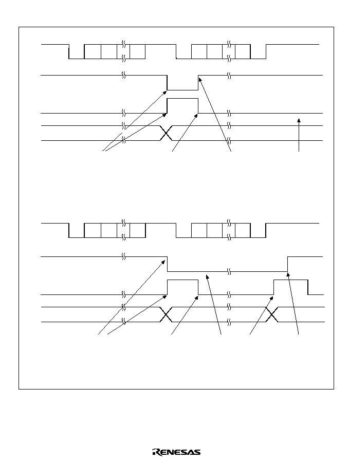
609
Figure 14.15 shows an example of SCIF operation for multiprocessor format reception.
1
0
D0
D1
D7
1
1
0
D0
D1
D7
0
1
1
MPB
MPB
ID1
ID2
Data2
Serial
data
1
0
D0
D1
D7
1
1
0
D0
D1
D7
0
1
1
MPB
MPB
Idle state
(mark state)
MPIE
RDF
SCFRDR value
ID1
Start
bit
Data (ID1)
Stop
bit
Start
bit
Stop
bit
Data (Data1)
Serial
data
MPIE
RDF
SCFRDR value
Start
bit
Data (ID2)
Stop
bit
Start
bit
Stop
bit
Data (Data2)
Idle state
(mark state)
RXI interrupt request
(multiprocessor interrupt)
MPIE = 0
SCFRDR data read
and RDF flag cleared
to 0 by RXI interrupt
handler
As data is not this
station's ID,
MPIE bit is set
to 1 again
RXI interrupt request
is not generated,
and SCFRDR
retains its state
RXI interrupt request
(multiprocessor interrupt)
MPIE = 0
SCFRDR data read
and RDF flag cleared
to 0 by RXI interrupt
handler
As data matches this
station's ID, reception
continues and data is
received by RXI
interrupt handler
(a) Data does not match station's ID
MPIE bit set
to 1 again
(b) Data matches station's ID
Figure 14.15 Example of SCIF Receive Operation
(Example with 8-Bit Data, Multiprocessor Bit, One Stop Bit, LSB-First Transfer)
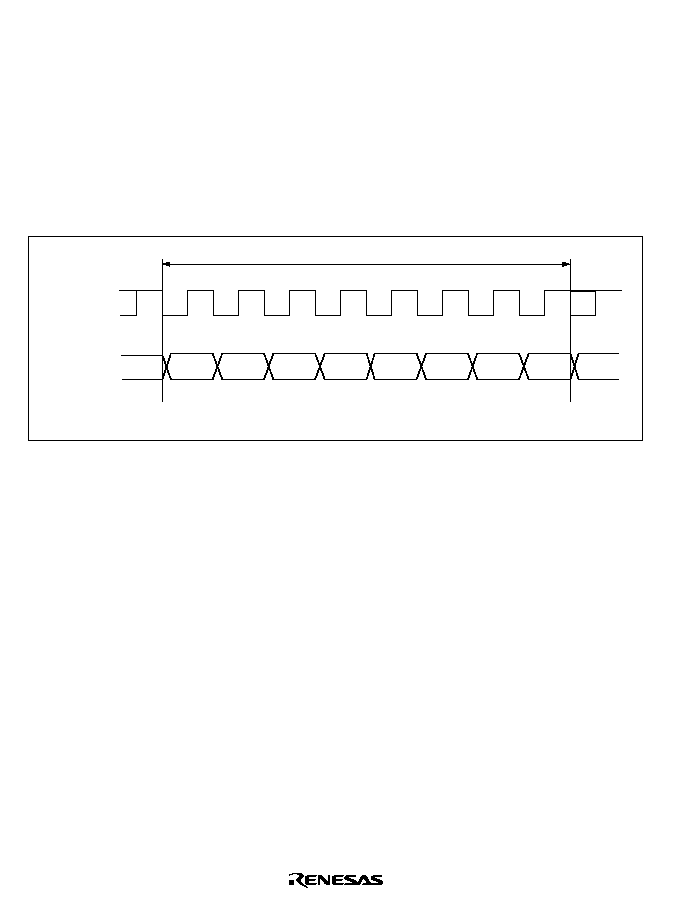
610
14.3.4
Operation in Synchronous Mode
In synchronous mode, data is transmitted or received in synchronization with clock pulses, making
it suitable for high-speed serial communication.
Inside the SCIF, the transmitter and receiver are independent units, enabling full-duplex
communication using a common clock. Both the transmitter and the receiver also have a 16-stage
FIFO buffer structure, so that data can be read or written during transmission or reception,
enabling continuous data transfer.
Figure 14.16 shows the general format for synchronous serial communication.
One unit of transfer data (character or frame)
Serial clock
Serial data
LSB
Bit 0
MSB
*
*
Don't care
Don't care
Note:
*
High except in continuous transmission/reception
Bit 1
Bit 2
Bit 3
Bit 4
Bit 5
Bit 6
Bit 7
Figure 14.16 Data Format in Synchronous Communication
(Example of LSB-First Transfer)
In synchronous serial communication, data on the communication line is output from one fall of
the serial clock to the next. Data is guaranteed valid at the rise of the serial clock.
In serial communication, each character is output starting with the LSB and ending with the MSB,
or vice versa, according to the setting of the TLM bit in the serial status 2 register (SC2SSR).
After the last data is output, the communication line remains in the state of the last data.
In synchronous mode, the SCIF receives data in synchronization with the fall of the serial clock.

611
Transmit/Receive Format: A fixed 8-bit data format is used. No parity or multiprocessor bits are
added.
Clock: Either an internal clock generated by the built-in baud rate generator or an external serial
clock input at the SCK pin can be selected, according to the setting of the C/
A bit in SCSMR and
the CKE1 and CKE0 bits in SCSCR. For details of SCIF clock source selection, see table 14.9.
When the SCIF is operated on an internal clock, the serial clock is output from the SCK pin.
Eight serial clock pulses are output in the transfer of one character, and when no
transmission/reception is performed the clock is fixed high. In receive-only operation, however,
the SCIF receives two characters as one unit, and so a 16-pulse serial clock is output. To perform
single-character receive operations, an external clock should be selected as the clock source.
Transmit/Receive Operations
∑
SCIF Initialization (Synchronous Mode)
Before transmitting and receiving data, it is necessary to clear the TE and RE bits to 0 in the
serial control register (SCSCR), then initialize the SCIF as described below.
When the operating mode, communication format, etc., is changed, the TE and RE bits must be
cleared to 0 before making the change using the following procedure. When the TE bit is
cleared to 0, the TDFE flag is set to 1 and the transmit shift register (SCTSR) is initialized.
Note that clearing the RE bit to 0 does not change the contents of the RDF, PER, FER, and
ORER flags, or the receive FIFO data register (SCFRDR).
Figure 14.17 shows a sample SCIF initialization flowchart.
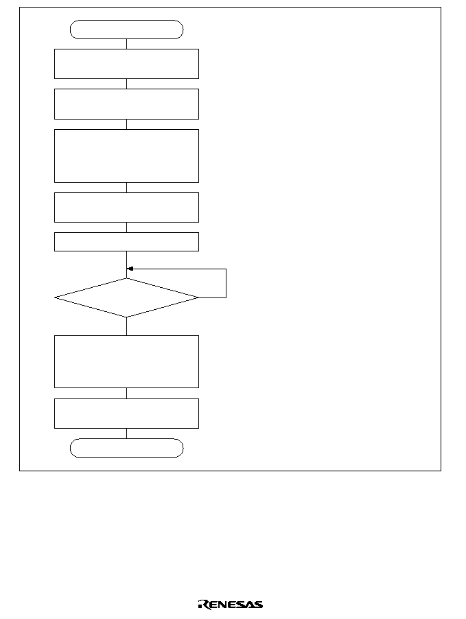
612
Initialization
Clear TE and RE bits to 0
in SCSCR
Clear TFRST and RFRST bits
to 1 in SCFCR
Set RIE, TIE, MPIE, CKE1,
and CKE0 bits in SCSCR
(leaving TE and RE bits
cleared to 0)
Set data transmit/receive format
in SCSMR
Set RTRG1≠0 bits and
TTRG1≠0 bits in SCFCR,
and clear TFRST and
RFRST bits to 0
Set TE or RE bit to 1 in SCSCR,
and set RIE, TIE, and MPIE bits
Set value in SCBRR
1-bit interval elapsed?
End
1. Set the clock selection in SCSCR.
Be sure to clear bits RIE, TIE,
MPIE, TE, and RE to 0.
2. Set the transmit/receive format in
the serial mode register (SCSMR).
3. Write a value corresponding to the
bit rate into the bit rate register
(SCBRR). (Not necessary if an
external clock is used.)
4. Wait at least one bit interval, then
set the TE bit or RE bit to 1 in
SCSCR.
Also set the RIE, TIE, and MPIE
bits. Setting the TE and RE bits
simultaneously enables the TxD
and RxD pins to be used.
Yes
No
Wait
2
3
4
1
Figure 14.17 Sample SCIF Initialization Flowchart
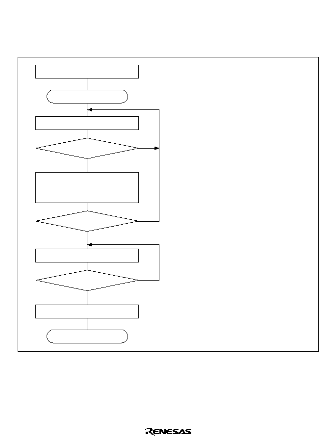
613
∑
Serial Data Transmission (Synchronous Mode)
Figure 14.18 shows a sample flowchart for serial transmission.
Use the following procedure for serial data transmission after enabling the SCIF for
transmission.
End
Read TDFE flag in SC1SSR
Initialization
Write transmit data to SCFTDR
and clear TDFE flag to 0
in SC1SSR
TDFE = 1?
All data transmitted?
Read TEND flag in SC1SSR
TEND = 1?
Clear TE bit to 0 in SCSCR
Start of transmission
Yes
No
No
No
2
1
3
Yes
Yes
1. PFC initialization: Set the TxD pin,
and the SCK pin if necessary, with
the PFC.
2. SCIF status check and transmit data
write: Read SC1SSR and check that
TDFE =1, then write transmit data to
the transmit FIFO data register
(SCFTDR) and clear the TDFE flag
to 0.
3. Serial transmission continuation
procedure: To continue serial
transmission, read 1 from the TDFE
flag to confirm that writing is possible,
then write data to SCFTDR, and then
clear the TDFE flag to 0.
Figure 14.18 Sample Serial Transmission Flowchart

614
In serial transmission, the SCIF operates as described below.
1. When data is written to the transmit FIFO data register (SCFTDR), the SCIF transfers the data
from SCFTDR to the transmit shift register (SCTSR), and starts transmitting. Check that the
TDFE flag is set to 1 in the serial status 1 register (SC1SSR) before writing transmit data to
SCFTDR. The number of data bytes that can be written is at least {16 ≠ (transmit trigger set
number)}.
2. When data is transferred from SCFTDR to SCTSR and transmission is started, transmit
operations are performed continually until there is no transmit data left in SCFTDR. If the
number of data bytes in SCFTDR falls to or below the transmit trigger number set in the FIFO
control register (SCFCR) during transmission, the TDFE flag is set. If the TIE bit setting in the
serial control register (SCSCR) is 1 at this time, a transmit-FIFO-data-empty interrupt (TXI) is
requested.
When clock output mode has been set, the SCIF outputs eight serial clock pulses for one unit
of data.
When use of an external clock has been specified, data is output in synchronization with the
input clock.
The serial transmit data is sent from the TxD pin starting with the LSB (bit 0) or MSB (bit 7)
according to the setting of the TLM bit in the serial status 2 register (SC2SSR).
3. The SCIF checks for transmit data in SCFTDR at the timing for sending the last bit. If there is
transmit data in SCFTDR, it is transferred to SCTSR and then serial transmission of the next
frame is started. If there is no transmit data in SCFTDR, the TEND flag is set to 1 in the serial
status 1 register (SC1SSR), the last bit is sent, and then the transmit data pin (TxD) holds its
state.
4. After completion of serial transmission, the SCK pin is fixed high.
Figure 14.19 shows an example of SCIF operation in transmission.
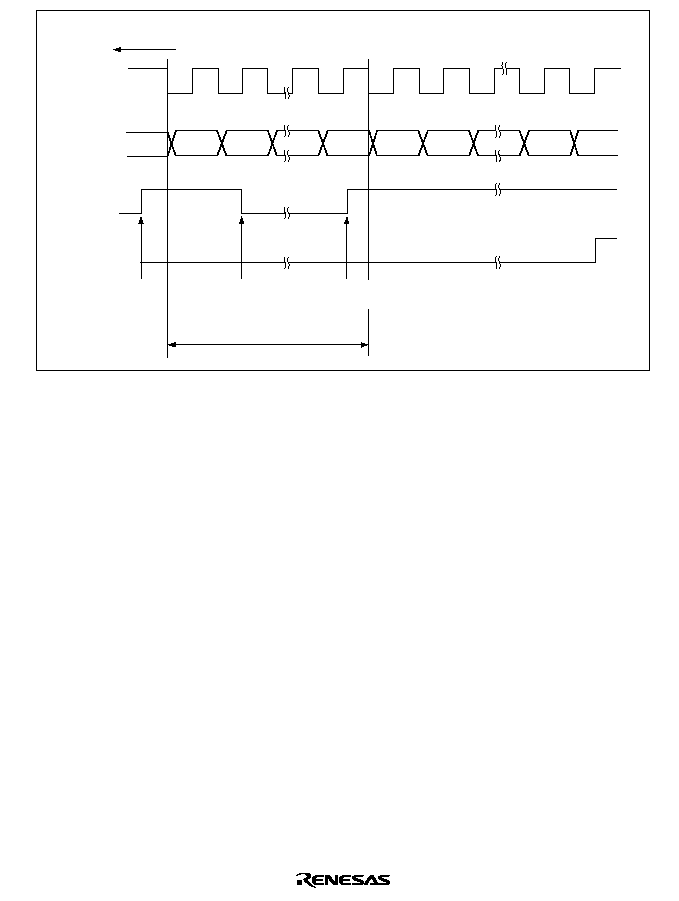
615
LSB
TDFE
TEND
Bit 0
Bit 1
Bit 7
Bit 0
Bit 1
Bit 6
Bit 7
Transfer
direction
Serial clock
Serial data
TXI interrupt
request
Data written to SCFTDR
and TDFE flag cleared
to 0 by TXI interrupt
handler
One frame
TXI interrupt
request
MSB
Figure 14.19 Example of SCIF Transmit Operation (Example of LSB-First Transfer)
∑
Serial Data Reception (Synchronous Mode)
Figure 14.20 shows a sample flowchart for serial reception.
Use the following procedure for serial data reception after enabling the SCIF for reception.
When changing the operating mode from asynchronous to synchronous without resetting
SCFRDR and SCFTDR by means of SCIF initialization, be sure to check that the ORER,
PER3 to PER0, and FER3 to FER0 flags are all cleared to 0. The RDF flag will not be set if
any of flags FER3 to FER0 or PER3 to PER0 are set to 1, and neither transmit nor receive
operations will be possible.
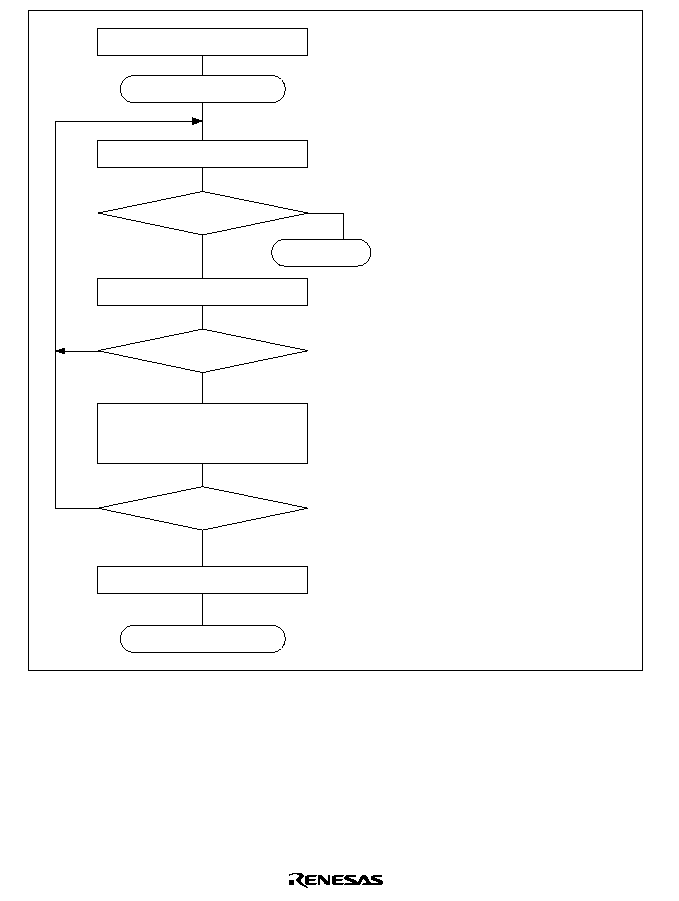
616
1. PFC initialization: Set the RxD pin,
and the SCK pin if necessary, with
the PFC.
2. Receive error handling: If a
receive error occurs, read the
ORER flag in SC2SSR, and after
performing the appropriate error
handling, clear the ORER flag to
0. Transmission/reception cannot
be resumed if the ORER flag is
set to 1.
3. SCIF status check and receive
data read: Read the serial status 1
register (SC1SSR) and check that
RDF = 1, then read receive data
from the receive FIFO data
register (SCFRDR) and clear the
RDF flag to 0. Transition of the
RDF flag from 0 to 1 can also be
identified by an RXI interrupt.
4. Serial reception continuation
procedure: To continue serial
reception, read at least the receive
trigger set number of data bytes
from SCFRDR, and write 0 to the
RDF flag after reading 1 from it.
The number of receive data bytes
in SCFRDR can be ascertained by
reading the lower 8 bits of the
FIFO data count register
(SCFDR). (The RDF bit is cleared
automatically when the DMAC is
activated by an RXI interrupt and
the SCFRDR value is read.)
Start of reception
Read ORER flag in SC2SSR
Initialization
Error handling
2
3
4
1
Read RDF flag in SC1SSR
RDF = 1?
Read receive data
from SCFRDR, and clear RDF
flag to 0 in SC1SSR
All data received?
Clear RE bit to 0 in SCSCR
End of reception
Yes
No
Yes
No
No
Yes
ORER = 1?
Figure 14.20 Sample Serial Reception Flowchart (1)
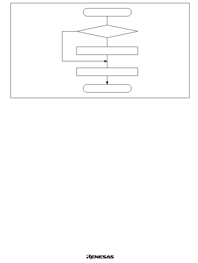
617
Error handling
Overrun error handling
Yes
No
ORER = 1?
Clear ORER flag to 0 in SC2SSR
End
Figure 14.20 Sample Serial Reception Flowchart (2)
In serial reception, the SCIF operates as described below.
1. The SCIF performs internal initialization in synchronization with serial clock input or output.
2. The received data is stored in the receive shift register (SCRSR) in LSB-to-MSB order or
MSB-to-LSB order according to the setting of the RLM bit in SC2SSR.
After reception, the SCIF checks whether the receive data can be transferred from SCRSR to
the receive FIFO data register (SCFRDR). If this check is passed, the receive data is stored in
SCFRDR.
If a receive error is detected in the error check, the operation is as shown in table 14.11.
Neither transmit nor receive operations can be performed subsequently when a receive error
has been found in the error check.
Also, as the RDF flag is not set to 1 when receiving, the flag must be cleared to 0.
3. If the RIE bit setting in the serial control register (SCSCR) is 1 when the RDF flag is set to 1, a
receive-FIFO-data-full interrupt (RXI) is requested. If the RIE bit setting in SCRSR is 1 when
the ORER flag is set to 1, a receive-error interrupt (ERI) is requested.
Figure 14.21 shows an example of SCIF operation in reception.

618
Serial clock
Serial data
Transfer
direction
Data read from SCFRDR
and RDF flag cleared to 0
by RXI interrupt handler
RXI interrupt
request
RDF
ORER
Bit 7
Bit 0
Bit 7
Bit 0
Bit 1
Bit 6
Bit 7
RXI interrupt
request
ERI interrupt
request due
to overrun error
One frame
Figure 14.21 Example of SCIF Receive Operation (Example of LSB-First Transfer)
∑
Simultaneous Serial Data Transmission and Reception (Synchronous Mode)
Figure 14.22 shows a sample flowchart for simultaneous serial transmit and receive operations.
Use the following procedure for simultaneous serial data transmit and receive operations after
enabling the SCIF for transmission and reception.
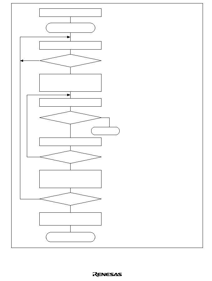
619
1. PFC initialization: Set the TxD and
RxD pins, and the SCK pin if
necessary, with the PFC.
2. SCIF status check and transmit data
write: Read SC1SSR and check that
the TDFE flag is set to 1, then write
transmit data to SCFTDR and clear
the TDFE flag to 0. Transition of the
TDFE flag from 0 to 1 can also be
identified by a TXI interrupt.
3. Receive error handling: If a receive
error occurs, read the ORER flag in
SC2SSR, and after performing the
appropriate error handling, clear the
ORER flag to 0.
Transmission/reception cannot be
resumed if the ORER flag is set to 1.
4. SCIF status check and receive data
read: Read SC1SSR and check that
the RDF flag is set to 1, then read
receive data from SCFRDR and
clear the RDF flag to 0. Transition of
the RDF flag from 0 to 1 can also be
identified by an RXI interrupt.
5. Serial transmission/reception
continuation procedure: To continue
serial transmission/reception, finish
reading the RDF flag, reading
SCFRDR, and clearing the RDF flag
to 0, before the MSB (bit 7) of the
current frame is received. Also,
before the MSB (bit 7) of the current
frame is transmitted, read 1 from the
TDFE flag to confirm that writing is
possible, then write data to SCFTDR
and clear the TDFE flag to 0.
Note: When switching from transmitting
or receiving to simultaneous
transmitting and receiving, first
clear the TE bit and RE bit to 0,
then set the TE bit and RE bit to
1 simultaneously.
Read TDFE flag in SC1SSR
Initialization
1
2
4
5
3
Write transmit data
to SCFTDR and clear TDRE
flag to 0 in SC1SSR
Read ORER flag in SC2SSR
Read RDF flag in SC1SSR
Read receive data
from SCFRDR, and clear RDF
flag to 0 in SC1SSR
Clear TE and RE bits to 0
in SCSCR
Error handling
Start of transmission/
reception
TDFE = 1?
ORER = 1?
RDF = 1?
All data transferred?
End of transmission/
reception
Yes
No
Yes
No
No
Yes
Yes
No
Figure 14.22 Sample Flowchart for Serial Data Transmission and Reception
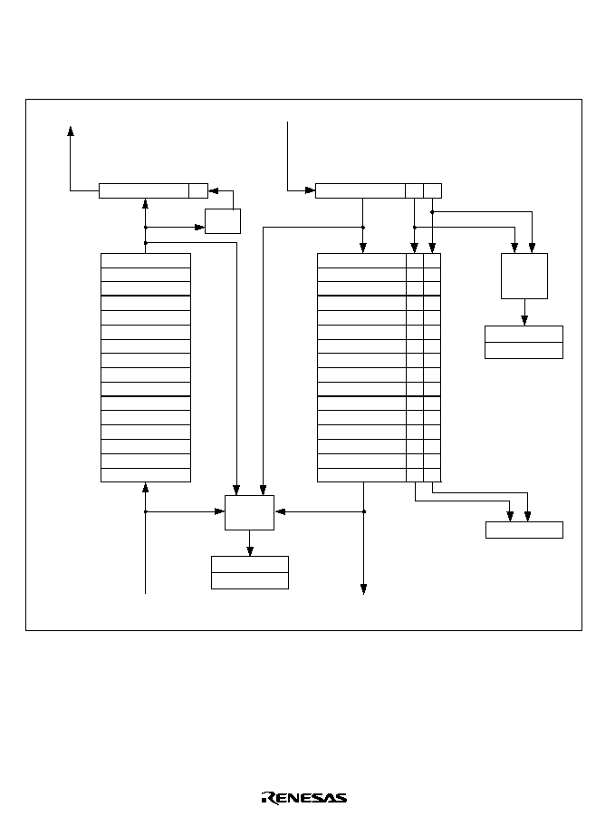
620
14.3.5
Use of Transmit/Receive FIFO Buffers
The SCIF has independent 16-stage FIFO buffers for transmission and reception. The
configuration of these buffers is shown in figure 14.23.
TxD
RxD
SCTSR
T3≠T0
Transmit data writes
by CPU or DMAC
Receive data reads
by CPU or DMAC
R3≠R0
P
P/G
ED15≠ED0
PER3≠PER0
SC1SSR
FER3≠FER0
1st stage
2nd stage
3rd stage
Data
counter
Error
counter
16th stage
SCFTDR
SCFRDR
SCFDR
SCFER
SCRSR
P
F
16th stage
1st stage
2nd stage
3rd stage
Figure 14.23 Transmit/Receive FIFO Configuration

621
In Serial Data Transmit Operations: In transmission, when transmit data is written to the
transmit FIFO by the CPU or DMAC and the TE bit is set to 1 in the serial control register
(SCSCR), the data is first transferred to the transmit shift register (SCTSR) in the order of writing
to the transmit FIFO, a parity bit is added by the parity generator (P/G), and then serial data is
transmitted from the TxD pin.
Each time data is written into the transmit FIFO, the value in bits T4 to T0 in the FIFO data count
register (SCFDR) is incremented, and each time data is transferred to SCTSR the value in bits T4
to T0 is decremented. The current number of data bytes in the transmit FIFO can thus be found by
reading bits T4 to T0 in SCFDR.
A value of H'10 in bits T4 to T0 means that data has been written into all 16 stages of the transmit
FIFO. If additional data is written to the FIFO in this state, bits T4 to T0 will not be incremented
and the written data will be lost.
When the transmit trigger number is set and transmit data is written to the FIFO by the DMAC,
care must be taken not to write data exceeding the number of empty bytes in SCFTDR indicated
by the FIFO control register (SCFCR) (see section 14.2.10).
In Serial Data Receive Operations: In reception, serial data input from the RxD pin is first
captured in the receive shift register (SCRSR) in the order specified by the RLM bit in the serial
status 2 register (SC2SSR). A parity bit check is carried out, and if there is a parity error the P
(parity error) flag for that data is set to 1. A stop bit check is also performed, and if a framing error
is found the F (framing error) flag for that data is set to 1. The receive FIFO buffer has a 10-bit
configuration, with the P and F flags for each 8-bit data unit stored together with that data.
∑
Receive FIFO Control in Normal Operation
Receive data held in the receive FIFO buffer is read by the CPU or DMAC.
Each time data is transferred from SCRSR to the receive FIFO, the value in bits R4 to R0 in
SCFDR is incremented, and each time the CPU or DMAC reads receive data from the receive
FIFO, the value in bits R4 to R0 is decremented. The current number of data bytes in the
receive FIFO can thus be found by reading bits R4 to R0 in SCFDR.
A value of H'10 in bits R4 to R0 means that receive data has been transferred to all 16 stages of
the receive FIFO. If the next serial receive operation is completed before the CPU or DMAC
reads data from the receive FIFO, an overrun error will result and the serial data will be lost. If
receive FIFO data is read when the value of bits R4 to R0 is H'00, an undefined value will be
returned.

622
∑
Receive FIFO Control in Error Data Reception
When data is transferred from SCRSR to the receive FIFO, the P and F flags are also
transferred. If either of these flags is set to 1, the error counter is incremented and the
corresponding bit (PER3 to PER0, FER3 to FER0) is updated in the serial status 1 register
(SC1SSR). The error counter is decremented if the P or F flag is 1 when data in the receive
FIFO is read by the CPU or DMAC. The settings of the P and F flags for the read receive data
are also reflected in the PER and FER flags in SC1SSR. PER and FER are set when data
containing a parity error or framing error is read from the receive FIFO; they are not set when
serial data containing a parity error or framing error is received from the RxD pin. PER and
FER are cleared when data with no parity error or framing error is read from the receive FIFO.
This data is transferred to the receive FIFO even if it contains a parity error or framing error.
Whether or not the receive operation is to be continued at this point can be specified with the
EI bit in SC2SSR. If the EI bit is set to 1, specifying continuation of the receive operation,
receive data is still transferred sequentially to the receive FIFO after an error occurs. The stage
of the 16-stage FIFO buffer in which the data with the error is located can be determined by
reading bits ED15 to ED0 in the FIFO error register (SCFER).
When the receive trigger number is set and receive data is read from the receive FIFO by the
DMAC, care must be taken not to read data exceeding the receive trigger number indicated by
the FIFO control register (SCFCR) (see section 14.2.10).
∑
Receive FIFO Control by DR Flag
When a number of data bytes equal to or exceeding the receive trigger number have been
received, a receive data read request is issued to the CPU or DMAC by means of an RXI
interrupt (RDF only). However, an RXI interrupt is not requested if all reception has been
completed with fewer than the receive trigger number of data bytes having been received. In
this case, the DR flag is set and an ERI interrupt is requested 16 etu after reception of the last
data is completed. The CPU should therefore read bits R4 to R0 in SCFDR to find the number
of data bytes left in the receive FIFO, and read all the data in the FIFO.
Note:
With an 8-bit, 1-stop-bit format, one etu is equivalent to 1.6 frames.
etu: Elementary time unit = sec/bit

623
14.3.6
Operation in IrDA Mode
In IrDA mode, the waveform of TxD/RxD transmit/receive data is modified to comply with the
IrDA 1.0 infrared communication specification. This makes it possible to carry out infrared
transmission and reception conforming to the IrDA 1.0 standard by connecting an infrared
transmission/reception transceiver/receiver.
In the IrDA 1.0 specification, communication is initially executed at 9600 bps, and then the
transfer rate can be changed as required. However, the communication speed is not changed
automatically in this module. When executing communication, therefore, it is necessary to check
the communication speed and have the appropriate speed set in this module by software.
Note:
In IrDA mode, reception is not possible when the TE bit is set to 1 (enabling
communication) in the serial control register (SCSCR). When performing reception, the
TE bit in SCSCR must be cleared to 0.
Transmission: In the case of a serial output signal (UART frame) from the SCIF, the waveform is
corrected and the signal is converted to an IR frame serial output signal by the IrDA module as
shown in figure 14.24.
When the serial data is 0, if the PSEL bit is 0 in the IrDA mode register (SCIMR) a pulse of 3/16
the IR frame bit width is generated and output, and if the PSEL bit is 1 a pulse of 3/16 the bit
width of the bit rate set in bits ICK3 to 0 in the serial mode register (SCSMR) is generated and
output. When the serial data is 1, a pulse is not output.
An infrared LED is driven by a signal demodulated to a 3/16 width.
Reception: Pulses of 3/16 the received IR frame bit width are converted to UART frames after
demodulation as shown in figure 14.24.
Demodulation to 0 is executed for pulse output and demodulation to 1 when there is no pulse
output.
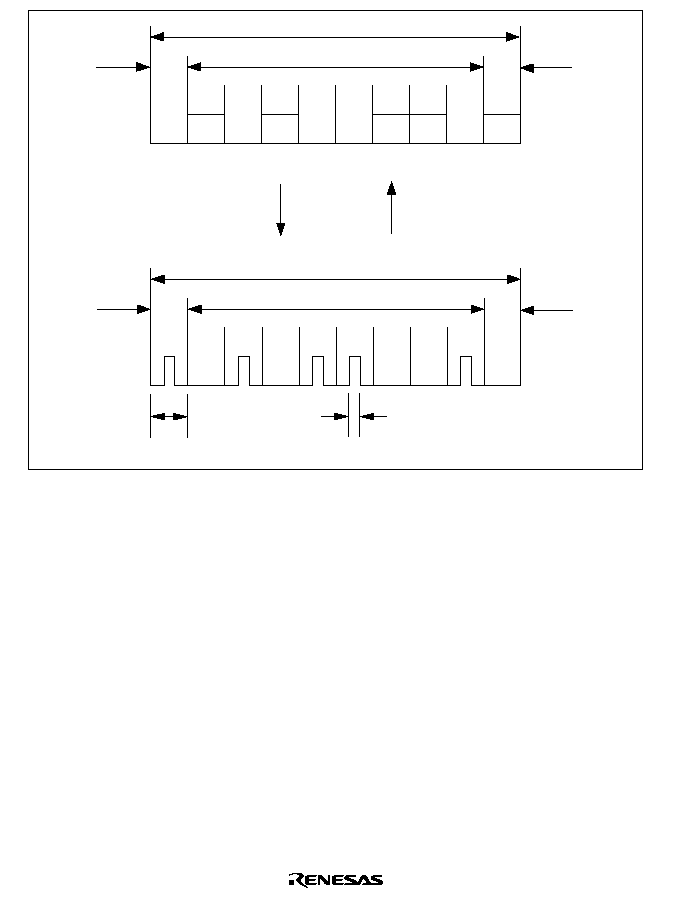
624
0
1
0
1
0
0
1
1
0
1
UART frame
Data
Start bit
Transmission
Reception
Stop bit
0
1
0
1
0
0
1
1
0
1
IR frame
Data
Start bit
Bit cycle
Stop bit
3/16 bit cycle
pulse width
Figure 14.24 IrDA Mode Transmit/Receive Operations
Pulse Width Selection: In transmission, the IR frame pulse width can be selected as either 3/16 of
the transmission bit rate or a smaller pulse width by means of the PSEL bit in the IrDA mode
register (SCIMR).
The SCIF includes a baud rate generator that generates the transmit frame bit rate and a baud rate
generator that generates the IRCLK signal for varying the pulse width.
When the PSEL bit is cleared to 0 in SCIMR, a width of 3/16 the bit rate set in the bit rate register
(SCBRR) is output as the IR frame pulse width. As the pulse width is the direct infrared emission
time; if the user wishes to minimize the pulse width in order to reduce power consumption, the
PSEL bit should be set to 1 in SCIMR and a setting should also be made in bits ICK3 to ICK0 in
the serial mode register (SCSMR) to generate the IRCLK signal, resulting in output with the
minimum settable pulse width.

625
The minimum IR frame pulse width must be 3/16 of the 115.2 kbps bit rate (= 1.63 µsec). With
this minimum pulse width, IRCLK = 921.6 kHz, and so the setting for bits ICK3 to ICK0 to give
the minimum settable pulse width is given by the following equation.
N
2
◊
IRCLK
≠ 1
P
P
:
Operating clock frequency
IRCLK: 921.6 kHz (fixed)
N:
Set value of ICK3 to ICK0 (0
N
15)
For example, when P
= 20 MHz, N = 10.
Table 14.12 shows the settings of bits ICK3 to ICK0 that can be used to obtain the minimum pulse
width for various operating frequencies.

626
Table 14.12
Bits ICK3 to ICK0 and Operating Frequencies in IrDA mode
(When PSEL = 1)
Operating Frequency
Setting of Bits ICK3 to ICK0 in SCSMR
P
(MHz)
ICK3
ICK2
ICK1
ICK0
2
0
0
0
0
3
1
5
1
0
6
1
8
1
0
0
10
1
12
1
0
14
1
16
1
0
0
0
18
1
20
1
0
21
1
22
1
23
1
0
0
24
1
25
1
26
1
0
27
0
28
1

627
14.4
SCIF Interrupt Sources and the DMAC
The SCIF has four interrupt sources: the break interrupt (BRI) request, receive-error interrupt
(ERI) request, receive-FIFO-data-full interrupt (RXI) request, and transmit-FIFO-data-empty
interrupt (TXI) request.
Table 14.13 shows the interrupt sources and their relative priorities. The interrupt sources can be
enabled or disabled with the TIE or RIE bit in SCSCR. Each kind of interrupt request is sent to the
interrupt controller independently.
When the TDFE flag is set to 1 in the serial status 1 register (SC1SSR), a TXI interrupt is
requested. A TXI interrupt request can activate the DMAC to perform data transfer. The TDFE bit
is cleared to 0 automatically when all writes to the transmit FIFO data register (SCFTDR) by the
DMAC are completed.
When the RDF flag is set to 1 in SC1SSR, an RXI interrupt is requested. An RXI interrupt request
can activate the DMAC to perform data transfer. The RDF bit is cleared to 0 automatically when
all receive FIFO data register (SCFRDR) reads by the DMAC are completed.
When the ER flag is set to 1, an ERI interrupt is requested. The DMAC cannot be activated by an
ERI interrupt request.
When the BRK flag is set to 1, a BRI interrupt is requested. The DMAC cannot be activated by a
BRI interrupt request.
A TXI interrupt indicates that transmit data can be written, and an RXI interrupt indicates that
there is receive data in SCFRDR.
Table 14.13
SCIF Interrupt Sources
Interrupt Source
Description
DMAC
Activation
Priority on
Reset Release
ERI
Receive error (ER)
Not possible
High
RXI
Receive data full (RDF) or data ready (DR)
Possible
(RDF only)
BRI
Break (BRK)
Not possible
TXI
Transmit data FIFO empty (TDFE)
Possible
Low

628
14.5
Usage Notes
The following points should be noted when using the SCIF.
SCFTDR Writing and the TDFE Flag: The TDFE flag in the serial status 1 register (SC1SSR)
is set when the number of transmit data bytes written in the transmit FIFO data register (SCFTDR)
has fallen to or below the transmit trigger number set by bits TTRG1 and TTRG0 in the FIFO
control register (SCFCR). After TDFE is set, transmit data up to the number of empty bytes in
SCFTDR can be written, allowing efficient continuous transmission.
However, if the number of data bytes written in SCFTDR is equal to or less than the transmit
trigger number, the TDFE flag will be set to 1 again after being read as 1 and cleared to 0. TDFE
clearing should therefore be carried out when SCFTDR contains more than the transmit trigger
number of transmit data bytes.
The number of transmit data bytes in SCFTDR can be found from the upper 8 bits of the FIFO
data count register (SCFDR).
Simultaneous Multiple Receive Errors: If a number of receive errors occur at the same time, the
state of the status flags in SC1SSR and SC2SSR is as shown in table 14.14. If there is an overrun
error, data is not transferred from the receive shift register (SCRSR) to the receive FIFO data
register (SCFRDR), and the receive data is lost.
Table 14.14
SC1SSR/SC2SSR Status Flags and Transfer of Receive Data
SC1SSR/SC2SSR Status Flags
Receive Data Transfer
Receive Errors
RDF
ORER
FER
PER
SCRSR
SCFRDR
Overrun error
1
1
0
0
◊
Framing error
0
0
1
0
O
Parity error
0
0
0
1
O
Overrun error + framing error
1
1
1
0
◊
Overrun error + parity error
1
1
0
1
◊
Framing error + parity error
0
0
1
1
O
Overrun error + framing error +
parity error
1
1
1
1
◊
Notes: O: Receive data is transferred from SCRSR to SCFRDR.
◊
: Receive data is not transferred from SCRSR to SCFRDR.

629
Break Detection and Processing: Break signals can be detected by reading the RxD pin directly
when a framing error (FER) is detected. In the break state the input from the RxD pin consists of
all 0s, so the FER flag is set and the parity error flag (PER) may also be set.
Note that although the SCIF stops transferring receive data to SCFRDR after receiving a break, the
receive operation continues, so if the FER and BRK flags are cleared to 0 they will be set to 1
again.
Sending a Break Signal: The TxD pin is a general I/O pin whose input/output direction and level
are determined by the I/O port data register (DR) and the control register (CR) of the pin function
controller (PFC). This fact can be used to send a break signal.
The DR value substitutes for the mark state until the PFC setting is made. The initial setting
should therefore be as an output port outputting 1.
To send a break signal during serial transmission, clear DR, then set the TxD pin as an output port
with the PFC.
When the TE bit is cleared to 0, the transmitter is initialized regardless of the current transmission
state.
Receive Error Flags and Transmit Operations (Synchronous Mode Only): Transmission
cannot be started when any of the receive error flags (ORER, PER3 to PER0, FER3 to FER0) is
set to 1, even if the TDFE flag is set to 1. Be sure to clear the receive error flags to 0 before
starting transmission.
Note also that the receive error flags are not cleared to 0 by clearing the RE bit to 0.
Receive Data Sampling Timing and Receive Margin in Asynchronous Mode: In asynchronous
mode, the SCIF operates on a base clock with a frequency of 16, 8, or 4 times the transfer rate.
In reception, the SCIF synchronizes internally with the fall of the start bit, which it samples on the
base clock. Receive data is latched at the rising edge of the eighth, fourth, or second base clock
pulse. The timing is shown in figure 14.25.

630
0 1 2
3 4
5 6 7 8 9 10 11 12 13 14 15 0 1 2
3 4
5 6 7 8 9 10 11 12 13 14 15 0 1 2
3 4
5
Base clock
16 clocks
8 clocks
≠7.5 clocks
+7.5 clocks
Start bit
D0
D1
Receive data
(RxD)
Synchronization
sampling timing
Data sampling
timing
Figure 14.25 Receive Data Sampling Timing in Asynchronous Mode
(Using base clock with frequency of 16 times the transfer rate, sampled in 8th clock cycle)
The receive margin in asynchronous mode can therefore be expressed as shown in equation (1).
M = 0.5 ≠
1
2N
D ≠ 0.5
N
≠ (L ≠ 0.5) F ≠ (1 + F)
◊
100%
................. ............ (1)
M: Receive margin (%)
N: Ratio of clock frequency to bit rate (N = 16, 8, or 4)
D: Clock duty cycle (D = 0 to 1.0)
L: Frame length (L = 9 to 12)
F: Absolute deviation of clock frequency
From equation (1), if F = 0 and D = 0.5, the receive margin is 46.875%, as given by equation (2).
When D = 0.5, F = 0, and N = 16:
M = (0.5 ≠ 1/(2
◊
16))
◊
100%
= 46.875%....................................................................................................... (2)
This is a theoretical value. A reasonable margin to allow in system designs is 20% to 30%.
When Using Synchronous External Clock Mode
∑
Do not set TE or RE to 1 until at least 4 peripheral operating clock cycles after external clock
SCK has changed from 0 to 1.
∑
Only set both TE and RE to 1 when external clock SCK is 1.
∑
In reception, note that if RE is cleared to 0 from 2.3 to 3.5 peripheral operating clock cycles
after the rising edge of the RxD D7 bit SCK input, RDF will be set to 1 but copying to
SCFRDR will not be possible.
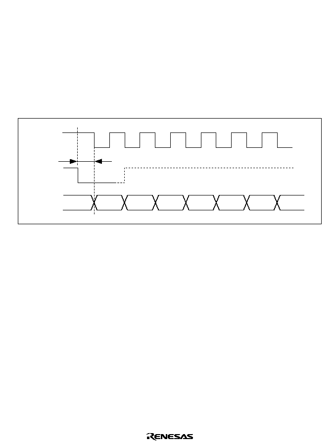
631
When Using Synchronous Internal Clock Mode: In reception, note that if RE is cleared to zero
1.5 peripheral operating clock cycles after the rising edge of the RxD D7 bit SCK output, RDF
will be set to 1 but copying to SCFRDR will not be possible.
When Using the DMAC: When an external clock source is used as the serial clock, the transmit
clock should not be input until at least 5 P
clock cycles after SCFTDR is updated by the DMAC.
Incorrect operation may result if the transmit clock is input within 4 P
cycles after SCFTDR is
updated. (See figure 14.26.)
When performing SCFRDR reads by the DMAC, be sure to set the relevant SCIF receive-FIFO-
data-full interrupt (RXI) as an activation source.
SCK
TDFE
TXD
D0
D1
D2
D3
D4
D5
D6
t
Figure 14.26 Example of Synchronous Transmission by DMAC
SCFRDR Reading and the RDF Flag: The RDF flag in the serial status 1 register (SC1SSR) is
set when the number of receive data bytes in the receive FIFO data register (SCFRDR) has
become equal to or greater than the receive trigger number set by bits RTRG1 and RTRG0 in the
FIFO control register (SCFCR). After RDF is set, receive data equivalent to the trigger number
can be read from SCFRDR, allowing efficient continuous reception.
However, if the number of data bytes in SCFRDR is equal to or greater than the trigger number,
the RDF flag will be set to 1 again if it is cleared to 0. RDF should therefore be cleared to 0 after
being read as 1 after receive data has been read to reduce the number of data bytes in SCFRDR to
less than the trigger number.
The number of receive data bytes in SCFRDR can be found from the lower 8 bits of the FIFO data
count register (SCFDR).

632
SCFRDR Reading when Overrun Occurs: If a receive operation is continued despite the fact
that the receive FIFO data register (SCFRDR) contains 16 bytes of data, overrun will occur.
If SCFRDR is read in this state, the data that caused the overrun is read in the 17th read. The value
returned in the 18th and subsequent reads will be undefined.
Also note that, from the first SCFRDR read onward, the number of receive data bytes in SCFRDR
indicated by the lower 8 bits of the FIFO data count register (SCFDR) is one more than the actual
number of receive data bytes.

633
Section 15 Serial I/O with FIFO (SIOF)
15.1
Overview
The serial I/O with FIFO functions mainly as an interface between the chip and a codec or modem
analog front-end.
15.1.1
Features
The serial I/O has the following features:
∑
Full-duplex operation
Independent transmit/receive registers and independent transmit/receive clocks
∑
Primary data transmit/receive FIFO/Double-buffered transmit/receive ports
Continuous data transmission/reception possible
∑
Interval transfer mode and continuous transfer mode
∑
Memory-mapped receive data register, transmit data register, serial control register, and serial
status register, receive control data register, transmit control data register, FIFO control
register, FIFO data count register
With the exception of SIRSR and SITSR, these registers are memory-mapped and can be
accessed by a MOV instruction.
∑
Choice of 8- or 16-bit data length
∑
Data transfer communication by means of polling or interrupts
Data transfer can be monitored by polling the receive data register full flag (RDRF), the
receive data register empty flag (RDRE), the receive control data register full flag (RCD), and
the transmit control data register empty flag (TCD). Interrupt requests can be generated during
data transfer by setting the receive interrupt request flag and the transmit interrupt request flag.
∑
Either MSB-first or LSB transfer can be selected for data I/O operations.
Figure 15.1 shows a block diagram of the serial I/O with FIFO.

634
16bits
SIRCDR
SISTR
SICTR
SIRDR
SIFCR
SIFDR
STCK
SRCK
SRXD
SIRDR:
SIRCDR:
SIRSR:
SITDR:
SITCDR:
SIRSR
STXD
SRS STS
MSB/LSB
Conversion circuit
SITCDR
SITDR
SITSR
selector
MSB/LSB
Conversion circuit
Peripheral bus
Receive data register
Receive control data register
Receive shift register
Transmit data register
Transmit control data register
SITSR:
SISTR:
SICTR:
SIFCR:
SIFDR:
Transmit shift register
Serial status register
Serial control register
FIFO control register
FIFO data count register
Bit counter
I/O control unit
Serial I/O with
FIFO module (SIOF)
Figure 15.1 SIOF Block Diagram
Table 15.1 shows the functions of the external pins.
Table 15.1
Serial I/O with FIFO (SIOF) External Pins
Name
Pin
I/O
Function
Serial receive data input pin
SRxD0
Input
Serial data input port
Serial receive clock input pin
SRCK0
Input
Serial receive clock port
Serial reception synchronization
input pin
SRS0
Input
Serial reception synchronization input
port
Serial transmit data output pin
STxD0
Output
Serial data output port
Serial transmit clock input pin
STCK0
Input
Serial transmit clock port
Serial transmission synchronization
input/output pin
STS0
I/O
Serial transmission synchronization
input/output port

635
15.2
Register Configuration
Table 15.2 shows the SIOF's registers.
Table 15.2
Register Configuration
Register
Abbreviation
R/W
Initial
Value
Address
Access Size (Bits)
Receive shift register
SIRSR0
--
--
--
--
Receive data register
SIRDR0
R
Not
specified
H'FFFFFC00
8, 16, 32
Transmit shift register
SITSR0
--
--
--
--
Transmit data register
SITDR0
R/W
H'0000
H'FFFFFC02
8, 16, 32
Serial control register
SICTR0
R/W
H'0000
H'FFFFFC04
8, 16, 32
Serial status register
SISTR0
R/(W)
*
H'0002
H'FFFFFC06
8, 16, 32
Receive control data
register
SIRCDR
R
H'0000
H'FFFFFC0C
8, 16, 32
Transmit control data
register
SITCDR
R/W
H'0000
H'FFFFFC0E
8, 16, 32
FIFO control register
SIFCR
R/W
H'0000
H'FFFFFC08
8, 16, 32
FIFO data count register SIFDR
R
H'0000
H'FFFFFC0A
8, 16, 32
Note:
*
Only 0 should be written, to clear flags (after reading 1 from the flag).
15.2.1
Receive Shift Register (SIRSR)
Bit:
15
14
13
...
3
2
1
0
...
Initial value:
--
--
--
...
--
--
--
--
R/W:
--
--
--
...
--
--
--
--
SIRSR is a 16-bit register used to receive serial data. The data is fetched in MSB first from the
SRxD pin in synchronization with the fall of the serial receive clock (SRCK), and is shifted into
SIRSR. The data length is set by the transmit/receive data length select bit (DL) in the
corresponding serial control register (SICTR). If the DL bit is cleared to 0 (data length 8 bits), the
receive data is fetched to the lower 8 bits, and the upper 8 bits are cleared to 0. When data transfer
to SIRSR is completed, the data contents are automatically transferred to the receive data register
(SIRDR), and the receive data register full flag (RDRF) is set in the serial status register (SISTR),
based on the settings of the receive FIFO watermark bits (RFWM3 to RFWM0) in SIFCR.
When transfer of control data to SIRSR is completed, the data contents are automatically

636
transferred to the receive control data register (SIRCDR), and the receive control data register full
flag (RCD) is set in SISTR.
If the next data word input operation ends before the RDRF flag is cleared, an overrun error
occurs, the receive overrun error flag (RERR) is set in SISTR, and an overrun error signal is sent
to the interrupt controller (INTC). The data in SIRSR overwrites the data in SIRDR.
If SIRCDR contains valid control data, SIRCDR is overwritten after the next control data input
operation completes.
15.2.2
Receive Data Register (SIRDR)
Bit:
15
14
13
...
3
2
1
0
...
Initial value:
0
0
0
...
0
0
0
0
R/W:
R
R
R
...
R
R
R
R
SIRDR is a 16-bit x 16-stage FIFO register that stores primary receive data. When primary data is
transferred from SIRSR to SIRDR, the receive data register full flag (RDRF) is set in the serial
status register (SISTR), based on the settings of RFWM3 to RFWM0 in SIFCR. If the receive
interrupt enable flag (RIE) is set in SICTR, a receive-data-full interrupt (RDFI) request is sent to
the interrupt controller (INTC) and the DMA controller (DMAC). When the flag is cleared, this
interrupt request signal is not generated. When SIRDR is read by the DMAC, the RDRF flag is
cleared automatically if the value is less than or equal to the setting of bits RFWM3 to RFWM0 in
SIFCR. When SIRDR is reset, its status is empty. The status of SIRDR is also empty when the
value of the receive FIFO data registry reset bit (RFRST) in SIFCR is 1.
Note:
Do not read from SIRDR when it contains no primary receive data (when the value of the
receive data register data count bits 4 to 0 (R4 to R0) in the FIFO data count register
(SIFDR) is 00000).
15.2.3
Transmit Shift Register (SITSR)
Bit:
15
14
13
...
3
2
1
0
...
Initial value:
--
--
--
...
--
--
--
--
R/W:
--
--
--
...
--
--
--
--
SITSR is a 16-bit register used to transmit serial data. The contents of this register are shifted in
MSB-first or LSB-first order, based on the LM bit in SIFCR, in synchronization with the rising
edge of the serial transmit clock (STCK), and output from the serial transmit data STXD pin. The

637
transfer data length is set by the DL bit in SICTR. The transmit mode bit (TRMD) in SIFCR
controls the LSB of the transmitted primary data or control data.
When the TRMD bit is cleared to 0 and the DL bit is cleared to 0 (8-bit data length), the lower 8
bits in the transmit data register (SITDR) are output. When the DL bit is set to 1 (16-bit data
length), all 16 bits in SITDR are output.
Setting the TRMD bit to 1 causes the LSB of the primary data to be output as 0. Performing write
access to the transmit control data register (SITCDR) in this case, if the DL bit is cleared to 0,
causes the lower 8 bits in SITDR to be output, with the LSB as 1, after which the lower 8 bits in
SITCDR are output. If the DL bit is set to 1, all 16 bits in SITDR are output, with the LSB as 1,
after which all 16 bits in SITCDR are output.
When transmit primary data with a value less than or equal to the transmit FIFO watermark bits
(TFWM3 to TFWM0) in SIFCR is transferred from SITDR to SITSR, the transmit data register
empty flag (TDRE) is set in SISTR. If output of the next primary data begins when the amount of
transmit primary data in SITDR is 0, an underrun error occurs, the transmit underrun error flag
(TERR) in SISTR is set, and an error interrupt request is sent to the INTC.
15.2.4
Transmit Data Register (SITDR)
Bit:
15
14
13
...
3
2
1
0
...
Initial value:
0
0
0
...
0
0
0
0
R/W:
W
W
W
...
W
W
W
W
SITDR is a 16-bit x 16-stage FIFO register that stores primary transmit data. Data should be
written to SITDR when the transmit data register empty flag (TDRE) is set to 1 in SISTR. If data
is written to SITDR when TDRE is 0, a SITDR overflow may occur. When transmit primary data
with a value less than or equal to the setting of TFWM3 to TFWM0 in SIFCR is transferred from
SITDR to SITSR, TDRE is set in SISTR. If at this point the transmit interrupt enable flag (TIE) is
set, a transmit-data-empty interrupt (TDEI) request is sent to the INTC and DMAC. If TIE is
cleared, this interrupt request is not generated. When the DMAC writes to SITDR data with a
value greater than the setting of TFWM3 to TFWM0 in SIFCR, the TDRE flag is cleared
automatically. The TDRE flag is set only by hardware.
When SITDR is reset, its status is empty. The status of SITDR is also empty when the value of the
transmit FIFO data registry reset bit (TFRST) in SITDR is 1.
Note: Do not write to SITDR when it is full of primary transmit data (when the value of the
transmit data register data count bits 4 to 0 (T4 to T0) in SIFDR is 10000).
Data should be written to SITDR in the size specified by the setting of the DL bit in
SICTR. Always set the TE bit to 1 before writing to this register.

638
15.2.5
Serial Control Register (SICTR)
Bit:
15
14
13
12
11
10
9
8
--
--
--
--
--
DMACE
TCIE
RCIE
Initial value:
0
0
0
0
0
0
0
0
R/W:
R
R
R
R
R
R/W
R/W
R/W
Bit:
7
6
5
4
3
2
1
0
--
TM
SE
DL
TIE
RIE
TE
RE
Initial value:
0
0
0
0
0
0
0
0
R/W:
R
R/W
R/W
R/W
R/W
R/W
R/W
R/W
SICTR is a 16-bit register used to set parameters for serial port control. SICTR is initialized to
H'0000 by a reset.
When modifying bit 4, 5, 6,or 10 (DMACE, TM, SE, or DL), TE and RE (bit 1, 0) should be
cleared to 0 beforehand.
Bits 15 to 11--Reserved: These bits are always read as 0. The write value should always be 0.
Bit 10--DMAC Activation Enable (DMACE): Specifies whether the DMAC is activated by
interrupts triggered by the RDRF and TDRE bits in SISTR.
Set this bit to 1 if SIRCDR and SITCDR are used. This will cause interrupts triggered by the
RDRF and TDRE bits in SISTR to be processed by the DMAC and interrupts triggered by the
RCD and TCD bits in SISTR to be processed by the CPU.
Clear this bit to 0 if SIRCDR and SITCDR are not used, or if all interrupts triggered by the RDRF,
TDRE, RCD and TCD bits in SISTR are to be processed by the CPU. The initial value of this bit
is 0.
Bit 10: DMACE
Description
0
DMAC is activated by RDRF and TDRE interrupts
(Initial value)
1
DMAC is not activated by RDRF and TDRE interrupts
Bit 9--Transmit-Control-Data-Register-Empty Interrupt Enable (TCIE): Enables the transmit-
control-data-register-empty interrupt. The initial value of this bit is 0.
Bit 9: TCIE
Description
0
Transmit-control-data-register-empty interrupt disabled
(Initial value)
1
Transmit-control-data-register-empty interrupt enabled

639
Bit 8--Receive-Control-Data-Register-Full Interrupt Enable (RCIE): Enables the receive-control-
data-register-full interrupt. The initial value of this bit is 0.
Bit 8: RCIE
Description
0
Receive-control-data-register-full interrupt disabled
(Initial value)
1
Receive-control-data-register-full interrupt enabled
Bit 7--Reserved: This bit is always read as 0. The write value should always be 0.
Bit 6--Transfer Mode Control (TM): Specifies whether the transmission synchronization signal is
to be input from an external source or generated internally by the chip. When this flag is cleared,
the transmission synchronization signal is STS pin input. When this flag is set, the transmission
synchronization signal is generated by the chip, and is output to an external device from the STS
pin. This bit does not affect reception.
Bit 6: TM
Description
0
External signal input from STS pin is used as transmission start indication
(Initial value)
1
Internal signal output from STS pin is used as transmission start indication
Note: If the transmit mode bit (TRMD) in SIFCR is set to 1, this bit must be cleared to 0.
If TM is set to 1 and SE is set to 1 (interval mode), output of the sync signal stops at the
point at which bits T4 to T0 in SIFDR are cleared to 0 (data count of transmit data register is
zero). If TE remains set to 1 and data is written to SITDR, output of the sync signal resumes
when the value of T4 to T0 in SIFDR becomes H'01 or above.
Bit 5--Synchronization Signal Enable (SE): Specifies whether the synchronization signals are to
be used for all serial data transfers, or only for the first transfer.
When this bit is cleared to 0, the synchronization signals (SRS and STS) are necessary only for the
first data transfer, and are not required for subsequent transfers. When this bit is set to 1, the
synchronization signals are necessary for all data transfers.
Bit 5: SE
Description
0
Continuous mode: SRS and STS are used only for the first data transfer
(Initial value)
1
Interval mode: SRS and STS are used for all data transfers
Note: If TRMD in SIFCR is set to 1, this bit must be cleared to 1.
When TM is cleared to 0 and SE is cleared to 0, after data is input SRS/STS once nothing
further should be input to SRS/STS between the start and completion of
transmission/receiving (transmit FIFO empty/receive FIFO full).

640
Bit 4--Transmit/Receive Data Length Select (DL): Specifies the serial I/O module's transfer data
length. The initial value of this bit is 0, indicating an 8-bit data length. When an 8-bit data length
is specified, the lower 8 bits in the receive shift register, receive data register, transmit shift
register, transmit data register, receive control data register, and transmit control data register are
used.
Bit 4: DL
Description
0
8-bit transfer data length
(Initial value)
1
16-bit transfer data length
Bit 3--Transmit Interrupt Enable (TIE): Enables the transmit-data-empty interrupt. The initial
value of this bit is 0.
Bit 3: TIE
Description
0
Transmit interrupt disabled
(Initial value)
1
Transmit interrupt enabled
Bit 2--Receive Interrupt Enable (RIE): Enables the receive-data-full interrupt. The initial value of
this bit is 0.
Bit 2: RIE
Description
0
Receive interrupt disabled
(Initial value)
1
Receive interrupt enabled
Bit 1--Enables data transmission. When this flag is cleared, the STXD pin goes to the high-
impedance state. When TM is set to 1, the STS pin also goes to the high-impedance state.
Bit 1: TE
Description
0
Transmission disabled: STxD pin goes to high-impedance state (Initial value)
When TM is set to 1, STS pin goes to high-impedance state
1
Transmission enabled
Bit 0--Receive Enable (RE): Enables data reception.
Bit 0: RE
Description
0
Reception disabled
(Initial value)
1
Reception enabled

641
15.2.6
Serial Status Register (SISTR)
Bit:
15
14
...
9
8
...
4
3
2
1
0
--
--
...
TCD
RCD
...
--
TERR
RERR
TDRE
RDRF
Initial value:
0
0
...
1
0
...
0
0
0
1
0
R/W:
R
R
... R/(W)
*
R/(W)
*
...
R
R/(W)
*
R/(W)
*
R/(W)
*
R/(W)
*
Note:
*
Only 0 should be written, to clear the flag.
SISTR is a 16-bit register that indicates the status of the serial I/O module. SISTR is initialized to
H'0002 by a reset. When the TFRST bit in SIFCR is set to 1, the TERR and TDRE bits are also
initialized. When the RFRST bit in SIFCR is set to 1, the RERR and RDRF bits are also
initialized.
Bits 15 to 4--Reserved: These bits are always read as 0. The write value should always be 0.
Bit 9--Transmit Control Data Register Empty (TCD): This flag indicates when SITCDR is empty
and can be written to.
Bit 9: TCD
Description
0
SITCDR transmit data is valid
TCD is cleared to 0 in the following cases:
∑
When 0 is written to TCD after reading TCD = 1
1
SITCDR transmit data is invalid
(Initial value)
TCD is set to 1 in the following cases:
∑
After data is transferred from SITCDR to SITSR
∑
When the processor is reset
Bit 8--Receive Control Data Register Full (RCD): This flag indicates when SIRCDR is in wait
status.
Bit 8: RCD
Description
0
SIRCDR receive data is invalid
(Initial value)
RCD is cleared to 0 in the following cases:
∑
When 0 is written to RCD after reading RCD = 1
∑
When the processor is reset
1
SIRCDR transmit data is valid
RCD is set to 1 in the following cases:
∑
After control data has been received normally and data has been
transferred from SIRSR to SIRCDR

642
Bit 7 to 4--Reserved: This bit is always read as 0. The write value should always be 0.
Bit 3--Transmit Underrun Error (TERR): Flag that indicates the occurrence of a transmit
underrun.
Bit 3: TERR
Description
0
Transmission is in progress, or has ended normally
(Initial value)
[Clearing conditions]
∑
When 0 is written to the TERR bit after reading TERR = 1
∑
When the TFRST bit in SIFCR is set to 1
∑
When the processor enters the reset state
1
A transmit underrun error has occurred
∑
When the amount of primary transmit data in SITDR is 0 and data is
transferred from SITDR to SITSR using a transmit operation
Bit 2--Receive Overrun Error (RERR): Flag that indicates the occurrence of a receive overrun.
Bit 2: RERR
Description
0
Reception is in progress, or has ended normally
(Initial value)
[Clearing conditions]
∑
When 0 is written to the RERR bit after reading RERR = 1
∑
When the RFRST bit in SIFCR is set to 1
∑
When the processor enters the reset state
1
A receive overrun error has occurred
RERR is set to 1 in the following cases:
∑
When the amount of primary receive data in SIRDR is 16 and the next
primary data receive operation completes

643
Bit 1--Transmit Data Register Empty (TDRE): Flag that indicates that primary data has been
transferred from SITDR to SITSR and the amount of data inside SITDR is less than or equal to the
setting of TFWM3 to TFWM0 in SIFCR.
Bit 1: TDRE
Description
0
Indicates that primary send data exceeding the transmit FIFO watermark
setting has been written to SITDR
TDRE is cleared to 0 in the following cases:
∑
When primary send data exceeding the setting of the transmit FIFO
watermark bits has been written to SITDR and 0 is written to TDRE after
reading TDRE = 1
∑
When the DMAC has written primary send data exceeding the setting of
the transmit FIFO watermark bits to SITDR
1
Indicates that the amount of primary send data in SITDR is less than or equal
to the transmit FIFO watermark setting
(Initial value)
TDRE is set to 1 in the following cases:
∑
When the amount of primary send data in SITDR is less than or equal to
the transmit FIFO watermark setting
∑
When the TFRST bit in SIFCR is set to 1
∑
When the processor is reset
Bit 0--Receive Data Register Full (RDRF): Flag that indicates that SIRDR receive data is waiting.
Bit 0: RDRF
Description
0
Indicates that the amount of primary receive data in SIRDR is less than the
receive FIFO watermark setting
(Initial value)
RDRF is cleared to 0 in the following cases:
∑
When the received primary data in SIRDR has been read to the point that
the amount of remaining data is less than the receive FIFO watermark
setting and 0 is written to RDRF after reading RDRF = 1
∑
When the DMAC has read the received primary data in SIRDR to the
point that the amount of remaining data is less than the receive FIFO
watermark setting
∑
When the RFRST bit in SIFCR is set to 1
∑
When the processor is reset
1
Indicates that the amount of primary receive data in SIRDR is greater than or
equal to the receive FIFO watermark setting
RDRF is set to 1 in the following cases:
∑
When the received primary data stored in SIRDR is greater than or equal
to the receive FIFO watermark setting

644
15.2.7
Receive Control Data Register (SIRCDR)
Bit:
15
14
13
12
11
10
9
8
7
6
5
4
3
2
1
0
Initial value:
0
0
0
0
0
0
0
0
0
0
0
0
0
0
0
0
R/W:
R
R
R
R
R
R
R
R
R
R
R
R
R
R
R
R
SIRCDR is a register that stores receive control data. Received data is stored in SIRCDR as
receive control data, synchronized with the timing used for transmission of transmit control data
from SITCDR.
The RCD bit in SISTR is set at the same time as control data is being transferred from SIRSR to
SIRCDR. When the RCIE pin in SICTR is set, a receive-control-data-full interrupt request (RDFI)
is sent to the INTC. No interrupt request signal is issued if the flag is cleared.
SIRCDR is initialized to H'0000 by a reset.
If the DL bit is cleared to 0 (data length 8 bits), the received control data is fetched to the lower 8
bits, and the upper 8 bits are cleared to 0.
15.2.8
Transmit Control Data Register (SITCDR)
Bit:
15
14
13
12
11
10
9
8
7
6
5
4
3
2
1
0
Initial value:
0
0
0
0
0
0
0
0
0
0
0
0
0
0
0
0
R/W: R/W R/W R/W R/W R/W R/W R/W R/W R/W R/W R/W R/W R/W R/W R/W R/W
SITCDR is a register that stores transmit control data.
Data should be written to SITCDR when the TCD bit is set to 1 in SISTR (SITCDR transmit data
invalid). If data is written to SITCDR when TCD in SISTR is cleared to 0, the previous data will
be overwritten. After writing transmit control data to SITCDR, 1 should be read from TCD in
SISTR and then 0 written to it. This makes the transmit data in SITCDR valid and causes the
transmit control data to be transmitted.
After TRMD in SIFCR is set to 1 transmission starts, a read interrupt is issued to SITCDR. STS
goes high and primary data bit 0 is transmitted as 1. When STS next goes high the control data
stored in SITCDR is transferred to SITSR. If the TCD bit is 0 at this point, and TCD bit is set to 1.
After this the control data previously transferred from SITCDR to SITSR is transmitted.
If the TRMD bit is cleared to 0, no control data is transmitted even if data is written to SITCDR.

645
If the TCD bit in SISTR is set to 1 and the TCIE bit in SICTR is set to 1, a transmit-control-data-
empty interrupt (TDEI0) request is sent to the INTC. If the flag is cleared, this interrupt request is
not generated.
The TCD bit in SISTR is set only by hardware.
SITCDR is initialized to H'0000 by a reset.
15.2.9
FIFO Control Register (SIFCR)
Bit: 15 14 13 12 11
10
9
8
7
6
5
4
3
2
1
0
TRMD LM
RFR
ST
TFR
ST
RFWM
3
RFWM
2
RFWM
1
RFWM
0
TFWM
3
TFWM
2
TFWM
1
TFWM
0
Initial value:
0
0
0
0
0
0
0
0
0
0
0
0
0
0
0
0
R/W:
R
R R R R/W R/W R/W R/W R/W R/W R/W R/W R/W R/W R/W R/W
SIFCR is a register used to perform software resets and to make threshold settings for SIRDR and
SITDR.
It also contains a bit used to select LSB first or MSB first when transmitting and receiving to
match the connected codec, as well as a bit for controlling the LSB for transmitted primary data
and control data.
SIFCR is initialized to H'0000 by a reset.
Note that the TE and RE bits in SICTR must be cleared to 0 before changing the values of bits 11
to 10 and 7 to 0 (TRMD, LM, RFWM3 to RFWM0, TFWM3 to TFWM0).
Bit 15 to 12--Reserved: These bits are always read as 0. The write value should always be 0.
Bit 11--Transfer Mode (TRMD): Controls the LSB (bit 0) for transmitted primary data and
control data.
Bit 11: TRMD
Description
0
Value stored in SITDR is always transmitted as LSB of primary data
(Initial value)
1
LSB of primary data is always transmitted as 0
However, the LSB is 1 when the primary data immediately precedes control
data
Note: If the TRMD bit is set to 1, in SICTR the TM bit (STS pin input) should be cleared to 0, the
SE bit (interval mode) set to 1, and the LM bit (transmit/receive MSB format) cleared to 0.
The sync signal output from the connected codec should be input to pins STS and SRS.
The serial clock output from the connected codec should be input to pins STCK and SRCK.

646
Bit 10--LSB/MSB First Select (LM): Used to select LSB first or MSB first for transmitting and
receiving.
Bit 10: LM
Description
0
MSB first for transmitting and receiving
(Initial value)
1
LSB first for transmitting and receiving
Note: This bit must be cleared to 0 if the TRMD bit is set to 1.
Bit 9--Receive FIFO Data Register Reset (RFRST): Invalidates the primary receive data in
SIRDR and resets it to empty status. Also initializes the RERR and RDRF bits in SISTR.
Note that SICTR is not initialized, so receiving continues if the RE bit is set to 1.
Bit 9: RFRST
Description
0
Reset disabled
(Initial value)
1
Reset enabled
Note: Reset status persists while this bit is set to 1. Clear this bit to 0 to cancel reset status.
Bit 8--Transmit FIFO Data Register Reset (TFRST): Invalidates the transmit data in SITDR and
resets it to empty status. Also initializes the TERR and TDRE bits in SISTR.
Note that SICTR is not initialized, so transmitting continues if the TE bit is set to 1.
Bit 8: TFRST
Description
0
Reset disabled
(Initial value)
1
Reset enabled
Note: Reset status persists while this bit is set to 1. Clear this bit to 0 to cancel reset status.

647
Bit 7 to 4--Receive FIFO Watermark (RFWM3 to RFWM0): These bits are used to make
threshold settings, which are used to set the RDRF bit in SISTR.
When the amount of primary receive data in SIRDR is equal to or greater than the watermark
setting, as shown in the table below, the RDRF bit is set to 1.
Bit 7: RFWM3
Bit 6: RFWM2
Bit 5: RFWM1
Bit 4: RFWM0
Watermark setting
0
0
0
0
1
(Initial value)
1
2
1
0
3
1
4
1
0
0
5
1
6
1
0
7
1
8
1
0
0
0
9
1
10
1
0
11
1
12
1
0
0
13
1
14
1
0
15
1
16

648
Bit 3 to 0-- Transmit FIFO Watermark (TFWM3 to TFWM0): These bits are used to make
threshold settings, which are used to set the TDRE bit in SISTR.
When the amount of primary send data in SITDR is less than or equal to the watermark setting, as
shown in the table below, the TDRE bit is set to 1.
Bit 3: TFWM3
Bit 2: TFWM2
Bit 1: TFWM1
Bit 0: TFWM0
Watermark setting
0
0
0
0
0
(Initial value)
1
1
1
0
2
1
3
1
0
0
4
1
5
1
0
6
1
7
1
0
0
0
8
1
9
1
0
10
1
11
1
0
0
12
1
13
1
0
14
1
15

649
15.2.10
FIFO Data Count Register (SIFDR)
Bit:
15
14
13
12
11
10
9
8
7
6
5
4
3
2
1
0
R4
R3
R2
R1
R0
T4
T3
T2
T1
T0
Initial value:
0
0
0
0
0
0
0
0
0
0
0
0
0
0
0
0
R/W:
R
R
R
R
R
R
R
R
R
R
R
R
R
R
R
R
SIFDR is a register that indicates the amount of primary data stored in SIRDR and SITDR.
The upper 8 bits indicate the amount of primary receive data stored in SIRDR, and the lower 8 bits
indicate the amount of primary transmit data stored in SITDR.
SIFDR is initialized to H'0000 by a reset. Also, it can be initialized to H'0000 by setting bits
RFRST and TFRST of SIFCR to 1.
Bit 15 to 13--Reserved: These bits are always read as 0.
Bit 12 to 8--Receive Data Register Data Count Bits 4 to 0 (R4 to R0): These bits indicate the
amount of primary receive data stored in SIRDR.
When the value of bits R4 to R0 is H'00 there is no primary receive data stored in SIRDR, and
when the value is H'10 SIRDR is full. In addition to the initialized status mentioned above, bits R4
to R0 can be cleared to H'00 by reading all the primary receive data from SIRDR.
Bit 7 to 5--Reserved: These bits are always read as 0.
Bit 4 to 0--Transmit Data Register Data Count Bits 4 to 0 (T4 to T0): These bits indicate the
amount of untransmitted primary data stored in SITDR.
When the value of bits T4 to T0 is H'00 there is no primary transmit data waiting to be
transmitted, and when the value is H'10 SITDR is full. In addition to the initialized status
mentioned above, bits T4 to T0 can be cleared to H'00 by transmitting all the primary transmit
data.
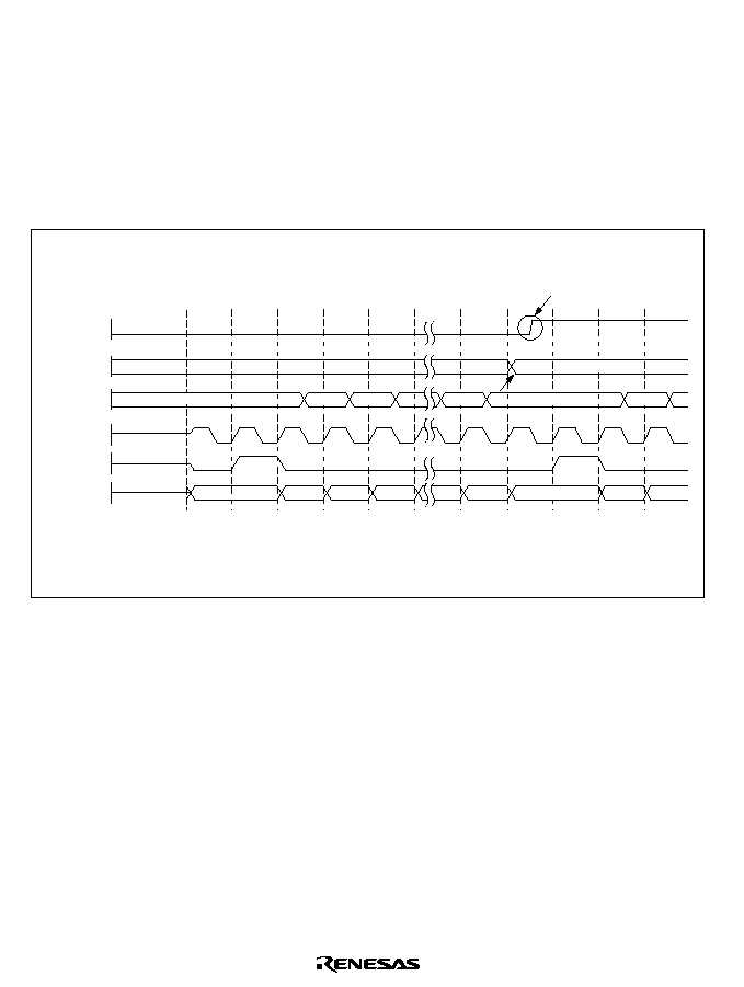
650
15.3
Operation
15.3.1
Input when TRMD = 0 in SIFCR
Figure 15.2 shows interval transfer mode (SE set to 1 in SICTR) with MSB first (LM cleared to 0
in SIFCR).
Figure 15.3 shows continuous transfer mode (SE cleared to 0 in SICTR) with MSB first (LM
cleared to 0 in SIFCR).
Note: DL = 0: 8-bit data transfer
SE = 1: Synchronous transfer in start signal mode
LM = 0: MSB first
TRMD = 0: LSB of transmitted primary data is value in SITDR
B[7]
A[7]
A[7:0]
A[7:0]
A[7:6]
A[7:1]
Set to 1 when an amount of data
equal to or greater than the setting of
bits RFWM3 to RFWM0 in SIFCR is
received
A[7]
A[6]
A[5]
A[0]
B[7]
B[6]
Invalid
SRXD
SRS
SRCK
SIRSR
SIRDR
RDRF
Synchronous internal clock
Undefined
Figure 15.2 Reception: Interval Transfer Mode/MSB First
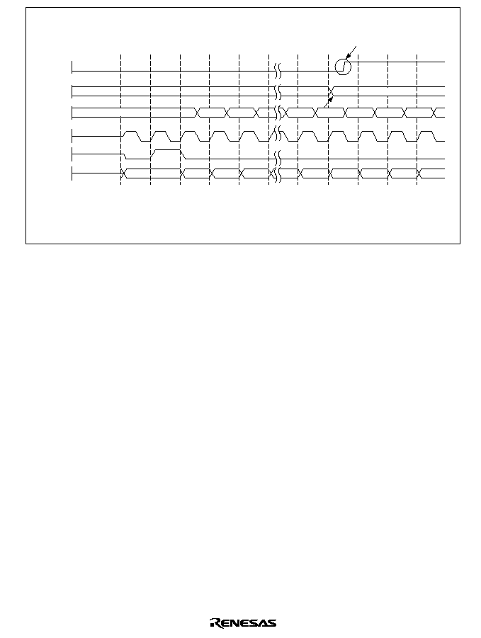
651
A[7]
A[6]
A[5]
A[0]
B[7]
B[6]
B[5]
B[4]
B[7]
A[7]
A[7:0]
A[7:0]
B[7:6]
B[7:5]
A[7:6]
A[7:1]
Undefined
SRXD
SRS
SRCK
SIRSR
SIRDR
RDRF
Note: DL = 0: 8-bit data transfer
SE = 0: Asynchronous transfer, no start signal mode
LM = 0: MSB first
TRMD = 0: LSB of transmitted primary data is value in SITDR
Set to 1 when an amount of
data equal to or greater than the
setting of bits RFWM3 to RFWM0
in SIFCR is received
Synchronous internal clock
Figure 15.3 Reception: Continuous Transfer Mode/MSB First
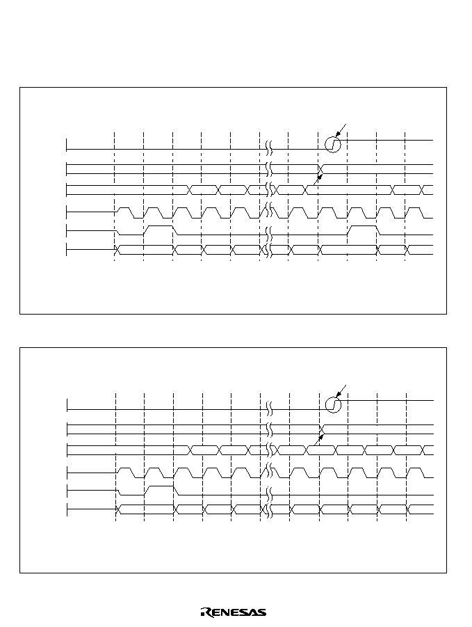
652
Figure 15.4 shows interval transfer mode (SE set to 1 in SICTR) with LSB first (LM set to 1 in
SIFCR).
Figure 15.5 shows continuous transfer mode (SE cleared to 0 in SICTR) with LSB first (LM set to
1 in SIFCR).
B[0]
A[0]
A[0:7]
A[7:0]
A[0:1]
A[0:6]
A[0]
A[1]
A[2]
A[7]
B[0]
B[1]
Invalid
SRXD
SRS
SRCK
SIRSR
SIRDR
RDRF
Note: DL = 0: 8-bit data transfer
SE = 1: Synchronous transfer in start signal mode
LM = 1: LSB first
TRMD = 0: LSB of transmitted primary data is value in SITDR
Set to 1 when an amount of
data equal to or greater than the
setting of bits RFWM3 to RFWM0
in SIFCR is received
Synchronous internal clock
Undefined
Figure 15.4 Reception: Interval Transfer Mode/LSB First
SRXD
SRS
SRCK
SIRSR
SIRDR
RDRF
A[0]
A[1]
A[2]
A[7]
B[0]
B[1]
B[2]
B[3]
B[0]
A[0]
A[0:7]
A[7:0]
B[0:1]
B[0:2]
A[0:1]
A[0:6]
Note: DL = 0: 8-bit data transfer
SE = 0: Asynchronous transfer, no start signal mode
LM = 1: LSB first
TRMD = 0: LSB of transmitted primary data is value in SITDR
Set to 1 when an amount of
data equal to or greater than the
setting of bits RFWM3 to RFWM0
in SIFCR is received
Synchronous internal clock
Undefined
Figure 15.5 Reception: Continuous Transfer Mode/LSB First
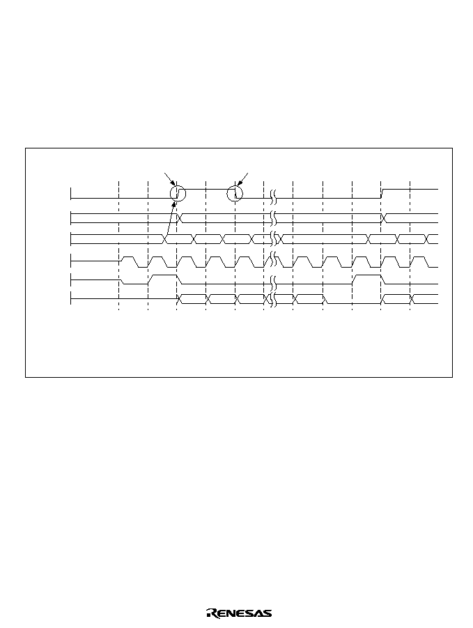
653
15.3.2
Output when TRMD = 0 in SIFCR
Figure 15.6 shows interval transfer mode when TM is cleared to 0 in SICTR and with MSB first.
Figure 15.7 shows continuous transfer mode when TM is cleared to 0 in SICTR and with MSB
first.
Figure 15.8 shows interval transfer mode when TM is set to 1 in SICTR and with MSB first.
Figure 15.9 shows continuous transfer mode when TM is set to 1 in SICTR and with MSB first.
STXD
STS
STCK
SITSR
SITDR
TDRE
C[7:0]
C[6:0]
C[5:0]
C[0]
C[7:0]
D[7:0]
D[7:0]
E[7:0]
Set to 1 when the amount of data in SITDR is
less than or equal to the setting of bits
TFWM3 to TFWM0 in SIFCR
C[7]
C[6]
C[5]
C[0]
D[7]
D[6]
D[7:0]
D[6:0]
Note: TM = 0: STS is input
DL = 0: 8-bit data transfer
SE = 1: Synchronous transfer in start signal mode
LM = 0: MSB first
TRMD = 0: LSB of transmitted primary data is value in SITDR
Cleared to 0 when an amount of data exceeding
the setting of bits TFWM3 to TFWM0 in SIFCR
has been written to SITDR
Synchronous internal clock
Undefined
Figure 15.6 Transmission: Interval Transfer Mode (TM = 0 Mode)/MSB First

654
STXD
STS
STCK
SITSR
SITDR
TDRE
C[7:0]
C[6:0]
C[5:0]
C[7:0]
D[7:0]
D[7:0]
E[7:0]
C[0]
D[7:0]
D[6:0]
C[7]
C[6]
C[5]
D[7]
D[6]
C[0]
D[5]
D[4]
D[5:0]
D[4:0]
Set to 1 when the amount of data in SITDR is
less than or equal to the setting of bits
TFWM3 to TFWM0 in SIFCR
Note: TM = 0: STS is input
DL = 0: 8-bit data transfer
SE = 0: Asynchronous transfer, no start signal mode
LM = 0: MSB first
TRMD = 0: LSB of transmitted primary data is value in SITDR
Cleared to 0 when an amount of data exceeding
the setting of bits TFWM3 to TFWM0 in SIFCR
has been written to SITDR
Synchronous internal clock
Undefined
Figure 15.7 Transmission: Continuous Transfer Mode (TM = 0 Mode)/MSB First
STXD
STS
STCK
SITSR
SITDR
C[7:0]
C[6:0]
C[5:0]
C[7:0]
D[7:0]
D[7:0]
E[7:0]
C[1:0]
C[0]
D[7:0]
C[7]
C[6]
C[5]
C[0]
D[7]
C[1]
D[6]
D[5]
D[6:0]
D[5:0]
SITDR
TDRE
Set to 1 when the amount of data in SITDR is
less than or equal to the setting of bits
TFWM3 to TFWM0 in SIFCR
Note: TM = 1: STS is output
DL = 0: 8-bit data transfer
SE = 1: Synchronous transfer in start signal mode
LM = 0: MSB first
TRMD = 0: LSB of transmitted primary data is value in SITDR
Cleared to 0 when an amount of data exceeding
the setting of bits TFWM3 to TFWM0 in SIFCR
has been written to SITDR
Synchronous internal clock
Undefined
Figure 15.8 Transmission: Interval Transfer Mode (TM = 1 Mode)/MSB First
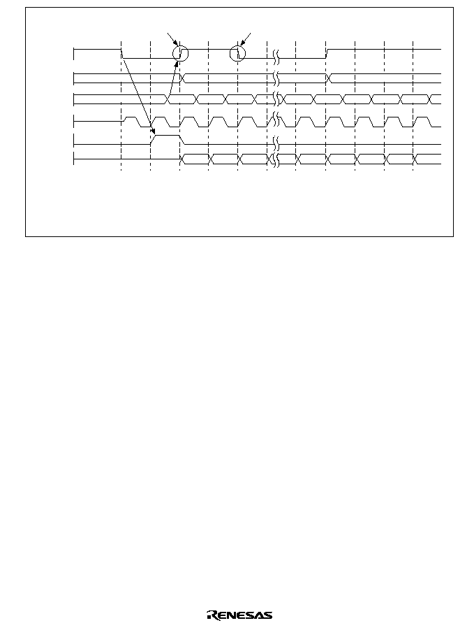
655
STXD
STS
STCK
SITSR
SITDR
TDRE
C[7:0] C[6:0] C[5:0]
C[7:0]
D[7:0]
D[7:0]
E[7:0]
C[0]
D[7:0] D[6:0]
C[7]
C[6]
C[5]
D[7]
D[6]
C[0]
D[5]
D[4]
D[5:0] D[4:0]
Set to 1 when the amount of data in SITDR is
less than or equal to the setting of bits
TFWM3 to TFWM0 in SIFCR
Note: TM = 1: STS is output
DL = 0: 8-bit data transfer
SE = 0: Asynchronous transfer, no start signal mode
LM = 0: MSB first
TRMD = 0: LSB of transmitted primary data is value in SITDR
Cleared to 0 when an amount of data exceeding
the setting of bits TFWM3 to TFWM0 in SIFCR
has been written to SITDR
Synchronous internal clock
Undefined
Figure 15.9 Transmission: Continuous Transfer Mode (TM = 1 Mode)/MSB First
Figure 15.10 shows interval transfer mode when TM is cleared to 0 in SICTR and with LSB first.
Figure 15.11 shows continuous transfer mode when TM is cleared to 0 in SICTR and with LSB
first.
Figure 15.12 shows interval transfer mode when TM is set to 1 in SICTR and with LSB first.
Figure 15.13 shows continuous transfer mode when TM is set to 1 in SICTR and with LSB first.

656
STXD
STS
STCK
SITSR
SITDR
TDRE
C[0:7]
C[1:7]
C[2:7]
C[7]
C[7:0]
D[7:0]
D[7:0]
E[7:0]
C[0]
C[1]
C[2]
C[7]
D[0]
D[1]
D[0:7]
D[1:7]
Set to 1 when the amount of data in SITDR is
less than or equal to the setting of bits
TFWM3 to TFWM0 in SIFCR
Note: TM = 0: STS is input
DL = 0: 8-bit data transfer
SE = 1: Synchronous transfer in start signal mode
LM = 1: LSB first
TRMD = 0: LSB of transmitted primary data is value in SITDR
Cleared to 0 when an amount of data exceeding
the setting of bits TFWM3 to TFWM0 in SIFCR
has been written to SITDR
Synchronous internal clock
Undefined
Figure 15.10 Transmission: Interval Transfer Mode (TM = 0 Mode)/LSB First
STXD
STS
STCK
SITSR
SITDR
TDRE
C[0:7]
C[1:7]
C[2:7]
C[7:0]
D[7:0]
D[7:0]
E[7:0]
C[7]
D[0:7]
D[1:7]
C[0]
C[1]
C[2]
D[0]
D[1]
C[7]
D[2]
D[3]
D[2:7]
D[3:7]
Set to 1 when the amount of data in SITDR is
less than or equal to the setting of bits
TFWM3 to TFWM0 in SIFCR
Note: TM = 0: STS is input
DL = 0: 8-bit data transfer
SE = 0: Asynchronous transfer in start signal mode
LM = 1: LSB first
TRMD = 0: LSB of transmitted primary data is value in SITDR
Cleared to 0 when an amount of data exceeding
the setting of bits TFWM3 to TFWM0 in SIFCR
has been written to SITDR
Synchronous internal clock
Undefined
Figure 15.11 Transmission: Continuous Transfer Mode (TM = 0 Mode)/LSB First
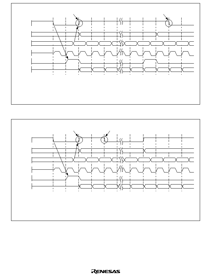
657
STXD
STS
STCK
SITSR
SITDR
C[0:7]
C[1:7]
C[2:7]
C[7:0]
D[7:0]
D[7:0]
E[7:0]
C[6:7]
C[7]
D[0:7]
C[0]
C[1]
C[2]
C[7]
D[0]
C[6]
D[1]
D[2]
D[1:7]
D[2:7]
TDRE
Set to 1 when the amount of data in SITDR is
less than or equal to the setting of bits
TFWM3 to TFWM0 in SIFCR
Note: TM = 1: STS is output
DL = 0: 8-bit data transfer
SE = 1: Synchronous transfer in start signal mode
LM = 1: LSB first
TRMD = 0: LSB of transmitted primary data is value in SITDR
Cleared to 0 when an amount of data exceeding
the setting of bits TFWM3 to TFWM0 in SIFCR
has been written to SITDR
Synchronous internal clock
Undefined
Figure 15.12 Transmission: Interval Transfer Mode (TM = 1 Mode)/LSB First
STXD
STS
STCK
SITSR
SITDR
TDRE
C[0:7]
C[1:7]
C[2:7]
C[7:0]
D[7:0]
D[7:0]
E[7:0]
C[7]
D[0:7]
D[1:7]
C[0]
C[1]
C[2]
D[0]
D[1]
C[7]
D[2]
D[3]
D[2:7]
D[3:7]
Set to 1 when the amount of data in SITDR is
less than or equal to the setting of bits
TFWM3 to TFWM0 in SIFCR
Note: TM = 1: STS is output
DL = 0: 8-bit data transfer
SE = 0: Asynchronous transfer, no start signal mode
LM = 1: LSB first
TRMD = 0: LSB of transmitted primary data is value in SITDR
Cleared to 0 when an amount of data exceeding
the setting of bits TFWM3 to TFWM0 in SIFCR
has been written to SITDR
Synchronous internal clock
Undefined
Figure 15.13 Transmission: Continuous Transfer Mode (TM = 1 Mode)/LSB First
15.3.3
Output when TRMD = 1 in SIFCR
Figure 15.14 shows output timing when TM is set to 1 in SIFTR.
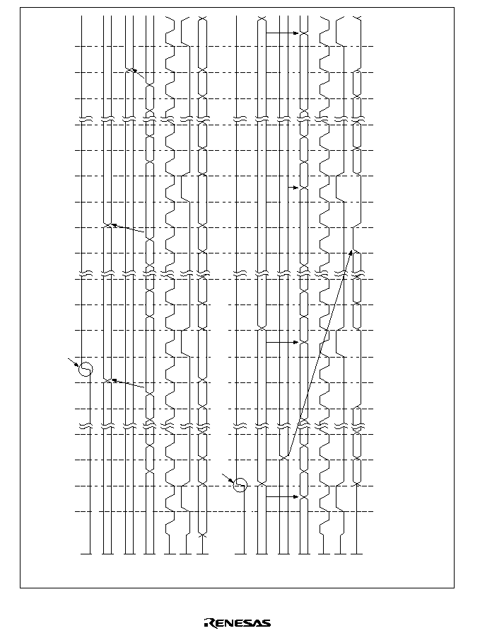
658
B[7]
A[7]
A[7:0]
A[7:0]
A[7:1]
Set to 1 when an amount of data equal to or greater than
the setting of bits RFWM3 to RFWM0 in SIFCR is received
A[7]
A[6]
A[0]
B[7]
B[6]
Invalid
B[0]
C[7]
C[6]
C[0]
SRXD
SRS
SRCK
SIRSR
SIRDR
RDRF
SIRCDR
Undefined
B[7:1]
C[7:0]
C[7:0]
C[7:1]
C[7]
Invalid
B[7:0]
E[7:0]
D[7:0]
D[6:0]
D[0]
D[7:0]
E[7:0]
E[7:0]
F[7:0]
F[7:0]
F[7:0]
D[7]
D[6]
D[0]
E[7]
E[6]
E[0]
Z[7]
Z[6]
Z[0]
STXD
STS
STCK
SITSR
SITDR
TDRE
SITCDR
Undefined
E[6:0]
Z[7:0]
Z[7:0]
Z[7:0]
Z[7:0]
Z[6:0]
Z[7:0]
E[0]
F[7:0]
Z[0]
Note:
TM = 0: STS is input
DL = 0: 8-bit data transfer
SE = 1: Synchronous transfer in start signal mode
LM = 0: MSB first
TRMD = 1: LSB of transmitted primary data is 0
Set to 1 when the amount of data in SITDR is less than or equal to
the setting of bits TFWM3 to TFWM0 in SIFCR
Invalid
B[7:0]
B[7:0]
Synchronous internal clock
Synchronous internal clock
Figure 15.14 Transmission: TRMD = 1 Mode

659
15.4
SIOF Interrupt Sources and DMAC
Each SIOF channel has four interrupt sources: the receive-overrun-error interrupt (RERI) request,
transmit-underrun-error interrupt (TERI) request, receive-data-full interrupt (RDFI) request, and
transmit-data-empty interrupt (TDEI) request. Table 15.3 shows the interrupt sources and their
relative priorities. The RDFI and TDEI interrupts are enabled by the RIE and TIE bits,
respectively, in SICTR. The RERI0 and TERI0 interrupts cannot be disabled.
An RDFI0 interrupt request is generated when the RDRF bit is set to 1 or the RCD bit is set to 1 in
SISTR.
The DMACE bit should be cleared to 0 in SICTR to have interrupts triggered by both the RDRF
bit and the RCD bit processed by the CPU. In this case the CPU should process interrupts after
reading SISTR and determining which bit triggered them.
Set the DMACE bit to 1 in SICTR to have interrupts triggered by the RDRF bit processed by the
DMAC and interrupts triggered by the RCD bit processed by the CPU. In addition, the priority of
interrupts from SIOF should be set to a high level in order to activate the interrupt controller
(INTC). This will cause interrupts triggered by the RDRF bit to be sent to the DMAC and
interrupts triggered by the RCD bit to be sent to the INTC. The data in SIRDR is read and if the
amount of primary data is less than the setting of bits RFWM3 to RFWM0 in SIFCR, RDRF is
automatically cleared to 0. Interrupts triggered by the RCD bit cannot be processed by the DMAC.
An TDEI0 interrupt request is generated when the TDRE bit is set to 1 or the TCD bit is set to 1 in
SISTR.
The DMACE bit should be cleared to 0 in SICTR to have interrupts triggered by both the TDRE
bit and the TCD bit processed by the CPU. In this case the CPU should process interrupts after
reading SISTR and determining which bit triggered them.
Set the DMACE bit to 1 in SICTR to have interrupts triggered by the TDRE bit processed by the
DMAC and interrupts triggered by the TCD bit processed by the CPU. In addition, the priority of
interrupts from SIOF should be set to a high level in order to activate the INTC. This will cause
interrupts triggered by the TDRE bit to be sent to the DMAC and interrupts triggered by the TCD
bit to be sent to the INTC. The DMAC writes data to SIRDR and if the amount of primary data is
equal to or greater than the setting of bits TFWM3 to TFWM0 in SIFCR, TDRE is automatically
cleared to 0. Interrupts triggered by the TCD bit cannot be processed by the DMAC.
When the RERR bit is set to 1 in SISTR, an RERI0 interrupt request is generated.
When the TERR bit is set to 1 in SISTR, a TERI0 interrupt request is generated.
Channel interrupt priority levels are set by means of the IRPE register, as described in section 5,
Interrupt Controller (INTC).

660
Table 15.3
SIOF Interrupt Sources
Interrupt Source
Description
DMAC Activation
Priority
RERI
Receive overrun error (RERR)
Not possible
High
TERI
Transmit underrun error (TERR)
Not possible
RDFI
Receive data register full (RDRF)
Possible
*
TDEI
Transmit data register empty (TDRE)
Possible
*
Low
Note:
*
The interrupt sources that can activate the DMAC are receive data full (RDRF) and transmit
data empty (TDRE).
It is not possible for receive control data full (RCD) or transmit control data empty (TCD) to
activate the DMAC.
The DMAC should be used to process RDRF and TDRE interrupts when using SIRCDR and
SITCDR, and the DMACE bit must be set to 1 in SICTR when using the CPU to process RCD
and TCD interrupts.
The DMACE bit should be cleared to 0 in SICTR if neither SIRCDR nor SITCDR is used and
both RDRF and TDRE interrupts as well as RCD and TCD interrupts are to be processed by
the CPU.

661
Section 16 Serial I/O (SIO)
16.1
Overview
A two-channel simple synchronous serial I/O is provided on-chip. The serial I/O functions mainly
as an interface between the chip and a codec or modem analog front-end.
16.1.1
Features
The serial I/O has the following features:
∑
Full-duplex operation
Independent transmit/receive registers and independent transmit/receive clocks
∑
Double-buffered transmit/receive ports
Continuous data transmission/reception possible
∑
Interval transfer mode and continuous transfer mode
∑
Memory-mapped receive register, transmit register, control register, and status register
With the exception of SIRSR and SITSR, these registers are memory-mapped and can be
accessed by a MOV instruction.
∑
Choice of 8- or 16-bit data length
∑
Data transfer communication by means of polling or interrupts
Data transfer can be monitored by polling the receive data register full flag (RDRF) and
transmit data register empty flag (TDRE) in the serial status register. Interrupt requests can be
generated during data transfer by setting the receive interrupt request flag and transmit
interrupt request flag.
∑
MSB-first transfer between SIO and data I/O
Figure 16.1 shows a block diagram of the serial I/O.
662
Peripheral bus
16
SIRDR
SITDR
SISTR
SICTR
STCK
SRCK
SRxD
SIRDR: Receive data register
SIRSR: Receive shift register
SISTR: Serial status register
SICTR: Serial control register
SITDR: Transmit data register
SITSR: Transmit shift register
Bit counter
I/O control unit
SIRSR
SITSR
STxD
SRS
STS
MSB
LSB
MSB
LSB
Serial I/O module
(SIO)
Figure 16.1 SIO Block Diagram

663
Table 16.1 shows the functions of the external pins. As the channels are independent, the channel
numbers are omitted from the signal names in the rest of this section.
Table 16.1
Serial I/O (SIO) External Pins
Channel
Name
Pin
I/O
Function
1
Serial receive data input pin
SRxD1
Input
Serial data input port 1
Serial receive clock input pin
SRCK1
Input
Serial receive clock port 1
Serial reception synchronization
input pin
SRS1
Input
Serial reception
synchronization input port 1
Serial transmit data output pin
STxD1
Output
Serial data output port 1
Serial transmit clock input pin
STCK1
Input
Serial transmit clock port 1
Serial transmission synchro-
nization input/output pin
STS1
I/O
Serial transmission synchro-
nization input/output port 1
2
Serial receive data input pin
SRxD2
Input
Serial data input port 2
Serial receive clock input pin
SRCK2
Input
Serial receive clock port 2
Serial reception synchronization
input pin
SRS2
Input
Serial reception
synchronization input port 2
Serial transmit data output pin
STxD2
Output
Serial data output port 2
Serial transmit clock input pin
STCK2
Input
Serial transmit clock port 2
Serial transmission
synchronization input/output pin
STS2
I/O
Serial transmission synchro-
nization input/output port 2
Note:
In a reset, all pins are initialized to the high-impedance state.

664
16.2
Register Configuration
Table 16.2 shows the SIO's registers. As the channels are independent, the channel numbers are
omitted from the signal names in the rest of this section.
Table 16.2
Register Configuration
Channel
Register
Abbrevia-
tion
R/W
Initial
Value
Address
Access Size
(Bits)
1
Receive shift register 1
SIRSR1
--
--
--
--
Receive data register 1
SIRDR1
R
H'0000
H'FFFFFC10 8, 16, 32
Transmit shift register 1
SITSR1
--
--
--
--
Transmit data register 1
SITDR1
R/W
H'0000
H'FFFFFC12 8, 16, 32
Serial control register 1
SICTR1
R/W
H'0000
H'FFFFFC14 8, 16, 32
Serial status register 1
SISTR1
R/(W)
*
H'0002
H'FFFFFC16 8, 16, 32
2
Receive shift register 2
SIRSR2
--
--
--
--
Receive data register 2
SIRDR2
R
H'0000
H'FFFFFC20 8, 16, 32
Transmit shift register 2
SITSR2
--
--
--
--
Transmit data register 2
SITDR2
R/W
H'0000
H'FFFFFC22 8, 16, 32
Serial control register 2
SICTR2
R/W
H'0000
H'FFFFFC24 8, 16, 32
Serial status register 2
SISTR2
R/(W)
*
H'0002
H'FFFFFC26 8, 16, 32
Note:
*
Only 0 should be written, to clear flags (after reading 1 from the flag).

665
16.2.1
Receive Shift Register (SIRSR)
Bit:
15
14
13
...
3
2
1
0
...
Initial value:
--
--
--
...
--
--
--
--
R/W:
--
--
--
...
--
--
--
--
SIRSR is a 16-bit register used to receive serial data. The data is fetched in MSB first from the
SRxD pin in synchronization with the fall of the serial receive clock (SRCK), and is shifted into
SIRSR. The data length is set by the transmit/receive data length select bit (DL) in the
corresponding serial control register (SICTR). When data transfer to SIRSR is completed, the data
contents are automatically transferred to the receive data register (SIRDR), and the receive data
register full flag (RDRF) is set in the serial status register (SISTR).
If the next data word input operation ends before the RDRF flag is cleared, an overrun error
occurs, the receive overrun error flag (RERR) is set in SISTR, and an overrun error signal is sent
to the interrupt controller (INTC). The data in SIRSR overwrites the data in SIRDR.
16.2.2
Receive Data Register (SIRDR)
Bit:
15
14
13
...
3
2
1
0
...
Initial value:
0
0
0
...
0
0
0
0
R/W:
R
R
R
...
R
R
R
R
SIRDR is a 16-bit register that stores serial receive data. When data is transferred from SIRSR to
SIRDR, the receive data register full flag (RDRF) is set in the serial status register (SISTR). If the
receive interrupt enable flag (RIE) is set in SICTR, a receive-data-full interrupt (RDFI) request is
sent to the interrupt controller (INTC) and the DMA controller (DMAC). When the flag is cleared,
this interrupt request signal is not generated. When SIRDR is read by the DMAC, the RDRF flag
is cleared automatically. SIRDR is initialized to H'0000 by a reset.

666
16.2.3
Transmit Shift Register (SITSR)
Bit:
15
14
13
...
3
2
1
0
...
Initial value:
--
--
--
...
--
--
--
--
R/W:
--
--
--
...
--
--
--
--
SITSR is a 16-bit register used to transmit serial data. The contents of this register are shifted in
MSB-first order in synchronization with the rising edge of the serial transmit clock (STCK), and
output from the STxD pin. The transfer data length is set by the transmit/receive data length select
bit (DL) in the serial control register (SICTR). When the DL bit is cleared to 0 (8-bit data length),
the lower 8 bits of SITDR are output. When the serial transmission synchronization signal (STS)
goes high, or the last data transmission ends without the synchronization enable (SE) bit being set
in SICTR, the contents of the transmit data register (SITDR) are transferred to SITSR, and if
TDRE is 0, TDRE is then set. If output of the next data begins before TDRE is cleared, an overrun
error occurs, the transmit overrun error flag (TERR) is set in SISTR, and a transmit overrun error
interrupt request is sent to the INTC.
16.2.4
Transmit Data Register (SITDR)
Bit:
15
14
13
...
3
2
1
0
...
Initial value:
0
0
0
...
0
0
0
0
R/W:
R/W
R/W
R/W
...
R/W
R/W
R/W
R/W
SITDR is a 16-bit register that stores serial transmit data. Data should be written to SITDR when
the transmit data register empty flag (TDRE) is set to 1 in SISTR. If data is written to SITDR
when TDRE is 0, the previous data will be overwritten. When STS goes high or data output from
transmit shift register SITSR ends with the SE bit cleared to 0 in SICTR, the data in SITDR is
automatically transferred to SITSR, and if TDRE is 0, TDRE is then set. If the transmit interrupt
enable flag (TIE) is set, a transmit-data-empty interrupt (TDEI) request is sent to the INTC and
DMAC. When TIE is cleared, this interrupt request is not generated. When the DMAC writes to
SITDR, the TDRE flag is cleared automatically. The TDRE flag is set only by hardware. SITDR is
initialized to H'0000 by a reset.

667
16.2.5
Serial Control Register (SICTR)
Bit:
15
14
13
12
11
10
9
8
--
--
--
--
--
--
--
--
Initial value:
0
0
0
0
0
0
0
0
R/W:
R
R
R
R
R
R
R
R
Bit:
7
6
5
4
3
2
1
0
--
TM
SE
DL
TIE
RIE
TE
RE
Initial value:
0
0
0
0
0
0
0
0
R/W:
R
R/W
R/W
R/W
R/W
R/W
R/W
R/W
SICTR is a 16-bit register used to set parameters for serial port control. SICTR is initialized to
H'0000 by a reset.
When modifying bit 4, 5, or 6 (TM, SE, or DL), TE and RE should be cleared to 0 beforehand.
Bits 15 to 7--Reserved: These bits are always read as 0. The write value should always be 0.
Bit 6--Transfer Mode Control (TM): Specifies whether the transmission synchronization signal is
to be input from an external source or generated internally by the chip. When this flag is cleared,
the transmission synchronization signal is STS pin input. When this flag is set, the transmission
synchronization signal is generated by the chip, and is output to an external device from the STS
pin. This bit does not affect reception.
Bit 6: TM
Description
0
External signal input from STS pin is used as transmission start indication
(Initial value)
1
Internal signal output from STS pin is used as transmission start indication
Bit 5--Synchronization Signal Enable (SE): Specifies whether the synchronization signals are to
be used for all serial data transfers, or only for the first transfer.
When this bit is cleared to 0, the synchronization signals (SRS and STS) are necessary only for the
first data transfer, and are not required for subsequent transfers. When this bit is set to 1, the
synchronization signals are necessary for all data transfers.
Bit 5: SE
Description
0
Continuous mode: SRS and STS are used only for the first data transfer
(Initial value)
1
Interval mode: SRS and STS are used for all data transfers

668
Bit 4--Transmit/Receive Data Length Select (DL): Specifies the serial I/O module's transfer data
length. The initial value of this bit is 0, indicating an 8-bit data length. When an 8-bit data length
is specified, the lower 8 bits of each I/O register are used.
Bit 4: DL
Description
0
8-bit transfer data length
(Initial value)
1
16-bit transfer data length
Bit 3--Transmit Interrupt Enable (TIE): Enables the transmit-data-empty interrupt. The initial
value of this bit is 0.
Bit 3: TIE
Description
0
Transmit interrupt disabled
(Initial value)
1
Transmit interrupt enabled
Bit 2--Receive Interrupt Enable (RIE): Enables the receive-data-full interrupt. The initial value of
this bit is 0.
Bit 2: RIE
Description
0
Receive interrupt disabled
(Initial value)
1
Receive interrupt enabled
Bit 1--Transmit Enable (TE): Enables data transmission. When this flag is cleared, the STxD,
STCK, and STS pins go to the high-impedance state.
Bit 1: TE
Description
0
Transmission disabled: STxD, STCK, and STS pins go to high-impedance
state
(Initial value)
1
Transmission enabled
Bit 0--Receive Enable (RE): Enables data reception. When this flag is cleared, the SRxD, SRCK,
and SRS pins go to the high-impedance state.
Bit 0: RE
Description
0
Reception disabled: SRxD, SRCK, and SRS pins go to high-impedance state
(Initial value)
1
Reception enabled

669
16.2.6
Serial Status Register (SISTR)
Bit:
15
14
...
4
3
2
1
0
--
--
...
--
TERR
RERR
TDRE
RDRF
Initial value:
0
0
...
0
0
0
1
0
R/W:
R
R
...
R
R/(W)
*
R/(W)
*
R/(W)
*
R/(W)
*
Note:
*
Only 0 should be written, to clear the flag.
SISTR is a 16-bit register that indicates the status of the serial I/O module. SISTR is initialized to
H'0002 by a reset.
Bits 15 to 4--Reserved: These bits are always read as 0. The write value should always be 0.
Bit 3--Transmit Underrun Error (TERR): Flag that indicates the occurrence of a transmit
underrun.
Bit 3: TERR
Description
0
Transmission is in progress, or has ended normally
(Initial value)
[Clearing conditions]
∑
When 0 is written to the TERR bit after reading TERR = 1
∑
When the processor enters the reset state
1
A transmit underrun error has occurred
TERR is set to 1 if data transmission is started while TDRE = 1
Bit 2--Receive Overrun Error (RERR): Flag that indicates the occurrence of a receive overrun.
Bit 2: RERR
Description
0
Reception is in progress, or has ended normally
(Initial value)
[Clearing conditions]
∑
When 0 is written to the RERR bit after reading RERR = 1
∑
When the processor enters the reset state
1
A receive overrun error has occurred
RERR is set to 1 if data reception ends while RDRF = 1

670
Bit 1--Transmit Data Register Empty (TDRE): Flag that indicates that the SITDR register is
empty and the next data can be written.
Bit 1: TDRE
Description
0
SITDR transmit data is valid
[Clearing conditions]
∑
When 0 is written to the TDRE bit after reading TDRE = 1
∑
When the DMAC writes data to SITDR
1
SITDR transmit data is invalid
(Initial value)
TDRE is set to 1 in the following cases:
∑
When data is transferred from SITDR to SITSR
∑
When the TE bit is cleared to 0 in the serial control register (SICTR)
∑
When the processor enters the reset state
Bit 0--Receive Data Register Full (RDRF): Flag that indicates that SIRDR receive data is waiting.
Bit 0: RDRF
Description
0
SIRDR receive data is invalid
(Initial value)
[Clearing conditions]
∑
When the DMAC reads data from SIRDR
∑
When 1 is read from RDRF and 0 is written
∑
When the RE bit is cleared to 0 in the serial control register (SICTR)
∑
When the processor enters the reset state
1
SIRDR receive data is valid
RDRF is set to 1 when serial data reception ends normally and the data is
transferred from SIRSR to SIRDR

671
16.3
Operation
16.3.1
Input
Figure 16.2 shows interval transfer mode (SE set to 1 in SICTR), and figure 16.3 shows
continuous transfer mode (SE cleared to 0 in SICTR).
B[7]
SRxD
Notes: DL = 0: 8-bit data transfer
SE = 1: Synchronous transfer in start signal mode
SRS
SRCK
A[7]
SIRSR
A[7:0]
A[7:6]
A[7:1]
A[7:0]
SIRDR
RDRF
A[7]
A[6]
A[5]
A[0]
A[1]
B[7]
synchronous internal clock
Undefined
Invalid
Figure 16.2 Reception: Interval Transfer Mode
SRxD
Notes: DL = 0: 8-bit data transfer
SE = 0: Asynchronous transfer, no start signal mode
SRCK
SRS
A[7]
A[6]
A[5]
A[0]
B[7]
B[6]
B[5]
A[1]
SIRSR
B[7]
A[7]
A[7:0]
B[7:6]
B[7:5]
A[7:6]
A[7:1]
A[7:0]
SIRDR
RDRF
synchronous internal clock
Undefined
Figure 16.3 Reception: Continuous Transfer Mode
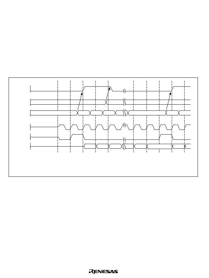
672
16.3.2
Output
Figure 16.4 shows interval transfer mode (SE set to 1 in SICTR) when TM is cleared to 0 in
SICTR.
Figure 16.5 shows continuous transfer mode (SE cleared to 0 in SICTR) when TM is cleared to 0
in SICTR.
Figure 16.6 shows interval transfer mode (SE set to 1 in SICTR) when TM is set to 1 in SICTR.
Figure 16.7 shows continuous transfer mode (SE cleared to 0 in SICTR) when TM is set to 1 in
SICTR.
STxD
Notes: TM = 0: STS is input
DL = 0: 8-bit data transfer
SE = 1: Synchronous transfer in start signal mode
STCK
STS
C[7]
C[6]
C[5]
C[0]
D[7]
C[1]
SITSR
C[6:0]
C[7:0]
D[7:0]
D[6:0]
C[5:0]
C[0]
Data C
SITDR
TDRE
synchronous internal clock
Undefined
Invalid
Figure 16.4 Transmission: Interval Transfer Mode (TM = 0 Mode)
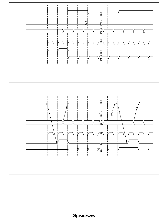
673
C[6:0]
STxD
Notes: TM = 0: STS is input
DL = 0: 8-bit data transfer
SE = 0: Asynchronous transfer, no start signal mode
STCK
STS
C[7]
C[6]
C[5]
C[0]
D[7]
D[6]
D[5]
C[1]
C[7:0]
SITSR
D[7:0]
D[6:0]
D[5:0]
D[4:0]
C[5:0]
C[0]
SITDR
TDRE
synchronous internal clock
Undefined
Data C
Figure 16.5 Transmission: Continuous Transfer Mode (TM = 0 Mode)
C[6:0]
STxD
Notes: TM = 1: STS is output
DL = 0: 8-bit data transfer
SE = 1: Synchronous transfer in start signal mode
STCK
STS
C[7]
C[6]
C[5]
C[0]
D[7]
C[1]
C[7:0]
SITSR
D[7:0]
D[6:0]
C[5:0]
Data C
SITDR
TDRE
synchronous internal clock
Undefined
C[0]
Invalid
Data D
Figure 16.6 Transmission: Interval Transfer Mode (TM = 1 Mode)
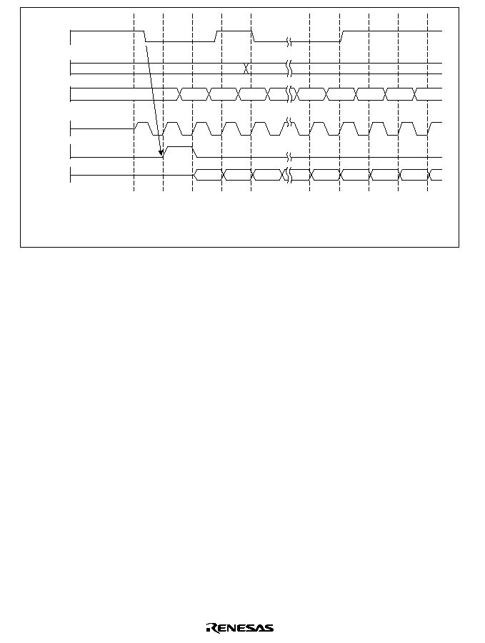
674
C[6:0]
STxD
Notes: TM = 1: STS is output
DL = 0: 8-bit data transfer
SE = 0: Asynchronous transfer, no start signal mode
STCK
STS
C[7]
C[6]
C[5]
C[0]
D[7]
D[6]
D[5]
C[1]
C[7:0]
SITSR
D[7:0]
D[6:0]
D[5:0]
D[4:0]
C[5:0]
C[0]
Data C
SITDR
TDRE
synchronous internal clock
Undefined
Figure 16.7 Transmission: Continuous Transfer Mode (TM = 1 Mode)

675
16.4
SIO Interrupt Sources and DMAC
Each SIO channel has four interrupt sources: the receive-overrun-error interrupt (RERI) request,
transmit-underrun-error interrupt (TERI) request, receive-data-full interrupt (RDFI) request, and
transmit-data-empty interrupt (TDEI) request. Table 16.3 shows the interrupt sources and their
relative priorities. The RDFI and TDEI interrupts are enabled by the RIE and TIE bits,
respectively, in SICTR. The RERI and TERI interrupts cannot be disabled.
An RDFI interrupt request is generated when the RDRF bit is set to 1 in SISTR. RDFI can activate
the DMA controller (DMAC) to read the data in SIRDR. RDRF is cleared to 0 automatically when
the DMAC reads data from SIRDR.
A TDEI interrupt request is generated when the TDRE bit is set to 1 in SISTR. TDEI can activate
the DMAC to write the next data to SITDR. TDRE is cleared to 0 automatically when the DMAC
writes data to SITDR.
When TDEI and RDFI interrupt requests are handled by the DMAC, and not by the interrupt
controller, a low priority level should be given to interrupts from the SIO to prevent the interrupt
controller from operating.
When the RERR bit is set to 1 in SISTR, an RERI interrupt request is generated.
When the TERR bit is set to 1 in SISTR, a TERI interrupt request is generated.
Channel interrupt priority levels are set by means of the IRPE register, as described in section 5,
Interrupt Controller (INTC).
Table 16.3
SIO Interrupt Sources
Interrupt Source
Description
DMAC Activation
Priority
RERI
Receive overrun error (RERR)
Not possible
High
TERI
Transmit underrun error (TERR)
Not possible
RDFI
Receive data register full (RDRF)
Possible
TDEI
Transmit data register empty (TDRE)
Possible
Low

676

677
Section 17 16-Bit Timer Pulse Unit (TPU)
17.1
Overview
An on-chip 16-bit timer pulse unit (TPU) is provided that comprises three 16-bit timer channels.
17.1.1
Features
The TPU has the following features:
∑
Maximum 8-pulse input/output
∑
A total of eight timer general registers (TGRs) are provided (four for channel 0 and two each
for channels 1, and 2).
Each register can be set independently as an output compare/input capture register.
TGRC and TGRD for channel 0 can be used as buffer registers
∑
Choice of seven or eight counter input clocks for each channel
∑
The following operations can be set for each channel:
Waveform output by compare match: Selection of 0, 1, or toggle output
Input capture function: Choice of rising edge, falling edge, or both edge detection
Counter clear operation: Counter clearing possible by compare match or input capture
Synchronous operation: Multiple timer counters (TCNT) can be written to simultaneously
simultaneous clearing by compare match and input capture possible
register simultaneous input/output possible by counter synchronous operation
PWM mode: Any PWM output duty can be set maximum of 7-phase PWM output possible
by combination with synchronous operation
∑
Buffer operation settable for channel 0
Input capture register double-buffering possible
Automatic rewriting of output compare register possible
∑
Phase counting mode settable independently for each of channels 1, and 2
Two-phase encoder pulse up/down-count possible
∑
Fast access via internal 16-bit bus
Fast access is possible via a 16-bit bus interface
∑
13 interrupt sources
For channel 0 four compare match/input capture dual-function interrupts and one overflow
interrupt can be requested independently
For channels 1, and 2, two compare match/input capture dual-function interrupts, one
overflow interrupt, and one underflow interrupt can be requested independently

678
∑
Automatic transfer of register data
Block transfer, 1-word data transfer, and 1-byte data transfer possible by direct memory
access controller (DMAC) activation
Table 17.1 lists the functions of the TPU.
Table 17.1
TPU Functions
Item
Channel 0
Channel 1
Channel 2
Count clock
P
/1
P
/4
P
/16
P
/64
TCLKA
TCLKB
TCLKC
TCLKD
P
/1
P
/4
P
/16
P
/64
P
/256
TCLKA
TCLKB
P
/1
P
/4
P
/16
P
/64
P
/1024
TCLKA
TCLKB
TCLKC
General registers
TGR0A
TGR0B
TGR1A
TGR1B
TGR2A
TGR2B
General registers/
buffer registers
TGR0C
TGR0D
--
--
I/O pins
TIOCA0
TIOCB0
TIOCC0
TIOCD0
TIOCA1
TIOCB1
TIOCA2
TIOCB2
Counter clear
function
TGR compare match or
input capture
TGR compare match or
input capture
TGR compare match or
input capture
Compare 0 output
O
O
O
match
1 output
O
O
O
output
Toggle
output
O
O
O
Input capture
function
O
O
O
Synchronous
operation
O
O
O
PWM mode
O
O
O
Phase counting
mode
--
O
O
Buffer operation
O
--
--
Notes: O : Possible
-- : Not possible

679
Table 17.1
TPU Functions (cont)
Item
Channel 0
Channel 1
Channel 2
DMAC activation
TGR compare match or
input capture
--
--
Interrupt sources
5 sources
∑
Compare match or
input capture 0A
∑
Compare match or
input capture 0B
∑
Compare match or
input capture 0C
∑
Compare match or
input capture 0D
∑
Overflow
4 sources
∑
Compare match or
input capture 1A
∑
Compare match or
input capture 1B
∑
Overflow
∑
Underflow
4 sources
∑
Compare match or
input capture 2A
∑
Compare match or
input capture 2B
∑
Overflow
∑
Underflow
Note:
-- : Not possible
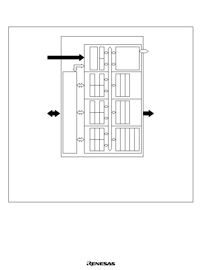
680
17.1.2
Block Diagram
Figure 17.1 shows a block diagram of the TPU.
Control logic
TMDR
TSR
TCR
TIOR
TIER
TGRA
TCNT
TGRB
TGRC
Channel 1
TMDR
TSR
TCR
TIOR
TIER
TGRA
TCNT
TGRB
Channel 0
TMDR
TSR
TCR
TIORH
TIER
Control logic for channels 0 to 2
TGRA
TCNT
TGRB
TGRD
TSYR
TSTR
Clock input
P
/1
P
/4
P
/16
P
/64
P
/256
P
/1024
TCLKA
TCLKB
TCLKC
TCLKD
I/O pins
TIOCA0
TIOCB0
TIOCC0
TIOCD0
TIOCA1
TIOCB1
TIOCA2
TIOCB2
Interrupt request signals
Channel 0:
Channel 1:
Channel 2:
Internal data bus
TIORL
Module data bus
TGI0A
TGI0B
TGI0C
TGI0D
TCI0V
TGI1A
TGI1B
TCI1V
TCI1U
TGI2A
TGI2B
TCI2V
TCI2U
Internal clock:
External clock:
Channel 0:
Channel 1:
Channel 2:
TCR:
Timer Control Register
TMDR: Timer Mode Register
TIOR:
Timer I/O Control Register
TIER:
Timer Interrupt Enable Register
TSR:
Timer Status Register
TCNT:
Timer Counter
TGR:
Timer General Register
TSTR:
Timer Start Register
TSYR:
Timer Synchro Register
Channel 2
Common
Bus interface
Figure 17.1 TPU Block Diagram

681
17.1.3
Pin Configuration
Table 17.2 shows the pin configuration of the TPU.
Table 17.2
Pin Configuration
Channel
Name
Abbreviation
I/O
Function
All
Clock input A
TCLKA
Input
External clock A input pin
(Channel 1 phase counting mode A
phase input)
Clock input B
TCLKB
Input
External clock B input pin
(Channel 1 phase counting mode B
phase input)
Clock input C
TCLKC
Input
External clock C input pin
(Channel 2 phase counting mode A
phase input)
Clock input D
TCLKD
Input
External clock D input pin
(Channel 2 phase counting mode B
phase input)
0
Input capture/output
compare match A0
TIOCA0
I/O
TGR0A input capture input/output
compare output/PWM output pin
Input capture/output
compare match B0
TIOCB0
I/O
TGR0B input capture input/output
compare output/PWM output pin
Input capture/output
compare match C0
TIOCC0
I/O
TGR0C input capture input/output
compare output/PWM output pin
Input capture/output
compare match D0
TIOCD0
I/O
TGR0D input capture input/output
compare output/PWM output pin
1
Input capture/output
compare match A1
TIOCA1
I/O
TGR1A input capture input/output
compare output/PWM output pin
Input capture/output
compare match B1
TIOCB1
I/O
TGR1B input capture input/output
compare output/PWM output pin
2
Input capture/output
compare match A2
TIOCA2
I/O
TGR2A input capture input/output
compare output/PWM output pin
Input capture/output
compare match B2
TIOCB2
I/O
TGR2B input capture input/output
compare output/PWM output pin

682
17.1.4
Register Configuration
Table 17.3 shows the register configuration of the TPU.
Table 17.3
Register Configuration
Channel
Name
Abbreviation R/W
Initial
Value
Address
Access size
(Bits)
0
Timer control register 0 TCR0
R/W
H'00
H'FFFFFC50
8,16
Timer mode register 0 TMDR0
R/W
H'C0
H'FFFFFC51
8,16
Timer I/O control
register 0H
TIOR0H
R/W
H'00
H'FFFFFC52
8,16
Timer I/O control
register 0L
TIOR0L
R/W
H'00
H'FFFFFC53
8,16
Timer interrupt enable
register 0
TIER0
R/W
H'40
H'FFFFFC54
8,16
Timer status register 0 TSR0
R/(W)
*
H'C0
H'FFFFFC55
8,16
Timer counter 0
TCNT0
R/W
H'0000
H'FFFFFC56
16
Timer general register
0A
TGR0A
R/W
H'FFFF
H'FFFFFC58
16
Timer general register
0B
TGR0B
R/W
H'FFFF
H'FFFFFC5A
16
Timer general register
0C
TGR0C
R/W
H'FFFF
H'FFFFFC5C
16
Timer general register
0D
TGR0D
R/W
H'FFFF
H'FFFFFC5E
16
1
Timer control register 1 TCR1
R/W
H'00
H'FFFFFC60
8,16
Timer mode register 1 TMDR1
R/W
H'C0
H'FFFFFC61
8,16
Timer I/O control
register 1
TIOR1
R/W
H'00
H'FFFFFC62
8,16
Timer interrupt enable
register 1
TIER1
R/W
H'40
H'FFFFFC64
8,16
Timer status register 1 TSR1
R/(W)
*
H'C0
H'FFFFFC65
8,16
Timer counter 1
TCNT1
R/W
H'0000
H'FFFFFC66
16
Timer general register
1A
TGR1A
R/W
H'FFFF
H'FFFFFC68
16
Timer general register
1B
TGR1B
R/W
H'FFFF
H'FFFFFC6A
16

683
Table 17.3
Register Configuration (cont)
Channel
Name
Abbreviation R/W
Initial
Value
Address
Access size
(Bits)
2
Timer control register 2
TCR2
R/W
H'00
H'FFFFFC70
8, 16
Timer mode register 2
TMDR2
R/W
H'C0
H'FFFFFC71
8, 16
Timer I/O control
register 2
TIOR2
R/W
H'00
H'FFFFFC72
8, 16
Timer interrupt enable
register 2
TIER2
R/W
H'40
H'FFFFFC74
8, 16
Timer status register 2
TSR2
R/(W)
*
H'C0
H'FFFFFC75
8, 16
Timer counter 2
TCNT2
R/W
H'0000
H'FFFFFC76
16
Timer general register
2A
TGR2A
R/W
H'FFFF
H'FFFFFC78
16
Timer general register
2B
TGR2B
R/W
H'FFFF
H'FFFFFC7A
16
All
Timer start register
TSTR
R/W
H'00
H'FFFFFC40
8, 16
Timer synchro register
TSYR
R/W
H'00
H'FFFFFC41
8, 16
Note:
*
Only 0 can be written, to clear the flags.
17.2
Register Descriptions
17.2.1
Timer Control Register (TCR)
Channel 0: TCR0
Bit:
7
6
5
4
3
2
1
0
CCLR2
CCLR1
CCLR0
CKEG1
CKEG0
TPSC2
TPSC1
TPSC0
Initial value:
0
0
0
0
0
0
0
0
R/W:
R/W
R/W
R/W
R/W
R/W
R/W
R/W
R/W
Channel 1: TCR1
Channel 2: TCR2
Bit:
7
6
5
4
3
2
1
0
--
CCLR1
CCLR0
CKEG1
CKEG0
TPSC2
TPSC1
TPSC0
Initial value:
0
0
0
0
0
0
0
0
R/W:
R
R/W
R/W
R/W
R/W
R/W
R/W
R/W

684
The TCR registers are 8-bit registers that control the TCNT channels. The TPU has three TCR
registers, one for each of channels 0 to 2. The TCR registers are initialized to H'00 by a reset.
TCNT operation should be stopped when making TCR settings.
Bits 7 to 5--Counter Clear 2 to 0 (CCLR2 to CCLR0): These bits select the TCNT counter
clearing source.
Channel
Bit 7:
CCLR2
Bit 6:
CCLR1
Bit 5:
CCLR0
Description
0
0
0
0
TCNT clearing disabled
(Initial value)
1
TCNT cleared by TGRA compare match/input
capture
1
0
TCNT cleared by TGRB compare match/input
capture
1
TCNT cleared by counter clearing for another
channel performing synchronous
clearing/synchronous operation
*
1
1
0
0
TCNT clearing disabled
1
TCNT cleared by TGRC compare match/input
capture
*
2
1
0
TCNT cleared by TGRD compare match/input
capture
*
2
1
TCNT cleared by counter clearing for another
channel performing synchronous
clearing/synchronous operation
*
1
Channel
Bit 7:
Reserved
*
3
Bit 6:
CCLR1
Bit 5:
CCLR0
Description
1, 2
0
0
0
TCNT clearing disabled
(Initial value)
1
TCNT cleared by TGRA compare match/input
capture
1
0
TCNT cleared by TGRB compare match/input
capture
1
TCNT cleared by counter clearing for another
channel performing synchronous clearing/
synchronous operation
*
1
Notes:
*
1 Synchronous operation setting is performed by setting the SYNC bit in TSYR to 1.
*
2 When TGRC or TGRD is used as a buffer register, TCNT is not cleared because the
buffer register setting has priority, and compare match/input capture does not occur.
*
3 Bit 7 is reserved in channels 1and 2. It is always read as 0. The write value should
always be 0.

685
Bits 4 and 3--Clock Edge 1 and 0 (CKEG1, CKEG0): These bits select the input clock edge.
When a both-edges count is selected, a clock divided by two from the input clock can be selected.
(e.g. P
/4 both edges = P
/2 rising edge). If phase counting mode is used on channels 1, and 2,
this setting is ignored and the phase counting mode setting has priority.
Bit 4: CKEG1
Bit 3: CKEG0
Description
0
0
Count at rising edge
(Initial value)
1
Count at falling edge
1
--
Count at both edges
Note:
Internal clock edge selection is valid when the input clock is P
/4 or slower. If P
/1 is
selected for the input clock, this setting is ignored and a rising-edge count is selected.
Bits 2 to 0--Time Prescaler 2 to 0 (TPSC2 to TPSC0): These bits select the TCNT counter clock.
The clock source can be selected independently for each channel. Table 17.4 shows the clock
sources that can be set for each channel.
Table 17.4
TPU Clock Sources
Internal Clock
External Clock
Channel
P
/1
P
/4
P
/16
P
/64
P
/256
P
/1024
TCLKA TCLKB TCLKC TCLKD
0
O
O
O
O
O
O
O
O
1
O
O
O
O
O
O
O
2
O
O
O
O
O
O
O
O
Notes:
O
: Setting
Blank: No setting

686
Channel
Bit 2:
TPSC2
Bit 1:
TPSC1
Bit 0:
TPSC0
Description
0
0
0
0
Internal clock: counts on P
/1 (Initial
value)
1
Internal clock: counts on P
/4
1
0
Internal clock: counts on P
/16
1
Internal clock: counts on P
/64
1
0
0
External clock: counts on TCLKA pin input
1
External clock: counts on TCLKB pin input
1
0
External clock: counts on TCLKC pin input
1
External clock: counts on TCLKD pin input
Channel
Bit 2:
TPSC2
Bit 1:
TPSC1
Bit 0:
TPSC0
Description
1
0
0
0
Internal clock: counts on P
/1 (Initial
value)
1
Internal clock: counts on P
/4
1
0
Internal clock: counts on P
/16
1
Internal clock: counts on P
/64
1
0
0
External clock: counts on TCLKA pin input
1
External clock: counts on TCLKB pin input
1
0
Internal clock: counts on P
/256
1
Setting prohibited
Note:
This setting is ignored when channel 1 is in phase counting mode.
Channel
Bit 2:
TPSC2
Bit 1:
TPSC1
Bit 0:
TPSC0
Description
2
0
0
0
Internal clock: counts on P
/1 (Initial
value)
1
Internal clock: counts on P
/4
1
0
Internal clock: counts on P
/16
1
Internal clock: counts on P
/64
1
0
0
External clock: counts on TCLKA pin input
1
External clock: counts on TCLKB pin input
1
0
External clock: counts on TCLKC pin input
1
Internal clock: counts on P
/1024
Note:
This setting is ignored when channel 2 is in phase counting mode.

687
17.2.2
Timer Mode Register (TMDR)
Channel 0: TMDR0
Bit:
7
6
5
4
3
2
1
0
--
--
BFB
BFA
MD3
MD2
MD1
MD0
Initial value:
1
1
0
0
0
0
0
0
R/W:
R
R
R/W
R/W
R/W
R/W
R/W
R/W
Channel 1: TMDR1
Channel 2: TMDR2
Bit:
7
6
5
4
3
2
1
0
--
--
--
--
MD3
MD2
MD1
MD0
Initial value:
1
1
0
0
0
0
0
0
R/W:
R
R
R
R
R/W
R/W
R/W
R/W
The TMDR registers are 8-bit readable/writable registers that are used to set the operating mode
for each channel. The TPU has three TMDR registers, one for each channel. The TMDR registers
are initialized to H'C0 by a reset.
TCNT operation should be stopped when making TMDR settings.
Bits 7 and 6--Reserved: These bits are always read as 1. The write value should always be 1.
Bit 5--Buffer Operation B (BFB): Specifies whether TGRB is to operate in the normal way, or
TGRB and TGRD are to be used together for buffer operation. When TGRD is used as a buffer
register, TGRD input capture/output compare is not generated.
In channels 1 and 2, which have no TGRD, bit 5 is reserved. It is always read as 0 and cannot be
modified.
Bit 5: BFB
Description
0
TGRB operates normally
(Initial value)
1
TGRB and TGRD used together for buffer operation

688
Bit 4--Buffer Operation A (BFA): Specifies whether TGRA is to operate in the normal way, or
TGRA and TGRC are to be used together for buffer operation. When TGRC is used as a buffer
register, TGRC input capture/output compare is not generated.
In channels 1 and 2, which have no TGRC, bit 4 is reserved. It is always read as 0 and cannot be
modified.
Bit 4: BFA
Description
0
TGRA operates normally
(Initial value)
1
TGRA and TGRC used together for buffer operation
Bits 3 to 0--Modes 3 to 0 (MD3 to MD0): These bits are used to set the timer operating mode.
Bit 3:
MD3
*
1
Bit 2:
MD2
*
2
Bit 1:
MD1
Bit 0:
MD0
Description
0
0
0
0
Normal operation
(Initial value)
1
Reserved
1
0
PWM mode 1
1
PWM mode 2
1
0
0
Phase counting mode 1
1
Phase counting mode 2
1
0
Phase counting mode 3
1
Phase counting mode 4
1
*
*
*
--
*
: Don't care
Notes:
*
1 MD3 is a reserved bit. In a write, it should always be written with 0.
*
2 Phase counting mode cannot be set for channel 0. In this case, 0 should always be
written to MD2.

689
17.2.3
Timer I/O Control Register (TIOR)
Channel 0: TIOR0H
Channel 1: TIOR1
Channel 2: TIOR2
Bit:
7
6
5
4
3
2
1
0
IOB3
IOB2
IOB1
IOB0
IOA3
IOA2
IOA1
IOA0
Initial value:
0
0
0
0
0
0
0
0
R/W:
R/W
R/W
R/W
R/W
R/W
R/W
R/W
R/W
Channel 0: TIOR0L
Bit:
7
6
5
4
3
2
1
0
IOD3
IOD2
IOD1
IOD0
IOC3
IOC2
IOC1
IOC0
Initial value:
0
0
0
0
0
0
0
0
R/W:
R/W
R/W
R/W
R/W
R/W
R/W
R/W
R/W
Note:
When TGRC or TGRD is designated for buffer operation, this setting is invalid and the
register operates as a buffer register.
The TIOR registers are 8-bit registers that control the TGR registers. The TPU has four TIOR
registers, two for channel 0 and one each for channels 1, and 2. The TIOR registers are initialized
to H'00 by a reset.
Note that TIOR is affected by the TMDR setting.
The initial output specified by TIOR becomes valid when the counter is halted (i.e. when the CST
bit is cleared to 0 in TSTR). In PWM mode 2, the output at the point at which the counter is
cleared to 0 is specified.

690
Bits 7 to 4-- I/O Control B3 to B0 (IOB3 to IOB0)
I/O Control D3 to D0 (IOD3 to IOD0):
Bits IOB3 to IOB0 specify the function of TGRB.
Bits IOD3 to IOD0 specify the function of TGRD.
TIOR0H
Channel
Bit 7:
IOB3
Bit 6:
IOB2
Bit 5:
IOB1
Bit 4:
IOB0 Description
0
0
0
0
0
TGR0B is Output disabled
(Initial value)
1
output
Initial output is 0
0 output at compare match
1
0
compare
output
1 output at compare match
1
register
Toggle output at compare
match
1
0
0
Output disabled
1
Initial output is 1
0 output at compare match
1
0
output
1 output at compare match
1
Toggle output at compare
match
1
0
0
0
TGR0B is Capture input
Input capture at rising edge
1
input
source is
Input capture at falling edge
1
*
capture
TIOCB0 pin
Input capture at both edges
1
*
*
register
Setting prohibited
*
: Don't care

691
TIOR0L
Channel
Bit 7:
IOD3
Bit 6:
IOD2
Bit 5:
IOD1
Bit 4:
IOD0 Description
0
0
0
0
0
TGR0D is Output disabled
(Initial value)
1
output
Initial output is 0
0 output at compare match
1
0
compare
output
1 output at compare match
1
register
*
1
Toggle output at compare
match
1
0
0
Output disabled
1
Initial output is 1
0 output at compare match
1
0
output
1 output at compare match
1
Toggle output at compare
match
1
0
0
0
TGR0D is Capture input
Input capture at rising edge
1
input
source is
Input capture at falling edge
1
*
capture
TIOCD0 pin
Input capture at both edges
1
*
*
register
*
1
Setting prohibited
*
: Don't care
Note:
*
1 When the BFB bit in TMDR0 is set to 1 and TGR0D is used as a buffer register, this
setting is invalid and input capture/output compare is not generated.

692
TIOR1
Channel
Bit 7:
IOB3
Bit 6:
IOB2
Bit 5:
IOB1
Bit 4:
IOB0 Description
1
0
0
0
0
TGR1B is Output disabled
(Initial value)
1
output
Initial output is 0
0 output at compare match
1
0
compare
output
1 output at compare match
1
register
Toggle output at compare
match
1
0
0
Output disabled
1
Initial output is 1
0 output at compare match
1
0
output
1 output at compare match
1
Toggle output at compare
match
1
0
0
0
TGR1B is Capture input
Input capture at rising edge
1
input
source is
Input capture at falling edge
1
*
capture
TIOCB1 pin
Input capture at both edges
1
*
*
register
Setting prohibited
*
: Don't care
TIOR2
Channel
Bit 7:
IOB3
Bit 6:
IOB2
Bit 5:
IOB1
Bit 4:
IOB0 Description
2
0
0
0
0
TGR2B is Output disabled
(Initial value)
1
output
Initial output is 0
0 output at compare match
1
0
compare
output
1 output at compare match
1
register
Toggle output at compare
match
1
0
0
Output disabled
1
Initial output is 1
0 output at compare match
1
0
output
1 output at compare match
1
Toggle output at compare
match
1
*
0
0
TGR2B is Capture input
Input capture at rising edge
1
input
source is
Input capture at falling edge
1
*
capture
register
TIOCB2 pin
Input capture at both edges
*
: Don't care

693
Bits 3 to 0-- I/O Control A3 to A0 (IOA3 to IOA0)
I/O Control C3 to C0 (IOC3 to IOC0):
IOA3 to IOA0 specify the function of TGRA.
IOC3 to IOC0 specify the function of TGRC.
TIOR0H
Channel
Bit 3:
IOA3
Bit 2:
IOA2
Bit 1:
IOA1
Bit 0:
IOA0 Description
0
0
0
0
0
TGR0A is Output disabled
(Initial value)
1
output
Initial output is 0
0 output at compare match
1
0
compare
output
1 output at compare match
1
register
Toggle output at compare
match
1
0
0
Output disabled
1
Initial output is 1
0 output at compare match
1
0
output
1 output at compare match
1
Toggle output at compare
match
1
0
0
0
TGR0A is Capture input
Input capture at rising edge
1
input
source is
Input capture at falling edge
1
*
capture
TIOCA0 pin
Input capture at both edges
1
*
*
register
Setting prohibited
*
: Don't care

694
TIOR0L
Channel
Bit 3:
IOC3
Bit 2:
IOC2
Bit 1:
IOC1
Bit 0:
IOC0 Description
0
0
0
0
0
TGR0C is Output disabled
(Initial value)
1
output
Initial output is 0
0 output at compare match
1
0
compare
output
1 output at compare match
1
register
*
1
Toggle output at compare
match
1
0
0
Output disabled
1
Initial output is 1
0 output at compare match
1
0
output
1 output at compare match
1
Toggle output at compare
match
1
0
0
0
TGR0C is Capture input
Input capture at rising edge
1
input
source is
Input capture at falling edge
1
*
capture
TIOCC0 pin
Input capture at both edges
1
*
*
register
*
1
Setting prohibited
*
: Don't care
Note:
*
1 When the BFA bit in TMDR0 is set to 1 and TGR0C is used as a buffer register, this
setting is invalid and input capture/output compare is not generated.

695
TIOR1
Channel
Bit 3:
IOA3
Bit 2:
IOA2
Bit 1:
IOA1
Bit 0:
IOA0 Description
1
0
0
0
0
TGR1A is Output disabled
(Initial value)
1
output
Initial output is 0
0 output at compare match
1
0
compare
output
1 output at compare match
1
register
Toggle output at compare
match
1
0
0
Output disabled
1
Initial output is 1
0 output at compare match
1
0
output
1 output at compare match
1
Toggle output at compare
match
1
0
0
0
TGR1A is Capture input
Input capture at rising edge
1
input
source is
Input capture at falling edge
1
*
capture
TIOCA1 pin
Input capture at both edges
1
*
*
register
Setting prohibited
*
: Don't care
TIOR2
Channel
Bit 3:
IOA3
Bit 2:
IOA2
Bit 1:
IOA1
Bit 0:
IOA0 Description
2
0
0
0
0
TGR2A is Output disabled
(Initial value)
1
output
Initial output is 0
0 output at compare match
1
0
compare
output
1 output at compare match
1
register
Toggle output at compare
match
1
0
0
Output disabled
1
Initial output is 1
0 output at compare match
1
0
output
1 output at compare match
1
Toggle output at compare
match
1
*
0
0
TGR2A is Capture input
Input capture at rising edge
1
input
source is
Input capture at falling edge
1
*
capture
register
TIOCA2 pin
Input capture at both edges
*
: Don't care

696
17.2.4
Timer Interrupt Enable Register (TIER)
Channel 0: TIER0
Bit:
7
6
5
4
3
2
1
0
--
--
--
TCIEV
TGIED
TGIEC
TGIEB
TGIEA
Initial value:
0
1
0
0
0
0
0
0
R/W:
R
R
R
R/W
R/W
R/W
R/W
R/W
Channel 1: TIER1
Channel 2: TIER2
Bit:
7
6
5
4
3
2
1
0
--
--
TCIEU
TCIEV
--
--
TGIEB
TGIEA
Initial value:
0
1
0
0
0
0
0
0
R/W:
R
R
R/W
R/W
R
R
R/W
R/W
The TIER registers are 8-bit registers that control enabling or disabling of interrupt requests for
each channel. The TPU has three TIER registers, one for each channel. The TIER registers are
initialized to H'40 by a reset.
Bit 7--Reserved: This bit is always read as 0. The write value should always be 0.
Bit 6--Reserved: This bit is always read as 1. The write value should always be 1.
Bit 5--Underflow Interrupt Enable (TCIEU): Enables or disables interrupt requests (TCIU) by the
TCFU flag when the TCFU flag in TSR is set to 1 in channels 1 and 2.
In channel 0, bit 5 is reserved. It is always read as 0 and cannot be modified.
Bit 5: TCIEU
Description
0
Interrupt requests (TCIU) by TCFU disabled
(Initial value)
1
Interrupt requests (TCIU) by TCFU enabled
Bit 4--Overflow Interrupt Enable (TCIEV): Enables or disables interrupt requests (TCIV) by the
TCFV flag when the TCFV flag in TSR is set to 1.
Bit 4: TCIEV
Description
0
Interrupt requests (TCIV) by TCFV disabled
(Initial value)
1
Interrupt requests (TCIV) by TCFV enabled

697
Bit 3--TGR Interrupt Enable D (TGIED): Enables or disables interrupt requests (TGID) by the
TGFD bit when the TGFD bit in TSR is set to 1 in channel 0.
In channels 1, and 2, bit 3 is reserved. It is always read as 0 and cannot be modified.
Bit 3: TGIED
Description
0
Interrupt requests (TGID) by TGFD bit disabled
(Initial value)
1
Interrupt requests (TGID) by TGFD bit enabled
Bit 2--TGR Interrupt Enable C (TGIEC): Enables or disables interrupt requests (TGIC) by the
TGFC bit when the TGFC bit in TSR is set to 1 in channel 0.
In channels 1 and 2, bit 2 is reserved. It is always read as 0 and cannot be modified.
Bit 2: TGIEC
Description
0
Interrupt requests (TGIC) by TGFC bit disabled
(Initial value)
1
Interrupt requests (TGIC) by TGFC bit enabled
Bit 1--TGR Interrupt Enable B (TGIEB): Enables or disables interrupt requests (TGIB) by the
TGFB bit when the TGFB bit in TSR is set to 1.
Bit 1: TGIEB
Description
0
Interrupt requests (TGIB) by TGFB bit disabled
(Initial value)
1
Interrupt requests (TGIB) by TGFB bit enabled
Bit 0--TGR Interrupt Enable A (TGIEA): Enables or disables interrupt requests (TGIA) by the
TGFA bit when the TGFA bit in TSR is set to 1.
Bit 0: TGIEA
Description
0
Interrupt requests (TGIA) by TGFA bit disabled
(Initial value)
1
Interrupt requests (TGIA) by TGFA bit enabled

698
17.2.5
Timer Status Register (TSR)
Channel 0: TSR0
Bit:
7
6
5
4
3
2
1
0
--
--
--
TCFV
TGFD
TGFC
TGFB
TGFA
Initial value:
1
1
0
0
0
0
0
0
R/W:
R
R
R
R/(W)
*
R/(W)
*
R/(W)
*
R/(W)
*
R/(W)
*
Note:
*
Only 0 can be written, to clear the flags.
Channel 1: TSR1
Channel 2: TSR2
Bit:
7
6
5
4
3
2
1
0
TCFD
--
TCFU
TCFV
--
--
TGFB
TGFA
Initial value:
1
1
0
0
0
0
0
0
R/W:
R
R
R/(W)
*
R/(W)
*
R
R
R/(W)
*
R/(W)
*
Note:
*
Only 0 can be written, to clear the flags.
The TSR registers are 8-bit registers that indicate the status of each channel. The TPU has three
TSR registers, one for each channel. The TSR registers are initialized to H'C0 by a reset.
Bit 7--Count Direction Flag (TCFD): Status flag that shows the direction in which TCNT counts
in channels 1, and 2.
In channel 0, bit 7 is reserved. It is always read as 1 and cannot be modified.
Bit 7: TCFD
Description
0
TCNT counts down
1
TCNT counts up
(Initial value)
Bit 6--Reserved: This bit is always read as 0. The write value should always be 0.

699
Bit 5--Underflow Flag (TCFU): Status flag that indicates that TCNT underflow has occurred
when channels 1 and 2 are set to phase counting mode.
In channel 0, bit 5 is reserved. It is always read as 0 and cannot be modified.
Bit 5: TCFU
Description
0
[Clearing condition]
(Initial value)
When 0 is written to TCFU after reading TCFU = 1
1
[Setting condition]
When the TCNT value underflows (changes from H'0000 to H'FFFF)
Bit 4--Overflow Flag (TCFV): Status flag that indicates that TCNT overflow has occurred.
Bit 4: TCFV
Description
0
[Clearing condition]
(Initial value)
When 0 is written to TCFV after reading TCFV = 1
1
[Setting condition]
When the TCNT value overflows (changes from H'FFFF to H'0000 )
Bit 3--Input Capture/Output Compare Flag D (TGFD): Status flag that indicates the occurrence of
TGRD input capture or compare match in channel 0.
In channels 1 and 2, bit 3 is reserved. It is always read as 0 and cannot be modified.
Bit 3: TGFD
Description
0
[Clearing conditions]
(Initial value)
∑
When DMAC is activated by TGID interrupt while DRCR setting in DMAC is
TGI0D
∑
When 0 is written to TGFD after reading TGFD = 1
1
[Setting conditions]
∑
When TCNT = TGRD while TGRD is functioning as output compare
register
∑
When TCNT value is transferred to TGRD by input capture signal while
TGRD is functioning as input capture register

700
Bit 2--Input Capture/Output Compare Flag C (TGFC): Status flag that indicates the occurrence of
TGRC input capture or compare match in channel 0.
In channels 1 and 2, bit 2 is reserved. It is always read as 0 and cannot be modified.
Bit 2: TGFC
Description
0
[Clearing conditions]
(Initial value)
∑
When DMAC is activated by TGIC interrupt while DRCR setting in DMAC is
TGI0C
∑
When 0 is written to TGFC after reading TGFC = 1
1
[Setting conditions]
∑
When TCNT = TGRC while TGRC is functioning as output compare
register
∑
When TCNT value is transferred to TGRC by input capture signal while
TGRC is functioning as input capture register
Bit 1--Input Capture/Output Compare Flag B (TGFB): Status flag that indicates the occurrence of
TGRB input capture or compare match.
Bit 1: TGFB
Description
0
[Clearing conditions]
(Initial value)
∑
When DMAC is activated by TGIB interrupt while DRCR setting in DMAC is
TGI0B
∑
When 0 is written to TGFB after reading TGFB = 1
1
[Setting conditions]
∑
When TCNT = TGRB while TGRB is functioning as output compare register
∑
When TCNT value is transferred to TGRB by input capture signal while
TGRB is functioning as input capture register

701
Bit 0--Input Capture/Output Compare Flag A (TGFA): Status flag that indicates the occurrence of
TGRA input capture or compare match.
Bit 0: TGFA
Description
0
[Clearing conditions]
(Initial value)
∑
When DMAC is activated by TGIA interrupt while DRCR setting in DMAC is
TGI0A
∑
When 0 is written to TGFA after reading TGFA = 1
1
[Setting conditions]
∑
When TCNT = TGRA while TGRA is functioning as output compare register
∑
When TCNT value is transferred to TGRA by input capture signal while
TGRA is functioning as input capture register
17.2.6
Timer Counter (TCNT)
Channel 0: TCNT0 (up-counter)
Channel 1: TCNT1 (up/down-counter
*
)
Channel 2: TCNT2 (up/down-counter
*
)
Bit:
15
14
13
12
11
10
9
8
Initial value:
0
0
0
0
0
0
0
0
R/W:
R/W
R/W
R/W
R/W
R/W
R/W
R/W
R/W
Bit:
7
6
5
4
3
2
1
0
Initial value:
0
0
0
0
0
0
0
0
R/W:
R/W
R/W
R/W
R/W
R/W
R/W
R/W
R/W
Note:
*
These counters can be used as up/down-counters only in phase counting mode. In other
cases they function as up-counters.
The TCNT registers are 16-bit counters. The TPU has three TCNT counters, one for each channel.
The TCNT counters are initialized to H'0000 by a reset.
The TCNT counters cannot be accessed in 8-bit units; they must always be accessed as a 16-bit
unit.

702
17.2.7
Timer General Register (TGR)
Bit:
15
14
13
12
11
10
9
8
Initial value:
1
1
1
1
1
1
1
1
R/W:
R/W
R/W
R/W
R/W
R/W
R/W
R/W
R/W
Bit:
7
6
5
4
3
2
1
0
Initial value:
1
1
1
1
1
1
1
1
R/W:
R/W
R/W
R/W
R/W
R/W
R/W
R/W
R/W
The TGR registers are 16-bit registers with a dual function as output compare and input capture
registers. The TPU has 8 TGR registers, four for channel 0 and two each for channels 1, and 2.
TGRC and TGRD for channel 0 can also be designated for operation as buffer registers*. The
TGR registers are initialized to H'FFFF by a reset.
The TGR registers cannot be accessed in 8-bit units; they must always be accessed as a 16-bit unit.
Note: * TGR buffer register combinations are TGRA≠TGRC and TGRB≠TGRD.
17.2.8
Timer Start Register (TSTR)
Bit:
7
6
5
4
3
2
1
0
--
--
--
--
--
CST2
CST1
CST0
Initial value:
0
0
0
0
0
0
0
0
R/W:
R
R
R
R
R
R/W
R/W
R/W
TSTR is an 8-bit readable/writable register that selects operation/stoppage for channels 0 to 2.
TSTR is initialized to H'00 by a reset.
TCNT counter operation should be stopped when setting the operating mode in TMDR or the
TCNT count clock in TCR.
Bits 7 to 3--Reserved: These bits are always read as 0. The write value should always be 0.

703
Bits 2 to 0--Counter Start 2 to 0 (CST2 to CST0): These bits select operation or stoppage for
TCNT.
Bit n: CSTn
Description
0
TCNTn count operation is stopped
(Initial value)
1
TCNTn performs count operation
Note:
n = 2 to 0
If 0 is written to the CST bit during operation with the TIOC pin designated for output, the
counter stops, but the TIOC pin output compare output level is retained. If TIOR is written to
when the CST bit is cleared to 0, the pin output level will be changed to the set initial output
value.
17.2.9
Timer Synchronous Register (TSYR)
Bit:
7
6
5
4
3
2
1
0
--
--
--
--
--
SYNC2
SYNC1
SYNC0
Initial value:
0
0
0
0
0
0
0
0
R/W:
R
R
R
R
R
R/W
R/W
R/W
TSYR is an 8-bit readable/writable register that selects independent operation or synchronous
operation for the channel 0 to 2 TCNT counters. A channel performs synchronous operation when
the corresponding bit in TSYR is set to 1.
TSYR is initialized to H'00 by a reset.
Bits 7 to 3--Reserved: These bits are always read as 0. The write value should always be 0.
Bits 2 to 0--Timer Synchro 2 to 0 (SYNC2 to SYNC0): These bits select whether operation is
independent of or synchronized with other channels.
When synchronous operation is selected, synchronous presetting of multiple channels*
1
, and
synchronous clearing through counter clearing on another channel*
2
are possible.
Bit n: SYNCn
Description
0
TCNTn operates independently
(Initial value)
TCNT presetting/clearing is unrelated to other channels
1
TCNTn performs synchronous operation
TCNT synchronous presetting/synchronous clearing is possible
Notes: n = 2 to 0
*
1 To set synchronous operation, the SYNC bits for two channels at least must be set to 1.
*
2 To set synchronous clearing, in addition to the SYNC bit , the TCNT clearing source
must also be set by means of bits CCLR2 to CCLR0 in TCR.
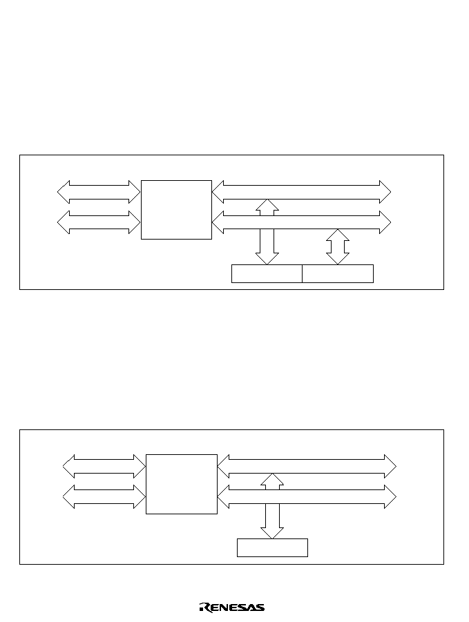
704
17.3
Interface to Bus Master
17.3.1
16-Bit Registers
TCNT and TGR are 16-bit registers. As the data bus to the bus master is 16 bits wide, these
registers can be read and written to in 16-bit units.
These registers cannot be read or written to in 8-bit units; 16-bit access must always be used.
An example of 16-bit register access operation is shown in figure 17.2.
Bus interface
H
Internal data bus
L
Bus
master
Module
data bus
TCNTH
TCNTL
Figure 17.2 16-Bit Register Access Operation [Bus Master
TCNT (16 Bits)]
17.3.2
8-Bit Registers
Registers other than TCNT and TGR are 8-bit. As the data bus to the CPU is 16 bits wide, these
registers can be read and written to in 16-bit units. They can also be read and written to in 8-bit
units.
Examples of 8-bit register access operation are shown in figures 17.3, 17.4, and 17.5.
Bus interface
H
Internal data bus
L
Module
data bus
TCR
Bus
master
Figure 17.3 8-Bit Register Access Operation [Bus Master
TCR (Upper 8 Bits)]

705
Bus interface
H
Internal data bus
L
Module
data bus
TMDR
Bus
master
Figure 17.4 8-Bit Register Access Operation [Bus Master
TMDR (Lower 8 Bits)]
Bus interface
H
Internal data bus
L
Module
data bus
TCR
TMDR
Bus
master
Figure 17.5 8-Bit Register Access Operation [Bus Master
TCR and TMDR (16 Bits)]

706
17.4
Operation
17.4.1
Overview
Operation in each mode is outlined below.
Normal Operation: Each channel has a TCNT and TGR register. TCNT performs up-counting,
and is also capable of free-running operation, synchronous counting, and external event counting.
Each TGR can be used as an input capture register or output compare register.
Synchronous Operation: The TCNT counter for a channel designated for synchronous operation
by means of TSYR performs synchronous presetting. That is, when TCNT for a channel
designated for synchronous operation is rewritten, the TCNT counters for the other channels are
also rewritten at the same time. Synchronous clearing of the TCNT counters is also possible by
setting the counter clear bits in TCR for channels designated for synchronous operation.
Buffer Operation
∑
When TGR is an output compare register
When a compare match occurs, the value in the buffer register for the relevant channel is
transferred to TGR.
∑
When TGR is an input capture register
When input capture occurs, the value in TCNT is transfer to TGR and the value previously
held in TGR is transferred to the buffer register.
PWM Mode: In this mode, a PWM waveform is output. The output level can be set by means of
TIOR. A PWM waveform with a duty of between 0% and 100% can be output, according to the
setting of each TGR register.
Phase Counting Mode: In this mode, TCNT is incremented or decremented by detecting the
phases of two clocks input from the external clock input pins in channels 1, and 2. When phase
counting mode is set, the corresponding TCLK pin functions as the clock input, and TCNT
performs up- or down-counting.
This can be used for two-phase encoder pulse input.
707
17.4.2
Basic Functions
Counter Operation: When one of bits CST0 to CST2 is set to 1 in TSTR, the TCNT counter for
the corresponding channel starts counting. TCNT can operate as a free-running counter, periodic
counter, and so on.
∑
Example of count operation setting procedure
Figure 17.6 shows an example of the count operation setting procedure.
Select counter clock
Operation selection
Select counter clearing source
Periodic counter
Set period
Start count operation
<Periodic counter>
1
2
4
3
5
Free-running counter
Start count operation
<Free-running counter>
5
1
2
3
4
5
Select the counter
clock with bits
TPSC2 to TPSC0 in
TCR. At the same
time, select the
input clock edge
with bits CKEG1
and CKEG0 in
TCR.
For periodic counter
operation, select
the TGR to be used
as the TCNT
clearing source with
bits CCLR2 to
CCLR0 in TCR.
Designate the TGR
selected in [2] as an
output compare
register by means
of TIOR.
Set the periodic
counter cycle in the
TGR selected in (2).
Set the CST bit in
TSTR to 1 to start
the count operation.
Select output compare register
Figure 17.6 Example of Counter Operation Setting Procedure
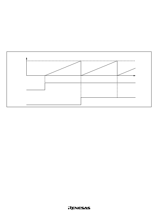
708
∑
Free-running count operation and periodic count operation
Immediately after a reset, the TPU's TCNT counters are all designated as free-running
counters. When the relevant bit in TSTR is set to 1 the corresponding TCNT counter starts up-
count operation as a free-running counter. When TCNT overflows (from H'FFFF to H'0000),
the TCFV bit in TSR is set to 1. If the value of the corresponding TCIEV bit in TIER is 1 at
this point, the TPU requests an interrupt. After overflow, TCNT starts counting up again from
H'0000.
Figure 17.7 illustrates free-running counter operation.
TCNT value
H'FFFF
H'0000
CST bit
TCFV
Time
Figure 17.7 Free-Running Counter Operation
When compare match is selected as the TCNT clearing source, the TCNT counter for the
relevant channel performs periodic count operation. The TGR register for setting the period is
designated as an output compare register, and counter clearing by compare match is selected
by means of bits CCLR2 to CCLR0 in TCR. After the settings have been made, TCNT starts
up-count operation as periodic counter when the corresponding bit in TSTR is set to 1. When
the count value matches the value in TGR, the TGF bit in TSR is set to 1 and TCNT is cleared
to H'0000.
If the value of the corresponding TGIE bit in TIER is 1 at this point, the TPU requests an
interrupt. After a compare match, TCNT starts counting up again from H'0000.
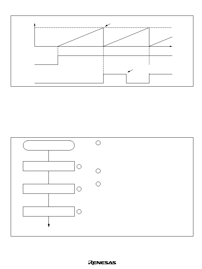
709
Figure 17.8 illustrates periodic counter operation.
TCNT value
TGR
H'0000
CST bit
TGF
Time
Counter cleared by TGR
compare match
Flag cleared by software or
DMAC activation
Figure 17.8 Periodic Counter Operation
Waveform Output by Compare Match: The TPU can perform 0, 1, or toggle output from the
corresponding output pin using compare match.
∑
Example of setting procedure for waveform output by compare match
Figure 17.9 shows an example of the setting procedure for waveform output by compare match
Select waveform output mode
Output selection
Set output timing
Start count operation
<Waveform output>
1
1
2
3
2
3
Select initial value 0 output or 1 output, and
compare match output value 0 output, 1
output, or toggle output, by means of TIOR.
The set initial value is output at the TIOC
pin until the first compare match occurs.
Set the timing for compare match
generation in TGR.
Set the CST bit in TSTR to 1 to start the
count operation.
Figure 17.9 Example of Setting Procedure for Waveform Output by Compare Match
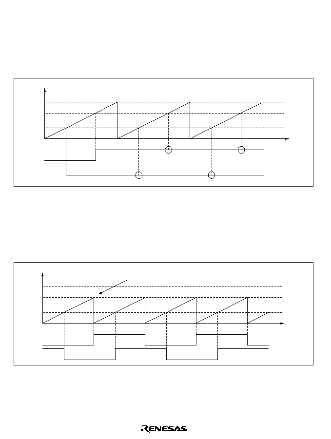
710
∑
Examples of waveform output operation
Figure 17.10 shows an example of 0 output/1 output.
In this example TCNT has been designated as a free-running counter, and settings have been
made so that 1 is output by compare match A, and 0 is output by compare match B. When the
set level and the pin level coincide, the pin level does not change.
TCNT value
H'FFFF
H'0000
TIOCA
TIOCB
Time
TGRA
TGRB
No change
No change
No change
No change
1 output
0 output
Figure 17.10 Example of 0 Output/1 Output Operation
Figure 17.11 shows an example of toggle output.
In this example TCNT has been designated as a periodic counter (with counter clearing
performed by compare match B), and settings have been made so that output is toggled by both
compare match A and compare match B.
TCNT value
H'FFFF
H'0000
TIOCB
TIOCA
Time
TGRB
TGRA
Toggle output
Toggle output
Counter cleared by TGRB compare match
Figure 17.11 Example of Toggle Output Operation

711
Input Capture Function: The TCNT value can be transferred to TGR on detection of the TIOC
pin input edge.
Rising edge, falling edge, or both edges can be selected as the detected edge.
∑
Example of input capture operation setting procedure
Figure 17.12 shows an example of the input capture operation setting procedure.
Select input capture input
Input selection
Start count
<Input capture operation>
1
1
2
2
Designate TGR as an input capture register by
means of TIOR, and select rising edge, falling
edge, or both edges as the input capture
source and input signal edge.
Set the CST bit in TSTR to 1 to start the count
operation.
Figure 17.12 Example of Input Capture Operation Setting Procedure

712
∑
Example of input capture operation
Figure 17.13 shows an example of input capture operation.
In this example both rising and falling edges have been selected as the TIOCA pin input
capture input edge, falling edge has been selected as the TIOCB pin input capture input edge,
and counter clearing by TGRB input capture has been designated for TCNT.
TCNT value
H'0180
H'0000
TIOCA
TGRA
Time
H'0010
H'0005
Counter cleared by TIOCB
input (falling edge)
H'0160
H'0005
H'0160
H'0010
TGRB
H'0180
TIOCB
Figure 17.13 Example of Input Capture Operation

713
17.4.3
Synchronous Operation
In synchronous operation, the values in a number of TCNT counters can be rewritten
simultaneously (synchronous presetting). Also, a number of TCNT counters can be cleared
simultaneously by making the appropriate setting in TCR (synchronous clearing).
Synchronous operation enables TGR to be incremented with respect to a single time base.
Channels 0 to 2 can all be designated for synchronous operation.
Example of Synchronous Operation Setting Procedure: Figure 17.14 shows an example of the
synchronous operation setting procedure.
Set synchronous
operation
Synchronous operation
selection
Set TCNT
Synchronous presetting
<Synchronous presetting>
1
2
Synchronous clearing
Select counter
clearing source
<Counter clearing>
3
Start count
5
Set synchronous
counter clearing
<Synchronous clearing>
4
Start count
5
Clearing
source generation
channel?
No
Yes
1
2
3
4
5
Set to 1 the SYNC bits in TSYR corresponding to the channels to be designated for synchronous
operation.
When the TCNT counter of any of the channels designated for synchronous operation is
written to, the same value is simultaneously written to the other TCNT counters.
Use bits CCLR2 to CCLR0 in TCR to specify TCNT clearing by input capture/output compare,
etc.
Use bits CCLR2 to CCLR0 in TCR to designate synchronous clearing for the counter clearing
source.
Set to 1 the CST bits in TSTR for the relevant channels, to start the count operation.
Figure 17.14 Example of Synchronous Operation Setting Procedure
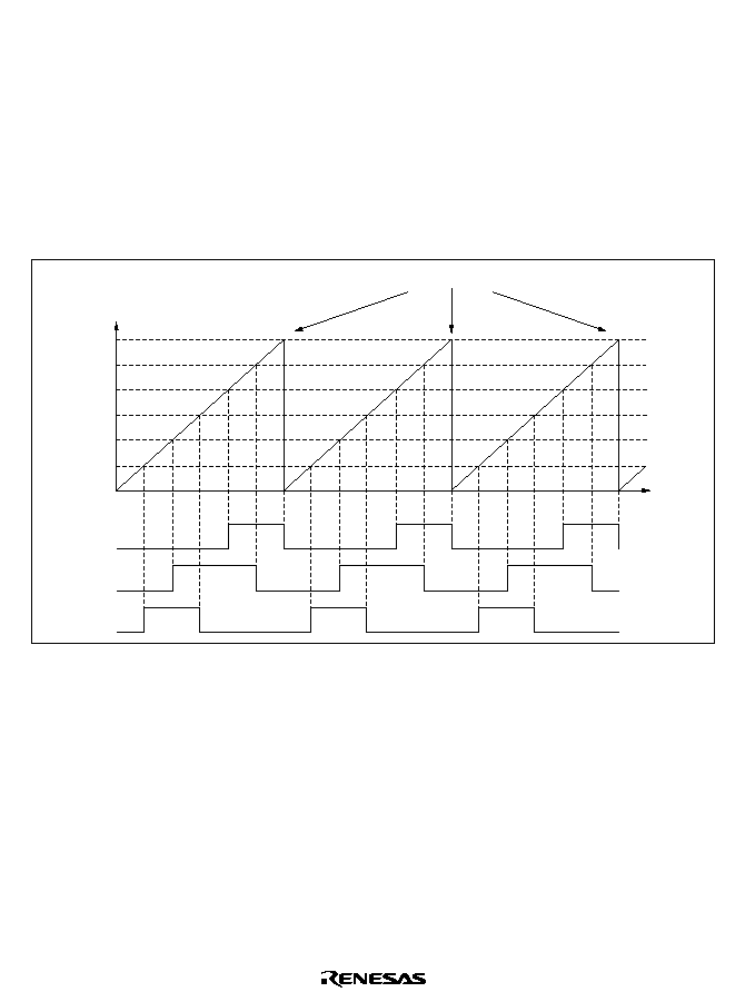
714
Example of Synchronous Operation: Figure 17.15 shows an example of synchronous operation.
In this example, synchronous operation and PWM mode 1 have been designated for channels 0 to
2, TGR0B compare match has been set as the channel 0 counter clearing source, and synchronous
clearing has been set for the channel 1 and 2 counter clearing source.
Three-phase PWM waveforms are output from pins TIOC0A, TIOC1A, and TIOC2A. At this
time, synchronous presetting, and synchronous clearing by TGR0B compare match, is performed
for channel 0 to 2 TCNT counters, and the data set in TGR0B is used as the PWM cycle.
For details of PWM modes, see section 17.4.5, PWM Modes.
TCNT0 to TCNT2 values
H'0000
TIOC0A
TIOC1A
Time
TGR0B
Synchronous clearing by TGR0B compare match
TGR2A
TGR1A
TGR2B
TGR0A
TGR1B
TIOC2A
Figure 17.15 Example of Synchronous Operation
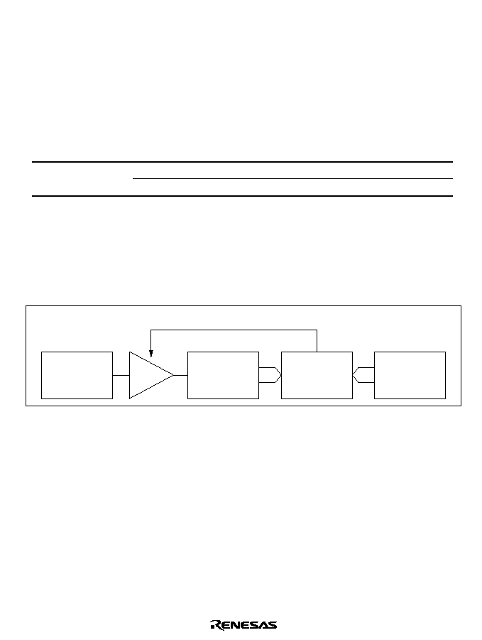
715
17.4.4
Buffer Operation
Buffer operation, provided for channel 0 enables TGRC and TGRD to be used as buffer registers.
Buffer operation differs depending on whether TGR has been designated as an input capture
register or as a compare match register.
Table 17.5 shows the register combinations used in buffer operation.
Table 17.5
Register Combinations in Buffer Operation
Channel
Timer General Register
Buffer Register
0
TGR0A
TGR0C
TGR0B
TGR0D
∑
When TGR is an output compare register
When a compare match occurs, the value in the buffer register for the corresponding channel is
transferred to the timer general register.
This operation is illustrated in figure 17.16.
Buffer register
Timer general
register
TCNT
Comparator
Compare match signal
Figure 17.16 Compare Match Buffer Operation
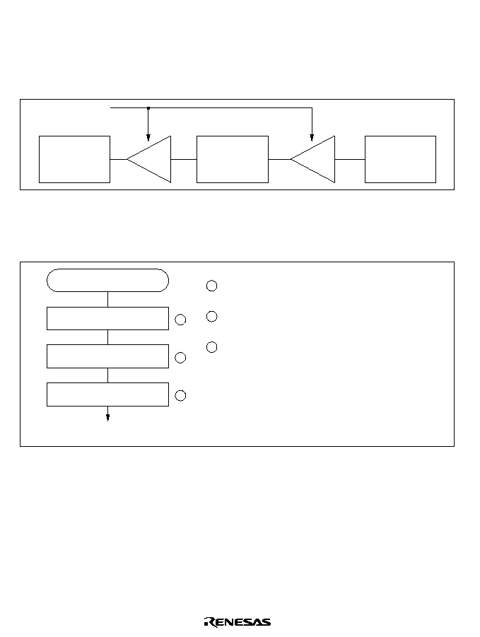
716
∑
When TGR is an input capture register
When input capture occurs, the value in TCNT is transferred to TGR and the value previously
held in the timer general register is transferred to the buffer register.
This operation is illustrated in figure 17.17.
Buffer register
Timer general
register
TCNT
Input capture
signal
Figure 17.17 Input Capture Buffer Operation
Example of Buffer Operation Setting Procedure: Figure 17.18 shows an example of the buffer
operation setting procedure.
Select TGR function
Buffer operation
Set buffer operation
Start count
<Buffer operation>
1
1
2
2
3
3
Designate TGR as an input capture register or
output compare register by means of TIOR.
Designate TGR for buffer operation with bits
BFA and BFB in TMDR.
Set the CST bit in TSTR to 1 to start the count
operation.
Figure 17.18 Example of Buffer Operation Setting Procedure
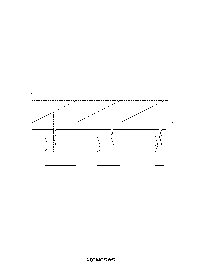
717
Examples of Buffer Operation
∑
When TGR is an output compare register
Figure 17.19 shows an operation example in which PWM mode 1 has been designated for
channel 0, and buffer operation has been designated for TGRA and TGRC. The settings used
in this example are TCNT clearing by compare match B, 1 output at compare match A, and 0
output at compare match B.
As buffer operation has been set, when compare match A occurs the output changes and the
value in buffer register TGRC is simultaneously transferred to timer general register TGRA.
This operation is repeated each time compare match A occurs.
For details of PWM modes, see section 17.4.5, PWM Modes.
TCNT value
TGR0B
H'0000
TGR0C
Time
TGR0A
H'0200
H'0520
TIOCA
H'0200
H'0450
H'0520
H'0450
TGR0A
H'0450
H'0200
Transfer
Figure 17.19 Example of Buffer Operation (1)
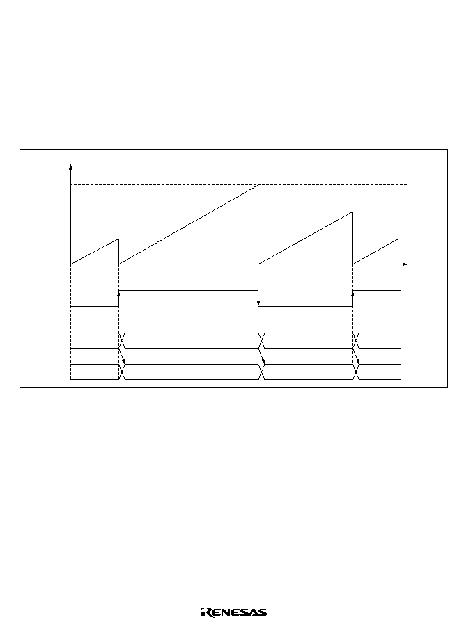
718
∑
When TGR is an input capture register
Figure 17.20 shows an operation example in which TGRA has been designated as an input
capture register, and buffer operation has been designated for TGRA and TGRC.
Counter clearing by TGRA input capture has been set for TCNT, and both rising and falling
edges have been selected as the TIOCA pin input capture input edge.
As buffer operation has been set, when the TCNT value is stored in TGRA upon occurrence of
input capture A, the value previously stored in TGRA is simultaneously transferred to TGRC.
TCNT value
H'09FB
H'0000
TGRC
Time
H'0532
TIOCA
TGRA
H'0F07
H'0532
H'0F07
H'0532
H'0F07
H'09FB
Figure 17.20 Example of Buffer Operation (2)

719
17.4.5
PWM Modes
In PWM mode, PWM waveforms are output from the output pins. 0, 1, or toggle output can be
selected as the output level in response to compare match of each TGR.
Designating TGR compare match as the counter clearing source enables the period to be set in that
register. All channels can be designated for PWM mode independently. Synchronous operation is
also possible.
There are two PWM modes, as described below.
∑
PWM mode 1
PWM output is generated by pairing TGRA with TGRB and TGRC with TGRD. The output
specified by bits IOA3≠IOA0 and IOC3≠IOC0 in TIOR is performed in response to compare
match A and C, and the output specified by bits IOB3≠IOB0 and IOD3≠IOD0 in TIOR in
response to compare match B and D, from pins TIOCA and TIOCC. The initial output value is
the value set in TGRA or TGRC. If the set values of paired TGRs are identical, the output
value does not change when a compare match occurs.
In PWM mode 1, a maximum 4-phase PWM output is possible.
∑
PWM mode 2
PWM output is generated using one TGR as the cycle register and the others as duty registers.
The output specified by TIOR is performed in response to a compare match. Also, when the
counter is cleared by a synchronization register compare match, pin output values are the initial
values set in TIOR. If the set values of the period and duty registers are identical, the output
value does not change when a compare match occurs.
In PWM mode 2, a maximum 7-phase PWM output is possible by combined use with
synchronous operation.
The correspondence between PWM output pins and registers is shown in table 17.6.

720
Table 17.6
PWM Output Registers and Output Pins
Output Pins
Channel
Registers
PWM Mode 1
PWM Mode 2
0
TGR0A
TIOCA0
TIOCA0
TGR0B
TIOCB0
TGR0C
TIOCC0
TIOCC0
TGR0D
TIOCD0
1
TGR1A
TIOCA1
TIOCA1
TGR1B
TIOCB1
2
TGR2A
TIOCA2
TIOCA2
TGR2B
TIOCB2
Note:
In PWM mode 2, PWM output is not possible for the TGR register in which the period is set.
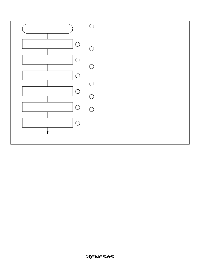
721
Example of PWM Mode Setting Procedure: Figure 17.21 shows an example of the PWM mode
setting procedure.
Select counter clock
PWM mode
Select counter clearing source
Select waveform output level
<PWM mode>
1
1
2
2
3
3
Set TGR
4
4
Set PWM mode
5
5
Start count
6
6
Select the counter clock with bits TPSC2 to
TPSC0 in TCR. At the same time, select the
input clock edge with bits CKEG1 and CKEG0
in TCR.
Use bits CCLR2 to CCLR0 in TCR to select
the TGR to be used as the TCNT clearing
source.
Use TIOR to designate the TGR as an output
compare register, and select the initial value
and output value.
Set the cycle in the TGR selected in [2], and
set the duty in the other the TGR.
Select the PWM mode with bits MD3 to MD0
in TMDR.
Set the CST bit in TSTR to 1 to start the count
operation.
Figure 17.21 Example of PWM Mode Setting Procedure
Examples of PWM Mode Operation: Figure 17.22 shows an example of PWM mode 1
operation.
In this example, TGRA compare match is set as the TCNT clearing source, 0 is set for the TGRA
initial output value and output value, and 1 output is set as the TGRB output value.
In this case, the value set in TGRA is used as the period, and the values set in TGRB registers as
the duty.

722
TCNT value
TGRA
H'0000
TIOCA
Time
TGRB
Counter cleared by
TGRA compare match
Figure 17.22 Example of PWM Mode Operation (1)
Figure 17.23 shows an example of PWM mode 2 operation.
In this example, synchronous operation is designated for channels 0 and 1, TGR1B compare match
is set as the TCNT clearing source, and 0 is set for the initial output value and 1 for the output
value of the other TGR registers, to output a 5-phase PWM waveform.
In this case, the value set in TGR1B is used as the cycle, and the values set in the other TGRs as
the duty.
TCNT value
TGR1B
H'0000
TIOCA0
Counter cleared by TGR1B
compare match
TGR1A
TGR0D
TGR0C
TGR0B
TGR0A
TIOCB0
TIOCC0
TIOCD0
TIOCA1
Figure 17.23 Example of PWM Mode Operation (2)
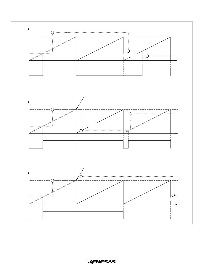
723
Figure 17.24 shows examples of PWM waveform output with 0% duty and 100% duty in PWM
mode.
TCNT value
TGRA
H'0000
TIOCA
Time
TGRB
0% duty
TGRB rewritten
TGRB
rewritten
TGRB rewritten
TCNT value
TGRA
H'0000
TIOCA
Time
TGRB
100% duty
TGRB rewritten
TGRB rewritten
TGRB rewritten
Output does not change when cycle register and duty register
compare matches occur simultaneously
TCNT value
TGRA
H'0000
TIOCA
Time
TGRB
100% duty
TGRB rewritten
TGRB rewritten
TGRB rewritten
Output does not change when cycle register and duty
register compare matches occur simultaneously
0% duty
Figure 17.24 Example of PWM Mode Operation (3)
724
17.4.6
Phase Counting Mode
In phase counting mode, the phase difference between two external clock inputs is detected and
TCNT is incremented/decremented accordingly. This mode can be set for channels 1, and 2.
When phase counting mode is set, an external clock is selected as the counter input clock and
TCNT operates as an up/down-counter regardless of the setting of bits TPSC2 to TPSC0 and bits
CKEG1 and CKEG0 in TCR. However, the functions of bits CCLR1 and CCLR0 in TCR, and of
TIOR, TIER, and TGR are valid, and input capture/compare match and interrupt functions can be
used.
When overflow occurs while TCNT is counting up, the TCFV flag in TSR is set; when underflow
occurs while TCNT is counting down, the TCFU flag is set.
The TCFD bit in TSR is the count direction flag. Reading the TCFD flag provides an indication of
whether TCNT is counting up or down.
Table 17.7 shows the correspondence between external clock pins and channels.
Table 17.7
Phase Counting Mode Clock Input Pins
External Clock Pins
Channels
A-Phase
B-Phase
When channel 1 is set to phase counting mode
TCLKA
TCLKB
When channel 2 is set to phase counting mode
TCLKC
TCLKD
Example of Phase Counting Mode Setting Procedure: Figure 17.25 shows an example of the
phase counting mode setting procedure.
Select phase counting mode
Phase counting mode
Start count
<Phase counting mode>
1
1
2
2
Select phase counting mode with bits MD3
to MD0 in TMDR.
Set the CST bit in TSTR to 1 to start the
count operation.
Figure 17.25 Example of Phase Counting Mode Setting Procedure
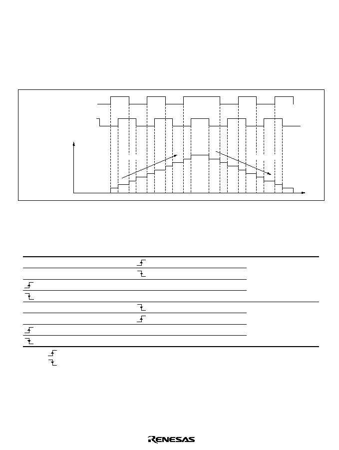
725
Examples of Phase Counting Mode Operation: In phase counting mode, TCNT counts up or
down according to the phase difference between two external clocks. There are four modes,
according to the count conditions.
∑
Phase counting mode 1
Figure 17.26 shows an example of phase counting mode 1 operation, and table 17.8
summarizes the TCNT up/down-count conditions.
TCNT value
Time
Down-count
Up-count
TCLKA (channel 1)
TCLKC (channel 2)
TCLKB (channel 1)
TCLKD (channel 2)
Figure 17.26 Example of Phase Counting Mode 1 Operation
Table 17.8
Up/Down-Count Conditions in Phase Counting Mode 1
TCLKA (Channel 1)
TCLKC (Channel 2)
High level
Low level
High level
Low level
Notes:
: Rising edge
: Falling edge
TCLKB (Channel 1)
TCLKD (Channel 2)
Low level
High level
High level
Low level
Operation
Up-count
Down-count
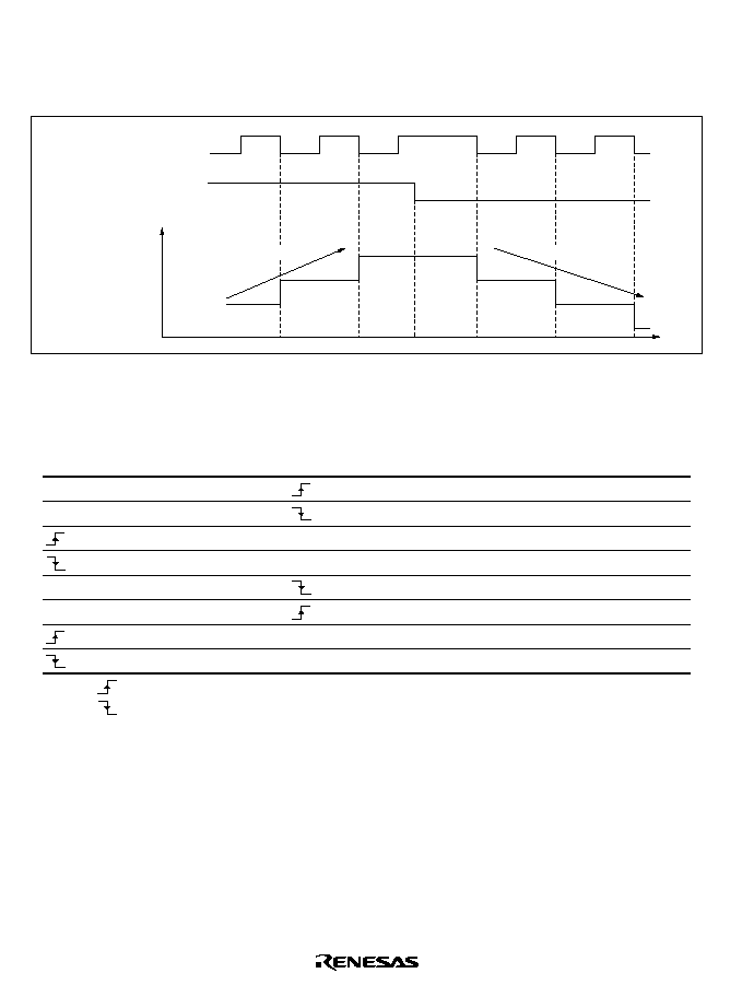
726
∑
Phase counting mode 2
Figure 17.27 shows an example of phase counting mode 2 operation, and table 17.9
summarizes the TCNT up/down-count conditions.
TCNT value
Time
Down-count
Up-count
TCLKA (Channel 1)
TCLKC (Channel 2)
TCLKB (Channel 1)
TCLKD (Channel 2)
Figure 17.27 Example of Phase Counting Mode 2 Operation
Table 17.9
Up/Down-Count Conditions in Phase Counting Mode 2
TCLKA (Channel 1)
TCLKC (Channel 2)
High level
Low level
High level
Low level
Notes:
: Rising edge
: Falling edge
TCLKB (Channel 1)
TCLKD (Channel 2)
Low level
High level
High level
Low level
Operation
Don't care
Don't care
Don't care
Up-count
Don't care
Don't care
Don't care
Down-count
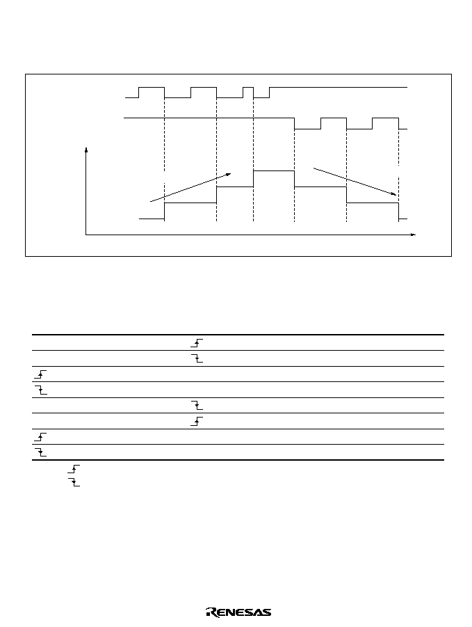
727
∑
Phase counting mode 3
Figure 17.28 shows an example of phase counting mode 3 operation, and table 17.10
summarizes the TCNT up/down-count conditions.
TCNT value
Time
Up-count
TCLKA (channel 1)
TCLKC (channel 2)
TCLKB (channel 1)
TCLKD (channel 2)
Down-count
Figure 17.28 Example of Phase Counting Mode 3 Operation
Table 17.10 Up/Down-Count Conditions in Phase Counting Mode 3
TCLKA (Channel 1)
TCLKC (Channel 2)
High level
Low level
High level
Low level
Notes:
: Rising edge
: Falling edge
TCLKB (Channel 1)
TCLKD (Channel 2)
Low level
High level
High level
Low level
Operation
Don't care
Don't care
Don't care
Up-count
Down-count
Don't care
Don't care
Don't care
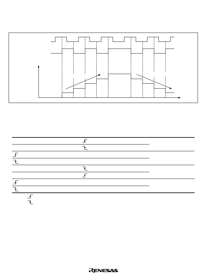
728
∑
Phase counting mode 4
Figure 17.29 shows an example of phase counting mode 4 operation, and table 17.11
summarizes the TCNT up/down-count conditions.
Time
TCLKA (channel 1)
TCLKC (channel 2)
TCLKB (channel 1)
TCLKD (channel 2)
Up-count
Down-count
TCNT value
Figure 17.29 Example of Phase Counting Mode 4 Operation
Table 17.11 Up/Down-Count Conditions in Phase Counting Mode 4
TCLKA (Channel 1)
TCLKC (Channel 2)
High level
Low level
High level
Low level
Notes:
: Rising edge
: Falling edge
TCLKB (Channel 1)
TCLKD (Channel 2)
Low level
High level
High level
Low level
Operation
Up-count
Don't care
Down-count
Don't care

729
17.5
Interrupts
17.5.1
Interrupt Sources and Priorities
There are three kinds of TPU interrupt source: TGR input capture/compare match, TCNT
overflow, and TCNT underflow. Each interrupt source has its own status flag and enable/disabled
bit, allowing generation of interrupt request signals to be enabled or disabled individually.
When an interrupt request is generated, the corresponding status flag in TSR is set to 1. If the
corresponding enable/disable bit in TIER is set to 1 at this time, an interrupt is requested. The
interrupt request is cleared by clearing the status flag to 0.
Relative channel priorities can be changed by the interrupt controller, but the priority order within
a channel is fixed. For details, see section 5, Interrupt Controller (INTC).
Table 17.12 lists the TPU interrupt sources.
Table 17.12 TPU Interrupts
Channel
Interrupt
Source
Description
DMAC
Activation
Priority
0
TGI0A
TGR0A input capture/compare match
Possible
High
TGI0B
TGR0B input capture/compare match
Possible
TGI0C
TGR0C input capture/compare match
Possible
TGI0D
TGR0D input capture/compare match
Possible
TCI0V
TCNT0 overflow
Not possible
1
TGI1A
TGR1A input capture/compare match
Not possible
TGI1B
TGR1B input capture/compare match
Not possible
TCI1V
TCNT1 overflow
Not possible
TCI1U
TCNT1 underflow
Not possible
2
TGI2A
TGR2A input capture/compare match
Not possible
TGI2B
TGR2B input capture/compare match
Not possible
TCI2V
TCNT2 overflow
Not possible
TCI2U
TCNT2 underflow
Not possible
Low
Note:
This table shows the initial state immediately after a reset. The relative channel priorities
can be changed by the interrupt controller.

730
Input Capture/Compare Match Interrupt: An interrupt is requested if the TGIE bit in TIER is
set to 1 when the TGF flag in TSR is set to 1 by the occurrence of a TGR input capture/compare
match on a particular channel. The interrupt request is cleared by clearing the TGF flag to 0. The
TPU has 8 input capture/compare match interrupts, four for channel 0, and two each for channels
1, and 2.
Overflow Interrupt: An interrupt is requested if the TCIEV bit in TIER is set to 1 when the
TCFV flag in TSR is set to 1 by the occurrence of TCNT overflow on a particular channel. The
interrupt request is cleared by clearing the TCFV flag to 0. The TPU has three overflow interrupts,
one for each channel.
Underflow Interrupt: An interrupt is requested if the TCIEU bit in TIER is set to 1 when the
TCFU flag in TSR is set to 1 by the occurrence of TCNT underflow on channel. The interrupt
request is cleared by clearing the TCFU flag to 0. The TPU has two underflow interrupts, one each
for channels 1 and 2.
17.5.2
DMAC Activation
The DMAC can be activated by the TGR input capture/compare match interrupt for a channel. For
details, see section 11, Direct Memory Access Controller (DMAC).
A total of four TPU input capture/compare match interrupts can be used as DMAC activation
sources for channel 0.
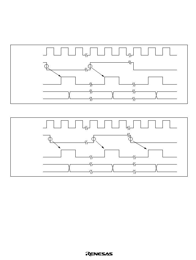
731
17.6
Operation Timing
17.6.1
Input/Output Timing
TCNT Count Timing: Figure 17.30 shows TCNT count timing in internal clock operation, and
figure 17.31 shows TCNT count timing in external clock operation.
TCNT
TCNT
input clock
Internal clock
P
N≠1
N
N+1
N+2
Falling edge
Rising edge
Figure 17.30 Count Timing in Internal Clock Operation
TCNT
TCNT
input clock
External clock
P
N≠1
N
N+1
N+2
Rising edge
Falling edge
Falling edge
Figure 17.31 Count Timing in External Clock Operation
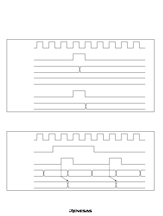
732
Output Compare Output Timing: A compare match signal is generated in the final state in
which TCNT and TGR match (the point at which the count value matched by TCNT is updated).
When a compare match signal is generated, the output value set in TIOR is output at the output
compare output pin (TIOC pin). After a match between TCNT and TGR, the compare match
signal is not generated until the TCNT input clock is generated.
Figure 17.32 shows output compare output timing.
TGR
TCNT
TCNT
input clock
P
N
N
N+1
Compare
match signal
TIOC pin
Figure 17.32 Output Compare Output Timing
Input Capture Signal Timing: Figure 17.33 shows input capture signal timing.
TCNT
Input capture
input
P
N
N+1
N+2
N
N+2
TGR
Input capture
signal
Figure 17.33 Input Capture Input Signal Timing
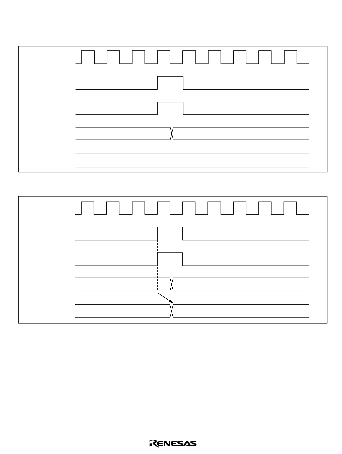
733
Timing for Counter Clearing by Compare Match/Input Capture: Figure 17.34 shows the
timing when counter clearing by compare match occurrence is specified, and figure
17.35 shows the timing when counter clearing by input capture occurrence is specified.
TCNT
Counter
clear signal
Compare
match signal
P
TGR
N
N
H'0000
Figure 17.34 Counter Clear Timing (Compare Match)
TCNT
Counter clear
signal
Input capture
signal
P
TGR
N
H'0000
N
Figure 17.35 Counter Clear Timing (Input Capture)
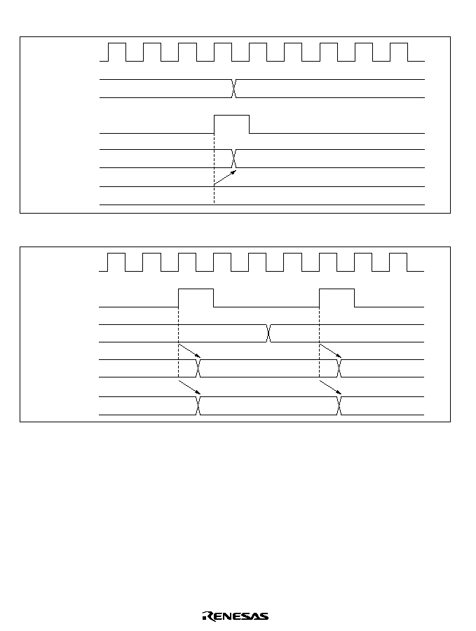
734
Buffer Operation Timing: Figures 17.36 and 17.37 show the timing in buffer operation.
TGRA,
TGRB
Compare
match signal
TCNT
P
TGRC,
TGRD
n
N
N
n
n+1
Figure 17.36 Buffer Operation Timing (Compare Match)
TGRA,
TGRB
TCNT
Input capture
signal
P
TGRC,
TGRD
N
n
n
N+1
N
N
N+1
Figure 17.37 Buffer Operation Timing (Input Capture)

735
17.6.2
Interrupt Signal Timing
TGF Flag Setting Timing in Case of Compare Match: Figure 17.38 shows the timing for
setting of the TGF flag in TSR by compare match occurrence, and TGI interrupt request signal
timing.
TGR
TCNT
TCNT input
clock
P
N
N
N+1
Compare
match signal
TGF flag
TGI interrupt
Figure 17.38 TGI Interrupt Timing (Compare Match)
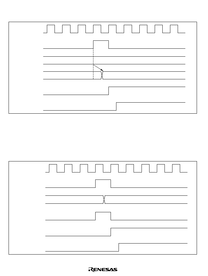
736
TGF Flag Setting Timing in Case of Input Capture: Figure 17.39 shows the timing for setting
of the TGF flag in TSR by input capture occurrence, and TGI interrupt request signal timing.
TGR
TCNT
Input capture
signal
P
N
N
TGF flag
TGI interrupt
Figure 17.39 TGI Interrupt Timing (Input Capture)
TCFV Flag/TCFU Flag Setting Timing: Figure 17.40 shows the timing for setting of the TCFV
flag in TSR by overflow occurrence, and TCIV interrupt request signal timing.
Figure 17.41 shows the timing for setting of the TCFU flag in TSR by underflow occurrence, and
TCIU interrupt request signal timing.
Overflow
signal
TCNT
(overflow)
TCNT input
clock
P
H'FFFF
H'0000
TCFV flag
TCIV interrupt
Figure 17.40 TCIV Interrupt Setting Timing
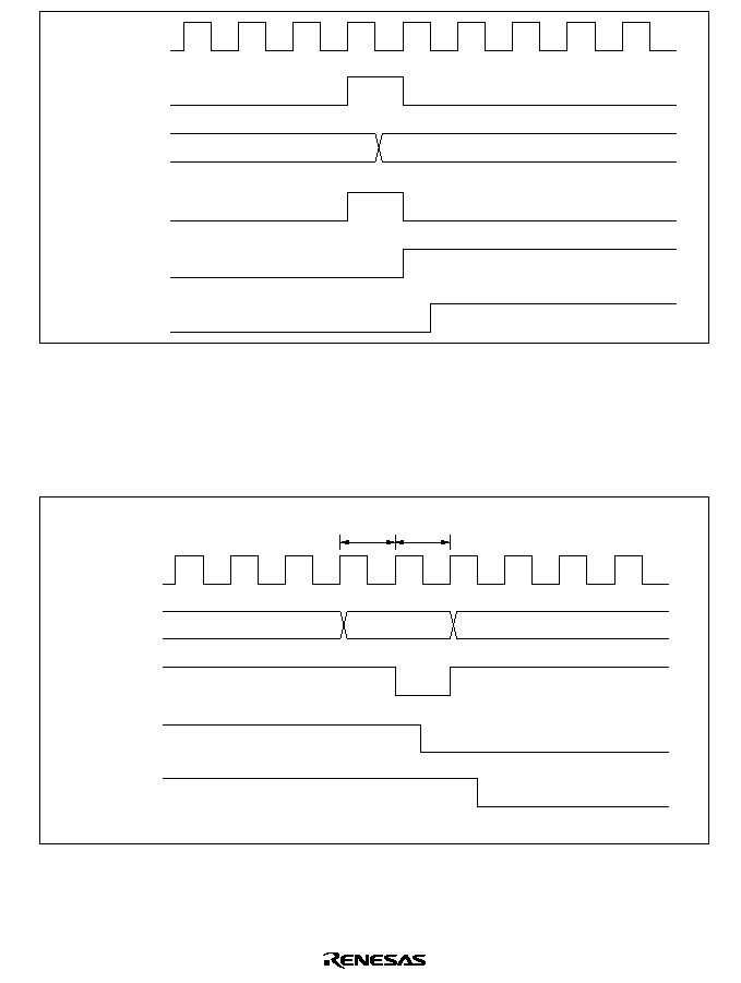
737
Underflow signal
TCNT
(underflow)
TCNT
input clock
P
H'0000
H'FFFF
TCFU flag
TCIU interrupt
Figure 17.41 TCIU Interrupt Setting Timing
Status Flag Clearing Timing: After a status flag is read as 1 by the CPU, it is cleared by writing
0 to it. When the DMAC is activated, the flag is cleared automatically. Figure 17.42 shows the
timing for status flag clearing by the CPU, and figure 17.43 shows the timing for status flag
clearing by the DMAC.
Status flag
Write signal
Address
P
TSR address
Interrupt
request
signal
TSR write cycle
T1
T2
Figure 17.42 Timing for Status Flag Clearing by CPU

738
Interrupt
request
signal
Status flag
Address
P
Source address
DMAC
read cycle
T1
T2
Destination
address
T1
T2
DMAC
write cycle
Figure 17.43 Timing for Status Flag Clearing by DMAC Activation
17.7
Usage Notes
Note that the kinds of operation and contention described below occur during TPU operation.
Input Clock Restrictions: The input clock pulse width must be at least 1.5 states in the case of
single-edge detection, and at least 2.5 states in the case of both-edge detection. The TPU will not
operate properly with a narrower pulse width.
In phase counting mode, the phase difference and overlap between the two input clocks must be at
least 1.5 states, and the pulse width must be at least 2.5 states. Figure 17.44 shows the input clock
conditions in phase counting mode.
Overlap
Phase
differ-
ence
Phase
differ-
ence
Overlap
TCLKA
(TCLKC)
TCLKB
(TCLKD)
Pulse width
Pulse width
Pulse width
Pulse width
Notes: Phase difference and overlap : 1.5 states or more
Pulse width
: 2.5 states or more
Figure 17.44 Phase Difference, Overlap, and Pulse Width in Phase Counting Mode
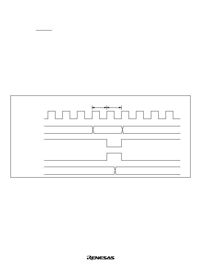
739
Caution on Period Setting: When counter clearing by compare match is set, TCNT is cleared in
the final state in which it matches the TGR value (the point at which the count value matched by
TCNT is updated). Consequently, the actual counter frequency is given by the following formula:
f =
P
(N + 1)
Where
f
: Counter frequency
P
: Peripheral module clock
N : TGR set value
Contention between TCNT Write and Clear Operations: If the counter clear signal is
generated in the T2 state of a TCNT write cycle, TCNT clearing takes precedence and the TCNT
write is not performed.
Figure 17.45 shows the timing in this case.
Counter clear
signal
Write signal
Address
P
TCNT address
TCNT
TCNT write cycle
T1
T2
N
H'0000
Figure 17.45 Contention between TCNT Write and Clear Operations
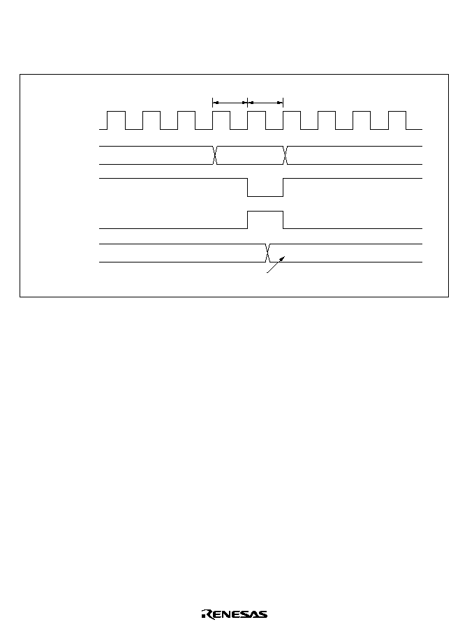
740
Contention between TCNT Write and Increment Operations: If incrementing occurs in the T2
state of a TCNT write cycle, the TCNT write takes precedence and TCNT is not incremented.
Figure 17.46 shows the timing in this case.
TCNT input
clock
Write signal
Address
P
TCNT address
TCNT
TCNT write cycle
T1
T2
N
M
TCNT write data
Figure 17.46 Contention between TCNT Write and Increment Operations
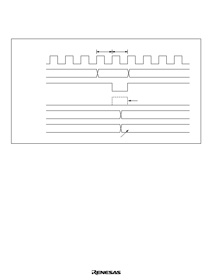
741
Contention between TGR Write and Compare Match: If a compare match occurs in the T2
state of a TGR write cycle, the TGR write takes precedence and the compare match signal is
inhibited. A compare match does not occur even if the same value as before is written.
Figure 17.47 shows the timing in this case.
Compare
match signal
Write signal
Address
P
TGR address
TCNT
TGR write cycle
T1
T2
N
M
TGR write data
TGR
N
N+1
Inhibited
Figure 17.47 Contention between TGR Write and Compare Match
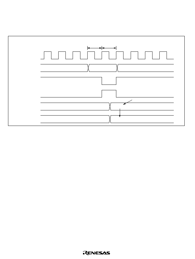
742
Contention between Buffer Register Write and Compare Match: If a compare match occurs in
the T2 state of a TGR write cycle, the data transferred to TGR by the buffer operation will be the
write data.
Figure 17.48 shows the timing in this case.
Compare
match signal
Write signal
Address
P
Buffer register
address
Buffer
register
TGR write cycle
T1
T2
M
TGR
N
M
Buffer register write data
Figure 17.48 Contention between Buffer Register Write and Compare Match
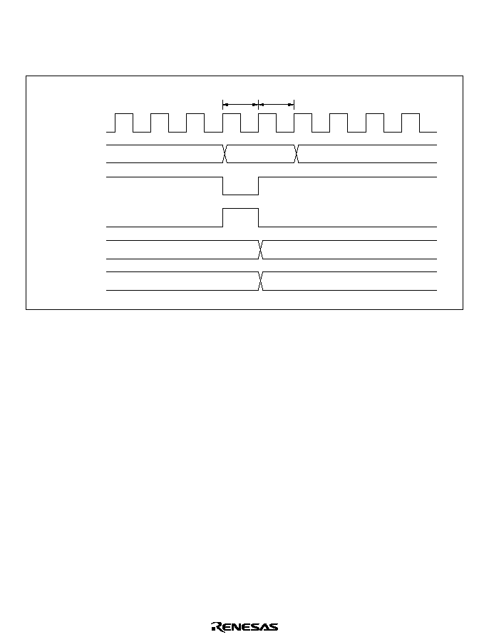
743
Contention between TGR Read and Input Capture: If the input capture signal is generated in
the T1 state of a TGR read cycle, the data that is read will be the data before input capture transfer.
Figure 17.49 shows the timing in this case.
Input capture
signal
Read signal
Address
P
TGR address
TGR
TGR read cycle
T1
T2
N
Internal
data bus
N
M
Figure 17.49 Contention between TGR Read and Input Capture
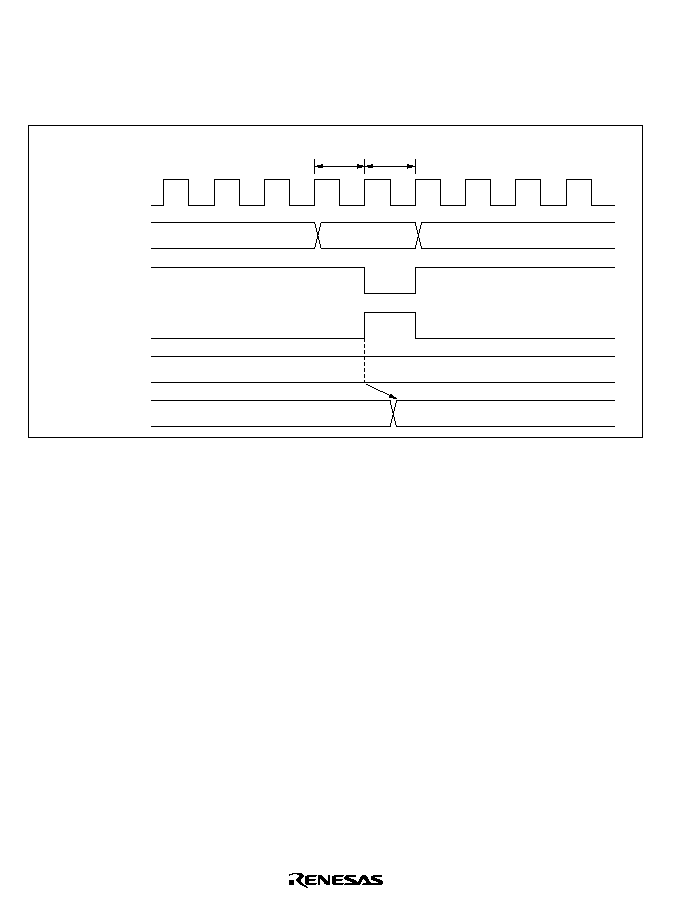
744
Contention between TGR Write and Input Capture: If the input capture signal is generated in
the T2 state of a TGR write cycle, the input capture operation takes precedence and the write to
TGR is not performed.
Figure 17.50 shows the timing in this case.
Input capture
signal
Write signal
Address
P
TCNT
TGR write cycle
T1
T2
M
TGR
M
TGR address
Figure 17.50 Contention between TGR Write and Input Capture
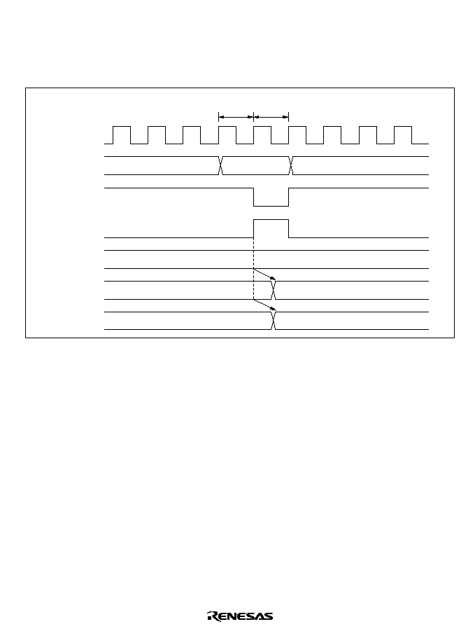
745
Contention between Buffer Register Write and Input Capture: If the input capture signal is
generated in the T2 state of a buffer register write cycle, the buffer operation takes precedence and
the write to the buffer register is not performed.
Figure 17.51 shows the timing in this case.
Input capture
signal
Write signal
Address
P
TCNT
Buffer register write cycle
T1
T2
N
TGR
N
M
M
Buffer
register
Buffer register
address
Figure 17.51 Contention between Buffer Register Write and Input Capture
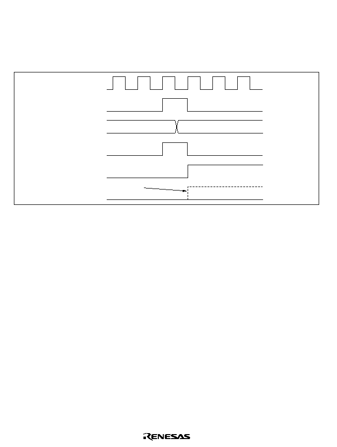
746
Contention between Overflow/Underflow and Counter Clearing: If overflow/underflow and
counter clearing occur simultaneously, the TCFV/TCFU flag in TSR is not set and TCNT clearing
takes precedence.
Figure 17.52 shows the operation timing when a TGR compare match is specified as the clearing
source, and H'FFFF is set in TGR.
Counter
clear signal
TCNT input
clock
P
TCNT
TGF
Disabled
TCFV
H'FFFF
H'0000
Figure 17.52 Contention between Overflow and Counter Clearing
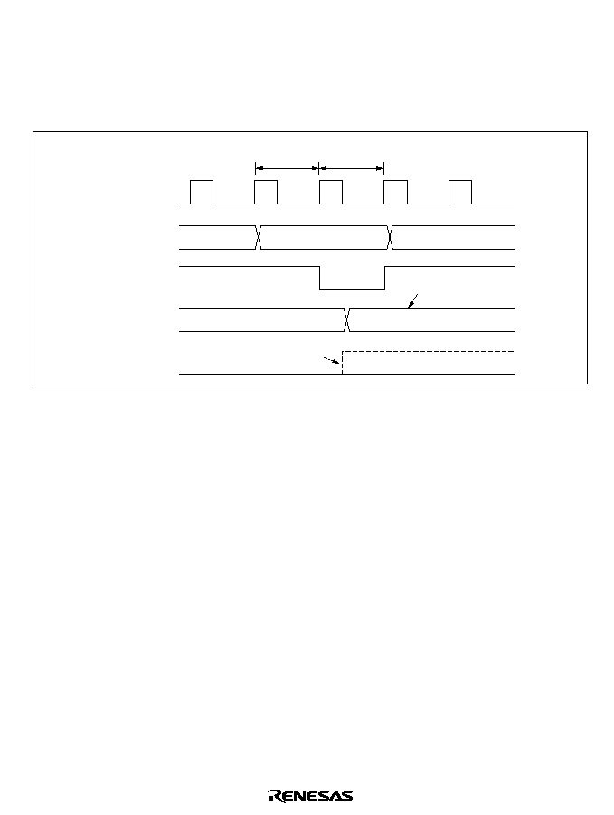
747
Contention between TCNT Write and Overflow/Underflow: If there is an up-count or down-
count in the T2 state of a TCNT write cycle, and overflow/underflow occurs, the TCNT write
takes precedence and the TCFV/TCFU flag in TSR is not set .
Figure 17.53 shows the operation timing in the case of contention between a TCNT write and
overflow.
Write signal
Address
P
TCNT address
TCNT
TCNT write cycle
T1
T2
H'FFFF
M
TCNT write data
TCFV flag
Disabled
Figure 17.53 Contention between TCNT Write and Overflow
Multiplexing of I/O Pins: In the Chip, the TCLKA input pin is multiplexed with the TIOCC0 I/O
pin, the TCLKB input pin with the TIOCD0 I/O pin, the TCLKC input pin with the TIOCB1 I/O
pin, and the TCLKD input pin with the TIOCB2 I/O pin. When an external clock is input,
compare match output should not be performed from a multiplexed pin.
Interrupts and Module Stop Mode: If module stop mode is entered when an interrupt has been
requested, it will not be possible to clear the CPU interrupt source or DMAC activation source.
Interrupts should therefore be disabled before entering module stop mode.

748
17.8
Usage Notes
17.8.1
Clearing Flags in TSR0 to TSR2
When bits TCFV, TGFD, TGFC, TGFB, and TGFA in TSR0, and bits TCFU, TCFV, TGFB, and
TGFA in TSR1 and TSR2, are cleared, it may happen that the interrupt request in the internal
logic cannot be cleared although the flag is cleared. In this case, if interrupt acceptance is enabled,
another interrupt will be generated.
Either of the following measures should therefore be taken when clearing flags in TSR0 to TSR2.
1. Execute clearing while the TPU timer is counting up.
2. If clearing when the TPU timer is stopped, write 0 to the flag again after executing clearing.
17.8.2
DMA Transfer by TPU0
When DMA transfer is performed by means of TPU channel 0 compare match or input capture,
internal logic interrupt requests (transfer requests) may not be cleared correctly. Therefore, it may
not be possible to execute DMA transfer when a subsequent transfer request is generated by TPU
channel 0 compare match or input capture.
Either of the following measures should therefore be taken when performing DMA transfer by
means of TPU channel 0 compare match or input capture.
1. Do not set on-chip RAM as the DMA transfer source or destination.
2. When on-chip RAM has not been set as the DMA transfer source or destination, execute the
transfer while the TPU channel 0 timer is counting up.

749
Section 18 Hitachi User Debug Interface (H-UDI)
18.1
Overview
The Hitachi user debug interface (H-UDI) provides data transfer and interrupt request functions.
The H-UDI performs serial transfer by means of external signal control.
18.1.1
Features
The H-UDI has the following features conforming to the IEEE 1149.1 standard.
∑
Five test signals (TCK, TDI, TDO, TMS, and
TRST)
∑
TAP controller
∑
Instruction register
∑
Data register
∑
Bypass register
∑
Boundary scan register
The H-UDI has seven instructions.
∑
Bypass mode
Test mode conforming to IEEE 1149.1
∑
EXTEST mode
Test mode corresponding to IEEE1149.1.
∑
SAMPLE/PRELOAD mode
Test mode corresponding to IEEE1149.1.
∑
CLAMP mode
Test mode corresponding to IEEE1149.1.
∑
HIGHZ mode
Test mode corresponding to IEEE1149.1.
∑
IDCODE mode
Test mode corresponding to IEEE1149.1.
∑
H-UDI interrupt
H-UDI interrupt request to INTC
This chip does not support test modes other than bypass mode.
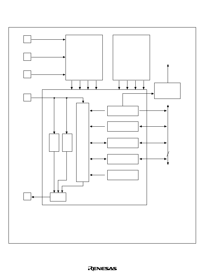
750
18.1.2
H-UDI Block Diagram
Figure 18.1 shows a block diagram of the H-UDI.
TCK
TMS
TRST
TDI
TAP
controller
Internal
bus controller
H-UDI
interrupt signal
SDSR
SDIDR
SDDRH
SDDRL
Shift register
SDBPR
Mux
TDO
Peripheral bus
SDIR:
Instruction register
TCK:
Test clock
SDSR:
Status register
TMS:
Test mode select
SDDRH: Data register H
TRST
:
Test reset
SDDRL: Data register L
TDI:
Test data input
SDBPR: Bypass register
TDO:
Test data output
SDBSR: Boundary scan register
SDIDR: ID code register
Decoder
16
SDIR
SDBSR
Figure 18.1 H-UDI Block Diagram

751
18.1.3
Pin Configuration
Table 18.1 shows the H-UDI pin configuration.
Table 18.1
Pin Configuration
Pin Name
Abbreviation
I/O
Function
Test clock
TCK
Input
Test clock input
Test mode select
TMS
Input
Test mode select input signal
Test data input
TDI
Input
Serial data input
Test data output
TDO
Output
Serial data output
Test reset
TRST
Input
Test reset input signal
18.1.4
Register Configuration
Table 18.2 shows the H-UDI registers.
Table 18.2
Register Configuration
Register
Abbreviation
R/W
*
1
Initial Value
*
2
Address
Access Size
(Bits)
Instruction register
SDIR
R
H'E000
H'FFFFFCB0
8/16/32
Status register
SDSR
R/W
H'0701
H'FFFFFCB2
8/16/32
Data register H
SDDRH
R/W
Undefined
H'FFFFFCB4
8/16/32
Data register L
SDDRL
R/W
Undefined
H'FFFFFCB6
8/16/32
Bypass register
SDBPR
--
--
--
--
Boundary scan
register
SDBSR
--
--
--
--
ID code register
SDIDR
--
H'0005200F
--
--
Notes:
*
1 Indicates whether the register can be read/written to by the CPU.
*
2 Initial value when the
TRST
signal is input. Registers are not initialized by a reset
(power-on or manual) or in standby mode.
Instructions and data can be input to the instruction register (SDIR) and data register (SDDR) by
serial transfer from the test data input pin (TDI). Data from SDIR, the status register (SDSR), and
SDDR can be output via the test data output pin (TDO). The bypass register (SDBPR) is a 1-bit
register to which TDI and TDO are connected in bypass mode. The boundary scan register
(SDBSR) is a 330-bit register, and is connected to TDI and TDO in the SAMPLE/PRELOAD or
EXTEST mode. The ID code register (SDIDR) is a 32-bit register; a fixed code can be output via

752
TDO in the IDCODE mode. All registers, except SDBPR, SDBSR, and SDIDR, can be accessed
from the CPU.
Table 18.3 shows the kinds of serial transfer possible with each register.
Table 18.3
H-UDI Register Serial Transfer
Register
Serial Input
Serial Output
SDIR
Possible
Possible
SDSR
Impossible
Possible
SDDRH
Possible
Possible
SDDRL
Possible
Possible
SDBPR
Possible
Possible
SDBSR
Possible
Possible
SDIDR
Impossible
Possible
18.2
External Signals
18.2.1
Test Clock (TCK)
The test clock pin (TCK) provides an independent clock supply to the H-UDI. As the clock input
to TCK is supplied directly to the H-UDI, a clock waveform with a duty cycle close to 50% should
be input (for details, see section 22, Electrical Characteristics). If no clock is input, TCK is fixed at
1 by internal pull-up.
18.2.2
Test Mode Select (TMS)
The test mode select pin (TMS) is sampled on the rise of TCK. TMS controls the internal state of
the TAP controller. If no signal is input, TMS is fixed at 1 by internal pull-up.
18.2.3
Test Data Input (TDI)
The test data input pin (TDI) performs serial input of instructions and data for H-UDI registers.
TDI is sampled on the rise of TCK. If no signal is input, TDI is fixed at 1 by internal pull-up.
18.2.4
Test Data Output (TDO)
The test data output pin (TDO) performs serial output of instructions and data from H-UDI
registers. Transfer is performed in synchronization with TCK. If there is no output, TDO goes to
the high-impedance state.

753
18.2.5
Test Reset (
TRST)
The test reset pin (
TRST) initializes the H-UDI asynchronously. If no signal is input, TRST is
fixed at 1 by internal pull-up.
18.3
Register Descriptions
18.3.1
Instruction Register (SDIR)
Bit:
15
14
13
12
11
10
9
8
TS3
TS2
TS1
TS0
--
--
--
--
Initial value:
1
1
1
0
0
0
0
0
R/W:
R
R
R
R
R
R
R
R
Bit:
7
6
5
4
3
2
1
0
--
--
--
--
--
--
--
--
Initial value:
0
0
0
0
0
0
0
0
R/W:
R
R
R
R
R
R
R
R
The instruction register (SDIR) is a 16-bit register that can only be read by the CPU. H-UDI
instructions can be transferred to SDIR by serial input from TDI. SDIR can be initialized by the
TRST signal, but is not initialized by a reset or in standby mode.
SDIR defines 4 valid bits for instruction. If an instruction exceeding 4 bits is input, the last 4 bits
of the serial data will be stored in SDIR.
Operation is not guaranteed if a reserved instruction is set in this register.
Bits 15 to 12--Test Set Bits (TS3≠TS0): Table 18.4 shows the instruction configuration.

754
Table 18.4
Instruction Configuration
Bit 15:
TS3
Bit 14:
TS2
Bit 13:
TS1
Bit 12:
TS0
Description
0
0
0
0
EXTEST mode
1
Reserved
1
0
CLAMP mode
1
HIGHZ mode
1
0
0
SAMPLE/PRELOAD mode
1
Reserved
1
0
Reserved
1
Reserved
1
0
0
0
Reserved
1
Reserved
1
0
H-UDI interrupt
1
Reserved
1
0
0
Reserved
1
Reserved
1
0
IDCODE mode
(Initial value)
1
BYPASS mode
Bits 11 to 0--Reserved: These bits are always read as 0. The write value should always be 0.

755
18.3.2
Status Register (SDSR)
Bit:
15
14
13
12
11
10
9
8
--
--
--
--
--
--
--
--
Initial value:
0
0
0
0
0
1
1
1
R/W:
R
R
R
R
R
R
R
R
Bit:
7
6
5
4
3
2
1
0
--
--
--
--
--
--
--
SDTRF
Initial value:
0
0
0
0
0
0
0
1
R/W:
R
R
R
R
R
R
R
R/W
The status register (SDSR) is a 16-bit register that can be read and written to by the CPU. Output
from TDO is possible for SDSR, but serial data cannot be written to SDSR via TDI. The SDTRF
bit is output by means of a 1-bit shift. In the case of a 2-bit shift, the SDTRF bit is first output,
followed by a reserved bit.
SDSR is initialized by
TRST signal input, but is not initialized by a reset or in standby mode.
Bits 15 to 1--Reserved: Bits 15 to 11 and 7 to 1 are always read as 0, and the write value should
always be 0. Bits 10 to 8 are always read as 1, and the write value should always be 1.
Bit 0--Serial Data Transfer Control Flag (SDTRF): Indicates whether H-UDI registers can be
accessed by the CPU. The SDTRF bit is reset by the
TRST signal , but is not initialized by a reset
or in standby mode.
Bit 0: SDTRF
Description
0
Serial transfer to SDDR has ended, and SDDR can be accessed
1
Serial transfer to SDDR in progress
(Initial value)

756
18.3.3
Data Register (SDDR)
The data register (SDDR) comprises data register H (SDDRH) and data register L (SDDRL), each
of which has the following configuration.
Bit:
15
14
13
12
11
10
9
8
Initial value:
--
--
--
--
--
--
--
--
R/W:
R/W
R/W
R/W
R/W
R/W
R/W
R/W
R/W
Bit:
7
6
5
4
3
2
1
0
Initial value:
--
--
--
--
--
--
--
--
R/W:
R/W
R/W
R/W
R/W
R/W
R/W
R/W
R/W
SDDRH and SDDRL are 16-bit registers that can be read and written to by the CPU. SDDR is
connected to TDO and TDI for serial data transfer to and from an external device.
32-bit data is input and output in serial data transfer. If data exceeding 32 bits is input, only the
last 32 bits will be stored in SDDR. Serial data is input starting from the MSB of SDDR (bit 15 of
SDDRH), and output starting from the LSB (bit 0 of SDDRL).
This register is not initialized by a reset, in standby mode, or by the
TRST signal.
18.3.4
Bypass Register (SDBPR)
The bypass register (SDBPR) is a one-bit shift register. In bypass mode, SDBPR is connected to
TDI and TDO, and the chip is excluded from the board test when a boundary scan test is
conducted. SDBPR cannot be read or written to by the CPU.
18.3.5
Boundary scan register (SDBSR)
The boundary scan register (SDBSR), a shift register that controls the I/O terminals of this LSI, is
provided on the PAD.
Using the EXTEST mode or the SAMPLE/PRELOAD mode, a boundary scan test conforming to
the IEEE1149.1 standard can be performed.
For SDBSR, read/write by the CPU cannot be performed.
Table 18.5 shows the relationship between the terminals of the LSI and the boundary scan register.

757
Table 18.5
Correspondence between Pins and Boundary Scan Register Bits
Pin No.
Pin Name
Input/Output
Bit No.
from TDI
34
D0
Input
329
Output
328
Output enable
327
36
D1
Input
326
Output
325
Output enable
324
37
D2
Input
323
Output
322
Output enable
321
38
D3
Input
320
Output
319
Output enable
318
39
D4
Input
317
Output
316
Output enable
315
40
D5
Input
314
Output
313
Output enable
312
41
D6
Input
311
Output
310
Output enable
309
43
D7
Input
308
Output
307
Output enable
306
44
D8
Input
305
Output
304
Output enable
303
46
D9
Input
302
Output
301
Output enable
300

758
Table 18.5
Correspondence between Pins and Boundary Scan Register Bits (cont)
Pin No.
Pin Name
Input/Output
Bit No.
47
D10
Input
299
Output
298
Output enable
297
48
D11
Input
296
Output
295
Output enable
294
49
D12
Input
293
Output
292
Output enable
291
51
D13
Input
290
Output
289
Output enable
288
53
D14
Input
287
Output
286
Output enable
285
54
D15
Input
284
Output
283
Output enable
282
55
D16
Input
281
Output
280
Output enable
279
56
D17
Input
278
Output
277
Output enable
276
57
D18
Input
275
Output
274
Output enable
273
59
D19
Input
272
Output
271
Output enable
270

759
Table 18.5
Correspondence between Pins and Boundary Scan Register Bits (cont)
Pin No.
Pin Name
Input/Output
Bit No.
62
D20
Input
269
Output
268
Output enable
267
63
D21
Input
266
Output
265
Output enable
264
64
D22
Input
263
Output
262
Output enable
261
65
D23
Input
260
Output
259
Output enable
258
68
D24
Input
257
Output
256
Output enable
255
70
D25
Input
254
Output
253
Output enable
252
71
D26
Input
251
Output
250
Output enable
249
72
D27
Input
248
Output
247
Output enable
246
73
D28
Input
245
Output
244
Output enable
243
74
D29
Input
242
Output
241
Output enable
240

760
Table 18.5
Correspondence between Pins and Boundary Scan Register Bits (cont)
Pin No.
Pin Name
Input/Output
Bit No.
75
D30
Input
239
Output
238
Output enable
237
77
D31
Input
236
Output
235
Output enable
234
80
A0
Output
233
Output enable
232
82
A1
Output
231
Output enable
230
83
A2
Output
229
Output enable
228
84
A3
Output
227
Output enable
226
85
A4
Output
225
Output enable
224
86
A5
Output
223
Output enable
222
87
A6
Output
221
Output enable
220
88
A7
Output
219
Output enable
218
90
A8
Output
217
Output enable
216
92
A9
Output
215
Output enable
214
93
A10
Output
213
Output enable
212
94
A11
Output
211
Output enable
210

761
Table 18.5
Correspondence between Pins and Boundary Scan Register Bits (cont)
Pin No.
Pin Name
Input/Output
Bit No.
95
A12
Output
209
Output enable
208
96
A13
Output
207
Output enable
206
97
A14
Output
205
Output enable
204
98
A15
Output
203
Output enable
202
100
A16
Output
201
Output enable
200
102
A17
Output
199
Output enable
198
103
A18
Output
197
Output enable
196
104
A19
Output
195
Output enable
194
105
A20
Output
193
Output enable
192
106
A21
Output
191
Output enable
190
107
A22
Output
189
Output enable
188
108
A23
Output
187
Output enable
186
111
A24
Output
185
Output enable
184
115
WAIT
Input
183
117
RAS
Output
182
Output enable
181
118
CAS
Output
180
Output enable
179

762
Table 18.5
Correspondence between Pins and Boundary Scan Register Bits (cont)
Pin No.
Pin Name
Input/Output
Bit No.
119
DQMUU/
WE3
Output
178
Output enable
177
120
DQMUL/
WE2
Output
176
Output enable
175
121
DQMLU/
WE1
Output
174
Output enable
173
122
DQMLL/
WE0
Output
172
Output enable
171
123
CAS3
Output
170
Output enable
169
124
CAS2
Output
168
Output enable
167
125
CAS1
Output
166
Output enable
165
126
CAS0
Output
164
Output enable
163
127
CKE
Output
162
Output enable
161
128
RD
Output
160
Output enable
159
129
REFOUT
Output
158
Output enable
157
131
BS
Output
156
Output enable
155
133
RD/
WR
Output
154
Output enable
153
134
CS0
Output
152
Output enable
151
135
CS1
Output
150
Output enable
149

763
Table 18.5
Correspondence between Pins and Boundary Scan Register Bits (cont)
Pin No.
Pin Name
Input/Output
Bit No.
136
CS2
Output
148
Output enable
147
137
CS3
Output
146
Output enable
145
138
CS4
Output
144
Output enable
143
139
BUSHIZ
Input
142
140
BH
Output
141
Output enable
140
141
DREQ1
Input
139
142
DREQ0
Input
138
143
DACK1
Output
137
Output enable
136
144
DACK0
Output
135
Output enable
134
145
BRLS
Input
133
148
BGR
Output
132
Output enable
131
151
PB15
Input
130
Output
129
Output enable
128
152
PB14
Input
127
Output
126
Output enable
125
153
PB13
Input
124
Output
123
Output enable
122
154
PB12
Input
121
Output
120
Output enable
119

764
Table 18.5
Correspondence between Pins and Boundary Scan Register Bits (cont)
Pin No.
Pin Name
Input/Output
Bit No.
156
PB11
Input
118
Output
117
Output enable
116
158
PB10
Input
115
Output
114
Output enable
113
159
PB9
Input
112
Output
111
Output enable
110
160
PB8
Input
109
Output
108
Output enable
107
161
PB7
Input
106
Output
105
Output enable
104
162
PB6
Input
103
Output
102
Output enable
101
163
PB5
Input
100
Output
99
Output enable
98
164
PB4
Input
97
Output
96
Output enable
95
165
PB3
Input
94
Output
93
Output enable
92
166
PB2
Input
91
Output
90
Output enable
89

765
Table 18.5
Correspondence between Pins and Boundary Scan Register Bits (cont)
Pin No.
Pin Name
Input/Output
Bit No.
168
PB1
Input
88
Output
87
Output enable
86
170
PB0
Input
85
Output
84
Output enable
83
171
PA13
Input
82
Output
81
Output enable
80
172
PA12
Input
79
Output
78
Output enable
77
173
PA11
Input
76
Output
75
Output enable
74
174
PA10
Input
73
Output
72
Output enable
71
175
PA9
Input
70
Output
69
Output enable
68
176
PA8
Input
67
Output
66
Output enable
65
177
PA7
Input
64
Output
63
Output enable
62
178
PA6
Input
61
Output
60
Output enable
59

766
Table 18.5
Correspondence between Pins and Boundary Scan Register Bits (cont)
Pin No.
Pin Name
Input/Output
Bit No.
180
PA5
Input
58
Output
57
Output enable
56
182
PA4
Input
55
Output
54
Output enable
53
183
CKPO
Output
52
Output enable
51
184
PA2
Input
50
Output
49
Output enable
48
185
PA1
Input
47
Output
46
Output enable
45
186
PA0
Input
44
Output
43
Output enable
42
187
RX≠ER
Input
41
188
RX≠DV
Input
40
189
COL
Input
39
190
CRS
Input
38
192
RX≠CLK
Input
37
194
ERXD0
Input
36
195
ERXD1
Input
35
196
ERXD2
Input
34
197
ERXD3
Input
33
198
MDIO
Input
32
Output
31
Output enable
30
199
MDC
Output
29
Output enable
28

767
Table 18.5
Correspondence between Pins and Boundary Scan Register Bits (cont)
Pin No.
Pin Name
Input/Output
Bit No.
201
TX≠CLK
Input
27
203
TX≠EN
Output
26
Output enable
25
204
ETXD0
Output
24
Output enable
23
205
ETXD1
Output
22
Output enable
21
206
ETXD2
Output
20
Output enable
19
207
ETXD3
Output
18
Output enable
17
208
TX≠ER
Output
16
Output enable
15
1
IRL3
Input
14
2
IRL2
Input
13
3
IRL1
Input
12
4
IRL0
Input
11
5
NMI
Input
10
13
MD4
Input
9
14
MD3
Input
8
15
MD2
Input
7
16
MD1
Input
6
17
MD0
Input
5
24
CKPREQ
/CKM
Input
4
25
CKPACK
Output
3
Output enable
2
27
IVECF
Output
1
Output enable
0
to TDO
Note:
The output enable signals are active-low. When an output enable signal is driven low, the
corresponding pin is driven. The exception is the output enable signal for the MDIO pin,
which is active-high.

768
18.3.6
ID code register (SDIDR)
The ID code register (SDIDR) is a 32-bit register. In the IDCODE mode, SDIDR can output
H'0005200F, which is a fixed code, from TDO. However, no serial data can be written to SDIDR
via TDI. For SDIDR, read/write by the CPU cannot be performed.
31 28
27 12
11 1
0
0 0 0 0
0 0 0 1 00 0 0 01 0 1 00 1 0
0 0 0 0 00 0 0 11 1
1
Version
(4 bits)
Part Number
(16 bits)
Manufacture Identify
(11 bits)
Fixed Code
(1 bit)

769
18.4
Operation
18.4.1
TAP Controller
Figure 18.2 shows the internal states of TAP controller. State transitions basically conform with
the JTAG standard.
Test-logic-reset
Capture-DR
Shift-DR
Exit1-DR
Pause-DR
Exit2-DR
Update-DR
Select-DR-scan
Run-test/idle
1
0
0
0
0
1
1
1
1
1
1
0
0
1
0
1
1
1
0
Capture-IR
Shift-IR
Exit1-IR
Pause-IR
Exit2-IR
Update-IR
Select-IR-scan
0
0
1
0
0
1
0
1
1
1
0
0
Figure 18.2 TAP Controller State Transitions

770
18.4.2
H-UDI Interrupt and Serial Transfer
When an H-UDI interrupt instruction is transferred to SDIR via TDI, an interrupt is generated.
Data transfer can be controlled by means of the H-UDI interrupt service routine. Transfer can be
performed by means of SDDR.
Control of data input/output between an external device and the H-UDI is performed by
monitoring the SDTRF bit in SDSR externally and internally. Internal SDTRF bit monitoring is
carried out by having SDSR read by the CPU.
The H-UDI interrupt and serial transfer procedure is as follows.
1. An instruction is input to SDIR by serial transfer, and an H-UDI interrupt request is generated.
2. After the H-UDI interrupt request is issued, the SDTRF bit in SDSR is monitored externally.
After output of SDTRF = 1 from TDO is observed, serial data is transferred to SDDR.
3. On completion of the serial transfer to SDDR, the SDTRF bit is cleared to 0, and SDDR can be
accessed by the CPU. After SDDR has been accessed, SDDR serial transfer is enabled by
setting the SDTRF bit to 1 in SDSR.
4. Serial data transfer between an external device and the H-UDI can be carried out by constantly
monitoring the SDTRF bit in SDSR externally and internally.
Figures 18.3, 18.4, and 18.5 show the timing of data transfer between an external device and the
H-UDI.
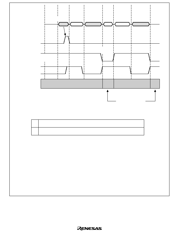
771
SDTRF
1
0
1
SDSR
SDDR
SDSR
SDDR
Shift
CPU
Shift
CPU
Input/
output
Serial data
H-UDI interrupt
request
SDTRF
(in SDSR)
*
1
SDSR and
SDDR MUX
*
2
SDDR access
state
Instruction
Input
Shift
disabled
Shift
enabled
SDSR serial transfer
(monitoring)
Shift
enabled
Notes:
*
1 SDTRF flag (in SDSR): Indicates whether SDDR access by the CPU or serial transfer
data input/output to SDDR is possible.
1
SDDR is shift-disabled. SDDR access by the CPU is enabled.
2
SDDR is shift-enabled. Do not access SDDR until SDTRF = 0.
Conditions:
∑ SDTRF = 1
-- When
TRST
= 0
-- When the CPU writes 1
-- In bypass mode
∑ SDTRF = 0
-- End of SDDR shift access in serial transfer
*
2 SDSR/SDDR (Update-DR state) internal MUX switchover timing
∑ Switchover from SDSR to SDDR: On completion of serial transfer in which
SDTRF = 1 is output from TDO
∑ Switchover from SDDR to SDSR: On completion of serial transfer to SDDR
Figure 18.3 Data Input/Output Timing Chart (1)
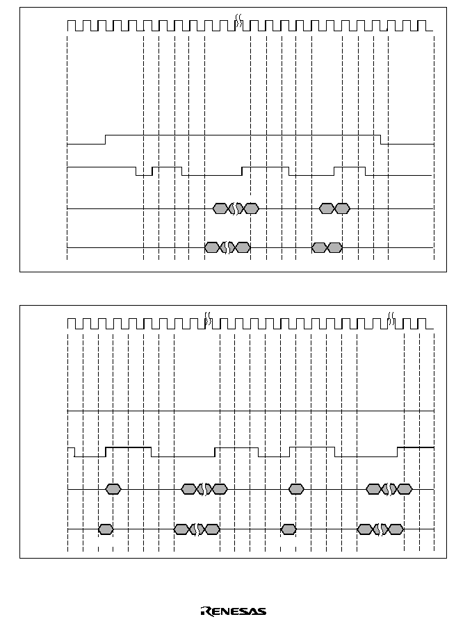
772
TCK
TMS
TDI
TDO
TRST
Test-Logic-Reset
Run-Test/Idle
Select-DR
Select-IR
Capture-IR
Shift-IR
Update-IR
Select-DR
Capture-DR
Shift-DR
Test-Logic-Reset
Run-Test/Idle
Exit1-DR
Update-DR
TS0
TS3
Exit1-IR
SDTRF
Figure 18.4 Data Input/Output Timing Chart (2)
TCK
TMS
TDI
TDO
TRST
Select-DR
Select-DR
Capture-DR
Shift-DR
Exit1-DR
Update-DR
Select-DR
Capture-DR
Shift-DR
Update-DR
Bit
0
Bit
31
Bit
0
Bit
31
Bit
0
Bit
31
Bit
0
Bit
31
SDTRF
SDTRF
Shift-DR
Capture-DR
Shift-DR
Select-DR
Update-DR
Capture-DR
Update-DR
Exit1-DR
Exit1-DR
Exit1-DR
Figure 18.5 Data Input/Output Timing Chart (3)

773
18.4.3
H-UDI Reset
The H-UDI can be reset in two ways.
∑
The H-UDI is reset when the
TRST signal is held at 0.
∑
When
TRST = 1, the H-UDI can be reset by inputting at least five TCK clock cycles while
TMS = 1.
18.5
Boundary Scan
The H-UDI pins can be placed in the boundary scan mode stipulated by IEEE1149.1 by setting a
command in SDIR.
18.5.1
Supported Instructions
The SH7616 supports the three essential instructions defined in IEEE1149.1 (BYPASS,
SAMPLE/PRELOAD, and EXTEST) and optional instructions (CLAMP, HIGHZ, and IDCODE).
BYPASS: The BYPASS instruction is an essential standard instruction that operates the bypass
register. This instruction shortens the shift path to speed up serial data transfer involving other
chips on the printed circuit board. While this instruction is executing, the test circuit has no effect
on the system circuits. The instruction code is 1111.
SAMPLE/PRELOAD: The SAMPLE/PRELOAD instruction inputs values from the SH7616's
internal circuitry to the boundary scan register, outputs values from the scan path, and loads data
onto the scan path. When this instruction is executing, the SH7616's input pin signals are
transmitted directly to the internal circuitry, and internal circuit values are directly output
externally from the output pins. The SH7616's system circuits are not affected by execution of
this instruction. The instruction code is 0100.
In a SAMPLE operation, a snapshot of a value to be transferred from an input pin to the internal
circuitry, or a value to be transferred from the internal circuitry to an output pin, is latched into the
boundary scan register and read from the scan path. Snapshot latching is performed in
synchronization with the rise of TCK in the Capture-DR state. Snapshot latching does not affect
normal operation of the SH7616.
In a PRELOAD operation, an initial value is set in the parallel output latch of the boundary scan
register from the scan path prior to the EXTEST instruction. Without a PRELOAD operation,
when the EXTEST instruction was executed an undefined value would be output from the output
pin until completion of the initial scan sequence (transfer to the output latch) (with the EXTEST
instruction, the parallel output latch value is constantly output to the output pin).
EXTEST: This instruction is provided to test external circuitry when the SH7616 is mounted on a
printed circuit board. When this instruction is executed, output pins are used to output test data

774
(previously set by the SAMPLE/PRELOAD instruction) from the boundary scan register to the
printed circuit board, and input pins are used to latch test results into the boundary scan register
from the printed circuit board. If testing is carried out by using the EXTEST instruction N times,
the Nth test data is scanned-in when test data (N-1) is scanned out.
Data loaded into the output pin boundary scan register in the Capture-DR state is not used for
external circuit testing (it is replaced by a shift operation).
The instruction code is 0000.
CLAMP: When the CLAMP instruction is enabled, the output pin outputs the value of the
boundary scan register that has been set by the SAMPLE/PRELOAD instruction. While the
CLAMP instruction is enabled, the state of the boundary scan register maintains the previous state
regardless of the state of the TAP controller.
A bypass register is connected between TDI and TDO. The related circuit operates in the same
way when the BYPASS instruction is enabled.
The instruction code is 0010.
HIGHZ: When the HIGHZ instruction is enabled, all output pins enter a high-impedance state.
While the HIGHZ instruction is enabled, the state of the boundary scan register maintains the
previous state regardless of the state of the TAP controller.
A bypass register is connected between TDI and TDO. The related circuit operates in the same
way when the BYPASS instruction is enabled.
The instruction code is 0010.
IDCODE: When the IDCODE instruction is enabled, the value of the ID code register is output
from TDO with LSB first when the TAP controller is in the Shift-DR state. While this instruction
is being executed, the test circuit does not affect the system circuit.
When the TAP controller is in the Test-Logic-Reset state, the instruction register is initialized to
the IDCODE instruction.
The instruction code is 0010.
18.5.2
Notes on Use
1. Boundary scan mode does not cover clock-related signals (EXTAL, XTAL, CKIO, CAP1,
CAP2).
2. Boundary scan mode does not cover reset-related signals (
RES, ASEMODE).
3. Boundary scan mode does not cover H-UDI-related signals (TCK, TDI, TDO, TMS,
TRST).
4. Fix the ASEMODE pin high.
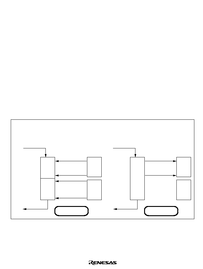
775
18.6
Usage Notes
∑
A reset must always be executed by driving the
TRST signal to 0, regardless of whether or not
the H-UDI is to be activated.
TRST must be held low for 20 TCK clock cycles. For details, see
section 22, Electrical Characteristics.
∑
The registers are not initialized in standby mode. If
TRST is set to 0 in standby mode, bypass
mode will be entered.
∑
The frequency of TCK must be lower than that of the peripheral module clock (P
). For
details, see section 22, Electrical Characteristics.
∑
In data transfer, data input/output starts with the LSB. Figure 18.6 shows serial data
input/output.
∑
When data that exceeds the number of bits of the register connected between TDI and TDO is
serially transferred, the serial data that exceeds the number of register bits and output from
TDO is the same as that input from TDI.
∑
If the H-UDI serial transfer sequence is disrupted, a
TRST reset must be executed. Transfer
should then be retried, regardless of the transfer operation.
∑
TDO is output at the falling edge of TCK when one of six instructions defined in IEEE1149.1
is selected. Otherwise, it is output at the rising edge of TCK.
TDI
SDIR
SDSR
SDIR
SDSR
SDIR
SDSR
TDO
Shift register
Bit 31
Bit 15
Bit 16
Bit 0
Bit 15
Bit 15
Bit 0
Bit 0
∑ SDIR and SDSR serial data input/output
In Capture-IR, SDIR and SDSR are captured into the shift register, and in Shift-IR bits 0 to 15 of SDSR and
bits 0 to 15 of SDIR are output in that order from TDO.
In Update-IR, data input from TDI is written to SDIR, but not to SDSR.
.
.
.
.
.
.
Capture-IR
TDI
TDI
input
data
TDO
Shift register
Bit 31
Bit 15
Bit 16
Bit 0
Bit 15
Bit 0
.
.
.
Update-IR
Figure 18.6 Serial Data Input/Output (1)
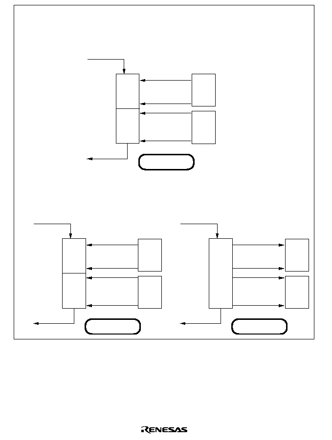
776
TDI
SDDRH
SDDRL
SDDRH
SDDRL
TDO
Shift register
Bit 31
Bit 15
Bit 16
Bit 0
Bit 15
Bit 15
Bit 0
Bit 0
Bit 15
Bit 15
Bit 0
Bit 0
.
.
.
.
.
.
.
.
.
Capture-DR
TDI
SDDRH
SDDRL
TDO
Shift register
Bit 31
Bit 15
Bit 16
Bit 0
.
.
.
Update-DR
TDI
SDIR
SDSR
SDIR
SDSR
TDO
Shift register
Bit 31
Bit 15
Bit 16
Bit 0
Bit 15
Bit 15
Bit 0
Bit 0
∑ SDDRH and SDDRL serial data input/output
(1) In H-UDI interrupt mode, before SDTRF = 1 is read from TDO when an H-UDI interrupt is generated,
SDSR and SDIR are captured into the shift register in Capture-DR, and in Shift-DR bits 0 to 15 of SDSR
and bits 0 to 15 of SDIR are output in that order from TDO.
In Update-DR, TDI input data is not written to any register.
(2) In H-UDI interrupt mode, after SDTRF = 1 is read from TDO when an H-UDI interrupt is generated,
SDDRH and SDDRL are captured into the shift register in Capture-DR, and in Shift-DR bits 0 to 15 of
SDDRL and bits 0 to 15 of SDDRH are output in that order from TDO.
Data input from TDI is written to SDDRH and SDDRL in Update-DR.
.
.
.
.
.
.
Capture-DR
TDI
input
data
Figure 18.6 Serial Data Input/Output (2)
777
∑ SDIDR serial data input/output
In IDCODE mode, SDIDR is captured into the shift register in Capture-DR, and in Shift-DR bits 0 to 31 of
SDIDR are output in that order from TDO.
In Update-DR, data input from TDI is not written to any register.
TDI
SDIDR
SDIDR
TDO
Shift register
Bit 31
Bit 15
Bit 0
Bit 0
.
.
.
.
Capture-DR
Figure 18.6 Serial Data Input/Output (3)

778

779
Section 19 Pin Function Controller (PFC)
19.1
Overview
The pin function controller (PFC) consists of registers to select multiplexed pin functions and
input/output direction. The pin function and input/output direction can be selected for individual
pins regardless of the operating mode of the chip. Table 19.1 shows the chip's multiplex pins.

780
Table 19.1
Multiplex Pins
Function 1 [00]
*
Function 2 [01]
*
Function 3 [10]
*
Function 4 [11]
*
Port
Signal
Name
I/O
Related
Module
Signal
Name
I/O
Related
Module
Signal
Name
I/O
Related
Module
Signal
Name
I/O
Related
Module
A
PA13
I/O
Port
SRCK0
I
SIO0
--
--
--
--
--
--
A
PA12
I/O
Port
SRS0
I
SIO0
--
--
--
--
--
--
A
PA11
I/O
Port
SRXD0
I
SIO0
--
--
--
--
--
--
A
PA10
I/O
Port
STCK0
I
SIO0
--
--
--
--
--
--
A
PA9
I/O
Port
STS0
I/O
SIO0
--
--
--
--
--
--
A
PA8
I/O
Port
STXD0
O
SIO0
--
--
--
--
--
--
A
WDTOVF
O
WDT
PA7
I/O
Port
--
--
--
--
--
--
A
PA6
I/O
Port
FTCI
I
FRT
--
--
--
--
--
--
A
PA5
I/O
Port
FTI
I
FRT
--
--
--
--
--
--
A
PA4
I/O
Port
FTOA
O
FRT
--
--
--
--
--
--
A
CKPO
O
Port
FTOB
O
FRT
--
--
--
--
--
--
A
PA2
I/O
Port
LNKSTA
I
EtherC
--
--
--
--
--
--
A
PA1
I/O
Port
EXOUT
O
EtherC
--
--
--
--
--
--
A
PA0
I/O
Port
CAMSEN I
EtherC
--
--
--
--
--
--
B
PB15
I/O
Port
--
--
--
SCK1
I/O
SCIF1
--
--
--
B
PB14
I/O
Port
--
--
--
RXD1
I
SCIF1
--
--
--
B
PB13
I/O
Port
--
--
--
TXD1
O
SCIF1
--
--
--
B
PB12
I/O
Port
SRCK2
I
SIO2
RTS
O
SCIF1
STATS1
O
BSC
B
PB11
I/O
Port
SRS2
I
SIO2
CTS
I
SCIF1
STATS0
O
BSC
B
PB10
I/O
Port
SRXD2
I
SIO2
TIOCA1
I/O
TPU1
--
--
--
B
PB9
I/O
Port
STCK2
I
SIO2
TIOCB1
I/O
TPU1
--
--
--
B
PB8
I/O
Port
STS2
I/O
SIO2
TIOCA2
I/O
TPU2
--
--
--
B
PB7
I/O
Port
STXD2
O
SIO2
TIOCB2
I/O
TPU2
--
--
--
B
PB6
I/O
Port
SRCK1
I
SIO1
SCK2
I/O
SCIF2
--
--
--
B
PB5
I/O
Port
SRS1
I
SIO1
RXD2
I
SCIF2
--
--
--
B
PB4
I/O
Port
SRXD1
I
SIO1
TXD2
O
SCIF2
--
--
--
B
PB3
I/O
Port
STCK1
I
SIO1
TIOCA0
I/O
TPU2
--
--
--
B
PB2
I/O
Port
STS1
I/O
SIO1
TIOCB0
I/O
TPU2
--
--
--
B
PB1
I/O
Port
STXD1
O
SIO1
TIOCC0
I/O
TPU2
--
--
--
B
PB0
I/O
Port
--
--
--
TIOCD0
I/O
TPU2
WOL
O
EtherC
Notes: In the initial state, function 1 is selected.
*
The initial value is "input."
The figures in brackets indicate the settings of the mode bits (MD1, MD0) in the PFC to
select multiplexed functions in port A[0:13] and port B[0:15].

781
19.2
Register Configuration
Table 19.2 shows the PFC registers.
Table 19.2
Register Configuration
Name
Abbreviation
R/W
Initial Value
Address
Access Size
Port A control register
PACR
R/W
H'0000
H'FFFFFC80
8, 16
Port A I/O register
PAIOR
R/W
H'0000
H'FFFFFC82
8, 16
Port B control register
PBCR
R/W
H'0000
H'FFFFFC88
8, 16
Port B I/O register
PBIOR
R/W
H'0000
H'FFFFFC8A
8, 16
Port B control register 2
PBCR2
R/W
H'0000
H'FFFFFC8E
8, 16
19.3
Register Descriptions
19.3.1
Port A Control Register (PACR)
Bit:
15
14
13
12
11
10
9
8
--
--
PA13MD PA12MD PA11MD PA10MD PA9MD PA8MD
Initial value:
0
0
0
0
0
0
0
0
R/W:
R
R
R/W
R/W
R/W
R/W
R/W
R/W
Bit:
7
6
5
4
3
2
1
0
PA7MD
PA6MD PA5MD
PA4MD PA3MD
PA2MD
PA1MD PA0MD
Initial value:
0
0
0
0
0
0
0
0
R/W:
R/W
R/W
R/W
R/W
R/W
R/W
R/W
R/W
The port A control register (PACR) is a 16-bit read/write register that selects the functions of the
14 multiplex pins in port A.
PACR is initialized to H'0000 by a power-on reset. It is not initialized by a manual reset or in
standby mode or sleep mode.
Bits 15 and 14--Reserved: These bits are always read as 0. The write value should always be 0.

782
Bit 13--PA13 Mode Bit (PA13MD): Selects the function of pin PA13/SRCK0.
Bit 13: PA13MD
Description
0
General input/output (PA13)
(Initial value)
1
SIOF serial receive clock input (SRCK0)
Bit 12--PA12 Mode Bit (PA12MD): Selects the function of pin PA12/SRS0.
Bit 12: PA12MD
Description
0
General input/output (PA12)
(Initial value)
1
SIOF serial receive synchronous input (SRS0)
Bit 11--PA11 Mode Bit (PA11MD): Selects the function of pin PA11/SRXD0.
Bit 11: PA11MD
Description
0
General input/output (PA11)
(Initial value)
1
SIOF serial receive data (SRXD0)
Bit 10--PA10 Mode Bit (PA10MD): Selects the function of pin PA10/STCK0.
Bit 10: PA10MD
Description
0
General input/output (PA10)
(Initial value)
1
SIOF serial transmit clock (STCK0)
Bit 9--PA9 Mode Bit (PA9MD): Selects the function of pin PA9/STS0.
Bit 9: PA9MD
Description
0
General input/output (PA9)
(Initial value)
1
SIOF serial transmit synchronous input/output (STS0)
Bit 8--PA8 Mode Bit (PA8MD): Selects the function of pin PA8/STXD0.
Bit 8: PA8MD
Description
0
General input/output (PA8)
(Initial value)
1
SIOF serial transmit data output (STXD0)

783
Bit 7--PA7 Mode Bit (PA7MD): Selects the function of pin
WDTOVF/PA7.
Bit 7: PA7MD
Description
0
WDT overflow signal output (
WDTOVF
)
*
(Initial value)
1
General input/output (PA7)
Note:
*
WDTOVF
is an output pin after a reset, so care is required when using this pin as a general
input port (PA7).
Bit 6--PA6 Mode Bit (PA6MD): Selects the function of pin PA6/FTCI.
Bit 6: PA6MD
Description
0
General input/output (PA6)
(Initial value)
1
FRT clock input (FTCI)
Bit 5--PA5 Mode Bit (PA5MD): Selects the function of pin PA5/FTI.
Bit 5: PA5MD
Description
0
General input/output (PA5)
(Initial value)
1
FRT input capture input (FTI)
Bit 4--PA4 Mode Bit (PA4MD): Selects the function of pin PA4/FTO4.
Bit 4: PA4MD
Description
0
General input/output (PA4)
(Initial value)
1
FRT output compare output (FTOA)
Bit 3--PA3 Mode Bit (PA3MD): Selects the function of pin CKPO/FTOB.
Bit 3: PA3MD
Description
0
Peripheral module clock output (CKPO)
(Initial value)
1
FRT output compare output (FTOB)
Bit 2--PA2 Mode Bit (PA2MD): Selects the function of pin PA2/LNKSTA.
Bit 2: PA2MD
Description
0
General input/output (PA2)
(Initial value)
1
EtherC rink status input (LNKSTA)
784
Bit 1--PA1 Mode Bit (PA1MD): Selects the function of pin PA1/EXOUT.
Bit 1: PA1MD
Description
0
General input/output (PA1)
(Initial value)
1
EtherC general external output (EXOUT)
Bit 0--PA0 Mode Bit (PA0MD): Selects the function of pin PA0.
Bit 0: PA0MD
Description
0
General input/output (PA0)
(Initial value)
1
EtherC CAM sense input (CAMSEN)
19.3.2
Port A I/O Register (PAIOR)
Bit:
15
14
13
12
11
10
9
8
--
--
PA13IOR PA12IOR PA11IOR PA10IOR PA9IOR PA8IOR
Initial value:
0
0
0
0
0
0
0
0
R/W:
R
R
R/W
R/W
R/W
R/W
R/W
R/W
Bit:
7
6
5
4
3
2
1
0
PA7IOR PA6IOR PA5IOR PA4IOR
--
PA2IOR PA1IOR PA0IOR
Initial value:
0
0
0
0
0
0
0
0
R/W:
R/W
R/W
R/W
R/W
R
R/W
R/W
R/W
The port A I/O register (PAIOR) is a 16-bit read/write register that selects the input/output
direction of the 14 multiplex pins in port A. Bits PA13IOR to PA4IOR and PA2IOR to PA0IOR
correspond to individual pins in port A. PAIOR is enabled when port A pins function as general
input pins (PA13 to PA4 and PA2 to PA0), and disabled otherwise. When port A pins function as
PA13 to PA4 and PA2 to PA0, a pin becomes an output when the corresponding bit in PAIOR is
set to 1, and an input when the bit is cleared to 0.
PAIOR is initialized to H'0000 by a power-on reset. It is not initialized by a manual reset or in
standby mode or sleep mode.

785
19.3.3
Port B Control Registers (PBCR, PBCR2)
The port B control registers (PBCR and PBCR2) are 16-bit read/write registers that select the
functions of the 16 multiplex pins in port B. PBCR selects the functions of the pins for the upper 8
bits in port B, and PBCR2 selects the functions of the pins for the lower 8 bits in port B.
PBCR and PBCR2 are initialized to H'0000 by a power-on reset. They are not initialized by a
manual reset or in standby mode or sleep mode.
Port B Control Register (PBCR)
Bit:
15
14
13
12
11
10
9
8
PB15
MD1
PB15
MD0
PB14
MD1
PB14
MD0
PB13
MD1
PB13
MD0
PB12
MD1
PB12
MD0
Initial value:
0
0
0
0
0
0
0
0
R/W:
R/W
R/W
R/W
R/W
R/W
R/W
R/W
R/W
Bit:
7
6
5
4
3
2
1
0
PB11
MD1
PB11
MD0
PB10
MD1
PB10
MD0
PB9
MD1
PB9
MD0
PB8
MD1
PB8
MD0
Initial value:
0
0
0
0
0
0
0
0
R/W:
R/W
R/W
R/W
R/W
R/W
R/W
R/W
R/W
Bits 15 and 14--PB15 Mode Bits 1 and 0 (PB15MD1, PB15MD0): These bits select the function
of pin PB15/SCK1.
Bit 15: PB15MD1
Bit 14: PB15MD0
Description
0
0
General input/output (PB15)
(Initial value)
1
Reserved
1
0
SCIF1 serial clock input/output (SCK1)
1
Reserved

786
Bits 13 and 12--PB14 Mode Bits 1 and 0 (PB14MD1, PB14MD0): These bits select the function
of pin PB14/RXD1.
Bit 13: PB14MD1
Bit 12: PB14MD0
Description
0
0
General input/output (PB14)
(Initial value)
1
Reserved
1
0
SCIF1 serial data input (RXD1)
1
Reserved
Bits 11 and 10--PB13 Mode Bits 1 and 0 (PB13MD1, PB13MD0): These bits select the function
of pin PB13/TXD1.
Bit 11: PB13MD1
Bit 10: PB13MD0
Description
0
0
General input/output (PB13)
(Initial value)
1
Reserved
1
0
SCIF1 serial data output (TXD1)
1
Reserved
Bits 9 and 8--PB12 Mode Bits 1 and 0 (PB12MD1, PB12MD0): These bits select the function of
pin PB12/SRCK2/
RTS/STATS1.
Bit 9: PB12MD1
Bit 8: PB12MD0
Description
0
0
General input/output (PB12)
(Initial value)
1
SIO2 serial receive clock input (SRCK2)
1
0
SCIF1 transmit request (
RTS
)
1
BSC status 1 output (STATS1)
Bits 7 and 6--PB11 Mode Bits 1 and 0 (PB11MD1, PB11MD0): These bits select the function of
pin PB11/SRS2/
CTS/STATS0.
Bit 7: PB11MD1
Bit 6: PB11MD0
Description
0
0
General input/output (PB11)
(Initial value)
1
SIO2 serial receive synchronous input (SRS2)
1
0
SCIF1 transmit permission (
CTS
)
1
BSC status 0 output (STATS0)

787
Bits 5 and 4--PB10 Mode Bits 1 and 0 (PB10MD1, PB10MD0): These bits select the function of
pin PB10/SRXD2/TIOCA1.
Bit 5: PB10MD1
Bit 4: PB10MD0
Description
0
0
General input/output (PB10)
(Initial value)
1
SIO2 serial receive data input (SRXD2)
1
0
TPU1 input capture input/output compare output
(TIOCA1)
1
Reserved
Bits 3 and 2--PB9 Mode Bits 1 and 0 (PB9MD1, PB9MD0): These bits select the function of pin
PB9/STCK2/TIOCB1, TCLKC.
Bit 3: PB9MD1
Bit 2: PB9MD0
Description
0
0
General input/output (PB9)
(Initial value)
1
SIO2 serial transmit clock input (STCK2)
1
0
TPU1 input capture input/output compare output
(TIOCB1)
*
1
Reserved
Note:
*
Timer clock input C (TCLKC) is selected when the TPU phase counting mode is set, or
according to the setting of bits TPSC2 to TPSC0 in TCR.
Bits 1 and 0--PB8 Mode Bits 1 and 0 (PB8MD1, PB8MD0): These bits select the function of pin
PB8/STS2/TIOCA2.
Bit 1: PB8MD1
Bit 0: PB8MD0
Description
0
0
General input/output (PB8)
(Initial value)
1
SIO2 serial transmit synchronous input/output (STS2)
1
0
TPU2 input capture input/output compare output
(TIOCA2)
1
Reserved

788
Port B Control Register 2 (PBCR2)
Bit:
15
14
13
12
11
10
9
8
PB7
MD1
PB7
MD0
PB6
MD1
PB6
MD0
PB5
MD1
PB5
MD0
PB4
MD1
PB4
MD0
Initial value:
0
0
0
0
0
0
0
0
R/W:
R/W
R/W
R/W
R/W
R/W
R/W
R/W
R/W
Bit:
7
6
5
4
3
2
1
0
PB3
MD1
PB3
MD0
PB2
MD1
PB2
MD0
PB1
MD1
PB1
MD0
PB0
MD1
PB0
MD0
Initial value:
0
0
0
0
0
0
0
0
R/W:
R/W
R/W
R/W
R/W
R/W
R/W
R/W
R/W
Bits 15 and 14--PB7 Mode Bits 1 and 0 (PB7MD1, PB7MD0): These bits select the function of
pin PB7/STXD2/TIOCB2, TCLKD.
Bit 15: PB7MD1
Bit 14: PB7MD0
Description
0
0
General input/output (PB7)
(Initial value)
1
SIO2 serial transmit data output (STXD2)
1
0
TPU2 input capture input/output compare output
(TIOCB2)
*
1
Reserved
Note:
*
Timer clock input D (TCLKD) is selected when the TPU phase counting mode is set, or
according to the setting of bits TPSC2 to TPSC0 in TCR.
Bits 13 and 12--PB6 Mode Bits 1 and 0 (PB6MD1, PB6MD0): These bits select the function of
pin PB6/SRCK1/SCK2.
Bit 13: PB6MD1
Bit 12: PB6MD0
Description
0
0
General input/output (PB6)
(Initial value)
1
SIO1 serial receive clock input (SRCK1)
1
0
SCIF2 serial clock input/output (SCK2)
1
Reserved

789
Bits 11 and 10--PB5 Mode Bits 1 and 0 (PB5MD1, PB5MD0): These bits select the function of
pin PB5/SRS1/RXD2.
Bit 11: PB5MD1
Bit 10: PB5MD0
Description
0
0
General input/output (PB5)
(Initial value)
1
SIO1 serial receive synchronous input (SRS1)
1
0
SCIF2 serial data input (RXD2)
1
Reserved
Bits 9 and 8--PB4 Mode Bits 1 and 0 (PB4MD1, PB4MD0): These bits select the function of pin
PB4/SRXD1/TXD2.
Bit 9: PB4MD1
Bit 8: PB4MD0
Description
0
0
General input/output (PB4)
(Initial value)
1
SIO1 serial receive data input (SRXD1)
1
0
SCIF2 serial data output (TXD2)
1
Reserved
Bits 7 and 6--PB3 Mode Bits 1 and 0 (PB3MD1, PB3MD0): These bits select the function of pin
PB3/STCK1/TIOCA0.
Bit 7: PB3MD1
Bit 6: PB3MD0
Description
0
0
General input/output (PB3)
(Initial value)
1
SIO1 serial transmit clock input (STCK1)
1
0
TPU0 input capture input/output compare output
(TIOCA0)
1
Reserved
Bits 5 and 4--PB2 Mode Bits 1 and 0 (PB2MD1, PB2MD0): These bits select the function of pin
PB2/STS1/TIOCB0.
Bit 5: PB2MD1
Bit 4: PB2MD0
Description
0
0
General input/output (PB2)
(Initial value)
1
SIO1 serial transmit synchronous input/output (STS1)
1
0
TPU0 input capture input/output compare output
(TIOCB0)
1
Reserved

790
Bits 3 and 2--PB1 Mode Bits 1 and 0 (PB1MD1, PB1MD0): These bits select the function of pin
PB1/STXD1/TIOCC0/TCLKA.
Bit 3: PB1MD1
Bit 2: PB1MD0
Description
0
0
General input/output (PB1)
(Initial value)
1
SIO1 serial transmit data output (STXD1)
1
0
TPU0 input capture input/output compare output
(TIOCC0)
*
1
Reserved
Note:
*
Timer clock input A (TCLKA) is selected when the TPU phase counting mode is set, or
according to the setting of bits TPSC2 to TPSC0 in TCR.
Bits 1 and 0--PB0 Mode Bits 1 and 0 (PB0MD1, PB0MD0): These bits select the function of pin
PB0/TIOCD0/TCLKB.
Bit 1: PB0MD1
Bit 0: PB0MD0
Description
0
0
General input/output (PB0)
(Initial value)
1
Reserved
1
0
TPU0 input capture input/output compare output
(TIOCD0)
*
1
EtherC Wake-On-LAN output (WOL)
Note:
*
Timer clock input B (TCLKB) is selected when the TPU phase counting mode is set, or
according to the setting of bits TPSC2 to TPSC0 in TCR.

791
19.3.4
Port B I/O Register (PBIOR)
Bit:
15
14
13
12
11
10
9
8
PB15
IOR
PB14
IOR
PB13
IOR
PB12
IOR
PB11
IOR
PB10
IOR
PB9
IOR
PB8
IOR
Initial value:
0
0
0
0
0
0
0
0
R/W:
R/W
R/W
R/W
R/W
R/W
R/W
R/W
R/W
Bit:
7
6
5
4
3
2
1
0
PB7
IOR
PB6
IOR
PB5
IOR
PB4
IOR
PB3
IOR
PB2
IOR
PB1
IOR
PB0
IOR
Initial value:
0
0
0
0
0
0
0
0
R/W:
R/W
R/W
R/W
R/W
R/W
R/W
R/W
R/W
The port B I/O register (PBIOR) is a 16-bit read/write register that selects the input/output
direction of the 16 multiplex pins in port B. Bits PB15IOR to PB0IOR correspond to individual
pins in port B. PBIOR is enabled when port B pins function as general input pins (PB15 to PB0),
and disabled otherwise. When port B pins function as PB15 to PB0, a pin becomes an output when
the corresponding bit in PBIOR is set to 1, and an input when the bit is cleared to 0.
PBIOR is initialized to H'0000 by a power-on reset. It is not initialized by a manual reset or in
standby mode or sleep mode.

792
793
Section 20 I/O Ports
20.1
Overview
This chip has two ports, designated A and B. Port A is a 14-bit input/output port, and port B is a
16-bit input/output port. The port pins are multiplexed as general input/output and other functions.
(The function of multiplexed multiplex pins is selected by means of the pin function controller
(PFC).) Ports A and B are each provided with a data register for storing pin data.
20.2
Port A
Port A is an input/output port with the 14 pins shown in figure 20.1. Of the 14 pins, the CKPO pin
has no port data register bit, and is multiplexed as an internal clock pin.
PA13 (input/output) / SRCK0
(input)
PA12 (input/output) / SRS0
(input)
PA11 (input/output) / SRXD0
(input)
PA10 (input/output) / STCK0
(input)
PA9
(input/output) / STS0
(input/output)
PA8 (input/output) /
STXD0
(output)
WDTOVF
*
(output) / PA7
(input/output)
PA6 (input/output) / FTCI
(input)
PA5 (input/output) /
FTI
(input)
PA4 (input/output) /
FTOA
(output)
CKPO (output) /
FTOB
(output)
PA2
(input/output) / LNKSTA (input)
PA1
(input/output) / EXOUT
(output)
PA0
(input/output)
Port A
Note:
*
The fact that the
WDTOVF
pin is set to output mode after a reset
must be noted when it is to be used as a general I/O port (PA7).
Figure 20.1 Port A

794
20.2.1
Register Configuration
The port A register is shown in table 20.1.
Table 20.1
Register Configuration
Name
Abbreviation
R/W
Initial Value
Address
Access Size
Port A data register
PADR
R/W
H'0000
H'FFFFFC84
8, 16
20.2.2
Port A Data Register (PADR)
Bit:
15
14
13
12
11
10
9
8
--
--
PA13DR PA12DR PA11DR PA10DR PA9DR
PA8DR
Initial value:
0
0
0
0
0
0
0
0
R/W:
R
R
R/W
R/W
R/W
R/W
R/W
R/W
Bit:
7
6
5
4
3
2
1
0
PA7DR
PA6DR
PA5DR
PA4DR
--
PA2DR
PA1DR
PA0DR
Initial value:
0
0
0
0
0
0
0
0
R/W:
R/W
R/W
R/W
R/W
R
R/W
R/W
R/W
The port A data register (PADR) is a 16-bit read/write register that stores port A data. Bits 15, 14,
and 3 are reserved: they always read 0, and the write value should always be 0. Bits PA13DR to
PA0DR correspond to pins PA13 to PA0. When a pin functions as a general output, if a value is
written to PADR, that value is output directly from the pin, and if PADR is read, the register value
is returned directly regardless of the pin state. When a pin functions as a general input, if PADR is
read the pin state, not the register value, is returned directly. If a value is written to PADR,
although that value is written into PADR it does not affect the pin state. Table 20.2 summarizes
port A data register read/write operations.
PADR is initialized to H'0000 by a power-on reset. It is not initialized by a manual reset or in
standby mode or sleep mode.

795
Table 20.2
Port A Data Register (PADR) Read/Write Operations
PAIOR
Pin Function
Read
Write
0
General input
Pin state
Value is written to PADR, but does not
affect pin state
Other than general input
Pin state
Value is written to PADR, but does not
affect pin state
1
General output
PADR value
Write value is output from pin
Other than general output
PADR value
Value is written to PADR, but does not
affect pin state
20.3
Port B
Port B is an input/output port with the 16 pins shown in figure 20.2.
PB15 (input/output)
PB14 (input/output)
PB13 (input/output)
PB12 (input/output)
PB11 (input/output)
PB10 (input/output)
PB9 (input/output)
PB8 (input/output)
PB7 (input/output)
PB6 (input/output)
PB5 (input/output)
PB4 (input/output)
PB3 (input/output)
PB2 (input/output)
PB1 (input/output)
PB0 (input/output)
/ Reserved
/ SCK1
(input/output)
/ Reserved
/ RXD1
(input)
/ Reserved
/ TXD1
(output)
/ SRCK2 (input)
/ RTS
(output)
/ STATS1 (output)
/ SRS2
(input)
/ CTS
(input)
/ STATS0 (output)
/ SRXD2 (input)
/ TIOCA1 (input/output)
/ STCK2 (input)
/ TIOCB1 (input/output)
/ STS2 (input/output) / TIOCA2 (input/output)
/ STXD2 (output)
/ TIOCB2 (input/output)
/ SRCK1 (input)
/ SCK2
(input/output)
/ SRS1
(input)
/ RXD2
(input)
/ SRXD1 (input)
/ TXD2
(output)
/ STCK1 (input)
/ TIOCA0 (input/output)
/ STS1
(input/output) / TIOCB0 (input/output)
/ STXD1 (output)
/ TIOCD0 (input/output)
/ Reserved
/ TIOCD0 (input/output) / WOL (output)
Port B
Figure 20.2 Port B
20.3.1
Register Configuration
Table 20.3 shows the port B register.

796
Table 20.3
Register Configuration
Name
Abbreviation
R/W
Initial Value
Address
Access Size
Port B data register
PBDR
R/W
H'0000
H'FFFFFC8C
8, 16
20.3.2
Port B Data Register (PBDR)
Bit:
15
14
13
12
11
10
9
8
PB15DR PB14DR PB13DR PB12DR PB11DR PB10DR PB9DR
PB8DR
Initial value:
0
0
0
0
0
0
0
0
R/W:
R/W
R/W
R/W
R/W
R/W
R/W
R/W
R/W
Bit:
7
6
5
4
3
2
1
0
PB7DR
PB6DR
PB5DR
PB4DR
PB3DR
PB2DR
PB1DR
PB0DR
Initial value:
0
0
0
0
0
0
0
0
R/W:
R/W
R/W
R/W
R/W
R/W
R/W
R/W
R/W
The port B data register (PBDR) is a 16-bit read/write register that stores port B data. Bits
PB15DR to PB0DR correspond to pins PB15 to PB0. When a pin functions as a general output, if
a value is written to PBDR, that value is output directly from the pin, and if PBDR is read, the
register value is returned directly regardless of the pin state. When a pin functions as a general
input, if PBDR is read the pin state, not the register value, is returned directly. If a value is written
to PBDR, although that value is written into PBDR it does not affect the pin state. Table 20.4
shows port B data register read/write operations.
PBDR is initialized to H'0000 by a power-on reset. It is not initialized by a manual reset or in
standby mode or sleep mode.
Table 20.4
Port B Data Register (PBDR) Read/Write Operations
PBIOR
Pin Function
Read
Write
0
General input
Pin state
Value is written to PBDR, but does not
affect pin state
Other than general input
Pin state
Value is written to PBDR, but does not
affect pin state
1
General output
PBDR value
Write value is output from pin
Other than general output
PBDR value
Value is written to PBDR, but does not
affect pin state

797
Section 21 Power-Down Modes
21.1
Overview
This chip has a module standby function (which reduces power consumption by selectively halting
operation of unnecessary modules among the on-chip peripheral modules and the DSP unit), a
sleep mode (which halts CPU functions), and a standby mode (which halts all functions).
21.1.1
Power-Down Modes
The following modes and function are provided as power-down modes:
1. Sleep mode
2. Standby mode
3. Module standby function
(UBC, DMAC, DSP, FRT, SCIF1≠2, TPU, SIOF, SIO1≠2)
Table 21.1 shows the transition conditions for entering the modes from the program execution
state, as well as the CPU and peripheral module states in each mode and the procedures for
canceling each mode.

798
Table 21.1
Power-Down Modes
State
Mode
Transition
Condition
On-Chip
Oscilla-
tion
Circuit,
E-DMAC,
EtherC
CPU,
Cache DSP
BSC
UBC, DMAC,
FRT,
SCIF1≠2,
TPU, SIOF,
SIO1≠2
Pins
Canceling
Procedure
Sleep
mode
SLEEP
instruction
executed
with SBY
bit set to 0
in SBYCR1
Runs
Halted Halted
Runs
Runs
Runs
1. Interrupt
2. DMA
address
error
3. Power-on
reset
4. Manual
reset
Standby
mode
SLEEP
instruction
executed
with SBY
bit set to 1
in SBYCR1
Halted
Halted Halted
Halted,
and
register
values
held
UBC: Halted,
and register
values held
Other than
UBC: Halted
Held or
high
impedance
1. NMI
interrupt
2. Power-on
reset
3. Manual
reset
Module
standby
function
MSTP bit
for relevant
module is
set to 1
Runs
Runs
When
MSTP
is 1,
the clock
supply is
halted
Runs
When an
MSTP bit is
1, the clock
supply to
the relevant
module is
halted
FRT, and
SCIF1, 2
pins are
initialized,
and others
operate
1. Clear
MSTP bit
to 0
2. Power-on
reset
3. Manual
reset
21.1.2
Register
Table 21.2 shows the register configuration.
Table 21.2
Register Configuration
Name
Abbreviation
R/W
Initial Value
Address
Access Size
Standby control register 1
SBYCR1
R/W
H'00
H'FFFFFE91
8
Standby control register 2
SBYCR2
R/W
H'00
H'FFFFFE93
8

799
21.2
Register Descriptions
21.2.1
Standby Control Register 1 (SBYCR1)
Bit:
7
6
5
4
3
2
1
0
SBY
HIZ
MSTP5
MSTP4
MSTP3
--
MSTP1
--
(UBC)
(DMAC)
(DSP)
(FRT)
Initial value:
0
0
0
0
0
0
0
0
R/W:
R/W
R/W
R/W
R/W
R/W
R
R/W
R
Standby control register 1 (SBYCR1) is an 8-bit read/write register that sets the power-down
mode. SBYCR is initialized to H'00 by a reset.
Bit 7--Standby (SBY): Specifies transition to standby mode. To enter the standby mode, halt the
WDT (set the TME bit in WTCSR to 0) and set the SBY bit.
Bit 7: SBY
Description
0
Executing a SLEEP instruction puts the chip into sleep mode
(Initial value)
1
Executing a SLEEP instruction puts the chip into standby mode
Bit 6--Port High Impedance (HIZ): Selects whether output pins are set to high impedance or
retain the output state in standby mode. When HIZ = 0 (initial state), the specified pin retains its
output state. When HIZ = 1, the pin goes to the high-impedance state. See Appendix B.1, Pin
States during Resets, Power-Down States and Bus Release State, for which pins are controlled.
Bit 6: HIZ
Description
0
Pin state retained in standby mode
(Initial value)
1
Pin goes to high impedance in standby mode
Bit 5--Module Stop 5 (MSTP5): Specifies halting the clock supply to the user break controller
(UBC). When the MSTP5 bit is set to 1, the supply of the clock to the UBC is halted. When the
clock halts, the UBC registers retain their pre-halt state. Do not set this bit while the UBC is
running.
Bit 5: MSTP5
Description
0
UBC running
(Initial value)
1
Clock supply to UBC halted

800
Bit 4--Module Stop 4 (MSTP4): Specifies halting the clock supply to the DMAC. When MSTP4
bit is set to 1, the supply of the clock to the DMAC is halted. When the clock halts, the DMAC
retains its pre-halt state. When MSTP4 is cleared to 0 and the DMAC begins running again, its
starts operating from its pre-halt state. Set this bit while the DMAC is halted; this bit cannot be set
while the DMAC is operating (transferring data).
Bit 4: MSTP4
Description
0
DMAC running
(Initial value)
1
Clock supply to DMAC halted
Bit 3--Module Stop 3 (MSTP3): Specifies halting the clock supply to the DSP unit. When the
MSTP3 bit is set to 1, the supply of the clock to the DSP unit is halted. When the clock halts, the
operation result prior to the halt is retained. This bit should be set when the DSP unit is halted.
When the DSP unit is halted, no instructions with a DSP register, MACH, or MACL as an operand
can be used.
Bit 3: MSTP3
Description
0
DSP running
(Initial value)
1
Clock supply to DSP halted
Bit 2--Reserved: This bit is always read as 0. The write value should always be 0.
Bit 1--Module Stop 1 (MSTP1): Specifies halting the clock supply to the 16-bit free-running
timer (FRT). When the MSTP1 bit is set to 1, the supply of the clock to the FRT is halted. When
the clock halts, all FRT registers are initialized except the FRT interrupt vector register in INTC,
which holds its previous value. When MSTP1 is cleared to 0 and the FRT begins running again, its
starts operating from its initial state.
Bit 1: MSTP1
Description
0
FRT running
(Initial value)
1
Clock supply to FRT halted
Bit 0--Reserved: This bit is always read as 0. The write value should always be 0.

801
21.2.2
Standby Control Register 2 (SBYCR2)
Bit:
7
6
5
4
3
2
1
0
--
--
MSTP11
(TPU)
MSTP10
(SIO2)
MSTP9
(SIO1)
MSTP8
(SIOF)
MSTP7
(SCIF2)
MSTP6
(SCIF1)
Initial value:
0
0
0
0
0
0
0
0
R/W:
R
R
R/W
R/W
R/W
R/W
R/W
R/W
Standby control register 2 (SBYCR2) is an 8-bit read/write register that sets the power-down mode
state. SBYCR2 is initialized to H'00 by a reset.
Bits 7 and 6--Reserved: These bits are always read as 0. The write value should always be 0.
Bit 5--Module Stop 11 (MSTP11): Specifies halting the clock supply to the 16-bit timer pulse
unit (TPU). When the MSTP11 bit is set to 1, the supply of the clock to the TPU is halted. When
the clock halts, the TPU retains its pre-halt state, and the TPU interrupt vector register in the INTC
retains its pre-halt value. Therefore, when MSTP11 is cleared to 0 and the clock supply to the TPU
is resumed, the TPU starts operating again.
Bit 5: MSTP11
Description
0
TPU running
(Initial value)
1
Clock supply to TPU halted
Bit 4--Module Stop 10 (MSTP10): Specifies halting the clock supply to SIO channel 2. When the
MSTP10 bit is set to 1, the supply of the clock to SIO channel 2 is halted. When the clock halts,
SIO channel 2 retains its pre-halt state, and the SIO channel 2 interrupt vector register in the INTC
retains its pre-halt value. Therefore, when MSTP10 is cleared to 0 and the clock supply to SIO
channel 2 is restarted, operation starts again.
Bit 4: MSTP10
Description
0
SIO channel 2 running
(Initial value)
1
Clock supply to SIO channel 2 halted

802
Bit 3--Module Stop 9 (MSTP9): Specifies halting the clock supply to SIO channel 1. When the
MSTP9 bit is set to 1, the supply of the clock to SIO channel 1 is halted. When the clock halts,
SIO channel 1 retains its pre-halt state, and the SIO channel 1 interrupt vector register in the INTC
retains its pre-halt value. Therefore, when MSTP9 is cleared to 0 and the clock supply to SIO
channel 1 is restarted, operation starts again.
Bit 3: MSTP9
Description
0
SIO channel 1 running
(Initial value)
1
Clock supply to SIO channel 1 halted
Bit 2--Module Stop 8 (MSTP8): Specifies halting the clock supply to SIOF. When the MSTP8 bit
is set to 1, the supply of the clock to SIOF is halted. When the clock halts, SIOF retains its pre-halt
state, and the SIOF interrupt vector register in the INTC retains its pre-halt value. Therefore, when
MSTP8 is cleared to 0 and the clock supply to SIOF is restarted, operation starts again.
Bit 2: MSTP8
Description
0
SIOF running
(Initial value)
1
Clock supply to SIOF halted
Bit 1--Module Stop 7 (MSTP7): Specifies halting the clock supply to SCIF2. When the MSTP7
bit is set to 1, the supply of the clock to SCIF2 is halted. When the clock halts, the SCIF2 registers
are initialized, but the SCIF2 interrupt vector register in the INTC retains its pre-halt value.
Therefore, when MSTP7 is cleared to 0 and SCIF2 begins running again, it starts operating from
its initial state.
Bit 1: MSTP7
Description
0
SCIF2 running
(Initial value)
1
Clock supply to SCIF2 halted
Bit 0--Module Stop 6 (MSTP6): Specifies halting the clock supply to SCIF1. When the MSTP6
bit is set to 1, the supply of the clock to SCIF1 is halted. When the clock halts, the SCIF1 registers
are initialized, but the SCIF1 interrupt vector register in the INTC retains its pre-halt value.
Therefore, when MSTP6 is cleared to 0 and SCIF1 begins running again, it starts operating from
its initial state.
Bit 0: MSTP6
Description
0
SCIF1 running
(Initial value)
1
Clock supply to SCIF1 halted

803
21.3
Sleep Mode
21.3.1
Transition to Sleep Mode
Executing the SLEEP instruction when the SBY bit in SBYCR1 is 0 causes a transition from the
program execution state to sleep mode. Although the CPU halts immediately after executing the
SLEEP instruction, the contents of its internal registers remain unchanged. The on-chip peripheral
modules continue to run in sleep mode.
21.3.2
Canceling Sleep Mode
Sleep mode is canceled by an interrupt, DMA address error, power-on reset, or manual reset.
Cancellation by an Interrupt: When an interrupt occurs, sleep mode is canceled and interrupt
exception handling is executed. Sleep mode is not canceled if the interrupt cannot be accepted
because its priority level is equal to or less than the mask level set in the CPU's status register
(SR) or if an interrupt by an on-chip peripheral module is disabled at the peripheral module.
Cancellation by a DMA Address Error: If a DMA address error occurs, sleep mode is canceled
and DMA address error exception handling is executed.
Cancellation by a Power-On Reset: A power-on reset cancels sleep mode.
Cancellation by a Manual Reset: A manual reset cancels sleep mode.
21.4
Standby Mode
21.4.1
Transition to Standby Mode
To enter standby mode, set the SBY bit to 1 in SBYCR1, then execute the SLEEP instruction. The
chip switches from the program execution state to standby mode. The NMI interrupt cannot be
accepted when the SLEEP instruction is executed, or for the following five cycles. In standby
mode, the clock supply to all on-chip peripheral modules is halted as well as the CPU. CPU
register contents are held, and some on-chip peripheral modules are initialized.

804
Table 21.3
Register States in Standby Mode
Module
Registers Initialized
Registers that Retain
Data
Registers
with Undefined
Contents
Interrupt controller (INTC)
--
All registers
--
User break controller (UBC)
--
All registers
--
Bus state controller (BSC)
--
All registers
--
Direct memory access
controller (DMAC)
DMA channel control
register 0, 1
DMA operation register
∑
DMA source address
registers 0 and 1
∑
DMA destination
address registers 0
and 1
∑
DMA transfer count
registers 0 and 1
∑
DMA request/
response selection
control registers 0
and 1
∑
Vector number
setting registers
DMA0 and DMA1
--
Watchdog timer (WDT)
Bits 7≠5 of the timer
control/status register
Bits 2≠0 of the timer
control/status register
--
Reset control/status
register
Timer counter
16-bit free-running timer (FRT)
All registers
--
--
Serial communication interface
with FIFO (SCIF1≠2)
All registers
--
--
Serial I/O with FIFO (SIOF)
--
All registers
--
Serial I/O (SIO1≠2)
--
All registers
--
Hitachi user debug interface
(H-UDI)
--
All registers
--
16-bit timer pulse unit (TPU)
--
All registers
--
Pin function controller (PFC)
--
All registers
--
Ethernet controller direct
memory access controller (E-
DMAC)
All registers
--
--
Ethernet controller (EtherC)
All registers
--
--
Others
--
Standby control register
1, 2
Frequency modification
register
--

805
21.4.2
Canceling Standby Mode
Standby mode is canceled by an NMI interrupt, a power-on reset, or a manual reset.
Cancellation by an NMI Interrupt: When a rising edge or falling edge is detected in the NMI
signal, after the elapse of the time set in the WDT timer control/status register, clocks are supplied
to the entire chip, standby mode is canceled, and NMI exception handling begins. Insure that the
interval set for the WDT is at least as long as the oscillation stabilization time. When standby
mode is canceled by a falling edge in the NMI signal, insure that the NMI pin goes high when
standby mode is entered (when the clock is halted), and goes low on recovering from standby
mode (when the clock starts after oscillation has stabilized). The low level at the NMI pin should
be held for at least 3 cycles after the start of clock signal output from the CKIO pin. When standby
mode is canceled by a rising edge in the NMI signal, insure that the NMI pin goes low when
standby mode is entered (when the clock is halted), and goes high on recovering from standby
mode (when the clock starts after oscillation has stabilized). The high level at the NMI pin should
be held for at least 3 cycles after the start of clock signal output from the CKIO pin.
Cancellation by a Power-On Reset: A power-on reset cancels standby mode.
Cancellation by a Manual Reset: A manual reset cancels standby mode.
21.4.3
Standby Mode Cancellation by NMI Interrupt
The following example describes moving to the standby mode upon the fall of the NMI signal and
clearing the standby mode when the NMI signal rises. Figure 21.1 shows the timing.
When the NMI pin level changes from high to low after the NMI edge select bit (NMIE) of the
interrupt control register (ICR) has been set to 0 (detect falling edge), an NMI interrupt is
accepted. When the NMIE bit is set to 1 (detect rising edge) by the NMI exception service routine,
the standby bit (SBY) of the standby control register 1 (SBYCR1) is set to 1 and a SLEEP
instruction is executed, the standby mode is entered. The standby mode is cleared the next time the
NMI pin level changes from low level to high level. The high level at the NMI pin should be held
for at least 3 cycles after the start of clock signal output from the CKIO pin.

806
Oscillator
CKIO
(output)
NMI
NMIE
SBY
Oscillation
settling time
Standby mode
Start of
oscillation
WDT
set time
NMI exception
handling
Exception
service routine,
SBY = 1,
SLEEP instruction
NMI
exception
handling
Figure 21.1 Standby Mode Cancellation by NMI Interrupt
21.4.4
Clock Pause Function
When the clock is input from the CKIO pin, the clock frequency can be modified or the clock
stopped. The
CKPREQ/CKM pin is provided for this purpose. Note that clock pauses are not
accepted while the watchdog timer (WDT) is operating (i.e. when the timer enable bit (TME) in
the WDT's timer control/status register (WTCSR) is 1). When the clock pause request function is
used, the standby bit (SBY) in the standby control register 1 (SBYCR1) must be set to 1 before
inputting the request signal. The clock pause function is used as described below.
1. Set the TME bit in the watchdog timer's WTCSR register to 0, and set the SBY bit in SBYCR1
to 1.
2. Apply a low level to the
CKPREQ/CKM pin.
3. When the chip enters the standby state internally, a low level is output from the
CKPACK pin.
4. After confirming that the
CKPACK pin has gone low, perform clock halting or frequency
modification.
5. To cancel the clock pause state (standby state), apply a high level to the
CKPREQ/CKM pin.
(Inside the chip , the standby state is canceled by detecting a rising edge at the
CKPREQ/CKM
pin.)
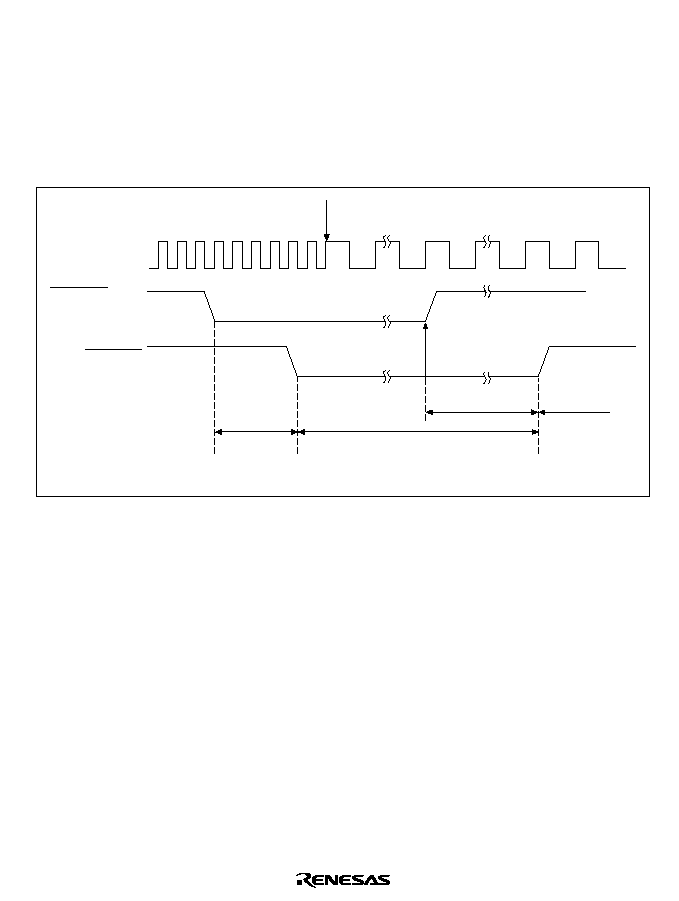
807
6. When PLL circuit 1 is operational, the WDT starts counting up inside the chip. When PLL
circuit 1 is halted, the WDT is not activated.
7. When the internal clock stabilizes, the
CKPACK pin goes high, giving external notification
that the chip can be operated.
The standby state, all on-chip peripheral module states, and all pin states during clock pause are
the same as in the normal standby mode. Figure 21.2 shows the timing chart for the clock pause
function.
CKIO input
CKPREQ/CKM
input
CKPACK
output
Frequency
modification
Clock pause request
cancellation
Clock pause
acceptance
processing
WDT count-up
Normal state
Clock pause state
Figure 21.2 Clock Pause Function Timing Chart (PLL Circuit 1 Operating)
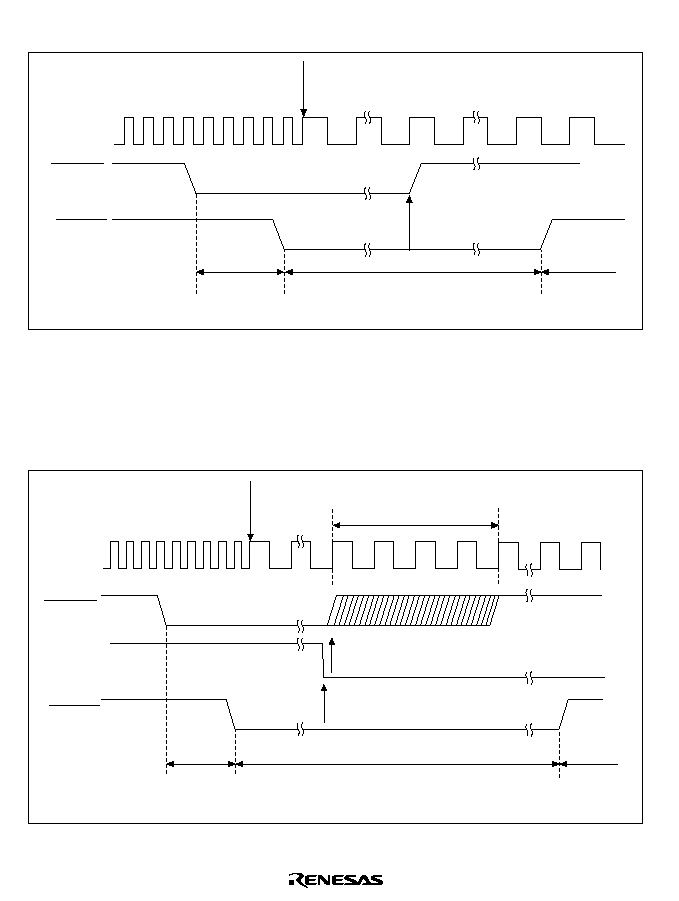
808
Figure 21.3 shows the clock pause function timing chart when the PLL circuit is halted.
CKIO input
CKPREQ/
CKM input
CKPACK
output
Frequency
modification
Clock pause request
cancellation
Clock pause
acceptance
processing
Normal state
Clock pause state
Figure 21.3 Clock Pause Function Timing Chart (PLL Circuit 1 Halted)
The clock pause state can be canceled by means of NMI input, in the same way as the normal
standby state. The clock pause request should be canceled within four CKIO clock cycles after
NMI input. Figure 21.4 shows the timing chart for clock pause state cancellation by means of NMI
input (in the case of rising edge detection).
CKIO input
CKPREQ/
CKM input
CKPACK
output
Frequency
modification
Clock pause request
cancellation
Clock pause
acceptance
processing
Normal state
Clock pause state
Max. 4 cycles
NMI interrupt
NMI input
Figure 21.4 Clock Pause Function Timing Chart (Cancellation by NMI Input)

809
21.4.5
Notes on Standby Mode
1. When the chip enters standby mode during use of the cache, disable the cache before making
the mode transition. Initialize the cache beforehand when the cache is used after returning to
standby mode. The contents of the on-chip RAM are not retained in standby mode when cache
is used as on-chip RAM.
2. If an on-chip peripheral register is written in the 10 clock cycles before the chip transits to
standby mode, read the register before executing the SLEEP instruction.
3. When using clock mode 0, 1, or 2, the CKIO pin is the clock output pin. Note the following
when standby mode is used in these clock modes. When standby mode is canceled by NMI, an
unstable clock is output from the CKIO pin during the oscillation settling time after NMI input.
This also applies to clock output in the case of cancellation by a power-on reset or manual
reset. Power-on reset and manual reset input should be continued for a period at least equal to
for the oscillation settling time.
4. Before entering the standby mode, stop operation of the internal DMAC (E-DMAC or
DMAC).
21.5
Module Standby Function
21.5.1
Transition to Module Standby Function
By setting one of bits MSTP11≠MSTP3, MSTP1 to 1 in standby control register 1 or 2, the supply
of the clock to the corresponding on-chip peripheral module or DSP unit can be halted. This
function can be used to reduce the power consumption. Do not perform read/write operations for a
module in module standby mode.
With the module standby function, the external pins of the DMAC and SIO0≠SIO2 on-chip
peripheral modules retain their states prior to halting, as do DMAC, DSP, and SIO0≠SIO2
registers. The external pins of the FRT, SCIF1≠2, and TPU are reset and all their registers are
initialized.
An on-chip peripheral module corresponding to a module standby bit must not be switched to the
module standby state while it is running. Also, interrupts from a module placed in the module stop
state should be disabled.
21.5.2
Clearing the Module Standby Function
Clear the module standby function by clearing the MSTP11≠MSTP3, MSTP1 bits, or by a power-
on reset or manual reset.

810

811
Section 22 Electrical Characteristics
22.1
Absolute Maximum Ratings
Table 22.1 shows the absolute maximum ratings.
Table 22.1
Absolute Maximum Ratings
Item
Symbol
Value
Unit
Power supply voltage (internal)
V
CC
≠0.3 to +4.2
V
Power supply voltage (5 V I/O)
PV
CC
≠0.3 to +7.0
V
Input voltage (excluding 5 V I/O)
V
in
≠0.3 to Vcc +0.3
V
Input voltage (5 V I/O)
V
in
≠0.3 to PVcc +0.3
V
Operating temperature
T
opr
≠20 to +75
∞C
Storage temperature
T
stg
≠55 to +125
∞C
Notes: 1. Permanent damage to the chip may result if the maximum ratings are exceeded.
2. When powering on, turn on the 5 V I/O power supply (PV
CC
) after, or at the same time
as, the internal power supply (V
CC
). When powering off, cut Vcc after, or at the same
time as, PV
CC
.

812
22.2
DC Characteristics
Tables 22.2 and 22.3 show the DC characteristics.
Table 22.2
DC Characteristics
Conditions: V
CC
= PLLV
CC
= 3.3 V ±0.3 V, PV
CC
= 5.0 V ± 0.5 V/3.3 V ±0.3 V, PV
CC
V
CC
,
V
SS
= PV
SS
= PLLV
SS
= 0 V, Ta = ≠20 to +75∞C
Item
Symbol
Min
Typ Max
Unit Test Conditions
Input high
voltage
RES
, NMI,
MD4 to MD0,
TRST
,
CKPREQ
/CKM
V
IH
V
CC
◊
0.9
--
V
CC
+ 0.3
V
Both 3.3 V and 5 V
2.6
--
PV
CC
+ 0.3 V
EXTAL, CKIO
V
CC
◊
0.9
--
V
CC
+ 0.3
V
Other input pins
V
CC
◊
0.7
--
V
CC
+ 0.3
V
Input low
voltage
RES
, NMI,
MD4 to MD0,
TRST
,
CKPREQ
/CKM
V
IL
≠0.3
--
V
CC
◊
0.1
V
Other input pins
≠0.3
--
0.8
V
Schmitt
trigger
PB14/RXD1,
PB5/SRS1/RXD2
VT
≠
--
--
0.8
V
input
voltage
VT
+
4.0
--
--
V
PV
CC
= 5 V ±0.5 V
VT
+
2.6
--
--
V
Other than above
VT
+
≠ VT
≠
0.3
--
--
V
Input
leakage
current
All input pins
lin
--
--
1.0
µA
Vin = 0.5 to
V
CC
≠ 0.5 V
Vin = 0.5 to
PV
CC
≠ 0.5 V
Three-state
leakage
current
All I/O and output
pins (off status)
l
STI
--
--
1.0
µA
Vin = 0.5 to
V
CC
≠ 0.5 V
Vin = 0.5 to
PV
CC
≠ 0.5 V
Output
Both 3.3 V and 5 V
V
OH
PV
CC
≠ 0.7 --
--
V
IOH = ≠200 µA
high
Other output pins
V
CC
≠ 0.5
--
--
V
IOH = ≠200 µA
voltage
V
CC
≠ 1.0
--
--
V
IOH = ≠1 mA
Output low Both 3.3 V and 5 V
V
OL
--
--
0.6
V
IOL = 1.6 mA
voltage
Other output pins
--
--
0.4
V
IOL = 1.6 mA

813
Table 22.2
DC Characteristics (cont)
Conditions: V
CC
= PLLV
CC
= 3.3 V ±0.3 V, PV
CC
= 5.0 V ± 0.5 V/3.3 V ±0.3 V, PV
CC
V
CC
,
V
SS
= PV
SS
= PLLV
SS
= 0 V, Ta = ≠20 to +75∞C
Item
Symbol
Min
Typ Max
Unit Test Conditions
Pin
CAP1, CAP2
Cin
--
--
40
pF
Ta = 25∞C
capacitance Other input pins
--
--
15
pF
Current
dissipation
Normal operation
lcc
--
--
350
mA
3.6 V, CPU
operating clock =
62.5 MHz, DMAC
used
--
--
300
mA
3.6 V, CPU
operating clock =
62.5 MHz, DMAC
not used
Sleep mode
--
--
250
mA
3.6 V, CPU
operating clock =
62.5 MHz,
peripheral
modules not used
Standby mode
--
--
990
µA
Note:
Do not leave the PLLVcc and PLLVss pins open when the PLL circuit is not used. Connect
the PLLVcc pin to Vcc and the PLLVss pin to Vss.
Table 22.3
Permissible Output Currents
Conditions: V
CC
= PLLV
CC
= 3.3 V ±0.3 V, PV
CC
= 5.0 V ± 0.5 V/3.3 V ±0.3 V, PV
CC
V
CC
,
V
SS
= PV
SS
= PLLV
SS
= 0 V, Ta = ≠20 to +75∞C
Item
Symbol
Min
Typ
Max
Unit
Permissible output low current (per pin)
I
OL
--
--
2.0
mA
Permissible output low current (total)
I
OL
--
--
80
mA
Permissible output high current (per pin)
≠I
OH
--
--
2.0
mA
Permissible output high current (total)
(≠I
OH
)
--
--
25
mA
Note:
To protect chip reliability, do not exceed the output current values in table 22.3.

814
22.3
AC Characteristics
In principle, input is synchronous. Unless specified otherwise, ensure that the setup time and hold
times for each input signal are observed.
Table 22.4
Maximum Operating Frequencies
Conditions: V
CC
= PLLV
CC
= 3.3 V ±0.3 V, PV
CC
= 5.0 V ± 0.5 V/3.3 V ±0.3 V, PV
CC
V
CC
,
V
SS
= PV
SS
= PLLV
SS
= 0 V, Ta = ≠20 to +75∞C
Item
Symbol
Min
Typ
Max
Unit
Notes
Operating
CPU, DSP
f
1
--
62.5
MHz
t
Icyc
frequency
External bus
(SDRAM not used)
1
--
31.25
t
Ecyc
External bus
(SDRAM used)
1
--
62.5
t
Ecyc
Peripheral modules
1
--
31.25
t
Pcyc

815
22.3.1
Clock Timing
Table 22.5
Clock Timing
Conditions: V
CC
= PLLV
CC
= 3.3 V ±0.3 V, PV
CC
= 5.0 V ± 0.5 V/3.3 V ±0.3 V, PV
CC
V
CC
,
V
SS
= PV
SS
= PLLV
SS
= 0 V, Ta = ≠20 to +75∞C
Item
Symbol
Min
Max
Unit
Figure
EXTAL clock input frequency
fEX
1
31.25
MHz
22.1
EXTAL clock input cycle time
tEXcyc
32
1000
ns
EXTAL clock input low-level pulse width
tEXL
8
*
1
, 12
*
2
--
ns
EXTAL clock input high-level pulse width
tEXH
8
*
1
, 12
*
2
--
ns
EXTAL clock input rise time
tEXR
--
4
ns
EXTAL clock input fall time
tEXF
--
4
ns
CKIO clock input frequency
fCKI
1
31.25
MHz
22.2
CKIO clock input cycle time
tCKIcyc
32
1000
ns
CKIO clock input low-level pulse width
tCKIL
8
*
3
, 12
*
4
--
ns
CKIO clock input high-level pulse width
tCKIH
8
*
3
, 12
*
4
--
ns
CKIO clock input rise time
tCKIR
--
4
ns
CKIO clock input fall time
tCKIF
--
4
ns
CKIO clock output frequency
fOP
1
*
5
, 8
*
6
62.5
MHz
22.3
CKIO clock output cycle time
tcyc
16
1000
*
5
,
125
*
6
ns
CKIO clock output low-level pulse width
tCKOL
3
--
ns
CKIO clock output high-level pulse width
tCKOH
3
--
ns
CKIO clock rise time
tCKOR
--
5
ns
CKIO clock fall time
tCKOF
--
5
ns
Power-on oscillation stabilization time
tOSC1
10
--
ms
22.4
Standby recovery oscillation stabilization
time 1
tOSC2
10
--
ms
22.5
Standby recovery oscillation stabilization
time 2
tOSC3
10
--
ms
22.6
PLL synchronization stabilization time
tPLL
1
--
ms
22.7
Notes:
*
1 When PLL circuit 2 is operating
*
2 When PLL circuit 2 is not used
*
3 When PLL circuit 1 is operating
*
4 When PLL circuit 1 is not used
*
5 When PLL circuit 1 and 2 are not used
*
6 When PLL circuit 1 or 2 is operating
816
t
EXH
t
EXF
t
EXR
t
EXL
t
EXcyc
V
IH
V
IH
V
IH
1/2 V
CC
1/2 V
CC
V
IL
V
IL
EXTAL
*
(input)
Note:
*
When clock is input from EXTAL pin
Figure 22.1 EXTAL Clock Input Timing
t
CKIH
t
CKIF
t
CKIR
t
CKIL
tCKI
cyc
V
IH
1/2 V
CC
1/2 V
CC
V
IH
V
IL
V
IH
V
IL
CKIO
(input)
Figure 22.2 CKIO Clock Input Timing
t
cyc
t
CKOL
t
CKOH
V
OH
1/2V
CC
CKIO
(output)
1/2V
CC
t
CKOR
t
CKOF
V
OH
V
OL
V
OL
V
OH
Figure 22.3 CKIO Clock Output Timing
817
CKIO,
internal clock
Vcc
Vcc min
RES
t
OSC1
t
RESW
Stable oscillation
Note: Oscillation stabilization time when using on-chip crystal oscillator
Figure 22.4 Power-On Oscillation Stabilization Time at Power-On
CKIO,
internal clock
Stable oscillation
Standby
t
OSC2
t
RESW
RES
Note: Oscillation stabilization time when using on-chip crystal oscillator
Figure 22.5 Oscillation Stabilization Time after Standby Recovery (Recovery by
RES)
818
t
OSC3
Stable oscillation
Standby
CKIO,
internal clock
NMI
Note: Oscillation stabilization time when using on-chip crystal oscillator
Figure 22.6 Oscillation Stabilization Time after Standby Recovery (Recovery by NMI)
t
PLL
EXTAL or
CKIO
Stable oscillation
Stable oscillation
Change of oscillation frequency
PLL synchronization
PLL synchronization
Internal clock
Figure 22.7 PLL Synchronization Stabilization Time

819
22.3.2
Control Signal Timing
Table 22.6
Control Signal Timing
Conditions: V
CC
= PLLV
CC
= 3.3 V ±0.3 V, PV
CC
= 5.0 V ± 0.5 V/3.3 V ±0.3 V, PV
CC
V
CC
,
V
SS
= PV
SS
= PLLV
SS
= 0 V, Ta = ≠20 to +75∞C
Item
Symbol
Min
Max
Unit
Figure
RES
rise and fall time
tRESr,
tRESf
--
200
ns
22.8
RES
pulse width
tRESW
20
--
tPcyc
NMI reset setup time
tNMIRS
tPcyc + 10
--
ns
NMI reset hold time
tNMIRH
tPcyc + 10
--
ns
NMI rise and fall time
tNMIr,
tNMIf
--
200
ns
RES
setup time
*
tRESS
3tEcyc + 40 --
ns
22.9
NMI setup time
*
tNMIS
40
--
ns
IRL3
≠
IRL0
setup time
*
tIRLS
30
--
ns
NMI hold time
tNMIH
20
--
ns
IRL3
≠
IRL0
hold time
*
tIRLH
20
--
ns
BRLS
setup time
tBLSS
10
--
ns
22.10
BRLS
hold time
tBLSH
5
--
ns
BGR
delay time
tBGRD
--
15
ns
Bus tri-state delay time
tBOFF
0
35
ns
Bus buffer on time
tBON
0
35
ns
Note:
*
The
RES
, NMI, and
IRL3
≠
IRL0
signals are asynchronous inputs. If the setup times shown
here are observed, a transition is judged to have occurred at the fall of the clock; if the
setup times cannot be observed, recognition may be delayed until the next fall of the clock.
820
tNMIRS
tNMIr
tNMIf
tRESW
tRESf
tRESr
tNMIRH
RES
NMI
VIH
VIL
VIH
VIL
VIH
VIH
VIL
VIL
Figure 22.8 Reset Input Timing
tRESS
CKIO
RES
tNMIS
NMI
tIRLS
IRL3
≠
IRL0
tNMIH
tIRLH
VIH
VIL
VIH
VIL
VIH
VIL
Figure 22.9 Interrupt Signal Input Timing
A24≠A0,
D31≠D0
RD
, RD/
WR
,
RAS
,
CAS
,
CSn
,
WEn
,
BS
,
IVECF
BRLS
(input)
BGR
(output)
t
BLSS
CKIO
t
BOFF
t
BON
t
BON
t
BOFF
t
BGRD
t
BGRD
t
BLSH
t
BLSS
t
BLSH
Figure 22.10 Bus Release Timing

821
22.3.3
Bus Timing
Table 22.7
PLL-On Bus Timing [Modes 0 and 4] (1)
Conditions: V
CC
= PLLV
CC
= 3.3 V ±0.3 V, PV
CC
= 5.0 V ± 0.5 V/3.3 V ±0.3 V, PV
CC
V
CC
,
V
SS
= PV
SS
= PLLV
SS
= 0 V, Ta = ≠20 to +75∞C
Item
Symbol Min
Max
Unit Figure
Address delay time
t
AD
1
14
ns
22.11, 12, 15, 16, 18, 20, 22, 24 to
28, 30 to 34, 37 to 40, 42 to 44
BS
delay time
t
BSD
--
15
ns
22.11, 12, 15, 16, 18, 20, 22, 24,
25, 28, 30, 31, 33, 34, 39, 42 to 44
CS
delay time 1
t
CSD1
1
14
ns
22.11, 12, 15, 16, 18, 20, 22 to 25,
28, 30 to 34, 39, 41, 42
CS
delay time 2
t
CSD2
--
14
ns
22.11, 12, 33, 34, 39, 42
Read/write delay time
t
RWD
1
14
ns
22.11, 12, 15 ,16, 18, 20 to 22, 24,
25, 28 to 34, 39, 42 to 44
Read strobe delay time 1
t
RSD1
--
14
ns
22.11, 12, 15, 16, 22, 30, 33, 34,
37, 39, 40, 42 to 44
Read data setup time 1
t
RDS1
8
--
ns
22.11, 33, 37, 42 to 44
Read data setup time 2 (EDO)
t
RDS2
8
--
ns
22.39, 40
Read data setup time 3 (SDRAM) t
RDS3
6.5
--
ns
22.15, 16
Read data hold time 2
t
RDH2
0
--
ns
22.11, 42
Read data hold time 4 (SDRAM)
t
RDH4
2
--
ns
22.15, 16
Read data hold time 5 (DRAM)
t
RDH5
0
--
ns
22.33, 37
Read data hold time 6 (EDO)
t
RDH6
3
--
ns
22.39, 40
Read data hold time 7 (EDO)
t
RDH7
1
--
ns
22.39
Read data hold time 8
(interrupt vector)
t
RDH8
2
--
ns
22.43, 44
Write enable delay time 1
t
WED1
--
14
ns
22.11, 12
Write data delay time 1
(except E¯
: I
¯ = 1:1)
t
WDD1
--
22
ns
22.12, 22, 24, 26, 34, 38
Write data delay time 2
(E¯
: I
¯ = 1:1)
t
WDD2
--
12
ns
22.25, 27
Write data hold time 1
t
WDH1
2
--
ns
22.12, 22, 24 to 27, 34, 38
Data buffer on time
t
DON
--
15
ns
22.12, 22, 24, 25, 34
Data buffer off time
t
DOF
--
15
ns
22.12, 22, 24, 25, 34

822
Table 22.7
PLL-On Bus Timing [Modes 0 and 4] (1) (cont)
Conditions: V
CC
= PLLV
CC
= 3.3 V ±0.3 V, PV
CC
= 5.0 V ± 0.5 V/3.3 V ±0.3 V, PV
CC
V
CC
,
V
SS
= PV
SS
= PLLV
SS
= 0 V, Ta = ≠20 to +75∞C
Item
Symbol Min
Max
Unit
Figure
DACK delay time 1
t
DACD1
--
14
ns
22.11, 12, 15, 18, 20, 22, 24,
25, 28, 33, 34, 37 to 40, 42
DACK delay time 2
t
DACD2
--
14
ns
22.11, 12, 33, 34, 37 to 40, 42
WAIT
setup time
t
WTS
10
--
ns
22.13, 14, 35, 36, 42 to 45
WAIT
hold time
t
WTH
5
--
ns
22.13, 14, 35, 36, 42 to 45
RAS
delay time 1 (SDRAM)
t
RASD1
1
14
ns
22.15 to 18, 20 to 25, 28 to 32
RAS
delay time 2 (DRAM, EDO)
t
RASD2
--
14
ns
22.33, 34, 39, 41
RAS
delay time 3 (EDO)
t
RASD3
--
14
ns
22.39
CAS
delay time 1 (SDRAM)
t
CASD1
1
14
ns
22.15, 16, 17, 18, 22 to 28, 30
to 32, 42
CAS
delay time 2 (DRAM)
t
CASD2
--
14
ns
22.33, 34, 37 to 41
DQM delay time
t
DQMD
1
14
ns
22.15, 16, 18 to 20, 22, 24 to
29
CKE delay time
t
CKED
1
14
ns
22.32
OE
delay time 1
t
OED1
--
14
ns
22.39
OE
delay time 2
t
OED2
--
14
ns
22.39
IVECF
delay time
t
IVD
--
15
ns
22.43, 44
Row address setup time
t
ASR
0
--
ns
22.33, 34, 39
Column address setup time
t
ASC
0
--
ns
22.33, 34, 37, 38, 39
Data input setup time
t
DS
0
--
ns
22.34, 38
Read/write address setup time
t
AS
0
--
ns
22.11, 12
REFOUT delay time
t
REFOD
--
15
ns
22.46

823
Table 22.7
PLL-On Bus Timing [Modes 0 and 4] (2)
Conditions: V
CC
= PLLV
CC
= 3.3 V ±5%, PV
CC
= 5.0 V ±5%/3.3 V ±5%, PV
CC
V
CC
,
V
SS
= PV
SS
= PLLV
SS
= 0 V, Ta = ≠5 to +70∞C, SDRAM bus cycle
Item
Symbol
Min
Max
Unit
Figure
Read data setup time 3
(SDRAM)
t
RDS3
6.5
--
ns
22.15, 16
Read data hold time 4
(SDRAM)
t
RDH4
1.5
--
ns
22.15, 16
Write data delay time 2
(E¯
: I
¯ = 1:1)
t
WDD2
--
9.5
ns
22.25, 27
Write data hold time 1
t
WDH1
2
--
ns
22.25, 27
Address delay time
t
AD
4
11
ns
22.15, 16, 18, 20, 22, 24, 25, 26,
27, 28, 30, 31, 32
CS
delay time 1
t
CSD1
2.5
9.5
ns
22.15, 16, 18, 20, 22, 23, 24, 25,
28, 30, 31, 32
Read/write delay time
t
RWD
2.5
9.5
ns
22.15, 16, 18, 20, 21, 22, 24, 25,
28, 29, 30, 31, 32
DQM delay time
t
DQMD
2.5
9.5
ns
22.15, 16, 18, 19, 20, 22, 24, 25,
26, 27, 28, 29
RAS
delay time 1
(SDRAM)
t
RASD1
2.5
9.5
ns
22.15, 16, 17, 20, 21, 22, 23, 24,
25, 28, 29, 30, 31, 32
CAS
delay time 1
(SDRAM)
t
CASD1
2.5
9.5
ns
22.15, 16, 17, 18, 22, 23, 24, 25,
26, 27, 28, 30, 31, 32
CKE delay time
t
CKED
2.5
9.5
ns
22.32
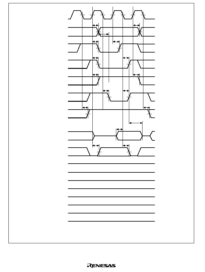
824
;;
;;
;
;
;;
;;
;;;;
;;;;
CKIO
BS
CSn
RD/
WR
RD
WEn
DQMxx
RAS
CAS
OE
CKE
DACKn
*
2
WAIT
A24≠A0
;;
;;
;;
T1
T2
tAD
tAS
tBSD
tBSD
tAD
;;
;;
;;
;;
;;
;;
tCSD1
tRWD
tRWD
;;
;
tWED1
tRDS1
tRDH2
*
1
tWED1
tCSD2
;
;;
;;
tRSD1
tRSD1
tDACD1
tDACD2
D31≠D0
Notes:
*
1 t
RDH2
is measured from the rise of
CSn
or
RD
, whichever comes first.
*
2 DACKn waveform when active-high is specified
Figure 22.11 Basic Read Cycle (No Wait)
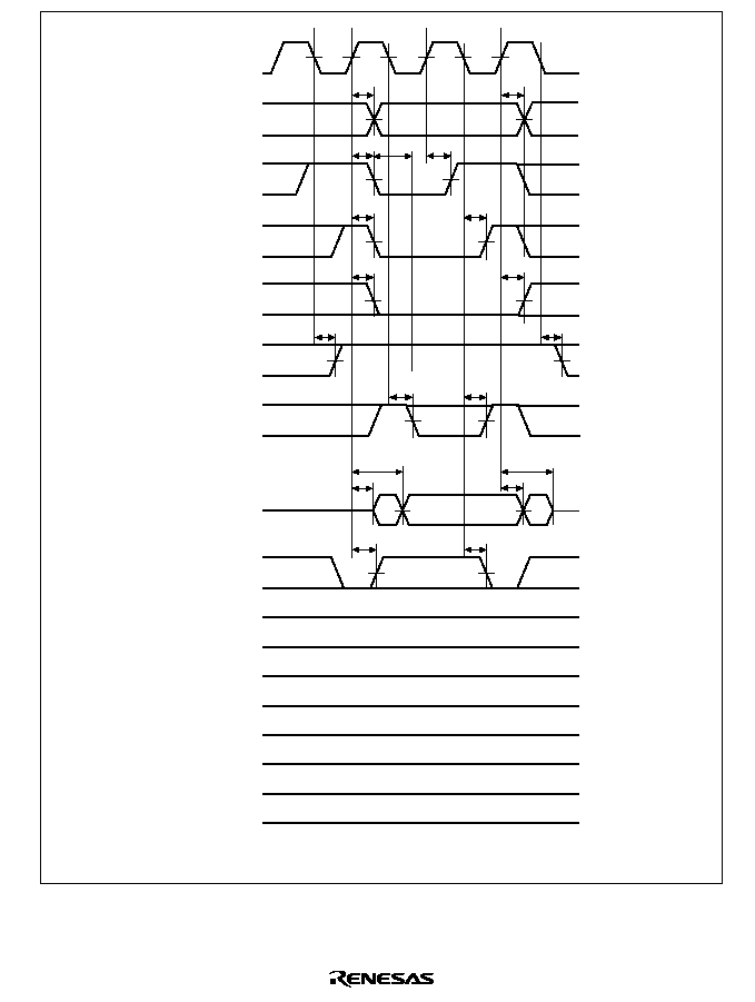
825
;;
;;
;;
;;;;
;;;;
;;
;;
;;
;;
CKIO
BS
CSn
RD/
WR
RD
WEn
DQMxx
RAS
CAS
OE
CKE
D31≠D0
DACKn
*
WAIT
A24≠A0
;
;
T1
T2
tAD
tBSD
tBSD
tAD
;;
;;
;;
;;
;;
;;
;;
;;
tCSD1
tRWD
tRWD
;;
;;
;;
;;
tRSD1
tRSD1
tCSD2
;;
;;
;;
tWED1
tWED1
tDACD1
tDACD2
;
;
tDON
tWDH1
tWDD1
tDOF
;;;;
;;;;
Note:
*
DACKn waveform when active-high is specified
tAS
Figure 22.12 Basic Write Cycle (No Wait)
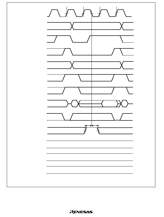
826
;;
T1
Tw
T2
CKIO
BS
CSn
RD/
WR
RD
WEn
DQMxx
RAS
CAS
OE
CKE
D31≠D0
DACKn
*
WAIT
A24≠A0
;;
;
;;
;
;;
;;
;;
;;
;;
;
;
;
;
;
;
;;
;;
;;
;;
;;
;;
;;
;;
tWTH
tWTS
;
;;;;
Note:
*
DACKn waveform when active-high is specified
Figure 22.13 Basic Bus Cycle (1 Wait Cycle)
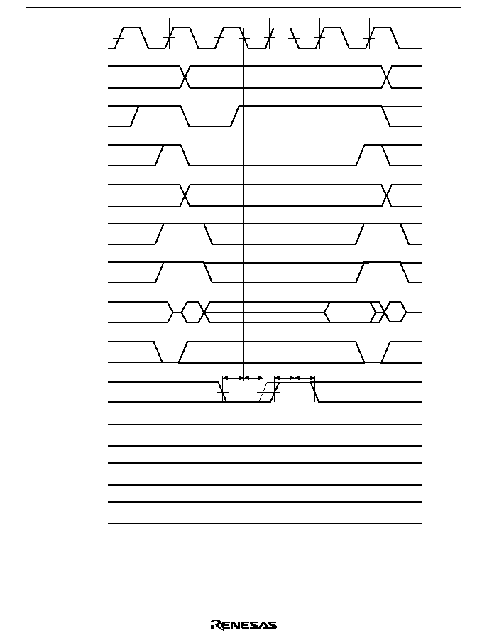
827
;;
;
;
;;
;;
;
;
;
T1
Tw
Twx
T2
CKIO
BS
CSn
RD/
WR
RD
WEn
DQMxx
RAS
CAS
OE
CKE
D31≠D0
DACKn
*
WAIT
A24≠A0
;;
;
;
;
;
;
;;
;;
;;
;
;;
;;
;
;;
;;
;
;;
;;
;;;;;
tWTS tWTH
tWTS tWTH
Note:
*
DACKn waveform when active-high is specified
Figure 22.14 Basic Bus Cycle (External Wait Input)

828
;;
;;;;;;;
;;;;;;;
;;
;;
;;
;;
;;
;;
;;
;;
;;
;
;
;;
;;;;
;
;
;
;
;;
;;
Tr
Tc
Td1
Td2
Td3
Td4
Tde
tAD
tAD
tBSD
tRWD
tCSD1
tDQMD
tRDS3
tRDH4
tRDS3
tRDS3
tRDH4
tRDS3
tRDH4
tDACD1
tRASD1
tRASD1
tCASD1
tCASD1
tDQMD
;;
;;
;;
;;
;;
tRASD1
tDACD1
tCASD1
tCASD1
*
1
;;
;;
;;
;;
tRDH4
;;
;;
;;
tRWD
tRSD1
;;
tCSD1
;;
;;
;;
tAD
tBSD
Notes:
*
1 Dotted line shows the case where synchronous DRAM in a different CS space is
accessed.
*
2 DACKn waveform when active-high is specified
CKIO
BS
CSn
RD/
WR
RD
WEn
DQMxx
D31≠D0
RAS
CAS
∑
OE
CKE
DACKn
*
2
WAIT
Address
upper bits
Address
lower bits
Figure 22.15 Synchronous DRAM Read Bus Cycle
(RCD = 1 Cycle, CAS Latency = 1 Cycle, Burst = 4)

829
;;
;
;
;;;;;;;
;;;;;;;
;;
;;
;;
;;
Tr
Tc
Td1
Td2
Td3
Td4
Tde
;;
tAD
;;
;;
tAD
;;
;;
tBSD
;;
;;
;;
tRWD
tCSD1
;;
tDQMD
tRDS3
tRDH4
tRASD1
tRASD1
tCASD1
tCASD1
tDQMD
;;;
;;;
Notes:
*
1 Dotted line shows the case where synchronous DRAM in a different CS space is
accessed.
*
2 DACKn waveform when active-high is specified
CKIO
BS
CSn
RD/
WR
RD
WEn
DQMxx
RAS
CAS
OE
CKE
D31≠D0
WAIT
Address
upper bits
Address
lower bits
DACKn
*
2
;;
;;
tCASD1
tCASD1
;;
tRASD1
;;
;;
;;
;;
;;
;;
tDQMD
;;
;;
tRSD1
;;
tRWD
;;
;;
tCSD1
;;
;;
;;
tBSD
;;
tAD
*
1
Figure 22.16 Synchronous DRAM Single Read Bus Cycle
(RCD = 1 Cycle, CAS Latency = 1 Cycle, Burst = 4)
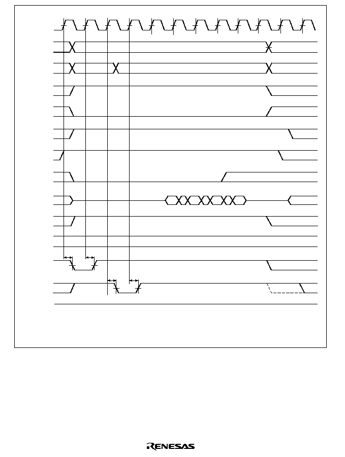
830
;;;;;;
;
;
;;
;;
CKIO
BS
CSn
RD/
WR
RD
WEn
DQMxx
RAS
CAS
≠
OE
CKE
D31
≠
D0
*
1
DACKn
*
2
WAIT
;
;
;
;
;
;
;
;
;
;
;
;
;
;
;
;;;
;;
;
;;
Tr
Trw
Tc
Tw
Td1
Td2
Td3
Td4
Tde
tRASD1
tCASD1 tCASD1
tRASD1
;
Address
upper bits
Address
lower bits
;;
;
;
;;
;
;
;;
;;
;
;
;
;;
;;
Notes:
*
1 Dotted line shows the case where synchronous DRAM in a different CS space is
accessed.
*
2 DACKn waveform when active-high is specified
Figure 22.17 Synchronous DRAM Read Bus Cycle
(RCD = 2 Cycles, CAS Latency = 2 Cycles, Burst = 4)
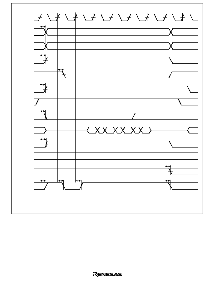
831
;;
;;;;;;;
;;;;;;;
;;
;;
Tnop
Tc
Td1
Td2
Td3
Td4
Tde
;;
tAD
;;
;;
tBSD
;;
;;
;;
;;
tRWD
tCSD1
;
;;
;;;;
;;
tDQMD
tDACD1
tCASD1
tCASD1
tCASD1
;;
;;
;
;
;
;
;;
;;
tCASD1
;;
tRASD1
;;
;;
;;
;;
;;
;;
;;
;;
;;
;;
CKIO
BS
CSn
RD/
WR
RD
WEn
DQMxx
CAS
CKE
D31≠D0
DACKn
*
WAIT
RAS
Address
upper bits
Address
lower bits
Note:
*
DACKn waveform when active-high is specified
Figure 22.18 Synchronous DRAM Read Bus Cycle
(Bank Active, Same Row Access, CAS Latency = 1 Cycle)
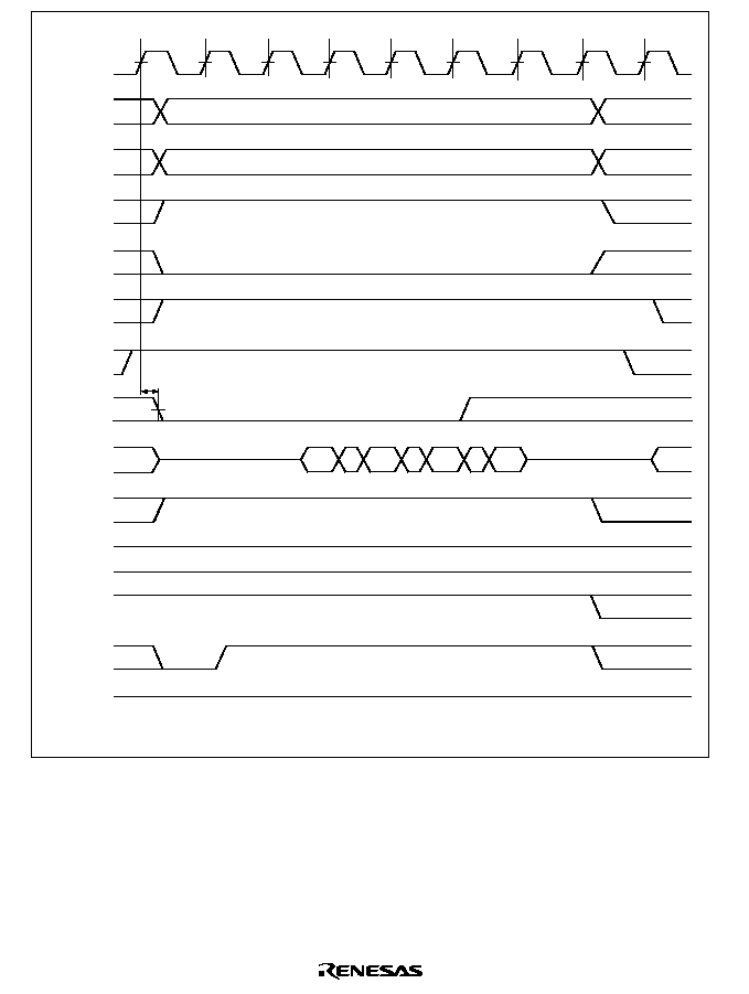
832
;
;
;
;
;;
;;
;;
;;
TC
TW
Td1
Td2
Td3
Td4
Tde
;
;;
;
;
;;;;
;
;
;
;;;;;;;
tDQMD
;;
;;
;;
;;
;;
;;
;;
;;
;;
;;
;;
;;
;;
Address
upper bits
Address
lower bits
BS
CKIO
CSn
RD/
WR
RD
WEn
DQMxx
D31≠D0
DACKn
*
WAIT
RAS
CAS
OE
CKE
Note:
*
DACKn waveform when active-high is specified
Figure 22.19 Synchronous DRAM Read Bus Cycle
(Bank Active, Same Row Access, CAS Latency = 2 Cycles)
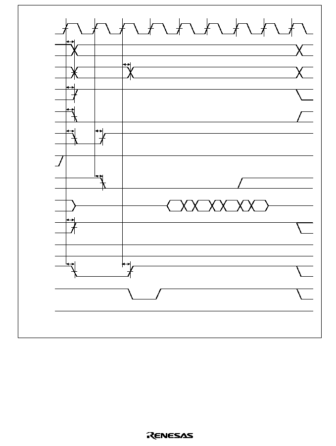
833
;;
;;
;;
;;
;;
;;
;;
;
;
;
;
;;
;;;
;;;
Tp
Tr
Tc
Td1
Td2
Td3
Tde
Td4
;;
;;
;;
;;
;;
;;
;;;;;;;
;;;;;;;
tAD
tAD
tRWD
tRWD
tDACD1
tRASD1
tRASD1
tDQMD
tCSD1
tBSD
Address
upper bits
Address
lower bits
BS
CKIO
CSn
RD/
WR
RD
WEn
DQMxx
D31≠D0
DACKn
*
WAIT
RAS
CAS
OE
CKE
Note:
*
DACKn waveform when active-high is specified
;
;
;
;
;
;
;
;
;
Figure 22.20 Synchronous DRAM Read Bus Cycle
(Bank Active, Different Row Access, TRP = 1 Cycle, RCD = 1 Cycle, CAS Latency = 1 Cycle)
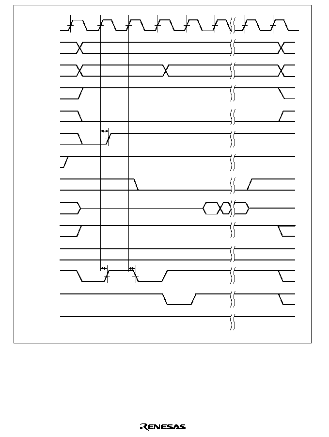
834
;
;
;
;
;
;
;
;
Address
upper bits
Address
lower bits
BS
;
;
;;
;;
CKIO
Tp
Tpw
Tr
Tc
Td1
Tde
CSn
;
;
;
;
RD/
WR
RD
WEn
DQMxx
D31≠D0
DACKn
*
;
;
;
;
;;;;;
;;;;;
WAIT
RAS
CAS
OE
CKE
tRWD
tRASD1
tRASD1
;
Note:
*
DACKn waveform when active-high is specified
Figure 22.21 Synchronous DRAM Read Bus Cycle (Bank Active, Different Row Access,
TRP = 2 Cycles, RCD = 1 Cycle, CAS Latency = 1 Cycle)
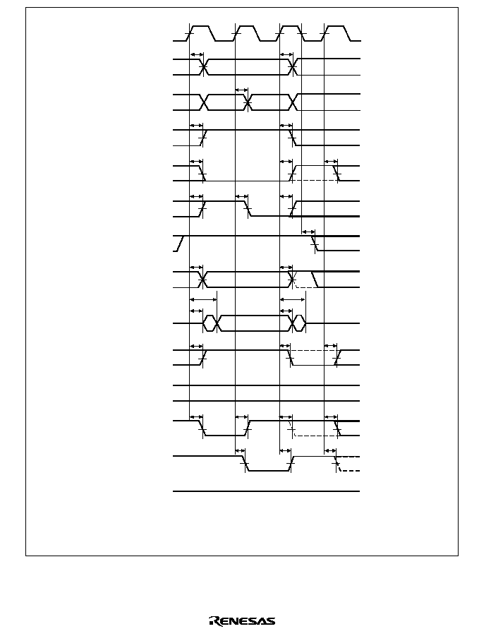
835
CKIO
Tr
Tc
Tap
;;
;;
;;
;;
Address
upper bits
;;
;;
WEn
DQMxx
D31≠D0
;;
Address
lower bits
BS
CSn
RD
RD/
WR
;;
;;
;
;;
;;
;;
;;
;;
;;
;;
;;
;;;;
;;
;;
;;
;
;
;;
;;
;;
;;
DACKn
*
2
;;;;
WAIT
RAS
CAS
OE
CKE
tAD
tAD
tAD
tBSD
tCSD1
tRWD
tDQMD
tDACD1
tRASD1
tRASD1
tCASD1
tCASD1
tCASD1
tRASD1
tRASD1
tDQMD
tDOF
tDACD1
tDACD1
tDON
tWDD1
tRWD
tRWD
tRSD1
tCSD1
tCSD1
tBSD
tWDH1
;;
Notes:
*
1 Dotted line shows the case where synchronous DRAM in a different CS space is
accessed.
*
2 DACKn waveform when active-high is specified
*
1
*
1
*
1
Figure 22.22 Synchronous DRAM Write Bus Cycle
(RASD = 0, RCD = 1 Cycle, TRWL = 1 Cycle)
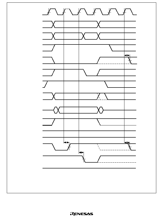
836
;;;;;
;;
;;;
;;
;;;;;
;;
;;
;;
;
;
;;
;;;;;
;;
;;;
;;
;;;
;
Tr
Trw
Tc
Trwl
Tap
CKIO
Address
upper bits
Address
lower bits
BS
CSn
RD/
WR
RD
WEn
DQMxx
D31≠D0
DACKn
*
2
WAIT
RAS
CAS
OE
CKE
tRASD1
tCASD1
tRASD1
tCSD1
Notes:
*
1 Dotted line shows the case where synchronous DRAM in a different CS space is
accessed.
*
2 DACKn waveform when active-high is specified
*
1
*
1
Figure 22.23 Synchronous DRAM Write Bus Cycle
(RASD = 0, RCD = 2 Cycles, TRWL = 2 Cycles)

837
;;
;
;;
;;;
;;;
;;
;
;
;
;
;
;;
;
;
;;
;;
;;;
;
;;
;
;;;
;;
;
Tc
CKIO
Address
upper bits
Address
lower bits
BS
CSn
RD/
WR
RD
WEn
DQMxx
D31≠D0
DACKn
*
WAIT
RAS
CAS
OE
CKE
tAD
tAD
tBSD
tBSD
tCSD1
tCSD1
tRWD
tRWD
tDQMD
tDQMD
tWDD1
tDOF
tWDH1
tDON
tDACD1
tDACD1
tRASD1
tCASD1
tCASD1
Note:
*
DACKn waveform when active-high is specified
Figure 22.24 Synchronous DRAM Write Bus Cycle
(Bank Active, Same Row Access, I
:E
other than 1:1)
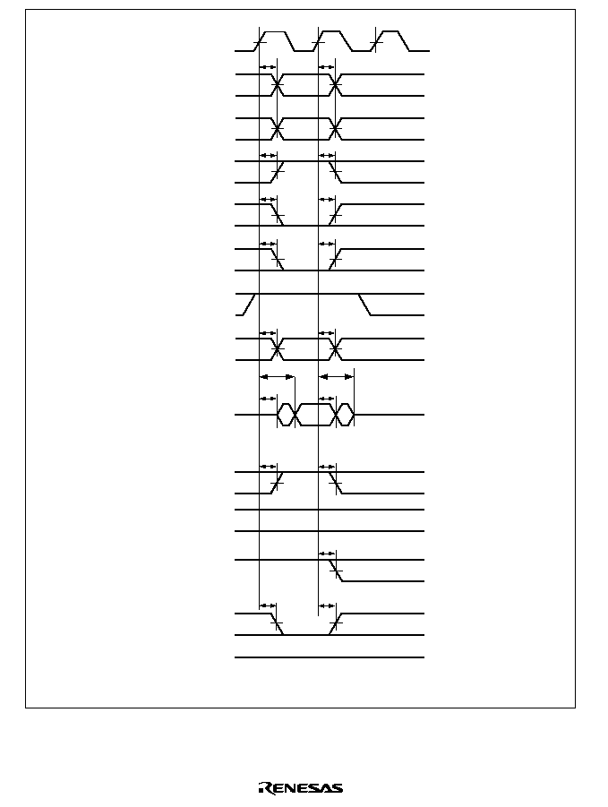
838
;;
;;
;;
;;
;;
;;;
;;;
;
;
;
;;
;;
;;
;;
;;
;;
;;
;;
;;
;;
;;
;;
;;
;;
;;
;;
;;
;;
;;
Tc
CKIO
Address
upper bits
Address
lower bits
BS
CSn
RD/
WR
RD
WEn
DQMxx
D31≠D0
DACKn
*
WAIT
RAS
CAS
OE
CKE
tAD
tAD
tBSD
tBSD
tCSD1
tCSD1
tRWD
tRWD
tDQMD
tDQMD
tWDD2
tDOF
tWDH1
tDON
tDACD1
tDACD1
tRASD1
tCASD1
tCASD1
Note:
*
DACKn waveform when active-high is specified
Figure 22.25 Synchronous DRAM Write Cycle
(Bank Active, Same Row Access, I
:E
= 1:1)
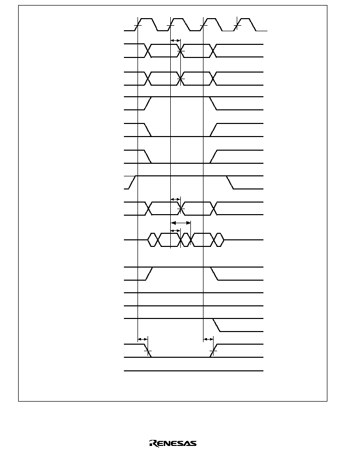
839
;;
;;;;
;;
;;
;;
;;
;;
;;
;;
;;
;;
;;
;;
;;
;;
;;
;;
;;
;;;;
;
;;
;;
Tc
CKIO
Address
upper bits
Address
lower bits
BS
CSn
RD/
WR
RD
WEn
DQMxx
D31≠D0
DACKn
*
WAIT
RAS
CAS
OE
CKE
tAD
Tc
tDQMD
tWDD1
tWDH1
tCASD1
tCASD1
;;
;;
;;
;;
;;
Note:
*
DACKn waveform when active-high is specified
Figure 22.26 Synchronous DRAM Continuous Write Cycle
(Bank Active, Same Row Access, I
:E
other than 1:1)
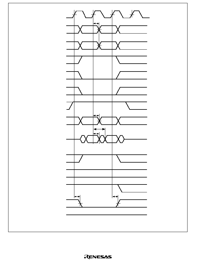
840
;;
;;;;
;;
;;
;;
;;
;;
;;
;;
;;
;;
;;
;;
;;
;;
;;
;;
;;
;;;;
;
;;
;;
Tc
CKIO
Address
upper bits
Address
lower bits
BS
CSn
RD/
WR
RD
WEn
DQMxx
D31≠D0
DACKn
*
WAIT
RAS
CAS
OE
CKE
tAD
Tc
tDQMD
tWDD2
tWDH1
tCASD1
tCASD1
;;
;;
;;
;;
;;
Note:
*
DACKn waveform when active-high is specified
Figure 22.27 Synchronous DRAM Continuous Write Cycle
(Bank Active, Same Row Access, I
:E
= 1:1)

841
;;
;;
;;
;;
;;
;;
;;;;;
;;
;;
;;
;;
;;
;;
;;
;;
;;
;;
;;
;;
;;
;;
;;
;;
;;
;
;
;;
;;
;;
;;
CKIO
Address
upper bits
Address
lower bits
BS
CSn
RD/
WR
RD
WEn
DQMxx
D31≠D0
DACKn
*
WAIT
RAS
CAS
OE
CKE
tAD
Tp
Tr
Tc
tBSD
tCSD1
tRWD
tRWD
tDQMD
tDQMD
tDACD1
tRASD1
tCASD1
Note:
*
DACKn waveform when active-high is specified
Figure 22.28 Synchronous DRAM Write Bus Cycle
(Bank Active, Different Row Access, TRP = 1 Cycle, RCD = 1 Cycle)

842
;;
;;
;;
;;
;;
;;
;;
;;
;;
;
;;
;;
;;
;;
;;
;;
;;
;;
;;
;;
;;
;;
;
Address
upper bits
Address
lower bits
BS
CKIO
Tp
Tpw
Tr
Trw
Tc
CSn
RD/
WR
RD
WEn
DQMxx
D31≠D0
DACKn
*
;;
;;;;;;
WAIT
RAS
CAS
OE
CKE
tRWD
tDQMD
tRASD1
tRASD1
Note:
*
DACKn waveform when active-high is specified
Figure 22.29 Synchronous DRAM Write Bus Cycle
(Bank Active, Different Row Access, TRP = 2 Cycles, RCD = 2 Cycles)
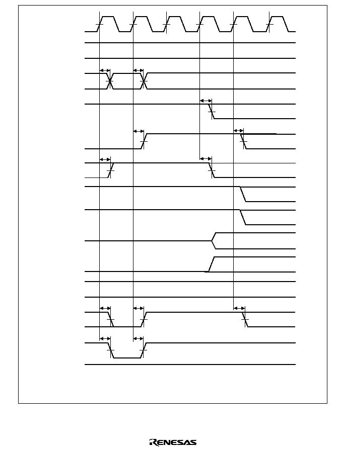
843
;;;
;;
;;
;;
;;
;;;
;;;;;
;;;;;
;;;;;
CKIO
;;;
;;;
BS
CSn
RD
RD/
WR
WEn
DQMxx
RAS
CAS
OE
CKE
D31≠D0
DACKn
WAIT
Address
upper bits
Trr
Trc1
Tre
Trc2
;
;
;;;;
;;;;
Address
lower bits
;
;;
tRASD1
tRSD1
tRASD1
tCASD1
tCASD1
;;
;;;
;
tAD
tAD
tCSD1
tRWD
tRWD
tBSD
tCSD1
Note: An auto-refresh cycle is always preceded by a precharge cycle. The number of cycles
between the two is determined by the number of cycles specified by TRP.
Figure 22.30 Synchronous DRAM Auto-Refresh Cycle
(TRAS = 4 Cycles)
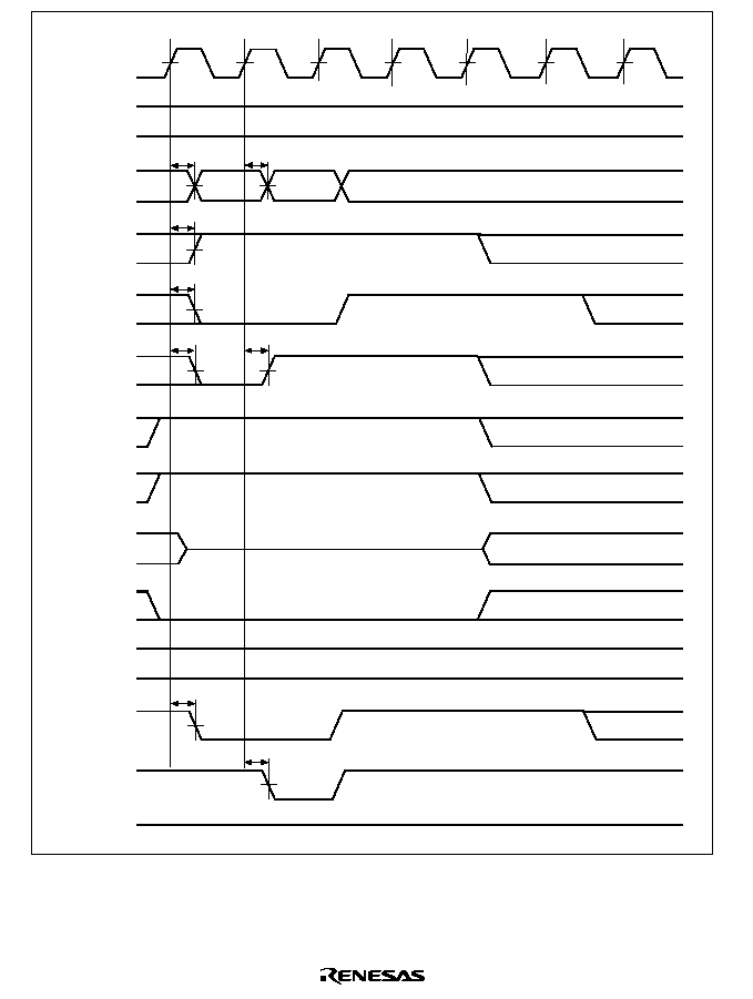
844
;;
;;;
;;;
;;;
;;;;;;
;;;;;;
;;;;;;
CKIO
;;;
;;;
;;
;;
BS
RD
CSn
RD/
WR
WEn
DQMxx
RAS
CAS
OE
D31≠D0
DACKn
WAIT
Address
upper bits
;;;
Tp
Trr
Trc2
Tre
Trc1
;;;;;;
Address
lower bits
CKE
;
;
;
;
;;
;;;
tRASD1
tCASD1
;;;
tAD
tAD
;;
tBSD
tCSD1
tRWD
tRWD
;;
;;
Figure 22.31 Synchronous DRAM Auto-Refresh Cycle
(Shown from Precharge Cycle, TRP = 1 Cycle, TRAS = 4 Cycles)
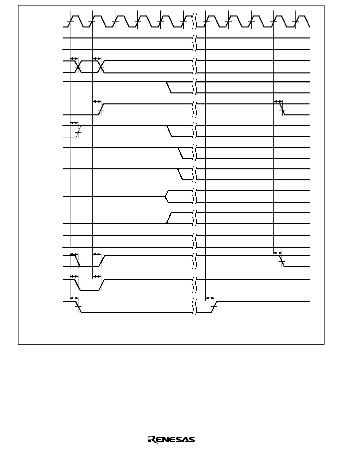
845
;
;;;;
;;;;;
Address
upper bits
Address
lower bits
BS
CKIO
Trr
Trc1
Trc2
Tre
Trc1
CSn
;
RD/
WR
WEn
DQMxx
D31≠D0
DACKn
;
;
;;;;
RD
;;;;
;;;;
;;;;
;;
;;
;;;;
;;;;
;;;;;;
;;;;;;
WAIT
RAS
CAS
OE
CKE
tAD
tRWD
tAD
tRASD1
tCASD1
tCKED
tCKED
tRASD1
tCSD1
tCSD1
Tre
tRASD1
tCASD1
Note: A self-refresh cycle is always preceded by a precharge cycle. The number of cycles
between the two is determined by the number of cycles specified by TRP.
Figure 22.32 Synchronous DRAM Self-Refresh Cycle (TRAS = 3)
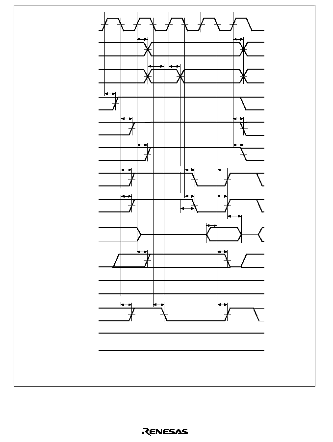
846
;;
;;;;;
;;;;;
;;
;;
;;
;;
;;
;;
;
;;
;;
;;
;;
CKIO
Tp
Tr
Tc1
Tc2
tAD
;;
tAD
tASR
tBSD
;;
tRDS1
tDACD2
tAD
BS
CSn
RD/
WR
RD
CASxx
RAS
CAS
OE
CKE
D31≠D0
DACKn
*
2
WAIT
Address
upper bits
Address
lower bits
;;
;;
tRSD1
tCASD2
;;
tCSD2
tCSD1
tRWD
tRWD
;;
;;
tRASD2
tRASD2
tDACD1
tRSD1
;;
tRDH5
*
1
tCASD2
tRASD2
Notes:
*
1 t
RDH5
is measured from the rise of
RD
or
CASxx
, whichever comes first.
*
2 DACKn waveform when active-high is specified
tRSD1
tCASD2
tASC
Figure 22.33 DRAM Read Cycle
(TRP = 1 Cycle, RCD = 1 Cycle, No Wait)

847
;;
;;
;;
;;;;;
;;;;;
;;
;;
;;
;;
;;
;
;;
;;
CKIO
Tp
Tr
Tc1
Tc2
tAD
;;
tAD
tBSD
tDACD2
tAD
BS
CSn
RD/
WR
RD
CASxx
RAS
CAS
OE
CKE
D31≠D0
DACKn
*
WAIT
Address
upper bits
Address
lower bits
;;
;;
;;
tCASD2
tCSD2
tCSD1
tRWD
tRWD
;;
;;
tRASD2
tRASD2
tRASD2
tRSD1
;;
;;;
;;;
;
;
;
;
tDON
tWDH1
tDOF
tCASD2
tCASD2
tWDD1
tASC
tDS
tDACD1
Note:
*
DACKn waveform when active-high is specified
tASR
Figure 22.34 DRAM Write Cycle
(TRP = 1 Cycle, RCD = 1 Cycle, No Wait)
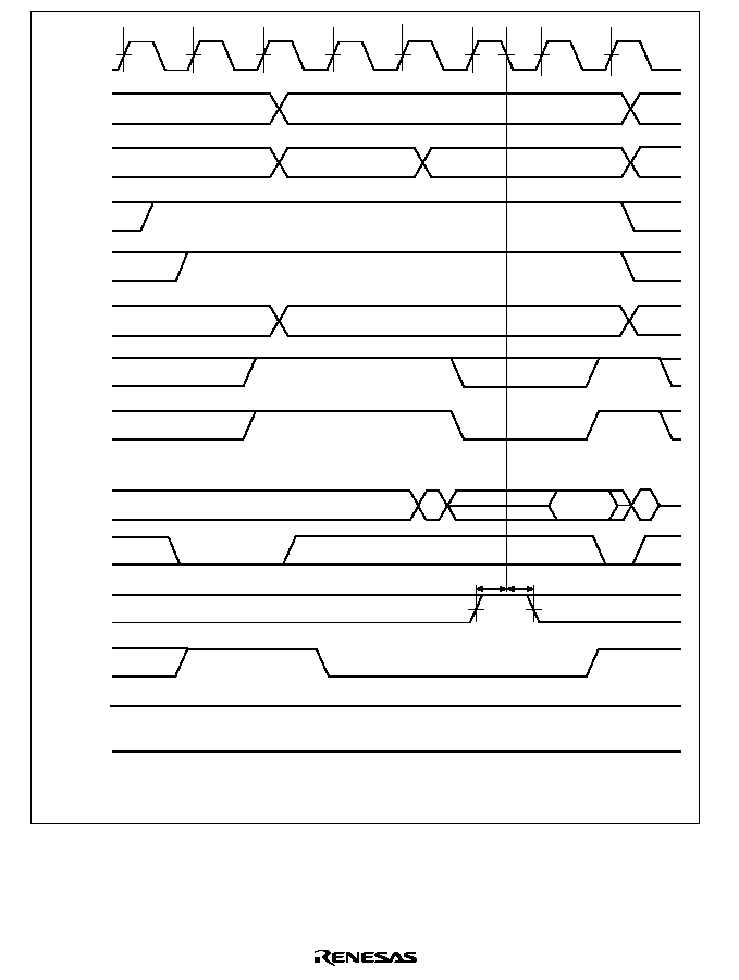
848
;;
;;
;;
;;
CKIO
BS
CSn
RD/
WR
RD
CASxx
RAS
CAS
OE
CKE
D31≠D0
DACKn
*
WAIT
Address
upper bits
;;
;;
;
;
Address
lower bits
;;
;
;
;;
;
;
;;
;
;
;;
;
;;
;;
;
;;
;;
;
;
;
;
;
;;
;;
;;
;;
;;;;
;;;;
;;;;
;
;
Tp
Tpw
Tr
Trw
Tc1
Tc2
Tw
tWTH
tWTS
Note:
*
DACKn waveform when active-high is specified
Figure 22.35 DRAM Bus Cycle
(TRP = 2 Cycles, RCD = 2 Cycles, 1 Wait)
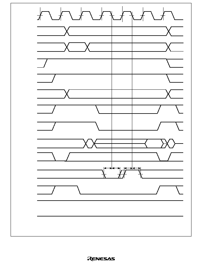
849
;;;
CKIO
Tp
Tr
Tc1
Tw
Twx
Tc2
BS
CSn
RD/
WR
RD
CASxx
RAS
CAS
OE
CKE
D31≠D0
DACKn
*
WAIT
Address
upper bits
Address
lower bits
;;
;;
;;
;;
;;
;;
;
;
;
;;
;;
;;
;;
;;
;
;;
;;
;
;
;;
;;
;
;
;;
;;
;;;
;;;
;;
;;;
;;
tWTS tWTH tWTS tWTH
;;
;;
;;
;;
Note:
*
DACKn waveform when active-high is specified
Figure 22.36 DRAM Bus Cycle
(TRP = 1 Cycle, RCD = 1 Cycle, External Wait Input)
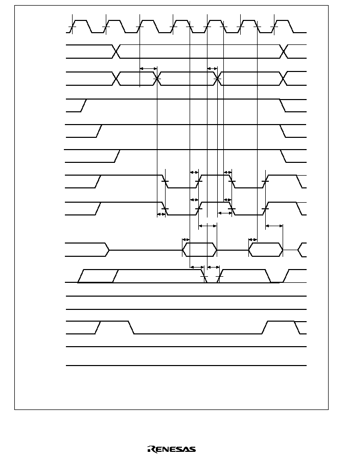
850
;;
;;;;;;
;;
;;
;;
CKIO
Tp
Tr
Tc1
Tc2
Tc1
Tc2
;
;;
tAD
tAD
tDACD1
BS
RD/
WR
RD
CASxx
RAS
CAS
OE
CKE
D31≠D0
DACKn
*
2
WAIT
Address
upper bits
Address
lower bits
;;
;;
;;
;;
;;
;;
;;
;;
;;
;;
;;
;;
tRSD1
tRSD1
;
;;
;;
;;
;;
tCASD2
tASC
tASC
tCASD2
;
;;
;;
tDACD2
tRDS1
CSn
;;
;;
tRDH5
*
1
tRDS1
tRDH5
*
1
Notes:
*
1 t
RDH5
is measured from the rise of
RD
or
CASxx
, whichever comes first.
*
2 DACKn waveform when active-high is specified
Figure 22.37 DRAM Burst Read Cycle
(TRP = 1 Cycle, RCD = 1 Cycle, No Wait)
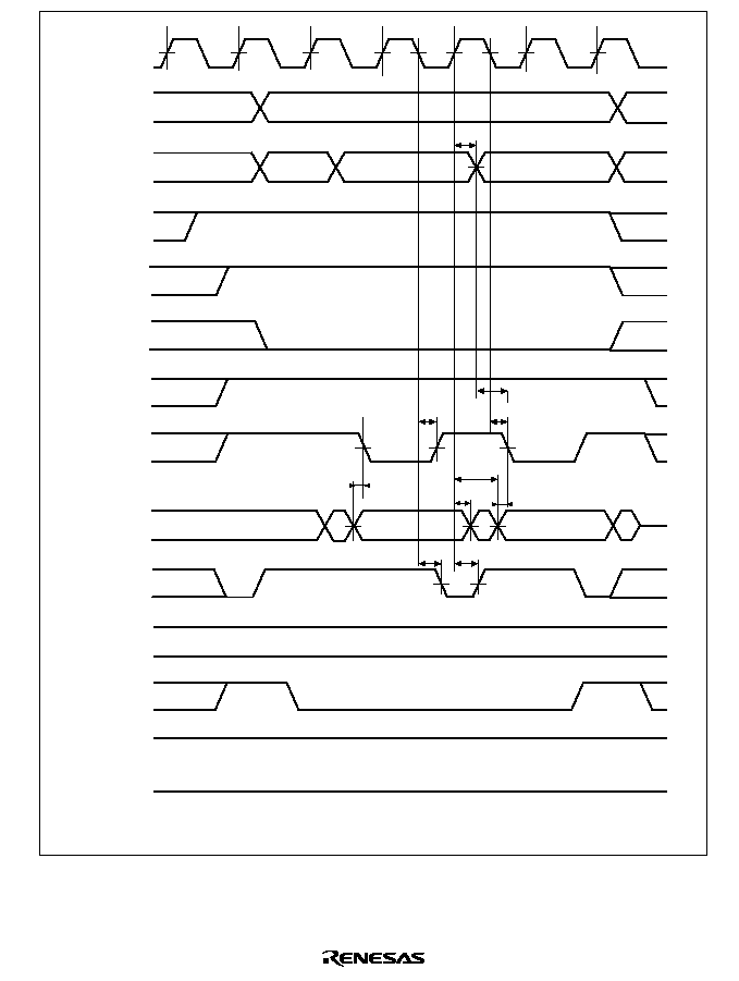
851
;
;
;;
;;;;;;
;;;;;;
;;;
;;;
;;
;;
;;
;;
CKIO
Tp
Tr
Tc1
Tc2
Tc1
Tc2
;;
tAD
tDACD1
BS
CSn
RD/
WR
RD
CASxx
RAS
CAS
OE
CKE
D31≠D0
DACKn
*
WAIT
Address
upper bits
Address
lower bits
;;
;;
;;
;;
;;
;;
;;
;;
;;
;
;;
tWDH1
;
;;
;;
tCASD2
;
;;
;;
tWDD1
tDACD2
;
;
;;
;;
Note:
*
DACKn waveform when active-high is specified
tCASD2
tASC
tDS
tDS
Figure 22.38 DRAM Burst Write Cycle
(TRP = 1 Cycle, RCD = 1 Cycle, No Wait)
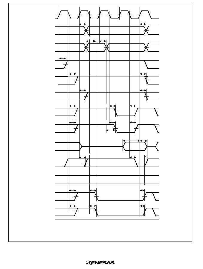
852
;;
;;;;
;;;;
;;
;;
;
;
;;
;;
;;
;;
;;
;
;;
;;
;
;
CKIO
Tp
Tr
Tc1
Tc2
tAD
;
tBSD
;
;
tRDS2
tDACD2
tRDH7
*
2
tAD
BS
CSn
RD/
WR
RD
CASxx
RAS
CAS
OE
CKE
D31≠D0
DACKn
*
1
WAIT
Address
upper bits
Address
lower bits
;
;
;
tRSD1
tCASD2
tASC
;
tCSD2
tCSD1
tRWD
tRWD
tCASD2
;
;;
tRASD3
tRASD2
tRASD2
;
;
;;
;;
tOED2
tOED1
tOED1
tRDH6
tRSD1
Notes:
*
1 DACKn waveform when active-high is specified
*
2 t
RDH7
is measured from the rise of
RAS
or
CAS
∑
OE
, whichever comes first.
tRSD1
tCASD2
tDACD1
tASR
tAD
Figure 22.39 EDO Read Cycle
(TRP = 1 Cycle, RCD = 1 Cycle, No Wait)
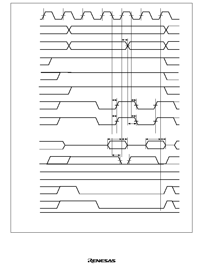
853
;;
;;;;;;
;;
;;
;;
CKIO
Tp
Tr
Tc1
Tc2
Tc1
Tc2
;
;;
tAD
tDACD1
BS
RD/
WR
RD
CASxx
RAS
CAS
OE
CKE
D31≠D0
DACKn
*
WAIT
Address
upper bits
Address
lower bits
;;
;;
;;
;;
;;
;;
;;
;
;
;;
;;
;
;;
tRSD1
tRSD1
;
;;
;;
tCASD2
tCASD2
tASC
;
;;
;;
tDACD2
tRDS2
CSn
;;
;;
;;
;;
tRDH6
tRDH6
tRDS2
Note:
*
DACKn waveform when active-high is specified
Figure 22.40 EDO Burst Read Cycle
(TRP = 1 Cycle, RCD = 1 Cycle, No Wait)
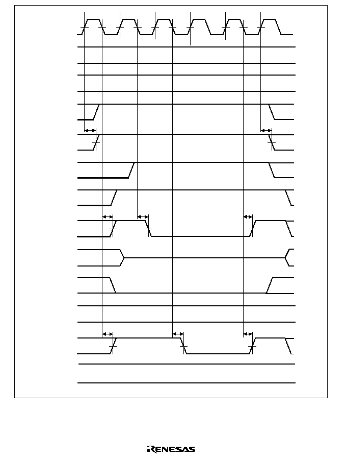
854
;;
;;
;
;;
;;
;;
;;
;;
;;
;;
;;
;
;
;
;
;;
;;
;;;;;
;;;;;
;;;;;
;;;;;
CKIO
BS
CSn
RD/
WR
RD
CASxx
RAS
CAS
OE
CKE
D31≠D0
DACKn
WAIT
Address
upper bits
Address
lower bits
Tp
tCSD1
Trr
Trc1
Trc2
Tre
tCASD2
tCASD2
tCASD2
;
tRASD2
tRASD2
tRASD2
tCSD1
;
;
;
;;
Figure 22.41 DRAM
CAS-Before-RAS Refresh Cycle
(TRP = 1 Cycle, TRAS = 2 Cycles)
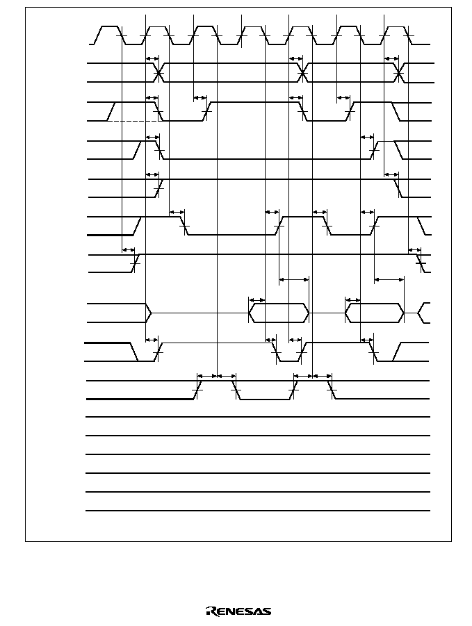
855
;;
;;
;;
;;
;;
CKIO
A24≠A0
;;
;;
;;
;
;
;;
;;
;;
;;
;;
;
;
;;;
;;;
;;;
;;;
;;
;;
;
BS
CSn
RD/
WR
RD
CASxx
RAS
CAS
OE
CKE
D31≠D0
DACKn
*
WAIT
T1
TW
T2
TW
T2
tAD
tBSD
tCSD1
tRWD
tRSD1
tRWD
tBSD
tBSD
tBSD
tAD
tAD
tCSD2
tRSD1
tRDH2
tRDS1
tWTS tWTH
tWTS tWTH
tDACD1
tDACD1
tDACD2
tDACD2
tRDS1
tRDH2
tCASD1
tCASD1
tRSD1
tRSD1
Note:
*
DACKn waveform when active-high is specified
Figure 22.42 Burst ROM Read Cycle
(Wait = 1)
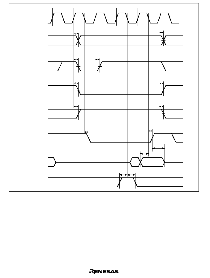
856
T1
T2
T3
T4
tAD
tAD
tRWD
tBSD
tBSD
tIVD
tRSD1
tRSD1
tRDS1
CKIO
A3≠A0
IVECF
RD/
WR
RD
D7≠D0
BS
tIVD
;
tRWD
tRDH8
WAIT
;;;
;;;
;;;
;;;
tWTS tWTH
Figure 22.43 Interrupt Vector Fetch Cycle
(No Wait, I
:E
= 1:1)
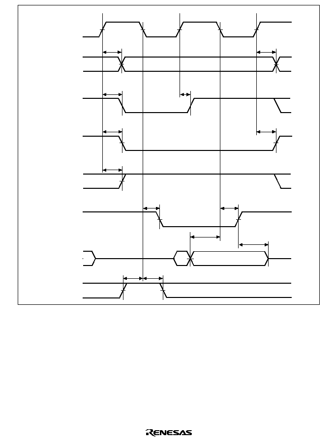
857
T1
T2
tAD
tAD
tIVD
tRWD
tBSD
tBSD
tIVD
tRSD1
tRSD1
tRDS1
CKIO
A3≠A0
IVECF
RD/
WR
RD
D7≠D0
BS
;
;
tRDH8
WAIT
;;;
;;
tWTS tWTH
Figure 22.44 Interrupt Vector Fetch Cycle
(No Wait, I
:E
other than 1:1)
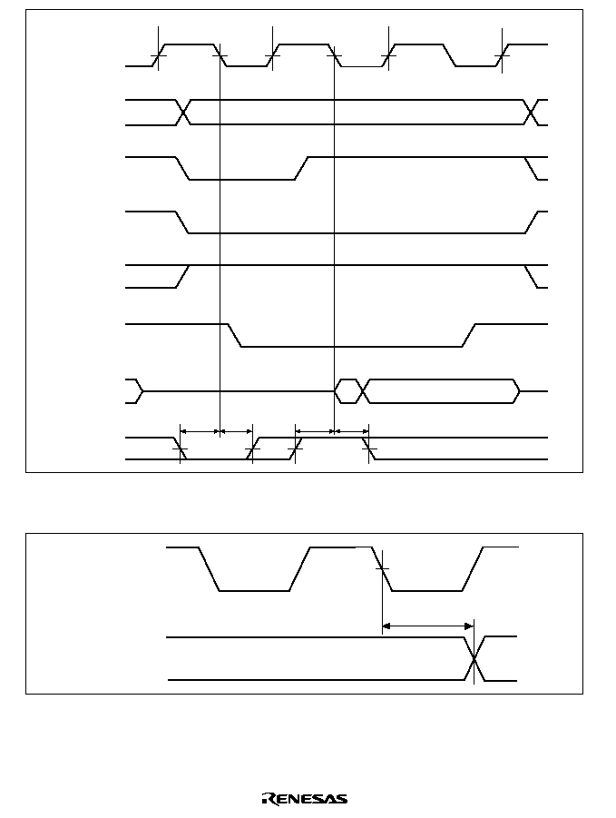
858
;
CKIO
A3≠A0
RD/
WR
WAIT
D7≠D0
RD
IVECF
T1
TW
T2
tWTH
tWTS
tWTH
tWTS
BS
;;;;;;
Figure 22.45 Interrupt Vector Fetch Cycle
(External Wait Input, I
:E
other than 1:1)
tREFOD
CKIO
REFOUT
Figure 22.46 REFOUT Delay Time
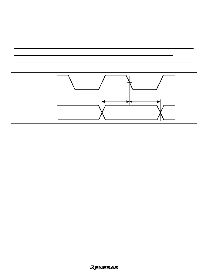
859
22.3.4
Direct Memory Access Controller Timing
Table 22.8
Direct Memory Access Controller Timing
Conditions: V
CC
= PLLV
CC
= 3.3 V ±0.3 V, PV
CC
= 5.0 V ± 0.5 V/3.3 V ±0.3 V, PV
CC
V
CC
,
V
SS
= PV
SS
= PLLV
SS
= 0 V, Ta = ≠20 to +75∞C
Item
Symbol
Min
Max
Unit
Figure
DREQ0, DREQ1 setup time
tDRQS
10
--
ns
22.47
DREQ0, DREQ1 hold time
tDRQH
5
--
ns
t
DRQH
t
DRQS
CKIO
DREQ0,
DREQ1
Figure 22.47 DREQ0, DREQ1 Input Timing

860
22.3.5
Free-Running Timer Timing
Table 22.9
Free-Running Timer Timing
Conditions: V
CC
= PLLV
CC
= 3.3 V ±0.3 V, PV
CC
= 5.0 V ± 0.5 V/3.3 V ±0.3 V, PV
CC
V
CC
,
V
SS
= PV
SS
= PLLV
SS
= 0 V, Ta = ≠20 to +75∞C
Item
Symbol
Min
Max
Unit
Figure
Output compare output delay time
tFOCD
--
100
ns
22.48, 22.49
Input capture input setup time
(tEcyc:tPcyc = 1:1)
tFICS
50
--
ns
22.48
Input capture input setup time
(tEcyc:tPcyc = 1:2)
tFICS
tcyc + 50
--
ns
22.49
Input capture input setup time
(tEcyc:tPcyc = 1:4)
tFICS
3tcyc + 50
--
ns
22.49
Input capture input hold time
tFICH
50
--
ns
22.48, 22.49
Timer clock input setup time
(tEcyc:tPcyc = 1:1)
tFCKS
50
--
ns
22.50
Timer clock input setup time
(tEcyc:tPcyc = 1:2)
tFCKS
tcyc + 50
--
ns
22.51
Timer clock input setup time
(tEcyc:tPcyc = 1:4)
tFCKS
3tcyc + 50
--
ns
22.51
Timer clock pulse width
(single edge specified)
tFCKWH
4.5
--
tPcyc 22.50, 22.51
Timer clock pulse width
(both edges specified)
tFCKWL
8.5
--
tPcyc

861
FTOA, FTOB
FTI
CKIO
tFICS
tFICH
tFOCD
Figure 22.48 FRT Input/Output Timing (tEcyc:tPcyc = 1:1)
FTOA, FTOB
FTI
CKIO
tFICS
tFICH
tFOCD
Figure 22.49 FRT Input/Output Timing (tEcyc:tPcyc other than 1:1)
CKIO
FTCI
tFCKWL
tFCKWH
tFCKS
Figure 22.50 FRT Clock Input Timing (tEcyc:tPcyc = 1:1)
CKIO
FTCI
tFCKWL
tFCKWH
tFCKS
Figure 22.51 FRT Clock Input Timing (tEcyc:tPcyc other than 1:1)
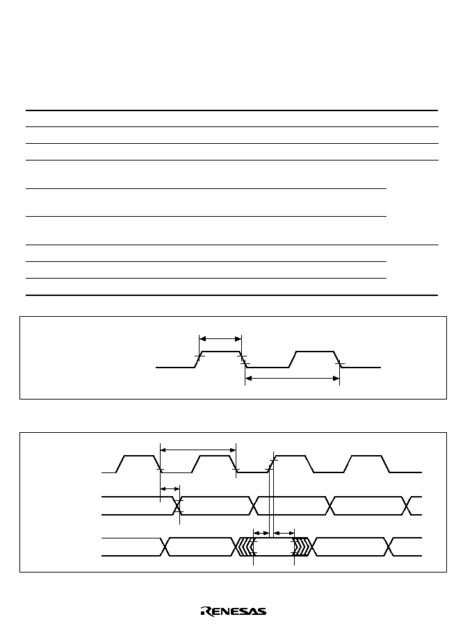
862
22.3.6
Serial Communication Interface Timing
Table 22.10 Serial Communication Interface Timing
Conditions: V
CC
= PLLV
CC
= 3.3 V ±0.3 V, PV
CC
= 5.0 V ± 0.5 V/3.3 V ±0.3 V, PV
CC
V
CC
,
V
SS
= PV
SS
= PLLV
SS
= 0 V, Ta = ≠20 to +75∞C
Item
Symbol
Min
Max
Unit
Figure
Input clock cycle
tscyc
4
--
tPcyc
22.52
Input clock cycle (synchronous mode)
tscyc
6
--
tPcyc
22.53
Input clock pulse width
tSCKW
0.4
0.6
tcscyc
22.52
Transmit data delay time
(synchronous mode)
tTXD
--
100
ns
22.53
Receive data setup time
(synchronous mode)
tRXS
100
--
ns
Receive data hold time
(synchronous mode)
tRXH
100
--
ns
RTS
delay time
tRTSD
--
100
ns
22.54
CTS
setup time (synchronous mode)
tCTSS
100
--
ns
CTS
hold time (synchronous mode)
tCTSH
100
--
ns
tSCKW
tscyc
SCK
SCK1
SCK2
Figure 22.52 Input Clock Input/Output Timing
tscyc
tTXD
tRXS
tRXH
SCK
TxD
(transmit data)
RxD
(receive data)
Figure 22.53 SCI Input/Output Timing (Synchronous Mode)

863
tscyc
tRTSD
tCTSS tCTSH
SCK1
RTS
CTS
Figure 22.54
RTS and CTS Input/Output Timing
Table 22.11 16-Bit Timer-Pulse Unit
Conditions: V
CC
= PLLV
CC
= 3.3 V ±0.3 V, PV
CC
= 5.0 V ± 0.5 V/3.3 V ±0.3 V, PV
CC
V
CC
,
V
SS
= PV
SS
= PLLV
SS
= 0 V, Ta = ≠20 to +75∞C
Item
Symbol
Min
Max
Unit
Figure
Timer output delay time
tTOCD
--
100
ns
22.55, 22.56
Timer input setup time
(tEcyc:tPcyc = 1:1)
tTICS
50
--
ns
Timer input setup time
(tEcyc:tPcyc = 1:2)
tTICS
tcyc + 50
--
ns
22.55, 22.56
Timer input setup time
(tEcyc:tPcyc = 1:4)
tTICS
3tcyc + 50
--
ns
Timer clock input setup time
(tEcyc:tPcyc = 1:1)
tTCKS
50
--
ns
22.57
Timer clock input setup time
(tEcyc:tPcyc = 1:2)
tTCKS
tcyc + 50
--
ns
Timer clock input setup time
(tEcyc:tPcyc = 1:4)
tTCKS
3tcyc + 50
--
ns
Timer clock pulse
width
Single edge
specified
tTCKWH
1.5
--
tcyc
Both edges
specified
tTCKWL
2.5
--

864
tTOCD
tTICS
CKIO
Output compare
output
*
Input capture
input
*
Note:
*
TIOCA0≠TIOCA2, TIOCB0≠TIOCB2, TIOCC0, TIOCD0
Figure 22.55 TPU Input/Output Timing (tEcyc:tPcyc = 1:1)
tTOCD
tTICS
CKIO
Output compare
output
*
Input capture
input
*
Note:
*
TIOCA0≠TIOCA2, TIOCB0≠TIOCB2, TIOCC0, TIOCD0
Figure 22.56 TPU Input/Output Timing (tEcyc:tPcyc other than 1:1)
tTCKS
tTCKS
tTCKWL
tTCKWH
CKIO
TCLKA≠TCLKD
Figure 22.57 TPU Clock Input Timing
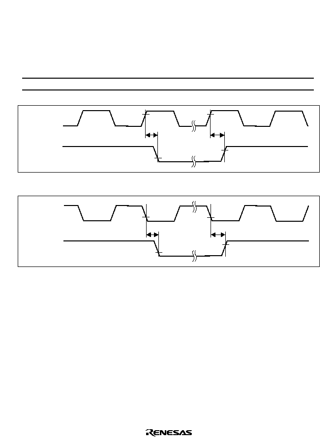
865
22.3.7
Watchdog Timer Timing
Table 22.12 Watchdog Timer Timing
Conditions: V
CC
= PLLV
CC
= 3.3 V ±0.3 V, PV
CC
= 5.0 V ± 0.5 V/3.3 V ±0.3 V, PV
CC
V
CC
,
V
SS
= PV
SS
= PLLV
SS
= 0 V, Ta = ≠20 to +75∞C
Item
Symbol
Min
Max
Unit
Figure
WDTOVF
delay time
tWOVD
--
70
ns
22.58, 22.59
CKIO
WDTOVF
tWOVD
tWOVD
Figure 22.58 Watchdog Timer Output Timing (tEcyc:tPcyc = 1:1)
CKIO
WDTOVF
tWOVD
tWOVD
Figure 22.59 Watchdog Timer Output Timing (tEcyc:tPcyc other than 1:1)

866
22.3.8
Serial I/O with FIFO / Serial I/O Timing
Table 22.13 Serial I/O with FIFO / Serial I/O Timing
Conditions: V
CC
= PLLV
CC
= 3.3 V ±0.3 V, PV
CC
= 5.0 V ± 0.5 V/3.3 V ±0.3 V, PV
CC
V
CC
,
V
SS
= PV
SS
= PLLV
SS
= 0 V, Ta = ≠20 to +75∞C
Item
Symbol
Min
Max
Unit
Figure
SRCK0, STCK0 clock input cycle time
tSFcyc
--
2
tPcyc
22.60
SRCKn, STCKn clock input cycle time
(n = 1 or 2)
tSIcyc
tPcyc or
*
66.7
--
ns
SRCK0, STCK0 clock input low-level width
tSFWL
0.4
◊
tSFcyc --
ns
SRCKn, STCKn clock input low-level width
(n = 1 or 2)
tWL
0.4
◊
tSIcyc --
ns
SRCK0, STCK0 clock input high-level width tSFWH
0.4
◊
tSFcyc --
ns
SRCKn, STCKn clock input high-level width
(n = 1 or 2)
tWH
0.4
◊
tSIcyc --
ns
SRS input setup time
tRSS
15
--
ns
22.61
SRS input hold time
tRSH
10
--
ns
SRXD input setup time
tSRDS
15
--
ns
SRXD input hold time
tSRDH
10
--
ns
STS0 input setup time
tSFTSS
1
--
tPcyc
22.62
STSn input setup time (n = 1 or 2)
tTSS
15
--
ns
STS input hold time
tTSH
10
--
ns
STS output delay time
tTSD
0
20
ns
22.63
STXD output delay time
tTDD
0
20
ns
22.62,
22.63
Note:
*
Specified as tPcyc or 66.7, whichever is greater.
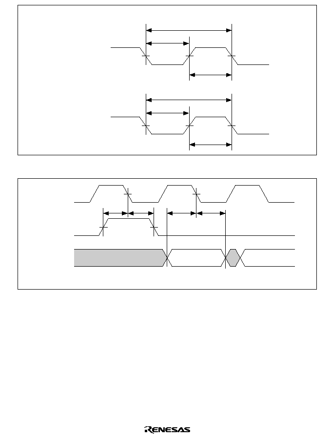
867
tSFWH
tSFWL
tSFcyc
STCK0, SRCK0
STCKn, SRCKn
n = 1 or 2
[SIOF]
[SIO]
tWH
tWL
tSIcyc
Figure 22.60 SIOF / SIO Input Clock Timing
SRCKn
(input)
SRSn
(input)
SRXDn
(input)
n = 0, 1, or 2
tSRDS
tSRDH
tRSS
tRSH
Figure 22.61 SIOF / SIO Receive Timing
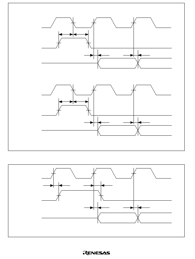
868
STCK0
(input)
[SIOF]
STS0
(input)
STXD0
(output)
tTDD
tTDD
tSFTSS
tTSH
STCKn
(input)
[SIO]
STSn
(input)
STXDn
(output)
n = 1, or 2
tTDD
tTDD
tTSS
tTSH
Figure 22.62 SIOF / SIO Transmit Timing (TMn = 0 Mode)
STCKn
(input)
STSn
(output)
STXDn
(output)
n = 0, 1, or 2
tTDD
tTDD
tTSD
tTSD
Figure 22.63 SIOF / SIO Transmit Timing (TMn = 1 Mode)

869
22.3.9
Hitachi User Debug Interface Timing
Table 22.14 Hitachi User Debug Interface Timing
Conditions: V
CC
= PLLV
CC
= 3.3 V ±0.3 V, PV
CC
= 5.0 V ± 0.5 V/3.3 V ±0.3 V, PV
CC
V
CC
,
V
SS
= PV
SS
= PLLV
SS
= 0 V, Ta = ≠20 to +75∞C
Item
Symbol
Min
Max
Unit
Figure
TCK clock input cycle time
ttcyc
tPcyc or
*
66.7 ns
--
ns
22.64
TCK clock input high-level width
tTCKH
0.4
0.6
ttcyc
TCK clock input low-level width
tTCKL
0.4
0.6
ttcyc
TRST
pulse width
tTRSW
20
--
ttcyc
22.65
TRST
setup time
tTRSS
40
--
ns
TMS setup time
tTMSS
30
--
ns
22.66
TMS hold time
tTMSH
10
--
ns
TDI setup time
tTDIS
30
--
ns
TDI hold time
tTDIH
10
--
ns
TDO delay time
tTDOD
0
30
ns
Note:
*
Specified as tPcyc or 66.7, whichever is greater.
tTCKH
tTCKL
TCK
ttcyc
Figure 22.64 H-UDI Clock Timing
TCK
tTRSS
tTRSW
tTRSS
TRST
Figure 22.65 H-UDI
TRST Timing
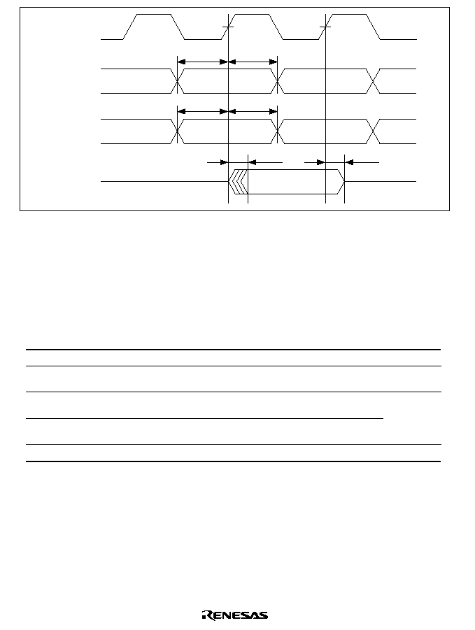
870
TCK
TMS
TDI
tTMSS
tTMSH
TDO
tTDIS
tTDIH
tTDOD
tTDOD
Figure 22.66 H-UDI Input/Output Timing
22.3.10
I/O Port Timing
Table 22.15 I/O Port Timing
Conditions: V
CC
= PLLV
CC
= 3.3 V ±0.3 V, PV
CC
= 5.0 V ± 0.5 V/3.3 V ±0.3 V, PV
CC
V
CC
,
V
SS
= PV
SS
= PLLV
SS
= 0 V, Ta = ≠20 to +75∞C
Item
Symbol
Min
Max
Unit
Figure
Port output data delay time
tPWD
--
50
ns
22.67, 22.68
Port input data setup time
(tEcyc:tPcyc = 1:1)
tPRS
50
--
ns
22.67
Port input data setup time
(tEcyc:tPcyc = 1:2)
tPRS
tcyc + 50
--
ns
22.68
Port input data setup time
(tEcyc:tPcyc = 1:4)
tPRS
3tcyc + 50
--
ns
Port input data hold time
tPRH
50
--
ns
22.67, 22.68

871
CKIO
PA0≠PA13
PB0≠PB15
(read)
PA0≠PA13
PB0≠PB15
(write)
tPWD
tPRS
tPRH
Figure 22.67 I/O Port Input/Output Timing (tEcyc:tPcyc = 1:1)
CKIO
PA0≠PA13
PB0≠PB15
(read)
PA0≠PA13
PB0≠PB15
(write)
tPWD
tPRS
tPRH
Figure 22.68 I/O Port Input/Output Timing (tEcyc:tPcyc
1:1)

872
22.3.11
Ethernet Controller Timing
Table 22.16 Ethernet Controller Timing
Conditions: V
CC
= PLLV
CC
= 3.3 V ±0.3 V, PV
CC
= 5.0 V ± 0.5 V/3.3 V ±0.3 V, PV
CC
V
CC
,
V
SS
= PV
SS
= PLLV
SS
= 0 V, Ta = ≠20 to +75∞C
Item
Symbol
Min
Typ
Max
Unit
Figure
TX-CLK cycle time
tTcyc
2.4
--
--
tcyc
22.69
TX-EN output delay time
tTENd
3
--
20
ns
ETXD[3:0] output delay time
tETDd
3
--
20
ns
CRS setup time
tCRSs
10
--
--
ns
CRS hold time
tCRSh
10
--
--
ns
COL setup time
tCOLs
10
--
--
ns
22.70
COL hold time
tCOLh
10
--
--
ns
RX-CLK cycle time
tRcyc
2.4
--
--
tcyc
22.71
RX-DV setup time
tRDVs
10
--
--
ns
RX-DV hold time
tRDVh
3
--
--
ns
ERXD[3:0] setup time
tERDs
10
--
--
ns
ERXD[3:0] hold time
tERDh
3
--
--
ns
RX-ER setup time
tRERs
10
--
--
ns
22.72
RX-ER hold time
tRERh
3
--
--
ns
MDIO setup time
tMDIOs
10
--
--
ns
22.73
MDIO hold time
tMDIOh
10
--
--
ns
MDIO output data hold time
*
tMDIOdh
5
--
18
ns
22.74
WOL output delay time
tWOLd
1
--
18
ns
22.75
EXOUT output delay time
tEXOUTd
1
--
28
ns
22.76
CAMSEN setup time
tCAMs
10
--
--
ns
22.77
CAMSEN hold time
tCAMh
3
--
--
ns
Note:
*
The user must ensure that the code satisfies this condition.
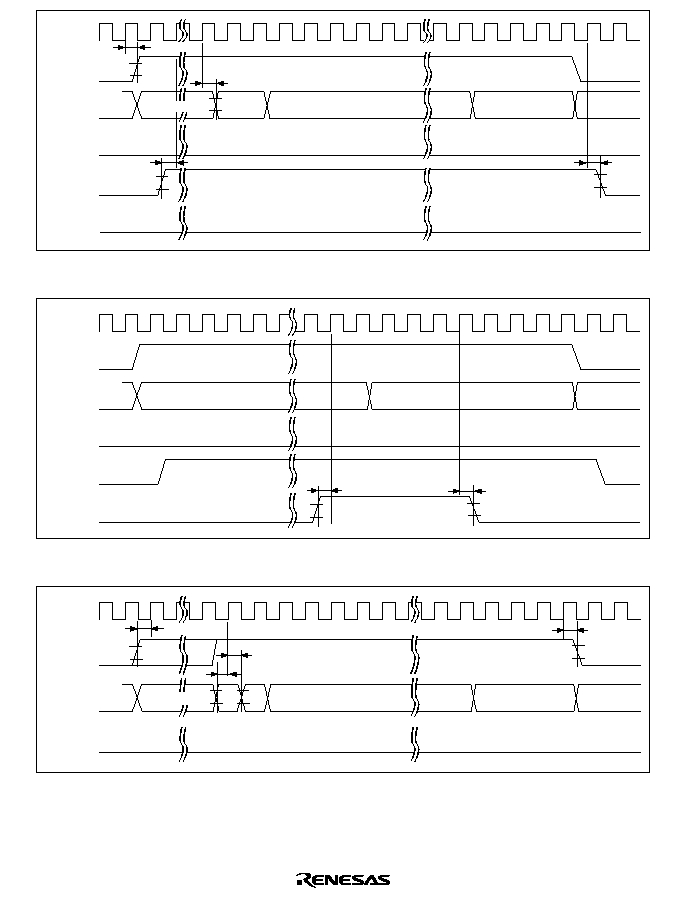
873
tTENd
SFD
DATA
CRC
tCRSh
TX-CLK
TX-EN
ETXD[3:0]
TX-ER
CRS
COL
tCRSs
tETDd
Preamble
Figure 22.69 MII Send Timing (Normal Operation)
Preamble
JAM
TX-CLK
TX-EN
ETXD[3:0]
TX-ER
CRS
COL
tCOLh
tCOLs
Figure 22.70 MII Send Timing (Case of Conflict)
tRDVs
SFD
DATA
CRC
RX-CLK
RX-DV
ERXD[3:0]
RX-ER
tERDs
tERDh
tRDVh
Preamble
Figure 22.71 MII Receive Timing (Normal Operation)

874
SFD
DATA
XXXX
RX-CLK
RX-DV
ERXD[3:0]
RX-ER
tRERs
tRERh
Preamble
Figure 22.72 MII Receive Timing (Case of Error)
MDC
tMDIOs
tMDIOh
MDIO
Figure 22.73 MDIO Input Timing
MDC
tMDIOdh
MDIO
Figure 22.74 MDIO Output Timing
RX-CLK
tWOLd
WOL
Figure 22.75 WOL Output Timing
CKIO
tEXOUTd
EXOUT
Figure 22.76 EXOUT Output Timing

875
SFD
DATA
RX-CLK
RX-DV
ERXD[3:0]
CAMSEN
tCAMS
Preamble
Dest Address
Source Address
tCAMh
Figure 22.77 CAMSEN Input Timing
22.3.12
STATS,
BH, and BUSHiZ Signal Timing
Table 22.17 STATS,
BH, and BUSHiZ Signal Timing
Conditions: V
CC
= PLLV
CC
= 3.3 V ±0.3 V, PV
CC
= 5.0 V ± 0.5 V/3.3 V ±0.3 V, PV
CC
V
CC
,
V
SS
= PV
SS
= PLLV
SS
= 0 V, Ta = ≠20 to +75∞C
Item
Symbol
Min
Typ
Max
Unit
Figure
STAS1 and STAS0 output delay time
tSTATd
--
--
16
ns
22.77
BH
output rising edge delay time
tBHNrd
--
--
16
ns
22.78
BH
output falling edge delay time
tBHNfd
--
--
16
ns
BUSHiZ
setup time
tBHIZs
7
--
--
ns
22.79
BUSHiZ
hold time
tBHIZh
8
--
--
ns
Output delay time of target pins
tBHIZd
--
--
16
ns
CPU
CPU
E-DMAC
E-DMAC E-DMAC
E-DMAC
G-DMAC
G-DMAC
G-DMAC
G-DMAC
CKI0
Address
CSn
STATS1, 0
tSTATd
Figure 22.78 STATS Output Timing
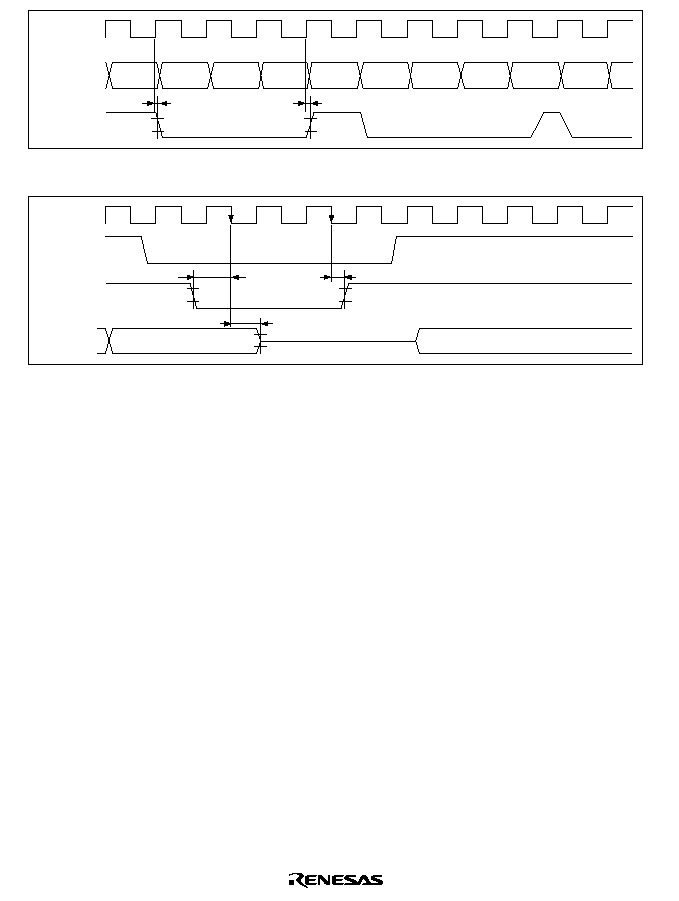
876
CPU
CPU
G-DMAC G-DMAC G-DMAC
G-DMAC G-DMAC
G-DMAC
G-DMAC
G-DMAC
CKI0
Address
BH
tBHNfd
tBHNrd
Read0
Read1
Read2
Read3
Write0
Write1
Write2
Write3
Figure 22.79
BH Output Timing
CKI0
tBHIZs
tBHIZh
tBHIZd
WAIT
BUSHiZ
Target Pins
Figure 22.80
BUSHiZ Bus Timing
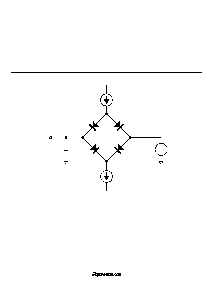
877
22.4
AC Characteristic Test Conditions
The AC characteristic test conditions are as follows:
∑
Input/output signal reference level: 1.5 V (Vcc = 3.3 to 3.6 V)
∑
Input pulse level: Vss to 3.0 V (Vss to Vcc for
RES, TRST, EXTAL, CKIO, MD0≠MD4, and
NMI)
∑
Input rise/fall time: 1 ns
The output load circuit is shown in figure 22.81.
IOL
CL
SH7616
output pin
DUT output
VREF
IOH
CL is the total value, including the capacitance of the test jig, etc. The capacitance of each pin is
as follows:
30 pF: CKIO, A24≠A0, D31≠D0,
BS
,
RD
,
CS4
≠
CS0
, DQMUU/
WE3
≠DQMLL/
WE0
,
CAS3
≠
CAS0
,
RAS
,
CAS
/
OE
, DACK1, DACK0
50 pF: All other pins
IOL and IOH values are as shown in table 22.3, Permissible Output Currents.
V
Figure 22.81 Output Load Circuit

878

879
Appendix A On-Chip Peripheral Module Registers
A.1
Addresses
On-chip peripheral module register addresses and bit names are shown in the following table. 16-
bit registers and 32-bit registers are shown, respectively, in two and four lines of 8 bits.
Register
Bit Names
Address
Name
Bit 7
Bit 6
Bit 5
Bit 4
Bit 3
Bit 2
Bit 1
Bit 0
Module
H'FFFFFC00
SIRDR
SIOF
H'FFFFFC01
H'FFFFFC02
SITDR
H'FFFFFC03
H'FFFFFC04
SICTR
--
--
--
--
--
DMACE
TCIE
RCIE
H'FFFFFC05
--
TM
SE
DL
TIE
RIE
TE
RE
H'FFFFFC06
SISTR
--
--
--
--
--
--
TCD
RCD
H'FFFFFC07
--
--
--
--
TERR
RERR
TDRE
RDRF
H'FFFFFC08
SIFCR
--
--
--
--
TRMD
LM
RFRST
TFRST
H'FFFFFC09
RFWM3
RFWM2
RFWM1
RFWM0
TFWM3
TFWM2
TFWM1
TFWM0
H'FFFFFC0A
SIFDR
--
--
--
R4
R3
R2
R1
R0
H'FFFFFC0B
--
--
--
T4
T3
T2
T1
T0
H'FFFFFC0C
SIRCDR
H'FFFFFC0D
H'FFFFFC0E
SITCDR
H'FFFFFC0F
H'FFFFFC10
SIRDR1
SIO
H'FFFFFC11
H'FFFFFC12
SITDR1
H'FFFFFC13
H'FFFFFC14
SICTR1
--
--
--
--
--
--
--
--
H'FFFFFC15
--
TM
SE
DL
TIE
RIE
TE
RE
H'FFFFFC16
SISTR1
--
--
--
--
--
--
--
--
H'FFFFFC17
--
--
--
--
TERR
RERR
TDRE
RDRF
H'FFFFFC18
to
H'FFFFFC1F
--
--
--
--
--
--
--
--
--
--

880
Register
Bit Names
Address
Name
Bit 7
Bit 6
Bit 5
Bit 4
Bit 3
Bit 2
Bit 1
Bit 0
Module
H'FFFFFC20
SIRDR2
SIO
H'FFFFFC21
H'FFFFFC22
SITDR2
H'FFFFFC23
H'FFFFFC24
SICTR2
--
--
--
--
--
--
--
--
H'FFFFFC25
--
TM
SE
DE
TIE
RIE
TE
RE
H'FFFFFC26
SISTR2
--
--
--
--
--
--
--
--
H'FFFFFC27
--
--
--
--
TERR
RERR
TDRE
RDRF
H'FFFFFC28
to
H'FFFFFC3F
--
--
--
--
--
--
--
--
--
--
H'FFFFFC40
TSTR
--
--
--
--
--
CST2
CST1
CST0
TPU
H'FFFFFC41
TSYR
--
--
--
--
--
SYNC2
SYNC1
SYNC0
H'FFFFFC42
to
H'FFFFFC4F
--
--
--
--
--
--
--
--
--
--
H'FFFFFC50
TCR0
CCLR2
CCLR1
CCLR0
CKEG1
CKEG0
TPSC2
TPSC1
TPSC0
TPU
H'FFFFFC51
TMDR0
--
--
BFB
BFA
MD3
MD2
MD1
MD0
H'FFFFFC52
TIOR0H
IOB3
IOB2
IOB1
IOB0
IOA3
IOA2
IOA1
IOA0
H'FFFFFC53
TIOR0L
IOD3
IOD2
IOD1
IOD0
IOC3
IOC2
IOC1
IOC0
H'FFFFFC54
TIER0
--
--
--
TCIEV
TGIED
TGIEC
TGIEB
TGIEA
H'FFFFFC55
TSR0
--
--
--
TCFV
TGFD
TGFC
TGFB
TGFA
H'FFFFFC56
TCNT0
H'FFFFFC57
H'FFFFFC58
TGR0A
H'FFFFFC59
H'FFFFFC5A
TGR0B
H'FFFFFC5B
H'FFFFFC5C
TGR0C
H'FFFFFC5D
H'FFFFFC5E
TGR0D
H'FFFFFC5F
H'FFFFFC60
TCR1
--
CCLR1
CCLR0
CKEG1
CKEG0
TPSC2
TPSC1
TPSC0
H'FFFFFC61
TMDR1
--
--
--
--
MD3
MD2
MD1
MD0
H'FFFFFC62
TIOR1
IOB3
IOB2
IOB1
IOB0
IOA3
IOA2
IOA1
IOA0
H'FFFFFC63
--
--
--
--
--
--
--
--
--
H'FFFFFC64
TIER1
--
--
TCIEU
TCIEV
--
--
TGIEB
TGIEA
H'FFFFFC65
TSR1
TCFD
--
TCFU
TCFV
--
--
TGFB
TGFA

881
Register
Bit Names
Address
Name
Bit 7
Bit 6
Bit 5
Bit 4
Bit 3
Bit 2
Bit 1
Bit 0
Module
H'FFFFFC66
TCNT1
TPU
H'FFFFFC67
H'FFFFFC68
TGR1A
H'FFFFFC69
H'FFFFFC6A
TGR1B
H'FFFFFC6B
H'FFFFFC6C
to
H'FFFFFC6F
--
--
--
--
--
--
--
--
--
--
H'FFFFFC70
TCR2
--
CCLR1
CCLR0
CKEG1
CKEG0
TPSC2
TPSC1
TPSC0
TPU
H'FFFFFC71
TMDR2
--
--
--
--
MD3
MD2
MD1
MD0
H'FFFFFC72
TIOR2
IOB3
IOB2
IOB1
IOB0
IOA3
IOA2
IOA1
IOA0
H'FFFFFC73
--
--
--
--
--
--
--
--
--
H'FFFFFC74
TIER2
--
--
TCIEU
TCIEV
--
--
TGIEB
TGIEA
H'FFFFFC75
TSR2
TCFD
--
TCFU
TCFV
--
--
TGFB
TGFA
H'FFFFFC76
TCNT2
H'FFFFFC77
H'FFFFFC78
TGR2A
H'FFFFFC79
H'FFFFFC7A
TGR2B
H'FFFFFC7B
H'FFFFFC7C
to
H'FFFFFC7F
--
--
--
--
--
--
--
--
--
--
H'FFFFFC80
PACR
--
--
PA13MD PA12MD PA11MD PA10MD PA9MD
PA8MD
PFC
H'FFFFFC81
PA7MD
PA6MD
PA5MD
PA4MD
PA3MD
PA2MD
PA1MD
PA0MD
H'FFFFFC82
PAIOR
--
--
PA13IOR PA12IOR PA11IOR PA10IOR PA9IOR
PA8IOR
H'FFFFFC83
PA7IOR
PA6IOR
PA5IOR
PA4IOR
--
PA2IOR
PA1IOR
PA0IOR
H'FFFFFC84
PADR
--
--
PA13DR
PA12DR
PA11DR
PA10DR
PA9DR
PA8DR
I/O port
H'FFFFFC85
PA7DR
PA6DR
PA5DR
PA4DR
--
PA2DR
PA1DR
PA0DR
H'FFFFFC86
to
H'FFFFFC87
--
--
--
--
--
--
--
--
--
--
H'FFFFFC88
PBCR
PB15MD1 PB15MD0 PB14MD1 PB14MD0 PB13MD1 PB13MD0 PB12MD1 PB12MD0 PFC
H'FFFFFC89
PB11MD1 PB11MD0 PB10MD1 PB10MD0 PB9MD1 PB9MD0 PB8MD1 PB8MD0
H'FFFFFC8A
PBIOR
PB15IOR PB14IOR PB13IOR PB12IOR PB11IOR PB10IOR PB9IOR
PB8IOR
H'FFFFFC8B
PB7IOR
PB6IOR
PB5IOR
PB4IOR
PB3IOR
PB2IOR
PB1IOR
PB0IOR
H'FFFFFC8C
PBDR
PB15DR
PB14DR
PB13DR
PB12DR
PB11DR
PB10DR
PB9DR
PB8DR
I/O port
H'FFFFFC8D
PB7DR
PB6DR
PB5DR
PB4DR
PB3DR
PB2DR
PB1DR
PB0DR

882
Register
Bit Names
Address
Name
Bit 7
Bit 6
Bit 5
Bit 4
Bit 3
Bit 2
Bit 1
Bit 0
Module
H'FFFFFC8E
PBCR2
PB7MD1 PB7MD0 PB6MD1 PB6MD0 PB5MD1 PB5MD0 PB4MD1 PB4MD0 PFC
H'FFFFFC8F
PB3MD1 PB3MD0 PB2MD1 PB2MD0 PB1MD1 PB1MD0 PB0MD1 PB0MD0
H'FFFFFC90
to
H'FFFFFCAF
--
--
--
--
--
--
--
--
--
--
H'FFFFF CB0
SDIR
TS3
TS2
TS1
TS0
--
--
--
--
H-UDI
H'FFFFF CB1
--
--
--
--
--
--
--
--
H'FFFFF CB2
SDSR
--
--
--
--
--
--
--
--
H'FFFFF CB3
--
--
--
--
--
--
--
SDTRF
H'FFFFF CB4
SDDRH
H-UDI
H'FFFFF CB5
H'FFFFF CB6
SDDRL
H'FFFFF CB7
H'FFFFF CB8
to
H'FFFFF CBF
--
--
--
--
--
--
--
--
--
--
H'FFFF FCC0 SCBRR1
C/
A
CHR/ICK3 PE/ICK1 O/
E
/ICK1 STOP/
ICK0
MP
CKS1
CKS0
SCIF1
H'FFFF FCC1 --
--
--
--
--
--
--
--
--
H'FFFF FCC2 SCBRR1
H'FFFF FCC3 --
--
--
--
--
--
--
--
--
H'FFFF FCC4 SCSCR1
TIE
RIE
TE
RE
MPIE
--
CKE1
CKE0
H'FFFF FCC5 --
--
--
--
--
--
--
--
--
H'FFFF FCC6 SCFTDR1
H'FFFF FCC7 --
--
--
--
--
--
--
--
--
H'FFFF FCC8 SC1SSR1 PER3
PER2
PER1
PER0
FER3
FER2
FER1
FER0
H'FFFF FCC9
ER
TEND
TDFE
BRK
FER
PER
RDF
DR
H'FFFF FCCA SC2SSR1 TLM
RLM
N1
N0
MPB
MPBT
EI
ORER
H'FFFF FCCB --
--
--
--
--
--
--
--
--
H'FFFF FCCC SCFRDR1
H'FFFF FCCD --
--
--
--
--
--
--
--
--
H'FFFF FCCE SCFCR1
RTRG1
RTRG0
TTRG1
TTRG0
MCE
TFRST
RFRST
LOOP
H'FFFF FCCF --
--
--
--
--
--
--
--
--
H'FFFF FCD0 SCFDR1
--
--
--
T4
T3
T2
T1
T0
SCIF1
H'FFFF FCD1
--
--
--
R4
R3
R2
R1
R0
H'FFFF FCD2 SCFER1
ED15
ED14
ED13
ED12
ED11
ED10
ED9
ED8
H'FFFF FCD3
ED7
ED6
ED5
ED4
ED3
ED2
ED1
ED0
H'FFFF FCD4 SCIMR1
IRMOD
PSEL
RIVS
--
--
--
--
--

883
Register
Bit Names
Address
Name
Bit 7
Bit 6
Bit 5
Bit 4
Bit 3
Bit 2
Bit 1
Bit 0
Module
H'FFFF FCD5
to
H'FFFF FCDF
--
--
--
--
--
--
--
--
--
--
H'FFFF FCE0
SCSMR2
C/
A
CHR/ICK3 PE/ICK2 O/
E
/ICK1 STOP/
ICK0
MP
CKS1
CKS0
SCIF2
H'FFFF FCE1
--
--
--
--
--
--
--
--
--
H'FFFF FCE2
SCBRR2
H'FFFF FCE3
--
--
--
--
--
--
--
--
--
H'FFFF FCE4
SCSCR2
TIE
RIE
TE
RE
MPIE
--
CKE1
CKE0
H'FFFF FCE5
--
--
--
--
--
--
--
--
--
H'FFFF FCE6
SCFTDR2
H'FFFF FCE7
--
--
--
--
--
--
--
--
--
H'FFFF FCE8
SC1SSR2 PER3
PER2
PER1
PER0
FER3
FER2
FER1
FER0
H'FFFF FCE9
ER
TEND
TDFE
BRK
FER
PER
RDF
DR
H'FFFF FCEA SC2SSR2 TLM
RLM
N1
N0
MPB
MPBT
EI
ORER
H'FFFF FCEB --
--
--
--
--
--
--
--
--
H'FFFF FCEC SCFRDR2
H'FFFF FCED --
--
--
--
--
--
--
--
--
H'FFFF FCEE SCFCR2
RTRG1
RTRG0
TTRG1
TTRG0
MCE
TFRST
RFRST
LOOP
H'FFFF FCEF --
--
--
--
--
--
--
--
--
H'FFFF FCF0
SCFDR2
--
--
--
T4
T3
T2
T1
T0
H'FFFF FCF1
--
--
--
R4
R3
R2
R1
R0
H'FFFF FCF2
SCFER2
ED15
ED14
ED13
ED12
ED11
ED10
ED9
ED8
H'FFFF FCF3
ED7
ED6
ED5
ED4
ED3
ED2
ED1
ED0
H'FFFF FCF4
SCIMR2
IRMOD
PSEL
RIVS
--
--
--
--
--
H'FFFF FCF5
to
H'FFFF FCFF
--
--
--
--
--
--
--
--
--
--
H'FFFF FD00
EDMR
--
--
--
--
--
--
--
--
E-DMAC
H'FFFF FD01
--
--
--
--
--
--
--
--
H'FFFF FD02
--
--
--
--
--
--
--
--
H'FFFF FD03
--
--
DL1
DL0
--
--
--
SWR
H'FFFF FD04
EDTRR
--
--
--
--
--
--
--
--
H'FFFF FD05
--
--
--
--
--
--
--
--
H'FFFF FD06
--
--
--
--
--
--
--
--
H'FFFF FD07
--
--
--
--
--
--
--
TR

884
Register
Bit Names
Address
Name
Bit 7
Bit 6
Bit 5
Bit 4
Bit 3
Bit 2
Bit 1
Bit 0
Module
H'FFFF FD08
EDRRR
--
--
--
--
--
--
--
--
E-DMAC
H'FFFF FD09
--
--
--
--
--
--
--
--
H'FFFF FD0A
--
--
--
--
--
--
--
--
H'FFFF FD0B
--
--
--
--
--
--
--
RR
H'FFFF FD0C TDLAR
TDLA31
TDLA30
TDLA29
TDLA28
TDLA27
TDLA26
TDLA25
TDLA24
H'FFFF FD0D
TDLA23
TDLA22
TDLA21
TDLA20
TDLA19
TDLA18
TDLA17
TDLA16
H'FFFF FD0E
TDLA15
TDLA14
TDLA13
TDLA12
TDLA11
TDLA10
TDLA9
TDLA8
H'FFFF FD0F
TDLA7
TDLA6
TDLA5
TDLA4
TDLA3
TDLA2
TDLA1
TDLA0
H'FFFF FD10
RDLAR
RDLA31
RDLA30
RDLA29
RDLA28
RDLA27
RDLA26
RDLA25
RDLA24
H'FFFF FD11
RDLA23
RDLA22
RDLA21
RDLA20
RDLA19
RDLA18
RDLA17
RDLA16
H'FFFF FD12
RDLA15
RDLA14
RDLA13
RDLA12
RDLA11
RDLA10
RDLA9
RDLA8
H'FFFF FD13
RDLA7
RDLA6
RDLA5
RDLA4
RDLA3
RDLA2
RDLA1
RDLA0
H'FFFF FD14
EESR
--
--
--
--
--
--
--
RFCOF
H'FFFF FD15
--
ECI
TC
TDE
TFUF
FR
RDE
RFOF
H'FFFF FD16
--
--
--
ITF
CND
DLC
CD
TRO
H'FFFF FD17
RMAF
--
RFAR
RRF
RTLF
RTSF
PRE
CERF
H'FFFF FD18
EESIPR
--
--
--
--
--
--
--
RFCOFIP
H'FFFF FD19
--
ECIIP
TCIP
TDEIP
TFUFIP
FRIP
RDEIP
RFOFIP
H'FFFF FD1A
--
--
--
ITFIP
CNDIP
DLCIP
CDIP
TROIP
H'FFFF FD1B
RMAFIP
--
RFARIP
RRFIP
RTLFIP
RTSFIP
PREIP
CERFIP
H'FFFF FD1C TRSCER
--
--
--
--
--
--
--
--
H'FFFF FD1D
--
--
--
--
--
--
--
--
H'FFFF FD1E
--
--
--
ITFCE
CNDCE
DLCCE
CDCE
TROCE
H'FFFF FD1F
RMAFCE --
RFARCE RRFCE
RTLFCE
RTSFCE PRECE
CERFCE
H'FFFF FD20
RMFCR
--
--
--
--
--
--
--
--
H'FFFF FD21
--
--
--
--
--
--
--
--
H'FFFF FD22
MFC15
MFC14
MFC13
MFC12
MFC11
MFC10
MFC9
MFC8
H'FFFF FD23
MFC7
MFC6
MFC5
MFC4
MFC3
MFC2
MFC1
MFC0
H'FFFF FD24
TFTR
--
--
--
--
--
--
--
--
H'FFFF FD25
--
--
--
--
--
--
--
--
H'FFFF FD26
--
--
--
--
--
TFT10
TFT9
TFT8
H'FFFF FD27
TFT7
TFT6
TFT5
TFT4
TFT3
TFT2
TFT1
TFT0

885
Register
Bit Names
Address
Name
Bit 7
Bit 6
Bit 5
Bit 4
Bit 3
Bit 2
Bit 1
Bit 0
Module
H'FFFF FD28
FDR
--
--
--
--
--
--
--
--
E-DMAC
H'FFFF FD29
--
--
--
--
--
--
--
--
H'FFFF FD2A
--
--
--
--
--
TFD2
TFD1
TFD0
H'FFFF FD2B
--
--
--
--
--
RFD2
RFD1
RFD0
H'FFFF FD2C RCR
--
--
--
--
--
--
--
--
H'FFFF FD2D
--
--
--
--
--
--
--
--
H'FFFF FD2E
--
--
--
--
--
--
--
--
H'FFFF FD2F
--
--
--
--
--
--
--
RNC
H'FFFF FD30
EDOCR
--
--
--
--
--
--
--
--
H'FFFF FD31
--
--
--
--
--
--
--
--
H'FFFF FD32
--
--
--
--
--
--
--
--
H'FFFF FD33
--
--
--
--
FEC
AEC
EDH
--
H'FFFF FD34
to
H'FFFF FD3F
--
--
--
--
--
--
--
--
--
H'FFFF FD40
RBWAR
RBWA31 RBWA30 RBWA29 RBWA28 RBWA27 RBWA26
RBWA25
RBWA24
H'FFFF FD41
RBWA23 RBWA22 RBWA21 RBWA20 RBWA19 RBWA18
RBWA17
RBWA16
H'FFFF FD42
RBWA15 RBWA14 RBWA13 RBWA12 RBWA11 RBWA10
RBWA9
RBWA8
H'FFFF FD43
RBWA7
RBWA6
RBWA5
RBWA4
RBWA3
RBWA2
RBWA1
RBWA0
H'FFFF FD44
RDFAR
RDFA31
RDFA30
RDFA29 RDFA28
RDFA27
RDFA26
RDFA25
RDFA24
H'FFFF FD45
RDFA23
RDFA22
RDFA21 RDFA20
RDFA19
RDFA18
RDFA17
RDFA16
H'FFFF FD46
RDFA15
RDFA14
RDFA13 RDFA12
RDFA11
RDFA10
RDFA9
RDFA8
H'FFFF FD47
RDFA7
RDFA6
RDFA5
RDFA4
RDFA3
RDFA2
RDFA1
RDFA0
H'FFFF FD48
to
H'FFFF FD4B
--
--
--
--
--
--
--
--
--
H'FFFF FD4C TBRAR
TBRA31
TBRA30
TBRA29
TBRA28
TBRA27
TBRA26
TBRA25
TBRA24
H'FFFF FD4D
TBRA23
TBRA22
TBRA21
TBRA20
TBRA19
TBRA18
TBRA17
TBRA16
H'FFFF FD4E
TBRA15
TBRA14
TBRA13
TBRA12
TBRA11
TBRA10
TBRA9
TBRA8
H'FFFF FD4F
TBRA7
TBRA6
TBRA5
TBRA4
TBRA3
TBRA2
TBRA1
TBRA0
H'FFFF FD50
TDFAR
TDFA31
TDFA30
TDFA29
TDFA28
TDFA27
TDFA26
TDFA25
TDFA24
H'FFFF FD51
TDFA23
TDFA22
TDFA21
TDFA20
TDFA19
TDFA18
TDFA17
TDFA16
H'FFFF FD52
TDFA15
TDFA14
TDFA13
TDFA12
TDFA11
TDFA10
TDFA9
TDFA8
H'FFFF FD53
TDFA7
TDFA6
TDFA5
TDFA4
TDFA3
TDFA2
TDFA1
TDFA0
H'FFFF FD54
to
H'FFFF FD5F
--
--
--
--
--
--
--
--
--

886
Register
Bit Names
Address
Name
Bit 7
Bit 6
Bit 5
Bit 4
Bit 3
Bit 2
Bit 1
Bit 0
Module
H'FFFF FD60
ECMR
--
--
--
--
--
--
--
--
EtherC
H'FFFF FD61
--
--
--
--
--
--
--
--
H'FFFF FD62
--
--
--
PRCEF
--
--
MPDE
--
H'FFFF FD63
--
RE
TE
--
ILB
ELB
DM
PRM
H'FFFF FD64
ECSR
--
--
--
--
--
--
--
--
H'FFFF FD65
--
--
--
--
--
--
--
--
H'FFFF FD66
--
--
--
--
--
--
--
--
H'FFFF FD67
--
--
--
--
--
LCHNG
MPD
ICD
H'FFFF FD68
ECSIPR
--
--
--
--
--
--
--
--
H'FFFF FD69
--
--
--
--
--
--
--
--
H'FFFF FD6A
--
--
--
--
--
--
--
--
H'FFFF FD6B
--
--
--
--
--
LCHNGIP MPDIP
ICDIP
H'FFFF FD6C PIR
--
--
--
--
--
--
--
--
H'FFFF FD6D
--
--
--
--
--
--
--
--
H'FFFF FD6E
--
--
--
--
--
--
--
--
H'FFFF FD6F
--
--
--
--
MDI
MDO
MMD
MMC
H'FFFF FD70
MAHR
MA47
MA46
MA45
MA44
MA43
MA42
MA41
MA40
H'FFFF FD71
MA39
MA38
MA37
MA36
MA35
MA34
MA33
MA32
H'FFFF FD72
MA31
MA30
MA29
MA28
MA27
MA26
MA25
MA24
H'FFFF FD73
MA23
MA22
MA21
MA20
MA19
MA18
MA17
MA16
H'FFFF FD74
MALR
--
--
--
--
--
--
--
--
H'FFFF FD75
--
--
--
--
--
--
--
--
H'FFFF FD76
MA15
MA14
MA13
MA12
MA11
MA10
MA9
MA8
H'FFFF FD77
MA7
MA6
MA5
MA4
MA3
MA2
MA1
MA0
H'FFFF FD78
RFLR
--
--
--
--
--
--
--
--
H'FFFF FD79
--
--
--
--
--
--
--
--
H'FFFF FD7A
--
--
--
--
RFL11
RFL10
RFL9
RFL8
H'FFFF FD7B
RFL7
RFL6
RFL5
RFL4
RFL3
RFL2
RFL1
RFL0
H'FFFF FD7C PSR
--
--
--
--
--
--
--
--
H'FFFF FD7D
--
--
--
--
--
--
--
--
H'FFFF FD7E
--
--
--
--
--
--
--
--
H'FFFF FD7F
--
--
--
--
--
--
--
LMON

887
Register
Bit Names
Address
Name
Bit 7
Bit 6
Bit 5
Bit 4
Bit 3
Bit 2
Bit 1
Bit 0
Module
H'FFFF FD80
TROCR
--
--
--
--
--
--
--
--
EtherC
H'FFFF FD81
--
--
--
--
--
--
--
--
H'FFFF FD82
TROC15
TROC14
TROC13
TROC12
TROC11
TROC10
TROC9
TROC8
H'FFFF FD83
TROC7
TROC6
TROC5
TROC4
TROC3
TROC2
TROC1
TROC0
H'FFFF FD84
CDCR
--
--
--
--
--
--
--
--
H'FFFF FD85
--
--
--
--
--
--
--
--
H'FFFF FD86
COLDC15 COLDC14 COLDC13 COLDC12 COLDC11 COLDC10 COLDC9 COLDC8
H'FFFF FD87
COLDC7
COLDC6
COLDC5
COLDC4
COLDC3
COLDC2
COLDC1 COLDC0
H'FFFF FD88
LCCR
--
--
--
--
--
--
--
--
H'FFFF FD89
--
--
--
--
--
--
--
--
H'FFFF FD8A
LCC15
LCC14
LCC13
LCC12
LCC11
LCC10
LCC9
LCC8
H'FFFF FD8B
LCC7
LCC6
LCC5
LCC4
LCC3
LCC2
LCC1
LCC0
H'FFFF FD8C CNDCR
--
--
--
--
--
--
--
--
H'FFFF FD8D
--
--
--
--
--
--
--
--
H'FFFF FD8E
CNDC15
CNDC14
CNDC13
CNDC12
CNDC11
CNDC10
CNDC9
CNDC8
H'FFFF FD8F
CNDC7
CNDC6
CNDC5
CNDC4
CNDC3
CNDC2
CNDC1
CNDC0
H'FFFF FD90
IFLCR
--
--
--
--
--
--
--
--
H'FFFF FD91
--
--
--
--
--
--
--
--
H'FFFF FD92
IFLC15
IFLC14
IFLC13
IFLC12
IFLC11
IFLC10
IFLC9
IFLC8
H'FFFF FD93
IFLC7
IFLC6
IFLC5
IFLC4
IFLC3
IFLC2
IFLC1
IFLC0
H'FFFF FD94
CEFCR
--
--
--
--
--
--
--
--
H'FFFF FD95
--
--
--
--
--
--
--
--
H'FFFF FD96
CEFC15
CEFC14
CEFC13
CEFC12
CEFC11
CEFC10
CEFC9
CEFC8
H'FFFF FD97
CEFC7
CEFC6
CEFC5
CEFC4
CEFC3
CEFC2
CEFC1
CEFC0
H'FFFF FD98
FRECR
--
--
--
--
--
--
--
--
H'FFFF FD99
--
--
--
--
--
--
--
--
H'FFFF FD9A
FREC15
FREC14
FREC13
FREC12
FREC11
FREC10
FREC9
FREC8
H'FFFF FD9B
FREC7
FREC6
FREC5
FREC4
FREC3
FREC2
FREC1
FREC0
H'FFFF FD9C TSFRCR --
--
--
--
--
--
--
--
H'FFFF FD9D
--
--
--
--
--
--
--
--
H'FFFF FD9E
TSFC15
TSFC14
TSFC13
TSFC12
TSFC11
TSFC10
TSFC9
TSFC8
H'FFFF FD9F
TSFC7
TSFC6
TSFC5
TSFC4
TSFC3
TSFC2
TSFC1
TSFC0

888
Register
Bit Names
Address
Name
Bit 7
Bit 6
Bit 5
Bit 4
Bit 3
Bit 2
Bit 1
Bit 0
Module
H'FFFF FDA0
TLFRCR --
--
--
--
--
--
--
--
EtherC
H'FFFF FDA1
--
--
--
--
--
--
--
--
H'FFFF FDA2
TLFC15
TLFC14
TLFC13
TLFC12
TLFC11
TLFC10
TLFC9
TLFC8
H'FFFF FDA3
TLFC7
TLFC6
TLFC5
TLFC4
TLFC3
TLFC2
TLFC1
TLFC0
H'FFFF FDA4
RFCR
--
--
--
--
--
--
--
--
H'FFFF FDA5
--
--
--
--
--
--
--
--
H'FFFF FDA6
RFC15
RFC14
RFC13
RFC12
RFC11
RFC10
RFC9
RFC8
H'FFFF FDA7
RFC7
RFC6
RFC5
RFC4
RFC3
RFC2
RFC1
RFC0
H'FFFF FDA8
MAFCR
--
--
--
--
--
--
--
--
H'FFFF FDA9
--
--
--
--
--
--
--
--
H'FFFF FDAA
MAFC15
MAFC14 MAFC13
MAFC12 MAFC11
MAFC10 MAFC9
MAFC8
H'FFFF FDAB
MAFC7
MAFC6
MAFC5
MAFC4
MAFC3
MAFC2
MAFC1
MAFC0
H'FFFF FDAC
to
H'FFFF FDB3
--
--
--
--
--
--
--
--
--
--
H'FFFF FDB4
SCDCR
COSDC
31
COSDC
30
COSDC
29
COSDC
28
COSDC
27
COSDC
26
COSDC
25
COSDC
24
EtherC
H'FFFF FDB5
COSDC
23
COSDC
22
COSDC
21
COSDC
20
COSDC
19
COSDC
18
COSDC
17
COSDC
16
H'FFFF FDB6
COSDC
15
COSDC
14
COSDC
13
COSDC
12
COSDC
11
COSDC
10
COSDC9 COSDC8
H'FFFF FDB7
COSDC7 COSDC6 COSDC5 COSDC4 COSDC3 COSDC2 COSDC1 COSDC0
H'FFFF FDB8
to
H'FFFF FE0F
--
--
--
--
--
--
--
--
--
--
H'FFFFFE10
TIER
ICIE
--
--
--
OCIAE
OCIBE
OVIE
--
FRT
H'FFFFFE11
FTCSR
ICF
--
--
--
OCFA
OCFB
OVF
CCLRA
H'FFFFFE12
FRC H
H'FFFFFE13
FRC L
H'FFFFFE14
OCRA H
OCRB H
H'FFFFFE15
OCRA L
OCRB L
H'FFFFFE16
TCR
IEDG
--
--
--
--
--
CKS1
CKS0
H'FFFFFE17
TOCR
--
--
--
OCRS
--
--
OLVLA
OLVLB
H'FFFFFE18
FICR H
H'FFFFFE19
FICR L
H'FFFFFE1A
to
H'FFFFFE3F
--
--
--
--
--
--
--
--
--
--

889
Register
Bit Names
Address
Name
Bit 7
Bit 6
Bit 5
Bit 4
Bit 3
Bit 2
Bit 1
Bit 0
Module
H'FFFFFE40
IPRD
TPU0IP3 TPU0IP2 TPU0IP1 TPU0IP0 TPU1IP3 TPU1IP2 TPU1IP1 TPU1IP0 INTC
H'FFFFFE41
TPU2IP3 TPU2IP2 TPU2IP1 TPU2IP0 SCF1IP3 SCF1IP2 SCF1IP1 SCF1IP0
H'FFFFFE42
VCRE
--
TG0AV6
TG0AV5
TG0AV4
TG0AV3
TG0AV2
TG0AV1
TG0AV0
H'FFFFFE43
--
TG0BV6
TG0BV5
TG0BV4
TG0BV3
TG0BV2
TG0BV1
TG0BV0
H'FFFFFE44
VCRF
--
TG0CV6
TG0CV5
TG0CV4
TG0CV3
TG0CV2
TG0CV1
TG0CV0
H'FFFFFE45
--
TG0DV6
TG0DV5
TG0DV4
TG0DV3
TG0DV2
TG0DV1
TG0DV0
H'FFFFFE46
VCRG
--
TC0VV6
TC0VV5
TC0VV4
TC0VV3
TC0VV2
TC0VV1
TC0VV0
H'FFFFFE47
--
--
--
--
--
--
--
--
H'FFFFFE48
VCRH
--
TG1AV6
TG1AV5
TG1AV4
TG1AV3
TG1AV2
TG1AV1
TG1AV0
H'FFFFFE49
--
TG1BV6
TG1BV5
TG1BV4
TG1BV3
TG1BV2
TG1BV1
TG1BV0
H'FFFFFE4A
VCRI
--
TC1VV6
TC1VV5
TC1VV4
TC1VV3
TC1VV2
TC1VV1
TC1VV0
H'FFFFFE4B
--
TC1UV6
TC1UV5
TC1UV4
TC1UV3
TC1UV2
TC1UV1
TC1UV0
H'FFFFFE4C
VCRJ
--
TG2AV6
TG2AV5
TG2AV4
TG2AV3
TG2AV2
TG2AV1
TG2AV0
H'FFFFFE4D
--
TG2BV6
TG2BV5
TG2BV4
TG2BV3
TG2BV2
TG2BV1
TG2BV0
H'FFFFFE4E
VCRK
--
TC2VV6
TC2VV5
TC2VV4
TC2VV3
TC2VV2
TC2VV1
TC2VV0
H'FFFFFE4F
--
TC2UV6
TC2UV 5 TC2UV4
TC2UV3
TC2UV2
TC2UV1
TC2UV0
H'FFFFFE50
VCRL
--
SER1V6
SER1V5
SER1V4
SER1V3
SER1V2
SER1V1
SER1V0
H'FFFFFE51
--
SRX1V6
SRX1V5
SRX1V4
SRX1V3
SRX1V2
SRX1V1
SER1V0
H'FFFFFE52
VCRM
--
SBR1V6
SBR1V5
SBR1V4
SBR1V3
SBR1V2
SBR1V1
SBR1V0
H'FFFFFE53
--
STX1V6
STX1V5
STX1V4
STX1V3
STX1V2
STX1V1
STX1V0
H'FFFFFE54
VCRN
--
SER2V6
SER2V5
SER2V4
SER2V3
SER2V2
SER2V1
SER2V0
H'FFFFFE55
--
SRX2V6
SRX2V5
SRX2V4
SRX2V3
SRX2V2
SRX2V1
SRX2V0
H'FFFFFE56
VCRO
--
SBR2V6
SBR2V5
SBR2V4
SBR2V3
SBR2V2
SBR2V1
SBR2V0
H'FFFFFE57
--
STX2V6
STX2V5
STX2V4
STX2V3
STX2V2
STX2V1
STX2V0
H'FFFFFE58
to
H'FFFFFE5F
--
--
--
--
--
--
--
--
--
--
H'FFFFFE60
IPRB
E-
DMACIP3
E-
DMACIP2
E-
DMACIP1
E-
DMACIP0
FRTIP3
FRTIP2
FRTIP1
FRTIP0
INTC
H'FFFFFE61
--
--
--
--
--
--
--
--
H'FFFFFE62
VCRA
--
EINV6
EINV5
EINV4
EINV3
EINV2
EINV1
EINV0
H'FFFFFE63
--
--
--
--
--
--
--
--
H'FFFFFE64
VCRB
--
--
--
--
--
--
--
--
H'FFFFFE65
--
--
--
--
--
--
--
--
H'FFFFFE66
VCRC
--
FICV6
FICV5
FICV4
FICV3
FICV2
FICV1
FICV0
H'FFFFFE67
--
FOCV6
FOCV5
FOCV4
FOCV3
FOCV2
FOCV1
FOCV0
H'FFFFFE68
VCRD
--
FOVV6
FOVV5
FOVV4
FOVV3
FOVV2
FOVV1
FOVV0
H'FFFFFE69
--
--
--
--
--
--
--
--

890
Register
Bit Names
Address
Name
Bit 7
Bit 6
Bit 5
Bit 4
Bit 3
Bit 2
Bit 1
Bit 0
Module
H'FFFFFE6A
to
H'FFFFFE70
--
--
--
--
--
--
--
--
--
--
H'FFFFFE71
DRCR0
--
--
--
RS4
RS3
RS2
RS1
RS0
DMAC
H'FFFFFE72
DRCR1
--
--
--
RS4
RS3
RS2
RS1
RS0
H'FFFFFE73
to
H'FFFFFE7F
--
--
--
--
--
--
--
--
--
--
H'FFFFFE80
WTCSR
OVF
WT/
IT
TME
--
--
CKS2
CKS1
CKS0
WDT
H'FFFFFE81
WTCNT
H'FFFFFE82
--
--
--
--
--
--
--
--
--
H'FFFFFE83
RSTCSR
WOVF
RSTE
RSTS
--
--
--
--
--
H'FFFFFE84
to
H'FFFFFE8F
--
--
--
--
--
--
--
--
--
--
H'FFFFFE90
FMR
PLL2ST
PLL1ST
CKIOST
--
FR3
FR2
FR1
FR0
On-chip
oscillation
circuit
H'FFFFFE91
SBYCR1
SBY
HIZ
MSTP5
MSTP4
MSTP3
--
MSTP1
--
Power-down
state
H'FFFFFE92
CCR
W1
W0
WB
CP
TW
OD
ID
CE
CACHE
H'FFFFFE93
SBYCR2
--
--
MSTP11
MSTP10
MSTP9
MSTP8
MSTP7
MSTP6
Power-down
state
H'FFFFFE94
to
H'FFFFFEBF
--
--
--
--
--
--
--
--
--
--
H'FFFFFEC0
IPRE
SCF2IP3 SCF2IP2 SCF2IP1 SCF2IP0 SIOFIP3
SIOFIP2
SIOFIP1
SIOFIP0
INTC
H'FFFFFEC1
SIO1IP3
SIO1P2
SIO2P1
SIO1IP0
SIO2IP3
SIO2IP2
SIO2IP1
SIO2IP0
H'FFFFFEC2
VCRP
--
RER0V6
RER0V5
RER0V4
RER0V3
RER0V2
RER0V1
RER0V0
H'FFFFFEC3
--
TER0V6
TER0V5
TER0V4
TER0V3
TER0V2
TER0V1
TER0V0
H'FFFFFEC4
VCRQ
--
RDF0V6
RDF0V5
RDF0V4
RDF0V3
RDF0V2
RDF0V1
RDF0V0
H'FFFFFEC5
--
TDE0V6
TDE0V5
TDE0V4
TDE0V3
TDE0V2
TDE0V1
TDE0V0
H'FFFFFEC6
VCRR
--
RER1V6
RER1V5
RER1V4
RER1V3
RER1V2
RER1V1
RER1V0
H'FFFFFEC7
--
TER1V6
TER1V5
TER1V4
TER1V3
TER1V2
TER1V1
TER1V0
H'FFFFFEC8
VCRS
--
RDF1V6
RDF1V5
RDF1V4
RDF1V3
RDF1V2
RDF1V1
RDF1V0
H'FFFFFEC9
--
TDE1V6
TDE1V5
TDE1V4
TDE1V3
TDE1V2
TDE1V1
TDE1V0
H'FFFFFECA
VCRT
--
RER2V6
RER2V5
RER2V4
RER2V3
RER2V2
RER2V1
RER2V0
H'FFFFFECB
--
TER2V6
TER2V5
TER2V4
TER2V3
TER2V2
TER2V1
TER2V0
H'FFFFFECC
VCRU
--
RDF2V6
RDF2V5
RDF2V4
RDF2V3
RDF2V2
RDF2V1
RDF2V0
H'FFFFFECD
--
TDE2V6
TDE2V5
TDE2V4
TDE2V3
TDE2V2
TDE2V1
TDE2V0
H'FFFFFECE
to
H'FFFFFEDF
--
--
--
--
--
--
--
--
--
--

891
Register
Bit Names
Address
Name
Bit 7
Bit 6
Bit 5
Bit 4
Bit 3
Bit 2
Bit 1
Bit 0
Module
H'FFFFFEE0
ICR
NMIL
--
--
--
--
--
--
NMIE
INTC
H'FFFFFEE1
--
--
--
--
--
--
EXIMD
VECMD
H'FFFFFEE2
IPRA
--
--
--
--
DMACIP3 DMACIP2 DMACIP1 DMACIP0
H'FFFFFEE3
WDTIP3
WDTIP2
WDTIP1
WDTIP0
--
--
--
--
H'FFFFFEE4
VCRWDT
--
WITV6
WITV5
WITV4
WITV3
WITV2
WITV1
WITV0
H'FFFFFEE5
--
BCMV6
BCMV5
BCMV4
BCMV3
BCMV2
BCMV1
BCMV0
H'FFFFFEE6
IPRC
IRQ0IP3
IRQ0IP2
IRQ0IP1
IRQ0IP0
IRQ1IP3
IRQ1IP2
IRQ1IP1
IRQ1IP0
H'FFFFFEE7
IRQ2IP3
IRQ2IP2
IRQ2IP1
IRQ2IP0
IRQ3IP3
IRQ3IP2
IRQ3IP1
IRQ3IP0
H'FFFFFEE8
IRQCSR
IRQ31S
IRQ30S
IRQ21S
IRQ20S
IRQ11S
IRQ10S
IRQ01S
IRQ00S
H'FFFFFEE9
IRL3PS
IRL2PS
IRL1PS
IRL0PS
IRQ3F
IRQ2F
IRQ1F
IRQ0F
H'FFFFFEEA
to
H'FFFFFEFF
--
--
--
--
--
--
--
--
--
--
H'FFFF FF00
BARAH
BAA31
BAA30
BAA29
BAA28
BAA27
BAA26
BAA25
BAA24
UBC
H'FFFF FF01
BAA23
BAA22
BAA21
BAA20
BAA19
BAA18
BAA17
BAA16
H'FFFF FF02
BARAL
BAA15
BAA14
BAA13
BAA12
BAA11
BAA10
BAA9
BAA8
H'FFFF FF03
BAA7
BAA6
BAA5
BAA4
BAA3
BAA2
BAA1
BAA0
H'FFFF FF04
BAMRAH
BAMA31 BAMA30 BAMA29 BAMA28 BAMA27 BAMA26 BAMA25 BAMA24
H'FFFF FF05
BAMA23 BAMA22 BAMA21 BAMA20 BAMA19 BAMA18 BAMA17 BAMA16
H'FFFF FF06
BAMRAL
BAMA15 BAMA14 BAMA13 BAMA12 BAMA11 BAMA10 BAMA9
BAMA8
H'FFFF FF07
BAMA7
BAMA6
BAMA5
BAMA4
BAMA3
BAMA2
BAMA1
BAMA0
H'FFFF FF08
BBRA
--
--
--
--
--
--
--
--
H'FFFF FF09
CPA1
CPA0
IDA1
IDA0
RWA1
RWA0
SZA1
SZA0
H'FFFF FF0A
to
H'FFFF FF0F
--
--
--
--
--
--
--
--
--
--
H'FFFF FF10
BRFR
SVF
PID2
PID1
PID0
--
--
--
--
UBC
H'FFFF FF11
DVF
--
--
--
--
--
--
--
H'FFFF FF12
to
H'FFFF FF13
--
--
--
--
--
--
--
--
--
--
H'FFFF FF14
BRSRH
BSA31
BSA30
BSA29
BSA28
BSA27
BSA26
BSA25
BSA24
UBC
H'FFFF FF15
BSA23
BSA22
BSA21
BSA20
BSA19
BSA18
BSA17
BSA16
H'FFFF FF16
BRSRL
BSA15
BSA14
BSA13
BSA12
BSA11
BSA10
BSA9
BSA8
H'FFFF FF17
BSA7
BSA6
BSA5
BSA4
BSA3
BSA2
BSA1
BSA0
H'FFFF FF18
BRDRH
BDA31
BDA30
BDA29
DA28
BDA27
BDA26
BDA25
BDA24
H'FFFF FF19
BDA23
BDA22
BDA21
BDA20
BDA19
BDA18
BDA17
BDA16

892
Register
Bit Names
Address
Name
Bit 7
Bit 6
Bit 5
Bit 4
Bit 3
Bit 2
Bit 1
Bit 0
Module
H'FFFF FF1A
BRDRL
BDA15
BDA14
BDA13
BDA12
BDA11
BDA10
BDA9
BDA8
UBC
H'FFFF FF1B
BDA7
BDA6
BDA5
BDA4
BDA3
BDA2
BDA1
BDA0
H'FFFF FF1C
to
H'FFFF FF1F
--
--
--
--
--
--
--
--
--
--
H'FFFF FF20
BARBH
BAB31
BAB30
BAB29
BAB28
BAB27
BAB26
BAB25
BAB24
UBC
H'FFFF FF21
BAB23
BAB22
BAB21
BAB20
BAB19
BAB18
BAB17
BAB16
H'FFFF FF22
BARBL
BAB15
BAB14
BAB13
BAB12
BAB11
BAB10
BAB9
BAB8
H'FFFF FF23
BAB7
BAB6
BAB5
BAB4
BAB3
BAB2
BAB1
BAB0
H'FFFF FF24
BAMRBH
BAMB31 BAMB30 BAMB29 BAMB28 BAMB27 BAMB26 BAMB25 BAMB24
H'FFFF FF25
BAMB23 BAMB22 BAMB21 BAMB20 BAMB19 BAMB18 BAMB17 BAMB16
H'FFFF FF26
BAMRBL
BAMB15 BAMB14 BAMB13 BAMB12 BAMB11 BAMB10 BAMB9
BAMB8
H'FFFF FF27
BAMB7
BAMB6
BAMB5
BAMB4
BAMB3
BAMB2
BAMB1
BAMB0
H'FFFF FF28
BBRB
--
--
--
--
--
--
--
--
H'FFFF FF29
CPB1
CPB0
IDB1
IDB0
RWB1
RWB0
SZB1
SZB0
H'FFFF FF2A
to
H'FFFF FF2F
--
--
--
--
--
--
--
--
--
--
H'FFFF FF30
BRCRH
CMFCA
CMFPA
--
--
PCTE
PCBA
--
--
UBC
H'FFFF FF31
CMFCB
CMFPB
--
SEQ1
SEQ0
PCBB
--
--
H'FFFF FF32
BRCRL
CMFCC
CMFPC
ETBEC
--
DBEC
PCBC
--
--
H'FFFF FF33
CMFCD
CMFPD
ETBED
--
DBED
PCBD
--
--
H'FFFF FF34
to
H'FFFF FF3F
--
--
--
--
--
--
--
--
--
--
H'FFFFFF40
BARCH
BAC31
BAC30
BAC29
BAC28
BAC27
BAC26
BAC25
BAC24
UBC
H'FFFFFF41
BAC23
BAC22
BAC21
BAC20
BAC19
BAC18
BAC17
BAC16
H'FFFFFF42
BARCL
BAC15
BAC14
BAC13
BAC12
BAC11
BAC10
BAC9
BAC8
H'FFFFFF43
BAC7
BAC6
BAC5
BAC4
BAC3
BAC2
BAC1
BAC0
H'FFFFFF44
BAMRCH
BAMC31 BAMC30 BAMC29 BAMC28 BAMC27 BAMC26 BAMC25 BAMC24
H'FFFFFF45
BAMC23 BAMC22 BAMC21 BAMC20 BAMC19 BAMC18 BAMC17 BAMC16
H'FFFFFF46
BAMRCL
BAMC15 BAMC14 BAMC13 BAMC12 BAMC11 BAMC10 BAMC9
BAMC8
H'FFFFFF47
BAMC7
BAMC6
BAMC5
BAMC4
BAMC3
BAMC2
BAMC1
BAMC0
H'FFFFFF48
BBRC
--
--
--
--
--
--
--
--
H'FFFFFF49
CPC1
CPC0
IDC1
IDC0
RWC1
RWC0
SZC1
SZC0
H'FFFFFF4A
to
H'FFFFFF4F
--
--
--
--
--
--
--
--
--
--

893
Register
Bit Names
Address
Name
Bit 7
Bit 6
Bit 5
Bit 4
Bit 3
Bit 2
Bit 1
Bit 0
Module
H'FFFF FF50
BDRCH
BDC31
BDC30
BDC29
BDC28
BDC27
BDC26
BDC25
BDC24
UBC
H'FFFF FF51
BDC23
BDC22
BDC21
BDC20
BDC19
BDC18
BDC17
BDC16
H'FFFF FF52
BDRCL
BDC15
BDC14
BDC13
BDC12
BDC11
BDC10
BDC9
BDC8
H'FFFF FF53
BDC7
BDC6
BDC5
BDC4
BDC3
BDC2
BDC1
BDC0
H'FFFF FF54
BDMRCH
BDMC31 BDMC30 BDMC29 BDMC28 BDMC27 BDMC26 BDMC25 BDMC24
H'FFFF FF55
BDMC23 BDMC22 BDMC21 BDMC20 BDMC19 BDMC18 BDMC17 BDMC16
H'FFFF FF56
BDMRCL
BDMC15 BDMC14 BDMC13 BDMC12 BDMC11 BDMC10 BDMC9
BDMC8
H'FFFF FF57
BDMC7
BDMC6
BDMC5
BDMC4
BDMC3
BDMC2
BDMC1
BDMC0
H'FFFF FF58
BETRC
--
--
--
--
ETRC11
ETRC10
ETRC9
ETRC8
H'FFFF FF59
ETRC7
ETRC6
ETRC5
ETRC4
ETRC3
ETRC2
ETRC1
ETRC0
H'FFFF FF5A
to
H'FFFF FF5F
--
--
--
--
--
--
--
--
--
--
H'FFFF FF60
BARDH
BAD31
BAD30
BAD29
BAD28
BAD27
BAD26
BAD25
BAD24
UBC
H'FFFF FF61
BAD23
BAD22
BAD21
BAD20
BAD19
BAD18
BAD17
BAD16
H'FFFF FF62
BARDL
BAD15
BAD14
BAD13
BAD12
BAD11
BAD10
BAD9
BAD8
H'FFFF FF63
BAD7
BAD6
BAD5
BAD4
BAD3
BAD2
BAD1
BAD0
H'FFFF FF64
BAMRDH
BAMD31 BAMD30 BAMD29 BAMD28 BAMD27 BAMD26 BAMD25 BAMD24
H'FFFF FF65
BAMD23 BAMD22 BAMD21 BAMD20 BAMD19 BAMD18 BAMD17 BAMD16
H'FFFF FF66
BAMRDL
BAMD15 BAMD14 BAMD13 BAMD12 BAMD11 BAMD10 BAMD9
BAMD8
H'FFFF FF67
BAMD7
BAMD6
BAMD5
BAMD4
BAMD3
BAMD2
BAMD1
BAMD0
H'FFFF FF68
BBRD
--
--
--
--
--
--
XYED
XYSD
H'FFFF FF69
CPD1
CPD0
IDD1
IDD0
RWD1
RWD0
SZD1
SZD0
H'FFFF FF6A
to
H'FFFF FF6F
--
--
--
--
--
--
--
--
--
--
H'FFFF FF70
BDRDH
BDD31
BDD30
BDD29
BDD28
BDD27
BDD26
BDD25
BDD24
UBC
H'FFFF FF71
BDD23
BDD22
BDD21
BDD20
BDD19
BDD18
BDD17
BDD16
H'FFFF FF72
BDRDL
BDD15
BDD14
BDD13
BDD12
BDD11
BDD10
BDD9
BDD8
H'FFFF FF73
BDD7
BDD6
BDD5
BDD4
BDD3
BDD2
BDD1
BDD0
H'FFFF FF74
BDMRDH
BDMD31 BDMD30 BDMD29 BDMD28 BDMD27 BDMD26 BDMD25 BDMD24
H'FFFF FF75
BDMD23 BDMD22 BDMD21 BDMD20 BDMD19 BDMD18 BDMD17 BDMD16

894
Register
Bit Names
Address
Name
Bit 7
Bit 6
Bit 5
Bit 4
Bit 3
Bit 2
Bit 1
Bit 0
Module
H'FFFF FF76
BDMRDL
BDMD15 BDMD14 BDMD13 BDMD12 BDMD11 BDMD10 BDMD9
BDMD8
USB
H'FFFF FF77
BDMD7
BDMD6
BDMD5
BDMD4
BDMD3
BDMD2
BDMD1
BDMD0
H'FFFF FF78
BETRD
--
--
--
--
ETRD11
ETRD10 ETRD9
ETRD8
H'FFFF FF79
ETRD7
ETRD6
ETRD5
ETRD4
ETRD3
ETRD2
ETRD1
ETRD0
H'FFFF FF7A
to
H'FFFF FF7F
--
--
--
--
--
--
--
--
--
--
H'FFFFFF80
SAR0
DMAC
H'FFFFFF81
H'FFFFFF82
H'FFFFFF83
H'FFFFFF84
DAR0
H'FFFFFF85
H'FFFFFF86
H'FFFFFF87
H'FFFFFF88
TCR0
--
--
--
--
--
--
--
--
H'FFFFFF89
H'FFFFFF8A
H'FFFFFF8B
H'FFFFFF8C
CHCR0
--
--
--
--
--
--
--
--
H'FFFFFF8D
--
--
--
--
--
--
--
--
H'FFFFFF8E
DM1
DM0
SM1
SM0
TS1
TS0
AR
AM
H'FFFFFF8F
AL
DS
DL
TB
TA
IE
TE
DE
H'FFFFFF90
SAR1
H'FFFFFF91
H'FFFFFF92
H'FFFFFF93
H'FFFFFF94
DAR1
H'FFFFFF95
H'FFFFFF96
H'FFFFFF97
H'FFFFFF98
TCR1
--
--
--
--
--
--
--
--
H'FFFFFF99
H'FFFFFF9A
H'FFFFFF9B

895
Register
Bit Names
Address
Name
Bit 7
Bit 6
Bit 5
Bit 4
Bit 3
Bit 2
Bit 1
Bit 0
Module
H'FFFFFF9C
CHCR1
--
--
--
--
--
--
--
--
DMAC
H'FFFFFF9D
--
--
--
--
--
--
--
--
H'FFFFFF9E
DM1
DM0
SM1
SM0
TS1
TS0
AR
AM
H'FFFFFF9F
AL
DS
DL
TB
TA
IE
TE
DE
H'FFFFFFA0
VCRDMA0 --
--
--
--
--
--
--
--
H'FFFFFFA1
--
--
--
--
--
--
--
--
H'FFFFFFA2
--
--
--
--
--
--
--
--
H'FFFFFFA3
VC7
VC6
VC5
VC4
VC3
VC2
VC1
VC0
H'FFFFFFA4
to
H'FFFFFFA7
--
--
--
--
--
--
--
--
--
--
H'FFFFFFA8
VCRDMA1 --
--
--
--
--
--
--
--
DMAC
H'FFFFFFA9
--
--
--
--
--
--
--
--
H'FFFFFFAA
--
--
--
--
--
--
--
--
H'FFFFFFAB
VC7
VC6
VC5
VC4
VC3
VC2
VC1
VC0
H'FFFFFFAC
to
H'FFFFFFAF
--
--
--
--
--
--
--
--
--
--
H'FFFFFFB0
DMAOR
--
--
--
--
--
--
--
--
DMAC
H'FFFFFFB1
--
--
--
--
--
--
--
--
H'FFFFFFB2
--
--
--
--
--
--
--
--
H'FFFFFFB3
--
--
--
--
PR
AE
NMIF
DME
H'FFFFFFB4
to
H'FFFFFFBF
--
--
--
--
--
--
--
--
--
--
H'FFFFFFC0
WCR2
A4WD1
A4WD0
--
A4WM
A3WM
A2WM
A1WM
A0WM
BSC
H'FFFFFFC1
--
--
--
--
IW41
IW40
W41
W40
H'FFFFFFC2
to
H'FFFFFFC3
--
--
--
--
--
--
--
--
--
--
H'FFFFFFC4
WCR3
--
--
A4SW2
A4SW1
A4SW0
--
A4HW1
A4HW0
BSC
H'FFFFFFC5
A3SHW1 A3SHW0 A2SHW1 A2SHW0 A1SHW1 A1SHW0 A0SHW1 A0SHW0
H'FFFFFFC6
to
H'FFFFFFDF
--
--
--
--
--
--
--
--
--
--
H'FFFFFFE0
BCR1
--
A4LW1
A4LW0
A2ENDIA
N
BSTROM --
AHLW1
AHLW0
BSC
H'FFFFFFE1
A1LW1
A1LW0
A0LW1
A0LW0
A4ENDIA
N
DRAM2
DRAM1
DRAM0
H'FFFFFFE2
to
H'FFFFFFE3
--
--
--
--
--
--
--
--
--
--

896
Register
Bit Names
Address
Name
Bit 7
Bit 6
Bit 5
Bit 4
Bit 3
Bit 2
Bit 1
Bit 0
Module
H'FFFFFFE4
BCR2
--
--
--
--
--
--
A4SZ1
A4SZ0
BSC
H'FFFFFFE5
A3SZ1
A3SZ0
A2SZ1
A2SZ0
A1SZ1
A1SZ0
--
--
H'FFFFFFE6
to
H'FFFFFFE7
--
--
--
--
--
--
--
--
--
--
H'FFFFFFE8
WCR1
IW31
IW30
IW21
IW20
IW11
IW10
IW01
IW00
BSC
H'FFFFFFE9
W31
W30
W21
W20
W11
W10
W01
W00
H'FFFFFFEA
to
H'FFFFFFEB
--
--
--
--
--
--
--
--
--
--
H'FFFFFFEC
MCR
TRP0
RCD0
TRWL0
TRAS1
TRAS0
BE
RASD
TRWL1
BSC
H'FFFFFFED
AMX2
SZ
AMX1
AMX0
RFSH
RMD
TRP1
RCD1
H'FFFFFFEE
to
H'FFFFFFEF
--
--
--
--
--
--
--
--
--
--
H'FFFFFFF0
RTCSR
--
--
--
--
--
--
--
--
BSC
H'FFFFFFF1
CMF
CMIE
CKS2
CKS1
CKS0
RRC2
RRC1
RRC0
H'FFFFFFF2
to
H'FFFFFFF3
--
--
--
--
--
--
--
--
--
--
H'FFFFFFF4
RTCNT
--
--
--
--
--
--
--
--
BSC
H'FFFFFFF5
H'FFFFFFF6
to
H'FFFFFFF7
--
--
--
--
--
--
--
--
--
--
H'FFFFFFF8
RTCOR
--
--
--
--
--
--
--
--
BSC
H'FFFFFFF9
H'FFFFFFFA
to
H'FFFFFFFB
--
--
--
--
--
--
--
--
--
--
H'FFFFFFFC
BCR3
--
--
--
--
A4LW2
AHLW2
A1LW2
A0LW2
BSC
H'FFFFFFFD
DSWW1
DSWW0
--
--
--
BASEL
EDO
BWE
H'FFFFFFFE
to
H'FFFFFFFF
--
--
--
--
--
--
--
--
--
--

897
Appendix B Pin States
B.1
Pin States in Reset, Power-Down State, and Bus-Released State
Pin State
Manual Reset
Power-Down State
Pin Type
Pin Name
Power-
On
Reset
Bus
Acquired
Bus
Released
Standby
Mode
(HIZ = 0)
Standby
Mode
(HIZ = 1)
Sleep
Mode
Bus-
Released
State
Bus control A24≠A0
O
O
Z
Z
Z
O
Z
D31≠D0
Z
IO
Z
Z
Z
IO
Z
CS4
≠
CS0
H
O
Z
H
H
H
Z
RD/
WR
H
O
Z
H
H
H
Z
RAS
H
O
Z
H
H
H
Z
CAS
/
OE
H
O
Z
H
H
H
Z
WAIT
Z
I
Z
Z
Z
I
Ignored
BS
H
O
Z
H
H
H
Z
RD
H
O
Z
H
H
H
Z
BGR
H
O
O
H
H
O
O
BRLS
Z
I
I
Z
Z
I
I
CKE
H
O
H
O
O
O
H
DQMUU/
WE3
H
O
Z
H
H
H
Z
DQMUL/
WE2
H
O
Z
H
H
H
Z
DQMLU/
WE1
H
O
Z
H
H
H
Z
DQMLL/
WE0
H
O
Z
H
H
H
Z
REFOUT
L
O
O
L
Z
O
O
CAS3
≠
CAS0
H
O
Z
H
H
H
Z
BH
H
O
Z
H
H
H
Z
BUSHiZ
Z
I
Z
Z
Z
I
Ignored
Interrupt
NMI
I
I
I
I
I
I
I
IRL3
≠
IRL0
Z
Z
Z
I
I
I
I
IVECF
H
H
H
H
Z
H
H

898
Pin State
Manual Reset
Power-Down State
Pin Type
Pin Name
Power-
On
Reset
Bus
Acquired
Bus
Released
Standby
Mode
(HIZ = 0)
Standby
Mode
(HIZ = 1)
Sleep
Mode
Bus-
Released
State
Clock
XTAL
O
*
O
*
O
*
O
*
O
*
O
*
O
*
EXTAL
I
*
I
*
I
*
I
*
I
*
I
*
I
*
CKIO
IO
*
IO
*
IO
*
IO
*
IO
*
IO
*
IO
*
CKPACK
H
H
H
H
H
H
H
CKPREQ
/CKM
I
I
I
I
I
I
I
PLLCAP2, PLLCAP1
IO
IO
IO
IO
IO
IO
IO
DMAC
DREQ1, DREQ0
Z
Z
Z
Z
Z
I
I
DACK1, DACK0
H
H
H
K
Z
O
O
System
RES
I
I
I
I
I
I
I
control
MD4≠MD0
I
I
I
I
I
I
I
Port,
PB15/SCK1
Z
IO/Z
IO/Z
K
Z
IO
IO
Internal
PB14/RXD1
Z
IO/Z
IO/Z
K
Z
IO/I
IO/I
peripheral
PB13/TXD1
Z
IO/Z
IO/Z
K
Z
IO/O
IO/O
module
PB12/SRCK2/
RTS
/
STATS1
Z
IO/Z/Z/O IO/Z/Z/O
K/K/K/O Z
IO/I/O/O
IO/I/O/O
PB11/SRS2/
CTS
/
STATS0
Z
IO/Z/Z/O IO/Z/Z/O
K/K/K/O Z
IO/I/I/O
IO/I/I/O
PB10/SRXD2/TIOCA1
Z
IO/Z/Z
IO/Z/Z
K/K/K
Z
IO/I/IO
IO/I/IO
PB9/STCK2/TIOCB1,
TCLKC
Z
IO/Z/Z
IO/Z/Z
K/K/K
Z
IO/I/IO
IO/I/IO
PB8/STS2/TIOCA2
Z
IO/Z/Z
IO/Z/Z
K/K/K
Z
IO/IO/IO
IO/IO/IO
PB7/STXD2/TIOCB2,
TCLKD
Z
IO/Z/Z
IO/Z/Z
K/K/K
Z
IO/O/IO
IO/O/IO
PB6/SRCK1/SCK2
Z
IO/Z/Z
IO/Z/Z
K/K/K
Z
IO/I/IO
IO/I/IO
PB5/SRS1/RXD2
Z
IO/Z/Z
IO/Z/Z
K/K/K
Z
IO/I/I
IO/I/I
PB4/SRXD1/TXD2
Z
IO/Z/Z
IO/Z/Z
K/K/K
Z
IO/I/O
IO/I/O
PB3/STCK1/TIOCA0
Z
IO/Z/Z
IO/Z/Z
K/K/K
Z
IO/I/IO
IO/I/IO
PB2/STS1/TIOCB0
Z
IO/Z/Z
IO/Z/Z
K/K/K
Z
IO/IO/IO
IO/IO/IO
PB1/STXD1/TIOCC0,
TCLKA
Z
IO/Z/Z
IO/Z/Z
K/K/K
Z
IO/O/IO
IO/O/IO

899
Pin State
Manual Reset
Power-Down State
Pin Type
Pin Name
Power-
On
Reset
Bus
Acquired
Bus
Released
Standby
Mode
(HIZ = 0)
Standby
Mode
(HIZ = 1)
Sleep
Mode
Bus-
Released
State
Port,
Internal
PB0/TIOCD0,
TCLKB/WOL
Z
IO/Z/O
IO/Z/O
K/K/O
Z
IO/IO/O
IO/IO/O
peripheral
PA13/SRCK0
Z
IO/Z
IO/Z
K/K
Z
IO/I
IO/I
module
PA12/SRS0
Z
IO/Z
IO/Z
K/K
Z
IO/I
IO/I
PA11/SRXD0
Z
IO/Z
IO/Z
K/K
Z
IO/I
IO/I
PA10/STCK0
Z
IO/Z
IO/Z
K/K
Z
IO/I
IO/I
PA9/STS0
Z
IO/Z
IO/Z
K/K
Z
IO/IO
IO/IO
PA8/STXD0
Z
IO/Z
IO/Z
K/K
Z
IO/O
IO/O
WDTOVF
/PA7
H
H/IO
H/IO
O/K
O/Z
O/IO
O/IO
PA6/FTCI
Z
IO/Z
IO/Z
K
Z
IO/I
IO/I
PA5/FTI
Z
IO/Z
IO/Z
K
Z
IO/I
IO/I
PA4/FTOA
Z
IO/L
IO/L
K
Z
IO/O
IO/O
CKPO/FTOB
H
H/L
H/L
K
Z
O/O
O/O
PA2/LNKSTA
Z
IO/I
IO/I
K
Z
IO/I
IO/I
PA1/EXOUT
Z
IO/O
IO/O
K
Z
IO/O
IO/O
PA0/CAMSEN
Z
IO/I
IO/I
K
Z
IO/I
IO/I
HUDI
TRST
I
I
I
I
I
I
I
TCK
I
I
I
I
I
I
I
TMS
I
I
I
I
I
I
I
TDI
I
I
I
I
I
I
I
TDO
O
O
O
O
O
O
O
ASEMODE
I
I
I
I
I
I
I

900
Pin State
Manual Reset
Power-Down State
Pin Type
Pin Name
Power-
On
Reset
Bus
Acquired
Bus
Released
Standby
Mode
(HIZ = 0)
Standby
Mode
(HIZ = 1)
Sleep
Mode
Bus-
Released
State
EtherC
TX-CLK
I
I
I
I
I
I
I
TX-EN
O
O
O
O
O
O
O
TX-ER
O
O
O
O
O
O
O
ETXD≠ETXD0
O
O
O
O
O
O
O
CRS
I
I
I
I
I
I
I
COL
I
I
I
I
I
I
I
MDC
O
O
O
O
O
O
O
MDIO
IO
IO
IO
IO
IO
IO
IO
RX-CLK
I
I
I
I
I
I
I
RX-DV
I
I
I
I
I
I
I
RX-ER
I
I
I
I
I
I
I
ERXD≠ERXD0
I
I
I
I
I
I
I
I:
Input
O: Output
H: High-level output
L: Low-level output
Z: High-impedance state
K: Input pins are in the high-impedance state; output pins maintain their previous state.
Notes: In sleep mode, if the DMAC is operating the address/data bus and bus control signals vary
according to the operation of the DMAC. (The same applies when refreshing is performed.)
*
Depends on the clock mode (
CKPREQN
, MD2≠MD0 setting).

901
Appendix C Product Lineup
Table C.1
SH7616 Product Lineup
Abbreviation
Voltage
Operating
Frequency
Mark Code
Package
SH7616
3.3 V
62.5 MHz
HD6417616ARF
FP-208C
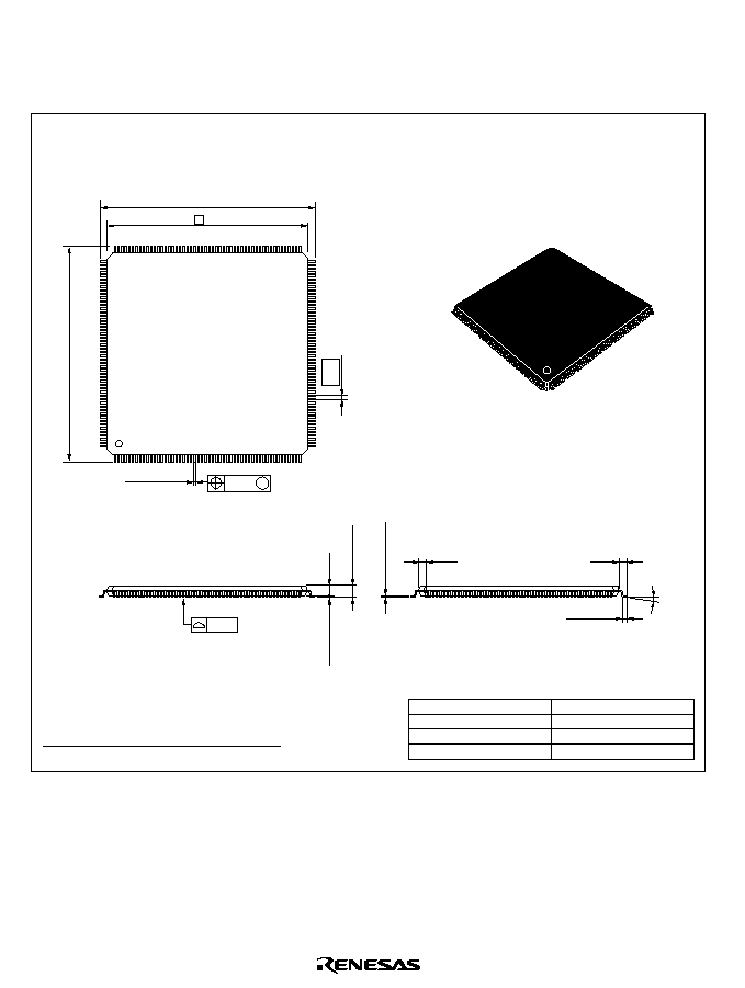
902
Appendix D Package Dimensions
Figure D.1 shows the FP-208C package dimensions.
Hitachi Code
JEDEC
EIAJ
Weight (reference value)
FP-208C
--
Conforms
2.7 g
Unit: mm
*Dimension including the plating thickness
Base material dimension
30.0
±
0.2
30.0
±
0.2
0.5
1.70 Max
0
∞
≠ 8
∞
*0.17
±
0.05
156
105
104
52
1
157
208
53
*0.22
±
0.05
0.08 M
0.08
1.40
0.5
±
0.1
1.0
28
0.10
±
0.05
1.25
0.20
±
0.04
0.15
±
0.04
Figure D.1 Package Dimensions (FP-208C)

SH7616 Hardware Manual
Publication Date: 1st Edition, November 2001
Published by:
Business Planning Division
Semiconductor & Integrated Circuits
Hitachi, Ltd.
Edited by:
Technical Documentation Group
Hitachi Kodaira Semiconductor Co., Ltd.
Copyright © Hitachi, Ltd., 2001. All rights reserved. Printed in Japan.