 | –≠–ª–µ–∫—Ç—Ä–æ–Ω–Ω—ã–π –∫–æ–º–ø–æ–Ω–µ–Ω—Ç: HD6417705 | –°–∫–∞—á–∞—Ç—å:  PDF PDF  ZIP ZIP |
Document Outline
- Cover
- Cautions
- General Precautions on Handling of Product
- Configuration of This Manual
- Preface
- Main Revisions and Additions in this Edition
- Contents
- Section 1 Overview
- 1.1 SH7705 Features
- 1.2 Block Diagram
- 1.3 Pin Assignment
- 1.4 Pin Functions
- Section 2 CPU
- 2.1 Processing States and Processing Modes
- 2.1.1 Processing States
- 2.1.2 Processing Modes
- 2.2 Memory Map
- 2.2.1 Logical Address Space
- 2.2.2 External Memory Space
- 2.3 Register Descriptions
- 2.3.1 General Registers
- 2.3.2 System Registers
- 2.3.3 Program Counter
- 2.3.4 Control Registers
- 2.4 Data Formats
- 2.4.1 Register Data Format
- 2.4.2 Memory Data Formats
- 2.5 Features of CPU Core Instructions
- 2.5.1 Instruction Execution Method
- 2.5.2 CPU Instruction Addressing Modes
- 2.5.3 CPU Instruction Formats
- 2.6 Instruction Set
- 2.6.1 CPU Instruction Set Based on Functions
- 2.6.2 Operation Code Map
- Section 3 Memory Management Unit (MMU)
- 3.1 Role of MMU
- 3.2 Register Descriptions
- 3.2.1 Page Table Entry Register High (PTEH)
- 3.2.2 Page Table Entry Register Low (PTEL)
- 3.2.3 Translation Table Base Register (TTB)
- 3.2.4 MMU Control Register (MMUCR)
- 3.3 TLB Functions
- 3.3.1 Configuration of the TLB
- 3.3.2 TLB Indexing
- 3.3.3 TLB Address Comparison
- 3.3.4 Page Management Information
- 3.4 MMU Functions
- 3.4.1 MMU Hardware Management
- 3.4.2 MMU Software Management
- 3.4.3 MMU Instruction (LDTLB)
- 3.4.4 Avoiding Synonym Problems
- 3.5 MMU Exceptions
- 3.5.1 TLB Miss Exception
- 3.5.2 TLB Protection Violation Exception
- 3.5.3 TLB Invalid Exception
- 3.5.4 Initial Page Write Exception
- 3.6 Memory-Mapped TLB
- 3.6.1 Address Array
- 3.6.2 Data Array
- 3.6.3 Usage Examples
- 3.7 Usage Note
- Section 4 Cache
- 4.1 Features
- 4.2 Register Descriptions
- 4.2.1 Cache Control Register 1 (CCR1)
- 4.2.2 Cache Control Register 2 (CCR2)
- 4.2.3 Cache Control Register 3 (CCR3)
- 4.3 Operation
- 4.3.1 Searching the Cache
- 4.3.2 Read Access
- 4.3.3 Prefetch Operation
- 4.3.4 Write Access
- 4.3.5 Write-Back Buffer
- 4.3.6 Coherency of Cache and External Memory
- 4.4 Memory-Mapped Cache
- 4.4.1 Address Array
- 4.4.2 Data Array
- 4.4.3 Usage Examples
- 4.5 Usage Note
- Section 5 Exception Handling
- 5.1 Register Descriptions
- 5.1.1 TRAPA Exception Register (TRA)
- 5.1.2 Exception Event Register (EXPEVT)
- 5.1.3 Interrupt Event Register (INTEVT)
- 5.1.4 Interrupt Event Register 2 (INTEVT2)
- 5.1.5 Exception Address Register (TEA)
- 5.2 Exception Handling Function
- 5.2.1 Exception Handling Flow
- 5.2.2 Exception Vector Addresses
- 5.2.3 Exception Codes
- 5.2.4 Exception Request and BL Bit (Multiple Exception Prevention)
- 5.2.5 Exception Source Acceptance Timing and Priority
- 5.3 Individual Exception Operations
- 5.3.1 Resets
- 5.3.2 General Exceptions
- 5.3.3 General Exceptions (MMU Exceptions)
- 5.4 Usage Notes
- Section 6 Interrupt Controller (INTC)
- 6.1 Features
- 6.2 Input/Output Pins
- 6.3 Register Descriptions
- 6.3.1 Interrupt Priority Level Setting Registers A to H (IPRA to IPRH)
- 6.3.2 Interrupt Control Register 0 (ICR0)
- 6.3.3 Interrupt Control Register 1 (ICR1)
- 6.3.4 Interrupt Control Register 2 (ICR2)
- 6.3.5 PINT Interrupt Enable Register (PINTER)
- 6.3.6 Interrupt Request Register 0 (IRR0)
- 6.3.7 Interrupt Request Register 1 (IRR1)
- 6.3.8 Interrupt Request Register 2 (IRR2)
- 6.4 Interrupt Sources
- 6.4.1 NMI Interrupt
- 6.4.2 IRQ Interrupts
- 6.4.3 IRL Interrupts
- 6.4.4 PINT Interrupt
- 6.4.5 On-Chip Peripheral Module Interrupts
- 6.4.6 Interrupt Exception Handling and Priority
- 6.5 Operation
- 6.5.1 Interrupt Sequence
- 6.5.2 Multiple Interrupts
- 6.6 Usage Note
- Section 7 Bus State Controller (BSC)
- 7.1 Overview
- 7.1.1 Features
- 7.1.2 Block Diagram
- 7.2 Pin Configuration
- 7.3 Area Overview
- 7.3.1 Address Map
- 7.3.2 Memory Bus Width
- 7.3.3 Shadow Space
- 7.4 Register Descriptions
- 7.4.1 Common Control Register (CMNCR)
- 7.4.2 CSn Space Bus Control Register (CSnBCR) (n = 0, 2, 3, 4, 5A, 5B, 6A, 6B)
- 7.4.3 CSn Space Wait Control Register (CSnWCR) (n = 0, 2, 3, 4, 5A, 5B, 6A, 6B)
- 7.4.4 SDRAM Control Register (SDCR)
- 7.4.5 Refresh Timer Control/Status Register (RTCSR)
- 7.4.6 Refresh Timer Counter (RTCNT)
- 7.4.7 Refresh Time Constant Register (RTCOR)
- 7.4.8 Reset Wait Counter (RWTCNT)
- 7.5 Endian/Access Size and Data Alignment
- 7.6 Normal Space Interface
- 7.6.1 Basic Timing
- 7.6.2 Access Wait Control
- 7.6.3 CSn Assert Period Expansion
- 7.7 Address/Data Multiplex I/O Interface
- 7.8 SDRAM Interface
- 7.8.1 SDRAM Direct Connection
- 7.8.2 Address Multiplexing
- 7.8.3 Burst Read
- 7.8.4 Single Read
- 7.8.5 Burst Write
- 7.8.6 Single Write
- 7.8.7 Bank Active
- 7.8.8 Refreshing
- 7.8.9 Low-Frequency Mode
- 7.8.10 Power-On Sequence
- 7.9 Burst ROM Interface
- 7.10 Byte-Selection SRAM Interface
- 7.11 Wait between Access Cycles
- 7.12 Bus Arbitration
- 7.13 Others
- Section 8 Direct Memory Access Controller (DMAC)
- 8.1 Features
- 8.2 Input/Output Pins
- 8.3 Register Descriptions
- 8.3.1 DMA Source Address Registers (SAR)
- 8.3.2 DMA Destination Address Registers (DAR)
- 8.3.3 DMA Transfer Count Registers (DMATCR)
- 8.3.4 DMA Channel Control Registers (CHCR)
- 8.3.5 DMA Operation Register (DMAOR)
- 8.3.6 DMA Extended Resource Selectors 0, 1 (DMARS0, DMARS1)
- 8.4 Operation
- 8.4.1 Transfer Flow
- 8.4.2 DMA Transfer Requests
- 8.4.3 Channel Priority
- 8.4.4 DMA Transfer Types
- 8.4.5 Number of Bus Cycle States and DREQ Pin Sampling Timing
- 8.5 Precautions
- 8.5.1 Precautions when Mixing Cycle-Steal Mode Channels and Burst Mode Channels
- Section 9 Clock Pulse Generator (CPG)
- 9.1 Features
- 9.2 Input/Output Pins
- 9.3 Clock Operating Modes
- 9.4 Register Descriptions
- 9.4.1 Frequency Control Register (FRQCR)
- 9.4.2 USB Clock Frequency Control Register (UCLKCR)
- 9.4.3 Usage Notes
- 9.5 Changing Frequency
- 9.5.1 Changing Multiplication Rate
- 9.5.2 Changing Division Ratio
- 9.5.3 Modification of Clock Operating Mode
- 9.6 Usage Notes
- Section 10 Watchdog Timer (WDT)
- 10.1 Features
- 10.2 Register Descriptions
- 10.2.1 Watchdog Timer Counter (WTCNT)
- 10.2.2 Watchdog Timer Control/Status Register (WTCSR)
- 10.2.3 Notes on Register Access
- 10.3 Operation
- 10.3.1 Canceling Software Standbys
- 10.3.2 Changing Frequency
- 10.3.3 Using Watchdog Timer Mode
- 10.3.4 Using Interval Timer Mode
- Section 11 Power-Down Modes
- 11.1 Features
- 11.2 Input/Output Pins
- 11.3 Register Descriptions
- 11.3.1 Standby Control Register (STBCR)
- 11.3.2 Standby Control Register 2 (STBCR2)
- 11.3.3 Standby Control Register 3 (STBCR3)
- 11.4 Sleep Mode
- 11.4.1 Transition to Sleep Mode
- 11.4.2 Canceling Sleep Mode
- 11.5 Software Standby Mode
- 11.5.1 Transition to Software Standby Mode
- 11.5.2 Canceling Software Standby Mode
- 11.6 Module Standby Function
- 11.6.1 Transition to Module Standby Function
- 11.6.2 Canceling Module Standby Function
- 11.7 Hardware Standby Mode
- 11.7.1 Transition to Hardware Standby Mode
- 11.7.2 Canceling Hardware Standby Mode
- 11.8 Timing of STATUS Pin Changes
- Section 12 Timer Unit (TMU)
- 12.1 Features
- 12.2 Input/Output Pin
- 12.3 Register Descriptions
- 12.3.1 Timer Start Register (TSTR)
- 12.3.2 Timer Control Registers (TCR)
- 12.3.3 Timer Constant Registers (TCOR)
- 12.3.4 Timer Counters (TCNT)
- 12.3.5 Input Capture Register_2 (TCPR_2)
- 12.4 Operation
- 12.4.1 Counter Operation
- 12.4.2 Input Capture Function
- 12.5 Interrupts
- 12.5.1 Status Flag Set Timing
- 12.5.2 Status Flag Clear Timing
- 12.5.3 Interrupt Sources and Priorities
- 12.6 Usage Notes
- 12.6.1 Writing to Registers
- 12.6.2 Reading Registers
- Section 13 Compare Match Timer (CMT)
- 13.1 Features
- 13.2 Register Descriptions
- 13.2.1 Compare Match Timer Start Register (CMSTR)
- 13.2.2 Compare Match Timer Control/Status Register (CMCSR)
- 13.2.3 Compare Match Counter (CMCNT)
- 13.2.4 Compare Match Constant Register (CMCOR)
- 13.3 Operation
- 13.3.1 Period Count Operation
- 13.3.2 CMCNT Count Timing
- 13.3.3 Compare Match Flag Set Timing
- Section 14 16-Bit Timer Pulse Unit (TPU)
- 14.1 Features
- 14.2 Input/Output Pins
- 14.3 Register Descriptions
- 14.3.1 Timer Control Registers (TCR)
- 14.3.2 Timer Mode Registers (TMDR)
- 14.3.3 Timer I/O Control Registers (TIOR)
- 14.3.4 Timer Interrupt Enable Registers (TIER)
- 14.3.5 Timer Status Registers (TSR)
- 14.3.6 Timer Counters (TCNT)
- 14.3.7 Timer General Registers (TGR)
- 14.3.8 Timer Start Register (TSTR)
- 14.4 Operation
- 14.4.1 Overview
- 14.4.2 Basic Functions
- 14.4.3 Buffer Operation
- 14.4.4 PWM Modes
- Section 15 Realtime Clock (RTC)
- 15.1 Features
- 15.2 Input/Output Pins
- 15.3 Register Descriptions
- 15.3.1 64-Hz Counter (R64CNT)
- 15.3.2 Second Counter (RSECCNT)
- 15.3.3 Minute Counter (RMINCNT)
- 15.3.4 Hour Counter (RHRCNT)
- 15.3.5 Day of Week Counter (RWKCNT)
- 15.3.6 Date Counter (RDAYCNT)
- 15.3.7 Month Counter (RMONCNT)
- 15.3.8 Year Counter (RYRCNT)
- 15.3.9 Second Alarm Register (RSECAR)
- 15.3.10 Minute Alarm Register (RMINAR)
- 15.3.11 Hour Alarm Register (RHRAR)
- 15.3.12 Day of Week Alarm Register (RWKAR)
- 15.3.13 Date Alarm Register (RDAYAR)
- 15.3.14 Month Alarm Register (RMONAR)
- 15.3.15 Year Alarm Register (RYRAR)
- 15.3.16 RTC Control Register 1 (RCR1)
- 15.3.17 RTC Control Register 2 (RCR2)
- 15.3.18 RTC Control Register 3 (RCR3)
- 15.4 Operation
- 15.4.1 Initial Settings of Registers after Power-On
- 15.4.2 Setting Time
- 15.4.3 Reading the Time
- 15.4.4 Alarm Function
- 15.4.5 Crystal Oscillator Circuit
- 15.5 Notes for Usage
- 15.5.1 Register Writing during RTC Count
- 15.5.2 Use of Realtime Clock (RTC) Periodic Interrupts
- 15.5.3 Standby Mode after Register Setting
- Section 16 Serial Communication Interface with FIFO (SCIF)
- 16.1 Features
- 16.2 Input/Output Pins
- 16.3 Register Descriptions
- 16.3.1 Receive Shift Register (SCRSR)
- 16.3.2 Receive FIFO Data Register (SCFRDR)
- 16.3.3 Transmit Shift Register (SCTSR)
- 16.3.4 Transmit FIFO Data Register (SCFTDR)
- 16.3.5 Serial Mode Register (SCSMR)
- 16.3.6 Serial Control Register (SCSCR)
- 16.3.7 FIFO Error Count Register (SCFER)
- 16.3.8 Serial Status Register (SCSSR)
- 16.3.9 Bit Rate Register (SCBRR)
- 16.3.10 FIFO Control Register (SCFCR)
- 16.3.11 FIFO Data Count Register (SCFDR)
- 16.3.12 Transmit Data Stop Register (SCTDSR)
- 16.4 Operation
- 16.4.1 Overview
- 16.4.2 Asynchronous Mode
- 16.4.3 Serial Operation in Asynchronous Mode
- 16.4.4 Clock Synchronous Mode
- 16.4.5 Serial Operation in Clock Synchronous Mode
- 16.5 SCIF Interrupt Sources and DMAC
- 16.6 Notes on Usage
- Section 17 Infrared Data Association Module (IrDA)
- 17.1 Features
- 17.2 Input/Output Pins
- 17.3 Register Description
- 17.3.1 IrDA Mode Register (SCSMR_Ir)
- 17.4 Operation
- 17.4.1 Overview
- 17.4.2 Transmitting
- 17.4.3 Receiving
- 17.4.4 Data Format Specification
- Section 18 USB Function Module
- 18.1 Features
- 18.2 Input/Output Pins
- 18.3 Register Descriptions
- 18.3.1 Interrupt Flag Register 0 (IFR0)
- 18.3.2 Interrupt Flag Register 1 (IFR1)
- 18.3.3 Interrupt Select Register 0 (ISR0)
- 18.3.4 Interrupt Select Register 1 (ISR1)
- 18.3.5 Interrupt Enable Register 0 (IER0)
- 18.3.6 Interrupt Enable Register 1 (IER1)
- 18.3.7 EP0i Data Register (EPDR0i)
- 18.3.8 EP0o Data Register (EPDR0o)
- 18.3.9 EP0s Data Register (EPDR0s)
- 18.3.10 EP1 Data Register (EPDR1)
- 18.3.11 EP2 Data Register (EPDR2)
- 18.3.12 EP3 Data Register (EPDR3)
- 18.3.13 EP0o Receive Data Size Register (EPSZ0o)
- 18.3.14 EP1 Receive Data Size Register (EPSZ1)
- 18.3.15 Trigger Register (TRG)
- 18.3.16 Data Status Register (DASTS)
- 18.3.17 FIFO Clear Register (FCLR)
- 18.3.18 DMA Transfer Setting Register (DMAR)
- 18.3.19 Endpoint Stall Register (EPSTL)
- 18.3.20 Transceiver Control Register (XVERCR)
- 18.4 Operation
- 18.4.1 Cable Connection
- 18.4.2 Cable Disconnection
- 18.4.3 Control Transfer
- 18.4.4 EP1 Bulk-Out Transfer (Dual FIFOs)
- 18.4.5 EP2 Bulk-In Transfer (Dual FIFOs)
- 18.4.6 EP3 Interrupt-In Transfer
- 18.5 Processing of USB Standard Commands and Class/Vendor Commands
- 18.5.1 Processing of Commands Transmitted by Control Transfer
- 18.6 Stall Operations
- 18.6.1 Overview
- 18.6.2 Forcible Stall by Application
- 18.6.3 Automatic Stall by USB Function Module
- 18.7 DMA Transfer
- 18.7.1 Overview
- 18.7.2 DMA Transfer for Endpoint 1
- 18.7.3 DMA Transfer for Endpoint 2
- 18.8 Example of USB External Circuitry
- 18.9 Usage Notes
- 18.9.1 Receiving Setup Data
- 18.9.2 Clearing the FIFO
- 18.9.3 Overreading and Overwriting the Data Registers
- 18.9.4 Assigning Interrupt Sources to EP0
- 18.9.5 Clearing the FIFO when DMA Transfer Is Enabled
- 18.9.6 Notes on TR Interrupt
- Section 19 Pin Function Controller
- 19.1 Overview
- 19.2 Register Descriptions
- 19.2.1 Port A Control Register (PACR)
- 19.2.2 Port B Control Register (PBCR)
- 19.2.3 Port C Control Register (PCCR)
- 19.2.4 Port D Control Register (PDCR)
- 19.2.5 Port E Control Register (PECR)
- 19.2.6 Port E Control Register 2 (PECR2)
- 19.2.7 Port F Control Register (PFCR)
- 19.2.8 Port F Control Register 2 (PFCR2)
- 19.2.9 Port G Control Register (PGCR)
- 19.2.10 Port H Control Register (PHCR)
- 19.2.11 Port J Control Register (PJCR)
- 19.2.12 Port K Control Register (PKCR)
- 19.2.13 Port L Control Register (PLCR)
- 19.2.14 Port M Control Register (PMCR)
- 19.2.15 Port N Control Register (PNCR)
- 19.2.16 Port N Control Register 2 (PNCR2)
- 19.2.17 Port SC Control Register (SCPCR)
- Section 20 I/O Ports
- 20.1 Port A
- 20.1.1 Register Description
- 20.1.2 Port A Data Register (PADR)
- 20.2 Port B
- 20.2.1 Register Description
- 20.2.2 Port B Data Register (PBDR)
- 20.3 Port C
- 20.3.1 Register Description
- 20.3.2 Port C Data Register (PCDR)
- 20.4 Port D
- 20.4.1 Register Description
- 20.4.2 Port D Data Register (PDDR)
- 20.5 Port E
- 20.5.1 Register Description
- 20.5.2 Port E Data Register (PEDR)
- 20.6 Port F
- 20.6.1 Register Description
- 20.6.2 Port F Data Register (PFDR)
- 20.7 Port G
- 20.7.1 Register Description
- 20.7.2 Port G Data Register (PGDR)
- 20.8 Port H
- 20.8.1 Register Description
- 20.8.2 Port H Data Register (PHDR)
- 20.9 Port J
- 20.9.1 Register Description
- 20.9.2 Port J Data Register (PJDR)
- 20.10 Port K
- 20.10.1 Register Description
- 20.10.2 Port K Data Register (PKDR)
- 20.11 Port L
- 20.11.1 Register Description
- 20.11.2 Port L Data Register (PLDR)
- 20.12 Port M
- 20.12.1 Register Description
- 20.12.2 Port M Data Register (PMDR)
- 20.13 Port N
- 20.13.1 Register Description
- 20.13.2 Port N Data Register (PNDR)
- 20.14 SC Port
- 20.14.1 Register Description
- 20.14.2 Port SC Data Register (SCPDR)
- Section 21 A/D Converter
- 21.1 Features
- 21.2 Input/Output Pins
- 21.3 Register Descriptions
- 21.3.1 A/D Data Registers A to D (ADDRA to ADDRD)
- 21.3.2 A/D Control/Status Registers (ADCSR)
- 21.4 Operation
- 21.4.1 Single Mode
- 21.4.2 Multi Mode
- 21.4.3 Scan Mode
- 21.4.4 Input Sampling and A/D Conversion Time
- 21.5 Interrupts and DMAC Transfer Request
- 21.6 Definitions of A/D Conversion Accuracy
- 21.7 Usage Notes
- 21.7.1 Allowable Signal-Source Impedance
- 21.7.2 Influence to Absolute Accuracy
- 21.7.3 Setting Analog Input Voltage
- 21.7.4 Notes on Board Design
- 21.7.5 Notes on Countermeasures to Noise
- Section 22 User Break Controller
- 22.1 Features
- 22.2 Register Descriptions
- 22.2.1 Break Address Register A (BARA)
- 22.2.2 Break Address Mask Register A (BAMRA)
- 22.2.3 Break Bus Cycle Register A (BBRA)
- 22.2.4 Break Address Register B (BARB)
- 22.2.5 Break Address Mask Register B (BAMRB)
- 22.2.6 Break Data Register B (BDRB)
- 22.2.7 Break Data Mask Register B (BDMRB)
- 22.2.8 Break Bus Cycle Register B (BBRB)
- 22.2.9 Break Control Register (BRCR)
- 22.2.10 Execution Times Break Register (BETR)
- 22.2.11 Branch Source Register (BRSR)
- 22.2.12 Branch Destination Register (BRDR)
- 22.2.13 Break ASID Register A (BASRA)
- 22.2.14 Break ASID Register B (BASRB)
- 22.3 Operation
- 22.3.1 Flow of the User Break Operation
- 22.3.2 Break on Instruction Fetch Cycle
- 22.3.3 Break on Data Access Cycle
- 22.3.4 Sequential Break
- 22.3.5 Value of Saved Program Counter
- 22.3.6 PC Trace
- 22.3.7 Usage Examples
- 22.3.8 Notes
- Section 23 User Debugging Interface (UDI)
- 23.1 Features
- 23.2 Input/Output Pins
- 23.3 Register Descriptions
- 23.3.1 Bypass Register (SDBPR)
- 23.3.2 Instruction Register (SDIR)
- 23.3.3 Boundary Scan Register (SDBSR)
- 23.3.4 ID Register (SDID)
- 23.4 Operation
- 23.4.1 TAP Controller
- 23.4.2 Reset Configuration
- 23.4.3 TDO Output Timing
- 23.4.4 UDI Reset
- 23.4.5 UDI Interrupt
- 23.5 Boundary Scan
- 23.5.1 Supported Instructions
- 23.5.2 Points for Attention
- 23.6 Usage Notes
- 23.7 Advanced User Debugger (AUD)
- Section 24 List of Registers
- 24.1 Register Addresses (by functional module, in order of the corresponding section numbers)
- 24.2 Register Bits
- 24.3 Register States in Each Operating Mode
- Section 25 Electrical Characteristics
- 25.1 Absolute Maximum Ratings
- 25.2 DC Characteristics
- 25.3 AC Characteristics
- 25.3.1 Clock Timing
- 25.3.2 Control Signal Timing
- 25.3.3 AC Bus Timing
- 25.3.4 Basic Timing
- 25.3.5 Burst ROM Timing
- 25.3.6 Synchronous DRAM Timing
- 25.3.7 DMAC Signal Timing
- 25.3.8 TMU Signal Timing
- 25.3.9 RTC Signal Timing
- 25.3.10 16-Bit Timer Pulse Unit (TPU) Signal Timing
- 25.3.11 SCIF Module Signal Timing
- 25.3.12 USB Module Signal Timing
- 25.3.13 USB Transceiver Timing
- 25.3.14 Port Input/Output Timing
- 25.3.15 UDI Related Pin Timing
- 25.3.16 AC Characteristics Measurement Conditions
- 25.4 A/D Converter Characteristics
- Appendix
- A. I/O Port States in Each Processing State
- B. Package Dimensions
- Index
- Colophon
- Address List
- Back Cover

2003.9.19
32
SH7705
Group
Hardware Manual
Renesas 32-Bit RISC Microcomputer
SuperH
TM
RISC engine Family/SH7700 Series
Rev.2.00
The revision list can be viewed directly by
clicking the title page.
The revision list summarizes the locations of
revisions and additions. Details should always
be checked by referring to the relevant text.

Renesas 32-Bit RISC Microcomputer
SuperH
RISC engine Family/SH7700 Series
SH7705 Group
Hardware Manual
REJ09B0082-0200O

Rev. 2.00, 09/03, page iv of xlvi
Cautions
Keep safety first in your circuit designs!
1. Renesas Technology Corp. puts the maximum effort into making semiconductor products
better and more reliable, but there is always the possibility that trouble may occur with them.
Trouble with semiconductors may lead to personal injury, fire or property damage.
Remember to give due consideration to safety when making your circuit designs, with
appropriate measures such as (i) placement of substitutive, auxiliary circuits, (ii) use of
nonflammable material or (iii) prevention against any malfunction or mishap.
Notes regarding these materials
1. These materials are intended as a reference to assist our customers in the selection of the
Renesas Technology Corp. product best suited to the customer's application; they do not
convey any license under any intellectual property rights, or any other rights, belonging to
Renesas Technology Corp. or a third party.
2. Renesas Technology Corp. assumes no responsibility for any damage, or infringement of any
third-party's rights, originating in the use of any product data, diagrams, charts, programs,
algorithms, or circuit application examples contained in these materials.
3. All information contained in these materials, including product data, diagrams, charts,
programs and algorithms represents information on products at the time of publication of these
materials, and are subject to change by Renesas Technology Corp. without notice due to
product improvements or other reasons. It is therefore recommended that customers contact
Renesas Technology Corp. or an authorized Renesas Technology Corp. product distributor for
the latest product information before purchasing a product listed herein.
The information described here may contain technical inaccuracies or typographical errors.
Renesas Technology Corp. assumes no responsibility for any damage, liability, or other loss
rising from these inaccuracies or errors.
Please also pay attention to information published by Renesas Technology Corp. by various
means, including the Renesas Technology Corp. Semiconductor home page
(http://www.renesas.com).
4. When using any or all of the information contained in these materials, including product data,
diagrams, charts, programs, and algorithms, please be sure to evaluate all information as a total
system before making a final decision on the applicability of the information and products.
Renesas Technology Corp. assumes no responsibility for any damage, liability or other loss
resulting from the information contained herein.
5. Renesas Technology Corp. semiconductors are not designed or manufactured for use in a
device or system that is used under circumstances in which human life is potentially at stake.
Please contact Renesas Technology Corp. or an authorized Renesas Technology Corp. product
distributor when considering the use of a product contained herein for any specific purposes,
such as apparatus or systems for transportation, vehicular, medical, aerospace, nuclear, or
undersea repeater use.
6. The prior written approval of Renesas Technology Corp. is necessary to reprint or reproduce in
whole or in part these materials.
7. If these products or technologies are subject to the Japanese export control restrictions, they
must be exported under a license from the Japanese government and cannot be imported into a
country other than the approved destination.
Any diversion or reexport contrary to the export control laws and regulations of Japan and/or
the country of destination is prohibited.
8. Please contact Renesas Technology Corp. for further details on these materials or the products
contained therein.

Rev. 2.00, 09/03, page v of xlvi
General Precautions on Handling of Product
1. Treatment of NC Pins
Note:
Do not connect anything to the NC pins.
The NC (not connected) pins are either not connected to any of the internal circuitry or are
used as test pins or to reduce noise. If something is connected to the NC pins, the
operation of the LSI is not guaranteed.
2. Treatment of Unused Input Pins
Note:
Fix all unused input pins to high or low level.
Generally, the input pins of CMOS products are high-impedance input pins. If unused pins
are in their open states, intermediate levels are induced by noise in the vicinity, a pass-
through current flows internally, and a malfunction may occur.
3. Processing before Initialization
Note:
When power is first supplied, the product's state is undefined.
The states of internal circuits are undefined until full power is supplied throughout the
chip and a low level is input on the reset pin. During the period where the states are
undefined, the register settings and the output state of each pin are also undefined. Design
your system so that it does not malfunction because of processing while it is in this
undefined state. For those products which have a reset function, reset the LSI immediately
after the power supply has been turned on.
4. Prohibition of Access to Undefined or Reserved Addresses
Note:
Access to undefined or reserved addresses is prohibited.
The undefined or reserved addresses may be used to expand functions, or test registers
may have been be allocated to these addresses. Do not access these registers; the system's
operation is not guaranteed if they are accessed.

Rev. 2.00, 09/03, page vi of xlvi
Configuration of This Manual
This manual comprises the following items:
1. General Precautions on Handling of Product
2. Configuration of This Manual
3. Preface
4. Contents
5. Overview
6. Description of Functional Modules
∑
CPU and System-Control Modules
∑
On-Chip Peripheral Modules
The configuration of the functional description of each module differs according to the
module. However, the generic style includes the following items:
i) Feature
ii) Input/Output Pin
iii) Register Description
iv) Operation
v) Usage Note
When designing an application system that includes this LSI, take notes into account. Each
section includes notes in relation to the descriptions given, and usage notes are given, as required,
as the final part of each section.
7. List of Registers
8. Electrical Characteristics
9. Appendix
10. Index

Rev. 2.00, 09/03, page vii of xlvi
Preface
The SH7705 single-chip RISC (Reduced Instruction Set Computer) microprocessor includes a
Renesas Technology original RISC CPU as its core, and the peripheral functions required to
configure a system.
Target users: This manual was written for users who will be using the SH7705 Micro-Computer
Unit (MCU) in the design of application systems. Users of this manual are expected
to understand the fundamentals of electrical circuits, logical circuits, and
microcomputers.
Objective:
This manual was written to explain the hardware functions and electrical
characteristics of the SH7705 MCU to the above users.
Refer to the SH-3/SH-3E/SH3-DSP Programming Manual for a detailed description
of the instruction set.
Notes on reading this manual:
∑
Product names
The following products are covered in this manual.
Product Classifications and Abbreviations
Basic Classification
Product Code
SH7705
HD6417705
∑
In order to understand the overall functions of the chip
Read the manual according to the contents. This manual can be roughly categorized into parts
on the CPU, system control functions, peripheral functions and electrical characteristics.
∑
In order to understand the details of the CPU's functions
Read the SH-3/SH-3E/SH3-DSP Programming Manual.

Rev. 2.00, 09/03, page viii of xlvi
Rules:
Register name:
The following notation is used for cases when the same or a
similar function, e.g. serial communication, is implemented
on more than one channel:
XXX_N (XXX is the register name and N is the channel
number)
Bit order:
The MSB (most significant bit) is on the left and the LSB
(least significant bit) is on the right.
Number notation: Binary is B'xxxx, hexadecimal is H'xxxx, decimal is xxxx
Signal notation:
An overbar is added to a low-active signal:
xxxx
Related Manuals:
The latest versions of all related manuals are available from our web site.
Please ensure you have the latest versions of all documents you require.
http://www.renesas.com/eng/
SH7705 manuals:
Manual Title
ADE No.
SH7705 Hardware Manual
This manual
SH-3/SH-3E/SH3-DSP Programming Manual
ADE-602-096
Users manuals for development tools:
Manual Title
ADE No.
SH Series C/C++ Compiler, Assembler, Optimizing Linkage Editor User's
Manual
ADE-702-246
SH Series Simulator/Debugger (for Windows) User's Manual
ADE-702-186
SH Series Simulator/Debugger (for UNIX) User's Manual
ADE-702-203
Embedded Workshop User's Manual
ADE-702-201
SH Series Embedded Workshop, Debugging Interface Tutorial
ADE-702-230

Rev. 2.00, 09/03, page ix of xlvi
Abbreviations
ADC
Analog to Digital Converter
ALU
Arithmetic Logic Unit
ASE
Adaptive System Evaluator
ASID
Address Space Identifier
AUD
Advanced User Debugger
BCD
Binary Coded Decimal
bps
bit per second
BSC
Bus State Controller
CCN
Cache Memory Controller
CMT
Compare Match Timer
CPG
Clock Pulse Generator
CPU
Central Processing Unit
DMAC
Direct Memory Access Controller
etu
Elementary Time Unit
FIFO
First-In First-Out
Hi-Z
High Impedance
UDI
User Debugging Interface
INTC
Interrupt Controller
IrDA
Infrared Data Association
JTAG
Joint Test Action Group
LQFP
Low Profile QFP
LRU
Least Recently Used
LSB
Least Significant Bit
MMU
Memory Management Unit
MPX
Multiplex
MSB
Most Significant Bit
PC
Program Counter
PFC
Pin Function Controller
PLL
Phase Locked Loop
PWM
Pulse Width Modulation
RAM
Random Access Memory
RISC
Reduced Instruction Set Computer
ROM
Read Only Memory
RTC
Realtime Clock
SCIF
Serial Communication Interface with FIFO

Rev. 2.00, 09/03, page x of xlvi
SDRAM Synchronous DRAM
TAP
Test Access Port
T.B.D
To Be Determined
TLB
Translation Lookaside Buffer
TMU
Timer Unit
TPU
Timer Pulse Unit
UART
Universal Asynchronous Receiver/Transmitter
UBC
User Break Controller
USB
Universal Serial Bus
WDT
Watchdog Timer
Rev. 2.00, 09/03, page xi of xlvi
Main Revisions and Additions in this Edition
Item
Page
Revisions (See Manual for Details)
1.1 SH7705 Features
Table 1.1 SH7705
Features
4
Features of USB function module (USB) amended
∑ Conforms to USB 2.0 full-speed specification
Note
*
6,
*
7 added
13, 15,
16
Pin No.
1.3 Pin Assignment
Table 1.2 Pin Functions
FP-
208C
TBP-
208A
Pin Name
I/O
Description
139
G15
TDI
*
7
/PTG0
I / I/O
Test data input (UDI) /
input/output port G
140
G14
TCK
*
7
/PTG1
I / I/O
Test clock (UDI) / input/output
port G
141
F17
TMS
*
7
/PTG2
I / I/O
Test mode select (UDI) /
input/output port G
142
F16
TRST*
1
*
7
/PTG3
I / I/O
Test reset (UDI) / input/output
port G
143
F15
TDO/PTF5
O / I/O
Test data output (UDI) /
input/output port F
144
F14
ASEBRKAK
/
PTF6
O / I/O
ASE break acknowledge
(UDI) / input/output port F
145
E17
ASEMD0*
2
*
7
/
PTF7
I / I/O
ASE mode (UDI) / input/output
port F
195
C6
RESETP*
6
I
Power-on reset request
Notes: 6. Pull-up MOS connected.
7. The pull-up MOS turns on if the pin function controller
(PFC) is used to select other functions (UDI).
4.4.1 Address Array
Address-Array Write
(Associative Operation)
105
Description amended
This operation is used to invalidate the address
specification for a cache.
4.4.3 Usage Examples
Invalidating a Specific Entry
107
Description largely revised
Invalidating an Address
Specification
108
Description added
5.2.5 Exception Source
Acceptance Timing and
Priority
Table 5.1 Exception Event
Vectors
117
Note
*
3 amended
Note: 3. If an interrupt is accepted, the exception event
register (EXPEVT) is not changed.
Rev. 2.00, 09/03, page xii of xlvi
Item
Page
Revisions (See Manual for Details)
6.1 Features
Figure 6.1 Block Diagram
of INTC
126
CMT deleted
DMAC
SCIF
ADC
USB
TMU
6
DMAC : Direct memory access controller
SCIF
: Serial communication interface (with FIFO)
ADC :
A/D
converter
USB
: USB interface
TMU
: Timer pulse unit
TPU
: 16-bit timer pulse unit
Input/output
control
(Interrupt request)
Legend:
IRQ5
-IRQ0
16
PINT15
-PINT0
NMI
6.4.6 Interrupt Exception
Handling and Priority
Table 6.4 Interrupt
Exception Handling Sources
and Priority (IRQ Mode)
140
IPR (bit numbers) amended for interrupt source TMU2
IPRA (7 to 4)
7.4.2 CSn Space Bus
Control Register (CSnBCR)
(n = 0, 2, 3, 4, 5A, 5B, 6A,
6B)
160
Bits 14 to 12 description added
Note: SDRAM can be specified only in area 2 and area 3. If
SDRAM is connected to only one area, SDRAM should be
specified for area 3. In this case area 2 should be specified
as normal space.
161
Note 5 added
Note: 5. The SDRAM bank active mode can only be used
for the CS3 space. (Refer to the explanation of the BACTV
bit in the SDRAM control register.)
177
Bits 31 to 18 description amended
7.4.5 Refresh Timer
Control/Status Register
(RTCSR)
Bit
Bit
Name
Initial
Value
R/W
Description
31 to 8
0
R
Reserved
179
Bits 31 to 18 description amended
Bit
Bit
Name
Initial
Value
R/W
Description
7.4.6 Refresh Timer
Counter (RTCNT)
31 to 8
0
R
Reserved

Rev. 2.00, 09/03, page xiii of xlvi
Item
Page
Revisions (See Manual for Details)
7.13 Others
Reset
237
In standby, sleep, and manual reset, control registers of the
bus state controller are not initialized. At manual reset, the
current bus cycle being executed is completed and then the
access wait state is entered.
Since the RTCNT continues
counting up during manual reset signal assertion, a refresh
request occurs to initiate the refresh cycle.
Note that arbitration requests using
BREQ
are not accepted
during manual reset signal assertion.
8.3.4 DMA Channel
Control Registers (CHCR)
244
Bits 15, 14 description amended
00: Fixed destination address
(setting prohibited in 16-byte transfer)
245
Bits 13, 12 description amended
00: Fixed source address
(setting prohibited in 16-byte transfer)
8.4.3 Channel Priority
Round-Robin Mode
258
The priority of round-robin mode is CH0 > CH1 > CH2 >
CH3 immediately after a reset.
When the round-robin mode is specified, cycle-steal mode
and burst mode should not be mixed among the bus modes
for multiple channels.
8.4.4 DMA Transfer Types
Address Modes
Figure 8.6 Example of
DMA Transfer Timing in
Dual Mode (Source:
Ordinary Memory,
Destination: Ordinary
Memory)
262
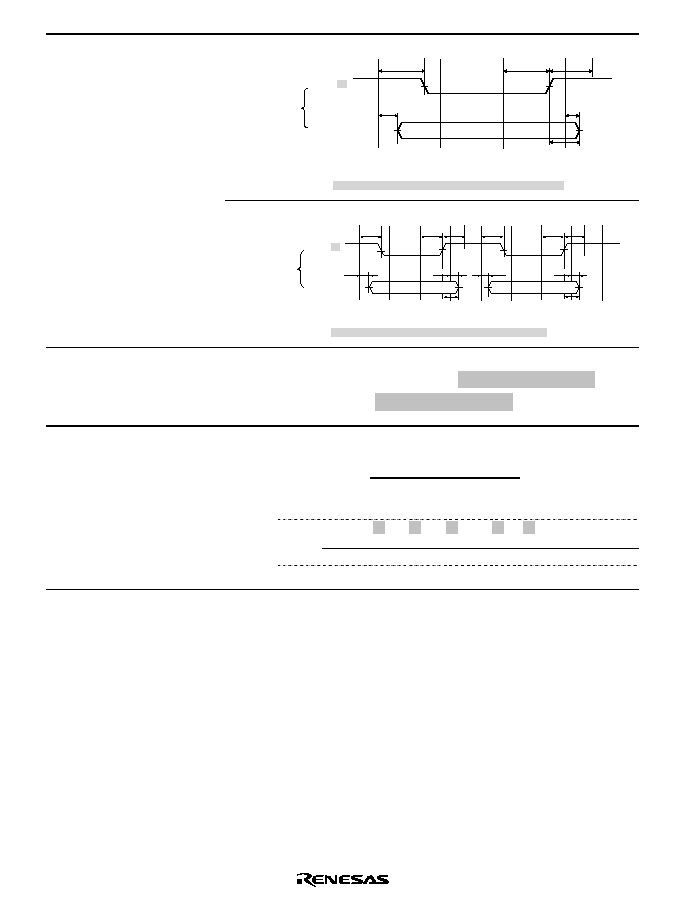
Figure amended
CKIO
A25 to A0
D31 to D0
WEn
RD
DACKn
(Active-Low)
CSn
Transfer source
address
Transfer destination
address
Data read cycle
Data
write
cycle
(1st cycle)
(2nd cycle)
Bus Mode and channel
Priority Order
266
Description largely revised
8.5 Precautions
270
Newly added
Rev. 2.00, 09/03, page xiv of xlvi
Item
Page
Revisions (See Manual for Details)
9.1 Features
Figure 9.1 Block Diagram
of Clock Pulse Generator
272
Figure amended
Peripheral bus
Bus interface
10.2.2 Watchdog Timer
Control/Status Register
(WTCSR)
289
Note added
Note: If manual reset is selected using the RSTS bit, a
frequency division ratio of 1/16, 1/32, 1/64, 1/256, 1/1,024,
or 1/4,096 is selected using bits CKS2 to CKS0, and a
watchdog timer counter overflow occurs, resulting in a
manual reset, the LSI will generate two manual resets in
succession. This will not affect its operation but will cause
change in the state of the STATUS pin.
11.6.1 Transition to
Module Standby Function
301
Description amended
This function can be used to reduce the power consumption
in the normal mode and sleep mode.
427
Table amended
Interrupt
Source
Description
DMAC Activation
16.5 SCIF Interrupt
Sources and DMAC
Table 16.4 SCIF Interrupt
Sources
ERI
Interrupt initiated by receive error flag
(ER) or break flag (BRK)
Not possible
RXI
Interrupt initiated by receive FIFO data
full flag (RDF) or receive data ready
(DR)
Possible
*
1
TXI
Interrupt initiated by transmit FIFO data
empty flag (TDFE) or transmit data stop
flag (TSF)
Possible
*
2
18.1 Features
437
Description amended
∑ The UDC (USB device controller) conforming to USB2.0
and transceiver process USB protocol automatically.
19.2.7 Port F Control
Register (PFCR)
489
Note
*
2 added to Bits 15 and 14
Note 2. Pull-up MOS on.
19.2.9 Port G Control
Register (PGCR)
491
Note
*
2 added to Bits 7 to 0
Note 2. Pull-up MOS on.

Rev. 2.00, 09/03, page xv of xlvi
Item
Page
Revisions (See Manual for Details)
22.2.10 Execution Times
Break Register (BETR)
552
Note added
Note: If the channel B brake condition set to during instruction fetch cycles and any of the
instructions below perform breaks, BETR is not decremented when the first break occurs.
The decremented values are listed below.
RTE
DMULS.L Rm,Rn
DMULU.L Rm,Rn
MAC.L @Rm+,@Rn+
MAC.W @Rm+,@Rn+
MUL.L Rm,Rn
AND.B #imm,@(R0,GBR)
OR.B #imm,@(R0,GBR)
TAS.B @Rn
TST.B #imm,@(R0,GBR)
XOR.B #imm,@(R0,GBR)
LDC Rm,SR
LDC Rm,GBR
LDC Rm,VBR
LDC Rm,SSR
LDC Rm,SPC
LDC Rm,R0_BANK
LDC Rm,R1_BANK
LDC Rm,R2_BANK
LDC Rm,R3_BANK
LDC Rm,R4_BANK
LDC Rm,R5_BANK
LDC Rm,R6_BANK
LDC Rm,R7_BANK
4
2
2
2
2
3
3
3
3
3
3
4
4
4
4
4
4
4
4
4
4
4
4
4
Instruction
Value
Decremented
LDC.L @Rm+,SR
LDC.L @Rm+,GBR
LDC.L @Rm+,VBR
LDC.L @Rm+,SSR
LDC.L @Rm+,SPC
LDC.L @Rm+,R0_BANK
LDC.L @Rm+,R1_BANK
LDC.L @Rm+,R2_BANK
LDC.L @Rm+,R3_BANK
LDC.L @Rm+,R4_BANK
LDC.L @Rm+,R5_BANK
LDC.L @Rm+,R6_BANK
LDC.L @Rm+,R7_BANK
LDC.L @Rn+,MOD
LDC.L @Rn+,RS
LDC.L @Rn+,RE
LDC Rn,MOD
LDC Rn,RS
LDC Rn,RE
BSR label
BSRF Rm
JSR @Rm
6
4
4
4
4
4
4
4
4
4
4
4
4
4
4
4
4
4
4
2
2
2
Instruction
Value
Decremented
23.2 Input/Output Pins
569
Note
*
added
Note:
*
The pull-up MOS turns on if the pin function
controller (PFC) is used to select other functions (UDI).
23.3.3 Boundary Scan
Register (SDBSR)
570
Description amended
SDBSR is a 385-bit shift register, located on the PAD, for
controlling the input/output pins of this LSI.
23.5.2 Points for Attention
582
Item 7 added under "23.5.2 Points for Attention"
7. The CKIO cock should operate during boundary scan.
The MD[2:0] pin should be set to the clock mode used
during normal operation, and EXTAL and CKIO should be
set within the frequency range specified in the Clock Pulse
Generator (CPG) section.
As during normal operation, the boundary scan test should
be performed after allowing sufficient settling time for the
crystal oscillator, PLL1, and PLL2.
24.1 Register Addresses
(by functional module, in
order of the corresponding
section numbers)
592
Access size of EP1 data register and EP2 data register
amended to 8/32
Rev. 2.00, 09/03, page xvi of xlvi
Item
Page
Revisions (See Manual for Details)
25.3.1 Clock Timing
Figure 25.5 Power-On
Oscillation Settling Time
633
Figure amended
V
CC
min
t
RESPW
t
RESPS
t
OSC1
V
CC
RESETP
TRST
CKIO,
internal clock
Stable oscillation
25.3.2 Control Signal
Timing
Table 25.6 Control Signal
Timing
636
Conditions amended
(Conditions: V
CC
Q = V
CC
-RTC = V
CC
-USB = 3.0 to 3.6 V,
V
CC
= V
CC
-PLL1 = V
CC
-PLL2 = 1.4 to 1.6 V, AV
CC
= 3.0 to
3.6 V, V
SS
Q = V
SS
= V
SS
-RTC = V
SS
-USB = V
SS
-PLL1 = V
SS
-
PLL2 = AV
SS
= 0 V, T
a
= ≠20 to 75∞C, Clock mode
0/1/2/4/5/6/7)
Note
*
1 amended
Note: 1.
RESETP
,
RESETM
, NMI, and IRQ5 to IRQ0 are
asynchronous.
Figure 25.15 Pin Drive
Timing at Standby
638
Figure amended
CKIO
t
STD
STATUS 0
STATUS 1
Normal mode
Normal mode
Standby mode
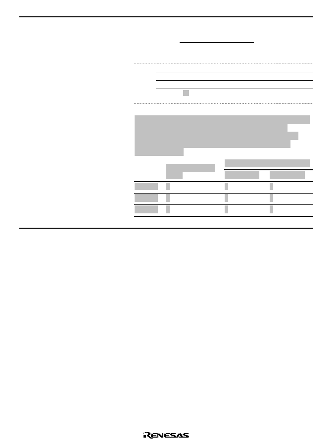
25.3.4 Basic Timing
Figure 25.16 Basic Bus
Cycle (No Wait)
640
Note
*
2 added
t
AH
t
WED
t
WED
t
WDH1
t
WDH4
t
WDD1
WEn*
2
D31 to D0
Write
Notes: 1. DACKn is a waveform when active-low is specified.
2. Output timing is the same when reading byte-selection SRAM.
Figure 25.17 Basic Bus
Cycle (One Software Wait)
641
Note
*
2 added
t
WED
t
WED
t
AH
t
WDH1
t
WDH4
t
WDD1
WEn*
2
D31 to D0
Notes: 1. DACKn is a waveform when active-low is specified.
2. Output timing is the same when reading byte-selection SRAM.
Write
Rev. 2.00, 09/03, page xvii of xlvi
Item
Page
Revisions (See Manual for Details)
25.3.4 Basic Timing
Figure 25.18 Basic Bus
Cycle (One External Wait)
642
Note
*
2 added
t
AH
t
WED
t
WED
t
WDH1
t
WDD1
WEn*
2
D31 to D0
Write
Notes: 1.
DACKn is a waveform when active-low is specified.
2. Output timing is the same when reading byte-selection SRAM.
Figure 25.19 Basic Bus
Cycle (One Software Wait,
External Wait Enabled
(WM Bit = 0), No Idle Cycle
Setting)
643
Note
*
2 added
t
WED
t
WED
t
WED
t
AH
t
WED
t
AH
t
WDD1
t
WDH1
t
WDH1
t
WDD1
D15 to D0
WEn*
2
Write
Notes:
1. DACKn is a waveform when active-low is specified.
2. Output timing is the same when reading byte-selection SRAM.
25.3.11 SCIF Module
Signal Timing
Table 25.13 SCIF Module
Signal Timing
671
Item amended
Transmission data delay time (clock synchronization)
RTS
delay time (clock synchronization)
679
Note
*
11 added
Reset
Power-Down
States
A. I/O Port States in Each
Processing State
Table A.1 I/O Port States
in Each Processing State
Category Pin
Power-
on
Reset
Manual
Reset
Software
Standby
Sleep
Bus
Mastership
Released
I/O
Handling
of Unused
Pins
System
control
RESETP
I
*
11
I
*
11
I
*
11
I
*
11
I
*
11
I
Must be
used
RESETM
I
I
I
I
I
I
Pull-up
Rev. 2.00, 09/03, page xviii of xlvi
Item
Page
Revisions (See Manual for Details)
Note
*
13 added
682,
684
Reset
Power-Down
States
A. I/O Port States in Each
Processing State
Table A.1 I/O Port States
in Each Processing State
Category Pin
Power-
on
Reset
Manual
Reset
Software
Standby
Sleep
Bus
Mastership
Released
I/O
Handling
of Unused
Pins
Port
NF/PTD[5] I
I
Z
I
I
I/I
Pull-up
PTE[7]
V
P
K
P
P
IO
Open
NF/PTJ[7] L
O
O
O
O
O/O Open
NF/PTJ
[6:0]
H
*
13
O
O
O
O
O/O Open
Note: 13. The values of PTJ6, PTJ1, and PTJ0 differ during
power-on reset and after the power-on reset state is
released. They conform to the port J data register value
after being switched to port status by the pin function
controller (PFC).
After Power-On Reset Release
During Power-On
Reset
PTD5/NF = 1
PTD5/NF = 0
PTJ6/NF
1
0
1
PTJ1/NF
1
1
0
PTJ0/NF
1
0
1

Rev. 2.00, 09/03, page xix of xlvi
Contents
Section 1 Overview ....................................................................................... 1
1.1
SH7705 Features.......................................................................................................... 1
1.2
Block Diagram............................................................................................................. 6
1.3
Pin Assignment............................................................................................................ 7
1.4
Pin Functions............................................................................................................... 17
Section 2 CPU ............................................................................................... 25
2.1
Processing States and Processing Modes....................................................................... 25
2.1.1
Processing States ............................................................................................. 25
2.1.2
Processing Modes............................................................................................ 26
2.2
Memory Map ............................................................................................................... 27
2.2.1
Logical Address Space..................................................................................... 27
2.2.2
External Memory Space................................................................................... 28
2.3
Register Descriptions ................................................................................................... 29
2.3.1
General Registers ............................................................................................ 32
2.3.2
System Registers ............................................................................................. 33
2.3.3
Program Counter ............................................................................................. 34
2.3.4
Control Registers............................................................................................. 35
2.4
Data Formats ............................................................................................................... 37
2.4.1
Register Data Format....................................................................................... 37
2.4.2
Memory Data Formats..................................................................................... 38
2.5
Features of CPU Core Instructions ............................................................................... 40
2.5.1
Instruction Execution Method .......................................................................... 40
2.5.2
CPU Instruction Addressing Modes ................................................................. 42
2.5.3
CPU Instruction Formats ................................................................................. 45
2.6
Instruction Set.............................................................................................................. 48
2.6.1
CPU Instruction Set Based on Functions .......................................................... 48
2.6.2
Operation Code Map ....................................................................................... 62
Section 3 Memory Management Unit (MMU) ............................................... 65
3.1
Role of MMU .............................................................................................................. 65
3.1.1
MMU of This LSI............................................................................................ 67
3.2
Register Descriptions ................................................................................................... 72
3.2.1
Page Table Entry Register High (PTEH) .......................................................... 72
3.2.2
Page Table Entry Register Low (PTEL) ........................................................... 73
3.2.3
Translation Table Base Register (TTB) ............................................................ 73
3.2.4
MMU Control Register (MMUCR) .................................................................. 73
3.3
TLB Functions............................................................................................................. 75
3.3.1
Configuration of the TLB ................................................................................ 75

Rev. 2.00, 09/03, page xx of xlvi
3.3.2
TLB Indexing.................................................................................................. 77
3.3.3
TLB Address Comparison ............................................................................... 78
3.3.4
Page Management Information ........................................................................ 80
3.4
MMU Functions .......................................................................................................... 81
3.4.1
MMU Hardware Management ......................................................................... 81
3.4.2
MMU Software Management .......................................................................... 81
3.4.3
MMU Instruction (LDTLB)............................................................................. 82
3.4.4
Avoiding Synonym Problems .......................................................................... 83
3.5
MMU Exceptions ........................................................................................................ 85
3.5.1
TLB Miss Exception ....................................................................................... 85
3.5.2
TLB Protection Violation Exception ................................................................ 86
3.5.3
TLB Invalid Exception .................................................................................... 87
3.5.4
Initial Page Write Exception ............................................................................ 88
3.6
Memory-Mapped TLB ................................................................................................. 90
3.6.1
Address Array ................................................................................................. 90
3.6.2
Data Array ...................................................................................................... 90
3.6.3
Usage Examples.............................................................................................. 92
3.7
Usage Note .................................................................................................................. 92
Section 4 Cache.............................................................................................. 93
4.1
Features....................................................................................................................... 93
4.1.1
Cache Structure............................................................................................... 93
4.2
Register Descriptions................................................................................................... 95
4.2.1
Cache Control Register 1 (CCR1) .................................................................... 96
4.2.2
Cache Control Register 2 (CCR2) .................................................................... 97
4.2.3
Cache Control Register 3 (CCR3) .................................................................... 100
4.3
Operation .................................................................................................................... 101
4.3.1
Searching the Cache ........................................................................................ 101
4.3.2
Read Access.................................................................................................... 102
4.3.3
Prefetch Operation .......................................................................................... 102
4.3.4
Write Access ................................................................................................... 102
4.3.5
Write-Back Buffer........................................................................................... 103
4.3.6
Coherency of Cache and External Memory ...................................................... 103
4.4
Memory-Mapped Cache............................................................................................... 104
4.4.1
Address Array ................................................................................................. 104
4.4.2
Data Array ...................................................................................................... 105
4.4.3
Usage Examples.............................................................................................. 107
4.5
Usage Note .................................................................................................................. 108
Section 5 Exception Handling ........................................................................109
5.1
Register Descriptions................................................................................................... 109
5.1.1
TRAPA Exception Register (TRA) .................................................................. 110
5.1.2
Exception Event Register (EXPEVT) .............................................................. 111

Rev. 2.00, 09/03, page xxi of xlvi
5.1.3
Interrupt Event Register (INTEVT).................................................................. 111
5.1.4
Interrupt Event Register 2 (INTEVT2) ............................................................. 112
5.1.5
Exception Address Register (TEA) .................................................................. 112
5.2
Exception Handling Function ....................................................................................... 113
5.2.1
Exception Handling Flow ................................................................................ 113
5.2.2
Exception Vector Addresses ............................................................................ 114
5.2.3
Exception Codes.............................................................................................. 114
5.2.4
Exception Request and BL Bit (Multiple Exception Prevention) ....................... 114
5.2.5
Exception Source Acceptance Timing and Priority ........................................... 115
5.3
Individual Exception Operations .................................................................................. 118
5.3.1
Resets.............................................................................................................. 118
5.3.2
General Exceptions.......................................................................................... 118
5.3.3
General Exceptions (MMU Exceptions) ........................................................... 121
5.4
Usage Notes................................................................................................................. 124
Section 6 Interrupt Controller (INTC)............................................................ 125
6.1
Features ....................................................................................................................... 125
6.2
Input/Output Pins......................................................................................................... 127
6.3
Register Descriptions ................................................................................................... 127
6.3.1
Interrupt Priority Level Setting Registers A to H (IPRA to IPRH)..................... 128
6.3.2
Interrupt Control Register 0 (ICR0).................................................................. 129
6.3.3
Interrupt Control Register 1 (ICR1).................................................................. 130
6.3.4
Interrupt Control Register 2 (ICR2).................................................................. 132
6.3.5
PINT Interrupt Enable Register (PINTER) ....................................................... 132
6.3.6
Interrupt Request Register 0 (IRR0) ................................................................. 133
6.3.7
Interrupt Request Register 1 (IRR1) ................................................................. 134
6.3.8
Interrupt Request Register 2 (IRR2) ................................................................. 135
6.4
Interrupt Sources.......................................................................................................... 136
6.4.1
NMI Interrupt.................................................................................................. 136
6.4.2
IRQ Interrupts ................................................................................................. 136
6.4.3
IRL Interrupts.................................................................................................. 137
6.4.4
PINT Interrupt................................................................................................. 138
6.4.5
On-Chip Peripheral Module Interrupts ............................................................. 138
6.4.6
Interrupt Exception Handling and Priority........................................................ 139
6.5
Operation..................................................................................................................... 144
6.5.1
Interrupt Sequence........................................................................................... 144
6.5.2
Multiple Interrupts........................................................................................... 147
6.6
Usage Note .................................................................................................................. 147
Section 7 Bus State Controller (BSC) ............................................................ 149
7.1
Overview ..................................................................................................................... 149
7.1.1
Features........................................................................................................... 149
7.1.2
Block Diagram ................................................................................................ 150

Rev. 2.00, 09/03, page xxii of xlvi
7.2
Pin Configuration ........................................................................................................ 151
7.3
Area Overview............................................................................................................. 152
7.3.1
Address Map ................................................................................................... 152
7.3.2
Memory Bus Width ......................................................................................... 154
7.3.3
Shadow Space ................................................................................................. 155
7.4
Register Descriptions................................................................................................... 155
7.4.1
Common Control Register (CMNCR) .............................................................. 156
7.4.2
CSn Space Bus Control Register (CSnBCR) (n = 0, 2, 3, 4, 5A, 5B, 6A, 6B) .... 158
7.4.3
CSn Space Wait Control Register (CSnWCR) (n = 0, 2, 3, 4, 5A, 5B, 6A, 6B) . 161
7.4.4
SDRAM Control Register (SDCR) .................................................................. 174
7.4.5
Refresh Timer Control/Status Register (RTCSR) ............................................. 177
7.4.6
Refresh Timer Counter (RTCNT) .................................................................... 179
7.4.7
Refresh Time Constant Register (RTCOR) ...................................................... 179
7.4.8
Reset Wait Counter (RWTCNT)...................................................................... 180
7.5
Endian/Access Size and Data Alignment ...................................................................... 180
7.6
Normal Space Interface................................................................................................ 187
7.6.1
Basic Timing................................................................................................... 187
7.6.2
Access Wait Control........................................................................................ 192
7.6.3
CSn Assert Period Expansion .......................................................................... 194
7.7
Address/Data Multiplex I/O Interface........................................................................... 195
7.8
SDRAM Interface........................................................................................................ 198
7.8.1
SDRAM Direct Connection ............................................................................. 198
7.8.2
Address Multiplexing ...................................................................................... 200
7.8.3
Burst Read ...................................................................................................... 212
7.8.4
Single Read..................................................................................................... 214
7.8.5
Burst Write ..................................................................................................... 215
7.8.6
Single Write .................................................................................................... 217
7.8.7
Bank Active .................................................................................................... 218
7.8.8
Refreshing....................................................................................................... 225
7.8.9
Low-Frequency Mode ..................................................................................... 228
7.8.10 Power-On Sequence ........................................................................................ 229
7.9
Burst ROM Interface.................................................................................................... 231
7.10
Byte-Selection SRAM Interface ................................................................................... 233
7.11
Wait between Access Cycles ........................................................................................ 235
7.12
Bus Arbitration ............................................................................................................ 235
7.13
Others.......................................................................................................................... 237
Section 8 Direct Memory Access Controller (DMAC)....................................239
8.1
Features....................................................................................................................... 239
8.2
Input/Output Pins......................................................................................................... 241
8.3
Register Descriptions................................................................................................... 241
8.3.1
DMA Source Address Registers (SAR)............................................................ 242
8.3.2
DMA Destination Address Registers (DAR) .................................................... 242

Rev. 2.00, 09/03, page xxiii of xlvi
8.3.3
DMA Transfer Count Registers (DMATCR) .................................................... 243
8.3.4
DMA Channel Control Registers (CHCR)........................................................ 243
8.3.5
DMA Operation Register (DMAOR) ............................................................... 248
8.3.6
DMA Extended Resource Selectors 0, 1 (DMARS0, DMARS1)....................... 250
8.4
Operation..................................................................................................................... 252
8.4.1
Transfer Flow.................................................................................................. 252
8.4.2
DMA Transfer Requests .................................................................................. 254
8.4.3
Channel Priority .............................................................................................. 257
8.4.4
DMA Transfer Types....................................................................................... 260
8.4.5
Number of Bus Cycle States and DREQ Pin Sampling Timing ......................... 267
8.5
Precautions .................................................................................................................. 270
8.5.1
Precautions when Mixing Cycle-Steal Mode Channels and Burst Mode
Channels ......................................................................................................... 270
Section 9 Clock Pulse Generator (CPG)......................................................... 271
9.1
Features ....................................................................................................................... 271
9.2
Input/Output Pins......................................................................................................... 274
9.3
Clock Operating Modes................................................................................................ 275
9.4
Register Descriptions ................................................................................................... 279
9.4.1
Frequency Control Register (FRQCR).............................................................. 279
9.4.2
USB Clock Frequency Control Register (UCLKCR) ........................................ 281
9.4.3
Usage Notes .................................................................................................... 281
9.5
Changing Frequency .................................................................................................... 282
9.5.1
Changing Multiplication Rate .......................................................................... 282
9.5.2
Changing Division Ratio.................................................................................. 282
9.5.3
Modification of Clock Operating Mode............................................................ 282
9.6
Usage Notes................................................................................................................. 283
Section 10 Watchdog Timer (WDT) .............................................................. 285
10.1
Features ....................................................................................................................... 285
10.2
Register Descriptions ................................................................................................... 286
10.2.1 Watchdog Timer Counter (WTCNT)................................................................ 286
10.2.2 Watchdog Timer Control/Status Register (WTCSR)......................................... 287
10.2.3 Notes on Register Access................................................................................. 289
10.3
Operation..................................................................................................................... 290
10.3.1 Canceling Software Standbys........................................................................... 290
10.3.2 Changing Frequency........................................................................................ 291
10.3.3 Using Watchdog Timer Mode.......................................................................... 291
10.3.4 Using Interval Timer Mode.............................................................................. 291
Section 11 Power-Down Modes..................................................................... 293
11.1
Features ....................................................................................................................... 293
11.2
Input/Output Pins......................................................................................................... 295

Rev. 2.00, 09/03, page xxiv of xlvi
11.3
Register Descriptions................................................................................................... 295
11.3.1 Standby Control Register (STBCR) ................................................................. 296
11.3.2 Standby Control Register 2 (STBCR2)............................................................. 297
11.3.3 Standby Control Register 3 (STBCR3)............................................................. 298
11.4
Sleep Mode.................................................................................................................. 299
11.4.1 Transition to Sleep Mode................................................................................. 299
11.4.2 Canceling Sleep Mode..................................................................................... 299
11.5
Software Standby Mode ............................................................................................... 300
11.5.1 Transition to Software Standby Mode .............................................................. 300
11.5.2 Canceling Software Standby Mode .................................................................. 300
11.6
Module Standby Function ............................................................................................ 301
11.6.1 Transition to Module Standby Function ........................................................... 301
11.6.2 Canceling Module Standby Function ............................................................... 302
11.7
Hardware Standby Mode.............................................................................................. 302
11.7.1 Transition to Hardware Standby Mode............................................................. 302
11.7.2 Canceling Hardware Standby Mode ................................................................. 302
11.8
Timing of STATUS Pin Changes ................................................................................. 303
Section 12 Timer Unit (TMU)........................................................................ 309
12.1
Features....................................................................................................................... 309
12.2
Input/Output Pin .......................................................................................................... 311
12.3
Register Descriptions................................................................................................... 311
12.3.1 Timer Start Register (TSTR)............................................................................ 312
12.3.2 Timer Control Registers (TCR)........................................................................ 313
12.3.3 Timer Constant Registers (TCOR) ................................................................... 317
12.3.4 Timer Counters (TCNT) .................................................................................. 317
12.3.5 Input Capture Register_2 (TCPR_2) ................................................................ 317
12.4
Operation .................................................................................................................... 318
12.4.1 Counter Operation ........................................................................................... 318
12.4.2 Input Capture Function .................................................................................... 320
12.5
Interrupts..................................................................................................................... 321
12.5.1 Status Flag Set Timing .................................................................................... 321
12.5.2 Status Flag Clear Timing ................................................................................. 321
12.5.3 Interrupt Sources and Priorities........................................................................ 322
12.6
Usage Notes................................................................................................................. 322
12.6.1 Writing to Registers ........................................................................................ 322
12.6.2 Reading Registers............................................................................................ 322
Section 13 Compare Match Timer (CMT) ......................................................323
13.1
Features....................................................................................................................... 323
13.2
Register Descriptions................................................................................................... 324
13.2.1 Compare Match Timer Start Register (CMSTR)............................................... 324
13.2.2 Compare Match Timer Control/Status Register (CMCSR)................................ 325

Rev. 2.00, 09/03, page xxv of xlvi
13.2.3 Compare Match Counter (CMCNT)................................................................. 326
13.2.4 Compare Match Constant Register (CMCOR).................................................. 326
13.3
Operation..................................................................................................................... 326
13.3.1 Period Count Operation ................................................................................... 326
13.3.2 CMCNT Count Timing.................................................................................... 327
13.3.3 Compare Match Flag Set Timing ..................................................................... 327
Section 14 16-Bit Timer Pulse Unit (TPU) .................................................... 329
14.1
Features ....................................................................................................................... 329
14.2
Input/Output Pins......................................................................................................... 332
14.3
Register Descriptions ................................................................................................... 332
14.3.1 Timer Control Registers (TCR)........................................................................ 334
14.3.2 Timer Mode Registers (TMDR) ....................................................................... 337
14.3.3 Timer I/O Control Registers (TIOR) ................................................................ 338
14.3.4 Timer Interrupt Enable Registers (TIER).......................................................... 339
14.3.5 Timer Status Registers (TSR)........................................................................... 340
14.3.6 Timer Counters (TCNT) .................................................................................. 341
14.3.7 Timer General Registers (TGR) ....................................................................... 341
14.3.8 Timer Start Register (TSTR)............................................................................ 341
14.4
Operation..................................................................................................................... 342
14.4.1 Overview......................................................................................................... 342
14.4.2 Basic Functions ............................................................................................... 343
14.4.3 Buffer Operation ............................................................................................. 346
14.4.4 PWM Modes ................................................................................................... 348
Section 15 Realtime Clock (RTC).................................................................. 351
15.1
Features ....................................................................................................................... 351
15.2
Input/Output Pins......................................................................................................... 353
15.3
Register Descriptions ................................................................................................... 353
15.3.1 64-Hz Counter (R64CNT) ............................................................................... 354
15.3.2 Second Counter (RSECCNT)........................................................................... 354
15.3.3 Minute Counter (RMINCNT) .......................................................................... 355
15.3.4 Hour Counter (RHRCNT)................................................................................ 355
15.3.5 Day of Week Counter (RWKCNT) .................................................................. 356
15.3.6 Date Counter (RDAYCNT) ............................................................................. 357
15.3.7 Month Counter (RMONCNT).......................................................................... 357
15.3.8 Year Counter (RYRCNT) ................................................................................ 358
15.3.9 Second Alarm Register (RSECAR) .................................................................. 358
15.3.10 Minute Alarm Register (RMINAR).................................................................. 359
15.3.11 Hour Alarm Register (RHRAR) ....................................................................... 360
15.3.12 Day of Week Alarm Register (RWKAR).......................................................... 361
15.3.13 Date Alarm Register (RDAYAR)..................................................................... 362
15.3.14 Month Alarm Register (RMONAR) ................................................................. 363

Rev. 2.00, 09/03, page xxvi of xlvi
15.3.15 Year Alarm Register (RYRAR) ....................................................................... 364
15.3.16 RTC Control Register 1 (RCR1) ...................................................................... 365
15.3.17 RTC Control Register 2 (RCR2) ...................................................................... 366
15.3.18 RTC Control Register 3 (RCR3) ...................................................................... 368
15.4
Operation .................................................................................................................... 369
15.4.1 Initial Settings of Registers after Power-On ..................................................... 369
15.4.2 Setting Time.................................................................................................... 369
15.4.3 Reading the Time ............................................................................................ 370
15.4.4 Alarm Function ............................................................................................... 371
15.4.5 Crystal Oscillator Circuit ................................................................................. 372
15.5
Notes for Usage ........................................................................................................... 373
15.5.1 Register Writing during RTC Count ................................................................ 373
15.5.2 Use of Realtime Clock (RTC) Periodic Interrupts............................................. 373
15.5.3 Standby Mode after Register Setting................................................................ 373
Section 16 Serial Communication Interface with FIFO (SCIF) ....................... 375
16.1
Features....................................................................................................................... 375
16.2
Input/Output Pins......................................................................................................... 378
16.3
Register Descriptions................................................................................................... 379
16.3.1 Receive Shift Register (SCRSR) ...................................................................... 380
16.3.2 Receive FIFO Data Register (SCFRDR) .......................................................... 380
16.3.3 Transmit Shift Register (SCTSR)..................................................................... 380
16.3.4 Transmit FIFO Data Register (SCFTDR) ......................................................... 381
16.3.5 Serial Mode Register (SCSMR) ....................................................................... 381
16.3.6 Serial Control Register (SCSCR) ..................................................................... 385
16.3.7 FIFO Error Count Register (SCFER) ............................................................... 389
16.3.8 Serial Status Register (SCSSR)........................................................................ 390
16.3.9 Bit Rate Register (SCBRR).............................................................................. 395
16.3.10 FIFO Control Register (SCFCR)...................................................................... 398
16.3.11 FIFO Data Count Register (SCFDR)................................................................ 401
16.3.12 Transmit Data Stop Register (SCTDSR) .......................................................... 401
16.4
Operation .................................................................................................................... 402
16.4.1 Overview ........................................................................................................ 402
16.4.2 Asynchronous Mode........................................................................................ 402
16.4.3 Serial Operation in Asynchronous Mode.......................................................... 404
16.4.4 Clock Synchronous Mode................................................................................ 415
16.4.5 Serial Operation in Clock Synchronous Mode .................................................. 416
16.5
SCIF Interrupt Sources and DMAC.............................................................................. 426
16.6
Notes on Usage............................................................................................................ 428
Section 17 Infrared Data Association Module (IrDA) ..................................... 431
17.1
Features....................................................................................................................... 431
17.2
Input/Output Pins......................................................................................................... 432

Rev. 2.00, 09/03, page xxvii of xlvi
17.3
Register Description..................................................................................................... 432
17.3.1 IrDA Mode Register (SCSMR_Ir).................................................................... 432
17.4
Operation..................................................................................................................... 434
17.4.1 Overview......................................................................................................... 434
17.4.2 Transmitting.................................................................................................... 434
17.4.3 Receiving ........................................................................................................ 435
17.4.4 Data Format Specification ............................................................................... 435
Section 18 USB Function Module.................................................................. 437
18.1
Features ....................................................................................................................... 437
18.2
Input/Output Pins......................................................................................................... 439
18.3
Register Descriptions ................................................................................................... 440
18.3.1 Interrupt Flag Register 0 (IFR0)....................................................................... 441
18.3.2 Interrupt Flag Register 1 (IFR1)....................................................................... 442
18.3.3 Interrupt Select Register 0 (ISR0) .................................................................... 443
18.3.4 Interrupt Select Register 1 (ISR1) .................................................................... 443
18.3.5 Interrupt Enable Register 0 (IER0)................................................................... 444
18.3.6 Interrupt Enable Register 1 (IER1)................................................................... 444
18.3.7 EP0i Data Register (EPDR0i) .......................................................................... 445
18.3.8 EP0o Data Register (EPDR0o)......................................................................... 445
18.3.9 EP0s Data Register (EPDR0s) ......................................................................... 445
18.3.10 EP1 Data Register (EPDR1) ............................................................................ 446
18.3.11 EP2 Data Register (EPDR2) ............................................................................ 446
18.3.12 EP3 Data Register (EPDR3) ............................................................................ 446
18.3.13 EP0o Receive Data Size Register (EPSZ0o) ..................................................... 447
18.3.14 EP1 Receive Data Size Register (EPSZ1)......................................................... 447
18.3.15 Trigger Register (TRG) ................................................................................... 448
18.3.16 Data Status Register (DASTS) ......................................................................... 449
18.3.17 FIFO Clear Register (FCLR)............................................................................ 449
18.3.18 DMA Transfer Setting Register (DMAR)......................................................... 450
18.3.19 Endpoint Stall Register (EPSTL) ..................................................................... 453
18.3.20 Transceiver Control Register (XVERCR)......................................................... 453
18.4
Operation..................................................................................................................... 454
18.4.1 Cable Connection ............................................................................................ 454
18.4.2 Cable Disconnection........................................................................................ 455
18.4.3 Control Transfer .............................................................................................. 455
18.4.4 EP1 Bulk-Out Transfer (Dual FIFOs)............................................................... 461
18.4.5 EP2 Bulk-In Transfer (Dual FIFOs) ................................................................. 462
18.4.6 EP3 Interrupt-In Transfer................................................................................. 463
18.5
Processing of USB Standard Commands and Class/Vendor Commands ........................ 464
18.5.1 Processing of Commands Transmitted by Control Transfer .............................. 464
18.6
Stall Operations ........................................................................................................... 465
18.6.1 Overview......................................................................................................... 465

Rev. 2.00, 09/03, page xxviii of xlvi
18.6.2 Forcible Stall by Application ........................................................................... 465
18.6.3 Automatic Stall by USB Function Module ....................................................... 467
18.7
DMA Transfer ............................................................................................................. 468
18.7.1 Overview ........................................................................................................ 468
18.7.2 DMA Transfer for Endpoint 1.......................................................................... 468
18.7.3 DMA Transfer for Endpoint 2.......................................................................... 469
18.8
Example of USB External Circuitry.............................................................................. 470
18.9
Usage Notes................................................................................................................. 473
18.9.1 Receiving Setup Data ...................................................................................... 473
18.9.2 Clearing the FIFO ........................................................................................... 473
18.9.3 Overreading and Overwriting the Data Registers.............................................. 473
18.9.4 Assigning Interrupt Sources to EP0.................................................................. 474
18.9.5 Clearing the FIFO when DMA Transfer Is Enabled.......................................... 474
18.9.6 Notes on TR Interrupt...................................................................................... 474
Section 19 Pin Function Controller................................................................. 475
19.1
Overview..................................................................................................................... 475
19.2
Register Descriptions................................................................................................... 479
19.2.1 Port A Control Register (PACR)...................................................................... 480
19.2.2 Port B Control Register (PBCR) ...................................................................... 481
19.2.3 Port C Control Register (PCCR) ...................................................................... 483
19.2.4 Port D Control Register (PDCR)...................................................................... 485
19.2.5 Port E Control Register (PECR)....................................................................... 487
19.2.6 Port E Control Register 2 (PECR2) .................................................................. 488
19.2.7 Port F Control Register (PFCR) ....................................................................... 489
19.2.8 Port F Control Register 2 (PFCR2) .................................................................. 490
19.2.9 Port G Control Register (PGCR)...................................................................... 491
19.2.10 Port H Control Register (PHCR) ...................................................................... 493
19.2.11 Port J Control Register (PJCR) ........................................................................ 494
19.2.12 Port K Control Register (PKCR)...................................................................... 496
19.2.13 Port L Control Register (PLCR)....................................................................... 498
19.2.14 Port M Control Register (PMCR)..................................................................... 499
19.2.15 Port N Control Register (PNCR)...................................................................... 500
19.2.16 Port N Control Register 2 (PNCR2) ................................................................. 502
19.2.17 Port SC Control Register (SCPCR) .................................................................. 503
Section 20 I/O Ports .......................................................................................507
20.1
Port A.......................................................................................................................... 507
20.1.1 Register Description ........................................................................................ 507
20.1.2 Port A Data Register (PADR) .......................................................................... 508
20.2
Port B.......................................................................................................................... 508
20.2.1 Register Description ........................................................................................ 509
20.2.2 Port B Data Register (PBDR)........................................................................... 509

Rev. 2.00, 09/03, page xxix of xlvi
20.3
Port C .......................................................................................................................... 510
20.3.1 Register Description ........................................................................................ 510
20.3.2 Port C Data Register (PCDR)........................................................................... 510
20.4
Port D.......................................................................................................................... 511
20.4.1 Register Description ........................................................................................ 511
20.4.2 Port D Data Register (PDDR) .......................................................................... 511
20.5
Port E .......................................................................................................................... 513
20.5.1 Register Description ........................................................................................ 513
20.5.2 Port E Data Register (PEDR) ........................................................................... 513
20.6
Port F .......................................................................................................................... 514
20.6.1 Register Description ........................................................................................ 514
20.6.2 Port F Data Register (PFDR) ........................................................................... 514
20.7
Port G.......................................................................................................................... 515
20.7.1 Register Description ........................................................................................ 515
20.7.2 Port G Data Register (PGDR) .......................................................................... 516
20.8
Port H.......................................................................................................................... 516
20.8.1 Register Description ........................................................................................ 517
20.8.2 Port H Data Register (PHDR) .......................................................................... 517
20.9
Port J ........................................................................................................................... 518
20.9.1 Register Description ........................................................................................ 518
20.9.2 Port J Data Register (PJDR)............................................................................. 518
20.10 Port K.......................................................................................................................... 519
20.10.1 Register Description ........................................................................................ 519
20.10.2 Port K Data Register (PKDR) .......................................................................... 519
20.11 Port L .......................................................................................................................... 520
20.11.1 Register Description ........................................................................................ 520
20.11.2 Port L Data Register (PLDR) ........................................................................... 521
20.12 Port M ......................................................................................................................... 521
20.12.1 Register Description ........................................................................................ 522
20.12.2 Port M Data Register (PMDR) ......................................................................... 522
20.13 Port N.......................................................................................................................... 523
20.13.1 Register Description ........................................................................................ 523
20.13.2 Port N Data Register (PNDR) .......................................................................... 523
20.14 SC Port ........................................................................................................................ 524
20.14.1 Register Description ........................................................................................ 525
20.14.2 Port SC Data Register (SCPDR) ...................................................................... 525
Section 21 A/D Converter.............................................................................. 527
21.1
Features ....................................................................................................................... 527
21.2
Input/Output Pins......................................................................................................... 529
21.3
Register Descriptions ................................................................................................... 529
21.3.1 A/D Data Registers A to D (ADDRA to ADDRD) ........................................... 530
21.3.2 A/D Control/Status Registers (ADCSR) ........................................................... 530

Rev. 2.00, 09/03, page xxx of xlvi
21.4
Operation .................................................................................................................... 533
21.4.1 Single Mode.................................................................................................... 533
21.4.2 Multi Mode ..................................................................................................... 533
21.4.3 Scan Mode ...................................................................................................... 534
21.4.4 Input Sampling and A/D Conversion Time....................................................... 534
21.5
Interrupts and DMAC Transfer Request ....................................................................... 536
21.6
Definitions of A/D Conversion Accuracy ..................................................................... 536
21.7
Usage Notes................................................................................................................. 538
21.7.1 Allowable Signal-Source Impedance................................................................ 538
21.7.2 Influence to Absolute Accuracy ....................................................................... 538
21.7.3 Setting Analog Input Voltage........................................................................... 538
21.7.4 Notes on Board Design.................................................................................... 539
21.7.5 Notes on Countermeasures to Noise................................................................. 539
Section 22 User Break Controller ................................................................... 541
22.1
Features....................................................................................................................... 541
22.2
Register Descriptions................................................................................................... 543
22.2.1 Break Address Register A (BARA).................................................................. 543
22.2.2 Break Address Mask Register A (BAMRA) ..................................................... 544
22.2.3 Break Bus Cycle Register A (BBRA)............................................................... 544
22.2.4 Break Address Register B (BARB) .................................................................. 545
22.2.5 Break Address Mask Register B (BAMRB) ..................................................... 546
22.2.6 Break Data Register B (BDRB) ....................................................................... 546
22.2.7 Break Data Mask Register B (BDMRB)........................................................... 547
22.2.8 Break Bus Cycle Register B (BBRB) ............................................................... 547
22.2.9 Break Control Register (BRCR)....................................................................... 549
22.2.10 Execution Times Break Register (BETR)......................................................... 552
22.2.11 Branch Source Register (BRSR) ...................................................................... 553
22.2.12 Branch Destination Register (BRDR)............................................................... 554
22.2.13 Break ASID Register A (BASRA) ................................................................... 554
22.2.14 Break ASID Register B (BASRB).................................................................... 555
22.3
Operation .................................................................................................................... 555
22.3.1 Flow of the User Break Operation.................................................................... 555
22.3.2 Break on Instruction Fetch Cycle ..................................................................... 557
22.3.3 Break on Data Access Cycle ............................................................................ 558
22.3.4 Sequential Break ............................................................................................. 559
22.3.5 Value of Saved Program Counter..................................................................... 559
22.3.6 PC Trace ......................................................................................................... 561
22.3.7 Usage Examples.............................................................................................. 562
22.3.8 Notes............................................................................................................... 566
Section 23 User Debugging Interface (UDI)................................................... 567
23.1
Features....................................................................................................................... 567

Rev. 2.00, 09/03, page xxxi of xlvi
23.2
Input/Output Pins......................................................................................................... 568
23.3
Register Descriptions ................................................................................................... 569
23.3.1 Bypass Register (SDBPR)................................................................................ 569
23.3.2 Instruction Register (SDIR) ............................................................................. 569
23.3.3 Boundary Scan Register (SDBSR) ................................................................... 570
23.3.4 ID Register (SDID).......................................................................................... 577
23.4
Operation..................................................................................................................... 578
23.4.1 TAP Controller................................................................................................ 578
23.4.2 Reset Configuration......................................................................................... 579
23.4.3 TDO Output Timing ........................................................................................ 579
23.4.4 UDI Reset ....................................................................................................... 580
23.4.5 UDI Interrupt .................................................................................................. 580
23.5
Boundary Scan............................................................................................................. 581
23.5.1 Supported Instructions ..................................................................................... 581
23.5.2 Points for Attention ......................................................................................... 582
23.6
Usage Notes................................................................................................................. 583
23.7
Advanced User Debugger (AUD) ................................................................................. 583
Section 24 List of Registers ........................................................................... 585
24.1
Register Addresses
(by functional module, in order of the corresponding section numbers) ......................... 586
24.2
Register Bits ................................................................................................................ 595
24.3
Register States in Each Operating Mode ....................................................................... 614
Section 25 Electrical Characteristics .............................................................. 623
25.1
Absolute Maximum Ratings......................................................................................... 623
25.2
DC Characteristics ....................................................................................................... 625
25.3
AC Characteristics ....................................................................................................... 630
25.3.1 Clock Timing .................................................................................................. 631
25.3.2 Control Signal Timing ..................................................................................... 636
25.3.3 AC Bus Timing ............................................................................................... 638
25.3.4 Basic Timing................................................................................................... 640
25.3.5 Burst ROM Timing ......................................................................................... 645
25.3.6 Synchronous DRAM Timing ........................................................................... 646
25.3.7 DMAC Signal Timing ..................................................................................... 668
25.3.8 TMU Signal Timing ........................................................................................ 669
25.3.9 RTC Signal Timing ......................................................................................... 670
25.3.10 16-Bit Timer Pulse Unit (TPU) Signal Timing ................................................. 670
25.3.11 SCIF Module Signal Timing ............................................................................ 671
25.3.12 USB Module Signal Timing............................................................................. 672
25.3.13 USB Transceiver Timing ................................................................................. 673
25.3.14 Port Input/Output Timing ................................................................................ 674
25.3.15 UDI Related Pin Timing .................................................................................. 675

Rev. 2.00, 09/03, page xxxii of xlvi
25.3.16 AC Characteristics Measurement Conditions ................................................... 677
25.4
A/D Converter Characteristics...................................................................................... 678
Appendix
..................................................................................................... 679
A.
I/O Port States in Each Processing State ....................................................................... 679
B.
Package Dimensions .................................................................................................... 685
Index
..................................................................................................... 687

Rev. 2.00, 09/03, page xxxiii of xlvi
Figures
Section 1 Overview
Figure 1.1 Block Diagram of SH7705 ........................................................................................6
Figure 1.2 Pin Assignment (FP-208C) .......................................................................................7
Figure 1.3 Pin Assignment (TBP-208A).....................................................................................8
Section 2 CPU
Figure 2.1 Processing State Transitions.................................................................................... 26
Figure 2.2 Logical Address to External Memory Space Mapping ............................................. 29
Figure 2.3 Register Configuration in Each Processing Mode .................................................... 31
Figure 2.4 General Registers.................................................................................................... 33
Figure 2.5 System Registers and Program Counter ................................................................... 34
Figure 2.6 Control Register Configuration ............................................................................... 37
Figure 2.7 Data Format on Memory (Big Endian Mode)........................................................... 38
Figure 2.8 Data Format on Memory (Little Endian Mode) ........................................................ 39
Section 3 Memory Management Unit (MMU)
Figure 3.1 MMU Functions ..................................................................................................... 66
Figure 3.2 Virtual Address Space (MMUCR.AT = 1)............................................................... 68
Figure 3.3 Virtual Address Space (MMUCR.AT = 0)............................................................... 69
Figure 3.4 P4 Area .................................................................................................................. 69
Figure 3.5 External Memory Space .......................................................................................... 70
Figure 3.6 Overall Configuration of the TLB ........................................................................... 75
Figure 3.7 Virtual Address and TLB Structure ......................................................................... 76
Figure 3.8 TLB Indexing (IX = 1)............................................................................................ 77
Figure 3.9 TLB Indexing (IX = 0)............................................................................................ 78
Figure 3.10 Objects of Address Comparison ............................................................................ 79
Figure 3.11 Operation of LDTLB Instruction ........................................................................... 82
Figure 3.12 Synonym Problem (32-kbyte Cache) ..................................................................... 84
Figure 3.13 MMU Exception Generation Flowchart ................................................................. 89
Figure 3.14 Specifying Address and Data for Memory-Mapped TLB Access............................ 91
Section 4 Cache
Figure 4.1 Cache Structure (32-kbyte Mode)............................................................................ 94
Figure 4.2 Cache Search Scheme ........................................................................................... 101
Figure 4.3 Write-Back Buffer Configuration .......................................................................... 103
Figure 4.4 Specifying Address and Data for Memory-Mapped Cache Access
(32-kbyte Mode).................................................................................................... 106
Section 5 Exception Handling
Figure 5.1 Register Bit Configuration .................................................................................... 110
Section 6 Interrupt Controller (INTC)
Figure 6.1 Block Diagram of INTC........................................................................................ 126

Rev. 2.00, 09/03, page xxxiv of xlvi
Figure 6.2 Example of IRL Interrupt Connection ................................................................... 137
Figure 6.3 Interrupt Operation Flowchart............................................................................... 146
Section 7 Bus State Controller (BSC)
Figure 7.1 BSC Functional Block Diagram ............................................................................ 150
Figure 7.2 Address Space ...................................................................................................... 154
Figure 7.3 Continuous Access for Normal Space (No Wait, WM Bit in CSnWCR = 1,
16-Bit Bus Width, Longword Access, No Wait State between Cycles) ................... 188
Figure 7.4 Continuous Access for Normal Space (No Wait, One Wait State between Cycles) . 189
Figure 7.5 Example of 32-Bit Data-Width SRAM Connection ............................................... 190
Figure 7.6 Example of 16-Bit Data-Width SRAM Connection ............................................... 191
Figure 7.7 Example of 8-Bit Data-Width SRAM Connection ................................................. 191
Figure 7.8 Wait Timing for Normal Space Access (Software Wait Only)................................ 192
Figure 7.9 Wait State Timing for Normal Space Access
(Wait State Insertion by
WAIT Signal).................................................................. 193
Figure 7.10
CSn Assert Period Expansion.............................................................................. 194
Figure 7.11 Access Timing for MPX Space (Address Cycle No Wait, Data Cycle No Wait) ... 195
Figure 7.12 Access Timing for MPX Space (Address Cycle Wait 1, Data Cycle No Wait)...... 196
Figure 7.13 Access Timing for MPX Space (Address Cycle Access Wait 1,
Data Cycle Wait 1, External Wait 1) ................................................................... 197
Figure 7.14 Example of 64-MBit Synchronous DRAM Connection (32-Bit Data Bus)............ 199
Figure 7.15 Example of 64-MBit Synchronous DRAM (16-Bit Data Bus) .............................. 200
Figure 7.16 Synchronous DRAM Burst Read Wait Specification Timing (Auto Precharge) .... 213
Figure 7.17 Basic Timing for Single Read (Auto Precharge) .................................................. 214
Figure 7.18 Basic Timing for Synchronous DRAM Burst Write (Auto Precharge) .................. 216
Figure 7.19 Basic Timing for Single Write (Auto Precharge) ................................................. 217
Figure 7.20 Burst Read Timing (No Auto Precharge) ............................................................. 219
Figure 7.21 Burst Read Timing (Bank Active, Same Row Address) ....................................... 220
Figure 7.22 Burst Read Timing (Bank Active, Different Row Addresses)............................... 221
Figure 7.23 Single Write Timing (No Auto Precharge)........................................................... 222
Figure 7.24 Single Write Timing (Bank Active, Same Row Address) ..................................... 223
Figure 7.25 Single Write Timing (Bank Active, Different Row Addresses)............................. 224
Figure 7.26 Auto-Refresh Timing .......................................................................................... 226
Figure 7.27 Self-Refresh Timing ........................................................................................... 227
Figure 7.28 Low-Frequency Mode Access Timing ................................................................. 228
Figure 7.29 Synchronous DRAM Mode Write Timing (Based on JEDEC) ............................. 231
Figure 7.30 Burst ROM Access (Bus Width 8 Bits, Access Size 32 Bits (Number of Burst 4),
Access Wait for the 1st Time 2, Access Wait for 2nd Time and after 1)............... 232
Figure 7.31 Byte-Selection SRAM Basic Access Timing ....................................................... 233
Figure 7.32 Example of Connection with 32-Bit Data-Width Byte-Selection SRAM .............. 234
Figure 7.33 Example of Connection with 16-Bit Data-Width Byte-Selection SRAM .............. 234
Figure 7.34 Bus Arbitration ................................................................................................... 237

Rev. 2.00, 09/03, page xxxv of xlvi
Section 8 Direct Memory Access Controller (DMAC)
Figure 8.1 Block Diagram of DMAC ..................................................................................... 240
Figure 8.2 DMAC Transfer Flowchart ................................................................................... 253
Figure 8.3 Round-Robin Mode .............................................................................................. 258
Figure 8.4 Channel Priority in Round-Robin Mode ................................................................ 259
Figure 8.5 Data Flow of Dual Address Mode ......................................................................... 261
Figure 8.6 Example of DMA Transfer Timing in Dual Mode
(Source: Ordinary Memory, Destination: Ordinary Memory).................................. 262
Figure 8.7 Data Flow in Single Address Mode ....................................................................... 263
Figure 8.8 Example of DMA Transfer Timing in Single Address Mode.................................. 263
Figure 8.9 DMA Transfer Example in Cycle-Steal Normal Mode
(Dual Address, DREQ Low Level Detection)......................................................... 264
Figure 8.10 Example of DMA Transfer in Cycle Steal Intermittent Mode
(Dual Address, DREQ Low Level Detection)....................................................... 265
Figure 8.11 DMA Transfer Example in Burst Mode
(Dual Address, DREQ Low Level Detection)....................................................... 265
Figure 8.12 Bus State when Multiple Channels are Operating................................................. 267
Figure 8.13 Example of DREQ Input Detection in Cycle Steal Mode Edge Detection ............. 267
Figure 8.14 Example of DREQ Input Detection in Cycle Steal Mode Level Detection ............ 268
Figure 8.15 Example of DREQ Input Detection in Burst Mode Edge Detection ...................... 268
Figure 8.16 Example of DREQ Input Detection in Burst Mode Level Detection ..................... 269
Figure 8.17 Example of DMA Transfer End Signal (in Cycle Steal Level Detection) .............. 269
Figure 8.18 BSC Ordinary Memory Access
(No Wait, Idle Cycle 1, Longword Access to 16-Bit Device) ................................ 270
Section 9 Clock Pulse Generator (CPG)
Figure 9.1 Block Diagram of Clock Pulse Generator .............................................................. 272
Figure 9.2 Points for Attention when Using Crystal Resonator ............................................... 283
Figure 9.3 Points for Attention when Using PLL Oscillator Circuit ........................................ 284
Section 10 Watchdog Timer (WDT)
Figure 10.1 Block Diagram of WDT ...................................................................................... 286
Figure 10.2 Writing to WTCNT and WTCSR ........................................................................ 290
Section 11 Power-Down Modes
Figure 11.1 Canceling Standby Mode with STBY Bit in STBCR............................................ 301
Figure 11.2 Power-On Reset STATUS Output ....................................................................... 303
Figure 11.3 Manual Reset STATUS Output ........................................................................... 303
Figure 11.4 Canceling Software Standby by Interrupt STATUS Output.................................. 304
Figure 11.5 Canceling Software Standby by Power-On Reset STATUS Output ...................... 304
Figure 11.6 Canceling Software Standby by Manual Reset STATUS Output .......................... 305
Figure 11.7 Canceling Sleep by Interrupt STATUS Output .................................................... 305
Figure 11.8 Canceling Sleep by Power-On Reset STATUS Output......................................... 306
Figure 11.9 Canceling Sleep by Manual Reset STATUS Output............................................. 306

Rev. 2.00, 09/03, page xxxvi of xlvi
Figure 11.10 Hardware Standby Mode (When CA Goes Low in Normal Operation)............... 307
Figure 11.11 Hardware Standby Mode Timing (When CA Goes Low during
WDT Operation while Standby Mode Is Canceled) ............................................ 307
Section 12 Timer Unit (TMU)
Figure 12.1 TMU Block Diagram .......................................................................................... 310
Figure 12.2 Setting Count Operation...................................................................................... 318
Figure 12.3 Auto-Reload Count Operation............................................................................. 319
Figure 12.4 Count Timing when Internal Clock Is Operating.................................................. 319
Figure 12.5 Count Timing when External Clock Is Operating (Both Edges Detected) ............. 320
Figure 12.6 Operation Timing when Using Input Capture Function
(Using TCLK Rising Edge) ................................................................................. 320
Figure 12.7 UNF Set Timing ................................................................................................. 321
Figure 12.8 Status Flag Clear Timing .................................................................................... 321
Section 13 Compare Match Timer (CMT)
Figure 13.1 CMT Block Diagram .......................................................................................... 323
Figure 13.2 Counter Operation .............................................................................................. 326
Figure 13.3 Count Timing ..................................................................................................... 327
Figure 13.4 CMF Set Timing................................................................................................. 327
Section 14 16-Bit Timer Pulse Unit (TPU)
Figure 14.1 Block Diagram of TPU ....................................................................................... 331
Figure 14.2 Example of Counter Operation Setting Procedure................................................ 343
Figure 14.3 Free-Running Counter Operation ........................................................................ 344
Figure 14.4 Periodic Counter Operation................................................................................. 344
Figure 14.5 Example of Setting Procedure for Waveform Output by Compare Match ............. 345
Figure 14.6 Example of 0 Output/1 Output Operation ............................................................ 345
Figure 14.7 Example of Toggle Output Operation .................................................................. 346
Figure 14.8 Compare Match Buffer Operation ....................................................................... 346
Figure 14.9 Example of Buffer Operation Setting Procedure .................................................. 347
Figure 14.10 Example of Buffer Operation ............................................................................ 348
Figure 14.11 Example of PWM Mode Setting Procedure ....................................................... 349
Figure 14.12 Example of PWM Mode Operation (1) .............................................................. 350
Figure 14.13 Examples of PWM Mode Operation (2) ............................................................ 350
Section 15 Realtime Clock (RTC)
Figure 15.1 RTC Block Diagram ........................................................................................... 352
Figure 15.2 Setting Time ....................................................................................................... 369
Figure 15.3 Reading the Time................................................................................................ 370
Figure 15.4 Using the Alarm Function ................................................................................... 371
Figure 15.5 Example of Crystal Oscillator Circuit Connection ............................................... 372
Figure 15.6 Using Periodic Interrupt Function ....................................................................... 373
Section 16 Serial Communication Interface with FIFO (SCIF)
Figure 16.1 Block Diagram of SCIF ...................................................................................... 377

Rev. 2.00, 09/03, page xxxvii of xlvi
Figure 16.2 Sample SCIF Initialization Flowchart .................................................................. 406
Figure 16.3 Sample Serial Transmission Flowchart ................................................................ 407
Figure 16.4 Example of Transmit Operation
(Example with 8-Bit Data, Parity, One Stop Bit) .................................................. 409
Figure 16.5 Example of Transmit Data Stop Function ............................................................ 409
Figure 16.6 Transmit Data Stop Function Flowchart .............................................................. 410
Figure 16.7 Sample Serial Reception Flowchart (1)................................................................ 411
Figure 16.8 Sample Serial Reception Flowchart (2)................................................................ 412
Figure 16.9 Example of SCIF Receive Operation
(Example with 8-Bit Data, Parity, One Stop Bit) .................................................. 414
Figure 16.10
CTS Control Operation ..................................................................................... 414
Figure 16.11
RTS Control Operation ..................................................................................... 415
Figure 16.12 Data Format in Clock Synchronous Communication .......................................... 416
Figure 16.13 Sample SCIF Initialization Flowchart (1) (Transmission)................................... 418
Figure 16.13 Sample SCIF Initialization Flowchart (2) (Reception)........................................ 419
Figure 16.13 Sample SCIF Initialization Flowchart (3)
(Simultaneous Transmission and Reception) ...................................................... 420
Figure 16.14 Sample Serial Transmission Flowchart (1)
(First Transmission after Initialization) .............................................................. 421
Figure 16.14 Sample Serial Transmission Flowchart (2)
(Second and Subsequent Transmission) ............................................................. 421
Figure 16.15 Sample Serial Reception Flowchart (1) (First Reception after Initialization) ....... 422
Figure 16.15 Sample Serial Reception Flowchart (2) (Second and Subsequent Reception) ...... 423
Figure 16.16 Sample Simultaneous Serial Transmission and Reception Flowchart (1)
(First Transfer after Initialization) ...................................................................... 424
Figure 16.16 Sample Simultaneous Serial Transmission and Reception Flowchart (2)
(Second and Subsequent Transfer) ..................................................................... 425
Section 17 Infrared Data Association Module (IrDA)
Figure 17.1 Block Diagram of IrDA....................................................................................... 431
Figure 17.2 Transmit/Receive Operation ................................................................................ 435
Section 18 USB Function Module
Figure 18.1 Block Diagram of USB ....................................................................................... 438
Figure 18.2 Cable Connection Operation ............................................................................... 454
Figure 18.3 Cable Disconnection Operation ........................................................................... 455
Figure 18.4 Transfer Stages in Control Transfer ..................................................................... 455
Figure 18.5 Setup Stage Operation......................................................................................... 456
Figure 18.6 Data Stage (Control-In) Operation....................................................................... 457
Figure 18.7 Data Stage (Control-Out) Operation .................................................................... 458
Figure 18.8 Status Stage (Control-In) Operation..................................................................... 459
Figure 18.9 Status Stage (Control-Out) Operation .................................................................. 460
Figure 18.10 EP1 Bulk-Out Transfer Operation ..................................................................... 461
Figure 18.11 EP2 Bulk-In Transfer Operation ........................................................................ 462

Rev. 2.00, 09/03, page xxxviii of xlvi
Figure 18.12 Operation of EP3 Interrupt-In Transfer .............................................................. 463
Figure 18.13 Forcible Stall by Application............................................................................. 466
Figure 18.14 Automatic Stall by USB Function Module......................................................... 467
Figure 18.15 RDFN Bit Operation for EP1 ............................................................................ 468
Figure 18.16 PKTE Bit Operation for EP2 ............................................................................. 469
Figure 18.17 Example of USB Function Module External Circuitry (Internal Transceiver) ..... 471
Figure 18.18 Example of USB Function Module External Circuitry (External Transceiver) .... 472
Figure 18.19 TR Interrupt Flag Set Timing ............................................................................ 474
Section 20 I/O Ports
Figure 20.1 Port A................................................................................................................. 507
Figure 20.2 Port B................................................................................................................. 508
Figure 20.3 Port C................................................................................................................. 510
Figure 20.4 Port D................................................................................................................. 511
Figure 20.5 Port E ................................................................................................................. 513
Figure 20.6 Port F ................................................................................................................. 514
Figure 20.7 Port G................................................................................................................. 515
Figure 20.8 Port H................................................................................................................. 516
Figure 20.9 Port J.................................................................................................................. 518
Figure 20.10 Port K............................................................................................................... 519
Figure 20.11 Port L ............................................................................................................... 520
Figure 20.12 Port M .............................................................................................................. 521
Figure 20.13 Port N............................................................................................................... 523
Figure 20.14 SC Port............................................................................................................. 524
Section 21 A/D Converter
Figure 21.1 Block Diagram of A/D Converter........................................................................ 528
Figure 21.2 A/D Conversion Timing...................................................................................... 535
Figure 21.3
Definitions of A/D Conversion Accuracy ........................................................... 537
Figure 21.4 Definitions of A/D Conversion Accuracy ............................................................ 537
Figure 21.5 Analog Input Circuit Example............................................................................. 538
Figure 21.6 Example of Analog Input Protection Circuit ........................................................ 539
Figure 21.7 Analog Input Pin Equivalent Circuit.................................................................... 540
Section 22 User Break Controller
Figure 22.1 Block Diagram of User Break Controller............................................................. 542
Section 23 User Debugging Interface (UDI)
Figure 23.1 Block Diagram of UDI........................................................................................ 567
Figure 23.2 TAP Controller State Transitions ........................................................................ 578
Figure 23.3 UDI Data Transfer Timing .................................................................................. 580
Figure 23.4 UDI Reset........................................................................................................... 580
Section 25 Electrical Characteristics
Figure 25.1 Power On/Off Sequence...................................................................................... 624
Figure 25.2 EXTAL Clock Input Timing ............................................................................... 632

Rev. 2.00, 09/03, page xxxix of xlvi
Figure 25.3 CKIO Clock Input Timing .................................................................................. 632
Figure 25.4 CKIO Clock Output Timing ................................................................................ 632
Figure 25.5 Power-On Oscillation Settling Time .................................................................... 633
Figure 25.6 Oscillation Settling Time at Standby Return (Return by Reset) ............................ 633
Figure 25.7 Oscillation Settling Time at Standby Return (Return by NMI) ............................. 633
Figure 25.8 Oscillation Settling Time at Standby Return
(Return by IRQ5 to IRQ0, PINT15 to PINT0, and
IRL3 to IRL0)......................... 634
Figure 25.9 PLL Synchronization Settling Time by Reset or NMI .......................................... 634
Figure 25.10 PLL Synchronization Settling Time by IRQ/IRL, PINT Interrupts ..................... 635
Figure 25.11 PLL Synchronization Settling Time when Frequency Multiplication
Ratio Modified ................................................................................................. 635
Figure 25.12 Reset Input Timing ........................................................................................... 637
Figure 25.13 Interrupt Signal Input Timing ............................................................................ 637
Figure 25.14 Bus Release Timing .......................................................................................... 637
Figure 25.15 Pin Drive Timing at Standby ............................................................................. 638
Figure 25.16 Basic Bus Cycle (No Wait) ............................................................................... 640
Figure 25.17 Basic Bus Cycle (One Software Wait) ............................................................... 641
Figure 25.18 Basic Bus Cycle (One External Wait) ................................................................ 642
Figure 25.19 Basic Bus Cycle (One Software Wait, External Wait Enabled (WM Bit = 0),
No Idle Cycle Setting) ...................................................................................... 643
Figure 25.20 Address/Data Multiplex I/O Bus Cycle
(Three Address Cycles, One Software Wait, One External Wait) ........................ 644
Figure 25.21 Burst ROM Read Cycle
(One Access Wait, One External Wait, One Burst Wait, Two Bursts) ................. 645
Figure 25.22 Synchronous DRAM Single Read Bus Cycle
(Auto Precharge, CAS Latency
=
2, TRCD
=
1 Cycle, TRP
=
1 Cycle) ............... 646
Figure 25.23 Synchronous DRAM Single Read Bus Cycle
(Auto Precharge, CAS Latency
=
2, TRCD
=
2 Cycle, TRP
=
2 Cycle) ............... 647
Figure 25.24 Synchronous DRAM Burst Read Bus Cycle (Single Read
◊
4),
(Auto Precharge, CAS Latency
=
2, TRCD
=
1 Cycle, TRP
=
2 Cycle) ............... 648
Figure 25.25 Synchronous DRAM Burst Read Bus Cycle (Single Read
◊
4),
(Auto Precharge, CAS Latency
=
2, TRCD
=
2 Cycle, TRP
=
1 Cycle) ............... 649
Figure 25.26 Synchronous DRAM Single Write Bus Cycle
(Auto Precharge, TRWL = 2 Cycle) ................................................................... 650
Figure 25.27 Synchronous DRAM Single Write Bus Cycle
(Auto Precharge, TRCD
=
3 Cycle, TRWL = 2 Cycle) ....................................... 651
Figure 25.28 Synchronous DRAM Burst Write Bus Cycle (Single Write
◊
4),
(Auto Precharge, TRCD
=
1 Cycle, TRWL = 2 Cycle) ....................................... 652
Figure 25.29 Synchronous DRAM Burst Write Bus Cycle (Single Write
◊
4),
(Auto Precharge, TRCD
=
2 Cycle, TRWL = 2 Cycle) ....................................... 653
Figure 25.30 Synchronous DRAM Burst Read Bus Cycle (Single Read
◊
4)
(Bank Active Mode: ACTV + READ Commands, CAS Latency = 2,
TRCD = 1 Cycle).............................................................................................. 654

Rev. 2.00, 09/03, page xl of xlvi
Figure 25.31 Synchronous DRAM Burst Read Bus Cycle (Single Read
◊
4)
(Bank Active Mode: READ Command, Same Row Address,
CAS Latency = 2, TRCD = 1 Cycle) ................................................................. 655
Figure 25.32 Synchronous DRAM Burst Read Bus Cycle (Single Read
◊
4)
(Bank Active Mode: PRE + ACTV + READ Commands,
Different Row Address, CAS Latency = 2, TRCD = 1 Cycle)............................ 656
Figure 25.33 Synchronous DRAM Burst Write Bus Cycle (Single Write
◊
4)
(Bank Active Mode: ACTV + WRITE Commands, TRCD = 1 Cycle,
TRWL = 1 Cycle)............................................................................................. 657
Figure 25.34 Synchronous DRAM Burst Write Bus Cycle (Single Write
◊
4)
(Bank Active Mode: WRITE Command, Same Row Address,
TRCD = 1 Cycle, TRWL = 1 Cycle) ................................................................. 658
Figure 25.35 Synchronous DRAM Burst Write Bus Cycle (Single Write
◊
4)
(Bank Active Mode: PRE + ACTV + WRITE Commands,
Different Row Address, TRCD = 1 Cycle, TRWL = 1 Cycle)............................ 659
Figure 25.36 Synchronous DRAM Auto-Refresh Timing (TRP = 2 Cycle) ............................. 660
Figure 25.37 Synchronous DRAM Self-Refresh Timing (TRP = 2 Cycle) .............................. 661
Figure 25.38 Synchronous DRAM Mode Register Write Timing (TRP = 2 Cycle).................. 662
Figure 25.39 Access Timing in Low-Frequency Mode (Auto Precharge) ................................ 664
Figure 25.40 Synchronous DRAM Auto-Refresh Timing
(TRP = 2 Cycle, Low-Frequency Mode) ............................................................ 665
Figure 25.41 Synchronous DRAM Self-Refresh Timing
(TRP = 2 Cycle, Low-Frequency Mode) ............................................................ 666
Figure 25.42 Synchronous DRAM Mode Register Write Timing
(TRP = 2 Cycle, Low-Frequency Mode) ............................................................ 667
Figure 25.43 DREQ Input Timing ......................................................................................... 668
Figure 25.44 DACK, TEND Output Timing .......................................................................... 668
Figure 25.45 TCLK Input Timing.......................................................................................... 669
Figure 25.46 TCLK Clock Input Timing................................................................................ 669
Figure 25.47 Oscillation Settling Time when RTC Crystal Oscillator Is Turned On ................ 670
Figure 25.48 TPU Output Timing .......................................................................................... 670
Figure 25.49 SCK Input Clock Timing .................................................................................. 671
Figure 25.50 SCIF Input/Output Timing in Clock Synchronous Mode.................................... 672
Figure 25.51 USB Clock Timing ........................................................................................... 672
Figure 25.52 Oscillation Settling Time when USB Crystal Oscillator Is Turned On ................ 673
Figure 25.53 I/O Port Timing ................................................................................................ 674
Figure 25.54 TCK Input Timing ............................................................................................ 675
Figure 25.55
TRST Input Timing (Reset Hold) ...................................................................... 676
Figure 25.56 UDI Data Transfer Timing ................................................................................ 676
Figure 25.57
ASEMD0 Input Timing..................................................................................... 676
Figure 25.58 Output Load Circuit .......................................................................................... 677

Rev. 2.00, 09/03, page xli of xlvi
Appendix
Figure B.1 Package Dimensions (FP-208C) ........................................................................... 685
Figure B.2 Package Dimensions (TBP-208A) ........................................................................ 686

Rev. 2.00, 09/03, page xlii of xlvi
Tables
Section 1 Overview
Table 1.1
SH7705 Features...................................................................................................... 2
Table 1.2
Pin Functions ........................................................................................................... 9
Table 1.3
Pin Functions ......................................................................................................... 17
Section 2 CPU
Table 2.1
Logical Address Space ........................................................................................... 28
Table 2.2
Register Initial Values ............................................................................................ 30
Table 2.3
Addressing Modes and Effective Addresses for CPU Instructions ........................... 42
Table 2.4
CPU Instruction Formats........................................................................................ 45
Table 2.5
CPU Instruction Types ........................................................................................... 48
Table 2.6
Data Transfer Instructions ...................................................................................... 52
Table 2.7
Arithmetic Operation Instructions........................................................................... 54
Table 2.8
Logic Operation Instructions .................................................................................. 56
Table 2.9
Shift Instructions.................................................................................................... 57
Table 2.10
Branch Instructions ............................................................................................ 58
Table 2.11
System Control Instructions................................................................................ 59
Table 2.12
Operation Code Map .......................................................................................... 62
Section 3 Memory Management Unit (MMU)
Table 3.1
Access States Designated by D, C, and PR Bits....................................................... 80
Section 4 Cache
Table 4.1
Number of Entries and Size/Way in Each Cache Size ............................................. 93
Table 4.2
LRU and Way Replacement (when Cache Locking Mechanism Is Disabled) ........... 95
Table 4.3
Way Replacement when a PREF Instruction Misses the Cache................................ 99
Table 4.4
Way Replacement when Instructions other than
the PREF Instruction Miss the Cache...................................................................... 99
Table 4.5
LRU and Way Replacement (when W2LOCK = 1 and W3LOCK = 0).................... 99
Table 4.6
LRU and Way Replacement (when W2LOCK = 0 and W3LOCK = 1).................... 99
Table 4.7
LRU and Way Replacement (when W2LOCK = 1 and W3LOCK = 1).................. 100
Table 4.8
Address Format Based on Size of Cache to be Assigned to Memory...................... 106
Section 5 Exception Handling
Table 5.1
Exception Event Vectors ...................................................................................... 116
Section 6 Interrupt Controller (INTC)
Table 6.1
Pin Configuration................................................................................................. 127
Table 6.2
Interrupt Sources and IPRA to IPRH..................................................................... 128
Table 6.3
IRL3 to IRL0 Pins and Interrupt Levels ................................................................ 138
Table 6.4
Interrupt Exception Handling Sources and Priority (IRQ Mode) ............................ 140

Rev. 2.00, 09/03, page xliii of xlvi
Section 7 Bus State Controller (BSC)
Table 7.1
Pin Configuration ................................................................................................. 151
Table 7.2
Physical Address Space Map ................................................................................ 152
Table 7.3
Correspondence between External Pins (MD3 and MD4) and Memory Size .......... 154
Table 7.4
32-Bit External Device/Big Endian Access and Data Alignment............................ 181
Table 7.5
16-Bit External Device/Big Endian Access and Data Alignment............................ 182
Table 7.6
8-Bit External Device/Big Endian Access and Data Alignment ............................. 183
Table 7.7
32-Bit External Device/Little Endian Access and Data Alignment......................... 184
Table 7.8
16-Bit External Device/Little Endian Access and Data Alignment......................... 185
Table 7.9
8-Bit External Device/Little Endian Access and Data Alignment........................... 186
Table 7.10
Relationship between A2/3BSZ[1:0], A2/3ROW[1:0],
and Address Multiplex Output (1)-1.................................................................. 201
Table 7.11
Relationship between A2/3BSZ[1:0], A2/3ROW[1:0],
and Address Multiplex Output (2)-1.................................................................. 203
Table 7.12
Relationship between A2/3BSZ[1:0], A2/3ROW[1:0],
and Address Multiplex Output (3)..................................................................... 205
Table 7.13
Relationship between A2/3BSZ[1:0], A2/3ROW[1:0],
and Address Multiplex Output (4)-1.................................................................. 206
Table 7.14
Relationship between A2/3BSZ[1:0], A2/3ROW[1:0],
and Address Multiplex Output (5)-1.................................................................. 208
Table 7.15
Relationship between A2/3BSZ[1:0], A2/3ROW[1:0],
and Address Multiplex Output (6)-1.................................................................. 210
Table 7.16
Relationship between Access Size and Number of Bursts .................................. 212
Table 7.17
Access Address in SDRAM Mode Register Write ............................................. 229
Table 7.18
Relationship between Bus Width, Access Size, and Number of Bursts............... 232
Section 8 Direct Memory Access Controller (DMAC)
Table 8.1
Pin Configuration ................................................................................................. 241
Table 8.2
Transfer Request Sources ..................................................................................... 251
Table 8.3
Selecting External Request Modes with RS Bits.................................................... 254
Table 8.4
Selecting External Request Detection with DL, DS Bits ........................................ 255
Table 8.5
Selecting External Request Detection with DO Bit................................................ 255
Table 8.6
Selecting On-Chip Peripheral Module Request Modes with RS3 to RS0 Bits......... 256
Table 8.7
Selecting On-Chip Peripheral Module Request Modes with RS3 to RS0 Bits......... 256
Table 8.8
Supported DMA Transfers.................................................................................... 260
Table 8.9
Relationship of Request Modes and Bus Modes by DMA Transfer Category ......... 266
Section 9 Clock Pulse Generator (CPG)
Table 9.1
Clock Pulse Generator Pins and Functions ............................................................ 274
Table 9.2
Clock Operating Modes........................................................................................ 275
Table 9.3
Possible Combination of Clock Modes and FRQCR Values .................................. 276
Section 11 Power-Down Modes
Table 11.1
States of Power-Down Modes ........................................................................... 294

Rev. 2.00, 09/03, page xliv of xlvi
Table 11.2
Pin Configuration ............................................................................................. 295
Section 12 Timer Unit (TMU)
Table 12.1
Pin Configuration ............................................................................................. 311
Table 12.2
TMU Interrupt Sources..................................................................................... 322
Section 14 16-Bit Timer Pulse Unit (TPU)
Table 14.1
TPU Functions ................................................................................................. 330
Table 14.2
Pin Configuration ............................................................................................. 332
Table 14.3
TPU Clock Sources .......................................................................................... 335
Table 14.4
TPSC2 to TPSC0 (1) ........................................................................................ 335
Table 14.4
TPSC2 to TPSC0 (2) ........................................................................................ 335
Table 14.4
TPSC2 to TPSC0 (3) ........................................................................................ 336
Table 14.4
TPSC2 to TPSC0 (4) ........................................................................................ 336
Table 14.5
IOA2 to IOA0 .................................................................................................. 338
Table 14.6
Register Combinations in Buffer Operation....................................................... 346
Section 15 Realtime Clock (RTC)
Table 15.1
Pin Configuration ............................................................................................. 353
Table 15.2
Recommended Oscillator Circuit Constants (Recommended Values)................. 372
Section 16 Serial Communication Interface with FIFO (SCIF)
Table 16.1
Pin Configuration ............................................................................................. 378
Table 16.2
SCSMR Settings for Serial Transfer Format Selection....................................... 403
Table 16.3
Serial Transfer Formats .................................................................................... 404
Table 16.4
SCIF Interrupt Sources ..................................................................................... 427
Section 17 Infrared Data Association Module (IrDA)
Table 17.1
Pin Configuration ............................................................................................. 432
Section 18 USB Function Module
Table 18.1
Pin Configuration ............................................................................................. 439
Table 18.2
Command Decoding on Application Side.......................................................... 464
Section 19 Pin Function Controller
Table 19.1
Multiplex Pins.................................................................................................. 475
Section 20 I/O Ports
Table 20.1
Port A Data Register (PADR) Read/Write Operations ....................................... 508
Table 20.2
Port B Data Register (PBDR) Read/Write Operations ....................................... 509
Table 20.3
Port C Data Register (PCDR) Read/Write Operations ....................................... 511
Table 20.4
Port D Data Register (PDDR) Read/Write Operations ....................................... 512
Table 20.5
Port E Data Register (PEDR) Read/Write Operations........................................ 514
Table 20.6
Port F Data Register (PFDR) Read/Write Operations ........................................ 515
Table 20.7
Port G Data Register (PGDR) Read/Write Operations ....................................... 516
Table 20.8
Port H Data Register (PHDR) Read/Write Operations ....................................... 517
Table 20.9
Port J Data Register (PJDR) Read/Write Operations.......................................... 519

Rev. 2.00, 09/03, page xlv of xlvi
Table 20.10
Port K Data Register (PKDR) Read/Write Operations ....................................... 520
Table 20.11
Port L Data Register (PLDR) Read/Write Operation ......................................... 521
Table 20.12
Port M Data Register (PMDR) Read/Write Operations...................................... 522
Table 20.13
Port N Data Register (PNDR) Read/Write Operations ....................................... 524
Table 20.14
SC Port Data Register (SCPDR) Read/Write Operations ................................... 525
Section 21 A/D Converter
Table 21.1
Pin Configuration ............................................................................................. 529
Table 21.2
Analog Input Channels and A/D Data Registers ................................................ 530
Table 21.3
A/D Conversion Time (Single Mode)................................................................ 535
Table 21.4
A/D Conversion Time (Multi Mode and Scan Mode) ........................................ 535
Table 21.5
A/D Converter Interrupt Source ........................................................................ 536
Table 21.6
Analog Input Pin Ratings.................................................................................. 540
Section 22 User Break Controller
Table 22.1
Data Access Cycle Addresses and Operand Size Comparison Conditions .......... 558
Section 23 User Debugging Interface (UDI)
Table 23.1
Pin Configuration ............................................................................................. 568
Table 23.2
UDI Commands ............................................................................................... 570
Table 23.3
SH7705 Pins and Boundary Scan Register Bits ................................................. 571
Table 23.4
Reset Configuration.......................................................................................... 579
Section 25 Electrical Characteristics
Table 25.1
Absolute Maximum Ratings ............................................................................. 623
Table 25.2
DC Characteristics (1) [Common Items] ........................................................... 625
Table 25.2
DC Characteristics (2-a) [Excluding USB-Related Pins].................................... 627
Table 25.2
DC Characteristics (2-b) [USB-Related Pins*] .................................................. 628
Table 25.2
DC Characteristics (2-c) [USB Transceiver-Related Pins*
1
] .............................. 629
Table 25.3
Permitted Output Current Values ...................................................................... 629
Table 25.4
Maximum Operating Frequencies ..................................................................... 630
Table 25.5
Clock Timing ................................................................................................... 631
Table 25.6
Control Signal Timing ...................................................................................... 636
Table 25.7
Bus Timing (1) ................................................................................................. 638
Table 25.8
Bus Timing (2) ................................................................................................. 663
Table 25.9
DMAC Signal Timing ...................................................................................... 668
Table 25.10
TMU Signal Timing ......................................................................................... 669
Table 25.11
RTC Signal Timing .......................................................................................... 670
Table 25.12
16-Bit Timer Pulse Unit (TPU) Signal Timing .................................................. 670
Table 25.13
SCIF Module Signal Timing ............................................................................. 671
Table 25.14
USB Module Clock Timing .............................................................................. 672
Table 25.15
USB Transceiver Timing .................................................................................. 673
Table 25.16
Port Input/Output Timing ................................................................................. 674
Table 25.17
UDI Related Pin Timing ................................................................................... 675
Table 25.18
A/D Converter Characteristics .......................................................................... 678

Rev. 2.00, 09/03, page xlvi of xlvi
Appendix
Table A.1
I/O Port States in Each Processing State............................................................ 679

Rev. 2.00, 09/03, page 1 of 690
Section 1 Overview
1.1
SH7705 Features
This LSI is a microprocessor that integrates a 32-bit RISC-type SuperH architecture CPU as its
core, together with 32-kbyte cache memory as well as peripheral functions required for system
configuration such as an interrupt controller.
High-speed data transfers can be formed by an on-chip direct memory access controller (DMAC),
and an external memory access support function enables direct connection to different kinds of
memory. This LSI also includes powerful peripheral functions that are essential to system
configuration, such as USB (Function) functionality and a serial interface with a large FIFO.
A powerful built-in power-management function keeps power consumption low, even during
high-speed operation. This LSI is ideal for use in electronic devices such as those for applications
that require both high speeds and low power consumption.
The features of this LSI are listed in table 1.1.

Rev. 2.00, 09/03, page 2 of 690
Table 1.1
SH7705 Features
Item
Features
CPU
∑
Original Renesas SuperH architecture
∑
Compatible with SH-1, SH-2 and SH-3 at object code level
∑
32-bit internal data bus
∑
General-registers
Sixteen 32-bit general registers (eight 32-bit shadow registers)
Five 32-bit control registers
Four 32-bit system registers
∑
RISC-type instruction set
Instruction length: 16-bit fixed length and improved code efficiency
Load/store architecture
Delayed branch instructions
Instruction set based on C language
∑
Instruction execution time: one instruction/cycle for basic instructions
∑
Logical address space: 4 Gbytes
∑
Five-stage pipeline
Memory
management
unit (MMU)
∑
4 Gbytes of address space, 256 address space identifiers (ASID: 8 bits)
∑
Page unit sharing
∑
Supports multiple page sizes: 1 kbyte or 4 kbytes
∑
128-entry, 4-way set associative TLB
∑
Supports software selection of replacement method and random-
replacement algorithms
∑
Contents of TLB are directly accessible by address mapping
Cache memory
∑
32-kbyte cache, mixture of instructions and data
∑
512 entries, 4-way set associative, 16-byte block length
∑
Write-back, write-through, LRU replacement algorithm
∑
1-stage write-back buffer
Interrupt
controller (INTC)
∑
Seven external interrupt pins (NMI, IRQ5 to IRQ0)
∑
On-chip peripheral interrupt: Priority level is independently selected for each
module

Rev. 2.00, 09/03, page 3 of 690
Item
Features
Bus state
controller (BSC)
∑
Physical address space is divided into eight areas: area 0, areas 2 to 4;
each a maximum of 64 Mbytes, and areas 5A, 5B, 6A, 6B; each a maximum
of 32 Mbytes
∑
The following features are settable for each area
Bus size (8, 16, or 32 bits). The supported bus size differs for each area.
Number of access wait cycles (Numbers of wait-state cycles during reading
and writing are independently selectable for some areas.)
Setting of idle wait cycles (for the same area or different area)
Specifying the memory type to be connected to each area enables direct
connection to SRAM, byte selection SRAM, SDRAM, and burst ROM. Some
areas support address/data multiplex I/O (MPX).
Outputs chip select signal (
CS0
,
CS2
to
CS4
,
CS5A
/
B
,
CS6A
/
B
) for
corresponding area (Programs are used to select the
CS
assert/negate
timing.)
∑
SDRAM refresh function
Supports auto-refresh and self-refresh modes
∑
SDRAM burst access function
Different SDRAM can be connected to area 2 or area 3 (size/latency)
∑
Usable as either big or little endian machine
Direct memory
access controller
(DMAC)
∑
Four channels. Two of these channels support external requests.
∑
Burst mode and cycle steal mode
∑
Outputs transfer end signal in channel with DREQ (one channel)
∑
Supports intermittent mode (supports 16 or 64 cycles)
Clock pulse
generator (CPG)
∑
Clock mode: Input clock can be selected from external input (EXTAL or
CKIO) or crystal resonator
∑
Three types of clocks generated
CPU clock: max. 133.34 MHz/100 MHz
Bus clock: max. 66.67 MHz
Peripheral clock: max. 33.34 MHz
∑
Seven types of clock mode (selection of multiplication ratio of PLL1 and
PLL2, and selection external clock or crystal resonator)
Watchdog timer
(WDT)
∑
One-channel watchdog timer
Power-down
mode
∑
Supports power-down mode
Sleep mode
Software standby mode and hardware standby mode
Module standby mode

Rev. 2.00, 09/03, page 4 of 690
Item
Features
Timer unit (TMU)
∑
Three-channel auto-reload-type 32-bit timer
∑
Input capture function (only channel 2)
∑
Five types of counter input clocks can be selected (P
/4, P
/16, P
/64,
P
/256, TCLK input)
Compare match
timer (CMT)
∑
16-bit counter
∑
Four types of clocks can be selected (P
/4, P
/8, P
/16, P
/64)
16-bit timer pulse
unit (TPU)
∑
Four PWM output (TO0, TO1, TO2, and TO3)
∑
Supports PWM function
Realtime clock
(RTC)
∑
Clock and calendar functions (BCD format)
∑
30-second adjust function
∑
Alarm/periodic/carry interrupt
∑
Automatic leap year adjustment
Serial
communication
interface
(SCIF_0, SCIF_2)
∑
Clock synchronous/asynchronous mode
∑
64-byte transmit/receive FIFOs
∑
High-speed UART
∑
UART supports FIFO stop and FIFO trigger
∑
Supports
RTS
/
CTS
∑
Supports IrDA 1.0 (only channel 0)
USB function
module (USB)
∑
Conforms to USB 2.0 full-speed specification
∑
Supports modes with an on-chip and external USB transceiver
∑
Supports control transfer (endpoint 0), bulk transfer (endpoint 1, 2), and
interrupt transfer (endpoint 3)
∑
The USB standard commands are supported, and class and bender
commands are handled by firmware
∑
On-chip FIFO buffer for endpoints (128 bytes/endpoint 1, 2)
∑
Module input clock: 48 MHz
I/O port
∑
Bitwise selection of input/output for input/output port
A/D converter
∑
10 bits
±
4 LSB, four channels
∑
Input range: 0 to AVcc (max. 3.6 V)
User break
controller (UBC)
∑
Address, data value, access type, and data size are available for setting as
break conditions
∑
Supports the sequential break function
∑
Two break channels

Rev. 2.00, 09/03, page 5 of 690
Item
Features
User debugging
interface (UDI)
∑
Supports the E10A emulator
∑
JTAG-standard pin assignment
∑
Real-time branch trace (AUD)
Power-supply
voltage
∑
I/O: 3.3
±
0.3 V, internal: 1.5
±
0.1 V
Power Supply Voltage
Product
Name
I/O
On-chip
Modules
Operating
Frequency Product Code
Package
133 MHz
HD6417705F133
100 MHz
HD6417705F100
208-pin
plastic
LQFP (FP-
208C)
133 MHz
HD6417705BP133
SH7705 3.3
±
0.3 V 1.5
±
0.1 V
100 MHz
HD6417705BP100
208-pin
TFBGA
(TBP-208A)
Product lineup
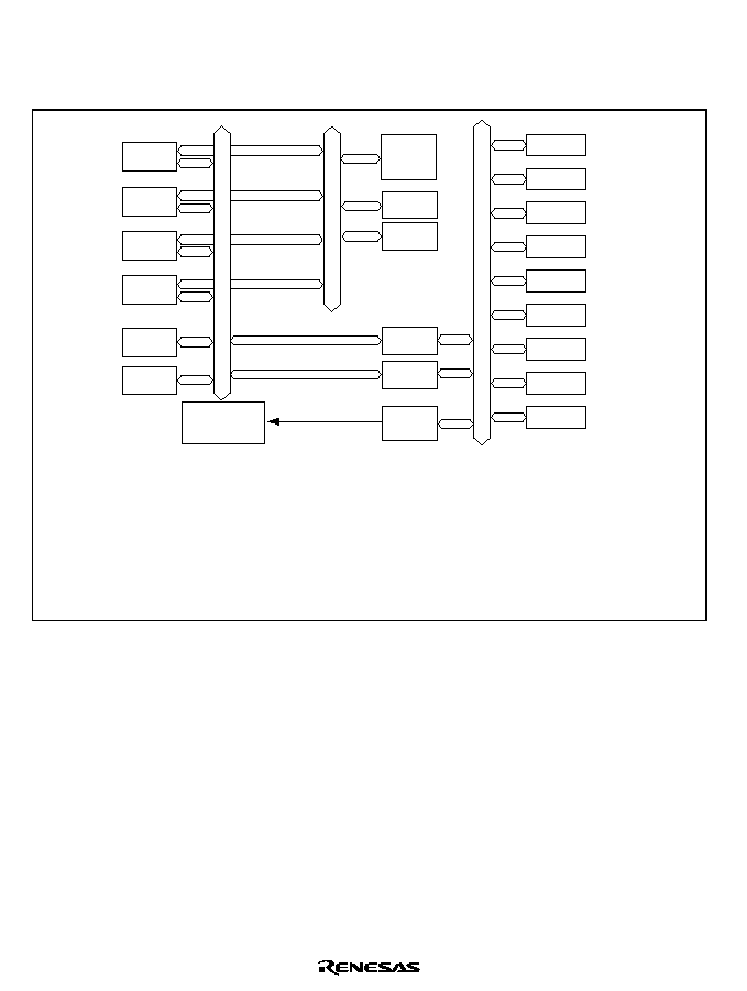
Rev. 2.00, 09/03, page 6 of 690
1.2
Block Diagram
Figure 1.1 shows an internal block diagram of the SH7705.
SH3
CPU
TMU
TPU
RTC
CMT
SCIF0/IrDA
SCIF2
USB
ADC
UDI
UBC
AUD
BSC
DMAC
CCN
CACHE
MMU
TLB
INTC
CPG/WDT
Legend:
CACHE:
CCN:
MMU:
TLB:
INTC:
CPG/WDT:
CPU:
UBC:
AUD:
BSC:
DMAC:
Cache memory
Cache memory controller
Memory management unit
Translation look-aside buffer
Interrupt controller
Clock pulse generator/watchdog timer
Central processing unit
User break controller
Advanced user debugger
Bus state controller
Direct memory access controller
Timer unit
16-bit timer pulse unit
Realtime clock
Compare match timer
Serial communication interface with FIFO
Infrared data association module
Universal serial bus
A/D converter
User debugging interface
Pin function controller
TMU:
TPU:
RTC:
CMT:
SCIF:
IrDA:
USB:
ADC:
UDI:
PFC:
I/O port
(PFC)
External bus
interface
I bus
L bus
Peripheral bus
Figure 1.1 Block Diagram of SH7705
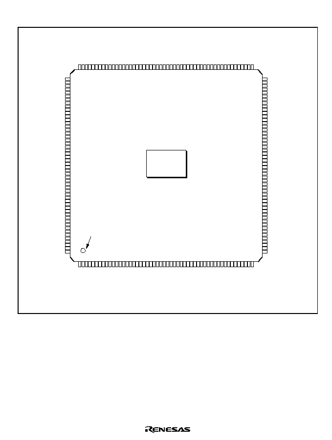
Rev. 2.00, 09/03, page 7 of 690
1.3
Pin Assignment
1
2
3
4
5
6
7
8
9
10
11
12
13
14
15
16
17
18
19
20
21
22
23
24
25
26
27
28
29
30
31
32
33
34
35
36
37
38
39
40
41
42
43
44
45
46
47
48
49
50
51
52
V
SS
Q
V
CC
-USB
D+
D-
V
SS
-USB
V
CC
-R
TC
XT
AL2
EXT
AL2
V
SS
-R
TC
VBUS/PTM6
MD6
D31/PTB7/PINT15
D30/PTB6/PINT14
D29/PTB5/PINT13
D28/PTB4/PINT12
D27/PTB3/PINT1
1
V
SS
Q
D26/PTB2/PINT10
V
CC
Q
D25/PTB1/PINT9
D24/PTB0/PINT8
D23/PT
A7/PINT7
D22/PT
A6/PINT6
D21/PT
A5/PINT5
D20/PT
A4/PINT4
V
SS
D19/PT
A3/PINT3
V
CC
D18/PT
A2/PINT2
D17/PT
A1/PINT1
D16/PT
A0/PINT0
V
SS
Q
D15
V
CC
Q
D14
D13
D12
D1
1
D10
D9
D8
D7
D6
V
SS
Q
D5
V
CC
Q
D4
D3
D2
D1
D0
V
SS
Q
156
155
154
153
152
151
150
149
148
147
146
145
144
143
142
141
140
139
138
137
136
135
134
133
132
131
130
129
128
127
126
125
124
123
122
121
120
11
9
11
8
11
7
11
6
11
5
11
4
11
3
11
2
111
11
0
109
108
107
106
105
V
SS
Q
EXT
AL
XT
AL
MD5
V
CC
-PLL2
V
SS
-PLL2
V
SS
-PLL1
V
CC
-PLL1
MD2
MD1
MD0
ASEMD0
/PTF7
ASEBRKAK
/PTF6
TDO/PTF5
TRST
/PTG3
TMS/PTG2
TCK/PTG1
TDI/PTG0
V
CC
Q
PTM3
PTM2
PTM1
PTM0
V
SS
Q
V
CC
NF
*
/PTM4
V
SS
NF
*
/PTJ7
NF
*
/PTJ6
NF
*
/PTJ5
NF
*
/PTJ4
NF
*
/PTJ3
NF
*
/PTJ2
NF
*
/PTJ1
NF
*
/PTJ0
AUDA
T
A
3/PTF3/T
O
3
AUDA
T
A
2/PTF2/T
O
2
AUDA
T
A
1/PTF1/T
O
1
AUDA
T
A
0/PTF0/T
O
0
AUDSYNC/PTF4
TEND0/PTE3
DACK1/PTE1
DACK0/PTE0
V
CC
Q
WAIT
/PTG7
V
SS
Q
BREQ
/PTG6
BACK
/PTG5
PTD5/NF
*
CKE/PTD4
CASU
/PTD3
V
SS
Q
INDEX
104
103
102
101
100
99
98
97
96
95
94
93
92
91
90
89
88
87
86
85
84
83
82
81
80
79
78
77
76
75
74
73
72
71
70
69
68
67
66
65
64
63
62
61
60
59
58
57
56
55
54
53
CASL/PTD2
RASU/PTD1
RASL/PTD0
CS6B/PTD7
CS6A/PTC7
CS5B/PTD6
CS5A/PTC6
CS4/PTC5
CS3/PTC4
CS2/PTC3
CS0
RD/
WR
WE3/DQMUU/AH/PTC2
WE2/DQMUL/PTC1
WE1/DQMLU
V
CC
Q
WE0/DQMLL
V
SS
Q
RD
BS/PTC0
A25/PTK7
A24/PTK6
A23/PTK5
A22/PTK4
V
CC
A21/PTK3
V
SS
A20/PTK2
A19/PTK1
A18
A17
A16
A15
V
CC
Q
A14
V
SS
Q
A13
A12
A11
A10
A9
A8
A7
A6
A5
V
CC
Q
A4
V
SS
Q
A3
A2
A1
A0/PTK0
157
158
159
160
161
162
163
164
165
166
167
168
169
170
171
172
173
174
175
176
177
178
179
180
181
182
183
184
185
186
187
188
189
190
191
192
193
194
195
196
197
198
199
200
201
202
203
204
205
206
207
208
STATUS0/PTE4/
RTS0
STATUS1/PTE5/
CTS0
V
SS
Q
CKIO
V
CC
Q
PTN0/SUSPND
PTN1/TXENL
PTN2/XVDATA
PTN3/TXDMNS
PTN4/TXDPLS
PTN5/DMNS
PTN6/DPLS
PTN7
TCLK/PTE6
PTE7
TxD0/SCPT0/IrTX
SCK0/SCPT1
TxD2/SCPT2
SCK2/SCPT3
RTS2/SCPT4
RxD0/SCPT0/IrRX
V
CC
Q
RxD2/SCPT2
V
SS
Q
CTS2/SCPT5
V
SS
RESETM
V
CC
IRQ0/
IRL0/PTH0
IRQ1/
IRL1/PTH1
IRQ2/
IRL2/PTH2
IRQ3/
IRL3/PTH3
IRQ4/PTH4
IRQ5/PTE2
AUDCK/PTG4
NMI
DREQ0/PTH5
DREQ1/PTH6
RESETP
CA
MD3
MD4
AV
SS
AN0/PTL0
AN1/PTL1
AN2/PTL2
AN3/PTL3
AV
CC
V
SS
Q
EXTAL_USB
XTAL_USB
V
CC
Q
SH7705
FP-208C
(Top view)
Note: * The initial functions of NF (No Function) pins are not assigned after power-on reset. Specifies the functions with Pin Function Controller (PFC).
Figure 1.2 Pin Assignment (FP-208C)
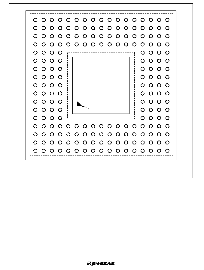
Rev. 2.00, 09/03, page 8 of 690
17
16
15
14
13
12
11
10
9
8
7
6
5
4
3
2
1
17
16
15
14
13
12
11
10
9
8
7
6
5
4
3
2
1
A
B
C
D
E
F
G
H
J
K
L
M
N
P
R
T
U
A
B
C
D
E
F
G
H
J
K
L
M
N
P
R
T
U
SH7705
TBP-208A
(Top view)
INDEX MARK
Note: The terminal area surrounded by the dotted line is the perspective view.
Figure 1.3 Pin Assignment (TBP-208A)

Rev. 2.00, 09/03, page 9 of 690
Table 1.2
Pin Functions
Pin No.
FP-
208C
TBP-
208A
Pin Name
I/O
Description
1
A1
VssQ
I/O power supply (0 V)
2
B1
Vcc-USB
USB power supply (3.3 V)
3
C3
D+
I/O
USB data line
4
C2
D-
I/O
USB data line
5
C1
Vss-USB
USB power supply (0 V)
6
D3
Vcc-RTC
*
5
RTC power supply (3.3 V)
*
5
7
D2
XTAL2
O
Crystal oscillator pin for on-chip RTC
8
D1
EXTAL2
I
Crystal oscillator pin for on-chip RTC
9
E4
Vss-RTC
*
5
RTC power supply (0 V)
*
5
10
E3
VBUS/PTM6
I / I/O
USB power supply detection / input/output port M
11
E2
MD6
I
connect to I/O power supply (0V)
12
E1
D31/PTB7/PINT15
I/O / I/O / I Data bus / input/output port B / PINT interrupt
13
F4
D30/PTB6/PINT14
I/O / I/O / I Data bus / input/output port B / PINT interrupt
14
F3
D29/PTB5/PINT13
I/O / I/O / I Data bus / input/output port B / PINT interrupt
15
F2
D28/PTB4/PINT12
I/O / I/O / I Data bus / input/output port B / PINT interrupt
16
F1
D27/PTB3/PINT11
I/O / I/O / I Data bus / input/output port B / PINT interrupt
17
G4
VssQ
I/O power supply (0 V)
18
G3
D26/PTB2/PINT10
I/O / I/O / I Data bus / input/output port B / PINT interrupt
19
G2
VccQ
I/O power supply (3.3 V)
20
G1
D25/PTB1/PINT9
I/O / I/O / I Data bus / input/output port B / PINT interrupt
21
H4
D24/PTB0/PINT8
I/O / I/O / I Data bus / input/output port B / PINT interrupt
22
H3
D23/PTA7/PINT7
I/O / I/O / I Data bus / input/output port A / PINT interrupt
23
H2
D22/PTA6/PINT6
I/O / I/O / I Data bus / input/output port A / PINT interrupt
24
H1
D21/PTA5/PINT5
I/O / I/O / I Data bus / input/output port A / PINT interrupt
25
J4
D20/PTA4/PINT4
I/O / I/O / I Data bus / input/output port A / PINT interrupt
26
J2
Vss
Internal power supply (0 V)
27
J1
D19/PTA3/PINT3
I/O / I/O / I Data bus / input/output port A / PINT interrupt
28
J3
Vcc
Internal power supply (1.5 V)
29
K1
D18/PTA2/PINT2
I/O / I/O / I Data bus / input/output port A / PINT interrupt
30
K2
D17/PTA1/PINT1
I/O / I/O / I Data bus / input/output port A / PINT interrupt
31
K3
D16/PTA0/PINT0
I/O / I/O / I Data bus / input/output port A / PINT interrupt

Rev. 2.00, 09/03, page 10 of 690
Pin No.
FP-
208C
TBP-
208A
Pin Name
I/O
Description
32
K4
VssQ
I/O power supply (0 V)
33
L1
D15
I/O
Data bus
34
L2
VccQ
I/O power supply (3.3 V)
35
L3
D14
I/O
Data bus
36
L4
D13
I/O
Data bus
37
M1
D12
I/O
Data bus
38
M2
D11
I/O
Data bus
39
M3
D10
I/O
Data bus
40
M4
D9
I/O
Data bus
41
N1
D8
I/O
Data bus
42
N2
D7
I/O
Data bus
43
N3
D6
I/O
Data bus
44
N4
VssQ
I/O power supply (0 V)
45
P1
D5
I/O
Data bus
46
P2
VccQ
I/O power supply (3.3 V)
47
P3
D4
I/O
Data bus
48
R1
D3
I/O
Data bus
49
R2
D2
I/O
Data bus
50
P4
D1
I/O
Data bus
51
T1
D0
I/O
Data bus
52
T2
VssQ
I/O power supply (0 V)
53
U1
A0/PTK0
O / I/O
Address bus / input/output port K
54
U2
A1
O
Address bus
55
R3
A2
O
Address bus
56
T3
A3
O
Address bus
57
U3
VssQ
I/O power supply (0 V)
58
R4
A4
O
Address bus
59
T4
VccQ
I/O power supply (3.3 V)
60
U4
A5
O
Address bus
61
P5
A6
O
Address bus
62
R5
A7
O
Address bus
63
T5
A8
O
Address bus

Rev. 2.00, 09/03, page 11 of 690
Pin No.
FP-
208C
TBP-
208A
Pin Name
I/O
Description
64
U5
A9
O
Address bus
65
P6
A10
O
Address bus
66
R6
A11
O
Address bus
67
T6
A12
O
Address bus
68
U6
A13
O
Address bus
69
P7
VssQ
I/O power supply (0 V)
70
R7
A14
O
Address bus
71
T7
VccQ
I/O power supply (3.3 V)
72
U7
A15
O
Address bus
73
P8
A16
O
Address bus
74
R8
A17
O
Address bus
75
T8
A18
O
Address bus
76
U8
A19/PTK1
O / I/O
Address bus / input/output port K
77
P9
A20/PTK2
O / I/O
Address bus / input/output port K
78
T9
Vss
Internal power supply (0 V)
79
U9
A21/PTK3
O / I/O
Address bus / input/output port K
80
R9
Vcc
Internal power supply (1.5 V)
81
U10
A22/PTK4
O / I/O
Address bus / input/output port K
82
T10
A23/PTK5
O / I/O
Address bus / input/output port K
83
R10
A24/PTK6
O / I/O
Address bus / input/output port K
84
P10
A25/PTK7
O / I/O
Address bus / input/output port K
85
U11
BS
/PTC0
O / I/O
Bus cycle start signal / input/output port C
86
T11
RD
O
Read strobe
87
R11
VssQ
I/O power supply (0 V)
88
P11
WE0
/DQMLL
O / O
D7 to D0 select signal / DQM (SDRAM)
89
U12
VccQ
I/O power supply (3.3 V)
90
T12
WE1
/DQMLU
O / O
D15 to D8 select signal / DQM (SDRAM)
91
R12
WE2
/DQMUL/PTC1 O / O / I/O
D23 to D16 select signal / DQM (SDRAM) /
input/output port C
92
P12
WE3
/DQMUU/
AH
/
PTC2
O / O / O /
I/O
D31 to D24 select signal / DQM (SDRAM) /
address hold / input/output port C
93
U13
RD/
WR
O
Read/write
94
T13
CS0
O
Chip select 0

Rev. 2.00, 09/03, page 12 of 690
Pin No.
FP-
208C
TBP-
208A
Pin Name
I/O
Description
95
R13
CS2
/PTC3
O / I/O
Chip select 2 / input/output port C
96
P13
CS3
/PTC4
O / I/O
Chip select 3 / input/output port C
97
U14
CS4
/PTC5
O / I/O
Chip select 4 / input/output port C
98
T14
CS5A*
3
/PTC6
O / I/O
Chip select 5A / input/output port C
99
R14
CS5B*
3
/PTD6
O / I/O
Chip select 5B / input/output port D
100
U15
CS6A*
3
/PTC7
O / I/O
Chip select 6A / input/output port C
101
T15
CS6B*
3
/PTD7
O / I/O
Chip select 6B / input/output port D
102
P14
RASL
/PTD0
O / I/O
Lower 32 Mbytes address RAS (SDRAM) /
input/output port D
103
U16
RASU*
3
/PTD1
O / I/O
Upper 32 Mbytes address RAS (SDRAM) /
input/output port D
104
T16
CASL
/PTD2
O / I/O
Lower 32 Mbytes address CAS (SDRAM) /
input/output port D
105
U17
VssQ
I/O power supply (0 V)
106
T17
CASU*
3
/PTD3
O / I/O
Upper 32 Mbytes address CAS (SDRAM) /
input/output port D
107
R15
CKE/PTD4
O / I/O
CK enable (SDRAM) / input/output port D
108
R16
PTD5/NF
*
4
I
Input port D / NF
*
4
109
R17
BACK
/PTG5
O / I/O
Bus acknowledge / input/output port G
110
P15
BREQ
/PTG6
I / I/O
Bus request / input/output port G
111
P16
VssQ
I/O power supply (0 V)
112
P17
WAIT
/PTG7
I / I/O
Hardware wait request / input/output port G
113
N14
VccQ
I/O power supply (3.3 V)
114
N15
DACK0/PTE0
O / I/O
DMA acknowledge 0 / input/output port E
115
N16
DACK1/PTE1
O / I/O
DMA acknowledge 1 / input/output port E
116
N17
TEND0/PTE3
O / I/O
DMA transfer end notification / input/output
port E
117
M14
AUDSYNC/PTF4
O / I/O
AUD synchronous / input/output port F
118
M15
AUDATA0/PTF0/TO0 O / I/O / O
AUD data output / input/output port F / timer
output
119
M16
AUDATA1/PTF1/TO1 O / I/O / O
AUD data output / input/output port F / timer
output
120
M17
AUDATA2/PTF2/TO2 O / I/O / O
AUD data output / input/output port F / timer
output

Rev. 2.00, 09/03, page 13 of 690
Pin No.
FP-
208C
TBP-
208A
Pin Name
I/O
Description
121
L14
AUDATA3/PTF3/TO3 O / I/O / O
AUD data output / input/output port F / timer
output
122
L15
NF
*
4
/PTJ0
O
NF
*
4
/output port J
123
L16
NF
*
4
/PTJ1
O
NF
*
4
/output port J
124
L17
NF
*
4
/PTJ2
O
NF
*
4
/output port J
125
K14
NF
*
4
/PTJ3
O
NF
*
4
/output port J
126
K15
NF
*
4
/PTJ4
O
NF
*
4
/output port J
127
K16
NF
*
4
/PTJ5
O
NF
*
4
/output port J
128
K17
NF
*
4
/PTJ6
O
NF
*
4
/output port J
129
J14
NF
*
4
/PTJ7
O
NF
*
4
/output port J
130
J16
Vss
Internal power supply (0 V)
131
J17
NF
*
4
/PTM4
I
NF
*
4
/ input port M
132
J15
Vcc
Internal power supply (1.5 V)
133
H17
VssQ
I/O power supply (0 V)
134
H16
PTM0
I/O
Input/output port M
135
H15
PTM1
I/O
Input/output port M
136
H14
PTM2
I/O
Input/output port M
137
G17
PTM3
I/O
Input/output port M
138
G16
VccQ
I/O power supply (3.3 V)
139
G15
TDI
*
7
/PTG0
I / I/O
Test data input (UDI) / input/output port G
140
G14
TCK
*
7
/PTG1
I / I/O
Test clock (UDI) / input/output port G
141
F17
TMS
*
7
/PTG2
I / I/O
Test mode select (UDI) / input/output port G
142
F16
TRST*
1
*
7
/PTG3
I / I/O
Test reset (UDI) / input/output port G
143
F15
TDO/PTF5
O / I/O
Test data output (UDI) / input/output port F
144
F14
ASEBRKAK
/PTF6
O / I/O
ASE break acknowledge (UDI) / input/output
port F
145
E17
ASEMD0*
2
*
7
/PTF7
I / I/O
ASE mode (UDI) / input/output port F
146
E16
MD0
I
Clock mode setting
147
E15
MD1
I
Clock mode setting
148
E14
MD2
I
Clock mode setting
149
D17
Vcc-PLL1
PLL1 power supply (1.5 V)
150
D16
Vss-PLL1
PLL1 power supply (0 V)

Rev. 2.00, 09/03, page 14 of 690
Pin No.
FP-
208C
TBP-
208A
Pin Name
I/O
Description
151
D15
Vss-PLL2
PLL2 power supply (0 V)
152
C17
Vcc-PLL2
PLL2 power supply (1.5 V)
153
C16
MD5
I
Endian setting
154
D14
XTAL
O
Crystal oscillator pin
155
B17
EXTAL
I
External clock / crystal oscillator pin
156
B16
VssQ
I/O power supply (0 V)
157
A17
STATUS0/PTE4/
RTS0
O / I/O / O
Processor status / input/output port E / SCIF0
transmit request
158
A16
STATUS1/PTE5/
CTS0
O / I/O / I
Processor status / input/output port E / SCIF0
transmit clear
159
C15
VssQ
I/O power supply (0 V)
160
B15
CKIO
I/O
System clock input/output
161
A15
VccQ
I/O power supply (3.3 V)
162
C14
PTN0/SUSPND
I/O / O
input/output port N / USB suspend
163
B14
PTN1/TXENL
I/O / O
input/output port N / USB output enable
164
A14
PTN2/XVDATA
I/O / I
input/output port N / USB differential receive
input
165
D13
PTN3/TXDMNS
I/O / O
input/output port N / USB D≠ transmit output
166
C13
PTN4/TXDPLS
I/O / O
input/output port N / USB D+ transmit output
167
B13
PTN5/DMNS
I/O / I
input/output port N / D≠ input from USB
receiver
168
A13
PTN6/DPLS
I/O / I
input/output port N / D+ input from USB
receiver
169
D12
PTN7
I/O
input/output port N
170
C12
TCLK/PTE6
I / I/O
TMU clock input / input/output port E
171
B12
PTE7
I/O
Input/output port E
172
A12
TxD0/SCPT0/IrTX
O / O / O
SCIF0 transmit data / SC port / IrDA TX port
173
D11
SCK0/SCPT1
I/O / I/O
SCIF0 clock / SC port
174
C11
TxD2/SCPT2
O / O
SCIF2 transmit data / SC port
175
B11
SCK2/SCPT3
I/O / I/O
SCIF2 clock / SC port
176
A11
RTS2
/SCPT4
O / I/O
SCIF2 transmit request / SC port
177
D10
RxD0/SCPT0/IrRX
I / I / I
SCIF0 receive data / SC port / IrDA RX port
178
C10
VccQ
I/O power supply (3.3 V)
179
B10
RxD2/SCPT2
I / I
SCIF2 receive data / SC port

Rev. 2.00, 09/03, page 15 of 690
Pin No.
FP-
208C
TBP-
208A
Pin Name
I/O
Description
180
A10
VssQ
I/O power supply (0 V)
181
D9
CTS2
/SCPT5
I / I/O
SCIF2 transmit clear / SC port
182
B9
Vss
I/O power supply (0 V)
183
A9
RESETM
I
Manual reset request
184
C9
Vcc
Internal power supply (1.5 V)
185
A8
IRQ0/
IRL0
/PTH0
I / I / I/O
External interrupt request / input/output port H
186
B8
IRQ1/
IRL1
/PTH1
I / I / I/O
External interrupt request / input/output port H
187
C8
IRQ2/
IRL2
/PTH2
I / I / I/O
External interrupt request / input/output port H
188
D8
IRQ3/
IRL3
/PTH3
I / I / I/O
External interrupt request / input/output port H
189
A7
IRQ4/PTH4
I / I/O
External interrupt request / input/output port H
190
B7
IRQ5/PTE2
I / I/O
External interrupt request / input/output port E
191
C7
AUDCK/PTG4
O / I/O
AUD clock / input/output port G
192
D7
NMI
I
Nonmaskable interrupt request
193
A6
DREQ0/PTH5
I / I/O
DMA request / input/output port H
194
B6
DREQ1/PTH6
I / I/O
DMA request / input/output port H
195
C6
RESETP*
6
I
Power-on reset request
196
D6
CA
I
Hardware standby request
197
A5
MD3
I
Area 0 bus width setting
198
B5
MD4
I
Area 0 bus width setting
199
C5
AVss
Analog power supply (0 V)
200
D5
AN0/PTL0
I / I
A/D converter input / input port L
201
A4
AN1/PTL1
I / I
A/D converter input / input port L
202
B4
AN2/PTL2
I / I
A/D converter input / input port L
203
C4
AN3/PTL3
I / I
A/D converter input / input port L
204
A3
AVcc
Analog power supply (3.3 V)
205
B3
VssQ
I/O power supply (0 V)
206
D4
EXTAL_USB
I
USB clock
207
A2
XTAL_USB
O
USB clock
208
B2
VccQ
I/O power supply (3.3 V)
Notes: The unused pins should be handled according to table A.1, I/O Port States in Each
Processing State, in Appendix.
1. The
TRST
pin must be driven low for a specified period when power supply is turned on
regardless of whether the UDI function is used or not. As the same as the
RESETP
pin,
the
TRST
pin should be driven low at the power-on set state and driven high after the
power-on reset state is released.

Rev. 2.00, 09/03, page 16 of 690
2. The input level of the
ASEMD0
pin must be high if the E10A emulator is not used. For
details, refer to section 23.4.2, Reset Configuration.
3. These pins are initialized to the general input port setting in which the pull-up MOS is off
at a power-on reset. When these pins are connected to memory and so on, their levels
must be fixed externally.
4. The initial functions of NF (No Function) pins are not assigned after power-on reset.
Specifies the functions with Pin Function Controller (PFC).
5. In hardware standby mode, supply power to all power supply pins including the RTC
power supply pins.
6. Pull-up MOS connected.
7. The pull-up MOS turns on if the pin function controller (PFC) is used to select other
functions (UDI).

Rev. 2.00, 09/03, page 17 of 690
1.4
Pin Functions
Table 1.3 lists the pin functions.
Table 1.3
Pin Functions
Classification
Symbol
I/O
Name
Function
Vcc
Power supply
Power supply for the internal
modules and ports for the system.
Connect all Vcc pins to the system
power supply. There will be no
operation if any pins are open.
Vss
Ground
Ground pin. Connect all Vss pins to
the system power supply (0 V).
There will be no operation if any
pins are open.
VccQ
Power supply
Power supply for I/O pins. Connect
all VccQ pins to the system power
supply. There will be no operation
if any pins are open.
Power supply
VssQ
Ground
Ground pin. Connect all VssQ pins
to the system power supply (0 V).
There will be no operation if any
pins are open.
Vcc-PLL1
PLL1 power
supply
Power supply for the on-chip PLL1
oscillator.
Vss-PLL1
PLL1 ground
Ground pin for the on-chip PLL1
oscillator.
Vcc-PLL2
PLL2 power
supply
Power supply for the on-chip PLL2
oscillator.
Vss-PLL2
PLL2 ground
Ground pin for the on-chip PLL2
oscillator.
EXTAL
I
External clock
For connection to a crystal
resonator. An external clock signal
may also be input to the EXTAL
pin.
XTAL
O
Crystal
For connection to a crystal
resonator.
Clock
CKIO
I/O
System clock
Supplies the system clock to
external devices.

Rev. 2.00, 09/03, page 18 of 690
Classification
Symbol
I/O
Name
Function
Operating mode
control
MD6 to MD0
I
Mode set
Sets the operating mode. Do not
change values on these pins
during operation.
MD2 to MD0 set the clock mode,
MD3 and MD4 set the bus-width
mode of area 0 and MD5 sets the
endian. MD6 pin should be
connected to VssQ.
RESETP
I
Power-on reset
When low, the system enters the
power-on reset state.
RESETM
I
Manual reset
When low, the system enters the
manual reset state.
STATUS1,
STATUS0
O
Status output
Indicates the operating state.
BREQ
I
Bus request
Low when an external device
requests the release of the bus
mastership.
BACK
O
Bus request
acknowledge
Indicates that the bus mastership
has been released to an external
device. Reception of the
BACK
signal informs the device which
has output the
BREQ
signal that it
has acquired the bus.
System control
CA
I
Chip active
High in normal operation, and low
in hardware standby mode.
NMI
I
Non-maskable
interrupt
Non-maskable interrupt request
pin. Fix to high level when not in
use.
IRQ5 to IRQ0
I
Interrupt
requests 5 to 0
Maskable interrupt request pin.
Selectable as level input or edge
input. The rising edge or falling
edge is selectable as the detection
edge. The low level or high level is
selectable as the detection level.
IRL3
to
IRL0
I
Interrupt
requests 3 to 0
Maskable interrupt request pin.
Input a coded interrupt level.
Interrupts
PINT15 to
PINT0
I
Interrupt
requests 15 to 0
PINT interrupt request pin.
Address bus
A25 to A0
O
Address bus
Outputs addresses.
Data bus
D31 to D0
I/O
Data bus
32-bit bidirectional data bus.

Rev. 2.00, 09/03, page 19 of 690
Classification
Symbol
I/O
Name
Function
CS0
,
CS2
to
CS4
,
CS5A
,
CS5B
,
CS6A
,
CS6B
,
O
Chip select 0,
2 to 4, 5A, 5B,
6A, 6B
Chip-select signal for external
memory or devices.
RD
O
Read
Indicates reading of data from
external devices.
RD/
WR
O
Read/write
Read/write signal.
BS
O
Bus start
Bus-cycle start.
WE3
O
Highest-byte
write
Indicates that bits 31 to 24 of the
data in the external memory or
device are being written.
WE2
O
Second-highest-
byte write
Indicates that bits 23 to 16 of the
data in the external memory or
device are being written.
WE1
O
Second-lowest-
byte write
Indicates that bits 15 to 8 of the
data in the external memory or
device are being written.
WE0
O
Lowest-byte
write
Indicates that bits 7 to 0 of the data
in the external memory or device
are being written.
CKE
O
CK enable
Clock enable. (SDRAM)
DQMUU
O
DQ mask UU
Selects D31 to D24. (SDRAM)
DQMUL
O
DQ mask UL
Selects D23 to D16. (SDRAM)
DQMLU
O
DQ mask LU
Selects D15 to D8. (SDRAM)
DQMLL
O
DQ mask LL
Selects D7 to D0. (SDRAM)
RASU
O
Row address U Specifies a row address. (SDRAM)
RASL
O
Row address L
Specifies a row address. (SDRAM)
CASU
O
Column address
U
Specifies a column address.
(SDRAM)
CASL
O
Column address
L
Specifies a column address.
(SDRAM)
AH
O
Address hold
Address hold signal.
Bus control
WAIT
I
Wait
Inserts a wait cycle into the bus
cycles during access to the
external space.

Rev. 2.00, 09/03, page 20 of 690
Classification
Symbol
I/O
Name
Function
DREQ0,
DREQ1
I
DMA-transfer
request
Input pin for external requests for
DMA transfer.
DACK0,
DACK1
O
DMA-transfer
strobe
Output strobe to external I/O, in
response to external requests for
DMA transfer.
Direct memory
access controller
(DMAC)
TEND0
O
DMA-transfer
end
Transfer end output for DMAC
channel 0.
Timer unit (TMU) TCLK
I
Clock input
External clock input pin/input
capture control input pin.
16-bit timer pulse
unit (TPU)
TO3 to TO0
O
Timer output
Output compare/PWM output pin.
TxD0, TxD2
O
Transmit data
Transmit data pin.
RxD0, RxD2
I
Receive data
Receive data pin.
SCK0, SCK2
I/O
Serial clock
Clock input/output pin.
RTS0
,
RTS2
O
Transmit
request
Modem control pin.
Serial
communication
interface with
FIFO
(SCIF0, SCIF2)
CTS0
,
CTS2
I
Transmit enable Modem control pin.
IrTX
O
IrDA TX port
IrDA transmit data output.
IrDA
IrRX
I
IrDA RX port
IrDA receive data input.
EXTAL2
I
RTC clock
RTC crystal oscillator pin. (32.768
kHz)
XTAL2
O
RTC clock
RTC crystal oscillator pin. (32.768
kHz)
Vcc-RTC
RTC power
supply
Power supply pin for the RTC.
Realtime clock
(RTC)
Vss-RTC
RTC ground
Ground pin for the RTC.
AN3 to AN0
I
Analog input pin Analog input pin.
AVcc
A/D analog
power supply
Power supply for the A/D
converter. When the A/D converter
is not in use, connect this pin to the
port power supply (VccQ).
A/D converter
(ADC)
AVss
A/D analog
ground
Ground pin for the A/D converter.
Connect this pin to the system
power supply (Vss).

Rev. 2.00, 09/03, page 21 of 690
Classification
Symbol
I/O
Name
Function
EXTAL_USB
I
USB clock
USB clock input pin. (48-MHz
input)
XTAL_USB
O
USB clock
USB clock pin.
XVDATA
I
Data input
Receive data input pin from the
differential receiver.
VBUS
I
USB power
supply detection
USB-cable connection-monitor pin.
TXDPLS
O
D
+
output
D
+
transmit output pin for the
driver.
TXDMNS
O
D
-
output
D
-
transmit output pin for the
driver.
DPLS
I
D
+
input
D
+
signal input pin from the
receiver to the driver.
DMNS
I
D
-
input
D
-
signal input pin from the
receiver to the driver.
TXENL
O
Output enable
Output enable pin for the driver.
SUSPND
O
Suspend
Suspend-state output pin for the
transceiver.
Vcc-USB
USB analog
power supply
USB power supply pin. When the
USB is not in use, connect this pin
to the port power supply (VccQ).
Vss-USB
USB analog
ground
USB ground pin. Connect this pin
to the system power supply (Vss).
D
-
I/O
D
-
I/O
On-chip USB transceiver D
-
.
USB
D
+
I/O
D
+
I/O
On-chip USB transceiver D
+
.

Rev. 2.00, 09/03, page 22 of 690
Classification
Symbol
I/O
Name
Function
PTA7 to PTA0
I/O
General
purpose port
8-bit general-purpose I/O port pins.
PTB7 to PTB0
I/O
General
purpose port
8-bit general-purpose I/O port pins.
PTC7 to PTC0
I/O
General
purpose port
8-bit general-purpose I/O port pins.
PTD7 to PTD0
I/O
General
purpose port
8-bit general-purpose I/O port pins.
PTE7 to PTE0
I/O
General
purpose port
8-bit general-purpose I/O port pins.
PTF7 to PTF0
I/O
General
purpose port
8-bit general-purpose I/O port pins.
PTG7 to PTG0
I/O
General
purpose port
8-bit general-purpose I/O port pins.
PTH6 to PTH0
I/O
General
purpose port
7-bit general-purpose I/O port pins.
PTJ7 to PTJ0
O
General
purpose port
8-bit general-purpose output port
pins.
PTK7 to PTK0
I/O
General
purpose port
8-bit general-purpose I/O port pins.
PTL3 to PTL0
I
General
purpose port
4-bit general-purpose input port
pins.
PTM6, PTM4 to
PTM0
I/O
General
purpose port
6-bit general-purpose I/O port pins.
PTN7 to PTN0
I/O
General
purpose port
8-bit general-purpose I/O port pins.
I/O port
SCPT5 to
SCPT0
I/O
Serial port
6-bit serial port pins.

Rev. 2.00, 09/03, page 23 of 690
Classification
Symbol
I/O
Name
Function
TCK
I
Test clock
Test-clock input pin.
TMS
I
Test mode
select
Inputs the test-mode select signal.
TDI
I
Test data input
Serial input pin for instructions and
data.
TDO
O
Test data
output
Serial output pin for instructions
and data.
User debugging
interface
(UDI)
TRST
I
Test reset
Initial-signal input pin.
AUDATA3 to
AUDATA0
O
AUD data
Destination-address output pin in
branch-trace mode.
AUDCK
O
AUD clock
Synchronous clock output pin in
branch-trace mode.
Advanced user
debugger
(AUD)
AUDSYNC
O
AUD
synchronous
signal
Data start-position acknowledge-
signal output pin in branch-trace
mode.
ASEBRKAK
O
Break mode
acknowledge
Indicates that the E10A emulator
has entered its break mode.
For the connection with the E10A,
see the SH7705 E10A Emulator
User's Manual (tentative title).
E10A interface
ASEMD0
I
ASE mode
Sets ASE mode.

Rev. 2.00, 09/03, page 24 of 690

Rev. 2.00, 09/03, page 25 of 690
Section 2 CPU
2.1
Processing States and Processing Modes
2.1.1
Processing States
This LSI supports four types of processing states: a reset state, an exception handling state, a
program execution state, and a low-power consumption state, according to the CPU processing
states.
Reset State: In the reset state, the CPU is reset. The LSI supports two types of resets: power-on
reset and manual reset. For details on resets, refer to section 5, Exception Handling.
In power-on reset, the registers and internal statuses of all LSI on-chip modules are initialized. In
manual reset, the register contents of a part of the LSI on-chip modules, such as the bus state
controller (BSC), are retained. For details, refer to section 24, List of Registers. The CPU internal
statuses and registers are initialized both in power-on reset and manual reset. After initialization,
the program branches to address H'A0000000 to pass control to the reset processing program to be
executed.
Exception Handling State: In the exception handling state, the CPU processing flow is changed
temporarily by a general exception or interrupt exception processing. The program counter (PC)
and status register (SR) are saved in the save program counter (SPC) and save status register
(SSR), respectively. The program branches to an address obtained by adding a vector offset to the
vector base register (VBR) and passes control to the exception processing program defined by the
user to be executed. For details on reset, refer to section 5, Exception Handling.
Program Execution State: The CPU executes programs sequentially.
Low-Power Consumption State: The CPU stops operation to reduce power consumption. The
low-power consumption state can be entered by executing the SLEEP instruction. For details on
the low-power consumption state, refer to section 11, Power-Down Modes.
Figure 2.1 shows a status transition diagram.
CPUS3D0S_000020020300

Rev. 2.00, 09/03, page 26 of 690
2.1.2
Processing Modes
This LSI supports two processing modes: user mode and privileged mode. These processing
modes can be determined by the processing mode bit (MD) of the status register (SR). If the MD
bit is cleared to 0, the user mode is selected. If the MD bit is set to 1, the privileged mode is
selected. The CPU enters the privileged mode by a transition to reset state or exception handling
state. In the privileged mode, any registers and resources in address spaces can be accessed.
Clearing the MD bit of the SR to 0 puts the CPU in the user mode. In the user mode, some of the
registers, including SR, and some of the address spaces cannot be accessed by the user program
and system control instructions cannot be executed. This function effectively protects the system
resources from the user program. To change the processing mode from user to privileged mode, a
transition to exception handling state is required.*
Note: *
To call a service routine used in privileged mode from user mode, the LSI supports an
unconditional trap instruction (TRAPA). When a transition from user mode to
privileged mode occurs, the contents of the SR and PC are saved. A program execution
in user mode can be resumed by restoring the contents of the SR and PC. To return
from an exception processing program, the LSI supports an RTE instruction.
(From any states)
Power-on reset
Manual reset
Reset state
Program execution state
Low-power
consumption state
Exception handling state
An exception
is accepted
Exception
handling
routine starts
Reset processing
routine starts
An exception
is accepted
Multiple
exceptions
SLEEP instruction
Figure 2.1 Processing State Transitions

Rev. 2.00, 09/03, page 27 of 690
2.2
Memory Map
2.2.1
Logical Address Space
The LSI supports 32-bit logical addresses and accesses system resources using the 4-Gbytes of
logical address space. User programs and data are accessed from the logical address space. The
logical address space is divided into several areas as shown in table 2.1.
P0/U0 Area: This area is called the P0 area when the CPU is in privileged mode and the U0 area
when in user mode. For the P0 and U0 areas, access using the cache is enabled. The P0 and U0
areas are handled as address translatable areas.
If the cache is enabled, access to the P0 or U0 area is cached. If a P0 or U0 address is specified
while the address translation unit is enabled, the P0 or U0 address is translated into a physical
address based on translation information defined by the user.
If the CPU is in user mode, only the U0 area can be accessed. If P1, P2, P3, or P4 is accessed in
user mode, a transition to an address error exception occurs.
P1 Area: The P1 area is defined as a cacheable but non-address translatable area. Normally,
programs executed at high speed in privileged mode, such as exception processing handlers, which
are at the core of the operating system (S), are assigned to the P1 area.
P2 Area: The P2 area is defined as a non-cacheable but non-address translatable area. A reset
processing program to be called from the reset state is described at the start address (H'A0000000)
of the P2 area. Normally, programs such as system initialization routines and OS initiation
programs are assigned to the P2 area. To access a part of an on-chip module control register, its
corresponding program should be assigned to the P2 area.
P3 Area: The P3 area is defined as a cacheable and address translatable area. This area is used if
an address translation is required for a privileged program.
P4 Area: The P4 area is defined as a control area which is non-cacheable and non-address
translatable. This area can be accessed only in privileged mode. A part of this LSI's on-chip
module control register is assigned to this area.

Rev. 2.00, 09/03, page 28 of 690
Table 2.1
Logical Address Space
Address
Range
Name
Mode
Description
H'00000000 to
H'7FFFFFFF
P0/U0
Privileged/user mode
2-Gbyte physical space, cacheable, address
translatable
In user mode, only this address space can
be accessed.
H'80000000 to
H'9FFFFFFF
P1
Privileged mode
0.5-Gbyte physical space, cacheable
H'A0000000 to
H'BFFFFFFF
P2
Privileged mode
0.5-Gbyte physical space, non-cacheable
H'C0000000 to
H'DFFFFFFF
P3
Privileged mode
0.5-Gbyte physical space, cacheable,
address translatable
H'E0000000 to
H'FFFFFFFF
P4
Privileged mode
0.5-Gbyte control space, non-cacheable
2.2.2
External Memory Space
The LSI uses 29 bits of the 32-bit logical address to access external memory. In this case, 0.5-
Gbyte of external memory space can be accessed. The external memory space is managed in area
units. Different types of memory can be connected to each area, as shown in figure 2.2. For
details, please refer to section 7, Bus State Controller (BSC). In addition, area 1 in the external
memory space is used as an on-chip I/O space where most of this LSI's on-chip module control
registers are mapped. *
1
Normally, the upper three bits of the 32-bit logical address are masked and the lower 29 bits are
used for external memory addresses.*
2
For example, address H'00000100 in the P0 area, address
H'80000100 in the P1 area, address H'A0000100 in the P2 area, and address H'C0000100 in the P3
area of the logical address space are mapped into address H'00000100 of area 0 in the external
memory space. The P4 area in the logical address space is not mapped into the external memory
address. If an address in the P4 area is accessed, an external memory cannot be accessed.
Notes: 1. To access an on-chip module control register mapped into area 1 in the external
memory space, access the address from the P2 area which is not cached in the logical
address space.
2. If the address translation unit is enabled, arbitrary mapping in page units can be
specified. For details, refer to section 3, Memory Management Unit (MMU).
Rev. 2.00, 09/03, page 29 of 690
P0 area
Privileged mode
User mode
External memory space
Area 0
Area 1
Area 2
Area 3
Area 4
Area 5
Area 6
Area 7
H'0000 0000
H'0000 0000
H'8000 0000
H'FFFF FFFF
H'8000 0000
H'A000 0000
H'C000 0000
H'E000 0000
H'FFFF FFFF
U0 area
Address error
P1 area
P2 area
P3 area
P4 area
Figure 2.2 Logical Address to External Memory Space Mapping
2.3
Register Descriptions
This LSI provides thirty-three 32-bit registers: 24 general registers, five control registers, three
system registers, and one program counter.
General Registers: This LSI incorporates 24 general registers: R0_BANK0 to R7_BANK0,
R0_BANK1 to R7_BANK1 and R8 to R15. R0 to R7 are banked. The process mode and the
register bank (RB) bit in the status register (SR) define which set of banked registers (R0_BANK0
to R7_BANK0 or R0_BANK1 to R7_BANK1) are accessed as general registers.
System Registers: This LSI incorporates the multiply and accumulate registers (MACH/MACL)
and procedure register (PR) as system registers. These registers can be accessed regardless of the
processing mode.
Program Counter: The program counter stores the value obtained by adding 4 to the current
instruction address.
Control Registers: This LSI incorporates the status register (SR), global base register (GBR),
save status register (SSR), save program counter (SPC), and vector base register (VBR) as control
register. Only the GBR can be accessed in user mode. Control registers other than the GBR can be
accessed only in privileged mode.

Rev. 2.00, 09/03, page 30 of 690
Table 2.2 shows the register values after reset. Figure 2.3 shows the register configurations in each
process mode.
Table 2.2
Register Initial Values
Register Type
Registers
Initial Values
General registers
R0_BANK0 to R7_BANK0,
R0_BANK1 to R7_BANK1,
R8 to R15
Undefined
System registers
MACH, MACL, PR
Undefined
Program counter
PC
H'A0000000
SR
MD bit = 1, RB bit = 1, BL bit = 1, I3 to I0
bits = H'F (1111), reserved bits = all 0, other
bits = undefined
GBR, SSR, SPC
Undefined
Control registers
VBR
H'00000000
Note:
*
Initialized by a power-on or manual reset.
Rev. 2.00, 09/03, page 31 of 690
31
R0_BANK0
*1 *2
R1_BANK0
*2
R2_BANK0
*2
R3_BANK0
*2
R4_BANK0
*2
R5_BANK0
*2
R6_BANK0
*2
R7_BANK0
*2
R8
R9
R10
R11
R12
R13
R14
R15
SR
GBR
MACH
MACL
PR
PC
0
31
R0_BANK1
*1 *3
R1_BANK1
*3
R2_BANK1
*3
R3_BANK1
*3
R4_BANK1
*3
R5_BANK1
*3
R6_BANK1
*3
R7_BANK1
*3
R0_BANK0
*1 *4
R1_BANK0
*4
R2_BANK0
*4
R3_BANK0
*4
R4_BANK0
*4
R5_BANK0
*4
R6_BANK0
*4
R7_BANK0
*4
R8
R9
R10
R11
R12
R13
R14
R15
SR
SSR
GBR
MACH
MACL
VBR
PR
PC
SPC
0
31
R0_BANK0
*1 *4
R1_BANK0
*4
R2_BANK0
*4
R3_BANK0
*4
R4_BANK0
*4
R5_BANK0
*4
R6_BANK0
*4
R7_BANK0
*4
R0_BANK1
*1 *3
R1_BANK1
*3
R2_BANK1
*3
R3_BANK1
*3
R4_BANK1
*3
R5_BANK1
*3
R6_BANK1
*3
R7_BANK1
*3
R8
R9
R10
R11
R12
R13
R14
R15
SR
SSR
GBR
MACH
MACL
VBR
PR
PC
SPC
0
(a) User mode register
configuration
(b) Privileged mode register
configuration (RB = 1)
(c) Privileged mode register
configuration (RB = 0)
Notes: 1. The R0 register is used as an index register in indexed register indirect addressing mode
and indexed GBR indirect addressing mode.
2.
Bank
register
3.
Bank
register
Accessed as a general register when the RB bit is set to 1 in the SR register.
Accessed only by LDC/STC instructions when the RB bit is cleared to 0.
4.
Bank
register
Accessed as a general register when the RB bit is cleared to 0 in the SR register.
Accessed only by LDC/STC instructions when the RB bit is set to 1.
Figure 2.3 Register Configuration in Each Processing Mode

Rev. 2.00, 09/03, page 32 of 690
2.3.1
General Registers
There are twenty-four 32-bit general registers: R0_BANK0 to R7_BANK0, R0_BANK1 to
R7_BANK1, and R8 to R15. R0 to R7 are banked. The process mode and the register bank (RB)
bit in the status register (SR) define which set of banked registers (R0_BANK0 to R7_BANK0 or
R0_BANK1 to R7_BANK1) are accessed as general registers. R0 to R7 registers in the selected
bank are accessed as R0 to R7. R0 to R7 in the non-selected bank is accessed as R0_BANK to
R7_BANK by the control register load instruction (LDC) and control register store instruction
(STC).
In user mode, bank 0 is selected regardless of he RB bit value. Sixteen registers: R0_BANK0 to
R7_BANK0 and R8 to R15 are accessed as general registers R0 to R15. The R0_BANK1 to
R7_BANK1 registers in bank 1 cannot be accessed.
In privileged mode that is entered by a transition to exception handling state, the RB bit is set to 1
to select bank 1. In privileged mode, sixteen registers: R0_BANK1 to R7_BANK1 and R8 to R15
are accessed as general registers R0 to R15. A bank is switched automatically when an exception
handling state is entered, registers R0 to R7 need not be saved by the exception handling routine.
The R0_BANK0 to R7_BANK0 registers in bank 0 can be accessed as R0_BANK to R7_BANK
by the LDC and STC instructions.
In privileged mode, bank 0 can also be used as general registers by clearing the RB bit to 0. In this
case, sixteen registers: R0_BANK0 to R7_BANK0 and R8 to R15 are accessed as general
registers R0 to R15. The R0_BANK1 to R7_BANK1 registers in bank 1 can be accessed as
R0_BANK to R7_BANK by the LDC and STC instructions.
The general registers R0 to R15 are used as equivalent registers for almost all instructions. In
some instructions, the R0 register is automatically used or only the R0 register can be used as
source or destination registers.

Rev. 2.00, 09/03, page 33 of 690
31
R0
*1 *2
R1
*2
R2
*2
R3
*2
R4
*2
R5
*2
R6
*2
R7
*2
R8
R9
R10
R11
R12
R13
R14
R15
0
General Registers: Undefined after reset
Notes: 1. R0 functions as an index register in the indexed
register-indirect addressing mode and indexed
GBR-indirect addressing mode. In some
instructions, only R0 can be used as the source
or destination register.
2. R0
-R7 are banked registers. In user mode,
BANK0 is used. In privileged mode, either
R0_BANK0 to R7_BANK0 or R0_BANK1 to
R7_BANK1 is selected by the RB bit of the SR
register.
Figure 2.4 General Registers
2.3.2
System Registers
The system registers: multiply and accumulate registers (MACH/MACL) and procedure register
(PR) as system registers can be accessed by the LDS and STS instructions.
Multiply and Accumulate Registers (MACH/MACL): The multiply and accumulate registers
(MACH/MACL) store the results of multiplication and accumulation instructions or multiplication
instructions. The MACH/MACL registers also store addition values for the multiplication and
accumulations. After reset, these registers are undefined. The MACH and MACL registers store
upper 32 bits and lower 32 bits, respectively.
Procedure Register (PR): The procedure register (PR) stores the return address for a subroutine
call using the BSR, BSRF, or JSR instruction. The return address stored in the PR register is
restored to the program counter (PC) by the RTS (return from the subroutine) instruction. After
reset, this register is undefined.
Rev. 2.00, 09/03, page 34 of 690
2.3.3
Program Counter
The program counter (PC) stores the value obtained by adding 4 to the current instruction address.
There is no instruction to read the PC directly. Before an exception handling state is entered, the
PC is saved in the save program counter (SPC). Before a subroutine call is executed, the PC is
saved in the procedure register (PR). In addition, the PC can be used for PC relative addressing
mode.
Figure 2.5 shows the system register and program counter configurations.
MACH
MACL
31
0
PR
31
0
PC
31
0
Multiply and accumulate high and low registers (MACH/MACL)
Procedure register (PR)
Program counter (PC)
Figure 2.5 System Registers and Program Counter

Rev. 2.00, 09/03, page 35 of 690
2.3.4
Control Registers
The control registers (SR, GBR, SSR, SPC, and VBR) can be accessed by the LDC or STC
instruction in privileged mode. The GBR register can be accessed in the user mode.
The control registers are described below.
Status Register (SR): The status register (SR) indicates the system status as shown below. The
SR register can be accessed only in privileged mode.
Bit
Bit Name
Initial
Value
R/W
Description
31
0
R
Reserved
This bit is always read as 0. The write value should always be
0.
30
MD
1
R/W
Processing Mode
Indicates the CPU processing mode.
0: User mode
1: Privileged mode
The MD bit is set to 1 in reset or exception handling state.
29
RB
1
R/W
Register Bank
The general registers R0 to R7 are banked registers. The RB
bit selects a bank used in the privileged mode.
0: Selects bank 0 registers. In this case, R0_BANK0 to
R7_BANK0 and R8 to R15 are used as general registers.
R0_BANK1 to R7_BANK1 can be accessed by the LDC or
STR instruction.
1: Selects bank 1 registers. In this case, R0_BANK1 to
R7_BANK1 and R8 to R15 are used as general registers.
R0_BANK0 to R7_BANK0 can be accessed by the LDC or
STR instruction.
The RB bit is set to 1 in reset or exception handling state.
28
BL
1
R/W
Block
Specifies whether an exception, interrupt, or user break is
enabled or not.
0: Enables an exception, interrupt, or user break.
1: Disables an exception, interrupt, or user break.
The BL bit is set to 1 in reset or exception handling state.
27 to 10
0
R
Reserved
These bits are always read as 0. The write value should
always be 0.

Rev. 2.00, 09/03, page 36 of 690
Bit
Bit Name
Initial
Value
R/W
Description
9
8
M
Q
R/W
R/W
M Bit
Q Bit
These bits are used by the DIV0S, DIV0U, and DIV1
instructions. These bits can be changed even in user mode by
using the DIV0S, DIV0U, and DIV1 instructions. These bits
are undefined at reset. These bits do not change in an
exception handling state.
7 to 4
I3 to I0
1
R/W
Interrupt Mask
Indicates the interrupt mask level. These bits do not change
even if an interrupt occurs. At reset, these bits are initialized
to B'1111. These bits are not affected in an exception
handling state.
3, 2
0
R
Reserved
These bits are always read as 0. The write value should
always be 0.
1
S
R/W
Saturation Mode
Specifies the saturation mode for multiply instructions or
multiply and accumulate instructions. This bit can be specified
by the SETS and CLRS instructions in user mode.
At reset, this bit is undefined. This bit is not affected in an
exception handling state.
0
T
R/W
T Bit
Indicates true or false for compare instructions or carry or
borrow occurrence for an operation instruction with carry or
borrow. This bit can be specified by the SETT and CLRT
instructions in user mode.
At reset, this bit is undefined. This bit is not affected in an
exception handling state.
Note:
The M, Q, S, and T bits can be set/cleared by the user mode specific instructions. Other bits
can be read or written in privileged mode.
Save Status Register (SSR): The save status register (SSR) can be accessed only in privileged
mode. Before entering the exception, the contents of the SR register is stored in the SSR register.
At reset, the SSR initial value is undefined.
Save Program Counter (SPC): The save program counter (SPC) can be accessed only in
privileged mode. Before entering the exception, the contents of the PC are stored in the SPC. At
reset, the SPC initial value is undefined.
Global Base Register (GBR): The global base register (GBR) is referenced as a base register in
GBR indirect addressing mode. At reset, the GBR initial value is undefined.
Rev. 2.00, 09/03, page 37 of 690
Vector Base Register (VBR): The global base register (GBR) can be accessed only in privileged
mode. If a transition from reset state to exception handling state occurs, this register is referenced
as a base address. For details, refer to section 5, Exception Handling. At reset, the VBR is
initialized as H'00000000.
Figure 2.6 shows the control register configuration.
31
0
31
SPC
SSR
0
Save status register (SSR)
Save program counter (SPC)
31
0
31
VBR
GBR
0
Global base register (GBR)
Vector base register (VBR)
31
0
0 MD RB BL 0
Status register (SR)
T
S
0
0
I0
I1
I2
I3
Q
M
0
Figure 2.6 Control Register Configuration
2.4
Data Formats
2.4.1
Register Data Format
Register operands are always longwords (32 bits). When the memory operand is only a byte (8
bits) or a word (16 bits), it is sign-extended into a longword when loaded into a register.
31
0
Longword
Rev. 2.00, 09/03, page 38 of 690
2.4.2
Memory Data Formats
Memory data formats are classified into byte, word, and longword. Memory can be accessed in
byte, word, and longword. When the memory operand is only a byte (8 bits) or a word (16 bits), it
is sign-extended into a longword when loaded into a register.
An address error will occur if word data starting from an address other than 2n or longword data
starting from an address other than 4n is accessed. In such cases, the data accessed cannot be
guaranteed.
When a word or longword operand is accessed, the byte positions on the memory corresponding to
the word or longword data on the register is determined to the specified endian mode (big endian
or little endian).
Figure 2.7 shows a byte correspondence in big endian mode. In big endian mode, the MSB byte in
the register corresponds to the lowest address in the memory, and the LSB the in the register
corresponds to the highest address. For example, if the contents of the general register R0 is stored
at an address indicated by the general register R1 in longword, the MSB byte of the R0 is stored at
the address indicated by the R1 and the LSB byte of the R1 register is stored at the address
indicated by the (R1 +3).
The on-chip device registers assigned to memory are accessed in big endian mode. Note that the
available access size (byte, word, or long word) differs in each register.
Note:
The CPU instruction codes of this LSI must be stored in word units. In big endian mode,
the instruction code must be stored from upper byte to lower byte in this order from the
word boundary of the memory.
31
@(R1+0) @(R1+1) @(R1+2) @(R1+3)
@(R1+0) @(R1+1) @(R1+2) @(R1+3)
@(R1+0) @(R1+1) @(R1+2) @(R1+3)
[7:0]
[15:8]
[7:0]
[31:24]
[23:16]
[15:8]
[7:0]
[31:24]
[23:16]
[15:8]
[7:0]
[7:0]
[7:0]
(a) Byte access
Example: MOV.B R0, @R1
(R1 = Address 4n)
(b) Word access
Example: MOV.W R0, @R1
(R1 = Address 4n)
(c) Longword access
Example: MOV.L R0, @R1
(R1 = Address 4n)
Byte position
in R0
Byte position
in memory
23
15
7
0
[15:8]
Figure 2.7 Data Format on Memory (Big Endian Mode)
Rev. 2.00, 09/03, page 39 of 690
The little endian mode can also be specified as data format. Either big-endian or little-endian mode
can be selected according to the MD5 pin at reset. When MD5 is low at reset, the processor
operates in big-endian mode. When MD5 is high at reset, the processor operates in little-endian
mode. The endian mode cannot be modified dynamically.
In little endian mode, the MSB byte in the register corresponds to the highest address in the
memory, and the LSB the in the register corresponds to the lowest address (figure 2.8). For
example, if the contents of the general register R0 is stored at an address indicated by the general
register R1 in longword, the MSB byte of the R0 is stored at the address indicated by the (R1+3)
and the LSB byte of the R1 register is stored at the address indicated by the R1.
If the little endian mode is selected, the on-chip device registers assigned to memory are accessed
in big endian mode. Note that the available access size (byte, word, or long word) differs in each
register.
Note:
The CPU instruction codes of this LSI must be stored in word units. In little endian mode,
the instruction code must be stored from lower byte to upper byte in this order from the
word boundary of the memory.
31
@(R1+3) @(R1+2) @(R1+1) @(R1+0)
@(R1+3) @(R1+2) @(R1+1) @(R1+0)
@(R1+3) @(R1+2) @(R1+1) @(R1+0)
[7:0]
[15:8]
[7:0]
[31:24]
[23:16]
[15:8]
[7:0]
[31:24]
[23:16]
[15:8]
[7:0]
[15:8]
[7:0]
[7:0]
(a) Byte access
Example: MOV.B R0, @R1
(R1 = Address 4n)
(b) Word access
Example: MOV.W R0, @R1
(R1 = Address 4n)
(c) Longword access
Example: MOV.L R0, @R1
(R1 = Address 4n)
Byte position
in R0
Byte position
in memory
23
15
7
0
Figure 2.8 Data Format on Memory (Little Endian Mode)

Rev. 2.00, 09/03, page 40 of 690
2.5
Features of CPU Core Instructions
2.5.1
Instruction Execution Method
Instruction Length: All instructions have a fixed length of 16 bits and are executed in the
sequential pipeline. In the sequential pipeline, almost all instructions can be executed in one cycle.
All data items are handles in longword (32 bits). Memory can be accessed in byte, word, or
longword. In this case, Memory byte or word data is sign-extended and operated on as longword
data. Immediate data is sign-extended to longword size for arithmetic operations (MOV, ADD,
and CMP/EQ instructions) or zero-extended to longword size for logical operations (TST, AND,
OR, and XOR instructions).
Load/Store Architecture: Basic operations are executed between registers. In operations
involving memory, data is first loaded into a register (load/store architecture). However, bit
manipulation instructions such as AND are executed directly on memory.
Delayed Branching: Unconditional branch instructions are executed as delayed branches. With a
delayed branch instruction, the branch is made after execution of the instruction (called the slot
instruction) immediately following the delayed branch instruction. This minimizes disruption of
the pipeline when a branch is made.
This LSI supports two types of conditional branch instructions: delayed branch instruction or
normal branch instruction.
Example:
BRA
TARGET
ADD
R1, R0
; ADD is executed before branching to the TARGET
T Bit: The result of a comparison is indicated by the T bit in the status register (SR), and a
conditional branch is performed according to whether the result is True or False. Processing speed
has been improved by keeping the number of instructions that modify the T bit to a minimum.
Example:
ADD
#1, R0
; The T bit cannot be modified by the ADD instruction
CMP/EQ
#0, R0
; The T bit is set to 1 if R0 is 0.
BT
Target
; Branch to TARGET if the T bit is set to 1 (R0=0).

Rev. 2.00, 09/03, page 41 of 690
Literal Constant: Byte literal constant is placed inside the instruction code as immediate data.
Since the instruction length is fixed to 16 bits, word and longword literal constant is not placed
inside the instruction code, but in a table in memory. The table in memory is referenced with a
MOV instruction using PC-relative addressing mode with displacement.
Example:
MOV.W
@(disp, PC)
Absolute Addresses: When data is referenced by absolute address, the absolute address value is
placed in a table in memory beforehand as well as word or longword literal constant. Using the
method whereby immediate data is loaded when an instruction is executed, this value is
transferred to a register and the data is referenced using register indirect addressing mode.
16-Bit/32-Bit Displacement: When data is referenced with a 16- or 32-bit displacement, the
displacement value is placed in a table in memory beforehand. Using the method whereby word or
longword immediate data is loaded when an instruction is executed, this value is transferred to a
register and the data is referenced using indexed register indirect addressing mode.

Rev. 2.00, 09/03, page 42 of 690
2.5.2
CPU Instruction Addressing Modes
The following table shows addressing modes and effective address calculation methods for
instructions executed by the CPU core.
Table 2.3
Addressing Modes and Effective Addresses for CPU Instructions
Addressing
Mode
Instruction
Format
Effective Address Calculation Method
Calculation
Formula
Register
direct
Rn
Effective address is register Rn.
(Operand is register Rn contents.)
--
Register
indirect
@Rn
Effective address is register Rn contents.
Rn
Rn
Rn
Register
indirect with
post-increment
@Rn+
Effective address is register Rn contents. A
constant is added to Rn after instruction
execution: 1 for a byte operand, 2 for a word
operand, 4 for a longword operand.
Rn
Rn
1/2/4
+
Rn + 1/2/4
Rn
After instruction
execution
Byte: Rn + 1
Rn
Word: Rn + 2
Rn
Longword: Rn + 4
Rn
Register
indirect with
pre-decrement
@≠Rn
Effective address is register Rn contents,
decremented by a constant beforehand: 1 for a
byte operand, 2 for a word operand, 4 for a
longword operand.
Rn
Rn - 1/2/4
1/2/4
-
Rn - 1/2/4
Byte: Rn ≠ 1
Rn
Word: Rn ≠ 2
Rn
Longword: Rn ≠ 4
Rn
(Instruction executed
with Rn after
calculation)
Register
indirect with
displacement
@(disp:4,
Rn)
Effective address is register Rn contents with
4-bit displacement disp added. After disp is
zero-extended, it is multiplied by 1 (byte), 2
(word), or 4 (longword), according to the
operand size.
Rn
Rn
+ disp
◊ 1/2/4
1/2/4
+
disp
(zero-extended)
◊
Byte: Rn + disp
Word: Rn + disp
◊
2
Longword: Rn +
disp
◊
4
Rev. 2.00, 09/03, page 43 of 690
Addressing
Mode
Instruction
Format
Effective Address Calculation Method
Calculation
Formula
Indexed
register indirect
@(R0, Rn) Effective address is sum of register Rn and R0
contents.
+
Rn
R0
Rn + R0
Rn + R0
GBR indirect
with
displacement
@(disp:8,
GBR)
Effective address is register GBR contents with
8-bit displacement disp added. After disp is
zero-extended, it is multiplied by 1 (byte), 2
(word), or 4 (longword), according to the
operand size.
GBR
GBR
+ disp
◊ 1/2/4
1/2/4
+
disp
(Zero-extended)
◊
Byte: GBR + disp
Word: GBR + disp
◊
2
Longword: GBR +
disp
◊
4
Indexed GBR
indirect
@(R0,
GBR)
Effective address is sum of register GBR and
R0 contents.
GBR
GBR + R0
R0
+
GBR + R0
PC-relative with
displacement
@(disp:8,
PC)
Effective address is PC with 8-bit displacement
disp added. After disp is zero-extended, it is
multiplied by 2 (word) or 4 (longword), according
to the operand size. With a longword operand,
the lower 2 bits of PC are masked.
PC
PC + disp
◊ 2
or
PC &
H'FFFFFFFC
+ disp
◊ 4
H'FFFFFFFC
+
&
◊
2/4
disp
(zero-extended)
*
*: With longword operand
Word: PC + disp
◊
2
Longword:
PC&H'FFFFFFFC
+ disp
◊
4
Rev. 2.00, 09/03, page 44 of 690
Addressing
Mode
Instruction
Format
Effective Address Calculation Method
Calculation
Formula
PC-relative
disp:8
Effective address is PC with 8-bit displacement
disp added after being sign-extended and
multiplied by 2.
PC
◊
2
disp
(sign-extended)
+
PC
+ disp
◊ 2
PC + disp
◊
2
disp:12
Effective address is PC with 12-bit displacement
disp added after being sign-extended and
multiplied by 2
PC
◊
2
disp
(sign-extended)
+
PC + disp
◊ 2
PC + disp
◊
2
Rn
Effective address is sum of PC and Rn.
PC
PC + Rn
Rn
+
PC + Rn
#imm:8
8-bit immediate data imm of TST, AND, OR,
or XOR instruction is zero-extended.
--
#imm:8
8-bit immediate data imm of MOV, ADD, or
CMP/EQ instruction is sign-extended.
--
Immediate
#imm:8
8-bit immediate data imm of TRAPA instruction
is zero-extended and multiplied by 4.
--
Note:
For addressing modes with displacement (disp) as shown below, the assembler description
in this manual indicates the value before it is scaled (x 1, x2, or x4) according to the
operand size to clarify the LSI operation. For details on assembler description, refer to the
description rules in each assembler.
@ (disp:4, Rn)
; Register indirect with displacement
@ (disp:8, Rn)
; GBR indirect with displacement
@ (disp:8, PC)
; PC relative with displacement
disp:8, disp
; PC relative

Rev. 2.00, 09/03, page 45 of 690
2.5.3
CPU Instruction Formats
Table 2.4 shows the instruction formats, and the meaning of the source and destination operands,
for instructions executed by the CPU core. The meaning of the operands depends on the
instruction code. The following symbols are used in the table.
xxxx:
Instruction code
mmmm: Source register
nnnn:
Destination register
iiii:
Immediate data
dddd:
Displacement
Table 2.4
CPU Instruction Formats
Instruction Format
Source
Operand
Destination
Operand
Sample Instruction
0 type
xxxx xxxx xxxx xxxx
15
0
--
--
NOP
n type
xxxx nnnn xxxx xxxx
15
0
--
nnnn: register
direct
MOVT
Rn
Control register or
system register
nnnn: register
direct
STS
MACH,Rn
Control register or
system register
nnnn: pre-
decrement register
indirect
STC.L
SR,@-Rn
m type
xxxx
mmmm
xxxx xxxx
15
0
mmmm: register
direct
Control register or
system register
LDC
Rm,SR
mmmm: post-
increment register
indirect
Control register or
system register
LDC.L
@Rm+,SR
mmmm: register
indirect
--
JMP
@Rm
PC-relative using
Rm
--
BRAF
Rm

Rev. 2.00, 09/03, page 46 of 690
Instruction Format
Source
Operand
Destination
Operand
Sample Instruction
nm type
xxxx nnnn
mmmm
xxxx
15
0
mmmm: register
direct
nnnn: register
direct
ADD
Rm,Rn
mmmm: register
indirect
nnnn: register
indirect
MOV.L Rm,@Rn
mmmm: post-
increment register
indirect (multiply-
and-accumulate
operation)
nnnn:
*
post-
increment register
indirect (multiply-
and-accumulate
operation)
MACH, MACL
MAC.W @Rm+,@Rn+
mmmm: post-
increment register
indirect
nnnn: register
direct
MOV.L @Rm+,Rn
mmmm: register
direct
nnnn: pre-
decrement register
indirect
MOV.L Rm,@-Rn
mmmm: register
direct
nnnn: indexed
register indirect
MOV.L Rm,@(R0,Rn)
md type
xxxx xxxx
mmmm
dddd
15
0
mmmmdddd:
register indirect
with displacement
R0 (register direct) MOV.B @(disp,Rm),R0
nd4 type
xxxx xxxx nnnn dddd
15
0
R0 (register direct) nnnndddd:
register indirect
with displacement
MOV.B R0,@(disp,Rn)
nmd type
xxxx nnnn
mmmm
dddd
15
0
mmmm: register
direct
nnnndddd:
register indirect
with displacement
MOV.L Rm,@(disp,Rn)
mmmmdddd:
register indirect
with displacement
nnnn: register
direct
MOV.L @(disp,Rm),Rn

Rev. 2.00, 09/03, page 47 of 690
Instruction Format
Source
Operand
Destination
Operand
Sample Instruction
d type
xxxx xxxx dddd dddd
15
0
dddddddd: GBR
indirect with
displacement
R0 (register direct) MOV.L @(disp,GBR),R0
R0 (register direct) dddddddd: GBR
indirect with
displacement
MOV.L R0,@(disp,GBR)
dddddddd:
PC-relative with
displacement
R0 (register direct) MOVA @(disp,PC),R0
dddddddd:
PC-relative
--
BF
label
d12 type
xxxx dddd dddd dddd
15
0
dddddddddddd:
PC-relative
--
BRA
label
(label=disp+PC)
nd8 type
xxxx nnnn dddd dddd
15
0
dddddddd: PC-
relative with
displacement
nnnn: register
direct
MOV.L @(disp,PC),Rn
i type
xxxx xxxx
i i i i
i i i i
15
0
iiiiiiii: immediate
Indexed GBR
indirect
AND.B #imm,@(R0,GBR)
iiiiiiii: immediate
R0 (register direct) AND
#imm,R0
iiiiiiii: immediate
--
TRAPA #imm
ni type
xxxx nnnn i i i i
i i i i
15
0
iiiiiiii: immediate
nnnn: register
direct
ADD
#imm,Rn
Note:
*
In multiply-and-accumulate instructions, nnnn is the source register.

Rev. 2.00, 09/03, page 48 of 690
2.6
Instruction Set
2.6.1
CPU Instruction Set Based on Functions
The CPU instruction set consists of 68 basic instruction types divided into six functional groups,
as shown in table 2.5. Tables 2.6 to 2.11 show the instruction notation, machine code, execution
time, and function.
Table 2.5
CPU Instruction Types
Type
Kinds of
Instruction
Op Code
Function
Number of
Instructions
MOV
Data transfer
Immediate data transfer
Peripheral module data transfer
Structure data transfer
39
MOVA
Effective address transfer
MOVT
T bit transfer
SWAP
Upper/lower swap
Data transfer
instructions
5
XTRCT
Extraction of middle of linked registers
21
ADD
Binary addition
33
ADDC
Binary addition with carry
ADDV
Binary addition with overflow check
CMP/cond
Comparison
DIV1
Division
DIV0S
Signed division initialization
DIV0U
Unsigned division initialization
DMULS
Signed double-precision multiplication
DMULU
Unsigned double-precision multiplication
DT
Decrement and test
EXTS
Sign extension
EXTU
Zero extension
MAC
Multiply-and-accumulate, double-
precision multiply-and-accumulate
Arithmetic
operation
instructions
MUL
Double-precision multiplication
(32
◊
32 bits)

Rev. 2.00, 09/03, page 49 of 690
Type
Kinds of
Instruction
Op Code
Function
Number of
Instructions
21
MULS
Signed multiplication (16
◊
16 bits)
33
MULU
Unsigned multiplication (16
◊
16 bits)
NEG
Sign inversion
NEGC
Sign inversion with borrow
SUB
Binary subtraction
SUBC
Binary subtraction with carry
Arithmetic
operation
instructions
SUBV
Binary subtraction with underflow
6
AND
Logical AND
14
NOT
Bit inversion
OR
Logical OR
TAS
Memory test and bit setting
TST
Logical AND and T bit setting
Logic
operation
instructions
XOR
Exclusive logical OR
12
ROTL
1-bit left shift
16
ROTR
1-bit right shift
ROTCL
1-bit left shift with T bit
ROTCR
1-bit right shift with T bit
SHAL
Arithmetic 1-bit left shift
SHAR
Arithmetic 1-bit right shift
SHLL
Logical 1-bit left shift
SHLLn
Logical n-bit left shift
SHLR
Logical 1-bit right shift
SHLRn
Logical n-bit right shift
SHAD
Arithmetic dynamic shift
Shift
instructions
SHLD
Logical dynamic shift

Rev. 2.00, 09/03, page 50 of 690
Type
Kinds of
Instruction
Op Code
Function
Number of
Instructions
9
BF
Conditional branch, delayed conditional
branch (T = 0)
11
BT
Conditional branch, delayed conditional
branch (T = 1)
BRA
Unconditional branch
BRAF
Unconditional branch
BSR
Branch to subroutine procedure
BSRF
Branch to subroutine procedure
JMP
Unconditional branch
JSR
Branch to subroutine procedure
Branch
instructions
RTS
Return from subroutine procedure
15
CLRT
T bit clear
75
CLRMAC
MAC register clear
CLRS
S bit clear
LDC
Load into control register
LDS
Load into system register
LDTLB
PTEH/PTEL load into TLB
NOP
No operation
PREF
Data prefetch to cache
RTE
Return from exception handling
SETS
S bit setting
SETT
T bit setting
SLEEP
Transition to power-down mode
STC
Store from control register
STS
Store from system register
System
control
instructions
TRAPA
Trap exception handling
Total:
68
188

Rev. 2.00, 09/03, page 51 of 690
The instruction code, operation, and number of execution states of the CPU instructions are shown
in the following tables, classified by instruction type, using the format shown below.
Instruction
Instruction Code
Operation
Privilege
Execution
States
T Bit
Indicated by mnemonic.
Explanation of Symbols
OP.Sz SRC, DEST
OP:
Operation code
Sz:
Size
SRC:
Source
DEST: Destination
Rm:
Source register
Rn:
Destination register
imm: Immediate data
disp: Displacement
Indicated in MSB
LSB order.
Explanation of Symbols
mmmm: Source register
nnnn: Destination register
0000: R0
0001: R1
.........
1111: R15
iiii:
Immediate data
dddd:
Displacement
*
2
Indicates summary of
operation.
Explanation of Symbols
,
:
Transfer direction
(xx):
Memory operand
M/Q/T: Flag bits in SR
&:
Logical AND of each bit
|:
Logical OR of each bit
^:
Exclusive logical OR of
each bit
~:
Logical NOT of each bit
<<n: n-bit left shift
>>n: n-bit right shift
Indicates a
privileged
instruction.
Value when
no wait
states are
inserted
*
1
Value of T
bit after
instruction is
executed
Explanation
of Symbols
--: No
change
Notes: 1. The table shows the minimum number of execution states. In practice, the number of
instruction execution states will be increased in cases such as the following:
a.
When there is a conflict between an instruction fetch and a data access
b.
When the destination register of a load instruction (memory
register) is also
used by the following instruction
2. Scaled (x1, x2, or x4) according to the instruction operand size, etc.

Rev. 2.00, 09/03, page 52 of 690
Table 2.6
Data Transfer Instructions
Instruction
Instruction Code Operation
Privileged
Mode
Cycles T Bit
MOV
#imm,Rn
1110nnnniiiiiiii
Imm
Sign extension
Rn
≠
1
≠
MOV.W
@(disp,PC),Rn
1001nnnndddddddd
(disp x 2+PC)
Sign extension
Rn
≠
1
≠
MOV.L
@(disp,PC),Rn
1101nnnndddddddd
(disp x 4+PC)
Rn
≠
1
≠
MOV
Rm,Rn
0110nnnnmmmm0011
Rm
Rn
≠
1
≠
MOV.B
Rm,@Rn
0010nnnnmmmm0000
Rm
(Rn)
≠
1
≠
MOV.W
Rm,@Rn
0010nnnnmmmm0001
Rm
(Rn)
≠
1
≠
MOV.L
Rm,@Rn
0010nnnnmmmm0010
Rm
(Rn)
≠
1
≠
MOV.B
@Rm,Rn
0110nnnnmmmm0000
(Rm)
Sign extension
Rn
≠
1
≠
MOV.W
@Rm,Rn
0110nnnnmmmm0001
(Rm)
Sign extension
Rn
≠
1
≠
MOV.L
@Rm,Rn
0110nnnnmmmm0010
(Rm)
Rn
≠
1
≠
MOV.B
Rm,@≠Rn
0010nnnnmmmm0100
Rn≠1
Rn, Rm
(Rn)
≠
1
≠
MOV.W
Rm,@≠Rn
0010nnnnmmmm0101
Rn≠2
Rn, Rm
(Rn)
≠
1
≠
MOV.L
Rm,@≠Rn
0010nnnnmmmm0110
Rn≠4
Rn, Rm
(Rn)
≠
1
≠
MOV.B
@Rm+,Rn
0110nnnnmmmm0100
(Rm)
Sign extension
Rn,
Rm+1
Rm
≠
1
≠
MOV.W
@Rm+,Rn
0110nnnnmmmm0101
(Rm)
Sign extension
Rn,
Rm+2
Rm
≠
1
≠
MOV.L
@Rm+,Rn
0110nnnnmmmm0110
(Rm)
Rn, Rm+4
Rm
≠
1
≠
MOV.B
R0,@(disp,Rn)
10000000nnnndddd
R0
(disp+Rn)
≠
1
≠
MOV.W
R0,@(disp,Rn)
10000001nnnndddd
R0
(disp x 2+Rn)
≠
1
≠
MOV.L
Rm,@(disp,Rn)
0001nnnnmmmmdddd
Rm
(disp x 4+Rn)
≠
1
≠
MOV.B
@(disp,Rm),R0
10000100mmmmdddd
(disp+Rm)
Sign extension
R0 ≠
1
≠
MOV.W
@(disp,Rm),R0
10000101mmmmdddd
(disp x 2+Rm)
Sign
extension
R0
≠
1
≠
MOV.L
@(disp,Rm),Rn
0101nnnnmmmmdddd
(disp x 4+Rm)
Rn
≠
1
≠
MOV.B
Rm,@(R0,Rn)
0000nnnnmmmm0100
Rm
(R0+Rn)
≠
1
≠
MOV.W
Rm,@(R0,Rn)
0000nnnnmmmm0101
Rm
(R0+Rn)
≠
1
≠
MOV.L
Rm,@(R0,Rn)
0000nnnnmmmm0110
Rm
(R0+Rn)
≠
1
≠

Rev. 2.00, 09/03, page 53 of 690
Instruction
Instruction Code Operation
Privileged
Mode
Cycles T Bit
MOV.B
@(R0,Rm),Rn
0000nnnnmmmm1100
(R0+Rm)
Sign extension
Rn ≠
1
≠
MOV.W
@(R0,Rm),Rn
0000nnnnmmmm1101
(R0+Rm)
Sign extension
Rn ≠
1
≠
MOV.L
@(R0,Rm),Rn
0000nnnnmmmm1110
(R0+Rm)
Rn
≠
1
≠
MOV.B
R0,@(disp,GBR)
11000000dddddddd
R0
(disp+GBR)
≠
1
≠
MOV.W
R0,@(disp,GBR)
11000001dddddddd
R0
(disp x 2+GBR)
≠
1
≠
MOV.L
R0,@(disp,GBR)
11000010dddddddd
R0
(disp x 4+GBR)
≠
1
≠
MOV.B
@(disp,GBR),R0
11000100dddddddd
(disp+GBR)
Sign
extension
R0
≠
1
≠
MOV.W
@(disp,GBR),R0
11000101dddddddd
(disp x 2+GBR)
Sign
extension
R0
≠
1
≠
MOV.L
@(disp,GBR),R0
11000110dddddddd
(disp x 4+GBR)
R0
≠
1
≠
MOVA
@(disp,PC),R0
11000111dddddddd
disp x 4+PC
R0
≠
1
≠
MOVT
Rn
0000nnnn00101001
T
Rn
≠
1
≠
SWAP.B
Rm,Rn
0110nnnnmmmm1000
Rm
Swap lowest two
bytes
Rn
≠
1
≠
SWAP.W
Rm,Rn
0110nnnnmmmm1001
Rm
Swap two consecutive
words
Rn
≠
1
≠
XTRCT
Rm,Rn
0010nnnnmmmm1101
Rm: Middle 32 bits of Rn
Rn ≠
1
≠

Rev. 2.00, 09/03, page 54 of 690
Table 2.7
Arithmetic Operation Instructions
Instruction
Instruction Code Operation
Privileged
Mode
Cycles T Bit
ADD
Rm,Rn
0011nnnnmmmm1100
Rn+Rm
Rn
≠
1
≠
ADD
#imm,Rn
0111nnnniiiiiiii
Rn+imm
Rn
≠
1
≠
ADDC
Rm,Rn
0011nnnnmmmm1110
Rn+Rm+T
Rn, Carry
T
≠
1
Carry
ADDV
Rm,Rn
0011nnnnmmmm1111
Rn+Rm
Rn, Overflow
T
≠
1
Overflow
CMP/EQ
#imm,R0
10001000iiiiiiii
If R0
=
imm, 1
T
≠
1
Comparison
result
CMP/EQ
Rm,Rn
0011nnnnmmmm0000
If Rn
=
Rm, 1
T
≠
1
Comparison
result
CMP/HS
Rm,Rn
0011nnnnmmmm0010
If Rn
Rm with unsigned data, 1
T
≠
1
Comparison
result
CMP/GE
Rm,Rn
0011nnnnmmmm0011
If Rn
Rm with signed data, 1
T
≠
1
Comparison
result
CMP/HI
Rm,Rn
0011nnnnmmmm0110
If Rn > Rm with unsigned data, 1
T
≠
1
Comparison
result
CMP/GT
Rm,Rn
0011nnnnmmmm0111
If Rn > Rm with signed data, 1
T
≠
1
Comparison
result
CMP/PL
Rn
0100nnnn00010101
If Rn
0, 1
T
≠
1
Comparison
result
CMP/PZ
Rn
0100nnnn00010001
If Rn > 0, 1
T
≠
1
Comparison
result
CMP/STR
Rm,Rn
0010nnnnmmmm1100
If Rn and Rm have an equivalent
byte, 1
T
≠
1
Comparison
result
DIV1
Rm,Rn
0011nnnnmmmm0100
Single-step division (Rn/Rm)
≠
1
Calculation
result
DIV0S
Rm,Rn
0010nnnnmmmm0111
MSB of Rn
Q, MSB of Rm
M, M ^ Q
T
≠
1
Calculation
result
DIV0U
0000000000011001
0
M/Q/T
≠
1
0
DMULS.L
Rm,Rn
0011nnnnmmmm1101
Signed operation of Rn
◊
Rm
MACH, MACL 32
◊
32
64 bits
≠
2 (to
5)
*
≠
DMULU.L
Rm,Rn
0011nnnnmmmm0101
Unsigned operation of Rn
◊
Rm
MACH, MACL 32
◊
32
64
bits
≠
2 (to
5)
*
≠
DT
Rn
0100nnnn00010000
Rn ≠ 1
Rn, if Rn
=
0, 1
T,
else 0
T
≠
1
Comparison
result

Rev. 2.00, 09/03, page 55 of 690
Instruction
Instruction Code Operation
Privileged
Mode
Cycles T Bit
EXTS.B
Rm,Rn
0110nnnnmmmm1110
A byte in Rm is sign-extended
Rn
≠
1
≠
EXTS.W
Rm,Rn
0110nnnnmmmm1111
A word in Rm is sign-extended
Rn
≠
1
≠
EXTU.B
Rm,Rn
0110nnnnmmmm1100
A byte in Rm is zero-extended
Rn
≠
1
≠
EXTU.W
Rm,Rn
0110nnnnmmmm1101
A word in Rm is zero-extended
Rn
≠
1
≠
MAC.L
@Rm+,
@Rn+
0000nnnnmmmm1111
Signed operation of (Rn)
◊
(Rm)
+
MAC
MAC,Rn + 4
Rn,
Rm + 4
Rm,
32
◊
32 + 64
64 bits
≠
2 (to 5)
*
≠
MAC.W
@Rm+,
@Rn+
0100nnnnmmmm1111
Signed operation of (Rn)
◊
(Rm)
+
MAC
MAC,Rn + 2
Rn,
Rm + 2
Rm,
16
◊
16 + 64
64 bits
≠
2 (to 5)
*
≠
MUL.L
Rm,Rn
0000nnnnmmmm0111
Rn
◊
Rm
MACL,
32
◊
32
32 bits
≠
2 (to 5)
*
≠
MULS.W
Rm,Rn
0010nnnnmmmm1111
Signed operation of Rn
◊
Rm
MACL,
16
◊
16
32 bits
≠
1(to 3)
*
≠
MULU.W
Rm,Rn
0010nnnnmmmm1110
Unsigned operation of Rn
◊
Rm
MACL,
16
◊
16
32 bits
≠
1(to 3)
*
≠
NEG
Rm,Rn
0110nnnnmmmm1011
0≠Rm
Rn
≠
1
≠
NEGC
Rm,Rn
0110nnnnmmmm1010
0≠Rm≠T
Rn, Borrow
T
≠
1
Borrow
SUB
Rm,Rn
0011nnnnmmmm1000
Rn≠Rm
Rn
≠
1
≠
SUBC
Rm,Rn
0011nnnnmmmm1010
Rn≠Rm≠T
Rn, Borrow
T
≠
1
Borrow
SUBV
Rm,Rn
0011nnnnmmmm1011
Rn≠Rm
Rn, Underflow
T
≠
1
Underflow
Note:
*
The number of execution cycles indicated within the parentheses ( ) are required when
the operation result is read from the MACH/MACL register immediately after the
instruction.

Rev. 2.00, 09/03, page 56 of 690
Table 2.8
Logic Operation Instructions
Instruction
Instruction
Code
Operation
Privileged
Mode
Cycles T Bit
AND
Rm,Rn
0010nnnnmmmm1001
Rn & Rm
Rn
≠
1
≠
AND
#imm,R0
11001001iiiiiiii
R0 & imm
R0
≠
1
≠
AND.B
#imm,@(R0,
GBR)
11001101iiiiiiii
(R0+GBR) & imm
(R0+GBR)
≠
3
≠
NOT
Rm,Rn
0110nnnnmmmm0111
~
Rm
Rn
≠
1
≠
OR
Rm,Rn
0010nnnnmmmm1011
Rn
Rm
Rn
≠
1
≠
OR
#imm,R0
11001011iiiiiiii
R0
imm
R0
≠
1
≠
OR.B
#imm,@(R0,
GBR)
11001111iiiiiiii
(R0+GBR)
imm
(R0+GBR)
≠
3
≠
TAS.B
@Rn
0100nnnn00011011
If (Rn) is 0, 1
T; 1
MSB of
(Rn)
≠
4
Test
result
TST
Rm,Rn
0010nnnnmmmm1000
Rn & Rm; if the result is 0, 1
T ≠
1
Test
result
TST
#imm,R0
11001000iiiiiiii
R0 & imm; if the result is 0, 1
T ≠
1
Test
result
TST.B
#imm,@(R0,
GBR)
11001100iiiiiiii
(R0 + GBR) & imm; if the result is
0, 1
T
≠
3
Test
result
XOR
Rm,Rn
0010nnnnmmmm1010
Rn ^ Rm
Rn
≠
1
≠
XOR
#imm,R0
11001010iiiiiiii
R0 ^ imm
R0
≠
1
≠
XOR.B
#imm,@(R0,
GBR)
11001110iiiiiiii
(R0+GBR) ^ imm
(R0+GBR)
≠
3
≠

Rev. 2.00, 09/03, page 57 of 690
Table 2.9
Shift Instructions
Instruction
Instruction Code Operation
Privileged
Mode
Cycles T Bit
ROTL
Rn
0100nnnn00000100
T
Rn
MSB
≠
1
MSB
ROTR
Rn
0100nnnn00000101
LSB
Rn
T
≠
1
LSB
ROTCL
Rn
0100nnnn00100100
T
Rn
T
≠
1
MSB
ROTCR
Rn
0100nnnn00100101
T
Rn
T
≠
1
LSB
SHAD
Rm, Rn
0100nnnnmmmm1100
Rn
0: Rn << Rm
Rn
Rn < 0: Rn >> Rm
[MSB
Rn]
≠
1
≠
SHAL
Rn
0100nnnn00100000
T
Rn
0
≠
1
MSB
SHAR
Rn
0100nnnn00100001
MSB
Rn
T
≠
1
LSB
SHLD
Rm, Rn
0100nnnnmmmm1101
Rn
0: Rn << Rm
Rn
Rn < 0: Rn >> Rm
[0
Rn]
≠
1
≠
SHLL
Rn
0100nnnn00000000
T
Rn
0
≠
1
MSB
SHLR
Rn
0100nnnn00000001
0
Rn
T
≠
1
LSB
SHLL2
Rn
0100nnnn00001000
Rn<<2
Rn
≠
1
≠
SHLR2
Rn
0100nnnn00001001
Rn>>2
Rn
≠
1
≠
SHLL8
Rn
0100nnnn00011000
Rn<<8
Rn
≠
1
≠
SHLR8
Rn
0100nnnn00011001
Rn>>8
Rn
≠
1
≠
SHLL16
Rn
0100nnnn00101000
Rn<<16
Rn
≠
1
≠
SHLR16
Rn
0100nnnn00101001
Rn>>16
Rn
≠
1
≠

Rev. 2.00, 09/03, page 58 of 690
Table 2.10
Branch Instructions
Instruction
Instruction Code Operation
Privileged
Mode
Cycles T Bit
BF
disp
10001011dddddddd
If T
=
0, disp
◊
2 + PC
PC;
if T
=
1, nop
≠
3/1
*
≠
BF/S
disp
10001111dddddddd
Delayed branch,
if T
=
0, disp
◊
2 + PC
PC;
if T
=
1, nop
≠
2/1
*
≠
BT
disp
10001001dddddddd
If T
=
1, disp
◊
2 + PC
PC;
if T
=
0, nop
≠
3/1
*
≠
BT/S
disp
10001101dddddddd
Delayed branch,
if T
=
1, disp
◊
2 + PC
PC;
if T
=
0, nop
≠
2/1
*
≠
BRA
disp
1010dddddddddddd
Delayed branch, disp
◊
2 + PC
PC
≠
2
≠
BRAF
Rm
0000mmmm00100011
Delayed branch,Rm + PC
PC ≠
2
≠
BSR
disp
1011dddddddddddd
Delayed branch, PC
PR, disp
◊
2 + PC
PC
≠
2
≠
BSRF
Rm
0000mmmm00000011
Delayed branch, PC
PR, Rm +
PC
PC
≠
2
≠
JMP
@Rm
0100mmmm00101011
Delayed branch, Rm
PC
≠
2
≠
JSR
@Rm
0100mmmm00001011
Delayed branch, PC
PR, Rm
PC
≠
2
≠
RTS
0000000000001011
Delayed branch, PR
PC
≠
2
≠
Note:
*
One state when the branch is not executed.

Rev. 2.00, 09/03, page 59 of 690
Table 2.11
System Control Instructions
Instruction
Instruction Code Operation
Privileged
Mode
Cycles T Bit
CLRM
AC
0000000000101000
0
MACH,MACL
≠
1
≠
CLRS
0000000001001000
0
S
≠
1
≠
CLRT
0000000000001000
0
T
≠
1
0
LDC
Rm,SR
0100mmmm00001110
Rm
SR
6
LSB
LDC
Rm,GBR
0100mmmm00011110
Rm
GBR
≠
4
≠
LDC
Rm,VBR
0100mmmm00101110
Rm
VBR
4
≠
LDC
Rm,SSR
0100mmmm00111110
Rm
SSR
4
≠
LDC
Rm,SPC
0100mmmm01001110
Rm
SPC
4
≠
LDC
Rm,R0_BANK
0100mmmm10001110
Rm
R0_BANK
4
≠
LDC
Rm,R1_BANK
0100mmmm10011110
Rm
R1_BANK
4
≠
LDC
Rm,R2_BANK
0100mmmm10101110
Rm
R2_BANK
4
≠
LDC
Rm,R3_BANK
0100mmmm10111110
Rm
R3_BANK
4
≠
LDC
Rm,R4_BANK
0100mmmm11001110
Rm
R4_BANK
4
≠
LDC
Rm,R5_BANK
0100mmmm11011110
Rm
R5_BANK
4
≠
LDC
Rm,R6_BANK
0100mmmm11101110
Rm
R6_BANK
4
≠
LDC
Rm,R7_BANK
0100mmmm11111110
Rm
R7_BANK
4
≠
LDC.L @Rm+,SR
0100mmmm00000111
(Rm)
SR, Rm+4
Rm
8
LSB
LDC.L @Rm+,GBR
0100mmmm00010111
(Rm)
GBR, Rm+4
Rm
≠
4
≠
LDC.L @Rm+,VBR
0100mmmm00100111
(Rm)
VBR, Rm+4
Rm
4
≠
LDC.L @Rm+,SSR
0100mmmm00110111
(Rm)
SSR, Rm+4
Rm
4
≠
LDC.L @Rm+,SPC
0100mmmm01000111
(Rm)
SPC, Rm+4
Rm
4
≠
LDC.L @Rm+,
R0_BANK
0100mmmm10000111
(Rm)
R0_BANK, Rm+4
Rm
4
≠
LDC.L @Rm+,
R1_BANK
0100mmmm10010111
(Rm)
R1_BANK, Rm+4
Rm
4
≠
LDC.L @Rm+,
R2_BANK
0100mmmm10100111
(Rm)
R2_BANK, Rm+4
Rm
4
≠
LDC.L @Rm+,
R3_BANK
0100mmmm10110111
(Rm)
R3_BANK, Rm+4
Rm
4
≠
LDC.L @Rm+,
R4_BANK
0100mmmm11000111
(Rm)
R4_BANK, Rm+4
Rm
4
≠
LDC.L @Rm+,
R5_BANK
0100mmmm11010111
(Rm)
R5_BANK, Rm+4
Rm
4
≠

Rev. 2.00, 09/03, page 60 of 690
Instruction
Instruction Code Operation
Privileged
Mode
Cycles T Bit
LDC.L
@Rm+,
R6_BANK
0100mmmm11100111
(Rm)
R6_BANK, Rm+4
Rm
4
≠
LDC.L
@Rm+,
R7_BANK
0100mmmm11110111
(Rm)
R7_BANK, Rm+4
Rm
4
≠
LDS
Rm,MACH
0100mmmm00001010
Rm
MACH
≠
1
≠
LDS
Rm,MACL
0100mmmm00011010
Rm
MACL
≠
1
≠
LDS
Rm,PR
0100mmmm00101010
Rm
PR
≠
1
≠
LDS.L
@Rm+,MACH
0100mmmm00000110
(Rm)
MACH, Rm+4
Rm
≠
1
≠
LDS.L
@Rm+,MACL
0100mmmm00010110
(Rm)
MACL, Rm+4
Rm
≠
1
≠
LDS.L
@Rm+,PR
0100mmmm00100110
(Rm)
PR, Rm+4
Rm
≠
1
≠
LDTLB
0000000000111000
PTEH/PTEL
TLB
1
≠
NOP
0000000000001001
No operation
≠
1
≠
PREF
@Rm
0000mmmm10000011
(Rm)
cache
≠
1
≠
RTE
0000000000101011
Delayed branch, SSR
SR,
SPC
PC
5
≠
SETS
0000000001011000
1
S
≠
1
≠
SETT
0000000000011000
1
T
≠
1
1
SLEEP
0000000000011011
Sleep
4
*
1
≠
STC
SR,Rn
0000nnnn00000010
SR
Rn
1
≠
STC
GBR,Rn
0000nnnn00010010
GBR
Rn
≠
1
≠
STC
VBR,Rn
0000nnnn00100010
VBR
Rn
1
≠
STC
SSR, Rn
0000nnnn00110010
SSR
Rn
1
≠
STC
SPC,Rn
0000nnnn01000010
SPC
Rn
1
≠
STC
R0_BANK,Rn
0000nnnn10000010
R0_BANK
Rn
1
≠
STC
R1_BANK,Rn
0000nnnn10010010
R1_BANK
Rn
1
≠
STC
R2_BANK,Rn
0000nnnn10100010
R2_BANK
Rn
1
≠
STC
R3_BANK,Rn
0000nnnn10110010
R3_BANK
Rn
1
≠
STC
R4_BANK,Rn
0000nnnn11000010
R4_BANK
Rn
1
≠
STC
R5_BANK,Rn
0000nnnn11010010
R5_BANK
Rn
1
≠
STC
R6_BANK,Rn
0000nnnn11100010
R6_BANK
Rn
1
≠
STC
R7_BANK,Rn
0000nnnn11110010
R7_BANK
Rn
1
≠
STC.L
SR,@≠Rn
0100nnnn00000011
Rn≠4
Rn, SR
(Rn)
1
≠
STC.L
GBR,@≠Rn
0100nnnn00010011
Rn≠4
Rn, GBR
(Rn)
≠
1
≠
STC.L
VBR,@≠Rn
0100nnnn00100011
Rn≠4
Rn, VBR
(Rn)
1
≠

Rev. 2.00, 09/03, page 61 of 690
Instruction
Instruction
Code
Operation
Privileged
Mode
Cycles T Bit
STC.L
SSR,@≠Rn
0100nnnn00110011
Rn≠4
Rn, SSR
(Rn)
1
≠
STC.L
SPC,@≠Rn
0100nnnn01000011
Rn≠4
Rn, SPC
(Rn)
1
≠
STC.L
R0_BANK,@≠Rn
0100nnnn10000011
Rn≠4
Rn, R0_BANK
(Rn)
1
≠
STC.L
R1_BANK,@≠Rn
0100nnnn10010011
Rn≠4
Rn, R1_BANK
(Rn)
1
≠
STC.L
R2_BANK,@≠Rn
0100nnnn10100011
Rn≠4
Rn, R2_BANK
(Rn)
1
≠
STC.L
R3_BANK,@≠Rn
0100nnnn10110011
Rn≠4
Rn, R3_BANK
(Rn)
1
≠
STC.L
R4_BANK,@≠Rn
0100nnnn11000011
Rn≠4
Rn, R4_BANK
(Rn)
1
≠
STC.L
R5_BANK,@≠Rn
0100nnnn11010011
Rn≠4
Rn, R5_BANK
(Rn)
1
≠
STC.L
R6_BANK,@≠Rn
0100nnnn11100011
Rn≠4
Rn, R6_BANK
(Rn)
1
≠
STC.L
R7_BANK,@≠Rn
0100nnnn11110011
Rn≠4
Rn, R7_BANK
(Rn)
1
≠
STS
MACH,Rn
0000nnnn00001010
MACH
Rn
≠
1
≠
STS
MACL,Rn
0000nnnn00011010
MACL
Rn
≠
1
≠
STS
PR,Rn
0000nnnn00101010
PR
Rn
≠
1
≠
STS.L
MACH,@≠Rn
0100nnnn00000010
Rn≠4
Rn, MACH
(Rn)
≠
1
≠
STS.L
MACL,@≠Rn
0100nnnn00010010
Rn≠4
Rn, MACL
(Rn)
≠
1
≠
STS.L
PR,@≠Rn
0100nnnn00100010
Rn≠4
Rn, PR
(Rn)
≠
1
≠
TRAPA
#imm
11000011iiiiiiii
Unconditional trap exception
occurs
*
2
≠
8
≠
Notes: The table shows the minimum number of clocks required for execution. In practice, the
number of execution cycles will be increased in the following conditions.
a.
If there is a conflict between an instruction fetch and a data access
b.
If the destination register of a load instruction (memory
register) is also
used by the following instruction.
For addressing modes with displacement (disp) as shown below, the assembler description
in this manual indicates the value before it is scaled (x 1, x2, or x4) according to the
operand size to clarify the LSI operation. For details on assembler description, refer to the
description rules in each assembler.
@ (disp:4, Rn) ; Register indirect with displacement
@ (disp:8, Rn) ; GBR indirect with displacement
@ (disp:8, PC) ; PC relative with displacement
disp:8, disp ; PC relative
1. Number of states before the chip enters the sleep state.
2. For details, refer to section 5, Exception Handling.

Rev. 2.00, 09/03, page 62 of 690
2.6.2
Operation Code Map
Table 2.12 shows the operation code map.
Table 2.12
Operation Code Map
Instruction Code
Fx: 0000
Fx: 0001
Fx: 0010
Fx: 0011 to 1111
MSB
LSB MD: 00
MD: 01
MD: 10
MD: 11
0000 Rn
Fx
0000
0000 Rn
Fx
0001
0000 Rn
00MD 0010
STC
SR, Rn
0000 Rn
01MD 0010
STC
SPC, Rn
STC
GBR, Rn
STC
VBR, Rn
STC
SSR, Rn
0000 Rn
10MD 0010
STC
R0_BANK, Rn STC
R1_BANK, Rn
STC
R2_BANK, Rn STC
R3_BANK, Rn
0000 Rn
11MD 0010
STC
R4_BANK, Rn
STC
R6_BANK, Rn STC
R7_BANK, Rn
0000 Rm
00MD 0011
BSRF
Rm
0000 Rm
10MD 0011
PREF
@Rm
STC
R5_BANK, Rn
BRAF
Rm
0000 Rn
Rm
01MD
MOV.B Rm, @(R0, Rn) MOV.W
Rm, @(R0,
Rn)
MOV.L
Rm,@(R0,
Rn)
MUL.L
Rm, Rn
0000 0000 00MD 1000
CLRT
SETT
0000 0000 01MD 1000
CLRS
SETS
0000 0000 Fx
1001
0000 0000 Fx
1010
NOP
DIV0U
CLRMAC
0000 0000 Fx
1011
0000 Rn
Fx
1000
RTE
0000 Rn
Fx
1001
RTS
SLEEP
MOVT
Rn
0000 Rn
Fx
1010
0000 Rn
Fx
1011
STS
MACH, Rn
STS
MACL, Rn
STS
PR, Rn
LDTLB
0000 Rn
Rm
11MD
MOV. B @(R0, Rm),
Rn
MOV.W @(R0, Rm),
Rn
MOV.L @(R0, Rm), Rn MAC.L
@Rm+,@Rn+
0001 Rn
Rm
disp
MOV.L
Rm, @(disp:4, Rn)
0010 Rn
Rm
00MD
MOV.B
Rm, @Rn
MOV.W
Rm, @Rn MOV.L
Rm, @Rn
0010 Rn
Rm
01MD
MOV.B
Rm, @≠Rn MOV.W
Rm, @≠Rn MOV.L
Rm, @≠Rn DIV0S
Rm, Rn
0010 Rn
Rm
10MD
TST
Rm, Rn
AND
Rm, Rn
XOR
Rm, Rn
OR
Rm, Rn
0010 Rn
Rm
11MD
CMP/STR
Rm, Rn
MULU.W
Rm, Rn
MULSW
Rm, Rn
0011 Rn
Rm
00MD
CMP/EQ
Rm, Rn
XTRCT
Rm, Rn
CMP/HS
Rm, Rn
CMP/GE
Rm, Rn

Rev. 2.00, 09/03, page 63 of 690
Instruction Code
Fx: 0000
Fx: 0001
Fx: 0010
Fx: 0011 to 1111
MSB
LSB MD: 00
MD: 01
MD: 10
MD: 11
0011 Rn
Rm
01MD
DIV1
Rm, Rn
CMP/HI
Rm, Rn
CMP/GT
Rm, Rn
0011 Rn
Rm
10MD
SUB
Rm, Rn
DMULU.L
Rm,Rn
SUBC
Rm, Rn
SUBV
Rm, Rn
0011 Rn
Rm
11MD
ADD
Rm, Rn
DMULS.L
Rm,Rn
ADDC
Rm, Rn
0100 Rn
Fx
0000
SHLL
Rn
DT
Rn
SHAL
Rn
0100 Rn
Fx
0001
SHLR
Rn
CMP/PZ
Rn
SHAR
Rn
0100 Rn
Fx
0010
STS.L
MACH, @≠Rn STS.L
MACL, @≠
Rn
STS.L
PR, @≠
Rn
ADDV
Rm, Rn
0100 Rn
00MD 0011
STC.L
SR, @≠Rn
0100 Rn
01MD 0011
STC.L
SPC, @≠Rn
STC.L
GBR, @≠Rn STC.L
VBR, @≠Rn STC.L
SSR, @≠Rn
0100 Rn
10MD 0011
STC.L
R0_BANK, @≠Rn
STC.L
R1_BANK, @≠Rn
STC.L
R2_BANK, @≠Rn
STC.L
R3_BANK, @≠Rn
0100 Rn
11MD 0011
STC.L
R4_BANK, @≠Rn
STC.L
R6_BANK, @≠Rn
0100 Rn
Fx
0100
ROTL
Rn
STC.L
R5_BANK, @≠Rn
ROTCL
Rn
0100 Rn
Fx
0101
ROTR
Rn
CMP/PL
Rn
ROTCR
Rn
0100 Rm
Fx
0110
LDS.L
@Rm+, MACH
LDS.L
@Rm+, MACL LDS.L
@Rm+, PR
STC.L
R7_BANK, @≠Rn
0100 Rm
00MD 0111
LDC.L
@Rm+, SR
0100 Rm
01MD 0111
LDC.L
@Rm+,
SPC
LDC.L
@Rm+, GBR LDC.L
@Rm+, VBR LDC.L
@Rm+, SSR
0100 Rm
10MD 0111
LDC.L
@Rm+, R0_BANK
LDC.L
@Rm+, R1_BANK
LDC.L
@Rm+, R2_BANK
LDC.L
@Rm+, R3_BANK
0100 Rm
11MD 0111
LDC.L
@Rm+, R4_BANK
LDC.L
@Rm+, R5_BANK
LDC.L
@Rm+, R6_BANK
0100 Rn
Fx
1000
SHLL2
Rn
SHLL8
Rn
SHLL16
Rn
0100 Rn
Fx
1001
SHLR2
Rn
SHLR8
Rn
SHLR16
Rn
0100 Rm
Fx
1010
LDS
Rm,
MACH
LDS
Rm,
MACL
LDS
Rm, PR
0100 Rm/
Rn
Fx
1011
JSR
@Rm
TAS.B
@Rn
JMP
@Rm
LDC.L
@Rm+, R7_BANK

Rev. 2.00, 09/03, page 64 of 690
Instruction Code
Fx: 0000
Fx: 0001
Fx: 0010
Fx: 0011 to 1111
MSB
LSB MD: 00
MD: 01
MD: 10
MD: 11
0100 Rn
Rm
1100
SHAD
Rm, Rn
0100 Rn
Rm
1101
SHLD
Rm, Rn
0100 Rm
00MD 1110
LDC
Rm, SR
0100 Rm
01MD 1110
LDC
Rm, SPC
LDC
Rm, GBR LDC
Rm, VBR LDC
Rm, SSR
0100 Rm
10MD 1110
LDC
Rm, R0_BANK LDC
Rm, R1_BANK LDC
Rm, R2_BANK LDC
Rm, R3_BANK
0100 Rm
11MD 1110
LDC
Rm, R4_BANK LDC
Rm, R5_BANK LDC
Rm, R6_BANK LDC
Rm, R7_BANK
0100 Rn
Rm
1111
MAC.W
Rm+,
Rn+
0101 Rn
Rm
disp
MOV.L
(disp:4, Rm), Rn
0110 Rn
Rm
00MD
MOV.B
@Rm, Rn
MOV.W
@Rm, Rn MOV.L
@Rm, Rn MOV
Rm, Rn
0110 Rn
Rm
01MD
MOV.B
@Rm+, Rn MOV.W
@Rm+, Rn MOV.L
@Rm+, Rn NOT
Rm, Rn
0110 Rn
Rm
10MD
SWAP.B
Rm, Rn
SWAP.W
Rm, Rn
NEGC
Rm, Rn
NEG
Rm, Rn
0110 Rn
Rm
11MD
EXTU.B
Rm, Rn
EXTU.W
Rm, Rn
EXTS.B
Rm, Rn
EXTS.W
Rm, Rn
0111 Rn
imm
ADD
# imm : 8, Rn
1000
00MD
Rn
disp
MOV. B
R0, @(disp: 4, Rn)
MOV. W
R0, @(disp: 4, Rn)
1000
01MD
Rm
disp
MOV.B
@(disp:4, Rm), R0
MOV.W
@(disp: 4, Rm), R0
1000
10MD
imm/disp
BT
disp: 8
BF
disp: 8
1000
11MD
imm/disp
CMP/EQ
#imm:8,
R0
BT/S
disp: 8
BF/S
disp: 8
1001 Rn
disp
MOV.W
(disp : 8, PC), Rn
1010 disp
BRA
disp: 12
1011 disp
BSR
disp: 12
1100
00MD
imm/disp
MOV.B
R0, @(disp: 8, GBR)
MOV.W
R0, @(disp: 8, GBR)
MOV.L
R0, @(disp: 8, GBR)
TRAPA
#imm: 8
1100
01MD
disp
MOV.B
@(disp: 8, GBR), R0
MOV.W
@(disp: 8, GBR), R0
MOV.L
@(disp: 8, GBR), R0
MOVA
@(disp: 8, PC), R0
1100
10MD
imm
TST
#imm: 8, R0 AND
#imm: 8, R0 XOR
#imm: 8, R0 OR
#imm: 8, R0
1100
11MD
imm
TST.B
#imm: 8, @(R0, GBR)
AND.B
#imm: 8, @(R0, GBR)
XOR.B
#imm: 8, @(R0, GBR)
OR.B
#imm: 8, @(R0, GBR)
1101 Rn
disp
MOV.L
@(disp: 8, PC), Rn
1110 Rn
imm
MOV
#imm:8, Rn
1111
************
Note:
For details, refer to the SH-3/SH-3H/SH3-DSP Programming Manual.

Rev. 2.00, 09/03, page 65 of 690
Section 3 Memory Management Unit (MMU)
This LSI has an on-chip memory management unit (MMU) that supports a virtual memory system.
The on-chip translation look-aside buffer (TLB) caches information for user-created address
translation tables located in external memory. It enables high-speed translation of virtual addresses
into physical addresses. Address translation uses the paging system and supports two page sizes (1
kbyte or 4 kbytes). The access rights to virtual address space can be set for each of the privileged
and user modes to provide memory protection.
3.1
Role of MMU
The MMU is a feature designed to make efficient use of physical memory. As shown in figure 3.1,
if a process is smaller in size than the physical memory, the entire process can be mapped onto
physical memory. However, if the process increases in size to the extent that it no longer fits into
physical memory, it becomes necessary to partition the process and to map those parts requiring
execution onto memory as occasion demands (figure 3.1 (1)). Having the process itself consider
this mapping onto physical memory would impose a large burden on the process. To lighten this
burden, the idea of virtual memory was born as a means of performing en bloc mapping onto
physical memory (figure 3.1 (2)). In a virtual memory system, substantially more virtual memory
than physical memory is provided, and the process is mapped onto this virtual memory. Thus a
process only has to consider operation in virtual memory. Mapping from virtual memory to
physical memory is handled by the MMU. The MMU is normally controlled by the operating
system, switching physical memory to allow the virtual memory required by a process to be
mapped onto physical memory in a smooth fashion. Switching of physical memory is performed
via secondary storage, etc.
The virtual memory system that came into being in this way is particularly effective in a time-
sharing system (TSS) in which a number of processes are running simultaneously (figure 3.1 (3)).
If processes running in a TSS had to take mapping onto virtual memory into consideration while
running, it would not be possible to increase efficiency. Virtual memory is thus used to reduce this
load on the individual processes and so improve efficiency (figure 3.1 (4)). In the virtual memory
system, virtual memory is allocated to each process. The task of the MMU is to perform efficient
mapping of these virtual memory areas onto physical memory. It also has a memory protection
feature that prevents one process from inadvertently accessing another process's physical memory.
When address translation from virtual memory to physical memory is performed using the MMU,
it may occur that the relevant translation information is not recorded in the MMU, with the result
that one process may inadvertently access the virtual memory allocated to another process. In this
case, the MMU will generate an exception, change the physical memory mapping, and record the
new address translation information.
Although the functions of the MMU could also be implemented by software alone, the need for
translation to be performed by software each time a process accesses physical memory would
MMUS300S_000020020300
Rev. 2.00, 09/03, page 66 of 690
result in poor efficiency. For this reason, a buffer for address translation (translation look-aside
buffer: TLB) is provided in hardware to hold frequently used address translation information. The
TLB can be described as a cache for storing address translation information. Unlike cache
memory, however, if address translation fails, that is, if an exception is generated, switching of
address translation information is normally performed by software. This makes it possible for
memory management to be performed flexibly by software.
The MMU has two methods of mapping from virtual memory to physical memory: a paging
method using fixed-length address translation, and a segment method using variable-length
address translation. With the paging method, the unit of translation is a fixed-size address space
(usually of 1 to 64 kbytes) called a page.
In the following text, the address space in virtual memory is referred to as virtual address space,
and address space in physical memory as physical memory space.
Process 1
Physical
memory
Physical
memory
Process 1
MMU
Physical
memory
Process 1
Process 3
Process 2
Process 1
Process 1
Process 2
Process 3
Virtual
memory
MMU
(1)
(2)
(3)
(4)
Physical
memory
Physical
memory
Virtual
memory
Figure 3.1 MMU Functions

Rev. 2.00, 09/03, page 67 of 690
3.1.1
MMU of This LSI
Virtual Address Space: This LSI supports a 32-bit virtual address space that enables access to a
4-Gbyte address space. As shown in figures 3.2 and 3.3, the virtual address space is divided into
several areas. In privileged mode, a 4-Gbyte space comprising areas P0 to P4 is accessible. In user
mode, a 2-Gbyte space of U0 area is accessible. Access to any area excluding the U0 area in user
mode will result in an address error.
If the MMU is enabled by setting the AT bit of the MMUCR register to 1, P0, P3, and U0 areas
can be used as any physical address area in 1- or 4-kbyte page units. By using an 8-bit address
space identifier, P0, P2, and U0 areas can be increased to up to 256 areas. Mapping from virtual
address to 29-bit physical address can be achieved by the TLB.
1. P0, P3, and U0 Areas
The P0, P3, and U0 areas can be address translated by the TLB and can be accessed through
the cache. If the MMU is enabled, these areas can be mapped to any physical address space in
1- or 4-kbyte page units via the TLB. If the CE bit in the cache control register (CCR1) is set
to 1 and if the corresponding cache enable bit (C bit) of the TLB entry is set to 1, access via the
cache is enabled. If the MMU is disabled, replacing the upper three bits of an address in these
areas with 0s creates the address in the corresponding physical address space. If the CE bit of
the CCR1 register is set to 1, access via the cache is enabled. When the cache is used, either
the copy-back or write-through mode is selected for write access via the WT bit in CCR1.
If these areas are mapped to the on-chip module control register area in area 1 in the physical
address space via the TLB, the C bit of the corresponding page must be cleared to 0.
2. P1 Area
The P1 area can be accessed via the cache and cannot be address-translated by the TLB.
Whether the MMU is enabled or not, replacing the upper three bits of an address in these areas
with 0s creates the address in the corresponding physical address space. Use of the cache is
determined by the CE bit in the cache control register (CCR1). When the cache is used, either
the copy-back or write-through mode is selected for write access by the CB bit in the CCR1
register.
3. P2 Area
The P2 area cannot be accessed via the cache and cannot be address-translated by the TLB.
Whether the MMU is enabled or not, replacing the upper three bits of an address in this area
with 0s creates the address in the corresponding physical address space.
4. P4 Area
The P4 area is mapped to the on-chip module control register of this LSI. This area cannot be
accessed via the cache and cannot be address-translated by the TLB. Figure 3.4 shows the
configuration of the P4 area.
Rev. 2.00, 09/03, page 68 of 690
H'8000 0000
H'A000 0000
H'C000 0000
H'E000 0000
H'FFFF FFFF
Area P0
cacheable
address translation possible
Area U0
cacheable
address translation possible
Area P1
cacheable
address translation not possible
Area P2
non-cacheable
address translation not possible
Area P3
cacheable
address translation possible
Area P4
non-cacheable
address translation not possible
Address error
H'0000 0000
H'8000 0000
H'FFFF FFFF
H'0000 0000
Privileged mode
User mode
Area 0
Area 1
Area 2
Area 3
Area 4
Area 5
Area 7
Area 6
External address
space
256
256
Figure 3.2 Virtual Address Space (MMUCR.AT = 1)
Rev. 2.00, 09/03, page 69 of 690
H'8000 0000
H'A000 0000
H'C000 0000
H'E000 0000
H'FFFF FFFF
Area P0
cacheable
Area U0
cacheable
Area P1
cacheable
Area P2
non-cacheable
Area P3
cacheable
Area P4
non-cacheable
Address error
H'0000 0000
H'8000 0000
H'FFFF FFFF
H'0000 0000
Privileged mode
User mode
Area 0
Area 1
Area 2
Area 3
Area 4
Area 5
Area 7
Area 6
External address space
Figure 3.3 Virtual Address Space (MMUCR.AT = 0)
H'F000 0000
H'F100 0000
H'F200 0000
H'F300 0000
H'F400 0000
H'FFFF FFFF
H'FC00 0000
Reserved area
Reserved area
Cache address array
Cache data array
TLB address array
TLB data array
H'E000 0000
Control register area
Figure 3.4 P4 Area

Rev. 2.00, 09/03, page 70 of 690
The area from H'F000 0000 to H'F0FF FFFF is for direct access to the cache address array. For
more information, see section 4.4, Memory-Mapped Cache.
The area from H'F100 0000 to H'F1FF FFFF is for direct access to the cache data array. For more
information, see section 4.4, Memory-Mapped Cache.
The area from H'F200 0000 to H'F2FF FFFF is for direct access to the TLB address array. For
more information, see section 3.6, Memory-Mapped TLB.
The area from H'F300 0000 to H'F3FF FFFF is for direct access to the TLB data array. For more
information, see section 3.6, Memory-Mapped TLB.
The area from H'FC00 0000 to H'FFFF FFFF is reserved for the on-chip module control registers.
For more information, see section 24, List of Registers.
Physical Address Space: This LSI supports a 29-bit physical address space. As shown in figure
3.5, the physical address space is divided into eight areas. Area 1 is mapped to the on-chip module
control register area. Area 7 is reserved.
For details on physical address space, refer to section 7, Bus State Controller (BSC).
H'0400 0000
H'0800 0000
H'0C00 0000
H'1000 0000
H'1400 0000
H'1C00 0000
H'1FFF FFFF
H'1800 0000
Area 0
Area 1
(On-Chip module
control register)
Area 2
Area 3
Area 4
Area 5
Area 6
Area 7
(Reserved Area)
H'0000 0000
Figure 3.5 External Memory Space

Rev. 2.00, 09/03, page 71 of 690
Address Transition: When the MMU is enabled, the virtual address space is divided into units
called pages. Physical addresses are translated in page units. Address translation tables in external
memory hold information such as the physical address that corresponds to the virtual address and
memory protection codes. When an access to area P1 or P2 occurs, there is no TLB access and the
physical address is defined uniquely by hardware. If it belongs to area P0, P3 or U0, the TLB is
searched by virtual address and, if that virtual address is registered in the TLB, the access hits the
TLB. The corresponding physical address and the page control information are read from the TLB
and the physical address is determined.
If the virtual address is not registered in the TLB, a TLB miss exception occurs and processing
will shift to the TLB miss handler. In the TLB miss handler, the TLB address translation table in
external memory is searched and the corresponding physical address and the page control
information are registered in the TLB. After returning from the handler, the instruction that caused
the TLB miss is re-executed. When the MMU is enabled, address translation information that
results in a physical address space of H'20000000 to H'FFFFFFFF should not be registered in the
TLB.
When the MMU is disabled, masking the upper three bits of the virtual address to 0s creates the
address in the corresponding physical address space. Since this LSI supports 29-bit address space
as physical address space, the upper three bits of the virtual address are ignored as shadow areas.
For details, refer to section 7, Bus State Controller (BSC). For example, address H'00001000 in
the P0 area, address H'80001000 in the P1 area, address H'A0001000 in the P2 area, and address
H'C0001000 in the P3 area are all mapped to the same physical memory. If these addresses are
accessed while the cache is enabled, the upper three bits are always cleared to 0 to guarantee the
continuity of addresses stored in the address array of the cache.
Single Virtual Memory Mode and Multiple Virtual Memory Mode: There are two virtual
memory modes: single virtual memory mode and multiple virtual memory mode. In single virtual
memory mode, multiple processes run in parallel using the virtual address space exclusively and
the physical address corresponding to a given virtual address is specified uniquely. In multiple
virtual memory mode, multiple processes run in parallel sharing the virtual address space, so a
given virtual address may be translated into different physical addresses depending on the process.
By the value set to the MMU control register (MMUCR), either single or multiple virtual mode is
selected.
In terms of operation, the only difference between single virtual memory mode and multiple
virtual memory mode is in the TLB address comparison method (see section 3.3.3, TLB Address
Comparison).
Address Space Identifier (ASID): In multiple virtual memory mode, the address space identifier
(ASID) is used to differentiate between processes running in parallel and sharing virtual address
space. The ASID is eight bits in length and can be set by software setting of the ASID of the
currently running process in page table entry register high (PTEH) within the MMU. When the
process is switched using the ASID, the TLB does not have to be purged.

Rev. 2.00, 09/03, page 72 of 690
In single virtual memory mode, the ASID is used to provide memory protection for processes
running simultaneously and using the virtual address space exclusively (see section 3.3.3, TLB
Address Comparison).
3.2
Register Descriptions
There are four registers for MMU processing. These are all on-chip module control registers, so
they are located in address space area P4 and can only be accessed from privileged mode by
specifying the address.
The MMU has the following registers. Refer to section 24, List of Registers, for the addresses and
access size for these registers.
∑
Page table entry register high (PTEH)
∑
Page table entry register low (PTEL)
∑
Translation table base register (TTB)
∑
MMU control register (MMUCR)
3.2.1
Page Table Entry Register High (PTEH)
The page table entry register high (PTEH) register residing at address H'FFFFFFF0, which
consists of a virtual page number (VPN) and ASID. The VPN set is the VPN of the virtual address
at which the exception is generated in case of an MMU exception or address error exception.
When the page size is 4 kbytes, the VPN is the upper 20 bits of the virtual address, but in this case
the upper 22 bits of the virtual address are set. The VPN can also be modified by software. As the
ASID, software sets the number of the currently executing process. The VPN and ASID are
recorded in the TLB by the LDTLB instruction.
A program that modifies the ASID in PTEH should be allocated in the P1 or P2 areas.
Bit
Bit
Name
Initial
Value
R/W
Description
31 to 10
VPN
R/W
Number of Virtual Page
9, 8
0
R
Reserved
These bits are always read as 0. The write value
should always be 0.
7 to 0
ASID
R/W
Address Space Identifier

Rev. 2.00, 09/03, page 73 of 690
3.2.2
Page Table Entry Register Low (PTEL)
The page table entry register low (PTEL) register residing at address H'FFFFFFF4, and used to
store the physical page number and page management information to be recorded in the TLB by
the LDTLB instruction. The contents of this register are only modified in response to a software
command.
Bit
Bit
Name
Initial
Value
R/W
Description
31 to 29
0
R
Reserved
These bits are always read as 0. The write value
should always be 0.
28 to 10
PPN
R/W
Number of Physical Page
9
8
7
6, 5
4
3
2
1
0
V
PR
SZ
C
D
SH
0
0
0
R
R/W
R
R/W
R/W
R/W
R/W
R/W
R
Page Management Information
For more details, see section 3.3, TLB Functions
3.2.3
Translation Table Base Register (TTB)
The translation table base register (TTB) residing at address H'FFFFFFF8, which points to the
base address of the current page table. The hardware does not set any value in TTB automatically.
TTB is available to software for general purposes. The initial value is undefined.
3.2.4
MMU Control Register (MMUCR)
The MMU control register (MMUCR) residing at address H'FFFFFFE0, which makes the MMU
settings described in figure 3.3. Any program that modifies MMUCR should reside in the P1 or P2
area.

Rev. 2.00, 09/03, page 74 of 690
Bit
Bit
Name
Initial
Value
R/W
Description
31 to 9
0
R
Reserved
These bits are always read as 0. The write value
should always be 0.
8
SV
R/W
Single Virtual Memory Mode
0: Multiple virtual memory mode
1: Single virtual memory mode
7, 6
0
R
Reserved
These bits are always read as 0. The write value
should always be 0.
5, 4
RC
0
R/W
Random Counter
A 2-bit random counter that is automatically updated
by hardware according to the following rules in the
event of an MMU exception.
When a TLB miss exception occurs, all of TLB entry
ways corresponding to the virtual address at which
the exception occurred are checked. If all ways are
valid, 1 is added to RC; if there is one or more invalid
way, they are set by priority from way 0, in the order
way 0, way 1, way 2, and way 3. In the event of an
MMU exception other than a TLB miss exception, the
way which caused the exception is set in RC.
3
0
R
Reserved
These bits are always read as 0. The write value
should always be 0.
2
TF
0
R/W
TLB Flush
Write 1 to flush the TLB (clear all valid bits of the TLB
to 0). When they are read, 0 is always returned.
1
IX
0
R/W
Index Mode
0: VPN bits 16 to 12 are used as the TLB index
number.
1: The value obtained by EX-ORing ASID bits 4 to 0
in PTEH and VPN bits 16 to 12 is used as the TLB
index number.
0
AT
0
R/W
Address Translation
Enables/disables the MMU.
0: MMU disabled
1: MMU enabled
Rev. 2.00, 09/03, page 75 of 690
3.3
TLB Functions
3.3.1
Configuration of the TLB
The TLB caches address translation table information located in the external memory. The address
translation table stores the logical page number and the corresponding physical number, the
address space identifier, and the control information for the page, which is the unit of address
translation. Figure 3.6 shows the overall TLB configuration. The TLB is 4-way set associative
with 128 entries. There are 32 entries for each way. Figure 3.7 shows the configuration of virtual
addresses and TLB entries.
Entry 1
Address array
Data array
Entry 0
Entry 1
Entry 31
Ways 0 to 3
Ways 0 to 3
VPN(11-10)
VPN(31-17)
ASID(7-0)
V
Entry 0
Entry 31
PPN(28-10) PR(1-0) SZ C D SH
Figure 3.6 Overall Configuration of the TLB
Rev. 2.00, 09/03, page 76 of 690
31
9
VPN
Virtual address (1-kbyte page)
Virtual address (4-kbyte page)
TLB entry
Offset
VPN
VPN (31-17)
VPN (11-0)
ASID V
PR SZ
SH
PPN
C D
Offset
0
10
31
11
0
(15)
(2)
(2)
(8)
(1)
(19)
(1) (1) (1) (1)
12
Legend:
VPN: Virtual page number
Upper 22 bits of virtual address for a 1-kbyte page, or upper 20 bits of virtual address for a 4-kbyte
page. Since VPN bits 16 to 12 are used as the index number, they are not stored in the TLB entry.
Attention must be paid to the synonym problem (see section 3.4.4, Avoiding Synonym Problems).
ASID: Address space identifier
Indicates the process that can access a virtual page. In single virtual memory mode and user mode, or
in multiple virtual memory mode, if the SH bit is 0, the address is compared with the ASID in PTEH
when address comparison is performed.
SH:
Share status bit
0: Page not shared between processes
1: Page shared between processes
SZ: Page-size
bit
0: 1-kbyte page
1: 4-kbyte page
V: Valid
bit
Indicates whether entry is valid.
0:
Invalid
1:
Valid
Cleared to 0 by a power-on reset. Not affected by a manual reset.
PPN: Physical page number
Upper 22 bits of physical address. PPN bits 11 to10 are not used in case of a 4-kbyte page.
PR:
Protection key field
2-bit field encoded to define the access rights to the page.
00: Reading only is possible in privileged mode.
01: Reading/writing is possible in privileged mode.
10: Reading only is possible in privileged/user mode.
11: Reading/writing is possible in privileged/user mode.
C:
Cacheable bit
Indicates whether the page is cacheable.
0: Non-cacheable
1: Cacheable
D:
Dirty bit
Indicates whether the page has been written to.
0: Not written to
1: Written to
Figure 3.7 Virtual Address and TLB Structure

Rev. 2.00, 09/03, page 77 of 690
3.3.2
TLB Indexing
The TLB uses a 4-way set associative scheme, so entries must be selected by index. VPN bits 16
to 12 are used as the index number regardless of the page size. The index number can be generated
in two different ways depending on the setting of the IX bit in MMUCR.
1. When IX = 0, VPN bits 16 to 12 alone are used as the index number
2. When IX = 1, VPN bits 16 to 12 are EX-ORed with ASID bits 4 to 0 to generate a 5-bit index
number
The first method is used to prevent lowered TLB efficiency that results when multiple processes
run simultaneously in the same virtual address space (multiple virtual memory) and a specific
entry is selected by indexing of each process. In single virtual memory mode (MMUCR.SV = 1),
IX bit should be set to 0. Figures 3.8 and 3.9 show the indexing schemes.
31
16
11
12
17
0
31
0
PTEH register
Virtual address
VPN
0
ASID
7
10
Index
ASID(4-0)
Exclusive-OR
Ways 0 to 3
VPN(31-17)
VPN(11-10)
ASID(7-0)
V
0
31
Address array
Data array
PPN(28-10) PR(1-0) SZ
C
D
SH
Figure 3.8 TLB Indexing (IX = 1)
Rev. 2.00, 09/03, page 78 of 690
31
16
11
12
17
0
Virtual address
Index
Ways 0 to 3
VPN(31-17)
VPN(11-10)
ASID(7-0)
V
0
31
Address array
Data array
PPN(28-10) PR(1-0) SZ
C
D
SH
Figure 3.9 TLB Indexing (IX = 0)
3.3.3
TLB Address Comparison
The results of address comparison determine whether a specific virtual page number is registered
in the TLB. The virtual page number of the virtual address that accesses external memory is
compared to the virtual page number of the indexed TLB entry. The ASID within the PTEH is
compared to the ASID of the indexed TLB entry. All four ways are searched simultaneously. If the
compared values match, and the indexed TLB entry is valid (V bit
=
1), the hit is registered.
It is necessary to have software ensure that TLB hits do not occur simultaneously in more than one
way, as hardware operation is not guaranteed if this occurs. An example of setting which causes
TLB hits to occur simultaneously in more than one way is described below. It is necessary to
ensure that this kind of setting is not made by software.
1. If there are two identical TLB entries with the same VPN and a setting is made such that a
TLB hit is made only by a process with ASID = H'FF when one is in the shared state (SH = 1)
and the other in the non-shared state (SH = 0), then if the ASID in PTEH is set to H'FF, there is
a possibility of simultaneous TLB hits in both these ways.
2. If several entries which have different ASID with the same VPN are registered in single virtual
memory mode, there is the possibility of simultaneous TLB hits in more than one way when
accessing the corresponding page in privileged mode. Several entries with the same VPN must
not be registered in single virtual memory mode.
3. There is the possibility of simultaneous TLB hits in more than one way. These hits may occur
depending on the contents of ASID in PTEH when a page to which SH is set 1 is registered in
the TLB in index mode (MMUCR.IX = 1). Therefore a page to which SH is set 1 must not be
registered in index mode. When memory is shared by several processings, different pages must
be registered in each ASID.
Rev. 2.00, 09/03, page 79 of 690
The object compared varies depending on the page management information (SZ, SH) in the TLB
entry. It also varies depending on whether the system supports multiple virtual memory or single
virtual memory.
The page-size information determines whether VPN (11 to 10) is compared. VPN (11 to 10) is
compared for 1-kbyte pages (SZ = 0) but not for 4-kbyte pages (SZ = 1).
The sharing information (SH) determines whether the PTEH. ASID and the ASID in the TLB
entry are compared. ASIDs are compared when there is no sharing between processes (SH
=
0) but
not when there is sharing (SH
=
1).
When single virtual memory is supported (MMUCR.SV
=
1) and privileged mode is engaged
(SR.MD
=
1), all process resources can be accessed. This means that ASIDs are not compared
when single virtual memory is supported and privileged mode is engaged. The objects of address
comparison are shown in figure 3.10.
SH = 1 or
(SR.MD = 1 and
MMUCR.SV = 1)?
SZ = 0?
SZ = 0?
No
No (4 kbytes)
Yes
Yes (1 kbyte)
No (4 kbytes)
Yes (1 kbyte)
Bits compared:
VPN 31 to 17
VPN 11 to 10
Bits compared:
VPN 31 to 17
Bits compared:
VPN 31 to 17
VPN 11 to 10
ASID 7 to 0
Bits compared:
VPN 31 to 17
ASID 7 to 0
Figure 3.10 Objects of Address Comparison

Rev. 2.00, 09/03, page 80 of 690
3.3.4
Page Management Information
In addition to the SH and SZ bits, the page management information of TLB entries also includes
D, C, and PR bits.
The D bit of a TLB entry indicates whether the page is dirty (i.e., has been written to). If the D bit
is 0, an attempt to write to the page results in an initial page write exception. For physical page
swapping between secondary memory and main memory, for example, pages are controlled so that
a dirty page is paged out of main memory only after that page is written back to secondary
memory. To record that there has been a write to a given page in the address translation table in
memory, an initial page write exception is used.
The C bit in the entry indicates whether the referenced page resides in a cacheable or non-
cacheable area of memory. When the on-chip module control registers in area 1 are mapped, set
the C bit to 0. The PR field specifies the access rights for the page in privileged and user modes
and is used to protect memory. Attempts at non-permitted accesses result in TLB protection
violation exceptions.
Access states designated by the D, C, and PR bits are shown in table 3.1.
Table 3.1
Access States Designated by D, C, and PR Bits
Privileged Mode
User Mode
Reading
Writing
Reading
Writing
D bit
0
Permitted
Initial page write
exception
Permitted
Initial page write
exception
1
Permitted
Permitted
Permitted
Permitted
C bit
0
Permitted
(no caching)
Permitted
(no caching)
Permitted
(no caching)
Permitted
(no caching)
1
Permitted
(with caching)
Permitted
(with caching)
Permitted
(with caching)
Permitted
(with caching)
PR bit
00
Permitted
TLB protection
violation exception
TLB protection
violation
exception
TLB protection
violation exception
01
Permitted
Permitted
TLB protection
violation
exception
TLB protection
violation exception
10
Permitted
TLB protection
violation exception
Permitted
TLB protection
violation exception
11
Permitted
Permitted
Permitted
Permitted

Rev. 2.00, 09/03, page 81 of 690
3.4
MMU Functions
3.4.1
MMU Hardware Management
There are two kinds of MMU hardware management as follows.
1. The MMU decodes the virtual address accessed by a process and performs address translation
by controlling the TLB in accordance with the MMUCR settings.
2. In address translation, the MMU receives page management information from the TLB, and
determines the MMU exception and whether the cache is to be accessed (using the C bit). For
details of the determination method and the hardware processing, see section 3.5, MMU
Exceptions.
3.4.2
MMU Software Management
There are three kinds of MMU software management, as follows.
1. MMU register setting
MMUCR setting, in particular, should be performed in areas P1 and P2 for which address
translation is not performed. Also, since SV and IX bit changes constitute address translation
system changes, in this case, TLB flushing should be performed by simultaneously writing 1 to
the TF bit also. Since MMU exceptions are not generated in the MMU disabled state with the
AT bit cleared to 0, use in the disabled state must be avoided with software that does not use
the MMU.
2. TLB entry recording, deletion, and reading
TLB entry recording can be done in two ways by using the LDTLB instruction, or by writing
directly to the memory-mapped TLB. For TLB entry deletion and reading, the memory
allocation TLB can be accessed. See section 3.4.3, MMU Instruction (LDTLB), for details of
the LDTLB instruction, and section 3.6, Memory-Mapped TLB, for details of the memory-
mapped TLB.
3. MMU exception processing
When an MMU exception is generated, it is handled on the basis of information set from the
hardware side. See section 3.5, MMU Exceptions, for details.
When single virtual memory mode is used, it is possible to create a state in which physical
memory access is enabled in the privileged mode only by clearing the share status bit (SH) to 0 to
specify recording of all TLB entries. This strengthens inter-process memory protection, and
enables special access levels to be created in the privileged mode only.
Recording a 1- or 4- kbyte page TLB entry may result in a synonym problem. See section 3.4.4,
Avoiding Synonym Problems.
Rev. 2.00, 09/03, page 82 of 690
3.4.3
MMU Instruction (LDTLB)
The load TLB instruction (LDTLB) is used to record TLB entries. When the IX bit in MMUCR is
0, the LDTLB instruction changes the TLB entry in the way specified by the RC bit in MMUCR
to the value specified by PTEH and PTEL, using VPN bits 16 to 12 specified in PTEH as the
index number. When the IX bit in MMUCR is 1, the EX-OR of VPN bits 16 to 12 specified in
PTEH and ASID bits 4 to 0 in PTEH are used as the index number.
Figure 3.11 shows the case where the IX bit in MMUCR is 0.
When an MMU exception occurs, the virtual page number of the virtual address that caused the
exception is set in PTEH by hardware. The way is set in the RC bit of MMUCR for each exception
according to the rules (see section 3.2.4, MMU Control Registers). Consequently, if the LDTLB
instruction is issued after setting only PTEL in the MMU exception processing routine, TLB entry
recording is possible. Any TLB entry can be updated by software rewriting of PTEH and the RC
bits in MMUCR.
As the LDTLB instruction changes address translation information, there is a risk of destroying
address translation information if this instruction is issued in the P0, U0, or P3 area. Make sure,
therefore, that this instruction is issued in the P1 or P2 area. Also, an instruction associated with an
access to the P0, U0, or P3 area (such as the RTE instruction) should be issued at least two
instructions after the LDTLB instruction.
VPN(31-17) VPN(11-10) ASID(7-0)
V
VPN
0
ASID
VPN
0
SV 0 0 RC 0 TF IX AT
PPN
0
0 V 0 PR SZ C D SH 0
Write
PPN(28-10) PR(1-0) SZ
C D SH
Write
Data array
Address array
Way selection
Ways 0 to 3
31
9
0
MMUCR
Index
31
17
12
10
8
0
PTEH register
31 29 28
10
0
PTEL register
0
31
0 0
Figure 3.11 Operation of LDTLB Instruction

Rev. 2.00, 09/03, page 83 of 690
3.4.4
Avoiding Synonym Problems
When a 1- or 4-kbyte page is recorded in a TLB entry, a synonym problem may arise. If a number
of virtual addresses are mapped onto a single physical address, the same physical address data will
be recorded in a number of cache entries, and it will not be possible to guarantee data congruity.
The reason that this problem occurs is explained below with reference to figure 3.12.
The relationship between bit n of the virtual address and cache size is shown in the following
table. Note that no synonym problems occur in 4-kbyte page when the cache size is 16 kbytes.
Cache Size
Bit n in Virtual Address
16 kbytes
11
32 kbytes
12
To achieve high-speed operation of this LSI's cache, an index number is created using virtual
address bits 12 to 4. When a 1-kbyte page is used, virtual address bits 12 to 10 is subject to address
translation and when a 4-kbyte page is used, a virtual address bit 12 is subject to address
translation. Therefore, the physical address bits 12 to 10 may not be the same as the virtual address
bits 12 to 10.
For example, assume that, with 1-kbyte page TLB entries, TLB entries for which the following
translation has been performed are recorded in two TLBs:
Virtual address 1 H'00000000
physical address
H'00000C00
Virtual address 2 H'00000C00
physical address
H'00000C00
Virtual address 1 is recorded in cache entry H'000, and virtual address 2 in cache entry H'0C0.
Since two virtual addresses are recorded in different cache entries despite the fact that the physical
addresses are the same, memory inconsistency will occur as soon as a write is performed to either
virtual address.
Consequently, the following restrictions apply to the recording of address translation information
in TLB entries.
1. When address translation information whereby a number of 1-kbyte page TLB entries are
translated into the same physical address is recorded in the TLB, ensure that the VPN bits 12 to
10 are the same.
2. When address translation information whereby a number of 4-kbyte page TLB entries are
translated into the same physical address is recorded in the TLB, ensure that the VPN bit 12 is
the same.
3. Do not use the same physical addresses for address translation information of different page
sizes.
Rev. 2.00, 09/03, page 84 of 690
The above restrictions apply only when performing accesses using the cache.
Note:
When multiple items of address translation information use the same physical memory to
provide for future SuperH RISC engine family expansion, ensure that the VPN bits 20 to
10 are the same.
∑ When using a 4-kbyte page
Virtual address
31
VPN
0
12
13
11 10
Offset
Physical address
28
PPN
0
Offset
Virtual address 12 to 4
Physical address 28 to 10
Cache
∑ When using a 1-kbyte page
Virtual address
31
VPN
0
10
11
12
13
Offset
Physical address
28
PPN
0
10
11
12
13
Offset
Virtual address 12 to 4
Physical address 28 to 10
Cache
12
13
11 10
Figure 3.12 Synonym Problem (32-kbyte Cache)

Rev. 2.00, 09/03, page 85 of 690
3.5
MMU Exceptions
When the address translation unit of the MMU is enabled, occurrence of the MMU exception is
checked following the CPU address error check. There are four MMU exceptions: TLB miss, TLB
protection violation, TLB invalid, and initial page write, and these MMU exceptions are checked
in this order.
3.5.1
TLB Miss Exception
A TLB miss results when the virtual address and the address array of the selected TLB entry are
compared and no match is found. TLB miss exception processing includes both hardware and
software operations.
Hardware Operations: In a TLB miss, this hardware executes a set of prescribed operations, as
follows:
1. The VPN field of the virtual address causing the exception is written to the PTEH register.
2. The virtual address causing the exception is written to the TEA register.
3. Either exception code H'040 for a load access, or H'060 for a store access, is written to the
EXPEVT register.
4. The PC value indicating the address of the instruction in which the exception occurred is
written to the save program counter (SPC). If the exception occurred in a delay slot, the PC
value indicating the address of the related delayed branch instruction is written to the SPC.
5. The contents of the status register (SR) at the time of the exception are written to the save
status register (SSR).
6. The mode (MD) bit in SR is set to 1 to place the privileged mode.
7. The block (BL) bit in SR is set to 1 to mask any further exception requests.
8. The register bank (RB) bit in SR is set to 1.
9. The RC field in the MMU control register (MMUCR) is incremented by 1 when all entries
indexed are valid. When some entries indexed are invalid, the smallest way number of them is
set in RC.
10. Execution branches to the address obtained by adding the value of the VBR contents and
H'00000400 to invoke the user-written TLB miss exception handler.
Software (TLB Miss Handler) Operations: The software searches the page tables in external
memory and allocates the required page table entry. Upon retrieving the required page table entry,
software must execute the following operations:
1. Write the value of the physical page number (PPN) field and the protection key (PR), page size
(SZ), cacheable (C), dirty (D), share status (SH), and valid (V) bits of the page table entry
recorded in the address translation table in the external memory into the PTEL register.

Rev. 2.00, 09/03, page 86 of 690
2. If using software for way selection for entry replacement, write the desired value to the RC
field in MMUCR.
3. Issue the LDTLB instruction to load the contents of PTEH and PTEL into the TLB.
4. Issue the return from exception handler (RTE) instruction to terminate the handler routine and
return to the instruction stream.
3.5.2
TLB Protection Violation Exception
A TLB protection violation exception results when the virtual address and the address array of the
selected TLB entry are compared and a valid entry is found to match, but the type of access is not
permitted by the access rights specified in the PR field. TLB protection violation exception
processing includes both hardware and software operations.
Hardware Operations: In a TLB protection violation exception, this hardware executes a set of
prescribed operations, as follows:
1. The VPN field of the virtual address causing the exception is written to the PTEH register.
2. The virtual address causing the exception is written to the TEA register.
3. Either exception code H'0A0 for a load access, or H'0C0 for a store access, is written to the
EXPEVT register.
4. The PC value indicating the address of the instruction in which the exception occurred is
written into SPC (if the exception occurred in a delay slot, the PC value indicating the address
of the related delayed branch instruction is written into SPC).
5. The contents of SR at the time of the exception are written to SSR.
6. The MD bit in SR is set to 1 to place the privileged mode.
7. The BL bit in SR is set to 1 to mask any further exception requests.
8. The RB bit in SR is set to 1.
9. The way that generated the exception is set in the RC field in MMUCR.
10. Execution branches to the address obtained by adding the value of the VBR contents and
H'00000100 to invoke the TLB protection violation exception handler.
Software (TLB Protection Violation Handler) Operations: Software resolves the TLB
protection violation and issues the RTE (return from exception handler) instruction to terminate
the handler and return to the instruction stream. Issue the RTE instruction after issuing two
instructions from the LDTLB instruction.

Rev. 2.00, 09/03, page 87 of 690
3.5.3
TLB Invalid Exception
A TLB invalid exception results when the virtual address is compared to a selected TLB entry
address array and a match is found but the entry is not valid (the V bit is 0). TLB invalid exception
processing includes both hardware and software operations.
Hardware Operations: In a TLB invalid exception, this hardware executes a set of prescribed
operations, as follows:
1. The VPN number of the virtual address causing the exception is written to the PTEH register.
2. The virtual address causing the exception is written to the TEA register.
3. Either exception code H'040 for a load access, or H'060 for a store access, is written to the
EXPEVT register.
4. The PC value indicating the address of the instruction in which the exception occurred is
written to the SPC. If the exception occurred in a delay slot, the PC value indicating the
address of the delayed branch instruction is written to the SPC.
5. The contents of SR at the time of the exception are written into SSR.
6. The mode (MD) bit in SR is set to 1 to place the privileged mode.
7. The block (BL) bit in SR is set to 1 to mask any further exception requests.
8. The RB bit in SR is set to 1.
9. The way number causing the exception is written to RC in MMUCR.
10. Execution branches to the address obtained by adding the value of the VBR contents and
H'00000100, and the TLB protection violation exception handler starts.
Software (TLB Invalid Exception Handler) Operations: The software searches the page tables
in external memory and assigns the required page table entry. Upon retrieving the required page
table entry, software must execute the following operations:
1. Write the values of the physical page number (PPN) field and the values of the protection key
(PR), page size (SZ), cacheable (C), dirty (D), share status (SH), and valid (V) bits of the page
table entry recorded in the external memory to the PTEL register.
2. If using software for way selection for entry replacement, write the desired value to the RC
field in MMUCR.
3. Issue the LDTLB instruction to load the contents of PTEH and PTEL into the TLB.
4. Issue the RTE instruction to terminate the handler and return to the instruction stream. The
RTE instruction should be issued after two LDTLB instructions.

Rev. 2.00, 09/03, page 88 of 690
3.5.4
Initial Page Write Exception
An initial page write exception results in a write access when the virtual address and the address
array of the selected TLB entry are compared and a valid entry with the appropriate access rights
is found to match, but the D (dirty) bit of the entry is 0 (the page has not been written to). Initial
page write exception processing includes both hardware and software operations.
Hardware Operations: In an initial page write exception, this hardware executes a set of
prescribed operations, as follows:
1. The VPN field of the virtual address causing the exception is written to the PTEH register.
2. The virtual address causing the exception is written to the TEA register.
3. Exception code H'080 is written to the EXPEVT register.
4. The PC value indicating the address of the instruction in which the exception occurred is
written to the SPC. If the exception occurred in a delay slot, the PC value indicating the
address of the related delayed branch instruction is written to the SPC.
5. The contents of SR at the time of the exception are written to SSR.
6. The MD bit in SR is set to 1 to place the privileged mode.
7. The BL bit in SR is set to 1 to mask any further exception requests.
8. The RB bit in SR is set to 1.
9. The way that caused the exception is set in the RC field in MMUCR.
10. Execution branches to the address obtained by adding the value of the VBR contents and
H'00000100 to invoke the user-written initial page write exception handler.
Software (Initial Page Write Handler) Operations: The software must execute the following
operations:
1. Retrieve the required page table entry from external memory.
2. Set the D bit of the page table entry in the external memory to 1.
3. Write the value of the PPN field and the PR, SZ, C, D, SH, and V bits of the page table entry
in the external memory to the PTEL register.
4. If using software for way selection for entry replacement, write the desired value to the RC
field in MMUCR.
5. Issue the LDTLB instruction to load the contents of PTEH and PTEL into the TLB.
6. Issue the RTE instruction to terminate the handler and return to the instruction stream. The
RTE instruction must be issued after two LDTLB instructions.
Rev. 2.00, 09/03, page 89 of 690
Start
SH = 0 and
(MMUCR.SV = 0 or
SR.MD = 0)?
VPNs
and ASIDs
match?
V=1?
User or
privileged?
D=1?
C=1?
Memory
access
Cache
access
Initial page write
exception
TLB protection
violation exception
PR?
TLB protection
violation exception
R/W?
R/W?
R/W?
R/W?
PR?
TLB invalid
exception
TLB miss
exception
CPU address
error
VPNs match?
No
No
No
No (Non-cacheable)
Yes (Cacheable)
Yes
Yes
Yes
Yes
Yes
No
Address error?
Yes
No
No
User mode
Privileged mode
01/11
00/10
00/01
10
11
W
W
W
W
R
R
R
R
Figure 3.13 MMU Exception Generation Flowchart

Rev. 2.00, 09/03, page 90 of 690
3.6
Memory-Mapped TLB
In order for TLB operations to be managed by software, TLB contents can be read or written to in
the privileged mode using the MOV instruction. The TLB is assigned to the P4 area in the virtual
address space. The TLB address array (VPN, V bit, and ASID) is assigned to H'F2000000 to
H'F2FFFFFF, and the data array (PPN, PR, SZ, C, D, and SH bits) to H'F3000000 to
H'F3FFFFFF. The V bit in the address array can also be accessed from the data array. Only
longword access is possible for both the address array and the data array. However, the instruction
data cannot be fetched from both arrays.
3.6.1
Address Array
The address array is assigned to H'F2000000 to H'F2FFFFFF. To access an address array, the 32-
bit address field (for read/write operations) and 32-bit data field (for write operations) must be
specified. The address field specifies information for selecting the entry to be accessed; the data
field specifies the VPN, V bit and ASID to be written to the address array (figure 3.14 (1)).
In the address field, specify the entry address for selecting the entry (bits 16 to 12), W for selecting
the way (bits 9 to 8) and H'F2 to indicate address array access (bits 31 to 24). The IX bit in
MMUCR indicates whether an EX-OR is taken of the entry address and ASID.
The following two operations can be used on the address array:
1. Address array read
VPN, V, and ASID are read from the TLB entry corresponding to the entry address and way
set in the address field.
2. TLB address array write
The data specified in the data field are written to the TLB entry corresponding to the entry
address and way set in the address field.
3.6.2
Data Array
The data array is assigned to H'F3000000 to H'F3FFFFFF. To access a data array, the 32-bit
address field (for read/write operations), and 32-bit data field (for write operations) must be
specified. The address section specifies information for selecting the entry to be accessed; the data
section specifies the longword data to be written to the data array (figure 3.14 (2)).
In the address section, specify the entry address for selecting the entry (bits 16 to 12), W for
selecting the way (bits 9 to 8), and H'F3 to indicate data array access (bits 31 to 24). The IX bit in
MMUCR indicates whether an EX-OR is taken of the entry address and ASID.
Both reading and writing use the longword of the data array specified by the entry address and
way number. The access size of the data array is fixed at longword.
Rev. 2.00, 09/03, page 91 of 690
1 1 1 1 0 0 1 0
9
VPN: Virtual page number
V: Valid
bit
W:
Way (00: Way 0, 01: Way 1, 10: Way 2, 11: Way 3)
ASID: Address space identifier
*:
Don't care bit
Address field
Data field
Address field
Data field
Address field
Data field
31
24 23
17 16
12 1110 9 8 7
0
31
17 16
12 1110 9 8 7
0
31
24 23
17 16
12 11
11
10 9 8 7
0
31
17 16
12
10 9 8 7
0
31
24 23
29 28
17 16
12 1110 9 8 7
0
1
2
31
10
8 7
0
6
6 5 4 3 2 1
0 0 0
VPN
1 1 1 1 0 0 1 0
1 1 1 1 0 0 1 1
(1) TLB address array access
∑ Read access
∑
Write access
(2) TLB data array access
∑ Read/write access
6
* . . . . . . . . . . . . *
VPN
W
0
* *
* . . . . . . . . . *
VPN
0 . . . . . . . 0 VPN 0 V
ASID
* . . . . . . . . . . . . *
VPN
* . . . . . . . *
W
0 * . . . . . . . . . *
*
*
VPN
V
*
ASID
* . . . . . . . . . . . . *
VPN
W
* . . . . . . . . . . . *
*
*
PPN
X V X PR SZ C D SH X
PPN: Physical page number
PR:
Protection key field
C:
Cacheable bit
SH: Share status bit
VPN: Virtual page number
X:
0 for read, don't care bit for write
W:
Way (00: Way 0, 01: Way 1, 10: Way 2, 11: Way 3)
V:
Valid bit
SZ: Page-size bit
D:
Dirty bit
*:
Don't care bit
00
1
2
00
1
2
00
Figure 3.14 Specifying Address and Data for Memory-Mapped TLB Access

Rev. 2.00, 09/03, page 92 of 690
3.6.3
Usage Examples
Invalidating Specific Entries: Specific TLB entries can be invalidated by writing 0 to the entry's
V bit. R0 specifies the write data and R1 specifies the address.
; R0=H'1547 381C
R1=H'F201 3000
; MMUCR.IX=0
; the V bit of way 0 of the entry selected by the VPN(16≠12)=B'1 0011
; index is cleared to0,achieving invalidation.
MOV.L
R0,@R1
Reading the Data of a Specific Entry: This example reads the data section of a specific TLB
entry. The bit order indicated in the data field in figure 3.14 (2) is read. R0 specifies the address
and the data section of a selected entry is read to R1.
; R0
=
H'F300 4300
VPN(16-12)=B'00100
Way 3
; MOV.L @R0,R1
3.7
Usage Note
The following operations should be performed in the P1 or P2 areas. In addition, when the P0, P3,
or U0 areas are accessed consecutively (this access includes instruction fetching), the instruction
code should be placed at least two instructions after the instruction that executes the following
operations.
1. Modification of SR.MD or SR.BL
2. Execution of the LDTLB instruction
3. Write to the memory-mapped TLB
4. Modification of MMUCR
5. Modification of PTEH.ASID

Rev. 2.00, 09/03, page 93 of 690
Section 4 Cache
4.1
Features
∑
Capacity: 16 or 32 kbytes
∑
Structure: Instructions/data mixed, 4-way set associative
∑
Locking: Way 2 and way 3 are lockable
∑
Line size: 16 bytes
∑
Number of entries: 256 entries/way in 16-kbyte mode or 512 entries/way in 32-kbyte mode
∑
Write system: Write-back/write-through is selectable for spaces P0, P1, P3, and U0
Group 1 (P0, P3, and U0 areas)
Group 2 (P1 area)
∑
Replacement method: Least-recently used (LRU) algorithm
Note:
After power-on reset or manual reset, initialized as 16-kbyte mode (256 entries/way).
4.1.1
Cache Structure
The cache mixes instructions and data and uses a 4-way set associative system. It is composed of
four ways (banks), and each of which is divided into an address section and a data section. Note
that the following sections will be described for the 32-kbyte mode as an example. For other cache
size modes, change the number of entries and size/way according to table 4.1. Each of the address
and data sections is divided into 512 entries. The entry data is called a line. Each line consists of
16 bytes (4 bytes
◊
4). The data capacity per way is 8 kbytes (16 bytes
◊
512 entries) in the cache
as a whole (4 ways). The cache capacity is 32 kbytes as a whole. Figure 4.1 shows the cache
structure.
Table 4.1
Number of Entries and Size/Way in Each Cache Size
Cache Size
Number of Entries
Size/Way
16 kbytes
256
4 kbytes
32 kbytes
512
8 kbytes
CACH000S_000020020300
Rev. 2.00, 09/03, page 94 of 690
24 (1 + 1 + 22) bits
128 (32
◊ 4) bits
6 bits
LW0 to LW3: Longword data 0
-3
Entry 0
Entry 1
Entry 511
0
1
511
0
1
511
V U Tag address
LW0
LW1
LW2
LW3
Address array (ways 0
-3)
Data array (ways 0
-3)
LRU
.
.
.
.
.
.
.
.
.
.
.
.
.
.
.
.
.
.
Figure 4.1 Cache Structure (32-kbyte Mode)
Address Array: The V bit indicates whether the entry data is valid. When the V bit is 1, data is
valid; when 0, data is not valid. The U bit indicates whether the entry has been written to in write-
back mode. When the U bit is 1, the entry has been written to; when 0, it has not. The tag address
holds the physical address used in the external memory access. It is composed of 22 bits (address
bits 31 to 10) used for comparison during cache searches.
In this LSI, the top three of 32 physical address bits are used as shadow bits (see section 7, Bus
State Controller (BSC)), and therefore the top three bits of the tag address are cleared to 0.
The V and U bits are initialized to 0 by a power-on reset, but are not initialized by a manual reset.
The tag address is not initialized by either a power-on or manual reset.
Data Array: Holds a 16-byte instruction or data. Entries are registered in the cache in line units
(16 bytes). The data array is not initialized by a power-on or manual reset.
LRU: With the 4-way set associative system, up to four instructions or data with the same entry
address can be registered in the cache. When an entry is registered, LRU shows which of the four
ways it is recorded in. There are six LRU bits, controlled by hardware. A least-recently-used
(LRU) algorithm is used to select the way.
Six LRU bits indicate the way to be replaced, when a cache miss occurs. Table 4.2 shows the
relationship between the LRU bits and the way to be replaced when the cache locking mechanism
is disabled. (For the relationship when the cache locking mechanism is enabled, refer to section
4.2.2, Cache Control Register 2.) If a bit pattern other than those listed in table 4.2 is set in the
LRU bits by software, the cache will not function correctly. When modifying the LRU bits by
software, set one of the patterns listed in table 4.2.
The LRU bits are initialized to 000000 by a power-on reset, but are not initialized by a manual
reset.

Rev. 2.00, 09/03, page 95 of 690
Table 4.2
LRU and Way Replacement (when Cache Locking Mechanism Is Disabled)
LRU (Bits 5 to 0)
Way to be Replaced
000000, 000100, 010100, 100000, 110000, 110100
3
000001, 000011, 001011, 100001, 101001, 101011
2
000110, 000111, 001111, 010110, 011110, 011111
1
111000, 111001, 111011, 111100, 111110, 111111
0
4.2
Register Descriptions
The cache has the following registers. For details on register addresses and register states during
each process, refer to section 24, List of Registers.
∑
Cache control register 1 (CCR1)
∑
Cache control register 2 (CCR2)
∑
Cache control register 3 (CCR3)

Rev. 2.00, 09/03, page 96 of 690
4.2.1
Cache Control Register 1 (CCR1)
The cache is enabled or disabled using the CE bit in CCR1. CCR1 also has a CF bit (which
invalidates all cache entries), and WT and CB bits (which select either write-through mode or
write-back mode). Programs that change the contents of the CCR1 register should be placed in
address space that is not cached.
Bit
Bit
Name
Initial
Value
R/W
Description
31 to 4
--
0
R
Reserved
These bits are always read as 0. The write value
should always be 0.
3
CF
0
R/W
Cache Flush
Writing 1 flushes all cache entries (clears the V, U,
and LRU bits of all cache entries to 0). This bit is
always read as 0. Write-back to external memory is
not performed when the cache is flushed.
2
CB
0
R/W
Write-Back
Indicates the cache's operating mode for space P1.
0: Write-through mode
1: Write-back mode
1
WT
0
R/W
Write-Through
Indicates the cache's operating mode for spaces P0,
U0, and P3.
0: Write-back mode
1: Write-through mode
0
CE
0
R/W
Cache Enable
Indicates whether the cache function is used.
0: The cache function is not used.
1: The cache function is used.

Rev. 2.00, 09/03, page 97 of 690
4.2.2
Cache Control Register 2 (CCR2)
The CCR2 register controls the cache locking mechanism in cache lock mode only. The CPU
enters the cache lock mode when the lock enable bit (bit 16) in the cache control register 2 (CCR2)
is set to 1. The cache locking mechanism is disabled in non-cache lock mode (DSP bit = 0).
When a prefetch instruction (PREF@Rn) is issued in cache lock mode and a cache miss occurs,
the line of data pointed to by Rn will be loaded into the cache, according to the setting of bits 9
and 8 (W3LOAD, W3LOCK) and bits 1 and 0 (W2LOAD, W2LOCK in CCR2).
Table 4.3 shows the relationship between the settings of bits and the way that is to be replaced
when the cache is missed by a prefetch instruction.
On the other hand, when the cache is hit by a prefetch instruction, new data is not loaded into the
cache and the valid entry is held. For example, a prefetch instruction is issued while bits
W3LOAD and W3LOCK are set to 1 and the line of data to which Rn points is already in way 0,
the cache is hit and new data is not loaded into way 3.
In cache lock mode, bits W3LOCK and W2LOCK restrict the way that is to be replaced, when
instructions other than the prefetch instruction are issued. Table 4.4 shows the relationship
between the settings of bits in CCR2 and the way that is to be replaced when the cache is missed
by instructions other than the prefetch instruction.
Programs that change the contents of the CCR2 register should be placed in address space that is
not cached.

Rev. 2.00, 09/03, page 98 of 690
Bit
Bit
Name
Initial
Value
R/W
Description
31 to 17
--
0
R
Reserved
These bits are always read as 0. The write value
should always be 0.
16
LE
0
R/W
Lock Enable (LE)
Controls cache lock mode.
0: Does not enter cache lock mode.
1: Enters cache lock mode.
15 to 10
--
0
R
Reserved
These bits are always read as 0. The write value
should always be 0.
9
8
W3LOAD
W3LOCK
0
0
R/W
R/W
Way 3 Load (W3LOAD)
Way 3 Lock (W3LOCK)
When the cache is missed by a prefetch instruction
while in cache lock mode and when bits W3LOAD
and W3LOCK in CCR2 are set to 1, the data is
always loaded into way 3. Under any other condition,
the prefetched data is loaded into the way to which
LRU points.
7 to 2
--
0
R
Reserved
These bits are always read as 0. The write value
should always be 0.
1
0
W2LOAD
W2LOCK
0
0
R/W
R/W
Way 2 Load (W2LOAD)
Way 2 Lock (W2LOCK)
When the cache is missed by a prefetch instruction
while in cache lock mode and when bits W2LOAD
and W2LOCK in CCR2 are set to 1, the data is
always loaded into way 2. Under any other condition,
the prefetched data is loaded into the way to which
LRU points.
Note:
W2LOAD and W3LOAD should not be set to 1 at the same time.

Rev. 2.00, 09/03, page 99 of 690
Table 4.3
Way Replacement when a PREF Instruction Misses the Cache
DSP Bit
W3LOAD
W3LOCK
W2LOAD
W2LOCK
Way to be Replaced
0
*
*
*
*
Determined by LRU (table 4.2)
1
*
0
*
0
Determined by LRU (table 4.2)
1
*
0
0
1
Determined by LRU (table 4.5)
1
0
1
*
0
Determined by LRU (table 4.6)
1
0
1
0
1
Determined by LRU (table 4.7)
1
0
*
1
1
Way 2
1
1
1
0
*
Way 3
Notes:
*
Don't care
W3LOAD and W2LOAD should not be set to 1 at the same time.
Table 4.4
Way Replacement when Instructions other than the PREF Instruction Miss the
Cache
DSP Bit
W3LOAD
W3LOCK
W2LOAD
W2LOCK
Way to be Replaced
0
*
*
*
*
Determined by LRU (table 4.2)
1
*
0
*
0
Determined by LRU (table 4.2)
1
*
0
*
1
Determined by LRU (table 4.5)
1
*
1
*
0
Determined by LRU (table 4.6)
1
*
1
*
1
Determined by LRU (table 4.7)
Notes:
*
Don't care
W3LOAD and W2LOAD should not be set to 1 at the same time.
Table 4.5
LRU and Way Replacement (when W2LOCK = 1 and W3LOCK = 0)
LRU (Bits 5 to 0)
Way to be Replaced
000000, 000001, 000100, 010100, 100000, 100001, 110000, 110100
3
000011, 000110, 000111, 001011, 001111, 010110, 011110, 011111
1
101001, 101011, 111000, 111001, 111011, 111100, 111110, 111111
0
Table 4.6
LRU and Way Replacement (when W2LOCK = 0 and W3LOCK = 1)
LRU (Bits 5 to 0)
Way to be Replaced
000000, 000001, 000011, 001011, 100000, 100001, 101001, 101011
2
000100, 000110, 000111, 001111, 010100, 010110, 011110, 011111
1
110000, 110100, 111000, 111001, 111011, 111100, 111110, 111111
0

Rev. 2.00, 09/03, page 100 of 690
Table 4.7
LRU and Way Replacement (when W2LOCK = 1 and W3LOCK = 1)
LRU (Bits 5 to 0)
Way to be Replaced
000000, 000001, 000011, 000100, 000110, 000111, 001011, 001111,
010100, 010110, 011110, 011111
1
100000, 100001, 101001, 101011, 110000, 110100, 111000, 111001,
111011, 111100, 111110, 111111
0
4.2.3
Cache Control Register 3 (CCR3)
The CCR3 register controls the cache size to be used. The cache size must be specified according
to the LSI to be selected. If the specified cache size exceeds the size of cache incorporated in the
LSI, correct operation cannot be guaranteed. Note that programs that change the contents of the
CCR3 register should be placed in un-cached address space. In addition, note that all cache entries
must be invalidated by setting the CF bit of the CCR1 to 1 before accessing the cache after the
CCR3 is modified.
Bit
Bit
Name
Initial
Value
R/W
Description
31 to 24
--
0
R
Reserved
These bits are always read as 0. The write value
should always be 0.
23 to 16
CSIZE7 to
CSIZE0
H'01
R/W
Cache Size
Specify the cache size as shown below.
0000 0001: 16-kbyte cache
0000 0010: 32-kbyte cache
Settings other than above are prohibited.
15 to 0
--
0
R
Reserved
These bits are always read as 0. The write value
should always be 0.

Rev. 2.00, 09/03, page 101 of 690
4.3
Operation
4.3.1
Searching the Cache
If the cache is enabled (the CE bit in CCR1 = 1), whenever instructions or data in spaces P0, P1,
P3, and U0 are accessed the cache will be searched to see if the desired instruction or data is in the
cache. Figure 4.2 illustrates the method by which the cache is searched. The cache is a physical
cache and holds physical addresses in its address section. The following will be described for the
32-kbyte mode as an example.
Entries are selected using bits 12 to 4 of the address (virtual) of the access to memory and the tag
address of that entry is read. The virtual address (bits 31 to 10) of the access to memory and the
physical address (tag address) read from the address array are compared. The address comparison
uses all four ways. When the comparison shows a match and the selected entry is valid (V = 1), a
cache hit occurs. When the comparison does not show a match or the selected entry is not valid (V
= 0), a cache miss occurs. Figure 4.2 shows a hit on way 1.
0
1
511
V U Tag address
LW0
LW1
LW2
LW3
Ways 0 to 3
Ways 0 to 3
31
13 12
4 3 2 1 0
Virtual address
CMP0 CMP1 CMP2 CMP3
Physical address
CMP0: Comparison circuit 0
CMP1: Comparison circuit 1
CMP2: Comparison circuit 2
CMP3: Comparison circuit 3
Hit signal 1
Entry selection
Longword (LW) selection
MMU
Figure 4.2 Cache Search Scheme

Rev. 2.00, 09/03, page 102 of 690
4.3.2
Read Access
Read Hit: In a read access, instructions and data are transferred from the cache to the CPU. The
LRU i
s
updated to indicate that the hit way is the most recently hit way.
Read Miss: An external bus cycle starts and the entry is updated. The way to be replaced is shown
in table 4.3. Entries are updated in 16-byte units. When the desired instruction or data that caused
the miss is loaded from external memory to the cache, the instruction or data is transferred to the
CPU in parallel with being loaded to the cache. When it is loaded to the cache, the U bit is cleared
to 0 and the V bit is set to 1 to indicate that the hit way is the most recently hit way. When the U
bit for the entry which is to be replaced by entry updating in write-back mode is 1, the cache-
update cycle starts after the entry is transferred to the write-back buffer. After the cache completes
its update cycle, the write-back buffer writes the entry back to the memory. Transfer is in 16-byte
units.
4.3.3
Prefetch Operation
Prefetch Hit: The LRU is updated to indicate that the hit way is the most recently hit way. The
other contents of the cache are not changed. Instructions and data are not transferred from the
cache to the CPU.
Prefetch Miss: Instructions and data are not transferred from the cache to the CPU. The way that
is to be replaced is shown in table 4.2. The other operations are the same as those for a read miss.
4.3.4
Write Access
Write Hit: In a write access in write-back mode, the data is written to the cache and no external
memory write cycle is issued. The U bit of the entry that has been written to is set to 1, and the
LRU is updated to indicate that the hit way is the most recently hit way. In write-through mode,
the data is written to the cache and an external memory write cycle is issued. The U bit of the
entry that has been written to is not updated, and the LRU is updated to indicate that the hit way is
the most recently hit way.
Write Miss: In write-back mode, an external write cycle starts when a write miss occurs, and the
entry is updated. The way to be replaced is shown in table 4.3. When the U bit of the entry which
is to be replaced by entry updating is 1, the cache-update cycle starts after the entry has been
transferred to the write-back buffer. Data is written to the cache and the U bit and the V bit are set
to 1. The LRU is updated to indicate that the replaced way is the most recently updated way. After
the cache has completed its update cycle, the write-back buffer writes the entry back to the
memory. Transfer is in 16-byte units. In write-through mode, no write to cache occurs in a write
miss; the write is only to the external memory.
Rev. 2.00, 09/03, page 103 of 690
4.3.5
Write-Back Buffer
When the U bit of the entry to be replaced in write-back mode is 1, the entry must be written back
to the external memory. To increase performance, the entry to be replaced is first transferred to the
write-back buffer and fetching of new entries to the cache takes priority over writing back to the
external memory. After the fetching of new entries to the cache completes, the write-back buffer
writes the entry back to the external memory. During the write-back cycles, the cache can be
accessed. The write-back buffer can hold one line of cache data (16 bytes) and its physical
address. Figure 4.3 shows the configuration of the write-back buffer.
Longword 0 Longword 1 Longword 2 Longword 3
PA (31 to 4)
PA (31 to 4):
Longword 0 to 3:
Physical address written to external memory
One line of cache data to be written to external
memory
Figure 4.3 Write-Back Buffer Configuration
4.3.6
Coherency of Cache and External Memory
Use software to ensure coherency between the cache and the external memory. When memory
shared by this LSI and another device is placed in an address space to which caching applies, use
the memory-mapped cache to make the data invalid and written back, as required. Memory that is
shared by this LSI's CPU and DMAC should also be handled in this way.

Rev. 2.00, 09/03, page 104 of 690
4.4
Memory-Mapped Cache
To allow software management of the cache, cache contents can be read and written by means of
MOV instructions in privileged mode. The cache is mapped onto the P4 area in virtual address
space. The address array is mapped onto addresses H'F0000000 to H'F0FFFFFF, and the data
array onto addresses H'F1000000 to H'F1FFFFFF. Only longword can be used as the access size
for the address array and data array, and instruction fetches cannot be performed.
4.4.1
Address Array
The address array is mapped onto H'F0000000 to H'F0FFFFFF. To access an address array, the
32-bit address field (for read/write accesses) and 32-bit data field (for write accesses) must be
specified. The address field specifies information for selecting the entry to be accessed; the data
field specifies the tag address, V bit, U bit, and LRU bits to be written to the address array.
In the address field, specify the entry address for selecting the entry, W for selecting the way, A
for enabling or disabling the associative operation, and H'F0 for indicating address array access.
As for W, 00 indicates way 0, 01 indicates way 1, 10 indicates way 2, and 11 indicates way 3).
In the data field, specify the tag address, LRU bits, U bit, and V bit. Figure 4.4 shows the address
and data formats in 32-kbyte mode. The following three operations are available in the address
array.
Address-Array Read: Read the tag address, LRU bits, U bit, and V bit for the entry that
corresponds to the entry address and way specified by the address field of the read instruction. In
reading, the associative operation is not performed, regardless of whether the associative bit (A
bit) specified in the address is 1 or 0.
Address-Array Write (non-Associative Operation): Write the tag address, LRU bits, U bit, and
V bit, specified by the data field of the write instruction, to the entry that corresponds to the entry
address and way as specified by the address field of the write instruction. Ensure that the
associative bit (A bit) in the address field is set to 0. When writing to a cache line for which the U
bit = 1 and the V bit =1, write the contents of the cache line back to memory, then write the tag
address, LRU bits, U bit, and V bit specified by the data field of the write instruction. Always
clear the uppermost 3 bits (bits 31 to 29) of the tag address to 0. When 0 is written to the V bit, 0
must also be written to the U bit for that entry.
Address-Array Write (Associative Operation): When writing with the associative bit (A bit) of
the address = 1, the addresses in the four ways for the entry specified by the address field of the
write instruction are compared with the tag address that is specified by the data field of the write
instruction. If the MMU is enabled in this case, a logical address specified by data is translated
into a physical address via the TLB before comparison. Write the U bit and the V bit specified by
the data field of the write instruction to the entry of the way that has a hit. However, the tag

Rev. 2.00, 09/03, page 105 of 690
address and LRU bits remain unchanged. When there is no way that receives a hit, nothing is
written and there is no operation. This operation is used to invalidate the address specification for
a cache. When the U bit of the entry that has received a hit is 1 at this point, writing back should
be performed. However, when 0 is written to the V bit, 0 must also be written to the U bit of that
entry.
4.4.2
Data Array
The data array is mapped onto H'F1000000 to H'F1FFFFFF. To access a data array, the 32-bit
address field (for read/write accesses) and 32-bit data field (for write accesses) must be specified.
The address field specifies information for selecting the entry to be accessed; the data field
specifies the longword data to be written to the data array.
In the address field, specify the entry address for selecting the entry, L for indicating the longword
position within the (16-byte) line, W for selecting the way, and H'F1 for indicating data array
access. As for L, 00 indicates longword 0, 01 indicates longword 1, 10 indicates longword 2, and
11 indicates longword 3. As for W, 00 indicates way 0, 01 indicates way 1, 10 indicates way 2,
and 11 indicates way 3).
Since access size of the data array is fixed at longword, bits 1 and 0 of the address field should be
set to 00.
Figure 4.4 shows the address and data formats in 32-kbyte mode. For other cache size modes,
change the entry address and w as shown in table 4.8.
The following two operations on the data array are available. The information in the address array
is not affected by these operations.
Data-Array Read: Read the data specified by L of the address filed, from the entry that
corresponds to the entry address and the way that is specified by the address filed.
Data-Array Write: Write the longword data specified by the data filed, to the position specified
by L of the address field, in the entry that corresponds to the entry address and the way specified
by the address field.
Rev. 2.00, 09/03, page 106 of 690
(1) Address array access
(a) Address specification
Read access
Write access
(b) Data specification (both read and write accesses)
(2) Data array access (both read and write accesses)
(a) Address specification
31
24
23
15
14
13
12
4
3
0
1111 0000
*--------*
W
Entry address
31
24
23
15
14
13
12
4
3
0
1111 0000
*--------*
W
Entry address
2
A
31
10
4
3
0
LRU
2
X
X
9
Tag address (31 to 10)
U
V
1
31
24
23
15
14
13
12
4
3
0
1111 0001
*--------*
W
Entry address
1
2
L
(b) Data specification
31
0
Longword
*: Don't care bit
X: 0 for read, don't care for write
0
* 0 0
* 0 0
2
0
0
Figure 4.4 Specifying Address and Data for Memory-Mapped Cache Access
(32-kbyte Mode)
Table 4.8
Address Format Based on Size of Cache to be Assigned to Memory
Cache Size
Entry Address Bits
W Bit
16 kbytes
11 to 4
13 to 12
32 kbytes
12 to 4
14 to 13

Rev. 2.00, 09/03, page 107 of 690
4.4.3
Usage Examples
Invalidating a Specific Entry: A specific cache entry can be invalidated by accessing the
allocated memory cache and writing a 0 to the entry's U and V bits. The A bit is cleared to 0, and
an address is specified for the entry address and the way. If the U bit of the way of the entry in
question was set to 1, the entry is written back and the V and U bits specified by the write data are
written to.
In the following example, the write data is specified in R0 and the address is specified in R1 (32-
kbyte mode).
; R0 = H'0000 0000 LRU = H'000, U = 0, V = 0
; R1 = H'F000 2080; Way = 1, Entry = B'000001000, A = 0
;
MOV.L R0, @R1
To invalidate all entries and ways, write 0 to the following addresses.
32-kbyte mode (2,048 writes)
Addresses
F000 0000
F000 0010
F000 0020
:
F000 7FF0
16-kbyte mode (1,024 writes)
Addresses
F000 0000
F000 0010
F000 0020
:
F000 3FF0
The above operation should be performed using a non-cacheable area.

Rev. 2.00, 09/03, page 108 of 690
Invalidating an Address Specification: An address specification can be invalidated by accessing
the memory allocation cache and writing a 0 to the entry's V bit. When the A bit is 1, the tag
address specified by the write data is compared to the tag address within the cache selected by the
entry address. If the tag addresses match, and if the U bit of the entry is set to 1, the entry is
written back and data is written to the specified the V and U bits. If no match is found, no
operation is carried out.
In the following example, the write data is specified in R0 and the address is specified in R1 (32-
kbyte mode).
; R0
=
H'01100010; Tag address
=
B'0000 0001 0001 0000 0000 00, U
=
0, V
=
0
; R1
=
H'F0000088; address array access, entry
=
B'00001000, A
=
1
;
MOV.L R0,@R1
In the following example, an address (32-bit) to be purged is specified in R0.
MOV.L
#H'00001FF0, R1 ; 32-kbyte mode, H'00000FF0 in the 16-kbyte mode.
AND
R0, R1
; The entry address is fetched.
MOV.L
#H'00000008, R2 ;
OR
R1, R2
; The start is set to H'F0 and the A bit to 1.
MOV.L
#H'1FFFFC00, R3 ;
AND
R0, R3
; The tag address is fetched. U = V = 0.
MOV.L
R3, @R2
; Associative purge.
The above operation should be performed using a non-cacheable area.
Reading the Data of a Specific Entry: To read the data field of a specific entry is enabled by the
memory-mapped cache access. The longword indicated in the data field of the data array in figure
4.4 is read into the register. In the example shown below, R0 specifies the address and R1 shows
what is read (32-kbyte mode).
; R0
=
H'F100 004C; data array access, entry
=
B'00000100
; Way
=
0, longword address
=
3
;
MOV.L @R0,R1 ; Longword 3 is read.
4.5
Usage Note
Do note execute the PREF instruction for the area that cannot be accessed using the cache (P2 and
P4 areas).

Rev. 2.00, 09/03, page 109 of 690
Section 5 Exception Handling
Exception handling is separate from normal program processing, and is performed by a routine
separate from the normal program. For example, if an attempt is made to execute an undefined
instruction code or an instruction protected by the CPU processing mode, a control function may
be required to return to the source program by executing the appropriate operation or to report an
abnormality and carry out end processing. In addition, a function to control processing requested
by LSI on-chip modules or an LSI external module to the CPU may also be required.
Transferring control to a user-defined exception processing routine and executing the process to
support the above functions are called exception handling. This LSI has two types of exceptions:
general exceptions and interrupts. The user can execute the required processing by assigning
exception handling routines corresponding to the required exception processing and then return to
the source program.
A reset input can terminate the normal program execution and pass control to the reset vector after
register initialization. This reset operation can also be regarded as an exception handling. This
section describes an overview of the exception handling operation. Here, general exceptions and
interrupts are referred to as exception handling. For interrupts, this section describes only the
process executed for interrupt requests. For details on how to generate an interrupt request, refer to
section 6, Interrupt Controller (INTC).
5.1
Register Descriptions
There are five registers for exception handling. A register with an undefined initial value should be
initialized by the software. Refer to section 24, List of Registers, for the addresses and access sizes
of these registers.
∑
TRAPA exception register (TRA)
∑
Exception event register (EXPEVT)
∑
Interrupt event register (INTEVT)
∑
Interrupt event register 2 (INTEVT2)
∑
Exception address register (TEA)
Rev. 2.00, 09/03, page 110 of 690
Figure 5.1 shows the bit configuration of each register.
31
TRA
EXPEVT
INTEVT
INTEVT2
TRA
EXPEVT
INTEVT
INTEVT2
TEA
TEA
10 9
2 1 0
31
12 11
0
0
0
0
0
0
31
12 11
0
31
12 11
0
31
0
Figure 5.1 Register Bit Configuration
5.1.1
TRAPA Exception Register (TRA)
TRA is assigned to address H'FFFFFFD0 and consists of the 8-bit immediate data (imm) of the
TRAPA instruction. TRA is automatically specified by the hardware when the TRAPA instruction
is executed. Only bits 9 to 2 of the TRA can be re-written using the software.
Bit
Bit Name
Initial Value
R/W
Description
31 to 10
R
Reserved
These bits are always read as 0. The write value
should always be 0.
9 to 2
TRA
R/W
8-bit Immediate Data
1, 0
R
Reserved
These bits are always read as 0. The write value
should always be 0.

Rev. 2.00, 09/03, page 111 of 690
5.1.2
Exception Event Register (EXPEVT)
EXPEVT is assigned to address H'FFFFFFD4 and consists of a 12-bit exception code. Exception
codes to be specified in EXPEVT are those for resets and general exceptions. These exception
codes are automatically specified the hardware when an exception occurs. Only bits 11 to 0 of
EXPEVT can be re-written using the software.
Bit
Bit Name
Initial Value
R/W
Description
31 to 12
0
R
Reserved
These bits are always read as 0. The write value
should always be 0.
11 to 0
EXPEVT
*
R/W
12-bit Exception Code
Note:
*
Initialized to H'000 at power-on reset and H'020 at manual reset.
5.1.3
Interrupt Event Register (INTEVT)
INTEVT is assigned to address H'FFFFFFD8 and consists of a 12-bit exception code. Exception
codes to be specified in INTEVT are those for interrupt requests. These exception codes are
automatically specified by the hardware when an exception occurs. Only bits 11 to 0 of INTEVT
can be re-written using the software.
Bit
Bit Name
Initial Value
R/W
Description
31 to 12
0
R
Reserved
These bits are always read as 0. The write value
should always be 0.
11 to 0
INTEVT
R/W
12-bit Exception Code

Rev. 2.00, 09/03, page 112 of 690
5.1.4
Interrupt Event Register 2 (INTEVT2)
INTEVT2 is assigned to address H'A4000000 and consists of a 12-bit exception code. Exception
codes to be specified in INTEVT2 are those for interrupt requests. These exception codes are
automatically specified by the hardware when an exception occurs. INTEVT2 cannot be modified
using the software.
Bit
Bit Name
Initial Value
R/W
Description
31 to 12
0
R
Reserved
These bits are always read as 0. The write value
should always be 0.
11 to 0
INTEVT2
R
12-bit Exception Code
5.1.5
Exception Address Register (TEA)
TEA is assigned to address H'FFFFFFFC and stores the logical address for an exception
occurrence when an exception related to memory accesses occurs. TEA can be modified using the
software.
Bit
Bit Name
Initial Value
R/W
Description
31 to 0
TEA
R/W
Logical address for exception occurrence

Rev. 2.00, 09/03, page 113 of 690
5.2
Exception Handling Function
5.2.1
Exception Handling Flow
In exception handling, the contents of the program counter (PC) and status register (SR) are saved
in the saved program counter (SPC) and saved status register (SSR), respectively, and execution of
the exception handler is invoked from a vector address. The return from exception handler (RTE)
instruction is issued by the exception handler routine on completion of the routine, restoring the
contents of PC and SR to return to the processor state at the point of interruption and the address
where the exception occurred.
A basic exception handling sequence consists of the following operations. If an exception occurs
and the CPU accepts it, operations 1 to 8 are executed.
1.
The address of the instruction to be returned to after exception handling is saved to SPC.
2.
The contents of SR is saved in SSR.
3.
The block (BL) bit in SR is set to 1, masking any subsequent exceptions.
4.
The mode (MD) bit in SR is set to 1 to place the privileged mode.
5.
The register bank (RB) bit in SR is set to 1.
6.
An exception code identifying the exception event is written to bits 11 to 0 of the exception
event (EXPEVT) or interrupt event (INTEVT or INTEVT2) register.
7.
If a TRAPA instruction is executed, an 8-bit immediate data specified by the TRAPA
instruction is set to TRA. For an exception related to memory accesses, the logic address
where the exception occurred is written to TEA.*
1
8.
Instruction execution jumps to the designated exception vector address to invoke the handler
routine.
The above operations from 1 to 8 are executed in sequence. During these operations, no other
exceptions may be accepted unless multiple exception acceptance is enabled.
In an exception handling routine for a general exception, the appropriate exception handling must
be executed based on an exception source determined by the EXPEVP. In an interrupt exception
handling routine, the appropriate exception handling must be executed based on an exception
source determined by the INTEVT or INTEVT2. After the exception handling routine has been
completed, program execution can be resumed by executing an RTE instruction. The RTE
instruction causes the following operations to be executed.
1.
The contents of the SSR are restored into the SR to return to the processing state in effect
before the exception handling took place.
2.
A delay slot instruction of the RTE instruction is executed.*
2
3.
Control is passed to the address stored in the SPC.

Rev. 2.00, 09/03, page 114 of 690
The above operations from 1 to 3 are executed in sequence. During these operations, no other
exceptions may be accepted. By changing the SPT and SSR before executing the RTE instruction,
a status different from that in effect before the exception handling can also be specified.
Notes: 1. The MMU registers are also modified if an MMU exception occurs.
2. For details on the CPU processing mode in which RTE delay slot instructions are
executed, please refer to section 5.4, Usage Notes.
5.2.2
Exception Vector Addresses
A vector address for general exceptions is determined by adding a vector offset to a vector base
address. The vector offset for general exceptions other than the TLB error exception is
H'00000100. The vector offset for interrupts is H'00000600. The vector base address is loaded into
the vector base register (VBR) using the software. The vector base address should reside in the P1
or P2 fixed physical address space.
5.2.3
Exception Codes
The exception codes are written to bits 11 to 0 of the EXPEVT register (for reset or general
exceptions) or the INTEVT2 register (for interrupt requests) to identify each specific exception
event. See section 6, Interrupt Controller (INTC), for details of the exception codes for interrupt
requests. Table 5.1 lists exception codes for resets and general exceptions.
5.2.4
Exception Request and BL Bit (Multiple Exception Prevention)
The BL bit in SR is set to 1 when a reset or exception is accepted. While the BL bit is set to 1,
acceptance of general exceptions is restricted as described below, making it possible to effectively
prevent multiple exceptions from being accepted.
If the BL bit is set to 1, an interrupt request is not accepted and is retained. The interrupt request is
accepted when the BL bit is cleared to 0. If the CPU is in low power consumption mode, an
interrupt is accepted even if the BL bit is set to 1 and the CPU returns from the low power
consumption mode.
A DMA error is not accepted and is retained if the BL bit is set to 1 and accepted when the BL bit
is cleared to 0. User break requests generated while the BL bit is set are ignored and are not
retained. Accordingly, user breaks are not accepted even if the BL bit is cleared to 0.
If a general exception other than a DMA address error or user break occurs while the BL bit is set
to 1, the CPU enters a state similar to that in effect immediately after a reset, and passes control to
the reset vector (H'A0000000) (multiple exception). In this case, unlike a normal reset, modules
other than the CPU are not initialized, the contents of EXPEVT, SPC, and SSR are undefined, and
this status is not detected by an external device.

Rev. 2.00, 09/03, page 115 of 690
To enable acceptance of multiple exceptions, the contents of SPC and SSR must be saved while
the BL bit is set to 1 after an exception has been accepted, and then the BL bit must be cleared to
0. Before restoring the SPC and SSR, the BL bit must be set to 1.
5.2.5
Exception Source Acceptance Timing and Priority
Exception Request of Instruction Synchronous Type and Instruction Asynchronous Type:
Resets and interrupts are requested asynchronously regardless of the program flow. In general
exceptions, a DMA address error and a user break under the specific condition are also requested
asynchronously. The user cannot expect on which instruction an exception is requested. For
general exceptions other than a DMA address error and a user break under a specific condition,
each general exception corresponds to a specific instruction.
Re-Execution Type and Processing-Completion Type Exceptions: All exceptions are classified
into two types: a re-execution type and a processing-completion type. If a re-execution type
exception is accepted, the current instruction executed when the exception is accepted is
terminated and the instruction address is saved to the SPC. After returning from the exception
processing, program execution resumes from the instruction where the exception was accepted. In
a processing-completion type exception, the current instruction executed when the exception is
accepted is completed, the next instruction address is saved to the SPC, and then the exception
processing is executed.
During a delayed branch instruction and delay slot, the following operations are executed. A re-
execution type exception detected in a delay slot is accepted before executing the delayed branch
instruction. A processing-completion type exception detected in a delayed branch instruction or a
delay slot is accepted when the delayed branch instruction has been executed. In this case, the
acceptance of delayed branch instruction or a delay slot precedes the execution of the branch
destination instruction. In the above description, a delay slot indicates an instruction following an
unconditional delayed branch instruction or an instruction following a conditional delayed branch
instruction whose branch condition is satisfied. If a branch does not occur in a conditional delayed
branch, the normal processing is executed.
Acceptance Priority and Test Priority: Acceptance priorities are determined for all exception
requests. The priority of resets, general exceptions, and interrupts are determined in this order: a
reset is always accepted regardless of the CPU status. Interrupts are accepted only when resets or
general exceptions are not requested.
If multiple general exceptions occur simultaneously in the same instruction, the priority is
determined as follows.
1.
A processing-completion type exception generated at the previous instruction*
2.
A user break before instruction execution (re-execution type)
3.
An exception related to an instruction fetch (CPU address error and MMU related exceptions:
re-execution type)

Rev. 2.00, 09/03, page 116 of 690
4.
An exception caused by an instruction decode (General illegal instruction exceptions and slot
illegal instruction exceptions: re-execution type, unconditional trap: processing-completion
type)
5.
An exception related to data access (CPU address error and MMU related exceptions: re-
execution type)
6.
Unconditional trap (processing-completion type)
7.
A user break other than one before instruction execution (processing-completion type)
8.
DMA address error (processing-completion type)
Note:* If a processing-completion type exception is accepted at an instruction, exception
processing starts before the next instruction is executed. This exception processing
executed before an exception generated at the next instruction is detected.
Only one exception is accepted at a time. Accepting multiple exceptions sequentially results in all
exception requests being processed.
Table 5.1
Exception Event Vectors
Exception
Type
Current
Instruction
Exception Event
Priority
*
1
Exception
Order
Process
at BL=1
Vector
Code
Vector
Offset
Power-on reset
1
1
Reset
H'A00
--
Reset
Aborted
Manual reset
1
2
Reset
H'020
--
User break(before instruction
execution)
2
0
Ignored
H'1E0
H'00000100
CPU address error (instruction
access)
2
1
Reset
H'0E0
H'00000100
TLB miss
*
4
(instruction access)
2
1-1
Reset
H'040
H'00000400
TLB invalid
*
4
(instruction
access)
2
1-2
Reset
H'040
H'00000100
TLB protection violation
*
4
(instruction access)
2
1-3
Reset
H'0A0
H'00000100
Illegal general instruction
exception
2
2
Reset
H'180
H'00000100
Illegal slot
instruction exception
2
2
Reset
H'1A0
H'00000100
CPU address error
(data access)
2
3
Reset
H'0E0/
H'100
H'00000100
General
exception
events
Re-executed
TLB miss
*
4
(data access)
2
3-1
Reset
H'040/
H'060
H'00000400

Rev. 2.00, 09/03, page 117 of 690
Exception
Type
Current
Instruction
Exception Event
Priority
*
1
Exception
Order
Process
at BL=1
Vector
Code
Vector
Offset
TLB invalid
*
4
(data access)
2
3-2
Reset
H'040/
H'060
H'00000100
TLB protection violation
*
4
(data access)
2
3-3
Reset
H'0A0/
H'0C0
H'00000100
Re-executed
Initial page write
*
4
(data access)
2
3-4
Reset
H'080
H'00000100
Unconditional trap (TRAPA
instruction)
2
4
Reset
H'160
H'00000100
General
exception
events
Completed
User breakpoint (After
instruction execution, address)
2
5
Ignored
H'1E0
H'00000100
User breakpoint
(Data break, I-BUS break)
2
5
Ignored
H'1E0
H'00000100
General
interrupt
requests
Completed
DMA address error
2
6
Retained H'5C0
H'00000100
Interrupt
requests
Completed
Interrupt requests
3
--
*
2
Retained --
*
3
H'00000600
Notes: 1. Priorities are indicated from high to low, 1 being the highest and 3 the lowest.
A reset has the highest priority. An interrupt is accepted only when general exceptions
are not requested.
2. For details on priorities in multiple interrupt sources, refer to section 6, Interrupt
Controller (INTC).
3. If an interrupt is accepted, the exception event register (EXPEVT) is not changed. The
interrupt source code is specified in interrupt source register 2 (EXPEVT2). For details,
refer to section 6, Interrupt Controller (INTC).
4. These exception codes are valid when the MMU is used.

Rev. 2.00, 09/03, page 118 of 690
5.3
Individual Exception Operations
This section describes the conditions for specific exception handling and the processor operations
for resets and general exceptions. For interrupts, refer to section 6, Interrupt Controller (INTC).
5.3.1
Resets
Power-On Reset:
∑
Conditions
Power-on reset is request
∑
Operations
Set EXPEVT to H'000, initialize the CPU and on-chip peripheral modules, and branch to the
reset vector H'A0000000. For details, refer to the register descriptions in the relevant sections.
Manual Reset:
∑
Conditions
Manual reset is request
∑
Operations
Set EXPEVT to H'020, initialize the CPU and on-chip peripheral modules, and branch to the
reset vector H'A0000000. For details, refer to the register descriptions in the relevant sections.
5.3.2
General Exceptions
CPU Address Error:
∑
Conditions
Instruction is fetched from odd address (4n + 1, 4n + 3)
Word data is accessed from addresses other than word boundaries (4n + 1, 4n + 3)
Longword is accessed from addresses other than longword boundaries (4n + 1, 4n + 2,
4n + 3)
The area ranging from H'80000000 to H'FFFFFFFF in logical space is accessed in user
mode
∑
Types
Instruction synchronous, re-execution type
∑
Save address
Instruction fetch: An instruction address to be fetched when an exception occurred
Data access: An instruction address where an exception occurs (a delayed branch instruction
address if an instruction is assigned to a delay slot)

Rev. 2.00, 09/03, page 119 of 690
∑
Exception code
An exception occurred during read: H'0E0
An exception occurred during write: H'1E0
∑
Remarks
The logical address (32 bits) that caused the exception is set in TEA.
Illegal General Instruction Exception:
∑
Conditions
When undefined code not in a delay slot is decoded
Delayed branch instructions: JMP, JSR, BRA, BRAF, BSR, BSRF, RTS, RTE, BT/S, BF/S
Note:
For details on undefined code, refer to section 2.6.2, Operation Code Map. When an
undefined code other than H'F000 to H'FFFF is decoded, operation cannot be guaranteed.
When a privileged instruction not in a delay slot is decoded in user mode
Privileged instructions: LDC, STC, RTE, LDTLB, SLEEP; instructions that access GBR
with LDC/STC are not privileged instructions.
∑
Types
Instruction synchronous, re-execution type
∑
Save address
An instruction address where an exception occurs
∑
Exception code
H'180
∑
Remarks
None
Illegal Slot Instruction:
∑
Conditions
When undefined code in a delay slot is decoded
Delayed branch instructions: JMP, JSR, BRA, BRAF, BSR, BSRF, RTS, RTE, BT/S, BF/S
When a privileged instruction in a delay slot is decoded in user mode
Privileged instructions: LDC, STC, RTE, LDTLB, SLEEP; instructions that access GBR
with LDC/STC are not privileged instructions.
When an instruction that rewrites PC in a delay slot is decoded
Instructions that rewrite PC: JMP, JSR, BRA, BRAF, BSR, BSRF, RTS, RTE, BT, BF,
BT/S, BF/S, TRAPA, LDC Rm, SR, LDC.L @Rm+, SR
∑
Types
Instruction synchronous, re-execution type

Rev. 2.00, 09/03, page 120 of 690
∑
Save address
A delayed branch instruction address
∑
Exception code
H'1A0
∑
Remarks
None
Unconditional Trap:
∑
Conditions
TRAPA instruction executed
∑
Types
Instruction synchronous, processing-completion type
∑
Save address
An address of an instruction following TRAPA
∑
Exception code
H'160
∑
Remarks
The exception is a processing-completion type, so PC of the instruction after the TRAPA
instruction is saved to SPC. The 8-bit immediate value in the TRAPA instruction is quadrupled
and set in TRA[9:2].
User Break Point Trap:
∑
Conditions
When a break condition set in the user break controller is satisfied
∑
Types
Break (L bus) before instruction execution: Instruction synchronous, re-execution type
Operand break (L bus): Instruction synchronous, processing-completion type
Data break (L bus): Instruction asynchronous, processing-completion type
I bus break: Instruction asynchronous, processing-completion type
∑
Save address
Re-execution type: An address of the instruction where a break occurs (a delayed branch
instruction address if an instruction is assigned to a delay slot)
Processing-completion type: An address of the instruction following the instruction where a
break occurs (a delayed branch instruction address if an instruction is assigned to a delay slot)
∑
Exception code
H'1E0

Rev. 2.00, 09/03, page 121 of 690
∑
Remarks
For details on user break controller, refer to section 22, User Break Controller (UBC).
DMA Address Error:
∑
Conditions
Word data accessed from addresses other than word boundaries (4n + 1, 4n + 3)
Longword accessed from addresses other than longword boundaries (4n + 1, 4n + 2, 4n +
3)
∑
Types
Instruction asynchronous, processing-completion type
∑
Save address
An address of the instruction following the instruction where a break occurs (a delayed branch
instruction destination address if an instruction is assigned to a delay slot)
∑
Exception code
H'5C0
∑
Remarks
An exception occurs when a DMA transfer is executed while an illegal instruction address
described above is specified in the DMAC. Since the DMA transfer is performed
asynchronously with the CPU instruction operation, an exception is also requested
asynchronously with the instruction execution. For details on DMAC, refer to section 8, Direct
Memory Access Controller (DMAC).
5.3.3
General Exceptions (MMU Exceptions)
When the address translation unit of the memory management unit (MMU) is valid, MMU
exceptions are checked after a CPU address error has been checked. Four types of MMU
exceptions are defined: TLP error exception, TLP invalid exception, TLB protection exception,
and initial page write exception. These exceptions are checked in this order.
A vector offset for a TLB error exception is defined as H'00000400 to simplify exception source
determination. For details on MMU exception operations, refer to section 3, Memory Management
Unit (MMU).
TLB Miss Exception:
∑
Conditions
Comparison of TLB addresses shows no address match.
∑
Types
Instruction synchronous, re-execution type

Rev. 2.00, 09/03, page 122 of 690
∑
Save address
Instruction fetch: An instruction address to be fetched when an exception occurred
Data access: An instruction address where an exception occurs (a delayed branch instruction
address if an instruction is assigned to a delay slot)
∑
Exception code
An exception occurred during read: H'040
An exception occurred during write: H'060
∑
Remarks
The logical address (32 bits) that caused the exception is set in TEA and the MMU registers
are updated. The vector address of the TLB miss exception is VBR + H'0400. To speed up
TLB miss processing, the offset differs from other exceptions.
TLB Invalid Exception:
∑
Conditions
Comparison of TLB addresses shows address match but V = 0.
∑
Types
Instruction synchronous, re-execution type
∑
Save address
Instruction fetch: An instruction address to be fetched when an exception occurred
Data access: An instruction address where an exception occurs (a delayed branch instruction
address if an instruction is assigned to a delay slot)
∑
Exception code
An exception occurred during read: H'040
An exception occurred during write: H'060
∑
Remarks
The logical address (32 bits) that caused the exception is set in TEA and the MMU registers
are updated.
TLB Protection Exception:
∑
Conditions
When a hit access violates the TLB protection information (PR bits)
∑
Types
Instruction synchronous, re-execution type
∑
Save address
Instruction fetch: An instruction address to be fetched when an exception occurred
Data access: An instruction address where an exception occurs (a delayed branch instruction
address if an instruction is assigned to a delay slot)

Rev. 2.00, 09/03, page 123 of 690
∑
Exception code
An exception occurred during read: H'0A0
An exception occurred during write: H'0C0
∑
Remarks
The logical address (32 bits) that caused the exception is set in TEA and the MMU registers
are updated.
Initial Page Write Exception:
∑
Conditions
A hit occurred to the TLB for a store access, but D
=
0.
∑
Types
Instruction synchronous, re-execution type
∑
Save address
Instruction fetch: An instruction address to be fetched when an exception occurred
Data access: An instruction address where an exception occurs (a delayed branch instruction
address if an instruction is assigned to a delay slot)
∑
Exception code
H'080
∑
Remarks
The logical address (32 bits) that caused the exception is set in TEA and the MMU registers
are updated.

Rev. 2.00, 09/03, page 124 of 690
5.4
Usage Notes
1.
An instruction assigned at a delay slot of the RTE instruction is executed after the contents of
the SSR is restored into the SR. An acceptance of an exception related to instruction access is
determined according to the SR before restore. An acceptance of other exceptions is
determined by the SR after restore, processing mode, and BL bit value. A processing-
completion type exception is accepted before an instruction at the RTE branch destination
address is executed. However, note that the correct operation cannot be guaranteed if a re-
execution type exception occurs.
2.
In an instruction assigned at a delay slot of the RTE instruction, a user break cannot be
accepted.
3.
If the MD and BL bits of the SR register are changed by the LDC instruction, an exception is
accepted according to the changed SR value from the next instruction.* A processing-
completion type exception is accepted before the next instruction is executed. An interrupt
and DMA address error in re-execution type exceptions are accepted before the next
instruction is executed.
Note:* If an LDC instruction is executed for the SR, the following instructions are re-fetched and
an instruction fetch exception is accepted according to the modified SR value.

Rev. 2.00, 09/03, page 125 of 690
Section 6 Interrupt Controller (INTC)
The interrupt controller (INTC) ascertains the priority of interrupt sources and controls interrupt
requests to the CPU. The INTC registers set the order of priority of each interrupt, allowing the
user to process interrupt requests according to the user-set priority.
6.1
Features
∑
16 levels of interrupt priority can be set
By setting the interrupt priority registers, the priorities of on-chip peripheral modules, and IRQ
interrupts can be selected from 16 levels for individual request sources.
∑
NMI noise canceller function
An NMI input-level bit indicates the NMI pin state. By reading this bit in the interrupt
exception service routine, the pin state can be checked, enabling it to be used as a noise
canceller.
∑
IRQ interrupts can be set
Detection of low level, high level, rising edge, or falling edge
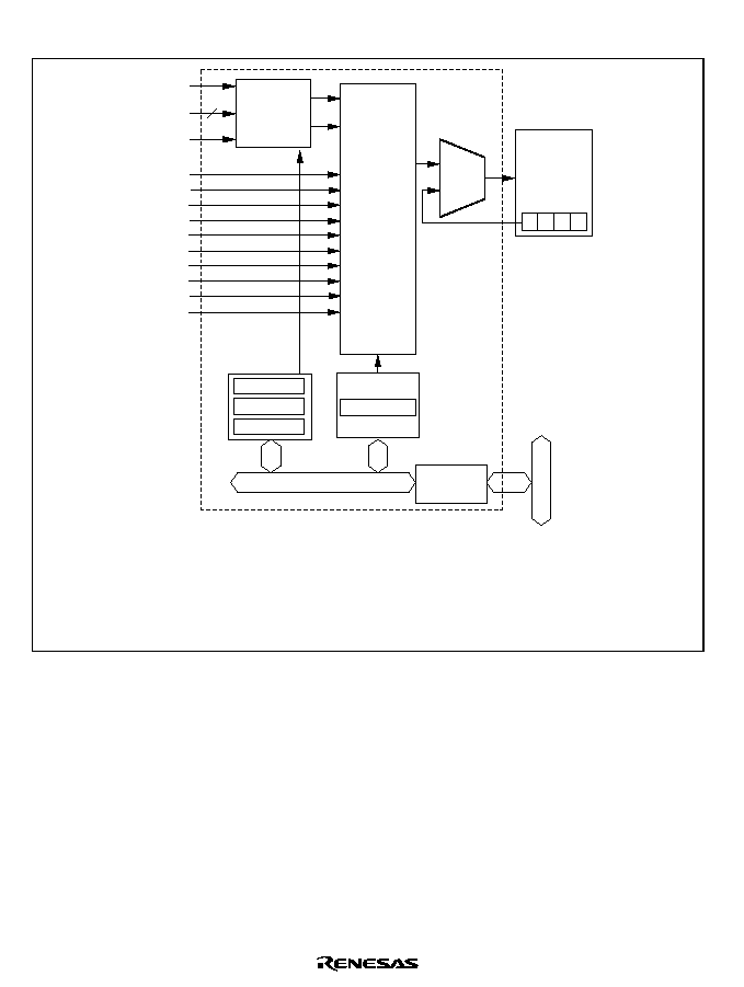
Rev. 2.00, 09/03, page 126 of 690
Figure 6.1 shows a block diagram of the INTC.
DMAC
SCIF
ADC
USB
TMU
TPU
WDT
UDI
REF
RTC
6
DMAC : Direct memory access controller
SCIF
: Serial communication interface (with FIFO)
ADC :
A/D
converter
USB
: USB interface
TMU
: Timer pulse unit
TPU
: 16-bit timer pulse unit
WDT
: Watchdog timer
UDI
: User debugging interface
RTC : Realtime clock
REF
: Refresh request in bus state controller
ICR
: Interrupt control register
IPR
: Interrupt priority level setting register
IRR
: Interrupt request register
PINTER : PINT interrupt enable register
SR
: Status register
Input/output
control
Priority
identifier
Com-
parator
Interrupt
request
SR
CPU
Bus
interface
Internal bus
INTC
I3 I2 I1 I0
(Interrupt request)
ICR
IRR
Legend:
PINTER
IRQ5
-IRQ0
16
PINT15
-PINT0
NMI
IPR
Figure 6.1 Block Diagram of INTC

Rev. 2.00, 09/03, page 127 of 690
6.2
Input/Output Pins
Table 6.1 shows the INTC pin configuration.
Table 6.1
Pin Configuration
Name
Abbreviation
I/O
Description
Nonmaskable interrupt input pin
NMI
Input
Input of interrupt request signal, not
maskable by the interrupt mask bits
in SR
Interrupt input pins
IRQ5 to IRQ0,
IRL3
to
IRL0
Input
Input of interrupt request signals
Port interrupt input pins
PINT15 to
PINT0
Input
Input of port interrupt signals
Note:
IRL3
to
IRL0
are multiplexed with IRQ3 to IRQ0; they cannot be used together with IRQ3 to
IRQ0 at the same time.
6.3
Register Descriptions
The INTC has the following registers. For details on register addresses and register states during
each processing, refer to section 24, List of Registers.
∑
Interrupt control register 0 (ICR0)
∑
Interrupt control register 1 (ICR1)
∑
Interrupt control register 2 (ICR2)
∑
PINT interrupt enable register (PINTER)
∑
Interrupt priority level setting register A (IPRA)
∑
Interrupt priority level setting register B (IPRB)
∑
Interrupt priority level setting register C (IPRC)
∑
Interrupt priority level setting register D (IPRD)
∑
Interrupt priority level setting register E (IPRE)
∑
Interrupt priority level setting register F (IPRF)
∑
Interrupt priority level setting register G (IPRG)
∑
Interrupt priority level setting register H (IPRH)
∑
Interrupt request register 0 (IRR0)
∑
Interrupt request register 1 (IRR1)
∑
Interrupt request register 2 (IRR2)

Rev. 2.00, 09/03, page 128 of 690
6.3.1
Interrupt Priority Level Setting Registers A to H (IPRA to IPRH)
IPRA to IPRH are 16-bit readable/writable registers in which priority levels from 0 to 15 are set
for on-chip peripheral module, and IRQ and PINT interrupts.
Bit
Bit Name
Initial Value
R/W
Description
15 to 0
IPR15 to
IPR0
0
R/W
These bits set the priority level for each interrupt
source in 4-bit units. For details, see table 6.2.
Table 6.2
Interrupt Sources and IPRA to IPRH
Register
Bits 15 to 12
Bits 11 to 8
Bits 7 to 4
Bits 3 to 0
IPRA
TMU0
TMU1
TMU2
RTC
IPRB
WDT
REF
Reserved
*
Reserved
*
IPRC
IRQ3
IRQ2
IRQ1
IRQ0
IPRD
PINT0 to PINT7
PINT8 to PINT15
IRQ5
IRQ4
IPRE
DMAC
SCIF0
SCIF2
ADC
IPRF
Reserved
*
Reserved
*
USB
Reserved
*
IPRG
TPU0
TPU1
Reserved
*
Reserved
*
IPRH
TPU2
TPU3
Reserved
*
Reserved
*
Note:
*
Always read as 0. The write value should always be 0.
As shown in table 6.2, on-chip peripheral module, or IRQ or PINT interrupts are assigned to four
4-bit groups in each register. These 4-bit groups (bits 15 to 12, bits 11 to 8, bits 7 to 4, and bits 3
to 0) are set with values from H'0 (0000) to H'F (1111). Setting H'0 means priority level 0
(masking is requested); H'F means priority level 15 (the highest level).

Rev. 2.00, 09/03, page 129 of 690
6.3.2
Interrupt Control Register 0 (ICR0)
ICR0 is a register that sets the input signal detection mode of external interrupt input pin NMI, and
indicates the input signal level at the NMI pin.
Bit
Bit Name
Initial Value
R/W
Description
15
NMIL
0/1
*
R
NMI Input Level
Sets the level of the signal input at the NMI pin.
This bit can be read from to determine the NMI
pin level. This bit cannot be modified.
0: NMI input level is low
1: NMI input level is high
14 to 9
0
R
Reserved
These bits are always read as 0. The write value
should always be 0.
8
NMIE
0
R/W
NMI Edge Select
Selects whether the falling or rising edge of the
interrupt request signal at the NMI pin is
detected.
0: Interrupt request is detected on falling edge of
NMI input
1: Interrupt request is detected on rising edge of
NMI input
7 to 0
0
R
Reserved
These bits are always read as 0. The write value
should always be 0.
Note:
*
When NMI input is high, 0 when NMI input is low.

Rev. 2.00, 09/03, page 130 of 690
6.3.3
Interrupt Control Register 1 (ICR1)
ICR1 is a 16-bit register that specifies the detection mode for external interrupt input pins IRQ0 to
IRQ5 individually: rising edge, falling edge, high level, or low level.
Bit
Bit Name
Initial Value
R/W
Description
15
MAI
0
R/W
Mask All Interrupts
When set to 1, masks all interrupt requests when
a low level is being input to the NMI pin. Masks
NMI interrupts in standby mode.
0: All interrupt requests are not masked when a
low level is being input to the NMI pin
1: All interrupt requests are masked when a low
level is being input to the NMI pin
14
IRQLVL
1
R/W
Interrupt Request Level Detect
Selects whether the IRQ3 to IRQ0 pins are
enabled or disabled to be used as four
independent interrupt pins. This bit does not
affect the IRQ4 and IRQ5 pins.
0: Used as four independent interrupt request
pins IRQ3 to IRQ0
1: Used as encoded 15-level interrupt pins as
IRL3
to
IRL0
13
BLMSK
0
R/W
BL Bit Mask
Specifies whether NMI interrupts are masked
when the BL bit of the SR register is 1.
0: NMI interrupts are masked when the BL bit is 1
1: NMI interrupts are accepted regardless of the
BL bit setting
12
0
R
Reserved
This bit is always read as 0. The write value
should always be 0.

Rev. 2.00, 09/03, page 131 of 690
Bit
Bit Name
Initial Value
R/W
Description
IRQn Sense Select
Select whether the interrupt signals to the IRQ5
to IRQ0 pins are detected at the falling edge, at
the rising edge, at low level, or at high level.
Bit 2n+1 Bit 2n
IRQn1S IRQn0S
0
0
An interrupt request is
detected at IRQn input
falling edge
0
1
An interrupt request is
detected at IRQn input
rising edge
1
0
An interrupt request is
detected at IRQn input
low level
1
1
An interrupt request is
detected at IRQn input
high level
11 to 0
IRQ51S to
IRQ00S
0
R/W
[Legend] n = 0 to 5

Rev. 2.00, 09/03, page 132 of 690
6.3.4
Interrupt Control Register 2 (ICR2)
ICR2 is a 16-bit register that specifies the detection mode for external interrupt input pins PINT15
to PINT0.
Bit
Bit Name
Initial Value
R/W
Description
15 to 0
PINT15S to
PINT0S
0
R/W
PINT15 to PINT0 Sense Select
Select whether interrupt request signals to
PINT15 to PINT0 are detected at low levels or
high levels.
PINTnS
0: Interrupt requests are detected at low level
input to the PINT pins
1: Interrupt requests are detected at high level
input to the PINT pins
[Legend] n = 0 to 15
6.3.5
PINT Interrupt Enable Register (PINTER)
PINTER is a 16-bit register that enables interrupt requests input to external interrupt input pins
PINT0 to PINT15.
When all or some of these pins, PINT0 to PINT15 are not used as an interrupt input, a bit
corresponding to a pin unused as an interrupt request should be cleared to 0.
Bit
Bit Name
Initial Value
R/W
Description
15 to 0
PINT15E to
PINT0E
0
R/W
PINT15 to PINT0 Interrupt Enable
Select whether the interrupt requests input to the
PINT15 to PINT0 pins is enabled.
PINTnE
0: Disables PINT input interrupt requests
1: Enables PINT input interrupt requests
[Legend] n = 0 to 15

Rev. 2.00, 09/03, page 133 of 690
6.3.6
Interrupt Request Register 0 (IRR0)
IRR0 is an 8-bit register that indicates interrupt requests from external input pins IRQ0 to IRQ5
and PINT0 to PINT15.
Bit
Bit Name
Initial Value
R/W
Description
7
PINT0R
0
R
PINT0 to PINT7 Interrupt Request
Indicates whether interrupt requests are input to
PINT0 to PINT7 pins.
0: Interrupt requests are not input to PINT0 to
PINT7 pins
1: Interrupt requests are input to PINT0 to PINT7
pins
6
PINT1R
0
R
PINT8 to PINT15 Interrupt Request
Indicates whether interrupt requests are input to
PINT8 to PINT15 pins.
0: Interrupt requests are not input to PINT8 to
PINT15 pins
1: Interrupt requests are input to PINT8 to
PINT15 pins
5 to 0
IRQ5R to
IRQ0R
0
R/W
IRQn Interrupt Request
Indicates whether there is interrupt request input
to the IRQn pin. When edge-detection mode is
set for IRQn, an interrupt request is cleared by
writing 0 to the IRQnR bit after reading IRQnR =
1.
When level-detection mode is set for IRQn, these
bits indicate whether an interrupt request is input.
The interrupt request is set/cleared by only 1/0
input to the IRQn pin.
IRQnR
0: No interrupt request input to IRQn pin
1: Interrupt request input to IRQn pin
[Legend] n = 0 to 5

Rev. 2.00, 09/03, page 134 of 690
6.3.7
Interrupt Request Register 1 (IRR1)
IRR1 is an 8-bit register that indicates whether DMAC or SCIF0 interrupt requests are generated.
Bit
Bit
Name
Initial
Value
R/W
Description
7
TXI0R
0
R
TXI0 Interrupt Request
Indicates whether a TXI0 (SCIF0) interrupt request is generated.
0: A TXI0 interrupt request is not generated
1: A TXI0 interrupt request is generated
6
0
R
Reserved
This bit is always read as 0.
5
RXI0R
0
R
RXI0 Interrupt Request
Indicates whether an RXI0 (SCIF0) interrupt request is
generated.
0: An RXI0 interrupt request is not generated
1: An RXI0 interrupt request is generated
4
ERI0R
0
R
ERI0 Interrupt Request
Indicates whether an ERI0 (SCIF0) interrupt request is
generated.
0: An ERI0 interrupt request is not generated
1: An ERI0 interrupt request is generated
3
DEI3R
0
R
DEI3 Interrupt Request
Indicates whether a DEI3 (DMAC) interrupt request is generated.
0: A DEI3 interrupt request is not generated
1: A DEI3 interrupt request is generated
2
DEI2R
0
R
DEI2 Interrupt Request
Indicates whether a DEI2 (DMAC) interrupt request is generated.
0: A DEI2 interrupt request is not generated
1: A DEI2 interrupt request is generated
1
DEI1R
0
R
DEI1 Interrupt Request
Indicates whether a DEI1 (DMAC) interrupt request is generated.
0: A DEI1 interrupt request is not generated
1: A DEI1 interrupt request is generated

Rev. 2.00, 09/03, page 135 of 690
Bit
Bit
Name
Initial
Value
R/W
Description
0
DEI0R
0
R
DEI0 Interrupt Request
Indicates whether a DEI0 (DMAC) interrupt request is generated.
0: A DEI0 interrupt request is not generated
1: A DEI0 interrupt request is generated
6.3.8
Interrupt Request Register 2 (IRR2)
IRR2 is an 8-bit register that indicates whether SCIF2 or ADC interrupt requests are generated.
Bit
Bit
Name
Initial
Value
R/W
Description
7 to 5
0
R
Reserved
These bits are always read as 0.
4
ADIR
0
R
ADI Interrupt Request
Indicates whether an ADI (ADC) interrupt request is generated.
0: An ADI interrupt request is not generated
1: An ADI interrupt request is generated
3
TXI2R
0
R
TXI2 Interrupt Request
Indicates whether a TXI2 (SCIF2) interrupt request is generated.
0: A TXI2 interrupt request is not generated
1: A TXI2 interrupt request is generated
2
0
R
Reserved
This bit is always read as 0.
1
RXI2R
0
R
RXI2 Interrupt Request
Indicates whether an RXI2 (SCIF2) interrupt request is
generated.
0: An RXI2 interrupt request is not generated
1: An RXI2 interrupt request is generated
0
ERI2R
0
R
ERI2 Interrupt Request
Indicates whether an ERI2 (SCIF2) interrupt request is
generated.
0: An ERI2 interrupt request is not generated
1: An ERI2 interrupt request is generated

Rev. 2.00, 09/03, page 136 of 690
6.4
Interrupt Sources
There are five types of interrupt sources: NMI, IRQ, IRL, PINT, and on-chip peripheral modules.
Each interrupt has a priority level (0 to 16), with 1 the lowest and 16 the highest. Priority level 0
masks an interrupt, so the interrupt request is ignored.
6.4.1
NMI Interrupt
The NMI interrupt has the highest priority level of 16. When the BLMSK bit in the interrupt
control register 1 (ICR1) is 1 or the BL bit in the status register (SR) is 0, NMI interrupt is
accepted. NMI interrupt is edge-detected. In sleep or standby mode, the interrupt is accepted
regardless of the BL setting. The NMI edge select bit (NMIE) in the interrupt control register 0
(ICR0) is used to select either rising or falling edge detection.
When using edge-input detection for NMI interrupt, a pulse width of at least two P
cycles
(peripheral clock) is necessary. NMI interrupt exception handling does not affect the interrupt
mask level bits (I3 to I0) in the status register (SR). When the MAI bit in ICR1 is 1, NMI interrupt
is not accepted.
It is possible to wake the chip up from sleep mode or standby mode with an NMI interrupt.
6.4.2
IRQ Interrupts
IRQ interrupts are input by level or edge from pins IRQ0 to IRQ5. The priority level can be set by
interrupt priority registers C and D (IPRC and IPRD) in a range from 0 to 15.
When using edge-sensing for IRQ interrupts, clear the interrupt source by having software read 1
from the corresponding bit in IRR0, then write 0 to the bit.
When ICR1 is rewritten, IRQ interrupts may be mistakenly detected, depending on the IRQ pin
states. To prevent this, rewrite the register while interrupts are masked, then release the mask after
clearing the illegal interrupt by writing 0 to interrupt request register 0 (IRR0).
Edge input interrupt detection requires input of a pulse width of more than two cycles on a P clock
basis.
When using level-sensing for IRQ interrupts, the pin levels must be retained until the CPU
samples the pins. Therefore, the interrupt source must be cleared by the interrupt handler.
The interrupt mask bits (I3 to I0) in the status register (SR) are not affected by IRQ interrupt
handling. IRQ interrupts can wake the chip up from the standby state when the relevant interrupt
level is higher than I3 to I0 in SR (but only when the RTC is used, the clock for the RTC is used to
wake the chip up from the standby state).
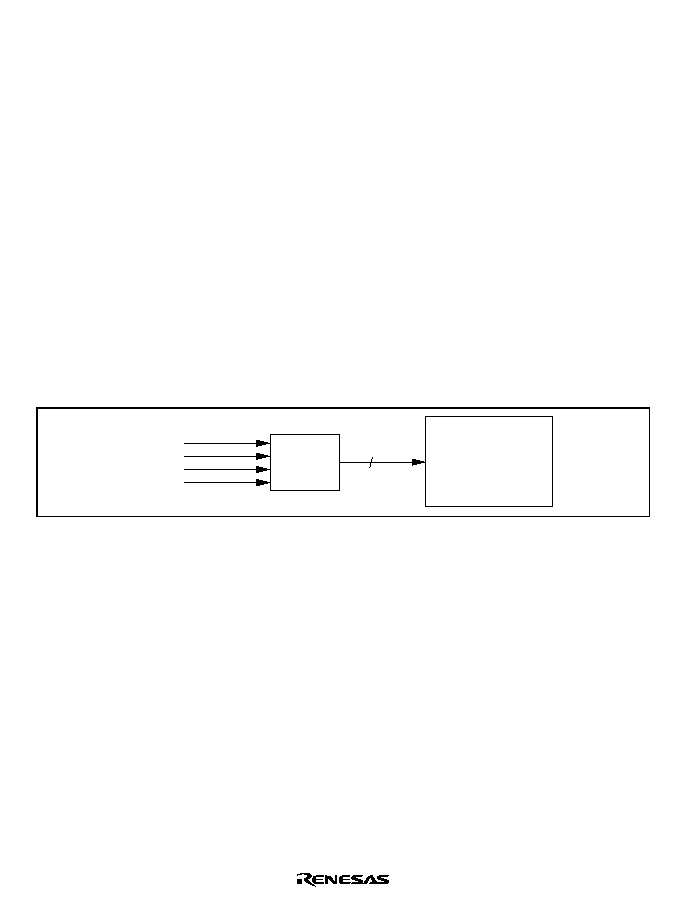
Rev. 2.00, 09/03, page 137 of 690
6.4.3
IRL Interrupts
IRL interrupts are input by level at pins
IRL3 to IRL0. The priority level is the higher of those
indicated by pins
IRL3 to IRL0. An IRL3 to IRL0 value of 0 (0000) indicates the highest-level
interrupt request (interrupt priority level 15). A value of 15 (1111) indicates no interrupt request
(interrupt priority level 0). Figure 6.2 shows an examples of an IRL interrupt connection. Table
6.3 shows
IRL pin and interrupt levels.
A noise-cancellation feature is built in, and the IRL interrupt is not detected unless the levels
sampled at every peripheral clock remain unchanged for two consecutive cycles, so that no
transient level on the
IRL pin change is detected. In standby mode, as the peripheral clock is
stopped, noise cancellation is performed using the clock for the RTC instead. Therefore when the
RTC is not used, recovery from standby mode by means of IRL interrupts cannot be performed in
standby mode.
The priority level of the IRL interrupt must not be lowered unless the interrupt is accepted and the
interrupt processing starts. However, the priority level can be changed to a higher one.
The interrupt mask bits (I3 to I0) in the status register (SR) are not affected by
IRL interrupt
processing.
Interrupt
request
Priority
encoder
IRL3 to IRL0
4
This LSI
IRL3 to IRL0
Figure 6.2 Example of IRL Interrupt Connection

Rev. 2.00, 09/03, page 138 of 690
Table 6.3
IRL3 to IRL0 Pins and Interrupt Levels
IRL3
IRL2
IRL1
IRL0
Interrupt Priority Level
Interrupt Request
0
0
0
0
15
Level 15 interrupt request
0
0
0
1
14
Level 14 interrupt request
0
0
1
0
13
Level 13 interrupt request
0
0
1
1
12
Level 12 interrupt request
0
1
0
0
11
Level 11 interrupt request
0
1
0
1
10
Level 10 interrupt request
0
1
1
0
9
Level 9 interrupt request
0
1
1
1
8
Level 8 interrupt request
1
0
0
0
7
Level 7 interrupt request
1
0
0
1
6
Level 6 interrupt request
1
0
1
0
5
Level 5 interrupt request
1
0
1
1
4
Level 4 interrupt request
1
1
0
0
3
Level 3 interrupt request
1
1
0
1
2
Level 2 interrupt request
1
1
1
0
1
Level 1 interrupt request
1
1
1
1
0
No interrupt request
6.4.4
PINT Interrupt
PINT interrupts are input from pins PINT0 to PINT15 with a level. The priority level can be set by
the interrupt priority level setting register D (IPRD) in a range from levels 0 to 15, in the unit of
PINT0 to PINT7 or PINT8 to PINT15. The PINT interrupt level should be held until the interrupt
is accepted and interrupt handling is started.
The interrupt mask bits (I3 to I0) in the status register (SR) are not affected by PINT interrupt
processing. PINT interrupts can wake the chip up from the standby state when the relevant
interrupt level is higher than I3 to I0 in SR (but only when the RTC is used, the clock for the RTC
is used to wake the chip up from the standby state).
6.4.5
On-Chip Peripheral Module Interrupts
On-chip peripheral module interrupts are generated by the following 10 modules:
∑
Direct memory access controller (DMAC)
∑
Serial communication interfaces (SCIF0 and SCIF2)
∑
A/D converter (ADC)

Rev. 2.00, 09/03, page 139 of 690
∑
USB interface (USB)
∑
Timer unit (TMU)
∑
16-bit timer pulse unit (TPU)
∑
Watchdog timer (WDT)
∑
Bus state controller (BSC)
∑
User-debugging interface (UDI)
∑
Realtime clock (RTC)
Not every interrupt source is assigned a different interrupt vector. Sources are reflected in the
interrupt event registers (INTEVT and INTEVT2). It is easy to identify sources by using the value
of INTEVT or INTEVT2 as a branch offset.
A priority level (from 0 to 15) can be set for each module except UDI by writing to the interrupt
priority level setting registers A to H (IPRA to IPRH). The priority level of the UDI interrupt is 15
(fixed).
The interrupt mask bits (I3 to I0) in the status register are not affected by on-chip peripheral
module interrupt handling.
6.4.6
Interrupt Exception Handling and Priority
There are five types of interrupt sources: NMI, IRQ, IRL, PINT, and on-chip peripheral modules.
The priority of each interrupt source is set within priority levels 0 to 16; level 16 is the highest and
level 1 is the lowest. When the priority is set to level 0, that interrupt is masked and the interrupt
request is ignored.
Tables 6.4 and 6.5 list the codes for the interrupt source and the interrupt event registers (INTEVT
and INTEVT2) and the order of interrupt priority.
Each interrupt source is assigned a unique code by INTEVT and INTEVT2. The start address of
the interrupt service routine is common for each interrupt source. This is why, for instance, the
value of INTEVT2 is used as an offset at the start of the interrupt service routine and branched to
in order to identify the interrupt source.
IRQ and PINT interrupts, and on-chip peripheral module interrupt priorities can be set freely
between 0 and 15 for each module by setting the interrupt priority level setting registers. A reset
assigns priority level 0 to IRQ, PINT, and on-chip peripheral module interrupts.
If the same priority level is assigned to two or more interrupt sources and interrupts from those
sources occur simultaneously, their priority order is the default priority order indicated at the right
in tables 6.4 and 6.5.

Rev. 2.00, 09/03, page 140 of 690
Table 6.4
Interrupt Exception Handling Sources and Priority (IRQ Mode)
Interrupt Source
Interrupt Code
*
1
Interrupt
Priority
(Initial Value)
IPR
(Bit Numbers)
Priority
within IPR
Setting Unit
Default
Priority
NMI
H'1C0
*
2
16
High
UDI
H'5E0
*
2
15
IRQ0
H'600
*
3
0 to 15 (0)
IPRC (3 to 0)
IRQ1
H'620
*
3
0 to 15 (0)
IPRC (7 to 4)
IRQ2
H'640
*
3
0 to 15 (0)
IPRC (11 to 8)
IRQ3
H'660
*
3
0 to 15 (0)
IPRC (15 to 12)
IRQ4
H'680
*
3
0 to 15 (0)
IPRD (3 to 0)
IRQ
IRQ5
H'6A0
*
3
0 to 15 (0)
IPRD (7 to 4)
PINT0 to
PINT7
H'700
*
3
0 to 15 (0)
IPRD (15 to 12)
PINT
PINT8 to
PINT15
H'720
*
3
0 to 15 (0)
IPRD (11 to 8)
DEI0
H'800
*
3
High
DEI1
H'820
*
3
DEI2
H'840
*
3
DMAC
DEI3
H'860
*
3
0 to 15 (0)
IPRE (15 to 12)
Low
ERI0
H'880
*
3
0 to 15 (0)
IPRE (11 to 8)
High
RXI0
H'8A0
*
3
SCIF0
TXI0
H'8E0
*
3
Low
ERI2
H'900
*
3
High
RXI2
H'920
*
3
SCIF2
TXI2
H'960
*
3
0 to 15 (0)
IPRE (7 to 4)
Low
ADC
ADI
H'980
*
3
0 to 15 (0)
IPRE (3 to 0)
--
USI0
H'A20
*
3
High
USB
USI1
H'A40
*
3
0 to 15 (0)
IPRF (7 to 4)
Low
TPU0
TPI0
H'C00
*
3
0 to 15 (0)
IPRG (15 to 12) --
TPU1
TPI1
H'C20
*
3
0 to 15 (0)
IPRG (11 to 8)
--
TPU2
TPI2
H'C80
*
3
0 to 15 (0)
IPRH (15 to 12) --
TPU3
TPI3
H'CA0
*
3
0 to 15 (0)
IPRH (11 to 8)
--
Low
Rev. 2.00, 09/03, page 141 of 690
Interrupt Source
Interrupt Code
*
1
Interrupt
Priority
(Initial Value)
IPR
(Bit Numbers)
Priority
within IPR
Setting Unit
Default
Priority
TMU0
TUNI0
H'400
*
2
0 to 15 (0)
IPRA (15 to 12) --
High
TMU1
TUNI1
H'420
*
2
0 to 15 (0)
IPRA (11 to 8)
--
TUNI2
H'440
*
2
High
TMU2
TICPI2
H'460
*
2
0 to 15 (0)
IPRA (7 to 4)
Low
ATI
H'480
*
2
High
PRI
H'4A0
*
2
RTC
CUI
H'4C0
*
2
0 to 15 (0)
IPRA (3 to 0)
Low
WDT
ITI
H'560
*
2
0 to 15 (0)
IPRB (15 to 12) --
REF
RCMI
H'580
*
2
0 to 15 (0)
IPRB (11 to 8)
--
Low
Notes: 1. The INTEVT2 code.
2. The same code as INTEVT2 is set in INTEVT.
3. The code indicating an interrupt level (H'200 to H'3C0 shown in table 6.6) is set in
INTEVT.
Rev. 2.00, 09/03, page 142 of 690
Table 6.5
Interrupt Exception Handling Sources and Priority (IRL Mode)
Interrupt Source
Interrupt Code
*
1
Interrupt
Priority
(Initial Value)
IPR (Bit
Numbers)
Priority
within IPR
Setting Unit
Default
Priority
NMI
H'1C0
*
2
16
--
--
High
UDI
H'5E0
*
2
15
--
--
IRL
IRL
(3:0) = 0000
H'200
*
3
15
--
--
IRL
(3:0) = 0001
H'220
*
3
14
--
--
IRL
(3:0) = 0010
H'240
*
3
13
--
--
IRL
(3:0) = 0011
H'260
*
3
12
--
--
IRL
(3:0) = 0100
H'280
*
3
11
--
--
IRL
(3:0) = 0101
H'2A0
*
3
10
--
--
IRL
(3:0) = 0110
H'2C0
*
3
9
--
--
IRL
(3:0) = 0111
H'2E0
*
3
8
--
--
IRL
(3:0) = 1000
H'300
*
3
7
--
--
IRL
(3:0) = 1001
H'320
*
3
6
--
--
IRL
(3:0) = 1010
H'340
*
3
5
--
--
IRL
(3:0) = 1011
H'360
*
3
4
--
--
IRL
(3:0) = 1100
H'380
*
3
3
--
--
IRL
(3:0) = 1101
H'3A0
*
3
2
--
--
IRL
(3:0) = 1110
H'3C0
*
3
1
--
--
IRQ
IRQ4
H'680
*
3
0 to 15 (0)
IPRD (3 to 0) --
IRQ5
H'6A0
*
3
0 to 15 (0)
IPRD (7 to 4) --
PINT
PINT0 to PINT 7 H'700
*
3
0 to 15 (0)
IPRD (15 to
12)
--
PINT8 to PINT 15 H'720
*
3
0 to 15 (0)
IPRD (11 to
8)
--
DMAC
DEI0
H'800
*
3
0 to 15 (0)
IPRE (15 to
12)
High
DEI1
H'820
*
3
DEI2
H'840
*
3
DEI3
H'860
*
3
Low
SCIF0
ERI0
H'880
*
3
0 to 15 (0)
IPRE (11 to 8)High
RXI0
H'8A0
*
3
TXI0
H'8E0
*
3
Low
Low
Rev. 2.00, 09/03, page 143 of 690
Interrupt Source
Interrupt Code
*
1
Interrupt
Priority
(Initial Value)
IPR (Bit
Numbers)
Priority
within IPR
Setting Unit
Default
Priority
SCIF2
ERI2
H'900
*
3
0 to 15 (0)
IPRE (7 to 4) High
High
RXI2
H'920
*
3
TXI2
H'960
*
3
Low
ADC
ADI
H'980
*
3
0 to 15 (0)
IPRE (3 to 0) --
USB
USI0
H'A20
*
3
0 to 15 (0)
IPRF (7 to 4) High
USI1
H'A40
*
3
Low
TPU0
TPI0
H'C00
*
3
0 to 15 (0)
IPRG (15 to
12)
--
TPU1
TPI1
H'C20
*
3
0 to 15 (0)
IPRG (11 to
8)
--
TPU2
TPI2
H'C80
*
3
0 to 15 (0)
IPRH (15 to
12)
--
TPU3
TPI3
H'CA0
*
3
0 to 15 (0)
IPRH (11 to
8)
--
TMU0
TUNI0
H'400
*
2
0 to 15 (0)
IPRA (15 to
12)
--
TMU1
TUNI1
H'420
*
2
0 to 15 (0)
IPRA (11 to 8)--
TMU2
TUNI2
H'440
*
2
0 to 15 (0)
IPRA (7 to 4) High
TICPI2
H'460
*
2
Low
RTC
ATI
H'480
*
2
0 to 15 (0)
IPRA (3 to 0) High
PRI
H'4A0
*
2
CUI
H'4C0
*
2
Low
WDT
ITI
H'560
*
2
0 to 15 (0)
IPRB (15 to
12)
--
REF
RCMI
H'580
*
2
0 to 15 (0)
IPRB (11 to 8)--
Low
Notes: 1. The INTEVT2 code.
2. The same code as INTEVT2 is set in INTEVT.
3. The code indicating an interrupt level (H'200 to H'3C0 shown in table 6.6) is set in
INTEVT.

Rev. 2.00, 09/03, page 144 of 690
Table 6.6
Interrupt Level and INTEVT Code
Interrupt level
INTEVT Code
15
H'200
14
H'220
13
H'240
12
H'260
11
H'280
10
H'2A0
9
H'2C0
8
H'2E0
7
H'300
6
H'320
5
H'340
4
H'360
3
H'380
2
H'3A0
1
H'3C0
6.5
Operation
6.5.1
Interrupt Sequence
The sequence of interrupt operations is described below. Figure 6.3 is a flowchart of the
operations.
1. The interrupt request sources send interrupt request signals to the interrupt controller.
2. The interrupt controller selects the highest-priority interrupt from the interrupt requests sent,
following the priority levels set in the interrupt priority level setting registers A to H (IPRA to
IPRH). Lower priority interrupts are held pending. If two of these interrupts have the same
priority level or if multiple interrupts occur within a single module, the interrupt with the
highest priority is selected, according to tables 6.4 and 6.5.
3. The priority level of the interrupt selected by the interrupt controller is compared with the
interrupt mask bits (I3 to I0) in the status register (SR) of the CPU. If the request priority level
is higher than the level in bits I3 to I0, the interrupt controller accepts the interrupt and sends
an interrupt request signal to the CPU.
4. Detection timing: The INTC operates, and notifies the CPU of interrupt requests, in
synchronization with the peripheral clock (P
). The CPU receives an interrupt at a break in
instructions.

Rev. 2.00, 09/03, page 145 of 690
5. The interrupt source code is set in the interrupt event registers (INTEVT and INTEVT2).
6. The status register (SR) and program counter (PC) are saved to SSR and SPC, respectively.
7. The block bit (BL), mode bit (MD), and register bank bit (RB) in SR are set to 1.
8. The CPU jumps to the start address of the interrupt handler (the sum of the value set in the
vector base register (VBR) and H'00000600). This jump is not a delayed branch. The interrupt
handler may branch with INTEVT or INTEVT2 value as its offset in order to identify the
interrupt source. This enables it to branch to the handling routine for the individual interrupt
source.
Notes: 1. The interrupt mask bits (I3 to I0) in the status register (SR) are not changed by
acceptance of an interrupt in this LSI.
2. The interrupt source flag should be cleared in the interrupt handler. To ensure that an
interrupt request that should have been cleared is not inadvertently accepted again, read
the interrupt source flag after it has been cleared, and then execute an RTE instruction.
Rev. 2.00, 09/03, page 146 of 690
Yes
Yes
Yes
Yes
Yes
Yes
Yes
Yes
Yes
Yes
Yes
Yes
Yes
No
No
No
No
No
No
No
No
No
No
No
No
No
Program
execution state
Interrupt
generated?
ICR1.MAI = 1?
ICR1.BLMSK = 1?
NMI?
NMI = low?
SR.BL=0
or sleep mode or software
standby mode?
NMI?
Level 15
interrupt?
I3-I0 level
14 or lower?
Level 14
interrupt?
I3-I0 level
13 or lower?
Level 1
interrupt?
I3-I0
level 0?
Set interrupt source in
INTEVT and INTEVT2
Save SR to SSR;
save PC to SPC
Set BL/MD/RB
bits in SR to 1
Branch to exception
handler
I3-I0: Interrupt mask bits in status register (SR)
Figure 6.3 Interrupt Operation Flowchart

Rev. 2.00, 09/03, page 147 of 690
6.5.2
Multiple Interrupts
When handling multiple interrupts, an interrupt handler should include the following procedures:
1. Branch to a specific interrupt handler corresponding to a code set in INTEVT or INTEVT2.
The code in INTEVT or INTEVT2 can be used as an offset for branching to the specific
handler.
2. Clear the interrupt source in each specific handler.
3. Save SSR and SPC to memory.
4. Clear the BL bit in SR, and set the accepted interrupt level in the interrupt mask bits in SR.
5. Handle the interrupt.
6. Execute the RTE instruction.
When these procedures are followed in order, an interrupt of higher priority than the one being
handled can be accepted after clearing BL in step 4. Figure 6.3 shows a sample interrupt operation
flowchart.
6.6
Usage Note
The interrupt accept timing in this LSI is not acknowledged externally. Thus, keep the following
note in mind when designing the system.
∑
Level interrupt
The level interrupt request should be held until the CPU accepts it. The level interrupt request
needs to be cleared (released) within the specific interrupt handler. If the level interrupt request
is not held, the operation may branch to the interrupt handling routine when the value in
INTEVT/2 becomes H'000.
When the standby state is cancelled, if the level interrupt request is not held, the operation will
go back to the standby state again in the middle of WDT counting. When canceling the
standby state again in such a condition by asserting the level interrupt request, the settling time
for the PLL or crystal oscillator is not secured enough and the operation may not recover from
the standby state correctly.
∑
Interrupt flag update
When an interrupt is acceptable and the generation of an interrupt request is enabled, updating
or clearing the interrupt flag may branch the operation to the interrupt handling routine when
the value in INTEVT2 becomes H'000.

Rev. 2.00, 09/03, page 148 of 690

BSCS311A_000020020100
Rev. 2.00, 09/03, page 149 of 690
Section 7 Bus State Controller (BSC)
7.1
Overview
The bus state controller (BSC) outputs control signals for various types of memory that is
connected to the external address space and external devices. BSC functions enable this LSI to
connect directly with SRAM, SDRAM, and other memory storage devices, and external devices.
7.1.1
Features
The BSC has the following features:
∑
Physical address space is divided into eight areas
A maximum 32 or 64 Mbytes for each of the eight areas, CS0, CS2 to CS4, CS5A, CS5B,
CS6A and CS6B, totally 384 Mbytes.
Can specify the normal space interface, byte-selection SRAM interface, burst ROM,
address/data multiplex I/O (MPX), or SDRAM for each address space.
Can select the data bus width (8, 16, or 32 bits) for each address space.
Controls the insertion of the wait state for each address space.
Controls the insertion of the wait state for each read access and write access.
Can set the independent idling cycle in the continuous access for five cases: read-write (in
same space/different space), read-read (in same space/different space), the first cycle is a
write access.
∑
Normal space interface
Supports the interface that can directly connect to the SRAM.
∑
Burst ROM interface
High-speed access to the ROM, such as flash memory, that has the page mode function.
∑
Address/data multiplex I/O (MPX) interface
Can directly connect to a peripheral LSI that needs an address/data multiplexing.
∑
SDRAM interface
Can set the SDRAM up to 2 areas.
Multiplex output for row address/column address.
Efficient access by single read/single write.
High-speed access by the bank-active mode.
Supports an auto-refresh and self-refresh.
Rev. 2.00, 09/03, page 150 of 690
∑
Bus arbitration
Shares all of the resources with other CPU and outputs the bus enable after receiving the
bus request from external devices.
7.1.2
Block Diagram
BSC functional block diagram is shown in figure 7.1.
Output
signal drive
controller
Wait between
access cycles
controller
Wait
controller
Memory
controller
Refresh
controller
Address/data
controller
Area
controller
CMNCR
CSnBCR
*
CSnWCR
*
SDCR
RTCSR
RTCNT
RTCOR
Comparator
CS0, CS2, CS3, CS4,
CS5A, CS5B, CS6A, CS6B
BS, RD, RD/WR, WE3 to WE0,
RASU, RASL, CASU, CASL,
AH, CKE, DQMUU, DQMUL,
DQMLU, DQMLL
WAIT
A25 to 0
D31 to 0
Internal
address bus
Internal
data bus
Note:
* CSnBCR, CSnWCR : n = 0, 2, 3, 4, 5A, 5B, 6A, 6B
Legend:
CSnBCR
: Area n bus control register
CSnWCR
: Area n wait control register
SDCR
: SDRAM control register
RTCSR
: Refresh timer control/status register
RTCNT
: Refresh timer counter
RTCOR
: Refresh timer constant register
BSC
Figure 7.1 BSC Functional Block Diagram

Rev. 2.00, 09/03, page 151 of 690
7.2
Pin Configuration
Table 7.1
Pin Configuration
Name
I/O
Function
A25 to A0
O
Address bus
D31 to D0
I/O
Data bus
BS
O
Bus cycle start
Asserted when a normal space, byte-selection SRAM, burst ROM, or
address/data multiplex I/O is accessed. Asserted by the same timing
as
CAS
in SDRAM access.
CS0
,
CS2
to
CS4
,
CS5A
,
CS5B
,
CS6A
,
CS6B
O
Chip select
RD/
WR
O
Read/write
Connects to
WE
pins when SDRAM or byte-selection SRAM is
connected.
RD
O
Read
WE3
,
DQMUU
O
Indicates that D31 to D24 are being written to when a normal space
is set.
Selects D31 to D24 when a byte-selection SRAM space is set.
Selects D31 to D24 when an SDRAM space is set.
WE2
,
DQMUL
O
Indicates that D23 to D16 are being written to when a normal space
is set.
Selects D23 to D16 when a byte-selection SRAM space is set.
Selects D23 to D16 when an SDRAM space is set.
WE1
,
DQMLU
O
Indicates that D15 to D8 are being written to when a normal space
and address/data multiplex I/O space are set.
Selects D15 to D8 when a byte-selection SRAM space is set.
Selects D15 to D8 when an SDRAM space is set.
WE0
,
DQMLL
O
Indicates that D7 to D0 are being written to when a normal space
and address/data multiplex I/O space are set.
Selects D7 to D0 when a byte-selection SRAM space is set.
Selects D7 to D0 when an SDRAM space is set.
RASU
RASL
O
Connects to
RAS
pin when SDRAM is connected.
CASU
CASL
O
Connects to
CAS
pin when SDRAM is connected.

Rev. 2.00, 09/03, page 152 of 690
Name
I/O
Function
CKE
O
Connects to CKE pin when SDRAM is connected.
AH
O
Holds the address in address/data multiplex I/O mode.
WAIT
I
External wait input
BREQ
I
Bus request input
BACK
O
Bus acknowledge output
MD3, MD4
I
Area 0 bus width (8/16/32 bits)
MD5
I
Specifies endian
0: Big endian
1: Little endian
7.3
Area Overview
In the architecture of this LSI, both logical spaces and physical spaces have 32-bit address spaces.
The cache access method is shown by the upper 3 bits. For details see section 4, Cache. The
remaining 29 bits are used for division of the space into eight areas. The BSC performs control for
this 29-bit space.
As listed in table 7.2, this LSI can be connected directly to eight areas of memory, and it outputs
chip select signals (
CS0, CS2 to CS4, CS5A, CS5B, CS6A, and CS6B) for each of them. CS0 is
asserted during area 0 access;
CS5B is asserted during area 5B access. When an SDRAM is
connected to area 2 or area 3,
RASU, RASL, CASU, CASL, DQMUU, DQMUL, DQMLU, and
DQMLL are asserted.
7.3.1
Address Map
The external address space has a capacity of 384 Mbytes and is used by dividing 8 partial spaces.
The kind of memory to be connected and the data bus width are specified in each partial space.
The address map for the external address space is listed below.
Table 7.2
Physical Address Space Map
Area
Memory to be
Connected
Physical Address
Capacity
Access
Size
H'00000000
to H'03FFFFFF
64 Mbytes 8, 16, 32
*
2
Area 0
Normal memory
*
1
,
Burst ROM
H'00000000
to H'03FFFFFF
+
H'20000000
◊
n
+
H'20000000
◊
n
Shadow
(n: 1 to 6)

Rev. 2.00, 09/03, page 153 of 690
Area
Memory to be
Connected
Physical Address
Capacity
Access
Size
H'04000000
to H'07FFFFFF
Area 1
Internal I/O register
*
7
H'04000000
to H'07FFFFFF
+
H'20000000
◊
n
+
H'20000000
◊
n
(n:1 to 6)
H'08000000
to H'0BFFFFFF
64 Mbytes 8, 16, 32
*
3,
*
5
Area 2
Normal memory
*
1
,
Synchronous DRAM
H'08000000
to H'0BFFFFFF
+
H'20000000
◊
n
+
H'20000000
◊
n
Shadow
(n:1 to 6)
H'0C000000
to H'0FFFFFFF
64 Mbytes 8, 16, 32
*
3,
*
5
Area 3
Normal memory
*
1
,
Synchronous DRAM
H'0C000000
to H'0FFFFFFF
+
H'20000000
◊
n
+
H'20000000
◊
n
Shadow
(n: 1 to 6)
H'10000000
to H'13FFFFFF
64 Mbytes 8, 16, 32
*
3
Area 4
Normal memory
*
1
,
Burst ROM,
Byte-selection SRAM
H'10000000
to H'13FFFFFF
+
H'20000000
◊
n
+
H'20000000
◊
n
Shadow
(n: 1 to 6)
H'14000000
to H'15FFFFFF
32 Mbytes 8, 16, 32
*
3
Area 5A
Normal memory
*
1
H'14000000
to H'15FFFFFF
+
H'20000000
◊
n
+
H'20000000
◊
n
Shadow
(n: 1 to 6)
H'16000000
to H'17FFFFFF
32 Mbytes 8, 16
*
3,
*
4
Area 5B
Normal memory
*
1
,
Address/data multiplex
I/O (MPX), Byte-
selection SRAM
H'16000000
to H'17FFFFFF
+
H'20000000
◊
n
+
H'20000000
◊
n
Shadow
(n: 1 to 6)
H'18000000
to H'19FFFFFF
32 Mbytes 8, 16
*
3
Area 6A
Normal memory
*
1
H'18000000
to H'19FFFFFF
+
H'20000000
◊
n
+
H'20000000
◊
n
Shadow
(n: 1 to 6)
H'1A000000
to H'1BFFFFFF
32 Mbytes 8, 16
*
3
Area 6B
Normal memory
*
1
H'1A000000
to H'1BFFFFFF
+
H'20000000
◊
n
+
H'20000000
◊
n
Shadow
(n: 1 to 6)
Area 7
*
6
Reserved area
H'1C000000
to H'1FFFFFFF
+
H'20000000
◊
n
+
H'20000000
◊
n
(n: 0 to 7)
Notes: 1. Memory that has an interface such as SRAM or ROM.
2. Memory bus width is specified by an external pin.
3. Memory bus width is specified by a register.
4. With the address/data multiplex I/O (MPX) interface, the bus width must be 16 bits.
5. With the SDRAM, the bus width must be 16 bits or 32 bits.
6. Do not access the reserved area. If the reserved area is accessed, the operation cannot
be guaranteed.
7. When the addresses of the on-chip module control registers (internal I/O registers) in
area 1 are not translated by the MMU, set the top three bits of the logical addresses to
101 to allocate in the P2 space.
Rev. 2.00, 09/03, page 154 of 690
Area 0 (
CS0)
H'00000000
H'20000000
H'40000000
H'60000000
H'80000000
H'A0000000
H'C0000000
H'E0000000
Internal I/O
Area 2 (
CS2)
Area 3 (
CS3)
Area 4 (
CS4)
Area 5A (
CS5A)
Area 6A (
CS6A)
H'00000000
H'04000000
H'08000000
H'0C000000
H'10000000
H'14000000
H'18000000
Reserved area
Physical address space
Logical address space
Note: For logical address spaces P0 and P3, when the memory management unit (MMU) is on, it can
optionally generate a physical address for the logical address. This figure can be applied when
MMU is off and when the MMU is on and each physical address for the logical address is equal
except for higher three bits. When translating a logical address to a physical address, refer to
table 7.2.
P0
P1
P2
P3
P4
Area 5B (
CS5B)
Area 6B (
CS6B)
H'16000000
H'1A000000
H'1BFFFFFF
Figure 7.2 Address Space
7.3.2
Memory Bus Width
The memory bus width in this LSI can be set for each area. In area 0, external pins can be used to
select byte (8 bits), word (16 bits), or longword (32 bits) on power-on reset. The correspondence
between the external pins (MD3, MD4) and memory size is listed in the table below.
Table 7.3
Correspondence between External Pins (MD3 and MD4) and Memory Size
MD4
MD3
Memory Size
0
Setting prohibited
0
1
8 bits
0
16 bits
1
1
32 bits
For areas other than area 0, byte, word, and longword may be chosen for the bus width using
CSnBCR that can be set in each area. The bus width that can be set differs according to a
connected interface. For more details, see the CSn Bus Control Register.

Rev. 2.00, 09/03, page 155 of 690
When port A or B is used, set the bus width of all areas to 8-bit or 16-bit.
For details see section 7.4.2, CSn Space Bus Control Register (CSnBCR).
7.3.3
Shadow Space
Areas 0, 2 to 4, 5A, 5B, 6A, and 6B are decoded by physical addresses A28 to A26, which
correspond to areas 000 to 110. Address bits 31 to 29 are ignored. This means that the range of
area 0 addresses, for example, is H'00000000 to H'03FFFFFF, and its corresponding shadow space
is the address space obtained by adding to it H'20000000
◊
n (n
=
1 to 6) in areas P1 to P3.
The address range for area 7 is H'1C000000 to H'1FFFFFFF. The address space H'1C000000 +
H'20000000
◊
n to H'1FFFFFFF + H'20000000
◊
n (n
=
0 to 7) corresponding to the area 7
shadow space is reserved, so do not use it.
Area P4 (H'E0000000 to H'EFFFFFFF) is the I/O area where on-chip registers are allocated. This
area has no shadow space.
7.4
Register Descriptions
The BSC has the following registers. Refer to section 24, List of Registers for the details of the
addresses of these registers and the state of registers in each operating mode.
Do not access spaces other than CS0 until the termination of the setting the memory interface.
∑
Common control register (CMNCR)
∑
Bus control register for CS0 space (CS0BCR)
∑
Bus control register for CS2 space (CS2BCR)
∑
Bus control register for CS3 space (CS3BCR)
∑
Bus control register for CS4 space (CS4BCR)
∑
Bus control register for CS5A space (CS5ABCR)
∑
Bus control register for CS5B space (CS5BBCR)
∑
Bus control register for CS6A space (CS6ABCR)
∑
Bus control register for CS6B space (CS6BBCR)
∑
Wait control register for CS0 space (CS0WCR)
∑
Wait control register for CS2 space (CS2WCR)
∑
Wait control register for CS3 space (CS3WCR)
∑
Wait control register for CS4 space (CS4WCR)
∑
Wait control register for CS5A space (CS5AWCR)
∑
Wait control register for CS5B space (CS5BWCR)
∑
Wait control register for CS6A space (CS6AWCR)

Rev. 2.00, 09/03, page 156 of 690
∑
Wait control register for CS6B space (CS6BWCR)
∑
SDRAM control register (SDCR)
∑
Refresh timer control/status register (RTCSR)*
1
∑
Refresh timer counter (RTCNT)*
1
∑
Refresh time constant register (RTCOR)*
1
∑
SDRAM mode register for CS2 space (SDMR2)*
2
∑
SDRAM mode register for CS3 space (SDMR3)*
2
Notes: 1. This register only accepts 32-bit writing to prevent incorrect writing. In this case, the
upper 16 bits of the data must be H'A55A, otherwise writing cannot be performed.
When reading, the upper 16 bits are read as H'0000.
2. The contents of this register are stored in SDRAM. When this register space is
accessed, the corresponding register in SDRAM is written to. For details, refer to
section 7.8.10, Power-On Sequence.
7.4.1
Common Control Register (CMNCR)
CMNCR is a 32-bit register that controls the common items for each area. Do not access external
memory other than area 0 until the CMNCR register initialization is complete.
Bit
Bit
Name
Initial
Value
R/W
Description
31 to 8
0
R
Reserved
These bits are always read as 0. The write value should
always be 0.
7
6
DMAIW1
DMAIW0
0
0
R/W
R/W
Wait states between access cycles when DMA single address
transfer is performed.
Specify the number of idle cycles to be inserted after an
access to an external device with DACK when DMA single
address transfer is performed. The method of inserting idle
cycles depends on the contents of DMAIWA.
00: No idle cycle inserted
01: 1 idle cycle inserted
10: 2 idle cycles inserted
11: 4 idle cycled inserted

Rev. 2.00, 09/03, page 157 of 690
Bit
Bit
Name
Initial
Value
R/W
Description
5
DMAIWA 0
R/W
Method of inserting wait states between access cycles when
DMA single address transfer is performed.
Specifies the method of inserting the idle cycles specified by
the DMAIW1 and DMAIW0 bits. Clearing this bit will make this
LSI insert the idle cycles when another device, which includes
this LSI, drives the data bus after an external device with
DACK drove it. Setting this bit will make this LSI insert the idle
cycles even when the continuous accesses to an external
device with DACK are performed.
4
1
R
Reserved
This bit is always read as 1. The write value should always be
1.
3
ENDIAN 0/1
*
R
Endian Flag
Samples the external pin for specifying endian on power-on
reset (MD5). All address spaces are defined by this bit. This is
a read-only bit.
0: The external pin for specifying endian (MD5) was low level
on power-on reset. This LSI is being operated as big
endian.
1: The external pin for specifying endian (MD5) was high level
on power-on reset. This LSI is being operated as little
endian.
2
0
R
Reserved
This bit is always read as 0. The write value should always be
0.
1
HIZMEM 0
R/W
High-Z Memory Control
Specifies the pin state in software standby mode for A25 to
A0,
BS
,
CS
, RD/
WR
,
WE
, and
RD
.
0: High impedance in software standby mode.
1: Driven in software standby mode
0
HIZCNT
0
R/W
High-Z Control
Specifies the state in software standby mode and bus
released for
RASU
,
RASL
,
CASU
, and
CASL
.
0: High impedance in software standby mode and bus
released for
RASU
,
RASL
,
CASU
, and
CASL
.
1: Driven in standby mode and bus released
for
RASU
,
RASL
,
CASU
, and
CASL
.
Note:
*
The external pin for specifying endian (MD5) is sampled on power-on reset.
When big endian is specified, this bit is read as 0 and when little endian is specified,
this bit is read as 1.

Rev. 2.00, 09/03, page 158 of 690
7.4.2
CSn Space Bus Control Register (CSnBCR) (n = 0, 2, 3, 4, 5A, 5B, 6A, 6B)
CSnBCR is a 32-bit readable/writable register that specifies the function of each area, the number
of idle cycles between bus cycles, and the bus-width.
Do not access external memory other than area 0 until CSnBCR register initialization is
completed.
Bit
Bit
Name
Initial
Value
R/W
Description
31, 30
0
R
Reserved
These bits are always read as 0. The write value should
always be 0.
29
28
IWW1
IWW0
1
1
R/W
R/W
Idle Cycles between Write-read Cycles and Write-write Cycles
These bits specify the number of idle cycles to be inserted
after the access to a memory that is connected to the space.
The target access cycles are the write-read cycle and write-
write cycle.
00: No idle cycle inserted
01: 1 idle cycle inserted
10: 2 idle cycles inserted
11: 4 idle cycles inserted
27
0
R
Reserved
This bit is always read as 0. The write value should always be
0.
26
25
IWRWD1
IWRWD2
1
1
R/W
R/W
Idle Cycles for Another Space Read-write
Specify the number of idle cycles to be inserted after the
access to a memory that is connected to the space. The
target access cycle is a read-write one in which continuous
accesses switch between different spaces.
00: Setting prohibited
01: 2 idle cycles inserted
10: 3 idle cycles inserted
11: 5 idle cycles inserted

Rev. 2.00, 09/03, page 159 of 690
Bit
Bit
Name
Initial
Value
R/W
Description
24
0
R
Reserved
This bit is always read as 0. The write value should always be
0.
23
22
IWRWS1
IWRWS0
1
1
R/W
R/W
Idle Cycles for Read-write in the Same Space
Specify the number of idle cycles to be inserted after the
access to a memory that is connected to the space. The
target cycle is a read-write cycle of which continuous
accesses are for the same space.
00: Setting prohibited.
01: 2 idle cycles inserted
10: 3 idle cycles inserted
11: 5 idle cycles inserted
21
0
R
Reserved
This bit is always read as 0. The write value should always be
0.
20
19
IWRRD1
IWRRD0
1
1
R/W
R/W
Idle Cycles for Read-read in Another Space
Specify the number of idle cycles to be inserted after the
access to a memory that is connected to the space. The
target cycle is a read-read cycle of which continuous
accesses switch between different space.
00: 1 idle cycle inserted
01: 2 idle cycles inserted
10: 3 idle cycles inserted
11: 5 idle cycles inserted
18
0
R
Reserved
This bit is always read as 0. The write value should always be
0.
17
16
IWRRS1
IWRRS0
1
1
R/W
R/W
Idle Cycles for Read-read in the Same Space
Specify the number of idle cycles to be inserted after the
access to a memory that is connected to the space. The
target cycle is a read-read cycle of which continuous
accesses are for the same space.
00: No idle cycle inserted
01: 1 idle cycle inserted
10: 2 idle cycles inserted
11: 4 idle cycles inserted

Rev. 2.00, 09/03, page 160 of 690
Bit
Bit
Name
Initial
Value
R/W
Description
15
0
R
Reserved
This bit is always read as 0. The write value should always be
0.
14
13
12
TYPE2
TYPE1
TYPE0
0
0
0
R/W
R/W
R/W
Memory Type
Specify the type of memory connected to a space.
000: Normal space
001: Burst ROM
010: Address/data multiplex I/O (MPX)
011: Byte-selection SRAM
100: SDRAM
101: Setting prohibited
110: Setting prohibited
111: Setting prohibited
Note:
SDRAM can be specified only in area 2 and area 3. If
SDRAM is connected to only one area, SDRAM
should be specified for area 3. In this case area 2
should be specified as normal space. Burst ROM can
be specified only in area 0 and area 4. Address/data
multiplex I/O (MPX) can be specified only in area 5B.
Byte-selection SRAM can be specified only in area 4
and area 5B.
11
0
R
Reserved
This bit is always read as 0. The write value should always be
0.
10
9
BSZ1
BSZ0
1
1
R/W
R/W
Data Bus Size
Specify the data bus sizes of spaces.
The data bus sizes of areas 2, 3, 4 and 5A are shown below.
00: Setting prohibited.
01: 8-bit size
10: 16-bit size
11: 32-bit size
The data bus sizes of areas 5B, 6A, and 6B are shown below.
00: Setting prohibited.
01: 8-bit size
10: 16-bit size
11: Setting Prohibited

Rev. 2.00, 09/03, page 161 of 690
Bit
Bit
Name
Initial
Value
R/W
Description
8 to 0
0
R
Reserved
These bits are always read as 0. The write value should
always be 0.
Notes: 1. When the CS5B space is specified as address/data multiplex I/O (MPX), specify the
bus size to 16 bits.
2. The data bus size of the CS0 space is specified by an external input pin. The value of
BSZ[1:0] bits in CS0BCR are invalid.
3. When both the CS2 and CS3 spaces are specified as the SDRAM space, specify the
same bus size for the CS2 and CS3 spaces.
4. When the CS2 or CS3 space is specified as the SDRAM space, specify the bus width to
16 bits or 32 bits.
5. The SDRAM bank active mode can only be used for the CS3 space. (Refer to the
explanation of the BACTV bit in the SDRAM control register.)
6. The initial values of the bus size assignment for areas 5B, 6A, and 6B after power-on
reset is specified to prohibited setting. Therefore, specify the 8- or 16-bit size before
accessing these areas.
7. When port A or B is used, specify the bus size of all areas to 8 bits or 16 bits.
When the memory type is specified to an area other than the areas that can be specified, the
operation of this LSI is not guaranteed.
7.4.3
CSn Space Wait Control Register (CSnWCR) (n = 0, 2, 3, 4, 5A, 5B, 6A, 6B)
CSnWCR is a 32-bit readable/writable register that specifies various wait cycles for memory
accesses. The bit configuration of this register varies as shown below according to the memory
type (TYPE 2, TYPE 1, or TYPE 0) specified by the CSn space bus control register (CSnBCR).
Specify the CSnWCR register before accessing the target area. Specify CSnBCR register first,
then specify the CSnWCR register.

Rev. 2.00, 09/03, page 162 of 690
1.
Normal Space, Byte-Selection SRAM, Address/Data Multiplex I/O (MPX)
CS0WCR, CS6AWCR, CS6BWCR
Bit
Bit Name
Initial
Value
R/W
Description
31 to 13
0
R
Reserved
These bits are always read as 0. The write value should
always be 0.
12
11
SW1
SW0
0
0
R/W
R/W
Number of Delay Cycles from Address,
CSn
Assertion to
RD
,
WEn
Assertion
Specify the number of delay cycles from address and
CSn
assertion to
RD
and
WEn
assertion.
00: 0.5 cycles
01: 1.5 cycles
10: 2.5 cycles
11: 3.5 cycles
10
9
8
7
WR3
WR2
WR1
WR0
1
0
1
0
R/W
R/W
R/W
R/W
Number of Access Wait Cycles
Specify the number of cycles that are necessary for read/write
access.
0000: 0 cycle
0001: 1 cycle
0010: 2 cycles
0011: 3 cycles
0100: 4 cycles
0101: 5 cycles
0110: 6 cycles
0111: 8 cycles
1000: 10 cycles
1001: 12 cycles
1010: 14 cycles
1011: 18 cycles
1100: 24 cycles
1101: Setting prohibited
1110: Setting prohibited
1111: Setting prohibited

Rev. 2.00, 09/03, page 163 of 690
Bit
Bit Name
Initial
Value
R/W
Description
6
WM
0
R/W
External Wait Mask Specification
Specifies whether or not the external wait input is valid. The
specification by this bit is valid even when the number of
access wait cycle is 0.
0: External wait is valid
1: External wait is ignored
5 to 2
0
R
Reserved
These bits are always read as 0. The write value should
always be 0.
1
0
HW1
HW0
0
0
R/W
R/W
Delay Cycles from RD,
WEn
negation to Address,
CSn
negation
Specify the number of delay cycles from RD and
WEn
negation to address and
CSn
negation.
00: 0.5 cycles
01: 1.5 cycles
10: 2.5 cycles
11: 3.5 cycles

Rev. 2.00, 09/03, page 164 of 690
CS2WCR, CS3WCR
Bit
Bit
Name
Initial
Value
R/W
Description
31 to 11
0
R
Reserved
These bits are always read as 0. The write value should
always be 0.
10
9
8
7
WR3
WR2
WR1
WR0
1
0
1
0
R/W
R/W
R/W
R/W
Number of Access Wait Cycles
Specify the number of cycles that are necessary for read/write
access.
0000: 0 cycle
0001: 1 cycle
0010: 2 cycles
0011: 3 cycles
0100: 4 cycles
0101: 5 cycles
0110: 6 cycles
0111: 8 cycles
1000: 10 cycles
1001: 12 cycles
1010: 14 cycles
1011: 18 cycles
1100: 24 cycles
1101: Setting prohibited
1110: Setting prohibited
1111: Setting prohibited
6
WM
0
R/W
External Wait Mask Specification
Specify whether or not the external wait input is valid. The
specification by this bit is valid even when the number of
access wait cycle is 0.
0: External wait is valid
1: External wait is ignored
5 to 0
0
R
Reserved
These bits are always read as 0. The write value should
always be 0.

Rev. 2.00, 09/03, page 165 of 690
CS4WCR, CS5AWCR
Bit
Bit
Name
Initial
Value
R/W
Description
31 to 19
0
R
Reserved
These bits are always read as 0. The write value should
always be 0.
18
17
16
WW2
WW1
WW0
0
0
0
R/W
R/W
R/W
Number of Write Access Wait Cycles
Specify the number of cycles that are necessary for write
access.
000: The same cycles as WR3 to WR0 setting (read access
wait)
001: 0 cycle
010: 1 cycles
011: 2 cycles
100: 3 cycles
101: 4 cycles
110: 5 cycles
111: 6 cycles
15 to 13
0
R
Reserved
These bits are always read as 0. The write value should
always be 0.
12
11
SW1
SW0
0
0
R/W
R/W
Number of Delay Cycles from Address,
CSn
Assertion to
RD
,
WEn
Assertion
Specify the number of delay cycles from address and
CSn
assertion to
RD
and
WEn
assertion.
00: 0.5 cycles
01: 1.5 cycles
10: 2.5 cycles
11: 3.5 cycles

Rev. 2.00, 09/03, page 166 of 690
Bit
Bit
Name
Initial
Value
R/W
Description
10
9
8
7
WR3
WR2
WR1
WR0
1
0
1
0
R/W
R/W
R/W
R/W
Number of Access Wait Cycles
Specify the number of cycles that are necessary for read/write
access.
0000: 0 cycle
0001: 1 cycle
0010: 2 cycles
0011: 3 cycles
0100: 4 cycles
0101: 5 cycles
0110: 6 cycles
0111: 8 cycles
1000: 10 cycles
1001: 12 cycles
1010: 14 cycles
1011: 18 cycles
1100: 24 cycles
1101: Setting prohibited
1110: Setting prohibited
1111: Setting prohibited
6
WM
0
R/W
External Wait Mask Specification
Specifies whether or not the external wait input is valid. The
specification by this bit is valid even when the number of
access wait cycle is 0.
0: External wait is valid
1: External wait is ignored
5 to 2
0
R
Reserved
These bits are always read as 0. The write value should
always be 0.
1
0
HW1
HW0
0
0
R/W
R/W
Delay Cycles from RD,
WEn
negation to Address,
CSn
negation
Specify the number of delay cycles from RD and
WEn
negation to address and
CSn
negation.
00: 0.5 cycles
01: 1.5 cycles
10: 2.5 cycles
11: 3.5 cycles

Rev. 2.00, 09/03, page 167 of 690
CS5BWCR
Bit
Bit
Name
Initial
Value
R/W
Description
31 to 21
0
R
Reserved
These bits are always read as 0. The write value should
always be 0.
20
MPXW
0
R/W
MPX Interface Address Wait
Specifies the wait to be inserted between address cycles for
address/data multiplex I/O. This specification is valid only
when area 5B is specified to address/data multiplex I/O.
0: No wait
1: 1 cycle wait inserted
19
0
R
Reserved
This bit is always read as 0. The write value should always be
0.
18
17
16
WW2
WW1
WW0
0
0
0
R/W
R/W
R/W
Number of Write Access Wait Cycles
Specify the number of cycles that are necessary for write
access.
000: The same cycles as WR3 to WR0 setting (read access
wait)
001: 0 cycle
010: 1 cycles
011: 2 cycles
100: 3 cycles
101: 4 cycles
110: 5 cycles
111: 6 cycles
15 to 13
0
R
Reserved
These bits are always read as 0. The write value should
always be 0.
12
11
SW1
SW0
0
0
R/W
R/W
Number of Delay Cycles from Address,
CSn
Assertion to
RD
,
WEn
Assertion
Specify the number of delay cycles from address and
CSn
assertion to
RD
and
WEn
assertion.
00: 0.5 cycles
01: 1.5 cycles
10: 2.5 cycles
11: 3.5 cycles

Rev. 2.00, 09/03, page 168 of 690
Bit
Bit
Name
Initial
Value
R/W
Description
10
9
8
7
WR3
WR2
WR1
WR0
1
0
1
0
R/W
R/W
R/W
R/W
Number of Access Wait Cycles
Specify the number of cycles that are necessary for read/write
access.
0000: 0 cycle
0001: 1 cycle
0010: 2 cycles
0011: 3 cycles
0100: 4 cycles
0101: 5 cycles
0110: 6 cycles
0111: 8 cycles
1000: 10 cycles
1001: 12 cycles
1010: 14 cycles
1011: 18 cycles
1100: 24 cycles
1101: Setting prohibited
1110: Setting prohibited
1111: Setting prohibited
6
WM
0
R/W
External Wait Mask Specification
Specify whether or not the external wait input is valid. The
specification by this bit is valid even when the number of
access wait cycle is 0.
0: External wait is valid
1: External wait is ignored
5 to 2
0
R
Reserved
These bits are always read as 0. The write value should
always be 0.
1
0
HW1
HW0
0
0
R/W
R/W
Delay Cycles from RD,
WEn
negation to Address,
CSn
negation
Specify the number of delay cycles from RD and
WEn
negation to address and
CSn
negation.
00: 0.5 cycles
01: 1.5 cycles
10: 2.5 cycles
11: 3.5 cycles

Rev. 2.00, 09/03, page 169 of 690
2. Burst ROM
CS0WCR
Bit
Bit
Name
Initial
Value
R/W
Description
31 to 18
0
R
Reserved
These bits are always read as 0. The write value should
always be 0.
17
16
BW1
BW0
0
0
R/W
R/W
Number of Burst Wait Cycles
Specify the number of wait cycles to be inserted between the
second or later access cycles in burst access.
00: 0 cycle
01: 1 cycle
10: 2 cycles
11: 3 cycles
15 to 11
0
R
Reserved
These bits are always read as 0. The write value should
always be 0.
10
9
8
7
W3
W2
W1
W0
1
0
1
0
R/W
R/W
R/W
R/W
Number of Access Wait Cycles
Specify the number of wait cycles to be inserted in the first
read/write access cycle.
0000: 0 cycle
0001: 1 cycle
0010: 2 cycles
0011: 3 cycles
0100: 4 cycles
0101: 5 cycles
0110: 6 cycles
0111: 8 cycles
1000: 10 cycles
1001: 12 cycles
1010: 14 cycles
1011: 18 cycles
1100: 24 cycles
1101: Setting prohibited
1110: Setting prohibited
1111: Setting prohibited

Rev. 2.00, 09/03, page 170 of 690
Bit
Bit
Name
Initial
Value
R/W
Description
6
WM
0
R/W
External Wait Mask Specification
Specify whether or not the external wait input is valid. The
specification by this bit is valid even when the number of
access wait cycle is 0.
0: External wait is valid
1: External wait is ignored
5 to 0
0
R
Reserved
These bits are always read as 0. The write value should
always be 0.
CS4WCR
Bit
Bit
Name
Initial
Value
R/W
Description
31 to 18
0
R
Reserved
These bits are always read as 0. The write value should
always be 0.
17
16
BW1
BW0
0
0
R/W
R/W
Number of Burst Wait Cycles
Specify the number of wait cycles to be inserted between the
second or later access cycles in burst access.
00: 0 cycle
01: 1 cycle
10: 2 cycles
11: 3 cycles
15 to 13
0
R
Reserved
These bits are always read as 0. The write value should
always be 0.
12
11
SW1
SW0
0
0
R/W
R/W
Number of Delay Cycles from Address,
CSn
Assertion to
RD
,
WEn
Assertion
Specify the number of delay cycles from address and
CSn
assertion to
RD
and
WEn
assertion.
00: 0.5 cycles
01: 1.5 cycles
10: 2.5 cycles
11: 3.5 cycles

Rev. 2.00, 09/03, page 171 of 690
Bit
Bit
Name
Initial
Value
R/W
Description
10
9
8
7
W3
W2
W1
W0
1
0
1
0
R/W
R/W
R/W
R/W
Number of Access Wait Cycles
Specify the number of wait cycles to be inserted in the first
read/write access cycle.
0000: 0 cycle
0001: 1 cycle
0010: 2 cycles
0011: 3 cycles
0100: 4 cycles
0101: 5 cycles
0110: 6 cycles
0111: 8 cycles
1000: 10 cycles
1001: 12 cycles
1010: 14 cycles
1011: 18 cycles
1100: 24 cycles
1101: Setting prohibited
1110: Setting prohibited
1111: Setting prohibited
6
WM
0
R/W
External Wait Mask Specification
Specifies whether or not the external wait input is valid. The
specification by this bit is valid even when the number of
access wait cycle is 0.
0: External wait is valid
1: External wait is ignored
5 to 2
0
R
Reserved
These bits are always read as 0. The write value should
always be 0.
1
0
HW1
HW0
0
0
R/W
R/W
Delay Cycles from
RD
,
WEn
negation to Address,
CSn
negation
Specify the number of delay cycles from
RD
and
WEn
negation to address and
CSn
negation.
00: 0.5 cycles
01: 1.5 cycles
10: 2.5 cycles
11: 3.5 cycles

Rev. 2.00, 09/03, page 172 of 690
3. SDRAM*
CS2WCR
Bit
Bit
Name
Initial
Value
R/W
Description
31 to 11
0
R
Reserved
These bits are always read as 0. The write value should
always be 0.
10
1
R
Reserved
This bit is always read as 1. The write value should always be
1.
9
0
R
Reserved
This bit is always read as 0. The write value should always be
0.
8
7
A2CL1
A2CL0
1
0
R/W
R/W
CAS Latency for Area 2
Specify the CAS latency for area 2.
00: Setting prohibited.
01: 2 cycles
10: 3 cycles
11: Setting prohibited
6 to 0
0
R
Reserved
These bits are always read as 0. The write value should
always be 0.

Rev. 2.00, 09/03, page 173 of 690
CS3WCR
Bit
Bit
Name
Initial
Value
R/W
Description
31 to 15
0
R
Reserved
These bits are always read as 0. The write value should
always be 0.
14
13
TRP1
TRP0
0
0
R/W
R/W
Number of Cycles from Auto-precharge/PRE Command to
ACTV Command
Specify the number of minimum cycles from the start of auto-
precharge or issuing of PRE command to the issuing of ACTV
command for the same bank. The setting for areas 2 and 3 is
common.
00: 1 cycle
01: 2 cycles
10: 3 cycles
11: 4 cycles
12
0
R
Reserved
This bit is always read as 0. The write value should always be
0.
11
10
TRCD1
TRCD0
0
1
R/W
R/W
Number of Cycles from ACTV Command to
READ(A)/WRIT(A) Command
Specify the number of minimum cycles from issuing ACTV
command to issuing READ(A)/WRIT(A) command. The
setting for areas 2 and 3 is common.
00: 1 cycle
01: 2 cycles
10: 3 cycles
11: 4 cycles
9
0
R
Reserved
This bit is always read as 0. The write value should always be
0.
8
7
A3CL1
A3CL0
1
0
R/W
R/W
CAS Latency for Area 3
Specify the CAS latency for area 3.
00: Setting prohibited.
01: 2 cycles
10: 3 cycles
11: Setting prohibited

Rev. 2.00, 09/03, page 174 of 690
Bit
Bit
Name
Initial
Value
R/W
Description
6, 5
0
R
Reserved
These bits are always read as 0. The write value should
always be 0.
4
3
TRWL1
TRWL0
0
0
R/W
R/W
Number of Cycles from WRITA/WRIT Command to Auto-
precharge/PRE Command
Specifies the number of cycles from issuing WRITA/WRIT
command to the start of auto-precharge or to issuing PRE
command. The setting for areas 2 and 3 is common.
00: 0 cycle
01: 1 cycle
10: 2 cycles
11: Setting prohibited
2
0
R
Reserved
This bit is always read as 0. The write value should always be
0.
1
0
TRC1
TRC0
0
0
R/W
R/W
Number of Cycles from REF Command/Self-refresh Release
to ACTV Command
Specify the number of cycles from issuing the REF command
or releasing self-refresh to issuing the ACTV command. The
setting for areas 2 and 3 is common.
00: 3 cycles
01: 4 cycles
10: 6 cycles
11: 9 cycles
Note:
*
Specify area 3 as SDRAM when only one area is connected with SDRAM. In this case,
specify area 2 as normal space.
7.4.4
SDRAM Control Register (SDCR)
SDCR specifies the method to refresh and access SDRAM, and the types of SDRAMs to be
connected.
The bits other than RFSH and RMODE should be written in the initialization after a power-on
reset and should not be modified after the initialization. When modifying these bits RFSH and
RMODE, do not change the values of other bits and write the previous values. Do not access area
2 or 3 until the SDCR register setting is complete when using synchronous DRAM.

Rev. 2.00, 09/03, page 175 of 690
Bit
Bit
Name
Initial
Value
R/W
Description
31 to 21
0
R
Reserved
These bits are always read as 0. The write value should
always be 0.
20
19
A2ROW1
A2ROW0
0
0
R/W
R/W
Number of Bits of Row Address for Area 2
Specifies the number of bits of row address for area 2.
00: 11 bits
01: 12 bits
10: 13 bits
11: Setting prohibited
18
0
R
Reserved
This bit is always read as 0. The write value should always be
0.
17
16
A2COL1
A2COL0
0
0
R/W
R/W
Number of Bits of Column Address for Area 2
Specifies the number of bits of column address for area 2.
00: 8 bits
01: 9 bits
10: 10 bits
11: Setting prohibited
15 to 13
0
R
Reserved
These bits are always read as 0. The write value should
always be 0.
12
SLOW
0
R/W
Low-Frequency Mode
Specifies the output timing of command, address, and write
data for SDRAM and the latch timing of read data from
SDRAM. Setting this bit makes the hold time for command,
address, write and read data extended. This mode is suitable
for SDRAM with low-frequency clock.
0: Command, address, and write data for SDRAM is output at
the rising edge of CKIO. Read data from SDRAM is
latched at the rising edge of CKIO.
1: Command, address, and write data for SDRAM is output at
the falling edge of CKIO. Read data from SDRAM is
latched at the falling edge of CKIO.

Rev. 2.00, 09/03, page 176 of 690
Bit
Bit
Name
Initial
Value
R/W
Description
11
RFSH
0
R/W
Refresh Control
Specifies whether or not the refresh operation of the SDRAM
is performed.
0: No refresh
1: Refresh
10
RMODE
0
R/W
Refresh Control
Specifies whether to perform auto-refresh or self-refresh
when the RFSH bit is 1. When the RFSH bit is 1 and this bit is
1, self-refresh starts immediately. When the RFSH bit is 1 and
this bit is 0, auto-refresh starts according to the contents that
are set in registers RTCSR, RTCNT, and RTCOR.
0: Auto-refresh is performed
1: Self-refresh is performed
9
0
R
Reserved
This bit is always read as 0. The write value should always be
0.
8
BACTV
0
R/W
Bank Active Mode
Specifies to access whether in auto-precharge mode (using
READA and WRITA commands) or in bank active mode
(using READ and WRIT commands).
0: Auto-precharge mode (using READA and WRITA
commands)
1: Bank active mode (using READ and WRIT commands)
Note:
Bank active mode can be used only when either the
upper or lower bits of the CS3 space are used. When
both the CS2 and CS3 spaces are set to SDRAM,
specify the auto-precharge mode.
7 to 5
0
R
Reserved
These bits are always read as 0. The write value should
always be 0.
4
3
A3ROW1
A3ROW0
0
0
R/W
R/W
Number of Bits of Row Address for Area 3
Specifies the number of bits of the row address for area 3.
00: 11 bits
01: 12 bits
10: 13 bits
11: Setting prohibited

Rev. 2.00, 09/03, page 177 of 690
Bit
Bit
Name
Initial
Value
R/W
Description
2
0
R
Reserved
This bit is always read as 0. The write value should always be
0.
1
0
A3COL1
A3COL0
0
0
R/W
R/W
Number of Bits of Column Address for Area 3
Specifies the number of bits of the column address for area 3.
00: 8 bits
01: 9 bits
10: 10 bits
11: Setting prohibited
7.4.5
Refresh Timer Control/Status Register (RTCSR)
RTCSR specifies various items about refresh for SDRAM.
This register only accepts 32-bit writing to prevent incorrect writing. In this case, the upper 16 bits
of the data must be H'A55A, otherwise writing cannot be performed. When reading, the upper 16
bits are read as H'0000.
RTCSR
Bit
Bit
Name
Initial
Value
R/W
Description
31 to 8
0
R
Reserved
7
CMF
0
R/W
Compare Match Flag
0: Clearing condition When 0 is written in CMF after reading
out RTCSR during CMF = 1.
1: Setting condition When the condition RTCNT = RTCOR is
satisfied.
6
CMIE
0
R/W
CMF Interrupt Enable
0: CMF interrupt request is disabled.
1: CMF interrupt request is enabled.

Rev. 2.00, 09/03, page 178 of 690
Bit
Bit
Name
Initial
Value
R/W
Description
5
4
3
CKS2
CKS1
CKS0
0
0
0
R/W
R/W
R/W
Clock Select
Select the clock input to count-up the refresh timer counter
(RTCNT).
000: Stop the counting-up
001: B
/4
010: B
/16
011: B
/64
100: B
/256
101: B
/1024
110: B
/2048
111: B
/4096
2
1
0
RRC2
RRC1
RRC0
0
0
0
R/W
R/W
R/W
Refresh Count
Specify the number of continuous refresh cycles, when the
refresh request occurs after the coincidence of the values of
the refresh timer counter (RTCNT) and the refresh time
constant register (RTCOR). These bits can make the period
of occurrence of refresh long.
000: Once
001: Twice
010: 4 times
011: 6 times
100: 8 times
101: Setting prohibited.
110: Setting prohibited.
111: Setting prohibited.

Rev. 2.00, 09/03, page 179 of 690
7.4.6
Refresh Timer Counter (RTCNT)
RTCNT is an 8-bit counter that counts up using the clock selected by bits CKS2 to CKS0 in
RTCSR.
This register only accepts 32-bit writing to prevent incorrect writing. In this case, the upper 16 bits
of the data must be H'A55A, otherwise writing cannot be performed. When reading, the upper 16
bits are read as H'0000.
When RTCNT matches RTCOR, RTCNT is cleared to 0. The value in RTCNT returns to 0 after
counting up to 255.
Bit
Bit
Name
Initial
Value
R/W
Description
31 to 8
0
R
Reserved
7 to 0
0
R/W
8-Bit Counter
7.4.7
Refresh Time Constant Register (RTCOR)
RTCOR is an 8-bit register. When RTCOR matches RTCNT, the CMF bit in RTCSR is set to 1
and RTCNT is cleared to 0.
This register only accepts 32-bit writing to prevent incorrect writing. In this case, the upper 16 bits
of the data must be H'A55A, otherwise writing cannot be performed. When reading, the upper 16
bits are read as H'0000.
When the RFSH bit in SDCR is 1, a memory refresh request is issued by this matching signal.
This request is maintained until the refresh operation is performed. If the request is not processed
when the next matching occurs, the previous request is ignored.
When the CMIE bit in RTCSR is 1, an interrupt request is issued by this matching signal. This
request signal is output until the CMF bit in RTCSR is cleared. Clearing the CMF bit only affects
the interrupt and does not affect the refresh request. Accordingly, the refresh requests and interval
timer interrupts can be used together. For example, the number of refresh requests can be counted
by using interrupts while the refresh is performed.

Rev. 2.00, 09/03, page 180 of 690
Bit
Bit
Name
Initial
Value
R/W
Description
31 to 8
0
R
Reserved
These bits are always read as 0. The write value should
always be 0.
7 to 0
0
R/W
Maximum Counter Value (eight bits)
7.4.8
Reset Wait Counter (RWTCNT)
RWTCNT is a 16-bit register. The lower seven bits of this register (bits 6 to 0) are valid as a
counter and the upper nine bits (bits 15 to 7) are reserved. This counter starts to count-up by
synchronizing the CKIO after a power-on reset is released. This counter stops when the value
reaches to H'007F. The access to an external bus has to wait when the counter is operating. This
counter is provided to minimize the time from releasing a reset for flash memory to the first
access. This counter cannot be read or written into.
7.5
Endian/Access Size and Data Alignment
This LSI supports big endian, in which the 0 address is the most significant byte (MSByte) in the
byte data and little endian, in which the 0 address is the least significant byte (LSByte) in the byte
data. Endian is specified on power-on reset by the external pin (MD5). When MD5 pin is low
level on power-on reset, the endian will become big endian and when MD5 pin is high level on
power-on reset, the endian will become little endian. Three data bus widths are available for
normal memory (byte, word, and longword). Word and longword are available for SDRAM. Data
bus width for address/data multiplex I/O (MPX) should be 16 bits. Data alignment is performed in
accordance with the data bus width of the device and endian. This also means that when longword
data is read from a byte-width device, the read operation must be done four times. In this LSI, data
alignment and conversion of data length is performed automatically between the respective
interfaces.
Tables 7.4 to 7.9 show the relationship between endian, device data width, and access unit.

Rev. 2.00, 09/03, page 181 of 690
Table 7.4
32-Bit External Device/Big Endian Access and Data Alignment
Data Bus
Strobe Signals
Operation
D31 to
D24
D23 to
D16
D15 to
D8
D7 to D0
WE3
,
DQMUU
WE2
,
DQMUL
WE1
,
DQMLU
WE0
,
DQMLL
Byte access
at 0
Data 7 to
Data 0
Assert
Byte access
at 1
Data 7 to
Data 0
Assert
Byte access
at 2
Data 7 to
Data 0
Assert
Byte access
at 3
Data 7 to
Data 0
Assert
Word access
at 0
Data 15 to
Data 8
Data 7 to
Data 0
Assert
Assert
Word access
at 2
Data 15
to Data 8
Data 7 to
Data 0
Assert
Assert
Longword
access at 0
Data 31 to
Data 24
Data 23 to
Data 16
Data 15
to Data 8
Data 7 to
Data 0
Assert
Assert
Assert
Assert

Rev. 2.00, 09/03, page 182 of 690
Table 7.5
16-Bit External Device/Big Endian Access and Data Alignment
Data Bus
Strobe Signals
Operation
D31 to
D24
D23 to
D16
D15 to
D8
D7 to D0
WE3
,
DQMUU
WE2
,
DQMUL
WE1
,
DQMLU
WE0
,
DQMLL
Byte access at 0
Data 7 to
Data 0
Assert
Byte access at 1
Data 7 to
Data 0
Assert
Byte access at 2
Data 7 to
Data 0
Assert
Byte access at 3
Data 7 to
Data 0
Assert
Word access at 0
Data 15
to Data 8
Data 7 to
Data 0
Assert
Assert
Word access at 2
Data 15
to Data 8
Data 7 to
Data 0
Assert
Assert
1st
time at 0
Data 31
to Data
24
Data 23
to Data
16
Assert
Assert
Longword
access
at 0
2nd
time at 2
Data 15
to Data 8
Data 7 to
Data 0
Assert
Assert

Rev. 2.00, 09/03, page 183 of 690
Table 7.6
8-Bit External Device/Big Endian Access and Data Alignment
Data Bus
Strobe Signals
Operation
D31 to
D24
D23 to
D16
D15 to
D8
D7 to D0
WE3
,
DQMUU
WE2
,
DQMUL
WE1
,
DQMLU
WE0
,
DQMLL
Byte access at 0
Data 7 to
Data 0
Assert
Byte access at 1
Data 7 to
Data 0
Assert
Byte access at 2
Data 7 to
Data 0
Assert
Byte access at 3
Data 7 to
Data 0
Assert
Word
access at 0
1st time
at 0
Data 15
to Data 8
Assert
2nd time
at 1
Data 7 to
Data 0
Assert
Word
access at 2
1st time
at 2
Data 15
to Data 8
Assert
2nd time
at 3
Data 7 to
Data 0
Assert
Longword
access at 0
1st time
at 0
Data 31
to Data
24
Assert
2nd time
at 1
Data 23
to Data
16
Assert
3rd time
at 2
Data 15
to Data 8
Assert
4th time
at 3
Data 7 to
Data 0
Assert

Rev. 2.00, 09/03, page 184 of 690
Table 7.7
32-Bit External Device/Little Endian Access and Data Alignment
Data Bus
Strobe Signals
Operation
D31 to
D24
D23 to
D16
D15 to
D8
D7 to D0
WE3
,
DQMUU
WE2
,
DQMUL
WE1
,
DQMLU
WE0
,
DQMLL
Byte access
at 0
Data 7 to
Data 0
Assert
Byte access
at 1
Data 7 to
Data 0
Assert
Byte access
at 2
Data 7 to
Data 0
Assert
Byte access
at 3
Data 7 to
Data 0
Assert
Word access
at 0
Data 15
to Data 8
Data 7 to
Data 0
Assert
Assert
Word access
at 2
Data 15 to
Data 8
Data 7 to
Data 0
Assert
Assert
Longword
access at 0
Data 31 to
Data 24
Data 23 to
Data 16
Data 15
to Data 8
Data 7 to
Data 0
Assert
Assert
Assert
Assert

Rev. 2.00, 09/03, page 185 of 690
Table 7.8
16-Bit External Device/Little Endian Access and Data Alignment
Data Bus
Strobe Signals
Operation
D31 to
D24
D23 to
D16
D15 to
D8
D7 to D0
WE3
,
DQMUU
WE2
,
DQMUL
WE1
,
DQMLU
WE0
,
DQMLL
Byte access at 0
Data 7 to
Data 0
Assert
Byte access at 1
Data 7 to
Data 0
Assert
Byte access at 2
Data 7 to
Data 0
Assert
Byte access at 3
Data7 to
Data 0
Assert
Word access at 0
Data 15
to Data 8
Data 7 to
Data 0
Assert
Assert
Word access at 2
Data 15
to Data 8
Data 7 to
Data 0
Assert
Assert
1st
time at 0
Data 15
to Data 8
Data 7 to
Data 0
Assert
Assert
Longword
access
at 0
2nd
time at 1
Data 31
to Data
24
Data 23
to Data
16
Assert
Assert

Rev. 2.00, 09/03, page 186 of 690
Table 7.9
8-Bit External Device/Little Endian Access and Data Alignment
Data Bus
Strobe Signals
Operation
D31 to
D24
D23 to
D16
D15 to
D8
D7 to D0
WE3
,
DQMUU
WE2
,
DQMUL
WE1
,
DQMLU
WE0
,
DQMLL
Byte access at 0
Data 7 to
Data 0
Assert
Byte access at 1
Data 7 to
Data 0
Assert
Byte access at 2
Data 7 to
Data 0
Assert
Byte access at 3
Data 7 to
Data 0
Assert
Word
access at 0
1st time
at 0
Data 7 to
Data 0
Assert
2nd time
at 1
Data 15 to
Data 8
Assert
Word
access at 2
1st time
at 2
Data 7 to
Data 0
Assert
2nd time
at 3
Data 15 to
Data 8
Assert
Longword
access at 0
1st time
at 0
Data 7 to
Data 0
Assert
2nd time
at 1
Data 15 to
Data 8
Assert
3rd time
at 2
Data 23 to
Data 16
Assert
4th time
at 3
Data 31 to
Data 24
Assert

Rev. 2.00, 09/03, page 187 of 690
7.6
Normal Space Interface
7.6.1
Basic Timing
For access to a normal space, this LSI uses strobe signal output in consideration of the fact that
mainly static RAM will be directly connected. When using SRAM with a byte-selection pin, see
section 7.10, Byte-Selection SRAM Interface. Figures 7.3 and 7.4 show the basic timings of
normal space accesses. A no-wait normal access is completed in two cycles. The
BS signal is
asserted for one cycle to indicate the start of a bus cycle.
There is no access size specification when reading. The correct access start address is output in the
least significant bit of the address, but since there is no access size specification, 32 bits are always
read in case of a 32-bit device, and 16 bits in case of a 16-bit device. When writing, only the
WEn
signal for the byte to be written is asserted.
Read/write for cache fill or writeback follows the selected bus width and transfers a total of 16
bytes continuously. The bus is not released during this transfer. For cache misses that occur during
byte or word operand accesses or branching to odd word boundaries, the fill is always performed
by longword accesses on the chip-external interface. Write-through-area write access and non-
cacheable read/write access are based on the actual address size.
It is necessary to output the read out data by using
RD when a buffer is established in the data bus.
The RD/
WR signal is in a read state (high output) when an access is not performed. Therefore,
care must be taken about the collision of output in controlling the external data buffer.
When the WM bit in CSnWCR is cleared to 0, a Tnop cycle is inserted to evaluate an external
wait. When the WM bit in CSnWCR is set to 1, an external wait is ignored and no Tnop cycle is
inserted.
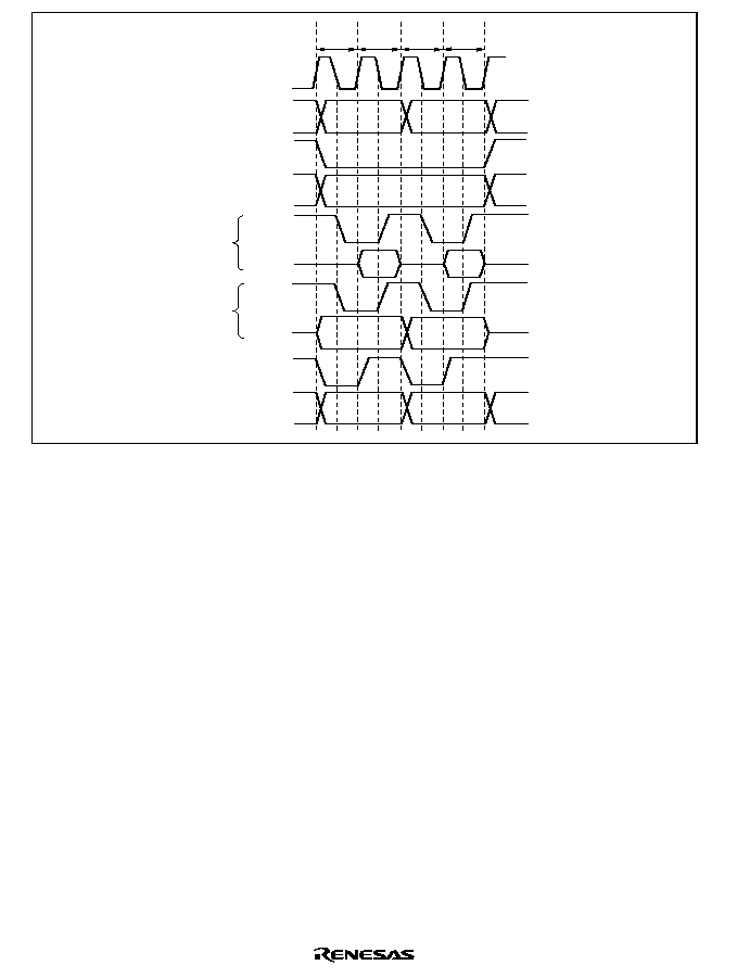
Rev. 2.00, 09/03, page 188 of 690
CKIO
A25 to A0
RD/
WR
Data
DACK
CS
T
1
T
2
T
1
T
2
RD
WEn
BS
Data
Read
Write
Figure 7.3 Continuous Access for Normal Space (No Wait, WM Bit in CSnWCR = 1,
16-Bit Bus Width, Longword Access, No Wait State between Cycles)
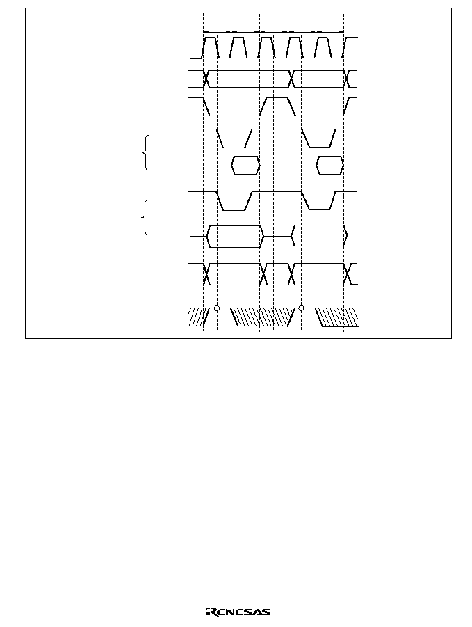
Rev. 2.00, 09/03, page 189 of 690
CKIO
A25 to A0
RD
Data
WEn
Data
DACKn
WAIT
CSn
T
1
T
2
Taw T
1
T
2
Read
Write
Figure 7.4 Continuous Access for Normal Space
(No Wait, One Wait State between Cycles)
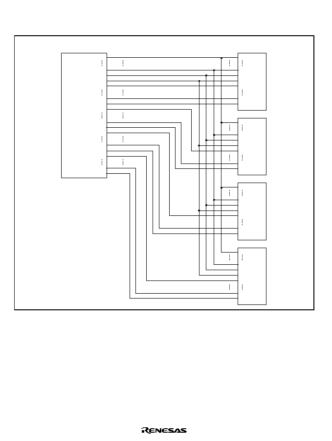
Rev. 2.00, 09/03, page 190 of 690
Figures 7.5 to 7.7 show examples of connection to 32-bit, 16-bit, and 8-bit data-width SRAM,
respectively.
A16
A0
CS
OE
I/O7
I/O0
WE
A18
A2
CSn
RD
D31
D24
WE3
D23
D16
WE2
D15
D8
WE1
D7
D0
WE0
This LSI
128k
◊ 8-bit
SRAM
A16
A0
CS
OE
I/O7
I/O0
WE
A16
A0
CS
OE
I/O7
I/O0
WE
A16
A0
CS
OE
I/O7
I/O0
WE
Figure 7.5 Example of 32-Bit Data-Width SRAM Connection
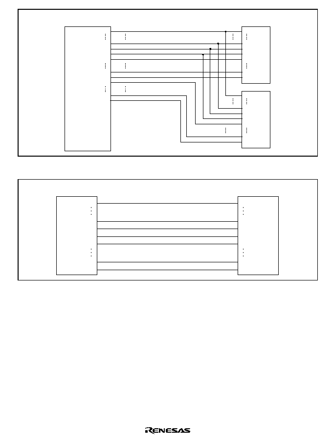
Rev. 2.00, 09/03, page 191 of 690
A16
A0
CS
OE
I/O7
I/O0
WE
A17
A1
CSn
RD
D15
D8
WE1
D7
D0
WE0
This LSI
128k
◊ 8-bit
SRAM
A16
A0
CS
OE
I/O7
I/O0
WE
Figure 7.6 Example of 16-Bit Data-Width SRAM Connection
A16
A0
CS
OE
I/O7
I/O0
WE
A16
A0
CSn
RD
D7
D0
WE0
This LSI
128k
◊ 8-bit
SRAM
Figure 7.7 Example of 8-Bit Data-Width SRAM Connection
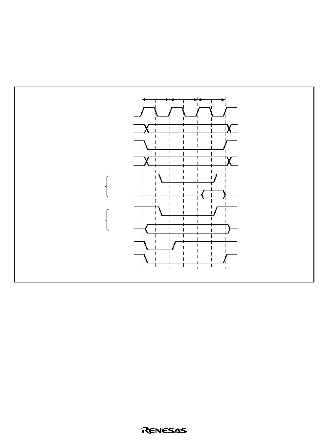
Rev. 2.00, 09/03, page 192 of 690
7.6.2
Access Wait Control
Wait cycle insertion on a normal space access can be controlled by the settings of bits WR3 to
WR0 in CSnWCR. It is possible for areas 4, 5A, and 5B to insert wait cycles independently in
read access and in write access. The areas other than 4, 5A, and 5B have common access wait for
read cycle and write cycle. The specified number of Tw cycles is inserted as wait cycles in a
normal space access shown in figure 7.8.
T
1
CKIO
A25 to A0
CSn
RD/
WR
RD
Data
WEn
Data
BS
Tw
Read
Write
T
2
DACKn
*
Note:
* The waveform for DACKn is when active low is specified.
Figure 7.8 Wait Timing for Normal Space Access (Software Wait Only)

Rev. 2.00, 09/03, page 193 of 690
When the WM bit in CSnWCR is cleared to 0, the external wait input
WAIT signal is also
sampled.
WAIT pin sampling is shown in figure 7.9. A 2-cycle wait is specified as a software
wait. The
WAIT signal is sampled on the falling edge of CKIO at the transition from the T
1
or Tw
cycle to the T
2
cycle.
T
1
CKIO
A25 to A0
CSn
RD/
WR
RD
Data
WEn
Data
WAIT
Tw
Tw
Twx
T
2
Read
Write
BS
Wait states inserted
by
WAIT signal
DACKn
*
Note:
* The waveform for DACKn is when active low is specified.
Figure 7.9 Wait State Timing for Normal Space Access
(Wait State Insertion by
WAIT Signal)
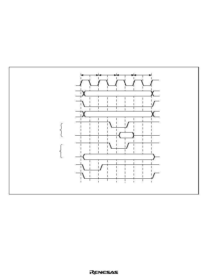
Rev. 2.00, 09/03, page 194 of 690
7.6.3
CSn Assert Period Expansion
The number of cycles from
CSn assertion to RD, WEn assertion can be specified by setting bits
SW1 and SW0 in CSnWCR. The number of cycles from
RD, WEn negation to CSn negation can
be specified by setting bits HW1 and HW0. Therefore, a flexible interface to an external device
can be obtained. Figure 7.10 shows an example. A Th cycle and a Tf cycle are added before and
after an ordinary cycle, respectively. In these cycles,
RD and WEn are not asserted, while other
signals are asserted. The data output is prolonged to the Tf cycle, and this prolongation is useful
for devices with slow writing operations.
T
1
CKIO
A25 to A0
CSn
RD/
WR
RD
Data
WEn
Data
BS
Th
Read
Write
T
2
DACKn
*
Tf
Note:
* The waveform for DACKn is when active low is specified.
Figure 7.10
CSn Assert Period Expansion

Rev. 2.00, 09/03, page 195 of 690
7.7
Address/Data Multiplex I/O Interface
The address/data multiplex (MPX) I/O interface can be selected by setting bits TYPE2 to TYPE0
to 010 in CS5BBCR. Do not set this value to the bits in CSnBCR other than those in area 5B,
otherwise the operation of the LSI is not guaranteed. Access timing for the MPX space is shown
below. In the MPX space,
CS5B, AH, RD, and WEn signals control the accessing. The basic
access for the MPX space consists of 2 cycles of address output followed by an access to a normal
space.
The address output is performed from cycle Ta2 to cycle Ta3. Because cycle Ta1 has a high-
impedance state, collisions of addresses and data can be avoided without inserting idle cycles,
even in continuous accesses. Address output is increased to 3 cycles by setting the MPXW bit to 1
in CS5BWCR. The RD/
WR signal is output at the same time as the CSn signal; it is high in the
read cycle and low in the write cycle.
The data cycle is the same as that in a normal space access.
Timing charts are shown in figures 7.11, 7.12, and 7.13.
T
1
CKIO
A25 to A16
CS5B
RD/
WR
RD
D15 to D0
WEn
D15 to D0
BS
Read
Write
T
2
DACKn
*
Ta1
Ta2
Ta3
AH
Address
Address
Data
Data
Note:
* The waveform for DACKn is when active low is specified.
Figure 7.11 Access Timing for MPX Space
(Address Cycle No Wait, Data Cycle No Wait)
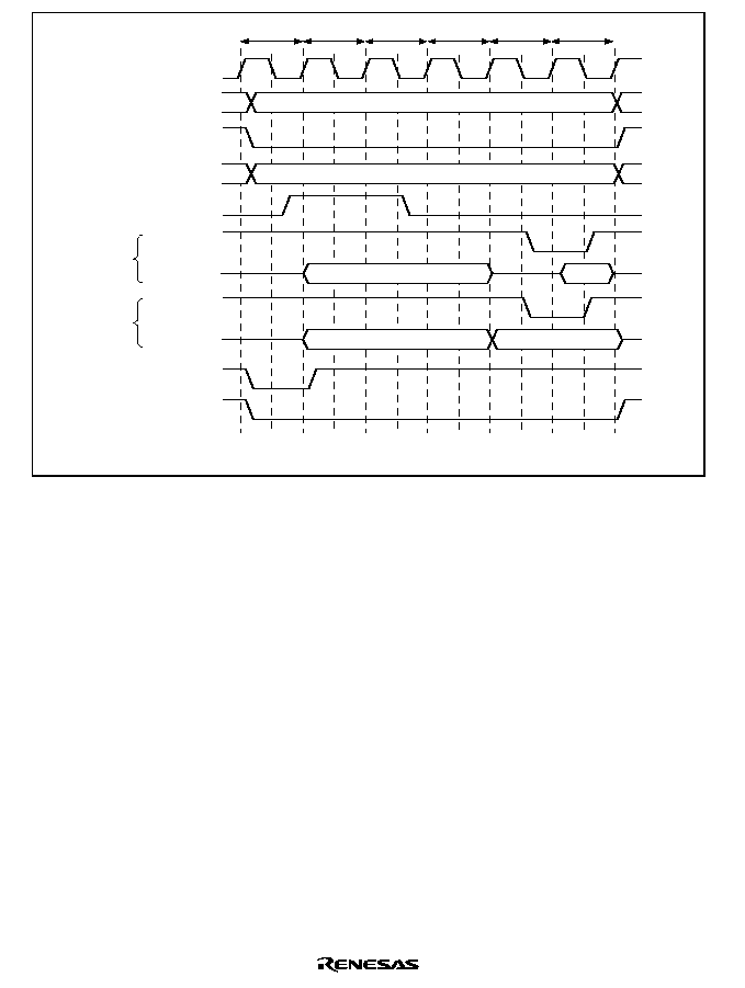
Rev. 2.00, 09/03, page 196 of 690
T
1
CKIO
A25 to A16
CS5B
RD/
WR
RD
D15 to D0
WEn
D15 to D0
BS
Read
Write
T
2
DACKn
*
Ta1
Ta2
Ta3
AH
Address
Address
Data
Data
Tadw
Note:
* The waveform for DACKn is when active low is specified.
Figure 7.12 Access Timing for MPX Space
(Address Cycle Wait 1, Data Cycle No Wait)
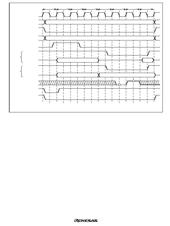
Rev. 2.00, 09/03, page 197 of 690
T
1
CKIO
A25 to A16
CS5B
RD/
WR
RD
D15 to D0
WEn
D15 to D0
BS
Read
Write
T
2
DACKn
*
Ta1
Ta2
Ta3
AH
Address
Address
Data
Data
Tadw
Tw
Twx
WAIT
Note:
* The waveform for DACKn is when active low is specified.
Figure 7.13 Access Timing for MPX Space
(Address Cycle Access Wait 1, Data Cycle Wait 1, External Wait 1)

Rev. 2.00, 09/03, page 198 of 690
7.8
SDRAM Interface
7.8.1
SDRAM Direct Connection
Since synchronous DRAM can be selected by the
CS signal, physical space areas 2 and 3 can be
connected using
RAS and other control signals in common. If the TYPE[2:0] bits in CSnBCR (n =
2 or 3) are set to 100, the synchronous DRAM interface can be selected. Do not set this value to
CSnBCR unless n = 2 or 3, otherwise the operation of this LSI is not guaranteed.
The SDRAM that can be connected to this LSI is a product that has 11/12/13 bits of row address,
8/9/10 bits of column address, 4 or less banks, and uses the A10 pin for setting precharge mode in
read and write command cycles. The control signals for direct connection of SDRAM are
RASU,
RASL, CASU, CASL, RD/WR, DQMUU, DQMUL, DQMLU, DQMLL, CKE, CS2, and CS3.
All the signals other than
CS2 and CS3 are common to all areas, and signals other than CKE are
valid when
CS2 or CS3 is asserted. SDRAM can be connected to up to 2 spaces. The data bus
width of the area that is connected to SDRAM can be set to 32 or 16 bits.
Burst read/single write (burst length 1) and burst read/burst write (burst length 1) are supported as
the SDRAM operating mode.
Commands for SDRAM can be specified by
RASU, RASL, CASU, CASL, RD/WR, and specific
address signals. These commands are shown below.
∑
NOP
∑
Auto-refresh (REF)
∑
Self-refresh (SELF)
∑
All banks pre-charge (PALL)
∑
Specified bank pre-charge (PRE)
∑
Bank active (ACTV)
∑
Read (READ)
∑
Read with pre-charge (READA)
∑
Write (WRIT)
∑
Write with pre-charge (WRITA)
∑
Write mode register (MRS)
The byte to be accessed is specified by DQMUU, DQMUL, DQMLU, and DQMLL. For the
relationship between DQMxx and the byte to be accessed, refer to section 7.5, Endian/Access Size
and Data Alignment.
Figures 7.14 and 7.15 show examples of the connection of SDRAM with the LSI.
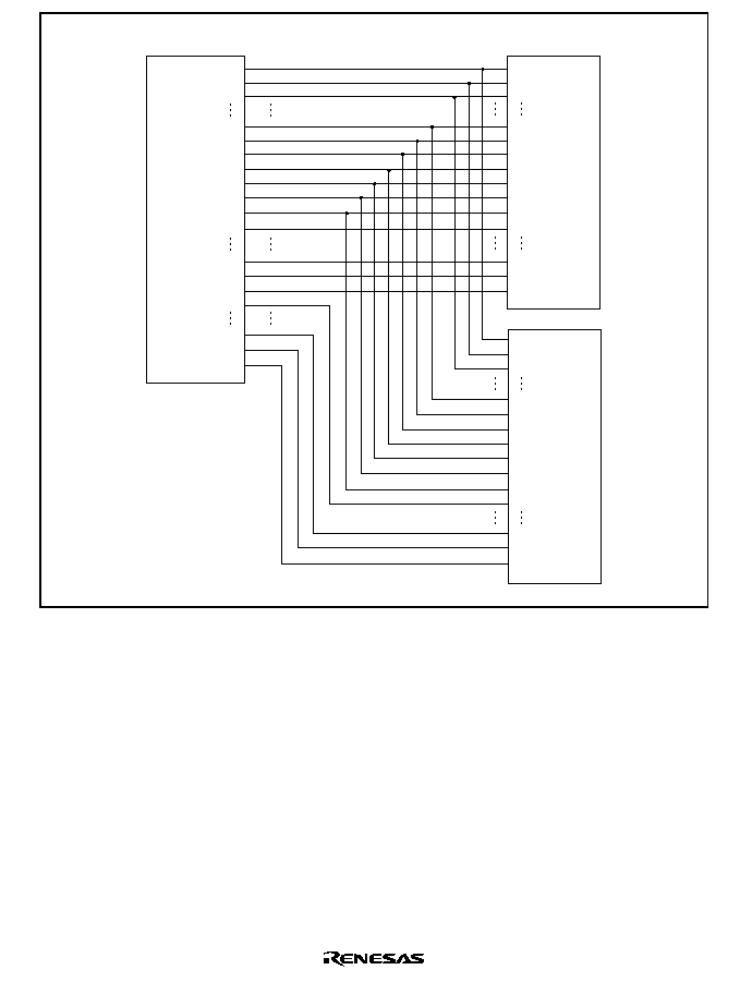
Rev. 2.00, 09/03, page 199 of 690
This LSI
A15
A14
A13
A2
CKIO
CKE
CSn
RASx
CASx
RD/
WR
D31
D16
DQMUU
DQMUL
D15
D0
DQMLU
DQMLL
64M synchronous DRAM
(1M
◊ 16-bit ◊ 4-bank)
A13
A12
A11
A0
CLK
CKE
CS
RAS
CAS
WE
DQ15
DQ0
DQMU
DQML
A13
A12
A11
A0
CLK
CKE
CS
RAS
CAS
WE
DQ15
DQ0
DQMU
DQML
Note: x is U or L
Figure 7.14 Example of 64-MBit Synchronous DRAM Connection (32-Bit Data Bus)
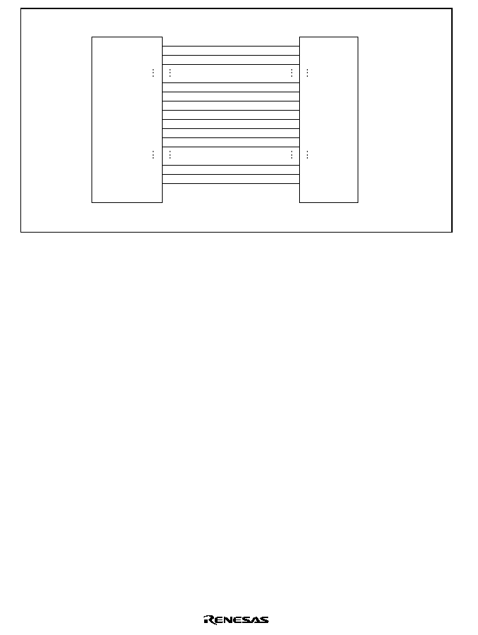
Rev. 2.00, 09/03, page 200 of 690
This LSI
64M synchronous DRAM
(1M
◊ 16-bit ◊ 4-bank)
A14
A13
A12
A1
CKIO
CKE
CSn
RASx
CASx
RD/
WR
D15
D0
DQMLU
DQMLL
A13
A12
A11
A0
CLK
CKE
CS
RAS
CAS
WE
DQ15
DQ0
DQMU
DQML
Note: x is U or L
Figure 7.15 Example of 64-MBit Synchronous DRAM (16-Bit Data Bus)
7.8.2
Address Multiplexing
An address multiplexing is specified so that SDRAM can be connected without external
multiplexing circuitry according to the setting of bits BSZ[1:0] in CSnBCR, AxROW[1:0] and
AxCOL[1:0] in SDCR. Tables 7.10 to 7.15 show the relationship between the settings of bits
BSZ[1:0], AxROW[1:0], and AxCOL[1:0] and the bits output at the address pins. Do not specify
those bits in the manner other than this table, otherwise the operation of this LSI is not guaranteed.
A25 to A18 are not multiplexed and the original values of address are always output at these pins.
When the data bus width is 16 bits (BSZ[1:0] = 10), A0 of SDRAM specifies a word address.
Therefore, connect this A0 pin of SDRAM to the A1 pin of the LSI; the A1 pin of SDRAM to the
A2 pin of the LSI, and so on. When the data bus width is 32 bits (BSZ[1:0] = 11), the A0 pin of
SDRAM specifies a longword address. Therefore, connect this A0 pin of SDRAM to the A2 pin of
the LSI; the A1 pin of SDRAM to the A3 pin of the LSI, and so on.

Rev. 2.00, 09/03, page 201 of 690
Table 7.10
Relationship between A2/3BSZ[1:0], A2/3ROW[1:0], and Address Multiplex
Output (1)-1
Setting
A2/3 BSZ[1:0]
A2/3 ROW[1:0]
A2/3 COL[1:0]
11 (32 bits)
00 (11 bits)
00 (8 bits)
Output Pin of
This LSI
Row Address
Output Cycle
Column Address
Output Cycle
Synchronous DRAM
Pin
Function
A17
A25
A17
A16
A24
A16
A15
A23
A15
Unused
A14
A22
*
2
A22
*
2
A12 (BA1)
A13
A21
*
2
A21
*
2
A11 (BA0)
Specifies bank
A12
A20
L/H
*
1
A10/AP
Specifies
address/precharge
A11
A19
A11
A9
A10
A18
A10
A8
A9
A17
A9
A7
A8
A16
A8
A6
A7
A15
A7
A5
A6
A14
A6
A4
A5
A13
A5
A3
A4
A12
A4
A2
A3
A11
A3
A1
A2
A10
A2
A0
Address
A1
A9
A1
A0
A8
A0
Unused
Example of connected memory
64-Mbit product (512 kwords x 32 bits x 4 banks, column 8 bits product): 1 device
16-Mbit product (512 kwords x 16 bits x 2 banks, column 8 bits product): 2 devices
Notes: 1. L/H is a bit used in the command specification; it is fixed at L or H according to the
access mode.
2. Bank address specification

Rev. 2.00, 09/03, page 202 of 690
Table 7.10
Relationship between A2/3BSZ[1:0], A2/3ROW[1:0], and Address Multiplex
Output (1)-2
Setting
A2/3 BSZ[1:0]
A2/3 ROW[1:0]
A2/3 COL[1:0]
11 (32 bits)
01 (12 bits)
00 (8 bits)
Output Pin of
This LSI
Row Address
Output Cycle
Column Address
Output Cycle
Synchronous DRAM
Pin
Function
A17
A25
A17
A16
A24
A16
Unused
A15
A23
*
2
A23
*
2
A13 (BA1)
A14
A22
*
2
A22
*
2
A12 (BA0)
Specifies bank
A13
A21
A13
A11
Address
A12
A20
L/H
*
1
A10/AP
Specifies
address/precharge
A11
A19
A11
A9
A10
A18
A10
A8
A9
A17
A9
A7
A8
A16
A8
A6
A7
A15
A7
A5
A6
A14
A6
A4
A5
A13
A5
A3
A4
A12
A4
A2
A3
A11
A3
A1
A2
A10
A2
A0
Address
A1
A9
A1
A0
A8
A0
Unused
Example of connected memory
128-Mbit product (1 Mword x 32 bits x 4 banks, column 8 bits product): 1 device
64-Mbit product (1 Mword x 16 bits x 4 banks, column 8 bits product): 2 devices
Notes: 1. L/H is a bit used in the command specification; it is fixed at L or H according to the
access mode.
2. Bank address specification

Rev. 2.00, 09/03, page 203 of 690
Table 7.11
Relationship between A2/3BSZ[1:0], A2/3ROW[1:0], and Address Multiplex
Output (2)-1
Setting
A2/3 BSZ[1:0]
A2/3 ROW[1:0]
A2/3 COL[1:0]
11 (32 bits)
01 (12 bits)
01 (9 bits)
Output Pin of
This LSI
Row Address
Output Cycle
Column Address
Output Cycle
Synchronous DRAM
Pin
Function
A17
A26
A17
A16
A25
A16
Unused
A15
A24
*
2
A24
*
2
A13 (BA1)
A14
A23
*
2
A23
*
2
A12 (BA0)
Specifies bank
A13
A22
A13
A11
Address
A12
A21
L/H
*
1
A10/AP
Specifies
address/precharge
A11
A20
A11
A9
A10
A19
A10
A8
A9
A18
A9
A7
A8
A17
A8
A6
A7
A16
A7
A5
A6
A15
A6
A4
A5
A14
A5
A3
A4
A13
A4
A2
A3
A12
A3
A1
A2
A11
A2
A0
Address
A1
A10
A1
A0
A9
A0
Unused
Example of connected memory
256-Mbit product (2 Mwords x 32 bits x 4 banks, column 9 bits product): 1 device
128-Mbit product (2 Mwords x 16 bits x 4 banks, column 9 bits product): 2 devices
Notes: 1. L/H is a bit used in the command specification; it is fixed at L or H according to the
access mode.
2. Bank address specification

Rev. 2.00, 09/03, page 204 of 690
Table 7.11
Relationship between A2/3BSZ[1:0], A2/3ROW[1:0], and Address Multiplex
Output (2)-2
Setting
A2/3 BSZ[1:0]
A2/3 ROW[1:0]
A2/3 COL[1:0]
11 (32 bits)
01 (12 bits)
10 (10 bits)
Output Pin of
This LSI
Row Address
Output Cycle
Column Address
Output Cycle
Synchronous DRAM
Pin
Function
A17
A27
A17
A16
A26
A16
Unused
A15
A25
*
2
A25
*
2
*
3
A13 (BA1)
A14
A24
*
2
A24
*
2
A12 (BA0)
Specifies bank
A13
A23
A13
A11
Address
A12
A22
L/H
*
1
A10/AP
Specifies
address/precharge
A11
A21
A11
A9
A10
A20
A10
A8
A9
A19
A9
A7
A8
A18
A8
A6
A7
A17
A7
A5
A6
A16
A6
A4
A5
A15
A5
A3
A4
A14
A4
A2
A3
A13
A3
A1
A2
A12
A2
A0
Address
A1
A11
A1
A0
A10
A0
Unused
Example of connected memory
512-Mbit product (4 Mwords x 32 bits x 4 banks, column 10 bits product): 1 device
256-Mbit product (4 Mwords x 16 bits x 4 banks, column 10 bits product): 2 devices
Notes: 1. L/H is a bit used in the command specification; it is fixed at L or H according to the
access mode.
2. Bank address specification
3. Only the
RASL
pin is asserted because the A25 pin specified the bank address.
RASU
is not asserted.

Rev. 2.00, 09/03, page 205 of 690
Table 7.12
Relationship between A2/3BSZ[1:0], A2/3ROW[1:0], and Address Multiplex
Output (3)
Setting
A2/3 BSZ[1:0]
A2/3 ROW[1:0]
A2/3 COL[1:0]
11 (32 bits)
10 (13 bits)
01 (9 bits)
Output Pin of
This LSI
Row Address
Output Cycle
Column Address
Output Cycle
Synchronous DRAM
Pin
Function
A17
A26
A17
Unused
A16
A25
*
2
*
3
A25
*
2
*
3
A14 (BA1)
A15
A24
*
2
A24
*
2
A13 (BA0)
Specifies bank
A14
A23
A14
A12
A13
A22
A13
A11
Address
A12
A21
L/H
*
1
A10/AP
Specifies
address/precharge
A11
A20
A11
A9
A10
A19
A10
A8
A9
A18
A9
A7
A8
A17
A8
A6
A7
A16
A7
A5
A6
A15
A6
A4
A5
A14
A5
A3
A4
A13
A4
A2
A3
A12
A3
A1
A2
A11
A2
A0
Address
A1
A10
A1
A0
A9
A0
Unused
Example of connected memory
512-Mbit product (4 Mwords x 32 bits x 4 banks, column 9 bits product): 1 device
256-Mbit product (4 Mwords x 16 bits x 4 banks, column 9 bits product): 2 devices
Notes: 1. L/H is a bit used in the command specification; it is fixed at L or H according to the
access mode.
2. Bank address specification
3. Only the
RASL
pin is asserted because the A25 pin specified the bank address.
RASU
is not asserted.

Rev. 2.00, 09/03, page 206 of 690
Table 7.13
Relationship between A2/3BSZ[1:0], A2/3ROW[1:0], and Address Multiplex
Output (4)-1
Setting
A2/3 BSZ[1:0]
A2/3 ROW[1:0]
A2/3 COL[1:0]
10 (16 bits)
00 (11 bits)
00 (8 bits)
Output Pin of
This LSI
Row Address
Output Cycle
Column Address
Output Cycle
Synchronous DRAM
Pin
Function
A17
A25
A17
A16
A24
A16
A15
A23
A15
A14
A22
A14
Unused
A13
A21
*
2
A21
*
2
A12 (BA1)
A12
A20
*
2
A20
*
2
A11 (BA0)
Specifies bank
A11
A19
L/H
*
1
A10/AP
Specifies
address/precharge
A10
A18
A10
A9
A9
A17
A9
A8
A8
A16
A8
A7
A7
A15
A7
A6
A6
A14
A6
A5
A5
A13
A5
A4
A4
A12
A4
A3
A3
A11
A3
A2
A2
A10
A2
A1
A1
A9
A1
A0
Address
A0
A8
A0
Unused
Example of connected memory
16-Mbit product (512 kwords x 16 bits x 2 banks, column 8 bits product): 1 device
Notes: 1. L/H is a bit used in the command specification; it is fixed at L or H according to the
access mode.
2. Bank address specification

Rev. 2.00, 09/03, page 207 of 690
Table 7.13
Relationship between A2/3BSZ[1:0], A2/3ROW[1:0], and Address Multiplex
Output (4)-2
Setting
A2/3 BSZ[1:0]
A2/3 ROW[1:0]
A2/3 COL[1:0]
10 (16 bits)
01 (12 bits)
00 (8 bits)
Output Pin of
This LSI
Row Address
Output Cycle
Column Address
Output Cycle
Synchronous DRAM
Pin
Function
A17
A25
A17
A16
A24
A16
A15
A23
A15
Unused
A14
A22
*
2
A22
*
2
A13 (BA1)
A13
A21
*
2
A21
*
2
A12 (BA0)
A12
A20
A12
A11
Specifies bank
Address
A11
A19
L/H
*
1
A10/AP
Specifies
address/precharge
A10
A18
A10
A9
A9
A17
A9
A8
A8
A16
A8
A7
A7
A15
A7
A6
A6
A14
A6
A5
A5
A13
A5
A4
A4
A12
A4
A3
A3
A11
A3
A2
A2
A10
A2
A1
A1
A9
A1
A0
Address
A0
A8
A0
Unused
Example of connected memory
64-Mbit product (1 Mword x 16 bits x 4 banks, column 8 bits product): 1 device
Notes: 1. L/H is a bit used in the command specification; it is fixed at L or H according to the
access mode.
2. Bank address specification

Rev. 2.00, 09/03, page 208 of 690
Table 7.14
Relationship between A2/3BSZ[1:0], A2/3ROW[1:0], and Address Multiplex
Output (5)-1
Setting
A2/3 BSZ[1:0]
A2/3 ROW[1:0]
A2/3 COL[1:0]
10 (16 bits)
01 (12 bits)
01 (9 bits)
Output Pin of
This LSI
Row Address
Output Cycle
Column Address
Output Cycle
Synchronous DRAM
Pin
Function
A17
A26
A17
A16
A25
A16
A15
A24
A15
Unused
A14
A23
*
2
A23
*
2
A13 (BA1)
A13
A22
*
2
A22
*
2
A12 (BA0)
Specifies bank
A12
A21
A12
A11
Address
A11
A20
L/H
*
1
A10/AP
Specifies
address/precharge
A10
A19
A10
A9
A9
A18
A9
A8
A8
A17
A8
A7
A7
A16
A7
A6
A6
A15
A6
A5
A5
A14
A5
A4
A4
A13
A4
A3
A3
A12
A3
A2
A2
A11
A2
A1
A1
A10
A1
A0
Address
A0
A9
A0
Unused
Example of connected memory
128-Mbit product (2 Mwords x 16 bits x 4 banks, column 9 bits product): 1 device
Notes: 1. L/H is a bit used in the command specification; it is fixed at L or H according to the
access mode.
2. Bank address specification

Rev. 2.00, 09/03, page 209 of 690
Table 7.14
Relationship between A2/3BSZ[1:0], A2/3ROW[1:0], and Address Multiplex
Output (5)-2
Setting
A2/3 BSZ[1:0]
A2/3 ROW[1:0]
A2/3 COL[1:0]
10 (16 bits)
01 (12 bits)
10 (10 bits)
Output Pin of
This LSI
Row Address
Output Cycle
Column Address
Output Cycle
Synchronous DRAM
Pin
Function
A17
A27
A17
A16
A26
A16
A15
A25
A15
Unused
A14
A24
*
2
A24
*
2
A13 (BA1)
A13
A23
*
2
A23
*
2
A12 (BA0)
Specifies bank
A12
A22
A12
A11
Address
A11
A21
L/H
*
1
A10/AP
Specifies
address/precharge
A10
A20
A10
A9
A9
A19
A9
A8
A8
A18
A8
A7
A7
A17
A7
A6
A6
A16
A6
A5
A5
A15
A5
A4
A4
A14
A4
A3
A3
A13
A3
A2
A2
A12
A2
A1
A1
A11
A1
A0
Address
A0
A10
A0
Unused
Example of connected memory
256-Mbit product (4 Mwords x 16 bits x 4 banks, column 10 bits product): 1 device
Notes: 1. L/H is a bit used in the command specification; it is fixed at L or H according to the
access mode.
2. Bank address specification

Rev. 2.00, 09/03, page 210 of 690
Table 7.15
Relationship between A2/3BSZ[1:0], A2/3ROW[1:0], and Address Multiplex
Output (6)-1
Setting
A2/3 BSZ[1:0]
A2/3 ROW[1:0]
A2/3 COL[1:0]
10 (16 bits)
10 (13 bits)
01 (9 bits)
Output Pin of
This LSI
Row Address
Output Cycle
Column Address
Output Cycle
Synchronous DRAM
Pin
Function
A17
A26
A17
A16
A25
A16
Unused
A15
A24
*
2
A24
*
2
A14 (BA1)
A14
A23
*
2
A23
*
2
A13 (BA0)
Specifies bank
A13
A22
A13
A12
A12
A21
A12
A11
Address
A11
A20
L/H
*
1
A10/AP
Specifies
address/precharge
A10
A19
A10
A9
A9
A18
A9
A8
A8
A17
A8
A7
A7
A16
A7
A6
A6
A15
A6
A5
A5
A14
A5
A4
A4
A13
A4
A3
A3
A12
A3
A2
A2
A11
A2
A1
A1
A10
A1
Address
A0
A9
A0
A0
Unused
Example of connected memory
256-Mbit product (4 Mwords x 16 bits x 4 banks, column 9 bits product): 1 device
Notes: 1. L/H is a bit used in the command specification; it is fixed at L or H according to the
access mode.
2. Bank address specification

Rev. 2.00, 09/03, page 211 of 690
Table 7.15
Relationship between A2/3BSZ[1:0], A2/3ROW[1:0], and Address Multiplex
Output (6)-2
Setting
A2/3 BSZ[1:0]
A2/3 ROW[1:0]
A2/3 COL[1:0]
10 (16 bits)
10 (13 bits)
10 (10 bits)
Output Pin of
This LSI
Row Address
Output Cycle
Column Address
Output Cycle
Synchronous DRAM
Pin
Function
A17
A27
A17
A16
A26
A16
Unused
A15
A25
*
2
*
3
A25
*
2
*
3
A14 (BA1)
A14
A24
*
2
A24
*
2
A13 (BA0)
Specifies bank
A13
A23
A13
A12
A12
A22
A12
A11
Address
A11
A21
L/H
*
1
A10/AP
Specifies
address/precharge
A10
A20
A10
A9
A9
A19
A9
A8
A8
A18
A8
A7
A7
A17
A7
A6
A6
A16
A6
A5
A5
A15
A5
A4
A4
A14
A4
A3
A3
A13
A3
A2
A2
A12
A2
A1
A1
A11
A1
A0
Address
A0
A10
A0
Unused
Example of connected memory
512-Mbit product (8 Mwords x 16 bits x 4 banks, column 10 bits product): 1 device
Notes: 1. L/H is a bit used in the command specification; it is fixed at L or H according to the
access mode.
2. Bank address specification
3. Only the
RASL
pin is asserted because the A25 pin specified the bank address.
RASU
is not asserted.

Rev. 2.00, 09/03, page 212 of 690
7.8.3
Burst Read
A burst read occurs in the following cases in this LSI.
∑
16-byte transfer in cache miss.
∑
16-byte transfer in DMAC (access to non-cacheable region)
∑
Access size in reading is larger than data bus width.
This LSI always accesses the SDRAM with burst length 1. For example, read access of burst
length 1 is performed consecutively 4 times to read 16-byte continuous data from the SDRAM that
is connected to a 32-bit data bus.
Table 7.16 shows the relationship between the access size and the number of bursts.
Table 7.16
Relationship between Access Size and Number of Bursts
Bus Width
Access Size
Number of Bursts
8 bits
1
16 bits
1
32 bits
2
16 bits
16 bits
8
8 bits
1
16 bits
1
32 bits
1
32 bits
16 bits
4
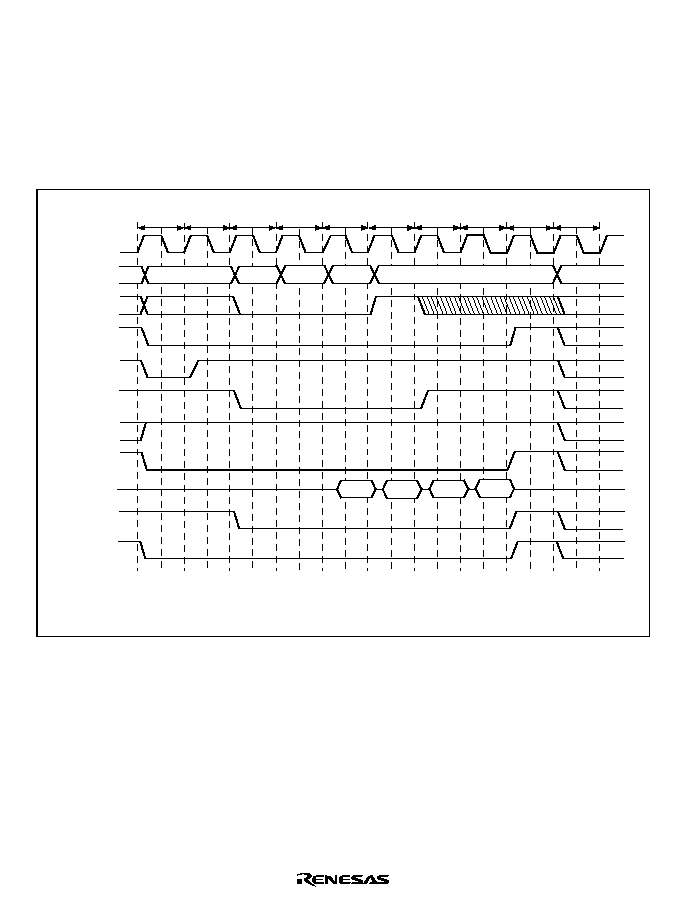
Rev. 2.00, 09/03, page 213 of 690
Figure 7.16 shows a timing chart in burst read. In burst read, an ACTV command is output in the
Tr cycle, the READ command is issued in the Tc1, Tc2, and Tc3 cycles, the READA command is
issued in the Tc4 cycle, and the read data is received at the rising edge of the external clock
(CKIO) in the Td1 to Td4 cycles. The Tap cycle is used to wait for the completion of an auto-
precharge induced by the READ command in the SDRAM. In the Tap cycle, a new command
will not be issued to the same bank. However, access to another CS space or another bank in the
same SDRAM space is enabled. The number of Tap cycles is specified by the TRP[1:0] bits of
the CS3WCR register.
Tc4
CKIO
A25 to A0
CSn
RD/
WR
RASU/L
DQMxx*
2
D31 to D0
BS
Tap
DACKn*
3
Tr
Tc2
Tc3
Tc1
Td4
Tde
Td2
Td3
Td1
A12/A11*
1
CASU/L
Notes: 1. Address pin to be connected to the A10 pin of SDRAM.
2. xx is UU, UL, LU, or LL.
3. The waveform for DACKn is when active low is specified.
Trw
Tw
Figure 7.16 Synchronous DRAM Burst Read Wait Specification Timing
(Auto Precharge)
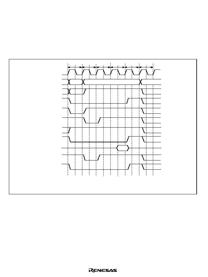
Rev. 2.00, 09/03, page 214 of 690
7.8.4
Single Read
A read access ends in one cycle when data exists in non-cacheable region and the data bus width is
larger than or equal to access size. As the burst length is set to 1 in synchronous DRAM burst
read/single write mode, only the required data is output. Consequently, no unnecessary bus cycles
are generated even when a cache-through area is accessed.
Figure 7.17 shows the basic timing chart for single read.
CKIO
A25 to A0
CSn
RD/
WR
RASU/L
DQMxx*
2
D31 to D0
BS
Tap
DACKn*
3
Tr
Tc1
Tde
Td1
Tw
A12/A11*
1
CASU/L
Notes: 1. Address pin to be connected to the A10 pin of SDRAM.
2. xx is UU, UL, LU, or LL
3. The waveform for DACKn is when active low is specified.
Figure 7.17 Basic Timing for Single Read (Auto Precharge)

Rev. 2.00, 09/03, page 215 of 690
7.8.5
Burst Write
A burst write occurs in the following cases in this LSI.
∑
Copyback of the cache
∑
16-byte transfer in DMAC (access to non-cacheable region)
∑
Access size in writing is larger than data bus width.
This LSI always accesses SDRAM with burst length 1. For example, write access of burst length 1
is performed continuously 4 times to write 16-byte continuous data to the SDRAM that is
connected to a 32-bit data bus.
The relationship between the access size and the number of bursts is shown in table 7.16.
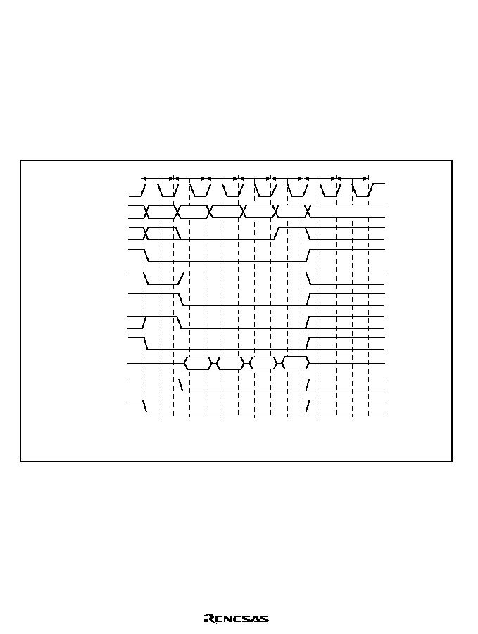
Rev. 2.00, 09/03, page 216 of 690
Figure 7.18 shows a timing chart for burst writes. In burst write, an ACTV command is output in
the Tr cycle, the WRIT command is issued in the Tc1, Tc2, and Tc3 cycles, and the WRITA
command is issued to execute an auto-precharge in the Tc4 cycle. In the write cycle, the write
data is output simultaneously with the write command. After the write command with the auto-
precharge is output, the Trw1 cycle that waits for the auto-precharge initiation is followed by the
Tap cycle that waits for completion of the auto-precharge induced by the WRITA command in the
SDRAM. In the Tap cycle, a new command will not be issued to the same bank. However, access
to another CS space or another bank in the same SDRAM space is enabled. The number of Trw1
cycles is specified by the TRWL[1:0] bits of the CS3WCR register. The number of Tap cycles is
specified by the TRP[1:0] bits of the CS3WCR register.
Tc4
CKIO
A25 to A0
CSn
RD/
WR
RASU/L
DQMxx*
2
D31 to D0
BS
Tap
DACKn*
3
Tr
Tc2
Tc3
Tc1
Trwl
A12/A11*
1
CASU/L
Notes: 1. Address pin to be connected to the A10 pin of SDRAM.
2. xx is UU, UL, LU, or LL.
3. The waveform for DACKn is when active low is specified.
Figure 7.18 Basic Timing for Synchronous DRAM Burst Write (Auto Precharge)
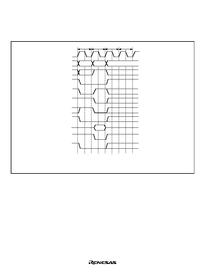
Rev. 2.00, 09/03, page 217 of 690
7.8.6
Single Write
A write access ends in one cycle when data is written in non-cacheable region and the data bus
width is larger than or equal to access size. This is called single write. Figure 7.19 shows the basic
timing chart for single write.
CKIO
A25 to A0
CSn
RD/
WR
RASU/L
DQMxx*
2
D31 to D0
BS
Tap
DACKn*
3
Tr
Tc1
Trwl
A12/A11*
1
CASU/L
Notes: 1. Address pin to be connected to the A10 pin of SDRAM.
2. xx is UU, UL, LU, or LL.
3. The waveform for DACKn is when active low is specified.
Figure 7.19 Basic Timing for Single Write (Auto Precharge)

Rev. 2.00, 09/03, page 218 of 690
7.8.7
Bank Active
The synchronous DRAM bank function is used to support high-speed accesses to the same row
address. When the BACTV bit in SDCR is 1, accesses are performed using commands (READ,
WRIT) without auto-precharge. This function is called bank-active function. This function is valid
only for either the upper or lower bits of area 3. When area 3 is set to bank-active mode, area 2
should be set to normal space or byte-selection SRAM. When areas 2 and 3 are both set to
SDRAM or both the upper and lower bits of area 3 are connected to SDRAM, auto pre-charge
mode must be set. In this case, precharging is not performed when the access ends. When
accessing the same row address in the same bank, it is possible to issue the READ or WRIT
command immediately, without issuing an ACTV command. As synchronous DRAM is internally
divided into several banks, it is possible to activate one row address in each bank. If the next
access is to a different row address, a PRE command is first issued to precharge the relevant bank,
then when precharging is completed, the access is performed by issuing an ACTV command
followed by a READ or WRIT command. If this is followed by an access to a different row
address, the access time will be longer because of the precharging performed after the access
request is issued.
In a write, when auto-precharge is performed, a command cannot be issued for a period of Trwl +
Tpc cycles after issuance of the WRITA command. When bank active mode is used, READ or
WRIT commands can be issued successively if the row address is the same. The number of cycles
can thus be reduced by Trwl + Tpc cycles for each write.
There is a limit on t
RAS
, the time for placing each bank in the active state. If there is no guarantee
that there will not be a cache hit and another row address will be accessed within the period in
which this value is maintained by program execution, it is necessary to set auto-refresh and set the
refresh cycle to no more than the maximum value of t
RAS
.
A burst read cycle without auto-precharge is shown in figure 7.20, a burst read cycle for the same
row address in figure 7.21, and a burst read cycle for different row addresses in figure 7.22.
Similarly, a burst write cycle without auto-precharge is shown in figure 7.23, a single write cycle
for the same row address in figure 7.24, and a single write cycle for different row addresses in
figure 7.25.
When bank active mode is set, if only accesses to the respective banks in the area 3 space are
considered, as long as accesses to the same row address continue, the operation starts with the
cycle in figure 7.20 or 7.23, followed by repetition of the cycle in figure 7.21 or 7.24. An access to
a different area during this time has no effect. If there is an access to a different row address in the
bank active state, after this is detected the bus cycle in figure 7.22 or 7.25 is executed instead of
that in figure 7.21 or 7.24. In bank active mode, too, all banks become inactive after a refresh
cycle or after the bus is released as the result of bus arbitration.
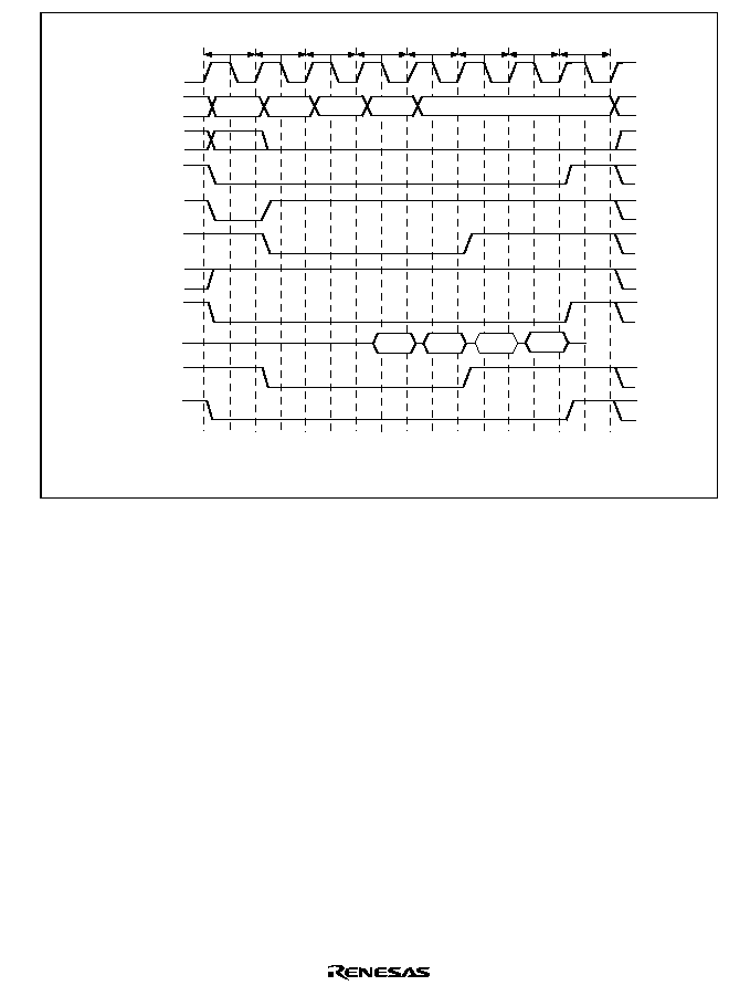
Rev. 2.00, 09/03, page 219 of 690
Tc4
CKIO
A25 to A0
CSn
RD/
WR
RASU/L
DQMxx*
2
D31 to D0
BS
DACKn*
3
Tr
Tc2
Tc3
Tc1
Td4
Td2
Td3
Td1
Tw
Tde
A12/A11*
1
CASU/L
Notes: 1. Address pin to be connected to the A10 pin of SDRAM.
2. xx is UU, UL, LU, or LL.
3. The waveform for DACKn is when active low is specified.
Figure 7.20 Burst Read Timing (No Auto Precharge)

Rev. 2.00, 09/03, page 220 of 690
Tc4
Tc2
Tc3
Tc1
Td4
Tde
Td2
Td3
Td1
Tw
CKIO
A25 to A0
CSn
RD/
WR
RASU/L
DQMxx*
2
D31 to D0
BS
DACKn*
3
A12/A11*
1
CASU/L
Notes: 1. Address pin to be connected to the A10 pin of SDRAM.
2. xx is UU, UL, LU, or LL.
3. The waveform for DACKn is when active low is specified.
Figure 7.21 Burst Read Timing (Bank Active, Same Row Address)

Rev. 2.00, 09/03, page 221 of 690
Tc4
Tpw
Tp
Tc2
Tc3
Tc1
Td4
Td2
Td3
Td1
Tw
Tde
Tr
CKIO
A25 to A0
CSn
RD/
WR
RASU/L
DQMxx*
2
D31 to D0
BS
DACKn*
3
A12/A11*
1
CASU/L
Notes: 1. Address pin to be connected to the A10 pin of SDRAM.
2. xx is UU, UL, LU, or LL.
3. The waveform for DACKn is when active low is specified.
Figure 7.22 Burst Read Timing (Bank Active, Different Row Addresses)
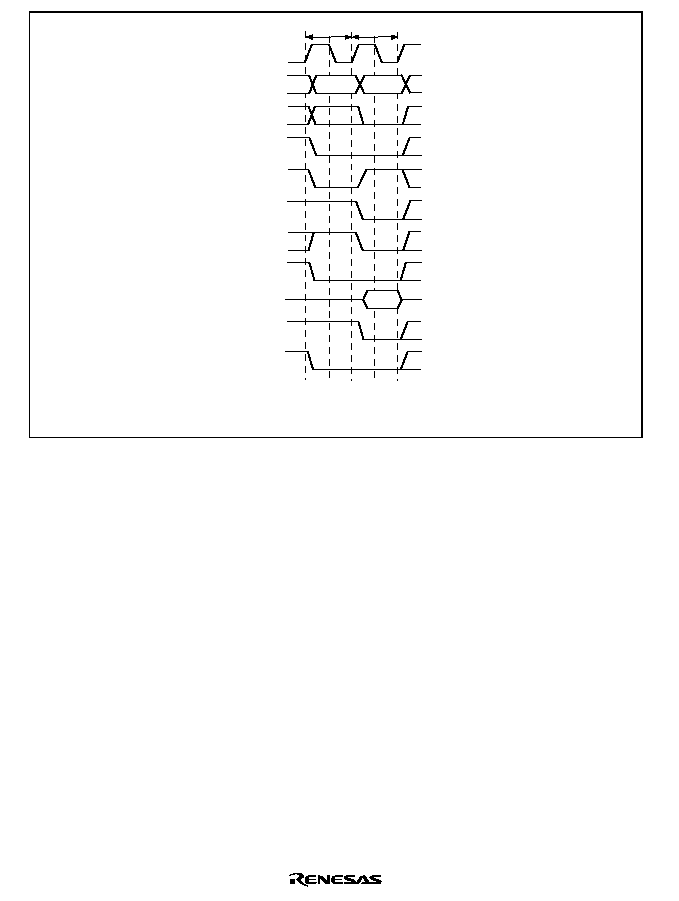
Rev. 2.00, 09/03, page 222 of 690
Tr
Tc1
CKIO
A25 to A0
CSn
RD/
WR
RASU/L
DQMxx*
2
D31 to D0
BS
DACKn*
3
A12/A11*
1
CASU/L
Notes: 1. Address pin to be connected to the A10 pin of SDRAM.
2. xx is UU, UL, LU, or LL.
3. The waveform for DACKn is when active low is specified.
Figure 7.23 Single Write Timing (No Auto Precharge)
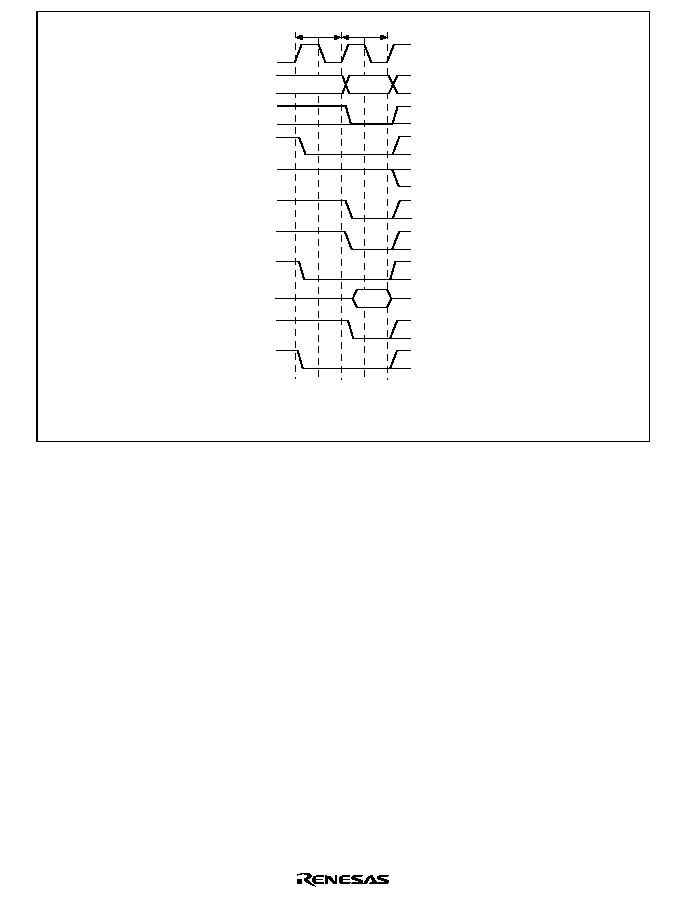
Rev. 2.00, 09/03, page 223 of 690
Tnop
Tc1
CKIO
A25 to A0
CSn
RD/
WR
RASU/L
DQMxx*
2
D31 to D0
BS
DACKn*
3
A12/A11*
1
CASU/L
Notes: 1. Address pin to be connected to the A10 pin of SDRAM.
2. xx is UU, UL, LU, or LL.
3. The waveform for DACKn is when active low is specified.
Figure 7.24 Single Write Timing (Bank Active, Same Row Address)
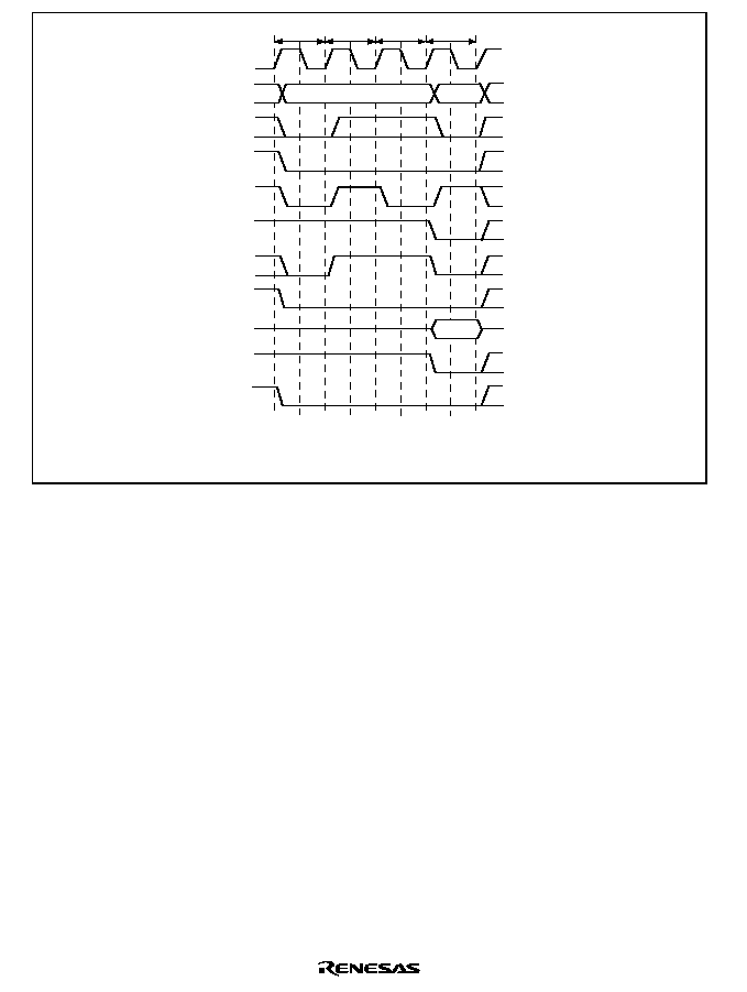
Rev. 2.00, 09/03, page 224 of 690
Tpw
Tp
Tc1
Tr
CKIO
A25 to A0
CSn
RD/
WR
RASU/L
DQMxx*
2
D31 to D0
BS
DACKn*
3
A12/A11*
1
CASU/L
Notes: 1. Address pin to be connected to the A10 pin of SDRAM.
2. xx is UU, UL, LU, or LL.
3. The waveform for DACKn is when active low is specified.
Figure 7.25 Single Write Timing (Bank Active, Different Row Addresses)

Rev. 2.00, 09/03, page 225 of 690
7.8.8
Refreshing
This LSI has a function for controlling synchronous DRAM refreshing. Auto-refreshing can be
performed by clearing the RMODE bit to 0 and setting the RFSH bit to 1 in SDCR. A continuous
refreshing can be performed by setting the RRC[2:0] bits in RTCSR. If synchronous DRAM is not
accessed for a long period, self-refresh mode, in which the power consumption for data retention
is low, can be activated by setting both the RMODE bit and the RFSH bit to 1.
1. Auto-refreshing
Refreshing is performed for the number of times specified by bits RRC[2:0] in RTCSR at
intervals determined by the input clock selected by bits CKS[2:0] in RTCSR, and the value set
in RTCOR. The value of these bits should be set so as to satisfy the refresh interval stipulation
for the synchronous DRAM used. First make the settings for RTCOR, RTCNT, and the
RMODE and RFSH bits in SDCR, then make bits CKS[2:0] and RRC[2:0] settings in RTCSR.
When the clock is selected by bits CKS[2:0], RTCNT starts counting up from the value at that
time. The RTCNT value is constantly compared with the RTCOR value, and if the two values
are the same, a refresh request is generated and auto-refresh is performed for the number of
times specified by bits RRC[2:0]. At the same time, RTCNT is cleared to zero and the count-
up is restarted. Figure 7.26 shows the auto-refresh cycle timing.
After starting, the auto refreshing, PALL command is issued in the Tp cycle to make all the
banks to pre-charged state from active state when some bank is being pre-charged. Then REF
command is issued in the Trr cycle after inserting idle cycles of which number is specified by
the TRP[1:0] bits in CSnWCR. A new command is not issued for the duration of the number
of cycles specified by the TRC[1:0] bits in CSnWCR after the Trr cycle. The TRC[1:0] bits
must be set so as to satisfy the SDRAM refreshing cycle time stipulation (t
RC
). A NOP cycle is
inserted between the Tp cycle and Trr cycle when the setting value of the TRP[1:0] bits in
CSnWCR is longer than or equal to 2 cycles.

Rev. 2.00, 09/03, page 226 of 690
Tpw
Tp
Trr
Trc
Trc
Trc
Hi-Z
CKIO
A25 to A0
CSn
RD/
WR
RASU/L
DQMxx*
2
D31 to D0
BS
DACKn*
3
A12/A11*
1
CASU/L
Notes: 1. Address pin to be connected to the A10 pin of SDRAM.
2. xx is UU, UL, LU, or LL.
3. The waveform for DACKn is when active low is specified.
Figure 7.26 Auto-Refresh Timing
2. Self-refreshing
Self-refresh mode in which the refresh timing and refresh addresses are generated within the
synchronous DRAM. Self-refreshing is activated by setting both the RMODE bit and the
RFSH bit in SDCR to 1. After starting the self-refreshing, PALL command is issued in Tp
cycle after the completion of the pre-charging bank. A SELF command is then issued after
inserting idle cycles of which number is specified by the TRP[1:0] bits in CSnWSR.
Synchronous DRAM cannot be accessed while in the self-refresh state. Self-refresh mode is
cleared by clearing the RMODE bit to 0. After self-refresh mode has been cleared, command
issuance is disabled for the number of cycles specified by the TRC[1:0] bits in CSnWCR. Self-
refresh timing is shown in figure 7.27. Settings must be made so that self-refresh clearing and
data retention are performed correctly, and auto-refreshing is performed at the correct
intervals. When self-refreshing is activated from the state in which auto-refreshing is set, auto-
refreshing is restarted if the RFSH bit is set to 1 and the RMODE bit is cleared to 0 when self-
refresh mode is cleared. If the transition from clearing of self-refresh mode to the start of auto-
refreshing takes time, this time should be taken into consideration when setting the initial value
of RTCNT. Making the RTCNT value 1 less than the RTCOR value will enable refreshing to
be started immediately.

Rev. 2.00, 09/03, page 227 of 690
After self-refreshing has been set, the self-refresh state continues even if the chip standby state
is entered using the LSI standby function, and is maintained even after recovery from standby
mode other than through a power-on reset. In case of a power-on reset, the bus state
controller's registers are initialized, and therefore the self-refresh state is cleared.
Tpw
Tp
Trr
Trc
Trc
Trc
Hi-Z
Trc
Trc
CKIO
CKE
A25 to A0
CSn
RD/
WR
RASU/L
DQMxx*
2
D31 to D0
BS
DACKn*
3
A12/A11*
1
CASU/L
Notes: 1. Address pin to be connected to the A10 pin of SDRAM.
2. xx is UU, UL, LU, or LL.
3. The waveform for DACKn is when active low is specified.
Figure 7.27 Self-Refresh Timing
3. Relationship between refresh requests and bus cycle
If a refresh request is generated during a bus cycle, refresh waits for the bus cycle to be
completed. If a refresh request is generated while the bus is released by the bus arbitration
function, refresh waits for the bus mastership to be obtained.
If a new refresh request is generated while refresh is waiting, the first refresh request is
canceled. To perform refresh correctly, the bus cycle and the bus-owned period must be shorter
than the refresh interval.
If a bus request is issued during self-refreshing, the bus is not released until the refresh is
completed.
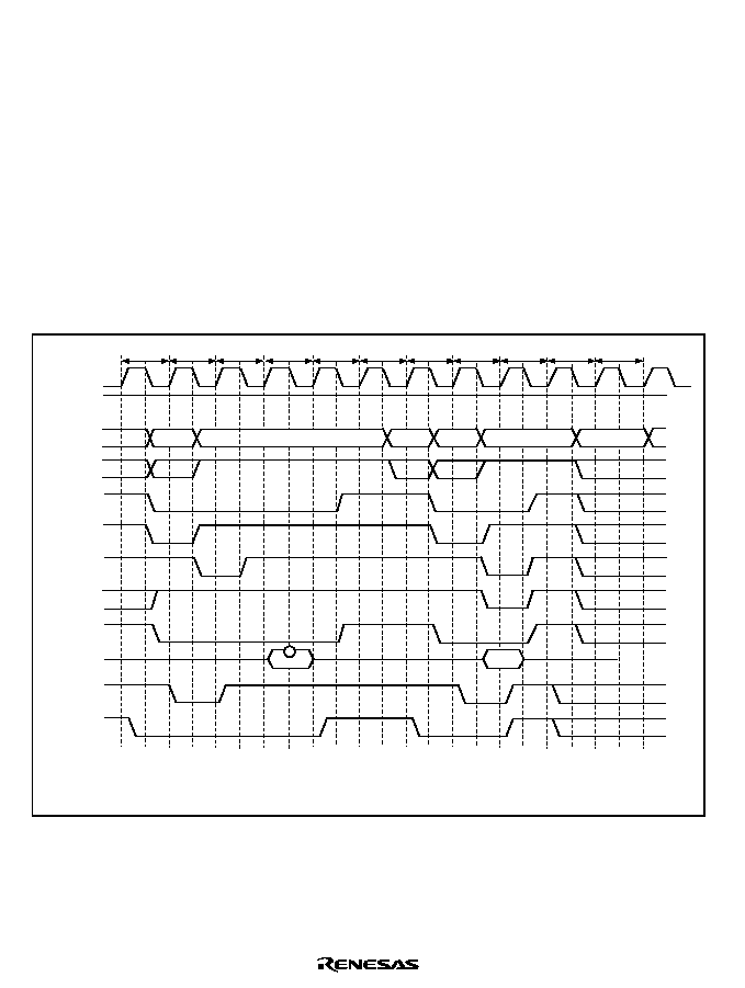
Rev. 2.00, 09/03, page 228 of 690
7.8.9
Low-Frequency Mode
When the SLOW bit in SDCR is set to 1, output of commands, addresses, and write data, and
fetch of read data are performed at a timing suitable for operating SDRAM at a low frequency.
Figure 7.28 shows the access timing in low-frequency mode. In this mode, commands, addresses,
and write data are output in synchronization with the falling edge of CKIO, which is half a cycle
delayed than the normal timing. Read data is fetched at the rising edge of CKIO, which is half a
cycle faster than the normal timing. This timing allows the hold time of commands, addresses,
write data, and read data to be extended.
If SDRAM is operated at a high frequency with the SLOW bit set to 1, the setup time of
commands, addresses, write data, and read data are not guaranteed. Take the operating frequency
and timing design into consideration when making the SLOW bit setting.
CKIO
A25 to A0
CSn
RD/
WR
D31 to D0
BS
Tc1
DACKn*
3
Tr
Td1
Tw
A12/A11*
1
Tde
Tap
Tr
Tc1
Tnop
Trwl
Tap
CKE
RASU/L
DQMxx*
2
CASU/L
Notes: 1. Address pin to be connected to the A10 pin of SDRAM.
2. xx is UU, UL, LU, or LL.
3. The waveform for DACKn is when active low is specified.
Figure 7.28 Low-Frequency Mode Access Timing

Rev. 2.00, 09/03, page 229 of 690
7.8.10
Power-On Sequence
In order to use synchronous DRAM, mode setting must first be performed after powering on. To
perform synchronous DRAM initialization correctly, the bus state controller registers must first be
set, followed by a write to the synchronous DRAM mode register. In synchronous DRAM mode
register setting, the address signal value at that time is latched by a combination of the
CSn, RAS,
CAS, and RD/WR signals. If the value to be set is X, the bus state controller provides for value X
to be written to the synchronous DRAM mode register by performing a write to address
H'A4FD4000 + X for area 2 synchronous DRAM, and to address H'A4FD5000 + X for area 3
synchronous DRAM. In this operation the data is ignored, but the mode write is performed as a
word-size access. To set burst read/single write, CAS latency 2 to 3, wrap type = sequential, and
burst length 1 supported by the LSI, arbitrary data is written in a word-size access to the addresses
shown in table 7.17. In this time 0 is output at the external address pins of A12 or later.
Table 7.17
Access Address in SDRAM Mode Register Write
(1) Setting for Area 2 (SDMR2)
Burst read/single write (burst length 1):
Data Bus Width
CAS Latency
Access Address
External Address Pin
16 bits
2
H'A4FD4440
H'0000440
3
H'A4FD4460
H'0000460
32 bits
2
H'A4FD4880
H'0000880
3
H'A4FD48C0
H'00008C0
Burst read/burst write (burst length 1):
Data Bus Width
CAS Latency
Access Address
External Address Pin
16 bits
2
H'A4FD4040
H'0000040
3
H'A4FD4060
H'0000060
32 bits
2
H'A4FD4080
H'0000080
3
H'A4FD40C0
H'00000C0

Rev. 2.00, 09/03, page 230 of 690
(2) Setting for Area 3 (SDMR3)
Burst read/single write (burst length 1):
Data Bus Width
CAS Latency
Access Address
External Address Pin
16 bits
2
H'A4FD5440
H'0000440
3
H'A4FD5460
H'0000460
32 bits
2
H'A4FD5880
H'0000880
3
H'A4FD58C0
H'00008C0
Burst read/burst write (burst length 1):
Data Bus Width
CAS Latency
Access Address
External Address Pin
16 bits
2
H'A4FD5040
H'0000040
3
H'A4FD5060
H'0000060
32 bits
2
H'A4FD5080
H'0000080
3
H'A4FD50C0
H'00000C0
Mode register setting timing is shown in figure 7.29. A PALL command (all bank pre-charge
command) is firstly issued. A REF command (auto refresh command) is then issued 8 times. An
MRS command (mode register write command) is finally issued. Idle cycles, of which number is
specified by the TRP[1:0] bits in CSnWCR, are inserted between the PALL and the first REF. Idle
cycles, of which number is specified by the TRC[1:0] bits in CSnWCR, are inserted between REF
and REF, and between the 8th REF and MRS. Idle cycles, of which number is one or more, are
inserted between the MRS and a command to be issued next.
It is necessary to keep idle time of certain cycles for SDRAM before issuing PALL command after
power-on. Refer the manual of the SDRAM for the idle time to be needed. When the pulse width
of the reset signal is longer then the idle time, mode register setting can be started immediately
after the reset, but care should be taken when the pulse width of the reset signal is shorter than the
idle time.
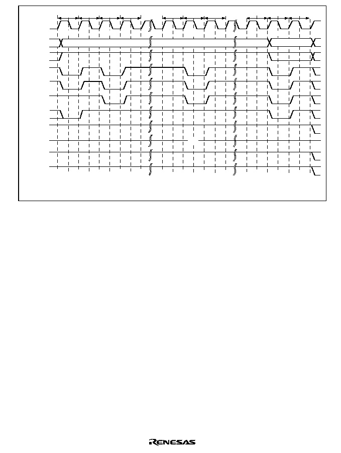
Rev. 2.00, 09/03, page 231 of 690
Tpw
Tp
Trr
Trc
Trc
Tmw
Hi-Z
Tnop
Trc
Trr
Trc
REF
REF
MRS
PALL
Notes: 1. Address pin to be connected to the A10 pin of SDRAM.
2. xx is UU, UL, LU, or LL.
3. The waveform for DACKn is when active low is specified.
CKIO
A25 to A0
CSn
RD/
WR
RASU/L
DQMxx*
2
D31 to D0
BS
DACKn*
3
A12/A11*
1
CASU/L
Figure 7.29 Synchronous DRAM Mode Write Timing (Based on JEDEC)
7.9
Burst ROM Interface
The burst ROM interface is provided to access ROM that has the page mode function, such as
flash memory, in high speed. Basically the access to the ROM is performed in the same way as for
normal space. When the first cycle is terminated, however, negation of the
RD signal is not
executed. The accesses after the 2nd access are performed by exchanging only the address. In the
accesses after the 2nd access, the address is changed at the falling edge of CKIO.
The number of wait cycles specified by the W[3:0] bits in CSnWCR are inserted for the first
access cycle. The number of wait cycles specified by the BW[1:0] bits in CSnWCR are inserted
for the second and subsequent access cycles.
In the access to the burst ROM, the
BS signal is asserted only to the first access cycle. An external
wait input is valid only to the first access cycle. In the single access or write access that do not
perform the burst operation in the burst ROM interface, access timing is same as a normal space.
Table 7.18 lists a relationship between bus width, access size, and the number of bursts. Figure
7.30 shows a timing chart.
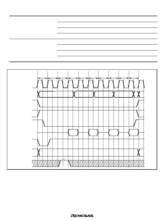
Rev. 2.00, 09/03, page 232 of 690
Table 7.18
Relationship between Bus Width, Access Size, and Number of Bursts
Bus Width
Access Size
Number of Bursts
8 bits
8 bits
1
16 bits
2
32 bits
4
16 bytes
16
16 bits
8 bits
1
16 bits
1
32 bits
2
16 bytes
8
CKIO
Address
RD
Data
DACK
WAIT
CS
T
1
Tw
Tw
TB2
Twb
TB2
Twb
TB2
Twb
T
2
RD/
WR
BS
Figure 7.30 Burst ROM Access (Bus Width 8 Bits, Access Size 32 Bits (Number of Burst 4),
Access Wait for the 1st Time 2, Access Wait for 2nd Time and after 1)
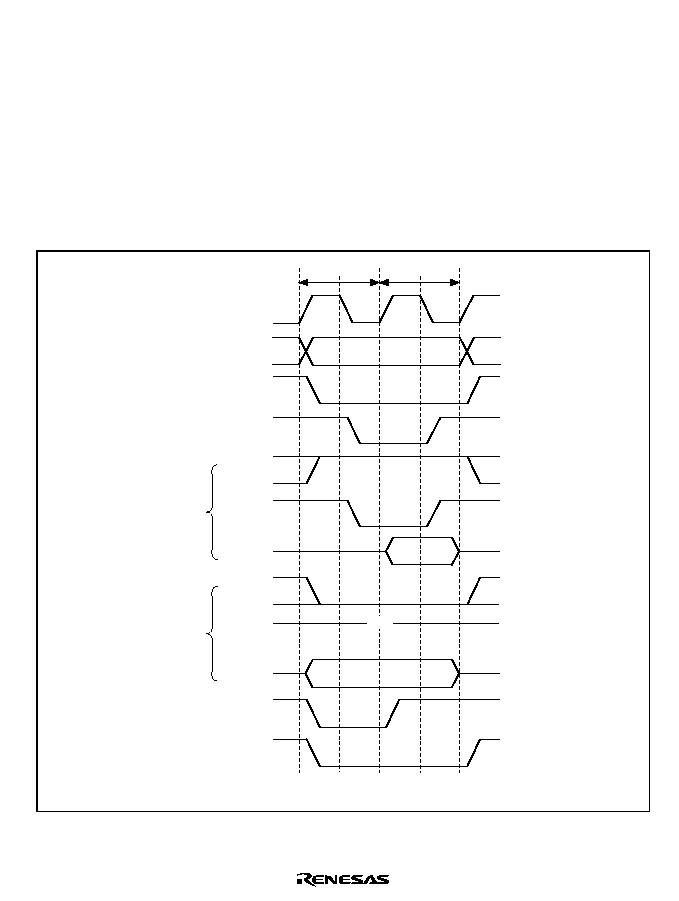
Rev. 2.00, 09/03, page 233 of 690
7.10
Byte-Selection SRAM Interface
The byte-selection SRAM interface is for outputting the byte-selection signal (
WEn) in both read
and write bus cycles. This interface has 16-bit data pins and accesses SRAM that has an upper
byte-selection pin and a lower byte-selection pin, such as UB and LB. The write access timing is
the same as that for the normal space interface. The read access timing differs from that for the
normal space interface in the
WEn timing, and a byte-selection signal is output from the WEn pin.
The basic access timing is shown in figure 7.31.
Note that in a write cycle, data is written in accordance with the byte-selection pin (
WEn) timing.
Check the data sheet of the memory to be used for the actual timing.
CKIO
A25 to A0
CSn
WEn
RD/
WR
RD
RD
D31 to D0
D31 to D0
RD/
WR
BS
DACKn
*
T
1
T
2
High
Write
Read
Note:
* The waveform for DACKn is when active low is specified.
Figure 7.31 Byte-Selection SRAM Basic Access Timing
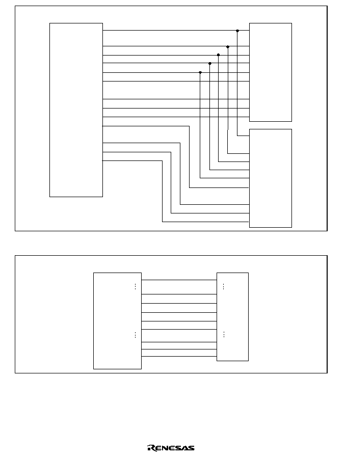
Rev. 2.00, 09/03, page 234 of 690
A15
A0
CS
OE
WE
I/O15
I/O0
UB
LB
A17
A2
CSn
RD
RD/
WR
D31
D16
D15
D0
A15
A0
CS
OE
WE
I/O15
I/O0
UB
LB
This LSI
64k
◊ 16-bit
SRAM
.
.
.
.
.
.
.
.
.
.
.
.
.
.
.
.
.
.
.
.
.
WE3
WE2
WE1
WE2
Figure 7.32 Example of Connection with 32-Bit Data-Width Byte-Selection SRAM
This LSI
A16
A1
CSn
RD
RD/
WR
D15
D0
WE1
WE0
A15
A0
CS
OE
WE
I/O 15
I/O 0
UB
LB
64k
◊ 16-bit
SRAM
Figure 7.33 Example of Connection with 16-Bit Data-Width Byte-Selection SRAM

Rev. 2.00, 09/03, page 235 of 690
7.11
Wait between Access Cycles
As the operating frequency of LSIs becomes higher, the off-operation of the data buffer often
collides with the next data access when the read operation from devices with slow access speed is
completed. As a result of these collisions, the reliability of the device is low and malfunctions may
occur. A function that avoids data collisions by inserting wait cycles between continuous access
cycles has been newly added.
The number of wait cycles between access cycles can be set by bits IWW[1:0], IWRWD[1:0],
IWRWS[1:0], IWRRD[1:0], and IWRRS[1:0] in CSnBCR, and bits DMAIW[1:0] and DMAIWA
in CMNCR. The conditions for setting the wait cycles between access cycles (idle cycles) are
shown below.
1. Continuous accesses are write-read or write-write
2. Continuous accesses are read-write for different spaces
3. Continuous accesses are read-write for the same space
4. Continuous accesses are read-read for different spaces
5. Continuous accesses are read-read for the same space
6. Data output from an external device caused by DMA single transfer is followed by data output
from another device that includes this LSI (DMAIWA = 0)
7. Data output from an external device caused by DMA single transfer is followed by any type of
access (DMAIWA = 1)
7.12
Bus Arbitration
This LSI supports bus arbitration. This LSI has bus mastership in the normal state and releases bus
mastership after receiving a bus request from another device.
To prevent device malfunction while the bus mastership is transferred between master and slave,
the LSI negates all of the bus control signals before bus release. When the bus mastership is
received, all of the bus control signals are first negated and then driven appropriately. In this case,
output buffer conflicts can be prevented because the master and slave drive the same signals with
the same values. In addition, to prevent noise while the bus control signal is in the high-impedance
state, pull-up resistors must be connected to these control signals.
Bus mastership is transferred at the boundary of bus cycles. Namely, bus mastership is released
immediately after receiving a bus request when a bus cycle is not being performed. The release of
bus mastership is delayed until the bus cycle is complete when a bus cycle is in progress. Even
when from outside the LSI it looks like a bus cycle is not being performed, a bus cycle may be
performing internally, started by inserting wait cycles between access cycles. Therefore, it cannot
be immediately determined whether or not bus mastership has been released by looking at the
CSn
signal or other bus control signals. The states that do not allow bus mastership release are shown
below.

Rev. 2.00, 09/03, page 236 of 690
1. 16-byte transition because of a cache miss
2. During copyback operation for the cache
3. Between the read and write cycles of a TAS instruction
4. Multiple bus cycles generated when data bus width is smaller than the access size (For
example, between bus cycles when longword access is made to memory with a data bus width
of 8 bits.)
5. 16-byte transfer by the DMAC
If self-refresh mode is specified for the SDRAM, the master device cannot release the bus. If the
master clock stops because a transition is underway to standby mode or the frequency is changed,
or if this LSI is being reset, the master device cannot release the bus. To prevent the slave from
issuing bus requests in such a case, the slave must be put into the sleep state so that no slave
access cycles are generated.
The refresh request and bus request are accepted during the DMA burst transfer.
Bus mastership is maintained until a new bus request is received. Bus mastership is released
immediately after the completion of the bus cycle in progress when an external bus request
(
BREQ) is asserted (low level) and a bus acknowledge signal (BACK) is asserted (low level). Bus
use is resumed when a negation (high level) of
BREQ, which shows that the slave has released the
bus, has been received.
SDRAM issues all bank pre-charge commands (PALLs) when active banks exist and releases the
bus after completion of a PALL command.
The bus release sequence is as follows. The address bus and data bus are placed in a high-
impedance state synchronized with the rising edge of CKIO. The bus mastership enable signal is
asserted 0.5 cycles after the above timing, synchronized with the falling edge of CKIO. Bus
control signals (
BS, CSn, RASU, RASL, CASU, CASL, DQMxx, WEn, RD, and RD/WR) are
made to the high-impedance states at the subsequent rising edge of CKIO. Bus request signals are
sampled at the falling edge of CKIO. The sequence for re-claiming bus mastership from a slave is
described below. After detecting the negation of
BREQ at the falling edge of CKIO, the bus
enable signal is negated at the subsequent falling edge of the clock. The address and data signals
are driven at the subsequent rising edge of CKIO. Figure 7.34 shows the bus arbitration timing.

Rev. 2.00, 09/03, page 237 of 690
CKIO
A25 to A0
CSn
Other bus
control signals
Data
BREQ
BACK
Figure 7.34 Bus Arbitration
In an original slave device designed by the user, multiple bus accesses are generated continuously
to reduce the overhead caused by bus arbitration. In this case, to execute SDRAM refresh
correctly, the slave device must be designed to release the bus mastership within the refresh
interval time.
The bus release by the
BREQ and BACK signal handshaking requires some overhead. If the slave
has many tasks, multiple bus cycles should be executed in a bus mastership acquisition. Reducing
the cycles required for master to slave bus mastership transitions streamlines the system design.
7.13
Others
Reset: The bus state controller (BSC) can be initialized completely only at power-on reset. At
power-on reset, all signals are negated and output buffers are turned off regardless of the bus cycle
state. All control registers are initialized.
In standby, sleep, and manual reset, control registers of the bus state controller are not initialized.
At manual reset, the current bus cycle being executed is completed and then the access wait state
is entered. Since the RTCNT continues counting up during manual reset signal assertion, a refresh
request occurs to initiate the refresh cycle.
Note that arbitration requests using
BREQ are not accepted during manual reset signal assertion.
On-Chip Peripheral Module Access: To access an on-chip module register, two or more
peripheral module clock (P
) cycles are required. Care must be taken in system design.

Rev. 2.00, 09/03, page 238 of 690

DMAS311B_000020020100
Rev. 2.00, 09/03, page 239 of 690
Section 8 Direct Memory Access Controller (DMAC)
This LSI includes the direct memory access controller (DMAC). The DMAC can be used in place
of the CPU to perform high-speed transfers between external devices with DACK (transfer request
acknowledge signal), external memory, memory-mapped external devices, and on-chip peripheral
modules.
8.1
Features
∑
Four channels (two channels can receive an external request)
∑
4-Gbyte physical address space
∑
Data transfer unit: Byte, word (2 bytes), longword (4 bytes), and 16 bytes (longword
◊
4)
∑
Maximum transfer count: 16777216 transfers
∑
Address mode: Dual address mode or single address mode can be selected.
∑
Transfer requests: External request, on-chip peripheral module request, or auto request can be
selected.
The following modules can issue an on-chip peripheral module request.
SCIF0, SCIF2, CMT, USB, and A/D converter
∑
Bus modes: Cycle steal mode (normal mode and intermittent mode 16/64) or burst mode can
be selected.
∑
Selectable channel priority levels:
The channel priority levels are selectable between fixed mode and round-robin mode.
∑
Interrupt request: An interrupt request can be generated to the CPU after transfers end.
∑
External request detection: Low-/high-level or rising/falling edge detection of DREQ input can
be selected.
∑
Transfer request acknowledge signal: Active levels for DACK can be set independently.
∑
Transfer end signal: Active level for TEND can be set. TEND is output at the same timing as
DACK in the last DMA transfer. (Only channel 0)

Rev. 2.00, 09/03, page 240 of 690
Figure 8.1 shows the block diagram of the DMAC.
On-chip
peripheral module
Peripheral bus
Internal bus
External
ROM
DREQ0, DREQ1
DEIn
DACK0, DACK1
TEND0
External
RAM
External I/O
(memory
mapped)
External I/O
(with
acknowledge-
ment)
Bus
interface
Bus state
controller
Request
priority
control
Start-up
control
Register
control
Transfer count
control
SAR_n
DAR_n
DMATCR_n
CHCR_n
DMAOR
DMARS0
-1
[Legend]
DMAOR:
DMA operation register
SARn:
DMA source address register
DARn:
DMA destination address register
DMATCRn: DMA transfer count register
CHCRn:
DMA channel control register
DMARS0/1:
DMA extension resource selector
DEIn:
DMA transfer-end interrupt request to the CPU
n : 0, 1, 2, 3
DMAC module
SCIF0, SCIF2
CMT, USB
A/D converter
Figure 8.1 Block Diagram of DMAC

Rev. 2.00, 09/03, page 241 of 690
8.2
Input/Output Pins
The external pins for the DMAC are described below.
Table 8.1 lists the configuration of the pins that are connected to external bus. The DMAC has
pins for 2 channels (channels 0 and 1) for external bus use. Channel 0 has the DMA transfer end
signal.
Table 8.1
Pin Configuration
Channel
Name
Symbol
I/O
Function
0
DMA transfer request
DREQ0
I
DMA transfer request input from
external device to channel 0
DMA transfer request
acknowledge
DACK0
O
DMA transfer request acknowledge
output from channel 0 to external device
DMA transfer end
TEND0
O
Transfer end output in channel 0
1
DMA transfer request
DREQ1
I
DMA transfer request input from
external device to channel 1
DMA transfer request
acknowledge
DACK1
O
DMA transfer request acknowledge
output from channel 1 to external device
8.3
Register Descriptions
The DMAC has the following registers. See section 24, List of Registers, for the addresses of
these registers and the states of them in each processing state. The SAR for channel 0 is expressed
such as SAR_0.
1. Channel 0
∑
DMA source address register_0 (SAR_0)
∑
DMA destination address register_0 (DAR_0)
∑
DMA transfer count register_0 (DMATCR_0)
∑
DMA channel control register_0 (CHCR_0)
2. Channel 1
∑
DMA source address register_1 (SAR_1)
∑
DMA destination address register_1 (DAR_1)
∑
DMA transfer count register_1 (DMATCR_1)
∑
DMA channel control register _1 (CHCR_1)

Rev. 2.00, 09/03, page 242 of 690
3. Channel 2
∑
DMA source address register_2 (SAR_2)
∑
DMA destination address register_2 (DAR_2)
∑
DMA transfer count register_2 (DMATCR_2)
∑
DMA channel control register_2 (CHCR_2)
4. Channel 3
∑
DMA source address register_3 (SAR_3)
∑
DMA destination address register_3 (DAR_3)
∑
DMA transfer count register_3 (DMATCR_3)
∑
DMA channel control register_3 (CHCR_3)
5. Common
∑
DMA operation register (DMAOR)
∑
DMA extended resource selector 0 (DMARS0)
∑
DMA extended resource selector 1 (DMARS1)
8.3.1
DMA Source Address Registers (SAR)
SAR are 32-bit readable/writable registers that specify the source address of a DMA transfer.
During a DMA transfer, these registers indicate the next source address. When the data of an
external device with DACK is transferred in single address mode, SAR is ignored.
To transfer data in 16 bits or in 32 bits, specify the address with 16-bit or 32-bit address boundary.
When transferring data in 16-byte units, a 16-byte boundary must be set for the source address
value. The initial value is undefined. The SAR retains the current value in software standby or
module standby mode.
8.3.2
DMA Destination Address Registers (DAR)
DAR are 32-bit readable/writable registers that specify the destination address of a DMA transfer.
During a DMA transfer, these registers indicate the next destination address. When the data of an
external device with DACK is transferred in single address mode, DAR is ignored.
To transfer data in 16 bits or in 32 bits, specify the address with 16-bit or 32-bit address boundary.
When transferring data in 16-byte units, a 16-byte boundary must be set for the source address
value. The initial value is undefined. The DAR retains the current value in software standby or
module standby mode.

Rev. 2.00, 09/03, page 243 of 690
8.3.3
DMA Transfer Count Registers (DMATCR)
DMATCR are 32-bit readable/writable registers that specify the DMA transfer count. The number
of transfers is 1 when the setting is H'00000001, 16,777,215 when H'00FFFFFF is set, and
16,777,216 (the maximum) when H'00000000 is set. During a DMA transfer, these registers
indicate the remaining transfer count.
The upper 8 bits of DMATCR are always read as 0. The write value should always be 0. To
transfer data in 16 bytes, one 16-byte transfer (128 bits) counts one. The initial value is undefined.
The DMATCR retains the current value in software standby or module standby mode.
8.3.4
DMA Channel Control Registers (CHCR)
CHCR are 32-bit readable/writable registers that control the DMA transfer mode.
Bit
Bit
Name
Initial
Value
R/W
Descriptions
31 to 24
0
R
Reserved
These bits are always read as 0. The write value should always
be 0.
23
DO
0
R/W
DMA Overrun
Selects whether DREQ is detected by overrun 0 or by overrun
1. This bit is valid only in CHCR_0 and CHCR_1. This bit is
always read as 0 in CHCR_2 and CHCR_3. The write value
should always be 0.
0: Detects DREQ by overrun 0
1: Detects DREQ by overrun 1
22
TL
0
R/W
Transfer End Level
Selects whether the TEND signal output is high active or low
active. This bit is valid only in CHCR_0. There are no TEND
pins in CHCR_1 to CHCR_3. Therefore this setting is invalid.
This bit is always read as 0. The write value should always be
0.
0: Low-active output of TEND
1: High-active output of TEND
21 to 18
0
R
Reserved
These bits are always read as 0. The write value should always
be 0.

Rev. 2.00, 09/03, page 244 of 690
Bit
Bit
Name
Initial
Value
R/W
Descriptions
17
AM
0
R/W
Acknowledge Mode
Selects whether DACK is output in data read cycle or in data
write cycle in dual address mode.
In single address mode, DACK is always output regardless of
the specification by this bit.
This bit is valid only in CHCR_0 and CHCR_1. This bit is
always read as 0 in CHCR_2 and CHCR_3. The write value
should always be 0.
0: DACK output in read cycle (Dual address mode)
1: DACK output in write cycle (Dual address mode)
16
AL
0
R/W
Acknowledge Level
Specifies the DACK signal output is high active or low active.
This bit is valid only in CHCR_0 and CHCR_1. This bit is
always read as 0 in CHCR_2 and CHCR_3. The write value
should always be 0.
0: Low-active output of DACK
1: High-active output of DACK
15
14
DM1
DM0
0
0
R/W
R/W
Destination Address Mode
Specify whether the DMA destination address is incremented,
decremented, or left fixed. (In single address mode, the DM1
and DM0 bits are ignored when data is transferred to an
external device with DACK.)
00: Fixed destination address
(setting prohibited in 16-byte transfer)
01: Destination address is incremented (+1 in byte-size
transfer, +2 in word-size transfer, +4 in longword-size
transfer, +16 in 16-byte transfer)
10: Destination address is decremented (≠1 in byte-size
transfer, ≠2 in word-size transfer, ≠4 in longword-size
transfer, setting prohibited in 16-byte transfer)
11: Setting prohibited

Rev. 2.00, 09/03, page 245 of 690
Bit
Bit
Name
Initial
Value
R/W
Descriptions
13
12
SM1
SM0
0
0
R/W
R/W
Source Address Mode
Specifies whether the DMA source address is incremented,
decremented, or left fixed. (In single address mode, the SM1
and SM0 bits are ignored when data is transferred from an
external device with DACK.)
00: Fixed source address
(setting prohibited in 16-byte transfer)
01: Source address is incremented (+1 in byte-size transfer, +2
in word-size transfer, +4 in longword-size transfer, +16 in
16-byte transfer)
10: Source address is decremented (≠1 in byte-size transfer, ≠2
in word-size transfer, ≠4 in longword-size transfer, setting
prohibited in 16-byte transfer)
11: Setting prohibited
11
10
9
8
RS3
RS2
RS1
RS0
0
0
0
0
R/W
R/W
R/W
R/W
Resource Select
Specifies which transfer requests will be sent to the DMAC. The
changing of transfer request source should be done in the state
that the DMA enable bit (DE) is set to 0.
0000: External request, dual address mode
0001: Setting prohibited
0010: External request/single address mode
External address space
external device with DACK
0011: External request/single address mode
External device with DACK
external address space
0100: Auto request
0101: Setting prohibited
0110: Setting prohibited
0111: Setting prohibited
1000: DMA extended resource selector specification
1001: Setting prohibited
1010: Setting prohibited
1011: Setting prohibited
1100: Setting prohibited
1101: Setting prohibited
1110: Peripheral module request, A/D converter
1111: Peripheral module request, CMT
Note: External request specification is valid only in CHCR_0
and CHCR_1. None of the external request specification
can be set in channels CHCR_2 and CHCR_3.

Rev. 2.00, 09/03, page 246 of 690
Bit
Bit
Name
Initial
Value
R/W
Descriptions
7
6
DL
DS
0
0
R/W
R/W
DREQ Level and DREQ Edge Select
Select the detection method of the DREQ pin input and the
detection level.
These bits are valid only in CHCR_0 and CHCR_1. These bits
are always read as 0 in CHCR_2 and CHCR_3. The write value
should always be 0.
In channels 0 and 1, also, if the transfer request source is
specified as an on-chip peripheral module or if an auto-request
is specified, these bits are invalid.
00: DREQ detected in low level
01: DREQ detected at falling edge
10: DREQ detected in high level
11: DREQ detected at rising edge
5
TB
0
R/W
Transfer Bus Mode
Specifies the bus mode when DMA transfers data.
0: Cycle steal mode
1: Burst mode
4
3
TS1
TS0
0
0
R/W
R/W
Transfer Size
Specify the size of data to be transferred.
Select the size of data to be transferred when the source or
destination is an on-chip peripheral module register of which
transfer size is specified.
00: Byte size
01: Word size (two bytes)
10: Longword size (four bytes)
11: 16-byte unit (four longword transfers)
2
IE
0
R/W
Interrupt Enable
Specifies whether or not an interrupt request is generated to the
CPU at the end of the DMA transfer. Setting this bit to 1
generates an interrupt request (DEI) to the CPU when the TE
bit is set to 1.
0: Interrupt request disabled
1: Interrupt request enabled

Rev. 2.00, 09/03, page 247 of 690
Bit
Bit
Name
Initial
Value
R/W
Descriptions
1
TE
0
R/(W)
*
Transfer End Flag
Indicates that the DMA transfer ends. The TE bit is set to 1
when data transfer ends when DMATCR becomes to 0.
The TE bit is not set to 1 in the following cases.
∑
DMA transfer ends due to an NMI interrupt or DMA address
error before DMATCR becomes to 0.
∑
DMA transfer is ended by clearing the DE bit and the DME
bit in the DMA operation register (DMAOR).
This bit can only be cleared by writing 0 after reading 1. Even if
the DE bit is set to 1 while this bit is set to 1, transfer is not
enabled.
0: During the DMA transfer or DMA transfer has been aborted
[Clearing conditions]
∑
Writing 0 after reading TE = 1
∑
Power-on reset
∑
Manual reset
1: Data transfer ends by the specified count (DMATCR = 0)
0
DE
0
R/W
DMA Enable
Enables or disables the DMA transfer. In auto request mode,
DMA transfer starts by setting the DE bit and DME bit in
DMAOR to 1. In this time, all of the bits TE, NMIF in DMAOR,
and AE must be 0. In an external request or peripheral module
request, DMA transfer starts if DMA transfer request is
generated by the devices or peripheral modules after setting
the bits DE and DME to 1. In this case, however, all of the bits
TE, NMIF, and AE must be 0 an in the case of auto request
mode. Clearing the DE bit to 0 can terminate the DMA transfer.
0: DMA transfer disabled
1: DMA transfer enabled
Note:
*
Only 0 can be written for clearing the flags.

Rev. 2.00, 09/03, page 248 of 690
8.3.5
DMA Operation Register (DMAOR)
DMAOR is a 16-bit readable/writable register that specifies the priority level of channels at the
DMA transfer. This register shows the DMA transfer status.
Bit
Bit
Name
Initial
Value
R/W
Description
15, 14
0
R
Reserved
These bits are always read as 0. The write value should
always be 0.
13
12
CMS1
CMS0
0
0
R/W
R/W
Cycle Steal Mode Select
Select either normal mode or intermittent mode in cycle steal
mode.
It is necessary that all channels' bus modes are set to cycle
steal mode to make valid intermittent mode.
00: Normal mode
01: Setting prohibited
10: Intermittent mode 16
Executes one DMA transfer in each of 16 clocks of an
external bus clock.
11: Intermittent mode 64
Executes one DMA transfer in each of 64 clocks of an
external bus clock.
11, 10
0
R
Reserved
These bits are always read as 0. The write value should
always be 0.
9
8
PR1
PR0
0
0
R/W
R/W
Priority Mode
Select the priority level between channels when there are
transfer requests for multiple channels simultaneously.
00: CH0 > CH1 > CH2 > CH3
01: CH0 > CH2 > CH3 > CH1
10: Setting prohibited
11: Round-robin mode
7 to 3
0
R
Reserved
These bits are always read as 0. The write value should
always be 0.

Rev. 2.00, 09/03, page 249 of 690
Bit
Bit
Name
Initial
Value
R/W
Description
2
AE
0
R/(W)
*
Address Error Flag
Indicates that an address error occurred by the DMAC. If this
bit is set, DMA transfer is not enabled even if the DE bit in
CHCR and the DME bit in DMAOR are set to 1. This bit can
only be cleared by writing 0 after reading 1.
0: No DMAC address error
[Clearing conditions]
∑
Writing 0 after reading AE = 1
∑
Power-on reset
∑
Manual reset
1: DMAC address error. DMA transfer disabled.
[Setting condition]
DMAC address error occurrence
1
NMIF
0
R/(W)
*
NMI Flag
Indicates that an NMI interrupt occurred. If this bit is set, DMA
transfer is not enabled even if the DE bit in CHCR and the
DME bit in DMAOR are set to 1. This bit can only be cleared
by writing 0 after reading 1.
When the NMI is input, the DMA transfer in progress can be
done in one transfer unit. When the DMAC is not in operation,
the NMIF bit is set to 1 even if the NMI interrupt was input.
0: No NMI interrupt
[Clearing conditions]
∑
Writing 0 after reading NMIF = 1
∑
Power-on reset
∑
Manual reset
1: NMI input. DMA transfer disabled.
[Setting condition]
NMI interrupt occurrence
0
DME
0
R/W
DMA Master Enable
Enables or disables DMA transfers on all channels. If the
DME bit and the DE bit in CHCR are set to 1, DMA transfers
are enabled. In this time, all of the bits TE in CHCR, NMIF in
DMAOR, and AE must be 0. If this bit is cleared during
transfer, transfers in all the channels can be terminated.
0: Disable DMA transfers on all channels
1: Enable DMA transfers on all channels
Note:
*
Only 0 can be written for clearing the flags.

Rev. 2.00, 09/03, page 250 of 690
8.3.6
DMA Extended Resource Selectors 0, 1 (DMARS0, DMARS1)
DMARS is a 16-bit readable/writable register that specifies the DMA transfer request sources
from peripheral modules in each channel. DMARS0 specifies for channels 0 and 1, DMARS1 for
channels 2 and 3. This register can set the transfer request of SCIF0, SCIF2, and USB.
When MID/RID other than the values listed in table 8.2 is set, the operation of this LSI is not
guaranteed. The transfer request from DMARS is valid only when the resource select bits (RS3 to
RS0) has been set to B'1000 for CHCR_0 to CHCR_3. Otherwise, even if DMARS has been set,
transfer request source is not accepted.
∑
DMARS0
Bit
Bit
Name
Initial
Value
R/W
Description
15
14
13
12
11
10
C1MID5
C1MID4
C1MID3
C1MID2
C1MID1
C1MID0
0
0
0
0
0
0
R/W
R/W
R/W
R/W
R/W
R/W
Transfer request source module ID5 to ID0 for DMA channel
1 (MID)
See table 8.2.
9
8
C1RID1
C1RID0
0
0
R/W
R/W
Transfer request resource register ID1 to ID0 for DMA
channel 1 (RID)
See table 8.2.
7
6
5
4
3
2
C0MID5
C0MID4
C0MID3
C0MID2
C0MID1
C0MID0
0
0
0
0
0
0
R/W
R/W
R/W
R/W
R/W
R/W
Transfer request source module ID5 to ID0 for DMA channel
0 (MID)
See table 8.2
1
0
C0RID1
C0RID0
0
0
R/W
R/W
Transfer request resource register ID1 to ID0 for DMA
channel 0 (RID)
See table 8.2.

Rev. 2.00, 09/03, page 251 of 690
∑
DMARS1
Bit
Bit
Name
Initial
Value
R/W
Description
15 to 10 C3MID5 to
C3MID0
0
R/W
Transfer request resource module ID5 to ID0 for DMA
channel 3 (MID)
See table 8.2.
9
8
C3RID1
C3RID0
0
0
R/W
R/W
Transfer request resource register ID1 and ID0 for DMA
channel 3 (RID)
See table 8.2.
7 to 2
C2MID5 to
C2MID0
0
R/W
Transfer request resource module ID5 to ID0 for DMA
channel 2 (MID)
See table 8.2.
1
0
C2RID1
C2RID0
0
0
R/W
R/W
Transfer request resource register ID1 and ID0 for DMA
channel 2 (RID)
See table 8.2.
Table 8.2
Transfer Request Sources
Peripheral
Module
Setting Value for One
Channel (MID + RID)
MID
RID
Function
H'21
B'01
Transmit
SCIF0
H'22
B'001000
B'10
Receive
H'29
B'01
Transmit
SCIF2
H'2A
B'001010
B'10
Receive
H'73
B'11
Transmit
USB
H'70
B'011100
B'00
Receive

Rev. 2.00, 09/03, page 252 of 690
8.4
Operation
When there is a DMA transfer request, the DMAC starts the transfer according to the
predetermined channel priority order; when the transfer end conditions are satisfied, it ends the
transfer. Transfers can be requested in three modes: auto request, external request, and on-chip
peripheral module request. In bus mode, burst mode or cycle steal mode can be selected.
8.4.1
Transfer Flow
After the DMA source address registers (SAR), DMA destination address registers (DAR), DMA
transfer count registers (DMATCR), DMA channel control registers (CHCR), DMA operation
register (DMAOR), and DMA extended resource selector (DMARS) are set, the DMAC transfers
data according to the following procedure:
1. Checks to see if transfer is enabled (DE = 1, DME = 1, TE = 0, AE = 0, NMIF = 0)
2. When a transfer request is generated and transfer is enabled, the DMAC transfers 1 transfer
unit of data (depending on the TS0 and TS1 settings). For an auto request, the transfer begins
automatically when the DE bit and DME bit are set to 1. The DMATCR value will be
decremented for each transfer. The actual transfer flows vary by address mode and bus mode.
3. When the specified number of transfer have been completed (when DMATCR reaches 0), the
transfer ends normally. If the IE bit in CHCR is set to 1 at this time, a DEI interrupt is sent to
the CPU.
4. When an address error or an NMI interrupt is generated, the transfer is aborted. Transfers are
also aborted when the DE bit in CHCR or the DME bit in DMAOR are cleared to 0.
Rev. 2.00, 09/03, page 253 of 690
Figure 8.2 is a flowchart of this procedure.
Normal end
NMIF = 1
or AE = 1 or DE = 0
or DME = 0?
Bus mode,
transfer request mode,
DREQ detection method
Initial settings
(SAR, DAR, DMATCR, CHCR, DMAOR, DMARS)
Transfer (1 transfer unit);
DMATCR
- 1 DMATCR, SAR and DAR
updated
DEI interrupt request (when IE = 1)
TE = 1
No
Yes
No
Yes
No
Yes
Yes
No
Yes
No
*
3
*
2
Start
Transfer aborted
DMATCR = 0?
Transfer request
occurs?*
1
DE, DME = 1 and
NMIF, AE, TE = 0?
NMIF = 1
or AE = 1 or DE = 0
or DME = 0?
Transfer end
Notes: 1. In auto-request mode, transfer begins when NMIF, AE, and TE bits are 0 and the DE and DME
bits are set to 1.
2.
DREQ = level detection in burst mode (external request), or cycle-steal mode.
3. DREQ = edge detection in burst mode (external request), or auto-request mode in burst mode.
Figure 8.2 DMAC Transfer Flowchart

Rev. 2.00, 09/03, page 254 of 690
8.4.2
DMA Transfer Requests
DMA transfer requests are basically generated in either the data transfer source or destination, but
they can also be generated by external devices and on-chip peripheral modules that are neither the
source nor the destination. Transfers can be requested in three modes: auto request, external
request, and on-chip peripheral module request. The request mode is selected in the RS3 to RS0
bits in the DMA channel control register (CHCR), and DMARS0 and DMARS1.
Auto-Request Mode: When there is no transfer request signal from an external source, as in a
memory-to-memory transfer or a transfer between memory and an on-chip peripheral module
unable to request a transfer, auto-request mode allows the DMAC to automatically generate a
transfer request signal internally. When the DE bit in CHCR and the DME bit in DMAOR are set
to 1, the transfer begins so long as the AE and NMIF bits in DMAOR are 0.
External Request Mode: In this mode a transfer is performed at the request signals (DREQ0 and
DREQ1) of an external device. This mode is valid only in channels 0 and 1. Choose one of the
modes shown in table 8.3 according to the application system. When this mode is selected, if the
DMA transfer is enabled (DE = 1, DME = 1, TE = 0, AE = 0, NMIF = 0), a transfer is performed
upon a request at the DREQ input.
Table 8.3
Selecting External Request Modes with RS Bits
RS3
RS2
RS1
RS0
Address Mode
Source
Destination
0
0
0
0
Dual address
mode
Any
Any
1
0
Single address
mode
External memory,
memory-mapped
external device
External device with
DACK
1
External device with
DACK
External memory,
memory-mapped
external device
Choose to detect DREQ by either the edge or level of the signal input with the DL bit and DS bit
of CHCR_0 and CHCR_1 as shown in table 8.4. The source of the transfer request does not have
to be the data transfer source or destination.

Rev. 2.00, 09/03, page 255 of 690
Table 8.4
Selecting External Request Detection with DL, DS Bits
CHCR_0 or CHCR_1
DL
DS
Detection of External Request
0
Low level detection
0
1
Falling edge detection
0
High level detection
1
1
Rising edge detection
When DREQ is accepted, the DREQ pin becomes request accept disabled state. After issuing
acknowledge signal DACK for the accepted DREQ, the DREQ pin again becomes request accept
enabled state.
When DREQ is used for level detection, there are the following two cases depending on the timing
to detect the next DREQ after outputting DACK. A case wherein transfer is aborted after the same
number of transfers has been performed as requests (overrun 0) and wherein another transfer is
aborted after transfers have been performed for (the number of requests plus 1) times (overrun 1).
The DO bit in CHCR selects overrun 0 or overrun 1.
Table 8.5
Selecting External Request Detection with DO Bit
CHCR_0 or CHCR_1
DO
External Request
0
Overrun 0
1
Overrun 1

Rev. 2.00, 09/03, page 256 of 690
On-Chip Peripheral Module Request Mode: In this mode a transfer is performed at the transfer
request signal of an on-chip peripheral module. Transfer request signals comprise the transmit data
empty transfer request and receive data full transfer request from the SCIF0 and SCIF2 set by
DMARS0/1, the compare-match timer transfer request from the CMT, and transfer requests from
the USB.
When this mode is selected, if the DMA transfer is enabled (DE = 1, DME = 1, TE = 0, AE = 0,
NMIF = 0), a transfer is performed upon the input of a transfer request signal.
When a transmit data empty transfer request of the SCIF is set as the transfer request, the transfer
destination must be the SCIF's transmit data register. Likewise, when receive data full transfer
request of the SCIF is set as the transfer request, the transfer source must be the SCIF's receive
data register. These conditions also apply to the USB. Any address can be specified for data source
and destination, when transfer request is generated by the CMT.
Table 8.6
Selecting On-Chip Peripheral Module Request Modes with RS3 to RS0 Bits
RS3
RS2 RS1 RS0
DMA Transfer
Request
Source
DMA Transfer
Request Signal
Source
Destination
Bus
Mode
1
1
1
0
ADC
AD-conversion end request
ADDR
Any
Cycle
steal
1
1
1
1
CMT
Compare-match transfer
request
Any
Any
Burst/
cycle
steal
Table 8.7
Selecting On-Chip Peripheral Module Request Modes with RS3 to RS0 Bits
CHCR
DMARS
RS[3:0]
MID
RID
DMA Transfer
Request
Source
DMA Transfer
Request Signal
Source
Destination
Bus
Mode
01
SCIF0
transmitter
TXI0
(transmit FIFO data empty)
Any
SCFTDR_0
Cycle
steal
001000
10
SCIF0
receiver
RXI0
(receive FIFO data full)
SCFRDR_0
Any
Cycle
steal
01
SCIF2
transmitter
TXI2
(transmit FIFO data empty)
Any
SCFTDR_2
Cycle
steal
001010
10
SCIF2
receiver
RXI2
(receive FIFO data full)
SCFRDR_2
Any
Cycle
steal
11
USB
transmitter
EP2 FIFO empty transfer
request
Any
EPDR2
Cycle
steal
1000
011100
00
USB
receiver
EP1 FIFO full transfer
request
EPDR1
Any
Cycle
steal

Rev. 2.00, 09/03, page 257 of 690
8.4.3
Channel Priority
When the DMAC receives simultaneous transfer requests on two or more channels, it selects a
channel according to a predetermined priority order. Two modes (fixed mode and round-robin
mode) are selected by bits PR1 and PR0 in the DMA operation register (DMAOR).
Fixed Mode: In these modes, the priority levels among the channels remain fixed. There are two
kinds of fixed modes as follows:
CH0 > CH1 > CH2 > CH3
CH0 > CH2 > CH3 > CH1
These are selected by the PR1 and the PR0 bits in the DMA operation register (DMAOR).
Rev. 2.00, 09/03, page 258 of 690
Round-Robin Mode: Each time one byte, word, longword, or 16-byte is transferred on one
channel, the priority order is rotated. The channel on which the transfer was just finished rotates to
the bottom of the priority order. The round-robin mode operation is shown in figure 8.3. The
priority of round-robin mode is CH0 > CH1 > CH2 > CH3 immediately after a reset.
When the round-robin mode is specified, cycle-steal mode and burst mode should not be mixed
among the bus modes for multiple channels.
CH 1
> CH2 > CH3 > CH0
CH0
> CH1 > CH2 > CH3
CH2
> CH3 > CH0 > CH1
CH0
> CH1 > CH2 > CH3
CH2
> CH3 > CH0 > CH1
CH0
> CH1 > CH2 > CH3
CH0
> CH1 > CH2 > CH3
CH3
> CH0 > CH1 > CH2
CH0
> CH1 > CH2 > CH3
(1) When channel 0 transfers
Initial priority order
Initial priority order
Initial priority order
Initial priority order
Priority order
after transfer
Priority order does not change
Channel 2 becomes bottom
priority.
The priority of channels 0 and 1,
which were higher than channel 2,
are also shifted. If immediately
after there is a request to transfer
channel 1 only, channel 1 becomes
bottom priority and the priority of
channels 3 and 0, which were
higher than channel 1, are also
shifted.
Channel 1 becomes bottom
priority.
The priority of channel 0, which
was higher than channel 1, is also
shifted.
Channel 0 becomes bottom
priority
Priority order
after transfer
Priority order
after transfer
Priority order
after transfer
Post-transfer priority order
when there is an
immediate transfer
request to channel 1 only
(2) When channel 1 transfers
(3) When channel 2 transfers
(4) When channel 3 transfers
Figure 8.3 Round-Robin Mode
Rev. 2.00, 09/03, page 259 of 690
Figure 8.4 shows how the priority order changes when channel 0 and channel 3 transfers are
requested simultaneously and a channel 1 transfer is requested during the channel 0 transfer. The
DMAC operates as follows:
1. Transfer requests are generated simultaneously to channels 0 and 3.
2. Channel 0 has a higher priority, so the channel 0 transfer begins first (channel 3 waits for
transfer).
3. A channel 1 transfer request occurs during the channel 0 transfer (channels 1 and 3 are both
waiting)
4. When the channel 0 transfer ends, channel 0 becomes lowest priority.
5. At this point, channel 1 has a higher priority than channel 3, so the channel 1 transfer begins
(channel 3 waits for transfer).
6. When the channel 1 transfer ends, channel 1 becomes lowest priority.
7. The channel 3 transfer begins.
8. When the channel 3 transfer ends, channels 3 and 2 shift downward in priority so that channel
3 becomes the lowest priority.
Transfer request Waiting channel(s) DMAC operation
Channel priority
(1) Channels 0 and 3
(3) Channel 1
0 > 1 > 2 > 3
(2) Channel 0 transfer
start
(4) Channel 0 transfer
ends
(5) Channel 1 transfer
starts
(6) Channel 1 transfer
ends
(7) Channel 3 transfer
starts
(8) Channel 3 transfer
ends
1 > 2 > 3 > 0
2 > 3 > 0 > 1
0 > 1 > 2 > 3
Priority order
changes
Priority order
changes
Priority order
changes
None
3
3
1,3
Figure 8.4 Channel Priority in Round-Robin Mode

Rev. 2.00, 09/03, page 260 of 690
8.4.4
DMA Transfer Types
DMA transfer has two types; single address mode transfer and dual address mode transfer. They
depend on the number of bus cycles of access to source and destination. A data transfer timing
depends on the bus mode, which has cycle steal mode and burst mode. The DMAC supports the
transfers shown in table 8.8.
Table 8.8
Supported DMA Transfers
Destination
Source
External
Device with
DACK
External
Memory
Memory-
Mapped
External Device
On-Chip Peripheral
Module
External device with DACK
Not available Dual, single Dual, single
Not available
External memory
Dual, single
Dual
Dual
Dual
Memory-mapped external
device
Dual, single
Dual
Dual
Dual
On-chip peripheral module
Not
available
Dual
Dual
Dual
Notes: 1. Dual: Dual address mode
2. Single: Single address mode
3. A 16-byte transfer is available only for the registers to which longword-size access is
enabled in the on-chip peripheral modules.

Rev. 2.00, 09/03, page 261 of 690
Address Modes
∑
Dual Address Mode
In dual address mode, both the transfer source and destination are accessed by an address. The
source and destination can be located externally or internally.
DMA transfer requires two bus cycles because data is read from the transfer source in a data
read cycle and written to the transfer destination in a data write cycle. At this time, transfer
data is temporarily stored in the DMAC. In the transfer between external memories as shown
in figure 8.5, data is read to the DMAC from one external memory in a data read cycle, and
then that data is written to the other external memory in a write cycle.
Data buffer
Address bus
Data bus
Address bus
Data bus
Memory
Transfer source
module
Transfer destination
module
Memory
Transfer source
module
Transfer destination
module
SAR
DAR
Data buffer
SAR
DAR
The SAR value is an address, data is read from the transfer source module,
and the data is temporarily stored in the DMAC.
The DAR value is an address and the value stored in the data buffer in the
DMAC is written to the transfer destination module.
DMAC
DMAC
First bus cycle
Second bus cycle
Figure 8.5 Data Flow of Dual Address Mode
Auto request, external request, and on-chip peripheral module request are available for the
transfer request. DACK can be output in read cycle or write cycle in dual address mode.
Channel control register (CHCR) can specify whether the DACK is output in read cycle or
write cycle.
Figure 8.6 shows an example of DMA transfer timing in dual address mode.
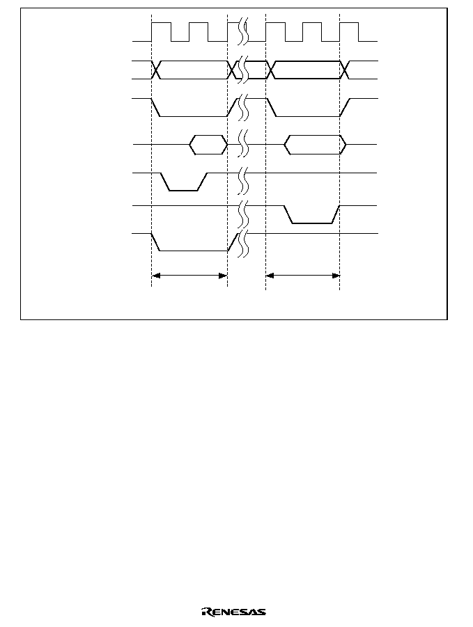
Rev. 2.00, 09/03, page 262 of 690
CKIO
A25 to A0
Note: In transfer between external memories, with DACK output in the read cycle,
DACK output timing is the same as that of CSn.
D31 to D0
WEn
RD
DACKn
(Active-Low)
CSn
Transfer source
address
Transfer destination
address
Data read cycle
Data write cycle
(1st cycle)
(2nd cycle)
Figure 8.6 Example of DMA Transfer Timing in Dual Mode
(Source: Ordinary Memory, Destination: Ordinary Memory)
∑
Single Address Mode
In single address mode, either the transfer source or transfer destination peripheral device is
accessed (selected) by means of the DACK signal, and the other device is accessed by address.
In this mode, the DMAC performs one DMA transfer in one bus cycle, accessing one of the
external devices by outputting the DACK transfer request acknowledge signal to it, and at the
same time outputting an address to the other device involved in the transfer. For example, in
the case of transfer between external memory and an external device with DACK shown in
figure 8.7, when the external device outputs data to the data bus, that data is written to the
external memory in the same bus cycle.
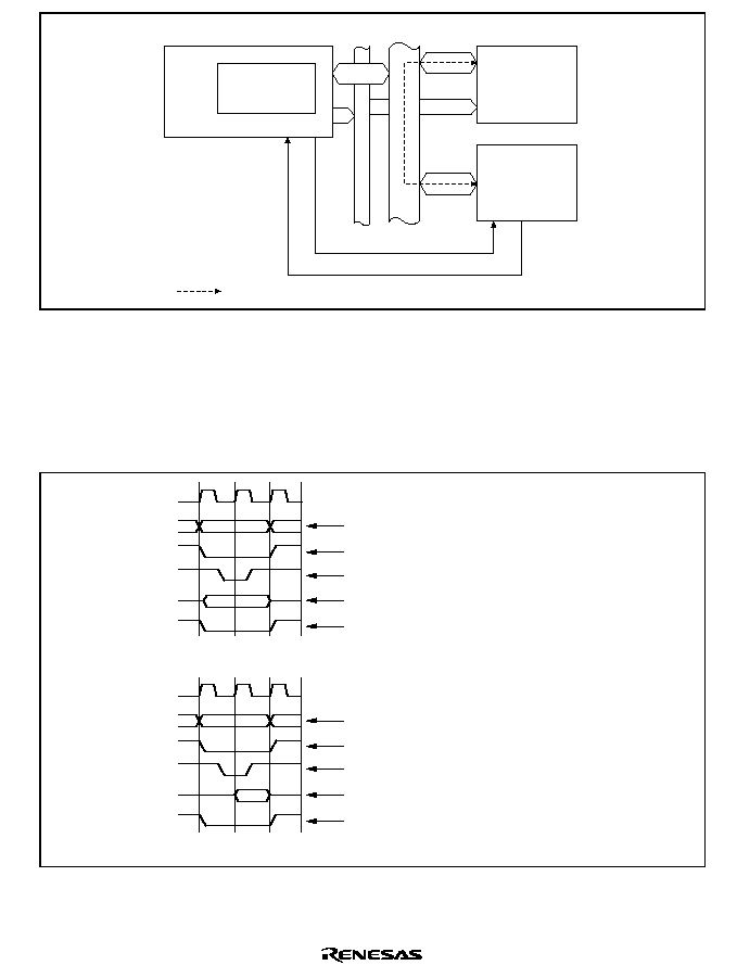
Rev. 2.00, 09/03, page 263 of 690
DMAC
This LSI
DACK
DREQ
External address bus
External data bus
External
memory
External device
with DACK
Data flow
Figure 8.7 Data Flow in Single Address Mode
Two kinds of transfer are possible in single address mode: (1) transfer between an external
device with DACK and a memory-mapped external device, and (2) transfer between an
external device with DACK and external memory. In both cases, only the external request
signal (DREQ) is used for transfer requests.
Figures 8.8 shows example of DMA transfer timing in single address mode.
Address output to external memory space
Select signal to external memory space
Select signal to external memory space
Data output from external device with DACK
DACK signal (active-low) to external device with DACK
Write strobe signal to external memory space
Address output to external memory space
Data output from external memory space
DACK signal (active-low) to external device with DACK
Read strobe signal to external memory space
(a) External device with DACK
external memory space (ordinary memory)
(b) External memory space (ordinary memory)
external device with DACK
CKIO
A25 to A0
D31 to D0
DACKn
CSn
WE
CKIO
A25 to A0
D31 to D0
DACKn
CSn
RD
Figure 8.8 Example of DMA Transfer Timing in Single Address Mode
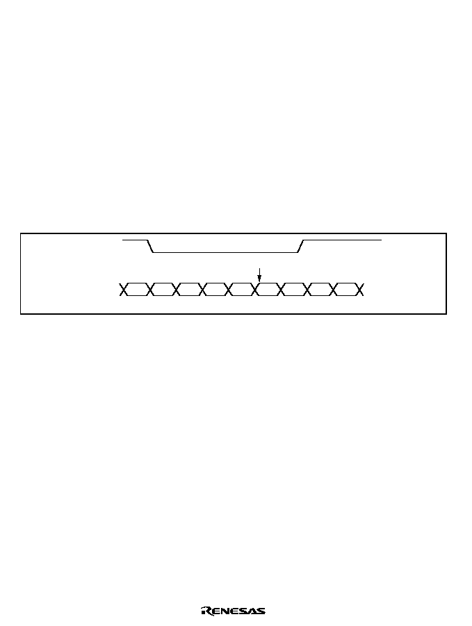
Rev. 2.00, 09/03, page 264 of 690
Bus Modes: There are two bus modes: cycle steal and burst. Select the mode in the TB bits of
channel control register (CHCR).
a. Cycle-Steal Mode
∑
Normal mode
In the normal mode of cycle-steal, the bus right is given to another bus master after a one-
transfer-unit (byte, word, long-word, or 16 bytes unit) DMA transfer. When another transfer
request occurs, the bus rights are obtained from the other bus master and a transfer is
performed for one transfer unit. When that transfer ends, the bus right is passed to the other
bus master. This is repeated until the transfer end conditions are satisfied.
In cycle-steal mode, transfer areas are not affected regardless of settings of the transfer request
source, transfer source, and transfer destination. Figure 8.9 shows an example of DMA transfer
timing in cycle steal mode. Transfer conditions shown in the figure are:
Dual address mode
DREQ low level detection
CPU
CPU
CPU
DMAC DMAC
CPU
DMAC DMAC CPU
DREQ
Bus cycle
Bus right returned to CPU once
Read/Write
Read/Write
Figure 8.9 DMA Transfer Example in Cycle-Steal Normal Mode
(Dual Address, DREQ Low Level Detection)
∑
Intermittent Mode 16 and Intermittent Mode 64
In intermittent mode of cycle steal, DMAC returns the bus right to other bus master whenever
a unit of transfer (byte, word, longword, or 16 bytes) is complete. If the next transfer request
occurs after that, DMAC gets the bus right from other bus master after waiting for 16 or 64
clocks in B
count. DMAC then transfers data of one unit and returns the bus right to other bus
master. These operations are repeated until the transfer end condition is satisfied. It is thus
possible to make lower the ratio of bus occupation by DMA transfer than the normal mode of
cycle steal.
When DMAC gets again the bus right, DMA transfer can be postponed in case of entry
updating due to cache miss.
This intermittent mode can be used for all transfer section; transfer requester, source, and
destination. The bus modes, however, must be cycle steal mode in all channels.
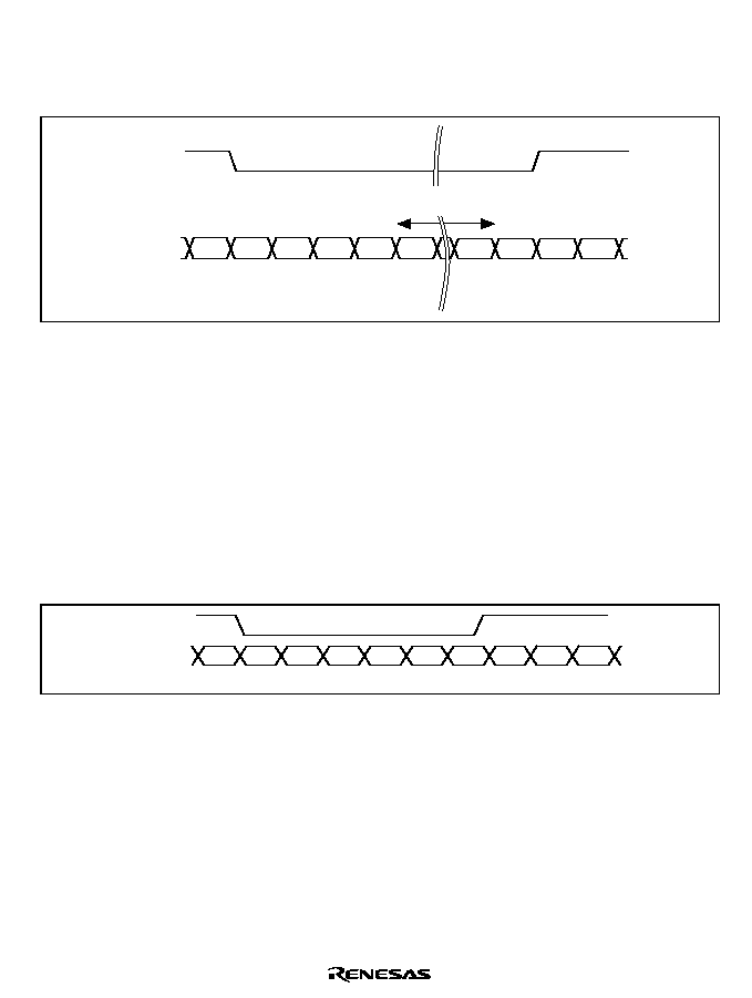
Rev. 2.00, 09/03, page 265 of 690
Figure 8.10 shows an example of DMA transfer timing in cycle steal intermittent mode.
Transfer conditions shown in the figure are:
Dual address mode
DREQ low level detection
DREQ
CPU
CPU
Bus cycle
CPU
More than 16 or 64 B
(change by the CPU's condition of using bus)
DMAC DMAC
CPU
CPU
DMAC DMAC
CPU
Read/Write
Read/Write
Figure 8.10 Example of DMA Transfer in Cycle Steal Intermittent Mode
(Dual Address, DREQ Low Level Detection)
b. Burst Mode
Once the bus right is obtained, the transfer is performed continuously until the transfer end
condition is satisfied. In external request mode with low level detection of the DREQ pin,
however, when the DREQ pin is driven high, the bus passes to the other bus master after the
DMAC transfer request that has already been accepted ends, even if the transfer end conditions
have not been satisfied.
Burst mode cannot be used for other than the CMT when the on-chip peripheral module is the
transfer request source. Figure 8.11 shows DMA transfer timing in burst mode.
CPU
CPU
CPU
DMAC DMAC DMAC
DMAC
DMAC DMAC
CPU
DREQ
Bus cycle
Read
Read
Read
Write
Write
Write
Figure 8.11 DMA Transfer Example in Burst Mode
(Dual Address, DREQ Low Level Detection)

Rev. 2.00, 09/03, page 266 of 690
Relationship between Request Modes and Bus Modes by DMA Transfer Category: Table 8.9
shows the relationship between request modes and bus modes by DMA transfer category.
Table 8.9
Relationship of Request Modes and Bus Modes by DMA Transfer Category
Address
Mode
Transfer Category
Request
Mode
Bus
Mode
Transfer
Size (bits)
Usable
Channels
Dual
External device with DACK and external
memory
External
B/C
8/16/32/128
0, 1
External device with DACK and memory-
mapped external device
External
B/C
8/16/32/128
0, 1
External memory and external memory
All
*
1
B/C
8/16/32/128
0 to 3
*
5
External memory and memory-mapped
external device
All
*
1
B/C
8/16/32/128
0 to 3
*
5
Memory-mapped external device and
memory-mapped external device
All
*
1
B/C
8/16/32/128
0 to 3
*
5
External memory and on-chip peripheral
module
All
*
2
B/C
*
3
8/16/32/128
*
4
0 to 3
*
5
Memory-mapped external device and
on-chip peripheral module
All
*
2
B/C
*
3
8/16/32/128
*
4
0 to 3
*
5
On-chip peripheral module and on-chip
peripheral module
All
*
2
B/C
*
3
8/16/32/128
*
4
0 to 3
*
5
Single
External device with DACK and external
memory
External
B/C
8/16/32
0, 1
External device with DACK and memory-
mapped external device
External
B/C
8/16/32
0, 1
B: Burst, C: Cycle steal
Notes: 1. External requests, auto requests, and on-chip peripheral module requests are all
available. In the case of on-chip peripheral module requests, however, the CMT is only
available.
2. External requests, auto requests, and on-chip peripheral module requests are all
available. However, with the exception of the CMT, the module must be designated as
the transfer request source or the transfer destination.
3. Only cycle steal except for the CMT as the transfer source.
4. Access size permitted for the on-chip peripheral module register functioning as the
transfer source or transfer destination.
5. If the transfer request is an external request, channels 0 and 1 are only available.
Bus Mode and Channel Priority Order: If, when the priority is set to fixed mode (CH0 > CH1)
and channel 1 is transferring in burst mode, a transfer request to channel 0, which has higher
priority, is generated, the transfer on channel 0 will begin immediately.
At this time, if channel 0 is set to burst mode, the transfer on channel 1 will resume when the
channel 0 transfer has completely finished.
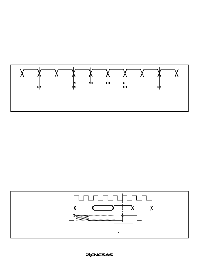
Rev. 2.00, 09/03, page 267 of 690
On the other hand, if channel 0 is operating in cycle-steal mode, channel 1 will begin operating
again after channel 0 completes the transfer of one transfer unit, and without the internal bus being
released. Transfer will then alternate between the two channels in the order channel 0, channel 1,
channel 0, channel 1, and so on. In other words, the CPU cycles following cycle-steal mode
transfer are replaced by bust mode transfer. Figure 8.12 shows an example of this. If multiple
channels are competing to execute burst mode transfers, the channel with the highest priority
performs the burst mode transfer first.
When DMA transfers are performed using multiple channels, the bus is not released to another bus
master until all of the competing burst mode transfers have completed.
CPU
DMA CH1
DMA CH1
DMA CH0
DMA CH1
DMA CH0
DMA CH1
DMA CH1
CPU
CH0
CH1
CH0
Cycle-steal mode between
DMAC CH0 and CH1
DMAC CH1
burst mode
CPU
CPU
Priority: CH0 > CH1
CH0: Cycle-steal mode
CH1: Burst mode
DMAC CH1
burst mode
Figure 8.12 Bus State when Multiple Channels are Operating
Cycle-steal mode channels and burst mode channels should not be mixed in round-robin mode.
Doing so runs the risk that priority changes may not be made properly, although the individual
channel transfer operations will be performed correctly.
8.4.5
Number of Bus Cycle States and DREQ Pin Sampling Timing
Number of Bus Cycle States: When the DMAC is the bus master, the number of bus cycle states
is controlled by the bus state controller (BSC) in the same way as when the CPU is the bus master.
For details, see section 7, Bus State Controller (BSC).
DREQ Pin Sampling Timing:
CKIO
Bus cycle
DREQ
(Rising)
DACK
(Active-high)
CPU
CPU
Acceptance start
2nd acceptance
1st acceptance
CPU
DMAC
Non sensitive period
Figure 8.13 Example of DREQ Input Detection in Cycle Steal Mode Edge Detection
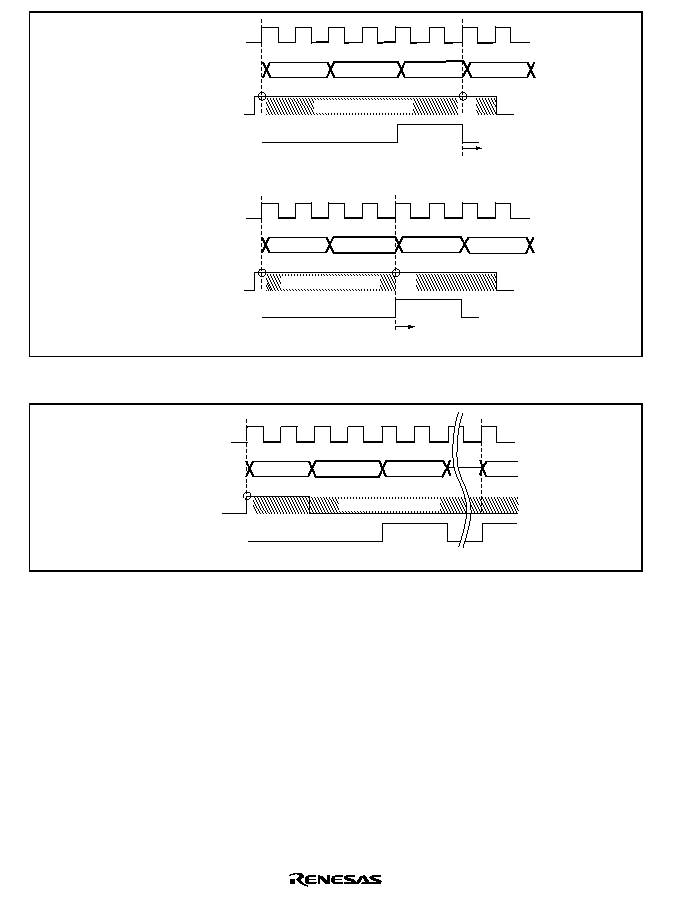
Rev. 2.00, 09/03, page 268 of 690
CKIO
Bus cycle
Bus cycle
DREQ
(Overrun 0 at high level)
DACK
(Active-high)
CPU
CPU
CPU
DMAC
CKIO
DREQ
(Overrun 1 at high level)
DACK
(Active-high)
CPU
CPU
CPU
DMAC
Non sensitive period
1st acceptance
2nd acceptance
Acceptance
start
Acceptance
start
1st acceptance
2nd acceptance
Non sensitive period
Figure 8.14 Example of DREQ Input Detection in Cycle Steal Mode Level Detection
CKIO
Bus cycle
DREQ
(Rising)
DACK
(Active-high)
CPU
CPU
DMAC
DMAC
Non sensitive period
Busrst acceptance
Figure 8.15 Example of DREQ Input Detection in Burst Mode Edge Detection
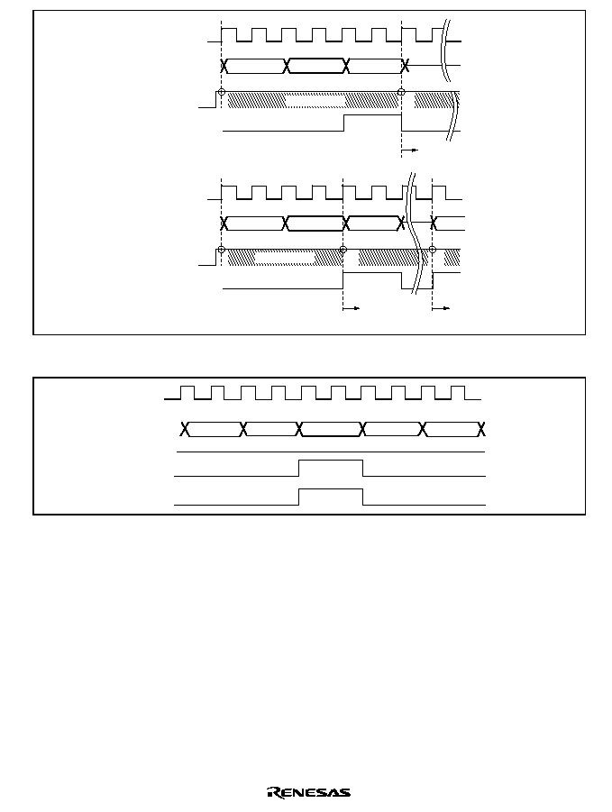
Rev. 2.00, 09/03, page 269 of 690
CKIO
Bus cycle
Bus cycle
DREQ
(Overrun 0 at
high level)
DACK
(Active-high)
CPU
1st acceptance
CPU
DMAC
CKIO
DREQ
(Overrun 1 at
high level)
DACK
(Active-high)
CPU
CPU
DMAC
DMAC
2nd acceptance
Acceptance
start
Acceptance
start
Acceptance
start
Non sensitive
Non sensitive
1st acceptance
2nd acceptance
3rd
acceptance
Figure 8.16 Example of DREQ Input Detection in Burst Mode Level Detection
CKIO
Bus cycle
DACK
DREQ
TEND
CPU
CPU
CPU
DMAC
Last DMA transfer
DMAC
Figure 8.17 Example of DMA Transfer End Signal (in Cycle Steal Level Detection)
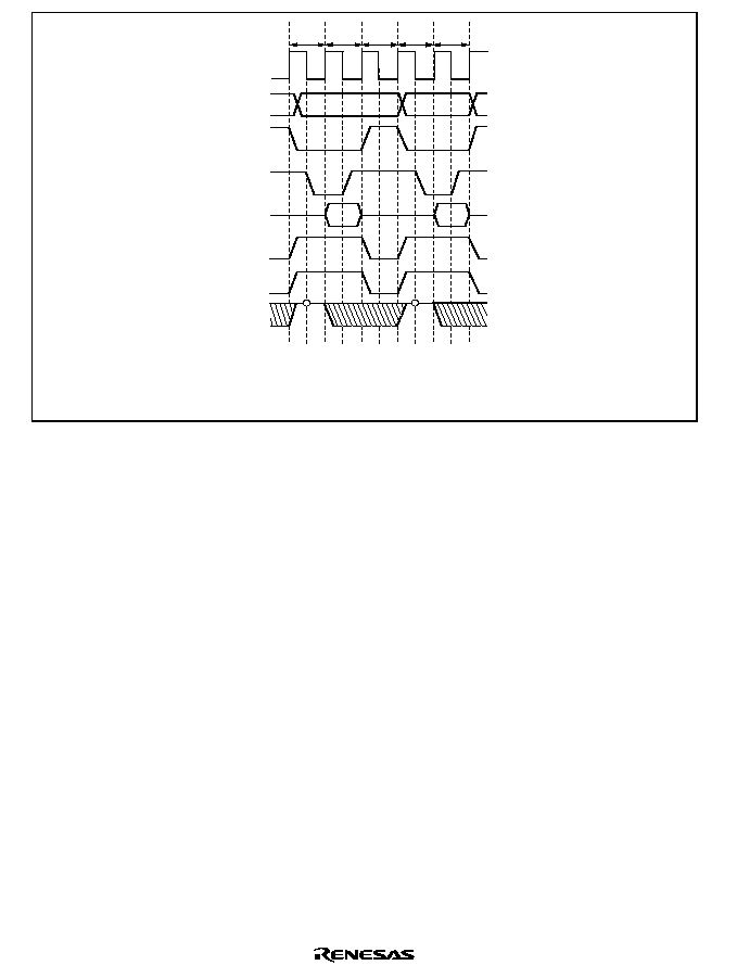
Rev. 2.00, 09/03, page 270 of 690
CKIO
Address
Data
RD
DACKn
WAIT
CSn
T1 T2
Taw T1 T2
TEND0
Note: TEND0 is asserted during the last transfer unit of
DMA transfer. When the transfer unit is divided into
several bus cycles and
CS is negated between bus
cycles, TEND0 is also divided.
Figure 8.18 BSC Ordinary Memory Access
(No Wait, Idle Cycle 1, Longword Access to 16-Bit Device)
8.5
Precautions
8.5.1
Precautions when Mixing Cycle-Steal Mode Channels and Burst Mode Channels
Transfer mode settings should not fulfill conditions (1) and (2) below at the same time.
(1) DMA transfer takes place using multiple channels, some of which operate in the burst mode
and some in the cycle-steal mode.
(2) A channel that uses the burst mode is set to dual address mode and DACK is output using the
write cycle.

CPGS312B_000020020100
Rev. 2.00, 09/03, page 271 of 690
Section 9 Clock Pulse Generator (CPG)
This LSI has a clock pulse generator (CPG) that generates an internal clock (I
), a peripheral clock
(P
), and a bus clock (B
). The CPG consists of oscillators, PLL circuits, and divider circuits.
9.1
Features
∑
Seven clock modes
Selection of seven clock modes depending on the frequency ranges and crystal oscillation or
external clock input.
∑
Three clocks generated independently
An internal clock for the CPU and cache (I
); a peripheral clock (P
) for the peripheral
modules; a bus clock (B
= CKIO) for the external bus interface.
∑
Frequency change function
Internal and peripheral clock frequencies can be changed independently using the phase-locked
loop (PLL) circuit and divider circuit within the CPG. Frequencies are changed by software
using the frequency control register (FRQCR) settings.
∑
Power-down mode control
The clock can be stopped for sleep mode and software standby mode and specific modules can
be stopped using the module standby function.
A block diagram of the CPG is shown in figure 9.1.
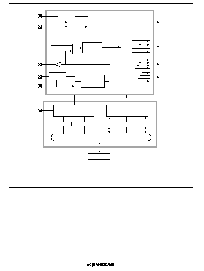
Rev. 2.00, 09/03, page 272 of 690
XTAL_USB
EXTAL_USB
CKIO
PLL circuit 1
(
◊1, 2, 3, 4)
Crystal
Oscillator
PLL circuit 2
(
◊1, 2, 4)
◊1
◊1/2
◊1/3
◊1/4
CPG oscillator circuit unit
Internal clock
(I
)
Peripheral bus
Bus interface
FRQCR:
STBCR:
STBCR2:
STBCR3:
UCLKCR:
Frequency control register
Standby control register
Standby control register 2
Standby control register 3
USB clock control register
Peripheral clock
(P
)
Bus clock
(B
= CKIO)
XTAL
EXTAL
MD2
MD1
MD0
FRQCR
UCLKCR
STBCR
STBCR2
STBCR3
CPG control unit
USB clock
Clock frequency
control circuit
Standby control circuit
Divider 1
Crystal
Oscillator
Figure 9.1 Block Diagram of Clock Pulse Generator

Rev. 2.00, 09/03, page 273 of 690
The clock pulse generator blocks function as follows:
1. PLL Circuit 1
PLL circuit 1 doubles, triples, quadruples, or leaves unchanged the input clock frequency from
the CKIO pin or PLL circuit 2. The multiplication rate is set by the frequency control register.
When this is done, the phase of the rising edge of the internal clock is controlled so that it will
synchronize with the phase of the rising edge of the CKIO pin.
2. PLL Circuit 2
PLL circuit 2 leaves unchanged, doubles, or quadruples the input clock frequency coming from
the crystal oscillator or EXTAL pin. The multiplication ratio is fixed by the clock-operating
mode. The clock-operating mode is set by pins MD0, MD1, and MD2. For more details on
clock operating modes, refer to table 9.2.
3. Crystal Oscillator
This oscillator circuit is used when a crystal resonator is connected to the XTAL and EXTAL
pins. This crystal oscillator operates according to the clock operating mode setting.
4. Divider 1
Divider 1 generates a clock at the operating frequency used by the internal or peripheral clock.
The operating frequency can be 1, 1/2, 1/3, or 1/4 times the output frequency of PLL circuit 1,
as long as it stays at or above the clock frequency of the CKIO pin. The division ratio is set in
the frequency control register.
5. Clock Frequency Control Circuit
The clock frequency control circuit controls the clock frequency using the MD0, MD1, and
MD2 pins and the frequency control register.
6. Standby Control Circuit
The standby control circuit controls the state of the on-chip oscillator and other modules during
clock switching and software/standby modes.
7. Frequency Control Register
The frequency control register has control bits assigned for the following functions: clock
output/non-output from the CKIO pin, the frequency multiplication ratio of PLL circuit 1, and
the frequency division ratio of the internal clock and the peripheral clock.
8. Standby Control Register
The standby control register has bits for controlling the power-down modes. See section 11,
Power-Down Modes, for more information.
9. USB Clock Control Register
The source clock generating the USB clock is set in the USB clock control register.

Rev. 2.00, 09/03, page 274 of 690
9.2
Input/Output Pins
Table 9.1 lists the CPG pins and their functions.
Table 9.1
Clock Pulse Generator Pins and Functions
Pin Name
Symbol
I/O
Description
MD0
I
Set the clock-operating mode.
MD1
I
Set the clock-operating mode.
Mode control pins
MD2
I
Set the clock-operating mode.
XTAL
O
Connects a crystal resonator.
Crystal oscillator
pins for system clock
(clock input pins)
EXTAL
I
Connects a crystal resonator. Also used to input an
external clock.
Clock I/O pin
CKIO
I/O
Inputs or outputs an external clock.
XTAL_USB
O
Connects a crystal resonator for the USB.
Crystal oscillator
pins for USB
(clock input pins)
EXTAL_USB I
Connects a crystal resonator for the USB. Also used to
input an external clock.
Note:
The values of the mode control pins are sampled only in a power-on reset. This can prevent
the erroneous operation of the LSI.

Rev. 2.00, 09/03, page 275 of 690
9.3
Clock Operating Modes
Table 9.2 shows the relationship between the mode control pins (MD2 to MD0) combinations and
the clock operating modes. Table 9.3 shows the usable frequency ranges in the clock operating
modes and the frequency range of the input clock.
Table 9.2
Clock Operating Modes
Pin Values
Clock I/O
Mode
MD2
MD1
MD0
Source
Output
PLL2
On/Off
PLL1
On/Off
CKIO
Frequency
0
0
0
0
EXTAL
CKIO
ON (
◊
1)
ON (
◊
1, 2, 3, 4)
(EXTAL)
1
0
0
1
EXTAL
CKIO
ON (
◊
4)
ON (
◊
1, 2, 3, 4)
(EXTAL)
◊
4
2
0
1
0
Crystal
resonator
CKIO
ON (
◊
4)
ON (
◊
1, 2, 3, 4)
(Crystal)
◊
4
4
1
0
0
Crystal
resonator
CKIO
ON (
◊
1)
ON (
◊
1, 2, 3, 4)
(Crystal)
5
1
0
1
EXTAL
CKIO
ON (
◊
2)
ON (
◊
1, 2, 3, 4)
(EXTAL)
◊
2
6
1
1
0
Crystal
resonator
CKIO
ON (
◊
2)
ON (
◊
1, 2, 3, 4)
(Crystal)
◊
2
7
1
1
1
CKIO
OFF
ON (
◊
1, 2, 3, 4)
(CKIO)
Mode 0: An external clock is input from the EXTAL pin and executes waveform shaping by PLL
circuit 2 before being supplied inside this LSI.
Mode 1: An external clock is input from the EXTAL pin and its frequency is multiplied by 4 by
PLL circuit 2 before being supplied inside this LSI, allowing a low-frequency external clock to be
used.
Mode 2: The on-chip crystal oscillator operates, with the oscillation frequency being multiplied by
4 by PLL circuit 2 before being supplied inside this LSI, allowing a low-frequency external clock
to be used.
Mode 4: The on-chip crystal oscillator operates and executes waveform shaping by PLL circuit 2
before being supplied inside this LSI.
Mode 5: An external clock is input from the EXTAL pin and its frequency is multiplied by 2 by
PLL circuit 2 before being supplied inside this LSI, allowing a low-frequency external clock to be
used.
Mode 6: The on-chip crystal oscillator operates, with the oscillation frequency being multiplied by
2 by PLL circuit 2 before being supplied inside this LSI, allowing a low crystal frequency to be
used.

Rev. 2.00, 09/03, page 276 of 690
Mode 7: In this mode, the CKIO pin is an input, an external clock is input to this pin, and executes
waveform shaping, and also frequency multiplication according to the setting, by PLL circuit 1
before being supplied to this LSI. As PLL circuit 1 compensates for fluctuations in the CKIO pin
load, this mode is suitable for connection of synchronous DRAM.
Table 9.3
Possible Combination of Clock Modes and FRQCR Values
Clock
Mode
FRQCR
*
1
PLL1
PLL2
Clock Rate
*
2
(I:B:P)
Input Clock/Crystal
Resonator
Frequency
Range
CKIO Frequency Range
H'1000
ON (
◊
1)
ON (
◊
1)
1:1:1
20.00 MHz to 33.34 MHz
20.00 MHz to 33.34 MHz
H'1001
ON (
◊
1)
ON (
◊
1)
1:1:1/2
20.00 MHz to 66.67 MHz
20.00 MHz to 66.67 MHz
H'1003
ON (
◊
1)
ON (
◊
1)
1:1:1/4
20.00 MHz to 66.67 MHz
20.00 MHz to 66.67 MHz
H'1101
ON (
◊
2)
ON (
◊
1)
2:1:1
20.00 MHz to 33.34 MHz
20.00 MHz to 33.34 MHz
H'1103
ON (
◊
2)
ON (
◊
1)
2:1:1/2
20.00 MHz to 66.67 MHz
20.00 MHz to 66.67 MHz
H'1111
ON (
◊
2)
ON (
◊
1)
1:1:1
20.00 MHz to 33.34 MHz
20.00 MHz to 33.34 MHz
H'1113
ON (
◊
2)
ON (
◊
1)
1:1:1/2
20.00 MHz to 66.67 MHz
20.00 MHz to 66.67 MHz
H'1202
ON (
◊
3)
ON (
◊
1)
3:1:1
26.70 MHz to 33.34 MHz
26.70 MHz to 33.34 MHz
H'1222
ON (
◊
3)
ON (
◊
1)
1:1:1
26.70 MHz to 33.34 MHz
26.70 MHz to 33.34 MHz
H'1303
ON (
◊
4)
ON (
◊
1)
4:1:1
20.00 MHz to 33.34 MHz
20.00 MHz to 33.34 MHz
H'1313
ON (
◊
4)
ON (
◊
1)
2:1:1
20.00 MHz to 33.34 MHz
20.00 MHz to 33.34 MHz
0
H'1333
ON (
◊
4)
ON (
◊
1)
1:1:1
20.00 MHz to 33.34 MHz
20.00 MHz to 33.34 MHz
H'1001
ON (
◊
1)
ON (
◊
4)
4:4:2
10.00 MHz to 16.67 MHz
40.00 MHz to 66.67 MHz
H'1003
ON (
◊
1)
ON (
◊
4)
4:4:1
10.00 MHz to 16.67 MHz
40.00 MHz to 66.67 MHz
H'1103
ON (
◊
2)
ON (
◊
4)
8:4:2
10.00 MHz to 16.67 MHz
40.00 MHz to 66.67 MHz
1, 2
H'1113
ON (
◊
2)
ON (
◊
4)
4:4:2
10.00 MHz to 16.67 MHz
40.00 MHz to 66.67 MHz
H'1000
ON (
◊
1)
ON (
◊
1)
1:1:1
20.00 MHz to 33.34 MHz
20.00 MHz to 33.34 MHz
H'1001
ON (
◊
1)
ON (
◊
1)
1:1:1/2
20.00 MHz to 33.34 MHz
20.00 MHz to 33.34 MHz
H'1003
ON (
◊
1)
ON (
◊
1)
1:1:1/4
20.00 MHz to 33.34 MHz
20.00 MHz to 33.34 MHz
H'1101
ON (
◊
2)
ON (
◊
1)
2:1:1
20.00 MHz to 33.34 MHz
20.00 MHz to 33.34 MHz
H'1103
ON (
◊
2)
ON (
◊
1)
2:1:1/2
20.00 MHz to 33.34 MHz
20.00 MHz to 33.34 MHz
H'1111
ON (
◊
2)
ON (
◊
1)
1:1:1
20.00 MHz to 33.34 MHz
20.00 MHz to 33.34 MHz
H'1113
ON (
◊
2)
ON (
◊
1)
1:1:1/2
20.00 MHz to 33.34 MHz
20.00 MHz to 33.34 MHz
H'1202
ON (
◊
3)
ON (
◊
1)
3:1:1
26.70 MHz to 33.34 MHz
26.70 MHz to 33.34 MHz
H'1222
ON (
◊
3)
ON (
◊
1)
1:1:1
26.70 MHz to 33.34 MHz
26.70 MHz to 33.34 MHz
H'1303
ON (
◊
4)
ON (
◊
1)
4:1:1
20.00 MHz to 33.34 MHz
20.00 MHz to 33.34 MHz
H'1313
ON (
◊
4)
ON (
◊
1)
2:1:1
20.00 MHz to 33.34 MHz
20.00 MHz to 33.34 MHz
4
H'1333
ON (
◊
4)
ON (
◊
1)
1:1:1
20.00 MHz to 33.34 MHz
20.00 MHz to 33.34 MHz

Rev. 2.00, 09/03, page 277 of 690
Clock
Mode
FRQCR
*
1
PLL1
PLL2
Clock Rate
*
2
(I:B:P)
Input Clock / Crystal
Resonator
Frequency
Range
CKIO Frequency Range
H'1000
ON (
◊
1)
ON (
◊
2)
2:2:2
10.00 MHz to 16.67 MHz
20.00 MHz to 33.34 MHz
H'1001
ON (
◊
1)
ON (
◊
2)
2:2:1
10.00 MHz to 33.34 MHz
20.00 MHz to 66.67 MHz
H'1003
ON (
◊
1)
ON (
◊
2)
2:2:1/2
10.00 MHz to 33.34 MHz
20.00 MHz to 66.67 MHz
H'1101
ON (
◊
2)
ON (
◊
2)
4:2:2
10.00 MHz to 16.67 MHz
20.00 MHz to 33.33 MHz
H'1103
ON (
◊
2)
ON (
◊
2)
4:2:1
10.00 MHz to 33.34 MHz
20.00 MHz to 66.67 MHz
H'1111
ON (
◊
2)
ON (
◊
2)
2:2:2
10.00 MHz to 16.67 MHz
20.00 MHz to 33.34 MHz
H'1113
ON (
◊
2)
ON (
◊
2)
2:2:1
10.00 MHz to 33.34 MHz
20.00 MHz to 66.67 MHz
H'1202
ON (
◊
3)
ON (
◊
2)
6:2:2
10.00 MHz to 16.67 MHz
20.00 MHz to 33.34 MHz
H'1222
ON (
◊
3)
ON (
◊
2)
2:2:2
10.00 MHz to 16.67 MHz
20.00 MHz to 33.34 MHz
H'1303
ON (
◊
4)
ON (
◊
2)
8:2:2
10.00 MHz to 16.67 MHz
20.00 MHz to 33.33 MHz
H'1313
ON (
◊
4)
ON (
◊
2)
4:2:2
10.00 MHz to 16.67 MHz
20.00 MHz to 33.33 MHz
5
H'1333
ON (
◊
4)
ON (
◊
2)
2:2:2
10.00 MHz to 16.67 MHz
20.00 MHz to 33.34 MHz
H'1000
ON (
◊
1)
ON (
◊
2)
2:2:2
10.00 MHz to 16.67 MHz
20.00 MHz to 33.34 MHz
H'1001
ON (
◊
1)
ON (
◊
2)
2:2:1
10.00 MHz to 33.34 MHz
20.00 MHz to 66.67 MHz
H'1003
ON (
◊
1)
ON (
◊
2)
2:2:1/2
10.00 MHz to 33.34 MHz
20.00 MHz to 66.67 MHz
H'1101
ON (
◊
2)
ON (
◊
2)
4:2:2
10.00 MHz to 16.67 MHz
20.00 MHz to 33.33 MHz
H'1103
ON (
◊
2)
ON (
◊
2)
4:2:1
10.00 MHz to 33.34 MHz
20.00 MHz to 66.67 MHz
H'1111
ON (
◊
2)
ON (
◊
2)
2:2:2
10.00 MHz to 16.67 MHz
20.00 MHz to 33.34 MHz
H'1113
ON (
◊
2)
ON (
◊
2)
2:2:1
10.00 MHz to 33.34 MHz
20.00 MHz to 66.67 MHz
H'1202
ON (
◊
3)
ON (
◊
2)
6:2:2
10.00 MHz to 16.67 MHz
20.00 MHz to 33.34 MHz
H'1222
ON (
◊
3)
ON (
◊
2)
2:2:2
10.00 MHz to 16.67 MHz
20.00 MHz to 33.34 MHz
H'1303
ON (
◊
4)
ON (
◊
2)
8:2:2
10.00 MHz to 16.67 MHz
20.00 MHz to 33.33 MHz
H'1313
ON (
◊
4)
ON (
◊
2)
4:2:2
10.00 MHz to 16.67 MHz
20.00 MHz to 33.33 MHz
6
H'1333
ON (
◊
4)
ON (
◊
2)
2:2:2
10.00 MHz to 16.67 MHz
20.00 MHz to 33.34 MHz

Rev. 2.00, 09/03, page 278 of 690
Clock
Mode
FRQCR
*
1
PLL1
PLL2
Clock Rate
*
2
(I:B:P)
Input Clock / Crystal
Resonator
Frequency
Range
CKIO Frequency Range
H'1000
ON (
◊
1)
OFF
1:1:1
20.00 MHz to 33.34 MHz
20.00 MHz to 33.34 MHz
H'1001
ON (
◊
1)
OFF
1:1:1/2
20.00 MHz to 66.67 MHz
20.00 MHz to 66.67 MHz
H'1003
ON (
◊
1)
OFF
1:1:1/4
20.00 MHz to 66.67 MHz
20.00 MHz to 66.67 MHz
H'1101
ON (
◊
2)
OFF
2:1:1
20.00 MHz to 33.34 MHz
20.00 MHz to 33.34 MHz
H'1103
ON (
◊
2)
OFF
2:1:1/2
20.00 MHz to 66.67 MHz
20.00 MHz to 66.67 MHz
H'1111
ON (
◊
2)
OFF
1:1:1
20.00 MHz to 33.34 MHz
20.00 MHz to 33.34 MHz
H'1113
ON (
◊
2)
OFF
1:1:1/2
20.00 MHz to 66.67 MHz
20.00 MHz to 66.67 MHz
H'1202
ON (
◊
3)
OFF
3:1:1
26.70 MHz to 33.34 MHz
26.70 MHz to 33.34 MHz
H'1222
ON (
◊
3)
OFF
1:1:1
26.70 MHz to 33.34 MHz
26.70 MHz to 33.34 MHz
H'1303
ON (
◊
4)
OFF
4:1:1
20.00 MHz to 33.34 MHz
20.00 MHz to 33.34 MHz
H'1313
ON (
◊
4)
OFF
2:1:1
20.00 MHz to 33.34 MHz
20.00 MHz to 33.34 MHz
7
H'1333
ON (
◊
4)
OFF
1:1:1
20.00 MHz to 33.34 MHz
20.00 MHz to 33.34 MHz
Notes: 1. This LSI cannot operate in an FRQCR value other than that listed in table 9.3.
2. Taking input clock frequency ratio as 1.
Cautions:
1. The input to divider 1 is the output of the PLL circuit 1.
2. The frequency of the internal clock (I
) is:
∑
The product of the frequency of the CKIO pin, the frequency multiplication ratio of PLL
circuit 1, and the division ratio of divider 1.
∑
Do not set the internal clock frequency lower than the CKIO pin frequency.
3. The frequency of the peripheral clock (P
) is:
∑
The product of the frequency of the CKIO pin, the frequency multiplication ratio of PLL
circuit 1, and the division ratio of divider 1.
∑
The peripheral clock frequency should not be set higher than the frequency of the CKIO
pin, higher than 33.34 MHz, or lower than 13 MHz when the USB is used.
4.
◊
1,
◊
2,
◊
3, or
◊
4 can be used as the multiplication ratio of PLL circuit 1.
◊
1,
◊
1/2,
◊1/
3, or
◊
1/4 can be selected as the division ratios of divider 1. Set the rate in the frequency control
register.
5. The output frequency of PLL circuit 1 is the product of the CKIO frequency and the
multiplication ratio of PLL circuit 1. Use the output frequency under 133.34 MHz.

Rev. 2.00, 09/03, page 279 of 690
9.4
Register Descriptions
The CPG has the following registers. Refer to section 24, List of Registers, for the addresses of the
registers and the state of each register in each processor state.
∑
Frequency control register (FRQCR)
∑
USB clock control register (UCLKCR)
9.4.1
Frequency Control Register (FRQCR)
The frequency control register (FRQCR) is a 16-bit readable/writable register used to specify
whether a clock is output from the CKIO pin, the on/off state of PLL circuit 1, PLL standby, the
frequency multiplication ratio of PLL circuit 1, and the frequency division ratio of the internal
clock and the peripheral clock. Only word access can be used on FRQCR. As for the combination
of the clock rate, refer to table 9.3. The combinations listed in table 9.3 should only be set on
FRQCR.
Bit
Bit
Name
Initial
Value
R/W
Description
15 to 13
0
R
Reserved
These bits are always read as 0. The write value
should always be 0.
12
CKOEN
1
R/W
Clock Output Enable
Specifies to output a clock from the CKIO pin or to fix
the CKIO pin low when software standby is canceled
(after an interrupt before STATUS1 becomes low and
STATUS0 becomes low). The CKIO pin is fixed low
during STATUS1 = low and STATUS0 = high, when
the CKOEN bit is cleared to 0. Therefore, the
malfunction of an external circuit because of an
unstable CKIO clock in releasing software standby
mode can be prevented.
In clock operating mode 7, the CKIO pin is in the input
state regardless of this bit.
0: Fixes the CKIO pin low in software standby mode.
1: Outputs a clock from the CKIO pin.
11, 10
0
R
Reserved
These bits are always read as 0. The write value
should always be 0.

Rev. 2.00, 09/03, page 280 of 690
Bit
Bit
Name
Initial
Value
R/W
Description
9
8
STC1
STC0
0
0
R/W
R/W
Frequency Multiplication Ratio
00:
◊
1 time
01:
◊
2 times
10:
◊
3 times
11:
◊
4 times
7, 6
0
R
Reserved
These bits are always read as 0. The write value
should always be 0.
5
4
IFC1
IFC0
0
0
R/W
R/W
Internal Clock Frequency Division Ratio
Specify the frequency division ratio of the internal
clock with respect to the output frequency of PLL
circuit 1.
00:
◊
1 time
01:
◊
1/2 time
10:
◊
1/3 time
11:
◊
1/4 time
3, 2
0
R
Reserved
These bits are always read as 0. The write value
should always be 0.
1
0
PFC1
PFC0
1
1
R/W
R/W
Peripheral Clock Frequency Division Ratio
Specify the frequency division ratio of the peripheral
clock with respect to the output frequency of PLL
circuit 1.
00:
◊
1 time
01:
◊
1/2 time
10:
◊
1/3 time
11:
◊
1/4 time

Rev. 2.00, 09/03, page 281 of 690
9.4.2
USB Clock Frequency Control Register (UCLKCR)
UCLKCR is an 8-bit readable/writable register.
Word-size access is used to write to this register. This writing should be performed with H'A5 in
the upper byte and the write data in the lower byte.
Bit
Bit
Name
Initial
Value
R/W
Description
7
6
USSCS1
USSCS0
1
1
R/W
R/W
Source Clock Selection Bit
These bits select the source clock.
00: Clock stopped
01: Setting prohibited
10: Setting prohibited
11: External input clock
5
USBEN
1
R/W
USB On-chip Oscillator Enable
This bit controls the operation of the USB on-chip
oscillator.
0: USB on-chip oscillator stopped
1: USB on-chip oscillator operates
4 to 0
0
R
Reserved
These bits are always read as 0. The write value
should always be 0.
9.4.3
Usage Notes
Note the following when using the USB. If these are used incorrectly, the correct clocks may not
be generated, causing faulty operation of the USB.
1. UCLKCR is used only for generation of the USB clocks. When the USB is not used, it is
recommended that UCLKCR be cleared to H'00 to halt the clock.
2. Halt the USB before changing the values of UCLKCR. Halt the USB by stopping the clock
supply using the USB module stop bits in STBCR3.
3. UCLKCR is initialized only by a power-on reset. In a manual reset, they retain their current set
values.
4. Use the USB module with P
> 13 MHz. Otherwise, the operation of this LSI is not
guaranteed.

Rev. 2.00, 09/03, page 282 of 690
9.5
Changing Frequency
The frequency of the internal clock and peripheral clock can be changed either by changing the
multiplication rate of PLL circuit 1 or by changing the division rates of divider 1. All of these are
controlled by software through the frequency control register. The methods are described below.
9.5.1
Changing Multiplication Rate
A PLL settling time is required when the multiplication rate of PLL circuit 1 is changed. The on-
chip WDT counts the settling time.
1. In the initial state, the multiplication rate of PLL circuit 1 is 1.
2. Set a value that will become the specified oscillation settling time in the WDT and stop the
WDT. The following must be set:
WTCSR.TME
=
0: WDT stops
WTCSR.CKS[2:0]: Division ratio of WDT count clock
WTCNT: Initial counter value
3. Set the desired value in the STC[1:0] bits. The division ratio can also be set in the IFC[1:0] bits
and PFC[1:0] bits.
4. The processor pauses internally and the WDT starts incrementing. The internal and peripheral
clocks both stop and the WDT is supplied with the clock. The clock will continue to be output
at the CKIO pin.
5. Supply of the clock that has been set begins at WDT count overflow, and the processor begins
operating again. The WDT stops after it overflows.
9.5.2
Changing Division Ratio
The WDT will not count unless the multiplication rate is changed simultaneously.
1. In the initial state, IFC[1:0]
=
00 and PFC[1:0]
=
11.
2. Set the IFC[1:0], PFC[1:0] bits to the new division ratio. The values that can be set are limited
by the clock mode and the multiplication rate of PLL circuit 1. Note that if the wrong value is
set, the processor will malfunction.
3. The clock is immediately supplied at the new division ratio.
9.5.3
Modification of Clock Operating Mode
The values of the mode control pins (MD2 to MD0) that define a clock-operating mode are
reflected at power-on reset.
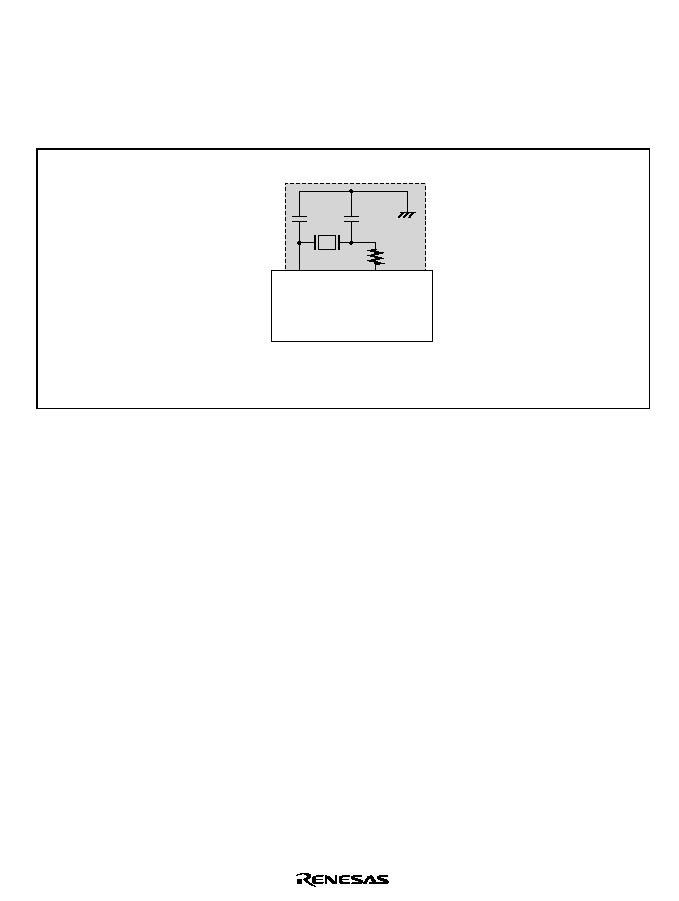
Rev. 2.00, 09/03, page 283 of 690
9.6
Usage Notes
When Using an External Crystal Resonator: Place the crystal resonator, capacitors CL1 and
CL2, and damping resistance R as close as possible to the EXTAL and XTAL pins. To prevent
induction from interfering with correct oscillation, use a common grounding point for the
capacitors connected to the resonator, and do not locate a wiring pattern near these components.
Note: The values for CL1, CL2, and damping resistance
should be determined after consultation with the
crystal resonator manufacturer.
XTAL
EXTAL
This LSI
CL2
R
CL1
Avoid crossing
signal lines
Figure 9.2 Points for Attention when Using Crystal Resonator
Decoupling Capacitors: As far as possible, insert a laminated ceramic capacitor of 0.1 to 1 µF as
a passive capacitor for each V
SS
/V
SS
Q and V
CC
/V
CC
Q pair. Mount the passive capacitors as close
as possible to the chip's power supply pins, and use components with a frequency characteristic
suitable for the chip's operating frequency, as well as a suitable capacitance value.
Digital system V
SS
/V
SS
Q and V
CC
/V
CC
Q pairs: 2-5, 17-19, 26-28, 32-34, 44-46, 57-59, 69-71, 78-
80, 87-89, 111-113, 130-132, 133-138, 159-161, 178-180, 182-184, 199-204
On-chip oscillator V
SS
/V
SS
Q and V
CC
/V
CC
Q pairs: 6-9, 149-150, 151-152, 205-208
When Using a PLL Oscillator Circuit: Keep the wiring from the PLL V
CC
and PLL V
SS
connection pattern to the power supply pins short, and make the pattern width wide, to minimize
the inductance value.
In clock mode 7, connect the EXTAL pin to V
CC
Q (3.3-V power) with pull-up resistor, and leave
the XTAL pin open.

Rev. 2.00, 09/03, page 284 of 690
V
CC
-PLL2
V
CC
-PLL1
V
CC
V
SS
V
SS
-PLL2
V
SS
-PLL1
Avoid crossing
signal lines
Power supply
Figure 9.3 Points for Attention when Using PLL Oscillator Circuit
Notes on Wiring Power Supply Pins: To avoid crossing signal lines, wire V
CC
-
PLL1,
V
CC
-
PLL2, V
SS
-
PLL1, and V
SS
-
PLL2 as three patterns from the power supply source on the
board so that they are independent of digital V
CC
and V
SS
.

WDTS311A_000020020100
Rev. 2.00, 09/03, page 285 of 690
Section 10 Watchdog Timer (WDT)
This LSI includes the watchdog timer (WDT) and can be reset by the overflow of the counter
when the value of the counter has not been updated because of an erroneous system operation.
The WDT is a single-channel timer that uses a peripheral clock as an input and counts the clock
settling time when clearing software standby mode and temporary standbys, such as frequency
changes. It can also be used as a conventional watchdog timer or an interval timer.
10.1
Features
∑
Can be used to ensure the clock settling time
Use the WDT to clear software standby mode and the temporary standbys which occur when
the clock frequency is changed.
∑
Can switch between watchdog timer mode and interval timer mode.
∑
Generates internal resets in watchdog timer mode
Internal resets occur after counter overflow.
Power-on reset and manual reset are available.
∑
Interrupt generation in interval timer mode
An interval timer interrupt is generated when the counter overflows.
∑
Choice of eight counter input clocks
Eight clocks (
◊
1 to
◊
1/4096) that are obtained by dividing the peripheral clock can be selected.

Rev. 2.00, 09/03, page 286 of 690
Figures 10.1 shows a block diagram of the WDT.
WTCSR
Standby
control
Bus interface
WTCNT
Divider
Clock selector
Clock
Standby
mode
Peripheral
clock
Standby
cancellation
Reset
control
Clock selection
WDT
Overflow
Internal
reset
request
Interrupt
control
Interrupt
request
WTCSR:
WTCNT:
Legend
Watchdog timer control/status register
Watchdog timer counter
Figure 10.1 Block Diagram of WDT
10.2
Register Descriptions
The WDT has the following two registers. Refer to section 24, List of Registers for the details of
the addresses of these registers and the state of registers in each operating mode.
∑
Watchdog timer counter (WTCNT)
∑
Watchdog timer control/status register (WTCSR)
10.2.1
Watchdog Timer Counter (WTCNT)
The watchdog timer counter (WTCNT) is an 8-bit readable/writable register that increments on the
selected clock. When an overflow occurs, it generates a reset in watchdog timer mode and an
interrupt in interval timer mode. The WTCNT counter is not initialized by an internal reset due to
the WDT overflow. The WTCNT counter is initialized to H'00 only by a power-on reset using the
RESETP pin.
Use a word access to write to the WTCNT counter, with H'5A in the upper byte. Use a byte access
to read WTCNT.

Rev. 2.00, 09/03, page 287 of 690
Note:
WTCNT differs from other registers in that it is more difficult to write to. See section
10.2.3, Notes on Register Access, for details.
10.2.2
Watchdog Timer Control/Status Register (WTCSR)
The watchdog timer control/status register (WTCSR) is an 8-bit readable/writable register
composed of bits to select the clock used for the count, overflow flags, and enable bits.
WTCSR holds its value in an internal reset due to the WDT overflow. WTCSR is initialized to
H'00 only by a power-on reset using the
RESETP pin.
When used to count the clock settling time for canceling a software standby, it retains its value
after counter overflow. Use a word access to write to the WTCSR counter, with H'A5 in the upper
byte. Use a byte access to read WTCSR.
Note:
WTCSR differs from other registers in that it is more difficult to write to. See section
10.2.3, Notes on Register Access, for details.

Rev. 2.00, 09/03, page 288 of 690
Bit
Bit
Name
Initial
Value
R/W
Description
7
TME
0
R/W
Timer Enable
Starts and stops timer operation. Clear this bit to 0
when using the WDT in software standby mode or
when changing the clock frequency.
0: Timer disabled: Count-up stops and WTCNT value
is retained
1: Timer enabled
6
WT/
IT
0
R/W
Timer Mode Select
Selects whether to use the WDT as a watchdog timer
or an interval timer.
0: Use as interval timer
1: Use as watchdog timer
Note:
If WT/
IT
is modified when the WDT is running,
the up-count may not be performed correctly.
5
RSTS
0
R/W
Reset Select
Selects the type of reset when WTCNT overflows in
watchdog timer mode. In interval timer mode, this
setting is ignored.
0: Power-on reset
1: Manual reset
4
WOVF
0
R/W
Watchdog Timer Overflow
Indicates that WTCNT has overflowed in watchdog
timer mode. This bit is not set in interval timer mode.
0: No overflow
1: WTCNT has overflowed in watchdog timer mode
3
IOVF
0
R/W
Interval Timer Overflow
Indicates that WTCNT has overflowed in interval timer
mode. This bit is not set in watchdog timer mode.
0: No overflow
1: WTCNT has overflowed in interval timer mode
Rev. 2.00, 09/03, page 289 of 690
Bit
Bit
Name
Initial
Value
R/W
Description
2
1
0
CKS2
CKS1
CKS0
0
0
0
R/W
R/W
R/W
Clock Select 2 to 0
These bits select the clock to be used for the WTCNT
count from the eight types obtainable by dividing the
peripheral clock. The overflow period that is shown
inside the parenthesis in the table is the value when
the peripheral clock (P
) is 15 MHz.
000
P
(17
µs)
001
P
/4 (68
µs)
010
P
/16 (273
µs)
011
P
/32 (546
µs)
100
P
/64 (1.09
ms)
101
P
/256 (4.36
ms)
110
P
/1024 (17.48
ms)
111
P
/4096 (69.91
ms)
Note:
If bits CKS2 to CKS0 are modified when the
WDT is running, the up-count may not be
performed correctly. Ensure that these bits are
modified only when the WDT is not running.
Note:
If manual reset is selected using the RSTS bit, a frequency division ratio of 1/16, 1/32, 1/64,
1/256, 1/1,024, or 1/4,096 is selected using bits CKS2 to CKS0, and a watchdog timer
counter overflow occurs, resulting in a manual reset, the LSI will generate two manual
resets in succession. This will not affect its operation but will cause change in the state of
the STATUS pin.
10.2.3
Notes on Register Access
The watchdog timer counter (WTCNT) and watchdog timer control/status register (WTCSR) are
more difficult to write to than other registers. The procedure for writing to these registers is given
below.
∑
These registers must be written by a word transfer instruction. They cannot be written by a
byte or longword transfer instruction.
When writing to WTCNT, set the upper byte to H'5A and transfer the lower byte as the write data,
as shown in figure 10.2. When writing to WTCSR, set the upper byte to H'A5 and transfer the
lower byte as the write data. This transfer procedure writes the lower byte data to WTCNT or
WTCSR.

Rev. 2.00, 09/03, page 290 of 690
15
8
7
0
H'5A
Write data
WTCNT write
15
8
7
0
H'A5
Write data
WTCSR write
Figure 10.2 Writing to WTCNT and WTCSR
10.3
Operation
10.3.1
Canceling Software Standbys
The WDT is used to cancel software standby mode with an interrupt such as an NMI. The
procedure when using an NMI interrupt is described below. (The WDT does not run when resets
are used for canceling, so keep the
RESETP or RESETM pin low until the clock stabilizes.)
1. Before transitioning to software standby mode, always clear the TME bit in WTCSR to 0.
When the TME bit is 1, an erroneous reset or interval timer interrupt may be generated when
the count overflows.
2. Set the type of count clock used in the CKS2 to CKS0 bits in WTCSR and the initial values for
the counter in the WTCNT counter. These values should ensure that the time till count
overflow is longer than the clock oscillation settling time.
3. Move to software standby mode by executing a SLEEP instruction, after that clock stops.
4. The WDT starts counting by detecting the edge change of the NMI signal.
5. When the WDT count overflows, the CPG starts supplying the clock and the processor
resumes operation. The WOVF flag in WTCSR is not set.
6. Since the WDT continues counting from H'00, clear the STBY bit in the STBCR register to 0
in the interrupt processing program and this will stop the WDT. When the STBY bit remains 1,
the LSI again enters the software standby mode when the WDT has counted up to H'80. This
software standby mode can be canceled by power-on resets.

Rev. 2.00, 09/03, page 291 of 690
10.3.2
Changing Frequency
To change the frequency used by the PLL, use the WDT. When changing the frequency only by
switching the divider, do not use the WDT.
1. Before changing the frequency, always clear the TME bit in WTCSR to 0. When the TME bit
is 1, an erroneous reset or interval timer interrupt may be generated when the count overflows.
2. Set the type of count clock used in the CKS2 to CKS0 bits of WTCSR and the initial values for
the counter in the WTCNT counter. These values should ensure that the time till count
overflow is longer than the clock oscillation settling time. The divided clock set by CKS2 to
CKS0 bits in WTCSR will be used for the base clock of P
after the frequency is changed.
3. When the frequency control register (FRQCR) is written, the processor stops temporarily. The
WDT starts counting.
4. When the WDT count overflows, the CPG resumes supplying the clock and the processor
resumes operation. The WOVF flag in WTCSR is not set.
5. The counter stops at the values H'00.
6. Before changing WTCNT after the execution of the frequency change instruction, always
confirm that the value of WTCNT is H'00 by reading WTCNT.
10.3.3
Using Watchdog Timer Mode
1. Set the WT/
IT bit in WTCSR to 1, set the reset type in the RSTS bit, set the type of count
clock in the CKS2 to CKS0 bits, and set the initial value of the counter in the WTCNT counter.
2. Set the TME bit in WTCSR to 1 to start the count in watchdog timer mode.
3. While operating in watchdog timer mode, rewrite the counter periodically to H'00 to prevent
the counter from overflowing.
4. When the counter overflows, the WDT sets the WOVF flag in WTCSR to 1 and generates the
reset signal specified by the RSTS bit. The counter then resumes counting.
10.3.4
Using Interval Timer Mode
When operating in interval timer mode, interval timer interrupts are generated at every overflow of
the counter. This enables interrupts to be generated at set periods.
1. Clear the WT/
IT bit in WTCSR to 0, set the type of count clock in the CKS2 to CKS0 bits, and
set the initial value of the counter in the WTCNT counter.
2. Set the TME bit in WTCSR to 1 to start the count in interval timer mode.
3. When the counter overflows, the WDT sets the IOVF flag in WTCSR to 1 and an interval
timer interrupt request is sent to the INTC. The counter then resumes counting.

Rev. 2.00, 09/03, page 292 of 690

LPWS300A_000020011000
Rev. 2.00, 09/03, page 293 of 690
Section 11 Power-Down Modes
This LSI has four types of the power-down modes: sleep mode, software standby mode, module
standby function, and hardware standby mode.
11.1
Features
This LSI has the following power-down modes and function:
1. Sleep mode
2. Software standby mode
3. Module standby function (Cache, TLB, UBC, DMAC, UDI, and on-chip peripheral module)
4. Hardware standby mode
Table 11.1 shows the transition conditions for entering the modes from the program execution
state, as well as the CPU and peripheral module states in each mode and the procedures for
canceling each mode.

Rev. 2.00, 09/03, page 294 of 690
Table 11.1
States of Power-Down Modes
State
Mode
Transition
Conditions
CPG CPU
CPU
Register
On-Chip
Peripheral
Modules
Pins
External
Memory
Canceling
Condition
Sleep mode Execute SLEEP
instruction with
STBY bit cleared
to 0 in STBCR
Run
Halt
Held
Run
*
3
Refresh
1. Interrupt
2. Reset
Software
standby
mode
Execute SLEEP
instruction with
STBY bit set to 1
in STBCR
Halt
Halt
Held
Halt
*
1
*
3
Self-
refresh
1. Interrupt
2. Reset
Module
standby
function
Set MSTP bit of
STBCR, STBCR2,
and STBCR3 to 1
Run
Run
Held
Specified
module
halts
*
2
Refresh
1. Clear MSTP
bit to 0
2. Power-on
reset
Hardware
standby
mode
Drive CA pin low
Halt
Halt
Held
Halt
*
1
*
4
Power-on reset
Notes: 1. The RTC still runs if the START bit in RCR2 is set to 1 (see section 15, Realtime Clock
(RTC)).
2. Depends on the on-chip peripheral module.
3. Refer to table A.1, in Appendix.
4. Hi-Z except EXTAL, XTAL, EXTAL2, XTAL2, EXTAL_USB, XTAL_USB, STATUS1, and
STATUS0.

Rev. 2.00, 09/03, page 295 of 690
11.2
Input/Output Pins
Table 11.2 lists the pins used for the power-down modes.
Table 11.2
Pin Configuration
Pin Name
Symbol
I/O
Description
Processing state
STATUS1,
STATUS0
O
Operating state of the processor.
HH: Reset
HL: Sleep mode
LH: Standby mode
LL: Normal operation
Note: H means high level, and L means low level.
Power-on reset
RESETP
I
Reset input signal. Power-on reset occurs at low-level.
Manual reset
RESETM
I
Reset input signal. Manual reset occurs at low-level.
Hardware standby
CA
I
Normal operation at high-level and hardware standby
mode is entered at low-level.
11.3
Register Descriptions
There are following five registers used for the power-down modes. Refer to section 24, List of
Registers, for the details of the addresses of these registers and the state of registers in each
operating mode.
∑
Standby control register (STBCR)
∑
Standby control register 2 (STBCR2)
∑
Standby control register 3 (STBCR3)

Rev. 2.00, 09/03, page 296 of 690
11.3.1
Standby Control Register (STBCR)
STBCR is an 8-bit readable/writable register that specifies the state of the power-down mode.
Bit
Bit Name
Initial Value R/W
Description
7
STBY
0
R/W
Standby
Specifies transition to software standby mode.
0: Executing SLEEP instruction puts chip into sleep
mode
1: Executing SLEEP instruction puts chip into
software standby mode
6, 5
0
R
Reserved
These bits are always read as 0. The write value
should always be 0.
4
STBXTL
0
R/W
Standby Crystal
Specifies stop/start of the crystal oscillator in
standby mode.
0: Crystal oscillator stops in standby mode.
1: Crystal oscillator continues operation in standby
mode.
3
0
R
Reserved
This bit is always read as 0. The write value should
always be 0.
2
MSTP2
0
R/W
Module Stop 2
Specifies halting the clock supply to the TMU when
the MSTP2 bit has been set to 1.
0: TMU runs
1: Clock supply to TMU halted
1
MSTP1
0
R/W
Module Stop 1
Specifies halting the clock supply to the RTC when
the MSTP1 bit has been set to 1.
0: RTC runs
1: Clock supply to RTC halted
0
0
R
Reserved
This bit is always read as 0. The write value should
always be 0.

Rev. 2.00, 09/03, page 297 of 690
11.3.2
Standby Control Register 2 (STBCR2)
STBCR2 is an 8-bit readable/writable register that controls the operation of modules in the power-
down mode.
Bit
Bit Name
Initial Value R/W
Description
7
MSTP10
0
R/W
Module Stop Bit 10
When the MSTP10 bit is set to 1, the clock supply to
the UDI is halted.
0: UDI runs
1: Clock supply to UDI is halted
6
MSTP9
0
R/W
Module Stop Bit 9
When the MSTP9 bit is set to 1, the clock supply to
the UBC is halted.
0: UBC runs
1: Clock supply to UBC is halted
5
MSTP8
0
R/W
Module Stop Bit 8
When the MSTP8 bit is set to 1, the clock supply to
the DMAC is halted.
0: DMAC runs
1: Clock supply to DMAC is halted
4
0
R
Reserved
This bit is always read as 0. The write value should
always be 0.
3
MSTP6
0
R/W
Module Stop Bit 6
When the MSTP6 bit is set to 1, the clock supply to
the TLB is halted.
0: TLB runs
1: Clock supply to TLB is halted
2
MSTP5
0
R/W
Module Stop Bit 5
When the MSTP5 bit is set to 1, the clock supply to
cache memory is halted.
0: Cache memory runs
1: Clock supply to cache memory is halted

Rev. 2.00, 09/03, page 298 of 690
Bit
Bit Name
Initial Value R/W
Description
1, 0
0
R
Reserved
These bits are always read as 0. The write value
should always be 0.
11.3.3
Standby Control Register 3 (STBCR3)
STBCR3 is an 8-bit readable/writable register that controls the operation of modules in the power-
down mode.
Bit
Bit Name
Initial Value R/W
Description
7
MSTP37
0
R/W
Module Stop Bit 37
When the MSTP37 bit is set to 1, the clock supply to
the USB is halted.
0: USB runs
1: Clock supply to USB is halted
6
0
R
Reserved
This bit is always read as 0. The write value should
always be 0.
5
MSTP35
0
R/W
Module Stop Bit 35
When the MSTP35 bit is set to 1, the clock supply to
the CMT is halted.
0: CMT runs
1: Clock supply to CMT is halted
4
MSTP34
0
R/W
Module Stop Bit 34
When the MSTP34 bit is set to 1, the clock supply to
the TPU is halted.
0: TPU runs
1: Clock supply to TPU is halted
3
MSTP33
0
R/W
Module Stop Bit 33
When the MSTP33 bit is set to 1, the clock supply to
the ADC is halted.
0: ADC runs
1: Clock supply to ADC is halted

Rev. 2.00, 09/03, page 299 of 690
Bit
Bit Name
Initial Value R/W
Description
2
MSTP32
0
R/W
Module Stop Bit 32
When the MSTP32 bit is set to 1, the clock supply to
the IrDA is halted.
0: IrDA runs
1: Clock supply to IrDA is halted
1
MSTP31
0
R/W
Module Stop Bit 31
When the MSTP31 bit is set to 1, the clock supply to
the SCIF2 is halted.
0: SCIF2 runs
1: Clock supply to SCIF2 is halted
0
MSTP30
0
R/W
Module Stop Bit 30
When the MSTP30 bit is set to 1, the clock supply to
the SCIF0 is halted.
0: SCIF0 runs
1: Clock supply to SCIF0 is halted
11.4
Sleep Mode
11.4.1
Transition to Sleep Mode
Executing the SLEEP instruction when the STBY bit in STBCR is 0 causes a transition from the
program execution state to sleep mode. Although the CPU halts immediately after executing the
SLEEP instruction, the contents of its internal registers remain unchanged. The on-chip peripheral
modules continue to run in sleep mode and the clock continues to be output to the CKIO pin.
In sleep mode, the STATUS1 pin is set high and the STATUS0 pin low.
11.4.2
Canceling Sleep Mode
Sleep mode is canceled by an interrupt (NMI, IRQ, IRL, PINT, and on-chip peripheral module) or
reset. Interrupts are accepted in sleep mode even when the BL bit in SR is 1. If necessary, save
SPC and SSR to the stack before executing the SLEEP instruction.
Canceling with an Interrupt: When an NMI, IRQ, IRL, PINT, or on-chip peripheral module
interrupt occurs, sleep mode is canceled and interrupt exception processing is executed. A code
indicating the interrupt source is set in INTEVT and INTEVT2.
Canceling with a Reset: Sleep mode is canceled by a power-on reset or a manual reset.

Rev. 2.00, 09/03, page 300 of 690
11.5
Software Standby Mode
11.5.1
Transition to Software Standby Mode
The LSI switches from a program execution state to software standby mode by executing the
SLEEP instruction when the STBY bit is 1 in STBCR. In software standby mode, not only the
CPU but also the clock and on-chip peripheral modules halt. The clock output from the CKIO pin
also halts.
The contents of the CPU and cache registers remain unchanged. Some registers of on-chip
peripheral modules are, however, initialized. For more details on the states of on-chip peripheral
modules registers in software standby mode, refer to section 24.3, Register States in Each
Operating Mode.
The procedure for moving to software standby mode is as follows:
1. Clear the TME bit in the WDT's timer control register (WTCSR) to 0 to stop the WDT.
2. Clear the WDT's timer counter (WTCNT) to 0 and set the CKS2 to CKS0 bits in WTCSR to
appropriate values to secure the specified oscillation settling time.
3. After the STBY bit in STBCR is set to 1, a SLEEP instruction is executed.
4. Software standby mode is entered and the clocks within the LSI are halted. The STATUS1 pin
output goes low and the STATUS0 pin output goes high.
11.5.2
Canceling Software Standby Mode
Software standby mode is canceled by an interrupt (NMI, IRQ, IRL, PINT, or RTC) or a reset.
Canceling with an Interrupt: The on-chip WDT can be used for hot starts. When the chip detects
an NMI, IRQ*
1
, IRL*
1
, PINT*
1
, or RTC*
1
interrupt, the clock will be supplied to the entire chip
and software standby mode canceled after the time set in the WDT's timer control/status register
has elapsed. The STATUS1 and STATUS0 pins both go low. Interrupt exception handling then
begins and a code indicating the interrupt source is set in INTEVT and INTEVT2. After branching
to the interrupt handling routine occurs, clear the STBY bit in STBCR. WTCNT stops
automatically. If the STBY bit is not cleared, WTCNT continues operation and transits to software
standby mode*
2
when it reaches H'80. This function prevents data from being broken in case of a
voltage rise when the power supply is unstable. At this time, a manual reset is not accepted until
the STBY bit is cleared to 0.
Interrupts are accepted in software standby mode even when the BL bit in SR is 1. If necessary,
save SPC and SSR to the stack before executing the SLEEP instruction.
Immediately after an interrupt is detected, the phase of the clock output of the CKIO pin may be
unstable, until software standby mode is cancelled.
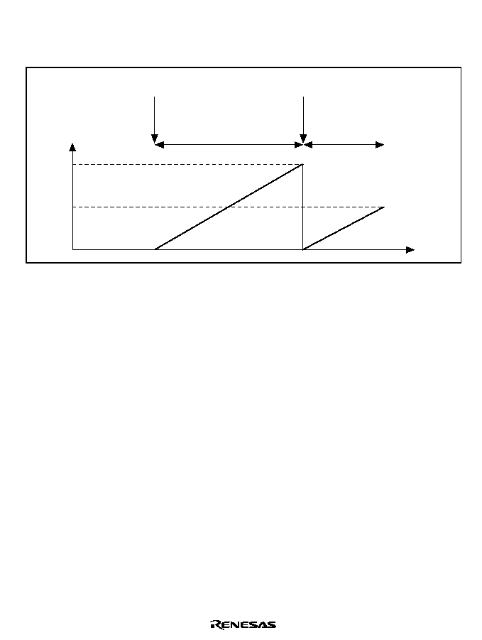
Rev. 2.00, 09/03, page 301 of 690
Notes: 1. Only when the RTC is being used can standby mode be canceled using IRQ, IRL,
PINT, or RTC.
2. Use a power-on reset to cancel software standby mode.
WTCNT value
H'FF
H'80
Time
Interrupt
request
WDT overflow and branch to
interrupt handling routine
Crystal oscillator settling
time and PLL synchronization
time
Clear the STBY bit in STBCR before
WTCNT reaches H'80. When the
STBY bit in STBCR is cleared, WTCNT
halts automatically.
Figure 11.1 Canceling Standby Mode with STBY Bit in STBCR
Canceling with a Reset: Software standby mode is canceled by a reset (power-on or manual).
Keep the
RESETP or RESETM pins low until the clock oscillation settles. The internal clock will
continue to be output to the CKIO pin.
11.6
Module Standby Function
11.6.1
Transition to Module Standby Function
Setting the standby control register MSTP bits to 1 halts the supply of clocks to the corresponding
on-chip peripheral modules. This function can be used to reduce the power consumption in the
normal mode and sleep mode. Before making a transition to module standby state, be sure to
disable the relevant module.
In module standby state, the functions of the external pins of the on-chip peripheral modules
change depending on the on-chip peripheral module and port settings. With a few exceptions, all
registers hold their values prior to halt.

Rev. 2.00, 09/03, page 302 of 690
11.6.2
Canceling Module Standby Function
The module standby function can be canceled by clearing the MSTP bits to 0 or by a power-on
reset.
When canceling the module standby function by clearing the corresponding MSTP bit, be sure to
read the relevant MSTP bit to confirm that it has been cleared to 0.
11.7
Hardware Standby Mode
11.7.1
Transition to Hardware Standby Mode
The LSI enters hardware standby mode by driving the CA pin low. In hardware standby mode, as
the same as software standby mode entered by executing the SLEEP instruction, all modules halt
except ones operated by the RTC clock. Even in hardware standby mode, supply power to all
power supply pins including the RTC power supply pins.
As differing from software standby mode, an interrupt or manual reset cannot be accepted in
hardware standby mode.
When the CA pin is driven low, the LSI enters hardware standby mode in the following procedure
depending on the state of CPG.
During Software Standby Mode: The LSI enters the hardware standby state with the clock
halted. An interrupt or manual reset cannot be accepted.
During WDT Operation for Canceling Software Standby Mode by an Interrupt: The CPU
restarts the operation after software standby mode is canceled. Then, the LSI enters hardware
standby mode.
During Sleep Mode: The CPU restarts the operation after sleep mode is canceled. Then, the LSI
enters hardware standby mode.
In hardware standby mode, the CA pin must be held low.
11.7.2
Canceling Hardware Standby Mode
The hardware standby function can be canceled only by the power-on reset.
When the CA pin is driven high while the
RESETP pin is low, the clock starts oscillating. Make
sure to hold the
RESETP pin low until the oscillation stabilizes. Then, drive the RESETP pin high
to start the power-on resetting by the CPU.
The operation is not guaranteed when an interrupt or manual reset is input.
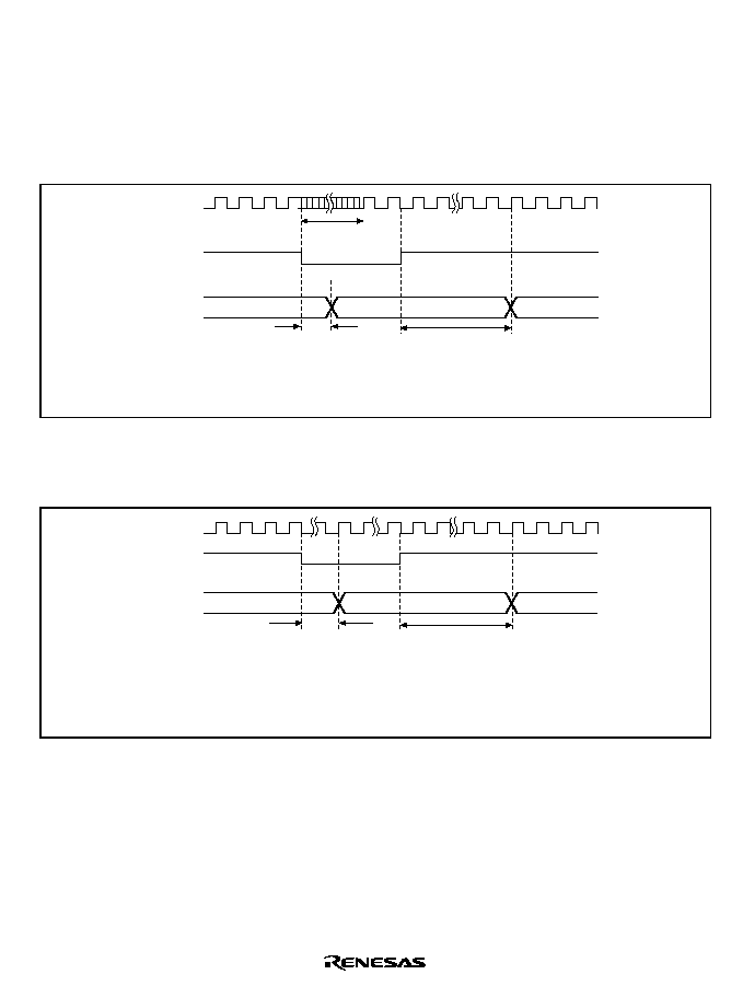
Rev. 2.00, 09/03, page 303 of 690
11.8
Timing of STATUS Pin Changes
The timing of the STATUS0 and STATUS1 pin changes is shown in figures 11.2 to 11.9.
In Case of A Reset:
a. Power-on reset
CKIO
RESETP
STATUS
Normal*
2
Normal*
2
Reset*
1
PLL settling
time
0 to 5 Bcyc*
3
0 to 30 Bcyc*
3
Notes: 1. Reset: HH (STATUS1 high, STATUS0 high)
2. Normal: LL (STATUS1 low, STATUS0 low)
3. Bcyc: Bus clock cycle
Figure 11.2 Power-On Reset STATUS Output
b. Manual reset
CKIO
RESETM
STATUS
Normal*
3
Normal*
3
Reset*
2
0 Bcyc or more*
1,4
0 to 30 Bcyc*
4
During manual reset, STATUS becomes HH (reset) and the internal
reset begins after waiting for the executing bus cycle to end.
Reset: HH (STATUS1 high, STATUS0 high)
Normal: LL (STATUS1 low, STATUS0 low)
Bcyc:
Bus clock cycle
Notes: 1.
2.
3.
4.
Figure 11.3 Manual Reset STATUS Output

Rev. 2.00, 09/03, page 304 of 690
In Case of Canceling Software Standby:
a. Canceling software standby by interrupt
CKIO
STATUS
Normal*
2
Normal*
2
WDT count
Oscillation stops
Standby*
1
Interrupt request
WDT overflow
Notes: 1. Standby: LH (STATUS1 low, STATUS0 high)
2. Normal: LL (STATUS1 low, STATUS0 low)
Figure 11.4 Canceling Software Standby by Interrupt STATUS Output
b. Canceling software standby by power-on reset
CKIO
STATUS
Normal*
5
Normal*
5
Oscillation stops
Standby*
4
*
2
0 to 10 Bcyc*
6
0 to 30 Bcyc*
6
Reset
Reset*
3
RESETP *
1
1. When software standby mode is cleared with a power-on reset, the WDT does
not count. Keep
RESETP low during the PLL's oscillation settling time.
2. Undefined
3. Reset:
HH (STATUS1 high, STATUS0 high)
4. Standby: LH (STATUS1 low, STATUS0 high)
5. Normal: LL (STATUS1 low, STATUS0 low)
6. Bcyc:
Bus clock cycle
Notes:
Figure 11.5 Canceling Software Standby by Power-On Reset STATUS Output
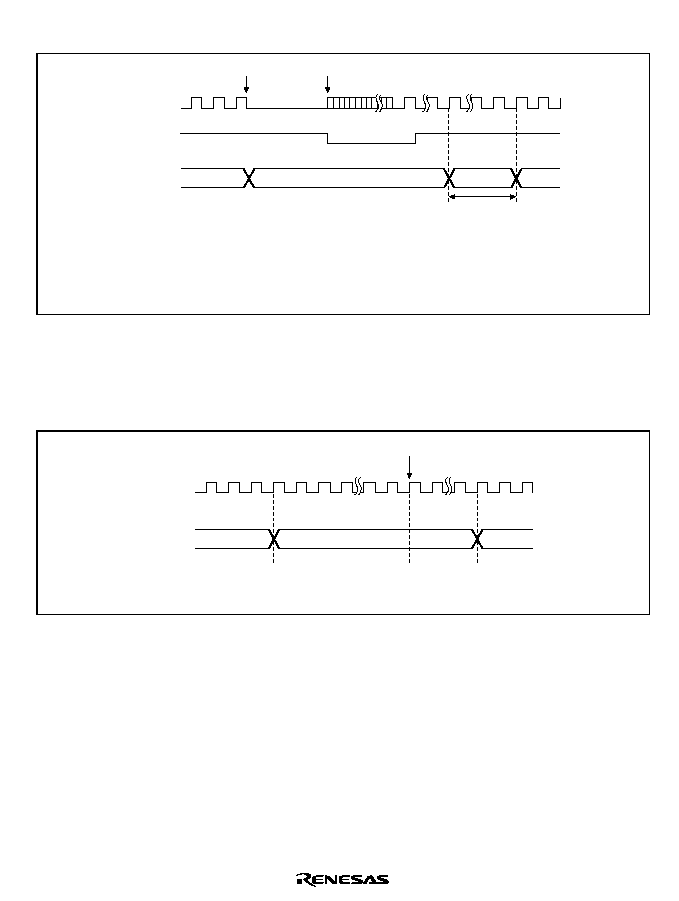
Rev. 2.00, 09/03, page 305 of 690
c. Canceling software standby by manual reset
CKIO
STATUS
Normal*
4
Normal*
4
Oscillation stops
Standby*
3
Reset*
2
0 to 20 Bcyc*
5
Reset
RESETM*
1
Notes: 1. When software standby mode is cleared with a manual reset, the WDT does not count.
Keep
RESETM low during the PLL's oscillation settling time.
2. Reset:
HH (STATUS1 high, STATUS0 high)
3. Standby: LH (STATUS1 low, STATUS0 high)
4. Normal: LL (STATUS1 low, STATUS0 low)
5. Bcyc:
Bus clock cycle
Figure 11.6 Canceling Software Standby by Manual Reset STATUS Output
In Case of Canceling Sleep:
a. Canceling sleep to interrupt
CKIO
STATUS
Normal*
2
Normal
*
2
Sleep*
1
Interrupt request
Notes: 1. Sleep: HL (STATUS1 high, STATUS0 low)
2. Normal: LL (STATUS1 low, STATUS0 low)
Figure 11.7 Canceling Sleep by Interrupt STATUS Output

Rev. 2.00, 09/03, page 306 of 690
b. Canceling sleep by power-on reset
CKIO
STATUS
Normal*
5
Normal*
5
Sleep*
4
0 to 10 Bcyc*
6
0 to 30 Bcyc*
6
Reset
Reset*
3
*
2
RESETP*
1
1. When the PLL1's multiplication ratio is changed by a power-on reset,
keep
RESETP low during the PLL's oscillation settling time.
2. Undefined
3. Reset: HH (STATUS1 high, STATUS0 high)
4. Sleep: HL (STATUS1 high, STATUS0 low)
5. Normal: LL (STATUS1 low, STATUS0 low)
6. Bcyc: Bus clock cycle
Notes:
Figure 11.8 Canceling Sleep by Power-On Reset STATUS Output
c. Canceling sleep by manual reset
CKIO
0 to 80 Bcyc*
5
0 to 30 Bcyc*
5
Reset
STATUS
Normal*
4
Normal*
4
Sleep*
3
Reset*
2
RESETM*
1
Notes: 1.
Keep RESETM low until STATUS becomes reset.
2. Reset: HH (STATUS1 high, STATUS0 high)
3. Sleep: HL (STATUS1 high, STATUS0 low)
4. Normal: LL (STATUS1 low, STATUS0 low)
5. Bcyc: Bus clock cycle
Figure 11.9 Canceling Sleep by Manual Reset STATUS Output
In Case of Hardware Standby:
Figures 11.10 and 11.11 show examples of pin timing in hardware standby mode.
The CA pin is sampled using EXTAL2 (32.768 kHz), and a hardware standby request is only
detected when the pin is low for two consecutive clock cycles.
The CA pin must be held low while the chip is in hardware standby mode.
Clock oscillation starts when the CA pin is driven high after the
RESETP pin is driven low.
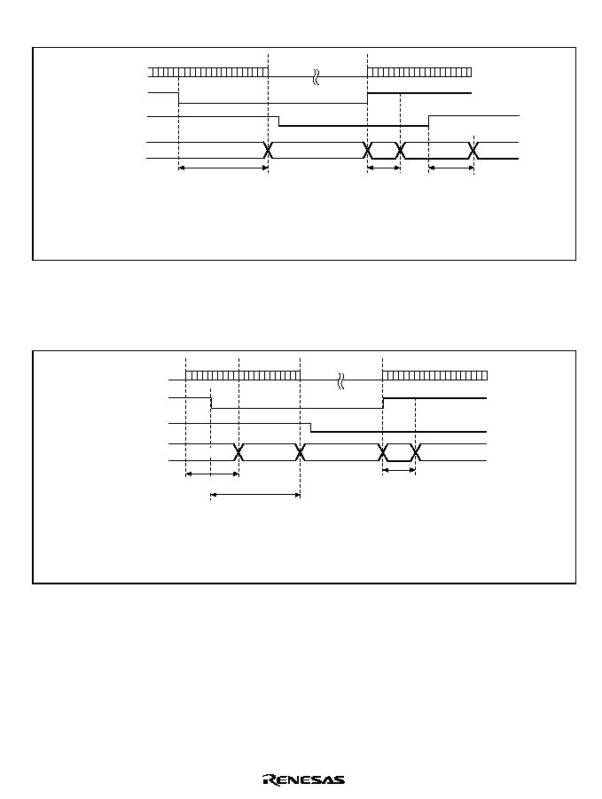
Rev. 2.00, 09/03, page 307 of 690
a. Normal operation to hardware standby
Normal*
3
Normal*
3
STATUS
CA
CKIO
Standby*
2
Reset*
1
RESETP
Undefined
2 Rcyc or more*
5
0
-10Bcyc*
4
0
-30Bcyc
Notes: 1. Reset:
HH (STATUS1 high, STATUS0 high)
2. Standby: LH (STATUS1 low, STATUS0 high)
3. Normal: LL (STATUS1 low, STATUS0 low)
4. Bcyc:
Bus clock cycle
5. Rcyc:
EXTAL2 (32.768 kHz) cycle
Figure 11.10 Hardware Standby Mode
(When CA Goes Low in Normal Operation)
b. Canceling software standby (during WDT operation) to hardware standby
Normal*
3
STATUS
CA
CKIO
Standby*
2
Reset*
1
RESETP
Undefined
2 Rcyc or more*
5
0
-10 Bcyc*
4
Standby
WDT operation
Notes: 1. Reset: HH (STATUS1 high, STATUS0 high)
2. Standby: LH (STATUS1 low, STATUS0 high)
3. Normal: LL (STATUS1 low, STATUS0 low)
4. Bcyc:
Bus clock cycle
5. Rcyc:
EXTAL2 (32.768 kHz) cycle
Figure 11.11 Hardware Standby Mode Timing
(When CA Goes Low during WDT Operation while Standby Mode Is Canceled)

Rev. 2.00, 09/03, page 308 of 690

TIMTMU2A_000020020100
Rev. 2.00, 09/03, page 309 of 690
Section 12 Timer Unit (TMU)
This LSI includes a three-channel 32-bit timer unit (TMU).
12.1
Features
∑
Each channel is provided with an auto-reload 32-bit down counter
∑
All channels are provided with 32-bit constant registers and 32-bit down counters for an auto-
reload function that can be read or written to at any time
∑
All channels generate interrupt requests when the 32-bit down counter underflows
(H'00000000
H'FFFFFFFF)
∑
Only channel 2 is provided with an input capture function
∑
Allows selection among five counter input clocks: External clock (TCLK), P
/4, P
/16, P
/64,
and P
/256
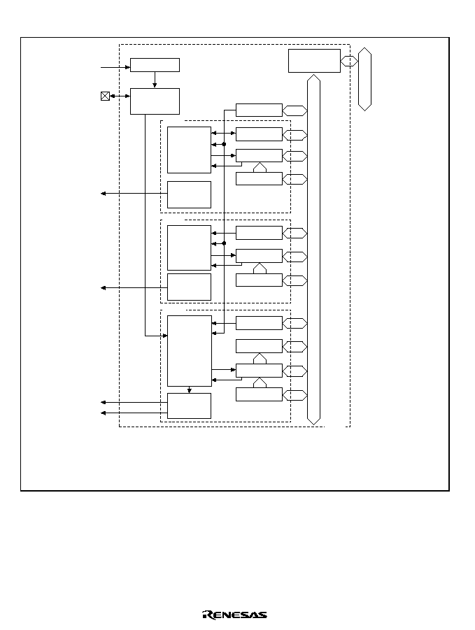
Rev. 2.00, 09/03, page 310 of 690
Figure 12.1 shows a block diagram of the TMU.
Prescaler
TSTR
TCR_0
TCNT_0
Module bus
Internal bus
TCOR_0
TCR_1
TCNT_1
TCOR_1
Counter
controller
TCLK
P
TUNI0
Bus interface
Ch. 0
Interrupt
controller
Interrupt
controller
Interrupt
controller
Counter
controller
Counter
controller
TUNI1
TUNI2
TICPI2
TCR_2
TCPR_2
TCNT_2
TCOR_2
TMU
Ch. 1
Ch. 2
Clock
controller
TSTR:
TCR_n:
Timer start register
TCNT_n:
TCOR_n:
TCPR_2:
32-bit timer counter
32-bit timer constant register
32-bit input capture register
Timer control register
(n: 0, 1, 2)
Legend:
Figure 12.1 TMU Block Diagram

Rev. 2.00, 09/03, page 311 of 690
12.2
Input/Output Pin
Table 12.1 shows the pin configuration of the TMU.
Table 12.1
Pin Configuration
Name
Abbreviation I/O
Description
Clock input
TCLK
I
External clock input pin/input capture control input pin
12.3
Register Descriptions
The TMU has the following registers. Refer to section 24, List of Registers, for more details of the
addresses of these registers and state of these registers in each processing state. For the register
name for each channel, TCOR for channel 0 is noted as TCOR_0.
1. Common
∑
Timer start register (TSTR)
2. Channel 0
∑
Timer constant register_0 (TCOR_0)
∑
Timer counter_0 (TCNT_0)
∑
Timer control register_0 (TCR_0)
3. Channel 1
∑
Timer constant register_1 (TCOR_1)
∑
Timer counter_1 (TCNT_1)
∑
Timer control register_1 (TCR_1)
4. Channel 2
∑
Timer constant register_2 (TCOR_2)
∑
Timer counter_2 (TCNT_2)
∑
Timer control register_2 (TCR_2)
∑
Input capture register_2 (TCPR_2)

Rev. 2.00, 09/03, page 312 of 690
12.3.1
Timer Start Register (TSTR)
TSTR is an 8-bit readable/writable register that selects whether to run or halt the timer counters
(TCNT).
TSTR is initialized by satisfying the initialization conditions shown in section 24, List of
Registers, changing the multiplication ratio of PLL1, or setting the MSTP2 bit in STBCR to 1.
Bit
Bit Name
Initial Value
R/W
Description
7 to 3
0
R
Reserved
These bits are always read as 0. The write value should
always be 0.
2
STR2
0
R/W
Counter Start 2
Selects whether to run or halt timer counter 2
(TCNT_2).
0: TCNT_2 count halted
1: TCNT_2 counts
1
STR1
0
R/W
Counter Start 1
Selects whether to run or halt timer counter 1
(TCNT_1).
0: TCNT_1 count halted
1: TCNT_1 counts
0
STR0
0
R/W
Counter Start 0
Selects whether to run or halt timer counter 0
(TCNT_0).
0: TCNT_0 count halted
1: TCNT_0 counts

Rev. 2.00, 09/03, page 313 of 690
12.3.2
Timer Control Registers (TCR)
TCR are 16-bit readable/writable registers that control the timer counters (TCNT) and interrupts.
TCR control the issuance of interrupts when the flag indicating timer counter (TCNT) underflow
has been set to 1, and also carry out counter clock selection. When the external clock has been
selected, they also select its edge.
Only TCR_2 controls the input capture function and the issuance of interrupts during input
capture.
TCR_0 and TCR_1:
Bit
Bit Name Initial Value
R/W
Description
15 to 9
0
R
Reserved
These bits are always read as 0. The write value should
always be 0.
8
UNF
0
R/(W)
*
Underflow Flag
Status flag that indicates occurrence of a TCNT
underflow.
0: TCNT has not underflowed
[Clearing condition]
0 is written to UNF
1: TCNT has underflowed
[Setting condition]
TCNT underflows
7, 6
0
R
Reserved
These bits are always read as 0. The write value should
always be 0.
5
UNIE
0
R/W
Underflow Interrupt Control
Controls enabling of interrupt generation when the
status flag (UNF) indicating TCNT underflow has been
set to 1.
0: Interrupt due to UNF (TUNI) is disabled
1: Interrupt due to UNF (TUNI) is enabled

Rev. 2.00, 09/03, page 314 of 690
Bit
Bit Name
Initial Value
R/W
Description
4
3
CKEG1
CKEG0
0
0
R/W
R/W
Clock Edge
Select an input edge of the external clock when the
external clock is selected.
00: Count on rising edge
01: Count on falling edge
1X: Count on both rising and falling edges
Note: X: Don't care
2
1
0
TPSC2
TPSC1
TPSC0
0
0
0
R/W
R/W
R/W
Timer Prescaler
Select the TCNT count clock.
000: Count on P
/4
001: Count on P
/16
010: Count on P
/64
011: Count on P
/256
100: Setting prohibited
101: Count on TCLK pin input
110: Setting prohibited
111: Setting prohibited
Note:
*
Only 0 can be written for clearing the flags. If 1 is written to this bit, the prior value is
retained.

Rev. 2.00, 09/03, page 315 of 690
TCR_2:
Bit
Bit Name
Initial Value
R/W
Description
15 to 10
0
R
Reserved
These bits are always read as 0. The write value
should always be 0.
9
ICPF
0
R/(W)
*
Input Capture Interrupt Flag
A function of channel 2 only: the flag is set when
input capture is requested via the TCLK pin.
0: No input capture request has been issued.
[Clearing condition]
0 is written to ICPF
1: Input capture has been requested via the TCLK
pin.
[Setting condition]
When an input capture is requested via the TCLK
pin
8
UNF
0
R/(W)
*
Underflow Flag
Status flag that indicates occurrence of a TCNT_2
underflow.
0: TCNT_2 has not underflowed
[Clearing condition]
0 is written to UNF
1: TCNT_2 has underflowed
[Setting condition]
TCNT_2 underflows

Rev. 2.00, 09/03, page 316 of 690
Bit
Bit Name
Initial Value
R/W
Description
7
6
ICPE1
ICPE0
0
0
R/W
R/W
Input Capture Control
A function of channel 2 only: determines whether
the input capture function can be used, and when
used, whether or not to enable interrupts.
Use the CKEG1 and CKEG0 bits to designate
use of either the rising or falling edge of the TCLK
pin to set the value of TCNT_2 in TCPR_2.
00: Input capture function is not used.
01: Setting prohibited
10: Input capture function is used. Interrupt due to
ICPF (TICPI2) are not enabled.
11: Input capture function is used. Interrupt due to
ICPF (TICPI2) are enabled.
5
UNIE
0
R/W
Underflow Interrupt Control
Controls enabling of interrupt generation when
the status flag (UNF) indicating TCNT_2
underflow has been set to 1.
0: Interrupt due to UNF (TUNI2) is not enabled.
1: Interrupt due to UNF (TUNI2) is enabled.
4
3
CKEG1
CKEG0
0
0
R/W
R/W
Clock Edge
Select an input edge of the external clock when
the external clock is selected, or when the input
capture function is used.
00: Count/capture register set on rising edge
01: Count/capture register set on falling edge
1X: Count/capture register set on both rising and
falling edge
Note: X: Don't care.

Rev. 2.00, 09/03, page 317 of 690
Bit
Bit Name
Initial Value
R/W
Description
2
1
0
TPSC2
TPSC1
TPSC0
0
0
0
R/W
R/W
R/W
Timer Prescaler
Select the TCNT_2 count clock.
000: Count on P
/4
001: Count on P
/
16
010: Count on P
/64
011: Count on P
/256
100: Setting prohibited
101: Count on TCLK pin input
110: Setting prohibited
111: Setting prohibited
Note:
*
Only 0 can be written for clearing the flags. If 1 is written to this bit, the prior value is
retained.
12.3.3
Timer Constant Registers (TCOR)
TCOR set the value to be set in TCNT when TCNT underflows.
TCOR are 32-bit readable/writable registers. Their initial value is H'FFFFFFFF.
12.3.4
Timer Counters (TCNT)
TCNT counts down upon input of a clock. The clock input is selected using the TPSC2 to TPSC0
bits in the timer control register (TCR).
When a TCNT countdown results in an underflow (H'00000000
H'FFFFFFFF), the underflow
flag (UNF) in the timer control register (TCR) of the relevant channel is set. The TCOR value is
simultaneously set in TCNT itself and the countdown continues from that value.
Initial value of TCNT is H'FFFFFFFF.
12.3.5
Input Capture Register_2 (TCPR_2)
TCPR_2 is a read-only 32-bit register used for the input capture function built only into timer 2.
The TCPR_2 setting conditions due to the TCLK pin are controlled by the input capture function
bits (ICPE1/ICPE0 and CKEG1/CKEG0) in TCR_2. When a TCPR_2 setting indication due to the
TCLK pin occurs, the value of TCNT_2 is copied into TCPR_2.
Initial value of TCPR_2 is undefined.
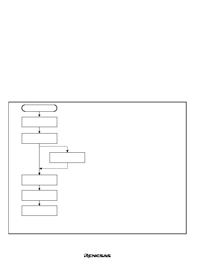
Rev. 2.00, 09/03, page 318 of 690
12.4
Operation
Each of the three channels has a 32-bit timer counter (TCNT) and a 32-bit timer constant register
(TCOR). The TCNT counts down. The auto-reload function enables synchronized counting and
counting by external events. Channel 2 has an input capture function.
12.4.1
Counter Operation
When the STR0 to STR2 bits in the timer start register (TSTR) are set to 1, the corresponding
timer counter (TCNT) starts counting. When a TCNT underflows, the UNF flag of the
corresponding timer control register (TCR) is set. At this time, if the UNIE bit in TCR is 1, an
interrupt request is sent to the CPU. Also at this time, the value is copied from TCOR to TCNT
and the down-count operation is continued.
Count Operation Setting Procedure: An example of the procedure for setting the count
operation is shown in figure 12.2.
Select operation
Select counter
clock
Set underflow
interrupt generation
Set timer constant
register
Initialize timer
counter
Start counting
(1)
(2)
(4)
(5)
(6)
Set input capture
interrupt generation
When using input
capture function
(3)
Note: When an interrupt has been generated, clear the flag in the interrupt handler that caused it.
If interrupts are enabled without clearing the flag, another interrupt will be generated.
Select the counter clock with the TPSC0-TPSC2
bits in the timer control register. If the external
clock is selected, select its edge with the CKEG1
and CKEG0 bits in the timer control register.
Use the UNIE bit in the timer control register to set
whether to generate an interrupt when timer
counter underflows.
When using the input capture function, set the
ICPE bits in the timer control register, including
the choice of whether or not to use the interrupt
function (channel 2 only).
Set a value in the timer constant register
(the cycle is the set value plus 1).
Set the initial value in the timer counter.
Set the STR bit in the timer start register to 1 to
start operation.
(1)
(2)
(3)
(4)
(5)
(6)
Figure 12.2 Setting Count Operation

Rev. 2.00, 09/03, page 319 of 690
Auto-Reload Count Operation: Figure 12.3 shows the TCNT auto-reload operation.
TCNT value
TCOR
H'00000000
STR0
-STR2
UNF
TCOR value set to
TCNT during underflow
Time
Figure 12.3 Auto-Reload Count Operation
TCNT Count Timing:
1. Internal Clock Operation: Set the TPSC2 to TPSC0 bits in TCR to select whether one of the
four internal clocks created by dividing the peripheral module clock is used (P
/4, P
/16,
P
/64, P
/256). Figure 12.4 shows the timing.
P
Internal
clock
Timer counter
input clock
TCNT
N + 1
N
N
- 1
Figure 12.4 Count Timing when Internal Clock Is Operating
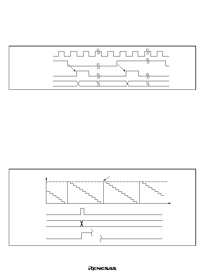
Rev. 2.00, 09/03, page 320 of 690
2. External Clock Operation: Set the TPSC2 to TPSC0 bits in TCR to select the external clock
(TCLK) as the timer clock. Use the CKEG1 and CKEG0 bits in TCR to select the detection
edge. Rise, fall or both may be selected. The pulse width of the external clock must be at least
2 peripheral module clock cycles (P
) for single edges or 3 peripheral module clock cycles
(P
) for both edges. A shorter pulse width will result in incorrect operation. Figure 12.5 shows
the timing for both-edge detection.
P
External
clock input
(TCLK)
TCNT
input clock
TCNT
N + 1
N
N
- 1
Figure 12.5 Count Timing when External Clock Is Operating (Both Edges Detected)
12.4.2
Input Capture Function
Channel 2 has an input capture function. When using the input capture function, set the timer
operation clock to internal clock with the TPSC2 to TPSC0 bits in TCR_2. Also, specifies use of
the input capture function and whether to generate interrupts on using it with the ICPE1 to ICPE0
bits in TCR_2, and specifies the use of either the rising or falling edge of the TCLK pin to set the
TCNT_2 value into TCPR_2 with the CKEG1 to CKEG0 bits in TCR_2. The input capture
function cannot be used in standby mode.
Figure 12.6 shows the timing at the rising edge of the TCLK pin input.
TCNT_2 value
TCOR_2
H'00000000
TCLK
TCPR_2
Set TCNT_2 value
TICPI2
TCOR_2 value set to
TCNT_2 during underflow
Time
Figure 12.6 Operation Timing when Using Input Capture Function
(Using TCLK Rising Edge)
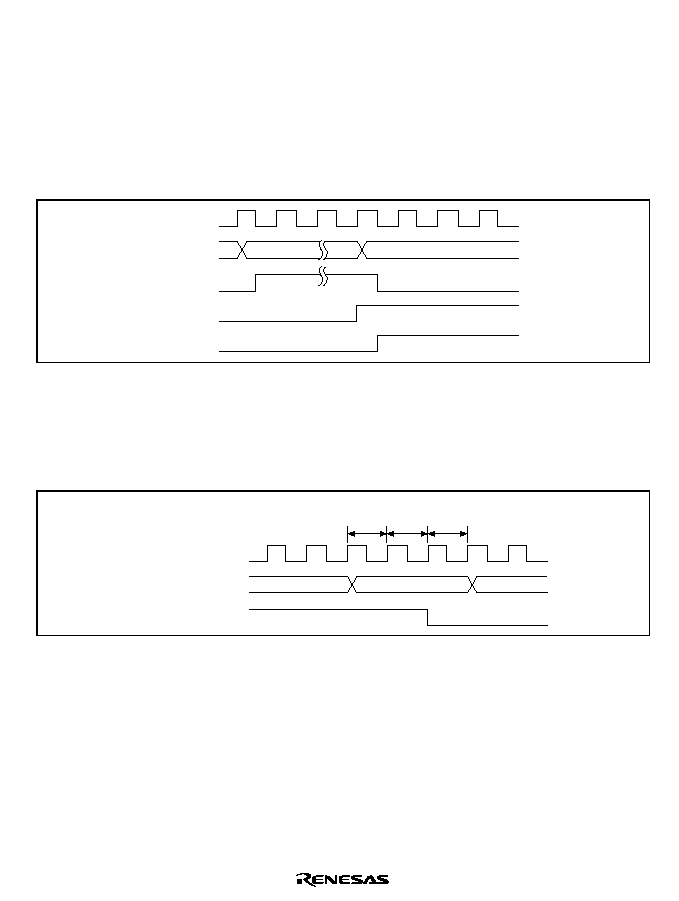
Rev. 2.00, 09/03, page 321 of 690
12.5
Interrupts
There are two sources of TMU interrupts: underflow interrupts (TUNI) and interrupts when using
the input capture function (TICPI2).
12.5.1
Status Flag Set Timing
The UNF bit is set to 1 when the TCNT underflows. Figure 12.7 shows the timing.
P
TCNT
Underflow
signal
UNF
TUNI
TCOR value
H'00000000
Figure 12.7 UNF Set Timing
12.5.2
Status Flag Clear Timing
The status flag can be cleared by writing 0 from the CPU. Figure 12.8 shows the timing.
P
Peripheral address bus
UNF, ICPF
TCR address
T
1
T
2
TCR write cycle
T
3
Figure 12.8 Status Flag Clear Timing

Rev. 2.00, 09/03, page 322 of 690
12.5.3
Interrupt Sources and Priorities
The TMU generates underflow interrupts for each channel. When the interrupt request flag and
interrupt enable bit are both set to 1, the relevant interrupt is requested. Codes are set in the
interrupt event register (INTEVT and INTEVT2) for these interrupts and interrupt processing must
be executed according to the codes.
The relative priorities of channels can be changed using the interrupt controller. For details, see
section 5, Exception Handling, and section 6, Interrupt Controller (INTC).
Table 12.2 lists TMU interrupt sources.
Table 12.2
TMU Interrupt Sources
Channel
Interrupt Source
Description
Priority
0
TUNI0
Underflow interrupt 0
High
1
TUNI1
Underflow interrupt 1
TUNI2
Underflow interrupt 2
2
TICPI2
Input capture interrupt 2
Low
12.6
Usage Notes
12.6.1
Writing to Registers
Synchronization processing is not performed for timer counting during register writes. When
writing to registers, always clear the appropriate start bits for the channel (STR2 to STR0) in the
timer start register (TSTR) to halt timer counting.
12.6.2
Reading Registers
Synchronization processing is performed for timer counting during register reads. When timer
counting and register read processing are performed simultaneously, the register value before
TCNT counting down is read.
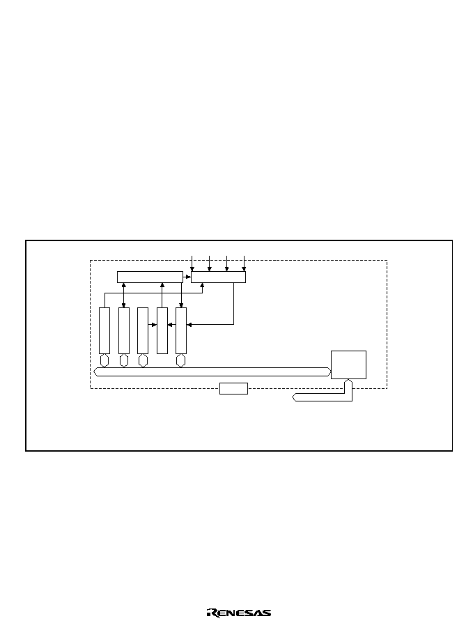
TIMCMT2A_000020020100
Rev. 2.00, 09/03, page 323 of 690
Section 13 Compare Match Timer (CMT)
The DMAC has an on-chip compare match timer (CMT) to generate a DMA transfer request. The
CMT has 16-bit counter.
Figure 13.1 shows a CMT block diagram.
13.1
Features
∑
Four types of counter input clock can be selected.
One of four internal clocks (P
/4, P
/8, P
/16, P
/64) can be selected.
∑
Generates a DMA transfer request when compare match occurs. (The CPU interrupt is not
supported.)
∑
When the CMT is not used, the operation can be halted by stopping the clock supply to the
CMT so that the power consumption can be reduced.
Internal bus
Bus
interface
Control circuit
Clock selection
CMSTR
CMCSR
CMCOR
Comparator
CMCNT
Module bus
CMT
P
/4 P/8 P/16 P/64
CMSTR:
CMCSR:
CMCOR:
CMCNT:
Compare match timer start register
Compare match timer control/status register
Compare match constant register
Compare match counter
[Legend]
Figure 13.1 CMT Block Diagram

Rev. 2.00, 09/03, page 324 of 690
13.2
Register Descriptions
The CMT has the following registers. Refer to section 24, List of Registers, for more detail of the
addresses and access size.
∑
Compare match timer start register (CMSTR)
∑
Compare match timer control/status register (CMCSR)
∑
Compare match counter (CMCNT)
∑
Compare match constant register (CMCOR)
13.2.1
Compare Match Timer Start Register (CMSTR)
CMSTR is a 16-bit register that selects whether to operate or halt the counter (CMCNT).
Bit
Bit Name
Initial Value
R/W
Description
15 to 1
--
0
R
Reserved
These bits are always read as 0. The write value
should always be 0.
0
STR
0
R/W
Count Start
Selects whether to operate or halt the compare
match counter.
0: CMCNT count operation halted
1: CMCNT count operation

Rev. 2.00, 09/03, page 325 of 690
13.2.2
Compare Match Timer Control/Status Register (CMCSR)
CMCSR is a 16-bit register that indicates the occurrence of compare matches, and sets the
enable/disable of DMA transfer requests and the clock used for incrementation.
Bit
Bit Name
Initial Value
R/W
Description
15 to 8
--
0
R
Reserved
These bits are always read as 0. The write value
should always be 0.
7
CMF
0
R/(W)
*
Compare Match Flag
Indicates whether CMCNT and CMCOR values
have matched or not.
0: CMCNT and CMCOR values have not matched
[Clearing condition]
Write 0 to CMF after reading CMF = 1
1: CMCNT and CMCOR values have matched
6, 5
--
0
R
Reserved
These bits are always read as 0. The write value
should always be 0.
4
CMR
0
R/W
Compare Match Request
0: Disables a DMA transfer request
1: Enables a DMA transfer request
3, 2
--
0
R
Reserved
These bits are always read as 0. The write value
should always be 0.
1
0
CKS1
CKS0
0
0
R/W
R/W
Clock Select
Select the clock input to CMCNT from among the
four internal clocks obtained by dividing the
peripheral clock (P
). When the STR bit in
CMSTR is set to 1, CMCNT begins incrementing
with the clock selected by the CKS1 and CKS0
bits.
00: P
/4
01: P
/8
10: P
/16
11: P
/64
Note:
*
Only 0 can be written for clearing the flags.
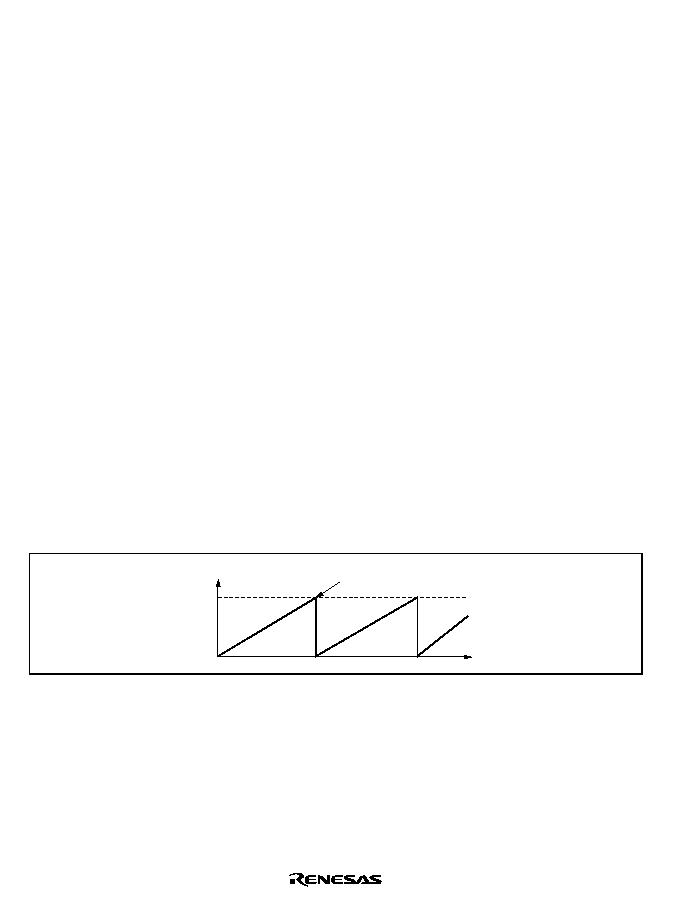
Rev. 2.00, 09/03, page 326 of 690
13.2.3
Compare Match Counter (CMCNT)
CMCNT is a 16-bit register used as an up-counter.
When an internal clock is selected with the CKS1 and CKS0 bits in CMCSR and the STR bit in
CMSTR is set to 1, CMCNT begins incrementing with the selected clock. When the CMCNT
value matches that of CMCOR, CMCNT is cleared to H'0000 and the CMF flag in CMCSR is set
to 1.
The initial value of CMCNT is H'0000.
13.2.4
Compare Match Constant Register (CMCOR)
CMCOR is a 16-bit register that sets the compare match period with CMCNT.
The initial value of CMCOR is H'FFFF.
13.3
Operation
13.3.1
Period Count Operation
When an internal clock is selected with the CKS1 and CKS0 bits in CMCSR and the STR bit in
CMSTR is set to 1, CMCNT begins incrementing with the selected clock. When the CMCNT
value matches that of CMCOR, CMCNT is cleared to H'0000 and the CMF flag in CMCSR is set
to 1. CMCNT begins counting up again from H'0000.
Figure 13.2 shows the compare match counter operation.
Counter cleared by
CMCOR compare match
CMCNT value
CMCOR
H'0000
Time
Figure 13.2 Counter Operation
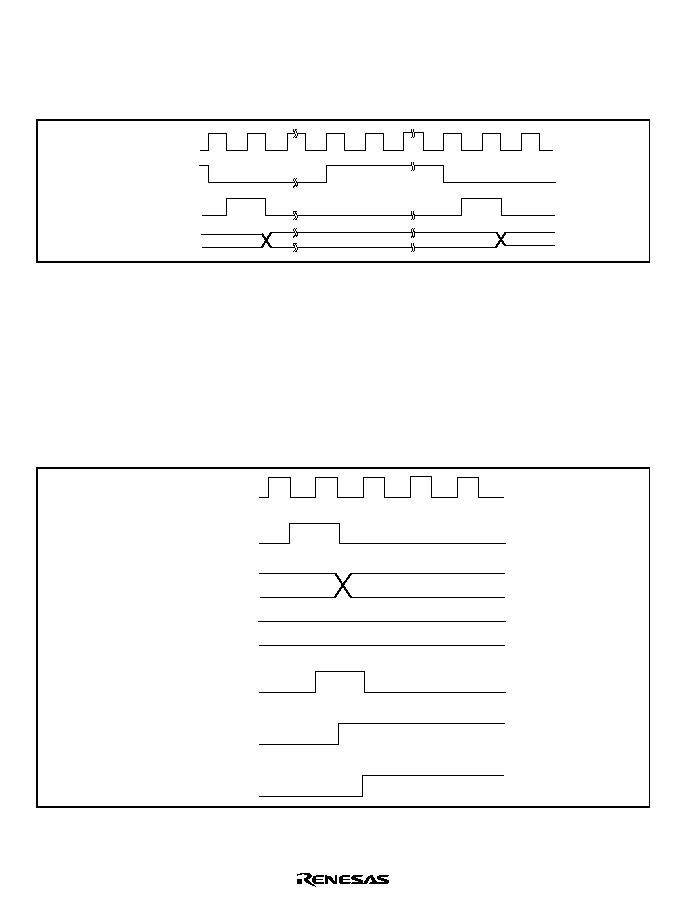
Rev. 2.00, 09/03, page 327 of 690
13.3.2
CMCNT Count Timing
One of four clocks (P
/4, P
/8, P
/16, P
/64) obtained by dividing the peripheral clock (P
) can
be selected by the CKS1 and CKS0 bits in CMCSR. Figure 13.3 shows the timing.
N+1
Internal clock
CMCNT input
clock
CMCNT
N-1
N
P
Figure 13.3 Count Timing
13.3.3
Compare Match Flag Set Timing
The CMF bit in CMCSR is set to 1 by the compare match signal generated when CMCOR and
CMCNT match. The compare match signal is generated upon the final state of the match (timing
at which the CMCNT matching count value is updated to H'0000). Consequently, after CMCOR
and CMCNT match, a compare match signal will not be generated until a CMCNT clock is input.
Figure 13.4 shows the CMF bit set timing.
CMCOR
CMCNT
input clock
Compare
match signal
CMF
CMI
CMCNT
N
N
0
P
Figure 13.4 CMF Set Timing

Rev. 2.00, 09/03, page 328 of 690

TIMTPU8A_000020020100
Rev. 2.00, 09/03, page 329 of 690
Section 14 16-Bit Timer Pulse Unit (TPU)
This LSI has an on-chip 16-bit timer pulse unit (TPU) that comprises four 16-bit timer channels.
14.1
Features
∑
Maximum 4-pulse output
A total of 16 timer general registers (TGRA to TGRD
◊
4 ch.) are provided (four each for
channels). TGRA can be set as an output compare register.
TGRB, TGRC, and TGRD for each channel can also be used as timer counter clearing
registers. TGRC and TGRD can also be used as buffer registers.
∑
Selection of four counter input clocks for channels 0 to 3
∑
The following operations can be set for each channel:
Waveform output at compare match: Selection of 0, 1, or toggle output
Counter clear operation: Counter clearing possible by compare match
PWM mode: Any PWM output duty cycle can be set
Maximum of 4-phase PWM output possible
∑
Buffer operation settable for each channel
Automatic rewriting of output compare register possible
∑
An interrupt request for each channel
Compare match and overflow interrupt requests can be enabled or disabled for each source
independently

Rev. 2.00, 09/03, page 330 of 690
Table 14.1 lists the functions of the TPU.
Table 14.1
TPU Functions
Item
Channel 0
Channel 1
Channel 2
Channel 3
Count clock
P
/1
P
/4
P
/16
P
/64
P
/1
P
/4
P
/16
P
/64
P
/1
P
/4
P
/16
P
/64
P
/1
P
/4
P
/16
P
/64
General registers
TGR0A
TGR0B
TGR1A
TGR1B
TGR2A
TGR2B
TGR3A
TGR3B
General registers/
buffer registers
TGR0C
TGR0D
TGR1C
TGR1D
TGR2C
TGR2D
TGR3C
TGR3D
Output pins
TO0
TO1
TO2
TO3
Counter clear
function
TGR compare
match
TGR compare
match
TGR compare
match
TGR compare
match
0 output
1 output
Compare
match
output
Toggle
output
PWM mode
Buffer operation
Interrupt sources
5 sources
∑
Compare
match
∑
Overflow
5 sources
∑
Compare
match
∑
Overflow
5 sources
∑
Compare
match
∑
Overflow
5 sources
∑
Compare
match
∑
Overflow
Legend
:
Possible
--:
Not possible
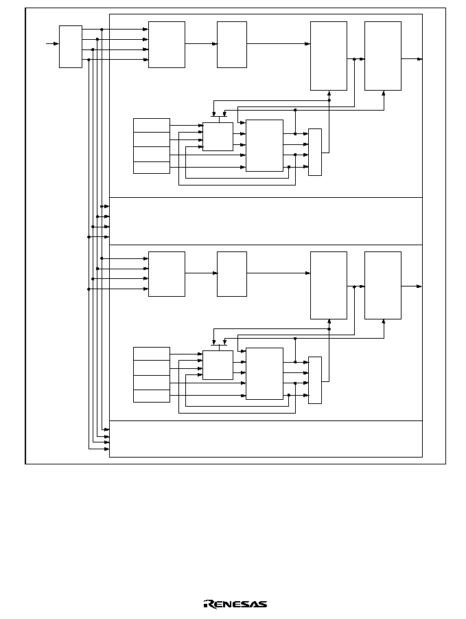
Rev. 2.00, 09/03, page 331 of 690
Divider
Clock
selection
Edge
selection
Comparator
Buffer
Counter
up
Output
control
Channel 0
Channel 2
Channel 1
Same as channel 0
Channel 3
Same as channel 2
clear
TGRA
P
TO0
TO2
TO1
TO3
P
/1
P
/4
P
/16
P
/64
TGRB
TGRC
TGRD
Selector
Clock
selection
Edge
selection
Comparator
Buffer
Counter
up
Output
control
clear
TGRA
TGRB
TGRC
TGRD
Selector
Figure 14.1 Block Diagram of TPU

Rev. 2.00, 09/03, page 332 of 690
14.2
Input/Output Pins
Table 14.2 shows the pin configuration of the TPU.
Table 14.2
Pin Configuration
Channel
Name
Symbol
I/O
Function
0
Output compare
match 0
TO0
O
TGR0A output compare output/PWM output
pin
1
Output compare
match 1
TO1
O
TGR1A output compare output/PWM output
pin
2
Output compare
match 2
TO2
O
TGR2A output compare output/PWM output
pin
3
Output compare
match 3
TO3
O
TGR3A output compare output/PWM output
pin
14.3
Register Descriptions
The TPU has the following registers. Refer to section 24, List of Registers, for more details of the
addresses of these registers and state of these registers in each processing state. For the register
name for each channel, TCR for channel 0 is noted as TCR_0.
1. Channel 0
∑
Timer control register_0 (TCR_0)
∑
Timer mode register_0 (TMDR_0)
∑
Timer I/O control register_0 (TIOR_0)
∑
Timer interrupt enable register_0 (TIER_0)
∑
Timer status register_0 (TSR_0)
∑
Timer counter_0 (TCNT_0)
∑
Timer general register A_0 (TGRA_0)
∑
Timer general register B_0 (TGRB_0)
∑
Timer general register C_0 (TGRC_0)
∑
Timer general register D_0 (TGRD_0)
2. Channel 1
∑
Timer control register_1 (TCR_1)
∑
Timer mode register_1 (TMDR_1)
∑
Timer I/O control register_1 (TIOR_1)
∑
Timer interrupt enable register_1 (TIER_1)
∑
Timer status register_1 (TSR_1)

Rev. 2.00, 09/03, page 333 of 690
∑
Timer counter_1 (TCNT_1)
∑
Timer general register A_1 (TGRA_1)
∑
Timer general register B_1 (TGRB_1)
∑
Timer general register C_1 (TGRC_1)
∑
Timer general register D_1 (TGRD_1)
3. Channel 2
∑
Timer control register_2 (TCR_2)
∑
Timer mode register_2 (TMDR_2)
∑
Timer I/O control register_2 (TIOR_2)
∑
Timer interrupt enable register_2 (TIER_2)
∑
Timer status register 2 (TSR_2)
∑
Timer counter_2 (TCNT_2)
∑
Timer general register A_2 (TGRA_2)
∑
Timer general register B_2 (TGRB_2)
∑
Timer general register C_2 (TGRC_2)
∑
Timer general register D_2 (TGRD_2)
4. Channel 3
∑
Timer control register_3 (TCR_3)
∑
Timer mode register_3 (TMDR_3)
∑
Timer I/O control register_3 (TIOR_3)
∑
Timer interrupt enable register_3 (TIER_3)
∑
Timer status register_3 (TSR_3)
∑
Timer counter_3 (TCNT_3)
∑
Timer general register A_3 (TGRA_3)
∑
Timer general register B_3 (TGRB_3)
∑
Timer general register C_3 (TGRC_3)
∑
Timer general register D_3 (TGRD_3)
5. Common
∑
Timer start register (TSTR)

Rev. 2.00, 09/03, page 334 of 690
14.3.1
Timer Control Registers (TCR)
TCR are 16-bit registers that control the TCNT channels.
TCR register settings should be made only when TCNT operation is stopped.
Bit
Bit Name
Initial
Value
R/W
Description
15 to 8
0
R
Reserved
These bits are always read as 0 and cannot be modified.
7
6
5
CCLR2
CCLR1
CCLR0
0
0
0
R/W
R/W
R/W
Counter Clear
Select the TCNT clearing source.
000: TCNT clearing disabled
001: TCNT cleared by TGRA compare match
010: TCNT cleared by TGRB compare match
011: Setting prohibited
100: TCNT clearing disabled
101: TCNT cleared by TGRC compare match
110: TCNT cleared by TGRD compare match
111: Setting prohibited
4
3
CKEG1
CKEG0
0
0
R/W
R/W
Clock Edge
Select the input clock edge. When the internal clock is
counted using both edges, the input clock period is halved
(e.g. P
/4 both edges = P
/2 rising edge).
00: Count at rising edge
01: Count at falling edge
1X: Count at both edges
*
[Legend] X: Don't care
Note:
*
Internal-clock edge selection is valid when the input
clock is P
/4 or slower. If the input clock is P
/1, this
operation is not performed.
2
1
0
TPSC2
TPSC1
TPSC0
0
0
0
R/W
R/W
R/W
Timer Prescaler
Select the TCNT count clock. The clock source can be
selected independently for each channel. Table 14.3 shows
the clock sources that can be set for each channel. For more
information on count clock selection, see table 14.4.

Rev. 2.00, 09/03, page 335 of 690
Table 14.3
TPU Clock Sources
Internal Clock
Channel
P
/1
P
/4
P
/16
P
/64
0
1
2
3
[Legend]
: Setting
Blank: No setting
Table 14.4
TPSC2 to TPSC0 (1)
Channel
Bit 2
TPSC2
Bit 1
TPSC1
Bit 0
TPSC0
Description
0
0
0
0
Internal clock: counts on P
/1
1
Internal clock: counts on P
/4
1
0
Internal clock: counts on P
/16
1
Internal clock: counts on P
/64
1
X
X
Setting prohibited
Note:
X: Don't care
Table 14.4
TPSC2 to TPSC0 (2)
Channel
Bit 2
TPSC2
Bit 1
TPSC1
Bit 0
TPSC0
Description
1
0
0
0
Internal clock: counts on P
/1
1
Internal clock: counts on P
/4
1
0
Internal clock: counts on P
/16
1
Internal clock: counts on P
/64
1
X
X
Setting prohibited
Note:
X: Don't care

Rev. 2.00, 09/03, page 336 of 690
Table 14.4
TPSC2 to TPSC0 (3)
Channel
Bit 2
TPSC2
Bit 1
TPSC1
Bit 0
TPSC0
Description
2
0
0
0
Internal clock: counts on P
/1
1
Internal clock: counts on P
/4
1
0
Internal clock: counts on P
/16
1
Internal clock: counts on P
/64
1
X
X
Setting prohibited
Note:
X: Don't care
Table 14.4
TPSC2 to TPSC0 (4)
Channel
Bit 2
TPSC2
Bit 1
TPSC1
Bit 0
TPSC0
Description
3
0
0
0
Internal clock: counts on P
/1
1
Internal clock: counts on P
/4
1
0
Internal clock: counts on P
/16
1
Internal clock: counts on P
/64
1
X
X
Setting prohibited
Note:
X: Don't care

Rev. 2.00, 09/03, page 337 of 690
14.3.2
Timer Mode Registers (TMDR)
TMDR are 16-bit readable/writable registers that are used to set the operating mode for each
channel.
TMDR register settings should be made only when TCNT operation is stopped.
Bit
Bit Name
Initial
Value
R/W
Description
15 to 7
0
R
Reserved
These bits are always read as 0 and cannot be modified.
6
BFWT
0
R/W
Buffer Write Timing
Specifies TGRA and TGRB update timing when TGRC and
TGRD are used as a compare match buffer. When TGRC
and TGRD are not used as a compare match buffer register,
this bit is ignored.
0: TGRA and TGRB are rewritten at compare match of each
register.
1: TGRA and TGRB are rewritten in counter clearing.
5
BFB
0
R/W
Buffer Operation B
Specifies whether TGRB is to operate in the normal way, or
TGRB and TGRD are to be used together for buffer
operation.
0: TGRB operates normally
1: TGRB and TGRD used together for buffer operation
4
BFA
0
R/W
Buffer Operation A
Specifies whether TGRA is to operate in the normal way, or
TGRA and TGRC are to be used together for buffer
operation.
0: TGRA operates normally
1: TGRA and TGRC used together for buffer operation
3
0
R
Reserved
This bit is always read as 0 and cannot be modified.
2
1
0
MD2
MD1
MD0
0
0
0
R/W
R/W
R/W
Timer Operating Mode
Set the timer-operating mode.
000: Normal operation
001: Setting prohibited
010: PWM mode
011: Setting prohibited
1XX: Setting prohibited
Note:
X: Don't care

Rev. 2.00, 09/03, page 338 of 690
14.3.3
Timer I/O Control Registers (TIOR)
TIOR are 16-bit registers that control the TO pin.
TIOR register settings should be made only when TCNT operation is stopped.
Care is required since TIOR is affected by the TMDR setting.
Bit
Bit Name
Initial
Value
R/W
Description
15 to 3
0
R
Reserved
These bits are always read as 0 and cannot be modified.
2
1
0
IOA2
IOA1
IOA0
0
0
0
R/W
R/W
R/W
I/O Control
Bits IOA2 to IOA0 specify the functions of TGRA and the TO
pin. For details, refer to table 14.5.
Table 14.5
IOA2 to IOA0
Bit 2
Bit 1
Bit 0
Channel IOA2
IOA1
IOA0
Description
0
Always 0 output
0
1
0 output at TGRA compare match
*
0
1 output at TGRA compare match
0
1
1
Initial output is 0
output for TO pin
Toggle output at TGRA compare match
*
0
Always 1 output
0
1
0 output at TGRA compare match
0
1 output at TGRA compare match
*
0 to 3
1
1
1
Initial output is 1
output for TO pin
Toggle output at TGRA compare match
*
Note:
*
This setting is invalid in PWM mode.

Rev. 2.00, 09/03, page 339 of 690
14.3.4
Timer Interrupt Enable Registers (TIER)
TIER are 16-bit registers that control enabling or disabling of interrupt requests for each channel.
Bit
Bit Name
Initial
Value
R/W
Description
15 to 5
0
R
Reserved
These bits are always read as 0 and cannot be modified.
4
TCIEV
0
R/W
Overflow Interrupt Enable
Enables or disables interrupt requests by the TCFV bit when
the TCFV bit in TSR is set to 1 (TCNT overflow).
0: Interrupt requests by TCFV disabled
1: Interrupt requests by TCFV enabled
3
TGIED
0
R/W
TGR Interrupt Enable D
Enables or disables interrupt requests by the TGFD bit when
the TGFD bit in TSR is set to 1 (TCNT and TGRD compare
match).
0: Interrupt requests by TGFD disabled
1: Interrupt requests by TGFD enabled
2
TGIEC
0
R/W
TGR Interrupt Enable C
Enables or disables interrupt requests by the TGFC bit when
the TGFC bit in TSR is set to 1 (TCNT and TGRC compare
match).
0: Interrupt requests by TGFC disabled
1: Interrupt requests by TGFC enabled
1
TGIEB
0
R/W
TGR Interrupt Enable B
Enables or disables interrupt requests by the TGFB bit when
the TGFB bit in TSR is set to 1 (TCNT and TGRB compare
match).
0: Interrupt requests by TGFB disabled
1: Interrupt requests by TGFB enabled
0
TGIEA
0
R/W
TGR Interrupt Enable A
Enables or disables interrupt requests by the TGFA bit when
the TGFA bit in TSR is set to 1 (TCNT and TGRA compare
match).
0: Interrupt requests by TGFA disabled
1: Interrupt requests by TGFA enabled

Rev. 2.00, 09/03, page 340 of 690
14.3.5
Timer Status Registers (TSR)
TSR are 16-bit registers that indicate the status of each channel.
Bit
Bit Name
Initial
Value R/W
Description
15 to 5
0
R
Reserved
These bits are always read as 0 and cannot be modified.
4
TCFV
0
R/(W)
*
Overflow Flag
Status flag that indicates that TCNT overflow has occurred.
[Clearing condition]
When 0 is written to TCFV after reading TCFV = 1
[Setting condition]
When the TCNT value overflows (changes from H'FFFF to
H'0000)
3
TGFD
0
R/(W)
*
Output Compare Flag D
Status flag that indicates the occurrence of TGRD compare
match.
[Clearing condition]
When 0 is written to TGFD after reading TGFD = 1
[Setting condition]
When TCNT = TGRD
2
TGFC
0
R/(W)
*
Output Compare Flag C
Status flag that indicates the occurrence of TGRC compare
match.
[Clearing condition]
When 0 is written to TGFC after reading TGFC = 1
[Setting condition]
When TCNT = TGRC
1
TGFB
0
R/(W)
*
Output Compare Flag B
Status flag that indicates the occurrence of TGRB compare
match.
[Clearing condition]
When 0 is written to TGFB after reading TGFB = 1
[Setting condition]
When TCNT = TGRB

Rev. 2.00, 09/03, page 341 of 690
Bit
Bit Name
Initial
Value R/W
Description
0
TGFA
0
R/(W)
*
Output Compare Flag A
Status flag that indicates the occurrence of TGRA compare
match.
[Clearing condition]
When 0 is written to TGFA after reading TGFA = 1
[Setting condition]
When TCNT = TGRA
Note:
*
Only 0 can be written for clearing the flags.
14.3.6
Timer Counters (TCNT)
TCNT are 16-bit counters.
The initial value of TCNT is H'0000.
14.3.7
Timer General Registers (TGR)
TGR are 16-bit registers.
TGRC and TGRD can also be designated for operation as buffer registers*. The initial value of
TGR is H'FFFF.
Note: *TGR buffer register combinations are TGRA--TGRC and TGRB--TGRD.
14.3.8
Timer Start Register (TSTR)
TSTR is a 16-bit readable/writable register that selects TCNT operation/stoppage for channels 0 to
3.
Bit
Bit Name
Initial
Value
R/W
Description
15 to 4
0
R
Reserved
These bits are always read as 0 and cannot be modified.
3
2
1
0
CST3
CST2
CST1
CST0
0
0
0
0
R/W
R/W
R/W
R/W
Counter Start
Select operation or stoppage for TCNT.
0: TCNTn count operation is stopped
1: TCNTn performs count operation
[Legend] n = 3 to 0

Rev. 2.00, 09/03, page 342 of 690
14.4
Operation
14.4.1
Overview
Operation in each mode is outlined below.
Normal Operation: Each channel has a TCNT and TGR register. TCNT performs up-counting,
and is also capable of free-running operation and periodic counting.
Buffer Operation: When a compare match occurs, the value in the buffer register for the relevant
channel is transferred to TGR. For update timing from a buffer register, rewriting on compare
match occurrence or on counter clearing can be selected.
PWM Mode: In this mode, a PWM waveform is output. The output level can be set by means of
TIOR. A PWM waveform with a duty cycle of between 0% and 100% can be output, according to
the setting of each TGR register.
Rev. 2.00, 09/03, page 343 of 690
14.4.2
Basic Functions
Counter Operation: When one of bits CST0 to CST3 is set to 1 in TSTR, the TCNT counter for
the corresponding channel starts counting. TCNT can operate as a free-running counter, periodic
counter, and so on.
∑
Example of count operation setting procedure
Figure 14.2 shows an example of the count operation setting procedure.
Select counter clock
Operation selection
Select counter clearing source
Periodic counter
Set period
Start count
<Periodic counter>
[1]
[2]
[4]
[3]
[6]
Free-running counter
Start count
<Free-running counter>
[6]
Set external pin function
[5]
[1]
[2]
[3]
[4]
[5]
[6]
Select output compare register
Select the counter clock
with bits TPSC2 to
TPSC0 in TCR. At the
same time, select the
input clock edge with bits
CKEG1 and CKEG0 in
TCR.
For periodic counter
operation, select the
TGRA to be used as the
TCNT clearing source
with bits CCLR2 to
CCLR0 in TCR.
Designate the output
compare register by
means of TIOR.
Set the periodic counter
cycle in the TGRA.
Set the external pin
function in pin function
controller (PFC).
Set the CST bit in TSTR
to 1 to start the count
operation.
Set external pin function
[5]
Figure 14.2 Example of Counter Operation Setting Procedure
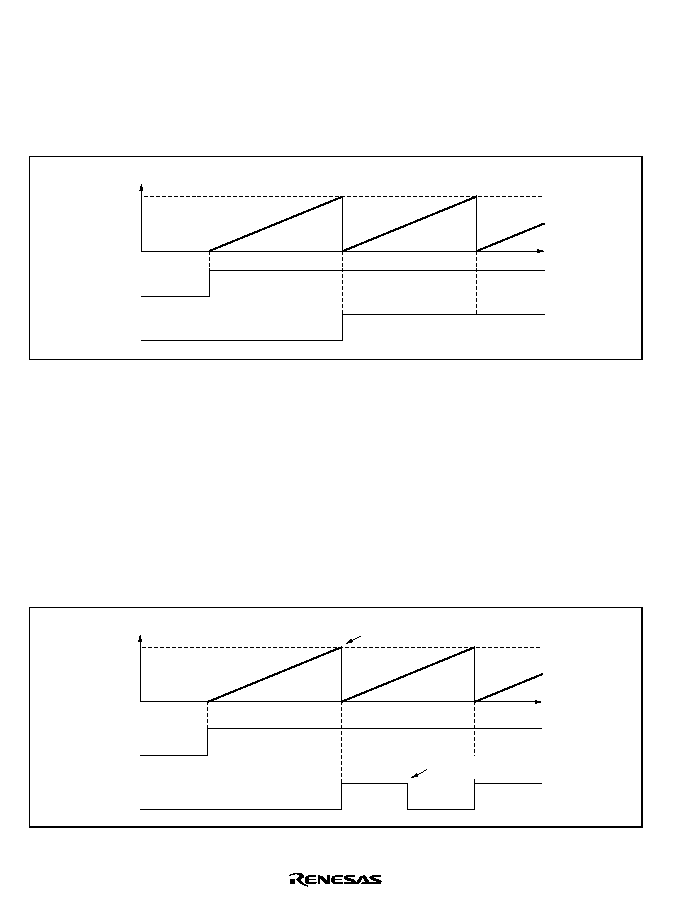
Rev. 2.00, 09/03, page 344 of 690
∑
Free-running count operation and periodic count operation
Immediately after a reset, the TPU's TCNT counters are all designated as free-running
counters. When the relevant bit in TSTR is set to 1 the corresponding TCNT counter starts up-
count operation as a free-running counter. When TCNT overflows (from H'FFFF to H'0000),
the TCFV bit in TSR is set to 1. After overflow, TCNT starts counting up again from H'0000.
Figure 14.3 illustrates free-running counter operation.
TCNT value
H'FFFF
H'0000
CST bit
TCFV
Time
Figure 14.3 Free-Running Counter Operation
When compare match is selected as the TCNT clearing source, the TCNT counter for the relevant
channel performs periodic count operation. The TGR register for setting the period is designated
as an output compare register, and counter clearing by compare match is selected by means of bits
CCLR2 to CCLR0 in TCR. After the settings have been made, TCNT starts up-count operation as
a periodic counter when the corresponding bit in TSTR is set to 1. When the count value matches
the value in TGR, the TGF bit in TSR is set to 1 and TCNT is cleared to H'0000.
After a compare match, TCNT starts counting up again from H'0000.
Figure 14.4 illustrates periodic counter operation.
TCNT value
TGRA
H'0000
CST bit
TGFA
Time
Counter cleared by TGRA
compare match
Flag cleared by software
Figure 14.4 Periodic Counter Operation
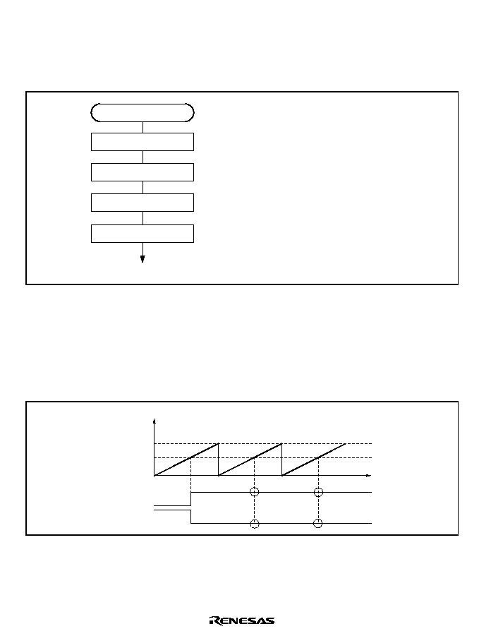
Rev. 2.00, 09/03, page 345 of 690
Waveform Output by Compare Match: The TPU can perform 0, 1, or toggle output from the
corresponding output pin (TO pin) using TGRA compare match.
∑
Example of setting procedure for waveform output by compare match
Figure 14.5 shows an example of the setting procedure for waveform output by compare match
Select waveform output mode
Output selection
Set output timing
Start count
<Waveform output>
[1]
[2]
Set external pin function
[3]
[4]
[1] Select initial value 0 output or 1 output, and
compare match output value 0 output, 1 output,
or toggle output, by means of TIOR. The set
initial value is output at the TO pin until the first
compare match occurs.
[2] Set the timing for compare match generation in
TGRA.
[3] Set the external pin function in pin function
controller
(PFC).
[4] Set the CST bit in TSTR to 1 to start the count
operation.
Figure 14.5 Example of Setting Procedure for Waveform Output by Compare Match
∑
Examples of waveform output operation
Figure 14.6 shows an example of 0 output/1 output.
In this example TCNT has been designated as a free-running counter, and settings have been
made so that 1 is output by compare match A, and 0 is output by compare match B. When the
set level and the pin level coincide, the pin level does not change.
TCNT value
H'FFFF
H'0000
TO pin (1 output)
TO pin (0 output)
Time
TGRA
No change
No change
No change
No change
Figure 14.6 Example of 0 Output/1 Output Operation

Rev. 2.00, 09/03, page 346 of 690
Figure 14.7 shows an example of toggle output.
In this example TCNT has been designated as a periodic counter (with counter clearing performed
by compare match B), and settings have been made so that output is toggled by compare match A.
TCNT value
H'FFFF
H'0000
TO pin
Time
TGRB
TGRA
Toggle output
Counter cleared by TGRB compare match
Figure 14.7 Example of Toggle Output Operation
14.4.3
Buffer Operation
Buffer operation, enables TGRC and TGRD to be used as buffer registers.
Table 14.6 shows the register combinations used in buffer operation.
Table 14.6
Register Combinations in Buffer Operation
Timer General Register
Buffer Register
TGRA
TGRC
TGRB
TGRD
When a compare match occurs, the value in the buffer register for the corresponding channel is
transferred to the timer general register. For update timing from a buffer register, rewriting on
compare match occurrence or on counter cleaning can be selected.
This operation is illustrated in figure 14.8.
Buffer register
Timer general
register
TCNT
Comparator
Compare match signal
Counter clearing signal
BFWT bit
Figure 14.8 Compare Match Buffer Operation
Rev. 2.00, 09/03, page 347 of 690
Example of Buffer Operation Setting Procedure: Figure 14.9 shows an example of the buffer
operation setting procedure.
Set buffer operation
Buffer operation
Set rewriting timing
Start count
<Buffer operation>
[1]
[2]
Set external pin function
[3]
[4]
[1] Designate TGR for buffer operation with bits
BFA and BFB in TMDR.
[2] Set rewriting timing from the buffer register with
bit BFWT in TMDR.
[3] Set the external pin function in pin function
controller
(PFC).
[4] Set the CST bit in TSTR to 1 to start the count
operation.
Figure 14.9 Example of Buffer Operation Setting Procedure
Example of Buffer Operation
Figure 14.10 shows an operation example in which PWM mode has been designated for channel 0,
and buffer operation has been designated for TGRA and TGRC. The settings used in this example
are TCNT clearing by compare match B, 1 output at compare match A, and 0 output at counter
clearing. Rewriting timing from the buffer register is set at counter clearing.
As buffer operation has been set, when compare match A occurs the output changes. When
counter clearing occurs by TGRB, the output changes and the value in buffer register TGRC is
simultaneously transferred to timer general register TGRA. This operation is repeated each time
compare match A occurs.
For details of PWM modes, see section 14.4.4, PWM Modes.

Rev. 2.00, 09/03, page 348 of 690
TCNT value
TGRB
H'0000
TGRC
Time
TGRA
N (A)
N (TGRB+1)
TO pin
N (A)
N (B)
N (TGRB+1)
N (TGRB+1)
N (B)
TGRA
N (B)
N (A)
Figure 14.10 Example of Buffer Operation
14.4.4
PWM Modes
In PWM mode, PWM waveforms are output from the output pins. 0 or 1 output can be selected as
the output level in response to compare match of each TGRA.
Designating TGRB compare match as the counter-clearing source enables the period to be set in
that register. All channels can be designated for PWM mode independently.
PWM output is generated from the TO pin using TGRB as the period register and TGRA as duty
cycle registers. The output specified in TIOR is performed by means of compare matches. Upon
counter clearing by a period register compare match, the output value of each pin is the initial
value set in TIOR. Set TIOR so that the initial output and an output value by compare match are
different. If the same levels or toggle outputs are selected, operation is disabled.
Conditions of duty cycle 0% and 100% are shown below.
∑
Duty cycle
0%: The set value of the period register (TGRB) is TGRA + 1 for the duty
register (TGRA).
∑
Duty cycle 100%: The set value of the duty register (TGRA) is 0.
In PWM mode, a maximum 4-phase PWM output is possible.
Rev. 2.00, 09/03, page 349 of 690
Example of PWM Mode Setting Procedure: Figure 14.11 shows an example of the PWM mode
setting procedure.
Select counter clock
PWM mode
Select counter clearing source
Select waveform output level
<PWM mode>
[1]
[2]
[3]
Set period
[4]
Set PWM mode
[5]
Set external pin function
[6]
Start count
[7]
[1] Select the counter clock with bits TPSC2 to
TPSC0 in TCR. At the same time, select the
input clock edge with bits CKEG1 and CKEG0 in
TCR.
[2] Use bits CCLR2 to CCLR0 in TCR to select the
TGRB to be used as the TCNT clearing source.
[3] Use TIOR to select the initial value and
output
value.
[4] Set the period in TGRB, and set the duty in
TGRA.
[5] Select the PWM mode with bits MD2 to MD0 in
TMDR.
[6] Set the external pin function in pin function
controller
(PFC).
[7] Set the CST bit in TSTR to 1 to start the count
operation.
Figure 14.11 Example of PWM Mode Setting Procedure
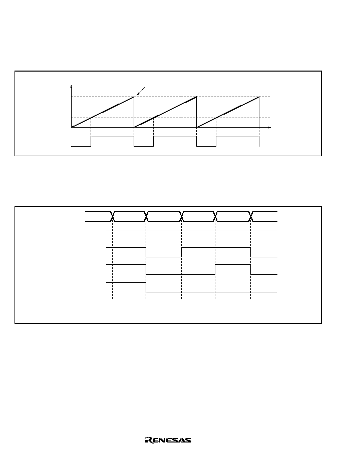
Rev. 2.00, 09/03, page 350 of 690
Examples of PWM Mode Operation: Figure 14.12 shows an example of PWM mode operation.
In this example, TGRB compare match is set as the TCNT clearing source, 0 is set as the initial
output value of the TO pin by TGRA, and 1 is set as the output value by TGRA compare match.
In this case, the value set in TGRB is used as the period, and the value set in TGRA as the duty.
TCNT value
TGRB
H'0000
TO
Time
TGRA
Counter cleared by
TGRB compare match
Figure 14.12 Example of PWM Mode Operation (1)
Figure 14.13 shows examples of PWM waveform output with 0% duty and 100% duty in PWM
mode.
TCNT
TGRA=1
TGRA=2
TGRA=3
Rewrite timing for TGRA
Period: TGRB=2
0
2
1
2
0
TGRA=0
Figure 14.13 Examples of PWM Mode Operation (2)

RTCS320A_000020020100
Rev. 2.00, 09/03, page 351 of 690
Section 15 Realtime Clock (RTC)
This LSI has a realtime clock (RTC) with its own 32.768 kHz crystal oscillator. A block diagram
of the RTC is shown in figure 15.1.
15.1
Features
The RTC has the following features:
∑
Clock and calendar functions (BCD format): seconds, minutes, hours, date, day of the week,
month, and year
∑
1-Hz to 64-Hz timer (binary format)
∑
Start/stop function
∑
30-second adjust function
∑
Alarm interrupt: frame comparison of seconds, minutes, hours, date, day of the week, month,
and year can be used as conditions for the alarm interrupt
∑
Periodic interrupts: the interrupt cycle may be 1/256 second, 1/64 second, 1/16 second, 1/4
second, 1/2 second, 1 second, or 2 seconds
∑
Carry interrupt: a carry interrupt indicates when a carry occurs during a counter read
∑
Automatic leap year adjustment
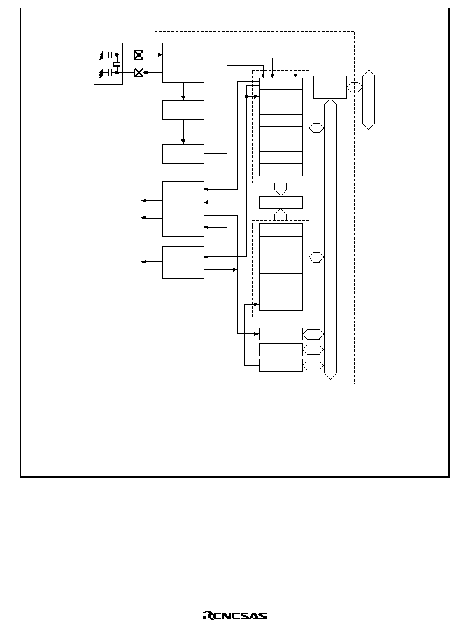
Rev. 2.00, 09/03, page 352 of 690
Module bus
RTC
Peripheral bus
Interrupt
control
circuit
Prescaler
(
˜ 2)
Bus
interface
Carry
detection
circuit
ATI
PRI
CUI
R64CNT
Reset
RSECCNT
RMINCNT
RHRCNT
RWKCNT
16.384 kHz
RDAYCNT
RMONCNT
RYRCNT
Comparator
RSECAR
RMINAR
RHRAR
RWKAR
RDAYAR
RCR1
RCR2
RCR3
30-
second
ADJ
EXTAL2
32.768 kHz
128 Hz
XTAL2
Externally
connected
circuit
Oscillator
circuit
Prescaler
(
˜ 128)
RYRAR
RMONAR
R64CNT:
RSECCNT:
RMINCNT:
RHRCNT:
RWKCNT:
RDAYCNT:
RMONCNT:
RYRCNT:
RSECAR:
64-Hz counter
Second counter
Minute counter
Hour counter
Day of the week counter
Date counter
Month counter
Year counter
Second alarm register
RHRAR:
RMINAR:
RWKAR:
RDAYAR:
RMONAR:
RYRAR:
RCR1:
RCR2:
RCR3:
Minute alarm register
Hour alarm register
Day of the week alarm register
Date alarm register
Month alarm register
Year alarm register
RTC control register 1
RTC control register 2
RTC control register 3
Legend:
Figure 15.1 RTC Block Diagram

Rev. 2.00, 09/03, page 353 of 690
15.2
Input/Output Pins
Table 15.1 shows the RTC pin configuration.
Table 15.1
Pin Configuration
Pin
Abbreviation I/O
Function
Crystal oscillator for RTC
EXTAL2
I
Connects crystal to RTC oscillator
*
Crystal oscillator for RTC
XTAL2
O
Connects crystal to RTC oscillator
*
Power-supply for RTC
V
CC
-RTC
--
Power-supply pin for RTC
GND for RTC
V
SS
-RTC
--
GND pin for RTC
Note:
*
Pull up (VccQ (3.3 V power)) EXTAL2 and leave XTAL2 open, when the RTC is not used.
15.3
Register Descriptions
The RTC has the following registers. Refer to section 24, List of Registers, for more detail of the
address and access size.
∑
64-Hz counter (R64CNT)
∑
Second counter (RSECCNT)
∑
Minute counter (RMINCNT)
∑
Hour counter (RHRCNT)
∑
Day of week counter (RWKCNT)
∑
Date counter (RDAYCNT)
∑
Month counter (RMONCNT)
∑
Year counter (RYRCNT)
∑
Second alarm register (RSECAR)
∑
Minute alarm register (RMINAR)
∑
Hour alarm register (RHRAR)
∑
Day of week alarm register (RWKAR)
∑
Date alarm register (RDAYAR)
∑
Month alarm register (RMONAR)
∑
Year alarm register (RYRAR)
∑
RTC control register 1 (RCR1)
∑
RTC control register 2 (RCR2)
∑
RTC control register 3 (RCR3)

Rev. 2.00, 09/03, page 354 of 690
15.3.1
64-Hz Counter (R64CNT)
The 64-Hz counter (R64CNT) is an 8-bit read-only register that indicates the state of the divider
circuit between 64 Hz and 1 Hz.
R64CNT is reset to H'00 by setting the RESET bit in RCR2 or the ADJ bit in RCR2 to 1.
R64CNT is not initialized by a power-on reset or manual reset, or in standby mode.
Bit
Bit Name
Initial Value
R/W
Description
7
0
R
Reserved
This bit is always read as 0.
6 to 0
R
64-Hz Counter
Each bit (bits 6 to 0) indicates the state of the
RTC divider circuit between 64 Hz and 1 Hz.
Bit
Frequency
6:
1 Hz
5:
2 Hz
4:
4 Hz
3:
8 Hz
2:
16 Hz
1:
32 Hz
0:
64 Hz
15.3.2
Second Counter (RSECCNT)
The second counter (RSECCNT) is an 8-bit readable/writable register used for setting/counting in
the BCD-coded second section. The count operation is performed by a carry for each second of the
64-Hz counter.
The range of second that can be set is 00 to 59 (decimal). Errant operation will result if any other
value is set. Carry out write processing after stopping the count operation with the START bit in
RCR2.
RSECCNT is not initialized by a power-on reset or manual reset, or in standby mode.

Rev. 2.00, 09/03, page 355 of 690
Bit
Bit Name
Initial Value
R/W
Description
7
0
R
Reserved
This bit is always read as 0. The write value
should always be 0.
6 to 4
R/W
10-unit of the second counter in the BCD-code.
The range that can be set is 0 to 5 (decimal).
3 to 0
R/W
1-unit of the second counter in the BCD-code.
The range that can be set is 0 to 9 (decimal).
15.3.3
Minute Counter (RMINCNT)
The minute counter (RMINCNT) is an 8-bit readable/writable register used for setting/counting in
the BCD-coded minute section. The count operation is performed by a carry for each minute of the
second counter.
The range of minute that can be set is 00 to 59 (decimal). Errant operation will result if any other
value is set. Carry out write processing after stopping the count operation with the START bit in
RCR2.
RMINCNT is not initialized by a power-on reset or manual reset, or in standby mode.
Bit
Bit Name
Initial Value
R/W
Description
7
0
R
Reserved
This bit is always read as 0. The write value
should always be 0.
6 to 4
R/W
10-unit of the minute counter in the BCD-code.
The range that can be set is 0 to 5 (decimal).
3 to 0
R/W
1-unit of the minute counter in the BCD-code.
The range that can be set is 0 to 9 (decimal).
15.3.4
Hour Counter (RHRCNT)
The hour counter (RHRCNT) is an 8-bit readable/writable register used for setting/counting in the
BCD-coded hour section. The count operation is performed by a carry for each 1 hour of the
minute counter.
The range of hour that can be set is 00 to 23 (decimal). Errant operation will result if any other
value is set. Carry out write processing after stopping the count operation with the START bit in
RCR2.
RHRCNT is not initialized by a power-on reset or manual reset, or in standby mode.

Rev. 2.00, 09/03, page 356 of 690
Bit
Bit Name
Initial Value
R/W
Description
7, 6
0
R
Reserved
These bits are always read as 0. The write value
should always be 0.
5, 4
R/W
10-unit of the hour counter in the BCD-code.
The range that can be set is 0 to 2 (decimal).
3 to 0
R/W
1-unit of the hour counter in the BCD-code.
The range that can be set is 0 to 9 (decimal).
15.3.5
Day of Week Counter (RWKCNT)
The day of week counter (RWKCNT) is an 8-bit readable/writable register used for
setting/counting in the day of week section. The count operation is performed by a carry for each
day of the date counter.
The range for day of the week that can be set is 0 to 6 (decimal). Errant operation will result if any
other value is set. Carry out write processing after stopping the count operation with the START
bit in RCR2.
RWKCNT is not initialized by a power-on reset or manual reset, or in standby mode.
Bit
Bit Name
Initial Value
R/W
Description
7 to 3
0
R
Reserved
These bits are always read as 0. The write value
should always be 0.
2 to 0
R/W
Counter for the day of week in the BCD-code.
The range that can be set is 0 to 6 (decimal).
Code
Day of Week
0:
Sunday
1:
Monday
2:
Tuesday
3:
Wednesday
4:
Thursday
5:
Friday
6:
Saturday

Rev. 2.00, 09/03, page 357 of 690
15.3.6
Date Counter (RDAYCNT)
The date counter (RDAYCNT) is an 8-bit readable/writable register used for setting/counting in
the BCD-coded date section. The count operation is performed by a carry for each day of the hour
counter.
The range of date that can be set changes within 01 to 31 (decimal) with some months and in leap
years. Please confirm the correct setting. Errant operation will result if any other value is set.
Carry out write processing after stopping the count operation with the START bit in RCR2.
RDAYCNT is not initialized by a power-on reset or manual reset, or in standby mode.
Bit
Bit Name
Initial Value
R/W
Description
7, 6
0
R
Reserved
These bits are always read as 0. The write value
should always be 0.
5, 4
R/W
10-unit of the date counter in the BCD-code.
The range that can be set is 0 to 3 (decimal).
3 to 0
R/W
1-unit of the date counter in the BCD-code.
The range that can be set is 0 to 9 (decimal).
15.3.7
Month Counter (RMONCNT)
The month counter (RMONCNT) is an 8-bit readable/writable register used for setting/counting in
the BCD-coded month section. The count operation is performed by a carry for each month of the
date counter.
The range of month that can be set is 01 to 12 (decimal). Errant operation will result if any other
value is set. Carry out write processing after stopping the count operation with the START bit in
RCR2.
RMONCNT is not initialized by a power-on reset or manual reset, or in standby mode.
Bit
Bit Name
Initial Value
R/W
Description
7 to 5
0
R
Reserved
These bits are always read as 0. The write value
should always be 0.
4
R/W
10-unit of the month counter in the BCD-code.
The range that can be set is 0 to 1 (decimal).
3 to 0
R/W
1-unit of the month counter in the BCD-code.
The range that can be set is 0 to 9 (decimal).

Rev. 2.00, 09/03, page 358 of 690
15.3.8
Year Counter (RYRCNT)
The year counter (RYRCNT) is a 16-bit readable/writable register used for setting/counting in the
BCD-coded year section. The four digits of the western calendar year are counted. The count
operation is performed by a carry for each year of the month counter.
The range for year that can be set is 0000 to 9999 (decimal). Errant operation will result if any
other value is set. Carry out write processing after stopping the count operation with the START
bit in RCR2 or using a carry flag.
RYRCNT is not initialized by a power-on reset or manual reset, or in standby mode.
Leap years are recognized by dividing the year counter value by 4 and obtaining a fractional result
of 0. The year counter value 0000 is recognized as a leap year.
Bit
Bit Name
Initial Value
R/W
Description
15 to 12
R/W
1000-unit of the year counter in the BCD-code.
The range that can be set is 0 to 9 (decimal).
11 to 8
R/W
100-unit of the year counter in the BCD-code.
The range that can be set is 0 to 9 (decimal).
7 to 4
R/W
10-unit of the year counter in the BCD-code.
The range that can be set is 0 to 9 (decimal).
3 to 0
R/W
1-unit of the year counter in the BCD-code.
The range that can be set is 0 to 9 (decimal).
15.3.9
Second Alarm Register (RSECAR)
The second alarm register (RSECAR) is an 8-bit readable/writable register, and an alarm register
corresponding to the second counter RSECCNT. When the ENB bit is set to 1, a comparison with
the RSECCNT value is performed. For alarm registers RSECAR, RMINAR, RHRAR, RWKAR,
RDAYAR, and RMONAR, a comparison with the corresponding counter value is performed for
those whose ENB bit is set to 1, and for RCR3, a comparison is performed when the YAEN bit is
set to 1. If all of those match, an RTC alarm interrupt is generated.
The range of second alarm that can be set is 00 to 59 (decimal). Errant operation will result if any
other value is set.
The ENB bit in RSECAR is initialized to 0 by a power-on reset, and it is not initialized by manual
reset and standby mode. The remaining RSECAR fields are not initialized by a power-on reset or
manual reset, or in standby mode.

Rev. 2.00, 09/03, page 359 of 690
Bit
Bit Name
Initial Value
R/W
Description
7
ENB
0
R/W
Second Alarm Enable
Specifies whether to compare RSECCNT with
RSECAR to generate a second alarm.
0: Not compared
1: Compared
6 to 4
R/W
10-unit of second alarm setting in the BCD-code.
The range that can be set is 0 to 5 (decimal).
3 to 0
R/W
1-unit of second alarm setting in the BCD-code.
The range that can be set is 0 to 9 (decimal).
15.3.10
Minute Alarm Register (RMINAR)
The minute alarm register (RMINAR) is an 8-bit readable/writable register, and an alarm register
corresponding to the minute counter RMINCNT. When the ENB bit is set to 1, a comparison with
the RMINCNT value is performed. For alarm registers RSECAR, RMINAR, RHRAR, RWKAR,
RDAYAR, and RMONAR, a comparison with the corresponding counter value is performed for
those whose ENB bit is set to 1, and for RCR3, a comparison is performed when the YAEN bit is
set to 1. If all of those match, an RTC alarm interrupt is generated.
The range of minute alarm that can be set is 00 to 59 (decimal). Errant operation will result if any
other value is set.
The ENB bit in RMINAR is initialized by a power-on reset, and it is not initialized by manual
reset and standby mode. The remaining RMINAR fields are not initialized by a power-on reset or
manual reset, or in standby mode.
Bit
Bit Name
Initial Value
R/W
Description
7
ENB
0
R/W
Minute Alarm Enable
Specifies whether to compare RMINCNT with
RMINAR to generate a second alarm.
0: Not compared
1: Compared
6 to 4
R/W
10-unit of minute alarm setting in the BCD-code.
The range that can be set is 0 to 5 (decimal).
3 to 0
R/W
1-unit of minute alarm setting in the BCD-code.
The range that can be set is 0 to 9 (decimal).

Rev. 2.00, 09/03, page 360 of 690
15.3.11
Hour Alarm Register (RHRAR)
The hour alarm register (RHRAR) is an 8-bit readable/writable register, and an alarm register
corresponding to the hour counter RHRCNT. When the ENB bit is set to 1, a comparison with the
RHRCNT value is performed. For alarm registers RSECAR, RMINAR, RHRAR, RWKAR,
RDAYAR, and RMONAR, a comparison with the corresponding counter value is performed for
those whose ENB bit is set to 1, and for RCR3, a comparison is performed when the YAEN bit is
set to 1. If all of those match, an RTC alarm interrupt is generated.
The range of hour alarm that can be set is 00 to 23 (decimal). Errant operation will result if any
other value is set.
The ENB bit in RHRAR is initialized by a power-on reset, and it is not initialized by manual reset
and standby mode. The remaining RHRAR fields are not initialized by a power-on reset or manual
reset, or in standby mode.
Bit
Bit Name
Initial Value
R/W
Description
7
ENB
0
R/W
Hour Alarm Enable
Specifies whether to compare RHRCNT with
RHRAR to generate a second alarm.
0: Not compared
1: Compared
6
0
R
Reserved
This bit is always read as 0. The write value
should always be 0.
5, 4
R/W
10-unit of hour alarm setting in the BCD-code.
The range that can be set is 0 to 2 (decimal).
3 to 0
R/W
1-unit of hour alarm setting in the BCD-code.
The range that can be set is 0 to 9 (decimal).

Rev. 2.00, 09/03, page 361 of 690
15.3.12
Day of Week Alarm Register (RWKAR)
The day of week alarm register (RWKAR) is an 8-bit readable/writable register, and an alarm
register corresponding to the day of week counter RWKCNT. When the ENB bit is set to 1, a
comparison with the RWKCNT value is performed. For alarm registers RSECAR, RMINAR,
RHRAR, RWKAR, RDAYAR, and RMONAR, a comparison with the corresponding counter
value is performed for those whose ENB bit is set to 1, and for RCR3, a comparison is performed
when the YAEN bit is set to 1. If all of those match, an RTC alarm interrupt is generated.
The range of day of the week alarm that can be set is 0 to 6 (decimal). Errant operation will result
if any other value is set.
The ENB bit in RWKAR is initialized by a power-on reset, and it is not initialized by manual reset
and standby mode. The remaining RWKAR fields are not initialized by a power-on reset or
manual reset, or in standby mode.
Bit
Bit Name
Initial Value
R/W
Description
7
ENB
0
R/W
Day of Week Alarm Enable
Specifies whether to compare RWKCNT with
RWKAR to generate a second alarm.
0: Not compared
1: Compared
6 to 3
0
R
Reserved
These bits are always read as 0. The write value
should always be 0.
2 to 0
R/W
Day of Week Alarm Code
The range that can be set is 0 to 6 (decimal).
Code
Day of the Week
0:
Sunday
1:
Monday
2:
Tuesday
3:
Wednesday
4:
Thursday
5:
Friday
6:
Saturday

Rev. 2.00, 09/03, page 362 of 690
15.3.13
Date Alarm Register (RDAYAR)
The date alarm register (RDAYAR) is an 8-bit readable/writable register, and an alarm register
corresponding to the date counter RDAYCNT. When the ENB bit is set to 1, a comparison with
the RDAYCNT value is performed. For alarm registers RSECAR, RMINAR, RHRAR, RWKAR,
RDAYAR, and RMONAR, a comparison with the corresponding counter value is performed for
those whose ENB bit is set to 1, and for RCR3, a comparison is performed when the YAEN bit is
set to 1. If all of those match, an RTC alarm interrupt is generated.
The range of date alarm that can be set is 01 to 31 (decimal). Errant operation will result if any
other value is set. The RDAYCNT range that can be set changes with some months and in leap
years. Please confirm the correct setting.
The ENB bit in RDAYAR is initialized by a power-on reset, and it is not initialized by manual
reset and standby mode. The remaining RDAYAR fields are not initialized by a power-on reset or
manual reset, or in standby mode.
Bit
Bit Name
Initial Value
R/W
Description
7
ENB
0
R/W
Date Alarm Enable
Specifies whether to compare RDAYCNT with
RDAYAR to generate a second alarm.
0: Not compared
1: Compared
6
0
R
Reserved
This bit is always read as 0. The write value
should always be 0.
5, 4
R/W
10-unit of date alarm setting in the BCD-code.
The range that can be set is 0 to 3 (decimal).
3 to 0
R/W
1-unit of date alarm setting in the BCD-code.
The range that can be set is 0 to 9 (decimal).

Rev. 2.00, 09/03, page 363 of 690
15.3.14
Month Alarm Register (RMONAR)
The month alarm register (RMONAR) is an 8-bit readable/writable register, and an alarm register
corresponding to the month counter RMONCNT. When the ENB bit is set to 1, a comparison with
the RMONCNT value is performed. For alarm registers RSECAR, RMINAR, RHRAR, RWKAR,
RDAYAR, and RMONAR, a comparison with the corresponding counter value is performed for
those whose ENB bit is set to 1, and for RCR3, a comparison is performed when the YAEN bit is
set to 1. If all of those match, an RTC alarm interrupt is generated.
The range of month alarm that can be set is 01 to 12 (decimal). Errant operation will result if any
other value is set.
The ENB bit in RMONAR is initialized by a power-on reset, and it is not initialized by manual
reset and standby mode. The remaining RMONAR fields are not initialized by a power-on reset or
manual reset, or in standby mode.
Bit
Bit Name
Initial Value
R/W
Description
7
ENB
0
R/W
Month Alarm Enable
Specifies whether to compare RMONCNT with
RMONAR to generate a second alarm.
0: Not compared
1: Compared
6, 5
0
R
Reserved
These bits are always read as 0. The write value
should always be 0.
4
R/W
10-unit of month alarm setting in the BCD-code.
The range that can be set is 0 to 1 (decimal).
3 to 0
R/W
1-unit of month alarm setting in the BCD-code.
The range that can be set is 0 to 9 (decimal).

Rev. 2.00, 09/03, page 364 of 690
15.3.15
Year Alarm Register (RYRAR)
The year alarm register (RYRAR) is a 16-bit readable/writable register, and an alarm register
corresponding to the year counter RYRCNT. When the YAEN bit in RCR3 is set to 1, a
comparison with the RYRCNT value is performed. For alarm registers RSECAR, RMINAR,
RHRAR, RWKAR, RDAYAR, and RMONAR, a comparison with the corresponding counter
value is performed for those whose ENB bit is set to 1, and for RCR3, a comparison is performed
when the YAEN bit is set to 1. If all of those match, an RTC alarm interrupt is generated.
The range of year alarm that can be set is 0000 to 9999 (decimal). Errant operation will result if
any other value is set.
The RYRAR contents are not initialized by a power-on reset or manual reset, or in standby mode.
Bit
Bit Name
Initial Value
R/W
Description
15 to 12
R/W
1000-unit of year alarm setting in the BCD-code.
The range that can be set is 0 to 9 (decimal).
11 to 8
R/W
100-unit of year alarm setting in the BCD-code.
The range that can be set is 0 to 9 (decimal).
7 to 4
R/W
10-unit of year alarm setting in the BCD-code.
The range that can be set is 0 to 9 (decimal).
3 to 0
R/W
1-unit of year alarm setting in the BCD-code.
The range that can be set is 0 to 9 (decimal).

Rev. 2.00, 09/03, page 365 of 690
15.3.16
RTC Control Register 1 (RCR1)
The RTC control register 1 (RCR1) is an 8-bit readable/writable register that affects carry flags
and alarm flags. It also selects whether to generate interrupts for each flag. Because flags are
sometimes set after an operand read, do not use this register in read-modify-write processing.
RCR1 is initialized to H'00 by a power-on reset or a manual reset. In a reset, all bits are initialized
to 0 except for the CF flag, which is undefined. When using the CF flag, it must be initialized
beforehand. This register is not initialized in standby mode.
Bit
Bit Name
Initial Value
R/W
Description
7
CF
Undefined
R/W
Carry Flag
Status flag that indicates that a carry has
occurred. CF is set to 1 when R64CNT or
RSECCNT is read during a carry occurrence by
R64CNT or RSECCNT. A count register value
read at this time cannot be guaranteed; another
read is required.
0: No carry by R64CNT or RSECCNT.
[Clearing condition] When 0 is written to CF
1: [Setting condition] When R64CNT or
RSECCNT is read during a carry occurrence by
R64CNT or RSECCNT, or 1 is written to CF
6, 5
--
0
R
Reserved
These bits are always read as 0. The write value
should always be 0.
4
CIE
0
R/W
Carry Interrupt Enable Flag
When the carry flag (CF) is set to 1, the CIE bit
enables interrupts.
0: A carry interrupt is not generated when the CF
flag is set to 1
1: A carry interrupt is generated when the CF flag
is set to 1
3
AIE
0
R/W
Alarm Interrupt Enable Flag
When the alarm flag (AF) is set to 1, the AIE bit
enables interrupts.
0: An alarm interrupt is not generated when the
AF flag is set to 1
1: An alarm interrupt is generated when the AF
flag is set to 1

Rev. 2.00, 09/03, page 366 of 690
Bit
Bit Name
Initial Value
R/W
Description
2, 1
--
0
R
Reserved
These bits are always read as 0. The write value
should always be 0.
0
AF
0
R/W
Alarm Flag
The AF flag is set to 1 when the alarm time set in
an alarm register (only registers with ENB bit of
the corresponding alarm registers and YAEN bit
in RCR3 set to 1) matches the clock and calendar
time. This flag is cleared to 0 when 0 is written,
but holds the previous value when 1 is written.
0: Clock/calendar and alarm register have not
matched.
[Clearing condition] When 0 is written to AF
1: [Setting condition] Clock/calendar and alarm
register have matched (only registers that ENB
bit and YAEN bit is 1)
15.3.17
RTC Control Register 2 (RCR2)
The RTC control register 2 (RCR2) is an 8-bit readable/writable register for periodic interrupt
control, 30-second adjustment ADJ, divider circuit RESET, and RTC count start/stop control. It is
initialized to H'09 by a power-on reset. It is initialized except for RTCEN and START by a
manual reset. It is not initialized in standby mode, and retains its contents.
Bit
Bit Name
Initial Value
R/W
Description
7
PEF
0
R/W
Periodic Interrupt Flag
Indicates interrupt generation with the period
designated by the PES2 to PES0 bits. When set
to 1, PEF generates periodic interrupts.
0: Interrupts not generated with the period
designated by the PES bits.
[Clearing condition] When 0 is written to PEF
1: [Setting condition] When interrupts are
generated with the period designated by the
PES bits or 1 is written to PEF

Rev. 2.00, 09/03, page 367 of 690
Bit
Bit Name
Initial Value
R/W
Description
6
5
4
PES2
PES1
PES0
0
0
0
R/W
R/W
R/W
Periodic Interrupt Interval
These bits specify the periodic interrupt interval.
000: No periodic interrupts generated
001: Periodic interrupt generated every 1/256
second
010: Periodic interrupt generated every 1/64
second
011: Periodic interrupt generated every 1/16
second
100: Periodic interrupt generated every 1/4
second
101: Periodic interrupt generated every 1/2
second
110: Periodic interrupt generated every 1 second
111: Periodic interrupt generated every 2 seconds
3
RTCEN
1
R/W
Controls the operation of the crystal oscillator for
the RTC.
0: Halts the crystal oscillator for the RTC.
1: Runs the crystal oscillator for the RTC.
2
ADJ
0
R/W
30 Second Adjustment
When 1 is written to the ADJ bit, times of 29
seconds or less will be rounded to 00 seconds
and 30 seconds or more to 1 minute. The divider
circuit will be simultaneously reset. This bit is
always read as 0.
0: Runs normally.
1: 30-second adjustment.
1
RESET
0
R/W
Reset
When 1 is written, initializes the divider circuit
(RTC prescaler and R64CNT). This bit is always
read as 0.
0: Runs normally.
1: Divider circuit is reset.

Rev. 2.00, 09/03, page 368 of 690
Bit
Bit Name
Initial Value
R/W
Description
0
START
1
R/W
Start Bit
Halts and restarts the counter (clock).
0: Second/minute/hour/day/week/month/year
counter halts.
*
1: Second/minute/hour/day/week/month/year
counter runs normally.
*
Note:
*
The 64-Hz counter always runs unless
stopped with the RTCEN bit.
15.3.18
RTC Control Register 3 (RCR3)
The RTC control register 3 (RCR3) is an 8-bit readable/writable register that controls the
comparison between the BCD-coded year section counter RYRCNT of the RTC and the year
alarm register RYRAR.
Bit
Bit Name
Initial Value
R/W
Description
7
YAEN
0
R/W
Year Alarm Enable
When this bit is set to 1, the year alarm register
(RYRAR) is compared with the year counter
(RYRCNT). For alarm registers RSECAR,
RMINAR, RHRAR, RWKAR, RDAYAR, and
RMONAR, a comparison with the corresponding
counter value is performed for those whose ENB
bit is set to 1, and for RCR3, a comparison is
performed when this bit is set to 1. If all of those
match, an RTC alarm interrupt is generated.
6 to 0
--
0
R
Reserved
These bits are always read as 0. The write value
should always be 0.
Rev. 2.00, 09/03, page 369 of 690
15.4
Operation
15.4.1
Initial Settings of Registers after Power-On
All the registers should be set after the power is turned on.
15.4.2
Setting Time
Figure 15.2 shows how to set the time when the clock is stopped.
Write 1 to RESET and 0 to
START in the RCR2 register
Order is irrelevant
Write 1 to START in the
RCR2 register
Set seconds, minutes,
hour, day, day of the
week, month and year
Stop clock,
reset divider circuit
Start clock
Figure 15.2 Setting Time
Rev. 2.00, 09/03, page 370 of 690
15.4.3
Reading the Time
Figure 15.3 shows how to read the time. If a carry occurs while reading the time, the correct time
will not be obtained, so it must be read again. Part (a) in figure 15.3 shows the method of reading
the time without using interrupts; part (b) in figure 15.3 shows the method using interrupts. To
keep programming simple, method (a) should normally be used.
Write 0 to CF in RCR1
Note: Set AF to 1 so that alarm
flag is not cleared.
Read RCR1 and check CF
Write 0 to CIE in RCR1
Carry flag = 1?
No
Yes
Clear the carry flag
Disable the carry
interrupt
Read counter
register
Write 1 to CIE in RCR1,
and write 0 to CF in RCR1
Note: Set AF in RCR1 to 1 so that
alarm flag is not cleared.
Interrupt
generated?
No
Yes
Enable the carry
interrupt
Clear the carry flag
Disable the carry
interrupt
Read counter
register
To read the time
without using interrupts
(b) To use interrupts
(a)
Write 0 to CIE in RCR1
Figure 15.3 Reading the Time

Rev. 2.00, 09/03, page 371 of 690
15.4.4
Alarm Function
Figure 15.4 shows how to use the alarm function.
Alarms can be generated using seconds, minutes, hours, day of the week, date, month, year, or any
combination of these. Set the ENB or YAEN bit for the register on which the alarm is placed to 1,
and then set the alarm time in the lower bits. Clear the ENB or YAEN bit for the register on which
the alarm is not placed to 0.
When the clock and alarm times match, 1 is set in the AF bit in RCR1. Alarm detection can be
checked by reading this bit, but normally it is done by interrupt. If 1 is placed in the AIE bit in
RCR1, an interrupt is generated when an alarm occurs.
Disable interrupt to prevent erroneous
interruption.(AIE bit in RCR1 is cleared)
Then write 1.
Clock running
Set alarm time
Cancel alarm interrupt
Always clear, since the flag may have been
set while the alarm time was being set.
(Write 0 to AF of RCR1 to clear it. )
Clear alarm flag
Monitor alarm time
(wait for interrupt or
check alarm flag)
Figure 15.4 Using the Alarm Function
Rev. 2.00, 09/03, page 372 of 690
15.4.5
Crystal Oscillator Circuit
Crystal oscillator circuit constants (recommended values) are shown in table 15.2, and the RTC
crystal oscillator circuit in figure 15.5.
Table 15.2
Recommended Oscillator Circuit Constants (Recommended Values)
f
osc
C
in
C
out
32.768 kHz
10 to 22 pF
10 to 22 pF
This LSI
EXTAL2
XTAL2
XTAL
C
in
C
out
R
f
R
D
Notes: 1. Select either the C
in
or C
out
side for frequency adjustment variable capacitor
according to requirements such as frequency range, stability, etc.
2. Built-in resistance value R
f
(Typ value) = 10 M
, R
D
(Typ value) = 400 k
3. C
in
and C
out
values include stray capacitance due to the wiring. Take care when
using a ground plane.
4. The crystal oscillation settling time depends on the mounted circuit constants,
stray capacitance, etc., and should be decided after consultation with the crystal
resonator manufacturer.
5. Place the crystal resonator and load capacitors C
in
and C
out
as close as possible
to the chip.
(Correct oscillation may not be possible if there is externally induced noise in the
EXTAL2 and XTAL2 pins.)
6. Ensure that the crystal resonator connection pin (EXTAL2, XTAL2) wiring is
routed as far away as possible from other power lines (except GND) and signal
lines.
Figure 15.5 Example of Crystal Oscillator Circuit Connection

Rev. 2.00, 09/03, page 373 of 690
15.5
Notes for Usage
15.5.1
Register Writing during RTC Count
The following RTC registers cannot be written to during an RTC count (while the START bit in
RCR2 = 1).
RSECCNT, RMINCNT, RHRCNT, RDAYCNT, RWKCNT, RMONCNT, RYRCNT
The RTC count must be halted before writing to any of the above registers.
15.5.2
Use of Realtime Clock (RTC) Periodic Interrupts
The method of using the periodic interrupt function is shown in figure 15.6.
A periodic interrupt can be generated periodically at the interval set by the periodic interrupt
interval bits (PES0 to PES2) in RCR2. When the time set by the PES0 to PES2 bits has elapsed,
the PEF bit is set to 1.
The PEF is cleared to 0 upon periodic interrupt generation when the periodic interrupt interval bits
(PES0 to PES2) is set. Periodic interrupt generation can be confirmed by reading this bit, but
normally the interrupt function is used.
Set PES0 to PES2,
and clear PEF to 0,
in RCR2
Clear PEF to 0
Set PES, clear PEF
Elapse of time set by PES
Clear PEF
Figure 15.6 Using Periodic Interrupt Function
15.5.3
Standby Mode after Register Setting
If the standby mode is entered after the RTC registers are set, the time cannot be counted
correctly. After setting the registers, wait for 2 RTC clock cycles or longer before the standby
mode is entered.

Rev. 2.00, 09/03, page 374 of 690

SCIS3C2B_000020020100
Rev. 2.00, 09/03, page 375 of 690
Section 16 Serial Communication Interface with FIFO
(SCIF)
This LSI has a two-channel serial communication interface with on-chip FIFO buffers (Serial
Communication Interface with FIFO: SCIF). The SCIF can perform asynchronous and clock
synchronous serial communication.
64-stage FIFO registers are provided for both transmission and reception, enabling fast, efficient,
and continuous communication.
16.1
Features
∑
Asynchronous mode
Serial data communication is executed using an asynchronous system in which
synchronization is achieved character by character. Serial data communication can be carried
out with standard asynchronous communication chips such as a Universal Asynchronous
Receiver/Transmitter (UART) or Asynchronous Communication Interface Adapter (ACIA).
There is a choice of eight serial data communication formats.
Data length: 7 or 8 bits
Stop bit length: 1 or 2 bits
Parity: Even/odd/none
LSB-first transfer
Receive error detection: Parity, framing, and overrun errors
Break detection: If a framing error is followed by at least one frame at the space "0" (low)
level, a break is detected.
∑
Clock synchronous mode
Serial data communication is synchronized with a clock. Serial data communication can be
carried out with other chips that have a synchronous communication function.
Data length: 8 bits
LSB-first transfer
∑
Full-duplex communication capability
The transmitter and receiver are independent units, enabling transmission and reception to be
performed simultaneously.
The transmitter and receiver both have a 64-stage FIFO buffer structure, enabling fast and
continuous serial data transmission and reception.
∑
On-chip baud rate generator allows any bit rate to be selected.
∑
Choice of serial clock source: internal clock from baud rate generator or external clock from
SCK pin.
∑
Six interrupt sources in asynchronous mode

Rev. 2.00, 09/03, page 376 of 690
There are six interrupt sources
transmit-data-stop, transmit-FIFO-data-empty, receive-FIFO-
data-full, receive-error (framing/parity error), break-receive, and receive-data-ready interrupts.
∑
Two interrupt sources in clock synchronous mode
There are two interrupt sources
transmit-FIFO-data-empty and receive-FIFO-data-full
interrupts.
∑
The DMA controller (DMAC) can be activated to execute a data transfer in the event of a
transmit-FIFO-data-empty, transmit-data-stop, or receive-FIFO-data-full interrupt. The DMAC
requests of transmit-FIFO-data-empty and transmit-data-stop interrupts are the same.
∑
On-chip modem control functions (
CTS and RTS)
∑
On-chip transmit-data-stop functions (only in asynchronous mode)
∑
When not in use, the SCIF can be stopped by halting its clock supply to reduce power
consumption.
∑
The amount of data in the transmit/receive FIFO registers and the number of receive errors in
the receive data in the receive FIFO register can be ascertained.
Rev. 2.00, 09/03, page 377 of 690
Figure 16.1 shows a block diagram of the SCIF.
SCIF4
Module data bus
SCFRDR
(64-stage)
RxD
TxD
CTS
RTS
SCK
SCFTDR
(64-stage)
SCTSR
SCRSR
SCFDR
SCFCR
SCFER
SCSSR
SCSCR
SCSMR
SCTDSR
SCBRR
Transmission/
reception control
Baud rate
generator
Clock
Parity
generation
Parity check
External clock
P
P
/4
P
/16
P
/64
SCIF
Bus interface
Peripheral
bus
SCRSR:
Receive shift register
SCFRDR:
Receive FIFO data register
SCTSR:
Transmit shift register
SCFTDR:
Transmit FIFO data register
SCSMR:
Serial mode register
SCSCR:
Serial control register
SCFER:
FIFO error count register
SCSSR:
Serial status register
SCBRR:
Bit rate register
SCFCR:
FIFO control register
SCFDR:
FIFO data count register
SCTDSR:
Transit data stop register
SCIF
interrupt
Note:
Figure 16.1 Block Diagram of SCIF

Rev. 2.00, 09/03, page 378 of 690
16.2
Input/Output Pins
Table 16.1 shows the SCIF pin configuration.
Table 16.1
Pin Configuration
Channel Pin Name
Abbreviation
*
1
I/O
Function
0
Serial clock
SCK0
SCK
Input/output
Clock input/output
Receive data
RxD0
RxD
*
2
Input
Receive data input
Transmit data
TxD0
TxD
*
2
Output
Transmit data output
Modem control
CTS0
CTS
Input
Transmission possible
Modem control
RTS0
RTS
Output
Transmit request
2
Serial clock
SCK2
SCK
Input/output
Clock input/output
Receive data
RxD2
RxD
*
2
Input
Receive data input
Transmit data
TxD2
TxD
*
2
Output
Transmit data output
Modem control
CTS2
CTS
Input
Transmission possible
Modem control
RTS2
RTS
Output
Transmit request
Notes: 1. The pins are collectively called SCK, RxD, TxD,
CTS
, and
RTS
without channel number
in the following descriptions.
2. These pins are made to function as serial pins by setting SCIF operation with the TE
and RE bits in SCSCR.

Rev. 2.00, 09/03, page 379 of 690
16.3
Register Descriptions
The SCIF has the following internal registers. For details on register addresses and register states
in each processing state, refer to section 24, List of Registers.
1. Channel 0
∑
Serial mode register 0 (SCSMR_0)
∑
Bit rate register 0 (SCBRR_0)
∑
Serial control register 0 (SCSCR_0)
∑
Transmit data stop register 0 (SCTDSR_0)
∑
FIFO error count register 0 (SCFER_0)
∑
Serial status register 0 (SCSSR_0)
∑
FIFO control register 0 (SCFCR_0)
∑
FIFO data count register 0 (SCFDR_0)
∑
Transmit FIFO data register 0 (SCFTDR_0)
∑
Receive FIFO data register 0 (SCFRDR_0)
2. Channel 2
∑
Serial mode register 2 (SCSMR_2)
∑
Bit rate register 2 (SCBRR_2)
∑
Serial control register 2 (SCSCR_2)
∑
Transmit data stop register 2 (SCTDSR_2)
∑
FIFO error count register 2 (SCFER_2)
∑
Serial status register 2 (SCSSR_2)
∑
FIFO control register 2 (SCFCR_2)
∑
FIFO data count register 2 (SCFDR_2)
∑
Transmit FIFO data register 2 (SCFTDR_2)
∑
Receive FIFO data register 2 (SCFRDR_2)

Rev. 2.00, 09/03, page 380 of 690
16.3.1
Receive Shift Register (SCRSR)
SCRSR is the register used to receive serial data.
The SCIF sets serial data input from the RxD pin in SCRSR in the order received, starting with the
LSB (bit 0), and converts it to parallel data. When one byte of data has been received, it is
transferred to the receive FIFO data register, SCFRDR, automatically.
SCRSR cannot be directly read or written to by the CPU.
16.3.2
Receive FIFO Data Register (SCFRDR)
SCFRDR is a 64-stage 8-bit FIFO register that stores received serial data.
When the SCIF has received one byte of serial data, it transfers the received data from SCRSR to
SCFRDR where it is stored, and completes the receive operation. SCRSR is then enabled for
reception, and consecutive receive operations can be performed until the receive FIFO data
register is full (64 data bytes).
SCFRDR is a read-only register, and cannot be written to by the CPU.
If a read is performed when there is no receive data in the receive FIFO data register, an undefined
value will be returned. When the receive FIFO data register is full of receive data, subsequent
serial data is lost.
Bit
Bit Name
Initial Value
R/W
Description
7 to 0
SCFRD7 to
SCFRD0
Undefined
R
Serial Receive Data FIFO
16.3.3
Transmit Shift Register (SCTSR)
SCTSR is the register used to transmit serial data.
To perform serial data transmission, the SCIF first transfers transmit data from SCFTDR to
SCTSR, then sends the data sequentially to the TxD pin starting with the LSB (bit 0).
When transmission of one byte is completed, the next transmit data is transferred from SCFTDR
to SCTSR, and transmission is started automatically.
SCTSR cannot be directly read or written to by the CPU.

Rev. 2.00, 09/03, page 381 of 690
16.3.4
Transmit FIFO Data Register (SCFTDR)
SCFTDR is an 8-bit 64-stage FIFO data register that stores data for serial transmission.
If SCTSR is empty when transmit data is written to SCFTDR, the SCIF transfers the transmit data
written in SCFTDR to SCTSR and starts serial transmission.
SCFTDR is a write-only register, and cannot be read by the CPU.
The next data cannot be written when SCFTDR is filled with 64 bytes of transmit data. Data
written in this case is ignored.
Bit
Bit Name
Initial Value
R/W
Description
7 to 0
SCFTD7 to
SCFTD0
Undefined
W
Serial Transmit Data FIFO
16.3.5
Serial Mode Register (SCSMR)
SCSMR is a 16-bit readable/writable register used to set the SCIF's serial transfer format and
select the baud rate generator clock source and the sampling rate.

Rev. 2.00, 09/03, page 382 of 690
Bit
Bit
Name
Initial
Value
R/W
Description
15 to 11
0
R
Reserved
These bits are always read as 0. The write value should
always be 0.
10
9
8
SRC2
SRC1
SRC0
0
0
0
R/W
R/W
R/W
Sampling Control
Select the sampling rate in asynchronous mode. This
setting is valid only in asynchronous mode.
000: Sampling rate 1/16
001: Sampling rate 1/5
010: Sampling rate 1/11
011: Sampling rate 1/13
100: Sampling rate 1/29
101: Setting prohibited
110: Setting prohibited
111: Setting prohibited
7
C/A
0
R/W
Communication Mode
Selects whether the SCI operates in the asynchronous
or clock synchronous mode.
0: Asynchronous mode
1: Clock synchronous mode
6
CHR
0
R/W
Character Length
Selects seven or eight bits as the data length.
This setting is only valid in asynchronous mode. In
clock synchronous mode, the data length is always
eight bits, regardless of the CHR setting.
0: 8-bit data
1: 7-bit data
*
Note:
*
When the 7-bit data is selected, the MSB bit (bit
7) in the transmit FIFO data register (SCFTDR)
is not transmitted.

Rev. 2.00, 09/03, page 383 of 690
Bit
Bit
Name
Initial
Value
R/W
Description
5
PE
0
R/W
Parity Enable
Selects whether or not parity bit addition is performed in
transmission, and parity bit checking in reception.
This setting is only valid in asynchronous mode. In
synchronous mode, parity bit addition and checking is
not performed, regardless of the PE setting.
0: Parity bit addition and checking disabled
1: Parity bit addition and checking enabled
*
Note:
*
When the PE bit is set to 1, the parity (even or
odd) specified by the O/E bit is added to
transmit data before transmission. In reception,
the parity bit is checked for the parity (even or
odd) specified by the O/E bit.
4
O/E
0
R/W
Parity Mode
Selects either even or odd parity for use in parity
addition and checking. The O/E bit setting is only valid
when the PE bit is set to 1, enabling parity bit addition
and checking. The O/E bit setting is invalid when parity
addition and checking is disabled in asynchronous and
clock synchronous mode.
0: Even parity
*
1
1: Odd parity
*
2
Notes: 1. When even parity is set, parity bit addition is
performed in transmission so that the total
number of 1-bits in the transmit character
plus the parity bit is even. In reception, a
check is performed to see if the total
number of 1-bits in the receive character
plus the parity bit is even.
2. When odd parity is set, parity bit addition is
performed in transmission so that the total
number of 1-bits in the transmit character
plus the parity bit is odd. In reception, a
check is performed to see if the total
number of 1-bits in the receive character
plus the parity bit is odd.

Rev. 2.00, 09/03, page 384 of 690
Bit
Bit
Name
Initial
Value
R/W
Description
3
STOP
0
R/W
Stop Bit Length
Selects one or two bits as the stop bit length. In
reception, only the first stop bit is checked, regardless
of the STOP bit setting. If the second stop bit is 1, it is
treated as a stop bit; if it is 0, it is treated as the start bit
of the next transmit character.
This setting is only valid in asynchronous mode. In
clock synchronous mode, this setting is invalid since
stop bits are not added.
0: One stop bit
*
1
1: Two stop bits
*
2
Notes: 1. In transmission, a single 1-bit (stop bit) is
added to the end of a transmit character
before it is sent.
2. In transmission, two 1-bits (stop bits) are
added to the end of a transmit character
before it is sent.
2
0
R
Reserved
This bit is always read as 0. The write value should
always be 0.
1
0
CKS1
CKS0
0
0
R/W
R/W
Clock Select
Select the clock source for the on-chip baud rate
generator.
00: P
01: P
/4
10: P
/16
11: P
/64
Note:
When the clock synchronous mode is selected (C/A bit = 1), the bits other than CKS1 and
CKS0 bits are all fixed to 0.

Rev. 2.00, 09/03, page 385 of 690
16.3.6
Serial Control Register (SCSCR)
SCSCR is a 16-bit readable/writable register that enables or disables the SCIF transfer operations
and interrupt requests, and selects the serial clock source.
Bit
Bit
Name
Initial
Value
R/W
Description
15 to 12
0
R
Reserved
These bits are always read as 0. The write value should
always be 0.
11
TSIE
0
R/W
Transmit Data Stop Interrupt Enable
Enables or disables generation of a transmit-data-stop
interrupt when the TSE bit in SCFCR is enabled and the
TSF flag in SCSSR is set to 1.
0: Transmit-data-stop interrupt disabled
*
1: Transmit-data-stop interrupt enabled
Note:
*
The interrupt request is cleared by clearing the
TSF flag to 0 after reading 1 from it or clearing
the TSIE bit to 0.
10
ERIE
0
R/W
Receive Error Interrupt Enable
Enables or disables generation of a receive-error
(framing or parity error) interrupt when the ER flag in
SCSSR is set to 1.
0: Receive-error interrupt disabled
*
1: Receive-error interrupt enabled
Note:
*
The interrupt request is cleared by clearing the
ER flag to 0 after reading 1 from it or clearing the
ERIE bit to 0.

Rev. 2.00, 09/03, page 386 of 690
Bit
Bit
Name
Initial
Value
R/W
Description
9
BRIE
0
R/W
Break Interrupt Enable
Enables or disables generation of a break-receive
interrupt when the BRK flag in SCSSR is set to 1.
0: Break-receive interrupt disabled
*
1: Break-receive interrupt enabled
Note:
*
The interrupt request is cleared by clearing the
BRK flag to 0 after reading 1 from it or clearing
the BRIE bit to 0.
8
DRIE
0
R/W
Receive Data Ready Interrupt Enable
Enables or disables generation of a receive-data-ready
interrupt when the DR flag in SCSSR is set to 1.
0: Receive-data-ready interrupt disabled
*
1: Receive-data-ready interrupt enabled
Note:
*
The interrupt request is cleared by clearing the
DR flag to 0 after reading 1 from it or clearing the
DRIE bit to 0.
7
TIE
0
R/W
Transmit Interrupt Enable
Enables or disables generation of a transmit-FIFO-data-
empty interrupt request when the TDFE flag in SCSSR is
set to 1.
0: Transmit-FIFO-data-empty interrupt request
disabled
*
1: Transmit-FIFO-data-empty interrupt request enabled
Note:
*
The interrupt request is cleared by writing
transmit data exceeding the transmit trigger set
number to SCFTDR, reading 1 from the TDFE
flag, then clearing it to 0, or clearing the TIE bit to
0.
6
RIE
0
R/W
Receive Interrupt Enable
Enables or disables generation of a receive-FIFO-data-
full interrupt request when the RDF flag in SCSSR is set
to 1.
0: Receive-FIFO-data-full interrupt request disabled
*
1: Receive-FIFO-data-full interrupt request enabled
Note:
*
The interrupt requests is cleared by reading 1
from the RDF flag, then clearing the flag to 0, or
clearing the RIE bit to 0.

Rev. 2.00, 09/03, page 387 of 690
Bit
Bit
Name
Initial
Value
R/W
Description
5
TE
0
R/W
Transmit Enable
Enables or disables the start of serial transmission by
the SCIF.
0: Transmission disabled
1: Transmission enabled
*
Note:
*
The serial mode register (SCSMR) and FIFO
control register (SCFCR) settings must be made,
the transmit format decided, and the transmit
FIFO reset, before the TE bit is set to 1.
4
RE
0
R/W
Receive Enable
Enables or disables the start of serial reception by the
SCIF.
0: Reception disabled
*
1
1: Reception enabled
*
2
Notes: 1. Clearing the RE bit to 0 does not affect the
DR, ER, BRK, RDF, FER, PER, and ORER
flags, which retain their state.
2. The serial mode register (SCSMR) and FIFO
control register (SCFCR) settings must be
made, the receive format decided, and the
receive FIFO reset, before the RE bit is set to
1.
3, 2
0
R
Reserved
These bits are always read as 0. The write value should
always be 0.

Rev. 2.00, 09/03, page 388 of 690
Bit
Bit
Name
Initial
Value
R/W
Description
1
0
CKE1
CKE0
0
0
R/W
R/W
Clock Enable
Select the SCIF clock source. The CKE1 and CKE0 bits
must be set before determining the SCIF operating mode
with SCSMR.
00: Internal clock/SCK pin functions as input pin (input
signal ignored)
01: Internal clock/SCK pin functions as serial clock
output
*
1
10: External clock/SCK pin functions as clock input
*
2
11: External clock/SCK pin functions as clock input
*
2
When data is sampled by the on-chip baud rate
generator, set bits CKE1 and CKE0 to B'00 (internal
clock/SCK pin functions as input pin (input signal
ignored)).
When using the SCK pin as a port, set bits CKE1 and
CKE0 to B'00.
Notes: 1. In synchronous mode, a clock with a
frequency equal to the bit rate is output.
2. In asynchronous mode, a clock with a
sampling rate should be input. For example,
when the sampling rate is 1/16, a clock with a
frequency of 8 times the bit rate should be
input. When an external clock is not input, set
bits CKE1 and CKE0 to B'00 or B'01.

Rev. 2.00, 09/03, page 389 of 690
16.3.7
FIFO Error Count Register (SCFER)
SCFER is a 16-bit read-only register that indicates the number of receive errors (framing or parity
error).
Bit
Bit
Name
Initial
Value
R/W
Description
15, 14
0
R
Reserved
These bits are always read as 0. The write value should
always be 0.
13 to 8
PER5
to
PER0
0
R
Parity Error Count
Indicates the number of data, in which parity errors are
generated, in receive data stored in the receive FIFO
data register (SCFRDR) in asynchronous mode.
After setting the ER bit in SCSSR, the value of bits 13
to 8 indicates the number of parity error generated data.
When all 64 bytes of receive data in SCFRDR have
parity errors, the PER5 to PER0 bits indicate 0.
7, 6
0
R
Reserved
These bits are always read as 0. The write value should
always be 0.
5 to 0
FER5
to
FER0
0
R
Framing Error Count
Indicates the number of data, in which framing errors
are generated, in receive data stored in the receive
FIFO data register (SCFRDR) in asynchronous mode.
After setting the ER bit in SCSSR, the value of bits 5 to
0 indicates the number of framing error generated data.
When all 64 bytes of receive data in SCFRDR have
framing errors, the FER5 to FER0 bits indicate 0.

Rev. 2.00, 09/03, page 390 of 690
16.3.8
Serial Status Register (SCSSR)
SCSSR is a 16-bit readable/writable register that indicates the SCIF status.
However, 1 cannot be written to the ORER, TSF, ER, TDFE, BRK, RDF, and DR flags. Also note
that in order to clear these flags to 0, they must be read as 1 beforehand. The TEND, FER, and
PER flags are read-only flags and cannot be modified.
Bit
Bit
Name
Initial
Value
R/W
Description
15 to 10
0
R
Reserved
These bits are always read as 0. The write value
should always be 0.
9
ORER
0
R/(W)
*
Overrun Error
Indicates that an overrun error occurred during
reception.
This bit is only valid in asynchronous mode.
0: Reception in progress, or reception has ended
successfully
*
1
[Clearing conditions]
∑
Power-on reset or manual reset
∑
When 0 is written to ORER after reading ORER =
1
1: An overrun error occurred during reception
*
2
[Setting condition]
When serial reception is completed while receive
FIFO is full
Notes: 1. The ORER flag is not affected and retains
its previous state when the RE bit in
SCSCR is cleared to 0.
2. The receive data prior to the overrun error
is retained in SCFRDR, and the data
received subsequently is lost. Serial
reception cannot be continued while the
ORER flag is set to 1.

Rev. 2.00, 09/03, page 391 of 690
Bit
Bit
Name
Initial
Value
R/W
Description
8
TSF
0
R/(W)
*
Transmit Data Stop
Indicates that the number of transmit data matches the
value of SCTDSR.
0: Number of transmit data does not match the value of
SCTDSR
[Clearing conditions]
∑
Power-on reset or manual reset
∑
When 0 is written to TSF after reading TSF = 1
1: Number of transmit data matches the value of SCTDSR
7
ER
0
R/(W)
*
Receive Error
Indicates that a framing error or parity error occurred during
reception in asynchronous mode.
*
1
0: No framing error or parity error occurred during reception
[Clearing conditions]
∑
Power-on reset or manual reset
∑
When 0 is written to ER after reading ER = 1
1: A framing error or parity error occurred during reception
[Setting conditions]
∑
When the SCIF checks whether the stop bit at the end
of the receive data is 1 when reception ends, and the
stop bit is 0
*
2
∑
When, in reception, the number of 1-bits in the receive
data plus the parity bit does not match the parity setting
(even or odd) specified by the O/E bit in SCSMR
Notes: 1. The ER flag is not affected and retains its
previous state when the RE bit in SCSCR is
cleared to 0. When a receive error occurs, the
receive data is still transferred to SCFRDR, and
reception continues.
The FER and PER bits in SCSSR can be used
to determine whether there is a receive error in
the data read from SCFRDR.
2. When the stop length is two bits, only the first
stop bit is checked for a value of 1; the second
stop bit is not checked.

Rev. 2.00, 09/03, page 392 of 690
Bit
Bit
Name
Initial
Value
R/W
Description
6
TEND
1
R
Transmit End
Indicates that there is no valid data in SCFTDR when the
last bit of the transmit character is sent, and transmission
has been ended.
0: Transmission is in progress
[Clearing condition]
When data is written to SCFTDR
1: Transmission has been ended
[Setting condition]
When there is no transmit data in SCFTDR on transmission
of a 1-byte serial transmit character
5
TDFE
1
R/(W)
*
Transmit FIFO Data Empty
Indicates that data has been transferred from SCFTDR to
SCTSR, the number of data bytes in SCFTDR has fallen to
or below the transmit trigger data number set by bits
TTRG1 and TTRG0 in the FIFO control register (SCFCR),
and new transmit data can be written to SCFTDR.
0: A number of transmit data bytes exceeding the transmit
trigger set number have been written to SCFTDR
[Clearing condition]
When transmit data exceeding the transmit trigger set
number is written to SCFTDR, and 0 is written to TDFE
after reading TDFE = 1
1: The number of transmit data bytes in SCFTDR does not
exceed the transmit trigger set number
[Setting conditions]
∑
Power-on reset or manual reset
∑
When the number of SCFTDR transmit data bytes falls
to or below the transmit trigger set number as the result
of a transmit operation
*
1
Note: 1. As SCFTDR is a 64-byte FIFO register, the
maximum number of bytes that can be written
when TDFE = 1 is 64 ≠ (transmit trigger set
number). Data written in excess of this will be
ignored. The number of data bytes in SCFTDR is
indicated by SCFDR.

Rev. 2.00, 09/03, page 393 of 690
Bit
Bit
Name
Initial
Value
R/W
Description
4
BRK
0
R/(W)
*
Break Detect
Indicates that a receive data break signal has been
detected in asynchronous mode.
0: A break signal has not been received
[Clearing conditions]
∑
Power-on reset or manual reset
∑
When 0 is written to BRK after reading BRK = 1
1: A break signal has been received
*
1
[Setting condition]
When data with a framing error is received, followed by the
space 0 level (low level) for at least one frame length
Note: 1.
When a break is detected, the receive data
(H'00) following detection is not transferred to
SCFRDR. When the break ends and the receive
signal returns to mark 1, receive data transfer is
resumed.
3
FER
0
R
Framing Error
Indicates a framing error in the data read from SCFRDR in
asynchronous mode.
0: There is no framing error in the receive data read from
SCFRDR
[Clearing conditions]
∑
Power-on reset or manual reset
∑
When there is no framing error in SCFRDR read data
1: There is a framing error in the receive data read from
SCFRDR
[Setting condition]
When there is a framing error in SCFRDR read data

Rev. 2.00, 09/03, page 394 of 690
Bit
Bit
Name
Initial
Value
R/W
Description
2
PER
0
R
Parity Error
Indicates a parity error in the data read from SCFRDR in
asynchronous mode.
0: There is no parity error in the receive data read from
SCFRDR
[Clearing conditions]
∑
Power-on reset or manual reset
∑
When there is no parity error in SCFRDR read data
1: There is a parity error in the receive data read from
SCFRDR
[Setting condition]
When there is a parity error in SCFRDR read data
1
RDF
0
R/(W)
*
Receive FIFO Data Full
Indicates that the received data has been transferred from
SCRSR to SCFRDR, and the number of receive data bytes
in SCFRDR is equal to or greater than the receive trigger
number set by bits RTRG1 and RTRG0 in the FIFO control
register (SCFCR).
0: The number of receive data bytes in SCFRDR is less
than the receive trigger set number
[Clearing conditions]
∑
Power-on reset or manual reset
∑
When SCFRDR is read until the number of receive data
bytes in SCFRDR falls below the receive trigger set
number, and 0 is written to RDF after reading RDF = 1
1: The number of receive data bytes in SCFRDR is equal to
or greater than the receive trigger set number
[Setting condition]
When SCFRDR contains at least the receive trigger set
number of receive data bytes
*
1
Note: 1. SCFRDR is a 64-byte FIFO register. When RDF =
1, at least the receive trigger set number of data
bytes can be read. If data is read when SCFRDR
is empty, an undefined value will be returned. The
number of receive data bytes in SCFRDR is
indicated by the lower bits of SCFDR.

Rev. 2.00, 09/03, page 395 of 690
Bit
Bit
Name
Initial
Value
R/W
Description
0
DR
0
R/(W)
*
Receive Data Ready
Indicates that there are fewer than the receive trigger
set number of data bytes in SCFRDR and no further
data will arrive in asynchronous mode.
0: Reception is in progress or has ended successfully
and there is no receive data left in SCFRDR
[Clearing conditions]
∑
Power-on reset or manual reset
∑
When all the receive data in SCFRDR has been
read, and 0 is written to DR after reading DR = 1
1: No further receive data has arrived
[Setting condition]
When SCFRDR contains fewer than the receive trigger
set number of receive data bytes and no further data
will arrive.
*
1
Note: 1. The DR bit is set 15 etu after the last data is
received at a sampling rate of 1/16 regardless
of the setting of the sampling control bits in
SCSMR.
etu: Elementary time unit (time for transfer of
one bit)
Note:
*
Only 0 can be written for clearing the flags.
16.3.9
Bit Rate Register (SCBRR)
SCBRR is an 8-bit readable/writable register that sets the serial transfer bit rate in accordance with
the baud rate generator operating clock selected by bits CKS1 and CKS0 in SCSMR.
Bit
Bit
Name
Initial
Value
R/W
Description
7 to 0
SCBR7
to
SCBR0
H'FF
R/W
Bit Rate Setting
The SCBRR setting is found from the following equation.

Rev. 2.00, 09/03, page 396 of 690
Asynchronous Mode:
1. When sampling rate is 1/16
N =
P
32 ◊ 2
2n-1
◊ B
◊ 10
6
- 1
2. When sampling rate is 1/5
N =
P
10 ◊ 2
2n-1
◊ B
◊ 10
6
- 1
3. When sampling rate is 1/11
N =
P
22 ◊ 2
2n-1
◊ B
◊ 10
6
- 1
4. When sampling rate is 1/13
N =
P
26 ◊ 2
2n-1
◊ B
◊ 10
6
- 1
5. When sampling rate is 1/29
N =
P
58 ◊ 2
2n-1
◊ B
◊ 10
6
- 1
Clock Synchronous Mode:
N =
P
4 ◊ 2
2n-1
◊ B
◊ 10
6
- 1
Where B:
Bit rate (bits/s)
N:
SCBRR setting for baud rate generator
Asynchronous mode: 0
N
255
Clock synchronous mode: 1
N
255
P
:
Peripheral module operating frequency (MHz)
n:
Baud rate generator input clock (n = 0 to 3)
(See the table below for the relation between n and the clock.)
SCSMR Setting
n
Clock
CKS1
CKS0
0
P
0
0
1
P
/4
0
1
2
P
/16
1
0
3
P
/64
1
1

Rev. 2.00, 09/03, page 397 of 690
The bit rate error in asynchronous mode is found from the following equation:
1. When sampling rate is 1/16
Error (%) =
P ◊ 10
6
(1+N) ◊ B ◊ 32 ◊ 2
2n-1
- 1 ◊ 100
2. When sampling rate is 1/5
Error (%) =
P ◊ 10
6
(1+N) ◊ B ◊ 10 ◊ 2
2n-1
- 1 ◊ 100
3. When sampling rate is 1/11
Error (%) =
P ◊ 10
6
(1+N) ◊ B ◊ 22 ◊ 2
2n-1
- 1 ◊ 100
4. When sampling rate is 1/13
Error (%) =
P ◊ 10
6
(1+N) ◊ B ◊ 26 ◊ 2
2n-1
- 1 ◊ 100
5. When sampling rate is 1/27
Error (%) =
P ◊ 10
6
(1+N) ◊ B ◊ 58 ◊ 2
2n-1
- 1 ◊ 100

Rev. 2.00, 09/03, page 398 of 690
16.3.10
FIFO Control Register (SCFCR)
SCFCR is a 16-bit readable/writable register that resets the data count and sets the trigger data
number for the transmit and receive FIFO registers, and also contains a loopback test enable bit.
Bit
Bit
Name
Initial
Value
R/W
Description
15
TSE
0
R/W
Transmit Data Stop Enable
Enables or disables the transmit data stop function.
This function is enabled only in asynchronous mode.
Since this function is not supported in clock synchronous
mode, clear this bit to 0 in clock synchronous mode.
0: Transmit data stop function disabled
1: Transmit data stop function enabled
14
TCRST
0
R/W
Transmit Count Reset
Clears the transmit count to 0. This bit is valid only when
the transmit data stop function is used.
0: Transmit count reset disabled
*
1: Transmit count reset enabled (clearing to 0)
Note:
*
The transmit count is reset (clearing to 0) is
performed in power-on reset or manual reset.
13 to 11
0
R
Reserved
These bits are always read as 0. The write value should
always be 0.
10
9
8
RSTRG2
RSTRG1
RSTRG0
0
0
0
R/W
R/W
R/W
RTS
Output Active Trigger
The
RTS
signal goes high when the number of receive
data bytes in SCFRDR is equal to or greater than the
trigger set number shown in below.
000: 63
001: 1
010: 8
011: 16
100: 32
101: 48
110: 54
111: 60

Rev. 2.00, 09/03, page 399 of 690
Bit
Bit
Name
Initial
Value
R/W
Description
7
6
RTRG1
RTRG0
0
0
R/W
R/W
Receive FIFO Data Number Trigger
Set the number of receive data bytes that sets the receive
data full (RDF) flag in the serial status register (SCSSR).
The RDF flag is set when the number of receive data bytes
in SCFRDR is equal to or greater than the trigger set
number shown in below.
00: 1
01: 16
10: 32
11: 48
5
4
TTRG1
TTRG0
0
0
R/W
R/W
Transmit FIFO Data Number Trigger
Set the number of remaining transmit data bytes that sets
the transmit FIFO data register empty (TDFE) flag in the
serial status register (SCSSR).
The TDFE flag is set when, as the result of a transmit
operation, the number of transmit data bytes in the transmit
FIFO data register (SCFTDR) falls to or below the trigger
set number shown in below.
00: 32 (32)
01: 16 (48)
10: 2 (62)
11: 0 (64)
Note:
The values in parentheses are the number of empty
bytes in SCFTDR when the flag is set.
3
MCE
0
R/W
Modem Control Enable
Enables modem control signals
CTS
and
RTS
.
This setting is only valid in asynchronous mode.
0: Modem signal disabled
*
1: Modem signal enabled
Note:
*
CTS
is fixed at active 0 regardless of the input
value, and
RTS
is also fixed at 0.

Rev. 2.00, 09/03, page 400 of 690
Bit
Bit
Name
Initial
Value
R/W
Description
2
TFRST
0
R/W
Transmit FIFO Data Register Reset
Invalidates the transmit data in the transmit FIFO data
register and resets it to the empty state.
0: Reset operation disabled
*
1: Reset operation enabled
Note:
*
A reset operation is performed in the event of a
power-on reset or manual reset.
1
RFRST
0
R/W
Receive FIFO Data Register Reset
Invalidates the receive data in the receive FIFO data
register and resets it to the empty state.
0: Reset operation disabled
*
1: Reset operation enabled
Note:
*
A reset operation is performed in the event of a
power-on reset or manual reset.
0
LOOP
0
R/W
Loopback Test
Internally connects the transmit output pin (TxD) and
receive input pin (RxD), and
RTS
pin and
CTS
pin, enabling
loopback testing.
0: Loopback test disabled
1: Loopback test enabled

Rev. 2.00, 09/03, page 401 of 690
16.3.11
FIFO Data Count Register (SCFDR)
SCFDR is a 16-bit read-only register that indicates the number of data bytes stored in the transmit
FIFO data register (SCFTDR) and receive FIFO data register (SCFRDR).
Bits 14 to 8 show the number of transmit data bytes in SCFTDR, and bits 6 to 0 show the number
of receive data bytes in SCFRDR.
Bit
Bit
Name
Initial
Value
R/W
Description
15
0
R
Reserved
This bit is always read as 0. The write value should
always be 0.
14 to 8
T6 to
T0
0
R
These bits show the number of untransmitted data
bytes in SCFTDR.
A value of H'00 means that there is no transmit data,
and a value of H'40 means that SCFTDR is full of
transmit data.
7
0
R
Reserved
This bit is always read as 0. The write value should
always be 0.
6 to 0
R6 to
R0
0
R
These bits show the number of receive data bytes in
SCFRDR.
A value of H'00 means that there is no receive data,
and a value of H'40 means that SCFRDR is full of
receive data.
16.3.12
Transmit Data Stop Register (SCTDSR)
SCTDSR is an 8-bit readable/writable register that sets the number of transmit data bytes.
SCTDSR is valid only when the TSE bit in the FIFO control register (SCFCR) is enabled.
Transmit operation is stopped when the number of data bytes set in SCTDSR is transmitted. The
setting value should be H'00 (one byte) to H'FF (256 bytes). This function is only enabled in
asynchronous mode.
SCTDSR is initialized to H'FF.

Rev. 2.00, 09/03, page 402 of 690
16.4
Operation
16.4.1
Overview
The SCIF can carry out serial communication in asynchronous mode, in which synchronization is
achieved character by character, and in clock synchronous mode, in which synchronization is
achieved with clock pulses.
64-stage FIFO buffers are provided for both transmission and reception, reducing the CPU
overhead and enabling fast, continuous communication to be performed.
16.4.2
Asynchronous Mode
The transfer format is selected using the serial mode register (SCSMR), as shown in table 16.2.
The SCIF clock source is determined by the CKE1 and CKE0 bits in the serial control register
(SCSCR).
∑
Data length: Choice of seven or eight bits
∑
Choice of parity addition and addition of one or two stop bits (the combination of these
parameters determines the transfer format and character length)
∑
Detection of framing errors, parity errors, overrun errors, receive-FIFO-data-full state, receive-
data-ready state, and breaks, during reception
∑
Indication of the number of data bytes stored in the transmit and receive FIFO registers
∑
Choice of internal or external clock as the SCIF clock source
When internal clock is selected: the SCIF operates on the baud rate generator clock.
When external clock is selected: A clock must be input according to the sampling rate. For
example, when the sampling rate is 1/16, a clock with a frequency of 8 times the bit rate
must be input (the on-chip baud rate generator is not used.)

Rev. 2.00, 09/03, page 403 of 690
Table 16.2
SCSMR Settings for Serial Transfer Format Selection
SCSMR Settings
SCIF Transfer Format
Bit 6:
CHR
Bit 5:
PE
Bit 3:
STOP
Mode
Data
Length
Multiprocessor
Bit
Parity
Bit
Stop Bit
Length
0
0
0
Asynchronous mode
8-bit data
None
No
1 bit
1
2 bits
1
0
Yes
1 bit
1
2 bits
1
0
0
7-bit data
No
1 bit
1
2 bits
1
0
Yes
1 bit
1
2 bits
Rev. 2.00, 09/03, page 404 of 690
16.4.3
Serial Operation in Asynchronous Mode
1. Data Transfer Format
Table 16.3 shows the transfer formats that can be used in asynchronous mode. Any of eight
transfer formats can be selected according to the SCSMR settings.
Table 16.3
Serial Transfer Formats
SCSMR Settings
Serial Transfer Format and Frame Length
CHR
PE
STOP
1
2
3
4
5
6
7
8
9
10
11
12
0
0
0
S
8-bit data
STOP
1
S
8-bit data
STOP STOP
1
0
S
8-bit data
P
STOP
1
S
8-bit data
P
STOP STOP
1
0
0
S
7-bit data
STOP
1
S
7-bit data
STOP STOP
1
0
S
7-bit data
P
STOP
1
S
7-bit data
P
STOP STOP
S:
Start bit
STOP: Stop bit
P:
Parity bit

Rev. 2.00, 09/03, page 405 of 690
2. Clock
Either an internal clock generated by the on-chip baud rate generator or an external clock input at
the SCK pin can be selected as the serial clock for the SCIF, according to the setting of the CKE1
and CKE0 bits in SCSCR.
When an external clock is input at the SCK pin, a clock must be input according to the sampling
rate. For example, when the sampling rate is 1/16, a clock with a frequency of 8 times the bit rate
must be input.
3. Data Transfer Operations
a. SCIF Initialization
Before transmitting and receiving data, it is necessary to clear the TE and RE bits in SCSCR to 0,
then initialize the SCIF as described below.
When the transfer format, etc., is changed, the TE and RE bits must be cleared to 0 before making
the change using the following procedure. When the TE bit is cleared to 0, the transmit shift
register (SCTSR) is initialized. Note that clearing the TE and RE bits to 0 does not change the
contents of SCSSR, SCFTDR, or SCFRDR. The TE bit should be cleared to 0 after all transmit
data has been sent and the TEND bit in SCSSR has been set to 1. Clearing to 0 can also be
performed during transmission, but the data being transmitted will go to the high-impedance state
after the clearance. Before setting TE to 1 again to start transmission, the TFRST bit in SCFCR
should first be set to 1 to reset SCFTDR.
When an external clock is used, the clock should not be stopped during operation, including
initialization, since operation will be unreliable in this case.
Rev. 2.00, 09/03, page 406 of 690
Figure 16.2 shows a sample SCIF initialization flowchart.
Clear TE and RE bits
in SCSCR to 0
Set TFRST and RFRST bits
in SCFCR to 1
Clear the C/A bit in SCSMR to 0, and
set the transmit/receive format
Set RTRG1
-0 and
TTRG1
-0 bits in SCFCR.
Clear TFRST and
RFRST bits to 0
Set TE and RE bits in SCSCR
to 1, and set RIE and TIE bits
Set value in SCBRR
Set CKE1 and CKE0 bits
in SCSCR to B'00
(leaving TE and RE bits
cleared to 0)
[1] Set the clock selection in SCSCR.
Be sure to clear bits RIE, TIE, TE, and RE to 0.
[2] Set the transmit and receive format in SCSMR.
[3] Write a value corresponding to the bit rate into
SCBRR. (Not necessary if an external clock is
used.)
[4] Wait at least one bit interval, then set the TE bit
and RE bits in SCSCR to 1. Also set the RIE
and TIE bits.
Setting the TE and RE bits enables the TxD
and RxD pins to be used. When transmitting,
the TxD pin will go to the mark state; when
receiving, the RxD pin will go to the idle state.
Initialization
End
1-bit interval elapsed?
No
Wait
Yes
[3]
[4]
[2]
[1]
Figure 16.2 Sample SCIF Initialization Flowchart

Rev. 2.00, 09/03, page 407 of 690
b. Serial Data Transmission
Figure 16.3 shows a sample flowchart for serial transmission.
Use the following procedure for serial data transmission after enabling the SCIF for transmission.
Read TDFE bit in SCSSR
Read TEND bit in SCSSR
Set SCPDR and SCPCR
Clear TE bit in SCSCR to 0
Write (64)
- transmit trigger
set number) bytes of transmit
data to SCFTDR, read 1 from
TDFE bit in SCSSR, then clear to 0
[1] SCIF status check and transmit data write:
Read the serial status register (SCSSR) and
check that the TDFE flag is set to 1, then write
transmit data to SCFTDR, read 1 from the TDFE
flag, then clear the flag to 0.
The number of data bytes that can be written is
64
- (transmit trigger set number).
[2] Serial transmission continuation procedure:
To continue serial transmission, read 1 from the
TDFE flag to confirm that writing is possible, then
write data to SCFTDR, and then clear the TDFE
bit to 0.
[3] Break output at the end of serial transmission:
To output a break in serial transmission, set the
port SC data register (SCPDR) and port SC
control register (SCPCR), then clear the TE bit in
SCSCR to 0.
In steps 1 and 2, it is possible to ascertain the
number of data bytes that can be written from the
number of transmit data bytes in SCFTDR
indicated by the upper 8 bits of SCFDR.
Start of transmission
End of transmission
TDFE = 1?
No
Yes
All data transmitted?
No
Yes
TEND = 1?
No
Yes
Break output?
No
Yes
[1]
[2]
[3]
Figure 16.3 Sample Serial Transmission Flowchart

Rev. 2.00, 09/03, page 408 of 690
In serial transmission, the SCIF operates as described below.
1. When data is written into SCFTDR, the SCIF transfers the data from SCFTDR to SCTSR and
starts transmitting. Confirm that the TDFE flag in the serial status register (SCSSR) is set to 1
before writing transmit data to SCFTDR. The number of data bytes that can be written is at
least 64 ≠ (transmit trigger set number).
2. When data is transferred from SCFTDR to SCTSR and transmission is started, consecutive
transmit operations are performed until there is no transmit data left in SCFTDR. When the
number of transmit data bytes in SCFTDR falls to or below the transmit trigger number set in
the FIFO control register (SCFCR), the TDFE flag is set. If the TIE bit in SCSCR is set to 1 at
this time, a transmit-FIFO-data-empty interrupt (TXI) request is generated.
When the transmit data stop function is used and the number of data bytes set in the transmit
data stop register (SCTDSR) is matched, transmit operation is stopped, and the TSF flag in the
serial status register (SCSSR) is set. If the TSIE bit in the serial control register (SCSCR) is set
to 1, a transmit-data-stop-interrupt (TDI) request is generated. The vectors of transmit-FIFO-
data-empty and transmit-data-stop interrupts are the same.
The serial transmit data is sent from the TxD pin in the following order.
a. Start bit: One 0-bit is output.
b. Transmit data: 8-bit or 7-bit data is output in LSB-first order.
c. Parity bit: One parity bit (even or odd parity) is output.
d. A format in which a parity bit is not output can also be selected.
e. Stop bit(s): One or two 1-bits (stop bits) are output.
f. Mark state: 1 is output continuously until the start bit that starts the next transmission is
sent.
3. The SCIF checks the SCFTDR transmit data at the timing for sending the stop bit. If data is
present, the data is transferred from SCFTDR to SCTSR, the stop bit is sent, and then serial
transmission of the next frame is started.
If there is no transmit data, the TEND flag in SCSSR is set to 1, the stop bit is sent, and then
the line goes to the mark state in which 1 is output.
Rev. 2.00, 09/03, page 409 of 690
Figure 16.4 shows an example of the operation for transmission in asynchronous mode.
0
1
1
1
0/1
0
1
TDFE
TEND
Parity
bit
Parity
bit
Serial
data
Start
bit
Start
bit
Data
Data
Stop
bit
Stop
bit
Idle state
(mark state)
TXI interrupt
request
Data written to SCFTDR
and TDFE flag read as
1 and then cleared to 0
by TXI interrupt handler
One frame
D0
D1
D7
D0
D1
D7
0/1
TXI interrupt
request
Figure 16.4 Example of Transmit Operation
(Example with 8-Bit Data, Parity, One Stop Bit)
∑
Transmit Data Stop Function
When a value in the SCTDSR register is matched with the number of transmit data bytes, this
function stops the transmit operation. Interrupts can be generated and the DMAC can be activated
by setting the TSIE bit (interrupt enable bit).
Figure 16.5 shows an example of operation for the transmit data stop function.
TSF flag
0
D0
D1
D6
D7
0/1
0
D0
D1
D6
D7
0/1
Start
bit
Transmit data
TxD
Parity
bit
Stop
bit
Start
bit
Figure 16.5 Example of Transmit Data Stop Function
Rev. 2.00, 09/03, page 410 of 690
Figure 16.6 shows a flowchart for the transmit data stop function.
Start of transmission
End of transmission
No
Set transmit data stop
number in SCTDSR
Set TSE and TSIE bits
in SCFCR to 1
Read TSF bit in SCSSR;
if it is 1, clear to 0 after reading
1 from TSF bit
Yes
TSF = 1 ?
[1] Set the transmit data stop number in SCTDSR, then set
the TSE bit in SCFCR to 1.When an interrupt is enabled,
also set the TSIE bit to 1.
[2] If the TSF bit in SCSSR is set to 1, clear it to 0 after
reading 1. When transmit data is written to SCFTDR in
this state, transmit operation is started.
[3] If the TSF bit is set to 1 (transmit data stop number is
matched with transmit data number), transmit operation
is stopped. If the TSIE bit is set to 1, an interrupt is
generated.
Serial transmission continuation procedure:
Set the TCRST bit in SCFCR to 1, clear transmit count, and
clear the TCRST bit to 0. Then follow steps 1, 2, and 3.
[1]
[2]
[3]
Figure 16.6 Transmit Data Stop Function Flowchart
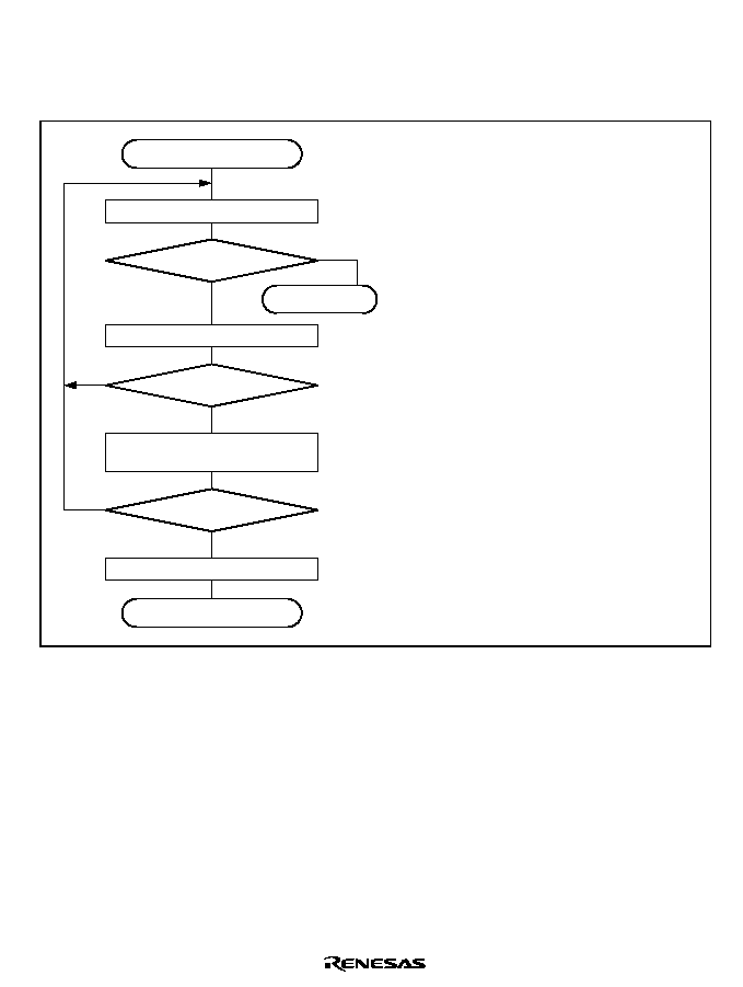
Rev. 2.00, 09/03, page 411 of 690
c. Serial Data Reception
Figures 16.7 and 16.8 show sample flowcharts for serial reception.
Use the following procedure for serial data reception after enabling the SCIF for reception.
Read DR, ER, and BRK flags in SCSSR
Read RDF flag in SCSSR
Read receive data from SCFRDR,
and clear RDF flag in SCSSR to 0
Clear RE bit in SCSCR to 0
[1] Receive error handling and break detection:
Read the DR, ER, and BRK flags in SCSSR to
identify any error, perform the appropriate error
handling, then clear the DR, ER, and BRK flags to 0.
In the case of a framing error, a break can also be
detected by reading the value of the RxD pin.
[2] SCIF status check and receive data read:
Read SCSSR and check that RDF = 1, then read the
receive data in SCFRDR, read 1 from the RDF flag,
and then clear the RDF flag to 0. The transition of the
RDF flag from 0 to 1 can also be identified by an RXI
interrupt.
[3] Serial reception continuation procedure:
To continue serial reception, read at least the receive
trigger set number of data bytes from SCFRDR, read
1 from the RDF flag, and then clear the RDF flag to
0. The number of receive data bytes in SCFRDR can
be ascertained by reading the lower bits of SCFDR.
Start of reception
End of reception
DR V ER V BRK = 1?
Yes
No
RDF = 1?
No
Yes
All data received?
No
Yes
Error handling
[3]
[2]
[1]
Figure 16.7 Sample Serial Reception Flowchart (1)
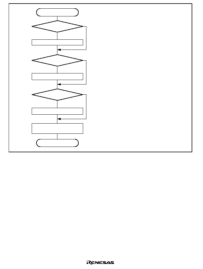
Rev. 2.00, 09/03, page 412 of 690
Receive error handling
Break handling
Read receive data in SCFRDR
Clear DR, ER, and BRK flags
in SCSSR to 0
[1] Whether a framing error or parity error has
occurred in the receive data read from
SCFRDR can be ascertained from the FER
and PER bits in SCSSR.
[2] When a break signal is received, receive data
is not transferred to SCFRDR while the BRK
flag is set. However, note that the last data in
SCFRDR is H'00 and the break data in which
a framing error occurred is stored.
Error handling
End
ER = 1?
No
Yes
BRK = 1?
No
Yes
DR = 1?
No
Yes
[1]
[2]
Figure 16.8 Sample Serial Reception Flowchart (2)

Rev. 2.00, 09/03, page 413 of 690
In serial reception, the SCIF operates as described below.
1. The SCIF monitors the communication line, and if 0 of a start bit is detected, performs internal
synchronization and starts reception.
2. The received data is stored in SCRSR in LSB-to-MSB order.
3. The parity bit and stop bit are received.
After receiving these bits, the SCIF carries out the following checks.
a. Stop bit check: the SCIF checks whether the stop bit is 1. If there are two stop bits, only the
first is checked.
b. The SCIF checks whether receive data can be transferred from the receive shift register
(SCRSR) to SCFRDR.
c. Break check: the SCIF checks that the BRK flag is 0, indicating that the break state is not
set.
If all the above checks are passed, the receive data is stored in SCFRDR.
Note:
Reception continues when a receive error (a framing error or parity error) occurs.
4. If the RIE bit in SCSCR is set to 1 when the RDF flag changes to 1, a receive-FIFO-data-full
interrupt (RXI) request is generated.
If the ERIE bit in SCSCR is set to 1 when the ER flag changes to 1, a receive-error interrupt
(ERI) request is generated.
If the BRIE bit in SCSCR is set to 1 when the BRK flag changes to 1, a break reception
interrupt (BRI) request is generated.
If the DRIE bit in SCSCR is set to 1 when the DR flag changes to 1, a receive-data-ready
interrupt (DRI) request is generated.
The vectors of receive-FIFO-data-full and receive-data-ready interrupts are the same. The
vectors of receive-error and break reception interrupts are the same.

Rev. 2.00, 09/03, page 414 of 690
Figure 16.9 shows an example of the operation for reception in asynchronous mode.
RDF
FER
ERI interrupt request
generated by receive
error
One frame
Data read and RDF flag
read as 1 then cleared
to 0 by RXI interrupt
handler
RXI interrupt
request
0
1
1
1
0/1
0
1
Parity
bit
Parity
bit
Serial
data
Start
bit
Start
bit
Data
Data
Stop
bit
Stop
bit
Idle state
(mark state)
D0
D1
D7
D0
D1
D7
0/1
Figure 16.9 Example of SCIF Receive Operation
(Example with 8-Bit Data, Parity, One Stop Bit)
∑
Modem Function
When using a modem function, transmission can be stopped and started again according to the
CTS input value. When the CTS is set to 1 during transmission, the data enters a mark state after
transmitting one frame. When
CTS is set to 0, the next transmit data is output starting with a start
bit.
Figure 16.10 shows an example of operation for the
CTS control.
CTS
Transmission stops
when CTS goes high
Transmission starts again
when CTS goes low
0
D0
D1
D6
D7
0/1
0
D0
D1
D6
D7
0/1
Start
bit
Transmit data
TxD
Parity
bit
Stop
bit
Start
bit
Figure 16.10
CTS Control Operation
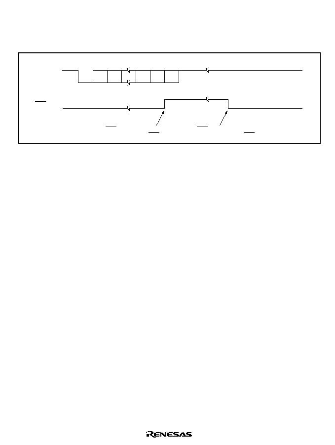
Rev. 2.00, 09/03, page 415 of 690
When using a modem function and the receive FIFO (SCFRDR) is at least the number of the
RTS
output trigger, the
RTS signal goes high.
Figure 16.11 shows an example of operation for the
RTS control.
RTS
RTS goes high when receive data is
at least number of RTS output trigger
0
D0
D1
D6
D7
0/1
Start
bit
Transmit data
TxD
Parity
bit
Stop
bit
RTS goes low when receive data is
less than number of RTS output trigger
Figure 16.11
RTS Control Operation
16.4.4
Clock Synchronous Mode
64-stage FIFO buffers are provided for both transmission and reception, reducing the CPU
overhead and enabling fast, continuous communication to be performed.
The operating clock source is selected using the serial mode register (SCSMR). The SCIF clock
source is determined by the CKE1 and CKE0 bits in the serial control register (SCSCR).
∑
Transmit/receive format: Fixed 8-bit data
∑
Indication of the number of data bytes stored in the transmit and receive FIFO registers
∑
Internal clock or external clock used as the SCIF clock source
When the internal clock is selected:
The SCIF operates on the baud rate generator clock and outputs a serial clock from SCK pin.
When the external clock is selected:
The SCIF operates on the external clock input through the SCK pin.
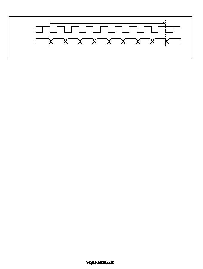
Rev. 2.00, 09/03, page 416 of 690
16.4.5
Serial Operation in Clock Synchronous Mode
Don't care
Don't care
*
*
LSB
MSB
Note:
* High except in continuous transmission/reception
Serial data
Serial clock
Bit 0
Bit 1
Bit 2
Bit 3
Bit 4
Bit 5
Bit 6
Bit 7
One unit of transfer data (character or frame)
Figure 16.12 Data Format in Clock Synchronous Communication
In clock synchronous serial communication, data on the communication line is output from a
falling edge of the serial clock to the next falling edge. Data is guaranteed valid at the rising edge
of the serial clock.
In serial communication, each character is output starting with the LSB and ending with the MSB.
After the MSB is output, the communication line remains in the state of the MSB.
In clock synchronous mode, the SCIF receives data in synchronization with the rising edge of the
serial clock.
1. Data Transfer Format
A fixed 8-bit data format is used. No parity or multiprocessor bits are added.
2. Clock
An internal clock generated by the on-chip baud rate generator or an external clock input through
the SCK pin can be selected as the serial clock for the SCIF, according to the setting of the CKE1
and CKE0 bits in SCSCR.
Eight serial clock pulses are output in the transfer of one character, and when no
transmission/reception is performed, the clock is fixed high. However, when the operation mode is
reception only, the synchronous clock output continues while the RE bit is set to 1. To fix the
clock high every time one character is transferred, write to the transmit FIFO data register
(SCFTDR) the same number of dummy data bytes as the data bytes to be received and set the TE
and RE bits to 1 at the same time to transmit the dummy data. When the specified number of data
bytes are transmitted, the clock is fixed high.
3. Data Transfer Operations
a. SCIF Initialization:
Before transmitting and receiving data, it is necessary to clear the TE and RE bits in SCSCR to 0,
then initialize the SCIF as described below.

Rev. 2.00, 09/03, page 417 of 690
When the clock source, etc., is changed, the TE and RE bits must be cleared to 0 before making
the change using the following procedure. When the TE bit is cleared to 0, the transmit shift
register (SCTSR) is initialized. Note that clearing the TE and RE bits to 0 does not change the
contents of SCSSR, SCFTDR, or SCFRDR. The TE bit should be cleared to 0 after all transmit
data has been sent and the TEND bit in SCSSR has been set to 1. The TE bit should not be cleared
to 0 during transmission; if attempted, the TxD pin will go to the high-impedance state. Before
setting TE to 1 again to start transmission, the TFRST bit in SCFCR should first be set to 1 to reset
SCFTDR.
Rev. 2.00, 09/03, page 418 of 690
Figure 16.13 shows sample SCIF initialization flowcharts.
No
Yes
Wait
End
1-bit interval elapsed?
Set transmit trigger number in TTRG1
and TTRG0 in SCFCR, write transmit
data exceeding transmit trigger setting
number, and clear TDFE flag to 0 after
reading 1 from it
Initialization
Clear TE and RE bits in SCSCR to 0
Set TFRST bit in SCFCR to 1
Set CKE1 and CKE0 bits in SCSCR
(leaving TE and RE bits cleared to 0)
Set C/A bit in SCSMR to 1
Set CKS1 and CKS0 bits
Set value in SCBRR
Clear TFRST bit to 0
[1] Be sure to set the TFRST bit in
SCFCR to 1, to reset the FIFOs.
[2] Set the clock selection in SCSCR.
Be sure to clear bits RIE, TIE, TE,
and RE to 0.
[3] Set the clock source selection in
SCSMR.
[4] Write a value corresponding to the
bit rate into SCBRR.
[5] Clear the TFRST bit in SCFCR to 0.
[6] Set the transmit trigger number,
write transmit data exceeding the
transmit trigger setting number, and
clear the TDFE flag to 0 after reading
it.
[7] Wait one bit interval.
[1]
[2]
[3]
[4]
[5]
[6]
[7]
Figure 16.13 Sample SCIF Initialization Flowchart (1) (Transmission)
Rev. 2.00, 09/03, page 419 of 690
No
Yes
Wait
[1] Be sure to set the RFRST bit in
SCFCR to 1, to reset the FIFOs.
[2] Set the clock selection in SCSCR.
Be sure to clear bits RIE, TIE, TE,
and RE to 0.
[3] Set the clock source selection in
SCSMR.
[4] Write a value corresponding to the
bit rate into SCBRR.
[5] Clear the RFRST bit in SCFCR to 0.
[6] Wait one bit interval.
Initialization
Clear TE and RE bits in SCSCR to 0
Set RFRST bit in SCFCR to 1
Set CKE1 and CKE0 bits in SCSCR
(leaving TE and RE bits cleared to 0)
Set C/A bit in SCSMR to 1
Set CKS1 and CKS0 bits
Set value in SCBRR
Clear RFRST bit in SCFCR to 0
1-bit interval elapsed?
End
[1]
[2]
[3]
[4]
[5]
[6]
Figure 16.13 Sample SCIF Initialization Flowchart (2) (Reception)

Rev. 2.00, 09/03, page 420 of 690
No
Yes
Wait
[1] Be sure to set the TFRST bit in
SCFCR to 1, to reset the FIFOs.
[2] Set the clock selection in SCSCR.
Be sure to clear bits RIE, TIE, TE,
and RE to 0.
[3] Set the clock source selection in
SCSMR.
[4] Write a value corresponding to the
bit rate into SCBRR.
[5] Clear the TFRST and RFRST bits in
SCFCR to 0.
[6] Set the transmit trigger number, write
transmit data exceeding the transmit
trigger setting number, and clear the
TDFE flag to 0 after reading it.
[7] Wait one bit interval.
Initialization
Clear TE and RE bits in SCSCR to 0
Set TFRST and RFRST bits in
SCFCR to 1
Set CKE1 and CKE0 bits in SCSCR
(leaving TE and RE bits cleared to 0)
Set C/A bit in SCSMR to 1
Set CKS1 and CKS0 bits
Set value in SCBRR
Clear TFRST and RFRST bits to 0
Set transmit trigger number in TTRG1
and TTRG0 in SCFCR, write transmit
data exceeding transmit trigger
setting number, and clear TDFE
flag to 0 after reading 1 from it
1-bit interval elapsed?
End
[1]
[2]
[3]
[4]
[5]
[6]
[7]
Figure 16.13 Sample SCIF Initialization Flowchart (3)
(Simultaneous Transmission and Reception)
Rev. 2.00, 09/03, page 421 of 690
b. Serial Data Transmission:
Figure 16.14 shows sample flowcharts for serial transmission.
No
Yes
[1] Write the remaining transmit
data to SCFTDR.
[2] Transmission is started when
the TE bit in SCSCR is set to 1.
[3] After the end of transmission,
clear the TE bit to 0.
Start of transmission
Write remaining transmit data to SCFTDR
Set TE bit in SCSCR
When using transmit FIFO data interrupt,
set TIE bit to 1
TEND =1?
Clear TE bit in SCSCR to 0
End of transmission
[1]
[2]
[3]
Figure 16.14 Sample Serial Transmission Flowchart (1)
(First Transmission after Initialization)
No
Yes
No
Wait
Yes
[1] Set the transmit trigger number
in
SCFCR.
[2] Write transmit data to SCFTDR,
and clear the TDFE flag to 0 after
reading 1 from it.
[3] Wait for one bit interval.
[4] Transmission is started when the
TE bit in SCSCR is set to 1.
[5] After the end of transmission, clear
the TE bit to 0.
Start of transmission
Set transmit trigger number in TTRG1
and TTRG0 in SCFCR
Write transmit data exceeding transmit
trigger setting number, and clear
TDFE flag to 0 after reading 1 from it
1-bit interval elapsed?
Set TE bit in SCSCR
When using transmit FIFO data
interrupt, set TIE bit to 1
TEND =1?
Clear TE bit in SCSCR to 0
End of transmission
[1]
[2]
[3]
[4]
[5]
Figure 16.14 Sample Serial Transmission Flowchart (2)
(Second and Subsequent Transmission)
Rev. 2.00, 09/03, page 422 of 690
c. Serial Data Reception
Figure 16.15 shows sample flowcharts for serial reception.
No
Yes
[1] Set the receive trigger number
in
SCFCR.
[2] Reception is started when the
RE bit in SCSCR is set to 1.
[3] Read receive data while the
RDF bit is 1.
[4] After the end of reception, clear
the RE bit to 0.
Start of reception
Set receive trigger number in RTRG1
and RTRG0 in SCFCR
Set RE bit in SCSCR
When using receive FIFO data interrupt,
set RIE bit to 1
RDF =1?
Read receive trigger number of receive
data bytes from SCFRDR
Clear RE bit in SCSCR to 0
End of reception
[1]
[2]
[3]
[4]
Figure 16.15 Sample Serial Reception Flowchart (1)
(First Reception after Initialization)
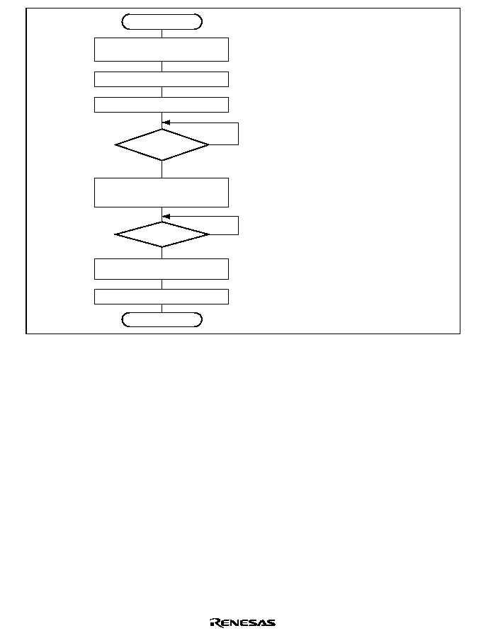
Rev. 2.00, 09/03, page 423 of 690
No
Yes
No
Wait
Yes
[1] Set the receive trigger number
in
SCFCR.
[2] Reset the receive FIFO.
[3] Wait for one bit interval.
[4] Reception is started when the RE
bit in SCSCR is set to 1.
[5] Read receive data while the RDF
bit is 1.
[6] After the end of reception, clear the
RE bit to 0.
Start of reception
Set receive trigger number in RTRG1
and RTRG0 in SCFCR
Set RFRST bit in SCFCR to 1
Clear RFRST bit in SCFCR to 0
1-bit interval elapsed?
Set RE bit in SCSCR
When using receive FIFO data interrupt,
set RIE bit to 1
RDF =1?
Read receive trigger number of receive
data bytes from SCFRDR
Clear RE bit in SCSCR to 0
End of reception
[1]
[2]
[3]
[4]
[5]
[6]
Figure 16.15 Sample Serial Reception Flowchart (2)
(Second and Subsequent Reception)
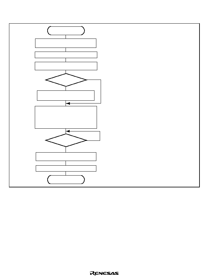
Rev. 2.00, 09/03, page 424 of 690
d. Simultaneous Serial Data Transmission and Reception
Figure 16.16 shows sample flowcharts for simultaneous serial transmission and reception.
No
Yes
No
Yes
[1] Set the receive trigger number
in
SCFCR.
[2] Write the remaining transmit data
to SCFTDR, and if there is receive
data in the FIFO, read receive data
until there is less than the receive
trigger setting number, read the
TDFE and RDF bits in SCSSR, and
if 1, clear to 0.
[3] Transmission/reception is started
when the TE and RE bits in SCSCR
are set to 1. The TE and RE bits
must be set simultaneously.
[4] After the end of transmission/reception,
clear the TE and RE bits to 0.
Start of simultaneous
transmission/reception
Set receive trigger number in RTRG1
and RTRG0 in SCFCR
Write remaining transmit data to SCFTDR
Read TDFE and RDF bits in SCSSR
TDFE =1?
RDF =1?
Write 0 to TDFE and RDF bits in
SCSSR after reading 1 from them
Set TE and RE bits in SCSCR
simultaneously
When using transmit FIFO data interrupt,
set TIE bit to 1
When using receive FIFO data interrupt,
set RIE bit to 1
TDFE =1?
RDF =1?
Read receive trigger number of receive
data bytes from SCFRDR
Clear TE and RE bits in SCSCR to 0
End of
transmission/reception
[2]
[1]
[3]
[4]
Figure 16.16 Sample Simultaneous Serial Transmission and Reception Flowchart (1)
(First Transfer after Initialization)
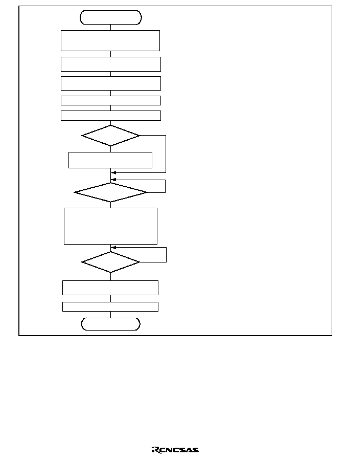
Rev. 2.00, 09/03, page 425 of 690
No
Yes
Yes
No
Yes
No
Wait
[1] Set the receive trigger number and
transmit trigger number in SCFCR.
[2] Reset the receive FIFO and transmit
FIFO.
[3] Write transmit data to SCFTDR, and
if there is receive data in the FIFO,
read receive data until there is less
than the receive trigger setting number,
read the TDFE and RDF bits in SCSSR,
and if 1, clear to 0.
[4] Wait for one bit interval.
[5] Transmission/reception is started when
the TE and RE bits in SCSCR are set
to 1. The TE and RE bits must be set
simultaneously.
[6] After the end of transmission/reception,
clear the TE and RE bits to 0.
Start of simultaneous
transmission/reception
Set receive trigger number in RTRG1
and RTRG0 in SCFCR, and set transmit
trigger number in TTRG1 and TTRG0
Set TFRST and RFRST bits in
SCFCR to 1
Clear TFRST and RFRST bits in
SCFCR to 0
Write transmit data to SCFTDR
Read TDFE and RDF bits in SCSSR
TDFE =1?
RDF =1?
Write 0 to TDFE and RDF bits in
SCSSR after reading 1 from them
1-bit interval elapsed?
Set TE and RE bits in SCSCR
simultaneously
When using transmit FIFO data
interrupt, set TIE bit to 1
When using receive FIFO data
interrupt, set RIE bit to 1
TDFE =1?
RDF =1?
Read receive trigger number of
receive data bytes from SCFRDR
End of
transmission/reception
Clear TE and RE bits in SCSCR to 0
[1]
[2]
[3]
[4]
[5]
[6]
Figure 16.16 Sample Simultaneous Serial Transmission and Reception Flowchart (2)
(Second and Subsequent Transfer)

Rev. 2.00, 09/03, page 426 of 690
16.5
SCIF Interrupt Sources and DMAC
The SCIF supports six interrupts in asynchronous mode--transmit-FIFO-data-empty (TXI),
transmit-data-stop (TDI), receive-error (ERI), receive-FIFO-data-full (RXI), break-receive (BRI),
and receive-data-ready (DRI). The vectors of transmit-data-stop and transmit-FIFO-data-empty
interrupts are the same. The vectors of receive-error and break-receive interrupts are the same. The
vectors of receive-FIFO-data-full and receive-data-ready interrupts are the same.
In clock synchronous mode, the SCIF supports two interrupts--transmit-FIFO-data-empty (TXI)
and receive-FIFO-data-full (RXI).
Table 16.4 shows the interrupt sources. The interrupt sources can be enabled or disabled by means
of the TIE, RIE, ERIE, BRIE, DRIE, and TSIE bits in SCSCR.
When the TDFE flag in SCSSR is set to 1, a TXI interrupt request is generated. When the TSF
flag in SCSSR is set to 1, a TDI interrupt request is generated. The DMAC can be activated and
data transfer performed on generation of TXI and TDI interrupt requests. The DMAC requests of
TXI and TDI are assigned to the same vector.
When the RDF flag in SCSSR is set to 1, an RXI interrupt request is generated. The DMAC can
be activated and data transfer performed on generation of an RXI interrupt request.
When using the DMAC for transmission/reception, set and enable the DMAC before making SCIF
settings. See section 8, Direct Memory Access Controller (DMAC), for details of the DMAC
setting procedure.
When the ER flag in SCSSR is set to 1, an ERI interrupt request is generated. When the BRK flag
in SCSSR is set to 1, a BRI interrupt request is generated. When the DR flag in SCSSR is set to 1,
a DRI interrupt request is generated. When the TSF flag in SCSSR is set to 1, a TDI interrupt
request is generated.
The vectors of TXI and TDI, ERI and BRI, and RXI and DRI are the same.
The DMAC activation and interrupts cannot be generated simultaneously by the same source. The
following procedure should be used for the DMAC activation.
1.
Set the interrupt enable bits (TIE and RIE) corresponding to the generated source to 1.
2.
Mask the corresponding interrupt requests by using the interrupt mask register of the interrupt
controller.

Rev. 2.00, 09/03, page 427 of 690
Table 16.4
SCIF Interrupt Sources
Interrupt Source
Description
DMAC Activation
ERI
Interrupt initiated by receive error flag (ER) or break
flag (BRK)
Not possible
RXI
Interrupt initiated by receive FIFO data full flag (RDF)
or receive data ready (DR)
Possible
*
1
TXI
Interrupt initiated by transmit FIFO data
empty flag (TDFE) or transmit data stop flag (TSF)
Possible
*
2
Notes: 1. The DMAC can be activated only by a receive-FIFO-data-full interrupt request.
2. The DMAC can be activated by a transmit-FIFO-data-empty (TDFE) or transmit-data-
stop (TSF) interrupt request. When the DMAC is activated by the TSF interrupt, it is
cleared by either of two cases listed below.
(1) The TSF flag is read by the CPU.
(2) The transmit FIFO is full.
See section 5, Exception Handling, for priorities and the relationship with non-SCIF interrupts.

Rev. 2.00, 09/03, page 428 of 690
16.6
Notes on Usage
Note the following when using the SCIF.
a. SCFTDR Writing and the TDFE Flag:
The TDFE flag in the serial status register (SCSSR) is set when the number of transmit data bytes
written in the transmit FIFO data register (SCFTDR) has fallen to or below the transmit trigger
number set by bits TTRG1 and TTRG0 in the FIFO control register (SCFCR). After TDFE is set,
transmit data up to the number of empty bytes in SCFTDR can be written, allowing efficient
continuous transmission.
However, if the number of data bytes written in SCFTDR is equal to or less than the transmit
trigger number, the TDFE flag will be set to 1 again after being read as 1 and cleared to 0. TDFE
clearing should therefore be carried out when SCFTDR contains more than the transmit trigger
number of transmit data bytes.
The number of transmit data bytes in SCFTDR can be found from the 14 to 8 bits of the FIFO data
count register (SCFDR).
b. SCFRDR Reading and the RDF Flag:
The RDF flag in the serial status register (SCSSR) is set when the number of receive data bytes in
the receive FIFO data register (SCFRDR) has become equal to or greater than the receive trigger
number set by bits RTRG1 and RTRG0 in the FIFO control register (SCFCR). After RDF is set,
receive data equivalent to the trigger number can be read from SCFRDR, allowing efficient
continuous reception.
However, if the number of data bytes in SCFRDR is still equal to or greater than the trigger
number after a read, the RDF flag will be set to 1 again if it is cleared to 0. RDF should therefore
be cleared to 0 after being read as 1 after all receive data has been read.
The number of receive data bytes in SCFRDR can be found from the 6 to 0 bits of the FIFO data
count register (SCFDR).
c. Break Detection and Processing:
Break signals can be detected by reading the RxD pin directly when a framing error (FER) is
detected. In the break state the input from the RxD pin consists of all 0s, so the FER flag is set and
the parity error flag (PER) may also be set.
Although the SCIF stops transferring receive data to SCFRDR after receiving a break, the receive
operation continues.

Rev. 2.00, 09/03, page 429 of 690
d. Receive Data Sampling Timing and Receive Margin:
As an example, when the sampling rate is 1/16, the SCIF operates on a base clock with a
frequency of 8 times the transfer rate.
In reception, the SCIF synchronizes internally with the fall of the start bit, which it samples on the
base clock. Receive data is latched at the rising edge of the fourth base clock pulse.
The receive margin can therefore be expressed as shown in equation (1).
M = 0.5 -
1
2N
D - 0.5
N
- (L - 0.5)F - (1 + F) ◊ 100%
..........................
(1)
M:
Receive margin (%)
N:
Ratio of clock frequency to bit rate (N = 16)
D:
Clock duty cycle (D = 0 to 1.0)
L:
Frame length (L = 9 to 12)
F:
Absolute deviation of clock frequency
From equation (1), if F = 0 and D = 0.5, the receive margin is 46.875%, as given by equation (2).
When D = 0.5 and F = 0:
M = (0.5 ≠ 1/(2
◊
16))
◊
100% = 46.875% ........................................... (2)
This is a theoretical value. A reasonable margin to allow in system designs is 20% to 30%.

Rev. 2.00, 09/03, page 430 of 690
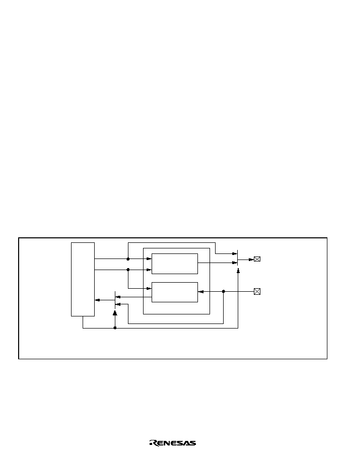
IFIRDA0A_000020020100
Rev. 2.00, 09/03, page 431 of 690
Section 17 Infrared Data Association Module (IrDA)
This LSI has an on-chip Infrared Data Association (IrDA) interface that is based on the IrDA 1.0
system and can perform infrared communication.
The IrDA is an optional module used for modulation and demodulation of signals for the SCIF
module, and it must always be used together with the SCIF module.
17.1
Features
∑
Conforms to the IrDA 1.0 system
∑
Asynchronous serial communication
Data length: 8 bits
Stop bit length: 1 bit
Parity bit: None
∑
On-chip 64-stage FIFO buffers for both transmit and receive operations
∑
On-chip baud rate generator with selectable bit rates
∑
Guard functions to protect the receiver during transmission
∑
Clock supply halted to reduce power consumption when not using the IrDA interface
Figure 17.1 shows a block diagram of the IrDA.
SCIF
TxD
Transfer clock
RxD
Switching IrDA/SCIF
IrDA
IrTx
IrRx
Modulation unit
Demodulation unit
Legend
SCIF: Serial communication interface with FIFO
Figure 17.1 Block Diagram of IrDA

Rev. 2.00, 09/03, page 432 of 690
17.2
Input/Output Pins
Table 17.1 shows the IrDA pin configuration.
Table 17.1
Pin Configuration
Pin Name
Signal Name
I/O
Function
Receive data pin
IrRx
Input
Receive data input
Transmit data pin
IrTx
Output
Transmit data output
Note:
Clock input from the serial clock pin cannot be set in IrDA mode.
17.3
Register Description
The IrDA has the following internal registers. For details on register addresses and register states
in each processing state, refer to section 24, List of Registers.
∑
IrDA mode register (SCSMR_Ir)
17.3.1
IrDA Mode Register (SCSMR_Ir)
SCSMR_Ir is a 16-bit register that selects IrDA or SCIF mode and selects the IrDA output pulse
width.
This module operates as IrDA when the IRMOD bit is set to 1. When the IRMOD bit is cleared to
0, this module can also operate as an SCIF.

Rev. 2.00, 09/03, page 433 of 690
Bit
Bit Name
Initial Value
R/W
Description
15 to 8
0
R
Reserved
These bits are always read as 0. The write
value should always be 0.
7
IRMOD
0
R/W
IrDA Mode
Selects whether this module operates as an
IrDA serial communication interface or as an
SCIF.
0: Operates as an SCIF
1: Operates as an IrDA
6 to 3
ICK3 to ICK0
0
R/W
Output Pulse Division Ratio
Specifies the ratio for dividing the peripheral
clock (P
) to generate the IRCLK clock pulse
to be used for IrDA. IRCLK is obtained as
follows:
IRCLK = 1/(2N + 2)
◊
P
N = Value set by ICK3 to ICK0
2
PSEL
0
R/W
Output Pulse Width Select
PSEL selects an IrDA output pulse width that
is 3/16 of the bit length for 115 kbps or 3/16 of
the bit length for the selected baud rate.
0: Pulse width is 3/16 of the bit length
1: Pulse width is 3/16 of 115 kbps bit length for
the baud rate selected by ICK3 to ICK0
1, 0
0
R
Reserved
These bits are always read as 0. The write
value should always be 0.
Example:
P
clock: 14.7456 MHz
IRCLK: 921.6 kHz (fixed)
N: Setting of ICK3 to ICK0 (0
N
15)
≠ 1 7
N
P
2◊IRCLK
Accordingly, N is 7.

Rev. 2.00, 09/03, page 434 of 690
17.4
Operation
The IrDA module can perform infrared communication conforming to IrDA 1.0 by connecting
infrared transmit/receive units. The serial communication interface unit includes a buffer in the
transmit unit and the receive unit, allowing CPU overhead to be reduced and continuous high-
speed communication to be performed.
17.4.1
Overview
The IrDA module modifies IrTx/IrRx transmit/receive data waveforms to satisfy the IrDA 1.0
specification for infrared communication.
In the IrDA 1.0 specification, communication is first performed at a speed of 9600 bps, and the
communication speed is changed. However, the communication rate cannot be automatically
changed in this module, so the communication speed should be confirmed, and the appropriate
speed set for this module by software.
17.4.2
Transmitting
The waveforms of a serial output signal (UART frame) from the SCIF are modified and the signal
is converted into the IR frame serial output signal by the IrDA module, as shown in figure 17.2.
When serial data is 0, a pulse of 3/16 the IR frame bit width is generated and output. When serial
data is 1, no pulse is output.
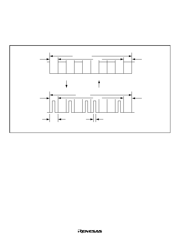
Rev. 2.00, 09/03, page 435 of 690
17.4.3
Receiving
Received 3/16 IR frame bit-width pulses are demodulated and converted to a UART frame, as
shown in figure 17.2.
Demodulation to 0 is performed for pulse output, and demodulation to 1 is performed for no pulse
output.
0
1
0
1
0
0
1
1
0
1
0
1
0
1
0
0
1
1
0
1
UART frame
Start bit
IR frame
Start bit
Bit cycle
3/16-bit cycle
pulse width
UART frame
Data
IR frame
Data
Receive
Transmit
Stop bit
Stop bit
Figure 17.2 Transmit/Receive Operation
17.4.4
Data Format Specification
The data format of UART frames used for IrDA communication must be specified by the SCIF0
registers. The UART frame has eight data bits, no parity bit, and one stop bit.
IrDA communication is performed in asynchronous mode, and this mode must also be specified
by the SCIF0 registers. The sampling rate must be set to 1/16.
The internal clock must be selected for the SCIF0 operation clock and the SCK0 pin must be
specified for the synchronizing clock output pin.
The IrDA communication rate is the same as the SCIF0 bit rate, which is specified by the SCIF0
registers.
For details on SCIF0 registers, refer to section 16, Serial Communication Interface with FIFO
(SCIF).

Rev. 2.00, 09/03, page 436 of 690

IFUSB40A_000020020100
Rev. 2.00, 09/03, page 437 of 690
Section 18 USB Function Module
This LSI incorporates a USB function module (USB).
18.1
Features
∑
The UDC (USB device controller) conforming to USB2.0 and transceiver process USB
protocol automatically.
Automatic processing of USB standard commands for endpoint 0 (some commands and
class/vendor commands require decoding and processing by firmware)
∑
Transfer speed: Full-speed
∑
Endpoint configuration:
Endpoint
Name
Abbreviation Transfer Type
Maximum
Packet Size
FIFO Buffer
Capacity (Byte)
DMA Transfer
Endpoint 0
EP0s
Setup
8
8
--
EP0i
Control-in
8
8
--
EP0o
Control-out
8
8
--
Endpoint 1
EP1
Bulk-out
64
128
Possible
Endpoint 2
EP2
Bulk-in
64
128
Possible
Endpoint 3
EP3
Interrupt
8
8
--
Configuration 1
Interface 0
Alternate Setting 0
Endpoint 1
Endpoint 2
Endpoint 3
∑
Interrupt requests: Generates various interrupt signals necessary for USB
transmission/reception
∑
Clock: External input (48 MHz) (Refer to section 9.4.1, Frequency Control Register (FRQCR),
and section 9.4.2, USB Clock Frequency Control Register (UCLKCR))
∑
Power-down mode
Power consumption can be reduced by stopping UDC internal clock when USB cable is
disconnected
Automatic transition to/recovery from suspend state
∑
Can be connected to a Philips PDIUSBP11 Series transceiver or compatible product in internal
transceiver bypass mode (the XVEROFF bit in XVERCR is set to 1)
When using a compatible product, carry out evaluation and investigation with the
manufacturer supplying the transceiver beforehand.
∑
Power mode: Self-powered
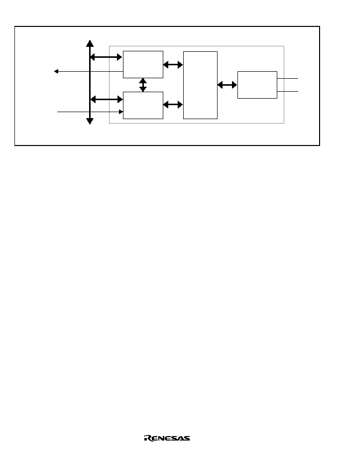
Rev. 2.00, 09/03, page 438 of 690
Figure 18.1 shows the block diagram of the USB.
Peripheral bus
Interrupt requests
DMA transfer requests
Status and
control registers
FIFO
UDC
Transceiver
USB function module
D+
D-
Clock (48 MHz)
UDC: USB device controller
Legend:
Figure 18.1 Block Diagram of USB

Rev. 2.00, 09/03, page 439 of 690
18.2
Input/Output Pins
Table 18.1 shows the USB pin configuration.
Table 18.1
Pin Configuration
Pin Name
I/O
Function
XVEROFF
Condition
XVDATA
Input
Input pin for receive data from differential receiver 1
DPLS
Input
Input pin to driver for D
+
signal from receiver
1
DMNS
Input
Input pin to driver for D≠ signal from receiver
1
TXDPLS
Output
D+ transmit output pin to driver
1
TXDMNS
Output
D- transmit output pin to driver
1
TXENL
Output
Driver output enable pin
1
VBUS
Input
USB cable connection monitor pin
1 or 0
SUSPND
Output
Transceiver suspend state output pin
1
EXTAL_USB
Input
USB clock input pin (external clock input/crystal
resonator connect)
XTAL_USB
Output
USB clock pin (crystal resonator connect)
D+
I/O
USB internal transceiver D
+
D-
I/O
USB internal transceiver D≠
Vcc-USB
Input
Power supply for USB
Vss-USB
Input
Ground for USB
Note:
The USB can be connected to a Philips PDIUSBP11 Series transceiver or compatible
product in internal transceiver bypass mode (the XVEROFF bit in XVERCR is set to 1).
When using a compatible product, carry out evaluation and investigation with the
manufacturer supplying the transceiver beforehand.

Rev. 2.00, 09/03, page 440 of 690
18.3
Register Descriptions
The USB has following registers. For the information on the addresses of these registers and the
state of the register in each processing condition, see section 24, List of Registers.
∑
Interrupt flag register 0 (IFR0)
∑
Interrupt flag register 1 (IFR1)
∑
Interrupt select register 0 (ISR0)
∑
Interrupt select register 1 (ISR1)
∑
Interrupt enable register 0 (IER0)
∑
Interrupt enable register 1 (IER1)
∑
EP0i data register (EPDR0i)
∑
EP0o data register (EPDR0o)
∑
EP0s data register (EPDR0s)
∑
EP1 data register (EPDR1)
∑
EP2 data register (EPDR2)
∑
EP3 data register (EPDR3)
∑
EP0o receive data size register (EPSZ0o)
∑
EP1 receive data size register (EPSZ1)
∑
Trigger register (TRG)
∑
Data status register (DASTS)
∑
FIFO clear register (FCLR)
∑
DMA transfer setting register (DMAR)
∑
Endpoint stall register (EPSTL)
∑
Transceiver control register (XVERCR)

Rev. 2.00, 09/03, page 441 of 690
18.3.1
Interrupt Flag Register 0 (IFR0)
IFR0, together with interrupt flag register 1 (IFR1), indicates interrupt status information required
by the application. When an interrupt source is generated, the corresponding bit is set to 1 and an
interrupt request is sent to the CPU according to the combination with interrupt enable register 0
(IER0). Clearing is performed by writing 0 to the bit to be cleared, and 1 to the other bits.
However, EP1FULL and EP2EMPTY are status bits, and cannot be cleared.
Bit
Bit Name
Initial
Value
R/W
Description
7
BRST
0
R/W
Bus Reset
This bit is set to 1 when a bus reset signal is detected on
the USB bus.
6
EP1FULL
0
R
EP1 FIFO Full
This bit is set when endpoint 1 receives one packet of
data successfully from the host, and holds a value of 1 as
long as there is valid data in the FIFO buffer.
This is a status bit, and cannot be cleared.
5
EP2TR
0
R/W
EP2 Transfer Request
This bit is set if there is no valid transmit data in the FIFO
buffer when an IN token for endpoint 2 is received from
the host. A NACK handshake is returned to the host until
data is written to the FIFO buffer and packet transmission
is enabled.
4
EP2EMPTY
1
R
EP2 FIFO Empty
This bit is set when at least one of the dual endpoint 2
transmit FIFO buffers is ready for transmit data to be
written.
This is a status bit, and cannot be cleared.
3
SETUPTS
0
R/W
Setup Command Receive Complete
This bit is set to 1 when endpoint 0 receives successfully
a setup command requiring decoding on the application
side, and returns an ACK handshake to the host.
2
EP0oTS
0
R/W
EP0o Receive Complete
This bit is set to 1 when endpoint 0 receives data from the
host successfully, stores the data in the FIFO buffer, and
returns an ACK handshake to the host.

Rev. 2.00, 09/03, page 442 of 690
Bit
Bit Name
Initial
Value
R/W
Description
1
EP0iTR
0
R/W
EP0i Transfer Request
This bit is set if there is no valid transmit data in the FIFO
buffer when an IN token for endpoint 0 is received from
the host. A NACK handshake is returned to the host until
data is written to the FIFO buffer and packet transmission
is enabled.
0
EP0iTS
0
R/W
EP0i Transmit Complete
This bit is set when data is transmitted to the host from
endpoint 0 and an ACK handshake is returned.
18.3.2
Interrupt Flag Register 1 (IFR1)
IFR1, together with interrupt flag register 0 (IFR0), indicates interrupt status information required
by the application. When an interrupt source is generated, the corresponding bit is set to 1 and an
interrupt request is sent to the CPU according to the combination with interrupt enable register 1
(IER1). Clearing is performed by writing 0 to the bit to be cleared, and 1 to the other bits.
Bit
Bit Name
Initial
Value
R/W
Description
7 to 4
0
R
Reserved
These bits are always read as 0. The write value should
always be 0.
3
VBUSMN
0
R
This is a status bit which monitors the state of the VBUS
pin. This bit reflects the state of the VBUS pin.
2
EP3TR
0
R/W
EP3 Transfer Request
This bit is set if there is no valid transmit data in the FIFO
buffer when an IN token for endpoint 3 is received from
the host. A NACK handshake is returned to the host until
data is written to the FIFO buffer and packet transmission
is enabled.
1
EP3TS
0
R/W
EP3 Transmit Complete
This bit is set when data is transmitted to the host from
endpoint 3 and an ACK handshake is returned.
0
VBUS
0
R/W
USB Disconnection Detection
When the function is connected to the USB bus or
disconnected from it, this bit is set to 1. The VBUS pin of
this module is used for detecting connection or
disconnection.

Rev. 2.00, 09/03, page 443 of 690
18.3.3
Interrupt Select Register 0 (ISR0)
ISR0 selects the vector numbers of the interrupt requests indicated in interrupt flag register 0
(IFR0). If the USB issues an interrupt request to the INTC when a bit in ISR0 is cleared to 0, the
interrupt corresponding to the bit will be USI0 (USB interrupt 0). If the USB issues an interrupt
request to the INTC when a bit in ISR0 is set to 1, the corresponding interrupt will be USI1 (USB
interrupt 1). If interrupts occur simultaneously, USI0 has priority by default.
Bit
Bit Name
Initial Value R/W
Description
7
BRST
0
R/W
Bus Reset
6
EP1FULL
0
R/W
EP1 FIFO Full
5
EP2TR
0
R/W
EP2 Transfer Request
4
EP2EMPTY
0
R/W
EP2 FIFO Empty
3
SETUPTS
0
R/W
Setup Command Receive Complete
2
EP0oTS
0
R/W
EP0o Receive Complete
1
EP0iTR
0
R/W
EP0i Transfer Request
0
EP0iTS
0
R/W
EP0i Transmit Complete
18.3.4
Interrupt Select Register 1 (ISR1)
ISR1 selects the vector numbers of the interrupt requests indicated in interrupt flag register 1
(IFR1). If the USB issues an interrupt request to the INTC when a bit in ISR1 is cleared to 0, the
interrupt corresponding to the bit will be USI0 (USB interrupt 0). If the USB issues an interrupt
request to the INTC when a bit in ISR1 is set to 1, the corresponding interrupt will be USI1 (USB
interrupt 1). If interrupts occur simultaneously, USI0 has priority by default.
Bit
Bit Name
Initial Value
R/W
Description
7 to 3
0
R
Reserved
These bits are always read as 0. The write value
should always be 0.
2
EP3TR
1
R/W
EP3 Transfer Request
1
EP3TS
1
R/W
EP3 Transmit Complete
0
VBUS
1
R/W
USB Bus Connect

Rev. 2.00, 09/03, page 444 of 690
18.3.5
Interrupt Enable Register 0 (IER0)
IER0 enables the interrupt requests of interrupt flag register 0 (IFR0). When an interrupt flag is set
to 1 while the corresponding bit of each interrupt is set to 1, an interrupt request is sent to the
CPU. The interrupt vector number is determined by the contents of interrupt select register 0
(ISR0).
Bit
Bit Name
Initial Value
R/W
Description
7
BRST
0
R/W
Bus Reset
6
EP1FULL
0
R/W
EP1 FIFO Full
5
EP2TR
0
R/W
EP2 Transfer Request
4
EP2EMPTY
1
R/W
EP2 FIFO Empty
3
SETUPTS
0
R/W
Setup Command Receive Complete
2
EP0oTS
0
R/W
EP0o Receive Complete
1
EP0iTR
0
R/W
EP0i Transfer Request
0
EP0iTS
0
R/W
EP0i Transmit Complete
18.3.6
Interrupt Enable Register 1 (IER1)
IER1 enables the interrupt requests of interrupt flag register 1 (IFR1). When an interrupt flag is set
to 1 while the corresponding bit of each interrupt is set to 1, an interrupt request is sent to the
CPU. The interrupt vector number is determined by the contents of interrupt select register 1
(ISR1).
Bit
Bit Name
Initial Value R/W
Description
7 to 3
0
R
Reserved
These bits are always read as 0. The write value
should always be 0.
2
EP3TR
0
R/W
EP3 Transfer Request
1
EP3TS
0
R/W
EP3 Transmit Complete
0
VBUS
0
R/W
USB Bus Connect

Rev. 2.00, 09/03, page 445 of 690
18.3.7
EP0i Data Register (EPDR0i)
EPDR0i is an 8-byte transmit FIFO buffer for endpoint 0. EPDR0i holds one packet of transmit
data for control-in. Transmit data is fixed by writing one packet of data and setting EP0iPKTE in
the trigger register. When an ACK handshake is returned from the host after the data has been
transmitted, EP0iTS in interrupt flag register 0 is set. This FIFO buffer can be initialized by means
of EP0iCLR in the FCLR register.
Bit
Bit Name
Initial Value
R/W
Description
7 to 0
D7 to D0
Undefined
W
Data register for control-in transfer
18.3.8
EP0o Data Register (EPDR0o)
EPDR0o is an 8-byte receive FIFO buffer for endpoint 0. EPDR0o holds endpoint 0 receive data
other than setup commands. When data is received successfully, EP0oTS in interrupt flag register
0 is set, and the number of receive bytes is indicated in the EP0o receive data size register. After
the data has been read, setting EP0oRDFN in the trigger register enables the next packet to be
received. This FIFO buffer can be initialized by means of BP0oCLR in the FCLR register.
Bit
Bit Name
Initial Value
R/W
Description
7 to 0
D7 to D0
Undefined
R
Data register for control-out transfer
18.3.9
EP0s Data Register (EPDR0s)
EPDR0s is an 8-byte FIFO buffer specifically for receiving endpoint 0 setup commands. Only the
setup command to be processed by the application is received. When command data is received
successfully, the SETUPTS bit in interrupt flag register 0 is set.
As a latest setup command must be received in high priority, if data is left in this buffer, it will be
overwritten with new data. If reception of the next command is started while the current command
is being read, command reception has priority, the read by the application is forcibly stopped, and
the read data is invalid.
Bit
Bit Name
Initial Value
R/W
Description
7 to 0
D7 to D0
Undefined
R
Data register for storing the setup command at
the control-out transfer

Rev. 2.00, 09/03, page 446 of 690
18.3.10
EP1 Data Register (EPDR1)
EPDR1 is a 128-byte receive FIFO buffer for endpoint 1. EPDR1 has a dual-buffer configuration,
and has a capacity of twice the maximum packet size. When one packet of data is received
successfully, EP1FULL in interrupt flag register 0 is set, and the number of receive bytes is
indicated in the EP1 receive data size register. After the data has been read, the buffer that was
read is enabled to receive data again by writing 1 to the EP1RDFN bit in the trigger register. The
receive data in this FIFO buffer can be transferred by DMA. This FIFO buffer can be initialized by
means of EP1CLR in the FCLR register.
Bit
Bit Name
Initial Value
R/W
Description
7 to 0
D7 to D0
Undefined
R
Data register for endpoint 1 transfer
18.3.11
EP2 Data Register (EPDR2)
EPDR2 is a 128-byte transmit FIFO buffer for endpoint 2. EPDR2 has a dual-buffer configuration,
and has a capacity of twice the maximum packet size. When transmit data is written to this FIFO
buffer and EP2PKTE in the trigger register is set, one packet of transmit data is fixed, and the
dual-FIFO buffer is switched over. The transmit data for this FIFO buffer can be transferred by
DMA. This FIFO buffer can be initialized by means of EP2CLR in the FCLR register.
Bit
Bit Name
Initial Value
R/W
Description
7 to 0
D7 to D0
Undefined
W
Data register for endpoint 2 transfer
18.3.12
EP3 Data Register (EPDR3)
EPDR3 is an 8-byte transmit FIFO buffer for endpoint 3. EPDR3 holds one packet of transmit data
for the interrupt transfer of endpoint 3. Transmit data is fixed by writing one packet of data and
setting EP3PKTE in the trigger register. When an ACK handshake is returned from the host after
one packet of data has been transmitted successfully, EP3TS in interrupt flag register 0 is set. This
FIFO buffer can be initialized by means of EP3CLR in the FCLR register.
Bit
Bit Name
Initial Value
R/W
Description
7 to 0
D7 to D0
Undefined
R
Data register for endpoint 3 transfer

Rev. 2.00, 09/03, page 447 of 690
18.3.13
EP0o Receive Data Size Register (EPSZ0o)
EPSZ0o indicates the number of bytes received at endpoint 0 from the host.
Bit
Bit Name
Initial Value
R/W
Description
7 to 0
--
0
R
Number of receive data for endpoint 0
18.3.14
EP1 Receive Data Size Register (EPSZ1)
EPSZ1 is a receive data size resister for endpoint 1. EPSZ1 indicates the number of bytes received
from the host. The FIFO for endpoint 1 has a dual-buffer configuration. The size of the received
data indicated by this register is the size of the currently selected side (can be read by CPU).
Bit
Bit Name
Initial Value
R/W
Description
7 to 0
--
0
R
Number of received bytes for endpoint 1

Rev. 2.00, 09/03, page 448 of 690
18.3.15
Trigger Register (TRG)
TRG generates one-shot triggers to control the transfer sequence for each endpoint.
Bit
Bit Name
Initial Value
R/W
Description
7
Undefined
Reserved
The write value should always be 0.
6
EP3PKTE
Undefined
W
EP3 Packet Enable
After one packet of data has been written to the
endpoint 3 transmit FIFO buffer, the transmit data is
fixed by writing 1 to this bit.
5
EP1RDFN
Undefined
W
EP1 Read Complete
Write 1 to this bit after one packet of data has been
read from the endpoint 1 FIFO buffer. The endpoint
1 receive FIFO buffer has a dual-buffer
configuration. Writing 1 to this bit initializes the FIFO
that was read, enabling the next packet to be
received.
4
EP2PKTE
Undefined
W
EP2 Packet Enable
After one packet of data has been written to the
endpoint 2 transmit FIFO buffer, the transmit data is
fixed by writing 1 to this bit.
3
Undefined
Reserved
The write value should always be 0.
2
EP0sRDFN
Undefined
W
EP0s Read Complete
Write 1 to this bit after data for the EP0s command
FIFO has been read. Writing 1 to this bit enables
transfer of data in the following data stage. A NACK
handshake is returned in response to transfer
requests from the host in the data stage until 1 is
written to this bit.
1
EP0oRDFN
Undefined
W
EP0o Read Complete
Writing 1 to this bit after one packet of data has
been read from the endpoint 0 transmit FIFO buffer
initializes the FIFO buffer, enabling the next packet
to be received.
0
EP0iPKTE
Undefined
W
EP0i Packet Enable
After one packet of data has been written to the
endpoint 0 transmit FIFO buffer, the transmit data is
fixed by writing 1 to this bit.

Rev. 2.00, 09/03, page 449 of 690
18.3.16
Data Status Register (DASTS)
DASTS indicates whether the transmit FIFO buffers contain valid data. A bit is set when data is
written to the corresponding FIFO buffer and the packet enable state is set, and cleared when all
data has been transmitted to the host.
Bit
Bit Name
Initial Value
R/W
Description
7, 6
0
R
Reserved
This bit is always read as 0.
5
EP3DE
0
R
EP3 Data Present
This bit is set when the endpoint 3 FIFO buffer
contains valid data.
4
EP2DE
0
R
EP2 Data Present
This bit is set when the endpoint 2 FIFO buffer
contains valid data.
3 to 1
0
R
Reserved
This bit is always read as 0.
0
EP0iDE
0
R
EP0i Data Present
This bit is set when the endpoint 0 FIFO buffer
contains valid data.
18.3.17
FIFO Clear Register (FCLR)
FCLR is a register to initialize the FIFO buffers for each endpoint. Writing 1 to a bit clears all the
data in the corresponding FIFO buffer. Note that the corresponding interrupt flag is not cleared.
Do not clear a FIFO buffer during transfer.
Bit
Bit Name
Initial Value
R/W
Description
7
Undefined
Reserved
The write value should always be 0.
6
EP3CLR
Undefined
W
EP3 Clear
Writing 1 to this bit initializes the endpoint 3 transmit
FIFO buffer.
5
EP1CLR
Undefined
W
EP1 Clear
Writing 1 to this bit initializes both sides of the
endpoint 1 receive FIFO buffer.

Rev. 2.00, 09/03, page 450 of 690
Bit
Bit Name
Initial Value
R/W
Description
4
EP2CLR
Undefined
W
EP2 Clear
Writing 1 to this bit initializes both sides of the
endpoint 2 transmit FIFO buffer.
3, 2
Undefined
Reserved
The write value should always be 0.
1
EP0oCLR
Undefined
W
EP0o Clear
Writing 1 to this bit initializes the endpoint 0 receive
FIFO buffer.
0
EP0iCLR
Undefined
W
EP0i Clear
Writing 1 to this bit initializes the endpoint 0 transmit
FIFO buffer.
18.3.18
DMA Transfer Setting Register (DMAR)
DMA transfer can be carried out between the endpoint 1 and 2 data registers and memory by
means of the on-chip direct memory access controller (DMA). Dual address transfer is performed
in bytes. To start DMA transfer, DMAC settings must be made in addition to the settings in this
register.
Bit
Bit Name
Initial Value R/W
Description
7 to 2
0
R
Reserved
These bits are always read as 0. The write value should
always be 0.

Rev. 2.00, 09/03, page 451 of 690
Bit
Bit Name
Initial Value R/W
Description
1
EP2DMAE
0
R/W
Endpoint 2 DMA Transfer Enable
When this bit is set, DMA transfer is enabled from
memory to the endpoint 2 transmit FIFO buffer. If there is
at least one byte of space in the FIFO buffer, a transfer
request is asserted for the DMAC. In DMA transfer, when
64 bytes are written to the FIFO buffer the EP2 packet
enable bit is set automatically, allowing 64 bytes of data
to be transferred, and if there is still space in the other of
the two FIFOs, a transfer request is asserted for the
DMAC again. However, if the size of the data packet to
be transmitted is less than 64 bytes, the EP2 packet
enable bit is not set automatically, and so should be set
by the CPU with a DMA transfer end interrupt.
As EP2-related interrupt requests to the CPU are not
automatically masked, interrupt requests should be
masked as necessary in the interrupt enable register.
∑
Operating procedure
1. Write of 1 to the EP2 DMAE bit in DMAR
2. Transfer count setting in the DMAC
3. DMAC activation
4. DMA transfer
5. DMA transfer end interrupt generated
Refer to section 18.7.3, DMA Transfer for Endpoint 2.

Rev. 2.00, 09/03, page 452 of 690
Bit
Bit Name
Initial Value R/W
Description
0
EP1DMAE
0
R/W
Endpoint 1 DMA Transfer Enable
When this bit is set, DMA transfer is enabled from the
endpoint 1 receive FIFO buffer to memory. If there is at
least one byte of receive data in the FIFO buffer, a
transfer request is asserted for the DMAC. In DMA
transfer, when all the received data is read, EP1 is read
automatically and the completion trigger operates.
EP1-related interrupt requests to the CPU are not
automatically masked.
∑
Operating procedure:
1. Write of 1 to the EP1 DMAE bit in DMAR
2. Transfer count setting in the DMAC
3. DMAC activation
4. DMA transfer
5. DMA transfer end interrupt generated
Refer to section 18.7.2, DMA Transfer for Endpoint 1.

Rev. 2.00, 09/03, page 453 of 690
18.3.19
Endpoint Stall Register (EPSTL)
The bits in EPSTL are used to forcibly stall the endpoints on the application side. While a bit is set
to 1, the corresponding endpoint returns a stall handshake to the host. The stall bit for endpoint 0 is
cleared automatically on reception of 8-byte command data for which decoding is performed by
the function and the EP0 STL bit is cleared. When the SETUPTS flag in the IFR0 register is set to
1, writing 1 to the EP0 STL bit is ignored. For detailed operation, see section 18.6, Stall
Operations.
Bit
Bit Name
Initial Value
R/W
Description
7 to 4
0
R
Reserved
These bits are always read as 0. The write value
should always be 0.
3
EP3STL
0
R/W
EP3 Stall
When this bit is set to 1, endpoint 3 is placed in the
stall state.
2
EP2STL
0
R/W
EP2 Stall
When this bit is set to 1, endpoint 2 is placed in the
stall state.
1
EP1STL
0
R/W
EP1 Stall
When this bit is set to 1, endpoint 1 is placed in the
stall state.
0
EP0STL
0
R/W
EP0 Stall
When this bit is set to 1, endpoint 0 is placed in the
stall state.
18.3.20
Transceiver Control Register (XVERCR)
The Transceiver Control Register sets either the internal transceiver or external transceiver for use.
Bit
Bit Name
Initial Value
R/W
Description
7 to 1
0
R
Reserved
These bits are always read as 0. The write value
should always be 0.
0
XVEROFF
0
R/W
Transceiver Control
1: The internal transceiver function is stopped and a
digital signal for the external transceiver is output
from the port.
0: The internal transceiver is operated.
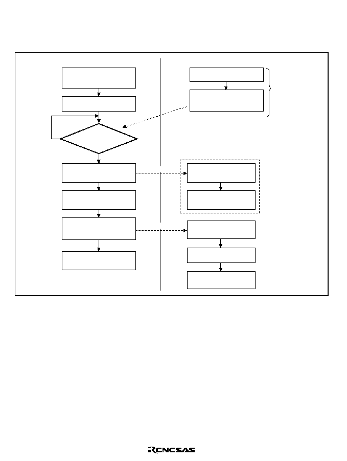
Rev. 2.00, 09/03, page 454 of 690
18.4
Operation
18.4.1
Cable Connection
Cable disconnected
VBUS pin = 0 V
UDC core reset
USB cable connection
IFR1.VBUS = 1
USB bus connection interrupt
UDC core reset release
Bus reset reception
IFR0.BRST = 1
Bus reset interrupt
Wait for setup command
reception complete interrupt
USB function
Application
General output port
D+ pull-up enabled?
USB module interrupt
setting
As soon as preparations are
completed, enable D+ pull-up
in general output port
Clear VBUS flag
(IFR1.VBUS)
Firmware preparations for
start of USB communication
Clear bus reset flag
(IFR0.BRST)
Clear FIFOs
(EP0, EP1, EP2, EP3)
Yes
No
Initial
settings
Wait for setup command
reception complete interrupt
Interrupt request
Interrupt request
Figure 18.2 Cable Connection Operation
The above flowchart shows the operation in the case of in section 18.8, Example of USB External
Circuitry.
In applications that do not require USB cable connection to be detected, processing by the USB
bus connection interrupt is not necessary. Preparations should be made with the bus-reset
interrupt.

Rev. 2.00, 09/03, page 455 of 690
18.4.2
Cable Disconnection
USB function
Application
Cable connected
VBUS pin = 1
USB cable disconnection
VBUS pin = 0
UDC core reset
End
Figure 18.3 Cable Disconnection Operation
The above flowchart shows the operation in section 18.8, Example of USB External Circuitry.
18.4.3
Control Transfer
Control transfer consists of three stages: setup, data (not always included), and status (figure 18.4).
The data stage comprises a number of bus transactions. Operation flowcharts for each stage are
shown below.
Control-in
Setup stage
Data stage
Status stage
Control-out
No data
SETUP(0)
DATA0
SETUP(0)
DATA0
SETUP(0)
DATA0
IN(1)
DATA1
OUT(1)
DATA1
IN(0)
DATA0
OUT(0)
. . .
. . .
DATA0
IN(0/1)
DATA0/1
OUT(0/1)
DATA0/1
OUT(1)
DATA1
IN(1)
DATA1
IN(1)
DATA1
Figure 18.4 Transfer Stages in Control Transfer
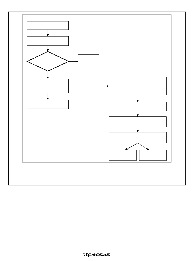
Rev. 2.00, 09/03, page 456 of 690
1. Setup Stage
USB function
Application
SETUP token reception
Receive 8-byte command
data in EP0s
To data stage
Set setup command
reception complete flag
(IFR0.SETUP TS = 1)
Automatic
processing by
this module
Clear SETUP TS flag
(IFR0.SETUP TS = 0)
Clear EP0i FIFO (CLR.EP0iCLR = 1)
Clear EP0o FIFO (CLR.EP0oCLR = 1)
Read 8-byte data from EP0s
Decode command data
Determine data stage direction*
1
Write 1 to EP0s read complete bit
(TRG.EP0s RDFN = 1)
To control-in
data stage
To control-out
data stage
Command
to be processed by
application?
Interrupt request
Yes
No
Notes: 1. In the setup stage, the application analyzes command data from the host requiring processing by
the application, and determines the subsequent processing (for example, data stage direction, etc.).
2. When the transfer direction is control-out, the EP0i transfer request interrupt required in the status
stage should be enabled here. When the transfer direction is control-in, this interrupt is not required
and should be disabled.
*
2
Figure 18.5 Setup Stage Operation
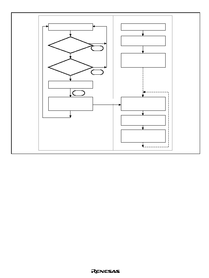
Rev. 2.00, 09/03, page 457 of 690
2. Data Stage (Control-In)
USB function
Application
IN token reception
Data transmission to host
Set EP0i transmission
complete flag
(IFR0.EP0i TS = 1)
From setup stage
Write data to EP0i
data register (EPDR0i)
Write 1 to EP0i packet
enable bit
(TRG.EP0i PKTE = 1)
Clear EP0i transmission
complete flag
(IFR0.EP0i TS = 0)
Write 1 to EP0i packet
enable bit
(TRG.EP0i PKTE = 1)
Write data to EP0i
data register (EPDR0i)
1 written
to TRG.EP0s
RDFN?
Valid data
in EP0i FIFO?
NACK
NACK
No
No
Yes
Yes
ACK
Interrupt request
Figure 18.6 Data Stage (Control-In) Operation
The application first analyzes command data from the host in the setup stage, and determines the
subsequent data stage direction. If the result of command data analysis is that the data stage is in-
transfer, one packet of data to be sent to the host is written to the FIFO. If there is more data to be
sent, this data is written to the FIFO after the data written first has been sent to the host (EP0iTS
bit in IFR0 = 1).
The end of the data stage is identified when the host transmits an OUT token and the status stage
is entered.
Note:
If the size of the data transmitted by the function is smaller than the data size requested by
the host, the function indicates the end of the data stage by returning to the host a packet
shorter than the maximum packet size. If the size of the data transmitted by the function is
an integral multiple of the maximum packet size, the function indicates the end of the data
stage by transmitting a zero-length packet.

Rev. 2.00, 09/03, page 458 of 690
3. Data Stage (Control-Out)
USB function
Application
OUT token reception
Data reception from host
OUT token reception
Set EP0o reception
complete flag
(IFR0.EP0o TS = 1)
Clear EP0o reception
complete flag
(IFR0.EP0o TS = 0)
Read data from EP0o
receive data size register
(EPSZ0o)
Write 1 to EP0o read
complete bit
(TRG.EP0o RDFN = 1)
Read data from EP0o
data register (EPDR0o)
1 written
to TRG.EP0s
RDFN?
1 written
to TRG.EP0o
RDFN?
NACK
NACK
ACK
No
Yes
No
Yes
Interrupt request
Figure 18.7 Data Stage (Control-Out) Operation
The application first analyzes command data from the host in the setup stage, and determines the
subsequent data stage direction. If the result of command data analysis is that the data stage is out-
transfer, the application waits for data from the host, and after data is received (EP0oTS bit in
IFR0 = 1), reads data from the FIFO. Next, the application writes 1 to the EP0o read complete bit,
empties the receive FIFO, and waits for reception of the next data.
The end of the data stage is identified when the host transmits an IN token and the status stage is
entered.
Rev. 2.00, 09/03, page 459 of 690
4. Status Stage (Control-In)
USB function
Application
OUT token reception
0-byte reception from host
End of control transfer
Set EP0o reception
complete flag
(IFR0.EP0o TS = 1)
Clear EP0o reception
complete flag
(IFR0.EP0o TS = 0)
Write 1 to EP0o read
complete bit
(TRG.EP0o RDFN = 1)
End of control transfer
ACK
Interrupt request
Figure 18.8 Status Stage (Control-In) Operation
The control-in status stage starts with an OUT token from the host. The application receives 0-byte
data from the host, and ends control transfer.
Rev. 2.00, 09/03, page 460 of 690
5. Status Stage (Control-Out)
USB function
Application
IN token reception
0-byte transmission to host
End of control transfer
Set EP0i transmission
complete flag
(IFR0.EP0i TS = 1)
Clear EP0i transfer
request flag
(IFR0.EP0i TR = 0)
Write 1 to EP0i packet
enable bit
(TRG.EP0i PKTE = 1)
Clear EP0i transmission
complete flag
(IFR0.EP0i TS = 0)
End of control transfer
Valid data
in EP0i FIFO?
ACK
Yes
No
NACK
Interrupt request
Interrupt request
Figure 18.9 Status Stage (Control-Out) Operation
The control-out status stage starts with an IN token from the host. When an IN-token is received at
the start of the status stage, there is not yet any data in the EP0i FIFO, and so an EP0i transfer
request interrupt is generated. The application recognizes from this interrupt that the status stage
has started. Next, in order to transmit 0-byte data to the host, 1 is written to the EP0i packet enable
bit but no data is written to the EP0i FIFO. As a result, the next IN token causes 0-byte data to be
transmitted to the host, and control transfer ends.
After the application has finished all processing relating to the data stage, 1 should be written to
the EP0i packet enable bit.
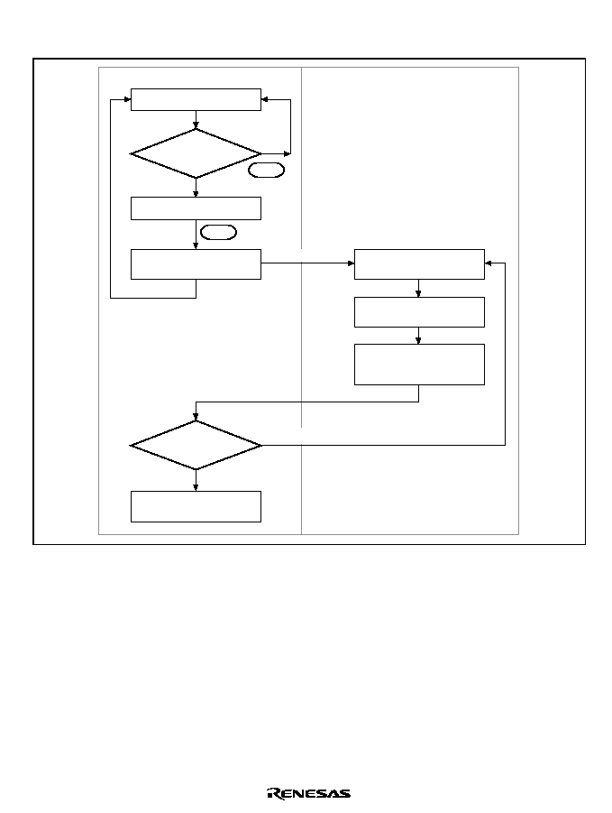
Rev. 2.00, 09/03, page 461 of 690
18.4.4
EP1 Bulk-Out Transfer (Dual FIFOs)
USB function
Application
OUT token reception
Data reception from host
Set EP1 FIFO full status
(IFR0.EP1 FULL = 1)
Clear EP1 FIFO full status
(IFR0.EP1 FULL = 0)
Read EP1 receive data
size register (EPSZ1)
Read data from EP1
data register (EPDR1)
Write 1 to EP1 read
complete bit
(TRG.EP1 RDFN = 1)
Space
in EP1 FIFO?
No
Yes
Both
EP1 FIFOs empty?
No
Yes
NACK
ACK
Interrupt request
Interrupt request
Figure 18.10 EP1 Bulk-Out Transfer Operation
EP1 has two 64-byte FIFOs, but the user can receive data and read receive data without being
aware of this dual-FIFO configuration.
When one FIFO is full after reception is completed, the EP1FULL bit in IFR0 is set. After the first
receive operation into one of the FIFOs when both FIFOs are empty, the other FIFO is empty, and
so the next packet can be received immediately. When both FIFOs are full, NACK is returned to
the host automatically. When reading of the receive data is completed following data reception, 1
is written to the EP1RDFN bit in TRG. This operation empties the FIFO that has just been read,
and makes it ready to receive the next packet.

Rev. 2.00, 09/03, page 462 of 690
18.4.5
EP2 Bulk-In Transfer (Dual FIFOs)
USB function
Application
IN token reception
Data transmission to host
Clear EP2 transfer
request flag
(IFR0.EP2 TR = 0)
Enable EP2 FIFO
empty interrupt
(IER0.EP2 EMPTY = 1)
IER0.EP2 EMPTY
interrupt
Write one packet of data
to EP2 data register
(EPDR2)
Write 1 to EP2 packet
enable bit
(TRG.EP2 PKTE = 1)
Set EP2
empty status
(IFR0.EP2
EMPTY = 1)
Valid data
in EP2 FIFO?
NACK
ACK
Interrupt request
Yes
No
Clear EP2 empty status
(IFR0.EP2 EMPTY = 0)
Space
in EP2 FIFO?
No
Yes
Interrupt
request
Figure 18.11 EP2 Bulk-In Transfer Operation
EP2 has two 64-byte FIFOs, but the user can transmit data and write transmit data without being
aware of this dual-FIFO configuration. However, one data write is performed for one FIFO. For
example, even if both FIFOs are empty, it is not possible to perform EP2PKTE at one time after
consecutively writing 128 bytes of data. EP2PKTE must be performed for each 64-byte write.
When performing bulk-in transfer, as there is no valid data in the FIFOs on reception of the first
IN token, an EP2TR bit interrupt in IFR0 is requested. With this interrupt, 1 is written to the
EP2EMPTY bit in IER0, and the EP2 FIFO empty interrupt is enabled. At first, both EP2 FIFOs
are empty, and so an EP2 FIFO empty interrupt is generated immediately.
The data to be transmitted is written to the data register using this interrupt. After the first transmit
data write for one FIFO, the other FIFO is empty, and so the next transmit data can be written to
the other FIFO immediately. When both FIFOs are full, EP2 EMPTY is cleared to 0. If at least one
FIFO is empty, the EP2EMPTY bit in IFR0 is set to 1. When ACK is returned from the host after
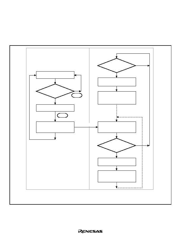
Rev. 2.00, 09/03, page 463 of 690
data transmission is completed, the FIFO used in the data transmission becomes empty. If the
other FIFO contains valid transmit data at this time, transmission can be continued.
When transmission of all data has been completed, write 0 to the EP2EMPTY bit in IER0 and
disable interrupt requests.
18.4.6
EP3 Interrupt-In Transfer
USB function
Application
IN token reception
Data transmission to host
Set EP3 transmission
complete flag
(IFR1.EP3 TS = 1)
Write data to EP3 data
register (EPDR3)
Write 1 to EP3 packet
enable bit
(TRG.EP3 PKTE = 1)
Clear EP3 transmission
complete flag
(IFR1.EP3 TS = 0)
Write data to EP3 data
register (EPDR3)
Write 1 to EP3 packet
enable bit
(TRG.EP3 PKTE = 1)
Valid data
in EP3FIFO?
Is there data
for transmission
to host?
Is there data
for transmission
to host?
No
Yes
No
Yes
No
Yes
NACK
ACK
Note: This flowchart shows just one example of interrupt transfer processing. Other possibilities include an
operation flow in which, if there is data to be transferred, the EP3 DE bit in the data status register is
referenced to confirm that the FIFO is empty, and then data is written to the FIFO.
Interrupt request
Figure 18.12 Operation of EP3 Interrupt-In Transfer

Rev. 2.00, 09/03, page 464 of 690
18.5
Processing of USB Standard Commands and Class/Vendor
Commands
18.5.1
Processing of Commands Transmitted by Control Transfer
A command transmitted from the host by control transfer may require decoding and execution of
command processing on the application side. Whether command decoding is required on the
application side is indicated in table 18.2 below.
Table 18.2
Command Decoding on Application Side
Decoding not Necessary on Application Side
Decoding Necessary on Application Side
Clear Feature
Get Configuration
Get Interface
Get Status
Set Address
Set Configuration
Set Feature
Set Interface
Get Descriptor
Class/Vendor command
Set Descriptor
Sync Frame
If decoding is not necessary on the application side, command decoding and data stage and status
stage processing are performed automatically. No processing is necessary by the user. An interrupt
is not generated in this case.
If decoding is necessary on the application side, this module stores the command in the EP0s
FIFO. After reception is completed successfully, the IFR0/SETUP TS flag is set and an interrupt
request is generated. In the interrupt routine, eight bytes of data must be read from the EP0s data
register (EPDR0s) and decoded by firmware. The necessary data stage and status stage processing
should then be carried out according to the result of the decoding operation.

Rev. 2.00, 09/03, page 465 of 690
18.6
Stall Operations
18.6.1
Overview
This section describes stall operations in this module. There are two cases in which the USB
function module stall function is used:
∑
When the application forcibly stalls an endpoint for some reason
∑
When a stall is performed automatically within the USB function module due to a USB
specification violation
The USB function module has internal status bits that hold the status (stall or non-stall) of each
endpoint. When a transaction is sent from the host, the module references these internal status bits
and determines whether to return a stall to the host. These bits cannot be cleared by the
application; they must be cleared with a Clear Feature command from the host.
18.6.2
Forcible Stall by Application
The application uses the EPSTL register to issue a stall request for the USB function module.
When the application wishes to stall a specific endpoint, it sets the corresponding bit in EPSTL (1-
1 in figure 18.13). The internal status bits are not changed at this time. When a transaction is sent
from the host for the endpoint for which the EPSTL bit was set, the USB function module
references the internal status bit, and if this is not set, references the corresponding bit in EPSTL
(1-2 in figure 18.13). If the corresponding bit in EPSTL is set, the USB function module sets the
internal status bit and returns a stall handshake to the host (1-3 in figure 18.13). If the
corresponding bit in EPSTL is not set, the internal status bit is not changed and the transaction is
accepted.
Once an internal status bit is set, it remains set until cleared by a Clear Feature command from the
host, without regard to the EPSTL register. Even after a bit is cleared by the Clear Feature
command (3-1 in figure 18.13), the USB function module continues to return a stall handshake
while the bit in EPSTL is set, since the internal status bit is set each time a transaction is executed
for the corresponding endpoint (1-2 in figure 18.13). To clear a stall, therefore, it is necessary for
the corresponding bit in EPSTL to be cleared by the application, and also for the internal status bit
to be cleared with a Clear Feature command (2-1, 2-2, and 2-3 in figure 18.13).
Rev. 2.00, 09/03, page 466 of 690
(1) Transition from normal operation to stall
(1-1)
Transaction request
USB
Reference
(1-2)
STALL handshake
Stall
To (2-1) or (3-1)
Normal status restored
(1-3)
(2) When Clear Feature is sent after EPSTL is cleared
(2-1)
STALL handshake
Transaction request
(2-2)
Clear Feature command
Clear Feature command
(2-3)
(3) When Clear Feature is sent before EPSTL is cleared to 0
(3-1)
1. 1 written to EPSTL
by application
1. IN/OUT token
received from host
2. EPSTL referenced
1. Transmission of
STALL handshake
1. Internal status bit
cleared to 0
1. Internal status bit
cleared to 0
2. EPSTL not changed
1. 1 set in EPSTL
2. Internal status bit
set to 1
3. Transmission of
STALL handshake
1. EPSTL cleared to 0
by application
2. IN/OUT token
received from host
3. Internal status bit
already set to 1
4. EPSTL not
referenced
5. Internal status bit
not changed
To (1-2)
Internal status bit
0
EPSTL
0
1
Internal status bit
0
EPSTL
1
Internal status bit
0
1
EPSTL
1
Internal status bit
1
EPSTL
1
0
Internal status bit
1
EPSTL
0
Internal status bit
1
0
EPSTL
0
Internal status bit
1
0
EPSTL
1
Figure 18.13 Forcible Stall by Application
Rev. 2.00, 09/03, page 467 of 690
18.6.3
Automatic Stall by USB Function Module
When a stall setting is made with the Set Feature command, or in the event of a USB specification
violation, the USB function module automatically sets the internal status bit for the relevant
endpoint without regard to the EPSTL register, and returns a stall handshake (1-1 in figure 18.14).
Once an internal status bit is set, it remains set until cleared by a Clear Feature command from the
host, without regard to the EPSTL register. After a bit is cleared by the Clear Feature command,
EPSTL is referenced (3-1 in figure 18.14). The USB function module continues to return a stall
handshake while the internal status bit is set, since the internal status bit is set even if a transaction
is executed for the corresponding endpoint (2-1 and 2-2 in figure 18.14). To clear a stall, therefore,
the internal status bit must be cleared with a Clear Feature command (3-1 in figure 18.14). If set
by the application, EPSTL should also be cleared (2-1 in figure 18.14).
(1) Transition from normal operation to stall
(1-1)
(2) When transaction is performed when internal status bit is set, and Clear Feature is sent
(2-1)
STALL handshake
Transaction request
STALL handshake
(2-2)
Clear Feature command
(3) When Clear Feature is sent before transaction is performed
(3-1)
1. In case of USB
specification
violation, etc., USB
function module
stalls endpoint
automatically
1. Transmission of
STALL handshake
1. Internal status bit
cleared to 0
2. EPSTL not changed
1. EPSTL cleared to 0
by application
2. IN/OUT token
received from host
3. Internal status bit
already set to 1
4. EPSTL not
referenced
5. Internal status bit
not changed
Normal status restored
Internal status bit
0
1
EPSTL
0
Internal status bit
1
EPSTL
0
Internal status bit
1
EPSTL
0
Internal status bit
1
0
EPSTL
0
Stall status maintained
To (2-1) or (3-1)
Figure 18.14 Automatic Stall by USB Function Module
Rev. 2.00, 09/03, page 468 of 690
18.7
DMA Transfer
18.7.1
Overview
DMA transfer can be performed for endpoints 1 and 2 in this module. Note that word or longword
data cannot be transferred.
When endpoint 1 holds at least one byte of valid receive data, a DMA request for endpoint 1 is
generated. When endpoint 2 holds no valid data, a DMA request for endpoint 2 is generated.
If the DMA transfer is enabled by setting the EP1DMAE bit to 1 in the DMA transfer setting
register, zero-length data reception at endpoint 1 is ignored. When the DMA transfer is enabled,
the RDFN bit for EP1 and PKTE bit for EP2 do not need to be set to 1 in TRG (note that the
PKTE bit must be set to 1 when the transfer data is less than the maximum number of bytes).
When all the data received at EP1 is read, the FIFO automatically enters the EMPTY state. When
the maximum number of bytes (64 bytes) are written to the EP2 FIFO, the FIFO automatically
enters the FULL state, and the data in the FIFO can be transmitted (see figures 18.15 and 18.16).
18.7.2
DMA Transfer for Endpoint 1
When the data received at EP1 is transferred by the DMAC, the USB function module
automatically performs the same processing as writing 1 to the RDFN bit in TRG if the currently
selected FIFO becomes empty. Accordingly, in DMA transfer, do not write 1 to the RDFN bit in
TRG. If the user writes 1 to the RDFN bit in DMA transfer, correct operation cannot be
guaranteed.
Figure 18.15 shows an example of receiving 150 bytes of data from the host. In this case, internal
processing which is the same as writing 1 to the RDFN bit in TRG is automatically performed
three times. This internal processing is performed when the currently selected data FIFO becomes
empty. Accordingly, this processing is automatically performed both when 64-byte data is sent
and when data less than 64 bytes is sent.
RDFN
(Automatically
performed)
RDFN
(Automatically
performed)
RDFN
(Automatically
performed)
64 bytes
64 bytes
22 bytes
Figure 18.15 RDFN Bit Operation for EP1
Rev. 2.00, 09/03, page 469 of 690
18.7.3
DMA Transfer for Endpoint 2
When the transmit data at EP2 is transferred by the DMAC, the USB function module
automatically performs the same processing as writing 1 to the PKTE bit in TRG if the currently
selected FIFO (64 bytes) becomes full. Accordingly, to transfer data of a multiple of 64 bytes, the
user need not write 1 to the PKTE bit. To transfer data of less than 64 bytes, the user must write 1
to the PKTE bit using the DMA transfer end interrupt of the on-chip DMAC. If the user writes 1 to
the PKTE bit when the maximum number of bytes (64 bytes) are transferred, correct operation
cannot be guaranteed.
Figure 18.16 shows an example for transmitting 150 bytes of data to the host. In this case, internal
processing which is the same as writing 1 to the PKTE bit in TRG is automatically performed
twice. This internal processing is performed when the currently selected data FIFO becomes full.
Accordingly, this processing is automatically performed only when 64-byte data is sent.
When the last 22 bytes are sent, the internal processing for writing 1 to the PKTE bit is not
performed, and the user must write 1 to the PKTE bit by software. In this case, the application has
no more data to transfer but the USB function module continues to output DMA requests for EP2
as long as the FIFO has an empty space. When all data has been transferred, write 0 to the
EP2DMAE bit in DMAR to cancel DMA requests for EP2.
PKTE
(Automatically
performed)
PKTE
(Automatically
performed)
PKTE is
not performed
Execute by DMA transfer
end interrupt (user)
64 bytes
64 bytes
22 bytes
Figure 18.16 PKTE Bit Operation for EP2

Rev. 2.00, 09/03, page 470 of 690
18.8
Example of USB External Circuitry
1. USB Transceiver
A USB transceiver IC (such as a PDIUSBP11) should be connected externally when no
internal transceiver is used. The USB transceiver manufacturer should be consulted concerning
the recommended circuit from the USB transceiver to the USB connector, etc.
2. D+ Pull-Up Control
In a system where it is wished to disable USB host/hub connection notification (D+ pull-up)
(during high-priority processing or initialization processing, for example), D+ pull-up should
be controlled using a general output port. However, if a USB cable is already connected to the
host/hub and D+ pull-up is prohibited, D+ and D≠ will both go low (both of D+ and D≠ pulled
down on the host/hub side) and the USB module will mistakenly identify this as reception of a
USB bus reset from the host. Therefore, the D+ pull-up control signal and VBUS pin input
signal should be controlled using a general output port and the USB cable VBUS (AND
circuit) as shown in figure 18.17. (The UDC core in this LSI maintains the powered state when
the VBUS pin is low, regardless of the D+/D≠ state.)
3. Detection of USB Cable Connection/Disconnection
As USB states, etc., are managed by hardware in this module, a VBUS signal that recognizes
connection/disconnection is necessary. The power supply signal (VBUS) in the USB cable is
used for this purpose. However, if the cable is connected to the USB host/hub when the
function (system installing this LSI) power is off, a voltage (5 V) will be applied from the USB
host/hub. Therefore, an IC (such as an HD74LV1G08A or 2G08A) that allows voltage
application when the system power is off should be connected externally.
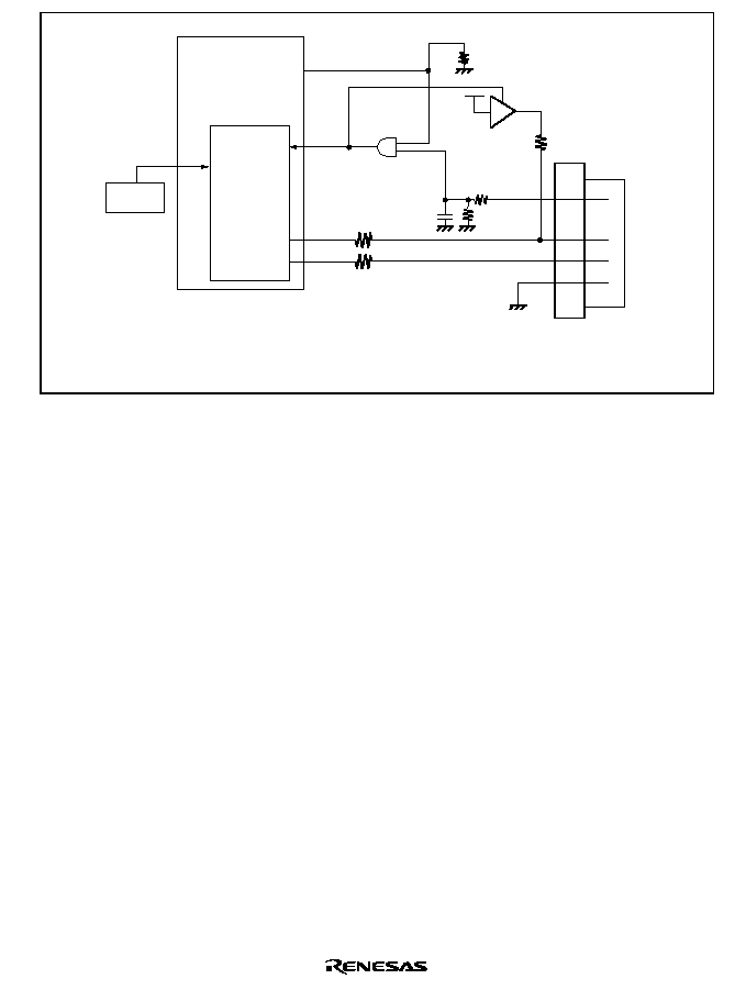
Rev. 2.00, 09/03, page 471 of 690
VBUS
EXTAL_USB
VBUS
GND
D+
D+
D-
D-
5V
3V
General output port,
etc.
This LSI
USB module
48 MHz
IC allowing voltage
application when system
(LSI) power is off
IC allowing voltage
application when system
(LSI) power is off
USB
connector
USB
cable
Note: Operation is not guaranteed with this sample circuit.
If external surge and ESD noise countermeasures are required for the system,
a protective diode or the noise canceler should be used for this purpose.
Figure 18.17 Example of USB Function Module External Circuitry
(Internal Transceiver)
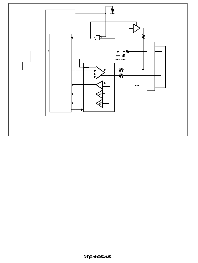
Rev. 2.00, 09/03, page 472 of 690
VBUS
VBUS
TXENL
TXDMNS
TXDPLS
XVDATA
DPLS
GND
DMNS
SUSPND
+
-
SUSPND
PDIUSBP11 etc
VM
VP
RCV
OE
SPEED
VMO
VPO
D+
D-
5V
3V
General output port,
etc.
USB module
IC allowing voltage
application when system
(LSI) power is off
IC allowing voltage
application when system
(LSI) power is off
USB
connector
USB
cable
Note: Operation is not guaranteed with this sample circuit.
If external surge and ESD noise countermeasures are required for the system,
a protective diode or the noise canceler should be used for this purpose.
This LSI
EXTAL_USB
48 MHz
Figure 18.18 Example of USB Function Module External Circuitry
(External Transceiver)

Rev. 2.00, 09/03, page 473 of 690
18.9
Usage Notes
18.9.1
Receiving Setup Data
Note the following for EPDR0s that receives 8-byte setup data:
1. As a latest setup command must be received in high priority, the write from the USB bus takes
priority over the read from the CPU. If the next setup command reception is started while the
CPU is reading data after the data is received, the read from the CPU is forcibly terminated.
Therefore, the data read after reception is started becomes invalid.
2. EPDR0s must always be read in 8-byte units. If the read is terminated at a midpoint, the data
received at the next setup cannot be read correctly.
18.9.2
Clearing the FIFO
If a USB cable is disconnected during data transfer, the data being received or transmitted may
remain in the FIFO. When disconnecting a USB cable, clear the FIFO.
While a FIFO is transferring data, it must not be cleared.
18.9.3
Overreading and Overwriting the Data Registers
Note the following when reading or writing to a data register of this module.
(1) Receive data registers
The receive data registers must not be read exceeding the valid amount of receive data, that is, the
number of bytes indicated by the receive data size register. Even for EPDR1 which has double
FIFO buffers, the maximum data to be read at one time is 64 bytes. After the data is read from the
current valid FIFO buffer, be sure to write 1 to EP1RDFN in TRG, which switches the valid
buffer, updates the receive data size to the new number of bytes, and enables the next data to be
received.
(2) Transmit data registers
The transmit data registers must not be written to exceeding the maximum packet size. Even for
EPDR2 which has double FIFO buffers, write data within the maximum packet size at one time.
After the data is written, write 1 to PKTE in TRG to switch the valid buffer and enable the next
data to be written. Data must not be continuously written to the two FIFO buffers.
Rev. 2.00, 09/03, page 474 of 690
18.9.4
Assigning Interrupt Sources to EP0
The EP0-related interrupt sources indicated by the interrupt source bits (bits 0 to 3) in IFR0 must
be assigned to the same interrupt signal with ISR0. The other interrupt sources have no limitations.
18.9.5
Clearing the FIFO when DMA Transfer Is Enabled
The endpoint 1 data register (EPDR1) cannot be cleared when DMA transfer for endpoint 1 is
enabled (EP1 DMAE in DMAR = 1). Cancel DMA transfer before clearing the register.
18.9.6
Notes on TR Interrupt
Note the following when using the transfer request interrupt (TR interrupt) for IN transfer to EP0i,
EP2, or EP3.
The TR interrupt flag is set if the FIFO for the target EP has no data when the IN token is sent
from the USB host. However, at the timing shown in figure 18.19, multiple TR interrupts occur
successively. Take appropriate measures against malfunction in such a case.
Note:
This module determines whether to return NAK if the FIFO of the target EP has no data
when receiving the IN token, but the TR interrupt flag is set only after a NAK handshake
is sent. If the next IN token is sent before PKTE of TRG is written to, the TR interrupt flag
is set again.
CPU
Host
IN token
IN token
IN token
Sets TR flag
(Sets the flag again)
Sets TR flag
Determines whether
to return NAK
Transmits data
TR interrupt routine
Clear
TR flag
Writes
transmit data
TRG.
PKTE
TR interrupt routine
USB
NAK
Determines whether
to return NAK
NAK
ACK
Figure 18.19 TR Interrupt Flag Set Timing
Rev. 2.00, 09/03, page 475 of 690
Section 19 Pin Function Controller
19.1
Overview
The pin function controller (PFC) consists of registers to select the pin functions and I/O
directions of multiplex pins. Pin functions and I/O directions can be individually selected for every
pin regardless of the LSI operating mode. Table 19.1 lists the multiplex pins of this LSI.
Table 19.1
Multiplex Pins
Port
Port Function (Related Module)
Other Functions (Related Module)
A
PTA7 input/output (port)/PINT7 input (INTC)
D23 input/output (BSC)
A
PTA6 input/output (port)/PINT6 input (INTC)
D22 input/output (BSC)
A
PTA5 input/output (port)/PINT5 input (INTC)
D21 input/output (BSC)
A
PTA4 input/output (port)/PINT4 input (INTC)
D20 input/output (BSC)
A
PTA3 input/output (port)/PINT3 input (INTC)
D19 input/output (BSC)
A
PTA2 input/output (port)/PINT2 input (INTC)
D18 input/output (BSC)
A
PTA1 input/output (port)/PINT1 input (INTC)
D17 input/output (BSC)
A
PTA0 input/output (port)/PINT0 input (INTC)
D16 input/output (BSC)
B
PTB7 input/output (port)/PINT15 input (INTC)
D31 input/output (BSC)
B
PTB6 input/output (port)/PINT14 input (INTC)
D30 input/output (BSC)
B
PTB5 input/output (port)/PINT13 input (INTC)
D29 input/output (BSC)
B
PTB4 input/output (port)/PINT12 input (INTC)
D28 input/output (BSC)
B
PTB3 input/output (port)/PINT11 input (INTC)
D27 input/output (BSC)
B
PTB2 input/output (port)/PINT10 input (INTC)
D26 input/output (BSC)
B
PTB1 input/output (port)/PINT9 input (INTC)
D25 input/output (BSC)
B
PTB0 input/output (port)/PINT8 input (INTC)
D24 input/output (BSC)
C
PTC7 input/output (port)
CS6A
output (BSC)
C
PTC6 input/output (port)
CS5A
output (BSC)
C
PTC5 input/output (port)
CS4
output (BSC)
C
PTC4 input/output (port)
CS3
output (BSC)
C
PTC3 input/output (port)
CS2
output (BSC)
C
PTC2 input/output (port)
WE3
output (BSC)/DQMUU output (BSC)/
AH
output (BSC)
C
PTC1 input/output (port)
WE2
output (BSC)/DQMUL output (BSC)
C
PTC0 input/output (port)
BS
output (BSC)
Rev. 2.00, 09/03, page 476 of 690
Port
Port Function (Related Module)
Other Functions (Related Module)
D
PTD7 input/output (port)
CS6B
output (BSC)
D
PTD6 input/output (port)
CS5B
output (BSC)
D
PTD5 input (port)
NF
*
1
D
PTD4 input/output (port)
CKE output (BSC)
D
PTD3 input/output (port)
CASU
output (BSC)
D
PTD2 input/output (port)
CASL
output (BSC)
D
PTD1 input/output (port)
RASU
output (BSC)
D
PTD0 input/output (port)
RASL
output (BSC)
E
PTE7 input/output (port)
E
PTE6 input/output (port)
TCLK input (TMU)
E
PTE5 input/output (port)
STATUS1 output (CPG)/
CTS0
input (SCIF0)
E
PTE4 input/output (port)
STATUS0 output (CPG)/
RTS0
output (SCIF0)
E
PTE3 input/output (port)
TEND0 output (DMAC)
E
PTE2 input/output (port)
IRQ5 input (INTC)
E
PTE1 input/output (port)
DACK1 output (DMAC)
E
PTE0 input/output (port)
DACK0 output (DMAC)
F
PTF7 input/output (port)
ASEMD0
input
F
PTF6 input/output (port)
ASEBRKAK
output
F
PTF5 input/output (port)
TDO output (UDI)
F
PTF4 input/output (port)
AUDSYNC
output (AUD)
F
PTF3 input/output (port)
AUDATA3 output (AUD)/TO3 output (TPU)
F
PTF2 input/output (port)
AUDATA2 output (AUD)/TO2 output (TPU)
F
PTF1 input/output (port)
AUDATA1 output (AUD)/TO1 output (TPU)
F
PTF0 input/output (port)
AUDATA0 output (AUD)/TO0 output (TPU)
G
PTG7 input/output (port)
WAIT
input (BSC)
G
PTG6 input/output (port)
BREQ
input (BSC)
G
PTG5 input/output (port)
BACK
output (BSC)
G
PTG4 input/output (port)
AUDCK output (AUD)
G
PTG3 input/output (port)
TRST
input (UDI)
G
PTG2 input/output (port)
TMS input (UDI)
G
PTG1 input/output (port)
TCK input (UDI)
G
PTG0 input/output (port)
TDI input (UDI)
Rev. 2.00, 09/03, page 477 of 690
Port
Port Function (Related Module)
Other Functions (Related Module)
H
PTH6 input/output (port)
DREQ1 input (DMAC)
H
PTH5 input/output (port)
DREQ0 input (DMAC)
H
PTH4 input/output (port)
IRQ4 input (INTC)
H
PTH3 input/output (port)
IRQ3 input (INTC)/
IRL3
input (INTC)
H
PTH2 input/output (port)
IRQ2 input (INTC)/
IRL2
input (INTC)
H
PTH1 input/output (port)
IRQ1 input (INTC)/
IRL1
input (INTC)
H
PTH0 input/output (port)
IRQ0 input (INTC)/
IRL0
input (INTC)
J
PTJ7 output (port)
NF
*
1
J
PTJ6 output (port)
NF
*
1
J
PTJ5 output (port)
NF
*
1
J
PTJ4 output (port)
NF
*
1
J
PTJ3 output (port)
NF
*
1
J
PTJ2 output (port)
NF
*
1
J
PTJ1 output (port)
NF
*
1
J
PTJ0 output (port)
NF
*
1
K
PTK7 input/output (port)
A25 output (BSC)
K
PTK6 input/output (port)
A24 output (BSC)
K
PTK5 input/output (port)
A23 output (BSC)
K
PTK4 input/output (port)
A22 output (BSC)
K
PTK3 input/output (port)
A21 output (BSC)
K
PTK2 input/output (port)
A20 output (BSC)
K
PTK1 input/output (port)
A19 output (BSC)
K
PTK0 input/output (port)
A0 output (BSC)
L
PTL3 input (port)
AN3 input (ADC)
L
PTL2 input (port)
AN2 input (ADC)
L
PTL1 input (port)
AN1 input (ADC)
L
PTL0 input (port)
AN0 input (ADC)
M
PTM6 input/output (port)
VBUS input (USB)
M
PTM4 input (port)
NF
*
1
M
PTM3 input/output (port)
M
PTM2 input/output (port)
M
PTM1 input/output (port)
M
PTM0 input/output (port)
Rev. 2.00, 09/03, page 478 of 690
Port
Port Function (Related Module)
Other Functions (Related Module)
N
PTN7 input/output (port)
N
PTN6 input/output (port)
DPLS input (USB)
N
PTN5 input/output (port)
DMNS input (USB)
N
PTN4 input/output (port)
TXDPLS output (USB)
N
PTN3 input/output (port)
TXDMNS output (USB)
N
PTN2 input/output (port)
XVDATA input (USB)
N
PTN1 input/output (port)
TXENL output (USB)
N
PTN0 input/output (port)
SUSPND output (USB)
SCPT
SCPT5 input/output (port)
CTS2
input (SCIF2)
SCPT
SCPT4 input/output (port)
RTS2
output (SCIF2)
SCPT
SCPT3 input/output (port)
SCK2 input/output (SCIF2)
SCPT
SCPT2 input (port)
*
2
RXD2 input (SCIF2)
SCPT
SCPT2 output (port)
*
2
TXD2 output (SCIF2)
SCPT
SCPT1 input/output (port)
SCK0 input/output (SCIF0)
SCPT
SCPT0 input (port)
*
2
RXD0 input (SCIF0)/IrRX input (IrDA)
SCPT
SCPT0 output (port)
*
2
TXD0 output (SCIF0)/IrTX output (IrDA)
Notes: 1. The initial functions of NF (No Function) pins are not assigned after power-on reset.
Specifies the functions with Pin Function Controller (PFC).
PTD5 and PTM4 must be pulled up.
PTJ[7:0] must be open except for the pins specified as port output pins.
The values of PTJ6, PTJ1, and PTJ0 differ during power-on reset and after the power-
on reset state is released. They conform to the port J data register value after being
switched to port status by the pin function controller (PFC).
After Power-On Reset Release
During Power-On Reset
PTD5/NF = 1
PTD5/NF = 0
PTJ6/NF
1
0
1
PTJ1/NF
1
1
0
PTJ0/NF
1
0
1
2. SCPT0 and SCPT2 each have two separate pins for input and output, however, a
common data register is accessed.
In table 19.1, pin functions in the shaded column can be used immediately after a power-on reset.

Rev. 2.00, 09/03, page 479 of 690
19.2
Register Descriptions
The PFC has the following registers. For details on register addresses and access sizes, see section
24, List of Registers.
∑
Port A control register (PACR)
∑
Port B control register (PBCR)
∑
Port C control register (PCCR)
∑
Port D control register (PDCR)
∑
Port E control register (PECR)
∑
Port E control register 2 (PECR2)
∑
Port F control register (PFCR)
∑
Port F control register 2 (PFCR2)
∑
Port G control register (PGCR)
∑
Port H control register (PHCR)
∑
Port J control register (PJCR)
∑
Port K control register (PKCR)
∑
Port L control register (PLCR)
∑
Port M control register (PMCR)
∑
Port N control register (PNCR)
∑
Port N control register 2 (PNCR2)
∑
Port SC control register (SCPCR)

Rev. 2.00, 09/03, page 480 of 690
19.2.1
Port A Control Register (PACR)
PACR is a 16-bit readable/writable register that selects the pin function and input pull-up MOS
control.
Bit
Bit
Name
Initial
Value
R/W
Description
15
14
PA7MD1
PA7MD0
0
0
R/W
R/W
PTA7 Mode
00: Other functions (see table 19.1)
01: Port output
10: Port input (pull-up MOS: On)
11: Port input (pull-up MOS: Off)
13
12
PA6MD1
PA6MD0
0
0
R/W
R/W
PTA6 Mode
00: Other functions (see table 19.1)
01: Port output
10: Port input (pull-up MOS: On)
11: Port input (pull-up MOS: Off)
11
10
PA5MD1
PA5MD0
0
0
R/W
R/W
PTA5 Mode
00: Other functions (see table 19.1)
01: Port output
10: Port input (pull-up MOS: On)
11: Port input (pull-up MOS: Off)
9
8
PA4MD1
PA4MD0
0
0
R/W
R/W
PTA4 Mode
00: Other functions (see table 19.1)
01: Port output
10: Port input (pull-up MOS: On)
11: Port input (pull-up MOS: Off)
7
6
PA3MD1
PA3MD0
0
0
R/W
R/W
PTA3 Mode
00: Other functions (see table 19.1)
01: Port output
10: Port input (pull-up MOS: On)
11: Port input (pull-up MOS: Off)

Rev. 2.00, 09/03, page 481 of 690
Bit
Bit
Name
Initial
Value
R/W
Description
5
4
PA2MD1
PA2MD0
0
0
R/W
R/W
PTA2 Mode
00: Other functions (see table 19.1)
01: Port output
10: Port input (pull-up MOS: On)
11: Port input (pull-up MOS: Off)
3
2
PA1MD1
PA1MD0
0
0
R/W
R/W
PTA1 Mode
00: Other functions (see table 19.1)
01: Port output
10: Port input (pull-up MOS: On)
11: Port input (pull-up MOS: Off)
1
0
PA0MD1
PA0MD0
0
0
R/W
R/W
PTA0 Mode
00: Other functions (see table 19.1)
01: Port output
10: Port input (pull-up MOS: On)
11: Port input (pull-up MOS: Off)
19.2.2
Port B Control Register (PBCR)
PBCR is a 16-bit readable/writable register that selects the pin function and input pull-up MOS
control.
Bit
Bit
Name
Initial
Value
R/W
Description
15
14
PB7MD1
PB7MD0
0
0
R/W
R/W
PTB7 Mode
00: Other functions (see table 19.1)
01: Port output
10: Port input (pull-up MOS: On)
11: Port input (pull-up MOS: Off)
13
12
PB6MD1
PB6MD0
0
0
R/W
R/W
PTB6 Mode
00: Other functions (see table 19.1)
01: Port output
10: Port input (pull-up MOS: On)
11: Port input (pull-up MOS: Off)

Rev. 2.00, 09/03, page 482 of 690
Bit
Bit
Name
Initial
Value
R/W
Description
11
10
PB5MD1
PB5MD0
0
0
R/W
R/W
PTB5 Mode
00: Other functions (see table 19.1)
01: Port output
10: Port input (pull-up MOS: On)
11: Port input (pull-up MOS: Off)
9
8
PB4MD1
PB4MD0
0
0
R/W
R/W
PTB4 Mode
00: Other functions (see table 19.1)
01: Port output
10: Port input (pull-up MOS: On)
11: Port input (pull-up MOS: Off)
7
6
PB3MD1
PB3MD0
0
0
R/W
R/W
PTB3 Mode
00: Other functions (see table 19.1)
01: Port output
10: Port input (pull-up MOS: On)
11: Port input (pull-up MOS: Off)
5
4
PB2MD1
PB2MD0
0
0
R/W
R/W
PTB2 Mode
00: Other functions (see table 19.1)
01: Port output
10: Port input (pull-up MOS: On)
11: Port input (pull-up MOS: Off)
3
2
PB1MD1
PB1MD0
0
0
R/W
R/W
PTB1 Mode
00: Other functions (see table 19.1)
01: Port output
10: Port input (pull-up MOS: On)
11: Port input (pull-up MOS: Off)
1
0
PB0MD1
PB0MD0
0
0
R/W
R/W
PTB0 Mode
00: Other functions (see table 19.1)
01: Port output
10: Port input (pull-up MOS: On)
11: Port input (pull-up MOS: Off)

Rev. 2.00, 09/03, page 483 of 690
19.2.3
Port C Control Register (PCCR)
PCCR is a 16-bit readable/writable register that selects the pin function and input pull-up MOS
control.
Bit
Bit
Name
Initial
Value
R/W
Description
15
14
PC7MD1
PC7MD0
1
1
R/W
R/W
PTC7 Mode
00: Other functions (see table 19.1)
01: Port output
10: Port input (pull-up MOS: On)
11: Port input (pull-up MOS: Off)
13
12
PC6MD1
PC6MD0
1
1
R/W
R/W
PTC6 Mode
00: Other functions (see table 19.1)
01: Port output
10: Port input (pull-up MOS: On)
11: Port input (pull-up MOS: Off)
11
10
PC5MD1
PC5MD0
0
0
R/W
R/W
PTC5 Mode
00: Other functions (see table 19.1)
01: Port output
10: Port input (pull-up MOS: On)
11: Port input (pull-up MOS: Off)
9
8
PC4MD1
PC4MD0
0
0
R/W
R/W
PTC4 Mode
00: Other functions (see table 19.1)
01: Port output
10: Port input (pull-up MOS: On)
11: Port input (pull-up MOS: Off)
7
6
PC3MD1
PC3MD0
0
0
R/W
R/W
PTC3 Mode
00: Other functions (see table 19.1)
01: Port output
10: Port input (pull-up MOS: On)
11: Port input (pull-up MOS: Off)

Rev. 2.00, 09/03, page 484 of 690
Bit
Bit
Name
Initial
Value
R/W
Description
5
4
PC2MD1
PC2MD0
0
0
R/W
R/W
PTC2 Mode
00: Other functions (see table 19.1)
01: Port output
10: Port input (pull-up MOS: On)
11: Port input (pull-up MOS: Off)
3
2
PC1MD1
PC1MD0
0
0
R/W
R/W
PTC1 Mode
00: Other functions (see table 19.1)
01: Port output
10: Port input (pull-up MOS: On)
11: Port input (pull-up MOS: Off)
1
0
PC0MD1
PC0MD0
0
0
R/W
R/W
PTC0 Mode
00: Other functions (see table 19.1)
01: Port output
10: Port input (pull-up MOS: On)
11: Port input (pull-up MOS: Off)

Rev. 2.00, 09/03, page 485 of 690
19.2.4
Port D Control Register (PDCR)
PDCR is a 16-bit readable/writable register that selects the pin function and input pull-up MOS
control.
Bit
Bit
Name
Initial
Value
R/W
Description
15
14
PD7MD1
PD7MD0
1
1
R/W
R/W
PTD7 Mode
00: Other functions (see table 19.1)
01: Port output
10: Port input (pull-up MOS: On)
11: Port input (pull-up MOS: Off)
13
12
PD6MD1
PD6MD0
1
1
R/W
R/W
PTD6 Mode
00: Other functions (see table 19.1)
01: Port output
10: Port input (pull-up MOS: On)
11: Port input (pull-up MOS: Off)
11
10
PD5MD1
PD5MD0
0
0
R/W
R/W
PTD5 Mode
00: NF
01: Setting prohibited
10: Port input (pull-up MOS: On)
11: Port input (pull-up MOS: Off)
9
8
PD4MD1
PD4MD0
0
0
R/W
R/W
PTD4 Mode
00: Other functions (see table 19.1)
01: Port output
10: Port input (pull-up MOS: On)
11: Port input (pull-up MOS: Off)
7
6
PD3MD1
PD3MD0
1
1
R/W
R/W
PTD3 Mode
00: Other functions (see table 19.1)
01: Port output
10: Port input (pull-up MOS: On)
11: Port input (pull-up MOS: Off)

Rev. 2.00, 09/03, page 486 of 690
Bit
Bit
Name
Initial
Value
R/W
Description
5
4
PD2MD1
PD2MD0
0
0
R/W
R/W
PTD2 Mode
00: Other functions (see table 19.1)
01: Port output
10: Port input (pull-up MOS: On)
11: Port input (pull-up MOS: Off)
3
2
PD1MD1
PD1MD0
1
1
R/W
R/W
PTD1 Mode
00: Other functions (see table 19.1)
01: Port output
10: Port input (pull-up MOS: On)
11: Port input (pull-up MOS: Off)
1
0
PD0MD1
PD0MD0
0
0
R/W
R/W
PTD0 Mode
00: Other functions (see table 19.1)
01: Port output
10: Port input (pull-up MOS: On)
11: Port input (pull-up MOS: Off)

Rev. 2.00, 09/03, page 487 of 690
19.2.5
Port E Control Register (PECR)
PECR is a 16-bit readable/writable register that selects the pin function and input pull-up MOS
control.
Bit
Bit
Name
Initial
Value
R/W
Description
15
14
PE7MD1
PE7MD0
1
0
R/W
R/W
PTE7 Mode
00: Setting prohibited
01: Port output
10: Port input (pull-up MOS: On)
11: Port input (pull-up MOS: Off)
13
12
PE6MD1
PE6MD0
1
0
R/W
R/W
PTE6 Mode
00: Other functions (see table 19.1)
01: Port output
10: Port input (pull-up MOS: On)
11: Port input (pull-up MOS: Off)
11
10
PE5MD1
PE5MD0
0
0
R/W
R/W
PTE5 Mode
00: Other functions (see table 19.1)
01: Port output
10: Port input (pull-up MOS: On)
11: Port input (pull-up MOS: Off)
9
8
PE4MD1
PE4MD0
0
0
R/W
R/W
PTE4 Mode
00: Other functions (see table 19.1)
01: Port output
10: Port input (pull-up MOS: On)
11: Port input (pull-up MOS: Off)
7
6
PE3MD1
PE3MD0
1
0
R/W
R/W
PTE3 Mode
00: Other functions (see table 19.1)
01: Port output
10: Port input (pull-up MOS: On)
11: Port input (pull-up MOS: Off)
5
4
PE2MD1
PE2MD0
1
1
R/W
R/W
PTE2 Mode
00: Other functions (see table 19.1)
01: Port output
10: Port input (pull-up MOS: On)
11: Port input (pull-up MOS: Off)

Rev. 2.00, 09/03, page 488 of 690
Bit
Bit
Name
Initial
Value
R/W
Description
3
2
PE1MD1
PE1MD0
1
0
R/W
R/W
PTE1 Mode
00: Other functions (see table 19.1)
01: Port output
10: Port input (pull-up MOS: On)
11: Port input (pull-up MOS: Off)
1
0
PE0MD1
PE0MD0
1
0
R/W
R/W
PTE0 Mode
00: Other functions (see table 19.1)
01: Port output
10: Port input (pull-up MOS: On)
11: Port input (pull-up MOS: Off)
19.2.6
Port E Control Register 2 (PECR2)
PECR2 is an 8-bit readable/writable register that selects the pin function.
Bit
Bit Name
Initial
Value
R/W
Description
7, 6
--
0
R
Reserved
These bits are always read as 0. The write value should
always be 0.
5
PE5MD2
0
R/W
PE5 Mode 2
This bit is valid when the PE5MD[1:0] bits in PECR are set
to B'00 (other functions).
0: STATUS1 (CPG)
1:
CTS0
(SCIF0)
4
PE4MD2
0
R/W
PE4 Mode 2
This bit is valid when the PE4MD[1:0] bits in PECR are set
to B'00 (other functions).
0: STATUS0 (CPG)
1:
RTS0
(SCIF0)
3 to 0
--
0
R
Reserved
These bits are always read as 0. The write value should
always be 0.

Rev. 2.00, 09/03, page 489 of 690
19.2.7
Port F Control Register (PFCR)
PFCR is a 16-bit readable/writable register that selects the pin function and input pull-up MOS
control.
Bit
Bit
Name
Initial
Value
R/W
Description
15
14
PF7MD1
PF7MD0
0
0
R/W
R/W
PTF7 Mode
00: Other functions
*
2
(see table 19.1)
01: Port output
10: Port input (pull-up MOS: On)
11: Port input (pull-up MOS: Off)
13
12
PF6MD1
PF6MD0
1
*
1
0
R/W
R/W
PTF6 Mode
00: Other functions (see table 19.1)
01: Port output
10: Port input (pull-up MOS: On)
11: Port input (pull-up MOS: Off)
11
10
PF5MD1
PF5MD0
0
0
R/W
R/W
PTF5 Mode
00: Other functions (see table 19.1)
01: Port output
10: Port input (pull-up MOS: On)
11: Port input (pull-up MOS: Off)
9
8
PF4MD1
PF4MD0
1
*
1
0
R/W
R/W
PTF4 Mode
00: Other functions (see table 19.1)
01: Port output
10: Port input (pull-up MOS: On)
11: Port input (pull-up MOS: Off)
7
6
PF3MD1
PF3MD0
1
*
1
0
R/W
R/W
PTF3 Mode
00: Other functions (see table 19.1)
01: Port output
10: Port input (pull-up MOS: On)
11: Port input (pull-up MOS: Off)
5
4
PF2MD1
PF2MD0
1
*
1
0
R/W
R/W
PTF2 Mode
00: Other functions (see table 19.1)
01: Port output
10: Port input (pull-up MOS: On)
11: Port input (pull-up MOS: Off)

Rev. 2.00, 09/03, page 490 of 690
Bit
Bit
Name
Initial
Value
R/W
Description
3
2
PF1MD1
PF1MD0
1
*
1
0
R/W
R/W
PTF1 Mode
00: Other functions (see table 19.1)
01: Port output
10: Port input (pull-up MOS: On)
11: Port input (pull-up MOS: Off)
1
0
PF0MD1
PF0MD0
1
*
1
0
R/W
R/W
PTF0 Mode
00: Other functions (see table 19.1)
01: Port output
10: Port input (pull-up MOS: On)
11: Port input (pull-up MOS: Off)
Notes: 1. Indicates the initial value when
ASEMD0
= 1. When
ASEMD0
= 0, the relevant bit
becomes 0, and other functions is selected.
2. Pull-up MOS on.
19.2.8
Port F Control Register 2 (PFCR2)
PFCR2 is an 8-bit readable/writable register that selects the pin function.
Bit
Bit
Name
Initial
Value
R/W
Description
7 to 4
--
0
R
Reserved
These bits are always read as 0. The write value should
always be 0.
3
PF3MD2
0
R/W
PTF3 Mode 2
This bit is valid when the PF3MD[1:0] bits in PFCR are set
to B'00 (other functions).
0: AUDATA3 (AUD)
1: TO3 (TPU)
2
PF2MD2
0
R/W
PTF2 Mode 2
This bit is valid when the PF2MD[1:0] bits in PFCR are set
to B'00 (other functions).
0: AUDATA2 (AUD)
1: TO2 (TPU)

Rev. 2.00, 09/03, page 491 of 690
Bit
Bit
Name
Initial
Value
R/W
Description
1
PF1MD2
0
R/W
PTF1 Mode 2
This bit is valid when the PF1MD[1:0] bits in PFCR are set to
B'00 (other functions).
0: AUDATA1 (AUD)
1: TO1 (TPU)
0
PF0MD2
0
R/W
PTF0 Mode 2
This bit is valid when the PF0MD[1:0] bits in PFCR are set to
B'00 (other functions).
0: AUDATA0 (AUD)
1: TO0 (TPU)
19.2.9
Port G Control Register (PGCR)
PGCR is a 16-bit readable/writable register that selects the pin function and input pull-up MOS
control.
Bit
Bit
Name
Initial
Value
R/W
Description
15
14
PG7MD1
PG7MD0
0
0
R/W
R/W
PTG7 Mode
00: Other functions (see table 19.1)
01: Port output
10: Port input (pull-up MOS: On)
11: Port input (pull-up MOS: Off)
13
12
PG6MD1
PG6MD0
0
0
R/W
R/W
PTG6 Mode
00: Other functions (see table 19.1)
01: Port output
10: Port input (pull-up MOS: On)
11: Port input (pull-up MOS: Off)
11
10
PG5MD1
PG5MD0
0
0
R/W
R/W
PTG5 Mode
00: Other functions (see table 19.1)
01: Port output
10: Port input (pull-up MOS: On)
11: Port input (pull-up MOS: Off)

Rev. 2.00, 09/03, page 492 of 690
Bit
Bit
Name
Initial
Value
R/W
Description
9
8
PG4MD1
PG4MD0
1
*
1
0
R/W
R/W
PTG4 Mode
00: Other functions (see table 19.1)
01: Port output
10: Port input (pull-up MOS: On)
11: Port input (pull-up MOS: Off)
7
6
PG3MD1
PG3MD0
0
0
R/W
R/W
PTG3 Mode
00: Other functions
*
2
(see table 19.1)
01: Port output
10: Port input (pull-up MOS: On)
11: Port input (pull-up MOS: Off)
5
4
PG2MD1
PG2MD0
0
0
R/W
R/W
PTG2 Mode
00: Other functions
*
2
(see table 19.1)
01: Port output
10: Port input (pull-up MOS: On)
11: Port input (pull-up MOS: Off)
3
2
PG1MD1
PG1MD0
0
0
R/W
R/W
PTG1 Mode
00: Other functions
*
2
(see table 19.1)
01: Port output
10: Port input (pull-up MOS: On)
11: Port input (pull-up MOS: Off)
1
0
PG0MD1
PG0MD0
0
0
R/W
R/W
PTG0 Mode
00: Other functions
*
2
(see table 19.1)
01: Port output
10: Port input (pull-up MOS: On)
11: Port input (pull-up MOS: Off)
Notes: 1. Indicates the initial value when
ASEMD0
= 1. When
ASEMD0
= 0, the relevant bit
becomes 0, and other functions is selected.
2. Pull-up MOS on.

Rev. 2.00, 09/03, page 493 of 690
19.2.10
Port H Control Register (PHCR)
PHCR is a 16-bit readable/writable register that selects the pin function and input pull-up MOS
control.
Bit
Bit
Name
Initial
Value
R/W
Description
15, 14
--
0
R
Reserved
These bits are always read as 0. The write value should
always be 0.
13
12
PH6MD1
PH6MD0
1
1
R/W
R/W
PTH6 Mode
00: Other functions (see table 19.1)
01: Port output
10: Port input (pull-up MOS: On)
11: Port input (pull-up MOS: Off)
11
10
PH5MD1
PH5MD0
1
1
R/W
R/W
PTH5 Mode
00: Other functions (see table 19.1)
01: Port output
10: Port input (pull-up MOS: On)
11: Port input (pull-up MOS: Off)
9
8
PH4MD1
PH4MD0
0
0
R/W
R/W
PTH4 Mode
00: Other functions (see table 19.1)
01: Port output
10: Port input (pull-up MOS: On)
11: Port input (pull-up MOS: Off)
7
6
PH3MD1
PH3MD0
0
0
R/W
R/W
PTH3 Mode
00: Other functions (see table 19.1)
01: Port output
10: Port input (pull-up MOS: On)
11: Port input (pull-up MOS: Off)
5
4
PH2MD1
PH2MD0
0
0
R/W
R/W
PTH2 Mode
00: Other functions (see table 19.1)
01: Port output
10: Port input (pull-up MOS: On)
11: Port input (pull-up MOS: Off)

Rev. 2.00, 09/03, page 494 of 690
Bit
Bit
Name
Initial
Value
R/W
Description
3
2
PH1MD1
PH1MD0
0
0
R/W
R/W
PTH1 Mode
00: Other functions (see table 19.1)
01: Port output
10: Port input (pull-up MOS: On)
11: Port input (pull-up MOS: Off)
1
0
PH0MD1
PH0MD0
0
0
R/W
R/W
PTH0 Mode
00: Other functions (see table 19.1)
01: Port output
10: Port input (pull-up MOS: On)
11: Port input (pull-up MOS: Off)
19.2.11
Port J Control Register (PJCR)
PJCR is a 16-bit readable/writable register that selects the pin function.
Bit
Bit
Name
Initial
Value
R/W
Description
15
14
PJ7MD1
PJ7MD0
0
0
R/W
R/W
PTJ7 Mode
00: NF
01: Port output
10: Setting prohibited
11: Setting prohibited
13
12
PJ6MD1
PJ6MD0
0
0
R/W
R/W
PTJ6 Mode
00: NF
01: Port output
10: Setting prohibited
11: Setting prohibited
11
10
PJ5MD1
PJ5MD0
0
0
R/W
R/W
PTJ5 Mode
00: NF
01: Port output
10: Setting prohibited
11: Setting prohibited

Rev. 2.00, 09/03, page 495 of 690
Bit
Bit
Name
Initial
Value
R/W
Description
9
8
PJ4MD1
PJ4MD0
0
0
R/W
R/W
PTJ4 Mode
00: NF
01: Port output
10: Setting prohibited
11: Setting prohibited
7
6
PJ3MD1
PJ3MD0
0
0
R/W
R/W
PTJ3 Mode
00: NF
01: Port output
10: Setting prohibited
11: Setting prohibited
5
4
PJ2MD1
PJ2MD0
0
0
R/W
R/W
PTJ2 Mode
00: NF
01: Port output
10: Setting prohibited
11: Setting prohibited
3
2
PJ1MD1
PJ1MD0
0
0
R/W
R/W
PTJ1 Mode
00: NF
01: Port output
10: Setting prohibited
11: Setting prohibited
1
0
PJ0MD1
PJ0MD0
0
0
R/W
R/W
PTJ0 Mode
00: NF
01: Port output
10: Setting prohibited
11: Setting prohibited

Rev. 2.00, 09/03, page 496 of 690
19.2.12
Port K Control Register (PKCR)
PKCR is a 16-bit readable/writable register that selects the pin function and input pull-up MOS
control.
Bit
Bit
Name
Initial
Value
R/W
Description
15
14
PK7MD1
PK7MD0
0
0
R/W
R/W
PTK7 Mode
00: Other functions (see table 19.1)
01: Port output
10: Port input (pull-up MOS: On)
11: Port input (pull-up MOS: Off)
13
12
PK6MD1
PK6MD0
0
0
R/W
R/W
PTK6 Mode
00: Other functions (see table 19.1)
01: Port output
10: Port input (pull-up MOS: On)
11: Port input (pull-up MOS: Off)
11
10
PK5MD1
PK5MD0
0
0
R/W
R/W
PTK5 Mode
00: Other functions (see table 19.1)
01: Port output
10: Port input (pull-up MOS: On)
11: Port input (pull-up MOS: Off)
9
8
PK4MD1
PK4MD0
0
0
R/W
R/W
PTK4 Mode
00: Other functions (see table 19.1)
01: Port output
10: Port input (pull-up MOS: On)
11: Port input (pull-up MOS: Off)
7
6
PK3MD1
PK3MD0
0
0
R/W
R/W
PTK3 Mode
00: Other functions (see table 19.1)
01: Port output
10: Port input (pull-up MOS: On)
11: Port input (pull-up MOS: Off)
5
4
PK2MD1
PK2MD0
0
0
R/W
R/W
PTK2 Mode
00: Other functions (see table 19.1)
01: Port output
10: Port input (pull-up MOS: On)
11: Port input (pull-up MOS: Off)

Rev. 2.00, 09/03, page 497 of 690
Bit
Bit
Name
Initial
Value
R/W
Description
3
2
PK1MD1
PK1MD0
0
0
R/W
R/W
PTK1 Mode
00: Other functions (see table 19.1)
01: Port output
10: Port input (pull-up MOS: On)
11: Port input (pull-up MOS: Off)
1
0
PK0MD1
PK0MD0
0
0
R/W
R/W
PTK0 Mode
00: Other functions (see table 19.1)
01: Port output
10: Port input (pull-up MOS: On)
11: Port input (pull-up MOS: Off)

Rev. 2.00, 09/03, page 498 of 690
19.2.13
Port L Control Register (PLCR)
PLCR is a 16-bit readable/writable register that selects the pin function.
Bit
Bit
Name
Initial
Value
R/W
Description
15 to 8
--
0
R
Reserved
These bits are always read as 0. The write value should
always be 0.
7
6
PL3MD1
PL3MD0
0
0
R/W
R/W
PTL3 Mode
00: Other functions (see table 19.1)
01: Setting prohibited
10: Setting prohibited
11: Port input (pull-up MOS: Off)
5
4
PL2MD1
PL2MD0
0
0
R/W
R/W
PTL2 Mode
00: Other functions (see table 19.1)
01: Setting prohibited
10: Setting prohibited
11: Port input (pull-up MOS: Off)
3
2
PL1MD1
PL1MD0
0
0
R/W
R/W
PTL1 Mode
00: Other functions (see table 19.1)
01: Setting prohibited
10: Setting prohibited
11: Port input (pull-up MOS: Off)
1
0
PL0MD1
PL0MD0
0
0
R/W
R/W
PTL0 Mode
00: Other functions (see table 19.1)
01: Setting prohibited
10: Setting prohibited
11: Port input (pull-up MOS: Off)

Rev. 2.00, 09/03, page 499 of 690
19.2.14
Port M Control Register (PMCR)
PMCR is a 16-bit readable/writable register that selects the pin function and input pull-up MOS
control.
Bit
Bit
Name
Initial
Value
R/W
Description
15, 14
--
0
R
Reserved
These bits are always read as 0. The write value should
always be 0.
13
12
PM6MD1
PM6MD0
1
0
R/W
R/W
PTM6 Mode
00: Other functions (see table 19.1)
01: Port output
10: Port input (pull-up MOS: On)
11: Port input (pull-up MOS: Off)
11, 10
--
0
R
Reserved
These bits are always read as 0. The write value should
always be 0.
9
8
PM4MD1
PM4MD0
0
0
R/W
R/W
PTM4 Mode
00: NF
01: Setting prohibited
10: Port input (pull-up MOS: On)
11: Port input (pull-up MOS: Off)
7
6
PM3MD1
PM3MD0
1
0
R/W
R/W
PTM3 Mode
00: Setting prohibited
01: Port output
10: Port input (pull-up MOS: On)
11: Port input (pull-up MOS: Off)
5
4
PM2MD1
PM2MD0
1
0
R/W
R/W
PTM2 Mode
00: Setting prohibited
01: Port output
10: Port input (pull-up MOS: On)
11: Port input (pull-up MOS: Off)

Rev. 2.00, 09/03, page 500 of 690
Bit
Bit
Name
Initial
Value
R/W
Description
3
2
PM1MD1
PM1MD0
1
0
R/W
R/W
PTM1 Mode
00: Setting prohibited
01: Port output
10: Port input (pull-up MOS: On)
11: Port input (pull-up MOS: Off)
1
0
PM0MD1
PM0MD0
1
0
R/W
R/W
PTM0 Mode
00: Setting prohibited
01: Port output
10: Port input (pull-up MOS: On)
11: Port input (pull-up MOS: Off)
19.2.15
Port N Control Register (PNCR)
PNCR is a 16-bit readable/writable register that selects the pin function and input pull-up MOS
control.
Bit
Bit
Name
Initial
Value
R/W
Description
15
14
PN7MD1
PN7MD0
1
0
R/W
R/W
PTN7 Mode
00: Setting prohibited
01: Port output
10: Port input (pull-up MOS: On)
11: Port input (pull-up MOS: Off)
13
12
PN6MD1
PN6MD0
1
0
R/W
R/W
PTN6 Mode
00: Other functions (see table 19.1)
01: Port output
10: Port input (pull-up MOS: On)
11: Port input (pull-up MOS: Off)
11
10
PN5MD1
PN5MD0
1
0
R/W
R/W
PTN5 Mode
00: Other functions (see table 19.1)
01: Port output
10: Port input (pull-up MOS: On)
11: Port input (pull-up MOS: Off)

Rev. 2.00, 09/03, page 501 of 690
Bit
Bit
Name
Initial
Value
R/W
Description
9
8
PN4MD1
PN4MD0
1
0
R/W
R/W
PTN4 Mode
00: Other functions (see table 19.1)
01: Port output
10: Port input (pull-up MOS: On)
11: Port input (pull-up MOS: Off)
7
6
PN3MD1
PN3MD0
1
0
R/W
R/W
PTN3 Mode
00: Other functions (see table 19.1)
01: Port output
10: Port input (pull-up MOS: On)
11: Port input (pull-up MOS: Off)
5
4
PN2MD1
PN2MD0
1
0
R/W
R/W
PTN2 Mode
00: Other functions (see table 19.1)
01: Port output
10: Port input (pull-up MOS: On)
11: Port input (pull-up MOS: Off)
3
2
PN1MD1
PN1MD0
1
0
R/W
R/W
PTN1 Mode
00: Other functions (see table 19.1)
01: Port output
10: Port input (pull-up MOS: On)
11: Port input (pull-up MOS: Off)
1
0
PN0MD1
PN0MD0
1
0
R/W
R/W
PTN0 Mode
00: Other functions (see table 19.1)
01: Port output
10: Port input (pull-up MOS: On)
11: Port input (pull-up MOS: Off)

Rev. 2.00, 09/03, page 502 of 690
19.2.16
Port N Control Register 2 (PNCR2)
PNCR2 is an 8-bit readable/writable register that selects the pin function.
Bit
Bit
Name
Initial
Value
R/W
Description
7
--
0
R
Reserved
This bit is always read as 0. The write value should
always be 0.
6
PN6MD2
0
R/W
PTN6 Mode 2
This bit is valid when the PN6MD[1:0] bits in PNCR are
set to B'00 (other functions).
0: Setting prohibited
1: DPLS (USB)
5
PN5MD2
0
R/W
PTN5 Mode 2
This bit is valid when the PN5MD[1:0] bits in PNCR are
set to B'00 (other functions).
0: Setting prohibited
1: DMNS (USB)
4
PN4MD2
0
R/W
PTN4 Mode 2
This bit is valid when the PN4MD[1:0] bits in PNCR are
set to B'00 (other functions).
0: Setting prohibited
1: TXDPLS (USB)
3
PN3MD2
0
R/W
PTN3 Mode 2
This bit is valid when the PN3MD[1:0] bits in PNCR are
set to B'00 (other functions).
0: Setting prohibited
1: TXDMNS (USB)
2
PN2MD2
0
R/W
PTN2 Mode 2
This bit is valid when the PN2MD[1:0] bits in PNCR are
set to B'00 (other functions).
0: Setting prohibited
1: XVDATA (USB)

Rev. 2.00, 09/03, page 503 of 690
Bit
Bit
Name
Initial
Value
R/W
Description
1
PN1MD2
0
R/W
PTN1 Mode 2
This bit is valid when the PN1MD[1:0] bits in PNCR are
set to B'00 (other functions).
0: Setting prohibited
1: TXENL (USB)
0
PN0MD2
0
R/W
PTN0 Mode 2
This bit is valid when the PN0MD[1:0] bits in PNCR are
set to B'00 (other functions).
0: Setting prohibited
1: SUSPND (USB)
19.2.17
Port SC Control Register (SCPCR)
SCPCR is a 16-bit readable/writable register that selects the pin function and input pull-up MOS
control. The settings of SCPCR become valid only when transmission/reception operation is
disabled by the settings of SCSCR in the on-chip serial communication interface (SCIF).
When the TE bit in SCSCR_0 or SCSCR_2 of the SCIF is set to 1, the output status of "other
functions: TxD0 or TxD2" has priority for the setting of SCPCR.
Similarly, when the RE bit in SCSCR_0 or SCSCR_2 is set to 1, the input status of "other
functions: RxD0 or RxD2" has priority for the setting of SCPCR.
Bit
Bit
Name
Initial
Value
R/W
Description
15 to 12
--
0
R
Reserved
These bits are always read as 0. The write value should
always be 0.
11
10
SCP5MD1
SCP5MD0
0
0
R/W
R/W
SCPT5 Mode
00: Other functions (see table 19.1)
01: Port output
10: Port input (pull-up MOS: On)
11: Port input (pull-up MOS: Off)

Rev. 2.00, 09/03, page 504 of 690
Bit
Bit
Name
Initial
Value
R/W
Description
9
8
SCP4MD1
SCP4MD0
0
0
R/W
R/W
SCPT4 Mode
00: Other functions (see table 19.1)
01: Port output
10: Port input (pull-up MOS: On)
11: Port input (pull-up MOS: Off)
7
6
SCP3MD1
SCP3MD0
0
0
R/W
R/W
SCPT3 Mode
00: Other functions (see table 19.1)
01: Port output
10: Port input (pull-up MOS: On)
11: Port input (pull-up MOS: Off)
5
4
SCP2MD1
SCP2MD0
0
0
R/W
R/W
SCPT2 Mode
These bits select pin function and input pull-up MOS
control.
When TE = 0 and RE = 0 in SCSCR_2, operation is as
follows:
00: Other functions (see table 19.1)
01: Port output
10: Port input (pull-up MOS: On)
11: Port input (pull-up MOS: Off)
When TE = 1 in SCSCR_2, the SCPT2/TxD2 pin functions
as TxD2.
When RE = 1 in SCSCR_2, the SCPT2/RxD2 pin
functions as RxD2.
Note: Since two pins (TxD2 and RxD2) are used to access
one bit (SCPT2), there is no combination of
simultaneous input/output of SCPT2.
When port input is set (when bit SCP2MD1 is set to 1), the
TxD2 pin enters an output state when the TE bit in
SCSCR_2 is set to 1, whereas it enters high-impedance
state when the TE bit is cleared to 0.

Rev. 2.00, 09/03, page 505 of 690
Bit
Bit
Name
Initial
Value
R/W
Description
3
2
SCP1MD1
SCP1MD0
0
0
R/W
R/W
SCPT1 Mode
These bits select pin function and input pull-up MOS
control.
00: Other functions (see table 19.1)
01: Port output
10: Port input (pull-up MOS: On)
11: Port input (pull-up MOS: Off)
1
0
SCP0MD1
SCP0MD0
0
0
R/W
R/W
SCPT0 Mode
These bits select pin function and input pull-up MOS
control.
When TE = 0 and RE = 0 in SCSCR_0, operation is as
follows:
00: Other functions (see table 19.1)
01: Port output
10: Port input (pull-up MOS: On)
11: Port input (pull-up MOS: Off)
When TE = 1 in SCSCR_0, the SCPT0/TxD0 pin
functions as TxD0.
When RE = 1 in SCSCR_0, the SCPT0/RxD0 pin
functions as RxD0.
Note: Since two pins (TxD0 and RxD0) are used to
access one bit (SCPT0), there is no combination of
simultaneous input/output of SCPT0.
When port input is set (when bit SCP0MD1 is set to 1),
the TxD0 pin enters an output state when the TE bit in
SCSCR_0 is set to 1, whereas it enters high-impedance
state when the TE bit is cleared to 0.

Rev. 2.00, 09/03, page 506 of 690
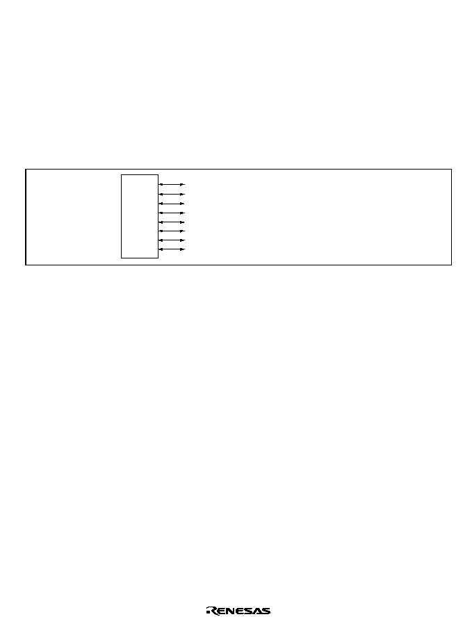
Rev. 2.00, 09/03, page 507 of 690
Section 20 I/O Ports
This LSI has fourteen I/O ports (ports A to H, J to N, and SC). All port pins are multiplexed with
other pin functions (the pin function controller (PFC) handles the selection of pin functions and
pull-up MOS control). Each port has a data register which stores data for the pins.
20.1
Port A
Port A is an 8-bit input/output port with the pin configuration shown in figure 20.1. Each pin has
an input pull-up MOS, which is controlled by the port A control register (PACR) in the PFC.
Port A
PTA7 (input/output)/D23 (input/output)/PINT7 (input)
PTA6 (input/output)/D22 (input/output)/PINT6 (input)
PTA5 (input/output)/D21 (input/output)/PINT5 (input)
PTA4 (input/output)/D20 (input/output)/PINT4 (input)
PTA3 (input/output)/D19 (input/output)/PINT3 (input)
PTA2 (input/output)/D18 (input/output)/PINT2 (input)
PTA1 (input/output)/D17 (input/output)/PINT1 (input)
PTA0 (input/output)/D16 (input/output)/PINT0 (input)
Figure 20.1 Port A
20.1.1
Register Description
Port A has the following register. For details on the register address and access size, see section
24, List of Registers.
∑
Port A data register (PADR)
Rev. 2.00, 09/03, page 508 of 690
20.1.2
Port A Data Register (PADR)
PADR is an 8-bit readable/writable register that stores data for pins PTA7 to PTA0. Bits PA7DT
to PA0DT correspond to pins PTA7 to PTA0. When the pin function is general output port, if the
port is read, the value of the corresponding PADR bit is returned directly. When the function is
general input port, if the port is read the corresponding pin level is read.
Bit
Bit
Name
Initial
Value
R/W
Description
7 to 0
PA7DT
to
PA0DT
0
R/W
Table 20.1 shows the function of PADR.
Table 20.1
Port A Data Register (PADR) Read/Write Operations
PACR State
PAnMD1 PAnMD0 Pin State
Read
Write
0
0
Other function PADR value
Data can be written to PADR but no effect on
pin state.
1
Output
PADR value
Written data is output from the pin.
1
0
Input (Pull-up
MOS on)
Pin state
Data can be written to PADR but no effect on
pin state.
1
Input (Pull-up
MOS off)
Pin state
Data can be written to PADR but no effect on
pin state.
Note:
n = 0 to 7
20.2
Port B
Port B is an 8-bit input/output port with the pin configuration shown in figure 20.2. Each pin has
an input pull-up MOS, which is controlled by the port B control register (PBCR) in the PFC.
Port B
PTB7 (input/output)/D31 (input/output)/PINT15 (input)
PTB6 (input/output)/D30 (input/output)/PINT14 (input)
PTB5 (input/output)/D29 (input/output)/PINT13 (input)
PTB4 (input/output)/D28 (input/output)/PINT12 (input)
PTB3 (input/output)/D27 (input/output)/PINT11 (input)
PTB2 (input/output)/D26 (input/output)/PINT10 (input)
PTB1 (input/output)/D25 (input/output)/PINT9 (input)
PTB0 (input/output)/D24 (input/output)/PINT8 (input)
Figure 20.2 Port B

Rev. 2.00, 09/03, page 509 of 690
20.2.1
Register Description
Port B has the following register. For details on the register address and access size, see section
24, List of Registers.
∑
Port B data register (PBDR)
20.2.2
Port B Data Register (PBDR)
PBDR is an 8-bit readable/writable register that stores data for pins PTB7 to PTB0. Bits PB7DT to
PB0DT correspond to pins PTB7 to PTB0. When the pin function is general output port, if the port
is read the value of the corresponding PBDR bit is returned directly. When the function is general
input port, if the port is read, the corresponding pin level is read.
Bit
Bit
Name
Initial
Value
R/W
Description
7 to 0
PB7DT
to
PB0DT
0
R/W
Table 20.2 shows the function of PBDR.
Table 20.2
Port B Data Register (PBDR) Read/Write Operations
PBCR State
PBnMD1 PBnMD0 Pin State
Read
Write
0
0
Other function PBDR value
Data can be written to PBDR but no effect on
pin state.
1
Output
PBDR value
Written data is output from the pin.
1
0
Input (Pull-up
MOS on)
Pin state
Data can be written to PBDR but no effect on
pin state.
1
Input (Pull-up
MOS off)
Pin state
Data can be written to PBDR but no effect on
pin state.
Note:
n = 0 to 7
Rev. 2.00, 09/03, page 510 of 690
20.3
Port C
Port C is an 8-bit input/output port with the pin configuration shown in figure 20.3. Each pin has
an input pull-up MOS, which is controlled by the port C control register (PCCR) in the PFC.
Port C
PTC7 (input/output)/
CS6A (output)
PTC6 (input/output)/
CS5A (output)
PTC5 (input/output)/
CS4 (output)
PTC4 (input/output)/
CS3 (output)
PTC3 (input/output)/
CS2 (output)
PTC2 (input/output)/
WE3 (output)/DQMUU (output)/AH (output)
PTC1 (input/output)/
WE2 (output)/DQMUL (output)
PTC0 (input/output)/
BS (output)
Figure 20.3 Port C
20.3.1
Register Description
Port C has the following register. For details on the register address and access size, see section
24, List of Registers.
∑
Port C data register (PCDR)
20.3.2
Port C Data Register (PCDR)
PCDR is an 8-bit readable/writable register that stores data for pins PTC7 to PTC0. Bits PC7DT to
PC0DT correspond to pins PTC7 to PTC0. When the pin function is general output port, if the port
is read, the value of the corresponding PCDR bit is returned directly. When the function is general
input port, if the port is read, the corresponding pin level is read.
Bit
Bit
Name
Initial
Value
R/W
Description
7 to 0
PC7DT
to
PC0DT
0
R/W
Table 20.3 shows the function of PCDR.

Rev. 2.00, 09/03, page 511 of 690
Table 20.3
Port C Data Register (PCDR) Read/Write Operations
PCCR State
PCnMD1 PCnMD0 Pin State
Read
Write
0
0
Other function PCDR value
Data can be written to PCDR but no effect on
pin state.
1
Output
PCDR value
Written data is output from the pin.
1
0
Input (Pull-up
MOS on)
Pin state
Data can be written to PCDR but no effect on
pin state.
1
Input (Pull-up
MOS off)
Pin state
Data can be written to PCDR but no effect on
pin state.
Note:
n = 0 to 7
20.4
Port D
Port D is an 8-bit input/output port with the pin configuration shown in figure 20.4. Each pin has
an input pull-up MOS, which is controlled by the port D control register (PDCR) in the PFC.
Port D
PTD7 (input/output)/
CS6B (output)
PTD6 (input/output)/
CS5B (output)
PTD5 (input) /NF (input)
PTD4 (input/output)/CKE (output)
PTD3 (input/output)/
CASU (output)
PTD2 (input/output)/
CASL (output)
PTD1 (input/output)/
RASU (output)
PTD0 (input/output)/
RASL (output)
Figure 20.4 Port D
20.4.1
Register Description
Port D has the following register. For details on the register address and access size, see section
24, List of Registers.
∑
Port D data register (PDDR)
20.4.2
Port D Data Register (PDDR)
PDDR is an 8-bit readable/writable register that stores data for pins PTD7 to PTD0. Bits PD7DT
to PD0DT correspond to pins PTD7 to PTD0. When the pin function is general output port, if the
port is read, the value of the corresponding PDDR bit is returned directly. When the function is
general input port, if the port is read, the corresponding pin level is read.

Rev. 2.00, 09/03, page 512 of 690
Bit
Bit
Name
Initial
Value
R/W
Description
7 to
0
PD7DT
to
PD0DT
0
R/W
Table 20.4 shows the function of PDDR.
Table 20.4
Port D Data Register (PDDR) Read/Write Operations
PDCR State
PDnMD1 PDnMD0 Pin State
Read
Write
0
0
Other function PDDR value
Data can be written to PDDR but no effect
on pin state.
1
Output
PDDR value
Written data is output from the pin.
1
0
Input (Pull-up
MOS on)
Pin state
Data can be written to PDDR but no effect
on pin state.
1
Input (Pull-up
MOS off)
Pin state
Data can be written to PDDR but no effect
on pin state.
Note:
n = 0 to 4, 6, and 7
PDCR State
PD5MD1 PD5MD0 Pin State
Read
Write
0
0
NF
PDDR value
Data can be written to PDDR but no effect
on pin state.
1
Setting
Prohibited
1
0
Input (Pull-up
MOS on)
Pin state
Data can be written to PDDR but no effect
on pin state.
1
Input (Pull-up
MOS off)
Pin state
Data can be written to PDDR but no effect
on pin state.
Rev. 2.00, 09/03, page 513 of 690
20.5
Port E
Port E is an 8-bit input/output port with the pin configuration shown in figure 20.5. Each pin has
an input pull-up MOS, which is controlled by the port E control register (PECR) in the PFC.
Port E
PTE7 (input/output)
PTE6 (input/output)/TCLK (input)
PTE5 (input/output)/STATUS1 (output)/
CTS0 (input)
PTE4 (input/output)/STATUS0 (output)/
RTS0 (output)
PTE3 (input/output)/TEND0 (output)
PTE2 (input/output)/IRQ5 (input)
PTE1 (input/output)/DACK1 (output)
PTE0 (input/output)/DACK0 (output)
Figure 20.5 Port E
20.5.1
Register Description
Port E has the following register. For details on the register address and access size, see section
24, List of Registers.
∑
Port E data register (PEDR)
20.5.2
Port E Data Register (PEDR)
PEDR is an 8-bit readable/writable register that stores data for pins PTE7 to PTE0. Bits PE7DT to
PE0DT correspond to pins PTE7 to PTE0. When the pin function is general output port, if the port
is read, the value of the corresponding PEDR bit is returned directly. When the function is general
input port, if the port is read the corresponding pin level is read.
Bit
Bit
Name
Initial
Value
R/W
Description
7 to 0
PE7DT
to
PE0DT
0
R/W
Table 20.5 shows the function of PEDR.
Rev. 2.00, 09/03, page 514 of 690
Table 20.5
Port E Data Register (PEDR) Read/Write Operations
PECR State
PEnMD1 PEnMD0 Pin State
Read
Write
0
0
Other function PEDR value
Data can be written to PEDR but no effect on
pin state.
1
Output
PEDR value
Written data is output from the pin.
1
0
Input (Pull-up
MOS on)
Pin state
Data can be written to PEDR but no effect on
pin state.
1
Input (Pull-up
MOS off)
Pin state
Data can be written to PEDR but no effect on
pin state.
Note:
n = 0 to 7
20.6
Port F
Port F is an 8-bit input port with the pin configuration shown in figure 20.6. Each pin has an input
pull-up MOS, which is controlled by the port F control register (PFCR) in the PFC.
Port F
PTF7 (input/output)/
ASEMD0 (input)
PTF6 (input/output)/
ASEBRKAK (output)
PTF5 (input/output)/TDO (output)
PTF4 (input/output)/AUDSYNC (output)
PTF3 (input/output)/AUDATA3 (output)/TO3 (output)
PTF2 (input/output)/AUDATA2 (output)/TO2 (output)
PTF1 (input/output)/AUDATA1 (output)/TO1 (output)
PTF0 (input/output)/AUDATA0 (output)/TO0 (output)
Figure 20.6 Port F
20.6.1
Register Description
Port F has the following register. For details on the register address and access size, see section 24,
List of Registers.
∑
Port F data register (PFDR)
20.6.2
Port F Data Register (PFDR)
PFDR is an 8-bit readable/writable register that stores data for pins PTF7 to PTF0. Bits PF7DT to
PF0DT correspond to pins PTF7 to PTF0. When the pin function is general output port, if the port
is read, the value of the corresponding PFDR bit is returned directly. When the function is general
input port, if the port is read the corresponding pin level is read.
Rev. 2.00, 09/03, page 515 of 690
Bit
Bit
Name
Initial
Value
R/W
Description
7 to
0
PF7DT
to
PF0DT
0
R/W
Table 20.6 shows the function of PFDR.
Table 20.6
Port F Data Register (PFDR) Read/Write Operations
PFCR State
PFnMD1
PFnMD0
Pin State
Read
Write
0
0
Other function PFDR value
Data can be written to PFDR but no effect on
pin state.
1
Output
PFDR value
Written data is output from the pin.
1
0
Input (Pull-up
MOS on)
Pin state
Data can be written to PFDR but no effect on
pin state.
1
Input (Pull-up
MOS off)
Pin state
Data can be written to PFDR but no effect on
pin state.
Note:
n = 0 to 7
20.7
Port G
Port G is an 8-bit input port with the pin configuration shown in figure 20.7. Each pin has an input
pull-up MOS, which is controlled by the port G control register (PGCR) in the PFC.
Port G
PTG5 (input/output)/
BACK (output)
PTG4 (input/output)/AUDCK (output)
PTG3 (input/output)/
TRST (input)
PTG2 (input/output)/TMS (input)
PTG1 (input/output)/TCK (input)
PTG0 (input/output)/TDI (input)
PTG7 (input/output)/
WAIT (input)
PTG6 (input/output)/
BREQ (input)
Figure 20.7 Port G
20.7.1
Register Description
Port G has the following register. For details on the register address and access size, see section
24, List of Registers.
∑
Port G data register (PGDR)
Rev. 2.00, 09/03, page 516 of 690
20.7.2
Port G Data Register (PGDR)
PGDR is an 8-bit readable/writable register that stores data for pins PTG7 to PTG0. Bits PG7DT
to PG0DT correspond to pins PTG7 to PTG0. When the pin function is general output port, if the
port is read, the value of the corresponding PGDR bit is returned directly. When the function is
general input port, if the port is read the corresponding pin level is read.
Bit
Bit
Name
Initial
Value
R/W
Description
7 to
0
PG7DT
to
PG0DT
0
R/W
Table 20.7 shows the function of PGDR.
Table 20.7
Port G Data Register (PGDR) Read/Write Operations
PGCR State
PGnMD1 PGnMD0 Pin State
Read
Write
0
0
Other function PGDR value
Data can be written to PGDR but no effect on
pin state.
1
Output
PGDR value
Written data is output from the pin.
1
0
Input (Pull-up
MOS on)
Pin state
Data can be written to PGDR but no effect on
pin state.
1
Input (Pull-up
MOS off)
Pin state
Data can be written to PGDR but no effect on
pin state.
Note:
n = 0 to 7
20.8
Port H
Port H is a 7-bit input/output port with the pin configuration shown in figure 20.8. Each pin has an
input pull-up MOS, which is controlled by the port H control register (PHCR) in the PFC.
Port H
PTH6 (input/output)/DREQ1 (input)
PTH5 (input/output)/DREQ0 (input)
PTH4 (input/output)/IRQ4 (input)
PTH3 (input/output)/IRQ3 (input)/
IRL3 (input)
PTH2 (input/output)/IRQ2 (input)/
IRL2 (input)
PTH1 (input/output)/IRQ1 (input)/
IRL1 (input)
PTH0 (input/output)/IRQ0 (input)/
IRL0 (input)
Figure 20.8 Port H

Rev. 2.00, 09/03, page 517 of 690
20.8.1
Register Description
Port H has the following register. For details on the register address and access size, see section
24, List of Registers.
∑
Port H data register (PHDR)
20.8.2
Port H Data Register (PHDR)
PHDR is an 8-bit readable/writable register that stores data for pins PTH6 to PTH0. Bits PH6DT
to PH0DT correspond to pins PTH6 to PTH0. When the pin function is general output port, if the
port is read, the value of the corresponding PHDR bit is returned directly. When the function is
general input port, if the port is read, the corresponding pin level is read.
Bit
Bit
Name
Initial
Value
R/W
Description
7
--
0
R
Reserved
This bit is always read as 0. The write value should
always be 0.
6 to
0
PH6DT
to
PH0DT
0
R/W
Table 20.8 shows the function of PHDR.
Table 20.8
Port H Data Register (PHDR) Read/Write Operations
PHCR State
PHnMD1 PHnMD0 Pin State
Read
Write
0
0
Other function PHDR value
Data can be written to PHDR but no effect
on pin state.
1
Output
PHDR value
Written data is output from the pin.
1
0
Input (Pull-up
MOS on)
Pin state
Data can be written to PHDR but no effect
on pin state.
1
Input (Pull-up
MOS off)
Pin state
Data can be written to PHDR but no effect
on pin state.
Note:
n = 0 to 6
Rev. 2.00, 09/03, page 518 of 690
20.9
Port J
Port J is an 8-bit output port with the pin configuration shown in figure 20.9.
Port J
PTJ7 (output)/NF (output)
PTJ6 (output)/NF (output)
PTJ5 (output)/NF (output)
PTJ4 (output)/NF (output)
PTJ3 (output)/NF (output)
PTJ2 (output)/NF (output)
PTJ1 (output)/NF (output)
PTJ0 (output)/NF (output)
Figure 20.9 Port J
20.9.1
Register Description
Port J has the following register. For details on the register address and access size, see section 24,
List of Registers.
∑
Port J data register (PJDR)
20.9.2
Port J Data Register (PJDR)
PJDR is an 8-bit readable/writable register that stores data for pins PTJ7 to PTJ0. Bits PJ7DT to
PJ0DT correspond to pins PTJ7 to PTJ0. When the pin function is general output port, if the port
is read, the value of the corresponding PJDR bit is returned directly.
Bit
Bit
Name
Initial
Value
R/W
Description
7 to 0
PJ7DT
to
PJ0DT
0
R/W
Table 20.9 shows the function of PJDR.
Rev. 2.00, 09/03, page 519 of 690
Table 20.9
Port J Data Register (PJDR) Read/Write Operations
PJCR State
PJnMD1
PJnMD0
Pin State
Read
Write
0
0
NF
PJDR value
Data can be written to PJDR but no effect on
pin state.
1
Output
PJDR value
Written data is output from the pin.
1
0
Setting
Prohibited
1
Setting
Prohibited
Note:
n = 0 to 7
20.10
Port K
Port K is an 8-bit input/output port with the pin configuration shown in figure 20.10. Each pin has
an input pull-up MOS, which is controlled by the port K control register (PKCR) in the PFC.
Port K
PTK7 (input/output)/A25 (output)
PTK6 (input/output)/A24 (output)
PTK5 (input/output)/A23 (output)
PTK4 (input/output)/A22 (output)
PTK3 (input/output)/A21 (output)
PTK2 (input/output)/A20 (output)
PTK1 (input/output)/A19 (output)
PTK0 (input/output)/A0 (output)
Figure 20.10 Port K
20.10.1
Register Description
Port K has the following register. For details on the register address and access size, see section
24, List of Registers.
∑
Port K data register (PKDR)
20.10.2
Port K Data Register (PKDR)
PKDR is an 8-bit readable/writable register that stores data for pins PTK7 to PTK0. Bits PK7DT
to PK0DT correspond to pins PTK7 to PTK0. When the pin function is general output port, if the
port is read, the value of the corresponding PKDR bit is returned directly. When the function is
general input port, if the port is read, the corresponding pin level is read.
Rev. 2.00, 09/03, page 520 of 690
Bit
Bit
Name
Initial
Value
R/W
Description
7 to 0
PK7DT
to
PK0DT
0
R/W
Table 20.10 shows the function of PKDR.
Table 20.10 Port K Data Register (PKDR) Read/Write Operations
PKCR State
PKnMD1 PKnMD0 Pin State
Read
Write
0
0
Other function PKDR value
Data can be written to PKDR but no effect
on pin state.
1
Output
PKDR value
Written data is output from the pin.
1
0
Input (Pull-up
MOS on)
Pin state
Data can be written to PKDR but no effect
on pin state.
1
Input (Pull-up
MOS off)
Pin state
Data can be written to PKDR but no effect
on pin state.
Note:
n = 0 to 7
20.11
Port L
Port L is a 4-bit input port with the pin configuration shown in figure 20.11.
Port L
PTL3 (input)/AN3 (input)
PTL2 (input)/AN2 (input)
PTL1 (input)/AN1 (input)
PTL0 (input)/AN0 (input)
Figure 20.11 Port L
20.11.1
Register Description
Port L has the following register. For details on the register address and access size, see section
24, List of Registers.
∑
Port L data register (PLDR)
Rev. 2.00, 09/03, page 521 of 690
20.11.2
Port L Data Register (PLDR)
PLDR is an 8-bit read-only register that stores data for pins PTL3 to PTL0. Bits PL3DT to PL0DT
correspond to pins PTL3 to PTL0. If the port is read, the corresponding pin level is read.
Bit
Bit
Name
Initial
Value
R/W
Description
7 to 4
--
0
R
Reserved
These bits are always read as 0.
3 to 0
PL3DT
to
PL0DT
0
R
Table 20.11 shows the function of PLDR.
Table 20.11 Port L Data Register (PLDR) Read/Write Operation
PLCR State
PLnMD1
PLnMD0
Pin State
Read
Write
0
0
Other function Read as 0
Invalid (no effect on pin state)
1
Setting
prohibited
--
--
0
Setting
prohibited
--
--
1
1
Input (Pull-up
MOS off)
Pin state
Invalid (no effect on pin state)
Note:
n = 0 to 3
20.12
Port M
Port M is a 6-bit input/output port with the pin configuration shown in figure 20.12. Each pin has
an input pull-up MOS, which is controlled by the port M control register (PMCR) in the PFC.
Port M
PTM6 (input/output)/VBUS (input)
PTM4 (input)/NF (input)
PTM3 (input/output)
PTM2 (input/output)
PTM1 (input/output)
PTM0 (input/output)
Figure 20.12 Port M

Rev. 2.00, 09/03, page 522 of 690
20.12.1
Register Description
Port M has the following register. For details on the register address and access size, see section
24, List of Registers.
∑
Port M data register (PMDR)
20.12.2
Port M Data Register (PMDR)
PMDR is an 8-bit readable/writable register that stores data for pins PTM6 and PTM4 to PTM0.
Bits PM6DT and PM4DT to PM0DT correspond to pins PTM6 and PTM4 to PTM0. When the pin
function is general output port, if the port is read, the value of the corresponding PMDR bit is
returned directly. When the function is general input port, if the port is read, the corresponding pin
level is read.
Bit
Bit
Name
Initial
Value
R/W
Description
7
--
0
R
Reserved
This bit is always read as 0. The write value should
always be 0.
6
PM6DT
0
R/W
Table 20.12 shows the function of PMDR.
5
--
0
R
Reserved
This bit is always read as 0. The write value should
always be 0.
4 to 0
PM4DT
to
PM0DT
0
R/W
Table 20.12 shows the function of PMDR.
Table 20.12 Port M Data Register (PMDR) Read/Write Operations
PMCR State
PMnMD1 PMnMD0 Pin State
Read
Write
0
0
Other function PMDR value
Data can be written to PMDR but no effect
on pin state.
1
Output
PMDR value
Written data is output from the pin.
1
0
Input (Pull-up
MOS on)
Pin state
Data can be written to PMDR but no effect
on pin state.
1
Input (Pull-up
MOS off)
Pin state
Data can be written to PMDR but no effect
on pin state.
Note:
n = 0 to 3 and 6
Rev. 2.00, 09/03, page 523 of 690
PMCR State
PM4MD1 PM4MD0 Pin State
Read
Write
0
0
NF
PMDR value
Data can be written to PMDR but no effect
on pin state.
1
Setting
Prohibited
PMDR value
Written data is output from the pin.
1
0
Input (Pull-up
MOS on)
Pin state
Data can be written to PMDR but no effect
on pin state.
1
Input (Pull-up
MOS off)
Pin state
Data can be written to PMDR but no effect
on pin state.
20.13
Port N
Port N is an 8-bit input/output port with the pin configuration shown in figure 20.13. Each pin has
an input pull-up MOS, which is controlled by the port N control register (PNCR) in the PFC.
Port N
PTN7 (input/output)
PTN6 (input/output)/DPLS (input)
PTN5 (input/output)/DMNS (input)
PTN4 (input/output)/TXDPLS (output)
PTN3 (input/output)/TXDMNS (output)
PTN2 (input/output)/XVDATA (input)
PTN1 (input/output)/TXENL (output)
PTN0 (input/output)/SUSPND (output)
Figure 20.13 Port N
20.13.1
Register Description
Port N has the following register. For details on the register address and access size, see section
24, List of Registers.
∑
Port N data register (PNDR)
20.13.2
Port N Data Register (PNDR)
PNDR is an 8-bit readable/writable register that stores data for pins PTN7 to PTN0. Bits PN7DT
to PN0DT correspond to pins PTN7 to PTN0. When the pin function is general output port, if the
port is read, the value of the corresponding PNDR bit is returned directly. When the function is
general input port, if the port is read, the corresponding pin level is read.
Rev. 2.00, 09/03, page 524 of 690
Bit
Bit
Name
Initial
Value
R/W
Description
7 to 0
PN7DT
to
PN0DT
0
R/W
Table 20.13 shows the function of PNDR.
Table 20.13 Port N Data Register (PNDR) Read/Write Operations
PNCR State
PNnMD1 PNnMD0 Pin State
Read
Write
0
0
Other function PNDR value
Data can be written to PNDR but no effect
on pin state.
1
Output
PNDR value
Written data is output from the pin.
1
0
Input (Pull-up
MOS on)
Pin state
Data can be written to PNDR but no effect
on pin state.
1
Input (Pull-up
MOS off)
Pin state
Data can be written to PNDR but no effect
on pin state.
Note:
n = 0 to 7
20.14
SC Port
The SC port is an 8-bit input/output port with the pin configuration shown in figure 20.14. Each
pin has an input pull-up MOS, which is controlled by the SC port control register (SCPCR) in the
PFC.
SC
Port
SCPT5 (input/output)/
CTS2 (input)
SCPT4 (input/output)/
RTS2 (output)
SCPT3 (input/output)/SCK2 (input/output)
SCPT2 (input)*/RxD2 (input)
SCPT2 (output)*/TxD2 (output)
SCPT1 (input/output)/SCK0 (input/output)
SCPT0 (input)*/RxD0 (input)/IrRX (input)
SCPT0 (output)*/TxD0 (output)/IrTX (output)
Note: * SCPT0 and SCPT2 each have two separate pins for input
and output, however, a common data register is accessed.
Figure 20.14 SC Port

Rev. 2.00, 09/03, page 525 of 690
20.14.1
Register Description
Port SC has the following register. For details on the register address and access size, see section
24, List of Registers.
∑
SC port data register (SCPDR)
20.14.2
Port SC Data Register (SCPDR)
SCPDR is an 8-bit readable/writable that stores data for pins SCPT5 to SCPT0. Bits SCP5DT to
SCP0DT correspond to pins SCPT5 to SCPT0. When the pin function is general output port, if the
port is read, the value of the corresponding SCPDR bit is returned directly. When the function is
general input port, if the port is read, the corresponding pin level is read.
When the RE bit of SCSCR_2 or SCSCR_0 in the serial communication interface with FIFO
(SCIF) is set to 1, the RxD2 and RxD0 pins become input pins, and their states can be read
regardless of the setting of SCPCR.
Bit
Bit
Name
Initial
Value
R/W
Description
7, 6
--
0
R
Reserved
These bits are always read as 0. The write value should
always be 0.
5 to 0
SCP5DT
to
SCP0DT
0
R/W
Table 20.14 shows the function of SCPDR.
Table 20.14 SC Port Data Register (SCPDR) Read/Write Operations
∑
SCP1DR and SCP3DR to SCP5DR
SCPCR State
SCPnMD1 SCPnMD0 Pin State
Read
Write
0
0
Other function
SCPDR value
Data can be written to SCPDR
but no effect on pin state.
1
Output
SCPDR value
Written data is output from the
pin.
1
0
Input (Pull-up MOS
on)
Pin state
Data can be written to SCPDR
but no effect on pin state.
1
Input (Pull-up MOS
off)
Pin state
Data can be written to SCPDR
but no effect on pin state.
Note: n= 1 and 3 to 5

Rev. 2.00, 09/03, page 526 of 690
∑
SCP0DR and SCP2DR
SCPCR State
SCPnMD1 SCPnMD0 Pin State
Read
Write
0
0
Other function
Prohibited
Prohibited
1
TxD: Output
RxD: Input (cannot be
read)
SCPDR value
Written data is output on TxD pin.
1
0
TxD: Output high
impedance
RxD: Input (Pull-up
MOS on)
RxD pin state
Data can be written to SCPDR but
no effect on pin state.
1
TxD: Output high
impedance
RxD: Input (Pull-up
MOS off)
RxD pin state
Data can be written to SCPDR but
no effect on pin state.
Note:
n = 0 and 2
The operations are not guaranteed when read and write operations are prohibited.

ADCMS60A_000020020100
Rev. 2.00, 09/03, page 527 of 690
Section 21 A/D Converter
This LSI includes a 10-bit successive-approximation A/D converter allowing selection of up to
four analog input channels.
21.1
Features
∑
10-bit resolution
∑
Four input channels
∑
Minimum conversion time: 8.5
µ
s per channel (P
= 33 MHz operation)
∑
Three conversion modes
Single mode: A/D conversion on one channel
Multi mode: A/D conversion on one to four channels
Scan mode: Continuous A/D conversion on one to four channels
∑
Four 16-bit data registers
A/D conversion results are transferred for storage into 16-bit data registers corresponding
to the channels.
∑
Sample-and-hold function
∑
Interrupt source
At the end of A/D conversion, an A/D conversion end interrupt (ADI) can be requested.
∑
Module standby mode can be set
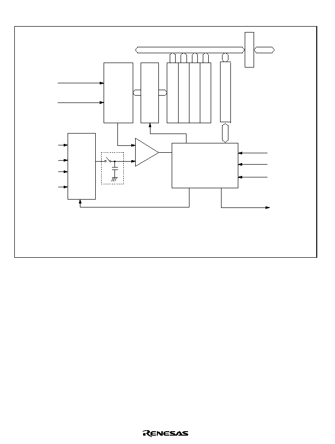
Rev. 2.00, 09/03, page 528 of 690
Figure 21.1 shows a block diagram of the A/D converter.
10-bit
D/A
ADDRA
ADDRB
ADDRD
Bus interface
Peripheral data bus
Analog
multi-
plexer
Control circuit
Successive approxi-
mation register
+
-
Comparator
Sample-and-
hold circuit
ADI
interrupt
signal
AV
SS
AN0
AN1
AN2
AN3
P
/8
P
/16
ADCSR
P
/4
AV
CC
ADCSR: A/D control/status register
ADDRA: A/D data register A
ADDRB: A/D data register B
ADDRC: A/D data register C
ADDRD: A/D data register D
Legend
Internal
data bus
ADDRC
Figure 21.1 Block Diagram of A/D Converter

Rev. 2.00, 09/03, page 529 of 690
21.2
Input/Output Pins
Table 21.1 summarizes the A/D converter's pins. The AV
CC
and AV
SS
pins are the power supply
for the analog circuits in the A/D converter. The AV
CC
pin also functions as the A/D conversion
reference voltage pin.
Table 21.1
Pin Configuration
Pin Name
Abbreviation
Input/
Output Function
Analog power supply
AVcc
Input
Analog power supply and reference voltage for
A/D conversion
Analog ground
AVss
Input
Analog ground and reference voltage for A/D
conversion
Analog input 0
AN0
Input
Analog input 0
Analog input 1
AN1
Input
Analog input 1
Analog input 2
AN2
Input
Analog input 2
Analog input 3
AN3
Input
Analog input 3
21.3
Register Descriptions
The A/D converter has the following registers. For more information on addresses of registers and
register states in the processing, see section 24, List of Registers.
∑
A/D data register A (ADDRA)
∑
A/D data register B (ADDRB)
∑
A/D data register C (ADDRC)
∑
A/D data register D (ADDRD)
∑
A/D control/status register (ADCSR)

Rev. 2.00, 09/03, page 530 of 690
21.3.1
A/D Data Registers A to D (ADDRA to ADDRD)
The four A/D data registers (ADDRA to ADDRD) are 16-bit read-only registers that store the
results of A/D conversion. Table 21.2 indicates the pairings of analog input channels and A/D data
registers that store the results of A/D conversion.
An A/D conversion produces 10-bit data, which is transferred for storage into bits 15 to 6 in the
A/D data register corresponding to the selected channel. Bits 5 to 0 of an A/D data register are
reserved bits that are always read as 0.
The A/D data registers are initialized to H'0000.
Table 21.2
Analog Input Channels and A/D Data Registers
Analog Input Channel
A/D Data Register that Store Results of A/D Conversion
AN0
ADDRA
AN1
ADDRB
AN2
ADDRC
AN3
ADDRD
21.3.2
A/D Control/Status Registers (ADCSR)
ADCSR is a 16-bit readable/writable register that selects the mode and controls the A/D converter.
Bit
Bit
Name
Initial
Value
R/W
Description
15
ADF
0
R/(W)
*
A/D End Flag
Indicates the end of A/D conversion.
[Setting conditions]
Single mode: A/D conversion ends
Multi mode: A/D conversion ends cycling through the
selected channels
Scan mode: A/D conversion ends cycling through the
selected channels
[Clearing conditions]
(1) Reading ADF while ADF = 1, then writing 0 to ADF
(2) DMAC is activated by ADI interrupt and ADDR is
read
Note:
*
Clear this bit by writing 0. Writing 1 is ignored.

Rev. 2.00, 09/03, page 531 of 690
Bit
Bit
Name
Initial
Value
R/W
Description
14
ADIE
0
R/W
A/D Interrupt Enable
Enables or disables the interrupt (ADI) requested by ADF.
Set the ADIE bit while the ADST bit is 0.
0: Interrupt (ADI) requested by ADF is disabled
1: Interrupt (ADI) requested by ADF is enabled
13
ADST
0
R/W
A/D Start
Starts or stops A/D conversion. The ADST bit remains set to
1 during A/D conversion.
0: A/D conversion is stopped.
1: Single mode:
A/D conversion starts; ADST is automatically cleared to 0
when conversion ends on selected channels.
Multi mode:
A/D conversion starts; when conversion is completed
cycling through the selected channels, ADST is
automatically cleared.
Scan mode:
A/D conversion starts and continues, A/D conversion is
continuously performed until ADST is cleared to 0 by
software, by a reset, or by a transition to standby mode.
12
DMASL
0
R/W
DMAC Select
Selects an interrupt due to ADF or activation of the DMAC.
Set the DMASL bit while the ADST bit is 0.
0: An interrupt by ADF is selected.
1: Activation of the DMAC by ADF is selected.
11 to 8
--
0
R
Reserved
These bits are always read as 0. The write value should
always be 0.

Rev. 2.00, 09/03, page 532 of 690
Bit
Bit
Name
Initial
Value
R/W
Description
7
6
CKS1
CKS0
0
1
R/W
R/W
Clock Select
Selects the A/D conversion time. Clear the ADST bit to 0
before changing the conversion time.
00: Conversion time = 151 states (maximum) at P
/4
01: Conversion time = 285 states (maximum) at P
/8
10: Conversion time = 545 states (maximum) at P
/16
11: Setting prohibited
Note:
If the minimum conversion time is not satisfied,
lack of accuracy or abnormal operation may
occur.
5
4
MULTI1
MULTI0
0
0
R/W
R/W
Mode Select
Selects single mode, multi mode, or scan mode.
00: Single mode
01: Setting prohibited
10: Multi mode
11: Scan mode
3
2
--
--
0
0
R
R
Reserved
These bits are always read as 0. The write value should
always be 0.
1
0
CH1
CH0
0
0
R/W
R/W
Channel Select
These bits and the MULTI bit select the analog input
channels. Clear the ADST bit to 0 before changing the
channel selection.
Single mode
Multi mode or scan mode
00: AN0
AN0
01: AN1
AN0, AN1
10: AN2
AN0 to AN2
11: AN3
AN0 to AN3

Rev. 2.00, 09/03, page 533 of 690
21.4
Operation
The A/D converter operates by successive approximations with 10-bit resolution. It has three
operating modes: single mode, multi mode, and scan mode. To avoid malfunction, switch
operating modes while the ADST bit of ADCSR is 0. Changing operating modes and channels and
setting the ADST bit can be performed simultaneously.
21.4.1
Single Mode
Single mode should be selected when only one A/D conversion on one channel is required.
1.
A/D conversion of the selected channel starts when the ADST bit of ADCSR is set to 1 by
software.
2.
When conversion ends, the conversion results are transmitted to the A/D data register that
corresponds to the channel.
3.
When conversion ends, the ADF bit of ADCSR is set to 1. If the ADIE bit is also set to 1, an
ADI interrupt is requested at this time.
4.
The ADST bit holds 1 during A/D conversion. When A/D conversion is completed, the ADST
bit is cleared to 0 and the A/D converter becomes idle. When the ADST bit is cleared to 0
during A/D conversion, the conversion is halted and the A/D converter becomes idle.
To clear the ADF flag to 0, first read ADF, then write 0 to ADF.
21.4.2
Multi Mode
Multi mode should be selected when performing A/D conversions on one or more channels.
1.
When the ADST bit is set to 1 by software, A/D conversion starts with the smaller number of
the analog input channel in the group (for instance, AN0, and AN1 to AN3).
2.
When conversion of each channel ends, the conversion results are transmitted to the A/D data
register that corresponds to the channel.
3.
When conversion of all selected channels ends, the ADF bit of ADCSR is set to 1. If the
ADIE bit is also set to 1, an ADI interrupt is requested at this time.
4.
When A/D conversion is completed, the ADST bit is cleared to 0 and the A/D converter
becomes idle. When the ADST bit is cleared to 0 during A/D conversion, the conversion is
halted and the A/D converter becomes idle.
To clear the ADF flag to 0, first read ADF, then write 0 to ADF.

Rev. 2.00, 09/03, page 534 of 690
21.4.3
Scan Mode
Scan mode should be selected when performing A/D conversions of analog inputs on one or more
specified channels. Scan mode is useful for monitoring analog inputs.
1.
When the ADST bit is set to 1 by software, A/D conversion starts with the smaller number of
the analog input channel in the group (for instance, AN0, and AN1 to AN3).
2.
When conversion of each channel ends, the conversion results are transmitted to the A/D data
register that corresponds to the channel.
3.
When conversion of all selected channels ends, the ADF bit of ADCSR is set to 1. If the
ADIE bit is also set to 1, an ADI interrupt is requested at this time. A/D conversion then starts
with the smaller number of the analog input channel.
4.
The ADST bit is not automatically cleared to 0. When the ADST bit is set to 1, steps 2 and 3
above are repeated. When the ADST bit is cleared to 0, the conversion is halted and the A/D
converter becomes idle.
To clear the ADF flag to 0, first read ADF, then write 0 to ADF.
21.4.4
Input Sampling and A/D Conversion Time
The A/D converter has a built-in sample-and-hold circuit. The A/D converter samples the analog
input at an A/D conversion start delay time t
D
after the ADST bit is set to 1, then starts conversion.
Figure 21.2 shows the A/D conversion timing. Table 21.3 indicates the A/D conversion time.
As indicated in figure 21.2, the A/D conversion time (t
CONV
) includes t
D
and the input sampling
time (t
SPL
). The length of t
D
varies depending on the timing of the write access to ADCSR. The
total conversion time therefore varies within the ranges indicated in table 21.3.
In multi mode and scan mode, the values given in table 21.3 apply to the first conversion. In the
second and subsequent conversions, the values given in table 21.4 apply to the first conversion.
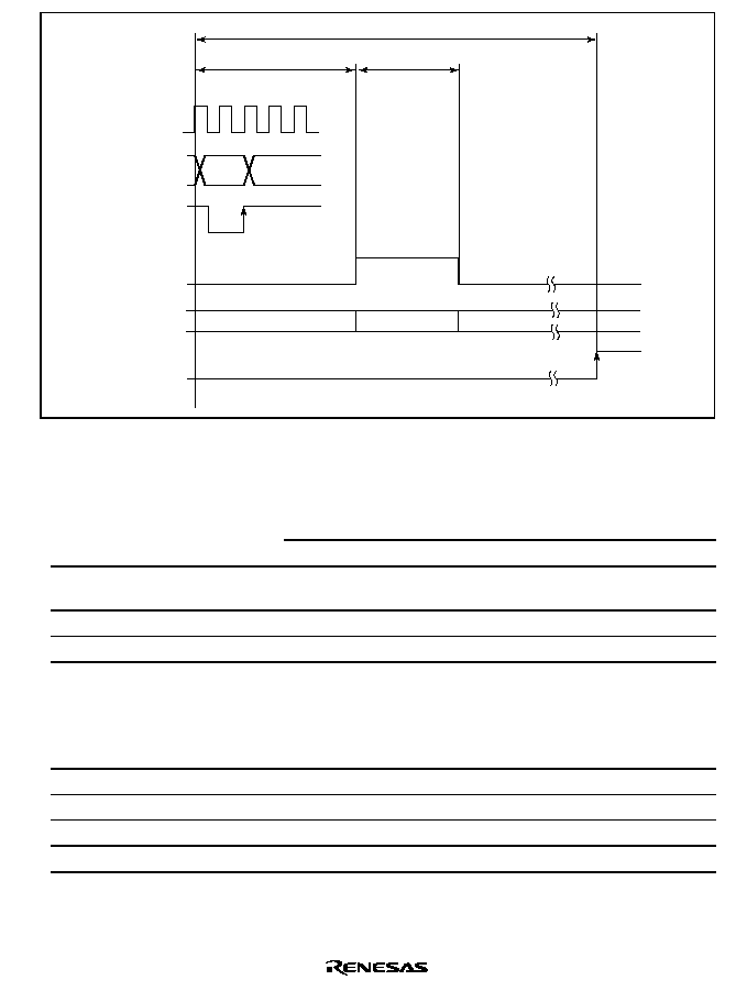
Rev. 2.00, 09/03, page 535 of 690
P
ADF
A/D conversion time (t
CONV
)
A/D conversion start delay time (t
D
) Analog input sampling time (t
SPL
)
Write cycle A/D
synchronization time
Address
Internal
write signal
Write timing of ADST
Analog input
sampling signal
A/D converter
Idle time
Sample and hold
A/D conversion executed
A/D conversion ended
Figure 21.2 A/D Conversion Timing
Table 21.3
A/D Conversion Time (Single Mode)
CKS1 = 1,
CKS0 = 0
CKS1 = 0,
CKS0 = 1
CKS1 = 0,
CKS0 = 0
Symbol
Min
Typ
Max
Min
Typ
Max
Min
Typ
Max
A/D conversion start
delay
t
D
18
--
21
10
--
13
6
--
9
Input sampling time
t
SPL
--
129
--
--
65
--
--
33
--
A/D conversion time
t
CONV
535
--
545
275
--
285
141
--
151
Note:
Values in the table are numbers of states for P
.
Table 21.4
A/D Conversion Time (Multi Mode and Scan Mode)
CKS1
CKS0
Conversion Time (cycles)
0
0
128 (fixed)
0
1
256 (fixed)
1
0
512 (fixed)
1
1
Unused

Rev. 2.00, 09/03, page 536 of 690
21.5
Interrupts and DMAC Transfer Request
The A/D converter generates an interrupt (ADI) at the end of A/D conversion. The ADI interrupt
request is enabled when ADF in ADCSR is set to 1and the ADIE bit in ADCSR is set to 1 after
A/D conversion. The ADI interrupt can activate the direct memory access controller (DMAC) by
setting the ADIE and DMASL bits to 1. Continuous conversion without loads of software is
enabled by reading data that has been converted by the ADI interrupt with DMAC.
When activating DMAC by ADI, the ADF bit in ADCSR is automatically cleared to 0 at DMAC
data transfer.
Table 21.5
A/D Converter Interrupt Source
Name
Interrupt source
Interrupt flag
DMAC activation
ADI
A/D conversion end
ADF
Yes
21.6
Definitions of A/D Conversion Accuracy
The following shows the definitions of A/D conversion accuracy. In the figure, the 10 bits of the
A/D converter have been simplified to 3 bits.
∑
Resolution
Digital output code number of the A/D converter
∑
Quantization error
Intrinsic error of the A/D converter and is expressed as 1/2 LSB (figure 21.3)
∑
Offset error
Deviation between analog input voltage and ideal A/D conversion characteristics when the
digital output value changes from the minimum (zero voltage) 0000000000 (H'00; 000 in
figure 21.3) to 0000000001 (H'01; 001 in figure 21.3) (figure 21.4)
∑
Full-scale error
Deviation between analog input voltage and ideal A/D conversion characteristics when the
digital output value changes from the 1111111110 (H'3EF; 110 in figure 21.3) to the maximum
1111111111 (H'3FF; 111 in figure 21.3) (figure 21.4).
∑
Nonlinearity error
Deviation between analog input voltage and ideal A/D conversion characteristics between zero
voltage and full-scale voltage (figure 21.4). Note that it does not include offset, full-scale, or
quantization error.
∑
Absolute accuracy
Deviation between analog and digital input values. Note that it includes offset, full-scale,
quantization, or nonlinearity error.

Rev. 2.00, 09/03, page 537 of 690
111
110
101
100
011
010
001
000
0
1/8
2/8
3/8
4/8
5/8
6/8
7/8
FS
Analog input
voltage
Quantization
error
Ideal A/D
conversion
characteristic
Digital output
Figure 21.3
Definitions of A/D Conversion Accuracy
Nonlinearity
error
Ideal A/D
conversion
characteristic
Actual A/D
conversion
characteristic
Full-scale error
Digital output
Analog input
voltage
Offset error
FS
Figure 21.4 Definitions of A/D Conversion Accuracy
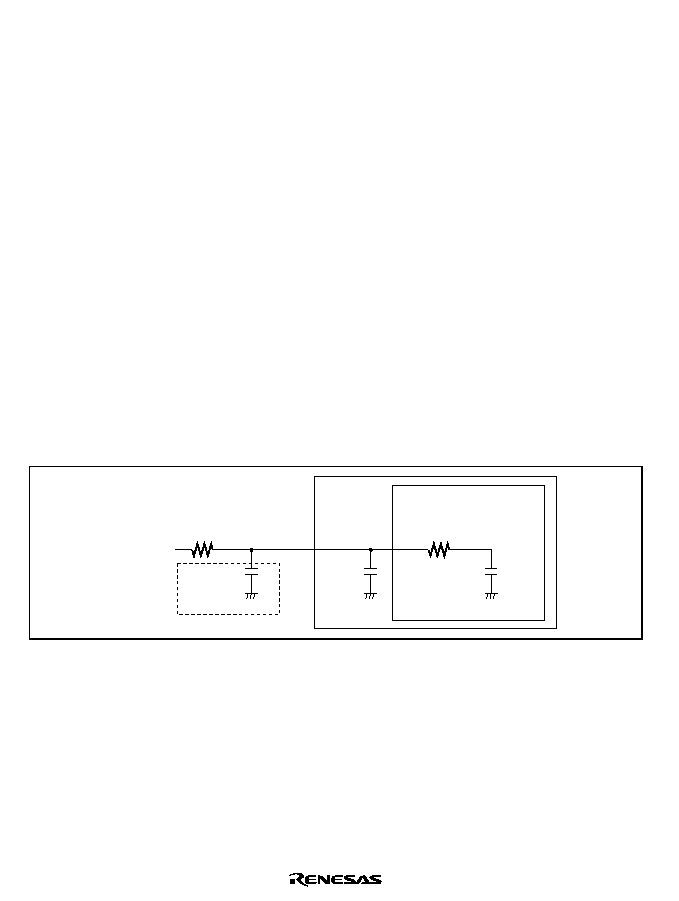
Rev. 2.00, 09/03, page 538 of 690
21.7
Usage Notes
21.7.1
Allowable Signal-Source Impedance
For the analog input design of this LSI, conversion accuracy is guaranteed for an input signal with
signal-source impedance of 5 k
or less. The specification is for charging input capacitance of the
sample and hold circuit of the A/D converter within sampling time. When the output impedance of
the sensor exceeds 5 k
, conversion accuracy is not guaranteed due to insufficient charging. If
large external capacitance is set at conversion in single mode, signal-source impedance is ignored
since input load is only internal input resistance of 3 k
. However, an analog signal with large
differential coefficient (5 mV/
µ
s or greater) cannot be followed up because of a low-pass filter
(figure 21.5). When converting high-speed analog signals or converting in scan mode, insert a
low-impedance buffer.
21.7.2
Influence to Absolute Accuracy
By adding capacitance, absolute accuracy may be degraded if noise is on GND because there is
coupling with GND. Therefore, connect electrically stable GND such as AVcc to prevent absolute
accuracy from being degraded.
A filter circuit must not interfere with digital signals, or must not be an antenna on a mounting
board.
20 pF
C
in
=
15 pF
3 k
to 5 k
Output impedance of sensor
Sensor input
This LSI
Lowpass
filter
(C = 0.1
µF)
Equivalent circuit
of A/D converter
Figure 21.5 Analog Input Circuit Example
21.7.3
Setting Analog Input Voltage
Operating the chip in excess of the following voltage range may result in damage to chip
reliability.
∑
Analog Input Voltage Range: During A/D conversion, the voltages (VANn) input to the analog
input pins ANn should be in the range AV
SS
VANn
AV
CC
(n = 0 to 3).
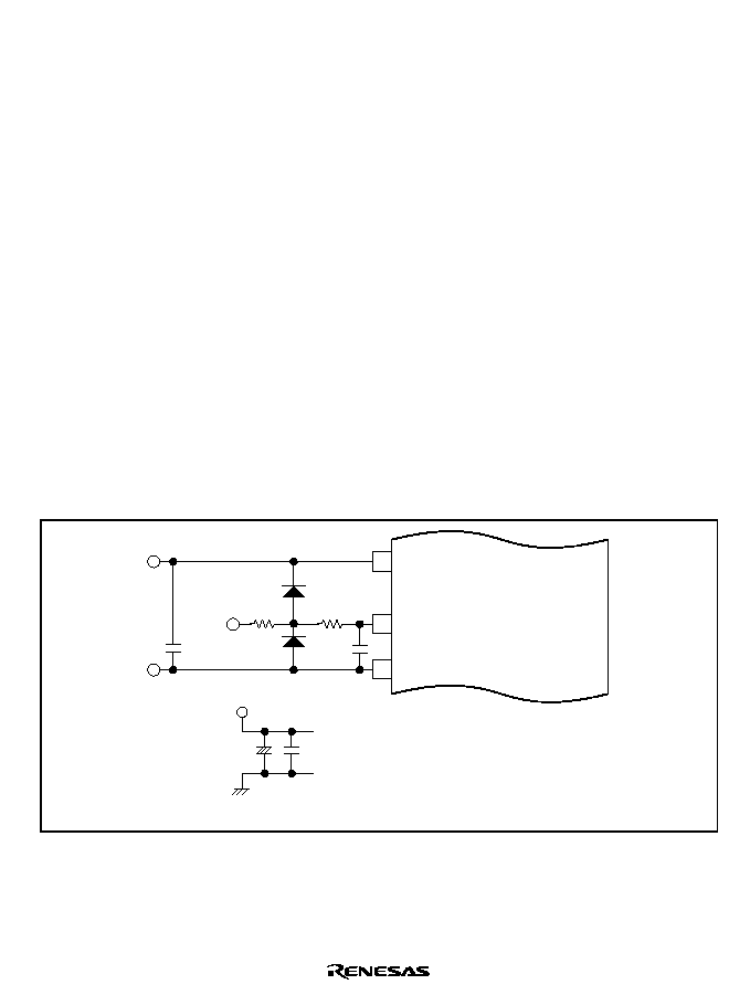
Rev. 2.00, 09/03, page 539 of 690
∑
Relationships of AV
CC
, AV
SS
and V
CC
Q, V
SS
Q: AV
CC
= V
CC
Q ± 0.2 V and AV
SS
= V
SS
Q. Even
when the A/D converter is not used, do not open AV
CC
and AV
SS
.
21.7.4
Notes on Board Design
In designing a board, separate digital circuits and analog circuits. Do not intersect or locate closely
signal lines of a digital circuit and an analog circuit. An analog circuit may malfunction due to
induction, thus affecting A/D conversion values. Separate analog input pins (AN0 to AN3) and the
analog power voltage (AVcc) from digital circuits with analog ground (AVss). Connect analog
ground (AVss) to one point of stable ground (Vss) on the board.
21.7.5
Notes on Countermeasures to Noise
Connect a protective circuit between AVcc and AVss, as shown in figure 21.6, to prevent damage
of analog input pins (AN0 to AN3) due to abnormal voltage such as excessive serge. Connect a
bypass capacitor that is connected to AVcc and a capacitor for a filter that is connected to AN0 to
AN3 to AVss.
When a capacitor for a filter is connected, input currents of AN0 to AN3 are averaged, may
causing errors. If A/D conversion is frequently performed in scan mode, voltages of analog input
pins cause errors when a current that is charged/discharged for capacitance of a sample & hold
circuit in the A/D converter is higher than a current that is input through input impedance (Rin).
Therefore, determine a circuit constant carefully.
0.01
µF
10
µF
AV
CC
AN0 to AN3
AV
SS
This LSI
*
1
100
0.1
µF
Notes: 1. Values are for reference.
R
in
*
2
2. R
in
is input impedance.
Figure 21.6 Example of Analog Input Protection Circuit
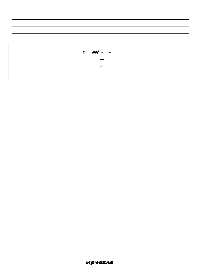
Rev. 2.00, 09/03, page 540 of 690
Table 21.6
Analog Input Pin Ratings
Item
Min
Max
Unit
Analog input capacitance
--
20
pF
Allowable signal-source impedance
--
5
k
20 pF
AN0 to AN3
3 k
To A/D converter
Note: Values are for reference.
Figure 21.7 Analog Input Pin Equivalent Circuit

UBCS311A_000020020100
Rev. 2.00, 09/03, page 541 of 690
Section 22 User Break Controller
The user break controller (UBC) provides functions that simplify program debugging. These
functions make it easy to design an effective self-monitoring debugger, enabling the chip to debug
programs without using an in-circuit emulator. Break conditions that can be set in the UBC are
instruction fetch or data read/write access, data size, data contents, address value, and stop timing
in the case of instruction fetch.
22.1
Features
The UBC has the following features:
∑
The following break comparison conditions can be set.
Number of break channels: two channels (channels A and B)
User break can be requested as either the independent or sequential condition on channels A
and B (sequential break setting: channel A and then channel B match with break conditions,
but not in the same bus cycle).
Address (Compares 40 bits configured of the ASID and addresses 32 bits: the ASID can be
selected either all-bit comparison or all-bit mask. Comparison bits for the address are
maskable in 1-bit units; user can mask addresses at lower 12 bits (4 k page), lower 10 bits
(1 k page), or any size of page, etc.)
One of the two address buses (L bus address (LAB) and I bus address (IAB)) can be
selected.
Data (only on channel B, 32-bit maskable)
One of the two data buses (L bus data (LDB) and I bus data (IDB)) can be selected.
Bus cycle: Instruction fetch or data access
Read/write
Operand size: Byte, word, or longword
∑
User break is generated upon satisfying break conditions. A user-designed user-break
condition exception processing routine can be run.
∑
In an instruction fetch cycle, it can be selected that a break is set before or after an instruction
is executed.
∑
Maximum repeat times for the break condition (only for channel B): 2
12
≠ 1 times.
∑
Eight pairs of branch source/destination buffers.
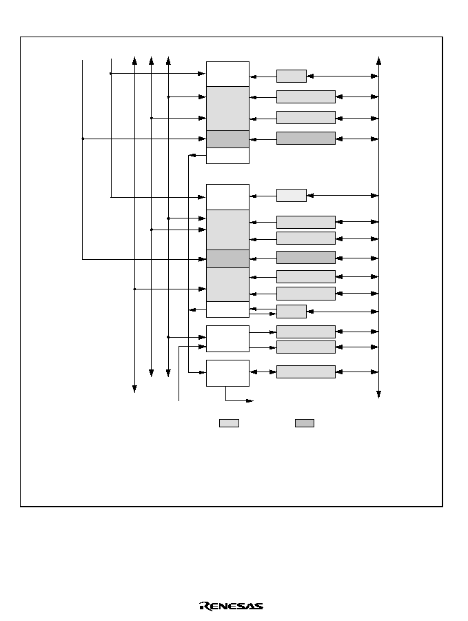
Rev. 2.00, 09/03, page 542 of 690
Figure 22.1 shows a block diagram of the UBC.
BBRA
BARA
BAMRA
CPU state
signals
IAB LAB
MDB
Access
comparator
Channel A
Access
comparator
Address
comparator
Data
comparator
PC trace
CONTROL
Channel B
BBRB
BETR
BASRA
BASRB
BARB
BAMRB
BBRB
BDMRB
BRSR
BRDR
BRCR
User break request
UBC Location
CCN Location
LDB/IDB
[Legend]
BBRA:
Break bus cycle register A
BARA:
Break address register A
BAMRA: Break address mask register A
BASRA: Break ASID register A
BBRB:
Break bus cycle register B
BARB:
Break address register B
BAMRB: Break address mask register B
BASRB: Break ASID register B
BDRB:
Break data register B
BDMRB: Break data mask register B
BETR:
Break execution times register
BRSR:
Branch source register
BRDR:
Branch destination register
BRCR:
Break control register
Access
Control
ASID
comparator
ASID
comparator
ASID
Address
comparator
Figure 22.1 Block Diagram of User Break Controller

Rev. 2.00, 09/03, page 543 of 690
22.2
Register Descriptions
The user break controller has the following registers. For details on register addresses and access
sizes, refer to section 24, List of Registers.
∑
Break address register A (BARA)
∑
Break address mask register A (BAMRA)
∑
Break bus cycle register A (BBRA)
∑
Break address register B (BARB)
∑
Break address mask register B (BAMRB)
∑
Break bus cycle register B (BBRB)
∑
Break data register B (BDRB)
∑
Break data mask register B (BDMRB)
∑
Break control register (BRCR)
∑
Execution times break register (BETR)
∑
Branch source register (BRSR)
∑
Branch destination register (BRDR)
∑
Break ASID register A (BASRA)
∑
Break ASID register B (BASRB)
22.2.1
Break Address Register A (BARA)
BARA is a 32-bit readable/writable register. BARA specifies the address used as a break condition
in channel A.
Bit
Bit
Name
Initial
Value
R/W
Description
31 to 0
BAA31 to
BAA0
0
R/W
Break Address A
Store the address on the LAB or IAB specifying break
conditions of channel A.

Rev. 2.00, 09/03, page 544 of 690
22.2.2
Break Address Mask Register A (BAMRA)
BAMRA is a 32-bit readable/writable register. BAMRA specifies bits masked in the break address
specified by BARA.
Bit
Bit
Name
Initial
Value
R/W
Description
31 to 0
BAMA31 to
BAMA0
0
R/W
Break Address Mask A
Specify bits masked in the channel A break address
bits specified by BARA (BAA31 to BAA0).
0: Break address bit BAAn of channel A is included in
the break condition
1: Break address bit BAAn of channel A is masked
and is not included in the break condition
Note:
n = 31 to 0
22.2.3
Break Bus Cycle Register A (BBRA)
BBRA is a 16-bit readable/writable register, which specifies (1) L bus cycle or I bus cycle, (2)
instruction fetch or data access, (3) read or write, and (4) operand size in the break conditions of
channel A.
Bit
Bit
Name
Initial
Value
R/W
Description
15 to 8
0
R
Reserved
These bits are always read as 0. The write value should
always be 0.
7
6
CDA1
CDA0
0
0
R/W
R/W
L Bus Cycle/I Bus Cycle Select A
Select the L bus cycle or I bus cycle as the bus cycle of the
channel A break condition.
00: Condition comparison is not performed
01: The break condition is the L bus cycle
10: The break condition is the I bus cycle
11: The break condition is the L bus cycle

Rev. 2.00, 09/03, page 545 of 690
Bit
Bit
Name
Initial
Value
R/W
Description
5
4
IDA1
IDA0
0
0
R/W
R/W
Instruction Fetch/Data Access Select A
Select the instruction fetch cycle or data access cycle as
the bus cycle of the channel A break condition.
00: Condition comparison is not performed
01: The break condition is the instruction fetch cycle
10: The break condition is the data access cycle
11: The break condition is the instruction fetch cycle or data
access cycle
3
2
RWA1
RWA0
0
0
R/W
R/W
Read/Write Select A
Select the read cycle or write cycle as the bus cycle of the
channel A break condition.
00: Condition comparison is not performed
01: The break condition is the read cycle
10: The break condition is the write cycle
11: The break condition is the read cycle or write cycle
1
0
SZA1
SZA0
0
0
R/W
R/W
Operand Size Select A
Select the operand size of the bus cycle for the channel A
break condition.
00: The break condition does not include operand size
01: The break condition is byte access
10: The break condition is word access
11: The break condition is longword access
22.2.4
Break Address Register B (BARB)
BARB is a 32-bit readable/writable register. BARB specifies the address used as a break condition
in channel B.
Bit
Bit
Name
Initial
Value
R/W
Description
31 to 0
BAB31
to
BAB0
0
R/W
Break Address B
Stores an address which specifies a break condition in
channel B.
BARB specifies the break address on LAB or IAB.

Rev. 2.00, 09/03, page 546 of 690
22.2.5
Break Address Mask Register B (BAMRB)
BAMRB is a 32-bit readable/writable register. BAMRB specifies bits masked in the break address
specified by BARB.
Bit
Bit
Name
Initial
Value
R/W
Description
31 to 0
BAMB31
to
BAMB0
0
R/W
Break Address Mask B
Specifies bits masked in the break address of channel B
specified by BARB (BAB31 to BAB0).
0: Break address BABn of channel B is included in the
break condition
1: Break address BABn of channel B is masked and is
not included in the break condition
Note:
n = 31 to 0
22.2.6
Break Data Register B (BDRB)
BDRB is a 32-bit readable/writable register.
Bit
Bit
Name
Initial
Value
R/W
Description
31 to 0
BDB31 to
BDB0
0
R/W
Break Data Bit B
Stores data which specifies a break condition in channel
B.
BDRB specifies the break data on LDB or IDB.
Notes: 1. Specify an operand size when including the value of the data bus in the break condition.
2. When the byte size is selected as a break condition, the same byte data must be set in
bits 15 to 8 and 7 to 0 in BDRB as the break data.

Rev. 2.00, 09/03, page 547 of 690
22.2.7
Break Data Mask Register B (BDMRB)
BDMRB is a 32-bit readable/writable register. BDMRB specifies bits masked in the break data
specified by BDRB.
Bit
Bit
Name
Initial
Value
R/W
Description
31 to 0
BDMB31 to
BDMB0
0
R/W
Break Data Mask B
Specifies bits masked in the break data of channel B
specified by BDRB (BDB31 to BDB0).
0: Break data BDBn of channel B is included in the
break condition
1: Break data BDBn of channel B is masked and is not
included in the break condition
Note:
n = 31 to 0
Notes: 1. Specify an operand size when including the value of the data bus in the break condition.
2. When the byte size is selected as a break condition, the same byte data must be set in
bits 15 to 8 and 7 to 0 in BDRB as the break mask data in BDMRB.
22.2.8
Break Bus Cycle Register B (BBRB)
BBRB is a 16-bit readable/writable register, which specifies (1) L bus cycle or I bus cycle, (2)
instruction fetch or data access, (3) read or write, and (4) operand size in the break conditions of
channel B.
Bit
Bit
Name
Initial
Value
R/W
Description
15 to 8
0
R
Reserved
These bits are always read as 0. The write value should
always be 0.

Rev. 2.00, 09/03, page 548 of 690
Bit
Bit
Name
Initial
Value
R/W
Description
7
6
CDB1
CDB0
0
0
R/W
R/W
L Bus Cycle/I Bus Cycle Select B
Select the L bus cycle or I bus cycle as the bus cycle of the
channel B break condition.
00: Condition comparison is not performed
01: The break condition is the L bus cycle
10: The break condition is the I bus cycle
11: The break condition is the L bus cycle
5
4
IDB1
IDB0
0
0
R/W
R/W
Instruction Fetch/Data Access Select B
Select the instruction fetch cycle or data access cycle as
the bus cycle of the channel B break condition.
00: Condition comparison is not performed
01: The break condition is the instruction fetch cycle
10: The break condition is the data access cycle
11: The break condition is the instruction fetch cycle or data
access cycle
3
2
RWB1
RWB0
0
0
R/W
R/W
Read/Write Select B
Select the read cycle or write cycle as the bus cycle of the
channel B break condition.
00: Condition comparison is not performed
01: The break condition is the read cycle
10: The break condition is the write cycle
11: The break condition is the read cycle or write cycle
1
0
SZB1
SZB0
0
0
R/W
R/W
Operand Size Select B
Select the operand size of the bus cycle for the channel B
break condition.
00: The break condition does not include operand size
01: The break condition is byte access
10: The break condition is word access
11: The break condition is longword access

Rev. 2.00, 09/03, page 549 of 690
22.2.9
Break Control Register (BRCR)
BRCR sets the following conditions:
1. Specifies whether channels A and B are used in two independent channel conditions or under
the sequential condition.
2. Specifies whether a break is set before or after instruction execution.
3. Specifies whether to include the number of execution times on channel B in comparison
conditions.
4. Specifies whether to include data bus on channel B in comparison conditions.
5. Enables PC trace.
6. Enables ASID check.
BRCR is a 32-bit readable/writable register that has break conditions match flags and bits for
setting a variety of break conditions.
Bit
Bit
Name
Initial
Value
R/W
Description
31 to 22
0
R
Reserved
These bits are always read as 0. The write value should
always be 0.
21
BASMA
0
R/W
Break ASID Mask A
Specifies whether bits in channel A break ASID7 to
ASID0 (BASA7 to BASA0) which are set in BASRA are
masked or not.
0: All BASRA bits are included in the break conditions
and the ASID is checked
1: All BASRA bits are not included in the break conditions
and the ASID is not checked
20
BASMB
0
R/W
Break ASID Mask B
Specifies whether bits in channel B break ASID7 to
ASID0 (BASB7 to BASB0) which are set in BASRB are
masked or not.
0: All BASRB bits are included in the break conditions
and the ASID is checked
1: All BASRB bits are not included in the break conditions
and the ASID is not checked
19 to 16
0
R
Reserved
These bits are always read as 0. The write value should
always be 0.

Rev. 2.00, 09/03, page 550 of 690
Bit
Bit
Name
Initial
Value
R/W
Description
15
SCMFCA
0
R/W
L Bus Cycle Condition Match Flag A
When the L bus cycle condition in the break conditions set
for channel A is satisfied, this flag is set to 1. In order to
clear this flag, write 0 into this bit.
0: The L bus cycle condition for channel A does not match
1: The L bus cycle condition for channel A matches
14
SCMFCB
0
R/W
L Bus Cycle Condition Match Flag B
When the L bus cycle condition in the break conditions set
for channel B is satisfied, this flag is set to 1. In order to
clear this flag, write 0 into this bit.
0: The L bus cycle condition for channel B does not match
1: The L bus cycle condition for channel B matches
13
SCMFDA
0
R/W
I Bus Cycle Condition Match Flag A
When the I bus cycle condition in the break conditions set for
channel A is satisfied, this flag is set to 1. In order to clear
this flag, write 0 into this bit.
0: The I bus cycle condition for channel A does not match
1: The I bus cycle condition for channel A matches
12
SCMFDB
0
R/W
I Bus Cycle Condition Match Flag B
When the I bus cycle condition in the break conditions set for
channel B is satisfied, this flag is set to 1. In order to clear
this flag, write 0 into this bit.
0: The I bus cycle condition for channel B does not match
1: The I bus cycle condition for channel B matches
11
PCTE
0
R/W
PC Trace Enable
0: Disables PC trace
1: Enables PC trace
10
PCBA
0
R/W
PC Break Select A
Selects the break timing of the instruction fetch cycle for
channel A as before or after instruction execution.
0: PC break of channel A is set before instruction execution
1: PC break of channel A is set after instruction execution

Rev. 2.00, 09/03, page 551 of 690
Bit
Bit
Name
Initial
Value
R/W
Description
9, 8
0
R
Reserved
These bits are always read as 0. The write value should
always be 0.
7
DBEB
0
R/W
Data Break Enable B
Selects whether or not the data bus condition is included in
the break condition of channel B.
0: No data bus condition is included in the condition of channel
B
1: The data bus condition is included in the condition of
channel B
6
PCBB
0
R/W
PC Break Select B
Selects the break timing of the instruction fetch cycle for
channel B as before or after instruction execution.
0: PC break of channel B is set before instruction execution
1: PC break of channel B is set after instruction execution
5, 4
0
R
Reserved
These bits are always read as 0. The write value should
always be 0.
3
SEQ
0
R/W
Sequence Condition Select
Selects two conditions of channels A and B as independent or
sequential conditions.
0: Channels A and B are compared under independent
conditions
1: Channels A and B are compared under sequential
conditions (channel A, then channel B)
2, 1
0
R
Reserved
These bits are always read as 0. The write value should
always be 0.
0
ETBE
0
R/W
Number of Execution Times Break Enable
Enables the execution-times break condition only on channel
B. If this bit is 1 (break enable), a user break is issued when
the number of satisfied break conditions matches with the
number of execution times that is specified by BETR.
0: The execution-times break condition is disabled on channel
B
1: The execution-times break condition is enabled on channel
B

Rev. 2.00, 09/03, page 552 of 690
22.2.10
Execution Times Break Register (BETR)
BETR is a 16-bit readable/writable register. When the execution-times break condition of channel
B is enabled, this register specifies the number of execution times to make the break. The
maximum number is 2
12
≠ 1 times. When a break condition is satisfied, it decrements the BETR
value. A break is issued when the break condition is satisfied after BETR becomes H'0001.
Bit
Bit
Name
Initial
Value
R/W
Description
15 to
12
0
R
Reserved
These bits are always read as 0. The write value should
always be 0.
11 to 0
BET11 to
BET0
0
R/W
Number of Execution Times
Note:
If the channel B brake condition set to during instruction fetch cycles and any of the
instructions below perform breaks, BETR is not decremented when the first break occurs.
The decremented values are listed below.
Instruction
Value
Decremented
Instruction
Value
Decremented
RTE
4
LDC.L @Rm+,SR
6
DMULS.L Rm,Rn
2
LDC.L @Rm+,GBR
4
DMULU.L Rm,Rn
2
LDC.L @Rm+,VBR
4
MAC.L @Rm+,@Rn+
2
LDC.L @Rm+,SSR
4
MAC.W @Rm+,@Rn+
2
LDC.L @Rm+,SPC
4
MUL.L Rm,Rn
3
LDC.L @Rm+,R0_BANK
4
AND.B #imm,@(R0,GBR)
3
LDC.L @Rm+,R1_BANK
4
OR.B #imm,@(R0,GBR)
3
LDC.L @Rm+,R2_BANK
4
TAS.B @Rn
3
LDC.L @Rm+,R3_BANK
4
TST.B #imm,@(R0,GBR)
3
LDC.L @Rm+,R4_BANK
4
XOR.B #imm,@(R0,GBR)
3
LDC.L @Rm+,R5_BANK
4
LDC Rm,SR
4
LDC.L @Rm+,R6_BANK
4
LDC Rm,GBR
4
LDC.L @Rm+,R7_BANK
4
LDC Rm,VBR
4
LDC.L @Rn+,MOD
4
LDC Rm,SSR
4
LDC.L @Rn+,RS
4
LDC Rm,SPC
4
LDC.L @Rn+,RE
4
LDC Rm,R0_BANK
4
LDC Rn,MOD
4
LDC Rm,R1_BANK
4
LDC Rn,RS
4
LDC Rm,R2_BANK
4
LDC Rn,RE
4
LDC Rm,R3_BANK
4
BSR label
2
LDC Rm,R4_BANK
4
BSRF Rm
2
LDC Rm,R5_BANK
4
JSR @Rm
2
LDC Rm,R6_BANK
4
LDC Rm,R7_BANK
4

Rev. 2.00, 09/03, page 553 of 690
22.2.11
Branch Source Register (BRSR)
BRSR is a 32-bit read-only register. BRSR stores bits 27 to 0 in the address of the branch source
instruction. BRSR has the flag bit that is set to 1 when a branch occurs. This flag bit is cleared to 0
when BRSR is read, the setting to enable PC trace is made, or BRSR is initialized by a power-on
reset. Other bits are not initialized by a power-on reset. The eight BRSR registers have a queue
structure and a stored register is shifted at every branch.
Bit
Bit
Name
Initial
Value
R/W
Description
31
SVF
0
R
BRSR Valid Flag
Indicates whether the branch source address is stored.
When a branch source address is fetched, this flag is
set to 1. This flag is cleared to 0 by reading from BRSR.
0: The value of BRSR register is invalid
1: The value of BRSR register is valid
30 to 28
0
R
Reserved
These bits are always read as 0.
27 to 0
BSA27
to BSA0
Undefined
R
Branch Source Address
Store bits 27 to 0 of the branch source address.

Rev. 2.00, 09/03, page 554 of 690
22.2.12
Branch Destination Register (BRDR)
BRDR is a 32-bit read-only register. BRDR stores bits 27 to 0 in the address of the branch
destination instruction. BRDR has the flag bit that is set to 1 when a branch occurs. This flag bit is
cleared to 0 when BRDR is read, the setting to enable PC trace is made, or BRDR is initialized by
a power-on reset. Other bits are not initialized by a power-on reset. The eight BRDR registers have
a queue structure and a stored register is shifted at every branch.
Bit
Bit
Name
Initial
Value
R/W
Description
31
DVF
0
R
BRDR Valid Flag
Indicates whether a branch destination address is
stored. When a branch destination address is
fetched, this flag is set to 1. This flag is cleared to 0
by reading BRDR.
0: The value of BRDR register is invalid
1: The value of BRDR register is valid
30 to
28
0
R
Reserved
These bits are always read as 0.
27 to 0
BDA27 to
BDA0
Undefined
R
Branch Destination Address
Store bits 27 to 0 of the branch destination address.
22.2.13
Break ASID Register A (BASRA)
BASRA is an 8-bit readable/writable register that specifies ASID which becomes the break
condition for channel A. BASRA is in CCN.
Bit
Bit
Name
Initial
Value
R/W
Description
7 to 0
BASA7
to
BASA0
R/W
Break ASID A
Store ASID (bits 7 to 0) which is the break condition
for channel A.

Rev. 2.00, 09/03, page 555 of 690
22.2.14
Break ASID Register B (BASRB)
BASRB is an 8-bit readable/writable register that specifies ASID which becomes the break
condition for channel B. BASRB is in CCN.
Bit
Bit
Name
Initial
Value
R/W
Description
7 to 0
BASB7
to
BASB0
R/W
Break ASID B
Store ASID (bits 7 to 0) which is the break condition for
channel B.
22.3
Operation
22.3.1
Flow of the User Break Operation
The flow from setting of break conditions to user break exception processing is described below:
1. The break addresses and corresponding ASID are set in the break address registers (BARA and
BARB) and break ASID registers (BASRA and BASRB in CNN). The masked addresses are
set in the break address mask registers (BAMRA and BAMRB). The break data is set in the
break data register (BDRB). The masked data is set in the break data mask register (BDMRB).
The bus break conditions are set in the break bus cycle registers (BBRA and BBRB). Three
groups of BBRA and BBRB (L bus cycle/I bus cycle select, instruction fetch/data access
select, and read/write select) are each set. No user break will be generated if even one of these
groups is set with 00. The respective conditions are set in the bits of the break control register
(BRCR). Make sure to set all registers related to breaks before setting BBRA/BBRB.
2. When the break conditions are satisfied, the UBC sends a user break request to the CPU and
sets the L bus condition match flag (SCMFCA or SCMFCB) and the I bus condition match
flag (SCMFDA or SCMFDB) for the appropriate channel.
3. The appropriate condition match flags (SCMFCA, SCMFDA, SCMFCB, and SCMFDB) can
be used to check if the set conditions match or not. The matching of the conditions sets flags,
but they are not reset. 0 must first be written to them before they can be used again.
4. There is a chance that the data access break and its following instruction fetch break occur
around the same time. There will be only one break request to the CPU, but these two break
channel match flags could be both set.

Rev. 2.00, 09/03, page 556 of 690
5. When selecting the I bus as the break condition, note the following:
Several bus masters, including the CPU and DMAC, are connected to the I bus. The UBC
monitors bus cycles generated by all bus masters, and determines the condition match.
Physical addresses are used for the I bus. Set a physical address in break address registers
(BARA and BARB). The bus cycles for logical addresses issued on the L bus by the CPU
are converted to physical addresses before being output to the I bus. (If the address
translation function is enabled, address translation by the MMU is carried out.)
For data access cycles issued on the L bus by the CPU, if their logical addresses are not to
be cached, they are issued with the data size specified on the L bus and their addresses are
not rounded.
For instruction fetch cycles issued on the L bus by the CPU, even though their logical
addresses are not to be cached, they are issued in longwords and their addresses are
rounded to match longword boundaries.
If a logical address issued on the L bus by the CPU is an address to be cached and a cache
miss occurs, its bus cycle is issued as a cache fill cycle on the I bus. In this case, it is issued
in longwords and its address is rounded to match longword boundaries. However note that
cache fill is not performed for a write miss in write through mode. In this case, the bus
cycle is issued with the data size specified on the L bus and its address is not rounded. In
write back mode, a write back cycle may be issued in addition to a read fill cycle. It is a
longword bus cycle whose address is rounded to match longword boundaries.
I bus cycles (including read fill cycles) resulting from instruction fetches on the L bus by
the CPU are defined as instruction fetch cycles on the I bus, while other bus cycles are
defined as data access cycles.
The DMAC only issues data access cycles for I bus cycles.
If a break condition is specified for the I bus, even when the condition matches in an I bus
cycle resulting from an instruction executed by the CPU, at which instruction the break is
to be accepted cannot be clearly defined.
6. While the block bit (BL) in the CPU status register (SR) is set to 1, no breaks can be accepted.
However, condition determination will be carried out, and if the condition matches, the
corresponding condition match flag is set to 1.

Rev. 2.00, 09/03, page 557 of 690
22.3.2
Break on Instruction Fetch Cycle
1. When L bus/instruction fetch/read/word or longword is set in the break bus cycle register
(BBRA or BBRB), the break condition becomes the L bus instruction fetch cycle. Whether it
breaks before or after the execution of the instruction can then be selected with the PCBA or
PCBB bit of the break control register (BRCR) for the appropriate channel. If an instruction
fetch cycle is set as a break condition, clear LSB in the break address register (BARA or
BARB) to 0. A break cannot be generated as long as this bit is set to 1.
2. An instruction set for a break before execution breaks when it is confirmed that the instruction
has been fetched and will be executed. This means this feature cannot be used on instructions
fetched by overrun (instructions fetched at a branch or during an interrupt transition, but not to
be executed). When this kind of break is set for the delay slot of a delayed branch instruction,
the break is generated prior to execution of the delayed branch instruction.
Note:
If a branch does not occur at a delayed conditional branch instruction, the subsequent
instruction is not recognized as a delay slot.
3. When the condition is specified to be occurred after execution, the instruction set with the
break condition is executed and then the break is generated prior to the execution of the next
instruction. As with pre-execution breaks, this cannot be used with overrun fetch instructions.
When this kind of break is set for a delayed branch instruction and its delay slot, a break is not
generated until the first instruction at the branch destination.
4. When an instruction fetch cycle is set for channel B, the break data register B (BDRB) is
ignored. Therefore, break data cannot be set for the break of the instruction fetch cycle.
5. If the I bus is set for a break of an instruction fetch cycle, the condition is determined for the
instruction fetch cycles on the I bus. For details, see 5 in section 22.3.1, Flow of the User
Break Operation.

Rev. 2.00, 09/03, page 558 of 690
22.3.3
Break on Data Access Cycle
1. If the L bus is specified as a break condition for data access break, condition comparison is
performed for the logical addresses (and data) accessed by the executed instructions, and a
break occurs if the condition is satisfied. If the I bus is specified as a break condition, condition
comparison is performed for the physical addresses (and data) of the data access cycles that are
issued on the I bus by all bus masters including the CPU, and a break occurs if the condition is
satisfied. For details on the CPU bus cycles issued on the I bus, see 5 in section 22.3.1, Flow of
the User Break Operation.
2. The relationship between the data access cycle address and the comparison condition for each
operand size is listed in table 22.1.
Table 22.1
Data Access Cycle Addresses and Operand Size Comparison Conditions
Access Size
Address Compared
Longword
Compares break address register bits 31 to 2 to address bus bits 31 to 2
Word
Compares break address register bits 31 to 1 to address bus bits 31 to 1
Byte
Compares break address register bits 31 to 0 to address bus bits 31 to 0
This means that when address H'00001003 is set in the break address register (BARA or
BARB), for example, the bus cycle in which the break condition is satisfied is as follows
(where other conditions are met).
Longword access at H'00001000
Word access at H'00001002
Byte access at H'00001003
3. When the data value is included in the break conditions on channel B:
When the data value is included in the break conditions, either longword, word, or byte is
specified as the operand size of the break bus cycle register B (BBRB). When data values are
included in break conditions, a break is generated when the address conditions and data
conditions both match. To specify byte data for this case, set the same data in two bytes at bits
15 to 8 and bits 7 to 0 of the break data register B (BDRB) and break data mask register B
(BDMRB). When word or byte is set, bits 31 to 16 of BDRB and BDMRB are ignored.
4. Access by a PREF instruction is handled as read access in longword units without access data.
Therefore, if including the value of the data bus when a PREF instruction is specified as a
break condition, a break will not occur.
5. If the L bus is selected, a break occurs on ending execution of the instruction that matches the
break condition, and immediately before the next instruction is executed. However, when data
is also specified as the break condition, the break may occur on ending execution of the
instruction following the instruction that matches the break condition. If the I bus is selected,
the instruction at which the break will occur cannot be determined. When this kind of break

Rev. 2.00, 09/03, page 559 of 690
occurs at a delayed branch instruction or its delay slot, the break may not actually take place
until the first instruction at the branch destination.
22.3.4
Sequential Break
1. By setting the SEQ bit in BRCR to 1, the sequential break is issued when a channel B break
condition matches after a channel A break condition matches. A user break is not generated
even if a channel B break condition matches before a channel A break condition matches.
When channels A and B conditions match at the same time, the sequential break is not issued.
To clear the channel A condition match when a channel A condition match has occurred but a
channel B condition match has not yet occurred in a sequential break specification, clear the
SEQ bit in BRCR to 0.
2. In sequential break specification, the L or I bus can be selected and the execution times break
condition can be also specified. For example, when the execution times break condition is
specified, the break condition is satisfied when a channel B condition matches with BETR =
H'0001 after a channel A condition has matched.
22.3.5
Value of Saved Program Counter
When a break occurs, the address of the instruction from where execution is to be resumed is
saved in the SPC, and the exception handling state is entered. If the L bus is specified as a break
condition, the instruction at which the break should occur can be clearly determined (except for
when data is included in the break condition). If the I bus is specified as a break condition, the
instruction at which the break should occur cannot be clearly determined.

Rev. 2.00, 09/03, page 560 of 690
1. When instruction fetch (before instruction execution) is specified as a break condition:
The address of the instruction that matched the break condition is saved in the SPC. The
instruction that matched the condition is not executed, and the break occurs before it. However
when a delay slot instruction matches the condition, the address of the delayed branch
instruction is saved in the SPC.
2. When instruction fetch (after instruction execution) is specified as a break condition:
The address of the instruction following the instruction that matched the break condition is
saved in the SPC. The instruction that matches the condition is executed, and the break occurs
before the next instruction is executed. However when a delayed branch instruction or delay
slot matches the condition, these instructions are executed, and the branch destination address
is saved in the SPC.
3. When data access (address only) is specified as a break condition:
The address of the instruction immediately after the instruction that matched the break
condition is saved in the SPC. The instruction that matches the condition is executed, and the
break occurs before the next instruction is executed. However when a delay slot instruction
matches the condition, the branch destination address is saved in the SPC.
4. When data access (address + data) is specified as a break condition:
When a data value is added to the break conditions, the address of an instruction that is within
two instructions of the instruction that matched the break condition is saved in the SPC. At
which instruction the break occurs cannot be determined accurately.
When a delay slot instruction matches the condition, the branch destination address is saved in
the SPC. If the instruction following the instruction that matches the break condition is a
branch instruction, the break may occur after the branch instruction or delay slot has finished.
In this case, the branch destination address is saved in the SPC.

Rev. 2.00, 09/03, page 561 of 690
22.3.6
PC Trace
1. Setting PCTE in BRCR to 1 enables PC traces. When branch (branch instruction, and interrupt
exception) is generated, the branch source address and branch destination address are stored in
BRSR and BRDR, respectively.
2. The values stored in BRSR and BRDR are as given below due to the kind of branch.
If a branch occurs due to a branch instruction, the address of the branch instruction is saved
in BRSR and the address of the branch destination instruction is saved in BRDR.
If a branch occurs due to an interrupt or exception, the value saved in SPC due to exception
occurrence is saved in BRSR and the start address of the exception handling routine is
saved in BRDR.
3. BRSR and BRDR have eight pairs of queue structures. The top of queues is read first when the
address stored in the PC trace register is read. BRSR and BRDR share the read pointer. Read
BRSR and BRDR in order, the queue only shifts after BRDR is read. After switching the
PCTE bit (in BRCR) off and on, the values in the queues are invalid.

Rev. 2.00, 09/03, page 562 of 690
22.3.7
Usage Examples
Break Condition Specified for an L Bus Instruction Fetch Cycle
1. Register specifications
BARA = H'00000404, BAMRA = H'00000000, BBRA = H'0054, BARB = H'00008010,
BAMRB = H'00000006, BBRB = H'0054, BDRB = H'00000000, BDMRB = H'00000000,
BRCR = H'00300400
Specified conditions: Channel A/channel B independent mode
∑
Channel A
Address:
H'00000404, Address mask: H'00000000
Bus cycle:
L bus/instruction fetch (after instruction execution)/read (operand size
is not included in the condition)
The ASID check is not included.
∑
Channel B
Address:
H'00008010, Address mask: H'00000006
Data:
H'00000000, Data mask: H'00000000
Bus cycle:
L bus/instruction fetch (before instruction execution)/read (operand size
is not included in the condition)
The ASID check is not included.
A user break occurs after an instruction of address H'00000404 is executed or before
instructions of addresses H'00008010 to H'00008016 are executed.
2. Register specifications
BARA = H'00037226, BAMRA = H'00000000, BBRA = H'0056, BARB = H'0003722E,
BAMRB = H'00000000, BBRB = H'0056, BDRB = H'00000000, BDMRB = H'00000000,
BRCR = H'00000008, BASRA = H'80, BASRB = H'70
Specified conditions: Channel A/channel B sequential mode
∑
Channel A
Address:
H'00037226, Address mask: H'00000000, ASID = H'80
Bus cycle:
L bus/instruction fetch (before instruction execution)/read/word
∑
Channel B
Address:
H'0003722E, Address mask: H'00000000, ASID = H'70
Data:
H'00000000, Data mask: H'00000000
Bus cycle:
L bus/instruction fetch (before instruction execution)/read/word
After an instruction with ASID = H'80 and address H'00037226 is executed, a user break
occurs before an instruction with ASID = H'70 and address H'0003722E is executed.

Rev. 2.00, 09/03, page 563 of 690
3. Register specifications
BARA = H'00027128, BAMRA = H'00000000, BBRA = H'005A, BARB = H'00031415,
BAMRB = H'00000000, BBRB = H'0054, BDRB = H'00000000, BDMRB = H'00000000,
BRCR = H'00300000
Specified conditions: Channel A/channel B independent mode
∑
Channel A
Address:
H'00027128, Address mask: H'00000000
Bus cycle:
L bus/instruction fetch (before instruction execution)/write/word
The ASID check is not included.
∑
Channel B
Address:
H'00031415, Address mask: H'00000000
Data: H'00000000, Data mask: H'00000000
The ASID check is not included.
Bus cycle:
L bus/instruction fetch (before instruction execution)/read (operand size
is not included in the condition)
On channel A, no user break occurs since instruction fetch is not a write cycle. On channel
B, no user break occurs since instruction fetch is performed for an even address.
4. Register specifications
BARA = H'00037226, BAMRA = H'00000000, BBRA = H'005A, BARB = H'0003722E,
BAMRB = H'00000000, BBRB = H'0056, BDRB = H'00000000, BDMRB = H'00000000,
BRCR = H'00000008, BASRA = H'80, BASRB = H'70
Specified conditions: Channel A/channel B sequential mode
∑
Channel A
Address:
H'00037226, Address mask: H'00000000, ASID = H'80
Bus cycle:
L bus/instruction fetch (before instruction execution)/write/word
∑
Channel B
Address:
H'0003722E, Address mask: H'00000000, ASID = H'70
Data: H'00000000, Data mask: H'00000000
Bus cycle:
L bus/instruction fetch (before instruction execution)/read/word
Since instruction fetch is not a write cycle on channel A, a sequential condition does not
match. Therefore, no user break occurs.

Rev. 2.00, 09/03, page 564 of 690
5. Register specifications
BARA = H'00000500, BAMRA = H'00000000, BBRA = H'0057, BARB = H'00001000,
BAMRB = H'00000000, BBRB = H'0057, BDRB = H'00000000, BDMRB = H'00000000,
BRCR = H'00300001, BETR = H'0005
Specified conditions: Channel A/channel B independent mode
∑
Channel A
Address:
H'00000500, Address mask: H'00000000
Bus cycle:
L bus/instruction fetch (before instruction execution)/read/longword
The ASID check is not included.
∑
Channel B
Address:
H'00001000, Address mask: H'00000000
Data:
H'00000000, Data mask: H'00000000
Bus cycle:
L bus/instruction fetch (before instruction execution)/read/longword
The number of execution-times break enable (5 times)
The ASID check is not included.
On channel A, a user break occurs before an instruction of address H'00000500 is executed.
On channel B, a user break occurs after the instruction of address H'00001000 are executed
four times and before the fifth time.
6. Register specifications
BARA = H'00008404, BAMRA = H'00000FFF, BBRA = H'0054, BARB = H'00008010,
BAMRB = H'00000006, BBRB = H'0054, BDRB = H'00000000, BDMRB = H'00000000,
BRCR = H'00000400, BASRA = H'80, BASRB = H'70
Specified conditions: Channel A/channel B independent mode
∑
Channel A
Address:
H'00008404, Address mask: H'00000FFF, ASID = H'80
Bus cycle:
L bus/instruction fetch (after instruction execution)/read (operand size
is not included in the condition)
∑
Channel B
Address:
H'00008010, Address mask: H'00000006, ASID = H'70
Data:
H'00000000, Data mask: H'00000000
Bus cycle:
L bus/instruction fetch (before instruction execution)/read (operand size
is not included in the condition)
A user break occurs after an instruction with ASID = H'80 and addresses H'00008000 to
H'00008FFE is executed or before an instruction with ASID = H'70 and addresses
H'00008010 to H'00008016 are executed.

Rev. 2.00, 09/03, page 565 of 690
Break Condition Specified for an L Bus Data Access Cycle
Register specifications:
BARA = H'00123456, BAMRA = H'00000000, BBRA = H'0064, BARB = H'000ABCDE,
BAMRB = H'000000FF, BBRB = H'006A, BDRB = H'0000A512, BDMRB = H'00000000,
BRCR = H'00000080, BASRA = H'80, BASRB = H'70
Specified conditions: Channel A/channel B independent mode
∑
Channel A
Address:
H'00123456, Address mask: H'00000000, ASID = H'80
Bus cycle:
L bus/data access/read (operand size is not included in the condition)
∑
Channel B
Address:
H'000ABCDE, Address mask: H'000000FF, ASID = H'70
Data:
H'0000A512, Data mask: H'00000000
Bus cycle:
L bus/data access/write/word
On channel A, a user break occurs with longword read from ASID = H'80 and address
H'00123454, word read from address H'00123456, or byte read from address H'00123456.
On channel B, a user break occurs when word H'A512 is written in ASID = H'70 and
addresses H'000ABC00 to H'000ABCFE.
Break Condition Specified for an I Bus Data Access Cycle
Register specifications:
BARA = H'00314156, BAMRA = H'00000000, BBRA = H'0094, BARB = H'00055555,
BAMRB = H'00000000, BBRB = H'00A9, BDRB = H'00007878, BDMRB = H'00000F0F,
BRCR = H'00000080, BASRA = H'80, BASRB = H'70
Specified conditions: Channel A/channel B independent mode
∑
Channel A
Address:
H'00314156, Address mask: H'00000000, ASID = H'80
Bus cycle:
I bus/instruction fetch/read (operand size is not included in the
condition)
∑
Channel B
Address:
H'00055555, Address mask: H'00000000, ASID = H'70
Data:
H'00000078, Data mask: H'0000000F
Bus cycle:
I bus/data access/write/byte
On channel A, a user break occurs when instruction fetch is performed for ASID = H'80
and address H'00314156 in the memory space.
On channel B, a user break occurs when byte data H'7* is written in address H'00055555
with ASID = H'70 on the I bus.

Rev. 2.00, 09/03, page 566 of 690
22.3.8
Notes
1. The CPU can read from or write to the UBC registers via the I bus. Accordingly, during the
period from executing an instruction to rewrite the UBC register till the new value is actually
rewritten, the desired break may not occur. In order to know the timing when the UBC register
is changed, read from the last written register. Instructions after then are valid for the newly
written register value.
2. UBC cannot monitor access to the L bus and I bus in the same channel.
3. Note on specification of sequential break:
A condition match occurs when a B-channel match occurs in a bus cycle after an A-channel
match occurs in another bus cycle in sequential break setting. Therefore, no break occurs even
if a bus cycle, in which an A-channel match and a channel B match occur simultaneously, is
set.
4. When a user break and another exception occur at the same instruction, which has higher
priority is determined according to the priority levels defined in table 5.1 in section 5,
Exception Handling. If an exception with higher priority occurs, the user break is not
generated.
Pre-execution break has the highest priority.
When a post-execution break or data access break occurs simultaneously with a re-
execution-type exception (including pre-execution break) that has higher priority, the re-
execution-type exception is accepted, and the condition match flag is not set (see the
exception in the following note). The break will occur and the condition match flag will be
set only after the exception source of the re-execution-type exception has been cleared by
the exception handling routine and re-execution of the same instruction has ended.
When a post-execution break or data access break occurs simultaneously with a
completion-type exception (TRAPA) that has higher priority, though a break does not
occur, the condition match flag is set.
5. Note the following exception for the above note.
If a post-execution break or data access break is satisfied by an instruction that generates a
CPU address error (or TLB related exception) by data access, the CPU address error (or TLB
related exception) is given priority to the break. Note that the UBC condition match flag is set
in this case.
6. Note the following when a break occurs in a delay slot.
If a pre-execution break is set at the delay slot instruction of the RTE instruction, the break
does not occur until the branch destination of the RTE instruction.
7. User breaks are disabled during USB module standby mode. Do not read from or write to the
UBC registers during USB module standby mode; the values are not guaranteed.
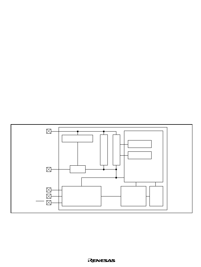
Rev. 2.00, 09/03, page 567 of 690
Section 23 User Debugging Interface (UDI)
This LSI incorporates a user debugging interface (UDI) and advanced user debugger (AUD) for a
boundary scan function and emulator support.
This section describes the UDI. The AUD is a function exclusively for use by an emulator. Refer
to the User's Manual for the relevant emulator for details of the AUD.
23.1
Features
The UDI (User Debugging Interface) is a serial I/O interface which supports with JTAG (Joint
Test Action Group, IEEE Standard 1149.1 and IEEE Standard Test Access Port and Boundary-
Scan Architecture) specifications.
The UDI in this LSI supports a boundary scan mode, and is also used for emulator connection.
When using an emulator, UDI functions should not be used. Refer to the emulator manual for the
method of connecting the emulator.
Figure 23.1 shows a block diagram of the UDI.
SDIR
SDID
TCK
TDO
TDI
TMS
SDBPR
MUX
SDBSR
Shift register
TAP controller
Decoder
Local
bus
TRST
Figure 23.1 Block Diagram of UDI

Rev. 2.00, 09/03, page 568 of 690
23.2
Input/Output Pins
Table 23.1 shows the pin configuration of the UDI.
Table 23.1
Pin Configuration
Pin Name
Input/Output
Description
TCK
*
Input
Serial Data Input/Output Clock Pin
Data is serially supplied to the UDI from the data input pin
(TDI), and output from the data output pin (TDO), in
synchronization with this clock.
TMS
*
Input
Mode Select Input Pin
The state of the TAP control circuit is determined by changing
this signal in synchronization with TCK. The protocol is
supported to the JTAG standard (IEEE Std.1149.1).
TRST*
Input
Reset Input Pin
Input is accepted asynchronously with respect to TCK, and
when low, the UDI is reset.
TRST
must be held low for a
constant period when power is turned on regardless of using
the UDI function. As the same as the
RESETP
pin, the
TRST
pin should be driven low at the power-on reset state and driven
high after the power-on reset state is released. This is different
from the JTAG standard.
See section 23.4.2, Reset Configuration, for more information.
TDI
*
Input
Serial Data Input Pin
Data transfer to the UDI is executed by changing this signal in
synchronization with TCK.
TDO
Output
Serial Data Output Pin
Data read from the UDI is executed by reading this pin in
synchronization with TCK. The data output timing depends on
the command type set in the SDIR. See section 23.3.2,
Instruction Register (SDIR), for more information.
ASEMD0*
Input
ASE Mode Select Pin
If a low level is input at the
ASEMD0
pin while the
RESETP
pin
is asserted, ASE mode is entered; if a high level is input, normal
mode is entered. In ASE mode, dedicated emulator function
can be used. The input level at the
ASEMD0
pin should be held
for at least one cycle after
RESETP
negation. See section
23.4.2, Reset Configuration, for more information.

Rev. 2.00, 09/03, page 569 of 690
Pin Name
Input/Output
Description
ASEBRKAK
AUDSYNC
AUDATA3 to 0
AUDCK
Output
Dedicated emulator pin
Note:
*
The pull-up MOS turns on if the pin function controller (PFC) is used to select other
functions (UDI).
23.3
Register Descriptions
The UDI has the following registers. For details on register addresses and register states in each
processing state, see section 24, List of Registers.
∑
Bypass register (SDBPR)
∑
Instruction register (SDIR)
∑
Boundary scan register (SDBSR)
∑
ID register (SDID)
23.3.1
Bypass Register (SDBPR)
SDBPR is a 1-bit register that cannot be accessed by the CPU. When SDIR is set to the bypass
mode, SDBPR is connected between UDI pins TDI and TDO. The initial value is undefined but
SDBPR is initialized when the TAP enters the Capture-DR state.
23.3.2
Instruction Register (SDIR)
SDIR is a 16-bit read-only register. The register is in JTAG IDCODE in its initial state. It is
initialized by
TRST assertion or in the TAP test-logic-reset state, and can be written to by the UDI
irrespective of the CPU mode. Operation is not guaranteed if a reserved command is set in this
register.

Rev. 2.00, 09/03, page 570 of 690
Bit
Bit
Name
Initial
Value
R/W
Description
15 to 13
TI7 to TI5
1
R
12
TI4
0
R
11 to 8
TI3 to TI0
1
R
Test Instruction 7 to 0
The UDI instruction is transferred to SDIR by a
serial input from TDI.
For commands, see table 23.2.
7 to 2
1
R
Reserved
These bits are always read as 1.
1
0
R
Reserved
This bit is always read as 0.
0
1
R
Reserved
This bit is always read as 1.
Table 23.2
UDI Commands
Bits 15 to 8
TI7
TI6
TI5
TI4
TI3
TI2
TI1
TI0
Description
0
0
0
0
--
--
--
--
JTAG EXTEST
0
0
1
0
--
--
--
--
JTAG CLAMP
0
0
1
1
--
--
--
--
JTAG HIGHZ
0
1
0
0
--
--
--
--
JTAG SAMPLE/PRELOAD
0
1
1
0
--
--
--
--
UDI reset negate
0
1
1
1
--
--
--
--
UDI reset assert
1
0
1
--
--
--
--
--
UDI interrupt
1
1
1
0
--
--
--
--
JTAG IDCODE (Initial value)
1
1
1
1
--
--
--
--
JTAG BYPASS
Other than the above
Reserved
23.3.3
Boundary Scan Register (SDBSR)
SDBSR is a 385-bit shift register, located on the PAD, for controlling the input/output pins of this
LSI. The initial value is undefined. SDBSR cannot be accessed by the CPU.
Using the EXTEST, SAMPLE/PRELOAD, CLAMP, and HIGHZ commands, a boundary scan
test which supports the JTAG standard can be carried out. Table 23.3 shows the correspondence
between this LSI's pins and boundary scan register bits.

Rev. 2.00, 09/03, page 571 of 690
Table 23.3
SH7705 Pins and Boundary Scan Register Bits
Bit
Pin Name
I/O
Bit
Pin Name
I/O
from TDI
353
D2
IN
384
VBUS/PTM6
IN
352
D1
IN
383
MD6
IN
351
D0
IN
382
D31/PTB7/PINT15
IN
350
VBUS/PTM6
OUT
381
D30/PTB6/PINT14
IN
349
D31/PTB7/PINT15
OUT
380
D29/PTB5/PINT13
IN
348
D30/PTB6/PINT14
OUT
379
D28/PTB4/PINT12
IN
347
D29/PTB5/PINT13
OUT
378
D27/PTB3/PINT11
IN
346
D28/PTB4/PINT12
OUT
377
D26/PTB2/PINT10
IN
345
D27/PTB3/PINT11
OUT
376
D25/PTB1/PINT9
IN
344
D26/PTB2/PINT10
OUT
375
D24/PTB0/PINT8
IN
343
D25/PTB1/PINT9
OUT
374
D23/PTA7/PINT7
IN
342
D24/PTB0/PINT8
OUT
373
D22/PTA6/PINT6
IN
341
D23/PTA7/PINT7
OUT
372
D21/PTA5/PINT5
IN
340
D22/PTA6/PINT6
OUT
371
D20/PTA4/PINT4
IN
339
D21/PTA5/PINT5
OUT
370
D19/PTA3/PINT3
IN
338
D20/PTA4/PINT4
OUT
369
D18/PTA2/PINT2
IN
337
D19/PTA3/PINT3
OUT
368
D17/PTA1/PINT1
IN
336
D18/PTA2/PINT2
OUT
367
D16/PTA0/PINT0
IN
335
D17/PTA1/PINT1
OUT
366
D15
IN
334
D16/PTA0/PINT0
OUT
365
D14
IN
333
D15
OUT
364
D13
IN
332
D14
OUT
363
D12
IN
331
D13
OUT
362
D11
IN
330
D12
OUT
361
D10
IN
329
D11
OUT
360
D9
IN
328
D10
OUT
359
D8
IN
327
D9
OUT
358
D7
IN
326
D8
OUT
357
D6
IN
325
D7
OUT
356
D5
IN
324
D6
OUT
355
D4
IN
323
D5
OUT
354
D3
IN
322
D4
OUT

Rev. 2.00, 09/03, page 572 of 690
Bit
Pin Name
I/O
Bit
Pin Name
I/O
321
D3
OUT
288
D3
Control
320
D2
OUT
287
D2
Control
319
D1
OUT
286
D1
Control
318
D0
OUT
285
D0
Control
317
VBUS/PTM6
Control
284
A0/PTK0
IN
316
D31/PTB7/PINT15
Control
283
A19/PTK1
IN
315
D30/PTB6/PINT14
Control
282
A20/PTK2
IN
314
D29/PTB5/PINT13
Control
281
A21/PTK3
IN
313
D28/PTB4/PINT12
Control
280
A22/PTK4
IN
312
D27/PTB3/PINT11
Control
279
A23/PTK5
IN
311
D26/PTB2/PINT10
Control
278
A24/PTK6
IN
310
D25/PTB1/PINT9
Control
277
A25/PTK7
IN
309
D24/PTB0/PINT8
Control
276
BS
/PTC0
IN
308
D23/PTA7/PINT7
Control
275
WE2
/DQMUL/PTC1
IN
307
D22/PTA6/PINT6
Control
274
WE3
/DQMUU/
AH
/PTC2
IN
306
D21/PTA5/PINT5
Control
273
CS2
/PTC3
IN
305
D20/PTA4/PINT4
Control
272
CS3
/PTC4
IN
304
D19/PTA3/PINT3
Control
271
CS4
/PTC5
IN
303
D18/PTA2/PINT2
Control
270
CS5A
/PTC6
IN
302
D17/PTA1/PINT1
Control
269
CS5B
/PTD6
IN
301
D16/PTA0/PINT0
Control
268
CS6A
/PTC7
IN
300
D15
Control
267
CS6B
/PTD7
IN
299
D14
Control
266
RASL
/PTD0
IN
298
D13
Control
265
RASU
/PTD1
IN
297
D12
Control
264
CASL
/PTD2
IN
296
D11
Control
263
A0/PTK0
OUT
295
D10
Control
262
A1
OUT
294
D9
Control
261
A2
OUT
293
D8
Control
260
A3
OUT
292
D7
Control
259
A4
OUT
291
D6
Control
258
A5
OUT
290
D5
Control
257
A6
OUT
289
D4
Control
256
A7
OUT

Rev. 2.00, 09/03, page 573 of 690
Bit
Pin Name
I/O
Bit
Pin Name
I/O
255
A8
OUT
222
RASL
/PTD0
OUT
254
A9
OUT
221
RASU
/PTD1
OUT
253
A10
OUT
220
CASL
/PTD2
OUT
252
A11
OUT
219
A0/PTK0
Control
251
A12
OUT
218
A1
Control
250
A13
OUT
217
A2
Control
249
A14
OUT
216
A3
Control
248
A15
OUT
215
A4
Control
247
A16
OUT
214
A5
Control
246
A17
OUT
213
A6
Control
245
A18
OUT
212
A7
Control
244
A19/PTK1
OUT
211
A8
Control
243
A20/PTK2
OUT
210
A9
Control
242
A21/PTK3
OUT
209
A10
Control
241
A22/PTK4
OUT
208
A11
Control
240
A23/PTK5
OUT
207
A12
Control
239
A24/PTK6
OUT
206
A13
Control
238
A25/PTK7
OUT
205
A14
Control
237
BS
/PTC0
OUT
204
A15
Control
236
RD
OUT
203
A16
Control
235
WE0
/DQMLL
OUT
202
A17
Control
234
WE1
/DQMLU
OUT
201
A18
Control
233
WE2
/DQMUL/PTC1
OUT
200
A19/PTK1
Control
232
WE3
/DQMUU/
AH
/PTC2
OUT
199
A20/PTK2
Control
231
RD/
WR
OUT
198
A21/PTK3
Control
230
CS0
OUT
197
A22/PTK4
Control
229
CS2
/PTC3
OUT
196
A23/PTK5
Control
228
CS3
/PTC4
OUT
195
A24/PTK6
Control
227
CS4
/PTC5
OUT
194
A25/PTK7
Control
226
CS5A
/PTC6
OUT
193
BS
/PTC0
Control
225
CS5B
/PTD6
OUT
192
RD
Control
224
CS6A
/PTC7
OUT
191
WE0
/DQMLL
Control
223
CS6B
/PTD7
OUT
190
WE1
/DQMLU
Control

Rev. 2.00, 09/03, page 574 of 690
Bit
Pin Name
I/O
Bit
Pin Name
I/O
189
WE2
/DQMUL/PTC1
Control
156
NF/PTJ5
IN
188
WE3
/DQMUU/
AH
/PTC2
Control
155
NF/PTJ6
IN
187
RD/
WR
Control
154
NF/PTJ7
IN
186
CS0
Control
153
NF/PTM4
IN
185
CS2
/PTC3
Control
152
PTM0
IN
184
CS3
/PTC4
Control
151
PTM1
IN
183
CS4
/PTC5
Control
150
PTM2
IN
182
CS5A
/PTC6
Control
149
PTM3
IN
181
CS5B
/PTD6
Control
148
ASEBRKAK
/PTF6
IN
180
CS6A
/PTC7
Control
147
MD0
IN
179
CS6B
/PTD7
Control
146
MD1
IN
178
RASL
/PTD0
Control
145
MD2
IN
177
RASU
/PTD1
Control
144
MD5
IN
176
CASL
/PTD2
Control
143
CASU
/PTD3
OUT
175
CASU
/PTD3
IN
142
CKE/PTD4
OUT
174
CKE/PTD4
IN
141
PTD5/NF
OUT
173
PTD5/NF
IN
140
BACK
/PTG5
OUT
172
BACK
/PTG5
IN
139
BREQ
/PTG6
OUT
171
BREQ
/PTG6
IN
138
WAIT
/PTG7
OUT
170
WAIT
/PTG7
IN
137
DACK0/PTE0
OUT
169
DACK0/PTE0
IN
136
DACK1/PTE1
OUT
168
DACK1/PTE1
IN
135
TEND0/PTE3
OUT
167
TEND0/PTE3
IN
134
AUDSYNC/PTF4
OUT
166
AUDSYNC/PTF4
IN
133
AUDATA0/PTF0/TO0
OUT
165
AUDATA0/PTF0/TO0
IN
132
AUDATA1/PTF1/TO1
OUT
164
AUDATA1/PTF1/TO1
IN
131
AUDATA2/PTF2/TO2
OUT
163
AUDATA2/PTF2/TO2
IN
130
AUDATA3/PTF3/TO3
OUT
162
AUDATA3/PTF3/TO3
IN
129
NF/PTJ0
OUT
161
NF/PTJ0
IN
128
NF/PTJ1
OUT
160
NF/PTJ1
IN
127
NF/PTJ2
OUT
159
NF/PTJ2
IN
126
NF/PTJ3
OUT
158
NF/PTJ3
IN
125
NF/PTJ4
OUT
157
NF/PTJ4
IN
124
NF/PTJ5
OUT

Rev. 2.00, 09/03, page 575 of 690
Bit
Pin Name
I/O
Bit
Pin Name
I/O
123
NF/PTJ6
OUT
90
PTM2
Control
122
NF/PTJ7
OUT
89
PTM3
Control
121
NF/PTM4
OUT
88
ASEBRKAK
/PTF6
Control
120
PTM0
OUT
87
STATUS0/PTE4/
RTS0
IN
119
PTM1
OUT
86
STATUS1/PTE5/
CTS0
IN
118
PTM2
OUT
85
PTN0/SUSPND
IN
117
PTM3
OUT
84
PTN1/TXENL
IN
116
ASEBRKAK
/PTF6
OUT
83
PTN2/XVDATA
IN
115
CASU
/PTD3
Control
82
PTN3/TXDMNS
IN
114
CKE/PTD4
Control
81
PTN4/TXDPLS
IN
113
PTD5/NF
Control
80
PTN5/DMNS
IN
112
BACK
/PTG5
Control
79
PTN6/DPLS
IN
111
BREQ
/PTG6
Control
78
PTN7
IN
110
WAIT
/PTG7
Control
77
TCLK/PTE6
IN
109
DACK0/PTE0
Control
76
PTE7
IN
108
DACK1/PTE1
Control
75
SCK0/SCPT1
IN
107
TEND0/PTE3
Control
74
SCK2/SCPT3
IN
106
AUDSYNC/PTF4
Control
73
RTS2
/SCPT4
IN
105
AUDATA0/PTF0/TO0
Control
72
RXD0/SCPT0/IrRX
IN
104
AUDATA1/PTF1/TO1
Control
71
RXD2/SCPT2
IN
103
AUDATA2/PTF2/TO2
Control
70
CTS2
/SCPT5
IN
102
AUDATA3/PTF3/TO3
Control
69
IRQ0/
IRL0
/PTH0
IN
101
NF/PTJ0
Control
68
IRQ1/
IRL1
/PTH1
IN
100
NAF/PTJ1
Control
67
IRQ2/
IRL2
/PTH2
IN
99
NF/PTJ2
Control
66
IRQ3/
IRL3
/PTH3
IN
98
NF/PTJ3
Control
65
IRQ4/PTH4
IN
97
NF/PTJ4
Control
64
IRQ5/PTE2
IN
96
NF/PTJ5
Control
63
AUDCK/PTG4
IN
95
NF/PTJ6
Control
62
NMI
IN
94
NF/PTJ7
Control
61
DREQ0/PTH5
IN
93
NF/PTM4
Control
60
DREQ1/PTH6
IN
92
PTM0
Control
59
MD3
IN
91
PTM1
Control
58
MD4
IN

Rev. 2.00, 09/03, page 576 of 690
Bit
Pin Name
I/O
Bit
Pin Name
I/O
57
AN0/PTL0
IN
27
DREQ1/PTH6
OUT
56
AN1/PTL1
IN
26
STATUS0/PTE4/
RTS0
Control
55
AN2/PTL2
IN
25
STATUS1/PTE5/
CTS0
Control
54
AN3/PTL3
IN
24
PTN0/SUSPND
Control
53
STATUS0/PTE4/
RTS0
OUT
23
PTN1/TXENL
Control
52
STATUS1/PTE5/
CTS0
OUT
22
PTN2/XVDATA
Control
51
PTN0/SUSPND
OUT
21
PTN3/TXDMNS
Control
50
PTN1/TXENL
OUT
20
PTN4/TXDPLS
Control
49
PTN2/XVDATA
OUT
19
PTN5/DMNS
Control
48
PTN3/TXDMNS
OUT
18
PTN6/DPLS
Control
47
PTN4/TXDPLS
OUT
17
PTN7
Control
46
PTN5/DMNS
OUT
16
TCLK/PTE6
Control
45
PTN6/DPLS
OUT
15
PTE7
Control
44
PTN7
OUT
14
TXD0/SCPT0/IrTX
Control
43
TCLK/PTE6
OUT
13
SCK0/SCPT1
Control
42
PTE7
OUT
12
TxD2/SCPT2
Control
41
TXD0/SCPT0/IrTX
OUT
11
SCK2/SCPT3
Control
40
SCK0/SCPT1
OUT
10
RTS2
/SCPT4
Control
39
TXD2/SCPT2
OUT
9
CTS2
/SCPT5
Control
38
SCK2/SCPT3
OUT
8
IRQ0/
IRL0
/PTH0
Control
37
RTS2
/SCPT4
OUT
7
IRQ1/
IRL1
/PTH1
Control
36
CTS2
/SCPT5
OUT
6
IRQ2/
IRL2
/PTH2
Control
35
IRQ0/
IRL0
/PTH0
OUT
5
IRQ3/
IRL3
/PTH3
Control
34
IRQ1/
IRL1
/PTH1
OUT
4
IRQ4/PTH4
Control
33
IRQ2/
IRL2
/PTH2
OUT
3
IRQ5/PTE2
Control
32
IRQ3/
IRL3
/PTH3
OUT
2
AUDCK/PTG4
Control
31
IRQ4/PTH4
OUT
1
DREQ0/PTH5
Control
30
IRQ5/PTE2
OUT
0
DREQ1/PTH6
Control
29
AUDCK/PTG4
OUT
28
DREQ0/PTH5
OUT
to TDO
Note:
Control is an active-low signal.
When Control is driven low, the corresponding pin is driven by the value of OUT.

Rev. 2.00, 09/03, page 577 of 690
23.3.4
ID Register (SDID)
SDID is a 32-bit read-only register that consists of connected 16-bit registers SDIDH and SDIDL,
each of which can be read by the CPU.
The IDCODE command is set from the UDI pin. This register can be read from the TDO when the
TAP state is Shift-DR. Writing is disabled.
Bit
Bit
Name
Initial
Value
R/W
Description
31 to 0
DID31 to DID0
Refer to
description
R
Device ID31 to 0
Device ID register that is stipulated by
JTAG. H'001A200F (initial value) for this
LSI. Upper four bits may be changed by the
chip version.
SDIDH corresponds to bits 31 to 16.
SDIDL corresponds to bits 15 to 0.
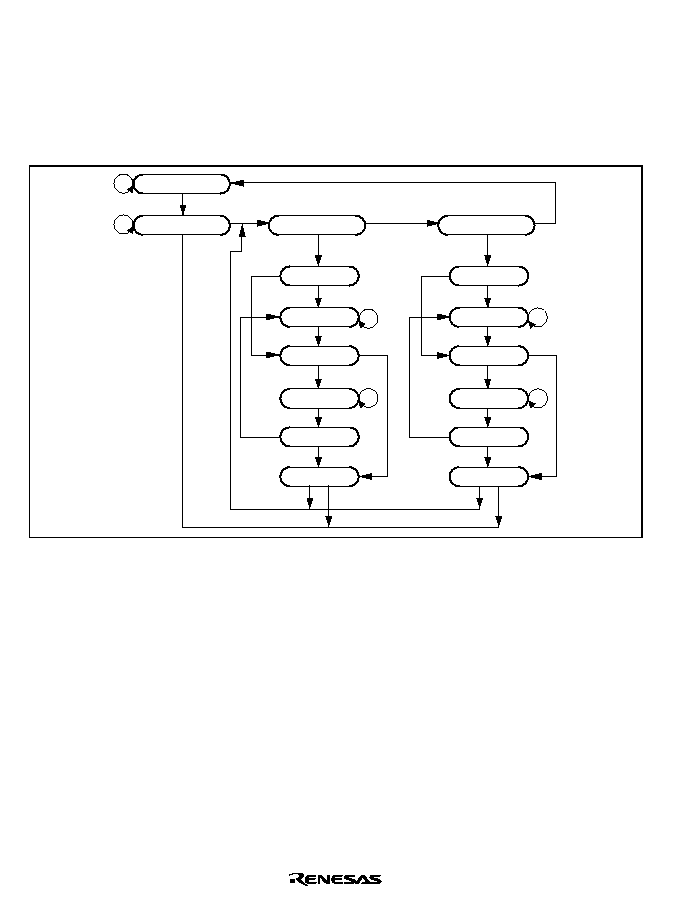
Rev. 2.00, 09/03, page 578 of 690
23.4
Operation
23.4.1
TAP Controller
Figure 23.2 shows the internal states of the TAP controller. State transitions basically conform to
the JTAG standard.
Test-logic-reset
Capture-DR
Shift-DR
Exit1-DR
Pause-DR
Exit2-DR
Update-DR
Select-DR-scan
Run-test/idle
1
0
0
0
0
1
1
1
1
0
0
1
0
1
1
1
0
Capture-IR
Shift-IR
Exit1-IR
Pause-IR
Exit2-IR
Update-IR
Select-IR-scan
0
0
1
0
0
1
1
0
1
1
1
0
0
Figure 23.2 TAP Controller State Transitions
Note:
The transition condition is the TMS value at the rising edge of TCK. The TDI value is
sampled at the rising edge of TCK; shifting occurs at the falling edge of TCK. For details
on change timing of the TDO value, see section 23.4.3, TDO Output Timing. The TDO is
at high impedance, except with shift-DR and shift-IR states. During the change to
TRST =
0, there is a transition to test-logic-reset asynchronously with TCK.

Rev. 2.00, 09/03, page 579 of 690
23.4.2
Reset Configuration
Table 23.4
Reset Configuration
ASEMD0*
1
RESETP
TRST
Chip State
H
L
L
Normal reset and UDI reset
*
4
H
Normal reset
*
4
H
L
UDI reset only
H
Normal operation
L
L
L
Reset hold
*
2
H
In ASE user mode
*
3
: Normal reset
In ASE break mode
*
3
:
RESETP
assert is
masked
H
L
UDI reset only
H
Normal operation
Notes: 1. Performs normal mode and ASE mode settings
ASEMD0
= H, normal mode
ASEMD0
= L, ASE mode
2. In ASE mode, reset hold is enabled by driving the
RESETP
and
TRST
pins low for a
constant cycle. In this state, the CPU does not start up, even if
RESETP
is driven high.
When
TRST
is driven high, UDI operation is enabled, but the CPU does not start up.
The reset hold state is canceled by the following:
∑ Another
RESETP
assert (power-on reset)
∑
TRST
reassert
3. ASE mode is classified into two modes; ASE break mode to execute the firm program
of an emulator and ASE user mode to execute the user program.
4. Make sure the
TRST
pin is low when the power is turned on.
23.4.3
TDO Output Timing
The timing of data output from the TDO is switched by the command type set in the SDIR. The
timing changes at the TCK falling edge when JTAG commands (EXTEST, CLAMP, HIGHZ,
SAMPLE/PRELOAD, IDCODE, and BYPASS) are set. This is a timing of the JTAG standard.
When the UDI commands (UDI reset negate, UDI reset assert, and UDI interrupt) are set, TDO is
output at the TCK rising edge earlier than the JTAG standard by a half cycle.
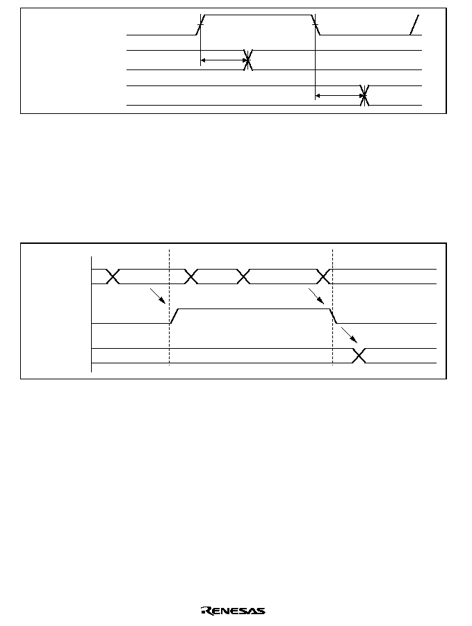
Rev. 2.00, 09/03, page 580 of 690
TDO
(when the UDI
command is set)
TCK
TDO
(when the boundary scan
command is set)
t
TDO
t
TDO
Figure 23.3 UDI Data Transfer Timing
23.4.4
UDI Reset
An UDI reset is executed by setting an UDI reset assert command in SDIR. An UDI reset is of the
same kind as a power-on reset. An UDI reset is released by inputting an UDI reset negate
command. The required time between the UDI reset assert command and UDI reset negate
command is the same as time for keeping the
RESETP pin low to apply a power-on reset.
UDI reset assert
UDI reset negate
SDIR
Chip internal reset
CPU state
Branch to H'A0000000
Figure 23.4 UDI Reset
23.4.5
UDI Interrupt
The UDI interrupt function generates an interrupt by setting a command from the UDI in the
SDIR. An UDI interrupt is a general exception/interrupt operation, resulting in a branch to an
address based on the VBR value plus offset, and with return by the RTE instruction. This interrupt
request has a fixed priority level of 15.
UDI interrupts are accepted in sleep mode, but not in standby mode.

Rev. 2.00, 09/03, page 581 of 690
23.5
Boundary Scan
A command can be set in SDIR by the UDI to place the UDI pins in boundary scan mode
stipulated by JTAG.
23.5.1
Supported Instructions
This LSI supports the three essential instructions defined in the JTAG standard (BYPASS,
SAMPLE/PRELOAD, and EXTEST) and three option instructions (IDCODE, CLAMP, and
HIGHZ).
1. BYPASS:
The BYPASS instruction is an essential standard instruction that operates the bypass register.
This instruction shortens the shift path to speed up serial data transfer involving other chips on
the printed circuit board. While this instruction is executing, the test circuit has no effect on the
system circuits. The upper four bits of the instruction code are 1111.
2. SAMPLE/PRELOAD:
The SAMPLE/PRELOAD instruction inputs values from this LSI's internal circuitry to the
boundary scan register, outputs values from the scan path, and loads data onto the scan path.
When this instruction is executing, this LSI's input pin signals are transmitted directly to the
internal circuitry, and internal circuit values are directly output externally from the output pins.
This LSI's system circuits are not affected by execution of this instruction. The upper four bits
of the instruction code are 0100.
In a SAMPLE operation, a snapshot of a value to be transferred from an input pin to the
internal circuitry, or a value to be transferred from the internal circuitry to an output pin, is
latched into the boundary scan register and read from the scan path. Snapshot latching is
performed in synchronization with the rise of TCK in the Capture-DR state. Snapshot latching
does not affect normal operation of this LSI.
In a PRELOAD operation, an initial value is set in the parallel output latch of the boundary
scan register from the scan path prior to the EXTEST instruction. Without a PRELOAD
operation, when the EXTEST instruction was executed an undefined value would be output
from the output pin until completion of the initial scan sequence (transfer to the output latch)
(with the EXTEST instruction, the parallel output latch value is constantly output to the output
pin).

Rev. 2.00, 09/03, page 582 of 690
3. EXTEST:
This instruction is provided to test external circuitry when this LSI is mounted on a printed
circuit board. When this instruction is executed, output pins are used to output test data
(previously set by the SAMPLE/PRELOAD instruction) from the boundary scan register to the
printed circuit board, and input pins are used to latch test results into the boundary scan
register from the printed circuit board. If testing is carried out by using the EXTEST
instruction N times, the Nth test data is scanned-in when test data (N-1) is scanned out.
Data loaded into the output pin boundary scan register in the Capture-DR state is not used for
external circuit testing (it is replaced by a shift operation).
The upper four bits of the instruction code are 0000.
4. IDCODE:
A command can be set in SDIR by the UDI pins to place the UDI pins in the IDCODE mode
stipulated by JTAG. When the UDI is initialized (
TRST is asserted or TAP is in the Test-
Logic-Reset state), the IDCODE mode is entered.
5. CLAMP, HIGHZ:
A command can be set in SDIR by the UDI pins to place the UDI pins in the CLAMP or
HIGHZ mode stipulated by JTAG.
23.5.2
Points for Attention
1. Boundary scan mode does not cover clock-related signals (EXTAL, EXTAL2, XTAL,
XTAL2, EXTAL_USB, XTAL_USB, and CKIO).
2. Boundary scan mode does not cover reset-related signals (
RESETP, RESETM, and CA).
3. Boundary scan mode does not cover UDI-related signals (TCK, TDI, TDO, TMS, and
TRST).
4. Fix the
RESETP pin low during boundary scan.
5. Fix the CA pin high during boundary scan.
6. Fix the
ASEMD0 pin high during boundary scan.
7. The CKIO cock should operate during boundary scan. The MD[2:0] pin should be set to the
clock mode used during normal operation, and EXTAL and CKIO should be set within the
frequency range specified in the Clock Pulse Generator (CPG) section.
As during normal operation, the boundary scan test should be performed after allowing
sufficient settling time for the crystal oscillator, PLL1, and PLL2.

Rev. 2.00, 09/03, page 583 of 690
23.6
Usage Notes
1. An UDI command, once set, will not be modified as long as another command is not re-issued
from the UDI. If the same command is given continuously, the command must be set after a
command (BYPASS, etc.) that does not affect chip operations is once set.
2. Because chip operations are suspended in standby mode, UDI commands are not accepted. To
keep the TAP state constant before and after standby mode, TCK must be high during standby
mode transition.
3. The UDI is used for emulator connection. Therefore, UDI functions cannot be used when using
an emulator.
23.7
Advanced User Debugger (AUD)
The AUD is a function only for an emulator. For details on the AUD, refer to each emulator's
User's Manual.

Rev. 2.00, 09/03, page 584 of 690

Rev. 2.00, 09/03, page 585 of 690
Section 24 List of Registers
This section gives information on the on-chip I/O registers and is configured as described
below.
1. Register Addresses (by functional module, in order of the corresponding section numbers)
∑
Descriptions by functional module, in order of the corresponding section numbers
Entries that consist of
lines are for separation of the functional modules.
∑
Access to reserved addresses which are not described in this list is prohibited.
∑
When registers consist of 16 or 32 bits, the addresses of the MSBs are given, on the
presumption of a big-endian system.
2. Register Bits
∑
Bit configurations of the registers are described in the same order as the Register Addresses
(by functional module, in order of the corresponding section numbers).
∑
Reserved bits are indicated by
in the bit name.
∑
No entry in the bit-name column indicates that the whole register is allocated as a counter or
for holding data.
∑
When registers consist of 16 or 32 bits, bits are described from the MSB side.
The order in which bytes are described is on the presumption of a big-endian system.
3. Register States in Each Operating Mode
∑
Register states are described in the same order as the Register Addresses (by functional
module, in order of the corresponding section numbers).
∑
For the initial state of each bit, refer to the description of the register in the corresponding
section.
∑
The register states described are for the basic operating modes. If there is a specific reset for
an on-chip module, refer to the section on that on-chip module.

Rev. 2.00, 09/03, page 586 of 690
24.1
Register Addresses
(by functional module, in order of the corresponding section
numbers)
Entries under Access size indicates numbers of bits.
Note:
Access to undefined or reserved addresses is prohibited. Since operation or continued
operation is not guaranteed when these registers are accessed, do not attempt such
access.
Register Name
Abbreviation
Number
of Bits Address
Module
Access
Size
MMU control register
MMUCR
32
H'FFFF FFE0
MMU
32
Page table entry register high
PTEH
32
H'FFFF FFF0
32
Page table entry register low
PTEL
32
H'FFFF FFF4
32
Translation table base register
TTB
32
H'FFFF FFF8
32
Cache control register 1
CCR1
32
H'FFFF FFEC Cache
32
Cache control register 2
CCR2
32
H'A400 00B0
32
Cache control register 3
CCR3
32
H'A400 00B4
32
Interrupt event register 2
INTEVT2
32
H'A400 0000
32
TRAPA exception register
TRA
32
H'FFFF FFD0
Exception
handling
32
Exception event register
EXPEVT
32
H'FFFF FFD4
32
Interrupt event register
INTEVT
32
H'FFFF FFD8
32
TLB exception address register
TEA
32
H'FFFF FFFC
32
Interrupt priority level setting register A IPRA
16
H'FFFF FEE2 INTC
16
Interrupt priority level setting register B IPRB
16
H'FFFF FEE4
16
Interrupt priority level setting register C IPRC
16
H'A400 0016
16
Interrupt priority level setting register D IPRD
16
H'A400 0018
16
Interrupt priority level setting register E IPRE
16
H'A400 001A
16
Interrupt priority level setting register F IPRF
16
H'A408 0000
16
Interrupt priority level setting register G IPRG
16
H'A408 0002
16
Interrupt priority level setting register H IPRH
16
H'A408 0004
16

Rev. 2.00, 09/03, page 587 of 690
Register Name
Abbreviation
Number
of Bits Address
Module
Access
Size
Interrupt control register 0
ICR0
16
H'FFFF FEE0 INTC
16
Interrupt control register 1
ICR1
16
H'A400 0010
16
Interrupt control register 2
ICR2
16
H'A400 0012
16
Interrupt request register 0
IRR0
8
H'A400 0004
8
Interrupt request register 1
IRR1
8
H'A400 0006
8
Interrupt request register 2
IRR2
8
H'A400 0008
8
PINT interrupt enable register
PINTER
16
H'A400 0014
16
Common control register
CMNCR
32
H'A4FD 0000
BSC
32
Bus control register for CS0 space
CS0BCR
32
H'A4FD 0004
32
Bus control register for CS2 space
CS2BCR
32
H'A4FD 0008
32
Bus control register for CS3 space
CS3BCR
32
H'A4FD 000C
32
Bus control register for CS4 space
CS4BCR
32
H'A4FD 0010
32
Bus control register for CS5A space
CS5ABCR
32
H'A4FD 0014
32
Bus control register for CS5B space
CS5BBCR
32
H'A4FD 0018
32
Bus control register for CS6A space
CS6ABCR
32
H'A4FD 001C
32
Bus control register for CS6B space
CS6BBCR
32
H'A4FD 0020
32
Wait control register for CS0 space
CS0WCR
32
H'A4FD 0024
32
Wait control register for CS2 space
CS2 WCR
32
H'A4FD 0028
32
Wait control register for CS3 space
CS3 WCR
32
H'A4FD 002C
32
Wait control register for CS4 space
CS4 WCR
32
H'A4FD 0030
32
Wait control register for CS5A space
CS5A WCR 32
H'A4FD 0034
32
Wait control register for CS5B space
CS5B WCR 32
H'A4FD 0038
32
Wait control register for CS6A space
CS6A WCR 32
H'A4FD 003C
32
Wait control register for CS6B space
CS6B WCR 32
H'A4FD 0040
32
SDRAM control register
SDCR
32
H'A4FD 0044
32
Refresh timer control/status register
RTCSR
32
H'A4FD 0048
32
Refresh timer counter
RTCNT
32
H'A4FD 004C
32
Refresh time constant register
RTCOR
32
H'A4FD 0050
32
SDRAM mode register for CS2 space SDMR2
H'A4FD 4xxx
*
2
16
SDRAM mode register for CS3 space SDMR3
H'A4FD 5xxx
*
2
16

Rev. 2.00, 09/03, page 588 of 690
Register Name
Abbreviation
Number
of Bits Address
Module
Access
Size
DMA source address register_0
SAR_0
32
H'A400 0020
DMAC
16/32
DMA destination address register_0
DAR_0
32
H'A400 0024
16/32
DMA transfer count register_0
DMATCR_0 32
H'A400 0028
16/32
DMA channel control register_0
CHCR_0
32
H'A400 002C
8/16/32
DMA source address register_1
SAR_1
32
H'A400 0030
16/32
DMA destination address register_1
DAR_1
32
H'A400 0034
16/32
DMA transfer count register_1
DMATCR_1 32
H'A400 0038
16/32
DMA channel control register_1
CHCR_1
32
H'A400 003C
8/16/32
DMA source address register_2
SAR_2
32
H'A400 0040
16/32
DMA destination address register_2
DAR_2
32
H'A400 0044
16/32
DMA transfer count register_2
DMATCR_2 32
H'A400 0048
16/32
DMA channel control register_2
CHCR_2
32
H'A400 004C
8/16/32
DMA source address register_3
SAR_3
32
H'A400 0050
16/32
DMA destination address register_3
DAR_3
32
H'A400 0054
16/32
DMA transfer count register_3
DMATCR_3 32
H'A400 0058
16/32
DMA channel control register_3
CHCR_3
32
H'A400 005C
8/16/32
DMA operation register
DMAOR
16
H'A400 0060
8/16
DMA extended resource selector 0
DMARS0
16
H'A409 0000
16
DMA extended resource selector 1
DMARS1
16
H'A409 0004
16
USB clock control register
UCLKCR
8
H'A40A 0008
CPG
8/16
*
1
Frequency control register
FRQCR
16
H'FFFF FF80
16
Watchdog timer counter
WTCNT
8
H'FFFF FF84
WDT
8/16
*
1
Watchdog timer control/status register WTCSR
8
H'FFFF FF86
8/16
*
1
Standby control register
STBCR
8
H'FFFF FF82
8
Standby control register 2
STBCR2
8
H'FFFF FF88
8
Standby control register 3
STBCR3
8
H'A40A 0000
Power-down
modes
8

Rev. 2.00, 09/03, page 589 of 690
Register Name
Abbreviation
Number
of Bits Address
Module
Access
Size
Timer start register
TSTR
8
H'FFFF FE92
TMU
8
Timer constant register_0
TCOR_0
32
H'FFFF FE94
32
Timer counter_0
TCNT_0
32
H'FFFF FE98
32
Timer control register_0
TCR_0
16
H'FFFF FE9C
16
Timer constant register_1
TCOR_1
32
H'FFFF FEA0
32
Timer counter_1
TCNT_1
32
H'FFFF FEA4
32
Timer control register_1
TCR_1
16
H'FFFF FEA8
16
Timer constant register_2
TCOR_2
32
H'FFFF FEAC
32
Timer counter_2
TCNT_2
32
H'FFFF FEB0
32
Timer control register_2
TCR_2
16
H'FFFF FEB4
16
Input capture register_2
TCPR_2
32
H'FFFF FEB8
32
Compare match timer start register
CMSTR
16
H'A400 0070
CMT
16
Compare match timer control/status
register
CMCSR
16
H'A400 0074
16
Compare match timer counter
CMCNT
16
H'A400 0078
16
Compare match timer constant register CMCOR
16
H'A400 007C
16
Timer start register
TSTR
16
H'A449 0000
TPU
16
Timer control register_0
TCR_0
16
H'A449 0010
16
Timer mode register_0
TMDR_0
16
H'A449 0014
16
Timer I/O control register_0
TIOR_0
16
H'A449 0018
16
Timer interrupt enable register_0
TIER_0
16
H'A449 001C
16
Timer status register_0
TSR_0
16
H'A449 0020
16
Timer counter_0
TCNT_0
16
H'A449 0024
16
Timer general register A_0
TGRA_0
16
H'A449 0028
16
Timer general register B_0
TGRB_0
16
H'A449 002C
16
Timer general register C_0
TGRC_0
16
H'A449 0030
16
Timer general register D_0
TGRD_0
16
H'A449 0034
16
Timer control register_1
TCR_1
16
H'A449 0050
16
Timer mode register_1
TMDR_1
16
H'A449 0054
16
Timer I/O control register_1
TIOR_1
16
H'A449 0058
16

Rev. 2.00, 09/03, page 590 of 690
Register Name
Abbreviation
Number
of Bits Address
Module
Access
Size
Timer interrupt enable register_1
TIER_1
16
H'A449 005C
TPU
16
Timer status register_1
TSR_1
16
H'A449 0060
16
Timer counter_1
TCNT_1
16
H'A449 0064
16
Timer general register A_1
TGRA_1
16
H'A449 0068
16
Timer general register B_1
TGRB_1
16
H'A449 006C
16
Timer general register C_1
TGRC_1
16
H'A449 0070
16
Timer general register D_1
TGRD_1
16
H'A449 0074
16
Timer control register_2
TCR_2
16
H'A449 0090
16
Timer mode register_2
TMDR_2
16
H'A449 0094
16
Timer I/O control register_2
TIOR_2
16
H'A449 0098
16
Timer interrupt enable register_2
TIER_2
16
H'A449 009C
16
Timer status register_2
TSR_2
16
H'A449 00A0
16
Timer counter_2
TCNT_2
16
H'A449 00A4
16
Timer general register A_2
TGRA_2
16
H'A449 00A8
16
Timer general register B_2
TGRB_2
16
H'A449 00AC
16
Timer general register C_2
TGRC_2
16
H'A449 00B0
16
Timer general register D_2
TGRD_2
16
H'A449 00B4
16
Timer control register_3
TCR_3
16
H'A449 00D0
16
Timer mode register_3
TMDR_3
16
H'A449 00D4
16
Timer I/O control register_3
TIOR_3
16
H'A449 00D8
16
Timer interrupt enable register_3
TIER_3
16
H'A449 00DC
16
Timer status register_3
TSR_3
16
H'A449 00E0
16
Timer counter_3
TCNT_3
16
H'A449 00E4
16
Timer general register A_3
TGRA_3
16
H'A449 00E8
16
Timer general register B_3
TGRB_3
16
H'A449 00EC
16
Timer general register C_3
TGRC_3
16
H'A449 00F0
16
Timer general register D_3
TGRD_3
16
H'A449 00F4
16

Rev. 2.00, 09/03, page 591 of 690
Register Name
Abbreviation
Number
of Bits Address
Module
Access
Size
64-Hz counter
R64CNT
8
H'FFFF FEC0 RTC
8
Second counter
RSECCNT
8
H'FFFF FEC2
8
Minute counter
RMINCNT
8
H'FFFF FEC4
8
Hour counter
RHRCNT
8
H'FFFF FEC6
8
Day of week counter
RWKCNT
8
H'FFFF FEC8
8
Date counter
RDAYCNT
8
H'FFFF FECA
8
Month counter
RMONCNT
8
H'FFFF FECC
8
Year counter
RYRCNT
16
H'FFFF FECE
16
Second alarm register
RSECAR
8
H'FFFF FED0
8
Minute alarm register
RMINAR
8
H'FFFF FED2
8
Hour alarm register
RHRAR
8
H'FFFF FED4
8
Day of week alarm register
RWKAR
8
H'FFFF FED6
8
Date alarm register
RDAYAR
8
H'FFFF FED8
8
Month alarm register
RMONAR
8
H'FFFF FEDA
8
RTC control register 1
RCR1
8
H'FFFF FEDC
8
RTC control register 2
RCR2
8
H'FFFF FEDE
8
Year alarm register
RYRAR
16
H'A413 FEE0
16
RTC control register 3
RCR3
8
H'A413 FEE4
8
Serial mode register_0
SCSMR_0
16
H'A440 0000
SCIF_0
16
Bit rate register_0
SCBRR_0
8
H'A440 0004
(Channel 0) 8
Serial control register_0
SCSCR_0
16
H'A440 0008
16
Transmit data stop register_0
SCTDSR_0 8
H'A440 000C
8
FIFO error count register_0
SCFER_0
16
H'A440 0010
16
Serial status register_0
SCSSR_0
16
H'A440 0014
16
FIFO control register_0
SCFCR_0
16
H'A440 0018
16
FIFO data count register_0
SCFDR_0
16
H'A440 001C
16
Transmit FIFO data register_0
SCFTDR_0
8
H'A440 0020
8
Receive FIFO data register_0
SCFRDR_0 8
H'A440 0024
8

Rev. 2.00, 09/03, page 592 of 690
Register Name
Abbreviation
Number
of Bits Address
Module
Access
Size
Serial mode register_2
SCSMR_2
16
H'A441 0000
SCIF_2
16
Bit rate register_2
SCBRR_2
8
H'A441 0004
(Channel 2) 8
Serial control register_2
SCSCR_2
16
H'A441 0008
16
Transmit data stop register_2
SCTDSR_2 8
H'A441 000C
8
FIFO error count register_2
SCFER_2
16
H'A441 0010
16
Serial status register_2
SCSSR_2
16
H'A441 0014
16
FIFO control register_2
SCFCR_2
16
H'A441 0018
16
FIFO data count register_2
SCFDR_2
16
H'A441 001C
16
Transmit FIFO data register_2
SCFTDR_2
8
H'A441 0020
8
Receive FIFO data register_2
SCFRDR_2 8
H'A441 0024
8
IrDA mode register
SCSMR_Ir
16
H'A44A 0000
IrDA
16
EP0i data register
EPDR0i
8B
H'A448 0000
USB
8
EP0o data register
EPDR0o
8B
H'A448 0004
8
EP0s data register
EPDR0s
8B
H'A448 0008
8
EP1 data register
EPDR1
128B
H'A448 000C
8/32
EP2 data register
EPDR2
128B
H'A448 0010
8/32
EP3 data register
EPDR3
8B
H'A448 0014
8
Interrupt flag register 0
IFR0
8
H'A448 0018
8
Interrupt flag register 1
IFR1
8
H'A448 001C
8
Trigger register
TRG
8
H'A448 0020
8
FIFO clear register
FCLR
8
H'A448 0024
8
EP0o receive data size register
EPSZ0o
8
H'A448 0028
8
Data status register
DASTS
8
H'A448 002C
8
Endpoint stall register
EPSTL
8
H'A448 0030
8
Interrupt enable register 0
IER0
8
H'A448 0034
8
Interrupt enable register 1
IER1
8
H'A448 0038
8
EP1 receive data size register
EPSZ1
8
H'A448 003C
8
DMA transfer setting register
DMAR
8
H'A448 0040
8
Interrupt select register 0
ISR0
8
H'A448 0044
8
Interrupt select register 1
ISR1
8
H'A448 0048
8
Transceiver control register
XVERCR
8
H'A448 0060
8

Rev. 2.00, 09/03, page 593 of 690
Register Name
Abbreviation
Number
of Bits Address
Module
Access
Size
Port A control register
PACR
16
H'A400 0100
PFC
16
Port B control register
PBCR
16
H'A400 0102
16
Port C control register
PCCR
16
H'A400 0104
16
Port D control register
PDCR
16
H'A400 0106
16
Port E control register
PECR
16
H'A400 0108
16
Port E control register 2
PECR2
8
H'A405 0148
8
Port F control register
PFCR
16
H'A400 010A
16
Port F control register 2
PFCR2
8
H'A405 014A
8
Port G control register
PGCR
16
H'A400 010C
16
Port H control register
PHCR
16
H'A400 010E
16
Port J control register
PJCR
16
H'A400 0110
16
Port K control register
PKCR
16
H'A400 0112
16
Port L control register
PLCR
16
H'A400 0114
16
Port SC control register
SCPCR
16
H'A400 0116
16
Port M control register
PMCR
16
H'A400 0118
16
Port N control register
PNCR
16
H'A400 011A
16
Port N control register 2
PNCR2
8
H'A405 015A
8
Port A data register
PADR
8
H'A400 0120
Port
8
Port B data register
PBDR
8
H'A400 0122
8
Port C data register
PCDR
8
H'A400 0124
8
Port D data register
PDDR
8
H'A400 0126
8
Port E data register
PEDR
8
H'A400 0128
8
Port F data register
PFDR
8
H'A400 012A
8
Port G data register
PGDR
8
H'A400 012C
8
Port H data register
PHDR
8
H'A400 012E
8
Port J data register
PJDR
8
H'A400 0130
8
Port K data register
PKDR
8
H'A405 0132
8
Port L data register
PLDR
8
H'A400 0134
8
SC port data register
SCPDR
8
H'A400 0136
8
Port M data register
PMDR
8
H'A400 0138
8
Port N data register
PNDR
8
H'A400 013A
8

Rev. 2.00, 09/03, page 594 of 690
Register Name
Abbreviation
Number
of Bits Address
Module
Access
Size
A/D data register A
ADDRA
16
H'A400 0080
ADC
16
A/D data register B
ADDRB
16
H'A400 0082
16
A/D data register C
ADDRC
16
H'A400 0084
16
A/D data register D
ADDRD
16
H'A400 0086
16
A/D control/status register
ADCSR
16
H'A400 0088
16
Break data register B
BDRB
32
H'FFFF FF90
UBC
32
Break data mask register B
BDMRB
32
H'FFFF FF94
32
Break control register
BRCR
32
H'FFFF FF98
32
Execution count break register
BETR
16
H'FFFF FF9C
16
Break address register B
BARB
32
H'FFFF FFA0
32
Break address mask register B
BAMRB
32
H'FFFF FFA4
32
Break bus cycle register B
BBRB
16
H'FFFF FFA8
16
Branch source register
BRSR
32
H'FFFF FFAC
32
Break address register A
BARA
32
H'FFFF FFB0
32
Break address mask register A
BAMRA
32
H'FFFF FFB4
32
Break bus cycle register A
BBRA
16
H'FFFF FFB8
16
Branch destination register
BRDR
32
H'FFFF FFBC
32
Break ASID register A
BASRA
8
H'FFFF FFE4
8
Break ASID register B
BASRB
8
H'FFFF FFE8
8
Instruction register
SDIR
16
H'A400 0200
UDI
16
ID register
SDID/SDIDH
16
H'A400 0214
16
ID register
SDIDL
16
H'A400 0216
16
Notes: 1. 8 bits when reading and 16 bits when writing.
2. The value of xxx depends on the setting value because of access control for the
SDRAM mode register.

Rev. 2.00, 09/03, page 595 of 690
24.2
Register Bits
Register addresses and bit names of the on-chip peripheral modules are described below.
Each line covers eight bits, and 16-bit and 32-bit registers are shown as 2 or 4 lines,
respectively.
Register
Abbreviation
Bit 31/
23/15/7
Bit 30/
22/14/6
Bit 29/
21/13/5
Bit 28/
20/12/4
Bit 27/
19/11/3
Bit 26/
18/10/2
Bit 25/
17/9/1
Bit 24/
16/8/0
Module
MMUCR
MMU
SV
RC1
RC0
TF
IX
AT
PTEH
VPN
VPN
VPN
VPN
VPN
VPN
VPN
VPN
VPN
VPN
VPN
VPN
VPN
VPN
VPN
VPN
VPN
VPN
VPN
VPN
VPN
VPN
ASID7
ASID6
ASID5
ASID4
ASID3
ASID2
ASID1
ASID0
PTEL
PPN
PPN
PPN
PPN
PPN
PPN
PPN
PPN
PPN
PPN
PPN
PPN
PPN
PPN
PPN
PPN
PPN
PPN
PPN
V
PR1
PR0
SZ
C
D
SH
TTB

Rev. 2.00, 09/03, page 596 of 690
Register
Abbreviation
Bit 31/
23/15/7
Bit 30/
22/14/6
Bit 29/
21/13/5
Bit 28/
20/12/4
Bit 27/
19/11/3
Bit 26/
18/10/2
Bit 25/
17/9/1
Bit 24/
16/8/0
Module
CCR1
Cache
CF
CB
WT
CE
CCR2
LE
W3LOAD W3LOCK
W2LOAD W2LOCK
CCR3
CSIZE7
CSIZE6
CSIZE5
CSIZE4
CSIZE3
CSIZE2
CSIZE1 CSIZE0
INTEVT2
Exception
handing
TRA
imm
imm
imm
imm
imm
imm
imm
imm
EXPEVT
INTEVT

Rev. 2.00, 09/03, page 597 of 690
Register
Abbreviation
Bit 31/
23/15/7
Bit 30/
22/14/6
Bit 29/
21/13/5
Bit 28/
20/12/4
Bit 27/
19/11/3
Bit 26/
18/10/2
Bit 25/
17/9/1
Bit 24/
16/8/0 Module
TEA
Exception
handing
IPRA
IPR15
IPR14
IPR13
IPR12
IPR11
IPR10
IPR9
IPR8
INTC
IPR7
IPR6
IPR5
IPR4
IPR3
IPR2
IPR1
IPR0
IPRB
IPR15
IPR14
IPR13
IPR12
IPR11
IPR10
IPR9
IPR8
IPR7
IPR6
IPR5
IPR4
IPR3
IPR2
IPR1
IPR0
IPRC
IPR15
IPR14
IPR13
IPR12
IPR11
IPR10
IPR9
IPR8
IPR7
IPR6
IPR5
IPR4
IPR3
IPR2
IPR1
IPR0
IPRD
IPR15
IPR14
IPR13
IPR12
IPR11
IPR10
IPR9
IPR8
IPR7
IPR6
IPR5
IPR4
IPR3
IPR2
IPR1
IPR0
IPRE
IPR15
IPR14
IPR13
IPR12
IPR11
IPR10
IPR9
IPR8
IPR7
IPR6
IPR5
IPR4
IPR3
IPR2
IPR1
IPR0
IPRF
IPR15
IPR14
IPR13
IPR12
IPR11
IPR10
IPR9
IPR8
IPR7
IPR6
IPR5
IPR4
IPR3
IPR2
IPR1
IPR0
IPRG
IPR15
IPR14
IPR13
IPR12
IPR11
IPR10
IPR9
IPR8
IPR7
IPR6
IPR5
IPR4
IPR3
IPR2
IPR1
IPR0
IPRH
IPR15
IPR14
IPR13
IPR12
IPR11
IPR10
IPR9
IPR8
IPR7
IPR6
IPR5
IPR4
IPR3
IPR2
IPR1
IPR0
ICR0
NMIL
NMIE
ICR1
MAI
IRQLVL
BLMSK
IRQ51S
IRQ50S
IRQ41S IRQ40S
IRQ31S
IRQ30S
IRQ21S
IRQ20S
IRQ11S
IRQ10S
IRQ01S IRQ00S
ICR2
PINT15S PINT14S PINT13S PINT12S PINT11S
PINT10S
PINT9S PINT8S
PINT7S
PINT6S
PINT5S
PINT4S
PINT3S
PINT2S
PINT1S PINT0S
IRR0
PINT0R
PINT1R
IRQ5R
IRQ4R
IRQ3R
IRQ2R
IRQ1R
IRQ0R
IRR1
TXI0R
RXI0R
ERI0R
DEI3R
DEI2R
DEI1R
DEI0R
IRR2
ADIR
TXI2R
RXI2R
ERI2R
PINTER
PINT15E PINT14E PINT13E PINT12E PINT11E
PINT10E
PINT9E PINT8E
PINT7E
PINT6E
PINT5E
PINT4E
PINT3E
PINT2E
PINT1E PINT0E

Rev. 2.00, 09/03, page 598 of 690
Register
Abbreviation
Bit 31/
23/15/7
Bit 30/
22/14/6
Bit 29/
21/13/5
Bit 28/
20/12/4
Bit 27/
19/11/3
Bit 26/
18/10/2
Bit 25/
17/9/1
Bit 24/
16/8/0
Module
CMNCR
BSC
DMAIW1 DMAIW0 DMAIWA
ENDIAN
HIZMEM HIZCNT
CS0BCR
IWW1
IWW0
IWRWD1 IWRWD0
IWRWS1 IWRWS0
IWRRD1 IWRRD0
IWRRS1 IWRRS0
TYPE2
TYPE1
TYPE0
BSZ1
BSZ0
CS2BCR
IWW1
IWW0
IWRWD1 IWRWD0
IWRWS1 IWRWS0
IWRRD1 IWRRD0
IWRRS1 IWRRS0
TYPE2
TYPE1
TYPE0
BSZ1
BSZ0
CS3BCR
IWW1
IWW0
IWRWD1 IWRWD0
IWRWS1 IWRWS0
IWRRD1 IWRRD0
IWRRS1 IWRRS0
TYPE2
TYPE1
TYPE0
BSZ1
BSZ0
CS4BCR
IWW1
IWW0
IWRWD1 IWRWD0
IWRWS1 IWRWS0
IWRRD1 IWRRD0
IWRRS1 IWRRS0
TYPE2
TYPE1
TYPE0
BSZ1
BSZ0
CS5ABCR
IWW1
IWW0
IWRWD1 IWRWD0
IWRWS1 IWRWS0
IWRRD1 IWRRD0
IWRRS1 IWRRS0
TYPE2
TYPE1
TYPE0
BSZ1
BSZ0
CS5BBCR
IWW1
IWW0
IWRWD1 IWRWD0
IWRWS1 IWRWS0
IWRRD1 IWRRD0
IWRRS1 IWRRS0
TYPE2
TYPE1
TYPE0
BSZ1
BSZ0
CS6ABCR
IWW1
IWW0
IWRWD1 IWRWD0
IWRWS1 IWRWS0
IWRRD1 IWRRD0
IWRRS1 IWRRS0
TYPE2
TYPE1
TYPE0
BSZ1
BSZ0

Rev. 2.00, 09/03, page 599 of 690
Register
Abbreviation
Bit 31/
23/15/7
Bit 30/
22/14/6
Bit 29/
21/13/5
Bit 28/
20/12/4
Bit 27/
19/11/3
Bit 26/
18/10/2
Bit 25/
17/9/1
Bit 24/
16/8/0
Module
CS6BBCR
IWW1
IWW0
IWRWD1 IWRWD0
BSC
IWRWS1 IWRWS0
IWRRD1 IWRRD0
IWRRS1 IWRRS0
TYPE2
TYPE1
TYPE0
BSZ1
BSZ0
SW1
SW0
WR3
WR2
WR1
CS0WCR
(except burst
ROM)
WR0
WM
HW1
HW0
BW1
BW0
W3
W2
W1
CS0WCR
(burst ROM)
W0
WM
WR3
WR2
WR1
CS2 WCR
(except
SDRAM)
WR0
WM
A2CL1
CS2 WCR
(SDRAM)
A2CL0
WR3
WR2
WR1
CS3 WCR
(except
SDRAM)
WR0
WM
TRP1
TRP0
TRCD1
TRCD0
A3CL1
CS3 WCR
(SDRAM)
A3CL0
TRWL1
TRWL0
TRC1
TRC0
WW2
WW1
WW0
SW1
SW0
WR3
WR2
WR1
CS4 WCR
(except burst
ROM)
WR0
WM
HW1
HW0

Rev. 2.00, 09/03, page 600 of 690
Register
Abbreviation
Bit 31/
23/15/7
Bit 30/
22/14/6
Bit 29/
21/13/5
Bit 28/
20/12/4
Bit 27/
19/11/3
Bit 26/
18/10/2
Bit 25/
17/9/1
Bit 24/
16/8/0
Module
BSC
BW1
BW0
SW1
SW0
W3
W2
W1
CS4 WCR
(burst ROM)
W0
WM
HW1
HW0
CS5A WCR
WW2
WW1
WW0
SW1
SW0
WR3
WR2
WR1
WR0
WM
HW1
HW0
CS5B WCR
MPXW
WW2
WW1
WW0
SW1
SW0
WR3
WR2
WR1
WR0
WM
HW1
HW0
CS6A WCR
SW1
SW0
WR3
WR2
WR1
WR0
WM
HW1
HW0
CS6B WCR
SW1
SW0
WR3
WR2
WR1
WR0
WM
HW1
HW0
SDCR
A2ROW1 A2ROW0
A2COL1 A2COL0
SLOW
RFSH
RMODE
BACTV
A3ROW1 A3ROW0
A3COL1 A3COL0
RTCSR
CMF
CMIE
CKS2
CKS1
CKS0
RRC2
RRC1
RRC0
RTCNT
RTCOR

Rev. 2.00, 09/03, page 601 of 690
Register
Abbreviation
Bit 31/
23/15/7
Bit 30/
22/14/6
Bit 29/
21/13/5
Bit 28/
20/12/4
Bit 27/
19/11/3
Bit 26/
18/10/2
Bit 25/
17/9/1
Bit 24/
16/8/0
Module
SDMR2
BSC
SDMR3
SAR_0
DMAC
DAR_0
DMATCR_0
CHCR_0
DO
TL
AM
AL
DM1
DM0
SM1
SM0
RS3
RS2
RS1
RS0
DL
DS
TB
TS1
TS0
IE
TE
DE
SAR_1
DAR_1
DMATCR_1

Rev. 2.00, 09/03, page 602 of 690
Register
Abbreviation
Bit 31/
23/15/7
Bit 30/
22/14/6
Bit 29/
21/13/5
Bit 28/
20/12/4
Bit 27/
19/11/3
Bit 26/
18/10/2
Bit 25/
17/9/1
Bit 24/
16/8/0
Module
CHCR_1
DMAC
DO
AM
AL
DM1
DM0
SM1
SM0
RS3
RS2
RS1
RS0
DL
DS
TB
TS1
TS0
IE
TE
DE
SAR_2
DAR_2
DMATCR_2
CHCR_2
DM1
DM0
SM1
SM0
RS3
RS2
RS1
RS0
TB
TS1
TS0
IE
TE
DE
SAR_3
DAR_3
DMATCR_3

Rev. 2.00, 09/03, page 603 of 690
Register
Abbreviation
Bit 31/
23/15/7
Bit 30/
22/14/6
Bit 29/
21/13/5
Bit 28/
20/12/4
Bit 27/
19/11/3
Bit 26/
18/10/2
Bit 25/
17/9/1
Bit 24/
16/8/0
Module
CHCR_3
DMAC
DM1
DM0
SM1
SM0
RS3
RS2
RS1
RS0
TB
TS1
TS0
IE
TE
DE
DMAOR
CMS1
CMS0
PR1
PR0
AE
NMIF
DME
DMARS0
C1MID5
C1MID4
C1MID3
C1MID2
C1MID1
C1MID0
C1RID1 C1RID0
C0MID5
C0MID4
C0MID3
C0MID2
C0MID1
C0MID0
C0RID1 C0RID0
DMARS1
C3MID5
C3MID4
C3MID3
C3MID2
C3MID1
C3MID0
C3RID1 C3RID0
C2MID5
C2MID4
C2MID3
C2MID2
C2MID1
C2MID0
C2RID1 C2RID0
UCLKCR
USSCS1 USSCS0 USBEN
CPG
FRQCR
CKOEN
STC1
STC0
IFC1
IFC0
PFC1
PFC0
WTCNT
WTCSR
TME
WT/IT
RSTS
WOVF
IOVF
CKS2
CKS1
CKS0
WDT
STBCR
STBY
STBXTL
MSTP2
MSTP1
STBCR2
MSTP10 MSTP9
MSTP8
MSTP6
MSTP5
STBCR3
MSTP37
MSTP35 MSTP34 MSTP33
MSTP32
MSTP31 MSTP30
Power-
down
modes
TSTR
STR2
STR1
STR0
TMU
TCOR_0
TCNT_0
UNF
TCR_0
UNIE
CKEG1
CKEG0
TPSC2
TPSC1
TPSC0

Rev. 2.00, 09/03, page 604 of 690
Register
Abbreviation
Bit 31/
23/15/7
Bit 30/
22/14/6
Bit 29/
21/13/5
Bit 28/
20/12/4
Bit 27/
19/11/3
Bit 26/
18/10/2
Bit 25/
17/9/1
Bit 24/
16/8/0
Module
TCOR_1
TMU
TCNT_1
TCR_1
UNF
UNIE
CKEG1
CKEG0
TPSC2
TPSC1
TPSC0
TCOR_2
TCNT_2
TCR_2
ICPF
UNF
ICPE1
ICPE0
UNIE
CKEG1
CKEG0
TPSC2
TPSC1
TPSC0
TCPR_2
CMSTR
CMT
STR
CMCSR
CMF
CMR
CKS1
CKS0
CMCNT
CMCOR

Rev. 2.00, 09/03, page 605 of 690
Register
Abbreviation
Bit 31/
23/15/7
Bit 30/
22/14/6
Bit 29/
21/13/5
Bit 28/
20/12/4
Bit 27/
19/11/3
Bit 26/
18/10/2
Bit 25/
17/9/1
Bit 24/
16/8/0
Module
TSTR
TPU
CST3
CST2
CST1
CST0
TCR_0
CCLR2
CCLR1
CCLR0
CKEG1
CKEG0
TPSC2
TPSC1
TPSC0
TMDR_0
BFWT
BFB
BFA
MD2
MD1
MD0
TIOR_0
IOA2
IOA1
IOA0
TIER_0
TCIEV
TGIED
TGIEC
TGIEB
TGIEA
TSR_0
TCFV
TGFD
TGFC
TGFB
TGFA
TCNT_0
TGRA_0
TGRB_0
TGRC_0
TGRD_0
TCR_1
CCLR2
CCLR1
CCLR0
CKEG1
CKEG0
TPSC2
TPSC1
TPSC0
TMDR_1
BFWT
BFB
BFA
MD2
MD1
MD0
TIOR_1
IOA2
IOA1
IOA0
TIER_1
TCIEV
TGIED
TGIEC
TGIEB
TGIEA
TSR_1
TCFV
TGFD
TGFC
TGFB
TGFA

Rev. 2.00, 09/03, page 606 of 690
Register
Abbreviation
Bit 31/
23/15/7
Bit 30/
22/14/6
Bit 29/
21/13/5
Bit 28/
20/12/4
Bit 27/
19/11/3
Bit 26/
18/10/2
Bit 25/
17/9/1
Bit 24/
16/8/0
Module
TCNT_1
TPU
TGRA_1
TGRB_1
TGRC_1
TGRD_1
TCR_2
CCLR2
CCLR1
CCLR0
CKEG1
CKEG0
TPSC2
TPSC1
TPSC0
TMDR_2
BFWT
BFB
BFA
MD2
MD1
MD0
TIOR_2
IOA2
IOA1
IOA0
TIER_2
TCIEV
TGIED
TGIEC
TGIEB
TGIEA
TSR_2
TCFV
TGFD
TGFC
TGFB
TGFA
TCNT_2
TGRA_2
TGRB_2
TGRC_2
TGRD_2
TCR_3
CCLR2
CCLR1
CCLR0
CKEG1
CKEG0
TPSC2
TPSC1
TPSC0

Rev. 2.00, 09/03, page 607 of 690
Register
Abbreviation
Bit 31/
23/15/7
Bit 30/
22/14/6
Bit 29/
21/13/5
Bit 28/
20/12/4
Bit 27/
19/11/3
Bit 26/
18/10/2
Bit 25/
17/9/1
Bit 24/
16/8/0
Module
TMDR_3
TPU
BFWT
BFB
BFA
MD2
MD1
MD0
TIOR_3
IOA2
IOA1
IOA0
TIER_3
TCIEV
TGIED
TGIEC
TGIEB
TGIEA
TSR_3
TCFV
TGFD
TGFC
TGFB
TGFA
TCNT_3
TGRA_3
TGRB_3
TGRC_3
TGRD_3
R64CNT
1Hz
2Hz
4Hz
8Hz
16Hz
32Hz
64Hz
RTC
RSECCNT
RMINCNT
RHRCNT
RWKCNT
RDAYCNT
RMONCNT
RYRCNT
RSECAR
ENB
RMINAR
ENB
RHRAR
ENB
RWKAR
ENB
RDAYAR
ENB
RMONAR
ENB

Rev. 2.00, 09/03, page 608 of 690
Register
Abbreviation
Bit 31/
23/15/7
Bit 30/
22/14/6
Bit 29/
21/13/5
Bit 28/
20/12/4
Bit 27/
19/11/3
Bit 26/
18/10/2
Bit 25/
17/9/1
Bit 24/
16/8/0
Module
RCR1
CF
CIE
AIE
AF
RTC
RCR2
PEF
PES2
PES1
PES0
RTCEN
ADJ
RESET
START
RYRAR
RCR3
YAEN
SCSMR_0
SRC2
SRC1
SRC0
SCIF_0
C/A
CHR
PE
O/E
STOP
CKS1
CKS0
SCBRR_0
SCBRD7 SCBRD6 SCBRD5 SCBRD4 SCBRD3
SCBRD2
SCBRD1 SCBRD0
SCSCR_0
TSIE
ERIE
BRIE
DRIE
TIE
RIE
TE
RE
CKE1
CKE0
SCTDSR_0
SCFER_0
PER5
PER4
PER3
PER2
PER1
PER0
FER5
FER4
FER3
FER2
FER1
FER0
SCSSR_0
ORER
TSF
ER
TEND
TDFE
BRK
FER
PER
RDF
DR
SCFCR_0
TSE
TCRST
RSTRG2
RSTRG1 RSTRG0
RTRG1
RTRG0
TTRG1
TTRG0
MCE
TFRST
RFRST
LOOP
SCFDR_0
T6
T5
T4
T3
T2
T1
T0
R6
R5
R4
R3
R2
R1
R0
SCFTDR_0
SCFTD7 SCFTD6
SCFTD5 SCFTD4 SCFTD3
SCFTD2
SCFTD1 SCFTD0
SCFRDR_0
SCFRD7 SCFRD6
SCFRD5 SCFRD4 SCFRD3
SCFRD2
SCFRD1 SCFRD0
SCSMR_2
SRC2
SRC1
SRC0
SCIF_2
C/A
CHR
PE
O/E
STOP
CKS1
CKS0
SCBRR_2
SCBRD7 SCBRD6 SCBRD5 SCBRD4 SCBRD3
SCBRD2
SCBRD1 SCBRD0
SCSCR_2
TSIE
ERIE
BRIE
DRIE
TIE
RIE
TE
RE
CKE1
CKE0
SCTDSR_2
SCFER_2
PER5
PER4
PER3
PER2
PER1
PER0
FER5
FER4
FER3
FER2
FER1
FER0
SCSSR_2
ORER
TSF
ER
TEND
TDFE
BRK
FER
PER
RDF
DR
SCFCR_2
TSE
TCRST
RSTRG2
RSTRG1 RSTRG0
RTRG1
RTRG0
TTRG1
TTRG0
MCE
TFRST
RFRST
LOOP

Rev. 2.00, 09/03, page 609 of 690
Register
Abbreviation
Bit 31/
23/15/7
Bit 30/
22/14/6
Bit 29/
21/13/5
Bit 28/
20/12/4
Bit 27/
19/11/3
Bit 26/
18/10/2
Bit 25/
17/9/1
Bit 24/
16/8/0
Module
SCFDR_2
T6
T5
T4
T3
T2
T1
T0
SCIF_2
R6
R5
R4
R3
R2
R1
R0
SCFTDR_2
SCFTD7 SCFTD6
SCFTD5 SCFTD4
SCFTD3
SCFTD2
SCFTD1
SCFTD0
SCFRDR_2
SCFRD7 SCFRD6
SCFRD5 SCFRD4
SCFRD3
SCFRD2
SCFRD1 SCFRD0
SCSMR_Ir
IrDA
IRMOD
ICK3
ICK2
ICK1
ICK0
PSEL
EPDR0i
D7
D6
D5
D4
D3
D2
D1
D0
USB
EPDR0o
D7
D6
D5
D4
D3
D2
D1
D0
EPDR0s
D7
D6
D5
D4
D3
D2
D1
D0
EPDR1
D7
D6
D5
D4
D3
D2
D1
D0
EPDR2
D7
D6
D5
D4
D3
D2
D1
D0
EPDR3
D7
D6
D5
D4
D3
D2
D1
D0
IFR0
BRST
EP1FULL EP2TR
EP2EMPTY
SETUPTS EP0oTS
EP0iTR
EP0iTS
IFR1
VBUSMN EP3TR
EP3TS
VBUS
TRG
EP3PKTE
EP1RDFN EP2PKTE
EP0sRDFN EP0oRDFN EP0iPKTE
FCLR
EP3CLR
EP1CLR EP2CLR
EP0oCLR EP0iCLR
EPSZ0o
D7
D6
D5
D4
D3
D2
D1
D0
DASTS
EP3DE
EP2DE
EP0iDE
EPSTL
EP3STL
EP2STL
EP1STL
EP0STL
IER0
BRST
EP1FULL EP2TR
EP2EMPTY
SETUPTS EP0oTS
EP0iTR
EP0iTS
IER1
EP3TR
EP3TS
VBUS
EPSZ1
D7
D6
D5
D4
D3
D2
D1
D0
DMAR
EP2DMAE EP1DMAE
ISR0
BRST
EP1FULL EP2TR
EP2EMPTY SETUPTS
EP0oTS
EP0iTR
EP0iTS
ISR1
EP3TR
EP3TS
VBUS
XVERCR
XVEROFF
PACR
PA7MD1 PA7MD0 PA6MD1 PA6MD0 PA5MD1
PA5MD0
PA4MD1
PA4MD0 PFC
PA3MD1 PA3MD0 PA2MD1 PA2MD0 PA1MD1
PA1MD0
PA0MD1
PA0MD0
PBCR
PB7MD1 PB7MD0 PB6MD1 PB6MD0 PB5MD1
PB5MD0
PB4MD1
PB4MD0
PB3MD1 PB3MD0 PB2MD1 PB2MD0 PB1MD1
PB1MD0
PB0MD1
PB0MD0
PCCR
PC7MD1 PC7MD0 PC6MD1 PC6MD0 PC5MD1
PC5MD0
PC4MD1
PC4MD0
PC3MD1 PC3MD0 PC2MD1 PC2MD0 PC1MD1
PC1MD0
PC0MD1
PC0MD0

Rev. 2.00, 09/03, page 610 of 690
Register
Abbreviation
Bit 31/
23/15/7
Bit 30/
22/14/6
Bit 29/
21/13/5
Bit 28/
20/12/4
Bit 27/
19/11/3
Bit 26/
18/10/2
Bit 25/
17/9/1
Bit 24/
16/8/0
Module
PDCR
PD7MD1 PD7MD0 PD6MD1 PD6MD0 PD5MD1
PD5MD0
PD4MD1
PD4MD0 PFC
PD3MD1 PD3MD0 PD2MD1 PD2MD0 PD1MD1
PD1MD0
PD0MD1
PD0MD0
PECR
PE7MD1 PE7MD0 PE6MD1 PE6MD0 PE5MD1
PE5MD0
PE4MD1
PE4MD0
PE3MD1 PE3MD0 PE2MD1 PE2MD0 PE1MD1
PE1MD0
PE0MD1
PE0MD0
PECR2
PE6MD2 PE5MD2 PE4MD2
PFCR
PF7MD1 PF7MD0 PF6MD1 PF6MD0 PF5MD1
PF5MD0
PF4MD1
PF4MD0
PF3MD1 PF3MD0 PF2MD1 PF2MD0 PF1MD1
PF1MD0
PF0MD1
PF0MD0
PFCR2
PF3MD2
PF2MD2
PF1MD2
PF0MD2
PGCR
PG7MD1 PG7MD0 PG6MD1 PG6MD0 PG5MD1
PG5MD0
PG4MD1
PG4MD0
PG3MD1 PG3MD0 PG2MD1 PG2MD0 PG1MD1
PG1MD0
PG0MD1
PG0MD0
PHCR
PH6MD1 PH6MD0 PH5MD1
PH5MD0
PH4MD1
PH4MD0
PH3MD1 PH3MD0 PH2MD1 PH2MD0 PH1MD1
PH1MD0
PH0MD1
PH0MD0
PJCR
PJ7MD1
PJ7MD0 PJ6MD1 PJ6MD0 PJ5MD1
PJ5MD0
PJ4MD1
PJ4MD0
PJ3MD1
PJ3MD0 PJ2MD1 PJ2MD0 PJ1MD1
PJ1MD0
PJ0MD1
PJ0MD0
PKCR
PK7MD1 PK7MD0 PK6MD1 PK6MD0 PK5MD1
PK5MD0
PK4MD1
PK4MD0
PK3MD1 PK3MD0 PK2MD1 PK2MD0 PK1MD1
PK1MD0
PK0MD1
PK0MD0
PLCR
PL3MD1
PL3MD0 PL2MD1 PL2MD0 PL1MD1
PL1MD0
PL0MD1
PL0MD0
SCPCR
SCP5MD1
SCP5MD0
SCP4MD1
SCP4MD0
SCP3MD1 SCP3MD0 SCP2MD1 SCP2MD0 SCP1MD1
SCP1MD0
SCP0MD1
SCP0MD0
PMCR
PM6MD1 PM6MD0
PM4MD1
PM4MD0
PM3MD1 PM3MD0 PM2MD1 PM2MD0 PM1MD1 PM1MD0
PM0MD1
PM0MD0
PNCR
PN7MD1 PN7MD0 PN6MD1 PN6MD0 PN5MD1
PN5MD0
PN4MD1
PN4MD0
PN3MD1 PN3MD0 PN2MD1 PN2MD0 PN1MD1
PN1MD0
PN0MD1
PN0MD0
PNCR2
PN6MD2 PN5MD2 PN4MD2 PN3MD2
PN2MD2
PN1MD2
PN0MD2
PADR
PA7DT
PA6DT
PA5DT
PA4DT
PA3DT
PA2DT
PA1DT
PA0DT
Port
PBDR
PB7DT
PB6DT
PB5DT
PB4DT
PB3DT
PB2DT
PB1DT
PB0DT
PCDR
PC7DT
PC6DT
PC5DT
PC4DT
PC3DT
PC2DT
PC1DT
PC0DT
PDDR
PD7DT
PD6DT
PD5DT
PD4DT
PD3DT
PD2DT
PD1DT
PD0DT
PEDR
PE7DT
PE6DT
PE5DT
PE4DT
PE3DT
PE2DT
PE1DT
PE0DT
PFDR
PF7DT
PF6DT
PF5DT
PF4DT
PF3DT
PF2DT
PF1DT
PF0DT
PGDR
PG7DT
PG6DT
PG5DT
PG4DT
PG3DT
PG2DT
PG1DT
PG0DT

Rev. 2.00, 09/03, page 611 of 690
Register
Abbreviation
Bit 31/
23/15/7
Bit 30/
22/14/6
Bit 29/
21/13/5
Bit 28/
20/12/4
Bit 27/
19/11/3
Bit 26/
18/10/2
Bit 25/
17/9/1
Bit 24/
16/8/0
Module
PHDR
PH6DT
PH5DT
PH4DT
PH3DT
PH2DT
PH1DT
PH0DT
Port
PJDR
PJ7DT
PJ6DT
PJ5DT
PJ4DT
PJ3DT
PJ2DT
PJ1DT
PJ0DT
PKDR
PK7DT
PK6DT
PK5DT
PK4DT
PK3DT
PK2DT
PK1DT
PK0DT
PLDR
PL3DT
PL2DT
PL1DT
PL0DT
SCPDR
SCP 5DT SCP 4DT SCP 3DT SCP 2DT SCP 1DT SCP 0DT
PMDR
PM6DT
PM4DT
PM3DT
PM2DT
PM1DT
PM0DT
PNDR
PN7DT
PN6DT
PN5DT
PN4DT
PN3DT
PN2DT
PN1DT
PN0DT
ADDRA
ADC
ADDRB
ADDRC
ADDRD
ADCSR
ADF
ADIE
ADST
DMASL
CKS1
CKS0
MULTI1
MULTI0
CH1
CH0
BDRB
BDB31
BDB30
BDB29
BDB28
BDB27
BDB26
BDB25
BDB24
UBC
BDB23
BDB22
BDB21
BDB20
BDB19
BDB18
BDB17
BDB16
BDB15
BDB14
BDB13
BDB12
BDB11
BDB10
BDB9
BDB8
BDB7
BDB6
BDB5
BDB4
BDB3
BDB2
BDB1
BDB0
BDMRB
BDMB31 BDMB30 BDMB29 BDMB28 BDMB27
BDMB26
BDMB25
BDMB24
BDMB23 BDMB22 BDMB21 BDMB20 BDMB19
BDMB18
BDMB17
BDMB16
BDMB15 BDMB14 BDMB13 BDMB12 BDMB11
BDMB10
BDMB9
BDMB8
BDMB7
BDMB6
BDMB5
BDMB4
BDMB3
BDMB2
BDMB1
BDMB0
BRCR
BASMA
BASMB
SCMFCA SCMFCB SCMFDA SCMFDB PCTE
PCBA
DBEB
PCBB
SEQ
ETBE
BETR
BET11
BET10
BET9
BET8
BET7
BET6
BET5
BET4
BET3
BET2
BET1
BET0

Rev. 2.00, 09/03, page 612 of 690
Register
Abbreviation
Bit 31/
23/15/7
Bit 30/
22/14/6
Bit 29/
21/13/5
Bit 28/
20/12/4
Bit 27/
19/11/3
Bit 26/
18/10/2
Bit 25/
17/9/1
Bit 24/
16/8/0
Module
BARB
BAB31
BAB30
BAB29
BAB28
BAB27
BAB26
BAB25
BAB24
UBC
BAB23
BAB22
BAB21
BAB20
BAB19
BAB18
BAB17
BAB16
BAB15
BAB14
BAB13
BAB12
BAB11
BAB10
BAB9
BAB8
BAB7
BAB6
BAB5
BAB4
BAB3
BAB2
BAB1
BAB0
BAMRB
BAMB31 BAMB30 BAMB29 BAMB28 BAMB27
BAMB26
BAMB25
BAMB24
BAMB23 BAMB22 BAMB21 BAMB20 BAMB19
BAMB18
BAMB17
BAMB16
BAMB15 BAMB14 BAMB13 BAMB12 BAMB11
BAMB10
BAMB9
BAMB8
BAMB7
BAMB6
BAMB5
BAMB4
BAMB3
BAMB2
BAMB1
BAMB0
BBRB
CDB1
CDB0
IDB1
IDB0
RWB1
RWB0
SZB1
SZB0
BRSR
SVF
BSA27
BSA26
BSA25
BSA24
BSA23
BSA22
BSA21
BSA20
BSA19
BSA18
BSA17
BSA16
BSA15
BSA14
BSA13
BSA12
BSA11
BSA10
BSA9
BSA8
BSA7
BSA6
BSA5
BSA4
BSA3
BSA2
BSA1
BSA0
BARA
BAA31
BAA30
BAA29
BAA28
BAA27
BAA26
BAA25
BAA24
BAA23
BAA22
BAA21
BAA20
BAA19
BAA18
BAA17
BAA16
BAA15
BAA14
BAA13
BAA12
BAA11
BAA10
BAA9
BAA8
BAA7
BAA6
BAA5
BAA4
BAA3
BAA2
BAA1
BAA0
BAMRA
BAMA31 BAMA30 BAMA29 BAMA28 BAMA27
BAMA26
BAMA25
BAMA24
BAMA23 BAMA22 BAMA21 BAMA20 BAMA19
BAMA18
BAMA17
BAMA16
BAMA15 BAMA14 BAMA13 BAMA12 BAMA11
BAMA10
BAMA9
BAMA8
BAMA7
BAMA6
BAMA5
BAMA4
BAMA3
BAMA2
BAMA1
BAMA0
BBRA
CDA1
CDA0
IDA1
IDA0
RWA1
RWA0
SZA1
SZA0
BRDR
DVF
BDA27
BDA26
BDA25
BDA24
BDA23
BDA22
BDA21
BDA20
BDA19
BDA18
BDA17
BDA16
BDA15
BDA14
BDA13
BDA12
BDA11
BDA10
BDA9
BDA8
BDA7
BDA6
BDA5
BDA4
BDA3
BDA2
BDA1
BDA0
BASRA
BASA7
BASA6
BASA5
BASA4
BASA3
BASA2
BASA1
BASA0
BASRB
BASB7
BASB6
BASB5
BASB4
BASB3
BASB2
BASB1
BASB0

Rev. 2.00, 09/03, page 613 of 690
Register
Abbreviation
Bit 31/
23/15/7
Bit 30/
22/14/6
Bit 29/
21/13/5
Bit 28/
20/12/4
Bit 27/
19/11/3
Bit 26/
18/10/2
Bit 25/
17/9/1
Bit 24/
16/8/0
Module
TI7
TI6
TI5
TI4
TI3
TI2
TI1
TI0
SDIR
UDI
DID31
DID30
DID29
DID28
DID27
DID26
DID25
DID24
SDID/SDIDH
DID23
DID22
DID21
DID20
DID19
DID18
DID17
DID16
DID15
DID14
DID13
DID12
DID11
DID10
DID9
DID8
SDIDL
DID7
DID6
DID5
DID4
DID3
DID2
DID1
DID0

Rev. 2.00, 09/03, page 614 of 690
24.3
Register States in Each Operating Mode
Register
Abbreviation
Power-On
Reset
Manual
Reset
Software
Standby
Module
Standby
Sleep
Module
MMUCR
Initialized
*
6
Initialized
*
6
Retained
Retained
Retained
MMU
PTEH
Undefined
Undefined
Retained
Retained
Retained
PTEL
Undefined
Undefined
Retained
Retained
Retained
TTB
Undefined
Undefined
Retained
Retained
Retained
CCR1
Initialized
Initialized
Retained
Retained
Retained
Cache
CCR2
Initialized
Initialized
Retained
Retained
Retained
CCR3
Initialized
Initialized
Retained
Retained
Retained
INTEVT2
Undefined
Undefined
Retained
Retained
Retained
TRA
Undefined
Undefined
Retained
Retained
Retained
Exception
handling
EXPEVT
Initialized
*
7
Initialized
*
7
Retained
Retained
Retained
INTEVT
Undefined
Undefined
Retained
Retained
Retained
TEA
Undefined
Undefined
Retained
Retained
Retained
IPRA
Initialized
Initialized
Retained
Retained
Retained
INTC
IPRB
Initialized
Initialized
Retained
Retained
Retained
IPRC
Initialized
Initialized
Retained
Retained
Retained
IPRD
Initialized
Initialized
Retained
Retained
Retained
IPRE
Initialized
Initialized
Retained
Retained
Retained
IPRF
Initialized
Initialized
Retained
Retained
Retained
IPRG
Initialized
Initialized
Retained
Retained
Retained
IPRH
Initialized
Initialized
Retained
Retained
Retained
ICR0
Initialized
*
8
Initialized
*
8
Retained
Retained
Retained
ICR1
Initialized
Initialized
Retained
Retained
Retained
ICR2
Initialized
Initialized
Retained
Retained
Retained
IRR0
Initialized
Initialized
Retained
Retained
Retained
IRR1
Initialized
Initialized
Retained
Retained
Retained
IRR2
Initialized
Initialized
Retained
Retained
Retained
PINTER
Initialized
Initialized
Retained
Retained
Retained
CMNCR
Initialized
*
9
Retained
Retained
Retained
Retained
BSC
CS0BCR
Initialized
Retained
Retained
Retained
Retained
CS2BCR
Initialized
Retained
Retained
Retained
Retained
CS3BCR
Initialized
Retained
Retained
Retained
Retained
CS4BCR
Initialized
Retained
Retained
Retained
Retained

Rev. 2.00, 09/03, page 615 of 690
Register
Abbreviation
Power-On
Reset
Manual
Reset
Software
Standby
Module
Standby
Sleep
Module
CS5ABCR
Initialized
Retained
Retained
Retained
Retained
BSC
CS5BBCR
Initialized
Retained
Retained
Retained
Retained
CS6ABCR
Initialized
Retained
Retained
Retained
Retained
CS6BBCR
Initialized
Retained
Retained
Retained
Retained
CS0WCR
Initialized
Retained
Retained
Retained
Retained
CS2 WCR
Initialized
Retained
Retained
Retained
Retained
CS3 WCR
Initialized
Retained
Retained
Retained
Retained
CS4 WCR
Initialized
Retained
Retained
Retained
Retained
CS5A WCR
Initialized
Re4ained
Retained
Retained
Retained
CS5B WCR
Initialized
Retained
Retained
Retained
Retained
CS6A WCR
Initialized
Retained
Retained
Retained
Retained
CS6B WCR
Initialized
Retained
Retained
Retained
Retained
SDCR
Initialized
Retained
Retained
Retained
Retained
RTCSR
Initialized
Retained
Retained
Retained
Retained
RTCNT
Initialized
Retained
Retained
Retained
Retained
RTCOR
Initialized
Retained
Retained
Retained
Retained
SDMR2
SDMR3
SAR_0
Undefined
Undefined
Retained
Retained
Retained
DMAC
DAR_0
Undefined
Undefined
Retained
Retained
Retained
DMATCR_0
Undefined
Undefined
Retained
Retained
Retained
CHCR_0
Initialized
Initialized
Retained
Retained
Retained
SAR_1
Undefined
Undefined
Retained
Retained
Retained
DAR_1
Undefined
Undefined
Retained
Retained
Retained
DMATCR_1
Undefined
Undefined
Retained
Retained
Retained
CHCR_1
Initialized
Initialized
Retained
Retained
Retained
SAR_2
Undefined
Undefined
Retained
Retained
Retained
DAR_2
Undefined
Undefined
Retained
Retained
Retained
DMATCR_2
Undefined
Undefined
Retained
Retained
Retained
CHCR_2
Initialized
Initialized
Retained
Retained
Retained
SAR_3
Undefined
Undefined
Retained
Retained
Retained
DAR_3
Undefined
Undefined
Retained
Retained
Retained

Rev. 2.00, 09/03, page 616 of 690
Register
Abbreviation
Power-On
Reset
Manual
Reset
Software
Standby
Module
Standby
Sleep
Module
DMATCR_3
Undefined
Undefined
Retained
Retained
Retained
DMAC
CHCR_3
Initialized
Initialized
Retained
Retained
Retained
DMAOR
Initialized
Initialized
Retained
Retained
Retained
DMARS0
Initialized
Initialized
Retained
Retained
Retained
DMARS1
Initialized
Initialized
Retained
Retained
Retained
UCLKCR
Initialized
Retained
Retained
Retained
Retained
CPG
FRQCR
Initialized
*
5
Retained
Retained
Retained
Retained
WTCNT
Initialized
*
5
Retained
Retained
Retained
Retained
WDT
WTCSR
Initialized
*
5
Retained
Retained
Retained
Retained
STBCR
Initialized
Retained
Retained
Retained
Retained
STBCR2
Initialized
Retained
Retained
Retained
Retained
STBCR3
Initialized
Retained
Retained
Retained
Retained
Power-down
modes
TSTR
Initialized
Initialized
Initialized
Initialized
Retained
TMU
TCOR_0
Initialized
Initialized
Retained
Retained
Retained
TCNT_0
Initialized
Initialized
Retained
Retained
Retained
TCR_0
Initialized
Initialized
Retained
Retained
Retained
TCOR_1
Initialized
Initialized
Retained
Retained
Retained
TCNT_1
Initialized
Initialized
Retained
Retained
Retained
TCR_1
Initialized
Initialized
Retained
Retained
Retained
TCOR_2
Initialized
Initialized
Retained
Retained
Retained
TCNT_2
Initialized
Initialized
Retained
Retained
Retained
TCR_2
Initialized
Initialized
Retained
Retained
Retained
TCPR_2
Undefined
Undefined
Retained
Retained
Retained
CMSTR
Initialized
Initialized
Retained
Retained
Retained
CMT
CMCSR
Initialized
Initialized
Retained
Retained
Retained
CMCNT
Initialized
Initialized
Retained
Retained
Retained
CMCOR
Initialized
Initialized
Retained
Retained
Retained

Rev. 2.00, 09/03, page 617 of 690
Register
Abbreviation
Power-On
Reset
Manual
Reset
Software
Standby
Module
Standby
Sleep
Module
TSTR
Initialized
Initialized
Retained
Retained
Retained
TPU
TCR_0
Initialized
Initialized
Retained
Retained
Retained
TMDR_0
Initialized
Initialized
Retained
Retained
Retained
TIOR_0
Initialized
Initialized
Retained
Retained
Retained
TIER_0
Initialized
Initialized
Retained
Retained
Retained
TSR_0
Initialized
Initialized
Retained
Retained
Retained
TCNT_0
Initialized
Initialized
Retained
Retained
Retained
TGRA_0
Initialized
Initialized
Retained
Retained
Retained
TGRB_0
Initialized
Initialized
Retained
Retained
Retained
TGRC_0
Initialized
Initialized
Retained
Retained
Retained
TGRD_0
Initialized
Initialized
Retained
Retained
Retained
TCR_1
Initialized
Initialized
Retained
Retained
Retained
TMDR_1
Initialized
Initialized
Retained
Retained
Retained
TIOR_1
Initialized
Initialized
Retained
Retained
Retained
TIER_1
Initialized
Initialized
Retained
Retained
Retained
TSR_1
Initialized
Initialized
Retained
Retained
Retained
TCNT_1
Initialized
Initialized
Retained
Retained
Retained
TGRA_1
Initialized
Initialized
Retained
Retained
Retained
TGRB_1
Initialized
Initialized
Retained
Retained
Retained
TGRC_1
Initialized
Initialized
Retained
Retained
Retained
TGRD_1
Initialized
Initialized
Retained
Retained
Retained
TCR_2
Initialized
Initialized
Retained
Retained
Retained
TMDR_2
Initialized
Initialized
Retained
Retained
Retained
TIOR_2
Initialized
Initialized
Retained
Retained
Retained
TIER_2
Initialized
Initialized
Retained
Retained
Retained
TSR_2
Initialized
Initialized
Retained
Retained
Retained
TCNT_2
Initialized
Initialized
Retained
Retained
Retained
TGRA_2
Initialized
Initialized
Retained
Retained
Retained
TGRB_2
Initialized
Initialized
Retained
Retained
Retained
TGRC_2
Initialized
Initialized
Retained
Retained
Retained
TGRD_2
Initialized
Initialized
Retained
Retained
Retained

Rev. 2.00, 09/03, page 618 of 690
Register
Abbreviation
Power-On
Reset
Manual
Reset
Software
Standby
Module
Standby
Sleep
Module
TCR_3
Initialized
Initialized
Retained
Retained
Retained
TPU
TMDR_3
Initialized
Initialized
Retained
Retained
Retained
TIOR_3
Initialized
Initialized
Retained
Retained
Retained
TIER_3
Initialized
Initialized
Retained
Retained
Retained
TSR_3
Initialized
Initialized
Retained
Retained
Retained
TCNT_3
Initialized
Initialized
Retained
Retained
Retained
TGRA_3
Initialized
Initialized
Retained
Retained
Retained
TGRB_3
Initialized
Initialized
Retained
Retained
Retained
TGRC_3
Initialized
Initialized
Retained
Retained
Retained
TGRD_3
Initialized
Initialized
Retained
Retained
Retained
R64CNT
Operation
continued
Operation
continued
Operation
continued
Retained
Operation
continued
RTC
RSECCNT
Operation
continued
Operation
continued
Operation
continued
Retained
Operation
continued
RMINCNT
Operation
continued
Operation
continued
Operation
continued
Retained
Operation
continued
RHRCNT
Operation
continued
Operation
continued
Operation
continued
Retained
Operation
continued
RWKCNT
Operation
continued
Operation
continued
Operation
continued
Retained
Operation
continued
RDAYCNT
Operation
continued
Operation
continued
Operation
continued
Retained
Operation
continued
RMONCNT
Operation
continued
Operation
continued
Operation
continued
Retained
Operation
continued
RYRCNT
Operation
continued
Operation
continued
Operation
continued
Retained
Operation
continued
RSECAR
Retained
*
1
Retained
Retained
Retained
Retained
RMINAR
Retained
*
1
Retained
Retained
Retained
Retained
RHRAR
Retained
*
1
Retained
Retained
Retained
Retained
RWKAR
Retained
*
1
Retained
Retained
Retained
Retained
RDAYAR
Retained
*
1
Retained
Retained
Retained
Retained
RMONAR
Retained
*
1
Retained
Retained
Retained
Retained
RCR1
Initialized
*
2
Initialized
*
2
Retained
Retained
Retained
RCR2
Initialized
*
10
Initialized
*
10
Retained
Retained
Retained
RYRAR
Retained
Retained
Retained
Retained
Retained
RCR3
Initialized
Retained
Retained
Retained
Retained

Rev. 2.00, 09/03, page 619 of 690
Register
Abbreviation
Power-On
Reset
Manual
Reset
Software
Standby
Module
Standby
Sleep
Module
SCSMR_0
Initialized
Initialized
Retained
Retained
Retained
SCIF_0
SCBRR_0
Initialized
Initialized
Retained
Retained
Retained
SCSCR_0
Initialized
Initialized
Retained
Retained
Retained
SCTDSR_0
Initialized
Initialized
Retained
Retained
Retained
SCFER_0
Initialized
Initialized
Retained
Retained
Retained
SCSSR_0
Initialized
Initialized
Retained
Retained
Retained
SCFCR_0
Initialized
Initialized
Retained
Retained
Retained
SCFDR_0
Initialized
Initialized
Retained
Retained
Retained
SCFTDR_0
Undefined
Undefined
Retained
Retained
Retained
SCFRDR_0
Undefined
Undefined
Retained
Retained
Retained
SCSMR_2
Initialized
Initialized
Retained
Retained
Retained
SCIF_2
SCBRR_2
Initialized
Initialized
Retained
Retained
Retained
SCSCR_2
Initialized
Initialized
Retained
Retained
Retained
SCTDSR_2
Initialized
Initialized
Retained
Retained
Retained
SCFER_2
Initialized
Initialized
Retained
Retained
Retained
SCSSR_2
Initialized
Initialized
Retained
Retained
Retained
SCFCR_2
Initialized
Initialized
Retained
Retained
Retained
SCFDR_2
Initialized
Initialized
Retained
Retained
Retained
SCFTDR_2
Undefined
Undefined
Retained
Retained
Retained
SCFRDR_2
Undefined
Undefined
Retained
Retained
Retained
SCSMR_Ir
Initialized
Initialized
Retained
Retained
Retained
IrDA
EPDR0i
Undefined
Undefined
Retained
Retained
Retained
USB
EPDR0o
Undefined
Undefined
Retained
Retained
Retained
EPDR0s
Undefined
Undefined
Retained
Retained
Retained
EPDR1
Undefined
Undefined
Retained
Retained
Retained
EPDR2
Undefined
Undefined
Retained
Retained
Retained
EPDR3
Undefined
Undefined
Retained
Retained
Retained
IFR0
Initialized
Initialized
Retained
Retained
Retained
IFR1
Initialized
Initialized
Retained
Retained
Retained
TRG
Undefined
Undefined
Retained
Retained
Retained
FCLR
Undefined
Undefined
Retained
Retained
Retained
EPSZ0o
Initialized
Initialized
Retained
Retained
Retained
DASTS
Initialized
Initialized
Retained
Retained
Retained

Rev. 2.00, 09/03, page 620 of 690
Register
Abbreviation
Power-On
Reset
Manual
Reset
Software
Standby
Module
Standby
Sleep
Module
EPSTL
Initialized
Initialized
Retained
Retained
Retained
USB
IER0
Initialized
Initialized
Retained
Retained
Retained
IER1
Initialized
Initialized
Retained
Retained
Retained
EPSZ1
Initialized
Initialized
Retained
Retained
Retained
DMAR
Initialized
Initialized
Retained
Retained
Retained
ISR0
Initialized
Initialized
Retained
Retained
Retained
ISR1
Initialized
Initialized
Retained
Retained
Retained
XVERCR
Initialized
Initialized
Retained
Retained
Retained
PACR
Initialized
Retained
Retained
Retained
Retained
PFC
PBCR
Initialized
Retained
Retained
Retained
Retained
PCCR
Initialized
Retained
Retained
Retained
Retained
PDCR
Initialized
Retained
Retained
Retained
Retained
PECR
Initialized
Retained
Retained
Retained
Retained
PECR2
Initialized
Retained
Retained
Retained
Retained
PFCR
Initialized
Retained
Retained
Retained
Retained
PFCR2
Initialized
Retained
Retained
Retained
Retained
PGCR
Initialized
Retained
Retained
Retained
Retained
PHCR
Initialized
Retained
Retained
Retained
Retained
PJCR
Initialized
Retained
Retained
Retained
Retained
PKCR
Initialized
Retained
Retained
Retained
Retained
PLCR
Initialized
Retained
Retained
Retained
Retained
SCPCR
Initialized
Retained
Retained
Retained
Retained
PMCR
Initialized
Retained
Retained
Retained
Retained
PNCR
Initialized
Retained
Retained
Retained
Retained
PNCR2
Initialized
Retained
Retained
Retained
Retained
PADR
Initialized
Retained
Retained
Retained
Retained
Port
PBDR
Initialized
Retained
Retained
Retained
Retained
PCDR
Initialized
Retained
Retained
Retained
Retained
PDDR
Initialized
Retained
Retained
Retained
Retained
PEDR
Initialized
Retained
Retained
Retained
Retained
PFDR
Initialized
Retained
Retained
Retained
Retained
PGDR
Initialized
Retained
Retained
Retained
Retained

Rev. 2.00, 09/03, page 621 of 690
Register
Abbreviation
Power-On
Reset
Manual
Reset
Software
Standby
Module
Standby
Sleep
Module
PHDR
Initialized
Retained
Retained
Retained
Retained
Port
PJDR
Initialized
Retained
Retained
Retained
Retained
PKDR
Initialized
Retained
Retained
Retained
Retained
PLDR
Initialized
Retained
Retained
Retained
Retained
SCPDR
Initialized
Retained
Retained
Retained
Retained
PMDR
Initialized
Retained
Retained
Retained
Retained
PNDR
Initialized
Retained
Retained
Retained
Retained
ADDRA
Initialized
Initialized
Initialized
Initialized
Retained
ADC
ADDRB
Initialized
Initialized
Initialized
Initialized
Retained
ADDRC
Initialized
Initialized
Initialized
Initialized
Retained
ADDRD
Initialized
Initialized
Initialized
Initialized
Retained
ADCSR
Initialized
Initialized
Initialized
Initialized
Retained
BDRB
Initialized
Retained
Retained
Retained
Retained
UBC
BDMRB
Initialized
Retained
Retained
Retained
Retained
BRCR
Initialized
Retained
Retained
Retained
Retained
BETR
Initialized
Retained
Retained
Retained
Retained
BARB
Initialized
Retained
Retained
Retained
Retained
BAMRB
Initialized
Retained
Retained
Retained
Retained
BBRB
Initialized
Retained
Retained
Retained
Retained
BRSR
Initialized
*
3
Retained
Retained
Retained
Retained
BARA
Initialized
Retained
Retained
Retained
Retained
BAMRA
Initialized
Retained
Retained
Retained
Retained
BBRA
Initialized
Retained
Retained
Retained
Retained
BRDR
Initialized
*
3
Retained
Retained
Retained
Retained
BASRA
Undefined
Retained
Retained
Retained
Retained
BASRB
Undefined
Retained
Retained
Retained
Retained
SDIR
Retained
Retained
Retained
Retained
Retained
UDI
SDID/SDIDH
*
4
SDIDL
*
4
Notes: 1.
The ENB bit is initialized. Other bits are retained.
2.
The CF bit is undefined.
3.
Although the flag is initialized, other bits are not initialized (except the reserved
bits).
4.
Values of these resisters are fixed.
5.
These registers are not initialized by a power-on reset caused by the WDT.

Rev. 2.00, 09/03, page 622 of 690
6.
The SV bit is undefined.
7.
EXPEVT[11:0] = H'000 at a power-on reset and EXPEVT[11:0] = H'020 at a
manual reset.
8.
The NMIL bit = 1 when the NMI input is high, and the NMIL bit = 0 when the NMI
input is low.
9.
The ENDIAN bit indicates the MD5 pin input sampled at a power-on reset.
10.
At a power-on reset, this register is initialized to H'09. At a manual reset, bits other
than the RTCEN and START bits are initialized.

Rev. 2.00, 09/03, page 623 of 690
Section 25 Electrical Characteristics
25.1
Absolute Maximum Ratings
Table 25.1 shows the absolute maximum ratings.
Table 25.1
Absolute Maximum Ratings
Item
Symbol
Rating
Unit
Power supply voltage (I/O)
V
CC
Q
V
CC
-RTC
≠0.3 to 4.2
V
Power supply voltage (internal)
V
CC
V
CC
-PLL1
V
CC
-PLL2
≠0.3 to 2.1
V
Input voltage (except port L)
V
in
≠0.3 to V
CC
Q + 0.3
V
Input voltage (port L)
V
in
≠0.3 to AV
CC
+ 0.3
V
Analog power supply voltage (AD)
AV
CC
≠0.3 to 4.2
V
Analog input voltage (AD)
V
AN
≠0.3 to AV
CC
+ 0.3
V
Analog power supply voltage (USB)
V
CC
-USB
≠0.3 to 4.2
V
Analog input voltage (USB)
V
IN
≠0.3 to (V
CC
-USB) + 0.3
V
Operating temperature
T
opr
≠20 to 75
∞C
Storage temperature
T
stg
≠55 to 125
∞C
Caution:
∑
Operating the chip in excess of the absolute maximum rating may result in permanent damage.
∑
Order of turning on 1.5 V power (Vcc, Vcc-PLL1, Vcc-PLL2) and 3.3 V power (VccQ, Vcc-
RTC, AVcc, Vcc-USB):
1. The 3.3 V power and the 1.5 V power should be turned on simultaneously or the 3.3 V
power should be tuned on first. When the 3.3 V is turned on first, turn on the 1.5 V power
within 1 ms. It is recommended that this interval will be as short as possible.
2. Until voltage is applied to all power supplies and a low level is input at the
RESETP pin,
internal circuits remain unsettled, and so pin states are also undefined. The system design
must ensure that these undefined states do not cause erroneous system operation.
3. When the power is turned on, make sure that the voltage of the 1.5 V power is lower than
that of the 3.3 V power.
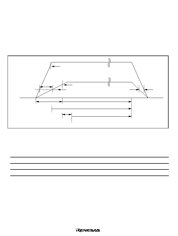
Rev. 2.00, 09/03, page 624 of 690
∑
Power-off order
1. In the reverse order of powering-on, first turn off the 1.5 V power, then turn off the 3.3 V
power within 1 ms. It is recommended that this interval will be as short as possible.
2. Pin states are undefined while only the 1.5 V power is off. The system design must ensure
that these undefined states do not cause erroneous system operation.
3. When the power is turned off, make sure that the voltage of the 1.5 V power is lower than
that of the 3.3 V power.
Waveforms and recommended times at power on/off are shown in figure 25.1.
tpwu
VccQ: 3.3 V power
VccQ (min) voltage
VccQ (min)
attain time
Vcc (min)
attain time
Vcc: 1.5 V power
Vcc (min) voltage
Vcc/2 level voltage
Normal operation term
States undefined
term
Operation stopped
Clock oscillation started
Oscillation settling time
Cancel the power-on reset and
go to normal operation
tunc
GND
tpwd
Figure 25.1 Power On/Off Sequence
Recommended Power On/Off Times
Item
Symbol
Max. Permitted
Value
Unit
VccQ to Vcc power-on time interval
tpwu
1
ms
VccQ to Vcc power-off time interval
tpwd
1
ms
State undefined term
tunc
10
ms
The recommended times shown above do not require strict settings.
The state undefined term indicates that pins are at the power rising stage. The pin state is stabilized
at VccQ (min) attain time. However, a power-on reset (
RESETP) is accepted successfully only
after VccQ (min) attain time and clock oscillation settling time. Set the state undefined term less
than 10 ms.

Rev. 2.00, 09/03, page 625 of 690
25.2
DC Characteristics
Tables 25.2 and 25.3 list DC characteristics.
Table 25.2
DC Characteristics (1) [Common Items]
(Condition: Ta = ≠20 to 75∞C)
Item
Symbol
Min
Typ
Max
Unit
Measurement
Conditions
V
CC
Q,
V
CC
-RTC
3.0
3.3
3.6
V
Power supply voltage
V
CC
,
V
CC
-PLL1
V
CC
-PLL2
1.4
1.5
1.6
--
133
200
V
CC
= 1.5 V
I
= 133 MHz
I
CC
--
105
150
V
CC
= 1.5 V
I
= 100 MHz
Normal
operation
I
CC
Q
--
20
40
mA
V
CC
Q = 3.3 V
B
= 33 MHz
I
CC
--
25
40
mA
In sleep mode
*
I
CC
Q
--
10
20
B
= 33 MHz
I
CC
--
150
500
µ
A
I
CC
Q
--
10
30
T
a
= 25∞C (RTC
on)
V
CC
Q = 3.3 V
V
CC
= 1.5 V
I
CC
--
150
500
µ
A
Current
consumption
In standby
mode
I
CC
Q
--
10
30
T
a
= 25∞C (RTC
off)
V
CC
Q = 3.3 V
V
CC
= 1.5 V
Input leak
current
All input pins
| I
in
|
--
--
1.0
µ
A
V
in
= 0.5 to
V
CC
Q ≠ 0.5 V
Three-state
leak current
I/O, all output
pins (off
condition)
| I
TSI
|
--
--
1.0
µ
A
Vin = 0.5 to
V
CC
Q ≠ 0.5 V
Pull-up
resistance
Port pin
R
pull
30
60
120
k

Rev. 2.00, 09/03, page 626 of 690
Item
Symbol
Min
Typ
Max
Unit
Measurement
Conditions
Pin
capacitance
All pins other
than the USB
transceiver pins
(D+, D-) and
PTM3 to PTM0
C
--
--
10
pF
USB
transceiver pins
(D+, D≠) and
PTM3 to PTM0
C
AN
--
--
20
pF
Analog power-supply
voltage (AD)
AV
CC
3.0
3.3
3.6
V
Analog power-supply
voltage (USB)
V
CC
-USB
3.0
3.3
3.6
V
Analog
power-supply
current (AD)
During A/D
conversion
AI
CC
--
0.8
2
mA
Idle
--
0.01
5.0
µ
A
Note:
*
No external bus cycles except refresh cycles.

Rev. 2.00, 09/03, page 627 of 690
Table 25.2
DC Characteristics (2-a) [Excluding USB-Related Pins]
(Condition: Ta = ≠20 to 75∞C)
Item
Symbol
Min
Typ
Max
Unit
Measurement
Conditions
Input high
voltage
RESETP
,
RESETM
, NMI
IRQ5 to IRQ0,
PINT15 to
PINT0, RXD0,
MD6 to MD0,
ASEMD0
,
TRST
, EXTAL,
CKIO, CA
V
IH
V
CC
Q
◊
0.9 --
V
CC
Q + 0.3
EXTAL2
--
--
--
When this pin
is not
connected to
the crystal
resonator, this
pin should be
connected to
the V
CC
Q pin
(pulled up).
Port L
2.0
--
AV
CC
+ 0.3
Other input
pins
2.0
--
V
CC
Q + 0.3
V
Input low
voltage
RESETP
,
RESETM
, NMI
IRQ5 to IRQ0,
PINT15 to
PINT0, RXD0,
MD6 to MD0,
ASEMD0
,
TRST
, EXTAL,
CKIO, CA
V
IL
≠0.3
--
V
CC
Q
◊
0.1
EXTAL2
--
--
--
When this pin
is not
connected to
the crystal
resonator, this
pin should be
connected to
the V
CC
Q pin
(pulled up).
Port L
≠0.3
--
AV
CC
◊
0.2
V

Rev. 2.00, 09/03, page 628 of 690
Item
Symbol
Min
Typ
Max
Unit
Measurement
Conditions
Input low
voltage
Other input
pins
V
IL
≠0.3
--
V
CC
Q
◊
0.2 V
Output high
voltage
All output pins V
OH
2.4
--
--
V
CC
Q = 3.0 V,
I
OH
= ≠200
µ
A
2.0
--
--
V
V
CC
Q = 3.0 V,
I
OH
= ≠2 mA
Output low
voltage
All output pins V
OL
--
--
0.55
V
V
CC
Q = 3.6 V,
I
OL
= 1.6 mA
Notes: 1. Even when the RTC is not used, power must be supplied between V
CC
-RTC and V
SS
-
RTC.
2. AV
CC
must satisfy the condition: V
CC
Q ≠ 0.2 V
AV
CC
V
CC
Q + 0.2 V. Do not leave the
AV
CC
and AV
SS
pins open if the A/D converter is not used; connect AV
CC
to V
CC
Q, and
AV
SS
to V
SS
Q.
3. Current consumption values are for V
IH
min = V
CC
Q ≠ 0.5 V and V
IL
max = 0.5 V with all
output pins unloaded.
Table 25.2
DC Characteristics (2-b) [USB-Related Pins*]
(Condition: Ta = ≠20 to 75∞C)
Item
Symbol
Min
Typ
Max
Unit
Measurement
Conditions
Power supply voltage
V
CC
Q
3.0
3.3
3.6
V
Input high voltage
V
IH
2.0
--
V
CC
Q + 0.3 V
Input low voltage
V
IL
≠0.3
--
V
CC
Q
◊
0.2 V
Input high voltage
(EXTAL_USB)
V
IH
(EXTAL_USB)
V
CC
Q ≠ 0.3--
V
CC
Q + 0.3 V
Input low voltage
(EXTAL_USB)
V
IL
(EXTAL_USB)
≠0.3
--
V
CC
Q
◊
0.2 V
Output high voltage
V
OH
2.4
--
--
V
V
CC
Q = 3.0 V,
I
OH
= ≠200
µ
A
2.0
--
--
V
CC
Q = 3.0 V,
I
OH
= ≠2 mA
Output low voltage
V
OL
--
--
0.55
V
V
CC
Q = 3.6 V,
I
OL
= 1.6 mA
Note:
*
XVDATA, DPLS, DMNS, TXDPLS, TXDMNS, TXENL, VBUS, SUSPND, and EXTAL_USB
pins

Rev. 2.00, 09/03, page 629 of 690
Table 25.2
DC Characteristics (2-c) [USB Transceiver-Related Pins*
1
]
(Condition: Ta = ≠20 to 75∞C)
Item
Symbol
Min
Typ
Max
Unit
Measurement
Conditions
Power supply voltage
*
2
V
CC
-USB
3.0
3.3
3.6
V
Differential input sensitivity
V
DI
0.2
--
--
V
(DP)≠(DM)
Differential common mode
range
V
CM
0.8
--
2.5
V
Single ended receiver
threshold voltage
V
SE
0.8
--
2.0
V
Output high voltage
V
OH
2.8
--
V
CC
-USB
V
Output low voltage
V
OL
--
--
0.3
V
Tri-state leak current
I
LO
≠10
--
10
µ
A
0V<V
IN
<3.3V
Notes: 1. D+ and D≠ pins
2. V
CC
-USB must satisfy the condition: V
CC
Q
V
CC
-USB. Even when the USB is not used,
power must be supplied between V
CC
-USB and V
SS
-USB.
Table 25.3
Permitted Output Current Values
(Conditions: V
CC
Q = V
CC
-RTC = V
CC
-USB = 3.0 to 3.6 V, V
CC
= V
CC
-PLL1 = V
CC
-PLL2 = 1.4 to
1.6 V, AV
CC
= 3.0 to 3.6 V, V
SS
Q = V
SS
= V
SS
-RTC = V
SS
-USB = V
SS
-PLL1 = V
SS
-PLL2 =
AV
SS
= 0 V, T
a
= ≠20 to 75∞C)
Item
Symbol
Min
Typ
Max
Unit
Output low-level permissible current (per pin)
I
OL
--
--
2.0
mA
Output low-level permissible current (total)
I
OL
--
--
120
mA
Output high-level permissible current (per pin)
≠I
OH
--
--
2.0
mA
Output high-level permissible current (total)
(≠I
OH
)
--
--
40
mA
Caution: To ensure LSI reliability, do not exceed the value for output current given in table 25.3.

Rev. 2.00, 09/03, page 630 of 690
25.3
AC Characteristics
In general, inputting for this LSI should be clock synchronous. Keep the setup and hold times for
each input signal unless otherwise specified.
Table 25.4
Maximum Operating Frequencies
(Conditions: V
CC
Q = V
CC
-RTC = V
CC
-USB = 3.0 to 3.6 V, V
CC
= V
CC
-PLL1 = V
CC
-PLL2 = 1.4 to
1.6 V, AV
CC
= 3.0 to 3.6 V, V
SS
Q = V
SS
= V
SS
-RTC = V
SS
-USB = V
SS
-PLL1 = V
SS
-PLL2 =
AV
SS
= 0 V, T
a
= ≠20 to 75∞C)
Item
Symbol
Min
Typ
Max
Unit
Remarks
133.34
133-MHz
product
CPU, cache (I
)
f
20
--
100
MHz
100-MHz
product
External bus (B
)
20
--
66.67
Operating
frequency
Peripheral module (P
)
5
--
33.34

Rev. 2.00, 09/03, page 631 of 690
25.3.1
Clock Timing
Table 25.5
Clock Timing
(Condition: V
CC
Q = V
CC
-RTC = V
CC
-USB = 3.0 to 3.6 V, V
CC
= V
CC
-PLL1 = V
CC
-PLL2 = 1.4 to 1.6 V,
AV
CC
= 3.0 to 3.6 V, V
SS
Q = V
SS
= V
SS
-RTC = V
SS
-USB = V
SS
-PLL1 = V
SS
-PLL2 = AV
SS
=
0 V, T
a
= ≠20 to 75∞C, Maximum External Bus Operating Frequency: 66.67 MHz)
Item
Symbol
Min
Max
Unit
Figure
EXTAL clock input frequency
f
EX
10
66.67 MHz
25.2
EXTAL clock input cycle time
t
EXcyc
15
100
ns
EXTAL clock input low pulse width
t
EXL
1.5
--
ns
EXTAL clock input high pulse width
t
EXH
1.5
--
ns
EXTAL clock input rise time
t
EXr
--
6
ns
EXTAL clock input fall time
t
EXf
--
6
ns
CKIO clock input frequency
f
CKI
20
66.67 MHz
25.3
CKIO clock input cycle time
t
CKICYC
15
50
ns
CKIO clock input low pulse width
t
CKIL
3
--
ns
CKIO clock input high pulse width
t
CKIH
3
--
ns
CKIO clock input rise time
t
CKIR
--
4
ns
CKIO clock input fall time
t
CKIF
--
4
ns
CKIO clock output frequency
t
OP
20
66.67 MHz
25.4
CKIO clock output cycle time
t
cyc
15
50
ns
CKIO clock output low pulse width
t
CKOL
3
--
ns
CKIO clock output high pulse width
t
CKOH
3
--
ns
CKIO clock output rise time
t
CKOr
--
5
ns
CKIO clock output fall time
t
CKOf
--
5
ns
Power-on oscillation settling time
t
OSC1
10
--
ms
25.5
RESETP
setup time
t
RESPS
20
--
ns
25.5
RESETP
assert time
t
RESPW
20
--
t
cyc
25.5, 25.6
RESETM
assert time
t
RESMW
20
--
t
cyc
25.6
Standby return oscillation settling time 1
t
OSC2
10
--
ms
25.6
Standby return oscillation settling time 2
t
OSC3
10
--
ms
25.7
Standby return oscillation settling time 3
t
OSC4
11
--
ms
25.8
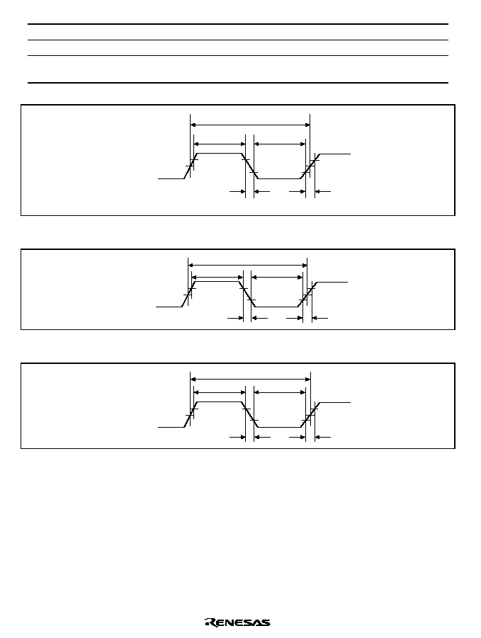
Rev. 2.00, 09/03, page 632 of 690
Item
Symbol
Min
Max
Unit
Figure
PLL synchronization settling time 1
t
PLL1
100
--
µs
25.9, 25.10
PLL synchronization settling time 2
t
PLL2
100
--
µs
25.11
Interrupt determination time
(RTC used and standby mode)
t
IRLSTB
100
--
µs
25.10
t
EXH
t
EXf
t
EXr
t
EXL
t
EXcyc
V
IH
V
IH
V
IH
1/2 V
CC
Q
1/2 V
CC
Q
V
IL
V
IL
EXTAL
*
(input)
Note:
* The clock input from the EXTAL pin.
Figure 25.2 EXTAL Clock Input Timing
t
CKIH
t
CKIF
t
CKIR
t
CKIL
t
CKICYC
V
IH
1/2 V
CC
Q
1/2 V
CC
Q
V
IH
V
IL
V
IH
V
IL
CKIO
(input)
Figure 25.3 CKIO Clock Input Timing
t
CKOH
t
CKOf
t
CKOr
t
CKOL
t
cyc
V
OH
1/2 V
CC
Q
1/2 V
CC
Q
V
OH
V
OH
V
OL
V
OL
CKIO
(output)
Figure 25.4 CKIO Clock Output Timing

Rev. 2.00, 09/03, page 633 of 690
V
CC
min
t
RESPW
t
RESPS
t
OSC1
V
CC
RESETP
TRST
CKIO,
internal clock
Stable oscillation
Note: Oscillation settling time when built-in oscillator is used
Figure 25.5 Power-On Oscillation Settling Time
CKIO,
internal
clock
Stable oscillation
Standby
t
OSC2
t
RESPW
t
RESMW
RESETP
RESETM
Note: Oscillation settling time when built-in oscillator is used
Figure 25.6 Oscillation Settling Time at Standby Return (Return by Reset)
CKIO,
internal
clock
Stable oscillation
Standby
t
OSC3
NMI
Note: Oscillation settling time when built-in oscillator is used
Figure 25.7 Oscillation Settling Time at Standby Return (Return by NMI)
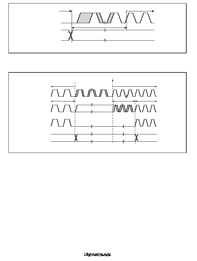
Rev. 2.00, 09/03, page 634 of 690
CKIO,
internal
clock
Stable oscillation
Standby
t
OSC4
IRL3 to IRL0
IRQ5 to IRQ0
PINT15 to PINT0
Note: Oscillation settling time when built-in oscillator is used in oscillation stop mode
Figure 25.8 Oscillation Settling Time at Standby Return
(Return by IRQ5 to IRQ0, PINT15 to PINT0, and
IRL3 to IRL0)
EXTAL input,
CKIO input
Stable input clock
Reset or NMI interrupt request
Stable input clock
Normal
Normal
Standby
PLL output,
CKIO output
Internal clock
STATUS 0
STATUS 1
PLL synchronization
Note: PLL oscillation settling time when clock is input from EXTAL pin
t
PLL1
PLL synchronization
Figure 25.9 PLL Synchronization Settling Time by Reset or NMI
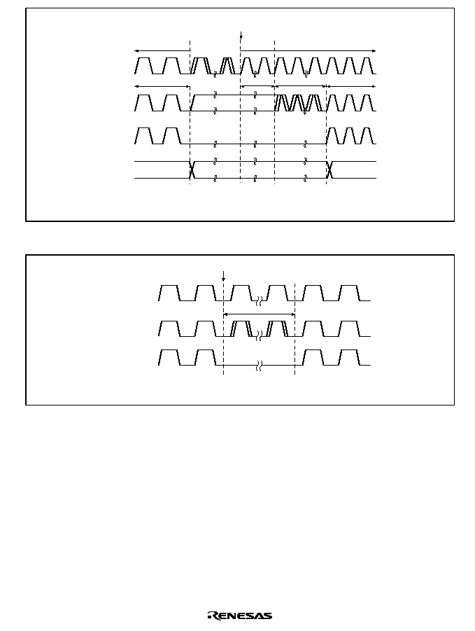
Rev. 2.00, 09/03, page 635 of 690
EXTAL input
or CKIO input
Stable input clock
PINT15 to PINT0,
IRQ5 to IRQ0/
IRL3 to IRL0 interrupt request
Stable input clock
Normal
Normal
PLL output,
CKIO output
Internal clock
STATUS 0
STATUS 1
Note: PLL oscillation settling time when clock is input from
EXTAL pin or CKIO pin in oscillation continuous mode.
t
PLL1
PLL synchronization
Standby
PLL synchronization
t
IRLSTB
Figure 25.10 PLL Synchronization Settling Time by IRQ/IRL, PINT Interrupts
EXTAL input
*1
(CKIO input)
CKIO output
*2
(PLL output)
Internal clock
Multiplication ratio modified
t
PLL2
Notes: 1. CKIO input in clock mode 7
2. PLL output except in clock mode 7
Figure 25.11 PLL Synchronization Settling Time when Frequency Multiplication
Ratio Modified

Rev. 2.00, 09/03, page 636 of 690
25.3.2
Control Signal Timing
Table 25.6
Control Signal Timing
(Conditions: V
CC
Q = V
CC
-RTC = V
CC
-USB = 3.0 to 3.6 V, V
CC
= V
CC
-PLL1 = V
CC
-PLL2 = 1.4 to
1.6 V, AV
CC
= 3.0 to 3.6 V, V
SS
Q = V
SS
= V
SS
-RTC = V
SS
-USB = V
SS
-PLL1 = V
SS
-PLL2 =
AV
SS
= 0 V, T
a
= ≠20 to 75∞C, Clock mode 0/1/2/4/5/6/7)
66.67 MHz
*
2
Item
Symbol
Min
Max
Unit
Figure
RESETP
pulse width
t
RESPW
20
*
3
--
t
cyc
25.12
RESETP
setup time
*
1
t
RESPS
20
--
ns
RESETM
pulse width
t
RESMW
20
*
4
--
t
cyc
RESETM
setup time
t
RESMS
10
--
ns
BREQ
setup time
t
BREQS
1/2 t
cyc
+10 --
ns
25.14
BREQ
hold time
t
BREQH
1/2 t
cyc
+3
--
ns
NMI setup time
*
1
t
NMIS
10
--
ns
25.13
NMI hold time
t
NMIH
3
--
ns
IRQ5 to IRQ0 setup time
*
1
t
IRQS
10
--
ns
IRQ5 to IRQ0 hold time
t
IRQH
3
--
ns
BACK
delay time
t
BACKD
--
1/2 t
cyc
+13 ns
25.14
STATUS1, STATUS0 delay time
t
STD
--
18
ns
25.15
Bus tri-state delay time 1
t
BOFF1
0
30
ns
25.14,
Bus tri-state delay time 2
t
BOFF2
0
30
ns
25.15
Bus buffer-on time 1
t
BON1
0
30
ns
Bus buffer-on time 2
t
BON2
0
30
ns
Notes: t
cyc
is the external bus clock cycle (B clock cycle).
1.
RESETP
,
RESETM
, NMI, and IRQ5 to IRQ0 are asynchronous. Changes are detected
at the clock rise when the setup shown is kept. When the setup cannot be kept,
detection can be delayed until the next clock rises.
2. The upper limit of the external bus clock is 66.67 MHz.
3. In standby mode, t
RESPW
= t
OSC2
(10 ms). When the crystal oscillation continues or the
clock multiplication ratio is changed in standby mode, t
RESPW
= t
PLL1
(100 µs).
4. In standby mode, t
RESMW
= t
OSC2
(10 ms). When the crystal oscillation continues or the
clock multiplication ratio is changed in standby mode,
RESETM
must be kept low until
STATUS (0-1) changes to reset (HH).
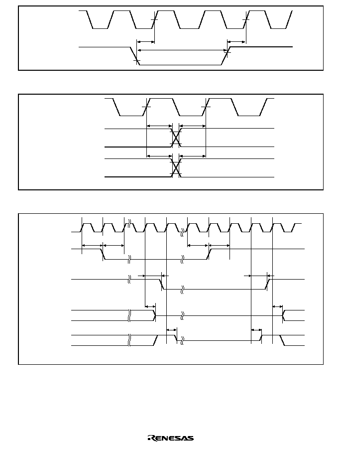
Rev. 2.00, 09/03, page 637 of 690
CKIO
t
RESPS
t
RESMS
t
RESPS
t
RESMS
RESETP
RESETM
t
RESPW
t
RESMW
Figure 25.12 Reset Input Timing
CKIO
NMI
t
NMIH
t
NMIS
V
IH
V
IL
IRQ5 to IRQ0
t
IRQH
t
IRQS
V
IH
V
IL
Figure 25.13 Interrupt Signal Input Timing
CKIO
BREQ
BACK
A25 to A0,
D31 to D0
RD, RD/WR,
RASU/L,
CASU/L,
CSn, WEn,
BS, CKE
BREQH
t
BREQS
t
BACKD
t
BACKD
t
BREQH
t
BREQS
t
BON1
t
BOFF1
t
BOFF2
t
BON2
t
Figure 25.14 Bus Release Timing
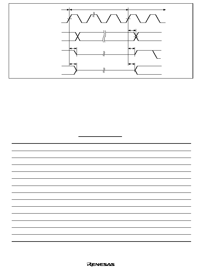
Rev. 2.00, 09/03, page 638 of 690
CKIO
t
BOFF2
t
BOFF1
t
STD
t
BON2
t
BON1
STATUS 0
STATUS 1
A25 to A0,
D31 to D0
RD, RD/WR,
RASU/L, CASU/L,
CSn, WEn, BS,
CKE
Normal mode
Normal mode
Standby mode
Figure 25.15 Pin Drive Timing at Standby
25.3.3
AC Bus Timing
Table 25.7
Bus Timing (1)
(Conditions: V
CC
Q = V
CC
-RTC = V
CC
-USB = 3.0 to 3.6 V, V
CC
= V
CC
-PLL1 = V
CC
-PLL2 = 1.4 to
1.6 V, AV
CC
= 3.0 to 3.6 V, V
SS
Q = V
SS
= V
SS
-RTC = V
SS
-USB = V
SS
-PLL1 = V
SS
-PLL2 =
AV
SS
= 0 V, T
a
= ≠20 to 75∞C, Clock mode 0/1/2/4/5/6/7)
66.67 MHz
Item
Symbol Min
Max
Unit
Figure
Address delay time 1
t
AD1
1
12
ns
25.16 to 25.38
Address delay time 2
t
AD2
--
1/2 t
cyc
+12 ns
25.21
Address setup time
t
AS
0
--
ns
25.16 to 25.19
Address hold time
t
AH
0
--
ns
25.16 to 25.19
BS
delay time
t
BSD
--
10
ns
25.16 to 25.35
CS
delay time 1
t
CSD1
1
10
ns
25.16 to 25.38
Read/write delay time 1
t
RWD1
1
10
ns
25.16 to 25.38
Read strobe delay time
t
RSD
--
1/2 t
cyc
+10 ns
25.16 to 25.21
Read data setup time 1
t
RDS1
1/2 t
cyc
+6
--
ns
25.16 to 25.20
Read data setup time 2
t
RDS2
6
--
ns
25.22 to 25.25, 25.30 to 25.32
Read data setup time 3
t
RDS3
1/2 t
cyc
+6
--
ns
25.21
Read data hold time 1
t
RDH1
0
--
ns
25.16 to 25.20
Read data hold time 2
t
RDH2
2
--
ns
25.22 to 25.25, 25.30 to 25.32
Read data hold time 3
t
RDH3
0
--
ns
25.21

Rev. 2.00, 09/03, page 639 of 690
66.67 MHz
Item
Symbol Min
Max
Unit
Figure
Write enable delay time
t
WED
--
1/2 t
cyc
+10 ns
25.16 to 25.21
Write data delay time 1
t
WDD1
--
12
ns
25.16 to 25.20
Write data delay time 2
t
WDD2
--
12
ns
25.26 to 25.29, 25.33 to 25.35
Write data hold time 1
t
WDH1
1
--
ns
25.16 to 25.20
Write data hold time 2
t
WDH2
1
--
ns
25.26 to 25.29, 25.33 to 25.35
Write data hold time 4
t
WDH4
0
--
ns
25.16 to 25.19
WAIT
setup time
t
W TS
1/2 t
cyc
+6
--
ns
25.17 to 25.21
WAIT
hold time
t
W TH
1/2 t
cyc
+2
--
ns
25.17 to 25.21
RAS
delay time 1
t
RASD1
1
10
ns
25.22 to 25.38
CAS
delay time 1
t
CASD1
1
10
ns
25.22 to 25.38
DQM
delay time 1
t
DQMD1
1
10
ns
25.22 to 25.35
CKE delay time 1
t
CKED1
1
10
ns
25.37
AH
delay time
t
AHD
1/2 t
cyc
1/2 t
cyc
+10 ns
25.20
Multiplex address delay
time
t
MAD
--
12
ns
25.20
Multiplex address hold
time
t
MAH
0
--
ns
25.20
DACK delay time
t
DACD
--
10
ns
25.16 to 25.35
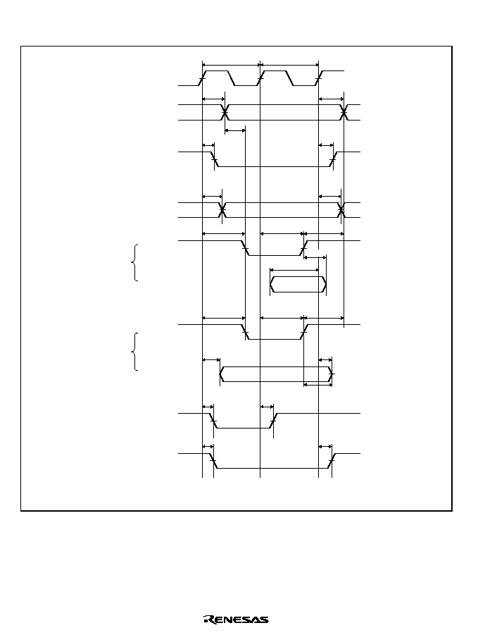
Rev. 2.00, 09/03, page 640 of 690
25.3.4
Basic Timing
T
1
t
AD1
t
AD1
t
AS
t
CSD1
t
CSD1
T
2
t
RWD1
t
RWD1
t
RSD
t
RSD
t
AH
t
AH
t
RDH1
t
RDS1
t
WED
t
WED
t
BSD
t
BSD
t
DACD
t
DACD
t
WDH1
t
WDH4
t
WDD1
CKIO
A25 to A0
CSn
RD/
WR
RD
D31 to D0
WEn*
2
BS
DACKn*
1
D31 to D0
Read
Write
Notes: 1. DACKn is a waveform when active-low is specified.
2. Output timing is the same when reading byte-selection SRAM.
Figure 25.16 Basic Bus Cycle (No Wait)
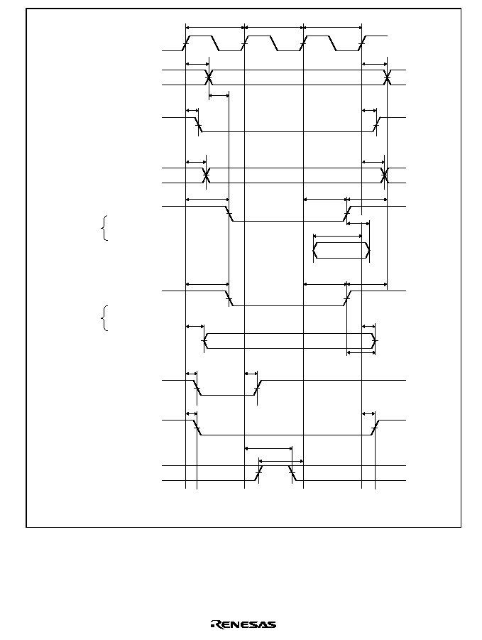
Rev. 2.00, 09/03, page 641 of 690
T
1
t
AD1
t
AD1
t
AS
t
CSD1
t
CSD1
Tw
T
2
t
RWD1
t
RWD1
t
RSD
t
RSD
t
RDH1
t
RDS1
t
WED
t
WED
t
AH
t
AH
t
BSD
t
BSD
t
WTH
t
WTS
t
DACD
t
DACD
t
WDH1
t
WDH4
t
WDD1
CKIO
A25 to A0
CSn
RD/
WR
RD
D31 to D0
WEn*
2
BS
WAIT
DACKn*
1
D31 to D0
Notes: 1. DACKn is a waveform when active-low is specified.
2. Output timing is the same when reading byte-selection SRAM.
Read
Write
Figure 25.17 Basic Bus Cycle (One Software Wait)
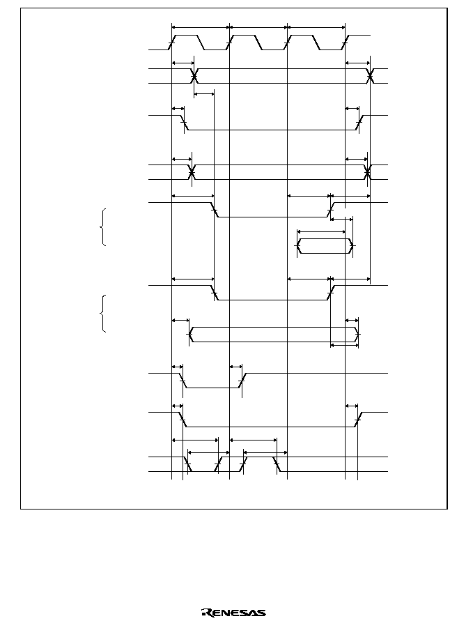
Rev. 2.00, 09/03, page 642 of 690
T
1
t
AD1
t
AD1
t
AS
t
CSD1
t
CSD1
TwX
T
2
t
RWD1
t
RWD1
t
RSD
t
RSD
t
AH
t
AH
t
RDH1
t
RDS1
t
WED
t
WED
t
BSD
t
BSD
t
WTH
t
WTH
t
WTS
t
WTS
t
DACD
t
DACD
t
WDH1
t
WDH4
t
WDD1
CKIO
A25 to A0
CSn
RD/
WR
RD
D31 to D0
WEn*
2
BS
WAIT
DACKn*
1
D31 to D0
Read
Write
Notes: 1.
DACKn is a waveform when active-low is specified.
2. Output timing is the same when reading byte-selection SRAM.
Figure 25.18 Basic Bus Cycle (One External Wait)
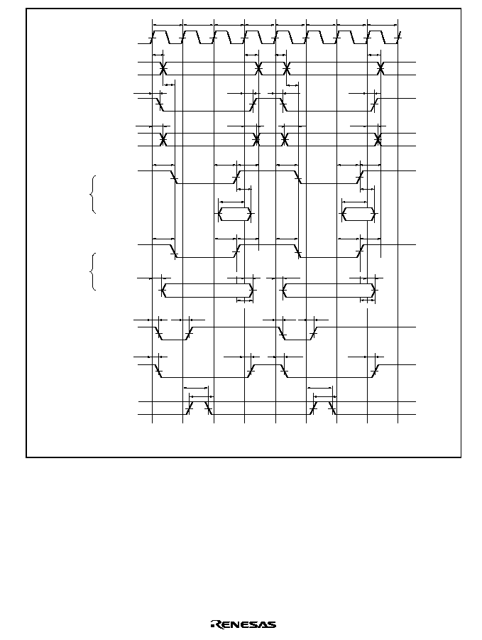
Rev. 2.00, 09/03, page 643 of 690
t
AD1
t
AD1
T
1
t
RWD1
t
RSD
t
WED
t
WED
t
WED
t
RDS1
t
RDS1
t
RDH1
t
RDH1
t
AS
t
RSD
t
RSD
t
AH
t
RSD
t
AH
t
WED
t
AH
t
AH
t
CSD1
t
WDD1
t
WDH1
t
WDH4
t
WDH1
t
WDH4
t
WDD1
t
BSD
t
BSD
t
DACD
t
DACD
t
DACD
t
DACD
t
BSD
t
BSD
t
RWD1
t
RWD1
t
RWD1
t
CSD1
t
CSD1
t
CSD1
t
AS
t
AD1
t
AD1
Tw
T
2
Tnop
T
1
Tw
T
2
Tnop
DACKn*
1
A25 to A0
D15 to D0
CSn
RD/
WR
RD
WAIT
D15 to D0
WEn*
2
BS
CKIO
t
WTH
t
WTS
t
WTH
t
WTS
Read
Write
Notes:
1. DACKn is a waveform when active-low is specified.
2. Output timing is the same when reading byte-selection SRAM.
Figure 25.19 Basic Bus Cycle (One Software Wait, External Wait Enabled
(WM Bit = 0), No Idle Cycle Setting)
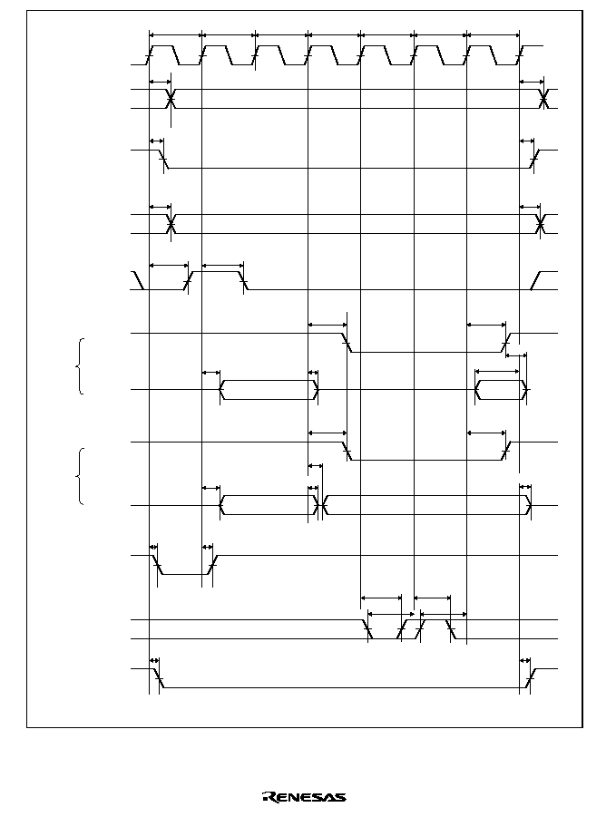
Rev. 2.00, 09/03, page 644 of 690
t
WDD1
Ta1
Ta2
Ta3
T
1
Tw
Tw
T
2
t
AD1
t
CSD1
t
AD1
t
RWD1
t
RWD1
t
CSD1
t
RSD
t
RSD
t
RDH1
t
RDS1
t
WED
t
WED
Data
Data
t
BSD
t
BSD
t
WTH
t
WTS
t
AHD
t
AHD
t
WTH
t
WTS
t
DACD
t
DACD
Address
t
WDH1
t
MAH
t
MAD
CKIO
A25 to A0
CSn
RD/
WR
RD
AH
D15 to D0
WE0/1
BS
WAIT
DACKn
*
D15 to D0
Address
t
MAH
t
MAD
Read
Write
Note:
* DACKn is a waveform when active-low is specified.
Figure 25.20 Address/Data Multiplex I/O Bus Cycle
(Three Address Cycles, One Software Wait, One External Wait)
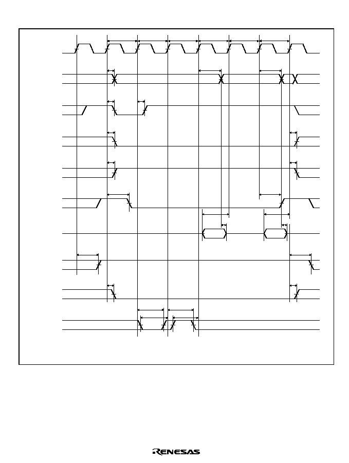
Rev. 2.00, 09/03, page 645 of 690
25.3.5
Burst ROM Timing
T
1
Tw
Twx
T2B
Twb
T2B
t
AD1
t
CSD1
t
AD2
t
AD2
t
RWD1
t
RWD1
t
CSD1
t
RSD
t
RSD
t
WED
t
WED
t
BSD
t
BSD
t
WTH
t
WTS
t
WTH
t
WTS
t
DACD
t
DACD
t
RDS3
t
RDH3
t
RDS3
t
RDH3
CKIO
A25 to A0
CSn
RD/
WR
RD
WEn
BS
WAIT
DACKn
D31 to D0
Notes: 1. t
RDH3
is specified by earlier one of change of A25 to A0 or the
RD rising edge.
2. DACKn is a waveform when active-low is specified.
Figure 25.21 Burst ROM Read Cycle (One Access Wait, One External Wait,
One Burst Wait, Two Bursts)
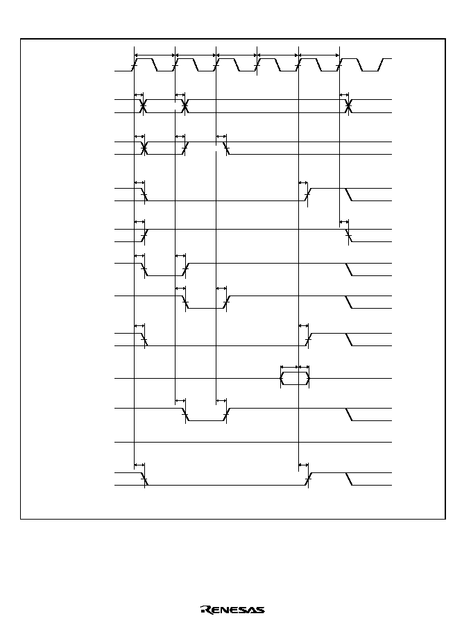
Rev. 2.00, 09/03, page 646 of 690
25.3.6
Synchronous DRAM Timing
Tc1
Tr
Tcw
Td1
Tde
t
AD1
t
AD1
t
CSD1
t
AD1
t
RWD1
t
RWD1
t
CSD1
t
AD1
t
AD1
t
AD1
t
RDH2
t
RDS2
CKIO
A25 to A0
CSn
RD/
WR
A12/A11*
1
D31 to D0
t
RASD1
t
RASD1
RASU/L
Row address
Read A command
Column address
t
CASD1
t
CASD1
CASU/L
t
BSD
t
BSD
(High)
BS
CKE
t
DQMD1
t
DQMD1
DQMxx
t
DACD
t
DACD
DACKn*
2
Notes: 1. Address pin to be connected to A10 of SDRAM.
2. DACKn is a waveform when active-low is specified.
Figure 25.22 Synchronous DRAM Single Read Bus Cycle
(Auto Precharge, CAS Latency
=
=
=
=
2, TRCD
=
=
=
=
1 Cycle, TRP
=
=
=
=
1 Cycle)
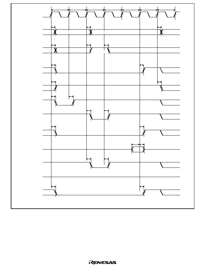
Rev. 2.00, 09/03, page 647 of 690
Trw
Tr
Tc1
Tcw
Td1
Tde
Tap
t
AD1
t
AD1
t
CSD1
t
AD1
t
RWD1
t
RWD1
t
CSD1
t
AD1
t
AD1
t
AD1
t
RDH2
t
RDS2
CKIO
A25 to A0
CSn
RD/
WR
A12/A11*
1
D31 to D0
t
RASD1
t
RASD1
RASU/L
Row address
Read A command
Column address
t
CASD1
t
CASD1
CASU/L
t
BSD
t
BSD
(High)
BS
CKE
t
DQMD1
t
DQMD1
DQMxx
t
DACD
t
DACD
DACKn*
2
Notes:
1. Address pin to be connected to A10 of SDRAM.
2. DACKn is a waveform when active-low is specified.
Figure 25.23 Synchronous DRAM Single Read Bus Cycle
(Auto Precharge, CAS Latency
=
=
=
=
2, TRCD
=
=
=
=
2 Cycle, TRP
=
=
=
=
2 Cycle)

Rev. 2.00, 09/03, page 648 of 690
Tc1
Tc2
Td1
Td2
Td3
Td4
Tr
Tc3
Tc4
Tde
t
AD1
t
CSD1
t
AD1
t
AD1
t
AD1
t
AD1
t
AD1
t
AD1
t
AD1
t
AD1
t
AD1
t
RWD1
t
RWD1
t
CSD1
CKIO
A25 to A0
CSn
RD/
WR
A12/A11*
1
D31 to D0
t
RASD1
t
RASD1
RASU/L
Row
address
Read A
command
Read command
Column
address
(1 to 4)
t
CASD1
t
CASD1
CASU/L
t
BSD
t
BSD
(High)
BS
CKE
t
DQMD1
t
DQMD1
DQMxx
t
DACD
t
DACD
DACKn*
2
t
RDH2
t
RDS2
t
RDH2
t
RDS2
Notes: 1. Address pin to be connected to A10 of SDRAM.
2. DACKn is a waveform when active-low is specified.
Figure 25.24 Synchronous DRAM Burst Read Bus Cycle (Single Read
◊
◊
◊
◊
4),
(Auto Precharge, CAS Latency
=
=
=
=
2, TRCD
=
=
=
=
1 Cycle, TRP
=
=
=
=
2 Cycle)
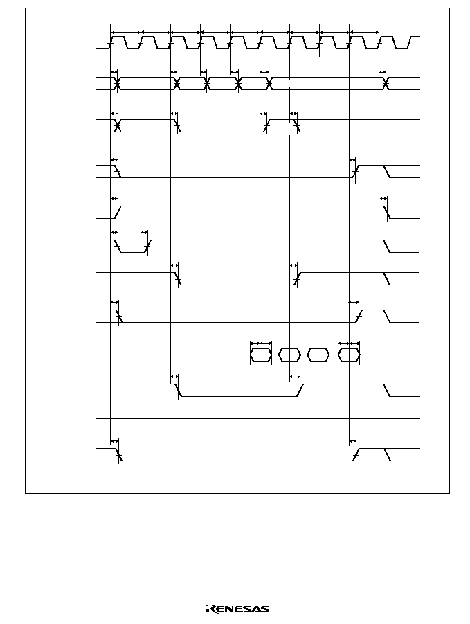
Rev. 2.00, 09/03, page 649 of 690
Tc1
Tc2
Td1
Td2
Td3
Td4
Tr
Trw
Tc3
Tc4
Tde
t
CSD1
t
CSD1
t
AD1
t
AD1
t
AD1
t
AD1
t
AD1
t
AD1
t
AD1
t
AD1
t
AD1
t
AD1
t
RWD1
t
RWD1
CKIO
A25 to A0
CSn
RD/
WR
A12/A11*
1
D31 to D0
t
RASD1
t
RASD1
RASU/L
Row address
Read A
command
Read command
Column
address
(1 to 4)
t
CASD1
t
CASD1
CASU/L
t
BSD
t
BSD
(High)
BS
CKE
t
DQMD1
t
DQMD1
DQMxx
t
DACD
t
DACD
DACKn*
2
t
RDH2
t
RDS2
t
RDH2
t
RDS2
Notes: 1. Address pin to be connected to A10 of SDRAM.
2. DACKn is a waveform when active-low is specified.
Figure 25.25 Synchronous DRAM Burst Read Bus Cycle (Single Read
◊
◊
◊
◊
4),
(Auto Precharge, CAS Latency
=
=
=
=
2, TRCD
=
=
=
=
2 Cycle, TRP
=
=
=
=
1 Cycle)
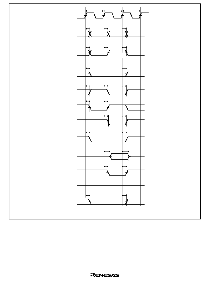
Rev. 2.00, 09/03, page 650 of 690
Trwl
Tr
Tc1
t
CSD1
t
CSD1
t
RWD1
t
RWD1
t
RWD1
t
AD1
t
AD1
t
AD1
t
AD1
t
AD1
t
AD1
CKIO
A25 to A0
CSn
RD/
WR
A12/A11*
1
D31 to D0
t
RASD1
t
RASD1
RASU/L
Row address
Write A
command
Column
address
t
CASD1
t
CASD1
CASU/L
t
BSD
t
BSD
(High)
BS
CKE
t
DQMD1
t
DQMD1
DQMxx
t
DACD
t
DACD
DACKn*
2
t
WDD2
t
WDH2
Notes: 1. Address pin to be connected to A10 of SDRAM.
2. DACKn is a waveform when active-low is specified.
Figure 25.26 Synchronous DRAM Single Write Bus Cycle
(Auto Precharge, TRWL = 2 Cycle)
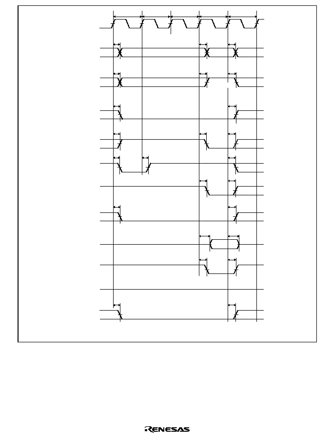
Rev. 2.00, 09/03, page 651 of 690
Trw
Tc1
Trwl
Tr
Trw
t
CSD1
t
CSD1
t
CASD1
t
CASD1
t
AD1
t
AD1
t
AD1
t
AD1
t
AD1
t
AD1
t
RWD1
CKIO
A25 to A0
CSn
RD/
WR
A12/A11*
1
D31 to D0
t
RASD1
RASU/L
Row address
Write A
command
Column
address
CASU/L
t
BSD
t
BSD
(High)
BS
CKE
t
DQMD1
t
RWD1
t
RWD1
t
RASD1
t
RASD1
t
DQMD1
DQMxx
t
DACD
t
DACD
DACKn*
2
t
WDH2
t
WDD2
Notes: 1. Address pin to be connected to A10 of SDRAM.
2. DACKn is a waveform when active-low is specified.
Figure 25.27 Synchronous DRAM Single Write Bus Cycle
(Auto Precharge, TRCD
=
=
=
=
3 Cycle, TRWL = 2 Cycle)
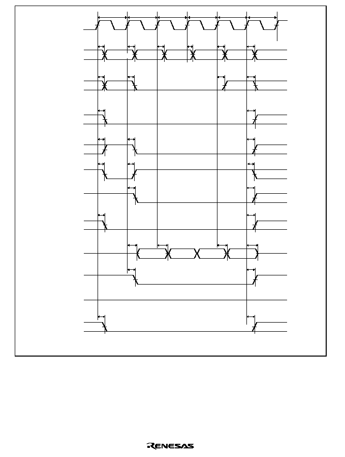
Rev. 2.00, 09/03, page 652 of 690
Tc2
Tc3
Tc4
Trwl
Tr
Tc1
t
CSD1
t
CSD1
t
AD1
t
AD1
t
AD1
t
AD1
t
AD1
t
AD1
t
AD1
t
AD1
t
AD1
t
AD1
t
RWD1
t
RWD1
t
RWD1
CKIO
A25 to A0
CSn
RD/
WR
A12/A11*
1
D31 to D0
t
RASD1
t
RASD1
RASU/L
Row address
Write A
command
Write command
Column
address
(1-4)
t
CASD1
t
CASD1
CASU/L
t
BSD
t
BSD
(High)
BS
CKE
t
DQMD1
t
DQMD1
DQMxx
t
DACD
t
DACD
DACKn*
2
t
WDH2
t
WDH2
t
WDD2
t
WDD2
t
RASD1
Notes: 1. Address pin to be connected to A10 of SDRAM.
2. DACKn is a waveform when active-low is specified.
Figure 25.28 Synchronous DRAM Burst Write Bus Cycle (Single Write
◊
◊
◊
◊
4),
(Auto Precharge, TRCD
=
=
=
=
1 Cycle, TRWL = 2 Cycle)
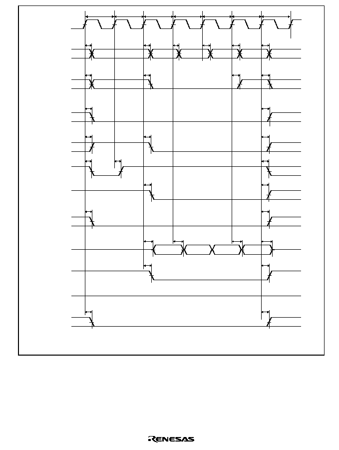
Rev. 2.00, 09/03, page 653 of 690
Tc2
Tc3
Tc4
Trwl
Tr
Tc1
Trw
t
CSD1
t
CSD1
t
AD1
t
AD1
t
AD1
t
AD1
t
AD1
t
AD1
t
AD1
t
AD1
t
AD1
t
AD1
t
RWD1
t
RWD1
t
RWD1
CKIO
A25 to A0
CSn
RD/
WR
A12/A11*
1
D31 to D0
t
RASD1
t
RASD1
RASU/L
Row address
Write A
command
Write command
Column
address
(1-4)
t
CASD1
t
CASD1
CASU/L
t
BSD
t
BSD
(High)
BS
CKE
t
DQMD1
t
DQMD1
DQMxx
t
DACD
t
DACD
DACKn*
2
t
WDH2
t
WDH2
t
WDD2
t
WDD2
t
RASD1
Notes: 1. Address pin to be connected to A10 of SDRAM.
2. DACKn is a waveform when active-low is specified.
Figure 25.29 Synchronous DRAM Burst Write Bus Cycle (Single Write
◊
◊
◊
◊
4),
(Auto Precharge, TRCD
=
=
=
=
2 Cycle, TRWL = 2 Cycle)
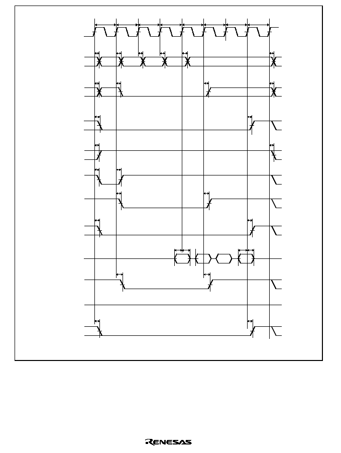
Rev. 2.00, 09/03, page 654 of 690
Tc3
Tc4
Tde
Tr
Tc2
Td1
Td2
Td3
Td4
Tc1
t
CSD1
t
CSD1
t
AD1
t
AD1
t
AD1
t
AD1
t
AD1
t
AD1
t
AD1
t
AD1
t
AD1
t
RWD1
t
RWD1
CKIO
A25 to A0
CSn
RD/
WR
A12/A11*
1
D31 to D0
t
RASD1
t
RASD1
RASU/L
Row
address
Read command
Column
address
(1-4)
t
CASD1
t
CASD1
CASU/L
t
BSD
t
BSD
(High)
BS
CKE
t
DQMD1
t
DQMD1
DQMxx
t
DACD
t
DACD
DACKn*
2
t
RDH2
t
RDS2
t
RDH2
t
RDS2
t
AD1
Notes: 1. Address pin to be connected to A10 of SDRAM.
2. DACKn is a waveform when active-low is specified.
Figure 25.30 Synchronous DRAM Burst Read Bus Cycle (Single Read
◊
◊
◊
◊
4)
(Bank Active Mode: ACTV + READ Commands, CAS Latency = 2, TRCD = 1 Cycle)

Rev. 2.00, 09/03, page 655 of 690
Tc2
Tc4
Tde
Tc1
Tc3
Td1
Td2
Td3
Td4
t
CSD1
t
CSD1
t
CSD1
t
AD1
t
AD1
t
AD1
t
AD1
t
AD1
t
RWD1
t
RWD1
CKIO
A25 to A0
CSn
RD/
WR
A12/A11*
1
D31 to D0
t
RASD1
t
RASD1
RASU/L
Read command
Column
address
(1-4)
t
CASD1
t
CASD1
CASU/L
t
BSD
t
BSD
(High)
BS
CKE
t
DQMD1
t
DQMD1
DQMxx
t
DACD
t
DACD
DACKn*
2
t
RDH2
t
RDS2
t
RDH2
t
RDS2
t
AD1
t
DQMD1
t
DACD
t
BSD
t
CASD1
Notes: 1. Address pin to be connected to A10 of SDRAM.
2. DACKn is a waveform when active-low is specified.
Figure 25.31 Synchronous DRAM Burst Read Bus Cycle (Single Read
◊
◊
◊
◊
4)
(Bank Active Mode: READ Command, Same Row Address,
CAS Latency = 2, TRCD = 1 Cycle)
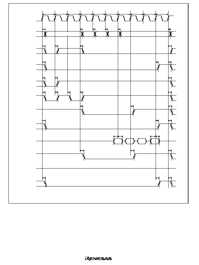
Rev. 2.00, 09/03, page 656 of 690
Tc3
Tc4
Tde
Tc2
Td1
Td2
Td3
Td4
Tc1
Tr
Tpw
Tp
t
CSD1
t
CSD1
t
AD1
t
AD1
t
AD1
t
AD1
t
AD1
t
AD1
t
AD1
t
AD1
t
AD1
t
AD1
t
RWD1
t
RWD1
t
RWD1
CKIO
A25 to A0
CSn
RD/
WR
A12/A11*
1
D31 to D0
t
RASD1
t
RASD1
t
RASD1
t
RASD1
RASU/L
Read command
Column
address
Row address
(1-4)
t
CASD1
t
CASD1
CASU/L
t
BSD
t
BSD
(High)
BS
CKE
t
DQMD1
t
DQMD1
DQMxx
t
DACD
t
DACD
DACKn*
2
t
RDH2
t
RDS2
t
RDH2
t
RDS2
t
CSD1
t
RASD1
t
CASD1
t
DQMD1
t
BSD
t
DACD
Notes: 1. Address pin to be connected to A10 of SDRAM.
2. DACKn is a waveform when active-low is specified.
Figure 25.32 Synchronous DRAM Burst Read Bus Cycle (Single Read
◊
◊
◊
◊
4)
(Bank Active Mode: PRE + ACTV + READ Commands,
Different Row Address, CAS Latency = 2, TRCD = 1 Cycle)
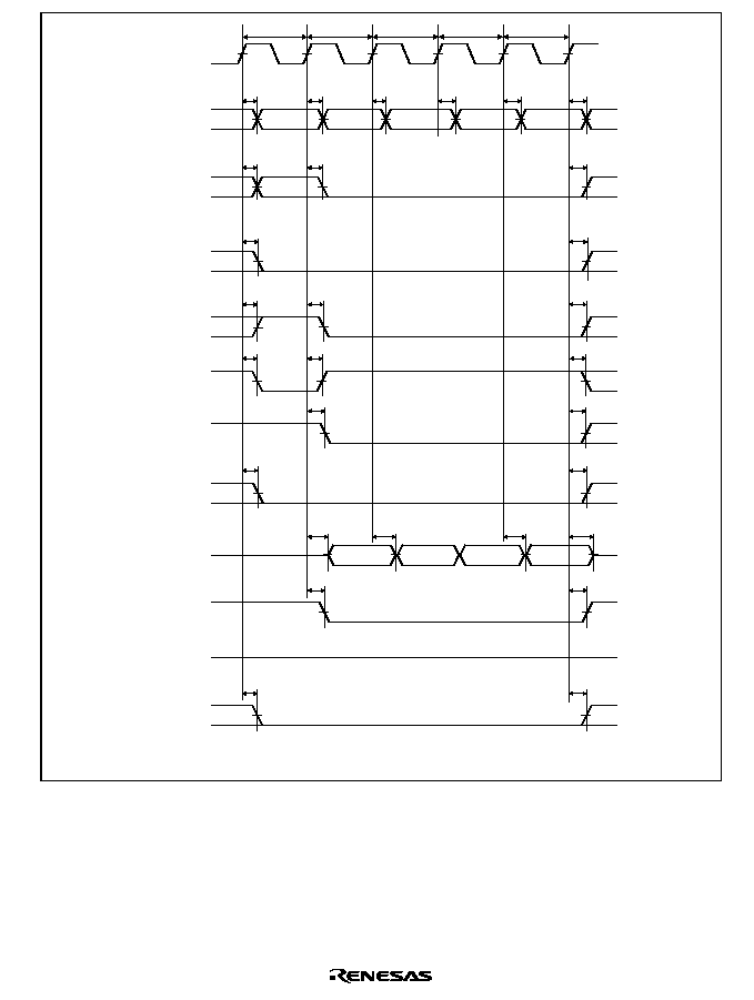
Rev. 2.00, 09/03, page 657 of 690
Tc2
Tc3
Tc4
Tr
Tc1
t
CSD1
t
CSD1
t
AD1
t
AD1
t
AD1
t
AD1
t
AD1
t
AD1
t
AD1
t
AD1
t
AD1
t
RWD1
CKIO
A25 to A0
CSn
RD/
WR
A12/A11*
1
D31 to D0
t
RASD1
t
RWD1
t
RWD1
t
RASD1
RASU/L
Row address
Write command
Column
address
(1-4)
t
CASD1
t
CASD1
CASU/L
t
BSD
t
BSD
(High)
BS
CKE
t
DQMD1
t
DQMD1
DQMxx
t
DACD
t
DACD
DACKn*
2
t
WDH2
t
WDH2
t
WDD2
t
WDD2
t
RASD1
Notes: 1. Address pin to be connected to A10 of SDRAM.
2. DACKn is a waveform when active-low is specified.
Figure 25.33 Synchronous DRAM Burst Write Bus Cycle (Single Write
◊
◊
◊
◊
4)
(Bank Active Mode: ACTV + WRITE Commands, TRCD = 1 Cycle, TRWL = 1 Cycle)
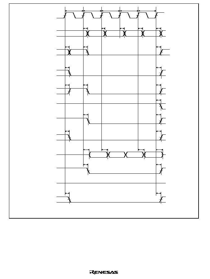
Rev. 2.00, 09/03, page 658 of 690
Tc2
Tc3
Tc4
Tnop
Tc1
t
CSD1
t
CSD1
t
AD1
t
AD1
t
AD1
t
AD1
t
AD1
t
AD1
t
AD1
t
AD1
t
RWD1
t
RWD1
t
RWD1
CKIO
A25 to A0
CSn
RD/
WR
A12/A11*
1
D31 to D0
RASU/L
Write command
Column
address
(1-4)
t
CASD1
t
CASD1
CASU/L
t
BSD
t
BSD
(High)
BS
CKE
t
DQMD1
t
DQMD1
DQMxx
t
DACD
t
DACD
DACKn*
2
t
WDH2
t
WDH2
t
WDD2
t
WDD2
t
RASD1
Notes: 1. Address pin to be connected to A10 of SDRAM.
2. DACKn is a waveform when active-low is specified.
Figure 25.34 Synchronous DRAM Burst Write Bus Cycle (Single Write
◊
◊
◊
◊
4)
(Bank Active Mode: WRITE Command, Same Row Address,
TRCD = 1 Cycle, TRWL = 1 Cycle)
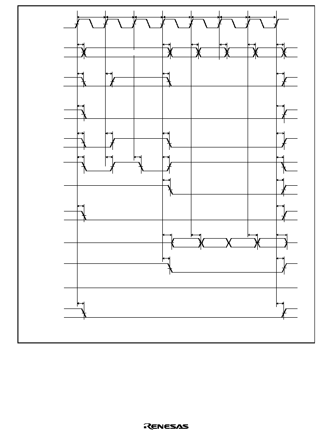
Rev. 2.00, 09/03, page 659 of 690
Tc2
Tc3
Tc4
Tr
Tpw
Tp
Tc1
t
CSD1
t
CSD1
t
AD1
t
AD1
t
AD1
t
AD1
t
AD1
t
AD1
t
AD1
t
AD1
t
AD1
t
AD1
t
RWD1
t
RWD1
t
RWD1
t
RWD1
t
RASD1
t
RASD1
t
RASD1
t
RASD1
CKIO
A25 to A0
CSn
RD/
WR
A12/A11*
1
D31 to D0
RASU/L
Write command
Row address
(1-4)
Column
address
t
CASD1
t
CASD1
CASU/L
t
BSD
t
BSD
(High)
BS
CKE
t
DQMD1
t
DQMD1
DQMxx
t
DACD
t
DACD
DACKn*
2
t
WDH2
t
WDD2
t
WDH2
t
WDD2
t
RASD1
Notes: 1. Address pin to be connected to A10 of SDRAM.
2. DACKn is a waveform when active-low is specified.
Figure 25.35 Synchronous DRAM Burst Write Bus Cycle (Single Write
◊
◊
◊
◊
4)
(Bank Active Mode: PRE + ACTV + WRITE Commands,
Different Row Address, TRCD = 1 Cycle, TRWL = 1 Cycle)
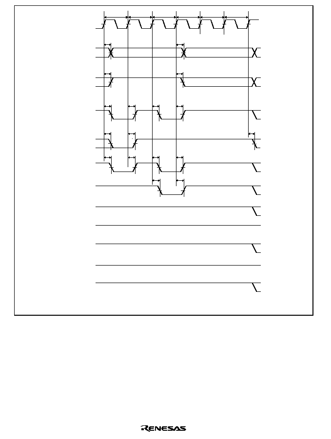
Rev. 2.00, 09/03, page 660 of 690
Trc
Trc
Trr
Tpw
Tp
Trc
t
CSD1
t
CSD1
t
CSD1
t
CSD1
t
AD1
t
AD1
t
AD1
t
AD1
t
RWD1
t
RWD1
t
RWD1
t
RASD1
t
RASD1
t
RASD1
t
RASD1
CKIO
A25 to A0
CSn
RD/
WR
A12/A11*
1
D31 to D0
RASU/L
t
CASD1
t
CASD1
CASU/L
(High)
(Hi-Z)
BS
CKE
DQMxx
DACKn*
2
Notes: 1. Address pin to be connected to A10 of SDRAM.
2. DACKn is a waveform when active-low is specified.
Figure 25.36 Synchronous DRAM Auto-Refresh Timing (TRP = 2 Cycle)
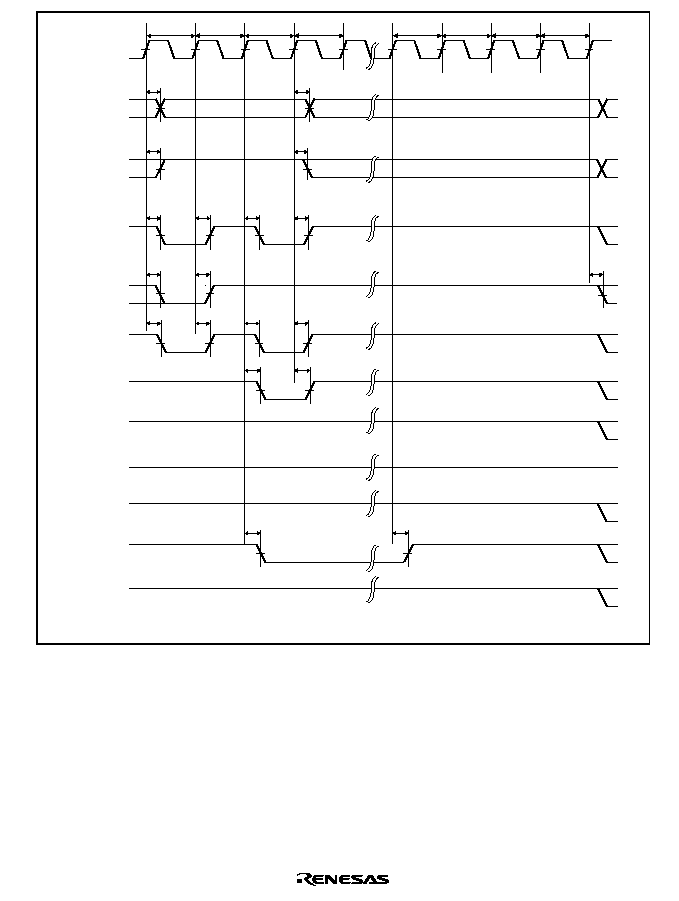
Rev. 2.00, 09/03, page 661 of 690
Trc
Trc
Trc
Trc
Trr
Tpw
Tp
Trc
t
CSD1
t
CSD1
t
CSD1
t
CSD1
t
AD1
t
AD1
t
AD1
t
AD1
t
RWD1
t
RWD1
t
RWD1
t
RASD1
t
RASD1
t
RASD1
t
RASD1
CKIO
A25 to A0
CSn
RD/
WR
A12/A11*
1
D31 to D0
RASU/L
t
CASD1
t
CASD1
CASU/L
(Hi-Z)
BS
CKE
DQMxx
DACKn*
2
t
CKED1
t
CKED1
Notes: 1. Address pin to be connected to A10 of SDRAM.
2. DACKn is a waveform when active-low is specified.
Figure 25.37 Synchronous DRAM Self-Refresh Timing (TRP = 2 Cycle)
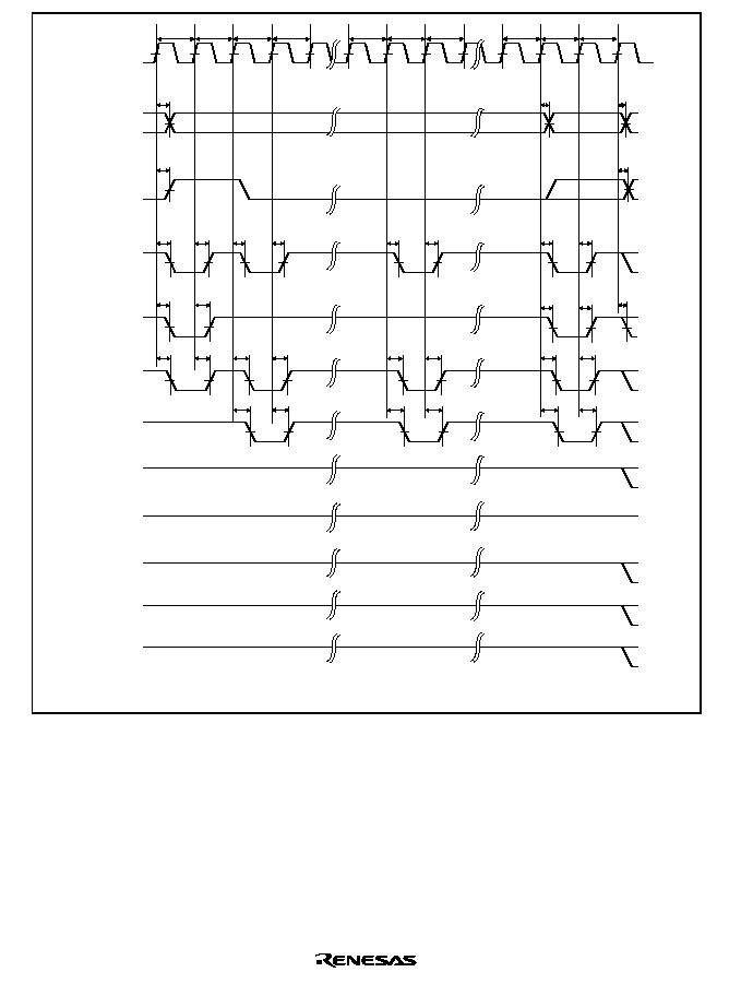
Rev. 2.00, 09/03, page 662 of 690
Trc
Trc
Trc
Tmw
Tde
Trr
Trr
Tpw
Tp
Trc
t
CSD1
t
CSD1
t
CSD1
t
CSD1
t
CSD1
t
CSD1
t
CSD1
t
CSD1
t
AD1
t
AD1
t
AD1
t
AD1
t
AD1
PALL
REF
REF
MRS
t
RWD1
t
RWD1
t
RWD1
t
RWD1
t
RWD1
t
RASD1
t
RASD1
t
RASD1
t
RASD1
t
RASD1
t
RASD1
t
RASD1
t
RASD1
CKIO
A25 to A0
CSn
RD/
WR
A12/A11*
1
D31 to D0
RASU/L
t
CASD1
t
CASD1
t
CASD1
t
CASD1
t
CASD1
t
CASD1
CASU/L
(Hi-Z)
BS
CKE
DQMxx
DACKn*
2
Notes: 1. Address pin to be connected to A10 of SDRAM.
2. DACKn is a waveform when active-low is specified.
Figure 25.38 Synchronous DRAM Mode Register Write Timing (TRP = 2 Cycle)

Rev. 2.00, 09/03, page 663 of 690
Table 25.8
Bus Timing (2)
(Conditions: V
CC
Q = V
CC
-RTC = V
CC
-USB = 3.0 to 3.6 V, V
CC
= V
CC
-PLL1 = V
CC
-PLL2 = 1.4 to
1.6 V, AV
CC
= 3.0 to 3.6 V, V
SS
Q = V
SS
= V
SS
-RTC = V
SS
-USB = V
SS
-PLL1 = V
SS
-PLL2 =
AV
SS
= 0 V, T
a
= ≠20 to 75∞C, Clock mode 0/1/2/4/5/6/7)
Item
Symbol
Min
Max
Unit
Figure
Address delay time 3
t
AD3
1/2 t
cyc
1/2 t
cyc
+12 ns
25.39 to 25.42
CS
delay time 2
t
CSD2
1/2 t
cyc
1/2 t
cyc
+10 ns
25.39 to 25.42
Read/write delay time 2
t
RWD2
1/2 t
cyc
1/2 t
cyc
+10 ns
25.39 to 25.42
Read data setup time 4
t
RDS4
1/2 t
cyc
+6 --
ns
25.39
Read data hold time 4
t
RDH4
0
--
ns
25.39
Write data delay time 3
t
WDD3
--
1/2 t
cyc
+12 ns
25.39
Write data hold time 3
t
WDH3
1/2 t
cyc
--
ns
25.39
RAS
delay time 2
t
RASD2
1/2 t
cyc
1/2 t
cyc
+10 ns
25.39 to 25.42
CAS
delay time 2
t
CASD2
1/2 t
cyc
1/2 t
cyc
+10 ns
25.39 to 25.42
DQM delay time 2
t
DQMD2
1/2 t
cyc
1/2 t
cyc
+10 ns
25.39
CKE delay time 2
t
CKED2
1/2 t
cyc
1/2 t
cyc
+10 ns
25.41
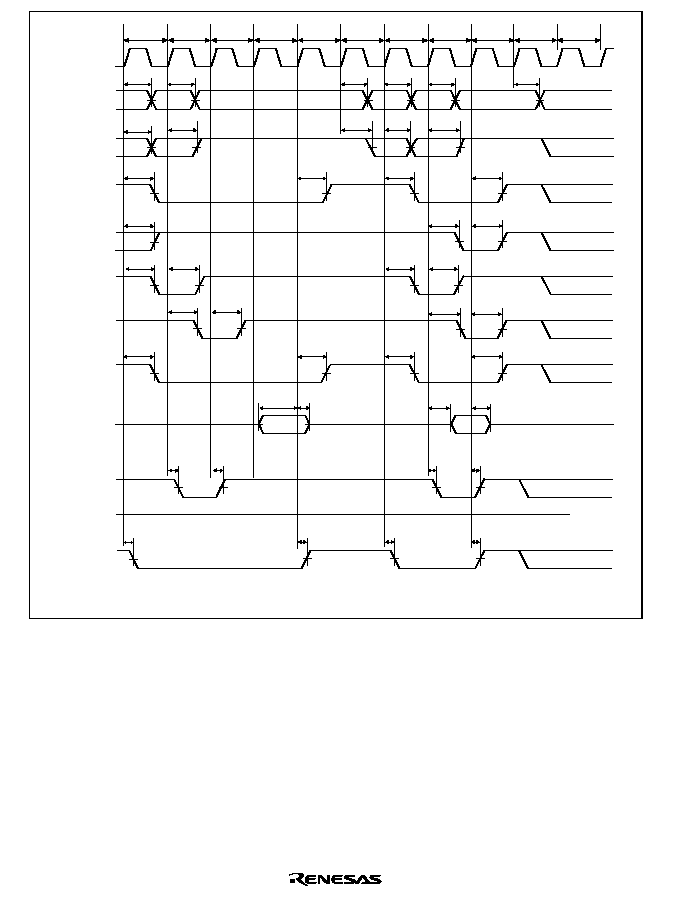
Rev. 2.00, 09/03, page 664 of 690
Tr
Td1
Tde
Tap
Trwl
Tap
Tnop
Tc1
Tr
Tc1
t
AD3
t
AD3
t
AD3
t
AD3
t
AD3
t
AD3
t
AD3
t
AD3
t
AD3
t
AD3
t
AD3
t
CSD2
t
CSD2
t
CSD2
t
CSD2
t
RWD2
t
RWD2
t
RWD2
CKIO
A25 to A0
CSn
RD/
WR
A12/A11*
1
D31 to D0
t
RASD2
t
RASD2
t
RASD2
t
RASD2
RASU/L
t
CASD2
t
CASD2
t
CASD2
t
CASD2
CASU/L
t
BSD
t
BSD
t
BSD
t
RDS4
t
RDH4
t
BSD
BS
CKE
t
DQMD2
t
DQMD2
t
DQMD2
t
DQMD2
DQMxx
t
DACD
t
DACD
t
DACD
t
DACD
DACKn*
2
t
WDH3
t
WDD3
Tw
(High)
Notes: 1. Address pin to be connected to A10 of SDRAM.
2. DACKn is a waveform when active-low is specified.
Figure 25.39 Access Timing in Low-Frequency Mode (Auto Precharge)
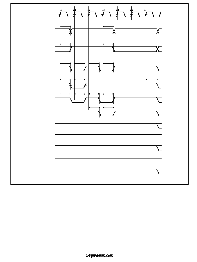
Rev. 2.00, 09/03, page 665 of 690
Trc
Trc
Trr
Tpw
Tp
Trc
t
CSD2
t
CSD2
t
CSD2
t
CSD2
t
AD3
t
AD3
t
AD3
t
AD3
t
RWD2
t
RWD2
t
RWD2
t
RASD2
t
RASD2
t
RASD2
t
RASD2
CKIO
A25 to A0
CSn
RD/
WR
A12/A11*
1
D31 to D0
RASU/L
t
CASD2
t
CASD2
CASU/L
(High)
(Hi-Z)
BS
CKE
DQMxx
DACKn*
2
Notes: 1. Address pin to be connected to A10 of SDRAM.
2. DACKn is a waveform when active-low is specified.
Figure 25.40 Synchronous DRAM Auto-Refresh Timing
(TRP = 2 Cycle, Low-Frequency Mode)
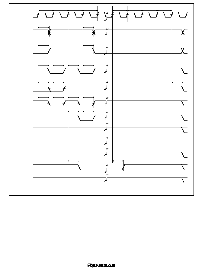
Rev. 2.00, 09/03, page 666 of 690
Trc
Trc
Trc
Trc
Trr
Tpw
Tp
Trc
t
CSD2
t
CSD2
t
CSD2
t
CSD2
t
AD3
t
AD3
t
AD3
t
AD3
t
RWD2
t
RWD2
t
RWD2
t
RASD2
t
RASD2
t
RASD2
t
RASD2
CKIO
A25 to A0
CSn
RD/
WR
A12/A11*
1
D31 to D0
RASU/L
t
CASD2
t
CASD2
CASU/L
(Hi-Z)
BS
CKE
DQMxx
DACKn*
2
t
CKED2
t
CKED2
Notes: 1. Address pin to be connected to A10 of SDRAM.
2. DACKn is a waveform when active-low is specified.
Figure 25.41 Synchronous DRAM Self-Refresh Timing
(TRP = 2 Cycle, Low-Frequency Mode)

Rev. 2.00, 09/03, page 667 of 690
Trc
Trc
Trc
Tmw
Tde
Trr
Trr
Tpw
Tp
Trc
t
CSD2
t
CSD2
t
CSD2
t
CSD2
t
CSD2
t
CSD2
t
CSD2
t
CSD2
t
AD3
t
AD3
t
AD3
t
AD3
t
AD3
PALL
REF
REF
MRS
t
RWD2
t
RWD2
t
RWD2
t
RWD2
t
RWD2
t
RASD2
t
RASD2
t
RASD2
t
RASD2
t
RASD2
t
RASD2
t
RASD2
t
RASD2
CKIO
A25 to A0
CSn
RD/
WR
A12/A11*
1
D31 to D0
RASU/L
t
CASD2
t
CASD2
t
CASD2
t
CASD2
t
CASD2
t
CASD2
CASU/L
(Hi-Z)
BS
CKE
DQMxx
DACKn*
2
Notes: 1. Address pin to be connected to A10 of SDRAM.
2. DACKn is a waveform when active-low is specified.
Figure 25.42 Synchronous DRAM Mode Register Write Timing
(TRP = 2 Cycle, Low-Frequency Mode)
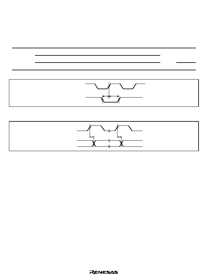
Rev. 2.00, 09/03, page 668 of 690
25.3.7
DMAC Signal Timing
Table 25.9
DMAC Signal Timing
(Conditions: V
CC
Q = V
CC
-RTC = V
CC
-USB = 3.0 to 3.6 V, V
CC
= V
CC
-PLL1 = V
CC
-PLL2 = 1.4 to
1.6 V, AV
CC
= 3.0 to 3.6 V, V
SS
Q = V
SS
= V
SS
-RTC = V
SS
-USB = V
SS
-PLL1 = V
SS
-PLL2 =
AV
SS
= 0 V, T
a
= ≠20 to 75∞C)
Module
Item
Symbol
Min
Max
Unit
Figure
DMAC
DREQ setup time
t
DRQS
10
--
ns
25.43
DREQ hold time
t
DRQH
3
--
DACK, TEND delay time
t
DACD
--
10
25.44
t
DRQS
t
DRQH
CKIO
DREQn
Figure 25.43 DREQ Input Timing
CKIO
TEND0
DACKn
t
DACD
t
DACD
Figure 25.44 DACK, TEND Output Timing
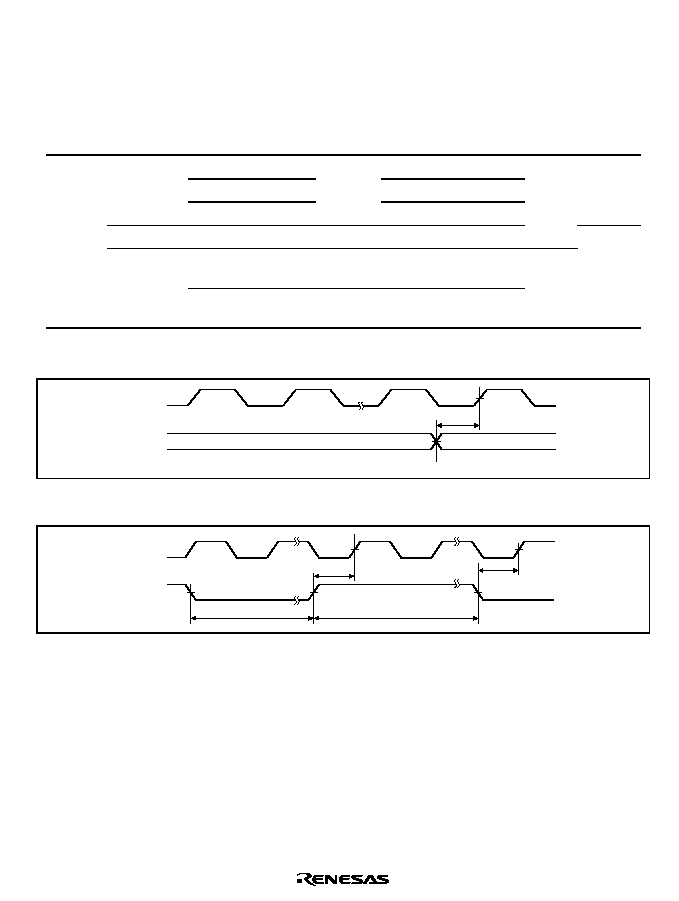
Rev. 2.00, 09/03, page 669 of 690
25.3.8
TMU Signal Timing
Table 25.10 TMU Signal Timing
(Conditions: V
CC
Q = V
CC
-RTC = V
CC
-USB = 3.0 to 3.6 V, V
CC
= V
CC
-PLL1 = V
CC
-PLL2 = 1.4 to
1.6 V, AV
CC
= 3.0 to 3.6 V, V
SS
Q = V
SS
= V
SS
-RTC = V
SS
-USB = V
SS
-PLL1 = V
SS
-PLL2 =
AV
SS
= 0 V, T
a
= ≠20 to 75∞C)
Module
Item
Symbol
Min
Max
Unit
Figure
B:P clock ratio = 1:1
15
--
B:P clock ratio = 2:1
t
cyc
+15
--
TMU
Timer input
setup time
B:P clock ratio = 4:1
t
TCLKS
3
◊
t
cyc
+15
--
ns
25.45
Timer clock input setup time
t
TCKS
15
--
25.46
Timer clock
pulse width
Edge specification
t
TCKW H/L
2.0
--
t
pcyc
*
Both edge
specification
t
TCKW H/L
3.0
--
Note:
*
t
pcyc
indicates a peripheral clock (P
) cycle.
t
TCLKS
CKIO
TCLK
(input)
Figure 25.45 TCLK Input Timing
t
TCKS
t
TCKS
t
TCKWH
t
TCKWL
CKIO
TCLK
(input)
Figure 25.46 TCLK Clock Input Timing
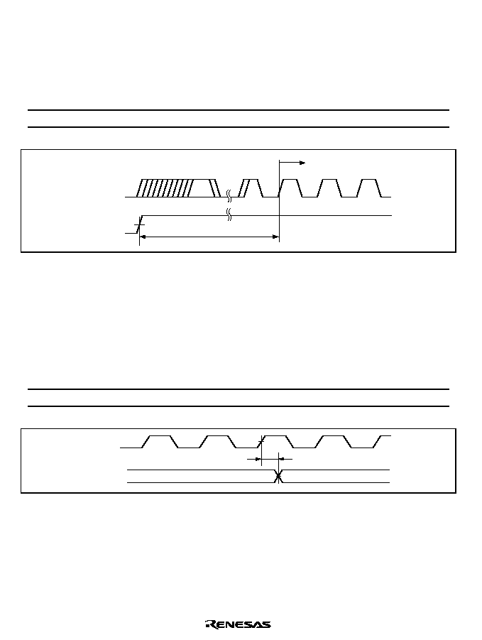
Rev. 2.00, 09/03, page 670 of 690
25.3.9
RTC Signal Timing
Table 25.11 RTC Signal Timing
(Conditions: V
CC
Q = V
CC
-RTC = V
CC
-USB = 3.0 to 3.6 V, V
CC
= V
CC
-PLL1 = V
CC
-PLL2 = 1.4 to
1.6 V, AV
CC
= 3.0 to 3.6 V, V
SS
Q = V
SS
= V
SS
-RTC = V
SS
-USB = V
SS
-PLL1 = V
SS
-PLL2 =
AV
SS
= 0 V, T
a
= ≠20 to 75∞C)
Module
Item
Symbol
Min
Max
Unit
Figure
RTC
Oscillation settling time
t
ROSC
3
--
s
25.47
V
CC
V
CCmin
t
ROSC
RTC crystal
oscillator
Stable oscillation
Figure 25.47 Oscillation Settling Time when RTC Crystal Oscillator Is Turned On
25.3.10
16-Bit Timer Pulse Unit (TPU) Signal Timing
Table 25.12 16-Bit Timer Pulse Unit (TPU) Signal Timing
(Conditions: V
CC
Q = V
CC
-RTC = V
CC
-USB = 3.0 to 3.6 V, V
CC
= V
CC
-PLL1 = V
CC
-PLL2 = 1.4 to
1.6 V, AV
CC
= 3.0 to 3.6 V, V
SS
Q = V
SS
= V
SS
-RTC = V
SS
-USB = V
SS
-PLL1 = V
SS
-PLL2 =
AV
SS
= 0 V, T
a
= ≠20 to 75∞C)
Item
Symbol
Min
Max
Unit
Figure
Timer output delay time
t
TOD
--
15
ns
25.48
CKIO
TO0, TO1
t
TOD
TO2, TO3
Figure 25.48 TPU Output Timing
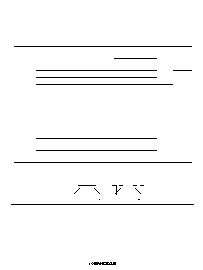
Rev. 2.00, 09/03, page 671 of 690
25.3.11
SCIF Module Signal Timing
Table 25.13 SCIF Module Signal Timing
(Conditions: V
CC
Q = V
CC
-RTC = V
CC
-USB = 3.0 to 3.6 V, V
CC
= V
CC
-PLL1 = V
CC
-PLL2 = 1.4 to
1.6 V, AV
CC
= 3.0 to 3.6 V, V
SS
Q = V
SS
= V
SS
-RTC = V
SS
-USB = V
SS
-PLL1 = V
SS
-PLL2 =
AV
SS
= 0 V, T
a
= ≠20 to 75∞C)
Module
Item
Symbol
Min
Max
Unit
Figure
Clock
synchronization
12
--
SCIF0,
SCIF2
Input clock
cycle
Asynchroniza-
tion
t
Scyc
4
--
t
pcyc
25.49
25.50
Input clock rise time
t
SCKr
--
1.5
25.49
Input clock fall time
t
SCKf
--
1.5
Input clock pulse width
t
SCKW
0.4
0.6
t
scyc
Transmission data delay time
(clock synchronization)
t
TXD
--
3 t
pcyc
*
+ 50
ns
25.50
Receive data setup time
(clock synchronization)
t
RXS
2 t
pcyc
*
--
Receive data hold time
(clock synchronization)
t
RXH
2 t
pcyc
*
--
RTS
delay time
(clock synchronization)
t
RTSD
--
100
CTS
setup time
(clock synchronization)
t
CTSS
100
--
CTS
hold time
(clock synchronization)
t
CTSH
100
--
Note:
*
t
pcyc
indicates a peripheral clock (P
) cycle.
t
SCKW
t
SCKr
t
SCKf
t
Scyc
SCK
Figure 25.49 SCK Input Clock Timing
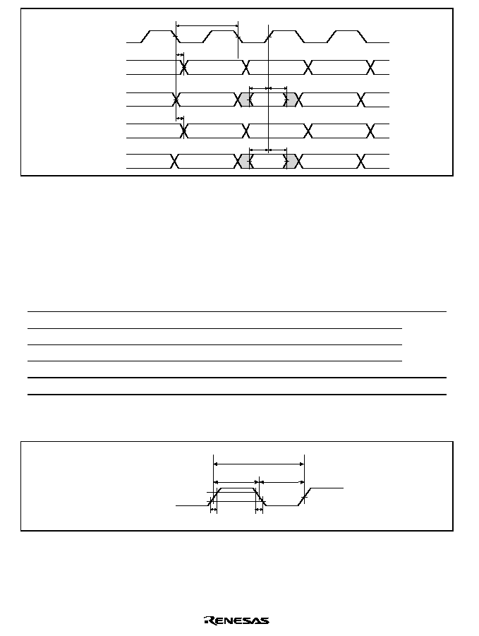
Rev. 2.00, 09/03, page 672 of 690
t
Scyc
t
TXD
t
RXH
t
RXS
t
RTSD
t
CTSH
t
CTSS
SCK
RTS
CTS
TxD
(data trans-
mission)
RxD
(data
reception)
Figure 25.50 SCIF Input/Output Timing in Clock Synchronous Mode
25.3.12
USB Module Signal Timing
Table 25.14 USB Module Clock Timing
(Conditions: V
CC
Q = V
CC
-RTC = V
CC
-USB = 3.0 to 3.6 V, V
CC
= V
CC
-PLL1 = V
CC
-PLL2 = 1.4 to
1.6 V, AV
CC
= 3.0 to 3.6 V, V
SS
Q = V
SS
= V
SS
-RTC = V
SS
-USB = V
SS
-PLL1 = V
SS
-PLL2 =
AV
SS
= 0 V, T
a
= ≠20 to 75∞C)
Item
Symbol
Min
Max
Unit
Figure
Frequency (48 MHz)
*
t
FREQ
47.9
48.1
MHz
25.51
Clock rise time
*
t
R48
--
4
ns
Clock fall time
*
t
F48
--
4
ns
Duty (t
HIGH
/t
LOW
)
*
t
DUTY
90
110
%
Oscillation settling time
t
UOSC
10
--
ms
25.52
Note:
*
When the USB is operated by supplying a clock to the EXTAL_USB pin from off-chip, the
supplied clock must satisfy the above clock specifications.
t
HIGH
t
LOW
t
FREQ
10%
t
R48
t
F48
90%
EXTAL_USB
Figure 25.51 USB Clock Timing
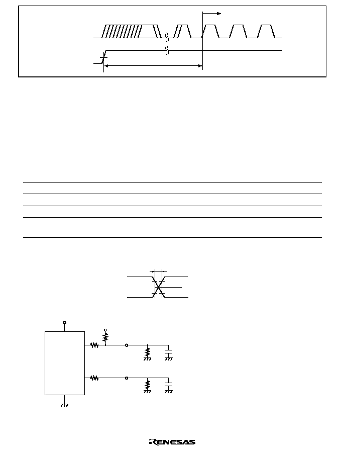
Rev. 2.00, 09/03, page 673 of 690
V
CC
V
CCmin
t
UOSC
USB crystal
oscillator
State oscillation
Figure 25.52 Oscillation Settling Time when USB Crystal Oscillator Is Turned On
25.3.13
USB Transceiver Timing
Table 25.15 USB Transceiver Timing
(Conditions: V
CC
Q = V
CC
-RTC = V
CC
-USB = 3.0 to 3.6 V, V
CC
= V
CC
-PLL1 = V
CC
-PLL2 = 1.4 to
1.6 V, AV
CC
= 3.0 to 3.6 V, V
SS
Q = V
SS
= V
SS
-RTC = V
SS
-USB = V
SS
-PLL1 = V
SS
-PLL2 =
AV
S
= 0 V, T
a
= ≠20 to 75∞C)
Item
Symbol
Min
Typ
Max
Unit
Measurement
Condition
Rising time
t
r
4
--
20
ns
C
L
= 50pF
Falling time
t
f
4
--
20
ns
C
L
= 50pF
Rising/falling time ratio
t
r
/ t
f
90
--
110
%
Output signal crossover
voltage
V
CRS
1.3
--
2.0
V
C
L
= 50pF
Note:
This transceiver complies with the full-speed specifications.
t
r
, t
f
90%
10%
Crossover voltage
DP
DM
Measured
element
Vcc-USB
DP
DM
Vcc
VSS
RS = 33
RL = 15k
RL = 15k
CL
CL
RL = 1.5k
RS = 33
1. t
r
and t
f
are judged by the time taken for the
transitions between 10% and 90% amplitude.
2. The electrostatic capacitance, C
L
, includes the
floating capacitance of the wiring connection
and the input capacitance of the probe.
Measurement circuit
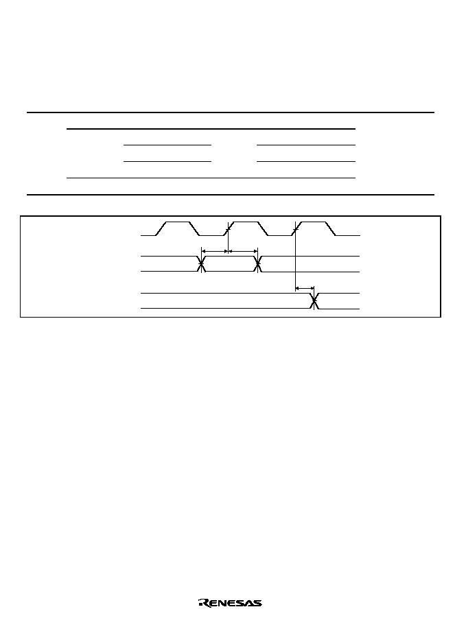
Rev. 2.00, 09/03, page 674 of 690
25.3.14
Port Input/Output Timing
Table 25.16 Port Input/Output Timing
(Conditions: V
CC
Q = V
CC
-RTC = V
CC
-USB = 3.0 to 3.6 V, V
CC
= V
CC
-PLL1 = V
CC
-PLL2 = 1.4 to
1.6 V, AV
CC
= 3.0 to 3.6 V, V
SS
Q = V
SS
= V
SS
-RTC = V
SS
-USB = V
SS
-PLL1 = V
SS
-PLL2 =
AV
SS
= 0 V, T
a
= ≠20 to 75∞C)
Module Item
Symbol
Min
Max
Unit
Figure
Output data delay time
t
PORTD
--
17
B:P clock ratio = 1:1
15
--
B:P clock ratio = 2:1
t
cyc
+15
--
Input data
setup time
B:P clock ratio = 4:1
t
PORTS
3
◊
t
cyc
+15
--
Port
Input data hold time
t
PORTH
8
--
ns
25.53
t
PORTS
CKIO
t
PORTH
t
PORTD
Ports 7 to 0
(read)
Ports 7 to 0
(write)
Figure 25.53 I/O Port Timing
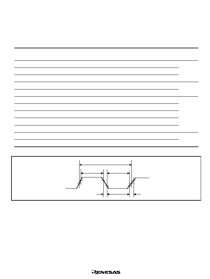
Rev. 2.00, 09/03, page 675 of 690
25.3.15
UDI Related Pin Timing
Table 25.17 UDI Related Pin Timing
(Conditions: V
CC
Q = V
CC
-RTC = V
CC
-USB = 3.0 to 3.6 V, V
CC
= V
CC
-PLL1 = V
CC
-PLL2 = 1.4 to
1.6 V, AV
CC
= 3.0 to 3.6 V, V
SS
Q = V
SS
= V
SS
-RTC = V
SS
-USB = V
SS
-PLL1 = V
SS
-PLL2 =
AV
SS
= 0 V, T
a
= ≠20 to 75∞C)
Item
Symbol
Min
Max
Unit
Figure
TCK cycle time
t
TCKcyc
50
--
ns
25.54,
25.56
TCK high-pulse width
t
TCKH
12
--
ns
25.54
TCK low-pulse width
t
TCKL
12
--
ns
TCK rise/fall time
t
TCKf
--
4
ns
TRST
setup time
t
TRSTS
12
--
ns
25.55
TRST
hold time
t
TRSTH
50
--
t
cyc
TDI setup time
t
TDIS
10
--
ns
25.56
TDI hold time
t
TDIH
10
--
ns
TMS setup time
t
TMSS
10
--
ns
TMS hold time
t
TMSH
10
--
ns
TDO delay time
t
TDOD
--
15
ns
ASEMD0
setup time
t
ASEMD0S
12
--
ns
25.57
ASEMD0
hold time
t
ASEMD0H
12
--
ns
t
TCKH
t
TCKf
t
TCKf
t
TCKL
t
TCKcyc
V
IH
V
IH
V
IH
1/2 V
CC
Q
1/2 V
CC
Q
V
IL
V
IL
Figure 25.54 TCK Input Timing
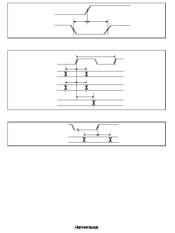
Rev. 2.00, 09/03, page 676 of 690
t
TRSTS
t
TRSTH
TRST
RESETP
Figure 25.55
TRST Input Timing (Reset Hold)
t
TMSS
t
TMSH
t
TDOD
t
TCKcyc
t
TDIH
t
TDIS
TCK
TDI
TMS
TDO
Figure 25.56 UDI Data Transfer Timing
t
ASEMD0H
t
ASEMD0S
RESETP
ASEMD0
Figure 25.57
ASEMD0 Input Timing
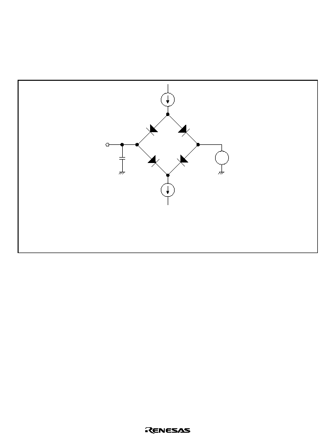
Rev. 2.00, 09/03, page 677 of 690
25.3.16
AC Characteristics Measurement Conditions
∑
I/O signal reference level: V
CC
Q/2 (V
CC
Q = 3.0 to 3.6 V, V
CC
= 1.4 to 1.6 V)
∑
Input pulse level: V
SS
Q to 3.0 V (where
RESETP, RESETM, ASEMD0, NMI, IRQ5 to IRQ0,
CKIO, and MD6 to MD0 are within V
SS
Q to V
CC
Q)
∑
Input rise and fall times: 1 ns
I
OL
I
OH
C
L
V
REF
LSI output pin
Reference voltage
Notes:
C
L
is the total value that includes the capacitance of measurement
instruments, etc., and is set as follows for each pin.
30 pF: CKIO,
RASU/L, CASU/L, CS0, CS2 to CS6B, BACK
50 pF: All other pins
I
OL
=1.6 mA, I
OH
= ≠200µA
1.
2.
V
Figure 25.58 Output Load Circuit

Rev. 2.00, 09/03, page 678 of 690
25.4
A/D Converter Characteristics
Table 25.18 lists the A/D converter characteristics.
Table 25.18 A/D Converter Characteristics
(Conditions: V
CC
Q = V
CC
-RTC = V
CC
-USB = 3.0 to 3.6 V, V
CC
= V
CC
-PLL1 = V
CC
-PLL2 = 1.4 to
1.6 V, AV
CC
= 3.0 to 3.6 V, V
SS
Q = V
SS
= V
SS
-RTC = V
SS
-USB = V
SS
-PLL1 = V
SS
-PLL2 =
AV
SS
= 0 V, T
a
= ≠20 to 75∞C)
Item
Min
Typ
Max
Unit
Resolution
10
10
10
bits
Conversion time
8.5
--
--
µs
Analog input capacitance
--
--
20
pF
Permissible signal-source impedance
(single-source)
--
--
5
k
Nonlinearity error
--
--
±3.0
LSB
Offset error
--
--
±2.0
LSB
Full-scale error
--
--
±2.0
LSB
Quantization error
--
--
±0.5
LSB
Absolute accuracy
--
--
±4.0
LSB

Rev. 2.00, 09/03, page 679 of 690
Appendix
A.
I/O Port States in Each Processing State
Table A.1
I/O Port States in Each Processing State
Reset
Power-Down States
Category Pin
Power-on
Reset
Manual
Reset
Software
Standby
Sleep
Bus
Mastership
Released
I/O
Handling of
Unused Pins
Clock
EXTAL
I
I
I
I
I
I
Pull-up
XTAL
O
O
O
O
O
O
Open
EXTAL2
I
I
I
I
I
I
Pull-up
XTAL2
O
O
O
O
O
O
Open
CKIO
I O
*
1
I O
*
1
I O
*
1
I O
*
1
I O
*
1
I O
Open
RESETP
I
*
11
I
*
11
I
*
11
I
*
11
I
*
11
I
Must be used
System
control
RESETM
I
I
I
I
I
I
Pull-up
BREQ
/PTG[6] Z
i P
*
2
i K
*
3
I P
*
2
I
I/IO
Pull-up
BACK
/PTG[5]
O
O P
*
2
O K
*
3
O P
*
2
L P
*
2
O/IO
Open
MD6
I
i
Z
i
i
I
Pull-down
MD[2:0]
I
i
i
i
i
I
Must be used
MD[5:3]
I
i
Z
i
i
I
Must be used
CA
I
I
I
I
I
I
Pull-up
STATUS0/
PTE[4]/
RTS0
H
H P
*
2
Z
*
6
H K
*
3
Z
*
6
L P
*
2
O
L P
*
2
O
O/IO/
O
Open
STATUS1/
PTE[5]/
CTS0
H
H P
*
2
Z
*
6
L K
*
3
Z
*
7
H P
*
2
I
L P
*
2
I
O/IO/
I
Open
Interrupt
IRQ[3:0]/
IRL[3:0]
/
PTH[3:0]
Z
I P
*
2
I K
*
3
I P
*
2
I P
*
2
I/I/IO
Pull-up
IRQ4/PTH[4]
Z
I P
*
2
I K
*
3
I P
*
2
I P
*
2
I/IO
Pull-up
IRQ5/PTE[2]
Z
I P
*
2
I K
*
3
I P
*
2
I P
*
2
I/IO
Pull-up
NMI
I
I
I
I
I
I
Pull-up
Address
A[25:19,0]/
PTK[7:0]
O
O P
*
2
ZO
*
8
K
*
3
O P
*
2
Z P
*
2
O/IO
Open
A[18:1]
O
O
ZO
*
8
O
Z
O
Open

Rev. 2.00, 09/03, page 680 of 690
Reset
Power-Down States
Category Pin
Power-on
Reset
Manual
Reset
Software
Standby
Sleep
Bus
Mastership
Released
I/O
Handling of
Unused Pins
Data
D[15:0]
Z
Z
Z
IO
Z
IO
Pull-up
D[23:16]/
PTA[7:0]/
PINT[7:0]
Z
Z P
*
2
Z P
*
2
IO P
*
2
Z P
*
2
IO/IO
/I
Pull-up
D[31:24]/
PTB[7:0]/
PINT[15:8]
Z
Z P
*
2
Z P
*
2
IO P
*
2
Z P
*
2
IO/IO
/I
Pull-up
CS0
H
O
ZH
*
6
O
Z
O
Open
Bus
control
CS2
/PTC[3]
H
O P
*
2
ZH
*
6
K
*
3
O P
*
2
Z P
*
2
O/IO
Open
CS3
/PTC[4]
H
O P
*
2
ZH
*
6
K
*
3
O P
*
2
Z P
*
2
O/IO
Open
CS4
/PTC[5]
H
O P
*
2
ZH
*
6
K
*
3
O P
*
2
Z P
*
2
O/IO
Open
CS5A
/PTC[6] Z
O P
*
2
ZH
*
6
K
*
3
O P
*
2
Z P
*
2
O/IO
Pull-up
CS5B
/PTD[6] Z
O P
*
2
ZH
*
6
K
*
3
O P
*
2
Z P
*
2
O/IO
Pull-up
CS6A
/PTC[7] Z
O P
*
2
ZH
*
6
K
*
3
O P
*
2
Z P
*
2
O/IO
Pull-up
CS6B
/PTD[7] Z
O P
*
2
ZH
*
6
K
*
3
O P
*
2
Z P
*
2
O/IO
Pull-up
BS
/PTC[0]
H
O P
*
2
ZH
*
6
K
*
3
O P
*
2
Z P
*
2
O/IO
Open
RASL
/PTD[0] H
O P
*
2
ZH
*
6
K
*
3
O P
*
2
ZH
*
6
P
*
2
O/IO
Open
RASU
/PTD[1]
Z
O P
*
2
ZH
*
6
K
*
3
O P
*
2
ZH
*
6
P
*
2
O/IO
Pull-up
CASL
/PTD[2] H
O P
*
2
ZH
*
6
K
*
3
O P
*
2
ZH
*
6
P
*
2
O/IO
Open
CASU
/PTD[3]
Z
O P
*
2
ZH
*
6
K
*
3
O P
*
2
ZH
*
6
P
*
2
O/IO
Pull-up
WE0
/DQMLL
H
O
ZH
*
6
O
Z
O/O
Open
WE1
/DQMLU H
O
ZH
*
6
O
Z
O/O
Open
WE2
/DQMUL/
PTC[1]
H
O P
*
2
ZH
*
6
K
*
3
O P
*
2
Z P
*
2
O/O/I
O
Open
WE3
/DQMUU/
AH
/PTC[2]
H
O P
*
2
ZH
*
6
K
*
3
O P
*
2
Z P
*
2
O/O/
O/IO
Open
RD/
WR
H
O
ZH
*
6
O
Z
O
Open
RD
H
O
ZH
*
6
O
Z
O
Open
CKE/PTD[4]
H
O P
*
2
OK
*
3
O P
*
2
OP
*
2
O/IO
Open
WAIT
/PTG[7] I
I P
*
2
I K
*
3
I P
*
2
I P
*
2
I/IO
Pull-up

Rev. 2.00, 09/03, page 681 of 690
Reset
Power-Down States
Category Pin
Power-on
Reset
Manual
Reset
Software
Standby
Sleep
Bus
Mastership
Released
I/O
Handling of
Unused Pins
DMAC
DREQ0/
PTH[5]
Z
Z P
*
2
Z K
*
3
I P
*
2
I P
*
2
I/IO
Pull-up
DACK0/
PTE[0]
V
O P
*
2
Z K
*
3
O P
*
2
O P
*
2
O/IO
Open
TEND0/
PTE[3]
V
O P
*
2
Z K
*
3
O P
*
2
O P
*
2
O/IO
Open
DREQ1/
PTH[6]
Z
Z P
*
2
Z K
*
3
I P
*
2
I P
*
2
I/IO
Pull-up
DACK1/
PTE[1]
V
O P
*
2
Z K
*
3
O P
*
2
O P
*
2
O/IO
Open
Timer
TCLK/PTE[6]
V
I P
*
2
Z K
*
3
I P
*
2
I P
*
2
I/IO
Open
SCIF
RxD0/
SCPT[0]/IrRX
Z
Z I
*
4
Z
I
I
I/I/I
Pull-up
TxD0/
SCPT[0]/IrTX
Z
Z O
*
5
Z O
*
5
O
O
O/O/
O
Open
SCK0/
SCPT[1]
Z
Z P
*
2
Z K
*
3
IO P
*
2
IO P
*
2
IO/IO Pull-up
RxD2/
SCPT[2]
Z
Z I
*
4
Z
I
I
I/I
Pull-up
TxD2/
SCPT[2]
Z
Z O
*
5
Z O
*
5
O
O
O/O
Open
SCK2/
SCPT[3]
Z
Z P
*
2
Z K
*
3
IO P
*
2
IO P
*
2
IO/IO Pull-up
RTS2
/
SCPT[4]
V
Z P
*
2
Z K
*
3
O P
O P
O/IO
Open
CTS2
/
SCPT[5]
Z
Z P
*
2
Z K
*
3
I P
*
2
I P
*
2
I/IO
Pull-up
Analog
AN[3:0]/
PTL[3:0]
i
Z I
*
4
i
I
I
I/I
Open
USB
VBUS/
PTM[6]
V
I P
*
2
Z K
*
2
I P
*
2
I P
*
2
I/IO
Open
SUSPND/
PTN[0]
V
O P
*
2
O K
*
3
O P
*
2
O P
*
2
O/IO
Open
TXENL/
PTN[1]
V
O P
*
2
O K
*
3
O P
*
2
O P
*
2
O/IO
Open
XVDATA/
PTN[2]
V
I P
*
2
V K
*
3
I P
*
2
I P
*
2
I/IO
Open

Rev. 2.00, 09/03, page 682 of 690
Reset
Power-Down States
Category Pin
Power-on
Reset
Manual
Reset
Software
Standby
Sleep
Bus
Mastership
Released
I/O
Handling of
Unused Pins
USB
TXDMNS/
PTN[3]
V
O P
*
2
O K
*
3
O P
*
2
O P
*
2
O/IO
Open
TXDPLS/
PTN[4]
V
O P
*
2
O K
*
3
O P
*
2
O P
*
2
O/IO
Open
DMNS/
PTN[5]
V
I P
*
2
V K
*
3
I P
*
2
I P
*
2
I/IO
Open
DPLS/PTN[6] V
I P
*
2
V K
*
3
I P
*
2
I P
*
2
I/IO
Open
EXTAL_USB
I
I
i
I
I
I
Pull-up
XTAL_USB
O
O
O
O
O
O
Open
D+
Z
IO
*
9
Z
IO
*
9
IO
*
9
IO
Open
D-
Z
IO
*
9
Z
IO
*
9
IO
*
9
IO
Open
Port
NF/PTD[5]
I
I
Z
I
I
I/I
Pull-up
PTE[7]
V
P
K
P
P
IO
Open
NF/PTJ[7]
L
O
O
O
O
O/O
Open
NF/PTJ[6:0]
H
*
13
O
O
O
O
O/O
Open
NF/PTM[4]
I
I
Z
I
I
I/I
Pull-up
PTM[3:0]
V
P
K
P
P
IO
Open
PTN[7]
V
P
K
P
P
IO
Open
AUDSYNC/
PTF[4]
V/V
*
10
O P
*
2
O K
*
3
O P
*
2
O P
*
2
O/IO
Open
AUDATA[3:0]/
PTF[3:0]/
TO[3:0]
V/V
*
10
O P
*
2
Z
*
8
O K
*
3
Z
*
8
O P
*
2
O P
*
2
O/IO/
O
Open
Advanced
user
debugger
AUDCK/
PTG[4]
O/V
*
10
O P
*
2
O K
*
3
O P
*
2
O P
*
2
O/IO
Open
TDI/PTG[0]
I
*
11
I
*
11
P
*
2
i
*
11
K
*
3
I
*
11
P
*
2
I
*
11
P
*
2
I/IO
Open
TCK/PTG[1]
I
*
11
I
*
11
P
*
2
i
*
11
K
*
3
I
*
11
P
*
2
I
*
11
P
*
2
I/IO
Open
TMS/PTG[2]
I
*
11
I
*
11
P
*
2
i
*
11
K
*
3
I
*
11
P
*
2
I
*
11
P
*
2
I/IO
Open
User
debugg-
ing
interface
TRST
/PTG[3]
I
*
11
I
*
11
P
*
2
i
*
11
K
*
3
I
*
11
P
*
2
I
*
11
P
*
2
I/IO
Must be used
TDO/PTF[5]
OZ
O P
*
2
Z K
*
3
O P
*
2
O P
*
2
O/IO
Open
ASEBRKAK
/
PTF[6]
V/V
*
10
O P
*
2
O K
*
3
O P
*
2
O P
*
2
O/IO
Open
ASEMD0
/
PTF[7]
I
*
11
I
*
11
P
*
2
V K
*
3
I
*
11
P
*
2
I
*
11
P
*
2
I/IO
Must be used

Rev. 2.00, 09/03, page 683 of 690
Reset
Power-Down States
Category Pin
Power-on
Reset
Manual
Reset
Software
Standby
Sleep
Bus
Mastership
Released
I/O
Handling of
Unused Pins
Vcc_USB
VccQ
Vss_USB
VssQ
Power
supply
voltage
Vcc-RTC
VccQ
Vss-RTC
VssQ
AVcc
VccQ
AVss
VssQ
VccQ
VccQ
VssQ
VssQ
Vcc-PLL1
Vcc
*
12
Vss-PLL1
Vss
*
12
Vcc-PLL2
Vcc
*
12
Vss-PLL2
Vss
*
12
Vcc
Vcc
Vss
Vss
Legend:
I
: Input state
i
: Input state (however, input is fixed by the internal logic.)
O
: Output state (high or low, undefined)
L
: Low-level output
H
: High-level output
Z
: High impedance (input/output buffer off)
V
: Input/output buffer off, pull-up on
K
: The high-level output or low-level output/input becomes high impedance.
P
: Input or output depending on the register settings.
Notes:
1.
Depends on clock mode.
2.
The state is P when the port function is used.
3.
The state is K when the port function is used.
4.
The state is I when the port function is used.
5.
The state is O when the port function is used.
6.
The state is Z or H depending on the register settings.
7.
The state is Z or L depending on the register settings.
8.
The state is Z or O depending on the register settings.
9.
The state is i when the USB is not used.
10.
The initial value (power-on reset) changes depending on the input level of the
ASEMD0
pin. First, this list shows the value when the
ASEMD0
pin is 0, then the
value when the
ASEMD0
pin is 1.

Rev. 2.00, 09/03, page 684 of 690
11.
Pull-up MOS open
12.
To avoid the power friction, Vcc-PLL1, Vcc-PLL2, and Vss-PLL1, Vss-PLL2, and
other digital Vcc, Vss should be arranged in three independent patterns from the
board power-supply source.
13.
The values of PTJ6, PTJ1, and PTJ0 differ during power-on reset and after the
power-on reset state is released. They conform to the port J data register value after
being switched to port status by the pin function controller (PFC).
After Power-On Reset Release
During Power-On Reset
PTD5/NF = 1
PTD5/NF = 0
PTJ6/NF
1
0
1
PTJ1/NF
1
1
0
PTJ0/NF
1
0
1
Connect the pull-up pins shown in table A.1 to 3.3 V power through the pull-up resistor.
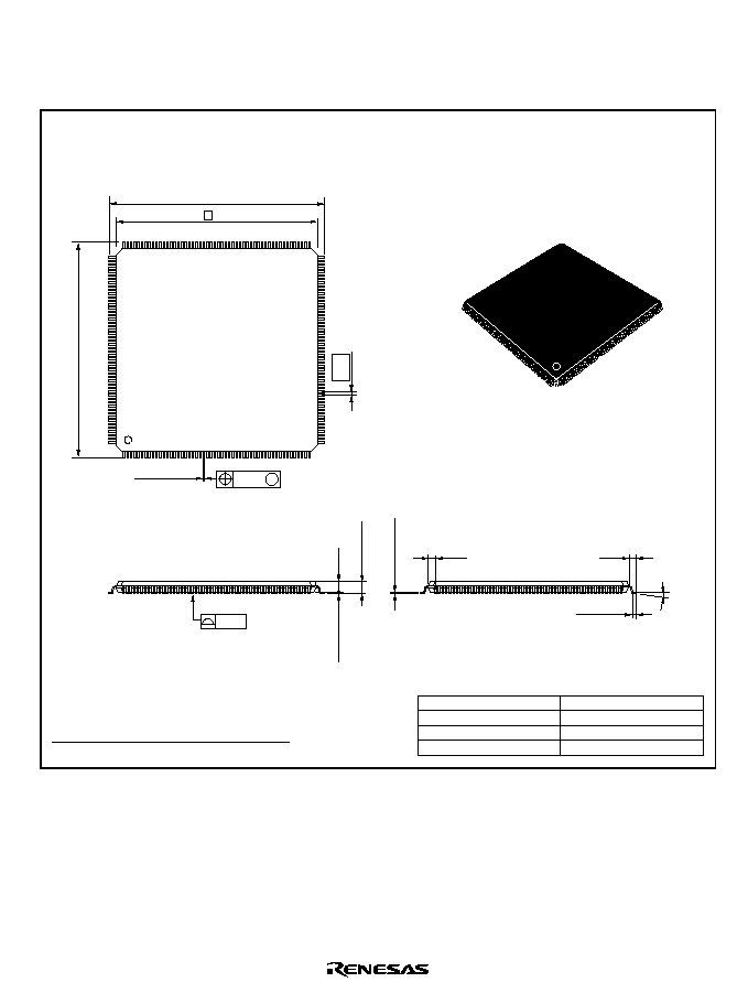
Rev. 2.00, 09/03, page 685 of 690
B.
Package Dimensions
Figures B.1 and B.2 show the package dimensions.
Package Code
JEDEC
JEITA
Mass (reference value)
FP-208C
Conforms
2.7 g
*Dimension including the plating thickness
Base material dimension
30.0
± 0.2
30.0
±
0.2
0.5
1.70 Max
0
∞ - 8∞
*
0.17
±
0.05
156
105
104
52
1
157
208
53
*0.22
± 0.05
0.08 M
0.08
1.40
0.5
± 0.1
1.0
28
0.10
±
0.05
1.25
0.20
± 0.04
0.15
±
0.04
Unit: mm
Figure B.1 Package Dimensions (FP-208C)
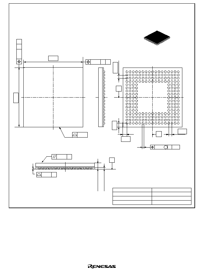
Rev. 2.00, 09/03, page 686 of 690
0.65
0.80
0.80
12.00
12.00
0.15
4
◊
0.2
C
C
0.10 C
0.65
0.31
±
0.05
1.20Max
B
A
D
C
F
E
H
G
K
J
M
L
P
N
T
R
U
17 15
16
13
14
11
12
9
10
7
8
5
6
3
4
1
2
0.20 C A
0.20
C
B
B
C
0.08
A B
208
◊ 0.40 ± 0.05
M
A
Unit: mm
Package Code
JEDEC
JEITA
Mass (reference value)
TBP-208A
0.26 g
Figure B.2 Package Dimensions (TBP-208A)

Rev. 2.00, 09/03, page 687 of 690
Index
16-bit timer pulse unit ........................... 329
16-Bit/32-Bit Displacement ..................... 41
A/D conversion time ............................. 534
A/D converter ....................................... 527
Absolute Addresses ................................. 41
Access wait control ............................... 192
Address multiplexing ............................ 200
Address Space Identifier.......................... 71
Address Transition .................................. 71
Address-Array Read .............................. 104
Address-Array Write
(Associative Operation)......................... 104
Address-Array Write
(non-Associative Operation) .................. 104
Advanced user debugger ....................... 583
Alarm function ...................................... 371
Asynchronous Mode.............................. 402
Auto-Reload count operation ................. 319
Auto-Request mode............................... 254
Big endian....................................... 38, 180
Boundary scan mode ............................. 581
Buffer operation .................................... 346
Bulk-in transfer ..................................... 462
Bulk-out transfer ................................... 461
Burst mode............................................ 265
Burst read ............................................. 212
Burst ROM interface ............................. 231
Bus arbitration ...................................... 235
Bus clock (B
) ...................................... 271
Bus State Controller .............................. 149
Byte-selection SRAM interface ............. 233
Clock Pulse Generator ........................... 271
Clock synchronous mode....................... 396
Compare match counter operation ......... 326
Compare match timer ............................ 323
Control Registers .................................... 29
Control transfer ..................................... 455
Crystal resonator ................................... 273
Cycle-Steal mode .................................. 264
Data stage ............................................. 457
Data-Array Read ................................... 105
Data-Array Write................................... 105
Delayed Branching .................................. 40
Direct memory access controller ............ 239
Dual Address mode ............................... 261
Emulator ............................................... 567
Exception handling................................ 109
Exception Handling State ........................ 25
External request mode ........................... 265
Fixed mode ........................................... 257
Free-running count ................................ 344
General Registers .................................... 29
Global Base Register (GBR) ................... 36
User debugging interface ....................... 567
I/O ports................................................ 507
Infrared data association (IrDA)............. 431
Input capture function............................ 320
Instruction Length ................................... 40
Internal clock (I
).................................. 271
Interrupt Controller................................ 125
Interrupt sources.................................... 136
Interrupt-in transfer ............................... 463
Interval timer mode ............................... 291
IrDA interface ....................................... 431
IRL Interrupts........................................ 137
IRQ Interrupts ....................................... 136
JTAG .................................................... 567
Literal Constant....................................... 41
Little endian .................................... 39, 180

Rev. 2.00, 09/03, page 688 of 690
Load/Store Architecture .......................... 40
Low-frequency mode ............................ 228
Low-Power Consumption State ............... 25
MMU...................................................... 65
Module Standby Function ..................... 301
Multi mode ........................................... 533
Multiple interrupts ................................ 147
Multiple Virtual Memory Mode............... 71
Multiply and Accumulate Registers ......... 33
NMI interrupt........................................ 136
On-Chip peripheral module interrupts.... 138
On-Chip peripheral module request modes
............................................................. 256
P0/U0 Area ............................................. 27
P1 Area................................................... 27
P2 Area................................................... 27
P3 Area................................................... 27
P4 Area................................................... 27
Peripheral clock (P
)............................. 271
Physical Address Space........................... 70
Pin function controller........................... 475
PINT interrupt....................................... 138
Power-Down modes .............................. 293
Priority.................................................. 137
Procedure Register .................................. 33
Processing Modes ................................... 26
Program Counter..................................... 29
PWM mode........................................... 348
Realtime clock ...................................... 351
Receive margin ..................................... 429
Refreshing ............................................ 225
Register
ADCSR.......................530, 594, 611, 621
ADDR.........................530, 594, 611, 621
BAMRA .....................544, 594, 612, 621
BAMRB......................546, 594, 612, 621
BARA.........................543, 594, 612, 621
BARB .........................545, 594, 612, 621
BASRA...................... 554, 594, 612, 621
BASRB ...................... 555, 594, 612, 621
BBRA ........................ 544, 594, 612, 621
BBRB ........................ 547, 594, 612, 621
BDMRB..................... 547, 594, 611, 621
BDRB ........................ 546, 594, 611, 621
BETR......................... 552, 594, 611, 621
BRCR ........................ 549, 594, 611, 621
BRDR ........................ 554, 594, 612, 621
BRSR......................... 553, 594, 612, 621
CCR1 ................................. 586, 596, 614
CCR2 ................................. 586, 596, 614
CCR3 ................................. 586, 596, 614
CHCR ........................ 243, 588, 601, 615
CMCNT..................... 326, 589, 604, 616
CMCOR..................... 326, 589, 604, 616
CMCSR ..................... 325, 589, 604, 616
CMNCR..................... 156, 587, 598, 614
CMSTR...................... 324, 589, 604, 616
CS0BCR ............................ 587, 598, 614
CS0WCR ........................... 587, 599, 615
CSnBCR ........................................... 158
CSnWCR .......................................... 161
DAR .......................... 242, 588, 601, 615
DASTS ...................... 449, 592, 609, 619
DMAOR .................... 248, 588, 603, 616
DMAR ....................... 450, 592, 609, 620
DMARS ..................... 250, 588, 603, 616
DMATCR .................. 243, 588, 601, 615
EPDR0i...................... 445, 592, 609, 619
EPDR0o ..................... 445, 592, 609, 619
EPDR0s ..................... 445, 592, 609, 619
EPDR1....................... 446, 592, 609, 619
EPDR2....................... 446, 592, 609, 619
EPDR3....................... 446, 592, 609, 619
EPSTL ....................... 453, 592, 609, 620
EPSZ0o...................... 447, 592, 609, 619
EPSZ1........................ 447, 592, 609, 620
EXPEVT............................ 586, 596, 614
FCLR ......................... 449, 592, 609, 619
FRQCR ...................... 279, 588, 603, 616
ICR0 ...................110, 129, 587, 597, 614
ICR1 .......................... 130, 587, 597, 614

Rev. 2.00, 09/03, page 689 of 690
ICR2 .......................... 132, 587, 597, 614
IER0 .......................... 444, 592, 609, 620
IER1 .......................... 444, 592, 609, 620
IFR0........................... 441, 592, 609, 619
IFR1........................... 442, 592, 609, 619
INTEVT............................. 586, 596, 614
INTEVT2........................... 586, 596, 614
IPR............................. 128, 586, 597, 614
IRR0 .......................... 133, 587, 597, 614
IRR1 .......................... 134, 587, 597, 614
IRR2 .......................... 135, 587, 597, 614
ISR0........................... 443, 592, 609, 620
ISR1........................... 443, 592, 609, 620
MMUCR............................ 586, 595, 614
PACR......................... 480, 593, 609, 620
PADR ........................ 508, 593, 610, 620
PBCR......................... 481, 593, 609, 620
PBDR......................... 509, 593, 610, 620
PCCR......................... 483, 593, 609, 620
PCDR......................... 510, 593, 610, 620
PDCR......................... 485, 593, 610, 620
PDDR ........................ 511, 593, 610, 620
PECR......................... 487, 593, 610, 620
PECR2 ....................... 488, 593, 610, 620
PEDR......................... 513, 593, 610, 620
PFCR ......................... 489, 593, 610, 620
PFCR2 ....................... 490, 593, 610, 620
PFDR ......................... 514, 593, 610, 620
PGCR......................... 491, 593, 610, 620
PGDR ........................ 516, 593, 610, 620
PHCR......................... 493, 593, 610, 620
PHDR ........................ 517, 593, 611, 621
PINTER ..................... 132, 587, 597, 614
PJCR.......................... 494, 593, 610, 620
PJDR.......................... 518, 593, 611, 621
PKCR......................... 496, 593, 610, 620
PKDR ........................ 519, 593, 611, 621
PLCR ......................... 498, 593, 610, 620
PLDR......................... 521, 593, 611, 621
PMCR........................ 499, 593, 610, 620
PMDR........................ 522, 593, 611, 621
PNCR......................... 500, 593, 610, 620
PNCR2....................... 502, 593, 610, 620
PNDR......................... 523, 593, 611, 621
PTEH .................................586, 595, 614
PTEL .................................586, 595, 614
R64CNT..................... 354, 591, 607, 618
RCR1 ......................... 365, 591, 608, 618
RCR2 ......................... 366, 591, 608, 618
RCR3 ......................... 368, 591, 608, 618
RDAYAR................... 362, 591, 607, 618
RDAYCNT ................ 357, 591, 607, 618
RHRAR...................... 360, 591, 607, 618
RHRCNT ................... 355, 591, 607, 618
RMINAR ................... 359, 591, 607, 618
RMINCNT ................. 355, 591, 607, 618
RMONAR .................. 363, 591, 607, 618
RMONCNT................ 357, 591, 607, 618
RSECAR.................... 358, 591, 607, 618
RSECCNT ................. 354, 591, 607, 618
RTCNT ...................... 179, 587, 600, 615
RTCOR ...................... 179, 587, 600, 615
RTCSR....................... 177, 587, 600, 615
RWKAR..................... 361, 591, 607, 618
RWKCNT .................. 356, 591, 607, 618
RYRAR...................... 364, 591, 608, 618
RYRCNT ................... 358, 591, 607, 618
SAR ........................... 242, 588, 601, 615
SCBRR ...................... 395, 591, 608, 619
SCFCR....................... 398, 591, 608, 619
SCFDR....................... 401, 591, 608, 619
SCFER ....................... 389, 591, 608, 619
SCFRDR .................... 380, 591, 608, 619
SCFTDR .................... 381, 591, 608, 619
SCPCR....................... 503, 593, 610, 620
SCPDR....................... 525, 593, 611, 621
SCRSR.............................................. 380
SCSCR....................... 385, 591, 608, 619
SCSMR (SCIF) .......... 381, 591, 608, 619
SCSMR_Ir (IrDA) ...... 432, 592, 609, 619
SCSSR ....................... 390, 591, 608, 619
SCTDSR .................... 401, 591, 608, 619
SCTSR .............................................. 380
SDBPR.............................................. 569
SDBSR.............................................. 570
SDCR......................... 174, 587, 600, 615

Rev. 2.00, 09/03, page 690 of 690
SDID ................................................ 577
SDID/SDIDH..................... 594, 613, 621
SDIDL ............................... 594, 613, 621
SDIR...........................569, 594, 613, 621
SDMR2.......................229, 587, 601, 615
SDMR3.......................230, 587, 601, 615
STBCR .......................296, 588, 603, 616
STBCR2 .....................297, 588, 603, 616
STBCR3 .....................298, 588, 603, 616
TCNT (TMU) .............317, 589, 603, 616
TCNT (TPU)...............341, 589, 605, 617
TCOR .........................317, 589, 603, 616
TCPR..........................317, 589, 604, 616
TCR (TMU) ................313, 589, 603, 616
TCR (TPU) .................334, 589, 605, 617
TEA................................... 586, 597, 614
TGR............................341, 589, 605, 617
TIER...........................339, 589, 605, 617
TIOR ..........................338, 589, 605, 617
TMDR ........................337, 589, 605, 617
TRA................................... 586, 596, 614
TRG............................448, 592, 609, 619
TSR ............................340, 589, 605, 617
TSTR (TMU) ..............312, 589, 603, 616
TSTR (TPU) ...............341, 589, 605, 617
TTB ................................... 586, 595, 614
UCLKCR....................281, 588, 603, 616
WTCNT......................286, 588, 603, 616
WTCSR ......................287, 588, 603, 616
XVERCR....................453, 592, 609, 620
Reset State .............................................. 25
Round-Robin mode ............................... 258
RTC crystal oscillator circuit................. 372
Save Program Counter (SPC) .................. 36
Save Status Register (SSR)...................... 36
Scan mode ............................................ 534
SDRAM interface.................................. 198
Sequential break.................................... 559
Serial communication interface with FIFO
............................................................. 375
Setup stage............................................ 456
Shadow space........................................ 155
Signal-Source impedance ...................... 538
Single Address mode............................. 262
Single mode .......................................... 533
Single Virtual Memory Mode .................. 71
Sleep mode ........................................... 299
Software standby mode.......................... 300
Stall operations ..................................... 465
Status Register (SR) ................................ 35
Status stage ........................................... 459
Synonym problem ................................... 83
System Registers ..................................... 29
T Bit ....................................................... 40
TAP controller ...................................... 578
Timer Unit ............................................ 309
TRAPA Exception Register ................... 110
USB function module............................ 437
USB standard commands....................... 464
User break controller ............................. 541
User break exception processing............ 555
Vector Base Register (VBR)................... 37
Virtual Address Space ............................. 67
Watchdog timer..................................... 285
Watchdog timer mode ........................... 291

SH7705 Group Hardware Manual
Publication Date: 1st Edition, November 2002
Rev.2.00, September 19, 2003
Published by:
Sales Strategic Planning Div.
Renesas Technology Corp.
Edited by:
Technical Documentation & Information Department
Renesas Kodaira Semiconductor Co., Ltd.
©2002, 2003 Renesas Technology Corp. All rights reserved. Printed in Japan.

Colophon 1.0
Sales Strategic Planning Div. Nippon Bldg., 2-6-2, Ohte-machi, Chiyoda-ku, Tokyo 100-0004, Japan
http://www.renesas.com
Renesas Technology America, Inc.
450 Holger Way, San Jose, CA 95134-1368, U.S.A
Tel: <1> (408) 382-7500 Fax: <1> (408) 382-7501
Renesas Technology Europe Limited.
Dukes Meadow, Millboard Road, Bourne End, Buckinghamshire, SL8 5FH, United Kingdom
Tel: <44> (1628) 585 100, Fax: <44> (1628) 585 900
Renesas Technology Europe GmbH
Dornacher Str. 3, D-85622 Feldkirchen, Germany
Tel: <49> (89) 380 70 0, Fax: <49> (89) 929 30 11
Renesas Technology Hong Kong Ltd.
7/F., North Tower, World Finance Centre, Harbour City, Canton Road, Hong Kong
Tel: <852> 2265-6688, Fax: <852> 2375-6836
Renesas Technology Taiwan Co., Ltd.
FL 10, #99, Fu-Hsing N. Rd., Taipei, Taiwan
Tel: <886> (2) 2715-2888, Fax: <886> (2) 2713-2999
Renesas Technology (Shanghai) Co., Ltd.
26/F., Ruijin Building, No.205 Maoming Road (S), Shanghai 200020, China
Tel: <86> (21) 6472-1001, Fax: <86> (21) 6415-2952
Renesas Technology Singapore Pte. Ltd.
1, Harbour Front Avenue, #06-10, Keppel Bay Tower, Singapore 098632
Tel: <65> 6213-0200, Fax: <65> 6278-8001
RENESAS SALES OFFICES

SH7705 Group
Hardware Manual
REJ09B0082-0200O
