
2003.9.19
32
SH7729R
Group
Hardware Manual
Renesas 32-Bit RISC Microcomputer
SuperH
RISC engine Family/SH7700 Series
Rev.5.00
The revision list can be viewed directly by
clicking the title page.
The revision list summarizes the locations of
revisions and additions. Details should always
be checked by referring to the relevant text.

Renesas 32-Bit RISC Microcomputer
SuperH
RISC engine Family/SH7700 Series
SH7729R Group
Hardware Manual
REJ09B0091-0500O

Rev. 5.0, 09/03, page iv of xlvi
Cautions
Keep safety first in your circuit designs!
1. Renesas Technology Corp. puts the maximum effort into making semiconductor products
better and more reliable, but there is always the possibility that trouble may occur with them.
Trouble with semiconductors may lead to personal injury, fire or property damage.
Remember to give due consideration to safety when making your circuit designs, with
appropriate measures such as (i) placement of substitutive, auxiliary circuits, (ii) use of
nonflammable material or (iii) prevention against any malfunction or mishap.
Notes regarding these materials
1. These materials are intended as a reference to assist our customers in the selection of the
Renesas Technology Corp. product best suited to the customer's application; they do not
convey any license under any intellectual property rights, or any other rights, belonging to
Renesas Technology Corp. or a third party.
2. Renesas Technology Corp. assumes no responsibility for any damage, or infringement of any
third-party's rights, originating in the use of any product data, diagrams, charts, programs,
algorithms, or circuit application examples contained in these materials.
3. All information contained in these materials, including product data, diagrams, charts,
programs and algorithms represents information on products at the time of publication of these
materials, and are subject to change by Renesas Technology Corp. without notice due to
product improvements or other reasons. It is therefore recommended that customers contact
Renesas Technology Corp. or an authorized Renesas Technology Corp. product distributor for
the latest product information before purchasing a product listed herein.
The information described here may contain technical inaccuracies or typographical errors.
Renesas Technology Corp. assumes no responsibility for any damage, liability, or other loss
rising from these inaccuracies or errors.
Please also pay attention to information published by Renesas Technology Corp. by various
means, including the Renesas Technology Corp. Semiconductor home page
(http://www.renesas.com).
4. When using any or all of the information contained in these materials, including product data,
diagrams, charts, programs, and algorithms, please be sure to evaluate all information as a total
system before making a final decision on the applicability of the information and products.
Renesas Technology Corp. assumes no responsibility for any damage, liability or other loss
resulting from the information contained herein.
5. Renesas Technology Corp. semiconductors are not designed or manufactured for use in a
device or system that is used under circumstances in which human life is potentially at stake.
Please contact Renesas Technology Corp. or an authorized Renesas Technology Corp. product
distributor when considering the use of a product contained herein for any specific purposes,
such as apparatus or systems for transportation, vehicular, medical, aerospace, nuclear, or
undersea repeater use.
6. The prior written approval of Renesas Technology Corp. is necessary to reprint or reproduce in
whole or in part these materials.
7. If these products or technologies are subject to the Japanese export control restrictions, they
must be exported under a license from the Japanese government and cannot be imported into a
country other than the approved destination.
Any diversion or reexport contrary to the export control laws and regulations of Japan and/or
the country of destination is prohibited.
8. Please contact Renesas Technology Corp. for further details on these materials or the products
contained therein.

Rev. 5.0, 09/03, page v of xlvi
General Precautions on Handling of Product
1. Treatment of NC Pins
Note:
Do not connect anything to the NC pins.
The NC (not connected) pins are either not connected to any of the internal circuitry or are
used as test pins or to reduce noise. If something is connected to the NC pins, the
operation of the LSI is not guaranteed.
2. Treatment of Unused Input Pins
Note:
Fix all unused input pins to high or low level.
Generally, the input pins of CMOS products are high-impedance input pins. If unused pins
are in their open states, intermediate levels are induced by noise in the vicinity, a pass-
through current flows internally, and a malfunction may occur.
3. Processing before Initialization
Note:
When power is first supplied, the product's state is undefined.
The states of internal circuits are undefined until full power is supplied throughout the
chip and a low level is input on the reset pin. During the period where the states are
undefined, the register settings and the output state of each pin are also undefined. Design
your system so that it does not malfunction because of processing while it is in this
undefined state. For those products which have a reset function, reset the LSI immediately
after the power supply has been turned on.
4. Prohibition of Access to Undefined or Reserved Addresses
Note:
Access to undefined or reserved addresses is prohibited.
The undefined or reserved addresses may be used to expand functions, or test registers
may have been be allocated to these addresses. Do not access these registers; the system's
operation is not guaranteed if they are accessed.

Rev. 5.0, 09/03, page vi of xlvi
Configuration of This Manual
This manual comprises the following items:
1. General Precautions on Handling of Product
2. Configuration of This Manual
3. Preface
4. Contents
5. Overview
6. Description of Functional Modules
∑
CPU and System-Control Modules
∑
On-Chip Peripheral Modules
The configuration of the functional description of each module differs according to the
module. However, the generic style includes the following items:
i) Feature
ii) Input/Output Pin
iii) Register Description
iv) Operation
v) Usage Note
When designing an application system that includes this LSI, take notes into account. Each section
includes notes in relation to the descriptions given, and usage notes are given, as required, as the
final part of each section.
7. List of Registers
8. Electrical Characteristics
9. Appendix
10. Main Revisions and Additions in this Edition (only for revised versions)
The list of revisions is a summary of points that have been revised or added to earlier versions.
This does not include all of the revised contents. For details, see the actual locations in this
manual.
11. Index

Rev. 5.0, 09/03, page vii of xlvi
Preface
The SH7729R is a microprocessor that integrates peripheral functions necessary for system
configuration with a 32-bit internal architecture SH2-DSP CPU as its core.
The SH7729R's on-chip peripheral functions include a cache memory, internal X/Y memory, an
interrupt controller, timers, three serial communication interfaces, a real time clock (RTC),
memory management unit (MMU), a user break controller (UBC), a bus state controller (BSC),
and I/O ports, making it ideal for use as a microcomputer in electronic devices that require high
speed together with low power consumption.
Intended Readership: This manual is intended for users undertaking the design of an application
system using the SH7729R. Readers using this manual require a basic
knowledge of electrical circuits, logic circuits, and microcomputers.
Purpose:
The purpose of this manual is to give users an understanding of the hardware
functions and electrical characteristics of the SH7729R. Details of execution
instructions can be found in the SH-3, SH-3E, SH3-DSP Programming
Manual, which should be read in conjunction with the present manual.
Using this Manual:
∑
For an overall understanding of the SH7729R's functions
Follow the Table of Contents. This manual is broadly divided into sections on the CPU, system
control functions, peripheral functions, and electrical characteristics.
∑
For a detailed understanding of CPU functions
Refer to the separate publication SH-3, SH-3E, SH3-DSP Programming Manual.
Note on bit notation: Bits are shown in high-to-low order from left to right.
Related Material: The latest information is available at our Web Site. Please make sure that you
have the most up-to-date information available.
(http://www.renesas.com/eng/)

Rev. 5.0, 09/03, page viii of xlvi
User's Manuals on the SH7729R:
Manual Title
ADE No.
SH7729R Hardware Manual
This manual
SH-3, SH-3E, SH-3DSP Programming Manual
ADE-602-096
Users manuals for development tools:
Manual Title
ADE No.
C/C++ Compiler, Assembler, Optimized Linkage Editor User's Manual
ADE-702-246
Simulator Debugger User's Manual
ADE-702-186
Embedded Workshop User's Manual
ADE-702-201
Rev. 5.0, 09/03, page ix of xlvi
List of Items Revised or Added for This Version
Section
Page
Description
1.2 Block Diagram
Figure 1.1 Block
Diagram
7
ASERAM deleted from figure
BRIDGE
External bus
interface
UDI
INTC
CPG/WDT
I bus 2
ASERAM deleted from legend
5.4 Memory-Mapped
Cache
5.4.1 Address Array
151,
152
Replaced

Rev. 5.0, 09/03, page x of xlvi
Section
Page
Description
5.4.2 Data Array
152
Description amended
The address array is mapped to H'F1000000 to H'F1FFFFFF. To
access an element of the data array, the 32-bit address field (for
read/write access) and 32-bit data field (for write access) must be
specified. The address field specifies the information that selects
the entry to be accessed; the data field specifies the longword
data to be written to the data array.
In the address field, specify the entry's address in bits 11-4, L in
bits 3-2 to indicate the longword's position within a line (which
consists of 16 bytes), W in bits 13-12 to select the way, and H'F1
in bits 31-24 to indicate access to the data array. The L bits (3-2)
specification is in the following form: 00 is longword 0, 01 is
longword 1, 10 is longword 2, and 11 is longword 3. Settings for
the W bits (13-12) are as follows: 00 is way 0, 01 is way 1, 10 is
way 2, and 11 is way 3. Since access is not allowed crossing
longword boundaries, always set 00 in bits 1-0 of the address
field.
The following two operations on the data array are possible. Note
that these operations will not change the information in the
address array.
(1) Data Array Read
Reads the data at the position selected by the L bits (3-2) of the
address field from the entry that corresponds to the entry address
and way that were specified in the address field.
(2) Data Array Write
Writes the longword data set in the data field into the entry that
corresponds to the entry address and way that were specified in
the address field. The longword data will be written to the entry at
the position selected by the L bits (3-2) of the address field.

Rev. 5.0, 09/03, page xi of xlvi
Section
Page
Description
5.5.1 Invalidating a
Specific Entry
154
Description amended
A specific cache entry can be invalidated by accessing the allocated
memory cache and writing a 0 to the entry's U and V bits. The A bit is
cleared to 0, and an address is specified for the entry address and the
way. If the U bit of the way of the entry in question was set to 1, the
entry is written back and the V and U bits specified by the write data are
written to.
In the following example, the write data is specified in R0 and the
address is specified in R1.
; R0 = H'0000 0000 LRU = H'000, U = 0, V = 0
; R1 = H'F000 1080, Way = 1, Entry = H'08, A = 0
;
MOV.L
R0, @R1
To invalidate all entries and ways, write 0 to the following addresses.
Addresses
F000 0000
F000 0010
F000 0020
:
F000 3FF0
This involves a total of 1,024 writes.
The above operation should be performed using a non-cacheable area.
5.5.2 Invalidating a
Specific Address
Newly added
5.5.3 Reading the
Data of a Specific Entry
155
Description amended
; R1=H'F100 004C; data array access, entry=H'04, Way = 0,
; longword address = 3
;
MOV.L @R0,R1 ; Longword 3 is read.
7.2.6 Interrupt
Exception Handling and
Priority
Table 7.4 Interrupt
Exception Handling
Sources and Priority
(IRQ Mode)
171
IPR (bit numbers) for SCI amended
(Before)IPRB(3-0)
(After)IPRB(7-4)
7.3.6 Interrupt
Request Register 0
(IRR0)
182
Description amended
When clearing an IRQ5R≠IRQ0R bit to 0, read the bit while bit set
to 1, and then write 0. In this case, 0 should be written only to the
bits to be cleared and 1 to the other bits. The contents of the bits
to which 1 is written do not change.
9.2.1 Standby Control
Register (STBCR)
230
Description added
Bit 1--Module Standby 1 (MSTP1)
Before switching the RTC to module standby, access at least one
among the registers RTC, SCI, and TMU.
Rev. 5.0, 09/03, page xii of xlvi
Section
Page
Description
9.3.1 Transition to
Sleep Mode
233
Description added
In sleep mode, the STATUS1 pin is set high and the STATUS0
pin low.
DMAC transfers should not be performed in the sleep mode
under conditions other than when the clock ratio of I0 (on-chip
clock) to B0 (bus clock) is 1:1.
9.5.1 Transition to
Module Standby
Function
237
Note
*
3 added to bit table
Note: 3. Before putting the RTC into module standby status, first
access one or more of the RTC, SCI, and TMU
registers. The RTC may then be put into module standby
status.
10.2.1 CPG Block
Diagram
Figure 10.1 Block
Diagram of Clock Pulse
Generator
250
Figure amended
CAP1
CKIO
Cycle = Bcyc
CAP2
XTAL
EXTAL
PLL circuit 1
(
◊ 1, 2, 3, 4,
6)
Divider 1
Internal
clock (I
)
Cycle = Icyc
Peripheral
clock (P
)
Cycle = Pcyc
Divider 2
Clock pulse generator
PLL circuit 2
(
◊ 1, 4)
Crystal
oscillator
◊ 1
◊ 1/2
◊ 1/3
◊ 1/4
◊ 1/6
◊ 1
◊ 1/2
◊ 1/3
◊ 1/4
◊ 1/6

Rev. 5.0, 09/03, page xiii of xlvi
Section
Page
Description
10.3 Clock Operating
Modes
Table 10.4 Available
Combinations of Clock
Mode and FRQCR
Values
256
Cautions 4 to 6 deleted
10.5.3 Notes on
Changing the
Frequency
259
Newly added
10.8.2 Changing the
Frequency
265
Description added
5.The counter stops at a value of H'00 or H'01. The stop value
depends on the clock ratio.
If the following three conditions are all met, FRQCR should not be
changed when a transfer using the DMAC is in progress.
∑ Bits IFC2 to IFC0 are changed.
∑ Bits STC2 to STC0 are not changed.
∑ The clock ratio is other than I
:B
= 1:1.
11.1.1 Features
Refresh function description deleted
292
Description added
Bit 7--Synchronous DRAM Bank Active (RASD): Specifies
whether synchronous DRAM is used in bank active mode or auto-
precharge mode. Set auto-precharge mode when areas 2 and 3
are both designated as synchronous DRAM space.
The bank active mode should not be used unless the bus width
for all areas is 32 bits.
Bit table amended
Bits 6 to 3--Address Multiplex (AMX3, AMX2, AMX1, AMX0)
Bit6:
AMX3
Bit5:
AMX2
Bit 4:
AMX1
Bit 3:
AMX0 Description
0
The row address begins with
A9
(The A9 value is output at
A1 when the row address is
output. 1M
◊
16-bit
◊
4-bank
products)
0
1
The row address begins with
A10
(The A10 value is output at
A1 when the row address is
output. 2M
◊
8-bit
◊
4-bank
products ,2M
◊
16-bit
◊
4-bank
products)
0
1
1
1
The row address begins with
A9
(The A9 value is output at
A1 when the row address is
output. 512k
◊
32-bit
◊
4-bank
products)
11.2.5 Individual
Memory Control
Register (MCR)
293
Rev. 5.0, 09/03, page xiv of xlvi
Section
Page
Description
11.2.13 MCS0 Control
Register (MCSCR0)
304
Description added
Bit 6--CS2/CS0 Select (CS2/0)
Note that the CS2/0 bit in MCSCR should always be cleared to 0
(area 0 selected).
11.3.4 Synchronous
DRAM Interface
334
Bank Active description added
... .In bank active mode, too, all banks become inactive after a
refresh cycle or after the bus is released as the result of bus
arbitration.
The bank active mode should not be used unless the bus width
for all areas is 32 bits.
11.3.7 Waits between
Access Cycles
Figure 11.40 Waits
between Access Cycles
363
Figure amended
T
1
CKIO
A25 to A0
T
2
Twait
T
1
T
2
Twait
T
1
T
2
11.3.10
MCS[0]
to
MCS[7]
Pin Control
366
Description amended
This enables 32-, 64-, 128-, or 256-Mbit memory to be connected
to area 0 or area 2. However, only CS2/0 = 0 (area 0) should be
used for MCSCR0. Table 11.15 shows MCSCR0≠MCSCR7
settings and
MCS[0]
≠
MCS[7]
assertion conditions.
12.6 Usage Notes
431,
432
Description added
13. DMAC transfers should not be performed in the sleep mode
under conditions other than when the clock ratio of I
(on-
chip clock) to B
(bus clock) is 1:1.
14. When the following three conditions are all met, the
frequency control register (FRQCR) should not be changed
while a DMAC transfer is in progress.
∑
Bits IFC2 to IFC0 are changed.
∑
STC2 to STC0 in FRQCR are not changed.
∑
The clock ratio of I
(on-chip clock) to B
(bus clock) after
the change is other than 1:1.
15. If the following three conditions are all met, big-endian
access is used when the DMAC is used to transfer data from
XY memory, even in the little-endian mode.
∑
The source address for the transfer is in XY memory.
∑
The indirect address mode is used.
∑
The byte size data is transferred.
∑
The data format is little-endian.
14.4.3 Precautions
when Using RTC
Module Standby
470
Newly added

Rev. 5.0, 09/03, page xv of xlvi
Section
Page
Description
Description amended
When the TDFE flag in the serial status register (SCSSR) is set to
1, a TXI interrupt request is generated. The DMAC can be
activated and data transfer performed when this interrupt is
generated. When data exceeding the transmit trigger number is
written to the transmit data register (SCFTDR) by the DMAC, 1 is
read from the TDFE flag, after which 0 is written to it to clear it.
When the RDF flag in SCSSR is set to 1, an RXI interrupt request
is generated. The DMAC can be activated and data transfer
performed when the RDF flag in SCSSR is set to 1. When
receive data less than the receive trigger number is read from the
receive data register (SCFRDR) by the DMAC, 1 is read from the
RDF flag, after which 0 is written to it to clear it.
17.4 SCIF Interrupts
Table 17.10 SCIF
Interrupt Sources
594
Table amended
(Before)Priority on Reset Release
(After)Priority
17.5 Usage Notes
595
Description amended
1. SCFTDR Writing and TDFE Flag:
However, if the number of data bytes written to SCFTDR is equal
to or less than the transmit trigger number, the TDFE flag will be
set to 1 again even after having been cleared to 0. TDFE clearing
should therefore be carried out after data exceeding the specified
transmit trigger number has been written to SCFTDR.
20.13.2 SC Port Data
Register (SCPDR)
654
Title amended
Rev. 5.0, 09/03, page xvi of xlvi
Section
Page
Description
21.3 Bus Master
Interface
Figure 21.2 A/D Data
Register Access
Operation (Reading
H'AA40)
665
Figure amended
Bus
interface
TEMP
[H'40]
ADDRn L
[H'40]
ADDRn H
[H'AA]
n = A to D
CPU
receives
data H'AA
Upper byte read
Module internal data bus
Bus
interface
TEMP
[H'40]
ADDRn L
[H'40]
ADDRn H
[H'AA]
n = A to D
CPU
receives
data H'40
Lower byte read
Module internal data bus
24.1 Absolute
Maximum Ratings
Table 24.1 Absolute
Maximum Ratings
701
Caution amended
2.Until voltage is applied to all power supplies, a low level is input
at the
RESETP
pin, and CKIO has operated for a maximum of 4
clock cycles, internal circuits remain unsettled, and so pin states
are also undefined. The system design must ensure that these
undefined states do not cause erroneous system operation.
Note that the
RESETP
pin cannot receive a low level signal while
a low level signal is being input to the CA pin.
Test conditions for in sleep mode amended
Item
Symbol Min
Typ Max
Unit
Test Conditions
In sleep
mode
*
1
Icc
--
15
30
*
1
: No external bus
cycles
except refresh
cycles
Vcc = 1.9 V
VccQ = 3.3 V
B
= 33 MHz
24.2 DC
Characteristics
Table 24.2 DC
Characteristics
703,
705
Note
*
added
*
If the IRL and IRLS interrupts are used, the minimum is 1.9 V.
Rev. 5.0, 09/03, page xvii of xlvi
Section
Page
Description
24.3.6 Synchronous
DRAM Timing
Figure 24.31
Synchronous DRAM
Burst Read Bus Cycle
(RAS Down, Same Row
Address, CAS Latency
= 2)
733
Tnop cycle deleted from figure
A25 to A16
(High)
t
AD
t
AD
t
AD
t
CASD2
t
CSD3
t
RWD
t
DQMD
t
BSD
t
RDH2
t
RDS2
t
RDH2
t
RDS2
t
BSD
t
RASD2
t
CASD2
t
DQMD
t
RWD
t
CSD3
t
AD
t
AD
t
AD
Tc1
Tc2
Tc3/Td1 Tc4/Td2
Td3
Td4
CKIO
A12 or A10
A15 to A0
CSn
RD/
WR
RAS
CAS
DQMxx
D31 to D0
BS
CKE
Row address
DACKn
t
DAKD1
t
DAKD1
Column address
Read command
24.3.8 Peripheral
Module Signal Timing
Figure 24.52 I/O Port
Timing
751
(Before) PORT 7 to 0 (read) (B:P clock ratio =1:2)
(After) PORT 7 to 0 (read) (B:P clock ratio =2:1)
(Before) PORT 7 to 0 (read) (B:P clock ratio =1:4)
(After) PORT 7 to 0 (read) (B:P clock ratio =4:1)
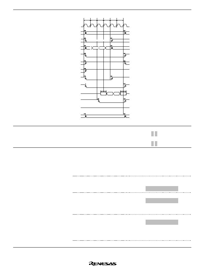
Function information amended for V
CC
≠RTC, V
CC
≠PLL1, V
CC
≠
PLL2, and V
CC
Pin
Pin No.
(FP-208C,
FP-208E)
Pin No.
(BP-
240A)
I/O
Function
V
CC
≠
RTC
3
E2
Power
supply
RTC oscillator power
supply
(2.0/1.9/1.8/1.7 V)
V
CC
≠
PLL1
V
CC
≠
PLL2
145
150
F16,
E17
Power
supply
PLL power supply
(2.0/1.9/1.8/1.7 V)
V
CC
29, 81,
134, 154,
175
L3, L4,
U11, T11,
J17, J16,
E18, C19,
C12, D12
Power
supply
Internal power supply
(2.0/1.9/1.8/1.7 V)
A.2 Pin Specifications
Table A.2 Pin
Specifications
767

Rev. 5.0, 09/03, page xviii of xlvi
Section
Page
Description
A.3 Treatment of
Unused Pins
768
"When RTC is not used" and "When PLL2 is not used" amended
(Before) (1.9/1.8V)
(After) (2.0/1.9/1.8/1.7V)
"When PLL1 is not used" deleted
"When hardware standby mode is not used" added
∑ When hardware standby mode is not used
CA: Pull up (3.3 V)
A.4 Pin States in
Access to Each
Address Space
Table A.3 Pin States
(Ordinary Memory/Little
Endian)
Table A.4 Pin States
(Ordinary Memory/Big
Endian)
Table A.5 Pin States
(Burst ROM/Little
Endian)
Table A.6 Pin States
(Burst ROM/Big
Endian)
Table A.9 Pin States
(PCMCIA/Little Endian)
Table A.10 Pin States
(PCMCIA/Big Endian)
770 to
782
Note 2 amended
Note: 2. Unused data pins should be switched to the port
function, or pulled up.

Rev. 5.0, 09/03, page xix of xlvi
Contents
Section 1 Overview
.............................................................................................................
1
1.1
Features .............................................................................................................................
1
1.2
Block Diagram ..................................................................................................................
7
1.3
Pin Description ..................................................................................................................
8
1.3.1
Pin Assignment ....................................................................................................
8
1.3.2
Pin Function ......................................................................................................... 10
Section 2 CPU
....................................................................................................................... 19
2.1
Registers ............................................................................................................................ 19
2.1.1
General Registers ................................................................................................. 23
2.1.2
Control Registers.................................................................................................. 25
2.1.3
System Registers .................................................................................................. 30
2.1.4
DSP Registers....................................................................................................... 30
2.2
Data Formats ..................................................................................................................... 35
2.2.1
Register Data Format (Non-DSP Type) ............................................................... 35
2.2.2
DSP-Type Data Formats ...................................................................................... 35
2.2.3
Memory Data Formats.......................................................................................... 37
2.3
Features of CPU Core Instructions .................................................................................... 37
2.4
Instruction Formats............................................................................................................ 41
2.4.1
CPU Instruction Addressing Modes ..................................................................... 41
2.4.2
DSP Data Addressing........................................................................................... 45
2.4.3
CPU Instruction Formats...................................................................................... 49
2.4.4
DSP Instruction Formats ...................................................................................... 53
2.5
Instruction Set.................................................................................................................... 59
2.5.1
CPU Instruction Set.............................................................................................. 59
2.6
DSP Extended-Function Instructions ................................................................................ 73
2.6.1
Introduction .......................................................................................................... 73
2.6.2
Added CPU System Control Instructions ............................................................. 73
2.6.3
Single and Double Data Transfer for DSP Data Instructions ............................... 75
2.6.4
DSP Operation Instruction Set ............................................................................. 79
Section 3 Memory Management Unit (MMU)
............................................................ 91
3.1
Overview ........................................................................................................................... 91
3.1.1
Features ................................................................................................................ 91
3.1.2
Role of MMU ....................................................................................................... 91
3.1.3
SH7729R MMU ................................................................................................... 94
3.1.4
Register Configuration ......................................................................................... 97
3.2
Register Description .......................................................................................................... 97
3.3
TLB Functions................................................................................................................... 99

Rev. 5.0, 09/03, page xx of xlvi
3.3.1
Configuration of the TLB ..................................................................................... 99
3.3.2
TLB Indexing ....................................................................................................... 101
3.3.3
TLB Address Comparison.................................................................................... 102
3.3.4
Page Management Information ............................................................................ 104
3.4
MMU Functions ................................................................................................................ 105
3.4.1
MMU Hardware Management ............................................................................. 105
3.4.2
MMU Software Management............................................................................... 105
3.4.3
MMU Instruction (LDTLB) ................................................................................. 106
3.4.4
Avoiding Synonym Problems............................................................................... 107
3.5
MMU Exceptions .............................................................................................................. 110
3.5.1
TLB Miss Exception ............................................................................................ 110
3.5.2
TLB Protection Violation Exception .................................................................... 111
3.5.3
TLB Invalid Exception......................................................................................... 112
3.5.4
Initial Page Write Exception ................................................................................ 113
3.5.5
Processing Flow in Event of MMU Exception
(Same Processing Flow for Address Error) .......................................................... 115
3.5.6
MMU Exception in Repeat Loop ......................................................................... 117
3.6
Memory-Mapped TLB ...................................................................................................... 118
3.6.1
Address Array ...................................................................................................... 118
3.6.2
Data Array ............................................................................................................ 119
3.6.3
Usage Examples ................................................................................................... 121
3.7
Usage Note ........................................................................................................................ 121
Section 4 Exception Handling
.......................................................................................... 123
4.1
Overview ........................................................................................................................... 123
4.1.1
Features ................................................................................................................ 123
4.1.2
Register Configuration ......................................................................................... 123
4.2
Exception Handling Function ............................................................................................ 123
4.2.1
Exception Handling Flow..................................................................................... 123
4.2.2
Exception Vector Addresses................................................................................. 124
4.2.3
Acceptance of Exceptions .................................................................................... 126
4.2.4
Exception Codes................................................................................................... 128
4.2.5
Exception Request Masks .................................................................................... 129
4.2.6
Returning from Exception Handling .................................................................... 129
4.3
Register Descriptions......................................................................................................... 130
4.4
Exception Handling Operation .......................................................................................... 131
4.4.1
Reset ..................................................................................................................... 131
4.4.2
Interrupts .............................................................................................................. 131
4.4.3
General Exceptions............................................................................................... 132
4.5
Individual Exception Operations ....................................................................................... 132
4.5.1
Resets ................................................................................................................... 132
4.5.2
General Exceptions............................................................................................... 133
4.5.3
Interrupts .............................................................................................................. 138

Rev. 5.0, 09/03, page xxi of xlvi
4.6
Cautions............................................................................................................................. 140
Section 5 Cache
.................................................................................................................... 143
5.1
Overview ........................................................................................................................... 143
5.1.1
Features ................................................................................................................ 143
5.1.2
Cache Structure .................................................................................................... 143
5.1.3
Register Configuration ......................................................................................... 145
5.2
Register Descriptions......................................................................................................... 145
5.2.1
Cache Control Register (CCR) ............................................................................. 145
5.2.2
Cache Control Register 2 (CCR2) ........................................................................ 146
5.3
Cache Operation ................................................................................................................ 148
5.3.1
Searching the Cache ............................................................................................. 148
5.3.2
Read Access ......................................................................................................... 150
5.3.3
Write Access ........................................................................................................ 150
5.3.4
Write-Back Buffer ................................................................................................ 150
5.3.5
Coherency of Cache and External Memory.......................................................... 151
5.4
Memory-Mapped Cache .................................................................................................... 151
5.4.1
Address Array ...................................................................................................... 151
5.4.2
Data Array ............................................................................................................ 152
5.5
Usage Examples ................................................................................................................ 154
5.5.1
Invalidating a Specific Entry ................................................................................ 154
5.5.2
Invalidating a Specific Address............................................................................ 155
5.5.3
Reading the Data of a Specific Entry ................................................................... 155
Section 6 X/Y Memory
...................................................................................................... 157
6.1
Overview ........................................................................................................................... 157
6.1.1
Features ................................................................................................................ 157
6.2
X/Y Memory Access from CPU........................................................................................ 158
6.3
X/Y Memory Access from DSP ........................................................................................ 160
6.4
X/Y Memory Access from DMAC ................................................................................... 160
Section 7 Interrupt Controller (INTC)
........................................................................... 161
7.1
Overview ........................................................................................................................... 161
7.1.1
Features ................................................................................................................ 161
7.1.2
Block Diagram ..................................................................................................... 162
7.1.3
Pin Configuration ................................................................................................. 163
7.1.4
Register Configuration ......................................................................................... 164
7.2
Interrupt Sources ............................................................................................................... 165
7.2.1
NMI Interrupt ....................................................................................................... 165
7.2.2
IRQ Interrupts ...................................................................................................... 165
7.2.3
IRL Interrupts ....................................................................................................... 166
7.2.4
PINT Interrupts .................................................................................................... 168
7.2.5
On-Chip Peripheral Module Interrupts................................................................. 168

Rev. 5.0, 09/03, page xxii of xlvi
7.2.6
Interrupt Exception Handling and Priority ........................................................... 169
7.3
INTC Registers.................................................................................................................. 175
7.3.1
Interrupt Priority Registers A to E (IPRA≠IPRE) ................................................ 175
7.3.2
Interrupt Control Register 0 (ICR0) ..................................................................... 176
7.3.3
Interrupt Control Register 1 (ICR1) ..................................................................... 177
7.3.4
Interrupt Control Register 2 (ICR2) ..................................................................... 180
7.3.5
PINT Interrupt Enable Register (PINTER) .......................................................... 181
7.3.6
Interrupt Request Register 0 (IRR0)..................................................................... 182
7.3.7
Interrupt Request Register 1 (IRR1)..................................................................... 184
7.3.8
Interrupt Request Register 2 (IRR2)..................................................................... 185
7.4
INTC Operation................................................................................................................. 187
7.4.1
Interrupt Sequence................................................................................................ 187
7.4.2
Multiple Interrupts................................................................................................ 189
7.5
Interrupt Response Time ................................................................................................... 189
Section 8 User Break Controller
...................................................................................... 193
8.1
Overview ........................................................................................................................... 193
8.1.1
Features ................................................................................................................ 193
8.1.2
Block Diagram ..................................................................................................... 195
8.1.3
Register Configuration ......................................................................................... 196
8.2
Register Descriptions......................................................................................................... 197
8.2.1
Break Address Register A (BARA)...................................................................... 197
8.2.2
Break Address Mask Register A (BAMRA) ........................................................ 198
8.2.3
Break Bus Cycle Register A (BBRA) .................................................................. 199
8.2.4
Break Address Register B (BARB) ...................................................................... 201
8.2.5
Break Address Mask Register B (BAMRB)......................................................... 202
8.2.6
Break Data Register B (BDRB) ........................................................................... 203
8.2.7
Break Data Mask Register B (BDMRB) .............................................................. 204
8.2.8
Break Bus Cycle Register B (BBRB)................................................................... 205
8.2.9
Break Control Register (BRCR)........................................................................... 207
8.2.10 Break Execution Times Register (BETR) ............................................................ 210
8.2.11 Branch Source Register (BRSR) .......................................................................... 211
8.2.12 Branch Destination Register (BRDR) .................................................................. 213
8.2.13 Break ASID Register A (BASRA) ....................................................................... 214
8.2.14 Break ASID Register B (BASRB) ....................................................................... 214
8.3
Operation Description ....................................................................................................... 215
8.3.1
Flow of the User Break Operation........................................................................ 215
8.3.2
Break on Instruction Fetch Cycle ......................................................................... 215
8.3.3
Break by Data Access Cycle ................................................................................ 216
8.3.4
Break on X/Y-Memory Bus Cycle ....................................................................... 217
8.3.5
Sequential Break .................................................................................................. 217
8.3.6
Value of Saved Program Counter......................................................................... 217
8.3.7
PC Trace............................................................................................................... 218

Rev. 5.0, 09/03, page xxiii of xlvi
8.3.8
Examples of Use................................................................................................... 220
8.3.9
Notes .................................................................................................................... 225
Section 9 Power-Down Modes
......................................................................................... 227
9.1
Overview ........................................................................................................................... 227
9.1.1
Power-Down Modes............................................................................................. 227
9.1.2
Pin Configuration ................................................................................................. 229
9.1.3
Register Configuration ......................................................................................... 229
9.2
Register Descriptions......................................................................................................... 229
9.2.1
Standby Control Register (STBCR) ..................................................................... 229
9.2.2
Standby Control Register 2 (STBCR2) ................................................................ 231
9.3
Sleep Mode........................................................................................................................ 233
9.3.1
Transition to Sleep Mode ..................................................................................... 233
9.3.2
Canceling Sleep Mode.......................................................................................... 233
9.4
Standby Mode.................................................................................................................... 234
9.4.1
Transition to Standby Mode ................................................................................. 234
9.4.2
Canceling Standby Mode ..................................................................................... 235
9.4.3
Clock Pause Function........................................................................................... 236
9.5
Module Standby Function ................................................................................................. 237
9.5.1
Transition to Module Standby Function ............................................................... 237
9.5.2
Clearing Module Standby Function...................................................................... 237
9.6
Timing of STATUS Pin Changes ...................................................................................... 238
9.6.1
Timing for Resets ................................................................................................. 238
9.6.2
Timing for Canceling Standby ............................................................................. 240
9.6.3
Timing for Canceling Sleep Mode ....................................................................... 243
9.7
Hardware Standby Mode................................................................................................... 245
9.7.1
Transition to Hardware Standby Mode ................................................................ 245
9.7.2
Canceling Hardware Standby Mode..................................................................... 245
9.7.3
Hardware Standby Mode Timing ......................................................................... 246
Section 10 On-Chip Oscillation Circuits
....................................................................... 249
10.1
Overview ........................................................................................................................... 249
10.1.1 Features ................................................................................................................ 249
10.2
Overview of CPG .............................................................................................................. 250
10.2.1 CPG Block Diagram............................................................................................. 250
10.2.2 CPG Pin Configuration ........................................................................................ 252
10.2.3 CPG Register Configuration................................................................................. 252
10.3
Clock Operating Modes..................................................................................................... 253
10.4
Register Descriptions......................................................................................................... 257
10.4.1 Frequency Control Register (FRQCR) ................................................................. 257
10.5
Changing the Frequency.................................................................................................... 259
10.5.1 Changing the Multiplication Rate ........................................................................ 259
10.5.2 Changing the Division Ratio ................................................................................ 259

Rev. 5.0, 09/03, page xxiv of xlvi
10.5.3 Notes on Changing the Frequency........................................................................ 259
10.6
Overview of WDT............................................................................................................. 260
10.6.1 Block Diagram of WDT ....................................................................................... 260
10.6.2 Register Configuration ......................................................................................... 260
10.7
WDT Registers .................................................................................................................. 261
10.7.1 Watchdog Timer Counter (WTCNT) ................................................................... 261
10.7.2 Watchdog Timer Control/Status Register (WTCSR) ........................................... 261
10.7.3 Notes on Register Access ..................................................................................... 263
10.8
Using the WDT ................................................................................................................. 264
10.8.1 Canceling Standby................................................................................................ 264
10.8.2 Changing the Frequency....................................................................................... 265
10.8.3 Using Watchdog Timer Mode .............................................................................. 265
10.8.4 Using Interval Timer Mode .................................................................................. 265
10.9
Notes on Board Design...................................................................................................... 266
Section 11
Bus State Controller (BSC)
......................................................................... 269
11.1
Overview ........................................................................................................................... 269
11.1.1 Features ................................................................................................................ 269
11.1.2 Block Diagram ..................................................................................................... 271
11.1.3 Pin Configuration ................................................................................................. 272
11.1.4 Register Configuration ......................................................................................... 274
11.1.5 Area Overview ..................................................................................................... 275
11.1.6 PCMCIA Support ................................................................................................. 278
11.2
BSC Registers.................................................................................................................... 281
11.2.1 Bus Control Register 1 (BCR1)............................................................................ 281
11.2.2 Bus Control Register 2 (BCR2)............................................................................ 285
11.2.3 Wait State Control Register 1 (WCR1) ................................................................ 286
11.2.4 Wait State Control Register 2 (WCR2) ................................................................ 287
11.2.5 Individual Memory Control Register (MCR) ....................................................... 291
11.2.6 PCMCIA Control Register (PCR) ........................................................................ 294
11.2.7 Synchronous DRAM Mode Register (SDMR)..................................................... 298
11.2.8 Refresh Timer Control/Status Register (RTCSR) ................................................ 299
11.2.9 Refresh Timer Counter (RTCNT) ........................................................................ 301
11.2.10 Refresh Time Constant Register (RTCOR) .......................................................... 302
11.2.11 Refresh Count Register (RFCR)........................................................................... 302
11.2.12 Cautions on Accessing Refresh Control Related Registers .................................. 303
11.2.13 MCS0 Control Register (MCSCR0)..................................................................... 304
11.2.14 MCS1 Control Register (MCSCR1)..................................................................... 305
11.2.15 MCS2 Control Register (MCSCR2)..................................................................... 305
11.2.16 MCS3 Control Register (MCSCR3)..................................................................... 305
11.2.17 MCS4 Control Register (MCSCR4)..................................................................... 305
11.2.18 MCS5 Control Register (MCSCR5)..................................................................... 305
11.2.19 MCS6 Control Register (MCSCR6)..................................................................... 305

Rev. 5.0, 09/03, page xxv of xlvi
11.2.20 MCS7 Control Register (MCSCR7)..................................................................... 305
11.3
BSC Operation .................................................................................................................. 306
11.3.1 Endian/Access Size and Data Alignment ............................................................. 306
11.3.2 Description of Areas............................................................................................. 311
11.3.3 Basic Interface...................................................................................................... 314
11.3.4 Synchronous DRAM Interface ............................................................................. 321
11.3.5 Burst ROM Interface ............................................................................................ 347
11.3.6 PCMCIA Interface ............................................................................................... 350
11.3.7 Waits between Access Cycles .............................................................................. 362
11.3.8 Bus Arbitration ..................................................................................................... 363
11.3.9 Bus Pull-Up .......................................................................................................... 364
11.3.10
MCS[0] to MCS[7] Pin Control ........................................................................... 366
Section 12 Direct Memory Access Controller (DMAC)
.......................................... 369
12.1
Overview ........................................................................................................................... 369
12.1.1 Features ................................................................................................................ 369
12.1.2 Block Diagram ..................................................................................................... 371
12.1.3 Pin Configuration ................................................................................................. 372
12.1.4 Register Configuration ......................................................................................... 373
12.2
Register Descriptions......................................................................................................... 375
12.2.1 DMA Source Address Registers 0≠3 (SAR0≠SAR3)........................................... 375
12.2.2 DMA Destination Address Registers 0≠3 (DAR0≠DAR3) .................................. 376
12.2.3 DMA Transfer Count Registers 0≠3 (DMATCR0≠DMATCR3) ......................... 377
12.2.4 DMA Channel Control Registers 0≠3 (CHCR0≠CHCR3) ................................... 378
12.2.5 DMA Operation Register (DMAOR) ................................................................... 385
12.3
Operation ........................................................................................................................... 387
12.3.1 DMA Transfer Flow............................................................................................. 387
12.3.2 DMA Transfer Requests....................................................................................... 389
12.3.3 Channel Priority ................................................................................................... 391
12.3.4 DMA Transfer Types ........................................................................................... 394
12.3.5 Number of Bus Cycle States and
DREQ Pin Sampling Timing........................... 407
12.3.6 Source Address Reload Function ......................................................................... 416
12.3.7 DMA Transfer Ending Conditions ....................................................................... 418
12.4
Compare Match Timer (CMT) .......................................................................................... 420
12.4.1 Overview .............................................................................................................. 420
12.4.2 Register Descriptions ........................................................................................... 421
12.4.3 Operation.............................................................................................................. 424
12.4.4 Compare Match .................................................................................................... 425
12.5
Examples of Use................................................................................................................ 427
12.5.1 Example of DMA Transfer between On-Chip IrDA and External Memory ........ 427
12.5.2 Example of DMA Transfer between A/D Converter and External Memory
(Address Reload On) ............................................................................................ 428

Rev. 5.0, 09/03, page xxvi of xlvi
12.5.3 Example of DMA Transfer between External Memory and SCIF Transmitter
(Indirect Address On) ........................................................................................... 429
12.6
Usage Notes....................................................................................................................... 431
Section 13 Timer (TMU)
................................................................................................... 433
13.1
Overview ........................................................................................................................... 433
13.1.1 Features ................................................................................................................ 433
13.1.2 Block Diagram ..................................................................................................... 434
13.1.3 Pin Configuration ................................................................................................. 435
13.1.4 Register Configuration ......................................................................................... 435
13.2
TMU Registers .................................................................................................................. 436
13.2.1 Timer Output Control Register (TOCR) .............................................................. 436
13.2.2 Timer Start Register (TSTR)................................................................................ 436
13.2.3 Timer Control Registers (TCR)............................................................................ 437
13.2.4 Timer Constant Registers (TCOR) ....................................................................... 441
13.2.5 Timer Counters (TCNT)....................................................................................... 442
13.2.6 Input Capture Register (TCPR2) .......................................................................... 443
13.3
TMU Operation ................................................................................................................. 444
13.3.1 Overview .............................................................................................................. 444
13.3.2 Basic Functions .................................................................................................... 444
13.4
Interrupts ........................................................................................................................... 448
13.4.1 Status Flag Setting Timing ................................................................................... 448
13.4.2 Status Flag Clearing Timing................................................................................. 449
13.4.3 Interrupt Sources and Priorities ............................................................................ 449
13.5
Usage Notes....................................................................................................................... 450
13.5.1 Writing to Registers.............................................................................................. 450
13.5.2 Reading Registers................................................................................................. 450
Section 14 Realtime Clock (RTC)
.................................................................................. 451
14.1
Overview ........................................................................................................................... 451
14.1.1 Features ................................................................................................................ 451
14.1.2 Block Diagram ..................................................................................................... 452
14.1.3 Pin Configuration ................................................................................................. 453
14.1.4 RTC Register Configuration................................................................................. 454
14.2
RTC Registers ................................................................................................................... 455
14.2.1 64-Hz Counter (R64CNT).................................................................................... 455
14.2.2 Second Counter (RSECCNT)............................................................................... 455
14.2.3 Minute Counter (RMINCNT) .............................................................................. 456
14.2.4 Hour Counter (RHRCNT) .................................................................................... 456
14.2.5 Day of Week Counter (RWKCNT) ...................................................................... 457
14.2.6 Date Counter (RDAYCNT).................................................................................. 458
14.2.7 Month Counter (RMONCNT).............................................................................. 458
14.2.8 Year Counter (RYRCNT) .................................................................................... 459

Rev. 5.0, 09/03, page xxvii of xlvi
14.2.9 Second Alarm Register (RSECAR)...................................................................... 459
14.2.10 Minute Alarm Register (RMINAR) ..................................................................... 460
14.2.11 Hour Alarm Register (RHRAR) ........................................................................... 460
14.2.12 Day of Week Alarm Register (RWKAR) ............................................................. 461
14.2.13 Date Alarm Register (RDAYAR) ........................................................................ 462
14.2.14 Month Alarm Register (RMONAR)..................................................................... 462
14.2.15 RTC Control Register 1 (RCR1) .......................................................................... 463
14.2.16 RTC Control Register 2 (RCR2) .......................................................................... 464
14.3
RTC Operation .................................................................................................................. 466
14.3.1 Initial Settings of Registers after Power-On ......................................................... 466
14.3.2 Setting the Time ................................................................................................... 466
14.3.3 Reading the Time ................................................................................................. 467
14.3.4 Alarm Function .................................................................................................... 468
14.3.5 Crystal Oscillator Circuit...................................................................................... 469
14.4
Usage Notes....................................................................................................................... 470
14.4.1 Register Writing during RTC Count .................................................................... 470
14.4.2 Use of Realtime Clock (RTC) Periodic Interrupts ............................................... 470
14.4.3 Precautions when Using RTC Module Standby ................................................... 470
Section 15 Serial Communication Interface (SCI)
..................................................... 471
15.1
Overview ........................................................................................................................... 471
15.1.1 Features ................................................................................................................ 471
15.1.2 Block Diagram ..................................................................................................... 472
15.1.3 Pin Configuration ................................................................................................. 475
15.1.4 Register Configuration ......................................................................................... 476
15.2
Register Descriptions......................................................................................................... 476
15.2.1 Receive Shift Register (SCRSR) .......................................................................... 476
15.2.2 Receive Data Register (SCRDR).......................................................................... 477
15.2.3 Transmit Shift Register (SCTSR)......................................................................... 477
15.2.4 Transmit Data Register (SCTDR) ........................................................................ 478
15.2.5 Serial Mode Register (SCSMR) ........................................................................... 478
15.2.6 Serial Control Register (SCSCR) ......................................................................... 481
15.2.7 Serial Status Register (SCSSR) ............................................................................ 484
15.2.8 SC Port Control Register (SCPCR)/SC Port Data Register (SCPDR) ................. 487
15.2.9 Bit Rate Register (SCBRR) .................................................................................. 489
15.3
Operation ........................................................................................................................... 497
15.3.1 Overview .............................................................................................................. 497
15.3.2 Operation in Asynchronous Mode........................................................................ 499
15.3.3 Multiprocessor Communication ........................................................................... 509
15.3.4 Synchronous Operation ........................................................................................ 518
15.4
SCI Interrupts .................................................................................................................... 528
15.5
Usage Notes....................................................................................................................... 529

Rev. 5.0, 09/03, page xxviii of xlvi
Section 16 Smart Card Interface
...................................................................................... 533
16.1
Overview ........................................................................................................................... 533
16.1.1 Features ................................................................................................................ 533
16.1.2 Block Diagram ..................................................................................................... 534
16.1.3 Pin Configuration ................................................................................................. 535
16.1.4 Smart Card Interface Registers............................................................................. 535
16.2
Register Descriptions......................................................................................................... 536
16.2.1 Smart Card Mode Register (SCSCMR)................................................................ 536
16.2.2 Serial Status Register (SCSSR) ............................................................................ 537
16.3
Operation ........................................................................................................................... 538
16.3.1 Overview .............................................................................................................. 538
16.3.2 Pin Connections.................................................................................................... 539
16.3.3 Data Format.......................................................................................................... 540
16.3.4 Register Settings................................................................................................... 541
16.3.5 Clock .................................................................................................................... 542
16.3.6 Data Transmission and Reception ........................................................................ 545
16.4
Usage Notes....................................................................................................................... 551
16.4.1 Receive Data Timing and Receive Margin in Asynchronous Mode .................... 551
16.4.2 Retransmission (Receive and Transmit Modes) ................................................... 553
Section 17 Serial Communication Interface with FIFO (SCIF)
............................. 555
17.1
Overview ........................................................................................................................... 555
17.1.1 Features ................................................................................................................ 555
17.1.2 Block Diagram ..................................................................................................... 556
17.1.3 Pin Configuration ................................................................................................. 559
17.1.4 Register Configuration ......................................................................................... 560
17.2
Register Descriptions......................................................................................................... 561
17.2.1 Receive Shift Register (SCRSR) .......................................................................... 561
17.2.2 Receive FIFO Data Register (SCFRDR).............................................................. 561
17.2.3 Transmit Shift Register (SCTSR)......................................................................... 561
17.2.4 Transmit FIFO Data Register (SCFTDR) ............................................................ 562
17.2.5 Serial Mode Register (SCSMR) ........................................................................... 562
17.2.6 Serial Control Register (SCSCR) ......................................................................... 564
17.2.7 Serial Status Register (SCSSR) ............................................................................ 566
17.2.8 Bit Rate Register (SCBRR) .................................................................................. 571
17.2.9 FIFO Control Register (SCFCR).......................................................................... 578
17.2.10 FIFO Data Count Register (SCFDR) ................................................................... 580
17.3
Operation ........................................................................................................................... 581
17.3.1 Overview .............................................................................................................. 581
17.3.2 Serial Operation.................................................................................................... 582
17.4
SCIF Interrupts .................................................................................................................. 594
17.5
Usage Notes....................................................................................................................... 595

Rev. 5.0, 09/03, page xxix of xlvi
Section 18 IrDA
.................................................................................................................... 599
18.1
Overview ........................................................................................................................... 599
18.1.1 Features ................................................................................................................ 599
18.1.2 Block Diagram ..................................................................................................... 600
18.1.3 Pin Configuration ................................................................................................. 603
18.1.4 Register Configuration ......................................................................................... 604
18.2
Register Description .......................................................................................................... 605
18.2.1 Serial Mode Register (SCSMR) ........................................................................... 605
18.3
Operation Description ....................................................................................................... 607
18.3.1 Overview .............................................................................................................. 607
18.3.2 Transmitting ......................................................................................................... 607
18.3.3 Receiving.............................................................................................................. 608
Section 19 Pin Function Controller
................................................................................ 609
19.1
Overview ........................................................................................................................... 609
19.2
Register Configuration ...................................................................................................... 613
19.3
Register Descriptions......................................................................................................... 614
19.3.1 Port A Control Register (PACR) .......................................................................... 614
19.3.2 Port B Control Register (PBCR) .......................................................................... 615
19.3.3 Port C Control Register (PCCR) .......................................................................... 616
19.3.4 Port D Control Register (PDCR) .......................................................................... 617
19.3.5 Port E Control Register (PECR)........................................................................... 618
19.3.6 Port F Control Register (PFCR) ........................................................................... 619
19.3.7 Port G Control Register (PGCR) .......................................................................... 620
19.3.8 Port H Control Register (PHCR) .......................................................................... 621
19.3.9 Port J Control Register (PJCR) ............................................................................ 623
19.3.10 Port K Control Register (PKCR) .......................................................................... 624
19.3.11 Port L Control Register (PLCR)........................................................................... 625
19.3.12 SC Port Control Register (SCPCR) ...................................................................... 626
Section 20 I/O Ports
............................................................................................................ 631
20.1
Overview ........................................................................................................................... 631
20.2
Port A ................................................................................................................................ 631
20.2.1 Register Description ............................................................................................. 631
20.2.2 Port A Data Register (PADR) .............................................................................. 632
20.3
Port B ................................................................................................................................ 633
20.3.1 Register Description ............................................................................................. 633
20.3.2 Port B Data Register (PBDR)............................................................................... 634
20.4
Port C ................................................................................................................................ 635
20.4.1 Register Description ............................................................................................. 635
20.4.2 Port C Data Register (PCDR)............................................................................... 636
20.5
Port D ................................................................................................................................ 637
20.5.1 Register Description ............................................................................................. 637

Rev. 5.0, 09/03, page xxx of xlvi
20.5.2 Port D Data Register (PDDR) .............................................................................. 638
20.6
Port E................................................................................................................................. 639
20.6.1 Register Description ............................................................................................. 639
20.6.2 Port E Data Register (PEDR) ............................................................................... 640
20.7
Port F ................................................................................................................................. 641
20.7.1 Register Description ............................................................................................. 641
20.7.2 Port F Data Register (PFDR)................................................................................ 642
20.8
Port G ................................................................................................................................ 643
20.8.1 Register Description ............................................................................................. 643
20.8.2 Port G Data Register (PGDR) .............................................................................. 644
20.9
Port H ................................................................................................................................ 645
20.9.1 Register Description ............................................................................................. 645
20.9.2 Port H Data Register (PHDR) .............................................................................. 646
20.10 Port J.................................................................................................................................. 647
20.10.1 Register Description ............................................................................................. 647
20.10.2 Port J Data Register (PJDR)................................................................................. 648
20.11 Port K ................................................................................................................................ 649
20.11.1 Register Description ............................................................................................. 649
20.11.2 Port K Data Register (PKDR) .............................................................................. 650
20.12 Port L................................................................................................................................. 651
20.12.1 Register Description ............................................................................................. 651
20.12.2 Port L Data Register (PLDR) ............................................................................... 652
20.13 SC Port .............................................................................................................................. 653
20.13.1 Register Description ............................................................................................. 653
20.13.2 SC Port Data Register (SCPDR) .......................................................................... 654
Section 21 A/D Converter
................................................................................................. 657
21.1
Overview ........................................................................................................................... 657
21.1.1 Features ................................................................................................................ 657
21.1.2 Block Diagram ..................................................................................................... 658
21.1.3 Input Pins.............................................................................................................. 659
21.1.4 Register
Configuration ......................................................................................... 660
21.2
Register Descriptions......................................................................................................... 661
21.2.1 A/D Data Registers A to D (ADDRA to ADDRD) .............................................. 661
21.2.2 A/D Control/Status Register (ADCSR) ................................................................ 662
21.2.3 A/D Control Register (ADCR)............................................................................. 664
21.3
Bus Master Interface.......................................................................................................... 665
21.4
Operation ........................................................................................................................... 666
21.4.1 Single Mode (MULTI = 0)................................................................................... 666
21.4.2 Multi Mode (MULTI = 1, SCN = 0) .................................................................... 668
21.4.3 Scan Mode (MULTI = 1, SCN = 1) ..................................................................... 670
21.4.4 Input Sampling and A/D Conversion Time .......................................................... 672
21.4.5 External Trigger Input Timing ............................................................................. 673

Rev. 5.0, 09/03, page xxxi of xlvi
21.5
Interrupts ........................................................................................................................... 674
21.6
Definitions of A/D Conversion Accuracy ......................................................................... 674
21.7
Usage Notes....................................................................................................................... 675
21.7.1 Setting Analog Input Voltage ............................................................................... 675
21.7.2 Processing of Analog Input Pins .......................................................................... 675
21.7.3 Access Size and Read Data .................................................................................. 676
Section 22 D/A Converter
................................................................................................. 679
22.1
Overview ........................................................................................................................... 679
22.1.1 Features ................................................................................................................ 679
22.1.2 Block Diagram ..................................................................................................... 679
22.1.3 I/O Pins................................................................................................................. 680
22.1.4 Register Configuration ......................................................................................... 680
22.2
Register Descriptions......................................................................................................... 681
22.2.1 D/A Data Registers 0 and 1 (DADR0/1) .............................................................. 681
22.2.2 D/A Control Register (DACR) ............................................................................. 681
22.3
Operation ........................................................................................................................... 683
Section 23 User Debugging Interface (UDI)
............................................................... 685
23.1
Overview ........................................................................................................................... 685
23.2
User Debugging Interface (UDI) ....................................................................................... 685
23.2.1 Pin Descriptions ................................................................................................... 685
23.2.2 Block Diagram ..................................................................................................... 686
23.3
Register Descriptions......................................................................................................... 686
23.3.1 Bypass Register (SDBPR).................................................................................... 687
23.3.2 Instruction Register (SDIR).................................................................................. 687
23.3.3 Boundary Scan Register (SDBSR) ....................................................................... 688
23.4
UDI Operation................................................................................................................... 695
23.4.1 TAP Controller..................................................................................................... 695
23.4.2 Reset Configuration.............................................................................................. 696
23.4.3 UDI Reset............................................................................................................. 697
23.4.4 UDI Interrupt........................................................................................................ 697
23.4.5 Bypass .................................................................................................................. 697
23.4.6 Using UDI to Recover from Sleep Mode ............................................................. 697
23.5
Boundary Scan .................................................................................................................. 698
23.5.1 Supported Instructions.......................................................................................... 698
23.5.2 Points for Attention .............................................................................................. 699
23.6
Usage Notes....................................................................................................................... 699
23.7
Advanced User Debugger (AUD) ..................................................................................... 699
Section 24 Electrical Characteristics
.............................................................................. 701
24.1
Absolute Maximum Ratings .............................................................................................. 701
24.2
DC Characteristics............................................................................................................. 703

Rev. 5.0, 09/03, page xxxii of xlvi
24.3
AC Characteristics............................................................................................................. 706
24.3.1 Clock Timing........................................................................................................ 707
24.3.2 Control Signal Timing.......................................................................................... 713
24.3.3 AC Bus Timing .................................................................................................... 716
24.3.4 Basic Timing ........................................................................................................ 718
24.3.5 Burst ROM Timing .............................................................................................. 721
24.3.6 Synchronous DRAM Timing ............................................................................... 724
24.3.7 PCMCIA Timing.................................................................................................. 742
24.3.8 Peripheral Module Signal Timing ........................................................................ 749
24.3.9 UDI-Related Pin Timing ...................................................................................... 753
24.3.10 AC Characteristic Test Conditions ....................................................................... 755
24.3.11 Delay Time Variation Due to Load Capacitance.................................................. 756
24.4 A/D
Converter
Characteristics........................................................................................... 757
24.5
D/A Converter Characteristics........................................................................................... 757
Appendix A Pin Functions
................................................................................................ 759
A.1
Pin States ........................................................................................................................... 759
A.2
Pin Specifications .............................................................................................................. 763
A.3
Treatment of Unused Pins ................................................................................................. 768
A.4
Pin States in Access to Each Address Space ..................................................................... 769
Appendix B Memory-Mapped Control Registers
....................................................... 783
B.1
Register Address Map ....................................................................................................... 783
B.2
Register Bits ...................................................................................................................... 789
Appendix C Product Lineup
............................................................................................. 802
Appendix D Package Dimensions
................................................................................... 803

Rev. 5.0, 09/03, page xxxiii of xlvi
Figures
Figure 1.1
Block Diagram .....................................................................................................
7
Figure 1.2
Pin Assignment (FP-208C, FP-208E) ..................................................................
8
Figure 1.3
Pin Assignment (BP-240A) ..................................................................................
9
Figure 2.1
Register Configuration in Each Processing Mode (1) .......................................... 21
Figure 2.2
Register Configuration in Each Processing Mode (2) .......................................... 22
Figure 2.3
General Purpose Registers (Not in DSP Mode) ................................................... 23
Figure 2.4
General Purpose Registers (DSP Mode) .............................................................. 24
Figure 2.5
Control Registers.................................................................................................. 27
Figure 2.6
System Registers .................................................................................................. 30
Figure 2.7
DSP Registers....................................................................................................... 32
Figure 2.8
Connections of DSP Registers and Buses ............................................................ 34
Figure 2.9
Longword Operand .............................................................................................. 35
Figure 2.10
Data Formats ........................................................................................................ 36
Figure 2.11
Byte, Word, and Longword Alignment ................................................................ 37
Figure 2.12
X and Y Data Transfer Addressing ...................................................................... 46
Figure 2.13
Single Data Transfer Addressing.......................................................................... 47
Figure 2.14
Modulo Addressing .............................................................................................. 48
Figure 2.15
DSP Instruction Formats ...................................................................................... 53
Figure 2.16
Sample Parallel Instruction Program.................................................................... 80
Figure 2.17
Examples of Conditional Operations and Data Transfer Instructions .................. 88
Figure 3.1
MMU Functions ................................................................................................... 93
Figure 3.2
Virtual Address Space Mapping........................................................................... 95
Figure 3.3
MMU Register Contents ...................................................................................... 98
Figure 3.4
Overall Configuration of the TLB ........................................................................ 99
Figure 3.5
Virtual Address and TLB Structure...................................................................... 100
Figure 3.6
TLB Indexing (IX = 1) ......................................................................................... 101
Figure 3.7
TLB Indexing (IX = 0) ......................................................................................... 102
Figure 3.8
Objects of Address Comparison ........................................................................... 103
Figure 3.9
Operation of LDTLB Instruction.......................................................................... 107
Figure 3.10
Synonym Problem ................................................................................................ 109
Figure 3.11
MMU Exception Generation Flowchart ............................................................... 114
Figure 3.12
MMU Exception Signals in Instruction Fetch ...................................................... 115
Figure 3.13
MMU Exception Signals in Data Access ............................................................. 116
Figure 3.14
MMU Exception in Repeat Loop ......................................................................... 117
Figure 3.15
Specifying Address and Data for Memory-Mapped TLB Access ........................ 120
Figure 4.1
Vector Table......................................................................................................... 124
Figure 4.2
Example of Acceptance Order of General Exceptions ......................................... 127
Figure 4.3
Bit Configurations of EXPEVT, INTEVT, INTEVT2, and TRA Registers......... 130
Figure 5.1
Cache Structure .................................................................................................... 144
Figure 5.2
CCR Register Configuration ................................................................................ 146
Figure 5.3
CCR2 Register Configuration .............................................................................. 147
Figure 5.4
Cache Search Scheme (Normal Mode) ................................................................ 149

Rev. 5.0, 09/03, page xxxiv of xlvi
Figure 5.5
Write-Back Buffer Configuration......................................................................... 150
Figure 5.6
Specifying Address and Data for Memory-Mapped Cache Access...................... 153
Figure 6.1
X/Y Memory Logical Address Mapping.............................................................. 159
Figure 6.2
X/Y Memory Physical Address Mapping ............................................................ 160
Figure 7.1
Block Diagram of INTC....................................................................................... 162
Figure 7.2
Example of IRL Interrupt Connection.................................................................. 166
Figure 7.3
Interrupt Operation Flowchart .............................................................................. 188
Figure 7.4
Example of Pipeline Operations when IRL Interrupt is Accepted ....................... 192
Figure 8.1
Block Diagram of User Break Controller ............................................................. 195
Figure 8.2
When Interrupt Occurs before Branch Instruction is Executed ............................ 218
Figure 9.1
Canceling Standby Mode with STBCR.STBY..................................................... 235
Figure 9.2
Power-On Reset (Clock Modes 0, 1, 2, and 7) STATUS Output ......................... 238
Figure 9.3
Manual Reset STATUS Output............................................................................ 239
Figure 9.4
Standby to Interrupt STATUS Output.................................................................. 240
Figure 9.5
Standby to Power-On Reset STATUS Output...................................................... 241
Figure 9.6
Standby to Manual Reset STATUS Output.......................................................... 242
Figure 9.7
Sleep to Interrupt STATUS Output ...................................................................... 243
Figure 9.8
Sleep to Power-On Reset STATUS Output.......................................................... 243
Figure 9.9
Sleep to Manual Reset STATUS Output .............................................................. 244
Figure 9.10
Hardware Standby Mode (When CA Goes Low in Normal Operation)............... 246
Figure 9.11
Hardware Standby Mode Timing (When CA Goes Low during WDT
Operation on Standby Mode Cancellation) .......................................................... 247
Figure 10.1
Block Diagram of Clock Pulse Generator ............................................................ 250
Figure 10.2
Block Diagram of WDT ....................................................................................... 260
Figure 10.3
Writing to WTCNT and WTCSR......................................................................... 264
Figure 10.4
Points for Attention when Using Crystal Resonator............................................. 266
Figure 10.5
Points for Attention when Using PLL Oscillator Circuit ..................................... 267
Figure 11.1
Block Diagram of Bus State Controller................................................................ 271
Figure 11.2
Correspondence between Logical Address Space and Physical Address Space .. 275
Figure 11.3
Physical Space Allocation .................................................................................... 277
Figure 11.4
PCMCIA Space Allocation .................................................................................. 278
Figure 11.5
Writing to RFCR, RTCSR, RTCNT, and RTCOR............................................... 303
Figure 11.6
Basic Timing of Basic Interface ........................................................................... 315
Figure 11.7
Example of 32-Bit Data-Width Static RAM Connection ..................................... 316
Figure 11.8
Example of 16-Bit Data-Width Static RAM Connection ..................................... 317
Figure 11.9
Example of 8-Bit Data-Width Static RAM Connection ....................................... 318
Figure 11.10 Basic Interface Wait Timing (Software Wait Only) ............................................. 319
Figure 11.11 Basic Interface Wait State Timing (Wait State Insertion by
WAIT Signal
WAITSEL = 1)..................................................................................................... 320
Figure 11.12 Example of 64-Mbit Synchronous DRAM Connection (32-Bit Bus Width)........ 322
Figure 11.13 Example of 64-Mbit Synchronous DRAM (16-Bit Bus Width) ........................... 323
Figure 11.14 Basic Timing for Synchronous DRAM Burst Read ............................................. 326
Figure 11.15 Synchronous DRAM Burst Read Wait Specification Timing .............................. 327

Rev. 5.0, 09/03, page xxxv of xlvi
Figure 11.16 Basic Timing for Synchronous DRAM Single Read............................................ 328
Figure 11.17 Basic Timing for Synchronous DRAM Burst Write ............................................ 330
Figure 11.18 Basic Timing for Synchronous DRAM Single Write........................................... 332
Figure 11.19 Burst Read Timing (No Precharge) ...................................................................... 335
Figure 11.20 Burst Read Timing (Same Row Address) ............................................................ 336
Figure 11.21 Burst Read Timing (Different Row Addresses) ................................................... 337
Figure 11.22 Burst Write Timing (No Precharge) ..................................................................... 338
Figure 11.23 Burst Write Timing (Same Row Address) ........................................................... 339
Figure 11.24 Burst Write Timing (Different Row Addresses) .................................................. 340
Figure 11.25 Auto-Refresh Operation ....................................................................................... 341
Figure 11.26 Synchronous DRAM Auto-Refresh Timing......................................................... 342
Figure 11.27 Synchronous DRAM Self-Refresh Timing .......................................................... 344
Figure 11.28 Synchronous DRAM Mode Write Timing ........................................................... 346
Figure 11.29 Burst ROM Wait Access Timing ......................................................................... 348
Figure 11.30 Burst ROM Basic Access Timing ........................................................................ 349
Figure 11.31 Example of PCMCIA Interface ............................................................................ 351
Figure 11.32 Basic Timing for PCMCIA Memory Card Interface ............................................ 353
Figure 11.33 Wait Timing for PCMCIA Memory Card Interface ............................................. 354
Figure 11.34 Basic Timing for PCMCIA Memory Card Interface Burst Access ...................... 355
Figure 11.35 Wait Timing for PCMCIA Memory Card Interface Burst Access ....................... 356
Figure 11.36 PCMCIA Space Allocation .................................................................................. 357
Figure 11.37 Basic Timing for PCMCIA I/O Card Interface .................................................... 359
Figure 11.38 Wait Timing for PCMCIA I/O Card Interface ..................................................... 360
Figure 11.39 Dynamic Bus Sizing Timing for PCMCIA I/O Card Interface ............................ 361
Figure 11.40 Waits between Access Cycles .............................................................................. 363
Figure 11.41 Pull-Up Timing for Pins A25 to A0 ..................................................................... 364
Figure 11.42 Pull-Up Timing for Pins D31 to D0 (Read Cycle) ............................................... 365
Figure 11.43 Pull-Up Timing for Pins D31 to D0 (Write Cycle) .............................................. 365
Figure 12.1
Block Diagram of DMAC .................................................................................... 371
Figure 12.2
DMAC Transfer Flowchart .................................................................................. 388
Figure 12.3
Round-Robin Mode.............................................................................................. 392
Figure 12.4
Changes in Channel Priority in Round-Robin Mode............................................ 393
Figure 12.5
Operation of Direct Address Mode in Dual Address Mode ................................. 395
Figure 12.6
Example of DMA Transfer Timing in the Direct Address Mode in Dual Mode
(Transfer Source: Ordinary Memory, Transfer Destination: Ordinary Memory). 396
Figure 12.7
Example of DMA Transfer Timing in the Direct Address Mode in Dual Mode
(16-byte Transfer, Transfer Source: Ordinary Memory,
Transfer Destination: Ordinary Memory)............................................................. 397
Figure 12.8
Example of DMA Transfer Timing in the Direct Address Mode in Dual Mode
(16-byte Transfer, Transfer Source: Synchronous DRAM,
Transfer Destination: Ordinary Memory)............................................................. 397
Figure 12.9
Indirect Address Operation in Dual Address Mode (When External Memory
Space has a 16-Bit Width) .................................................................................... 399

Rev. 5.0, 09/03, page xxxvi of xlvi
Figure 12.10 Example of Transfer Timing in the Indirect Address Mode in Dual Address
Mode .................................................................................................................... 400
Figure 12.11 Data Flow in Single Address Mode...................................................................... 401
Figure 12.12 Example of DMA Transfer Timing in Single Address Mode .............................. 402
Figure 12.13 Example of DMA Transfer Timing in Single Address Mode (External Memory3
Space (Ordinary Memory)
External Device with DACK) .............................. 403
Figure 12.14 Example of Transfer in Cycle-Steal Mode ........................................................... 403
Figure 12.15 Example of Transfer in Burst Mode ..................................................................... 404
Figure 12.16 Bus State when Multiple Channels Are Operating............................................... 406
Figure 12.17 Cycle-Steal Mode, Level Input (CPU Access: 2 Cycles) ..................................... 409
Figure 12.18 Cycle-Steal Mode, Level Input (CPU Access: 3 Cycles) ..................................... 410
Figure 12.19 Cycle-Steal Mode, Level input (CPU Access: 2 Cycles,
DMA RD Access: 4 Cycles)................................................................................. 411
Figure 12.20 Cycle-Steal Mode, Level input (CPU Access: 2 Cycles, DREQ Input Delayed) . 412
Figure 12.21 Cycle-Steal Mode, Edge input (CPU Access: 2 Cycles) ...................................... 413
Figure 12.22 Burst Mode, Level Input ...................................................................................... 414
Figure 12.23 Burst Mode, Edge Input ....................................................................................... 415
Figure 12.24 Source Address Reload Function Diagram........................................................... 416
Figure 12.25 Timing Chart of Source Address Reload Function............................................... 417
Figure 12.26 Block Diagram of CMT ....................................................................................... 420
Figure 12.27 Counter Operation ................................................................................................ 424
Figure 12.28 Count Timing ....................................................................................................... 425
Figure 12.29 CMF Setting Timing ............................................................................................ 426
Figure 12.30 Timing of CMF Clearing by the CPU .................................................................. 426
Figure 13.1
Block Diagram of TMU ....................................................................................... 434
Figure 13.2
Setting the Count Operation ................................................................................. 445
Figure 13.3
Auto-Reload Count Operation.............................................................................. 446
Figure 13.4
Count Timing when Operating on Internal Clock ................................................ 446
Figure 13.5
Count Timing when Operating on External Clock (Both Edges Detected) .......... 447
Figure 13.6
Count Timing when Operating on On-Chip RTC Clock ...................................... 447
Figure 13.7
Operation Timing when Using Input Capture Function
(Using TCLK Rising Edge).................................................................................. 448
Figure 13.8
UNF Setting Timing............................................................................................. 448
Figure 13.9
Status Flag Clearing Timing................................................................................. 449
Figure 14.1
Block Diagram of RTC ........................................................................................ 452
Figure 14.2
Setting the Time ................................................................................................... 466
Figure 14.3
Reading the Time ................................................................................................. 467
Figure 14.4
Using the Alarm Function .................................................................................... 468
Figure 14.5
Example of Crystal Oscillator Circuit Connection ............................................... 469
Figure 14.6
Using Periodic Interrupt Function ........................................................................ 470
Figure 15.1
Block Diagram of SCI .......................................................................................... 472
Figure 15.2
SCPT[1]/SCK0 Pin .............................................................................................. 473
Figure 15.3
SCPT[0]/TxD0 Pin............................................................................................... 474

Rev. 5.0, 09/03, page xxxvii of xlvi
Figure 15.4
SCPT[0]/RxD0 Pin............................................................................................... 475
Figure 15.5
Example of Data Format in Asynchronous Communication
(8-Bit Data with Parity and Two Stop Bits) ......................................................... 499
Figure 15.6
Output Clock and Serial Data Timing (Asynchronous Mode) ............................. 501
Figure 15.7
Sample Flowchart for SCI Initialization............................................................... 502
Figure 15.8
Sample Flowchart for Transmitting Serial Data ................................................... 503
Figure 15.9
Example of SCI Transmit Operation in Asynchronous Mode
(8-Bit Data with Parity and One Stop Bit) ........................................................... 505
Figure 15.10 Sample Flowchart for Receiving Serial Data ....................................................... 506
Figure 15.11 Example of SCI Receive Operation (8-Bit Data with Parity and One Stop Bit) .. 509
Figure 15.12 Communication Among Processors Using Multiprocessor Format
(Sending Data H'AA to Receiving Processor A) .................................................. 510
Figure 15.13 Sample Flowchart for Transmitting Multiprocessor Serial Data.......................... 511
Figure 15.14 Example of SCI Multiprocessor Transmit Operation (8-Bit Data with
Multiprocessor Bit and One Stop Bit) .................................................................. 512
Figure 15.15 Sample Flowchart for Receiving Multiprocessor Serial Data .............................. 514
Figure 15.16 Example of SCI Receive Operation (8-Bit Data with Multiprocessor Bit and
One Stop Bit)........................................................................................................ 516
Figure 15.17 Data Format in Synchronous Communication ..................................................... 518
Figure 15.18 Sample Flowchart for SCI Initialization............................................................... 520
Figure 15.19 Sample Flowchart for Transmitting Serial Data ................................................... 521
Figure 15.20 Example of SCI Transmit Operation .................................................................... 522
Figure 15.21 Sample Flowchart for Receiving Serial Data ....................................................... 524
Figure 15.22 Example of SCI Receive Operation...................................................................... 526
Figure 15.23 Sample Flowchart for Transmitting/Receiving Serial Data.................................. 527
Figure 15.24 Receive Data Sampling Timing in Asynchronous Mode ..................................... 530
Figure 16.1
Block Diagram of Smart Card Interface ............................................................... 534
Figure 16.2
Pin Connection Diagram for Smart Card Interface .............................................. 539
Figure 16.3
Data Format for Smart Card Interface .................................................................. 540
Figure 16.4
Waveform of Start Character................................................................................ 542
Figure 16.5
Initialization Flowchart (Example)....................................................................... 546
Figure 16.6
Transmission Flowchart ....................................................................................... 548
Figure 16.7
Reception Flowchart (Example) ........................................................................... 550
Figure 16.8
Receive Data Sampling Timing in Smart Card Mode .......................................... 552
Figure 16.9
Retransmission in SCI Receive Mode .................................................................. 553
Figure 16.10 Retransmission in SCI Transmit Mode ................................................................ 554
Figure 17.1
Block Diagram of SCIF........................................................................................ 556
Figure 17.2
SCPT[5]/SCK2 Pin .............................................................................................. 557
Figure 17.3
SCPT[4]/TxD2 Pin............................................................................................... 558
Figure 17.4
SCPT[4]/RxD2 Pin............................................................................................... 559
Figure 17.5
Sample Flowchart for SCIF Initialization ............................................................ 584
Figure 17.6
Sample Flowchart for Transmitting Serial Data ................................................... 586
Figure 17.7
Example of Transmit Operation (8-Bit Data, Parity, One Stop Bit)..................... 588

Rev. 5.0, 09/03, page xxxviii of xlvi
Figure 17.8
Example of Operation Using Modem Control (
CTS)........................................... 588
Figure 17.9
Sample Flowchart for Receiving Serial Data ....................................................... 590
Figure 17.10 Sample Flowchart for Receiving Serial Data (cont)............................................. 591
Figure 17.11 Example of SCIF Receive Operation (8-Bit Data, Parity, One Stop Bit) ............. 593
Figure 17.12 Example of Operation Using Modem Control (
RTS)........................................... 593
Figure 17.13 Receive Data Sampling Timing in Asynchronous Mode ..................................... 596
Figure 18.1
Block Diagram of IrDA........................................................................................ 600
Figure 18.2
SCPT[3]/SCK1 Pin .............................................................................................. 601
Figure 18.3
SCPT[2]/TxD1 Pin............................................................................................... 602
Figure 18.4
SCPT[2]/RxD1 Pin............................................................................................... 603
Figure 18.5
Transmit/Receive Operation................................................................................. 608
Figure 20.1
Port A ................................................................................................................... 631
Figure 20.2
Port B ................................................................................................................... 633
Figure 20.3
Port C ................................................................................................................... 635
Figure 20.4
Port D ................................................................................................................... 637
Figure 20.5
Port E.................................................................................................................... 639
Figure 20.6
Port F.................................................................................................................... 641
Figure 20.7
Port G ................................................................................................................... 643
Figure 20.8
Port H ................................................................................................................... 645
Figure 20.9
Port J .................................................................................................................... 647
Figure 20.10 Port K ................................................................................................................... 649
Figure 20.11 Port L.................................................................................................................... 651
Figure 20.12 SC Port ................................................................................................................. 653
Figure 21.1
Block Diagram of A/D Converter ........................................................................ 658
Figure 21.2
A/D Data Register Access Operation (Reading H'AA40).................................... 665
Figure 21.3
Example of A/D Converter Operation (Single Mode, Channel 1 Selected) ......... 667
Figure 21.4
Example of A/D Converter Operation (Multi Mode, Channels AN0 to AN2
Selected) ............................................................................................................... 669
Figure 21.5
Example of A/D Converter Operation (Scan Mode, Channels AN0 to AN2
Selected) ............................................................................................................... 671
Figure 21.6
A/D Conversion Timing ....................................................................................... 672
Figure 21.7
External Trigger Input Timing ............................................................................. 673
Figure 21.8
Definitions of A/D Conversion Accuracy ............................................................ 675
Figure 21.9
Example of Analog Input Protection Circuit ........................................................ 676
Figure 21.10 Analog Input Pin Equivalent Circuit .................................................................... 676
Figure 22.1
Block Diagram of D/A Converter ........................................................................ 679
Figure 22.2
Example of D/A Converter Operation.................................................................. 683
Figure 23.1
Block Diagram of UDI ......................................................................................... 686
Figure 23.2
TAP Controller State Transitions ......................................................................... 695
Figure 23.3
UDI Reset............................................................................................................. 697
Figure 24.1
EXTAL Clock Input Timing ................................................................................ 708
Figure 24.2
CKIO Clock Input Timing ................................................................................... 708
Figure 24.3
CKIO Clock Output Timing ................................................................................. 708

Rev. 5.0, 09/03, page xxxix of xlvi
Figure 24.4
Power-on Oscillation Settling Time ..................................................................... 709
Figure 24.5
Oscillation Settling Time on Return from Standby (Return by Reset) ................. 709
Figure 24.6
Oscillation Settling Time on Return from Standby (Return by NMI) .................. 710
Figure 24.7
Oscillation Settling Time on Return from Standby (Return by
IRQ4 to IRQ0,
PINT0/1 and
IRL3 to IRL0)................................................................................. 710
Figure 24.8
PLL Synchronization Settling Time during Standby Recovery (Reset or NMI) .. 711
Figure 24.9
PLL Synchronization Settling Time during Standby Recovery (IRQ/IRL or
PINT0/PINT1 Interrupt)....................................................................................... 711
Figure 24.10 PLL Synchronization Settling Time in Case of IRQ/IRL Interrupt ...................... 712
Figure 24.11 Reset Input Timing............................................................................................... 714
Figure 24.12 Interrupt Signal Input Timing............................................................................... 714
Figure 24.13
IRQOUT Timing.................................................................................................. 714
Figure 24.14 Bus Release Timing.............................................................................................. 715
Figure 24.15 Pin Drive Timing at Standby................................................................................ 715
Figure 24.16 Basic Bus Cycle (No Wait) .................................................................................. 718
Figure 24.17 Basic Bus Cycle (One Wait)................................................................................. 719
Figure 24.18 Basic Bus Cycle (External Wait, WAITSEL = 1) ................................................ 720
Figure 24.19 Burst ROM Bus Cycle (No Wait) ........................................................................ 721
Figure 24.20 Burst ROM Bus Cycle (Two Waits) .................................................................... 722
Figure 24.21 Burst ROM Bus Cycle (External Wait, WAITSEL = 1) ...................................... 723
Figure 24.22 Synchronous DRAM Read Bus Cycle (RCD
=
0, CAS Latency
=
1, TPC
=
0) .. 724
Figure 24.23 Synchronous DRAM Read Bus Cycle (RCD
=
2, CAS Latency
=
2, TPC
=
1) .. 725
Figure 24.24 Synchronous DRAM Read Bus Cycle (Burst Read (Single Read
◊
4),
RCD
=
0, CAS Latency
=
1, TPC
=
1) ................................................................. 726
Figure 24.25 Synchronous DRAM Read Bus Cycle (Burst Read (Single Read
◊
4), RCD
=
1,
CAS Latency
=
3, TPC
=
0) ................................................................................. 727
Figure 24.26 Synchronous DRAM Write Bus Cycle (RCD
=
0, TPC
=
0, TRWL = 0)............ 728
Figure 24.27 Synchronous DRAM Write Bus Cycle (RCD
=
2, TPC
=
1, TRWL = 1)............ 729
Figure 24.28 Synchronous DRAM Write Bus Cycle (Burst Write (Single Write
◊
4),
RCD
=
0, TPC
=
1, TRWL = 0) ........................................................................... 730
Figure 24.29 Synchronous DRAM Write Bus Cycle (Burst Mode (Single Write
◊
4),
RCD
=
1, TPC
=
0, TRWL = 0) ........................................................................... 731
Figure 24.30 Synchronous DRAM Burst Read Bus Cycle (RAS Down, Same Row Address,
CAS Latency = 1)................................................................................................. 732
Figure 24.31 Synchronous DRAM Burst Read Bus Cycle (RAS Down, Same Row Address,
CAS Latency = 2)................................................................................................. 733
Figure 24.32 Synchronous DRAM Burst Read Bus Cycle (RAS Down, Different Row
Address, TPC = 0, RCD = 0, CAS Latency = 1) .................................................. 734
Figure 24.33 Synchronous DRAM Burst Read Bus Cycle
(RAS Down, Different Row Address, TPC = 1, RCD = 0, CAS Latency = 1) .... 735
Figure 24.34 Synchronous DRAM Burst Write Bus Cycle (RAS Down, Same Row Address) 736
Figure 24.35 Synchronous DRAM Burst Write Bus Cycle (RAS Down, Different Row
Address, TPC = 0, RCD = 0) ............................................................................... 737

Rev. 5.0, 09/03, page xl of xlvi
Figure 24.36 Synchronous DRAM Burst Write Bus Cycle (RAS Down, Different Row
Address, TPC = 1, RCD = 1) ............................................................................... 738
Figure 24.37 Synchronous DRAM Auto-Refresh Timing (TRAS = 1, TPC = 1) ..................... 739
Figure 24.38 Synchronous DRAM Self-Refresh Cycle (TRAS
=
1, TPC = 1) ......................... 740
Figure 24.39 Synchronous DRAM Mode Register Write Cycle ............................................... 741
Figure 24.40 PCMCIA Memory Bus Cycle (TED = 0, TEH = 0, No Wait) ............................. 742
Figure 24.41 PCMCIA Memory Bus Cycle (TED = 2, TEH = 1, One Wait, External Wait,
WAITSEL = 1)..................................................................................................... 743
Figure 24.42 PCMCIA Memory Bus Cycle (Burst Read, TED = 0, TEH = 0, No Wait).......... 744
Figure 24.43 PCMCIA Memory Bus Cycle (Burst Read, TED = 1, TEH = 1, Two Waits,
Burst Pitch = 3, WAITSEL = 1) ........................................................................... 745
Figure 24.44 PCMCIA I/O Bus Cycle (TED = 0, TEH = 0, No Wait)...................................... 746
Figure 24.45 PCMCIA I/O Bus Cycle (TED = 2, TEH = 1, One Wait, External Wait,
WAITSEL = 1)..................................................................................................... 747
Figure 24.46 PCMCIA I/O Bus Cycle (TED = 1, TEH = 1, One Wait, Bus Sizing,
WAITSEL = 1)..................................................................................................... 748
Figure 24.47 TCLK Input Timing ............................................................................................. 750
Figure 24.48 TCLK Clock Input Timing................................................................................... 750
Figure 24.49 RTC Crystal Oscillator Oscillation Settling Time at Power-On........................... 750
Figure 24.50 SCK Input Clock Timing ..................................................................................... 750
Figure 24.51 SCI I/O Timing in Synchronous Mode ................................................................ 751
Figure 24.52 I/O Port Timing .................................................................................................... 751
Figure 24.53
DREQ Input Timing............................................................................................. 752
Figure 24.54 DRAK Output Timing.......................................................................................... 752
Figure 24.55 TCK Input Timing................................................................................................ 753
Figure 24.56 TRST Input Timing (Reset Hold)......................................................................... 753
Figure 24.57 UDI Data Transfer Timing ................................................................................... 754
Figure 24.58
ASEMD0 Input Timing........................................................................................ 754
Figure 24.59 Output Load Circuit.............................................................................................. 755
Figure 24.60 Load Capacitance vs. Delay Time........................................................................ 756
Figure D.1
Package Dimensions (FP-208C)........................................................................... 803
Figure D.2
Package Dimensions (FP-208E)........................................................................... 804
Figure D.3
Package Dimensions (BP-240A) .......................................................................... 805

Rev. 5.0, 09/03, page xli of xlvi
Tables
Table 1.1
SH7729R Features ..................................................................................................
2
Table 1.2
Characteristics.........................................................................................................
6
Table 1.3
SH7729R Pin Functions.......................................................................................... 10
Table 2.1
Initial Register Values ............................................................................................ 22
Table 2.2
Operation of SR Bits in Each SH-3 DSP Mode ...................................................... 29
Table 2.3
Destination Register in DSP Instructions ............................................................... 31
Table 2.4
Source Register in DSP Operations ........................................................................ 32
Table 2.5
DSR Register Bits................................................................................................... 33
Table 2.6
Word Data Sign Extension ..................................................................................... 38
Table 2.7
Delayed Branch Instructions................................................................................... 38
Table 2.8
T Bit........................................................................................................................ 39
Table 2.9
Immediate Data Referencing .................................................................................. 39
Table 2.10
Absolute Address Referencing ............................................................................... 40
Table 2.11
Displacement Referencing ...................................................................................... 40
Table 2.12
Addressing Modes and Effective Addresses for CPU Instructions......................... 41
Table 2.13
Overview of Data Transfer Instructions.................................................................. 45
Table 2.14
CPU Instruction Formats ........................................................................................ 50
Table 2.15
Double Data Transfer Instruction Formats ............................................................. 54
Table 2.16
Single Data Transfer Instruction Formats ............................................................... 55
Table 2.17
A-Field Parallel Data Transfer Instructions ............................................................ 56
Table 2.18
B-Field ALU Operation Instructions and Multiply Instructions............................. 57
Table 2.19
CPU Instruction Types ........................................................................................... 59
Table 2.20
Data Transfer Instructions ...................................................................................... 63
Table 2.21
Arithmetic Operation Instructions .......................................................................... 65
Table 2.22
Logic Operation Instructions .................................................................................. 67
Table 2.23
Shift Instructions..................................................................................................... 68
Table 2.24
Branch Instructions ................................................................................................. 69
Table 2.25
System Control Instructions.................................................................................... 70
Table 2.26
Added CPU System Control Instructions ............................................................... 74
Table 2.27
Double Data Transfer Instructions.......................................................................... 76
Table 2.28
Single Data Transfer Instructions ........................................................................... 77
Table 2.29
Correspondence between DSP Data Transfer Operands and Registers .................. 78
Table 2.30
DSP Operation Instruction Formats........................................................................ 79
Table 2.31
Correspondence between DSP Instruction Operands and Registers ....................... 80
Table 2.32
DSP Operation Instructions .................................................................................... 81
Table 2.33
DC Bit Update Definitions ..................................................................................... 87
Table 2.34
Examples of NOPX and NOPY Instruction Codes................................................. 89
Table 3.1
Register Configuration............................................................................................ 97
Table 3.2
Access States Designated by D, C, and PR Bits ..................................................... 104
Table 4.1
Register Configuration............................................................................................ 123
Table 4.2
Exception Event Vectors ........................................................................................ 125
Table 4.3
Exception Codes ..................................................................................................... 128

Rev. 5.0, 09/03, page xlii of xlvi
Table 4.4
Types of Reset ........................................................................................................ 133
Table 5.1
Cache Specifications............................................................................................... 143
Table 5.2
LRU and Way Replacement ................................................................................... 145
Table 5.3
Register Configuration............................................................................................ 145
Table 5.4
LRU and Way Replacement (when W2LOCK=1) ................................................. 147
Table 5.5
LRU and Way Replacement (when W3LOCK=1) ................................................. 147
Table 5.6
LRU and Way Replacement (when W2LOCK=1 and W3LOCK=1)..................... 148
Table 6.1
X/Y Memory Specifications ................................................................................... 157
Table 7.1
INTC Pins ............................................................................................................... 163
Table 7.2
INTC Registers ....................................................................................................... 164
Table 7.3
IRL3≠IRL0/IRLS3≠IRLS0 Pins and Interrupt Levels ............................................ 167
Table 7.4
Interrupt Exception Handling Sources and Priority (IRQ Mode) ........................... 170
Table 7.5
Interrupt Exception Handling Sources and Priority (IRL Mode)............................ 172
Table 7.6
Interrupt Levels and INTEVT Codes...................................................................... 174
Table 7.7
Interrupt Request Sources and IPRA≠IPRE............................................................ 175
Table 7.8
Interrupt Response Time......................................................................................... 190
Table 8.1
UBC Registers ........................................................................................................ 196
Table 8.2
Data Access Cycle Addresses and Operand Size Comparison Conditions............. 216
Table 8.3
BSA Values Stored in Exception Handling before Execution of Branch
Destination Instruction............................................................................................ 219
Table 9.1
Power-Down Modes ............................................................................................... 228
Table 9.2
Pin Configuration.................................................................................................... 229
Table 9.3
Register Configuration............................................................................................ 229
Table 9.4
Register States in Standby Mode ............................................................................ 234
Table 10.1
CPG Pins and Functions ......................................................................................... 252
Table 10.2
CPG Register .......................................................................................................... 252
Table 10.3
Clock Operating Modes .......................................................................................... 253
Table 10.4
Available Combinations of Clock Mode and FRQCR Values................................ 254
Table 10.5
Register Configuration............................................................................................ 261
Table 11.1
BSC Pins................................................................................................................. 272
Table 11.2
BSC Registers......................................................................................................... 274
Table 11.3
Physical Address Space Map .................................................................................. 276
Table 11.4
Correspondence between External Pins (MD4 and MD3) and Memory Size......... 277
Table 11.5
PCMCIA Interface Characteristics ......................................................................... 278
Table 11.6
PCMCIA Support Interface .................................................................................... 279
Table 11.7
32-Bit External Device/Big-Endian Access and Data Alignment .......................... 306
Table 11.8
16-Bit External Device/Big-Endian Access and Data Alignment .......................... 307
Table 11.9
8-Bit External Device/Big-Endian Access and Data Alignment ............................ 308
Table 11.10 32-Bit External Device/Little-Endian Access and Data Alignment........................ 309
Table 11.11 16-Bit External Device/Little-Endian Access and Data Alignment........................ 309
Table 11.12 8-Bit External Device/Little-Endian Access and Data Alignment.......................... 310
Table 11.13 Relationship between Bus Width, AMX Bits, and Address Multiplex Output ....... 324

Rev. 5.0, 09/03, page xliii of xlvi
Table 11.14 Example of Correspondence between SH7729R and Synchronous DRAM
Address Pins (AMX2≠0 = 011 (32-Bit Bus Width)) .............................................. 325
Table 11.15 MCSCRx Settings and
MCS[x] Assertion Conditions (x: 0≠7).............................. 367
Table 12.1
DMAC Pins ............................................................................................................ 372
Table 12.2
DMAC Registers .................................................................................................... 373
Table 12.3
Selecting External Request Modes with RS Bits .................................................... 389
Table 12.4
Selecting On-Chip Peripheral Module Request Modes with RS Bits ..................... 390
Table 12.5
Supported DMA Transfers...................................................................................... 394
Table 12.6
Relationship between Request Modes and Bus Modes by DMA Transfer
Category.................................................................................................................. 405
Table 12.7
Register Configuration............................................................................................ 421
Table 12.8
Transfer Conditions and Register Settings for Transfer between On-Chip SCI
and External Memory ............................................................................................. 427
Table 12.9
Transfer Conditions and Register Settings for Transfer between On-Chip A/D
Converter and External Memory ............................................................................ 428
Table 12.10 Values in DMAC after End of Fourth Transfer ...................................................... 429
Table 12.11 Transfer Conditions and Register Settings for Transfer between External
Memory and SCIF Transmitter............................................................................... 430
Table 13.1
TMU Pin ............................................................................................................... 435
Table 13.2
TMU Registers........................................................................................................ 435
Table 13.3
TMU Interrupt Sources........................................................................................... 449
Table 14.1
RTC Pins................................................................................................................. 453
Table 14.2
RTC Registers......................................................................................................... 454
Table 14.3
Day-of-Week Codes (RWKCNT) .......................................................................... 457
Table 14.4
Day-of-Week Codes (RWKAR) ............................................................................. 461
Table 14.5
Recommended Oscillator Circuit Constants (Recommended Values).................... 469
Table 15.1
SCI Pins .................................................................................................................. 475
Table 15.2
SCI Registers .......................................................................................................... 476
Table 15.3
SCSMR Settings ..................................................................................................... 490
Table 15.4
Bit Rates and SCBRR Settings in Asynchronous Mode ......................................... 490
Table 15.5
Bit Rates and SCBRR Settings in Synchronous Mode ........................................... 494
Table 15.6
Maximum Bit Rates for Various Frequencies with Baud Rate Generator
(Asynchronous Mode) ............................................................................................ 495
Table 15.7
Maximum Bit Rates with External Clock Input (Asynchronous Mode) ................. 496
Table 15.8
Maximum Bit Rates with External Clock Input (Synchronous Mode) ................... 496
Table 15.9
Serial Mode Register Settings and SCI Communication Formats .......................... 498
Table 15.10 SCSMR and SCSCR Settings and SCI Clock Source Selection ............................. 498
Table 15.11 Serial Communication Formats (Asynchronous Mode) ......................................... 500
Table 15.12 Receive Error Conditions and SCI Operation......................................................... 508
Table 15.13 SCI Interrupt Sources ............................................................................................. 528
Table 15.14 SCSSR Status Flags and Transfer of Receive Data ................................................ 529
Table 16.1
Smart Card Interface Pins ....................................................................................... 535
Table 16.2
Registers ................................................................................................................. 535

Rev. 5.0, 09/03, page xliv of xlvi
Table 16.3
Register Settings for Smart Card Interface ............................................................. 541
Table 16.4
Relationship of n to CKS1 and CKS0..................................................................... 543
Table 16.5
Examples of Bit Rate B (Bits/s) for SCBRR Settings (n
=
0)................................. 543
Table 16.6
Examples of SCBRR Settings for Bit Rate B (Bits/s) (n
=
0)................................. 543
Table 16.7
Maximum Bit Rates for Frequencies (Smart Card Interface Mode) ....................... 544
Table 16.8
Register Set Values and SCK Pin ........................................................................... 544
Table 16.9
Smart Card Mode Operating State and Interrupt Sources....................................... 551
Table 17.1
SCIF Pins ................................................................................................................ 559
Table 17.2
SCIF Registers ........................................................................................................ 560
Table 17.3
SCSMR Settings ..................................................................................................... 571
Table 17.4
Bit Rates and SCBRR Settings ............................................................................... 572
Table 17.5
Maximum Bit Rates for Various Frequencies with Baud Rate Generator
(Asynchronous Mode) ............................................................................................ 576
Table 17.6
Maximum Bit Rates with External Clock Input (Asynchronous Mode) ................. 577
Table 17.7
SCSMR Settings and SCIF Communication Formats ............................................ 581
Table 17.8
SCSCR Settings and SCIF Clock Source Selection................................................ 582
Table 17.9
Serial Communication Formats .............................................................................. 582
Table 17.10 SCIF Interrupt Sources ........................................................................................... 594
Table 18.1
IrDA Pins ................................................................................................................ 603
Table 18.2
IrDA Registers ........................................................................................................ 604
Table 19.1
List of Multiplexed Pins ......................................................................................... 609
Table 19.2
Pin Function Controller Registers........................................................................... 613
Table 20.1
Port A Register ....................................................................................................... 631
Table 20.2
Port A Data Register (PADR) Read/Write Operations ........................................... 632
Table 20.3
Port B Register........................................................................................................ 633
Table 20.4
Port B Data Register (PBDR) Read/Write Operations ........................................... 634
Table 20.5
Port C Register........................................................................................................ 635
Table 20.6
Port C Data Register (PCDR) Read/Write Operations ........................................... 636
Table 20.7
Port D Register ....................................................................................................... 637
Table 20.8
Port D Data Register (PDDR) Read/Write Operations ........................................... 638
Table 20.9
Port E Register........................................................................................................ 639
Table 20.10 Port E Data Register (PEDR) Read/Write Operations ............................................ 640
Table 20.11 Port F Register ........................................................................................................ 641
Table 20.12 Port F Data Register (PFDR) Read/Write Operations ............................................ 642
Table 20.13 Port G Register ....................................................................................................... 643
Table 20.14 Port G Data Register (PGDR) Read/Write Operations ........................................... 644
Table 20.15 Port H Register ....................................................................................................... 645
Table 20.16 Port H Data Register (PHDR) Read/Write Operations ........................................... 646
Table 20.17 Port J Register......................................................................................................... 647
Table 20.18 Port J Data Register (PJDR) Read/Write Operations.............................................. 648
Table 20.19 Port K Register ....................................................................................................... 649
Table 20.20 Port K Data Register (PKDR) Read/Write Operations ........................................... 650
Table 20.21 Port L Register........................................................................................................ 651

Rev. 5.0, 09/03, page xlv of xlvi
Table 20.22 Port L Data Register (PLDR) Read/Write Operation ............................................. 652
Table 20.23 SC Port Register ..................................................................................................... 653
Table 20.24 Read/Write Operation of the SC Port Data Register (SCPDR) .............................. 655
Table 21.1
A/D Converter Pins................................................................................................. 659
Table 21.2
A/D Converter Registers......................................................................................... 660
Table 21.3
Analog Input Channels and A/D Data Registers .................................................... 661
Table 21.4
A/D Conversion Time (Single Mode)..................................................................... 673
Table 21.5
Analog Input Pin Ratings........................................................................................ 677
Table 21.6
Relationship between Access Size and Read Data ................................................. 677
Table 22.1
D/A Converter Pins................................................................................................. 680
Table 22.2
D/A Converter Registers......................................................................................... 680
Table 23.1
UDI Registers ......................................................................................................... 687
Table 23.2
UDI Commands ...................................................................................................... 688
Table 23.3
SH7729R Pins and Boundary Scan Register Bits ................................................... 689
Table 23.4
Reset Configuration ................................................................................................ 696
Table 24.1
Absolute Maximum Ratings ................................................................................... 701
Table 24.2
DC Characteristics .................................................................................................. 703
Table 24.3
Permissible Output Current Values ........................................................................ 706
Table 24.4
Operating Frequency Range ................................................................................... 706
Table 24.5
Clock Timing .......................................................................................................... 707
Table 24.6
Control Signal Timing ........................................................................................... 713
Table 24.7
Bus Timing ............................................................................................................. 716
Table 24.8
Peripheral Module Signal Timing........................................................................... 749
Table 24.9
UDI-Related Pin Timing......................................................................................... 753
Table 24.10 A/D Converter Characteristics................................................................................ 757
Table 24.11 D/A Converter Characteristics................................................................................ 757
Table A.1
Pin States during Resets, Power-Down States, and Bus-Released State................. 759
Table A.2
Pin Specifications ................................................................................................... 763
Table A.3
Pin States (Ordinary Memory/Little Endian).......................................................... 769
Table A.4
Pin States (Ordinary Memory/Big Endian)............................................................. 771
Table A.5
Pin States (Burst ROM/Little Endian) .................................................................... 773
Table A.6
Pin States (Burst ROM/Big Endian) ....................................................................... 775
Table A.7
Pin States (Synchronous DRAM/Little Endian) ..................................................... 777
Table A.8
Pin States (Synchronous DRAM/Big Endian) ........................................................ 778
Table A.9
Pin States (PCMCIA/Little Endian)........................................................................ 779
Table A.10 Pin States (PCMCIA/Big Endian) .......................................................................... 781
Table B.1
Memory-Mapped Control Registers ....................................................................... 783
Table B.2
Register Bits ........................................................................................................... 789
Table C.1
SH7729R Models ................................................................................................... 802

Rev. 5.0, 09/03, page xlvi of xlvi

Rev. 5.0, 09/03, page 1 of 806
Section 1 Overview
1.1
Features
The SH7729R is a single-chip RISC microprocessor that integrates a 32-bit RISC-type SuperH
RISC engine architecture CPU with a digital signal processing (DSP) extension as its core,
together with cache memory, an on-chip X/Y memory, and a memory management unit (MMU),
as well as peripheral functions required for system configuration such as a timer, a realtime clock,
an interrupt controller, and a serial communication interface. The SH7729R includes data
protection, virtual memory, and other functions provided by incorporating an MMU, into a
SuperH Series microprocessor (SH-1 or SH-2). The provision of on-chip DSP functions enables
applications that previously required the use of two chips--a microprocessor and a DSP--to be
implemented with a single chip.
The SH7729R chip has the same peripheral modules as the SH7729. High-speed data transfers can
be formed by an on-chip direct memory access controller (DMAC), and an external memory
access support function enables direct connection to different kinds of memory. The SH7729R
microprocessor also supports an infrared communication function, an A/D converter, and a D/A
converter.
A powerful built-in power management function keeps power consumption low, even during high-
speed operation. The SH7729R can run at six times the system bus operating speed, making it also
ideal for devices such as PDAs that require both high speed and low power consumption.
The features of the SH7729R are listed in table 1.1.

Rev. 5.0, 09/03, page 2 of 806
Table 1.1
SH7729R Features
Item
Features
CPU
∑
Original
Renesas
Technology
SuperH
architecture
∑
Compatible with SH-1, SH-2, and SH-3 series at object code level
∑
32-bit
internal
data
bus
∑
General-registers
Sixteen 32-bit general registers (eight 32-bit shadow registers)
Eight 32-bit control registers
Four 32-bit system registers
∑
RISC-type
instruction
set
Instruction length: 16-bit fixed length for improved code efficiency
Load/store architecture
Delayed branch instructions
Instruction set based on C language
∑
Instruction execution time: one instruction/cycle for basic instructions
∑
Logical
address
space:
4
Gbytes
∑
Space identifier ASID: 8 bits, 256 logical address spaces
∑
Five-stage
pipeline
DSP
∑
Mixture of 16-bit and 32-bit instructions
∑
Multiplier, ALU, barrel shifter, and DSP register
∑
16-bit
◊
16-bit
32-bit one cycle multiplier
∑
Large DSP data registers
Six 32-bit data registers
Two 40-bit data registers
∑
Extended Harvard Architecture for DSP data bus
Two data buses
One instruction bus
∑
Max. four parallel operations: ALU, multiply, and two load or store
∑
Two
addressing
units
to
generate addresses for two memory access
∑
DSP data addressing modes: increment, indexing (with or without modulo
addressing)
∑
Zero-overhead
repeat
loop
control
∑
Conditional
execution
instructions
∑
User DSP mode and privileged DSP mode

Rev. 5.0, 09/03, page 3 of 806
Item
Features
Clock pulse
generator (CPG)
∑
Clock mode: Input clock can be selected from external input (EXTAL or
CKIO) or crystal oscillator
∑
Three
types
of
clocks
generated:
CPU clock: 1≠24 times the input clock, maximum 200 MHz
Bus clock: 1≠4 times the input clock, maximum 66.67 MHz
Peripheral clock: 1/4≠4 times the input clock, maximum 33.34 MHz
∑
Power-down
modes:
Sleep mode
Standby mode
Module standby mode
∑
One-channel
watchdog
timer
Memory
management
unit (MMU)
∑
4 Gbytes of address space, 256 address spaces (8-bit ASID)
∑
Page
unit
sharing
∑
Supports multiple page sizes: 1 kbyte or 4 kbytes
∑
128-entry, 4-way set associative TLB
∑
Supports software selection of replacement method and random-replacement
algorithms
Cache memory
∑
16-kbyte cache, mixed instruction/data
∑
256 entries, 4-way set associative, 16-byte block length
∑
Write-back, write-through, LRU replacement algorithm
∑
1-stage
write-back
buffer
∑
Maximum 2 ways of the cache can be locked
X/Y memory
∑
User-selectable
mapping
mechanism
Fixed mapping for realtime applications (privileged DSP mode)
Automatic mapping through TLB (user DSP mode)
∑
Three independent read/write ports
8-/16-/32-bit access from the CPU
Maximum two 16-bit accesses from the DSP
8-/16-/32-bit and 16-byte access from the DMAC
∑
8-kbyte RAM each for X and Y memory
Interrupt
controller (INTC)
∑
7
external
interrupt
pins
(NMI,
IRQ5≠IRQ0)
∑
Level interrupt pins: 15 levels
∑
16 port interrupt pins (PINT15≠PINT0)
∑
On-chip peripheral interrupts: Priority level set for each module

Rev. 5.0, 09/03, page 4 of 806
Item
Features
User break
controller (UBC)
∑
Two
break
channels
∑
Addresses, data values, type of access, and data size can all be set as break
conditions
∑
Supports a sequential break function
Bus state
controller (BSC)
∑
Physical address space divided into six areas (area 0, areas 2 to 6), each a
maximum of 64 Mbytes, with the following features settable for each area:
Bus size (8, 16, or 32 bits)
Number of wait cycles (also supports a hardware wait function)
Specifying the memory to be connected to each area enables direct
connection to SRAM, DRAM, synchronous DRAM, and burst ROM
Supports PCMCIA interface (2 channels)
Outputs chip select signal (CS0, CS2≠CS6) for corresponding area
∑
Synchronous
DRAM
refresh
function
Programmable refresh interval
Supports self-refresh mode
∑
Synchronous DRAM burst access function
∑
Big or little endian can be set
User debugging
Interface (UDI)
∑
E10A
emulator
support
∑
JTAG-compliant
∑
Realtime branch trace
∑
1-kbyte on-chip RAM for fast emulation program execution
Timer (TMU)
∑
3-channel
auto-reload-type
32-bit
timer
∑
Input
capture
function
∑
Selection of six counter input clocks
∑
Maximum
resolution:
2
MHz
Realtime clock
(RTC)
∑
Built-in clock, calendar functions, and alarm functions
∑
On-chip 32-kHz crystal oscillator circuit with a maximum resolution (cycle
interrupt) of 1/256 second
Serial communi-
cation interface 0
(SCI0)
∑
Asynchronous mode or clock synchronous mode can be selected
∑
Full-duplex
communication
∑
Supports
smart
card
interface
Serial communi-
cation interface 1
(SCI1)
∑
16-byte
FIFO
for
transmission/reception
∑
DMA
transfer
capability
∑
IrDA: interface based on 1.0

Rev. 5.0, 09/03, page 5 of 806
Item
Features
Serial communi-
cation interface 2
(SCI2)
∑
16-byte
FIFO
for
transmission/reception
∑
DMA
transfer
capability
∑
Hardware
flow
control
Direct memory
access controller
(DMAC)
∑
Four
channels
∑
Burst mode and cycle-steal mode
∑
Data transfer size: 8-/16-/32-bit and 16-byte
I/O port
∑
Twelve 8-bit ports
A/D converter
(ADC)
∑
10 bits ± 4 LSB, 8 channels
∑
Conversion
time:
10
µ
s
∑
Input range: 0≠AVcc (max. 3.6 V)
D/A converter
(DAC)
∑
8 bits ± 4 LSB, 2 channels
∑
Conversion
time:
16
µ
s
∑
Output range: 0≠AVcc (max. 3.6 V)
Product lineup
Power Supply Voltage
Abbr.
I/O
Internal
Operating
Frequency Model Name
Package
SH7729R 3.3
±
0.3 V 2.0
±
0.15 V
*
200 MHz
HD6417729RHF200B 208-pin plastic
HQFP (FP-208E)
1.9
±
0.15 V
167 MHz
HD6417729RF167B
208-pin plastic
LQFP (FP-208C)
HD6417729RBP167B 240-pin CSP
(BP-240A)
1.8 +0.25 V
1.8 ≠0.15 V
133 MHz
HD6417729RF133B
208-pin plastic
LQFP (FP-208C)
HD6417729RBP133B 240-pin CSP
(BP-240A)
1.7 +0.25 V
1.7 ≠0.15 V
100 MHz
HD6417729RF100B
208-pin plastic
LQFP (FP-208C)
HD6417729RBP100B 240-pin CSP
(BP-240A)
Note:
*
2.0 +0.15 V, ≠0.1 V when using IRL and IRLS interrupts.

Rev. 5.0, 09/03, page 6 of 806
Table 1.2
Characteristics
Item
Characteristics
Power supply voltage
∑
I/O:
3.3
±
0.3 V, Internal: 2.0
±
0.15 V (200 MHz)
*
,
1.9
±
0.15 V (167 MHz models), 1.8
±
0.15 V, ≠0.15 V (133 MHz),
1.7 +0.25 V, ≠0.25 V (100MHz)
Operating frequency
∑
Internal frequency: 200 MHz (200 MHz models),
167 MHz (167 MHz models), 133.34 MHz (133 MHz models),
100 MHz (100 MHz models)
∑
External
frequency:
maximum
66.67
MHz
Process
∑
0.25-
µ
m CMOS/5-layer metal
Note:
*
2.0 +0.15 V, ≠0.1 V when using IRL and IRLS interrupts.
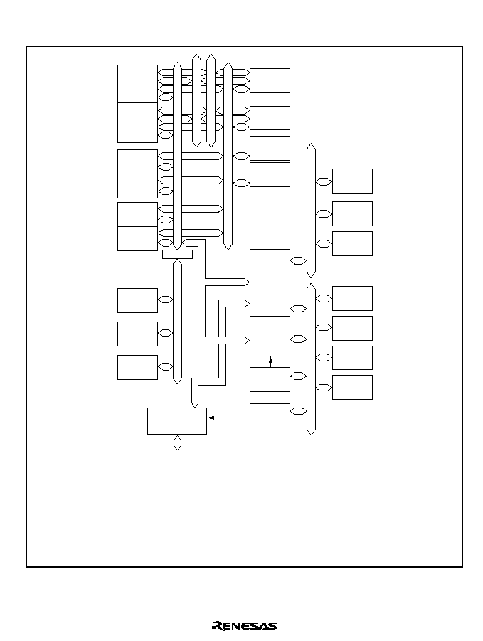
Rev. 5.0, 09/03, page 7 of 806
1.2
Block Diagram
XYCNT
XYMEM
MMU
TLB
SH3
CPU
DSP
UBC
SCI
TMU
RTC
IrDA
SCIF
ADC
DAC
AUD
DMAC
CMT
BRIDGE
I/O port
External bus
interface
BSC
CCN
CACHE
UDI
INTC
CPG/WDT
Peripheral bus 1
Peripheral bus 2
I bus 1
I bus 2
L bus
Y bus
X bus
Legend:
ADC:
AUD:
BSC:
CACHE:
CCN:
CMT:
CPG/WDT:
CPU:
DAC:
DMAC:
DSP:
UDI:
INTC:
A/D converter
Advanced user debugger
Bus state controller
Cache memory
Cache memory controller
Compare match timer
Clock pulse generator/watchdog timer
Central processing unit
D/A converter
Direct memory access controller
Digital signal processor
User debugging interface
Interrupt controller
IrDA:
MMU:
RTC:
SCI:
SCIF:
TLB:
TMU:
UBC:
XYCNT:
XYMEM:
Serial communicatiion interface (with IRDA)
Memory management unit
Realtime clock
Serial communication interface (with smart card interface)
Serial communication interface (with FIFO)
Translation look-aside buffer
Timer unit
User break controller
X/Y memory controller
X/Y memory
Figure 1.1 Block Diagram
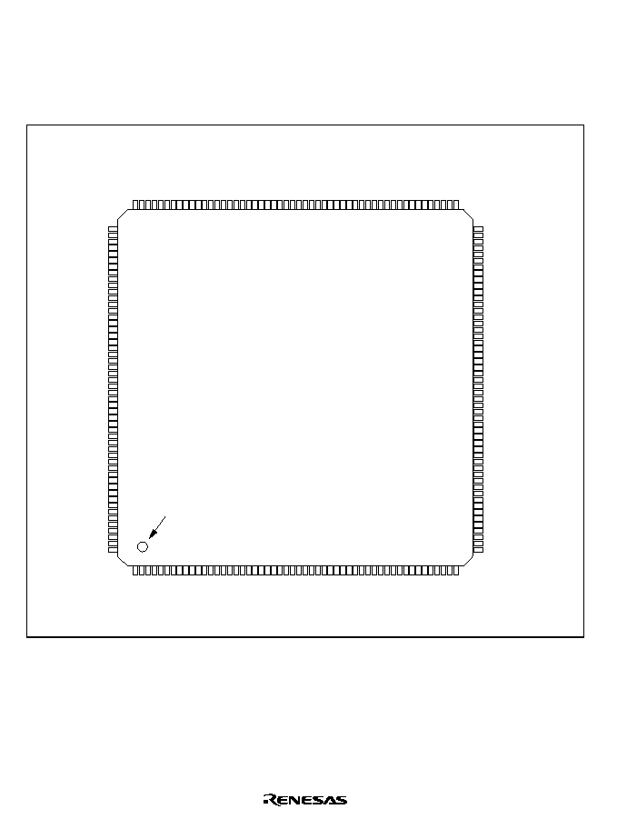
Rev. 5.0, 09/03, page 8 of 806
1.3
Pin Description
1.3.1
Pin Assignment
Figure 1.2 shows the pin arrangement of the SH7729R.
156
155
154
153
152
151
150
149
148
147
146
145
144
143
142
141
140
139
138
137
136
135
134
133
132
131
130
129
128
127
126
125
124
123
122
121
120
11
9
11
8
11
7
11
6
11
5
11
4
11
3
11
2
111
11
0
109
108
107
106
105
EXT
AL
XT
AL
V
CC
V
SS
V
SS
AUDCK/PTH[6]
V
CC
-PLL2
CAP2
V
SS
-PLL2
V
SS
-PLL1
CAP1
V
CC
-PLL1
MD0
IRLS0
/PTF[0]/PINT[8]
IRLS1
/PTF[1]/PINT[9]
IRLS2
/PTF[2]/PINT[10]
IRLS3
/PTF[3]/PINT[1
1]
TCK/PTF[4]/PINT[12]
TDI/PTF[5]/PINT[13]
TMS/PTF[6]/PINT[14]
TRST
/PTF[7]/PINT[15]
AUDA
T
A
[0]/PTG[0]
V
CC
AUDA
T
A
[1]/PTG[1]
V
SS
AUDA
T
A
[2]/PTG[2]
AUDA
T
A
[3]/PTG[3]
CKIO2/PTG[4]
ASEBRKAK
/PTG[5]
ASEMD0
/PTG[6]
IOIS16
/PTG[7]
ADTRG
/PTH[5]
RESETM WAIT BREQ BACK TDO/PTE[0] PTE[1] RAS3U
/PTE[2]
PTE[3]
PTE[6]
DACK1/PTD[7]
DACK0/PTD[5]
PTJ[5]
PTJ[4]
V
CC
Q
CASU
/PTJ[3]
V
SS
Q
CASL
/PTJ[2]
PTJ[1]
RAS3L
/PTJ[0]
CKE/PTK[5]
104
103
102
101
100
99
98
97
96
95
94
93
92
91
90
89
88
87
86
85
84
83
82
81
80
79
78
77
76
75
74
73
72
71
70
69
68
67
66
65
64
63
62
61
60
59
58
57
56
55
54
53
CE2B/PTE[5]
CE2A/PTE[4]
CS6/CE1B
CS5/CE1A/PTK[3]
CS4/PTK[2]
CS3/PTK[1]
CS2/PTK[0]
V
CC
Q
CS0/MCS[0]
V
SS
Q
AUDSYNC/PTE[7]
RD/
WR
WE3/DQMUU/ICIOWR/PTK[7]
WE2/DQMUL/ICIORD/PTK[6]
WE1/DOMLU/WE
WE0/DQMLL
RD
BS/PTK[4]
A25
V
CC
Q
A24
V
SS
Q
A23
V
CC
A22
V
SS
A21
A20
A19
A18
A17
A16
A15
V
CC
Q
A14
V
SS
Q
A13
A12
A11
A10
A9
A8
A7
A6
A5
V
CC
Q
A4
V
SS
Q
A3
A2
A1
A0
SH7729R
FP-208C
FP-208E
(Top view)
INDEX
MD1
MD2
V
CC
-R
TC
XT
AL2
EXT
AL2
V
SS
-R
TC
NMI
IRQ0/
IRL0
/PTH[0]
IRQ1/
IRL1
/PTH[1]
IRQ2/
IRL2
/PTH[2]
IRQ3/
IRL3
/PTH[3]
IRQ4/PTH[4]
D31/PTB[7]
D30/PTB[6]
D29/PTB[5]
D28/PTB[4]
D27/PTB[3]
D26/PTB[2]
V
SS
Q
D25/PTB[1]
V
CC
Q
D24/PTB[0]
D23/PT
A[7]
D22/PT
A[6]
D21/PT
A[5]
D20/PT
A[4]
V
SS
D19/PT
A[3]
V
CC
D18/PT
A[2]
D17/PT
A[1]
D16/PT
A[0]
V
SS
Q
D15
V
CC
Q
D14
D13
D12
D1
1
D10
D9
D8
D7
D6
V
SS
Q
D5
V
CC
Q
D4
D3
D2
D1
D0
1
2
3
4
5
6
7
8
9
10
11
12
13
14
15
16
17
18
19
20
21
22
23
24
25
26
27
28
29
30
31
32
33
34
35
36
37
38
39
40
41
42
43
44
45
46
47
48
49
50
51
52
STATUS0/PTJ[6]
STATUS1/PTJ[7]
TCLK/PTH[7]
IRQOUT
V
SS
Q
CKIO
V
CC
Q
TxD0/SCPT[0]
SCK0/SCPT[1]
TxD1/SCPT[2]
SCK1/SCPT[3]
TxD2/SCPT[4]
SCK2/SCPT[5]
RTS2/SCPT[6]
RxD0/SCPT[0]
RxD1/SCPT[2]
V
SS
RXD2/SCPT[4]
V
CC
CTS2/IRQ5/SCPT[7]
MCS[7]/PTC[7]/PINT[7]
MCS[6]/PTC[6]/PINT[6]
MCS[5]/PTC[5]/PINT[5]
MCS[4]/PTC[4]/PINT[4]
V
SS
Q
WAKEUP/PTD[3]
V
CC
Q
RESETOUT/PTD[2]
MCS[3]/PTC[3]/PINT[3]
MCS[2]/PTC[2]/PINT[2]
MCS[1]/PTC[1]/PINT[1]
MCS[0]/PTC[0]/PINT[0]
DRAK0/PTD[1]
DRAK1/PTD[0]
DREQ0/PTD[4]
DREQ1/PTD[6]
RESETP
CA
MD3
MD4
MD5
AV
SS
AN[0]/PTL[0]
AN[1]/PTL[1]
AN[2]/PTL[2]
AN[3]/PTL[3]
AN[4]/PTL[4]
AN[5]/PTL[5]
AV
CC
AN[6]/DA[1]/PTL[6]
AN[7]/DA[0]/PTL[7]
AV
SS
157
158
159
160
161
162
163
164
165
166
167
168
169
170
171
172
173
174
175
176
177
178
179
180
181
182
183
184
185
186
187
188
189
190
191
192
193
194
195
196
197
198
199
200
201
202
203
204
205
206
207
208
Figure 1.2 Pin Assignment (FP-208C, FP-208E)
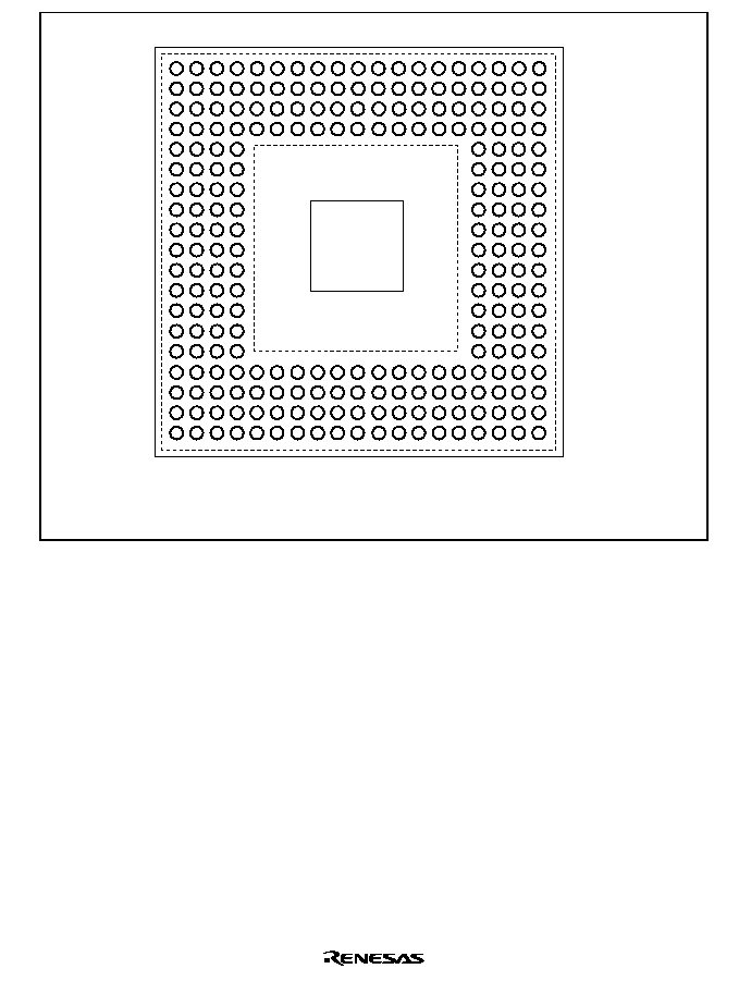
Rev. 5.0, 09/03, page 9 of 806
17
16
15
19
18
14
13
12
11
10
9
8
7
6
5
4
3
2
1
17
16
15
19
18
14
13
12
11
10
9
8
7
6
5
4
3
2
1
SH7729R
BP-240A
(Top View)
A B C D E F G H J K L M N P R T U V W
A B C D E F G H J K L M N P R T U V W
Note: The area within dotted lines shows a cutaway view of the pins.
Figure 1.3 Pin Assignment (BP-240A)

Rev. 5.0, 09/03, page 10 of 806
1.3.2
Pin Function
Table 1.3 shows the pin functions.
Table 1.3
SH7729R Pin Functions
Pin No.
FP-208C,
FP-208E
BP-240A
Pin Name
I/O
Description
1
D2
MD1
I
Clock mode setting
2
C2
MD2
I
Clock mode setting
3
E2
Vcc-RTC
*
1
--
RTC power supply V
*
3
4
D1
XTAL2
O
On-chip RTC crystal oscillator pin
5
D3
EXTAL2
I
On-chip RTC crystal oscillator
pin
*
6
6
E1
Vss-RTC
*
1
--
RTC power supply (0 V)
7
C3
NMI
I
Nonmaskable interrupt request
8
E3
IRQ0/
IRL0
/PTH[0]
I
External interrupt request/input
port H
9
E4
IRQ1/
IRL1
/PTH[1]
I
External interrupt request/input
port H
10
F1
IRQ2/
IRL2
/PTH[2]
I
External interrupt request/input
port H
11
F2
IRQ3/
IRL3
/PTH[3]
I
External interrupt request/input
port H
12
F3
IRQ4/PTH[4]
I
External interrupt request/input
port H
13
F4
D31/PTB[7]
I/O
Data bus / I/O port B
14
G1
D30/PTB[6]
I/O
Data bus / I/O port B
15
G2
D29/PTB[5]
I/O
Data bus / I/O port B
16
G3
D28/PTB[4]
I/O
Data bus / I/O port B
17
G4
D27/PTB[3]
I/O
Data bus / I/O port B
18
H1
D26/PTB[2]
I/O
Data bus / I/O port B
19
H2
VssQ
--
Input/output power supply (0 V)
20
H3
D25/PTB[1]
I/O
Data bus / I/O port B
21
H4
VccQ
--
Input/output power supply (3.3 V)
22
J1
D24/PTB[0]
I/O
Data bus / I/O port B
23
J2
D23/PTA[7]
I/O
Data bus / I/O port A

Rev. 5.0, 09/03, page 11 of 806
Pin No.
FP-208C,
FP-208E
BP-240A
Pin Name
I/O
Description
24
J4
D22/PTA[6]
I/O
Data bus / I/O port A
25
J3
D21/PTA[5]
I/O
Data bus / I/O port A
26
K2
D20/PTA[4]
I/O
Data bus / I/O port A
27
K3
Vss
--
Power supply (0 V)
--
K4
Vss
--
Power supply (0 V)
28
K1
D19/PTA[3]
I/O
Data bus / I/O port A
29
L3
Vcc
--
Power supply
*
3
--
L4
Vcc
--
Power supply
*
3
30
L2
D18/PTA[2]
I/O
Data bus / I/O port A
31
L1
D17/PTA[1]
I/O
Data bus / I/O port A
32
M4
D16/PTA[0]
I/O
Data bus / I/O port A
33
M3
VssQ
--
Input/output power supply (0 V)
34
M2
D15
I/O
Data bus
35
M1
VccQ
--
Input/output power supply (3.3 V)
36
N4
D14
I/O
Data bus
37
N3
D13
I/O
Data bus
38
N2
D12
I/O
Data bus
39
N1
D11
I/O
Data bus
40
P4
D10
I/O
Data bus
41
P3
D9
I/O
Data bus
42
P2
D8
I/O
Data bus
43
P1
D7
I/O
Data bus
44
R4
D6
I/O
Data bus
45
R3
VssQ
--
Input/output power supply (0 V)
46
T4
D5
I/O
Data bus
47
R1
VccQ
--
Input/output power supply (3.3 V)
48
T3
D4
I/O
Data bus
49
T1
D3
I/O
Data bus
50
R2
D2
I/O
Data bus
51
U2
D1
I/O
Data bus
52
T2
D0
I/O
Data bus
53
V4
A0
O
Address bus

Rev. 5.0, 09/03, page 12 of 806
Pin No.
FP-208C,
FP-208E
BP-240A
Pin Name
I/O
Description
54
V3
A1
O
Address bus
55
V5
A2
O
Address bus
56
W4
A3
O
Address bus
57
U4
VssQ
--
Input/output power supply (0 V)
58
W5
A4
O
Address bus
59
U3
VccQ
--
Input/output power supply (3.3 V)
60
U5
A5
O
Address bus
61
T5
A6
O
Address bus
62
W6
A7
O
Address bus
63
V6
A8
O
Address bus
64
U6
A9
O
Address bus
65
T6
A10
O
Address bus
66
W7
A11
O
Address bus
67
V7
A12
O
Address bus
68
U7
A13
O
Address bus
69
T7
VssQ
--
Input/output power supply (0 V)
70
W8
A14
O
Address bus
71
V8
VccQ
--
Input/output power supply (3.3 V)
72
U8
A15
O
Address bus
73
T8
A16
O
Address bus
74
W9
A17
O
Address bus
75
V9
A18
O
Address bus
76
T9
A19
O
Address bus
77
U9
A20
O
Address bus
78
V10
A21
O
Address bus
79
U10
Vss
--
Power supply (0 V)
--
T10
Vss
--
Power supply (0 V)
80
W10
A22
O
Address bus
81
U11
Vcc
--
Power supply
*
3
--
T11
Vcc
--
Power supply
*
3
82
V11
A23
O
Address bus

Rev. 5.0, 09/03, page 13 of 806
Pin No.
FP-208C,
FP-208E
BP-240A
Pin Name
I/O
Description
83
W11
VssQ
--
Input/output power supply (0 V)
84
T12
A24
O
Address bus
85
U12
VccQ
--
Input/output power supply (3.3 V)
86
V12
A25
O
Address bus
87
W12
BS
/PTK[4]
O / I/O
Bus cycle start signal / I/O port K
88
T13
RD
O
Read strobe
89
U13
WE0
/DQMLL
O
D7≠D0 select signal / DQM
(SDRAM)
90
V13
WE1
/DQMLU/
WE
O
D15≠D8 select signal / DQM
(SDRAM)
91
W13
WE2
/DQMUL/
ICIORD
/
PTK[6]
O / I/O
D23≠D16 select signal / DQM
(SDRAM) / PCMCIA I/O read /
I/O port K
92
T14
WE3
/DQMUU/
ICIOWR
/
PTK[7]
O / I/O
D31≠D24 select signal / DQM
(SDRAM) / PCMCIA I/O write /
I/O port K
93
U14
RD/
WR
O
Read/write
94
V14
AUDSYNC
/PTE[7]
O / I/O
AUD synchronous / I/O port E
95
W14
VssQ
--
Input/output power supply (0 V)
96
T15
CS0
/
MCS[0]
O
Chip select 0/mask ROM chip
select 0
97
U15
VccQ
--
Input/output power supply (3.3 V)
98
T16
CS2
/PTK[0]
O / I/O
Chip select 2 / I/O port K
99
W15
CS3
/PTK[1]
O / I/O
Chip select 3 / I/O port K
100
U16
CS4
/PTK[2]
O / I/O
Chip select 4 / I/O port K
101
W16
CS5
/
CE1A
/PTK[3]
O / I/O
Chip select 5/CE1 (area 5
PCMCIA) / I/O port K
102
V15
CS6
/
CE1B
O
Chip select 6/CE1 (area 6
PCMCIA)
103
V17
CE2A
/PTE[4]
O / I/O
CE2 (area5 PCMCIA) / I/O port E
104
V16
CE2B
/PTE[5]
O / I/O
CE2 (area6 PCMCIA) / I/O port E
105
T18
CKE/PTK[5]
O / I/O
CK enable (SDRAM) / I/O port K

Rev. 5.0, 09/03, page 14 of 806
Pin No.
FP-208C,
FP-208E
BP-240A
Pin Name
I/O
Description
106
U18
RAS3L
/PTJ[0]
O / I/O
Lower 32/64 MB address
(SDRAM) RAS / I/O port J
107
U19
PTJ[1]
I/O
I/O port J
*
5
108
R18
CASL
/PTJ[2]
O / I/O
Lower 32/64 MB address
(SDRAM) CAS / I/O port J
109
T19
VssQ
--
Input/output power supply (0 V)
110
T17
CASU
/PTJ[3]
O / I/O
Upper 32 MB address (SDRAM)
CAS / I/O port J
111
R19
VccQ
--
Input/output power supply (3.3 V)
112
U17
PTJ[4]
I/O
I/O port J
113
R17
PTJ[5]
I/O
I/O port J
114
R16
DACK0/PTD[5]
O / I/O
DMA acknowledge 0 / I/O port D
115
P19
DACK1/PTD[7]
O / I/O
DMA acknowledge 1 / I/O port D
116
P18
PTE[6]
I/O
I/O port E
117
P17
PTE[3]
I/O
I/O port E
118
P16
RAS3U
/PTE[2]
O / I/O
Upper 32 MB address (SDRAM)
RAS / I/O port E
119
N19
PTE[1]
I/O
I/O port E
120
N18
TDO/PTE[0]
O / I/O
Test data output / I/O port E
121
N17
BACK
O
Bus acknowledge
122
N16
BREQ
I
Bus request
123
M19
WAIT
I
Hardware wait request
124
M18
RESETM
I
Manual reset request
125
M17
ADTRG
/PTH[5]
I
Analog trigger / input port H
126
M16
IOIS16
/PTG[7]
I
IOIS6 (PCMCIA) / input port G
127
L19
ASEMD0
/PTG[6]
I
ASE mode
*
4
/ input port G
128
L18
ASEBRKAK
/PTG[5]
O/I
ASE break acknowledge / input
port G
129
L16
PTG[4]/CKIO2
O/I
Input port G / clock output
130
L17
AUDATA[3]/PTG[3]
I/O / O
AUD data / input port G
131
K18
AUDATA[2]/PTG[2]
I/O / O
AUD data / input port G

Rev. 5.0, 09/03, page 15 of 806
Pin No.
FP-208C,
FP-208E
BP-240A
Pin Name
I/O
Description
132
K17
Vss
--
Power supply (0 V)
--
K16
Vss
--
Power supply (0 V)
133
K19
AUDATA[1]/PTG[1]
O/I
AUD data / input port G
134
J17
Vcc
--
Power supply
*
3
--
J16
Vcc
--
Power supply
*
3
135
J18
AUDATA[0]/PTG[0]
O/I
AUD data / input port G
136
J19
TRST
/PTF[7]/PINT[15]
I
Test reset / input port F / port
interrupt
137
H16
TMS/PTF[6]/PINT[14]
I
Test mode switch / input port F /
port interrupt
138
H17
TDI/PTF[5]/PINT[13]
I
Test data input / input port F / port
interrupt
139
H18
TCK/PTF[4]/PINT[12]
I
Test clock / input port F / port
interrupt
140
H19
IRLS
3/PTF[3]/
PINT[11]
I
External interrupt request / input
port F / port interrupt
141
G16
IRLS
2/PTF[2]/
PINT[10]
I
External interrupt request / input
port F / port interrupt
142
G17
IRLS
1/PTF[1]/PINT[9]
I
External interrupt request / input
port F / port interrupt
143
G18
IRLS
0/PTF[0]/PINT[8]
I
External interrupt request / input
port F / port interrupt
144
G19
MD0
I
Clock mode setting
145
F16
Vcc-PLL1
*
2
--
PLL1 power supply
*
3
146
F17
CAP1
--
PLL1 external capacitance pin
147
F18
Vss-PLL1
*
2
--
PLL1 power supply (0 V)
148
F19
Vss-PLL2
*
2
--
PLL2 power supply (0 V)
149
E16
CAP2
--
PLL2 external capacitance pin
150
E17
Vcc-PLL2
*
2
--
PLL2 power supply
*
3
151
D16
AUDCK/PTH[6]
I
AUD clock / input port H
152
E19
Vss
--
Power supply (0 V)
153
D17
Vss
--
Power supply (0 V)
--
D19
Vss
--
Power supply (0 V)

Rev. 5.0, 09/03, page 16 of 806
Pin No.
FP-208C,
FP-208E
BP-240A
Pin Name
I/O
Description
154
E18
Vcc
--
Power supply
*
3
--
C19
Vcc
--
Power supply
*
3
155
C18
XTAL
O
Clock oscillator pin
156
D18
EXTAL
I
External clock / crystal oscillator
pin
157
B16
STATUS0/PTJ[6]
O / I/O
Processor status / I/O port J
158
B17
STATUS1/PTJ[7]
O / I/O
Processor status / I/O port J
159
B15
TCLK/PTH[7]
I/O
TMU or RTC clock input/output /
I/O port H
160
A16
IRQOUT
O
Interrupt request notification
161
C16
VssQ
--
Input/output power supply (0 V)
162
A15
CKIO
I/O
System clock input/output
163
C17
VccQ
--
Input/output power supply (3.3 V)
164
C15
TxD0/SCPT[0]
O
Transmit data 0 / SCI output port
165
D15
SCK0/SCPT[1]
I/O
Serial clock 0 / SCI I/O port
166
A14
TxD1/SCPT[2]
O
Transmit data 1 / SCI output port
167
B14
SCK1/SCPT[3]
I/O
Serial clock 1 / SCI I/O port
168
C14
TxD2/SCPT[4]
O
Transmit data 2 / SCI output port
169
D14
SCK2/SCPT[5]
I/O
Serial clock 2 / SCI I/O port
170
A13
RTS2
/SCPT[6]
O / I/O
Transmit request 2 / SCI I/O port
171
B13
RxD0/SCPT[0]
I
Transmit data 0 / SCI input port
172
C13
RxD1/SCPT[2]
I
Transmit data 1 / SCI input port
173
D13
Vss
--
Power supply (0 V)
--
A12
Vss
--
Power supply (0 V)
174
B12
RxD2/SCPT[4]
I
Transmit data 2 / SCI input port
175
C12
Vcc
--
Power supply
*
3
--
D12
Vcc
--
Power supply
*
3
176
A11
CTS2
/IRQ5/SCPT[7]
I
Transmit clear 2 / external interrupt
request / SCI input port
177
B11
MCS[7]
/PTC[7]/PINT[7]
O / I/O / I
Mask ROM chip select /
I/O port C / port interrupt

Rev. 5.0, 09/03, page 17 of 806
Pin No.
FP-208C,
FP-208E
BP-240A
Pin Name
I/O
Description
178
D11
MCS[6]
/PTC[6]/PINT[6]
O / I/O / I
Mask ROM chip select /
I/O port C / port interrupt
179
C11
MCS[5]
/PTC[5]/PINT[5]
O / I/O / I
Mask ROM chip select /
I/O port C / port interrupt
180
B10
MCS[4]
/PTC[4]/PINT[4]
O / I/O / I
Mask ROM chip select /
I/O port C / port interrupt
181
C10
VssQ
--
Input/output power supply (0 V)
182
D10
WAKEUP
/PTD[3]
O / I/O
Standby mode interrupt request
notification / I/O port D
183
A10
VccQ
--
Input/output power supply (3.3 V)
184
C9
RESETOUT
/PTD[2]
O / I/O
Reset output / I/O port D
185
D9
MCS[3]
/PTC[3]/PINT[3]
O / I/O / I
Mask ROM chip select /
I/O port C / port interrupt
186
B9
MCS[2]
/PTC[2]/PINT[2]
O / I/O / I
Mask ROM chip select /
I/O port C / port interrupt
187
A9
MCS[1]
/PTC[1]/PINT[1]
O / I/O / I
Mask ROM chip select /
I/O port C / port interrupt
188
D8
MCS[0]
/PTC[0]/PINT[0]
O / I/O / I
Mask ROM chip select /
I/O port C / port interrupt
189
C8
DRAK0/PTD[1]
O / I/O
DMA request acceptance /
I/O port D
190
B8
DRAK1/PTD[0]
O / I/O
DMA request acceptance /
I/O port D
191
A8
DREQ0
/PTD[4]
I
DMA request / input port D
192
D7
DREQ1
/PTD[6]
I
DMA request / input port D
193
C7
RESETP
I
Power-on reset request
194
B7
CA
I
Chip activate (hardware standby
request signal)
195
A7
MD3
I
Area 0 bus width setting
196
D6
MD4
I
Area 0 bus width setting
197
C6
MD5
I
Endian setting
198
B6
AVss
--
Analog power supply (0 V)
199
A6
AN[0]/PTL[0]
I
A/D converter input / input port L
200
D5
AN[1]/PTL[1]
I
A/D converter input / input port L

Rev. 5.0, 09/03, page 18 of 806
Pin No.
FP-208C,
FP-208E
BP-240A
Pin Name
I/O
Description
201
C5
AN[2]/PTL[2]
I
A/D converter input / input port L
202
D4
AN[3]/PTL[3]
I
A/D converter input / input port L
203
A5
AN[4]/PTL[4]
I
A/D converter input / input port L
204
C4
AN[5]/PTL[5]
I
A/D converter input / input port L
205
A4
AVcc
--
Analog power supply (3.3 V)
206
B5
AN[6]/DA[1]/PTL[6]
I
A/D converter input / input port L
207
B3
AN[7]/DA[0]/PTL[7]
I
A/D converter input / input port L
208
B4
AVss
--
Analog power supply (0 V)
Notes: 1. Must be connected to the power supply even when the RTC is not used.
2. Except in hardware standby mode, all power supply
pins must be connected to the
system power supply. (Supply power constantly.) In hardware standby mode, power
must be supplied at least to V
CC
≠RTC and V
SS
≠RTC. If power is not supplied to power
supply pins other than V
CC
≠RTC and V
SS
≠RTC, hold the CA pin low.
3. 2.0 V in 200 MHz models, 1.9 V in 167 MHz models, 1.8 V in 133 MHz models, 1.7 V in
100 MHz models.
4. Drive high when using the user system alone, and not using an emulator or the UDI.
When this pin is low or open,
RESETP
may be masked (see section 23 User
Debugging Interface (UDI)).
5. B2, B1, C1, U1, V1, W1, V2, W2, W3, W17, W18, W19, V18, V19, B19, A19, B18, A18,
A17, A3, A2, and A1 are NC pins. No connection should be made to these pins.
6. If EXTAL2 is not used, pull this pin up to the Vcc-RTC level.

Rev. 5.0, 09/03, page 19 of 806
Section 2 CPU
2.1
Registers
The SH7729R has the same registers as the SH-3. In addition, the SH7729R also supports the
same DSP-related registers as in the SH2-DSP. The basic software-accessible registers are divided
into four distinct groups:
∑
General registers
∑
Control registers
∑
System registers
∑
DSP registers
With the exception of a number of DSP registers, all of these registers are 32-bit width. The
general registers are accessible from user mode, with R0≠R7 banked to provide each processor
mode access to a separate set of R0≠R7 registers (i.e. R0≠R7_BANK0, and R0≠R7_BANK1). In
privileged mode, the register bank bit (RB) in the status register (SR) defines which set of banked
registers (R0≠R7_BANK0 or R0≠R7_BANK1) are accessed as general registers, and which are
accessed only by LDC/STC instructions.
The control registers can be accessed by LDC/STC instructions. The GBR, RS, RE, and MOD
registers can also be accessed in user mode. Control registers are:
∑
SR: Status register
∑
SSR: Saved status register
∑
SPC: Saved program counter
∑
GBR: Global base register
∑
VBR: Vector base register
∑
RS: Repeat start register (DSP mode only)
∑
RE: Repeat end register (DSP mode only)
∑
MOD: Modulo register (DSP mode only)
The system registers are accessed by the LDS/STS instructions (the PC is software-accessible, but
is included here because its contents are saved in, and restored from, SPC in exception handling).
The system registers are:
∑
MACH: Multiply and accumulate high register
∑
MACL: Multiply and accumulate low register
∑
PR: Procedure register
∑
PC: Program counter

Rev. 5.0, 09/03, page 20 of 806
This section explains the usage of these registers in different modes.
Figures 2.1 and 2.2 show the register configuration in each processing mode.
Switching between user mode and privileged mode is carried out by means of the operation mode
bit (MD) in the status register.
The DSP mode is switched by means of the DSP bit in the status register (see figure 2.5).

Rev. 5.0, 09/03, page 21 of 806
31
R0_BANK0
*1 *2
R1_BANK0
*2
R2_BANK0
*2
R3_BANK0
*2
R4_BANK0
*2
R5_BANK0
*2
R6_BANK0
*2
R7_BANK0
*2
R8
R9
R10
R11
R12
R13
R14
R15
SR
GBR
MACH
MACL
PR
PC
0
31
R0_BANK1
*1 *3
R1_BANK1
*3
R2_BANK1
*3
R3_BANK1
*3
R4_BANK1
*3
R5_BANK1
*3
R6_BANK1
*3
R7_BANK1
*3
R0_BANK0
*1 *4
R1_BANK0
*4
R2_BANK0
*4
R3_BANK0
*4
R4_BANK0
*4
R5_BANK0
*4
R6_BANK0
*4
R7_BANK0
*4
R8
R9
R10
R11
R12
R13
R14
R15
SR
SSR
GBR
MACH
MACL
VBR
PR
PC
SPC
0
31
R0_BANK0
*1 *4
R1_BANK0
*4
R2_BANK0
*4
R3_BANK0
*4
R4_BANK0
*4
R5_BANK0
*4
R6_BANK0
*4
R7_BANK0
*4
R0_BANK1
*1 *3
R1_BANK1
*3
R2_BANK1
*3
R3_BANK1
*3
R4_BANK1
*3
R5_BANK1
*3
R6_BANK1
*3
R7_BANK1
*3
R8
R9
R10
R11
R12
R13
R14
R15
SR
SSR
GBR
MACH
MACL
VBR
PR
PC
SPC
0
Notes: 1. The R0 register is used as an index register in indexed register indirect addressing mode
and indexed GBR indirect addressing mode.
2.
Bank
register
3.
Bank
register
Accessed as a general register when the RB bit is set to 1 in the SR register.
Accessed only by LDC/STC instructions when the RB bit is cleared to 0.
4.
Bank
register
Accessed as a general register when the RB bit is cleared to 0 in the SR register.
Accessed only by LDC/STC instructions when the RB bit is set to 1.
(a) User mode register
configuration
(b) Privileged mode register
configuration (RB = 1)
(c) Privileged mode register
configuration (RB = 0)
Figure 2.1 Register Configuration in Each Processing Mode (1)
Rev. 5.0, 09/03, page 22 of 806
39
A0G
A1G
32 31
A0
A1
M0
M1
X0
X1
Y0
Y1
DSR
RS
RE
MOD
0
(d) DSP mode register configuration (DSP = 1)
Figure 2.2 Register Configuration in Each Processing Mode (2)
Register values after a reset are shown in table 2.1.
Table 2.1
Initial Register Values
Type
Registers
Initial Value
*
General registers
R0 to R15
Undefined
Control registers
SR
MD bit = 1, RB bit = 1, BL bit = 1, I3
to I0 = 1111 (H'F), reserved bits = 0,
others undefined
GBR, SSR, SPC
Undefined
VBR
H'00000000
RS, RE
Undefined
MOD
Undefined
System registers
MACH, MACL, PR
Undefined
PC
H'A0000000
DSP registers
A0, A0G, A1, A1G, M0, M1,
X0, X1, Y0, Y1
Undefined
DSR
H'00000000
Note:
*
Initialized by a power-on or manual reset.

Rev. 5.0, 09/03, page 23 of 806
2.1.1
General Registers
There are sixteen 32-bit general registers (Rn), designated R0 to R15. The general registers are
used for data processing and address calculation.
With SuperH microcomputer type instructions, R0 is used as an index register. With a number of
instructions, R0 is the only register that can be used. R15 is used as the stack pointer (SP). In
exception handling, R15 is used to reference the stack when saving and restoring the status register
(SR) and program counter (PC).
With DSP type instructions, eight of the sixteen general registers are used for addressing of X and
Y data memory and data memory (single data) that uses the L-bus.
To access X memory, R4 and R5 are used as the X address register [Ax] and R8 is used as the X
index register [Ix]. To access Y memory, R6 and R7 are used as the Y address register [Ay] and
R9 is used as the Y index register [Iy]. To access single data that uses the L-bus, R2, R3, R4, and
R5 are used as the single data address register [As] and R8 is used as the single data index register
[Is].
Figure 2.3 shows the general registers, which are identical to those of the SH3, when DSP
extension is disabled.
31
R0
*1 *2
R1
*2
R2
*2
R3
*2
R4
*2
R5
*2
R6
*2
R7
*2
R8
R9
R10
R11
R12
R13
R14
R15
0
General Registers (when not in DSP mode)
Notes: 1. R0 functions as an index register in the
indexed register-indirect addressing mode
and indexed GBR-indirect addressing mode.
In some instructions, only R0 can be used as
the source register or destination register.
2.
R0
-R7 are banked registers. In user mode,
BANK0 is used. In privileged mode, SR.RB
specifies BANK.
SR.RB = 0; BANK0 is used
SR.RB = 1; BANK1 is used
Figure 2.3 General Purpose Registers (Not in DSP Mode)

Rev. 5.0, 09/03, page 24 of 806
On the other hand, registers R2≠R9 are also used for DSP data address calculation when DSP
extension is enabled (see figure 2.4). Other symbols that represent the purpose of the registers in
DSP type instructions is shown in [ ].
31
R0
R1
R2 [As]
R3 [As]
R4 [As, Ax]
R5 [As, Ax]
R6 [Ay]
R7 [Ay]
R8 [Ix, Is]
R9 [Iy]
R10
R11
R12
R13
R14
R15
0
General Registers (DSP mode enabled)
X or Y data transfer operation
R4, 5 [Ax]: Address register set for X data memory.
R8 [x]:
Index register for address register set Ax.
R6, 7 [Ay]: Address register set for Y data memory.
R9 [Iy]:
Index register for address register set Ay.
Single data transfer operation
R2
-5 [As]: Address register set for memory.
R8 [Is]:
Index register for address register set As.
Figure 2.4 General Purpose Registers (DSP Mode)
DSP type instructions can access X and Y data memory simultaneously. To specify addresses for
X and Y data memory, two address pointer sets are provided. These are:
R8[Ix], R4,5[Ax] for X memory access, and R9[Iy], R6,7[Ay] for Y memory access.
The symbols R2≠R9 are used by the assembler, but users can use the register name (alias) to
indicate the purpose of the register in the DSP instruction. The coding in assembler is as follows.
Ix: .REG (R8)

Rev. 5.0, 09/03, page 25 of 806
The name Ix is the alias for R8. Other aliases are as follows.
Ax0:
.REG
(R4)
Ax1:
.REG
(R5)
Ix:
.REG
(R8)
Ay0:
.REG
(R6)
Ay1:
.REG
(R7)
Iy:
.REG
(R9)
As0:
.REG
(R4)
;
This is optional, if another alias is required for single data transfer.
As1:
.REG
(R5)
;
This is optional, if another alias is required for single data transfer.
As2:
.REG
(R2)
As3:
.REG
(R3)
Is:
.REG
(R8)
;
This is optional, if another alias is required for single data transfer.
2.1.2
Control Registers
The SH7729R has 8 control registers: SR, SSR, SPC, GBR, VBR, RS, RE, and MOD (figure 2.5).
SSR, SPC, GBR and VBR are the same as the SH-3 registers.
In SR, there are six additional control bits: RC[11:0], RF0, RF1, DMX, DMY and DSP. Bits
DMX, DMY, RC[11:0], and RF[1:0] can be modified in privileged mode, privileged DSP mode,
and use DSP mode. DMX and DMY are used for modulo addressing control. If DMX is 1, the
modulo addressing mode is effective for the X memory address pointer, Ax (R4 or R5). If DMY is
1, the modulo addressing mode is effective for the Y memory address pointer, Ay (R6 or R7).
However, both X and Y address pointers cannot be operated in modulo addressing mode even
though both DMX and DMY bits are set. The case where DMX = DMY = 1 is reserved for future
expansion. Modulo addressing is available for X and Y data transfer operations (MOVX and
MOVY), but not for a single data transfer operation (MOVS).
RF1 and RF0 hold information on the number of repeat steps, and are set when a SETRC
instruction is executed. When RF[1:0] = 00, the current repeat module consists of one instruction
step. RF[1:0] = 01 means two instruction steps, RF[1:0] = 11 means three instruction steps, and
RF[1:0] = 10 means the current repeat module consists of four or more instructions.
Although RC[11:0] and RF[1:0] can be changed by a store/load to SR, use of the dedicated
manipulation instruction SETRC is recommended.

Rev. 5.0, 09/03, page 26 of 806
SR also has a 12-bit repeat counter, RC, which is used for efficient loop control. The repeat start
register (RS) and repeat end register (RE) are also provided for loop control. They hold the start
and end addresses of a loop (the contents of the RS and RE registers are slightly different from the
actual loop start and end addresses). The modulo register, MOD, is provided to implement modulo
addressing for circular data buffering. MOD holds the modulo start address (MS) and modulo end
address (ME).
In order to access RS, RE, and MOD, load/store (control register) instructions for these registers
are provided. An example for RS is as follows:
LDC Rm,RS;
Rm
RS
LDC.L @Rm+,RS;
(Rm)
RS, Rm+4
Rm
STC RS,Rn;
RS
Rn
STC.L RS,@-Rn;
Rn-4
Rn, RS
(Rn)
Address set instructions for RS and RE are also provided.
LDRS @(disp,PC); disp
◊
2 + PC
RS
LDRE @(disp,PC); disp
◊
2 + PC
RE

Rev. 5.0, 09/03, page 27 of 806
31
0 MD
RC
*
0-0
DSP
*
DMY
*
DMX
*
M
Q
I3
I2
I1
I0 RF1
*
RF0
*
S
T
RB
BL
28 27
16 15 13 12
11
10
9
8
7
6
5
4
3
2
1
0
SR (Status register)
MD bit:
Processing mode bit
MD = 1: Privileged mode
MD = 0: User mode
RB bit:
Register bank bit; used to define the general registers in privileged mode.
RB = 1:
R0_BANK1 to R7_BANK1 are used as general registers.
R0_BANK0 to R7_BANK0 accessed by LDC/STC instructions.
RB = 0:
R0_BANK0 to R7_BANK0 are used as general registers.
R0_BANK1 to R7_BANK1 accessed by LDC/STC instructions.
BL bit:
Block bit; used to mask exception in privileged mode.
BL = 1: Interrupts are masked (not accepted)
BL = 0: Interrupts are accepted
RC [11:0]: 12-bit repeat counter
DSP bit:
DSP operation mode
DSP = 1: DSP instructions (LDS Rm, DSR/A0/X0/X1/Y0/Y1,
LDS.L @Rm+, DSR/A0/X0/X1/Y0/Y1,
STS DSR/A0/X0/X1/Y0/Y1, Rn,
STS.L DSR/A0/X0/X1/Y0/Y1, @
-Rn,
LDC Rm, RS/RE/MOD,
LDC.L @Rm+, RS/RE/MOD,
STC
RS/RE/MOD,Rn,
STC.L RS/RE/MOD, @
-Rn,
LDRS, LDRE, SETRC, MOVS, MOVX, MOVY,
Pxxx) are enabled.
DSP = 0: All DSP instructions are treated as illegal instructions; only SH3 instructions are
supported.
DMY bit:
Modulo addressing enable for Y side
DMX bit:
Modulo addressing enable for X side
Q, M bit:
Used by DIV0U/S and DIV1 instructions.
I [3:0]:
4-bit field indicating the interrupt request mask level.
RF [1:0]:
Used for repeat control
S bit:
Used by the MAC instructions and DSP data.
T bit:
The MOVT, CMP/cond, TAS.TST, BT, BF, SETT, CLRT and DT instructions use the T bit to
indicate true (logic one) or false (logic zero). The ADDV/C, SUBV/C, DIV0U/S, DIV1,
NEGC, SHAR/L, SHLR/L, ROTR/L and ROTCR/L instructions also use the T bit to indicate
a carry, borrow, overflow, or underflow.
Reserved bits [bit31, bits15 to 13]: Always read as 0, and should always be written with 0.
*:
Used in DSP mode.
Figure 2.5 Control Registers
Rev. 5.0, 09/03, page 28 of 806
SSR
31
0
Saved status register
SPC
31
0
Saved program counter
GBR
31
0
Global base register
VBR
31
0
Vector base register
RS
31
0
Repeat start register
RE
31
0
Repeat end register
ME(Modulo end address)
MS(Modulo start address)
31
16 15
0
Modulo register
MOD
Saved status register (SSR)
Stores current SR value at time of exception and returns value to SR when returning to instruction
stream from exception or interrupt handler.
Saved program counter (SPC)
Stores current PC value at time of exception to indicate return address on completion of exception
handling.
Global base register (GBR)
Stores base address of GBR-indirect addressing mode. The GBR-indirect addressing mode is used for
data transfer and logical operations on the on-chip peripheral module register area.
Vector base register (VBR)
Stores base address of exception vector area.
Repeat start register (RS)
Used in DSP mode only. Indicates start address of repeat loop.
Repeat end register (RE)
Used in DSP mode only. Indicates end address of repeat loop.
Modulo register(MOD)
Used in DSP mode only.
MD[31:16] [ME]: Modulo end address, MD[15:0][MS]: Modulo start address.
In X/Y operand address generation, the CPU compares the address with ME, and if it is the same,
loads MS in either the X or Y operand address register (depending on bits DMX and DMY in the SR
register).
Figure 2.5 Control Registers (cont)

Rev. 5.0, 09/03, page 29 of 806
Details of the status register (SR) when STC/LDC instructions are used are shown below.
1. When the DSP is not operating, operation is the same as for the SH-3.
2. In privileged DSP mode, operation is the same as in privileged mode.
3. In user DSP mode, SR can be read with an STC instruction.
4. In user DSP mode, an LDC instruction can be issued for SR, but in this case DSP-related bits
are not write-protected.
Table 2.2
Operation of SR Bits in Each SH-3 DSP Mode
Privileged
Mode
User Mode
Privileged
DSP Mode
User DSP
Mode
Field
MD = 1 &
DSP = 0
MD = 0 &
DSP = 0
MD = 1 &
DSP = 1
MD = 0 &
DSP = 1
Access to
DSP-Related
Bit with
Dedicated
Instruction
Initial Value after
Reset
MD
S: OK, L: OK
S, L: Invalid
instruction
S: OK, L: OK
S: OK, L: NG
1
RB
S: OK, L: OK
S, L: Invalid
instruction
S: OK, L: OK
S: OK, L: NG
1
BL
S: OK, L: OK
S, L: Invalid
instruction
S: OK, L: OK
S: OK, L: NG
1
RC
[11:0]
S: OK, L: OK
S, L: Invalid
instruction
S: OK, L: OK
S: OK, L: OK
SETRC
instruction
000000000000
DSP
S: OK, L: OK
S, L: Invalid
instruction
S: OK, L: OK
S: OK, L: NG
0
DMX
S: OK, L: OK
S, L: Invalid
instruction
S: OK, L: OK
S: OK, L: OK
0
DMY
S: OK, L: OK
S, L: Invalid
instruction
S: OK, L: OK
S: OK, L: OK
0
Q
S: OK, L: OK
S, L: Invalid
instruction
S: OK, L: OK
S: OK, L: NG
x
M
S: OK, L: OK
S, L: Invalid
instruction
S: OK, L: OK
S: OK, L: NG
x
I[3:0]
S: OK, L: OK
S, L: Invalid
instruction
S: OK, L: OK
S: OK, L: NG
1111
RF[1:0]
S: OK, L: OK
S, L: Invalid
instruction
S: OK, L: OK
S: OK, L: OK
SETRC
instruction
x
S
S: OK, L: OK
S, L: Invalid
instruction
S: OK, L: OK
S: OK, L: NG
x
T
S: OK, L: OK
S, L: Invalid
instruction
S: OK, L: OK
S: OK, L: NG
x
Legend
S (STC): Store SR to Rn,SR->Rn
L (LDC): Load Rn to Sr,Rn->SR
OK: STC/LDC operation is enabled.
Invalid instruction: Exception occurs when an invalid instruction is executed.
NG: Previous value is retained. No change.

Rev. 5.0, 09/03, page 30 of 806
2.1.3
System Registers
The SH7729R has four system registers, MACL, MACH, PR, and PC (figure 2.6).
MACH
MACL
31
0
PR
31
0
PC
31
0
Multiply and accumulate high and low registers
(MACH/L)
Store the results of multiplicationand accumulation
operations.
Procedure register (PR)
Stores the subroutine procedure return address.
Program counter (PC)
Indicates the start address of the current instruction.
Figure 2.6 System Registers
The DSR, A0, X0, X1, Y0, and Y1 registers are also treated as system registers. Therefore,
instructions for data transfer between general registers and system registers are supported for these
registers.
2.1.4
DSP Registers
The SH7729R has eight data registers and one status register as DSP registers (figure 2.7). The
data registers are 32-bit width with the exception of registers A0 and A1. Registers A0 and A1
include 8 guard bits (fields A0G and A1G), giving them a total width of 40 bits.
Three kinds of operation access the DSP data registers. The first is DSP data processing. When a
DSP fixed-point data operation uses A0 or A1 as the source register, it uses the guard bits (bits
39≠32). When it uses A0 or A1 as the destination register, guard bits 39≠32 are valid. When a DSP
fixed-point data operation uses a DSP register other than A0 or A1 as the source register, it sign-
extends the source value to bits 39≠32. When it uses one of these registers as the destination
register, bits 39≠32 of the result are discarded.
The second kind of operation is an X or Y data transfer operation,
"
MOVX.W MOVY.W". This
operation accesses the X and Y memories through the 16-bit X and Y data buses (figure 2.8). The
register to be loaded or stored by this operation always comprises the upper 16 bits (bits 31≠16).
X0 or X1 can be the destination of an X memory load and Y0 or Y1 can be the destination of a Y
memory load, but no other register can be the destination register in this operation. When data is
read into the upper 16 bits of a register (bits 31≠16), the lower 16 bits of the register (bits 15≠0)
are automatically cleared.
A0 and A1 can be stored in the X or Y memory using the X or Y data transfer instructions
MOVX.W and MOVY.W, but no other registers can be stored.
Rev. 5.0, 09/03, page 31 of 806
The third kind of operation is a single-data transfer instruction, "MOVS.W" or "MOVS.L". These
instructions access any memory location through the LDB (figure 2.8). All DSP registers connect
to the LDB and can be the source or destination register of the data transfer. These instructions
have word and longword access modes. In word mode, registers to be loaded or stored by this
instruction comprise the upper 16 bits (bits 31≠16) for DSP registers except A0G and A1G. When
data is loaded into a register other than A0G and A1G in word mode, the lower half of the register
is cleared. When A0 or A1 is used, the data is sign-extended to bits 39≠32 and the lower half is
cleared. When A0G or A1G is the destination register in word mode, data is loaded into an 8-bit
register, but A0 or A1 is not cleared. In longword mode, when the destination register is A0 or A1,
it is sign-extended to bits 39≠32.
Tables 2.3 and 2.4 show the data type of registers used in DSP instructions. Some instructions
cannot use some registers shown in the tables because of instruction code limitations. For
example, PMULS can use A1 as the source register, but cannot use A0. These tables ignore details
of register selectability.
Table 2.3
Destination Register in DSP Instructions
Guard Bits
Register Bits
Registers
Instructions
39
32 31
16 15
0
A0, A1
DSP
Fixed-point, PSHA,
PMULS
Sign-extended 40-bit result
Integer, PDMSB
Sign-extended 24-bit result
Cleared
Logical, PSHL
Cleared
16-bit result
Cleared
MOVS.W
Sign-extended 16-bit data
Cleared
Data
transfer
MOVS.L
Sign-extended 32-bit data
A0G, A1G
MOVS.W
Data
No update
Data
transfer
MOVS.L
Data
No update
DSP
Fixed-point, PSHA,
PMULS
32-bit result
Integer, logical,
PDMSB, PSHL
16-bit result
Cleared
MOVX/Y.W, MOVS.W
16-bit result
Cleared
X0, X1
Y0, Y1
M0, M1
Data
transfer
MOVS.L
32-bit data
Rev. 5.0, 09/03, page 32 of 806
Table 2.4
Source Register in DSP Operations
Guard Bits
Register Bits
Registers
Instructions
39
32 31
16 15
0
A0, A1
DSP
Fixed-point, PDMSB,
PSHA
40-bit data
Integer
24-bit data
Logical, PSHL, PMULS
16-bit data
MOVX/Y.W, MOVS.W
16-bit data
Data
transfer
MOVS.L
32-bit data
A0G, A1G
MOVS.W
Data
Data
transfer
MOVS.L
Data
DSP
Fixed-point, PDMSB,
PSHA
Sign
*
32-bit data
Integer
Sign
*
16-bit data
Logical, PSHL, PMULS
16-bit data
MOVS.W
16-bit data
X0, X1
Y0, Y1
M0, M1
Data
transfer
MOVS.L
32-bit data
Note:
*
The data is sign-extended and input to the ALU.
31
32
39
A0
A0G
A1G
A1
M0
M1
X0
X1
Y0
Y1
0
1
2
3
4
5
6
7
DC
CS [2:0]
V
N
Z
GT
8
31
0
(a) DSP Data Registers
(b) DSP Status Register (DSR)
Reset status
DSR: All
zeros
Others: Undefined
Figure 2.7 DSP Registers

Rev. 5.0, 09/03, page 33 of 806
Table 2.5
DSR Register Bits
Bits
Name (Abbreviation)
Function
31≠8
Reserved bits
0: Always read as 0; always use 0 as the write value
7
Signed Greater Than bit
(GT)
Indicates that the operation result is positive (except
0), or that operand 1 is greater than operand 2
1: Operation result is positive, or operand 1 is greater
than operand 2
6
Zero bit (Z)
Indicates that the operation result is zero (0), or that
operand 1 is equal to operand 2
1: Operation result is zero (0), or operand 1 is equal
to operand 2
5
Negative bit (N)
Indicates that the operation result is negative, or that
operand 1 is smaller than operand 2
1: Operation result is negative, or operand 1 is
smaller than operand 2
4
Overflow bit (V)
Indicates that the operation result has overflowed
1: Operation result has overflowed
3≠1
Condition Select bits (CS) Designate the mode for selecting the operation result
status to be set in the DC bit
Do not set these bits to 110 or 111
000: Carry/borrow mode
001: Negative value mode
010: Zero mode
011: Overflow mode
100: Signed greater mode
101: Signed greater than or equal to mode
0
DSP Condition bit (DC)
Sets the status of the operation result in the mode
designated by the CS bits
0: Designated mode status has not occurred (false)
1: Designated mode status has occurred
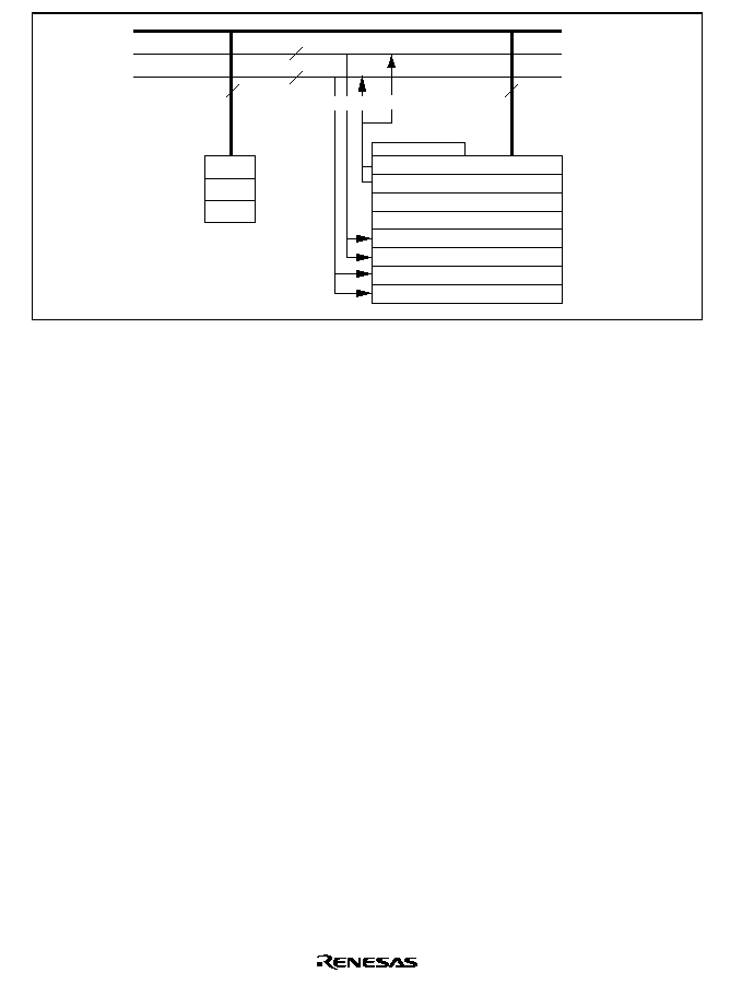
Rev. 5.0, 09/03, page 34 of 806
A0G
32
0
39
31
16
A0
A1
M0
M1
X0
X1
Y0
Y1
0
7
A1G
DSR
16 bit
16 bit
8 bit
32 bit
LDB
XDB
YDB
MOVX.W
MOVS.W,
MOVS.L
MOVS.W,
MOVS.L
MOVY.W
Figure 2.8 Connections of DSP Registers and Buses
The DSP unit has one DSP status register (DSR). DSR holds the status of DSP data operation
results (zero, negative, and so on) and has a DC bit which is similar to the T bit in the CPU. The
DC bit indicates one of the status flags. A DSP data processing instruction controls its execution
based on the DC bit. This control affects only the operations in the DSP unit; it controls the update
of DSP registers only. It cannot control operations in the CPU, such as address register updating
and load/store operations. Control bits CS[2:0] specify the condition to be reflected in the DC bit.
Unconditional DSP type data operations, except PMULS, MOVX, MOVY and MOVS, update the
condition flags and DC bit, but no CPU instructions, including MAC instructions, update the DC
bit. Conditional DSP type instructions do not update DSR either.
DSR is assigned as a system register and the following load/store instructions are provided:
STS DSR,Rn;
STS.L DSR,@-Rn;
LDS Rn,DSR;
LDS.L @Rn+,DSR;
When DSR is read by an STS instruction, the upper bits (bits 31 to 8) are all 0.

Rev. 5.0, 09/03, page 35 of 806
2.2
Data Formats
2.2.1
Register Data Format (Non-DSP Type)
Register operands are always longwords (32 bits) (figure 2.9). When the memory operand is only
a byte (8 bits) or a word (16 bits), it is sign-extended into a longword when loaded into a register.
31
0
Longword
Figure 2.9 Longword Operand
2.2.2
DSP-Type Data Formats
The SH7729R has several different data formats that depend on the instruction. This section
explains the data formats for DSP type instructions.
Figure 2.10 shows three DSP-type data formats with different binary point positions. A CPU-type
data format with the binary point to the right of bit 0 is also shown for reference.
The DSP-type fixed point data format has the binary point between bit 31 and bit 30. The DSP-
type integer format has the binary point between bit 16 and bit 15. The DSP-type logical format
does not have a binary point. The valid data lengths of the data formats depend on the instruction
and the DSP register.
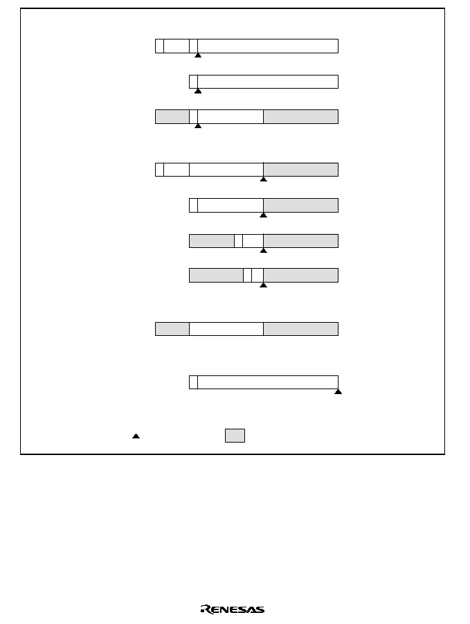
Rev. 5.0, 09/03, page 36 of 806
39
S
31 30
0
-2
8
to +2
8
- 2
-31
39
S
32 31
0
-2
23
to +2
23
- 1
39
S
S
31 30
16 15
16 15
0
-1 to +1 - 2
-15
39
31
16 15
0
S
31
0
-2
15
to +2
15
- 1
16 15
31
22
0
-32 to +32
16 15
S
31
21
0
-16 to +16
16 15
S
31 30
0
-1 to +1 - 2
-31
S
31
0
-2
31
to +2
31
- 1
DSP type fixed point
With guard bits
Without guard bits
Multiplier input
DSP type integer
DSP type logical
With guard bits
CPU type integer
S: Sign bit
Longword
: Binary point
: Does not affect the operations
Without guard bits
Shift amount for
arithmetic shift (PSHA)
Shift amount for
logical shift (PSHL)
Figure 2.10 Data Formats
The shift amount for the arithmetic shift (PSHA) instruction has a 7-bit field that can represent
values from ≠64 to +63, but ≠32 to +32 are valid numbers for the instruction. Also the shift
amount for a logical shift operation has a 6-bit field, but ≠16 to +16 are valid numbers for the
instruction.
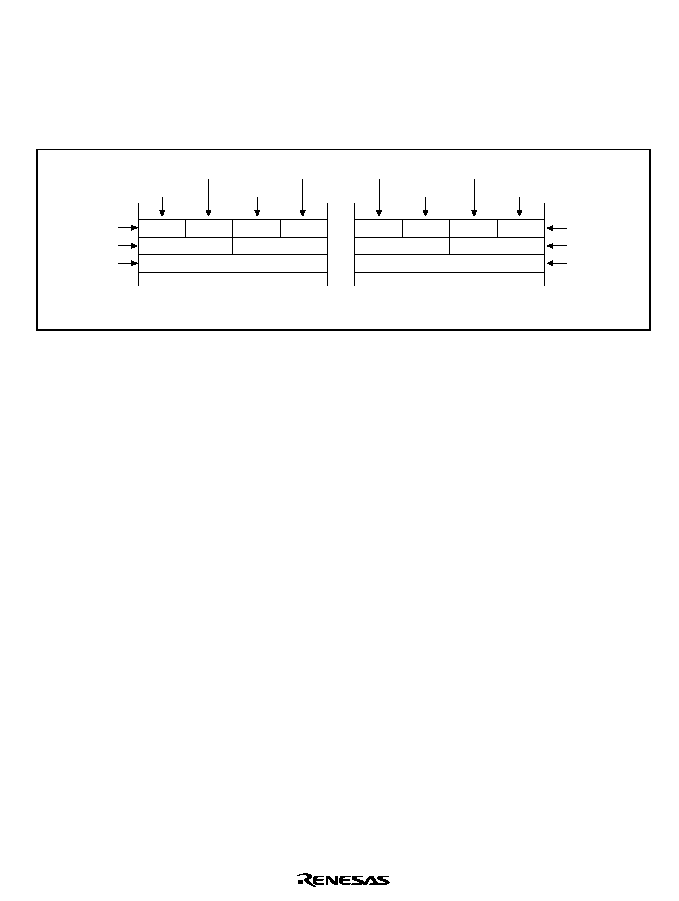
Rev. 5.0, 09/03, page 37 of 806
2.2.3
Memory Data Formats
Memory data formats are classified into byte, word, and longword. Byte data can be accessed from
any address, but an address error will occur if word data starting from an address other than 2n or
longword data starting from an address other than 4n is accessed. In such cases, the data accessed
cannot be guaranteed (figure 2.11).
31
0
15
23
7
Byte 0
Byte 1
Byte 2
Byte 3
Word 1
Word 0
Address A + 4
Address A + 8
Longword
Address A
Address A
Address A + 2
Address A + 1
Address A + 3
Big-endian mode
31
0
15
23
7
Byte 3
Byte 2
Byte 1
Byte 0
Word 0
Word 1
Address A + 4
Address A
Longword
Address A + 8
Address A + 11
Address A + 9
Address A + 10
Address A + 8
Little-endian mode
Figure 2.11 Byte, Word, and Longword Alignment
Either big-endian or little-endian byte order can be selected for the data format, according to the
MD5 pin at reset. When MD5 is low at reset, this LSI operates in big-endian mode. When MD5 is
high at reset, this LSI operates in little-endian mode.
2.3
Features of CPU Core Instructions
The CPU core instructions are RISC-type instructions with the following features:
Fixed 16-Bit Length: All instructions have a fixed length of 16 bits. This improves program code
efficiency.
One Instruction per State: Pipelining is used, and basic instructions can be executed in one state.
Data Size: The basic data size for operations is longword. Byte, word, or longword can be
selected as the memory access size. Memory byte or word data is sign-extended and operated on
as longword data. Immediate data is sign-extended to longword size for arithmetic operations or
zero-extended to longword size for logical operations.

Rev. 5.0, 09/03, page 38 of 806
Table 2.6
Word Data Sign Extension
SH7729R CPU
Description
Example of Other CPU
MOV.W @(disp,PC),R1
ADD
R1,R0
........
.DATA.W H'1234
R1 sign-extended to 32 bits,
becomes H'00001234, and is
then operated on by the ADD
instruction.
ADD.W #H'1234,R0
Note:
Immediate data is referenced by @(disp,PC).
Load/Store Architecture: Basic operations are executed between registers. In operations
involving memory, data is first loaded into a register (load/store architecture). However, bit
manipulation instructions such as AND are executed directly on memory.
Delayed Branching: Unconditional branch instructions, etc., are executed as delayed branches.
With a delayed branch instruction, the branch is made after execution of the instruction (called the
slot instruction) immediately following the delayed branch instruction. This minimizes disruption
of the pipeline when a branch is made.
With a delayed branch, the actual branch operation occurs after execution of the slot instruction.
However, instruction execution for register updating, etc., excluding the branch operation, is
performed in delayed branch instruction
delay slot instruction order. For example, even though
the contents of the register holding the branch destination address are changed in the delay slot,
the branch destination address remains as the register contents prior to the change.
Table 2.7
Delayed Branch Instructions
SH7729R CPU
Description
Example of Other CPU
BRA
TRGET
ADD
R1,R0
ADD is executed before branch to
TRGET.
ADD.W R1,R0
BRA
TRGET
Multiply/Multiply-and-Accumulate Operations: A 16
◊
16
32 multiply operation is
executed in 1 to 3 states, and a 16
◊
16 + 64
64 multiply-and-accumulate operation in 2 to 3
states. A 32
◊
32
64 multiply operation and a 32
◊
32 + 64
64 multiply-and-accumulate
operation are each executed in 2 to 5 states.

Rev. 5.0, 09/03, page 39 of 806
T Bit: The result of a comparison is indicated by the T bit in the status register (SR), and a
conditional branch is performed according to whether the result is True or False.
Table 2.8
T Bit
SH7729R CPU
Description
Example of Other CPU
CMP/GE
R1,R0
BT
TRGET0
BF
TRGET1
If R0
R1, the T bit is set.
A branch is made to TRGET0
if R0
R1, or to TRGET1 if R0 < R1.
CMP.W R1,R0
BGE
TRGET0
BLT
TRGET1
ADD
#≠1,R0
CMP/EQ #0,R0
BT
TRGET
The T bit is not set by ADD.
If R0 = 0, the T bit is set.
A branch is made if R0 = 0.
SUB.W #1,R0
BEQ TRGET
Immediate Data: Byte immediate data is placed inside the instruction code. Word and longword
immediate data is not placed inside the instruction code, but in a table in memory. The table in
memory is referenced with an immediate data transfer instruction (MOV) using PC-relative
addressing mode with displacement.
Table 2.9
Immediate Data Referencing
Type
SH7729R CPU
Example of Other CPU
8-bit immediate
MOV
#H'12,R0
MOV.B
#H'12,R0
16-bit immediate
MOV.W
@(disp,PC),R0
........
.DATA.W H'1234
MOV.W
#H'1234,R0
32-bit immediate
MOV.L
@(disp,PC),R0
........
.DATA.L H'12345678
MOV.L
#H'12345678,R0
Note:
Immediate data is referenced by @(disp,PC).

Rev. 5.0, 09/03, page 40 of 806
Absolute Addresses: When data is referenced by absolute address, the absolute address value is
placed in a table in memory beforehand. Using the method whereby immediate data is loaded
when an instruction is executed, this value is transferred to a register and the data is referenced
using register indirect addressing mode.
Table 2.10
Absolute Address Referencing
Type
SH7729R CPU
Example of Other CPU
Absolute address
MOV.L
@(disp,PC),R1
MOV.B
@R1,R0
........
.DATA.L H'12345678
MOV.B @H'12345678,R0
16-Bit/32-Bit Displacement: When data is referenced with a 16- or 32-bit displacement, the
displacement value is placed in a table in memory beforehand. Using the method whereby
immediate data is loaded when an instruction is executed, this value is transferred to a register and
the data is referenced using indexed register indirect addressing mode.
Table 2.11
Displacement Referencing
Type
SH7729R CPU
Example of Other CPU
16-bit displacement
MOV.W
@(disp,PC),R0
MOV.W
@(R0,R1),R2
........
.DATA.W H'1234
MOV.W
@(H'1234,R1),R2
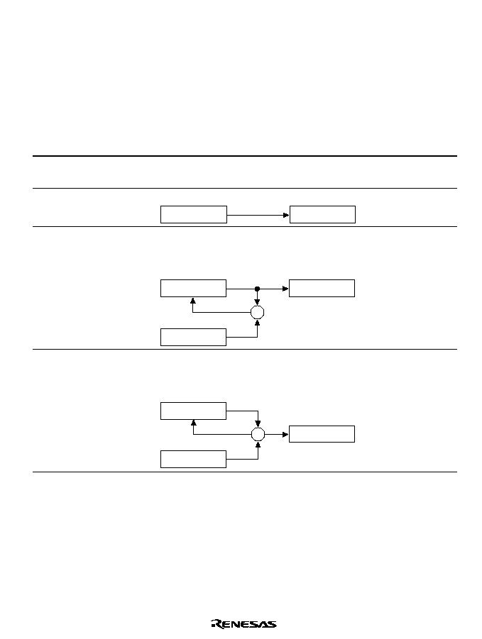
Rev. 5.0, 09/03, page 41 of 806
2.4
Instruction Formats
2.4.1
CPU Instruction Addressing Modes
The following table shows addressing modes and effective address calculation methods for
instructions executed by the CPU core.
Table 2.12
Addressing Modes and Effective Addresses for CPU Instructions
Addressing
Mode
Instruction
Format
Effective Address Calculation Method
Calculation
Formula
Register
direct
Rn
Effective address is register Rn.
(Operand is register Rn contents.)
--
Register
indirect
@Rn
Effective address is register Rn contents.
Rn
Rn
Rn
Register
indirect with
post-increment
@Rn+
Effective address is register Rn contents. A
constant is added to Rn after instruction
execution: 1 for a byte operand, 2 for a word
operand, 4 for a longword operand.
Rn
Rn
1/2/4
+
Rn + 1/2/4
Rn
After instruction
execution
Byte: Rn + 1
Rn
Word: Rn + 2
Rn
Longword: Rn + 4
Rn
Register
indirect with
pre-decrement
@≠Rn
Effective address is register Rn contents,
decremented by a constant beforehand: 1 for a
byte operand, 2 for a word operand, 4 for a
longword operand.
Rn
1/2/4
Rn
- 1/2/4
-
Rn
- 1/2/4
Byte: Rn ≠ 1
Rn
Word: Rn ≠ 2
Rn
Longword: Rn ≠ 4
Rn
(Instruction
executed with Rn
after calculation)
Rev. 5.0, 09/03, page 42 of 806
Addressing
Mode
Instruction
Format
Effective Address Calculation Method
Calculation
Formula
Register
indirect with
displacement
@(disp:4,
Rn)
Effective address is register Rn contents with
4-bit displacement disp added. After disp is
zero-extended, it is multiplied by 1 (byte), 2
(word), or 4 (longword), according to the
operand size.
Rn
1/2/4
+
◊
disp
(zero-extended)
Rn
+ disp ◊ 1/2/4
Byte: Rn + disp
Word: Rn + disp
◊
2
Longword: Rn +
disp
◊
4
Indexed
register indirect
@(R0, Rn) Effective address is sum of register Rn and R0
contents.
Rn
R0
Rn
+ R0
+
Rn + R0
GBR indirect
with
displacement
@(disp:8,
GBR)
Effective address is register GBR contents with
8-bit displacement disp added. After disp is
zero-extended, it is multiplied by 1 (byte), 2
(word), or 4 (longword), according to the
operand size.
GBR
1/2/4
+
◊
disp
(zero-extended)
GBR
+ disp ◊ 1/2/4
Byte: GBR + disp
Word: GBR + disp
◊
2
Longword: GBR +
disp
◊
4
Rev. 5.0, 09/03, page 43 of 806
Addressing
Mode
Instruction
Format
Effective Address Calculation Method
Calculation
Formula
Indexed GBR
indirect
@(R0,
GBR)
Effective address is sum of register GBR and
R0 contents.
GBR
R0
GBR
+ R0
+
GBR + R0
PC-relative with
displacement
@(disp:8,
PC)
Effective address is PC with 8-bit displacement
disp added. After disp is zero-extended, it is
multiplied by 2 (word) or 4 (longword), according
to the operand size. With a longword operand,
the lower 2 bits of PC are masked.
PC
H'FFFFFFFC
+
2/4
◊
&
*
*: With longword operand
disp
(zero-extended)
PC
+ disp ◊ 2
or
PC&H'FFFFFFFC
+ disp ◊ 4
Word: PC + disp
◊
2
Longword:
PC&H'FFFFFFFC
+ disp
◊
4
Rev. 5.0, 09/03, page 44 of 806
Addressing
Mode
Instruction
Format
Effective Address Calculation Method
Calculation
Formula
PC-relative
disp:8
Effective address is PC with 8-bit displacement
disp added after being sign-extended and
multiplied by 2.
PC
2
+
◊
disp
(sign-extended)
PC
+ disp ◊ 2
PC + disp
◊
2
disp:12
Effective address is PC with 12-bit displacement
disp added after being sign-extended and
multiplied by 2
PC
2
+
◊
disp
(sign-extended)
PC
+ disp ◊ 2
PC + disp
◊
2
Rn
Effective address is sum of PC and Rn.
PC
Rn
+
PC
+ Rn
PC + Rn
Immediate
#imm:8
8-bit immediate data imm of TST, AND, OR,
or XOR instruction is zero-extended.
--
#imm:8
8-bit immediate data imm of MOV, ADD, or
CMP/EQ instruction is sign-extended.
--
#imm:8
8-bit immediate data imm of TRAPA instruction
is zero-extended and multiplied by 4.
--

Rev. 5.0, 09/03, page 45 of 806
2.4.2
DSP Data Addressing
Two different memory accesses are made with DSP instructions. The two kinds of instructions are
X and Y data transfer instructions (MOVX.W, MOVY.W) and single data transfer instructions
(MOVS.W, MOVSL). The data addressing is different for these two kinds of instruction. An
overview of the data transfer instructions is given in table 2.13.
Table 2.13
Overview of Data Transfer Instructions
X/Y Data Transfer Processing
(MOVX.W, MOVY.W)
Single Data Transfer Processing
(MOVS.W, MOVS.L)
Address register
Ax: R4, R5, Ay: R6, R7
As: R2, R3, R4, R5
Index register
Ix: R8, Iy: R9
Is: R8
Addressing
Nop/Inc (+2)/index addition:
post-increment
Nop/Inc (+2, +4)/index addition:
post-increment
--
Dec (≠2, ≠4): pre-decrement
Modulo addressing
Possible
Not possible
Data bus
XDB, YDB
LDB
Data length
16 bits (word)
16/32 bits (word/longword)
Bus contention
No
Yes
Memory
X/Y data memory
Entire memory space
Source register
Dx, Dy: A0, A1
Ds: A0/A1, M0/M1, X0/X1, Y0/Y1,
A0G, A1G
Destination register
Dx: X0/X1, Dy: Y0/Y1
Ds: A0/A1, M0/M1, X0/X1, Y0/Y1,
A0G, A1G
X/Y Data Addressing: With DSP instructions, the X and Y data memory can be accessed
simultaneously using the MOVX.W and MOVY.W instructions. Two address pointers are
provided for DSP instructions to enable simultaneous access to X and Y data memory. Only
pointer addressing can be used with DSP instructions; immediate addressing is not available.
Address registers are divided into two, with register R4 or R5 functioning as the X memory
address register (Ax), and register R6 or R7 as the Y memory address register (Ay). The following
three kinds of addressing can be used with X and Y data transfer instructions.
1. Non-update address register addressing:
The Ax and Ay registers are address pointers. They are not updated.
2. Addition index register addressing:
The Ax and Ay registers are address pointers. After a data transfer, the value of the Ix or Iy
register is added to each (post-increment).
Rev. 5.0, 09/03, page 46 of 806
3. Increment address register addressing:
The Ax and Ay registers are address pointers. After a data transfer, they are each incremented
by 2 (post-increment).
There is an index register for each address pointer. The R8 register is the index register (Ix) for the
X memory address register (Ax), and the R9 register is the index register (Iy) for the Y memory
address register (Ay).
The X and Y data transfer instructions perform word-length processing, and use 16-bit access to
the X/Y data memory. A value of 2 is therefore added to the address register in the increment
processing. To perform decrementing, ≠2 is set in the index register and addition index register
addressing is specified. In X/Y data addressing, only bits 1 to 15 of the address pointer are valid.
When using X/Y data addressing, 0 must always be written to bit 0 of the address pointer and
index register.
X/Y data transfer addressing is shown in figure 2.12. When accessing X and Y memory using the
X and Y buses, the upper word of Ax (R4 or R5) and Ay (R6 or R7) is ignored. The result of
@AY+ or @Ay+Iy is stored in the lower word of Ay, while the upper word retains its original
value.
ALU
AU
R8[Ix]
R4[Ax]
R5[Ax]
R9[Iy]
R6[Ay]
R7[Ay]
+2 (INC)
+0 (no update)
+2 (INC)
+0 (no update)
Note: Three address processing methods:
1. Increment
2. Index register addition (Ix/Iy)
3. No increment
Post-updating is used in all cases.
The address pointer can be decremented by setting
-2/-4 in the index register.
AU: Adder provided
for DSP addressing
Figure 2.12 X and Y Data Transfer Addressing
Single Data Addressing: DSP instructions include two single data transfer instructions
(MOVS.W, MOVS.L) that load data into, or store data from, a DSP register. With these
instructions, one of registers R2 to R5 is used as the single data transfer address register (As).
The following four kinds of addressing can be used with single data transfer instructions.
Rev. 5.0, 09/03, page 47 of 806
1. Non-update address register addressing:
The As register is an address pointer. It is not updated.
2. Addition index register addressing:
The As register is an address pointer. After a data transfer, the value of the Is register is added
to the As register (post-increment).
3. Increment address register addressing:
The As register is an address pointer. After a data transfer, the As register is incremented by 2
or 4 (post-increment).
4. Decrement address register addressing:
The As register is an address pointer. Before a data transfer, ≠2 or ≠4 is added to the As
register (i.e. 2 or 4 is subtracted) (pre-decrement).
The R8 register is the index register (Is) for the address pointer (As). Single data transfer
addressing is shown in figure 2.13.
ALU
R8[Is]
R4[As]
R5[As]
-2/-4 (DEC)
+2/+4 (INC)
+0 (no update)
R3[As]
R2[As]
31
0
31
0
LAB
32
Note: Four address processing methods:
1. No update
2. Index register addition (Is)
3. Increment
4. Decrement
Post-increment
Pre-decrement
Figure 2.13 Single Data Transfer Addressing
Modulo Addressing: Like other DSPs, the SH7729R has a modulo addressing mode. Address
registers are updated in the same way in this mode. When the address pointer value reaches the
preset modulo end address, the address pointer value becomes the modulo start address.
Modulo addressing is only available for the X and Y data transfer instructions (MOVX.W,
MOVY.W). Modulo addressing mode is specified for the X address register by setting the DMX
bit in the SR register, and for the Y address register by setting the DMY bit. Modulo addressing is
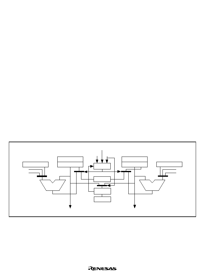
Rev. 5.0, 09/03, page 48 of 806
valid for either the X or the Y address register, only; it cannot be set for both at the same time.
Therefore, DMX and DMY cannot both be set simultaneously.
The MOD register is provided to set the start and end addresses of the modulo address area. The
MOD register contains MS (Modulo Start) and ME (Modulo End). An example of the use of the
MOD register (MS and ME fields) is shown below.
MOV.L ModAddr,Rn;
Rn=ModEnd, ModStart
LDC Rn,MOD;
ME=ModEnd, MS=ModStart
ModAddr:
.DATA.W ModEnd
.DATA.W ModStart
ModStart: .DATA
:
ModEnd:
.DATA
The start and end addresses are specified in MS and ME, then the DMX or DMY bit is set to 1.
The address register contents are compared with ME, and if they match, start address MS is stored
in the address register. The lower 16 bits of the address register are compared with ME.
The maximum modulo size is 64 kbytes. This is sufficient to access the X and Y data memory. A
block diagram of modulo addressing is shown in figure 2.14.
ALU
AU
R8[Ix]
R9[Iy]
R6[Ay]
R7[Ay]
+2
+0
31 0
R4[Ax]
R5[Ax]
31 16 15 0
XAB
+2
+0
31 0
31 16 15 0
YAB
DMX DMY
CONT
MS
CMP
ME
15 1
15 1
Instruction (MOVX/MOVY)
Figure 2.14 Modulo Addressing
An example of modulo addressing is given below.
MS = H'7008; ME=H'700C; R4=H'A5007008;
DMX = 1; DMY = 0:
(Modulo addressing setting for address register Ax (R4, R5))

Rev. 5.0, 09/03, page 49 of 806
As a result of the above settings, the R4 register changes as follows.
R4: H'A5007008
Inc.
R4: H'A500700A
Inc.
R4: H'A500700C
Inc.
R4: H'A5007008
(Reaches modulo end address, so becomes modulo start address)
Place the data so that the upper 16 bits of the modulo start and end addresses are the same. This is
because the modulo start address overwrites only the lower 15 bits of the address register,
excluding bit 0.
Note:
When addition indexing is used for DSP data addressing, the address pointer may exceed
the ME value without actually reaching it. In this case, the address pointer will not return
to the modulo start address. Not only with modulo addressing, but when X and Y data
addressing is used, bit 0 is ignored. 0 must always be written to bit 0 of the address
pointer, index register, MS, and ME.
2.4.3
CPU Instruction Formats
Table 2.14 shows the instruction formats, and the meaning of the source and destination operands,
for instructions executed by the CPU core. The meaning of the operands depends on the
instruction code. The following symbols are used in the table.
xxxx:
Instruction code
mmmm: Source register
nnnn:
Destination register
iiii:
Immediate data
dddd:
Displacement

Rev. 5.0, 09/03, page 50 of 806
Table 2.14
CPU Instruction Formats
Instruction Format
Source
Operand
Destination
Operand
Sample Instruction
0 type
xxxx
xxxx
xxxx
xxxx
15
0
--
--
NOP
--
nnnn
: register
direct
MOV T Rn
Control register or
system register
nnnn
: register
direct
STS
MACH,Rn
n type
xxxx
xxxx
xxxx
nnnn
15
0
Control register or
system register
nnnn
: pre-
decrement register
indirect
STC.L
SR,@-Rn
mmmm
: register
direct
Control register or
system register
LDC
Rm,SR
m type
xxxx
mmmm
xxxx
xxxx
15
0
mmmm
: post-
increment register
indirect
Control register or
system register
LDC.L
@Rm+,SR
mmmm
: register
indirect
--
JMP
@Rm
PC-relative using
Rm
--
BRAF
Rm

Rev. 5.0, 09/03, page 51 of 806
Instruction Format
Source
Operand
Destination
Operand
Sample Instruction
mmmm
: register
direct
nnnn
: register
direct
ADD
Rm,Rn
nm type
nnnn
xxxx
xxxx
15
0
mmmm
mmmm
: register
indirect
nnnn
: register
indirect
MOV.L Rm,@Rn
mmmm
: post-
increment register
indirect (multiply-
and-accumulate
operation)
nnnn
:
*
post-
increment register
indirect (multiply-
and-accumulate
operation)
MACH, MACL
MAC.W @Rm+,@Rn+
mmmm
: post-
increment register
indirect
nnnn
: register
direct
MOV.L @Rm+,Rn
mmmm
: register
direct
nnnn
: pre-
decrement register
indirect
MOV.L Rm,@-Rn
mmmm
: register
direct
nnnn
: indexed
register indirect
MOV.L Rm,@(R0,Rn)
md type
xxxx
dddd
15
0
mmmm
xxxx
mmmmdddd
:
register indirect
with displacement
R0 (register direct) MOV.B @(disp,Rm),R0
nd4 type
dddd
nnnn
xxxx
15
0
xxxx
R0 (register direct)
nnnndddd
:
register indirect
with displacement
MOV.B R0,@(disp,Rn)
mmmm
: register
direct
nnnndddd
:
register indirect
with displacement
MOV.L Rm,@(disp,Rn)
nmd type
nnnn
xxxx
dddd
15
0
mmmm
mmmmdddd
:
register indirect
with displacement
nnnn
: register
direct
MOV.L @(disp,Rm),Rn
Note:
*
In multiply-and-accumulate instructions, nnnn is the source register.
Rev. 5.0, 09/03, page 52 of 806
Instruction Format
Source
Operand
Destination
Operand
Sample Instruction
dddddddd
: GBR
indirect with
displacement
R0 (register direct) MOV.L @(disp,GBR),R0
d type
dddd
xxxx
15
0
xxxx
dddd
R0 (register direct)
dddddddd
: GBR
indirect with
displacement
MOV.L
@R0,@(disp,GBR)
dddddddd
:
PC-relative with
displacement
R0 (register direct) MOVA @(disp,PC),R0
dddddddd
:
PC-relative
--
BF
label
d12 type
dddd
xxxx
15
0
dddd
dddd
dddddddddddd
:
PC-relative
--
BRA
label
(label=disp+PC)
nd8 type
dddd
nnnn
xxxx
15
0
dddd
dddddddd
: PC-
relative with
displacement
nnnn
: register
direct
MOV.L @(disp,PC),Rn
iiiiiiii
:
immediate
Indexed GBR
indirect
AND.B #imm,@(R0,GBR)
i type
i i i i
xxxx
15
0
xxxx
i i i i
iiiiiiii
:
immediate
R0 (register direct) AND
#imm,R0
iiiiiiii
:
immediate
--
TRAPA #imm
ni type
nnnn
i i i i
xxxx
15
0
i i i i
iiiiiiii
:
immediate
nnnn
: register
direct
ADD
#imm,Rn
Rev. 5.0, 09/03, page 53 of 806
2.4.4
DSP Instruction Formats
The SH7729R includes new instructions for digital signal processing. The new instructions are of
the following two kinds.
1. Memory and DSP register double and single data transfer instructions (16-bit length)
2. Parallel processing instructions processed by the DSP unit (32-bit length)
The instruction formats are shown in figure 2.15.
15
16
25
26
31
0
0
0
0
15
15
15
9
9
10
10
A field
A field
A field
B field
1 1 1 1 1 0
1 1 1 1 0 1
1 1 1 1 0 0
0 0 0 0
1 1 1 0
CPU core instructions
Double data transfer
instructions
Single data transfer
instructions
Parallel processing
instructions
.
.
.
Figure 2.15 DSP Instruction Formats
Rev. 5.0, 09/03, page 54 of 806
Double and Single Data Transfer Instructions: The format of double data transfer instructions
is shown in table 2.15, and that of single data transfer instructions in table 2.16.
Table 2.15
Double Data Transfer Instruction Formats
Type
Mnemonic
15 14 13 12 11 10
9
8
7
6
5
4
3
2
1
0
NOPX
1
1
1
1
0
0
0
0
0
0
0
MOVX.W @Ax,Dx
Ax
Dx
0
0
1
MOVX.W @Ax+,Dx
1
0
MOVX.W @Ax+Ix,Dx
1
1
MOVX.W Da,@Ax
Da
1
0
1
MOVX.W Da,@Ax+
1
0
X memory
data
transfer
MOVX.W Da,@Ax+Ix
1
1
NOPY
1
1
1
1
0
0
0
0
0
0
0
MOVY.W @Ay,Dy
Ay
Dy
0
0
1
MOVY.W @Ay+,Dy
1
0
MOVY.W @Ay+Iy,Dy
1
1
MOVY.W Da,@Ay
Da
1
0
1
MOVY.W Da,@Ay+
1
0
Y memory
data
transfer
MOVY.W Da,@Ay+Iy
1
1
Note:
Ax: 0 = R4, 1 = R5
Ay: 0 = R6, 1 = R7
Dx: 0 = X0, 1 = X1
Dy: 0 = Y0, 1 = Y1
Da: 0 = A0, 1 = A1

Rev. 5.0, 09/03, page 55 of 806
Table 2.16
Single Data Transfer Instruction Formats
Type
Mnemonic
15 14 13 12 11 10
9
8
7
6
5
4
3
2
1
0
MOVS.W @-As,Ds
1
1
1
1
0
1
As
Ds 0:(
*
)
0
0
0
0
MOVS.W @As,Ds
0:R4
1:(
*
)
0
1
MOVS.W @As+,Ds
1:R5
2:(
*
)
1
0
MOVS.W @As+Is,Ds
2:R2
3:(
*
)
1
1
MOVS.W Ds,@-As
3:R3
4:(
*
)
0
0
0
1
MOVS.W Ds,@As
5:A1
0
1
MOVS.W Ds,@As+
6:(
*
)
1
0
MOVS.W Ds,@As+Is
7:A0
1
1
MOVS.L @-As,Ds
8:X0
0
0
1
0
MOVS.L @As,Ds
9:X1
0
1
MOVS.L @As+,Ds
A:Y0
1
0
MOVS.L @As+Is,Ds
B:Y1
1
1
MOVS.L Ds,@-As
C:M0
0
0
1
1
MOVS.L Ds,@As
D:A1G
0
1
MOVS.L Ds,@As+
E:M1
1
0
Single
data
transfer
MOVS.L Ds,@As+Is
F:A0G
1
1
Note:
*
Codes reserved for system use.
Parallel Processing Instructions: Parallel processing instructions are provided for efficient
execution of digital signal processing using the DSP unit. They are 32 bits long and allow four
simultaneous processes, an ALU operation, multiplication, and two data transfers.
Parallel processing instructions are divided into an A field and a B field. The A field defines data
transfer instructions and the B field an ALU operation instruction and multiply instruction. These
instructions can be defined independently, and the processing is executed in parallel,
independently and simultaneously. A-field parallel data transfer instructions are shown in table
2.17, and B-field ALU operation instructions and multiply instructions in table 2.18.
Rev. 5.0, 09/03, page 56 of 806
Table 2.17
A-Field Parallel Data Transfer Instructions
NOPX
MOVX.W @Ax, Dx
MOVX.W @Ax+, Dx
MOVX.W @Ax+Ix, Dx
MOVX.W Da, @Ax
MOVX.W Da, @Ax+
MOVX.W Da, @Ax+Ix
NOPY
MOVY.W @Ay, Dy
MOVY.W @Ay+, Dy
MOVY.W @Ay+Iy, Dy
MOVY.W Da, @Ay
MOVY.W Da, @Ay+
MOVY.W Da, @Ay+Iy
Mnemonic
X memory
data
transfer
Type
31
30
29
28
27
26
25
24
23
22
21
20
19
18
17
16
15
14
13
12
11
10
9
8
7
6
5
43
2
1
0
Y memory
data
transfer
111110
Note:
Ax:
0 = R4, 1 = R5
Ay:
0 = R6, 1 = R7
Dx:
0 = X0, 1 = X1
Dy:
0 = Y0, 1 = Y1
Da:
0 = A0, 1 = A1
0
Ax
0
Ay
0
Dx
Da
0
Dy
Da
0
0
1
0
0
1
0
0
1
1
0
1
1
0
1
0
1
1
0
1
0
0
1
1
0
1
1
0
1
0
1
1
0
1
B field
B field
111110
Rev. 5.0, 09/03, page 57 of 806
Table 2.18
B-Field ALU Operation Instructions and Multiply Instructions
PSHL #imm, Dz
PSHA #imm, Dz
Reserved
PMULS Se, Sf, Dg
Reserved
PSUB Sx, Sy, Du
PMULS Se, Sf, Dg
PADD Sx, Sy, Du
PMULS Se, Sf, Dg
Reserved
PSUBC Sx, Sy, Dz
PADDC Sx, Sy, Dz
PCMP Sx, Sy
Reserved
Reserved
Reserved
PABS Sx, Dz
PRND Sx, Dz
PABS Sy, Dz
PRND Sy, Dz
Reserved
Mnemonic
imm. shift
Type
0:(
*
)
1:(
*
)
2:(
*
)
3:(
*
)
4:(
*
)
5:A1
6:(
*
)
7:A0
8:X0
9:X1
A:Y0
B:Y1
C:M0
D:(
*
)
E:M1
F:(
*
)
31
30
29
28
27
26
25
24
23
22
21
20
19
18
17
16
15
14
13
12
11
10
9
8
7
6
5
4
3
2
1
0
6-operand
parallel
instructions
3-operand
instructions
111110
0
0
0
0
0
0
0
0
1
0
0
0
0
1
1
1
1
0
0
0
0
1
0
0
1
1
0
0
1
1
0
0
1
1
0
0
1
1
0
0
1
1
0
1
0
1
0
1
0
1
0
1
0
1
0
1
0
1
0
1
0
1
0
1
0
0
1
-
16 < = imm < = +16
-
32 < = imm < = +32
Se
Sf
Sx
Sy
Dg
Du
0:X0
1:X1
2:Y0
3:A1
0:Y0
1:Y1
2:X0
3:A1
0:X0
1:X1
2:A0
3:A1
0:Y0
1:Y1
2:M0
3:M1
0:M0
1:M1
2:A0
3:A1
0:X0
1:Y0
2:A0
3:A1
0
0
1
1
0
1
0
1
00
Dz
Dz
Note:
*
Codes reserved for system use.
A field
Rev. 5.0, 09/03, page 58 of 806
[if cc] PSHL Sx, Sy, Dz
[if cc] PSHA Sx, Sy, Dz
[if cc] PSUB Sx, Sy, Dz
[if cc] PADD Sx, Sy, Dz
Reserved
[if cc] PAND Sx, Sy, Dz
[if cc] PXOR Sx, Sy, Dz
[if cc] POR Sx, Sy, Dz
[if cc] PDEC Sx, Dz
[if cc] PINC Sx, Dz
[if cc] PDEC Sy, Dz
[if cc] PINC Sy, Dz
[if cc] PCLR Dz
[if cc] PDMSB Sx, Dz
Reserved
[if cc] PDMSB Sy, Dz
[if cc] PNEG Sx, Dz
[if cc] PCOPY Sx, Dz
[if cc] PNEG Sy, Dz
[if cc] PCOPY Sy, Dz
Reserved
[if cc] PSTS MACH, Dz
[if cc] PSTS MACL, Dz
[if cc] PLDS Dz, MACH
[if cc] PLDS Dz, MACL
(
*
2) Reserved
Reserved
Mnemonic
Type
if cc
01:
10:
DCT
11:
DCF
31
30
29
28
27
26
25
24
23
22
21
20
19
18
17
16
15
14
13
12
11
10
9
8
7
6
5
43
2
1
0
Conditional
3-operand
instructions
111110
11
0
0
1
1
0
0
1
1
0
0
1
1
0
0
1
1
0
0
1
1
0
0
1
1
0
1
0
1
0
1
0
1
0
1
0
1
0
1
0
1
0
1
0
1
0
1
0
1
Sx
0:X0
1:X1
2:A0
3:A1
0
0
1
1
1
1
0
0
1
0
1
0
1
*
0:(
*
1)
1:(
*
1)
2:(
*
1)
3:(
*
1)
4:(
*
1)
5:A1
6:(
*
1)
7:A0
8:X0
9:X1
A:Y0
B:Y1
C:M0
D:(
*
1)
E:M1
F:(
*
1)
Dz
111111
0
0
0
0
Sy
0:Y0
1:Y1
2:M0
3:M1
Uncon-
ditional
if cc
Notes:
1. Codes reserved for system use.
2. [if cc]: DCT (DC bit True), DCF (DC bit False) or none (unconditional instruction)
A field

Rev. 5.0, 09/03, page 59 of 806
2.5
Instruction Set
2.5.1
CPU Instruction Set
The SH-1/SH-2/SH-3 compatible instruction set consists of 68 basic instruction types divided into
six functional groups, as shown in table 2.19. Tables 2.20 to 2.25 show the instruction notation,
machine code, execution time, and function.
Table 2.19
CPU Instruction Types
Type
Kinds of
Instruction
Op Code
Function
Number of
Instructions
Data transfer
instructions
5
MOV
Data transfer
Immediate data transfer
Peripheral module data transfer
Structure data transfer
39
MOVA
Effective address transfer
MOVT
T bit transfer
SWAP
Upper/lower swap
XTRCT
Extraction of middle of linked registers
21
ADD
Binary addition
33
ADDC
Binary addition with carry
Arithmetic
operation
instructions
ADDV
Binary addition with overflow check
CMP/cond
Comparison
DIV1
Division
DIV0S
Signed division initialization
DIV0U
Unsigned division initialization
DMULS
Signed double-precision multiplication
DMULU
Unsigned double-precision multiplication
DT
Decrement and test
EXTS
Sign extension
EXTU
Zero extension
MAC
Multiply-and-accumulate, double-
precision multiply-and-accumulate
MUL
Double-precision multiplication
(32
◊
32 bits)

Rev. 5.0, 09/03, page 60 of 806
Type
Kinds of
Instruction
Op Code
Function
Number of
Instructions
21
MULS
Signed multiplication (16
◊
16 bits)
33
MULU
Unsigned multiplication (16
◊
16 bits)
Arithmetic
operation
instructions
NEG
Sign inversion
NEGC
Sign inversion with borrow
SUB
Binary subtraction
SUBC
Binary subtraction with carry
SUBV
Binary subtraction with underflow
6
AND
Logical AND
14
NOT
Bit inversion
Logic
operation
instructions
OR
Logical OR
TAS
Memory test and bit setting
TST
Logical AND and T bit setting
XOR
Exclusive logical OR
12
ROTL
1-bit left shift
16
Shift
instructions
ROTR
1-bit right shift
ROTCL
1-bit left shift with T bit
ROTCR
1-bit right shift with T bit
SHAL
Arithmetic 1-bit left shift
SHAR
Arithmetic 1-bit right shift
SHLL
Logical 1-bit left shift
SHLLn
Logical n-bit left shift
SHLR
Logical 1-bit right shift
SHLRn
Logical n-bit right shift
SHAD
Arithmetic dynamic shift
SHLD
Logical dynamic shift

Rev. 5.0, 09/03, page 61 of 806
Type
Kinds of
Instruction
Op Code
Function
Number of
Instructions
Branch
instructions
9
BF
Conditional branch, delayed conditional
branch (T = 0)
11
BT
Conditional branch, delayed conditional
branch (T = 1)
BRA
Unconditional branch
BRAF
Unconditional branch
BSR
Branch to subroutine procedure
BSRF
Branch to subroutine procedure
JMP
Unconditional branch
JSR
Branch to subroutine procedure
RTS
Return from subroutine procedure
15
CLRT
T bit clear
75
CLRMAC
MAC register clear
System
control
instructions
CLRS
S bit clear
LDC
Load into control register
LDS
Load into system register
LDTLB
PTEH/PTEL load into TLB
NOP
No operation
PREF
Data prefetch to cache
RTE
Return from exception handling
SETS
S bit setting
SETT
T bit setting
SLEEP
Transition to power-down mode
STC
Store from control register
STS
Store from system register
TRAPA
Trap exception handling
Total:
68
188

Rev. 5.0, 09/03, page 62 of 806
The instruction code, operation, and number of execution states of the CPU instructions are shown
in the following tables, classified by instruction type, using the format shown below.
Instruction
Instruction Code
Operation
Privilege
Execution
States
T Bit
Indicated by mnemonic.
Explanation of Symbols
OP.Sz SRC, DEST
OP:
Operation code
Sz:
Size
SRC:
Source
DEST: Destination
Rm:
Source register
Rn:
Destination register
imm: Immediate data
disp: Displacement
Indicated in MSB
LSB order.
Explanation of Symbols
mmmm: Source register
nnnn: Destination register
0000: R0
0001: R1
.........
1111: R15
iiii:
Immediate data
dddd:
Displacement
*
2
Indicates summary of
operation.
Explanation of Symbols
,
:
Transfer direction
(xx):
Memory operand
M/Q/T: Flag bits in SR
&: Logical AND of each bit
|:
Logical OR of each bit
^:
Exclusive logical OR of
each bit
~: Logical
NOT
of
each
bit
<<n: n-bit
left
shift
>>n: n-bit
right
shift
Indicates a
privileged
instruction.
Value when
no wait
states are
inserted
*
1
Value of T bit
after
instruction is
executed
Explanation
of Symbols
--: No
change
Notes: 1. The table shows the minimum number of execution states. In practice, the number of
instruction execution states will be increased in cases such as the following:
(1) When there is contention between an instruction fetch and a data access
(2) When the destination register of a load instruction (memory
register) is also
used by the following instruction
2. Scaled (x1, x2, or x4) according to the instruction operand size, etc.

Rev. 5.0, 09/03, page 63 of 806
Data Transfer Instructions
Table 2.20
Data Transfer Instructions
Instruction
Operation
Code
Privileged
Mode
Cycles T Bit
MOV
#imm,Rn
imm
Sign extension
Rn
1110nnnniiiiiiii
--
1
--
MOV.W
@(disp,PC),Rn
(disp
◊
2 + PC)
Sign
extension
Rn
1001nnnndddddddd
--
1
--
MOV.L
@(disp,PC),Rn
(disp
◊
4
+ PC)
Rn
1101nnnndddddddd
--
1
--
MOV
Rm,Rn
Rm
Rn
0110nnnnmmmm0011
--
1
--
MOV.B
Rm,@Rn
Rm
(Rn)
0010nnnnmmmm0000
--
1
--
MOV.W
Rm,@Rn
Rm
(Rn)
0010nnnnmmmm0001
--
1
--
MOV.L
Rm,@Rn
Rm
(Rn)
0010nnnnmmmm0010
--
1
--
MOV.B
@Rm,Rn
(Rm)
Sign extension
Rn
0110nnnnmmmm0000
--
1
--
MOV.W
@Rm,Rn
(Rm)
Sign extension
Rn
0110nnnnmmmm0001
--
1
--
MOV.L
@Rm,Rn
(Rm)
Rn
0110nnnnmmmm0010
--
1
--
MOV.B
Rm,@
≠
Rn
Rn≠1
Rn, Rm
(Rn)
0010nnnnmmmm0100
--
1
--
MOV.W
Rm,@
≠
Rn
Rn≠2
Rn, Rm
(Rn)
0010nnnnmmmm0101
--
1
--
MOV.L
Rm,@
≠
Rn
Rn≠4
Rn, Rm
(Rn)
0010nnnnmmmm0110
--
1
--
MOV.B
@Rm+,Rn
(Rm)
Sign extension
Rn, Rm + 1
Rm
0110nnnnmmmm0100
--
1
--
MOV.W
@Rm+,Rn
(Rm)
Sign extension
Rn, Rm + 2
Rm
0110nnnnmmmm0101
--
1
--
MOV.L
@Rm+,Rn
(Rm)
Rn,Rm + 4
Rm
0110nnnnmmmm0110
--
1
--
MOV.B
R0,@(disp,Rn)
R0
(disp + Rn)
10000000nnnndddd
--
1
--
MOV.W
R0,@(disp,Rn)
R0
(disp
◊
2
+ Rn)
10000001nnnndddd
--
1
--
MOV.L
Rm,@(disp,Rn)
Rm
(disp
◊
4
+ Rn)
0001nnnnmmmmdddd
--
1
--
MOV.B
@(disp,Rm),R0
(disp + Rm)
Sign
extension
R0
10000100mmmmdddd
--
1
--
MOV.W
@(disp,Rm),R0
(disp
◊
2
+ Rm)
Sign
extension
R0
10000101mmmmdddd
--
1
--
MOV.L
@(disp,Rm),Rn
(disp
◊
4
+ Rm)
Rn
0101nnnnmmmmdddd
--
1
--
MOV.B
Rm,@(R0,Rn)
Rm
(R0 + Rn)
0000nnnnmmmm0100
--
1
--

Rev. 5.0, 09/03, page 64 of 806
Instruction
Operation
Code
Privileged
Mode
Cycles T Bit
MOV.W
Rm,@(R0,Rn)
Rm
(R0 + Rn)
0000nnnnmmmm0101
--
1
--
MOV.L
Rm,@(R0,Rn)
Rm
(R0 + Rn)
0000nnnnmmmm0110
--
1
--
MOV.B
@(R0,Rm),Rn
(R0 + Rm)
Sign
extension
Rn
0000nnnnmmmm1100
--
1
--
MOV.W
@(R0,Rm),Rn
(R0 + Rm)
Sign
extension
Rn
0000nnnnmmmm1101
--
1
--
MOV.L
@(R0,Rm),Rn
(R0 + Rm)
Rn
0000nnnnmmmm1110
--
1
--
MOV.B
R0,@(disp,GBR)
R0
(disp + GBR)
11000000dddddddd
--
1
--
MOV.W
R0,@(disp,GBR)
R0
(disp
◊
2
+ GBR)
11000001dddddddd
--
1
--
MOV.L
R0,@(disp,GBR)
R0
(disp
◊
4
+ GBR)
11000010dddddddd
--
1
--
MOV.B
@(disp,GBR),R0
(disp + GBR)
Sign
extension
R0
11000100dddddddd
--
1
--
MOV.W
@(disp,GBR),R0
(disp
◊
2
+ GBR)
Sign extension
R0
11000101dddddddd
--
1
--
MOV.L
@(disp,GBR),R0
(disp
◊
4
+ GBR)
R0
11000110dddddddd
--
1
--
MOVA
@(disp,PC),R0
disp
◊
4
+ PC
R0
11000111dddddddd
--
1
--
MOVT
Rn
T
Rn
0000nnnn00101001
--
1
--
SWAP.B Rm,Rn
Rm
Swap lowest two
bytes
REG
0110nnnnmmmm1000
--
1
--
SWAP.W Rm,Rn
Rm
Swap two
consecutive words
Rn
0110nnnnmmmm1001
--
1
--
XTRCT
Rm,Rn
Rm: Middle 32 bits of
Rn
Rn
0010nnnnmmmm1101
--
1
--

Rev. 5.0, 09/03, page 65 of 806
Arithmetic Operation Instructions
Table 2.21
Arithmetic Operation Instructions
Instruction
Operation
Code
Privileged
Mode
Cycles T Bit
ADD
Rm,Rn
Rn + Rm
Rn
0011nnnnmmmm1100
--
1
--
ADD
#imm,Rn
Rn + imm
Rn
0111nnnniiiiiiii
--
1
--
ADDC
Rm,Rn
Rn + Rm + T
Rn,
Carry
T
0011nnnnmmmm1110
--
1
Carry
ADDV
Rm,Rn
Rn + Rm
Rn,
Overflow
T
0011nnnnmmmm1111
--
1
Overflow
CMP/EQ
#imm,R0
If R0
=
imm, 1
T
10001000iiiiiiii
--
1
Comparison
result
CMP/EQ
Rm,Rn
If Rn
=
Rm, 1
T
0011nnnnmmmm0000
--
1
Comparison
result
CMP/HS
Rm,Rn
If Rn
Rm with
unsigned data, 1
T
0011nnnnmmmm0010
--
1
Comparison
result
CMP/GE
Rm,Rn
If Rn
Rm with signed
data, 1
T
0011nnnnmmmm0011
--
1
Comparison
result
CMP/HI
Rm,Rn
If Rn > Rm with
unsigned data, 1
T
0011nnnnmmmm0110
--
1
Comparison
result
CMP/GT
Rm,Rn
If Rn > Rm with signed
data, 1
T
0011nnnnmmmm0111
--
1
Comparison
result
CMP/PZ
Rn
If Rn
0, 1
T
0100nnnn00010001
--
1
Comparison
result
CMP/PL
Rn
If Rn > 0, 1
T
0100nnnn00010101
--
1
Comparison
result
CMP/STR Rm,Rn
If Rn and Rm have an
equivalent byte, 1
T
0010nnnnmmmm1100
--
1
Comparison
result
DIV1
Rm,Rn
Single-step division
(Rn/Rm)
0011nnnnmmmm0100
--
1
Calculation
result
DIV0S
Rm,Rn
MSB of Rn
Q, MSB
of Rm
M, M ^ Q
T
0010nnnnmmmm0111
--
1
Calculation
result
DIV0U
0
M/Q/T
0000000000011001
--
1
0
DMULS.L Rm,Rn
Signed operation of
Rn
◊
Rm
MACH,
MACL 32
◊
32
64 bits
0011nnnnmmmm1101
--
2(5)
*
1
--
DMULU.L Rm,Rn
Unsigned operation of
Rn
◊
Rm
MACH,
MACL 32
◊
32
64 bits
0011nnnnmmmm0101
--
2(5)
*
1
--

Rev. 5.0, 09/03, page 66 of 806
Instruction
Operation
Code
Privileged
Mode
Cycles T Bit
DT
Rn
Rn ≠ 1
Rn, if Rn
=
0, 1
T, else 0
T
0100nnnn00010000
--
1
Comparison
result
EXTS.B Rm,Rn
A byte in Rm is sign-
extended
Rn
0110nnnnmmmm1110
--
1
--
EXTS.W Rm,Rn
A word in Rm is sign-
extended
Rn
0110nnnnmmmm1111
--
1
--
EXTU.B Rm,Rn
A byte in Rm is zero-
extended
Rn
0110nnnnmmmm1100
--
1
--
EXTU.W Rm,Rn
A word in Rm is zero-
extended
Rn
0110nnnnmmmm1101
--
1
--
MAC.L
@Rm+,@Rn+
Signed operation of (Rn)
◊
(Rm)
+
MAC
MAC,
Rn + 4
Rn,
Rm + 4
Rm,
32
◊
32 + 64
64 bits
0000nnnnmmmm1111
--
2(5)
*
1
--
MAC.W
@Rm+,@Rn+
Signed operation of (Rn)
◊
(Rm)
+
MAC
MAC,
Rn + 2
Rn,
Rm + 2
Rm,
16
◊
16 + 64
64 bits
0100nnnnmmmm1111
--
2(5)
*
1
--
MUL.L
Rm,Rn
Rn
◊
Rm
MACL,
32
◊
32
32 bits
0000nnnnmmmm0111
--
2(5)
*
1
--
MULS.W Rm,Rn
Signed operation of Rn
◊
Rm
MACL,
16
◊
16
32 bits
0010nnnnmmmm1111
--
1(3)
*
2
--
MULU.W Rm,Rn
Unsigned operation of
Rn
◊
Rm
MACL,
16
◊
16
32 bits
0010nnnnmmmm1110
--
1(3)
*
2
--
NEG
Rm,Rn
0≠Rm
Rn
0110nnnnmmmm1011
--
1
--
NEGC
Rm,Rn
0≠Rm≠T
Rn,
Borrow
T
0110nnnnmmmm1010
--
1
Borrow
SUB
Rm,Rn
Rn≠Rm
Rn
0011nnnnmmmm1000
--
1
--
SUBC
Rm,Rn
Rn≠Rm≠T
Rn,
Borrow
T
0011nnnnmmmm1010
--
1
Borrow
SUBV
Rm,Rn
Rn≠Rm
Rn,
Underflow
T
0011nnnnmmmm1011
--
1
Underflow
Notes: 1. The normal minimum number of execution cycles is two, but five cycles are required
when the operation result is read from the MAC register immediately after the
instruction.
2. The normal minimum number of execution cycles is one, but three cycles are required
when the operation result is read from the MAC register immediately after the MUL
instruction.

Rev. 5.0, 09/03, page 67 of 806
Logic Operation Instructions
Table 2.22
Logic Operation Instructions
Instruction
Operation
Code
Privileged
Mode
Cycles T Bit
AND
Rm,Rn
Rn & Rm
Rn
0010nnnnmmmm1001
--
1
--
AND
#imm,R0
R0 & imm
R0
11001001iiiiiiii
--
1
--
AND.B #imm,@(R0,GBR)
(R0 + GBR) & imm
(R0 + GBR)
11001101iiiiiiii
--
3
--
NOT
Rm,Rn
~Rm
Rn
0110nnnnmmmm0111
--
1
--
OR
Rm,Rn
Rn | Rm
Rn
0010nnnnmmmm1011
--
1
--
OR
#imm,R0
R0 | imm
R0
11001011iiiiiiii
--
1
--
OR.B
#imm,@(R0,GBR)
(R0 + GBR) | imm
(R0 + GBR)
11001111iiiiiiii
--
3
--
TAS.B @Rn
If (Rn) is 0, 1
T;
1
MSB of (Rn)
0100nnnn00011011
--
3
Test
result
TST
Rm,Rn
Rn & Rm; if the result
is 0, 1
T
0010nnnnmmmm1000
--
1
Test
result
TST
#imm,R0
R0 & imm; if the result
is 0, 1
T
11001000iiiiiiii
--
1
Test
result
TST.B #imm,@(R0,GBR)
(R0 + GBR) & imm;
if the result is 0, 1
T
11001100iiiiiiii
--
3
Test
result
XOR
Rm,Rn
Rn ^ Rm
Rn
0010nnnnmmmm1010
--
1
--
XOR
#imm,R0
R0 ^ imm
R0
11001010iiiiiiii
--
1
--
XOR.B #imm,@(R0,GBR)
(R0 + GBR) ^ imm
(R0 + GBR)
11001110iiiiiiii
--
3
--

Rev. 5.0, 09/03, page 68 of 806
Shift Instructions
Table 2.23
Shift Instructions
Instruction
Operation
Code
Privileged
Mode
Cycles T Bit
ROTL
Rn
T
Rn
MSB
0100nnnn00000100
--
1
MSB
ROTR
Rn
LSB
Rn
T
0100nnnn00000101
--
1
LSB
ROTCL
Rn
T
Rn
T
0100nnnn00100100
--
1
MSB
ROTCR
Rn
T
Rn
T
0100nnnn00100101
--
1
LSB
SHAD
Rm,Rn
Rn
0: Rn << Rm
Rn
Rn < 0: Rn >> Rm
[MSB
Rn]
0100nnnnmmmm1100
--
1
--
SHAL
Rn
T
Rn
0
0100nnnn00100000
--
1
MSB
SHAR
Rn
MSB
Rn
T
0100nnnn00100001
--
1
LSB
SHLD
Rm,Rn
Rn
0: Rn << Rm
Rn
Rn < 0: Rn >> Rm
[0
Rn]
0100nnnnmmmm1101
--
1
--
SHLL
Rn
T
Rn
0
0100nnnn00000000
--
1
MSB
SHLR
Rn
0
Rn
T
0100nnnn00000001
--
1
LSB
SHLL2
Rn
Rn << 2
Rn
0100nnnn00001000
--
1
--
SHLR2
Rn
Rn >> 2
Rn
0100nnnn00001001
--
1
--
SHLL8
Rn
Rn << 8
Rn
0100nnnn00011000
--
1
--
SHLR8
Rn
Rn >> 8
Rn
0100nnnn00011001
--
1
--
SHLL16
Rn
Rn << 16
Rn
0100nnnn00101000
--
1
--
SHLR16
Rn
Rn >> 16
Rn
0100nnnn00101001
--
1
--

Rev. 5.0, 09/03, page 69 of 806
Branch Instructions
Table 2.24
Branch Instructions
Instruction
Operation
Code
Privileged
Mode
Cycles
T Bit
BF
label
If T
=
0, disp
◊
2 + PC
PC;
if T
=
1, nop (where label is
disp + PC)
10001011dddddddd
--
3/1
*
--
BF/S
label
Delayed branch, if T
=
0,
disp
◊
2 + PC
PC;
if T
=
1, nop
10001111dddddddd
--
2/1
*
--
BT
label
Delayed branch, if T
=
1,
disp
◊
2 + PC
PC;
if T
=
0, nop
10001001dddddddd
--
3/1
*
--
BT/S
label
If T
=
1, disp
◊
2 + PC
PC;
if T
=
0, nop
10001101dddddddd
--
2/1
*
--
BRA
label
Delayed branch,
disp
◊
2 + PC
PC
1010dddddddddddd
--
2
--
BRAF
Rm
Delayed branch,
Rm + PC
PC
0000mmmm00100011
--
2
--
BSR
label
Delayed branch, PC
PR,
disp
◊
2 + PC
PC
1011dddddddddddd
--
2
--
BSRF
Rm
Delayed branch, PC
PR,
Rm + PC
PC
0000mmmm00000011
--
2
--
JMP
@Rm
Delayed branch, Rm
PC
0100mmmm00101011
--
2
--
JSR
@Rm
Delayed branch, PC
PR,
Rm
PC
0100mmmm00001011
--
2
--
RTS
Delayed branch, PR
PC
0000000000001011
--
2
--
Note:
*
One state when the branch is not executed.

Rev. 5.0, 09/03, page 70 of 806
System Control Instructions
Table 2.25
System Control Instructions
Instruction
Operation
Code
Privileged
Mode
Cycles T Bit
CLRMAC
0
MACH, MACL
0000000000101000
--
1
--
CLRS
0
S
0000000001001000
--
1
--
CLRT
0
T
0000000000001000
--
1
0
LDC
Rm,SR
Rm
SR
0100mmmm00001110
5
LSB
LDC
Rm,GBR
Rm
GBR
0100mmmm00011110
--
1
--
LDC
Rm,VBR
Rm
VBR
0100mmmm00101110
1
--
LDC
Rm,SSR
Rm
SSR
0100mmmm00111110
1
--
LDC
Rm,SPC
Rm
SPC
0100mmmm01001110
1
--
LDC
Rm,R0_BANK
Rm
R0_BANK
0100mmmm10001110
1
--
LDC
Rm,R1_BANK
Rm
R1_BANK
0100mmmm10011110
1
--
LDC
Rm,R2_BANK
Rm
R2_BANK
0100mmmm10101110
1
--
LDC
Rm,R3_BANK
Rm
R3_BANK
0100mmmm10111110
1
--
LDC
Rm,R4_BANK
Rm
R4_BANK
0100mmmm11001110
1
--
LDC
Rm,R5_BANK
Rm
R5_BANK
0100mmmm11011110
1
--
LDC
Rm,R6_BANK
Rm
R6_BANK
0100mmmm11101110
1
--
LDC
Rm,R7_BANK
Rm
R7_BANK
0100mmmm11111110
1
--
LDC.L @Rm+,SR
(Rm)
SR, Rm + 4
Rm
0100mmmm00000111
7
LSB
LDC.L @Rm+,GBR
(Rm)
GBR, Rm + 4
Rm
0100mmmm00010111
--
1
--
LDC.L @Rm+,VBR
(Rm)
VBR, Rm + 4
Rm
0100mmmm00100111
1
--
LDC.L @Rm+,SSR
(Rm)
SSR, Rm + 4
Rm
0100mmmm00110111
1
--
LDC.L @Rm+,SPC
(Rm)
SPC, Rm + 4
Rm
0100mmmm01000111
1
--
LDC.L @Rm+,
R0_BANK
(Rm)
R0_BANK,
Rm + 4
Rm
0100mmmm10000111
1
--
LDC.L @Rm+,
R1_BANK
(Rm)
R1_BANK,
Rm + 4
Rm
0100mmmm10010111
1
--
LDC.L @Rm+,
R2_BANK
(Rm)
R2_BANK,
Rm + 4
Rm
0100mmmm10100111
1
--
LDC.L @Rm+,
R3_BANK
(Rm)
R3_BANK,
Rm + 4
Rm
0100mmmm10110111
1
--
LDC.L @Rm+,
R4_BANK
(Rm)
R4_BANK,
Rm + 4
Rm
0100mmmm11000111
1
--

Rev. 5.0, 09/03, page 71 of 806
Instruction
Operation
Code
Privileged
Mode
Cycles T Bit
LDC.L @Rm+,
R5_BANK
(Rm)
R5_BANK,
Rm + 4
Rm
0100mmmm11010111
1
--
LDC.L @Rm+,
R6_BANK
(Rm)
R6_BANK,
Rm + 4
Rm
0100mmmm11100111
1
--
LDC.L @Rm+,
R7_BANK
(Rm)
R7_BANK,
Rm + 4
Rm
0100mmmm11110111
1
--
LDS
Rm,MACH
Rm
MACH
0100mmmm00001010
--
1
--
LDS
Rm,MACL
Rm
MACL
0100mmmm00011010
--
1
--
LDS
Rm,PR
Rm
PR
0100mmmm00101010
--
1
--
LDS.L @Rm+,MACH
(Rm)
MACH, Rm + 4
Rm
0100mmmm00000110
--
1
--
LDS.L @Rm+,MACL
(Rm)
MACL, Rm + 4
Rm
0100mmmm00010110
--
1
--
LDS.L @Rm+,PR
(Rm)
PR, Rm + 4
Rm
0100mmmm00100110
--
1
--
LDTLB
PTEH/PTEL
TLB
0000000000111000
1
--
NOP
No operation
0000000000001001
--
1
--
PREF
@Rm
(Rm)
cache
0000mmmm10000011
--
1
--
RTE
Delayed branch,
SSR/SPC
SR/PC
0000000000101011
4
--
SETS
1
S
0000000001011000
--
1
--
SETT
1
T
0000000000011000
--
1
1
SLEEP
Sleep
0000000000011011
4
*
--
STC
SR,Rn
SR
Rn
0000nnnn00000010
1
--
STC
GBR,Rn
GBR
Rn
0000nnnn00010010
--
1
--
STC
VBR,Rn
VBR
Rn
0000nnnn00100010
1
--
STC
SSR,Rn
SSR
Rn
0000nnnn00110010
1
--
STC
SPC,Rn
SPC
Rn
0000nnnn01000010
1
--
STC
R0_BANK,Rn
R0_BANK
Rn
0000nnnn10000010
1
--
STC
R1_BANK,Rn
R1_BANK
Rn
0000nnnn10010010
1
--
STC
R2_BANK,Rn
R2_BANK
Rn
0000nnnn10100010
1
--
STC
R3_BANK,Rn
R3_BANK
Rn
0000nnnn10110010
1
--
STC
R4_BANK,Rn
R4_BANK
Rn
0000nnnn11000010
1
--
STC
R5_BANK,Rn
R5_BANK
Rn
0000nnnn11010010
1
--
STC
R6_BANK,Rn
R6_BANK
Rn
0000nnnn11100010
1
--
STC
R7_BANK,Rn
R7_BANK
Rn
0000nnnn11110010
1
--

Rev. 5.0, 09/03, page 72 of 806
Instruction
Operation
Code
Privileged
Mode
Cycles T Bit
STC.L SR,@
≠
Rn
Rn≠4
Rn, SR
(Rn)
0100nnnn00000011
2
--
STC.L GBR,@
≠
Rn
Rn≠4
Rn, GBR
(Rn)
0100nnnn00010011
--
2
--
STC.L VBR,@
≠
Rn
Rn≠4
Rn, VBR
(Rn)
0100nnnn00100011
2
--
STC.L SSR,@
≠
Rn
Rn≠4
Rn, SSR
(Rn)
0100nnnn00110011
2
--
STC.L SPC,@
≠
Rn
Rn≠4
Rn, SPC
(Rn)
0100nnnn01000011
2
--
STC.L R0_BANK,
@
≠
Rn
Rn≠4
Rn, R0_BANK
(Rn)
0100nnnn10000011
2
--
STC.L R1_BANK,
@
≠
Rn
Rn≠4
Rn, R1_BANK
(Rn)
0100nnnn10010011
2
--
STC.L R2_BANK,
@
≠
Rn
Rn≠4
Rn, R2_BANK
(Rn)
0100nnnn10100011
2
--
STC.L R3_BANK,
@
≠
Rn
Rn≠4
Rn, R3_BANK
(Rn)
0100nnnn10110011
2
--
STC.L R4_BANK,
@
≠
Rn
Rn≠4
Rn, R4_BANK
(Rn)
0100nnnn11000011
2
--
STC.L R5_BANK,
@
≠
Rn
Rn≠4
Rn, R5_BANK
(Rn)
0100nnnn11010011
2
--
STC.L R6_BANK,
@
≠
Rn
Rn≠4
Rn, R6_BANK
(Rn)
0100nnnn11100011
2
--
STC.L R7_BANK,
@
≠
Rn
Rn≠4
Rn, R7_BANK
(Rn)
0100nnnn11110011
2
--
STS
MACH,Rn
MACH
Rn
0000nnnn00001010
--
1
--
STS
MACL,Rn
MACL
Rn
0000nnnn00011010
--
1
--
STS
PR,Rn
PR
Rn
0000nnnn00101010
--
1
--
STS.L MACH,@
≠
Rn
Rn≠4
Rn, MACH
(Rn)
0100nnnn00000010
--
1
--
STS.L MACL,@
≠
Rn
Rn≠4
Rn, MACL
(Rn)
0100nnnn00010010
--
1
--
STS.L PR,@
≠
Rn
Rn≠4
Rn, PR
(Rn)
0100nnnn00100010
--
1
--
TRAPA #imm
PC
SPC, SR
SSR,
imm << 2
TRA,
VBR + H'0100
PC
11000011iiiiiiii
--
8
--
Note:
*
Number of states before the chip enters the sleep state.
The table shows the minimum number of clocks required for execution. In practice, the
number of execution cycles will be increased if there is contention between an instruction
fetch and a data access, or if the destination register of a load instruction (memory
register) is also used by the following instruction.

Rev. 5.0, 09/03, page 73 of 806
2.6
DSP Extended-Function Instructions
2.6.1
Introduction
The DSP extended-function instructions are classified into the following three groups:
1. Additional system control instructions for the CPU unit (section 2.6.2, Added CPU System
Control Instructions)
2. DSP unit memory-register single and double data transfer (section 2.6.3, Single and Double
Data Transfer for DSP Data Instructions)
3. DSP unit parallel processing (section 2.6.4, DSP Operation Instruction Set)
2.6.2
Added CPU System Control Instructions
The instructions in this class are treated as part of the CPU core functions, and therefore all the
added instructions have a 16-bit code length. All the additional instructions belong to the system
control instruction group. Table 2.26 summarizes the added system instructions.
Control registers--RS, RE, and MOD--have been added to the CPU core to support loop control
and modulo addressing functions, and LDC and STS instructions have been provided for these
registers.
The DSP engine's DSR, A0, X0, X1, Y0, and Y1 registers are treated as system registers such as
STS and LDS instructions are supported for these registers. As digital signal processing operations
usually employ a multi-level nested-loop structure, DSP performance can be improved by means
of a zero-overhead loop control function. SETRC instructions are provided to set the repeat count
in the RC field in SR[27:16]. When an immediate operand type SETRC instruction is executed,
the 8-bit immediate operand data is set in SR[23:16], and 0 is set in the remaining bits, SR[27:24].
When a register operand type SETRC instruction is executed, Rn[11:0] is set in SR[27:16]. The
start address and end address of the repeat loop are set in the RS register and RE register. There
are two ways of setting the addresses: by using an LDC instruction, or by using the LDRS and
LDRE instructions.

Rev. 5.0, 09/03, page 74 of 806
Table 2.26
Added CPU System Control Instructions
Instruction
Instruction Code
Operation
Execu-
tion
States
T Bit
SETRC
#imm
10000010iiiiiiii
imm
RC (of SR)
3
--
SETRC
Rn
0100nnnn00010100
Rn[11:0]
R C (of SR)
3
--
LDRS
@(disp,PC)
10001100dddddddd
(disp
◊
2 + PC)
RS
3
--
LDRE
@(disp,PC)
10001110dddddddd
(disp
◊
2 + PC)
RE
3
--
STC
MOD,Rn
0000nnnn01010010
MOD
Rn
1
--
STC
RS,Rn
0000nnnn01100010
RS
Rn
1
--
STC
RE,Rn
0000nnnn01110010
RE
Rn
1
--
STS
DSR,Rn
0000nnnn01101010
DSR
Rn
1
--
STS
A0,Rn
0000nnnn01111010
A0
Rn
1
--
STS
X0,Rn
0000nnnn10001010
X0
Rn
1
--
STS
X1,Rn
0000nnnn10011010
X1
Rn
1
--
STS
Y0,Rn
0000nnnn10101010
Y0
Rn
1
--
STS
Y1,Rn
0000nnnn10111010
Y1
Rn
1
--
STS.L
DSR,@-Rn
0100nnnn01100010
Rn ≠ 4
Rn, DSR
(Rn)
1
--
STS.L
A0,@-Rn
0100nnnn01110010
Rn ≠ 4
Rn, A0
(Rn)
1
--
STS.L
X0,@-Rn
0100nnnn10000010
Rn ≠ 4
Rn, X0
(Rn)
1
--
STS.L
X1,@-Rn
0100nnnn10010010
Rn ≠ 4
Rn, X1
(Rn)
1
--
STS.L
Y0,@-Rn
0100nnnn10100010
Rn ≠ 4
Rn, Y0
(Rn)
1
--
STS.L
Y1,@-Rn
0100nnnn10110010
Rn ≠ 4
Rn, Y1
(Rn)
1
--
STC.L
MOD,@-Rn
0100nnnn01010011
Rn ≠ 4
Rn, MOD
(Rn)
2
--
STC.L
RS,@-Rn
0100nnnn01100011
Rn ≠ 4
Rn, RS
(Rn)
2
--
STC.L
RE,@-Rn
0100nnnn01110011
Rn ≠ 4
Rn, RE
(Rn)
2
--
LDS.L
@Rn+,DSR
0100nnnn01100110
(Rn)
DSR, Rn + 4
Rn
1
--
LDS.L
@Rn+,A0
0100nnnn01110110
(Rn)
A0, Rn + 4
Rn
1
--
LDS.L
@Rn+,X0
0100nnnn10000110
(Rn)
X0, Rn + 4
Rn
1
--
LDS.L
@Rn+,X1
0100nnnn10010110
(Rn)
X1, Rn + 4
Rn
1
--
LDS.L
@Rn+,Y0
0100nnnn10100110
(Rn)
Y0, Rn + 4
Rn
1
--
LDS.L
@Rn+,Y1
0100nnnn10110110
(Rn)
Y1, Rn + 4
Rn
1
--
LDC.L
@Rn+,MOD
0100nnnn01010111
(Rn)
MOD, Rn + 4
Rn
5
--
LDC.L
@Rn+,RS
0100nnnn01100111
(Rn)
RS, Rn + 4
Rn
5
--

Rev. 5.0, 09/03, page 75 of 806
Instruction
Instruction Code
Operation
Execu-
tion
States
T Bit
LDC.L
@Rn+,RE
0100nnnn01110111
(Rn)
RE, Rn + 4
Rn
5
--
LDS
Rn,DSR
0100nnnn01101010
Rn
DSR
1
--
LDS
Rn,A0
0100nnnn01111010
Rn
A0
1
--
LDS
Rn,X0
0100nnnn10001010
Rn
X0
1
--
LDS
Rn,X1
0100nnnn10011010
Rn
X1
1
--
LDS
Rn,Y0
0100nnnn10101010
Rn
Y0
1
--
LDS
Rn,Y1
0100nnnn10111010
Rn
Y1
1
--
LDC
Rn,MOD
0100nnnn01011110
Rn
MOD
3
--
LDC
Rn,RS
0100nnnn01101110
Rn
RS
3
--
LDC
Rn,RE
0100nnnn01111110
Rn
RE
3
--
2.6.3
Single and Double Data Transfer for DSP Data Instructions
The instructions in this class are provided to reduce the program code size for DSP operations. All
the new instructions in this class have a 16-bit code length. Instructions in this class are divided
into two groups: single data transfer instructions and double data transfer instructions. The
operand flexibility of the double data transfer instructions is the same as with the A field in
parallel instruction class data transfer instructions described in section 2.6.4, DSP Operation
Instruction Set. However, conditional load instructions cannot be used with these 16-bit
instructions. In single transfer, the Ax pointer and two address pointers (R2 and R3) are used as
the As pointer, but the Ay pointer is not used. Tables 2.27 and 2.28 list the single and double data
transfer instructions.
With double data transfer group instructions, X memory and Y memory can be accessed in
parallel. The Ax pointer can only be used by X memory access instructions, and the Ay pointer
only by Y memory access instructions. Double data transfer instructions can only access the on-
chip X and Y memory areas. Single data transfer instructions use a 16-bit instruction code, and can
access any memory address space.
Rn (n = 2 to 7) registers are normally used as the Ax, Ay, and As pointers. The pointer names
themselves can be changed with the assembler rename function. The following renaming scheme
is recommended.
R2:As2, R3:As3, R4:Ax0 (As0), R5:Ax1 (As1), R6:Ay0, R7:Ay1, R8:Ix(Is), R9:Iy

Rev. 5.0, 09/03, page 76 of 806
Table 2.27
Double Data Transfer Instructions
Instruction
Instruction Code
Operation
Execu-
tion
States
DC
NOPX
1111000*0*0*00**
X memory no
operation
1
--
X memory
data
transfer
MOVX.W @Ax,Dx
111100A*D*0*01**
(Ax)
MSW of Dx,
0
LSW of Dx
1
--
MOVX.W @Ax+,Dx
111100A*D*0*10**
(Ax)
MSW of Dx,
0
LSW of Dx,
Ax + 2
Ax
1
--
MOVX.W @Ax+Ix,Dx
111100A*D*0*11**
(Ax)
MSW of Dx,
0
LSW of Dx,
Ax + Ix
Ax
1
--
MOVX.W Da,@Ax
111100A*D*1*01**
MSW of Da
(Ax)
1
--
MOVX.W Da,@Ax+
111100A*D*1*10**
MSW of Da
(Ax),
Ax + 2
Ax
1
--
MOVX.W Da,@Ax+Ix
111100A*D*1*11**
MSW of Da
(Ax),
Ax + Ix
Ax
1
--
NOPY
111100*0*0*0**00
Y memory no
operation
1
--
Y memory
data
transfer
MOVY.W @Ay,Dy
111100*A*D*0**01
(Ay)
MSW of Dy,
0
LSW of Dy
1
--
MOVY.W @Ay+,Dy
111100*A*D*0**10
(Ay)
MSW of Dy,
0
LSW of Dy,
Ay + 2
Ay
1
--
MOVY.W @Ay+Iy,Dy
111100*A*D*0**11
(Ay)
MSW of Dy,
0
LSW of Dy,
Ay + Iy
Ay
1
--
MOVY.W Da,@Ay
111100*A*D*1**01
MSW of Da
(Ay)
1
--
MOVY.W Da,@Ay+
111100*A*D*1**10
MSW of Da
(Ay),
Ay + 2
Ay
1
--
MOVY.W Da,@Ay+Iy
111100*A*D*1**11
MSW of Da
(Ay),
Ay + Iy
Ay
1
--

Rev. 5.0, 09/03, page 77 of 806
Table 2.28
Single Data Transfer Instructions
Instruction
Instruction Code
Operation
Execu-
tion
States
DC
MOVS.W @-As,Ds
111101AADDDD0000
As ≠ 2
As, (As)
MSW of Ds, 0
LSW of Ds
1
--
MOVS.W @As,Ds
111101AADDDD0100
(As)
MSW of Ds,
0
LSW of Ds
1
--
MOVS.W @As+,Ds
111101AADDDD1000
(As)
MSW of Ds,
0
LSW of Ds, As + 2
As
1
--
MOVS.W @As+Ix,Ds
111101AADDDD1100
(Asc)
MSW of Ds,
0
LSW of Ds, As + Ix
As
1
--
MOVS.W Ds,@-As
*
111101AADDDD0001
As ≠ 2
As,
MSW of Ds
(As)
1
--
MOVS.W Ds,@As
*
111101AADDDD0101
MSW of Ds
(As)
1
--
MOVS.W Ds,@As+
*
111101AADDDD1001
MSW of Ds
(As),
As + 2
As
1
--
MOVS.W Ds,@As+Ix
*
111101AADDDD1101
MSW of Ds
(As),
As + Ix
As
1
--
MOVS.L @-As,Ds
111101AADDDD0010
As ≠ 4
As, (As)
Ds
1
--
MOVS.L @As,Ds
111101AADDDD0110
(As)
Ds
1
--
MOVS.L @As+,Ds
111101AADDDD1010
(As)
Ds, As + 4
As
1
--
MOVS.L @As+Ix,Ds
111101AADDDD1110
(As)
Ds, As + Ix
As
1
--
MOVS.L Ds,@-As
111101AADDDD0011
As ≠ 4
As, Ds
(As)
1
--
MOVS.L Ds,@As
111101AADDDD0111
Ds
(As)
1
--
MOVS.L Ds,@As+
111101AADDDD1011
Ds
(As), As + 4
As
1
--
MOVS.L Ds,@As+Ix
111101AADDDD1111
Ds
(As), As + Ix
As
1
--
Note:
*
If guard bit registers A0G and A1G are specified in source operand Ds, the data is output
to the LDB[7:0] bus and the sign bit is copied into the upper bits, [31:8].

Rev. 5.0, 09/03, page 78 of 806
The correspondence between DSP data transfer operands and registers is shown in table 2.29.
CPU core registers are used as a pointer address that indicates a memory address.
Table 2.29
Correspondence between DSP Data Transfer Operands and Registers
Register
Ax
Ix
Dx
Ay
Iy
Dy
Da
As
Is
Ds
R0
CPU
register
R1
R2 (As2)
Yes
R3 (As3)
Yes
R4 (Ax0, As0)
Yes
Yes
R5 (Ax1, As1)
Yes
Yes
R6 (Ay0)
Yes
R7 (Ay1)
Yes
R8 (Ix, Is)
Yes
Yes
R9 (Iy)
Yes
A0
Yes
Yes
DSP
register
A1
Yes
Yes
M0
Yes
M1
Yes
X0
Yes
Yes
X1
Yes
Yes
Y0
Yes
Yes
Y1
Yes
Yes
A0G
Yes
A1G
Yes

Rev. 5.0, 09/03, page 79 of 806
2.6.4
DSP Operation Instruction Set
DSP operation instructions are instructions for digital signal processing performed by the DSP
unit. These instructions have a 32-bit instruction code, and multiple instructions can be executed
in parallel. The instruction code is divided into an A field and B field; a double data transfer
instruction is specified in the A field, and a single or double data operation instruction in the B
field. Instructions can be specified independently, and are also executed independently. The
function of the A field--that is, the data transfer instruction field--is basically the same as in the
double data transfer instructions described in section 2.6.3, Single and Double Data Transfer for
DSP Data Instructions, but has a special function in load instructions.
B-field data operation instructions are of three kinds: double data operation instructions,
conditional single data operation instructions, and unconditional single data operation instructions.
The formats of the DSP operation instructions are shown in table 2.30. The respective operands
are selected independently from the DSP registers. The correspondence between DSP operation
instruction operands and registers is shown in table 2.31.
Table 2.30
DSP Operation Instruction Formats
Type
Instruction Formats
Instructions
Double data operation instructions
(6 operands)
ALUop. Sx, Sy, Du
MLTop. Se, Sf, Dg
PADD PMULS,
PSUB PMULS
Conditional single
data operation
instructions
3 operands
ALUop. Sx, Sy, Dz
DCT
ALUop. Sx, Sy, Dz
DCF
ALUop. Sx, Sy, Dz
PADD, PAND, POR, PSHA,
PSHL, PSUB, PXOR
2 operands
ALUop. Sx, Dz
DCT
ALUop. Sx, Dz
DCF
ALUop. Sx, Dz
ALUop. Sy, Dz
DCT
ALUop. Sy, Dz
DCF
ALUop. Sy, Dz
PCOPY, PDEC, PDMSB,
PINC,PLDS, PSTS, PNEG
1 operand
ALUop. Dz
DCT
ALUop. Dz
DCF
ALUop. Dz
PCLR
3 operands
ALUop. Sx, Sy, Du
MLTop. Se, Sf, Dg
PADDC, PSUBC, PMULS
Unconditional single
data operation
instructions
2 operands
ALUop. Sx, Dz
ALUop. Sy, Dz
ALUop. Sx, Sy
PCMP, PABS, PRND
1 operand
ALUop. Dz
PSHA #imm, PSHL #imm

Rev. 5.0, 09/03, page 80 of 806
Table 2.31
Correspondence between DSP Instruction Operands and Registers
ALU and BPU Operations
Multiply Operations
Register
Sx
Sy
Dz
Du
Se
Sf
Dg
A0
Yes
Yes
Yes
Yes
A1
Yes
Yes
Yes
Yes
Yes
Yes
M0
Yes
Yes
Yes
M1
Yes
Yes
Yes
X0
Yes
Yes
Yes
Yes
Yes
X1
Yes
Yes
Yes
Y0
Yes
Yes
Yes
Yes
Yes
Y1
Yes
Yes
Yes
When writing parallel instructions, the B-field instruction is written first, followed by the A-field
instruction. A sample parallel processing program is shown in figure 2.16.
DCF
PADD A0, M0, A0 PMULS X0, Y0, M0 MOVX.W @R4+, X0 MOVY.W @R6+, Y0 [;]
PINC X1, A1 MOVX.W A0, @R5+R8 MOVY.W @R7+, Y0 [;]
PCMP X1, M0 MOVX.W @R4+, X0 [NOPY] [;]
Figure 2.16 Sample Parallel Instruction Program
Square brackets mean that the contents can be omitted.
The no operation instructions NOPX and NOPY can be omitted. Table 2.32 gives an overview of
the B field in parallel operation instructions.
A semicolon is the instruction line delimiter, but this can also be omitted. If the semicolon
delimiter is used, the area to the right of the semicolon can be used as a comment field. This has
the same function as with conventional SH tools.
The DSR register condition code bit (DC) is updated on the basis of the result of an unconditional
ALU or shift operation instruction. Conditional instructions do not update the DC bit. Multiply
instructions, also, do not update the DC bit. The DC bit updating conditions are determined by bits
CS0 to CS2 in the DSR register. The DC bit update rules are shown in table 2.33.

Rev. 5.0, 09/03, page 81 of 806
Table 2.32
DSP Operation Instructions
Instruction
Instruction Code
Operation
Execu-
tion
States
DC
PMULS Se,Sf,Dg 111110**********
0100eeff0000gg00
Se
*
Sf
Dg (signed)
1
--
PADD Sx,Sy,Du
PMULS Se,Sf,Dg
111110**********
0111eeffxxyygguu
Sx + Sy
Du
Se
*
Sf
Dg (signed)
1
*
PSUB Sx,Sy,Du
PMULS Se,Sf,Dg
111110**********
0110eeffxxyygguu
Sx ≠ Sy
Du
Se
*
Sf
Dg (signed)
1
*
PADD Sx,Sy,Dz
111110**********
10110001xxyyzzzz
Sx + Sy
Dz
1
*
DCT
PADD Sx,Sy,Dz
111110**********
10110010xxyyzzzz
If DC = 1, Sx + Sy
Dz
If DC = 0, nop
1
*
DCF
PADD Sx,Sy,Dz
111110**********
10110011xxyyzzzz
If DC = 0, Sx + Sy
Dz
If DC = 1, nop
1
*
PSUB Sx,Sy,Dz
111110**********
10100001xxyyzzzz
Sx ≠ Sy
Dz
1
*
DCT
PSUB Sx,Sy,Dz
111110**********
10100010xxyyzzzz
If DC = 1, Sx ≠ Sy
Dz
If DC = 0, nop
1
--
DCF
PSUB Sx,Sy,Dz
111110**********
10100011xxyyzzzz
If DC = 0, Sx ≠ Sy
Dz
If DC = 1, nop
1
--
PSHA Sx,Sy,Dz
111110**********
1010001xxyyzzzz
If Sy > = 0, Sx << Sy
Dz
(arithmetic shift)
If Sy<0, Sx>>Sy
Dz
1
*
DCT
PSHA Sx,Sy,Dz
111110**********
10010010xxyyzzzz
If DC = 1 & Sy > = 0,
Sx << Sy
Dz (arithmetic
shift)
If DC = 1 & Sy < 0,
Sx >> Sy
Dz
If DC = 0, nop
1
--
Note:
*
See table 2.33.

Rev. 5.0, 09/03, page 82 of 806
Instruction
Instruction Code
Operation
Execu-
tion
States
DC
DCF
PSHA Sx,Sy,Dz
111110**********
10010011xxyyzzzz
If DC = 0 & Sy > = 0,
Sx << Sy
Dz (arithmetic
shift)
If DC = 0 & Sy < 0,
Sx >> Sy
Dz
If DC = 1, nop
1
--
PSHL Sx,Sy,Dz
111110**********
10000001xxyyzzzz
If Sy > = 0, Sx << Sy
Dz
(logical shift)
If Sy < 0, Sx >> Sy
Dz
1
*
DCT
PSHL Sx,Sy,Dz
111110**********
10000010xxyyzzzz
If DC = 1 & Sy > = 0,
Sx << Sy
Dz (logical shift)
If DC = 1 & Sy < 0,
Sx >> Sy
Dz
If DC = 0, nop
1
--
DCF
PSHL Sx,Sy,Dz
111110**********
10000011xxyyzzzz
If DC = 0 & Sy > = 0,
Sx << Sy
Dz (logical shift)
If DC = 0 & Sy < 0,
Sx >> Sy
Dz
If DC = 1, nop
1
--
PCOPY Sx,Dz
111110**********
11011001xx00zzzz
Sx
Dz
1
*
PCOPY Sy,Dz
111110**********
1111100100yyzzzz
Sy
Dz
1
*
DCT
PCOPY Sx,Dz
111110**********
11011010xx00zzzz
If DC = 1, Sx
Dz
If DC = 0, nop
1
--
DCT
PCOPY Sy,Dz
111110**********
1111101000yyzzzz
If DC = 1, Sy
Dz
If DC = 0, nop
1
--
DCF
PCOPY Sx,Dz
111110**********
11011011xx00zzzz
If DC = 0, Sx
Dz
If DC = 1, nop
1
--
DCF
PCOPY Sy,Dz
111110**********
1111101100yyzzzz
If DC = 0, Sy
Dz
If DC = 1, nop
1
--
Note:
*
See table 2.33.

Rev. 5.0, 09/03, page 83 of 806
Instruction
Instruction Code
Operation
Execu-
tion
States
DC
PDMSB Sx,Dz
111110**********
10011101xx00zzzz
Sx
Dz normalization count
shift value
1
*
PDMSB Sy,Dz
111110**********
1011110100yyzzzz
Sx
Dz normalization count
shift value
1
*
DCT
PDMSB Sx,Dz
111110**********
10011110xx00zzzz
If DC = 1, normalization count
shift value Sx
Dz
If DC = 0, nop
1
--
DCT
PDMSB Sy,Dz
111110**********
1011111000yyzzzz
If DC = 1, normalization count
shift value Sy
Dz
If DC = 0, nop
1
--
DCF
PDMSB Sx,Dz
111110**********
10011111xx00zzzz
If DC = 0, normalization count
shift value Sx
Dz
If DC = 1, nop
1
--
DCF
PDMSB Sy,Dz
111110**********
1011111100yyzzzz
If DC = 0, normalization count
shift value Sy
Dz
If DC = 1, nop
1
--
PINC Sx,Dz
111110**********
10011001xx00zzzz
MSW of Sx
Dz
1
*
PINC Sy,Dz
111110**********
1011100100yyzzzz
MSW of Sy
Dz
1
*
DCT
PINC Sx,Dz
111110**********
10011010xx00zzzz
If DC = 1, MSW of Sx + 1
Dz
If DC = 0, nop
1
--
DCT
PINC Sy,Dz
111110**********
1011101000yyzzzz
If DC = 1, MSW of Sy + 1
Dz
If DC = 0, nop
1
--
DCF
PINC Sx,Dz
111110**********
10011011xx00zzzz
If DC = 0, MSW of Sx + 1
Dz
If DC = 1, nop
1
--
DCF
PINC Sy,Dz
111110**********
1011101100yyzzzz
If DC = 0, MSW of Sy + 1
Dz
If DC = 1, nop
1
--
PNEG Sx,Dz
111110**********
11001001xx00zzzz
0 ≠ Sx
Dz
1
*
Note:
*
See table 2.33.

Rev. 5.0, 09/03, page 84 of 806
Instruction
Instruction Code
Operation
Execu-
tion
States
DC
PNEG Sy,Dz
111110**********
1110100100yyzzzz
0 ≠ Sy
Dz
1
*
DCT PNEG Sx,Dz
111110**********
11001010xx00zzzz
If DC = 1, 0 ≠ Sx
Dz
If DC = 0, nop
1
--
DCT PNEG Sy,Dz
111110**********
1110101000yyzzzz
If DC = 1, 0 ≠ Sy
Dz
If DC = 0, nop
1
--
DCF PNEG Sx,Dz
111110**********
11001011xx00zzzz
If DC = 0, 0 ≠ Sx
Dz
If DC = 1, nop
1
--
DCF PNEG Sy,Dz
111110**********
1110101100yyzzzz
If DC = 0, 0 ≠ Sy
Dz
If DC = 1, nop
1
--
POR Sx,Sy,Dz
111110**********
10110101xxyyzzzz
Sx | Sy
Dz
1
*
DCT
POR Sx,Sy,Dz
111110**********
10110110xxyyzzzz
If DC = 1, Sx | Sy
Dz
If DC = 0, nop
1
--
DCF
POR Sx,Sy,Dz
111110**********
10110111xxyyzzzz
If DC = 0, Sx | Sy
Dz
If DC = 1, nop
1
--
PAND Sx,Sy,Dz
111110**********
10010101xxyyzzzz
Sx & Sy
Dz
1
*
DCT
PAND Sx,Sy,Dz
111110**********
10010110xxyyzzzz
If DC = 1, Sx & Sy
Dz
If DC = 0, nop
1
--
DCF PAND Sx,Sy,Dz
111110**********
10010111xxyyzzzz
If DC = 0, Sx & Sy
Dz
If DC = 1, nop
1
--
PXOR Sx,Sy,Dz
111110**********
10100101xxyyzzzz
Sx ^ Sy
Dz
1
*
DCT PXOR Sx,Sy,Dz
111110**********
10100110xxyyzzzz
If DC = 1, Sx ^ Sy
Dz
If DC = 0, nop
1
--
DCF PXOR Sx,Sy,Dz
111110**********
10100111xxyyzzzz
If DC = 1, Sx ^ Sy
Dz
If DC = 0, nop
1
--
PDEC Sx,Dz
111110**********
10001001xx00zzzz
Sx [39:16] ≠ 1
Dz
1
*
Note:
*
See table 2.33.

Rev. 5.0, 09/03, page 85 of 806
Instruction
Instruction Code
Operation
Execu-
tion
States
DC
PDEC Sy,Dz
111110**********
1010100100yyzzzz
Sy [31:16] ≠ 1
Dz
1
*
DCT
PDEC Sx,Dz
111110**********
10001010xx00zzzz
If DC = 1, Sx [39:16] ≠ 1
Dz
If DC = 0, nop
1
--
DCT
PDEC Sy,Dz
111110**********
1010101000yyzzzz
If DC = 1, Sy [31:16] ≠ 1
Dz
If DC = 0, nop
1
--
DCF
PDEC Sx,Dz
111110**********
10001011xx00zzzz
If DC = 0, Sx [39:16] ≠ 1
Dz
If DC = 1, nop
1
--
DCF
PDEC Sy,Dz
111110**********
1010101100yyzzzz
If DC = 0, Sy [31:16] ≠ 1
Dz
If DC = 1, nop
1
--
PCLR Dz
111110**********
100011010000zzzz
H'00000000
Dz
1
*
DCT
PCLR Dz
111110**********
100011100000zzzz
If DC = 1, H'00000000
Dz
If DC = 0, nop
1
--
DCF
PCLR Dz
111110**********
100011110000zzzz
If DC = 0, H'00000000
Dz
If DC = 1, nop
1
--
PSHA #imm,Dz
111110**********
00010iiiiiiizzzz
If imm > = 0, Dz << imm
Dz
(arithmetic shift)
If imm<0, Dz>>imm
Dz
1
*
PSHL #imm,Dz
111110**********
00000iiiiiiizzzz
If imm > = 0, Dz << imm
Dz
(logical shift)
If imm < 0, Dz >> imm
Dz
1
*
PSTS MACH,Dz
111110**********
110011010000zzzz
MACH
Dz
1
--
DCT PSTS MACH,Dz
111110**********
110011100000zzzz
If DC = 1, MACH
Dz
1
--
DCF PSTS MACH,Dz
111110**********
110011110000zzzz
If DC = 0, MACH
Dz
1
--
PSTS MACL,Dz
111110**********
110111010000zzzz
MACL
Dz
1
--
Note:
*
See table 2.33.

Rev. 5.0, 09/03, page 86 of 806
Instruction
Instruction Code
Operation
Execu-
tion
States
DC
DCT PSTS MACL,Dz
111110**********
110111100000zzzz
If DC = 1, MACL
Dz
1
--
DCF PSTS MACL,Dz
111110**********
110111110000zzzz
If DC = 0, MACL
Dz
1
--
PLDS Dz,MACH
111110**********
111011010000zzzz
Dz
MACH
1
--
DCT
PLDS Dz,MACH
111110**********
111011100000zzzz
If DC = 1, Dz
MACH
1
--
DCF
PLDS Dz,MACH
111110**********
111011110000zzzz
If DC = 0, Dz
MACH
1
--
PLDS Dz,MACL
111110**********
111111010000zzzz
Dz
MACL
1
--
DCT
PLDS Dz,MACL
111110**********
111111100000zzzz
If DC = 1, Dz
MACL
1
--
DCF
PLDS Dz,MACL
111110**********
111111110000zzzz
If DC = 0, Dz
MACL
1
--
PADDC Sx,Sy,Dz 111110**********
10110000xxyyzzzz
Sx + Sy + DC
Dz
Carry
DC
1
Carry
PSUBC Sx,Sy,Dz 111110**********
10100000xxyyzzzz
Sx ≠ Sy ≠ DC
Dz
Borrow
DC
1
Borrow
PCMP Sx,Sy
111110**********
10000100xxyy0000
Sx ≠ Sy
DC update
*
1
*
PABS Sx,Dz
111110**********
10001000xx00zzzz
If Sx < 0, 0 ≠ Sx
Dz
If Sx > = 0, nop
1
*
PABS Sy,Dz
111110**********
1010100000yyzzzz
If Sy < 0, 0 ≠ Sy
Dz
If Sx > = 0, nop
1
*
PRND Sx,Dz
111110**********
10011000xx00zzzz
Sx + H'00008000
Dz
LSW of Dz
H'0000
1
*
PRND Sy,Dz
111110**********
1011100000yyzzzz
Sy + H'00008000
Dz
LSW of Dz
H'0000
1
*
Note:
*
See table 2.33.

Rev. 5.0, 09/03, page 87 of 806
Table 2.33
DC Bit Update Definitions
CS [2:0]
Condition Mode
Description
0
0
0
Carry or borrow
mode
The DC bit is set if an ALU arithmetic operation generates a carry
or borrow, and is cleared otherwise.
When a shift instruction (PSHA or PSHL) is executed, the last bit
data shifted out is copied into the DC bit.
When an ALU logical operation is executed, the DC bit is always
cleared.
0
0
1
Negative value
mode
When an ALU arithmetic operation or arithmetic shift (PSHA)
operation is executed, the MSB of the result, including the guard
bits, is copied into the DC bit.
When an ALU logical operation or logical shift (PSHL) operation is
executed, the MSB of the result, excluding the guard bits, is copied
into the DC bit.
0
1
0
Zero value mode
The DC bit is set if the result of an ALU arithmetic or shift operation
is all-zeros, and is cleared otherwise.
0
1
1
Overflow mode
The DC bit is set if the result of an ALU arithmetic operation or
arithmetic shift (PSHA) operation exceeds the destination register
range, excluding the guard bits, and is cleared otherwise.
When an ALU logical operation or logical shift (PSHL) operation is
executed, the DC bit is always cleared.
1
0
0
Signed greater-than
mode
This mode is similar to signed greater-or-equal mode, but DC is
cleared if the result is all-zeros.
DC = ~{(negative value ^ over-range) | zero value};
In case of arithmetic operation
DC = 0; In case of logical operation
1
0
1
Signed greater-or-
equal mode
If the result of an ALU arithmetic operation or arithmetic shift
(PSHA) operation exceeds the destination register range, including
the guard bits (ÏoverrangeÓ), the definition is the same as in
negative value mode. If the result is not over-range, the definition is
the negative value mode with the DC bit inverted.
When an ALU logical operation or logical shift (PSHL) operation is
executed, the DC bit is always cleared.
DC = ~(negative value ^ over-range);
In case of arithmetic operation
DC = 0 ; In case of logical operation
1
1
0
Reserved
1
1
1
Reserved

Rev. 5.0, 09/03, page 88 of 806
Conditional Operations and Data Transfer: Some DSP instruction can be executed
conditionally, as described earlier. The specified condition is valid only for the B field of the
instruction, and is not valid for data transfer instructions for which a parallel specification is made.
Examples are shown in figure 2.17.
DCT PADD X0,Y0,A0 MOVX.W @R4+,X0 MOVY.W A0,@R6+R9 ;
When condition is True
Before execution:
After execution:
X0=H'33333333, Y0=H'55555555, A0=H'123456789A,
R4=H'00008000, R6=H'00008233, R9=H'00000004
(R4)=H'1111, (R6)=H'2222
X0=H'11110000, Y0=H'55555555, A0=H'FF88888888,
R4=H'00008002, R6=H'00008237, R9=H'00000004
(R4)=H'1111, (R6)=H'3456
When condition is False
Before execution:
After execution:
X0=H'33333333, Y0=H'55555555, A0=H'123456789A,
R4=H'00008000, R6=H'00008233, R9=H'00000004
(R4)=H'1111, (R6)=H'2222
X0=H'11110000, Y0=H'55555555, A0=H'123456789A,
R4=H'00008002, R6=H'00008237, R9=H'00000004
(R4)=H'1111, (R6)=H'3456
Figure 2.17 Examples of Conditional Operations and Data Transfer Instructions
Assignment of NOPX and NOPY Instruction Codes: When there is no data transfer instruction
to be parallel-processed simultaneously with a DSP operation instruction, an NOPX or NOPY
instruction can be written as the data transfer instruction, or the instruction can be omitted. The
instruction code is the same whether an NOPX or NOPY instruction is written or the instruction is
omitted. Examples of NOPX and NOPY instruction codes are shown in table 2.34.

Rev. 5.0, 09/03, page 89 of 806
Table 2.34
Examples of NOPX and NOPY Instruction Codes
Instruction
Code
PADD X0,Y0,A0
MOVX.W @R4+,X0
MOVY.W @R6+R9,Y0
1111100000001011
1011000100000111
PADD X0,Y0,A0
NOPX
MOVY.W @R6+R9,Y0
1111100000000011
1011000100000111
PADD X0,Y0,A0
NOPX
NOPY
1111100000000000
1011000100000111
PADD X0,Y0,A0
NOPX
1111100000000000
1011000100000111
PADD X0,Y0,A0
1111100000000000
1011000100000111
MOVX.W @R4+,X0
MOVY.W @R6+R9,Y0
1111000000001011
MOVX.W @R4+,X0
NOPY
1111000000001000
MOVS.W @R4+,X0
1111010010001000
NOPX
MOVY.W @R6+R9,Y0
1111000000000011
MOVY.W @R6+R9,Y0
1111000000000011
NOPX
NOPY
1111000000000000
NOP
0000000000001001

Rev. 5.0, 09/03, page 90 of 806

Rev. 5.0, 09/03, page 91 of 806
Section 3 Memory Management Unit (MMU)
3.1
Overview
3.1.1
Features
The SH7729R has an on-chip memory management unit (MMU) that implements address
translation. The SH7729R features a resident translation look-aside buffer (TLB) that caches
information for user-created address translation tables located in external memory. It enables high-
speed translation of virtual addresses into physical addresses. Address translation uses the paging
system and supports two page sizes (1 kbyte and 4 kbytes). The access right to virtual address
space can be set for privileged and user modes to provide memory protection.
3.1.2
Role of MMU
The MMU is a feature designed to make efficient use of physical memory. As shown in figure 3.1,
if a process is smaller in size than the physical memory, the entire process can be mapped onto
physical memory. However, if the process increases in size to the extent that it no longer fits into
physical memory, it becomes necessary to partition the process and to map those parts requiring
execution onto memory as occasion demands (1). Having the process itself consider this mapping
onto physical memory would impose a large burden on the process. To lighten this burden, the
idea of virtual memory was born as a means of performing en bloc mapping onto physical
memory (2). In a virtual memory system, substantially more virtual memory than physical
memory is provided, and the process is mapped onto this virtual memory. Thus a process only has
to consider operation in virtual memory. Mapping from virtual memory to physical memory is
handled by the MMU. The MMU is normally controlled by the operating system, switching
physical memory to allow the virtual memory required by a process to be mapped onto physical
memory in a smooth fashion. Switching of physical memory is carried out via secondary storage,
etc.
The virtual memory system that came into being in this way is particularly effective in a time-
sharing system (TSS) in which a number of processes are running simultaneously (3). If processes
running in a TSS had to take mapping onto virtual memory into consideration while running, it
would not be possible to increase efficiency. Virtual memory is thus used to reduce this load on
the individual processes and so improve efficiency (4). In the virtual memory system, virtual
memory is allocated to each process. The task of the MMU is to perform efficient mapping of
these virtual memory areas onto physical memory. It also has a memory protection feature that
prevents one process from inadvertently accessing another process's physical memory.
When address translation from virtual memory to physical memory is performed using the MMU,
it may occur that the relevant translation information is not recorded in the MMU, with the result
that one process may inadvertently access the virtual memory allocated to another process. In this

Rev. 5.0, 09/03, page 92 of 806
case, the MMU will generate an exception, change the physical memory mapping, and record the
new address translation information.
Although the functions of the MMU could also be implemented by software alone, the need for
translation to be performed by software each time a process accesses physical memory would
result in poor efficiency. For this reason, a buffer for address translation (translation look-aside
buffer: TLB) is provided in hardware to hold frequently used address translation information. The
TLB can be described as a cache for storing address translation information. Unlike cache
memory, however, if address translation fails, that is, if an exception is generated, switching of
address translation information is normally performed by software. This makes it possible for
memory management to be performed flexibly by software.
The MMU has two methods of mapping from virtual memory to physical memory: a paging
method using fixed-length address translation, and a segment method using variable-length
address translation. With the paging method, the unit of translation is a fixed-size address space
(usually of 1 to 64 kbytes) called a page. This LSI uses the paging method.
In the following text, the SH7729R address space in virtual memory is referred to as virtual
address space, and address space in physical memory as physical memory space.
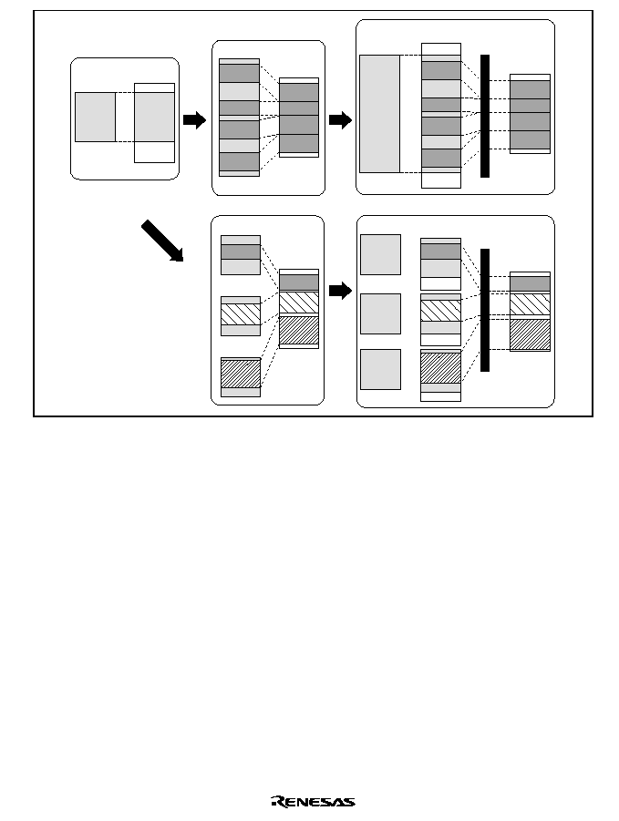
Rev. 5.0, 09/03, page 93 of 806
Process 1
Physical
memory
MMU
(1)
(2)
(3)
(4)
Process 1
Physical
memory
Process 1
Virtual
memory
MMU
Physical
memory
Process 1
Process 2
Process 3
Physical
memory
Process 1
Process 2
Process 3
Virtual
memory
Physical
memory
Figure 3.1 MMU Functions

Rev. 5.0, 09/03, page 94 of 806
3.1.3
SH7729R MMU
Virtual Address Space: The SH7729R uses 32-bit virtual addresses to access a 4-Gbyte virtual
address space that is divided into several areas. Address space mapping is shown in figure 3.2.
(a) Privileged Mode
In privileged mode, there are five areas, P0≠P4. The P0 and P3 areas are mapped onto physical
address space in page units, in accordance with address translation table information. Write-back
or write-through can be selected for write access by means of a cache control register (CCR)
setting.
Mapping of the P1 area is fixed in physical address space (H'00000000 to H'1FFFFFFF). In the
P1 area, setting a virtual address MSB (bit 31) to 0 generates the corresponding physical address.
P1 area accesses can be cached, and the cache control register (CCR) is set to indicate whether to
cache or not. Write-back or write-through mode can be selected.
Mapping of the P2 area is fixed in physical address space (H'00000000 to H'1FFFFFFF). In the P2
area, setting the top three virtual address bits (bits 31, 30, and 29) to 0 generates the corresponding
physical address. P2 area access cannot be cached.
The P1 and P2 areas are not mapped by the address translation table, so the TLB is not used and
no exceptions such as TLB misses occur. Initialization of MMU control registers, exception
handling routines, and the like should be located in the P1 and P2 areas. Routines that require
high-speed processing should be placed in the P1 area, since it can be cached.
Some peripheral module control registers are located in area 1 of the physical address space. When
the physical address space is not used for address translation, these registers should be located in
the P2 area. When address translation is to be used, set no caching.
The P4 area is used for mapping peripheral module register addresses, etc.
(b) User Mode
In user mode, 2 Gbytes of the virtual address space from H'00000000 to H'7FFFFFFF (area U0)
can be accessed. U0 is mapped onto physical address space in page units, in accordance with
address translation table information. When the DSP bit in CPU status register (SR) is off, 2
Gbytes of the virtual address space from H'80000000 to H'FFFFFFFF cannot be accessed in the
user mode. Attempting to do so creates an address error. Write-back or write-through mode can
be selected for write accesses by means of a cache control register (CCR) setting. When the DSP
bit in CPU status register (SR) is on, a new 16-Mbyte address space, Uxy, is defined from address
H'A5000000 to H'A5FFFFFF for X/Y RAM. This Uxy space is non-cached, fixed physical
address space. Any access to address space beyond U0 and Uxy creates an address error. For
details of the X/Y RAM space, refer to section 6, X/Y Memory.

Rev. 5.0, 09/03, page 95 of 806
H'80000000
H'A0000000
H'C0000000
H'E0000000
H'FFFFFFFF
2-Gbyte virtual space,
cacheable
(write-back/write-through)
2-Gbyte virtual space,
cacheable
(write-back/write-through)
Address error
H'00000000
H'00000000
H'80000000
H'FFFFFFFF
Area P0
Area P1
Area P2
Area P3
Area P4
Area U0
Privileged mode
User mode
0.5-Gbyte fixed physical
space, cacheable
(write-back/write-through)
0.5-Gbyte fixed
physical space,
non-cacheable
0.5-Gbyte virtual space,
cacheable
(write-back/write-through)
0.5-Gbyte control space,
non-cacheable
Address error
Area Uxy
(Exists only
when
SR.DSP = 1)
Figure 3.2 Virtual Address Space Mapping
Physical Address Space: The SH7729R supports a 32-bit physical address space, but the upper 3
bits are actually ignored and treated as a shadow. See section 11, Bus State Controller (BSC), for
details.
Address Translation: When the MMU is enabled, the virtual address space is divided into units
called pages. Physical addresses are translated in page units. Address translation tables in external
memory hold information such as the physical address that corresponds to the virtual address and
memory protection codes. When an access to an area other than P4 occurs, if the accessed virtual
address belongs to area P1 or P2 there is no TLB access and the physical address is uniquely
defined. If it belongs to area P0, P3, or U0, the TLB is searched by virtual address and, if that
virtual address is registered in the TLB, the access hits the TLB. The corresponding physical
address and the page control information are read from the TLB and the physical address is
determined.

Rev. 5.0, 09/03, page 96 of 806
If the virtual address is not registered in the TLB, a TLB miss exception occurs and processing
will shift to the TLB miss handler. In the TLB miss handler, the TLB address translation table in
external memory is searched and the corresponding physical address and the page control
information are registered in the TLB. After returning from the handler, the instruction that caused
the TLB miss is re-executed. When the MMU is enabled, address translation information that
results in a physical address space of H'80000000≠H'FFFFFFFF should not be registered in the
TLB.
When the MMU is disabled, the virtual address is used directly as the physical address. As the
SH7729R supports a 29-bit address space as the physical address space, the top 3 bits of the
physical address are ignored, and constitute a shadow space (see section 11, Bus State Controller
(BSC)). For example, addresses H'00001000 in the P0 area, H'80001000 in the P1 area,
H'A0001000 in the P2 area, and H'C0001000 in the P3 area are all mapped onto the same physical
address. When access to these addresses is performed with the cache enabled, an address with the
top 3 bits of the physical address masked to 0 is stored in the cache address array to ensure data
congruity.
Single Virtual Memory Mode and Multiple Virtual Memory Mode: There are two virtual
memory modes: single virtual memory mode and multiple virtual memory mode. In single virtual
memory mode, multiple processes run in parallel using the virtual address space exclusively and
the physical address corresponding to a given virtual address is specified uniquely. In multiple
virtual memory mode, multiple processes run in parallel sharing the virtual address space, so a
given virtual address may be translated into different physical addresses depending on the process.
Single or multiple virtual mode is selected by a value set in the MMU control register (MMUCR).
In terms of operation, the only difference between single virtual memory mode and multiple
virtual memory mode is in the TLB address comparison method (see section 3.3.3, TLB Address
Comparison).
Address Space Identifier (ASID): In multiple virtual memory mode, the address space identifier
(ASID) is used to differentiate between processes running in parallel and sharing virtual address
space. The ASID is 8 bits in length and can be set by software setting of the ASID of the currently
running process in the page table entry register high (PTEH) within the MMU. When the process
is switched using the ASID, the TLB does not have to be purged.
In single virtual memory mode, the ASID is used to provide memory protection for processes
running simultaneously and using the virtual address space exclusively (see section 3.4.2, MMU
Software Management).

Rev. 5.0, 09/03, page 97 of 806
3.1.4
Register Configuration
Table 3.1 shows the configuration of the MMU control registers.
Table 3.1
Register Configuration
Name
Abbreviation
R/W
Size
Initial Value
*
1
Address
Page table entry register high PTEH
R/W
Longword
Undefined
H'FFFFFFF0
Page table entry register low
PTEL
R/W
Longword
Undefined
H'FFFFFFF4
Translation table base
register
TTB
R/W
Longword
Undefined
H'FFFFFFF8
TLB exception address
register
TEA
R/W
Longword
Undefined
H'FFFFFFFC
MMU control register
MMUCR
R/W
Longword
*
2
H'FFFFFFE0
Notes: 1. Initialized by a power-on reset or manual reset.
2. SV bit: Undefined
Other bits: 0
3.2
Register Description
There are five registers for MMU processing. These registers are located in address space area P4
and can only be accessed from privileged mode by specifying the address.
1. The page table entry register high (PTEH) register residing at address H'FFFFFFF0, which
consists of a virtual page number (VPN) and ASID. The VPN set is the VPN of the virtual
address at which the exception is generated in case of an MMU exception or address error
exception. When the page size is 4 kbytes, the VPN is the upper 20 bits of the virtual address,
but in this case the upper 22 bits of the virtual address are set. The VPN can also be modified
by software. As the ASID, software sets the number of the currently executing process. The
VPN and ASID are recorded in the TLB by the LDTLB instruction.
2. The page table entry register low (PTEL) register residing at address H'FFFFFFF4, and used to
store the physical page number and page management information to be recorded in the TLB
by the LDTLB instruction. The contents of this register are only modified in response to a
software command. (Refer to section 3.4.3, MMU Instruction (LDTLB), and section 3.5,
MMU Exceptions.)
3. The translation table base register (TTB) residing at address H'FFFFFFF8, which points to the
base address of the current page table. The software does not set any value in TTB
automatically. TTB is available to software for general purposes.
4. The TLB exception address register (TEA) residing at address H'FFFFFFFC, which stores the
virtual address corresponding to a TLB or address error exception. This value remains valid
until the next exception or interrupt.
Rev. 5.0, 09/03, page 98 of 806
5. The MMU control register (MMUCR) residing at address H'FFFFFFE0, which makes the
MMU settings described in figure 3.3. Any program that modifies MMUCR should reside in
the P1 or P2 area.
The MMU registers are shown in figure 3.3.
31
7
VPN
PTEH
PTEL
ASID
0
PPN
0
10
31
29 28
6
4 3 2 1 0
10
31
TTB
TTB
0
31
Virtual address causing MMU exception
or address error exception
TEA
0
PR
*
SZ
*
C
*
D
*
8
9
7
V
*
0
000
0
SH
*
0
MMUCR
0
31
8
4
6 5
7
3 2 1
0
SV
RC
00
0 TF IX AT
0: Reserved bits. Always read as 0. Writing is ignored. However, 0 should also be
specified in a write to MMUCR only.
SV: 0: Multiple virtual memory mode
1: Single virtual memory mode
RC: A 2-bit random counter, automatically updated by hardware according to the
following rules in the event of an MMU exception. When a TLB miss exception
occurs, all TLB entry ways corresponding to the virtual address at which the
exception occurred are checked, and if all ways are valid, 1 is added to RC; if
there is one or more invalid way, they are set by priority from way 0, in the order:
way 0, way 1, way 2, way 3. In the event of an MMU exception other than a TLB
miss exception, the way which caused the exception is set in RC.
TF: TLB flush bit. Write 1 to flush the TLB (clear all valid bits of the TLB to 0). Always
reads 0.
IX: Index mode bit. When 0, VPN bits 16
-12 are used as the TLB index number.
When 1, the value obtained by EX-ORing ASID bits 4
-0 in PTEH and VPN bits
16
-12 is used as the TLB index number.
AT: Address translation bit. Enables/disables the MMU.
0: MMU disabled
1: MMU enabled
Note:
* Refer to section 3.3, TLB Functions.
Figure 3.3 MMU Register Contents

Rev. 5.0, 09/03, page 99 of 806
3.3
TLB Functions
3.3.1
Configuration of the TLB
The TLB caches address translation table information located in external memory. The address
translation table stores the physical page number translated from the virtual page number and the
control information for the page, which is the unit of address translation. Figure 3.4 shows the
overall TLB configuration. The TLB is 4-way set associative with 128 entries. There are 32 entries
for each way. Figure 3.5 shows the configuration of virtual addresses and TLB entries.
Entry 1
Address array
Data array
Entry 0
Entry 1
Entry 31
Ways 0
-3
Ways 0
-3
VPN(11
-10)
VPN(31
-17)
ASID(7
-0) V
Entry 0
Entry 31
PPN(28
-10) PR(1-0) SZ C D SH
Figure 3.4 Overall Configuration of the TLB
Rev. 5.0, 09/03, page 100 of 806
31
9
VPN
Virtual address (1-kbyte page)
Virtual address (4-kbyte page)
TLB entry
Offset
VPN
VPN (31
-17) VPN (11-10) ASID V
Offset
0
10
31
11
0
(15)
(2)
(8)
(1)
12
Legend
VPN: Virtual page number. Upper 22 bits of virtual address for a 1-kbyte page, or upper 20 bits of
virtual address for a 4-kbyte page. Since VPN bits 16
-12 are used as the index number, they
are not stored in the TLB entry.
ASID: Address space identifier. Indicates the process that can access a virtual page. In single
virtual memory mode and user mode, or in multiple virtual memory mode, if the SH bit is 0,
the address is compared with the ASID in PTEH when address comparison is performed.
SH: Share status bit
0 = Page not shared between processes
1 = Page shared between processes
SZ:
Page-size
bit
0 = 1-kbyte page
1 = 4-kbyte page
V: Valid bit. Indicates whether entry is valid.
0 = Invalid
1 = Valid
Cleared to 0 by a power-on reset. Not affected by a manual reset.
PPN: Physical page number. Upper 29 bits of physical address. PPN bits 11
-10 are not used in
case of a 4-kbyte page. Attention must be paid to the synonym problem in case of a 1-kbyte
page (see section 3.4.4, Avoiding Synonym Problems).
PR: Protection key field. 2-bit field encoded to define the access rights to the page.
00: Reading only is possible in privileged mode.
01: Reading/writing is possible in privileged mode.
10: Reading only is possible in privileged/user mode.
11: Reading/writing is possible in privileged/user mode.
C: Cacheable bit. Indicates whether the page is cacheable.
0:
Non-cacheable
1:
Cacheable
D: Dirty bit. Indicates whether the page has been written to.
0 = Not written to
1 = Written to
PR
PPN
C
D
(2)
(29)
(1)
(1)
SZ
SH
(1)
(1)
Figure 3.5 Virtual Address and TLB Structure
Rev. 5.0, 09/03, page 101 of 806
3.3.2
TLB Indexing
The TLB uses a 4-way set associative scheme, so entries must be selected by index. VPN bits 16
to 12 and ASID bits 4 to 0 in PTEH are used as the index number. The index number can be
generated in two different ways depending on the setting of the IX bit in MMUCR.
1. When IX = 0, VPN bits 16≠12 alone are used as the index number
2. When IX = 1, VPN bits 16≠12 are EX-ORed with ASID bits 4≠0 to generate the index number
The second method is used to prevent lowered TLB efficiency that results when multiple
processes run simultaneously in the same virtual address space (multiple virtual memory) and a
specific entry is selected by generating an index number for each process. Figures 3.6 and 3.7
show the indexing schemes.
31
16
11
12
17
0
31
0
PTEH register
Virtual address
VPN
0
ASID
7
10
Index
ASID(4
-0)
Exclusive-OR
Ways 0 to 3
VPN(31
-17)
VPN(11
-10)
ASID(7
-0) V
0
31
Address array
Data array
PPN(31
-10) PR(1-0) SZ C D SH
Figure 3.6 TLB Indexing (IX = 1)
Rev. 5.0, 09/03, page 102 of 806
31
16
11
12
17
0
Virtual address
Ways 0 to 3
VPN(31
-17)
VPN(11
-10) ASID(7-0)
V
0
Address array
Data array
PPN(28
-10) PR(1-0) SZ C D SH
Index
31
Figure 3.7 TLB Indexing (IX = 0)
3.3.3
TLB Address Comparison
A TLB address comparison is performed when an instruction is fetched from a program in
external memory or data in external memory is referenced. The items used in the comparison are
VPN and ASID. The VPN of the virtual address that accesses external memory is compared to the
VPN of the TLB entry selected with the index number. The ASID within the PTEH is compared to
the ASID of the indexed TLB entry. All four ways are searched simultaneously. If the compared
values match, and the indexed TLB entry is valid (V bit
=
1), the hit is registered.
It is necessary to have software ensure that TLB hits do not occur simultaneously in more than one
way, as hardware operation is not guaranteed if this occurs. For example, if there are two identical
TLB entries with the same VPN and a setting is made such that a TLB hit is made only by a
process with ASID = H'FF when one is in the shared state (SH = 1) and the other in the non-shared
state (SH = 0), then if the ASID in PTEH is set to H'FF, there is a possibility of simultaneous TLB
hits in both these ways. It is therefore necessary to ensure that this kind of setting is not made by
software.
The object compared varies depending on the page management information (SZ, SH) in the TLB
entry. It also varies depending on whether the system supports multiple virtual memory or single
virtual memory.
The page-size information determines whether VPN (11≠10) is compared. VPN (11≠10) is
compared for 1-kbyte pages (SZ = 0) but not for 4-kbyte pages (SZ = 1).
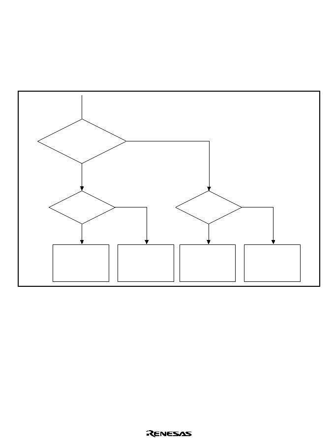
Rev. 5.0, 09/03, page 103 of 806
The sharing information (SH) determines whether PTEH.ASID and the ASID in the TLB entry are
compared. ASIDs are compared when there is no sharing between processes (SH
=
0) but not
when there is sharing (SH
=
1).
When single virtual memory is supported (MMUCR.SV
=
1) and privileged mode is engaged
(SR.MD
=
1), all process resources can be accessed. This means that ASIDs are not compared
when single virtual memory is supported and privileged mode is engaged. The objects of address
comparison are shown in figure 3.8.
Bits compared:
VPN (31
-17)
VPN (11
-10)
SZ = 0?
Yes
No
Yes (1 kbyte)
No (4 kbytes)
Bits compared:
VPN (31
-17)
Bits compared:
VPN (31
-17)
VPN (11
-10)
ASID (7
-0)
SZ = 0?
Yes (1 kbyte)
No (4 kbytes)
Bits compared:
VPN (31
-17)
ASID (7
-0)
SH = 1 or
(SR.MD = 1 and
MMUCR.SV = 1)?
Figure 3.8 Objects of Address Comparison

Rev. 5.0, 09/03, page 104 of 806
3.3.4
Page Management Information
In addition to the SH and SZ bits, the page management information of TLB entries also includes
D, C, and PR bits.
The D bit of a TLB entry indicates whether the page is dirty (i.e., has been written to). If the D bit
is 0, an attempt to write to the page results in an initial page write exception. For physical page
swapping between secondary memory and main memory, for example, pages are controlled so that
a dirty page is paged out of main memory only after that page is written back to secondary
memory. To record that there has been a write to a given page in the address translation table in
memory, an initial page write exception is used.
The C bit in the entry indicates whether the referenced page resides in a cacheable or non-
cacheable area of memory. When the control register in area 1 is mapped, set the C bit to 0.
The PR field specifies the access rights for the page in privileged and user modes and is used to
protect memory. Attempts at nonpermitted accesses result in TLB protection violation exceptions.
Access states designated by the D, C, and PR bits are shown in table 3.2.
Table 3.2
Access States Designated by D, C, and PR Bits
Privileged Mode
User Mode
Reading
Writing
Reading
Writing
D bit
0
Permitted
Initial page write
exception
Permitted
Initial page write
exception
1
Permitted
Permitted
Permitted
Permitted
C bit
0
Permitted
(no caching)
Permitted
(no caching)
Permitted
(no caching)
Permitted
(no caching)
1
Permitted
(with caching)
Permitted
(with caching)
Permitted
(with caching)
Permitted
(with caching)
PR bit
00
Permitted
TLB protection
violation exception
TLB protection
violation
exception
TLB protection
violation exception
01
Permitted
Permitted
TLB protection
violation
exception
TLB protection
violation exception
10
Permitted
TLB protection
violation exception
Permitted
TLB protection
violation exception
11
Permitted
Permitted
Permitted
Permitted

Rev. 5.0, 09/03, page 105 of 806
3.4
MMU Functions
3.4.1
MMU Hardware Management
There are two kinds of MMU hardware management as follows:
1. The MMU decodes the virtual address accessed by a process and performs address translation
by controlling the TLB in accordance with the MMUCR settings.
2. In address translation, the MMU receives page management information from the TLB, and
determines the MMU exception and whether the cache is to be accessed (using the C bit). For
details of the determination method and the hardware processing, see section 3.5, MMU
Exceptions.
3.4.2
MMU Software Management
There are three kinds of MMU software management, as follows.
1. MMU register setting. MMUCR setting, in particular, should be performed in areas P1 and P2
for which address translation is not performed. Also, since SV and IX bit changes constitute
address translation system changes, in this case, TLB flushing should be performed by
simultaneously writing 1 to the TF bit also. Since MMU exceptions are not generated in the
MMU disabled state with the AT bit cleared to 0, use in the disabled state must be avoided
with software that does not use the MMU.
2. TLB entry recording, deletion, and reading. TLB entry recording can be done in two ways: by
using the LDTLB instruction, or by writing directly to the memory-mapped TLB. For TLB
entry deletion and reading, the memory-mapped TLB can be accessed. See section 3.4.3,
MMU Instruction (LDTLB), for details of the LDTLB instruction, and section 3.6, Memory-
Mapped TLB, for details of the memory-mapped TLB.
3. MMU exception handling. When an MMU exception is generated, it is handled on the basis of
information set from the hardware side. See section 3.5, MMU Exceptions, for details.
When single virtual memory mode is used, it is possible to create a state in which physical
memory access is enabled in privileged mode only by clearing the share status bit (SH) to 0 to
specify recording of all TLB entries. This strengthens inter-process memory protection, and
enables special access levels to be created in privileged mode only.
Recording a 1-kbyte page TLB entry may result in a synonym problem. See section 3.4.4,
Avoiding Synonym Problems.

Rev. 5.0, 09/03, page 106 of 806
3.4.3
MMU Instruction (LDTLB)
The load TLB instruction (LDTLB) is used to record TLB entries. When the IX bit in MMUCR is
0, the LDTLB instruction changes the TLB entry in the way specified by the RC bit in MMUCR
to the value specified by PTEH and PTEL, using VPN bits 16≠12 specified in PTEH as the index
number. When the IX bit in MMUCR is 1, the EX-OR of VPN bits 16≠12 specified in PTEH and
ASID bits 4≠0 in PTEH is used as the index number.
Figure 3.9 shows the case where the IX bit in MMUCR is 0.
When an MMU exception occurs, the virtual page number of the virtual address that caused the
exception is set in PTEH by hardware. The way is set in the RC bit of MMUCR for each
exception (see figure 3.3). Consequently, if the LDTLB instruction is issued after setting only
PTEL in the MMU exception handling routine, TLB entry recording is possible. Any TLB entry
can be updated by software rewriting of PTEH and the RC bits in MMUCR.
As the LDTLB instruction changes address translation information, there is a risk of destroying
address translation information if this instruction is issued in the P0, U0, or P3 area. Make sure,
therefore, that this instruction is issued in the P1 or P2 area. Also, an instruction associated with an
access to the P0, U0, or P3 area (such as the RTE instruction) should be issued at least two
instructions after the LDTLB instruction.
Rev. 5.0, 09/03, page 107 of 806
VPN(31
-17) VPN(11-10) ASID(7-0) V
VPN
0
ASID
VPN
0
SV 0 0 RC 0 TF IX AT
PPN
0
000
V 0 PR SZ C D SH 0
Write
PPN(28
-10) PR(1-0) SZ C D SH
Write
Data array
Address array
Way selection
Ways 0 to 3
31
9
0
MMUCR
Index
31
17
12
10
8
0
PTEH register
3129 28
10
0
PTEL register
0
31
Figure 3.9 Operation of LDTLB Instruction
3.4.4
Avoiding Synonym Problems
When a 1-kbyte page is recorded in a TLB entry, a synonym problem may arise. If a number of
virtual addresses are mapped onto a single physical address, the same physical address data will be
recorded in a number of cache entries, and it will not be possible to guarantee data congruity. The
reason why this problem only occurs when using a 1-kbyte page is explained below with reference
to figure 3.10.
To achieve high-speed operation of the SH7729R cache, an index number is created using virtual
address bits 11≠4. When a 4-kbyte page is used, virtual address bits 11≠4 are included in the
offset, and since they are not subject to address translation, they are the same as physical address
bits 11≠4. In cache-based address comparison and recording in the address array, since the cache
tag address is a physical address, physical address bits 28≠10 are recorded.
When a 1-kbyte page is used, also, a cache index number is created using virtual address bits 11-4.
However, in case of a 1-kbyte page, virtual address bits 11 and 10 are subject to address
translation and therefore may not be the same as physical address bits 11 and 10. Consequently,
the physical address is recorded in a different entry from that of the index number indicated by the
physical address in the cache address array.

Rev. 5.0, 09/03, page 108 of 806
Note:
When multiple address information items use the same physical memory to provide for
future expansion of the SuperH RISC engine family, it is recommended that VPN[20:10]
be made equal. Also, the same physical addresses should not be used with different page
size address conversion information.
For example, assume that, with 1-kbyte page TLB entries, TLB entries for which the following
translation has been performed are recorded in two TLBs:
Virtual address 1 H'00000000
physical address H'00000C00
Virtual address 2 H'00000C00
physical
address
H'00000C00
Virtual address 1 is recorded in cache entry H'00, and virtual address 2 in cache entry H'C0. Since
two virtual addresses are recorded in different cache entries despite the fact that the physical
addresses are the same, memory inconsistency will occur as soon as a write is performed to either
virtual address. Therefore, when recording a 1-kbyte TLB entry, if the physical address is the same
as a physical address already used in another TLB entry, it should be recorded in such a way that
physical address bits 11 and 10 are the same.
Rev. 5.0, 09/03, page 109 of 806
When using a 4-kbyte page
Virtual address
31
VPN
0
12 11
29 28
10
Offset
Physical address
31
PPN
000
29 28
000
0
Offset
Virtual address (11
-4)
Physical address (28
-10)
Cache address
array
When using a 1-kbyte page
Virtual address
31
VPN
0
10
11
Offset
Physical address
31
PPN
0
10
11
Offset
Virtual address (11
-4)
Physical address (28
-10)
Cache address
array
9
9
12 11 10
Figure 3.10 Synonym Problem

Rev. 5.0, 09/03, page 110 of 806
3.5
MMU Exceptions
There are four MMU exceptions: TLB miss, TLB protection violation, TLB invalid, and initial
page write.
3.5.1
TLB Miss Exception
A TLB miss exception occurs when the virtual address and the address array of the selected TLB
entry are compared and no match is found. TLB miss exception handling includes both hardware
and software operations.
Hardware Operations: In a TLB miss, the SH7729R hardware executes a set of prescribed
operations, as follows:
1. The VPN field of the virtual address causing the exception is written to the PTEH register.
2. The virtual address causing the exception is written to the TEA register.
3. Either exception code H'040 for a load access, or H'060 for a store access, is written to the
EXPEVT register.
4. The PC value indicating the address of the instruction in which the exception occurred is
written to the saved program counter (SPC). If the exception occurred in a delay slot, the PC
value indicating the address of the related delayed branch instruction is written to SPC.
5. The contents of the status register (SR) at the time of the exception are written to the saved
status register (SSR).
6. The mode (MD) bit in SR is set to 1 to place the SH7729R in privileged mode.
7. The block (BL) bit in SR is set to 1 to mask any further exception requests.
8. The register bank (RB) bit in SR is set to 1.
9. The random counter (RC) field in the MMU control register (MMUCR) is incremented by 1
when all ways are checked for the TLB entry corresponding to the virtual address at which the
exception occurred, and all ways are valid. If one or more ways are invalid, those ways are set
in RC in prioritized order from way 0 through way 1, way 2, and way 3.
10. Execution branches to the address obtained by adding the value of the VBR contents and
H'00000400 to invoke the user-written TLB miss exception handler.
Software (TLB Miss Handler) Operations: The software searches the page tables in external
memory and allocates the required page table entry. Upon retrieving the required page table entry,
software must execute the following operations:
1. Write the value of the physical page number (PPN) field and the protection key (PR), page size
(SZ), cacheable (C), dirty (D), share status (SH), and valid (V) bits of the page table entry
recorded in the address translation table in external memory into the PTEL register in the
SH7729R.

Rev. 5.0, 09/03, page 111 of 806
2. If using software for way selection for entry replacement, write the desired value to the RC
field in MMUCR.
3. Issue an LDTLB instruction to load the contents of PTEH and PTEL into the TLB.
4. Issue an RTE (return from exception handler) instruction to terminate the handler and return to
the instruction stream. The RTE instruction should be issued after two LDTLB instructions.
3.5.2
TLB Protection Violation Exception
A TLB protection violation exception occurs when the virtual address and the address array of the
selected TLB entry are compared and a valid entry is found to match, but the type of access is not
permitted by the access rights specified in the PR field. TLB protection violation exception
handling includes both hardware and software operations.
Hardware Operations: In a TLB protection violation exception, the SH7729R hardware executes
a set of prescribed operations, as follows:
1. The VPN field of the virtual address causing the exception is written to the PTEH register.
2. The virtual address causing the exception is written to the TEA register.
3. Either exception code H'0A0 for a load access, or H'0C0 for a store access, is written to the
EXPEVT register.
4. The PC value indicating the address of the instruction in which the exception occurred is
written into SPC (if the exception occurred in a delay slot, the PC value indicating the address
of the related delayed branch instruction is written into SPC).
5. The contents of SR at the time of the exception are written to SSR.
6. The MD bit in SR is set to 1 to place the SH7729R in privileged mode.
7. The BL bit in SR is set to 1 to mask any further exception requests.
8. The register bank (RB) bit in SR is set to 1.
9. The way that generated the exception is set in the RC field in MMUCR.
10. Execution branches to the address obtained by adding the value of the VBR contents and
H'00000100 to invoke the TLB protection violation exception handler.
Software (TLB Protection Violation Handler) Operations: Software resolves the TLB
protection violation and issues an RTE (return from exception handler) instruction to terminate the
handler and return to the instruction stream. The RTE instruction should be issued after two
LDTLB instructions.

Rev. 5.0, 09/03, page 112 of 806
3.5.3
TLB Invalid Exception
A TLB invalid exception occurs when the virtual address is compared to a selected TLB entry
address array and a match is found but the entry is not valid (the V bit is 0). TLB invalid exception
handling includes both hardware and software operations.
Hardware Operations: In a TLB invalid exception, the SH7729R hardware executes a set of
prescribed operations, as follows:
1. The VPN number of the virtual address causing the exception is written to the PTEH register.
2. The virtual address causing the exception is written to the TEA register.
3. The way number causing the exception is written to RC in MMUCR.
4. Either exception code H'040 for a load access, or H'060 for a store access, is written to the
EXPEVT register.
5. The PC value indicating the address of the instruction in which the exception occurred is
written to SPC. If the exception occurred in a delay slot, the PC value indicating the address of
the delayed branch instruction is written to SPC.
6. The contents of SR at the time of the exception are written to SSR.
7. The mode (MD) bit in SR is set to 1 to place the SH7729R in privileged mode.
8. The block (BL) bit in SR is set to 1 to mask any further exception requests.
9. The register bank (RB) bit in SR is set to 1.
10. Execution branches to the address obtained by adding the value of the VBR contents and
H'00000100, and the TLB protection violation exception handler starts.
Software (TLB Invalid Exception Handler) Operations: The software searches the page tables
in external memory and assigns the required page table entry. Upon retrieving the required page
table entry, software must execute the following operations:
1. Write the values of the physical page number (PPN) field and the values of the protection key
(PR), page size (SZ), cacheable (C), dirty (D), share status (SH), and valid (V) bits of the page
table entry recorded in the external memory to the PTEL register.
2. If using software for way selection for entry replacement, write the desired value to the RC
field in MMUCR.
3. Issue an LDTLB instruction to load the contents of PTEH and PTEL into the TLB.
4. Issue an RTE instruction to terminate the handler and return to the instruction stream. The RTE
instruction should be issued after two LDTLB instructions.

Rev. 5.0, 09/03, page 113 of 806
3.5.4
Initial Page Write Exception
An initial page write exception occurs in a write access when the virtual address and the address
array of the selected TLB entry are compared and a valid entry with the appropriate access rights
is found to match, but the D (dirty) bit of the entry is 0 (the page has not been written to). Initial
page write exception handling includes both hardware and software operations.
Hardware Operations: In an initial page write exception, the SH7729R hardware executes a set
of prescribed operations, as follows:
1. The VPN field of the virtual address causing the exception is written to the PTEH register.
2. The virtual address causing the exception is written to the TEA register.
3. Exception code H'080 is written to the EXPEVT register.
4. The PC value indicating the address of the instruction in which the exception occurred is
written to SPC. If the exception occurred in a delay slot, the PC value indicating the address of
the related delayed branch instruction is written to SPC.
5. The contents of SR at the time of the exception are written to SSR.
6. The MD bit in SR is set to 1 to place the SH7729R in privileged mode.
7. The BL bit in SR is set to 1 to mask any further exception reque sts.
8. The register bank (RB) bit in SR is set to 1.
9. The way that caused the exception is set in the RC field in MMUCR.
10. Execution branches to the address obtained by adding the value of the VBR contents and
H'00000100 to invoke the user-written initial page write exception handler.
Software (Initial Page Write Handler) Operations: The software must execute the following
operations:
1. Retrieve the required page table entry from external memory.
2. Set the D bit of the page table entry in external memory to 1.
3. Write the value of the PPN field and the PR, SZ, C, D, SH, and V bits of the page table entry
in the external memory to the PTEL register.
4. If using software for way selection for entry replacement, write the desired value to the RC
field in MMUCR.
5. Issue an LDTLB instruction to load the contents of PTEH and PTEL into the TLB.
6. Issue an RTE instruction to terminate the handler and return to the instruction stream. The RTE
instruction should be issued after two LDTLB instructions.
Figure 3.11 shows the flowchart for MMU exceptions.
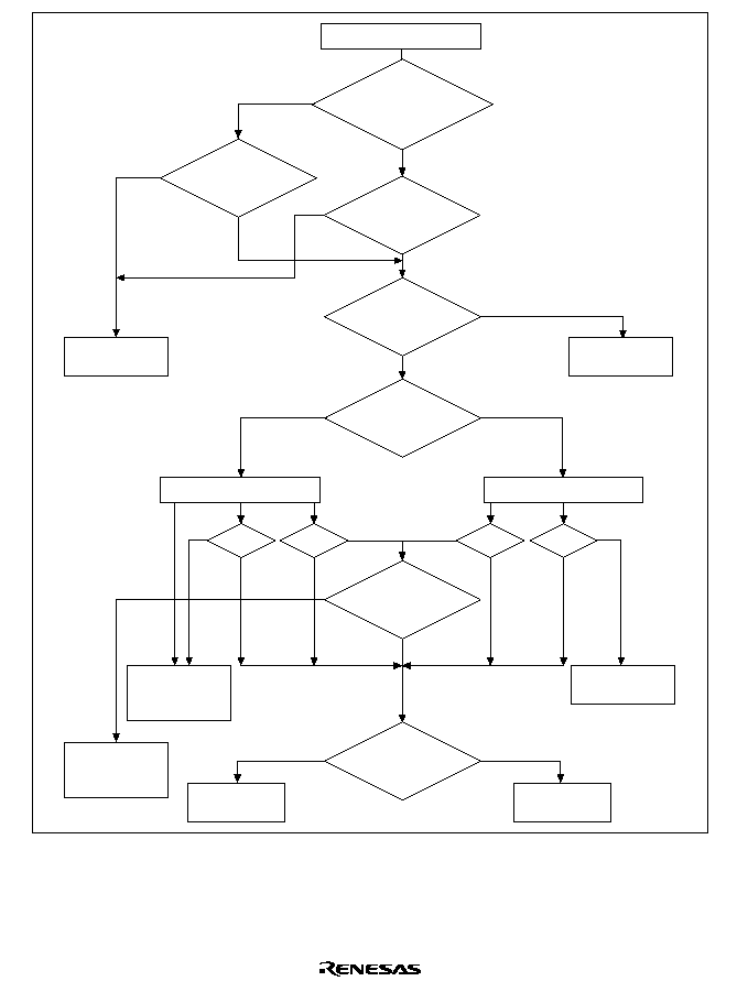
Rev. 5.0, 09/03, page 114 of 806
Start
TLB miss
exception
Initial page
write
exception
PR check
PR check
Yes
SH = 0
and (MMUCR.SV = 0
or SR.MD = 0)?
VPNs
and ASIDs
match?
VPNs match?
No
Yes
Yes
Yes
Yes
User or
privileged?
D = 1?
C = 1?
V = 1?
No
No
User mode
Privileged mode
No
No
TLB protection
violation
exception
TLB protection
exception
Cache
access
W
00/01
10
01/11
00/10
11
W
W
W
R
R
R
R
R/W?
R/W?
R/W?
R/W?
TLB invalid
exception
Memory
access
No (noncacheable)
Yes (cacheable)
Figure 3.11 MMU Exception Generation Flowchart
Rev. 5.0, 09/03, page 115 of 806
3.5.5
Processing Flow in Event of MMU Exception (Same Processing Flow for Address
Error)
MMU Exception in Instruction Fetch Mode
ID
EX
MA
WB
ID
EX
MA
WB
ID
EX
MA
WB
NOP
NOP
IF
ID
EX
MA
WB
: Exception source stage
IF
ID
EX
MA
WB
NOP
MMU exception handler
TLB-related exception signals in an instruction fetch
Handler transition
processing
= Instruction fetch
= Instruction decode
= Instruction execution
= Memory access
= Write back
= No operation
IF
Figure 3.12 MMU Exception Signals in Instruction Fetch

Rev. 5.0, 09/03, page 116 of 806
MMU Exception in Data Access Mode
IF
ID
EX
IF
ID
EX
IF
ID
ID
EX
MA
WB
ID
EX
MA
WB
ID
EX
MA WB
NOP
NOP
IF
ID
EX
MA WB
: Exception source stage
: Stage cancellation for instruction
that has begun execution
IF
ID
EX
MA
WB
NOP
= Instruction fetch
= Instruction decode
= Instruction execution
= Memory access
= Write back
= No operation
MMU exception handler
Handler transition
processing
MA
WB
MA
WB
EX
MA
WB
TLB-related exception signals in a data access
Figure 3.13 MMU Exception Signals in Data Access

Rev. 5.0, 09/03, page 117 of 806
3.5.6
MMU Exception in Repeat Loop
When an MMU exception or CPU address error occurs immediately before or within a repeat
loop, the PC of the instruction that generated the exception cannot be saved in SPC correctly and
the repeat loop cannot be restarted after returning from the exception handler. EXPEVT is set to
H'070 in cases of TLB miss, TLB invalid, and CPU address error. EXPEVT is set to H'0D0 in
case of TLB protection violation. Figure 3.14 shows where such cases occur.
In a repeat loop of 4 or more instructions, only the last 4 instructions are relevant (see figure 3.14
(4)).
: Exception source stage where SPC is not correct
and repeat loop can not be restarted
(1) 1 instruction repeated (inst1, SR.RC=2)
inst-1
inst0
inst1
inst1
inst2
IF
ID
EX MA WB
IF
ID
EX MA WB
IF
ID
EX MA WB
IF
ID
EX MA WB
IF
ID
EX MA WB
(2) 2 instructions repeated (inst1 and inst2, SR.RC=2)
inst-1
inst0
inst1
inst2
inst1
inst2
inst3
IF
ID
EX MA WB
IF
ID
EX MA WB
IF
ID
EX MA WB
IF
ID
EX MA WB
IF
ID
EX MA WB
IF
ID
EX MA WB
IF
ID
EX MA WB
(3) 3 instructions repeated (inst1, inst2 and inst3, SR.RC=2)
inst-1
inst0
inst1
inst2
inst3
inst1
inst2
inst3
inst4
IF
ID
EX MA WB
IF
ID
EX MA WB
IF
ID
EX MA WB
IF
ID
EX MA WB
IF
ID
EX MA WB
IF
ID
EX MA WB
IF
ID
EX MA WB
IF
ID
EX MA WB
IF
ID
EX MA WB
Figure 3.14 MMU Exception in Repeat Loop
Rev. 5.0, 09/03, page 118 of 806
(4) 4 or more instructions repeated (inst1, inst2, ..., instN, SR.RC=2)
inst-1
inst0
inst1
inst2
:
instN-3
instN-2
instN-1
instN
inst1
inst2
:
instN-3
instN-2
instN-1
instN
instN+1
IF
ID
EX MA WB
IF
ID
EX MA WB
IF
ID
EX MA WB
IF
ID
EX MA WB
IF
ID
EX MA WB
IF
ID
EX MA WB
IF
ID
EX MA WB
IF
ID
EX MA WB
:
IF
ID
EX MA WB
IF
ID
EX MA WB
IF
ID
EX MA WB
IF
ID
EX MA WB
IF
ID
EX MA WB
IF
ID
EX MA WB
IF
ID
EX MA WB
:
: Exception source stage where SPC is not correct
and repeat loop can not be restarted
Figure 3.14 MMU Exception in Repeat Loop (cont)
3.6
Memory-Mapped TLB
In order for TLB operations to be managed by software, TLB contents can be read or written to in
privileged mode using the MOV instruction. The TLB is assigned to the P4 area in the virtual
address space. The TLB address array (VPN, V bit, and ASID) is assigned to H'F2000000≠
H'F2FFFFFF, and the data array (PPN, PR, SZ, C, D, and SH bits) to H'F3000000≠H'F3FFFFFF.
The V bit in the address array can also be accessed from the data array. Only longword access is
possible for both the address array and the data array.
3.6.1
Address Array
The address array is assigned to H'F2000000≠H'F2FFFFFF. To access an address array, the
32-bit address field (for read/write operations) and 32-bit data field (for write operations) must be
specified. The address field specifies information for selecting the entry to be accessed; the data
field specifies the VPN, V bit and ASID to be written to the address array (figure 3.15 (1)).
In the address field, specify VPN (16≠12) as the index address for selecting the entry (bits 16≠12),
the W bits for selecting the way (bits 9≠8), and H'F2 to indicate address array access (bits 31≠24).
The IX bit in MMUCR indicates whether the EX-OR of VPN (16≠12) and ASID (4≠0) in the
PTEH register is used as the index address.

Rev. 5.0, 09/03, page 119 of 806
When writing, the write is performed to the entry selected with the index address and way.
When reading, the VPN, V bit, and ASID of the entry selected with the index address and way in
the format of the data field in figure 3.12 without comparing addresses. 0 is written to data field
bits 16≠12.
To invalidate a specific entry, specify the entry and way, and write 0 to the corresponding V bit.
3.6.2
Data Array
The data array is assigned to H'F3000000≠H'F3FFFFFF. To access a data array, the 32-bit address
field (for read/write operations), and 32-bit data field (for write operations) must be specified. The
address section specifies information for selecting the entry to be accessed; the data section
specifies the longword data to be written to the data array (figure 3.15 (2)). Longword data has the
same bit configuration as PTEL.
In the address field, specify VPN (16≠12) as the index address for selecting the entry (bits 16≠12),
the W bits for selecting the way (bits 9≠8), and H'F3 to indicate data array access (bits 31≠24).
The IX bit in MMUCR indicates whether the EX-OR of VPN (16≠12) and ASID (4≠0) in the
PTEH register is used as the index address.
Both reading and writing use longword data of the data array specified by the entry address and
way number.

Rev. 5.0, 09/03, page 120 of 806
VPN
31
23
11110010
*
*
16
(1) TLB Address Array Access
∑ Read access
(2) TLB Data Array Access
∑ Read/write access
W
0
*
VPN
*
31
23
24
24
17
17
17
11110010
*
*
*
*
16
∑ Write access
W
6
0
*
*
0
VPN
31
23
24
11110011
*
*
16
17
Address field
W
0
*
*
31
Data field
10
PPN
8
9
7 6 5 4
3 2
1
0
X
V
X
X
VPN
31
16
Data field
12
10
11
8
9
7
12
10
11
8
9
7
12
10
11
8
9
7
12
10
11
8
9
7
6
*
0
0
ASID
0 V
VPN
0
0
17
VPN
16
12
10
11
VPN
31
ASID
8
9
7
0
* V
D
C
SH
PR SZ
VPN:
V:
W:
Virtual page number
Valid bit
Way (00: Way 0, 01: Way 1, 10: Way 2, 11: Way 3)
ASID:
:
Address space identifier
Don't care bit
0 read and written
PPN:
PR:
C:
SH:
VPN:
X:
W:
Physical page number
Protection key field
Cacheable bit
Share status bit
Virtual page number
0 for read, don't care bit for write
Way (00: Way 0, 01: Way 1, 10: Way 2, 11: Way 3)
V:
SZ:
D:
:
Valid bit
Page-size bit
Dirty bit
Don't care bit
Address field
Data field
Address field
*
*
*
* *
* *
Figure 3.15 Specifying Address and Data for Memory-Mapped TLB Access

Rev. 5.0, 09/03, page 121 of 806
3.6.3
Usage Examples
Invalidating Specific Entries: Specific TLB entries can be invalidated by writing 0 to the entry's
V bit. R0 specifies the write data and R1 specifies the address.
; R0=H'1547 381C R1=H'F201 30
; MMUCR.IX=0
; VPN(31≠17)=B'0001 0101 0100 011 VPN(11≠10)=B'10 ASID=B'0001 1100
; corresponding entry association is made from the entry selected by
; the VPN(16≠12)=B'1 0011 index, the V bit of the hit way is cleared to
; 0,achieving invalidation.
MOV.L R0,@R1
Reading the Data of a Specific Entry: This example reads the data section of a specific TLB
entry. The data is read in the bit order indicated in the data field in figure 3.15 (2) is read. R0
specifies the address and the data section of a selected entry is read to R1.
; R1
=
H'F300 4300 VPN(16-12)=B'00100 Way 3
; MOV.L @R0,R1
3.7
Usage Note
Instructions that manipulate the MD or BL bit in register SR (the LDC Rm, SR instruction, LDC
@Rm+, SR instruction, and RTE instruction) and the following instruction, or the LDTLB
instruction, should be used with the TLB disabled or in a fixed physical address space (the P1 or
P2 space).

Rev. 5.0, 09/03, page 122 of 806

Rev. 5.0, 09/03, page 123 of 806
Section 4 Exception Handling
4.1
Overview
4.1.1
Features
Exception handling is separate from normal program processing, and is performed by a routine
separate from the normal program. In response to an exception handling request due to abnormal
termination of the executing instruction, control is passed to a user-written exception handler.
However, in response to an interrupt request, normal program execution continues until the end of
the executing instruction. Here, all exceptions other than resets and interrupts will be called
general exceptions. There are thus three types of exceptions: resets, general exceptions, and
interrupts.
4.1.2
Register Configuration
Table 4.1 lists the registers used for exception handling. A register with an undefined initial value
should be initialized by software.
Table 4.1
Register Configuration
Register
Abbr.
R/W
Size
Initial Value
Address
TRAPA exception register TRA
R/W
Longword
Undefined
H'FFFFFFD0
Exception event register
EXPEVT R/W
Longword
Power-on reset: H'000
Manual reset: H'020
*
1
H'FFFFFFD4
Interrupt event register
INTEVT
R/W
Longword
Undefined
H'FFFFFFD8
Interrupt event register2
INTEVT2 R
Longword
Undefined
H'04000000
(H'A4000000)
*
2
Notes: 1. H'000 is set in a power-on reset, and H'020 in a manual reset.
2. When address translation by the MMU does not apply, the address in parentheses
should be used.
4.2
Exception Handling Function
4.2.1
Exception Handling Flow
In exception handling, the contents of the program counter (PC) and status register (SR) are saved
in the saved program counter (SPC) and saved status register (SSR), respectively, and execution of
the exception handler is invoked from a vector address. The return from exception handler (RTE)
instruction is issued by the exception handler routine on completion of the routine, restoring the

Rev. 5.0, 09/03, page 124 of 806
contents of PC and SR to return to the processor state at the point of interruption and the address
where the exception occurred.
A basic exception handling sequence consists of the following operations:
1. The contents of PC and SR are saved in SPC and SSR, respectively.
2. The block (BL) bit in SR is set to 1, masking any subsequent exceptions.
3. The mode (MD) bit in SR is set to 1 to place the SH7729R in privileged mode.
4. The register bank (RB) bit in SR is set to 1.
5. An exception code identifying the exception event is written to bits 11≠0 of the exception
event (EXPEVT) or interrupt event (INTEVT or INTEVT2) register.
6. Instruction execution jumps to the designated exception vector address to invoke the handler
routine.
4.2.2
Exception Vector Addresses
The reset vector address is fixed at H'A0000000. The other three events are assigned offsets from
the vector base address by software. Translation look-aside buffer (TLB) miss exceptions have an
offset from the vector base address of H'00000400. The vector address offset for general exception
events other than TLB miss exceptions is H'00000100. The interrupt vector address offset is
H'00000600. The vector base address is loaded into the vector base register (VBR) by software.
The vector base address should reside in P1 or P2 fixed physical address space. Figure 4.1 shows
the relationship between the vector base address, the vector offset, and the vector table.
VBR
(Vector base address)
+ Vector offset
H'A000 0000
Vector table
Figure 4.1 Vector Table
In table 4.2, exceptions and their vector addresses are listed by exception type, instruction
completion state, relative acceptance priority, relative order of occurrence within an instruction
execution sequence and vector address for exceptions and their vector addresses.

Rev. 5.0, 09/03, page 125 of 806
Table 4.2
Exception Event Vectors
Exception
Type
Current
Instruction Exception Event
Priority
*
1
Exception
Order
Vector
Address
Vector
Offset
Reset
Aborted
Power-on reset
1
--
H'A00000000 --
Manual reset
1
--
H'A00000000 --
UDI reset
1
--
H'A00000000 --
Aborted
and retried
CPU address error
(instruction access)
2
1
--
H'00000100
General
exception
events
TLB miss (instruction
access not in repeat
loop)
2
2
--
H'00000400
TLB miss (instruction
access in repeat loop)
*
4
2
2
--
H'00000100
TLB invalid (instruction
access)
2
3
--
H'00000100
TLB protection violation
(instruction access)
2
4
--
H'00000100
General illegal
instruction exception
2
5
--
H'00000100
Illegal slot instruction
exception
2
5
--
H'00000100
CPU address error
(data access)
2
6
--
H'00000100
TLB miss (data access
not in repeat loop)
2
7
--
H'00000400
TLB miss (data access
in repeat loop)
*
4
2
7
--
H'00000100
TLB invalid (data
access)
2
8
--
H'00000100
TLB protection violation
(data access)
2
9
--
H'00000100
Initial page write
2
10
--
H'00000100
Completed Unconditional trap
(TRAPA instruction)
2
5
--
H'00000100
User breakpoint trap
2
n
*
2
--
H'00000100
DMA address error
2
--
--
H'00000100
Nonmaskable interrupt 3
--
--
H'00000600
General
interrupt
requests
Completed
External hardware
interrupt
4
*
3
--
--
H'00000600
UDI interrupt
4
*
3
--
--
H'00000600

Rev. 5.0, 09/03, page 126 of 806
Notes: 1. Priorities are indicated from high to low, 1 being the highest and 4 the lowest.
2. The user defines the break point traps. 1 is a break point before instruction execution
and 11 is a break point after instruction execution. For an operand break point, use 11.
3. Use software to specify relative priorities of external hardware interrupts and peripheral
module interrupts (see section 7, Interrupt Controller (INTC)).
4. See section 4.5.2, General Exceptions, for details.
4.2.3
Acceptance of Exceptions
Processor resets and interrupts are asynchronous events unrelated to the instruction stream. All
exception events are prioritized to establish an acceptance order whenever two or more exception
events occur simultaneously.
All general exception events occur in a relative order in the execution sequence of an instruction
(i.e. execution order), but are handled at priority level 2 in instruction-stream order (i.e. program
order), where an exception detected in a preceding instruction is accepted prior to an exception
detected in a subsequent instruction.
Three general exception events (reserved instruction code exception, unconditional trap, and slot
illegal instruction exception) are detected in the decode stage (ID stage) of different instructions
and are mutually exclusive events in the instruction pipeline. They have the same execution
priority. Figure 4.2 shows the order of general exception acceptance.
Rev. 5.0, 09/03, page 127 of 806
IF
Instruction n
ID
EX
MA
TLB miss (data access)
WB
IF
Instruction n + 1
Instruction n + 2
ID
EX
MA
TLB miss (instruction access)
WB
IF
ID
EX
MA
RIE (reserved instruction exception)
WB
Pipeline Sequence:
TLB miss (instruction n)
Re-execution of instruction n
1
2
3
TLB miss (instruction n + 1)
Re-execution of instruction n + 1
RIE (instruction n + 2)
IF
ID
EX
MA
WB
= Instruction fetch
= Instruction decode
= Instruction execution
= Memory access
= Write back
Handling Order:
Program Order:
TLB miss (instruction n+1)
TLB miss (instruction n) and general illegal instruction exception (instruction n + 2) = simultaneous detection
Detection Order:
Figure 4.2 Example of Acceptance Order of General Exceptions
All exceptions other than a reset are detected in the pipeline ID stage, and accepted at instruction
boundaries. However, an exception is not accepted between a delayed branch instruction and the
delay slot. A re-execution type exception detected in a delay slot is accepted before execution of
the delayed branch instruction. A completion type exception detected in a delayed branch
instruction or delay slot is accepted after execution of the delayed branch instruction. The delay
slot here refers to the next instruction after a delayed unconditional branch instruction, or the next
instruction when a delayed conditional branch instruction is true.

Rev. 5.0, 09/03, page 128 of 806
4.2.4
Exception Codes
Table 4.3 lists the exception codes written to EXPEVT register (for reset or general exceptions) or
the INTEVT and INTEVT2 registers (for general interrupt requests) to identify each specific
exception event.
Table 4.3
Exception Codes
Exception Type
Exception Event
Exception Code
Reset
Power-on reset
H'000
Manual reset
H'020
UDI reset
H'000
General exception events
TLB miss/invalid (read)
H'040
TLB miss/invalid (write)
H'060
TLB miss/invalid/CPU Address error in
repeat loop
H'070
Initial page write
H'080
TLB protection violation (read)
H'0A0
TLB protection violation (write)
H'0C0
TLB protection violation in repeat loop
H'0D0
CPU address error (read)
H'0E0
CPU address error (write)
H'100
Unconditional trap (TRAPA instruction)
H'160
Illegal general instruction exception
H'180
Illegal slot instruction exception
H'1A0
User breakpoint trap
H'1E0
DMA address error
H'5C0
General interrupt requests
Nonmaskable interrupt
H'1C0
UDI interrupt
H'5E0
External hardware interrupts:
IRL3≠IRL0
= 0000
H'200
IRL3≠IRL0
= 0001
H'220

Rev. 5.0, 09/03, page 129 of 806
Exception Type
Exception Event
Exception Code
General interrupt requests
External hardware interrupts (cont):
(cont)
IRL3≠IRL0
= 0010
H'240
IRL3≠IRL0
= 0011
H'260
IRL3≠IRL0
= 0100
H'280
IRL3≠IRL0
= 0101
H'2A0
IRL3≠IRL0
= 0110
H'2C0
IRL3≠IRL0
= 0111
H'2E0
IRL3≠IRL0
= 1000
H'300
IRL3≠IRL0
= 1001
H'320
IRL3≠IRL0
= 1010
H'340
IRL3≠IRL0
= 1011
H'360
IRL3≠IRL0
= 1100
H'380
IRL3≠IRL0
= 1101
H'3A0
IRL3≠IRL0
= 1110
H'3C0
4.2.5
Exception Request Masks
When the BL bit in SR is 0, exceptions and interrupts are accepted.
If a general exception event occurs when the BL bit in SR is 1, the CPU's internal registers are set
to their post-reset state, other module registers retain their contents prior to the general exception,
and a branch is made to the same address (H'A0000000) as for a reset.
If a general interrupt occurs when BL
=
1, the request is masked (held pending) and not accepted
until the BL bit is cleared to 0 by software. For reentrant exception handling, SPC and SSR must
be saved and the BL bit in SR cleared to 0.
4.2.6
Returning from Exception Handling
The RTE instruction is used to return from exception handling. When RTE is executed, the SPC
value is set in PC, and the SSR value in SR, and the return from exception handling is performed
by branching to the SPC address.
If SPC and SSR have been saved in external memory, set the BL bit in SR to 1, then restore SPC
and SSR, and issue an RTE instruction.

Rev. 5.0, 09/03, page 130 of 806
4.3
Register Descriptions
There are four registers related to exception handling. These are peripheral module registers, and
therefore reside in area P4. They can be accessed by specifying the address in privileged mode
only.
1. The exception event register (EXPEVT) resides at address H'FFFFFFD4, and contains a 12-bit
exception code. The exception code set in EXPEVT is that for a reset or general exception
event. The exception code is set automatically by hardware when an exception occurs.
EXPEVT can also be modified by software.
2. The interrupt event register (INTEVT) resides at address H'FFFFFFD8, and contains a 12-bit
interrupt exception code or a code indicating the interrupt priority. Which is set when an
interrupt occurs depends on the interrupt source (see tables 7.4 and 7.5). The exception code or
interrupt priority code is set automatically by hardware when an exception occurs. INTEVT
can also be modified by software.
3. Interrupt event register 2 (INTEVT2) resides at address H'04000000, and contains a 12-bit
exception code. The exception code set in INTEVT2 is that for an interrupt request. The
exception code is set automatically by hardware when an exception occurs.
4. The TRAPA exception register (TRA) resides at address H'FFFFFFD0, and contains 8-bit
immediate data (imm) for the TRAPA instruction. TRA is set automatically by hardware when
a TRAPA instruction is executed. TRA can also be modified by software.
The bit configurations of the EXPEVT, INTEVT, INTEVT2, and TRA registers are shown in
figure 4.3.
31
0
0 Exception code
imm
00
11
0
EXPEVT register, INTEVT and INTEVT2 registers
8-bit immediate data in TRAPA instruction
imm:
0:
Reserved bits, always read as 0
31
0
0
9
2
0
TRA register
Figure 4.3 Bit Configurations of EXPEVT, INTEVT, INTEVT2, and TRA Registers

Rev. 5.0, 09/03, page 131 of 806
4.4
Exception Handling Operation
4.4.1
Reset
The reset sequence is used to power up or restart the SH7729R from the initialization state. The
RESETP and RESETM signals are sampled every clock cycle, and in the case of a power-on reset,
all processing being executed (excluding the RTC) is suspended, all unfinished events are
canceled, and reset processing is executed immediately. In the case of a manual reset, however,
reset processing is executed after completion of any memory access being executed. The reset
sequence consists of the following operations:
1. The MD bit in SR is set to 1 to place the SH7729R in privileged mode.
2. The BL bit in SR is set to 1, masking any subsequent exceptions (except the NMI interrupt
when the BLMSK bit is 1).
3. The RB bit in SR is set to 1.
4. An encoded value of H'000 in a power-on reset or H'020 in a manual reset is written to bits 11≠
0 of the EXPEVT register to identify the exception event.
5. Instruction execution jumps to the user-written exception handler at address H'A0000000.
4.4.2
Interrupts
An interrupt handling request is accepted on completion of the current instruction. The interrupt
acceptance sequence consists of the following operations:
1. The contents of PC and SR are saved to SPC and SSR, respectively.
2. The BL bit in SR is set to 1, masking any subsequent exceptions (except the NMI interrupt
when the BLMSK bit is 1).
3. The MD bit in SR is set to 1 to place the SH7729R in privileged mode.
4. The RB bit in SR is set to 1.
5. An encoded value identifying the exception event is written to bits 11≠0 of the INTEVT and
INTEVT2 registers.
6. Instruction execution jumps to the vector location designated by the sum of the value of the
contents of the vector base register (VBR) and H'00000600 to invoke the exception handler.

Rev. 5.0, 09/03, page 132 of 806
4.4.3
General Exceptions
When the SH7729R encounters any exception condition other than a reset or interrupt request, it
executes the following operations:
1. The contents of PC and SR are saved to SPC and SSR, respectively.
2. The BL bit in SR is set to 1, masking any subsequent exceptions (except the NMI interrupt
when the BLMSK bit is 1).
3. The MD bit in SR is set to 1 to place the SH7729R in privileged mode.
4. The RB bit in SR is set to 1.
5. An encoded value identifying the exception event is written to bits 11≠0 of the EXPEVT
register.
6. Instruction execution jumps to the vector location designated by either the sum of the vector
base address and offset H'00000400 in the vector table in a TLB miss trap, or by the sum of the
vector base address and offset H'00000100 for exceptions other than TLB miss traps, to invoke
the exception handler.
4.5
Individual Exception Operations
This section describes the conditions for specific exception handling, and this LSI operations.
4.5.1
Resets
∑
Power-On Reset
Conditions:
RESETP low
Operations: EXPEVT set to H'000, VBR and SR initialized, branch to PC
=
H'A0000000.
Initialization sets the VBR register to H'0000000. In SR, the MD, RB and BL bits are set to
1 and the interrupt mask bits (I3 to I0) are set to B'1111. The CPU and on-chip peripheral
modules are initialized. See the register descriptions in the relevant sections for details. A
power-on reset must always be performed when powering on. A low level is output from
the
RESETOUT pin, and a high level is output from the STATUS0 and STATUS1 pins.
∑
Manual Reset
Conditions:
RESETM low
Operations: EXPEVT set to H'020, VBR and SR initialized, branch to PC
=
H'A0000000.
Initialization sets the VBR register to H'0000000. In SR, the MD, RB, and BL bits are set
to 1 and the interrupt mask bits (I3 to I0) are set to B'1111. The CPU and on-chip
peripheral modules are initialized. See the register descriptions in the relevant sections for
details. A low level is output from the
RESETOUT pin, and a high level is output from the
STATUS0 and STATUS1 pins.

Rev. 5.0, 09/03, page 133 of 806
∑
UDI Reset
Conditions: UDI reset command input (see section 23.4.3, UDI Reset)
Operations: EXPEVT set to H'000, VBR and SR initialized, branch to PC
=
H'A0000000.
Initialization sets the VBR register to H'0000000. In SR, the MD, RB and BL bits are set to
1 and the interrupt mask bits (I3 to I0) are set to B'1111. The CPU and on-chip peripheral
modules are initialized. See the register descriptions in the relevant sections for details.
Table 4.4
Types of Reset
Internal State
Type
Conditions for Transition
to Reset State
CPU
On-Chip Peripheral Modules
Power-on
reset
RESETP
= Low
Initialized
(See register configuration in
relevant sections)
Manual
reset
RESETM
= Low
Initialized
UDI
reset
UDI reset command input
Initialized
4.5.2
General Exceptions
∑
TLB miss exception
Conditions: Comparison of TLB addresses shows no address match.
Operations: The virtual address (32 bits) that caused the exception is set in TEA and the
corresponding virtual page number (22 bits) is set in PTEH (31≠10). The ASID of PTEH
indicates the ASID at the time the exception occurred. If all ways are valid, 1 is added to
the RC bit in MMUCR. If there is one or more invalid way, they are set by priority starting
with way 0.
PC and SR of the instruction that generated the exception are saved to SPC and SSR,
respectively. If the exception occurred during a read, H'040 is set in EXPEVT; if the exception
occurred during a write, H'060 is set in EXPEVT. The BL, MD and RB bits in SR are set to 1
and a branch occurs to PC = VBR + H'0400.
To speed up TLB miss processing, the offset differs from other exceptions.

Rev. 5.0, 09/03, page 134 of 806
∑
TLB invalid exception
Conditions: Comparison of TLB addresses shows address match but the TLB entry valid
bit (V) is 0.
Operations: The virtual address (32 bits) that caused the exception is set in TEA and the
corresponding virtual page number (22 bits) is set in PTEH (31≠10). The ASID of PTEH
indicates the ASID at the time the exception occurred. The way that generated the
exception is set in the RC bits in MMUCR.
PC and SR of the instruction that generated the exception are saved to SPC and SSR,
respectively. If the exception occurred during a read, H'040 is set in EXPEVT; if the exception
occurred during a write, H'060 is set in EXPEVT. The BL, MD, and RB bits in SR are set to 1
and a branch occurs to PC
=
VBR + H'0100.
∑
TLB exception/CPU address error in repeat loop
Conditions: TLB miss, TLB invalid or CPU address error in the last several instructions of
repeat loop (see section 3.5.6, MMU Exception in Repeat Loop)
Operations: TEA, PTEH and RC bit in MMUCR are set in the way of the type of
exception.
SR of the instruction that generated the exception is saved to SSR, but SPC is not the PC of the
instruction that generated the exception. A repeat loop cannot be restarted after returning from
the exception handler. In order to complete a repeat loop, ensure that a TLB exception or CPU
address error does not occur in the last several instructions of the repeat loop (see section 3.5.6,
MMU Exception in Repeat Loop). If a TLB exception or CPU address error occurs in the last
several instructions of a repeat loop, H'070 is set in EXPEVT. The BL, MD, and RB bits in SR
are set to 1 and a branch occurs to PC
=
VBR + H'0100.
∑
Initial page write exception
Conditions: A hit occurred to the TLB for a store access, but the TLB entry data bit (D) is
0.
This occurs for initial writes to the page registered by the load.
Operations: The virtual address (32 bits) that caused the exception is set in TEA and the
corresponding virtual page number (22 bits) is set in PTEH (31≠10). The ASID of PTEH
indicates the ASID at the time the exception occurred. The way that generated the
exception is set in the RC bit in MMUCR.
PC and SR of the instruction that generated the exception are saved to SPC and SSR,
respectively. H'080 is set in EXPEVT. The BL, MD, and RB bits in SR are set to 1 and a
branch occurs to PC
=
VBR + H'0100.

Rev. 5.0, 09/03, page 135 of 806
∑
TLB protection exception
Conditions: When a hit access violates the TLB protection information (PR bits) shown
below:
PR
Privileged mode
User mode
00
Only read enabled
No access
01
Read/write enabled
No access
10
Only read enabled
Only read enabled
11
Read/write enabled
Read/write enabled
Operations: The virtual address (32 bits) that caused the exception is set in TEA and the
corresponding virtual page number (22 bits) is set in PTEH (31≠10). The ASID of PTEH
indicates the ASID at the time the exception occurred. The way that generated the
exception is set in the RC bits in MMUCR.
PC and SR of the instruction that generated the exception are saved to SPC and SSR,
respectively. If the exception occurred during a read, H'0A0 is set in EXPEVT; if the exception
occurred during a write, H'0C0 is set in EXPEVT. The BL, MD, and RB bits in SR are set to 1
and a branch occurs to PC
=
VBR + H'0100.
∑
TLB protection exception in repeat loop
Conditions: TLB protection exception in the last several instruction of a repeat loop (see
section 3.5.6, MMU Exception in Repeat Loop)
Operations: TEA, PTEH, and RC bit in MMUCR are set in the way of the type of
exception.
SR of the instruction that generated the exception is saved to SSR, but SPC is not the PC of the
instruction that generated the exception. A repeat loop cannot be restarted after returning from
the exception handler. In order to complete a repeat loop, ensure that a TLB exception or CPU
address error does not occur in the last several instructions of the repeat loop (see section 3.5.6,
MMU Exception in Repeat Loop). If a TLB protection exception occurs in an instruction
immediately before or during a repeat loop, H'0D0 is set in EXPEVT. The BL, MD, and RB
bits in SR are set to 1 and a branch occurs to PC = VBR + H'0100.
∑
CPU address error
Conditions:
a. Instruction fetch from odd address (4n + 1, 4n + 3)
b. Word data accessed from addresses other than word boundaries (4n + 1, 4n + 3)
c. Longword accessed from addresses other than longword boundaries (4n + 1, 4n + 2,
4n + 3)
d. Virtual space accessed in user mode in the area H'80000000 to H'FFFFFFFF

Rev. 5.0, 09/03, page 136 of 806
Operations: The virtual address (32 bits) that caused the exception is set in TEA. PC and
SR of the instruction that generated the exception are saved to SPC and SSR, respectively.
If the exception occurred during a read, H'0E0 is set in EXPEVT; if the exception occurred
during a write, H'100 is set in EXPEVT. The BL, MD, and RB bits in SR are set to 1 and a
branch occurs to PC
=
VBR + H'0100. See section 3.5.5, Processing Flow in Event of
MMU Exception, for more information.
∑
Unconditional trap
Conditions: TRAPA instruction executed
Operations: The exception is a processing-completion type, so PC of the instruction after
the TRAPA instruction is saved to SPC. SR from the time when the TRAPA instruction
was executing is saved to SSR. The 8-bit immediate value in the TRAPA instruction is
quadrupled and set in TRA (9≠0). H'160 is set in EXPEVT. The BL, MD, and RB bits in
SR are set to 1 and a branch occurs to PC = VBR + H'0100.
∑
Illegal general instruction exception
Conditions:
a. When undefined code not in a delay slot is decoded
Delay branch instructions: JMP, JSR, BRA, BRAF, BSR, BSRF, RTS, RTE, BT/S,
BF/S
Undefined instruction: H'Fxxx
b. When a privileged instruction not in a delay slot is decoded in user mode
Privileged instructions: LDC, STC, RTE, LDTLB, SLEEP; instructions that access
GBR with LDC/STC are not privileged instructions and therefore do not apply.
c. When a DSP instruction not in a delay slot is decoded without DSP extension
(SR.DSP=0)
DSP instructions: LDS Rm, DSR/A0/X0/X1/Y0/Y1, LDS.L @Rm+,
DSR/A0/X0/X1/Y0/Y1, STS DSR/A0/X0/X1/Y0/Y1,
Rn, STS.L DSR/A0/X0/X1/Y0/Y1, @-Rn, LDC Rm,
RS/RE/MOD, LDC.L @Rm+, RS/RE/MOD,
STC RS/RE/MOD, Rn, STC.L RS/RE/MOD, @-Rn,
LDRS, LDRE, SETRC, MOVS, MOVX, MOVY, Pxxx
d. When an instruction that rewrites PC/SR/RS/RE in the last three instructions of repeat
loop is decoded.
Instructions that rewrite PC: JMP, JSR, BRA, BRAF, BSR, BSRF, RTS, RTE,
BT, BF, BT/S, BF/S, TRAPA, LDC Rm, SR,
LDC.L @Rm+, SR
Instructions that rewrite SR: LDC Rm, SR, LDC.L @Rm+, SR, SETRC
Instructions that rewrite RS: LDC Rm, RS, LDC.L @Rm+, RS, LDRS
Instructions that rewrite RE: LDC Rm, RE, LDC.L @Rm+, RE, LDRE

Rev. 5.0, 09/03, page 137 of 806
Operations: PC and SR of the instruction that generated the exception are saved to SPC and
SSR, respectively. H'180 is set in EXPEVT. The BL, MD, and RB bits in SR are set to 1
and a branch occurs to PC = VBR + H'0100. When an undefined instruction other than
H'Fxxx is decoded, operation cannot be guaranteed.
∑
Illegal slot instruction
Conditions:
a. When undefined code in a delay slot is decoded
Delay branch instructions: JMP, JSR, BRA, BRAF, BSR, BSRF, RTS, RTE, BT/S,
BF/S
b. When an instruction that rewrites PC in a delay slot is decoded
Instructions that rewrite PC: JMP, JSR, BRA, BRAF, BSR, BSRF, RTS, RTE, BT, BF,
BT/S, BF/S, TRAPA, LDC Rm, SR, LDC.L @Rm+, SR
c. When a privileged instruction in a delay slot is decoded in user mode
Privileged instructions: LDC, STC, RTE, LDTLB, SLEEP; instructions that access
GBR with LDC/STC are not privileged instructions and therefore do not apply.
d. When a DSP instruction in a delay slot is decoded without DSP extension (SR.DSP=0)
DSP instructions: LDS Rm, DSR/A0/X0/X1/Y0/Y1, LDS.L @Rm+,
DSR/A0/X0/X1/Y0/Y1, STS DSR/A0/X0/X1/Y0/Y1, Rn,
STS.L DSR/A0/X0/X1/Y0/Y1, @-Rn, LDC Rm,
RS/RE/MOD, LDC.L @Rm+, RS/RE/MOD,
STC RS/RE/MOD, Rn, STC.L RS/RE/MOD, @-Rn,
LDRS, LDRE, SETRC, MOVS, MOVX, MOVY, Pxxx
Operations: PC of the previous delay branch instruction is saved to SPC. SR of the
instruction that generated the exception is saved to SSR. H'1A0 is set in EXPEVT. The BL,
MD, and RB bits in SR are set to 1 and a branch occurs to PC
=
VBR + H'0100. When an
undefined instruction other than H'Fxxx is decoded, operation cannot be guaranteed.
∑
User break point trap
Conditions: When a break condition set in the user break controller is satisfied
Operations: When a post-execution break occurs, PC of the next instruction after the
instruction that set the break point is set in SPC. If a pre-execution break occurs, PC of the
instruction that set the break point is set in SPC. SR when the break occurs is set in SSR.
H'1E0 is set in EXPEVT. The BL, MD, and RB bits in SR are set to 1 and a branch occurs
to PC
=
VBR + H'0100. See section 8, User Break Controller, for more information.
∑
DMA address error
Conditions:
a. Word data accessed from addresses other than word boundaries (4n + 1, 4n + 3)
b. Longword accessed from addresses other than longword boundaries (4n + 1, 4n + 2,
4n + 3)

Rev. 5.0, 09/03, page 138 of 806
Operations: PC of the instruction immediately after the instruction executed before the
exception occurs is saved to SPC. SR when the exception occurs is saved to SSR. H'5C0 is
set in EXPEVT. The BL, MD, and RB bits in SR are set to 1 and a branch occurs to PC
=
VBR + H'0100.
4.5.3
Interrupts
1. NMI
Conditions: NMI pin edge detection
Operations: PC after the instruction that receives the interrupt are saved to SPC,
respectively. PC after the instruction that receives the interrupt is saved to SPC, and SR at
the point the interrupt is accepted is saved to SSR. H'01C0 is set to INTEVT and
INTEVT2. The BL, MD, and RB bits of the SR are set to 1 and a branch occurs to PC =
VBR + H'0600. This interrupt is not masked by the interrupt mask bits in SR and is
accepted with top priority when the BL bit in SR is 0. When the BL bit is 1, the interrupt is
masked. See section 7, Interrupt Controller (INTC), for more information.
2. IRL Interrupts
The value of the interrupt mask bits in SR is lower than the IRL3≠IRL0 level and the BL bit in
SR is 0. The interrupt is accepted at an instruction boundary.
Operations: The PC value after the instruction at which the interrupt is accepted is saved to
SPC. SR at the time the interrupt is accepted is saved to SSR. The code corresponding to
the IRL3≠IRL0 level is set in INTEVT and INTEVT2. The corresponding code is given as
H'200 + [IRL3≠IRL0]
◊
H'20. See table 7.5, for the corresponding codes. The BL, MD, and
RB bits in SR are set to 1 and a branch occurs to VBR + H'0600. The received level is not
set in the interrupt mask bits in SR. See section 7, Interrupt Controller (INTC), for more
information.
3. IRQ Pin Interrupts
Conditions: The IRQ pin is asserted, the interrupt mask bits in SR are lower than the IRQ
priority level, and the BL bit in SR is 0. The interrupt is accepted at an instruction
boundary.
Operations: The PC value after the instruction at which the interrupt is accepted is saved to
SPC. SR at the point the interrupt is accepted is saved to SSR. The code corresponding to
the interrupt source is set in INTEVT and INTEVT2. The BL, MD, and RB bits in SR are
set to 1 and a branch occurs to VBR + H'0600. The received level is not set in the interrupt
mask bits in SR. See section 7, Interrupt Controller (INTC), for more information.

Rev. 5.0, 09/03, page 139 of 806
4. PINT Pin Interrupts
Conditions: The PINT pin is asserted, the interrupt mask bits in SR are lower than the
PINT priority level, and the BL bit in SR is 0. The interrupt is accepted at an instruction
boundary.
Operations: The PC value after the instruction at which the interrupt is accepted is saved to
SPC. SR at the point the interrupt is accepted is saved to SSR. The code corresponding to
the interrupt source is set in INTEVT and INTEVT2. The BL, MD, and RB bits of SR are
set to 1 and a branch occurs to VBR + H'0600. The received level is not set in the interrupt
mask bits in SR. See section 7, Interrupt Controller (INTC), for more information.
5. On-Chip Peripheral Interrupts
Conditions: The interrupt mask bits in SR are lower than the on-chip module (TMU, RTC,
SCI, IrDA, SCIF, A/D, DMAC, WDT, REF) interrupt level and the BL bit in SR is 0. The
interrupt is accepted at an instruction boundary.
Operations: The PC value after the instruction at which the interrupt is accepted is saved to
SPC. SR at the point the interrupt is accepted is saved to SSR.The code corresponding to
the interrupt source is set in INTEVT and INTEVT2. The BL, MD, and RB bits in SR are
set to 1 and a branch occurs to VBR + H'0600. See section 7, Interrupt Controller (INTC),
for more information.
6. UDI Interrupt
Conditions: An UDI interrupt command is input (see section 23.4.4, UDI Interrupt),
SR.IMASK is lower than 15, and the BL bit in SR is 0. The interrupt is accepted at an
instruction boundary.
Operations: The PC value after the instruction that accepts the interrupt is saved to SPC.
SR at the point the interrupt is accepted is saved to SSR. H'5E0 is set to INTEVT and
INTEVT2. The BL, MD, and RB bits in SR are set to 1 and a branch occurs to VBR +
H'0600. See section 7, Interrupt Controller (INTC), for more information.

Rev. 5.0, 09/03, page 140 of 806
4.6
Cautions
∑
Return from exception handling
Check the BL bit in SR with software. When SPC and SSR have been saved to external
memory, set the BL bit in SR to 1 before restoring them.
Issue an RTE instruction, which sets SPC in PC and SSR in SR, and causes a branch to the
SPC address, and return from exception handling.
∑
Operation when exception or interrupt occurs while SR.BL
=
1
Interrupt: Acceptance is suppressed until the BL bit in SR is cleared to 0. If there is an
interrupt request and the reception conditions are satisfied, the interrupt is accepted after
the execution of the instruction that clears the BL bit in SR to 0. In sleep or standby mode,
however, the interrupt will be accepted even when the BL bit in SR is 1.
Exception: No user break point trap will occur even when the break conditions are met.
When one of the other exceptions occurs, a branch is made to the fixed address of the reset
(H'A0000000). In this case, the values of the EXPEVT, SPC, and SSR registers are
undefined. Differently from general reset processing, the
RESETOUT pin is not asserted,
and reset status is output from the STATUS0 and STATUS1 pins.
∑
SPC when exception occurs: The PC saved to SPC when an exception occurs is as shown
below:
Re-executing-type exceptions: PC of the instruction that caused the exception is set in SPC
and re-executed after return from exception handling. If the exception occurred in a delay
slot, however, PC of the immediately prior delayed branch instruction is set in SPC. If the
condition of the conditional delayed branch instruction is not satisfied, the delay slot PC is
set in SPC.
Completed-type exceptions and interrupts: PC of the instruction after the one that caused
the exception is set in SPC. If the exception was caused by a conditional delayed branch
instruction, however, the branch destination PC is set in SPC. If the condition of the
conditional delayed branch instruction is not satisfied, the delay slot PC is set in SPC.
∑
Initial register values after reset
Undefined registers
R0_BANK0/1≠R7_BANK0/1, R8≠R15, GBR, SPC, SSR, MACH, MACL, PR
Initialized registers
VBR = H'00000000
SR.MD = 1, SR.BL = 1, SR.RB = 1, SR.I3≠SR.I0 = H'F. Other SR bits are undefined.
PC = H'A0000000
∑
Ensure that an exception is not generated at an RTE instruction delay slot, as operation is not
guaranteed in this case.

Rev. 5.0, 09/03, page 141 of 806
∑
When the BL bit in the SR register is set to 1, ensure that a TLB-related exception or address
error does not occur at an LDC instruction that updates the SR register and the following
instruction. This will be identified as the occurrence of multiple exceptions, and may initiate
reset processing.

Rev. 5.0, 09/03, page 142 of 806

Rev. 5.0, 09/03, page 143 of 806
Section 5 Cache
5.1
Overview
5.1.1
Features
The cache specifications are listed in table 5.1.
Table 5.1
Cache Specifications
Parameter
Specification
Capacity
16 kbytes
Structure
Instructions/data mixed, 4-way set associative
Locking
Way 2 and way 3 are lockable
Line size
16 bytes
Number of entries
256 entries/way
Write system
P0, P1, P3, U0: Write-back/write-through selectable
Replacement method
Least-recently-used (LRU) algorithm
5.1.2
Cache Structure
The cache mixes data and instructions and uses a 4-way set associative system. It is composed of
four ways (banks), each of which is divided into an address section and a data section. Each of the
address and data sections is divided into 256 entries. The data section of the entry is called a line.
Each line consists of 16 bytes (4 bytes
◊
4). The data capacity per way is 4 kbytes (16 bytes
◊
256
entries), with a total of 16 kbytes in the cache as a whole (4 ways). Figure 5.1 shows the cache
structure.
Rev. 5.0, 09/03, page 144 of 806
24 (1 + 1 + 22) bits
128 (32
◊ 4) bits
6 bits
LW0
-LW3: Longword data 0-3
Entry 0
Entry 1
Entry 255
0
1
255
0
1
255
V U Tag address
LW0
LW1
LW2
LW3
Address array (ways 0
-3)
Data array (ways 0
-3)
LRU
.
.
.
.
.
.
.
.
.
.
.
.
.
.
.
.
.
.
Figure 5.1 Cache Structure
Address Array: The V bit indicates whether the entry data is valid. When the V bit is 1, data is
valid; when 0, data is not valid. The U bit indicates whether the entry has been written to in write-
back mode. When the U bit is 1, the entry has been written to; when 0, it has not. The address tag
holds the physical address used in the external memory access. It is composed of 22 bits (address
bits 31≠10) used for comparison during cache searches.
In the SH7729R, the top three of 32 physical address bits are used as shadow bits (see section 11,
Bus State Controller (BSC)), and therefore in a normal replace operation the top three bits of the
tag address are cleared to 0.
The V and U bits are initialized to 0 by a power-on reset, but are not initialized by a manual reset.
The tag address is not initialized by either a power-on or manual reset.
Data Array: Holds a 16-byte instruction or data. Entries are registered in the cache in line units
(16 bytes). The data array is not initialized by a power-on or manual reset.
LRU: With the 4-way set associative system, up to four instructions or data with the same entry
address (address bits 11≠4) can be registered in the cache. When an entry is registered, LRU
shows which of the four ways it is recorded in. There are six LRU bits, controlled by hardware. A
least-recently-used (LRU) algorithm is used to select the way.
In normal operation, four ways are used as cache and six LRU bits indicate the way to be replaced
(table 5.2). If a bit pattern other than those listed in table 5.2 is set in the LRU bits by software, the
cache will not function correctly. When modifying the LRU bits by software, set one of the
patterns listed in table 5.2.
The LRU bits are initialized to 0 by a power-on reset, but are not initialized by a manual reset.

Rev. 5.0, 09/03, page 145 of 806
Table 5.2
LRU and Way Replacement
LRU (5≠0)
Way to be Replaced
000000, 000100, 010100, 100000, 110000, 110100
3
000001, 000011, 001011, 100001, 101001, 101011
2
000110, 000111, 001111, 010110, 011110, 011111
1
111000, 111001, 111011, 111100, 111110, 111111
0
5.1.3
Register Configuration
Table 5.3 shows details of the cache control registers.
Table 5.3
Register Configuration
Register
Abbr.
R/W
Initial Value
Address
Access Size
Cache control register
CCR
R/W
H'00000000
H'FFFFFFEC
32
Cache control register 2
CCR2
W
H'00000000
H'040000B0
(H'A40000B0)
*
32
Note:
*
When address translation by the MMU does not apply, the address in parentheses should
be used.
5.2
Register Descriptions
5.2.1
Cache Control Register (CCR)
The cache is enabled or disabled using the CE bit in the cache control register (CCR). CCR also
has a CF bit (which invalidates all cache entries), and WT and CB bits (which select either write-
through mode or write-back mode). Programs that change the contents of the CCR register should
be placed in address space that is not cached. When updating the contents of the CCR register, bit
4 must always be cleared to 0. Figure 5.2 shows the configuration of the CCR register.

Rev. 5.0, 09/03, page 146 of 806
CE
WT
CF
CB
0
0
0
1
2
3
4
5
6
31
...
...
...
...
...
...
...
...
Bits 5, 4: Always set to 0 when setting the register.
CF:
Cache flush bit. Writing 1 flushes all cache entries (clears the V, U, and LRU bits of all
cache entries to 0). Always reads 0. Write-back to external memory is not performed when
the cache is flushed.
CB:
Cache write-back bit. Indicates the cache's operating mode for area P1.
1 = write-back mode, 0 = write-through mode.
WT:
Write-through bit. Indicates the cache's operating mode for areas P0, U0, and P3.
1 = write-through mode, 0 = write-back mode.
CE:
Cache enable bit. Indicates whether the cache function is used.
1 = cache used, 0 = cache not used.
Figure 5.2 CCR Register Configuration
5.2.2
Cache Control Register 2 (CCR2)
CCR2 register is used to enable or disable the cache locking mechanism in DSP mode (set by CPU
status register bit 12) only. Executing a prefetch instruction (PREF) in DSP mode will bring the
line of data pointed to by Rn into the cache, according to the setting of CCR2 [9:8] (W3LOAD,
W3LOCK) and [1:0] (W2LOAD, W2LOCK).
When CCR2[9:8]=11, in DSP mode PREF @Rn will bring the data into way 3. When
CCR2[9:8]=00, 01, or 10 in DSP mode, or any setting in non-DSP mode, PREF @Rn will place
the data into the way pointed to by LRU.
When CCR2[1:0]=11, in DSP mode PREF @Rn will bring the data into way 2. When
CCR2[1:0]=00, 01, or 10 in DSP mode, or any setting in non-DSP mode, PREF @Rn will place
the data into the way pointed to by LRU.
CCR2 must be set before the cache is enabled (CCR.CE = 1).
When a PREF instruction is issued and there is a cache hit, the operation is treated as NOP.
Figure 5.3 shows the configuration of the CCR2 register.
CCR2 is a write-only register; if read, an undefined value will be returned.
Rev. 5.0, 09/03, page 147 of 806
31
9
8
7
2
1
0
W2
LOAD
W3
LOCK
W3
LOAD
W2
LOCK
W2LOCK: Way 2 lock bit. W2LOAD: Way 2 load bit.
When W2LOCK = 1 & W2LOAD = 1 & DSP = 1, the prefetched data will always be loaded
into way 2. In all other conditions the prefetched data will be loaded into the way pointed to
by LRU.
W3LOCK: Way 3 lock bit. W3LOAD: Way 3 load bit.
When W3LOCK = 1 & W3LOAD = 1 & DSP = 1, the prefetched data will always be loaded
into way 3. In all other conditions the prefetched data will be loaded into the way pointed to
by LRU.
Note: W2LOAD and W3LOAD should not be set high at the same time.
Figure 5.3 CCR2 Register Configuration
Whenever CCR2 bit 8 (W3LOCK) or bit 0 (W2LOCK) is high the cache is locked. The locked
data will not be overwritten unless the W3LOCK bit and W2LOCK bit are reset or the PREF
condition in DSP mode matches. In cache locking mode, the LRU values in table 5.2 will be
replaced by those in tables 5.4 to 5.6.
Table 5.4
LRU and Way Replacement (when W2LOCK=1)
LRU (5≠0)
Way to be Replaced
000000, 000001, 000100, 010100, 100000, 100001, 110000, 110100
3
000011, 000110, 000111, 001011, 001111, 010110, 011110, 011111
1
101001, 101011, 111000, 111001, 111011, 111100, 111110, 111111
0
Table 5.5
LRU and Way Replacement (when W3LOCK=1)
LRU (5≠0)
Way to be Replaced
000000, 000001, 000011, 001011, 100000, 100001, 101001, 101011
2
000100, 000110, 000111, 001111, 010100, 010110, 011110, 011111
1
110000, 110100, 111000, 111001, 111011, 111100, 111110, 111111
0

Rev. 5.0, 09/03, page 148 of 806
Table 5.6
LRU and Way Replacement (when W2LOCK=1 and W3LOCK=1)
LRU (5≠0)
Way to be Replaced
000000, 000001, 000011, 000100, 000110, 000111, 001011, 001111,
010100, 010110, 011110, 011111
1
100000, 100001, 101001, 101011, 110000, 110100, 111000, 111001,
111011, 111100, 111110, 111111
0
5.3
Cache Operation
5.3.1
Searching the Cache
If the cache is enabled, whenever instructions or data in memory are accessed the cache will be
searched to see if the desired instruction or data is in the cache. Figure 5.4 illustrates the method
by which the cache is searched. The cache is a physical cache and holds physical addresses in its
address section.
Entries are selected using bits 11≠4 of the address (virtual) of the access to memory and the
address tag of that entry is read. In parallel to reading of the address tag, the virtual address is
translated to a physical address in the MMU. The physical address after translation and the
physical address read from the address section are compared. The address comparison uses all four
ways. When the comparison shows a match and the selected entry is valid (V = 1), a cache hit
occurs. When the comparison does not show a match or the selected entry is not valid (V = 0), a
cache miss occurs. Figure 5.4 shows a hit on way 1.
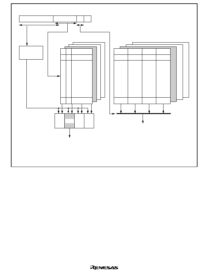
Rev. 5.0, 09/03, page 149 of 806
0
1
255
V U Tag address
LW0
LW1
LW2
LW3
Ways 0
-3
Ways 0
-3
31
12 11
4 3 2 1 0
Virtual address
CMP0 CMP1 CMP2 CMP3
Physical address
CMP0: Comparison circuit 0
CMP1: Comparison circuit 1
CMP2: Comparison circuit 2
CMP3: Comparison circuit 3
Hit signal 1
Entry selection
Longword (LW) selection
MMU
Figure 5.4 Cache Search Scheme (Normal Mode)

Rev. 5.0, 09/03, page 150 of 806
5.3.2
Read Access
Read Hit: In a read access, instructions and data are transferred from the cache to the CPU. The
transfer unit is 32 bits. LRU is updated.
Read Miss: An external bus cycle starts and the entry is updated. The way replaced is the one
least recently used. Entries are updated in 16-byte units. When the desired instruction or data that
caused the miss is loaded from external memory to the cache, the instruction or data is transferred
to the CPU in parallel with being loaded to the cache. When it is loaded in the cache, the U bit is
cleared to 0 and the V bit is set to 1.
5.3.3
Write Access
Write Hit: In a write access in write-back mode, the data is written to the cache and the U bit of
the entry written is set to 1. Writing occurs only to the cache; no external memory write cycle is
issued. In write-through mode, the data is written to the cache and an external memory write cycle
is issued.
Write Miss: In write-back mode, an external write cycle starts when a write miss occurs, and the
entry is updated. The way to be replaced is the one least recently used. When the U bit of the entry
to be replaced is 1, the cache fill cycle starts after the entry is transferred to the write-back buffer.
The write-back unit is 16 bytes. Data is written to the cache and the U bit is set to 1. After the
cache completes its fill cycle, the write-back buffer writes the entry back to the memory. In write-
through mode, no write to cache occurs in a write miss; the write is only to the external memory.
5.3.4
Write-Back Buffer
When the U bit of the entry to be replaced in the write-back mode is 1, it must be written back to
the external memory. To increase performance, the entry to be replaced is first transferred to the
write-back buffer and fetching of new entries to the cache takes priority over writing back to the
external memory. During the write-back cycles, the cache can be accessed. The write-back buffer
can hold one line of cache data (16 bytes) and its physical address. Figure 5.5 shows the
configuration of the write-back buffer.
Longword 0 Longword 1 Longword 2 Longword 3
PA (31
-4)
PA (31
-4):
Longword 0
-3:
Physical address written to external memory
The line of cache data to be written to
external memory
Figure 5.5 Write-Back Buffer Configuration

Rev. 5.0, 09/03, page 151 of 806
5.3.5
Coherency of Cache and External Memory
Use software to ensure coherency between the cache and the external memory. When memory
shared by this LSI and another device is accessed, the latest data may be in a write-back mode
cache, so invalidate the entry that includes the latest data in the cache, generate a write-back, and
update the data in memory before using it. When the caching area is updated by a device other
than the SH7729R, invalidate the entry that includes the updated data in the cache.
5.4
Memory-Mapped Cache
To allow software management of the cache, cache contents can be read and written by means of
MOV instructions in the privileged mode. The cache is mapped onto the P4 area in virtual address
space. The address array is mapped onto addresses H'F0000000 to H'F0FFFFFF, and the data
array onto addresses H'F1000000 to H'F1FFFFFF. Only longword can be used as the access size
for the address array and data array, and instruction fetches cannot be performed.
5.4.1
Address Array
The address array is mapped to H'F0000000 to H'F0FFFFFF. The 32-bit address field (for
read/write accessed) and 32-bit data field (for write access) must be specified to access an element
of the address array. The address field specifies information that selects the entry to be accessed;
the data field specifies the tag address, V bit, U bit, and LRU bits to be written to the address array
(figure 5.6 (1)).
In the address field, specify the entry's address in bits 11-4 to select the entry, W in bits 13-12 to
select the way, the A bit (bit 3) to specify an associative operation, and H'F0 in bits 31-24 to
indicate access to the address array. Settings for the W bits (13-12) are as follows: 00 is way 0, 01
is way 1, 10 is way 2, and 11 is way 3.
In the data field, specify the tag address in bits 31-10, LRU in bits 9-4, U bit in bit 1, and V bit in
bit 0. The upper 3 bits (bit 31-29) of the tag address must always be 0.
The following three operations on the address array are possible.
(1) Address Array Read
Reads the tag address, LRU, U bit, and V bit from the entry that corresponds to the entry address
and w`ay that were specified in the address field. No associative operation will be performed,
regardless of the value of the associative bit (the A bit).
(2) Address Array Write (without Associative Operation)
Writes the tag address, LRU, U bit, and V bit specified in the data field to the entry that
corresponds to the entry address and way that were specified in the address field. The associative
bit (A bit) of the address field must be set to 0. An attempt to write to a cache line for which both
the U bit and V bit are set results in a write-back for that cache line. The tag address, LRU, U bit,

Rev. 5.0, 09/03, page 152 of 806
and V bit specified in the data field are then written. Note that, when a 0 is written to the V bit, a 0
should always be written to the U bit of the same entry, too.
(3) Address Array Write (with Associative Operation)
The associative bit (A bit) in the address field indicates whether the addresses are compared
during writing. With the A bit set to 1, all 4 ways for the entry specified in the address field will be
compared to the tag address specified in the data field for a match. The values of the U bit and V
bit specified in the data field will be written to the way that has a hit. However, the tag address and
the LRU will not be changed. If no way receives a hit, writing does not take place and the result is
no operation.
This operation is used to invalidate the address specification for a cache. Write back will take
place when the U bit of the entry that received a hit is 1. Note that, when a 0 is written to the V bit,
a 0 should always be written to the U bit of the same entry, too.
5.4.2
Data Array
The address array is mapped to H'F1000000 to H'F1FFFFFF. To access an element of the data
array, the 32-bit address field (for read/write access) and 32-bit data field (for write access) must
be specified. The address field specifies the information that selects the entry to be accessed; the
data field specifies the longword data to be written to the data array.
In the address field, specify the entry's address in bits 11-4, L in bits 3-2 to indicate the longword's
position within a line (which consists of 16 bytes), W in bits 13-12 to select the way, and H'F1 in
bits 31-24 to indicate access to the data array. The L bits (3-2) specification is in the following
form: 00 is longword 0, 01 is longword 1, 10 is longword 2, and 11 is longword 3. Settings for the
W bits (13-12) are as follows: 00 is way 0, 01 is way 1, 10 is way 2, and 11 is way 3. Since access
is not allowed crossing longword boundaries, always set 00 in bits 1-0 of the address field.
The following two operations on the data array are possible. Note that these operations will not
change the information in the address array.
(1) Data Array Read
Reads the data at the position selected by the L bits (3-2) of the address field from the entry that
corresponds to the entry address and way that were specified in the address field.
(2) Data Array Write
Writes the longword data set in the data field into the entry that corresponds to the entry address
and way that were specified in the address field. The longword data will be written to the entry at
the position selected by the L bits (3-2) of the address field.

Rev. 5.0, 09/03, page 153 of 806
1. Address array access
Address
specification
Read access
Write access
Data specification
2. Data array access (both read and write accesses)
Address
specification
31
24
23
14
13
12
11
4
3
0
1111 0000
*............*
*............*
*............*
* * *
* * *
W
Entry
31
24
23
14
13
12
11
4
3
0
1111 0000
W
Entry
2
A
31 30 29
10
4
3
0
LRU
2
X
0 0 0
X
9
Address tag (31
-10)
U
V
1
31
24
23
14
13
12
11
4
3
0
1111 0001
W
Entry
* *
1
2
L
Data specification
31
0
Longword
X: 0 for read, don't care for write
*: Don't care bit
0
2
Figure 5.6 Specifying Address and Data for Memory-Mapped Cache Access

Rev. 5.0, 09/03, page 154 of 806
5.5
Usage Examples
5.5.1
Invalidating a Specific Entry
A specific cache entry can be invalidated by accessing the allocated memory cache and writing a 0
to the entry's U and V bits. The A bit is cleared to 0, and an address is specified for the entry
address and the way. If the U bit of the way of the entry in question was set to 1, the entry is
written back and the V and U bits specified by the write data are written to.
In the following example, the write data is specified in R0 and the address is specified in R1.
; R0 = H'0000 0000 LRU = H'000, U = 0, V = 0
; R1 = H'F000 1080, Way = 1, Entry = H'08, A = 0
;
MOV.L
R0, @R1
To invalidate all entries and ways, write 0 to the following addresses.
Addresses
F000 0000
F000 0010
F000 0020
:
F000 3FF0
This involves a total of 1,024 writes.
The above operation should be performed using a non-cacheable area.

Rev. 5.0, 09/03, page 155 of 806
5.5.2
Invalidating a Specific Address
A specific address can be invalidated by writing 0 to the entry's V bit. When the A bit is 1, the
address tag specified by the write data is compared to the address tag within the cache selected by
the entry address, and data is written when a match is found. If no match is found, there is no
operation. R0 specifies the write data and R1 specifies the address. When the V bit of an entry in
the address array is set to 0, the entry is written back if the entry's U bit is 1.
; R0
=
H'01100010; Tag address
=
B'0000 0001 0001 0000 0000 00, U
=
0, V
=
0
; R1
=
H'F0000088; address array access, entry
=
H'08, A
=
1
;
MOV.L R0,@R1
In the following example, an address (32-bit) to be purged is specified in R0.
MOV.L #H'00000FF0, R1
;
AND
R0, R1
; The entry address is fetched.
MOV.L #H'F0000008, R2
;
OR
R1, R2
; The start is set to H'F0 and the A bit
to 1.
MOV.L #H'1FFFFC00, R3
;
AND
R0, R3
; The tag address is fetched. U = V = 0.
MOV.L R3, @R2
; Associative purge.
The above operation should be performed using a non-cacheable area.
5.5.3
Reading the Data of a Specific Entry
This example reads the data section of a specific cache entry. The longword indicated in the data
field of the data array in figure 5.6 is read into the register. R0 specifies the address and R1 is read.
; R1
=
H'F100 004C; data array access, entry
=
H'04, Way
=
0,
; longword address
=
3
;
MOV.L @R0,R1 ; Longword 3 is read.

Rev. 5.0, 09/03, page 156 of 806

Rev. 5.0, 09/03, page 157 of 806
Section 6 X/Y Memory
6.1
Overview
The SH7729R has on-chip X-RAM and Y-RAM. It can be used by the CPU, DSP and DMAC to
store instructions or data.
6.1.1
Features
The X/Y memory features are listed in table 6.1.
Table 6.1
X/Y Memory Specifications
Parameter
Features
Addressing
method
User selectable mapping mechanism
∑
Fixed mapping for mission-critical realtime applications (P2/Uxy area)
∑
Automatic mapping through TLB for easy to use (P0/P3/U0 area)
Ports
Three independent read/write ports
∑
8-/16-/32-bit
access
from
the
CPU
∑
Maximum of two simultaneous 16-bit accesses, or 16/32-bit accesses,
from the DSP
∑
8-/16-/32-bit
access
from
the
DMAC
Size
8-kbyte RAM each for X and Y memory

Rev. 5.0, 09/03, page 158 of 806
6.2
X/Y Memory Access from CPU
The X/Y memory can be located in either a mappable area or fixed-mapped area, depending on the
mode bit (MD) and DSP bit (DSP) setting in the status register (SR). Figure 6.1 shows X/Y
memory logical mapping.
1. Privileged Mode
MD = 1, DSP = 0: Any physical address in space P0 or P3 can map to X/Y memory through
TLB translation. Addresses ranging from H'A500 0000 to H'A5FF FFFF in the P2 space can
also fixed-map to X/Y memory. Since the DSP extension is disabled, the DSP instruction set
and registers are not available to the programmer.
2. User Mode
MD = 0, DSP = 0: Any physical address in the U0 space can access X/Y memory through TLB
translation. Any access to addresses beyond the U0 space will cause an address error. Since the
DSP extension is disabled, the DSP instruction set and registers are not available to the
programmer.
3. Privileged-DSP Mode
MD = 1, DSP = 1: Any physical address in space P0 or P3 can map to X/Y memory through
TLB translation. Addresses ranging from H'A500 0000 to H'A5FF FFFF in the P2 space can
also fixed-map to X/Y memory. Since the DSP extension is enabled, the DSP instruction set
and registers are available to the programmer.
4. User-DSP Mode
MD = 0, DSP = 1: Any physical address in space U0 can map to X/Y memory through TLB
translation. Addresses ranging from H'A500 0000 to H'A5FF FFFF in the Uxy spaces can also
fixed-map to X/Y memory. Any access outside U0 and Uxy space will cause an address error.
Since the DSP extension is enabled, the DSP instruction set and registers are available to the
programmer.
For the mappable area, the C (cacheable) bit in the TLB entry must be cleared to 0 to guarantee a
two-cycle access.
Mapping through TLB translation provides a flexible X/Y memory addressing scheme but takes
two cycles even when the C bit in the TLB entry is cleared to 0. Fixed mapping provides a one-
cycle access for read and two-cycle access for write, which is the appropriate method for mission-
critical realtime operations.
The X/Y memory resides in the second 16 Mbytes of physical address space area 1, from H'A500
0000 to H'A5FF FFFF. This 16-Mbyte address space is shadowed and maps to the same 128-kbyte
X/Y ROM/RAM. Figures 6.1 and 6.2 show X/Y memory physical mapping.

Rev. 5.0, 09/03, page 159 of 806
P4
P3
P2
P1
P0
MD = 1, DSP = 0
Privileged mode
Same as SH-3
When MD = 1, CPU can
change DSP flag
Address error
U0
MD = 0, DSP = 0
User mode
Same as SH-3
When MD = 0, user cannot
change DSP flag
Address error
Address error
U0
MD = 0, DSP = 1
User DSP mode
Uxy: Address range
From H'A500 0000
To H'A5FF FFFF
P4
P3
P2
P1
P0
MD = 1, DSP = 1
Privileged DSP mode
When MD = 1, CPU can
change DSP flag
X
Y
X
Y
Address range
From H'A500 0000
To H'A5FF FFFF
Figure 6.1 X/Y Memory Logical Address Mapping

Rev. 5.0, 09/03, page 160 of 806
128-kbyte X/Y Memory
X-ROM/X-RAM
Reserved space
X-ROM/X-RAM
Reserved space
Y-ROM/X-RAM
Reserved space
Y-ROM/X-RAM
Reserved space
X-RAM, 8 kbytes
Y-RAM, 8 kbytes
501FFFF
5018FFF
5017000
5010000
5008FFF
5007000
5000000
Area 1, 64 Mbytes
I/O register space
16 Mbytes
Reserved area
16 Mbytes
Reserved area
32 Mbytes
7FFFFFF
X/Y Memory
6000000
5020000
5000000
4000000
Figure 6.2 X/Y Memory Physical Address Mapping
6.3
X/Y Memory Access from DSP
The X/Y memory can be accessed by the DSP through the X bus and Y bus. Accesses via the X
bus/Y bus are always 16-bit, while accesses via the L bus are either 16-bit or 32-bit. Accesses via
the X bus and Y bus cannot be specified simultaneously.
6.4
X/Y Memory Access from DMAC
The X/Y memory also exists on the I bus and can be accessed by the DMAC. DMAC access uses
an 8-/16-/32-bit unit. If the I bus accesses X/Y memory simultaneously with an access from the X
bus/Y bus or L bus, the I bus master has a higher priority.
When accessing X/Y memory from the DMAC, use physical addresses in the range H'05000000 to
H'05FFFFFF.

Rev. 5.0, 09/03, page 161 of 806
Section 7 Interrupt Controller (INTC)
7.1
Overview
The interrupt controller (INTC) ascertains the priority of interrupt sources and controls interrupt
requests to the CPU. The INTC registers set the order of priority of each interrupt, allowing the
user to process interrupt requests according to the user-set priority.
7.1.1
Features
The INTC has the following features:
∑
16 levels of interrupt priority can be set: By setting the five interrupt-priority registers, the
priorities of on-chip peripheral module, IRQ, and PINT interrupts can be selected from 16
levels for individual request sources.
∑
NMI noise canceler function: An NMI input-level bit indicates the NMI pin state. By reading
this bit in the interrupt exception service routine, the pin state can be checked, enabling it to be
used as a noise canceler.
∑
External devices can be notified that an interrupt has been received (
IRQOUT): When the
SH7729R has released the bus, the external bus master can be notified that an external
interrupt, an on-chip peripheral module interrupt, or a memory refresh request has occurred,
enabling the bus to be requested.
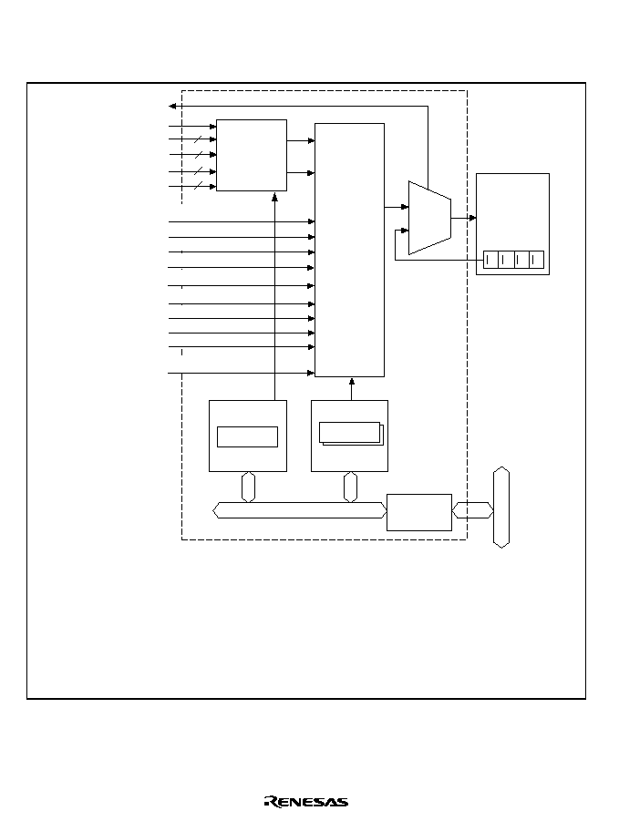
Rev. 5.0, 09/03, page 162 of 806
7.1.2
Block Diagram
Figure 7.1 shows a block diagram of the INTC.
REF
IrDA
DMAC
ICR
Input/output
control
Com-
parator
Priority
identifier
3
4
6
16
Interrupt
request
SR
IPRA
-IPRE
IRL3-IRL0
NMI
IRQ0
-IRQ5
PINT0
-PINT15
IRQOUT
: Timer unit
: Realtime clock unit
: Serial communication interface
: Serial communication interface (with IrDA)
: Serial communication interface (with FIFO)
: Watchdog timer
: Refresh requests in the bus state controller
: Interrupt control register
: Interrupt priority registers A
-E
: Status register
: Direct memory access controller
: Analog-to-digital converter
: User debugging interface
Legend
TMU
RTC
SCI
IrDA
SCIF
WDT
REF
ICR
IPRA
-IPRE
SR
DMAC
ADC
UDI
(Interrupt request)
SCIF
TMU
(Interrupt request)
(Interrupt request/
IPR
CPU
Internal bus
Bus
interface
2 1 0
(Interrupt request)
(Interrupt request)
RTC
WDT
(Interrupt request)
(Interrupt request)
IRLS3-IRLS0
4
SCI
(Interrupt request)
ADC
(Interrupt request)
INTC
UDI
(Interrupt request)
refresh request)
Figure 7.1 Block Diagram of INTC

Rev. 5.0, 09/03, page 163 of 806
7.1.3
Pin Configuration
Table 7.1 shows the INTC pin configuration.
Table 7.1
INTC Pins
Name
Abbreviation
I/O
Description
Nonmaskable interrupt input
pin
NMI
I
Input of interrupt request signal, not
maskable by the interrupt mask bits in
SR
Interrupt input pins
IRQ5≠IRQ0
IRL3
≠
IRL0
IRLS3
≠
IRLS0
I
Input of interrupt request signals,
maskable by the interrupt mask bits in
SR
Port interrupt input pins
PINT0≠PINT15
I
Input of port interrupt request signals,
maskable by the interrupt mask bits in
SR
Interrupt request output pin
IRQOUT
O
Output of signal that notifies external
devices that an interrupt source or
memory refresh has occurred

Rev. 5.0, 09/03, page 164 of 806
7.1.4
Register Configuration
The INTC has the 12 registers listed in table 7.2.
Table 7.2
INTC Registers
Name
Abbr.
R/W
Initial Value
*
1
Address
Access
Size
Interrupt control register 0
ICR0
R/W
*
2
H'FFFFFEE0
16
Interrupt control register 1
ICR1
R/W
H'0000
H'04000010
(H'A4000010)
*
3
16
Interrupt control register 2
ICR2
R/W
H'0000
H'04000012
(H'A4000012)
*
3
16
PINT interrupt enable register
PINTER
R/W
H'0000
H'04000014
(H'A4000014)
*
3
16
Interrupt priority register A
IPRA
R/W
H'0000
H'FFFFFEE2
16
Interrupt priority register B
IPRB
R/W
H'0000
H'FFFFFEE4
16
Interrupt priority register C
IPRC
R/W
H'0000
H'04000016
(H'A4000016)
*
3
16
Interrupt priority register D
IPRD
R/W
H'0000
H'04000018
(H'A4000018)
*
3
16
Interrupt priority register E
IPRE
R/W
H'0000
H'0400001A
(H'A400001A)
*
3
16
Interrupt request register 0
IRR0
R/W
H'00
H'04000004
(H'A4000004)
*
3
8
Interrupt request register 1
IRR1
R
H'00
H'04000006
(H'A4000006)
*
3
8
Interrupt request register 2
IRR2
R
H'00
H'04000008
(H'A4000008)
*
3
8
Notes: 1. Initialized by a power-on or manual reset.
2. H'8000 when the NMI pin is high, H'0000 when the NMI pin is low.
3. When address translation by the MMU does not apply, the address in parentheses
should be used.

Rev. 5.0, 09/03, page 165 of 806
7.2
Interrupt Sources
There are five types of interrupt sources: NMI, IRQ, IRL,PINT, and on-chip peripheral modules.
Each interrupt has a priority level (0≠16), with 0 the lowest and 16 the highest. Priority level 0
masks an interrupt.
7.2.1
NMI Interrupt
The NMI interrupt has the highest priority level of 16. When the BLMSK bit in the interrupt
control register (ICR1) is 1 or the BL bit in the status register (SR) is 0, NMI interrupts are
accepted when the MAI bit in the ICR1 register is 0. NMI interrupts are edge-detected. In sleep or
standby mode, the interrupt is accepted regardless of the BL setting. The NMI edge select bit
(NMIE) in the interrupt control register 0 (ICR0) is used to select either rising or falling edge
detection. When the NMIE bit in the ICR0 register is changed, an NMI interrupt is not detected for
20 cycles after changing ICR0. NMIE to avoid a false detection of NMI. NMI interrupt exception
handling does not affect the interrupt mask level bits (I3≠I0) in the status register (SR).
When the BL bit is 1 and the BLMSK bit in the ICR1 register is set to 1 and only NMI interrupts
are accepted, the SPC register and SSR register are updated by the NMI interrupt handler, making
it impossible to return to the original processing from exception handling initiated prior to the
NMI interrupt. Use should therefore be restricted to cases where return is not necessary.
It is possible to wake the chip up from the standby state with an NMI interrupt (except when the
MAI bit in the ICR1 register is set to 1).
7.2.2
IRQ Interrupts
IRQ interrupts are input by level or edge from pins IRQ0≠IRQ5. The priority level can be set by
interrupt priority registers C≠D (IPRC≠IPRD) in a range from 0 to 15.
When using edge-sensing for IRQ interrupts, clear the interrupt source by having software read 1
from the corresponding bit in IRR0, then write 0 to the bit.
When the ICR1 register is rewritten, IRQ interrupts may be mistakenly detected, depending on the
pin states. To prevent this, rewrite the register while interrupts are masked, then release the mask
after clearing the illegal interrupt by writing 0 to interrupt request register 0 (IRR0).
Edge input interrupt detection requires input of a pulse width of more than two cycles on a P clock
basis.
The interrupt mask bits (I3≠I0) in the status register (SR) are not affected by IRQ interrupt
handling.
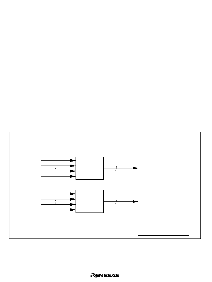
Rev. 5.0, 09/03, page 166 of 806
Interrupts IRQ4≠IRQ0 can wake the chip up from the standby state when the relevant interrupt
level is higher than the setting of I3≠I0 in the SR register (but only when the RTC 32-kHz
oscillator is used).
If the IRQ edge is input immediately before the CPU enters the standby mode (during the period
between when the CPU executes a SLEEP instruction and when STATUS0 becomes high level),
the interrupt may not be detected. However, the interrupt will be accepted correctly if the IRQ
edge is re-input after the CPU has entered the standby mode (when STATUS0 is high level). In
addition, the interrupt may not be detected if the IRQ edge is input during frequency change
processing (WDT count).
7.2.3
IRL Interrupts
IRL interrupts are input by level at pins
IRL3≠IRL0 and IRLS3≠IRLS0. IRLS3≠IRLS0 are
enabled when the IRQLVL bit and IRLSEN bit in interrupt control register 1 (ICR1) are both 1.
The priority level is the higher level indicated by pins
IRL3≠IRL0 and IRLS3≠IRLS0. An IRL3≠
IRL0/IRLS3≠IRLS0 value of 0 (0000) indicates the highest-level interrupt request (interrupt
priority level 15). A value of 15 (1111) indicates no interrupt request (interrupt priority level 0).
Figure 7.2 shows an example of IRL interrupt connection. Table 7.3 shows
IRL/IRLS pins and
interrupt levels.
Interrupt
request
Priority
encoder
IRL3 to IRL0
4
SH7729R
IRL3 to IRL0
Interrupt
request
Priority
encoder
IRLS3 to IRLS0
4
IRLS3 to IRLS0
Figure 7.2 Example of IRL Interrupt Connection

Rev. 5.0, 09/03, page 167 of 806
Table 7.3
I
I
I
IR
R
R
RLLLL3333≠IIIIR
R
R
RLLLL0000/IIIIR
R
R
RLLLLSSSS3333≠IIIIR
R
R
RLLLLSSSS0000 Pins and Interrupt Levels
I
I
I
IR
R
R
RL3
L3
L3
L3
/
I
I
I
IR
R
R
RLLLLS
S
S
S3333
I
I
I
IR
R
R
RL2
L2
L2
L2
/
I
I
I
IR
R
R
RLLLLS
S
S
S2222
I
I
I
IR
R
R
RL1
L1
L1
L1
/
I
I
I
IR
R
R
RLLLLS
S
S
S1111
I
I
I
IR
R
R
RL0
L0
L0
L0
/
I
I
I
IR
R
R
RLLLLS
S
S
S0000
Interrupt Priority Level
Interrupt Request
0
0
0
0
15
Level 15 interrupt request
0
0
0
1
14
Level 14 interrupt request
0
0
1
0
13
Level 13 interrupt request
0
0
1
1
12
Level 12 interrupt request
0
1
0
0
11
Level 11 interrupt request
0
1
0
1
10
Level 10 interrupt request
0
1
1
0
9
Level 9 interrupt request
0
1
1
1
8
Level 8 interrupt request
1
0
0
0
7
Level 7 interrupt request
1
0
0
1
6
Level 6 interrupt request
1
0
1
0
5
Level 5 interrupt request
1
0
1
1
4
Level 4 interrupt request
1
1
0
0
3
Level 3 interrupt request
1
1
0
1
2
Level 2 interrupt request
1
1
1
0
1
Level 1 interrupt request
1
1
1
1
0
No interrupt request
A noise-cancellation feature is built in, and the IRL interrupt is not detected unless the levels
sampled at every peripheral module clock cycle remain unchanged for two consecutive cycles, so
that no transient level on the
IRL/IRLS pin change is detected. In standby mode, as the peripheral
clock is stopped, noise cancellation is performed using the 32-kHz clock for the RTC instead.
Therefore when the RTC is not used, interruption by means of IRL interrupts cannot be performed
in standby mode.
The priority level of the IRL interrupt must not be lowered until the interrupt is accepted and
interrupt handling starts. Correct operation cannot be guaranteed if the level is not maintained.
However, the priority level can be changed to a higher one.
The interrupt mask bits (I3≠I0) in the status register (SR) are not affected by
IRL/IRLS interrupt
handling.
If the interrupt level of an IRL interrupt is higher than the setting in bits I3-I0 in the SR register, it
can be used to recover from the standby state (but only when using the RTC 32-kHz oscillator).

Rev. 5.0, 09/03, page 168 of 806
7.2.4
PINT Interrupts
PINT interrupts are input by level from pins PINT0≠PINT15. The priority level can be set by
interrupt priority register D (IPRD) in a range from 0 to 15, in groups of PINT0≠PINT7 and
PINT8≠PINT15.
The PINT interrupt level should be held until the interrupt is accepted and interrupt handling is
started. Correct operation cannot be guaranteed if the level is not maintained.
The interrupt mask bits (I3≠I0) in the status register (SR) are not affected by PINT interrupt
handling.
PINT interrupts can wake the chip up from the standby state when the relevant interrupt level is
higher than the setting of I3≠I0 in the SR register (but only when the RTC 32-kHz oscillator is
used).
7.2.5
On-Chip Peripheral Module Interrupts
On-chip peripheral module interrupts are generated by the following ten modules:
∑
Timer unit (TMU)
∑
Realtime clock (RTC)
∑
Serial communication interfaces (SCI, IrDA, SCIF)
∑
Bus state controller (BSC)
∑
Watchdog timer (WDT)
∑
Direct memory access controller (DMAC)
∑
Analog-to-digital converter (ADC)
∑
User-debugging interface (UDI)
Not every interrupt source is assigned a different interrupt vector. Sources are reflected in the
interrupt event registers (INTEVT and INTEVT2). It is easy to identify sources by using the value
of the INTEVT or INTEVT2 register as a branch offset.
A priority level (from 0 to 15) can be set for each module except UDI by writing to interrupt
priority registers A, B, and E (IPRA, IPRB, and IPRE). The priority level of the UDI interrupt is
15 (fixed).
The interrupt mask bits (I3≠I0) in the status register are not affected by on-chip peripheral module
interrupt handling.
TMU and RTC interrupts can wake the chip up from the standby state when the relevant interrupt
level is higher than the setting of I3≠I0 in the SR register (but only when the RTC 32-kHz
oscillator is used).

Rev. 5.0, 09/03, page 169 of 806
7.2.6
Interrupt Exception Handling and Priority
Tables 7.4 and 7.5 list the codes for the interrupt event registers (INTEVT and INTEVT2), and the
order of interrupt priority. Each interrupt source is assigned a unique code. The start address of the
interrupt service routine is common to each interrupt source. This is why, for instance, the value of
INTEVT or INTEVT2 is used as offset at the start of the interrupt service routine and branched to
in order to identify the interrupt source.
The priority of the on-chip peripheral module, IRQ, and PINT interrupts is set within priority
levels 0≠15 as required by using interrupt priority registers A≠E (IPRA≠IPRE). The priority of the
on-chip peripheral module, IRQ, and PINT interrupts is set to 0 by a reset.
When the priorities of multiple interrupt sources are set to the same level and such interrupts are
generated simultaneously, they are handled according to the default order shown in tables 7.4 and
7.5.
Rev. 5.0, 09/03, page 170 of 806
Table 7.4
Interrupt Exception Handling Sources and Priority (IRQ Mode)
Interrupt Source
INTEVT Code
(INTEVT2 Code)
Interrupt
Priority
(Initial Value)
IPR (Bit
Numbers)
Priority
within IPR
Setting Unit
Default
Priority
NMI
H'1C0 (H'1C0)
16
--
--
High
UDI
H'5E0 (H'5E0)
15
--
--
IRQ
IRQ0
H'200≠3C0
*
(H'600)
0≠15 (0)
IPRC (3≠0)
--
IRQ1
H'200≠3C0
*
(H'620)
0≠15 (0)
IPRC (7≠4)
--
IRQ2
H'200≠3C0
*
(H'640)
0≠15 (0)
IPRC (11≠8)
--
IRQ3
H'200≠3C0
*
(H'660)
0≠15 (0)
IPRC (15≠12) --
IRQ4
H'200≠3C0
*
(H'680)
0≠15 (0)
IPRD (3≠0)
--
IRQ5
H'200≠3C0
*
(H'6A0)
0≠15 (0)
IPRD (7≠4)
--
PINT
PINT0-7
H'200≠3C0
*
(H'700)
0≠15 (0)
IPRD (15≠12) --
PINT8-15
H'200≠3C0
*
(H'720)
0≠15 (0)
IPRD (11≠8)
--
DMAC
DEI0
H'200≠3C0
*
(H'800)
0≠15 (0)
IPRE (15≠12) High
DEI1
H'200≠3C0
*
(H'820)
DEI2
H'200≠3C0
*
(H'840)
DEI3
H'200≠3C0
*
(H'860)
Low
IrDA
ERI1
H'200≠3C0
*
(H'880)
0≠15 (0)
IPRE (11≠8)
High
RXI1
H'200≠3C0
*
(H'8A0)
BRI1
H'200≠3C0
*
(H'8C0)
TXI1
H'200≠3C0
*
(H'8E0)
Low
SCIF
ERI2
H'200≠3C0
*
(H'900)
0≠15 (0)
IPRE (7≠4)
High
RXI2
H'200≠3C0
*
(H'920)
BRI2
H'200≠3C0
*
(H'940)
TXI2
H'200≠3C0
*
(H'960)
Low
ADC
ADI
H'200≠3C0
*
(H'980)
0≠15 (0)
IPRE (3≠0)
--
TMU0
TUNI0
H'400 (H'400)
0≠15 (0)
IPRA (15≠12) --
TMU1
TUNI1
H'420 (H'420)
0≠15 (0)
IPRA (11≠8)
--
TMU2
TUNI2
H'440 (H'440)
0≠15 (0)
IPRA (7≠4)
High
TICPI2
H'460 (H'460)
Low
Low
Rev. 5.0, 09/03, page 171 of 806
Interrupt Source
INTEVT Code
(INTEVT2 Code)
Interrupt
Priority
(Initial Value)
IPR (Bit
Numbers)
Priority
within IPR
Setting Unit
Default
Priority
RTC
ATI
H'480 (H'480)
0≠15 (0)
IPRA (3≠0)
High
High
PRI
H'4A0 (H'4A0)
CUI
H'4C0 (H'4C0)
Low
SCI
ERI
H'4E0 (H'4E0)
0≠15 (0)
IPRB (7≠4)
High
RXI
H'500 (H'500)
TXI
H'520 (H'520)
TEI
H'540 (H'540)
Low
WDT
ITI
H'560 (H'560)
0≠15 (0)
IPRB (15≠12) --
REF
RCMI
H'580 (H'580)
0≠15 (0)
IPRB (11≠8)
High
ROVI
H'5A0 (H'5A0)
Low
Low
Note:
*
The code corresponding to an interrupt level shown in table 7.6 is set.

Rev. 5.0, 09/03, page 172 of 806
Table 7.5
Interrupt Exception Handling Sources and Priority (IRL Mode)
Interrupt Source
INTEVT Code
(INTEVT2 Code)
Interrupt
Priority
(Initial Value)
IPR (Bit
Numbers)
Priority
within IPR
Setting Unit
Default
Priority
NMI
H'1C0 (H'1C0)
16
--
--
High
UDI
H'5E0 (H'5E0)
15
--
--
IRL
IRL(3:0)*
2
= 0000 H'200 (H'200)
15
--
--
IRL(3:0)*
2
= 0001 H'220 (H'220)
14
--
--
IRL(3:0)*
2
= 0010 H'240 (H'240)
13
--
--
IRL(3:0)*
2
= 0011 H'260 (H'260)
12
--
--
IRL(3:0)*
2
= 0100 H'280 (H'280)
11
--
--
IRL(3:0)*
2
= 0101 H'2A0 (H'2A0)
10
--
--
IRL(3:0)*
2
= 0110 H'2C0 (H'2C0)
9
--
--
IRL(3:0)*
2
= 0111 H'2E0 (H'2E0)
8
--
--
IRL(3:0)*
2
= 1000 H'300 (H'300)
7
--
--
IRL(3:0)*
2
= 1001 H'320 (H'320)
6
--
--
IRL(3:0)*
2
= 1010 H'340 (H'340)
5
--
--
IRL(3:0)*
2
= 1011 H'360 (H'360)
4
--
--
IRL(3:0)*
2
= 1100 H'380 (H'380)
3
--
--
IRL(3:0)*
2
= 1101 H'3A0 (H'3A0)
2
--
--
IRL(3:0)*
2
= 1110 H'3C0 (H'3C0)
1
--
--
IRQ
IRQ4
H'200≠3C0
*
1
(H'680) 0≠15 (0)
IPRD (3≠0)
--
IRQ5
H'200≠3C0
*
1
(H'6A0) 0≠15 (0)
IPRD (7≠4)
--
PINT
PINT0≠7
H'200≠3C0
*
1
(H'700) 0≠15 (0)
IPRD (15≠12) --
PINT8≠15
H'200≠3C0
*
1
(H'720) 0≠15 (0)
IPRD (11≠8) --
DMAC DEI0
H'200≠3C0
*
1
(H'800) 0≠15 (0)
IPRE (15≠12) High
DEI1
H'200≠3C0
*
1
(H'820)
DEI2
H'200≠3C0
*
1
(H'840)
DEI3
H'200≠3C0
*
1
(H'860)
Low
IrDA
ERI1
H'200≠3C0
*
1
(H'880) 0≠15 (0)
IPRE (11≠8)
High
RXI1
H'200≠3C0
*
1
(H'8A0)
BRI1
H'200≠3C0
*
1
(H'8C0)
TXI1
H'200≠3C0
*
1
(H'8E0)
Low
Low
Rev. 5.0, 09/03, page 173 of 806
Interrupt Source
INTEVT Code
(INTEVT2 Code)
Interrupt
Priority
(Initial Value)
IPR (Bit
Numbers)
Priority
within IPR
Setting Unit
Default
Priority
SCIF
ERI2
H'200≠3C0
*
1
(H'900) 0≠15 (0)
IPRE (7≠4)
High
High
RXI2
H'200≠3C0
*
1
(H'920)
BRI2
H'200≠3C0
*
1
(H'940)
TXI2
H'200≠3C0
*
1
(H'960)
Low
ADC
ADI
H'200≠3C0
*
1
(H'980) 0≠15 (0)
IPRE (3≠0)
--
TMU0 TUNI0
H'400 (H'400)
0≠15 (0)
IPRA (15≠12) --
TMU1 TUNI1
H'420 (H'420)
0≠15 (0)
IPRA (11≠8)
--
TMU2 TUNI2
H'440 (H'440)
0≠15 (0)
IPRA (7≠4)
High
TICPI2
H'460 (H'460)
Low
RTC
ATI
H'480 (H'480)
0≠15 (0)
IPRA (3≠0)
High
PRI
H'4A0 (H'4A0)
CUI
H'4C0 (H'4C0)
Low
SCI
ERI
H'4E0 (H'4E0)
0≠15 (0)
IPRB (7≠4)
High
RXI
H'500 (H'500)
TXI
H'520 (H'520)
TEI
H'540 (H'540)
Low
WDT
ITI
H'560 (H'560)
0≠15 (0)
IPRB (15≠12) --
REF
RCMI
H'580 (H'580)
0≠15 (0)
IPRB (11≠8)
High
ROVI
H'5A0 (H'5A0)
Low
Low
Notes: 1. The code corresponding to an interrupt level shown in table 7.6 is set.
2. When
IRLS3
≠
IRLS0
are enabled, IRL is the higher level of
IRL3
≠
IRL0
and
IRLS3
≠
IRLS0
.

Rev. 5.0, 09/03, page 174 of 806
Table 7.6
Interrupt Levels and INTEVT Codes
Interrupt level
INTEVT Code
15
H'200
14
H'220
13
H'240
12
H'260
11
H'280
10
H'2A0
9
H'2C0
8
H'2E0
7
H'300
6
H'320
5
H'340
4
H'360
3
H'380
2
H'3A0
1
H'3C0
Rev. 5.0, 09/03, page 175 of 806
7.3
INTC Registers
7.3.1
Interrupt Priority Registers A to E (IPRA≠IPRE)
Interrupt priority registers A to E (IPRA to IPRE) are 16-bit readable/writable registers in which
priority levels from 0 to 15 are set for on-chip peripheral module, IRQ, and PINT interrupts. These
registers are initialized to H'0000 by a power-on reset or manual reset, but are not initialized in
standby mode.
Bit:
15
14
13
12
11
10
9
8
Initial value:
0
0
0
0
0
0
0
0
R/W:
R/W
R/W
R/W
R/W
R/W
R/W
R/W
R/W
Bit:
7
6
5
4
3
2
1
0
Initial value:
0
0
0
0
0
0
0
0
R/W:
R/W
R/W
R/W
R/W
R/W
R/W
R/W
R/W
Table 7.7 lists the relationship between the interrupt sources and the IPRA--IPRE bits.
Table 7.7
Interrupt Request Sources and IPRA≠IPRE
Register
Bits 15 to 12
Bits 11 to 8
Bits 7 to 4
Bits 3 to 0
IPRA
TMU0
TMU1
TMU2
RTC
IPRB
WDT
REF
SCI0
Reserved
*
IPRC
IRQ3
IRQ2
IRQ1
IRQ0
IPRD
PINT0 to PINT7
PINT8 to PINT15
IRQ5
IRQ4
IPRE
DMAC
IrDA
SCIF
ADC
Note:
*
Always read as 0. Only 0 should be written.
As shown in table 7.7, on-chip peripheral module, IRQ, or PINT interrupts are assigned to four 4-
bit groups in each register. These 4-bit groups (bits 15 to 12, bits 11 to 8, bits 7 to 4, and bits 3 to
0) are set with values from H'0 (0000) to H'F (1111). Setting H'0 means priority level 0 (masking
is requested); H'F is priority level 15 (the highest level). A reset initializes IPRA≠IPRE to H'0000.

Rev. 5.0, 09/03, page 176 of 806
7.3.2
Interrupt Control Register 0 (ICR0)
ICR0 is a register that sets the input signal detection mode of external interrupt input pin NMI, and
indicates the input signal level at the NMI pin. This register is initialized to H'0000 or H'8000 by a
power-on reset or manual reset, but is not initialized in standby mode.
Bit:
15
14
13
12
11
10
9
8
NMIL
--
--
--
--
--
--
NMIE
Initial value:
0/1
*
0
0
0
0
0
0
0
R/W:
R
R
R
R
R
R
R
R/W
Bit:
7
6
5
4
3
2
1
0
--
--
--
--
--
--
--
--
Initial value:
0
0
0
0
0
0
0
0
R/W:
R
R
R
R
R
R
R
R
Note:
*
1 when NMI input is high, 0 when NMI input is low.
Bit 15--NMI Input Level (NMIL): Sets the level of the signal input at the NMI pin. This bit can
be read to determine the NMI pin level. This bit cannot be modified.
Bit 15: NMIL
Description
0
NMI input level is low
1
NMI input level is high
Bit 8--NMI Edge Select (NMIE): Selects whether the falling or rising edge of the interrupt
request signal at the NMI pin is detected.
Bit 8: NMIE
Description
0
Interrupt request is detected on falling edge of NMI input
1
Interrupt request is detected on rising edge of NMI input
Bits 14 to 9 and 7 to 0--Reserved: These bits are always read as 0. The write value should
always be 0.

Rev. 5.0, 09/03, page 177 of 806
7.3.3
Interrupt Control Register 1 (ICR1)
ICR1 is a 16-bit register that specifies the detection mode for external interrupt input pins IRQ0 to
IRQ5 individually: rising edge, falling edge, or low level. This register is initialized to H'4000 by a
power-on reset or manual reset, but is not initialized in standby mode.
Bit:
15
14
13
12
11
10
9
8
MAI
IRQLVL
BLMSK IRLSEN IRQ51S IRQ50S IRQ41S IRQ40S
Initial value:
0
1
0
0
0
0
0
0
R/W:
R/W
R/W
R/W
RW
R/W
R/W
R/W
R/W
Bit:
7
6
5
4
3
2
1
0
IRQ31S IRQ30S IRQ21S IRQ20S IRQ11S IRQ10S IRQ01S IRQ00S
Initial value:
0
0
0
0
0
0
0
0
R/W:
R/W
R/W
R/W
R/W
R/W
R/W
R/W
R/W
Bit 15--Mask All Interrupts (MAI): When set to 1, all interrupt requests are masked while a
low level is being input to the NMI pin. Masks NMI interrupts in standby mode.
Bit 15: MAI
Description
0
All interrupt requests are not masked when NMI pin is low level
(Initial value)
1
All interrupt requests are masked when NMI pin is low level
Bit 14--Interrupt Request Level Detect (IRQLVL): Selects whether the IRQ3≠IRQ0 pins are
used as four independent interrupt pins or as 15-level interrupt pins encoded as
IRL3≠IRL0.
Bit 14: IRQLVL Description
0
Used as four independent interrupt request pins IRQ3≠IRQ0
1
Used as 15-level interrupt pins encoded as
IRL3
≠
IRL0
(Initial value)
Bit 13--BL Bit Mask (BLMSK): Specifies whether NMI interrupts are masked when the BL bit
in the SR register is 1.
Bit 13: BLMSK Description
0
NMI interrupts are masked when BL bit is 1
(Initial value)
1
NMI interrupts are accepted regardless of BL bit setting

Rev. 5.0, 09/03, page 178 of 806
Bit 12--
I
I
I
IR
R
R
RLLLLSSSS Enable (IRLSEN): Enables pins IRLS3≠IRLS0. This bit is valid only when the
IRQLVL bit is 1.
Bit 12: IRLSEN Description
0
Pins
IRLS3
≠
IRLS0
disabled
(Initial value)
1
Pins
IRLS3
≠
IRLS0
enabled
Bits 11 and 10--IRQ5 Sense Select (IRQ51S, IRQ50S): Select whether the interrupt signal to
the IRQ5 pin is detected at the rising edge, at the falling edge, or at the low level.
Bit 11: IRQ51S Bit 10: IRQ50S Description
0
0
An interrupt request is detected at IRQ5 input falling edge
(Initial value)
1
An interrupt request is detected at IRQ5 input rising edge
1
0
An interrupt request is detected at IRQ5 input low level
1
Reserved
Bits 9 and 8--IRQ4 Sense Select (IRQ41S, IRQ40S): Select whether the interrupt signal to the
IRQ4 pin is detected at the rising edge, at the falling edge, or at the low level.
Bit 9: IRQ41S
Bit 8: IRQ40S
Description
0
0
An interrupt request is detected at IRQ4 input falling edge
(Initial value)
1
An interrupt request is detected at IRQ4 input rising edge
1
0
An interrupt request is detected at IRQ4 input low level
1
Reserved
Bits 7 and 6--IRQ3 Sense Select (IRQ31S, IRQ30S): Select whether the interrupt signal to the
IRQ3 pin is detected at the rising edge, at the falling edge, or at the low level.
Bit 7: IRQ31S
Bit 6: IRQ30S
Description
0
0
An interrupt request is detected at IRQ3 input falling edge
(Initial value)
1
An interrupt request is detected at IRQ3 input rising edge
1
0
An interrupt request is detected at IRQ3 input low level
1
Reserved

Rev. 5.0, 09/03, page 179 of 806
Bits 5 and 4--IRQ2 Sense Select (IRQ21S, IRQ20S): Select whether the interrupt signal to the
IRQ2 pin is detected at the rising edge, at the falling edge, or at the low level.
Bit 5: IRQ21S
Bit 4: IRQ20S
Description
0
0
An interrupt request is detected at IRQ2 input falling edge
(Initial value)
1
An interrupt request is detected at IRQ2 input rising edge
1
0
An interrupt request is detected at IRQ2 input low level
1
Reserved
Bits 3 and 2--IRQ1 Sense Select (IRQ11S, IRQ10S): Select whether the interrupt signal to the
IRQ1 pin is detected at the rising edge, at the falling edge, or at the low level.
Bit 3: IRQ11S
Bit 2: IRQ10S
Description
0
0
An interrupt request is detected at IRQ1 input falling edge
(Initial value)
1
An interrupt request is detected at IRQ1 input rising edge
1
0
An interrupt request is detected at IRQ1 input low level
1
Reserved
Bits 1 and 0--IRQ0 Sense Select (IRQ01S, IRQ00S): Select whether the interrupt signal to the
IRQ0 pin is detected at the rising edge, at the falling edge, or at the low level.
Bit 1: IRQ01S
Bit 0: IRQ00S
Description
0
0
An interrupt request is detected at IRQ0 input falling edge
(Initial value)
1
An interrupt request is detected at IRQ0 input rising edge
1
0
An interrupt request is detected at IRQ0 input low level
1
Reserved

Rev. 5.0, 09/03, page 180 of 806
7.3.4
Interrupt Control Register 2 (ICR2)
ICR2 is a 16-bit readable/writable register that sets the detection mode for external interrupt input
pins PINT0 to PINT15. This register is initialized to H'0000 by a power-on reset or manual reset,
but is not initialized in standby mode.
Bit:
15
14
13
12
11
10
9
8
PINT15S PINT14S PINT13S PINT14S PINT11S PINT10S PINT9S PINT8S
Initial value:
0
0
0
0
0
0
0
0
R/W:
R/W
R/W
R/W
R/W
R/W
R/W
R/W
R/W
Bit:
7
6
5
4
3
2
1
0
PINT7S PINT6S PINT5S PINT4S PINT3S PINT2S PINT1S PINT0S
Initial value:
0
0
0
0
0
0
0
0
R/W:
R/W
R/W
R/W
R/W
R/W
R/W
R/W
R/W
Bits 15 to 0--PINT15 to PINT0 Sense Select (PINT15S to PINT0S): Select whether interrupt
request signals to PINT15 to PINT0 are detected at the low level or high level.
Bits 15≠0:
PINT15S to PINT0S
Description
0
Interrupt requests are detected at low level input to the PINT pin
(Initial value)
1
Interrupt requests are detected at high level input to the PINT pin
Rev. 5.0, 09/03, page 181 of 806
7.3.5
PINT Interrupt Enable Register (PINTER)
PINTER is a 16-bit readable/writable register that enables interrupt requests input to external
interrupt input pins PINT0 to PINT15. This register is initialized to H'0000 by a power-on reset or
manual reset, but is not initialized in standby mode.
Bit:
15
14
13
12
11
10
9
8
PINT15E PINT14E PINT13E PINT12E PINT11E PINT10E PINT9E PINT8E
Initial value:
0
0
0
0
0
0
0
0
R/W:
R/W
R/W
R/W
R/W
R/W
R/W
R/W
R/W
Bit:
7
6
5
4
3
2
1
0
PINT7E PINT6E PINT5E PINT4E PINT3E PINT2E PINT1E PINT0E
Initial value:
0
0
0
0
0
0
0
0
R/W:
R/W
R/W
R/W
R/W
R/W
R/W
R/W
R/W
Bits 15 to 0--PINT15 to PINT0 Interrupt Enable (PINT15E to PINT0E): Enable or diable
interrupt request input to pins PINT15 to PINT0.
Bits 15≠0:
PINT15E to PINT0E
Description
0
PINT input interrupt requests disabled
(Initial value)
1
PINT input interrupt requests enabled
When all or some of pins PINT0≠PINT15 are not used for interrupt input, bits corresponding to
pins not used as interrupt request pins should be cleared to 0.

Rev. 5.0, 09/03, page 182 of 806
7.3.6
Interrupt Request Register 0 (IRR0)
IRR0 is an 8-bit register that indicates interrupt requests from external input pins IRQ0 to IRQ5
and PINT0 to PINT15. This register is initialized to H'00 by a power-on reset or manual reset, but
is not initialized in standby mode.
Bit:
7
6
5
4
3
2
1
0
PINT0R PINT1R
IRQ5R
IRQ4R
IRQ3R
IRQ2R
IRQ1R
IRQ0R
Initial value:
0
0
0
0
0
0
0
0
R/W:
R
R
R/W
R/W
R/W
R/W
R/W
R/W
When clearing an IRQ5R≠IRQ0R bit to 0, read the bit while bit set to 1, and then write 0. In this
case, 0 should be written only to the bits to be cleared and 1 to the other bits. The contents of the
bits to which 1 is written do not change.
Bit 7--PINT0 to PINT7 Interrupt Request (PINT0R): Indicates whether there is interrupt
request input to pins PINT0 to PINT7.
Bit 7: PINT0R
Description
0
No interrupt request to pins PINT0 to PINT7
(Initial value)
1
Interrupt to pins PINT0 to PINT7
Bit 6--PINT8 to PINT15 Interrupt Request (PINT1R): Indicates whether there is interrupt
request input to pins PINT8 to PINT15.
Bit 6: PINT1R
Description
0
No interrupt request input to pins PINT8 to PINT15
(Initial value)
1
Interrupt request input to pins PINT8 to PINT15
Bit 5--IRQ5 Interrupt Request (IRQ5R): Indicates whether there is interrupt request input to
the IRQ5 pin. When edge detection mode is set for IRQ5, an interrupt request is cleared by
clearing the IRQ5R bit.
Bit 5: IRQ5R
Description
0
No interrupt request input to IRQ5 pin
(Initial value)
1
Interrupt request input to IRQ5 pin

Rev. 5.0, 09/03, page 183 of 806
Bit 4--IRQ4 Interrupt Request (IRQ4R): Indicates whether there is interrupt request input to
the IRQ4 pin. When edge detection mode is set for IRQ4, an interrupt request is cleared by
clearing the IRQ4R bit.
Bit 4: IRQ4R
Description
0
No interrupt request input to IRQ4 pin
(Initial value)
1
Interrupt request input to IRQ4 pin
Bit 3--IRQ3 Interrupt Request (IRQ3R): Indicates whether there is interrupt request input to
the IRQ3 pin. When edge detection mode is set for IRQ3, an interrupt request is cleared by
clearing the IRQ3R bit.
Bit 3: IRQ3R
Description
0
No interrupt request input to IRQ3 pin
(Initial value)
1
Interrupt request input to IRQ3 pin
Bit 2--IRQ2 Interrupt Request (IRQ2R): Indicates whether there is interrupt request input to
the IRQ2 pin. When edge detection mode is set for IRQ2, an interrupt request is cleared by
clearing the IRQ2R bit.
Bit 2: IRQ2R
Description
0
No interrupt request input to IRQ2 pin
(Initial value)
1
Interrupt request input to IRQ2 pin
Bit 1--IRQ1 Interrupt Request (IRQ1R): Indicates whether there is interrupt request input to
the IRQ1 pin. When edge detection mode is set for IRQ1, an interrupt request is cleared by
clearing the IRQ1R bit.
Bit 1: IRQ1R
Description
0
No interrupt request input to IRQ1 pin
(Initial value)
1
Interrupt request input to IRQ1 pin
Bit 0--IRQ0 Interrupt Request (IRQ0R): Indicates whether there is interrupt request input to
the IRQ0 pin. When edge detection mode is set for IRQ0, an interrupt request is cleared by
clearing the IRQ0R bit.
Bit 0: IRQ0R
Description
0
No interrupt request input to IRQ0 pin
(Initial value)
1
Interrupt request input to IRQ0 pin

Rev. 5.0, 09/03, page 184 of 806
7.3.7
Interrupt Request Register 1 (IRR1)
IRR1 is an 8-bit read-only register that indicates whether DMAC or IrDA interrupt requests have
been generated. This register is initialized to H'00 by a power-on reset or manual reset, but is not
initialized in standby mode.
Bit:
7
6
5
4
3
2
1
0
TXI1R
BRI1R
RXI1R
ERI1R
DEI3R
DEI2R
DEI1R
DEI0R
Initial value:
0
0
0
0
0
0
0
0
R/W:
R
R
R
R
R
R
R
R
Bit 7--TXI1 Interrupt Request (TXI1R): Indicates whether a TXI1 (IrDA) interrupt request has
been generated.
Bit 7: TXI1
Description
0
TXI1 interrupt request not generated
(Initial value)
1
TXI1 interrupt request generated
Bit 6--BRI1 Interrupt Request (BRI1R): Indicates whether a BRI1 (IrDA) interrupt request has
been generated.
Bit 6: BRI1R
Description
0
BRI1 interrupt request not generated
(Initial value)
1
BRI1 interrupt request generated
Bit 5--RXI1 Interrupt Request (RXI1R): Indicates whether an RXI1 (IrDA) interrupt request
has been generated.
Bit 5: RXI1R
Description
0
RXI1 interrupt request not generated
(Initial value)
1
RXI1 interrupt request generated
Bit 4--ERI1 Interrupt Request (ERI1R): Indicates whether an ERI1 (IrDA) interrupt request
has been generated.
Bit 4: ERI1R
Description
0
ERI1 interrupt request not generated
(Initial value)
1
ERI1 interrupt request generated

Rev. 5.0, 09/03, page 185 of 806
Bit 3--DEI3 Interrupt Request (DEI3R): Indicates whether a DEI3 (DMAC) interrupt request
has been generated.
Bit 3: DEI3R
Description
0
DEI3 interrupt request not generated
(Initial value)
1
DEI3 interrupt request generated
Bit 2--DEI2 Interrupt Request (DEI2R): Indicates whether a DEI2 (DMAC) interrupt request
has been generated.
Bit 2: DEI2R
Description
0
DEI2 interrupt request not generated
(Initial value)
1
DEI2 interrupt request generated
Bit 1--DEI1 Interrupt Request (DEI1R): Indicates whether a DEI1 (DMAC) interrupt request
has been generated.
Bit 1: DEI1R
Description
0
DEI1 interrupt request not generated
(Initial value)
1
DEI1 interrupt request generated
Bit 0--DEI0 Interrupt Request (DEI0R): Indicates whether a DEI0 (DMAC) interrupt request
has been generated.
Bit 0: DEI0R
Description
0
DEI0 interrupt request not generated
(Initial value)
1
DEI0 interrupt request generated
7.3.8
Interrupt Request Register 2 (IRR2)
IRR2 is an 8-bit read-only register that indicates whether an A/D converter or SCIF interrupt
request has been generated. This register is initialized to H'00 by a power-on reset or manual reset,
but is not initialized in standby mode.
Bit:
7
6
5
4
3
2
1
0
--
--
--
ADIR
TXI2R
BRI2R
RXI2R
ERI2R
Initial value:
0
0
0
0
0
0
0
0
R/W:
R
R
R
R
R
R
R
R

Rev. 5.0, 09/03, page 186 of 806
Bits 7 to 5--Reserved: These bits are always read as 0. The write value should always be 0.
Bit 4--ADI Interrupt Request (ADIR): Indicates whether an ADI (ADC) interrupt request has
been generated.
Bit 4: ADIR
Description
0
ADI interrupt request not generated
(Initial value)
1
ADI interrupt request generated
Bit 3--TXI2 Interrupt Request (TXI2R): Indicates whether a TXI2 (SCIF) interrupt request has
been generated.
Bit 3: TXI2R
Description
0
TXI2 interrupt request not generated
(Initial value)
1
TXI2 interrupt request generated
Bit 2--BRI2 Interrupt Request (BRI2R): Indicates whether a BRI2 (SCIF) interrupt request has
been generated.
Bit 2: BRI2R
Description
0
BRI2 interrupt request not generated
(Initial value)
1
BRI2 interrupt request generated
Bit 1--RXI2 Interrupt Request (RXI2R): Indicates whether an RXI2 (SCIF) interrupt request
has been generated.
Bit 1: RXI2R
Description
0
RXI2 interrupt request not generated
(Initial value)
1
RXI2 interrupt request generated
Bit 0--ERI2 Interrupt Request (ERI2R): Indicates whether an ERI2 (SCIF) interrupt request
has been generated.
Bit 0: ERI2R
Description
0
ERI2 interrupt request not generated
(Initial value)
1
ERI2 interrupt request generated

Rev. 5.0, 09/03, page 187 of 806
7.4
INTC Operation
7.4.1
Interrupt Sequence
The sequence of interrupt operations is described below. Figure 7.3 is a flowchart of the
operations.
1. The interrupt request sources send interrupt request signals to the interrupt controller.
2. The interrupt controller selects the highest-priority interrupt from the interrupt requests sent,
following the priority levels set in interrupt priority registers A to E (IPRA to IPRE). Lower
priority interrupts are held pending. If two of these interrupts have the same priority level or if
multiple interrupts occur within a single module, the interrupt with the highest default priority
or the highest priority within its IPR setting unit (as indicated in tables 7.4 and 7.5) is selected.
3. The priority level of the interrupt selected by the interrupt controller is compared with the
interrupt mask bits (I3≠I0) in the status register (SR) of the CPU. If the request priority level is
higher than the level in bits I3≠I0, the interrupt controller accepts the interrupt and sends an
interrupt request signal to the CPU. When the interrupt controller receives an interrupt, a low
level is output from the
IRQOUT pin.
4. Detection timing: The INTC operates, and notifies the CPU of interrupt requests, in
synchronization with the peripheral clock (P
). The CPU receives an interrupt at a break in
instructions.
5. The interrupt source code is set in the interrupt event registers (INTEVT and INTEVT2).
6. The status register (SR) and program counter (PC) are saved to SSR and SPC, respectively.
7. The block bit (BL), mode bit (MD), and register bank bit (RB) in SR are set to 1.
8. The CPU jumps to the start address of the interrupt handler (the sum of the value set in the
vector base register (VBR) and H'00000600). This jump is not a delayed branch. The interrupt
handler may branch with the INTEVT and INTEVT2 register value as its offset in order to
identify the interrupt source. This enables it to branch to the handling routine for the individual
interrupt source.
Notes: 1. The interrupt mask bits (I3≠I0) in the status register (SR) are not changed by
acceptance of an interrupt in the SH7729R.
2.
IRQOUT outputs a low level until the interrupt request is cleared. However, if the
interrupt source is masked by an interrupt mask bit, the
IRQOUT pin returns to the
high level. The level is output without regard to the BL bit.
3. The interrupt source flag should be cleared in the interrupt handler. To ensure that an
interrupt request that should have been cleared is not inadvertently accepted again, read
the interrupt source flag after it has been cleared, then wait for the interval shown in
table 7.8 (Time for priority decision and SR mask bit comparison) before clearing the
BL bit or executing an RTE instruction.
Rev. 5.0, 09/03, page 188 of 806
I3
-I0: Interrupt mask bits in status register (SR)
Program
execution state
ICR1.MAI = 1?
Interrupt
generated?
NMI = low?
SR.BL= 0
or sleep mode?
Yes
Yes
Yes
Yes
Yes
Yes
Yes
Yes
Yes
Yes
Yes
Yes
Yes
No
No
No
No
No
No
No
No
No
No
No
No
No
ICR1.BLMSK = 1?
NMI?
NMI?
Level 15
interrupt?
IRQOUT = low
Set interrupt cause in
INTEVT, INTEVT2
Save SR to SSR;
save PC to SPC
Set BL/MD/RB
bits in SR to 1
Branch to exception
handler
I3
-I0 level
14 or lower?
Level 14
interrupt?
I3
-I0 level
13 or lower?
Level 1
interrupt?
I3
-I0
level 0?
Figure 7.3 Interrupt Operation Flowchart

Rev. 5.0, 09/03, page 189 of 806
7.4.2
Multiple Interrupts
When handling multiple interrupts, an interrupt handler should include the following procedures:
1. Branch to a specific interrupt handler corresponding to a code set in INTEVT and INTEVT2.
The code in INTEVT and INTEVT2 can be used as a branch-offset for branching to the
specific handler.
2. Clear the cause of the interrupt in each specific handler.
3. Save SSR and SPC to memory.
4. Clear the BL bit in SR, and set the accepted interrupt level in the interrupt mask bits in SR.
5. Handle the interrupt.
6. Execute the RTE instruction.
When these procedures are followed in order, an interrupt of higher priority than the one being
handled can be accepted after clearing BL in step 4. Figure 7.3 shows a sample interrupt operation
flowchart.
7.5
Interrupt Response Time
The time from generation of an interrupt request until interrupt exception handling is performed
and fetching of the first instruction of the exception handler is started (the interrupt response time)
is shown in table 7.8. Figure 7.4 shows an example of pipeline operation when an IRL interrupt is
accepted. When SR.BL is 1, interrupt exception handling is masked, and is kept waiting until
completion of an instruction that clears BL to 0.

Rev. 5.0, 09/03, page 190 of 806
Table 7.8
Interrupt Response Time
Number of States
Item
NMI
IRQ
PINT
Peripheral
Modules
Notes
0.5
◊
Icyc
+ 1.5
◊
Pcyc
*
5
Time for priority
decision and SR
mask bit comparison
0.5
◊
Icyc
+ 0.5
◊
Bcyc
+ 0.5
◊
Pcyc
0.5
◊
Icyc
+ 1
◊
Bcyc
+ 4.5
◊
Pcyc
*
4
0.5
◊
Icyc
+ 3.5
◊
Pcyc
0.5
◊
Icyc
+ 3
◊
Pcyc
*
6
Wait time until end
of sequence being
executed by CPU
X (
0)
◊
Icyc X (
0)
◊
Icyc X (
0)
◊
Icyc X (
0)
◊
Icyc Interrupt exception
handling is kept
waiting until the
executing instruc-
tion ends. If the
number of instruc-
tion execution
states is S
*
1
, the
maximum wait
time is: X = S ≠ 1.
However, if BL is
set to 1 by instru-
ction execution or
by an exception,
interrupt exception
handling is
deferred until
completion of an
instruction that
clears BL to 0. If
the following
instruction masks
interrupt exception
handling, the
handling may be
further deferred.
Time from interrupt
exception handling
(save of SR and PC)
until fetch of first
instruction of
exception handler is
started
5
◊
Icyc
5
◊
Icyc
5
◊
Icyc
5
◊
Icyc

Rev. 5.0, 09/03, page 191 of 806
Number of States
Item
NMI
IRQ
PINT
Peripheral
Modules
Notes
Response
time
Total
(5.5 + X)
◊
Icyc
+ 1.5
◊
Pcyc
*
5
(5.5 + X)
◊
Icyc
+ 0.5
◊
Bcyc
+ 0.5
◊
Pcyc
(5.5 + X)
◊
Icyc
+ 1
◊
Bcyc +
4.5
◊
Pcyc
*
4
(5.5 + X)
◊
Icyc
+ 3.5
◊
Pcyc
*
5
(5.5 + X)
◊
Icyc
+ 3
◊
Pcyc
*
6
Minimum
case
*
2
7.5
16.5
12.5
8.5
*
5
/11.5
*
6
At 60-MHz (CKIO
= 30) operation:
0.13≠0.28
µ
s
Maximum
case
*
3
8.5 + S
26.5 + S
18.5 + S
10.5 + S
*
5
16.5 + S
*
6
At 60-MHz (CKIO
= 15) operation:
0.26≠0.56
µ
s (in
case of operand
cache-hit)
At 60-MHz (CKIO
= 15) operation:
0.29≠0.59
µ
s
(when external
memory access is
performed with
wait = 0)
Icyc:
Duration of one cycle of internal clock supplied to CPU.
Bcyc: Duration of one CKIO cycle.
Pcyc: Duration of one cycle of peripheral clock supplied to peripheral modules.
Notes: 1. S also includes the memory access wait time.
The processing requiring the maximum execution time is LDC.L @Rm+, SR. When the
memory access is a cache-hit, this requires seven instruction execution cycles. When
the external access is performed, the corresponding number of cycles must be added.
There are also instructions that perform two external memory accesses; if the external
memory access is slow, the number of instruction execution cycles will increase
accordingly.
2. The internal clock:CKIO:peripheral clock ratio is 2:1:1.
3. The internal clock:CKIO:peripheral clock ratio is 4:1:1.
4. IRQ mode
5. Modules: TMU, RTC, SCI, WDT, REFC
6. Modules: DMAC, ADC, IrDA, SCIF
Rev. 5.0, 09/03, page 192 of 806
Interrupt
acceptance
IRL
0.5
◊ Icyc
+ 0.5 ◊ Bcyc
+ 2 ◊ Pcyc
Instruction (instruction
replaced by interrupt
exception handling)
IF
ID
EX
EX
EX
EX
IF
IF
ID
EX
5
◊ Icyc
Start of interrupt
handling
IF: Instruction fetch: Instruction is fetched from memory in which program is stored.
ID: Instruction decode: Fetched instruction is decoded.
EX: Instruction execution: Data operation and address calculation are performed.
Overrun fetch
First instruction of interrupt
handler
Figure 7.4 Example of Pipeline Operations when IRL Interrupt is Accepted

Rev. 5.0, 09/03, page 193 of 806
Section 8 User Break Controller
8.1
Overview
The user break controller (UBC) provides functions that simplify program debugging. Break
conditions are set in the UBC and a user break is generated according to the conditions of the bus
cycle generated by the CPU or on-chip DMAC. The breakpoint check function monitors
instruction fetches and operand read/writes, generating a variable combination of pre-execution
instruction fetch, post-execution instruction fetch, and post-execution operand access breakpoint
traps under designated read/write conditions.
This function makes it easy to design an effective self-monitoring debugger, enabling the chip to
debug programs without using an in-circuit emulator.
8.1.1
Features
The UBC has the following features:
∑
The following break comparison conditions can be set.
Number of break channels: two channels (channels A and B)
User break can be requested as either the independent or sequential condition on channels A
and B (sequential break setting: when a channel A break condition match is followed by a
channel B break condition match, and both matches do not occur in the same bus cycle).
Address (Compares 40 bits comprising a 32-bit logical address prefixed with an ASID
address. Comparison bits are maskable in 32-bit units; user can mask addresses at lower 12
bits (4-k page), lower 10 bits (1-k page), or any size of page, etc.)
One of four address buses (logic address bus (LAB), internal address bus (IAB),
X-memory address bus (XAB), or Y-memory address bus (YAB)) can be selected.
Data (only on channel B, 32-bit maskable)
One of the four data buses (logic data bus (LDB), internal data bus (IDB), X-memory data
bus (XDB), or Y-memory data bus (YDB)) can be selected.
Bus master: CPU or DMAC cycle
Bus cycle: Instruction fetch or data access
Read/write
Operand size: Byte, word, or longword
∑
User break is generated upon satisfying break conditions. A user-designed user-break
condition exception handling routine can be run.
∑
In an instruction fetch cycle, break setting before or after instruction execution can be set.
∑
Breaks can be specified for on-chip I/O accesses or LDTLB instruction execution in ASE
mode.

Rev. 5.0, 09/03, page 194 of 806
∑
The number of repetitions can be specified as a break condition. (channel B only)
∑
Maximum repetitions for the break condition: 2
12
≠ 1 times.
∑
Eight pairs of branch source/destination buffers.

Rev. 5.0, 09/03, page 195 of 806
8.1.2
Block Diagram
BBRA
BARA
BAMRA
BASRA
ASID
comparator
CPU state
signals
XAB/YAB
IAB
LAB
MDB
Access
comparator
Address
comparator
Channel A
ASID
comparator
Access
comparator
Address
comparator
Data
comparator
PC Trace
CONTROL
Channel B
BBRB
BETR
BARB
BAMRB
BASRB
BDRB
BDMRB
BRSR
BRDR
BRCR
User break request
UBC Location
CCN Location
LDB/IDB/
XDB/YDB
Legend
BBRA:
Break bus cycle register A
BARA:
Break address register A
BAMRA: Break address mask register A
BASRA:
Break ASID register A
BBRB:
Break bus cycle register B
BARB:
Break address register B
BAMRB: Break address mask register B
BASRB: Break
ASID
register
B
BDRB:
Break data register B
BDMRB: Break data mask register B
BETR:
Break execution times register
BRSR:
Branch source register
BRDR:
Branch destination register
BRCR:
Break control register
Access
Control
Figure 8.1 Block Diagram of User Break Controller

Rev. 5.0, 09/03, page 196 of 806
8.1.3
Register Configuration
Table 8.1
UBC Registers
Name
Abbr.
R/W
Initial
Value
*
1
Address
Access
Size
Location
Break address register A
BARA
R/W
H'00000000
H'FFFFFFB0
32
UBC
Break address mask
register A
BAMRA
R/W
H'00000000
H'FFFFFFB4
32
UBC
Break bus cycle register A
BBRA
R/W
H'0000
H'FFFFFFB8
16
UBC
Break address register B
BARB
R/W
H'00000000
H'FFFFFFA0
32
UBC
Break address mask
register B
BAMRB
R/W
H'00000000
H'FFFFFFA4
32
UBC
Break bus cycle register B
BBRB
R/W
H'0000
H'FFFFFFA8
16
UBC
Break data register B
BDRB
R/W
H'00000000
H'FFFFFF90
32
UBC
Break data mask register B
BDMRB
R/W
H'00000000
H'FFFFFF94
32
UBC
Break control register
BRCR
R/W
H'00000000
H'FFFFFF98
32
UBC
Execution count break
register
BETR
R/W
H'0000
H'FFFFFF9C
16
UBC
Branch source register
BRSR
R
Undefined
*
2
H'FFFFFFAC
32
UBC
Branch destination register
BRDR
R
Undefined
*
2
H'FFFFFFBC
32
UBC
Break ASID register A
BASRA
R/W
Undefined
H'FFFFFFE4
8
CCN
Break ASID register B
BASRB
R/W
Undefined
H'FFFFFFE8
8
CCN
Notes: 1. Initialized by a power-on reset. Values held in the standby state and undefined in a
manual reset.
2. Bit 31 of BRSR and BRDR (valid flag) is initialized by a power-on reset, but other bits
are not.
Rev. 5.0, 09/03, page 197 of 806
8.2
Register Descriptions
8.2.1
Break Address Register A (BARA)
Bit:
31
30
29
28
27
26
25
24
BAA31
BAA30
BAA29
BAA28
BAA27
BAA26
BAA25
BAA24
Initial value:
0
0
0
0
0
0
0
0
R/W:
R/W
R/W
R/W
R/W
R/W
R/W
R/W
R/W
Bit:
23
22
21
20
19
18
17
16
BAA23
BAA22
BAA21
BAA20
BAA19
BAA18
BAA17
BAA16
Initial value:
0
0
0
0
0
0
0
0
R/W:
R/W
R/W
R/W
R/W
R/W
R/W
R/W
R/W
Bit:
15
14
13
12
11
10
9
8
BAA15
BAA14
BAA13
BAA12
BAA11
BAA10
BAA9
BAA8
Initial value:
0
0
0
0
0
0
0
0
R/W:
R/W
R/W
R/W
R/W
R/W
R/W
R/W
R/W
Bit:
7
6
5
4
3
2
1
0
BAA7
BAA6
BAA5
BAA4
BAA3
BAA2
BAA1
BAA0
Initial value:
0
0
0
0
0
0
0
0
R/W:
R/W
R/W
R/W
R/W
R/W
R/W
R/W
R/W
BARA is a 32-bit readable/writable register that specifies the address used as a break condition in
channel A. BARA is initialized to H'00000000 by a power-on reset.
Bits 31 to 0--Break Address A31 to A0 (BAA31 to BAA0): Store the address on the LAB or
IAB specifying break conditions of channel A.

Rev. 5.0, 09/03, page 198 of 806
8.2.2
Break Address Mask Register A (BAMRA)
Bit:
31
30
29
28
27
26
25
24
BAMA31 BAMA30 BAMA29 BAMA28 BAMA27 BAMA26 BAMA25 BAMA24
Initial value:
0
0
0
0
0
0
0
0
R/W:
R/W
R/W
R/W
R/W
R/W
R/W
R/W
R/W
Bit:
23
22
21
20
19
18
17
16
BAMA23 BAMA22 BAMA21 BAMA20 BAMA19 BAMA18 BAMA17 BAMA16
Initial value:
0
0
0
0
0
0
0
0
R/W:
R/W
R/W
R/W
R/W
R/W
R/W
R/W
R/W
Bit:
15
14
13
12
11
10
9
8
BAMA15 BAMA14 BAMA13 BAMA12 BAMA11 BAMA10 BAMA9
BAMA8
Initial value:
0
0
0
0
0
0
0
0
R/W:
R/W
R/W
R/W
R/W
R/W
R/W
R/W
R/W
Bit:
7
6
5
4
3
2
1
0
BAMA7
BAMA6
BAMA5
BAMA4
BAMA3
BAMA2
BAMA1
BAMA0
Initial value:
0
0
0
0
0
0
0
0
R/W:
R/W
R/W
R/W
R/W
R/W
R/W
R/W
R/W
BAMRA is a 32-bit readable/writable register that specifies bits masked in the break address
specified by BARA. BAMRA is initialized to H'00000000 by a power-on reset.
Bits 31 to 0--Break Address Mask Register A31 to A0 (BAMA31 to BAMA0): Specify bits
masked in the channel A break address bits specified by BARA (BAA31≠BAA0).
Bits 31≠0:
BAMAn
Description
0
Break address bit BAAn of channel A is included in the break condition
(Initial value)
1
Break address bit BAAn of channel A is masked and is not included in the break
condition
n = 31≠0

Rev. 5.0, 09/03, page 199 of 806
8.2.3
Break Bus Cycle Register A (BBRA)
Bit:
15
14
13
12
11
10
9
8
--
--
--
--
--
--
--
--
Initial value:
0
0
0
0
0
0
0
0
R/W:
R
R
R
R
R
R
R
R
Bit:
7
6
5
4
3
2
1
0
CDA1
CDA0
IDA1
IDA0
RWA1
RWA0
SZA1
SZA0
Initial value:
0
0
0
0
0
0
0
0
R/W:
R/W
R/W
R/W
R/W
R/W
R/W
R/W
R/W
Break bus cycle register A (BBRA) is a 16-bit readable/writable register that specifies (1) CPU
cycle or DMAC cycle, (2) instruction fetch or data access, (3) read or write, and (4) operand size
in the break conditions of channel A. BBRA is initialized to H'0000 by a power-on reset.
Bits 15 to 8--Reserved: These bits are always read as 0. The write value should always be 0.
Bits 7 and 6--CPU Cycle/DMAC Cycle Select A (CDA1, CDA0): Select a CPU cycle or
DMAC cycle as the bus cycle of the channel A break condition.
Bit 7: CDA1
Bit 6: CDA0
Description
0
0
Condition comparison is not performed
(Initial value)
*
1
Break condition is CPU cycle
1
0
Break condition is DMAC cycle
Note:
*
Don't care
Bits 5 and 4--Instruction Fetch/Data Access Select A (IDA1, IDA0): Select an instruction
fetch cycle or data access cycle as the bus cycle of the channel A break condition.
Bit 5: IDA1
Bit 4: IDA0
Description
0
0
Condition comparison is not performed
(Initial value)
1
Break condition is instruction fetch cycle
1
0
Break condition is data access cycle
1
Break condition is instruction fetch cycle or data access cycle

Rev. 5.0, 09/03, page 200 of 806
Bits 3 and 2--Read/Write Select A (RWA1, RWA0): Select a read cycle or write cycle as the
bus cycle of the channel A break condition.
Bit 3: RWA1
Bit 2: RWA0
Description
0
0
Condition comparison is not performed
(Initial value)
1
Break condition is read cycle
1
0
Break condition is write cycle
1
Break condition is read cycle or write cycle
Bits 1 and 0--Operand Size Select A (SZA1, SZA0): Select the operand size of the bus cycle
for the channel A break condition.
Bit 1: SZA1
Bit 0: SZA0
Description
0
0
Break condition does not include operand size
(Initial value)
1
Break condition is byte access
1
0
Break condition is word access
1
Break condition is longword access

Rev. 5.0, 09/03, page 201 of 806
8.2.4
Break Address Register B (BARB)
Bit:
31
30
29
28
27
26
25
24
BAB31
BAB30
BAB29
BAB28
BAB27
BAB26
BAB25
BAB24
Initial value:
0
0
0
0
0
0
0
0
R/W:
R/W
R/W
R/W
R/W
R/W
R/W
R/W
R/W
Bit:
23
22
21
20
19
18
17
16
BAB23
BAB22
BAB21
BAB20
BAB19
BAB18
BAB17
BAB16
Initial value:
0
0
0
0
0
0
0
0
R/W:
R/W
R/W
R/W
R/W
R/W
R/W
R/W
R/W
Bit:
15
14
13
12
11
10
9
8
BAB15
BAB14
BAB13
BAB12
BAB11
BAB10
BAB9
BAB8
Initial value:
0
0
0
0
0
0
0
0
R/W:
R/W
R/W
R/W
R/W
R/W
R/W
R/W
R/W
Bit:
7
6
5
4
3
2
1
0
BAB7
BAB6
BAB5
BAB4
BAB3
BAB2
BAB1
BAB0
Initial value:
0
0
0
0
0
0
0
0
R/W:
R/W
R/W
R/W
R/W
R/W
R/W
R/W
R/W
BARB is a 32-bit readable/writable register that specifies the address used as a break condition in
channel B. Control bits XYE and XYS in BBRB select an address bus for break condition B. If
XYE is 0, then BARB specifies the break address on the logic or internal bus, LAB or IAB. If
XYE is 1, then BAB31≠16 specifies the break address on XAB (bits 15≠1) and BAB15≠0
specifies the break address on YAB (bits 15≠1). However, one of two address buses must be
chosen for the break. BARB is initialized to H'00000000 by a power-on reset.
BAB31≠16
BAB15≠0
XYE = 0
L(I) AB31≠16
L(I) AB15≠0
XYE = 1
XAB15≠1 (XYS = 0)
YAB15≠1 (XYS = 1)

Rev. 5.0, 09/03, page 202 of 806
8.2.5
Break Address Mask Register B (BAMRB)
Bit:
31
30
29
28
27
26
25
24
BAMB31 BAMB30 BAMB29 BAMB28 BAMB27 BAMB26 BAMB25 BAMB24
Initial value:
0
0
0
0
0
0
0
0
R/W:
R/W
R/W
R/W
R/W
R/W
R/W
R/W
R/W
Bit:
23
22
21
20
19
18
17
16
BAMB23 BAMB22 BAMB21 BAMB20 BAMB19 BAMB18 BAMB17 BAMB16
Initial value:
0
0
0
0
0
0
0
0
R/W:
R/W
R/W
R/W
R/W
R/W
R/W
R/W
R/W
Bit:
15
14
13
12
11
10
9
8
BAMB15 BAMB14 BAMB13 BAMB12 BAMB11 BAMB10 BAMB9
BAMB8
Initial value:
0
0
0
0
0
0
0
0
R/W:
R/W
R/W
R/W
R/W
R/W
R/W
R/W
R/W
Bit:
7
6
5
4
3
2
1
0
BAMB7
BAMB6
BAMB5
BAMB4
BAMB3
BAMB2
BAMB1
BAMB0
Initial value:
0
0
0
0
0
0
0
0
R/W:
R/W
R/W
R/W
R/W
R/W
R/W
R/W
R/W
BAMRB is a 32-bit readable/writable register that specifies bits masked in the break address
specified by BARB. BAMRB is initialized to H'00000000 by a power-on reset.
BAMB31≠16
BAMB15≠0
XYE = 0
Mask L(I) AB31≠16
Mask L(I) AB15≠0
XYE = 1
Mask XAB15≠1 (XYS = 0)
Mask YAB15≠1 (XYS = 1)
Bits 31≠0:
BAMBn
Description
0
Break address BABn of channel B is included in the break condition (Initial value)
1
Break address BABn of channel B is masked and is not included in the break
condition
n = 31≠0

Rev. 5.0, 09/03, page 203 of 806
8.2.6
Break Data Register B (BDRB)
Bit:
31
30
29
28
27
26
25
24
BDB31
BDB30
BDB29
BDB28
BDB27
BDB26
BDB25
BDB24
Initial value:
0
0
0
0
0
0
0
0
R/W:
R/W
R/W
R/W
R/W
R/W
R/W
R/W
R/W
Bit:
23
22
21
20
19
18
17
16
BDB23
BDB22
BDB21
BDB20
BDB19
BDB18
BDB17
BDB16
Initial value:
0
0
0
0
0
0
0
0
R/W:
R/W
R/W
R/W
R/W
R/W
R/W
R/W
R/W
Bit:
15
14
13
12
11
10
9
8
BDB15
BDB14
BDB13
BDB12
BDB11
BDB10
BDB9
BDB8
Initial value:
0
0
0
0
0
0
0
0
R/W:
R/W
R/W
R/W
R/W
R/W
R/W
R/W
R/W
Bit:
7
6
5
4
3
2
1
0
BDB7
BDB6
BDB5
BDB4
BDB3
BDB2
BDB1
BDB0
Initial value:
0
0
0
0
0
0
0
0
BDRB is a 32-bit readable/writable register. The control bits XYE and XYS in BBRB select a data
bus for break condition B. If XYE is 0, then BDRB specifies the break data on LDB or IDB. If
XYE is 1, then BDB31≠16 specifies the break data on XDB (bits 15≠0) and BDB15≠0 specifies
the break data on YDB (bits 15≠0). However, one of two data buses must be chosen for the break.
BDRB is initialized to H'00000000 by a power-on reset.
BDB31≠16
BDB15≠0
XYE = 0
L(I) DB31≠16
L(I) DB15≠0
XYE = 1
XDB15≠0 (XYS = 0)
YDB15≠0 (XYS = 1)

Rev. 5.0, 09/03, page 204 of 806
8.2.7
Break Data Mask Register B (BDMRB)
Bit:
31
30
29
28
27
26
25
24
BDMB31 BDMB30 BDMB29 BDMB28 BDMB27 BDMB26 BDMB25 BDMB24
Initial value:
0
0
0
0
0
0
0
0
R/W:
R/W
R/W
R/W
R/W
R/W
R/W
R/W
R/W
Bit:
23
22
21
20
19
18
17
16
BDMB23 BDMB22 BDMB21 BDMB20 BDMB19 BDMB18 BDMB17 BDMB16
Initial value:
0
0
0
0
0
0
0
0
R/W:
R/W
R/W
R/W
R/W
R/W
R/W
R/W
R/W
Bit:
15
14
13
12
11
10
9
8
BDMB15 BDMB14 BDMB13 BDMB12 BDMB11 BDMB10 BDMB9
BDMB8
Initial value:
0
0
0
0
0
0
0
0
R/W:
R/W
R/W
R/W
R/W
R/W
R/W
R/W
R/W
Bit:
7
6
5
4
3
2
1
0
BDMB7
BDMB6
BDMB5
BDMB4
BDMB3
BDMB2
BDMB1
BDMB0
Initial value:
0
0
0
0
0
0
0
0
R/W:
R/W
R/W
R/W
R/W
R/W
R/W
R/W
R/W
BDMRB is a 32-bit readable/writable register that specifies bits masked in the break data specified
by BDRB. BDMRB is initialized to H'00000000 by a power-on reset.
BDMB31≠16
BDMB15≠0
XYE = 0
Mask L(I) DB31≠16
Mask L(I) DB15≠0
XYE = 1
Mask XDB15≠0 (XYS = 0)
Mask YDB15≠0 (XYS = 1)
Bits 31≠0:
BDMBn
Description
0
Break data BDBn of channel B is included in the break condition
(Initial value)
1
Break data BDBn of channel B is masked and is not included in the break
condition
n = 31≠0
Notes: 1. Specify an operand size when including the value of the data bus in the break condition.
2. When a byte size is selected as a break condition, the break data must be set in bits
15-8 in BDRB for an even break address and bits 7-0 for an odd break address. Other
bits have no influence on a break condition.

Rev. 5.0, 09/03, page 205 of 806
8.2.8
Break Bus Cycle Register B (BBRB)
Bit:
15
14
13
12
11
10
9
8
--
--
--
--
--
--
XYE
XYS
Initial value:
0
0
0
0
0
0
0
0
R/W:
R
R
R
R
R
R
R/W
R/W
Bit:
7
6
5
4
3
2
1
0
CDB1
CDB0
IDB1
IDB0
RWB1
RWB0
SZB1
SZB0
Initial value:
0
0
0
0
0
0
0
0
R/W:
R/W
R/W
R/W
R/W
R/W
R/W
R/W
R/W
Break bus cycle register B (BBRB) is a 16-bit readable/writable register that specifies (1) logic or
internal bus (L or I bus), X bus, or Y bus, (2) CPU cycle or DMAC cycle, (3) instruction fetch or
data access, (4) read/write, and (5) operand size in the break conditions of channel B. BBRB is
initialized to H'0000 by a power-on reset.
Bits 15 to 10--Reserved: These bits are always read as 0. The write value should always be 0.
Bit 9--X/Y Memory Bus Enable (XYE): Selects the logic or internal bus (L or I bus) or X/Y
memory bus as the bus of the channel B break condition.
Bit 9: XYE
Description
0
Internal bus (I bus) selected for the channel B break condition
1
X/Y memory bus (X/Y bus) selected for the channel B break condition
Bit 8--X or Y Memory Bus Select (XYS): Selects the X bus or the Y bus as the bus of the
channel B break condition.
Bit 8: XYS
Description
0
X bus selected for the channel B break condition
1
Y bus selected for the channel B break condition

Rev. 5.0, 09/03, page 206 of 806
Bits 7 and 6--CPU Cycle/DMAC Cycle Select B (CDB1, CDB0): Select a CPU cycle or
DMAC cycle as the bus cycle of the channel B break condition.
Bit 7: CDB1
Bit 6: CDB0
Description
0
0
Condition comparison is not performed
(Initial value)
*
1
Break condition is CPU cycle
1
0
Break condition is DMAC cycle
Note:
*
Don't care.
Bits 5 and 4--Instruction Fetch/Data Access Select B (IDB1, IDB0): Select an instruction fetch
cycle or data access cycle as the bus cycle of the channel B break condition.
Bit 5: IDB1
Bit 4: IDB0
Description
0
0
Condition comparison is not performed
(Initial value)
1
Break condition is instruction fetch cycle
1
0
Break condition is data access cycle
1
Break condition is instruction fetch cycle or data access cycle
Bits 3 and 2--Read/Write Select B (RWB1, RWB0): Select a read cycle or write cycle as the
bus cycle of the channel B break condition.
Bit 3: RWB1
Bit 2: RWB0
Description
0
0
Condition comparison is not performed
(Initial value)
1
Break condition is read cycle
1
0
Break condition is write cycle
1
Break condition is read cycle or write cycle
Bits 1 and 0--Operand Size Select B (SZB1, SZB0): Select the operand size of the bus cycle for
the channel B break condition.
Bit 1: SZB1
Bit 0: SZB0
Description
0
0
Break condition does not include operand size (Initial value)
1
Break condition is byte access
1
0
Break condition is word access
1
Break condition is longword access

Rev. 5.0, 09/03, page 207 of 806
8.2.9
Break Control Register (BRCR)
Bit:
31
30
29
28
27
26
25
24
--
--
--
--
--
--
--
--
Initial value:
0
0
0
0
0
0
0
0
R/W:
R
R
R
R
R
R
R
R
Bit:
23
22
21
20
19
18
17
16
--
--
BASMA BASMB
--
--
--
--
Initial value:
0
0
0
0
0
0
0
0
R/W:
R
R
R/W
R/W
R
R
R
R
Bit:
15
14
13
12
11
10
9
8
SCMFCA SCMFCB SCMFDA SCMFDB
PCTE
PCBA
--
--
Initial value:
0
0
0
0
0
0
0
0
R/W:
R/W
R/W
R/W
R/W
R/W
R/W
R
R
Bit:
7
6
5
4
3
2
1
0
DBEB
PCBB
--
--
SEQ
--
--
ETBE
Initial value:
0
0
0
0
0
0
0
0
R/W:
R/W
R/W
R
R
R/W
R
R
R/W
BRCR sets the following conditions:
1. Use of channels A and B as two independent channel conditions or as a sequential condition
2. Break setting before or after instruction execution
3. Break setting by the number of execution times
4. Determination of whether to include data bus on channel B in comparison conditions
5. Enabling of PC trace
6. Enabling of ASID check
The break control register (BRCR) is a 32-bit readable/writable register that has break condition
match flags and bits for setting a variety of break conditions.
BRCR is initialized to H'00000000 by a power-on reset.

Rev. 5.0, 09/03, page 208 of 806
Bits 31 to 22--Reserved: These bits are always read as 0. The write value should always be 0.
Bit 21--Break ASID Mask A (BASMA): Specifies whether or not channel A break bits ASID7
to ASID0 (BASA7 to BASA0) set in BASRA are masked.
Bit 21: BASMA Description
0
All BASRA bits are included in break condition, ASID is checked
(Initial value)
1
No BASRA bits are included in break condition, ASID is not checked
Bit 20--Break ASID Mask B (BASMB): Specifies whether or not channel B break bits ASID7
to ASID0 (BASB7 to BASB0) set in BASRB are masked.
Bit 20: BASMB Description
0
All BASRB bits are included in break condition, ASID is checked
(Initial value)
1
No BASRB bits are included in break condition, ASID is not checked
Bits 19 to 16--Reserved: These bits are always read as 0. The write value should always be 0.
Bit 15--CPU Condition Match Flag A (SCMFCA): When the CPU bus cycle condition in the
break conditions set for channel A is satisfied, this flag is set to 1 (not cleared to 0). In order to
clear this flag, write 0 to this bit.
Bit 15:
SCMFCA
Description
0
CPU cycle condition for channel A is not matched
(Initial value)
1
CPU cycle condition for channel A is matched
Bit 14--CPU Condition Match Flag B (SCMFCB): When the CPU bus cycle condition in the
break conditions set for channel B is satisfied, this flag is set to 1 (not cleared to 0). In order to
clear this flag, write 0 to this bit.
Bit 14:
SCMFCB
Description
0
CPU cycle condition for channel B is not matched
(Initial value)
1
CPU cycle condition for channel B is matched

Rev. 5.0, 09/03, page 209 of 806
Bit 13--DMAC Condition Match Flag A (SCMFDA): When the on-chip DMAC bus cycle
condition in the break conditions set for channel A is satisfied, this flag is set to 1 (not cleared to
0). In order to clear this flag, write 0 to this bit.
Bit 13:
SCMFDA
Description
0
DMAC cycle condition for channel A is not matched
(Initial value)
1
DMAC cycle condition for channel A is matched
Bit 12--DMAC Condition Match Flag B (SCMFDB): When the on-chip DMAC bus cycle
condition in the break conditions set for channel B is satisfied, this flag is set to 1 (not cleared to
0). In order to clear this flag, write 0 to this bit.
Bit 12:
SCMFDB
Description
0
DMAC cycle condition for channel B is not matched
(Initial value)
1
DMAC cycle condition for channel B is matched
Bit 11--PC Trace Enable (PCTE): Enables a PC trace.
Bit 11: PCTE
Description
0
PC trace disabled
(Initial value)
1
PC trace enabled
Bit 10--PC Break Select A (PCBA): Selects the break timing of the instruction fetch cycle for
channel A as before or after instruction execution.
Bit 10: PCBA
Description
0
PC break of channel A is set before instruction execution
(Initial value)
1
PC break of channel A is set after instruction execution
Bits 9 and 8--Reserved: These bits are always read as 0. The write value should always be 0.
Bit 7--Data Break Enable B (DBEB): Selects whether or not the data bus condition is included
in the channel B break condition.
Bit 7: DBEB
Description
0
Data bus condition not included in channel B condition
(Initial value)
1
Data bus condition included in channel B condition

Rev. 5.0, 09/03, page 210 of 806
Bit 6--PC Break Select B (PCBB): Selects the break timing of the instruction fetch cycle for
channel B as before or after instruction execution.
Bit 6: PCBB
Description
0
PC break of channel B is set before instruction execution
(Initial value)
1
PC break of channel B is set after instruction execution
Bits 5 and 4--Reserved: These bits are always read as 0. The write value should always be 0.
Bit 3--Sequence Condition Select (SEQ): Selects two conditions of channels A and B as
independent or sequential.
Bit 3: SEQ
Description
0
Channels A and B are compared as independent conditions
(Initial value)
1
Channels A and B are compared as a sequential condition
Bits 2 and 1--Reserved: These bits are always read as 0. The write value should always be 0.
Bit 0--Execution Times Break Enable (ETBE): Enables the execution-times break condition on
channel B only. If this bit is 1 (break enabled), a user break is issued when the number of break
conditions matches the number of execution times specified by the BETR register.
Bit 0: ETBE
Description
0
Execution-times break condition is masked on channel B
(Initial value)
1
Execution-times break condition is enabled on channel B
8.2.10
Break Execution Times Register (BETR)
Bit:
15
14
13
12
11
10
9
8
--
--
--
--
Initial value:
0
0
0
0
0
0
0
0
R/W:
R
R
R
R
R/W
R/W
R/W
R/W
Bit:
7
6
5
4
3
2
1
0
Initial value:
0
0
0
0
0
0
0
0
R/W:
R/W
R/W
R/W
R/W
R/W
R/W
R/W
R/W

Rev. 5.0, 09/03, page 211 of 806
When the execution-times break condition of channel B is enabled, this register specifies the
number of execution times to make the break. The maximum number is 2
12
≠ 1 times. BETR is
initialized to H'0000 by a power-on reset. When a break condition is satisfied, the BETR value is
decremented by 1. A break is issued when the break condition is satisfied after the BETR value
reaches H'0001. Bits 15≠12 are always read as 0, and 0 should always be written to these bits.
8.2.11
Branch Source Register (BRSR)
Bit:
31
30
29
28
27
26
25
24
SVF
PID2
PID1
PID0
BSA27
BSA26
BSA25
BSA24
Initial value:
0
*
*
*
*
*
*
*
R/W:
R
R
R
R
R
R
R
R
Bit:
23
22
21
20
19
18
17
16
BSA23
BSA22
BSA21
BSA20
BSA19
BSA18
BSA17
BSA16
Initial value:
*
*
*
*
*
*
*
*
R/W:
R
R
R
R
R
R
R
R
Bit:
15
14
13
12
11
10
9
8
BSA15
BSA14
BSA13
BSA12
BSA11
BSA10
BSA9
BSA8
Initial value:
*
*
*
*
*
*
*
*
R/W:
R
R
R
R
R
R
R
R
Bit:
7
6
5
4
3
2
1
0
BSA7
BSA6
BSA5
BSA4
BSA3
BSA2
BSA1
BSA0
Initial value:
*
*
*
*
*
*
*
*
R/W:
R
R
R
R
R
R
R
R
Note:
*
Undefined
BRSR is a 32-bit read-only register that stores the last fetched address before a branch and the
pointer (3 bits) which indicates the number of cycles from fetch to execution for the last executed
instruction. BRSR has a flag bit that is set to 1 when a branch occurs. This flag bit is cleared to 0
when BRSR is read, and also is initialized by a power-on reset or manual reset. Other bits are not
initialized by a reset. Four BRSR registers have a queue structure and the stored register is shifted
every branch.

Rev. 5.0, 09/03, page 212 of 806
Bit 31--BRSR Valid Flag (SVF): Indicates whether the address and the pointer that indicates the
branch source address can be calculated. When a branch source address is fetched, this flag is set
to 1. This flag is cleared to 0 by reading BRSR.
Bit 31: SVF
Description
0
BRSR register value is invalid
(Initial value)
1
BRSR register value is valid
Bits 30 to 28--Instruction Decode Pointer (PID2 to PID0): PID is a 3-bit binary pointer (0≠7).
These bits indicate the instruction buffer number which stores the last instruction executed before
a branch.
Bits 30 to 28:
PID
Description
Even
PID indicates the instruction buffer number
Odd
PiD+2 indicates the instruction buffer number
Bits 27 to 0--Branch Source Address (BSA27 to BSA0): These bits store the last address
fetched before a branch.

Rev. 5.0, 09/03, page 213 of 806
8.2.12
Branch Destination Register (BRDR)
Bit:
31
30
29
28
27
26
25
24
DVF
--
--
--
BDA27
BDA26
BDA25
BDA24
Initial value:
0
*
*
*
*
*
*
*
R/W:
R
R
R
R
R
R
R
R
Bit:
23
22
21
20
19
18
17
16
BDA23
BDA22
BDA21
BDA20
BDA19
BDA18
BDA17
BDA16
Initial value:
*
*
*
*
*
*
*
*
R/W:
R
R
R
R
R
R
R
R
Bit:
15
14
13
12
11
10
9
8
BDA15
BDA14
BDA13
BDA12
BDA11
BDA10
BDA9
BDA8
Initial value:
*
*
*
*
*
*
*
*
R/W:
R
R
R
R
R
R
R
R
Bit:
7
6
5
4
3
2
1
0
BDA7
BDA6
BDA5
BDA4
BDA3
BDA2
BDA1
BDA0
Initial value:
*
*
*
*
*
*
*
*
R/W:
R
R
R
R
R
R
R
R
Note:
*
Undefined
BRDR is a 32-bit read-only register that stores the branch destination fetch address. BRDR has a
flag bit that is set to 1 when a branch occurs. This flag bit is cleared to 0 when BRDR is read, and
is also initialized by a power-on reset or manual reset. Other bits are not initialized by a reset. Four
BRDR registers have a queue structure, and the stored register is shifted every branch.
Bit 31--BRDR Valid Flag (DVF): Indicates whether a branch destination address is stored.
When a branch destination address is fetched, this flag is set to 1. This flag is set to 0 by reading
BRDR.
Bit 31: DVF
Description
0
BRDR register value is invalid
(Initial value)
1
BRDR register value is valid
Bits 30 to 28--Reserved: These bits are always read as 0. The write value should always be 0.
Bits 27 to 0--Branch Destination Address (BDA27 to BDA0): These bits store the first address
fetched after a branch.

Rev. 5.0, 09/03, page 214 of 806
8.2.13
Break ASID Register A (BASRA)
Bit:
7
6
5
4
3
2
1
0
BASA7
BASA6
BASA5
BASA4
BASA3
BASA2
BASA1
BASA0
Initial value:
*
*
*
*
*
*
*
*
R/W:
R/W
R/W
R/W
R/W
R/W
R/W
R/W
R/W
Note:
*
Undefined
Break ASID register A (BASRA) is an 8-bit readable/writable register that specifies the ASID that
serves as the break condition for channel A. It is not initialized by a reset. It is located in CCN.
Bits 7 to 0--Break ASID A7 to 0 (BASA7 to BASA0): These bits store the ASID (bits 7 to 0)
that is the channel A break condition.
8.2.14
Break ASID Register B (BASRB)
Bit:
7
6
5
4
3
2
1
0
BASB7
BASB6
BASB5
BASB4
BASB3
BASB2
BASB1
BASB0
Initial value:
*
*
*
*
*
*
*
*
R/W:
R/W
R/W
R/W
R/W
R/W
R/W
R/W
R/W
Note:
*
Undefined
Break ASID register B (BASRB) is an 8-bit readable/writable register that specifies the ASID that
serves as the break condition for channel B. It is not initialized by a reset. It is located in CCN.
Bits 7 to 0--Break ASID A7 to 0 (BASB7 to BASB0): These bits store the ASID (bits 7 to 0)
that is the channel B break condition.

Rev. 5.0, 09/03, page 215 of 806
8.3
Operation Description
8.3.1
Flow of the User Break Operation
The flow from setting of break conditions to user break exception processing is described below:
1. The break addresses and the corresponding ASIDs are loaded in the break address registers
(BARA and BARB) and break ASID registers (BASRA and BASRB in CCN). The masked
addresses are set in the break address mask registers (BAMRA and BAMRB). The break data
is set in the break data register (BDRB). The masked data is set in the break data mask register
(BDMRB). The breaking bus conditions are set in the break bus cycle registers (BBRA and
BBRB). Three groups of the BBRA and BBRB (CPU cycle/DMAC cycle select, instruction
fetch/data access select, and read/write select) are each set. No user break will be generated if
even one of these groups is set with 00. The respective conditions are set in the bits of BRCR.
2. When the break conditions are satisfied, the UBC sends a user break request to the interrupt
controller. The break type will be sent to the CPU indicating instruction fetch, pre/post
instruction break, data access break, or on-chip I/O access/LDTLB break. When conditions
match, the CPU condition match flags (SCMFCA and SCMFCB) and DMAC condition match
flags (SCMFDA and SCMFDB) for the respective channels are set.
3. The appropriate condition match flags (SCMFCA, SCMFDA, SCMFCB, and SCMFDB) can
be used to check if the set conditions match or not. The matching of the conditions sets flags,
but they are not reset. 0 must first be written to them before they can be used again.
4. There is a chance that a data access break and its following instruction fetch break will occur
around the same time; there will be only one break request to the CPU, but these two break
channel match flags could be both set.
8.3.2
Break on Instruction Fetch Cycle
1. When CPU/instruction fetch/read/word or longword is set in the break bus cycle registers
(BBRA/BBRB), the break condition becomes the CPU instruction fetch cycle. Whether it then
breaks before or after execution of the instruction can then be selected with the PCBA/PCBB
bits in the break control register (BRCR) for the appropriate channel.
2. An instruction set for a break before execution breaks when it is confirmed that the instruction
has been fetched and will be executed. This means this feature cannot be used on instructions
fetched by overrun (instructions fetched at a branch or during an interrupt transition, but not to
be executed). When this kind of break is set for the delay slot of a delay branch instruction, the
break is generated prior to execution of the instruction that then first accepts the break.
Meanwhile, breaks set for pre-instruction-break on a delay slot instruction and post-
instruction-break on a SLEEP instruction are also prohibited.

Rev. 5.0, 09/03, page 216 of 806
3. When the condition is specified to occur after execution, the instruction set with the break
condition is executed and then the break is generated prior to the execution of the next
instruction. As with pre-execution breaks, this cannot be used with overrun fetch instructions.
When this kind of break is set for a delay branch instruction, the break is generated at the
instruction that then first accepts the break.
4. When an instruction fetch cycle is set for channel B, break data register B (BDRB) is ignored.
There is thus no need to set break data for an instruction fetch cycle break.
8.3.3
Break by Data Access Cycle
1. The memory cycle in which a CPU data access break occurs depend on the instruction.
2. The relationship between the data access cycle address and the comparison condition for
operand size is shown in table 8.2:
Table 8.2
Data Access Cycle Addresses and Operand Size Comparison Conditions
Access Size
Address Compared
Longword
Compares break address register bits 31≠2 to address bus bits 31≠2
Word
Compares break address register bits 31≠1 to address bus bits 31≠1
Byte
Compares break address register bits 31≠0 to address bus bits 31≠0
This means that when address H'00001003 is set without specifying the size condition, for
example, the bus cycle in which the break condition is satisfied is as follows (where other
conditions are met).
Longword access at H'00001000
Word access at H'00001002
Byte access at H'00001003
3. When the data value is included in the break condition on channel B:
When the data value is included in the break condition, longword, word, or byte is specified as
the operand size in the break bus cycle registers (BBRA and BBRB). When data values are
included in break conditions, a break is generated when the address conditions and data
conditions both match. To specify byte data for this case, set the same data in two bytes at bits
15≠8 and bits 7≠0 of the break data register B (BDRB) and break data mask register B
(BDMRB). When word or byte is set, bits 31≠16 of BDRB and BDMRB are ignored.
4. When the DMAC data access is included in the break condition:
When the address is included in the break condition on DMAC data access, the operand size of
the break bus cycle registers (BBRA and BBRB) should be byte, word, or no specified operand
size. When the data value is included, select either byte or word.

Rev. 5.0, 09/03, page 217 of 806
8.3.4
Break on X/Y-Memory Bus Cycle
1. The break condition on an X/Y-memory bus cycle is specified only in channel B. If XYE in
BBRB is set to 1, break address and break data on the X/Y-memory bus are selected. At this
time, select the X-memory bus or Y-memory bus by specifying XYS in BBRB. The break
condition cannot include both X-memory and Y-memory at the same time. The break
condition is applied to X/Y-memory bus cycles by specifying CPU/data access/read or
write/word or no specified operand size in the break bus cycle register B (BBRB).
2. When X-memory address is selected as the break condition, specify the X-memory address in
the upper 16 bits of BARB and BAMRB. When Y-memory address is selected, specify the Y-
memory address in the lower 16 bits. Specification of X/Y-memory data is the same for BDRB
and BDMRB.
8.3.5
Sequential Break
1. When SEQ in BRCR is set to 1, the sequential break is issued when the channel B break
condition matches after the channel A break condition matches. A user break is ignored even if
the channel B break condition matches before the channel A break condition matches. When
channel A and B conditions match at the same time, a sequential break is not issued.
2. In sequential break specification, the internal/X/Y bus can be selected and the execution times
break condition can be also specified. For example, when the execution times break condition
is specified, the break condition is satisfied by a channel B condition match with BETR =
H'0001 after a channel A condition match.
8.3.6
Value of Saved Program Counter
When a break occurs, PC is saved to SPC in user breaks but saved to a fixed address
(H'FD000000) in the ASE space in an ASE break. The PC value saved is as follows depending on
the type of break.
1. When instruction fetch (before instruction execution) is specified as a break condition:
The value of the program counter (PC) saved is the address of the instruction that matches the
break condition. The fetched instruction is not executed, and a break occurs before it.
2. When instruction fetch (after instruction execution) is specified as a break condition:
The PC value saved is the address of the instruction to be executed following the instruction in
which the break condition matches. The fetched instruction is executed, and a break occurs
before execution of the next instruction.
3. When data access (address only) is specified as a break condition:
The PC value is the address of the instruction to be executed following the instruction that
matched the break condition. The instruction that matched the condition is executed and the
break occurs before the next instruction is executed.

Rev. 5.0, 09/03, page 218 of 806
4. When data access (address + data) is specified as a break condition:
The PC value is the start address of the instruction that follows the instruction already executed
when break processing started. When a data value is added to the break conditions, the place
where the break will occur cannot be specified exactly. The break will occur before the
execution of an instruction fetched in the vicinity of the data access where the break occurred.
8.3.7
PC Trace
1. A PC trace is started by setting the PC trace enable bit (PCTE) to 1 in BRCR. When a branch
(branch instruction, repeat, interrupt) occurs, an address that enables the branch source address
to be calculated and the branch destination address are stored in the branch source register
(BRSR) and branch destination register (BRDR). The branch destination instruction fetch
address is stored in BRDR, while the last instruction fetch address before the branch is stored
in BRSR. The branch flag register (BRFR) holds a pointer that indicates the relationship to the
instruction executed immediately before the branch.
2. The address of the instruction executed immediately before the branch can be calculated from
the address stored in BRSR and the pointer stored in BRFR. If the address stored in BRSR is
BSA, the pointer stored in BRFR is PID, and the address prior to the branch is IA, then IA =
BSA ≠ 2
◊
PID.
With this equation, caution is required in the case where an interrupt (branch) is executed
before the branch destination instruction is executed. In the example in figure 8.2, the address
of instruction "Exec" executed immediately before the branch is calculated using the equation
IA = BSA ≠ 2
◊
PID. However, if branch "branch" has a delay slot and the branch destination
is address 4n + 2, branch destination address "Dest" specified by the branch instruction is
stored in BRSR. Therefore, the equation IA = BSA ≠ 2
◊
PID does not apply in this case, and
this PID is invalid. In this case only, BSA is at the 4n + 2 boundary, classified as shown in
table 8.3.
Exec:
Dest:
Int:
branch Dest
instr;
Not executed
Interrupt
interrupt routine
Figure 8.2 When Interrupt Occurs before Branch Instruction Is Executed

Rev. 5.0, 09/03, page 219 of 806
Table 8.3
BSA Values Stored in Exception Handling before Execution of Branch
Destination Instruction
Branch
Branch Destination
(Dest)
BSA
Branch Source Address Calculable
by Means of BRSR and BRFR
Delay
4n
4n
Exec = IA = BSA ≠ 2
◊
PID
4n + 2
4n + 2
Dest = BSA
No delay
4n or 4n + 2
4n
Exec = IA = BSA ≠ 2
◊
PID
If PID is an odd number, the value incremented by 2 indicates the instruction buffer, but the
equations in the table do not take this into account. Therefore, the calculation can be performed
using the values of BSA stored in BRSR and PID stored in BRFR.
3. The location indicated by IA, the address prior to the branch, depends on the type of branch.
a. Branch instruction: Branch instruction address
b. Repeat loop: Second-before-last instruction of the repeat loop
Repeat_Start: inst (1) ;----->
BRDR
inst (2) ;
:
inst (n≠1) ;----->
Address calculated from BRSR and BRFR
Repeat End: inst (n) ;
c. Interrupt: Instruction executed immediately before the interrupt
The start address of the interrupt routine is stored in BRDR.
In a repeat loop consisting of no more than three instructions, an instruction fetch cycle is not
generated. A PC trace is invalid, since the branch destination address is unknown.
4. BRSR, BRDR, and BRFR have a four-queue structure. When reading addresses stored in a PC
trace, reads are performed from the head of the queue. BRFR, BRSR, and BRDR are read in
that order. After BRDR is read, the queue shifts by one. BRSR and BRDR should be read by
longword access. Also, the PC trace has a trace pointer, which initially points to the bottom of
the queues. The first pair of branch addresses will be stored at the bottom of the queues, then
push up when next pairs come into the queues. The trace pointer will points to the next branch
address to be executed, unless it got push out of the queues. When the branch address has been
executed, the trace pointer will shift down to next pair of addresses, until it reaches the bottom
of the queues. After switching the PCTE bit (in BRCR) off and on, the values in the queues are
invalid. The read pointer stay at the position before PCTE is switched, but the trace pointer
restart at the bottom of the queues.

Rev. 5.0, 09/03, page 220 of 806
8.3.8
Examples of Use
Break Condition Specified for CPU Instruction Fetch Cycle
1. Register specifications
BARA = H'00000404, BAMRA = H'00000000, BBRA = H'0054, BARB = H'00008010,
BAMRB = H'00000006, BBRB = H'0054, BDRB = H'00000000, BDMRB = H'00000000,
BRCR = H'00300400
Specified conditions: Channel A/channel B independent mode
∑
Channel A
Address:
H'00000404, Address mask: H'00000000
Bus cycle: CPU/instruction fetch (after instruction execution)/read (operand size is not
included in the condition)
No ASID check is included
∑
Channel B
Address:
H'00008010, Address mask: H'00000006
Data:
H'00000000, Data mask: H'00000000
Bus cycle: CPU/instruction fetch (before instruction execution)/read (operand size is not
included in the condition)
No ASID check is included
A user break occurs after the instruction at address H'00000404 is executed or before
instructions at addresses H'00008010 to H'00008016 are executed.
2. Register specifications
BARA = H'00037226, BAMRA = H'00000000, BBRA = H'0056, BARB = H'0003722E,
BAMRB = H'00000000, BBRB = H'0056, BDRB = H'00000000, BDMRB = H'00000000,
BRCR = H'00000008, BASRA = H'80, BASRB = H'70
Specified conditions: Channel A/channel B sequential mode
∑
Channel A
Address:
H'00037226, Address mask: H'00000000, ASID = H'80
Bus cycle: CPU/instruction fetch (before instruction execution)/read/word
∑
Channel B
Address:
H'0003722E, Address mask: H'00000000, ASID = H'70
Data:
H'00000000, Data mask: H'00000000
Bus cycle: CPU/instruction fetch (before instruction execution)/read/word
The instruction with ASID = H'80 and address H'00037226 is executed, and a user break
occurs before the instruction with ASID = H'70 and address H'0003722E is executed.

Rev. 5.0, 09/03, page 221 of 806
3. Register specifications
BARA = H'00027128, BAMRA = H'00000000, BBRA = H'005A, BARB = H'00031415,
BAMRB = H'00000000, BBRB = H'0054, BDRB = H'00000000, BDMRB = H'00000000,
BRCR = H'00300000
Specified conditions: Channel A/channel B independent mode
∑
Channel A
Address:
H'00027128, Address mask: H'00000000
Bus cycle: CPU/instruction fetch (before instruction execution)/write/word
No ASID check is included
∑
Channel B
Address:
H'00031415, Address mask: H'00000000
Data:
H'00000000, Data mask: H'00000000
Bus cycle: CPU/instruction fetch (before instruction execution)/read (operand size is not
included in the condition)
No ASID check is included
On channel A, no user break occurs since an instruction fetch is not a write cycle. On channel
B, no user break occurs since an instruction fetch is performed for an even address.
4. Register specifications
BARA = H'00037226, BAMRA = H'00000000, BBRA = H'005A, BARB = H'0003722E,
BAMRB = H'00000000, BBRB = H'0056, BDRB = H'00000000, BDMRB = H'00000000,
BRCR = H'00000008, BASRA = H'80, BASRB = H'70
Specified conditions: Channel A/channel B sequential mode
∑
Channel A
Address:
H'00037226, Address mask: H'00000000, ASID: H'80
Bus cycle: CPU/instruction fetch (before instruction execution)/write/word
∑
Channel B
Address:
H'0003722E, Address mask: H'00000000, ASID: H'70
Data:
H'00000000, Data mask: H'00000000
Bus cycle: CPU/instruction fetch (before instruction execution)/read/word
Since the instruction fetch is not a write cycle on channel A, a sequential condition is not
matched. Therefore, no user break occurs.

Rev. 5.0, 09/03, page 222 of 806
5. Register specifications
BARA = H'00000500, BAMRA = H'00000000, BBRA = H'0057, BARB = H'00001000,
BAMRB = H'00000000, BBRB = H'0057, BDRB = H'00000000, BDMRB = H'00000000,
BRCR = H'00300001, BETR = H'0005
Specified conditions: Channel A/channel B independent mode
∑
Channel A
Address: H'00000500,
Address
mask:
H'00000000
Bus cycle: CPU/instruction fetch (before instruction execution)/read/longword
∑
Channel B
Address:
H'00001000, Address mask: H'00000000
Data:
H'00000000, Data mask: H'00000000
Bus cycle: CPU/instruction fetch (before instruction execution)/read/longword
Execution-times break enabled (5 times)
On channel A, a user break occurs before the instruction at address H'00000500 is executed.
On channel B, a user break occurs before the fifth instruction execution after the instruction at
address H'00001000 has been executed four times.
6. Register specifications
BARA = H'00008404, BAMRA = H'00000FFF, BBRA = H'0054, BARB = H'00008010,
BAMRB = H'00000006, BBRB = H'0054, BDRB = H'00000000, BDMRB = H'00000000,
BRCR = H'00000400, BASRA = H'80, BASRB = H'70
Specified conditions: Channel A/channel B independent mode
∑
Channel A
Address:
H'00008404, Address mask: H'00000FFF, ASID: H'80
Bus cycle: CPU/instruction fetch (after instruction execution)/read (operand size is not
included in the condition)
∑
Channel B
Address:
H'00008010, Address mask: H'00000006, ASID: H'70
Data: H'00000000,
Data
mask:
H'00000000
Bus cycle: CPU/instruction fetch (before instruction execution)/read (operand size is not
included in the condition)
A user break occurs after an instruction with ASID = H'80 and address H'00008000 to
H'00008FFE is executed or before instructions with ASID = H'70 and addresses H'00008010
to H'00008016 are executed.

Rev. 5.0, 09/03, page 223 of 806
Break Condition Specified for CPU Data Access Cycle
1. Register specifications
BARA = H'00123456, BAMRA = H'00000000, BBRA = H'0064, BARB = H'000ABCDE,
BAMRB = H'000000FF, BBRB = H'006A, BDRB = H'0000A512, BDMRB = H'00000000,
BRCR = H'00000080, BASRA = H'80, BASRB = H'70
Specified conditions: Channel A/channel B independent mode
∑
Channel A
Address:
H'00123456, Address mask: H'00000000, ASID: H'80
Bus cycle: CPU/data access/read (operand size is not included in the condition)
∑
Channel B
Address:
H'000ABCDE, Address mask: H'000000FF, ASID: H'70
Data: H'0000A512,
Data
mask:
H'00000000
Bus cycle: CPU/data access/write/word
On channel A, a user break occurs with ASID = H'80 during longword read to address
H'00123454, word read to address H'00123456, or byte read to address H'00123456. On
channel B, a user break occurs with ASID = H'70 when word H'A512 is written in addresses
H'000ABC00 to H'000ABCFE.
2. Register specifications:
BARA = H'01000000, BAMRA = H'00000000, BBRA = H'0066, BARB = H'0000F000,
BAMRB = H'FFFF0000, BBRB = H'036A, BDRB = H'00004567, BDMRB = H'00000000,
BRCR = H'00300080
Specified conditions: Channel A/channel B independent mode
∑
Channel A
Address: H'01000000,
Address
mask:
H'00000000
Bus cycle: CPU/data access/read/word
No ASID check is included
∑
Channel B
Y Address: H'0001F000, Address mask: H'FFFF0000
Data: H'00004567,
Data
mask:
H'00000000
Bus cycle: CPU/data access/write/word
No ASID check is included
On channel A, a user break occurs during word read to address H'01000000 in the memory
space. On channel B, a user break occurs when word H'4567 is written in address H'0001F000
in Y memory space. X/Y-memory space is changed by a mode specification.

Rev. 5.0, 09/03, page 224 of 806
Break Condition Specified for DMAC Data Access Cycle
1. Register specifications:
BARA = H'00314156, BAMRA = H'00000000, BBRA = H'0094, BARB = H'00055555,
BAMRB = H'00000000, BBRB = H'00A9, BDRB = H'00000078, BDMRB = H'0000000F,
BRCR = H'00000080, BASRA = H'80, BASRB = H'70
Specified conditions: Channel A/channel B independent mode
∑
Channel A
Address:
H'00314156, Address mask: H'00000000, ASID: H'80
Bus cycle: DMAC/instruction fetch/read (operand size is not included in the condition)
∑
Channel B
Address:
H'00055555, Address mask: H'00000000, ASID: H'70
Data: H'00000078,
Data
mask:
H'0000000F
Bus cycle: DMAC/data access/write/byte
On channel A, no user break occurs since an instruction fetch is not performed in DMAC
cycles. On channel B, a user break occurs with ASID = H'70 when the DMAC writes byte
H'7* in address H'00055555.

Rev. 5.0, 09/03, page 225 of 806
8.3.9
Notes
1. Only the CPU can read/write to UBC registers.
2. The UBC cannot monitor CPU and DMAC access in the same channel.
3. Notes on the specification of a sequential break are given below:
a. A condition match occurs when a channel B match occurs in a bus cycle after a channel A
match occurs in another bus cycle in sequential break setting. Therefore, no condition
match occurs if a bus cycle in which a channel A match and a channel B match occur
simultaneously is set.
b. Since the CPU has a pipeline configuration, the pipeline determines the order of an
instruction fetch cycle and a memory cycle. Therefore, when a channel condition matches
in the order of bus cycles, a sequential condition is satisfied.
c. When the bus cycle condition for channel A is specified as a break before execution
(PCBA = 0 in BRCR) and an instruction fetch cycle (in BBRA), the following point must
be noted. A break is issued, and condition match flags in BRCR are set to 1, when the bus
cycle conditions both for channels A and B match simultaneously.
4. The change of a UBC register value is executed in the MA (memory access) stage. Therefore,
even if the break condition matches in the instruction fetch address following the instruction in
which pre-execution break is specified as the break condition, no break occurs. In order to
ascertain the timing of a UBC register is change, read the last register written to. Instructions
after then are valid for the newly written register value.
5. Note the following when specifying an instruction in repeat execution, including a repeat
instruction, as the break condition: When an instruction in a repeat loop is specified as the
break condition,
a. A break is not issued during execution of a repeat loop with fewer than three instructions.
b. When an execution-times break is set, no instruction fetch from memory occurs during
execution of a repeat loop with fewer than three instructions. Therefore, the value in the
execution times register, BETR, is not decremented.
6. The branch instruction should not be executed as soon as PC trace registers BRSR and BRDR
are read.
7. If a PC break and a TLB exception or error occur in the same instruction, the priority is as
follows:
a. Break and instruction fetch exceptions: Instruction fetch exception occurs first.
b. Break before execution and operand exception: Break before execution occurs first.
c. Break after execution and operand exception: Operand exception occurs first.

Rev. 5.0, 09/03, page 226 of 806

Rev. 5.0, 09/03, page 227 of 806
Section 9 Power-Down Modes
9.1
Overview
In the power-down modes, all CPU and some on-chip peripheral module functions are halted. This
lowers power consumption.
9.1.1
Power-Down Modes
The SH7729R has the following power-down modes and function:
1. Sleep mode
2. Standby mode
3. Module standby function (TMU, RTC, SCI, X/Y memory, UBC, DMAC, DAC, ADC, SCIF,
and IrDA on-chip peripheral modules)
4. Hardware standby mode
Table 9.1 shows the transition conditions for entering the modes from the program execution state,
as well as the CPU and peripheral module states in each mode and the procedures for canceling
each mode.

Rev. 5.0, 09/03, page 228 of 806
Table 9.1
Power-Down Modes
State
Mode
Transition
Conditions
CPG
CPU
CPU
Reg-
ister
On-Chip
Memory
On-Chip
Peripheral
Modules
Pins
External
Memory
Canceling
Procedure
Sleep
mode
Execute SLEEP
instruction with
STBY bit cleared
to 0 in STBCR
Runs
Halts
(Reg-
ister:
held)
Held
Held
Run
Held
Refresh
1. Interrupt
2. Reset
Standby
mode
Execute SLEEP
instruction with
STBY bit set to
1 in STBCR
Halts
Halts
(Reg-
ister:
held)
Held
Held
Halt
*
1
Held
Self-
refresh
1. Interrupt
2. Reset
Module
standby
function
Set MSTP bit to
1 in STBCR
Runs
Runs
or halts
Held
Held
Specified
module
halts
*
2
Refresh
1. Clear MSTP
bit to 0
2. Reset
Hardware
standby
mode
Drive CA pin low
Halts
Halts
Held
Held
Halt
*
3
Held
Self-
refresh
Power-on
reset
Notes: 1. The RTC still runs if the START bit in RCR2 is set to 1 (see section 14, Realtime Clock
(RTC)). The TMU still runs when output of the RTC is used as input to its counter (see
section 13, Timer (TMU)).
2. Depends on the on-chip peripheral module.
TMU external pin: Held
SCI external pin: Reset
3. The RTC still runs if the START bit in RCR2 is set to 1. The TMU does not run.

Rev. 5.0, 09/03, page 229 of 806
9.1.2
Pin Configuration
Table 9.2 lists the pins used for the power-down modes.
Table 9.2
Pin Configuration
Pin Name
Symbol
I/O
Description
Processing state 1
STATUS1
O
Operating state of the processor.
Processing state 0
STATUS0
HH: Reset, HL: Sleep mode, LH: Standby mode,
LL: Normal operation
Wakeup from
standby mode
WAKEUP
O
Active-low assertion after accepting wakeup interrupt
in standby mode until returning to normal operation
with WDT overflow
Note:
H: high level; L: low level
9.1.3
Register Configuration
Table 9.3 shows the control register configuration for the power-down modes.
Table 9.3
Register Configuration
Name
Abbreviation
R/W
Initial Value
Access Size
Address
Standby control register
STBCR
R/W
H'00
*
Byte
H'FFFFFF82
Standby control register 2
STBCR2
R/W
H'00
*
Byte
H'FFFFFF88
Note:
*
Initialized by a power-on reset. This value is not initialized by a manual reset; the current
value is retained.
9.2
Register Descriptions
9.2.1
Standby Control Register (STBCR)
The standby control register (STBCR) is an 8-bit readable/writable register that sets the power-
down mode. STBCR is initialized to H'00 by a power-on reset. Always set bits 6≠3 to 0 when
writing to the STBCR register.
Bit:
7
6
5
4
3
2
1
0
STBY
--
--
STBXTL
--
MSTP2
MSTP1
MSTP0
Initial value:
0
0
0
0
0
0
0
0
R/W:
R/W
R
R
R/W
R
R/W
R/W
R/W

Rev. 5.0, 09/03, page 230 of 806
Bit 7--Standby (STBY): Specifies transition to standby mode.
Bit 7: STBY
Description
0
Executing SLEEP instruction puts chip into sleep mode
(Initial
value)
1
Executing SLEEP instruction puts chip into standby mode
Bits 6, 5, and 3--Reserved: These bits are always read as 0. The write value should always be 0.
Bit 4--Standby Crystal (STBXTL): Specifies halting or operating of the clock pulse generator
in standby mode.
Bit 4: STBXTL
Description
0
Clock pulse generator is halted in standby mode
1
Clock pulse generator is operates in standby mode
Bit 2--Module Standby 2 (MSTP2): Specifies halting of the clock supply to the timer unit TMU
(an on-chip peripheral module). When the MSTP2 bit is set to 1, the supply of the clock to the
TMU is halted.
Bit 2: MSTP2
Description
0
TMU runs
(Initial value)
1
Clock supply to TMU is halted
Bit 1--Module Standby 1 (MSTP1): Specifies halting of the clock supply to the realtime clock
RTC (an on-chip peripheral module). When the MSTP1 bit is set to 1, the supply of the clock to
the RTC is halted. When the clock halts, all RTC registers become inaccessible, but the counter
keeps running.
Bit 1: MSTP1
Description
0
RTC runs
(Initial value)
1
Clock supply to RTC is halted
Before switching the RTC to module standby, access at least one among the registers RTC, SCI,
and TMU.
Bit 0--Module Standby 0 (MSTP0): Specifies halting of the clock supply to the serial
communication interface SCI (an on-chip peripheral module). When the MSTP0 bit is set to 1, the
supply of the clock to the SCI is halted.

Rev. 5.0, 09/03, page 231 of 806
Bit 0: MSTP0
Description
0
SCI operates
(Initial value)
1
Clock supply to SCI is halted
9.2.2
Standby Control Register 2 (STBCR2)
The standby control register 2 (STBCR2) is a readable/writable 8-bit register that sets the power-
down mode. STBCR2 is initialized to H'00 by a power-on reset.
Bit:
7
6
5
4
3
2
1
0
MSTP9 MDCHG MSTP8
MSTP7
MSTP6
MSTP5
MSTP4
MSTP3
Initial value:
0
0
0
0
0
0
0
0
R/W:
R/W
R/W
R/W
R/W
R/W
R/W
R/W
R/W
Bit 7--Module Stop 9 (MSTP9): Specifies halting of the clock supply to the X/Y memory (an
on-chip peripheral module). When the MSTP9 bit is set to 1, the supply of the clock to the
memory is halted.
Bit 7: MSTP9
Description
0
X/Y memory runs
(Initial value)
1
Clock supply to X/Y memory halted
Bit 6--Pin MD5 to MD0 Control (MDCHG): Specifies whether or not pins MD5 to MD0 are
changed in standby mode. When this bit is set to 1, the MD5 to MD0 pin values are latched when
returning from standby mode by means of a reset or interrupt.
Bit 6: MDCHG
Description
0
Pins MD5 to MD0 are not changed in standby mode
(Initial value)
1
Pins MD5 to MD0 are changed in standby mode
Bit 5-- Module Stop 8 (MSTP8): Specifies halting of the clock supply to the user break
controller UBC (an on-chip peripheral module). When the MSTP8 bit is set to 1, the supply of the
clock to the UBC is halted.
Bit 5: MSTP8
Description
0
UBC runs
(Initial value)
1
Clock supply to UBC is halted

Rev. 5.0, 09/03, page 232 of 806
Bit 4--Module Stop 7 (MSTP7): Specifies halting of the clock supply to the DMAC (an on-chip
peripheral module). When the MSTP7 bit is set to 1, the supply of the clock to the DMAC is
halted.
Bit 4: MSTP7
Description
0
DMAC runs
(Initial value)
1
Clock supply to DMAC halted
Bit 3--Module Stop 6 (MSTP6): Specifies halting of the clock supply to the DAC (an on-chip
peripheral module). When the MSTP6 bit is set to 1, the supply of the clock to the DAC is halted.
Bit 3: MSTP6
Description
0
DAC runs
(Initial value)
1
Clock supply to DAC halted
Bit 2--Module Stop 5 (MSTP5): Specifies halting of the clock supply to the ADC (an on-chip
peripheral module). When the MSTP5 bit is set to 1, the supply of the clock to the ADC is halted
and all registers are initialized.
Bit 2: MSTP5
Description
0
ADC runs
(Initial value)
1
Clock supply to ADC halted and all registers initialized
Bit 1--Module Stop 4 (MSTP4): Specifies halting of the clock supply to the SCI2 (SCIF) serial
communication interface with FIFO (an on-chip peripheral module). When the MSTP1 bit is set to
1, the supply of the clock to SCI2 (SCIF) is halted.
Bit 1: MSTP4
Description
0
SCI2 (SCIF) runs
(Initial value)
1
Clock supply to SCI2 (SCIF) halted
Bit 0--Module Stop 3 (MSTP3): Specifies halting of the clock supply to the SCI1 (IrDA)
Infrared Data Association interface with FIFO (an on-chip peripheral module). When the MSTP1
bit is set to 1, the supply of the clock to SCI1 (IrDA) is halted.
Bit 0: MSTP3
Description
0
SCI1(IrDA) runs
(Initial value)
1
Clock supply to SCI1(IrDA) halted

Rev. 5.0, 09/03, page 233 of 806
9.3
Sleep Mode
9.3.1
Transition to Sleep Mode
Executing the SLEEP instruction when the STBY bit in STBCR is 0 causes a transition from the
program execution state to sleep mode. Although the CPU halts immediately after executing the
SLEEP instruction, the contents of its internal registers remain unchanged. The on-chip peripheral
modules continue to run in sleep mode and the clock continues to be output to the CKIO and
CKIO2 pins. In sleep mode, the STATUS1 pin is set high and the STATUS0 pin low.
DMAC transfers should not be performed in the sleep mode under conditions other than when the
clock ratio of I
(on-chip clock) to B
(bus clock) is 1:1.
9.3.2
Canceling Sleep Mode
Sleep mode is canceled by an interrupt (NMI, IRQ, IRL, on-chip peripheral module, PINT) or
reset. Interrupts are accepted in sleep mode even when the BL bit in the SR register is 1. If
necessary, save SPC and SSR to the stack before executing the SLEEP instruction.
Canceling with an Interrupt: When an NMI, IRQ, IRL or on-chip peripheral module interrupt
occurs, sleep mode is canceled and interrupt exception handling is executed. A code indicating the
interrupt source is set in the INTEVT and INTEVT2 registers.
Canceling with a Reset: Sleep mode is canceled by a power-on reset or a manual reset.

Rev. 5.0, 09/03, page 234 of 806
9.4
Standby Mode
9.4.1
Transition to Standby Mode
To enter standby mode, set the STBY bit to 1 in STBCR, then execute the SLEEP instruction. The
chip switches from the program execution state to standby mode. In standby mode, power
consumption is greatly reduced by halting not only the CPU, but the clock and on-chip peripheral
modules as well. The clock output from the CKIO and CKIO2 pins also halts. CPU and cache
register contents are held, but some on-chip peripheral modules are initialized. Table 9.4 lists the
states of registers in standby mode.
Table 9.4
Register States in Standby Mode
Module
Registers Initialized
Registers Retaining Data
Interrupt controller
--
All registers
On-chip clock pulse generator
--
All registers
User break controller (UBC)
--
All registers
Bus state controller (BSC)
--
All registers
Timer unit (TMU)
TSTR register
Registers other than TSTR
Realtime clock (RTC)
--
All registers
A/D converter (ADC)
All registers
--
D/A converter (DAC)
--
All registers
The procedure for moving to standby mode is as follows:
1. Clear the TME bit in the WDT's timer control register (WTCSR) to 0 to stop the WDT. Set the
WDT's timer counter (WTCNT) and the CKS2≠CKS0 bits in the WTCSR register to
appropriate values to secure the specified oscillation settling time.
2. After the STBY bit in the STBCR register is set to 1, a SLEEP instruction is executed.
3. Standby mode is entered and the clocks within the chip are halted. The STATUS1 pin output
goes low and the STATUS0 pin output goes high.
Rev. 5.0, 09/03, page 235 of 806
9.4.2
Canceling Standby Mode
Standby mode is canceled by an interrupt (NMI, IRQ, IRL, PINT, or on-chip peripheral module)
or a reset.
Canceling with an Interrupt: The on-chip WDT can be used for hot starts. When the chip detects
an NMI, IRL, IRQ, PINT*
1
, or on-chip peripheral module (except interval timer)*
2
interrupt, the
clock will be supplied to the entire chip and standby mode canceled after the time set in the
WDT's timer control/status register has elapsed. The STATUS1 and STATUS0 pins both go low.
Interrupt handling then begins and a code indicating the interrupt source is set in the INTEVT and
INTEVT2 registers. After the branch to the interrupt handling routine, clear the STBY bit in the
STBCR register. WTCNT stops automatically. If the STBY bit is not cleared, WTCNT continues
operation and a transition is made to standby mode*
3
when it reaches H'80. This function prevents
the data from being destroyed due to a rise in voltage with an unstable power supply, etc.
Interrupts are accepted in standby mode even when the BL bit in the SR register is 1. If necessary,
save SPC and SSR to the stack before executing the SLEEP instruction. Immediately after an
interrupt is detected, the phase of the CKIO pin clock output may be unstable, until the processor
starts interrupt handling. (The canceling condition is that the IRL3≠IRL0 level is higher than the
mask level in the I3≠I0 bits in the SR register.)
Notes: 1. When the RTC is being used, standby mode can be canceled using IRL3≠IRL0, IRQ4≠
IRQ0, or PINT0/1.
2. Standby mode can be canceled with an RTC or TMU (only when running on the RTC
clock) interrupt.
3. This standby mode can be canceled only by a power-on reset.
WTCNT value
H'FF
H'80
Time
Interrupt
request
WDT overflow and branch to
interrupt handling routine
Crystal oscillator settling
time and PLL synchronization
time
Clear bit STBCR.STBY before
WTCNT reaches H'80. When
STBCR.STBY is cleared, WTCNT
halts automatically.
Figure 9.1 Canceling Standby Mode with STBCR.STBY

Rev. 5.0, 09/03, page 236 of 806
Canceling with a Reset: Standby mode is canceled by a reset (power-on or manual). Keep the
RESET pin low until the clock oscillation settles. The internal clock will continue to be output to
the CKIO and CKIO2 pins.
9.4.3
Clock Pause Function
In standby mode, the clock input from the EXTAL pin or CKIO pin can be halted and the
frequency can be changed. This function is used as follows:
1. Enter standby mode using the appropriate procedures.
2. Once standby mode is entered and the clock stopped within the chip, the STATUS1 pin output
is low and the STATUS0 pin output is high.
3. Once the STATUS1 pin goes low and the STATUS0 pin goes high, the input clock is stopped
or the frequency is changed.
4. When the frequency is changed, an NMI, IRL, IRQ, PINT, or on-chip peripheral module
(except interval timer) interrupt is input after the change. When the clock is stopped, the same
interrupts are input after the clock is applied.
5. After the time set in the WDT has elapsed, the clock starts being applied internally within the
chip, the STATUS1 and STATUS0 pins both go low, and operation resumes from interrupt
exception handling.

Rev. 5.0, 09/03, page 237 of 806
9.5
Module Standby Function
9.5.1
Transition to Module Standby Function
Setting the standby control register MSTP9≠MSTP0 bits to 1 halts the supply of clocks to the
corresponding on-chip peripheral modules. This function can be used to reduce the power
consumption in sleep mode. The module standby function holds the state prior to halting the
external pins of the on-chip peripheral modules. TMU external pins hold their state prior to the
halt. SCI external pins go to the reset state. With a few exceptions, all registers hold their values.
Bit
Value
Description
MSTP9
0
X/Y memory runs
1
Supply of clock to X/Y memory halted
MSTP8
0
UBC runs
1
Supply of clock to UBC halted
MSTP7
0
DMAC runs
1
Supply of clock to DMAC halted
MSTP6
0
DAC runs
1
Supply of clock to DAC halted
MSTP5
0
ADC runs
1
Supply of clock to ADC halted, and all registers initialized
MSTP4
0
SCIF runs
1
Supply of clock to SCIF halted
MSTP3
0
IrDA runs
1
Supply of clock to IrDA halted
MSTP2
0
TMU runs
1
Supply of clock to TMU halted. Registers initialized
*
1
MSTP1
0
RTC runs
1
Supply of clock to RTC halted. Register access prohibited
*
2
*
3
MSTP0
0
SCI runs
1
Supply of clock to SCI halted
Notes: 1. The registers initialized are the same as in standby mode (see table 9.4).
2. The counter runs.
3. Before putting the RTC into module standby status, first access one or more o f the
RTC, SCI, and TMU registers. The RTC may then be put into module standby status.
9.5.2
Clearing Module Standby Function
The module standby function can be cleared by clearing the MSTP9≠MSTP0 bits to 0, or by a
power-on reset or manual reset.
Rev. 5.0, 09/03, page 238 of 806
9.6
Timing of STATUS Pin Changes
The timing of STATUS1 and STATUS0 pin changes is shown in figures 9.1 to 9.8.
9.6.1
Timing for Resets
Power-On Reset
CKIO, CKIO2
*4
RESETP
STATUS
Normal
*2
Normal
*2
Reset
*1
PLL settling
time
0 to 5 Bcyc
*3
0 to 30 Bcyc
*3
RESETOUT
Notes: 1. Reset: HH (STATUS1 high, STATUS0 high)
2. Normal: LL (STATUS1 low, STATUS0 low)
3. Bcyc:
Bus clock cycle
4. CKIO2 output can only be used in clock modes 0, 1, and 2.
Figure 9.2 Power-On Reset (Clock Modes 0, 1, 2, and 7) STATUS Output
Rev. 5.0, 09/03, page 239 of 806
Manual Reset
CKIO, CKIO2
*5
RESETM
STATUS
Normal
*3
Normal
*3
Reset
*2
0 Bcyc or more
*1 *4
0 to 30 Bcyc
*4
RESETOUT
Notes: 1. In a manual reset, STATUS becomes HH (reset) and the internal reset begins
after waiting for the executing bus cycle to end.
2. Reset: HH (STATUS1 high, STATUS0 high)
3. Normal: LL (STATUS1 low, STATUS0 low)
4. Bcyc:
Bus clock cycle
5. CKIO2 output can only be used in clock modes 0, 1, and 2.
Figure 9.3 Manual Reset STATUS Output
Rev. 5.0, 09/03, page 240 of 806
9.6.2
Timing for Canceling Standby
Standby to Interrupt
CKIO, CKIO2
*3
STATUS
Normal
*2
Normal
*2
WDT count
Oscillation stops
Standby
*1
Interrupt request
WDT overflow
WAKEUP
Notes:
1. Standby: LH (STATUS1 low, STATUS0 high)
2. Normal: LL (STATUS1 low, STATUS0 low)
3. CKIO2 output can only be used in clock modes 0, 1, and 2.
Figure 9.4 Standby to Interrupt STATUS Output
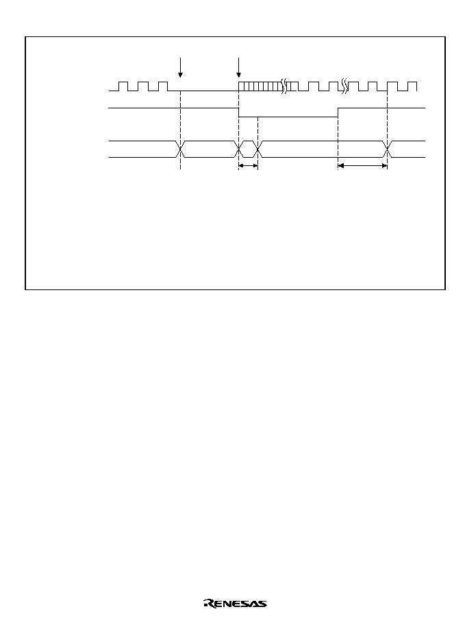
Rev. 5.0, 09/03, page 241 of 806
Standby to Power-On Reset
CKIO, CKIO2
*7
STATUS
Normal
*5
Normal
*5
Oscillation stops
Standby
*4
0 to 10 Bcyc
*6
0 to 30 Bcyc
*6
Reset
Reset
*3
RESETP
*1
*2
Notes: 1. When standby mode is cleared with a power-on reset, the WDT does not count.
Keep
RESETP low during the PLL's oscillation settling time.
2.
Undefined
3. Reset:
HH (STATUS1 high, STATUS0 high)
4. Standby: LH (STATUS1 low, STATUS0 high)
5. Normal: LL (STATUS1 low, STATUS0 low)
6. Bcyc:
Bus clock cycle
7. CKIO2 output can only be used in clock modes 0, 1, and 2.
Figure 9.5 Standby to Power-On Reset STATUS Output

Rev. 5.0, 09/03, page 242 of 806
Standby to Manual Reset
CKIO, CKIO2
*6
STATUS
Normal
*4
Normal
*4
Oscillation stops
Standby
*3
Reset
*2
0 to 20 Bcyc
*5
Reset
RESETM
*1
Notes: 1. When standby mode is cleared with a manual reset, the WDT does not count.
Keep
RESETM low during the PLL's oscillation settling time.
2. Reset:
HH (STATUS1 high, STATUS0 high)
3. Standby: LH (STATUS1 low, STATUS0 high)
4. Normal: LL (STATUS1 low, STATUS0 low)
5. Bcyc:
Bus clock cycle
6. CKIO2 output can only be used in clock modes 0, 1, and 2.
Figure 9.6 Standby to Manual Reset STATUS Output
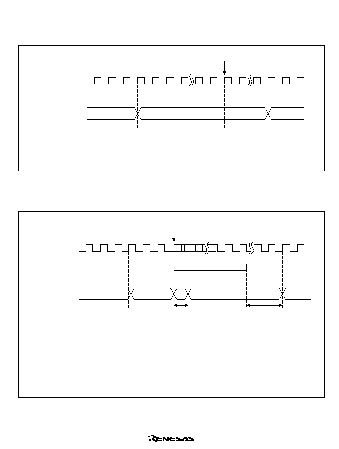
Rev. 5.0, 09/03, page 243 of 806
9.6.3
Timing for Canceling Sleep Mode
Sleep to Interrupt
CKIO, CKIO2
*3
STATUS
Normal
*2
Normal
*2
Sleep
*1
Interrupt request
Notes: 1. Sleep: HL (STATUS1 high, STATUS0 low)
2. Normal: LL (STATUS1 low, STATUS0 low)
3. CKIO2 output can only be used in clock modes 0, 1, and 2.
Figure 9.7 Sleep to Interrupt STATUS Output
Sleep to Power-On Reset
CKIO, CKIO2
*7
STATUS
Normal
*5
Normal
*5
Sleep
*4
0 to 10 Bcyc
*6
0 to 30 Bcyc
*6
Reset
Reset
*3
*2
RESETP
*1
Notes: 1. When the PLL1's multiplication ratio is changed by a power-on reset, keep
RESETP low during the PLL's oscillation settling time.
2.
Undefined
3. Reset: HH (STATUS1 high, STATUS0 high)
4. Sleep: HL (STATUS1 high, STATUS0 low)
5. Normal: LL (STATUS1 low, STATUS0 low)
6. Bcyc:
Bus clock cycle
7. CKIO2 output can only be used in clock modes 0, 1, and 2.
Figure 9.8 Sleep to Power-On Reset STATUS Output
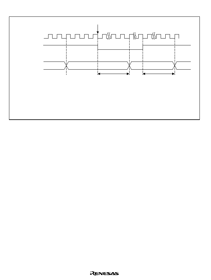
Rev. 5.0, 09/03, page 244 of 806
Sleep to Manual Reset
CKIO, CKIO2
*6
0 to 80 Bcyc
*5
0 to 30 Bcyc
*5
Reset
STATUS
Normal
*4
Normal
* 4
Sleep
*3
Reset
*2
RESETM
*1
Notes: 1. Keep
RESETM low until STATUS becomes reset.
2. Reset: HH (STATUS1 high, STATUS0 high)
3. Sleep: HL (STATUS1 high, STATUS0 low)
4. Normal: LL (STATUS1 low, STATUS0 low)
5. Bcyc:
Bus clock cycle
6. CKIO2 output can only be used in clock modes 0, 1, and 2.
Figure 9.9 Sleep to Manual Reset STATUS Output

Rev. 5.0, 09/03, page 245 of 806
9.7
Hardware Standby Mode
9.7.1
Transition to Hardware Standby Mode
Driving the CA pin low causes a transition to hardware standby mode. In hardware standby mode,
all modules except those operating on an RTC clock are halted, as in the standby mode entered on
execution of a SLEEP instruction ((software) standby mode).
Hardware standby mode differs from (software) standby mode as follows.
1. Interrupts and manual resets are not accepted.
2. The TMU does not operate.
Operation when a low-level signal is input at the CA pin depends on the CPG state, as follows.
1. In standby mode
The clock remains stopped and the chip enters the hardware standby state. Acceptance of
interrupts and manual resets is disabled, TCLK output is fixed low, and the TMU halts.
2. During WDT operation when standby mode is canceled by an interrupt
The chip enters hardware standby mode after standby mode is canceled and the CPU resumes
operation.
3. In sleep mode
The chip enters hardware standby mode after sleep mode is canceled and the CPU resumes
operation.
Hold the CA pin low in hardware standby mode.
9.7.2
Canceling Hardware Standby Mode
Hardware standby mode can only be canceled by a power-on reset.
When the CA pin is driven high while the
RESETP pin is low, clock oscillation is started. Hold
the
RESETP pin low until clock oscillation stabilizes. When the RESETP pin is driven high, the
CPU begins power-on reset processing.
Operation is not guaranteed in the event of an interrupt or manual reset.
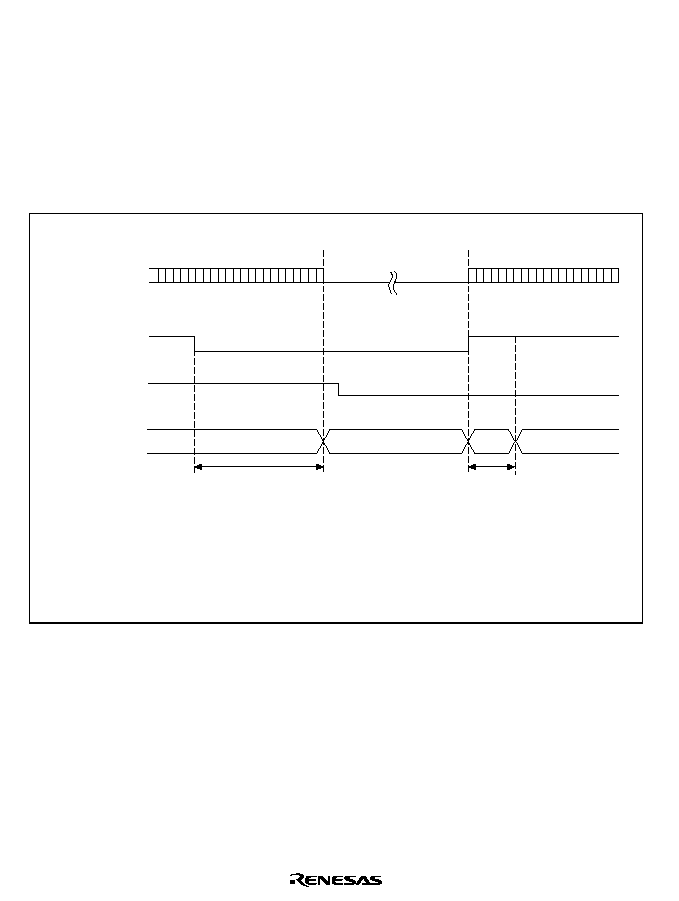
Rev. 5.0, 09/03, page 246 of 806
9.7.3
Hardware Standby Mode Timing
Figures 9.10 and 9.11 show examples of pin timing in hardware standby mode.
The CA pin is sampled using EXTAL2 (32.768 kHz), and a hardware standby request is only
recognized when the pin is low for two consecutive clock cycles.
The CA pin must be held low while the chip is in hardware standby mode.
Clock oscillation starts when the CA pin is driven high after the
RESETP pin is driven low.
Normal
*3
STATUS
CA
CKIO, CKIO2
*6
Standby
*2
Reset
*1
RESETP
Undefined
Rcyc: EXTAL2 (32.768 kHz) cycle
2 Rcyc or more
*5
0
-10Bcyc
*4
Notes: 1. Reset:
HH (STATUS1 high, STATUS0 high)
2. Standby: LH (STATUS1 low, STATUS0 high)
3. Normal: LL (STATUS1 low, STATUS0 low)
4. Bcyc:
Bus clock cycle
5. Rcyc:
EXTAL2 (32.768 kHz) cycle
6. CKIO2 output can only be used in clock modes 0, 1, and 2.
Figure 9.10 Hardware Standby Mode
(When CA Goes Low in Normal Operation)
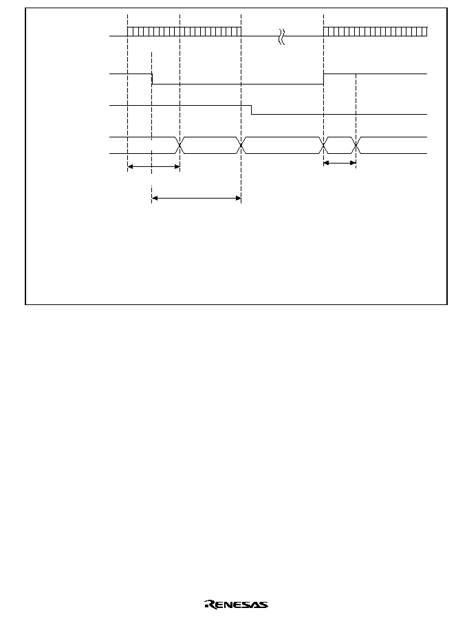
Rev. 5.0, 09/03, page 247 of 806
Normal
*3
STATUS
CA
CKIO, CKIO2
*6
Standby
*2
Reset
*1
RESETP
Undefined
2 Rcyc or more
*5
0
-10 Bcyc
*4
Standby
*2
WDT operation
Notes: 1. Reset:
HH (STATUS1 high, STATUS0 high)
2. Standby: LH (STATUS1 low, STATUS0 high)
3. Normal: LL (STATUS1 low, STATUS0 low)
4. Bcyc:
Bus clock cycle
5. Rcyc:
EXTAL2 (32.768 kHz) cycle
6. CKIO2 output can only be used in clock modes 0, 1, and 2.
Figure 9.11 Hardware Standby Mode Timing
(When CA Goes Low during WDT Operation on Standby Mode Cancellation)

Rev. 5.0, 09/03, page 248 of 806

Rev. 5.0, 09/03, page 249 of 806
Section 10 On-Chip Oscillation Circuits
10.1
Overview
The clock pulse generator (CPG) supplies all clocks to the processor and controls the power-down
modes. The watchdog timer (WDT) is a single-channel timer that counts the clock settling time
and is used when clearing standby mode and temporary standbys, such as frequency changes. It
can also be used as an ordinary watchdog timer or interval timer.
10.1.1
Features
The CPG has the following features:
∑
Four clock modes: Selection of four clock modes for different frequency ranges, power
consumption, direct crystal input, and external clock input.
∑
Three clocks generated independently: An internal clock for the CPU, cache, and TLB (I
); a
peripheral clock (P
) for the on-chip peripheral modules; and a bus clock (CKIO) for the
external bus interface.
∑
Frequency change function: Internal and peripheral clock frequencies can be changed
independently using the PLL circuit and divider circuit within the CPG. Frequencies are
changed by software using frequency control register (FRQCR) settings.
∑
Power-down mode control: The clock can be stopped for sleep mode and standby mode and
specific modules can be stopped using the module standby function.
The WDT has the following features:
∑
Can be used to ensure the clock settling time: Use the WDT to cancel standby mode and the
temporary standbys which occur when the clock frequency is changed.
∑
Can switch between watchdog timer mode and interval timer mode.
∑
Generates internal resets in watchdog timer mode: Internal resets occur after counter overflow.
Selection of power-on reset or manual reset.
∑
Generates interrupts in interval timer mode: Internal timer interrupts occur after counter
overflow.
∑
Selection of eight counter input clocks. Eight clocks (
◊
1 to
◊
1/4096) can be obtained by
dividing the peripheral clock.
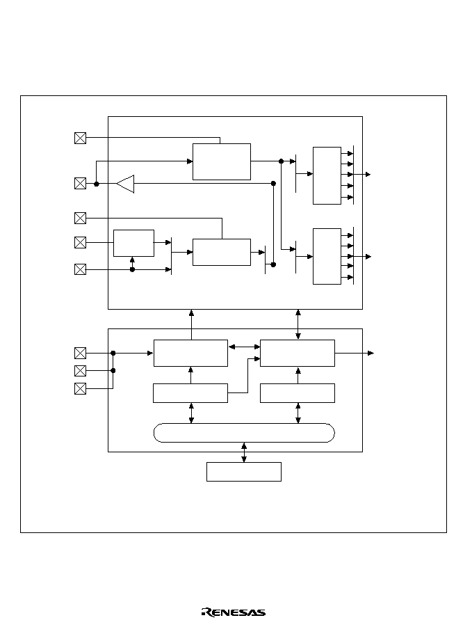
Rev. 5.0, 09/03, page 250 of 806
10.2
Overview of CPG
10.2.1
CPG Block Diagram
A block diagram of the on-chip clock pulse generator is shown in figure 10.1.
CAP1
CKIO
Cycle = Bcyc
CAP2
XTAL
EXTAL
MD2
MD1
MD0
FRQCR
Internal bus
Bus interface
STBCR
PLL circuit 1
(
◊ 1, 2, 3, 4,
6)
Divider 1
Internal
clock (I
)
Cycle = Icyc
Peripheral
clock (P
)
Cycle = Pcyc
Standby
control
Divider 2
Clock pulse generator
PLL circuit 2
(
◊ 1, 4)
Crystal
oscillator
CPG control unit
Clock frequency
control circuit
Standby control
circuit
◊ 1
◊ 1/2
◊ 1/3
◊ 1/4
◊ 1/6
◊ 1
◊ 1/2
◊ 1/3
◊ 1/4
◊ 1/6
Legend
FRQCR: Frequency control register
STBCR: Standby control register
Figure 10.1 Block Diagram of Clock Pulse Generator

Rev. 5.0, 09/03, page 251 of 806
The clock pulse generator blocks function as follows:
1. PLL Circuit 1: PLL circuit 1 doubles, triples, quadruples, sextuples, or leaves unchanged the
input clock frequency from the CKIO pin. The multiplication rate is set by the frequency
control register. When this is done, the phase of the leading edge of the internal clock is
controlled so that it will agree with the phase of the leading edge of the CKIO pin.
2. PLL Circuit 2: PLL circuit 2 leaves unchanged or quadruples the frequency of the crystal
oscillator or the input clock frequency from the EXTAL pin. The multiplication ratio is fixed
by the clock operation mode. The clock operation mode is set by pins MD0, MD1, and MD2.
See table 10.3 for more information on clock operation modes.
3. Crystal Oscillator: This oscillator is used when a crystal oscillator element is connected to the
XTAL and EXTAL pins. It operates according to the clock operating mode setting.
4. Divider 1: Divider 1 generates a clock at the operating frequency used by the internal clock.
The operating frequency can be 1, 1/2, 1/3, 1/4, or 1/6 times the output frequency of PLL
circuit 1, as long as it is not lower than the CKIO pin clock frequency. The division ratio is set
in the frequency control register.
5. Divider 2: Divider 2 generates a clock at the operating frequency used by the peripheral clock.
The operating frequency can be 1, 1/2, 1/3, 1/4, or 1/6 times the output frequency of PLL
circuit 1 or the CKIO pin clock frequency, as long as it is not higher than the CKIO pin clock
frequency. The division ratio is set in the frequency control register.
6. Clock Frequency Control Circuit: The clock frequency control circuit controls the clock
frequency using the MD pins and the frequency control register.
7. Standby Control Circuit: The standby control circuit controls the state of the clock pulse
generator and other modules during clock switching and sleep/standby modes.
8. Frequency Control Register: The frequency control register has control bits assigned for the
following functions: clock output/non-output from the CKIO pin, on/off control of PLL circuit
1, PLL standby, the frequency multiplication ratio of PLL 1, and the frequency division ratio
of the internal clock and the peripheral clock.
9. Standby Control Register: The standby control register has bits for controlling the power-down
modes. See section 9, Power-Down Modes, for more information.

Rev. 5.0, 09/03, page 252 of 806
10.2.2
CPG Pin Configuration
Table 10.1 lists the CPG pins and their functions.
Table 10.1
CPG Pins and Functions
Pin Name
Symbol
I/O
Description
MD0
I
MD1
I
Mode control
pins
MD2
I
Set the clock operating mode
XTAL
O
Connects a crystal oscillator
Crystal I/O pins
(clock input pins)
EXTAL
I
Connects a crystal oscillator. Also used to input an external
clock
Clock I/O pin
CKIO
I/O
Inputs or outputs an external clock. Level can be fixed
during output
CAP1
I
Connects capacitor for PLL circuit 1 operation
(recommended value 470 pF)
Capacitor
connection pins
for PLL
CAP2
I
Connects capacitor for PLL circuit 2 operation
(recommended value 470 pF)
10.2.3
CPG Register Configuration
Table 10.2 shows the CPG register configuration.
Table 10.2
CPG Register
Register Name
Abbreviation
R/W
Initial Value
Address
Access Size
Frequency control register
FRQCR
R/W
H'0102
H'FFFFFF80
16

Rev. 5.0, 09/03, page 253 of 806
10.3
Clock Operating Modes
Table 10.3 shows the relationship between the mode control pin (MD2≠MD0) combinations and
the clock operating modes. Table 10.4 shows the usable frequency ranges in the clock operating
modes.
Table 10.3
Clock Operating Modes
Pin Values
Clock I/O
Mode MD2 MD1 MD0
Source
Output
PLL2
On/Off
PLL1
On/Off
Divider 1
Input
Divider 2
Input
CKIO
Frequency
0
0
0
0
EXTAL
CKIO
On,
multi-
plication
ratio: 1
On
PLL1
output
PLL1
(EXTAL)
1
0
0
1
EXTAL
CKIO
On,
multi-
plication
ratio: 4
On
PLL1
output
PLL1
(EXTAL)
◊
4
2
0
1
0
Crystal
oscillator
CKIO
On,
multi-
plication
ratio: 4
On
PLL1
output
PLL1
(Crystal)
◊
4
7
1
1
1
CKIO
--
Off
On
PLL1
output
PLL1
(CKIO)
--
Values except
above
Reserved (Setting prohibited)
Mode 0: An external clock is input from the EXTAL pin and undergoes waveform shaping by
PLL circuit 2 before being supplied inside the chip. PLL circuit 1 is constantly on, and there are
no frequency range restrictions compared to mode 3. An input clock frequency of 25 MHz to
66.67 MHz can be used, and the CKIO frequency range is 25 MHz to 66.67 MHz.
As PLL circuit 1 compensates for fluctuations in the CKIO pin load, this mode is suitable for
connection of synchronous DRAM.
Mode 1: An external clock is input from the EXTAL pin and its frequency is multiplied by 4 by
PLL circuit 2 before being supplied inside the chip, allowing a low-frequency external clock to be
used. An input clock frequency of 6.25 MHz to 16.67 MHz can be used, and the CKIO frequency
range is 25 MHz to 66.67 MHz.
As PLL circuit 1 compensates for fluctuations in the CKIO pin load, this mode is suitable for
connection of synchronous DRAM.

Rev. 5.0, 09/03, page 254 of 806
Mode 2: The on-chip crystal oscillator operates, with the oscillation frequency being multiplied
by 4 by PLL circuit 2 before being supplied inside the chip, allowing a low crystal frequency to be
used. A crystal oscillation frequency of 6.25 MHz to 16.67 MHz can be used, and the CKIO
frequency range is 25 MHz to 66.67 MHz.
As PLL circuit 1 compensates for fluctuations in the CKIO pin load, this mode is suitable for
connection of synchronous DRAM.
Mode 7: In this mode, the CKIO pin is an input, an external clock is input to this pin, and
undergoes waveform shaping, and also frequency multiplication according to the setting, by PLL
circuit 1 before being supplied to the chip. In modes 0 to 4, the system clock is generated from the
output of the chip's CKIO pin. Consequently, if a large number of ICs are operating on the clock
cycle, the CKIO pin load will be large. This mode, however, assumes a comparatively large-scale
system. If a large number of ICs are operating on the clock cycle, a clock generator with a number
of low-skew clock outputs can be provided, so that the ICs can operate synchronously by
distributing the clocks to each one.
As PLL circuit 1 compensates for fluctuations in the CKIO pin load, this mode is suitable for
connection of synchronous DRAM.
Table 10.4
Available Combinations of Clock Mode and FRQCR Values
Clock
Mode
FRQCR
PLL1
PLL2
Clock Rate
*
(I:B:P)
Input Frequency
Range
CKIO Frequency
Range
0
H'0100
ON (
◊
1) ON (
◊
1) 1:1:1
25 MHz to 33.34 MHz
25 MHz to 33.34 MHz
H'0101
ON (
◊
1) ON (
◊
1) 1:1:1/2
25 MHz to 66.67 MHz
25 MHz to 66.67 MHz
H'0102
ON (
◊
1) ON (
◊
1) 1:1:1/4
25 MHz to 66.67 MHz
25 MHz to 66.67 MHz
H'0111
ON (
◊
2) ON (
◊
1) 2:1:1
25 MHz to 33.34 MHz
25 MHz to 33.34 MHz
H'0112
ON (
◊
2) ON (
◊
1) 2:1:1/2
25 MHz to 66.67 MHz
25 MHz to 66.67 MHz
H'0115
ON (
◊
2) ON (
◊
1) 1:1:1
25 MHz to 33.34 MHz
25 MHz to 33.34 MHz
H'0116
ON (
◊
2) ON (
◊
1) 1:1:1/2
25 MHz to 66.67 MHz
25 MHz to 66.67 MHz
H'0122
ON (
◊
4) ON (
◊
1) 4:1:1
25 MHz to 33.34 MHz
25 MHz to 33.34 MHz
H'0126
ON (
◊
4) ON (
◊
1) 2:1:1
25 MHz to 33.34 MHz
25 MHz to 33.34 MHz
H'012A
ON (
◊
4) ON (
◊
1) 1:1:1
25 MHz to 33.34 MHz
25 MHz to 33.34 MHz
H'A100
ON (
◊
3) ON (
◊
1) 3:1:1
25 MHz to 33.34 MHz
25 MHz to 33.34 MHz
H'A101
ON (
◊
3) ON (
◊
1) 3:1:1/2
25 MHz to 66.67 MHz
25 MHz to 66.67 MHz
H'E100
ON (
◊
3) ON (
◊
1) 1:1:1
25 MHz to 33.34 MHz
25 MHz to 33.34 MHz
H'E101
ON (
◊
3) ON (
◊
1) 1:1:1/2
25 MHz to 66.67 MHz
25 MHz to 66.67 MHz
H'A111
ON (
◊
6) ON (
◊
1) 6:1:1
25 MHz to 33.34 MHz
25 MHz to 33.34 MHz

Rev. 5.0, 09/03, page 255 of 806
Clock
Mode
FRQCR
PLL1
PLL2
Clock Rate
*
(I:B:P)
Input Frequency
Range
CKIO Frequency
Range
1, 2
H'0100
ON (
◊
1) ON (
◊
4) 4:4:4
6.25 MHz to 8.34 MHz
25 MHz to 33.34 MHz
H'0101
ON (
◊
1) ON (
◊
4) 4:4:2
6.25 MHz to 16.67 MHz 25 MHz to 66.67 MHz
H'0102
ON (
◊
1) ON (
◊
4) 4:4:1
6.25 MHz to 16.67 MHz 25 MHz to 66.67 MHz
H'0111
ON (
◊
2) ON (
◊
4) 8:4:4
6.25 MHz to 8.34 MHz
25 MHz to 33.34 MHz
H'0112
ON (
◊
2) ON (
◊
4) 8:4:2
6.25 MHz to 16.67 MHz 25 MHz to 66.67 MHz
H'0115
ON (
◊
2) ON (
◊
4) 4:4:4
6.25 MHz to 8.34 MHz
25 MHz to 33.34 MHz
H'0116
ON (
◊
2) ON (
◊
4) 4:4:2
6.25 MHz to 16.67 MHz 25 MHz to 66.67 MHz
H'0122
ON (
◊
4) ON (
◊
4) 16:4:4
6.25 MHz to 8.34 MHz
25 MHz to 33.34 MHz
H'0126
ON (
◊
4) ON (
◊
4) 8:4:4
6.25 MHz to 8.34 MHz
25 MHz to 33.34 MHz
H'012A
ON (
◊
4) ON (
◊
4) 4:4:4
6.25 MHz to 8.34 MHz
25 MHz to 33.34 MHz
H'A100
ON (
◊
3) ON (
◊
4) 12:4:4
6.25 MHz to 8.34 MHz
25 MHz to 33.34 MHz
H'A101
ON (
◊
3) ON (
◊
4) 12:4:2
6.25 MHz to 16.67 MHz 25 MHz to 66.67 MHz
H'E100
ON (
◊
3) ON (
◊
4) 4:4:4
6.25 MHz to 8.34 MHz
25 MHz to 33.34 MHz
H'E101
ON (
◊
3) ON (
◊
4) 4:4:2
6.25 MHz to 16.67 MHz 25 MHz to 66.67 MHz
H'A111
ON (
◊
6) ON (
◊
4) 24:4:4
6.25 MHz to 8.34 MHz
25 MHz to 33.34 MHz
7
H'0100
ON (
◊
1) OFF
1:1:1
25 MHz to 33.34 MHz
25 MHz to 33.34 MHz
H'0101
ON (
◊
1) OFF
1:1:1/2
25 MHz to 66.67 MHz
25 MHz to 66.67 MHz
H'0102
ON (
◊
1) OFF
1:1:1/4
25 MHz to 66.67 MHz
25 MHz to 66.67 MHz
H'0111
ON (
◊
2) OFF
2:1:1
25 MHz to 33.34 MHz
25 MHz to 33.34 MHz
H'0112
ON (
◊
2) OFF
2:1:1/2
25 MHz to 66.67 MHz
25 MHz to 66.67 MHz
H'0115
ON (
◊
2) OFF
1:1:1
25 MHz to 33.34 MHz
25 MHz to 33.34 MHz
H'0116
ON (
◊
2) OFF
1:1:1/2
25 MHz to 66.67 MHz
25 MHz to 66.67 MHz
H'0122
ON (
◊
4) OFF
4:1:1
25 MHz to 33.34 MHz
25 MHz to 33.34 MHz
H'0126
ON (
◊
4) OFF
2:1:1
25 MHz to 33.34 MHz
25 MHz to 33.34 MHz
H'012A
ON (
◊
4) OFF
1:1:1
25 MHz to 33.34 MHz
25 MHz to 33.34 MHz
H'A100
ON (
◊
3) OFF
3:1:1
25 MHz to 33.34 MHz
25 MHz to 33.34 MHz
H'A101
ON (
◊
3) OFF
3:1:1/2
25 MHz to 66.67 MHz
25 MHz to 66.67 MHz
H'E100
ON (
◊
3) OFF
1:1:1
25 MHz to 33.34 MHz
25 MHz to 33.34 MHz
H'E101
ON (
◊
3) OFF
1:1:1/2
25 MHz to 66.67 MHz
25 MHz to 66.67 MHz
H'A111
ON (
◊
6) OFF
6:1:1
25 MHz to 33.34 MHz
25 MHz to 33.34 MHz
Note:
*
Taking input clock as 1.

Rev. 5.0, 09/03, page 256 of 806
Cautions:
1. The input to divider 1 becomes the output of PLL circuit 1 when PLL circuit 1 is on.
2. The input of divider 2 becomes the output of PLL circuit 1.
3. The frequency of the internal clock (I
) becomes:
∑
The product of the frequency of the CKIO pin, the frequency multiplication ratio of PLL
circuit 1, and the division ratio of divider 1 when PLL circuit 1 is on.
∑
Do not set the internal clock frequency lower than the CKIO pin frequency.

Rev. 5.0, 09/03, page 257 of 806
10.4
Register Descriptions
10.4.1
Frequency Control Register (FRQCR)
The frequency control register (FRQCR) is a 16-bit readable/writable register used to specify the
frequency multiplication ratio of PLL circuit 1, and the frequency division ratio of the internal
clock and the peripheral clock.
Only word access can be used on the FRQCR register. FRQCR is initialized to H'0102 by a
power-on reset trigged by the
RESETP pin, but retains its value in a manual reset and in standby
mode.
FRQCR:
Bit:
15
14
13
12
11
10
9
8
STC2
IFC2
PFC2
--
--
--
--
--
Initial value:
0
0
0
0
0
0
0
1
R/W:
R/W
R/W
R/W
R
R
R
R
R
Bit:
7
6
5
4
3
2
1
0
--
--
STC1
STC0
IFC1
IFC0
PFC1
PFC0
Initial value:
0
0
0
0
0
0
1
0
R/W:
R
R
R/W
R/W
R/W
R/W
R/W
R/W
Bits 15, 5, and 4--Frequency Multiplication Ratio (STC2, STC1, STC0): These bits specify
the frequency multiplication ratio of PLL circuit 1.
Bit 15: STC2
Bit 5: STC1
Bit 4: STC0
Description
0
0
0
◊
1 (Initial
value)
0
0
1
◊
2
1
0
0
◊
3
0
1
0
◊
4
1
0
1
◊
6
Values except above
Reserved (Setting prohibited)

Rev. 5.0, 09/03, page 258 of 806
Bits 14, 3, and 2--Internal Clock Frequency Division Ratio (IFC2, IFC1, IFC0): These bits
specify the frequency division ratio of the internal clock with respect to the output frequency of
PLL circuit 1.
Bit 14: IFC2
Bit 3: IFC1
Bit 2: IFC0
Description
0
0
0
◊
1 (Initial
value)
0
0
1
◊
1/2
1
0
0
◊
1/3
0
1
0
◊
1/4
Values except above
Reserved (Setting prohibited)
Note:
Do not set the internal clock frequency lower than the CKIO pin frequency.
Bits 13, 1, and 0--Peripheral Clock Frequency Division Ratio (PFC2, PFC1, PFC0): These
bits specify the division ratio of the peripheral clock frequency with respect to the frequency of the
output frequency of PLL circuit 1 or the frequency of the CKIO pin.
Bit 13: PFC2
Bit 1: PFC1
Bit 0: PFC0
Description
0
0
0
◊
1
0
0
1
◊
1/2
1
0
0
◊
1/3
0
1
0
◊
1/4
(Initial value)
1
0
1
◊
1/6
Values except above
Reserved (Setting prohibited)
Note:
Do not set the peripheral clock frequency higher than the CKIO pin frequency.
Bits 12 to 9, 7, and 6--Reserved: These bits are always read as 0. The write value should always
be 0.
Bit 8--Reserved: This bit is always read as 1. The write value should always be 1.

Rev. 5.0, 09/03, page 259 of 806
10.5
Changing the Frequency
The frequency of the internal clock and peripheral clock can be changed either by changing the
multiplication ratio of PLL circuit 1 or by changing the division ratios of dividers 1 and 2. All of
these are controlled by software through the frequency control register. The methods are described
below.
10.5.1
Changing the Multiplication Rate
A PLL settling time is required when the multiplication rate of PLL circuit 1 is changed. The on-
chip WDT counts the settling time.
1. In the initial state, the multiplication rate of PLL circuit 1 is 1.
2. Set a value that will become the specified oscillation settling time in the WDT and stop the
WDT. The following must be set:
WTCSR register TME bit
=
0: WDT stops
WTCSR register CKS2≠CKS0 bits: Division ratio of WDT count clock
WTCNT counter: Initial counter value
3. Set the desired value in the STC2, STC1, and STC0 bits. The division ratio can also be set in
the IFC2≠IFC0 bits and PFC2≠PFC0 bits.
4. The processor pauses internally and the WDT starts incrementing. In clock modes 0≠2 and 7,
the internal and peripheral clocks both stop (except for the peripheral clock supplied to the
WDT).
5. Supply of the clock that has been set begins at WDT count overflow, and the processor begins
operating again. The WDT stops after it overflows.
10.5.2
Changing the Division Ratio
The WDT will not count unless the multiplication ratio is changed simultaneously.
1. In the initial state, IFC2≠IFC0
=
000 and PFC2≠PFC0
=
010.
2. Set the IFC2, IFC1, IFC0, PFC2, PFC1, and PFC0 bits to the new division ratio. The values
that can be set are limited by the clock mode and the multiplication ratio of PLL circuit 1. Note
that if the wrong value is set, the processor will malfunction.
3. The clock is immediately supplied at the new division ratio.
10.5.3
Notes on Changing the Frequency
If the following three conditions are all met, FRQCR should not be changed when a transfer using
the DMAC is in progress.
∑
Bits IFC2 to IFC0 are changed.
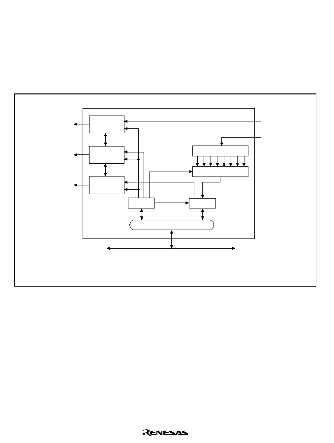
Rev. 5.0, 09/03, page 260 of 806
∑
Bits STC2 to STC0 are not changed.
∑
The clock ratio is other than I
:B
= 1:1.
10.6
Overview of WDT
10.6.1
Block Diagram of WDT
Figure 10.2 shows a block diagram of the WDT.
WTCSR
Standby
control
Bus interface
WTCNT
Divider
Clock selector
Clock
Internal bus
Standby
mode
Peripheral
clock
Standby
cancellation
Reset
control
Clock selection
WDT
Overflow
Internal
reset
request
Interrupt
control
Interrupt
request
WTCSR:
WTCNT:
Legend
Watchdog timer control/status register
Watchdog timer counter
Figure 10.2 Block Diagram of WDT
10.6.2
Register Configuration
The WDT has two registers that select the clock, switch the timer mode, and perform other
functions. Table 10.5 shows the WDT registers.

Rev. 5.0, 09/03, page 261 of 806
Table 10.5
Register Configuration
Name
Abbreviation
R/W
Access Size
Initial Value
Address
Watchdog timer counter
WTCNT
R/W
*
R: byte;
W: word
*
H'00
H'FFFFFF84
Watchdog timer
control/status register
WTCSR
R/W
*
R: byte;
W: word
*
H'00
H'FFFFFF86
Note:
*
Write with word access. Write with H'5A and H'A5, respectively, in the upper byte. Byte or
longword writes are not possible. Read with byte access.
10.7
WDT Registers
10.7.1
Watchdog Timer Counter (WTCNT)
The watchdog timer counter (WTCNT) is an 8-bit readable/writable counter that increments on the
selected clock. WTCNT differs from other registers in that it is more difficult to write to. See
section 10.7.3, Notes on Register Access, for details. When an overflow occurs, it generates a reset
in watchdog timer mode and an interrupt in interval time mode. Its address is H'FFFFFF84. The
WTCNT counter is initialized to H'00 only by a power-on reset through the
RESETP pin. Use
word access to write to the WTCNT counter, with H'5A in the upper byte. Use byte access to read
WTCNT.
Bit:
7
6
5
4
3
2
1
0
Initial value:
0
0
0
0
0
0
0
0
R/W:
R/W
R/W
R/W
R/W
R/W
R/W
R/W
R/W
10.7.2
Watchdog Timer Control/Status Register (WTCSR)
The watchdog timer control/status register (WTCSR) is an 8-bit readable/writable register
composed of bits to select the clock used for the count, bits to select the timer mode, and overflow
flags. WTCSR differs from other registers in that it is more difficult to write to. See section 10.7.3,
Notes on Register Access, for details. Its address is H'FFFFFF86. The WTCSR register is
initialized to H'00 only by a power-on reset through the
RESETP pin. When a WDT overflow
causes an internal reset, WTCSR retains its value. When used to count the clock settling time for
canceling a standby, it retains its value after counter overflow. Use word access to write to the
WTCSR counter, with H'A5 in the upper byte. Use byte access to read WTCSR.
Note:
The method of writing data to this register differs from that for ordinary registers in order
to ensure that data is not overwritten mistakenly. Refer to section 10.7.3, Notes on
Register Access, for details.

Rev. 5.0, 09/03, page 262 of 806
Bit:
7
6
5
4
3
2
1
0
TME
WT/
IT
RSTS
WOVF
IOVF
CKS2
CKS1
CKS0
Initial value:
0
0
0
0
0
0
0
0
R/W:
R/W
R/W
R/W
R/W
R/W
R/W
R/W
R/W
Bit 7--Timer Enable (TME): Starts and stops timer operation. Clear this bit to 0 when using the
WDT in standby mode or when changing the clock frequency.
Bit 7: TME
Description
0
Timer disabled: Count-up stops and WTCNT value is retained
(Initial value)
1
Timer enabled
Bit 6--Timer Mode Select (WT/
I
I
I
ITTTT): Selects whether to use the WDT as a watchdog timer or an
interval timer.
Bit 6: WT/
I
I
I
ITTTT
Description
0
Used as interval timer
(Initial value)
1
Used as watchdog timer
Note:
If WT/
IT
is modified when the WDT is running, the up-count may not be performed correctly.
Bit 5--Reset Select (RSTS): Selects the type of reset when WTCNT overflows in watchdog
timer mode. In interval timer mode, this setting is ignored.
Bit 5: RSTS
Description
0
Power-on reset
(Initial value)
1
Manual reset
Note:
RESETOUT
is output.
Bit 4--Watchdog Timer Overflow (WOVF): Indicates that the WTCNT has overflowed in
watchdog timer mode. This bit is not set in interval timer mode.
Bit 4: WOVF
Description
0
No overflow
(Initial value)
1
WTCNT has overflowed in watchdog timer mode
Bit 3--Interval Timer Overflow (IOVF): Indicates that WTCNT has overflowed in interval
timer mode. This bit is not set in watchdog timer mode.

Rev. 5.0, 09/03, page 263 of 806
Bit 3: IOVF
Description
0
No overflow
(Initial value)
1
WTCNT has overflowed in interval timer mode
Bits 2 to 0--Clock Select 2 to 0 (CKS2 to CKS0): These bits select the clock to be used for the
WTCNT count from the eight types obtainable by dividing the peripheral clock. The overflow
period in the table is the value when the peripheral clock (P
) is 15 MHz.
Bit 2: CKS2
Bit 1: CKS1
Bit 0: CKS0
Clock Division Ratio
Overflow Period
(when P
= 15 MHz)
0
0
0
1
(Initial value)
17
µ
s
1
1/4
68
µ
s
1
0
1/16
273
µ
s
1
1/32
546
µ
s
1
0
0
1/64
1.09 ms
1
1/256
4.36 ms
1
0
1/1024
17.48 ms
1
1/4096
69.91 ms
Note:
If bits CKS2≠CKS0 are modified when the WDT is running, the up-count may not be
performed correctly. Ensure that these bits are modified only when the WDT is not running.
10.7.3
Notes on Register Access
The watchdog timer counter (WTCNT) and watchdog timer control/status register (WTCSR) are
more difficult to write to than other registers. The procedure for writing to these registers is given
below.
Writing to WTCNT and WTCSR: These registers must be written to using a word transfer
instruction. They cannot be written to with a byte or longword transfer instruction. When writing
to WTCNT, set the upper byte to H'5A and transfer the lower byte as the write data, as shown in
figure 10.3. When writing to WTCSR, set the upper byte to H'A5 and transfer the lower byte as
the write data. This transfer procedure writes the lower byte data to WTCNT or WTCSR.

Rev. 5.0, 09/03, page 264 of 806
15
8
7
0
H'5A
Write data
Address: H'FFFFFF84
WTCNT write
15
8
7
0
H'A5
Write data
Address: H'FFFFFF86
WTCSR write
Figure 10.3 Writing to WTCNT and WTCSR
10.8
Using the WDT
10.8.1
Canceling Standby
The WDT can be used to cancel standby mode with an NMI or other interrupt. The procedure is
described below. (The WDT does not run when a reset is used for canceling, so keep the RESET
pin low until the clock stabilizes.)
1. Before transitioning to standby mode, always clear the TME bit in WTCSR to 0. When the
TME bit is 1, an erroneous reset or interval timer interrupt may be generated when the count
overflows.
2. Set the type of count clock used in the CKS2≠CKS0 bits in WTCSR and the initial values for
the counter in the WTCNT counter. These values should ensure that the time till count
overflow is longer than the clock oscillation settling time.
3. Switch to standby mode by executing a SLEEP instruction to stop the clock.
4. The WDT starts counting by detecting the edge change of the NMI signal or detecting
interrupts.
5. When the WDT count overflows, the CPG starts supplying the clock and the processor
resumes operation. The WOVF flag in WTCSR is not set when this happens.
6.
Since the WDT continues counting from H'00, set the STBY bit in the STBCR register to 0 in
the interrupt handling routine and this will stop the WDT. When the STBY bit remains at 1,
the SH7729R again enters standby mode when the WDT has counted up to H'80. This standby
mode can be canceled by a power-on reset

Rev. 5.0, 09/03, page 265 of 806
10.8.2
Changing the Frequency
To change the frequency used by the PLL, use the WDT. When changing the frequency only by
switching the divider, do not use the WDT.
1. Before changing the frequency, always clear the TME bit in WTCSR to 0. When the TME bit
is 1, an erroneous reset or interval timer interrupt may be generated when the count overflows.
2. Set the type of count clock used in the CKS2≠CKS0 bits of WTCSR and the initial values for
the counter in the WTCNT counter. These values should ensure that the time till count
overflow is longer than the clock oscillation settling time.
3. When the frequency control register (FRQCR) is written to, the clock stops and the processor
enters standby mode temporarily. The WDT starts counting.
4. When the WDT count overflows, the CPG resumes supplying the clock and the processor
resumes operation. The WOVF flag in WTCSR is not set when this happens.
5. The counter stops at a value of H'00 or H'01. The stop value depends on the clock ratio.
If the following three conditions are all met, FRQCR should not be changed when a transfer
using the DMAC is in progress.
∑ Bits IFC2 to IFC0 are changed.
∑ Bits STC2 to STC0 are not changed.
∑ The clock ratio is other than I
:B
= 1:1.
10.8.3
Using Watchdog Timer Mode
1. Set the WT/
IT bit in the WTCSR register to 1, set the reset type in the RSTS bit, set the type of
count clock in the CKS2≠CKS0 bits, and set the initial value of the counter in the WTCNT
counter.
2. Set the TME bit in WTCSR to 1 to start the count in watchdog timer mode.
3. While operating in watchdog timer mode, rewrite the counter periodically to H'00 to prevent
the counter from overflowing.
4. When the counter overflows, the WDT sets the WOVF flag in WTCSR to 1 and generates the
type of reset specified by the RSTS bit. The counter then resumes counting.
When a reset is generated, a low level is output at the
RESETOUT pin, and a high level at the
STATUS0 and STATUS1 pins. The output period is approximately 1 count clock cycle in the
case of a power-on reset, and approximately 5 peripheral clock cycles in the case of a manual
reset.
10.8.4
Using Interval Timer Mode
When operating in interval timer mode, interval timer interrupts are generated at every overflow of
the counter. This enables interrupts to be generated at set periods.
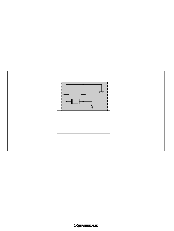
Rev. 5.0, 09/03, page 266 of 806
1. Clear the WT/
IT bit in the WTCSR register to 0, set the type of count clock in the CKS2≠
CKS0 bits, and set the initial value of the counter in the WTCNT counter.
2. Set the TME bit in WTCSR to 1 to start the count in interval timer mode.
3. When the counter overflows, the WDT sets the IOVF flag in WTCSR to 1 and an interval
timer interrupt request is sent to the INTC. The counter then resumes counting.
10.9
Notes on Board Design
When Using an External Crystal Resonator: Place the crystal resonator, capacitors CL1 and
CL2, and damping resistor R close to the EXTAL and XTAL pins. To prevent induction from
interfering with correct oscillation, use a common grounding point for the capacitors connected to
the resonator, and do not locate a wiring pattern near these components.
Note: The values for CL1, CL2, and the damping resistance should be determined after
consultation with the crystal manufacturer.
XTAL
EXTAL
SH7729R
R
CL2
CL1
Avoid crossing
signal lines
Figure 10.4 Points for Attention when Using Crystal Resonator
Decoupling Capacitors: Insert a laminated ceramic capacitor of 0.01 to 0.1
µ
F as a passive
capacitor for each V
SS
/V
CC
pair. Mount the passive capacitors close to the SH7729R power supply
pins, and use components with a frequency characteristic suitable for the chip's operating
frequency, as well as a suitable capacitance value.
Digital system V
SS
/V
CC
pairs: 19-21, 27-29, 33-35, 45-47, 57-59, 69-71, 79-81, 83-85, 95-97, 109-
111, 132-134, 153-154, 161-163, 173-175, 181-183, 205-208
On-chip oscillator V
SS
/V
CC
pairs: 3-6, 145-147, 148-150
When Using a PLL Oscillator Circuit: Keep the wiring from the PLL V
CC
and V
SS
connection
pattern to the power supply pins short, and make the pattern width large, to minimize the
Rev. 5.0, 09/03, page 267 of 806
inductance component. Ground the oscillation stabilization capacitors C1 and C2 to V
SS
(PLL1)
and V
SS
(PLL2), respectively. Place C1 and C2 close to the CAP1 and CAP2 pins and do not
locate a wiring pattern in the vicinity. In clock mode 7, connect the EXTAL pin to V
CC
or V
SS
and
leave the XTAL pin open.
CAP2
V
CC
(PLL2)
V
CC
(PLL1)
V
CC
C1 = 470 pF
C2 = 470 pF
V
SS
CAP1
V
SS
(PLL2)
V
SS
(PLL1)
Avoid crossing
signal lines
Power supply
Reference values
C2
C1
Figure 10.5 Points for Attention when Using PLL Oscillator Circuit

Rev. 5.0, 09/03, page 268 of 806

Rev. 5.0, 09/03, page 269 of 806
Section 11
Bus State Controller (BSC)
11.1
Overview
The bus state controller (BSC) divides physical address space and output control signals for
various types of memory and bus interface specifications. BSC functions enable the chip to link
directly with synchronous DRAM, SRAM, ROM, and other memory storage devices without an
external circuit. The BSC also allows direct connection to PCMCIA interfaces, simplifying system
design and allowing high-speed data transfers in a compact system.
11.1.1
Features
The BSC has the following features:
∑
Physical address space is divided into six areas
A maximum 64 Mbytes for each of the six areas, 0, 2≠6
Area bus width can be selected by register (area 0 is set by external pin)
Wait states can be inserted using the
WAIT pin
Wait state insertion can be controlled through software. Register settings can be used to
specify the insertion of 1≠10 cycles independently for each area (1≠38 cycles for areas 5
and 6 and the PCMCIA interface only)
The type of memory connected can be specified for each area, and control signals are
output for direct memory connection
Wait cycles are automatically inserted to avoid data bus conflict for continuous memory
accesses to different areas or writes directly following reads in the same area
∑
Direct interface to synchronous DRAM
Multiplexes row/column addresses according to synchronous DRAM capacity
Supports burst operation
Supports bank active mode
Has both auto-refresh and self-refresh functions
Controls timing of synchronous DRAM direct-connection control signals according to
register setting
∑
Burst ROM interface
Insertion of wait states controllable through software
Register setting control of burst transfers
∑
PCMCIA direct-connection interface
Insertion of wait states controllable through software
Bus sizing function for I/O bus width (only in little-endian mode)

Rev. 5.0, 09/03, page 270 of 806
∑
Short refresh cycle control
The overflow interrupt function of the refresh counter enables the refresh function
immediately after a self-refresh operation using low power-consumption DRAM
∑
The refresh counter can be used as an interval timer
Outputs an interrupt request signal using the compare-match function
Outputs an interrupt request signal when the refresh counter overflows
∑
Automatically disables the output of clock signals to anywhere but the refresh counter, except
during execution of external bus cycles
Rev. 5.0, 09/03, page 271 of 806
11.1.2
Block Diagram
Figure 11.1 shows a block diagram of the bus state controller.
WCR1
WCR2
BCR1
Module bus
MCR
BSC
RFCR
RTCNT
Comparator
Refresh
controller
Peripheral bus
Internal bus
Interrupt
controller
Memory
controller
Area
controller
Wait
controller
WAIT
CS0, CS6-CS2,
CE2A, CE2B
MCS0-MCS7
BS
RD
RD/
WR
WE3-WE0
RASxx
CASx
CKE
ICIORD, ICIOWR
IOIS16
WCR:
BCR:
MCR:
PCR:
Legend
Bus
interface
RTCSR
RTCOR
BCR2
PCR
MCSCRn
Wait state control register
Bus control register
Memory control register
PCMCIA control register
RFCR:
RTCNT:
RTCOR:
RTCSR:
MCSCRn:
Refresh count register
Refresh timer count register
Refresh time constant register
Refresh timer control/status register
MCSn control register (n = 0
-7)
Figure 11.1 Block Diagram of Bus State Controller

Rev. 5.0, 09/03, page 272 of 806
11.1.3
Pin Configuration
Table 11.1 shows the BSC pin configuration.
Table 11.1
BSC Pins
Pin Name
Signal
I/O
Description
Address bus
A25≠A0
O
Address output
Data bus
D15≠D0
I/O
Data I/O
D31≠D16
I/O
Data I/O when using 32-bit bus width
Bus cycle start
BS
O
Shows start of bus cycle. During burst transfers,
asserted every data cycle.
Chip select 0, 2≠4
CS0
,
CS2
≠
CS4
O
Chip select signals to indicate area being
accessed.
Chip select 5, 6
CS5
/
CE1A
,
CS6
/
CE1B
O
Chip select signals to indicate area being
accessed.
CS
5/
CE1A
and
CS
6/
CE1B
can also be
used as
CE1A
and
CE1B
of PCMCIA.
PCMCIA card
select
CE2A
,
CE2B
O
CE2A and CE2B signals when PCMCIA is used
Read/write
RD/
WR
O
Data bus direction indication signal. PCMCIA write
indication signal.
Row address
strobe 3L
RAS3L
O
When synchronous DRAM is used in area 3,
RAS3L for lower 32-Mbyte address and 64-Mbyte
address.
Row address
strobe 3U
RAS3U
O
When synchronous DRAM is used in area 3,
RAS3U for upper 32-Mbyte address.
Column address
strobe
CASL
O
When synchronous DRAM is used, CASL signal for
lower 32-Mbyte address and 64-Mbyte address.
Column address
strobe LH
CASU
O
When synchronous DRAM is used, CASU signal for
upper 32-Mbyte address.
Data enable 0
WE0
/DQMLL
O
When memory other than synchronous DRAM is
used, D7≠D0 write strobe signal. When
synchronous DRAM is used, selects D7≠D0.
Data enable 1
WE1
/DQMLU/
WE
O
When memory other than synchronous DRAM and
PCMCIA is used, D15≠D8 write strobe signal.
When synchronous DRAM is used, selects D15≠
D8. When PCMCIA is used, strobe signal indicating
write cycle.
Data enable 2
WE2
/DQMUL/
ICIORD
O
When memory other than synchronous DRAM and
PCMCIA is used, D23≠D16 write strobe signal.
When synchronous DRAM is used, selects D23≠
D16. When PCMCIA is used, strobe signal
indicating I/O read.

Rev. 5.0, 09/03, page 273 of 806
Pin Name
Signal
I/O
Description
Data enable 3
WE3
/DQMUU/
ICIOWR
O
When memory other than synchronous DRAM and
PCMCIA is used, D31≠D24 write strobe signal.
When synchronous DRAM is used, selects D31≠
D24. When PCMCIA is used, strobe signal
indicating I/O write.
Read
RD
O
Strobe signal indicating read cycle
Wait
WAIT
I
Wait state request signal
Clock enable
CKE
O
Clock enable control signal for synchronous DRAM
IOIS16
IOIS16
I
Signal indicating PCMCIA 16-bit I/O. Valid only in
little-endian mode.
Bus release
request
BREQ
I
Bus release request signal
Bus release
acknowledgment
BACK
O
Bus release acknowledge signal
Mask ROM chip
select
MCS[0]
≠
MCS[7]
O
Chip select signal for mask ROM connected to area
0 or 2.

Rev. 5.0, 09/03, page 274 of 806
11.1.4
Register Configuration
The BSC has 21 registers (table 11.2). Synchronous DRAM also has a built-in synchronous
DRAM mode register. These registers control direct connection interfaces to memory, wait states,
refreshes, and PCMCIA devices.
Table 11.2
BSC Registers
Name
Abbr.
R/W
Initial Value
*
Address
Bus Width
Bus control register 1
BCR1
R/W
H'0000
H'FFFFFF60
16
Bus control register 2
BCR2
R/W
H'3FF0
H'FFFFFF62
16
Wait state control register 1
WCR1
R/W
H'3FF3
H'FFFFFF64
16
Wait state control register 2
WCR2
R/W
H'FFFF
H'FFFFFF66
16
Individual memory control
register
MCR
R/W
H'0000
H'FFFFFF68
16
PCMCIA control register
PCR
R/W
H'0000
H'FFFFFF6C
16
Refresh timer control/status
register
RTCSR
R/W
H'0000
H'FFFFFF6E
16
Refresh timer counter
RTCNT
R/W
H'0000
H'FFFFFF70
16
Refresh time constant register
RTCOR
R/W
H'0000
H'FFFFFF72
16
Refresh count register
RFCR
R/W
H'0000
H'FFFFFF74
16
Synchronous DRAM mode
register, area 2
SDMR
W
--
H'FFFFD000≠
H'FFFFDFFF
8
Synchronous DRAM mode
register, area 3
H'FFFFE000≠
H'FFFFEFFF
MCS0 control register
MCSCR0
R/W
H'0000
H'FFFFFF50
16
MCS1 control register
MCSCR1
R/W
H'0000
H'FFFFFF52
16
MCS2 control register
MCSCR2
R/W
H'0000
H'FFFFFF54
16
MCS3 control register
MCSCR3
R/W
H'0000
H'FFFFFF56
16
MCS4 control register
MCSCR4
R/W
H'0000
H'FFFFFF58
16
MCS5 control register
MCSCR5
R/W
H'0000
H'FFFFFF5A
16
MCS6 control register
MCSCR6
R/W
H'0000
H'FFFFFF5C
16
MCS7 control register
MCSCR7
R/W
H'0000
H'FFFFFF5E
16
Notes: For details, see section 11.2.7, Synchronous DRAM Mode Register (SDMR).
*
Initialized by a power-on reset.
Rev. 5.0, 09/03, page 275 of 806
11.1.5
Area Overview
Space Allocation: In the architecture of the SH7729R, both logical spaces and physical spaces
have 32-bit address spaces. The logical space is divided into five areas by the value of the upper
bits of the address. The physical space is divided into eight areas.
Logical space can be allocated to physical space using a memory management unit (MMU). For
details, refer to section 3, Memory Management Unit (MMU), which describes area allocation for
physical space.
As shown in table 11.3, the SH7729R can be connected directly to six memory/PCMCIA interface
areas, and it outputs chip select signals (
CS0, CS2≠CS6, CE2A, CE2B) for each of them. CS0 is
asserted during area 0 access;
CS6 is asserted during area 6 access. When PCMCIA interface is
selected in area 5 or 6, in addition to
CS5/CS6, CE2A/CE2B are asserted for the corresponding
bytes accessed.
Area 0 (
CS0)
Internal I/O
Area 2 (
CS2)
Area 3 (
CS3)
Area 4 (
CS4)
Area 5 (
CS5)
Area 6 (
CS6)
H'00000000
H'20000000
H'40000000
H'60000000
H'80000000
H'A0000000
H'C0000000
H'E0000000
H'00000000
H'04000000
H'08000000
H'0C000000
H'10000000
H'14000000
H'18000000
Reserved area
Physical address space
Logical address space
P0, U0
P1
P2
P3
P4
Note: For logical address spaces P0 and P3, when the memory management unit (MMU) is
on, it can optionally generate a physical address for the logical address. This diagram
can be applied when the MMU is off, and when the MMU is on and each physical
address corresponding to a logical address is equal except for the upper three bits.
When translating logical addresses to arbitrary physical addresses, refer to table 11.3.
Figure 11.2 Correspondence between Logical Address Space and Physical Address Space

Rev. 5.0, 09/03, page 276 of 806
Table 11.3
Physical Address Space Map
Area
Connectable Memory
Physical Address
Capacity
Access Size
0
H'00000000 to H'03FFFFFF
64 Mbytes
8, 16, 32
*
2
Ordinary memory
*
1
,
burst ROM
H'00000000 + H'20000000
◊
n to
H'03FFFFFF + H'20000000
◊
n
Shadow
n = 1≠6
1
Internal I/O registers
*
7
H'04000000 to H'07FFFFFF
64 Mbytes
8, 16, 32
*
3
H'04000000 + H'20000000
◊
n to
H'07FFFFFF + H'20000000
◊
n
Shadow
n = 1≠6
2
H'08000000 to H'0BFFFFFF
64 Mbytes
8, 16, 32
*
3
*
4
Ordinary memory
*
1
,
synchronous DRAM
H'08000000 + H'20000000
◊
n to
H'0BFFFFFF + H'20000000
◊
n
Shadow
n = 1≠6
3
H'0C000000 to H'0FFFFFFF
64 Mbytes
8, 16, 32
*
3
*
4
Ordinary memory,
synchronous DRAM
H'0C000000 + H'20000000
◊
n to
H'0FFFFFFF + H'20000000
◊
n
Shadow
n = 1≠6
4
Ordinary memory
H'10000000 to H'13FFFFFF
64 Mbytes
8, 16, 32
*
3
H'10000000 + H'20000000
◊
n to
H'13FFFFFF + H'20000000
◊
n
Shadow
n = 1≠6
5
H'14000000 to H'15FFFFFF
32 Mbytes
8, 16, 32
*
3
*
5
H'16000000 to H'17FFFFFF
32 Mbytes
Ordinary memory,
PCMCIA, burst ROM
Ordinary memory, burst
ROM
H'14000000 + H'20000000
◊
n to
H'17FFFFFF + H'20000000
◊
n
Shadow
n = 1≠6
6
H'18000000 to H'19FFFFFF
32 Mbytes
8, 16, 32
*
3
*
5
H'1A000000 to H'1BFFFFFF
Ordinary memory,
PCMCIA, burst ROM
H'18000000 + H'20000000
◊
n to
H'1BFFFFFF + H'20000000
◊
n
Shadow
n = 1≠6
7
*
6
Reserved area
H'1C000000 + H'20000000
◊
n
to H'1FFFFFFF + H'20000000
◊
n
n = 0≠7
Notes: 1. Memory with interface such as SRAM or ROM.
2. Use external pin to specify memory bus width.
3. Use register to specify memory bus width.
4. With synchronous DRAM interfaces, bus width must be 16 or 32 bits.
5. With PCMCIA interface, bus width must be 8 or 16 bits.
6. Do not access the reserved area. If the reserved area is accessed, correct operation
cannot be guaranteed.
7. When the control register in area 1 is not used for address translation by the MMU, set
the first three bits of the logical address to 101 for allocation to the P2 space.
Rev. 5.0, 09/03, page 277 of 806
Area 0: H'00000000
Area 1: H'04000000
Area 2: H'08000000
Area 3: H'0C000000
Area 4: H'10000000
Area 5: H'14000000
The PCMCIA interface is shared
by the memory and I/O card
The PCMCIA interface is shared
by the memory and I/O card
Area 6: H'18000000
Ordinary memory/
burst ROM
Internal I/O
Ordinary memory/
synchronous DRAM
Ordinary memory/
synchronous DRAM
Ordinary memory
Ordinary memory/
burst ROM/PCMCIA
Ordinary memory/
burst ROM/PCMCIA
Figure 11.3 Physical Space Allocation
Memory Bus Width: The memory bus width in the SH7729R can be set for each area. In area 0,
external pins can be used to select byte (8 bits), word (16 bits), or longword (32 bits) on power-on
reset. The correspondence between the external pins (MD4 and MD3) and the memory size is
shown in table below.
Table 11.4
Correspondence between External Pins (MD4 and MD3) and Memory Size
MD4
MD3
Memory Size
0
0
Reserved (Do not set)
0
1
8 bits
1
0
16 bits
1
1
32 bits
For areas 2≠6, byte, word, and longword can be chosen for the bus width using bus control register
2 (BCR2) whenever ordinary memory, ROM, or burst ROM are used. When the synchronous
DRAM interface is used, word or longword can be chosen as the bus width.
When the PCMCIA interface is used, set the bus width to byte or word. When synchronous
DRAM is connected to both area 2 and area 3, set the same bus width for areas 2 and 3. When
using the port function, set each of the bus widths to byte or word for all areas. For more
information, see section 11.2.2, Bus Control Register 2 (BCR2).

Rev. 5.0, 09/03, page 278 of 806
Shadow Space: Areas 0 and 2≠6 are decoded by physical addresses A28≠A26, which correspond
to areas 000 to 110. Address bits 31≠29 are ignored. This means that the range of area 0 addresses,
for example, is H'00000000 to H'03FFFFFF, and its corresponding shadow space is the address
space obtained by adding to it H'20000000
◊
n (n
=
1≠6). The address range for area 7, which is
on-chip I/O space, is H'1C000000 to H'1FFFFFFF. The address space H'1C000000 + H'20000000
◊
n≠H'1FFFFFFF + H'20000000
◊
n (n
=
0≠7) corresponding to the area 7 shadow space is
reserved, and must not be used.
11.1.6
PCMCIA Support
The SH7729R supports PCMCIA standard interface specifications in physical space areas 5 and 6.
Table 11.5
PCMCIA Interface Characteristics
Item
Feature
Access
Random access
Data bus
8/16 bits
Memory type
Mask ROM, OTPROM, EPROM, EEPROM, flash memory, SRAM
Memory capacity
Maximum 32 Mbytes
I/O space capacity
Maximum 32 Mbytes
Other features
Dynamic bus sizing of I/O bus width
*
The PCMCIA interface can be accessed from the address translation
area or non-address translation area.
Note:
*
Dynamic bus sizing of the I/O bus width is supported only in little-endian mode.
Common memory/Attribute memory
Area 5: H'14000000
Area 5: H'16000000
Common memory/Attribute memory
Area 6: H'18000000
I/O space
I/O space
Area 6: H'1A000000
Figure 11.4 PCMCIA Space Allocation

Rev. 5.0, 09/03, page 279 of 806
Table 11.6
PCMCIA Support Interface
IC Memory Card Interface
I/O Card Interface
Pin Signal
I/O
Function
Signal
I/O
Function
SH7729R Pin
1
GND
--
Ground
GND
--
Ground
--
2
D3
I/O
Data
D3
I/O
Data
D3
3
D4
I/O
Data
D4
I/O
Data
D4
4
D5
I/O
Data
D5
I/O
Data
D5
5
D6
I/O
Data
D6
I/O
Data
D6
6
D7
I/O
Data
D7
I/O
Data
D7
7
CE1
I
Card enable
CE1
I
Card enable
CE1A
or
CE1B
8
A10
I
Address
A10
I
Address
A10
9
OE
I
Output enable
OE
I
Output enable
RD
10
A11
I
Address
A11
I
Address
A11
11
A9
I
Address
A9
I
Address
A9
12
A8
I
Address
A8
I
Address
A8
13
A13
I
Address
A13
I
Address
A13
14
A14
I
Address
A14
I
Address
A14
15
WE
/
PGM
I
Write enable
WE
/
PGM
I
Write enable
WE
16
RDY/
BSY
O
Ready/Busy
IREQ
O
Ready/Busy
--
17
V
CC
Operation power
V
CC
Operation power
--
18
VPP1
Program power
VPP1
Program/
peripheral power
--
19
A16
I
Address
A16
I
Address
A16
20
A15
I
Address
A15
I
Address
A15
21
A12
I
Address
A12
I
Address
A12
22
A7
I
Address
A7
I
Address
A7
23
A6
I
Address
A6
I
Address
A6
24
A5
I
Address
A5
I
Address
A5
25
A4
I
Address
A4
I
Address
A4
26
A3
I
Address
A3
I
Address
A3
27
A2
I
Address
A2
I
Address
A2
28
A1
I
Address
A1
I
Address
A1
29
A0
I
Address
A0
I
Address
A0
30
D0
I/O
Data
D0
I/O
Data
D0

Rev. 5.0, 09/03, page 280 of 806
IC Memory Card Interface
I/O Card Interface
Pin Signal
I/O
Function
Signal
I/O
Function
SH7729R Pin
31
D1
I/O
Data
D1
I/O
Data
D1
32
D2
I/O
Data
D2
I/O
Data
D2
33
WP
O
Write protect
IOIS16
O
16-bit I/O port
IOIS16
34
GND
Ground
GND
Ground
--
35
GND
Ground
GND
Ground
--
36
CD1
O
Card detection
CD1
O
Card detection
--
37
D11
I/O
Data
D11
I/O
Data
D11
38
D12
I/O
Data
D12
I/O
Data
D12
39
D13
I/O
Data
D13
I/O
Data
D13
40
D14
I/O
Data
D14
I/O
Data
D14
41
D15
I/O
Data
D15
I/O
Data
D15
42
CE2
I
Card enable
CE2
I
Card enable
CE2A
or
CE2B
43
VS1
I
Voltage sense 1
VS1
I
Voltage sense 1
--
44
RFU
Reserved
IORD
I
I/O read
ICIORD
45
RFU
Reserved
IOWR
I
I/O write
ICIOWR
46
A17
I
Address
A17
I
Address
A17
47
A18
I
Address
A18
I
Address
A18
48
A19
I
Address
A19
I
Address
A19
49
A20
I
Address
A20
I
Address
A20
50
A21
I
Address
A21
I
Address
A21
51
V
CC
Power supply
V
CC
Power supply
--
52
VPP2
Program power
VPP2
Program/
peripheral power
--
53
A22
I
Address
A22
I
Address
A22
54
A23
I
Address
A23
I
Address
A23
55
A24
I
Address
A24
I
Address
A24
56
A25
I
Address
A25
I
Address
A25
57
VS2
I
Voltage sense 2
VS2
I
Voltage sense 2
--
58
RESET
I
Reset
RESET
I
Reset
--
59
WAIT
O
Wait request
WAIT
O
Wait request
--
60
RFU
Reserved
INPACK
O
Input acknowledge --
Rev. 5.0, 09/03, page 281 of 806
IC Memory Card Interface
I/O Card Interface
Pin Signal
I/O
Function
Signal
I/O
Function
SH7729R Pin
61
REG
I
Attribute memory
space select
REG
I
Attribute memory
space select
--
62
BVD2
O
Battery voltage
detection
SPKR
O
Digital voice signal --
63
BVD1
O
Battery voltage
detection
STSCHG
O
Card state
change
--
64
D8
I/O
Data
D8
I/O
Data
D8
65
D9
I/O
Data
D9
I/O
Data
D9
66
D10
I/O
Data
D10
I/O
Data
D10
67
CD2
O
Card detection
CD2
O
Card detection
--
68
GND
Ground
GND
Ground
--
11.2
BSC Registers
11.2.1
Bus Control Register 1 (BCR1)
Bus control register 1 (BCR1) is a 16-bit readable/writable register that sets the functions and bus
cycle state for each area. It is initialized to H'0000 by a power-on reset, but is not initialized by a
manual reset or in standby mode. Do not access external memory outside area 0 until BCR1
register initialization is complete.
Bit:
15
14
13
12
11
10
9
8
PULA
PULD
HIZMEM HIZCNT ENDIAN A0BST1 A0BST0 A5BST1
Initial value:
0
0
0
0
0/1
*
0
0
0
R/W:
R/W
R/W
R/W
R/W
R
R/W
R/W
R/W
Bit:
7
6
5
4
3
2
1
0
A5BST0 A6BST1 A6BST0
DRAM
TP2
DRAM
TP1
DRAM
TP0
A5 PCM A6 PCM
Initial value:
0
0
0
0
0
0
0
0
R/W:
R/W
R/W
R/W
R/W
R/W
R/W
R/W
R/W
Note:
*
Samples the value of the external pin (MD5) designating the endian in a power-on reset.

Rev. 5.0, 09/03, page 282 of 806
Bit 15--Pin A25 to A0 Pull-Up (PULA): Specifies whether or not pins A25 to A0 are pulled up
for 4 cycles immediately after
BACK is asserted.
Bit 15: PULA
Description
0
Not pulled up
(Initial value)
1
Pulled up
Bit 14--Pin D31 to D0 Pull-Up (PULD): Specifies whether or not pins D31 to D0 are pulled up
when not in use.
Bit 14: PULD
Description
0
Not pulled up
(Initial value)
1
Pulled up
Bit 13--Hi-Z Memory Control (HIZMEM): Specifies the state of A25≠A0,
BS, CS, RD/WR,
WE/DQM, RD, CE2A, CE2B and DRAK0/1 in standby mode.
Bit 13: HIZMEM
Description
0
High impedance (Hi-Z) in standby mode
1
Driven in standby mode
Bit 12--High-Z Control (HIZCNT): Specifies the state of the
RAS and CAS signals in standby
mode and when the bus is released.
Bit 12: HIZCNT
Description
0
RAS
and
CAS
signals are high-impedance (High-Z) in standby mode and
when bus is released
(Initial value)
1
RAS
and
CAS
signals are driven in standby mode and when bus is released
Bit 11--Endian Flag (ENDIAN): Samples the value of the external pin designating the endian in
a power-on reset. The endian for all physical spaces is decided by this bit, which is read-only.
Bit 11: ENDIAN
Description
0
(On reset) Endian setting external pin (MD5) is low. Indicates the SH7729R
is set as big-endian
1
(On reset) Endian setting external pin (MD5) is high. Indicates the SH7729R
is set as little-endian

Rev. 5.0, 09/03, page 283 of 806
Bits 10 and 9--Area 0 Burst ROM Control (A0BST1, A0BST0): Specify whether to use burst
ROM in physical space area 0. When burst ROM is used, these bits set the number of burst
transfers.
Bit 10: A0BST1
Bit 9: A0BST0
Description
0
0
Access area 0 accessed as ordinary memory
(Initial value)
1
Access area 0 accessed as burst ROM (4 consecutive
accesses). Can be used when bus width is 8, 16, or 32
1
0
Access area 0 accessed as burst ROM (8 consecutive
accesses). Can be used only when bus width is 8 or 16.
Bus width of 32 should not be selected when this setting
is used
1
Access area 0 accessed as burst ROM (16 consecutive
accesses). Can be used only when bus width is 8. Bus
width of 16 or 32 should not be selected when this
setting is used
Bits 8 and 7--Area 5 Burst Enable (A5BST1, A5BST0): Specify whether to use burst ROM
and PCMCIA burst mode in physical space area 5. When burst ROM and PCMCIA burst mode
are used, these bits set the number of burst transfers.
Bit 8: A5BST1
Bit 7: A5BST0
Description
0
0
Access area 5 accessed as ordinary memory
(Initial value)
1
Burst access of area 5 (4 consecutive accesses). Can
be used when bus width is 8, 16, or 32
1
0
Burst access of area 5 (8 consecutive accesses). Can
be used only when bus width is 8 or 16. Bus width of 32
should not be selected when this setting is used
1
Burst access of area 5 (16 consecutive accesses). Can
be used only when bus width is 8. Bus width of 16 or 32
should not be selected when this setting is used
Bits 6 and 5--Area 6 Burst Enable (A6BST1, A6BST0): Specify whether to use burst ROM
and PCMCIA burst mode in physical space area 6. When burst ROM and PCMCIA burst mode
are used, these bits set the number of burst transfers.

Rev. 5.0, 09/03, page 284 of 806
Bit 6: A6BST1
Bit 5: A6BST0
Description
0
0
Access area 6 accessed as ordinary memory
(initial value)
1
Burst access of area 6 (4 consecutive accesses). Can
be used when bus width is 8, 16, or 32
1
0
Burst access of area 6 (8 consecutive accesses). Can
be used only when bus width is 8 or 16. Bus width of 32
should not be selected when this setting is used
1
Burst access of area 6 (16 consecutive accesses). Can
be used only when bus width is 8. Bus width of 16 or 32
should not be selected when this setting is used
Bits 4 to 2--Area 2, Area 3 Memory Type (DRAMTP2, DRAMTP1, DRAMTP0): Designate
the types of memory connected to physical space areas 2 and 3. Ordinary memory, such as ROM,
SRAM, or flash ROM, can be directly connected. Synchronous DRAM can also be directly
connected.
Bit 4: DRAMTP2
Bit 3: DRAMTP1
Bit 2: DRAMTP0
Description
0
0
0
Areas 2 and 3 are ordinary memory
(Initial value)
1
Reserved (Setting prohibited)
1
0
Area 2: ordinary memory; area 3:
synchronous DRAM
*
2
1
Areas 2 and 3 are synchronous
DRAM
*
1
*
2
1
0
0
Reserved (Setting prohibited)
1
Reserved (Setting prohibited)
1
0
Reserved (Setting prohibited)
1
Reserved (Setting prohibited)
Notes: 1. When selecting this mode, set the same bus width for area 2 and area 3.
2. Do not access synchronous DRAM when clock ratio I
:B
= 1:1.
Bit 1--Area 5 Bus Type (A5PCM): Designates whether to access physical space area 5 as
PCMCIA space.
Bit 1: A5PCM
Description
0
Physical space area 5 accessed as ordinary memory
(Initial value)
1
Physical space area 5 accessed as PCMCIA space
Bit 0--Area 6 Bus Type (A6PCM): Designates whether to access physical space area 6 as
PCMCIA space.
Rev. 5.0, 09/03, page 285 of 806
Bit 0: A6PCM
Description
0
Physical space area 6 accessed as ordinary memory
(Initial value)
1
Physical space area 6 accessed as PCMCIA space
11.2.2
Bus Control Register 2 (BCR2)
Bus control register 2 (BCR2) is a 16-bit readable/writable register that selects the bus size of each
area. It is initialized to H'3FF0 by a power-on reset, but is not initialized by a manual reset or in
standby mode. Do not access external memory outside area 0 until BCR2 register initialization is
complete.
Bit:
15
14
13
12
11
10
9
8
--
--
A6SZ1
A6SZ0
A5SZ1
A5SZ0
A4SZ1
A4SZ0
Initial value:
0
0
1
1
1
1
1
1
R/W:
R
R
R/W
R/W
R/W
R/W
R/W
R/W
Bit:
7
6
5
4
3
2
1
0
A3SZ1
A3SZ0
A2SZ1
A2SZ0
--
--
--
--
Initial value:
1
1
1
1
0
0
0
0
R/W:
R/W
R/W
R/W
R/W
R
R
R
R
Bits 15, 14, 3, 2, 1, and 0--Reserved: These bits are always read as 0. The write value should
always be 0.
Bits 2n + 1, 2n--Area n (2≠6) Bus Size Specification (AnSZ1, AnSZ0): Specify the bus size of
physical space area n (n
=
2 to 6).
Bit 2n + 1: AnSZ1
Bit 2n: AnSZ0
Port A/B
Description
0
0
Not used
Reserved (Setting prohibited)
1
Byte (8-bit) size
1
0
Word (16-bit) size
1
Longword (32-bit) size
0
0
Used
Reserved (Setting prohibited)
1
Byte (8-bit) size
1
0
Word (16-bit) size
1
Reserved (Setting prohibited)
Rev. 5.0, 09/03, page 286 of 806
11.2.3
Wait State Control Register 1 (WCR1)
Wait state control register 1 (WCR1) is a 16-bit readable/writable register that specifies the
number of idle (wait) state cycles inserted for each area. For some memories, data bus drive may
not be turned off quickly even when the read signal from the external device is turned off. This
can result in conflicts between data buses when consecutive memory accesses are to different
memories or when a write immediately follows a memory read. The SH7729R automatically
inserts the number of idle states set in WCR1 in those cases.
WCR1 is initialized to H'3FF3 by a power-on reset. It is not initialized by a manual reset or in
standby mode.
Bit:
15
14
13
12
11
10
9
8
WAITSE
L
--
A6IW1
A6IW0
A5IW1
A5IW0
A4IW1
A4IW0
Initial value:
0
0
1
1
1
1
1
1
R/W:
R/W
R
R/W
R/W
R/W
R/W
R/W
R/W
Bit:
7
6
5
4
3
2
1
0
A3IW1
A3IW0
A2IW1
A2IW0
--
--
A0IW1
A0IW0
Initial value:
1
1
1
1
0
0
1
1
R/W:
R/W
R/W
R/W
R/W
R
R
R/W
R/W
Bit 15--WAIT Sampling Timing Select (WAITSEL): Specifies the WAIT signal sampling
timing.
Bit 15: WAITSEL
Description
0
Setting to 1 when using the WAIT signal
*
(Initial value)
1
Sampled
WAIT
signal at fall of CKIO
Note:
*
Operation is not guaranteed if
WAIT
is asserted while WAITSEL = 0.
Bits 14, 3, and 2 --Reserved: These bits are always read as 0. The write value should always be
0.

Rev. 5.0, 09/03, page 287 of 806
Bits 2n + 1, 2n--Area n (6≠2, 0) Intercycle Idle Specification (AnIW1, AnIW0): Specify the
number of idles inserted between bus cycles when switching between physical space area n (6≠2,
0) and another space or between a read access and a write access in the same physical space.
Bit 2n + 1: AnIW1
Bit 2n: AnIW0
Description
0
0
1 idle cycle inserted
1
1 idle cycle inserted
1
0
2 idle cycles inserted
1
3 idle cycles inserted
(Initial value)
11.2.4
Wait State Control Register 2 (WCR2)
Wait state control register 2 (WCR2) is a 16-bit readable/writable register that specifies the
number of wait state cycles inserted for each area. It also specifies the data access pitch for burst
memory accesses. This allows direct connection of even low-speed memories without an external
circuit. WCR2 is initialized to H'FFFF by a power-on reset. It is not initialized by a manual reset
or in standby mode.
Bit:
15
14
13
12
11
10
9
8
A6 W2
A6 W1
A6 W0
A5 W2
A5 W1
A5 W0
A4 W2
A4 W1
Initial value:
1
1
1
1
1
1
1
1
R/W:
R/W
R/W
R/W
R/W
R/W
R/W
R/W
R/W
Bit:
7
6
5
4
3
2
1
0
A4 W0
A3 W1
A3 W0
A2 W1
A2 W0
A0 W2
A0 W1
A0 W0
Initial value:
1
1
1
1
1
1
1
1
R/W:
R/W
R/W
R/W
R/W
R/W
R/W
R/W
R/W

Rev. 5.0, 09/03, page 288 of 806
Bits 15 to 13--Area 6 Wait Control (A6W2, A6W1, A6W0): Specify the number of wait states
inserted in physical space area 6. Also specify the burst pitch for burst transfer.
Description
First Cycle
Burst Cycle
(Excluding First Cycle)
Bit 15:
A6W2
Bit 14:
A6W1
Bit 13:
A6W0
Inserted
Wait States
W
W
W
WA
A
A
AIIIITTTT
Pin
Number of States
Per Data Transfer
W
W
W
WA
A
A
AIIIITTTT
Pin
0
0
0
0
Disabled
2
Enabled
1
1
Enabled
2
Enabled
1
0
2
Enabled
3
Enabled
1
3
Enabled
4
Enabled
1
0
0
4
Enabled
4
Enabled
1
6
Enabled
6
Enabled
1
0
8
Enabled
8
Enabled
1
10
(Initial value)
Enabled
10
Enabled
Bits 12 to 10--Area 5 Wait Control (A5W2, A5W1, A5W0): Specify the number of wait states
inserted in physical space area 5. Also specify the burst pitch for burst transfer.
Description
First Cycle
Burst Cycle
(Excluding First Cycle)
Bit 12:
A5W2
Bit 11:
A5W1
Bit 10:
A5W0
Inserted
Wait States
W
W
W
WA
A
A
AIIIITTTT
Pin
Number of States
Per Data Transfer
W
W
W
WA
A
A
AIIIITTTT
Pin
0
0
0
0
Disabled
2
Enabled
1
1
Enabled
2
Enabled
1
0
2
Enabled
3
Enabled
1
3
Enabled
4
Enabled
1
0
0
4
Enabled
4
Enabled
1
6
Enabled
6
Enabled
1
0
8
Enabled
8
Enabled
1
10
(Initial value)
Enabled
10
Enabled

Rev. 5.0, 09/03, page 289 of 806
Bits 9 to 7--Area 4 Wait Control (A4W2, A4W1, A4W0): Specify the number of wait states
inserted in physical space area 4.
Description
Bit 9: A4W2
Bit 8: A4W1
Bit 7: A4W0
Inserted Wait State
W
W
W
WA
A
A
AIIIITTTT
Pin
0
0
0
0
Ignored
1
1
Enabled
1
0
2
Enabled
1
3
Enabled
1
0
0
4
Enabled
1
6
Enabled
1
0
8
Enabled
1
10
Enabled
(Initial value)
Bits 6 and 5--Area 3 Wait Control (A3W1, A3W0): Specify the number of wait states inserted
in physical space area 3.
∑
For Ordinary Memory
Description
Bit 6: A3W1
Bit 5: A3W0
Inserted Wait States
W
W
W
WA
A
A
AIIIITTTT
Pin
0
0
0
Ignored
1
1
Enabled
1
0
2
Enabled
1
3
Enabled
(Initial value)
∑
For Synchronous DRAM
Description
Bit 6: A3W1
Bit 5: A3W0
Synchronous DRAM: CAS Latency
0
0
1
1
1
1
0
2
1
3
(Initial value)

Rev. 5.0, 09/03, page 290 of 806
Bits 4 and 3--Area 2 Wait Control (A2W1, A2W0): Specify the number of wait states inserted
in physical space area 2.
∑
For Ordinary Memory
Description
Bit 4: A2W0
Bit 3: A2W0
Inserted Wait States
W
W
W
WA
A
A
AIIIITTTT
Pin
0
0
0
Ignored
1
1
Enabled
1
0
2
Enabled
1
3
Enabled (Initial value)
∑
For Synchronous DRAM
Description
Bit 4: A2W1
Bit 3: A2W0
Synchronous DRAM: CAS Latency
0
0
1
1
1
1
0
2
1
3
(Initial value)
Bits 2 to 0--Area 0 Wait Control (A0W2, A0W1, A0W0): Specify the number of wait states
inserted in physical space area 0. Also specify the burst pitch for burst transfer.
Description
First Cycle
Burst Cycle
(Excluding First Cycle)
Bit 2:
A0W2
Bit 1:
A0W1
Bit 0:
A0W0
Inserted
Wait States
W
W
W
WA
A
A
AIIIITTTT
Pin
Number of States
Per Data Transfer
W
W
W
WA
A
A
AIIIITTTT
Pin
0
0
0
0
Ignored
2
Enabled
1
1
Enabled
2
Enabled
1
0
2
Enabled
3
Enabled
1
3
Enabled
4
Enabled
1
0
0
4
Enabled
4
Enabled
1
6
Enabled
6
Enabled
1
0
8
Enabled
8
Enabled
1
10
(Initial value)
Enabled
10
Enabled

Rev. 5.0, 09/03, page 291 of 806
11.2.5
Individual Memory Control Register (MCR)
The individual memory control register (MCR) is a 16-bit readable/writable register that specifies
RAS and CAS timing and burst control for synchronous DRAM (areas 2 and 3), specifies address
multiplexing, and controls refresh. This enables direct connection of synchronous DRAM without
external circuits.
MCR is initialized to H'0000 by a power-on reset, but is not initialized by a manual reset or in
standby mode. Bits TPC1≠TPC0, RCD1≠RCD0, TRWL1≠TRWL0, TRAS1≠TRAS0, RASD, BE,
AMX2≠AMX0, and EDOMODE are written to in the initialization after a power-on reset and
should not then be modified again. When RFSH and RMODE are written to, write the same values
to the other bits. When using synchronous DRAM, do not access areas 2 and 3 until this register is
initialized.
Bit:
15
14
13
12
11
10
9
8
TPC1
TPC0
RCD1
RCD0
TRWL1
TRWL0
TRAS1
TRAS0
Initial value:
0
0
0
0
0
0
0
0
R/W:
R/W
R/W
R/W
R/W
R/W
R/W
R/W
R/W
Bit:
7
6
5
4
3
2
1
0
RASD
AMX3
AMX2
AMX1
AMX0
RFSH
RMODE
--
Initial value:
0
0
0
0
0
0
0
0
R/W:
R/W
R/W
R/W
R/W
R/W
R/W
R/W
R
Bits 15 and 14--RAS Precharge Time (TPC1, TPC0): When synchronous DRAM interface is
selected as connected memory, they set the minimum number of cycles until output of the next
bank-active command after precharge. However, the number of cycles input immediately after the
issue of an all-bank-precharge command (PALL) in the case of an auto-refresh or a precharge
command (PRE) in the bank active mode is one fewer than the normal value. TPC1 should not be
set to 0 and TPC0 to 1 in the bank active mode.
Description
Bit 15:
TPC1
Bit 14:
TPC0
Normal Operation
Immediately after
Precharge Command
*
Immediately after
Self-Refresh
0
0
1 cycle (Initial value)
0 cycle (Initial value)
2 cycles (Initial value)
1
2 cycles
1 cycle
5 cycles
1
0
3 cycles
2 cycles
8 cycles
1
4 cycles
3 cycles
11 cycles
Note:
*
Immediately after all-bank-precharge (PALL) in the case of an auto-refresh or precharge
(PRE) in the bank active mode.

Rev. 5.0, 09/03, page 292 of 806
Bits 13 and 12--RAS≠CAS Delay (RCD1, RCD0): When synchronous DRAM interface is
selected as connected memory, these bits set the bank active read/write command delay time.
Bit 13: RCD1
Bit 12: RCD0
Description
0
0
1 cycle
(Initial value)
1
2 cycles
1
0
3 cycles
1
4 cycles
Bits 11 and 10--Write-Precharge Delay (TRWL1, TRWL0): Set the synchronous DRAM
write-precharge delay time. This designates the time between the end of a write cycle and the next
bank-active command. This setting is valid only when synchronous DRAM is connected. After the
write cycle, the next bank-active command is not issued for the period TPC + TRWL.
Bit 11: TRWL1
Bit 10: TRWL0
Description
0
0
1 cycle
(Initial value)
1
2 cycles
1
0
3 cycles
1
Reserved (Setting prohibited)
Bits 9 and 8--
C
C
C
CA
A
A
ASSSS-Before-R
R
R
RA
A
A
ASSSS Refresh R
R
R
RA
A
A
ASSSS Assert Time (TRAS1, TRAS0): When
synchronous DRAM interface is selected as a connected memory, no bank-active command is
issued during the period TPC + TRAS after an auto-refresh command.
Bit 9: TRAS1
Bit 8: TRAS0
Description
0
0
2 cycles
(Initial value)
1
3 cycles
1
0
4 cycles
1
5 cycles
Bit 7--Synchronous DRAM Bank Active (RASD): Specifies whether synchronous DRAM is
used in bank active mode or auto-precharge mode. Set auto-precharge mode when areas 2 and 3
are both designated as synchronous DRAM space. The bank active mode should not be used
unless the bus width for all areas is 32 bits.
Bit 7: RASD
Description
0
Auto-precharge mode
(Initial value)
1
Bank active mode

Rev. 5.0, 09/03, page 293 of 806
Bits 6 to 3--Address Multiplex (AMX3, AMX2, AMX1, AMX0): Specify address multiplexing
for synchronous DRAM.
For Synchronous DRAM Interface:
Bit6:
AMX3
Bit5:
AMX2
Bit 4:
AMX1
Bit 3:
AMX0
Description
1
1
0
1
The row address begins with A10
(The A10 value is output at
A1 when the row address is output. 4M
◊
16-bit
◊
4-bank
products)
1
0
The row address begins with A11
(The A11 value is output at
A1 when the row address is output. 8M
◊
16-bit
◊
4-bank
products)
*
1
0
1
0
0
The row address begins with A9
(The A9 value is output at A1
when the row address is output. 1M
◊
16-bit
◊
4-bank
products) (Initial
value)
1
The row address begins with A10
(The A10 value is output at
A1 when the row address is output. 2M
◊
8-bit
◊
4-bank
products, 2M
◊
16-bit
◊
4-bank products)
1
1
The row address begins with A9
(The A9 value is output at A1
when the row address is output. 512k
◊
32-bit
◊
4-bank
products)
*
2
0
0
0
0
Begin synchronous DRAM access after setting AMX3 to 0 =
*
1
**
Values except above
Reserved (Setting prohibited)
Notes: 1. Can only be set when using a 16-bit bus width.
2. Can only be set when using a 32-bit bus width.
Bit 2--Refresh Control (RFSH): The RFSH bit determines whether or not synchronous DRAM
refresh operations are is performed. If the refresh function is not used, the timer for generation of
periodic refresh requests can also be used as an interval timer.
Bit 2: RFSH
Description
0
No refresh
(Initial value)
1
Refresh
Rev. 5.0, 09/03, page 294 of 806
Bit 1--Refresh Mode (RMODE): Selects whether to perform an ordinary refresh or a self-
refresh when the RFSH bit is 1. When the RFSH bit is 1 and this bit is 0, an auto-refresh is
performed on synchronous DRAM at the period set by refresh-related registers RTCNT, RTCOR,
and RTCSR. When a refresh request occurs during an external bus cycle, the refresh cycle is
performed after the bus cycle ends. When the RFSH bit is 1 and this bit is also 1, the synchronous
DRAM will wait for the end of any executing external bus cycle before going into a self-refresh.
All refresh requests to memory that is in the self-refresh state are ignored.
Bit 1: RMODE
Description
0
Auto refresh (RFSH must be 1)
(Initial value)
1
Self-refresh (RFSH must be 1)
Bit 0--Reserved: This bit is always read as 0. The write value should always be 0.
11.2.6
PCMCIA Control Register (PCR)
The PCMCIA control register (PCR) is a 16-bit readable/writable register that specifies the
assertion and negation timing of the
OE and WE signals for the PCMCIA interface connected to
areas 5 and 6. The
OE and WE signal assertion width is set by the wait control bits in the WCR2
register.
PCR is initialized to H'0000 by a power-on reset, but is not initialized, and retains its contents, in a
manual reset and in standby mode.
Bit:
15
14
13
12
11
10
9
8
A6W3
A5W3
--
--
A5TED2 A6TED2 A5TEH2 A6TEH2
Initial value:
0
0
0
0
0
0
0
0
R/W:
R/W
R/W
R/W
R/W
R/W
R/W
R/W
R/W
Bit:
7
6
5
4
3
2
1
0
A5TED1 A5TED0 A6TED1 A6TED0 A5TEH1 A5TEH0 A6TEH1 A6TEH0
Initial value:
0
0
0
0
0
0
0
0
R/W:
R/W
R/W
R/W
R/W
R/W
R/W
R/W
R/W

Rev. 5.0, 09/03, page 295 of 806
Bit 15--Area 6 Wait Control (A6W3): Specifies the number of inserted wait states for area 6
combined with bits A6W2≠A6W0 in WCR2. Also specifies the number of transfer states in burst
transfer. Clear this bit to 0 when area 6 is not set to PCMCIA.
First Cycle
Burst Cycle
A6W3
A6W2
A6W1
A6W0
Inserted Wait
States
W
W
W
WA
A
A
AIIIITTTT
Pin
Number of
States per
One-data
Transfer
W
W
W
WA
A
A
AIIIITTTT
Pin
0
0
0
0
0
Ignored
2
Enabled
0
0
0
1
1
Enabled
2
Enabled
0
0
1
0
2
Enabled
3
Enabled
0
0
1
1
3
Enabled
4
Enabled
0
1
0
0
4
Enabled
5
Enabled
0
1
0
1
6
Enabled
7
Enabled
0
1
1
0
8
Enabled
9
Enabled
0
1
1
1
10
(Initial value)
Enabled
11
Enabled
1
0
0
0
12
Enabled
13
Enabled
1
0
0
1
14
Enabled
15
Enabled
1
0
1
0
18
Enabled
19
Enabled
1
0
1
1
22
Enabled
23
Enabled
1
1
0
0
26
Enabled
27
Enabled
1
1
0
1
30
Enabled
31
Enabled
1
1
1
0
34
Enabled
35
Enabled
1
1
1
1
38
Enabled
39
Enabled
Bit 14--Area 5 Wait Control (A5W3): Specifies the number of inserted wait states for area 5
combined with bits A5W2≠A5W0 in WCR2. Also specifies the number of transfer states in burst
transfer. Clear this bit to 0 when area 5 is not set to PCMCIA.
The relationship between the set value and the number of waits is the same as for A6W3.
Bits 13 and 12--Reserved: These bits are always read as 0. The write value should always be 0.

Rev. 5.0, 09/03, page 296 of 806
Bits 11, 7, and 6--Area 5 Address
O
O
O
OEEEE/W
W
W
WEEEE Assert Delay (A5TED2, A5TED1, A5TED0):
Specify the delay time from address output to
OE/WE assertion for the PCMCIA interface
connected to area 5.
Bit 11:
A5TED2
Bit 7:
A5TED1
Bit 6:
A5TED0
Description
0
0
0
0.5-cycle delay
(Initial value)
1
1.5-cycle delay
1
0
2.5-cycle delay
1
3.5-cycle delay
1
0
0
4.5-cycle delay
1
5.5-cycle delay
1
0
6.5-cycle delay
1
7.5-cycle delay
Bits 10, 5, and 4--Area 6 Address
O
O
O
OEEEE/W
W
W
WEEEE Assert Delay (A6TED2, A6TED1, A6TED0): The
A6TED bits specify the delay time from address output to
OE/WE assertion for the PCMCIA
interface connected to area 6.
Bit 10:
A6TED2
Bit 5:
A6TED1
Bit 4:
A6TED0
Description
0
0
0
0.5-cycle delay
(Initial value)
1
1.5-cycle delay
1
0
2.5-cycle delay
1
3.5-cycle delay
1
0
0
4.5-cycle delay
1
5.5-cycle delay
1
0
6.5-cycle delay
1
7.5-cycle delay

Rev. 5.0, 09/03, page 297 of 806
Bits 9, 3, and 2--Area 5
O
O
O
OEEEE/W
W
W
WEEEE Negate Address Delay (A5TEH2, A5TEH1, A5TEH0):
Specify the address hold delay time from
OE/WE negation for the PCMCIA interface connected to
area 5.
Bit 9:
A5TEH2
Bit 3:
A5TEH1
Bit 2:
A5TEH0
Description
0
0
0
0.5-cycle delay
(Initial value)
1
1.5-cycle delay
1
0
2.5-cycle delay
1
3.5-cycle delay
1
0
0
4.5-cycle delay
1
5.5-cycle delay
1
0
6.5-cycle delay
1
7.5-cycle delay
Bits 8, 1, and 0--Area 6
O
O
O
OEEEE/W
W
W
WEEEE Negate Address Delay (A6TEH2, A6TEH1, A6TEH0):
Specify the address hold delay time from
OE/WE negation for the PCMCIA interface connected to
area 6.
Bit 8:
A6TEH2
Bit 1:
A6TEH1
Bit 0:
A6TEH0
Description
0
0
0
0.5-cycle delay
(Initial value)
1
1.5-cycle delay
1
0
2.5-cycle delay
1
3.5-cycle delay
1
0
0
4.5-cycle delay
1
5.5-cycle delay
1
0
6.5-cycle delay
1
7.5-cycle delay

Rev. 5.0, 09/03, page 298 of 806
11.2.7
Synchronous DRAM Mode Register (SDMR)
The synchronous DRAM mode register (SDMR) is an 8-bit write-only register that is written to
via the synchronous DRAM address bus. It sets synchronous DRAM mode for areas 2 and 3.
SDMR is undefined after a power-on reset. The register contents are not initialized by a manual
reset or in standby mode; values remain unchanged.
Writes to the synchronous DRAM mode register use the address bus rather than the data bus. If
the value to be set is X and the SDMR address is Y, the value X is written in the synchronous
DRAM mode register by writing in address X + Y. Since, with a 32-bit bus width, A0 of the
synchronous DRAM is connected to A2 of the chip and A1 of the synchronous DRAM is
connected to A3 of the chip, the value actually written to the synchronous DRAM is the X value
shifted two bits right. With a 16-bit bus width, the value written is the X value shifted one bit
right. For example, with a 32-bit bus width, when H'0230 is written to the SDMR register of area
2, random data is written to the address H'FFFFD000 (address Y) + H'08C0 (value X), or
H'FFFFD8C0. As a result, H'0230 is written to the SDMR register. The range for value X is
H'0000 to H'0FFC. When H'0230 is written to the SDMR register of area 3, random data is written
to the address H'FFFFE000 (address Y) + H'08C0 (value X), or H'FFFFE8C0. As a result, H'0230
is written to the SDMR register. The range for value X is H'0000 to H'0FFC.
Bit:
31
12
11
10
9
8
SDMR address
--
--
--
--
Initial value:
--
......................
--
--
--
--
--
R/W:
--
......................
--
W
*
W
*
W
W
Bit:
7
6
5
4
3
2
1
0
--
--
--
--
--
--
--
--
Initial value:
--
--
--
--
--
--
--
--
R/W:
W
W
W
W
W
W
--
--
Note:
*
Depending on the type of synchronous DRAM.

Rev. 5.0, 09/03, page 299 of 806
11.2.8
Refresh Timer Control/Status Register (RTCSR)
The refresh timer control/status register (RTCSR) is a 16-bit readable/writable register that
specifies the refresh cycle, whether to generate an interrupt, and the cycle of that interrupt. It is
initialized to H'0000 by a power-on reset, but is not initialized by a manual reset or in standby
mode. Make the RTCOR setting before setting bits CKS2 to CKS0 in RTCSR.
Note:
The method of writing to RTCSR differs from that for general registers to ensure that
RTCSR is not rewritten incorrectly. Use a word transfer instruction to set the upper byte as
B'10100101 and the lower byte as the write data. For details, see section 11.2.12, Cautions
on Accessing Refresh Control Related Registers.
Bit:
15
14
13
12
11
10
9
8
--
--
--
--
--
--
--
--
Initial value:
0
0
0
0
0
0
0
0
R/W:
R
R
R
R
R
R
R
R
Bit:
7
6
5
4
3
2
1
0
CMF
CMIE
CKS2
CKS1
CKS0
OVF
OVIE
LMTS
Initial value:
0
0
0
0
0
0
0
0
R/W:
R/W
R/W
R/W
R/W
R/W
R/W
R/W
R/W
Bits 15 to 8--Reserved: These bits are always read as 0. The write value should always be 0.
Bit 7--Compare Match Flag (CMF): Indicates that the values of RTCNT and RTCOR match.
Bit 7: CMF
Description
0
The values of RTCNT and RTCOR do not match
(Initial value)
Clearing condition: When a refresh is performed after 0 has been written to
CMF and RFSH
=
1 and RMODE
=
0 (to perform a CBR refresh)
1
The values of RTCNT and RTCOR match
Setting condition: RTCNT
=
RTCOR
*
Note:
*
Contents do not change when 1 is written to CMF.
Bit 6--Compare Match Interrupt Enable (CMIE): Enables or disables an interrupt request
caused when CMF in RTCSR is set to 1. Do not set this bit to 1 when using auto-refresh.
Bit 6: CMIE
Description
0
Interrupt request by CMF is disabled
(Initial value)
1
Interrupt request by CMF is enabled

Rev. 5.0, 09/03, page 300 of 806
Bits 5 to 3--Clock Select Bits (CKS2 to CKS0): Select the clock input to RTCNT. The source
clock is the external bus clock (BCLK). The RTCNT count clock is CKIO divided by the specified
ratio. RTCOR must be set before setting CKS2≠CKS0.
Description
Bit 5: CKS2
Bit 4: CKS1
Bit 3: CKS0
Normal external bus clock
0
0
0
Clock input disabled
1
Bus clock (CKIO)/4
1
0
CKIO/16
1
CKIO/64
1
0
0
CKIO/256
1
CKIO/1024
1
0
CKIO/2048
1
CKIO/4096
Bit 2--Refresh Count Overflow Flag (OVF): Indicates when the number of refresh requests
indicated in the refresh count register (RFCR) exceeds the limit set in the LMTS bit in RTCSR.
Bit 2: OVF
Description
0
RFCR has not exceeded the count limit value set in LMTS
(Initial value)
Clearing condition: When 0 is written to OVF
1
RFCR has exceeded the count limit value set in LMTS
Setting condition: When the RFCR value has exceeded the count limit value
set in LMTS
*
Note:
*
Contents do not change when 1 is written to OVF.
Bit 1--Refresh Count Overflow Interrupt Enable (OVIE): Selects whether to suppress
generation of interrupt requests by the OVF bit in RTCSR when OVF is set to 1.
Bit 1: OVIE
Description
0
Interrupt request by OVF is disabled
(Initial value)
1
Interrupt request by OVF is enabled

Rev. 5.0, 09/03, page 301 of 806
Bit 0--Refresh Count Overflow Limit Select (LMTS): Indicates the count limit value to be
compared to the number of refreshes indicated in the refresh count register (RFCR). When the
value in RFCR overflows the value specified by LMTS, the OVF flag is set.
Bit 0: LMTS
Description
0
Count limit value is 1024
(Initial value)
1
Count limit value is 512
11.2.9
Refresh Timer Counter (RTCNT)
RTCNT is a 16-bit register containing a readable/writable 8-bit counter that counts up on an input
clock. The clock select bits (CKS2≠CKS0) in RTCSR select the input clock. When RTCNT
matches RTCOR, the CMF bit in RTCSR is set and RTCNT is cleared. RTCNT is initialized to
H'00 by a power-on reset, but continues incrementing after a manual reset. It is not initialized in
standby mode, but holds its contents.
Note:
The method of writing to RTCNT differs from that for general registers to ensure that
RTCNT is not rewritten incorrectly. Use a word transfer instruction to set the upper byte
as B'10100101 and the lower byte as the write data. For details, see section 11.2.12,
Cautions on Accessing Refresh Control Related Registers.
Bit:
15
14
13
12
11
10
9
8
Initial value:
0
0
0
0
0
0
0
0
R/W:
--
--
--
--
--
--
--
--
Bit:
7
6
5
4
3
2
1
0
Initial value:
0
0
0
0
0
0
0
0
R/W:
R/W
R/W
R/W
R/W
R/W
R/W
R/W
R/W

Rev. 5.0, 09/03, page 302 of 806
11.2.10
Refresh Time Constant Register (RTCOR)
The refresh time constant register (RTCOR) is a 16-bit register with a readable/writable lower 8
bits. The values of RTCOR and RTCNT (lower 8 bits) are constantly compared. When the values
match, the compare match flag (CMF) in RTCSR is set and RTCNT is cleared to 0. When the
refresh bit (RFSH) in the individual memory control register (MCR) is set to 1 and the refresh
mode is set to auto refresh, a memory refresh cycle occurs when the CMF bit is set. RTCOR is
initialized to H'00 by a power-on reset. It is not initialized by a manual reset or in standby mode,
but holds its contents. Make the RTCOR setting before setting bits CKS2 to CKS0 in RTCSR.
Note:
The method of writing to RTCOR differs from that for general registers to ensure that
RTCOR is not rewritten incorrectly. Use a word transfer instruction to set the upper byte
as B'10100101 and the lower byte as the write data. For details, see section 11.2.12,
Cautions on Accessing Refresh Control Related Registers.
Bit:
15
14
13
12
11
10
9
8
Initial value:
0
0
0
0
0
0
0
0
R/W:
--
--
--
--
--
--
--
--
Bit:
7
6
5
4
3
2
1
0
Initial value:
0
0
0
0
0
0
0
0
R/W:
R/W
R/W
R/W
R/W
R/W
R/W
R/W
R/W
11.2.11
Refresh Count Register (RFCR)
The refresh count register (RFCR) is a 16-bit register containing a readable/writable 10-bit counter
that increments every time RTCOR and RTCNT match. When RFCR exceeds the count limit
value set in the LMTS bit in RTCSR, the OVF bit in RTCSR is set and RFCR is cleared. RFCR is
initialized to H'0000 by a power-on reset. It is not initialized by a manual reset or in standby
mode, but holds its contents.
Note:
The method of writing to RFCR differs from that for general registers to ensure that RFCR
is not rewritten incorrectly. Use a word transfer instruction to set the six bits starting from
the MSB in the upper byte as B'101001, and the remaining bits as the write data. For
details, see section 11.2.12, Cautions on Accessing Refresh Control Related Registers.
Rev. 5.0, 09/03, page 303 of 806
Bit:
15
14
13
12
11
10
9
8
Initial value:
0
0
0
0
0
0
0
0
R/W:
--
--
--
--
--
--
R/W
R/W
Bit:
7
6
5
4
3
2
1
0
Initial value:
0
0
0
0
0
0
0
0
R/W:
R/W
R/W
R/W
R/W
R/W
R/W
R/W
R/W
11.2.12
Cautions on Accessing Refresh Control Related Registers
RFCR, RTCSR, RTCNT, and RTCOR require that a specific code be appended to the data when it
is written to prevent data from being mistakenly overwritten by program overruns or other write
operations (figure 11.5). Perform reads and writes using the following methods:
1. When writing to RFCR, RTCSR, RTCNT, and RTCOR, use only word transfer instructions.
Byte transfer instructions cannot be used.
When writing to RTCNT, RTCSR, or RTCOR, place B'10100101 in the upper byte and the
write data in the lower byte. When writing to RFCR, place B'101001 in the upper 6 bits and
the write data in the remaining bits, as shown in figure 11.5.
2. When reading from RFCR, RTCSR, RTCNT, and RTCOR, carry out reads with a 16-bit
width. 0 is read from undefined bits.
15
1
0
8
RTCSR, RTCNT,
RTCOR
0
RFCR
7
1
0
0
1
0
1
15
1
0
10
0
9
1
0
0
1
Write data
Write data
Figure 11.5 Writing to RFCR, RTCSR, RTCNT, and RTCOR
Rev. 5.0, 09/03, page 304 of 806
11.2.13
MCS0 Control Register (MCSCR0)
The MCS0 control register (MCSCR0) is a 16-bit readable/writable register that specifies the
MCS[0] pin output conditions.
MCSCR0 is initialized to H'0000 by a power-on reset, but is not initialized by a manual reset or in
standby mode.
As the
MCS[0] pin is multiplexed as the PTC0 pin, when using the pin as MCS[0], bits
PC0MD[1:0] in the PCCR register should be set to 00 (other function).
Bit:
15
14
13
12
11
10
9
8
--
--
--
--
--
--
--
--
Initial value:
0
0
0
0
0
0
0
0
R/W:
R/W
R/W
R/W
R/W
R/W
R/W
R/W
R/W
Bit:
7
6
5
4
3
2
1
0
--
CS2/0
CAP1
CAP0
A25
A24
A23
A22
Initial value:
0
0
0
0
0
0
0
0
R/W:
R/W
R/W
R/W
R/W
R/W
R/W
R/W
R/W
Bits 15 to 7--Reserved: These bits are always read as 0. The write value should always be 0.
Bit 6--CS2/CS0 Select (CS2/0): Selects whether an area 2 or area 0 address is to be decoded.
Bit 6: CS2/0
Description
0
Area 0 is selected
1
Area 2 is selected
Note that the CS2/0 bit in MCSCR should always be cleared to 0 (area 0 selected).
Bits 5 and 4--Connected Memory Size Specification (CAP1, CAP0)
Bit 5: CAP1
Bit 4: CAP0
Description
0
0
32-Mbit memory is connected
0
1
64-Mbit memory is connected
1
0
128-Mbit memory is connected
1
1
256-Mbit memory is connected
Bits 3 to 0--Start Address Specification (A25, A24, A23, A22): These bits specify the start
address of the memory area for which
MCS[0] is asserted.

Rev. 5.0, 09/03, page 305 of 806
11.2.14
MCS1 Control Register (MCSCR1)
The MCS1 control register (MCSCR1) specifies the
MCS[1] pin output conditions.
The bit configuration and functions are the same as those of MCSCR0.
11.2.15
MCS2 Control Register (MCSCR2)
The MCS2 control register (MCSCR2) specifies the
MCS[2] pin output conditions.
The bit configuration and functions are the same as those of MCSCR0.
11.2.16
MCS3 Control Register (MCSCR3)
The MCS3 control register (MCSCR3) specifies the
MCS[3] pin output conditions.
The bit configuration and functions are the same as those of MCSCR0.
11.2.17
MCS4 Control Register (MCSCR4)
The MCS4 control register (MCSCR4) specifies the
MCS[4] pin output conditions.
The bit configuration and functions are the same as those of MCSCR0.
11.2.18
MCS5 Control Register (MCSCR5)
The MCS5 control register (MCSCR5) specifies the
MCS[5] pin output conditions.
The bit configuration and functions are the same as those of MCSCR0.
11.2.19
MCS6 Control Register (MCSCR6)
The MCS6 control register (MCSCR6) specifies the
MCS[6] pin output conditions.
The bit configuration and functions are the same as those of MCSCR0.
11.2.20
MCS7 Control Register (MCSCR7)
The MCS7 control register (MCSCR7) specifies the
MCS[7] pin output conditions.
The bit configuration and functions are the same as those of MCSCR0.

Rev. 5.0, 09/03, page 306 of 806
11.3
BSC Operation
11.3.1
Endian/Access Size and Data Alignment
The SH7729R supports both big endian, in which the 0 address is the most significant byte in the
byte data, and little endian, in which the 0 address is the least significant byte. Switching between
the two is designated by an external pin (MD5 pin) at the time of a power-on reset. After a power-
on reset, big endian is engaged when MD5 is low; little endian is engaged when MD5 is high.
Three data bus widths are available for ordinary memory (byte, word, longword) and two data bus
widths (word and longword) for synchronous DRAM. For the PCMCIA interface, choose from
byte and word. This means data alignment is done by matching the device's data width and
endian. The access unit must also be matched to the device's bus width. This also means that when
longword data is read from a byte-width device, four read operations must be performed. In the
SH7729R, data alignment and conversion of data length is performed automatically between the
respective interfaces.
Tables 11.7 to 11.12 show the relationship between endian, device data width, and access unit.
Table 11.7
32-Bit External Device/Big-Endian Access and Data Alignment
Data Bus
Strobe Signals
Operation
D31≠D24
D23≠D16
D15≠D8
D7≠D0
W
W
W
WE
E
E
E3333
,
DQMUU
W
W
W
WE
E
E
E2222
,
DQMUL
W
W
W
WE
E
E
E1111
,
DQMLU
W
W
W
WE
E
E
E0000
,
DQMLL
Byte access
at 0
Data
7≠0
--
--
--
Asserted
Byte access
at 1
--
Data
7≠0
--
--
Asserted
Byte access
at 2
--
--
Data
7≠0
--
Asserted
Byte access
at 3
--
--
--
Data
7≠0
Asserted
Word access
at 0
Data
15≠8
Data
7≠0
--
--
Asserted
Asserted
Word access
at 2
--
--
Data
15≠8
Data
7≠0
Asserted
Asserted
Longword
access at 0
Data
31≠24
Data
23≠16
Data
15≠8
Data
7≠0
Asserted
Asserted
Asserted
Asserted

Rev. 5.0, 09/03, page 307 of 806
Table 11.8
16-Bit External Device/Big-Endian Access and Data Alignment
Data Bus
Strobe Signals
Operation
D31≠
D24
D23≠
D16
D15≠D8
D7≠D0
W
W
W
WE
E
E
E3333
,
DQMUU
W
W
W
WE
E
E
E2222
,
DQMUL
W
W
W
WE
E
E
E1111
,
DQMLU
W
W
W
WE
E
E
E0000
,
DQMLL
Byte access at 0
--
--
Data
7≠0
--
Asserted
--
Byte access at 1
--
--
--
Data
7≠0
Asserted
Byte access at 2
--
--
Data
7≠0
--
Asserted
--
Byte access at 3
--
--
--
Data
7≠0
Asserted
Word access at 0
--
--
Data
15≠8
Data
7≠0
Asserted
Asserted
Word access at 2
--
--
Data
15≠8
Data
7≠0
Asserted
Asserted
1st time
at 0
--
--
Data
31≠24
Data
23≠16
Asserted
Asserted
Longword
access
at 0
2nd time
at 2
--
--
Data
15≠8
Data
7≠0
Asserted
Asserted

Rev. 5.0, 09/03, page 308 of 806
Table 11.9
8-Bit External Device/Big-Endian Access and Data Alignment
Data Bus
Strobe Signals
Operation
D31≠
D24
D23≠
D16
D15≠
D8
D7≠D0
W
W
W
WE
E
E
E3333
,
DQMUU
W
W
W
WE
E
E
E2222
,
DQMUL
W
W
W
WE
E
E
E1111
,
DQMLU
W
W
W
WE
E
E
E0000
,
DQMLL
Byte access at 0
--
--
--
Data 7≠0
Asserted
Byte access at 1
--
--
--
Data 7≠0
Asserted
Byte access at 2
--
--
--
Data 7≠0
Asserted
Byte access at 3
--
--
--
Data 7≠0
Asserted
Word access
at 0
1st time
at 0
--
--
--
Data
15≠8
Asserted
2nd time
at 1
--
--
--
Data
7≠0
Asserted
Word access
at 2
1st time
at 2
--
--
--
Data
15≠8
Asserted
2nd time
at 3
--
--
--
Data
7≠0
Asserted
Longword
access at 0
1st time
at 0
--
--
--
Data
31≠24
Asserted
2nd time
at 1
--
--
--
Data
23≠16
Asserted
3rd time
at 2
--
--
--
Data
15≠8
Asserted
4th time
at 3
--
--
--
Data
7≠0
Asserted

Rev. 5.0, 09/03, page 309 of 806
Table 11.10 32-Bit External Device/Little-Endian Access and Data Alignment
Data Bus
Strobe Signals
Operation
D31≠D24 D23≠D16 D15≠D8
D7≠D0
W
W
W
WE
E
E
E3333
,
DQMUU
W
W
W
WE
E
E
E2222
,
DQMUL
W
W
W
WE
E
E
E1111
,
DQMLU
W
W
W
WE
E
E
E0000
,
DQMLL
Byte access
at 0
--
--
--
Data
7≠0
Asserted
Byte access
at 1
--
--
Data
7≠0
--
Asserted
Byte access
at 2
--
Data
7≠0
--
--
Asserted
Byte access
at 3
Data
7≠0
--
--
--
Asserted
Word access
at 0
--
--
Data
15≠8
Data
7≠0
Asserted
Asserted
Word access
at 2
Data
15≠8
Data 7≠0
--
--
Asserted
Asserted
Longword
access at 0
Data
31≠24
Data
23≠16
Data
15≠8
Data
7≠0
Asserted
Asserted
Asserted
Asserted
Table 11.11 16-Bit External Device/Little-Endian Access and Data Alignment
Data Bus
Strobe Signals
Operation
D31≠
D24
D23≠
D16
D15≠D8
D7≠D0
W
W
W
WE
E
E
E3333
,
DQMUU
W
W
W
WE
E
E
E2222
,
DQMUL
W
W
W
WE
E
E
E1111
,
DQMLU
W
W
W
WE
E
E
E0000
,
DQMLL
Byte access at 0
--
--
--
Data
7≠0
Asserted
Byte access at 1
--
--
Data
7≠0
--
Asserted
Byte access at 2
--
--
--
Data
7≠0
Asserted
Byte access at 3
--
--
Data
7≠0
--
Asserted
Word access at 0
--
--
Data
15≠8
Data
7≠0
Asserted
Asserted
Word access at 2
--
--
Data
15≠8
Data
7≠0
Asserted
Asserted
1st time
at 0
--
--
Data
15≠8
Data
7≠0
Asserted
Asserted
Longword
access
at 0
2nd time
at 2
--
--
Data
31≠24
Data
23≠16
Asserted
Asserted

Rev. 5.0, 09/03, page 310 of 806
Table 11.12 8-Bit External Device/Little-Endian Access and Data Alignment
Data Bus
Strobe Signals
Operation
D31≠
D24
D23≠
D16
D15≠
D8
D7≠D0
W
W
W
WE
E
E
E3333
,
DQMUU
W
W
W
WE
E
E
E2222
,
DQMUL
W
W
W
WE
E
E
E1111
,
DQMLU
W
W
W
WE
E
E
E0000
,
DQMLL
Byte access at 0
--
--
--
Data
7≠0
Asserted
Byte access at 1
--
--
--
Data
7≠0
Asserted
Byte access at 2
--
--
--
Data
7≠0
Asserted
Byte access at 3
--
--
--
Data
7≠0
Asserted
Word access
at 0
1st time
at 0
--
--
--
Data
7≠0
Asserted
2nd time
at 1
--
--
--
Data
15≠8
Asserted
Word access
at 2
1st time
at 2
--
--
--
Data
7≠0
Asserted
2nd time
at 3
--
--
--
Data
15≠8
Asserted
Longword
access at 0
1st time
at 0
--
--
--
Data
7≠0
Asserted
2nd time
at 1
--
--
--
Data
15≠8
Asserted
3rd time
at 2
--
--
--
Data
23≠16
Asserted
4th time
at 3
--
--
--
Data
31≠24
Asserted

Rev. 5.0, 09/03, page 311 of 806
11.3.2
Description of Areas
Area 0: Area 0 physical address bits A28≠A26 are 000. Address bits A31≠A29 are ignored and
the address range is H'00000000 + H'20000000
◊
n ≠ H'03FFFFFF + H'20000000
◊
n (n
=
0≠6
and n
=
1≠6 are the shadow spaces).
Ordinary memories such as SRAM, ROM, and burst ROM can be connected to this space. Byte,
word, or longword can be selected as the bus width using external pins MD3 and MD4. When the
area 0 space is accessed, the
CS0 signal is asserted. The RD signal that can be used as OE and the
WE0≠WE3 signals for write control are also asserted. The number of bus cycles is selected
between 0 and 10 wait cycles using the A0W2≠A0W0 bits in WCR2. When the burst function is
used, the bus cycle pitch of the burst cycle is determined within a range of 2≠10 according to the
number of waits.
Area 1: Area 1 physical address bits A28≠A26 are 001. Address bits A31≠A29 are ignored and
the address range is H'04000000 + H'20000000
◊
n ≠ H'07FFFFFF + H'20000000
◊
n (n
=
0≠6
and n
=
1≠6 are the shadow spaces).
Area 1 is the area specifically for internal peripheral modules. External memories cannot be
connected.
Control registers of the peripheral modules shown below are mapped to this area 1. Their
addresses are physical addresses, to which logical addresses can be mapped when the MMU is
enabled:
DMAC, PORT, IrDA, SCIF, ADC, DAC, INTC (except INTEVT, IPRA, IPRB)
These registers must be set not to be cached.
Area 2: Area 2 physical address bits A28≠A26 are 010. Address bits A31≠A29 are ignored and
the address range is H'08000000 + H'20000000
◊
n ≠ H'0BFFFFFF + H'20000000
◊
n (n
=
0≠6
and n
=
1≠6 are the shadow spaces).
Ordinary memories such as SRAM and ROM, as well as synchronous DRAM, can be connected
to this space. Byte, word, or longword can be selected as the bus width using bits A2SZ1 and
A2SZ0 in BCR2 for ordinary memory.
When the area 2 space is accessed, the
CS2 signal is asserted. When ordinary memories are
connected, the
RD signal that can be used as OE and the WE0≠WE3 signals for write control are
also asserted and the number of bus cycles is selected between 0 and 3 wait cycles using bits
A2W1 and A2W0 bits in WCR2.
When synchronous DRAM is connected, the
RAS3U and RAS3L signals, CASU and CASL
signals, RD/
WR signal, and byte control signals DQMHH, DQMHL, DQMLH, and DQMLL are

Rev. 5.0, 09/03, page 312 of 806
all asserted and addresses multiplexed. Control of
RAS3U, RAS3L, CASU, CASL, data timing,
and address multiplexing is set with MCR.
Area 3: Area 3 physical address bits A28≠A26 are 011. Address bits A31≠A29 are ignored and
the address range is H'0C000000 + H'20000000
◊
n ≠ H'0FFFFFFF + H'20000000
◊
n (n
=
0≠6
and n
=
1≠6 are the shadow spaces).
Ordinary memories such as SRAM and ROM, as well as synchronous DRAM, can be connected
to this space. Byte, word or longword can be selected as the bus width using bits A3SZ1 and
A3SZ0 bits in BCR2 for ordinary memory.
When area 3 space is accessed,
CS3 is asserted.
When ordinary memories are connected, the
RD signal that can be used as OE and the WE0≠WE3
signals for write control are asserted and the number of bus cycles is selected between 0 and 3 wait
cycles using the A3W1 and A3W0 bits in WCR2.
When synchronous DRAM is connected, the
RAS3U and RAS3L signals, CASU and CASL
signals, RD/
WR signal, and byte control signals DQMHH, DQMHL, DQMLH, and DQMLL are
all asserted and addresses multiplexed. The
RAS3U and RAS3L signals, CASHH signal, CASHL
signal,
CASLH signal, CASLL signal, and RD/WR signal are all asserted and addresses
multiplexed.
Area 4: Area 4 physical address bits A28≠A26 are 100. Address bits A31≠A29 are ignored and
the address range is H'10000000 + H'20000000
◊
n ≠ H'13FFFFFF + H'20000000
◊
n (n
=
0≠6
and n
=
1≠6 are the shadow spaces).
Only ordinary memories such as SRAM and ROM can be connected to this space. Byte, word, or
longword can be selected as the bus width using bits A4SZ1 and A4SZ0 in BCR2. When the area
4 space is accessed, the
CS4 signal is asserted. The RD signal that can be used as OE and the
WE0≠WE3 signals for write control are also asserted. The number of bus cycles is selected
between 0 and 10 wait cycles using the A4W2≠A4W0 bits in WCR2.
The number of bus cycles is selected between 0 and 10 wait cycles using bits A4W2 to A4W0 in
WCR2. In addition, any number of wait cycles can be inserted in each bus cycle by means of the
external wait pin (
WAIT).
Area 5: Area 5 physical address bits A28≠A26 are 101. Address bits A31≠A29 are ignored and
the address range is the 64 Mbytes at H'14000000 + H'20000000
◊
n ≠ H'17FFFFFF +
H'20000000
◊
n (n
=
0≠6 and n
=
1≠6 are the shadow spaces).
Ordinary memories such as SRAM and ROM as well as burst ROM and PCMCIA interfaces can
be connected to this space. When the PCMCIA interface is used, the IC memory card interface
address range comprises the 32 Mbytes at H'14000000 + H'20000000
◊
n to H'15FFFFFF +
H'20000000
◊
n (n = 0≠6 and n = 1≠6 are the shadow spaces), and the I/O card interface address

Rev. 5.0, 09/03, page 313 of 806
range comprises the 32 Mbytes at H'16000000 + H'20000000
◊
n to H'17FFFFFF + H'20000000
◊
n (n = 0≠6 and n = 1≠6 are the shadow spaces).
For ordinary memory and burst ROM, byte, word, or longword can be selected as the bus width
using bits A5SZ1 and A5SZ0 in BCR2. For the PCMCIA interface, byte or word can be selected
as the bus width using bits A5SZ1 and A5SZ0 bits in BCR2.
When the area 5 space is accessed and ordinary memory is connected, the
CS5 signal is asserted.
The
RD signal that can be used as OE and the WE0≠WE3 signals for write control are also
asserted. When the PCMCIA interface is used, the
CE1A signal, CE2A signal, RD signal as OE
signal, and
WE1 signal are asserted.
The number of bus cycles is selected between 0 and 10 wait cycles using the A5W2≠A5W0 bits in
WCR2. With the PCMCIA interface, from 0 to 38 wait cycles can be selected using the A5W2≠
A5W0 bits in WCR2 and the A5W3 bit in PCR. In addition, any number of waits can be inserted
in each bus cycle by means of the external wait pin (
WAIT). When a burst function is used, the
bus cycle pitch of the burst cycle is determined within a range of 2≠11 (2≠39 for the PCMCIA
interface) according to the number of waits. The setup and hold times of address/
CS5 for the
read/write strobe signals can be set in the range 0.5≠7.5 using bits A5TED2≠A5TED0 and
A5TEH2≠A5TEH0 in the PCR register.
Area 6: Area 6 physical address bits A28≠A26 are 110. Address bits A31≠A29 are ignored and
the address range is the 64 Mbytes at H'18000000 + H'20000000
◊
n ≠ H'1BFFFFFF +
H'20000000
◊
n (n
=
0≠6 and n
=
1≠6 are the shadow spaces).
Ordinary memories such as SRAM and ROM as well as burst ROM and PCMCIA interfaces can
be connected to this space. When the PCMCIA interface is used, the IC memory card interface
address range is 32 Mbytes at H'18000000 + H'20000000
◊
n ≠ H'19FFFFFF + H'20000000
◊
n
and the I/O card interface address range is 32 Mbytes at H'1A000000 + H'20000000
◊
n ≠
H'1BFFFFFF + H'20000000
◊
n (n
=
0≠6 and n
=
1≠6 are the shadow spaces).
For ordinary memory and burst ROM, byte, word, or longword can be selected as the bus width
using bits A6SZ1 and A6SZ0 in BCR2. For the PCMCIA interface, byte or word can be selected
as the bus width using bits A6SZ1 and A6SZ0 in BCR2.
When the area 6 space is accessed and ordinary memory is connected, the
CS6 signal is asserted.
The
RD signal that can be used as OE and the WE0≠WE3 signals for write control are also
asserted. When the PCMCIA interface is used, the
CE1B signal, CE2B signal, RD signal as OE
signal, and
WE, ICIORD, and ICIOWR signals are asserted.
The number of bus cycles is selected between 0 and 10 wait cycles using the A6W2≠A6W0 bits in
WCR2. With the PCMCIA interface, from 0 to 38 wait cycles can be selected using the A6W2≠
A6W0 bits in WCR2 and the A6W3 bit in PCR. In addition, any number of waits can be inserted
in each bus cycle by means of the external wait pin (
WAIT). The bus cycle pitch of the burst cycle
is determined within a range of 2≠11 (2≠39 for the PCMCIA interface) according to the number of

Rev. 5.0, 09/03, page 314 of 806
waits. The address/
CS6 setup and hold times for the read/write strobe signals can be set in the
range 0.5≠7.5 using bits A6TED2≠A6TED0 and A6TEH2≠A6TEH0 in the PCR register.
11.3.3
Basic Interface
Basic Timing: The basic interface of the SH7729R uses strobe signal output in consideration of
the fact that mainly static RAM will be directly connected. Figure 11.6 shows the basic timing of
normal space accesses. A no-wait normal access is completed in two cycles. The
BS signal is
asserted for one cycle to indicate the start of a bus cycle. The
CSn signal is negated on the T2
clock falling edge to secure the negation period. Therefore, in case of access at minimum pitch,
there is a half-cycle negation period.
There is no access size specification when reading. The correct access start address is output in the
least significant bit of the address, but since there is no access size specification, 32 bits are always
read in case of a 32-bit device, and 16 bits in case of a 16-bit device. When writing, only the
WE
signal for the byte to be written is asserted. For details, see section 11.3.1, Endian/Access Size and
Data Alignment.
Read/write for cache fill or write-back follows the set bus width and transfers a total of 16 bytes
continuously. The bus is not released during this transfer. For cache misses that occur during byte
or word operand accesses or branching to odd word boundaries, the fill is always performed by
longword accesses on the chip-external interface. Write-through-area write access and non-
cacheable read/write access are based on the actual address size.
Rev. 5.0, 09/03, page 315 of 806
T
1
CKIO
A25 to A0
CSn
RD/
WR
RD
D31 to D0
WEn
D31 to D0
BS
T
2
Read
Write
Figure 11.6 Basic Timing of Basic Interface
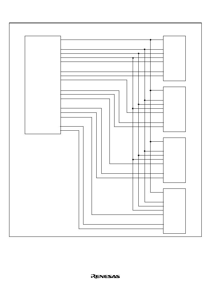
Rev. 5.0, 09/03, page 316 of 806
Figures 11.7, 11.8, and 11.9 show examples of connection to 32, 16, and 8-bit data-width static
RAM, respectively.
A16
A0
CS
OE
I/O7
I/O0
WE
A18
A2
CSn
RD
D31
D24
WE3
D23
D16
WE2
D15
D8
WE1
D7
D0
WE0
SH7729R
128k
◊ 8-bit
SRAM
A16
A0
CS
OE
I/O7
I/O0
WE
A16
A0
CS
OE
I/O7
I/O0
WE
A16
A0
CS
OE
I/O7
I/O0
WE
∑
∑
∑
∑
∑
∑
∑
∑
∑
∑
∑
∑
∑
∑
∑
∑
∑
∑
∑
∑
∑
∑
∑
∑
∑
∑
∑
∑
∑
∑
∑
∑
∑
∑
∑
∑
∑
∑
∑
∑
∑
∑
∑
∑
∑
∑
∑
∑
∑
∑
∑
∑
∑
∑
∑
∑
∑
∑
∑
∑
∑
∑
∑
∑
∑
∑
∑
∑
∑
∑
∑
∑
∑
∑
∑
∑
∑
∑
∑
∑
∑
∑
∑
∑
∑
∑
∑
∑
∑
∑
∑
∑
∑
∑
∑
∑
Figure 11.7 Example of 32-Bit Data-Width Static RAM Connection
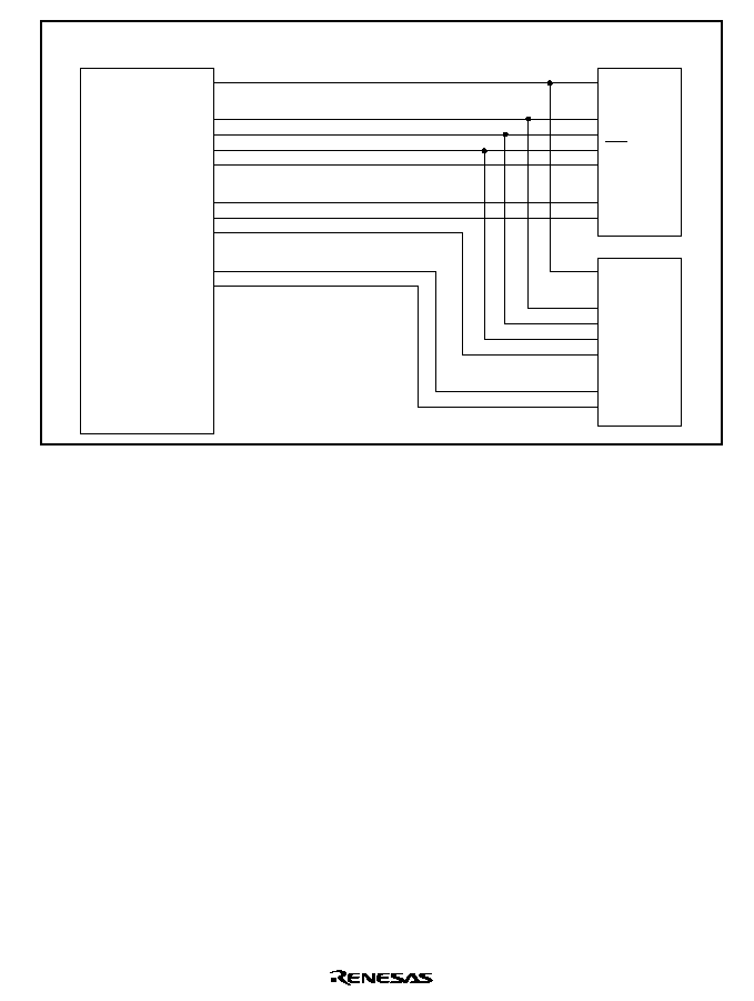
Rev. 5.0, 09/03, page 317 of 806
A16
A0
CS
OE
I/O7
I/O0
WE
A17
A1
CSn
RD
D15
D8
WE1
D7
D0
WE0
SH7729R
128k
◊ 8-bit
SRAM
A16
A0
CS
OE
I/O7
I/O0
WE
∑
∑
∑
∑
∑
∑
∑
∑
∑
∑
∑
∑
∑
∑
∑
∑
∑
∑
∑
∑
∑
∑
∑
∑
∑
∑
∑
∑
∑
∑
∑
∑
∑
∑
∑
∑
∑
∑
∑
∑
∑
∑
∑
∑
∑
∑
∑
∑
∑
∑
∑
∑
Figure 11.8 Example of 16-Bit Data-Width Static RAM Connection

Rev. 5.0, 09/03, page 318 of 806
A16
A0
CSn
RD
D7
D0
WE0
SH7729R
128k
◊ 8-bit
SRAM
A16
A0
CS
OE
I/O7
I/O0
WE
∑
∑
∑
∑
∑
∑
∑
∑
∑
∑
∑
∑
∑
∑
∑
∑
∑
∑
∑
∑
∑
∑
∑
∑
∑
∑
∑
∑
∑
∑
∑
∑
Figure 11.9 Example of 8-Bit Data-Width Static RAM Connection
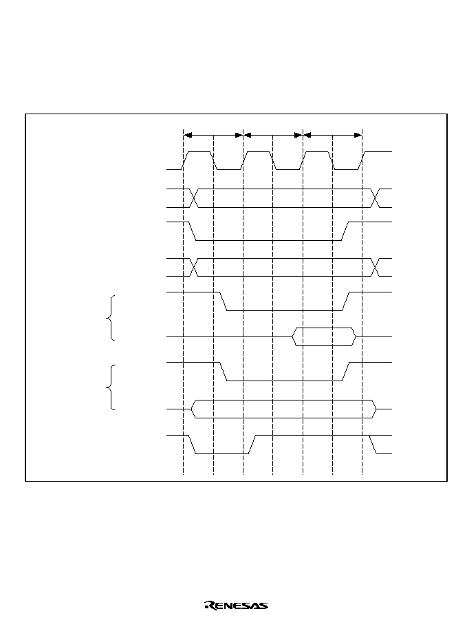
Rev. 5.0, 09/03, page 319 of 806
Wait State Control: Wait state insertion on the basic interface can be controlled by the WCR2
settings. If the WCR2 wait specification bits corresponding to a particular area are not zero, a
software wait is inserted in accordance with that specification. For details, see section 11.2.4, Wait
State Control Register 2 (WCR2).
The specified number of Tw cycles are inserted as wait cycles using the basic interface wait timing
shown in figure 11.10.
T
1
CKIO
A25 to A0
CSn
RD/
WR
RD
D31 to D0
WEn
D31 to D0
BS
Tw
T
2
Read
Write
Figure 11.10 Basic Interface Wait Timing (Software Wait Only)
When software wait insertion is specified by WCR2, the external wait input
WAIT signal is also
sampled.
WAIT pin sampling is shown in figure 11.11. A 2-cycle wait is specified as a software
wait. Sampling is performed at the transition from the Tw state to the T
2
state; therefore, if the
WAIT signal has no effect if asserted in the T
1
cycle or the first Tw cycle.
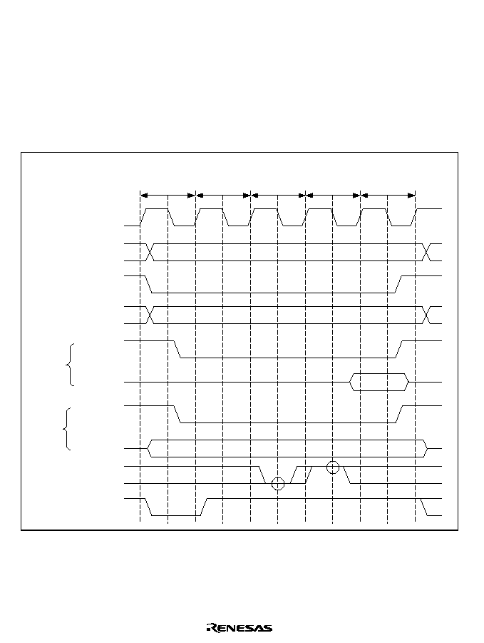
Rev. 5.0, 09/03, page 320 of 806
When the WAITSEL bit in the WCR1 register is set to 1, the
WAIT signal is sampled at the
falling edge of the clock. If the setup time and hold times with respect to the falling edge of the
clock are not satisfied, the value sampled at the next falling edge is used.
However, the
WAIT signal is ignored in the following three cases:
∑
A write to external address space in dual address mode with 16-byte DMA transfer
∑
Transfer from an external device with DACK to external address space in single address mode
with 16-byte DMA transfer
∑
Cache write-back access
T
1
CKIO
A25 to A0
CSn
RD/
WR
RD
D31 to D0
WEn
D31 to D0
WAIT
Tw
Tw
Tw
T
2
Read
Write
BS
Wait states inserted
by
WAIT signal
Figure 11.11 Basic Interface Wait State Timing (Wait State Insertion by
W
W
W
WA
A
A
AIIIITTTT Signal
WAITSEL = 1)

Rev. 5.0, 09/03, page 321 of 806
11.3.4
Synchronous DRAM Interface
Synchronous DRAM Direct Connection: Since synchronous DRAM can be selected by the
CS
signal, physical space areas 2 and 3 can be connected using
RAS and other control signals in
common. If the memory type bits (DRAMTP2≠0) in BCR1 are set to 010, area 2 is ordinary
memory space and area 3 is synchronous DRAM space; if set to 011, areas 2 and 3 are both
synchronous DRAM space. Note, however, that synchronous DRAM must not be accessed when
clock ratio I
:B
= 1:1.
With the SH7729R, burst length 1 burst read/single write mode is supported as the synchronous
DRAM operating mode. A data bus width of 16 or 32 bits can be selected. The burst enable bit
(BE) in MCR is ignored, a 16-bit burst transfer is performed in a cache fill/write-back cycle, and
only one access is performed in a write-through area write or a non-cacheable area read/write.
The control signals for direct connection of synchronous DRAM are
RAS3L, RAS3U, CASL,
CASU, RD/WR, CS2 or CS3, DQMUU, DQMUL, DQMLU, DQMLL, and CKE. All the signals
other than
CS2 and CS3 are common to all areas, and signals other than CKE are valid and fetched
to the synchronous DRAM only when CS2 or CS3 is asserted. Synchronous DRAM can therefore
be connected in parallel to a number of areas. CKE is negated (low) only when self-refreshing is
performed, and is always asserted (high) at other times.
In the refresh cycle and mode-register write cycle,
RAS3U and RAS3L or CASU and CASL are
output.
Commands for synchronous DRAM are specified by
RAS3L, RAS3U, CASL, CASU, RD/WR,
and special address signals. The commands are NOP, auto-refresh (REF), self-refresh (SELF),
precharge all banks (PALL), row address strobe bank active (ACTV), read (READ), read with
precharge (READA), write (WRIT), write with precharge (WRITA), and mode register write
(MRS).
Byte specification is performed by DQMUU, DQMUL, DQMLU, and DQMLL. A read/write is
performed for the byte for which the corresponding DQM is low. In big-endian mode, DQMUU
specifies an access to address 4n, and DQMLL specifies an access to address 4n + 3. In little-
endian mode, DQMUU specifies an access to address 4n + 3, and DQMLL specifies an access to
address 4n.
Figures 11.12 and 11.13 show examples of the connection of two 1M
◊
16-bit
◊
4-bank
synchronous DRAMs and one 1M
◊
16-bit
◊
4-bank synchronous DRAM, respectively.
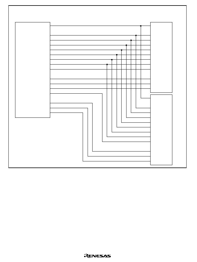
Rev. 5.0, 09/03, page 322 of 806
A15
A2
CKI0
CKE
CSn
RAS3x
CASx
RD/
WR
D31
D16
DQMUU
DQMUL
D15
D0
DQMLU
DQMLL
SH7729R
1 M
◊ 16-bit ◊ 4-bank
synchronous
DRAM
A13
A0
CLK
CKE
CS
RAS
CAS
WE
I/O15
I/O0
DQMU
DQML
A13
A0
CLK
CKE
CS
RAS
CAS
WE
I/O15
I/O0
DQMU
DQML
Note : "x" is U or L
∑
∑
∑
∑
∑
∑
∑
∑
∑
∑
∑
∑
∑
∑
∑
∑
∑
∑
∑
∑
∑
∑
∑
∑
∑
∑
∑
∑
∑
∑
∑
∑
∑
∑
∑
∑
∑
∑
∑
∑
∑
∑
∑
∑
∑
∑
∑
∑
∑
∑
∑
∑
∑
∑
∑
∑
Figure 11.12 Example of 64-Mbit Synchronous DRAM Connection (32-Bit Bus Width)
Rev. 5.0, 09/03, page 323 of 806
SH7729R
64M synchronous DRAM
(1M
◊ 16 bit ◊ 4 bank)
A14
A13
A12
A1
CKIO
CKE
CSn
RAS3x
CASx
RD/
WR
D15
D0
DQMLU
DQMLL
A13
A12
A11
A0
CLK
CKE
CS
RAS
CAS
WE
DQ15
DQ0
DQMU
DQML
∑
∑
∑
∑
∑
∑
∑
∑
∑
∑
∑
∑
∑
∑
∑
∑
∑
∑
∑
∑
∑
∑
∑
∑
∑
∑
∑
∑
∑
∑
∑
∑
Figure 11.13 Example of 64-Mbit Synchronous DRAM (16-Bit Bus Width)
Address Multiplexing: Synchronous DRAM can be connected without external multiplexing
circuitry in accordance with the address multiplex specification bits AMX2-AMX0 in MCR. Table
11.13 shows the relationship between the address multiplex specification bits and the bits output at
the address pins.
A25≠A16 and A0 are not multiplexed; the original values are always output at these pins.
When A0, the LSB of the synchronous DRAM address, is connected to the SH7729R, it performs
longword address specification. Connection should therefore be made in the following order: with
a 32-bit bus width, connect pin A0 of the synchronous DRAM to pin A2 of the SH7729R, then
connect pin A1 to pin A3; with a 16-bit bus width, connect pin A0 of the synchronous DRAM to
pin A1 of the SH7729R, then connect pin A1 to pin A2.

Rev. 5.0, 09/03, page 324 of 806
Table 11.13 Relationship between Bus Width, AMX Bits, and Address Multiplex Output
Setting
External Address Pins
Bus
Width
Memory
Type
AMX3 AMX2 AMX1 AMX0
Output
Timing
A1 to
A8
A9
A10
A11
A12
A13
A14
A15
A16
32 bits
1
1
0
1
Column
address
A1 to
A8
A9
A10
A11
L/H
*
3
A13
A23
A24
*
4
A25
*
4
4M
◊
16 bits
◊
4 banks
*
1
Row
address
A10 to
A17
A18
A19
A20
A21
A22
A23
A24
*
4
A25
*
4
0
1
0
1
Column
address
A1 to
A8
A9
A10
A11
L/H
*
3
A13
A23
*
4
A24
*
4
2M
◊
16 bits
◊
4 banks
*
2
Row
address
A10 to
A17
A18
A19
A20
A21
A22
A23
*
4
A24
*
4
0
1
0
0
Column
address
A1 to
A8
A9
A10
A11
L/H
*
3
A13
A22
*
4
A23
*
4
1M
◊
16 bits
◊
4 banks
*
2
Row
address
A9 to
A16
A17
A18
A19
A20
A21
A22
*
4
A23
*
4
0
1
0
1
Column
address
A1 to
A8
A9
A10
A11
L/H
*
3
A13
A23
*
4
A24
*
4
2M
◊
8 bits
◊
4 banks
*
2
Row
address
A10 to
A17
A18
A19
A20
A21
A22
A23
*
4
A24
*
4
0
1
1
1
Column
address
A1 to
A8
A9
A10
A11
L/H
*
3
A21
*
4
A22
*
4
A15
512k
◊
32
bits
◊
4 banks
*
2
Row
address
A9 to
A16
A17
A18
A19
A20
A21
*
4
A22
*
4
A23
16 bits
1
1
1
0
Column
address
A1 to
A8
A9
A10
L/H
*
3
A12
A23
A24
*
4
A25
*
4
8M
◊
16 bits
◊
4 banks
*
1
Row
address
A11 to
A18
A19
A20
A21
A22
A23
A24
*
4
A25
*
4
1
1
0
1
Column
address
A1 to
A8
A9
A10
L/H
*
3
A12
A22
A23
*
4
A24
*
4
4M
◊
16 bits
◊
4 banks
*
2
Row
address
A10 to
A17
A18
A19
A20
A21
A22
A23
*
4
A24
*
4
0
1
0
1
Column
address
A1 to
A8
A9
A10
L/H
*
3
A12
A22
*
4
A23
*
4
A24
2M
◊
16 bits
◊
4 banks
*
2
Row
address
A10 to
A17
A18
A19
A20
A21
A22
*
4
A23
*
4
A24
0
1
0
0
Column
address
A1 to
A8
A9
A10
L/H
*
3
A12
A21
*
4
A22
*
4
A15
1M
◊
16 bits
◊
4 banks
*
2
Row
address
A9 to
A16
A17
A18
A19
A20
A21
*
4
A22
*
4
A23
0
1
0
1
Column
address
A1 to
A8
A9
A10
L/H
*
3
A12
A22
*
4
A23
*
4
A24
2M
◊
8 bits
◊
4 banks
*
2
Row
address
A10 to
A17
A18
A19
A20
A21
A22
*
4
A23
*
4
A24
Notes:
1.
Only RAS3L or CASL is output.
2.
When addresses are upper 32 Mbytes,
RAS3U
or
CASU
is output.
When addresses are lower 32 Mbytes,
RAS3L
or
CASL
is output.
3.
L/H is a bit used in the command specification: it is fixed at L or H according to the access mode.
4.
Bank address specification.

Rev. 5.0, 09/03, page 325 of 806
Table 11.14 Example of Correspondence between SH7729R and Synchronous DRAM
Address Pins (AMX [3:0] = 0100 (32-Bit Bus Width))
SH7729R Address Pin
Synchronous DRAM Address Pin
RAS Cycle
CAS Cycle
Function
A15
A23
A23
A13(BA1)
A14
A22
A22
A12(BA0)
BANK select bank address
A13
A21
A13
A11
Address
A12
A20
L/H
A10
Address precharge setting
A11
A19
A11
A9
A10
A18
A10
A8
A9
A17
A9
A7
A8
A16
A8
A6
A7
A15
A7
A5
A6
A14
A6
A4
A5
A13
A5
A3
A4
A12
A4
A2
A3
A11
A3
A1
A2
A10
A2
A0
Address
A1
A9
A1
Not used
A0
A0
A0
Not used
Burst Read: In the example in figure 11.14 it is assumed that four 2M
◊
8-bit synchronous
DRAMs are connected and a 32-bit data width is used, and the burst length is 1. Following the Tr
cycle in which ACTV command output is performed, a READ command is issued in the Tc1, Tc2,
and Tc3 cycles, and a READA command in the Tc4 cycle, and the read data is accepted at the
rising edge of the external command clock (CKIO) from cycle Td1 to cycle Td4. The Tpc cycle is
used to wait for completion of auto-precharge based on the READA command inside the
synchronous DRAM; no new access command can be issued to the same bank during this cycle,
but access to synchronous DRAM for another area is possible. In the SH7729R, the number of
Tpc cycles is determined by the TPC bit specification in MCR, and commands cannot be issued
for the same synchronous DRAM during this interval.
The example in figure 11.14 shows the basic timing. To connect low-speed synchronous DRAM,
the cycle can be extended by setting WCR2 and MCR bits. The number of cycles from the ACTV
command output cycle, Tr, to the READ command output cycle, Tc1, can be specified by the
RCD bits in MCR, with values of 0 to 3 specifying 1 to 4 cycles, respectively. In case of 2 or more
cycles, a Trw cycle, in which an NOP command is issued for the synchronous DRAM, is inserted
between the Tr cycle and the Tc cycle. The number of cycles from READ and READA command
output cycles Tc1-Tc4 to the first read data latch cycle, Td1, can be specified as 1 to 3 cycles

Rev. 5.0, 09/03, page 326 of 806
independently for areas 2 and 3 by means of bits A2W1 and A2W0 or A3W1 and A3W0 in
WCR2. This number of cycles corresponds to the number of synchronous DRAM CAS latency
cycles.
CKIO
A25 to A16,
A13
A12
A15, A14,
A11 to A0
CS2 or CS3
RAS3x
CASx
RD/
WR
DQMxx
D31 to D0
BS
Tr
Tc1
Tc2/Td1
Tc3/Td2
Tc4/Td3
Td4
Tpc
Figure 11.14 Basic Timing for Synchronous DRAM Burst Read
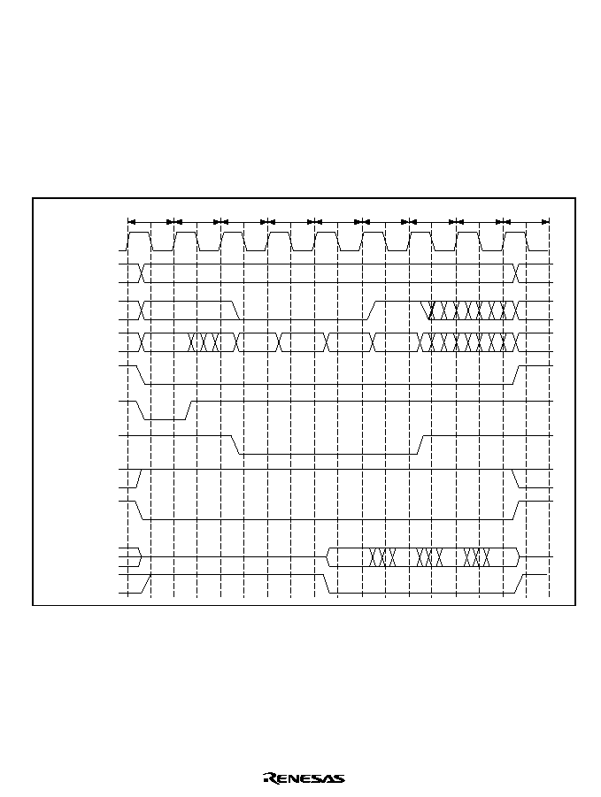
Rev. 5.0, 09/03, page 327 of 806
Figure 11.15 shows the burst read timing when RCD is set to 1, A3W1 and A3W0 are set to 10,
and TPC is set to 1.
The BS cycle, which is asserted for one cycle at the start of a bus cycle for normal access space, is
asserted in each of cycles Td1≠Td4 in a synchronous DRAM cycle. When a burst read is
performed, the address is updated each time
CAS is asserted. As the unit of burst transfer is 16
bytes, address updating is performed for A3 and A2 only (A3, A2, and A1 in the case of a 16-bit
bus width). The order of access is as follows: in a fill operation in the event of a cache miss, the
missed data is read first, then 16-byte boundary data including the missed data is read in
wraparound mode.
CKIO
A25 to A16,
A13
A12
A15, A14,
A11 to A0
CS2 or CS3
RAS3x
CASx
RD/WR
DQMxx
D31 to D0
BS
Tr
Tc1
Tc2
Tc3/Td1 Tc4/Td2
Td3
Tpc
Trw
Td4
Figure 11.15 Synchronous DRAM Burst Read Wait Specification Timing
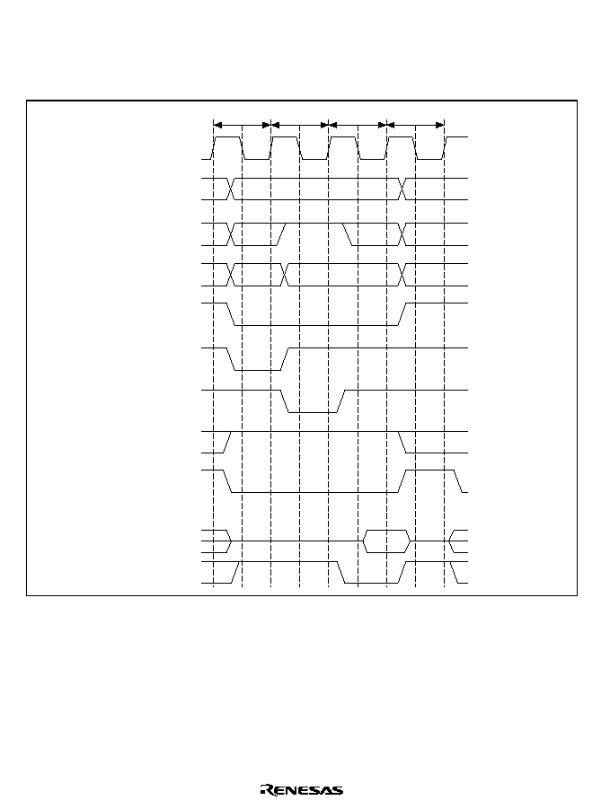
Rev. 5.0, 09/03, page 328 of 806
Single Read: Figure 11.16 shows the timing when a single address read is performed. As the burst
length is set to 1 in synchronous DRAM burst read/single write mode, only the required data is
output. Consequently, no unnecessary bus cycles are generated even when a cache-through area is
accessed.
CKIO
A25 to A16,
A13
A12
A15, A14,
A11 to A0
CS2 or CS3
RAS3x
CASx
RD/
WR
DQMxx
D31 to D0
BS
Tr
Tc1
Td1
Tpc
Figure 11.16 Basic Timing for Synchronous DRAM Single Read

Rev. 5.0, 09/03, page 329 of 806
Burst Write: The timing chart for a burst write is shown in figure 11.17. In the SH7729R, a burst
write occurs in the event of cache write-back or 16-byte DMAC transfer. In a burst write
operation, following the Tr cycle in which ACTV command output is performed, a WRIT
command is issued in the Tc1, Tc2, and Tc3 cycles, and a WRITA command that performs auto-
precharge is issued in the Tc4 cycle. In the write cycle, the write data is output at the same time as
the write command. In case of the write with auto-precharge command, precharging of the
relevant bank is performed in the synchronous DRAM after completion of the write command,
and therefore no command can be issued for the same bank until precharging is completed.
Consequently, in addition to the precharge wait cycle, Tpc, used in a read access, cycle Trwl is
also added as a wait interval until precharging is started following the write command. Issuance of
a new command for the same bank is deferred during this interval. The number of Trwl cycles can
be specified by the TRWL bits in MCR.

Rev. 5.0, 09/03, page 330 of 806
CKIO
CSn
RD/
WR
RAS3x
CASx
DQMxx
D31 to D0
(read)
BS
Tr
Tc1
Tc2
Tc3
Tc4
(Trwl)
(Tpc)
Address
upper bits
A12, A11,
A10 or A9
Address
lower bits
Figure 11.17 Basic Timing for Synchronous DRAM Burst Write

Rev. 5.0, 09/03, page 331 of 806
Single Write: The basic timing chart for write access is shown in figure 11.18. In a single write
operation, following the Tr cycle in which ACTV command output is performed, a WRITA
command that performs auto-precharge is issued in the Tc1 cycle. In the write cycle, the write
data is output at the same time as the write command. In case of the write with auto-precharge
command, precharging of the relevant bank is performed in the synchronous DRAM after
completion of the write command, and therefore no command can be issued for the same bank
until precharging is completed. Consequently, in addition to the precharge wait cycle, Tpc, used in
a read access, cycle Trwl is also added as a wait interval until precharging is started following the
write command. Issuance of a new command for the same bank is deferred during this interval.
The number of Trwl cycles can be specified by the TRWL bits in MCR.
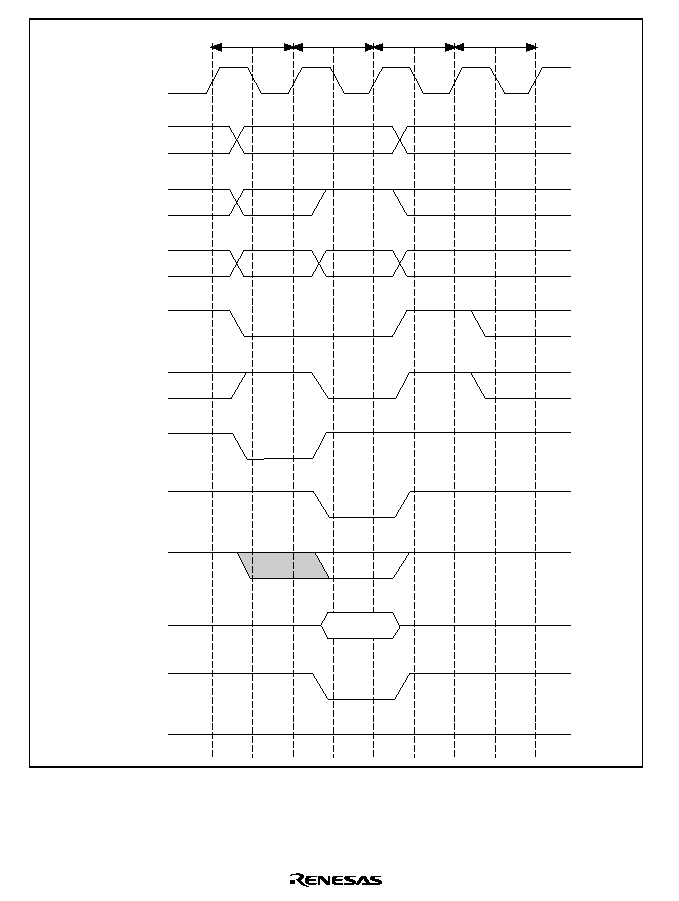
Rev. 5.0, 09/03, page 332 of 806
CKIO
CSn
RD/
WR
RAS3x
CASx
DQMxx
D31 to D0
BS
Address
upper bits
A12 or A10
Address
lower bits
CKE
Tr
Tc1
(Trwl)
(Tpc)
Figure 11.18 Basic Timing for Synchronous DRAM Single Write

Rev. 5.0, 09/03, page 333 of 806
Bank Active: The synchronous DRAM bank function is used to support high-speed accesses to
the same row address. When the RASD bit in MCR is 1, read/write command accesses are
performed using commands without auto-precharge (READ, WRIT). In this case, precharging is
not performed when the access ends. When accessing the same row address in the same bank, it is
possible to issue the READ or WRIT command immediately, without issuing an ACTV command,
in the same way as in the RAS down state in DRAM fast page mode. As synchronous DRAM is
internally divided into two or four banks, it is possible to activate one row address in each bank. If
the next access is to a different row address, a PRE command is first issued to precharge the
relevant bank, then when precharging is completed, the access is performed by issuing an ACTV
command followed by a READ or WRIT command. If this is followed by an access to a different
row address, the access time will be longer because of the precharging performed after the access
request is issued.
In a write, when auto-precharge is performed, a command cannot be issued for a period of Trwl +
Tpc cycles after issuance of the WRITA command. When bank active mode is used, READ or
WRIT commands can be issued successively if the row address is the same. The number of cycles
can thus be reduced by Trwl + Tpc cycles for each write. The number of cycles between issuance
of the precharge command and the row address strobe command is determined by the TPC bits in
MCR.
Whether faster execution speed is achieved by use of bank active mode or by use of basic access is
determined by the probability of accessing the same row address (P1), and the average number of
cycles from completion of one access to the next access (Ta). If Ta is greater than Tpc, the delay
due to the precharge wait when writing is imperceptible. In this case, the access speed for bank
active mode and basic access is determined by the number of cycles from the start of access to
issuance of the read/write command: (Tpc + Trcd)
◊
(1 ≠ P1) and Trcd, respectively.
There is a limit on Tras, the time for placing each bank in the active state. If there is no guarantee
that there will not be a cache hit and another row address will be accessed within the period in
which this value is maintained by program execution, it is necessary to set auto-refresh and set the
refresh cycle to no more than the maximum value of Tras. In this way, it is possible to observe the
restrictions on the maximum active state time for each bank. If auto-refresh is not used, measures
must be taken in the program to ensure that the banks do not remain active for longer than the
prescribed time.
A burst read cycle without auto-precharge is shown in figure 11.19, a burst read cycle for the same
row address in figure 11.20, and a burst read cycle for different row addresses in figure 11.21.
Similarly, a burst write cycle without auto-precharge is shown in figure 11.22, a burst write cycle
for the same row address in figure 11.23, and a burst write cycle for different row addresses in
figure 11.24.

Rev. 5.0, 09/03, page 334 of 806
A Tnop cycle, in which no operation is performed, is inserted before the Tc cycle in which the
READ command is issued in figure 11.20, but when synchronous DRAM is read, there is a two-
cycle latency for the DQMxx signal that performs the byte specification. If the Tc cycle were
performed immediately, without inserting a Tnop cycle, it would not be possible to perform the
DQMxx signal specification for Td1 cycle data output. This is the reason for inserting the Tnop
cycle. If the CAS latency is two cycles or longer, Tnop cycle insertion is not performed, since the
timing requirements will be met even if the DQMxx signal is set after the Tc cycle.
When bank active mode is set, if only accesses to the respective banks in the area 3 space are
considered, as long as accesses to the same row address continue, the operation starts with the
cycle in figure 11.19 or 11.22, followed by repetition of the cycle in figure 11.20 or 11.23. An
access to a different area 3 space during this time has no effect. If there is an access to a different
row address in the bank active state, after this is detected the bus cycle in figure 11.21 or 11.24 is
executed instead of that in figure 11.20 or 11.23. In bank active mode, too, all banks become
inactive after a refresh cycle or after the bus is released as the result of bus arbitration.
The bank active mode should not be used unless the bus width for all areas is 32 bits.
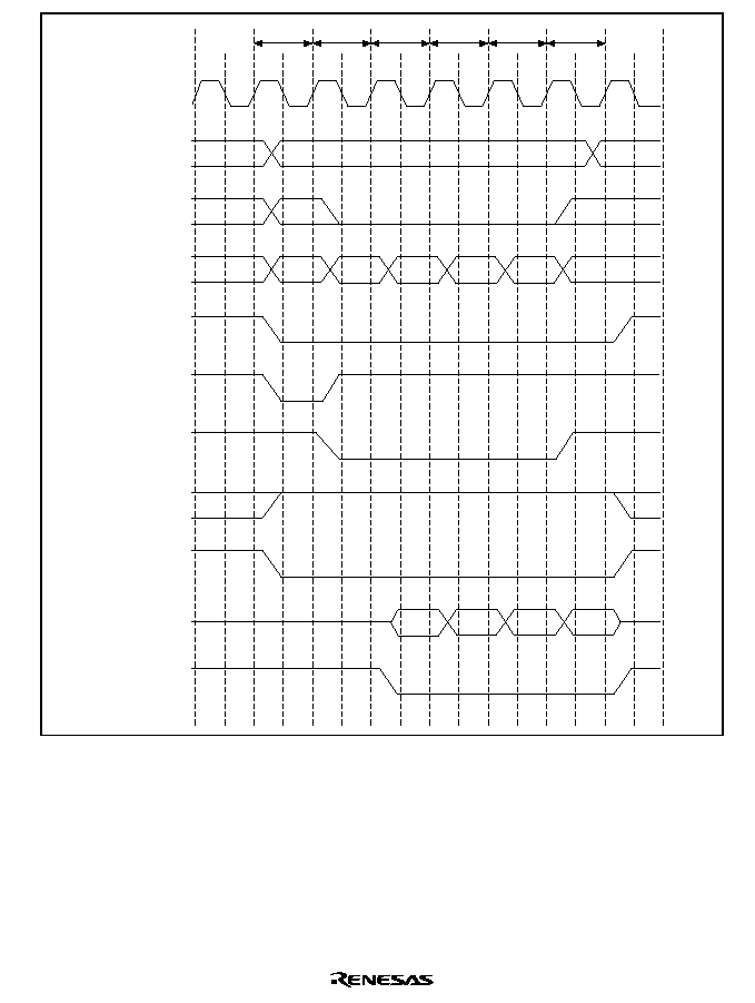
Rev. 5.0, 09/03, page 335 of 806
CKIO
A25
-A16,
A13 (A25
-
A16, A11)
A12 (A10)
A15, A14,
A11
-A0
(A15
-A12,
A9
-A0)
CS2 or CS3
RAS3x
CASx
RD/
WR
DQMxx
D31
-D0
BS
Tr
Tc1
Tc2/Td1 Tc3/Td2 Tc4/Td3
Td4
Figure 11.19 Burst Read Timing (No Precharge)
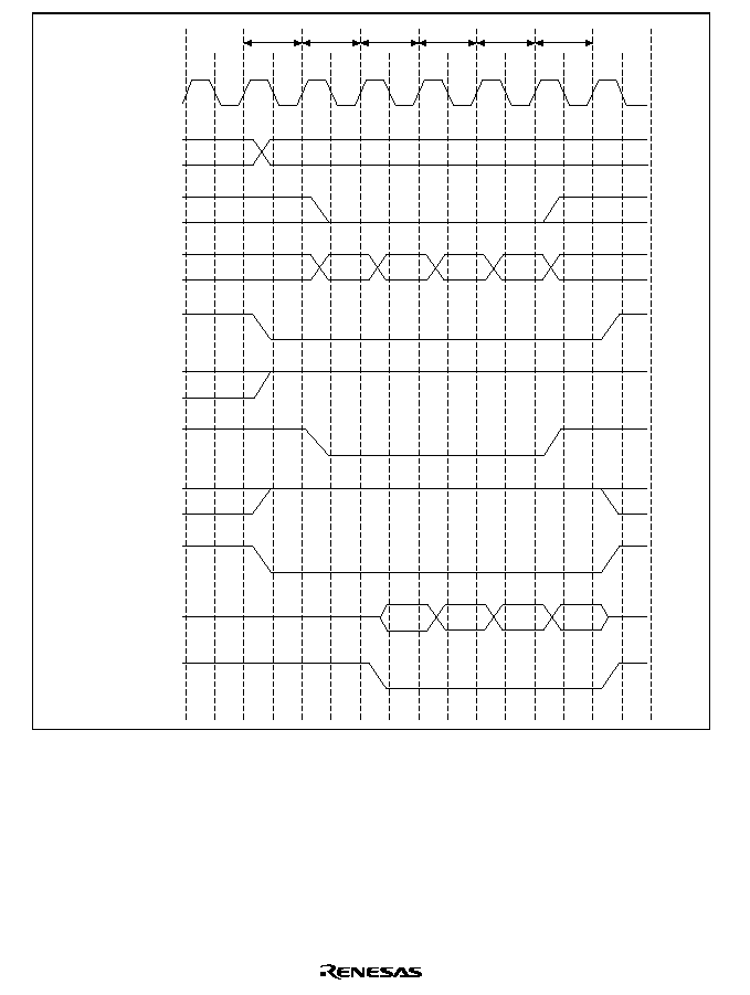
Rev. 5.0, 09/03, page 336 of 806
CKIO
A25
-A16,
A13 (A25
-
A16, A11)
A12 (A10)
A15, A14,
A11
-A0
(A15
-A12,
A9
-A0)
CS2 or CS3
RAS3x
CASx
RD/
WR
DQMxx
D31
-D0
BS
Tnop
Tc1
Tc2/Td1 Tc3/Td2 Tc4/Td3
Td4
Figure 11.20 Burst Read Timing (Same Row Address)
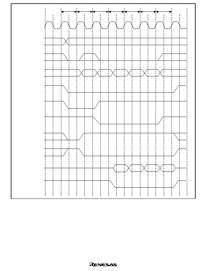
Rev. 5.0, 09/03, page 337 of 806
CKIO
A25
-A16,
A13 (A25
-
A16, A11)
A12 (A10)
A15, A14,
A11
-A0
(A15
-A12,
A9
-A0)
CS2 or CS3
RAS3x
CASx
RD/
WR
DQMxx
D31
-D0
BS
Tp
Tr
Tc1
Tc2/Td1 Tc3/Td2 Tc4/Td3
Td4
Figure 11.21 Burst Read Timing (Different Row Addresses)
Rev. 5.0, 09/03, page 338 of 806
CKIO
A25
-A16,
A13 (A25
-
A16, A11)
A12 (A10)
A15, A14,
A11
-A0
(A15
-A12,
A9
-A0)
CS2 or CS3
RAS3x
CASx
RD/
WR
DQMxx
D31
-D0
BS
Tr
Tc1
Tc2
Tc3
Tc4
Figure 11.22 Burst Write Timing (No Precharge)
Rev. 5.0, 09/03, page 339 of 806
CKIO
A25
-A16,
A13 (A25
-
A16, A11)
A12 (A10)
A15, A14,
A11
-A0
(A15
-A12,
A9
-A0)
CS2 or CS3
RAS3x
CASx
RD/
WR
DQMxx
D31
-D0
BS
Tc1
Tc2
Tc3
Tc4
Figure 11.23 Burst Write Timing (Same Row Address)
Rev. 5.0, 09/03, page 340 of 806
CKIO
A25
-A16,
A13 (A25
-
A16, A11)
A12 (A10)
A15, A14,
A11
-A0
(A15
-A12,
A9
-A0)
CS2 or CS3
RAS3x
CASx
RD/
WR
DQMxx
D31
-D0
BS
Tp
Tr
Tc1
Tc2
Tc3
Td4
Figure 11.24 Burst Write Timing (Different Row Addresses)
Rev. 5.0, 09/03, page 341 of 806
Refreshing: The bus state controller is provided with a function for controlling synchronous
DRAM refreshing. Auto-refreshing can be performed by clearing the RMODE bit to 0 and setting
the RFSH bit to 1 in MCR. If synchronous DRAM is not accessed for a long period, self-refresh
mode, in which the power consumption for data retention is low, can be activated by setting both
the RMODE bit and the RFSH bit to 1.
∑
Auto-Refreshing
Refreshing is performed at intervals determined by the input clock selected by bits CKS2-0 in
RTCSR, and the value set in RTCOR. The value of bits CKS2-0 in RTCOR should be set so as
to satisfy the refresh interval stipulation for the synchronous DRAM used. First make the
settings for RTCOR, RTCNT, and the RMODE and RFSH bits in MCR, then make the CKS2-
CKS0 setting. When the clock is selected by CKS2-CKS0, RTCNT starts counting up from the
value at that time. The RTCNT value is constantly compared with the RTCOR value, and if the
two values are the same, a refresh request is generated and an auto-refresh is performed. At the
same time, RTCNT is cleared to zero and the count-up is restarted. Figure 11.26 shows the
auto-refresh cycle timing.
All-bank precharging is performed in the Tp cycle, then an REF command is issued in the TRr
cycle following the interval specified by the TPC bits in MCR. After the TRr cycle, new
command output cannot be performed for the duration of the number of cycles specified by the
TRAS bits in MCR plus the number of cycles specified by the TPC bits in MCR. The TRAS
and TPC bits must be set so as to satisfy the synchronous DRAM refresh cycle time stipulation
(active/active command delay time).
Auto-refreshing is performed in normal operation, in sleep mode, and in case of a manual
reset.
RTCOR value
RTCNT
H'00000000
RTCSR.CKS(2
-0)
CMF
External bus
CMF flag cleared by start of
refresh cycle
= 000
000
RTCNT cleared to 0 when
RTCNT = RTCOR
Auto-refresh cycle
Time
Figure 11.25 Auto-Refresh Operation
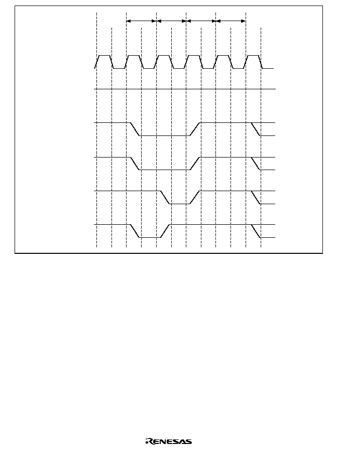
Rev. 5.0, 09/03, page 342 of 806
Tp
TRr
TRrw
TRrw
CKIO
CKE
CSn
RAS3U,
RAS3L
CASU,
CASL
RD/
WR
Figure 11.26 Synchronous DRAM Auto-Refresh Timing

Rev. 5.0, 09/03, page 343 of 806
∑
Self-Refreshing
Self-refresh mode is a kind of standby mode in which the refresh timing and refresh addresses
are generated within the synchronous DRAM. Self-refreshing is activated by setting both the
RMODE bit and the RFSH bit to 1. The self-refresh state is maintained while the CKE signal
is low. Synchronous DRAM cannot be accessed while in the self-refresh state. Self-refresh
mode is cleared by clearing the RMODE bit to 0. After self-refresh mode has been cleared,
command issuance is disabled for the number of cycles specified by the TPC bits in MCR.
Self-refresh timing is shown in figure 11.27. Settings must be made so that self-refresh
clearing and data retention are performed correctly, and auto-refreshing is performed at the
correct intervals. When self-refreshing is activated from the state in which auto-refreshing is
set, or when exiting standby mode other than through a power-on reset, auto-refreshing is
restarted if RFSH is set to 1 and RMODE is cleared to 0 when self-refresh mode is cleared. If
the transition from clearing of self-refresh mode to the start of auto-refreshing takes time, this
time should be taken into consideration when setting the initial value of RTCNT. Making the
RTCNT value 1 less than the RTCOR value will enable refreshing to be started immediately.
After self-refreshing has been set, the self-refresh state continues even if the chip standby state
is entered using the SH7729R's standby function, and is maintained even after recovery from
standby mode other than through a power-on reset. In case of a power-on reset, the bus state
controller's registers are initialized, and therefore the self-refresh state is cleared.
Self-refreshing is performed in normal operation, in sleep mode, in standby mode, and in case
of a manual reset.
When using synchronous DRAM, use the following procedure to initiate self-refreshing.
1. Clear the refresh control bit to 0.
2. Write H'00 to the RTCNT register.
3. Set the refresh control bit and refresh mode bit to 1.
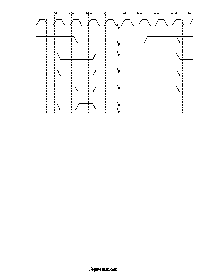
Rev. 5.0, 09/03, page 344 of 806
TRs1
CKIO
RD/
WR
CSn
RAS3U, RAS3L
CASU, CASL
CKE
(TRs2)
(TRs2)
TRs3
(Tpc)
(Tpc)
Tp
Figure 11.27 Synchronous DRAM Self-Refresh Timing
∑
Relationship between Refresh Requests and Bus Cycle Requests
If a refresh request is generated during execution of a bus cycle, execution of the refresh is
deferred until the bus cycle is completed. If a refresh request occurs when the bus has been
released by the bus arbiter, refresh execution is deferred until the bus is acquired. If a match
between RTCNT and RTCOR occurs while a refresh is waiting to be executed, so that a new
refresh request is generated, the previous refresh request is eliminated. In order for refreshing
to be performed normally, care must be taken to ensure that no bus cycle or bus mastership
occurs that is longer than the refresh interval. When a refresh request is generated, the
IRQOUT pin is asserted (driven low). Therefore, normal refreshing can be performed by
having the
IRQOUT pin monitored by a bus master other than the SH7729R requesting the
bus, or the bus arbiter, and returning the bus to the SH7729R. When refreshing is started, and
if no other interrupt request has been generated, the
IRQOUT pin is negated (driven high).

Rev. 5.0, 09/03, page 345 of 806
Power-On Sequence: In order to use synchronous DRAM, mode setting must first be performed
after powering on. To perform synchronous DRAM initialization correctly, the bus state controller
registers must first be set, followed by a write to the synchronous DRAM mode register. In
synchronous DRAM mode register setting, the address signal value at that time is latched by a
combination of the
RAS, CAS, and RD/WR signals. If the value to be set is X, the bus state
controller provides for value X to be written to the synchronous DRAM mode register by
performing a write to address H'FFFFD000 + X for area 2 synchronous DRAM, and to address
H'FFFFE000 + X for area 3 synchronous DRAM. In this operation the data is ignored, but the
mode write is performed as a byte-size access. To set burst read/single write, CAS latency 1 to 3,
wrap type = sequential, and burst length 1 supported by the SH7729R, arbitrary data is written in a
byte-size access to the following addresses.
With 32-bit bus width:
Area 2
Area 3
CAS latency 1
FFFFD840
FFFFE840
CAS latency 2
FFFFD880
FFFFE880
CAS latency 3
FFFFD8C0
FFFFE8C0
With 16-bit bus width:
Area 2
Area 3
CAS latency 1
FFFFD420
FFFFE420
CAS latency 2
FFFFD440
FFFFE440
CAS latency 3
FFFFD460
FFFFE460
Mode register setting timing is shown in figure 11.28.
As a result of the write to address H'FFFFD000 + X or H'FFFFE000 + X, a precharge all banks
(PALL) command is first issued in the TRp1 cycle, then a mode register write command is issued
in the TMw1 cycle.
Address signals, when the mode-register write command is issued, are as follows:
32-bit bus width:
A15≠A9 = 0000100 (burst read and single write)
A8≠A6 = CAS latency
A5 = 0 (burst type = sequential)
A4≠A2 = 000 (burst length 1)
16-bit bus width:
A14≠A8 = 0000100 (burst read and single write)
A7≠A5 = CAS latency
A4 = 0 (burst type = sequential)
A3≠A1 = 000 (burst length 1)

Rev. 5.0, 09/03, page 346 of 806
Before mode register setting, a 100
µ
s idle time (depending on the memory manufacturer) must be
guaranteed after powering on requested by the synchronous DRAM. If the reset signal pulse width
is greater than this idle time, there is no problem in performing mode register setting immediately.
The number of dummy auto-refresh cycles specified by the manufacturer (usually 8) or more must
be executed. This is usually achieved automatically while various kinds of initialization are being
performed after auto-refresh setting, but a way of carrying this out more dependably is to set a
short refresh request generation interval just while these dummy cycles are being executed. With
simple read or write access, the address counter in the synchronous DRAM used for auto-
refreshing is not initialized, and so the cycle must always be an auto-refresh cycle.
CKIO
A11
A12 or A10
A9 to A2
CSn
RD/
WR
RAS3U or RAS3L
CASU or CASL
D31 to D0
CKE
TRp1
TRp2
TRp3
TRp4
TMw1
TMw2
TMw3
TMw4
(High)
A15 to A13
or A15 to A12
Figure 11.28 Synchronous DRAM Mode Write Timing

Rev. 5.0, 09/03, page 347 of 806
11.3.5
Burst ROM Interface
Setting bits A0BST1≠0, A5BST1≠0, and A6BST1≠0 in BCR1 to a non-zero value allows burst
ROM to be connected to areas 0, 5, and 6. The burst ROM interface provides high-speed access to
ROM that has a nibble access function. The timing for nibble access to burst ROM is shown in
figure 11.29. Two wait cycles are set. Basically, access is performed in the same way as for
normal space, but when the first cycle ends the
CS0 signal is not negated, and only the address is
changed before the next access is executed. When 8-bit ROM is connected, the number of
consecutive accesses can be set as 4, 8, or 16 by bits A0BST1≠0, A5BST1≠0, or A6BST1≠0.
When 16-bit ROM is connected, 4 or 8 can be set in the same way. When 32-bit ROM is
connected, only 4 can be set.
WAIT pin sampling is performed in the first access if one or more wait states are set, and is
always performed in the second and subsequent accesses.
The second and subsequent access cycles also comprise two cycles when a burst ROM setting is
made and the wait specification is 0. The timing in this case is shown in figure 11.30.

Rev. 5.0, 09/03, page 348 of 806
T
1
T
W
T
W
TB2
TB1
T
W
TB2
CKIO
A25 to A4
A3 to A0
CSn
RD/
WR
RD
D31 to
D0
BS
WAIT
T
2
Note: For a write cycle, a basic bus cycle (write cycle) is performed.
TB1
Figure 11.29 Burst ROM Wait Access Timing

Rev. 5.0, 09/03, page 349 of 806
T
1
TB2
TB1
TB2
TB1
TB2
TB1
T
2
CKIO
A25 to A4
A3 to A0
CSn
RD/
WR
RD
D31 to D0
BS
WAIT
Note: For a write cycle, a basic bus cycle (write cycle) is performed.
Figure 11.30 Burst ROM Basic Access Timing

Rev. 5.0, 09/03, page 350 of 806
11.3.6
PCMCIA Interface
In the SH7729R, setting the A5PCM bit in BCR1 to 1 makes the bus interface for physical space
area 5 an IC memory card and I/O card interface as stipulated in JEIDA version 4.2
(PCMCIA2.1). Setting the A6PCM bit to 1 makes the bus interface for physical space area 6 an IC
memory card and I/O card interface as stipulated in JEIDA version 4.2.
When the PCMCIA interface is used, a bus size of 8 or 16 bits can be set by bits A5SZ1 and
A5SZ0, or A6SZ1 and A6SZ0, in BCR2.
Figure 11.31 shows an example of PCMCIA card connection to the SH7729R. To enable active
insertion of the PCMCIA cards (i.e. insertion or removal while system power is being supplied), a
3-state buffer must be connected between the SH7729R's bus interface and the PCMCIA cards.
As operation in big-endian mode is not explicitly stipulated in the JEIDA/PCMCIA specifications,
the PCMCIA interface for the SH7729R in big-endian mode is stipulated independently.
However, the
WAIT signal is ignored in the following three cases:
∑
A write to external address space in dual address mode with 16-byte DMA transfer
∑
Transfer from an external device with DACK to external address space in single address mode
with 16-byte DMA transfer
∑
Cache write-back access
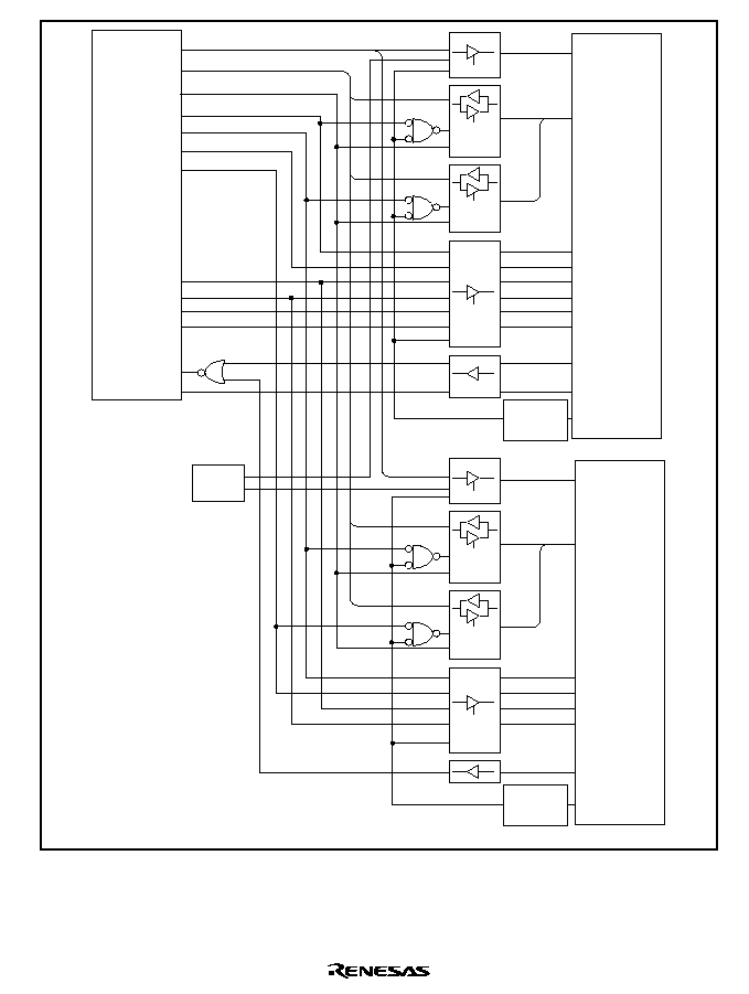
Rev. 5.0, 09/03, page 351 of 806
A24 to A0
D15 to D0
RD/
WR
CE1B/(CS6)
CE1A/(CS5)
RD
WE1
ICIORD
ICIOWR
WAIT
IOIS16
SH7729R
A25 to A0
D15 to D0
CE2
OE
WE/PGM
(
IORD)
(
IOWR)
WAIT
(
IOIS16)
CD1, CD2
CE1
PC card
(memory/IO)
G
G
G
DIR
DIR
G
D7 to D0
D15 to D8
A25 to A0
D15 to D0
CE2
OE
WE/PGM
WAIT
CD1, CD2
CE1
PC card
(memory/IO)
G
G
G
DIR
DIR
G
D7 to D0
D15 to D8
CE2B
CE2A
Output
port
Card
detection
circuit
Card
detection
circuit
Figure 11.31 Example of PCMCIA Interface

Rev. 5.0, 09/03, page 352 of 806
Memory Card Interface Basic Timing: Figure 11.32 shows the basic timing for the PCMCIA IC
memory card interface. When physical space areas 5 and 6 are designated as PCMCIA interface
areas, bus accesses are automatically performed as IC memory card interface accesses.
With a high external bus frequency (CKIO), the setup and hold times for the address (A24≠A0),
card enable (
CS5, CE2A, CS6, CE2B), and write data (D15≠D0) in a write cycle, become
insufficient with respect to
RD and WR (the WE pin in the SH7729R). The SH7729R provides for
this by enabling setup and hold times to be set for physical space areas 5 and 6 in the PCR register.
Also, software waits by means of a WCR2 register setting and hardware waits by means of the
WAIT pin can be inserted in the same way as for the basic interface. Figure 11.33 shows the
PCMCIA memory bus wait timing.
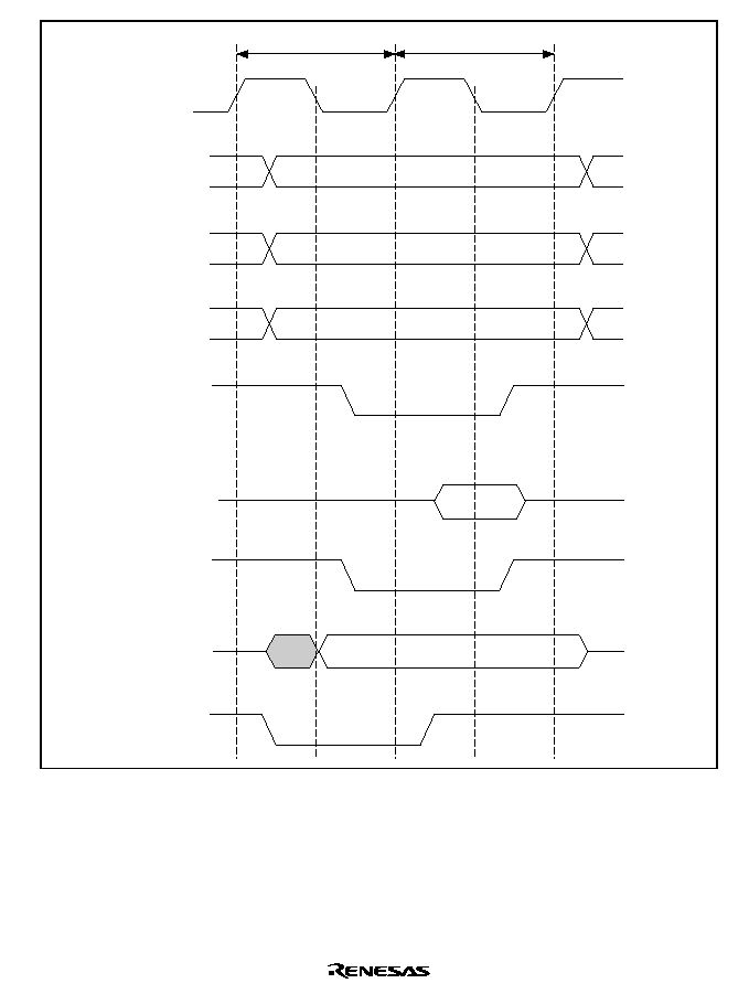
Rev. 5.0, 09/03, page 353 of 806
CKIO
Tpcm1
Tpcm2
A25 to A0
CExx
RD/
WR
D15 to D0
(read)
D15 to D0
(read)
RD
(read)
WE
(write)
BS
Figure 11.32 Basic Timing for PCMCIA Memory Card Interface
Rev. 5.0, 09/03, page 354 of 806
CKIO
Tpcm0
A25 to A0
RD/
WR
CExx
RD
(read)
D15 to D0
(read)
D15 to D0
(write)
WE
(write)
BS
WAIT
Tpcm0w
Tpcm1
Tpcm1w Tpcm1w
Tpcm2
Tpcm2w
Figure 11.33 Wait Timing for PCMCIA Memory Card Interface
Rev. 5.0, 09/03, page 355 of 806
Memory Card Interface Burst Timing: In the SH7729R, when the IC memory card interface is
selected, page mode burst access mode can be used, for read access only, by setting bits A5BST1
and A5BST0 in BCR1 for physical space area 5, or bits A6BST1 and A6BST0 in BCR1 for area
6. This burst access mode is not stipulated in JEIDA version 4.2 (PCMCIA2.1), but allows high-
speed data access using ROM provided with a burst mode, etc.
Burst access mode timing is shown in figures 11.34 and 11.35.
CKIO
Tpcm1
A25 to A4
CExx
A3 to A0
RD/
WR
RD
(read)
D15 to D0
(read)
BS
Tpcm2
Tpcm1
Tpcm2
Tpcm1
Tpcm2
Tpcm1
Tpcm2
Figure 11.34 Basic Timing for PCMCIA Memory Card Interface Burst Access
Rev. 5.0, 09/03, page 356 of 806
CKIO
Tpcm0
A25 to A4
CExx
A3 to A0
RD/
WR
RD
(read)
D15 to D0
(read)
BS
WAIT
Tpcm1 Tpcm1w Tpcm1w Tpcm1w Tpcm2
Tpcm1 Tpcm1w
Tpcm2 Tpcm2w
Figure 11.35 Wait Timing for PCMCIA Memory Card Interface Burst Access
Rev. 5.0, 09/03, page 357 of 806
When the entire 32-Mbyte memory space is used as IC memory card interface space, the common
memory/attribute memory switching signal
REG is generated using a port, etc. If 16 Mbytes or
less of memory space is sufficient, using 16 Mbytes of memory space as common memory space
and 16 Mbytes as attribute memory space enables the A24 pin to be used for the
REG signal.
I/O space
I/O space
I/O space
Area 5: H'14000000
Area 5: H'16000000
Area 6: H'18000000
Area 6: H'1A000000
Area 5: H'14000000
Area 5: H'15000000
Area 5: H'16000000
H'17000000
Area 6: H'18000000
Area 6: H'19000000
Area 6: H'1A000000
H'1B000000
Attribute memory
Common memory
Attribute memory
Common memory
I/O space
Up to 16-Mbyte capacity (REG = A24)
32-Mbyte capacity (REG = I/O port)
Common memory/
attribute memory
Common memory/
attribute memory
Figure 11.36 PCMCIA Space Allocation

Rev. 5.0, 09/03, page 358 of 806
I/O Card Interface Timing: Figures 11.37 and 11.38 show the timing for the PCMCIA I/O card
interface.
Switching between the I/O card interface and the IC memory card interface is performed
according to the accessed address. When PCMCIA is designed for physical space area 5, the bus
access is automatically performed as an I/O card interface access when a physical address from
H'16000000 to H'17FFFFFF is accessed. When PCMCIA is designated for physical space area 6,
the bus access is automatically performed as an I/O card interface access when a physical address
from H'1A000000 to H'1BFFFFFF is accessed.
When accessing a PCMCIA I/O card, the access should be performed using a non-cacheable area
in virtual space (P2 or P3 space) or an area specified as non-cacheable by the MMU.
When an I/O card interface access is made to a PCMCIA card in little-endian mode, dynamic
sizing of the I/O bus width is possible using the
IOIS16 pin. When a 16-bit bus width is set for
area 5 or area 6, if the
IOIS16 signal is high during a word-size I/O bus cycle, the I/O port is
recognized as being 8 bits in width. In this case, a data access for only 8 bits is performed in the
I/O bus cycle being executed, followed automatically by a data access for the remaining 8 bits.
Figure 11.39 shows the basic timing for dynamic bus sizing.
In big-endian mode, the
IOIS16 signal is not supported, and should be fixed low.
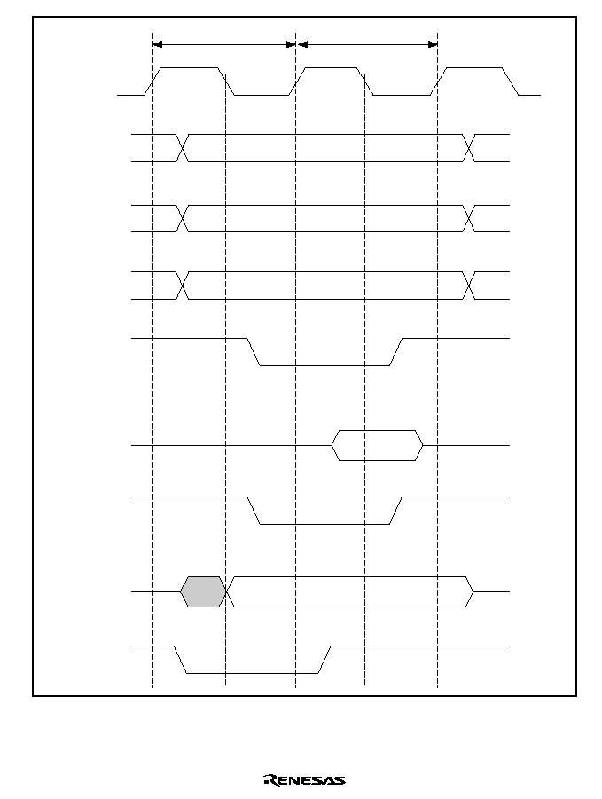
Rev. 5.0, 09/03, page 359 of 806
CKIO
Tpci1
Tpci2
A25 to A0
RD/
WR
CExx
ICIORD
(read)
D15 to D0
(read)
ICIOWR
(write)
D15 to D0
(write)
BS
Figure 11.37 Basic Timing for PCMCIA I/O Card Interface
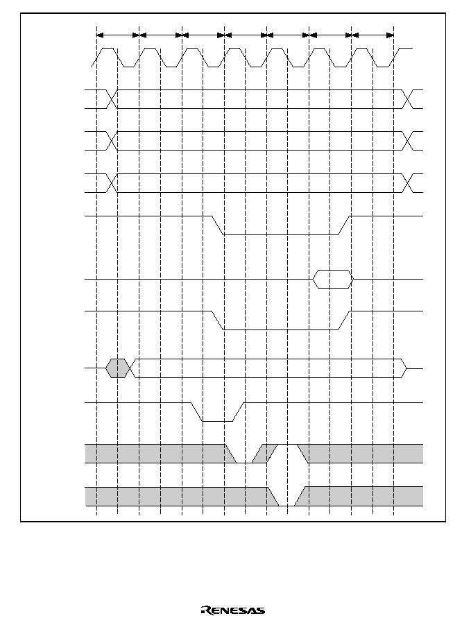
Rev. 5.0, 09/03, page 360 of 806
CKIO
A25 to A0
RD/
WR
CExx
ICIORD
(read)
ICIOWR
(write)
D15 to D0
(read)
D15 to D0
(write)
BS
WAIT
IOIS16
Tpci0
Tpci0w
Tpci1
Tpci1w
Tpci1w
Tpci2
Tpci2w
Figure 11.38 Wait Timing for PCMCIA I/O Card Interface
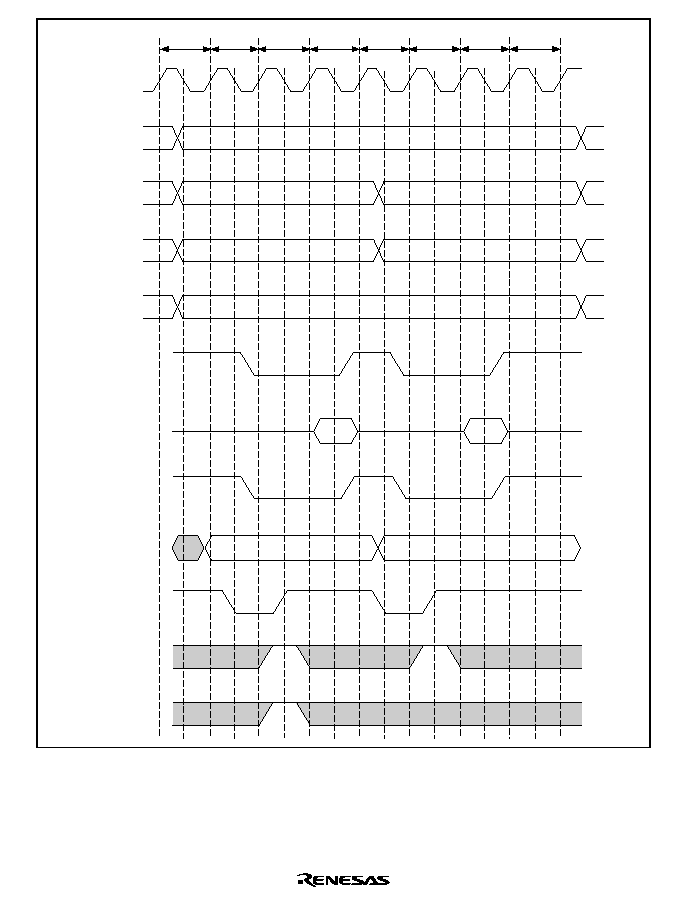
Rev. 5.0, 09/03, page 361 of 806
CKIO
Tpci0
A25 to A1
CExx
A0
RD/
WR
ICIORD
(read)
D15 to D0
(read)
ICIOWR
(write)
D15 to D0
(write)
BS
WAIT
IOIS16
Tpci1
Tpci1w
Tpci2
Tpci1
Tpci1w
Tpci2
Tpci2w
Figure 11.39 Dynamic Bus Sizing Timing for PCMCIA I/O Card Interface

Rev. 5.0, 09/03, page 362 of 806
11.3.7
Waits between Access Cycles
A problem associated with higher external memory bus operating frequencies is that data buffer
turn-off on completion of a read from a low-speed device may be too slow, causing a collision
with data in the next access. This results in lower reliability or incorrect operation. To avoid this
problem, a data collision prevention feature has been provided. This memorizes the preceding
access area and the kind of read/write. If there is a possibility of a bus collision when the next
access is started, a wait cycle is inserted before the access cycle thus preventing a data collision.
There are two cases in which a wait cycle is inserted: when an access is followed by an access to a
different area, and when a read access is followed by a write access from the SH7729R. When the
SH7729R performs consecutive write cycles, the data transfer direction is fixed (from the
SH7729R to other memory) and there is no problem. With read accesses to the same area, in
principle, data is output from the same data buffer, and wait cycle insertion is not performed. Bits
AnIW1 and AnIW0 (n = 0, 2≠6) in WCR1 specify the number of idle cycles to be inserted
between access cycles when a physical space area access is followed by an access to another area,
or when the SH7729R performs a write access after a read access to physical space area n. If there
is originally space between accesses, the number of idle cycles inserted is the specified number of
idle cycles minus the number of empty cycles.
Waits are not inserted between accesses when bus arbitration is performed, since empty cycles are
inserted for arbitration purposes.
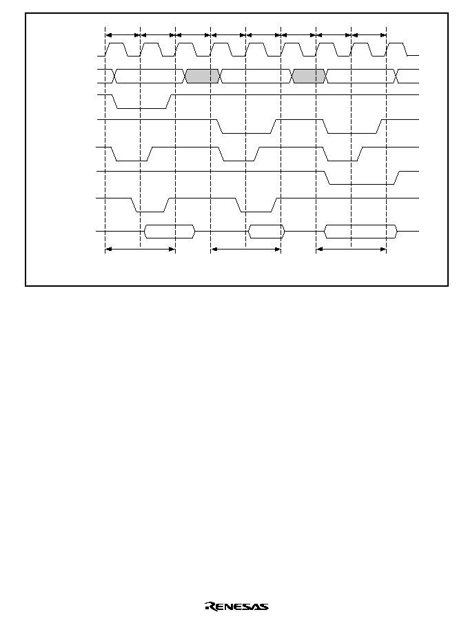
Rev. 5.0, 09/03, page 363 of 806
T
1
CKIO
CSm
CSn
A25 to A0
BS
RD/
WR
RD
D31 to D0
T
2
Twait
T
1
T
2
Twait
T
1
T
2
Area m read
Area m inter-access wait specification
Area n inter-access wait specification
Area n space read
Area n space write
Figure 11.40 Waits between Access Cycles
11.3.8
Bus Arbitration
When a bus release request (
BREQ) is received from an external device, buses are released after
the bus cycle being executed is completed and a bus grant signal (
BACK) is output
.
The bus is not
released during burst transfers for cache fills or TAS instruction execution between the read cycle
and write cycle. Bus arbitration is not executed in multiple bus cycles that are generated when the
data bus width is shorter than the access size; i.e. in the bus cycles when longword access is
executed for the 8-bit memory. At the negation of
BREQ, BACK is negated and bus use is
restarted
.
See Appendix A.1, Pin States, for the pin states when the bus is released.
The SH7729R sometimes needs to retrieve a bus it has released. For example, when memory
generates a refresh request or an interrupt request internally, the SH7729R must perform the
appropriate processing. The SH7729R has a bus request signal (
IRQOUT) for this purpose. When
it must retrieve the bus, it asserts the
IRQOUT signal. Devices asserting an external bus release
request receive the assertion of the
IRQOUT signal and negate the BREQ signal to release the bus.
The SH7729R retrieves the bus and carries out the processing.
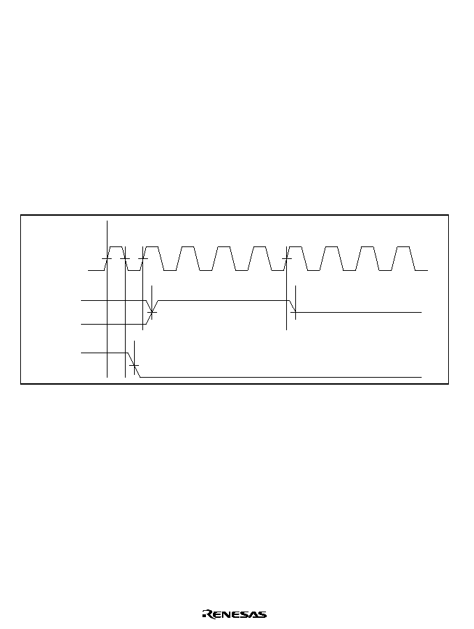
Rev. 5.0, 09/03, page 364 of 806
I
I
I
IR
R
R
RQ
Q
Q
QO
O
O
OU
U
U
UTTTT Pin Assertion Conditions:
∑
When a memory refresh request has been generated but the refresh cycle has not yet begun
∑
When an interrupt is generated with an interrupt request level higher than the setting of the
interrupt mask bits (I3≠I0) in the status register (SR). (This does not depend on the SR.BL bit.)
11.3.9
Bus Pull-Up
With the SH7729R, address pin pull-up can be performed when the bus is released by setting the
PULA bit in BCR1 to 1. The address pins are pulled up for a 4-clock period after
BACK is
asserted. Figure 11.41 shows the address pin pull-up timing. Similarly, data pin pull-up can be
performed by setting the PULD bit in BCR1 to 1. The data pins should be pulled up when the data
bus is not in use. The data pin pull-up timing for a read cycle is shown in figure 11.42, and the
timing for a write cycle in figure 11.43.
Hi-Z
Pull-up
CKIO
A25
-A0
BACK
Figure 11.41 Pull-Up Timing for Pins A25 to A0
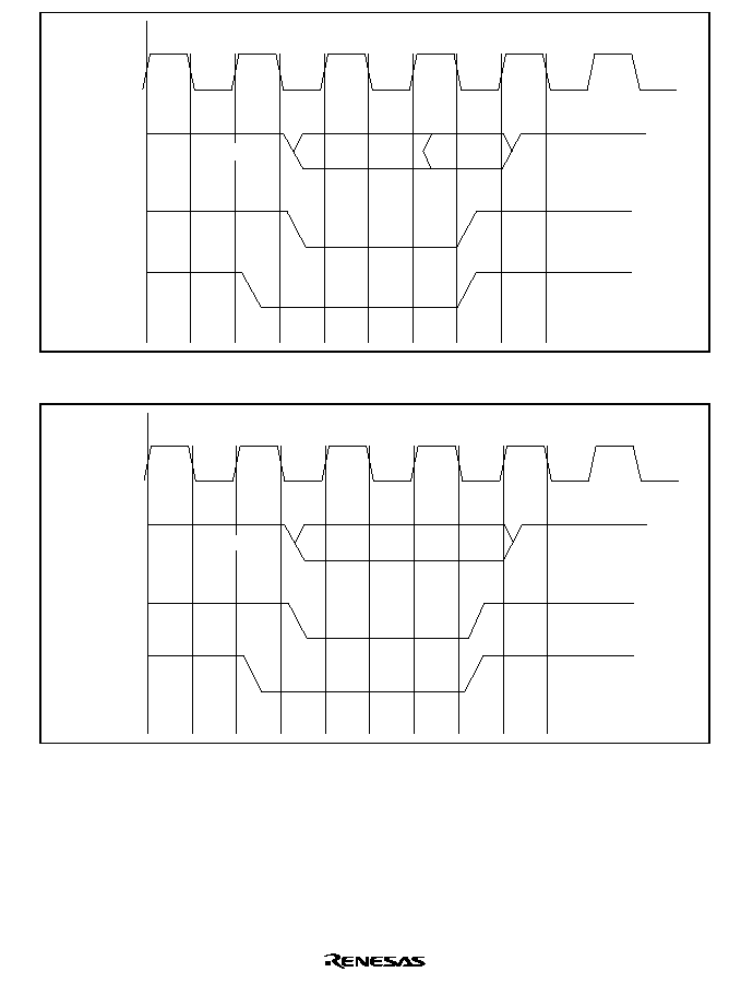
Rev. 5.0, 09/03, page 365 of 806
Pull-up
CKIO
D31
-D0
RD
CSn
Pull-up
Figure 11.42 Pull-Up Timing for Pins D31 to D0 (Read Cycle)
Pull-up
CKIO
D31
-D0
WEn
CSn
Pull-up
Figure 11.43 Pull-Up Timing for Pins D31 to D0 (Write Cycle)

Rev. 5.0, 09/03, page 366 of 806
11.3.10
M
M
M
MC
C
C
CSSSS[[[[0000]]]] to M
M
M
MC
C
C
CSSSS[[[[7777]]]] Pin Control
The SH7729R is provided with pins
MCS[0]≠MCS[7] as dedicated CS pins for the ROM
connected to area 0 or 2. Assertion of
MCS[0]≠MCS[7] is controlled by settings in MCSCR0≠
MCSCR7. This enables 32-, 64-, 128-, or 256-Mbit memory to be connected to area 0 or area 2.
However, only CS2/0 = 0 (area 0) should be used for MCSCR0. Table 11.15 shows MCSCR0≠
MCSCR7 settings and
MCS[0]≠MCS[7] assertion conditions.
As the
MCS[0]≠MCS[7] pins are multiplexed as the PTC0≠PTC7 pins, when using these pins as
MCS[0]≠MCS[7], the corresponding bits in the PCCR register should be set to "other function."
When CS2/0 = 0 in the MCSCR0 and when the PTC0 pin is switched to
MCS[0] (when
PCOMD1≠PCOMD0 are set to "other function"), the
CS0 pin is also switched to MCS[0].
As port register writes operate on the peripheral clock, they take time compared with instruction
execution by the CPU operating on the high-speed internal clock. Therefore, if an instruction that
accesses
MCS[1] to MCS[7] is located several instructions after an instruction that switches port C
to
MCS, the switch from PTC[n] to MCSn and from CS0 to MCS[0] may not be performed
correctly.
To prevent this problem, the following switching procedure should be used.
∑
When the program runs with cache on
(1) To switch port C to
MCS, set the corresponding bits in the PCCR register to 00 ("other
function").
(2) Read the PCCR register and check whether the set value is read. Repeat until the set value is
read.
(3) Perform a dummy read from non-cacheable CS0 space (e.g. address H'A0000000). This will
result in an access to the CS0 space, and immediately afterward, CS0 will be switched to
MCS[0], and port C[n] will be switched to MCS[n].
(4) Access can now be made to the
MCS[1] to MCS[7] spaces.
∑
When the program runs in
MCS[0] space with cache off
(1) Set the PCCR register as in (1) above.
(2) Place at least three NOP instructions after the instruction in (1). As a result, whe n the PCCR
register is rewritten, an access to the CS0 space will be generated, and immediately afterward,
CS0 will be switched to
MCS[0], and port C[n] will be switched to MCS[n].
(3) Access can now be made to the
MCS[1] to MCS[7] spaces.

Rev. 5.0, 09/03, page 367 of 806
Table 11.15 MCSCRx Settings and
M
M
M
MC
C
C
CSSSS[[[[xxxx]]]] Assertion Conditions (x: 0≠7)
MCSCRx Settings
M
M
M
MC
C
C
CS
S
S
S[[[[xxxx]]]]
Assertion Conditions
CS2/0 CAP1 CAP0 A25
A24
A23
A22
C
C
C
CS
S
S
S0000
C
C
C
CS
S
S
S2222
Address Bus A [25:0]
Notes
0
1
1
0
--
--
--
L
H
H'0000000 to H'1FFFFFF 256-Mbit ROM
1
--
--
--
L
H
H'2000000 to H'3FFFFFF
1
0
0
0
--
--
L
H
H'0000000 to H'0FFFFFF 128-Mbit ROM
0
1
--
--
L
H
H'1000000 to H'1FFFFFF
1
0
--
--
L
H
H'2000000 to H'2FFFFFF
1
1
--
--
L
H
H'3000000 to H'3FFFFFF
0
1
0
0
0
--
L
H
H'0000000 to H'07FFFFF 64-Mbit ROM
0
0
1
--
L
H
H'0800000 to H'0FFFFFF
0
1
0
--
L
H
H'1000000 to H'17FFFFF
0
1
1
--
L
H
H'1800000 to H'1FFFFFF
1
0
0
--
L
H
H'2000000 to H'27FFFFF
1
0
1
--
L
H
H'2800000 to H'2FFFFFF
1
1
0
--
L
H
H'3000000 to H'37FFFFF
1
1
1
--
L
H
H'3800000 to H'3FFFFFF
0
0
0
0
0
0
L
H
H'0000000 to H'03FFFFF 32-Mbit ROM
0
0
0
1
L
H
H'0400000 to H'07FFFFF
0
0
1
0
L
H
H'0800000 to H'0BFFFFF
0
0
1
1
L
H
H'0C00000 to H'0FFFFFF
0
1
0
0
L
H
H'1000000 to H'13FFFFF
0
1
0
1
L
H
H'1400000 to H'17FFFFF
0
1
1
0
L
H
H'1800000 to H'1BFFFFF
0
1
1
1
L
H
H'1C00000 to H'1FFFFFF
1
0
0
0
L
H
H'2000000 to H'23FFFFF
1
0
0
1
L
H
H'2400000 to H'27FFFFF
1
0
1
0
L
H
H'2800000 to H'2BFFFFF
1
0
1
1
L
H
H'2C00000 to H'2FFFFFF
1
1
0
0
L
H
H'3000000 to H'33FFFFF
1
1
0
1
L
H
H'3400000 to H'37FFFFF
1
1
1
0
L
H
H'3800000 to H'3BFFFFF
1
1
1
1
L
H
H'3C00000 to H'3FFFFFF

Rev. 5.0, 09/03, page 368 of 806
MCSCRx Settings
M
M
M
MC
C
C
CS
S
S
S[[[[xxxx]]]]
Assertion Conditions
CS2/0 CAP1 CAP0 A25
A24
A23
A22
C
C
C
CS
S
S
S0000
C
C
C
CS
S
S
S2222
Address Bus A[25:0]
Notes
1
1
1
0
--
--
--
H
L
H'0000000 to H'1FFFFFF 256-Mbit ROM
1
--
--
--
H
L
H'2000000 to H'3FFFFFF
1
0
0
0
--
--
H
L
H'0000000 to H'0FFFFFF 128-Mbit ROM
0
1
--
--
H
L
H'1000000 to H'1FFFFFF
1
0
--
--
H
L
H'2000000 to H'2FFFFFF
1
1
--
--
H
L
H'3000000 to H'3FFFFFF
0
1
0
0
0
--
H
L
H'0000000 to H'07FFFFF 64-Mbit ROM
0
0
1
--
H
L
H'0800000 to H'0FFFFFF
0
1
0
--
H
L
H'1000000 to H'17FFFFF
0
1
1
--
H
L
H'1800000 to H'1FFFFFF
1
0
0
--
H
L
H'2000000 to H'27FFFFF
1
0
1
--
H
L
H'2800000 to H'2FFFFFF
1
1
0
--
H
L
H'3000000 to H'37FFFFF
1
1
1
--
H
L
H'3800000 to H'3FFFFFF
0
0
0
0
0
0
H
L
H'0000000 to H'03FFFFF 32-Mbit ROM
0
0
0
1
H
L
H'0400000 to H'07FFFFF
0
0
1
0
H
L
H'0800000 to H'0BFFFFF
0
0
1
1
H
L
H'0C00000 to H'0FFFFFF
0
1
0
0
H
L
H'1000000 to H'13FFFFF
0
1
0
1
H
L
H'1400000 to H'17FFFFF
0
1
1
0
H
L
H'1800000 to H'1BFFFFF
0
1
1
1
H
L
H'1C00000 to H'1FFFFFF
1
0
0
0
H
L
H'2000000 to H'23FFFFF
1
0
0
1
H
L
H'2400000 to H'27FFFFF
1
0
1
0
H
L
H'2800000 to H'2BFFFFF
1
0
1
1
H
L
H'2C00000 to H'2FFFFFF
1
1
0
0
H
L
H'3000000 to H'33FFFFF
1
1
0
1
H
L
H'3400000 to H'37FFFFF
1
1
1
0
H
L
H'3800000 to H'3BFFFFF
1
1
1
1
H
L
H'3C00000 to H'3FFFFFF

Rev. 5.0, 09/03, page 369 of 806
Section 12 Direct Memory Access Controller (DMAC)
12.1
Overview
The SH7729R includes a four-channel direct memory access controller (DMAC). The DMAC can
be used in place of the CPU to perform high-speed transfers between external devices that have
DACK (transfer request acknowledge signal), external memory, memory-mapped external
devices, and on-chip peripheral modules (IrDA, SCIF, A/D converter, and D/A converter). Using
the DMAC reduces the burden on the CPU and increases overall operating efficiency.
12.1.1
Features
The DMAC has the following features.
∑
Four channels
∑
4-GB physical address space
∑
8-bit, 16-bit, 32-bit, or 16-byte transfer (In 16-byte transfer, four 32-bit reads are executed,
followed by four 32-bit writes.)
∑
16 Mbytes (16,777,216 transfers)
∑
Address mode: Dual address mode and single address mode are supported. In addition, direct
address transfer mode or indirect address transfer mode can be selected.
Dual address mode transfer: Both the transfer source and transfer destination are accessed
by address. Dual address mode has direct address transfer mode and indirect address
transfer mode.
Direct address transfer mode: The values specified in the DMAC registers indicates the
transfer source and transfer destination. Two bus cycles are required for one data transfer.
Indirect address transfer mode: Data is transferred with the address stored prior to the
address specified in the transfer source address in the DMAC. Other operations are the
same as those of direct address transfer mode. This function is only available in channel 3.
Four bus cycles are required for one data transfer.
Single address mode transfer: Either the transfer source or transfer destination peripheral
device is accessed (selected) by means of the DACK signal, and the other device is
accessed by address. One transfer unit of data is transferred in one bus cycle.
∑
Channel functions: The transfer mode that can be specified depends on the channel:
Channel 0: External request can be accepted.
Channel 1: External request can be accepted.
Channel 2: This channel has a source address reload function, which reloads a source
address every four transfers.
Channel 3: In this channel, direct address mode or indirect address transfer mode can be
specified.

Rev. 5.0, 09/03, page 370 of 806
∑
Reload function: The value that was specified in the source address register can be
automatically reloaded every four DMA transfers. This function is only available in channel 2.
∑
Transfer requests
External request (From two
DREQ pins (channels 0 and 1 only). DREQ can be detected
either by edge or by level.)
On-chip module request (Requests from on-chip peripheral modules such as serial
communications interface (IrDA and SCIF), A/D converter (A/D) and a timer (CMT). This
request can be accepted in all the channels.)
Auto request (The transfer request is generated automatically within the DMAC.)
∑
Selectable bus modes: Cycle-steal mode or burst mode
∑
Selectable channel priority levels:
Fixed mode: The channel priority is fixed.
Round-robin mode: The priority of the channel in which the execution request was accepted is
made the lowest.
∑
Interrupt request: An interrupt request to the CPU can be generated after the specified number
of transfers.
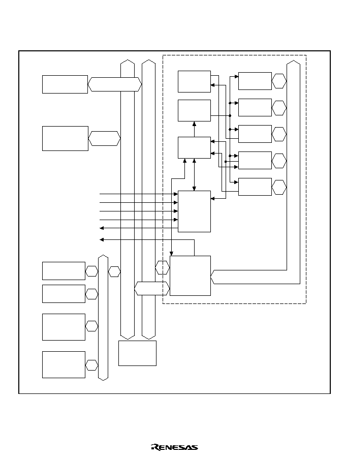
Rev. 5.0, 09/03, page 371 of 806
12.1.2
Block Diagram
Figure 12.1 shows a block diagram of the DMAC.
Peripheral bus
Internal bus
DREQ0, DREQ1
Iteration
control
SARn
DMAC module
Register
control
Start-up
control
Request
priority
control
Bus interface
Bus state
controller
On-chip
peripheral
module
DARn
DMATCRn
CHCRn
DMAOR
IrDA, SCIF
A/D converter
CMT
DEIn
X/Y
memory
External
RAM
External
ROM
External I/O
(memory
mapped)
External I/O
(with
acknowledge)
DACK0, DACK1
DRAK0, DRAK1
Legend
DMAOR:
SARn:
DARn:
DMATCRn:
CHCRn:
DEIn:
n = 0 to 3
DMAC operation register
DMAC source address register
DMAC destination address register
DMAC transfer count register
DMAC channel control register
DMA transfer-end interrupt request to
CPU
Figure 12.1 Block Diagram of DMAC

Rev. 5.0, 09/03, page 372 of 806
12.1.3
Pin Configuration
Table 12.1 shows the DMAC pins.
Table 12.1
DMAC Pins
Channel
Name
Symbol
I/O
Function
0
DMA transfer request
DREQ0
I
DMA transfer request input from
external device to channel 0
DREQ acknowledge
DACK0
O
Strobe output to an external I/O upon
DMA transfer request from external
device to channel 0
DMA request
acknowledge
DRAK0
O
Output showing that DREQ0 has been
accepted
1
DMA transfer request
DREQ1
I
DMA transfer request input from
external device to channel 1
DREQ acknowledge
DACK1
O
Strobe output to an external I/O upon
DMA transfer request from external
device to channel 1
DMA request
acknowledge
DRAK1
O
Output showing that DREQ1 has been
accepted

Rev. 5.0, 09/03, page 373 of 806
12.1.4
Register Configuration
Table 12.2 summarizes the DMAC registers. The DMAC has a total of 17 registers: four control
registers for each other control register shared by all channels.
Table 12.2
DMAC Registers
Channel
Name
Abbrevi-
ation
R/W
Initial Value Address
Access
Size
0
DMA source address register 0
SAR0
R/W
Undefined
H'04000020
(H'A4000020)
*
4
16, 32
*
2
DMA destination address register 0
DAR0
R/W
Undefined
H'04000024
(H'A4000024)
*
4
16, 32
*
2
DMA transfer count register 0
DMATCR0
R/W
Undefined
H'04000028
(H'A4000028)
*
4
16, 32
*
3
DMA channel control register 0
CHCR0
R/W
*
1
H'00000000
H'0400002C
(H'A400002C)
*
4
8, 16, 32
*
2
1
DMA source address register 1
SAR1
R/W
Undefined
H'04000030
(H'A4000030)
*
4
16, 32
*
2
DMA destination address register 1
DAR1
R/W
Undefined
H'04000034
(H'A4000034)
*
4
16, 32
*
2
DMA transfer count register 1
DMATCR1
R/W
Undefined
H'04000038
(H'A4000038)
*
4
16, 32
*
3
DMA channel control register 1
CHCR1
R/W
*
1
H'00000000
H'0400003C
(H'A400003C)
*
4
8, 16, 32
*
2
2
DMA source address register 2
SAR2
R/W
Undefined
H'04000040
(H'A4000040)
*
4
16, 32
*
2
DMA destination address register 2
DAR2
R/W
Undefined
H'04000044
(H'A4000044)
*
4
16, 32
*
2
DMA transfer count register 2
DMATCR2
R/W
Undefined
H'04000048
(H'A4000048)
*
4
16, 32
*
3
DMA channel control register 2
CHCR2
R/W
*
1
H'00000000
H'0400004C
(H'A400004C)
*
4
8, 16, 32
*
2

Rev. 5.0, 09/03, page 374 of 806
Channel
Name
Abbrevi-
ation
R/W
Initial Value Address
Access
Size
3
DMA source address register 3
SAR3
R/W
Undefined
H'04000050
(H'A4000050)
*
4
16, 32
*
2
DMA destination address register 3
DAR3
R/W
Undefined
H'04000054
(H'A4000054)
*
4
16, 32
*
2
DMA transfer count register 3
DMATCR3
R/W
Undefined
H'04000058
(H'A4000058)
*
4
16, 32
*
3
DMA channel control register 3
CHCR3
R/W
*
1
H'00000000
H'0400005C
(H'A400005C)
*
4
8, 16, 32
*
2
Shared
DMA operation register
DMAOR
R/W
*
1
H'0000
H'04000060
(H'A4000060)
*
4
8, 16
*
2
Notes: These registers are located in area 1 of physical space. Therefore, when the cache is on,
either access these registers from the P2 area of logical space or else make an appropriate
setting using the MMU so that these registers are not cached.
1. Only 0 can be written to bit 1 of CHCR0 to CHCR3, and bits 1 and 2 of DMAOR to clear
the flag after 1 is read.
2. If 16-bit access is used on SAR0 to SAR3, DAR0 to DAR3, and CHCR0 to CHCR3, the
value in the 16 bits that were not accessed is retained.
3. DMATCR comprises the 24 bits from bit 0 to bit 23. The upper 8 bits, bits 24 to 31,
cannot be written with 1 and are always read as 0.
4. When address translation by the MMU does not apply, the address in parentheses
should be used.
Rev. 5.0, 09/03, page 375 of 806
12.2
Register Descriptions
12.2.1
DMA Source Address Registers 0≠3 (SAR0≠SAR3)
DMA source address registers 0≠3 (SAR0≠SAR3) are 32-bit readable/writable registers that
specify the source address of a DMA transfer. During a DMA transfer, these registers indicate the
next source address.
To transfer data in 16 bits or in 32 bits, specify a 16-bit or 32-bit address boundary address. When
transferring data in 16-byte units, a 16-byte boundary (address 16n) must be set for the source
address value. Operation is not guaranteed if other addresses are specified.
The initial value is undefined in a reset. The previous value is retained in standby mode.
Bit:
31
30
29
28
27
26
25
24
Initial value:
--
--
--
--
--
--
--
--
R/W:
R/W
R/W
R/W
R/W
R/W
R/W
R/W
R/W
Bit:
23
22
21
20
...
0
...
Initial value:
--
--
--
--
...
--
R/W:
R/W
R/W
R/W
R/W
...
R/W

Rev. 5.0, 09/03, page 376 of 806
12.2.2
DMA Destination Address Registers 0≠3 (DAR0≠DAR3)
DMA destination address registers 0≠3 (DAR0≠DAR3) are 32-bit readable/writable registers that
specify the destination address of a DMA transfer. These registers include a count function, and
during a DMA transfer, these registers indicate the next destination address.
To transfer data in 16 bits or in 32 bits, specify a 16-bit or 32-bit address boundary address. To
transfer data in 16-bit or 32-bit units, make sure to specify a destination address with a 16-byte
boundary (16n address). Operation is not guaranteed if other addresses are specified.
The initial value is undefined in a reset. The previous value is retained in standby mode.
Bit:
31
30
29
28
27
26
25
24
Initial value:
--
--
--
--
--
--
--
--
R/W:
R/W
R/W
R/W
R/W
R/W
R/W
R/W
R/W
Bit:
23
22
21
20
...
0
...
Initial value:
--
--
--
--
...
--
R/W:
R/W
R/W
R/W
R/W
...
R/W

Rev. 5.0, 09/03, page 377 of 806
12.2.3
DMA Transfer Count Registers 0≠3 (DMATCR0≠DMATCR3)
DMA transfer count registers 0≠3 (DMATCR0≠DMATCR3) are 24-bit readable/writable registers
that specify the DMA transfer count (bytes, words, or longwords). The number of transfers is 1
when the setting is H'000001, and 16,777,216 (the maximum) when H'000000 is set. During a
DMA transfer, these registers indicate the remaining number of transfers.
In 16-byte transfer, one 16-byte transfer (128 bits) is counted as one.
Writing to upper eight bits in DMATCR is invalid; 0s are read if these bits are read.
When using 16-byte transfer, an integral multiple of 4 (4n) must be set for the number of transfers
to ensure normal operation.
The initial value is undefined in a reset. The previous value is retained in standby mode.
Bit:
31
30
29
28
27
26
25
24
Initial value:
--
--
--
--
--
--
--
--
R/W:
R
R
R
R
R
R
R
R
Bit:
23
22
21
20
...
0
...
Initial value:
--
--
--
--
...
--
R/W:
R/W
R/W
R/W
R/W
...
R/W

Rev. 5.0, 09/03, page 378 of 806
12.2.4
DMA Channel Control Registers 0≠3 (CHCR0≠CHCR3)
DMA channel control registers 0≠3 (CHCR0≠CHCR3) are 32-bit readable/writable registers that
specify the operation mode, transfer method, etc., for each channel. Writing to bits 31 to 21 and 7
in this register is invalid; 0s are read if these bits are read.
Bit 20 is only used in CHCR3; it is not used in CHCR0 to CHCR2. Consequently, writing to this
bit is invalid in CHCR0 to CHCR2; 0 is read if this bit is read. Bit 19 is only used in CHCR2; it is
not used in CHCR0, CHCR1, and CHCR3. Consequently, writing to this bit is invalid in CHCR0,
CHCR1, and CHCR3; 0 is read if this bit is read. Bits 6 and 16 to 18 are only used in CHCR0 and
CHCR1; they are not used in CHCR2 and CHCR3. Consequently, writing to these bits is invalid
in CHCR2 and CHCR3; 0s are read if these bits are read.
These register values are initialized to zero in a power-on reset. The previous value is retained in
standby mode.
Bit:
31
...
21
20
19
18
17
16
--
...
--
DI
RO
RL
AM
AL
Initial value:
0
...
0
0
0
0
0
0
R/W:
R
...
R
(R/W)
*
2
(R/W)
*
2
(R/W)
*
2
(R/W)
*
2
(R/W)
*
2
Bit:
15
14
13
12
11
10
9
8
DM1
DM0
SM1
SM0
RS3
RS2
RS1
RS0
Initial value:
0
0
0
0
0
0
0
0
R/W:
R/W
R/W
R/W
R/W
R/W
R/W
R/W
R/W
Bit:
7
6
5
4
3
2
1
0
--
DS
TM
TS1
TS0
IE
TE
DE
Initial value:
0
0
0
0
0
0
0
0
R/W:
R
(R/W)
*
2
R/W
R/W
R/W
R/W
R/(W)
*
1
R/W
Notes: 1. Only 0 can be written to the TE bit after 1 is read.
2. The DI, RO, RL, AM, AL, and DS bits are not included in some channels.

Rev. 5.0, 09/03, page 379 of 806
Bits 31 to 21, 7--Reserved: These bits are always read as 0. The write value should always be 0.
Bit 20--Direct/Indirect Selection (DI): Selects direct address mode or indirect address mode in
channel 3.
This bit is only valid in CHCR3. Writing to this bit is invalid in CHCR0 to CHCR2; 0 is read if
this bit is read. When using 16-byte transfer, direct address mode must be specified. Operation is
not guaranteed if indirect address mode is specified.
Bit 20: DI
Description
0
Direct address mode
(Initial value)
1
Indirect address mode
Bit 19--Source Address Reload Bit (RO): Selects whether the source address initial value is
reloaded in channel 2.
This bit is only valid in CHCR2. Writing to this bit is invalid in CHCR0, CHCR1, and CHCR3; 0
is read if this bit is read. When using 16-byte transfer, this bit must be cleared to 0, specifying
non-reloading. Operation is not guaranteed if reloading is specified.
Bit 19: RO
Description
0
Source address is not reloaded
(Initial value)
1
Source address is reloaded
Bit 18--Request Check Level Bit (RL): Specifies whether DRAK (
DREQ acknowledge) signal
output is active-high or active-low.
This bit is only valid in CHCR0 and CHCR1. Writing to this bit is invalid in CHCR2 and
CHCR3; 0 is read if this bit is read.
Bit 18: RL
Description
0
Active-low DRAK output
(Initial value)
1
Active-high DRAK output

Rev. 5.0, 09/03, page 380 of 806
Bit 17--Acknowledge Mode Bit (AM): Specifies whether DACK is output in the data read cycle
or in the data write cycle in dual address mode.
This bit is only valid in CHCR0 and CHCR1. Writing to this bit is invalid in CHCR2 and
CHCR3; 0 is read if this bit is read.
Bit 17: AM
Description
0
DACK output in read cycle
(Initial value)
1
DACK output in write cycle
Bit 16--Acknowledge Level (AL): Specifies whether DACK (acknowledge) signal output is
active-high or active-low.
This bit is only valid in CHCR0 and CHCR1. Writing to this bit is invalid in CHCR2 and
CHCR3; 0 is read if this bit is read.
Bit 16: AL
Description
0
Active-low DACK output
(Initial value)
1
Active-high DACK output
Bits 15 and 14--Destination Address Mode Bits 1 and 0 (DM1, DM0): Select whether the
DMA destination address is incremented, decremented, or left fixed.
Bit 15: DM1
Bit 14: DM0
Description
0
0
Fixed destination address
*
(Initial value)
0
1
Destination address is incremented (+1 in 8-bit transfer, +2 in
16-bit transfer, +4 in 32-bit transfer, +16 in 16-byte transfer)
1
0
Destination address is decremented (≠1 in 8-bit transfer, ≠2 in
16-bit transfer, ≠4 in 32-bit transfer; illegal setting in 16-byte
transfer)
1
1
Setting prohibited
Note:
*
This setting cannot be used when the transfer destination is X/Y memory in 16-byte
transfer.

Rev. 5.0, 09/03, page 381 of 806
Bits 13 and 12--Source Address Mode Bits 1 and 0 (SM1, SM0): Select whether the DMA
source address is incremented, decremented, or left fixed.
Bit 13: SM1
Bit 12: SM0
Description
0
0
Fixed source address
*
(Initial value)
0
1
Source address is incremented (+1 in 8-bit transfer, +2 in 16-
bit transfer, +4 in 32-bit transfer, +16 in 16-byte transfer)
1
0
Source address is decremented (≠1 in 8-bit transfer, ≠2 in 16-
bit transfer, ≠4 in 32-bit transfer; illegal setting in 16-byte
transfer)
1
1
Setting prohibited
Note:
*
This setting cannot be used when the transfer destination is X/Y memory in 16-byte
transfer.
If the transfer source is specified by indirect address, specify the address holding the value of the
address in which the data to be transferred is stored (i.e. the indirect address) in source address
register 3 (SAR3).
Specification of SAR3 incrementing or decrementing in indirect address mode depends on the
SM1 and SM0 settings. In this case, however, the SAR3 increment or decrement value is +4, ≠4,
or fixed at 0, regardless of the transfer data size specified in TS1 and TS0.

Rev. 5.0, 09/03, page 382 of 806
Bits 11 to 8--Resource Select Bits 3 to 0 (RS3 to RS0): Specify which transfer requests will be
sent to the DMAC.
Bit 11:
RS3
Bit 10:
RS2
Bit 9:
RS1
Bit 8:
RS0
Description
0
0
0
0
External request
*
, dual address mode
(Initial value)
0
0
0
1
Setting prohibited
0
0
1
0
External request / Single address mode
External address space
external device with DACK
0
0
1
1
External request / Single address mode
External device with DACK
external address space
0
1
0
0
Auto request
0
1
0
1
Setting prohibited
0
1
1
0
Setting prohibited
0
1
1
1
Setting prohibited
1
0
0
0
Setting prohibited
1
0
0
1
Setting prohibited
1
0
1
0
IrDA transmission
1
0
1
1
IrDA reception
1
1
0
0
SCIF transmission
1
1
0
1
SCIF reception
1
1
1
0
Internal A/D
1
1
1
1
CMT
Notes: When using 16-byte transfer, the following settings must not be made:
1010 IrDA transmission
1011 IrDA reception
1100 SCIF transmission
1101 SCIF reception
1110 A/D converter
1111 CMT
Operation is not guaranteed if these settings are made.
*
External request specification is valid only in channels 0 and 1. None of the request
sources can be selected in channels 2 and 3.

Rev. 5.0, 09/03, page 383 of 806
Bit 6--
D
D
D
DR
R
R
REEEEQ
Q
Q
Q Select Bit (DS): Selects low-level or falling-edge detection as the sampling method
for the
DREQ pin used in external request mode.
This bit is only valid in CHCR0 and CHCR1. Writing to this bit is invalid in CHCR2 and
CHCR3; 0 is read if this bit is read.
In channels 0 and 1, if an on-chip peripheral module is specified as a transfer request source or an
auto-request is specified, the specification of this bit is ignored and falling-edge detection is fixed
except in an auto-request.
Bit 6: DS
Description
0
DREQ
detected by low level
(Initial value)
1
DREQ
detected at falling edge
Bit 5--Transmit Mode (TM): Specifies the bus mode when transferring data.
Bit 5: TM
Description
0
Cycle-steal mode
(Initial value)
1
Burst mode
Bits 4 and 3--Transmit Size Bits 1 and 0 (TS1, TS0): Specify the size of data to be transferred.
Bit 4: TS1
Bit 3: TS0
Description
0
0
Byte size (8 bits)
(Initial value)
0
1
Word size (16 bits)
1
0
Longword size (32 bits)
1
1
16-byte unit (4 longword transfers)
Bit 2--Interrupt Enable Bit (IE): If this bit is set to 1, an interrupt is requested on completion of
the number of data transfers specified in DMATCR (i.e. when TE = 1).
Bit 2: IE
Description
0
Interrupt request is not generated on completion of data transfers
specified in DMATCR
(Initial value)
1
Interrupt request is generated on completion of data transfers specified in
DMATCR

Rev. 5.0, 09/03, page 384 of 806
Bit 1--Transfer End Bit (TE): Set to 1 on completion of the number of data transfers specified
in DMATCR. At this time, if the IE bit is set to 1, an interrupt request is generated.
If data transfer ends due to an NMI interrupt, a DMAC address error, or clearing of the DE bit or
the DME bit in DMAOR before this bit is set to 1, this bit will not be set to 1. Even if the DE bit
is set to 1 while this bit is set to 1, transfer is not enabled.
Bit 1: TE
Description
0
Data transfers specified in DMATCR not completed
(Initial value)
Clearing conditions: Writing 0 to TE after reading TE = 1
Power-on reset, manual reset
1
Data transfers specified in DMATCR completed
Bit 0--DMAC Enable Bit (DE): Enables operation of the corresponding channel.
Bit 0: DE
Description
0
Channel operation disabled
(Initial value)
1
Channel operation enabled
If an auto-request is specified (RS3 to RS0), transfer starts when this bit is set to 1. In an external
request or an internal module request, transfer starts when a transfer request is generated after this
bit is set to 1. Clearing this bit during transfer terminates the transfer.
Even if the DE bit is set, transfer is not enabled if the TE bit is 1, the DME bit in DMAOR is 0, or
the NMIF bit in DMAOR is 1.
Rev. 5.0, 09/03, page 385 of 806
12.2.5
DMA Operation Register (DMAOR)
The DMA operation register (DMAOR) is a 16-bit readable/writable register that controls the
DMAC transfer mode. Writing to bits 15 to 10 and bits 7 to 3 is invalid in this register; 0 is always
read if these bits are read.
DMAOR is initialized to 0 by a power-on reset, and in hardware standby mode or software
standby mode.
Bit:
15
14
13
12
11
10
9
8
--
--
--
--
--
--
PR1
PR0
Initial value:
0
0
0
0
0
0
0
0
R/W:
R
R
R
R
R
R
R/W
R/W
Bit:
7
6
5
4
3
2
1
0
--
--
--
--
--
AE
NMIF
DME
Initial value:
0
0
0
0
0
0
0
0
R/W:
R
R
R
R
R
R/(W)
*
R/(W)
*
R/W
Note:
*
Only 0 can be written to the AE and NMIF bits after 1 is read.
Bits 15 to 10--Reserved: These bits are always read as 0. The write value should always be 0.
Bits 9 and 8--Priority Mode Bits 1 and 0 (PR1, PR0): Select the priority level between
channels when there are simultaneous transfer requests for multiple channels.
Bit 9: PR1
Bit 8: PR0
Description
0
0
CH0 > CH1 > CH2 > CH3
(Initial value)
0
1
CH0 > CH2 > CH3 > CH1
1
0
CH2 > CH0 > CH1 > CH3
1
1
Round-robin
Bits 7 to 3--Reserved: These bits are always read as 0. The write value should always be 0.

Rev. 5.0, 09/03, page 386 of 806
Bit 2--Address Error Flag Bit (AE): Indicates that an address error occurred during DMA
transfer. If this bit is set during data transfer, transfers on all channels are suspended. The CPU
cannot write 1 to this bit. This bit can only be cleared by writing 0 after reading 1.
Bit 2: AE
Description
0
No DMAC address error; DMA transfer is enabled
(Initial value)
Clearing conditions: Writing 0 to AE after reading AE = 1
Power-on reset, manual reset
1
DMAC address error; DMA transfer is disabled
This bit is set by occurrence of a DMAC address error
Bit 1--NMI Flag Bit (NMIF): Indicates that an NMI interrupt occurred. This bit is set regardless
of whether the DMAC is in the operating or halted state. The CPU cannot write 1 to this bit. Only
0 can be written to clear this bit after 1 is read.
Bit 1: NMIF
Description
0
No NMI input; DMA transfer is enabled
(Initial value)
Clearing conditions: Writing 0 to NMIF after reading NMIF = 1
Power-on reset, manual reset
1
NMI input; DMA transfer is disabled
This bit is set by occurrence of an NMI interrupt
Bit 0--DMA Master Enable Bit (DME): Enables or disables DMA transfers on all channels. If
the DME bit and the DE bit corresponding to each channel in CHCR are set to 1, transfer is
enabled on the corresponding channel. If this bit is cleared during transfer, transfer on all the
channels will be terminated.
Even if the DME bit is set, transfer is not enabled if the TE bit is 1 or the DE bit is 0 in CHCR, or
the NMIF bit is 1 in DMAOR.
Bit 0: DME
Description
0
DMA transfer disabled on all channels
(Initial value)
1
DMA transfer enabled on all channels

Rev. 5.0, 09/03, page 387 of 806
12.3
Operation
When there is a DMA transfer request, the DMAC starts the transfer according to the
predetermined channel priority order; when the transfer end conditions are satisfied, it ends the
transfer. Transfers can be requested in three modes: auto-request, external request, and on-chip
module request. The dual address mode has direct address transfer mode and indirect address
transfer mode. Burst mode or cycle-steal mode can be selected as the bus mode.
12.3.1
DMA Transfer Flow
After the DMA source address register (SAR), DMA destination address register (DAR), DMA
transfer count register (DMATCR), DMA channel control register (CHCR), and DMA operation
register (DMAOR) are set, the DMAC transfers data according to the following procedure:
1. Checks to see if transfer is enabled (DE = 1, DME = 1, TE = 0, NMIF = 0)
2. When a transfer request comes and transfer is enabled, the DMAC transfers 1 transfer unit of
data (according to the TS0 and TS1 settings). For an auto-request, the transfer begins
automatically when the DE bit and DME bit are set to 1. The DMATCR value will be
decremented for each transfer. The actual transfer flows vary by address mode and bus mode.
3. When the specified number of transfers have been completed (when DMATCR reaches 0), the
transfer ends normally. If the IE bit in CHCR is set to 1 at this time, a DEI interrupt is sent to
the CPU.
4. When an NMI interrupt is generated, the transfer is aborted. Transfers are also aborted when
the DE bit in CHCR or the DME bit in DMAOR are changed to 0.
Figure 12.2 is a flowchart of this procedure.
Rev. 5.0, 09/03, page 388 of 806
Normal end
NMIF = 1 or
DE = 0 or DME
= 0?
Bus mode,
transfer request mode,
DREQ detection selection
system
Initial settings
(SAR, DAR, DMATCR, CHCR, DMAOR)
Transfer (1 transfer unit);
DMATCR
- 1 DMATCR, SAR and DAR
updated
DEI interrupt request (when IE = 1)
No
Yes
No
Yes
No
Yes
Yes
No
Yes
No
*
3
*
2
Start
Transfer aborted
DMATCR = 0?
Transfer request?*
1
DE, DME = 1 and
AE, NMIF, TE = 0?
Does
NMIF = 1 or
DE = 0 or DME
= 0?
Transfer end
Notes: 1. In auto-request mode, transfer begins when AE, NMIF and TE are both 0 and the DE and DME
bits are set to 1.
2.
DREQ = level detection in burst mode (external request) or cycle-steal mode.
3.
DREQ = edge detection in burst mode (external request), or auto-request mode in burst mode.
Figure 12.2 DMAC Transfer Flowchart

Rev. 5.0, 09/03, page 389 of 806
12.3.2
DMA Transfer Requests
DMA transfer requests are basically generated in either the data transfer source or destination, but
they can also be generated by devices and on-chip peripheral modules that are neither the source
nor the destination. Transfers can be requested in three modes: auto-request, external request, and
on-chip module request. The request mode is selected in the RS3≠RS0 bits of DMA channel
control registers 0≠3 (CHCR0≠CHCR3).
Auto-Request Mode: When there is no transfer request signal from an external source, as in a
memory-to-memory transfer or a transfer between memory and an on-chip peripheral module
unable to request a transfer, the auto-request mode allows the DMAC to automatically generate a
transfer request signal internally. When the DE bit of CHCR0≠CHCR3 and the DME bit of
DMAOR are set to 1, the transfer begins so long as the TE bit of CHCR0≠CHCR3 and the NMIF
bit of DMAOR are 0.
External Request Mode: In this mode a transfer is performed in response to the request signal
(
DREQ) of an external device. Choose one of the modes shown in table 12.3 according to the
application system. When this mode is selected, if DMA transfer is enabled (DE = 1, DME = 1,
TE = 0, NMIF = 0), a transfer is performed upon a request at the
DREQ input. Choose DREQ
detection by either a falling edge or low level of the signal input with the DS bit in CHCR0 and
CHCR1 (DS = 0 for level detection, DS = 1 for edge detection). The source of the transfer request
does not have to be the data transfer source or destination.
Table 12.3
Selecting External Request Modes with RS Bits
RS3
RS2
RS1
RS0
Address Mode
Source
Destination
0
0
0
0
Dual address
mode
Any
*
Any
*
1
0
Single address
mode
External memory,
memory-mapped
external device
External device with
DACK
1
External device with
DACK
External memory,
memory-mapped
external device
Note:
*
External memory, memory-mapped external device, on-chip memory, on-chip peripheral
module (excluding DMAC, UBC, and BSC)
On-Chip Module Request: In this mode a transfer is performed in response to a transfer request
signal (interrupt request signal) of an on-chip module. This mode cannot be set in case of 16-byte
transfer. These are six transfer request signals: the receive-data-full interrupts (RXI) and the
transmit-data-empty interrupts (TXI) from two serial communication interfaces (IrDA, SCIF), the
A/D conversion end interrupt (ADI) of the A/D converter, and the compare match timer interrupt
(CMI) of the CMT (table 12.4). When this mode is selected, if DMA transfer is enabled (DE = 1,
DME = 1, TE = 0, NMIF = 0), a transfer is performed upon input of a transfer request signal. The

Rev. 5.0, 09/03, page 390 of 806
source of the transfer request does not have to be the data transfer source or destination. When
RXI is set as the transfer request, however, the transfer source must be the SCI's receive data
register (RDR). Likewise, when TXI is set as the transfer request, the transfer source must be the
SCI's transmit data register (TDR). If the transfer requester is the A/D converter, the data transfer
source must be the A/D data register.
Table 12.4
Selecting On-Chip Peripheral Module Request Modes with RS Bits
RS3 RS2 RS1 RS0
DMA
Transfer
Request
Source
DMA Transfer Request Signal
Source
Desti-
nation Bus Mode
1
0
1
0
IrDA
transmitter
TXI1 (IrDA transmit-data-empty
interrupt transfer request)
Any
*
TDR1
Cycle-steal
1
0
1
1
IrDA
receiver
RXI1 (IrDA receive-data-full
interrupt transfer request)
RDR1
Any
*
Cycle-steal
1
1
0
0
SCIF
transmitter
TXI2 (SCIF transmit-data-empty
interrupt transfer request)
Any
*
TDR2
Cycle-steal
1
1
0
1
SCIF
receiver
RXI2 (SCIF receive-data-full
interrupt transfer request)
RDR1
Any
*
Cycle-steal
1
1
1
0
A/D
converter
ADI (A/D conversion end
interrupt)
ADDR
Any
*
Cycle-steal
1
1
1
1
CMT
CMI (Compare match timer
interrupt)
Any
*
Any
*
Burst/
cycle-steal
ADDR: A/D data register of A/D converter
Note:
*
External memory, memory-mapped external device, on-chip peripheral module (excluding
DMAC, BSC, UBC)
When outputting transfer requests from on-chip peripheral modules, the appropriate interrupt
enable bits must be set to output the interrupt signals.
If the interrupt request signal of the on-chip peripheral module is used as a DMA transfer request
signal, an interrupt is not sent to the CPU.
The DMA transfer request signals in table 12.4 are automatically discontinued when the
corresponding DMA transfer is performed. If cycle-steal mode is being employed, they are
withdrawn at the first transfer; if burst mode is being used, they are discontinued at the last
transfer.

Rev. 5.0, 09/03, page 391 of 806
12.3.3
Channel Priority
When the DMAC receives simultaneous transfer requests on two or more channels, it selects a
channel according to a predetermined priority order. Two modes (fixed mode and round-robin
mode) are selected by priority bits PR1 and PR0 in the DMA operation register (DMAOR).
Fixed Mode: In these modes, the priority order of the channels remain fixed. There are three kinds
of fixed modes as follows:
CH0 > CH1 > CH2 > CH3
CH0 > CH2 > CH3 > CH1
CH2 > CH0 > CH1 > CH3
These are selected by the PR1 and PR0 bits in DMAOR.
Round-Robin Mode: Each time one word, byte, or longword is transferred on one channel, the
priority order is rotated. The channel on which the transfer was just finished rotates to the bottom
of the priority order. The round-robin mode operation is shown in figure 12.3. The priority of the
round-robin mode is CH0 > CH1 > CH2 > CH3 immediately after reset.
Rev. 5.0, 09/03, page 392 of 806
CH1 > CH2 > CH3 > CH0
CH0 > CH1 > CH2 > CH3
CH2 > CH3 > CH0 > CH1
CH0 > CH1 > CH2 > CH3
CH2 > CH3 > CH0 > CH1
CH0 > CH1 > CH2 > CH3
CH0 > CH1 > CH2 > CH3
CH3 > CH0 > CH1 > CH2
CH0 > CH1 > CH2 > CH3
(1) When channel 0 transfers
Initial priority order
Initial priority order
Initial priority order
Priority order
after transfer
Priority order
after transfer
Priority order does not change.
Channel 2 becomes lowest-
priority.
The priority of channels 0 and 1,
which were higher than channel 2,
are also shifted. If immediately
after there is a request to transfer
channel 1 only, channel 1 becomes
lowest-priority and the priority of
channels 0 and 3, which were
higher than channel 1, is also
shifted.
Channel 0 becomes lowest-
priority.
The priority of channel 0, which
was higher than channel 3, is also
shifted.
Channel 0 becomes lowest-
priority.
Priority order
after transfer
Priority order
after transfer
Priority order
after transfer
Post-transfer priority order
when there is an
immediate transfer
request to channel 1 only
(2) When channel 1 transfers
(3) When channel 2 transfers
(4) When channel 3 transfers
Figure 12.3 Round-Robin Mode
Rev. 5.0, 09/03, page 393 of 806
Figure 12.4 shows how the priority order changes when channel 0 and channel 3 transfers are
requested simultaneously and a channel 1 transfer is requested during the channel 0 transfer. The
DMAC operates as follows:
1. Transfer requests are generated simultaneously for channels 0 and 3.
2. Channel 0 has a higher priority, so the channel 0 transfer begins first (channel 3 waits for
transfer).
3. A channel 1 transfer request occurs during the channel 0 transfer (channels 1 and 3 are both
waiting)
4. When the channel 0 transfer ends, channel 0 becomes lowest-priority.
5. At this point, channel 1 has a higher priority than channel 3, so the channel 1 transfer begins
(channel 3 waits for transfer).
6. When the channel 1 transfer ends, channel 1 becomes lowest-priority.
7. The channel 3 transfer begins.
8. When the channel 3 transfer ends, channels 3 and 2 shift downward in priority so that channel
3 becomes the lowest-priority.
Transfer request Waiting channel(s) DMAC operation
Channel priority
(1) Channels 0 and 3
(3) Channel 1
0 > 1 > 2 > 3
(2) Channel 0 transfer
start
(4) Channel 0 transfer
ends
(5) Channel 1 transfer
starts
(6) Channel 1 transfer
ends
(7) Channel 3 transfer
starts
(8) Channel 3 transfer
ends
1 > 2 > 3 > 0
2 > 3 > 0 > 1
0 > 1 > 2 > 3
Priority order
changes
Priority order
changes
Priority order
changes
None
3
3
1,3
Figure 12.4 Changes in Channel Priority in Round-Robin Mode

Rev. 5.0, 09/03, page 394 of 806
12.3.4
DMA Transfer Types
The DMAC supports the transfers shown in table 12.5. In dual address mode, both the transfer
source address and the transfer destination address are output. Dual address mode has a direct
address mode and indirect address mode. In direct address mode, an output address value is the
data transfer target address; in indirect address mode, the value stored in the output address, not
the output address value itself, is the data transfer target address. Data transfer timing depends on
the bus mode, which may be cycle-steal mode or burst mode.
Table 12.5
Supported DMA Transfers
Destination
Source
External
Device with
DACK
External
Memory
Memory-
Mapped
External
Device
On-Chip
Peripheral
Module
XY Memory
External device with
DACK
Not available Dual, single
Dual, single
Not available Not available
External memory
Dual, single
Dual
Dual
Dual
Dual
Memory-mapped
external device
Dual, single
Dual
Dual
Dual
Dual
On-chip peripheral
module
Not available Dual
Dual
Dual
Dual
X/Y memory
Not available Dual
Dual
Dual
Dual
Notes: 1. Dual: Dual address mode
2. Single: Single address mode
3. Dual address mode includes direct address mode and indirect address mode.
4. 16-byte transfer is not available for on-chip peripheral modules.
Address Modes:
∑
Dual Address Mode
In dual address mode, both the transfer source and destination are accessed (selectable) by an
address. The source and destination can be located externally or internally. Dual address mode
has (1) a direct address transfer mode and (2) an indirect address transfer mode.
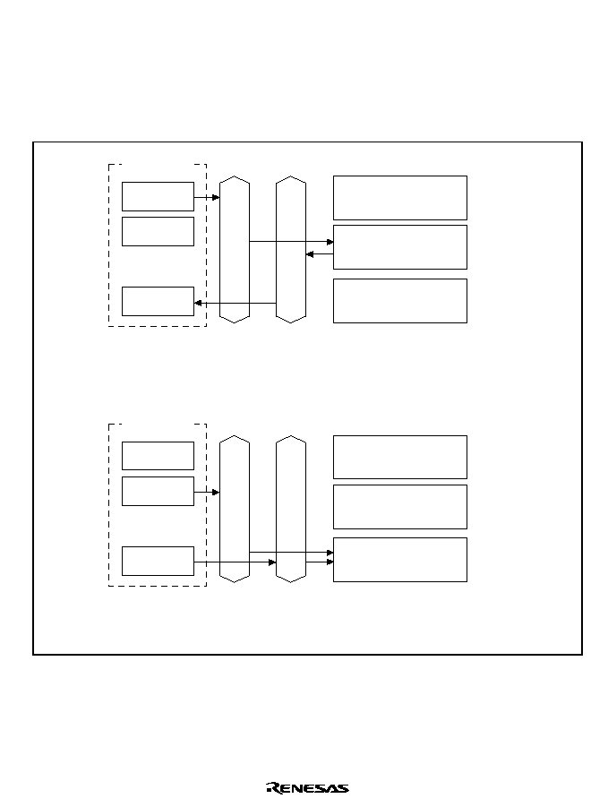
Rev. 5.0, 09/03, page 395 of 806
(1) In direct address transfer mode, DMA transfer requires two bus cycles because data is read
from the transfer source in a data read cycle and written to the transfer destination in a
data write cycle. At this time, transfer data is temporarily stored in the DMAC. In the
transfer between external memories as shown in figure 12.5, data is read to the DMAC
from one external memory in a data read cycle, and then that data is written to the other
external memory in a write cycle. Figures 12.6 to 12.8 show examples of the timing at
this time.
Data buffer
Address bus
Data bus
Address bus
Data bus
Memory
Transfer source
module
Transfer destination
module
Memory
Transfer source
module
Transfer destination
module
SAR
DAR
Data buffer
SAR
DAR
The SAR value is an address, data is read from the transfer source module,
and the data is temporarily stored in the DMAC.
First bus cycle
Second bus cycle
The DAR value is an address, and the value stored in the data buffer in the
DMAC is written to the transfer destination module.
DMAC
DMAC
Figure 12.5 Operation of Direct Address Mode in Dual Address Mode
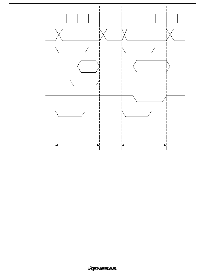
Rev. 5.0, 09/03, page 396 of 806
(1st cycle)
(2nd cycle)
Data read cycle
Data write cycle
Transfer source
address
Transfer destination
address
CKIO
A25 to A0
CSn
D31 to D0
RD
WEn
DACKn
Note: In transfer between external memories, with DACK output in the read cycle, DACK
output timing is the same as that of
CSn.
Figure 12.6 Example of DMA Transfer Timing in the Direct Address Mode in Dual Mode
(Transfer Source: Ordinary Memory, Transfer Destination: Ordinary Memory)
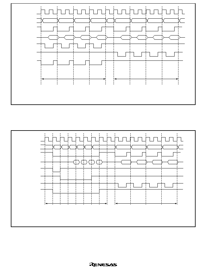
Rev. 5.0, 09/03, page 397 of 806
Transfer
source address
+4
+8
+12
Transfer
destination address
+4
+8
+12
Data read cycle
(1st cycle)
(2nd cycle)
A25
-A0
CKIO
CSn
RD
WEm
DACKn
D31
-D0
Note: In transfer between external memories, with DACK output in the read cycle, DACK
output timing is the same as that of
CSn.
Figure 12.7 Example of DMA Transfer Timing in the Direct Address Mode in Dual Mode
(16-byte Transfer, Transfer Source: Ordinary Memory, Transfer Destination: Ordinary
Memory)
Transfer source address
Transfer destination address
+4
+8
+12
A25
-A0
CKIO
CSn
RAS
CAS
RD/
WR
DACKn
D31
-D0
Data read cycle
(1st cycle)
(2nd cycle)
Data write cycle
Note: In transfer between external memories, with DACK output in the read cycle, DACK
output timing is the same as that of
CSn.
Figure 12.8 Example of DMA Transfer Timing in the Direct Address Mode in Dual Mode
(16-byte Transfer, Transfer Source: Synchronous DRAM, Transfer Destination: Ordinary
Memory)

Rev. 5.0, 09/03, page 398 of 806
(2) In indirect address transfer mode, the address of memory in which data to be transferred is
stored is specified in the transfer source address register (SAR3) in the DMAC. 16-byte
transfer is not possible. Consequently, in this mode, the address value specified in the
transfer source address register in the DMAC is read first. This value is temporarily
stored in the DMAC. Next, the read value is output as an address, and the value stored in
that address is stored in the DMAC again. Then, the value read afterwards is written to
the address specified in the transfer destination address; this completes one DMA transfer.
Figure 12.9 shows an example. In this example, the transfer destination, the transfer
source, and the storage destination of the indirect address are external memories, and
transfer data is 16 or 8 bits. Figure 12.10 shows an example of the transfer timing.
In this mode, one NOP cycle (CK1 cycle shown in figure 12.10) is required to output data
read as an indirect address to an address bus.
If transfer data is 32 bits, the third and fourth bus cycles shown in figure 12.10 are
required twice for each; a total of six bus cycles and one NOP cycle are required.
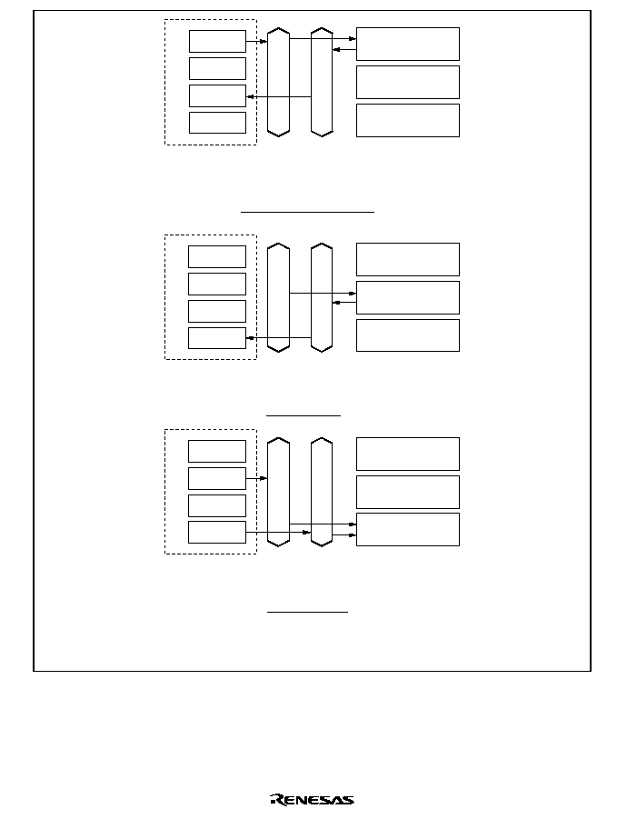
Rev. 5.0, 09/03, page 399 of 806
Memory
Transfer source
module
Transfer destination
module
SAR3
DAR3
Data
buffer
Temporary
buffer
D
M
A
C
When the value in SAR3 is an address, the memory data is read and
the value is stored in the temporary buffer. The value to be read must
be 32 bits since it is used for the address.
Memory
Transfer source
module
Data bus
Address bus
Transfer destination
module
SAR3
DAR3
Data
buffer
Temporary
buffer
D
M
A
C
Memory
Transfer source
module
Data bus
Address bus
Transfer destination
module
SAR3
DAR3
Data
buffer
Temporary
buffer
D
M
A
C
First and second bus cycles
When the value in the temporary buffer is an address, the data is read
from the transfer source module to the data buffer.
Third bus cycle
Fourth bus cycle
When the value in DAR3 is an address, the value in the data buffer is
written to the transfer source module.
Note: This example shows memory, the transfer source module, and
the transfer destination module; in practice, any module can be
connected in the addressing space.
Data bus
Address bus
Figure 12.9 Indirect Address Operation in Dual Address Mode
(When External Memory Space has a 16-Bit Width)

Rev. 5.0, 09/03, page 400 of 806
Transfer
source
address (H)
Transfer
source
address (L)
Indirect
address
NOP
Transfer
destination
address
Indirect
address (H)
Indirect
address (L)
Transfer
data
Transfer
data
Transfer
data
Transfer
data
Transfer
data
Transfer source
address
*1
Transfer source address
*2
Indirect
address
NOP
Indirect
address
Address read cycle
(1st)
(2nd)
(3rd)
NOP
cycle
Data
read cycle
(4th)
Data
write cycle
CKIO
A25 to A0
CSn
D31 to D0
Internal
address
bus
Internal
data bus
DMAC
indirect
address
buffer
DMAC
data
buffer
RD
WEn
Notes: 1.
2.
The internal address bus value does not change, and is controlled by the port.
The DMAC does not fetch the value until 32-bit data is output to the internal
data bus.
Transfer between external memories
Figure 12.10 Example of Transfer Timing in the Indirect Address Mode
in Dual Address Mode
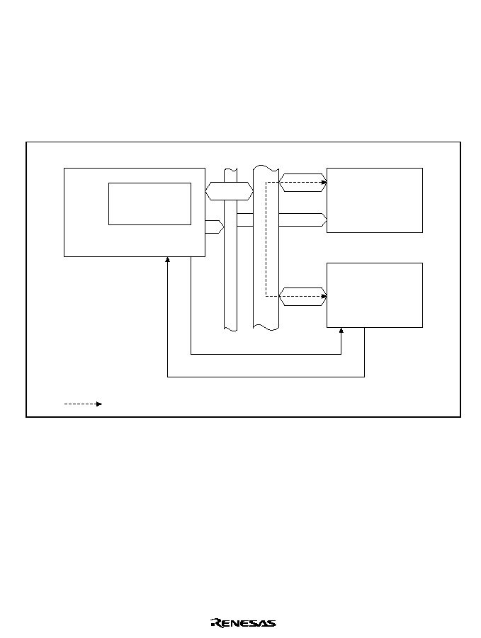
Rev. 5.0, 09/03, page 401 of 806
∑
Single Address Mode
In single address mode, either the transfer source or transfer destination peripheral device is
accessed (selected) by means of the DACK signal, and the other device is accessed by address.
In this mode, the DMAC performs one DMA transfer in one bus cycle, accessing one of the
external devices by outputting the DACK transfer request acknowledge signal to it, and at the
same time outputting an address to the other device involved in the transfer. For example, in
the case of transfer between external memory and an external device with DACK shown in
figure 12.11, when the external device outputs data to the data bus, that data is written to the
external memory in the same bus cycle.
DMAC
SH7729R
DACK
DREQ
External address bus
External data bus
External
memory
External device
with DACK
Data flow
Figure 12.11 Data Flow in Single Address Mode
Two kinds of transfer are possible in single address mode: (1) transfer between an external
device with DACK and a memory-mapped external device, and (2) transfer between an
external device with DACK and external memory. In both cases, only the external request
signal (
DREQ) is used for transfer requests.
Figures 12.12 and 12.13 show examples of DMA transfer timing in single address mode.

Rev. 5.0, 09/03, page 402 of 806
Address output to external memory space
Data output from external device with DACK
DACK signal (active-low) to external device with DACK
Write strobe signal to external memory space
Address output to external memory space
Data output from external memory space
DACK signal (active-low) to external device with DACK
Read strobe signal to external memory space
(a) External device with DACK external memory space (ordinary memory)
(b) External memory space external device with DACK (active-low)
CKIO
A25 to A0
D31 to D0
DACKn
CSn
WE
BS
CKIO
A25 to A0
D31 to D0
DACKn
CSn
RD
BS
Figure 12.12 Example of DMA Transfer Timing in Single Address Mode
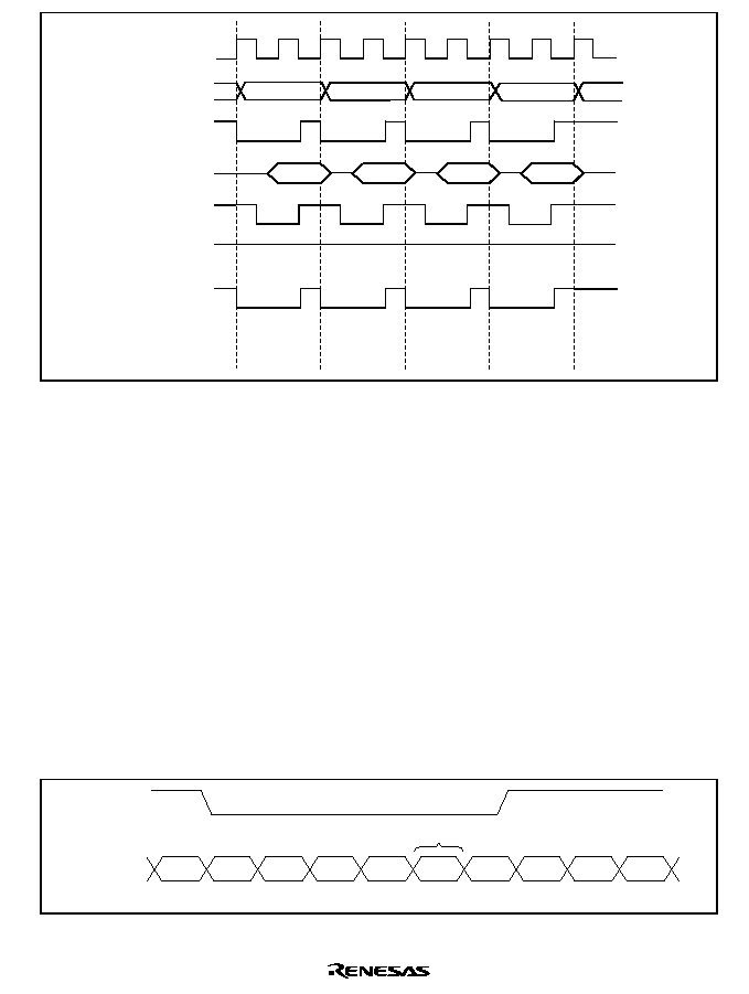
Rev. 5.0, 09/03, page 403 of 806
CKIO
A25 to A0
D31 to D0
RD
WEn
DACKn
CSn
Transfer
source address
+4
+8
+12
Figure 12.13 Example of DMA Transfer Timing in Single Address Mode
(External Memory Space (Ordinary Memory)
External Device with DACK)
Bus Modes: There are two bus modes: cycle-steal and burst. Select the mode in the TM bits of
CHCR0≠CHCR3.
∑
Cycle-Steal Mode
In cycle-steal mode, the bus is given to another bus master after a one-transfer-unit (8-, 16-, or
32-bit unit) DMA transfer. When another transfer request occurs, the bus is obtained from the
other bus master and transfer is performed for one transfer unit. When that transfer ends, the
bus is passed to the other bus master. This is repeated until the transfer end conditions are
satisfied.
In the cycle-steal mode, transfer areas are not affected regardless of the transfer request source,
transfer source, and transfer destination settings. Figure 12.14 shows an example of DMA
transfer timing in cycle-steal mode. Transfer conditions shown in the figure are:
Dual address mode
DREQ level detection
CPU
CPU
CPU
DMAC DMAC
CPU
DMAC DMAC CPU
CPU
DREQ
Bus cycle
Bus returned to CPU
Read
Write
Write
Read
Figure 12.14 Example of Transfer in Cycle-Steal Mode
Rev. 5.0, 09/03, page 404 of 806
∑
Burst Mode
Once the bus is obtained, the transfer is performed continuously until the transfer end
condition is satisfied. In external request mode with low level detection of the
DREQ pin,
however, when the
DREQ pin is driven high, the bus passes to the other bus master after the
DMAC transfer request that has already been accepted ends, even if the transfer end conditions
have not been satisfied.
Burst mode cannot be used when a SCIF (IrDA or SCIF) is the transfer request source. Figure
12.15 shows an example of burst mode timing.
CPU
CPU
CPU
DMAC DMAC DMAC
DMAC
DMAC DMAC
CPU
DREQ
Bus cycle
Read
Read
Read
Write
Write
Write
Figure 12.15 Example of Transfer in Burst Mode

Rev. 5.0, 09/03, page 405 of 806
Relationship between Request Modes and Bus Modes by DMA Transfer Category: Table
12.6 shows the relationship between request modes and bus modes by DMA transfer category.
Table 12.6
Relationship between Request Modes and Bus Modes by DMA Transfer
Category
Address
Mode
Transfer Category
Request
Mode
Bus
Mode
Transfer
Size (Bits)
Usable
Channels
Dual
External device with DACK and
external memory
External
B/C
8/16/32/128
0,1
External device with DACK and
memory-mapped external device
External
B/C
8/16/32/128
0, 1
External memory and external
memory
All
*
1
B/C
8/16/32/128
0≠3
*
5
External memory and memory-
mapped external device
All
*
1
B/C
8/16/32/128
0≠3
*
5
Memory-mapped external device and
memory-mapped external device
All
*
1
B/C
8/16/32/128
0≠3
*
5
External memory and on-chip
peripheral module
All
*
2
B/C
*
3
8/16/32
*
4
0≠3
*
5
Memory-mapped external device and
on-chip peripheral module
All
*
2
B/C
*
3
8/16/32
*
4
0≠3
*
5
On-chip peripheral module and on-
chip peripheral module
All
*
2
B/C
*
3
8/16/32
*
4
0≠3
*
5
X/Y memory and X/Y memory
All
B/C
8/16/32/128
0≠3
X/Y memory and memory-mapped
external device
All
*
1
B/C
8/16/32/128
0≠3
X/Y memory and on-chip peripheral
module
All
*
2
B/C
*
3
8/16/32
0≠3
X/Y memory and external memory
All
B/C
8/16/32/128
0≠3
Single
External device with DACK and
external memory
External
B/C
8/16/32/128
0, 1
External device with DACK and
memory-mapped external device
External
B/C
8/16/32/128
0, 1
B: Burst, C: Cycle-steal
Notes: 1. External requests, auto requests and on-chip peripheral module (CMT) requests are all
available.
2. External requests, auto requests and on-chip peripheral module requests are all
available. When the IrDA, SCI, or A/D converter is also the transfer request source,
however, the transfer destination or transfer source must be the IrDA, SCI, or A/D
converter, respectively.
3. If the transfer request source is the IrDA, SCI, or A/D converter only cycle-steal mode is
available.
Rev. 5.0, 09/03, page 406 of 806
4. The access size permitted when the transfer destination or source is an on-chip
peripheral module register.
5. If the transfer request is an external request, only channels 0 and 1 are available.
Bus Mode and Channel Priority Order: When, for example, channel 1 is transferring in burst
mode and there is a transfer request to channel 0, which has higher priority, the channel 0 transfer
will begin immediately.
At this time, if the priority is set in the fixed mode (CH0 > CH1), the channel 1 transfer will
continue when the channel 0 transfer has completely finished, even if channel 0 is operating in
cycle-steal mode or burst mode.
If the priority is set in round-robin mode, channel 1 will begin operating again after channel 0
completes the transfer of one transfer unit, even if channel 0 is in cycle-steal mode or burst mode.
The bus will then switch between the two in the order channel 1, channel 0, channel 1, channel 0.
Even if the priority is set in fixed mode or in round-robin mode, the bus will not be given to the
CPU since channel 1 is in burst mode. This example is illustrated in figure 12.16.
CPU
DMAC
CH1
DMAC
CH1
DMAC
CH0
DMAC
CH1
DMAC
CH0
DMAC
CH1
DMAC
CH1
CPU
CH0
CH1
CH0
Round-robin mode in
DMAC CH0 and CH1
DMAC CH1
Burst mode
CPU
CPU
Priority: Round-robin mode
CH0: Cycle-steal mode
CH1: Burst mode
DMAC CH1
Burst mode
Figure 12.16 Bus State when Multiple Channels Are Operating

Rev. 5.0, 09/03, page 407 of 806
12.3.5
Number of Bus Cycle States and
D
D
D
DR
R
R
REEEEQ
Q
Q
Q Pin Sampling Timing
Number of Bus Cycle States: When the DMAC is the bus master, the number of bus cycle states
is controlled by the bus state controller (BSC) in the same way as when the CPU is the bus master.
For details, see section 11, Bus State Controller (BSC).
D
D
D
DR
R
R
REEEEQ
Q
Q
Q Pin Sampling Timing: In external request mode, the DREQ pin is sampled by clock pulse
(CKIO) falling edge or low level detection. When
DREQ input is detected, a DMAC bus cycle is
generated and DMA transfer performed, at the earliest, three states later.
The second and subsequent
DREQ sampling operations are started two cycles after the first
sample.
Operation
∑
Cycle-Steal Mode
In cycle-steal mode, the
DREQ sampling timing is the same regardless of whether level or
edge detection is used.
For example, in figure 12.17 (cycle-steal mode, level input), DMAC transfer begins, at the
earliest, three cycles after the first sampling is performed. The second sampling is started two
cycles after the first. If
DREQ is not detected at this time, sampling is performed in each
subsequent cycle.
Thus,
DREQ sampling is performed one step in advance. The third sampling operation is not
performed until the idle cycle following the end of the first DMA transfer.
The above conditions are the same whatever the number of CPU transfer cycles, as shown in
figure 12.18. The above conditions are also the same whatever the number of DMA transfer
cycles, as shown in figure 12.19.
DACK is output in a read in the example in figure 12.17, and in a write in the example in
figure 12.18. In both cases, DACK is output for the same duration as
CSn.
Figure 12.20 shows an example in which sampling is executed in all subsequent cycles when
DREQ cannot be detected.
Figure 12.21 shows examples of edge detection in the cycle-steal mode.

Rev. 5.0, 09/03, page 408 of 806
∑
Burst Mode, Level Detection
In the case of burst mode with level detection, the
DREQ sampling timing is the same as in
cycle-steal mode.
For example, in figure 12.22, DMAC transfer begins, at the earliest, three cycles after the first
sampling is performed. The second sampling is started two cycles after the first. Subsequent
sampling operations are performed in the idle cycle following the end of the DMA transfer
cycle.
In burst mode, also, the DACK output period is the same as in cycle-steal mode.
∑
Burst Mode, Edge Detection
In the case of burst mode with edge detection,
DREQ sampling is only performed once.
For example, in figure 12.23, DMAC transfer begins, at the earliest, three cycles after the first
sampling is performed. After this, DMAC transfer is executed continuously until the number
of data transfers set in the DMATCR register have been completed.
DREQ is not sampled
during this time.
To restart DMA transfer after it has been suspended by an NMI, first clear NMIF, then input
an edge request again.
In burst mode, also, the DACK output period is the same as in cycle-steal mode.
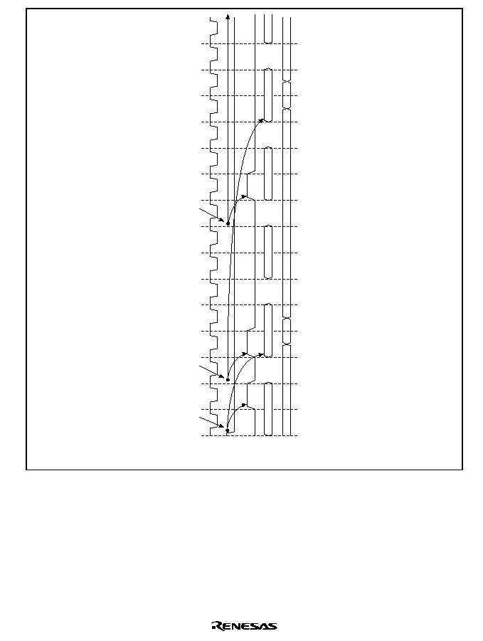
Rev. 5.0, 09/03, page 409 of 806
CKIO
DRAK
DREQ
DACK
Bus cycle
DMAC(R)
CPU
DMAC(W)
DMAC(R)
CPU
DMAC(W)
1st sampling
2nd sampling
3
rd sampling
Figure 12.17 Cycle-Steal Mode, Level Input (CPU Access: 2 Cycles)
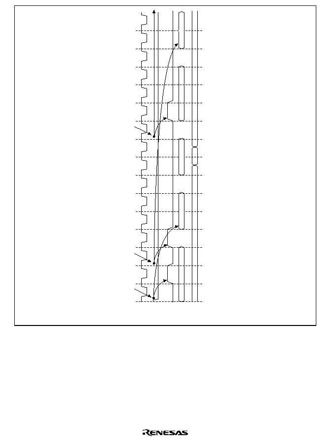
Rev. 5.0, 09/03, page 410 of 806
CPU
CPU
CKIO
DRAK
DREQ
DACK
DMAC(R)
DMAC(W)
DMAC(R)
1st sampling
2nd sampling
3
rd sampling
Bus cycle
Figure 12.18 Cycle-Steal Mode, Level Input (CPU Access: 3 Cycles)
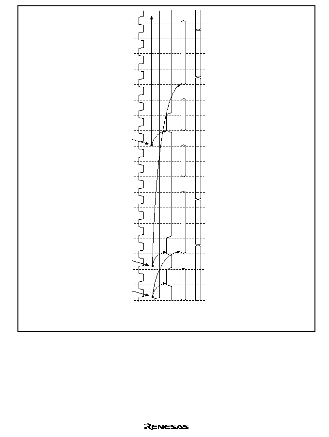
Rev. 5.0, 09/03, page 411 of 806
CKIO
DRAK
(High output)
Bus cycle
DREQ
DACK
(RD output)
DMAC(W)
CPU
DMAC(W)
DMAC(R)
CPU
1st sampling
2nd sampling
3
rd sampling
Figure 12.19 Cycle-Steal Mode, Level input
(CPU Access: 2 Cycles, DMA RD Access: 4 Cycles)
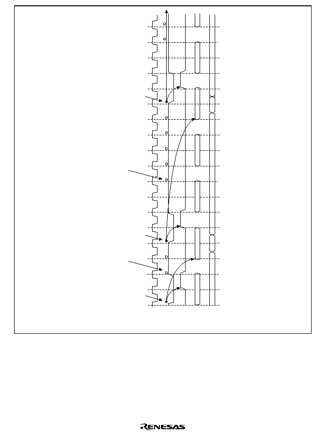
Rev. 5.0, 09/03, page 412 of 806
CKIO
DRAK
Bus cycle
DREQ
DACK
(RD output)
CPU
CPU
DMAC(W)
DMAC(R)
DMAC(W)
DMAC(R)
CPU
3rd sampling is performed,
but since
DREQ
is high,
per-cycle sampling starts
2nd sampling is performed,
but since
DREQ
is high,
per-cycle sampling starts
1st sampling
2nd sampling
3rd sampling
Figure 12.20 Cycle-Steal Mode, Level input (CPU Access: 2 Cycles, DREQ Input Delayed)
Rev. 5.0, 09/03, page 413 of 806
CKIO
DRAK
Bus cycle
DREQ
DACK
(RD output)
CPU
CPU
DMAC(W)
DMAC(R)
DMAC(W)
DMAC(R)
CPU
High
High
High
High
2nd sampling is performed,
but since there is no
DREQ
falling edge,
per-cycle sampling starts
3rd sampling is performed,
but since there is no
DREQ
falling edge,
per-cycle sampling starts
1st sampling
2nd sampling
3
rd sampling
Note: When a
DREQ
falling edge is detected,
DREQ
must be high for at least one cycle before the sampling point.
Figure 12.21 Cycle-Steal Mode, Edge input (CPU Access: 2 Cycles)
Rev. 5.0, 09/03, page 414 of 806
CKIO
DRAK
DREQ
DACK
Bus cycle
DMAC(R)
DMAC(W)
DMAC(R)
DMAC(W)
DMAC(R)
CPU
1st sampling
2nd sampling
3
rd sampling
Figure 12.22 Burst Mode, Level Input
Rev. 5.0, 09/03, page 415 of 806
CKIO
DRAK
DREQ
DACK
Bus cycle
CPU
DMAC(R)
DMAC(W)
DMAC(R)
DMAC(W)
DMAC(R)
1st sampling
Figure 12.23 Burst Mode, Edge Input
Rev. 5.0, 09/03, page 416 of 806
12.3.6
Source Address Reload Function
Channel 2 includes a reload function, in which the value is returned to the value set in the source
address register (SAR2) every four transfers by setting the RO bit in CHCR2. 16-byte transfer
cannot be used. Figure 12.24 shows this operation. Figure 12.25 shows a timing chart for the
source address reload function under the following conditions: burst mode, auto-request, 16-bit
transfer data size, SAR2 incremented, DAR2 fixed, reload function on, and use of channel 2 only.
SAR2
(initial value)
DMAC
Transfer
request
DMAC control
Reload control
4 time
count
CHCR2
DMATCR2
SAR2
RO bit = 1
Count signal
Reload
signal
Reload signal
Address bus
Figure 12.24 Source Address Reload Function Diagram
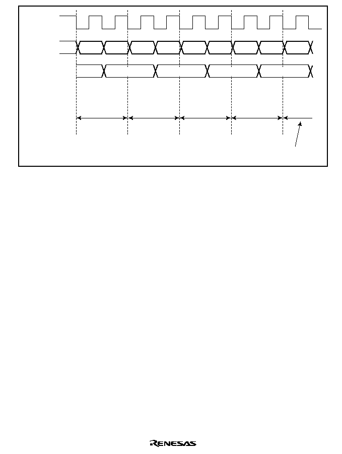
Rev. 5.0, 09/03, page 417 of 806
CK
Internal
address bus
Internal
data bus
SAR2
DAR2
DAR2
DAR2
DAR2
SAR2+2
SAR2+4
SAR2+6
SAR2
SAR2 data
SAR2+2 data
SAR2+4 data
SAR2+6 data
First transfer on
channel 2
Second transfer
Third transfer
Fourth transfer
Fifth transfer
SAR2 output
DAR2 output
SAR2+2 output
DAR2 output
SAR2+4 output
DAR2 output
SAR2+6 output
DAR2 output
SAR2 reload
SAR2 output
DAR2 output
Figure 12.25 Timing Chart of Source Address Reload Function
The reload function can be executed with a transfer data size of 8, 16, or 32 bits.
DMATCR2, which specifies the transfer count, increments 1 each time a transfer ends regardless
of whether the reload function is on or off. Consequently, a multiple of four must be specified in
DMATCR2 when the reload function is on. Operation is not guaranteed if other values are
specified.
The counter that counts the execution of four transfers for the reload function is reset by clearing
the DME bit in DMAOR or the DE bit in CHCR2, by setting the transfer end flag (TE bit in
CHCR2), and by NMI input, as well as by a reset or standby transition, but the SAR2, DAR2, and
DMATCR2 registers are not reset. Therefore, if these sources are generated, there will be a mix of
an initialized counter and uninitialized registers in the DMAC, and a malfunction will be caused
by restarting the DMAC in that state. Consequently, if one of these sources other than setting of
the TE bit occurs during use of the reload function, set SAR2, DAR2, and DMATCR2 again.

Rev. 5.0, 09/03, page 418 of 806
12.3.7
DMA Transfer Ending Conditions
The DMA transfer ending conditions are different for ending on an individual channel and ending
on all channels together. At the end of transfer, the following conditions are applied except in the
case where the value set in the DMA transfer count register (DMATCR) reaches 0.
(a) Cycle-steal mode (external request, internal request, and auto-request)
When the transfer ending conditions are satisfied, DMAC transfer request acceptance is
suspended. The DMAC stops operating after completing the number of transfers that it has
accepted until the ending conditions are satisfied.
In cycle-steal mode, the operation is the same regardless of whether the transfer request is
detected by level or edge.
(b) Burst mode, edge detection (external request, internal request, and auto-request)
The timing from the point where the ending conditions are satisfied to the point where the
DMAC stops operating is the same as in cycle-steal mode. With edge detection in burst mode,
though only one transfer request is generated to start the DMAC, stop request sampling is
performed at the same timing as transfer request sampling in cycle-steal mode. As a result, the
period when a stop request is not sampled is regarded as the period when a transfer request is
generated, and after performing the DMA transfer for this period, the DMAC stops operating.
(c) Burst mode, level detection (external request)
Same as in (a).
(d) Bus timing when transfer is suspended
Transfer is suspended when one transfer ends. Even if transfer ending conditions are satisfied
during a read in direct address transfer in dual address mode, the subsequent write process is
executed, and after the transfer in (a) to (c) above has been executed, DMAC operation is
suspended.
Individual Channel Ending Conditions: There are two ending conditions. A transfer ends when
the value of the channel's DMA transfer count register (DMATCR) is 0, or when the DE bit in the
channel's CHCR register is cleared to 0.
∑
When DMATCR is 0: When the DMATCR value becomes 0 and the corresponding channel's
DMA transfer ends, the transfer end flag bit (TE) is set in CHCR. If the IE (interrupt enable)
bit has been set, a DMAC interrupt (DEI) request is sent to the CPU. This transfer ending does
not apply to (a) to (d) described above.
∑
When DE in CHCR is 0: Software can halt a DMA transfer by clearing the DE bit in the
channel's CHCR register. The TE bit is not set when this happens. This transfer ending applies
to (a) to (d) described above.

Rev. 5.0, 09/03, page 419 of 806
Conditions for Ending on All Channels Simultaneously: Transfers on all channels end (1) when
the NMIF (NMI flag) bit is set to 1 in DMAOR, or (2) when the DME bit in DMAOR is cleared to
0.
∑
Transfer ending when the NMIF bit is set to 1 in DMAOR: When an NMI interrupt occurs, the
NMIF bit is set to 1 in DMAOR and all channels stop their transfers according to the
conditions in (a) to (d) described above, and pass the bus to an other bus master. Consequently,
even if the NMI bit is set to 1 during transfer, SAR, DAR, DMATCR are updated. The TE bit
is not set. To resume transfer after NMI interrupt exception handling, clear the NMIF bit to 0.
At this time, if there are channels that should not be restarted, clear the corresponding DE bit
in CHCR.
∑
Transfer ending when DME is cleared to 0 in DMAOR: Clearing the DME bit to 0 in DMAOR
forcibly aborts transfer on all channels. The TE bit is not set. All channels abort their transfer
according to the conditions in (a) to (d) in section 12.3.7, DMA Transfer Ending Conditions, as
in NMI interrupt generation. In this case, the values in SAR, DAR, and DMATCR are also
updated.
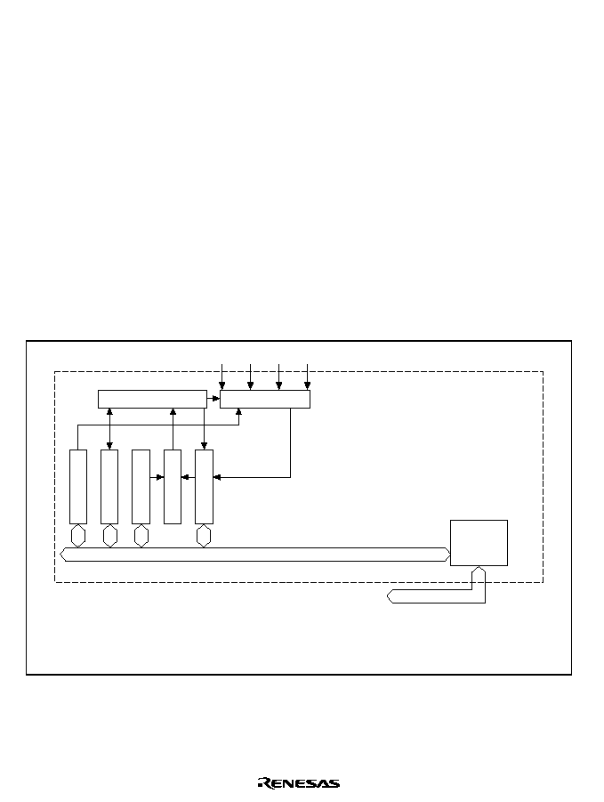
Rev. 5.0, 09/03, page 420 of 806
12.4
Compare Match Timer (CMT)
12.4.1
Overview
The DMAC has an on-chip compare match timer (CMT) to generate DMA transfer requests. The
CMT has a 16-bit counter.
Features
The CMT has the following features:
∑
Four types of counter input clock can be selected
One of four internal clocks (P
/4, P
/8, P
/16, P
/64) can be selected.
∑
Generates a DMA transfer request when compare match occurs.
Block Diagram
Figure 12.26 shows a block diagram of the CMT.
Internal bus
Bus
interface
Control circuit
Clock selection
CMSTR
CMCSR0
CMCOR0
Comparator
CMCNT0
Module bus
CMT
P
/4 P/8 P/16 P/64
CMSTR:
CMCSR0:
CMCOR0:
CMCNT0:
Compare match timer start register
Compare match timer control/status register 0
Compare match timer constant register 0
Compare match timer counter 0
Figure 12.26 Block Diagram of CMT

Rev. 5.0, 09/03, page 421 of 806
Register Configuration
Table 12.7 summarizes the CMT register configuration.
Table 12.7
Register Configuration
Name
Abbreviation
R/W
Initial
Value
Address
Access Size
(Bits)
Compare match timer start
register
CMSTR
R/(W)
H'0000
H'04000070
(H'A4000070)
*
2
8, 16, 32
Compare match timer
control/status register 0
CMCSR0
R/(W)
*
1
H'0000
H'04000072
(H'A4000072)
*
2
8, 16, 32
Compare match counter 0
CMCNT0
R/W
H'0000
H'04000074
(H'A4000074)
*
2
8, 16, 32
Compare match constant
register 0
CMCOR0
R/W
H'FFFF
H'04000076
(H'A4000076)
*
2
8, 16, 32
Notes: 1. The only value that can be written to the CMF bit in CMCSR0 is 0 to clear the flag.
2. When address translation by the MMU does not apply, the address in parentheses
should be used.
12.4.2
Register Descriptions
Compare Match Timer Start Register (CMSTR)
The compare match timer start register (CMSTR) is a 16-bit register that selects whether compare
match counter 0 (CMCNT0) is operated or halted. It is initialized to H'0000 by a reset, but retains
its previous value in standby mode.
Bit:
15
14
13
12
11
10
9
8
--
--
--
--
--
--
--
--
Initial value:
0
0
0
0
0
0
0
0
R/W:
R
R
R
R
R
R
R
R
Bit:
7
6
5
4
3
2
1
0
--
--
--
--
--
--
--
STR0
Initial value:
0
0
0
0
0
0
0
0
R/W:
R
R
R
R
R
R
R/W
R/W
Bits 15 to 2--Reserved: These bits are always read as 0. The write value should alway be 0.
Bit 1--Reserved: This bit can be read or written. The write value should always be 0.

Rev. 5.0, 09/03, page 422 of 806
Bit 0--Count Start 0 (STR0): Selects whether to operate or halt compare match timer counter 0.
Bit 0: STR0
Description
0
CMCNT0 count operation halted
(Initial value)
1
CMCNT0 count operation
Compare Match Timer Control/Status Register 0 (CMCSR0)
The compare match timer control/status register 0 (CMCSR0) is a 16-bit register that indicates the
occurrence of compare matches, sets the enable/disable status of interrupts, and establishes the
clock used for incrementation. It is initialized to H'0000 by a reset, but retains its previous value in
standby mode.
Bit:
15
14
13
12
11
10
9
8
--
--
--
--
--
--
--
--
Initial value:
0
0
0
0
0
0
0
0
R/W:
R
R
R
R
R
R
R
R
Bit:
7
6
5
4
3
2
1
0
CMF
--
--
--
--
--
CKS1
CKS0
Initial value:
0
0
0
0
0
0
0
0
R/W:
R/(W)
*
R/W
R
R
R
R
R/W
R/W
Note:
*
The only value that can be written is 0 to clear the flag.
Bits 15 to 8 and 5 to 2--Reserved: These bits are always read as 0. The write value should
always be 0.
Bit 7--Compare Match Flag (CMF): Indicates whether or not the compare match timer counter
0 CMCNT0 and compare match timer constant 0 (CMCOR0) values match.
Bit 7: CMF
Description
0
CMCNT0 and CMCOR0 values do not match
(Initial value)
Clearing condition: Write 0 to CMF after reading CMF = 1
1
CMCNT0 and CMCOR0 values match
Rev. 5.0, 09/03, page 423 of 806
Bit 6--Reserved: This bit can be read or written. The wite value should always be 0.
Bits 1 and 0--Clock Select 1 and 0 (CKS1, CKS0): Select the clock input to CMCNT from
among the four internal clocks obtained by dividing the system clock (P
). When the STR bit in
CMSTR is set to 1, CMCNT0 begins incrementing on the clock selected by CKS1 and CKS0.
Bit 1: CKS1
Bit 0: CKS0
Description
0
0
P
/4 (Initial
value)
1
P
/8
1
0
P
/16
1
P
/64
Compare Match Counter 0 (CMCNT0)
Compare match counter 0 (CMCNT0) is a 16-bit register used as an up-counter.
When an internal clock is selected with the CKS1 and CKS0 bits in the CMCSR0 register and the
STR bit in CMSTR is set to 1, CMCNT0 begins incrementing on that clock. When the CMCNT0
value matches that of compare match constant register 0 (CMCOR0), CMCNT0 is cleared to
H'0000 and the CMF flag in CMCSR0 is set to 1.
CMCNT0 is initialized to H'0000 by a reset, but retains its previous value in standby mode.
Bit:
15
14
13
12
11
10
9
8
Initial value:
0
0
0
0
0
0
0
0
R/W:
R/W
R/W
R/W
R/W
R/W
R/W
R/W
R/W
Bit:
7
6
5
4
3
2
1
0
Initial value:
0
0
0
0
0
0
0
0
R/W:
R/W
R/W
R/W
R/W
R/W
R/W
R/W
R/W
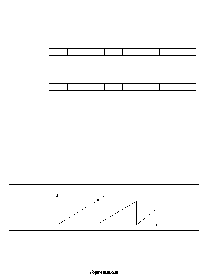
Rev. 5.0, 09/03, page 424 of 806
Compare Match Constant Register 0 (CMCOR0)
Compare match constant register 0 (CMCOR0) is a 16-bit register that sets the CMCNT0 compare
match period.
CMCOR0 is initialized to H'FFFF by a reset, but retains its previous value in standby mode.
Bit:
15
14
13
12
11
10
9
8
Initial value:
1
1
1
1
1
1
1
1
R/W:
R/W
R/W
R/W
R/W
R/W
R/W
R/W
R/W
Bit:
7
6
5
4
3
2
1
0
Initial value:
1
1
1
1
1
1
1
1
R/W:
R/W
R/W
R/W
R/W
R/W
R/W
R/W
R/W
12.4.3
Operation
Period Count Operation
When an internal clock is selected with the CKS1 and CKS0 bits in the CMCSR0 register and the
STR bit in CMSTR is set to 1, CMCNT0 begins incrementing on the selected clock. When the
CMCNT counter value matches that of CMCOR0, the CMCNT0 counter is cleared to H'0000 and
the CMF flag in the CMCSR0 register is set to 1. The CMCNT0 counter begins counting up again
from H'0000.
Figure 12.27 shows the compare match counter operation.
Counter cleared by
CMCOR0 compare match
CMCNT0 value
CMCOR0
H'0000
Time
Figure 12.27 Counter Operation
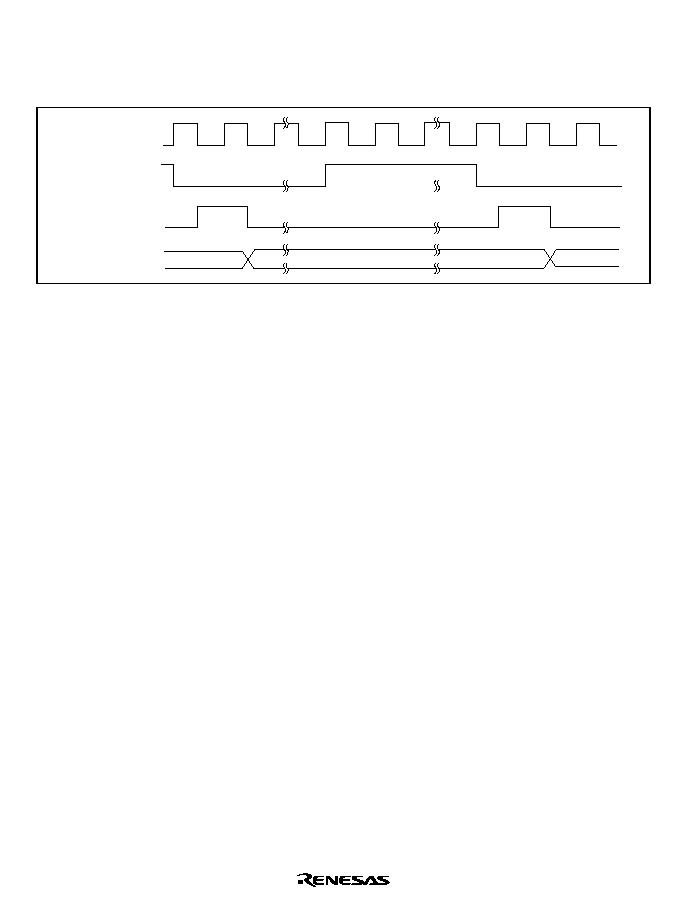
Rev. 5.0, 09/03, page 425 of 806
CMCNT0 Count Timing
One of four clocks (P
/4, P
/8, P
/16, P
/64) obtained by dividing the P
clock can be selected
with the CKS1 and CKS0 bits in CMCSR0. Figure 12.28 shows the timing.
N+1
CK
Internal clock
CMCNT0 input
clock
CMCNT0
N-1
N
Figure 12.28 Count Timing
12.4.4
Compare Match
Compare Match Flag Setting Timing
The CMF bit in the CMCSR0 register is set to 1 by the compare match signal generated when the
CMCOR0 register and the CMCNT0 counter match. The compare match signal is generated in the
final state of the match (timing at which the CMCNT0 counter matching count value is updated).
Consequently, after the CMCOR0 register and the CMCNT0 counter match, a compare match
signal will not be generated until a CMCNT0 counter input clock occurs. Figure 12.29 shows the
CMF bit setting timing.

Rev. 5.0, 09/03, page 426 of 806
CK
CMCOR0
CMCNT0
input clock
Compare
match signal
CMF
CMI
CMCNT0
N
N
0
Figure 12.29 CMF Setting Timing
Compare Match Flag Clearing Timing
The CMF bit in the CMCSR0 register is cleared by writing 0 to it after reading 1. Figure 12.30
shows the timing when the CMF bit is cleared by the CPU.
CK
CMF
CMCSR0 write cycle
T
1
T
2
Figure 12.30 Timing of CMF Clearing by the CPU

Rev. 5.0, 09/03, page 427 of 806
12.5
Examples of Use
12.5.1
Example of DMA Transfer between On-Chip IrDA and External Memory
In this example, receive data of the on-chip IrDA is transferred to external memory using DMAC
channel 3. Table 12.8 shows the transfer conditions and register settings. In addition, it is
recommended that the trigger for the number of receive FIFO data bytes in IrDA be set to 1
(RTRG1 = RTRG0 = 0 in SCFCR).
Table 12.8
Transfer Conditions and Register Settings for Transfer between On-Chip SCI
and External Memory
Transfer Conditions
Register
Setting
Transfer source: RDR1 of on-chip IrDA
SAR3
H'0400014A
Transfer destination: External memory
DAR3
H'00400000
Number of transfers: 64
DMATCR3
H'00000040
Transfer source address: Fixed
CHCR3
H'00004B05
Transfer destination address: Incremented
Transfer request source: IrDA (RXI1)
Bus mode: Cycle-steal
Transfer unit: Byte
Interrupt request generated at end of transfer
Channel priority order: 0 > 2 > 3 > 1
DMAOR
H'0101

Rev. 5.0, 09/03, page 428 of 806
12.5.2
Example of DMA Transfer between A/D Converter and External Memory
(Address Reload On)
In this example, DMA transfer is performed between the on-chip A/D converter (transfer source)
and the external memory (transfer destination) with the address reload function on. Table 12.9
shows the transfer conditions and register settings.
Table 12.9
Transfer Conditions and Register Settings for Transfer between On-Chip A/D
Converter and External Memory
Transfer Conditions
Register
Setting
Transfer source: On-chip A/D converter
SAR2
H'04000080
Transfer destination: External memory
DAR2
H'00400000
Number of transfers: 128 (reloading 32 times)
DMATCR2
H'00000080
Transfer source address: Incremented
CHCR2
H'00089E35
Transfer destination address: Decremented
Transfer request source: A/D converter
Bus mode: Burst
Transfer unit: Longword
Interrupt request generated at end of transfer
Channel priority order: 0 > 2 > 3 > 1
DMAOR
H'0101
When the address reload function is on, the value set in SAR returns to the initially set value every
four transfers. In this example, when an interrupt request is generated from the A/D converter,
byte data is read from the register at address H'04000080 in the A/D converter, and is written to
external memory address H'00400000. Since longword data has been transferred, the values in
SAR and DAR are H'04000084 and H'003FFFFC, respectively. The bus is kept and data transfers
are performed successively because this transfer is in burst mode.
After four transfers end, fifth and sixth transfers are performed if the address reload function is off,
and the value in SAR is incremented from H'0400008C to H'04000090, H'04000094
...
If the
address reload function is on, DMA transfer stops after the fourth transfer ends, and the bus
request signal to the CPU is cleared. At this time, the value stored in SAR is not incremented
from H'0400008C to H'04000090, but returns to the initially set value, H'04000080. The value in
DAR continues to be incremented regardless of whether the address reload function is on or off.

Rev. 5.0, 09/03, page 429 of 806
As a result, the values in the DMAC are as shown in table 12.10 when the fourth transfer ends,
depending on whether the address reload function is on or off.
Table 12.10 Values in DMAC after End of Fourth Transfer
Items
Address reload on
Address reload off
SAR
H'04000080
H'04000090
DAR
H'003FFFFC
H'003FFFFC
DMATCR
H'0000007C
H'0000007C
Bus
Released
Held
DMAC operation
Stops
Keeps operating
Interrupt
Not generated
Not generated
Transfer request source flag
clearing
Executed
Not executed
Notes: 1. An interrupt is generated regardless of whether the address reload function is on or off,
if transfers are executed until the value in DMATCR reaches 0 and the IE bit in CHCR
has been set to 1.
2. The transfer request source flag is cleared regardless of whether the address reload
function is on or off, if transfers are executed until the value in DMATCR reaches 0.
3. Specify burst mode when using the address reload function. This function may not be
correctly executed in cycle-steal mode.
4. Set a multiple of four in DMATCR when using the address reload function. This function
may not be correctly executed if other values are specified.
12.5.3
Example of DMA Transfer between External Memory and SCIF Transmitter
(Indirect Address On)
In this example, DMA transfer is performed between the external memory specified by indirect
address (transfer source) and the SCIF transmitter (transfer destination) using DMAC channel 3.
Table 12.11 shows the transfer conditions and register settings. In addition, the trigger for the
number of transmit FIFO data bytes is set to 1 (TTRG1 = TTRG0 = 1 in SCFCR).

Rev. 5.0, 09/03, page 430 of 806
Table 12.11 Transfer Conditions and Register Settings for Transfer between External
Memory and SCIF Transmitter
Transfer Conditions
Register
Setting
Transfer source: External memory
SAR3
H'00400000
Value stored in address H'00400000
--
H'00450000
Value stored in address H'04500000
--
H'55
Transfer destination: On-chip SCIF TDR2
DAR3
H'04000156
Number of transfers: 10
DMATCR3
H'0000000A
Transfer source address: Incremented
CHCR3
H'00011C01
Transfer destination address: Fixed
Transfer request source: SCIF (TXI2)
Bus mode: Cycle-steal
Transfer unit: Byte
No interrupt request generated at end of transfer
Channel priority order: 0 > 1 > 2 > 3
DMAOR
H'0001
If the indirect address is on, data stored in the address set in SAR is not used as transfer source
data. In the indirect address, after the value stored in the address set in SAR is read, that read value
is used as an address again, and the value stored in that address is read and stored in the address
set in DAR.
In the example shown in table 12.11, when an SCIF transfer request is generated, the DMAC reads
the value in address H'00400000 set in SAR3. Since the value H'00450000 is stored in that
address, the DMAC reads the value H'00450000. Next, the DMAC uses that read value as an
address again, and reads the value H'55 stored in that address. Then, the DMAC writes the value
H'55 to address H'04000156 set in DAR3; this completes one indirect address transfer.
In the indirect address, when data is read first from the address set in SAR3, the data transfer size
is always longword regardless of the settings of the TS0 and TS1 bits that specify the transfer data
size. However, whether the transfer source address is fixed, incremented, or decremented is
specified by the SM0 and SM1 bits. Therefore, in this example, though the transfer data size is
specified as byte, the value in SAR3 is H'00400004 when one transfer ends. Write operations are
the same as in normal dual address transfer.

Rev. 5.0, 09/03, page 431 of 806
12.6
Usage Notes
1. The DMA channel control registers (CHCR0≠CHCR3) can be accessed with any data size. The
DMA operation register (DMAOR) must be accessed by byte (eight bits) or word (16 bits);
other registers must be accessed by word (16 bits) or longword (32 bits).
2. Before rewriting the RS0≠RS3 bits in CHCR0≠CHCR3, first clear the DE bit to 0 (when
rewriting CHCR with a byte address, be sure to set the DE bit to 0 in advance).
3. Even if an NMI interrupt is input when the DMAC is not operating, the NMIF bit in DMAOR
will be set.
4. Before entering standby mode, the DME bit in DMAOR must be cleared to 0 and the transfers
accepted by the DMAC completed.
5. The on-chip peripherals which the DMAC can access are the IRDA, SCIF, A/D converter, D/A
converter, and I/O ports. Do not access other peripherals with the DMAC.
6. When starting up the DMAC, set CHCR or DMAOR last. Normal operation is not guaranteed
if settings for another register are made last.
7. Even if the maximum number of transfers are performed in the same channel after the
DMATCR count reaches 0 and DMA transfer ends normally, write 0 to DMATCR.
Otherwise, normal DMA transfer may not be performed.
8. When using the address reload function, specify burst mode as the transfer mode. In cycle-steal
mode, normal DMA transfer may not be performed.
9. When using the address reload function, set a multiple of four in DMATCR. Normal operation
is not guaranteed if other values are specified.
10. When detecting an external request at the falling edge, keep the external request pin high when
setting the DMAC.
11. Do not access the space from H'4000062 to H'400006F, which is not used in the DMAC.
Accessing this space may cause malfunctions.
12. The
WAIT signal is ignored in the case of a write to external address space in dual address
mode with 16-byte transfer, or transfer from an external device with DACK to external address
space in single address mode with 16-byte transfer.
13. DMAC transfers should not be performed in the sleep mode under conditions other than when
the clock ratio of I
(on-chip clock) to B
(bus clock) is 1:1.
14. When the following three conditions are all met, the frequency control register (FRQCR)
should not be changed while a DMAC transfer is in progress.
∑
Bits IFC2 to IFC0 are changed.
∑
STC2 to STC0 in FRQCR are not changed.
∑
The clock ratio of I
(on-chip clock) to B
(bus clock) after the change is other than 1:1.
15. If the following three conditions are all met, big-endian access is used when the DMAC is
used to transfer data from XY memory, even in the little-endian mode.
∑
The source address for the transfer is in XY memory.
∑
The indirect address mode is used.

Rev. 5.0, 09/03, page 432 of 806
∑
The byte size data is transferred.
∑
The data format is little-endian.

Rev. 5.0, 09/03, page 433 of 806
Section 13 Timer (TMU)
13.1
Overview
The SH7729R has a three-channel (channels 0 to 2) 32-bit timer unit (TMU).
13.1.1
Features
The TMU has the following features:
∑
Each channel is provided with an auto-reload 32-bit down counter
∑
Channel 2 is provided with an input capture function
∑
All channels are provided with 32-bit constant registers and 32-bit down counters that can be
read or written to at any time.
∑
All channels generate interrupt requests when the 32-bit down counter underflows
(H'00000000
H'FFFFFFFF).
∑
Allows selection between 6 counter input clocks: External clock (TCLK), on-chip RTC output
clock (16 kHz), P
/4, P
/16, P
/64, P
/256. (P
is the internal clock for peripheral modules.)
See section 10, On-Chip Oscillation Circuits, for more information on the clock pulse
generator.
∑
All channels can operate when the SH7729R is in standby mode: When the RTC output clock
is being used as the counter input clock, the SH7729R is still able to count in standby mode.
∑
Synchronized read: TCNT is a sequentially changing 32-bit register. Since the peripheral
module used has an internal bus width of 16 bits, a time lag can occur between the time when
the upper 16 bits and lower 16 bits are read. To correct the discrepancy in the counter read
value caused by this time lag, a synchronization circuit is built into the TCNT so that the entire
32-bit data in the TCNT can be read at once.
∑
The maximum operating frequency of the 32-bit counter is 2 MHz on all channels: Operate the
SH7729R so that the clock input to the timer counters of each channel (obtained by dividing
the external clock and internal clock with the prescaler) does not exceed the maximum
operating frequency.
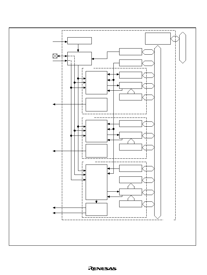
Rev. 5.0, 09/03, page 434 of 806
13.1.2
Block Diagram
Figure 13.1 shows a block diagram of the TMU.
TOCR
Prescaler
TSTR
TCR0
TCNT0
Module bus
Internal bus
TCOR0
TCR1
TCNT1
TCOR1
Counter
controller
TCLK
P
RTCCLK
TUNI0
Bus interface
Ch. 0
Interrupt
controller
Interrupt
controller
Interrupt
controller
Counter
controller
Counter
controller
TUNI1
TUNI2
TICPI2
TCR2
TCPR2
TCNT2
TCOR2
TMU
Ch. 1
Ch. 2
Clock
controller
TOCR:
TSTR:
TCR:
Legend
Timer output control register
Timer start register
TCNT:
TCOR:
TCPR2:
32-bit timer counter
32-bit timer constant register
32-bit input capture register
Timer control register
Figure 13.1 Block Diagram of TMU

Rev. 5.0, 09/03, page 435 of 806
13.1.3
Pin Configuration
Table 13.1 shows the pin configuration of the TMU.
Table 13.1
TMU Pin
Channel
Pin
I/O
Description
Clock input/clock output
TCLK
I/O
External clock input pin/input capture control input
pin/realtime clock (RTC) output pin
13.1.4
Register Configuration
Table 13.2 shows the TMU register configuration.
Table 13.2
TMU Registers
Channel
Register
Abbre-
viation
R/W
Initial Value
*
Address
Access
Size
Common
Timer output control
register
TOCR
R/W
H'00
H'FFFFFE90
8
Timer start register
TSTR
R/W
H'00
H'FFFFFE92
8
0
Timer constant register 0
TCOR0
R/W
H'FFFFFFFF
H'FFFFFE94
32
Timer counter 0
TCNT0
R/W
H'FFFFFFFF
H'FFFFFE98
32
Timer control register 0
TCR0
R/W
H'0000
H'FFFFFE9C
16
1
Timer constant register 1
TCOR1
R/W
H'FFFFFFFF
H'FFFFFEA0
32
Timer counter 1
TCNT1
R/W
H'FFFFFFFF
H'FFFFFEA4
32
Timer control register 1
TCR1
R/W
H'0000
H'FFFFFEA8
16
2
Timer constant register 2
TCOR2
R/W
H'FFFFFFFF
H'FFFFFEAC
32
Timer counter 2
TCNT2
R/W
H'FFFFFFFF
H'FFFFFEB0
32
Timer control register 2
TCR2
R/W
H'0000
H'FFFFFEB4
16
Input capture register 2
TCPR2
R
Undefined
H'FFFFFEB8
32
Note:
*
Initialized by power-on resets or manual resets.

Rev. 5.0, 09/03, page 436 of 806
13.2
TMU Registers
13.2.1
Timer Output Control Register (TOCR)
TOCR is an 8-bit readable/writable register that selects whether to use the external TCLK pin as
an external clock or an input capture control usage input pin, or an output pin for the on-chip RTC
output clock. TOCR is initialized to H'00 by a power-on reset or manual reset, but is not initialized
in standby mode.
Bit:
7
6
5
4
3
2
1
0
--
--
--
--
--
--
--
TCOE
Initial value:
0
0
0
0
0
0
0
0
R/W:
R
R
R
R
R
R
R
R/W
Bits 7 to 1--Reserved: These bits are always read as 0. The write value should always be 0.
Bit 0--Timer Clock Pin Control (TCOE): Selects use of the timer clock pin (TCLK) as an
external clock output pin or input pin for input capture control for the on-chip timer, or as an
output pin for the on-chip RTC output clock. Since the TCLK pin is multiplexed as the PTH7 pin,
when the pin is used as TCLK, bits PH7MD1 and PH7MD0 in the PHCR register should be set to
00 (the "other function" setting).
Bit 0: TCOE
Description
0
Timer clock pin (TCLK) used as external clock input or input capture control
input pin for the on-chip timer
(Initial value)
1
Timer clock pin (TCLK) used as output pin for on-chip RTC output clock
13.2.2
Timer Start Register (TSTR)
TSTR is an 8-bit readable/writable register that selects whether to run or halt the timer counters
(TCNT) for channels 0≠2. TSTR is initialized to H'00 by a power-on reset or manual reset, but is
not initialized in standby mode when the input clock selected for the channel is the on-chip RTC
clock (RTCCLK). Only when an external clock (TCLK) or the peripheral clock (P
) is used as the
input clock, it is initialized in standby mode when the multiplication ratio of PLL circuit 1 is
changed or when the MSTP2 bit in STBCR is set to 1.
Bit:
7
6
5
4
3
2
1
0
--
--
--
--
--
STR2
STR1
STR0
Initial value:
0
0
0
0
0
0
0
0
R/W:
R
R
R
R
R
R/W
R/W
R/W

Rev. 5.0, 09/03, page 437 of 806
Bits 7 to 3--Reserved: These bits are always read as 0. The write value should always be 0.
Bit 2--Counter Start 2 (STR2): Selects whether to run or halt timer counter 2 (TCNT2).
Bit 2: STR2
Description
0
TCNT2 count halted
(Initial value)
1
TCNT2 counts
Bit 1--Counter Start 1 (STR1): Selects whether to run or halt timer counter 1 (TCNT1).
Bit 1: STR1
Description
0
TCNT1 count halted
(Initial value)
1
TCNT1 counts
Bit 0--Counter Start 0 (STR0): Selects whether to run or halt timer counter 0 (TCNT0).
Bit 0: STR0
Description
0
TCNT0 count halted
(Initial value)
1
TCNT0 counts
13.2.3
Timer Control Registers (TCR)
The timer control registers (TCR) control the timer counters (TCNT) and interrupts. The TMU has
three TCR registers, one for each channel.
The TCR registers are 16-bit readable/writable registers that control the issuance of interrupts
when the flag indicating timer counter (TCNT) underflow has been set to 1, and also carry out
counter clock selection. When the external clock has been selected, they also select its edge.
Additionally, TCR2 controls the channel 2 input capture function and the issuance of interrupts
during input capture. The TCR registers are initialized to H'0000 by a power-on reset and manual
reset, but are not initialized in standby mode.

Rev. 5.0, 09/03, page 438 of 806
Channels 0 and 1 TCR Bit Configuration:
Bit:
15
14
13
12
11
10
9
8
--
--
--
--
--
--
--
UNF
Initial value:
0
0
0
0
0
0
0
0
R/W:
R
R
R
R
R
R
R
R/W
Bit:
7
6
5
4
3
2
1
0
--
--
UNIE
CKEG1
CKEG0
TPSC2
TPSC1
TPSC0
Initial value:
0
0
0
0
0
0
0
0
R/W:
R
R
R/W
R/W
R/W
R/W
R/W
R/W
Channel 2 TCR Bit Configuration:
Bit:
15
14
13
12
11
10
9
8
--
--
--
--
--
--
ICPF
UNF
Initial value:
0
0
0
0
0
0
0
0
R/W:
R
R
R
R
R
R
R/W
R/W
Bit:
7
6
5
4
3
2
1
0
ICPE1
ICPE0
UNIE
CKEG1
CKEG0
TPSC2
TPSC1
TPSC0
Initial value:
0
0
0
0
0
0
0
0
R/W:
R/W
R/W
R/W
R/W
R/W
R/W
R/W
R/W
Bits 15 to 10, 9 (except TCR2), 7, and 6 (except TCR2)--Reserved: These bits are always read
as 0. The write value should always be 0.
Bit 9--Input Capture Interrupt Flag (ICPF): A function of channel 2 only: the flag is set when
input capture is requested via the TCLK pin.
Bit 9: ICPF
Description
0
No input capture request has been issued
Clearing condition: When 0 is written to ICPF
(Initial value)
1
Input capture has been requested via the TCLK pin
Setting condition: When input capture is requested via the TCLK pin
*
Note:
*
Contents do not change when 1 is written to ICPF.

Rev. 5.0, 09/03, page 439 of 806
Bit 8--Underflow Flag (UNF): Status flag that indicates occurrence of a TCNT underflow.
Bit 8: UNF
Description
0
TCNT has not underflowed
Clearing condition: When 0 is written to UNF
(Initial value)
1
TCNT has underflowed (H'00000000
H'FFFFFFFF)
Setting condition: When TCNT underflows
*
Note:
*
Contents do not change when 1 is written to UNF.
Bits 7 and 6--Input Capture Control (ICPE1, ICPE0): A function of channel 2 only:
determines whether the input capture function can be used, and when used, whether or not to
enable interrupts.
When using this input capture function it is necessary to set the TCLK pin to input mode with the
TCOE bit in the TOCR register. Additionally, use the CKEG bit to designate use of either the
rising or falling edge of the TCLK pin to set the value in TCNT2 in the input capture register
(TCPR2).
Bit 7: ICPE1
Bit 6: ICPE0
Description
0
0
Input capture function is not used
(Initial value)
1
Reserved (Setting prohibited)
1
0
Input capture function is used. Interrupt due to ICPF (TICPI2)
is not enabled
1
Input capture function is used. Interrupt due to ICPF (TICPI2)
is enabled
Bit 5--Underflow Interrupt Control (UNIE): Controls enabling of interrupt generation when
the status flag (UNF) indicating TCNT underflow has been set to 1.
Bit 5: UNIE
Description
0
Interrupt due to UNF (TUNI) is not enabled
(Initial value)
1
Interrupt due to UNF (TUNI) is enabled

Rev. 5.0, 09/03, page 440 of 806
Bits 4 and 3--Clock Edge 1 and 0 (CKEG1, CKEG0): Select the external clock edge when the
external clock is selected, or when the input capture function is used.
Bit 4: CKEG1
Bit 3: CKEG0
Description
0
0
Count/capture register set on rising edge
(Initial value)
1
Count/capture register set on falling edge
1
X
Count/capture register set on both rising and falling edge
Note:
X means 0, 1, or `Don't care'.
Bits 2 to 0--Timer Prescaler 2 to 0 (TPSC2 to TPSC0): Select the TCNT count clock.
Bit 2: TPSC2
Bit 1: TPSC1
Bit 0: TPSC0
Description
0
0
0
Internal clock: count on P
/4 (Initial
value)
1
Internal clock: count on P
/
16
1
0
Internal clock: count on P
/64
1
Internal clock: count on P
/256
1
0
0
Internal clock: count on clock output of on-chip
RTC (RTCCLK)
1
External clock: count on TCLK pin input
1
0
Reserved (Setting prohibited)
1
Reserved (Setting prohibited)

Rev. 5.0, 09/03, page 441 of 806
13.2.4
Timer Constant Registers (TCOR)
The timer constant registers are 32-bit registers. The TMU has three TCOR registers, one for each
channel.
TCOR is a 32-bit readable/writable register. When a TCNT count-down results in an underflow,
the TCOR value is set in TCNT and the count-down continues from that value. TCOR is
initialized to H'FFFFFFFF by a power-on reset or manual reset, but is not initialized, and retains
its contents, in standby mode.
Bit:
31
30
29
28
27
26
25
24
Initial value:
1
1
1
1
1
1
1
1
R/W:
R/W
R/W
R/W
R/W
R/W
R/W
R/W
R/W
Bit:
23
22
21
20
19
18
17
16
Initial value:
1
1
1
1
1
1
1
1
R/W:
R/W
R/W
R/W
R/W
R/W
R/W
R/W
R/W
Bit:
15
14
13
12
11
10
9
8
Initial value:
1
1
1
1
1
1
1
1
R/W:
R/W
R/W
R/W
R/W
R/W
R/W
R/W
R/W
Bit:
7
6
5
4
3
2
1
0
Initial value:
1
1
1
1
1
1
1
1
R/W:
R/W
R/W
R/W
R/W
R/W
R/W
R/W
R/W

Rev. 5.0, 09/03, page 442 of 806
13.2.5
Timer Counters (TCNT)
The timer counters are 32-bit readable/writable registers. The TMU has three timer counters, one
for each channel.
TCNT counts down upon input of a clock. The clock input is selected using the TPSC2
≠
TPSC0
bits in the timer control register (TCR).
When a TCNT count-down results in an underflow (H'00000000
H'FFFFFFFF), the underflow
flag (UNF) in the timer control register (TCR) of the relevant channel is set. The TCOR value is
simultaneously set in TCNT itself and the count-down continues from that value.
Because the internal bus for the SH7729R on-chip peripheral modules is 16 bits wide, a time lag
can occur between the time when the upper 16 bits and lower 16 bits are read. Since TCNT counts
sequentially, this time lag can create discrepancies between the data in the upper and lower halves.
To correct the discrepancy, a buffer register is connected to TCNT so that the upper and lower
halves are not read separately. The entire 32-bit data in TCNT can thus be read at once.
TCNT is initialized to H'FFFFFFFF by a power-on reset or manual reset, but is not initialized, and
retains its contents, in standby mode.
Bit:
31
30
29
28
27
26
25
24
Initial value:
1
1
1
1
1
1
1
1
R/W:
R/W
R/W
R/W
R/W
R/W
R/W
R/W
R/W
Bit:
23
22
21
20
19
18
17
16
Initial value:
1
1
1
1
1
1
1
1
R/W:
R/W
R/W
R/W
R/W
R/W
R/W
R/W
R/W
Bit:
15
14
13
12
11
10
9
8
Initial value:
1
1
1
1
1
1
1
1
R/W:
R/W
R/W
R/W
R/W
R/W
R/W
R/W
R/W
Bit:
7
6
5
4
3
2
1
0
Initial value:
1
1
1
1
1
1
1
1
R/W:
R/W
R/W
R/W
R/W
R/W
R/W
R/W
R/W

Rev. 5.0, 09/03, page 443 of 806
13.2.6
Input Capture Register (TCPR2)
Input capture register 2 (TCPR2) is a read-only 32-bit register provided only in timer 2. Control of
TCPR2 setting conditions due to the TCLK pin is affected by the input capture function bits
(ICPE1/ICPE2 and CKEG1/CKEG0) in TCR2. When a TCPR2 setting indication due to the
TCLK pin occurs, the value of TCNT2 is copied into TCPR2.
TCNT2 is not initialized by a power-on reset or manual reset, or in standby mode.
Bit:
31
30
29
28
27
26
25
24
Initial value:
--
--
--
--
--
--
--
--
R/W:
R
R
R
R
R
R
R
R
Bit:
23
22
21
20
19
18
17
16
Initial value:
--
--
--
--
--
--
--
--
R/W:
R
R
R
R
R
R
R
R
Bit:
15
14
13
12
11
10
9
8
Initial value:
--
--
--
--
--
--
--
--
R/W:
R
R
R
R
R
R
R
R
Bit:
7
6
5
4
3
2
1
0
Initial value:
--
--
--
--
--
--
--
--
R/W:
R
R
R
R
R
R
R
R

Rev. 5.0, 09/03, page 444 of 806
13.3
TMU Operation
13.3.1
Overview
Each of three channels has a 32-bit timer counter (TCNT) and a 32-bit timer constant register
(TCOR). TCNT counts down. The auto-reload function enables synchronized counting and
counting by external events. Channel 2 has an input capture function.
13.3.2
Basic Functions
Counter Operation: When the STR0
≠
STR2 bits in the timer start register (TSTR) are set, the
corresponding timer counter (TCNT) starts counting. When a TCNT underflows, the UNF flag of
the corresponding timer control register (TCR) is set. At this time, if the UNIE bit in TCR is 1, an
interrupt request is sent to the CPU. Also at this time, the value is copied from TCOR to TCNT
and the down-count operation is continued.
The count operation is set as follows (figure 13.2):
1. Select the counter clock with the TPSC2≠TPSC0 bits in the timer control register (TCR). If the
external clock is selected, set the TCLK pin to input mode with the TOCE bit in TOCR, and
select its edge with the CKEG1 and CKEG0 bits in TCR.
2. Use the UNIE bit in TCR to set whether to generate an interrupt when TCNT underflows.
3. When using the input capture function, set the ICPE bits in TCR, including the choice of
whether or not to use the interrupt function (channel 2 only).
4. Set a value in the timer constant register (TCOR) (the cycle is the set value plus 1).
5. Set the initial value in the timer counter (TCNT).
6. Set the STR bit in the timer start register (TSTR) to 1 to start operation.
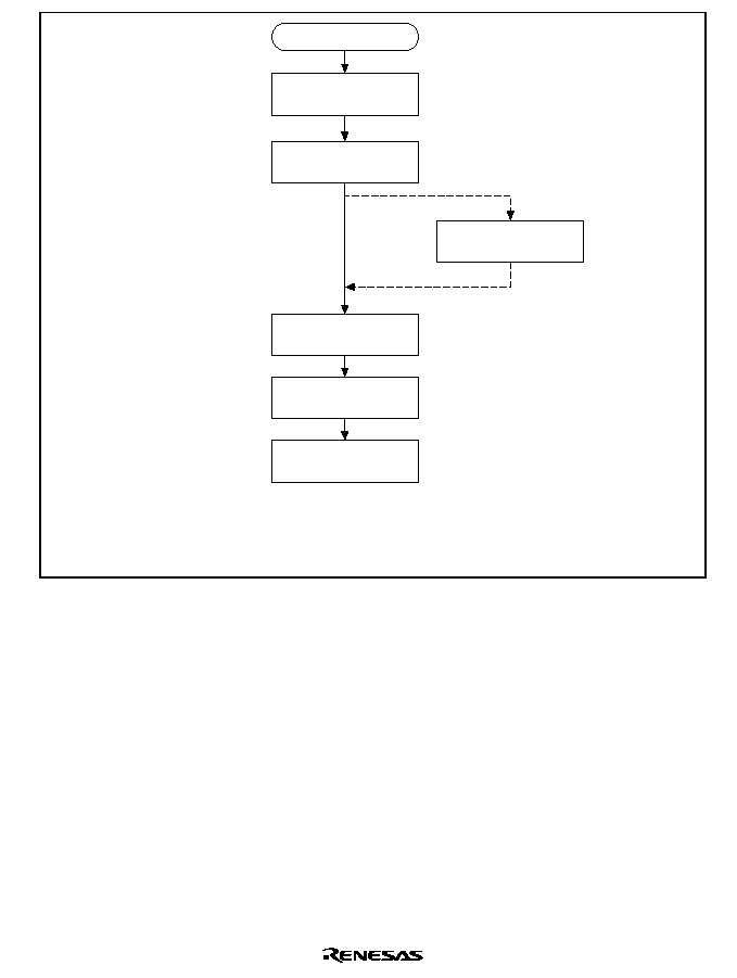
Rev. 5.0, 09/03, page 445 of 806
Select operation
Select counter
clock
Set underflow
interrupt generation
Set timer constant
register
Initialize timer
counter
Start counting
(1)
(2)
(4)
(5)
(6)
Set interrupt
generation
When using input
capture function
(3)
Note: When an interrupt has been generated, clear the flag in the interrupt handler that
caused it. If interrupts are enabled without clearing the flag, another interrupt will be
generated.
Figure 13.2 Setting the Count Operation
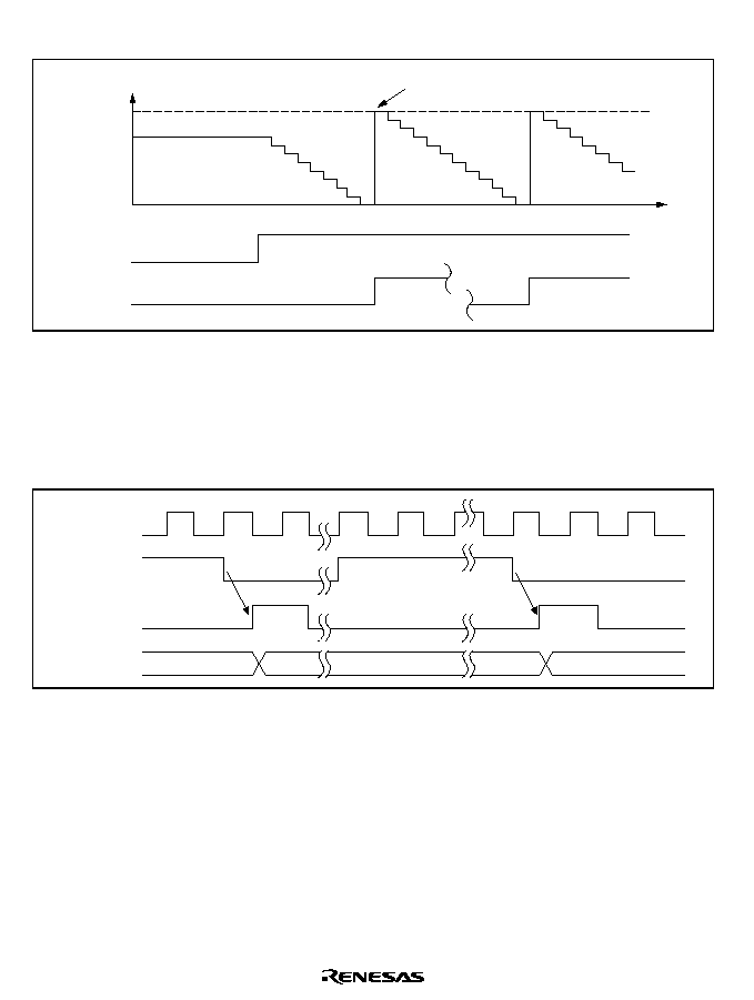
Rev. 5.0, 09/03, page 446 of 806
Auto-Reload Count Operation: Figure 13.3 shows the TCNT auto-reload operation.
TCNT value
TCOR
H'00000000
STR0
-STR2
UNF
TCOR value set to
TCNT during underflow
Time
Figure 13.3 Auto-Reload Count Operation
TCNT Count Timing:
∑
Internal Clock Operation: Set the TPSC2≠TPSC0 bits in TCR to select whether peripheral
module clock P
or one of the four internal clocks created by dividing it is used (P
/4, P
/16,
P
/64, P
/256). Figure 13.4 shows the timing.
P
Internal
clock
TCNT
input clock
TCNT
N + 1
N
N
- 1
Figure 13.4 Count Timing when Operating on Internal Clock
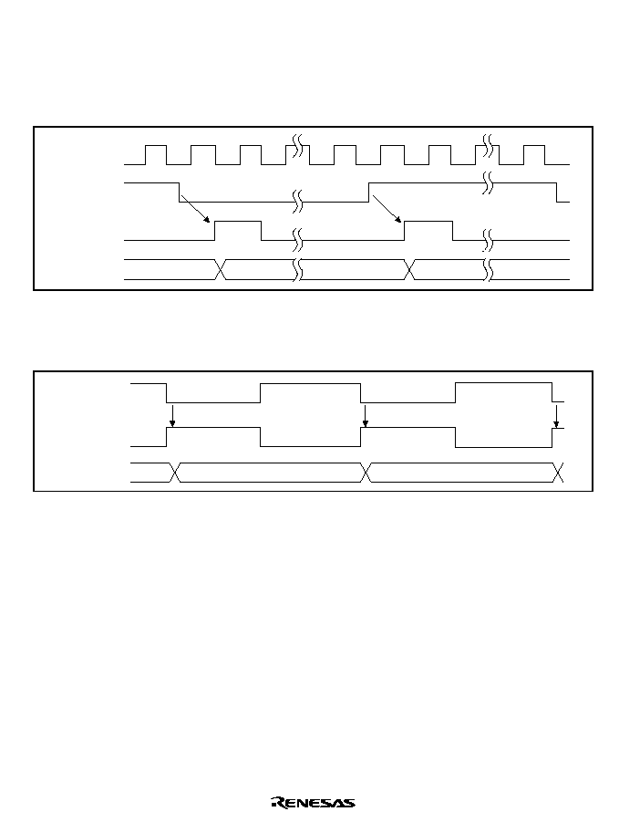
Rev. 5.0, 09/03, page 447 of 806
∑
External Clock Operation: Set the TPSC2≠TPSC0 bits in TCR to select the external clock
(TCLK) as the timer clock. Use the CKEG1 and CKEG0 bits in TCR to select the detection
edge. Rising, falling, or both edges may be selected. The pulse width of the external clock
must be at least 1.5 peripheral module clock cycles for single edges or 2.5 peripheral module
clock cycles for both edges. A shorter pulse width will result in accurate operation. Figure 13.5
shows the timing for both-edge detection.
P
External
clock input
pin
TCNT
input clock
TCNT
N + 1
N
N
- 1
Figure 13.5 Count Timing when Operating on External Clock (Both Edges Detected)
∑
On-Chip RTC Clock Operation: Set the TPSC2≠TPSC0 bits in TCR to select the on-chip RTC
clock as the timer clock. Figure 13.6 shows the timing.
RTC output
clock
TCNT
TCNT input
clock
N + 1
N
N
- 1
Figure 13.6 Count Timing when Operating on On-Chip RTC Clock
Input Capture Function: Channel 2 has an input capture function (figure 13.7). When using the
input capture function, set the TCLK pin to input mode with the TCOE bit in the timer output
control register (TOCR) and set the timer operation clock to internal clock or on-chip RTC clock
with the TPCS2≠TPCS0 bits in the timer control register (TCR2). Also, designate use of the input
capture function and whether to generate interrupts on input capture with the IPCE1≠IPCE0 bits in
TCR2, and designate the use of either the rising or falling edge of the TCLK pin to set the timer
counter (TCNT2) value into the input capture register (TCPR2) with the CKEG1≠CKEG0 bits in
TCR2.
The input capture function cannot be used in standby mode.
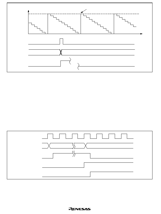
Rev. 5.0, 09/03, page 448 of 806
TCNT value
TCOR
H'00000000
TCLK
TCPR2
Set TCNT value
ICPI
TCOR value set to
TCNT during underflow
Time
Figure 13.7 Operation Timing when Using Input Capture Function
(Using TCLK Rising Edge)
13.4
Interrupts
There are two sources of TMU interrupts: underflow interrupts (TUNI) and interrupts when using
the input capture function (TICPI2).
13.4.1
Status Flag Setting Timing
UNF is set to 1 when the TCNT underflows. Figure 13.8 shows the timing.
P
TCNT
Underflow
signal
UNF
TUNI
TCOR value
H'00000000
Figure 13.8 UNF Setting Timing

Rev. 5.0, 09/03, page 449 of 806
13.4.2
Status Flag Clearing Timing
The status flag can be cleared by writing 0 from the CPU. Figure 13.9 shows the timing.
P
Peripheral address bus
UNF
TCR address
T
1
T
2
TCR write cycle
T
3
Figure 13.9 Status Flag Clearing Timing
13.4.3
Interrupt Sources and Priorities
The TMU produces underflow interrupts for each channel. When the interrupt request flag and
interrupt enable bit are both set to 1, an interrupt is requested. Codes are set in the interrupt event
registers (INTEVT, INTEVT2) for these interrupts and interrupt handling occurs according to the
codes.
The relative priorities of channels can be changed using the interrupt controller (see section 4,
Exception Handling, and section 7, Interrupt Controller (INTC)). Table 13.3 lists TMU interrupt
sources.
Table 13.3
TMU Interrupt Sources
Channel
Interrupt Source
Description
Priority
0
TUNI0
Underflow interrupt 0
High
1
TUNI1
Underflow interrupt 1
2
TUNI2
Underflow interrupt 2
2
TICPI2
Input capture interrupt 2
Low

Rev. 5.0, 09/03, page 450 of 806
13.5
Usage Notes
13.5.1
Writing to Registers
Synchronization processing is not performed for timer counting during register writes. When
writing to registers, always clear the appropriate start bits for the channel (STR2≠STR0) in the
timer start register (TSTR) to halt timer counting.
13.5.2
Reading Registers
Synchronization processing is performed for timer counting during register reads. When timer
counting and register read processing are performed simultaneously, the register value before
TCNT counting down (with synchronization processing) is read.

Rev. 5.0, 09/03, page 451 of 806
Section 14 Realtime Clock (RTC)
14.1
Overview
The SH7729R has a realtime clock (RTC) with its own 32.768-kHz crystal oscillator.
14.1.1
Features
∑
Clock and calendar functions (BCD display): Seconds, minutes, hours, date, day of the week,
month, and year
∑
1-Hz to 64-Hz timer (binary display)
∑
Start/stop function
∑
30-second adjust function
∑
Alarm interrupt: Frame comparison of seconds, minutes, hours, date, day of the week, and
month can be used as conditions for the alarm interrupt
∑
Cyclic interrupts: The interrupt cycle may be 1/256 second, 1/64 second, 1/16 second, 1/4
second, 1/2 second, 1 second, or 2 seconds
∑
Carry interrupt: A carry interrupt indicates when a carry occurs during a counter read
∑
Automatic leap year correction
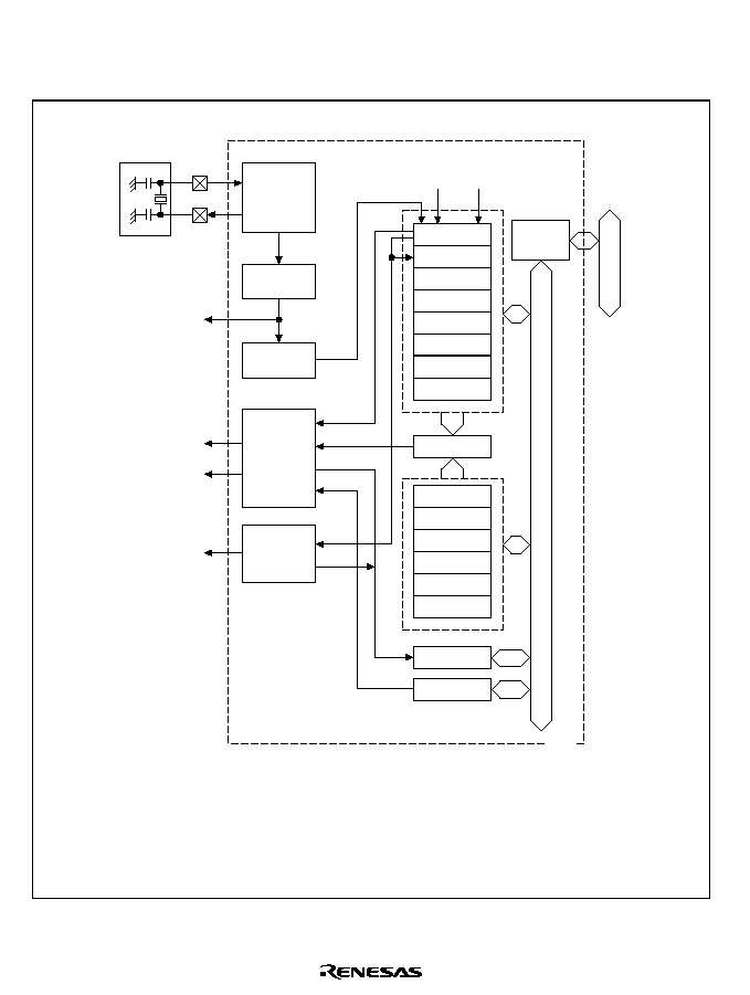
Rev. 5.0, 09/03, page 452 of 806
14.1.2
Block Diagram
Figure 14.1 shows a block diagram of the RTC.
Module bus
RTC
Internal bus
Interrupt
control
circuit
Prescaler
(
˜ 2)
RTCCLK
Bus
interface
Carry
detection
circuit
ATI
PRI
CUI
Legend
R64CNT:
64 Hz counter
RSECCNT: Second
counter
RMINCNT: Minute
counter
RHRCNT: Hour
counter
RWKCNT: Day-of-week
counter
RDAYCNT: Day
counter
RMONCNT: Month counter
RYRCNT: Year
counter
RSECAR:
Second alarm register
RMINAR:
Minute alarm register
RHRAR:
Hour alarm register
RWKAR:
Day-of-week alarm register
RDAYAR:
Day alarm register
RMONAR:
Month alarm register
RCR1:
RTC control register 1
RCR2:
RTC control register 2
R64CNT
Reset
RSECCNT
RMINCNT
RHRCNT
RWKCNT
16.384 kHz
RDAYCNT
RMONCNT
RYRCNT
Comparator
RSECAR
RMINAR
RHRAR
RWKAR
RDAYAR
RCR1
RCR2
30-
second
ADJ
EXTAL2
32.768 kHz
128 Hz
XTAL2
Externally
connected
circuit
Oscillator
circuit
Prescaler
(
˜ 128)
RMONAR
Figure 14.1 Block Diagram of RTC

Rev. 5.0, 09/03, page 453 of 806
14.1.3
Pin Configuration
Table 14.1 shows the RTC pin configuration.
Table 14.1
RTC Pins
Pin
Abbreviation
I/O
Description
RTC oscillator crystal pin
EXTAL2
I
Connects crystal to RTC oscillator
*
2
RTC oscillator crystal pin
XTAL2
O
Connects crystal to RTC oscillator
*
2
Clock input/clock output
TCLK
I/O
External clock input pin/input capture
control input pin/realtime clock (RTC)
output pin (shared by TMU)
Dedicated power-supply pin
for RTC
Vcc≠RTC
--
Dedicated power-supply pin for RTC
*
1
Dedicated GND pin for RTC
Vss≠RTC
--
Dedicated GND pin for RTC
*
1
Notes: 1. Except in hardware standby mode, power must be supplied to all power supply pins,
including these, even when only the RTC is used (including standby mode).
2. When the RTC is not used, pull EXTAL2 up (to Vcc) and make no connection for
XTAL2.

Rev. 5.0, 09/03, page 454 of 806
14.1.4
RTC Register Configuration
Table 14.2 shows the RTC register configuration.
Table 14.2
RTC Registers
Name
Abbreviation R/W
Initial Value
Address
Access Size
64-Hz counter
R64CNT
R
Undefined
H'FFFFFEC0
8
Second counter
RSECCNT
R/W
Undefined
H'FFFFFEC2
8
Minute counter
RMINCNT
R/W
Undefined
H'FFFFFEC4
8
Hour counter
RHRCNT
R/W
Undefined
H'FFFFFEC6
8
Day of week counter
RWKCNT
R/W
Undefined
H'FFFFFEC8
8
Date counter
RDAYCNT
R/W
Undefined
H'FFFFFECA
8
Month counter
RMONCNT
R/W
Undefined
H'FFFFFECC
8
Year counter
RYRCNT
R/W
Undefined
H'FFFFFECE
8
Second alarm register
RSECAR
R/W
Undefined
*
H'FFFFFED0
8
Minute alarm register
RMINAR
R/W
Undefined
*
H'FFFFFED2
8
Hour alarm register
RHRAR
R/W
Undefined
*
H'FFFFFED4
8
Day of week alarm register
RWKAR
R/W
Undefined
*
H'FFFFFED6
8
Date alarm register
RDAYAR
R/W
Undefined
*
H'FFFFFED8
8
Month alarm register
RMONAR
R/W
Undefined
*
H'FFFFFEDA
8
RTC control register 1
RCR1
R/W
H'00
H'FFFFFEDC
8
RTC control register 2
RCR2
R/W
H'09
H'FFFFFEDE
8
Note:
*
Only the ENB bits of each register are initialized.

Rev. 5.0, 09/03, page 455 of 806
14.2
RTC Registers
14.2.1
64-Hz Counter (R64CNT)
The 64-Hz counter (R64CNT) is an 8-bit read-only register that indicates the state of the RTC
divider circuit between 64 Hz and 1 Hz.
R64CNT is reset to H'00 by setting the RESET bit in RTC control register 2 (RCR2) or the ADJ
bit in RCR2 to 1.
R64CNT is not initialized by a power-on reset or manual reset, or in standby mode.
Bit 7 is always read as 0.
Bit:
7
6
5
4
3
2
1
0
--
1Hz
2Hz
4Hz
8Hz
16Hz
32Hz
64Hz
Initial value:
0
--
--
--
--
--
--
--
R/W:
R
R
R
R
R
R
R
R
14.2.2
Second Counter (RSECCNT)
The second counter (RSECCNT) is an 8-bit readable/writable register used for setting/counting in
the BCD-coded second section of the RTC. The count operation is performed by a carry for each
second of the 64
-
Hz counter.
The range that can be set is 00
≠
59 (decimal). Errant operation will result if any other value is set.
Carry out write processing after halting the count operation with the START bit in RCR2.
RSECCNT is not initialized by a power-on reset or manual reset, or in standby mode.
Bit:
7
6
5
4
3
2
1
0
--
10 seconds
1 second
Initial value:
0
--
--
--
--
--
--
--
R/W:
R
R/W
R/W
R/W
R/W
R/W
R/W
R/W

Rev. 5.0, 09/03, page 456 of 806
14.2.3
Minute Counter (RMINCNT)
The minute counter (RMINCNT) is an 8-bit readable/writable register used for setting/counting in
the BCD-coded minute section of the RTC. The count operation is performed by a carry for each
minute of the second counter.
The range that can be set is 00≠59 (decimal). Errant operation will result if any other value is set.
Carry out write processing after halting the count operation with the START bit in RCR2.
RMINCNT is not initialized by a power-on reset or manual reset, or in standby mode.
Bit:
7
6
5
4
3
2
1
0
--
10 minutes
1 minute
Initial value:
0
--
--
--
--
--
--
--
R/W:
R
R/W
R/W
R/W
R/W
R/W
R/W
R/W
14.2.4
Hour Counter (RHRCNT)
The hour counter (RHRCNT) is an 8-bit readable/writable register used for setting/counting in the
BCD-coded hour section of the RTC. The count operation is performed by a carry for each 1 hour
of the minute counter.
The range that can be set is 00
≠
23 (decimal). Errant operation will result if any other value is set.
Carry out write processing after halting the count operation with the START bit in RCR2 or using
a carry flag as shown in figure 14.2.
RHRCNT is not initialized by a power-on reset or manual reset, or in standby mode.
Bit:
7
6
5
4
3
2
1
0
--
--
10 hours
1 hour
Initial value:
0
0
--
--
--
--
--
--
R/W:
R
R
R/W
R/W
R/W
R/W
R/W
R/W
Rev. 5.0, 09/03, page 457 of 806
14.2.5
Day of Week Counter (RWKCNT)
The day of week counter (RWKCNT) is an 8-bit readable/writable register used for
setting/counting in the BCD-coded day of week section of the RTC. The count operation is
performed by a carry for each day of the date counter.
The range that can be set is 0
≠
6 (decimal). Errant operation will result if any other value is set.
Carry out write processing after halting the count operation with the START bit in RCR2.
RWKCNT is not initialized by a power-on reset or manual reset, or in standby mode.
Bit:
7
6
5
4
3
2
1
0
--
--
--
--
--
Day of week
Initial value:
0
0
0
0
0
--
--
--
R/W:
R
R
R
R
R
R/W
R/W
R/W
Days of the week are coded as shown in table 14.3.
Table 14.3
Day-of-Week Codes (RWKCNT)
Day of Week
Code
Sunday
0
Monday
1
Tuesday
2
Wednesday
3
Thursday
4
Friday
5
Saturday
6

Rev. 5.0, 09/03, page 458 of 806
14.2.6
Date Counter (RDAYCNT)
The date counter (RDAYCNT) is an 8-bit readable/writable register used for setting/counting in
the BCD-coded date section of the RTC. The count operation is performed by a carry for each day
of the hour counter.
The range that can be set is 01
≠
31 (decimal). Errant operation will result if any other value is set.
Carry out write processing after halting the count operation with the START bit in RCR2.
RDAYCNT is not initialized by a power-on reset or manual reset, or in standby mode.
The RDAYCNT range that can be set changes with each month and in leap years. Please confirm
the correct setting.
Bit:
7
6
5
4
3
2
1
0
--
--
10 days
1 day
Initial value:
0
0
--
--
--
--
--
--
R/W:
R
R
R/W
R/W
R/W
R/W
R/W
R/W
14.2.7
Month Counter (RMONCNT)
The month counter (RMONCNT) is an 8-bit readable/writable register used for setting/counting in
the BCD-coded month section of the RTC. The count operation is performed by a carry for each
month of the date counter.
The range that can be set is 00
≠
12 (decimal). Errant operation will result if any other value is set.
Carry out write processing after halting the count operation with the START bit in RCR2.
RMONCNT is not initialized by a power-on reset or manual reset, or in standby mode.
Bit:
7
6
5
4
3
2
1
0
--
--
--
10
months
1 month
Initial value:
0
0
0
--
--
--
--
--
R/W:
R
R
R
R/W
R/W
R/W
R/W
R/W

Rev. 5.0, 09/03, page 459 of 806
14.2.8
Year Counter (RYRCNT)
The year counter (RYRCNT) is an 8-bit readable/writable register used for setting/counting in the
BCD-coded year section of the RTC. The least significant 2 digits of the western calendar year are
displayed. The count operation is performed by a carry for each year of the month counter.
The range that can be set is 00
≠
99 (decimal). Errant operation will result if any other value is set.
Carry out write processing after halting the count operation with the START bit in RCR2.
RYRCNT is not initialized by a power-on reset or manual reset, or in standby mode.
Leap years are recognized by dividing the year counter value by 4 and obtaining a fractional result
of 0.
Bit:
7
6
5
4
3
2
1
0
10 years
1 year
Initial value:
--
--
--
--
--
--
--
--
R/W:
R/W
R/W
R/W
R/W
R/W
R/W
R/W
R/W
14.2.9
Second Alarm Register (RSECAR)
The second alarm register (RSECAR) is an 8-bit readable/writable register, and an alarm register
corresponding to the BCD-coded second section counter RSECCNT of the RTC. When the ENB
bit is set to 1, a comparison with the RSECCNT value is performed. From among the
RSECAR/RMINAR/RHRAR/RWKAR/RDAYAR/RMONAR registers, the counter and alarm
register comparison is performed only on those with ENB bits set to 1, and if each of those
coincide, an RTC alarm interrupt is generated.
The range that can be set is 00
≠
59 (decimal) + ENB bit. Errant operation will result if any other
value is set.
The ENB bit in RSECAR is initialized to 0 by a power-on reset. The remaining RSECAR fields
are not initialized by a power-on reset or manual reset, or in standby mode.
Bit:
7
6
5
4
3
2
1
0
ENB
10 seconds
1 second
Initial value:
0
--
--
--
--
--
--
--
R/W:
R/W
R/W
R/W
R/W
R/W
R/W
R/W
R/W

Rev. 5.0, 09/03, page 460 of 806
14.2.10
Minute Alarm Register (RMINAR)
The minute alarm register (RMINAR) is an 8-bit readable/writable register, and an alarm register
corresponding to the BCD-coded minute section counter RMINCNT of the RTC. When the ENB
bit is set to 1, a comparison with the RMINCNT value is performed. From among the
RSECAR/RMINAR/RHRAR/RWKAR/RDAYAR/RMONAR registers, the counter and alarm
register comparison is performed only on those with ENB bits set to 1, and if each of those
coincide, an RTC alarm interrupt is generated.
The range that can be set is 00
≠
59 (decimal) + ENB bit. Errant operation will result if any other
value is set.
The ENB bit in RMINAR is initialized by a power-on reset. The remaining RMINAR fields are
not initialized by a power-on reset or manual reset, or in standby mode.
Bit:
7
6
5
4
3
2
1
0
ENB
10 minutes
1 minute
Initial value:
0
--
--
--
--
--
--
--
R/W:
R/W
R/W
R/W
R/W
R/W
R/W
R/W
R/W
14.2.11
Hour Alarm Register (RHRAR)
The hour alarm register (RHRAR) is an 8-bit readable/writable register, and an alarm register
corresponding to the BCD-coded hour section counter RHRCNT of the RTC. When the ENB bit is
set to 1, a comparison with the RHRCNT value is performed. From among the
RSECAR/RMINAR/RHRAR/RWKAR/RDAYAR/RMONAR registers, the counter and alarm
register comparison is performed only on those with ENB bits set to 1, and if each of those
coincide, an RTC alarm interrupt is generated.
The range that can be set is 00
≠
23 (decimal) + ENB bit. Errant operation will result if any other
value is set.
The ENB bit in RHRAR is initialized by a power-on reset. The remaining RHRAR fields are not
initialized by a power-on reset or manual reset, or in standby mode.
Bit:
7
6
5
4
3
2
1
0
ENB
--
10 hours
1 hour
Initial value:
0
0
--
--
--
--
--
--
R/W:
R/W
R
R/W
R/W
R/W
R/W
R/W
R/W

Rev. 5.0, 09/03, page 461 of 806
14.2.12
Day of Week Alarm Register (RWKAR)
The day of week alarm register (RWKAR) is an 8-bit readable/writable register, and an alarm
register corresponding to the BCD-coded day of week section counter RWKCNT of the RTC.
When the ENB bit is set to 1, a comparison with the RWKCNT value is performed. From among
the RSECAR/RMINAR/RHRAR/RWKAR/RDAYAR/RMONAR registers, the counter and alarm
register comparison is performed only on those with ENB bits set to 1, and if each of those
coincide, an RTC alarm interrupt is generated.
The range that can be set is 0
≠
6 (decimal) + ENB bit. Errant operation will result if any other
value is set.
The ENB bit in RWKAR is initialized by a power-on reset. The remaining RWKAR fields are not
initialized by a power-on reset or manual reset, or in standby mode.
Bit:
7
6
5
4
3
2
1
0
ENB
--
--
--
--
Day of week
Initial value:
0
0
0
0
0
--
--
--
R/W:
R/W
R
R
R
R
R/W
R/W
R/W
Days of the week are coded as shown in table 14.4.
Table 14.4
Day-of-Week Codes (RWKAR)
Day of Week
Code
Sunday
0
Monday
1
Tuesday
2
Wednesday
3
Thursday
4
Friday
5
Saturday
6

Rev. 5.0, 09/03, page 462 of 806
14.2.13
Date Alarm Register (RDAYAR)
The date alarm register (RDAYAR) is an 8-bit readable/writable register, and an alarm register
corresponding to the BCD-coded date section counter RDAYCNT of the RTC. When the ENB bit
is set to 1, a comparison with the RDAYCNT value is performed. From among the registers
RSECAR, RMINAR, RHRAR, RWKAR, RDAYAR, RMONAR, the counter and alarm register
comparison is performed only on those with ENB bits set to 1, and if each of those coincide, an
RTC alarm interrupt is generated.
The range that can be set is 01
≠
31 (decimal) + ENB bit. Errant operation will result if any other
value is set. The RDAYCNT range that can be set changes with some months and in leap years.
Please confirm the correct setting.
The ENB bit in RDAYAR is initialized by a power-on reset. The remaining RDAYAR fields are
not initialized by a power-on reset or manual reset, or in standby mode.
Bit:
7
6
5
4
3
2
1
0
ENB
--
10 days
1 day
Initial value:
0
0
--
--
--
--
--
--
R/W:
R/W
R
R/W
R/W
R/W
R/W
R/W
R/W
14.2.14
Month Alarm Register (RMONAR)
The month alarm register (RMONAR) is an 8-bit readable/writable register, and an alarm register
corresponding to the BCD-coded month section counter RMONCNT of the RTC. When the ENB
bit is set to 1, a comparison with the RMONCNT value is performed. From among the registers
RSECAR, RMINAR, RHRAR, RWKAR, RDAYAR, RMONAR, the counter and alarm register
comparison is performed only on those with ENB bits set to 1, and if each of those coincide, an
RTC alarm interrupt is generated.
The range that can be set is 01
≠
12 (decimal) + ENB bit. Errant operation will result if any other
value is set.
The ENB bit in RMONAR is initialized by a power-on reset. The remaining RMONAR fields are
not initialized by a power-on reset or manual reset, or in standby mode.
Bit:
7
6
5
4
3
2
1
0
ENB
--
--
10
months
1 month
Initial value:
0
0
0
--
--
--
--
--
R/W:
R/W
R
R
R/W
R/W
R/W
R/W
R/W

Rev. 5.0, 09/03, page 463 of 806
14.2.15
RTC Control Register 1 (RCR1)
The RTC control register 1 (RCR1) is an 8-bit readable/writable register that affects carry flags
and alarm flags. It also selects whether to generate interrupts for each flag. Because flags are
sometimes set after an operand read, do not use this register in read-modify-write processing.
RCR1 is initialized to H'00 by a power-on reset. In a manual reset, all bits are initialized to 0
except for the CF flag, which is undefined. When using the CF flag, it must be initialized
beforehand. This register is not initialized in standby mode.
Bit:
7
6
5
4
3
2
1
0
CF
--
--
CIE
AIE
--
--
AF
Initial value:
0
0
0
0
0
0
0
0
R/W:
R/W
R
R
R/W
R/W
R
R
R/W
Bit 7
--
Carry Flag (CF): Status flag that indicates that a carry has occurred. CF is set to 1 when a
count-up to R64CNT or RSECCNT occurs. A count register value read at this time cannot be
guaranteed; another read is required.
Bit 7: CF
Description
0
No count up of R64CNT or RSECCNT
Clearing condition: When 0 is written to CF
(Initial value)
1
Count up of R64CNT or RSECCNT
Setting condition: When 1 is written to CF
Bits 6, 5, 2, and 1
--
Reserved: These bits are always read as 0. The write value should always be
0.
Bit 4
--
Carry Interrupt Enable Flag (CIE): When the carry flag (CF) is set to 1, the CIE bit
enables interrupts.
Bit 4: CIE
Description
0
A carry interrupt is not generated when the CF flag is set to 1
(Initial value)
1
A carry interrupt is generated when the CF flag is set to 1

Rev. 5.0, 09/03, page 464 of 806
Bit 3
--
Alarm Interrupt Enable Flag (AIE): When the alarm flag (AF) is set to 1, the AIE bit
allows interrupts.
Bit 3: AIE
Description
0
An alarm interrupt is not generated when the AF flag is set to 1
(Initial value)
1
An alarm interrupt is generated when the AF flag is set to 1
Bit 0
--
Alarm Flag (AF): The AF flag is set to 1 when the alarm time set in an alarm register
(only registers with ENB bit set to 1) matches the clock and calendar time. This flag is cleared to
0 when 0 is written, but holds its previous value when 1 is written.
Bit 0: AF
Description
0
Clock/calendar and alarm register have not matched since last reset to 0
Clearing condition: When 0 is written to AF
(Initial value)
1
Setting condition: Clock/calendar and alarm register have matched (only
registers with ENB set)
*
Note:
*
Contents do not change when 1 is written to AF.
14.2.16
RTC Control Register 2 (RCR2)
The RTC control register 2 (RCR2) is an 8-bit readable/writable register for periodic interrupt
control, 30-second adjustment ADJ, divider circuit RESET, and RTC count start/stop control. It is
initialized to H'09 by a power-on reset. It is initialized except for RTCEN and START by a
manual reset. It is not initialized, and retains its contents, in standby mode.
Bit:
7
6
5
4
3
2
1
0
PEF
PES2
PES1
PES0
RTCEN
ADJ
RESET
START
Initial value:
0
0
0
0
1
0
0
1
R/W:
R/W
R/W
R/W
R/W
R/W
R/W
R/W
R/W
Bit 7
--
Periodic Interrupt Flag (PEF): Indicates interrupt generation with the period designated
by the PES bits. When set to 1, PEF generates periodic interrupts.
Bit 7: PEF
Description
0
Interrupts not generated with the period designated by the PES bits
Clearing condition: When 0 is written to PEF
(Initial value)
1
Interrupts generated with the period designated by the PES bits
Setting condition: When 1 is written to PEF

Rev. 5.0, 09/03, page 465 of 806
Bits 6 to 4--Periodic Interrupt Flags (PES2-PES0): Specify the periodic interrupt.
Bit 6: PES2
Bit 5: PES1
Bit 4: PES0
Description
0
0
0
No periodic interrupts generated (Initial value)
1
Periodic interrupt generated every 1/256 second
1
0
Periodic interrupt generated every 1/64 second
1
Periodic interrupt generated every 1/16 second
1
0
0
Periodic interrupt generated every 1/4 second
1
Periodic interrupt generated every 1/2 second
1
0
Periodic interrupt generated every 1 second
1
Periodic interrupt generated every 2 seconds
Bit 3
--
RTCEN: Controls the operation of the crystal oscillator for the RTC.
Bit 3: RTCEN
Description
0
Crystal oscillator for RTC is halted
1
Crystal oscillator for RTC runs
(Initial value)
Bit 2
--
30
Second Adjustment (ADJ): When 1 is written to the ADJ bit, times of 29 seconds or
less will be rounded to 00 seconds and 30 seconds or more to 1 minute. The divider circuit will be
simultaneously reset. This bit is always read as 0. The maximum duration between when the ADJ
bit is set to 1 and when the new setting is reflected in the readout value from the seconds counter
(RSECCNT) is approximately 91.6 µs (when a 32.768 kHz quartz oscillator is connected to the
EXTAL2 pin).
Bit 2: ADJ
Description
0
Runs normally
(Initial value)
1 (Write)
30-second adjustment
Bit 1
--
Reset (RESET): When 1 is written, initializes the divider circuit (RTC prescaler and
R64CNT). This bit is always read as 0.
Bit 1: RESET
Description
0
Runs normally
(Initial value)
1 (Write)
Divider circuit is reset
Rev. 5.0, 09/03, page 466 of 806
Bit 0
--
Start Bit (START): Halts and restarts the counter (clock).
Bit 0: START
Description
0
Second/minute/hour/day/week/month/year counter halts
*
1
Second/minute/hour/day/week/month/year counter runs normally
*
(Initial value)
Note:
*
The 64-Hz counter always runs unless stopped with the RTCEN bit.
14.3
RTC Operation
14.3.1
Initial Settings of Registers after Power-On
All the registers should be set after the power is turned on.
14.3.2
Setting the Time
Figure 14.2 shows how to set the time when the clock is stopped. This works when the entire
calendar or clock is to be set.
Write 1 to RESET and 0 to
START in the RCR2 register
Order is irrelevant
Write 1 to START in the
RCR2 register
Set seconds, minutes,
hour, day, day of the
week, month and year
Stop clock,
reset divider circuit
To reset the divider circuit (RTC prescaler
and R64CNT) and set the counter
Start clock
Figure 14.2 Setting the Time
Rev. 5.0, 09/03, page 467 of 806
14.3.3
Reading the Time
Figure 14.3 shows how to read the time. If a carry occurs while reading the time, the correct time
will not be obtained, so it must be read again. Part (a) in figure 14.3 shows the method of reading
the time without using interrupts; part (b) in figure 14.3 shows the method using carry interrupts.
To keep programming simple, method (a) should normally be used.
Write 0 to CIE in RCR1
Note: Set AF to 1 so that alarm
flag is not cleared.
Read RCR1 and check CF
Write 0 to CIE in RCR1
Carry flag = 1?
No
Yes
Clear the carry flag
Disable the carry
interrupt
Read counter
register
Write 1 to CIE in RCR1,
and write 0 to CF in RCR1
Note: Set AF in RCR1 to 1 so that
alarm flag is not cleared.
Interrupt
generated?
No
Yes
Enable the carry
interrupt
Clear the carry flag
Disable the carry
interrupt
Read counter
register
To read the time
without using interrupts
b. To use interrupts
a.
Figure 14.3 Reading the Time
Rev. 5.0, 09/03, page 468 of 806
14.3.4
Alarm Function
Figure 14.4 shows how to use the alarm function.
Alarms can be generated using seconds, minutes, hours, day of the week, date, month, or any
combination of these. Set the ENB bit (bit 7) to 1 in the register to which the alarm applies, and
then set the alarm time in the lower bits. Clear the ENB bit to 0 in registers to which the alarm
does not apply.
When the clock and alarm times match, 1 is set in the AF bit (bit 0) in RCR1. Alarm detection can
be checked by reading this bit, but normally it is done by interrupt. If 1 is placed in the AIE bit (bit
3) in RCR1, an interrupt is generated when an alarm occurs.
When using interrupts, the interrupt
enable bit (bit 3 of RCR1) is 1.
Clock running
Set alarm time
Set whether to use
alarm interrupt
Always set, since the flag may have been
set while the alarm time was being set.
Write 0 to bit 0 of RCR1 to clear it.
Clear alarm flag
Monitor alarm time
(wait for interrupt or
check alarm flag)
Figure 14.4 Using the Alarm Function

Rev. 5.0, 09/03, page 469 of 806
14.3.5
Crystal Oscillator Circuit
Crystal oscillator circuit constants (recommended values) are shown in table 14.5, and the RTC
crystal oscillator circuit in figure 14.5.
Table 14.5
Recommended Oscillator Circuit Constants (Recommended Values)
fosc
Cin
Cout
32.768 kHz
10 to 22 pF
10 to 22 pF
SH7729R
EXTAL2
XTAL2
XTAL
C
in
C
out
R
f
R
D
Notes: 1. Select either the C
in
or C
out
side for the frequency adjustment variable capacitor
according to requirements such as frequency range, degree of stability, etc.
2. Built-in resistance value R
f
(Typ value) = 10 M
, R
D
(Typ value) = 400 k
3. C
in
and C
out
values include floating capacitance due to the wiring. Take care
when using a ground plane.
4. The crystal oscillation settling time depends on the mounted circuit constants,
floating capacitance, etc., and should be decided after consultation with the
crystal resonator manufacturer.
5. Place the crystal resonator and load capacitors C
in
and C
out
as close as possible
to the chip.
(Correct oscillation may not be possible if there is externally induced noise in the
EXTAL2 and XTAL2 pins.)
6. Ensure that the crystal resonator connection pin (EXTAL2, XTAL2) wiring is
routed as far away as possible from other power lines (except GND) and signal
lines.
Figure 14.5 Example of Crystal Oscillator Circuit Connection

Rev. 5.0, 09/03, page 470 of 806
14.4
Usage Notes
14.4.1
Register Writing during RTC Count
The following RTC registers cannot be written to during an RTC count (while bit 0 = 1 in RCR2).
RSECCNT, RMINCNT, RHRCNT, RDAYCNT, RWKCNT, RMONCNT, RYRCNT
The RTC count must be halted before writing to any of the above registers.
14.4.2
Use of Realtime Clock (RTC) Periodic Interrupts
The method of using the periodic interrupt function is shown in figure 14.6.
A periodic interrupt can be generated periodically at the interval set by the periodic interrupt
enable flag (PES) in RTC control register 2 (RCR2). When the time set by the periodic interrupt
enable flag (PES) has elapsed, the periodic interrupt flag (PEF) is set to 1.
The periodic interrupt flag (PEF) is cleared to 0 upon periodic interrupt generation when the
periodic interrupt enable flag (PES) is set. Periodic interrupt generation can be confirmed by
reading this bit, but normally the interrupt function is used.
Set PES, and clear PEF to 0,
in RCR2
Clear PEF to 0
Set PES, clear PEF
Elapse of time set by PES
Clear PEF
Figure 14.6 Using Periodic Interrupt Function
14.4.3
Precautions when Using RTC Module Standby
Before switching the RTC to module standby, access at least one among the registers RTC, SCI,
and TMU.

Rev. 5.0, 09/03, page 471 of 806
Section 15 Serial Communication Interface (SCI)
15.1
Overview
The SH7729R has an on-chip serial communication interface (SCI) that supports both
asynchronous and clock synchronous serial communication. It also has a multiprocessor
communication function for serial communication among two or more processors. The SCI
supports a smart card interface, which is a serial communication feature for IC card interfaces that
conforms to the ISO/IEC standard 7816-3 for identification cards. See section 16, Smart Card
Interface, for more information.
15.1.1
Features
Selection of asynchronous or synchronous as the serial communication mode.
∑
Asynchronous mode:
Serial data communication is synchronized by start-stop in character units. The SCI can
communicate with a universal asynchronous receiver/transmitter (UART), an asynchronous
communication interface adapter (ACIA), or any other communications chip that employs
a standard asynchronous serial system. It can also communicate with two or more other
processors using the multiprocessor communication function. There are 12 selectable serial
data communication formats.
Data length: 7 or 8 bits
Stop bit length: 1 or 2 bits
Parity: Even, odd, or none
Multiprocessor bit: 1 or 0
Receive error detection: Parity, overrun, and framing errors
Break detection: By reading the RxD level directly from the SC port data register (SCPDR)
when a framing error occurs
∑
Synchronous mode:
Serial data communication is synchronized with a clock signal. The SCI can communicate
with other chips having a synchronous communication function. There is one serial data
communication format.
Data length: 8 bits
Receive error detection: Overrun errors
∑
Full duplex communication: The transmitting and receiving sections are independent, so the
SCI can transmit and receive simultaneously. Both sections use double buffering, so
continuous data transfer is possible in both the transmit and receive directions.
∑
On-chip baud rate generator with selectable bit rates
Rev. 5.0, 09/03, page 472 of 806
∑
Internal or external transmit/receive clock source: From either baud rate generator (internal) or
SCK pin (external)
∑
Four types of interrupts: Transmit-data-empty, transmit-end, receive-data-full, and receive-
error interrupts are requested independently.
∑
When the SCI is not in use, it can be stopped by halting the clock supplied to it, saving power.
15.1.2
Block Diagram
Figure 15.1 shows a block diagram of the SCI.
RxD
TxD
SCK
SCI
SCBRR
SCSSR
SCSCR
SCTSR
SCRDR
SCRSR
SCSMR
SCPCR
SCPDR
Parity generation
Parity check
Clock
External clock
Module data bus
Internal
data bus
P
P
/4
P
/16
P
/64
TXI
TEI
RXI
ERI
Bus interface
Baud rate
generator
Transmit/
receive
control
SCRSR:
SCRDR:
SCTSR:
SCTDR:
SCSMR:
Legend
Receive shift register
Receive data register
Transmit shift register
Transmit data register
Serial mode register
SCSCR:
SCSSR:
SCBRR:
SCPDR:
SCPCR:
Serial control register
Serial status register
Bit rate register
SC port data register
SC port control register
SCTDR
Figure 15.1 Block Diagram of SCI
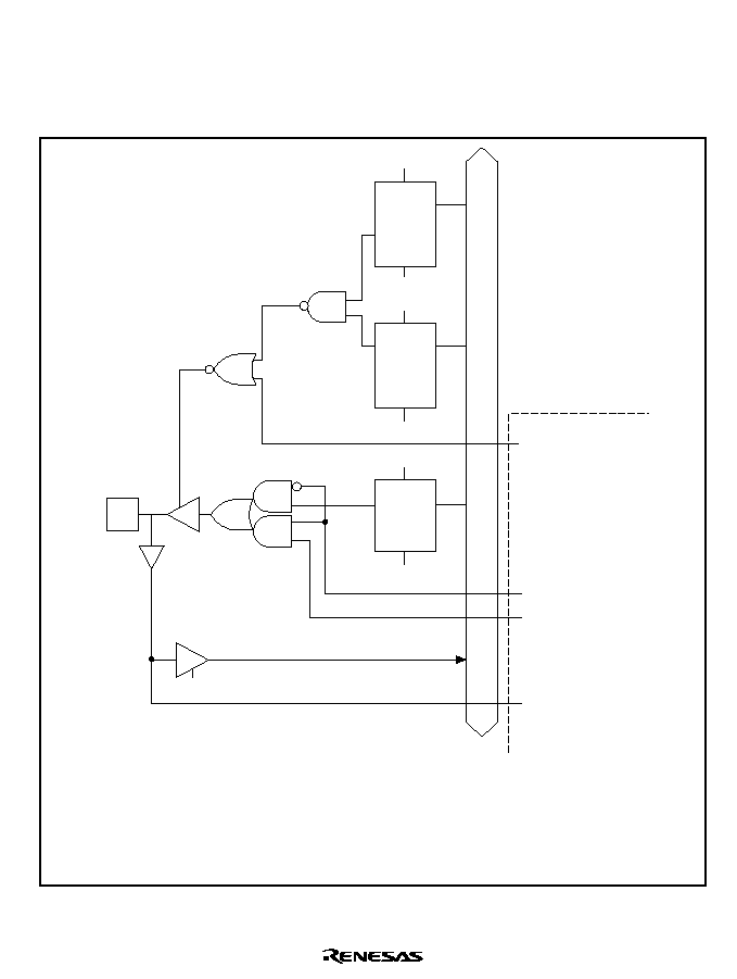
Rev. 5.0, 09/03, page 473 of 806
Figures 15.2, 15.3, and 15.4 show block diagrams of the SCI I/O port pins.
SCIF pin I/O and data control is performed by bits 11 to 8 of SCPCR and bits 5 and 4 of SCPDR.
For details, see section 15.2.8, SC Port Control Register (SCPCR)/SC Port Data Register
(SCPDR).
Internal data bus
Output enable
Clock input enable
SCI
Serial clock output
Serial clock input
R
SCP1MD0
PCRW
Reset
C
Q
Q
D
R
SCP1MD1
PCRW
Reset
C
Q
D
R
SCP1DT1
PDRW
Reset
SCPT[1]/SCK0
C
D
PDRW: SCPDR write
PDRR:
PCRW:
SCPDR read
SCPCR write
PDRR*
Note:
*
Legend
When reading the SCK0 pin, clear the C/
A bit in SCSMR and the CKE1 and CKE0
bits in SCSCR to 0, and set the SCP1MD1 bit in SCPCR to 1 (see section 15.2.8,
SC Port Control Register (SCPCR)/SC Port Data Register (SCPDR)).
Figure 15.2 SCPT[1]/SCK0 Pin
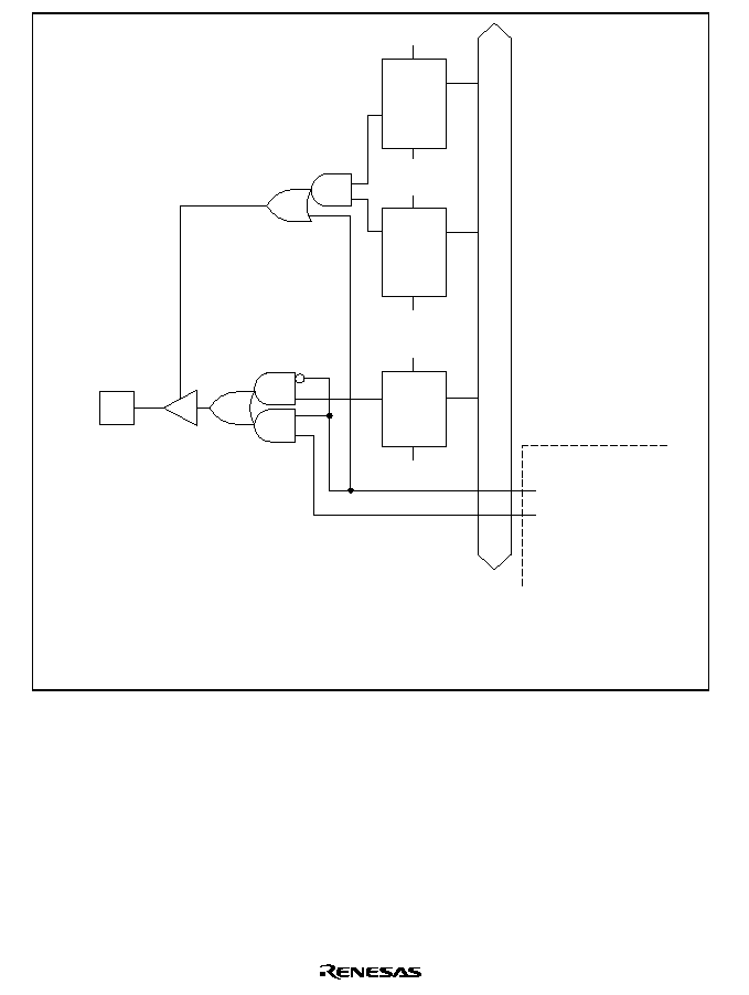
Rev. 5.0, 09/03, page 474 of 806
Internal data bus
Output enable
SCI
Serial
transmission
output
R
SCP0MD0
PCRW
Reset
C
Q
Q
D
R
SCP0MD1
PCRW
Reset
C
Q
D
R
SCP0DT1
PDRW
Reset
SCPT[0]/TxD0
C
D
PCRW:
PDRW:
SCPCR write
SCPDR write
Legend
Figure 15.3 SCPT[0]/TxD0 Pin
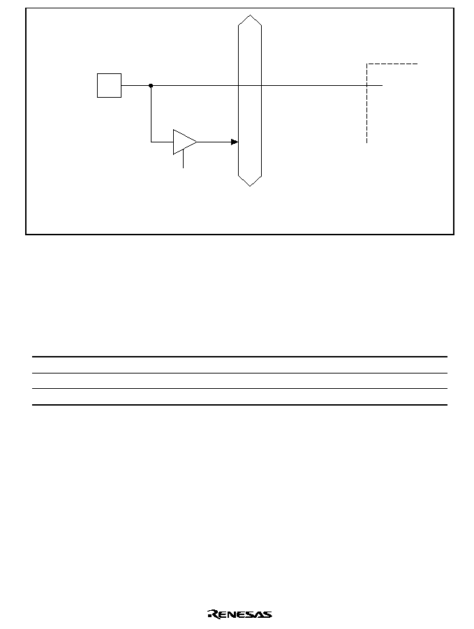
Rev. 5.0, 09/03, page 475 of 806
SCI
Serial
receive
data
Internal data bus
PDRR*
SCPT[0]/RxD0
PDRR: PDR read
Note:
* When reading the RxD0 pin, set the RE bit in SCSCR to 1.
Legend
Figure 15.4 SCPT[0]/RxD0 Pin
15.1.3
Pin Configuration
The SCI has the serial pins summarized in table 15.1.
Table 15.1
SCI Pins
Pin Name
Abbreviation
I/O
Function
Serial clock pin
SCK0
I/O
Clock I/O
Receive data pin
RxD0
Input
Receive data input
Transmit data pin
TxD0
Output
Transmit data output
Note:
These pins are made to function as serial pins by performing SCI operation settings with the
TE, RE, CKEI, and CKEO bits in SCSCR and the C/
A
bit in SCSMR. Break state
transmission and detection can be performed by means of the SCI's SCSPTR register.

Rev. 5.0, 09/03, page 476 of 806
15.1.4
Register Configuration
Table 15.2 summarizes the SCI internal registers. These registers select the communication mode
(asynchronous or synchronous), specify the data format and bit rate, and control the transmitter
and receiver sections.
Table 15.2
SCI Registers
Name
Abbreviation
R/W
Initial Value
Address
Access size
Serial mode register
SCSMR
R/W
H'00
H'FFFFFE80
8
Bit rate register
SCBRR
R/W
H'FF
H'FFFFFE82
8
Serial control register
SCSCR
R/W
H'00
H'FFFFFE84
8
Transmit data register
SCTDR
R/W
H'FF
H'FFFFFE86
8
Serial status register
SCSSR
R/(W)
*
1
H'84
H'FFFFFE88
8
Receive data register
SCRDR
R
H'00
H'FFFFFE8A
8
SC port data register
SCPDR
R/W
H'00
H'04000136
(H'A4000136)
*
2
8
SC port control register
SCPCR
R/W
H'A888
H'04000116
(H'A4000116)
*
2
16
Notes: These registers are located in area 1 of physical space. Therefore, when the cache is on,
either access these registers from the P2 area of logical space or else make an appropriate
setting using the MMU so that these registers are not cached.
1. The only value that can be written is 0 to clear the flags.
2. When address translation by the MMU does not apply, the address in parentheses
should be used.
15.2
Register Descriptions
15.2.1
Receive Shift Register (SCRSR)
The receive shift register (SCRSR) receives serial data. Data input at the RxD pin is loaded into
SCRSR in the order received, LSB (bit 0) first, converting the data to parallel form. When one
byte has been received, it is automatically transferred to SCRDR. The CPU cannot read or write to
SCRSR directly.
Bit:
7
6
5
4
3
2
1
0
R/W:
--
--
--
--
--
--
--
--

Rev. 5.0, 09/03, page 477 of 806
15.2.2
Receive Data Register (SCRDR)
The receive data register (SCRDR) stores serial receive data. The SCI completes the reception of
one byte of serial data by moving the received data from the receive shift register (SCRSR) into
SCRDR for storage. SCRSR is then ready to receive the next data. This double buffering allows
the SCI to receive data continuously.
The CPU can read but not write to SCRDR. SCRDR is initialized to H'00 by a reset and in standby
or module standby mode.
Bit:
7
6
5
4
3
2
1
0
Initial value:
0
0
0
0
0
0
0
0
R/W:
R
R
R
R
R
R
R
R
15.2.3
Transmit Shift Register (SCTSR)
The transmit shift register (SCTSR) transmits serial data. The SCI loads transmit data from the
transmit data register (SCTDR) into SCTSR, then transmits the data serially from the TxD pin,
LSB (bit 0) first. After transmitting one-byte data, the SCI automatically loads the next transmit
data from SCTDR into SCTSR and starts transmitting again. If the TDRE bit in SCSSR is 1,
however, the SCI does not load the SCTDR contents into SCTSR. The CPU cannot read or write
to SCTSR directly.
Bit:
7
6
5
4
3
2
1
0
R/W:
--
--
--
--
--
--
--
--
Rev. 5.0, 09/03, page 478 of 806
15.2.4
Transmit Data Register (SCTDR)
The transmit data register (SCTDR) is an 8-bit register that stores data for serial transmission.
When the SCI detects that the transmit shift register (SCTSR) is empty, it moves transmit data
written in SCTDR into SCTSR and starts serial transmission. Continuous serial transmission is
possible by writing the next transmit data in SCTDR during serial transmission from SCTSR.
The CPU can always read and write to SCTDR. SCTDR is initialized to H'FF by a reset and in
standby or module standby mode.
Bit:
7
6
5
4
3
2
1
0
Initial value:
1
1
1
1
1
1
1
1
R/W:
R/W
R/W
R/W
R/W
R/W
R/W
R/W
R/W
15.2.5
Serial Mode Register (SCSMR)
The serial mode register (SCSMR) is an 8-bit register that specifies the SCI serial communication
format and selects the clock source for the baud rate generator.
The CPU can always read and write to SCSMR. SCSMR is initialized to H'00 by a reset and in
standby or module standby mode.
Bit:
7
6
5
4
3
2
1
0
C/
A
CHR
PE
O/
E
STOP
MP
CKS1
CKS0
Initial value:
0
0
0
0
0
0
0
0
R/W:
R/W
R/W
R/W
R/W
R/W
R/W
R/W
R/W
Bit 7--Communication Mode (C/
A
A
A
A): Selects whether the SCI operates in asynchronous or
synchronous mode.
Bit 7: C/
A
A
A
A
Description
0
Asynchronous mode
(Initial value)
1
Synchronous mode

Rev. 5.0, 09/03, page 479 of 806
Bit 6--Character Length (CHR): Selects 7-bit or 8-bit data in asynchronous mode. In the
synchronous mode, the data length is always eight bits, regardless of the CHR setting.
Bit 6: CHR
Description
0
8-bit data
(Initial value)
1
7-bit data
When 7-bit data is selected, the MSB (bit 7) of the transmit data register is not
transmitted.
Bit 5--Parity Enable (PE): Selects whether to add a parity bit to transmit data and to check the
parity of receive data, in asynchronous mode. In synchronous mode, a parity bit is neither added
nor checked, regardless of the PE setting.
Bit 5: PE
Description
0
Parity bit not added or checked
(Initial value)
1
Parity bit added and checked
When PE is set to 1, an even or odd parity bit is added to transmit data,
depending on the parity mode (O/
E
) setting. Receive data parity is checked
according to the even/odd (O/
E
) mode setting.
Bit 4--Parity Mode (O/
E
E
E
E): Selects even or odd parity when parity bits are added and checked.
The O/
E setting is used only in asynchronous mode and only when the parity enable bit (PE) is set
to 1 to enable parity addition and checking. The O/
E setting is ignored in synchronous mode, or in
asynchronous mode when parity addition and checking is disabled.
Bit 4: O/
E
E
E
E
Description
0
Even parity
(Initial value)
If even parity is selected, the parity bit is added to transmit data to make an even
number of 1s in the transmitted character and parity bit combined. Receive data
is checked to see if it has an even number of 1s in the received character and
parity bit combined.
1
Odd parity
If odd parity is selected, the parity bit is added to transmit data to make an odd
number of 1s in the transmitted character and parity bit combined. Receive data
is checked to see if it has an odd number of 1s in the received character and
parity bit combined.

Rev. 5.0, 09/03, page 480 of 806
Bit 3--Stop Bit Length (STOP): Selects one or two bits as the stop bit length in asynchronous
mode. This setting is used only in asynchronous mode. It is ignored in synchronous mode because
no stop bits are added.
When receiving, only the first stop bit is checked, regardless of the STOP bit setting. If the second
stop bit is 1, it is treated as a stop bit, but if the second stop bit is 0, it is treated as the start bit of
the next incoming character.
Bit 3: STOP
Description
0
One stop bit
(Initial value)
When transmitting, a single 1-bit is added at the end of each transmitted
character.
1
Two stop bits
When transmitting, two 1-bits are added at the end of each transmitted character.
Bit 2--Multiprocessor Mode (MP): Selects multiprocessor format. When multiprocessor format
is selected, settings of the parity enable (PE) and parity mode (O/
E) bits are ignored. The MP bit
setting is used only in asynchronous mode; it is ignored in synchronous mode. For the
multiprocessor communication function, see section 15.3.3, Multiprocessor Communication.
Bit 2: MP
Description
0
Multiprocessor function disabled
(Initial value)
1
Multiprocessor format selected
Bits 1 and 0--Clock Select 1 and 0 (CKS1, CKS0): Select the internal clock source of the on-
chip baud rate generator. Four clock sources are available. P
, P
/4, P
/16, and P
/64. For further
information on the clock source, bit rate register settings, and baud rate, see section 15.2.9, Bit
Rate Register (SCBRR).
Bit 1: CKS1
Bit 0: CKS0
Description
0
0
P
(Initial value)
1
P
/4
1
0
P
/16
1
P
/64
Note:
P
: Peripheral clock

Rev. 5.0, 09/03, page 481 of 806
15.2.6
Serial Control Register (SCSCR)
The serial control register (SCSCR) operates the SCI transmitter/receiver, selects the serial clock
output in asynchronous mode, enables/disables interrupt requests, and selects the transmit/receive
clock source. The CPU can always read and write to SCSCR. SCSCR is initialized to H'00 by a
reset and in standby or module standby mode.
Bit:
7
6
5
4
3
2
1
0
TIE
RIE
TE
RE
MPIE
TEIE
CKE1
CKE0
Initial value:
0
0
0
0
0
0
0
0
R/W:
R/W
R/W
R/W
R/W
R/W
R/W
R/W
R/W
Bit 7--Transmit Interrupt Enable (TIE): Enables or disables the transmit-data-empty interrupt
(TXI) requested when the transmit data register empty bit (TDRE) in the serial status register
(SCSSR) is set to 1 due to transfer of serial transmit data from SCTDR to SCTSR.
Bit 7: TIE
Description
0
Transmit-data-empty interrupt request (TXI) is disabled
(Initial value)
The TXI interrupt request can be cleared by reading TDRE after it has been set
to 1, then clearing TDRE to 0, or by clearing TIE to 0.
1
Transmit-data-empty interrupt request (TXI) is enabled
Bit 6--Receive Interrupt Enable (RIE): Enables or disables the receive-data-full interrupt (RXI)
requested when the receive data register full bit (RDRF) in the serial status register (SCSSR) is set
to 1 due to transfer of serial receive data from SCRSR to SCRDR. It also enables or disables
receive-error interrupt (ERI) requests.
Bit 6: RIE
Description
0
Receive-data-full interrupt (RXI) and receive-error interrupt (ERI) requests are
disabled
(Initial value)
RXI and ERI interrupt requests can be cleared by reading the RDRF flag or error
flag (FER, PER, or ORER) after it has been set to 1, then clearing the flag to 0, or
by clearing RIE to 0.
1
Receive-data-full interrupt (RXI) and receive-error interrupt (ERI) requests are
enabled

Rev. 5.0, 09/03, page 482 of 806
Bit 5--Transmit Enable (TE): Enables or disables the SCI serial transmitter.
Bit 5: TE
Description
0
Transmitter disabled
(Initial value)
The transmit data register empty bit (TDRE) in the serial status register (SCSSR)
is fixed at 1.
1
Transmitter enabled
Serial transmission starts when the transmit data register empty (TDRE) bit in the
serial status register (SCSSR) is cleared to 0 after writing of transmit data into the
SCTDR. Select the transmit format in SCSMR before setting TE to 1.
Bit 4--Receive Enable (RE): Enables or disables the SCI serial receiver.
Bit 4: RE
Description
0
Receiver disabled
(Initial value)
Clearing RE to 0 does not affect the receive flags (RDRF, FER, PER, ORER).
These flags retain their previous values.
1
Receiver enabled
Serial reception starts when a start bit is detected in asynchronous mode, or
synchronous clock input is detected in synchronous mode. Select the receive
format in SCSMR before setting RE to 1.
Bit 3--Multiprocessor Interrupt Enable (MPIE): Enables or disables multiprocessor interrupts.
The MPIE setting is used only in asynchronous mode, and only if the multiprocessor mode bit
(MP) in the serial mode register (SCSMR) is set to 1 during reception. The MPIE setting is
ignored in synchronous mode or when the MP bit is cleared to 0.
Bit 3: MPIE
Description
0
Multiprocessor interrupts are disabled (normal receive operation)
(Initial value)
MPE is cleared to 0 when MPIE is cleared to 0, or the multiprocessor bit (MPB) is
set to 1 in receive data.
1
Multiprocessor interrupts are enabled
Receive-data-full interrupt requests (RXI), receive-error interrupt requests (ERI),
and setting of the RDRF, FER, and ORER status flags in the serial status register
(SCSSR) are disabled until data with a multiprocessor bit of 1 is received.
The SCI does not transfer receive data from SCRSR to SCRDR, does not detect
receive errors, and does not set the RDRF, FER, and ORER flags in the serial
status register (SCSSR). When it receives data that includes MPB
=
1, the
SCSSR's MPB flag is set to 1, and the SCI automatically clears MPIE to 0,
generates RXI and ERI interrupts (if the TIE and RIE bits in the SCSCR are set to
1), and allows the FER and ORER bits to be set.

Rev. 5.0, 09/03, page 483 of 806
Bit 2--Transmit-End Interrupt Enable (TEIE): Enables or disables the transmit-end interrupt
(TEI) requested if SCTDR does not contain new transmit data when the MSB is transmitted.
Bit 2: TEIE
Description
0
Transmit-end interrupt (TEI) requests are disabled
*
(Initial value)
1
Transmit-end interrupt (TEI) requests are enabled
*
Note:
*
The TEI request can be cleared by reading the TDRE bit in the serial status register
(SCSSR) after it has been set to 1, then clearing TDRE to 0 and clearing the transmit end
(TEND) bit to 0, or by clearing the TEIE bit to 0.
Bits 1 and 0--Clock Enable 1 and 0 (CKE1, CKE0): Select the SCI clock source and enable or
disable clock output from the SCK pin. Depending on the combination of CKE1 and CKE0, the
SCK pin can be used for serial clock output or serial clock input.
The CKE0 setting is valid only in asynchronous mode, and only when the SCI is internally
clocked (CKE1
=
0). The CKE0 setting is ignored in synchronous mode, or when an external
clock source is selected (CKE1
=
1). Before selecting the SCI operating mode in the serial mode
register (SCSMR), set CKE1 and CKE0. For further details on selection of the SCI clock source,
see table 15.10 in section 15.3, Operation.
Bit 1:
CKE1
Bit 0:
CKE0
Description
0
0
Asynchronous mode
Internal clock, SCK pin used for input pin (input
signal is ignored)
(Initial value)
Synchronous mode
Internal clock, SCK pin used for serial clock output
(Initial value)
1
Asynchronous mode
Internal clock, SCK pin used for clock output
*
1
Synchronous mode
Internal clock, SCK pin used for serial clock output
1
0
Asynchronous mode
External clock, SCK pin used for clock input
*
2
Synchronous mode
External clock, SCK pin used for serial clock input
1
Asynchronous mode
External clock, SCK pin used for clock input
*
2
Synchronous mode
External clock, SCK pin used for serial clock input
Notes: 1. The output clock frequency is the same as the bit rate.
2. The input clock frequency is 16 times the bit rate.

Rev. 5.0, 09/03, page 484 of 806
15.2.7
Serial Status Register (SCSSR)
The serial status register (SCSSR) is an 8-bit register containing multiprocessor bit values, and
status flags that indicate the SCI operating state.
The CPU can always read and write to SCSSR, but cannot write 1 to the status flags (TDRE,
RDRF, ORER, PER, and FER). These flags can be cleared to 0 only if they have first been read
(after being set to 1). Bits 2 (TEND) and 1 (MPB) are read-only bits that cannot be written.
SCSSR is initialized to H'84 by a reset and in standby or module standby mode.
Bit:
7
6
5
4
3
2
1
0
TDRE
RDRF
ORER
FER
PER
TEND
MPB
MPBT
Initial value:
1
0
0
0
0
1
0
0
R/W:
R/(W)
*
R/(W)
*
R/(W)
*
R/(W)
*
R/(W)
*
R
R
R/W
Note:
*
The only value that can be written is 0 to clear the flag.
Bit 7--Transmit Data Register Empty (TDRE): Indicates that the SCI has loaded transmit data
from SCTDR into SCTSR and new serial transmit data can be written in SCTDR.
Bit 7: TDRE
Description
0
SCTDR contains valid transmit data
TDRE is cleared to 0 when software reads TDRE after it has been set to 1, then
writes 0 in TDRE or data is written in SCTDR.
1
SCTDR does not contain valid transmit data
(Initial value)
TDRE is set to 1 when the chip is reset or enters standby mode, the TE bit in the
serial control register (SCSCR) is cleared to 0, or SCTDR contents are loaded
into SCTSR, so new data can be written in SCTDR.
Bit 6--Receive Data Register Full (RDRF): Indicates that SCRDR contains received data.
Bit 6: RDRF
Description
0
SCRDR does not contain valid receive data
(Initial value)
RDRF is cleared to 0 when the chip is reset or enters standby mode, or software
reads RDRF after it has been set to 1, then writes 0 in RDRF.
1
SCRDR contains valid receive data
RDRF is set to 1 when serial data is received normally and transferred from
SCRSR to SCRDR.
Note:
SCRDR and RDRF are not affected by detection of receive errors or by clearing of the RE
bit to 0 in the serial control register. They retain their previous contents. If RDRF is still set
to 1 when reception of the next data ends, an overrun error (ORER) occurs and the receive
data is lost.

Rev. 5.0, 09/03, page 485 of 806
Bit 5--Overrun Error (ORER): Indicates that data reception aborted due to an overrun error.
Bit 5: ORER
Description
0
Receiving is in progress or has ended normally
*
1
(Initial value)
ORER is cleared to 0 when the chip is reset or enters standby mode, or when
software reads ORER after it has been set to 1, then writes 0 to ORER.
1
A receive overrun error occurred
*
2
ORER is set to 1 if reception of the next serial data ends when RDRF is set to 1.
Notes: 1. Clearing the RE bit to 0 in the serial control register does not affect the ORER bit, which
retains its previous value.
2. SCRDR continues to hold the data received before the overrun error, so subsequent
receive data is lost. Serial receiving cannot continue while ORER is set to 1. In
synchronous mode, serial transmitting is also disabled.
Bit 4--Framing Error (FER): Indicates that data reception aborted due to a framing error in
asynchronous mode.
Bit 4: FER
Description
0
Receiving is in progress or has ended normally
(Initial value)
Clearing the RE bit to 0 in the serial control register does not affect the FER bit,
which retains its previous value.
FER is cleared to 0 when the chip is reset or enters standby mode, or when
software reads FER after it has been set to 1, then writes 0 to FER.
1
A receive framing error occurred
When the stop bit length is two bits, only the first bit is checked. The second stop
bit is not checked. When a framing error occurs, the SCI transfers the receive
data into SCRDR but does not set RDRF. Serial receiving cannot continue while
FER is set to 1. In synchronous mode, serial transmitting is also disabled.
FER is set to 1 if the stop bit at the end of receive data is checked and found to
be 0.

Rev. 5.0, 09/03, page 486 of 806
Bit 3--Parity Error (PER): Indicates that data reception (with parity) aborted due to a parity
error in asynchronous mode.
Bit 3: PER
Description
0
Receiving is in progress or has ended normally
(Initial value)
Clearing the RE bit to 0 in the serial control register does not affect the PER bit,
which retains its previous value.
PER is cleared to 0 when the chip is reset or enters standby mode, or when
software reads PER after it has been set to 1, then writes 0 to PER.
1
A receive parity error occurred
When a parity error occurs, the SCI transfers the receive data into SCRDR but
does not set RDRF. Serial receiving cannot continue while PER is set to 1. In
synchronous mode, serial transmitting is also disabled.
PER is set to 1 if the number of 1s in receive data, including the parity bit, does
not match the even or odd parity setting of the parity mode bit (O/
E
) in the serial
mode register (SCSMR).
Bit 2--Transmit End (TEND): Indicates that when the last bit of a serial character was
transmitted, SCTDR did not contain valid data, so transmission has ended. TEND is a read-only
bit and cannot be written to.
Bit 2: TEND
Description
0
Transmission is in progress
TEND is cleared to 0 when software reads TDRE after it has been set to 1, then
writes 0 to TDRE.
1
End of transmission
(Initial value)
TEND is set to 1 when the chip is reset or enters standby mode, when TE is
cleared to 0 in the serial control register (SCSCR), or if TDRE is 1 when the last
bit of a one-byte serial character is transmitted.
Bit 1--Multiprocessor Bit (MPB): Stores the value of the multiprocessor bit in receive data
when a multiprocessor format is selected for receiving in asynchronous mode. MPB is a read-only
bit and cannot be written to.
Bit 1: MPB
Description
0
Multiprocessor bit value in receive data is 0
(Initial value)
If RE is cleared to 0 when a multiprocessor format is selected, MPB retains its
previous value.
1
Multiprocessor bit value in receive data is 1

Rev. 5.0, 09/03, page 487 of 806
Bit 0--Multiprocessor Bit Transfer (MPBT): Stores the value of the multiprocessor bit added to
transmit data when a multiprocessor format is selected for transmitting in asynchronous mode.
The MPBT setting is ignored in synchronous mode, when a multiprocessor format is not selected,
or when the SCI is not transmitting.
Bit 0: MPBT
Description
0
Multiprocessor bit value in transmit data is 0
(Initial value)
1
Multiprocessor bit value in transmit data is 1
15.2.8
SC Port Control Register (SCPCR)/SC Port Data Register (SCPDR)
The SC port control register (SCPCR) and SC port data register (SCPDR) control I/O and data for
the port pins multiplexed with the serial communication interface (SCI) pins.
SCPCR settings are used to perform I/O control, to enable data written in SCPDR to be output to
the TxD pin, and input data to be read from the RxD pin, and to control serial
transmission/reception breaks.
It is also possible to read data on the SCK pin, and write output data.
SCPCR
Bit:
15
14
13
12
11
10
9
8
7
6
5
4
3
2
1
0
SCP7
MD1
SCP7
MD0
SCP6
MD1
SCP6
MD0
SCP5
MD1
SCP5
MD0
SCP4
MD1
SCP4
MD0
SCP3
MD1
SCP3
MD0
SCP2
MD1
SCP2
MD0
SCP1
MD1
SCP1
MD0
SCP0
MD1
SCP0
MD0
Initial value:
1
0
1
0
1
0
0
0
1
0
0
0
1
0
0
0
R/W:
R/W R/W R/W R/W R/W R/W R/W R/W R/W R/W R/W R/W R/W R/W R/W R/W
SCPDR
Bit:
7
6
5
4
3
2
1
0
SCP7DT SCP6DT SCP5DT SCP4DT SCP3DT SCP2DT SCP1DT SCP0DT
Initial value:
0
0
0
0
0
0
0
0
R/W:
R
R/W
R/W
R/W
R/W
R/W
R/W
R/W
SCI pin I/O and data control are performed by bits 3≠0 of SCPCR and bits 1 and 0 of SCPDR.

Rev. 5.0, 09/03, page 488 of 806
SCPCR Bits 3 and 2--Serial Clock Port I/O (SCP1MD1, SCP1MD0): Specify serial port SCK
pin I/O. When the SCK pin is actually used as a port I/O pin, clear the C/
A bit in SCSMR and bits
CKE1 and CKE0 in SCSCR to 0.
Bit 3:
SCP1MD1
Bit 2:
SCP1MD0
Description
0
0
SCP1DT bit value is not output to SCK pin
0
1
SCP1DT bit value is output to SCK pin
1
0
SCK pin value is read from SCP1DT bit
1
1
(Initial values: 1 and 0)
SCPDR Bit 1--Serial Clock Port Data (SCP1DT): Specifies the serial port SCK pin I/O data.
Input or output is specified by the SCP1MD0 and SCP1MD1 bits. In output mode, the value of
the SCP1DT bit is output to the SCK pin. In output mode, the SCK pin value is read from the
SCP1DT bit.
Bit 1:
SCP1DT
Description
0
I/O data is low
(Initial value)
1
I/O data is high
SCPCR Bits 1 and 0--Serial Port Break I/O (SCP0MD1, SCP0MD0): Specify the serial port
TxD pin output condition. When the TxD pin is actually used as a port output pin and outputs the
value set with the SCP0DT bit, clear the TE bit in SCSCR to 0.
Bit 1:
SCP0MD1
Bit 0:
SCP0MD0
Description
0
0
SCP0DT bit value is not output to TxD pin
(Initial value)
0
1
SCP0DT bit value is output to TxD pin

Rev. 5.0, 09/03, page 489 of 806
SCPDR Bit 0--Serial Port Break Data (SCP0DT): Specifies the serial port RxD pin input data
and TxD pin output data. The TxD pin output condition is specified by the SCP0MD0 and
SCP0MD1 bits. When the TxD pin is set to output mode, the value of the SCP0DT bit is output to
the TxD pin. The RxD pin value is read from the SCP0DT bit regardless of the values of the
SCP0MD0 and SCP0MD1 bits, if RE in SCSCR is set to 1. The initial value of this bit after a
power-on reset is undefined.
Bit 0:
SCP0DT
Description
0
I/O data is low
(Initial value)
1
I/O data is high
Block diagrams of the SCI I/O port pins are shown in figures 15.2, 15.3, and 15.4.
15.2.9
Bit Rate Register (SCBRR)
The bit rate register (SCBRR) is an 8-bit register that, together with the baud rate generator clock
source selected by the CKS1 and CKS0 bits in the serial mode register (SCSMR), determines the
serial transmit/receive bit rate.
The CPU can always read and write to SCBRR. SCBRR is initialized to H'FF by a reset, and in
module standby or standby mode. Each channel has independent baud rate generator control, so
different values can be set in two channels.
Bit:
7
6
5
4
3
2
1
0
Initial value:
1
1
1
1
1
1
1
1
R/W:
R/W
R/W
R/W
R/W
R/W
R/W
R/W
R/W
The SCBRR setting is calculated as follows:
Asynchronous mode: N
=
P
64
◊
2
2n ≠ 1
◊
B
◊
10
6
≠ 1
Synchronous mode: N
=
P
8
◊
2
2n ≠ 1
◊
B
◊
10
6
≠ 1
B:
Bit rate (bits/s)
N:
SCBRR setting for baud rate generator (0
N
255)
P
: Operating frequency for peripheral modules (MHz)
n:
Baud rate generator clock source (n
=
0, 1, 2, 3) (for the clock sources and values of
n, see table 15.3.)

Rev. 5.0, 09/03, page 490 of 806
Table 15.3
SCSMR Settings
SCSMR Settings
n
Clock Source
CKS1
CKS0
0
P
0
0
1
P
/4
0
1
2
P
/16
1
0
3
P
/64
1
1
Note:
The bit rate error in asynchronous is given by the following formula:
Error (
%
)
= (
P
◊
10
6
(N + 1)
◊
B
◊
64
◊
2
2n ≠ 1
) ◊
100
Table 15.4 lists examples of SCBRR settings in asynchronous mode, and table 15.5 lists examples
of SCBRR settings in synchronous mode.
Table 15.4
Bit Rates and SCBRR Settings in Asynchronous Mode
P
(MHz)
2
2.097152
2.4576
Bit Rate (bits/s) n
N
Error (
%
%
%
%
) n
N
Error (
%
%
%
%
) n
N
Error (
%
%
%
%
)
110
1
141
0.03
1
148
≠0.04
1
174
≠0.26
150
1
103
0.16
1
108
0.21
1
127
0.00
300
0
207
0.16
0
217
0.21
0
255
0.00
600
0
103
0.16
0
108
0.21
0
127
0.00
1200
0
51
0.16
0
54
≠0.70
0
63
0.00
2400
0
25
0.16
0
26
1.14
0
31
0.00
4800
0
12
0.16
0
13
≠2.48
0
15
0.00
9600
0
6
≠6.99
0
6
≠2.48
0
7
0.00
19200
0
2
8.51
0
2
13.78
0
3
0.00
31250
0
1
0.00
0
1
4.86
0
1
22.88
38400
0
1
≠18.62
0
1
≠14.67
0
1
0.00

Rev. 5.0, 09/03, page 491 of 806
P
(MHz)
3
3.6864
4
Bit Rate (bits/s) n
N
Error (
%
%
%
%
) n
N
Error (
%
%
%
%
) n
N
Error (
%
%
%
%
)
110
1
212
0.03
2
64
0.70
2
70
0.03
150
1
155
0.16
1
191
0.00
1
207
0.16
300
1
77
0.16
1
95
0.00
1
103
0.16
600
0
155
0.16
0
191
0.00
0
207
0.16
1200
0
77
0.16
0
95
0.00
0
103
0.16
2400
0
38
0.16
0
47
0.00
0
51
0.16
4800
0
19
≠2.34
0
23
0.00
0
25
0.16
9600
0
9
≠2.34
0
11
0.00
0
12
0.16
19200
0
4
≠2.34
0
5
0.00
0
6
≠6.99
31250
0
2
0.00
--
--
--
0
3
0.00
38400
--
--
--
0
2
0.00
0
2
8.51
P
(MHz)
4.9152
5
6
Bit Rate (bits/s) n
N
Error (
%
%
%
%
) n
N
Error (
%
%
%
%
) n
N
Error (
%
%
%
%
)
110
2
86
0.31
2
88
≠0.25
2
106
≠0.44
150
1
255
0.00
2
64
0.16
2
77
0.16
300
1
127
0.00
1
129
0.16
1
155
0.16
600
0
255
0.00
1
64
0.16
1
77
0.16
1200
0
127
0.00
0
129
0.16
0
155
0.16
2400
0
63
0.00
0
64
0.16
0
77
0.16
4800
0
31
0.00
0
32
≠1.36
0
38
0.16
9600
0
15
0.00
0
15
1.73
0
19
≠2.34
19200
0
7
0.00
0
7
1.73
0
9
≠2.34
31250
0
4
≠1.70
0
4
0.00
0
5
0.00
38400
0
3
0.00
0
3
1.73
0
4
≠2.34

Rev. 5.0, 09/03, page 492 of 806
P
(MHz)
6.144
7.3728
8
Bit Rate (bits/s) n
N
Error (
%
%
%
%
) n
N
Error (
%
%
%
%
) n
N
Error (
%
%
%
%
)
110
2
108
0.08
2
130
≠0.07
2
141
0.03
150
2
79
0.00
2
95
0.00
2
103
0.16
300
1
159
0.00
1
191
0.00
1
207
0.16
600
1
79
0.00
1
95
0.00
1
103
0.16
1200
0
159
0.00
0
191
0.00
0
207
0.16
2400
0
79
0.00
0
95
0.00
0
103
0.16
4800
0
39
0.00
0
47
0.00
0
51
0.16
9600
0
19
0.00
0
23
0.00
0
25
0.16
19200
0
9
0.00
0
11
0.00
0
12
0.16
31250
0
5
2.40
0
6
5.33
0
7
0.00
38400
0
4
0.00
0
5
0.00
0
6
≠6.99
P
(MHz)
9.8304
10
12
12.288
Bit Rate
(bits/s)
n
N
Error
(
%
%
%
%
)
n
N
Error
(
%
%
%
%
)
n
N
Error
(
%
%
%
%
)
n
N
Error
(
%
%
%
%
)
110
2
174
≠0.26
2
177
≠0.25
2
212
0.03
2
217
0.08
150
2
127
0.00
2
129
0.16
2
155
0.16
2
159
0.00
300
1
255
0.00
2
64
0.16
2
77
0.16
2
79
0.00
600
1
127
0.00
1
129
0.16
1
155
0.16
1
159
0.00
1200
0
255
0.00
1
64
0.16
1
77
0.16
1
79
0.00
2400
0
127
0.00
0
129
0.16
0
155
0.16
0
159
0.00
4800
0
63
0.00
0
64
0.16
0
77
0.16
0
79
0.00
9600
0
31
0.00
0
32
≠1.36
0
38
0.16
0
39
0.00
19200
0
15
0.00
0
15
1.73
0
19
0.16
0
19
0.00
31250
0
9
≠1.70
0
9
0.00
0
11
0.00
0
11
2.40
38400
0
7
0.00
0
7
1.73
0
9
≠2.34
0
9
0.00

Rev. 5.0, 09/03, page 493 of 806
P
(MHz)
14.7456
16
19.6608
20
Bit Rate
(bits/s)
n
N
Error
(
%
%
%
%
)
n
N
Error
(
%
%
%
%
)
n
N
Error
(
%
%
%
%
)
n
N
Error
(
%
%
%
%
)
110
3
64
0.70
3
70
0.03
3
86
0.31
3
88
≠0.25
150
2
191
0.00
2
207
0.16
2
255
0.00
3
64
0.16
300
2
95
0.00
2
103
0.16
2
127
0.00
2
129
0.16
600
1
191
0.00
1
207
0.16
1
255
0.00
2
64
0.16
1200
1
95
0.00
1
103
0.16
1
127
0.00
1
129
0.16
2400
0
191
0.00
0
207
0.16
0
255
0.00
1
64
0.16
4800
0
95
0.00
0
103
0.16
0
127
0.00
0
129
0.16
9600
0
47
0.00
0
51
0.16
0
63
0.00
0
64
0.16
19200
0
23
0.00
0
25
0.16
0
31
0.00
0
32
≠1.36
31250
0
14
≠1.70
0
15
0.00
0
19
≠1.70
0
19
0.00
38400
0
11
0.00
0
12
0.16
0
15
0.00
0
15
1.73
P
(MHz)
24
24.576
28.7
30
Bit Rate
(bits/s)
n
N
Error
(
%
%
%
%
)
n
N
Error
(
%
%
%
%
)
n
N
Error
(
%
%
%
%
)
n
N
Error
(
%
%
%
%
)
110
3
106
≠0.44
3
108
0.08
3
126
0.31
3
132
0.13
150
3
77
0.16
3
79
0.00
3
92
0.46
3
97
≠0.35
300
2
155
0.16
2
159
0.00
2
186
≠0.08
2
194
0.16
600
2
77
0.16
2
79
0.00
2
92
0.46
2
97
≠0.35
1200
1
155
0.16
1
159
0.00
1
186
≠0.08
1
194
0.16
2400
1
77
0.16
1
79
0.00
1
92
0.46
1
97
≠0.35
4800
0
155
0.16
0
159
0.00
0
186
≠0.08
0
194
≠1.36
9600
0
77
0.16
0
79
0.00
0
92
0.46
0
97
≠0.35
19200
0
38
0.16
0
39
0.00
0
46
≠0.61
0
48
≠0.35
31250
0
23
0.00
0
24
≠1.70
0
28
≠1.03
0
29
0.00
38400
0
19
≠2.34
0
19
0.00
0
22
1.55
0
23
1.73

Rev. 5.0, 09/03, page 494 of 806
Table 15.5
Bit Rates and SCBRR Settings in Synchronous Mode
P
(MHz)
4
8
16
28.7
30
Bit Rate
(bits/s)
n
N
n
N
n
N
n
N
n
N
110
--
--
--
--
--
--
--
--
--
--
250
2
249
3
124
3
249
--
--
--
--
500
2
124
2
249
3
124
3
223
3
233
1k
1
249
2
124
2
249
3
111
3
116
2.5k
1
99
1
199
2
99
2
178
2
187
5k
0
199
1
99
1
199
2
89
2
93
10k
0
99
0
199
1
99
1
178
1
187
25k
0
39
0
79
0
159
1
71
1
74
50k
0
19
0
39
0
79
0
143
0
149
100k
0
9
0
19
0
39
0
71
0
74
250k
0
3
0
7
0
15
--
--
0
29
500k
0
1
0
3
0
7
--
--
0
14
1M
0
0
*
0
1
0
3
--
--
--
--
2M
0
0
*
0
1
--
--
--
--
Note:
Settings with an error of 1
%
or less are recommended.
Blank: No setting possible
--:
Setting possible, but error occurs
*
:
Continuous transmit/receive operation not possible

Rev. 5.0, 09/03, page 495 of 806
Table 15.6 indicates the maximum bit rates in asynchronous mode when the baud rate generator is
used. Tables 15.7 and 15.8 list the maximum rates for external clock input.
Table 15.6
Maximum Bit Rates for Various Frequencies with Baud Rate Generator
(Asynchronous Mode)
Settings
P
(MHz)
Maximum Bit Rate (bits/s)
n
N
2
62500
0
0
2.097152
65536
0
0
2.4576
76800
0
0
3
93750
0
0
3.6864
115200
0
0
4
125000
0
0
4.9152
153600
0
0
8
250000
0
0
9.8304
307200
0
0
12
375000
0
0
14.7456
460800
0
0
16
500000
0
0
19.6608
614400
0
0
20
625000
0
0
24
750000
0
0
24.576
768000
0
0
28.7
896875
0
0
30
937500
0
0

Rev. 5.0, 09/03, page 496 of 806
Table 15.7
Maximum Bit Rates with External Clock Input (Asynchronous Mode)
P
(MHz)
External Input Clock (MHz)
Maximum Bit Rate (bits/s)
2
0.5000
31250
2.097152
0.5243
32768
2.4576
0.6144
38400
3
0.7500
46875
3.6864
0.9216
57600
4
1.0000
62500
4.9152
1.2288
76800
8
2.0000
125000
9.8304
2.4576
153600
12
3.0000
187500
14.7456
3.6864
230400
16
4.0000
250000
19.6608
4.9152
307200
20
5.0000
312500
24
6.0000
375000
24.576
6.1440
384000
28.7
7.1750
448436
30
7.5000
468750
Table 15.8
Maximum Bit Rates with External Clock Input (Synchronous Mode)
P
(MHz)
External Input Clock (MHz)
Maximum Bit Rate (bits/s)
8
1.3333
1333333.3
16
2.6667
2666666.7
24
4.0000
4000000.0
28.7
4.7833
4783333.3
30
5.0000
5000000.0

Rev. 5.0, 09/03, page 497 of 806
15.3
Operation
15.3.1
Overview
For serial communication, the SCI has an asynchronous mode in which characters are
synchronized individually, and a synchronous mode in which communication is synchronized with
clock pulses. Asynchronous/synchronous mode and the transmission format are selected in the
serial mode register (SCSMR), as shown in table 15.9. The SCI clock source is selected by the
combination of the C/
A bit in the serial mode register (SCSMR) and the CKE1 and CKE0 bits in
the serial control register (SCSCR), as shown in table 15.10.
Asynchronous Mode:
∑
Data length is selectable: 7 or 8 bits.
∑
Parity and multiprocessor bits are selectable. So is the stop bit length (1 or 2 bits). The
combination of the preceding selections constitutes the communication format and character
length.
∑
In receiving, it is possible to detect framing errors (FER), parity errors (PER), overrun errors
(ORER) and breaks.
∑
An internal or external clock can be selected as the SCI clock source.
When an internal clock is selected, the SCI operates using the on-chip baud rate generator,
and can output a serial clock signal with a frequency matching the bit rate.
When an external clock is selected, the external clock input must have a frequency 16 times
the bit rate. (The on-chip baud rate generator is not used.)
Synchronous Mode:
∑
The transmission/reception format has a fixed 8-bit data length.
∑
In receiving, it is possible to detect overrun errors (ORER).
∑
An internal or external clock can be selected as the SCI clock source.
When an internal clock is selected, the SCI operates using the on-chip baud rate generator,
and outputs a serial clock signal to external devices.
When an external clock is selected, the SCI operates on the input serial clock. The on-chip
baud rate generator is not used.

Rev. 5.0, 09/03, page 498 of 806
Table 15.9
Serial Mode Register Settings and SCI Communication Formats
SCSMR Settings
SCI Communication Format
Bit 7
C/
A
A
A
A
Bit 6
CHR
Bit 5
PE
Bit 2
MP
Bit 3
STOP
Mode
Data
Length
Parity
Bit
Multipro-
cessor Bit
Stop Bit
Length
0
0
0
0
0
8-bit
Not set
Not set
1 bit
1
2 bits
1
0
Set
1 bit
1
2 bits
1
0
0
7-bit
Not set
1 bit
1
2 bits
1
0
Set
1 bit
1
Asynchronous
2 bits
0
*
1
0
8-bit
Not set
Set
1 bit
*
1
2 bits
1
*
0
7-bit
1 bit
*
1
Asynchronous
(multiprocessor
format)
2 bits
1
*
*
*
*
Synchronous
8-bit
Not set
None
Note:
Asterisks (
*
) indicate don't care bits.
Table 15.10 SCSMR and SCSCR Settings and SCI Clock Source Selection
SCSMR
SCSCR Settings
SCI Transmit/Receive Clock
Bit 7
C/
A
A
A
A
Bit 1
CKE1
Bit 0
CKE0
Mode
Clock
Source
SCK
Pin Function
0
0
0
Internal
SCI does not use the SCK pin
1
Outputs a clock with frequency
matching the bit rate
1
0
External
1
Asynchronous
mode
Inputs a clock with frequency 16
times the bit rate
1
0
0
Internal
Outputs the serial clock
1
1
0
External
Inputs the serial clock
1
Synchronous
mode
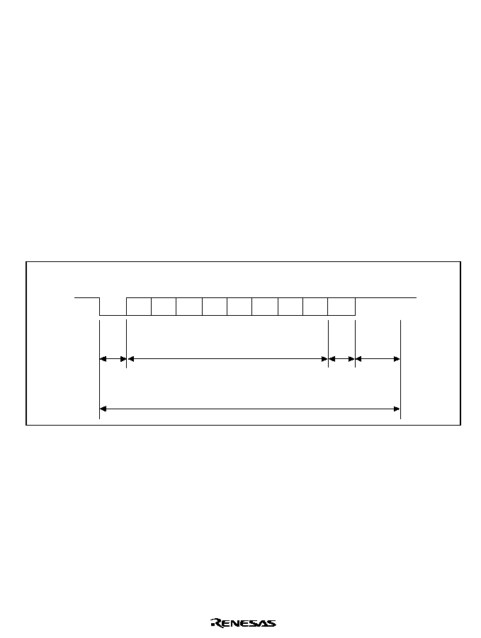
Rev. 5.0, 09/03, page 499 of 806
15.3.2
Operation in Asynchronous Mode
In asynchronous mode, each transmitted or received character begins with a start bit and ends with
a stop bit. Serial communication is synchronized one character at a time.
The transmitting and receiving sections of the SCI are independent, so full duplex communication
is possible. The transmitter and receiver are both double buffered, so data can be written and read
while transmitting and receiving are in progress, enabling continuous transmitting and receiving.
Figure 15.5 shows the general format of asynchronous serial communication. In asynchronous
serial communication, the communication line is normally held in the mark (high) state. The SCI
monitors the line and starts serial communication when the line goes to the space (low) state,
indicating a start bit. One serial character consists of a start bit (low), data (LSB first), parity bit
(high or low), and stop bit (high), in that order.
When receiving in asynchronous mode, the SCI synchronizes at the falling edge of the start bit.
The SCI samples each data bit on the eighth pulse of a clock with a frequency 16 times the bit rate.
Receive data is latched at the center of each bit.
0
D
0
D
1
D
2
D
3
D
4
D
5
D
6
D
7
1
1
0/1
1
1
(LSB)
(MSB)
Serial
data
Start
bit
1 bit
Transmit/receive data
7 or 8 bits
One unit of communication data (character or frame)
Idle (mark) state
Parity
bit
Stop
bit
1 or
no bit
1 or
2 bits
Figure 15.5 Example of Data Format in Asynchronous Communication
(8-Bit Data with Parity and Two Stop Bits)

Rev. 5.0, 09/03, page 500 of 806
Transmit/Receive Formats: Table 15.11 lists the 12 communication formats that can be selected
in asynchronous mode. The format is selected by settings in the serial mode register (SCSMR).
Table 15.11 Serial Communication Formats (Asynchronous Mode)
SCSMR Bits
Serial Transmit/Receive Format and Frame Length
CHR PE
MP
STOP
1
2
3
4
5
6
7
8
9
10
11
12
0
0
0
0
START
8-bit data
STOP
0
0
0
1
START
8-bit data
STOP STOP
0
1
0
0
START
8-bit data
P
STOP
0
1
0
1
START
8-bit data
P
STOP STOP
1
0
0
0
START
7-bit data
STOP
1
0
0
1
START
7-bit data
STOP STOP
1
1
0
0
START
7-bit data
P
STOP
1
1
0
1
START
7-bit data
P
STOP STOP
0
--
1
0
START
8-bit data
MPB
STOP
0
--
1
1
START
8-bit data
MPB
STOP STOP
1
--
1
0
START
7-bit data
MPB
STOP
1
--
1
1
START
7-bit data
MPB
STOP STOP
-- :
Don't care bits
START: Start bit
STOP: Stop bit
P:
Parity bit
MPB:
Multiprocessor bit
Clock: An internal clock generated by the on-chip baud rate generator or an external clock input
from the SCK pin can be selected as the SCI transmit/receive clock. The clock source is selected
by the C/
A bit in the serial mode register (SCSMR) and bits CKE1 and CKE0 in the serial control
register (SCSCR) (table 15.10).
When an external clock is input at the SCK pin, it must have a frequency equal to 16 times the
desired bit rate.

Rev. 5.0, 09/03, page 501 of 806
When the SCI operates on an internal clock, it can output a clock signal at the SCK pin. The
frequency of this output clock is equal to the bit rate. The phase is aligned as in figure 15.6 so that
the rising edge of the clock occurs at the center of each transmit data bit.
0
D0
D1
D2
D3
D4
D5
D6
D7
0/1
1
1
1 frame
Figure 15.6 Output Clock and Serial Data Timing (Asynchronous Mode)
Transmitting and Receiving Data (SCI Initialization (Asynchronous Mode)): Before
transmitting or receiving, clear the TE and RE bits to 0 in the serial control register (SCSCR), then
initialize the SCI as follows.
When changing the operation mode or communication format, always clear the TE and RE bits to
0 before following the procedure given below. Clearing TE to 0 sets TDRE to 1 and initializes the
transmit shift register (SCTSR). Clearing RE to 0, however, does not initialize the RDRF, PER,
FER, and ORER flags or receive data register (SCRDR), which retain their previous contents.
When an external clock is used, the clock should not be stopped during initialization or subsequent
operation. SCI operation becomes unreliable if the clock is stopped.
Figure 15.7 shows a sample flowchart for initializing the SCI. The procedure for initializing the
SCI is:
1. Select the clock source in the serial control register (SCSCR). Leave RIE, TIE, TEIE, MPIE,
TE, and RE cleared to 0. If clock output is selected in asynchronous mode, clock output starts
immediately after the setting is made in SCSCR.
2. Select the communication format in the serial mode register (SCSMR).
3. Write the value corresponding to the bit rate in the bit rate register (SCBRR) (not necessary if
an external clock is used).
4. Wait for at least the interval required to transmit or receive one bit, then set TE or RE in the
serial control register (SCSCR) to 1. Also set RIE, TIE, TEIE, and MPIE as necessary. Setting
TE or RE enables the SCI to use the TxD or RxD pin. The initial state is the mark state when
transmitting, or the idle state (waiting for a start bit) when receiving.
Rev. 5.0, 09/03, page 502 of 806
Initialization
Clear TE and RE bits in SCSCR to 0
Select communication
format in SCSMR
Set value in SCBRR
Set CKE1 and CKE0 bits in SCSCR
(TE and RE bits are 0)
Wait
Set TE and RE bits in SCSCR to 1
and set RIE, TEIE, and MPIE bits
Has a 1-bit
interval elapsed?
End
No
Yes
(1)
(2)
(3)
(4)
Note: Numbers in parentheses refer to steps in the preceding procedure description.
Figure 15.7 Sample Flowchart for SCI Initialization
Transmitting Serial Data (Asynchronous Mode): Figure 15.8 shows a sample flowchart for
transmitting serial data. The procedure for transmitting serial data is:
1. SCI status check and transmit data write: Read the serial status register (SCSSR), check that
the TDRE bit is 1, then write transmit data in the transmit data register (SCTDR) and clear
TDRE to 0.
2. To continue transmitting serial data: Read the TDRE bit to check whether it is safe to write (if
it reads 1); if so, write data in SCTDR, then clear TDRE to 0.
3. To output a break at the end of serial transmission: Set the port SC data register (SCPDR) and
port SC control register (SCPCR), then clear the TE bit to 0 in the serial control register
(SCSCR). For SCPCR and SCPDR settings, see section 15.2.8, SC Port Control Register
(SCPCR)/SC Port Data Register (SCPDR).
Rev. 5.0, 09/03, page 503 of 806
TDRE = 1?
Write transmit data to
SCTDR and clear TDRE bit in
SCSSR to 0
All data transmitted?
Yes
TEND = 1?
Read TEND bit
in SCSSR
Break output?
Yes
Clear TE bit in SCSCR to 0
End of transmission
Yes
Read TDRE bit
in SCSSR
No
No
Yes
No
No
(1)
(2)
(3)
Start of transmission
Set SCPDR and SCPCR
Note: Numbers in parentheses refer to steps in the preceding procedure description.
Figure 15.8 Sample Flowchart for Transmitting Serial Data

Rev. 5.0, 09/03, page 504 of 806
In transmitting serial data, the SCI operates as follows:
1. The SCI monitors the TDRE bit in SCSSR. When TDRE is cleared to 0, the SCI recognizes
that the transmit data register (SCTDR) contains new data, and loads this data from SCTDR
into the transmit shift register (SCTSR).
2. After loading the data from SCTDR into SCTSR, the SCI sets the TDRE bit to 1 and starts
transmitting. If the transmit-data-empty interrupt enable bit (TIE) is set to 1 in SCSCR, the SCI
requests a transmit-data-empty interrupt (TXI) at this time. Serial transmit data is transmitted
in the following order from the TxD pin:
a. Start bit: One 0 bit is output.
b. Transmit data: Seven or eight bits of data are output, LSB first.
c. Parity bit or multiprocessor bit: One parity bit (even or odd parity) or one multiprocessor
bit is output. Formats in which neither a parity bit nor a multiprocessor bit is output can
also be selected.
d. Stop bit: One or two 1-bits (stop bits) are output.
e. Marking: Output of 1-bits continues until the start bit of the next transmit data.
3. The SCI checks the TDRE bit when it outputs the stop bit. If TDRE is 0, the SCI loads new
data from SCTDR into SCTSR, outputs the stop bit, then begins serial transmission of the next
frame. If TDRE is 1, the SCI sets the TEND bit to 1 in SCSSR, outputs the stop bit, then
continues output of 1-bits (marking). If the transmit-end interrupt enable bit (TEIE) in SCSCR
is set to 1, a transmit-end interrupt (TEI) is requested.
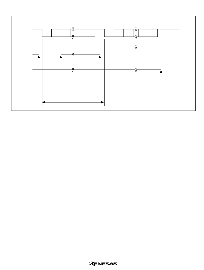
Rev. 5.0, 09/03, page 505 of 806
Figure 15.9 shows an example of SCI transmit operation in asynchronous mode.
0
1
1
1
0/1
0
1
TDRE
TEND
Parity
bit
Parity
bit
Serial
data
Start
bit
Data
Stop
bit
Start
bit
Data
Stop
bit
Idle (mark)
state
TXI interrupt
request
generated
TEI interrupt
request
generated
TXI interrupt
handler writes
data to SCTDR
and clears
TDRE bit to 0
1 frame
D
0
D
1
D
7
D
0
D
1
D
7
0/1
TXI interrupt
request
generated
Figure 15.9 Example of SCI Transmit Operation in Asynchronous Mode
(8-Bit Data with Parity and One Stop Bit)
Receiving Serial Data (Asynchronous Mode): Figure 15.10 shows a sample flowchart for
receiving serial data. The procedure for receiving serial data after enabling the SCI for reception
is:
1. Receive error handling and break detection: If a receive error occurs, read the ORER, PER and
FER bits in SCSSR to identify the error. After executing the necessary error handling, clear
ORER, PER and FER to 0. Receiving cannot resume if ORER, PER or FER remains set to 1.
When a framing error occurs, the RxD pin can be read to detect the break state.
2. SCI status check and receive-data read: Read the serial status register (SCSSR), check that
RDRF is set to 1, then read receive data from the receive data register (SCRDR) and clear
RDRF to 0. The RXI interrupt can also be used to determine if the RDRF bit has changed from
0 to 1.
3. To continue receiving serial data: Read the RDRF and SCRDR bits and clear RDRF to 0
before the stop bit of the current frame is received.
Rev. 5.0, 09/03, page 506 of 806
Start of reception
Read ORER, PER, and FER
bits in SCSSR
All data received?
End of reception
No
Yes
PER
FER ORER = 1?
RDRF = 1?
Yes
Yes
Clear RE bit in SCSCR to 0
No
No
Read RDRF bit in SCSSR
Error handling
Read receive data from SCRDR
and clear RDRF bit in SCSSR to 0
(1)
(2)
(3)
Note: Numbers in parentheses refer to steps in the preceding procedure description.
Figure 15.10 Sample Flowchart for Receiving Serial Data
Rev. 5.0, 09/03, page 507 of 806
Error handling
ORER = 1?
Overrun error handling
FER = 1?
Yes
Break?
No
Framing error handling
PER = 1?
Yes
Parity error handling
Clear ORER, PER, and
FER bits in SCSSR to 0
End
No
No
No
Yes
Yes
Clear RE bit in SCSCR to 0
Figure 15.10 Sample Flowchart for Receiving Serial Data (cont)

Rev. 5.0, 09/03, page 508 of 806
In receiving, the SCI operates as follows:
1. The SCI monitors the communication line. When it detects a start bit (0), the SCI synchronizes
internally and starts receiving.
2. Receive data is shifted into SCRSR in order from the LSB to the MSB.
3. The parity bit and stop bit are received. After receiving these bits, the SCI makes the following
checks:
a. Parity check: The number of 1s in the receive data must match the even or odd parity
setting of the O/
E bit in SCSMR.
b. Stop bit check: The stop bit value must be 1. If there are two stop bits, only the first stop bit
is checked.
c. Status check: RDRF must be 0 so that receive data can be loaded from SCRSR into
SCRDR.
If these checks all pass, the SCI sets RDRF to 1 and stores the received data in SCRDR. If
one of the checks fails (receive error), the SCI operates as indicated in table 15.12.
Note:
When a receive error flag is set, further receiving is disabled. The RDRF bit is not set to 1.
Be sure to clear the error flags.
4. After setting RDRF to 1, if the receive-data-full interrupt enable bit (RIE) is set to 1 in
SCSCR, the SCI requests a receive-data-full interrupt (RXI). If one of the error flags (ORER,
PER, or FER) is set to 1 and the receive-data-full interrupt enable bit (RIE) in SCSCR is also
set to 1, the SCI requests a receive-error interrupt (ERI).
Table 15.12 Receive Error Conditions and SCI Operation
Receive Error
Abbreviation
Condition
Data Transfer
Overrun error
ORER
Receiving of next data ends while
RDRF is still set to 1 in SCSSR
Receive data not loaded
from SCRSR into SCRDR
Framing error
FER
Stop bit is 0
Receive data loaded from
SCRSR into SCRDR
Parity error
PER
Parity of receive data differs from
even/odd parity setting in SCSMR
Receive data loaded from
SCRSR into SCRDR
Rev. 5.0, 09/03, page 509 of 806
Figure 15.11 shows an example of SCI receive operation in asynchronous mode.
RDRF
FER
ERI interrupt
request generated
by framing error
1 frame
RXI interrupt handler
reads data and clears
RDRF bit to 0
RXI interrupt
request generated
0
1
1
1
0/1
0
1
Parity
bit
Parity
bit
Serial
data
Start
bit
Data
Stop
bit
Start
bit
Data
Stop
bit
Idle (mark)
state
D
0
D
1
D
7
D
0
D
1
D
7
0/1
Figure 15.11 Example of SCI Receive Operation
(8-Bit Data with Parity and One Stop Bit)
15.3.3
Multiprocessor Communication
The multiprocessor communication function enables several processors to share a single serial
communication line. The processors communicate in asynchronous mode using a format with an
additional multiprocessor bit (multiprocessor format).
In multiprocessor communication, each receiving processor is addressed by a unique ID. A serial
communication cycle consists of an ID-sending cycle that identifies the receiving processor, and a
data-sending cycle. The multiprocessor bit distinguishes ID-sending cycles from data-sending
cycles. The transmitting processor starts by sending the ID of the receiving processor with which
it wants to communicate as data with the multiprocessor bit set to 1. Next the transmitting
processor sends transmit data with the multiprocessor bit cleared to 0.
Receiving processors skip incoming data until they receive data with the multiprocessor bit set to
1. When they receive data with the multiprocessor bit set to 1, receiving processors compare the
data with their IDs. The receiving processor with a matching ID continues to receive further
incoming data. Processors with IDs not matching the received data skip further incoming data
until they again receive data with the multiprocessor bit set to 1. Multiple processors can send and
receive data in this way.
Figure 15.12 shows an example of communication among processors using the multiprocessor
format.
Rev. 5.0, 09/03, page 510 of 806
Receiving
station A
(ID = 01)
(ID = 02)
(ID = 03)
(ID = 04)
Receiving
station B
Receiving
station C
Serial communication line
H'01
H'AA
(MPB = 0)
(MPB = 1)
ID transmit cycle:
specifies receiving station
Serial
data
Transmitting
station
Receiving
station D
Data transmit cycle:
data transmission to
receiving station specified
by ID
MPB: Multiprocessor bit
Figure 15.12 Communication Among Processors Using Multiprocessor Format
(Sending Data H'AA to Receiving Processor A)
Communication Formats: Four formats are available. Parity-bit settings are ignored when the
multiprocessor format is selected. For details see table 15.11.
Clock: See the description in the asynchronous mode section.
Transmitting Multiprocessor Serial Data: Figure 15.13 shows a sample flowchart for
transmitting multiprocessor serial data. The procedure for transmitting multiprocessor serial data
is:
1. SCI status check and transmit data write: Read the serial status register (SCSSR), check that
the TDRE bit is 1, then write transmit data in the transmit data register (SCTDR). Also set
MPBT (multiprocessor bit transfer) to 0 or 1 in SCSSR. Finally, clear TDRE to 0.
2. To continue transmitting serial data: Read the TDRE bit to check whether it is safe to write (if
it reads 1); if so, write data in SCTDR, then clear TDRE to 0.
3. To output a break at the end of serial transmission: Set the port SC data register (SCPDR) and
port SC control register (SCPCR), then clear the TE bit to 0 in the serial control register
(SCSCR). For SCPCR and SCPDR settings, see section 15.2.8, SC Port Control Register
(SCPCR)/SC Port Data Register (SCPDR).
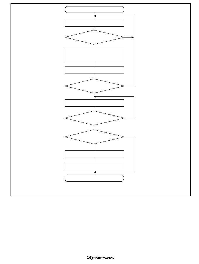
Rev. 5.0, 09/03, page 511 of 806
TDRE = 1?
Write transmit data to SCTDR
and set MPBT bit in SCSSR
Transmission ended?
Yes
TEND = 1?
Read TEND bit in SCSSR
Clear TDRE bit to 0
Break output?
Yes
Clear TE bit SCSCR to 0
End of transmission
Yes
Read TDRE bit
in SCSSR
No
No
Yes
No
No
(1)
(2)
(3)
Start of transmission
Set SCPDR and SCPCR
Note: Numbers in parentheses refer to steps in the preceding procedure description.
Figure 15.13 Sample Flowchart for Transmitting Multiprocessor Serial Data
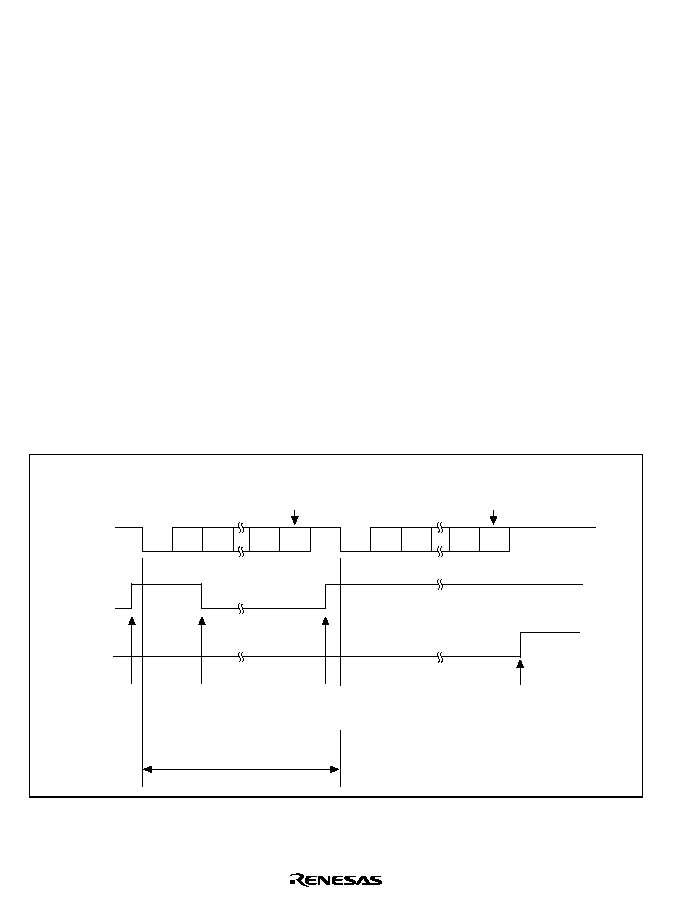
Rev. 5.0, 09/03, page 512 of 806
In transmitting serial data, the SCI operates as follows:
1. The SCI monitors the TDRE bit in SCSSR. When TDRE is cleared to 0 the SCI recognizes
that the transmit data register (SCTDR) contains new data, and loads this data from SCTDR
into the transmit shift register (SCTSR).
2. After loading the data from SCTDR into SCTSR, the SCI sets the TDRE bit to 1 and starts
transmitting. If the transmit-data-empty interrupt enable bit (TIE) in SCSCR is set to 1, the SCI
requests a transmit-data-empty interrupt (TXI) at this time. Serial transmit data is transmitted
in the following order from the TxD pin:
a. Start bit: One 0-bit is output.
b. Transmit data: Seven or eight bits are output, LSB first.
c. Multiprocessor bit: One multiprocessor bit (MPBT value) is output.
d. Stop bit: One or two 1-bits (stop bits) are output.
e. Marking: Output of 1-bits continues until the start bit of the next transmit data.
3. The SCI checks the TDRE bit when it outputs the stop bit. If TDRE is 0, the SCI loads data
from SCTDR into SCTSR, outputs the stop bit, then begins serial transmission of the next
frame. If TDRE is 1, the SCI sets the TEND bit in SCSSR to 1, outputs the stop bit, then
continues output of 1 bits in the mark state. If the transmit-end interrupt enable bit (TEIE) in
SCSCR is set to 1, a transmit-end interrupt (TEI) is requested at this time.
Figure 15.14 shows SCI transmission with a multiprocessor format.
TDRE
TEND
TXI interrupt
request
generated
TEI interrupt
request
generated
Writes data to TDR
with the TXI interrupt
processing routine
and clears TDRE
bit to 0
1 frame
0
1
1
1
0/1
0
1
Multi-
processor
bit
Serial
data
Start
bit
Data
Stop
bit
Start
bit
Data
Stop
bit
Idle (mark)
state
D
0
D
1
D
7
D
0
D
1
D
7
0/1
Multi-
processor
bit
TXI interrupt
request
generated
Figure 15.14 Example of SCI Multiprocessor Transmit Operation
(8-Bit Data with Multiprocessor Bit and One Stop Bit)

Rev. 5.0, 09/03, page 513 of 806
Receiving Multiprocessor Serial Data: Figure 15.15 shows a sample flowchart for receiving
multiprocessor serial data. The procedure for receiving multiprocessor serial data is:
1. ID receive cycle: Set the MPIE bit in the serial control register (SCSCR) to 1.
2. SCI status check and compare to ID reception: Read the serial status register (SCSSR), check
that RDRF is set to 1, then read data from the receive data register (SCRDR) and compare with
the processor's own ID. If the ID does not match the receive data, set MPIE to 1 again and
clear RDRF to 0. If the ID matches the receive data, clear RDRF to 0.
3. SCI status check and data receiving: Read SCSSR, check that RDRF is set to 1, then read data
from the receive data register (SCRDR).
4. Receive error handling and break detection: If a receive error occurs, read the ORER and FER
bits in SCSSR to identify the error. After executing the necessary error handling, clear both
ORER and FER to 0. Receiving cannot resume if ORER or FER remain set to 1. When a
framing error occurs, the RxD pin can be read to detect the break state.
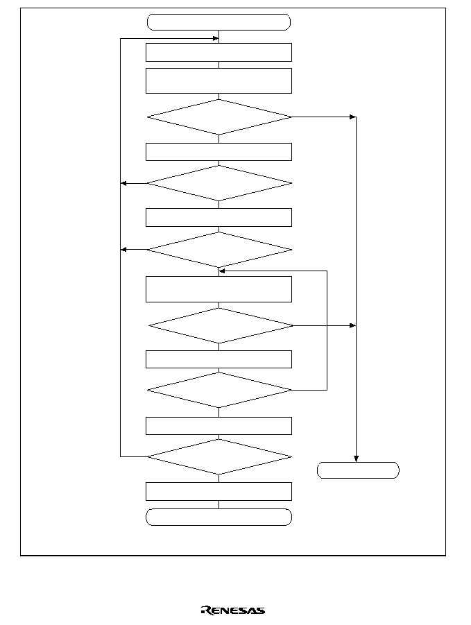
Rev. 5.0, 09/03, page 514 of 806
RDRF = 1?
FER = 1 or ORER = 1?
RDRF = 1?
All data received?
No
End of reception
Yes
Set MPIE bit
in SCSCR to 1
Read RDRF bit
in SCSSR
Clear RE bit
in SCSCR to 0
No
No
Read ORER and FER
bits in SCSSR
FER = 1 or ORER = 1?
Read RDRF bit
in SCSSR
Read receive data
from SCRDR
Is ID the
station's ID?
Yes
Read ORER and FER
bits in SSCSR
No
Error handling
Yes
Yes
Yes
No
Start of reception
No
Yes
Read receive data
from SCRDR
(1)
(2)
(4)
(3)
Note: Numbers in parentheses refer to steps in the preceding procedure description.
Figure 15.15 Sample Flowchart for Receiving Multiprocessor Serial Data
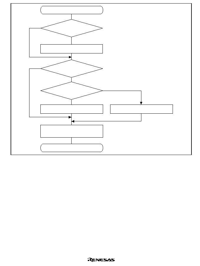
Rev. 5.0, 09/03, page 515 of 806
ORER = 1?
Break?
Yes
Framing error handling
Yes
Error handling
Overrun error handling
Yes
FER = 1?
Clear ORER and
FER bits in SCSSR to 0
End
No
No
No
Clear RE bit in SCSCR to 0
Figure 15.15 Sample Flowchart for Receiving Multiprocessor Serial Data (cont)
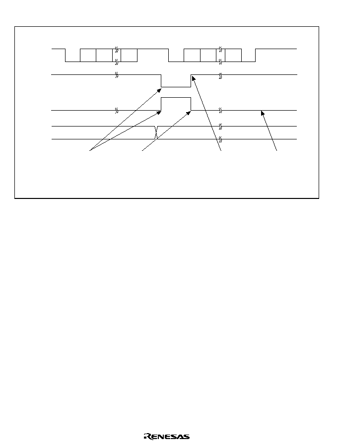
Rev. 5.0, 09/03, page 516 of 806
Figure 15.16 shows an example of SCI receive operation using a multiprocessor format.
RDRF
MPIE
RDR
value
ID1
RXI interrupt request
(multiprocessor interrupt)
generated, MPIE = 0
Example: Own ID does not match data
RXI interrupt handler
reads RDR data and
clears RDRF bit to 0
ID is not station's
ID, so MPIE bit is
set to 1 again
No RXI interrupt
generated;
RDR state
is maintained
0
1
1
1
1
0
1
Stop
bit
MPB
Serial
data
Start
bit
Data
(ID1)
Data
(data 1)
Start
bit
MPB
Stop
bit
Idle (mark)
state
D
0
D
1
D
7
D
0
D
1
D
7
0
Figure 15.16 Example of SCI Receive Operation
(8-Bit Data with Multiprocessor Bit and One Stop Bit)

Rev. 5.0, 09/03, page 517 of 806
RDRF
MPIE
RDR
value
Example: Own ID matches data
ID1
ID2
Data2
0
1
1
1
1
0
1
MPB
MPB
Serial
data
Start
bit
Data
(ID2)
Data
(Data 2)
Stop
bit
Start
bit
Stop
bit
Idle (mark)
state
D
0
D
1
D
7
D
0
D
1
D
7
0
RXI interrupt request
(multiprocessor
interrupt) generated,
MPIE = 0
RXI interrupt handler
reads RDR data and
clears RDRF bit to 0
ID is that of station,
so reception continues
unchanged and data
is received by RXI
interrupt handler
MPIE bit
set to 1
again
Figure 15.16 Example of SCI Receive Operation (cont)
(8-Bit Data with Multiprocessor Bit and One Stop Bit)
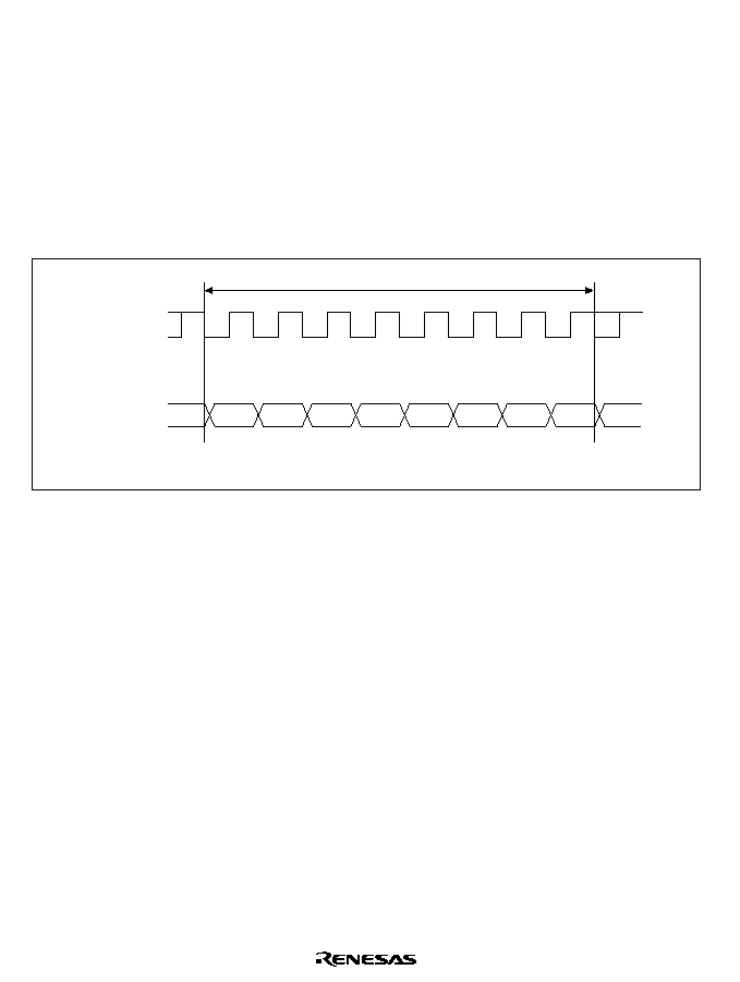
Rev. 5.0, 09/03, page 518 of 806
15.3.4
Synchronous Operation
In synchronous mode, the SCI transmits and receives data in synchronization with clock pulses.
This mode is suitable for high-speed serial communication.
The SCI transmitter and receiver are independent, so full-duplex communication is possible while
sharing the same clock. The transmitter and receiver are also double buffered, so continuous
transmitting or receiving is possible by reading or writing data while transmitting or receiving is in
progress.
Figure 15.17 shows the general format in synchronous serial communication.
Bit 0
Bit 1
Bit 2
Bit 3
Bit 4
Bit 5
Bit 6
Bit 7
LSB
MSB
Serial clock
Serial data
Don't care
Don't care
*
*
One unit of communication data (character or frame)
Note:
* High except in continuous transmitting or receiving
Figure 15.17 Data Format in Synchronous Communication
In synchronous serial communication, each data bit is output on the communication line from one
falling edge of the serial clock to the next. Data is guaranteed valid at the rising edge of the serial
clock. In each character, the serial data bits are transmitted in order from the LSB (first) to the
MSB (last). After output of the MSB, the communication line remains in the state of the MSB. In
synchronous mode, the SCI transmits or receives data by synchronizing with the falling edge of
the serial clock.
Communication Format: The data length is fixed at eight bits. No parity bit or multiprocessor bit
can be added.

Rev. 5.0, 09/03, page 519 of 806
Clock: An internal clock generated by the on-chip baud rate generator or an external clock input
from the SCK pin can be selected as the SCI transmit/receive clock. The clock source is selected
by the C/
A bit in the serial mode register (SCSMR) and bits CKE1 and CKE0 in the serial control
register (SCSCR). See table 15.10.
When the SCI operates on an internal clock, it outputs the clock signal at the SCK pin. Eight clock
pulses are output per transmitted or received character. When the SCI is not transmitting or
receiving, the clock signal remains in the high state. When only receiving, the SCI receives in 2-
character units, so a 16-pulse serial clock is output. To receive in 1-character units, select an
external clock source.
Transmitting and Receiving Data SCI Initialization (Synchronous Mode): Before
transmitting, receiving, or changing the mode or communication format, the software must clear
the TE and RE bits to 0 in the serial control register (SCSCR), then initialize the SCI. Clearing TE
to 0 sets TDRE to 1 and initializes the transmit shift register (SCTSR). Clearing RE to 0, however,
does not initialize the RDRF, PER, FER, and ORER flags and receive data register (SCRDR),
which retain their previous contents.
Figure 15.18 shows a sample flowchart for initializing the SCI. The procedure for initializing the
SCI is:
1. Select the clock source in the serial control register (SCSCR). Leave RIE , TIE, TEIE, MPIE,
TE and RE cleared to 0.
2. Select the communication format in the serial mode register (SCSMR).
3. Write the value corresponding to the bit rate in the bit rate register (SCBRR) (not necessary if
an external clock is used).
4. Wait for at least the interval required to transmit or receive one bit, then set TE or RE in the
serial control register (SCSCR) to 1. Also set RIE, TIE, TEIE and MPIE. Setting TE and RE
allows use of the TxD and RxD pins.
Rev. 5.0, 09/03, page 520 of 806
Initialization
Clear TE and RE bits in SCSCR to 0
(1)
Has a 1-bit
period elapsed?
Set TE and RE bits in SCSCR to 1
and set RIE, TIE, TEIE, and MPIE bits
Set transmit/receive format in SCSMR
Yes
No
Set value in SCBRR
Set RIE, TIE, TEIE, MPIE, CKE1,
and CKE0 bits in SCSCR
(TE and RE are 0)
End
Wait
(2)
(3)
(4)
Note: Numbers in parentheses refer to steps in the preceding procedure description.
Figure 15.18 Sample Flowchart for SCI Initialization
Transmitting Serial Data (Synchronous Mode): Figure 15.19 shows a sample flowchart for
transmitting serial data. The procedure for transmitting serial data is:
1. SCI status check and transmit data write: Read the serial status register (SCSSR), check that
the TDRE bit is 1, then write transmit data in the transmit data register (SCTDR) and clear
TDRE to 0.
2. To continue transmitting serial data: Read the TDRE bit to check whether it is safe to write (if
it reads 1); if so, write data in SCTDR, then clear TDRE to 0.
Rev. 5.0, 09/03, page 521 of 806
Start of transmission
Read TDRE bit in SCSSR
All data transmitted?
Yes
No
End of transmission
(1)
(2)
TDRE = 1?
Write transmit data to SCTDR
and clear TDRE bit in SCSSR to 0
Yes
No
Read TEND bit in SCSSR
TEND = 1?
Yes
No
Clear TE bit in SCSCR to 0
Note: Numbers in parentheses refer to steps in the preceding procedure description.
Figure 15.19 Sample Flowchart for Transmitting Serial Data
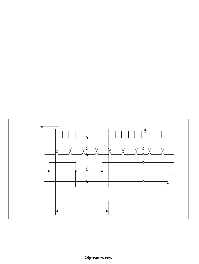
Rev. 5.0, 09/03, page 522 of 806
In transmitting serial data, the SCI operates as follows:
1. The SCI monitors the TDRE bit in SCSSR. When TDRE is cleared to 0 the SCI recognizes
that the transmit data register (SCTDR) contains new data and loads this data from SCTDR
into the transmit shift register (SCTSR).
2. After loading the data from SCTDR into SCTSR, the SCI sets the TDRE bit to 1 and starts
transmitting. If the transmit-data-empty interrupt enable bit (TIE) in SCSCR is set to 1, the SCI
requests a transmit-data-empty interrupt (TXI) at this time.
If clock output mode is selected, the SCI outputs eight synchronous clock pulses. If an external
clock source is selected, the SCI outputs data in synchronization with the input clock. Data is
output from the TxD pin in order from the LSB (bit 0) to the MSB (bit 7).
3. The SCI checks the TDRE bit when it outputs the MSB (bit 7). If TDRE is 0, the SCI loads
data from SCTDR into SCTSR, then begins serial transmission of the next frame. If TDRE is
1, the SCI sets the TEND bit in SCSSR to 1, transmits the MSB, then holds the transmit data
pin (TxD) in the MSB state. If the transmit-end interrupt enable bit (TEIE) in SCSCR is set to
1, a transmit-end interrupt (TEI) is requested at this time.
4. After the end of serial transmission, the SCK pin is held in the high state.
Figure 15.20 shows an example of SCI transmit operation.
Bit 0
Bit 1
Bit 7
Bit 0
Bit 1
Bit 6
Serial clock
Serial data
Transfer direction
Bit 7
TXI interrupt
handler writes
data to TDR and
clears TDRE
bit to 0
1 frame
TDRE
TEND
LSB
MSB
TXI interrupt
request
generated
TXI interrupt
request
generated
TEI interrupt
request
generated
Figure 15.20 Example of SCI Transmit Operation

Rev. 5.0, 09/03, page 523 of 806
Receiving Serial Data (Synchronous Mode): Figure 15.21 shows a sample flowchart for
receiving serial data. When switching from asynchronous mode to synchronous mode, make sure
that ORER, PER, and FER are cleared to 0. If PER or FER is set to 1, the RDRF bit will not be set
and both transmitting and receiving will be disabled.
The procedure for receiving serial data is:
1. Receive error handling: If a receive error occurs, read the ORER bit in SCSSR to identify the
error. After executing the necessary error handling, clear ORER to 0. Transmitting/receiving
cannot resume if ORER remains set to 1.
2. SCI status check and receive data read: Read the serial status register (SCSSR), check that
RDRF is set to 1, then read receive data from the receive data register (SCRDR) and clear
RDRF to 0. The RXI interrupt can also be used to determine if the RDRF bit has changed from
0 to 1.
3. To continue receiving serial data: Read SCRDR, and clear RDRF to 0 before the MSB (bit 7)
of the current frame is received.
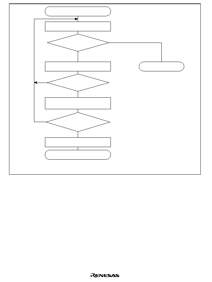
Rev. 5.0, 09/03, page 524 of 806
Read ORER bit in SCSSR
All data received?
End of reception
No
Yes
ORER = 1?
RDRF = 1?
Yes
Clear RE bit in SCSCR to 0
No
No
Read RDRF bit in SCSSR
(3)
(2)
Yes
Error handling
(1)
Read receive data from SCRDR
and clear RDRF bit in SCSSR to 0
Start of reception
Note: Numbers in parentheses refer to steps in the preceding procedure description.
Figure 15.21 Sample Flowchart for Receiving Serial Data
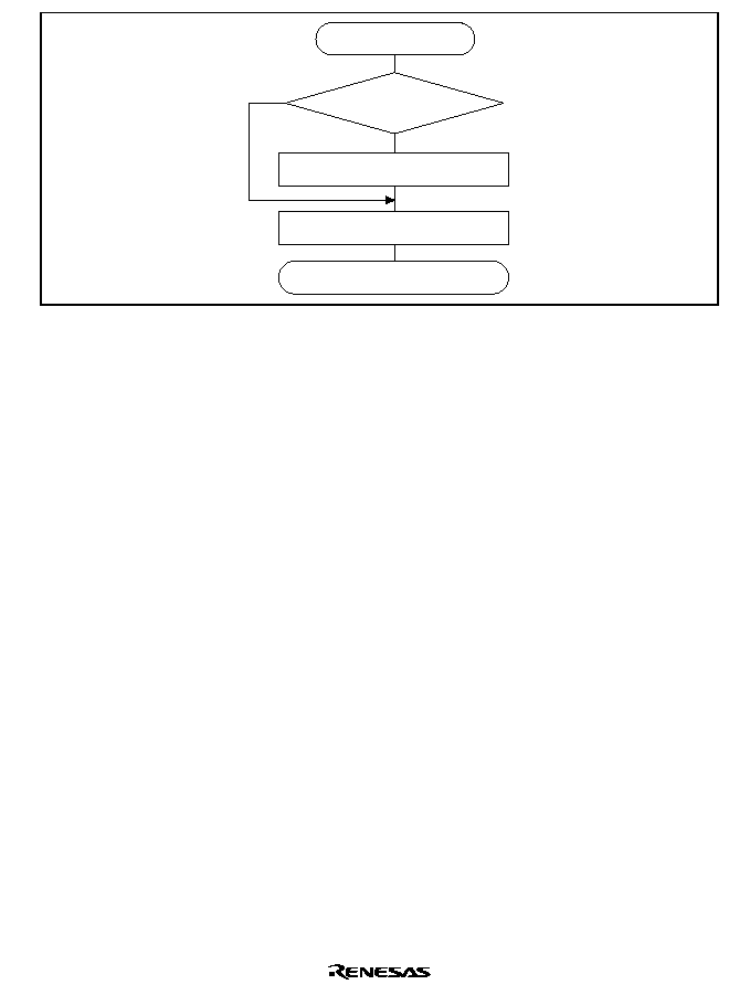
Rev. 5.0, 09/03, page 525 of 806
Error handling
End
ORER = 1?
No
Clear ORER bit in SCSSR to 0
Yes
Overrun error handling
Figure 15.21 Sample Flowchart for Receiving Serial Data (cont)
In receiving, the SCI operates as follows:
1. The SCI synchronizes with serial clock input or output and initializes internally.
2. Receive data is shifted into SCRSR in order from the LSB to the MSB. After receiving the
data, the SCI checks that RDRF is 0 so that receive data can be loaded from SCRSR into
SCRDR. If this check is passed, the SCI sets RDRF to 1 and stores the received data in
SCRDR. If the check is not passed (receive error), the SCI operates as indicated in table 15.12.
This state prevents further transmission or reception. While receiving, the RDRF bit is not set
to 1. Be sure to clear the error flag.
3. After setting RDRF to 1, if the receive-data-full interrupt enable bit (RIE) is set to 1 in
SCSCR, the SCI requests a receive-data-full interrupt (RXI). If the ORER bit is set to 1 and the
receive-data-full interrupt enable bit (RIE) in SCSCR is also set to 1, the SCI requests a
receive-error interrupt (ERI).
Figure 15.22 shows an example of SCI receive operation.
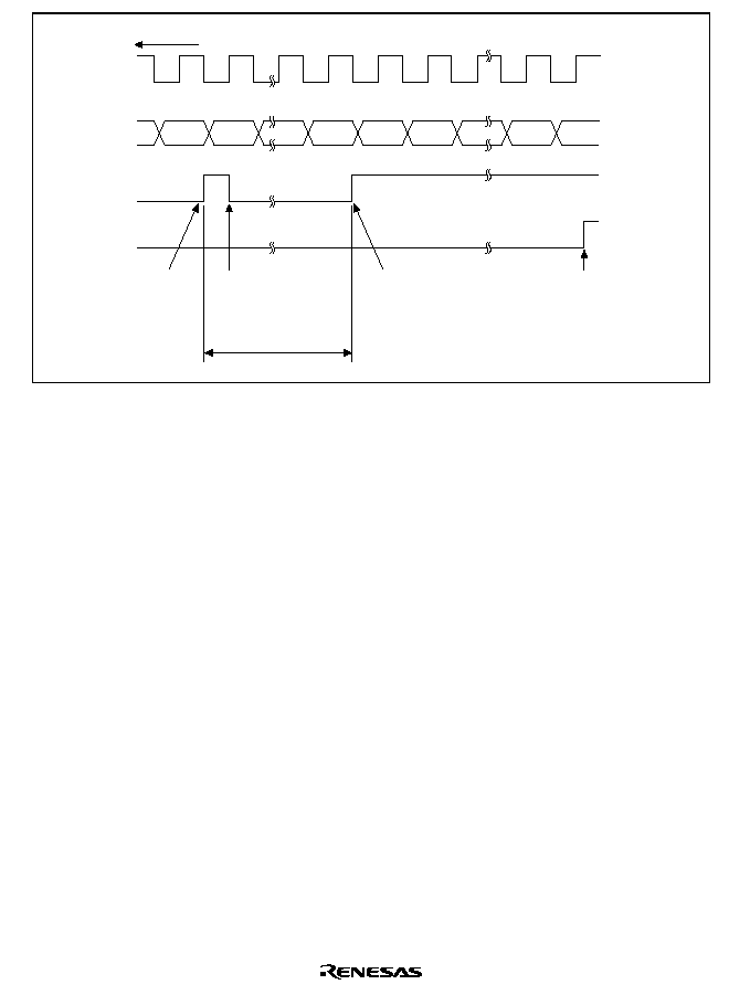
Rev. 5.0, 09/03, page 526 of 806
Bit 7
Bit 0
Bit 7
Bit 0
Bit 1
Bit 6
Serial
clock
Serial
data
Transfer direction
Bit 7
RXI interrupt
handler reads data
and clears RDRF
bit to 0
1 frame
RXI interrupt
request
generated
RXI interrupt
request
generated
ERI interrupt
request generated
by overrun error
RDRF
ORER
Figure 15.22 Example of SCI Receive Operation
Transmitting and Receiving Serial Data Simultaneously (Synchronous Mode): Figure 15.23
shows a sample flowchart for transmitting and receiving serial data simultaneously. The procedure
for setting the SCI to transmit and receive serial data simultaneously is:
1. SCI status check and transmit data write: Read the serial status register (SCSSR), check that
the TDRE bit is 1, then write transmit data in the transmit data register (SCTDR) and clear
TDRE to 0. The TXI interrupt can also be used to determine if the TDRE bit has changed from
0 to 1.
2. Receive error handling: If a receive error occurs, read the ORER bit in SCSSR to identify the
error. After executing the necessary error handling, clear ORER to 0. Transmitting/receiving
cannot resume if ORER remains set to 1.
3. SCI status check and receive data read: Read the serial status register (SCSSR), check that
RDRF is set to 1, then read receive data from the receive data register (SCRDR) and clear
RDRF to 0. The RXI interrupt can also be used to determine if the RDRF bit has changed from
0 to 1.
4. To continue transmitting and receiving serial data: Read the RDRF bit and SCRDR, and clear
RDRF to 0 before the MSB (bit 7) of the current frame is received. Also read the TDRE bit to
check whether it is safe to write (if it reads 1); if so, write data in SCTDR, then clear TDRE to
0 before the MSB (bit 7) of the current frame is transmitted.
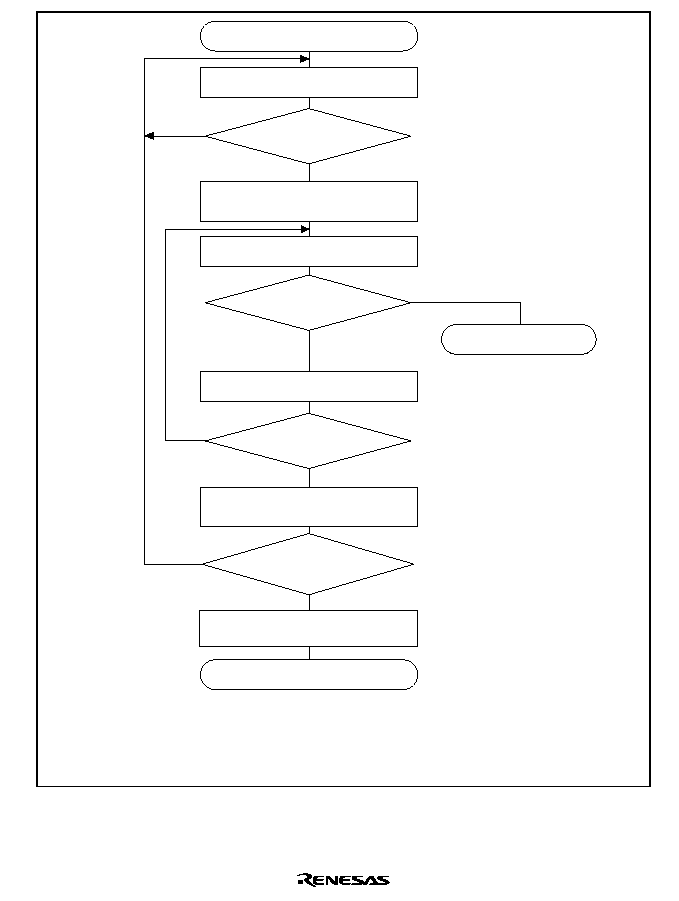
Rev. 5.0, 09/03, page 527 of 806
Start of transmission/reception
Read TDRE bit in SCSSR
All data
transmitted/received?
End of transmission/reception
(1)
No
Yes
TDRE = 1?
Write transmit data to SCTDR
and clear TDRE bit in SCSSR to 0
RDRF = 1?
No
Yes
Yes
No
Read ORER bit in SCSSR
Error processing
(2)
ORER = 1?
No
Read RDRF bit in SCSSR
(4)
Yes
(3)
Read receive data from SCRDR
and clear RDRF bit in SCSSR to 0
Clear TE and RE bits
in SCSCR to 0
Notes: 1.
2.
Numbers in parentheses refer to steps in the preceding procedure description.
In switching from transmitting or receiving to simultaneous transmitting
and receiving, clear both TE and RE to 0, then set both TE and RE to 1 simultaneously.
Figure 15.23 Sample Flowchart for Transmitting/Receiving Serial Data

Rev. 5.0, 09/03, page 528 of 806
15.4
SCI Interrupts
The SCI has four interrupt sources transmit-end (TEI), receive-error (ERI), receive-data-full
(RXI), and transmit-data-empty (TXI). Table 15.13 lists the interrupt sources and indicates their
priority. These interrupts can be enabled and disabled by the TIE, RIE, and TEIE bits in the serial
control register (SCSCR). Each interrupt request is sent separately to the interrupt controller.
TXI is requested when the TDRE bit in SCSSR is set to 1. TDRE is automatically cleared to 0
when data is written in the transmit data register (SCTDR).
RXI is requested when the RDRF bit in SCSSR is set to 1. RDRF is automatically cleared to 0
when the receive data register (SCRDR) is read.
ERI is requested when the ORER, PER, or FER bit in SCSSR is set to 1.
TEI is requested when the TEND bit in SCSSR is set to 1. Where the TXI interrupt indicates that
transmit data writing is enabled, the TEI interrupt indicates that the transmit operation is complete.
Table 15.13 SCI Interrupt Sources
Interrupt Source
Description
Priority When Reset Is Cleared
ERI
Receive error (ORER, PER, or FER)
High
RXI
Receive data full (RDRF)
TXI
Transmit data empty (TDRE)
TEI
Transmit end (TEND)
Low
See section 4, Exception Handling, for priorities and the relationship to non-SCI interrupts.

Rev. 5.0, 09/03, page 529 of 806
15.5
Usage Notes
Note the following points when using the SCI.
SCTDR Writing and TDRE Flag: The TDRE bit in the serial status register (SCSSR) is a status
flag indicating loading of transmit data from SCTDR into SCTSR. The SCI sets TDRE to 1 when
it transfers data from SCTDR to SCTSR. Data can be written to SCTDR regardless of the TDRE
bit state. If new data is written in SCTDR when TDRE is 0, however, the old data stored in
SCTDR will be lost because the data has not yet been transferred to SCTSR. Before writing
transmit data to SCTDR, be sure to check that TDRE is set to 1.
Simultaneous Multiple Receive Errors: Table 15.14 indicates the state of SCSSR status flags
when multiple receive errors occur simultaneously. When an overrun error occurs, the SCRSR
contents cannot be transferred to SCRDR, so receive data is lost.
Table 15.14 SCSSR Status Flags and Transfer of Receive Data
SCSSR Status Flags
Receive Error Status
RDRF
ORER
FER
PER
Receive Data Transfer
SCRSR
SCRDR
Overrun error
1
1
0
0
X
Framing error
0
0
1
0
O
Parity error
0
0
0
1
O
Overrun error + framing error
1
1
1
0
X
Overrun error + parity error
1
1
0
1
X
Framing error + parity error
0
0
1
1
O
Overrun error + framing error + parity error 1
1
1
1
X
X: Receive data is not transferred from SCRSR to SCRDR.
O: Receive data is transferred from SCRSR to SCRDR.
Break Detection and Processing: Break signals can be detected by reading the RxD pin directly
when a framing error (FER) is detected. In the break state, the input from the RxD pin consists of
all 0s, so FER is set and the parity error flag (PER) may also be set. In the break state, the SCI
receiver continues to operate, so if the FER bit is cleared to 0, it will be set to 1 again.
Sending a Break Signal: The TxD pin I/O condition and level can be determined by means of the
SCP0DT bit in the port SC data register (SCPDR) and bits SCP0MD0 and SCP0MD1 in the port
SC control register (SCPCR). This feature can be used to send breaks. To send a break during
serial transmission, clear the SCP0DT bit to 0 (designating low level), then clear the TE bit to 0
(halting transmission). When the TE bit is cleared to 0, the transmitter is initialized regardless of
the current transmission state, and 0 is output from the TxD pin.
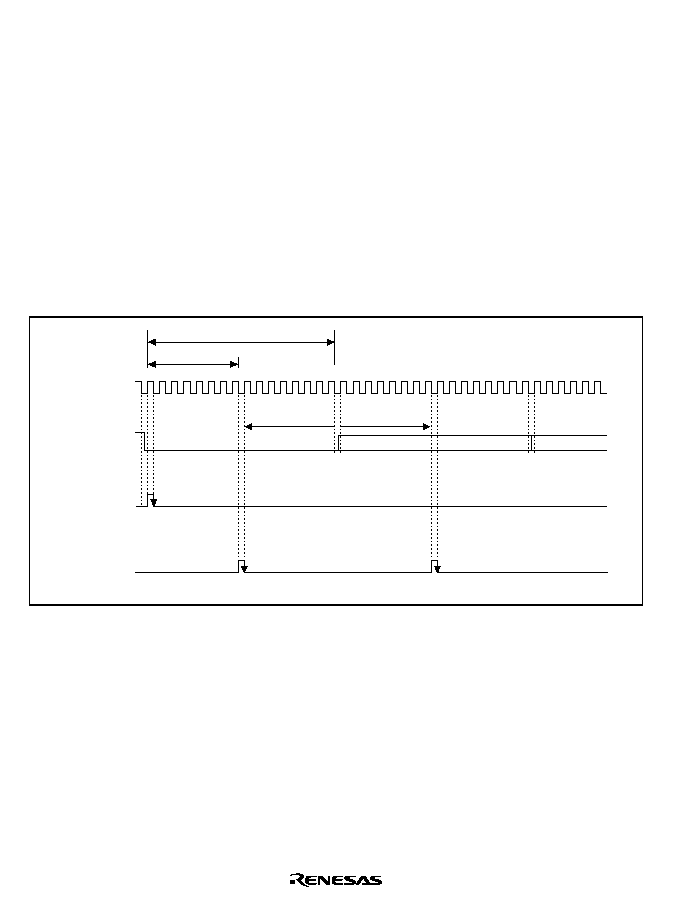
Rev. 5.0, 09/03, page 530 of 806
TEND Flag and TE Bit Processing: The TEND flag is set to 1 during transmission of the stop bit
of the last data. Consequently, if the TE bit is cleared to 0 immediately after setting of the TEND
flag has been confirmed, the stop bit will be in the process of transmission and will not be
transmitted normally. Therefore, the TE bit should not be cleared to 0 for at least 0.5 serial clock
cycles (or 1.5 cycles if two stop bits are used) after setting of the TEND flag is confirmed.
Receive Error Flags and Transmitter Operation (Synchronous Mode Only): When a receive
error flag (ORER, PER, or FER) is set to 1, the SCI will not start transmitting even if TDRE is set
to 1. Be sure to clear the receive error flags to 0 before starting to transmit. Note that clearing RE
to 0 does not clear the receive error flags.
Receive Data Sampling Timing and Receive Margin in Asynchronous Mode: In asynchronous
mode, the SCI operates on a base clock of 16 times the transfer rate frequency. In receiving, the
SCI synchronizes internally with the falling edge of the start bit, which it samples on the base
clock. Receive data is latched at the rising edge of the eighth base clock pulse (figure 15.24).
0 1 2 3 4 5 6 7 8 9 10111213 1415 0 1 2 3 4 5 6 7 8 9 10111213 1415 0 1 2 3 4 5
Base clock
Receive
data (RxD)
Synchro-
nization
sampling
timing
Data
sampling
timing
8 clocks
16 clocks
Start bit
-7.5 clocks
+7.5 clocks
D0
D1
Figure 15.24 Receive Data Sampling Timing in Asynchronous Mode

Rev. 5.0, 09/03, page 531 of 806
The receive margin in asynchronous mode can therefore be expressed as in equation 1.
Equation 1:
M = 0.5
-
1
2N
D
- 0.5
N
- (L - 0.5)F - (1 + F) ◊ 100%
Where:
M
=
Receive margin (
%
)
N
=
Ratio of clock frequency to bit rate (N
=
16)
D
=
Clock duty cycle (D
=
0 to 1.0)
L
=
Frame length (L
=
9 to 12)
F
=
Absolute deviation of clock frequency
From equation 1, if F
=
0 and D
=
0.5, the receive margin is 46.875%, as in equation 2.
Equation 2:
M
=
(0.5 ≠ 1/(2
◊
16))
◊
100
%
=
46.875
%
This is a theoretical value. A reasonable margin to allow in system designs is 20% to 30%.
Notes on Synchronous External Clock Mode:
∑
Set TE
=
RE
=
1 only when external clock SCK is 1.
∑
Do not set TE
=
RE
=
1 until at least four clocks after external clock SCK has changed from 0
to 1.
∑
When receiving, RDRF is set to 1 when RE is set to zero 2.5≠3.5 clocks after the rising edge of
the SCK input of the D7 bit in RxD, but data cannot be copied to SCRDR.
Note on Synchronous Internal Clock Mode: When receiving, RDRF is set to 1 when RE is
cleared to zero 1.5 clocks after the rising edge of the SCK output of the D7 bit in RxD, but data
cannot be copied to SCRDR.

Rev. 5.0, 09/03, page 532 of 806

Rev. 5.0, 09/03, page 533 of 806
Section 16 Smart Card Interface
16.1
Overview
As an added serial communications interface function, the SCI supports an IC card (smart card)
interface that conforms to the ISO/IEC7816-3 (Identification Card) data transmission protocol
format T = 0 (asynchronous full-duplex character transmission protocol). Register settings are
used to switch between the normal serial communication interface and the smart card interface.
16.1.1
Features
The smart card interface has the following features:
∑
Asynchronous mode
Data length: 8 bits
Parity bit generation and check
Receive mode error signal detection (parity error)
Transmit mode error signal detection and automatic re-transmission of data
Supports both direct convention and inverse convention
∑
Bit rate can be selected using on-chip baud rate generator.
∑
Three types of interrupts: Transmit-data-empty, receive-data-full, and communication-error
interrupts are requested independently.
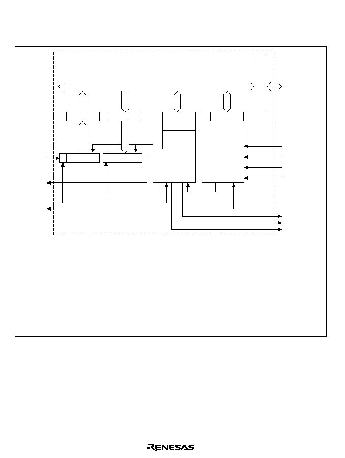
Rev. 5.0, 09/03, page 534 of 806
16.1.2
Block Diagram
Figure 16.1 shows a block diagram of the smart card interface.
RxD
TxD
SCK
SCI
SCBRR
SCSCR
SCSMR
SCTDR
SCTSR
SCRDR
SCRSR
SCSCMR
SCSSR
Parity generation
Parity check
Clock
External clock
Module data bus
Internal
data bus
P
P
/4
P
/16
P
/64
TXI
RXI
ERI
Bus interface
Baud rate
generator
Transmit/
receive
control
SCSCMR:
SCRSR:
SCRDR:
SCTSR:
SCTDR:
SCSMR:
SCSCR:
SCSSR:
SCBRR:
Legend
Smart card mode register
Receive shift register
Receive data register
Transmit shift register
Transmit data register
Serial mode register
Serial control register
Serial status register
Bit rate register
Figure 16.1 Block Diagram of Smart Card Interface

Rev. 5.0, 09/03, page 535 of 806
16.1.3
Pin Configuration
Table 16.1 summarizes the smart card interface pins.
Table 16.1
Smart Card Interface Pins
Pin Name
Abbreviation
I/O
Function
Serial clock pin
SCK0
Output
Clock output
Receive data pin
RxD0
Input
Receive data input
Transmit data pin
TxD0
Output
Transmit data output
16.1.4
Smart Card Interface Registers
Table 16.2 summarizes the registers used by the smart card interface. The SCSMR, SCBRR,
SCSCR, SCTDR, and SCRDR registers are the same as for the normal SCI function. They are
described in section 15, Serial Communication Interface (SCI).
Table 16.2
Registers
Name
Abbreviation R/W
Initial Value
*
3
Address
Access Size
Serial mode register
SCSMR
R/W
H'00
H'FFFFFE80
8
Bit rate register
SCBRR
R/W
H'FF
H'FFFFFE82
8
Serial control register
SCSCR
R/W
H'00
H'FFFFFE84
8
Transmit data register
SCTDR
R/W
H'FF
H'FFFFFE86
8
Serial status register
SCSSR
R/(W)
*
1
H'84
H'FFFFFE88
8
Receive data register
SCRDR
R
H'00
H'FFFFFE8A
8
Smart card mode register
SCSCMR
R/W
H'00
*
2
H'FFFFFE8C
8
Notes: 1. Only 0 can be written, to clear the flags.
2. Bits 0, 2, and 3 are cleared. The value of the other bits is undefined.
3. Initialized by a power-on or manual reset.

Rev. 5.0, 09/03, page 536 of 806
16.2
Register Descriptions
This section describes the registers added for the smart card interface and the bits whose functions
are changed.
16.2.1
Smart Card Mode Register (SCSCMR)
The smart card mode register (SCSCMR) is an 8-bit readable/writable register that selects smart
card interface functions. SCSCMR bits 0, 2, and 3 are initialized to H'00 by a reset and in standby
mode.
Bit:
7
6
5
4
3
2
1
0
--
--
--
--
SDIR
SINV
--
SMIF
Initial value:
--
--
--
--
0
0
--
0
R/W:
R
R
R
R
R/W
R/W
R
R/W
Bits 7 to 4 and 1--Reserved: These bits are always read as 0. The write value should always be
0.
Bit 3--Smart Card Data Transfer Direction (SDIR): Selects the serial/parallel conversion
format.
Bit 3: SDIR
Description
0
Contents of SCTDR are transferred LSB-first, and receive data is stored in
SCRDR LSB-first
(Initial value)
1
Contents of SCTDR are transferred MSB-first, and receive data is stored in
SCRDR MSB-first
Bit 2--Smart Card Data Inversion (SINV): Specifies whether to invert the logic level of the
data. This function is used in combination with bit 3 for transmitting and receiving with an inverse
convention card. SINV does not affect the logic level of the parity bit. See section 16.3.4, Register
Settings, for information on how parity is set.
Bit 2: SINV
Description
0
Contents of SCTDR are transferred unchanged, and receive data is stored
in SCRDR unchanged
(Initial value)
1
Contents of SCTDR are inverted before transfer, and receive data is
inverted before storage in SCRDR

Rev. 5.0, 09/03, page 537 of 806
Bit 0--Smart Card Interface Mode Select (SMIF): Enables the smart card interface function.
Bit 0 : SMIF
Description
0
Smart card interface function disabled
(Initial value)
1
Smart card interface function enabled
16.2.2
Serial Status Register (SCSSR)
In smart card interface mode, the function of SCSSR bit 4 is changed. The setting conditions for
bit 2, the TEND bit, are also changed.
Bit:
7
6
5
4
3
2
1
0
TDRE
RDRF
ORER FER/ERS
PER
TEND
MPB
MPBT
Initial value:
1
0
0
0
0
1
0
0
R/W:
R/(W)
*
R/(W)
*
R/(W)
*
R/(W)
*
R/(W)
*
R
R
R/W
Note:
*
Only 0 can be written, to clear the flag.
Bits 7 to 5: These bits have the same function as in the ordinary SCI. See section 15, Serial
Communication Interface (SCI), for more information.
Bit 4--Error Signal Status (ERS): In the smart card interface mode, bit 4 indicates the state of
the error signal returned from the receiving side during transmission. The smart card interface
cannot detect framing errors.
Bit 4: ERS
Description
0
Receiving ended normally with no error signal
(Initial value)
ERS is cleared to 0 when the chip is reset or enters standby mode, or when
software reads ERS after it has been set to 1, then writes 0 to ERS.
1
An error signal indicating a parity error was transmitted from the receiving side
ERS is set to 1 if the error signal sampled is low.
Note:
The ERS flag maintains its state even when the TE bit in SCSCR is cleared to 0.

Rev. 5.0, 09/03, page 538 of 806
Bits 3 to 0: These bits have the same function as in the ordinary SCI. See section 15, Serial
Communication Interface (SCI), for more information. The setting conditions for bit 2, the
transmit end bit (TEND), are changed as follows.
Bit 2: TEND
Description
0
Transmission is in progress
TEND is cleared to 0 when software reads TDRE after it has been set to 1, then
writes 0 to TDRE.
1
End of transmission
(Initial value)
TEND is set to 1 when:
the chip is reset or enters standby mode,
the TE bit in SCSCR is 0 and the FER/ERS bit is also 0,
the C/
A
bit in SCSMR is 0, and TDRE = 1 and FER/ERS = 0 (normal
transmission) 2.5 etu after a one-byte serial character is transmitted, or
the C/
A
bit in SCSMR is 1, and TDRE = 1 and FER/ERS = 0 (normal
transmission) 1.0 etu after a one-byte serial character is transmitted.
Note:
etu: Elementary Time Unit (time for transfer of 1 bit)
16.3
Operation
16.3.1
Overview
The primary functions of the smart card interface are described below.
1. Each frame consists of 8-bit data and 1 parity bit.
2. During transmission, the card leaves a guard time of at least 2 etu (elementary time units: time
for transfer of 1 bit) from the end of the parity bit to the start of the next frame.
3. During reception, the card outputs an error signal low level for 1 etu after 10.5 etu has elapsed
from the start bit if a parity error was detected.
4. During transmission, it automatically transmits the same data after allowing at least 2 etu from
the time the error signal is sampled.
5. Only start-stop type asynchronous communication functions are supported; no synchronous
communication functions are available.
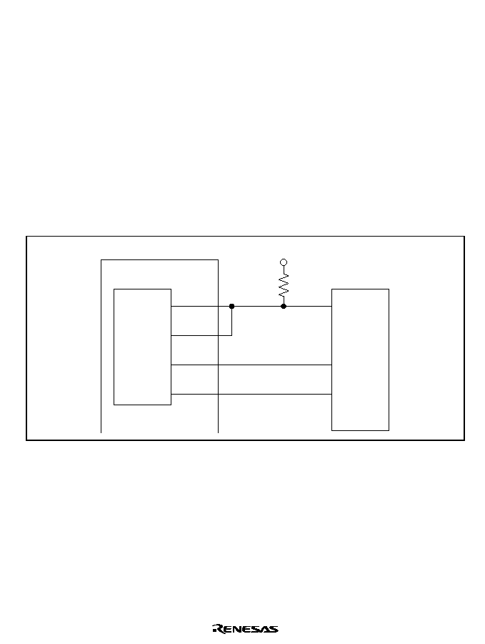
Rev. 5.0, 09/03, page 539 of 806
16.3.2
Pin Connections
Figure 16.2 shows the pin connection diagram for the smart card interface. During communication
with an IC card, transmission and reception are both carried out over the same data transfer line,
so connect the TxD and RxD pins on the chip. Pull up the data transfer line to the power supply
V
CC
side with a resistor.
When using the clock generated by the smart card interface on an IC card, input the SCK pin
output to the IC card's CLK pin. This connection is not necessary when the internal clock is used
on the IC card.
Use the chip's port output as the reset signal. Apart from these pins, power and ground pin
connections are usually also required.
Note:
When the IC card is not connected and both RE and TE are set to 1, closed communication
is possible and auto-diagnosis can be performed.
LSI
TxD
IO
CLK
RST
RxD
SCK
Px (port)
Clock line
Data line
Reset line
IC card
Connected device
V
CC
Figure 16.2 Pin Connection Diagram for Smart Card Interface
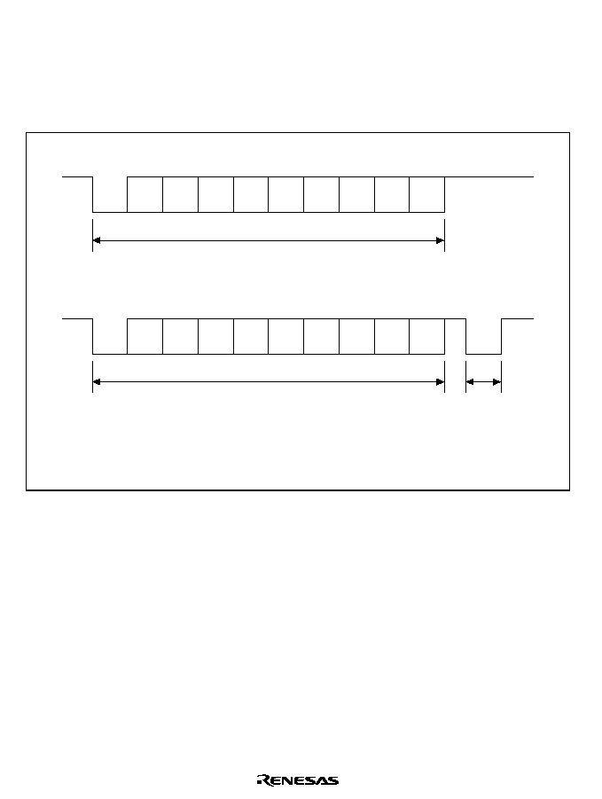
Rev. 5.0, 09/03, page 540 of 806
16.3.3
Data Format
Figure 16.3 shows the data format for the smart card interface. In this mode, parity is checked
every frame while receiving and error signals sent to the transmitting side whenever an error is
detected so that data can be re-transmitted. During transmission, error signals are sampled and data
re-transmitted whenever an error signal is detected.
Ds
D0
D1
D2
D3
D4
D5
D6
D7
Dp
With no parity error
Transmitting station output
Ds
D0
D1
D2
D3
D4
D5
D6
D7
Dp
DE
With parity error
Transmitting station output
Receiving
station output
Ds:
D0
-D7:
Dp:
DE:
Start bit
Data bits
Parity bit
Error signal
Figure 16.3 Data Format for Smart Card Interface
The operating sequence is:
1. The data line is high-impedance when not in use and is fixed high with a pull-up resistor.
2. The transmitting side starts one frame of data transmission. The data frame starts with a start
bit (Ds, low level). The start bit is followed by eight data bits (D0≠D7) and a parity bit (Dp).
3. On the smart card interface, the data line returns to high-impedance after this. The data line is
pulled high with a pull-up resistor.
4. The receiving side checks parity. When the data is received normally with no parity errors, the
receiving side then waits to receive the next data. When a parity error occurs, the receiving
side outputs an error signal (DE, low level) and requests re-transfer of data. The receiving
station returns the signal line to high-impedance after outputting the error signal for a specified
period. The signal line is pulled high with a pull-up resistor.

Rev. 5.0, 09/03, page 541 of 806
5. The transmitting side transmits the next frame of data unless it receives an error signal. If it
does receive an error signal, it returns to step 2 to re-transmit the erroneous data.
16.3.4
Register Settings
Table 16.3 shows the bit map of the registers that the smart card interface uses. Bits shown as 1 or
0 must be set to the indicated value. The settings for the other bits are described below.
Table 16.3
Register Settings for Smart Card Interface
Register
Address
Bit 7
Bit 6
Bit 5
Bit 4
Bit 3
Bit 2
Bit 1
Bit 0
SCSMR
H'FFFFFE80
C/
A
0
1
O/
E
1
0
CKS1
CKS0
SCBRR
H'FFFFFE82
BRR7
BRR6
BRR5
BRR4
BRR3
BRR2
BRR1
BRR0
SCSCR
H'FFFFFE84
TIE
RIE
TE
RE
0
0
CKE1
CKE0
SCTDR
H'FFFFFE86
TDR7
TDR6
TDR5
TDR4
TDR3
TDR2
TDR1
TDR0
SCSSR
H'FFFFFE88
TDRE
RDRF
ORER
FER/
ERS
PER
TEND
0
0
SCRDR
H'FFFFFE8A
RDR7
RDR6
RDR5
RDR4
RDR3
RDR2
RDR1
RDR0
SCSCMR
H'FFFFFE8C
--
--
--
--
SDIR
SINV
--
SMIF
Note:
Dashes indicate unused bits.
1. Setting the serial mode register (SCSMR): The C/
A bit selects the setting timing of the TEND
flag, and selects the clock output state in combination with bits CKE1 and CKE0 in the serial
control register (SCSCR). Clear the O/
E bit to 0 if the IC card uses the direct convention, and
set it to 1 if the card uses the inverse convention. Select the on-chip baud rate generator clock
source with the CKS1 and CKS0 bits (see section 16.3.5, Clock).
2. Setting the bit rate register (SCBRR): Set the bit rate. See section 16.3.5, Clock, to see how to
calculate the set value.
3. Setting the serial control register (SCSCR): The TIE, RIE, TE and RE bits function as they do
for the ordinary SCI. See section 15, Serial Communication Interface (SCI), for more
information. The CKE0 bit specifies the clock output. When no clock is output, clear CKE0 to
0; when a clock is output, set CKE0 to 1.
4. Setting the smart card mode register (SCSCMR): The SDIR and SINV bits are both cleared to
0 for IC cards that use the direct convention, and both set to 1 when the inverse convention is
used. The SMIF bit is set to 1 for the smart card interface.
Figure 16.4 shows sample waveforms for register settings of the two types of IC cards (direct
convention and inverse convention) and their start characters.
In the direct convention type, the logical 1 level is state Z, the logical 0 level is state A, and
communication is LSB-first. The start character data is H'3B. Parity is even (from the smart
card standard), and so the parity bit is 1.
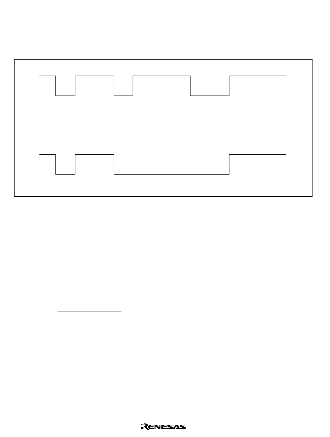
Rev. 5.0, 09/03, page 542 of 806
In the inverse convention type, the logical 1 level is state A, the logical 0 level is state Z, and
communication is MSB first. The start character data is H'3F. Parity is even (from the smart
card standard), and so the parity bit is 0, which corresponds to state Z.
Only data bits D7≠D0 are inverted by the SINV bit. To invert the parity bit, set the O/
E bit in
SCSMR to odd parity mode. This applies to both transmission and reception.
Ds
D0
D1
D2
D3
D4
D5
D6
D7
Dp
A
(Z)
Z
Z
A
Z
Z
Z
A
A
Z
(Z)
State
a. Direct convention (SDIR, SINV, and O/
E are all 0)
Ds
D7
D6
D5
D4
D3
D2
D1
D0
Dp
A
(Z)
Z
Z
A
A
A
A
A
A
Z
(Z)
State
b. Inverse convention (SDIR, SINV, and O/
E are all 1)
Figure 16.4 Waveform of Start Character
16.3.5
Clock
Only the internal clock generated by the on-chip baud rate generator can be used as the
communication clock in the smart card interface. The bit rate for the clock is set by the bit rate
register (SCBRR) and the CKS1 and CKS0 bits in the serial mode register (SCSMR), and is
calculated using the equation below. Table 16.5 shows sample bit rates. If clock output is then
selected by setting CKE0 to 1, a clock with a frequency 372 times the bit rate is output from the
SCK0 pin.
B =
◊
10
6
1488
◊
2
2n
-
1
◊
(N
+ 1)
P
Where: N
=
Value set in SCBRR (0
N
255)
B
=
Bit rate (bits/s)
P
=
Peripheral module operating frequency (MHz)
n
=
0 to 3 (table 16.4)

Rev. 5.0, 09/03, page 543 of 806
Table 16.4
Relationship of n to CKS1 and CKS0
n
CKS1
CKS0
0
0
0
1
0
1
2
1
0
3
1
1
Table 16.5
Examples of Bit Rate B (Bits/s) for SCBRR Settings (n
=
=
=
=
0)
P
(MHz)
N
7.1424
10.00
10.7136
13.00
14.2848
16.00
18.00
0
9600.0
13440.9
14400.0
17473.1
19200.0
21505.4
24193.5
1
4800.0
6720.4
7200.0
8736.6
9600.0
10752.7
12096.8
2
3200.0
4480.3
4800.0
5824.4
6400.0
7168.5
8064.5
Note:
The bit rate is rounded to one decimal place.
Calculate the value to be set in the bit rate register (SCBRR) from the operating frequency and the
bit rate. N is an integer in the range 0
N
255, specifying a smallish error.
N =
◊
10
6
-
1
1488
◊
2
2n
-
1
◊
B
P
Table 16.6
Examples of SCBRR Settings for Bit Rate B (Bits/s) (n
=
=
=
=
0)
(MHz) (9600 Bits/s)
7.1424
10.00
10.7136
13.00
14.2848
16.00
18.00
N
Error
N
Error
N
Error
N
Error
N
Error
N
Error
N
Error
0
0.00
1
30.00
1
25.00
1
8.99
1
0.00
1
12.01
2
15.99
Rev. 5.0, 09/03, page 544 of 806
Table 16.7
Maximum Bit Rates for Frequencies (Smart Card Interface Mode)
P
(MHz)
Maximum Bit Rate (Bits/s)
N
n
7.1424
9600
0
0
10.00
13441
0
0
10.7136
14400
0
0
13.00
17473
0
0
14.2848
19200
0
0
16.00
21505
0
0
18.00
24194
0
0
The bit rate error is found as follows:
Error (%) = (
◊
10
6
-
1)
◊
100
1488
◊
2
2n
-
1
◊
B
◊
(N
+ 1)
P
Table 16.8 shows the relationship between transmit/receive clock register set values and output
states on the smart card interface.
Table 16.8
Register Set Values and SCK Pin
Register Value
SCK Pin
Setting
SMIF
C/
A
A
A
A
CKE1
CKE0
Output
State
1
*
1
1
0
0
0
Port
Determined by setting of port
register SCP1MD1 and
SCP1MD0 bits
1
0
0
1
SCK (serial clock) output state
2
*
2
1
1
0
0
Low output
Low output state
1
1
0
1
SCK (serial clock) output state
3
*
2
1
1
1
0
High output
High output state
1
1
1
1
SCK (serial clock) output state
Notes: 1. The SCK output state changes as soon as the CKE0 bit is modified. The CKE1 bit
should be cleared to 0.
2. The clock duty remains constant despite stopping and starting of the clock by
modification of the CKE0 bit.

Rev. 5.0, 09/03, page 545 of 806
16.3.6
Data Transmission and Reception
Initialization: Initialize the SCI using the following procedure before sending or receiving data.
Initialization is also required for switching from transmit mode to receive mode or from receive
mode to transmit mode. Figure 16.5 shows a flowchart of the initialization process.
1. Clear TE and RE in the serial control register (SCSCR) to 0.
2. Clear error flags FER/ERS, PER, and ORER to 0 in the serial status register (SCSSR).
3. Set the C/
A bit, parity bit (O/E bit), and baud rate generator select bits (CKS1 and CKS0 bits)
in the serial mode register (SCSMR). At this time also clear the CHR and MP bits to 0 and set
the STOP and PE bits to 1.
4. Set the SMIF, SDIR, and SINV bits in the smart card mode register (SCSCMR). When the
SMIF bit is set to 1, the TxD and RxD pins both switch from ports to SCI pins and become
high-impedance.
5. Set the value corresponding to the bit rate in the bit rate register (SCBRR).
6. Set the clock source select bits (CKE1 and CKE0 bits) in the serial control register (SCSCR).
Clear the TIE, RIE, TE, RE, MPIE, and TEIE bits to 0. When the CKE0 bit is set to 1, a clock
is output from the SCK pin.
7. After waiting at least 1 bit, set the TIE, RIE, TE, and RE bits in SCSCR. Do not set the TE and
RE bits simultaneously unless performing auto-diagnosis.
Rev. 5.0, 09/03, page 546 of 806
Initialization
Clear TE and RE bits in SCSCR to 0
Set value in SCBRR
Clear FER/ERS, PER
and ORER flags in SCSSR to 0
Wait
Set TIE, RIE, TE, and RE bits
in SCSCR
Has a 1-bit
interval elapsed?
End
(2)
Set parity in O/
E bit,
set clock in CKS1 and CKS0 bits,
and set C/
A, in SCSMR
(3)
Set clock in CKE1 and CKE0 bits,
and clear TIE, RIE, TE, RE, MPIE,
and TEIE bits to 0, in SCSCR
(6)
(5)
(4)
(1)
(7)
No
Yes
Set SMIF, SDIR,
and SINV bits in SCSMR
Note: Numbers in parentheses refer to steps in the preceding procedure description.
Figure 16.5 Initialization Flowchart (Example)

Rev. 5.0, 09/03, page 547 of 806
Serial Data Transmission: The processing procedures in the smart card mode differ from
ordinary SCI processing because data is retransmitted when an error signal is sampled during a
data transmission. This results in the transmission processing flowchart shown in figure 16.6.
1. Initialize the smart card interface mode as described in Initialization above.
2. Check that the FER/ERS bit in SCSSR is cleared to 0.
3. Repeat steps 2 and 3 until the TEND flag in SCSSR is set to 1.
4. Write the transmit data into SCTDR, clear the TDRE flag to 0 and start transmitting. The
TEND flag will be cleared to 0.
5. To transmit more data, return to step 2.
6. To end transmission, clear the TE bit to 0.
This processing can be interrupted. When the TIE bit is set to 1 and interrupt requests are enabled,
a transmit-data-empty interrupt (TXI) will be requested when the TEND flag is set to 1 at the end
of transmission. When the RIE bit is set to 1 and interrupt requests are enabled, a communication
error interrupt (ERI) will be requested when the ERS flag is set to 1 when an error occurs in
transmission. See Interrupt Operation below for more information.
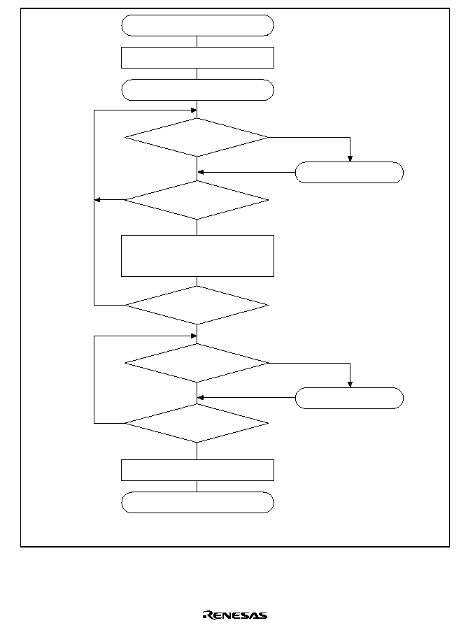
Rev. 5.0, 09/03, page 548 of 806
Start
End of transmission
Start of transmission
Initialize
Write transmit data in SCTDR
and clear TDRE
flag in SCSSR to 0
(1)
Clear TE bit in SCSCR to 0
(6)
Error handling
(2)
FER/ERS = 0?
TEND = 1?
Yes
Yes
Yes
Yes
No
No
All data transmitted?
No
TEND = 1?
No
Error handling
FER/ERS = 0?
Yes
No
(4)
(5)
(3)
Note: Numbers in parentheses refer to steps in the preceding procedure description.
Figure 16.6 Transmission Flowchart

Rev. 5.0, 09/03, page 549 of 806
Serial Data Reception: The processing procedures in smart card mode are the same as in ordinary
SCI processing. The reception processing flowchart is shown in figure 16.7.
1. Initialize the smart card interface mode as described above in Initialization and in figure 16.5.
2. Check that the ORER and PER flags in SCSSR are cleared to 0. If either flag is set, clear both
to 0 after performing the appropriate error handling procedures.
3. Repeat steps 2 and 3 until the RDRF flag is set to 1.
4. Read the receive data from SCRDR.
5. To receive more data, clear the RDRF flag to 0 and return to step 2.
6. To end reception, clear the RE bit to 0.
This processing can be interrupted. When the RIE bit is set to 1 and interrupt requests are enabled,
a receive-data-full interrupt (RXI) will be requested when the RDRF flag is set to 1 at the end of
reception. When an error occurs during reception and either the ORER or PER flag is set to 1, a
communication error interrupt (ERI) will be requested. See Interrupt Operation below for more
information.
The received data will be transferred to SCRDR even when a parity error occurs during reception
and PER is set to 1, so this data can still be read.
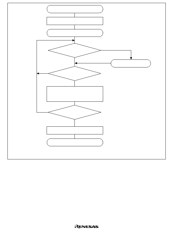
Rev. 5.0, 09/03, page 550 of 806
Start
End of reception
Start of reception
Initialize
Write receive data from
SCRDR and clear
RDRF flag in SCSSR to 0
(1)
Clear RE bit in SCSCR to 0
(6)
Error handling
(2)
ORER = 0 or PER = 0?
RDRF = 1?
Yes
Yes
Yes
No
No
All data received?
No
(4)
(5)
(3)
Note: Numbers in parentheses refer to steps in the preceding procedure description.
Figure 16.7 Reception Flowchart (Example)

Rev. 5.0, 09/03, page 551 of 806
Switching Modes: When switching from receive mode to transmit mode, check that the receive
operation is completed before starting initialization, clearing RE to 0, and setting TE to 1. The
RDRF, PER, and ORER flags can be used to check if reception is completed. When switching
from transmit mode to receive mode, check that the transmit operation is completed before starting
initialization, clearing TE to 0, and setting RE to 1. The TEND flag can be used to check if
transmission is completed.
Interrupt Operation: In the smart card interface mode, there are three types of interrupts:
transmit-data-empty (TXI), communication error (ERI) and receive-data-full (RXI). In this mode,
the transmit-end interrupt (TEI) cannot be requested.
Set the TEND flag in SCSSR to 1 to request a TXI interrupt. Set the RDRF flag in SCSSR to 1 to
request an RXI interrupt. Set the ORER, PER, or FER/ERS flag in SCSSR to 1 to request an ERI
interrupt (table 16.9).
Table 16.9
Smart Card Mode Operating State and Interrupt Sources
Mode
State
Flag
Mask Bit
Interrupt Source
Transmit mode
Normal
TEND
TIE
TXI
Error
FER/ERS
RIE
ERI
Receive mode
Normal
RDRF
RIE
RXI
Error
PER,
ORER
RIE
ERI
16.4
Usage Notes
When the SCI is used as a smart card interface, be sure that all criteria in sections 16.4.1, Receive
Data Timing and Receive Margin in Asynchronous Mode and 16.4.2, Retransmission (Receive
and Transmit Modes) are applied.
16.4.1
Receive Data Timing and Receive Margin in Asynchronous Mode
In asynchronous mode, the SCI runs on a base clock with a frequency of 372 times the transfer
rate. During reception, the SCI samples the falling of the start bit using the base clock to achieve
internal synchronization. Receive data is latched internally at the rising edge of the 186th base
clock cycle (figure 16.8).
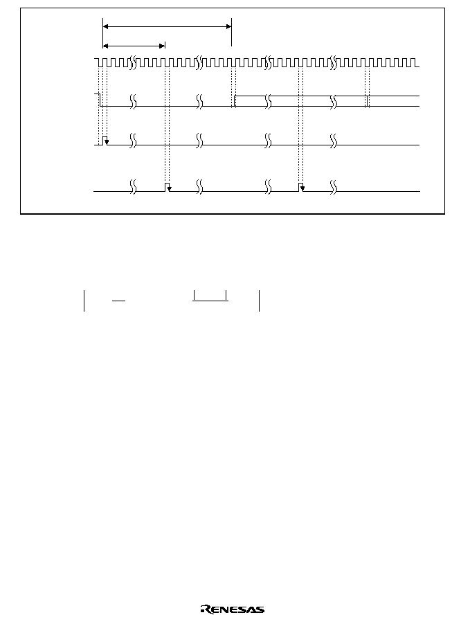
Rev. 5.0, 09/03, page 552 of 806
0
185
371 0
185
371 0
Base clock
Receive
data (RxD)
Synchro-
nization
sampling
timing
Data
sampling
timing
186 clock cycles
372 clock cycles
Start
bit
D0
D1
Figure 16.8 Receive Data Sampling Timing in Smart Card Mode
The receive margin is found from the following equation:
For smart card mode:
M = (0.5
-
)
-
1
2N
D
-
0.5
N
(L
-
0.5)F
-
(1
+
F)
◊
100%
Where:
M
=
Receive margin (%)
N
=
Ratio of bit rate to clock (N
=
372)
D
=
Clock duty (D
=
0 to 1.0)
L
=
Frame length (L
=
10)
F
=
Absolute value of clock frequency deviation
Using this equation, the receive margin when F
=
0 and D
=
0.5 is as follows:
M
=
(0.5 ≠ 1/2
◊
372)
◊
100
%
=
49.866
%

Rev. 5.0, 09/03, page 553 of 806
16.4.2
Retransmission (Receive and Transmit Modes)
Retransmission when SCI is in Receive Mode: Figure 16.9 shows the retransmission operation
in the SCI receive mode.
1. When the received parity bit is checked and an error is found, the PER bit in SCSSR is
automatically set to 1. If the RIE bit in SCSCR is enabled at this time, an ERI interrupt is
requested. Be sure to clear the PER bit before the next parity bit is sampled.
2. The RDRF bit in SCSSR is not set in the frame that caused the error.
3. When the received parity bit is checked and no error is found, the PER bit in SCSSR is not set.
4. When the received parity bit is checked and no error is found, reception is considered to have
been completed normally and the RDRF bit in SCSSR is automatically set to 1. If the RIE bit
in SCSCR is enabled at this time, an RXI interrupt is requested.
5. When a normal frame is received, the pin maintains a three-state state when it transmits the
error signal.
D0
Ds
D2
D1
D4
D3
D6
D5
Dp DE
D7
D0
Ds
D2
D1
D4
D3
D6
D5
Dp
(DE)
D7
D0
Ds
D2
D1
D4
D3
nth transfer frame
RDRF
PER
2
1
4
5
3
Retransmitted frame
Transfer frame n + 1
Figure 16.9 Retransmission in SCI Receive Mode
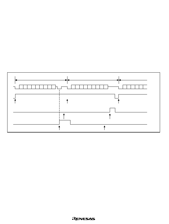
Rev. 5.0, 09/03, page 554 of 806
Retransmission when SCI is in Transmit Mode: Figure 16.10 shows the retransmission
operation in the SCI transmit mode.
1. After transmission of one frame is completed, the FER/ERS bit in SCSSR is set to 1 when a
error signal is returned from the receiving side. If the RIE bit in SCSCR is enabled at this time,
an ERI interrupt is requested. Be sure to clear the FER/ERS bit before the next parity bit is
sampled.
2. The TEND bit in SCSSR is not set in the frame that received the error signal indicating the
error.
3. The FER/ERS bit in SCSSR is not set when no error signal is returned from the receiving side.
4. When no error signal is returned from the receiving side, the TEND bit in SCSSR is set to 1
when the transmission of the frame that includes the retransmission is considered completed. If
the TIE bit in SCSCR is enabled at this time, a TXI interrupt will be requested.
D0
Ds
D2
D1
D4
D3
D6
D5
Dp DE
D7
D0
Ds
D2
D1
D4
D3
D6
D5
Dp
(DE)
D7
D0
Ds
D2
D1
D4
D3
nth transfer frame
TEND
FER/ERS
Transfer from SCTDR
to SCTSR
Transfer from SCTDR
to SCTSR
Transfer from SCTDR
to SCTSR
1
2
4
3
Retransmitted frame
Transfer frame n + 1
TDRE
Figure 16.10 Retransmission in SCI Transmit Mode

Rev. 5.0, 09/03, page 555 of 806
Section 17 Serial Communication Interface with FIFO
(SCIF)
17.1
Overview
The SH7729R has a two-channel serial communication interface with FIFO (SCIF) that supports
asynchronous serial communication. It also has 16-stage FIFO registers for both transmission and
reception that enable the SH7729R to perform efficient high-speed continuous communication.
17.1.1
Features
∑
Asynchronous serial communication:
Serial data communication is performed by start-stop in character units. The SCI can
communicate with a universal asynchronous receiver/transmitter (UART), an asynchronous
communication interface adapter (ACIA), or any other communications chip that employs
a standard asynchronous serial system. There are eight selectable serial data
communication formats.
Data length: 7 or 8 bits
Stop bit length: 1 or 2 bits
Parity: Even, odd, or none
Receive error detection: Parity and framing errors
Break detection: Break is detected when a framing error is followed by at least one frame at
the space 0 level (low level). It is also detected by reading the RxD level directly from the
port SC data register (SCPDR) when a framing error occurs.
∑
Full duplex communication: The transmitting and receiving sections are independent, so the
SCI can transmit and receive simultaneously. Both sections use 16-stage FIFO buffering, so
high-speed continuous data transfer is possible in both the transmit and receive directions.
∑
On-chip baud rate generator with selectable bit rates
∑
Internal or external transmit/receive clock source: From either baud rate generator (internal) or
SCK pin (external)
∑
Four types of interrupts: Transmit-FIFO-data-empty, break, receive-FIFO-data-full, and
receive-error interrupts are requested independently. The direct memory access controller
(DMAC) can be activated to execute a data transfer by a transmit-FIFO-data-empty or receive-
FIFO-data-full interrupt.
∑
When the SCIF is not in use, it can be stopped by halting the clock supplied to it, saving
power.
∑
On-chip modem control functions (RTS and CTS)
∑
The quantity of data in the transmit and receive FIFO registers and the number of receive
errors of the receive data in the receive FIFO register can be ascertained.
∑
A time-out error (DR) can be detected when receiving.
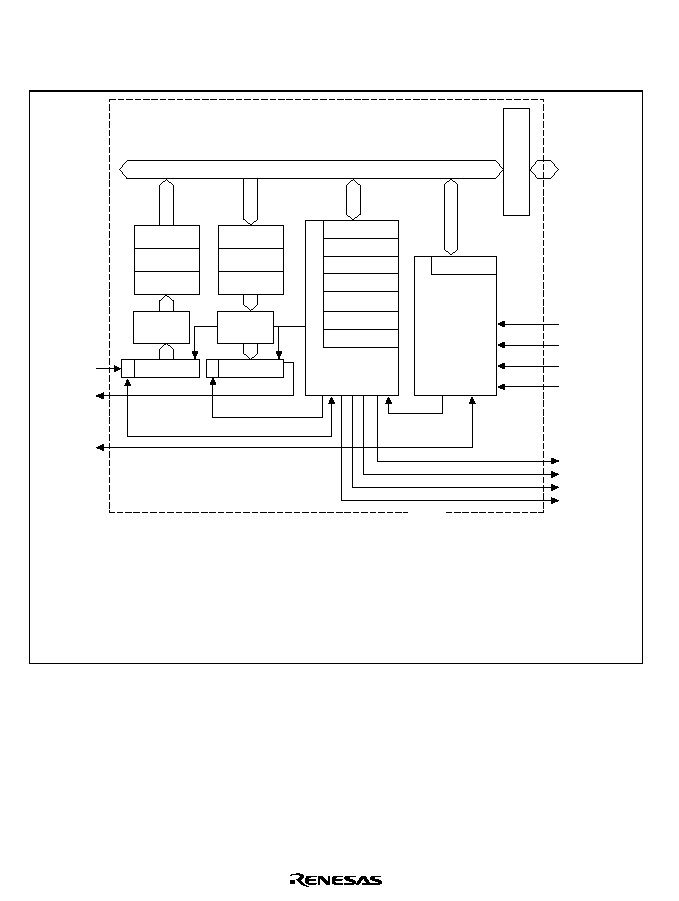
Rev. 5.0, 09/03, page 556 of 806
17.1.2
Block Diagram
Figure 17.1 shows a block diagram of the SCIF.
RxD
TxD
SCK
SCIF
SCBRR
SCSSR2
SCSCR2
SCFTDR2
SCTSR
SCFRDR2
(16
Transmit
buffer
Receive
buffer
(16
stages)
stages)
SCRSR
SCSMR2
SCFDR2
SCFCR2
SCPCR
SCFDR
Parity generation
Parity check
Clock
External clock
Module data bus
Internal
data bus
P
P
/4
P
/16
P
/64
TXI
TEI
RXI
BRI
Bus interface
Baud rate
generator
Transmit/
receive
control
SCRSR:
SCFRDR:
SCTSR:
SCFTDR2:
SCSMR2:
SCSCR2:
Legend
Receive shift register
Receive FIFO data register
Transmit shift register
Transmit FIFO data register
Serial mode register
Serial control register
SCSSR2:
SCBRR2:
SCFCR2:
SCFDR2:
SCPDR:
SCPCR:
Serial status register
Bit rate register
FIFO control register
FIFO data count register
Port SC data register
Port SC control register
Figure 17.1 Block Diagram of SCIF

Rev. 5.0, 09/03, page 557 of 806
Figures 17.2 to 17.4 show the SCIF I/O port pins.
SCIF pin I/O and data control is performed by bits 11 to 8 of SCPCR and bits 5 and 4 of SCPDR.
For details, see section 15.2.8, SC Port Control Register (SCPCR)/SC Port Data Register
(SCPDR).
Internal data bus
Output enable
Clock input enable
SCIF
Serial clock output
Serial clock input
R
P5MD0
PCRW
Reset
C
Q
Q
D
R
SCP5MD1
PCRW
Reset
C
Q
D
R
SCP5DT1
PDRW
Reset
SCPT[5]/SCK2
C
D
PDRW:
Legend
SCPDR write
PDRR:
PCRW:
SCPDR read
SCPCR write
PDRR*
Note:
* When reading the SCK2 pin, clear the CKE1 and CKE0 bits in SCSCR to 0,
and set the SCP5MD1 bit in SCSPR to 1 (see section 15.2.8,
SC Port Control Register (SCPCR)/SC Port Data Register (SCPDR)).
Figure 17.2 SCPT[5]/SCK2 Pin

Rev. 5.0, 09/03, page 558 of 806
Internal data bus
Output enable
SCIF
Serial
transmission
output
R
SCP4MD0
PCRW
Reset
C
Q
Q
D
R
SCP4MD1
PCRW
Reset
C
Q
D
R
SCP4DT1
PDRW
Reset
SCPT[4]/TxD2
C
D
PCRW:
PDRW:
SCPCR write
SCPDR write
Legend
Figure 17.3 SCPT[4]/TxD2 Pin
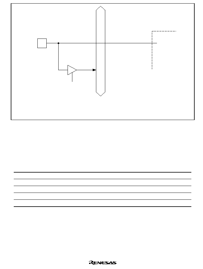
Rev. 5.0, 09/03, page 559 of 806
SCIF
Internal data bus
PDRR*
Serial
receive
data
SCPT[4]/RxD2
PDRR: SCPDR read
Legend
Note:
* When reading the RxD2 pin, set the RE bit in SCSCR to 1.
Figure 17.4 SCPT[4]/RxD2 Pin
17.1.3
Pin Configuration
The SCIF has the serial pins summarized in table 17.1.
Table 17.1
SCIF Pins
Pin Name
Abbreviation
I/O
Function
Serial clock pin
SCK2
I/O
Clock I/O
Receive data pin
RxD2
Input
Receive data input
Transmit data pin
TxD2
Output
Transmit data output
Request to send pin
RTS2
Output
Request to send
Clear to send pin
CTS2
Input
Clear to send

Rev. 5.0, 09/03, page 560 of 806
17.1.4
Register Configuration
Table 17.2 summarizes the SCIF internal registers. These registers specify the data format and bit
rate, and control the transmitter and receiver sections.
Table 17.2
SCIF Registers
Register Name
Abbreviation R/W
Initial Value Address
Access
Size
Serial mode register 2
SCSMR2
R/W
H'00
H'04000150
(H'A4000150)
*
2
8 bits
Bit rate register 2
SCBRR2
R/W
H'FF
H'04000152
(H'A4000152)
*
2
8 bits
Serial control register 2
SCSCR2
R/W
H'00
H'04000154
(H'A4000154)
*
2
8 bits
Transmit FIFO data register 2
SCFTDR2
W
--
H'04000156
(H'A4000156)
*
2
8 bits
Serial status register 2
SCSSR2
R/(W)
*
1
H'0060
H'04000158
(H'A4000158)
*
2
16 bits
Receive FIFO data register 2
SCFRDR2
R
Undefined
H'0400015A
(H'A400015A)
*
2
8 bits
FIFO control register 2
SCFCR2
R/W
H'00
H'0400015C
(H'A400015C)
*
2
8 bits
FIFO data count register 2
SCFDR2
R
H'0000
H'0400015E
(H'A400015E)
*
2
16 bits
Notes: These registers are located in area 1 of physical space. Therefore, when the cache is on,
either access these registers from the P2 area of logical space or else make an appropriate
setting using the MMU so that these registers are not cached.
1. Only 0 can be written to clear the flag.
2. When address translation by the MMU does not apply, the address in parentheses
should be used.

Rev. 5.0, 09/03, page 561 of 806
17.2
Register Descriptions
17.2.1
Receive Shift Register (SCRSR)
The receive shift register (SCRSR) receives serial data. Data input at the RxD pin is loaded into
SCRSR in the order received, LSB (bit 0) first, converting the data to parallel form. When one
byte has been received, it is automatically transferred to SCFRDR, the receive FIFO data register.
The CPU cannot read or write to SCRSR directly.
Bit:
7
6
5
4
3
2
1
0
R/W:
--
--
--
--
--
--
--
--
17.2.2
Receive FIFO Data Register (SCFRDR)
The 16-byte receive FIFO data register (SCFRDR) stores serial receive data. The SCIF completes
the reception of one byte of serial data by moving the received data from the receive shift register
(SCRSR) into SCFRDR for storage. Continuous reception is possible until 16 bytes are stored.
The CPU can read but not write to SCFRDR. If data is read when there is no receive data in the
SCFRDR, the value is undefined. When this register is full of receive data, subsequent serial data
is lost.
Bit:
7
6
5
4
3
2
1
0
R/W:
R
R
R
R
R
R
R
R
17.2.3
Transmit Shift Register (SCTSR)
The transmit shift register (SCTSR) transmits serial data. The SCI loads transmit data from the
transmit FIFO data register (SCFTDR) into SCTSR, then transmits the data serially from the TxD
pin, LSB (bit 0) first. After transmitting one data byte, the SCI automatically loads the next
transmit data from SCFTDR into SCTSR and starts transmitting again. The CPU cannot read or
write to SCTSR directly.
Bit:
7
6
5
4
3
2
1
0
R/W:
--
--
--
--
--
--
--
--

Rev. 5.0, 09/03, page 562 of 806
17.2.4
Transmit FIFO Data Register (SCFTDR)
The transmit FIFO data register (SCFTDR) is a FIFO register comprising sixteen 8-bit stages that
stores data for serial transmission. When the SCIF detects that the transmit shift register (SCTSR)
is empty, it moves transmit data written in the SCFTDR into SCTSR and starts serial transmission.
Continuous serial transmission is performed until there is no transmit data left in SCFTDR. The
CPU can always write to SCFTDR.
When SCFTDR is full of transmit data (16 stages), no more data can be written. If writing of new
data is attempted, the data is ignored.
Bit:
7
6
5
4
3
2
1
0
R/W:
W
W
W
W
W
W
W
W
17.2.5
Serial Mode Register (SCSMR)
The serial mode register (SCSMR) is an 8-bit register that specifies the SCIF serial
communication format and selects the clock source for the baud rate generator.
The CPU can always read and write to SCSMR. SCSMR is initialized to H'00 by a reset and in
standby or module standby mode.
Bit:
7
6
5
4
3
2
1
0
--
CHR
PE
O/
E
STOP
--
CKS1
CKS0
Initial value:
0
0
0
0
0
0
0
0
R/W:
R
R/W
R/W
R/W
R/W
R
R/W
R/W
Bit 7--Reserved: This bit is always read as 0. The write value should always be 0.
Bit 6--Character Length (CHR): Selects 7-bit or 8-bit data in asynchronous mode.
Bit 6: CHR
Description
0
8-bit data
(Initial value)
1
7-bit data
When 7-bit data is selected, the MSB (bit 7) of the transmit FIFO data register is
not transmitted.

Rev. 5.0, 09/03, page 563 of 806
Bit 5--Parity Enable (PE): Selects whether to add a parity bit to transmit data and to check the
parity of receive data.
Bit 5: PE
Description
0
Parity bit not added or checked
(Initial value)
1
Parity bit added and checked
When PE is set to 1, an even or odd parity bit is added to transmit data,
depending on the parity mode (O/
E
) setting. Receive data parity is checked
according to the even/odd (O/
E
) mode setting.
Bit 4--Parity Mode (O/
E
E
E
E): Selects even or odd parity when parity bits are added and checked.
The O/
E setting is used only when the parity enable bit (PE) is set to 1 to enable parity addition
and checking. The O/
E setting is ignored when parity addition and checking is disabled.
Bit 4: O/
E
E
E
E
Description
0
Even parity
(Initial value)
If even parity is selected, the parity bit is added to transmit data to make an even
number of 1s in the transmitted character and parity bit combined. Receive data
is checked to see if it has an even number of 1s in the received character and
parity bit combined.
1
Odd parity
If odd parity is selected, the parity bit is added to transmit data to make an odd
number of 1s in the transmitted character and parity bit combined. Receive data
is checked to see if it has an odd number of 1s in the received character and
parity bit combined.
Bit 3--Stop Bit Length (STOP): Selects one or two bits as the stop bit length.
When receiving, only the first stop bit is checked, regardless of the STOP bit setting. If the second
stop bit is 1, it is treated as a stop bit, but if the second stop bit is 0, it is treated as the start bit of
the next incoming character.
Bit 3: STOP
Description
0
One stop bit
(Initial value)
When transmitting, a single 1-bit is added at the end of each transmitted
character.
1
Two stop bits
When transmitting, two 1-bits are added at the end of each transmitted character.
Bit 2--Reserved: This bit is always read as 0. The write value should always be 0.

Rev. 5.0, 09/03, page 564 of 806
Bits 1 and 0--Clock Select 1 and 0 (CKS1, CKS0): Select the internal clock source of the on-
chip baud rate generator. Four clock sources are available. P
, P
/4, P
/16 and P
/64. For further
information on the clock source, bit rate register settings, and baud rate, see section 17.2.8, Bit
Rate Register (SCBRR).
Bit 1: CKS1
Bit 0: CKS0
Description
0
0
P
(Initial
value)
1
P
/4
1
0
P
/16
1
P
/64
Note:
P
: Peripheral clock
17.2.6
Serial Control Register (SCSCR)
The serial control register (SCSCR) operates the SCIF transmitter/receiver, selects the serial clock
output in asynchronous mode, enables/disables interrupt requests, and selects the transmit/receive
clock source. The CPU can always read and write to SCSCR. SCSCR is initialized to H'00 by a
reset and in standby or module standby mode.
Bit:
7
6
5
4
3
2
1
0
TIE
RIE
TE
RE
--
--
CKE1
CKE0
Initial value:
0
0
0
0
0
0
0
0
R/W:
R/W
R/W
R/W
R/W
R
R
R/W
R/W
Bit 7--Transmit Interrupt Enable (TIE): Enables or disables the transmit-FIFO-data-empty
interrupt (TXI) requested when the serial transmit data is transferred from the transmit FIFO data
register (SCFTDR) to the transmit shift register (SCTSR), when the quantity of data in the
transmit FIFO register becomes less than the specified number of transmission triggers, and when
the TDFE flag in the serial FIFO status register (SCFSR) is set to1.
Bit 7: TIE
Description
0
Transmit-FIFO-data-empty interrupt request (TXI) is disabled
(Initial value)
The TXI interrupt request can be cleared by writing a greater quantity of transmit
data than the specified transmission trigger number to SCFTDR and by clearing
TDFE to 0 after reading 1 from TDFE, or can be cleared by clearing TIE to 0.
1
Transmit-FIFO-data-empty interrupt request (TXI) is enabled

Rev. 5.0, 09/03, page 565 of 806
Bit 6--Receive Interrupt Enable (RIE): Enables or disables the receive-data-full (RXI) and
receive-error (ERI) interrupts requested when serial receive data is transferred from the receive
shift register (SCRSR) to the receive FIFO data register (SCFRDR), when the quantity of data in
the receive FIFO register becomes more than the specified receive trigger number, and when the
RDRF flag in SCSSR is set to1.
Bit 6: RIE
Description
0
Receive-data-full interrupt (RXI), receive-error interrupt (ERI), and receive break
interrupt (BRI) requests are disabled
(Initial value)
RXI and ERI interrupt requests can be cleared by reading the DR, ER, or RDF
flag after it has been set to 1, then clearing the flag to 0, or by clearing RIE to 0.
With the RDF flag, read 1 from the RDF flag and clear it to 0, after reading
receive data from SCRDR until the quantity of receive data becomes less than
the specified receive trigger number.
1
Receive-data-full interrupt (RXI) and receive-error interrupt (ERI) requests are
enabled
Bit 5--Transmit Enable (TE): Enables or disables the SCIF serial transmitter.
Bit 5: TE
Description
0
Transmitter disabled
(Initial value)
1
Transmitter enabled
Serial transmission starts after writing of transmit data into SCFTDR2. Select the
transmit format in SCSMR2 and SCFCR2 and reset the TFIFO before setting TE
to 1.
Bit 4--Receive Enable (RE): Enables or disables the SCIF serial receiver.
Bit 4: RE
Description
0
Receiver disabled
(Initial value)
Clearing RE to 0 does not affect the receive flags (DR, ER, BRK, FER, PER, and
ORER). These flags retain their previous values.
1
Receiver enabled
Serial reception starts when a start bit is detected. Select the receive format in
SCSMR2 before setting RE to 1.
Bits 3 and 2--Reserved: These bits are always read as 0. The write value should always be 0.

Rev. 5.0, 09/03, page 566 of 806
Bits 1 and 0--Clock Enable 1 and 0 (CKE1, CKE0): Select the SCIF clock source and enable
or disable clock output from the SCK pin. Depending on the combination of CKE1 and CKE0, the
SCK pin can be used for serial clock output or serial clock input.
The CKE0 setting is valid only when the SCIF is operating on the internal clock (CKE1
=
0). The
CKE0 setting is ignored when an external clock source is selected (CKE1
=
1). Before selecting
the SCIF operating mode in the serial mode register (SCSMR), set CKE1 and CKE0. For further
details on selection of the SCIF clock source, see table 17.7 in section 17.3, Operation.
Bit 1: CKE1
Bit 0: CKE0
Description
0
0
Internal clock, SCK pin used for input pin (input signal is
ignored) (Initial
value)
1
Internal clock, SCK pin used for clock output
*
1
1
0
External clock, SCK pin used for clock input
*
2
1
External clock, SCK pin used for clock input
*
2
Notes: 1. The output clock frequency is 16 times the bit rate.
2. The input clock frequency is 16 times the bit rate.
17.2.7
Serial Status Register (SCSSR)
The serial status register (SCSSR) is a 16-bit register. The upper 8 bits indicate the number of
receive errors in the SCFRDR data, and the lower 8 bits indicate the SCIF operating state.
The CPU can always read and write to SCSSR, but cannot write 1 to the status flags (ER, TEND,
TDFE, BRK, OPER, and DR). These flags can be cleared to 0 only if they have first been read
(after being set to 1). Bits 3 (FER) and 2 (PER) are read-only bits that cannot be written. SCSSR is
initialized to H'0060 by a reset and in standby or module standby mode.
Lower 8 bits:
7
6
5
4
3
2
1
0
ER
TEND
TDFE
BRK
FER
PER
RDF
DR
Initial value:
0
1
1
0
0
0
0
0
R/W:
R/(W)
*
R/(W)
*
R/(W)
*
R/(W)
*
R
R
R/(W)
*
R/(W)
*
Note:
*
The only value that can be written is 0 to clear the flag.

Rev. 5.0, 09/03, page 567 of 806
Bit 7--Receive Error (ER): Indicates the occurrence of a framing error, or of a parity error when
receiving data that includes parity.
Bit 7: ER
Description
0
Receiving is in progress or has ended normally
*
1
(Initial value)
ER is cleared to 0 when the chip is reset or enters standby mode, or when 0 is
written after 1 is read from ER
1
A framing error or parity error has occurred
ER is set to 1 when the stop bit is 0 after checking whether or not the last stop bit
of the received data is 1 at the end of one data receive operation
*
2
, or when the
total number of 1s in the receive data plus parity bit does not match the even/odd
parity specified by the O/
E
bit in SCSMR
Notes: 1. Clearing the RE bit to 0 in SCSCR does not affect the ER bit, which retains its previous
value. Even if a receive error occurs, the receive data is transferred to SCFRDR and
the receive operation is continued. Whether or not the data read from SCRDR includes
a receive error can be detected by the FER and PER bits in SCSSR.
2. In stop mode, only the first stop bit is checked; the second stop bit is not checked.
Bit 6--Transmit End (TEND): Indicates that when the last bit of a serial character was
transmitted, SCFTDR did not contain valid data, so transmission has ended.
Bit 6: TEND
Description
0
Transmission is in progress
TEND is cleared to 0 when data is written in SCFTDR
1
End of transmission
(Initial value)
TEND is set to 1 when the chip is reset or enters standby mode, when TE is
cleared to 0 in the serial control register (SCSCR), or when SCFTDR does not
contain receive data when the last bit of a one-byte serial character is transmitted

Rev. 5.0, 09/03, page 568 of 806
Bit 5--Transmit FIFO Data Empty (TDFE): Indicates that data has been transferred from the
transmit FIFO data register (SCFTDR) to the transmit shift register (SCTSR), the quantity of data
in SCFTDR has become less than the transmission trigger number specified by the TTRG1 and
TTRG0 bits in the FIFO control register (SCFCR), and writing of transmit data to SCFTDR is
enabled.
Bit 5: TDFE
Description
0
The quantity of transmit data written to SCFTDR is greater than the specified
transmission trigger number
(Initial value)
TDFE is cleared to 0 when data exceeding the specified transmission trigger
number is written to SCFTDR, or when software reads TDFE after it has been
set to 1, then writes 0 to TDFE
1
The quantity of transmit data in SCFTDR is less than the specified transmission
trigger number
*
TDFE is set to 1 by a reset or in standby mode, or when the quantity of transmit
data in SCFTDR becomes less than the specified transmission trigger number as
a result of transmission
Note:
*
Since SCFTDR is a 16-byte FIFO register, the maximum quantity of data that can be
written when TDFE is 1 is "16 minus the specified transmission trigger number". If an
attempt is made to write additional data, the data is ignored. The quantity of data in
SCFTDR is indicated by the upper 8 bits of SCFTDR.
Bit 4--Break Detection (BRK): Indicates that a break signal has been detected in receive data.
Bit 4: BRK
Description
0
No break signal received
(Initial value)
BRK is cleared to 0 when the chip is reset or enters standby mode, or when
software reads BRK after it has been set to 1, then writes 0 to BRK
1
Break signal received
*
BRK is set to 1 when data including a framing error is received, and a framing
error occurs with space 0 in the subsequent receive data
Note:
*
When a break is detected, transfer of the receive data (H'00) to SCFRDR stops after
detection. When the break ends and the receive signal becomes mark 1, the transfer of
receive data resumes. The receive data of a frame in which a break signal is detected is
transferred to SCFRDR. After this, however, no receive data is transferred until a break
ends with the received signal being mark 1, and the next data is received.

Rev. 5.0, 09/03, page 569 of 806
Bit 3--Framing Error (FER): Indicates a framing error in the data read from the receive FIFO
data register (SCFRDR).
Bit 3: FER
Description
0
No receive framing error occurred in the data read from SCFRDR (Initial value)
FER is cleared to 0 when the chip undergoes a power-on reset or enters standby
mode, or when no framing error is present in the data read from SCFRDR
1
A receive framing error occurred in the data read from SCFRDR
FER is set to 1 when a framing error is present in the data read from SCFRDR
Bit 2--Parity Error (PER): Indicates a parity error in the data read from the receive FIFO data
register (SCFRDR).
Bit 2: PER
Description
0
No receive parity error occurred in the data read from SCFRDR
(Initial value)
PER is cleared to 0 when the chip undergoes a power-on reset or enters standby
mode, or when no parity error is present in the data read from SCFRDR
1
A receive framing error occurred in the data read from SCFRDR
PER is set to 1 when a parity error is present in the data read from SCFRDR
Bit 1--Receive FIFO Data Full (RDF): Indicates that receive data has been transferred to the
receive FIFO data register (SCFRDR), and the quantity of data in SCFRDR has become equal or
greater than the receive trigger number specified by the RTRG1 and RTRG0 bits in the FIFO
control register (SCFCR).
Bit 1: RDF
Description
0
The quantity of transmit data written to SCFRDR is less than the specified
receive trigger number
(Initial value)
When, after a power-on reset or in the standby mode, the quantity of receive
data in SCFRDR is less than the specified receive trigger value and 1 is read
from RDF, which is then cleared to 0
1
The quantity of receive data in SCFRDR is equal or greater than the specified
receive trigger number
RDF is set to 1 when a quantity of receive data equal or greater than the
specified receive trigger number is stored in SCFRDR
*
Note:
*
Since SCFTDR is a 16-byte FIFO register, the maximum quantity of data that can be read
when RDF is 1 is the specified receive trigger number. If an attempt is made to read after
all the data in SCFRDR has been read, the data is undefined. The quantity of receive data
in SCFRDR is indicated by the lower 8 bits of SCFTDR.

Rev. 5.0, 09/03, page 570 of 806
Bit 0--Receive Data Ready (DR): Indicates that the quantity of data in the receive FIFO data
register (SCFRDR) is less than the specified receive trigger number, and that the next data has not
yet been received after the elapse of 15 etu from the last stop bit.
Bit 0: DR
Description
0
Receiving is in progress, or no receive data remains in SCFRDR after receiving
ended normally
(Initial value)
DR is cleared to 0 when the chip undergoes a power-on reset or enters standby
mode, or when software reads DR after it has been set to 1, then writes 0 to DR
1
Next receive data has not been received
DR is set to 1 when SCFRDR contains less data than the specified receive
trigger number, and the next data has not yet been received after the elapse of
15 etu from the last stop bit
*
Note:
*
This is equivalent to 1.5 frames with the 8-bit, 1-stop-bit format. (etu: elementary time unit)
Upper 8 bits:
15
14
13
12
11
10
9
8
PER3
PER2
PER1
PER0
FER3
FER2
FER1
FER0
Initial value:
0
0
0
0
0
0
0
0
R/W:
R
R
R
R
R
R
R
R
Bits 15 to 12--Number of Parity Errors 3 to 0 (PER3 to PER0): Indicate the quantity of data
including a parity error in the receive data stored in the receive FIFO data register (SCFRDR).
The value indicated by bits 15 to 12 represents the number of parity errors in SCFRDR.
Bits 11 to 8--Number of Framing Errors 3 to 0 (FER3 to FER0): Indicate the quantity of data
including a framing error in the receive data stored in SCFRDR. The value indicated by bits 11 to
8 represents the number of framing errors in SCFRDR.
Rev. 5.0, 09/03, page 571 of 806
17.2.8
Bit Rate Register (SCBRR)
The bit rate register (SCBRR) is an 8-bit register that, together with the baud rate generator clock
source selected by the CKS1 and CKS0 bits in the serial mode register (SCSMR), determines the
serial transmit/receive bit rate.
The CPU can always read and write to SCBRR. SCBRR is initialized to H'FF by a reset and in
module standby or standby mode. Each channel has independent baud rate generator control, so
different values can be set in two channels.
Bit:
7
6
5
4
3
2
1
0
Initial value:
1
1
1
1
1
1
1
1
R/W:
R/W
R/W
R/W
R/W
R/W
R/W
R/W
R/W
The SCBRR setting is calculated as follows:
Asynchronous mode:
N =
P
64
◊
2
2n ≠ 1
◊
B
◊
10
6
≠ 1
B:
Bit rate (bits/s)
N:
SCBRR setting for baud rate generator (0
N
255)
P
: Operating frequency for peripheral modules (MHz)
n:
Baud rate generator clock source (n
=
0, 1, 2, 3) (for the clock sources and values of
n, see table 17.3.)
Table 17.3
SCSMR Settings
SCSMR Settings
n
Clock Source
CKS1
CKS0
0
P
0
0
1
P
/4
0
1
2
P
/16
1
0
3
P
/64
1
1
Note:
The bit rate error is given by the following formula:
P
◊ 10
6
- 1 ◊ 100
(N
+1) ◊ 64 ◊ 2
2n
-1
◊ B
Error (%) =

Rev. 5.0, 09/03, page 572 of 806
Table 17.4 lists examples of SCBRR settings.
Table 17.4
Bit Rates and SCBRR Settings
P
(MHz)
2
2.097152
2.4576
Bit Rate (bits/s) n
N
Error (
%
%
%
%
) n
N
Error (
%
%
%
%
) n
N
Error (
%
%
%
%
)
110
1
141
0.03
1
148
≠0.04
1
174
≠0.26
150
1
103
0.16
1
108
0.21
1
127
0.00
300
0
207
0.16
0
217
0.21
0
255
0.00
600
0
103
0.16
0
108
0.21
0
127
0.00
1200
0
51
0.16
0
54
≠0.70
0
63
0.00
2400
0
25
0.16
0
26
1.14
0
31
0.00
4800
0
12
0.16
0
13
≠2.48
0
15
0.00
9600
0
6
≠6.99
0
6
≠2.48
0
7
0.00
19200
0
2
8.51
0
2
13.78
0
3
0.00
31250
0
1
0.00
0
1
4.86
0
1
22.88
38400
0
1
≠18.62
0
0
≠14.67
0
1
0.00
P
(MHz)
3
3.6864
4
Bit Rate (bits/s) n
N
Error (
%
%
%
%
) n
N
Error (
%
%
%
%
) n
N
Error (
%
%
%
%
)
110
1
212
0.03
2
64
0.70
2
70
0.03
150
1
155
0.16
1
191
0.00
1
207
0.16
300
1
77
0.16
1
95
0.00
1
103
0.16
600
0
155
0.16
0
191
0.00
0
207
0.16
1200
0
77
0.16
0
95
0.00
0
103
0.16
2400
0
38
0.16
0
47
0.00
0
51
0.16
4800
0
19
≠2.34
0
23
0.00
0
25
0.16
9600
0
9
≠2.34
0
11
0.00
0
12
0.16
19200
0
4
≠2.34
0
5
0.00
0
6
≠6.99
31250
0
2
0.00
0
3
≠7.84
0
3
0.00
38400
--
--
--
0
2
0.00
0
2
8.51

Rev. 5.0, 09/03, page 573 of 806
P
(MHz)
4.9152
5
6
Bit Rate (bits/s) n
N
Error (
%
%
%
%
) n
N
Error (
%
%
%
%
) n
N
Error (
%
%
%
%
)
110
2
86
0.31
2
88
≠0.25
2
106
≠0.44
150
1
255
0.00
2
64
0.16
2
77
0.16
300
1
127
0.00
1
129
0.16
1
155
0.16
600
0
255
0.00
1
64
0.16
1
77
0.16
1200
0
127
0.00
0
129
0.16
0
155
0.16
2400
0
63
0.00
0
64
0.16
0
77
0.16
4800
0
31
0.00
0
32
≠1.36
0
38
0.16
9600
0
15
0.00
0
15
1.73
0
19
≠2.34
19200
0
7
0.00
0
7
1.73
0
9
≠2.34
31250
0
4
≠1.70
0
4
0.00
0
5
0.00
38400
0
3
0.00
0
3
1.73
0
4
≠2.34
P
(MHz)
6.144
7.3728
8
Bit Rate (bits/s) n
N
Error (
%
%
%
%
) n
N
Error (
%
%
%
%
) n
N
Error (
%
%
%
%
)
110
2
108
0.08
2
130
≠0.07
2
141
0.03
150
2
79
0.00
2
95
0.00
2
103
0.16
300
1
159
0.00
1
191
0.00
1
207
0.16
600
1
79
0.00
1
95
0.00
1
103
0.16
1200
0
159
0.00
0
191
0.00
0
207
0.16
2400
0
79
0.00
0
95
0.00
0
103
0.16
4800
0
39
0.00
0
47
0.00
0
51
0.16
9600
0
19
0.00
0
23
0.00
0
25
0.16
19200
0
9
0.00
0
11
0.00
0
12
0.16
31250
0
5
2.40
0
6
5.33
0
7
0.00
38400
0
4
0.00
0
5
0.00
0
6
≠6.99

Rev. 5.0, 09/03, page 574 of 806
P
(MHz)
9.8304
10
12
12.288
Bit Rate
(bits/s)
n
N
Error
(
%
%
%
%
)
n
N
Error
(
%
%
%
%
)
n
N
Error
(
%
%
%
%
)
n
N
Error
(
%
%
%
%
)
110
1
174
≠0.26
2
177
≠0.25
1
212
0.03
2
217
0.08
150
1
127
0.00
2
129
0.16
1
155
0.16
2
159
0.00
300
0
255
0.00
2
64
0.16
1
77
0.16
2
79
0.00
600
0
127
0.00
1
129
0.16
0
155
0.16
1
159
0.00
1200
0
255
0.00
1
64
0.16
0
77
0.16
1
79
0.00
2400
0
127
0.00
0
129
0.16
0
38
0.16
0
159
0.00
4800
0
63
0.00
0
64
0.16
0
19
0.16
0
79
0.00
9600
0
31
0.00
0
32
≠1.36
0
9
0.16
0
39
0.00
19200
0
15
0.00
0
15
1.73
0
4
0.16
0
19
0.00
31250
0
9
≠1.70
0
9
0.00
0
2
0.00
0
11
2.40
38400
0
1
0.00
0
7
1.73
0
9
≠2.34
0
9
0.00
P
(MHz)
14.7456
16
19.6608
20
Bit Rate
(bits/s)
n
N
Error
(
%
%
%
%
)
n
N
Error
(
%
%
%
%
)
n
N
Error
(
%
%
%
%
)
n
N
Error
(
%
%
%
%
)
110
3
64
0.70
3
70
0.03
3
86
0.31
3
88
≠0.25
150
2
191
0.00
2
207
0.16
2
255
0.00
2
64
0.16
300
2
95
0.00
2
103
0.16
2
127
0.00
2
129
0.16
600
1
191
0.00
1
207
0.16
1
255
0.00
1
64
0.16
1200
1
95
0.00
1
103
0.16
1
127
0.00
1
129
0.16
2400
0
191
0.00
0
207
0.16
0
255
0.00
0
64
0.16
4800
0
95
0.00
0
103
0.16
0
127
0.00
0
129
0.16
9600
0
47
0.00
0
51
0.16
0
63
0.00
0
64
0.16
19200
0
23
0.00
0
25
0.16
0
31
0.00
0
32
≠1.36
31250
0
14
≠1.70
0
15
0.00
0
19
≠1.70
0
19
0.00
38400
0
11
0.00
0
12
0.16
0
15
0.00
0
15
1.73
115200
0
3
0.00
0
3
8.51
0
4
6.67
0
4
8.51
500000
0
0
≠7.84
0
0
0.00
0
0
22.9
0
0
25.0

Rev. 5.0, 09/03, page 575 of 806
P
(MHz)
24
24.576
28.7
30
Bit Rate
(bits/s)
n
N
Error
(
%
%
%
%
)
n
N
Error
(
%
%
%
%
)
n
N
Error
(
%
%
%
%
)
n
N
Error
(
%
%
%
%
)
110
3
106
≠0.44
3
108
0.08
3
126
0.31
3
132
0.13
150
3
77
0.16
3
79
0.00
3
92
0.46
3
97
≠0.35
300
2
155
0.16
2
159
0.00
2
186
≠0.08
2
194
0.16
600
2
77
0.16
2
79
0.00
2
92
0.46
2
97
≠0.35
1200
1
155
0.16
1
159
0.00
1
186
≠0.08
1
194
0.16
2400
1
77
0.16
1
79
0.00
1
92
0.46
1
97
≠0.35
4800
0
155
0.16
0
159
0.00
0
186
≠0.08
0
194
≠1.36
9600
0
77
0.16
0
79
0.00
0
92
0.46
0
97
≠0.35
19200
0
38
0.16
0
39
0.00
0
46
≠0.61
0
48
≠0.35
31250
0
23
0.00
0
24
≠1.70
0
28
≠1.03
0
29
0.00
38400
0
19
≠2.34
0
19
0.00
0
22
1.55
0
23
1.73
115200
0
6
≠6.99
0
6
≠4.76
0
7
≠2.68
0
7
1.73
500000
0
1
≠25.0
0
1
≠23.2
0
1
≠10.3
0
1
≠6.25

Rev. 5.0, 09/03, page 576 of 806
Table 17.5 indicates the maximum bit rates in asynchronous mode when the baud rate generator is
used. Table 17.6 list the maximum rates for external clock input.
Table 17.5
Maximum Bit Rates for Various Frequencies with Baud Rate Generator
(Asynchronous Mode)
Settings
P
(MHz)
Maximum Bit Rate (bits/s)
n
N
2
62500
0
0
2.097152
65536
0
0
2.4576
76800
0
0
3
93750
0
0
3.6864
115200
0
0
4
125000
0
0
4.9152
153600
0
0
8
250000
0
0
9.8304
307200
0
0
12
375000
0
0
14.7456
460800
0
0
16
500000
0
0
19.6608
614400
0
0
20
625000
0
0
24
750000
0
0
24.576
768000
0
0
28.7
896875
0
0
30
937500
0
0

Rev. 5.0, 09/03, page 577 of 806
Table 17.6
Maximum Bit Rates with External Clock Input (Asynchronous Mode)
P
(MHz)
External Input Clock (MHz)
Maximum Bit Rate (bits/s)
2
0.5000
31250
2.097152
0.5243
32768
2.4576
0.6144
38400
3
0.7500
46875
3.6864
0.9216
57600
4
1.0000
62500
4.9152
1.2288
76800
8
2.0000
125000
9.8304
2.4576
153600
12
3.0000
187500
14.7456
3.6864
230400
16
4.0000
250000
19.6608
4.9152
307200
20
5.0000
312500
24
6.0000
375000
24.576
6.1440
384000
28.7
7.1750
448436
30
7.5000
468750

Rev. 5.0, 09/03, page 578 of 806
17.2.9
FIFO Control Register (SCFCR)
Bit:
7
6
5
4
3
2
1
0
RTRG1
RTRG0
TTRG1
TTRG0
MCE
TFRST
RFRST
LOOP
Initial value:
0
0
0
0
0
0
0
0
R/W:
R/W
R/W
R/W
R/W
R/W
R/W
R/W
R/W
The FIFO control register (SCFCR) resets the quantity of data in the transmit and receive FIFO
registers, sets the trigger data quantity, and contains an enable bit for loop-back testing. SCFCR
can always be read and written to by the CPU. It is initialized to H'00 by a reset, by the module
standby function, and in standby mode.
Bits 7 and 6--Receive FIFO Data Trigger (RTRG1, RTRG0): Set the quantity of receive data
which sets the receive data full (RDF) flag in the serial status register (SCSSR). The RDF flag is
set when the quantity of receive data stored in the receive FIFO register (SCFRDR) becomes equal
or greater than the set trigger number shown below.
Bit 7: RTRG1
Bit 6: RTRG0
Receive Trigger Number
0
0
1
(Initial value)
0
1
4
1
0
8
1
1
14
Bits 5 and 4--Transmit FIFO Data Trigger (TTRG1, TTRG0): Set the quantity of remaining
transmit data which sets the transmit FIFO data register empty (TDFE) flag in the serial status
register (SCSSR). The TDFE flag is set when the quantity of transmit data in the transmit FIFO
data register (SCFTDR) becomes less than the set trigger number shown below.
Bit 5: TTRG1
Bit 4: TTRG0
Transmit Trigger Number
0
0
8 (8)
*
0
1
4 (12)
1
0
2 (14)
1
1
1 (15)
Note:
*
Initial value. Values in parentheses mean the number of empty bits in SCFTDR when the
TDFE flag is set to 1.

Rev. 5.0, 09/03, page 579 of 806
Bit 3--Modem Control Enable (MCE): Enables modem control signals CTS and RTS.
Bit 3: MCE
Description
0
Modem signal disabled
*
(Initial value)
1
Modem signal enabled
Note:
*
CTS is fixed at active 0 regardless of the input value, and RTS is also fixed at 0.
Bit 2--Transmit FIFO Data Register Reset (TFRST): Disables the transmit data in the transmit
FIFO data register and resets the data to the empty state.
Bit 2: TFRST
Description
0
Reset operation disabled
*
(Initial value)
1
Reset operation enabled
Note:
*
Reset is executed in a reset or in standby mode.
Bit 1--Receive FIFO Data Register Reset (RFRST): Disables the receive data in the receive
FIFO data register and resets the data to the empty state.
Bit 1: RFRST
Description
0
Reset operation disabled
*
(Initial value)
1
Reset operation enabled
Note:
*
Reset is executed in a reset or in standby mode.
Bit 0--Loop-Back Test (LOOP): Internally connects the transmit output pin (TXD) and receive
input pin (RXD) and enables loop-back testing.
Bit 0: LOOP
Description
0
Loop back test disabled
(Initial value)
1
Loop back test enabled

Rev. 5.0, 09/03, page 580 of 806
17.2.10
FIFO Data Count Register (SCFDR)
SCFDR is a 16-bit register which indicates the quantity of data stored in the transmit FIFO data
register (SCFTDR) and the receive FIFO data register (SCFRDR). It indicates the quantity of
transmit data in SCFTDR with the upper 8 bits, and the quantity of receive data in SCFRDR with
the lower 8 bits. SCFDR can always be read by the CPU.
Upper 8 Bits:
15
14
13
12
11
10
9
8
--
--
--
T4
T3
T2
T1
T0
Initial value:
0
0
0
0
0
0
0
0
R/W:
R
R
R
R
R
R
R
R
The upper 8 bits of SCFDR indicate the quantity of non-transmitted data stored in SCFTDR. H'00
means no transmit data, and H'10 means that SCFTDR is full of transmit data.
Lower 8 Bits:
7
6
5
4
3
2
1
0
--
--
--
R4
R3
R2
R1
R0
Initial value:
0
0
0
0
0
0
0
0
R/W:
R
R
R
R
R
R
R
R
The lower 8 bits of SCFDR indicate the quantity of receive data stored in SCFRDR. H'00 means
no receive data, and H'10 means that SCFRDR full of receive data.

Rev. 5.0, 09/03, page 581 of 806
17.3
Operation
17.3.1
Overview
For serial communication, the SCIF has an asynchronous mode in which characters are
synchronized individually. Refer to section 15.3.2, Operation in Asynchronous Mode. The SCIF
has a 16-byte FIFO buffer for both transmit and receive operations, reducing the overhead of the
CPU, and enabling continuous high-speed communication. Moreover, it has
RTS and CTS signals
as modem control signals. The transmission format is selected in the serial mode register
(SCSMR), as shown in table 17.7. The SCI clock source is selected by the combination of the
CKE1 and CKE0 bits in the serial control register (SCSCR), as shown in table 17.8.
∑
Data length is selectable: 7 or 8 bits.
∑
Parity and multiprocessor bits are selectable, as is the stop bit length (1 or 2 bits). The
combination of the preceding selections constitutes the communication format and character
length.
∑
In receiving, it is possible to detect framing errors (FER), parity errors (PER), receive FIFO
data full, receive data ready, and breaks.
∑
In transmitting, it is possible to detect transmit FIFO data empty.
∑
The number of stored data bytes is indicated for both the transmit and receive FIFO registers.
∑
An internal or external clock can be selected as the SCIF clock source.
When an internal clock is selected, the SCIF operates using the on-chip baud rate
generator, and can output a serial clock signal with a frequency 16 times the bit rate.
When an external clock is selected, the external clock input must have a frequency 16 times
the bit rate. (The on-chip baud rate generator is not used.)
Table 17.7
SCSMR Settings and SCIF Communication Formats
SCSMR Settings
SCIF Communication Format
Mode
Bit 6
CHR
Bit 5
PE
Bit 3
STOP
Data
Length
Parity
Bit
Stop Bit Length
Asynchronous
0
0
0
8-bit
Not set
1 bit
1
2 bits
1
0
Set
1 bit
1
2 bits
1
0
0
7-bit
Not set
1 bit
1
2 bits
1
0
Set
1 bit
1
2 bits

Rev. 5.0, 09/03, page 582 of 806
Table 17.8
SCSCR Settings and SCIF Clock Source Selection
SCSCR Settings
SCIF Transmit/Receive Clock
Mode
Bit 1
CKE1
Bit 0
CKE0
Clock Source
SCK Pin Function
0
0
Internal
SCIF does not use the SCK pin
1
Outputs a clock with a frequency 16 times
the bit rate
1
0
External
Asynchronous
mode
1
Inputs a clock with frequency 16 times the
bit rate
17.3.2
Serial Operation
Transmit/Receive Formats: Table 17.9 lists the eight communication formats that can be
selected. The format is selected by settings in the serial mode register (SCSMR).
Table 17.9
Serial Communication Formats
SCSMR Bits
Serial Transmit/Receive Format and Frame Length
CHR
PE
STOP
1
2
3
4
5
6
7
8
9
10
11
12
0
0
0
START
8-bit data
STOP
0
0
1
START
8-bit data
STOP STOP
0
1
0
START
8-bit data
P
STOP
0
1
1
START
8-bit data
P
STOP STOP
1
0
0
START
7-bit data
STOP
1
0
1
START
7-bit data
STOP STOP
1
1
0
START
7-bit data
P
STOP
1
1
1
START
7-bit data
P
STOP STOP
START: Start bit
STOP: Stop bit
P:
Parity bit

Rev. 5.0, 09/03, page 583 of 806
Clock: An internal clock generated by the on-chip baud rate generator or an external clock input
from the SCK pin can be selected as the SCIF transmit/receive clock. The clock source is selected
by bits CKE1 and CKE0 in the serial control register (SCSCR) (table 17.8).
When an external clock is input at the SCK pin, it must have a frequency equal to 16 times the
desired bit rate.
When the SCIF operates on an internal clock, it can output a clock signal at the SCK pin. The
frequency of this output clock is 16 times the bit rate.
Transmitting and Receiving Data (SCIF Initialization): Before transmitting or receiving, clear
the TE and RE bits to 0 in the serial control register (SCSCR), then initialize the SCIF as follows.
When changing the communication format, always clear the TE and RE bits to 0 before following
the procedure given below. Clearing TE to 0 initializes the transmit shift register (SCTSR).
Clearing TE and RE to 0, however, does not initialize the serial status register (SCSSR), transmit
FIFO data register (SCFTDR), or receive FIFO data register (SCFRDR), which retain their
previous contents. Clear TE to 0 after all transmit data has been transmitted and the TEND flag in
the SCSSR is set. The TE bit can be cleared to 0 during transmission, but the transmit data goes to
the high impedance state after the bit is cleared to 0. Set the TFRST bit in SCFCR to 1 and reset
SCFTDR before TE is set again to start transmission.
When an external clock is used, the clock should not be stopped during initialization or subsequent
operation. SCIF operation becomes unreliable if the clock is stopped.
Figure 17.5 shows a sample flowchart for initializing the SCIF. The procedure for initializing the
SCIF is:
1. Set the clock selection in SCSCR.
Be sure to clear bits RIE TIE, TE, and RE to 0.
When clock output is selected, the clock is output immediately after SCSCR settings are made.
2. Set the communication format in SCSMR.
3. Write a value corresponding to the bit rate into the bit rate register (SCBRR).
(Not necessary if an external clock is used.)
4. Wait at least one bit interval, then set the TE bit or RE bit in SCSCR to 1. Also set the RIE
and TIE bits.
Setting the TE and RE bits enables the TxD and RxD pins to be used. When transmitting, the
SCIF will go to the mark state; when receiving, it will go to the idle state, waiting for a start
bit.
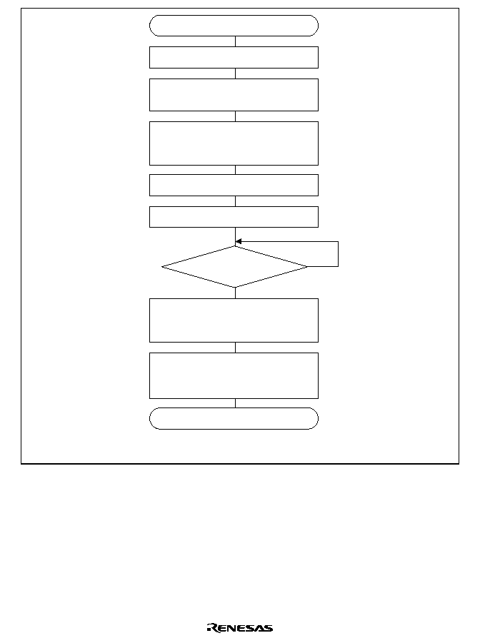
Rev. 5.0, 09/03, page 584 of 806
Initialization
Clear TE and RE bits in SCSCR to 0
Set TFRST and RFRST bits in
SCFCR to 1
1-bit interval elapsed?
Set RTRG1-0, TTRG1-0, and MCE
in SCFCR
Clear TFRST and RFRST bits to 0
Set TE and RE bits in
SCSCR to 1,and set RIE, TIE,
TEIE, and MPIE bits
Set communication format in SCSMR
Yes
No
Set value in SCBRR
Set CKE1 and CKE0
bits in SCSCR (leaving TE and RE
bits cleared to 0)
End
(1)
(2)
(3)
(4)
Wait
Note: Numbers in parentheses refer to steps in the preceding procedure description.
Figure 17.5 Sample Flowchart for SCIF Initialization

Rev. 5.0, 09/03, page 585 of 806
∑
Serial data transmission
Figure 17.6 shows a sample flowchart for serial transmission.
Use the following procedure for serial data transmission after enabling the SCIF for transmission.
1. SCIF status check and transmit data write:
Read serial status register (SCSSR) and check that the TDFE flag is set to 1, then write
transmit data to the transmit FIFO data register (SCFTDR), read 1 from the TDFE and TEND
flags, then clear these flags to 0.
The number of transmit data bytes that can be written is (16 - transmit trigger set number).
2. Serial transmission continuation procedure:
To continue serial transmission, read 1 from the TDFE flag to confirm that writing is possible,
then write data to SCFTDR, and then clear the TDFE flag to 0.
3. Break output at the end of serial transmission:
To output a break in serial transmission, set the port SC data register (SCPDR) and port SC
control register (SCPCR), then clear the TE bit to 0 in the serial control register (SCSCR). For
information on SCPDR and SCPCR, see section 17.2.8, Bit Rate Register (SCBRR).
In steps 1 and 2, it is possible to ascertain the number of data bytes that can be written from the
number of transmit data bytes in SCFTDR indicated by the upper 8 bits of the FIFO data count
register (SCFDR).
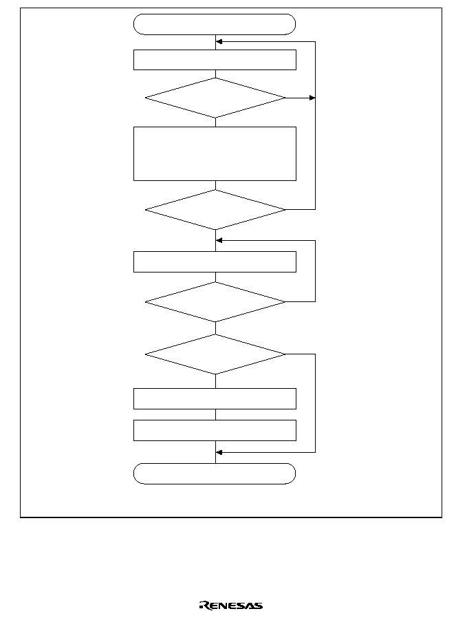
Rev. 5.0, 09/03, page 586 of 806
Start of transmission
Read TDFE bit in SCSSR
TEND= 1?
Read TEND bit in SCSSR
Clear TE bit in SCSCR to 0
Set SCPDR and SCPCR
Yes
No
TDFE= 1?
No
All data transmitted?
No
Yes
Yes
Break output?
Yes
No
Write transmit data (16 - transmit
trigger set number) to SCFTDR, read 1
from TDFE bit and TEND flag in
SCSSR, then clear to 0
End of transmission
(1)
(2)
(3)
Note: Numbers in parentheses refer to steps in the preceding procedure description.
Figure 17.6 Sample Flowchart for Transmitting Serial Data

Rev. 5.0, 09/03, page 587 of 806
In serial transmission, the SCIF operates as described below.
1. When data is written into the transmit FIFO data register (SCFTDR), the SCIF transfers the
data from SCFTDR to the transmit shift register (SCTSR) and starts transmitting. Confirm
that the TDFE flag in the serial status register (SCSSR) is set to 1 before writing transmit data
to SCFTDR. The number of data bytes that can be written is (16 ≠ transmit trigger setting).
2. When data is transferred from SCFTDR to SCTSR and transmission is started, consecutive
transmit operations are performed until there is no transmit data left in SCFTDR. When the
number of transmit data bytes in SCFTDR falls below the transmit trigger number set in the
FIFO control register (SCFCR), the TDFE flag is set. If the TIE bit in the serial control
register (SCSR) is set to 1 at this time, a transmit-FIFO-data-empty interrupt (TXI) request is
generated.
The serial transmit data is sent from the TxD pin in the following order.
a. Start bit: One-bit 0 is output.
b. Transmit data: 8-bit or 7-bit data is output in LSB-first order.
c. Parity bit: One parity bit (even or odd parity) is output. (A format in which a parity bit is
not output can also be selected.)
d. Stop bit(s): One or two 1-bits (stop bits) are output.
e. Mark state: 1 is output continuously until the start bit that starts the next transmission is
sent.
3. The SCIF checks the SCFTDR transmit data at the timing for sending the stop bit. If data is
present, the data is transferred from SCFTDR to SCTSR, the stop bit is sent, and then serial
transmission of the next frame is started.
If there is no transmit data, the TEND flag in SCSSR is set to 1, the stop bit is sent, and then
the line goes to the mark state in which 1 is output continuously.

Rev. 5.0, 09/03, page 588 of 806
Figure 17.7 shows an example of the operation for transmission.
0
1
1
1
0/1
0
1
TDFE
TEND
Parity
bit
Parity
bit
Serial
data
Start
bit
Data
Stop
bit
Start
bit
Data
Stop
bit
Idle (mark)
state
TXI interrupt
request
Data written to
SCFTDR and TDFE
flag read as 1 then
cleared to 0 by TXI
interrupt handler
One frame
D
0
D
1
D
7
D
0
D
1
D
7
0/1
TXI interrupt
request
Figure 17.7 Example of Transmit Operation
(8-Bit Data, Parity, One Stop Bit)
4. When modem control is enabled, transmission can be stopped and restarted in accordance with
the
CTS input value. When CTS is set to 1, if transmission is in progress, the line goes to the
mark state after transmission of one frame. When
CTS is set to 0, the next transmit data is
output starting from the start bit.
Figure 17.8 shows an example of the operation when modem control is used.
0
0/1
0
CTS
Parity
bit
Serial
data
TXD
Start
bit
Stop
bit
Start
bit
D
0
D
1
D
7
D
0
D
1
D
7
0/1
Rise at this point
before stop bit
Figure 17.8 Example of Operation Using Modem Control (
C
C
C
CTTTTSSSS)

Rev. 5.0, 09/03, page 589 of 806
∑
Serial data reception
Figures 17.9 and 17.10 show a sample flowchart for serial reception.
Use the following procedure for serial data reception after enabling the SCIF for reception.
1. Receive error handling and break detection: Read the DR, ER, and BRK flags in SCSSR to
identify any error, perform the appropriate error handling, then clear the DR, ER, and BRK
flags to 0. In the case of a framing error, a break can also be detected by reading the value of
the RxD pin.
2. SCIF status check and receive data read: Read the serial status register (SCSSR) and check that
RDF = 1, then read the receive data in the receive FIFO data register (SCFRDR), read 1 from
the RDF flag, and then clear the RDF flag to 0. The transition of the RDF flag from 0 to 1 can
be identified by an RXI interrupt.
3. Serial reception continuation procedure: To continue serial reception, read at least the receive
trigger set number of receive data bytes from SCFRDR, read 1 from the RDF flag, then clear
the RDF flag to 0. The number of receive data bytes in SCFRDR can be ascertained by
reading the lower bits of SCFDR.
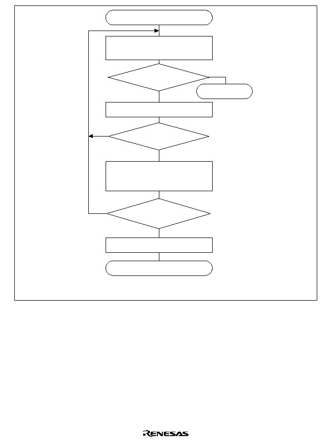
Rev. 5.0, 09/03, page 590 of 806
Start of reception
Read ORER, PER, FER
flags in SCSSR
All data received?
End of reception
No
Yes
BRK
ER DR = 1?
RDF = 1?
Yes
Yes
Clear RE bit in SCSCR to 0
No
No
Read RDF flag in SCSSR
Error handling
Read receive data from SCFRDR,
and clear RDF flag in
SCSSR to 0
(1)
(2)
(3)
Note: Numbers in parentheses refer to steps in the preceding procedure description.
Figure 17.9 Sample Flowchart for Receiving Serial Data
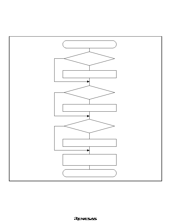
Rev. 5.0, 09/03, page 591 of 806
1. Whether a framing error or parity error has occurred in the receive data read from SCFRDR
can be ascertained from the FER and PER bits in SCSSR.
2. When a break signal is received, receive data is not transferred to SCFRDR while the BRK
flag is set. However, note that the last data in SCFRDR is H'00 and the break data in which a
framing error occurred is stored.
Error handling
End
BRK = 1?
DR = 1?
ER = 1?
Yes
Yes
Clear DR, ER, BRK flags in
SCSSR to 0
No
No
No
Receive error handling
Break processing
Read receive data from SCFRDR
Figure 17.10 Sample Flowchart for Receiving Serial Data (cont)

Rev. 5.0, 09/03, page 592 of 806
In serial reception, the SCIF operates as described below.
1. The SCIF monitors the transmission line, and if a 0 start bit is detected, performs internal
synchronization and starts reception.
2. The received data is stored in SCRSR in LSB-to-MSB order.
3. The parity bit and stop bit are received.
After receiving these bits, the SCIF carries out the following checks.
a. Stop bit check: The SCIF checks whether the stop bit is 1. If there are two stop bits, only
the first is checked.
b. The SCIF checks whether receive data can be transferred from the receive shift register
(SCRSR) to SCFRDR.
c. Break check: The SCIF checks that the BRK flag is 0, indicating that the break state is not
set.
If all the above checks are passed, the receive data is stored in SCFRDR.
Note:
Reception is not suspended when a receive error occurs.
4. If the RIE bit in SCSR is set to 1 when the RDF or DR flag changes to 1, a receive-FIFO-data-
full interrupt (RXI) request is generated.
If the RIE bit in SCSR is set to 1 when the ER flag changes to 1, a receive-error interrupt (ERI)
request is generated.
If the RIE bit in SCSR is set to 1 when the BRK flag changes to 1, a break reception interrupt
(BRI) request is generated.
Figure 17.11 shows an example of the operation for reception.
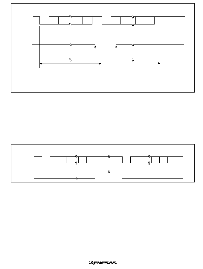
Rev. 5.0, 09/03, page 593 of 806
RDF
FER
ERI interrupt
request generated
by receive error
One frame
Data read and RDF
flag read as 1 then
cleared to 0 by
RXI interrupt handler
RXI interrupt
request
0
1
1
1
0/1
0
1
Parity
bit
Parity
bit
Serial
data
Start
bit
Data
Stop
bit
Start
bit
Data
Stop
bit
Idle (mark)
state
D
0
D
1
D
7
D
0
D
1
D
7
0/1
Figure 17.11 Example of SCIF Receive Operation
(8-Bit Data, Parity, One Stop Bit)
5. When modem control is enabled, the
RTS signal is output when SCFRDR is empty. When
RTS is 0, reception is possible. When RTS is 1, this indicates that SCFRDR is full and
reception is not possible.
Figure 17.12 shows an example of the operation when modem control is used.
0
0/1
0
1
RTS
Parity bit
Serial
data
RXD
Start
bit
Start
D
0
D
1
D
2
D
7
Figure 17.12 Example of Operation Using Modem Control (
R
R
R
RTTTTSSSS)

Rev. 5.0, 09/03, page 594 of 806
17.4
SCIF Interrupts
The SCIF has four interrupt sources: transmit-FIFO-data-empty (TXI), receive-error (ERI),
receive-data-full (RXI), and break (BRI).
Table 17.10 shows the interrupt sources and their order of priority. The interrupt sources are
enabled or disabled by means of the TIE and RIE bits in SCSCR. A separate interrupt request is
sent to the interrupt controller for each of these interrupt sources.
When the TDFE flag in the serial status register (SCSSR) is set to 1, a TXI interrupt request is
generated. The DMAC can be activated and data transfer performed when this interrupt is
generated. When data exceeding the transmit trigger number is written to the transmit data
register (SCFTDR) by the DMAC, 1 is read from the TDFE flag, after which 0 is written to it to
clear it.
When the RDF flag in SCSSR is set to 1, an RXI interrupt request is generated. The DMAC can
be activated and data transfer performed when the RDF flag in SCSSR is set to 1. When receive
data less than the receive trigger number is read from the receive data register (SCFRDR) by the
DMAC, 1 is read from the RDF flag, after which 0 is written to it to clear it.
When the ER flag in SCSSR is set to 1, an ERI interrupt request is generated.
When the BRK flag in SCSSR is set to 1, a BRI interrupt request is generated.
The TXI interrupt indicates that transmit data can be written, and the RXI interrupt indicates that
there is receive data in SCFRDR.
Table 17.10 SCIF Interrupt Sources
Interrupt
Source
Description
DMAC
Activation
Priority
ERI
Interrupt initiated by receive error flag (ER)
Not possible
High
RXI
Interrupt initiated by receive data FIFO full flag
(RDF) or data ready flag (DR)
Possible
(RDF only)
BRI
Interrupt initiated by break flag (BRK)
Not possible
TXI
Interrupt initiated by transmit FIFO data empty flag
(TDFE)
Possible
Low
See section 4, Exception Handling, for priorities and the relationship to non-SCIF interrupts.

Rev. 5.0, 09/03, page 595 of 806
17.5
Usage Notes
Note the following when using the SCIF.
1. SCFTDR Writing and TDFE Flag: The TDFE flag in the serial status register (SCSSR) is set
when the number of transmit data bytes written in the transmit FIFO data register (SCFTDR) has
fallen below the transmit trigger number set by bits TTRG1 and TTRG0 in the FIFO control
register (SCFCR). After TDFE is set, transmit data up to the number of empty bytes in SCFTDR
can be written, allowing efficient continuous transmission.
However, if the number of data bytes written to SCFTDR is equal to or less than the transmit
trigger number, the TDFE flag will be set to 1 again even after having been cleared to 0. TDFE
clearing should therefore be carried out after data exceeding the specified transmit trigger number
has been written to SCFTDR.
The number of transmit data bytes in SCFTDR can be found from the upper 8 bits of the FIFO
data count register (SCFDR).
2. SCFRDR Reading and RDF Flag: The RDF flag in the serial status register (SCSSR) is set
when the number of receive data bytes in the receive FIFO data register (SCFRDR) has become
equal to or greater than the receive trigger number set by bits RTRG1 and RTRG0 in the FIFO
control register (SCFCR). After RDF is set, receive data equivalent to the trigger number can be
read from SCFRDR, allowing efficient continuous reception.
However, if the number of data bytes in SCFRDR is equal to or greater than the trigger number,
the RDF flag will be set to 1 again if it is cleared to 0. RDF should therefore be cleared to 0 after
being read as 1 after all the receive data has been read.
The number of receive data bytes in SCFRDR can be found from the lower 8 bits of the FIFO data
count register (SCFDR).
3. Break Detection and Processing: Break signals can be detected by reading the RxD pin
directly when a framing error (FER) is detected. In the break state the input from the RxD pin
consists of all 0s, so the FER flag is set and the parity error flag (PER) may also be set. Note that,
although transfer of receive data to SCFRDR is halted in the break state, the SCIF receiver
continues to operate, so if the BRK flag is cleared to 0 it will be set to 1 again.
4. Sending a Break Signal: The I/O condition and level of the TxD pin are determined by the
SCP4DT bit in the port SC data register (SCPDR) and bits SCP4MD0 and SCP4MD1 in the port
SC control register (SCPCR). This feature can be used to send a break signal.
To send a break signal during serial transmission, clear the CP4DT bit to 0 (designating low
level), then set the SCP4MD0 and SCP4MD1 bits to 0 and 1, respectively, and finally clear the TE
bit to 0 (halting transmission). When the TE bit is cleared to 0, the transmitter is initialized
regardless of the current transmission state, and 0 is output from the TxD pin.
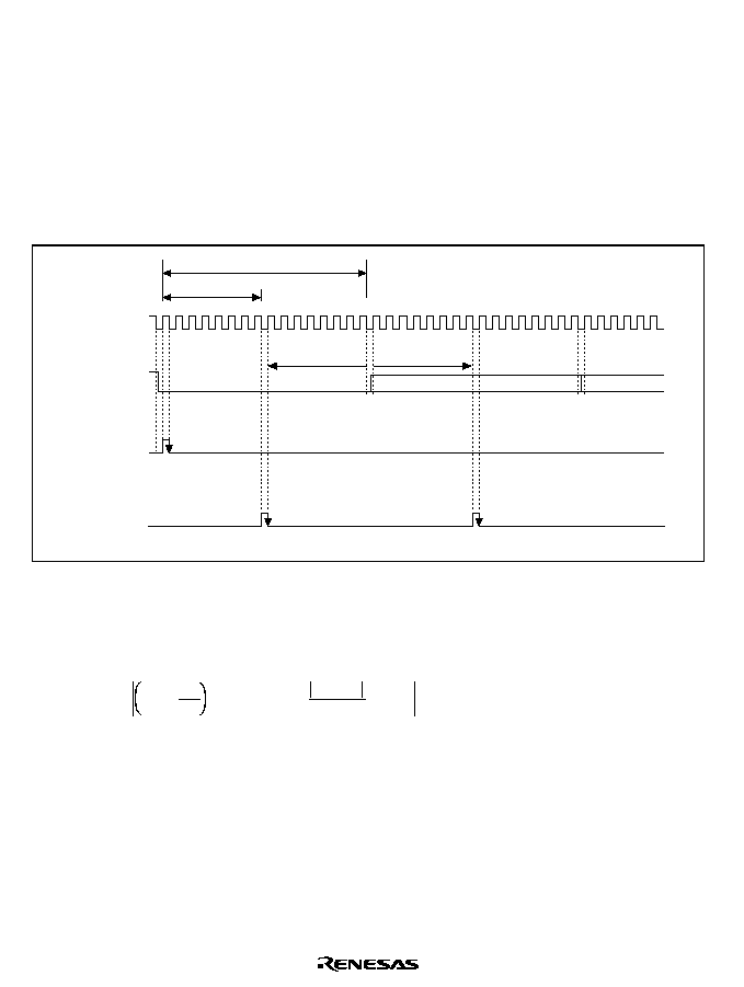
Rev. 5.0, 09/03, page 596 of 806
5. TEND Flag and TE Bit Processing: The TEND flag is set to 1 during transmission of the stop
bit of the last data. Consequently, if the TE bit is cleared to 0 immediately after setting of the
TEND flag has been confirmed, the stop bit will be in the process of transmission and will not be
transmitted normally. Therefore, the TE bit should not be cleared to 0 for at least 0.5 serial clock
cycles (or 1.5 cycles if two stop bits are used) after setting of the TEND flag is confirmed.
6. Receive Data Sampling Timing and Receive Margin: The SCIF operates on a base clock
with a frequency of 16 times the transfer rate. In reception, the SCIF synchronizes internally with
the fall of the start bit, which it samples on the base clock. Receive data is latched at the rising
edge of the eighth base clock pulse. The timing is shown in figure 17.13.
0 1 2 3 4 5 6 7 8 9 10111213 1415 0 1 2 3 4 5 6 7 8 9 10111213 1415 0 1 2 3 4 5
Base clock
Receive
data (RxD)
Synchro-
nization
sampling
timing
Data
sampling
timing
8 clocks
16 clocks
Start bit
-7.5 clocks
+7.5 clocks
D0
D1
Figure 17.13 Receive Data Sampling Timing in Asynchronous Mode
The receive margin in asynchronous mode can therefore be expressed as shown in equation 1.
Equation 1:
M = 0.5
-
1
2N
D
- 0.5
N
- (L - 0.5) F - (1 + F) ◊ 100%
Where:
M: Receive margin (%)
N: Ratio of clock frequency to bit rate (N = 16)
D: Clock duty cycle (D = 0 to 1.0)
L: Frame length (L = 9 to 12)
F: Absolute deviation of clock frequency
From equation 1, if F = 0 and D = 0.5, the receive margin is 46.875%, as given by equation 2.

Rev. 5.0, 09/03, page 597 of 806
Equation 2:
When D = 0.5 and F = 0:
M
=
(0.5 ≠ 1/(2
◊
16))
◊
100
%
=
46.875
%
This is a theoretical value. A reasonable margin to allow in system designs is 20% to 30%.

Rev. 5.0, 09/03, page 598 of 806

Rev. 5.0, 09/03, page 599 of 806
Section 18 IrDA
18.1
Overview
The SH7729R has an on-chip Infrared Data Association (IrDA) interface which is based on the
IrDA 1.0 system and can perform infrared communication. It also can be used as the SCIF by
making register settings.
18.1.1
Features
∑
Conforms to the IrDA 1.0 system
∑
Asynchronous serial communication
Data length: 8 bits
Stop bit length: 1 bit
Parity bit: None
∑
On-chip 16-stage FIFO buffers for both transmit and receive operations
∑
On-chip baud rate generator with selectable bit rates
∑
Guard functions to protect the receiver during transmission
∑
Clock supply halted to reduce power consumption when not using the IrDA interface
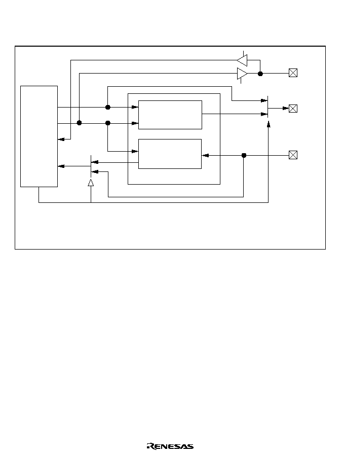
Rev. 5.0, 09/03, page 600 of 806
18.1.2
Block Diagram
Figure 18.1 shows a block diagram of the IrDA.
SCIF
Clock input
TxD
Transfer clock
RxD
Switching IrDA/SCIF
IRDA
SCK
TxD1
RxD1
Modulation unit
Demodulation unit
Legend
SCIF: Serial communication interface with FIFO
Figure 18.1 Block Diagram of IrDA
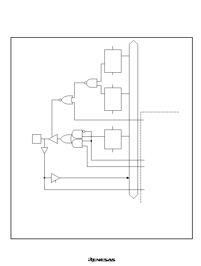
Rev. 5.0, 09/03, page 601 of 806
Figures 18.2 to 18.4 show the IrDA I/O port pins.
SCIF pin I/O and data control is performed by bits 7 to 4 of SCPCR and bits 3 and 2 of SCPDR.
For details, see section 15.2.8, SC Port Control Register (SCPCR)/SC Port Data Register
(SCPDR).
Internal data bus
Output enable
Clock input enable
IrDA
Serial clock output
Serial clock input
R
SCP3MD0
PCRW
Reset
C
Q
Q
D
R
SCP3MD1
PCRW
Reset
C
Q
D
R
SCP3DT1
PDRW
Reset
SCPT[3]/SCK1
C
D
PDRW:
Legend
SCPDR write
PDRR:
PCRW:
SCPDR read
SCPCR write
PDRR*
Note:
* When reading the SCK1 pin, the CKE1 and CKE0 bits in SCSCR to 0, and
set the SCP3MD1 bit in SCSPR to 1 (see section 15.2.8, SC Port Control
Register (SCPCR)/SC Port Data Register (SCPDR)).
Figure 18.2 SCPT[3]/SCK1 Pin
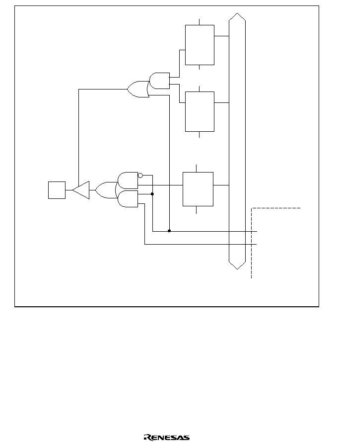
Rev. 5.0, 09/03, page 602 of 806
Internal data bus
Output enable
IrDA
Serial
transfer
output
Q
R
SCP2DT1
PDRW
Reset
SCPT[2]/TxD1
C
D
PCRW:
PDRW:
Legend
SCPCR write
SCPDR write
R
SCP2MD0
PCRW
Reset
C
Q
D
R
SCP2MD1
PCRW
Reset
C
Q
D
Figure 18.3 SCPT[2]/TxD1 Pin
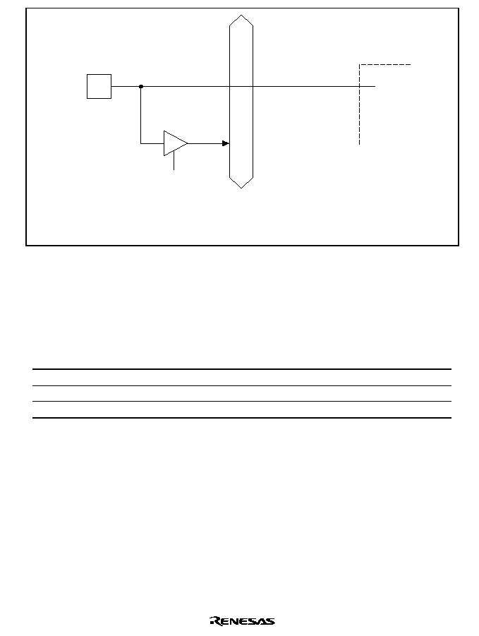
Rev. 5.0, 09/03, page 603 of 806
IrDA
Serial
receive
data
Internal data bus
PDRR*
SCPT[2]/RxD1
Legend
PDRR: SCPDR read
Note:
* When reading the RxD1 pin, set the RE bit in SCSCR to 1.
Figure 18.4 SCPT[2]/RxD1 Pin
18.1.3
Pin Configuration
The IrDA has the serial pins summarized in table 18.1.
Table 18.1
IrDA Pins
Pin Name
Signal Name
I/O
Function
Serial clock pin
SCK1
I/O
Clock I/O
Receive data pin
RxD1
Input
Receive data input
Transmit data pin
TxD1
Output
Transmit data output
Note:
Clock input from the serial clock pin cannot be set in IrDA mode.

Rev. 5.0, 09/03, page 604 of 806
18.1.4
Register Configuration
The IrDA has the internal registers shown in table 18.2. These registers select IrDA or SCIF
mode, specify the data format and a bit rate, and control the transmit and receive units.
Table 18.2
IrDA Registers
Register Name
Abbreviation
R/W
Initial Value
Address
Access
Size
Serial mode register 1
SCSMR1
R/W
H'00
H'04000140
(H'A4000140)
*
2
8 bits
Bit rate register 1
SCBRR1
R/W
H'FF
H'04000142
(H'A4000142)
*
2
8 bits
Serial control register 1
SCSCR1
R/W
H'00
H'04000144
(H'A4000144)
*
2
8 bits
Transmit FIFO data register 1
SCFTDR1
W
--
H'04000146
(H'A4000146)
*
2
8 bits
Serial status register 1
SCSSR1
R/(W)
*
1
H'0060
H'04000148
(H'A4000148)
*
2
16 bits
Receive FIFO data register 1
SCFRDR1
R
Undefined
H'0400014A
(H'A400014A)
*
2
8 bits
FIFO control register 1
SCFCR1
R/W
H'00
H'0400014C
(H'A400014C)
*
2
8 bits
FIFO data count register 1
SCFDR1
R
H'0000
H'0400014E
(H'A400014E)
*
2
16 bits
Notes: These registers are located in area 1 of physical space. Therefore, when the cache is on,
either access these registers from the P2 area of logical space or else make an appropriate
setting using the MMU so that these registers are not cached.
1. Only 0 can be written to clear the flag.
2. When address translation by the MMU does not apply, the address in parentheses
should be used.

Rev. 5.0, 09/03, page 605 of 806
18.2
Register Description
Specifications of the registers in the IrDA are the same as those in the SCIF except for the serial
mode register described below. Therefore, refer to section 17, Serial Communication Interface
with FIFO (SCIF), for details of these registers.
18.2.1
Serial Mode Register (SCSMR)
Bit:
7
6
5
4
3
2
1
0
IRMOD
ICK3
ICK2
ICK1
ICK0
PSEL
CKS1
CKS0
Initial value:
0
0
0
0
0
0
0
0
R/W:
R/W
R/W
R/W
R/W
R/W
R/W
R/W
R/W
SCSMR is an 8-bit register that selects IrDA or SCIF mode, specifies the SCIF serial
communication format, selects the IrDA output pulse width, and selects the baud rate generator
clock source.
This module operates as IrDA when the IRMOD bit is set to 1. At this time, bits 3 to 6 are fixed at
0. This register functions in the same way as the SCSMR register in the SCIF when the IRMOD
bit is cleared to 0; therefore, this module can also operate as an SCIF.
SCSMR is initialized to H'00 by a power-on reset or manual reset, when the module is stopped by
the module standby function, and in standby mode.
Bit 7--IrDA Mode (IRMOD): Selects whether this module operates as an IrDA serial
communication interface or as an SCIF.
Bit 7: IRMOD
Description
0
Operates as an SCIF
(Initial value)
1
*
Operates as an IrDA
Note:
*
Do not set the CKE1 bit in the serial control register (SCSCRT) to 1 if the IRMCD bit is set
to 1.

Rev. 5.0, 09/03, page 606 of 806
Bits 6 to 3--Ir Clock Select Bits (ICK3 to ICK0)
Bit 2--Output Pulse Width Select (PSEL): PSEL selects an IrDA output pulse width that is 3/16
of the bit length for 115 kbps or 3/16 of the bit length for the selected baud rate.
The Ir clock select bits should be set properly to fix the output pulse width at 3/16 of the bit length
for 115 kbps by setting the PSEL bit to 1.
Bit 6:
ICK3
Bit 5:
ICK2
Bit 4:
ICK1
Bit 3:
ICK0
Bit 2:
PSEL
Description
ICK3
ICK2
ICK1
ICK0
1
Pulse width: 3/16 of 115 kbps bit length
Don't
care
Don't
care
Don't
care
Don't
care
0
Pulse width: 3/16 of bit length
It is necessary to generate a fixed clock pulse, IRCLK, by dividing the P
clock by 1/2N + 2 (with
the value of N determined by the setting of ICK3≠ICK0).
Example:
P
clock: 14.7456 MHz
IRCLK: 921.6 kHz (fixed)
N: Setting of ICK3≠ICK0 (0
N
15)
- 1 7
N
P
2XIRCLK
Accordingly, N is 7.
Bits 1 and 0--Clock Select 1 and 0 (CKS1, CKS0): Select the internal baud rate generator clock
source. P
, P
/4, P
/16, or P
/64 can be selected by setting the CKS1 and CKS0 bits.
Refer to section 15.2.9, Bit Rate Register (SCBRR), for the relationship between the clock source,
the bit rate register set value, and the baud rate.
Bit 1: CKS1
Bit 0: CKS0
Description
0
0
P
clock
(Initial value)
0
1
P
/4 clock
1
0
P
/16
1
1
P
/64
Note:
P
: Peripheral clock

Rev. 5.0, 09/03, page 607 of 806
18.3
Operation Description
The IrDA module can perform infrared communication conforming to IrDA 1.0 by connecting
infrared transmit/receive units. The serial communication interface unit includes a 16-stage FIFO
buffer in the transmit unit and the receive unit, allowing CPU overhead to be reduced and
continuous high-speed communication to be performed. This module also supports DMAC data
transfer. The IrDA module differs from the SCIF described in section 17, Serial Communication
Interface with FIFO (SCIF) in that it does not include modem control signals RTS and CTS.
Refer to section 17.3, Operation, for SCIF mode operation.
18.3.1
Overview
The IrDA module modifies TxD/RxD transmit/receive data waveforms to satisfy the IrDA 1.0
specification for infrared communication.
In the IrDA 1.0 specification, communication is first performed at a speed of 9600 bps, and the
communication speed is changed. However, the communication rate cannot be automatically
changed in this module, so the communication speed should be confirmed, and the appropriate
speed set for this module by software.
Note:
In IrDA mode, reception cannot be performed when the TE bit in the serial control register
(SCSCR) is set to 1 (enabling transmission). When performing reception, clear the TE bit
in SCSCR to 0.
As the SH7729R's RxD1 pin is active-high in IrDA mode, a (Schmidt) inverter must be
inserted when connecting an active-low IrDA module.
The RxD1 pin is active-low in SCIF mode.
18.3.2
Transmitting
In the case of a serial output signal (UART frame) from the SCIF, its waveforms are modified and
the signal is converted into the IR frame serial output signal by the IrDA module, as shown in
figure 18.5.
When serial data is 0, a pulse of 3/16 the IR frame bit width is generated and output. When serial
data is 1, no pulse is output.
An infrared LED is driven by this signal demodulated to 3/16 width.
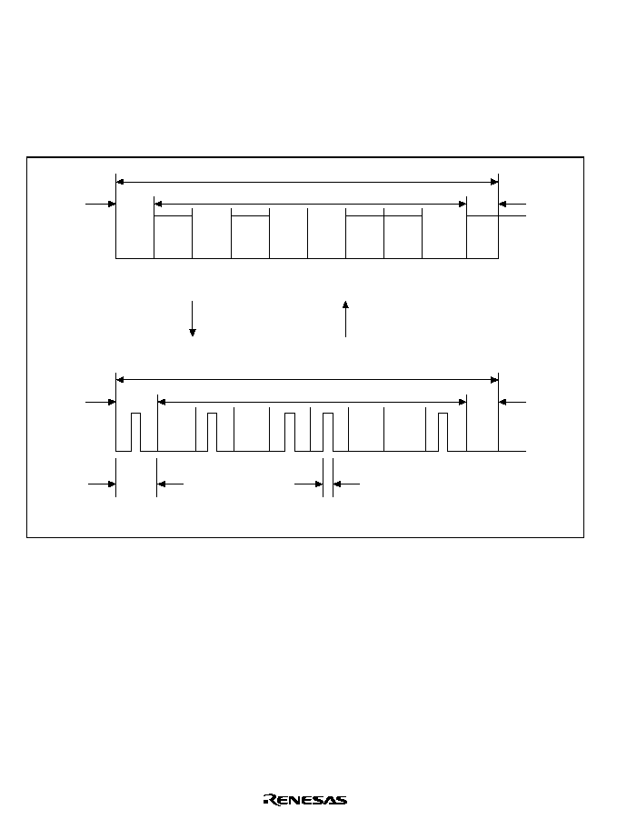
Rev. 5.0, 09/03, page 608 of 806
18.3.3
Receiving
Received 3/16 IR frame bit-width pulses are demodulated and converted to a UART frame, as
shown in figure 18.5.
Demodulation to 0 is performed for pulse output, and demodulation to 1 is performed for no pulse
output.
UART frame
Data
IR frame
Data
Receive
Transmit
Stop bit
Stop bit
Start bit
Start bit
Bit cycle
3/16-bit cycle
pulse width
0
1
0
1
0
0
1
1
0
1
0
1
0
1
0
0
1
1
0
1
Figure 18.5 Transmit/Receive Operation

Rev. 5.0, 09/03, page 609 of 806
Section 19 Pin Function Controller
19.1
Overview
The pin function controller (PFC) is composed of registers for selecting the function of
multiplexed pins and the input/output direction. The pin function and input/output direction can be
selected for each pin individually without regard to the operating mode of the chip. Table 19.1
lists the multiplexed pins.
Table 19.1
List of Multiplexed Pins
Port
Port Function
(Related Module)
Other Function
(Related Module)
A
PTA7 input/output (port)
D23 input/output (data bus)
A
PTA6 input/output (port)
D22 input/output (data bus)
A
PTA5 input/output (port)
D21 input/output (data bus)
A
PTA4 input/output (port)
D20 input/output (data bus)
A
PTA3 input/output (port)
D19 input/output (data bus)
A
PTA2 input/output (port)
D18 input/output (data bus)
A
PTA1 input/output (port)
D17 input/output (data bus)
A
PTA0 input/output (port)
D16 input/output (data bus)
B
PTB7 input/output (port)
D31 input/output (data bus)
B
PTB6 input/output (port)
D30 input/output (data bus)
B
PTB5 input/output (port)
D29 input/output (data bus)
B
PTB4 input/output (port)
D28 input/output (data bus)
B
PTB3 input/output (port)
D27 input/output (data bus)
B
PTB2 input/output (port)
D26 input/output (data bus)
B
PTB1 input/output (port)
D25 input/output (data bus)
B
PTB0 input/output (port)
D24 input/output (data bus)
C
PTC7 input/output (port)/PINT7 input (INTC)
MCS7
output (BSC)
C
PTC6 input/output (port)/PINT6 input (INTC)
MCS6
output (BSC)
C
PTC5 input/output (port)/PINT5 input (INTC)
MCS5
output (BSC)
C
PTC4 input/output (port)/PINT4 input (INTC)
MCS4
output (BSC)
C
PTC3 input/output (port)/PINT3 input (INTC)
MCS3
output (BSC)
C
PTC2 input/output (port)/PINT2 input (INTC)
MCS2
output (BSC)
C
PTC1 input/output (port)/PINT1 input (INTC)
MCS1
output (BSC)

Rev. 5.0, 09/03, page 610 of 806
Port
Port Function
(Related Module)
Other Function
(Related Module)
C
PTC0 input/output (port)/PINT0 input (INTC)
MCS0
output (BSC)
D
PTD7 input/output (port)
DACK1 output (DMAC)
D
PTD6 input (port)
DREQ1
input (DMAC)
D
PTD5 input/output (port)
DACK0 output (DMAC)
D
PTD4 input (port)
DREQ0
input (DMAC)
D
PTD3 input/output (port)
WAKEUP
output (WTC)
D
PTD2 input/output (port)
RESETOUT
output
D
PTD1 input/output (port)
DRAK0 output (DMAC)
D
PTD0 input/output (port)
DRAK1 output (DMAC)
E
PTE7 input/output (port)
AUDSYNC
output (AUD)
*
1
E
PTE6 input/output (port)
--
E
PTE5 input/output (port)
CE2B
output (PCMCIA)
E
PTE4 input/output (port)
CE2A
output (PCMCIA)
E
PTE3 input/output (port)
--
E
PTE2 input/output (port)
RAS3U
output (BSC)
E
PTE1 input/output (port)
--
E
PTE0 input/output (port)
TDO output (UDI)
*
2
F
PTF7 input (port)/PINT15 input (INTC)
TRST input (AUD, UDI)
*
2
F
PTF6 input (port)/PINT14 input (INTC)
TMS input (UDI)
*
2
F
PTF5 input (port)/PINT13 input (INTC)
TD1 input (UDI)
*
2
F
PTF4 input (port)/PINT12 input (INTC)
TCK input (UDI)
*
2
F
PTF3 input (port)/PINT11 input (INTC)
IRLS3
input (INTC)
F
PTF2 input (port)/PINT10 input (INTC)
IRLS2
input (INTC)
F
PTF1 input (port)/PINT9 input (INTC)
IRLS1
input (INTC)
F
PTF0 input (port)/PINT8 input (INTC)
IRLS0
input (INTC)
G
PTG7 input (port)
IOIS16
input (PCMCIA)
G
PTG6 input (port)
ASEMD0
input (AUD, UDI)
*
2
G
PTG5 input (port)
ASEBRKAK
output (AUD)
*
1
G
PTG4 input (port)
CKIO2 output (CPG)
G
PTG3 input (port)
AUDATA3 output (AUD)
*
1
G
PTG2 input (port)
AUDATA2 output (AUD)
*
1

Rev. 5.0, 09/03, page 611 of 806
Port
Port Function
(Related Module)
Other Function
(Related Module)
G
PTG1 input (port)
AUDATA1 output (AUD)
*
1
G
PTG0 input (port)
AUDATA0 output (AUD)
*
1
H
PTH7 input/output (port)
TCLK input/output (TMU)
H
PTH6 input (port)
AUDCK input (AUD)
*
1
H
PTH5 input (port)
ADTRG
input (ADC)
H
PTH4 input (port)/IRQ4 input (INTC)
IRQ4 input (INTC)
H
PTH3 input (port)/IRQ3 input (INTC)
IRQ3 input (INTC)
H
PTH2 input (port)/IRQ2 input (INTC)
IRQ2 input (INTC)
H
PTH1 input (port)/IRQ1 input (INTC)
IRQ1 input (INTC)
H
PTH0 input (port)/IRQ0 input (INTC)
IRQ0 input (INTC)
J
PTJ7 input/output (port)
STATUS1 output (CPG)
J
PTJ6 input/output (port)
STATUS0 output (CPG)
J
PTJ5 input/output (port)
--
J
PTJ4 input/output (port)
--
J
PTJ3 input/output (port)
CASU
output (BSC)
J
PTJ2 input/output (port)
CASL
output (BSC)
J
PTJ1 input/output (port)
--
J
PTJ0 input/output (port)
RAS3L
output (BSC)
K
PTK7 input/output (port)
WE3
output (BSC)/DQMUU output
(BSC)/
ICIOWR
output (BSC)
K
PTK6 input/output (port)
WE2
output (BSC)/DQMUL output
(BSC)/
ICIORD
output (BSC)
K
PTK5 input/output (port)
CKE output (BSC)
K
PTK4 input/output (port)
BS
output (BSC)
K
PTK3 input/output (port)
CS5
output (BSC)/
CE1A
output (BSC)
K
PTK2 input/output (port)
CS4
output (BSC)
K
PTK1 input/output (port)
CS3
output (BSC)
K
PTK0 input/output (port)
CS2
output (BSC)
L
PTL7 input (port)
AN7 input (ADC)/DA0 output (DAC)
L
PTL6 input (port)
AN6 input (ADC)/DA1 output (DAC)
L
PTL5 input (port)
AN5 input (ADC)

Rev. 5.0, 09/03, page 612 of 806
Port
Port Function
(Related Module)
Other Function
(Related Module)
L
PTL4 input (port)
AN4 input (ADC)
L
PTL3 input (port)
AN3 input (ADC)
L
PTL2 input (port)
AN2 input (ADC)
L
PTL1 input (port)
AN1 input (ADC)
L
PTL0 input (port)
AN0 input (ADC)
SCPT
SCPT7 input (port)/IRQ5 input (INTC)
CTS2
input (UART ch 3)/IRQ5 input (INTC)
SCPT
SCPT6 input/output (port)
RTS2
output (UART ch 3)
SCPT
SCPT5 input/output (port)
SCK2 input/output (UART ch 3)
SCPT
SCPT4 input (port)
RxD2 input (UART ch 3)
SCPT4 output (port)
TxD2 output (UART ch 3)
SCPT
SCPT3 input/output (port)
SCK1 input/output (UART ch 2)
SCPT
SCPT2 input (port)
RxD1 input (UART ch 2)
SCPT2 output (port)
TxD1 output (UART ch 2)
SCPT
SCPT1 input/output (port)
SCK0 input/output (UART ch 1)
SCPT
SCPT0 input (port)
RxD0 input (UART ch 1)
SCPT0 output (port)
TxD0 output (UART ch 1)
Notes: SCPT0, SCPT2, and SCPT4 have the same data register to be accessed although they
have different input pins and output pins.
1. For use of emulator only
2. For use of emulator or boundary scan only

Rev. 5.0, 09/03, page 613 of 806
19.2
Register Configuration
Table 19.2 summarizes the registers of the pin function controller.
Table 19.2
Pin Function Controller Registers
Name
Abbreviation
R/W
Initial Value
Address
Access
Size
Port A control register
PACR
R/W
H'0000
H'04000100
(H'A4000100)
*
16
Port B control register
PBCR
R/W
H'0000
H'04000102
(H'A4000102)
*
16
Port C control register
PCCR
R/W
H'AAAA
H'04000104
(H'A4000104)
*
16
Port D control register
PDCR
R/W
H'AA8A
H'04000106
(H'A4000106)
*
16
Port E control register
PECR
R/W
H'AAAA/H'2AA8
H'04000108
(H'A4000108)
*
16
Port F control register
PFCR
R/W
H'AAAA/H'00AA
H'0400010A
(H'A400010A)
*
16
Port G control register
PGCR
R/W
H'AAAA/H'A200
H'0400010C
(H'A400010C)
*
16
Port H control register
PHCR
R/W
H'AAAA/H'8AAA
H'0400010E
(H'A400010E)
*
16
Port J control register
PJCR
R/W
H'0000
H'04000110
(H'A4000110)
*
16
Port K control register
PKCR
R/W
H'0000
H'04000112
(H'A4000112)
*
16
Port L control register
PLCR
R/W
H'0000
H'04000114
(H'A4000114)
*
16
SC port control register
SCPCR
R/W
H'A888
H'04000116
(H'A4000116)
*
16
Notes: These registers are located in area 1 of physical space. Therefore, when the cache is on,
either access these registers from the P2 area of logical space or else make an appropriate
setting using the MMU so that these registers are not cached.
The initial value of the port E, F, G, and H control registers depends on the state of the
ASEMD0
pin.
If a low level is input at the
ASEMD0
pin while the
RESETP
pin is asserted, ASE mode is
entered; if a high level is input, normal mode is entered. See section 23, User Debugging
Interface (UDI), for more information on the UDI.
*
When address translation by the MMU does not apply, the address in parentheses
should be used.

Rev. 5.0, 09/03, page 614 of 806
19.3
Register Descriptions
19.3.1
Port A Control Register (PACR)
Bit:
15
14
13
12
11
10
9
8
7
6
5
4
3
2
1
0
PA7
MD1
PA7
MD0
PA6
MD1
PA6
MD0
PA5
MD1
PA5
MD0
PA4
MD1
PA4
MD0
PA3
MD1
PA3
MD0
PA2
MD1
PA2
MD0
PA1
MD1
PA1
MD0
PA0
MD1
PA0
MD0
Initial value:
0
0
0
0
0
0
0
0
0
0
0
0
0
0
0
0
R/W: R/W R/W R/W R/W R/W R/W R/W R/W R/W R/W R/W R/W R/W R/W R/W R/W
The port A control register (PACR) is a 16-bit readable/writable register that selects the pin
functions. PACR is initialized to H'0000 by a power-on reset, but is not initialized by a manual
reset, in standby mode, or in sleep mode.
Bits 15 and 14--PA7 Mode 1 and 0 (PA7MD1, PA7MD0)
Bits 13 and 12--PA6 Mode 1 and 0 (PA6MD1, PA6MD0)
Bits 11 and 10--PA5 Mode 1 and 0 (PA5MD1, PA5MD0)
Bits 9 and 8--PA4 Mode 1 and 0 (PA4MD1, PA4MD0)
Bits 7 and 6--PA3 Mode 1 and 0 (PA3MD1, PA3MD0)
Bits 5 and 4--PA2 Mode 1 and 0 (PA2MD1, PA2MD0)
Bits 3 and 2--PA1 Mode 1 and 0 (PA1MD1, PA1MD0)
Bits 1 and 0--PA0 Mode 1 and 0 (PA0MD1, PA0MD0)
These bits select the pin functions and perform input pull-up MOS control.
Bit (2n + 1)
Bit 2n
PAnMD1
PAnMD0
Pin Function
0
0
Other function (see table 19.1)
(Initial value)
0
1
Port output
1
0
Port input (Pull-up MOS: on)
1
1
Port input (Pull-up MOS: off)
(n = 0 to 7)

Rev. 5.0, 09/03, page 615 of 806
19.3.2
Port B Control Register (PBCR)
Bit:
15
14
13
12
11
10
9
8
7
6
5
4
3
2
1
0
PB7
MD1
PB7
MD0
PB6
MD1
PB6
MD0
PB5
MD1
PB5
MD0
PB4
MD1
PB4
MD0
PB3
MD1
PB3
MD0
PB2
MD1
PB2
MD0
PB1
MD1
PB1
MD0
PB0
MD1
PB0
MD0
Initial value:
0
0
0
0
0
0
0
0
0
0
0
0
0
0
0
0
R/W: R/W R/W R/W R/W R/W R/W R/W R/W R/W R/W R/W R/W R/W R/W R/W R/W
The port B control register (PBCR) is a 16-bit readable/writable register that selects the pin
functions. PBCR is initialized to H'0000 by a power-on reset, but is not initialized by a manual
reset, in standby mode, or in sleep mode.
Bits 15 and 14--PB7 Mode 1 and 0 (PB7MD1, PB7MD0)
Bits 13 and 12--PB6 Mode 1 and 0 (PB6MD1, PB6MD0)
Bits 11 and 10--PB5 Mode 1 and 0 (PB5MD1, PB5MD0)
Bits 9 and 8--PB4 Mode 1 and 0 (PB4MD1, PB4MD0)
Bits 7 and 6--PB3 Mode 1 and 0 (PB3MD1, PB3MD0)
Bits 5 and 4--PB2 Mode 1 and 0 (PB2MD1, PB2MD0)
Bits 3 and 2--PB1 Mode 1 and 0 (PB1MD1, PB1MD0)
Bits 1 and 0--PB0 Mode 1 and 0 (PB0MD1, PB0MD0)
These bits select the pin functions and perform input pull-up MOS control.
Bit (2n + 1)
Bit 2n
PBnMD1
PBnMD0
Pin Function
0
0
Other function (see table 19.1)
(Initial value)
0
1
Port output
1
0
Port input (Pull-up MOS: on)
1
1
Port input (Pull-up MOS: off)
(n = 0 to 7)

Rev. 5.0, 09/03, page 616 of 806
19.3.3
Port C Control Register (PCCR)
Bit:
15
14
13
12
11
10
9
8
7
6
5
4
3
2
1
0
PC7
MD1
PC7
MD0
PC6
MD1
PC6
MD0
PC5
MD1
PC5
MD0
PC4
MD1
PC4
MD0
PC3
MD1
PC3
MD0
PC2
MD1
PC2
MD0
PC1
MD1
PC1
MD0
PC0
MD1
PC0
MD0
Initial value:
1
0
1
0
1
0
1
0
1
0
1
0
1
0
1
0
R/W: R/W R/W R/W R/W R/W R/W R/W R/W R/W R/W R/W R/W R/W R/W R/W R/W
The port C control register (PCCR) is a 16-bit readable/writable register that selects the pin
functions. PCCR is initialized to H'AAAA by a power-on reset, but is not initialized by a manual
reset, in standby mode, or in sleep mode.
Bits 15 and 14--PC7 Mode 1 and 0 (PC7MD1, PC7MD0)
Bits 13 and 12--PB6 Mode 1 and 0 (PC6MD1, PC6MD0)
Bits 11 and 10--PC5 Mode 1 and 0 (PC5MD1, PC5MD0)
Bits 9 and 8--PC4 Mode 1 and 0 (PC4MD1, PC4MD0)
Bits 7 and 6--PC3 Mode 1 and 0 (PC3MD1, PC3MD0)
Bits 5 and 4--PC2 Mode 1 and 0 (PC2MD1, PC2MD0)
Bits 3 and 2--PC1 Mode 1 and 0 (PC1MD1, PC1MD0)
Bits 1 and 0--PC0 Mode 1 and 0 (PC0MD1, PC0MD0)
These bits select the pin functions and perform input pull-up MOS control.
Bit (2n + 1)
Bit 2n
PCnMD1
PCnMD0
Pin Function
0
0
Other function (see table 19.1)
0
1
Port output
1
0
Port input (Pull-up MOS: on)
(Initial value)
1
1
Port input (Pull-up MOS: off)
(n = 0 to 7)

Rev. 5.0, 09/03, page 617 of 806
19.3.4
Port D Control Register (PDCR)
Bit:
15
14
13
12
11
10
9
8
7
6
5
4
3
2
1
0
PD7
MD1
PD7
MD0
PD6
MD1
PD6
MD0
PD5
MD1
PD5
MD0
PD4
MD1
PD4
MD0
PD3
MD1
PD3
MD0
PD2
MD1
PD2
MD0
PD1
MD1
PD1
MD0
PD0
MD1
PD0
MD0
Initial value:
1
0
1
0
1
0
1
0
1
0
0
0
1
0
1
0
R/W: R/W R/W R/W R/W R/W R/W R/W R/W R/W R/W R/W R/W R/W R/W R/W R/W
The port D control register (PDCR) is a 16-bit readable/writable register that selects the pin
functions. PDCR is initialized to H'AA8A by a power-on reset, but is not initialized by a manual
reset, in standby mode, or in sleep mode.
Bits 15 and 14--PD7 Mode 1 and 0 (PD7MD1, PD7MD0)
Bits 11 and 10--PD5 Mode 1 and 0 (PD5MD1, PD5MD0)
Bits 7 and 6--PD3 Mode 1 and 0 (PD3MD1, PD3MD0)
Bits 5 and 4--PD2 Mode 1 and 0 (PD2MD1, PD2MD0)
Bits 3 and 2--PD1 Mode 1 and 0 (PD1MD1, PD1MD0)
Bits 1 and 0--PD0 Mode 1 and 0 (PD0MD1, PD0MD0)
These bits select the pin functions and perform input pull-up MOS control.
Bit (2n + 1)
Bit 2n
PDnMD1
PDnMD0
Pin Function
0
0
Other function (see table 19.1)
(Initial value) (n = 2)
0
1
Port output
1
0
Port input (Pull-up MOS: on)
(Initial value) (n = 0, 1, 3, 5, 7)
1
1
Port input (Pull-up MOS: off)
(n = 0 to 3, 5, 7)
Bits 13 and 12--PD6 Mode 1 and 0 (PD6MD1, PD6MD0)
Bits 9 and 8--PD4 Mode 1 and 0 (PD4MD1, PD4MD0)
These bits select the pin functions and perform input pull-up MOS control.
Bit (2n + 1)
Bit 2n
PDnMD1
PDnMD0
Pin Function
0
0
Other function (see table 19.1)
0
1
Reserved
1
0
Port input (Pull-up MOS: on)
(Initial value)
1
1
Port input (Pull-up MOS: off)
(n = 4, 6)

Rev. 5.0, 09/03, page 618 of 806
19.3.5
Port E Control Register (PECR)
Bit:
15
14
13
12
11
10
9
8
7
6
5
4
3
2
1
0
PE7
MD1
PE7
MD0
PE6
MD1
PE6
MD0
PE5
MD1
PE5
MD0
PE4
MD1
PE4
MD0
PE3
MD1
PE3
MD0
PE2
MD1
PE2
MD0
PE1
MD1
PE1
MD0
PE0
MD1
PE0
MD0
Initial value:
1/0
0
1
0
1
0
1
0
1
0
1
0
1
0
1/0
0
R/W: R/W R/W R/W R/W R/W R/W R/W R/W R/W R/W R/W R/W R/W R/W R/W R/W
The port E control register (PECR) is a 16-bit readable/writable register that selects the pin
functions. PECR is initialized to H'AAAA (
ASEMD0 = 1) or H'2AA8 (ASEMD0 = 0) by a
power-on reset, but is not initialized by a manual reset, in software standby mode, or in sleep
mode.
Bits 15 and 14--PE7 Mode 1 and 0 (PE7MD1, PE7MD0)
Bits 13 and 12--PE6 Mode 1 and 0 (PE6MD1, PE6MD0)
Bits 11 and 10--PE5 Mode 1 and 0 (PE5MD1, PE5MD0)
Bits 9 and 8--PE4 Mode 1 and 0 (PE4MD1, PE4MD0)
Bits 7 and 6--PE3 Mode 1 and 0 (PE3MD1, PE3MD0)
Bits 5 and 4--PE2 Mode 1 and 0 (PE2MD1, PE2MD0)
Bits 3 and 2--PE1 Mode 1 and 0 (PE1MD1, PE1MD0)
Bits 1 and 0--PE0 Mode 1 and 0 (PE0MD1, PE0MD0)
These bits select the pin functions and perform input pull-up MOS control.
Bit (2n + 1)
Bit 2n
PEnMD1
PEnMD0
Pin Function
0
0
Reserved (n = 0, 7) (see table 19.1)
(Initial value) (
ASEMD0
= 0)
0
1
Port output
1
0
Port input (Pull-up MOS: on)
(Initial value) (
ASEMD0
= 1)
1
1
Port input (Pull-up MOS: off)
(n = 0, 7)
Bit (2n + 1)
Bit 2n
PEnMD1
PEnMD0
Pin Function
0
0
Other function (n = 2, 4, 5) (see table 19.1), Reserved (n = 1, 3, 6)
0
1
Port output
1
0
Port input (Pull-up MOS: on)
(Initial value)
1
1
Port input (Pull-up MOS: off)
(n = 1 to 6)

Rev. 5.0, 09/03, page 619 of 806
19.3.6
Port F Control Register (PFCR)
Bit:
15
14
13
12
11
10
9
8
7
6
5
4
3
2
1
0
PF7
MD1
PF7
MD0
PF6
MD1
PF6
MD0
PF5
MD1
PF5
MD0
PF4
MD1
PF4
MD0
PF3
MD1
PF3
MD0
PF2
MD1
PF2
MD0
PF1
MD1
PF1
MD0
PF0
MD1
PF0
MD0
Initial value:
1/0
0
1/0
0
1/0
0
1/0
0
1
0
1
0
1
0
1
0
R/W: R/W R/W R/W R/W R/W R/W R/W R/W R/W R/W R/W R/W R/W R/W R/W R/W
The port F control register (PFCR) is a 16-bit readable/writable register that selects the pin
functions. PFCR is initialized to H'AAAA (ASEMD0 = 1) or H'00AA (ASEMD0 = 0) by a power-
on reset, but is not initialized by a manual reset, in standby mode, or in sleep mode.
Bits 15 and 14--PF7 Mode 1 and 0 (PF7MD1, PF7MD0)
Bits 13 and 12--PF6 Mode 1 and 0 (PF6MD1, PF6MD0)
Bits 11 and 10--PF5 Mode 1 and 0 (PF5MD1, PF5MD0)
Bits 9 and 8--PF4 Mode 1 and 0 (PF4MD1, PF4MD0)
Bits 7 and 6--PF3 Mode 1 and 0 (PF3MD1, PF3MD0)
Bits 5 and 4--PF2 Mode 1 and 0 (PF2MD1, PF2MD0)
Bits 3 and 2--PF1 Mode 1 and 0 (PF1MD1, PF1MD0)
Bits 1 and 0--PF0 Mode 1 and 0 (PF0MD1, PF0MD0)
These bits select the pin functions and perform input pull-up MOS control.
Bit (2n + 1)
Bit 2n
PFnMD1
PFnMD0
Pin Function
0
0
Other function (see table 19.1)
(Initial value) (
ASEMD0
= 0)
0
1
Reserved
1
0
Port input (Pull-up MOS: on)
(Initial value) (
ASEMD0
= 1)
1
1
Port input (Pull-up MOS: off)
(n = 4 to 7)
Bit (2n + 1)
Bit 2n
PFnMD1
PFnMD0
Pin Function
0
0
Other function (see table 19.1)
0
1
Reserved
1
0
Port input (Pull-up MOS: on)
(Initial value)
1
1
Port input (Pull-up MOS: off)
(n = 0 to 3)

Rev. 5.0, 09/03, page 620 of 806
19.3.7
Port G Control Register (PGCR)
Bit:
15
14
13
12
11
10
9
8
7
6
5
4
3
2
1
0
PG7
MD1
PG7
MD0
PG6
MD1
PG6
MD0
PG5
MD1
PG5
MD0
PG4
MD1
PG4
MD0
PG3
MD1
PG3
MD0
PG2
MD1
PG2
MD0
PG1
MD1
PG1
MD0
PG0
MD1
PG0
MD0
Initial value:
1
0
1/0
0
1/0
0
1
0
1/0
0
1/0
0
1/0
0
1/0
0
R/W: R/W R/W R/W R/W R/W R/W R/W R/W R/W R/W R/W R/W R/W R/W R/W R/W
The port G control register (PGCR) is a 16-bit readable/writable register that selects the pin
functions. PGCR is initialized to H'AAAA (
ASEMD0 = 1) or H'A200 (ASEMD0 = 0) by a power-
on reset, but is not initialized by a manual reset, in standby mode, or in sleep mode.
Bits 15 and 14--PG7 Mode 1 and 0 (PG7MD1, PG7MD0)
Bits 13 and 12--PG6 Mode 1 and 0 (PG6MD1, PG6MD0)
Bits 11 and 10--PG5 Mode 1 and 0 (PG5MD1, PG5MD0)
Bits 9 and 8--PG4 Mode 1 and 0 (PG4MD1, PG4MD0)
Bits 7 and 6--PG3 Mode 1 and 0 (PG3MD1, PG3MD0)
Bits 5 and 4--PG2 Mode 1 and 0 (PG2MD1, PG2MD0)
Bits 3 and 2--PG1 Mode 1 and 0 (PG1MD1, PG1MD0)
Bits 1 and 0--PG0 Mode 1 and 0 (PG0MD1, PG0MD0)
These bits select the pin functions and perform input pull-up MOS control.
Bit (2n + 1)
Bit 2n
PGnMD1
PGnMD0
Pin Function
0
0
Other function (n = 1≠3, 5) (see table 19.1)
(Initial value) (
ASEMD0
= 0)
0
1
Reserved
1
0
Port input (Pull-up MOS: on)
(Initial value) (
ASEMD0
= 1)
1
1
Port input (Pull-up MOS: off)
(n = 1 to 3, 5)
Bit (2n + 1)
Bit 2n
PGnMD1
PGnMD0
Pin Function
0
0
Other function (n = 4, 6, 7) (see table 19.1)
0
1
Reserved
1
0
Port input (Pull-up MOS: on)
(Initial value)
*
1
1
Port input (Pull-up MOS: off)
(n = 4, 6, 7)
Note:
*
When n = 6,
ASEMD0
/PTG6 functions as
ASEMD0
input while the reset signal is
asserted, and as PTG6 input immediately after the reset signal is negated.

Rev. 5.0, 09/03, page 621 of 806
Bit 3
Bit 0
PG1MD1
*
PG0MD0
Pin Function
0
0
Other function (see table 19.1)
(Initial value)
ASEMD0
= 0
0
1
Reserved
1
0
Port input (Pull-up MOS: on)
(Initial value)
ASEMD0
= 1
1
1
Port input (Pull-up MOS: off)
Note:
*
Controlled by PG1MD1 (bit 3), not PG0MD1 (bit 1).
19.3.8
Port H Control Register (PHCR)
Bit:
15
14
13
12
11
10
9
8
7
6
5
4
3
2
1
0
PH7
MD1
PH7
MD0
PH6
MD1
PH6
MD0
PH5
MD1
PH5
MD0
PH4
MD1
PH4
MD0
PH3
MD1
PH3
MD0
PH2
MD1
PH2
MD0
PH1
MD1
PH1
MD0
PH0
MD1
PH0
MD0
Initial value:
1
0
1/0
0
1
0
1
0
1
0
1
0
1
0
1
0
R/W: R/W R/W R/W R/W R/W R/W R/W R/W R/W R/W R/W R/W R/W R/W R/W R/W
The port H control register (PHCR) is a 16-bit readable/writable register that selects the pin
functions. PHCR is initialized to H'AAAA (
ASEMD0 = 1) or H'8AAA (ASEMD0 = 0) by a
power-on reset, but is not initialized by a manual reset, in standby mode, or in sleep mode.
Bits 15 and 14--PH7 Mode 1, 0 (PH7MD1, PH7MD0): These bits select the pin functions and
perform input pull-up MOS control.
Bit 15
Bit 14
PH7MD1
PH7MD0
Pin Function
0
0
Other function (see table 19.1)
0
1
Port output
1
0
Port input (Pull-up MOS: on)
(Initial value)
1
1
Port input (Pull-up MOS: off)

Rev. 5.0, 09/03, page 622 of 806
Bits 13 and 12--PH6 Mode 1 and 0 (PH6MD1, PH6MD0)
Bits 11 and 10--PH5 Mode 1 and 0 (PH5MD1, PH5MD0)
Bits 9 and 8--PH4 Mode 1 and 0 (PH4MD1, PH4MD0)
Bits 7 and 6--PH3 Mode 1 and 0 (PH3MD1, PH3MD0)
Bits 5 and 4--PH2 Mode 1 and 0 (PH2MD1, PH2MD0)
Bits 3 and 2--PH1 Mode 1 and 0 (PH1MD1, PH1MD0)
Bits 1 and 0--PH0 Mode 1 and 0 (PH0MD1, PH0MD0)
These bits select the pin functions and perform input pull-up MOS control.
Bit 13
Bit 12
PH6MD1
PH6MD0
Pin Function
0
0
Other function (see table 19.1)
(Initial value) (
ASEMD0
= 0)
0
1
Reserved
1
0
Port input (Pull-up MOS: on)
(Initial value) (
ASEMD0
= 1)
1
1
Port input (Pull-up MOS: off)
Bit (2n + 1)
Bit 2n
PHnMD1
PHnMD0
Pin Function
0
0
Other function (see table 19.1)
0
1
Reserved
1
0
Port input (Pull-up MOS: on)
(Initial value)
1
1
Port input (Pull-up MOS: off)
(n = 0 to 5)

Rev. 5.0, 09/03, page 623 of 806
19.3.9
Port J Control Register (PJCR)
Bit:
15
14
13
12
11
10
9
8
7
6
5
4
3
2
1
0
PJ7
MD1
PJ7
MD0
PJ6
MD1
PJ6
MD0
PJ5
MD1
PJ5
MD0
PJ4
MD1
PJ4
MD0
PJ3
MD1
PJ3
MD0
PJ2
MD1
PJ2
MD0
PJ1
MD1
PJ1
MD0
PJ0
MD1
PJ0
MD0
Initial value:
0
0
0
0
0
0
0
0
0
0
0
0
0
0
0
0
R/W: R/W R/W R/W R/W R/W R/W R/W R/W R/W R/W R/W R/W R/W R/W R/W R/W
The port J control register (PJCR) is a 16-bit readable/writable register that selects the pin
functions. PJCR is initialized to H'0000 by a power-on reset, but is not initialized by a manual
reset, in standby mode, or in sleep mode.
Bits 15 and 14--PJ7 Mode 1 and 0 (PJ7MD1, PJ7MD0)
Bits 13 and 12--PJ6 Mode 1 and 0 (PJ6MD1, PJ6MD0)
Bits 11 and 10--PJ5 Mode 1 and 0 (PJ5MD1, PJ5MD0)
Bits 9 and 8--PJ4 Mode 1 and 0 (PJ4MD1, PJ4MD0)
Bits 7 and 6--PJ3 Mode 1 and 0 (PJ3MD1, PJ3MD0)
Bits 5 and 4--PJ2 Mode 1 and 0 (PJ2MD1, PJ2MD0)
Bits 3 and 2--PJ1 Mode 1 and 0 (PJ1MD1, PJ1MD0)
Bits 1 and 0--PJ0 Mode 1 and 0 (PJ0MD1, PJ0MD0)
These bits select the pin functions and perform input pull-up MOS control.
Bit (2n + 1)
Bit 2n
PJnMD1
PJnMD0
Pin Function
0
0
Other function (n = 0, 2, 3, 6, 7) (see table 19.1),
Reserved (n = 1, 4, 5)
(Initial value)
0
1
Port output
1
0
Port input (Pull-up MOS: on)
1
1
Port input (Pull-up MOS: off)
(n = 0 to 7)

Rev. 5.0, 09/03, page 624 of 806
19.3.10
Port K Control Register (PKCR)
Bit:
15
14
13
12
11
10
9
8
7
6
5
4
3
2
1
0
PK7
MD1
PK7
MD0
PK6
MD1
PK6
MD0
PK5
MD1
PK5
MD0
PK4
MD1
PK4
MD0
PK3
MD1
PK3
MD0
PK2
MD1
PK2
MD0
PK1
MD1
PK1
MD0
PK0
MD1
PK0
MD0
Initial value:
0
0
0
0
0
0
0
0
0
0
0
0
0
0
0
0
R/W: R/W R/W R/W R/W R/W R/W R/W R/W R/W R/W R/W R/W R/W R/W R/W R/W
The port K control register (PKCR) is a 16-bit readable/writable register that selects the pin
functions. PKCR is initialized to H'0000 by a power-on reset, but is not initialized by a manual
reset, in standby mode, or in sleep mode.
Bits 15 and 14--PK7 Mode 1 and 0 (PK7MD1, PK7MD0)
Bits 13 and 12--PK6 Mode 1 and 0 (PK6MD1, PK6MD0)
Bits 11 and 10--PK5 Mode 1 and 0 (PK5MD1, PK5MD0)
Bits 9 and 8--PK4 Mode 1 and 0 (PK4MD1, PK4MD0)
Bits 7 and 6--PK3 Mode 1 and 0 (PK3MD1, PK3MD0)
Bits 5 and 4--PK2 Mode 1 and 0 (PK2MD1, PK2MD0)
Bits 3 and 2--PK1 Mode 1 and 0 (PK1MD1, PK1MD0)
Bits 1 and 0--PK0 Mode 1 and 0 (PK0MD1, PK0MD0)
These bits select the pin functions and perform input pull-up MOS control.
Bit (2n + 1)
Bit 2n
PKnMD1
PKnMD0
Pin Function
0
0
Other function (see table 19.1)
(Initial value)
0
1
Port output
1
0
Port input (Pull-up MOS: on)
1
1
Port input (Pull-up MOS: off)
(n = 0 to 7)

Rev. 5.0, 09/03, page 625 of 806
19.3.11
Port L Control Register (PLCR)
Bit:
15
14
13
12
11
10
9
8
7
6
5
4
3
2
1
0
PL7
MD1
PL7
MD0
PL6
MD1
PL6
MD0
PL5
MD1
PL5
MD0
PL4
MD1
PL4
MD0
PL3
MD1
PL3
MD0
PL2
MD1
PL2
MD0
PL1
MD1
PL1
MD0
PL0
MD1
PL0
MD0
Initial value:
0
0
0
0
0
0
0
0
0
0
0
0
0
0
0
0
R/W: R/W R/W R/W R/W R/W R/W R/W R/W R/W R/W R/W R/W R/W R/W R/W R/W
The port L control register (PLCR) is a 16-bit readable/writable register that selects the pin
functions. PLCR is initialized to H'0000 by a power-on reset, but is not initialized by a manual
reset, in standby mode, or in sleep mode.
Bits 15 and 14--PL7 Mode 1 and 0 (PL7MD1, PL7MD0)
Bits 13 and 12--PL6 Mode 1 and 0 (PL6MD1, PL6MD0)
Bits 11 and 10--PL5 Mode 1 and 0 (PL5MD1, PL5MD0)
Bits 9 and 8--PL4 Mode 1 and 0 (PL4MD1, PL4MD0)
Bits 7 and 6--PL3 Mode 1 and 0 (PL3MD1, PL3MD0)
Bits 5 and 4--PL2 Mode 1 and 0 (PL2MD1, PL2MD0)
Bits 3 and 2--PL1 Mode 1 and 0 (PL1MD1, PL1MD0)
Bits 1 and 0--PL0 Mode 1 and 0 (PL0MD1, PL0MD0)
These bits select the pin functions and perform input pull-up MOS control.
Bit (2n + 1)
Bit 2n
PLnMD1
PLnMD0
Pin Function
0
0
Other function (see table 19.1)
(Initial value)
0
1
Reserved
1
0
Port input
1
1
Port input
(n = 0 to 7)
When the DA0 and DA1 pins are used as the D/A converter outputs or when PTL7 and PTL6 are
used in the "other function" state, PLCR should by kept at its initial value.

Rev. 5.0, 09/03, page 626 of 806
19.3.12
SC Port Control Register (SCPCR)
Bit:
15
14
13
12
11
10
9
8
7
6
5
4
3
2
1
0
SCP7
MD1
SCP7
MD0
SCP6
MD1
SCP6
MD0
SCP5
MD1
SCP5
MD0
SCP4
MD1
SCP4
MD0
SCP3
MD1
SCP3
MD0
SCP2
MD1
SCP2
MD0
SCP1
MD1
SCP1
MD0
SCP0
MD1
SCP0
MD0
Initial value:
1
0
1
0
1
0
0
0
1
0
0
0
1
0
0
0
R/W: R/W R/W R/W R/W R/W R/W R/W R/W R/W R/W R/W R/W R/W R/W R/W R/W
The SC port control register (SCPCR) is a 16-bit readable/writable register that selects the pin
functions. The setting of SCPCR is valid only when transmit/receive operations are disabled in the
SCSCR register. SCPCR is initialized to H'A888 by a power-on reset, but is not initialized by a
manual reset, in standby mode, or in sleep mode. When the TE bit in SCSCR is set to 1, the "other
function" output state has a higher priority than the SCPCR setting for the TxD[2:0] pins. When
the RE bit in SCSCR is set to 1, the input state has a higher priority than the SCPCR setting for the
RxD[2:0] pins.
Bits 15 and 14--SCP7 Mode 1 and 0 (SCP7MD1, SCP7MD0): These bits select the pin
function and perform input pull-up MOS control.
Bit 15
Bit 14
SCP7MD1
SCP7MD0
Pin Function
0
0
Other function (see table 19.1)
0
1
Reserved
1
0
Port input (Pull-up MOS: on)
(Initial value)
1
1
Port input (Pull-up MOS: off)
Bits 13, 12--SCP6 Mode 1, 0 (SCP6MD1, SCP6MD0): These bits select the pin function and
perform input pull-up MOS control.
Bit 13
Bit 12
SCP6MD1
SCP6MD0
Pin Function
0
0
Other function (see table 19.1)
0
1
Port output
1
0
Port input (Pull-up MOS: on)
(Initial value)
1
1
Port input (Pull-up MOS: off)

Rev. 5.0, 09/03, page 627 of 806
Bits 11 and 10--SCP5 Mode 1 and 0 (SCP5MD1, SCP5MD0): These bits select the pin
functions and perform input pull-up MOS control.
Bit 11
Bit 10
SCP5MD1
SCP5MD0
Pin Function
0
0
Other function (see table 19.1)
0
1
Port output
1
0
Port input (Pull-up MOS: on)
(Initial value)
1
1
Port input (Pull-up MOS: off)
Bits 9 and 8--SCP4 Mode 1 and 0 (SCP4MD1, SCP4MD0): These bits select the pin function
and perform input pull-up MOS control.
Bit 9
Bit 8
SCP4MD1
SCP4MD0
Pin Function
0
0
Transmit data output 2 (TxD2)
Receive data input 2 (RxD2)
(Initial value)
0
1
General output (SCPT[4] output pin)
Receive data input 2 (RxD2)
1
0
SCPT[4] input pin pull-up (input pin)
Transmit data output 2 (TxD2)
1
1
General input (SCPT[4] input pin)
Transmit data output 2 (TxD2)
Note:
There is no SCPT[4] simultaneous I/O combination because one bit (SCP4DT) is accessed
using two pins, TxD2 and RxD2.
When port input is set (bit SCPnMD1 is set to 1) and when the TE bit in SCSCR is set to 1, the
TxD2 pin is in the output state. When the TE bit is cleared to 0, the TxD2 pin goes to the high-
impedance state.
Bits 7 and 6--SCP3 Mode 1 and 0 (SCP3MD1, SCP3MD0): These bits select the pin function
and perform input pull-up MOS control.
Bit 7
Bit 6
SCP3MD1
SCP3MD0
Pin Function
0
0
Other function (see table 19.1)
0
1
Port output
1
0
Port input (Pull-up MOS: on)
(Initial value)
1
1
Port input (Pull-up MOS: off)

Rev. 5.0, 09/03, page 628 of 806
Bits 5 and 4--SCP2 Mode 1 and 0 (SCP2MD1, SCP2MD0): These bits select the pin function
and perform input pull-up MOS control.
Bit 5
Bit 4
SCP2MD1
SCP2MD0
Pin Function
0
0
Transmit data output 1 (TxD1)
Receive data input 1 (RxD1)
(Initial value)
0
1
General output (SCPT[2] output pin)
Receive data input 1 (RxD1)
1
0
SCPT[2] input pin pull-up (input pin)
Transmit data output 1 (TxD1)
1
1
General input (SCPT[2] input pin)
Transmit data output 1 (TxD1)
Note:
There is no SCPT[2] simultaneous I/O combination because one bit (SCP2DT) is accessed
using two pins, TxD1 and RxD1.
When port input is set (bit SCPnMD1 is set to 1) and when the TE bit in SCSCR is set to 1, the
TxD1 pin is in the output state. When the TE bit is cleared to 0, the TxD1 pin goes to the high-
impedance state.
Bits 3 and 2--SCP1 Mode 1 and 0 (SCP1MD1, SCP1MD0): These bits select the pin function
and perform input pull-up MOS control.
Bit 3
Bit 2
SCP1MD1
SCP1MD0
Pin Function
0
0
Other function (see table 19.1)
0
1
Port output
1
0
Port input (Pull-up MOS: on)
(Initial value)
1
1
Port input (Pull-up MOS: off)

Rev. 5.0, 09/03, page 629 of 806
Bits 1 and 0--SCP0 Mode 1 and 0 (SCP0MD1, SCP0MD0): These bits select the pin function
and perform input pull-up MOS control.
Bit 1
Bit 0
SCP0MD1
SCP0MD0
Pin Function
0
0
Transmit data output 0 (TxD0)
Receive data input 0 (RxD0)
(Initial value)
0
1
General output (SCPT[0] output pin)
Receive data input 0 (RxD0)
1
0
SCPT[0] input pin pull-up (input pin)
Transmit data output 0 (TxD0)
1
1
General input (SCPT[0] input pin)
Transmit data output 0 (TxD0)
Note:
There is no SCPT[0] simultaneous I/O combination because one bit (SCP0DT) is accessed
using two pins, TxD0 and RxD0.
When port input is set (bit SCPnMD1 is set to 1) and when the TE bit in SCSCR is set to 1, the
TxD0 pin is in the output state. When the TE bit is cleared to 0, the TxD0 pin goes to the high-
impedance state.

Rev. 5.0, 09/03, page 630 of 806
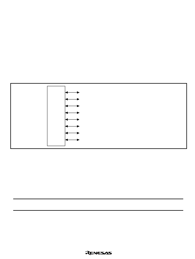
Rev. 5.0, 09/03, page 631 of 806
Section 20 I/O Ports
20.1
Overview
The SH7729R has twelve 8-bit ports (ports A to L and SC). All port pins are multiplexed with
other pin functions (the pin function controller (PFC) handles the selection of pin functions and
pull-up MOS control). Each port has a data register which stores data for the pins.
20.2
Port A
Port A is an 8-bit input/output port with the pin configuration shown in figure 20.1. Each pin has
an input pull-up MOS, which is controlled by the port A control register (PACR) in the PFC.
PTA7 (input/output) / D23 (input/output)
PTA6 (input/output) / D22 (input/output)
PTA5 (input/output) / D21 (input/output)
PTA4 (input/output) / D20 (input/output)
PTA3 (input/output) / D19 (input/output)
PTA2 (input/output) / D18 (input/output)
PTA1 (input/output) / D17 (input/output)
PTA0 (input/output) / D16 (input/output)
Port A
Figure 20.1 Port A
20.2.1
Register Description
Table 20.1 summarizes the port A register.
Table 20.1
Port A Register
Name
Abbreviation
R/W
Initial Value
Address
Access Size
Port A data register
PADR
R/W
H'00
H'04000120
(H'A4000120)
*
8
Notes: This register is located in area 1 of physical space. Therefore, when the cache is on, either
access this register from the P2 area of logical space or else make an appropriate setting
using the MMU so that this register is not cached.
*
When address translation by the MMU does not apply, the address in parentheses
should be used.

Rev. 5.0, 09/03, page 632 of 806
20.2.2
Port A Data Register (PADR)
Bit:
7
6
5
4
3
2
1
0
PA7DT
PA6DT
PA5DT
PA4DT
PA3DT
PA2DT
PA1DT
PA0DT
Initial value:
0
0
0
0
0
0
0
0
R/W:
R/W
R/W
R/W
R/W
R/W
R/W
R/W
R/W
The port A data register (PADR) is an 8-bit readable/writable register that stores data for pins
PTA7 to PTA0. Bits PA7DT to PA0DT correspond to pins PTA7 to PTA0. When the pin function
is general output port, if the port is read the value of the corresponding PADR bit is returned
directly. When the function is general input port, if the port is read the corresponding pin level is
read. Table 20.2 shows the function of PADR.
PADR is initialized to H'00 by a power-on reset. It retains its previous value in standby mode and
sleep mode, and in a manual reset.
Table 20.2
Port A Data Register (PADR) Read/Write Operations
PAnMD1
PAnMD0
Pin State
Read
Write
0
0
Other function
(See table 19.1)
PADR value
Value is written to PADR, but does not
affect pin state
1
Output
PADR value
Write value is output from pin.
1
0
Input (Pull-up
MOS on)
Pin state
Value is written to PADR, but does not
affect pin state
1
Input (Pull-up
MOS off)
Pin state
Value is written to PADR, but does not
affect pin state
(n = 7 to 0)
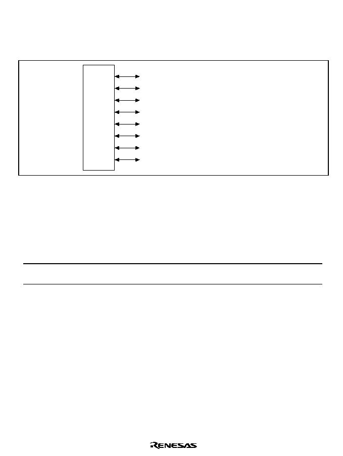
Rev. 5.0, 09/03, page 633 of 806
20.3
Port B
Port B is an 8-bit input/output port with the pin configuration shown in figure 20.2. Each pin has
an input pull-up MOS, which is controlled by the port B control register (PBCR) in the PFC.
PTB7 (input/output) / D31 (input/output)
PTB6 (input/output) / D30 (input/output)
PTB5 (input/output) / D29 (input/output)
PTB4 (input/output) / D28 (input/output)
PTB3 (input/output) / D27 (input/output)
PTB2 (input/output) / D26 (input/output)
PTB1 (input/output) / D25 (input/output)
PTB0 (input/output) / D24 (input/output)
Port B
Figure 20.2 Port B
20.3.1
Register Description
Table 20.3 summarizes the port B register.
Table 20.3
Port B Register
Name
Abbreviation
R/W
Initial Value
Address
Access Size
Port B data register
PBDR
R/W
H'00
H'04000122
(H'A4000122)
*
8
Notes: This register is located in area 1 of physical space. Therefore, when the cache is on, either
access this register from the P2 area of logical space or else make an appropriate setting
using the MMU so that this register is not cached.
*
When address translation by the MMU does not apply, the address in parentheses
should be used.

Rev. 5.0, 09/03, page 634 of 806
20.3.2
Port B Data Register (PBDR)
Bit:
7
6
5
4
3
2
1
0
PB7DT
PB6DT
PB5DT
PB4DT
PB3DT
PB2DT
PB1DT
PB0DT
Initial value:
0
0
0
0
0
0
0
0
R/W:
R/W
R/W
R/W
R/W
R/W
R/W
R/W
R/W
The port B data register (PBDR) is an 8-bit readable/writable register that stores data for pins
PTB7 to PTB0. Bits PB7DT to PB0DT correspond to pins PTB7 to PTB0. When the pin function
is general output port, if the port is read the value of the corresponding PBDR bit is returned
directly. When the function is general input port, if the port is read the corresponding pin level is
read. Table 20.4 shows the function of PBDR.
PBDR is initialized to H'00 by a power-on reset. It retains its previous value in standby mode and
sleep mode, and in a manual reset.
Table 20.4
Port B Data Register (PBDR) Read/Write Operations
PBnMD1
PBnMD0
Pin State
Read
Write
0
0
Other function
(See table 19.1)
PBDR value
Value is written to PBDR, but does not
affect pin state
1
Output
PBDR value
Write value is output from pin
1
0
Input (Pull-up
MOS on)
Pin state
Value is written to PBDR, but does not
affect pin state
1
Input (Pull-up
MOS off)
Pin state
Value is written to PBDR, but does not
affect pin state
(n = 7 to 0)
Rev. 5.0, 09/03, page 635 of 806
20.4
Port C
Port C is an 8-bit input/output port with the pin configuration shown in figure 20.3. Each pin has
an input pull-up MOS, which is controlled by the port C control register (PCCR) in the PFC.
PTC7 (input/output) / PINT7 (input) / MSC7 (output)
PTC6 (input/output) / PINT6 (input) / MSC6 (output)
PTC5 (input/output) / PINT5 (input) / MSC5 (output)
PTC4 (input/output) / PINT4 (input) / MSC4 (output)
PTC3 (input/output) / PINT3 (input) / MSC3 (output)
PTC2 (input/output) / PINT2 (input) / MSC2 (output)
PTC1 (input/output) / PINT1 (input) / MSC1 (output)
PTC0 (input/output) / PINT0 (input) / MSC0 (output)
Port C
Figure 20.3 Port C
20.4.1
Register Description
Table 20.5 summarizes the port C register.
Table 20.5
Port C Register
Name
Abbreviation
R/W
Initial Value
Address
Access Size
Port C data register
PCDR
R/W
H'00
H'04000124
(H'A4000124)
*
8
Notes: This register is located in area 1 of physical space. Therefore, when the cache is on, either
access this register from the P2 area of logical space or else make an appropriate setting
using the MMU so that this register is not cached.
*
When address translation by the MMU does not apply, the address in parentheses
should be used.

Rev. 5.0, 09/03, page 636 of 806
20.4.2
Port C Data Register (PCDR)
Bit:
7
6
5
4
3
2
1
0
PC7DT
PC6DT
PC5DT
PC4DT
PC3DT
PC2DT
PC1DT
PC0DT
Initial value:
0
0
0
0
0
0
0
0
R/W:
R/W
R/W
R/W
R/W
R/W
R/W
R/W
R/W
The port C data register (PCDR) is an 8-bit readable/writable register that stores data for pins
PTC7 to PTC0. Bits PC7DT to PC0DT correspond to pins PTC7 to PTC0. When the pin function
is general output port, if the port is read, the value of the corresponding PCDR bit is returned
directly. When the function is general input port, if the port is read, the corresponding pin level is
read. Table 20.6 shows the function of PCDR.
PCDR is initialized to H'00 by a power-on reset, after which the general input port function (pull-
up MOS on) is set as the initial pin function, and the corresponding pin levels are read.
Table 20.6
Port C Data Register (PCDR) Read/Write Operations
PCnMD1
PCnMD0
Pin State
Read
Write
0
0
Other function
(See table 19.1)
PCDR value
Value is written to PCDR, but does not
affect pin state
1
Output
PCDR value
Write value is output from pin
1
0
Input (Pull-up
MOS on)
Pin state
Value is written to PCDR, but does not
affect pin state
1
Input (Pull-up
MOS off)
Pin state
Value is written to PCDR, but does not
affect pin state
(n = 7 to 0)
Rev. 5.0, 09/03, page 637 of 806
20.5
Port D
Port D comprises a 6-bit input/output port and 2-bit input port with the pin configuration shown in
figure 20.4. Each pin has an input pull-up MOS, which is controlled by the port D control register
(PDCR) in the PFC.
PTD7 (input/output) / DACK1 (output)
PTD6 (input) / DREQ1 (input)
PTD5 (input/output) / DACK0 (output)
PTD4 (input) / DREQ0 (input)
PTD3 (input/output) / WAKEUP (output)
PTD2 (input/output) / RESETOUT (output)
PTD1 (input/output) / DRAK0 (output)
PTD0 (input/output) / DRAK1 (output)
Port D
Figure 20.4 Port D
20.5.1
Register Description
Table 20.7 summarizes the port D register.
Table 20.7
Port D Register
Name
Abbreviation
R/W
Initial Value
Address
Access Size
Port D data register
PDDR
R/W or R
B'0
*
0
*
0000
H'04000126
(H'A4000126)
*
1
8
Notes: This register is located in area 1 of physical space. Therefore, when the cache is on, either
access this register from the P2 area of logical space or else make an appropriate setting
using the MMU so that this register is not cached.
*
Means no value.
1. When address translation by the MMU does not apply, the address in parentheses
should be used.

Rev. 5.0, 09/03, page 638 of 806
20.5.2
Port D Data Register (PDDR)
Bit:
7
6
5
4
3
2
1
0
PD7DT
PD6DT
PD5DT
PD4DT
PD3DT
PD2DT
PD1DT
PD0DT
Initial value:
0
*
0
*
0
0
0
0
R/W:
R/W
R
R/W
R
R/W
R/W
R/W
R/W
Note:
*
Undefined
The port D data register (PDDR) is a 6-bit readable/writable and 2-bit read-only register that stores
data for pins PTD7 to PTD0. Bits PD7DT to PD0DT correspond to pins PTD7 to PTD0. When the
pin function is general output port, if the port is read, the value of the corresponding PDDR bit is
returned directly. When the function is general input port, if the port is read, the corresponding pin
level is read. Table 20.8 shows the function of PDDR.
PDDR is initialized to B'0*0*0000 by a power-on reset. After initialization, the general input port
function (pull-up MOS on) is set as the initial pin function, and the corresponding pin levels are
read from bits PD7DT--PD3DT, PD1DT, and PD0DT. PDDR retains its previous value in
standby mode and sleep mode, and in a manual reset.
Note that the low level is read if bits 6 and 4 are read except in general-purpose input.
Table 20.8
Port D Data Register (PDDR) Read/Write Operations
PDnMD1
PDnMD0
Pin State
Read
Write
0
0
Other function
(See table 19.1)
PDDR value
Value is written to PDDR, but does not
affect pin state
1
Output
PDDR value
Write value is output from pin
1
0
Input (Pull-up
MOS on)
Pin state
Value is written to PDDR, but does not
affect pin state
1
Input (Pull-up
MOS off)
Pin state
Value is written to PDDR, but does not
affect pin state
(n = 0, 1, 2, 3, 5, 7)
PDnMD1
PDnMD0
Pin State
Read
Write
0
0
Other function
(See table 19.1)
Low level
Ignored (no effect on pin state)
1
Reserved
Low level
Ignored (no effect on pin state)
1
0
Input (Pull-up
MOS on)
Pin state
Ignored (no effect on pin state)
1
Input (Pull-up
MOS off)
Pin state
Ignored (no effect on pin state)
(n = 4, 6)
Rev. 5.0, 09/03, page 639 of 806
20.6
Port E
Port E is an 8-bit input/output port with the pin configuration shown in figure 20.5. Each pin has
an input pull-up MOS, which is controlled by the port E control register (PECR) in the PFC.
PTE7 (input/output) / AUDSYNC (output)
PTE6 (input/output)
PTE5 (input/output) / CE2B (output)
PTE4 (input/output) / CE2A (output)
PTE3 (input/output)
PTE2 (input/output) / RAS3U (output)
PTE1 (input/output)
PTE0 (input/output) / TDO (output)
Port E
Figure 20.5 Port E
20.6.1
Register Description
Table 20.9 summarizes the port E register.
Table 20.9
Port E Register
Name
Abbreviation
R/W
Initial Value
Address
Access Size
Port E data register
PEDR
R/W
H'00
H'04000128
(H'A4000128)
*
8
Notes: This register is located in area 1 of physical space. Therefore, when the cache is on, either
access this register from the P2 area of logical space or else make an appropriate setting
using the MMU so that this register is not cached.
*
When address translation by the MMU does not apply, the address in parentheses
should be used.

Rev. 5.0, 09/03, page 640 of 806
20.6.2
Port E Data Register (PEDR)
Bit:
7
6
5
4
3
2
1
0
PE7DT
PE6DT
PE5DT
PE4DT
PE3DT
PE2DT
PE1DT
PE0DT
Initial value:
0
0
0
0
0
0
0
0
R/W:
R/W
R/W
R/W
R/W
R/W
R/W
R/W
R/W
The port E data register (PEDR) is an 8-bit readable/writable register that stores data for pins
PTE7 to PTE0. Bits PE7DT to PE0DT correspond to pins PTE7 to PTE0. When the pin function is
general output port, if the port is read the value of the corresponding PEDR bit is returned directly.
When the function is general input port, if the port is read the corresponding pin level is read.
Table 20.10 shows the function of PEDR.
PEDR is initialized to H'00 by a power-on reset, after which the general input port function (pull-
up MOS on) is set as the initial pin function, and the corresponding pin levels are read. It retains
its previous value in standby mode and sleep mode, and in a manual reset.
Table 20.10 Port E Data Register (PEDR) Read/Write Operations
PEnMD1
PEnMD0
Pin State
Read
Write
0
0
Other function
(See table 19.1)
PEDR value
Value is written to PEDR, but does not
affect pin state
1
Output
PEDR value
Write value is output from pin
1
0
Input (Pull-up
MOS on)
Pin state
Value is written to PEDR, but does not
affect pin state
1
Input (Pull-up
MOS off)
Pin state
Value is written to PEDR, but does not
affect pin state
(n = 0 to 7)
Rev. 5.0, 09/03, page 641 of 806
20.7
Port F
Port F is an 8-bit input port with the pin configuration shown in figure 20.6. Each pin has an input
pull-up MOS, which is controlled by the port F control register (PFCR) in the PFC.
PTF7 (input) / PINT15 (input) / TRST (input)
PTF6 (input) / PINT14 (input) / TMS (input)
PTF5 (input) / PINT13 (input) / TDI (input)
PTF4 (input) / PINT12 (input) / TCK (input)
PTF3 (input) / PINT11 (input) / IRLS3 (input)
PTF2 (input) / PINT10 (input) / IRSL2 (input)
PTF1 (input) / PINT9 (input) / IRLS1 (input)
PTF0 (input) / PINT8 (input) / IRLS0 (input)
Port F
Figure 20.6 Port F
20.7.1
Register Description
Table 20.11 summarizes the port F register.
Table 20.11 Port F Register
Name
Abbreviation
R/W
Initial Value
Address
Access Size
Port F data register
PFDR
R
H'
**
H'0400012A
(H'A400012A)
*
1
8
Notes: This register is located in area 1 of physical space. Therefore, when the cache is on, either
access this register from the P2 area of logical space or else make an appropriate setting
using the MMU so that this register is not cached.
*
Means no value.
1. When address translation by the MMU does not apply, the address in parentheses
should be used.

Rev. 5.0, 09/03, page 642 of 806
20.7.2
Port F Data Register (PFDR)
Bit:
7
6
5
4
3
2
1
0
PF7DT
PF6DT
PF5DT
PF4DT
PF3DT
PF2DT
PF1DT
PF0DT
Initial value:
*
*
*
*
*
*
*
*
R/W:
R
R
R
R
R
R
R
R
Note:
*
Undefined
The port F data register (PFDR) is an 8-bit read-only register that stores data for pins PTF7 to
PTF0. Bits PF7DT to PF0DT correspond to pins PTF7 to PTF0. When the function is general
input port, if the port is read the corresponding pin level is read. Table 20.12 shows the function of
PFDR.
PFDR is initialized by a power-on reset, after which the general input port function (pull-up MOS
on) is set as the initial pin function, and the corresponding pin levels are read.
Table 20.12 Port F Data Register (PFDR) Read/Write Operations
PFnMD1
PFnMD0
Pin State
Read
Write
0
0
Other function
(See table 19.1)
H'00
Ignored (no effect on pin state)
1
Reserved
H'00
Ignored (no effect on pin state)
1
0
Input (Pull-up
MOS on)
Pin state
Ignored (no effect on pin state)
1
Input (Pull-up
MOS off)
Pin state
Ignored (no effect on pin state)
(n = 0 to 7)
Rev. 5.0, 09/03, page 643 of 806
20.8
Port G
Port G comprises a 5-bit input/output port and 3-bit input port with the pin configuration shown in
figure 20.7. Each pin has an input pull-up MOS, which is controlled by the port G control register
(PGCR) in the PFC.
PTG7 (input) / IOIS16 (input)
PTG6 (input) / ASEMD0 (input)
PTG5 (input) / ASEBRKAK (output)
PTG4 (input) / CKIO2 (output)
PTG3 (input) / AUDATA3 (input/output)
PTG2 (input) / AUDATA2 (input/output)
PTG1 (input) / AUDATA1 (input/output)
PTG0 (input) / AUDATA0 (input/output)
Port G
Figure 20.7 Port G
20.8.1
Register Description
Table 20.13 summarizes the port G register.
Table 20.13 Port G Register
Name
Abbreviation
R/W
Initial Value
Address
Access Size
Port G data register
PGDR
R/W
H'
**
H'0400012C
(H'A400012C)
*
1
8
Notes: This register is located in area 1 of physical space. Therefore, when the cache is on, either
access this register from the P2 area of logical space or else make an appropriate setting
using the MMU so that this register is not cached.
*
Means no value.
1. When address translation by the MMU does not apply, the address in parentheses
should be used.

Rev. 5.0, 09/03, page 644 of 806
20.8.2
Port G Data Register (PGDR)
Bit:
7
6
5
4
3
2
1
0
PG7DT
PG6DT
PG5DT
PG4DT
PG3DT
PG2DT
PG1DT
PG0DT
Initial value:
*
*
*
*
*
*
*
*
R/W:
R
R
R
R
R
R
R
R
Note:
*
Undefined
The port G data register (PGDR) is an 8-bit read-only register that stores data for pins PTG7 to
PTG0. Bits PG7DT to PG0DT correspond to pins PTG7 to PTG0. When the function is general
input port, if the port is read the corresponding pin level is read. Table 20.14 shows the function of
PGDR.
PGDR is initialized by a power-on reset, after which the general input port function (pull-up MOS
on) is set as the initial pin function, and the corresponding pin levels are read.
Table 20.14 Port G Data Register (PGDR) Read/Write Operations
PGnMD1
PGnMD0
Pin State
Read
Write
0
0
Other function
(See table 19.1)
H'00
Ignored (no effect on pin state)
1
Reserved
H'00
Ignored (no effect on pin state)
1
0
Input (Pull-up
MOS on)
Pin state
Ignored (no effect on pin state)
1
Input (Pull-up
MOS off)
Pin state
Ignored (no effect on pin state)
(n = 0 to 7)
Rev. 5.0, 09/03, page 645 of 806
20.9
Port H
Port H comprises a 1-bit input/output port and 5-bit input port with the pin configuration shown in
figure 20.8. Each pin has an input pull-up MOS, which is controlled by the port H control register
(PHCR) in the PFC.
PTH7 (input/output) / TCLK (output)
PTH4 (input) / IRQ4 (input)
PTH3 (input) / IRQ3 (input)
PTH2 (input) / IRQ2 (input)
PTH6 (input) / AUDCK (input)
PTH5 (input) / ADTRG (input)
PTH1 (input) / IRQ1 (input)
PTH0 (input) / IRQ0 (input)
Port H
Figure 20.8 Port H
20.9.1
Register Description
Table 20.15 summarizes the port H register.
Table 20.15 Port H Register
Name
Abbreviation
R/W
Initial Value
Address
Access Size
Port H data register
PHDR
R/W or R
B'0
*******
H'0400012E
(H'A400012E)
*
1
8
Notes: This register is located in area 1 of physical space. Therefore, when the cache is on, either
access this register from the P2 area of logical space or else make an appropriate setting
using the MMU so that this register is not cached.
*
Means no value.
1. When address translation by the MMU does not apply, the address in parentheses
should be used.

Rev. 5.0, 09/03, page 646 of 806
20.9.2
Port H Data Register (PHDR)
Bit:
7
6
5
4
3
2
1
0
PH7DT
PH6DT
PH5DT
PH4DT
PH3DT
PH2DT
PH1DT
PH0DT
Initial value:
0
*
*
*
*
*
*
*
R/W:
R/W
R
R
R
R
R
R
R
Note:
*
Undefined
The port H data register (PHDR) is a 1-bit readable/writable and 7-bit read-only register that stores
data for pins PTH7 to PTH0. Bits PH7DT to PH0DT correspond to pins PTH7 to PTH0. When the
pin function is general output port, if the port is read, the value of the corresponding PHDR bit is
returned directly. When the function is general input port, if the port is read, the corresponding pin
level is read. Table 20.16 shows the function of PHDR.
PHDR is initialized to B'0******* by a power-on reset, after which the general input port function
(pull-up MOS on) is set as the initial pin function, and the corresponding pin levels are read. It
retains its previous value in standby mode and sleep mode, and in a manual reset.
Note that the low level is read if bits 6 to 0 are read except in general-purpose input.
Table 20.16 Port H Data Register (PHDR) Read/Write Operations
PHnMD1
PHnMD0
Pin State
Read
Write
0
0
Other function
(See table 19.1)
PHDR value
Value is written to PHDR, but does not
affect pin state
1
Output
PHDR value
Write value is output from pin
1
0
Input (Pull-up
MOS on)
Pin state
Value is written to PHDR, but does not
affect pin state
1
Input (Pull-up
MOS off)
Pin state
Value is written to PHDR, but does not
affect pin state
(n = 7)
PHnMD1
PHnMD0
Pin State
Read
Write
0
0
Other function
(See table 19.1)
Low level
Ignored (no effect on pin state)
1
Reserved
Low level
Ignored (no effect on pin state)
1
0
Input (Pull-up
MOS on)
Pin state
Ignored (no effect on pin state)
1
Input (Pull-up
MOS off)
Pin state
Ignored (no effect on pin state)
(n = 0 to 6)

Rev. 5.0, 09/03, page 647 of 806
20.10
Port J
Port J is an 8-bit input/output port with the pin configuration shown in figure 20.9. Each pin has
an input pull-up MOS, which is controlled by the port J control register (PJCR) in the PFC.
PTJ7 (input/output) / STATUS1 (output)
PTJ6 (input/output) / STATUS0 (output)
PTJ5 (input/output)
PTJ4 (input/output)
PTJ3 (input/output) / CASU (output)
PTJ2 (input/output) / CASL (output)
PTJ1 (input/output)
PTJ0 (input/output) / RAS3L (output)
Port J
Figure 20.9 Port J
20.10.1
Register Description
Table 20.17 summarizes the port J register.
Table 20.17 Port J Register
Name
Abbreviation
R/W
Initial Value
Address
Access Size
Port J data register
PJDR
R/W
H'00
H'04000130
(H'A4000130)
*
8
Notes: This register is located in area 1 of physical space. Therefore, when the cache is on, either
access this register from the P2 area of logical space or else make an appropriate setting
using the MMU so that this register is not cached.
*
When address translation by the MMU does not apply, the address in parentheses
should be used.

Rev. 5.0, 09/03, page 648 of 806
20.10.2
Port J Data Register (PJDR)
Bit:
7
6
5
4
3
2
1
0
PJ7DT
PJ6DT
PJ5DT
PJ4DT
PJ3DT
PJ2DT
PJ1DT
PJ0DT
Initial value:
0
0
0
0
0
0
0
0
R/W:
R/W
R/W
R/W
R/W
R/W
R/W
R/W
R/W
The port J data register (PJDR) is an 8-bit readable/writable register that stores data for pins PTJ7
to PTJ0. Bits PJ7DT to PJ0DT correspond to pins PTJ7 to PTJ0. When the pin function is general
output port, if the port is read the value of the corresponding PJDR bit is returned directly. When
the function is general input port, if the port is read, the corresponding pin level is read. Table
20.18 shows the function of PJDR.
PJDR is initialized to H'00 by a power-on reset. It retains its previous value in software standby
mode and sleep mode, and in a manual reset.
Table 20.18 Port J Data Register (PJDR) Read/Write Operations
PJnMD1
PJnMD0
Pin State
Read
Write
0
0
Other function
(See table 19.1)
PJDR value
Value is written to PJDR, but does not
affect pin state
1
Output
PJDR value
Write value is output from pin
1
0
Input (Pull-up
MOS on)
Pin state
Value is written to PJDR, but does not
affect pin state
1
Input (Pull-up
MOS off)
Pin state
Value is written to PJDR, but does not
affect pin state
(n = 0 to 7)

Rev. 5.0, 09/03, page 649 of 806
20.11
Port K
Port K is an 8-bit input/output port with the pin configuration shown in figure 20.10. Each pin has
an input pull-up MOS, which is controlled by the port K control register (PKCR) in the PFC.
PTK7 (input/output) / WE3 (output) / DQMUU (output) / ICIOWR (output)
PTK6 (input/output) / WE2 (output) / DQMUL (output) / ICIORD (output)
PTK5 (input/output) / CKE (output)
PTK4 (input/output) / BS (output)
PTK3 (input/output) / CS5 (output) / CE1A (output)
PTK2 (input/output) / CS4 (output)
PTK1 (input/output) / CS3 (output)
PTK0 (input/output) / CS2 (output)
Port K
Figure 20.10 Port K
20.11.1
Register Description
Table 20.19 summarizes the port K register.
Table 20.19 Port K Register
Name
Abbreviation
R/W
Initial Value
Address
Access Size
Port K data register
PKDR
R/W
H'00
H'04000132
(H'A4000132)
*
8
Notes: This register is located in area 1 of physical space. Therefore, when the cache is on, either
access this register from the P2 area of logical space or else make an appropriate setting
using the MMU so that this register is not cached.
*
When address translation by the MMU does not apply, the address in parentheses
should be used.

Rev. 5.0, 09/03, page 650 of 806
20.11.2
Port K Data Register (PKDR)
Bit:
7
6
5
4
3
2
1
0
PK7DT
PK6DT
PK5DT
PK4DT
PK3DT
PK2DT
PK1DT
PK0DT
Initial value:
0
0
0
0
0
0
0
0
R/W:
R/W
R/W
R/W
R/W
R/W
R/W
R/W
R/W
The port K data register (PKDR) is an 8-bit readable/writable register that stores data for pins
PTK7 to PTK0. Bits PK7DT to PK0DT correspond to pins PTK7 to PTK0. When the pin function
is general output port, if the port is read, the value of the corresponding PKDR bit is returned
directly. When the function is general input port, if the port is read, the corresponding pin level is
read. Table 20.20 shows the function of PKDR.
PKDR is initialized to H'00 by a power-on reset. It retains its previous value in standby mode and
sleep mode, and in a manual reset.
Table 20.20 Port K Data Register (PKDR) Read/Write Operations
PKnMD1
PKnMD0
Pin State
Read
Write
0
0
Other function
(See table 19.1)
PKDR value
Value is written to PKDR, but does not
affect pin state
1
Output
PKDR value
Write value is output from pin
1
0
Input (Pull-up
MOS on)
Pin state
Value is written to PKDR, but does not
affect pin state
1
Input (Pull-up
MOS off)
Pin state
Value is written to PKDR, but does not
affect pin state
(n = 0 to 7)
Rev. 5.0, 09/03, page 651 of 806
20.12
Port L
Port L is an 8-bit input port with the pin configuration shown in figure 20.11.
PTL7 (input) / AN7 (input) / DA0 (output)
PTL6 (input) / AN6 (input) / DA1 (output)
PTL5 (input) / AN5 (input)
PTL4 (input) / AN4 (input)
PTL3 (input) / AN3 (input)
PTL2 (input) / AN2 (input)
PTL1 (input) / AN1 (input)
PTL0 (input) / AN0 (input)
Port L
Figure 20.11 Port L
20.12.1
Register Description
Table 20.21 summarizes the port L register.
Table 20.21 Port L Register
Name
Abbreviation
R/W
Initial Value
Address
Access Size
Port L data register
PLDR
R
H'00
H'04000134
(H'A4000134)
*
8
Notes: This register is located in area 1 of physical space. Therefore, when the cache is on, either
access this register from the P2 area of logical space or else make an appropriate setting
using the MMU so that this register is not cached.
*
When address translation by the MMU does not apply, the address in parentheses
should be used.

Rev. 5.0, 09/03, page 652 of 806
20.12.2
Port L Data Register (PLDR)
Bit:
7
6
5
4
3
2
1
0
PL7DT
PL6DT
PL5DT
PL4DT
PL3DT
PL2DT
PL1DT
PL0DT
Initial value:
0
0
0
0
0
0
0
0
R/W:
R
R
R
R
R
R
R
R
The port L data register (PLDR) is an 8-bit read-only register that stores data for pins PTL7 to
PTL0. Bits PL7DT to PL0DT correspond to pins PTL7 to PTL0. When the function is general
input port, if the port is read, the corresponding pin level is read. Table 20.22 shows the function
of PLDR.
PLDR is initialized to H'00 by power-on reset. It retains its previous value in software standby
mode and sleep mode, and in a manual reset.
As port L also has analog pin functions, it has no pull-up MOS.
Table 20.22 Port L Data Register (PLDR) Read/Write Operation
PLnMD1
PLnMD0
Pin State
Read
Write
0
0
Other function
(See table 19.1)
H'00
Ignored (no effect on pin state)
1
Reserved
H'00
Ignored (no effect on pin state)
1
0
Input
Pin state
Ignored (no effect on pin state)
1
Input
Pin state
Ignored (no effect on pin state)
(n = 0 to 7)
Rev. 5.0, 09/03, page 653 of 806
20.13
SC Port
The SC port comprises a 4-bit input/output port, 3-bit output port, and 4-bit input port with the pin
configuration shown in figure 20.12. Each pin has an input pull-up MOS, which is controlled by
the SC port control register (SCPCR) in the PFC.
SCPT7 (input) / CTS2 (input) / IRQ5 (input)
SCPT6 (input/output) / RTS2 (output)
SCPT5 (input/output) / SCK2 (input/output)
SCPT4 (input) / RxD2 (input)
SCPT4 (output) / TxD2 (output)
SCPT3 (input/output) / SCK1 (input/output)
SCPT2 (input) / RxD1 (input)
SCPT2 (output) / TxD1 (output)
SCPT1 (input/output) / SCK0 (input/output)
SCPT0 (input) / RxD0 (input)
SCPT0 (output) / TxD0 (output)
SC Port
Figure 20.12 SC Port
20.13.1
Register Description
Table 20.23 summarizes the SC port register.
Table 20.23 SC Port Register
Name
Abbreviation
R/W
Initial Value
Address
Access Size
SC Port data register
SCPDR
R/W or R B'
*
0000000
H'04000136
(H'A4000136)
*
1
8
Notes: This register is located in area 1 of physical space. Therefore, when the cache is on, either
access this register from the P2 area of logical space or else make an appropriate setting
using the MMU so that this register is not cached.
*
Means no value.
1. When address translation by the MMU does not apply, the address in parentheses
should be used.

Rev. 5.0, 09/03, page 654 of 806
20.13.2
SC Port Data Register (SCPDR)
Bit:
7
6
5
4
3
2
1
0
SCP7DT SCP6DT SCP5DT SCP4DT SCP3DT SCP2DT SCP1DT SCP0DT
Initial value:
*
0
0
0
0
0
0
0
R/W:
R
R/W
R/W
R/W
R/W
R/W
R/W
R/W
Note:
*
Undefined
The SC port data register (SCPDR) is a 7-bit readable/writable and 1-bit read-only register that
stores data for pins SCPT7 to SCPT0. Bits SCP7DT to SCP0DT correspond to pins SCPT7 to
SCPT0. When the pin function is general output port, if the port is read, the value of the
corresponding SCPDR bit is returned directly. When the function is general input port, if the port
is read, the corresponding pin level is read. Table 20.24 shows the function of SCPDR.
SCPDR is initialized to B'*0000000 by a power-on reset. After initialization, the general input
port function (pull-up MOS on) is set as the initial pin function, and the corresponding pin levels
are read from bits SCP7DT--SCP5DT, SCP3DT, and SCP1DT. SCPDR retains its previous
value in standby mode and sleep mode, and in a manual reset.
Note that the low level is read if bit 7 is read except in general-purpose input.

Rev. 5.0, 09/03, page 655 of 806
Table 20.24 Read/Write Operation of the SC Port Data Register (SCPDR)
SCPnMD1
SCPnMD0
Pin State
Read
Write
0
0
Other function
(See table 19.1)
SCPDR value
Value is written to SCPDR, but does
not affect pin state
1
Output
SCPDR value
Write value is output from pin
1
0
Input (Pull-up
MOS on)
Pin state
Value is written to SCPDR, but does
not affect pin state
1
Input (Pull-up
MOS off)
Pin state
Value is written to SCPDR, but does
not affect pin state
(n = 0 to 6)
SCPnMD1
SCPnMD0
Pin State
Read
Write
0
0
Other function
(See table 19.1)
Low level
Ignored (no effect on pin state)
1
Output
Low level
Ignored (no effect on pin state)
1
0
Input (Pull-up
MOS on)
Pin state
Ignored (no effect on pin state)
1
Input (Pull-up
MOS off)
Pin state
Ignored (no effect on pin state)
(n = 7)

Rev. 5.0, 09/03, page 656 of 806

Rev. 5.0, 09/03, page 657 of 806
Section 21 A/D Converter
21.1
Overview
The SH7729R includes a 10-bit successive-approximation A/D converter allowing selection of up
to eight analog input channels.
21.1.1
Features
A/D converter features are listed below.
∑
10-bit resolution
∑
Eight input channels
∑
High-speed conversion
Conversion time: maximum 15
µ
s per channel (P
= 33 MHz operation)
∑
Three conversion modes
Single mode: A/D conversion on one channel
Multi mode: A/D conversion on one to four channels
Scan mode: Continuous A/D conversion on one to four channels
∑
Four 16-bit data registers
A/D conversion results are transferred for storage into data registers corresponding to the
channels.
∑
Sample-and-hold function
∑
A/D conversion can be externally triggered
∑
A/D interrupt requested at the end of conversion
At the end of A/D conversion, an A/D end interrupt (ADI) can be requested.
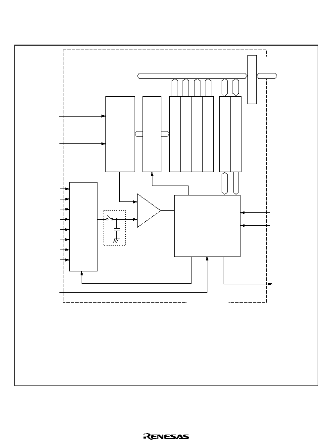
Rev. 5.0, 09/03, page 658 of 806
21.1.2
Block Diagram
Figure 21.1 shows a block diagram of the A/D converter.
10-bit
D/A
ADDRA
ADDRB
ADDRD
Bus interface
Peripheral data bus
Analog
multi-
plexer
Control circuit
Successive approxi-
mation register
+
-
Comparator
Sample-and-
hold circuit
ADI
interrupt
signal
AV
SS
AN0
AN1
AN2
AN3
AN4
AN5
AN6
AN7
/8
/16
ADCSR
ADCR
AV
CC
A/D converter
ADCR: A/D control register
ADCSR: A/D control/status register
ADDRA: A/D data register A
ADDRB: A/D data register B
ADDRC: A/D data register C
ADDRD: A/D data register D
Legend
Internal
data bus
ADTRG
ADDRC
Figure 21.1 Block Diagram of A/D Converter

Rev. 5.0, 09/03, page 659 of 806
21.1.3
Input Pins
Table 21.1 summarizes the A/D converter's input pins. The eight analog input pins are divided
into two groups: group 0 (AN0 to AN3), and group 1 (AN4 to AN7). AVCC and AVSS are the
power supply inputs for the analog circuits in the A/D converter. AVcc also functions as the A/D
converter reference voltage pin.
Table 21.1
A/D Converter Pins
Pin Name
Abbreviation
I/O
Function
Analog power supply pin
AVcc
Input
Analog power supply
Analog ground pin
AVss
Input
Analog ground and reference voltage
Analog input pin 0
AN0
Input
Group 0 analog inputs
Analog input pin 1
AN1
Input
Analog input pin 2
AN2
Input
Analog input pin3
AN3
Input
Analog input pin 4
AN4
Input
Group1 analog inputs
Analog input pin 5
AN5
Input
Analog input pin6
AN6
Input
Analog input pin7
AN7
Input
A/D external trigger input
pin
ADTRG
Input
External trigger input for starting A/D
conversion

Rev. 5.0, 09/03, page 660 of 806
21.1.4 Register
Configuration
Table 21.2 summarizes the A/D converter's registers.
Table 21.2
A/D Converter Registers
Name
Abbreviation
R/W
Initial Value
Address
Access size
A/D data register A (high)
ADDRAH
R
H'00
H'04000080
(H'A4000080)
*
2
16, 8
A/D data register A (low)
ADDRAL
R
H'00
H'04000082
(H'A4000082)
*
2
8
A/D data register B (high)
ADDRBH
R
H'00
H'04000084
(H'A4000084)
*
2
16, 8
A/D data register B (low)
ADDRBL
R
H'00
H'04000086
(H'A4000086)
*
2
8
A/D data register C (high)
ADDRCH
R
H'00
H'04000088
(H'A4000088)
*
2
16, 8
A/D data register C (low)
ADDRCL
R
H'00
H'0400008A
(H'A400008A)
*
2
8
A/D data register D (high)
ADDRDH
R
H'00
H'0400008C
(H'A400008C)
*
2
16, 8
A/D data register D (low)
ADDRDL
R
H'00
H'0400008E
(H'A400008E)
*
2
8
A/D control/status register
ADCSR
R/(W)
*
1
H'00
H'04000090
(H'A4000090)
*
2
8
A/D control register
ADCR
R/W
H'3F
H'04000092
(H'A4000092)
*
2
8
Notes: These registers are located in area 1 of physical space. Therefore, when the cache is on,
either access these registers from the P2 area of logical space or else make an appropriate
setting using the MMU so that these registers are not cached.
1. Only 0 can be written to bit 7, to clear the flag.
2. When address translation by the MMU does not apply, the address in parentheses
should be used.

Rev. 5.0, 09/03, page 661 of 806
21.2
Register Descriptions
21.2.1
A/D Data Registers A to D (ADDRA to ADDRD)
Bit:
15
14
13
12
11
10
9
8
AD9
AD8
AD7
AD6
AD5
AD4
AD3
AD2
Initial value:
0
0
0
0
0
0
0
0
R/W:
R
R
R
R
R
R
R
R
Bit:
7
6
5
4
3
2
1
0
AD1
AD0
--
--
--
--
--
--
Initial value:
0
0
0
0
0
0
0
0
R/W:
R
R
R
R
R
R
R
R
n = A to D
The four A/D data registers (ADDRA to ADDRD) are 16-bit read-only registers that store the
results of A/D conversion.
An A/D conversion produces 10-bit data, which is transferred for storage into the A/D data
register corresponding to the selected channel. The upper 8 bits of the result are stored in the upper
byte (bits 15 to 8) of the A/D data register. The lower 2 bits are stored in the lower byte (bits 7 and
6). Bits 5 to 0 of an A/D data register are reserved bits that are always read as 0. Table 21.3
indicates the pairings of analog input channels and A/D data registers.
The A/D data registers are initialized to H'0000 by a reset and in standby mode.
Table 21.3
Analog Input Channels and A/D Data Registers
Analog Input Channel
Group 0
Group 1
A/D Data Register
AN0
AN4
ADDRA
AN1
AN5
ADDRB
AN2
AN6
ADDRC
AN3
AN7
ADDRD

Rev. 5.0, 09/03, page 662 of 806
21.2.2
A/D Control/Status Register (ADCSR)
Bit:
7
6
5
4
3
2
1
0
ADF
ADIE
ADST
MULTI
CKS
CH2
CH1
CH0
Initial value:
0
0
0
0
0
0
0
0
R/W:
R/(W)
*
R/W
R/W
R/W
R/W
R/W
R/W
R/W
Note:
*
Write 0 to clear the flag.
ADCSR is an 8-bit readable/writable register that selects the mode and controls the A/D converter.
ADCSR is initialized to H'00 by a reset and in standby mode.
Bit 7--A/D End Flag (ADF): Indicates the end of A/D conversion.
Bit 7: ADF
Description
0
[Clearing conditions]
(Initial value)
(1) Cleared by reading ADF while ADF = 1, then writing 0 to ADF
(2) Cleared when DMAC is activated by ADI interrupt and ADDR is read
1
[Setting conditions]
Single mode: A/D conversion ends
Multi mode: A/D conversion ends on all selected channels
Bit 6--A/D Interrupt Enable (ADIE): Enables or disables the interrupt (ADI) requested at the
end of A/D conversion.
Bit 6: ADIE
Description
0
A/D end interrupt request (ADI) is disabled
(Initial value)
1
A/D end interrupt request (ADI) is enabled
Bit 5--A/D Start (ADST): Starts or stops A/D conversion. The ADST bit remains set to 1 during
A/D conversion. It can also be set to 1 by external trigger input at the
ADTRG pin.
Bit 5: ADST
Description
0
A/D conversion is stopped
(Initial value)
1
Single mode: A/D conversion starts; ADST is automatically cleared to 0 when
conversion ends
Scan mode: A/D conversion starts and continues, cycling through the selected
channels, until ADST is cleared to 0 by software, by a reset, or by a transition to
standby mode

Rev. 5.0, 09/03, page 663 of 806
Bit 4--Multi Mode (MULTI): Selects single mode, multi mode or scan mode. For further
information on operation in these modes, see section 21.4, Operation.
Bit 4: MULTI
ADCR: Bit5: SCN
Description
0
--
Single mode
(Initial value)
1
0
Multi mode
1
scan mode
Bit 3--Clock Select (CKS): Selects the A/D conversion time. Clear the ADST bit to 0 before
changing the conversion time.
Bit 3:CKS
Description
0
Conversion time = 536 states (maximum)
(Initial value)
1
Conversion time = 266 states (maximum)
Bits 2 to 0--Channel Select 2 to 0 (CH2 to CH0): These bits and the MULTI bit select the
analog input channels. Clear the ADST bit to 0 before changing the channel selection.
Channel Selection
Description
CH2
CH1
CH0
Single Mode
(MULTI = 0)
Multi Mode
(MULTI = 1)
0
0
0
AN0 (Initial value)
AN0
1
AN1
AN0, AN1
1
0
AN2
AN0 to AN2
1
AN3
AN0 to AN3
1
0
0
AN4
AN4
1
AN5
AN4, AN5
1
0
AN6
AN4 to AN6
1
AN7
AN4 to AN7

Rev. 5.0, 09/03, page 664 of 806
21.2.3
A/D Control Register (ADCR)
Bit:
7
6
5
4
3
2
1
0
TRGE1
TRGE0
SCN
RESVD1 RESVD2
--
--
--
Initial value:
0
0
0
0
0
1
1
1
R/W:
R/W
R/W
R/W
R/W
R/W
R
R
R
ADCR is an 8-bit readable/writable register that enables or disables external triggering of A/D
conversion. ADCR is initialized to H'07 by a reset and in standby mode.
Bits 7 and 6--Trigger Enable (TRGE1, TRGE0): Enables or disables external triggering of
A/D conversion.
The TRGE1 and TRGE0 bits should only be set when conversion is not in progress.
Bit 7: TRGE1
Bit 6: TRGE0
Description
0
0
A/D conversion does not start when an external trigger is input
0
1
(Initial value)
1
0
A/D conversion starts at the falling edge of an input signal from
1
1
the external trigger pin (
ADTRG
)
Bit 5--Scan Mode (SCN): Selects multi mode or scan mode when the MULTI bit is set to 1. See
the description of bit 4 in section 21.2.2, A/D Control/Status Register (ADCSR).
Bits 4 and 3--Reserved (RESVD1, RESVD2): These bits are always read as 0. The write value
should always be 0.
Bits 2 to 0--Reserved: These bits are always read as 1. The write value should always be 1.
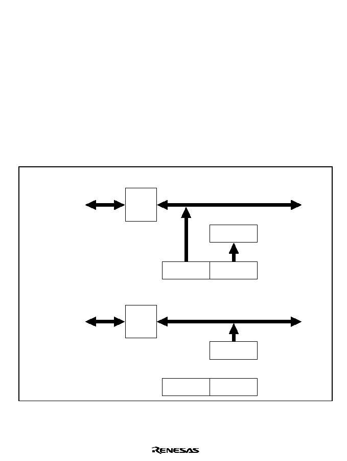
Rev. 5.0, 09/03, page 665 of 806
21.3
Bus Master Interface
ADDRA to ADDRD are 16-bit registers, but they are connected to the bus master by the upper 8
bits of the 16-bit peripheral data bus. Therefore, although the upper byte can be accessed directly
by the bus master, the lower byte is read through an 8-bit temporary register (TEMP).
An A/D data register is read as follows. When the upper byte is read, the upper-byte value is
transferred directly to the bus master and the lower-byte value is transferred into TEMP. Next,
when the lower byte is read, the TEMP contents are transferred to the bus master.
When reading an A/D data register, always read the upper byte before the lower byte. It is possible
to read only the upper byte, but if only the lower byte is read, the read value is not guaranteed.
Figure 21.2 shows the data flow for access to an A/D data register.
See section 21.7.3, Access Size and Read Data.
Bus
interface
TEMP
[H'40]
ADDRn L
[H'40]
ADDRn H
[H'AA]
n = A to D
CPU
receives
data H'AA
Upper byte read
Module internal data bus
Bus
interface
TEMP
[H'40]
ADDRn L
[H'40]
ADDRn H
[H'AA]
n = A to D
CPU
receives
data H'40
Lower byte read
Module internal data bus
Figure 21.2 A/D Data Register Access Operation (Reading H'AA40)

Rev. 5.0, 09/03, page 666 of 806
21.4
Operation
The A/D converter operates by successive approximations with 10-bit resolution. It has three
operating modes: single mode, multi mode, and scan mode.
21.4.1
Single Mode (MULTI = 0)
Single mode should be selected when only one A/D conversion on one channel is required. A/D
conversion starts when the ADST bit is set to 1 by software, or by external trigger input. The
ADST bit remains set to 1 during A/D conversion and is automatically cleared to 0 when
conversion ends.
When conversion ends the ADF bit is set to 1. If the ADIE bit is also set to 1, an ADI interrupt is
requested at this time. To clear the ADF flag to 0, first read ADCSR, then write 0 to ADF.
When the mode or analog input channel must be switched during A/D conversion, to prevent
incorrect operation, first clear the ADST bit to 0 in ADCSR to halt A/D conversion. After making
the necessary changes, set the ADST bit to 1 to start A/D conversion again. The ADST bit can be
set at the same time as the mode or channel is changed.
Typical operations when channel 1 (AN1) is selected in single mode are described next.
Figure 21.3 shows a timing diagram for this example.
1. Single mode is selected (MULTI = 0), input channel AN1 is selected (CH2 = CH1 = 0, CH0 =
1), the A/D interrupt is enabled (ADIE = 1), and A/D conversion is started (ADST = 1).
2. When A/D conversion is completed, the result is transferred into ADDRB. At the same time
the ADF flag is set to 1, the ADST bit is cleared to 0, and the A/D converter becomes idle.
3. Since ADF = 1 and ADIE = 1, an ADI interrupt is requested.
4. The A/D interrupt handling routine starts.
5. The routine reads ADCSR, then writes 0 to the ADF flag.
6. The routine reads and processes the conversion result (ADDRB = 0).
7. Execution of the A/D interrupt handling routine ends. Then, when the ADST bit is set to 1,
A/D conversion starts and steps 2 to 7 are executed.
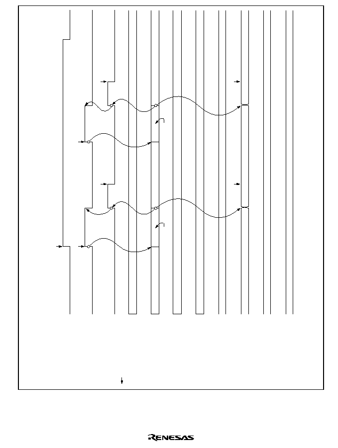
Rev. 5.0, 09/03, page 667 of 806
Channel 0 (AN0)
operating
ADIE
ADST
ADF
Channel 1 (AN1)
operating
Channel 2 (AN2)
operating
Channel 3 (AN3)
operating
ADDRA
ADDRB
ADDRC
ADDRD
Waiting
Waiting
Waiting
Waiting
Waiting
Waiting
A/D conversion starts
Set
*
Set
*
Set
*
Clear
*
Clear
*
A/D conversion result 1
A
/D conversion result 2
Read result
Read result
A/D conversion 1
A
/D conversion result 2
Note:
*Vertical arrows ( ) indicate instruction execution by software.
Figure 21.3 Example of A/D Converter Operation (Single Mode, Channel 1 Selected)

Rev. 5.0, 09/03, page 668 of 806
21.4.2
Multi Mode (MULTI = 1, SCN = 0)
Multi mode should be selected when performing A/D conversions on one or more channels. When
the ADST bit is set to 1 by software or external trigger input, A/D conversion starts on the first
channel in the group (AN0 when CH2 = 0, AN4 when CH2 = 1). When two or more channels are
selected, after conversion of the first channel ends, conversion of the second channel (AN1 or
AN5) starts immediately. When A/D conversions end on the selected channels, the ADST bit is
cleared to 0. The conversion results are transferred for storage into the A/D data registers
corresponding to the channels.
When the mode or analog input channel selection must be changed during A/D conversion, to
prevent incorrect operation, first clear the ADST bit to 0 in ADCSR to halt A/D conversion. After
making the necessary changes, set the ADST bit to 1. A/D conversion will start again from the
first channel in the group. The ADST bit can be set at the same time as the mode or channel
selection is changed.
Typical operations when three channels in group 0 (AN0 to AN2) are selected in scan mode are
described next. Figure 21.4 shows a timing diagram for this example.
1. Multi mode is selected (MULTI = 1), channel group 0 is selected (CH2 = 0), analog input
channels AN0 to AN2 are selected (CH1 = 1, CH0 = 0), and A/D conversion is started (ADST
= 1).
2. When A/D conversion of the first channel (AN0) is completed, the result is transferred into
ADDRA. Next, conversion of the second channel (AN1) starts automatically.
3. Conversion proceeds in the same way through the third channel (AN2).
4. When conversion of all selected channels (AN0 to AN2) is completed, the ADF flag is set to 1
and ADST bit is cleared to 0. If the ADIE bit is set to 1, an ADI interrupt is requested at this
time.
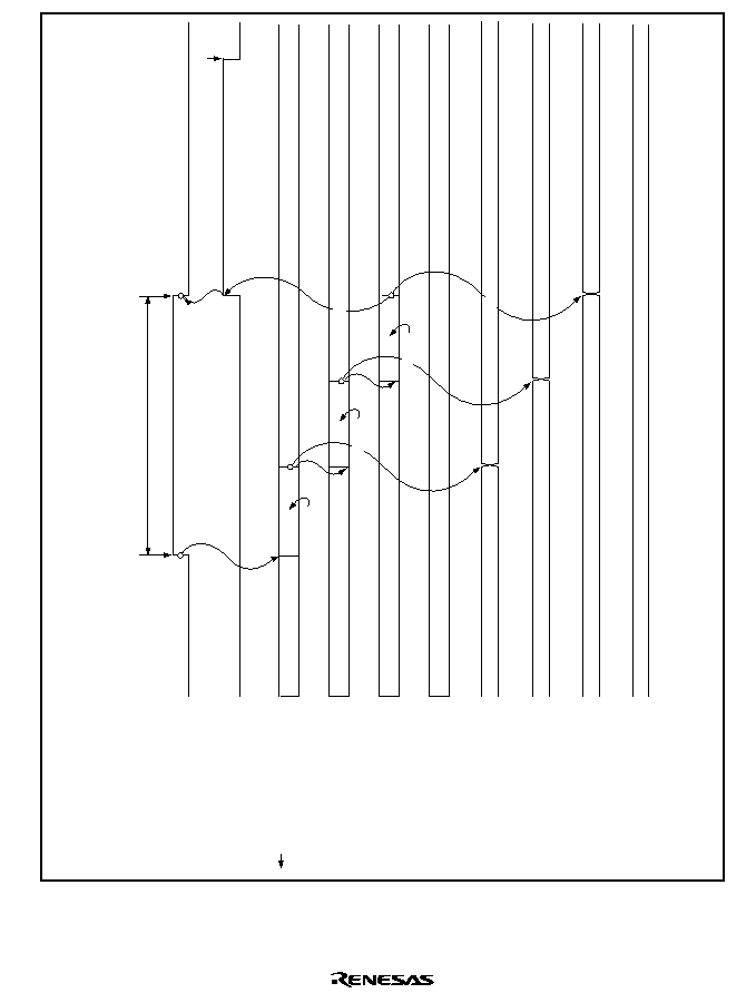
Rev. 5.0, 09/03, page 669 of 806
Channel 0 (AN0)
operating
ADST
ADF
Channel 1 (AN1)
operating
Channel 2 (AN2)
operating
Channel 3 (AN3)
operating
ADDRA
ADDRB
ADDRC
ADDRD
Waiting
Waiting
Waiting
Waiting
Set
*
Clear
*
Clear
A/D conversion result 2
Waiting
Waiting
A/D conversion result 3
A/D conversion 1
Waiting
A/D conversion result 1
Transfer
A/D conversion 3
A/D conversion
A/D conversion 2
Note:
*Vertical arrows ( ) indicate instruction execution by software.
Figure 21.4 Example of A/D Converter Operation (Multi Mode,
Channels AN0 to AN2 Selected)

Rev. 5.0, 09/03, page 670 of 806
21.4.3
Scan Mode (MULTI = 1, SCN = 1)
Scan mode is useful for monitoring analog inputs in a group of one or more channels. When the
ADST bit in the A/D control/status register (ADCSR) is set to 1 by software or external trigger
input, A/D conversion starts on the first channel in the group (AN0 when CH2 = 0, AN4 when
CH2 = 1)). When two or more channels are selected, after conversion of the first channel ends,
conversion of the second channel (AN1 or AN5) starts immediately. A/D conversion continues
cyclically on the selected channels until the ADST bit is cleared to 0. The conversion results are
transferred for storage into the A/D data registers corresponding to the channels.
When the mode or analog input channel must be changed during analog conversion, to prevent
incorrect operation, first clear the ADST bit to 0 to halt A/D conversion. After making the
necessary changes, set the ADST bit to 1. A/D conversion will start again from the first channel
in the group. The ADST bit can be set at the same time as the mode or channel selection is
changed.
Typical operations when three channels (AN0 to AN2) are selected in scan mode are described
next. Figure 21.5 shows a timing diagram for this example.
1. Scan mode is selected (MULTI = 1, SCN = 1), channel group 2 is selected (CH2 = 0), analog
input channels AN0 to AN2 are selected (CH1 = 1, CH0 = 0), and A/D conversion is started
(ADST = 1).
2. When A/D conversion of the first channel (AN0) is completed, the result is transferred into
ADDRA. Next, conversion of the second channel (AN1) starts automatically.
3. Conversion proceeds in the same way through the third channel (AN2).
4. When conversion of all the selected channels (AN0 to AN2) is completed, the ADF flag is set
to 1 and conversion of the first channel (AN0) starts again. If the ADIE bit is set to 1, an ADI
interrupt is requested at this time.
5. Steps 2 to 4 are repeated as long as the ADST bit remains set to 1. When the ADST bit is
cleared to 0, A/D conversion stops. After that, if the ADST bit is set to 1, A/D conversion
starts again from the first channel (AN0).

Rev. 5.0, 09/03, page 671 of 806
ADST
ADF
Channel 0 (AN
0
)
operating
Channel 1 (AN
1
)
operating
Channel 2 (AN
2
)
operating
Channel 3 (AN
3
)
operating
ADDRA
ADDRB
ADDRC
ADDRD
Waiting
Waiting
Waiting
Waiting
Waiting
Waiting
Waiting
Waiting
Waiting
Transfer
A/D conversion 1
A/D conversion 4
A/D conversion 2
A/D conversion 3
A/D conversion result 1
A/D conversion result 4
A/D conversion result 2
A/D conversion result 3
Clear
*
1
Clear
*
1
Set
*
1
Continuous A/D conversion
A/D conversion 5
Notes: 1.
Vertical arrows ( ) indicate instruction execution by software.
2.
Data during conversion is ignored.
Figure 21.5 Example of A/D Converter Operation (Scan Mode,
Channels AN0 to AN2 Selected)
Rev. 5.0, 09/03, page 672 of 806
21.4.4
Input Sampling and A/D Conversion Time
The A/D converter has a built-in sample-and-hold circuit. The A/D converter samples the analog
input at a time t
D
after the ADST bit is set to 1, then starts conversion. Figure 21.6 shows the A/D
conversion timing. Table 21.4 indicates the A/D conversion time.
As indicated in figure 21.6, the A/D conversion time includes t
D
and the input sampling time. The
length of t
D
varies depending on the timing of the write access to ADCSR. The total conversion
time therefore varies within the ranges indicated in table 21.4.
In multi mode and scan mode, the conversion time values given in table 21.4 apply to the first
conversion. In the second and subsequent conversions, the conversion time is fixed at 256 states
when CKS = 0 in ADCSR, or 128 states when CKS = 1. In both cases, the CKS bit should be set
according to the P
frequency so that the conversion time is within the range shown in table 24.10
in section 24, Electrical Characteristics.
P
Write
signal
ADF
*1
Input sampling
timing
t
D
A/D conversion start delay
t
SPL
Input sampling time
t
CONV
A/D conversion time
Notes: 1. ADCSR write cycle
2. ADCSR address
Address
*2
t
D
t
SPL
t
CONV
Figure 21.6 A/D Conversion Timing
Rev. 5.0, 09/03, page 673 of 806
Table 21.4
A/D Conversion Time (Single Mode)
CKS = 0
CKS = 1
Symbol
Min
Typ
Max
Min
Typ
Max
A/D conversion start
delay
t
D
17
--
28
10
--
17
Input sampling time
t
SPL
--
129
--
--
65
--
A/D conversion time
t
CONV
514
--
525
259
--
266
Note:
Values in the table are numbers of states (t
cyc
).
21.4.5
External Trigger Input Timing
A/D conversion can be externally triggered. When the TRGE1 and TRGE0 bits are set to 1 in
ADCR, external trigger input is enabled at the
ADTRG pin. A high-to-low transition at the
ADTRG pin sets the ADST bit to 1 in ADCSR, starting A/D conversion. Other operations,
regardless of the conversion mode, are the same as if the ADST bit had been set to 1 by software.
Figure 21.7 shows the timing.
A/D conversion
P
ADTRG
External
trigger signal
ADST
Figure 21.7 External Trigger Input Timing

Rev. 5.0, 09/03, page 674 of 806
21.5
Interrupts
The A/D converter generates an interrupt (ADI) at the end of A/D conversion. The ADI interrupt
request can be enabled or disabled by the ADIE bit in ADCSR.
21.6
Definitions of A/D Conversion Accuracy
The A/D converter compares an analog value input from an analog input channel with its analog
reference value and converts it to 10-bit digital data. The absolute accuracy of this A/D conversion
is the deviation between the input analog value and the output digital value. It includes the
following errors:
∑
Offset error
∑
Full-scale error
∑
Quantization error
∑
Nonlinearity error
These four error quantities are explained below with reference to figure 21.8. In the figure, the 10
bits of the A/D converter have been simplified to 3 bits.
Offset error is the deviation between actual and ideal A/D conversion characteristics when the
digital output value changes from the minimum (zero voltage) 0000000000 (000 in the figure) to
000000001 (001 in the figure)(figure 21.8, item (1)). Full-scale error is the deviation between
actual and ideal A/D conversion characteristics when the digital output value changes from the
1111111110 (110 in the figure) to the maximum 1111111111 (111 in the figure)(figure 21.8, item
(2)). Quantization error is the intrinsic error of the A/D converter and is expressed as 1/2 LSB
(figure 21.8, item (3)). Nonlinearity error is the deviation between actual and ideal A/D conversion
characteristics between zero voltage and full-scale voltage (figure 21.8, item (4)). Note that it does
not include offset, full-scale, or quantization error.
Rev. 5.0, 09/03, page 675 of 806
111
110
101
100
011
010
001
000
0 1/8 2/8 3/8 4/8 5/8 6/8 7/8 FS
Analog input
voltage
FS: Full-scale voltage
(3) Quantization
error
Ideal A/D
conversion
characteristic
(4) Nonlinearity
error
Ideal A/D
conversion
characteristic
Actual A/D
convertion
characteristic
(2) Full-scale error
Digital output
Analog input
voltage
(1) Offset error
FS
Digital output
Figure 21.8 Definitions of A/D Conversion Accuracy
21.7
Usage Notes
When using the A/D converter, note the following points.
21.7.1
Setting Analog Input Voltage
∑
Analog Input Voltage Range: During A/D conversion, the voltages input to the analog input
pins ANn should be in the range AV
SS
ANn
AV
CC
(n = 0 to 7).
∑
Relationships of AV
CC
and AV
SS
to V
CC
and V
SS
: AV
CC
, AV
SS
, V
CC
and V
SS
should be
related as follows: AV
CC
= V
CC
± 0.3 V and AV
SS
= V
SS
.
21.7.2
Processing of Analog Input Pins
To prevent damage from voltage surges at the analog input pins (AN0 to AN7), connect an input
protection circuit like the one shown in figure 21.9. The circuit shown also includes an RC filter to
suppress noise. This circuit is shown as an example; the circuit constants should be selected
according to actual application conditions. Table 21.5 lists the analog input pin specifications and
figure 21.10 shows an equivalent circuit diagram of the analog input ports.
Rev. 5.0, 09/03, page 676 of 806
21.7.3
Access Size and Read Data
Table 21.6 shows the relationship between access size and read data. Note the read data obtained
with different access sizes, bus widths, and endian modes.
The case is shown here in which H'3FF is obtained when AVCC is input as an analog input. FF is
the data containing the upper 8 bits of the conversion result, and C0 is the data containing the
lower 2 bits.
0.01
µF
10
µF
AV
CC
AN0 to AN7
AV
SS
SH7729R
*
100
0.1
µF
Note:
*
Figure 21.9 Example of Analog Input Protection Circuit
1.0 k
AN0 to AN7
20 pF
1 M
Figure 21.10 Analog Input Pin Equivalent Circuit

Rev. 5.0, 09/03, page 677 of 806
Table 21.5
Analog Input Pin Ratings
Item
Min
Max
Unit
Analog input capacitance
--
20
pF
Allowable signal-source impedance
--
5
k
Table 21.6
Relationship between Access Size and Read Data
Bus Width
32 Bits (D31≠D0)
16 Bits (D15≠D0)
8 Bits (D7≠D0)
Access
Size
Command Endian
Big
Little
Big
Little
Big
Little
Byte
access
MOV.L
MOV.B
MOV.L
MOV.B
#ADDRAH,R9
@R9,R8
#ADDRAL,R9
@R9,R8
FFFFFFFF
C0C0C0C0
FFFFFFFF
C0C0C0C0
FFFF
C0C0
FFFF
C0C0
FF
C0
FF
C0
Word
access
MOV.L
MOV.W
MOV.L
MOV.W
#ADDRAH,R9
@R9,R8
#ADDRAL,R9
@R9,R8
FFxxFFxx
C0xxC0xx
FFxxFFxx
C0xxC0xx
FFxx
C0xx
FFxx
C0xx
FF
xx
C0
xx
xx
FF
xx
C0
Longword
access
MOV.L
MOV.L
#ADDRAH,R9
@R9,R8
FFxxC0xx
FFxxC0xx
FFxx
C0xx
C0xx
FFxx
FF
xx
C0
xx
xx
C0
xx
FF
In this table:
#ADDRAH .EQU H'04000080
#ADDRAL .EQU H'04000082
Values are shown in hexadecimal for the case where read data is output to an
external device via R8.

Rev. 5.0, 09/03, page 678 of 806
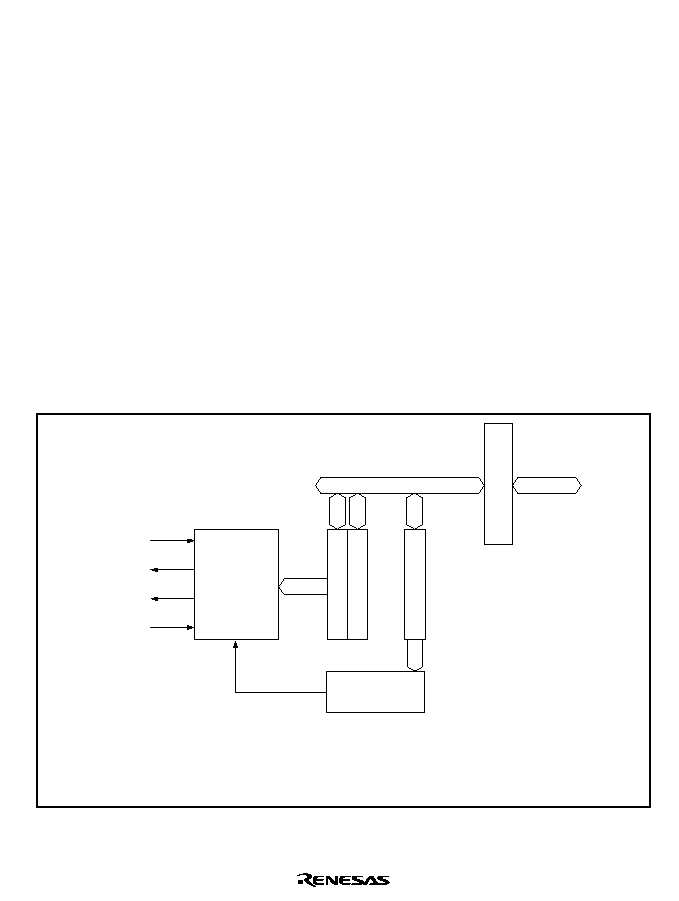
Rev. 5.0, 09/03, page 679 of 806
Section 22 D/A Converter
22.1
Overview
The SH7729R includes a D/A converter with two channels.
22.1.1
Features
D/A converter features are listed below.
∑
Eight-bit resolution
∑
Two output channels
∑
Conversion time: maximum 10
µ
s (with 20-pF capacitive load)
∑
Output voltage: 0 V to AVcc
22.1.2
Block Diagram
Figure 22.1 shows a block diagram of the D/A converter.
AV
CC
DA
0
DA
1
DACR
DADR0
DADR1
Module data bus
Bus interface
On-chip
data bus
Control circuit
Legend
DACR:
D/A control register
DADR0: D/A data register 0
DADR1: D/A data register 1
8-bit D/A
AV
SS
Figure 22.1 Block Diagram of D/A Converter

Rev. 5.0, 09/03, page 680 of 806
22.1.3
I/O Pins
Table 22.1 summarizes the D/A converter's input and output pins.
Table 22.1
D/A Converter Pins
Pin Name
Abbreviation
I/O
Function
Analog power supply pin
AVcc
Input
Analog power supply
Analog ground pin
AVss
Input
Analog ground and reference voltage
Analog output pin 0
DA0
Output
Analog output, channel 0
Analog output pin 1
DA1
Output
Analog output, channel 1
22.1.4
Register Configuration
Table 22.2 summarizes the D/A converter's registers.
Table 22.2
D/A Converter Registers
Name
Abbreviation
R/W
Initial Value
Address
*
1
D/A data register 0
DADR0
R/W
H'00
H'040000A0
(H'A40000A0)
*
2
D/A data register 1
DADR1
R/W
H'00
H'040000A2
(H'A40000A2)
*
2
D/A control register
DACR
R/W
H'1F
H'040000A4
(H'A40000A4)
*
2
Notes: These registers are located in area 1 of physical space. Therefore, when the cache is on,
either access these registers from the P2 area of logical space or else make an appropriate
setting using the MMU so that these registers are not cached.
1. Lower 16 bits of the address
2. When address translation by the MMU does not apply, the address in parentheses
should be used.

Rev. 5.0, 09/03, page 681 of 806
22.2
Register Descriptions
22.2.1
D/A Data Registers 0 and 1 (DADR0/1)
Bit:
7
6
5
4
3
2
1
0
Initial value:
0
0
0
0
0
0
0
0
R/W:
R/W
R/W
R/W
R/W
R/W
R/W
R/W
R/W
The D/A data registers (DADR0 and DADR1) are 8-bit readable/writable registers that store the
data to be converted. When analog output is enabled, the D/A data register values are constantly
converted and output at the analog output pins.
The D/A data registers are initialized to H'00 by a reset.
22.2.2
D/A Control Register (DACR)
Bit:
7
6
5
4
3
2
1
0
DAOE1
DAOE0
DAE
--
--
--
--
--
Initial value:
0
0
0
1
1
1
1
1
R/W:
R/W
R/W
R/W
R
R
R
R
R
DACR is an 8-bit readable/writable register that controls the operation of the D/A converter.
DACR is initialized to H'1F by a reset.
Bit 7--D/A Output Enable 1 (DAOE1): Controls D/A conversion and analog output.
Bit 7: DAOE1
Description
0
DA1 analog output is disabled
(Initial value)
1
Channel-1 D/A conversion and DA1 analog output are enabled
Bit 6--D/A Output Enable 0 (DAOE0): Controls D/A conversion and analog output.
Bit 6: DAOE0
Description
0
DA0 analog output is disabled
(Initial value)
1
Channel-0 D/A conversion and DA0 analog output are enabled

Rev. 5.0, 09/03, page 682 of 806
Bit 5--D/A Enable (DAE): Controls D/A conversion, together with bits DAOE0 and DAOE1.
When the DAE bit is cleared to 0, D/A conversion is controlled independently in channels 0 and 1.
When the chip enters standby mode while D/A conversion is enabled, the D/A output is held and
the analog power-supply current is equivalent to that during D/A conversion. To reduce the analog
power-supply current in standby mode, clear the DAOE0 and DAOE1 bits and disable the D/A
output.
Bit 7: DAOE1
Bit 6: DAOE0
Bit 5: DAE
Description
0
0
--
D/A conversion is disabled in channels 0 and 1
(Initial value)
0
1
0
D/A conversion is enabled in channel 0
D/A conversion is disabled in channel 1
0
1
1
D/A conversion is enabled in channels 0 and 1
1
0
0
D/A conversion is disabled in channel 0
D/A conversion is enabled in channel 1
1
0
1
D/A conversion is enabled in channels 0 and 1
1
1
--
D/A conversion is enabled in channels 0 and 1
When the DAE bit is set to 1, even if bits DAOE0 and DAOE1 in DACR and the ADST bit in
ADCSR are cleared to 0, the same current is drawn from the analog power supply as during A/D
and D/A conversion.
Bits 4 to 0--Reserved: Read-only bits, always read as 1.
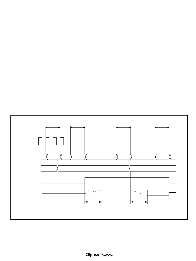
Rev. 5.0, 09/03, page 683 of 806
22.3
Operation
The D/A converter has two built-in D/A conversion circuits that can perform conversion
independently.
D/A conversion is performed constantly while enabled in DACR. If the DADR0 or DADR1 value
is modified, conversion of the new data begins immediately. The conversion results are output
when bits DAOE0 and DAOE1 are set to 1.
An example of D/A conversion on channel 0 is given next. Timing is indicated in figure 22.2.
1. Data to be converted is written in DADR0.
2. Bit DAOE0 is set to 1 in DACR. D/A conversion starts and DA0 becomes an output pin. The
converted result is output after the conversion time. The output value is (DADR0 contents/256)
◊
AVcc. Output of this conversion result continues until the value in DADR0 is modified or
the DAOE0 bit is cleared to 0.
3. If the DADR0 value is modified, conversion starts immediately, and the result is output after
the conversion time.
4. When the DAOE0 bit is cleared to 0, DA0 becomes an input pin.
DADR0
write cycle
t
DCONV
High-impedance state
Conversion
result 1
Conversion data 1
Conversion data 2
Conversion
result 2
t
DCONV
Address bus
DADR0
DAOE0
DA0
t
DCONV
: D/A conversion time
Legend
DACR
write cycle
DADR0
write cycle
DACR
write cycle
Figure 22.2 Example of D/A Converter Operation

Rev. 5.0, 09/03, page 684 of 806

Rev. 5.0, 09/03, page 685 of 806
Section 23 User Debugging Interface (UDI)
23.1
Overview
The SH7729R incorporates a user debugging interface (UDI) and advanced user debugger (AUD)
for program debugging.
23.2
User Debugging Interface (UDI)
The UDI (user debugging interface) performs on-chip debugging which is supported by the
SH7729R. The UDI described here is a serial interface which is compatible with JTAG (Joint Test
Action Group, IEEE Standard 1149.1 and IEEE Standard Test Access Port and Boundary-Scan
Architecture) specifications.
The UDI in the SH7729R supports a boundary scan mode, and is also used for emulator
connection.
When using an emulator, UDI functions should not be used. Refer to the emulator manual for the
method of connecting the emulator.
23.2.1
Pin Descriptions
TCK: UDI serial data input/output clock pin. Data is serially supplied to the UDI from the data
input pin (TDI), and output from the data output pin (TDO), in synchronization with this clock.
TMS: Mode select input pin. The state of the TAP control circuit is determined by changing this
signal in synchronization with TCK. The protocol complies with the JTAG standard (IEEE Std.
1149.1).
T
T
T
TR
R
R
RSSSSTTTT: UDI reset input pin. Input is accepted asynchronously with respect to TCK, and when low,
the UDI is reset. See section 23.4.2, Reset Configuration, for more information.
TDI: UDI serial data input pin. Data transfer to the UDI is executed by changing this signal in
synchronization with TCK.
TDO: UDI serial data output pin. Data output from the UDI is executed by reading this signal in
synchronization with TCK.
A
A
A
ASSSSEEEEM
M
M
MD
D
D
D0000: ASE mode select pin. If a low level is input at the ASEMD0 pin while the RESETP
pin is asserted, ASE mode is entered; if a high level is input, normal mode is entered. In ASE
mode, boundary scan and emulator functions can be used. The input level at the
ASEMD0 pin
should be held for at least one cycle after
RESETP negation.
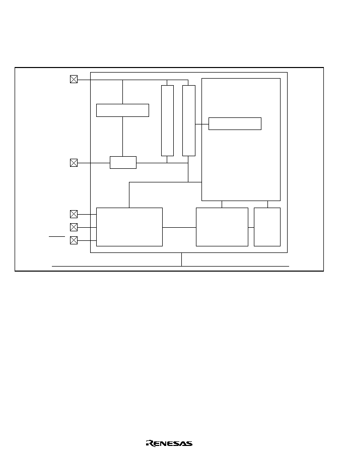
Rev. 5.0, 09/03, page 686 of 806
A
A
A
ASSSSEEEEB
B
B
BR
R
R
RKAK
KAK
KAK
KAK: Dedicated emulator pin
23.2.2
Block Diagram
Figure 23.1 shows a block diagram of the UDI.
SDIR
TCK
TDO
TDI
TMS
TRST
SDBPR
MUX
SDBSR
Shift register
TAP controller
Decoder
Local
bus
Figure 23.1 Block Diagram of UDI
23.3
Register Descriptions
The UDI has the following registers.
∑
SDBPR: Bypass register
∑
SDIR: Instruction register
∑
SDBSR: Boundary scan register

Rev. 5.0, 09/03, page 687 of 806
Table 23.1 shows the UDI register configuration.
Table 23.1
UDI Registers
CPU Side
UDI Side
Name
Abbreviation
R/W
Size
Address
R/W
Size
Initial
Value
*
Bypass register
SDBPR
--
--
--
R/W
1
Undefined
Instruction register
SDIR
R
16
H'04000200
R/W
16
H'FFFF
Boundary register
SDBSR
--
--
--
R/W
--
Undefined
Note:
*
Initialized when
TRST
pin is low or when TAP is in the test-logic-reset state.
23.3.1
Bypass Register (SDBPR)
The bypass register is a 1-bit register that cannot be accessed by the CPU. When SDIR is set to the
bypass mode, SDBPR is connected between UDI pins TDI and TDO.
23.3.2
Instruction Register (SDIR)
The instruction register (SDIR) is a 16-bit read-only register. The register is in bypass mode in its
initial state. It is initialized by
TRST or in the TAP test-logic-reset state, and can be written to by
the UDI irrespective of the CPU mode. Operation is not guaranteed if a reserved command is set
in this register
Bit:
15
14
13
12
11
10
9
8
TI3
TI2
TI1
TI0
--
--
--
--
Initial value:
1
1
1
1
1
1
1
1
Bit:
7
6
5
4
3
2
1
0
--
--
--
--
--
--
--
--
Initial value:
1
1
1
1
1
1
1
1
Bits 15 to 12--Test Instruction Bits (TI3 to TI0): Cannot be written by the CPU.

Rev. 5.0, 09/03, page 688 of 806
Table 23.2
UDI Commands
TI3
TI2
TI1
TI0
Description
0
0
0
0
EXTEST
0
1
0
0
SAMPLE/PRELOAD
0
1
0
1
Reserved
0
1
1
0
UDI reset negate
0
1
1
1
UDI reset assert
1
0
0
--
Reserved
1
0
1
--
UDI interrupt
1
1
0
--
Reserved
1
1
1
0
Reserved
1
1
1
1
Bypass mode
(Initial value)
0
0
0
1
Recovery from sleep
Bits 11 to 0--Reserved: These bits are always read as 1.
23.3.3
Boundary Scan Register (SDBSR)
The boundary scan register (SDBSR) is a shift register, located on the PAD, for controlling the
input/output pins of the SH7729R.
Using the EXTEST and SAMPLE/PRELOAD commands, a boundary scan test conforming to the
JTAG standard can be carried out. Table 23.3 shows the correspondence between SH7729R pins
and boundary scan register bits.

Rev. 5.0, 09/03, page 689 of 806
Table 23.3
SH7729R Pins and Boundary Scan Register Bits
Bit
Pin Name
I/O
Bit
Pin Name
I/O
from TDI
308
D1
IN
338
D31/PTB7
IN
307
D0
IN
337
D30/PTB6
IN
306
MD1
IN
336
D29/PTB5
IN
305
MD2
IN
335
D28/PTB4
IN
304
NMI
IN
334
D27/PTB3
IN
303
IRQ0/
IRL0
/PTH0
IN
333
D26/PTB2
IN
302
IRQ1/
IRL1
/PTH1
IN
332
D25/PTB1
IN
301
IRQ2/
IRL2
/PTH2
IN
331
D24/PTB0
IN
300
IRQ3/
IRL3
/PTH3
IN
330
D23/PTA7
IN
299
IRQ4/PTH4
IN
329
D22/PTA6
IN
298
D31/PTB7
OUT
328
D21/PTA5
IN
297
D30/PTB6
OUT
327
D20/PTA4
IN
296
D29/PTB5
OUT
326
D19/PTA3
IN
295
D28/PTB4
OUT
325
D18/PTA2
IN
294
D27/PTB3
OUT
324
D17/PTA1
IN
293
D26/PTB2
OUT
323
D16/PTA0
IN
292
D25/PTB1
OUT
322
D15
IN
291
D24/PTB0
OUT
321
D14
IN
290
D23/PTA7
OUT
320
D13
IN
289
D22/PTA6
OUT
319
D12
IN
288
D21/PTA5
OUT
318
D11
IN
287
D20/PTA4
OUT
317
D10
IN
286
D19/PTA3
OUT
316
D9
IN
285
D18/PTA2
OUT
315
D8
IN
284
D17/PTA1
OUT
314
D7
IN
283
D16/PTA0
OUT
313
D6
IN
282
D15
OUT
312
D5
IN
281
D14
OUT
311
D4
IN
280
D13
OUT
310
D3
IN
279
D12
OUT
309
D2
IN
278
D11
OUT

Rev. 5.0, 09/03, page 690 of 806
Bit
Pin Name
I/O
Bit
Pin Name
I/O
277
D10
OUT
247
D12
Control
276
D9
OUT
246
D11
Control
275
D8
OUT
245
D10
Control
274
D7
OUT
244
D9
Control
273
D6
OUT
243
D8
Control
272
D5
OUT
242
D7
Control
271
D4
OUT
241
D6
Control
270
D3
OUT
240
D5
Control
269
D2
OUT
239
D4
Control
268
D1
OUT
238
D3
Control
267
D0
OUT
237
D2
Control
266
D31/PTB7
Control
236
D1
Control
265
D30/PTB6
Control
235
D0
Control
264
D29/PTB5
Control
234
BS
/PTK4
IN
263
D28/PTB4
Control
233
WE2
/DQMUL/
ICIORD
/
PTK6
IN
262
D27/PTB3
Control
232
WE3
/DQMUU/
ICIORD
/
PTK7
IN
261
D26/PTB2
Control
231
AUDSYNC
/PTE7
IN
260
D25/PTB1
Control
230
CS2
/PTK0
IN
259
D24/PTB0
Control
229
CS3
/PTK1
IN
258
D23/PTA7
Control
228
CS4
/PTK2
IN
257
D22/PTA6
Control
227
CS5
/
CE1A
/PTK3
IN
256
D21/PTA5
Control
226
CE2A
/PTE4
IN
255
D20/PTA4
Control
225
CE2B
/PTE5
IN
254
D19/PTA3
Control
224
A0
OUT
253
D18/PTA2
Control
223
A1
OUT
252
D17/PTA1
Control
222
A2
OUT
251
D16/PTA0
Control
221
A3
OUT
250
D15
Control
220
A4
OUT
249
D14
Control
219
A5
OUT
248
D13
Control
218
A6
OUT

Rev. 5.0, 09/03, page 691 of 806
Bit
Pin Name
I/O
Bit
Pin Name
I/O
217
A7
OUT
187
CS4
/PTK2
OUT
216
A8
OUT
186
CS5
/CE1A/PTK3
OUT
215
A9
OUT
185
CS6
/
CE1B
OUT
214
A10
OUT
184
CE2A
/PTE4
OUT
213
A11
OUT
183
CE2B
/PTE5
OUT
212
A12
OUT
182
A0
Control
211
A13
OUT
181
A1
Control
210
A14
OUT
180
A2
Control
209
A15
OUT
179
A3
Control
208
A16
OUT
178
A4
Control
207
A17
OUT
177
A5
Control
206
A18
OUT
176
A6
Control
205
A19
OUT
175
A7
Control
204
A20
OUT
174
A8
Control
203
A21
OUT
173
A9
Control
202
A22
OUT
172
A10
Control
201
A23
OUT
171
A11
Control
200
A24
OUT
170
A12
Control
199
A25
OUT
169
A13
Control
198
BS
/PTK4
OUT
168
A14
Control
197
RD
OUT
167
A15
Control
196
WE0
/DQMLL
OUT
166
A16
Control
195
WE1
/DQMLU/
WE
OUT
165
A17
Control
194
WE2
/DQMUL/
ICIORD
/
PTK6
OUT
164
A18
Control
193
WE3
/DQMUU/
ICIOWR
/
PTK7
OUT
163
A19
Control
192
RD/
WR
OUT
162
A20
Control
191
AUDSYNC
/PTE7
OUT
161
A21
Control
190
CS0
/MCS0
OUT
160
A22
Control
189
CS2
/PTK0
OUT
159
A23
Control
188
CS3
/PTK1
OUT
158
A24
Control

Rev. 5.0, 09/03, page 692 of 806
Bit
Pin Name
I/O
Bit
Pin Name
I/O
157
A25
Control
127
BREQ
IN
156
BS
/PTK4
Control
126
WAIT
IN
155
RD
Control
125
AUDCK/PTH6
IN
154
WE0
/DQMLL
Control
124
IOIS16
/PTG7
IN
153
WE1
/DQMLU/
WE
Control
123
ASEBRKAK
/PTG5
IN
152
WE2
/DQMUL/
ICIORD
/
PTK6
Control
122
PTG4
IN
151
WE3
/DQMUU/
ICIOWR
/
PTK7
Control
121
AUDATA3/PTG3
IN
150
RD/
WR
Control
120
AUDATA2/PTG2
IN
149
AUDSYNC
/PTE7
Control
119
AUDATA1/PTG1
IN
148
CS0
/MCS0
Control
118
AUDATA0/PTG0
IN
147
CS2
/PTK0
Control
117
ADTRG
/PTH5
IN
146
CS3
/PTK1
Control
116
IRLS3
/PTF3/PINT11
IN
145
CS4
/PTK2
Control
115
IRLS2
/PTF2/PINT10
IN
144
CS5
/
CE1A
/PTK3
Control
114
IRLS1
/PTF1/PINT9
IN
143
CS6
/
CE1B
Control
113
IRLS0
/PTF0/PINT8
IN
142
CE2A
/PTE4
Control
112
MD0
IN
141
CE2B
/PTE5
Control
111
CKE/PTK5
OUT
140
CKE/PTK5
IN
110
RAS3L
/PTJ0
OUT
139
RAS3L
/PTJ0
IN
109
RAS2L
/PTJ1
OUT
138
RAS2L
/PTJ1
IN
108
CASLL
/
CASL
/PTJ2
OUT
137
CASLL
/
CASL
/PTJ2
IN
107
CASLH
/
CASU
/PTJ3
OUT
136
CASLH
/
CASU
/PTJ3
IN
106
CASHL
/PTJ4
OUT
135
CASHL
/PTJ4
IN
105
CASHH
/PTJ5
OUT
134
CASHH
/PTJ5
IN
104
DACK0/PTD5
OUT
133
DACK0/PTD5
IN
103
DACK1/PTD7
OUT
132
DACK1/PTD7
IN
102
CAS2L
/PTE6
OUT
131
CAS2L
/PTE6
IN
101
CAS2H
/PTE3
OUT
130
CAS2H
/PTE3
IN
100
RAS3U
/PTE2
OUT
129
RAS3U
/PTE2
IN
99
RAS2U
/PTE1
OUT
128
RAS2U
/PTE1
IN
98
BACK
OUT

Rev. 5.0, 09/03, page 693 of 806
Bit
Pin Name
I/O
Bit
Pin Name
I/O
97
ASEBRKAK
/PTG5
OUT
65
RxD2/SCPT4
IN
96
AUDATA3/PTG3
OUT
64
WAKEUP
/PTD3
IN
95
AUDATA2/PTG2
OUT
63
RESETOUT
/PTD2
IN
94
AUDATA1/PTG1
OUT
62
DRAK0/PTD1
IN
93
AUDATA0/PTG0
OUT
61
DRAK1/PTD0
IN
92
CKE/PTK5
Control
60
DREQ0
/PTD4
IN
91
RAS3L
/PTJ0
Control
59
DREQ1
/PTD6
IN
90
RAS2L
/PTJ1
Control
58
RxD1/SCPT2
IN
89
CASLL
/
CASL
/PTJ2
Control
57
CTS2
/IRQ5/SCPT7
IN
88
CASLH
/
CASU
/PTJ3
Control
56
MCS7
/PTC7/PINT7
IN
87
CASHL
/PTJ4
Control
55
MCS6
/PTC6/PINT6
IN
86
CASHH
/PTJ5
Control
54
MCS5
/PTC5/PINT5
IN
85
DACK0/PTD5
Control
53
MCS4
/PTC4/PINT4
IN
84
DACK1/PTD7
Control
52
MCS3
/PTC3/PINT3
IN
83
CAS2L
/PTE6
Control
51
MCS2
/PTC2/PINT2
IN
82
CAS2H
/PTE3
Control
50
MCS1
/PTC1/PINT1
IN
81
RAS3U
/PTE2
Control
49
MCS0
/PTC0/PINT0
IN
80
RAS2U
/PTE1
Control
48
MD3
IN
79
BACK
Control
47
MD4
IN
78
ASEBRKAK
/PTG5
Control
46
MD5
IN
77
AUDATA3/PTG3
Control
45
STATUS0/PTJ6
OUT
76
AUDATA2/PTG2
Control
44
STATUS1/PTJ7
OUT
75
AUDATA1/PTG1
Control
43
TCLK/PTH7
OUT
74
AUDATA0/PTG0
Control
42
IRQOUT
OUT
73
STATUS0/PTJ6
IN
41
TxD0/SCPT0
OUT
72
STATUS1/PTJ7
IN
40
SCK0/SCPT1
OUT
71
TCLK/PTH7
IN
39
TxD1/SCPT2
OUT
70
SCK0/SCPT1
IN
38
SCK1/SCPT3
OUT
69
SCK1/SCPT3
IN
37
TxD2/SCPT4
OUT
68
SCK2/SCPT5
IN
36
SCK2/SCPT5
OUT
67
RTS2
/SCPT6
IN
35
RTS2/SCPT6
OUT
66
RxD0/SCPT0
IN
34
MCS7
/PTC7/PINT7
OUT

Rev. 5.0, 09/03, page 694 of 806
Bit
Pin Name
I/O
Bit
Pin Name
I/O
33
MCS6
/PTC6/PINT6
OUT
15
SCK1/SCPT3
Control
32
MCS5
/PTC5/PINT5
OUT
14
TxD2/SCPT4
Control
31
MCS4
/PTC4/PINT4
OUT
13
SCK2/SCPT5
Control
30
WAKEUP
/PTD3
OUT
12
RTS2/SCPT6
Control
29
RESETOUT
/PTD2
OUT
11
MCS7
/PTC7/PINT7
Control
28
MCS3
/PTC3/PINT3
OUT
10
MCS6
/PTC6/PINT6
Control
27
MCS2
/PTC2/PINT2
OUT
9
MCS5
/PTC5/PINT5
Control
26
MCS1
/PTC1/PINT1
OUT
8
MCS4
/PTC4/PINT4
Control
25
MCS0
/PTC0/PINT0
OUT
7
WAKEUP
/PTD3
Control
24
DRAK0/PTD1
OUT
6
RESETOUT
/PTD2
Control
23
DRAK1/PTD0
OUT
5
MCS3
/PTC3/PINT3
Control
22
STATUS0/PTJ6
Control
4
MCS2
/PTC2/PINT2
Control
21
STATUS1/PTJ7
Control
3
MCS1
/PTC1/PINT1
Control
20
TCLK/PTH7
Control
2
MCS0
/PTC0/PINT0
Control
19
IRQOUT
Control
1
DRAK0/PTD1
Control
18
TxD0/SCPT0
Control
0
DRAK1/PTD0
Control
17
SCK0/SCPT1
Control
to TDO
16
TxD1/SCPT2
Control
Note:
Control is an active-low signal.
When Control is driven low, the corresponding pin is driven by the value of OUT.
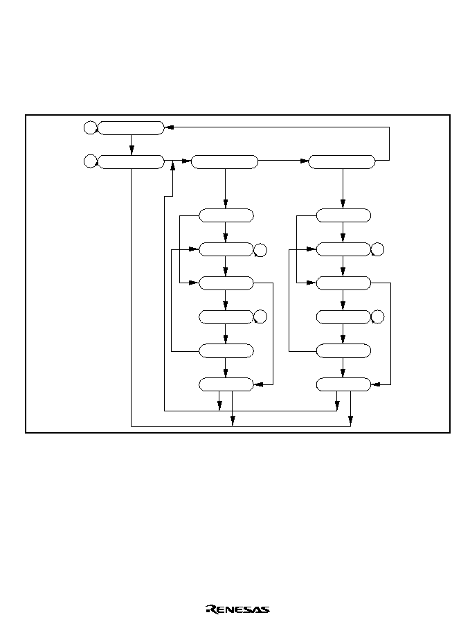
Rev. 5.0, 09/03, page 695 of 806
23.4
UDI Operation
23.4.1
TAP Controller
Figure 23.2 shows the internal states of the TAP controller. State transitions basically conform
with the JTAG standard.
Test-logic-reset
Capture-DR
Shift-DR
Exit1-DR
Pause-DR
Exit2-DR
Update-DR
Select-DR-scan
Run-test/idle
1
0
0
0
0
1
1
1
1
0
0
1
0
1
1
1
0
Capture-IR
Shift-IR
Exit1-IR
Pause-IR
Exit2-IR
Update-IR
Select-IR-scan
0
0
1
0
0
1
0
1
1
1
0
0
Figure 23.2 TAP Controller State Transitions
Note:
The transition condition is the TMS value at the rising edge of TCK. The TDI value is
sampled at the rising edge of TCK; shifting occurs at the falling edge of TCK. The TDO
value changes at the TCK falling edge. The TDO is at high impedance, except with shift-
DR (shift-SR) and shift-IR states. During the change to
TRST = 0, there is a transition to
test-logic-reset asynchronously with TCK.

Rev. 5.0, 09/03, page 696 of 806
23.4.2
Reset Configuration
Table 23.4
Reset Configuration
AS
AS
AS
ASD
D
D
DM
M
M
MD
D
D
D0000*
1
R
R
R
RESE
ESE
ESE
ESETTTTP
P
P
P
T
T
T
TR
R
R
RS
S
S
STTTT
Chip State
High-level
Low-level
Low-level
Normal reset and UDI reset
High-level
Normal reset
High-level
Low-level
UDI reset only
High-level
Normal operation
Low-level
Low-level
Low-level
Reset hold
*
2
High-level
ASE user mode
*
3
: Normal reset
ASE break mode
*
3
:
RESETP
assertion
masked
High-level
Low-level
UDI reset only
High-level
Normal operation
Notes: 1. Performs main chip mode and ASE mode settings
ASEMD0
= H, main chip mode
ASEMD0
= L, ASE mode
2. In ASE mode, reset hold is enabled by driving the
RESETP
and
TRST
pins low for a
constant cycle. In this state, the CPU does not start up, even if
RESETP
is driven high.
When
TRST
is driven high, UDI operation is enabled, but the CPU does not start up.
The reset hold state is cancelled by the following:
∑
Boot request from UDI (boot sequence)
∑ Another
RESETP
assert (power-on reset)
3. There are two ASE modes, one for executing software in the emulator's firmware (ASE
break mode) and one for executing user software (ASE user mode).
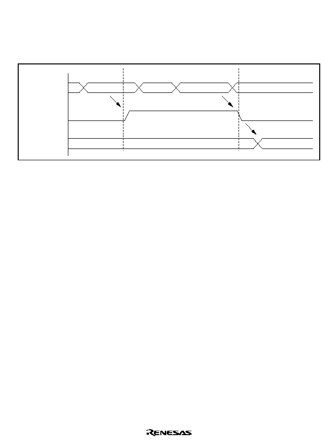
Rev. 5.0, 09/03, page 697 of 806
23.4.3
UDI Reset
An UDI reset is executed by setting an UDI reset assert command in SDIR. An UDI reset is of the
same kind as a power-on reset. An UDI reset is released by inputting an UDI reset negate
command.
UDI reset assert
UDI reset negate
SDIR
Chip internal reset
CPU state
Branch to H'A0000000
Figure 23.3 UDI Reset
23.4.4
UDI Interrupt
The UDI interrupt function generates an interrupt by setting a command from the UDI in the
SDIR. An UDI interrupt is a general exception/interrupt operation, resulting in a branch to an
address based on the VBR value plus offset, and with return by the RTE instruction. This interrupt
request has a fixed priority level of 15.
UDI interrupts are not accepted in sleep mode or standby mode.
23.4.5
Bypass
The JTAG-based bypass mode for the UDI pins can be selected by setting a command from the
UDI in SDIR.
23.4.6
Using UDI to Recover from Sleep Mode
It is possible to recover from sleep mode by setting a command (0001) from the UDI in SDIR.

Rev. 5.0, 09/03, page 698 of 806
23.5
Boundary Scan
A command can be set in SDIR by the UDI to place the UDI pins in the boundary scan mode
stipulated by JTAG.
23.5.1
Supported Instructions
The SH7729R supports the three essential instructions defined in the JTAG standard (BYPASS,
SAMPLE/PRELOAD, and EXTEST).
BYPASS: The BYPASS instruction is an essential standard instruction that operates the bypass
register. This instruction shortens the shift path to speed up serial data transfer involving other
chips on the printed circuit board. While this instruction is executing, the test circuit has no effect
on the system circuits. The instruction code is 1111.
SAMPLE/PRELOAD: The SAMPLE/PRELOAD instruction inputs values from the SH7729R's
internal circuitry to the boundary scan register, outputs values from the scan path, and loads data
onto the scan path. When this instruction is executing, the SH7729R's input pin signals are
transmitted directly to the internal circuitry, and internal circuit values are directly output
externally from the output pins. The SH7729R's system circuits are not affected by execution of
this instruction. The instruction code is 0100.
In a SAMPLE operation, a snapshot of a value to be transferred from an input pin to the internal
circuitry, or a value to be transferred from the internal circuitry to an output pin, is latched into the
boundary scan register and read from the scan path. Snapshot latching is performed in
synchronization with the rise of TCK in the Capture-DR state. Snapshot latching does not affect
normal operation of the SH7729R.
In a PRELOAD operation, an initial value is set in the parallel output latch of the boundary scan
register from the scan path prior to the EXTEST instruction. Without a PRELOAD operation,
when the EXTEST instruction was executed an undefined value would be output from the output
pin until completion of the initial scan sequence (transfer to the output latch) (with the EXTEST
instruction, the parallel output latch value is constantly output to the output pin).
EXTEST: This instruction is provided to test external circuitry when the SH7729R is mounted on
a printed circuit board. When this instruction is executed, output pins are used to output test data
(previously set by the SAMPLE/PRELOAD instruction) from the boundary scan register to the
printed circuit board, and input pins are used to latch test results into the boundary scan register
from the printed circuit board. If testing is carried out by using the EXTEST instruction N times,
the Nth test data is scanned-in when test data (N-1) is scanned out.

Rev. 5.0, 09/03, page 699 of 806
Data loaded into the output pin boundary scan register in the Capture-DR state is not used for
external circuit testing (it is replaced by a shift operation).
The instruction code is 0000.
23.5.2
Points for Attention
1. Boundary scan mode covers clock-related signals (EXTAL, EXTAL2, XTAL, XTAL2,
CKIO).
2. Boundary scan mode does not cover reset-related signals (
RESETP, RESETM, CA).
3. Boundary scan mode does not cover UDI-related signals (TCK, TDI, TDO, TMS, TRST).
4. When a boundary scan test is carried out, ensure that the CKIO clock operates constantly.
The CKIO frequency range is as follows:
Minimum: 1 MHz
Maximum: Maximum frequency for respective clock mode specified in the CPG section
Set pins MD[2:0] to the clock mode to be used.
After powering on, wait for the CKIO clock to stabilize before performing a boundary scan
test.
5. Fix the
RESETP pin low.
6. Fix the CA pin high, and the
ASEMD0 pin low.
23.6
Usage Notes
1. An UDI command other than an UDI interrupt, once set, will not be modified as long as
another command is not re-issued from the UDI. An UDI interrupt command, however, will
be changed to a bypass command once set.
2. Because chip operations are suspended in standby mode, UDI commands are not accepted.
However, the TAP controller remains in operation at this time.
3. The UDI is used for emulator connection. Therefore, UDI functions cannot be used when
using an emulator.
23.7
Advanced User Debugger (AUD)
The AUD is a function exclusively for use by an emulator. Refer to the User's Manual for the
relevant emulator for details of the AUD.

Rev. 5.0, 09/03, page 700 of 806

Rev. 5.0, 09/03, page 701 of 806
Section 24 Electrical Characteristics
24.1
Absolute Maximum Ratings
Table 24.1 shows the absolute maximum ratings.
Table 24.1
Absolute Maximum Ratings
Item
Symbol
Rating
Unit
Power supply voltage (I/O)
VccQ
≠0.3 to 4.2
V
Power supply voltage (internal)
Vcc
Vcc ≠ PLL1
Vcc ≠ PLL2
Vcc ≠ RTC
≠0.3 to 2.5
V
Input voltage (except port L)
Vin
≠0.3 to VccQ + 0.3
V
Input voltage (port L)
Vin
≠0.3 to AVcc + 0.3
V
Analog power supply voltage
AVcc
≠0.3 to 4.6
V
Analog input voltage
V
AN
≠0.3 to AVcc + 0.3
V
Operating temperature
Topr
≠20 to 75
∞C
Storage temperature
Tstr
≠55 to 125
∞C
Caution: Operating the chip in excess of the absolute maximum rating may result in permanent
damage.
∑
Order of turning on 1.7 V/1.8 V/1.9 V/2.0 V power (Vcc, Vcc-PLL1, Vcc-PLL2, Vcc-RTC)
and 3.3 V power (VccQ, AVcc):
1. First turn on the 3.3 V power, then turn on the 1.7 V/1.8 V/1.9 V/2.0 V power within 1 ms.
This interval should be as short as possible.
2. Until voltage is applied to all power supplies, a low level is input at the
RESETP pin, and
CKIO has operated for a maximum of 4 clock cycles, internal circuits remain unsettled, and
so pin states are also undefined. The system design must ensure that these undefined states
do not cause erroneous system operation.
Note that the
RESETP pin cannot receive a low level signal while a low level signal is
being input to the CA pin.
Waveforms at power-on are shown in the following figure.
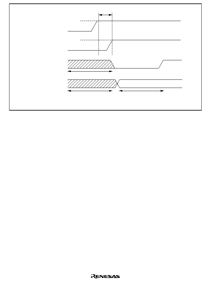
Rev. 5.0, 09/03, page 702 of 806
Pin states undefined
(Max. 1 ms)
3.3 V
1.7 V/1.8 V/
1.9 V/2.0 V power
3.3 V power
1.7 V/1.8 V/
1.9 V/2.0 V power
RESETP
All other pins*
Pin states undefined
Power-on reset state
Note:
* Except power/GND, clock related, and analog pins
Power-On Sequence
∑
Power-off order
1. In the reverse order of powering-on, first turn off the 1.7 V/1.8 V/1.9 V/2.0 V power, then
turn off the 3.3 V power within 1 ms. This interval should be as short as possible.
2. Pin states are undefined while only the 1.7 V/1.8 V/1.9 V/2.0 V power is off. The system
design must ensure that these undefined states do not cause erroneous system operation.

Rev. 5.0, 09/03, page 703 of 806
24.2
DC Characteristics
Tables 24.2 and 24.3 list the DC characteristics.
Table 24.2
DC Characteristics
Ta = ≠20 to 75∞C
Item
Symbol
Min
Typ
Max
Unit
Test Conditions
Power supply voltage
VccQ
3.0
3.3
3.6
V
Vcc,
1.85
2.00
2.15
200 MHz models
Vcc-PLL1, 1.75
1.90
2.05
167 MHz models
Vcc-PLL2, 1.65
1.80
2.05
100/133 MHz models
Vcc-RTC
1.55
1.70
1.95
100 MHz models
Current
dissipation
Normal
operation
Icc
--
510
820
mA
Vcc = 2.0 V
*
I
= 200 MHz
--
400
650
Vcc = 1.9 V
I
= 167 MHz
--
310
500
Vcc = 1.8 V
I
= 133 MHz
--
230
380
Vcc = 1.7 V
I
= 100 MHz
IccQ
--
20
40
VccQ = 3.3 V
B
= 33 MHz
In sleep
mode
*
1
Icc
--
15
30
*
1
: No external bus cycles
except refresh cycles
Vcc = 1.9 V
VccQ = 3.3 V
IccQ
--
10
20
B
= 33 MHz
In standby
mode
Icc
--
40
120
µ
A
Ta = 25∞C (RTC on)
VccQ = 3.3 V
IccQ
--
10
30
Vcc = 1.55 V to 2.15 V
Icc
--
290
900
Ta = 25∞C (RTC off)
VccQ = 3.3 V
IccQ
--
10
30
Vcc = 1.55 V to 2.15 V

Rev. 5.0, 09/03, page 704 of 806
Item
Symbol
Min
Typ
Max
Unit
Test Conditions
Input high
voltage
RESETP
,
RESETM
,
NMI,
IRQ5
≠
IRQ0
,
MD5≠MD0,
IRL3
≠
IRL0
,
IRLS3
≠
IRLS0
,
PINT15≠
PINT0,
ASEMD0
,
ADTRG
,
TRST
,
EXTAL,
CKIO,
RxD1, CA
V
IH
VccQ
◊
0.9
--
VccQ +
0.3
V
EXTAL2
--
--
--
If a crystal resonator is not
connected, connect to Vcc.
Port L
2.0
--
AVcc +
0.3
Other input
pins
2.0
--
VccQ +
0.3
Input low
voltage
RESETP
,
RESETM
,
NMI,
IRQ5
≠
IRQ0
,
MD5≠MD0,
IRL3
≠
IRL0
,
IRLS3
≠
IRLS0
,
PINT15≠
PINT0,
ASEMD0
,
ADTRG
,
TRST
,
EXTAL,
CKIO,
RxD1, CA
V
IL
≠0.3
--
VccQ
◊
0.1
V
EXTAL2
--
--
--
If a crystal resonator is not
connected, connect to Vcc.
Port L
≠0.3
--
AVcc
◊
0.2
Other input
pins
≠0.3
--
VccQ
◊
0.2

Rev. 5.0, 09/03, page 705 of 806
Item
Symbol
Min
Typ
Max
Unit
Test Conditions
Input leak
current
All input
pins
I Iin I
--
--
1.0
µ
A
Vin = 0.5 to VccQ≠0.5 V
Three-state
leak current
I/O, all
output
pins (off
condition)
I Isti I
--
--
1.0
µ
A
Vin = 0.5 to VccQ≠0.5 V
Output high
voltage
All output
pins
V
OH
2.4
--
--
V
VccQ = 3.0 V,
I
OH
= ≠200
µ
A
2.0
--
--
VccQ = 3.0 V,
I
OH
= ≠2 mA
V
OL
--
--
0.55
VccQ = 3.6 V,
I
OL
= 1.6 mA
Pull-up
resistance
Port pin
Ppull
30
60
120
k
Pin
capacity
All pins
C
--
--
10
pF
Analog
power
supply
voltage
AVcc
3.0
3.3
3.6
V
During A/D
conversion
AIcc
--
0.8
2
mA
Analog
power
supply
current
During A/D
and D/A
conversion
--
2.4
6
mA
Idle
--
1.0
20
µ
A
Ta = 25∞C
Notes: When the PLL circuits are not used, connect Vcc-PLL1 and Vcc-PLL2 to Vcc, and Vss-
PLL1 and Vss-PLL2 to Vss.
Power must be supplied between Vcc-RTC and Vss-RTC even if the RTC is not used.
AVcc conditions must be: VccQ ≠ 0.3 V
AVcc
VccQ + 0.3 V. If the A/D and D/A
converters are not used, do not leave the AVcc and AVss pins open. Connect AVcc to
VccQ, and connect AVss to VssQ.
Current dissipation values shown are for V
IH
min = VccQ ≠ 0.5 V and V
IL
max = 0.5 V with all
output pins unloaded.
The same voltage should be supplied to Vcc, Vcc-RTC, Vcc-PLL1, and Vcc-PLL2.
*
If the IRL and IRLS interrupts are used, the minimum is 1.9 V.

Rev. 5.0, 09/03, page 706 of 806
Table 24.3
Permissible Output Current Values
VccQ = 3.3 ± 0.3 V, Vcc = 1.55 V to 2.15 V, AVcc = 3.3 ± 0.3 V, Ta = ≠20 to 75∞C
Item
Symbol
Min
Typ
Max
Unit
Permissible output low current (per pin)
I
OL
--
--
2.0
mA
Permissible output low current (total)
I
OL
--
--
120
mA
Permissible output low current (per pin)
≠I
OH
--
--
2.0
mA
Permissible output low current (total)
(≠I
OH
)
--
--
40
mA
Note:
To ensure chip reliability, do not exceed the output current values given in table 24.3.
24.3
AC Characteristics
In general, SH7729R input should be synchronous. Observe the setup and hold times for each
input signal unless otherwise specified.
Table 24.4
Operating Frequency Range
VccQ = 3.3 ± 0.3 V, VccQ = 1.55 V to 2.15 V, AVcc = 3.3 ± 0.3 V, Ta = ≠20 to 75∞C
Item
Symbol
Min
Typ
Max
Unit
Remarks
Operating
frequency
CPU, cache, TLB
f
30
--
200
MHz
200 MHz
models
25
167
167 MHz
models
133
133 MHz
models
100
100 MHz
models
External bus
30
--
66.67
200 MHz
models
25
167 MHz,
133 MHz,
100 MHz
models
Peripheral module
7.5
--
33.34
200 MHz
models
6.25
167 MHz,
133 MHz,
100 MHz
models

Rev. 5.0, 09/03, page 707 of 806
24.3.1
Clock Timing
Table 24.5
Clock Timing
VccQ = 3.3 ± 0.3 V, Vcc = 1.55 V to 2.15 V, AVcc = 3.3 ± 0.3 V, Ta = ≠20 to 75∞C
Item
Symbol
Min
Max
Unit
Figure
EXTAL clock input frequency (clock mode 0)
f
EX
25
66.67
MHz
24.1
EXTAL clock input cycle time (clock mode 0)
t
EXcyc
15
40
ns
EXTAL clock input frequency (clock mode 1)
f
EX
6.25
16.67
MHz
EXTAL clock input cycle time (clock mode 1)
t
EXcyc
60
160
ns
EXTAL clock input low pulse width
t
EXL
1.5
--
ns
EXTAL clock input high pulse width
t
EXH
1.5
--
ns
EXTAL clock input rise time
t
EXR
--
6
ns
EXTAL clock input fall time
t
EXF
--
6
ns
CKIO clock input frequency
f
CKI
25
66
MHz
24.2
CKIO clock input cycle time
t
CKIcyc
15.2
40
ns
CKIO clock input low pulse width
t
CKIL
1.5
--
ns
CKIO clock input high pulse width
t
CKIH
1.5
--
ns
CKIO clock input rise time
t
CKIR
--
6
ns
CKIO clock input fall time
t
CKIF
--
6
ns
CKIO clock output frequency
f
OP
25
66
MHz
24.3
CKIO clock output cycle time
t
cyc
15.2
40
ns
CKIO clock output low pulse width
t
CKOL
3
--
ns
CKIO clock output high pulse width
t
CKOH
3
--
ns
CKIO clock output rise time
t
CKOR
--
5
ns
CKIO clock output fall time
t
CKOF
--
5
ns
CKIO2 clock output delay time
t
CK2D
-3
3
ns
CKIO2 clock output rise time
t
CK2OR
--
7
ns
CKIO2 clock output fall time
t
CK2OF
--
7
ns
Power-on oscillation settling time
t
OSC1
10
--
ms
24.4
RESETP
setup time
t
RESPS
20
--
ns
24.4, 24.5
RESETM
setup time
t
RESMS
6
--
ns
RESETP
assert time
t
RESPW
20
--
tcyc
RESETM
assert time
t
RESMW
20
--
tcyc
Standby return oscillation settling time 1
t
OSC2
10
--
ms
24.5
Standby return oscillation settling time 2
t
OSC3
10
--
ms
24.6
Standby return oscillation settling time 3
t
OSC4
11
--
ms
24.7
PLL synchronization settling time 1
(Standby release)
t
PLL1
100
--
µ
s
24.8, 24.9
PLL synchronization settling time 2
(Multiplication change)
t
PLL2
100
--
µ
s
24.10
IRQ/IRL interrupt determination time
(RTC used and standby mode)
t
IRQSTB
100
--
µ
s
24.9
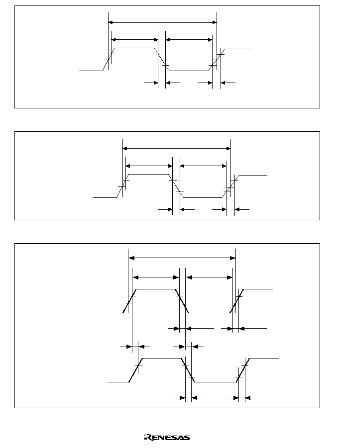
Rev. 5.0, 09/03, page 708 of 806
t
EXH
t
EXF
t
EXR
t
EXL
t
EXcyc
V
IH
V
IH
V
IH
1/2 V
CC
Q
1/2 V
CC
Q
V
IL
V
IL
EXTAL*
(input)
Note:
* When clock is input from EXTAL pin
Figure 24.1 EXTAL Clock Input Timing
t
CKIH
t
CKIF
t
CKIR
t
CKIL
t
CKIcyc
V
IH
1/2 V
CC
Q
1/2 V
CC
Q
V
IH
V
IL
V
IH
V
IL
CKIO
(input)
Figure 24.2 CKIO Clock Input Timing
t
cyc
t
CKOL
t
CKOH
V
OH
V
OH
1/2V
CC
Q
CKIO
(output)
CKIO2
(output)
1/2V
CC
Q
t
CKOR
t
CKOF
V
OH
V
OL
V
OL
V
OH
t
CK2D
t
CK2D
t
CK2OR
t
CK2OF
Figure 24.3 CKIO Clock Output Timing
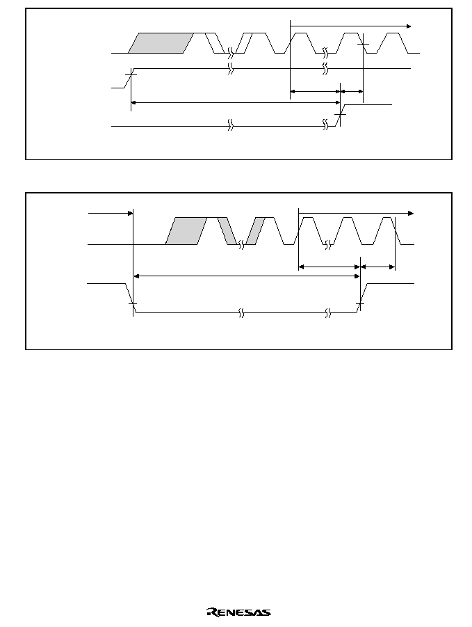
Rev. 5.0, 09/03, page 709 of 806
V
CC
min
t
RESPW
t
RESPS
t
OSC1
V
CC
RESETP
CKIO,
internal clock
Stable oscillation
Note: Oscillation settling time when on-chip oscillator is used
Figure 24.4 Power-on Oscillation Settling Time
CKIO,
internal
clock
Stable oscillation
Standby
t
OSC2
t
RESPW/MW
t
RESPS/MS
RESETP
RESETM
Note: Oscillation settling time when on-chip oscillator is used
Figure 24.5 Oscillation Settling Time on Return from Standby (Return by Reset)
Rev. 5.0, 09/03, page 710 of 806
CKIO,
internal
clock
Stable oscillation
Standby
t
OSC3
NMI
Note: Oscillation settling time when using on-chip oscillator in oscillation stop mode
WAKEUP
Figure 24.6 Oscillation Settling Time on Return from Standby (Return by NMI)
CKIO,
internal
clock
Stable oscillation
Standby
t
OSC4
IRL3 to IRL0
IRQ4 to IRQ0
PINT0/1
Note:
Oscillation settling time when using on-chip oscillator in oscillation stop
mode (only when using RTC)
WAKEUP
Figure 24.7 Oscillation Settling Time on Return from Standby
(Return by IRQ4 to IRQ0, PINT0/1 and
I
I
I
IR
R
R
RLLLL3333 to IIIIR
R
R
RLLLL0000)
Rev. 5.0, 09/03, page 711 of 806
EXTAL input
or CKIO
input
Stable input clock
Reset or NMI interrupt request
Stable input clock
Normal
Normal
Standby
PLL output,
CKIO output
Internal clock
STATUS 0
STATUS 1
PLL synchronization
Note: PLL oscillation settling time when clock is input from EXTAL pin or CKIO pin
in oscillation continuation mode
t
PLL1
PLL synchronization
Figure 24.8 PLL Synchronization Settling Time during Standby Recovery (Reset or NMI)
EXTAL input
or CKIO input
Stable input clock
IRQ4
- IRQ0/IRL3 - IRL0 interrupt request
Stable input clock
Normal
Normal
PLL output,
CKIO output
Internal clock
STATUS 0
STATUS 1
Note: PLL oscillation settling time when clock is input from EXTAL pin or CKIO pin
in oscillation continuation mode
t
PLL1
PLL synchronization
Standby
PLL synchronization
t
IRLSTB
Figure 24.9 PLL Synchronization Settling Time during Standby Recovery
(IRQ/IRL or PINT0/PINT1 Interrupt)
Rev. 5.0, 09/03, page 712 of 806
EXTAL input*
1
Multiplication ratio change
CKIO output*
2
,
PLL output
Internal clock
Notes: 1. CKLO input in clock mode 7
2. PLL output in clock mode 7
t
PLL2
Figure 24.10 PLL Synchronization Settling Time in Case of IRQ/IRL Interrupt

Rev. 5.0, 09/03, page 713 of 806
24.3.2
Control Signal Timing
Table 24.6
Control Signal Timing
VccQ = 3.3 ± 0.3 V, Vcc = 1.55 V to 2.15 V, AVcc = 3.3 ± 0.3 V, Ta = ≠20 to 75∞C
Item
Symbol
Min
Max
Unit
Figure
RESETP
pulse width
t
RESPW
20
*
2
--
tcyc
24.11,
RESETP
setup time
*
1
t
RESPS
20
--
ns
24.12
RESETP
hold time
t
RESPH
4
--
ns
RESETM
pulse width
t
RESMW
20
*
3
--
tcyc
RESETM
setup time
t
RESMS
6
--
ns
RESETM
hold time
t
RESMH
34
--
ns
BREQ
setup time
t
BREQS
6
--
ns
24.14
BREQ
hold time
t
BREQH
4
--
ns
NMI setup time
*
1
t
NMIS
10
--
ns
24.12
NMI hold time
t
NMIH
4
--
ns
IRQ5≠IRQ0 setup time
*
1
t
IRQS
10
--
ns
IRQ5≠IRQ0 hold time
t
IRQH
4
--
ns
IRQOUT
delay time
t
IRQOD
--
10
ns
24.13
BACK
delay time
t
BACKD
--
10
ns
24.14,
STATUS1, STATUS0 delay time
t
STD
--
10
ns
24.15
Bus tri-state delay time 1
t
BOFF1
0
15
ns
Bus tri-state delay time 2
t
BOFF2
0
15
ns
Bus buffer-on time 1
t
BON1
0
15
ns
Bus buffer-on time 2
t
BON2
0
15
ns
Notes: 1.
RESETP
, NMI, and IRQ5 to IRQ0 are asynchronous. Changes are detected at the
clock fall when the setup time shown is used. If the setup time cannot be used,
detection can be delayed until the next clock falls.
2. t
RESPW
= t
OSC1
(100
µ
s) when XTAL oscillation is continued in standby mode, and t
RESPW
= t
OSC2
(10 ms) when oscillation is stopped. In sleep mode, t
RESPW
= t
PLL1
(100
µ
s).
When the clock multiplication ratio is changed, t
RESPW
= t
PLL1
(100
µ
s).
3. In standby mode, t
RESMW
= t
OSC2
(10 ms). In sleep mode, RESETM must be kept low
until STATUS (0-1) changes to reset (HH). When the clock multiplication ratio is
changed, RESETM must be kept low until STATUS (0-1) changes to reset (HH).

Rev. 5.0, 09/03, page 714 of 806
CKIO
t
RESPS/MS
t
RESPS/MS
RESETP
RESETM
t
RESPW/MW
Figure 24.11 Reset Input Timing
CKIO
RESETP
RESETM
t
RESPH/MH
t
RESPS/MS
V
IH
V
IL
NMI
t
NMIH
t
NMIS
V
IH
V
IL
IRQ5 to IRQ0
t
IRQH
t
IRQS
V
IH
V
IL
Figure 24.12 Interrupt Signal Input Timing
CKIO
t
IRQOD
t
IRQOD
IRQOUT
Figure 24.13
I
I
I
IR
R
R
RQOU
QOU
QOU
QOUTTTT Timing
Rev. 5.0, 09/03, page 715 of 806
CKIO
BREQ
BACK
RD, RD/WR,
RAS, CAS,
CSn, WEn, BS,
MCSn
A25 to A0,
D31 to D0
t
BACKD
t
BOFF2
t
BOFF1
t
BON1
t
BACKD
t
BON2
t
BREQH
t
BREQH
t
BREQS
t
BREQS
Figure 24.14 Bus Release Timing
CKIO
t
STD
t
BOFF2
t
BOFF1
t
STD
t
BON2
t
BON1
Normal mode
Standby mode
Normal mode
STATUS 0
STATUS 1
RD, RD/WR,
RAS, CAS,
CSn, WEn,
BS, MCSn
A25 to A0,
D31 to D0
Figure 24.15 Pin Drive Timing at Standby

Rev. 5.0, 09/03, page 716 of 806
24.3.3
AC Bus Timing
Table 24.7
Bus Timing
Clock Modes 0/1/2/7, VccQ = 3.3 ± 0.3 V, Vcc = 1.55 V to 2.15 V, AVcc = 3.3 ± 0.3 V,
Ta = ≠20 to 75∞C
Item
Symbol
Min
Max
Unit
Figure
Address delay time
t
AD
1.5
12
ns
24.16≠24.36, 24.39≠24.46
Address setup time
t
AS
0
--
ns
24.16≠24.18
Address hold time
*
1
t
AH
4
--
ns
24.16≠24.21
BS
delay time
t
BSD
--
10
ns
24.16≠24.36, 24.39≠24.46
CS
delay time 1
t
CSD1
--
10
ns
24.16≠24.36, 24.39≠24.46
CS
delay time 2
t
CSD3
--
10
ns
24.16≠24.21
CS
delay time 3
(SDRAM access)
t
CSD3
1.5
10
ns
24.22≠24.39
Read/write delay time
t
RWD
1.5
10
ns
24.16≠24.36, 24.39≠24.46
Read/write hold time
t
RWH
0
--
ns
24.16≠24.21
Read strobe delay time
t
RSD
--
10
ns
24.16≠24.21, 24.40≠24.43
Read data setup time 1
t
RDS1
6
--
ns
24.16≠24.21, 24.40≠24.46
Read data setup time 2
t
RDS2
5
--
ns
24.22≠24.25, 24.30≠24.33
Read data hold time 1
*
2
t
RDH1
0
--
ns
24.16≠24.25, 24.40≠24.46
Read data hold time 2
t
RDH2
1
--
ns
24.22≠24.25, 24.30≠24.33
Write enable delay time
t
WED
--
10
ns
24.16≠24.18, 24.40, 24.41
Write data delay time 1
t
WDD1
--
14
ns
24.16≠24.18, 24.40, 24.41, 24.44≠24.46
Write data delay time 2
t
WDD2
1.5
12
ns
24.26≠24.29, 24.34≠24.36
Write data hold time 1
t
WDH1
1.5
--
ns
24.16≠24.18, 25.40, 25.41, 24.44≠24.46
Write data hold time 2
t
WDH2
1.5
--
ns
24.26≠24.29, 24.34≠24.36
Write data hold time 3
t
WDH3
2
--
ns
24.16≠24.18
Write data hold time 4
t
WDH4
2
--
ns
24.40, 24.41, 24.44≠24.46
WAIT
setup time
t
WTS
5
--
ns
24.17≠24.21, 24.41, 24.43, 24.45, 24.46
WAIT
hold time
t
WTH
0
--
ns
24.17≠24.21, 24.41, 24.43, 24.45, 24.46
RAS
delay time 2
t
RASD2
1.5
10
ns
24.22≠24.39
CAS
delay time 2
t
CASD2
1.5
10
ns
24.22≠24.39
DQM
delay time
t
DQMD
1.5
10
ns
24.22≠24.36
CKE delay time
t
CKED
1.5
10
ns
24.38

Rev. 5.0, 09/03, page 717 of 806
Item
Symbol
Min
Max
Unit
Figure
ICIORD
delay time
t
ICRSD
--
10
ns
24.44≠24.46
ICIOWR
delay time
t
ICWSD
--
10
ns
24.44≠24.46
IOIS16
setup time
t
IO16S
6
--
ns
24.45, 24.46
IOIS16
hold time
t
IO16H
4
--
ns
24.45, 24.46
DACK delay time 1
(Based on CKLO rise)
t
DAKD1
--
10
ns
24.16≠24.36, 24.39≠24.46
DACK delay time 2
(Based on CKLO fall)
t
DAKD2
--
10
ns
24.16≠24.21
Notes: 1. Specified based on the slowest negate timing for
CSn
,
RD
, or
WEn
.
2. Specified based on whichever negate timing is faster,
CSn
or
RD
.
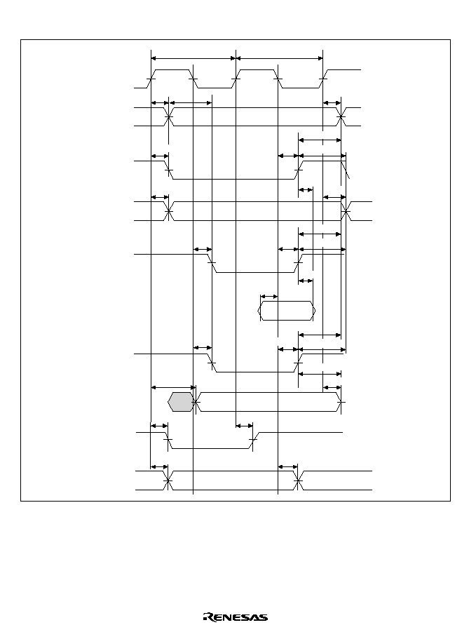
Rev. 5.0, 09/03, page 718 of 806
24.3.4
Basic Timing
T
1
CKIO
A25 to A0
CSn
RD/
WR
RD
D31 to D0
(read)
WEn
D31 to D0
(write)
BS
T
2
t
AD
t
AS
t
AH
t
AD
t
CSD1
t
RWD
t
RSD
t
CSD2
t
WED
t
WDD1
t
RDS1
t
BSD
t
BSD
t
DAKD1
t
DAKD1
t
RDH1
t
RDH1
t
WED
t
RSD
t
AH
t
RWH
t
RWD
t
WDH1
t
RWH
t
RWH
t
AH
t
WDH3
DACKn
(read)
(write)
Figure 24.16 Basic Bus Cycle (No Wait)
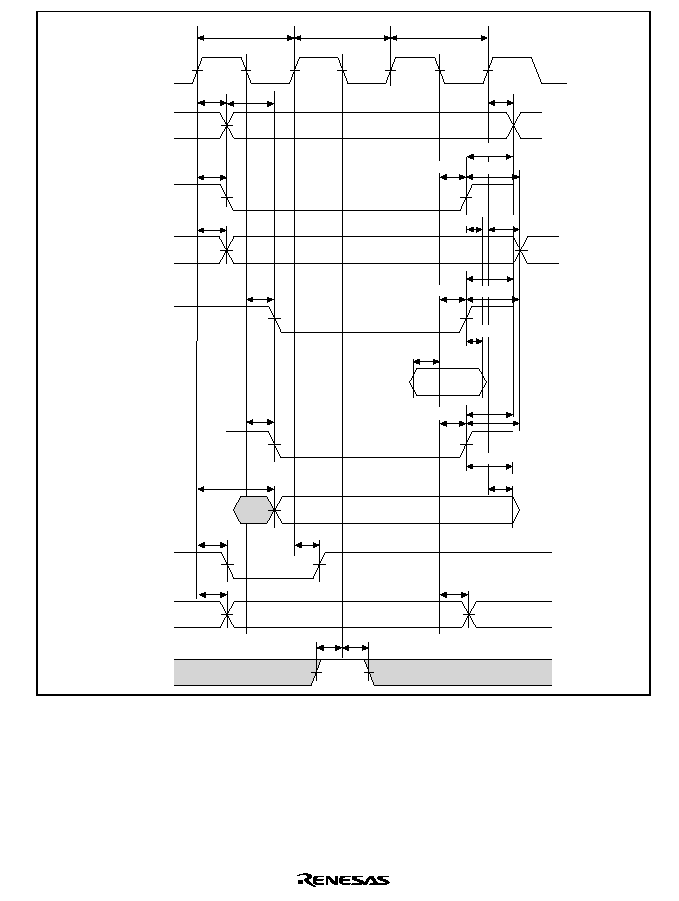
Rev. 5.0, 09/03, page 719 of 806
T
1
T
w
T
2
CKIO
A25 to A0
CSn
RD/
WR
RD
D31 to D0
(read)
WEn
D31 to D0
(write)
BS
WAIT
t
AD
t
AD
t
RWD
t
RWH
t
AH
t
AH
t
RSD
t
CSD1
t
WED
t
WDD1
t
BSD
t
WTS
t
WTH
t
BSD
t
RDS1
t
CSD2
t
WED
t
RSD
t
RDH1
t
RDH1
t
RWD
t
AH
t
RWH
t
WDH3
t
WDH1
t
RWH
t
DAKD1
t
DAKD1
DACKn
(read)
(write)
t
AS
Figure 24.17 Basic Bus Cycle (One Wait)
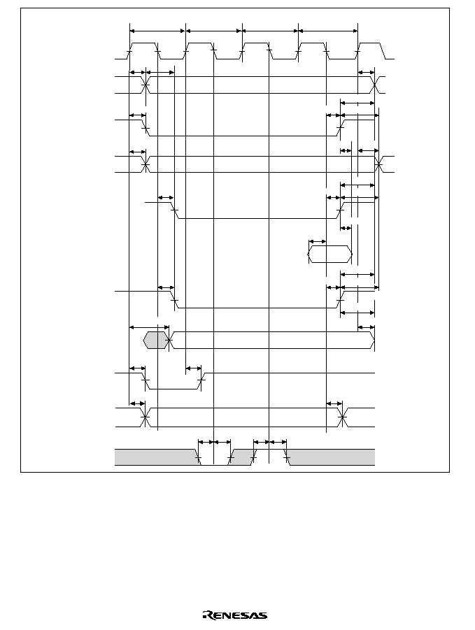
Rev. 5.0, 09/03, page 720 of 806
T
1
T
w
T
w
T
2
CKIO
A25 to A0
CSn
RD/
WR
RD
D31 to D0
(read)
WEn
D31 to D0
(write)
BS
WAIT
t
AD
t
AD
t
RWD
t
RSD
t
WED
t
WTS
t
WTH
t
BSD
t
BSD
t
RDS1
t
WTS
t
WTH
t
CSD1
t
CSD2
t
RSD
t
WED
t
RDH1
t
AH
t
RWH
t
RDH1
t
AH
t
RWH
t
RWD
t
RWH
t
AH
t
WDH3
t
WDH1
t
DAKD1
t
DAKD1
DACKn
t
WDD1
(read)
(write)
t
AS
Figure 24.18 Basic Bus Cycle (External Wait, WAITSEL = 1)
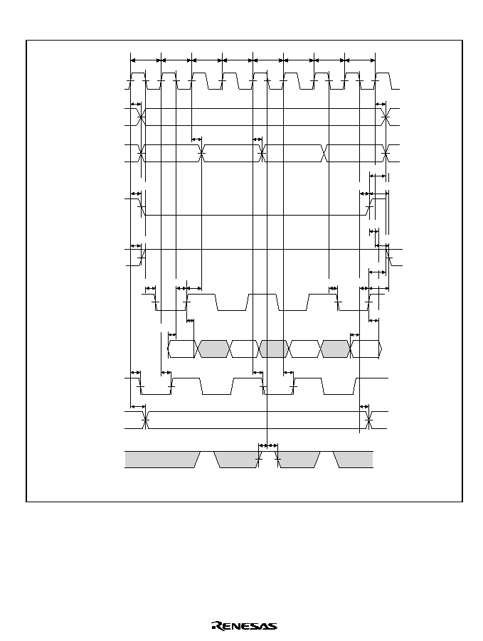
Rev. 5.0, 09/03, page 721 of 806
24.3.5
Burst ROM Timing
CKIO
A25 to A4
A3 to A0
CSn
RD/
WR
RD
D31 to D0
BS
DACKn
WAIT
t
AD
t
AD
t
AD
t
AD
t
CSD1
t
RWD
t
BSD
t
BSD
t
AH
t
BSD
t
DAKD1
t
DAKD1
t
CSD2
t
RSD
t
RDS1
t
WTS
t
WTH
t
RDS
t
RSD
T
1
T
B2
T
B1
T
B2
T
B1
T
B2
T
B1
T
2
t
RSD
t
RDH1
t
RSD
t
AH
t
RDH1
t
RWH
t
AH
t
RWH
t
RWD
t
RDH1
t
BSD
Note: In the write cycle, the basic bus cycle is performed.
Figure 24.19 Burst ROM Bus Cycle (No Wait)
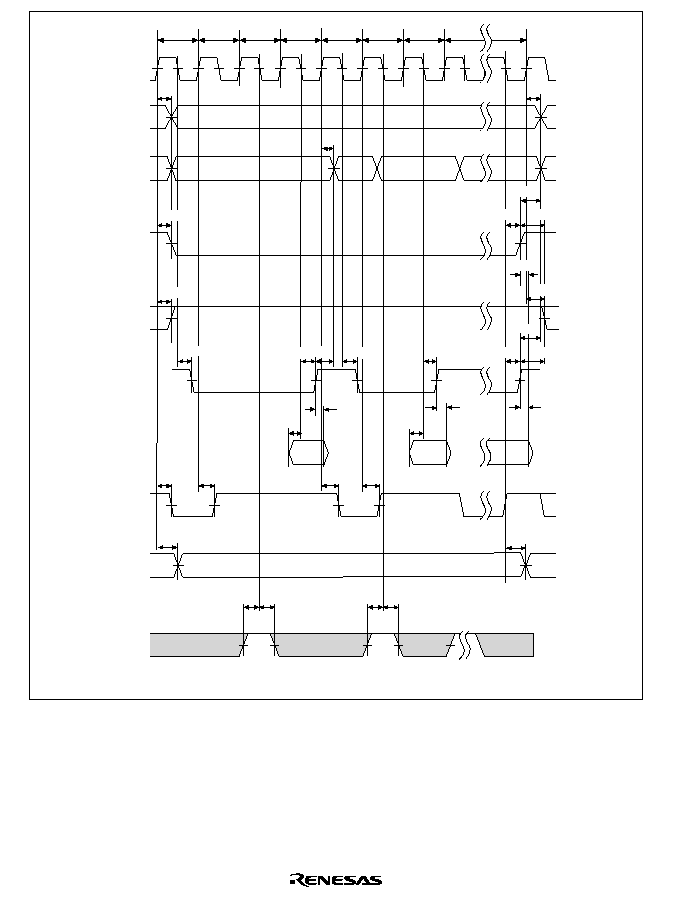
Rev. 5.0, 09/03, page 722 of 806
CKIO
A25 to A4
A3 to A0
CSn
RD/
WR
RD
D31 to D0
BS
WAIT
DACKn
t
AD
t
AD
t
AD
t
CSD1
t
RWH
t
RWD
t
RSD
t
RSD
t
RDH1
t
RDH1
t
RDS1
t
BSD
t
DAKD1
t
DAKD1
t
BSD
t
BSD
t
BSD
t
WTS
t
WTH
t
WTS
t
WTH
T
1
T
w
T
w
T
B2
T
B1
T
B2
T
w
T
2
T
2
t
CSD2
t
RDS1
t
RSD
t
RSD
t
AH
t
AH
t
RDH1
t
AH
t
RSD
t
RWD
t
RWH
t
RDH1
Note: In the write cycle, the basic bus cycle is performed.
Figure 24.20 Burst ROM Bus Cycle (Two Waits)
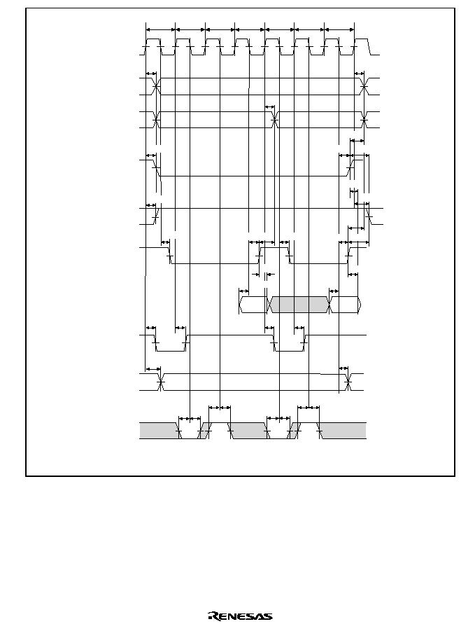
Rev. 5.0, 09/03, page 723 of 806
CKIO
A25 to A4
A3 to A0
CSn
RD/
WR
RD
D31 to D0
BS
DACKn
WAIT
T
1
T
w
T
w
T
B2
T
B1
T
2
T
Bw
t
AD
t
AD
t
CSD1
t
CSD2
t
RWD
t
RWH
t
RDH1
t
AH
t
AH
t
RWD
t
RSD
t
RSD1
t
AH
t
AD
t
BSD
t
BSD
t
WTS
t
WTH
t
WTS
t
WTH
t
WTS
t
WTH
t
WTS
t
WTH
t
BSD
t
BSD
t
RDS1
t
RDH1
t
RSD
t
DAKD1
t
DAKD1
t
RDH1
t
RWH
t
RSD1
t
RDS
Note: In the write cycle, the basic bus cycle is performed.
Figure 24.21 Burst ROM Bus Cycle (External Wait, WAITSEL = 1)
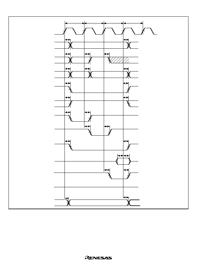
Rev. 5.0, 09/03, page 724 of 806
24.3.6
Synchronous DRAM Timing
CKIO
A12 or A10
RD/
WR
CSn
RAS
CAS
BS
DQMxx
CKE
A25 to A16
A15 to A0
Tr
tAD
Row address
Row address
Read A
command
Row address Column address
Tc1
Tc2
(Tpc)
D31 to D0
tAD
tAD
tAD
tAD
tCSD3
tRWD
tCSD3
tRWD
tRASD2
tDQMD
tDQMD
tRDH2
tBSD
tBSD
(High)
tRDS2
tRASD2
tCASD2
tCASD2
tAD
tAD
tAD
DACKn
tDAKD1
tDAKD1
Figure 24.22 Synchronous DRAM Read Bus Cycle (RCD
=
=
=
=
0, CAS Latency
=
=
=
=
1, TPC
=
=
=
=
0)
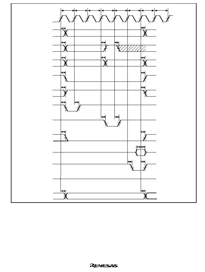
Rev. 5.0, 09/03, page 725 of 806
CKIO
A12 or A10
RD/
WR
CSn
RAS
CAS
BS
DQMxx
CKE
(High)
A25 to A16
A15 to A0
Tr
Trw
Trw
Tc1
Tcw
Td1
(Tpc)
(Tpc)
D31 to D0
Row address
Row address
Read A
command
Row address
Column address
tAD
tAD
tAD
tAD
tCSD3
tRWD
tDQMD
tRDH2
tBSD
tBSD
tRDS2
tCSD3
tRWD
tRASD2
tDQMD
tRASD2
tCASD2
tCASD2
tAD
tAD
tAD
tAD
DACKn
tDAKD1
tDAKD1
Figure 24.23 Synchronous DRAM Read Bus Cycle (RCD
=
=
=
=
2, CAS Latency
=
=
=
=
2, TPC
=
=
=
=
1)
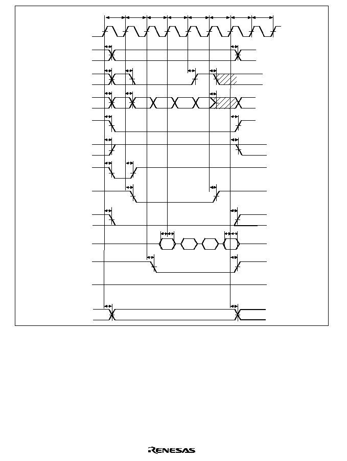
Rev. 5.0, 09/03, page 726 of 806
CKIO
A12 or A10
RD/
WR
CSn
RAS
CAS
BS
DQMxx
CKE
(High)
A25 to A16
A15 to A0
Tr
Tc1
Tc2/Td1 Tc3/Td2
Tc4/Td3
Td4
(Tpc)
(Tpc)
D31 to D0
Row address
Row
address
Read A
command
Read command
Row
address
Column address (1-4)
tAD
tAD
tAD
tAD
tAD
tAD
tAD
tAD
tAD
tCSD3
tCSD3
tRWD
tRWD
tRASD2
tDQMD
tBSD
tBSD
tRDS2 tRDH2
tRDS2 tRDH2
tDQMD
tRASD2
tCASD2
tCASD2
tDAKD1
tDAKD1
DACKn
Figure 24.24 Synchronous DRAM Read Bus Cycle (Burst Read (Single Read
◊
◊
◊
◊
4), RCD
=
=
=
=
0,
CAS Latency
=
=
=
=
1, TPC
=
=
=
=
1)
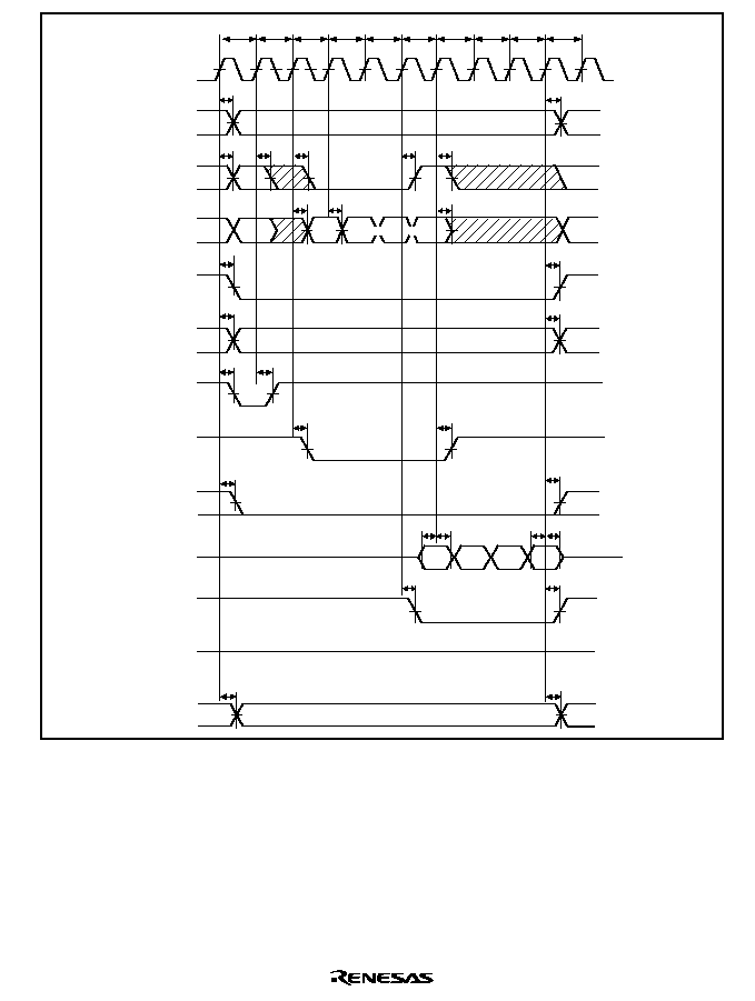
Rev. 5.0, 09/03, page 727 of 806
CKIO
A12 or A10
RD/
WR
CSn
RAS
CAS
BS
DQMxx
CKE
A25 to A16
A15 to A0
Tr
Trw
Tc1
Tc2
Tc3 Tc4/Td1
Td2
Td3
Td4
(Tpc)
D31 to D0
(read)
tAD
tAD
tAD
tAD
tAD
tAD
tAD
tAD
tAD
tAD
tCSD3
tRWD
tDQMD
tRDS2
tBSD
tBSD
tRDH2
tRDS2 tRDH2
tCSD3
tRWD
tRASD2
tRASD2
tCASD2
tDQMD
tCASD2
Row address
Row
address
Row
address
Read command
(High)
Column address (1-4)
tDAKD1
tDAKD1
DACKn
Figure 24.25 Synchronous DRAM Read Bus Cycle (Burst Read (Single Read
◊
◊
◊
◊
4), RCD
=
=
=
=
1,
CAS Latency
=
=
=
=
3, TPC
=
=
=
=
0)
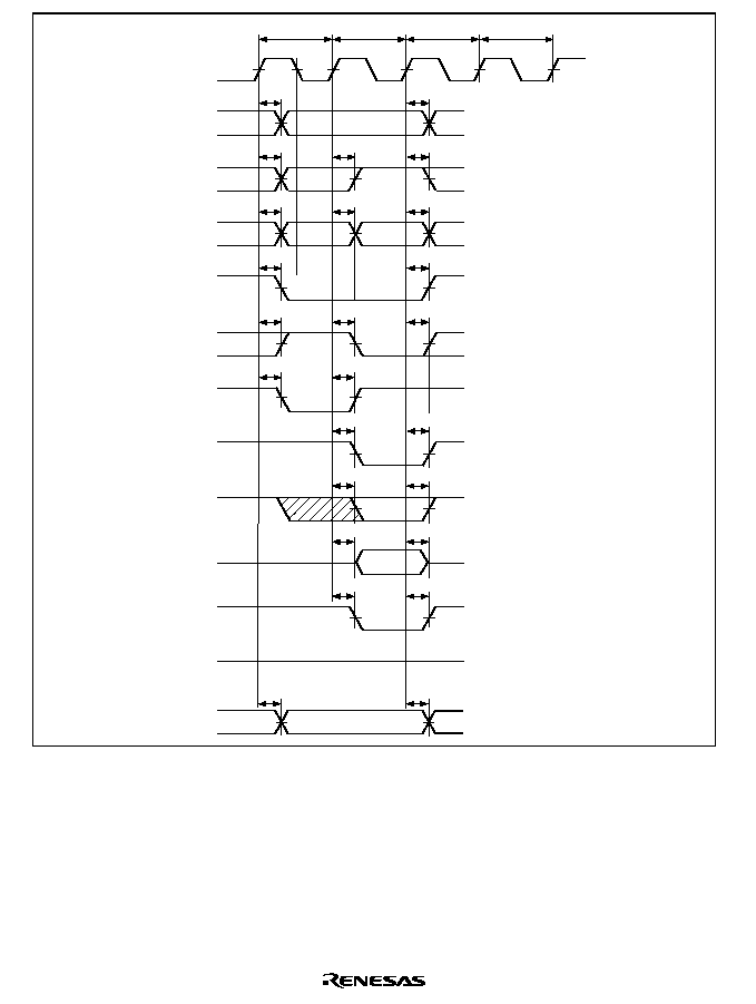
Rev. 5.0, 09/03, page 728 of 806
CKIO
A12 or A10
RD/
WR
CSn
RAS
CAS
BS
DQMxx
CKE
A25 to A16
A15 to A0
Tr
Tc1
(Trwl)
(Tpc)
(High)
D31 to D0
tAD
Row address
Row address
Write A
command
Row address
Column address
tAD
tAD
tCSD3
tRWD
tRASD2
tAD
tAD
tAD
tAD
tAD
tCSD3
tRWD
tRWD
tRASD2
tCASD2
tDQMD
tWDD2
tBSD
tDQMD
tWDH2
tBSD
tCASD2
tDAKD1
tDAKD1
DACKn
Figure 24.26 Synchronous DRAM Write Bus Cycle (RCD
=
=
=
=
0, TPC
=
=
=
=
0, TRWL = 0)
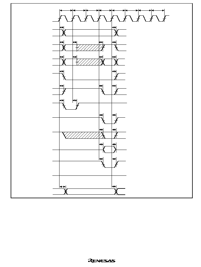
Rev. 5.0, 09/03, page 729 of 806
CKIO
A12 or A10
RD/
WR
CSn
RAS
CAS
BS
DQMxx
CKE
A25 to A16
A15 to A0
Tr
Trw
Trw
Tc1
(Trwl)
(Trwl)
(Tpc)
(Tpc)
(High)
D31 to D0
tAD
Row address
Row
address
Write A
command
Row
address
Column
address
tAD
tAD
tAD
tAD
tAD
tAD
tCSD3
tRWD
tRWD
tAD
tAD
tAD
tCSD3
tRWD
tRASD2
tRASD2
tDQMD
tWDD2
tBSD
tCASD2
tDQMD
tWDH2
tBSD
tCASD2
tDAKD1
tDAKD1
DACKn
Figure 24.27 Synchronous DRAM Write Bus Cycle (RCD
=
=
=
=
2, TPC
=
=
=
=
1, TRWL = 1)

Rev. 5.0, 09/03, page 730 of 806
CKIO
A12 or A10
RD/
WR
CSn
RAS
CAS
BS
DQMxx
CKE
A25 to A16
A15 to A0
Tr
Tc1
Tc2
Tc3
Tc4
(Trwl)
(Tpc)
(Tpc)
(High)
D31 to D0
tAD
Row address
Row
address
Write A
command
Write command
Row
address
tAD
tAD
tAD
tAD
tCSD3
tRWD
tRWD
tAD
tAD
tAD
tAD
tCSD3
tRWD
tRASD2
tRASD2
tDQMD
tWDD2
tWDD2
tBSD
tCASD2
tDQMD
tWDH2
tBSD
tCASD2
Column address (1-4)
tDAKD1
tDAKD1
DACKn
Figure 24.28 Synchronous DRAM Write Bus Cycle (Burst Write (Single Write
◊
◊
◊
◊
4),
RCD
=
=
=
=
0, TPC
=
=
=
=
1, TRWL = 0)
Rev. 5.0, 09/03, page 731 of 806
CKIO
A12 or A10
RD/
WR
CSn
RAS
CAS
BS
DQMxx
CKE
(High)
A25 to A16
A15 to A0
Tr
Trw
Tc1
Tc2
Tc3
Td4
(Trwl)
(Tpc)
D31 to D0
Row address
Row
address
Write A
command
Write command
Row
address
Column address (1-4)
tAD
tAD
tAD
tAD
tAD
tAD
tAD
tAD
tAD
tCSD3
tCSD3
tRWD
tRWD
tRWD
tRASD2
tDQMD
tBSD
tBSD
tWDD2
tWDD2
tWDH2
tDQMD
tRASD2
tCASD2
tCASD2
tDAKD1
tDAKD1
DACKn
Figure 24.29 Synchronous DRAM Write Bus Cycle (Burst Mode (Single Write
◊
◊
◊
◊
4),
RCD
=
=
=
=
1, TPC
=
=
=
=
0, TRWL = 0)

Rev. 5.0, 09/03, page 732 of 806
CKIO
A12 or A10
RD/
WR
CSn
RAS
CAS
BS
DQMxx
CKE
A25 to A16
A15 to A0
Tnop
Tc1
Tc2/Td1 Tc3/Td2 Tc4/Td3
Td4
D31 to D0
t
AD
t
AD
t
CSD3
t
CSD3
t
RWD
t
RWD
t
RASD2
t
DQMD
t
DQMD
t
BSD
t
BSD
(High)
t
AD
t
AD
t
AD
t
RDS2
t
RDH2
t
RDS2
t
RDH2
t
CASD2
t
CASD2
t
AD
Row address
Read command
Column address
t
DAKD1
t
DAKD1
DACKn
Figure 24.30 Synchronous DRAM Burst Read Bus Cycle
(RAS Down, Same Row Address, CAS Latency = 1)

Rev. 5.0, 09/03, page 733 of 806
A25 to A16
(High)
t
AD
t
AD
t
AD
t
CASD2
t
CSD3
t
RWD
t
DQMD
t
BSD
t
RDH2
t
RDS2
t
RDH2
t
RDS2
t
BSD
t
RASD2
t
CASD2
t
DQMD
t
RWD
t
CSD3
t
AD
t
AD
t
AD
Tc1
Tc2
Tc3/Td1 Tc4/Td2
Td3
Td4
CKIO
A12 or A10
A15 to A0
CSn
RD/
WR
RAS
CAS
DQMxx
D31 to D0
BS
CKE
Row address
DACKn
t
DAKD1
t
DAKD1
Column address
Read command
Figure 24.31 Synchronous DRAM Burst Read Bus Cycle
(RAS Down, Same Row Address, CAS Latency = 2)

Rev. 5.0, 09/03, page 734 of 806
CKIO
A12 or A10
RD/
WR
CSn
RAS
CAS
BS
DQMxx
CKE
A25 to A16
A15 to A0
Tp
Tr
Tc1
Tc2/Td1
Tc3/Td2
Tc4/Td3
Td4
D31 to D0
t
AD
t
AD
t
CSD3
t
CSD3
t
RWD
t
RWD
t
RWD
t
RASD2
t
RASD2
t
DQMD
t
DQMD
t
DQMD
t
BSD
t
BSD
t
DAKD1
t
DAKD1
(HIGH)
t
AD
t
AD
t
AD
t
AD
t
AD
t
AD
t
RDS2
t
RDH2
t
RDS2
t
RDH2
t
AD
Row
address
Row
address
t
CASD2
t
CASD2
DACKn
Row address
Read command
Column address
Figure 24.32 Synchronous DRAM Burst Read Bus Cycle
(RAS Down, Different Row Address, TPC = 0, RCD = 0, CAS Latency = 1)
Rev. 5.0, 09/03, page 735 of 806
CKIO
A12 or A10
RD/
WR
CSn
RAS
CAS
BS
DQMxx
CKE
A25 to A16
A15 to A0
Tp
Tpw
Tr
Tc1
Tc2/Td1
Tc3/Td2
Tc4/Td3
D31
to D0
t
AD
t
AD
t
CSD3
t
CSD3
t
RWD
t
RWD
t
RWD
t
RASD2
t
RASD2
t
RASD2
t
RASD2
t
DQMD
t
DQMD
t
DQMD
t
BSD
t
BSD
(HIGH)
t
AD
t
AD
t
AD
t
AD
t
AD
t
AD
t
RDS2
t
RDH2
t
RDS2
t
RDH2
t
AD
Td4
Row address
t
CASD2
t
CASD2
Row
address
Row
address
tDAKD1
tDAKD1
DACKn
Column address
Read command
Figure 24.33 Synchronous DRAM Burst Read Bus Cycle
(RAS Down, Different Row Address, TPC = 1, RCD = 0, CAS Latency = 1)
Rev. 5.0, 09/03, page 736 of 806
CKIO
A12 or A10
RD/
WR
CSn
RAS
CAS
BS
DQMxx
CKE
A25 to A16
A15 to A0
Tc1
Tc2
Tc3
Tc4
D31 to D0
t
AD
t
AD
t
CSD3
t
CSD3
t
RWD
t
RWD
t
RASD2
t
RASD2
t
DQMD
t
DQMD
t
WDD2
t
WDD2
t
BSD
t
BSD
(HIGH)
t
AD
t
AD
t
AD
t
CASD2
t
CASD2
t
AD
Row address
Write command
Column address
tDAKD1
tDAKD1
DACKn
Figure 24.34 Synchronous DRAM Burst Write Bus Cycle
(RAS Down, Same Row Address)
Rev. 5.0, 09/03, page 737 of 806
t
WDD2
t
WDD2
CKIO
A12 or A10
RD/
WR
CSn
RAS
CAS
BS
DQMxx
CKE
A25 to A16
A15 to A0
Tp
Tr
Tc1
Tc2
Tc3
Tc4
D31 to D0
t
AD
t
AD
t
CSD3
t
CSD3
t
RWD
t
RWD
t
RWD
t
RWD
t
RASD2
t
RASD2
t
DQMD
t
DQMD
t
DQMD
t
BSD
t
BSD
(HIGH)
t
AD
t
AD
t
AD
t
AD
t
AD
t
AD
t
AD
Row address
Write command
Row
address
Row
address
Column address
t
CASD2
t
CASD2
tDAKD1
tDAKD1
DACKn
Figure 24.35 Synchronous DRAM Burst Write Bus Cycle
(RAS Down, Different Row Address, TPC = 0, RCD = 0)

Rev. 5.0, 09/03, page 738 of 806
CKIO
A12 or A10
RD/
WR
CSn
RAS
CAS
BS
DQMxx
CKE
A25 to A16
A15 to A0
Tp
Tpw
Tr
Trw
Tc1
Tc2
Tc3
D31 to
D0
t
AD
t
AD
t
CSD3
t
CSD3
t
RWD
t
RWD
t
RWD
t
RWD
t
RASD2
t
RASD2
t
RASD2
t
RASD2
t
DQMD
t
DQMD
t
DQMD
t
WDD2
t
WDD2
t
BSD
t
BSD
(HIGH)
t
AD
t
AD
t
AD
t
AD
t
AD
t
AD
Td4
Write command
Column address
t
CASD2
t
CASD2
Row
address
Row
address
t
AD
t
AD
Row address
tDAKD1
tDAKD1
DACKn
Figure 24.36 Synchronous DRAM Burst Write Bus Cycle
(RAS Down, Different Row Address, TPC = 1, RCD = 1)
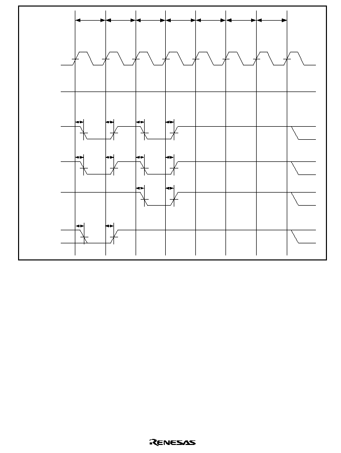
Rev. 5.0, 09/03, page 739 of 806
CKIO
CSn
RD/
WR
CASxx
CKE
RAS3x
Tp
Tpc
TRr
TRrw
TRrw
(Tpc)
(Tpc)
t
CSD3
t
CSD3
t
CSD3
t
CSD3
t
RASD2
t
RASD2
t
RASD2
t
RASD2
t
CASD2
t
CASD2
t
RWD
t
RWD
(High)
Figure 24.37 Synchronous DRAM Auto-Refresh Timing (TRAS = 1, TPC = 1)
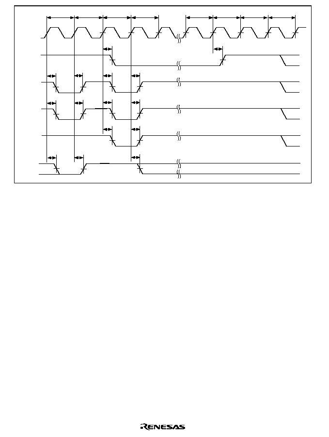
Rev. 5.0, 09/03, page 740 of 806
TRs1
tCKED
tCKED
CKIO
RD/
WR
CSn
RAS
CAS
CKE
tCSD3
tRASD2
tCASD2
tCSD3
tRASD2
tCASD2
tRWD
(TRs2)
(TRs2)
TRs3
(Tpc)
(Tpc)
Tpc
Tp
tCSD3
tCSD3
tRASD2
tRASD2
tRWD
tRWD
Figure 24.38 Synchronous DRAM Self-Refresh Cycle (TRAS
=
=
=
=
1, TPC = 1)
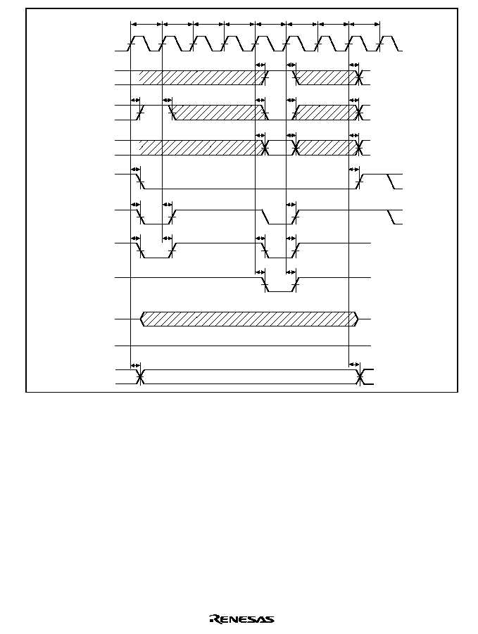
Rev. 5.0, 09/03, page 741 of 806
CKIO
A12 or A10
RD/
WR
CSn
RAS
CASxx
D31 to D0
A13 or A11
A11 to A2
or A9 to A2
TRp1
TRp2
TRp3
TRp4
TMw1
TMw2
TMw3
TMw4
(High)
CKE
tAD
tAD
tAD
tAD
tAD
tAD
tAD
tAD
tAD
tAD
tAD
tCSD3
tCSD3
tRWD
tRWD
tRWD
tRASD2
tRASD2
tRASD2
tRASD2
tCASD2
tCASD2
tDAKD1
tDAKD1
DACKn
Figure 24.39 Synchronous DRAM Mode Register Write Cycle
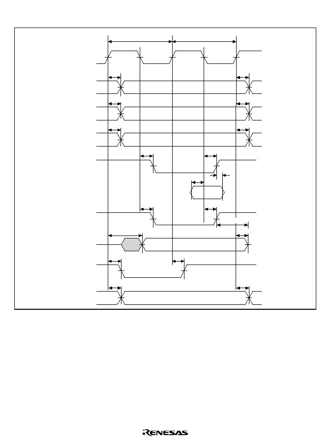
Rev. 5.0, 09/03, page 742 of 806
24.3.7
PCMCIA Timing
T
pcm1
T
pcm2
CKIO
A25 to A0
CExx
RD/
WR
RD
D15 to D0
WE1
D15 to D0
BS
DACKn
t
AD
t
AD
t
CSD1
t
CSD1
t
RWD
t
RSD
t
RSD
t
RWD
t
DAKD1
t
DAKD1
t
WED
t
WDD1
t
WED
t
RDS1
t
RDH1
t
BSD
t
BSD
t
WDH4
t
WDH1
(read)
(read)
(write)
(write)
Figure 24.40 PCMCIA Memory Bus Cycle (TED = 0, TEH = 0, No Wait)
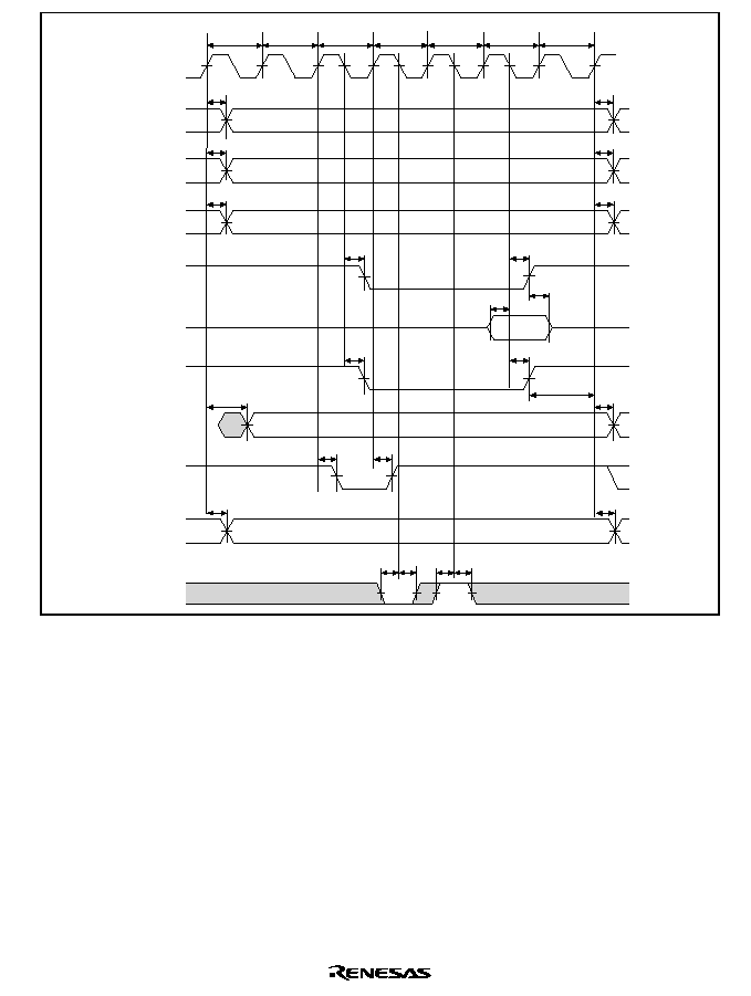
Rev. 5.0, 09/03, page 743 of 806
CKIO
T
pcm0
T
pcm0w
T
pcm1
T
pcm1w
T
pcm1w
T
pcm2
T
pcm2w
A25 to A0
CExx
RD/
WR
RD
(read)
D15 to D0
(read)
WE1
(write)
D15 to D0
(write)
BS
DACKn
WAIT
t
AD
t
CSD1
t
RWD
t
AD
t
CSD1
t
RWD
t
WDH4
t
RSD
t
RSD
t
DAKD1
t
DAKD1
t
WED
t
WDD1
t
WED
t
WDH1
t
RDH1
t
BSD
t
WTS
t
WTH
t
WTS
t
WTH
t
RDS1
t
BSD
Figure 24.41 PCMCIA Memory Bus Cycle
(TED = 2, TEH = 1, One Wait, External Wait, WAITSEL = 1)
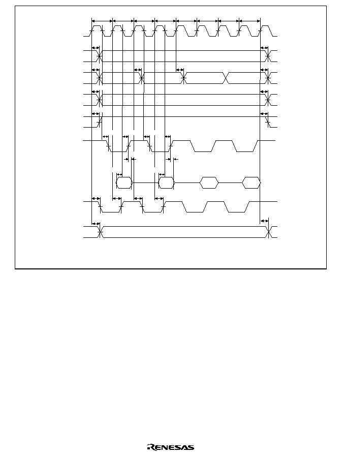
Rev. 5.0, 09/03, page 744 of 806
CKIO
T
pcm1
T
pcm2
T
pcm1
T
pcm2
T
pcm1
T
pcm2
T
pcm1
T
pcm2
A25 to A4
A3 to A0
CExx
RD/
WR
RD
D15 to D0
BS
DACKn
t
AD
t
AD
t
CSD1
t
RWD
t
CSD1
t
RWD
t
AD
t
AD
t
AD
t
AD
t
DAKD1
t
RSD
t
RSD
t
RDH1
t
RDH1
t
RSD
t
RSD
t
BSD
t
BSD
t
BSD
t
BSD
t
RDS1
t
RDS1
Note: Even though burst mode is set, the write cycle operation is the same as in normal mode.
(read)
(read)
t
DAKD1
Figure 24.42 PCMCIA Memory Bus Cycle
(Burst Read, TED = 0, TEH = 0, No Wait)
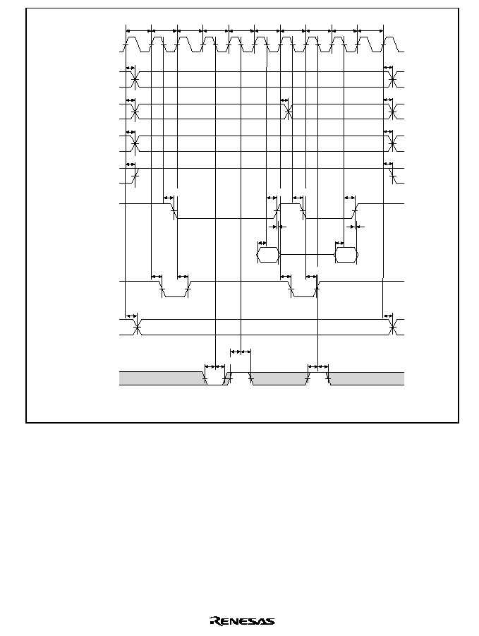
Rev. 5.0, 09/03, page 745 of 806
CKIO
T
pcm0
T
pcm1
T
pcm1w
T
pcm1w
T
pcm1w
T
pcm2
T
pcm1
T
pcm1w
T
pcm2
T
pcm2w
A25 to A4
A3 to A0
CExx
RD/
WR
RD
(read)
D15 to D0
(read)
BS
DACKn
WAIT
t
AD
t
AD
t
CSD1
t
RWD
t
CSD1
t
DAKD1
t
RWD
t
AD
t
AD
t
AD
t
RSD
t
RSD
t
RSD
t
RSD
t
DAKD1
t
BSD
t
BSD
t
BSD
t
RDS1
t
RDH1
t
RDH1
t
RDS1
t
WTS
t
WTH
t
WTS
t
WTS
t
WTH
t
WTH
Note: Even though burst mode is set, the write cycle operation is the same as in normal mode.
t
BSD
Figure 24.43 PCMCIA Memory Bus Cycle
(Burst Read, TED = 1, TEH = 1, Two Waits, Burst Pitch = 3, WAITSEL = 1)
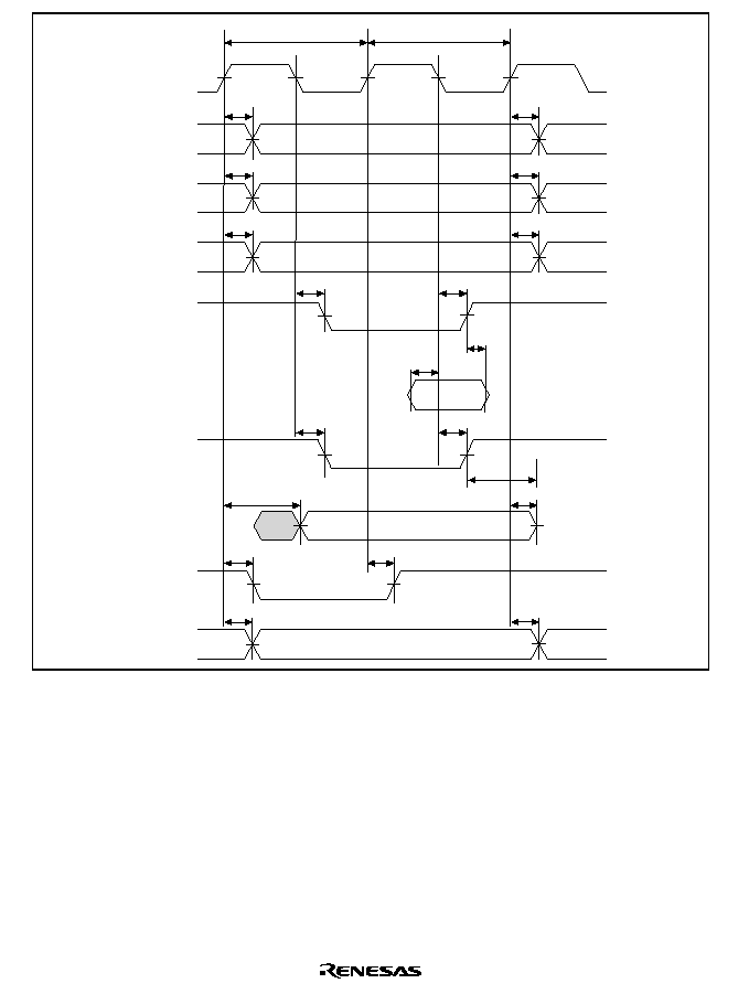
Rev. 5.0, 09/03, page 746 of 806
T
pci1
T
pci2
CKIO
A25 to A0
CExx
RD/
WR
ICIORD
(read)
D15 to D0
(read)
ICIOWR
(write)
D15 to D0
(write)
BS
DACKn
t
AD
t
AD
t
CSD1
t
CSD1
t
RWD
t
ICRSD
t
ICRSD
t
RWD
t
DAKD1
t
DAKD1
t
ICWSD
t
WDD1
t
ICWSD
t
RDH1
t
RDS1
t
BSD
t
BSD
t
WDH1
t
WDH4
Figure 24.44 PCMCIA I/O Bus Cycle (TED = 0, TEH = 0, No Wait)
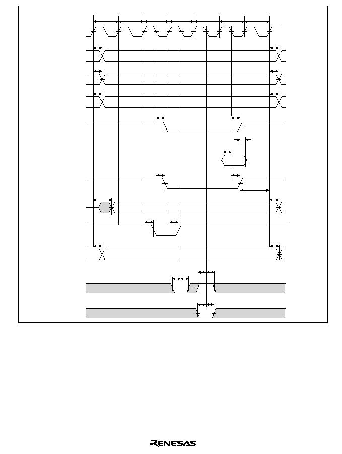
Rev. 5.0, 09/03, page 747 of 806
CKIO
T
pci0
T
pci0w
T
pci1
T
pci1w
T
pci1w
T
pci2
T
pci2w
A25 to A0
CExx
RD/
WR
ICIORD
(read)
D15 to D0
(read)
ICIOWR
(write)
D15 to D0
(write)
BS
DACKn
WAIT
IOIS16
t
AD
t
CSD1
t
RWD
t
AD
t
CSD1
t
RWD
t
ICRSD
t
ICRSD
t
DAKD1
t
DAKD1
t
ICWSD
t
WDD1
t
ICWSD
t
WDH1
t
WDH4
t
RDH1
t
WTS
t
WTH
t
WTS
t
WTH
t
IO16S
t
IO16H
t
RDS1
t
BSD
t
BSD
Figure 24.45 PCMCIA I/O Bus Cycle
(TED = 2, TEH = 1, One Wait, External Wait, WAITSEL = 1)

Rev. 5.0, 09/03, page 748 of 806
CKIO
T
pci0
T
pci1
T
pci1w
T
pci2
T
pci1
T
pci1w
T
pci2
T
pci2w
A25 to A4
A0
CExx
RD/
WR
ICIORD
D15 to D0
ICIOWR
D15 to D0
BS
WAIT
IOIS16
DACKn
t
AD
t
AD
t
CSD1
t
CSD1
t
RWD
t
RWD
t
WDD1
t
WDH4
t
BSD
t
AD
t
AD
t
ICRSD
t
ICRSD
t
ICRSD
t
ICRSD
t
ICWSD
t
WTS
t
WTH
t
WTH
t
IO16S
t
IO16H
t
AD
t
RDS1
t
DAKD1
t
DAKD1
t
RDS1
t
ICWSD
t
ICWSD
t
RDH1
t
RDH1
t
WDH1
t
BSD
t
WTS
(read)
(read)
(write)
(write)
t
WDD1
t
WDH4
t
BSD
t
BSD
t
ICWSD
t
CSD1
Figure 24.46 PCMCIA I/O Bus Cycle
(TED = 1, TEH = 1, One Wait, Bus Sizing, WAITSEL = 1)

Rev. 5.0, 09/03, page 749 of 806
24.3.8
Peripheral Module Signal Timing
Table 24.8
Peripheral Module Signal Timing
VccQ = 3.3 ± 0.3 V, Vcc = 1.55 V to 2.15 V, AVcc = 3.3 ± 0.3 V, Ta = ≠20 to 75∞C
Module
Item
Symbol Min
Max
Unit
Figure
Timer input setup time
t
TCLKS
15
--
ns
24.47
TMU,
RTC
Timer clock input setup time
t
TCKS
15
--
24.48
Edge specification
t
TCKWH
1.5
--
pcyc
*
Timer clock
pulse width
Both-edge specification
t
TCKWL
2.5
--
Oscillation settling time
t
ROSC
3
--
S
24.49
SCI
Asynchronous
t
SCYC
4
--
pcyc
*
Input clock
cycle
Synchronous
6
--
24.50,
24.51
Input clock rise time
t
SCKR
--
1.5
24.50
Input clock fall time
t
SCKF
--
1.5
Input clock pulse width
t
SCKW
0.4
0.6
tscyc
Transmit data delay time
t
TXD
--
100
ns
24.51
Receive data setup time (synchronous)
t
RXS
100
--
Receive data hold time (synchronous)
t
RXH
100
--
RTS
delay time
t
RTSD
--
100
CTS
setup time (synchronous)
t
CTSS
100
--
CTS
hold time (synchronous)
t
CTSH
100
--
Port
Output data delay time
t
PORTD
--
17
ns
24.52
Input data setup time
t
PORTS1
15
--
Input data hold time
t
PORTH1
8
--
Input data setup time
t
PORTS2
tcyc +
15
--
Input data hold time
t
PORTH2
8
--
Input data setup time
t
PORTS3
3
◊
tcyc
+ 15
--
Input data hold time
t
PORTH3
8
--
DMAC
DREQ
setup time
t
DRES
6
--
ns
24.53
DREQ
hold time
t
DREQH
4
--
DRAK delay time
t
DRAKD
--
10
24.54
Note:
*
pcyc is the P clock cycle.
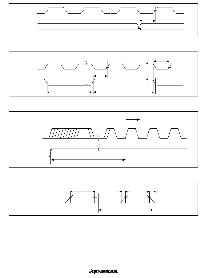
Rev. 5.0, 09/03, page 750 of 806
t
TCLKS
CKIO
TCLK
(input)
Figure 24.47 TCLK Input Timing
t
TCKS
t
TCKS
t
TCKWH
t
TCKWL
CKIO
TCLK
(input)
Figure 24.48 TCLK Clock Input Timing
RTC crystal
oscillator
Stable
oscillation
V
CC
V
CCmin
t
ROSC
Figure 24.49 RTC Crystal Oscillator Oscillation Settling Time at Power-On
t
SCKW
t
SCKR
t
SCKF
t
Scyc
SCK
Figure 24.50 SCK Input Clock Timing
Rev. 5.0, 09/03, page 751 of 806
t
Scyc
t
TXD
SCK
TxD
(data trans-
mission)
RxD
(data
reception)
t
RXH
t
RXS
t
RTSD
RTS
CTS
t
CTSH
t
CTSS
Figure 24.51 SCI I/O Timing in Synchronous Mode
CKIO
PORT 7 to 0
(write)
PORT 7 to 0
(read)
(B:P clock ratio = 1:1)
PORT 7 to 0
(read)
(B:P clock ratio = 2:1)
PORT 7 to 0
(read)
(B:P clock ratio = 4:1)
t
PORTS1
t
PORTH1
t
PORTS2
t
PORTH2
t
PORTD
t
PORTS3
t
PORTH3
Figure 24.52 I/O Port Timing
Rev. 5.0, 09/03, page 752 of 806
t
PTE[1]S
t
PTE[1]H
RESETP
PTE[1]
DREQn
CKIO
t
DRQS
t
DRQH
Figure 24.53
D
D
D
DR
R
R
REEEEQ
Q
Q
Q Input Timing
DRAK0/1
CKIO
t
DRAKD
t
DRAKD
Figure 24.54 DRAK Output Timing
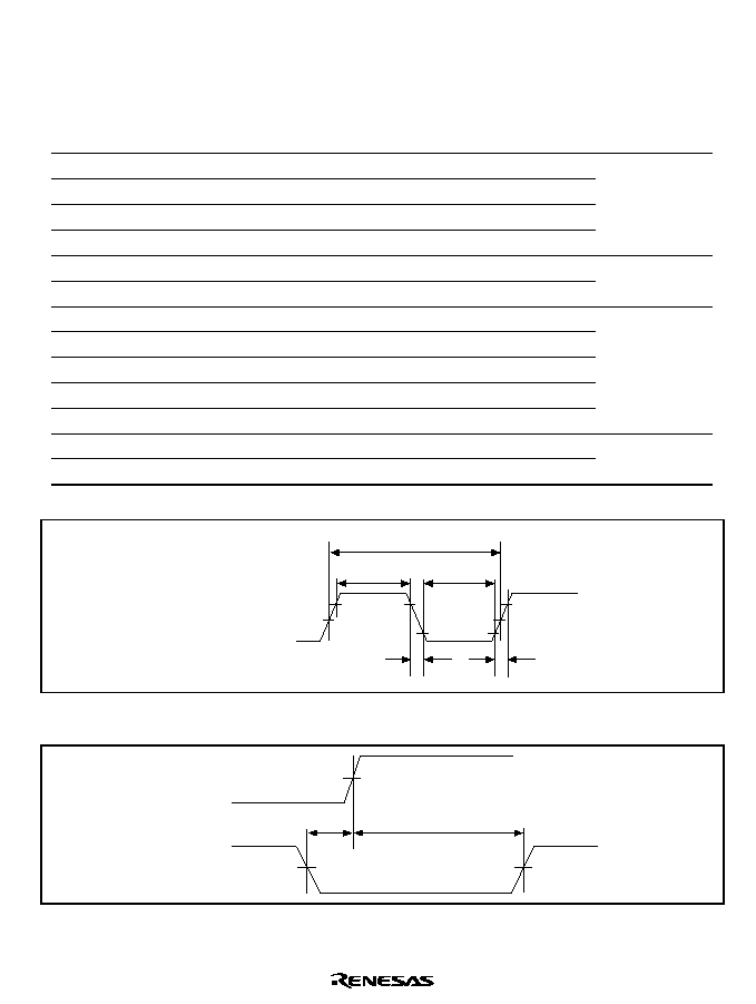
Rev. 5.0, 09/03, page 753 of 806
24.3.9
UDI-Related Pin Timing
Table 24.9
UDI-Related Pin Timing
VccQ = 3.3 ± 0.3 V, Vcc = 1.55 V to 2.15 V, AVcc = 3.3 ± 0.3 V, Ta = ≠20 to 75∞C
Item
Symbol
Min
Max
Unit
Figure
TCK cycle time
t
TCKcyc
50
--
ns
24.55
TCK high pulse width
t
TCKH
12
--
ns
TCK low pulse width
t
TCKL
12
--
ns
TCK rise/fall time
t
TCKf
--
4
ns
TRST setup time
t
TRSTS
12
--
ns
24.56
TRST hold time
t
TRSTH
50
--
t
cyc
TDI setup time
t
TDIS
10
--
ns
24.57
TDI hold time
t
TDIH
10
--
ns
TMS setup time
t
TMSS
10
--
ns
TMS hold time
t
TMSH
10
--
ns
TDO delay time
t
TDOD
--
16
ns
ASEMD0
setup time
t
ASEMDH
12
--
ns
24.58
ASEMD0
hold time
t
ASEMDS
12
--
ns
t
TCKL
t
TCKf
V
IL
V
IL
V
IH
V
IH
V
IL
1/2
VcoQ
1/2
VcoQ
TCK
(input)
t
TCKf
t
TCKH
t
TCKcyc
Figure 24.55 TCK Input Timing
RESETP
t
TRSTS
t
TRSTH
TRST
Figure 24.56 TRST Input Timing (Reset Hold)
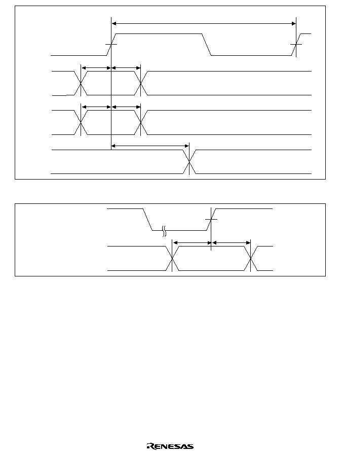
Rev. 5.0, 09/03, page 754 of 806
TCK
TDI
TMS
t
TDIS
t
TMSS
t
TDIH
t
TCKcyc
t
TMSH
t
TDOD
TDO
Figure 24.57 UDI Data Transfer Timing
t
ASEMD0S
t
ASEMD0H
RESETP
ASEMD0
Figure 24.58
A
A
A
ASSSSEEEEM
M
M
MD
D
D
D0000 Input Timing
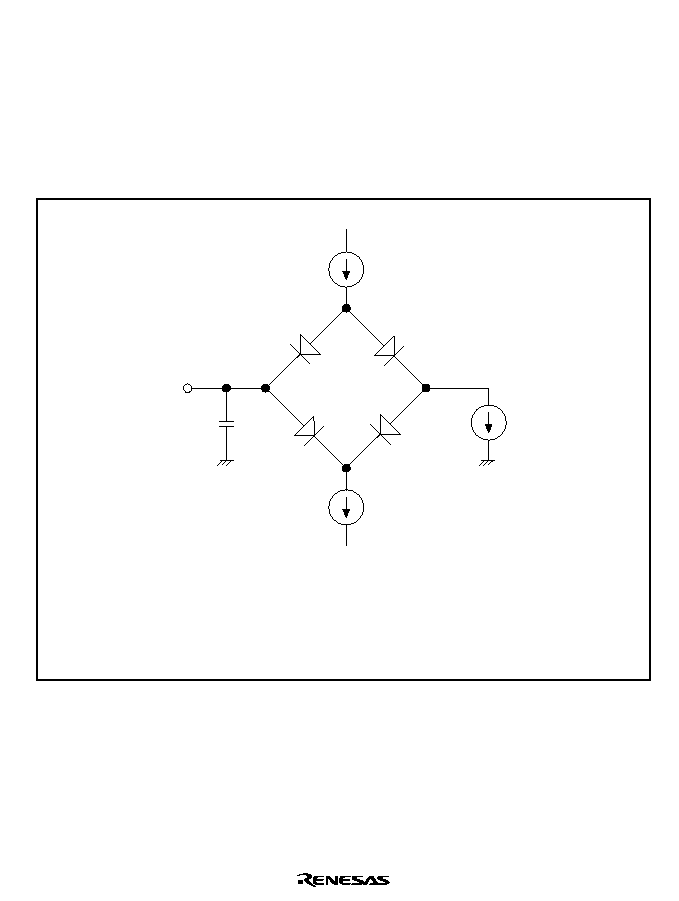
Rev. 5.0, 09/03, page 755 of 806
24.3.10
AC Characteristic Test Conditions
I/O signal reference level: VccQ/2 (VccQ = 3.3 ± 0.3 V, Vcc = 1.55 V to 2.15 V)
Input pulse level: Vss to 3.0 V (where
RESETP, RESETM, ASEMD0, IRL3 to IRL0, IRLS3 to
IRLS0, ADTRG, PINT15 to PINT0,
TRST, RxD1, CA, NMI, IRQ5≠IRQ0, CKIO, and
MD5≠MD0 are within Vss to Vcc)
Input rise and fall times: 1 ns
I
OL
I
OH
C
L
V
REF
SH7729R output pin
DUT output
Notes: 1. C
L
is the total value that includes the capacitance of measurement instruments, etc.,
and is set as follows for each pin.
30pF: CKIO,
RAS, CAS, CS0, CS2-CS6, CE2A, CE2B, BACK
50pF: All other pins
2.
I
OL
and I
OH
are the values shown in table 24.3.
Figure 24.59 Output Load Circuit

Rev. 5.0, 09/03, page 756 of 806
24.3.11
Delay Time Variation Due to Load Capacitance
A graph (reference data) of the variation in delay time when a load capacitance greater than that
stipulated (30 pF) is connected to the SH7729R's pins is shown below. The graph shown in figure
24.60 should be taken into consideration in the design process if the stipulated capacitance is
exceeded in connecting an external device.
If the connected load capacitance exceeds the range shown in figure 24.60, the graph will not be a
straight line.
+3
+2
+1
+0
+0 +10 +20 +30
+40 +50
Load Capacitance [pF]
Delay T
ime
[ns]
Figure 24.60 Load Capacitance vs. Delay Time

Rev. 5.0, 09/03, page 757 of 806
24.4
A/D Converter Characteristics
Table 24.10 lists the A/D converter characteristics.
Table 24.10 A/D Converter Characteristics
VccQ = 3.3 ± 0.3 V, Vcc = 1.55 V to 2.15 V, AVcc = 3.3 ± 0.3 V, Ta = ≠20 to 75∞C
Item
Min
Typ
Max
Unit
Resolution
10
10
10
bits
Conversion time
15
--
--
µ
s
Analog input capacitance
--
--
20
pF
Permissible signal-source (single-
source) impedance
--
--
5
k
Nonlinearity error
--
--
±3
LSB
Offset error
--
--
±2
LSB
Full-scale error
--
--
±2
LSB
Quantization error
--
--
±0.5
LSB
Absolute accuracy
--
--
±4
LSB
24.5
D/A Converter Characteristics
Table 24.11 lists the D/A converter characteristics.
Table 24.11 D/A Converter Characteristics
VccQ = 3.3 ± 0.3 V, Vcc = 1.55 V to 2.15 V, AVcc = 3.3 ± 0.3 V, Ta = ≠20 to 75∞C
Item
Min
Typ
Max
Unit
Test Conditions
Resolution
8
8
8
bits
Conversion time
--
--
10.0
µ
s
20-pF capacitive
load
Absolute accuracy
--
±2.5
±4.0
LSB
2-M
resistance
load

Rev. 5.0, 09/03, page 758 of 806

Rev. 5.0, 09/03, page 759 of 806
Appendix A Pin Functions
A.1
Pin States
Table A.1 shows pin states during resets, power-down states, and the bus-released state.
Table A.1
Pin States during Resets, Power-Down States, and Bus-Released State
Reset
Power-Down
Category
Pin
Power-On
Reset
Manual
Reset
Standby
Sleep
Bus
Released
EXTAL
I
I
I
I
I
XTAL
O
*
1
O
*
1
O
*
1
O
*
1
O
*
1
CKIO
IO
*
1
IO
*
1
IO
*
1
IO
*
1
IO
*
1
EXTAL2
I
I
I
I
I
XTAL2
O
O
O
O
O
Clock
CAP1, CAP2
--
--
--
--
--
RESETP
I
I
I
I
I
RESETM
I
I
I
I
I
BREQ
I
I
I
I
I
BACK
O
O
O
O
L
MD[5:0]
I
I
I
I
I
CA
I
I
I
I
I
System control
STATUS[1:0]/PTJ[7:6]
O
OP
*
2
OP
*
2
OP
*
2
OP
*
2
IRQ[3:0]/
IRL[3:0]
/
PTH[3:0]
V
*
7
I
I
I
I
IRQ4/ PTH[4]
V
*
7
I
I
I
I
NMI
I
I
I
I
I
IRLS[3:0]
/PTF[3:0]/
PINT[11:8]
V
I
IZ
I
I
MCS
[7:0]/PTC[7:0]/
PINT[7:0]
V
OP
*
2
ZH
*
10
K
*
2
OP
*
2
ZP
*
2
TCK/PTF4/PINT12
IV
I
IZ
I
I
TDI/PTFS/PINT13
IV
I
IZ
I
I
TMS/PTF6/PINT14
IV
I
IZ
I
I
TRST
/PTF7/PINT15
IV
I
IZ
I
I
Interrupt
IRQOUT
O
O
O
O
O
Rev. 5.0, 09/03, page 760 of 806
Reset
Power-Down
Category
Pin
Power-On
Reset
Manual
Reset
Standby
Sleep
Bus
Released
Address bus
A[25:0]
Z
O
ZL
*
9
O
Z
D[15:0]
Z
I
Z
IO
Z
D[23:16]/PTA[7:0]
Z
IP
*
2
ZK
*
2
IOP
*
2
ZP
*
2
Data bus
D[31:24]/PTB[7;0]
Z
IP
*
2
ZK
*
2
IOP
*
2
ZP
*
2
CS0
/
MCS0
H
O
ZH
*
10
O
Z
CS[2:4]
/PTK[0:2]
H
OP
*
2
ZH
*
10
K
*
2
OP
*
2
ZP
*
2
CS5
/
CE1A
/PTK[3]
H
OP
*
2
ZH
*
10
K
*
2
OP
*
2
ZP
*
2
CS6
/
CE1B
H
O
ZH
*
10
O
Z
BS
/PTK[4]
H
OP
*
2
ZH
*
10
K
*
2
OP
*
2
ZP
*
2
RAS3L
/PTJ[0]
H
OP
*
2
ZOK
*
3
OP
*
2
ZOP
*
3
RAS3U
/PTE[2]
V
OP
*
2
ZOK
*
3
OP
*
2
ZOP
*
3
CASL
/PTJ[2]
H
OP
*
2
ZOK
*
3
OP
*
2
ZOP
*
3
CASU
/PTJ[3]
H
OP
*
2
ZOK
*
3
OP
*
2
ZOP
*
3
WE0
/DQMLL
H
O
ZH
*
10
O
Z
WE1
/DQMLU/
WE
H
O
ZH
*
10
O
Z
WE2
/DQMUL/
ICIORD
/
PTK[6]
H
OP
*
2
ZH
*
10
K
*
2
OP
*
2
ZP
*
2
WE3
/DQMUU/
ICIOWR
/
PTK[7]
H
OP
*
2
ZH
*
10
K
*
2
OP
*
2
ZP
*
2
RD/
WR
H
O
ZH
*
10
O
Z
RD
H
O
ZH
*
10
O
Z
CKE/PTK[5]
H
OP
*
2
OK
*
2
OP
*
2
OP
*
2
Bus control
WAIT
Z
I
Z
I
Z
DREQ0
/PTD[4]
V
ZI
*
6
Z
I
I
DACK0
/PTD[5]
V
OP
*
2
ZK
*
2
OP
*
2
OP
*
2
DRAK0/PTD[1]
V
OP
*
2
ZH
*
10
K
*
2
OP
*
2
OP
*
2
DREQ1
/PTD[6]
V
ZI
*
6
Z
I
I
DACK1
/PTD[7]
V
OP
*
2
ZK
*
2
OP
*
2
OP
*
2
DMAC
DRAK1/PTD[0]
V
OP
*
2
ZH
*
10
K
*
2
OP
*
2
OP
*
2
Timer
TCLK/PTH[7]
V
ZP
IOP
*
4
IOP
*
4
IOP
*
4

Rev. 5.0, 09/03, page 761 of 806
Reset
Power-Down
Category
Pin
Power-On
Reset
Manual
Reset
Standby
Sleep
Bus
Released
RxD0/SCPT[0]
Z
ZI
*
6
Z
IZ
*
5
IZ
*
5
TxD0/SCPT[0]
Z
ZO
*
6
ZK
*
2
OZ
*
5
OZ
*
5
SCI/Smart card
without FIFO
SCK0/SCPT[1]
V
ZP
*
2
ZK
*
2
IOP
*
4
IOP
*
4
RxD1/SCPT[2]
Z
ZI
*
6
Z
IZ
*
5
IZ
*
5
TxD1/SCPT[2]
Z
ZO
*
6
ZK
*
2
OZ
*
5
OZ
*
5
SCIF/IrDA
with FIFO
SCK1/SCPT[3]
V
ZP
*
2
ZK
*
2
IOP
*
4
IOP
*
4
RxD2/SCPT[4]
Z
ZI
*
6
Z
IZ
*
5
IZ
*
5
TxD2/SCPT[4]
Z
ZO
*
6
ZK
*
2
OZ
*
5
OZ
*
5
SCK2/SCPT[5]
V
ZP
*
2
ZK
*
2
IOP
*
4
IOP
*
4
RTS2
/SCPT[6]
V
OP
*
2
ZK
*
2
OP
*
2
OP
*
2
SCIF with FIFO
CTS2
/IRQ5/SCPT[7]
V
*
7
ZI
*
6
I
I
I
AUDSYNC
/PTE[7]
OV
OP
*
2
OK
*
2
OP
*
2
OP
*
2
CE2B
/PTE[5]
V
OP
*
2
ZH
*
10
K
*
2
OP
*
2
ZP
*
2
CE2A
/PTE[4]
V
OP
*
2
ZH
*
10
K
*
2
OP
*
2
ZP
*
2
TDO/PTE[0]
OV
OP
*
2
OK
*
2
OP
*
2
OP
*
2
IOIS16
/PTG[7]
V
I
Z
I
I
PTG[6:0]
V
I
Z
I
I
AUDCK/PHT[6]
V
I
Z
I
I
ADTRG
/PTH[5]
V
*
7
I
IZ
I
I
WAKEUP
/PTD[3]
V
OP
*
2
OK
*
2
OP
*
2
ZP
*
2
RESETOUT
/PTD[2]
O
OP
*
2
ZK
*
2
OP
*
2
OP
*
2
AUDATA[3:0]/PTG[3:0]
IV port
I
IZ port
I
I
CKIO2/PTG[4]
OV port
OI port
OZ port
OI port
OI port
ASEBRKAK
/PTG[5]
OV port
OI port
OZ port
OI port
OI port
ASEMD0
/PTG[6]
I (ASEMD)
I
Z
I
I
PTJ[1]
H
OP
*
2
ZOK
*
3
OP
*
2
ZOP
*
3
PTE[1]
V
*
12
OP
*
2
ZOK
*
3
OP
*
2
ZOP
*
3
PTE[6]
V
OP
*
2
ZOK
*
3
OP
*
2
ZOP
*
3
PTE[3]
V
OP
*
2
ZOK
*
3
OP
*
2
ZOP
*
3
PTJ[4]
H
OP
*
2
ZOK
*
3
OP
*
2
ZOP
*
3
Port
PTJ[5]
H
OP
*
2
ZOK
*
3
OP
*
2
ZOP
*
3

Rev. 5.0, 09/03, page 762 of 806
Reset
Power-Down
Category
Pin
Power-On
Reset
Manual
Reset
Standby
Sleep
Bus
Released
AN[5:0]/PTL[5:0]
Z
ZI
*
6
Z
I
I
Analog
AN[6:7]/DA[1:0]/PTL[6:7]
Z
ZI
*
6
OZ
*
11
IO
*
8
IO
*
8
I:
Input
O: Output
H: High-level output
L: Low-level output
Z: High impedance
P: Input or output depending on register setting
K: Input pin is high impedance, output pin holds its state
V: I/O buffer off, pull-up MOS on
Notes: 1.
Depending on the clock mode (MD2≠MD0 setting).
2.
K or P when the port function is used.
3.
K or P when the port function is used. Z or O when the port function is not used
depending on register setting.
4.
K or P when the port function is used. I or O when the port function is not used
depending on register setting.
5.
Depending on register setting.
6.
I or O when the port function is used.
7.
Input Schmitt buffers of IRQ[5:0] and ADTRG on; other input buffers off.
8.
I when the port function is used. I or O when the port function is not used, depending
on register setting.
9.
In standby mode, Z or L depending on register setting.
10. In standby mode, Z or H depending on register setting.
11. O when DA output is enabled; Z otherwise.
12. In a power-on reset, leave open or input a high level.

Rev. 5.0, 09/03, page 763 of 806
A.2
Pin Specifications
Table A.2 shows the pin specifications.
Table A.2
Pin Specifications
Pin
Pin No.
(FP-208C,
FP-208E)
Pin No.
(BP-240A)
I/O
Function
MD5
197
C6
I
Operating mode pin (endian mode)
MD4, MD3
196, 195
D6, A7
I
Operating mode pin (area 0 bus
width)
MD2 to MD0
2, 1, 144
C2, D2,G19
I
Operating mode pin (clock mode)
RAS3L
/PTJ[0]
106
U18
I/O
RAS (SDRAM) / I/O port
PTJ[1]
107
U19
I/O
I/O port
CE2A
/PTE[4]
103
V17
I/O
PCMCIA CE2A / I/O port
CE2B
/PTE[5]
104
V16
I/O
PCMCIA CE2B / I/O port
RXD0/SCPT[0]
171
B13
I
Serial port 0 data input / input port
RXD1/SCPT[2]
172
C13
I
Serial port 1 data input / input port
RXD2/SCPT[4]
174
B12
I
Serial port 2 data input / input port
TXD0/SCPT[0]
164
C15
O
Serial port 0 data output / output port
TXD1/SCPT[2]
166
A14
O
Serial port 1 data output / output port
TXD2/SCPT[4]
168
C14
O
Serial port 2 data output / output port
SCK0/SCPT[1]
165
D15
I/O
Serial port 0 clock input/output / I/O
port
SCK1/SCPT[3]
167
B14
I/O
Serial port 1 clock input/output / I/O
port
SCK2/SCPT[5]
169
D14
I/O
Serial port 2 clock input/output / I/O
port
RTS2
/SCPT[6]
170
A13
I/O
Serial port 2 transfer request / I/O
port
STATUS1/PTJ[7] 158
B17
I/O
Processor state / I/O port
STATUS0/PTJ[6] 157
B16
I/O
Processor state / I/O port

Rev. 5.0, 09/03, page 764 of 806
Pin
Pin No.
(FP-208C,
FP-208E)
Pin No.
(BP-240A)
I/O
Function
A25 to A0
86, 84, 82, 80,
78 to 72, 70,
68 to 60, 58,
56 to 53
V12, T12,
V11, W10,
V10, U9, T9,
V9, W9, T8,
U8, W8, U7,
V7, W7, T6,
U6, V6, W6,
T5, U5, W5,
W4, V5, V3,
V4
O
Address bus
D31 to D24/
PTB[7] to PTB[0]
13 to 18, 20,
22
F4, G1, G2,
G3, G4, H1,
H3, J1
I/O
Data bus / I/O port
D23 to D16/
PTA[7] to PTA[0]
23 to 26, 28,
30 to 32
J2, J4, J3, K2,
K1, L2, L1, M4
I/O
Data bus / I/O port
D15 to D0
34, 36 to 44,
46, 48 to 52
M2, N4, N3,
N2, N1, P4,
P3, P2, P1,
R4, T4, T3,
T1, R2, U2,T2
I/O
Data bus
MCS[7:0]
/
PTC[7:0]/
PINT[7:0]
177 to
180,185 to
188
B11, D11,
C11, B10, D9,
B9, A9, D8
I/O
Mask ROM chip select / I/O port /
port interrupt request
WAKEUP
/PTD[3] 182
D10
I/O
Wakeup / I/O port
RESETOUT
/
PTD[2]
184
C9
I/O
Reset output / I/O port
DRAK0/PTD[1]
189
C8
I/O
DMA control pin / I/O port
DRAK1/PTD[0]
190
B8
I/O
DMA control pin / I/O port
DREQ0
/PTD[4]
191
A8
I
DMA transfer request 0 / input port
DREQ1
/PTD[6]
192
D7
I
DMA transfer request 1 / input port
AN[5:0]/PTL[5:0]
204 to 199
C4, A5, D4,
C5, D5, A6
I
Analog input pin / input port
AN[7:6]/DA[1:0]/
PTL[7:6]
207, 206
B3, B5
I/O
Analog I/O pin / input port
CS6
/
CE1B
102
V15
O
Chip select 6 / PCMCIA CE1B
CS5
/
CE1A
/
PTK[3]
101
W16
I/O
Chip select 5 / PCMCIA CE2B / I/O
port
CS4
/PTK[2]
100
U16
I/O
Chip select 4 / I/O port
CS3
/PTK[1]
99
W15
I/O
Chip select 3 / I/O port

Rev. 5.0, 09/03, page 765 of 806
Pin
Pin No.
(FP-208C,
FP-208E)
Pin No.
(BP-240A)
I/O
Function
CS2
/PTK[0]
98
T16
I/O
Chip select 2 / I/O port
CS0
/
MCS0
96
T15
O
Chip select 0 / Mask ROM chip
select 0
BS
/PTK[4]
87
W12
I/O
Bus cycle start / I/O port
PTJ[5]
113
R17
I/O
I/O port
PTJ[4]
112
U17
I/O
I/O port
CASU
/PTJ[3]
110
T17
I/O
CAS(SDRAM) / I/O port
CASL
/PTJ[2]
108
R18
I/O
CAS(SDRAM) / I/O port
DACK0
/PTD[5]
114
R16
I/O
DMA transfer strobe 0 / I/O port
DACK1
/PTD[7]
115
P19
I/O
DMA transfer strobe 1 / I/O port
RD
88
T13
O
Read strobe pin
WE0
/ DQMLL
89
U13
O
D7≠D0 select signal/ DQM(SDRAM)
WE1
/DQMLU/
WE
90
V13
O
D15≠D8 select signal /
DQM(SDRAM)/ PCMCIA
WE
signal
WE2
/DQMUL/
ICIORD
/PTK[6]
91
W13
I/O
D23≠D16 select signal /
DQM(SDRAM) / PCMCIA
IORD
signal / I/O port
WE3
/DQMUU/
ICIOWR
/PTK[7]
92
T14
I/O
D31≠D24 select signal
/DQM(SDRAM) / PCMCIA
IOWR
signal / I/O port
RD/
WR
93
U14
O
Read/write select signal
AUDSYNC
/
PTE[7]
94
V14
I/O
AUD synchronous I/O port
PTE[6]
116
P18
I/O
I/O port
PTE[3]
117
P17
I/O
I/O port
RAS3U
/PTE[2]
118
P16
I/O
RAS(SDRAM) / I/O port
PTE[1]
119
N19
I/O
I/O port
TDO/PTE[0]
120
N18
I/O
Test data output I/O port
RESETM
124
M18
I
Manual reset input
ADTRG
/PTH[5]
125
M17
I
ADC trigger request / Input port
IOIS16
/PTG[7]
126
M16
I
I/O for PC card / input port
ASMD0
/PTG[6]
127
L19
I
ASE mode / input port
ASEBRKAK
/
PTG[5]
128
L18
I
ASE break accept / input port

Rev. 5.0, 09/03, page 766 of 806
Pin
Pin No.
(FP-208C,
FP-208E)
Pin No.
(BP-240A)
I/O
Function
CKIO2/PTG[4]
129
L16
I/O
System clock output / input port
AUDATA[3]/
PTG[3]
130
L17
I
AUD data / input port
AUDATA[2]/
PTG[2]
131
K18
I
AUD data / input port
AUDATA[1]/
PTG[1]
133
K19
I
AUD data / input port
AUDATA[0]/
PTG[0]
135
J18
I
AUD data / input port
TRST
/PTF[7]/
PINT[15]
136
J19
I
Test reset / input port / port interrupt
request
TMS/PTF[6]/
PINT[14]
137
H16
I
Test mode switch / input port / port
interrupt request
TDI/PTF[5]/
PINT[13]
138
H17
I
Test data input / input port / port
interrupt request
TCK/PTF[4]/
PINT[12]
139
H18
I
Test clock / input port / port interrupt
request
IRLS
[3:0]/
PTF[3:0]/
PINT[11:8]
140 to 143
H19, G16,
G17, G18
I
External interrupt request / input port
/ port interrupt request
AUDCK/PTH[6]
151
D16
I
AUD clock / input port
WAIT
123
M19
I
Hardware wait request
BREQ
122
N16
I
Bus request
BACK
121
N17
O
Bus acknowledge
IRQOUT
160
A16
O
Interrupt / refresh request output
RESETP
193
C7
I
Power-on reset input
NMI
7
C3
I
Nonmaskable interrupt request
IRQ[3:0]/
IRL[3:0]
/
PTH[3:0]
11 to 8
F2, F1, E4, E3
I
External interrupt request / external
interrupt source / input port
IRQ4/PTH[4]
12
F3
I
External interrupt request / input port
CTS2
/IRQ5/
SCPT[7]
176
A11
I
Serial port 2 transfer enable /
external interrupt request / input port
TCLK/PTH[7]
159
B15
I/O
Clock I/O (for TMU/RTC) / I/O port
EXTAL
156
D18
I
External clock / crystal oscillator pin
XTAL
155
C18
O
Crystal oscillator pin
CAP1
146
F17
--
External capacitance pin (for PLL1)
CAP2
149
E16
--
External capacitance pin (for PLL2)

Rev. 5.0, 09/03, page 767 of 806
Pin
Pin No.
(FP-208C,
FP-208E)
Pin No.
(BP-240A)
I/O
Function
CKIO
162
A15
I/O
System clock I/O
XTAL2
4
D1
O
Crystal oscillator pin (for on-chip
RTC)
EXTAL2
5
D3
I
Crystal oscillator pin (for on-chip
RTC)
CKE/PTK[5]
105
T18
I/O
CK enable for SDRAM / I/O port
CA
194
B7
I
Setting hardware standby pin
V
CC
Q
21, 35, 47, 59,
71, 85, 97,
111,
163, 183
H4, M1, R1,
U3, V8, U15,
R19, C17,
A10, U12
Power
supply
Power supply (3.3 V)
V
CC
≠RTC
3
E2
Power
supply
RTC oscillator power supply
(2.0/1.9/1.8/1.7 V)
V
CC
≠PLL1
V
CC
≠PLL2
145
150
F16,
E17
Power
supply
PLL power supply (2.0/1.9/1.8/1.7 V)
AV
CC
205
A4
Power
supply
Analog power supply (3.3 V)
V
SS
Q
19, 33, 45, 57,
69, 83, 95,
109,
161, 181
H2, M3, R3,
T7, U4, W11,
W14, T19,
C16, C10
Power
supply
Power supply (0 V)
V
CC
29, 81, 134,
154, 175
L3, L4, U11,
T11, J17, J16,
E18, C19,
C12, D12
Power
supply
Internal power supply (2.0/1.9/1.8/1.7
V)
V
SS
27, 79, 132,
152, 153, 173
K3, K4, U10,
T10, K17,
K16, E19,
D17, D19,
A12, D13
Power
supply
Internal power supply (0 V)
V
SS
≠RTC
6
E1
Power
supply
RTC-oscillator power supply (0 V)
V
SS
≠PLL1
V
SS
≠PLL2
147
148
F18
F19
Power
supply
PLL power supply (0 V)
AV
SS
198, 208
B6, B4
Power
supply
Analog power supply (0 V)
Note:
Except in hardware standby mode, power must be supplied constantly to all power supply
pins. In hardware standby mode, power must be supplied to Vcc-RTC and Vss-RTC at
least.

Rev. 5.0, 09/03, page 768 of 806
A.3
Treatment of Unused Pins
∑
When RTC is not used
EXTAL2:
Pull up to V
CC
(2.0/1.9/1.8/1.7 V)
XTAL2:
Leave unconnected
V
CC
≠RTC:
Power supply (2.0/1.9/1.8/1.7 V)
V
SS
≠RTC:
Power supply (0 V)
∑
When PLL2 is not used
CAP2:
Leave unconnected
V
CC
≠PLL2: Power supply (2.0/1.9/1.8/1.7 V)
V
SS
≠PLL2:
Power supply (0 V)
∑
When on-chip crystal oscillator is not used
XTAL:
Leave unconnected
∑
When EXTAL pin is not used
EXTAL:
Pull up to V
CC
Q (3.3 V)
∑
When A/D converter is not used
AN[7:0]:
Leave unconnected
AV
CC
:
Power supply (3.3 V)
AV
SS
:
Power supply (0 V)
∑
When UDI is not used
ASEMD0:
Pull up to V
CC
Q (3.3 V)
∑
When hardware standby mode is not used
CA: Pull up (3.3 V)

Rev. 5.0, 09/03, page 769 of 806
A.4
Pin States in Access to Each Address Space
Table A.3
Pin States (Ordinary Memory/Little Endian)
8-Bit Bus Width
16-Bit Bus Width
Pin
Byte/Word/Long-
word Access
Byte Access
(Address 2n)
Byte Access
(Address 2n + 1)
Word/Longword
Access
CS6
to
CS2
,
CS0
Enabled
Enabled
Enabled
Enabled
R
Low
Low
Low
Low
RD
W High
High
High
High
R
High
High
High
High
RD/
WR
W Low
Low
Low
Low
BS
Enabled
Enabled
Enabled
Enabled
RAS3U
/PTE[2]
High
High
High
High
RAS3L
/PTJ[0]
High
High
High
High
CASL
/PTJ[2]
High
High
High
High
CASU
/PTJ[3]
High
High
High
High
R
High
High
High
High
WE0
/DQMLL
W Low
Low
High
Low
R
High
High
High
High
WE1
/DQMLU/
WE
W High
High
Low
Low
R
High
High
High
High
WE2
/DQMUL/
ICIORD
/PTK[6]
W High
High
High
High
R
High
High
High
High
WE3
/DQMUU/
ICIOWR
/PTK[7]
W High
High
High
High
CE2A
/PTE[4]
High
High
High
High
CE2B
/PTE[5]
High
High
High
High
CKE/PTK[5]
Disabled
Disabled
Disabled
Disabled
WAIT
Enabled
*
1
Enabled
*
1
Enabled
*
1
Enabled
*
1
IOIS16
/PTG[7]
Disabled
Disabled
Disabled
Disabled
A25 to A0
Address
Address
Address
Address
D7 to D0
Valid data
Valid data
Invalid data
Valid data
D15 to D8
High-Z
*
2
Invalid data
Valid data
Valid data
D31 to D16
High-Z
*
2
High-Z
*
2
High-Z
*
2
High-Z
*
2

Rev. 5.0, 09/03, page 770 of 806
32-Bit Bus Width
Pin
Byte
Access
(Address
4n)
Byte
Access
(Address
4n + 1)
Byte
Access
(Address
4n + 2)
Byte
Access
(Address
4n + 3)
Word
Access
(Address
4n)
Word
Access
(Address
4n + 2)
Longword
Access
CS6
to
CS2
,
CS0
Enabled
Enabled
Enabled
Enabled
Enabled
Enabled
Enabled
R
Low
Low
Low
Low
Low
Low
Low
RD
W High
High
High
High
High
High
High
R
High
High
High
High
High
High
High
RD/
WR
W Low
Low
Low
Low
Low
Low
Low
BS
Enabled
Enabled
Enabled
Enabled
Enabled
Enabled
Enabled
RAS3U
/PTE[2]
High
High
High
High
High
High
High
RAS3L
/PTJ[0]
High
High
High
High
High
High
High
CASL
/PTJ[2]
High
High
High
High
High
High
High
CASU
/PTJ[3]
High
High
High
High
High
High
High
R
High
High
High
High
High
High
High
WE0
/DQMLL
W Low
High
High
High
Low
High
Low
R
High
High
High
High
High
High
High
WE1
/DQMLU/
WE
W High
Low
High
High
Low
High
Low
R
High
High
High
High
High
High
High
WE2
/DQMUL/
ICIORD
/PTK[6]
W High
High
Low
High
High
Low
Low
R
High
High
High
High
High
High
High
WE3
/DQMUU/
ICIOWR
/PTK[7]
W High
High
High
Low
High
Low
Low
CE2A
/PTE[4]
High
High
High
High
High
High
High
CE2B
/PTE[5]
High
High
High
High
High
High
High
CKE/PTK[5]
Disabled
Disabled
Disabled
Disabled
Disabled
Disabled
Disabled
WAIT
Enabled
*
1
Enabled
*
1
Enabled
*
1
Enabled
*
1
Enabled
*
1
Enabled
*
1
Enabled
*
1
IOIS16
/PTG[7]
Disabled
Disabled
Disabled
Disabled
Disabled
Disabled
Disabled
A25 to A0
Address
Address
Address
Address
Address
Address
Address
D7 to D0
Valid
data
Invalid
data
Invalid
data
Invalid
data
Valid
data
Invalid
data
Valid
data
D15 to D8
Invalid
data
Valid
data
Invalid
data
Invalid
data
Valid
data
Invalid
data
Valid
data
D23 to D16
Invalid
data
Invalid
data
Valid
data
Invalid
data
Invalid
data
Valid
data
Valid
data
D31 to D24
Invalid
data
Invalid
data
Invalid
data
Valid
data
Invalid
data
Valid
data
Valid
data
Notes: 1. Disabled when WCR2 register wait setting is 0.
2. Unused data pins should be switched to the port function, or pulled up.

Rev. 5.0, 09/03, page 771 of 806
Table A.4
Pin States (Ordinary Memory/Big Endian)
8-Bit Bus Width
16-Bit Bus Width
Pin
Byte/Word/Long-
word Access
Byte Access
(Address 2n)
Byte Access
(Address 2n + 1)
Word/Longword
Access
CS6
to
CS2
,
CS0
Enabled
Enabled
Enabled
Enabled
R
Low
Low
Low
Low
RD
W High
High
High
High
R
High
High
High
High
RD/
WR
W Low
Low
Low
Low
BS
Enabled
Enabled
Enabled
Enabled
RAS3U
/PTE[2]
High
High
High
High
RAS3L
/PTJ[0]
High
High
High
High
CASL
/PTJ[2]
High
High
High
High
CASU
/PTJ[3]
High
High
High
High
R
High
High
High
High
WE0
/DQMLL
W Low
High
Low
Low
R
High
High
High
High
WE1
/DQMLU/
WE
W High
Low
High
Low
R
High
High
High
High
WE2
/DQMUL/
ICIORD
/PTK[6]
W High
High
High
High
R
High
High
High
High
WE3
/DQMUU/
ICIOWR
/PTK[7]
W High
High
High
High
CE2A
/PTE[4]
High
High
High
High
CE2B
/PTE[5]
High
High
High
High
CKE/PTK[5]
Disabled
Disabled
Disabled
Disabled
WAIT
Enabled
*
1
Enabled
*
1
Enabled
*
1
Enabled
*
1
IOIS16
/PTG[7]
Disabled
Disabled
Disabled
Disabled
A25 to A0
Address
Address
Address
Address
D7 to D0
Valid data
Invalid data
Valid data
Valid data
D15 to D8
High-Z
*
2
Valid data
Invalid data
Valid data
D31 to D16
High-Z
*
2
High-Z
*
2
High-Z
*
2
High-Z
*
2

Rev. 5.0, 09/03, page 772 of 806
32-Bit Bus Width
Pin
Byte
Access
(Address
4n)
Byte
Access
(Address
4n + 1)
Byte
Access
(Address
4n + 2)
Byte
Access
(Address
4n + 3)
Word
Access
(Address
4n)
Word
Access
(Address
4n + 2)
Longword
Access
CS6
to
CS2
,
CS0
Enabled
Enabled
Enabled
Enabled
Enabled
Enabled
Enabled
R
Low
Low
Low
Low
Low
Low
Low
RD
W High
High
High
High
High
High
High
R
High
High
High
High
High
High
High
RD/
WR
W Low
Low
Low
Low
Low
Low
Low
BS
Enabled
Enabled
Enabled
Enabled
Enabled
Enabled
Enabled
RAS3U
/PTE[2]
High
High
High
High
High
High
High
RAS3L
/PTJ[0]
High
High
High
High
High
High
High
CASL
/PTJ[2]
High
High
High
High
High
High
High
CASU
/PTJ[3]
High
High
High
High
High
High
High
R
High
High
High
High
High
High
High
WE0
/DQMLL
W High
High
High
Low
High
Low
Low
R
High
High
High
High
High
High
High
WE1
/DQMLU/
WE
W High
High
Low
High
High
Low
Low
R
High
High
High
High
High
High
High
WE2
/DQMUL/
ICIORD
/PTK[6]
W High
Low
High
High
Low
High
Low
R
High
High
High
High
High
High
High
WE3
/DQMUU/
ICIOWR
/PTK[7]
W Low
High
High
High
Low
High
Low
CE2A
/PTE[4]
High
High
High
High
High
High
High
CE2B
/PTE[5]
High
High
High
High
High
High
High
CKE/PTK[5]
Disabled
Disabled
Disabled
Disabled
Disabled
Disabled
Disabled
WAIT
Enabled
*
1
Enabled
*
1
Enabled
*
1
Enabled
*
1
Enabled
*
1
Enabled
*
1
Enabled
*
1
IOIS16
/PTG[7]
Disabled
Disabled
Disabled
Disabled
Disabled
Disabled
Disabled
A25 to A0
Address
Address
Address
Address
Address
Address
Address
D7 to D0
Invalid
data
Invalid
data
Invalid
data
Valid
data
Invalid
data
Valid
data
Valid
data
D15 to D8
Invalid
data
Invalid
data
Valid
data
Invalid
data
Invalid
data
Valid
data
Valid
data
D23 to D16
Invalid
data
Valid
data
Invalid
data
Invalid
data
Valid
data
Invalid
data
Valid
data
D31 to D24
Valid
data
Invalid
data
Invalid
data
Invalid
data
Valid
data
Invalid
data
Valid
data
Notes: 1. Disabled when WCR2 register wait setting is 0.
2. Unused data pins should be switched to the port function, or pulled up.

Rev. 5.0, 09/03, page 773 of 806
Table A.5
Pin States (Burst ROM/Little Endian)
8-Bit Bus Width
16-Bit Bus Width
Pin
Byte/Word/Long-
word Access
Byte Access
(Address 2n)
Byte Access
(Address 2n + 1)
Word/Longword
Access
CS6
to
CS2
,
CS0
Enabled
Enabled
Enabled
Enabled
R
Low
Low
Low
Low
RD
W --
--
--
--
R
High
High
High
High
RD/
WR
W --
--
--
--
BS
Enabled
Enabled
Enabled
Enabled
RAS3U
/PTE[2]
High
High
High
High
RAS3L
/PTJ[0]
High
High
High
High
CASL
/PTJ[2]
High
High
High
High
CASU
/PTJ[3]
High
High
High
High
R
High
High
High
High
WE0
/DQMLL
W --
--
--
--
R
High
High
High
High
WE1
/DQMLU/
WE
W --
--
--
--
R
High
High
High
High
WE2
/DQMUL/
ICIORD
/PTK[6]
W --
--
--
--
R
High
High
High
High
WE3
/DQMUU/
ICIOWR
/PTK[7]
W --
--
--
--
CE2A
/PTE[4]
High
High
High
High
CE2B
/PTE[5]
High
High
High
High
CKE/PTK[5]
Disabled
Disabled
Disabled
Disabled
WAIT
Enabled
*
1
Enabled
*
1
Enabled
*
1
Enabled
*
1
IOIS16
/PTG[7]
Disabled
Disabled
Disabled
Disabled
A25 to A0
Address
Address
Address
Address
D7 to D0
Valid data
Valid data
Invalid data
Valid data
D15 to D8
High-Z
*
2
Invalid data
Valid data
Valid data
D31 to D16
High-Z
*
2
High-Z
*
2
High-Z
*
2
High-Z
*
2

Rev. 5.0, 09/03, page 774 of 806
32-Bit Bus Width
Pin
Byte
Access
(Address
4n)
Byte
Access
(Address
4n + 1)
Byte
Access
(Address
4n + 2)
Byte
Access
(Address
4n + 3)
Word
Access
(Address
4n)
Word
Access
(Address
4n + 2)
Longword
Access
CS6
to
CS2
,
CS0
Enabled
Enabled
Enabled
Enabled
Enabled
Enabled
Enabled
R
Low
Low
Low
Low
Low
Low
Low
RD
W --
--
--
--
--
--
--
R
High
High
High
High
High
High
High
RD/
WR
W --
--
--
--
--
--
--
BS
Enabled
Enabled
Enabled
Enabled
Enabled
Enabled
Enabled
RAS3U
/PTE[2]
High
High
High
High
High
High
High
RAS3L
/PTJ[0]
High
High
High
High
High
High
High
CASL
/PTJ[2]
High
High
High
High
High
High
High
CASU
/PTJ[3]
High
High
High
High
High
High
High
R
High
High
High
High
High
High
High
WE0
/DQMLL
W --
--
--
--
--
--
--
R
High
High
High
High
High
High
High
WE1
/DQMLU/
WE
W --
--
--
--
--
--
--
R
High
High
High
High
High
High
High
WE2
/DQMUL/
ICIORD
/PTK[6]
W --
--
--
--
--
--
--
R
High
High
High
High
High
High
High
WE3
/DQMUU/
ICIOWR
/PTK[7]
W --
--
--
--
--
--
--
CE2A
/PTE[4]
High
High
High
High
High
High
High
CE2B
/PTE[5]
High
High
High
High
High
High
High
CKE/PTK[5]
Disabled
Disabled
Disabled
Disabled
Disabled
Disabled
Disabled
WAIT
Enabled
*
1
Enabled
*
1
Enabled
*
1
Enabled
*
1
Enabled
*
1
Enabled
*
1
Enabled
*
1
IOIS16
/PTG[7]
Disabled
Disabled
Disabled
Disabled
Disabled
Disabled
Disabled
A25 to A0
Address
Address
Address
Address
Address
Address
Address
D7 to D0
Valid
data
Invalid
data
Invalid
data
Invalid
data
Valid
data
Invalid
data
Valid
data
D15 to D8
Invalid
data
Valid
data
Invalid
data
Invalid
data
Valid
data
Invalid
data
Valid
data
D23 to D16
Invalid
data
Invalid
data
Valid
data
Invalid
data
Invalid
data
Valid
data
Valid
data
D31 to D24
Invalid
data
Invalid
data
Invalid
data
Valid
data
Invalid
data
Valid
data
Valid
data
Notes: 1. Disabled when WCR2 register wait setting is 0.
2. Unused data pins should be switched to the port function, or pulled up.

Rev. 5.0, 09/03, page 775 of 806
Table A.6
Pin States (Burst ROM/Big Endian)
8-Bit Bus Width
16-Bit Bus Width
Pin
Byte/Word/Long-
word Access
Byte Access
(Address 2n)
Byte Access
(Address 2n + 1)
Word/Longword
Access
CS6
to
CS2
,
CS0
Enabled
Enabled
Enabled
Enabled
R
Low
Low
Low
Low
RD
W --
--
--
--
R
High
High
High
High
RD/
WR
W --
--
--
--
BS
Enabled
Enabled
Enabled
Enabled
RAS3U
/PTE[2]
High
High
High
High
RAS3L
/PTJ[0]
High
High
High
High
CASL
/PTJ[2]
High
High
High
High
CASU
/PTJ[3]
High
High
High
High
R
High
High
High
High
WE0
/DQMLL
W --
--
--
--
R
High
High
High
High
WE1
/DQMLU/
WE
W --
--
--
--
R
High
High
High
High
WE2
/DQMUL/
ICIORD
/PTK[6]
W --
--
--
--
R
High
High
High
High
WE3
/DQMUU/
ICIOWR
/PTK[7]
W --
--
--
--
CE2A
/PTE[4]
High
High
High
High
CE2B
/PTE[5]
High
High
High
High
CKE/PTK[5]
Disabled
Disabled
Disabled
Disabled
WAIT
Enabled
*
1
Enabled
*
1
Enabled
*
1
Enabled
*
1
IOIS16
/PTG[7]
Disabled
Disabled
Disabled
Disabled
A25 to A0
Address
Address
Address
Address
D7 to D0
Valid data
Invalid data
Valid data
Valid data
D15 to D8
High-Z
*
2
Valid data
Invalid data
Valid data
D31 to D16
High-Z
*
2
High-Z
*
2
High-Z
*
2
High-Z
*
2

Rev. 5.0, 09/03, page 776 of 806
32-Bit Bus Width
Pin
Byte
Access
(Address
4n)
Byte
Access
(Address
4n + 1)
Byte
Access
(Address
4n + 2)
Byte
Access
(Address
4n + 3)
Word
Access
(Address
4n)
Word
Access
(Address
4n + 2)
Longwor
d Access
CS6
to
CS2
,
CS0
Enabled
Enabled
Enabled
Enabled
Enabled
Enabled
Enabled
R
Low
Low
Low
Low
Low
Low
Low
RD
W --
--
--
--
--
--
--
R
High
High
High
High
High
High
High
RD/
WR
W --
--
--
--
--
--
--
BS
Enabled
Enabled
Enabled
Enabled
Enabled
Enabled
Enabled
RAS3U
/PTE[2]
High
High
High
High
High
High
High
RAS3L
/PTJ[0]
High
High
High
High
High
High
High
CASL
/PTJ[2]
High
High
High
High
High
High
High
CASU
/PTJ[3]
High
High
High
High
High
High
High
R
High
High
High
High
High
High
High
WE0
/DQMLL
W --
--
--
--
--
--
--
R
High
High
High
High
High
High
High
WE1
/DQMLU/
WE
W --
--
--
--
--
--
--
R
High
High
High
High
High
High
High
WE2
/DQMUL/
ICIORD
/PTK[6]
W --
--
--
--
--
--
--
R
High
High
High
High
High
High
High
WE3
/DQMUU/
ICIOWR
/PTK[7]
W --
--
--
--
--
--
--
CE2A
/PTE[4]
High
High
High
High
High
High
High
CE2B
/PTE[5]
High
High
High
High
High
High
High
CKE/PTK[5]
Disabled
Disabled
Disabled
Disabled
Disabled
Disabled
Disabled
WAIT
Enabled
*
1
Enabled
*
1
Enabled
*
1
Enabled
*
1
Enabled
*
1
Enabled
*
1
Enabled
*
1
IOIS16
/PTG[7]
Disabled
Disabled
Disabled
Disabled
Disabled
Disabled
Disabled
A25 to A0
Address
Address
Address
Address
Address
Address
Address
D7 to D0
Invalid
data
Invalid
data
Invalid
data
Valid
data
Invalid
data
Valid
data
Valid
data
D15 to D8
Invalid
data
Invalid
data
Valid
data
Invalid
data
Invalid
data
Valid
data
Valid
data
D23 to D16
Invalid
data
Valid
data
Invalid
data
Invalid
data
Valid
data
Invalid
data
Valid
data
D31 to D24
Valid
data
Invalid
data
Invalid
data
Invalid
data
Valid
data
Invalid
data
Valid
data
Notes: 1. Disabled when WCR2 register wait setting is 0.
2. Unused data pins should be switched to the port function, or pulled up.

Rev. 5.0, 09/03, page 777 of 806
Table A.7
Pin States (Synchronous DRAM/Little Endian)
32-Bit Bus Width
Pin
Byte
Access
(Address
4n)
Byte
Access
(Address
4n + 1)
Byte
Access
(Address
4n + 2)
Byte
Access
(Address
4n + 3)
Word
Access
(Address
4n)
Word
Access
(Address
4n + 2)
Longword
Access
CS6
to
CS2
,
CS0
Enabled
Enabled
Enabled
Enabled
Enabled
Enabled
Enabled
R
High
High
High
High
High
High
High
RD
W High
High
High
High
High
High
High
R
High
High
High
High
High
High
High
RD/
WR
W Low
Low
Low
Low
Low
Low
Low
BS
Enabled
Enabled
Enabled
Enabled
Enabled
Enabled
Enabled
RAS3U
/PTE[2]
Enabled
Enabled
Enabled
Enabled
Enabled
Enabled
Enabled
RAS3L
/PTJ[0]
Enabled
Enabled
Enabled
Enabled
Enabled
Enabled
Enabled
CASL
/PTJ[2]
Enabled
Enabled
Enabled
Enabled
Enabled
Enabled
Enabled
CASU
/PTJ[3]
Enabled
Enabled
Enabled
Enabled
Enabled
Enabled
Enabled
R
Low
High
High
High
Low
High
Low
WE0
/DQMLL
W Low
High
High
High
Low
High
Low
R
High
Low
High
High
Low
High
Low
WE1
/DQMLU/
WE
W High
Low
High
High
Low
High
Low
R
High
High
Low
High
High
Low
Low
WE2
/DQMUL/
ICIORD
/PTK[6]
W High
High
Low
High
High
Low
Low
R
High
High
High
Low
High
Low
Low
WE3
/DQMUU/
ICIOWR
/PTK[7]
W High
High
High
Low
High
Low
Low
CE2A
/PTE[4]
High
High
High
High
High
High
High
CE2B
/PTE[5]
High
High
High
High
High
High
High
CKE/PTK[5]
High
*
High
*
High
*
High
*
High
*
High
*
High
*
WAIT
Disabled
Disabled
Disabled
Disabled
Disabled
Disabled
Disabled
IOIS16
/PTG[7]
Disabled
Disabled
Disabled
Disabled
Disabled
Disabled
Disabled
A25 to A0
Address
command
Address
command
Address
command
Address
command
Address
command
Address
command
Address
command
D7 to D0
Valid
data
Invalid
data
Invalid
data
Invalid
data
Valid
data
Invalid
data
Valid
data
D15 to D8
Invalid
data
Valid
data
Invalid
data
Invalid
data
Valid
data
Invalid
data
Valid
data
D23 to D16
Invalid
data
Invalid
data
Valid
data
Invalid
data
Invalid
data
Valid
data
Valid
data
D31 to D24
Invalid
data
Invalid
data
Invalid
data
Valid
data
Invalid
data
Valid
data
Valid
data
Notes:
*
Normally high. Low in self-refreshing.

Rev. 5.0, 09/03, page 778 of 806
Table A.8
Pin States (Synchronous DRAM/Big Endian)
32-Bit Bus Width
Pin
Byte
Access
(Address
4n)
Byte
Access
(Address
4n + 1)
Byte
Access
(Address
4n + 2)
Byte
Access
(Address
4n + 3)
Word
Access
(Address
4n)
Word
Access
(Address
4n + 2)
Longword
Access
CS6
to
CS2
,
CS0
Enabled
Enabled
Enabled
Enabled
Enabled
Enabled
Enabled
R
High
High
High
High
High
High
High
RD
W High
High
High
High
High
High
High
R
High
High
High
High
High
High
High
RD/
WR
W Low
Low
Low
Low
Low
Low
Low
BS
Enabled
Enabled
Enabled
Enabled
Enabled
Enabled
Enabled
RAS3U
/PTE[2]
Enabled
Enabled
Enabled
Enabled
Enabled
Enabled
Enabled
RAS3L
/PTJ[0]
Enabled
Enabled
Enabled
Enabled
Enabled
Enabled
Enabled
CASL
/PTJ[2]
Enabled
Enabled
Enabled
Enabled
Enabled
Enabled
Enabled
CASU
/PTJ[3]
Enabled
Enabled
Enabled
Enabled
Enabled
Enabled
Enabled
R
High
High
High
Low
High
Low
Low
WE0
/DQMLL
W
High
High
High
Low
High
Low
Low
R
High
High
Low
High
High
Low
Low
WE1
/DQMLU/
WE
W
High
High
Low
High
High
Low
Low
R
High
Low
High
High
Low
High
Low
WE2
/DQMUL/
ICIORD
/PTK[6]
W
High
Low
High
High
Low
High
Low
R
Low
High
High
High
Low
High
Low
WE3
/DQMUU/
ICIOWR
/PTK[7]
W
Low
High
High
High
Low
High
Low
CE2A
/PTE[4]
High
High
High
High
High
High
High
CE2B
/PTE[5]
High
High
High
High
High
High
High
CKE/PTK[5]
High
*
High
*
High
*
High
*
High
*
High
*
High
*
WAIT
Disabled
Disabled
Disabled
Disabled
Disabled
Disabled
Disabled
IOIS16
/PTG[7]
Disabled
Disabled
Disabled
Disabled
Disabled
Disabled
Disabled
A25 to A0
Address
command
Address
command
Address
command
Address
command
Address
command
Address
command
Address
command
D7 to D0
Invalid
data
Invalid
data
Invalid
data
Valid
data
Invalid
data
Valid
data
Valid
data
D15 to D8
Invalid
data
Invalid
data
Valid
data
Invalid
data
Invalid
data
Valid
data
Valid
data
D23 to D16
Invalid
data
Valid
data
Invalid
data
Invalid
data
Valid
data
Invalid
data
Valid
data
D31 to D24
Valid
data
Invalid
data
Invalid
data
Invalid
data
Valid
data
Invalid
data
Valid
data
Notes:
*
Normally high. Low in self-refreshing.

Rev. 5.0, 09/03, page 779 of 806
Table A.9
Pin States (PCMCIA/Little Endian)
PCMCIA Memory Interface (Area 5)
PCMCIA/IO Interface (Area 5)
8-Bit Bus
Width
16-Bit Bus Width
8-Bit Bus
Width
16-Bit Bus Width
Pin
Byte/
Word/
Long-
word
Access
Byte
Access
(Ad-
dress
2n)
Byte
Access
(Ad-
dress
2n + 1)
Word/
Long-
word
Access
Byte/
Word/
Long-
word
Access
Byte
Access
(Ad-
dress
2n)
Byte
Access
(Ad-
dress
2n + 1)
Word/
Long-
word
Access
CS6
to
CS2
,
CS0
Enabled
Enabled
High
Enabled
Enabled
Enabled
High
Enabled
R
Low
Low
Low
Low
High
High
High
High
RD
W High
High
High
High
High
High
High
High
R
High
High
High
High
High
High
High
High
RD/
WR
W Low
Low
Low
Low
Low
Low
Low
Low
BS
Enabled
Enabled
Enabled
Enabled
Enabled
Enabled
Enabled
Enabled
RAS3U
/PTE[2]
High
High
High
High
High
High
High
High
RAS3L
/PTJ[0]
High
High
High
High
High
High
High
High
CASL
/PTJ[2]
High
High
High
High
High
High
High
High
CASU
/PTJ[3]
High
High
High
High
High
High
High
High
R
High
High
High
High
High
High
High
High
WE0
/DQMLL
W High
High
High
High
High
High
High
High
R
High
High
High
High
High
High
High
High
WE1
/DQMLU/
WE
W Low
Low
Low
Low
High
High
High
High
R
High
High
High
High
Low
Low
Low
Low
WE2
/DQMUL/
ICIORD
/PTK[6]
W High
High
High
High
High
High
High
High
R
High
High
High
High
High
High
High
High
WE3
/DQMUU/
ICIOWR
/PTK[7]
W High
High
High
High
Low
Low
Low
Low
CE2A
/PTE[4]
High
High
Low
Low
High
High
Low
Low
CE2B
/PTE[5]
High
High
High
High
High
High
High
High
CKE/PTK[5]
Disabled
Disabled
Disabled
Disabled
Disabled
Disabled
Disabled
Disabled
WAIT
Enabled
*
1
Enabled
*
1
Enabled
*
1
Enabled
*
1
Enabled
*
1
Enabled
*
1
Enabled
*
1
Enabled
*
1
IOIS16
/PTG[7]
Disabled
Disabled
Disabled
Disabled
Disabled
Disabled
Enabled
Enabled
A25 to A0
Address
Address
Address
Address
Address
Address
Address
Address
D7 to D0
Valid
data
Valid
data
Invalid
data
Valid
data
Valid
data
Valid
data
Invalid
data
Valid
data
D15 to D8
High-Z
*
2
Invalid
data
Valid
data
Valid
data
High-Z
*
2
Invalid
data
Valid
data
Valid
data
D31 to D16
High-Z
*
2
High-Z
*
2
High-Z
*
2
High-Z
*
2
High-Z
*
2
High-Z
*
2
High-Z
*
2
High-Z
*
2

Rev. 5.0, 09/03, page 780 of 806
PCMCIA Memory Interface (Area 6)
PCMCIA/IO Interface (Area 6)
8-Bit
Bus
Width
16-Bit Bus Width
8-Bit
Bus
Width
16-Bit Bus Width
Pin
Byte/
Word/
Long-
word
Access
Byte
Access
(Ad-
dress
2n)
Byte
Access
(Ad-
dress
2n + 1)
Word/
Long-
word
Access
Byte/
Word/
Long-
word
Access
Byte
Access
(Ad-
dress
2n)
Byte
Access
(Ad-
dress
2n+1)
Word/
Long-
word
Access
CS6
to
CS2
,
CS0
Enabled
Enabled
High
Enabled
Enabled
Enabled
High
Enabled
R
Low
Low
Low
Low
High
High
High
High
RD
W High
High
High
High
High
High
High
High
R
High
High
High
High
High
High
High
High
RD/
WR
W Low
Low
Low
Low
Low
Low
Low
Low
BS
Enabled
Enabled
Enabled
Enabled
Enabled
Enabled
Enabled
Enabled
RAS3U
/PTE[2]
High
High
High
High
High
High
High
High
RAS3L
/PTJ[0]
High
High
High
High
High
High
High
High
CASL
/PTJ[2]
High
High
High
High
High
High
High
High
CASU
/PTJ[3]
High
High
High
High
High
High
High
High
R
High
High
High
High
High
High
High
High
WE0
/DQMLL
W High
High
High
High
High
High
High
High
R
High
High
High
High
High
High
High
High
WE1
/DQMLU/
WE
W Low
Low
Low
Low
High
High
High
High
R
High
High
High
High
Low
Low
Low
Low
WE2
/DQMUL/
ICIORD
/PTK[6]
W High
High
High
High
High
High
High
High
R
High
High
High
High
High
High
High
High
WE3
/DQMUU/
ICIOWR
/PTK[7] W High
High
High
High
Low
Low
Low
Low
CE2A
/PTE[4]
High
High
High
High
High
High
High
High
CE2B
/PTE[5]
High
High
Low
Low
High
High
Low
Low
CKE/PTK[5]
Disabled
Disabled
Disabled
Disabled
Disabled
Disabled
Disabled
Disabled
WAIT
Enabled
*
1
Enabled
*
1
Enabled
*
1
Enabled
*
1
Enabled
*
1
Enabled
*
1
Enabled
*
1
Enabled
*
1
IOIS16
/PTG[7]
Disabled
Disabled
Disabled
Disabled
Disabled
Disabled
Enabled
Enabled
A25 to A0
Address
Address
Address
Address
Address
Address
Address
Address
D7 to D0
Valid
data
Valid
data
Invalid
data
Valid
data
Valid
data
Valid
data
Invalid
data
Valid
data
D15 to D8
High-Z
*
2
Invalid
data
Valid
data
Valid
data
High-Z
*
2
Invalid
data
Valid
data
Valid
data
D31 to D16
High-Z
*
2
High-Z
*
2
High-Z
*
2
High-Z
*
2
High-Z
*
2
High-Z
*
2
High-Z
*
2
High-Z
*
2
Notes: 1. Disabled when WCR2 register wait setting is 0.
2. Unused data pins should be switched to the port function, or pulled up.

Rev. 5.0, 09/03, page 781 of 806
Table A.10 Pin States (PCMCIA/Big Endian)
PCMCIA Memory Interface (Area 5)
PCMCIA I/O Interface (Area 5)
8-Bit Bus
Width
16-Bit Bus Width
8-Bit Bus
Width
16-Bit Bus Width
Pin
Byte/
Word/
Long-
word
Access
Byte
Access
(Ad-
dress
2n)
Byte
Access
(Ad-
dress
2n + 1)
Word/
Long-
word
Access
Byte/
Word/
Long-
word
Access
Byte
Access
(Ad-
dress
2n)
Byte
Access
(Ad-
dress
2n + 1)
Word/
Long-
word
Access
CS6
to
CS2
,
CS0
Enabled
Enabled
High
Enabled
Enabled
Enabled
High
Enabled
R
Low
Low
Low
Low
High
High
High
High
RD
W High
High
High
High
High
High
High
High
R
High
High
High
High
High
High
High
High
RD/
WR
W Low
Low
Low
Low
Low
Low
Low
Low
BS
Enabled
Enabled
Enabled
Enabled
Enabled
Enabled
Enabled
Enabled
RAS3U
/PTE[2]
High
High
High
High
High
High
High
High
RAS3L
/PTJ[0]
High
High
High
High
High
High
High
High
CASL
/PTJ[2]
High
High
High
High
High
High
High
High
CASU
/PTJ[3]
High
High
High
High
High
High
High
High
R
High
High
High
High
High
High
High
High
WE0
/DQMLL
W High
High
High
High
High
High
High
High
R
High
High
High
High
High
High
High
High
WE1
/DQMLU/
WE
W Low
Low
Low
Low
High
High
High
High
R
High
High
High
High
Low
Low
Low
Low
WE2
/DQMUL/
ICIORD
/PTK[6]
W High
High
High
High
High
High
High
High
R
High
High
High
High
High
High
High
High
WE3
/DQMUU/
ICIOWR
/PTK[7]
W High
High
High
High
Low
Low
Low
Low
CE2A
/PTE[4]
High
High
Low
Low
High
High
Low
Low
CE2B
/PTE[5]
High
High
High
High
High
High
High
High
CKE/PTK[5]
Disabled
Disabled
Disabled
Disabled
Disabled
Disabled
Disabled
Disabled
WAIT
Enabled
*
1
Enabled
*
1
Enabled
*
1
Enabled
*
1
Enabled
*
1
Enabled
*
1
Enabled
*
1
Enabled
*
1
IOIS16
/PTG[7]
Disabled
Disabled
Disabled
Disabled
Disabled
Disabled
Disabled
Disabled
A25 to A0
Address
Address
Address
Address
Address
Address
Address
Address
D7 to D0
Valid
data
Invalid
data
Valid
data
Valid
data
Valid
data
Invalid
data
Valid
data
Valid
data
D15 to D8
High-Z
*
2
Valid
data
Invalid
data
Valid
data
High-Z
*
2
Valid
data
Invalid
data
Valid
data
D31 to D16
High-Z
*
2
High-Z
*
2
High-Z
*
2
High-Z
*
2
High-Z
*
2
High-Z
*
2
High-Z
*
2
High-Z
*
2

Rev. 5.0, 09/03, page 782 of 806
PCMCIA Memory Interface (Area 6)
PCMCIA/IO Interface (Area 6)
8-Bit
Bus
Width
16-Bit Bus Width
8-Bit
Bus
Width
16-Bit Bus Width
Pin
Byte/
Word/
Long-
word
Access
Byte
Access
(Ad-
dress
2n)
Byte
Access
(Ad-
dress
2n + 1)
Word/
Long-
word
Access
Byte/
Word/
Long-
word
Access
Byte
Access
(Ad-
dress
2n)
Byte
Access
(Ad-
dress
2n+1)
Word/
Long-
word
Access
CS6
to
CS2
,
CS0
Enabled
Enabled
High
Enabled
Enabled
Enabled
High
Enabled
R
Low
Low
Low
Low
High
High
High
High
RD
W High
High
High
High
High
High
High
High
R
High
High
High
High
High
High
High
High
RD/
WR
W Low
Low
Low
Low
Low
Low
Low
Low
BS
Enabled
Enabled
Enabled
Enabled
Enabled
Enabled
Enabled
Enabled
RAS3U
/PTE[2]
High
High
High
High
High
High
High
High
RAS3L
/PTJ[0]
High
High
High
High
High
High
High
High
CASL
/PTJ[2]
High
High
High
High
High
High
High
High
CASU
/PTJ[3]
High
High
High
High
High
High
High
High
R
High
High
High
High
High
High
High
High
WE0
/DQMLL
W High
High
High
High
High
High
High
High
R
High
High
High
High
High
High
High
High
WE1
/DQMLU/
WE
W Low
Low
Low
Low
High
High
High
High
R
High
High
High
High
Low
Low
Low
Low
WE2
/DQMUL/
ICIORD
/PTK[6]
W High
High
High
High
High
High
High
High
R
High
High
High
High
High
High
High
High
WE3
/DQMUU/
ICIOWR
/PTK[7]
W High
High
High
High
Low
Low
Low
Low
CE2A
/PTE[4]
High
High
High
High
High
High
High
High
CE2B
/PTE[5]
High
High
Low
Low
High
High
Low
Low
CKE/PTK[5]
Disabled
Disabled
Disabled
Disabled
Disabled
Disabled
Disabled
Disabled
WAIT
Enabled
*
1
Enabled
*
1
Enabled
*
1
Enabled
*
1
Enabled
*
1
Enabled
*
1
Enabled
*
1
Enabled
*
1
IOIS16
/PTG[7]
Disabled
Disabled
Disabled
Disabled
Disabled
Disabled
Enabled
Enabled
A25 to A0
Address
Address
Address
Address
Address
Address
Address
Address
D7 to D0
Valid
data
Invalid
data
Valid
data
Valid
data
Valid
data
Invalid
data
Invalid
data
Valid
data
D15 to D8
High-Z
*
2
Valid
data
Invalid
data
Valid
data
High-Z
*
2
Valid
data
Invalid
data
Valid
data
D31 to D16
High-Z
*
2
High-Z
*
2
High-Z
*
2
High-Z
*
2
High-Z
*
2
High-Z
*
2
High-Z
*
2
High-Z
*
2
Notes: 1. Disabled when WCR2 register wait setting is 0.
2. Unused data pins should be switched to the port function, or pulled up.

Rev. 5.0, 09/03, page 783 of 806
Appendix B Memory-Mapped Control Registers
B.1
Register Address Map
Table B.1
Memory-Mapped Control Registers
Control Register
Module
*
1
Bus
*
2
Address
*
4
Size (Bits)
Access Size (Bits)
*
3
PTEH
CCN
L
H'FFFFFFF0
32
32
PTEL
CCN
L
H'FFFFFFF4
32
32
TTB
CCN
L
H'FFFFFFF8
32
32
TEA
CCN
L
H'FFFFFFFC
32
32
MMUCR
CCN
L
H'FFFFFFE0
32
32
BASRA
CCN
L
H'FFFFFFE4
32
32
BASRB
CCN
L
H'FFFFFFE8
32
32
CCR
CCN
L
H'FFFFFFEC
32
32
CCR2
CCN
I
H'040000B0
32
32
TRA
CCN
L
H'FFFFFFD0
32
32
EXPEVT
CCN
L
H'FFFFFFD4
32
32
INTEVT
CCN
L
H'FFFFFFD8
32
32
BARA
UBC
L
H'FFFFFFB0
32
32
BAMRA
UBC
L
H'FFFFFFB4
8
8
BBRA
UBC
L
H'FFFFFFB8
16
16
BARB
UBC
L
H'FFFFFFA0
32
32
BAMRB
UBC
L
H'FFFFFFA4
8
8
BBRB
UBC
L
H'FFFFFFA8
16
16
BDRB
UBC
L
H'FFFFFF90
32
32
BDMRB
UBC
L
H'FFFFFF94
32
32
BRCR
UBC
L
H'FFFFFF98
16
16
BETR
UBC
L
H'FFFFFF9C
16
16
BRSR
UBC
L
H'FFFFFFAC
32
32
BRDR
UBC
L
H'FFFFFFBC
32
32
FRQCR
CPG
I
H'FFFFFF80
16
16
STBCR
CPG
I
H'FFFFFF82
8
8
STBCR2
CPG
I
H'FFFFFF88
8
8
WTCNT
CPG
I
H'FFFFFF84
8
16

Rev. 5.0, 09/03, page 784 of 806
Control Register
Module
*
1
Bus
*
2
Address
*
4
Size (Bits)
Access Size (Bits)
*
3
WTCSR
CPG
I
H'FFFFFF86
8
16
BCR1
BSC
I
H'FFFFFF60
16
16
BCR2
BSC
I
H'FFFFFF62
16
16
WCR1
BSC
I
H'FFFFFF64
16
16
WCR2
BSC
I
H'FFFFFF66
16
16
MCR
BSC
I
H'FFFFFF68
16
16
PCR
BSC
I
H'FFFFFF6C
16
16
RTCSR
BSC
I
H'FFFFFF6E
16
16
RTCNT
BSC
I
H'FFFFFF70
16
16
RTCOR
BSC
I
H'FFFFFF72
16
16
RFCR
BSC
I
H'FFFFFF74
16
16
SDMR
BSC
I
H'FFFFD000≠
H'FFFFEFFF
--
8
MCSCR0
BSC
I
H'FFFFFF50
16
16
MCSCR1
BSC
I
H'FFFFFF52
16
16
MCSCR2
BSC
I
H'FFFFFF54
16
16
MCSCR3
BSC
I
H'FFFFFF56
16
16
MCSCR4
BSC
I
H'FFFFFF58
16
16
MCSCR5
BSC
I
H'FFFFFF5A
16
16
MCSCR6
BSC
I
H'FFFFFF5C
16
16
MCSCR7
BSC
I
H'FFFFFF5E
16
16
R64CNT
RTC
P
H'FFFFFEC0
8
8
RSECCNT
RTC
P
H'FFFFFEC2
8
8
RMINCNT
RTC
P
H'FFFFFEC4
8
8
RHRCNT
RTC
P
H'FFFFFEC6
8
8
RWKCNT
RTC
P
H'FFFFFEC8
8
8
RDAYCNT
RTC
P
H'FFFFFECA
8
8
RMONCNT
RTC
P
H'FFFFFECC
8
8
RYRCNT
RTC
P
H'FFFFFECE
8
8
RSECAR
RTC
P
H'FFFFFED0
8
8
RMINAR
RTC
P
H'FFFFFED2
8
8
RHRAR
RTC
P
H'FFFFFED4
8
8
RWKAR
RTC
P
H'FFFFFED6
8
8

Rev. 5.0, 09/03, page 785 of 806
Control Register
Module
*
1
Bus
*
2
Address
*
4
Size (Bits)
Access Size (Bits)
*
3
RDAYAR
RTC
P
H'FFFFFED8
8
8
RMONAR
RTC
P
H'FFFFFEDA
8
8
RCR1
RTC
P
H'FFFFFEDC
8
8
RCR2
RTC
P
H'FFFFFEDE
8
8
ICR0
INTC
I
H'FFFFFEE0
16
16
IPRA
INTC
I
H'FFFFFEE2
16
16
IPRB
INTC
I
H'FFFFFEE4
16
16
TOCR
TMU
P
H'FFFFFE90
8
8
TSTR
TMU
P
H'FFFFFE92
8
8
TCOR0
TMU
P
H'FFFFFE94
32
32
TCNT0
TMU
P
H'FFFFFE98
32
32
TCR0
TMU
P
H'FFFFFE9C
16
16
TCOR1
TMU
P
H'FFFFFEA0
32
32
TCNT1
TMU
P
H'FFFFFEA4
32
32
TCR1
TMU
P
H'FFFFFEA8
16
16
TCOR2
TMU
P
H'FFFFFEAC
32
32
TCNT2
TMU
P
H'FFFFFEB0
32
32
TCR2
TMU
P
H'FFFFFEB4
16
16
TCPR2
TMU
P
H'FFFFFEB8
32
32
SCSMR
SCI
P
H'FFFFFE80
8
8
SCBRR
SCI
P
H'FFFFFE82
8
8
SCSCR
SCI
P
H'FFFFFE84
8
8
SCTDR
SCI
P
H'FFFFFE86
8
8
SCSSR
SCI
P
H'FFFFFE88
8
8
SCRDR
SCI
P
H'FFFFFE8A
8
8
SCSCMR
SCI
P
H'FFFFFE8C
8
8
INTEVT2
INTC
I
H'04000000
32
32
IRR0
INTC
I
H'04000004
16
8
IRR1
INTC
I
H'04000006
16
8
IRR2
INTC
I
H'04000008
16
8
ICR1
INTC
I
H'04000010
16
16
ICR2
INTC
I
H'04000012
16
16

Rev. 5.0, 09/03, page 786 of 806
Control Register
Module
*
1
Bus
*
2
Address
*
4
Size (Bits)
Access Size (Bits)
*
3
PINTER
INTC
I
H'04000014
16
16
IPRC
INTC
I
H'04000016
16
16
IPRD
INTC
I
H'04000018
16
16
IPRE
INTC
I
H'0400001A
16
16
SAR0
DMAC
P
H'04000020
32
16,32
DAR0
DMAC
P
H'04000024
32
16,32
DMATCR0
DMAC
P
H'04000028
32
16,32
CHCR0
DMAC
P
H'0400002C
32
8,16,32
SAR1
DMAC
P
H'04000030
32
16,32
DAR1
DMAC
P
H'04000034
32
16,32
DMATCR1
DMAC
P
H'04000038
32
16,32
CHCR1
DMAC
P
H'0400003C
32
8,16,32
SAR2
DMAC
P
H'04000040
32
16,32
DAR2
DMAC
P
H'04000044
32
16,32
DMATCR2
DMAC
P
H'04000048
32
16,32
CHCR2
DMAC
P
H'0400004C
32
8,16,32
SAR3
DMAC
P
H'04000050
32
16,32
DAR3
DMAC
P
H'04000054
32
16,32
DMATCR3
DMAC
P
H'04000058
32
16,32
CHCR3
DMAC
P
H'0400005C
32
8,16,32
DMAOR
DMAC
P
H'04000060
16
8,16
CMSTR
CMT
P
H'04000070
16
8,16,32
CMCSR
CMT
P
H'04000072
16
8,16,32
CMCNT
CMT
P
H'04000074
16
8,16,32
CMCOR
CMT
P
H'04000076
16
8,16,32
ADDRAH
A/D
P
H'04000080
8
8,16,32
*
5
*
6
ADDRAL
A/D
P
H'04000082
8
8,16
*
5
ADDRBH
A/D
P
H'04000084
8
8,16,32
*
5
*
6
ADDRBL
A/D
P
H'04000086
8
8,16
*
5
ADDRCH
A/D
P
H'04000088
8
8,16,32
*
5
*
6
ADDRCL
A/D
P
H'0400008A
8
8,16
*
5
ADDRDH
A/D
P
H'0400008C
8
8,16,32
*
5
*
6

Rev. 5.0, 09/03, page 787 of 806
Control Register
Module
*
1
Bus
*
2
Address
*
4
Size (Bits)
Access Size (Bits)
*
3
ADDRDL
A/D
P
H'0400008E
8
8,16
*
5
ADCSR
A/D
P
H'04000090
8
8,16,32
*
5
*
6
ADCR
A/D
P
H'04000092
8
8,16
DADR0
D/A
P
H'040000A0
8
8,16,32
*
5
*
6
DADR1
D/A
P
H'040000A2
8
8,16
*
5
DACR
D/A
P
H'040000A4
8
8,16,32
PACR
PORT
P
H'04000100
16
16
PBCR
PORT
P
H'04000102
16
16
PCCR
PORT
P
H'04000104
16
16
PDCR
PORT
P
H'04000106
16
16
PECR
PORT
P
H'04000108
16
16
PFCR
PORT
P
H'0400010A
16
16
PGCR
PORT
P
H'0400010C
16
16
PHCR
PORT
P
H'0400010E
16
16
PJCR
PORT
P
H'04000110
16
16
PKCR
PORT
P
H'04000112
16
16
PLCR
PORT
P
H'04000114
16
16
SCPCR
PORT
P
H'04000116
16
16
PADR
PORT
P
H'04000120
8
8
PBDR
PORT
P
H'04000122
8
8
PCDR
PORT
P
H'04000124
8
8
PDDR
PORT
P
H'04000126
8
8
PEDR
PORT
P
H'04000128
8
8
PFDR
PORT
P
H'0400012A
8
8
PGDR
PORT
P
H'0400012C
8
8
PHDR
PORT
P
H'0400012E
8
8
PJDR
PORT
P
H'04000130
8
8
PKDR
PORT
P
H'04000132
8
8
PLDR
PORT
P
H'04000134
8
8
SCPDR
PORT
P
H'04000136
8
8
SCSMR1
IrDA
P
H'04000140
8
8
SCBRR1
IrDA
P
H'04000142
8
8

Rev. 5.0, 09/03, page 788 of 806
Control Register
Module
*
1
Bus
*
2
Address
*
4
Size (Bits)
Access Size (Bits)
*
3
SCSCR1
IrDA
P
H'04000144
8
8
SCFTDR1
IrDA
P
H'04000146
8
8
SCSSR1
IrDA
P
H'04000148
16
16
SCFRDR1
IrDA
P
H'0400014A
8
8
SCFCR1
IrDA
P
H'0400014C
8
8
SCFDR1
IrDA
P
H'0400014E
16
16
SCSMR2
SCIF
P
H'04000150
8
8
SCBRR2
SCIF
P
H'04000152
8
8
SCSCR2
SCIF
P
H'04000154
8
8
SCFTDR2
SCIF
P
H'04000156
8
8
SCSSR2
SCIF
P
H'04000158
16
16
SCFRDR2
SCIF
P
H'0400015A
8
8
SCFCR2
SCIF
P
H'0400015C
8
8
SCFDR2
SCIF
P
H'0400015E
16
16
SDIR
UDI
I
H'04000200
16
16
SDSR
UDI
I
H'04000204
16
16
SDDR/SDDRH
UDI
I
H'04000208
16/32
16/32
SDDRL
UDI
I
H'0400020A
16
16
SDAR
UDI
I
H'0400020C
16
16
SDARE
UDI
I
H'04000210
16
16
Notes: 1. Modules:
CCN: Cache controller
UBC: User break controller
CPG: Clock pulse generator BSC: Bus state controller
RTC: Realtime clock
INTC: Interrupt controller
TMU: Timer unit
SCI: Serial communication interface
2. Internal buses:
L: CPU, CCN, cache, TLB, and DSP connected
I:
BSC, cache, DMAC, INTC, CPG, and UDI connected
P: BSC and peripheral modules (RTC, TMU, SCI, SCIF, IrDA, A/D, D/A, DMAC, ports,
CMT) connected
3. The access size shown is for control register access (read/write). An incorrect result
will be obtained if a different size from that shown is used for access.
4. To exclude area 1 control registers from address translation by the MMU, set the first 3
bits of the logical address to 101, to locate the registers in the P2 space.
5. With 16-bit access, it is not possible to read data in two registers simultaneously.
6. With 32-bit access, it is possible to read data in the register at [accessed address + 2]
simultaneously.

Rev. 5.0, 09/03, page 789 of 806
B.2
Register Bits
Table B.2
Register Bits
Register
Bit 7
Bit 6
Bit 5
Bit 4
Bit 3
Bit 2
Bit 1
Bit 0
Module
--
--
--
--
SDMR
BSC
SCSMR
C/A
CHR
PE
O/E
STOP
MP
CKS1
CKS0
SCI
SCBRR
SCI
SCSCR
TIE
RIE
TE
RE
MPIE
TEIE
CKE1
CKE0
SCI
SCTDR
SCI
SCSSR
TDRE
RDRF
ORER
FER
PER
TEND
MPB
MPBT
SCI
SCRDR
SCI
SCSCMR
--
--
--
--
SDIR
SINV
--
SMIF
SCI
TOCR
--
--
--
--
--
--
--
TCOE
TMU
TSTR
--
--
--
--
--
STR2
STR1
STR0
TMU
TCOR0
TMU
TCNT0
TMU
--
--
--
--
--
--
--
UNF
TCR0
--
--
UNIE
CKEG1
CKEG0
TPSC2
TPSC1
TPSC0
TMU
TCOR1
TMU
TCNT1
TMU

Rev. 5.0, 09/03, page 790 of 806
Register
Bit 7
Bit 6
Bit 5
Bit 4
Bit 3
Bit 2
Bit 1
Bit 0
Module
--
--
--
--
--
--
--
UNF
TCR1
--
--
UNIE
CKEG1
CKEG0
TPSC2
TPSC1
TPSC0
TMU
TCOR2
TMU
TCNT2
TMU
--
--
--
--
--
--
ICPF
UNF
TCR2
ICPE1
ICPE0
UNIE
CKEG1
CKEG0
TPSC2
TPSC1
TPSC0
TMU
TCPR2
TMU
R64CNT
--
1 Hz
2 Hz
4 Hz
8 Hz
16 Hz
32 Hz
64 Hz
RTC
RSECCNT
--
10 sec
1 sec
RTC
RMINCNT
--
10 min
1 min
RTC
RHRCNT
--
--
10 hours
1 hour
RTC
RWKCNT
--
--
--
--
--
Day of week
RTC
RDAYCNT
--
--
10 days
1 day
RTC
RMONCNT
--
--
--
10
months
1 month
RTC
RYRCNT
10 years
1 year
RTC
RSECAR
ENB
10 sec
1 sec
RTC
RMINAR
ENB
10 min
1 min
RTC
RHRAR
ENB
--
10 hours
1 hour
RTC
RWKAR
ENB
--
--
--
--
Day of week
RTC
RDAYAR
ENB
--
10 days
1 day
RTC
RMONAR
ENB
--
--
10
months
1 month
RTC

Rev. 5.0, 09/03, page 791 of 806
Register
Bit 7
Bit 6
Bit 5
Bit 4
Bit 3
Bit 2
Bit 1
Bit 0
Module
RCR1
CF
--
--
CIE
AIE
--
--
AF
RTC
RCR2
PEF
PES2
PES1
PES0
RTCEN
ADJ
RESET
START
RTC
NML
--
--
--
--
--
--
NMIE
ICR0
--
--
--
--
--
--
--
--
INTC
TMU0
TMU1
IPRA
TMU2
RTC
INTC
WDT
REF
IPRB
SCI
--
--
--
--
INTC
PULA
PULD
HIZMEM HIZCNT ENDIAN A0BST1 A0BST0 A5BST1
BCR1
A5BST0 A6BST1 A6BST0
DRAMTP2 DRAMTP1 DRAMTP0
A5PCM
A6PCM
BSC
--
--
A6SZ1
A6SZ0
A5SZ1
A5SZ0
A4SZ1
A4SZ0
BCR2
A3SZ1
A3SZ0
A2SZ1
A2SZ0
--
--
--
--
BSC
WAITSEL
--
A6IW1
A6IW0
A5IW1
A5IW0
A4IW1
A4IW0
WCR1
A3IW1
A3IW0
A2IW1
A2IW0
--
--
A0IW1
A0IW0
BSC
A6W2
A6W1
A6W0
A5W2
A5W1
A5W0
A4W2
A4W1
WCR2
A4W0
A3W1
A3W0
A2W1
A2W0
A0W2
A0W1
A0W0
BSC
TPC1
TPC0
RCD1
RCD0
TRWL1
TRWL0
TRAS1
TRAS0
MCR
RASD
AMX3
AMX2
AMX1
AMX0
RFSH
RMODE EDOMO
DE
BSC
A6W3
A5W3
--
--
A5TED2 A6TED2 A5TEH2 A6TEH2
PCR
A5TED1 A5TED0 A6TED1 A6TED0 A5TEH1 A5TEH0 A6TEH1 A6TEH0
BSC
--
--
--
--
--
--
--
--
RTCSR
CMF
CMIE
CKS2
CKS1
CKS0
OVF
OVIE
LMTS
BSC
--
--
--
--
--
--
--
--
RTCNT
BSC
--
--
--
--
--
--
--
--
RTCOR
BSC

Rev. 5.0, 09/03, page 792 of 806
Register
Bit 7
Bit 6
Bit 5
Bit 4
Bit 3
Bit 2
Bit 1
Bit 0
Module
--
--
--
--
--
--
--
--
RFCR
BSC
STC2
IFC2
PFC2
--
--
--
SLPFRQ
CKOEN
FRQCR
PLLEN
PSTBY
STC1
STC0
IFC1
IFC0
PFC1
PFC0
CPG
STBCR
STBY
--
--
STBXTL
--
MSTP2 MSTP1
MSTP0
CPG
STBCR2
MSTP9
MDCHG
MSTP8
MSTP7
MSTP6 MSTP5 MSTP4
MSTP3
CPG
WTCNT
CPG
WTCSR
TME
WT/IT
RSTS
WOVF
IOVF
CKS2
CKS1
CKS0
CPG
BDRB
UBC
BDMRB
UBC
--
--
--
--
--
--
--
--
--
--
BASMA
BASMB
--
--
--
--
SCMFCA
SCMFCB
SCMFDA SCMFDB
PCTE
PCBA
--
--
BRCR
DBEB
PCBB
--
--
SEQ
--
--
ETBE
UBC
BARB
UBC
BAMRB
--
--
--
--
--
BASM
BAM
BAM
UBC
--
--
--
--
--
--
--
--
BBRB
CDB1
CDB0
IDB1
IDB0
RWB1
RWB0
SZB1
SZB0
UBC

Rev. 5.0, 09/03, page 793 of 806
Register
Bit 7
Bit 6
Bit 5
Bit 4
Bit 3
Bit 2
Bit 1
Bit 0
Module
BARA
UBC
BAMRA
UBC
--
--
--
--
--
--
--
--
BBRA
CDA1
CDA0
IDA1
IDA0
RWA1
RWA0
SZA1
SZA0
UBC
--
--
--
--
BETR
UBC
SVF
PID2
PID1
PID0
BSA27
BSA26
BSA25
BSA24
BSA23
BSA22
BSA21
BSA20
BSA19
BSA18
BSA17
BSA16
BSA15
BSA14
BSA13
BSA12
BSA11
BSA10
BSA9
BSA8
BRSR
BSA7
BSA6
BSA5
BSA4
BSA3
BSA2
BSA1
BSA0
UBC
DVF
--
--
--
BDA27
BDA26
BDA25
BDA24
BDA23
BDA22
BDA21
BDA20
BDA19
BDA18
BDA17
BDA16
BDA15
BDA14
BDA13
BDA12
BDA11
BDA10
BDA9
BDA8
BRDR
BDA7
BDA6
BDA5
BDA4
BDA3
BDA2
BDA1
BDA0
UBC
--
--
--
--
--
--
--
--
--
--
--
--
--
--
--
--
--
--
--
--
--
--
TRA
--
--
CCN
--
--
--
--
--
--
--
--
--
--
--
--
--
--
--
--
--
--
--
--
EXPEVT
CCN
--
--
--
--
--
--
--
--
--
--
--
--
--
--
--
--
--
--
--
--
INTEVT
CCN

Rev. 5.0, 09/03, page 794 of 806
Register
Bit 7
Bit 6
Bit 5
Bit 4
Bit 3
Bit 2
Bit 1
Bit 0
Module
--
--
--
--
--
--
--
--
--
--
--
--
--
--
--
--
--
--
--
--
--
--
--
SV
MMUCR
--
--
RC
RC
--
TF
IX
AT
CCN
BASRA
UBC
BASRB
UBC
--
--
--
--
--
--
--
--
--
--
--
--
--
--
--
--
--
--
--
--
--
--
--
--
CCR
--
--
0
0
CF
CB
WT
CE
CCN
--
--
--
--
--
--
--
--
--
--
--
--
--
--
--
--
--
--
--
--
--
--
W3LOAD
W3LOCK
CDR2
--
--
--
--
--
--
W2LOAD
W2LOCK
CCN
--
--
PTEH
CCN
--
V
PTEL
--
PR
PR
SZ
C
D
SH
--
CCN
TTB
CCN
TEA
CCN
Rev. 5.0, 09/03, page 795 of 806
Register
Bit 7
Bit 6
Bit 5
Bit 4
Bit 3
Bit 2
Bit 1
Bit 0
Module
INTEVT2
INTC
IRR0
PINT0R
PINT1R
IRQ5R
IRQ4R
IRQ3R
IRQ2R
IRQ1R
IRQ0R
INTC
IRR1
TXI1R
BRI1R
RXI1R
ERI1R
DEI3R
DEI2R
DEI1R
DEI0R
INTC
IRR2
--
--
--
ADIR
TXI2R
BRI2R
RXI2R
ERI2R
INTC
MAI
IRQLVL
BLMSK
--
IRQ51S
IRQ50S
IRQ41S
IRQ40S
ICR1
IRQ31S
IRQ30S
IRQ21S
IRQ20S
IRQ11S
IRQ10S
IRQ01S
IRQ00S
INTC
PINT15S PINT14S PINT13S PINT12S PINT11S PINT10S PINT9S
PINT8S
ICR2
PINT7S
PINT6S
PINT5S
PINT4S
PINT3S
PINT2S
PINT1S
PINT0S
INTC
PINT15E PINT14E PINT13E PINT12E PINT11E PINT10E PINT9E
PINT8E
PINTER
PINT7E
PINT6E
PINT5E
PINT4E
PINT3E
PINT2E
PINT1E
PINT0E
INTC
IPRC
IRQ3 level
IRQ1 level
IRQ2 level
IRQ0 level
INTC
PINT0 to 7 level
PINT8 to 15 level
IPRD
IRQ5 level
IRQ4 level
INTC
DMAC level
IrDA level
IPRE
SCIF level
A/D level
INTC
SAR0
DMAC
DAR0
DMAC

Rev. 5.0, 09/03, page 796 of 806
Register
Bit 7
Bit 6
Bit 5
Bit 4
Bit 3
Bit 2
Bit 1
Bit 0
Module
--
--
--
--
--
--
--
--
DMATCR0
DMAC
--
--
--
--
--
--
--
--
--
--
--
--
--
RL
AM
AL
DM1
DM0
SM1
SM0
RS3
RS2
RS1
RS0
CHCR0
--
DS
TM
TS1
TS0
IE
TE
DE
DMAC
SAR1
DMAC
DAR1
DMAC
--
--
--
--
--
--
--
--
DMATCR1
DMAC
--
--
--
--
--
--
--
--
--
--
--
--
--
RL
AM
AL
DM1
DM0
SM1
SM0
RS3
RS2
RS1
RS0
CHCR1
--
DS
TM
TS1
TS0
IE
TE
DE
DMAC
SAR2
DMAC
DAR2
DMAC

Rev. 5.0, 09/03, page 797 of 806
Register
Bit 7
Bit 6
Bit 5
Bit 4
Bit 3
Bit 2
Bit 1
Bit 0
Module
--
--
--
--
--
--
--
--
DMATCR2
DMAC
--
--
--
--
--
--
--
--
--
--
--
--
RO
--
--
--
DM1
DM0
SM1
SM0
RS3
RS2
RS1
RS0
CHCR2
--
--
TM
TS1
TS0
IE
TE
DE
DMAC
SAR3
DMAC
DAR3
DMAC
--
--
--
--
--
--
--
--
DMATCR3
DMAC
--
--
--
--
--
--
--
--
--
--
--
DI
--
--
--
--
DM1
DM0
SM1
SM0
RS3
RS2
RS1
RS0
CHCR3
--
--
TM
TS1
TS0
IE
TE
DE
DMAC
--
--
--
--
--
--
PR1
PR0
DMAOR
--
--
--
--
--
AE
NMIF
DME
DMAC
--
--
--
--
--
--
--
--
CMSTR
--
--
--
--
--
--
--
STR
CMT
--
--
--
--
--
--
--
--
CMCSR
CMF
--
--
--
--
--
CKS1
CKS0
CMT
CMCNT
CMT

Rev. 5.0, 09/03, page 798 of 806
Register
Bit 7
Bit 6
Bit 5
Bit 4
Bit 3
Bit 2
Bit 1
Bit 0
Module
CMCOR
CMT
ADDRAH
AD9
AD8
AD7
AD6
AD5
AD4
AD3
AD2
A/DC
ADDRAL
AD1
AD0
--
--
--
--
--
--
A/DC
ADDRBH
AD9
AD8
AD7
AD6
AD5
AD4
AD3
AD2
A/DC
ADDRBL
AD1
AD0
--
--
--
--
--
--
A/DC
ADDRCH
AD9
AD8
AD7
AD6
AD5
AD4
AD3
AD2
A/DC
ADDRCL
AD1
AD0
--
--
--
--
--
--
A/DC
ADDRDH
AD9
AD8
AD7
AD6
AD5
AD4
AD3
AD2
A/DC
ADDRDL
AD1
AD0
--
--
--
--
--
--
A/DC
ADCSR
ADF
ADE
ADST
SCAN
CKS
CH2
CH1
CH0
A/DC
ADCR
TRGE
--
--
--
--
--
--
--
A/DC
DADR0
D/AC
DADR1
D/AC
DACR
DAOE1
DAOE0
DAE
--
--
--
--
--
D/AC
PA7M
D1
PA7M
D0
PA6M
D1
PA6M
D0
PA5M
D1
PA5M
D0
PA4M
D1
PA4M
D0
PACR
PA3M
D1
PA3M
D0
PA2M
D1
PA2M
D0
PA1M
D1
PA1M
D0
PA0M
D1
PA0M
D0
PORT
PB7M
D1
PB7M
D0
PB6M
D1
PB6M
D0
PB5M
D1
PB5M
D0
PB4M
D1
PB4M
D0
PBCR
PB3M
D1
PB3M
D0
PB2M
D1
PB2M
D0
PB1M
D1
PB1M
D0
PB0M
D1
PB0M
D0
PORT
PC7M
D1
PC7M
D0
PC6M
D1
PC6M
D0
PC5M
D1
PC5M
D0
PC4M
D1
PC4M
D0
PCDR
PC3M
D1
PC3M
D0
PC2M
D1
PC2M
D0
PC1M
D1
PC1M
D0
PC0M
D1
PC0M
D0
PORT
PD7M
D1
PD7M
D0
PD6M
D1
PD6M
D0
PD5M
D1
PD5M
D0
PD4M
D1
PD4M
D0
PDCR
PD3M
D1
PD3M
D0
PD2M
D1
PD2M
D0
PD1M
D1
PD1M
D0
PD0M
D1
PD0M
D0
PORT
PE7M
D1
PE7M
D0
PE6M
D1
PE6M
D0
PE5M
D1
PE5M
D0
PE4M
D1
PE4M
D0
PECR
PE3M
D1
PE3M
D0
PE2M
D1
PE2M
D0
PE1M
D1
PE1M
D0
PE0M
D1
PE0M
D0
PORT

Rev. 5.0, 09/03, page 799 of 806
Register
Bit 7
Bit 6
Bit 5
Bit 4
Bit 3
Bit 2
Bit 1
Bit 0
Module
PF7M
D1
PF7M
D0
PF6M
D1
PF6M
D0
PF5M
D1
PF5M
D0
PF4M
D1
PF4M
D0
PFCR
PF3M
D1
PF3M
D0
PF2M
D1
PF2M
D0
PF1M
D1
PF1M
D0
PF0M
D1
PF0M
D0
PORT
PG7M
D1
PG7M
D0
PG6M
D1
PG6M
D0
PG5M
D1
PG5M
D0
PG4M
D1
PG4M
D0
PGCR
PG3M
D1
PG3M
D0
PG2M
D1
PG2M
D0
PG1M
D1
PG1M
D0
PG0M
D1
PG0M
D0
PORT
PH7M
D1
PH7M
D0
PH6M
D1
PH6M
D0
PH5M
D1
PH5M
D0
PH4M
D1
PH4M
D0
PHCR
PH3M
D1
PH3M
D0
PH2M
D1
PH2M
D0
PH1M
D1
PH1M
D0
PH0M
D1
PH0M
D0
PORT
PJ7M
D1
PJ7M
D0
PJ6M
D1
PJ6M
D0
PJ5M
D1
PJ5M
D0
PJ4M
D1
PJ4M
D0
PJCR
PJ3M
D1
PJ3M
D0
PJ2M
D1
PJ2M
D0
PJ1M
D1
PJ1M
D0
PJ0M
D1
PJ0M
D0
PORT
PK7M
D1
PK7M
D0
PK6M
D1
PK6M
D0
PK5M
D1
PK5M
D0
PK4M
D1
PK4M
D0
PKCR
PK3M
D1
PK3M
D0
PK2M
D1
PK2M
D0
PK1M
D1
PK1M
D0
PK0M
D1
PK0M
D0
PORT
PL7M
D1
PL7M
D0
PL6M
D1
PL6M
D0
PL5M
D1
PL5M
D0
PL4M
D1
PL4M
D0
PLCR
PL3M
D1
PL3M
D0
PL2M
D1
PL2M
D0
PL1M
D1
PL1M
D0
PL0M
D1
PL0M
D0
PORT
SCP7M
D1
SCP7M
D0
SCP6M
D1
SCP6M
D0
SCP5M
D1
SCP5M
D0
SCP4M
D1
SCP4M
D0
SCPCR
SCP3M
D1
SCP3M
D0
SCP2M
D1
SCP2M
D0
SCP1M
D1
SCP1M
D0
SCP0M
D1
SCP0M
D0
PORT
PADR
PA7DT
PA6DT
PA5DT
PA4DT
PA3DT
PA2DT
PA1DT
PA0DT
PORT
PBDR
PB7DT
PB6DT
PB5DT
PB4DT
PB3DT
PB2DT
PB1DT
PB0DT
PORT
PCDR
PC7DT
PC6DT
PC5DT
PC4DT
PC3DT
PC2DT
PC1DT
PC0DT
PORT
PDDR
PD7DT
PD6DT
PD5DT
PD4DT
PD3DT
PD2DT
PD1DT
PD0DT
PORT
PEDR
PE7DT
PE6DT
PE5DT
PE4DT
PE3DT
PE2DT
PE1DT
PE0DT
PORT
PFDR
PF7DT
PF6DT
PF5DT
PF4DT
PF3DT
PF2DT
PF1DT
PF0DT
PORT
PGDR
PG7DT
PG6DT
PG5DT
PG4DT
PG3DT
PG2DT
PG1DT
PG0DT
PORT
PHDR
PH7DT
PH6DT
PH5DT
PH4DT
PH3DT
PH2DT
PH1DT
PH0DT
PORT

Rev. 5.0, 09/03, page 800 of 806
Register
BIT7
BIT6
BIT5
BIT4
BIT3
BIT2
BIT1
BIT0
Module
PJDR
PJ7DT
PJ6DT
PJ5DT
PJ4DT
PJ3DT
PJ2DT
PJ1DT
PJ0DT
PORT
PKDR
PK7DT
PK6DT
PK5DT
PK4DT
PK3DT
PK2DT
PK1DT
PK0DT
PORT
PLDR
PL7DT
PL6DT
PL5DT
PL4DT
PL3DT
PL2DT
PL1DT
PL0DT
PORT
SCPDR
SCP7DT SCP6DT SCP5DT SCP4DT SCP3DT SCP2DT SCP1DT SCP0DT
PORT
TI3
TI2
TI1
TI0
--
--
--
--
UDI
SDIR
--
--
--
--
--
--
--
--
PR3
PR2
PR1
PR0
VR3
VR2
VR1
VR0
SDSR
--
--
--
--
--
ASEMW
BRKAF
SDTRF
UDI
SDDR
(SDDRL)
UDI
--
--
--
--
--
--
AR9
AR8
SDAR
AR7
AR6
AR5
AR4
AR3
AR2
--
--
UDI
SDARE
--
--
--
--
--
--
ARE9
ARE8
ARE7
ARE6
ARE5
ARE4
ARE3
ARE2
--
--
UDI
SCSMR1
IRM0D
ICK3
ICK2
ICK1
ICK0
PSEL
CKS1
CKS0
IrDA
SCBRR1
IrDA
SCSCR1
TIE
RIE
TE
RE
--
--
CKE1
CKE0
IrDA
SCFTDR1
IrDA
PER3
PER2
PER1
PER0
FER3
FER2
FER1
FER0
SCSSR1
ER
TEND
TDFE
BRK
FER
PER
RDF
DR
IrDA
SCFRDR1
IrDA
SCFCR1
RTRG1
RTRG0
TTRG1
TTRG0
MCE
TFRST
RFRST
LOOP
IrDA
--
--
--
T4
T3
T2
T1
T0
SCFDR1
--
--
--
R4
R3
R2
R1
R0
IrDA
SCSMR2
--
CHR
PE
O/E
STOP
--
CKS1
CKS0
SCIF
SCBRR2
SCIF
SCSCR2
TIE
RIE
TE
RE
--
--
CKE1
CKE0
SCIF
SCFTDR2
SCIF
PER3
PER2
PER1
PER0
FER3
FER2
FER1
FER0
SCSSR2
ER
TEND
TDFE
BRK
FER
PER
RDF
DR
SCIF

Rev. 5.0, 09/03, page 801 of 806
Register
BIT7
BIT6
BIT5
BIT4
BIT3
BIT2
BIT1
BIT0
Module
SCFRDR2
SCIF
SCFCR2
RTRG1
RTRG0
TTRG1
TTRG0
MCE
TFRST
RFRST
LOOP
SCIF
--
--
--
T4
T3
T2
T1
T0
SCFDR2
--
--
--
R4
R3
R2
R1
R0
SCIF
Legend
MMU: (Memory management unit)
UBC:
(User break controller)
CPG: (Clock pulse generator)
BSC:
(Bus state controller)
RTC:
(Realtime clock)
INTC: (Interrupt controller)
TMU: (Timer unit)
SC1:
(Serial communication interface controller)
IrDA:
(Serial communication interface with IrDA)
SCIF: (Serial communication interface with FIFO)
CCN: (Cache controller)
DMAC: (Direct memory access controller)
ADC:
(Analog to Digital converter)
DAC:
(Digital to Analog converter)
PORT: (Port controller)
UDI:
(User debugging interface)

Rev. 5.0, 09/03, page 802 of 806
Appendix C Product Lineup
Table C.1
SH7729R Models
Power Supply Voltage
Abbr.
I/O
Internal
Operating
Frequency
Model Marking
Package
2.0
±
0.15 V
200 MHz
HD6417729RHF200B
208-pin plastic HQFP
(FP-208E)
HD6417729RF167B
208-pin plastic LQFP
(FP-208C)
1.9
±
0.15 V
167 MHz
HD6417729RBP167B
240-pin CSP
(BP-240A)
HD6417729RF133B
208-pin plastic LQFP
(FP-208C)
1.8 +0.25 V
1.8 ≠0.15 V
133 MHz
HD6417729RBP133B
240-pin CSP
(BP-240A)
HD6417729RF100B
208-pin plastic LQFP
(FP-208C)
SH7729R
3.3
±
0.3 V
1.7 +0.25 V
1.7 ≠0.15 V
100 MHz
HD6417729RBP100B
240-pin CSP
(BP-240A)
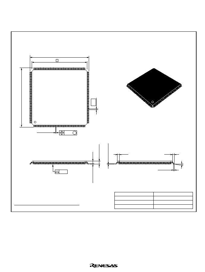
Rev. 5.0, 09/03, page 803 of 806
Appendix D Package Dimensions
Figures D.1, D.2, and D.3 show the SH7729R package dimensions.
Package Code
JEDEC
JEITA
Mass (reference value)
FP-208C
Conforms
2.7 g
*Dimension including the plating thickness
Base material dimension
30.0
± 0.2
30.0
±
0.2
0.5
1.70 Max
0
∞ - 8∞
* 0.17
±
0.05
156
105
104
52
1
157
208
53
*0.22 ± 0.05
0.08 M
0.08
1.40
0.5
± 0.1
1.0
28
0.10
±
0.05
1.25
0.20
± 0.04
0.15
±
0.04
Unit: mm
Figure D.1 Package Dimensions (FP-208C)

Rev. 5.0, 09/03, page 804 of 806
Package Code
JEDEC
JEITA
Mass (reference value)
FP-208E
Conforms
5.3 g
*Dimension including the plating thickness
Base material dimension
30.6
± 0.2
30.6
±
0.2
0.5
3.56 Max
0
∞ - 8∞
* 0.17
±
0.05
156
105
104
52
1
157
208
53
*0.22 ± 0.05
0.10 M
0.10
3.20
0.5
± 0.1
1.3
28
0.15
+
0.10 -0.15
1.25
0.20
± 0.04
0.15
±
0.04
Unit: mm
Figure D.2 Package Dimensions (FP-208E)
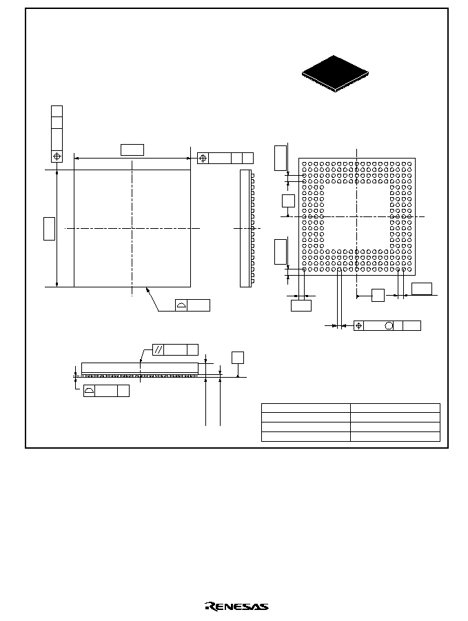
Rev. 5.0, 09/03, page 805 of 806
0.65
0.65
13.00
13.00
0.15
4
◊
0.2
C
C
0.10 C
0.65
0.33
±
0.05
1.40Max
B
A
D
C
F
E
H
G
K
J
M
L
P
N
T
R
V
U
W
1
2
3
4
5
6
7
8
9
10
11
12
13
14
15
16
17
18
19
0.20 C A
0.20
C
B
B
C
0.08
A B
240
◊ 0.40 ± 0.05
M
0.65
A
Unit: mm
Package Code
JEDEC
JEITA
Mass (reference value)
BP-240A
0.4 g
Figure D.3 Package Dimensions (BP-240A)

Rev. 5.0, 09/03, page 806 of 806

SH7729R Group Hardware Manual
Publication Date: 1st Edition, August 2001
Rev.5.00, September 19, 2003
Published by:
Sales Strategic Planning Div.
Renesas Technology Corp.
Edited by:
Technical Documentation & Information Department
Renesas Kodaira Semiconductor Co., Ltd.
©2001, 2003 Renesas Technology Corp. All rights reserved. Printed in Japan.

Colophon 1.0
Sales Strategic Planning Div. Nippon Bldg., 2-6-2, Ohte-machi, Chiyoda-ku, Tokyo 100-0004, Japan
http://www.renesas.com
Renesas Technology America, Inc.
450 Holger Way, San Jose, CA 95134-1368, U.S.A
Tel: <1> (408) 382-7500 Fax: <1> (408) 382-7501
Renesas Technology Europe Limited.
Dukes Meadow, Millboard Road, Bourne End, Buckinghamshire, SL8 5FH, United Kingdom
Tel: <44> (1628) 585 100, Fax: <44> (1628) 585 900
Renesas Technology Europe GmbH
Dornacher Str. 3, D-85622 Feldkirchen, Germany
Tel: <49> (89) 380 70 0, Fax: <49> (89) 929 30 11
Renesas Technology Hong Kong Ltd.
7/F., North Tower, World Finance Centre, Harbour City, Canton Road, Hong Kong
Tel: <852> 2265-6688, Fax: <852> 2375-6836
Renesas Technology Taiwan Co., Ltd.
FL 10, #99, Fu-Hsing N. Rd., Taipei, Taiwan
Tel: <886> (2) 2715-2888, Fax: <886> (2) 2713-2999
Renesas Technology (Shanghai) Co., Ltd.
26/F., Ruijin Building, No.205 Maoming Road (S), Shanghai 200020, China
Tel: <86> (21) 6472-1001, Fax: <86> (21) 6415-2952
Renesas Technology Singapore Pte. Ltd.
1, Harbour Front Avenue, #06-10, Keppel Bay Tower, Singapore 098632
Tel: <65> 6213-0200, Fax: <65> 6278-8001
RENESAS SALES OFFICES

SH7729R Group
Hardware Manual
REJ09B0091-0500O
