Document Outline
- Cover
- Cautions
- Contents
- Section 1 Overview
- 1.1 Overview
- 1.2 Internal Block Diagram
- 1.3 Pin Arrangement and Functions
- 1.3.1 Pin Arrangement
- 1.3.2 Pin Functions
- Section 2 CPU
- 2.1 Overview
- 2.1.1 Features
- 2.1.2 Differences between H8S/2600 CPU and H8S/2000 CPU
- 2.1.3 Differences from H8/300 CPU
- 2.1.4 Differences from H8/300H CPU
- 2.2 CPU Operating Modes
- 2.3 Address Space
- 2.4 Register Configuration
- 2.4.1 Overview
- 2.4.2 General Registers
- 2.4.3 Control Registers
- 2.4.4 Initial Register Values
- 2.5 Data Formats
- 2.5.1 General Register Data Formats
- 2.5.2 Memory Data Formats
- 2.6 Instruction Set
- 2.6.1 Overview
- 2.6.2 Instructions and Addressing Modes
- 2.6.3 Table of Instructions Classified by Function
- 2.6.4 Basic Instruction Formats
- 2.6.5 Notes on Use of Bit-Manipulation Instructions
- 2.7 Addressing Modes and Effective Address Calculation
- 2.7.1 Addressing Mode
- 2.7.2 Effective Address Calculation
- 2.8 Processing States
- 2.8.1 Overview
- 2.8.2 Reset State
- 2.8.3 Exception-Handling State
- 2.8.4 Program Execution State
- 2.8.5 Power-Down State
- 2.9 Basic Timing
- 2.9.1 Overview
- 2.9.2 On-Chip Memory (ROM, RAM)
- 2.9.3 On-Chip Supporting Module Access Timing
- Section 3 MCU Operating Modes
- 3.1 Overview
- 3.1.1 Operating Mode Selection
- 3.1.2 Register Configuration
- 3.2 Register Descriptions
- 3.2.1 Mode Control Register (MDCR)
- 3.2.2 System Control Register (SYSCR)
- 3.3 Operating Mode (Mode 1)
- 3.4 Address Map in Each Operating Mode
- Section 4 Power-Down State
- 4.1 Overview
- 4.1.1 Register Configuration
- 4.2 Register Descriptions
- 4.2.1 Standby Control Register (SBYCR)
- 4.2.2 Low-Power Control Register (LPWRCR)
- 4.2.3 Timer Register A (TMA)
- 4.2.4 Module Stop Control Register (MSTPCR)
- 4.3 Medium-Speed Mode
- 4.4 Sleep Mode
- 4.4.1 Sleep Mode
- 4.4.2 Clearing Sleep Mode
- 4.5 Module Stop Mode
- 4.6 Standby Mode
- 4.6.1 Standby Mode
- 4.6.2 Clearing Standby Mode
- 4.6.3 Setting Oscillation Settling Time after Clearing Standby Mode
- 4.7 Watch Mode
- 4.7.1 Watch Mode
- 4.7.2 Clearing Watch Mode
- 4.8 Subsleep Mode
- 4.8.1 Subsleep Mode
- 4.8.2 Clearing Subsleep Mode
- 4.9 Subactive Mode
- 4.9.1 Subactive Mode
- 4.9.2 Clearing Subactive Mode
- 4.10 Direct Transition
- 4.10.1 Overview of Direct Transition
- Section 5 Exception Handling
- 5.1 Overview
- 5.1.1 Exception Handling Types and Priority
- 5.1.2 Exception Handling Operation
- 5.1.3 Exception Sources and Vector Table
- 5.2 Reset
- 5.2.1 Overview
- 5.2.2 Reset Sequence
- 5.2.3 Interrupts after Reset
- 5.3 Interrupts
- 5.4 Trap Instruction
- 5.5 Stack Status after Exception Handling
- 5.6 Notes on Use of the Stack
- Section 6 Interrupt Controller
- 6.1 Overview
- 6.1.1 Features
- 6.1.2 Block Diagram
- 6.1.3 Pin Configuration
- 6.1.4 Register Configuration
- 6.2 Register Descriptions
- 6.2.1 System Control Register (SYSCR)
- 6.2.2 Interrupt Control Registers A to D (ICRA to ICRD)
- 6.2.3 IRQ Enable Register (IENR)
- 6.2.4 IRQ Edge Select Registers (IEGR)
- 6.2.5 IRQ Status Register (IRQR)
- 6.2.6 Port Mode Register (PMR1)
- 6.3 Interrupt Sources
- 6.3.1 External Interrupts
- 6.3.2 Internal Interrupts
- 6.3.3 Interrupt Exception Vector Table
- 6.4 Interrupt Operation
- 6.4.1 Interrupt Control Modes and Interrupt Operation
- 6.4.2 Interrupt Control Mode 0
- 6.4.3 Interrupt Control Mode 1
- 6.4.4 Interrupt Exception Handling Sequence
- 6.4.5 Interrupt Response Times
- 6.5 Usage Notes
- 6.5.1 Contention between Interrupt Generation and Disabling
- 6.5.2 Instructions that Disable Interrupts
- 6.5.3 Interrupts during Execution of EEPMOV Instruction
- Section 7 ROM
- 7.1 Overview
- 7.2 Overview of Flash Memory
- 7.2.1 Features
- 7.2.2 Block Diagram
- 7.2.3 Flash Memory Operating Modes
- 7.2.4 Pin Configuration
- 7.2.5 Register Configuration
- 7.3 Flash Memory Register Descriptions
- 7.3.1 Flash Memory Control Register 1 (FLMCR1)
- 7.3.2 Flash Memory Control Register 2 (FLMCR2)
- 7.3.3 Erase Block Register 1 (EBR1)
- 7.3.4 Erase Block Register 2 (EBR2)
- 7.3.5 Serial/Timer Control Register (STCR)
- 7.4 On-Board Programming Modes
- 7.4.1 Boot Mode
- 7.4.2 User Program Mode
- 7.5 Programming/Erasing Flash Memory
- 7.5.1 Program Mode (n=1 when the target address range is H'00000 to H'3FFFF and n=2 when the target address range is H'40000 to
- 7.5.2 Program-Verify Mode
- 7.5.3 Erase Mode (n = 1 when the target address range is H'00000 to H'3FFFF and n = 2 when the target address range is H'40000 t
- 7.5.4 Erase-Verify Mode (n = 1 when the target address range is H'00000 to H'3FFFF and n = 2 when the target address range is H'
- 7.6 Flash Memory Protection
- 7.6.1 Hardware Protection
- 7.6.2 Software Protection
- 7.6.3 Error Protection
- 7.7 Interrupt Handling when Programming/Erasing Flash Memory
- 7.8 Flash Memory Writer Mode
- 7.8.1 Writer Mode Setting
- 7.8.2 Socket Adapters and Memory Map
- 7.8.3 Writer Mode Operation
- 7.8.4 Memory Read Mode
- 7.8.5 Auto-Program Mode
- 7.8.6 Auto-Erase Mode
- 7.8.7 Status Read Mode
- 7.8.8 Status Polling
- 7.8.9 Writer Mode Transition Time
- 7.8.10 Notes on Memory Programming
- 7.9 Notes when Converting the FÖZTAT Application Software to the Mask-ROM Versions
- Section 8 RAM
- Section 9 Clock Pulse Generator
- 9.1 Overview
- 9.1.1 Block Diagram
- 9.1.2 Register Configuration
- 9.2 Register Descriptions
- 9.2.1 Standby Control Register (SBYCR)
- 9.2.2 Low-Power Control Register (LPWRCR)
- 9.3 Oscillator
- 9.3.1 Connecting a Crystal Resonator
- 9.3.2 External Clock Input
- 9.4 Duty Adjustment Circuit
- 9.5 Medium-Speed Clock Divider
- 9.6 Bus Master Clock Selection Circuit
- 9.7 Subclock Oscillator Circuit
- 9.7.1 Connecting 32.768 kHz Crystal Resonator
- 9.7.2 When Subclock is not Needed
- 9.8 Subclock Waveform Shaping Circuit
- 9.9 Notes on the Resonator
- Section 10 I/O Port
- 10.1 Overview
- 10.1.1 Port Functions
- 10.1.2 Port Input
- 10.1.3 MOS Pull-Up Transistors
- 10.2 Port 0
- 10.2.1 Overview
- 10.2.2 Register Configuration
- (1) Port Mode Register 0 (PMR0)
- (2) Port Data Register 0 (PDR0)
- 10.2.3 Pin Functions
- 10.2.4 Pin States
- 10.3 Port 1
- 10.3.1 Overview
- 10.3.2 Register Configuration
- Port Mode Register 1 (PMR1)
- Port Control Register 1 (PCR1)
- Port Data Register 1 (PDR1)
- MOS Pull-Up Select Register 1 (PUR1)
- 10.3.3 Pin Functions
- 10.3.4 Pin States
- 10.4 Port 2
- 10.4.1 Overview
- 10.4.2 Register Configuration
- Port Control Register 2 (PCR2)
- Port Data Register 2 (PDR2)
- MOS Pull-Up Select Register 2 (PUR2)
- 10.4.3 Pin Functions
- 10.4.4 Pin States
- 10.5 Port 3
- 10.5.1 Overview
- 10.5.2 Register Configuration
- Port Mode Register 3 (PMR3)
- Port Control Register 3 (PCR3)
- Port Data Register 3 (PDR3)
- MOS Pull-Up Select Register 3 (PUR3)
- 10.5.3 Pin Functions
- 10.5.4 Pin States
- 10.6 Port 4
- 10.6.1 Overview
- 10.6.2 Register Configuration
- Port Mode Register 4 (PMR4)
- Port Control Register 4 (PCR4)
- Port Data Register 4 (PDR4)
- 10.6.3 Pin Functions
- 10.6.4 Pin States
- 10.7 Port 6
- 10.7.1 Overview
- 10.7.2 Register Configuration
- Port Mode Register 6 (PMR6)
- Port Mode Register A (PMRA)
- Port Control Register 6 (PCR6)
- Port Data Register 6 (PDR6)
- Realtime Output Trigger Select Register (RTPSR1)
- Real Time Output Trigger Edge Select Register (RTPEGR)
- 10.7.3 Pin Functions
- 10.7.4 Operation
- 10.7.5 Pin States
- 10.8 Port 7
- 10.8.1 Overview
- 10.8.2 Register Configuration
- Port Mode Register 7 (PMR7)
- Port Mode Register B (PMRB)
- Port Control Register 7 (PCR7)
- Port Data Register 7 (PDR7)
- Realtime Output Trigger Select Register 2 (RTPSR2)
- Realtime Output Trigger Edge Selection Register (RTPEGR)
- 10.8.3 Pin Functions
- 10.8.4 Operation
- 10.8.5 Pin States
- 10.9 Port 8
- 10.9.1 Overview
- 10.9.2 Register Configuration
- Port Mode Register 8 (PMR8)
- Port Mode Register C (PMRC)
- Port Control Register 8 (PCR8)
- Port Data Register 8 (PDR8)
- 10.9.3 Pin Functions
- 10.9.4 Pin States
- Section 11 Timer A
- 11.1 Overview
- 11.1.1 Features
- 11.1.2 Block Diagram
- 11.1.3 Register Configuration
- 11.2 Register Descriptions
- 11.2.1 Timer Mode Register A (TMA)
- 11.2.2 Timer Counter A (TCA)
- 11.2.3 Module Stop Control Register (MSTPCR)
- 11.3 Operation
- 11.3.1 Operation as the Interval Timer
- 11.3.2 Operation as Clock Timer
- 11.3.3 Initializing the Counts
- Section 12 Timer B
- 12.1 Overview
- 12.1.1 Features
- 12.1.2 Block Diagram
- 12.1.3 Pin Configuration
- 12.1.4 Register Configuration
- 12.2 Register Descriptions
- 12.2.1 Timer Mode Register B (TMB)
- 12.2.2 Timer Counter B (TCB)
- 12.2.3 Timer Load Register B (TLB)
- 12.2.4 Port Mode Register A (PMRA)
- 12.2.5 Module Stop Control Register (MSTPCR)
- 12.3 Operation
- 12.3.1 Operation as the Interval Timer
- 12.3.2 Operation as the Auto Reload Timer
- 12.3.3 Event Counter
- Section 13 Timer J
- 13.1 Overview
- 13.1.1 Features
- 13.1.2 Block Diagram
- 13.1.3 Pin Configuration
- 13.1.4 Register Configuration
- 13.2 Register Descriptions
- 13.2.1 Timer Mode Register J (TMJ)
- 13.2.2 Timer J Control Register (TMJC)
- 13.2.3 Timer J Status Register (TMJS)
- 13.2.4 Timer Counter J (TCJ)
- 13.2.5 Timer Counter K (TCK)
- 13.2.6 Timer Load Register J (TLJ)
- 13.2.7 Timer Load Register K (TLK)
- 13.2.8 Module Stop Control Register (MSTPCR)
- 13.3 Operation
- 13.3.1 8-bit Reload Timer (TMJ-1)
- 13.3.2 8-bit Reload Timer (TMJ-2)
- 13.3.3 Remote Controlled Data Transmission
- 13.3.4 TMJ-2 Expansion Function
- Section 14 Timer L
- 14.1 Overview
- 14.1.1 Features
- 14.1.2 Block Diagram
- 14.1.3 Register Configuration
- 14.2 Register Descriptions
- 14.2.1 Timer L Mode Register (LMR)
- 14.2.2 Linear Time Counter (LTC)
- 14.2.3 Reload/Compare Match Register (RCR)
- 14.2.4 Module Stop Control Register (MSTPCR)
- 14.3 Operation
- 14.3.1 Compare Match Clear Operation
- Section 15 Timer R
- 15.1 Overview
- 15.1.1 Features
- 15.1.2 Block Diagram
- 15.1.3 Pin Configuration
- 15.1.4 Register Configuration
- 15.2 Register Descriptions
- 15.2.1 Timer R Mode Register 1 (TMRM1)
- 15.2.2 Timer R Mode Register 2 (TMRM2)
- 15.2.3 Timer R Control/Status Register (TMRCS)
- 15.2.4 Timer R Capture Register 1 (TMRCP1)
- 15.2.5 Timer R Capture Register 2 (TMRCP2)
- 15.2.6 Timer R Load Register 1 (TMRL1)
- 15.2.7 Timer R Load Register 2 (TMRL2)
- 15.2.8 Timer R Load Register 3 (TMRL3)
- 15.2.9 Module Stop Control Register (MSTPCR)
- 15.3 Operation
- 15.3.1 Reload Timer Counter Equipped with Capturing Function TMRU-1
- 15.3.2 Reload Timer Counter Equipped with Capturing Function TMRU-2
- 15.3.3 Reload Counter Timer TMRU-3
- 15.3.4 Mode Identification
- 15.3.5 Reeling Controls
- 15.3.6 Acceleration and Braking Processes of the Capstan Motor
- 15.3.7 Slow Tracking Mono-Multi Function
- 15.4 Interrupt Cause
- 15.5 Settings for Respective Functions
- 15.5.1 Mode Identification
- 15.5.2 Reeling Controls
- 15.5.3 Slow Tracking Mono-Multi Function
- 15.5.4 Acceleration and Braking Processes of the Capstan Motor
- Section 16 Timer X1
- 16.1 Overview
- 16.1.1 Features
- 16.1.2 Block Diagram
- 16.1.3 Pin Configuration
- 16.1.4 Register Configuration
- 16.2 Register Descriptions
- 16.2.1 Free Running Counter (FRC)
- 16.2.2 Output Comparing Registers A and B (OCRA and OCRB)
- 16.2.3 Input Capture Registers A Through D (ICRA Through ICRD)
- 16.2.4 Timer Interrupt Enabling Register (TIER)
- 16.2.5 Timer Control/Status Register X (TCSRX)
- 16.2.6 Timer Control Register X (TCRX)
- 16.2.7 Timer Output Comparing Control Register (TOCR)
- 16.2.8 Module Stop Control Register (MSTPCR)
- 16.3 Operation
- 16.3.1 Operation of Timer X1
- 16.3.2 Counting Timing of the FRC
- 16.3.3 Output Comparing Signal Outputting Timing
- 16.3.4 FRC Clearing Timing
- 16.3.5 Input Capture Signal Inputting Timing
- 16.3.6 Input Capture Flag (ICFA through ICFD) Setting Up Timing
- 16.3.7 Output Comparing Flag (OCFA and OCFB) Setting Up Timing
- 16.3.8 Overflow Flag (CVF) Setting Up Timing
- 16.4 Operation Mode of Timer X1
- 16.5 Interrupt Causes
- 16.6 Exemplary Uses of Timer X1
- 16.7 Precautions when Using Timer X1
- 16.7.1 Competition between Writing and Clearing with the FRC
- 16.7.2 Competition between Writing and Counting Up with the FRC
- 16.7.3 Competition between Writing and Comparing Match with the OCR
- 16.7.4 Changing Over the Internal Clocks and Counter Operations
- Section 17 Watchdog Timer (WDT)
- 17.1 Overview
- 17.1.1 Features
- 17.1.2 Block Diagram
- 17.1.3 Register Configuration
- 17.2 Register Descriptions
- 17.2.1 Watchdog Timer Counter (WTCNT)
- 17.2.2 Watchdog Timer Control/Status Register (WTCSR)
- 17.2.3 System Control Register (SYSCR)
- 17.2.4 Notes on Register Access
- 17.3 Operation
- 17.3.1 Watchdog Timer Operation
- 17.3.2 Interval Timer Operation
- 17.3.3 Timing of Setting of Overflow Flag (OVF)
- 17.4 Interrupts
- 17.5 Usage Notes
- 17.5.1 Contention between Watchdog Timer Counter (WTCNT) Write and Increment
- 17.5.2 Changing Value of CKS2 to CKS0
- 17.5.3 Switching between Watchdog Timer Mode and Interval Timer Mode
- Section 18 8-Bit PWM
- 18.1 Overview
- 18.1.1 Features
- 18.1.2 Block Diagram
- 18.1.3 Pin Configuration
- 18.1.4 Register Configuration
- 18.2 Register Descriptions
- 18.2.1 8-bit PWM Data Registers 0, 1, 2 and 3 (PWR0, PWR1, PWR2, PWR3)
- 18.2.2 8-bit PWM Control Register (PW8CR)
- 18.2.3 Port Mode Register 3 (PMR3)
- 18.2.4 Module Stop Control Register (MSTPCR)
- 18.3 8-Bit PWM Operation
- Section 19 12-Bit PWM
- 19.1 Overview
- 19.1.1 Features
- 19.1.2 Block Diagram
- 19.1.3 Pin Configuration
- 19.1.4 Register Configuration
- 19.2 Register Descriptions
- 19.2.1 12-Bit PWM Control Registers (CPWCR, DPWCR)
- 19.2.2 12-Bit PWM Data Registers (DPWDR, CPWDR)
- 19.3 Operation
- Section 20 14-Bit PWM
- 20.1 Overview
- 20.1.1 Features
- 20.1.2 Block Diagram
- 20.1.3 Pin Configuration
- 20.1.4 Register Configuration
- 20.2 Register Descriptions
- 20.2.1 PWM Control Register (PWCR)
- 20.2.2 PWM Data Registers U and L (PWDRU, PWDRL)
- 20.2.3 Module Stop Control Register (MSTPCR)
- 20.3 14-Bit PWM Operation
- Section 21 Prescalar Unit
- 21.1 Overview
- 21.1.1 Features
- 21.1.2 Block Diagram
- 21.1.3 Pin Configuration
- 21.1.4 Register Configuration
- 21.2 Registers
- 21.2.1 Input Capture Register 1 (ICR1)
- 21.2.2 Prescalar Unit Control/Status Register (PCSR)
- 21.2.3 Port Mode Register 1 (PMR1)
- 21.3 Noise Cancel Circuit
- 21.4 Operation
- 21.4.1 Prescalar S (PSS)
- 21.4.2 Prescalar W (PSW)
- 21.4.3 Stable Oscillation Wait Time Count
- 21.4.4 8-bit PWM
- 21.4.5 8-bit Input Capture Using ,& ,& ,& ,& Pin
- 21.4.6 Frequency Division Clock Output
- Section 22 Serial Communication Interface 1 (SCI1)
- 22.1 Overview
- 22.1.1 Features
- 22.1.2 Block Diagram
- 22.1.3 Pin Configuration
- 22.1.4 Register Configuration
- 22.2 Register Descriptions
- 22.2.1 Receive Shift Register 1 (RSR1)
- 22.2.2 Receive Data Register 1 (RDR1)
- 22.2.3 Transmit Shift Register 1 (TSR1)
- 22.2.4 Transmit Data Register 1 (TDR1)
- 22.2.5 Serial Mode Register 1 (SMR1)
- 22.2.6 Serial Control Register 1 (SCR1)
- 22.2.7 Serial Status Register 1 (SSR1)
- 22.2.8 Bit Rate Register 1 (BRR1)
- 22.2.9 Serial Interface Mode Register 1 (SCMR1)
- 22.2.10 Module Stop Control Register (MSTPCR)
- 22.3 Operation
- 22.3.1 Overview
- 22.3.2 Operation in Asynchronous Mode
- 22.3.3 Multiprocessor Communication Function
- 22.3.4 Operation in Synchronous Mode
- 22.4 SCI Interrupts
- 22.5 Usage Notes
- Section 23
- 23.1 Overview
- 23.1.1 Features
- 23.1.2 Block Diagram
- 23.1.3 Pin Configuration
- 23.1.4 Register Configuration
- 23.2 Register Descriptions
- 23.2.1 I2C Bus Data Register (ICDR)
- 23.2.2 Slave Address Register (SAR)
- 23.2.3 Second Slave Address Register (SARX)
- 23.2.4 I2C Bus Mode Register (ICMR)
- 23.2.5 I2C Bus Control Register (ICCR)
- 23.2.6 I2C Bus Status Register (ICSR)
- 23.2.7 Serial/Timer Control Register (STCR)
- 23.2.8 DDC Switch Register (DDCSWR)
- 23.2.9 Module Stop Control Register (MSTPCR)
- 23.3 Operation
- 23.3.1 I2C Bus Data Format
- 23.3.2 Master Transmit Operation
- 23.3.3 Master Receive Operation
- 23.3.4 Slave Receive Operation
- 23.3.5 Slave Transmit Operation
- 23.3.6 IRIC Setting Timing and SCL Control
- 23.3.7 Automatic Switching from Formatless Transfer to I
- 23.3.8 Noise Canceler
- 23.3.9 Sample Flowcharts
- 23.3.10 Initializing Internal Status
- 23.4 Usage Notes
- Section 24 A/D Converter
- 24.1 Overview
- 24.1.1 Features
- 24.1.2 Block Diagram
- 24.1.3 Pin Configuration
- 24.1.4 Register Configuration
- 24.2 Register Descriptions
- 24.2.1 Software-Triggered A/D Result Register (ADR)
- 24.2.2 Hardware-Triggered A/D Result Register (AHR)
- 24.2.3 A/D Control Register (ADCR)
- 24.2.4 A/D Control/Status Register (ADCSR)
- 24.2.5 Trigger Select Register (ADTSR)
- 24.2.6 Port Mode Register 0 (PMR0)
- 24.2.7 Module Stop Control Register (MSTPCR)
- 24.3 Interface to Bus Master
- 24.4 Operation
- 24.4.1 Software-Triggered A/D Conversion
- 24.4.2 Hardware- or External-Triggered A/D Conversion
- 24.5 Interrupt Sources
- Section 25 Address Trap Controller (ATC)
- 25.1 Overview
- 25.1.1 Features
- 25.1.2 Block Diagram
- 25.1.3 Register Configuration
- 25.2 Register Descriptions
- 25.2.1 Address Trap Control Register (ATCR)
- 25.2.2 Trap Address Register 2 to 0 (TAR2 to TAR0)
- 25.3 Precautions in Usage
- 25.3.1 Basic Operations
- 25.3.2 Enabling
- 25.3.3 Bcc Instruction
- 25.3.4 BSR Instruction
- 25.3.5 JSR Instruction
- 25.3.6 JMP Instruction
- 25.3.7 RTS Instruction
- 25.3.8 SLEEP Instruction
- 25.3.9 Competing Interrupt
- Section 26 Servo Circuits
- 26.1 Overview
- 26.1.1 Functions
- 26.1.2 Block Diagram
- 26.2 Servo Port
- 26.2.1 Overview
- 26.2.2 Block Diagram
- 26.2.3 Pin Configuration
- 26.2.4 Register Configuration
- 26.2.5 Register Description
- Servo Port Mode Register (SPMR)
- Servo Monitor Control Register (SVMCR)
- CTL Gain Control Register (CTLGR)
- 26.2.6 DFG/DPG Input Signals
- 26.3 Reference Signal Generators
- 26.3.1 Overview
- 26.3.2 Block Diagram
- 26.3.3 Register Configuration
- 26.3.4 Register Description
- Reference Period Mode Register (RFM)
- Reference Period Register 1 (RFD)
- Reference Period Register 2 (CRF)
- REF30 Counter Register (RFC)
- Reference Period Mode Register 2 (RFM2)
- 26.3.5 Operation
- 26.4 HSW (Head-switch) Timing Generator
- 26.4.1 Overview
- 26.4.2 Block Diagram
- 26.4.3 HSW Timing Generator Configuration
- 26.4.4 Register Configuration
- 26.4.5 Register Description
- HSW Mode Register 1 (HSM1)
- HSW Mode Register 2 (HSM2)
- FIFO Output Pattern Register 1 (FPDRA)
- FIFO Output Pattern Register 2 (FPDRB)
- FIFO Timing Pattern Register 1 (FTPRA)
- FIFO Timing Pattern Register 2 (FTPRB)
- DFG Reference Register 1 (DFCRA)
- DFG Reference Register 2 (DFCRB)
- FIFO Timer Capture Register (FTCTR)
- DFG Reference Count Register (DFCTR)
- 26.4.6 Operation
- 26.4.7 Interrupts
- 26.4.8 Cautions
- 26.5 High-Speed Switching Circuit for Four-Head Special Playback
- 26.5.1 Overview
- 26.5.2 Block Diagram
- 26.5.3 Pin Configuration
- 26.5.4 Register Description
- Special Playback Control Register (CHCR)
- 26.6 Drum Speed Error Detector
- 26.6.1 Overview
- 26.6.2 Block Diagram
- 26.6.3 Register Configuration
- 26.6.4 Register Description
- DFG Speed Error Data Register (DFER)
- DFG Lock Upper Data Register (DFRUDR)
- DFG Lock LOWER Data Register (DFRLDR)
- Drum Speed Error Detection Control Register (DFVCR)
- 26.6.5 Operation
- 26.6.6 f H Correction in Trick Play Mode
- 26.7 Drum Phase Error Detector
- 26.7.1 Overview
- 26.7.2 Block Diagram
- 26.7.3 Register Configuration
- 26.7.4 Register Description
- Drum Phase Preset Data Registers (DPPR1, DPPR2)
- Drum Phase Error Data Registers (DPER1, DPER2)
- Drum Phase Error Detection Control Register (DPGCR)
- 26.7.5 Operation
- 26.7.6 Phase Comparison
- 26.8 Capstan Speed Error Detector
- 26.8.1 Overview
- 26.8.2 Block Diagram
- 26.8.3 Register Configuration
- 26.8.4 Register Description
- Specified CFG Speed Preset Data Register (CFPR)
- CFG Speed Error Data Register (CFER)
- CFG Lock UPPER Data Register (CFRUDR)
- CFG Lock LOWER Data Register (CFRLDR)
- Capstan Speed Error Detection Control Register (CFVCR)
- 26.8.5 Operation
- 26.9 Capstan Phase Error Detector
- 26.9.1 Overview
- 26.9.2 Block Diagram
- 26.9.3 Register Configuration
- 26.9.4 Register Description
- Specified Capstan Phase Preset Data Registers (CPPR1, CPPR2)
- Capstan Phase Error Data Registers (CPER1, CPER2)
- Capstan Phase Error Detection Control Register (CPGCR)
- 26.9.5 Operation
- 26.10 X-Value and Tracking Adjustment Circuit
- 26.10.1 Overview
- 26.10.2 Block Diagram
- 26.10.3 Register Description
- X-Value and TRK-Value Control Register (XTCR)
- X-Value Data Register (XDR)
- TRK-Value Data Register (TRDR)
- 26.11 Digital Filters
- 26.11.1 Overview
- 26.11.2 Block Diagram
- 26.11.3 Arithmetic Buffer
- 26.11.4 Register Configuration
- 26.11.5 Register Description
- Gain Constants (DGKp, DGKs, CGKp, CGKs)
- Coefficients (DAp, DBp, DAs, DBs, CAp, CBp, CAs, CBs)
- Offset (DOfp, DOfs, COfp, COfs)
- Delay Initialization Register (CZp, CZs, DZp, DZs)
- Drum System Digital Filter Control Register (DFIC)
- Capstan System Digital Filter Control Register (CFIC)
- Digital Filter Control Register (DFUCR)
- 26.11.6 Filter Characteristics
- 26.11.7 Operations in Case of Transient Response
- 26.11.8 Initialization of Z
- 26.12 Additional V Signal Generator
- 26.12.1 Overview
- 26.12.2 Pin Configuration
- 26.12.3 Register Configuration
- 26.12.4 Register Description
- 26.12.5 Additional V Pulse Signal
- 26.13 CTL Circuit
- 26.13.1 Overview
- 26.13.2 Block Diagram
- 26.13.3 Pin Configuration
- 26.13.4 Register Configuration
- 26.13.5 Register Description
- CTL Control Register (CTCR)
- CTL Mode Register (CTLM)
- REC-CTL Duty Data Register 1 (RCDR1)
- REC-CTL Duty Data Register 2 (RCDR2)
- REC-CTL Duty Data Register 3 (RCDR3)
- REC-CTL Duty Data Register 4 (RCDR4)
- REC-CTL Duty Data Register 5 (RCDR5)
- Duty I/O Register (DI/O)
- Bit Pattern Register (BTPR)
- 26.13.6 Operation
- 26.13.7 CTL Input Section
- 26.13.8 Duty Discriminator
- 26.13.9 CTL Output Section
- 26.13.10 Trapezoid Waveform Circuit
- 26.13.11 Note on CTL Interrupt
- 26.14 Frequency Dividers
- 26.14.1 Overview
- 26.14.2 CTL Frequency Divider
- Register Description
- DVCTL Control Register (CTVC)
- CTL Frequency Division Register (CTLR)
- 26.14.3 CFG Frequency Divider
- Register Description:
- DVCFG Control Register (CDVC)
- CFG Frequency Division Register 2 (CDIVR2)
- DVCFG Mask Period Register (CTMR)
- 26.14.4 DFG Noise Removal Circuit
- Register Description:
- FG Control Register (FGCR)
- 26.15 Sync Signal Detector
- 26.15.1 Overview
- 26.15.2 Block Diagram
- 26.15.3 Pin Configuration
- 26.15.4 Register Configuration
- 26.15.5 Register Description
- Vertical Sync Signal Threshold Register (VTR)
- Horizontal Sync Signal Threshold Register (HTR)
- H Complement Start Time Setting Register (HRTR)
- Complementary H Pulse Width Setting Register (HPWR)
- Noise Detection Window Setting Register (NWR)
- Noise Detection Register (NDR)
- Sync Signal Control Register (SYNCR)
- 26.15.6 Noise Detection
- 26.15.7 Activation of the Sync Signal Detector
- 26.16 Servo Interrupt
- 26.16.1 Overview
- 26.16.2 Register Configuration
- 26.16.3 Register Description
- Servo Interrupt Enable Register 1 (SIENR1)
- Servo Interrupt Enable Register 2 (SIENR2)
- Servo Interrupt Request Register 1 (SIRQR1)
- Servo Interrupt Request Register 2 (SIRQR2)
- Section 27 Sync Separator for OSD and Data Slicer
- 27.1 Overview
- 27.1.1 Features
- 27.1.2 Block Diagram
- 27.1.3 Pin Configuration
- 27.1.4 Register Configuration
- 27.2 Register Description
- 27.2.1 Sync Separation Input Mode Register (SEPIMR)
- 27.2.2 Sync Separation Control Register (SEPCR)
- 27.2.3 Sync Separation AFC Control Register (SEPACR)
- 27.2.4 Horizontal Sync Signal Threshold Register (HVTHR)
- 27.2.5 Vertical Sync Signal Threshold Register (VVTHR)
- 27.2.6 Field Detection Window Register (FWIDR)
- 27.2.7 H Complement and Mask Timing Register (HCMMR)
- 27.2.8 Noise Detection Counter (NDETC)
- 27.2.9 Noise Detection Level Register (NDETR)
- 27.2.10 Data Slicer Detection Window Register (DDETWR)
- 27.2.11 Internal Sync Frequency Register (INFRQR)
- 27.3 Operation
- 27.3.1 Selecting Source Signals for Sync Separation
- 27.3.2 Vsync Separation
- 27.3.3 Hsync Separation
- 27.3.4 Field Detection
- 27.3.5 Noise Detection
- 27.3.6 Automatic Frequency Controller (AFC)
- 27.3.7 Module Stop Control Register (MSTPCR)
- Section 28 Data Slicer
- 28.1 Overview
- 28.1.1 Features
- 28.1.2 Block Diagram
- 28.1.3 Pin Configuration
- 28.1.4 Register Configuration
- 28.1.5 Data Slicer Use Conditions
- 28.2 Register Description
- 28.2.1 Slice Even- (Odd-) Field Mode Register (SEVFD, SODFD)
- 28.2.2 Slice Line Setting Registers 1 to 4 (SLINE1 to SLINE4)
- 28.2.3 Slice Detection Registers 1 to 4 (SDTCT1 to SDTCT4)
- 28.2.4 Slice Data Registers 1 to 4 (SDATA1 to SDATA4)
- 28.2.5 Module Stop Control Register (MSTPCR)
- 28.2.6 Monitor Output Setting Register (DOUT)
- 28.3 Operation
- 28.3.1 Slice Line Specification
- 28.3.2 Slice Sequence
- Section 29 On-Screen Display (OSD)
- 29.1 Overview
- 29.1.1 Features
- 29.1.2 Block Diagram
- 29.1.3 Pin Configuration
- 29.1.4 Register Configuration
- 29.1.5 TV Formats and Display Modes
- 29.2 Description of Display Functions
- 29.2.1 Superimposed Mode and Text Display Mode
- 29.2.2 Character Configuration
- 29.2.3 On-Screen Display Configuration
- 29.3 Settings in Character Units
- 29.3.1 Character Configuration
- 29.3.2 Character Colors
- 29.3.3 Halftones/Cursors
- 29.3.4 Blinking
- 29.3.5 Button Display
- 29.3.6 Character Data ROM (OSDROM)
- 29.3.7 Display Data RAM (OSDRAM)
- 29.4 Settings in Row Units
- 29.4.1 Button Patterns
- 29.4.2 Display Enlargement
- 29.4.3 Character Brightness
- 29.4.4 Cursor Color, Brightness, Halftone Levels
- 29.4.5 Row Registers (CLINEn, n = rows 1 to 12)
- 29.5 Settings in Screen Units
- 29.5.1 Display Positions
- 29.5.2 Turning the OSD Display On and Off
- 29.5.3 Display Method
- 29.5.4 Blinking Period
- 29.5.5 Borders
- 29.5.6 Background Color and Brightness
- 29.5.7 Character, Cursor, and Background Chroma Saturation
- 29.5.8 Display Position Registers (HPOS and VPOS)
- 29.5.9 Screen Control Register (DCNTL)
- 29.6 Other Settings
- 29.6.1 TV Format
- 29.6.2 Display Data RAM Control
- 29.6.3 Timing of OSD Display Updates Using Register Rewriting
- 29.6.4 4fsc/2fsc
- 29.6.5 OSDV Interrupts
- 29.6.6 OSD Format Register (DFORM)
- 29.7 Digital Output
- 29.7.1 R, G, and B Outputs
- 29.7.2 YCO and YBO Outputs
- 29.7.3 Digital Output Specification Register (DOUT)
- 29.7.4 Module Stop Control Register (MTSTPCR)
- 29.8 Notes on OSD Font Creation
- 29.8.1 Note 1 on Font Creation (Font Width)
- 29.8.2 Note 2 on Font Creation (Borders)
- 29.8.3 Note 3 on Font Creation (Blinking)
- 29.8.4 Note 4 on Font Creation (Buttons)
- 29.9 OSD Oscillator, AFC, and Dot Clock
- 29.9.1 Sync Signals
- 29.9.2 AFC Circuit
- 29.9.3 Dot Clock
- 29.9.4 4/2fsc
- 29.10 OSD Operation in CPU Operation Modes
- 29.11 Character Data ROM (OSDROM) Access by CPU
- 29.11.1 Serial Timer Control Register (STCR)
- Section 30 Electrical Characteristics
- 30.1 Absolute Maximum Ratings
- 30.2 Electrical Characteristics of HD6432199, HD6432198, HD6432197,and HD6432196
- 30.2.1 DC Characteristics of HD6432199, HD6432198, HD6432197, and HD6432196
- 30.2.2 Allowable Output Currents of HD6432199, HD6432198, HD6432197, and HD6432196
- 30.2.3 AC Characteristics of HD6432199, HD6432198, HD6432197, and HD6432196
- 30.2.4 Serial Interface Timing of HD6432199, HD6432198, HD6432197, and HD6432196
- 30.2.5 A/D Converter Characteristics of HD6432199, HD6432198, HD6432197, and HD6432196
- 30.2.6 Servo Section Electrical Characteristics of HD6432199, HD6432198, HD6432197,and HD6432196
- 30.2.7 OSD Electrical Characteristics of HD6432199, HD6432198, HD6432197, and HD6432196
- 30.3 Electrical Characteristics of HD64F2199
- 30.3.1 DC Characteristics of HD64F2199
- 30.3.2 Allowable Output Currents of HD64F2199
- 30.3.3 AC Characteristics of HD64F2199
- 30.3.4 Serial Interface Timing of HD64F2199
- 30.3.5 A/D Converter Characteristics of HD64F2199
- 30.3.6 Servo Section Electrical Characteristics of HD64F2199
- 30.3.7 OSD Electrical Characteristics of HD64F2199
- Appendix A Instruction Set
- A.1 Instructions
- Operation Notation
- Condition Code Notation
- A.2 Instruction Codes
- A.3 Operation Code Map
- A.4 Number of Execution States
- A.5 Bus Status during Instruction Execution
- A.6 Change of Condition Codes
- Appendix B Internal I/O Registers
- B.1 Addresses
- B.2 Function List
- Appendix C Pin Circuit Diagrams
- Appendix D Port States in Each Processing State
- Appendix E Usage Notes
- E.1 Power Supply Rise and Fall Order
- E.2 Sample External Circuits
- E.3 Handling of Pins When OSD Is Not Used
- Appendix F Product Lineup
- Appendix G Package Dimensions

Regarding the change of names mentioned in the document, such as Hitachi
Electric and Hitachi XX, to Renesas Technology Corp.
The semiconductor operations of Mitsubishi Electric and Hitachi were transferred to Renesas
Technology Corporation on April 1st 2003. These operations include microcomputer, logic, analog
and discrete devices, and memory chips other than DRAMs (flash memory, SRAMs etc.)
Accordingly, although Hitachi, Hitachi, Ltd., Hitachi Semiconductors, and other Hitachi brand
names are mentioned in the document, these names have in fact all been changed to Renesas
Technology Corp. Thank you for your understanding. Except for our corporate trademark, logo and
corporate statement, no changes whatsoever have been made to the contents of the document, and
these changes do not constitute any alteration to the contents of the document itself.
Renesas Technology Home Page: http://www.renesas.com
Renesas Technology Corp.
Customer Support Dept.
April 1, 2003
To all our customers

Cautions
Keep safety first in your circuit designs!
1. Renesas Technology Corporation puts the maximum effort into making semiconductor products better
and more reliable, but there is always the possibility that trouble may occur with them. Trouble with
semiconductors may lead to personal injury, fire or property damage.
Remember to give due consideration to safety when making your circuit designs, with appropriate
measures such as (i) placement of substitutive, auxiliary circuits, (ii) use of nonflammable material or
(iii) prevention against any malfunction or mishap.
Notes regarding these materials
1. These materials are intended as a reference to assist our customers in the selection of the Renesas
Technology Corporation product best suited to the customer's application; they do not convey any
license under any intellectual property rights, or any other rights, belonging to Renesas Technology
Corporation or a third party.
2. Renesas Technology Corporation assumes no responsibility for any damage, or infringement of any
third-party's rights, originating in the use of any product data, diagrams, charts, programs, algorithms, or
circuit application examples contained in these materials.
3. All information contained in these materials, including product data, diagrams, charts, programs and
algorithms represents information on products at the time of publication of these materials, and are
subject to change by Renesas Technology Corporation without notice due to product improvements or
other reasons. It is therefore recommended that customers contact Renesas Technology Corporation
or an authorized Renesas Technology Corporation product distributor for the latest product information
before purchasing a product listed herein.
The information described here may contain technical inaccuracies or typographical errors.
Renesas Technology Corporation assumes no responsibility for any damage, liability, or other loss
rising from these inaccuracies or errors.
Please also pay attention to information published by Renesas Technology Corporation by various
means, including the Renesas Technology Corporation Semiconductor home page
(http://www.renesas.com).
4. When using any or all of the information contained in these materials, including product data, diagrams,
charts, programs, and algorithms, please be sure to evaluate all information as a total system before
making a final decision on the applicability of the information and products. Renesas Technology
Corporation assumes no responsibility for any damage, liability or other loss resulting from the
information contained herein.
5. Renesas Technology Corporation semiconductors are not designed or manufactured for use in a device
or system that is used under circumstances in which human life is potentially at stake. Please contact
Renesas Technology Corporation or an authorized Renesas Technology Corporation product distributor
when considering the use of a product contained herein for any specific purposes, such as apparatus or
systems for transportation, vehicular, medical, aerospace, nuclear, or undersea repeater use.
6. The prior written approval of Renesas Technology Corporation is necessary to reprint or reproduce in
whole or in part these materials.
7. If these products or technologies are subject to the Japanese export control restrictions, they must be
exported under a license from the Japanese government and cannot be imported into a country other
than the approved destination.
Any diversion or reexport contrary to the export control laws and regulations of Japan and/or the
country of destination is prohibited.
8. Please contact Renesas Technology Corporation for further details on these materials or the products
contained therein.

Hitachi Single-Chip Microcomputer
H8S/2199 Series
H8S/2199
HD6432199
H8S/2198
HD6432198
H8S/2197
HD6432197
H8S/2196
HD6432196
H8S/2199F-ZTAT
TM
HD64F2199
Hardware Manual
ADE-602-191
Rev 1.0
2/15/00
Hitachi, Ltd.

Cautions
1. Hitachi neither warrants nor grants licenses of any rights of Hitachi's or any third party's
patent, copyright, trademark, or other intellectual property rights for information contained in
this document. Hitachi bears no responsibility for problems that may arise with third party's
rights, including intellectual property rights, in connection with use of the information
contained in this document.
2. Products and product specifications may be subject to change without notice. Confirm that you
have received the latest product standards or specifications before final design, purchase or
use.
3. Hitachi makes every attempt to ensure that its products are of high quality and reliability.
However, contact Hitachi's sales office before using the product in an application that
demands especially high quality and reliability or where its failure or malfunction may directly
threaten human life or cause risk of bodily injury, such as aerospace, aeronautics, nuclear
power, combustion control, transportation, traffic, safety equipment or medical equipment for
life support.
4. Design your application so that the product is used within the ranges guaranteed by Hitachi
particularly for maximum rating, operating supply voltage range, heat radiation characteristics,
installation conditions and other characteristics. Hitachi bears no responsibility for failure or
damage when used beyond the guaranteed ranges. Even within the guaranteed ranges,
consider normally foreseeable failure rates or failure modes in semiconductor devices and
employ systemic measures such as fail-safes, so that the equipment incorporating Hitachi
product does not cause bodily injury, fire or other consequential damage due to operation of
the Hitachi product.
5. This product is not designed to be radiation resistant.
6. No one is permitted to reproduce or duplicate, in any form, the whole or part of this document
without written approval from Hitachi.
7. Contact Hitachi's sales office for any questions regarding this document or Hitachi
semiconductor products.

Rev. 1.0, 02/00, page i of 19
Contents
Section 1
Overview
......................................................................................................
1
1.1
Overview .....................................................................................................................
1
1.2
Internal Block Diagram ................................................................................................
7
1.3
Pin Arrangement and Functions....................................................................................
8
1.3.1
Pin Arrangement ..........................................................................................
8
1.3.2
Pin Functions................................................................................................
9
Section 2
CPU
...............................................................................................................
17
2.1
Overview .....................................................................................................................
17
2.1.1
Features........................................................................................................
17
2.1.2
Differences between H8S/2600 CPU and H8S/2000 CPU..............................
18
2.1.3
Differences from H8/300 CPU......................................................................
18
2.1.4
Differences from H8/300H CPU ...................................................................
19
2.2
CPU Operating Modes .................................................................................................
20
2.3
Address Space..............................................................................................................
25
2.4
Register Configuration .................................................................................................
26
2.4.1
Overview......................................................................................................
26
2.4.2
General Registers .........................................................................................
27
2.4.3
Control Registers..........................................................................................
28
2.4.4
Initial Register Values ..................................................................................
29
2.5
Data Formats ...............................................................................................................
30
2.5.1
General Register Data Formats .....................................................................
30
2.5.2
Memory Data Formats ..................................................................................
32
2.6
Instruction Set............................................................................................................. .
33
2.6.1
Overview......................................................................................................
33
2.6.2
Instructions and Addressing Modes...............................................................
34
2.6.3
Table of Instructions Classified by Function..................................................
35
2.6.4
Basic Instruction Formats .............................................................................
45
2.6.5
Notes on Use of Bit-Manipulation Instructions..............................................
46
2.7
Addressing Modes and Effective Address Calculation ..................................................
47
2.7.1
Addressing Mode .........................................................................................
47
2.7.2
Effective Address Calculation.......................................................................
50
2.8
Processing States..........................................................................................................
54
2.8.1
Overview......................................................................................................
54
2.8.2
Reset State....................................................................................................
55
2.8.3
Exception-Handling State .............................................................................
56
2.8.4
Program Execution State...............................................................................
57
2.8.5
Power-Down State........................................................................................
58
2.9
Basic Timing ...............................................................................................................
59

Rev. 1.0, 02/00, page ii of 19
2.9.1
Overview .....................................................................................................
59
2.9.2
On-Chip Memory (ROM, RAM)...................................................................
59
2.9.3
On-Chip Supporting Module Access Timing.................................................
60
Section 3
MCU Operating Modes
............................................................................
61
3.1
Overview.....................................................................................................................
61
3.1.1
Operating Mode Selection ............................................................................
61
3.1.2
Register Configuration..................................................................................
61
3.2
Register Descriptions ...................................................................................................
62
3.2.1
Mode Control Register (MDCR)...................................................................
62
3.2.2
System Control Register (SYSCR)................................................................
62
3.3
Operating Mode (Mode 1)............................................................................................
63
3.4
Address Map in Each Operating Mode .........................................................................
64
Section 4
Power-Down State
.....................................................................................
67
4.1
Overview.....................................................................................................................
67
4.1.1
Register Configuration..................................................................................
71
4.2
Register Descriptions ...................................................................................................
72
4.2.1
Standby Control Register (SBYCR) ..............................................................
72
4.2.2
Low-Power Control Register (LPWRCR) .....................................................
74
4.2.3
Timer Register A (TMA) ..............................................................................
76
4.2.4
Module Stop Control Register (MSTPCR) ....................................................
77
4.3
Medium-Speed Mode...................................................................................................
78
4.4
Sleep Mode..................................................................................................................
79
4.4.1
Sleep Mode ..................................................................................................
79
4.4.2
Clearing Sleep Mode ....................................................................................
79
4.5
Module Stop Mode ......................................................................................................
80
4.5.1
Module Stop Mode .......................................................................................
80
4.6
Standby Mode..............................................................................................................
81
4.6.1
Standby Mode ..............................................................................................
81
4.6.2
Clearing Standby Mode ................................................................................
81
4.6.3
Setting Oscillation Settling Time after Clearing Standby Mode .....................
81
4.7
Watch Mode ................................................................................................................
83
4.7.1
Watch Mode.................................................................................................
83
4.7.2
Clearing Watch Mode...................................................................................
83
4.8
Subsleep Mode ............................................................................................................
84
4.8.1
Subsleep Mode .............................................................................................
84
4.8.2
Clearing Subsleep Mode ...............................................................................
84
4.9
Subactive Mode ...........................................................................................................
85
4.9.1
Subactive Mode............................................................................................
85
4.9.2
Clearing Subactive Mode..............................................................................
85
4.10
Direct Transition..........................................................................................................
86
4.10.1
Overview of Direct Transition ......................................................................
86

Rev. 1.0, 02/00, page iii of 19
Section 5
Exception Handling
...................................................................................
87
5.1
Overview .....................................................................................................................
87
5.1.1
Exception Handling Types and Priority .........................................................
87
5.1.2
Exception Handling Operation ......................................................................
88
5.1.3
Exception Sources and Vector Table .............................................................
88
5.2
Reset ...........................................................................................................................
90
5.2.1
Overview......................................................................................................
90
5.2.2
Reset Sequence.............................................................................................
90
5.2.3
Interrupts after Reset ....................................................................................
91
5.3
Interrupts .....................................................................................................................
92
5.4
Trap Instruction ...........................................................................................................
93
5.5
Stack Status after Exception Handling ..........................................................................
94
5.6
Notes on Use of the Stack ............................................................................................
95
Section 6 Interrupt Controller
......................................................................................
97
6.1
Overview .....................................................................................................................
97
6.1.1
Features........................................................................................................
97
6.1.2
Block Diagram .............................................................................................
98
6.1.3
Pin Configuration .........................................................................................
99
6.1.4
Register Configuration..................................................................................
99
6.2
Register Descriptions ................................................................................................... 100
6.2.1
System Control Register (SYSCR)................................................................ 100
6.2.2
Interrupt Control Registers A to D (ICRA to ICRD) ...................................... 101
6.2.3
IRQ Enable Register (IENR)......................................................................... 102
6.2.4
IRQ Edge Select Registers (IEGR)................................................................ 103
6.2.5
IRQ Status Register (IRQR).......................................................................... 104
6.2.6
Port Mode Register (PMR1) ......................................................................... 105
6.3
Interrupt Sources.......................................................................................................... 106
6.3.1
External Interrupts ........................................................................................ 106
6.3.2
Internal Interrupts ......................................................................................... 107
6.3.3
Interrupt Exception Vector Table .................................................................. 108
6.4
Interrupt Operation....................................................................................................... 111
6.4.1
Interrupt Control Modes and Interrupt Operation........................................... 111
6.4.2
Interrupt Control Mode 0 .............................................................................. 113
6.4.3
Interrupt Control Mode 1 .............................................................................. 115
6.4.4
Interrupt Exception Handling Sequence ........................................................ 118
6.4.5
Interrupt Response Times ............................................................................. 119
6.5
Usage Notes................................................................................................................. 120
6.5.1
Contention between Interrupt Generation and Disabling ................................ 120
6.5.2
Instructions that Disable Interrupts................................................................ 121
6.5.3
Interrupts during Execution of EEPMOV Instruction..................................... 121

Rev. 1.0, 02/00, page iv of 19
Section 7
ROM
............................................................................................................. 123
7.1
Overview..................................................................................................................... 123
7.1.1
Block Diagram ............................................................................................. 123
7.2
Overview of Flash Memory.......................................................................................... 124
7.2.1
Features........................................................................................................ 124
7.2.2
Block Diagram ............................................................................................. 125
7.2.3
Flash Memory Operating Modes................................................................... 126
7.2.4
Pin Configuration ......................................................................................... 130
7.2.5
Register Configuration.................................................................................. 130
7.3
Flash Memory Register Descriptions ............................................................................ 131
7.3.1
Flash Memory Control Register 1 (FLMCR1) ............................................... 131
7.3.2
Flash Memory Control Register 2 (FLMCR2) ............................................... 134
7.3.3
Erase Block Register 1 (EBR1)..................................................................... 137
7.3.4
Erase Block Register 2 (EBR2)..................................................................... 137
7.3.5
Serial/Timer Control Register (STCR) .......................................................... 138
7.4
On-Board Programming Modes.................................................................................... 140
7.4.1
Boot Mode ................................................................................................... 141
7.4.2
User Program Mode ..................................................................................... 146
7.5
Programming/Erasing Flash Memory ........................................................................... 147
7.5.1
Program Mode (n=1 when the target address range is H'00000 to H'3FFFF
and n=2 when the target address range is H'40000 to H'47FFF) ..................... 147
7.5.2
Program-Verify Mode .................................................................................. 148
7.5.3
Erase Mode (n = 1 when the target address range is H'00000 to H'3FFFF
and n = 2 when the target address range is H'40000 to H'47FFF) ................... 150
7.5.4
Erase-Verify Mode (n = 1 when the target address range is H'00000 to H'3FFFF
and n = 2 when the target address range is H'40000 to H'47FFF) ................... 152
7.6
Flash Memory Protection ............................................................................................. 153
7.6.1
Hardware Protection ..................................................................................... 153
7.6.2
Software Protection ...................................................................................... 154
7.6.3
Error Protection............................................................................................ 155
7.7
Interrupt Handling when Programming/Erasing Flash Memory..................................... 156
7.8
Flash Memory Writer Mode ......................................................................................... 157
7.8.1
Writer Mode Setting ..................................................................................... 157
7.8.2
Socket Adapters and Memory Map ............................................................... 157
7.8.3
Writer Mode Operation................................................................................. 158
7.8.4
Memory Read Mode..................................................................................... 159
7.8.5
Auto-Program Mode..................................................................................... 162
7.8.6
Auto-Erase Mode ......................................................................................... 164
7.8.7
Status Read Mode......................................................................................... 165
7.8.8
Status Polling ............................................................................................... 167
7.8.9
Writer Mode Transition Time ....................................................................... 168
7.8.10
Notes on Memory Programming ................................................................... 168

Rev. 1.0, 02/00, page v of 19
7.9
Notes when Converting the F≠ZTAT Application Software to the Mask-ROM
Versions ...................................................................................................................... 169
Section 8
RAM
............................................................................................................. 171
8.1
Overview ..................................................................................................................... 171
8.1.1
Block Diagram ............................................................................................. 171
Section 9
Clock Pulse Generator
.............................................................................. 173
9.1
Overview ..................................................................................................................... 173
9.1.1
Block Diagram ............................................................................................. 173
9.1.2
Register Configuration.................................................................................. 173
9.2
Register Descriptions ................................................................................................... 174
9.2.1
Standby Control Register (SBYCR) .............................................................. 174
9.2.2
Low-Power Control Register (LPWRCR) ..................................................... 175
9.3
Oscillator ..................................................................................................................... 176
9.3.1
Connecting a Crystal Resonator .................................................................... 176
9.3.2
External Clock Input..................................................................................... 178
9.4
Duty Adjustment Circuit .............................................................................................. 181
9.5
Medium-Speed Clock Divider ...................................................................................... 181
9.6
Bus Master Clock Selection Circuit .............................................................................. 181
9.7
Subclock Oscillator Circuit .......................................................................................... 182
9.7.1
Connecting 32.768 kHz Crystal Resonator .................................................... 182
9.7.2
When Subclock is not Needed....................................................................... 183
9.8
Subclock Waveform Shaping Circuit............................................................................ 183
9.9
Notes on the Resonator ................................................................................................ 183
Section 10 I/O Port
......................................................................................................... 185
10.1
Overview ..................................................................................................................... 185
10.1.1
Port Functions .............................................................................................. 185
10.1.2
Port Input ..................................................................................................... 185
10.1.3
MOS Pull-Up Transistors.............................................................................. 188
10.2
Port 0........................................................................................................................... 189
10.2.1
Overview...................................................................................................... 189
10.2.2
Register Configuration.................................................................................. 190
10.2.3
Pin Functions................................................................................................ 191
10.2.4
Pin States ..................................................................................................... 191
10.3
Port 1........................................................................................................................... 192
10.3.1
Overview...................................................................................................... 192
10.3.2
Register Configuration.................................................................................. 192
10.3.3
Pin Functions................................................................................................ 196
10.3.4
Pin States ..................................................................................................... 197
10.4
Port 2........................................................................................................................... 198
10.4.1
Overview...................................................................................................... 198

Rev. 1.0, 02/00, page vi of 19
10.4.2
Register Configuration.................................................................................. 198
10.4.3
Pin Functions ............................................................................................... 201
10.4.4
Pin States ..................................................................................................... 203
10.5
Port 3........................................................................................................................... 204
10.5.1
Overview ..................................................................................................... 204
10.5.2
Register Configuration.................................................................................. 204
10.5.3
Pin Functions ............................................................................................... 208
10.5.4
Pin States ..................................................................................................... 211
10.6
Port 4........................................................................................................................... 212
10.6.1
Overview ..................................................................................................... 212
10.6.2
Register Configuration.................................................................................. 212
10.6.3
Pin Functions ............................................................................................... 215
10.6.4
Pin States ..................................................................................................... 217
10.7
Port 6........................................................................................................................... 218
10.7.1
Overview ..................................................................................................... 218
10.7.2
Register Configuration.................................................................................. 219
10.7.3
Pin Functions ............................................................................................... 224
10.7.4
Operation ..................................................................................................... 226
10.7.5
Pin States ..................................................................................................... 227
10.8
Port 7........................................................................................................................... 228
10.8.1
Overview ..................................................................................................... 228
10.8.2
Register Configuration.................................................................................. 229
10.8.3
Pin Functions ............................................................................................... 234
10.8.4
Operation ..................................................................................................... 235
10.8.5
Pin States ..................................................................................................... 236
10.9
Port 8........................................................................................................................... 237
10.9.1
Overview ..................................................................................................... 237
10.9.2
Register Configuration.................................................................................. 238
10.9.3
Pin Functions ............................................................................................... 244
10.9.4
Pin States ..................................................................................................... 246
Section 11 Timer A
........................................................................................................ 247
11.1
Overview..................................................................................................................... 247
11.1.1
Features........................................................................................................ 247
11.1.2
Block Diagram ............................................................................................. 248
11.1.3
Register Configuration.................................................................................. 248
11.2
Register Descriptions ................................................................................................... 249
11.2.1
Timer Mode Register A (TMA) .................................................................... 249
11.2.2
Timer Counter A (TCA) ............................................................................... 251
11.2.3
Module Stop Control Register (MSTPCR) .................................................... 251
11.3
Operation..................................................................................................................... 252
11.3.1
Operation as the Interval Timer..................................................................... 252
11.3.2
Operation as Clock Timer ............................................................................. 252

Rev. 1.0, 02/00, page vii of 19
11.3.3
Initializing the Counts................................................................................... 252
Section 12 Timer B
........................................................................................................ 253
12.1
Overview ..................................................................................................................... 253
12.1.1
Features........................................................................................................ 253
12.1.2
Block Diagram ............................................................................................. 253
12.1.3
Pin Configuration ......................................................................................... 254
12.1.4
Register Configuration.................................................................................. 254
12.2
Register Descriptions ................................................................................................... 255
12.2.1
Timer Mode Register B (TMB)..................................................................... 255
12.2.2
Timer Counter B (TCB)................................................................................ 257
12.2.3
Timer Load Register B (TLB)....................................................................... 257
12.2.4
Port Mode Register A (PMRA) ..................................................................... 258
12.2.5
Module Stop Control Register (MSTPCR) .................................................... 259
12.3
Operation..................................................................................................................... 260
12.3.1
Operation as the Interval Timer..................................................................... 260
12.3.2
Operation as the Auto Reload Timer ............................................................. 260
12.3.3
Event Counter .............................................................................................. 260
Section 13 Timer J
......................................................................................................... 261
13.1
Overview ..................................................................................................................... 261
13.1.1
Features........................................................................................................ 261
13.1.2
Block Diagram ............................................................................................. 261
13.1.3
Pin Configuration ......................................................................................... 263
13.1.4
Register Configuration.................................................................................. 263
13.2
Register Descriptions ................................................................................................... 264
13.2.1
Timer Mode Register J (TMJ)....................................................................... 264
13.2.2
Timer J Control Register (TMJC).................................................................. 267
13.2.3
Timer J Status Register (TMJS) .................................................................... 270
13.2.4
Timer Counter J (TCJ).................................................................................. 271
13.2.5
Timer Counter K (TCK) ............................................................................... 271
13.2.6
Timer Load Register J (TLJ) ......................................................................... 272
13.2.7
Timer Load Register K (TLK) ...................................................................... 272
13.2.8
Module Stop Control Register (MSTPCR) .................................................... 273
13.3
Operation..................................................................................................................... 274
13.3.1
8-bit Reload Timer (TMJ-1).......................................................................... 274
13.3.2
8-bit Reload Timer (TMJ-2).......................................................................... 274
13.3.3
Remote Controlled Data Transmission .......................................................... 275
13.3.4
TMJ-2 Expansion Function........................................................................... 278
Section 14 Timer L
........................................................................................................ 279
14.1
Overview ..................................................................................................................... 279
14.1.1
Features........................................................................................................ 279

Rev. 1.0, 02/00, page viii of 19
14.1.2
Block Diagram ............................................................................................. 280
14.1.3
Register Configuration.................................................................................. 281
14.2
Register Descriptions ................................................................................................... 282
14.2.1
Timer L Mode Register (LMR)..................................................................... 282
14.2.2
Linear Time Counter (LTC).......................................................................... 284
14.2.3
Reload/Compare Match Register (RCR) ....................................................... 284
14.2.4
Module Stop Control Register (MSTPCR) .................................................... 285
14.3
Operation..................................................................................................................... 286
14.3.1
Compare Match Clear Operation................................................................... 286
Section 15 Timer R
........................................................................................................ 289
15.1
Overview..................................................................................................................... 289
15.1.1
Features........................................................................................................ 289
15.1.2
Block Diagram ............................................................................................. 289
15.1.3
Pin Configuration ......................................................................................... 291
15.1.4
Register Configuration.................................................................................. 291
15.2
Register Descriptions ................................................................................................... 292
15.2.1
Timer R Mode Register 1 (TMRM1)............................................................. 292
15.2.2
Timer R Mode Register 2 (TMRM2)............................................................. 294
15.2.3
Timer R Control/Status Register (TMRCS) ................................................... 297
15.2.4
Timer R Capture Register 1 (TMRCP1) ........................................................ 299
15.2.5
Timer R Capture Register 2 (TMRCP2) ........................................................ 300
15.2.6
Timer R Load Register 1 (TMRL1)............................................................... 300
15.2.7
Timer R Load Register 2 (TMRL2)............................................................... 301
15.2.8
Timer R Load Register 3 (TMRL3)............................................................... 301
15.2.9
Module Stop Control Register (MSTPCR) .................................................... 302
15.3
Operation..................................................................................................................... 303
15.3.1
Reload Timer Counter Equipped with Capturing Function TMRU-1.............. 303
15.3.2
Reload Timer Counter Equipped with Capturing Function TMRU-2.............. 304
15.3.3
Reload Counter Timer TMRU-3 ................................................................... 304
15.3.4
Mode Identification ...................................................................................... 305
15.3.5
Reeling Controls........................................................................................... 305
15.3.6
Acceleration and Braking Processes of the Capstan Motor............................. 305
15.3.7
Slow Tracking Mono-Multi Function ............................................................ 306
15.4
Interrupt Cause ............................................................................................................ 308
15.5
Settings for Respective Functions................................................................................. 309
15.5.1
Mode Identification ...................................................................................... 309
15.5.2
Reeling Controls........................................................................................... 310
15.5.3
Slow Tracking Mono-Multi Function ............................................................ 310
15.5.4
Acceleration and Braking Processes of the Capstan Motor............................. 311
Section 16 Timer X1
...................................................................................................... 313
16.1
Overview..................................................................................................................... 313

Rev. 1.0, 02/00, page ix of 19
16.1.1
Features........................................................................................................ 313
16.1.2
Block Diagram ............................................................................................. 314
16.1.3
Pin Configuration ......................................................................................... 315
16.1.4
Register Configuration.................................................................................. 316
16.2
Register Descriptions ................................................................................................... 317
16.2.1
Free Running Counter (FRC) ........................................................................ 317
16.2.2
Output Comparing Registers A and B (OCRA and OCRB)............................ 318
16.2.3
Input Capture Registers A Through D (ICRA Through ICRD)....................... 319
16.2.4
Timer Interrupt Enabling Register (TIER) ..................................................... 321
16.2.5
Timer Control/Status Register X (TCSRX) ................................................... 324
16.2.6
Timer Control Register X (TCRX)................................................................ 328
16.2.7
Timer Output Comparing Control Register (TOCR) ...................................... 330
16.2.8
Module Stop Control Register (MSTPCR) .................................................... 332
16.3
Operation..................................................................................................................... 333
16.3.1
Operation of Timer X1 ................................................................................. 333
16.3.2
Counting Timing of the FRC ........................................................................ 334
16.3.3
Output Comparing Signal Outputting Timing................................................ 335
16.3.4
FRC Clearing Timing ................................................................................... 335
16.3.5
Input Capture Signal Inputting Timing .......................................................... 336
16.3.6
Input Capture Flag (ICFA through ICFD) Setting Up Timing ........................ 337
16.3.7
Output Comparing Flag (OCFA and OCFB) Setting Up Timing .................... 338
16.3.8
Overflow Flag (CVF) Setting Up Timing ...................................................... 338
16.4
Operation Mode of Timer X1 ....................................................................................... 339
16.5
Interrupt Causes ........................................................................................................... 340
16.6
Exemplary Uses of Timer X1 ....................................................................................... 341
16.7
Precautions when Using Timer X1 ............................................................................... 342
16.7.1
Competition between Writing and Clearing with the FRC ............................. 342
16.7.2
Competition between Writing and Counting Up with the FRC....................... 343
16.7.3
Competition between Writing and Comparing Match with the OCR .............. 344
16.7.4
Changing Over the Internal Clocks and Counter Operations .......................... 345
Section 17 Watchdog Timer (WDT)
.......................................................................... 347
17.1
Overview ..................................................................................................................... 347
17.1.1
Features........................................................................................................ 347
17.1.2
Block Diagram ............................................................................................. 348
17.1.3
Register Configuration.................................................................................. 349
17.2
Register Descriptions ................................................................................................... 350
17.2.1
Watchdog Timer Counter (WTCNT)............................................................. 350
17.2.2
Watchdog Timer Control/Status Register (WTCSR)...................................... 350
17.2.3
System Control Register (SYSCR)................................................................ 353
17.2.4
Notes on Register Access.............................................................................. 354
17.3
Operation..................................................................................................................... 355
17.3.1
Watchdog Timer Operation........................................................................... 355

Rev. 1.0, 02/00, page x of 19
17.3.2
Interval Timer Operation .............................................................................. 356
17.3.3
Timing of Setting of Overflow Flag (OVF) ................................................... 357
17.4
Interrupts ..................................................................................................................... 358
17.5
Usage Notes................................................................................................................. 358
17.5.1
Contention between Watchdog Timer Counter (WTCNT)
Write and Increment ..................................................................................... 358
17.5.2
Changing Value of CKS2 to CKS0 ............................................................... 359
17.5.3
Switching between Watchdog Timer Mode and Interval Timer Mode............ 359
Section 18 8-Bit PWM
.................................................................................................. 361
18.1
Overview..................................................................................................................... 361
18.1.1
Features........................................................................................................ 361
18.1.2
Block Diagram ............................................................................................. 361
18.1.3
Pin Configuration ......................................................................................... 362
18.1.4
Register Configuration.................................................................................. 362
18.2
Register Descriptions ................................................................................................... 363
18.2.1
8-bit PWM Data Registers 0, 1, 2 and 3 (PWR0, PWR1, PWR2, PWR3)....... 363
18.2.2
8-bit PWM Control Register (PW8CR) ......................................................... 364
18.2.3
Port Mode Register 3 (PMR3) ...................................................................... 365
18.2.4
Module Stop Control Register (MSTPCR) .................................................... 366
18.3
8-Bit PWM Operation .................................................................................................. 367
Section 19 12-Bit PWM
................................................................................................ 369
19.1
Overview..................................................................................................................... 369
19.1.1
Features........................................................................................................ 369
19.1.2
Block Diagram ............................................................................................. 370
19.1.3
Pin Configuration ......................................................................................... 371
19.1.4
Register Configuration.................................................................................. 371
19.2
Register Descriptions ................................................................................................... 372
19.2.1
12-Bit PWM Control Registers (CPWCR, DPWCR) ..................................... 372
19.2.2
12-Bit PWM Data Registers (DPWDR, CPWDR) ......................................... 375
19.3
Operation..................................................................................................................... 376
19.3.1
Output Waveform......................................................................................... 376
Section 20 14-Bit PWM
................................................................................................ 379
20.1
Overview..................................................................................................................... 379
20.1.1
Features........................................................................................................ 379
20.1.2
Block Diagram ............................................................................................. 380
20.1.3
Pin Configuration ......................................................................................... 380
20.1.4
Register Configuration.................................................................................. 381
20.2
Register Descriptions ................................................................................................... 382
20.2.1
PWM Control Register (PWCR) ................................................................... 382
20.2.2
PWM Data Registers U and L (PWDRU, PWDRL)....................................... 383

Rev. 1.0, 02/00, page xi of 19
20.2.3
Module Stop Control Register (MSTPCR) .................................................... 384
20.3
14-Bit PWM Operation ................................................................................................ 385
Section 21 Prescalar Unit
.............................................................................................. 387
21.1
Overview ..................................................................................................................... 387
21.1.1
Features........................................................................................................ 387
21.1.2
Block Diagram ............................................................................................. 388
21.1.3
Pin Configuration ......................................................................................... 389
21.1.4
Register Configuration.................................................................................. 389
21.2
Registers...................................................................................................................... 390
21.2.1
Input Capture Register 1 (ICR1) ................................................................... 390
21.2.2
Prescalar Unit Control/Status Register (PCSR).............................................. 390
21.2.3
Port Mode Register 1 (PMR1)....................................................................... 393
21.3
Noise Cancel Circuit .................................................................................................... 394
21.4
Operation..................................................................................................................... 394
21.4.1
Prescalar S (PSS).......................................................................................... 394
21.4.2
Prescalar W (PSW)....................................................................................... 395
21.4.3
Stable Oscillation Wait Time Count .............................................................. 395
21.4.4
8-bit PWM ................................................................................................... 396
21.4.5
8-bit Input Capture Using
,& Pin................................................................... 396
21.4.6
Frequency Division Clock Output ................................................................. 396
Section 22 Serial Communication Interface 1 (SCI1)
............................................ 397
22.1
Overview ..................................................................................................................... 397
22.1.1
Features........................................................................................................ 397
22.1.2
Block Diagram ............................................................................................. 399
22.1.3
Pin Configuration ......................................................................................... 400
22.1.4
Register Configuration.................................................................................. 400
22.2
Register Descriptions ................................................................................................... 401
22.2.1
Receive Shift Register 1 (RSR1) ................................................................... 401
22.2.2
Receive Data Register 1 (RDR1)................................................................... 401
22.2.3
Transmit Shift Register 1 (TSR1).................................................................. 402
22.2.4
Transmit Data Register 1 (TDR1) ................................................................. 402
22.2.5
Serial Mode Register 1 (SMR1) .................................................................... 403
22.2.6
Serial Control Register 1 (SCR1) .................................................................. 406
22.2.7
Serial Status Register 1 (SSR1) ..................................................................... 410
22.2.8
Bit Rate Register 1 (BRR1)........................................................................... 413
22.2.9
Serial Interface Mode Register 1 (SCMR1) ................................................... 420
22.2.10
Module Stop Control Register (MSTPCR) .................................................... 421
22.3
Operation..................................................................................................................... 422
22.3.1
Overview...................................................................................................... 422
22.3.2
Operation in Asynchronous Mode................................................................. 424
22.3.3
Multiprocessor Communication Function...................................................... 434

Rev. 1.0, 02/00, page xii of 19
22.3.4
Operation in Synchronous Mode................................................................... 442
22.4
SCI Interrupts .............................................................................................................. 450
22.5
Usage Notes................................................................................................................. 451
Section 23 I
2
C Bus Interface (IIC)
............................................................................. 459
23.1
Overview..................................................................................................................... 459
23.1.1
Features........................................................................................................ 459
23.1.2
Block Diagram ............................................................................................. 460
23.1.3
Pin Configuration ......................................................................................... 461
23.1.4
Register Configuration.................................................................................. 462
23.2
Register Descriptions ................................................................................................... 463
23.2.1
I
2
C Bus Data Register (ICDR)....................................................................... 463
23.2.2
Slave Address Register (SAR) ...................................................................... 466
23.2.3
Second Slave Address Register (SARX) ....................................................... 468
23.2.4
I
2
C Bus Mode Register (ICMR) .................................................................... 469
23.2.5
I
2
C Bus Control Register (ICCR) .................................................................. 473
23.2.6
I
2
C Bus Status Register (ICSR) ..................................................................... 480
23.2.7
Serial/Timer Control Register (STCR) .......................................................... 484
23.2.8
DDC Switch Register (DDCSWR)................................................................ 485
23.2.9
Module Stop Control Register (MSTPCR) .................................................... 488
23.3
Operation..................................................................................................................... 489
23.3.1
I
2
C Bus Data Format..................................................................................... 489
23.3.2
Master Transmit Operation ........................................................................... 490
23.3.3
Master Receive Operation............................................................................. 494
23.3.4
Slave Receive Operation............................................................................... 496
23.3.5
Slave Transmit Operation ............................................................................. 499
23.3.6
IRIC Setting Timing and SCL Control .......................................................... 500
23.3.7
Automatic Switching from Formatless Transfer to I
2
C
Bus Format Transfer..................................................................................... 502
23.3.8
Noise Canceler ............................................................................................. 503
23.3.9
Sample Flowcharts ....................................................................................... 503
23.3.10
Initializing Internal Status............................................................................. 507
23.4
Usage Notes................................................................................................................. 509
Section 24 A/D Converter
............................................................................................ 513
24.1
Overview..................................................................................................................... 513
24.1.1
Features........................................................................................................ 513
24.1.2
Block Diagram ............................................................................................. 514
24.1.3
Pin Configuration ......................................................................................... 515
24.1.4
Register Configuration.................................................................................. 516
24.2
Register Descriptions ................................................................................................... 517
24.2.1
Software-Triggered A/D Result Register (ADR) ........................................... 517
24.2.2
Hardware-Triggered A/D Result Register (AHR) .......................................... 517

Rev. 1.0, 02/00, page xiii of 19
24.2.3
A/D Control Register (ADCR)...................................................................... 518
24.2.4
A/D Control/Status Register (ADCSR) ......................................................... 521
24.2.5
Trigger Select Register (ADTSR) ................................................................. 524
24.2.6
Port Mode Register 0 (PMR0)....................................................................... 524
24.2.7
Module Stop Control Register (MSTPCR) .................................................... 525
24.3
Interface to Bus Master ................................................................................................ 526
24.4
Operation..................................................................................................................... 527
24.4.1
Software-Triggered A/D Conversion............................................................. 527
24.4.2
Hardware- or External-Triggered A/D Conversion ........................................ 528
24.5
Interrupt Sources.......................................................................................................... 529
Section 25 Address Trap Controller (ATC)
.............................................................. 531
25.1
Overview ..................................................................................................................... 531
25.1.1
Features........................................................................................................ 531
25.1.2
Block Diagram ............................................................................................. 531
25.1.3
Register Configuration.................................................................................. 532
25.2
Register Descriptions ................................................................................................... 532
25.2.1
Address Trap Control Register (ATCR) ........................................................ 532
25.2.2
Trap Address Register 2 to 0 (TAR2 to TAR0).............................................. 534
25.3
Precautions in Usage .................................................................................................... 535
25.3.1
Basic Operations .......................................................................................... 535
25.3.2
Enabling....................................................................................................... 537
25.3.3
Bcc Instruction ............................................................................................. 537
25.3.4
BSR Instruction ............................................................................................ 541
25.3.5
JSR Instruction ............................................................................................. 542
25.3.6
JMP Instruction ............................................................................................ 544
25.3.7
RTS Instruction ............................................................................................ 545
25.3.8
SLEEP Instruction ........................................................................................ 546
25.3.9
Competing Interrupt ..................................................................................... 550
Section 26 Servo Circuits
............................................................................................. 555
26.1
Overview ..................................................................................................................... 555
26.1.1
Functions...................................................................................................... 555
26.1.2
Block Diagram ............................................................................................. 556
26.2
Servo Port.................................................................................................................... 557
26.2.1
Overview...................................................................................................... 557
26.2.2
Block Diagram ............................................................................................. 557
26.2.3
Pin Configuration ......................................................................................... 560
26.2.4
Register Configuration.................................................................................. 561
26.2.5
Register Description ..................................................................................... 561
26.2.6
DFG/DPG Input Signals ............................................................................... 565
26.3
Reference Signal Generators ........................................................................................ 566
26.3.1
Overview...................................................................................................... 566

Rev. 1.0, 02/00, page xiv of 19
26.3.2
Block Diagram ............................................................................................. 566
26.3.3
Register Configuration.................................................................................. 568
26.3.4
Register Description ..................................................................................... 569
26.3.5
Operation ..................................................................................................... 574
26.4
HSW (Head-switch) Timing Generator......................................................................... 589
26.4.1
Overview ..................................................................................................... 589
26.4.2
Block Diagram ............................................................................................. 589
26.4.3
HSW Timing Generator Configuration.......................................................... 591
26.4.4
Register Configuration.................................................................................. 592
26.4.5
Register Description ..................................................................................... 592
26.4.6
Operation ..................................................................................................... 606
26.4.7
Interrupts...................................................................................................... 612
26.4.8
Cautions....................................................................................................... 613
26.5
High-Speed Switching Circuit for Four-Head Special Playback .................................... 614
26.5.1
Overview ..................................................................................................... 614
26.5.2
Block Diagram ............................................................................................. 614
26.5.3
Pin Configuration ......................................................................................... 615
26.5.4
Register Description ..................................................................................... 615
26.6
Drum Speed Error Detector.......................................................................................... 618
26.6.1
Overview ..................................................................................................... 618
26.6.2
Block Diagram ............................................................................................. 618
26.6.3
Register Configuration.................................................................................. 620
26.6.4
Register Description ..................................................................................... 621
26.6.5
Operation ..................................................................................................... 626
26.6.6
f
H
Correction in Trick Play Mode .................................................................. 628
26.7
Drum Phase Error Detector .......................................................................................... 629
26.7.1
Overview ..................................................................................................... 629
26.7.2
Block Diagram ............................................................................................. 630
26.7.3
Register Configuration.................................................................................. 631
26.7.4
Register Description ..................................................................................... 632
26.7.5
Operation ..................................................................................................... 635
26.7.6
Phase Comparison ........................................................................................ 637
26.8
Capstan Speed Error Detector ...................................................................................... 638
26.8.1
Overview ..................................................................................................... 638
26.8.2
Block Diagram ............................................................................................. 639
26.8.3
Register Configuration.................................................................................. 640
26.8.4
Register Description ..................................................................................... 641
26.8.5
Operation ..................................................................................................... 646
26.9
Capstan Phase Error Detector ....................................................................................... 648
26.9.1
Overview ..................................................................................................... 648
26.9.2
Block Diagram ............................................................................................. 648
26.9.3
Register Configuration.................................................................................. 650
26.9.4
Register Description ..................................................................................... 651

Rev. 1.0, 02/00, page xv of 19
26.9.5
Operation ..................................................................................................... 654
26.10 X-Value and Tracking Adjustment Circuit.................................................................... 656
26.10.1
Overview...................................................................................................... 656
26.10.2
Block Diagram ............................................................................................. 656
26.10.3
Register Description ..................................................................................... 658
26.11 Digital Filters............................................................................................................... 661
26.11.1
Overview...................................................................................................... 661
26.11.2
Block Diagram ............................................................................................. 662
26.11.3
Arithmetic Buffer ......................................................................................... 664
26.11.4
Register Configuration.................................................................................. 665
26.11.5
Register Description ..................................................................................... 666
26.11.6
Filter Characteristics..................................................................................... 674
26.11.7
Operations in Case of Transient Response..................................................... 676
26.11.8
Initialization of Z
-1
........................................................................................ 676
26.12 Additional V Signal Generator ..................................................................................... 678
26.12.1
Overview...................................................................................................... 678
26.12.2
Pin Configuration ......................................................................................... 679
26.12.3
Register Configuration.................................................................................. 679
26.12.4
Register Description ..................................................................................... 679
26.12.5
Additional V Pulse Signal............................................................................. 681
26.13 CTL Circuit ................................................................................................................. 684
26.13.1
Overview...................................................................................................... 684
26.13.2
Block Diagram ............................................................................................. 685
26.13.3
Pin Configuration ......................................................................................... 686
26.13.4
Register Configuration.................................................................................. 686
26.13.5
Register Description ..................................................................................... 687
26.13.6
Operation ..................................................................................................... 701
26.13.7
CTL Input Section ........................................................................................ 704
26.13.8
Duty Discriminator ....................................................................................... 707
26.13.9
CTL Output Section...................................................................................... 713
26.13.10 Trapezoid Waveform Circuit ......................................................................... 716
26.13.11 Note on CTL Interrupt .................................................................................. 717
26.14 Frequency Dividers...................................................................................................... 718
26.14.1
Overview...................................................................................................... 718
26.14.2
CTL Frequency Divider................................................................................ 718
26.14.3
CFG Frequency Divider................................................................................ 722
26.14.4
DFG Noise Removal Circuit ......................................................................... 731
26.15 Sync Signal Detector.................................................................................................... 733
26.15.1
Overview...................................................................................................... 733
26.15.2
Block Diagram ............................................................................................. 734
26.15.3
Pin Configuration ......................................................................................... 735
26.15.4
Register Configuration.................................................................................. 735
26.15.5
Register Description ..................................................................................... 736

Rev. 1.0, 02/00, page xvi of 19
26.15.6
Noise Detection............................................................................................ 744
26.15.7
Activation of the Sync Signal Detector.......................................................... 747
26.16 Servo Interrupt............................................................................................................. 748
26.16.1
Overview ..................................................................................................... 748
26.16.2
Register Configuration.................................................................................. 748
26.16.3
Register Description ..................................................................................... 748
Section 27 Sync Separator for OSD and Data Slicer
.............................................. 757
27.1
Overview..................................................................................................................... 757
27.1.1
Features........................................................................................................ 758
27.1.2
Block Diagram ............................................................................................. 758
27.1.3
Pin Configuration ......................................................................................... 760
27.1.4
Register Configuration.................................................................................. 760
27.2
Register Description..................................................................................................... 761
27.2.1
Sync Separation Input Mode Register (SEPIMR) .......................................... 761
27.2.2
Sync Separation Control Register (SEPCR)................................................... 765
27.2.3
Sync Separation AFC Control Register (SEPACR) ....................................... 768
27.2.4
Horizontal Sync Signal Threshold Register (HVTHR)................................... 770
27.2.5
Vertical Sync Signal Threshold Register (VVTHR)....................................... 773
27.2.6
Field Detection Window Register (FWIDR).................................................. 775
27.2.7
H Complement and Mask Timing Register (HCMMR).................................. 777
27.2.8
Noise Detection Counter (NDETC)............................................................... 779
27.2.9
Noise Detection Level Register (NDETR)..................................................... 780
27.2.10
Data Slicer Detection Window Register (DDETWR)..................................... 781
27.2.11
Internal Sync Frequency Register (INFRQR) ................................................ 783
27.3
Operation..................................................................................................................... 784
27.3.1
Selecting Source Signals for Sync Separation................................................ 784
27.3.2
Vsync Separation.......................................................................................... 790
27.3.3
Hsync Separation.......................................................................................... 791
27.3.4
Field Detection ............................................................................................. 792
27.3.5
Noise Detection............................................................................................ 792
27.3.6
Automatic Frequency Controller (AFC) ........................................................ 793
27.3.7
Module Stop Control Register (MSTPCR) .................................................... 797
Section 28 Data Slicer
................................................................................................... 799
28.1
Overview..................................................................................................................... 799
28.1.1
Features........................................................................................................ 799
28.1.2
Block Diagram ............................................................................................. 800
28.1.3
Pin Configuration ......................................................................................... 801
28.1.4
Register Configuration.................................................................................. 802
28.1.5
Data Slicer Use Conditions ........................................................................... 802
28.2
Register Description..................................................................................................... 803
28.2.1
Slice Even- (Odd-) Field Mode Register (SEVFD, SODFD).......................... 803

Rev. 1.0, 02/00, page xvii of 19
28.2.2
Slice Line Setting Registers 1 to 4 (SLINE1 to SLINE4) ............................... 807
28.2.3
Slice Detection Registers 1 to 4 (SDTCT1 to SDTCT4)................................. 808
28.2.4
Slice Data Registers 1 to 4 (SDATA1 to SDATA4)....................................... 811
28.2.5
Module Stop Control Register (MSTPCR) .................................................... 812
28.2.6
Monitor Output Setting Register (DOUT) ..................................................... 813
28.3
Operation..................................................................................................................... 814
28.3.1
Slice Line Specification ................................................................................ 814
28.3.2
Slice Sequence ............................................................................................. 817
Section 29 On-Screen Display (OSD)
....................................................................... 819
29.1
Overview ..................................................................................................................... 819
29.1.1
Features........................................................................................................ 819
29.1.2
Block Diagram ............................................................................................. 821
29.1.3
Pin Configuration ......................................................................................... 822
29.1.4
Register Configuration.................................................................................. 823
29.1.5
TV Formats and Display Modes.................................................................... 824
29.2
Description of Display Functions.................................................................................. 824
29.2.1
Superimposed Mode and Text Display Mode ................................................ 824
29.2.2
Character Configuration................................................................................ 825
29.2.3
On-Screen Display Configuration ................................................................. 826
29.3
Settings in Character Units ........................................................................................... 827
29.3.1
Character Configuration................................................................................ 827
29.3.2
Character Colors........................................................................................... 827
29.3.3
Halftones/Cursors......................................................................................... 828
29.3.4
Blinking ....................................................................................................... 829
29.3.5
Button Display ............................................................................................. 830
29.3.6
Character Data ROM (OSDROM) ................................................................ 831
29.3.7
Display Data RAM (OSDRAM) ................................................................... 833
29.4
Settings in Row Units................................................................................................... 838
29.4.1
Button Patterns ............................................................................................. 838
29.4.2
Display Enlargement .................................................................................... 838
29.4.3
Character Brightness..................................................................................... 838
29.4.4
Cursor Color, Brightness, Halftone Levels .................................................... 838
29.4.5
Row Registers (CLINEn, n = rows 1 to 12) ................................................... 840
29.5
Settings in Screen Units ............................................................................................... 845
29.5.1
Display Positions.......................................................................................... 845
29.5.2
Turning the OSD Display On and Off ........................................................... 846
29.5.3
Display Method ............................................................................................ 846
29.5.4
Blinking Period ............................................................................................ 846
29.5.5
Borders ........................................................................................................ 847
29.5.6
Background Color and Brightness................................................................. 847
29.5.7
Character, Cursor, and Background Chroma Saturation ................................. 847
29.5.8
Display Position Registers (HPOS and VPOS) .............................................. 848

Rev. 1.0, 02/00, page xviii of 19
29.5.9
Screen Control Register (DCNTL) ................................................................ 850
29.6
Other Settings .............................................................................................................. 855
29.6.1
TV Format ................................................................................................... 855
29.6.2
Display Data RAM Control .......................................................................... 855
29.6.3
Timing of OSD Display Updates Using Register Rewriting........................... 855
29.6.4
4fsc/2fsc....................................................................................................... 855
29.6.5
OSDV Interrupts .......................................................................................... 855
29.6.6
OSD Format Register (DFORM) .................................................................. 856
29.7
Digital Output.............................................................................................................. 860
29.7.1
R, G, and B Outputs ..................................................................................... 860
29.7.2
YCO and YBO Outputs ................................................................................ 863
29.7.3
Digital Output Specification Register (DOUT) .............................................. 864
29.7.4
Module Stop Control Register (MTSTPCR) .................................................. 866
29.8
Notes on OSD Font Creation........................................................................................ 868
29.8.1
Note 1 on Font Creation (Font Width)........................................................... 868
29.8.2
Note 2 on Font Creation (Borders) ................................................................ 868
29.8.3
Note 3 on Font Creation (Blinking)............................................................... 870
29.8.4
Note 4 on Font Creation (Buttons) ................................................................ 871
29.9
OSD Oscillator, AFC, and Dot Clock ........................................................................... 872
29.9.1
Sync Signals ................................................................................................ 872
29.9.2
AFC Circuit.................................................................................................. 872
29.9.3
Dot Clock..................................................................................................... 872
29.9.4
4/2fsc ........................................................................................................... 873
29.10 OSD Operation in CPU Operation Modes..................................................................... 875
29.11 Character Data ROM (OSDROM) Access by CPU ....................................................... 876
29.11.1
Serial Timer Control Register (STCR) .......................................................... 876
Section 30 Electrical Characteristics
.......................................................................... 877
30.1
Absolute Maximum Ratings......................................................................................... 877
30.2
Electrical Characteristics of HD6432199, HD6432198, HD6432197, and
HD6432196 ................................................................................................................. 878
30.2.1
DC Characteristics of HD6432199, HD6432198, HD6432197,
and HD6432196 ........................................................................................... 878
30.2.2
Allowable Output Currents of HD6432199, HD6432198, HD6432197,
and HD6432196 ........................................................................................... 885
30.2.3
AC Characteristics of HD6432199, HD6432198, HD6432197,
and HD6432196 ........................................................................................... 886
30.2.4
Serial Interface Timing of HD6432199, HD6432198, HD6432197,
and HD6432196 ........................................................................................... 889
30.2.5
A/D Converter Characteristics of HD6432199, HD6432198, HD6432197,
and HD6432196 ........................................................................................... 893
30.2.6
Servo Section Electrical Characteristics of HD6432199, HD6432198,
HD6432197, and HD6432196....................................................................... 894

Rev. 1.0, 02/00, page xix of 19
30.2.7
OSD Electrical Characteristics of HD6432199, HD6432198, HD6432197,
and HD6432196 ........................................................................................... 896
30.3
Electrical Characteristics of HD64F2199 ...................................................................... 900
30.3.1
DC Characteristics of HD64F2199................................................................ 900
30.3.2
Allowable Output Currents of HD64F2199 ................................................... 907
30.3.3
AC Characteristics of HD64F2199................................................................ 908
30.3.4
Serial Interface Timing of HD64F2199 ......................................................... 911
30.3.5
A/D Converter Characteristics of HD64F2199 .............................................. 915
30.3.6
Servo Section Electrical Characteristics of HD64F2199 ................................ 916
30.3.7
OSD Electrical Characteristics of HD64F2199 .............................................. 918
Appendix A Instruction Set
.......................................................................................... 923
A.1
Instructions .................................................................................................................. 923
A.2
Instruction Codes ......................................................................................................... 934
A.3
Operation Code Map .................................................................................................... 944
A.4
Number of Execution States ......................................................................................... 948
A.5
Bus Status during Instruction Execution ....................................................................... 958
A.6
Change of Condition Codes.......................................................................................... 972
Appendix B Internal I/O Registers
............................................................................. 977
B.1
Addresses .................................................................................................................... 977
B.2
Function List................................................................................................................ 986
Appendix C Pin Circuit Diagrams
............................................................................ 1116
C.1
Pin Circuit Diagrams.................................................................................................. 1116
Appendix D Port States in Each Processing State
................................................. 1130
D.1
Pin Circuit Diagrams.................................................................................................. 1130
Appendix E Usage Notes
............................................................................................ 1131
E.1
Power Supply Rise and Fall Order.............................................................................. 1131
E.2
Sample External Circuits............................................................................................ 1133
E.3
Handling of Pins When OSD Is Not Used................................................................... 1138
Appendix F Product Lineup
....................................................................................... 1140
Appendix G Package Dimensions
............................................................................. 1141

Rev. 1.0, 02/00, page 1 of 1141
Section 1 Overview
1.1
Overview
The H8S/2199 Series comprise microcomputers (MCUs) built around the H8S/2000 CPU,
employing Hitachi's proprietary architecture, and equipped with supporting modules on-chip.
The H8S/2000 has an internal 32-bit architecture, is provided with sixteen 16-bit general
registers and a concise, optimized instruction set designed for high-speed operation, and can
address a 16-Mbyte linear address space. The instruction set is upward-compatible with H8/300
and H8/300H CPU instructions at the object-code level, facilitating migration from the H8/300,
H8/300L, or H8/300H Series.
The H8S/2199 Series is equipped with a digital servo circuit, sync separator, OSD, data slicer,
ROM, RAM, seven types of timers, three types of PWM, two types of serial communication
interface, an I
2
C bus interface, A/D converter, and I/O port as on-chip supporting modules.
The on-chip ROM is either flash memory (F-ZTAT
TM
*) or mask ROM, with a capacity of 128,
112, 96, or 80 kbytes. ROM is connected to the CPU via a 16-bit data bus, enabling both byte
and word data to be accessed in one state. Instruction fetching has been speeded up, and
processing speed increased.
The features of the H8S/2199 Series are shown in table 1.1.
Note: * F-ZTAT
TM
is a trademark of Hitachi, Ltd.

Rev. 1.0, 02/00, page 2 of 1141
Table 1.1
Features of the H8S/2199 Series
Item
Specifications
CPU
∑
General-register architecture
Sixteen 16-bit general registers (also usable as sixteen 8-bit registers
or eight 32-bit registers)
∑
High-speed operation suitable for real-time control
Maximum operating frequency: 10 MHz/4 to 5.5 V
High-speed arithmetic operations
8/16/32-bit register-register add/subtract: 100 ns (10-MHz operation)
16
◊
16-bit register-register multiply: 2000 ns (10-MHz operation)
32
˜
16-bit register-register divide: 2000 ns (10-MHz operation)
∑
Instruction set suitable for high-speed operation
Sixty-five basic instructions
8/16/32-bit transfer/arithmetic and logic instructions
Unsigned/signed multiply and divide instructions
Powerful bit-manipulation instructions
∑
CPU operating modes
Advanced mode: 16-Mbyte address space
Timer
∑
Seven types of timer are incorporated
Timer A
∑
8-bit interval timer
∑
Clock source can be selected among 8 types of internal clock of
which frequencies are divided from the system clock (
) and
subclock (
SUB)
∑
Functions as clock time base by subclock input
Timer B
∑
Functions as 8-bit interval timer or reload timer
∑
Clock source can be selected among 7 types of internal clock or
external event input
Timer J
∑
Functions as two 8-bit down counters or one 16-bit down counter
(reload timer/event counter timer/timer output, etc., 5 types of
operation modes)
∑
Remote controlled transmit function
∑
Take up/Supply Reel Pulse Frequency division

Rev. 1.0, 02/00, page 3 of 1141
Item
Specifications
Timer
Timer L
∑
8-bit up/down counter
∑
Clock source can be selected among 2 types of internal clock,
CFG frequency division signal, and PB and REC-CTL (control
pulse)
∑
Compare-match clearing function/auto reload function
Timer R
∑
Three reload timers
∑
Mode discrimination
∑
Reel control
∑
Capstan motor acceleration/deceleration detection function
∑
Slow tracking mono-multi
Timer X1
∑
16-bit free-running counter
∑
Clock source can be selected among 3 types of internal clock and
DVCFG
∑
Two output compare outputs
∑
Four input capture inputs
Watchdog timer
∑
Functions as watchdog timer or 8-bit interval timer
∑
Generates reset signal or NMI at overflow
Prescaler unit
Divides system clock frequency and generates frequency division
clock for supporting module functions
Divides subclock frequency and generates input clock for Timer A
(clock time base)
Generates 8-bit PWM frequency and duty period
8-bit input capture at external signal edge
Frequency division clock output enabled
PWM
∑
Three types of PWM are incorporated
14-bit PWM: Pulse resolution type x 1 channel
8-bit PWM: Duty control type x 4 channels
12-bit PWM: Pulse pitch control type x 2 channels

Rev. 1.0, 02/00, page 4 of 1141
Item
Specifications
Serial
communication
interface (SCI)
Asynchronous mode or synchronous mode selectable
Desired bit rate selectable with built-in baud rate generator
Multiprocessor communication function
I
2
C bus interface
(2 channels)
Conforms to Phillips I
2
C bus interface standard
Start and stop conditions generated automatically
Selection of acknowledge output levels when receiving, and automatic
loading of acknowledge bit when transmitting
Selection of acknowledgement mode or serial mode (without
acknowledge bit)
A/D converter
Resolution: 10 bits
Input: 12 channels
High-speed conversion: 13.4
µ
s minimum conversion time (10 MHz
operation)
Sample-and-hold function
A/D conversion can be activated by software or external trigger
Address trap
controller
Interrupt occurs when the preset address is found during bus cycle
To-be-trapped addresses can be individually set at three different
locations
I/O port
56 input/output pins
8 input-only pins
Can be switched for each supporting module
Servo circuit
∑
Digital servo circuits on-chip
Input and output circuits
Error detection circuit
Phase and gain compensation
Sync signal
(servo)
∑
On-chip sync signal detection circuit
Can separately detect horizontal and vertical sync signals
Noise detection function
Sync separator
for OSD and
data slicer
∑
Sync separator including AFC
Horizontal and vertical sync signals separated from the composite
video signal
Noise detection
Selection of sync separation methods

Rev. 1.0, 02/00, page 5 of 1141
Item
Specifications
OSD (On Screen
Display)
Screen of 32 characters
◊
12 lines
384 types of characters
Character configuration: 12 dots
◊
18 lines
Character colors:
Eight hues
Background colors: Eight hues
Cursor colors:
Eight hues
Halftone display
Button display
Data slicer
Slice lines: Four lines
Slice levels: Seven levels
Sampling clock generated by AFC
Slice interrupt
Error detection
Flash memory or mask ROM (Refer to the product line-up)
High-speed static RAM
Product Name
ROM
RAM
H8S/2199
128 k bytes
3 k bytes
H8S/2198
112 k bytes
3 k bytes
H8S/2197
96 k bytes
3 k bytes
H8S/2196
80 k bytes
3 k bytes
Memory
Power-down
state
Medium-speed mode
Sleep mode
Module stop mode
Standby mode
Subclock operation
Subactive mode, watch mode, subsleep mode
Interrupt
controller
Six external interrupt pins (
,54
to
,54
)
48 internal interrupt sources
Three priority levels settable

Rev. 1.0, 02/00, page 6 of 1141
Item
Specifications
Clock pulse
generator
∑
Two types of clock pulse generator on-chip
System clock pulse generator: 8 to 10 MHz
Subclock pulse generator: 32.768 kHz
Packages
112-pin plastic QFP (FP-112)
Product lineup
Note:
*
F-ZTAT version
Product Code
Series
Mask ROM
Versions
F-ZTAT
Versions
ROM/RAM
(bytes)
Packages
HD6432199
HD64F2199
128 k/3 k
(256 k
*
/
8 k
*
)
FP-112
HD6432198
112 k/3 k
FP-112
HD6432197
96 k/3 k
FP-112
H8S/2199
HD6432196
80 k/3 k
FP-112

Rev. 1.0, 02/00, page 7 of 1141
1.2
Internal Block Diagram
Figure 1.1 shows an internal block diagram of the H8S/2199 Series.
P23/SDA1
P25/SDA0
P22/SCK1
P26/SCL0
P21/SO1
P27/SYNCI
P20/SI1
P24/SCL1
V
SS
VCL
V
SS
V
CC
V
SS
V
CC
MD0
OSC2
OSC1
X2
X1
Hsync(Csync)
Sync signal
detection
OV
CC
OV
SS
SV
SS
SV
CC
CAPPWM
CTL(+)
CTLSMT(i)
CTLBias
CVin2
Csync/Hsync
VLPF/Vsync
CTL(≠)
AUDIO FF
VIDEO FF
Vpulse
CTL FB
CTL REF
CTLAmp(o)
DFG
CFG
DRMPWM
DPG
P13/
P15/
P12/
Interrupt
controller
R A M
R O M
Internal data bus
External data bus
External address bus
External data bus
External address bus
Internal address bus
Servo pins (CTL input/output
amplifier, three-level output, etc.)
CVin1
CVout
OSD
(Analog input/output)
Sync
separation
Sub-carrier
oscillator
AFC
H8S/2000 CPU
Bus
controller
Address trap
controller
P16/
P11/
P17/TMOW
P10/
P14/
P03/AN3
P05/AN5
P02/AN2
P06/AN6
P01/AN1
P07/AN7
P00/AN0
P04/AN4
ANA
AN9
AN8
ANB
AV
CC
AV
SS
P83/C.Rotary/R
P85/COMP/B
P82/EXCTL
P86/EXTTRG
P81/EXCAP/YBO
P87/DPG
P80/YCO
P84/H.Amp SW/G
P33/PWM1
P35/PWM3
P32/PWM0
P36/BUZZ
P31/SV2
P37/TMO
P30/SV1
P34/PWM2
P43/FTIC
P45/FTOA
P42/FTIB
P46/FTOB
P41/FTIA
P47/RPTRG
P40/PWM14
P44/FTID
P73/PPG3
P75/PPG5/RP9
P72/PPG2
P76/PPG6/RPA
P71/PPG1
P77/PPG7/RPB
P70/PPG0
P74/PPG4/RP8
4fscout/2fscout
AFC pc
AFC osc
AFC LPF
4fscin/2fscin
P63/RP3
P65/RP5
P62/RP2
P66/RP6/
P61/RP1
P67/RP7/TMBI
P60/RP0
P64/RP4
14-bit PWM
12-bit PWM
8-bit PWM
Prescaler unit
Watchdog
timer
Timer L
Timer A
SCI1
Timer B
Timer J
I
2
C bus
interface
Timer R
A/D converter
Timer 1
Port 7
Port 6
Port 4
Port 3
Port 2
Port 1
Port 0
Port 8
Analog
port
Subclock pulse
generator
Subclock pulse pulse generator
Servo circuit
Data slicer
OSD
Figure 1.1 Internal Block Diagram of H8S/2199 Series
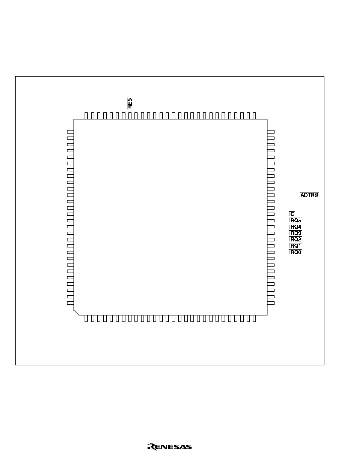
Rev. 1.0, 02/00, page 8 of 1141
1.3
Pin Arrangement and Functions
1.3.1
Pin Arrangement
Figure 1.2 shows the pin arrangement of the H8S/2199 Series.
P33/PWM1
P34/PWM2
MD0
VCL
OSC2
V
SS
OSC1
X1
X2
FWE
P40/PWM14
P41/FTIA
P42/FTIB
P43/FTIC
P44/FTID
P45/FTOA
P46/FTOB
P47/RPTRG
P21/SO1
P20/SI1
P22/SCK1
P23/SDA1
P24/SCL1
P25/SDA0
P26/SCL0
P27/SYNCI
V
SS
P32/PWM0
P31/SV2
P30/SV1
P70/PPG0
P71/PPG1
P72/PPG2
P73/PPG3
P74/PPG4/RP8
P75/PPG5/RP9
P76/PPG6/RPA
P77/PPG7/RPB
P80/YCO
P81/EXCAP/YBO
P82/EXCTL
P83/C.Rotary/R
P84/H.Amp SW/G
P85/COMP/B
P86/EXTTRG
P87/DPG
DFG
VIDEO FF
AUDIO FF
DRM PWM
CAP PWM
Vpulse
V
SS
Csync
V
CC
V
CC
P35/PWM3
P36/BUZZ
P37/TMO
P60/RP0
P61/RP1
P62/RP2
P63/RP3
P64/RP4
P65/RP5
P66/RP6/
P67/RP7/TMBI
P17/TMOW
P16/
P15/
P14/
P13/
P12/
P11/
P10/
AV
CC
P00/AN0
P01/AN1
P02/AN2
P03/AN3
P04/AN4
P05/AN5
P06/AN6
1
SV
SS
FP-112
(Top view)
84
2
CTLREF
83
3
CTL(+)
82
4
CTL(≠)
81
5
CTLBias
80
6
CTLFB
79
7
CTLAmp(o)
78
8
CTLSMT(i)
77
9
CFG
76
10
SV
CC
75
11
AFCpc
74
12
AFCosc
73
13
AFCLPF
72
14
Csync/Hsync
71
15
VLPF/Vsync
70
16
CVin2
69
17
CVin1
68
18
OV
CC
67
19
CVout
66
20
OV
SS
65
21
4fscout/2fscout
64
22
4fscin/2fscin
63
23
AV
SS
62
24
ANB
61
25
ANA
60
26
AN9
59
27
AN8
58
28
P07/AN7
57
56
55
54
53
52
51
50
49
48
47
46
45
44
43
42
41
40
39
38
37
36
35
34
33
32
31
30
29
85
86
87
88
89
90
91
92
93
94
95
96
97
98
99
100
101
102
103
104
105
106
107
108
109
110
111
112
Figure 1.2 Pin Arrangement of H8S/2199 Series

Rev. 1.0, 02/00, page 9 of 1141
1.3.2
Pin Functions
Table 1.2 summarizes the functions of the H8S/2199 Series pins.
Table 1.2
Pin Functions
Type
Symbol
Pin No.
I/O
Name and Function
V
CC
56, 112
Input
Power supply:
All Vcc pins should be connected to the system
power supply (+5V)
V
SS
57, 79,
110
Input
Ground:
All Vcc pins should be connected to the system
power supply (0V)
SV
CC
10
Input
Servo power supply:
SVcc pin should be connected to the servo
analog power supply (+5V)
SV
SS
1
Input
Servo ground:
SVss pin should be connected to the servo
analog power supply (0V)
AV
CC
36
Input
Analog power supply:
Power supply pin for A/D converter. It should be
connected to the system power supply (+5V)
when the A/D converter is not used
AV
SS
23
Input
Analog ground:
Ground pin for A/D converter. It should be
connected to the system power supply (0V)
OV
CC
18
Input
OSD power supply:
V
CC
(OSD) should be connected to the OSD
analog power supply (+5 V)
OV
SS
20
Input
OSD ground:
V
SS
(OSD) should be connected to the OSD
analog power supply (0 V)
Power
supply
V
CL
81
Input
Smoothing capacitor connection:
Connect 0.1-µF power-smoothing capacitance
between V
CL
and V
SS
OSC1
78
Input
OSC2
80
Output
Connected to a crystal oscillator. It can also
input an external clock. See section 9, Clock
Pulse Generator, for typical connection
diagrams for a crystal oscillator and external
clock input
X1
76
Input
Clock
X2
75
Output
Connected to a 32.768 kHz crystal oscillator.
See section 9, Clock Pulse Generator, for typical
connection diagrams

Rev. 1.0, 02/00, page 10 of 1141
Type
Symbol
Pin No.
I/O
Name and Function
Operating
mode
control
MD0
82
Input
Mode pin:
This pin sets the operating mode. This pin
should not be changed while the MCU is in
operation
5(6
77
Input
Reset input:
When this pin is driven low, the chip is reset
System
control
FWE
74
Input
Flash memory enable:
Enables/disables flash memory programming.
This pin is available only with MCU with flash
memory on-chip. For mask ROM type, do not
connect anything to this pin
,54
37
Input
External interrupt request 0:
External interrupt input pin for which rising edge
sense, falling edge sense or both edges sense
are selectable
Interrupts
,54
,54
,54
,54
,54
38
39
40
41
42
Input
External interrupt requests 1 to 5:
External interrupt input pins for which rising or
falling edge sense are selectable
,&
43
Input
Input capture input:
Input capture input pin for prescaler unit
Prescaler
unit
TMOW
44
Output
Frequency division clock output:
Output pin for clock of which frequency is divided
by prescaler
TMBI
45
Input
Timer B event input:
Input pin for events to be input to Timer B
counter
,54
,54
38
39
Input
Timer J event input:
Input pin for events to be input to Timer J RDT-
1or RDT-2 counter
TMO
53
Output
Timer J timer output:
Output pin for toggle at underflow of RDT-1 of
Timer J, or remote controlled transmit data
Timers
BUZZ
54
Output
Timer J buzzer output:
Output pin for toggle which is selectable among
fixed frequency, 1Hz frequency divided from
subclock (32 kHz), and frequency division CTL
signal

Rev. 1.0, 02/00, page 11 of 1141
Type
Symbol
Pin No.
I/O
Name and Function
,54
40
Input
Timer R input capture:
Input pin for input capture of Timer R TMRU-1 or
TMRU-2
FTOA
FTOB
68
67
Output
Timer X1 output compare A and B output:
Output pin for output compare A and B of Timer
X1
Timers
FTIA
FTIB
FTIC
FTID
72
71
70
69
Input
Timer X1 input capture A, B, C and D input:
Input pin for input capture A, B, C and D of
Timer X1
PWM0
PWM1
PWM2
PWM3
85
84
83
55
Output
8-bit PWM square waveform output:
Output pin for waveform generated by 8-bit
PWM 0, 1, 2 and 3
PWM
PWM14
73
Output
14-bit PWM square waveform output:
Output pin for waveform generated by 14-bit
PWM
SCK1
63
Input
/output
SCI clock input/output:
Clock input pins for SCI 1
SI1
65
Input
SCI receive data input:
Receive data input pins for SCI 1
Serial
commu-
nication
interface
(SCI)
SO1
64
Output
SCI transmit data output:
Transmit data output pins for SCI 1
SCL0
SCL1
59
61
Input
/output
I
2
C bus interface clock input/output:
Clock input/output pin for I
2
C bus interface
SDA0
SDA1
60
62
Input
/output
I
2
C bus interface data input/output:
Data input/output pin for I
2
C bus interface
I
2
C bus
interface
SYNCI
58
Input
I
2
C bus interface clock input:
I
2
C formalless serial clock input

Rev. 1.0, 02/00, page 12 of 1141
Type
Symbol
Pin No.
I/O
Name and Function
AN7 to
AN0
28 to 35
Input
Analog input channels 7 to 0:
Analog data input pins. A/D conversion is
started by a software triggering
AN8
AN9
ANA
ANB
27
26
25
24
Input
Analog input channels 8, 9, A and B:
Analog data input pins. A/D conversion is
started by an external trigger, a hardware
trigger, or software
A/D
converter
$'75*
46
Input
A/D conversion external trigger input:
A/D conversion for analog data input pins 8, 9,
A, and B is started by an external trigger
AUDIO FF
106
Output
Audio FF:
Output pin for audio head switching signal
VIDEO FF
105
Output
Video FF:
Output pin for video head switching signal
CAPPWM
108
Output
Capstan mix:
12-bit PWM output pin giving result of capstan
speed error and phase error after filtering
DRMPWM
107
Output
Drum mix:
12-bit PWM output pin giving result of drum
speed error and phase error after filtering
Vpulse
109
Output
Additional V pulse:
Three-level output pin for additional V signal
synchronized to the Video FF signal
C.Rotary
99
Output
Color rotary signal:
Output pin for color signal processing control
signal in four-head special-effects playback
H.AmpSW
100
Output
Head-amp switch:
Output pin for preamplifier output select signal in
four-head special-effects playback.
COMP
101
Input
Compare input:
Input pin for signal giving the result of
preamplifier output comparison in four-head
special-effects playback.
CTL (+)
CTL (-)
3
4
Input
/output
CTL head (+) and (-) pins:
I/O pins for CTL signals
Servo
circuits
CTL Bias
5
Input
CTL primary amp bias supply:
Bias supply pin for CTL primary amp

Rev. 1.0, 02/00, page 13 of 1141
Type
Symbol
Pin No.
I/O
Name and Function
CTL Amp
(o)
7
Output
CTL amp output:
Output pin for CTL amp
CTL SMT
(l)
8
Input
CTL Schmitt amp input:
Input pin for CTL Schmitt amp
CTLFB
6
Input
CLT feedback input:
Input pin for CTL amp high-range characteristics
control
CTLREF
2
Output
CTL amp reference voltage output:
Output pin for 1/2Vcc (SV)
CFG
9
Input
Capstan FG input:
Schmitt comparator input pin for CFG signal
DFG
104
Input
Drum FG input:
Schmitt input pin for DFG signal
DPG
103
Input
Drum PG input:
Schmitt input pin for DPG signal
EXCTL
98
Input
External CTL input:
Input pin for external CTL signal
Csync
111
Input
Mixed sync signal input:
Input pin for mixed sync signal
EXCAP
97
Input
Capstan external sync signal input:
Signal input pin for external synchronization of
capstan phase control
EXTTRG
102
Input
External trigger signal input:
Signal input pin for synchronization with
reference signal generator
SV1
87
Output
Servo monitor output pin 1:
Output pin for servo module internal signal
SV2
86
Output
Servo monitor output pin 2:
Output pin for servo module internal signal
Servo
circuits
PPG7 to
PPG0
95 to 88
Output
PPG:
Output pin for HSW timing generator. To be
used when head switching is required as well as
Audio FF and Video FF

Rev. 1.0, 02/00, page 14 of 1141
Type
Symbol
Pin No.
I/O
Name and Function
Csync/
Hsync
14
Input/
output
Sync signal input/output:
Composite sync signal input/output or horizontal
sync signal input
VLPF/
Vsync
15
Input
Sync signal input:
Pin for connecting external LPF for vertical sync
signal or input pin for vertical sync signal
AFC pc
11
Input/
output
AFC oscillation:
Pin for connecting external circuit for AFC
oscillation
AFC osc
12
Input/
output
AFC oscillation:
Pin for connecting external circuit for AFC
oscillation
AFC LPF
13
Input/
output
Pin for connecting external LPF for AFC
4 fsc in/
2 fsc in
22
Input
fsc oscillation:
Input pin for subcarrier oscillator. 4fsc or 2fsc
can be selected
fsc: Subcarrier frequency
4 fsc out/
2 fsc out
21
Output
fsc oscillation:
Output pin for subcarrier oscillator. 4fsc or 2fsc
can be selected
fsc: Subcarrier frequency
Sync
separator
CVin2
16
Input
Composite video input:
Composite video signal input. Input 2-Vp-p
composite video signal, and the sync tip of the
signal is clamped to about 2.0 V
CVin1
17
Input
Composite video input:
Composite video signal input for OSD. Input 2-
Vp-p composite video signal, and the sync tip of
the signal is clamped to about 1.4 V
CVout
19
Output
Composite video output:
Composite video signal output for OSD. 2-Vp-p
composite video signal is output
R
99
Output
OSD digital output:
Color signal R output
G
100
Output
OSD digital output:
Color signal G output
OSD
B
101
Output
OSD digital output:
Color signal B output

Rev. 1.0, 02/00, page 15 of 1141
Type
Symbol
Pin No.
I/O
Name and Function
OSD
YCO
96
Output
OSD digital output:
Character data output
YBO
97
Output
OSD digital output:
Character display position output
Data
slicer
CVin2
16
Input
Composite video input:
Composite video signal input. Input 2-Vp-p
composite video signal, and the sync tip of the
signal is clamped to about 2.0 V.
P07 to P00
28 to 35
Input
Port 0:
8-bit input pins
P17 to P10
44 to 37
Input
/output
Port 1:
8-bit I/O pins
P27 to P20
58 to 65
Input
/output
Port 2:
8-bit I/O pins
P37 to P30
53 to 55
83 to 87
Input
/output
Port 3:
8-bit I/O pins
P47 to P40
66 to 73
Input
/output
Port 4:
8-bit I/O pins
P67 to P60
45 to 52
Input
/output
Port 6:
8-bit I/O pins
P77 to P70
95 to 88
Input
/output
Port 7:
8-bit I/O pins
P87 to P80
103 to
96
Input
/output
Port 8:
8-bit I/O pins
RP7 to RP0
45 to 52
Output
Realtime output port:
8-bit realtime output pins
RPB to
RP8
95 to 92
Output
Realtime output port:
4-bit realtime output pins
I/O port
RPTRG
66
Input
Realtime output port trigger input:
Input pin for realtime output port trigger

Rev. 1.0, 02/00, page 17 of 1141
Section 2 CPU
2.1
Overview
The H8S/2000 CPU is a high-speed central processing unit with an internal 32-bit architecture
that is upward-compatible with the H8/300 and H8/300H CPUs. The H8S/2000 CPU has sixteen
16-bit general registers, can address a 16-Mbyte (architecturally 4-Gbyte) linear address space,
and is ideal for realtime control.
2.1.1
Features
The H8S/2000 CPU has the following features.
∑
Upward-compatible with H8/300 and H8/300H CPUs
Can execute H8/300 and H8/300H object programs
∑
General-register architecture
Sixteen 16-bit general registers (also usable as sixteen 8-bit registers or eight 32-bit registers)
∑
Sixty-five basic instructions
8/16/32-bit arithmetic and logic instructions
Multiply and divide instructions
Powerful bit-manipulation instructions
∑
Eight addressing modes
Register direct [Rn]
Register indirect [@ERn]
Register indirect with displacement [@(d:16,ERn) or @(d:32,ERn)]
Register indirect with post-increment or pre-decrement [@ERn+ or @-ERn]
Absolute address [@aa:8, @aa:16, @aa:24, or @aa:32]
Immediate [#xx:8, #xx:16, or #xx:32]
Program-counter relative [@(d:8,PC) or @(d:16,PC)]
Memory indirect [@@aa:8]
∑
16-Mbyte address space
Program: 16 Mbytes
Data:
16 Mbytes (4 Gbytes architecturally)
∑
High-speed operation
All frequently-used instructions execute in one or two states
Maximum clock rate:
10 MHz
8/16/32-bit register-register add/subtract: 100 ns
8
◊
8-bit register-register multiply:
1200 ns

Rev. 1.0, 02/00, page 18 of 1141
16
˜
8-bit register-register divide:
1200 ns
16
◊
16-bit register-register multiply:
2000 ns
32
˜
16-bit register-register divide:
2000 ns
∑
Two CPU operating modes
Normal mode*/Advanced mode
∑
Power-down state
Transition to power-down state by SLEEP instruction
CPU clock speed selection
Note: * Normal mode is not available for this LSI.
2.1.2
Differences between H8S/2600 CPU and H8S/2000 CPU
The differences between the H8S/2600 CPU and the H8S/2000 CPU are shown below.
∑
Register configuration
The MAC register is supported only by the H8S/2600 CPU.
∑
Basic instructions
The four instructions MAC, CLRMAC, LDMAC, and STMAC are supported only by the
H8S/2600 CPU.
∑
Number of execution states
The number of execution states of the MULXU and MULXS instructions differ as follows.
Number of Execution States
Instruction
Mnemonic
H8S/2600
H8S/2000
MULXU.B Rs, Rd
3
12
MULXU
MULXU.W Rs, Erd
4
20
MULXS.B Rs, Rd
4
13
MULXS
MULXS.W Rs, Erd
5
21
There are also differences in the address space, EXR register functions, power-down state, etc.,
depending on the product.
2.1.3
Differences from H8/300 CPU
In comparison to the H8/300 CPU, the H8S/2000 CPU has the following enhancements.
∑
More general registers and control registers
Eight 16-bit extended registers, and one 8-bit control register, have been added.

Rev. 1.0, 02/00, page 19 of 1141
∑
Expanded address space
Normal mode supports the same 64-kbyte address space as the H8/300 CPU.
Advanced mode supports a maximum 16-Mbyte address space.
∑
Enhanced addressing mode
The addressing modes have been enhanced to make effective use of the 16-Mbyte address
space.
∑
Enhanced instructions
Addressing modes of bit-manipulation instructions have been enhanced.
Signed multiply and divide instructions have been added.
Two-bit shift instructions have been added.
Instructions for saving and restoring multiple registers have been added.
A test and set instruction has been added.
∑
Higher speed
Basic instructions execute twice as fast.
2.1.4
Differences from H8/300H CPU
In comparison to the H8/300H CPU, the H8S/2000 CPU has the following enhancements.
∑
Additional control register
One 8-bit control register has been added.
∑
Enhanced instructions
Addressing modes of bit-manipulation instructions have been enhanced.
Two-bit shift instructions have been added.
Instructions for saving and restoring multiple registers have been added.
A test and set instruction has been added.
∑
Higher speed
Basic instructions execute twice as fast.
Rev. 1.0, 02/00, page 20 of 1141
2.2
CPU Operating Modes
The H8S/2000 CPU has two operating modes: normal and advanced. Normal mode supports a
maximum 64-kbyte address space. Advanced mode supports a maximum 16-Mbyte total
address space (architecturally the maximum total address space is 4 Gbytes, with a maximum of
16 Mbytes for the program area and a maximum of 4 Gbytes for the data area).
The mode is selected by the mode pins of the microcontroller.
CPU operating mode
Normal mode*
Advanced mode
Maximum 64 kbytes for program
and data areas combined
Maximum 16 Mbytes for program
and data areas combined
Note: * Normal mode is not available for this LSI.
Figure 2.1 CPU Operating Modes
(1) Normal Mode (Not available for this LSI)
The exception vector table and stack have the same structure as in the H8/300 CPU.
(a) Address Space
A maximum address space of 64 kbytes can be accessed.
(b) Extended Registers (En)
The extended registers (E0 to E7) can be used as 16-bit registers, or as the upper 16-bit
segments of 32-bit registers. When En is used as a 16-bit register it can contain any
value, even when the corresponding general register (Rn) is used as an address register.
If the general register is referenced in the register indirect addressing mode with pre-
decrement (@-Rn) or post-increment (@Rn+) and a carry or borrow occurs, however, the
value in the corresponding extended register (En) will be affected.
(c) Instruction Set
All instructions and addressing modes can be used. Only the lower 16 bits of effective
addresses (EA) are valid.
Rev. 1.0, 02/00, page 21 of 1141
(d) Exception Vector Table and Memory Indirect Branch Addresses
In normal mode the top area starting at H'0000 is allocated to the exception vector table.
One branch address is stored per 16 bits. The configuration of the exception vector table
in normal mode is shown in figure 2.2. For details of the exception vector table, see
section 5, Exception Handling.
H'0000
H'0001
H'0002
H'0003
H'0004
H'0005
H'0006
H'0007
H'0008
H'0009
H'000A
H'000B
Reset exception vector
Exception vector 1
Exception vector 2
Exception vector table
(Reserved for system use)
Figure 2.2 Exception Vector Table (Normal Mode)
The memory indirect addressing mode (@@aa:8) employed in the JMP and JSR
instructions uses an 8-bit absolute address included in the instruction code to specify a
memory operand that contains a branch address. In normal mode the operand is a 16-bit
word operand, providing a 16-bit branch address. Branch addresses can be stored in the
top area from H'0000 to H'00FF. Note that this area is also used for the exception vector
table.
Rev. 1.0, 02/00, page 22 of 1141
(e) Stack Structure
When the program counter (PC) is pushed onto the stack in a subroutine call, and the PC
and condition-code register (CCR) are pushed onto the stack in exception handling, they
are stored as shown in figure 2.3. The extended control register (EXR) is not pushed onto
the stack. For details, see section 5, Exception Handling.
(a) Subroutine Branch
(b) Exception Handling
PC
(16 bits)
CCR
CCR*
PC
(16 bits)
SP
SP
Note: * Ignored when returning.
Figure 2.3 Stack Structure in Normal Mode
(2) Advanced Mode
(a) Address Space
Linear access is provided to a 16-Mbyte maximum address space (architecturally a
maximum 16-Mbyte program area and a maximum 4-Gbyte data area, with a maximum
of 4 Gbytes for program and data areas combined).
(b) Extended Registers (En)
The extended registers (E0 to E7) can be used as 16-bit registers, or as the upper 16-bit
segments of 32-bit registers or address registers.
(c) Instruction Set
All instructions and addressing modes can be used.
Rev. 1.0, 02/00, page 23 of 1141
(d) Exception Vector Table and Memory Indirect Branch Addresses
In advanced mode the top area starting at H'00000000 is allocated to the exception vector
table in units of 32 bits. In each 32 bits, the upper 8 bits are ignored and a branch address
is stored in the lower 24 bits (figure 2.4). For details of the exception vector table, see
section 5, Exception Handling.
H'00000000
H'00000003
H'00000004
H'0000000B
H'0000000C
Exception vector table
Reserved
Reset exception vector
(Reserved for system use)
Reserved
Exception vector 1
Reserved
H'00000010
H'00000008
H'00000007
Figure 2.4 Exception Vector Table (Advanced Mode)
The memory indirect addressing mode (@@aa:8) employed in the JMP and JSR
instructions uses an 8-bit absolute address included in the instruction code to specify a
memory operand that contains a branch address. In advanced mode the operand is a 32-
bit longword operand, providing a 32-bit branch address. The upper 8 bits of these 32
bits are a reserved area that is regarded as H'00. Branch addresses can be stored in the
area from H'00000000 to H'000000FF. Note that the first part of this range is also the
exception vector table.
Rev. 1.0, 02/00, page 24 of 1141
(e) Stack Structure
In advanced mode, when the program counter (PC) is pushed onto the stack in a
subroutine call, and the PC and condition-code register (CCR) are pushed onto the stack
in exception handling, they are stored as shown in figure 2.5. The extended control
register (EXR) is not pushed onto the stack. For details, see section 5, Exception
Handling.
(a) Subroutine Branch
(b) Exception Handling
PC
(24 bits)
CCR
PC
(24 bits)
SP
SP
Reserved
Figure 2.5 Stack Structure in Advanced Mode
Rev. 1.0, 02/00, page 25 of 1141
2.3
Address Space
Figure 2.6 shows a memory map of the H8S/2000 CPU. The H8S/2000 CPU provides linear
access to a maximum 64-kbyte address space in normal mode, and a maximum 16-Mbyte
(architecturally 4-Gbyte) address space in advanced mode.
(b) Advanced mode
H'0000
H'FFFF
H'00000000
H'FFFFFFFF
H'00FFFFFF
(a) Normal mode*
Data area
Program area
Cannot be used
with this LSI
Note: * Normal mode is not available for this LSI.
Figure 2.6 Memory Map
Rev. 1.0, 02/00, page 26 of 1141
2.4
Register Configuration
2.4.1
Overview
The CPU has the internal registers shown in figure 2.7. There are two types of registers:
general registers and control registers.
T ≠ ≠ ≠ ≠ I2 I1 I0
EXR
7 6 5 4 3 2 1 0
PC
23
0
15
0 7
0 7
0
E0
E1
E2
E3
E4
E5
E6
E7
R0H
R1H
R2H
R3H
R4H
R5H
R6H
R7H
R0L
R1L
R2L
R3L
R4L
R5L
R6L
R7L
General Registers (Rn) and Extended Registers (En)
Control Registers (CR)
[Legend]
SP
PC
EXR
T
I2 to I0
CCR
I
UI
ER0
ER1
ER2
ER3
ER4
ER5
ER6
ER7 (SP)
I UI H U N Z V C
CCR
7 6 5 4 3 2 1 0
: Half-carry flag
: User bit
: Negative flag
: Zero flag
: Overflow flag
: Carry flag
H
U
N
Z
V
C
: Stack pointer
: Program counter
: Extended control register
: Trace bit
: Interrupt mask bits
: Condition-code register
: Interrupt mask bit
: User bit or interrupt mask bit
Note: * Does not affect operation in this LSI.
*
Figure 2.7 CPU Registers
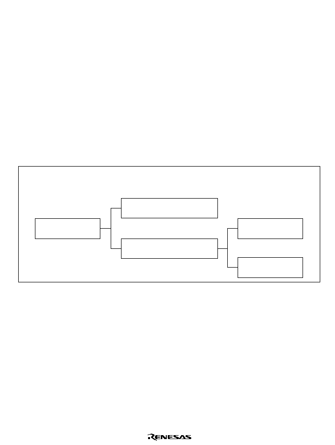
Rev. 1.0, 02/00, page 27 of 1141
2.4.2
General Registers
The CPU has eight 32-bit general registers. These general registers are all functionally alike and
can be used as both address registers and data registers. When a general register is used as a
data register, it can be accessed as a 32-bit, 16-bit, or 8-bit register. When the general registers
are used as 32-bit registers or address registers, they are designated by the letters ER (ER0 to
ER7).
The ER registers divide into 16-bit general registers designated by the letters E (E0 to E7) and R
(R0 to R7). These registers are functionally equivalent, providing a maximum of sixteen 16-bit
registers. The E registers (E0 to E7) are also referred to as extended registers.
The R registers divide into 8-bit general registers designated by the letters RH (R0H to R7H) and
RL (R0L to R7L). These registers are functionally equivalent, providing a maximum of sixteen
8-bit registers.
Figure 2.8 illustrates the usage of the general registers. The usage of each register can be
selected independently.
q
Address registers
q
32-bit registers
q
16-bit registers
q
8-bit registers
ER registers
(ER0 to ER7)
E registers (extended registers)
(E0 to E7)
R registers
(R0 to R7)
RH registers
(R0H to R7H)
RL registers
(R0L to R7L)
Figure 2.8 Usage of General Registers
General register ER7 has the function of stack pointer (SP) in addition to its general-register
function, and is used implicitly in exception handling and subroutine calls. Figure 2.9 shows the
stack.
Rev. 1.0, 02/00, page 28 of 1141
SP (ER7)
Free area
Stack area
Figure 2.9 Stack
2.4.3
Control Registers
The control registers are the 24-bit program counter (PC), 8-bit extended control register (EXR),
and 8-bit condition-code register (CCR).
(1) Program Counter (PC)
This 24-bit counter indicates the address of the next instruction the CPU will execute. The
length of all CPU instructions is 2 bytes (one word), so the least significant PC bit is ignored.
(When an instruction is fetched, the least significant PC bit is regarded as 0.)
(2) Extended Control Register (EXR)
An 8-bit register. In this LSI, this register does not affect operation.
Bit 7: Trace Bit (T)
This bit is reserved. In this LSI, this bit does not affect operation.
Bits 6 to 3: Reserved
These bits are reserved. They are always read as 1.
Bits 2 to 0: Interrupt Mask Bits (I2 to I0)
These bits are reserved. In this LSI, these bits do not affect operation.
(3) Condition: Code Register (CCR)
This 8-bit register contains internal CPU status information, including an interrupt mask bit
(I) and half-carry (H), negative (N), zero (Z), overflow (V), and carry (C) flags.
Bit 7: Interrupt Mask Bit (I)
Masks interrupts other than NMI when set to 1. (NMI is accepted regardless of the I bit
setting.) The I bit is set to 1 by hardware at the start of an exception-handling sequence.
For details, see section 6, Interrupt Controller.

Rev. 1.0, 02/00, page 29 of 1141
Bit 6: User Bit or Interrupt Mask Bit (UI)
Can be written and read by software using the LDC, STC, ANDC, ORC, and XORC
instructions. This bit can also be used as an interrupt mask bit. For details, see section 6,
Interrupt Controller.
Bit 5: Half-Carry Flag (H)
When the ADD.B, ADDX.B, SUB.B, SUBX.B, CMP.B, or NEG.B instruction is
executed, this flag is set to 1 if there is a carry or borrow at bit 3, and cleared to 0
otherwise. When the ADD.W, SUB.W, CMP.W, or NEG.W instruction is executed, the
H flag is set to 1 if there is a carry or borrow at bit 11, and cleared to 0 otherwise. When
the ADD.L, SUB.L, CMP.L, or NEG.L instruction is executed, the H flag is set to 1 if
there is a carry or borrow at bit 27, and cleared to 0 otherwise.
Bit 4: User Bit (U)
Can be written and read by software using the LDC, STC, ANDC, ORC, and XORC
instructions.
Bit 3: Negative Flag (N)
Stores the value of the most significant bit (sign bit) of data.
Bit 2: Zero Flag (Z)
Set to 1 to indicate zero data, and cleared to 0 to indicate non-zero data.
Bit 1: Overflow Flag (V)
Set to 1 when an arithmetic overflow occurs, and cleared to 0 otherwise.
Bit 0: Carry Flag (C)
Set to 1 when a carry occurs, and cleared to 0 otherwise. Used by:
(a) Add instructions, to indicate a carry
(b) Subtract instructions, to indicate a borrow
(c) Shift and rotate instructions, to store the carry
The carry flag is also used as a bit accumulator by bit-manipulation instructions.
Some instructions leave some or all of the flag bits unchanged. For the action of each
instruction on the flag bits, see section 29, Appendix A.1, List of Instructions.
Operations can be performed on the CCR bits by the LDC, STC, ANDC, ORC, and XORC
instructions. The N, Z, V, and C flags are used as branching conditions for conditional
branch (Bcc) instructions.
2.4.4
Initial Register Values
Reset exception handling loads the CPU's program counter (PC) from the vector table, clears the
trace bit in EXR to 0, and sets the interrupt mask bits in CCR and EXR to 1. The other CCR bits
and the general registers are not initialized. In particular, the stack pointer (ER7) is not
initialized. The stack pointer should therefore be initialized by an MOV.L instruction executed
immediately after a reset.
Rev. 1.0, 02/00, page 30 of 1141
2.5
Data Formats
The CPU can process 1-bit, 4-bit (BCD), 8-bit (byte), 16-bit (word), and 32-bit (longword) data.
Bit-manipulation instructions operate on 1-bit data by accessing bit n (n = 0, 1, 2, ..., 7) of byte
operand data. The DAA and DAS decimal-adjust instructions treat byte data as two digits of 4-
bit BCD data.
2.5.1
General Register Data Formats
Figure 2.10 shows the data formats in general registers.
7
0
7
0
MSB
LSB
MSB
LSB
7
0
4 3
Upper digit Lower digit
Don't care
Don't care
Don't care
7
0
4 3
Upper digit Lower digit
7
0
Don't care
6
5 4
3 2
7
1 0
7
0
Don't care
6
5 4
3 2
7
1 0
Don't care
Data Format
Data type
1-bit data
1-bit data
4-bit BCD data
4-bit BCD data
Byte data
Byte data
General Register
RnH
RnL
RnH
RnL
RnH
RnL
Figure 2.10 General Register Data Formats (1)
Rev. 1.0, 02/00, page 31 of 1141
15
0
MSB
LSB
15
0
MSB
LSB
31
16
MSB
15
0
LSB
En
Rn
Data Type
Word data
Word data
Longword data
General Register
Rn
En
ERn
Data format
ERn
En
Rn
RnH
RnL
MSB
LSB
: General register ER
: General register E
: General register R
: General register RH
: General register RL
: Most significant bit
: Least significant bit
[Legend]
Figure 2.11 General Register Data Formats (2)
Rev. 1.0, 02/00, page 32 of 1141
2.5.2
Memory Data Formats
Figure 2.12 shows the data formats in memory.
The CPU can access word data and longword data in memory, but word or longword data must
begin at an even address. If an attempt is made to access word or longword data at an odd
address, no address error occurs but the least significant bit of the address is regarded as 0, so the
access starts at the preceding address. This also applies to instruction fetches.
7
0
7
6
5
4
3
2
1
0
MSB
LSB
MSB
MSB
LSB
LSB
Address
Address L
Address L
Address 2M
Address 2N
Address 2N+1
Address 2N+2
Address 2N+3
1-bit data
Byte data
Word data
Longword data
Data Type
Data Format
Address 2M+1
Figure 2.12 Memory Data Formats
When ER7 (SP) is used as an address register to access the stack, the operand size should be
word size or longword size.

Rev. 1.0, 02/00, page 33 of 1141
2.6
Instruction Set
2.6.1
Overview
The H8S/2000 CPU has 65 types of instructions. The instructions are classified by function in
table 2.1.
Table 2.1
Instruction Classification
Function
Instructions
Size
Types
MOV
BWL
POP
*
1
, PUSH
*
1
WL
LDM, STM
L
Data transfer
MOVFPE, MOVTPE
B
5
ADD, SUB, CMP, NEG
BWL
ADDX, SUBX, DAA, DAS
B
INC, DEC
BWL
ADDS, SUBS
L
MULXU, DIVXU, MULXS, DIVXS
BW
EXTU, EXTS
WL
Arithmetic
TAS
B
19
Logic operations
AND, OR, XOR, NOT
BWL
4
Shift
SHAL, SHAR, SHLL, SHLR, ROTL, ROTR,
ROTXL, ROTXR
BWL
8
Bit manipulation
RSET, BCLR, BNOT, BTST, BLD, BILD, BST,
BIST, BAND, BIAND, BOR, BIOR, BXOR,
BIXOR
B
14
Branch
Bcc
*
2
, JMP, BSR, JSR, RTS
5
System control
TRAPA, RTE, SLEEP, LDC, STC, ANDC, ORC,
XORC, NOP
9
Block data transfer
EEPMOV
1
Total: 65 types
Notes: B: byte size; W: word size; L: longword size.
1. POP.W Rn and PUSH.W Rn are identical to MOV.W @SP+, Rn and MOV.W Rn, @-
SP.
POP.L ERn and PUSH.L ERn are identical to MOV.L @SP+, ERn and MOV.L ERn,
@-SP.
2. Bcc is the general name for conditional branch instructions.
Rev. 1.0, 02/00, page 34 of 1141
2.6.2
Instructions and Addressing Modes
Table 2.2 indicates the combinations of instructions and addressing modes that the H8S/2000
CPU can use.
Table 2.2
Combinations of Instructions and Addressing Modes
Addressing Modes
Function
Arithmetic operations
System control
Branch
Logic
operation
Instruction
MOV
POP, PUSH
LDM, STM
ADD, CMP
SUB
ADDX, SUBX
ADDS, SUBS
INC, DEC
DAA, DAS
NEG
EXTU, EXTS
TAS
MOVFPE,
MOVTPE*
MULXU,
DIVXU
MULXS,
DIVXS
AND, OR,
XOR
ANDC,
ORC, XORC
NOT
Bcc, BSR
JMP, JSR
RTS
TRAPA
RTE
SLEEP
LDC
STC
NOP
Shift
Bit manipulation
Block data transfer
Data transfer
BWL
#xx
--
--
BWL
WL
B
--
--
--
--
--
--
--
--
--
BWL
B
--
--
--
--
--
--
--
B
--
--
--
--
--
BWL
Rn
--
--
BWL
BWL
B
L
BWL
B
BWL
WL
--
--
BW
BW
BWL
--
BWL
--
--
--
--
--
--
B
B
--
BWL
B
--
BWL
@ERn
--
--
--
--
--
--
--
--
--
--
B
--
--
--
--
--
--
--
--
--
--
--
--
W
W
--
--
B
--
BWL
@(d:16, ERn)
--
--
--
--
--
--
--
--
--
--
--
--
--
--
--
--
--
--
--
--
--
--
--
W
W
--
--
--
--
BWL
@(d:32, ERn)
--
--
--
--
--
--
--
--
--
--
--
--
--
--
--
--
--
--
--
--
--
--
--
W
W
--
--
--
--
BWL
@-ERn/@ERn+
--
--
--
--
--
--
--
--
--
--
--
--
--
--
--
--
--
--
--
--
--
--
--
W
W
--
--
--
--
B
@aa:8
--
--
--
--
--
--
--
--
--
--
--
--
--
--
--
--
--
--
--
--
--
--
--
--
--
--
--
B
--
BWL
@aa:16
--
--
--
--
--
--
--
--
--
--
--
B
--
--
--
--
--
--
--
--
--
--
--
W
W
--
--
B
--
--
@aa:24
--
--
--
--
--
--
--
--
--
--
--
--
--
--
--
--
--
--
--
--
--
--
--
--
--
--
--
--
BWL
@aa:32
--
--
--
--
--
--
--
--
--
--
--
--
--
--
--
--
--
--
--
--
--
--
--
W
W
--
--
B
--
--
@(d:8, PC)
--
--
--
--
--
--
--
--
--
--
--
--
--
--
--
--
--
--
--
--
--
--
--
--
--
--
--
--
--
@(d:16, PC)
--
--
--
--
--
--
--
--
--
--
--
--
--
--
--
--
--
--
--
--
--
--
--
--
--
--
--
--
--
@@aa:8
--
--
--
--
--
--
--
--
--
--
--
--
--
--
--
--
--
--
--
--
--
--
--
--
--
--
--
--
--
--
WL
L
--
--
--
--
--
--
--
--
--
--
--
--
--
--
--
--
--
--
--
--
--
BW
[Legend]
B:
Byte
W:
Work
L:
Longword
Note:
*
Cannot be used in this LSI.

Rev. 1.0, 02/00, page 35 of 1141
2.6.3
Table of Instructions Classified by Function
Tables 2.3 to 2.10 summarize the functions of the instructions. The notation used in table 2.3 is
defined below.
Operation Notation
Rd
General register (destination)
*
Rs
General register (source)
*
Rn
General register
*
ERn
General register (32-bit register)
(EAd)
Destination operand
(EAs)
Source operand
EXR
Extended control register
CCR
Condition-code register
N
N (negative) flag in CCR
Z
Z (zero) flag in CCR
V
V (overflow) flag in CCR
C
C (carry) flag in CCR
PC
Program counter
SP
Stack pointer
#IMM
Immediate data
Disp
Displacement
+
Addition
-
Subtraction
◊
Multiplication
˜
Division
Logical AND
Logical OR
Logical exclusive OR
Move
NOT (logical complement)
:8/:16/:24/:32
8-, 16-, 24-, or 32-bit length
Note:
*
General registers include 8-bit registers (R0H to R7H, R0L to R7L), 16-bit registers (R0 to
R7, E0 to E7), and 32-bit registers (ER0 to ER7).

Rev. 1.0, 02/00, page 36 of 1141
Table 2.3
Data Transfer Instructions
Instruction
Size
*
Function
MOV
B/W/L
(EAs)
Rd, Rs
(EAd)
Moves data between two general registers or between a general
register and memory, or moves immediate data to a general
register
MOVFPE
B
Cannot be used in this LSI
MOVTPE
B
Cannot be used in this LSI
POP
W/L
@SP+
Rn
Pops a general register from the stack
POP.W Rn is identical to MOV.W @SP+, Rn
POP.L ERn is identical to MOV.L @SP+, ERn
PUSH
W/L
Rn
@-SP
Pushes a general register onto the stack
PUSH.W Rn is identical to MOV.W Rn, @-SP
PUSH.L ERn is identical to MOV.L ERn, @-SP
LDM
L
@SP+
Rn (register list)
Pops two or more general registers from the stack
STM
L
Rn (register list)
@-SP
Pushes two or more general registers onto the stack
Note:
*
Size refers to the operand size.
B:
Byte
W: Word
L:
Longword

Rev. 1.0, 02/00, page 37 of 1141
Table 2.4
Arithmetic Instructions
Instruction
Size
*
Function
ADD
SUB
B/W/L
Rd
±
Rs
Rd, Rd
±
#IMM
Rd
Performs addition or subtraction on data in two general registers,
or on immediate data and data in a general register. (Immediate
byte data cannot be subtracted from byte data in a general
register. Use the SUBX or ADD instruction)
ADDX
SUBX
B
Rd
±
Rs
±
C
Rd, Rd
±
#IMM
±
C
Rd
Performs addition or subtraction with carry on byte data in two
general registers, or on immediate data and data in a general
register
INC
DEC
B/W/L
Rd
±
1
Rd, Rd
±
2
Rd
Increments or decrements a general register by 1 or 2. (Byte
operands can be incremented or decremented by 1 only)
ADDS
SUBS
B
Rd
±
1
Rd, Rd
±
2
Rd, Rd
±
4
Rd
Adds or subtracts the value 1, 2, or 4 to or from data in a 32-bit
register
DAA
DAS
B/W
Rd decimal adjust
Rd
Decimal-adjusts an addition or subtraction result in a general
register by referring to the CCR to produce 4-bit BCD data
MULXU
B/W
Rd
◊
Rs
Rd
Performs unsigned multiplication on data in two general
registers: either 8 bits
◊
8 bits
16 bits or 16 bits
◊
16 bits
32
bits
MULXS
B/W
Rd
◊
Rs
Rd
Performs signed multiplication on data in two general registers:
either 8 bits
◊
8 bits
16 bits or 16 bits
◊
16 bits
32 bits
DIVXU
B/W
Rd
˜
Rs
Rd
Performs unsigned division on data in two general registers:
either 16 bits
˜
8 bits
◊
8-bit quotient and 8-bit remainder or 32
bits
˜
16 bits
◊
16-bit quotient and 16-bit remainder

Rev. 1.0, 02/00, page 38 of 1141
Instruction
Size
*
Function
DIVXS
B/W
Rd
˜
Rs
Rd
Performs signed division on data in two general registers: either
16 bits
˜
8 bits
8-bit quotient and 8-bit remainder or 32 bits
˜
16 bits
16-bit quotient and 16-bit remainder
CMP
B/W/L
Rd - Rs, Rd - #IMM
Compares data in a general register with data in another
general register or with immediate data, and sets CCR bits
according to the result
NEG
B/W/L
0 - Rd
Rd
Takes the two's complement (arithmetic complement) of data in
a general register
EXTU
W/L
Rd (zero extension)
Rd
Extends the lower 8 bits of a 16-bit register to word size, or the
lower 16 bits of a 32-bit register to longword size, by padding
with zeros on the left
EXTS
W/L
Rd (sign extension)
Rd
Extends the lower 8 bits of a 16-bit register to word size, or the
lower 16 bits of a 32-bit register to longword size, by extending
the sign bit
TAS
B
@ERd - 0, 1
(<bit 7> of @ERd)
Tests memory contents, and sets the most significant bit (bit 7)
to 1
Note:
*
Size refers to the operand size.
B:
Byte
W: Word
L:
Longword

Rev. 1.0, 02/00, page 39 of 1141
Table 2.5
Logic Instructions
Instruction
Size
*
Function
AND
B/W/L
Rd
Rs
Rd, Rd
#IMM
Rd
Performs a logical AND operation on a general register and
another general register or immediate data
OR
B/W/L
Rd
Rs
Rd, Rd
#IMM
Rd
Performs a logical OR operation on a general register and
another general register or immediate data
XOR
B/W/L
Rd
Rs
Rd, Rd
#IMM
Rd
Performs a logical exclusive OR operation on a general register
and another general register or immediate data
NOT
B/W/L
~ Rd
Rd
Takes the one's complement (logical complement) of general
register contents
Note:
*
Size refers to the operand size.
B:
Byte
W: Word
L:
Longword
Table 2.6
Shift Instructions
Instruction
Size
*
Function
SHAL
SHAR
B/W/L
Rd (shift)
Rd
Performs an arithmetic shift on general register contents
A 1-bit or 2-bit shift is possible
SHLL
SHLR
B/W/L
Rd (shift)
Rd
Performs a logical shift on general register contents
A 1-bit or 2-bit shift is possible
ROTL
ROTR
B/W/L
Rd (rotate)
Rd
Rotates general register contents
1-bit or 2-bit rotation is possible
ROTXL
ROTXR
B/W/L
Rd (rotate)
Rd
Rotates general register contents through the carry flag
1-bit or 2-bit rotation is possible
Note:
*
Size refers to the operand size.
B:
Byte
W: Word
L:
Longword

Rev. 1.0, 02/00, page 40 of 1141
Table 2.7
Bit Manipulation Instructions
Instruction
Size
*
Function
BSET
B
1
(<bit-No.> of <EAd>)
Sets a specified bit in a general register or memory operand to
1. The bit number is specified by 3-bit immediate data or the
lower three bits of a general register
BCLR
B
0
(<bit-No.> of <EAd>)
Clears a specified bit in a general register or memory operand
to 0. The bit number is specified by 3-bit immediate data or the
lower three bits of a general register
BNOT
B
~ (<bit-No.> of <EAd>)
(<bit-No.> of <EAd>)
Inverts a specified bit in a general register or memory operand.
The bit number is specified by 3-bit immediate data or the lower
three bits of a general register
BTST
B
~ (<bit-No.> of <EAd>)
Z
Tests a specified bit in a general register or memory operand
and sets or clears the Z flag accordingly. The bit number is
specified by 3-bit immediate data or the lower three bits of a
general register
BAND
B
C
(<bit-No.> of <EAd>)
C
ANDs the carry flag with a specified bit in a general register or
memory operand and stores the result in the carry flag
BIAND
B
C
[~(<bit-No.> of <EAd>)]
C
ANDs the carry flag with the inverse of a specified bit in a
general register or memory operand and stores the result in the
carry flag
The bit number is specified by 3-bit immediate data
BOR
B
C
(<bit-No.> of <EAd>)
C
ORs the carry flag with a specified bit in a general register or
memory operand and stores the result in the carry flag
BIOR
B
C
[~(<bit-No.> of <EAd>)]
C
ORs the carry flag with the inverse of a specified bit in a general
register or memory operand and stores the result in the carry
flag
The bit number is specified by 3-bit immediate data

Rev. 1.0, 02/00, page 41 of 1141
Instruction
Size
*
Function
BOXR
B
C
(<bit-No.> of <EAd>)
C
Exclusive-ORs the carry flag with a specified bit in a general
register or memory operand and stores the result in the carry
flag
BIXOR
B
C
[~ (<bit-No.> of <EAd>)]
C
Exclusive-ORs the carry flag with the inverse of a specified bit in
a general register or memory operand and stores the result in
the carry flag
The bit number is specified by 3-bit immediate data
BLD
B
(<bit-No.> of <EAd>)
C
Transfers a specified bit in a general register or memory
operand to the carry flag
BILD
B
~ (<bit-No.> of <EAd>)
C
Transfers the inverse of a specified bit in a general register or
memory operand to the carry flag
The bit number is specified by 3-bit immediate data
BST
B
C
(<bit-No.> of <EAd>)
Transfers the carry flag value to a specified bit in a general
register or memory operand
BIST
B
~ C
(<bit-No.> of <EAd>)
Transfers the inverse of the carry flag value to a specified bit in
a general register or memory operand
The bit number is specified by 3-bit immediate data
Note:
*
Size refers to the operand size.
B:
Byte

Rev. 1.0, 02/00, page 42 of 1141
Table 2.8
Branch Instructions
Instruction
Size
*
Function
Bcc
Branches to a specified address if a specified condition is true
The branching conditions are listed below
JMP
Branches unconditionally to a specified address
BSR
Branches to a subroutine at a specified address
JSR
Branches to a subroutine at a specified address
RTS
Returns from a subroutine
Mnemonic
Description
Condition
BRA (BT)
Always (True)
Always
BRN (BF)
Never (False)
Never
BHI
HIgh
CVZ = 0
BLS
Low of Same
CVZ = 1
BCC (BHS)
Carry Clear (High or
Same)
C = 0
BCS (BLO)
Carry Set (LOw)
C = 1
BNE
Not Equal
Z = 0
BEQ
EQual
Z = 1
BVC
oVerflow Clear
V = 0
BVS
oVerflow Set
V = 1
BPL
PLus
N = 0
BMI
MInus
N = 1
BGE
Greater or Equal
NV = 0
BLT
Less Than
N
V = 1
BGT
Greater Than
Z
(N
V) = 0
BLE
Less or Equal
Z
(N
V) = 1

Rev. 1.0, 02/00, page 43 of 1141
Table 2.9
System Control Instructions
Instruction
Size
*
Function
TRAPA
Starts trap-instruction exception handling
RTE
Returns from an exception-handling routine
SLEEP
Causes a transition to a power-down state
LDC
B/W
(EAs)
CCR, (EAs)
EXR
Moves contents of a general register or memory or immediate
data to CCR or EXR. Although CCR and EXR are 8-bit
registers, word-size transfers are performed between them and
memory. The upper 8 bits are valid
STC
B/W
CCR
(EAd), EXR
(EAd)
Transfers CCR or EXR contents to a general register or
memory. Although CCR and EXR are 8-bit registers, word-size
transfers are performed between them and memory. The upper
8 bits are valid
ANDC
B
CCR
#IMM
CCR, EXR
#IMM
EXR
Logically ANDs the CCR or EXR contents with immediate data
ORC
B
CCR
#IMM
CCR, EXR
#IMM
EXR
Logically ORs the CCR or EXR contents with immediate data
XORC
B
CCR
#IMM
CCR, EXR
#IMM
EXR
Logically exclusive-ORs the CCR or EXR contents with
immediate data
NOP
PC + 2
PC
Only increments the program counter
Note:
*
Size refers to the operand size.
B:
Byte
W: Word

Rev. 1.0, 02/00, page 44 of 1141
Table 2.10 Block Data Transfer Instructions
Instruction
Size
*
Function
EEPMOV.B
if R4L
0 then
Repeat @ER5+
@er6+
R4L
-
1
R4L
Until R4L = 0
else next;
EEPMOV.W
if R4
0 then
Repeat @ER5+
@er6+
R4
-
1
R4
Until R4 = 0
else next;
Transfers a data block according to parameters set in general
registers R4L or R4, ER5, and ER6
R4L or R4: size of block (bytes)
ER5: starting source address
ER6: starting destination address
Execution of the next instruction begins as soon as the transfer
is completed

Rev. 1.0, 02/00, page 45 of 1141
2.6.4
Basic Instruction Formats
The CPU instructions consist of 2-byte (1-word) units. An instruction consists of an operation
field (op field), a register field (r field), an effective address extension (EA field), and a
condition field (cc).
Figure 2.13 shows examples of instruction formats.
op
op
r n
r m
NOP, RTS, etc.
ADD.B Rn, Rm, etc.
MOV.B@(d:16, Rn), Rm, etc.
(1) Operation field only
(2) Operation field and register fields
(3) Operation field, register fields, and effective address extension
r n
r m
op
EA (disp)
(4) Operation field, effective address extension, and condition field
op
cc
EA (disp)
BRA d:16, etc.
Figure 2.13 Instruction Formats (Examples)
(1) Operation Field
Indicates the function of the instruction, the addressing mode, and the operation to be carried
out on the operand. The operation field always includes the first four bits of the instruction.
Some instructions have two operation fields.
(2) Register Field
Specifies a general register. Address registers are specified by 3 bits, data registers by 3 bits
or 4 bits. Some instructions have two register fields. Some have no register field.
(3) Effective Address Extension
Eight, 16, or 32 bits specifying immediate data, an absolute address, or a displacement.
(4) Condition Field
Specifies the branching condition of Bcc instructions.

Rev. 1.0, 02/00, page 46 of 1141
2.6.5
Notes on Use of Bit-Manipulation Instructions
The BSET, BCLR, BNOT, BST, and BIST instructions read a byte of data, carry out bit
manipulation, then write back the byte of data. Caution is therefore required when using these
instructions on a register containing write-only bits, or a port.
The BCLR instruction can be used to clear internal I/O register flags to 0. In this case, the
relevant flag need not be read beforehand if it is clear that it has been set to 1 in an interrupt
handling routine, etc.

Rev. 1.0, 02/00, page 47 of 1141
2.7
Addressing Modes and Effective Address Calculation
2.7.1
Addressing Mode
The CPU supports the eight addressing modes listed in table 2.11. Each instruction uses a subset
of these addressing modes. Arithmetic and logic instructions can use the register direct and
immediate modes. Data transfer instructions can use all addressing modes except program-
counter relative and memory indirect. Bit-manipulation instructions use register direct, register
indirect, or absolute addressing mode to specify an operand, and register direct (BSET, BCLR,
BNOT, and BTST instructions) or immediate (3-bit) addressing mode to specify a bit number in
the operand.
Table 2.11 Addressing Modes
No.
Addressing Mode
Symbol
1
Register direct
Rn
2
Register indirect
@ERn
3
Register indirect with displacement
@(d:16,ERn)/@(d:32,ERn)
4
Register indirect with post-increment
Register indirect with pre-decrement
@ERn+
@-ERn
5
Absolute address
@aa:8/#@aa:16/@aa:24/@aa:32
6
Immediate
#xx:8/#xx:16/#xx:32
7
Program-counter relative
@(d:8,PC)/@(d:16,PC)
8
Memory indirect
@@aa:8
(1) Register Direct≠Rn
The register field of the instruction code specifies an 8-, 16-, or 32-bit general register
containing the operand. R0H to R7H and R0L to R7L can be specified as 8-bit registers. R0
to R7 and E0 to E7 can be specified as 16-bit registers. ER0 to ER7 can be specified as
32-bit registers.
(2) Register Indirect≠@Ern
The register field of the instruction code specifies an address register (ERn) which contains
the address of the operand in memory. If the address is a program instruction address, the
lower 24 bits are valid and the upper 8 bits are all assumed to be 0 (H'00).
(3) Register Indirect with Displacement≠@(d:16, ERn) or @(d:32, ERn)
A 16-bit or 32-bit displacement contained in the instruction is added to an address register
(ERn) specified by the register field of the instruction, and the sum gives the address of a
memory operand. A 16-bit displacement is sign-extended when added.

Rev. 1.0, 02/00, page 48 of 1141
(4) Register Indirect with Post-Increment or Pre-Decrement≠@ERn+ or @-ERn
(a) Register indirect with post-increment≠@ERn+
The register field of the instruction code specifies an address register (ERn) which
contains the address of a memory operand. After the operand is accessed, 1, 2, or 4 is
added to the address register contents and the sum is stored in the address register. The
value added is 1 for byte access, 2 for word access, or 4 for longword access. For word
or longword access, the register value should be even.
(b) Register indirect with pre-decrement≠@-ERn
The value 1, 2, or 4 is subtracted from an address register (ERn) specified by the register
field in the instruction code, and the result becomes the address of a memory operand.
The result is also stored in the address register. The value subtracted is 1 for byte access,
2 for word access, or 4 for longword access. For word or longword access, the register
value should be even.
(5) Absolute Address≠@aa:8, @aa:16, @aa:24, or @aa:32
The instruction code contains the absolute address of a memory operand. The absolute
address may be 8 bits long (@aa:8), 16 bits long (@aa:16), 24 bits long (@aa:24), or 32 bits
long (@aa:32).
To access data, the absolute address should be 8 bits (@aa:8), 16 bits (@aa:16), or 32 bits
(@aa:32) long. For an 8-bit absolute address, the upper 24 bits are all assumed to be 1
(H'FFFF). For a 16-bit absolute address the upper 16 bits are a sign extension. A 32-bit
absolute address can access the entire address space.
A 24-bit absolute address (@aa:24) indicates the address of a program instruction. The
upper 8 bits are all assumed to be 0 (H'00).
Table 2.12 indicates the accessible absolute address ranges.
Table 2.12 Absolute Address Access Ranges
Absolute Address
Normal Mode
Advanced Mode
8 bits
(@aa:8)
H'FF00 to H'FFFF
H'FFFF00 to H'FFFFFF
16 bits
(@aa:16)
H'000000 to H007FFF, H'FF8000 to
H'FFFFFF
Data address
32 bits
(@aa:32)
Program instruction
address
24 bits
(@aa:24)
H'0000 to H'FFFF
H'000000 to H'FFFFFF
Rev. 1.0, 02/00, page 49 of 1141
(6) Immediate≠#xx:8, #xx:16, or #xx:32
The instruction contains 8-bit (#xx:8), 16-bit (#xx:16), or 32-bit (#xx:32) immediate data as
an operand.
The ADDS, SUBS, INC, and DEC instructions contain immediate data implicitly. Some bit
manipulation instructions contain 3-bit immediate data in the instruction code, specifying a
bit number. The TRAPA instruction contains 2-bit immediate data in its instruction code,
specifying a vector address.
(7) Program-Counter Relative≠@(d:8, PC) or @(d:16, PC)
This mode is used in the Bcc and BSR instructions. An 8-bit or 16-bit displacement
contained in the instruction is sign-extended and added to the 24-bit PC contents to generate
a branch address. Only the lower 24 bits of this branch address are valid; the upper 8 bits are
all assumed to be 0 (H'00). The PC value to which the displacement is added is the address
of the first byte of the next instruction, so the possible branching range is -126 to +128 bytes
(-63 to +64 words) or -32766 to +32768 bytes (-16383 to +16384 words) from the branch
instruction. The resulting value should be an even number.
(8) Memory Indirect≠@@aa:8
This mode can be used by the JMP and JSR instructions. The instruction code contains an 8-
bit absolute address specifying a memory operand. This memory operand contains a branch
address. The upper bits of the absolute address are all assumed to be 0, so the address range
is 0 to 255 (H'0000 to H'00FF in normal mode, H'000000 to H'0000FF in advanced mode).
In normal mode the memory operand is a word operand and the branch address is 16 bits
long. In advanced mode the memory operand is a longword operand, the first byte of which
is assumed to be all 0 (H'00).
Note that the first part of the address range is also the exception vector area. For further
details, see section 5, Exception Handling.
(a) Normal Mode*
Note: * Not available for this LSI
(b) Advanced Mode
Branch address
Specified by
@aa:8
Specified by
@aa:8
Reserved
Branch address
Figure 2.14 Branch Address Specification in Memory Indirect Mode

Rev. 1.0, 02/00, page 50 of 1141
If an odd address is specified in word or longword memory access, or as a branch address,
the least significant bit is regarded as 0, causing data to be accessed or an instruction code to
be fetched at the address preceding the specified address. (For further information, see
section 2.5.2, Memory Data Formats.)
2.7.2
Effective Address Calculation
Table 2.13 indicates how effective addresses are calculated in each addressing mode.
In normal mode the upper 8 bits of the effective address are ignored in order to generate a 16-bit
address.
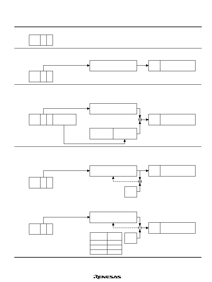
Rev. 1.0, 02/00, page 51 of 1141
Table 2.13 Effective Address Calculation
No.
Addressing Mode and
Instruction Format
Effective Address
Calculation
Effective Address (EA)
1
Register direct (Rn)
op
rm rn
Operand is general register
contents
2
Register indirect (@ERn)
General register contents
31
0
31
0
r
op
24 23
Don't
care
3
Register indirect with displacement
@(d:16, ERn) or @(d:32, ERn)
General register contents
Sign extension
disp
31
0
31
0
31
0
op
r
disp
Don't
care
24 23
4
Register indirect with post-increment or pre-decrement
∑
Register indirect with post-increment @ERn+
General register contents
1, 2, or
4
31
0
31
0
r
op
Don't
care
24 23
∑
Register indirect with pre-decrement @≠ERn
General register contents
1, 2, or
4
Byte
Word
Longword
1
2
4
Operand
Size
Value
Added
31
0
31
0
op
r
Don't
care
24 23
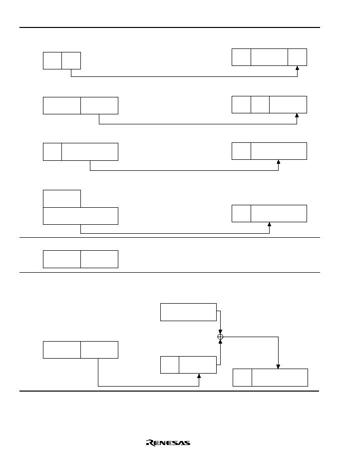
Rev. 1.0, 02/00, page 52 of 1141
No.
Addressing Mode and
Instruction Format
Effective Address
Calculation
Effective Address (EA)
5
Absolute address
@aa:8
@aa:16
@aa:32
31
0
8 7
@aa:24
31
0
16 15
31
0
31
0
op
abs
op
abs
abs
op
op
abs
H'FFFF
24 23
Don't
care
Don't
care
Don't
care
Don't
care
24 23
24 23
24 23
Sign
exten-
sion
6
Immediate #xx:8/#xx:16/#xx:32
op
IMM
Operand is immediate data
7
Program-counter relative
@(d:8, PC)/@(d:16, PC)
0
0
23
23
disp
31
0
24 23
op
disp
PC contents
Don't
care
Sign
exten-
sion
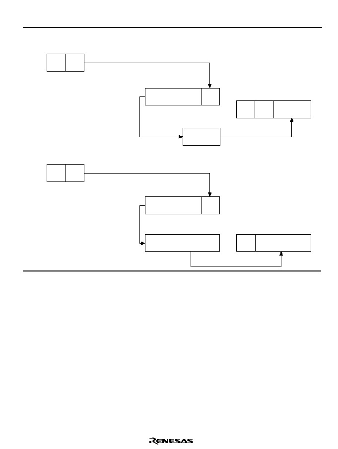
Rev. 1.0, 02/00, page 53 of 1141
No.
Addressing Mode and
Instruction Format
Effective Address
Calculation
Effective Address (EA)
8
Memory indirect @@aa:8
∑
Normal mode
0
0
31
8 7
0
15
H'000000
31
0
16 15
op
abs
abs
Memory
contents
H'00
24 23
Don't
care
∑
Advanced mode
31
0
31
8 7
0
abs
H'000000
31
0
24 23
op
abs
Memory contents
Don't
care
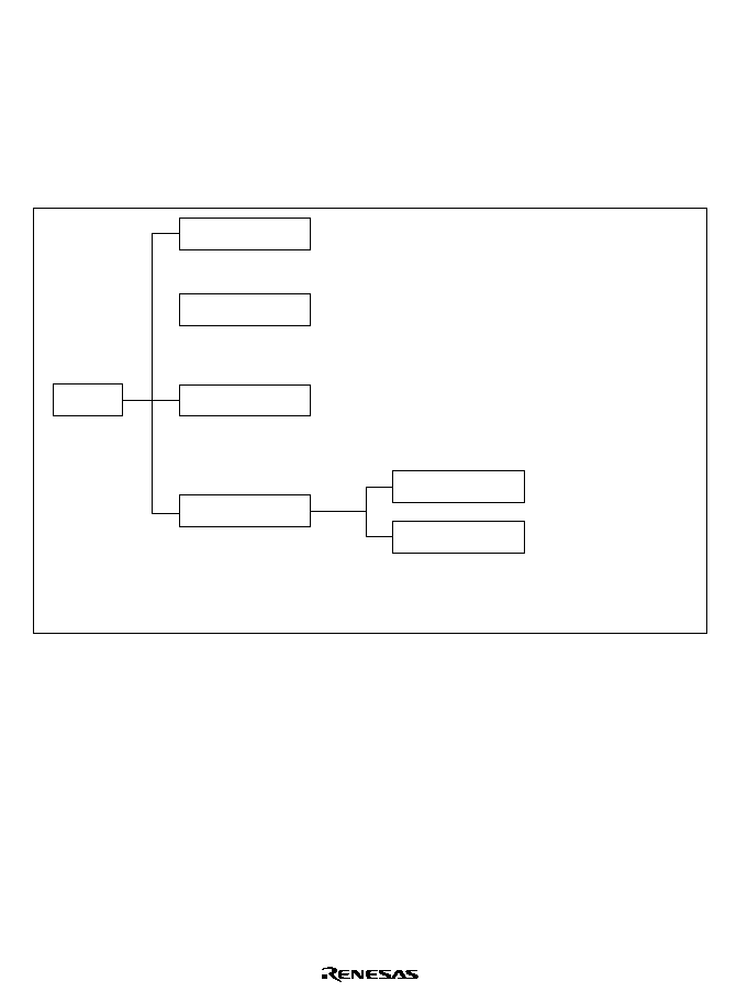
Rev. 1.0, 02/00, page 54 of 1141
2.8
Processing States
2.8.1
Overview
The CPU has four main processing states:
the reset state, exception-handling state, program
execution state, and power-down state. Figure 2.15 shows a diagram of the processing states.
Figure 2.16 indicates the state transitions.
Reset state
The CPU and all on-chip supporting modules have been initialized and are stopped.
Exception-handling
state
A transient state in which the CPU changes the normal processing flow in response
to a reset, interrupt or trap instruction.
Program execution
state
The CPU executes program instructions in sequence.
Power-down state
CPU operation is stopped
to conserve power.*
Sleep mode
Standby mode
Processing
states
Note: *
The power-down state also includes a medium-speed mode, modue stop mode, sub-active mode,
sub-sleep mode and watch mode.
Figure 2.15 Processing States
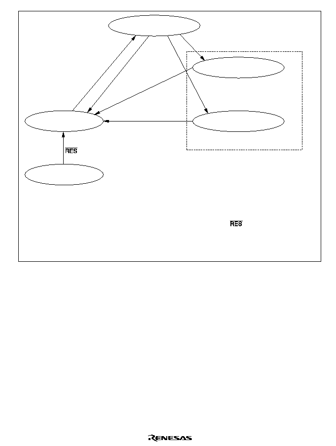
Rev. 1.0, 02/00, page 55 of 1141
Reset state
Exception-handling state
Sleep mode
Standby mode
Power-down state
Program execution state
Interrupt request
External interrupt request
= High
Request for exception handling
SLEEP instruction
with LSON=0,
SSBY=1,
TMA3=0
SLEEP instruction
with LSON=0,
SSBY=0
Notes:
End of exception handling
*1
*2
1.
2.
From any state, a transition to the reset state occurs whenever
goes low. A transition can
also be made to the reset state when the watchdog timer overflows.
The power-down state also includes a watch mode, subactive mode, subsleep mode, etc. For
details, see section 4, Power-Down State.
Figure 2.16 State Transitions
2.8.2
Reset State
When the
#$ input goes low all current processing stops and the CPU enters the reset state.
All interrupts are disabled in the reset state. Reset exception handling starts when the
#$
signal changes from low to high.
The reset state can also be entered by a watchdog timer overflow. For details, see section 17,
Watchdog Timer.

Rev. 1.0, 02/00, page 56 of 1141
2.8.3
Exception-Handling State
The exception-handling state is a transient state that occurs when the CPU alters the normal
processing flow due to a reset, interrupt, or trap instruction. The CPU fetches a start address
(vector) from the exception vector table and branches to that address.
(1) Types of Exception Handling and Their Priority
Exception handling is performed for resets, interrupts, and trap instructions. Table 2.14
indicates the types of exception handling and their priority. Trap instruction exception
handling is always accepted in the program execution state.
Exception handling and the stack structure depend on the interrupt control mode set in
SYSCR.
Table 2.14 Exception Handling Types and Priority
Priority
Type of Exception
Detection Timing
Start of Exception Handling
Reset
Synchronized with
clock
Exception handling starts
immediately after a low-to-high
transition at the
#$
pin, or when the
watchdog timer overflows
Interrupt
End of instruction
execution or end of
exception-handling
sequence
*
1
When an interrupt is requested,
exception handling starts at the end
of the current instruction or current
exception-handling sequence
High
Low
Trap instruction
When TRAPA
instruction is executed
Exception handling starts when a trap
(TRAPA) instruction is executed
*
2
Notes: 1. Interrupts are not detected at the end of the ANDC, ORC, XORC, and LDC
instructions, or immediately after reset exception handling.
2. Trap instruction exception handling is always accepted in the program execution state.
(2) Reset Exception Handling
After the
#$ pin has gone low and the reset state has been entered, when #$ goes high
again, reset exception handling starts. When reset exception handling starts the CPU fetches
a start address (vector) from the exception vector table and starts program execution from
that address. All interrupts, including NMI, are disabled during reset exception handling and
after it ends.
(3) Interrupt Exception Handling and Trap Instruction Exception Handling
When interrupt or trap-instruction exception handling begins, the CPU references the stack
pointer (ER7) and pushes the program counter and other control registers onto the stack.
Next, the CPU alters the settings of the interrupt mask bits in the control registers. Then the
CPU fetches a start address (vector) from the exception vector table and program execution
starts from that start address.

Rev. 1.0, 02/00, page 57 of 1141
Figure 2.17 shows the stack after exception handling ends.
PC
(16 bits)
SP
CCR
CCR
*1
PC
(24 bits)
SP
CCR
Normal Mode
Advanced Mode
*2
Notes: 1. Ignored when returning.
2. Normal mode is not available for this LSI.
Figure 2.17 Stack Structure after Exception Handling (Examples)
2.8.4
Program Execution State
In this state the CPU executes program instructions in sequence.

Rev. 1.0, 02/00, page 58 of 1141
2.8.5
Power-Down State
The power-down state includes both modes in which the CPU stops operating and modes in
which the CPU does not stop. There are five modes in which the CPU stops operating: sleep
mode, standby mode, subsleep mode, and watch mode. There are also three other power-down
modes: medium-speed mode, module stop mode, and subactive mode. In medium-speed mode,
the CPU operates on a medium-speed clock. Module stop mode permits halting of the operation
of individual modules, other than the CPU. Subactive mode, subsleep mode, and watch mode
are power-down modes that use subclock input. For details, see section 4, Power-Down State.
(1) Sleep Mode
A transition to sleep mode is made if the SLEEP instruction is executed while the software
standby bit (SSBY) in the standby control register (SBYCR) and the LSON bit in the low-
power control register (LPWRCR) are both cleared to 0. In sleep mode, CPU operations stop
immediately after execution of the SLEEP instruction. The contents of CPU registers are
retained.
(2) Standby Mode
A transition to standby mode is made if the SLEEP instruction is executed while the SSBY
bit in SBYCR is set to 1 and the LSON bit in LPWRCR and the TMA3 bit in the TMA
(timer A) are both cleared to 0. In standby mode, the CPU and clock halt and all MCU
operations stop. As long as a specified voltage is supplied, the contents of CPU registers and
on-chip RAM are retained.
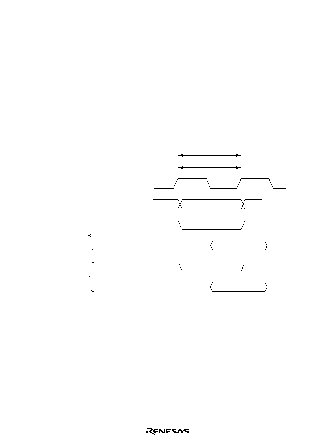
Rev. 1.0, 02/00, page 59 of 1141
2.9
Basic Timing
2.9.1
Overview
The CPU is driven by a system clock, denoted by the symbol
. The period from one rising edge
of
to the next is referred to as a "state." The memory cycle or bus cycle consists of one or two
states. Different methods are used to access on-chip memory and on-chip supporting modules.
2.9.2
On-Chip Memory (ROM, RAM)
On-chip memory is accessed in one state. The data bus is 16 bits wide, permitting both byte and
word transfer instruction. Figure 2.18 shows the on-chip memory access cycle.
Internal address bus
Internal read signal
Internal data bus
Internal write signal
Internal data bus
Bus cycle
T1
Address
Read data
Write data
Read access
Write access
Figure 2.18 On-Chip Memory Access Cycle
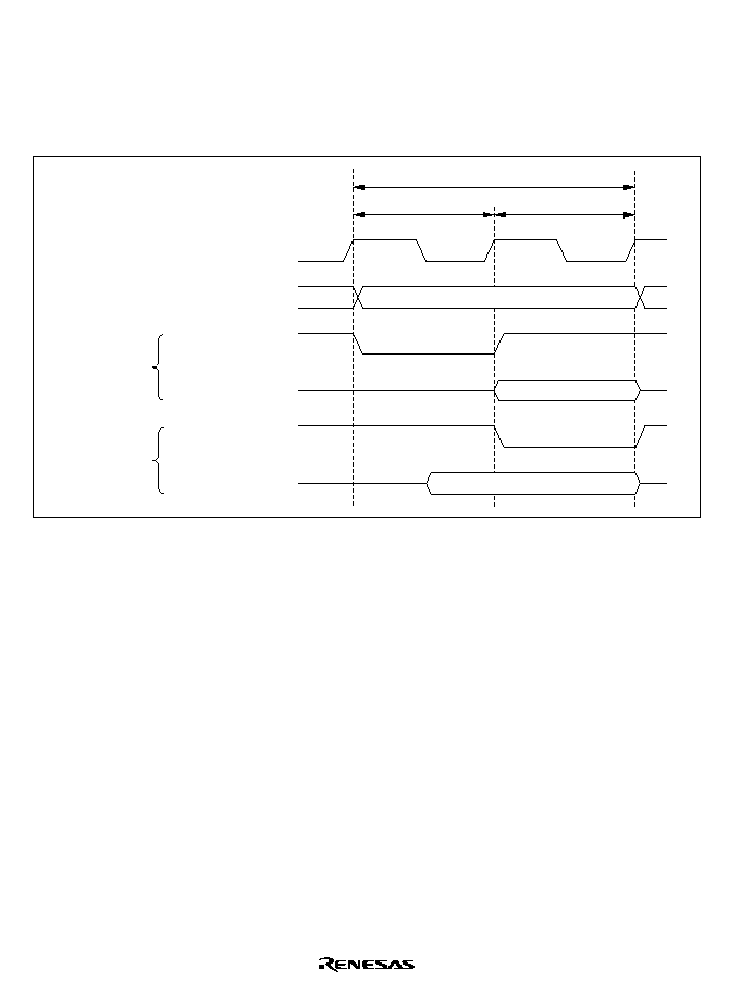
Rev. 1.0, 02/00, page 60 of 1141
2.9.3
On-Chip Supporting Module Access Timing
The on-chip supporting modules are accessed in two states. The data bus is either 8 bits or 16
bits wide, depending on the particular internal I/O register being accessed. Figure 2.19 shows
the access timing for the on-chip supporting modules.
Internal address bus
Internal read signal
Internal data bus
Internal write signal
Internal data bus
Bus cycle
T1
Address
Read access
Write access
Read data
Write data
T2
Figure 2.19 On-Chip Supporting Module Access Cycle

Rev. 1.0, 02/00, page 61 of 1141
Section 3 MCU Operating Modes
3.1
Overview
3.1.1
Operating Mode Selection
This LSI has one operating mode (mode 1). This mode is selected depending on settings of the
mode pin (MD0).
Table 3.1 lists the MCU operating modes.
Table 3.1
MCU Operating Mode Selection
MCU Operating Mode
MD0
CPU Operating Mode
Description
0
0
1
1
Advanced
Single-chip mode
The CPU's architecture allows for 4 Gbytes of address space, but this LSI actually accesses a
maximum of 16 Mbytes.
Mode 1 operation starts in single-chip mode after reset release.
This LSI can only be used in mode 1. This means that the mode pins must be set at mode 1. Do
not changes the inputs at the mode pins during operation.
3.1.2
Register Configuration
This LSI has a mode control register (MDCR) that indicates the inputs at the mode pin (MD0)
and a system control register (SYSCR) and that controls the operation of this LSI. Table 3.2
summarizes these registers.
Table 3.2
MCU Registers
Name
Abbreviation
R/W
Initial Value
Address
*
Mode control register
MDCR
R
Undetermined
H'FFE9
System control register
SYSCR
R/W
H'09
H'FFE8
Note:
*
Lower 16 bits of the address.

Rev. 1.0, 02/00, page 62 of 1141
3.2
Register Descriptions
3.2.1
Mode Control Register (MDCR)
0
--*
1
0
2
0
3
0
4
0
5
--
--
--
--
--
0
6
--
0
7
--
--
--
--
--
--
--
--
R
MDS0
0
Bit :
Initial value :
R/W :
Note: *
Determined by MD0 pin
MDCR is an 8-bit read-only register monitors the current operating mode of this LSI.
Bit 7 to 1: Reserved.
These bits cannot be modified and are always read as 0.
Bit 0: Mode Select 0 (MDS0)
This bit indicates the value which reflects the input levels at mode pin (MD0) (the current
operating mode). Bit MDS0 corresponds to MD0 pin. They are read-only bits-they cannot be
written to. The mode pin (MD0) input levels are latched into these bits when MDCR is read.
3.2.2
System Control Register (SYSCR)
0
--
1
1
0
--
2
0
--
3
1
4
0
R/W
5
0
6
--
0
7
--
--
--
--
R
R
INTM1
INTM0
XRST
--
--
0
Bit :
Initial value :
R/W :
Bits 7 and 6
Reserved: These bits cannot be modified and are always read as 0.

Rev. 1.0, 02/00, page 63 of 1141
Bits 5 and 4
Interrupt control modes 1 and 0 (INTM1, INTM0)
These bits are for selecting the interrupt control mode of the interrupt controller. For details of
the interrupt control modes, see section 6.4.1, Interrupt Control Modes and Interrupt Operation.
Bit 5
Bit 4
INTM1
INTM0
Interrupt
Control Mode
Description
0
0
Interrupt is controlled by bit I
(Initial value)
0
1
1
Interrupt is controlled by bits I and UI, and ICR
0
Cannot be used in this LSI
1
1
Cannot be used in this LSI
Bit 3
External Reset (XRST): Indicates the reset source. When the watchdog timer is used, a
reset can be generated by watchdog timer overflow as well as by external reset input. XRST is a
read-only bit. It is set to 1 by an external reset and cleared to 0 by watchdog timer overflow.
Bit 3
XRST
Description
0
A reset is generated by watchdog timer overflow
1
A reset is generated by an external reset
(Initial value)
Bits 2 and 1
Reserved: These bits cannot be modified and are always read as 0.
Bit 0
Reserved: This bit is always read as 1.
3.3
Operating Mode (Mode 1)
The CPU can access a 16 Mbyte address space in advanced mode.
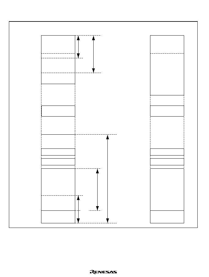
Rev. 1.0, 02/00, page 64 of 1141
3.4
Address Map in Each Operating Mode
H8S/2196
H8S/2197
Memory indirect
branch address
Absolute address, 16 bits
3 kbytes
Vector area
On-chip ROM
(80 kbytes)
Internal I/O register
Internal I/O register
On-chip RAM
Vector area
On-chip ROM
(96 kbytes)
Internal I/O register
Internal I/O register
OSD ROM
(24 kbytes)
On-chip RAM
H'000000
H'000000
H'017FFF
H'FFD000
H'040000
H'045FFF
H'FFD2FF
H'FFD800
H'FFDAFF
H'FFF3B0
H'FFFFAF
H'FFFFB0
H'FFFFFF
H'0000FF
H'007FFF
H'013FFF
H'FF8000
H'FFD000
H'FFD2FF
H'FFF3B0
H'FFFF00
H'FFFFAF
H'FFFFB0
H'FFFFFF
OSD RAM (768 bytes)
OSD ROM
(24 kbytes)
H'040000
H'045FFF
H'FFD800
H'FFDAFF
OSD RAM (768 bytes)
Absolute address,
8 bits
Absolute address, 16 bits
Figure 3.1 Address Map (1)
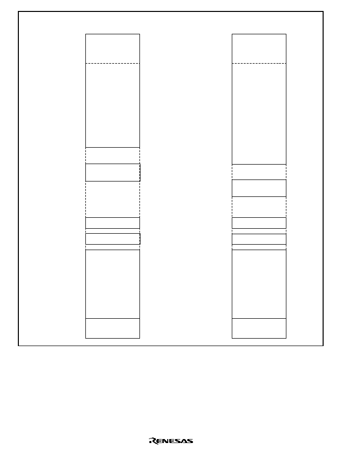
Rev. 1.0, 02/00, page 65 of 1141
H8S/2198
H8S/2199
Vector area
On-chip ROM
(112 kbytes)
Internal I/O register
Internal I/O register
On-chip RAM
Vector area
On-chip ROM
(128 kbytes)
Internal I/O register
Internal I/O register
On-chip RAM
H'000000
H'000000
H'01FFFF
H'FFD000
H'FFD2FF
H'FFF3B0
H'FFFFAF
H'FFFFB0
H'FFFFFF
H'01BFFF
H'FFD000
H'FFD2FF
H'FFF3B0
H'FFFFAF
H'FFFFB0
H'FFFFFF
OSD ROM
(24 kbytes)
H'040000
H'045FFF
H'FFD800
H'FFDAFF
OSD RAM (768 bytes)
OSD ROM
(24 kbytes)
H'040000
H'045FFF
H'FFD800
H'FFDAFF
OSD RAM (768 bytes)
Figure 3.2 Address Map (2)

Rev. 1.0, 02/00, page 67 of 1141
Section 4 Power-Down State
4.1
Overview
In addition to the normal program execution state, this LSI has a power-down state in which
operation of the CPU and oscillator is halted and power dissipation is reduced. Low-power
operation can be achieved by individually controlling the CPU, on-chip supporting modules, and
so on.
This LSI operating modes are as follows:
1. High-speed mode
2. Medium-speed mode
3. Sub-active mode
4. Sleep mode
5. Sub-sleep mode
6. Watch mode
7. Module stop mode
8. Standby mode
Of these, 2 to 8 are power-down modes. Certain combinations of these modes can be set.
After a reset, the MCU is in high-speed mode.
Table 4.1 shows the internal chip states in each mode, and table 4.2 shows the conditions for
transition to the various modes. Figure 4.1 shows a mode transition diagram.

Rev. 1.0, 02/00, page 68 of 1141
Table 4.1
H8S/2199 Series Internal States in Each Mode
Function
High-Speed
Medium-
Speed
Sleep
Module
Stop
Watch
Sub-active Sub-sleep Standby
System clock
Functioning Functioning Functioning Functioning Halted
Halted
Halted
Halted
Subclock pulse generator
Functioning Functioning Functioning Functioning Functioning Functioning Functioning Functioning
Instructions
Halted
Halted
Halted
Halted
CPU
operation
Registers
Functioning Medium-
speed
Retained
Functioning
Retained
Subclock
operation
Retained
Retained
IRQ0
IRQ1
Functioning Functioning Functioning Functioning
IRQ2
IRQ3
IRQ4
External
interrupts
IRQ5
Functioning Functioning Functioning Functioning
Halted
Halted
Functioning Halted
I/O
Functioning Functioning Retained
Functioning Halted
Functioning Retained
Halted
Timer A
Functioning Functioning Functioning Functioning
/halted
(retained)
Subclock
operation
Subclock
operation
Subclock
operation
Halted
(retained)
Timer B
Timer J
Timer L
Functioning
/halted
(retained)
Halted
(retained)
Halted
(retained)
Halted
(retained)
Halted
(retained)
Timer R
On-chip
supporting
module
operation
Timer X1
Functioning Functioning Functioning
Functioning
/halted
(reset)
Halted
(reset)
Halted
(reset)
Halted
(reset)
Halted
(reset)
Watchdog
timer
Functioning Functioning Functioning Functioning Halted
(retained)
Halted
(retained)
Halted
(retained)
Halted
(retained)
8-bit PWM
12-bit PWM
*
2
14-bit PWM
Functioning Functioning Functioning Functioning
/halted
(retained)
Halted
(retained)
Halted
(retained)
Halted
(retained)
Halted
(retained)
PSU
Functioning Functioning Functioning Functioning
/halted
Subclock
operation
Subclock
operation
Subclock
operation
Halted
SCI1
Functioning
/halted
*
1
Halted
*
1
Halted
*
1
Halted
*
1
Halted
*
1
IIC
Functioning
/halted
(retained)
Halted
(retained)
Halted
(retained)
Halted
(retained)
Halted
(retained)
A/D
Functioning Functioning Functioning
Functioning
/halted
(reset)
Halted
(reset)
Halted
(reset)
Halted
(reset)
Halted
(reset)
Servo
Functioning Functioning Halted
(reset)
Functioning
/halted
(reset)
Halted
(reset)
Halted
(reset)
Halted
(reset)
Halted
(reset)
Sync
separator
Functioning Functioning Halted
(retained)
Functioning
/halted
(retained)
Halted
(retained)
Halted
(retained)
Halted
(retained)
Halted
(retained)
Data slicer
Halted
(reset)
OSD
Functioning Functioning Halted
(reset)
Functioning
/halted
(reset)
Halted
(reset)
Halted
(reset)
Halted
(reset)
Notes: 1. "Halted (retained)" means that internal register values are retained. The internal state
is "operation suspended."
2. "Halted (reset)" means that internal register values and internal states are initialized.
3. In module stop mode, only modules for which a stop setting has been made are halted
(reset or retained).

Rev. 1.0, 02/00, page 69 of 1141
4. In the power-down mode, the analog section of the servo circuits are not turned off,
therefore Vcc (Servo) current does not go low. When power-down is needed,
externally shut down the analog system power.
*
1 The SCI1 status differs from the internal register. For details, refer to section 22, Serial
Communication Interface 1.
*
2 The state of the 12-bit PWM is the same as that of the servo circuit.
Program-halted state
Conditions for mode transition (1)
Conditions for mode transition (2)
Interruption factor
Sleep
(high-speed)
mode
Sleep
(medium-speed)
mode
Subsleep
mode
Program execution state
Reset state
Flag
SLEEP
instruction
Interrupt
LSON SSBY TMA3 DTON
a
0
1
0
*
b
*
1
1
0
c
0
1
1
1
d
1
1
1
1
e
0
0
*
*
f
1
0
1
*
g
SCK1 to 0 = 0
h
SCK1 to 0 0 (either 1 bit = 0)
Power-down mode
Active
(high-speed)
mode
Active
(medium-speed)
mode
Subactive
mode
Program-halted state
Watch
mode
Standby
mode
IRQ0
to
1
IRQ0
to
1, Timer A interruption
All interruption (excluding servo system)
IRQ0
to
5, Timer A interruption
1
2
3
4
Interrupt
Interrupt
SLEEP
instruction
SLEEP
instruction
e
Note: When a transition is made between
modes by means of an interrupt,
transition cannot be made on interrupt
source generation alone. Ensure that
interrupt handling is performed after
accepting the interrupt request
SLEEP
instruction a
1
Interrupt
1
2
SLEEP
instruction
SLEEP
instruction
SLEEP
instruction
SLEEP
instruction
a
b
g
h
d
SLEEP
instruction
c
e
3
Interrupt 2
Interrupt 3
Interrupt 2
Interrupt 4
c
SLEEP
instruction
d
b
b
SLEEP
instruction
SLEEP
instruction 1
Note:
*
Don't care
Figure 4.1 Mode Transitions

Rev. 1.0, 02/00, page 70 of 1141
Table 4.2
Power-Down Mode Transition Conditions
Control Bit States at Time of
Transition
State before
Transition
SSBY
TMA3
LSON
DTON
State after Transition
by SLEEP Instruction
State after Return
by Interrupt
0
*
0
*
Sleep
High-speed/
medium-speed
*
1
0
*
1
*
1
0
0
*
Standby
High-speed/
medium-speed
*
1
1
0
1
*
1
1
0
0
Watch
High-speed/
medium-speed
*
1
1
1
1
0
Watch
Subactive
1
1
0
1
High-speed/
medium-
speed
1
1
1
1
Subactive
0
0
*
*
0
1
0
*
0
1
1
*
Subsleep
Subactive
1
0
*
*
1
1
0
0
Watch
High-speed/
medium-speed
*
2
1
1
1
0
Watch
Subactive
1
1
0
1
High-speed/
medium-speed
*
2
Subactive
1
1
1
1
Notes:
*
Don't care
: Do not set.
1. Returns to the state before transition.
2. Mode varies depending on the state of SCK1 to SCK0.

Rev. 1.0, 02/00, page 71 of 1141
4.1.1
Register Configuration
The power-down state is controlled by the SBYCR, LPWRCR, TMA (Timer A), and MSTPCR
registers. Table 4.3 summarizes these registers.
Table 4.3
Power-Down State Registers
Name
Abbreviation
R/W
Initial Value
Address
*
Standby control register
SBYCR
R/W
H'00
H'FFEA
Low-power control register
LPWRCR
R/W
H'00
H'FFEB
MSTPCRH
R/W
H'FF
H'FFEC
Module stop control register
MSTPCRL
R/W
H'FF
H'FFED
Timer mode register A
TMA
R/W
H'30
H'FFBA
Note:
*
Lower 16 bits of the address.

Rev. 1.0, 02/00, page 72 of 1141
4.2
Register Descriptions
4.2.1
Standby Control Register (SBYCR)
0
0
1
0
R/W
2
0
3
--
--
--
--
0
4
0
R/W
5
0
6
0
7
R/W
R/W
STS1
R/W
STS2
0
R/W
SSBY
STS0
SCK1
SCK0
Bit :
Initial value :
R/W :
SBYCR is an 8-bit readable/writable register that performs power-down mode control.
SBYCR is initialized to H'00 by a reset.
Bit 7
Software Standby (SSBY): Determines the operating mode, in combination with other
control bits, when a power-down mode transition is made by executing a SLEEP instruction.
The SSBY setting is not changed by a mode transition due to an interrupt, etc.
Bit 7
SSBY
Description
0
Transition to sleep mode after execution of SLEEP instruction in high-speed mode
or medium-speed mode
Transition to subsleep mode after execution of SLEEP instruction in subactive
mode
(Initial value)
1
Transition to standby mode, subactive mode, or watch mode after execution of
SLEEP instruction in high-speed mode or medium-speed mode
Transition to watch mode or high-speed mode after execution of SLEEP
instruction in subactive mode

Rev. 1.0, 02/00, page 73 of 1141
Bits 6 to 4
Standby Timer Select 2 to 0 (STS2 to STS0): These bits select the time the MCU
waits for the clock to stabilize when standby mode, watch mode, or subactive mode is cleared
and a transition is made to high-speed mode or medium-speed mode by means of a specific
interrupt or instruction. With crystal oscillation, see table 4.5 and make a selection according to
the operating frequency so that the standby time is at least 10 ms (the oscillation settling time).
Bit 6
Bit 5
Bit 4
STS2
STS1
STS0
Description
0
0
0
Standby time = 8192 states
0
0
1
Standby time = 16384 states
0
1
0
Standby time = 32768 states
0
1
1
Standby time = 65536 states
1
0
0
Standby time = 131072 states
1
0
1
Standby time = 262144 states
1
1
*
Reserved
Note:
*
Don't care
Bits 3 and 2
Reserved: These bits cannot be modified and are always read as 0.
Bits 1 and 0
System Clock Select 1, 0 (SCK1, SCK0): These bits select the CPU clock for the
bus master in high-speed mode and medium-speed mode.
Bit 1
Bit 2
SCK1
SCK0
Description
0
0
Bus master is in high-speed mode (Initial value)
0
1
Medium-speed clock is
/16
1
0
Medium-speed clock is
/32
1
1
Medium-speed clock is
/64

Rev. 1.0, 02/00, page 74 of 1141
4.2.2
Low-Power Control Register (LPWRCR)
0
0
1
0
R/W
R/W
2
0
3
0
4
--
--
--
--
--
--
0
5
0
6
0
7
R/W
NESEL
R/W
LSON
0
R/W
DTON
SA1
SA0
Bit :
Initial value :
R/W :
LPWRCR is an 8-bit readable/writable register that performs power-down mode control.
LPWRCR is initialized to H'00 by a reset.
Bit 7
Direct-Transfer on Flag (DTON): Specifies whether a direct transition is made between
high-speed mode, medium-speed mode, and subactive mode when making a power-down
transition by executing a SLEEP instruction. The operating mode to which the transition is
made after SLEEP instruction execution is determined by a combination of other control bits.
Bit 7
DTON
Description
0
∑
When a SLEEP instruction is executed in high-speed mode or medium-speed
mode, a transition is made to sleep mode, standby mode, or watch mode
∑
When a SLEEP instruction is executed in subactive mode, a transition is made
to subsleep mode or watch mode
(Initial value)
1
∑
When a SLEEP instruction is executed in high-speed mode or medium-speed
mode, transition is made directly to subactive mode, or a transition is made to
sleep mode or standby mode
∑
When a SLEEP instruction is executed in subactive mode, a transition is made
directly to high-speed mode, or a transition is made to subsleep mode

Rev. 1.0, 02/00, page 75 of 1141
Bit 6
Low-Speed on Flag (LSON): Determines the operating mode in combination with other
control bits when making a power-down transition by executing a SLEEP instruction. Also
controls whether a transition is made to high-speed mode or to subactive mode when watch
mode is cleared.
Bit 6
LSON
Description
0
∑
When a SLEEP instruction is executed in high-speed mode or medium-speed
mode, transition is made to sleep mode, standby mode, or watch mode
∑
When a SLEEP instruction is executed in subactive mode, a transition is made
to watch mode, or directly to high-speed mode
∑
After watch mode is cleared, a transition is made to high-speed mode
(Initial value)
1
∑
When a SLEEP instruction is executed in high-speed mode a transition is made
to watch mode, subactive mode, sleep mode or standby mode
∑
When a SLEEP instruction is executed in subactive mode, a transition is made
to subsleep mode or watch mode
∑
After watch mode is cleared, a transition is made to subactive mode
Bit 5
Noise Elimination Sampling Frequency Select (NESEL): Selects the frequency at
which the subclock (
w) generated by the subclock pulse generator is sampled with the clock (
)
generated by the system clock oscillator. When
= 5 MHz or higher, clear this bit to 0.
Bit 5
NESEL
Description
0
Sampling at
divided by 16
1
Sampling at
divided by 4
Bits 4 to 2
Reserved: These bits cannot be modified and are always read as 0.
Bits 1 and 0
Subactive Mode Clock Select 1, 0 (SA1, SA0): These bits select the CPU
operating clock in the subactive mode. These bits cannot be modified in the subactive mode.
Bit 1
Bit 0
SA1
SA0
Description
0
0
Operating clock of CPU is
w/8
(Initial value)
0
1
Operating clock of CPU is
w/4
1
*
Operating clock of CPU is
w/2
Note:
*
Don't care

Rev. 1.0, 02/00, page 76 of 1141
4.2.3
Timer Register A (TMA)
0
0
1
0
R/W
2
0
3
0
4
1
5
--
--
1
6
0
7
R/W
R/W
R/W
R/W
TMA3
R/W
TMA2
R/W
TMAIE
0
R/(W)*
TMAOV
TMA1
TMA0
Bit :
Initial value :
R/W :
Note: *
Only 0 can be written, to clear the flag.
The timer register A (TMA) controls timer A interrupts and selects input clock.
Only bit 3 is explained here. For details of other bits, see section 11.2.1, Timer Mode Register
A.
TMA is a readable/writable register which is initialized to H'30 by a reset.
Bit 3
Clock Source, Prescaler Select (TMA3): Selects timer A clock source between PSS and
PSW. It also controls transition operation to the power-down mode. The operation mode to
which the MCU is transited after SLEEP instruction execution is determined by the combination
with other control bits.
For details, see the description of clock select 2 to 0 in section 11.2.1, Timer Mode Register A.
Bit 3
TMA3
Description
0
∑
Timer A counts
-based prescaler (PSS) divided clock pulses
∑
When a SLEEP instruction is executed in high-speed mode or medium-speed
mode, a transition is made to sleep mode or software standby mode
(Initial value)
1
∑
Timer A counts
w-based prescaler (PSW) divided clock pulses
∑
When a SLEEP instruction is executed in high-speed mode or medium-speed
mode, a transition is made to sleep mode, watch mode, or subactive mode
∑
When a SLEEP instruction is executed in subactive mode, a transition is made
to subsleep mode, watch mode, or high-speed mode

Rev. 1.0, 02/00, page 77 of 1141
4.2.4
Module Stop Control Register (MSTPCR)
7
1
MSTP15
R/W
MSTPCRH
6
1
MSTP14
R/W
5
1
MSTP13
R/W
4
1
MSTP12
R/W
3
1
MSTP11
R/W
2
1
MSTP10
R/W
1
1
MSTP9
R/W
0
1
MSTP8
R/W
7
1
MSTP7
R/W
6
1
MSTP6
R/W
5
1
MSTP5
R/W
4
1
MSTP4
R/W
3
1
MSTP3
R/W
2
1
MSTP2
R/W
1
1
MSTP1
R/W
0
1
MSTP0
R/W
MSTPCRL
Bit :
Initial value :
R/W :
MSTPCR comprises two 8-bit readable/writable registers that perform module stop mode
control.
MSTPCR is initialized to H'FFFF by a reset.
MSTRCRH and MSTPCRL Bits 7 to 0
Module Stop (MSTP 15 to MSTP 0): These bits
specify module stop mode. See table 4.4 for the method of selecting on-chip supporting
modules.
MSTPCRH, MSTPCRL
Bits 7 to 0
MSTP 15 to MSTP 0
Description
0
Module stop mode is cleared
1
Module stop mode is set
(Initial value)
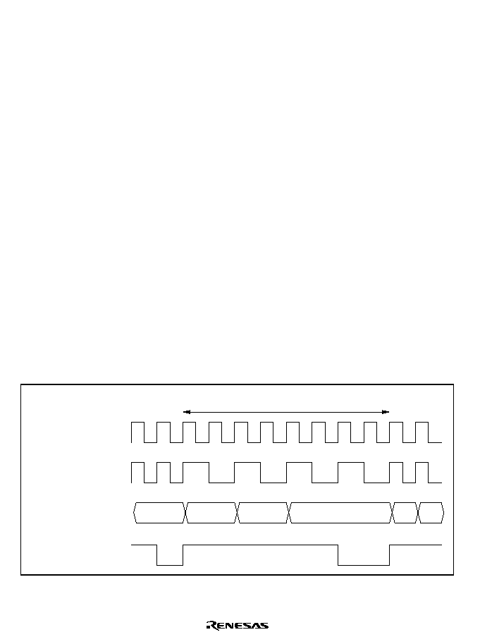
Rev. 1.0, 02/00, page 78 of 1141
4.3
Medium-Speed Mode
When the SCK1 and SCK0 bits in SBYCR are set to 1 in high-speed mode, the operating mode
changes to medium-speed mode at the end of the bus cycle. In medium-speed mode, the CPU
operates on the operating clock (
16,
32 or
64) specified by the SCK1 and SCK0 bits. The
on-chip supporting modules other than the CPU always operate on the high-speed clock (
).
In medium-speed mode, a bus access is executed in the specified number of states with respect
to the bus master operating clock. For example, if
16 is selected as the operating clock, on-
chip memory is accessed in 16 states, and internal I/O registers in 32 states.
Medium-speed mode is cleared by clearing the both bits SCK1 and SCK0 to 0. A transition is
made to high-speed mode and medium-speed mode is cleared at the end of the current bus cycle.
If a SLEEP instruction is executed when the SSBY bit in SBYCR and the LSON bit in
LPWRCR are cleared to 0, a transition is made to sleep mode. When sleep mode is cleared by
an interrupt, medium-speed mode is restored.
If a SLEEP instruction is executed when the SSBY bit in SBYCR is set to 1, and the LSON bit
in LPWRCR and the TMA3 bit in TMA (Timer A) are both cleared to 0, a transition is made to
software standby mode. When standby mode is cleared by an external interrupt, medium-speed
mode is restored.
When the
5(6 pin is driven low, a transition is made to the reset state, and medium-speed mode
is cleared. The same applies in the case of a reset caused by overflow of the watchdog timer.
Figure 4.2 shows the timing for transition to and clearance of medium-speed mode.
Medium-speed mode
Internal
,
supporting module clock
CPU clock
Internal address bus
Internal write signal
SBYCR
SBYCR
Figure 4.2 Medium-Speed Mode Transition and Clearance Timing

Rev. 1.0, 02/00, page 79 of 1141
4.4
Sleep Mode
4.4.1
Sleep Mode
If a SLEEP instruction is executed when the SSBY bit in SBYCR and the LSON bit in
LPWRCR are both cleared to 0, the CPU will enter sleep mode. In sleep mode, CPU operation
stops but the contents of the CPU's internal registers are retained. Other supporting modules
(excluding some functions) do not stop.
4.4.2
Clearing Sleep Mode
Sleep mode is cleared by any interrupt, or with the
5(6 pin.
Clearing with an Interrupt: When an interrupt request signal is input, sleep mode is cleared
and interrupt exception handling is started. Sleep mode will not be cleared if interrupts are
disabled, or if interrupts other than NMI have been masked by the CPU.
Clearing with the
#$
#$ Pin: When the 5(6 pin is driven low, the reset state is entered. When
the
5(6 pin is driven high after the prescribed reset input period, the CPU begins reset exception
handling.

Rev. 1.0, 02/00, page 80 of 1141
4.5
Module Stop Mode
4.5.1
Module Stop Mode
Module stop mode can be set for individual on-chip supporting modules.
When the corresponding MSTP bit in MSTPCR is set to 1, module operation stops at the end of
the bus cycle and a transition is made to module stop mode. The CPU continues operating
independently.
Table 4.4 shows MSTP bits and the on-chip supporting modules.
When the corresponding MSTP bit is cleared to 0, module stop mode is cleared and the module
starts operating again at the end of the bus cycle. In module stop mode, the internal states of
modules excluding some modules are retained.
After reset release, all modules are in module stop mode.
When an on-chip supporting module is in module stop mode, read/write access to its registers is
disabled.
Table 4.4
MSTP Bits and Corresponding On-Chip Supporting Modules
Register
Bit
Module
MSTP15
Timer A
MSTP14
Timer B
MSTP13
Timer J
MSTP12
Timer L
MSTP11
Timer R
MSTP10
Timer X1
MSTP9
Sync separator
MSTPCRH
MSTP8
Serial communication interface 1 (SCI1)
MSTP7
I
2
C bus interface (IIC0)
MSTP6
I
2
C bus interface (IIC1)
MSTP5
14-bit PWM
MSTP4
8-bit PWM
MSTP3
Data slicer
MSTP2
A/D converter
MSTP1
Servo circuit
MSTPCRL
MSTP0
OSD

Rev. 1.0, 02/00, page 81 of 1141
4.6
Standby Mode
4.6.1
Standby Mode
If a SLEEP instruction is executed when the SSBY bit in SBYCR is set to 1, the LSON bit in
LPWRCR is cleared to 0, and the TMA3 bit in TMA (Timer A) is cleared to 0, standby mode
will be entered. In this mode, the CPU, on-chip supporting modules, and oscillator (except for
subclock oscillator) all stop. However, the contents of the CPU's internal registers and data in
the on-chip RAM, as well as on-chip peripheral circuits (with some exceptions), are maintained
in the current state. (Timer X1 and SCI1 are partially reset.) The I/O port, at this time, is
caused to the high impedance state.
In this mode the oscillator stops, and therefore power dissipation is significantly reduced.
4.6.2
Clearing Standby Mode
Standby mode is cleared by an external interrupt (pin
,54 to ,54), or by means of the 5(6
pin.
Clearing with an Interrupt: When an
,54 to ,54 interrupt request signal is input, clock
oscillation starts, and after the elapse of the time set in bits STS2 to STS0 in SYSCR, stable
clocks are supplied to the entire chip, standby mode is cleared, and interrupt exception handling
is started.
Standby mode cannot be cleared with an
,54 to ,54 interrupt if the corresponding enable bit
has been cleared to 0 or has been masked by the CPU.
Clearing with the
#$
#$ Pin: When the 5(6 pin is driven low, clock oscillation is started. At
the same time as clock oscillation starts, clocks are supplied to the entire chip. Note that the
5(6 pin must be held low until clock oscillation stabilizes. When the 5(6 pin goes high, the
CPU begins reset exception handling.
4.6.3
Setting Oscillation Settling Time after Clearing Standby Mode
Bits STS2 to STS0 in SBYCR should be set as described below.
Using a Crystal Oscillator: Set bits STS2 to STS0 so that the standby time is at least 10 ms (the
oscillation settling time).
Table 4.5 shows the standby times for different operating frequencies and settings of bits STS2
to STS0.

Rev. 1.0, 02/00, page 82 of 1141
Table 4.5
Oscillation Settling Time Settings
STS2
STS1
STS0
Standby Time
10 MHz
8 MHz
Unit
0
8192 states
0.8
1.0
0
1
16384 states
1.6
2.0
0
32768 states
3.3
4.1
0
1
1
65536 states
6.6
8.2
0
131072 states
13.1
*
1
16.4
*
1
0
1
262144 states
26.2
32.8
ms
1
1
*
Reserved
µ
s
Notes:
*
Don't care
1. Recommended time setting
Using an External Clock: Any value can be set.

Rev. 1.0, 02/00, page 83 of 1141
4.7
Watch Mode
4.7.1
Watch Mode
If a SLEEP instruction is executed in high-speed mode, medium-speed mode or subactive mode
when the SSBY in SBYCR is set to 1, the DTON bit in LPWRCR is cleared to 0, and the TMA3
bit in TMA (Timer A) is set to 1, the CPU will make a transition to watch mode.
In this mode, the CPU and all on-chip supporting modules except timer A stop. As long as the
prescribed voltage is supplied, the contents of CPU registers, some on-chip supporting module
registers, and on-chip RAM, are retained, and I/O ports are placed in the high-impedance state.
4.7.2
Clearing Watch Mode
Watch mode is cleared by an interrupt (Timer A interrupt, or pin
,54 to ,54), or by means of
the
5(6 pin.
Clearing with an Interrupt: When an interrupt request signal is input, watch mode is cleared
and a transition is made to high-speed mode or medium-speed mode if the LSON bit in
LPWRCR is cleared to 0, or to subactive mode if the LSON bit is set to 1. When making a
transition to medium-speed mode, after the elapse of the time set in bits STS2 to STS0 in
SBYCR, stable clocks are supplied to the entire chip, and interrupt exception handling is started.
Watch mode cannot be cleared with an
,54 to ,54 interrupt if the corresponding enable bit
has been cleared to 0, or with an on-chip supporting module interrupt if acceptance of the
relevant interrupt has been disabled by the interrupt enable register or masked by the CPU.
See section 4.6.3, Setting Oscillation Settling Time after Clearing Standby Mode, for the
oscillation settling time setting when making a transition from watch mode to high-speed mode
or medium-speed mode.
Clearing with the
#$
#$ Pin: See (2) Clearing with the 5(6 Pin in section 4.6.2, Clearing
Standby Mode.

Rev. 1.0, 02/00, page 84 of 1141
4.8
Subsleep Mode
4.8.1
Subsleep Mode
If a SLEEP instruction is executed in subactive mode when the SSBY in SBYCR is cleared to 0,
the LSON bit in LPWRCR is set to 1, and the TMA3 bit in TMA (Timer A) is set to 1, the CPU
will make a transition to subsleep mode.
In this mode, the CPU and all on-chip supporting modules other than Timer A stop. As long as
the prescribed voltage is supplied, the contents of CPU registers, some on-chip supporting
module registers, and on-chip RAM, are retained, and I/O ports are placed in the high-
impedance state.
4.8.2
Clearing Subsleep Mode
Subsleep mode is cleared by an interrupt (Timer A interrupt, or pin
,54 to ,54), or by means
of the
5(6 pin.
Clearing with an Interrupt: When an interrupt request signal is input, subsleep mode is cleared
and interrupt exception handling is started. Subsleep mode cannot be cleared with an
,54 to
,54 interrupt if the corresponding enable bit has been cleared to 0, or with an on-chip
supporting module interrupt if acceptance of the relevant interrupt has been disabled by the
interrupt enable register or masked by the CPU.
Clearing with the
#$
#$ Pin: See (2) Clearing with the 5(6 Pin in section 4.6.2, Clearing
Standby Mode.

Rev. 1.0, 02/00, page 85 of 1141
4.9
Subactive Mode
4.9.1
Subactive Mode
If a SLEEP instruction is executed in high-speed mode when the SSBY bit in SBYCR, the
DTON bit in LPWRCR, and the TMA3 bit in TMA (timer A) are all set to 1, the CPU will make
a transition to subactive mode. When an interrupt is generated in watch mode, if the LSON bit
in LPWRCR is set to 1, a transition is made to subactive mode. When an interrupt is generated
in subsleep mode, a transition is made to subactive mode.
In subactive mode, the CPU performs sequential program execution at low speed on the
subclock. In this mode, all on-chip supporting modules other than timer A stop.
4.9.2
Clearing Subactive Mode
Subsleep mode is cleared by a SLEEP instruction, or by means of the
5(6 pin.
Clearing with a SLEEP Instruction: When a SLEEP instruction is executed while the SSBY
bit in SBYCR is set to 1, the DTON bit in LPWRCR is cleared to 0, and the TMA3 bit in TMA
(timer A) is set to 1, subactive mode is cleared and a transition is made to watch mode. When a
SLEEP instruction is executed while the SSBY bit in SBYCR is cleared to 0, the LSON bit in
LPWRCR is set to 1, and the TMA3 bit in TMA (timer A) is set to 1, a transition is made to
subsleep mode. When a SLEEP instruction is executed while the SSBY bit in SBYCR is set to
1, the DTON bit is set to 1 and the LSON bit is cleared to 0 in LPWRCR, and the TMA3 bit in
TMA (timer A) is set to 1, a transition is made directly to high-speed or medium-speed mode.
For details of direct transition, see section 4.10, Direct Transition.
Clearing with the
#$
#$ Pin: See (2) Clearing with the 5(6 Pin in section 4.6.2, Clearing
Standby Mode.

Rev. 1.0, 02/00, page 86 of 1141
4.10
Direct Transition
4.10.1
Overview of Direct Transition
There are three operating modes in which the CPU executes programs: high-speed mode,
medium-speed mode, and subactive mode. A transition between high-speed mode and subactive
mode without halting the program* is called a direct transition. A direct transition can be
carried out by setting the DTON bit in LPWRCR to 1 and executing a SLEEP instruction. After
the transition, direct transition interrupt exception handling is started.
Direct Transition from High-Speed Mode to Subactive Mode: If a SLEEP instruction is
executed in high-speed mode while the SSBY bit in SBYCR, the LSON bit and DTON bit in
LPWRCR, and the TMA3 bit in TMA (Timer A) are all set to 1, a transition is made to
subactive mode.
Direct Transition from Subactive Mode to High-Speed Mode/Medium-Speed Mode: If a
SLEEP instruction is executed in subactive mode while the SSBY bit in SBYCR is set to 1, the
LSON bit is cleared to 0 and the DTON bit is set to 1 in LPWRCR, and the TMA3 bit in TMA
(timer A) is set to 1, after the elapse of the time set in bits STS2 to STS0 in SBYCR, a transition
is made to directly to high-speed mode or medium-speed mode.
Note: *
At the time of transition from subactive mode to high- or medium-speed mode, an
oscillation stabilization wait time is generated.

Rev. 1.0, 02/00, page 87 of 1141
Section 5 Exception Handling
5.1
Overview
5.1.1
Exception Handling Types and Priority
As table 5.1 indicates, exception handling may be caused by a reset, trap instruction, or
interrupt. Exception handling is prioritized as shown in table 5.1. If two or more exceptions
occur simultaneously, they are accepted and processed in order of priority. Trap instruction
exceptions are accepted at all times in the program execution state.
Exception handling sources, the stack structure, and the operation of the CPU vary depending on
the interrupt control mode set by the INTM0 and INTM1 bits in SYSCR.
Table 5.1
Exception Types and Priority
Priority
Exception
Type
Start of Exception Handling
Reset
Starts immediately after a low-to-high transition at the
#$
pin, or
when the watchdog timer overflows
Trace
*
1
Starts when execution of the current instruction or exception
handling ends, if the trace (T) bit is set to 1
Interrupt
Starts when execution of the current instruction or exception
handling ends, if an interrupt request has been issued
*
2
Direct transition
Started by a direct transition resulting from execution of a SLEEP
instruction
High
Low
Trap instruction
(TRAPA)
*
3
Started by execution of a trap instruction (TRAPA)
Notes: 1. Traces are enabled only in interrupt control modes 2 and 3. (They cannot be used in
this LSI.) Trace exception handling is not executed after execution of an RTE
instruction.
2. Interrupt detection is not performed on completion of ANDC, ORC, XORC, or LDC
instruction execution, or on completion of reset exception handling.
3. Trap instruction exception handling requests are accepted at all times in the program
execution state.

Rev. 1.0, 02/00, page 88 of 1141
5.1.2
Exception Handling Operation
Exceptions originate from various sources. Trap instructions and interrupts are handled as
follows:
1. The program counter (PC) and condition-code register (CCR) are pushed onto the stack.
2. The interrupt mask bits are updated. The T bit is cleared to 0.
3. A vector address corresponding to the exception source is generated, and program execution
starts from that address.
For a reset exception, steps 2 and 3 above are carried out.
5.1.3
Exception Sources and Vector Table
The exception sources are classified as shown in figure 5.1. Different vector addresses are
assigned to different exception sources.
Table 5.2 lists the exception sources and their vector addresses.
Exception sources
∑ Reset
∑ Interrupts
∑ Trap instruction
Note:
*
In this LSI, the watchdog timer generates NMIs.
∑ Trace (cannot be used in this LSI)
∑ Direct transition
External interrupts NMI
*
, IRQ5 to IRQ0
Internal interrupts Interrupt sources in on-chip supporting modules
...
...
Figure 5.1 Exception Sources

Rev. 1.0, 02/00, page 89 of 1141
Table 5.2
Exception Vector Table
Exception Source
Vector Number
Vector Address
*
1
Reset
0
H'0000 to H'0003
1
H'0004 to H'0007
2
H'0008 to H'000B
3
H'000C to H'000F
4
H'0010 to H'0013
Reserved for system use
5
H'0014 to H'0017
Direct transition
6
H'0018 to H001B
External interrupt
NMI
*
2
7
H'001C to H'001F
8
H'0020 to H'0023
9
H'0024 to H'0027
10
H'0028 to H'002B
Trap instruction (4 sources)
11
H'002C to H'002F
12
H'0030 to H'0033
13
H'0034 to H'0037
14
H'0038 to H'003B
Reserved for system use
15
H'003C to H'003F
#0
16
H'0040 to H'0043
#1
17
H'0044 to H'0047
Address trap
#2
18
H'0048 to H'004B
Internal interrupt (IC)
19
H'004C to H'004F
Internal interrupt (HSW1)
20
H'0050 to H'0053
IRQ0
21
H'0054 to H'0057
IRQ1
22
H'0058 to H'005B
IRQ2
23
H'005C to H'005F
IRQ3
24
H'0060 to H'0063
IRQ4
25
H'0064 to H'0067
External interrupt
IRQ5
26
H'0068 to H'006B
Internal interrupt
*
2
27
...
31
H'006C to H'006F
...
H'007C to H'007F
Reserved
32
...
33
H'0080 to H'0083
...
H'0084 to H'0087
Internal interrupt
*
3
34
...
67
H'0088 to H'008B
...
H'010C to H'010F
Notes: 1. Lower 16 bits of the address.
2. In this LSI, the watch dog timer generates NMIs.
3. For details on internal interrupt vectors, see section 6.3.3, Interrupt Exception Vector
Table.

Rev. 1.0, 02/00, page 90 of 1141
5.2
Reset
5.2.1
Overview
A reset has the highest exception priority. When the
5(6 pin goes low, all processing halts and
the LSI enters the reset state. A reset initializes the internal state of the CPU and the registers of
on-chip supporting modules. Immediately after a reset, interrupt control mode 0 is set.
Reset exception handling begins when the
5(6 pin changes from low to high.
The LSIs can also be reset by overflow of the watchdog timer. For details, see section 17,
Watchdog Timer.
5.2.2
Reset Sequence
The LSI enters the reset state when the
5(6 pin goes low.
To ensure that the chip is reset, hold the
5(6 pin low during the oscillation stabilizing time of
the clock oscillator when powering on. To reset the chip during operation, hold the
5(6 pin low
for at least 20 states. For pin states in a reset, see Appendix D, Port States in the Different
Processing States.
When the
5(6 pin goes high after being held low for the necessary time, the chip starts reset
exception handling as follows:
1. The internal state of the CPU and the registers of the on-chip supporting modules are
initialized, and the I bit is set to 1 in CCR.
2. The reset exception vector address is read and transferred to the PC, and program execution
starts from the address indicated by the PC.
Figure 5.2 shows examples of the reset sequence.
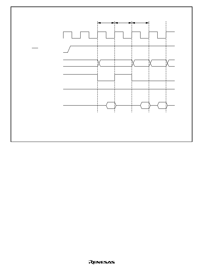
Rev. 1.0, 02/00, page 91 of 1141
RES
Internal address bus
Internal read signal
Internal write signal
Internal data bus
Vector
fetch
(1)
(2)
(3)
(4)
: Reset exception vector address ((1) = H'0000 or H'000000)
: Start address (contents of reset exception vector address)
: Start address ((3) = (2))
: First program instruction
(1)
(3)
High level
Internal
processing
Fetch of first program
instruction
(2)
(4)
Figure 5.2 Reset Sequence (Mode 1)
5.2.3
Interrupts after Reset
If an interrupt is accepted after a reset but before the stack pointer (SP) is initialized, the PC and
CCR will not be saved correctly, leading to a program crash. To prevent this, all interrupt
requests, including NMI, are disabled immediately after a reset. Since the first instruction of a
program is always executed immediately after the reset state ends, make sure that this instruction
initializes the stack pointer (example: MOV.L #xx:32, SP).

Rev. 1.0, 02/00, page 92 of 1141
5.3
Interrupts
Interrupt exception handling can be requested by six external sources (
,54 to ,54) and
internal sources in the on-chip supporting modules. Figure 5.3 shows the interrupt sources and
the number of interrupts of each type.
The on-chip supporting modules that can request interrupts include the watchdog timer (WDT),
prescaler unit (PSU), Timers A, B, J, L, R and X1 (TMR), serial communication interface (SCI),
A/D converter (ADC), I
2
C bus interface (IIC), servo circuits, sync detection, data slicer, OSD,
address trap, etc. Each interrupt source has a separate vector address.
NMI is the highest-priority interrupt. Interrupts are controlled by the interrupt controller. The
interrupt controller has two interrupt control modes and can assign interrupts other than NMI to
either three priority/mask levels to enable multiplexed interrupt control.
For details on interrupts, see section 6, Interrupt Controller.
WDT
*
2
(1)
PSU (1)
TMR (15)
SCI (4)
ADC (1)
IIC (3)
Servo circuits (9)
Synchronized detection (1)
Address trap (3)
Interrupts
Internal
interrupts
External
interrupts
Notes: Numbers in parentheses are the numbers of interrupt sources.
In this LSI, the watchdog timer generates NMIs.
When the watchdog timer is used as an interval timer, it generates an interrupt
request at each counter overflow.
1.
2.
NMI
*
1
(1)
IRQ5 to IRQ0 (6)
Figure 5.3 Interrupt Sources and Number of Interrupts

Rev. 1.0, 02/00, page 93 of 1141
5.4
Trap Instruction
Trap instruction exception handling starts when a TRAPA instruction is executed. Trap
instruction exception handling can be executed at all times in the program execution state.
The TRAPA instruction fetches a start address from a vector table entry corresponding to a
vector number from 0 to 3, as specified in the instruction code.
Table 5.3 shows the status of CCR and EXR after execution of trap instruction exception
handling.
Table 5.3
Status of CCR and EXR after Trap Instruction Exception Handling
CCR
EXR
*
Interrupt
Control Mode
I
UI
I2 to I0
T
0
1
1
1
1
Legend:
1:
Set to 1
0:
Cleared to 0
:
Retains value prior to execution.
*
:
Does not affect operation in this LSI.

Rev. 1.0, 02/00, page 94 of 1141
5.5
Stack Status after Exception Handling
Figures 5.4 and 5.5 show the stack after completion of trap instruction exception handling and
interrupt exception handling.
CCR
CCR*
PC
(16 bits)
SP
Note: * Ignored on return.
Interrupt control modes 0 and 1
Figure 5.4 Stack Status after Exception Handling (Normal Mode)*
Note: * Normal mode is not available for this LSI.
CCR
PC
(24 bits)
SP
Interrupt control modes 0 and 1
Figure 5.5 Stack Status after Exception Handling (Advanced Mode)
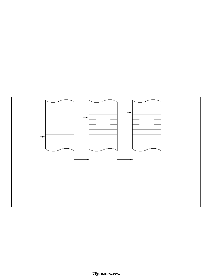
Rev. 1.0, 02/00, page 95 of 1141
5.6
Notes on Use of the Stack
When accessing word data or longword data, this chip assumes that the lowest address bit is 0.
The stack should always be accessed by word transfer instruction or longword transfer
instruction, and the value of the stack pointer (SP: ER7) should always be kept even.
Use the following instructions to save registers:
PUSH.W
Rn
(or MOV.W Rn, @-SP)
PUSH.L
ERn
(or MOV.L ERn, @-SP)
Use the following instructions to restore registers:
POP.W Rn
(or MOV.W @SP+, Rn)
POP.L ERn (or MOV.L @SP+, ERn)
Setting SP to an odd value may lead to a malfunction. Figure 5.6 shows an example of what
happens when the SP value is odd.
SP
[Legend]
: Condition-code register
: Program counter
: General register R1L
: Stack pointer
H'FFFEFA
H'FFFEFB
H'FFFEFC
H'FFFEFD
H'FFFEFF
R1L
PC
SP
CCR
PC
SP
CCR
PC
R1L
SP
Note: This diagram illustrates an example in which the interrupt control mode is 0, is advanced mode.
TRAPA instruction executed
MOV.B R1L, @-ER7
SP set to H'FFFEFF
Data saved above SP
Contents of CCR lost
Figure 5.6 Operation when SP Value is Odd

Rev. 1.0, 02/00, page 97 of 1141
Section 6 Interrupt Controller
6.1
Overview
6.1.1
Features
This LSI controls interrupts by means of an interrupt controller. The interrupt controller has the
following features:
∑
Two Interrupt Control Modes
Either of two interrupt control modes can be set by means of the INTM1 and INTM0 bits
in the system control register (SYSCR).
∑
Priorities Settable with ICR
An interrupt control register (ICR) is provided for setting interrupt priorities. Three
priority levels can be set for each module for all interrupts except NMI.
∑
Independent Vector Addresses
All interrupt sources are assigned independent vector addresses, making it unnecessary
for the source to be identified in the interrupt handling routine.
∑
Six External Interrupt Pins
NMI is the highest-priority interrupt, and is accepted at all times.
Falling edge, rising edge, or both edge detection can be selected for interrupt IRQ0.
Falling edge or rising edge can be individually selected for interrupts IRQ5 to IRQ1.
Note: * In this LSI, the watch dog timer generates NMIs.
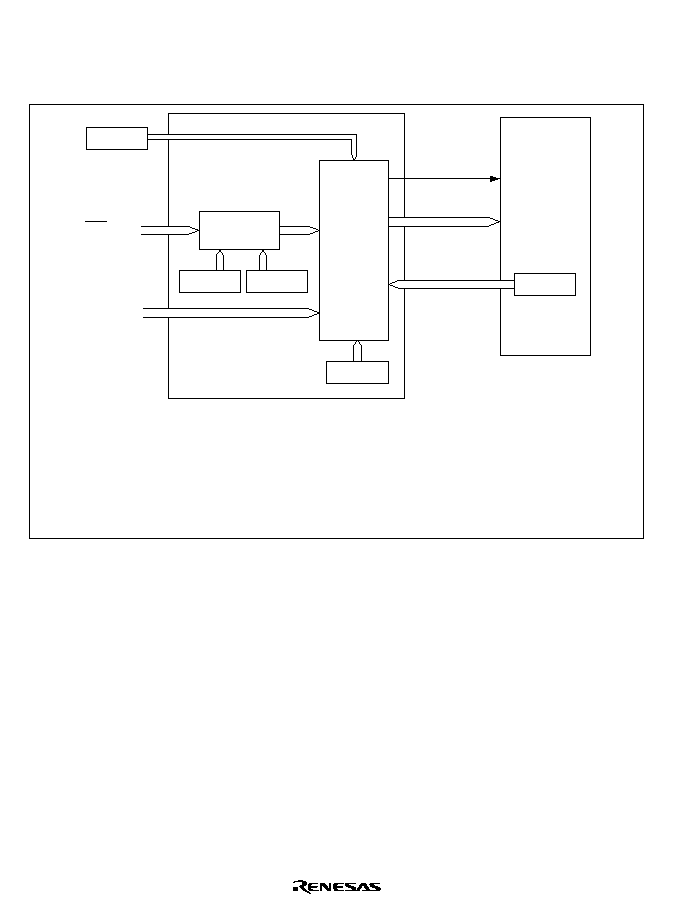
Rev. 1.0, 02/00, page 98 of 1141
6.1.2
Block Diagram
Figure 6.1 shows a block diagram of the interrupt controller.
IRQ input
Internal
interrupt
requests
[Legend]
IEGR
IENR
IRQR
ICR
SYSCR
: IRQ edge select register
: IRQ enable register
: IRQ status register
: Interrupt control register
: System control register
Interrupt
request
Vector
number
I, UI
IRQ input
unit IRQR
IEGR
IENR
ICR
CPU
Interrupt controller
SYSCR
INTM1, INTM0
CCR
Priority
determina-
tion
Figure 6.1 Block Diagram of Interrupt Controller

Rev. 1.0, 02/00, page 99 of 1141
6.1.3
Pin Configuration
Table 6.1 summarizes the pins of the interrupt controller.
Table 6.1
Interrupt Controller Pins
Name
Symbol
I/O
Function
External interrupt
request 0
,54
Input
Maskable external interrupts; rising, falling, or both
edges can be selected
External interrupt
requests 1 to 5
,54
to
,54
Input
Maskable external interrupts: rising, or falling
edges can be selected
6.1.4
Register Configuration
Table 6.2 summarizes the registers of the interrupt controller.
Table 6.2
Interrupt Controller Registers
Name
Abbreviation
R/W
Initial Value
Address
*
1
System control register
SYSCR
R/W
H'00
H'FFE8
IRQ edge select register
IEGR
R/W
H'00
H'FFF0
IRQ enable register
IENR
R/W
H'00
H'FFF1
IRQ status register
IRQR
R/ (W)
*
2
H'00
H'FFF2
Interrupt control register A
ICRA
R/W
H'00
H'FFF3
Interrupt control register B
ICRB
R/W
H'00
H'FFF4
Interrupt control register C
ICRC
R/W
H'00
H'FFF5
Interrupt control register D
ICRD
R/W
H'00
H'FFF6
Port mode register 1
PMR1
R/W
H'00
H'FFCE
Notes: 1. Lower 16 bits of the address.
2. Only 0 can be written, for flag clearing.

Rev. 1.0, 02/00, page 100 of 1141
6.2
Register Descriptions
6.2.1
System Control Register (SYSCR)
0
0
1
0
--
2
0
--
3
1
R
4
0
R/W
5
0
R
0
7
--
--
XRST
INTM0
INTM1
0
6
--
--
--
--
--
--
Bit :
Initial value :
R/W :
SYSCR is an 8-bit readable register that selects the interrupt control mode.
Only bits 5, 4, 2 and 1 are described here; for details on the other bits, see section 3.2.2, System
Control Register (SYSCR).
SYSCR is initialized to H'08 by a reset.
Bits 5 and 4
Interrupt Control Mode (INTM1, INTM0): These bits select one of two
interrupt control modes for the interrupt controller. The INTM1 bit must not be set to 1.
Bit 5
Bit 4
INTM1
INTM0
Interrupt Control
Mode
Description
0
0
Interrupts are controlled by I bit (Initial value)
0
1
1
Interrupts are controlled by I and UI bits and ICR
0
Cannot be used in this LSI
1
1
Cannot be used in this LSI

Rev. 1.0, 02/00, page 101 of 1141
6.2.2
Interrupt Control Registers A to D (ICRA to ICRD)
0
0
1
0
R/W
2
0
R/W
3
0
4
0
R/W
0
R/W
5
0
7
ICR4
ICR3
ICR2
ICR1
ICR0
0
R/W
ICR7
R/W
R/W
R/W
ICR6
ICR5
6
Bit :
Initial value :
R/W :
The ICR registers are four 8-bit readable/writable registers that set the interrupt control level for
interrupts other than NMI.
The correspondence between ICR settings and interrupt sources is shown in table 6.3.
The ICR registers are initialized to H'00 by a reset.
Bits 7 to 0
Interrupt Control Level (ICR7 to ICR0): Set the control level for the
corresponding interrupt source.
Bit n
ICRn
Description
0
Corresponding interrupt source is control level 0 (non-priority)
(Initial value)
1
Corresponding interrupt source is control level 1 (priority)
(n = 7 to 0)
Table 6.3
Correspondence between Interrupt Sources and ICR Settings
ICRA7
ICRA6
ICRA5
ICRA4
ICRA3
ICRA2
ICRA1
CIRA0
ICRA
Reserved
Input
capture
HSW1
IRQ0
IRQ1
IRQ2
IRQ3
IRQ4
IRQ5
Sync
separator,
OSD
ICRB7
ICRB6
ICRB5
ICRB4
ICRB3
ICRB2
ICRB1
ICRB0
ICRB
Data slicer
Sync
separator
Servo
(drum,
capstan
latch)
Timer A
Timer B
Timer J
Timer R
Timer L
ICRC7
ICRC6
ICRC5
ICRC4
ICRC3
ICRC2
ICRC1
ICRC0
ICRC
Timer X1
Synchro-
nized
detection
Watchdog
timer
Servo
IIC
SCI1
(UART)
IIC0
A/D
ICRD7
ICRD6
ICRD5
ICRD4
ICRD3
ICRD2
ICRD1
ICRD0
ICRD
HSW2
Reserved
Reserved
Reserved
Reserved
Reserved
Reserved
Reserved

Rev. 1.0, 02/00, page 102 of 1141
6.2.3
IRQ Enable Register (IENR)
0
0
1
0
R/W
2
0
R/W
3
0
4
0
R/W
5
0
0
7
R/W
R/W
R/W
IRQ5E
IRQ4E
IRQ3E
IRQ2E
IRQ1E
IRQ0E
0
6
--
--
--
--
Bit :
Initial value :
R/W :
IENR is an 8-bit readable/writable register that controls enabling and disabling of interrupt
requests IRQ5 to IRQ0.
IENR is initialized to H'00 by a reset.
Bits 7 and 6
Reserved: These bits are always read as 0. Do not write 1 to them.
Bits 5 to 0
IRQ5 to IRQ0 Enable (IRQ5E to IRQ0E): These bits select whether IRQ5 to
IRQ0 are enabled or disabled.
Bit n
IRQnE
Description
0
,54Q
interrupt disabled
(Initial value)
1
,54Q
interrupt enabled
(n = 5 to 0)

Rev. 1.0, 02/00, page 103 of 1141
6.2.4
IRQ Edge Select Registers (IEGR)
0
0
1
0
R/W
2
0
R/W
3
0
4
0
R/W
5
0
0
7
--
--
R/W
R/W
R/W
IRQ4EG
R/W
IRQ5EG
IRQ3EG
IRQ2EG
IRQ1EG IRQ0EG1 IRQ0EG0
0
6
Bit :
Initial value :
R/W :
IEGR is an 8-bit readable/writable register that selects detected edge of the input at pins
,54 to
,54.
IEGR register is initialized to H'00 by a reset.
Bit 7
Reserved: This bit is always read as 0. Do not write 1 to it.
Bits 6 to 2
,54
,54 to ,54
,54 Pins Detected Edge Select (IRQ5EG to IRQ1EG): These bits
select detected edge for interrupts IRQ5 to IRQ1.
Bits 6 to 2
IRQnEG
Description
0
Interrupt request generated at falling edge of
,54Q
pin input
(Initial value)
1
Interrupt request generated at rising edge of
,54Q
pin input
(n = 5 to 1)
Bits 1 and 0
,54
,54 Pin Detected Edge Select (IRQ0EG1, IRQ0EG0): These bits select
detected edge for interrupt IRQ0.
Bit 1
Bit 0
IRQ0EG1
IRQ0EG0
Description
0
0
Interrupt request generated at falling edge of
,54
pin input (Initial
value)
0
1
Interrupt request generated at rising edge of
,54
pin input
1
*
Interrupt request generated at both falling and rising edges of
,54
pin
input
Note:
*
Don't care

Rev. 1.0, 02/00, page 104 of 1141
6.2.5
IRQ Status Register (IRQR)
0
0
1
0
R/(W)*
2
0
R/(W)*
3
0
4
0
R/(W)*
5
0
0
7
R/(W)*
R/(W)*
R/(W)*
IRQ5F
IRQ4F
IRQ3F
IRQ2F
IRQ1F
IRQ0F
0
6
--
--
--
--
Note: * Only 0 can be written, to clear the flag.
Bit :
Initial value :
R/W :
IRQR is an 8-bit readable/writable register that indicates the status of IRQ5 to IRQ0 interrupt
requests.
IRQR is initialized to H'00 by a reset.
Bits 7 and 6
Reserved: These bits are always read as 0. Do not write 1 to them.
Bits 5 to 0
IRQ5 to IRQ0 Flags: These bits indicate the status of IRQ5 to IRQ0 interrupt
requests.
Bit n
IRQnF
Description
0
[Clearing conditions]
(Initial value)
Cleared by reading IRQnF set to 1, then writing 0 in IRQnF
When IRQn interrupt exception handling is executed
1
[Setting conditions]
∑
When a falling edge occurs in
,54Q
input while falling edge detection is set
(IRQnEG = 0)
∑
When a rising edge occurs in
,54Q
input while rising edge detection is set
(IRQnEG = 0)
∑
When a falling or rising edge occurs in
,54
input while both-edge detection is
set (IRQ0EG1 = 1)
(n = 5 to 0)

Rev. 1.0, 02/00, page 105 of 1141
6.2.6
Port Mode Register (PMR1)
0
0
1
0
R/W
2
0
R/W
3
0
4
0
R/W
0
R/W
5
0
7
0
R/W
PMR17
PMR16
PMR15
PMR14
PMR13
PMR12
PMR11
PMR10
R/W
R/W
R/W
6
Bit :
Initial value :
R/W :
Port Mode Register 1 (PMR1) controls pin function switching-over of port 1. Switching is
specified for each bit.
PMR1 is an 8-bit readable/writable register and is initialized to H'00 by a reset.
Only bits 5 to 0 are explained here. For details, see section 10.3.2, Register Configuration.
Bits 5 to 0
P15/
,54
,54 to P10/,54
,54 pin switching (PMR15 to PMR10): These bits are for
setting the P1n/
,54Q pin as the input pin for P1n or as the ,54Q pin for external interrupt
request input.
Bit n
PMR1n
Description
0
P1n/
,54Q
pin functions as the P1n input/output pin
(Initial value)
1
P1n/IRQn pin functions as the
,54Q
input/output pin
(n = 5 to 0)
Notes on switching the pin function by PMR1 are as follows:
∑
When the port is set as the
,& input pin or ,54 to ,54 input pin, the pin level must be high
or low regardless of active mode or power-down mode. Do not set the pin level at medium.
∑
Switching the pin function of P16/
,& or P15/,54 to P10/,54 may be mistakenly identified
as edge detection and detection signal may be generated. To prevent this, operate as follows:
Set the interrupt enable/disable flag to disable before switching the pin function.
Clear the applicable interrupt request flag to 0 after switching the pin function and
executing another instruction.
Program example
:
MOV.B R0L,@IENR
Interrupt disabled
MOV.B R1L,@PMR1
Pin function change
NOP
Optional instruction
BCLR m @IRQR
Applicable interrupt clear
MOV.B R1L,@IENR
Interrupt enabled
:
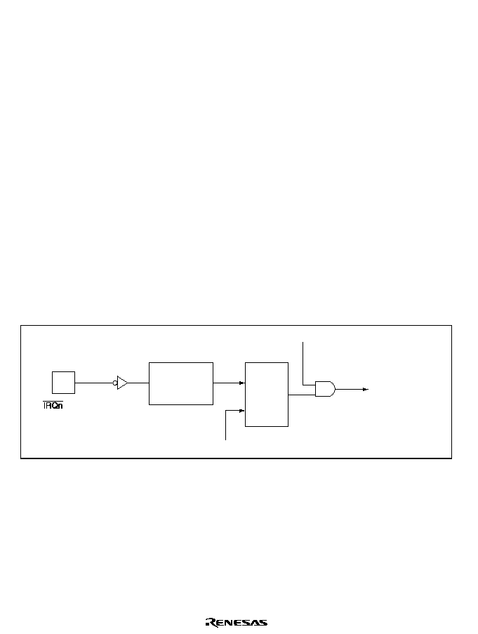
Rev. 1.0, 02/00, page 106 of 1141
6.3
Interrupt Sources
Interrupt sources comprise external interrupts (IRQ5 to IRQ0) and internal interrupts.
6.3.1
External Interrupts
There are six external interrupt sources; IRQ5 to IRQ0. Of these, IRQ1 to IRQ0 can be used to
restore this chip from standby mode.
∑
IRQ5 to IRQ0 Interrupts: Interrupts IRQ5 to IRQ0 are requested by an input signal at pins
,54 to ,54. Interrupts IRQ5 to IRQ0 have the following features:
(a) Using IEGR, it is possible to select whether an interrupt is requested by a falling edge,
rising edge, or both edges, at pin
,54.
(b) Using IEGR, it is possible to select whether an interrupt is requested by a falling edge or
rising edge at pins
,54 to ,54.
(c) Enabling or disabling of interrupt requests IRQ5 to IRQ0 can be selected with IENR.
(d) The interrupt control level can be set with ICR.
(e) The status of interrupt requests IRQ5 to IRQ0 is indicated in IRQR. IRQR flags can be
cleared to 0 by software.
Figure 6.2 shows a block diagram of interrupts IRQ5 to IRQ0.
Clear signal
R
S
Q
Edge detection
circuit
IRQnEG
IRQnF
IRQnE
Note: n = 5 to 0
IRQn interrupt
request
input
Figure 6.2 Block Diagram of Interrupts IRQ5 to IRQ0
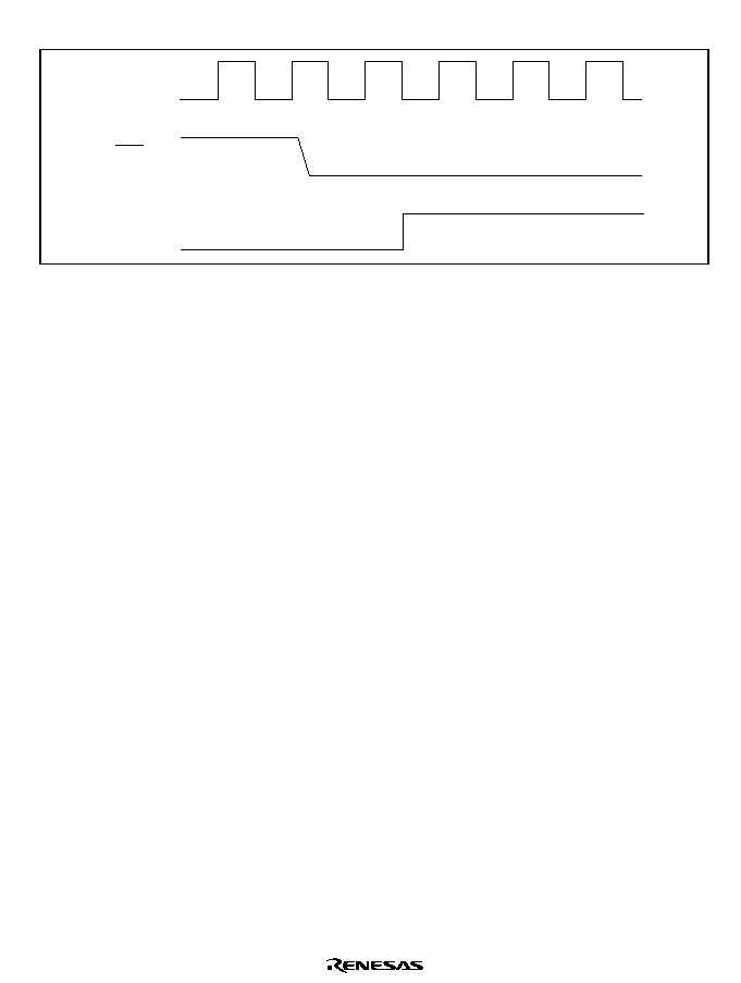
Rev. 1.0, 02/00, page 107 of 1141
Figure 6.3 shows the timing of IRQnF setting.
Internal
IRQnF
IRQn
input pin
Figure 6.3 Timing of IRQnF Setting
The vector numbers for IRQ5 to IRQ0 interrupt exception handling are 21 to 26.
Upon detection of IRQ5 to IRQ0 interrupts, the applicable pin is set in the port register 1 (PMR1)
as
,54Q pin.
6.3.2
Internal Interrupts
There are 38 sources for internal interrupts from on-chip supporting modules.
∑
For each on-chip supporting module there are flags that indicate the interrupt request status,
and enable bits that select enabling or disabling of these interrupts. If any one of these is set
to 1, an interrupt request is issued to the interrupt controller.
∑
The interrupt control level can be set by means of ICR.
∑
The NMI is the highest priority interrupt and is always accepted regardless of the control
mode and CPU interrupt mask bit. In this LSI, NMIs are used as interrupts generated by the
watchdog timer

Rev. 1.0, 02/00, page 108 of 1141
6.3.3
Interrupt Exception Vector Table
Table 6.4 shows interrupt exception handling sources, vector addresses, and interrupt priorities.
For default priorities, the lower the vector number, the higher the priority.
Priorities among modules can be set by means of ICR. The situation when two or more modules
are set to the same priority, and priorities within a module, are fixed as shown in table 6.4.
Table 6.4
Interrupt Sources, Vector Addresses, and Interrupt Priorities
Priority
Interrupt Source
Origin of Interrupt
Source
Vector
No.
Vector Address
ICR
Remarks
Reset
External pin
0
H'0000 to H'0003
1
H'0004 to H'0007
2
H'0008 to H'000B
3
H'000C to H'000F
4
H'0010 to H'0013
Reserved
5
H'0014 to H'0017
Direct transition
Instruction
6
H'0018 to H'001B
NMI
Watchdog timer
7
H'001C to H'001F
TRAPA#0
8
H'0020 to H'0023
TRAPA#1
9
H'0024 to H'0027
TRAPA#2
10
H'0028 to H'002B
Trap instruction
TRAPA#3
Instruction
11
H'002C to H'002F
12
H'0030 to H'0033
13
H'0034 to H'0037
14
H'0038 to H'003B
High
Low
Reserved
15
H'003C to H'003F

Rev. 1.0, 02/00, page 109 of 1141
Priority
Interrupt Source
Origin of Interrupt
Source
Vector
No.
Vector Address
ICR
Remarks
#0
16
H'0040 to H'0043
#1
17
H'0044 to H'0047
Address trap
#2
ATC
18
H'0048 to H'004B
IC
PSU
19
H'004C to H'004F
ICRA6
HSW1
Servo circuit
20
H'0050 to H'0053
ICRA5
IRQ0
21
H'0054 to H'0057
ICRA4
IRQ1
22
H'0058 to H'005B
ICRA3
IRQ2
23
H'005C to H'005F
IRQ3
24
H'0060 to H'0063
ICRA2
IRQ4
25
H'0064 to H'0067
IRQ5
External pin
26
H'0068 to H'006B
ICRA1
External V interrupt
Sync separator
27
H'006C to H'006F
ICRA0
OSD V interrupt
OSD
28
H'0070 to H'0073
Data slicer odd field interrupt
Data slicer
29
H'0074 to H'0077
ICRB7
Data slicer even field interrupt
30
H'0078 to H'007B
Noise interrupt
Sync separator
31
H'007C to H'007F
ICRB6
Reserved
32
H'0080 to H'0083
33
H'0084 to H'0087
Drum latch 1 (speed)
Servo circuit
34
H'0088 to H'008B
ICRB5
Capstan latch 1 (speed)
35
H'008C to H'008F
TMAI
Timer A
36
H'0090 to H'0093
ICRB4
TMBI
Timer B
37
H'0094 to H'0097
ICRB3
High
TMJ1I
Timer J
38
H'0098 to H'009B
ICRB2
TMJ2I
39
H'009C to H'009F
TMR1I
Timer R
40
H'00A0 to H'00A3
ICRB1
TMR2I
41
H'00A4 to H'00A7
TMR3I
42
H'00A8 to H'00AB
Low
TMLI
Timer L
43
H'00AC to H'00AF
ICRB0

Rev. 1.0, 02/00, page 110 of 1141
Priority
Interrupt Source
Origin of Interrupt
Source
Vector
No.
Vector Address
ICR
Remarks
ICXA
Timer X1
44
H'00B0 to H'00B3
ICXB
45
H'00B4 to H'00B7
ICXC
46
H'00B8 to H'00BB
ICXD
47
H'00BC to H'00BF
OCX1
48
H'00C0 to H'00C3
OCX2
49
H'00C4 to H'00C7
OVFX
50
H'00C8 to H'00CB
ICRC7
VD interrupts
Sync signal
detection
51
H'00CC to H'00CF
ICRC6
Reserved
52
H'00D0 to H'00D3
8-bit interval timer
Watchdog timer
53
H'00D4 to H'00D7
ICRC5
CTL
54
H'00D8 to H'00DB
Drum latch 2 (speed)
55
H'00DC to H'00DF
Capstan latch 2 (speed)
56
H'00E0 to H'00E3
Drum latch 3 (phase)
57
H'00E4 to H'00D7
Capstan latch 3 (phase)
Servo circuit
58
H'00E8 to H'00EB
ICRC4
IIC1
IIC1
59
H'00EC to H'00EF
ICRC3
ERI
60
H'00F0 to H'00F3
RXI
61
H'00F4 to H'00F7
TXI
62
H'00F8 to H'00FB
SCI1
TEI
SCI1
(UART)
63
H'00FC to H'00FF
ICRC2
64
H'0100 to H'0103
IIC0
DDCSW
IIC0
65
H'0104 to H'0107
ICRC1
A/D conversion end
A/D
66
H'0108 to H'010B
ICRC0
High
Low
HSW2
Servo circuit
67
H'010C to H'010F
ICRD7

Rev. 1.0, 02/00, page 111 of 1141
6.4
Interrupt Operation
6.4.1
Interrupt Control Modes and Interrupt Operation
Interrupt operations in this LSI differ depending on the interrupt control mode.
NMI* interrupts and address trap interrupts are accepted at all times except in the reset state. In
the case of IRQ interrupts and on-chip supporting module interrupts, an enable bit is provided
for each interrupt. Clearing an enable bit to 0 disables the corresponding interrupt request.
Interrupt sources in which the enable bits are set to 1 are controlled by the interrupt controller.
Table 6.5 shows the interrupt control modes.
The interrupt controller performs interrupt control according to the interrupt control mode set by
the INTM1 and INTM0 bits in SYSCR, the priorities set in ICR, and the masking state indicated
by the I and UI bits in the CPU's CCR.
Note: * In this LSI, the NMI interrupt is generated by the watchdog timer.
Table 6.5
Interrupt Control Modes
SYSCR
Interrupt
Control
Mode
INTM1
INTM0
Priority Setting
Register
Interrupt
Mask Bits
Description
0
0
ICR
I
Interrupt mask control is
performed by the I bit
Priority can be set with ICR
1
0
1
ICR
I, UI
3-level interrupt mask control is
performed by the I and UI bits
Priority can be set with ICR
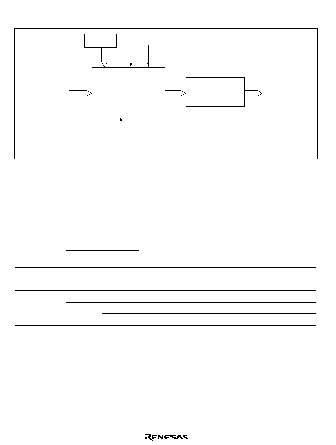
Rev. 1.0, 02/00, page 112 of 1141
Figure 6.4 shows a block diagram of the priority decision circuit.
Interrupt control modes 0 and 1
I
Interrupt source
UI
Vector number
Interrupt acceptance
control and 3-level
mask control
Default priority
determination
I C R
Figure 6.4 Block Diagram of Interrupt Priority Determination Operation
∑
Interrupt Acceptance Control and 3-Level Control: In interrupt control modes 0 and 1,
interrupt acceptance control and 3-level mask control is performed by means of the I and UI
bits in CCR, and ICR (control level).
Table 6.6 shows the interrupts selected in each interrupt control mode.
Table 6.6
Interrupts Selected in Each Interrupt Control Mode
Interrupt Mask Bit
Interrupt
Control
Mode
I
UI
Selected Interrupts
0
*
All interrupts (control level 1 has priority)
0
1
*
NMI
*
1
and address trap interrupts
0
*
All interrupts (control level 1 has priority)
0
NMI
*
1
, address trap and control level 1 interrupts
1
1
1
NMI
*
1
and address trap interrupts
Notes:
*
Don't care
1. In this LSI, the NMI interrupt is generated by the watchdog timer.
∑
Default Priority Determination: If the same value is set for ICR, acceptance of multiple
interrupts is enabled, and so only the interrupt source with the highest priority according to
the preset default priorities is selected and has a vector number generated.
Interrupt sources with a lower priority than the accepted interrupt source are held pending.
Table 6.7 shows operations and control signal functions in each interrupt control mode.

Rev. 1.0, 02/00, page 113 of 1141
Table 6.7
Operations and Control Signal Functions in Each Interrupt Control Mode
Setting
Interrupt Acceptance Control,
3-Level Control
Interrupt
Control
Mode
INTM1
INTM0
I
UI
ICR
Default Priority
Determination
0
0
{
IM
PR
{
1
0
1
{
IM
IM
PR
{
Legend:
{
:
Interrupt operation control performed
IM:
Used as interrupt mask bit
PR:
Sets priority
:
Not used
6.4.2
Interrupt Control Mode 0
Enabling and disabling of IRQ interrupts and on-chip supporting module interrupts can be set by
the I bit in the CPU's CCR, and ICR. Interrupts are enabled when the I bit is cleared to 0, and
disabled when set to 1. Control level 1 interrupt sources have higher priority.
Figure 6.5 shows a flowchart of the interrupt acceptance operation in this case.
∑
If an interrupt source occurs when the corresponding interrupt enable bit is set to 1, an
interrupt request is sent to the interrupt controller.
∑
When interrupt requests are sent to the interrupt controller, a control level 1 interrupt,
according to the control level set in ICR, has priority for selection, and other interrupt
requests are held pending. If a number of interrupt requests with the same control level
setting are generated at the same time, the interrupt request with the highest priority
according to the priority system shown in table 6.4 is selected.
∑
The I bit is then referenced. If the I bit is cleared to 0, the interrupt request is accepted. If
the I bit is set to 1, only an NMI*
1
or an address trap interrupt is accepted, and other interrupt
requests are held pending.
∑
When an interrupt request is accepted, interrupt exception handling starts after execution of
the current instruction has been completed.
∑
The PC and CCR are saved to the stack area by interrupt exception handling. The PC saved
on the stack shows the address of the first instruction to be executed after returning from the
interrupt handling routine.
∑
Next, the I bit in CCR is set to 1. This disables all interrupts except NMI* and address trap.
∑
A vector address is generated for the accepted interrupt, and execution of the interrupt
handling routine starts at the address indicated by the contents of that vector address.
Note: * In this LSI, the NMI interrupt is generated by the watchdog timer.
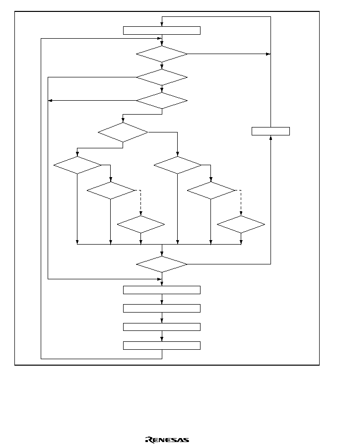
Rev. 1.0, 02/00, page 114 of 1141
Program execution state
Interrupt
generated?
NMI
Address trap
interrupt?
Control level 1
interrupt?
I C
I = 0
Yes
Yes
Yes
Yes
Yes
Yes
Yes
No
Yes
Yes
Yes
Yes
No
No
No
No
No
No
Save PC and CCR
I
1
Read vector address
Branch to interrupt handling routine
I C
No
No
H S W 1
H S W 1
H S W 2
H S W 2
Hold pending
Figure 6.5 Flowchart of Procedure Up to Interrupt Acceptance in
Interrupt Control Mode 0
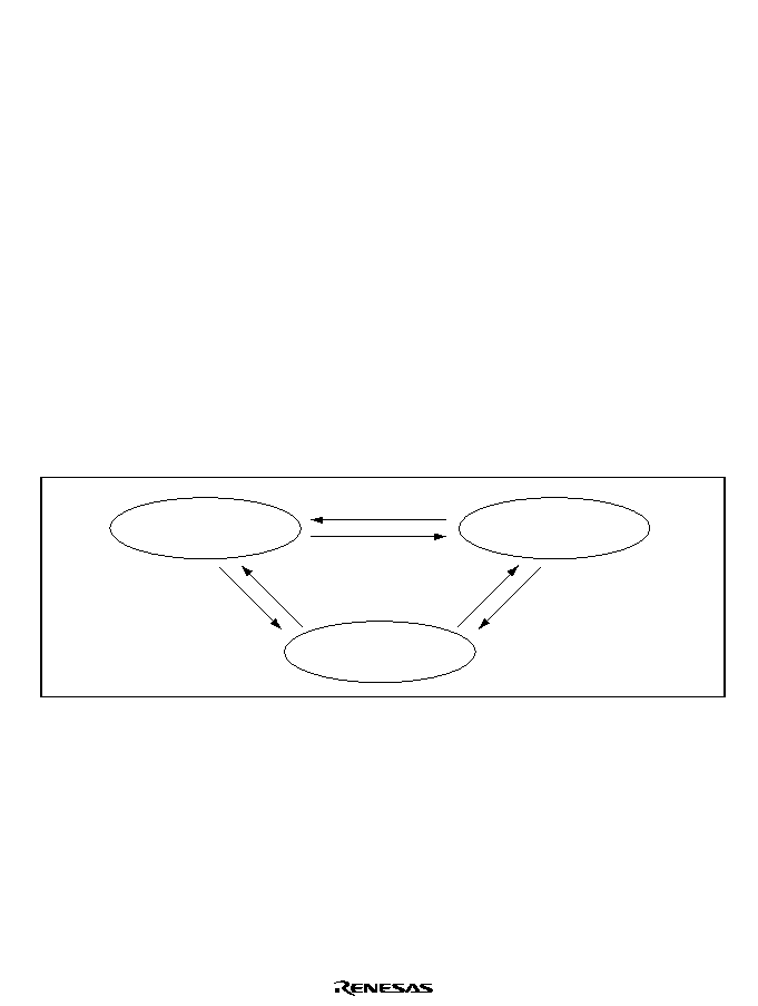
Rev. 1.0, 02/00, page 115 of 1141
6.4.3
Interrupt Control Mode 1
Three-level masking is implemented for IRQ interrupts and on-chip supporting module
interrupts by means of the I and UI bits in the CPU's CCR and ICR.
∑
Control level 0 interrupt requests are enabled when the I bit is cleared to 0, and disabled
when set to 1.
∑
Control level 1 interrupt requests are enabled when the I bit or UI bit is cleared to 0, and
disabled when both the I bit and the UI bit are set to 1.
For example, if the interrupt enable bit for an interrupt request is set to 1, and H'04, H'00, H'00
and H'00 are set in ICRA, ICRB, ICRC and ICRD respectively, (i.e. IRQ2 interrupt is set to
control level 1 and other interrupts to control level 0), the situation is as follows:
∑
When I = 0, all interrupts are enabled
(Priority order: NMI > IRQ2 > IC > HSW1 > ...)
∑
When I = 1 and UI = 0, only NMI, address trap and IRQ2 interrupts are enabled
∑
When I = 1 and UI = 1, only NMI and address trap interrupts are enabled
Figure 6.6 shows the state transitions in these cases.
Only NMI, address trap and
IRQ2 interrupts enabled
All interrupts enabled
Exception handling
execution or UI
1
Exception handling
execution or
I
1, UI
1
I
0
I
1, UI
0
UI
0
I
0
Only NMI and address trap
interrupts enabled
Figure 6.6 Example of State Transitions in Interrupt Control Mode 1
Figure 6.7 shows an operation flowchart of interrupt reception.

Rev. 1.0, 02/00, page 116 of 1141
(1) If an interrupt source occurs when the corresponding interrupt enable bit is set to 1, an
interrupt request is sent to the interrupt controller.
(2) When interrupt requests are sent to the interrupt controller, a control level 1 interrupt,
according to the control level set in ICR, has priority for selection, and other interrupt
requests are held pending. If a number of interrupt requests with the same control level
setting are generated at the same time, the interrupt request with the highest priority
according to the priority system shown in table 6.4 is selected.
(3) The I bit is then referenced. If the I bit is cleared to 0, the UI bit has no effect.
An interrupt request set to interrupt control level 0 is accepted when the I bit is cleared to 0.
If the I bit is set to 1, only NMI* and address trap interrupts are accepted, and other interrupt
requests are held pending.
An interrupt request set to interrupt control level 1 has priority over an interrupt request set
to interrupt control level 0, and is accepted if the I bit is cleared to 0, or if the I bit is set to 1
and the UI bit is cleared to 0.
When both the I bit and the UI bit are set to 1, only NMI* and address trap interrupts are
accepted, and other interrupt requests are held pending.
(4) When an interrupt request is accepted, interrupt exception handling starts after execution of
the current instruction has been completed.
(5) The PC and CCR are saved to the stack area by interrupt exception handling. The PC saved
on the stack shows the address of the first instruction to be executed after returning from the
interrupt handling routine.
(6) Next, the I and UI bits in CCR are set to 1. This masks all interrupts except NMI* and
address trap.
(7) A vector address is generated for the accepted interrupt, and execution of the interrupt
handling routine starts at the address indicated by the contents of that vector address.
Note: * In this LSI, the NMI interrupt is generated by the watchdog timer.
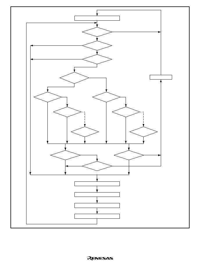
Rev. 1.0, 02/00, page 117 of 1141
Program execution state
NMI
I C
Yes
Yes
Yes
Yes
Yes
Yes
Yes
No
Yes
Yes
Yes
Yes
No
No
No
No
No
No
I C
No
No
H S W 1
H S W 1
H S W 2
H S W 2
Yes
No
Yes
No
Interrupt
generated?
Address trap
interrupt?
Control level 1
interrupt?
I = 0
I = 0
UI = 0
Save PC and CCR
I
1, UI
1
Read vector address
Branch to interrupt handling routine
Hold pending
Figure 6.7 Flowchart of Procedure Up to Interrupt Acceptance in
Interrupt Control Mode 1
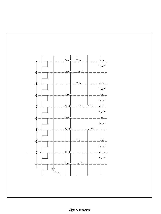
Rev. 1.0, 02/00, page 118 of 1141
6.4.4
Interrupt Exception Handling Sequence
Figure 6.8 shows the interrupt exception handling sequence. The example shown is for the case
where interrupt control 0 is set in advanced mode, and the program area and stack area are in on-
chip memory.
(1)
(1)
Instruction prefetch address (Not executed.
This is the contents of the saved PC, the
return address.)
Saved PC and saved CCR
Vector address
Interrupt handling routine start address (vector address contents)
Interrupt handling routine start address ((13) = (10)(12))
First instruction of interrupt handling routine
(2)(4)
(6)(8)
(10)(12)
(13)
(9)(11)
(14)
(3)
(5)
(7)
(9)
(11)
(13)
Internal
address bus
Interrupt
request signal
Internal read
signal
Internal
write signal
Internal
data bus
(2)
(4)
(6)
(8)
(10)
(12)
(14)
Stack
Vector fetch
Interrupt level
determination
Wait for end of
instruction
Interrupt
acceptance
Internal
operation
Internal
operation
Instruction
prefetch
Interrupt handling routine
instruction prefetch
Instruction code (Not executed.)
(3)
Instruction prefetch address (Not executed.)
(5)
SP-2
(7)
SP-4
Figure 6.8 Interrupt Exception Handling

Rev. 1.0, 02/00, page 119 of 1141
6.4.5
Interrupt Response Times
Table 6.8 shows interrupt response times-the interval between generation of an interrupt request
and execution of the first instruction in the interrupt handling routine. The symbols used in table
6.8 are explained in table 6.9.
Table 6.8
Interrupt Response Times
No.
Number of States
Advanced Mode
1
Interrupt priority determination
*
1
3
2
Number of wait states until executing instruction ends
*
2
1 to 19+2
S
I
3
PC, CCR stack save
2
S
k
4
Vector fetch
2
S
I
5
Instruction fetch
*
3
2
S
I
6
Internal processing
*
4
2
Total (using on-chip memory)
12 to 32
Notes: 1. Two states in case of internal interrupt.
2. Refers to DIVXS instruction.
3. Prefetch after interrupt acceptance and interrupt handling routine prefetch.
4. Internal processing after interrupt acceptance and internal processing after vector
fetch.
Table 6.9
Number of States in Interrupt Handling Routine Execution
Object of Access
Symbol
Internal Memory
Instruction fetch S
I
1
Stack operation SK
1
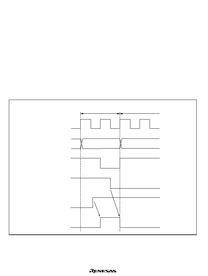
Rev. 1.0, 02/00, page 120 of 1141
6.5
Usage Notes
6.5.1
Contention between Interrupt Generation and Disabling
When an interrupt enable bit is cleared to 0 to disable interrupts, the disabling becomes effective
after execution of the instruction.
In other words, when an interrupt enable bit is cleared to 0 by an instruction such as BCLR or
MOV, if an interrupt is generated during execution of the instruction, the interrupt concerned
will still be enabled on completion of the instruction, and so interrupt exception handling for that
interrupt will be executed on completion of the instruction. However, if there is an interrupt
request of higher priority than that interrupt, interrupt exception handling will be executed for
the higher-priority interrupt, and the lower-priority interrupt will be ignored.
The same also applies when an interrupt source flag is cleared to 0.
Figure 6.9 shows an example in which the OCIAE bit in timer X1 TIER is cleared to 0.
TIER address
Internal
address bus
Internal
write signal
OCIAE
OCFA
OCIA
interrupt signal
TIER write cycle
by CPU
OCIA interrupt
exception handling
Figure 6.9 Contention between Interrupt Generation and Disabling
The above contention will not occur if an enable bit or interrupt source flag is cleared to 0 while
the interrupt is masked.

Rev. 1.0, 02/00, page 121 of 1141
6.5.2
Instructions that Disable Interrupts
Instructions that disable interrupts are LDC, ANDC, ORC, and XORC. After any of these
instructions is executed, all interrupts including NMI are disabled and the next instruction is
always executed. When the I bit or UI bit is set by one of these instructions, the new value
becomes valid two states after execution of the instruction ends.
6.5.3
Interrupts during Execution of EEPMOV Instruction
Interrupt operation differs between the EEPMOV.B instruction and the EEPMOV.W instruction.
With the EEPMOV.B instruction, an interrupt request (including NMI) issued during the transfer
is not accepted until the move is completed.
With the EEPMOV.W instruction, if an interrupt request is issued during the transfer, interrupt
exception handling starts at a break in the transfer cycle. The PC value saved on the stack in this
case is the address of the next instruction.
Therefore, if an interrupt is generated during execution of an EEPMOV.W instruction, the
following coding should be used.
L1: EEPMOV.W
MOV.W R4,R4
BNE L1
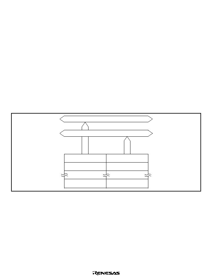
Rev. 1.0, 02/00, page 123 of 1141
Section 7 ROM
7.1
Overview
The H8S/2199 has 128 kbytes of on-chip ROM (flash memory or mask ROM), the H8S/2198 has
112 kbytes, the H8S/2197 has 96 kbytes, and the H8S/2196 has 80 kbytes*. The ROM is
connected to the CPU by a 16-bit data bus. The CPU accesses both byte and word data in one
state, enabling faster instruction fetches and higher processing speed.
The flash memory versions of the H8S/2199 can be erased and programmed on-board as well as
with a general-purpose PROM programmer.
Note: * For details on product line-up, refer to section 1, Overview.
7.1.1
Block Diagram
Figure 7.1 shows a block diagram of the ROM.
Internal data bus (upper 8 bits)
Internal data bus (lower 8 bits)
H'000000
H'000002
H'01FFFE
H'000001
H'000003
H'01FFFF
Figure 7.1 ROM Block Diagram (H8S/2199)

Rev. 1.0, 02/00, page 124 of 1141
7.2
Overview of Flash Memory
7.2.1
Features
The features of the flash memory are summarized below.
∑
Four flash memory operating modes
Program mode
Erase mode
Program-verify mode
Erase-verify mode
∑
Programming/erase methods
The flash memory is programmed 128 bytes at a time. Erasing is performed by block erase (in
single-block units). When erasing all blocks, the individual blocks must be erased
sequentially. Block erasing can be performed as required on 4-kbyte, 32-kbyte, and 64-kbyte
blocks. (In OSD ROM, block erasing can be performed on 1-kbyte, 2-kbyte, and 28-kbyte
blocks).
∑
Programming/erase times
The flash memory programming time is TBD ms (typ.) for simultaneous 128-byte
programming, equivalent to TBD
µ
s (typ.) per byte, and the erase time is TBD ms (typ.) per
block.
∑
Reprogramming capability
The flash memory can be reprogrammed up to TBD times.
∑
On-board programming modes
There are two modes in which flash memory can be programmed/erased/verified on-board:
Boot mode
User program mode
∑
Automatic bit rate adjustment
If data transfer on boot mode, automatic adjustment is possible at host transfer bit rates and
MCU's bit rates.
∑
Protect modes
There are three protect modes, hardware, software, and error protect, which allow protected
status to be designated for flash memory program/erase/verify operations.
∑
Writer mode
Flash memory can be programmed/erased in writer mode, using a PROM programmer, as well
as in on-board programming mode.
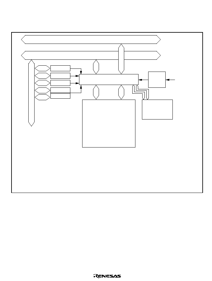
Rev. 1.0, 02/00, page 125 of 1141
7.2.2
Block Diagram
Figure 7.2 shows a block diagram of the flash memory.
Module bus
Bus interface/controller
Flash memory
(256 kbytes)
Operat-
ing
mode
FLMCR1
STCR
FLMCR1
FLMCR2
EBR1
EBR2
: Serial timer control register
: Flash memory control register 1
: Flash memory control register 2
: Erase block register 1
: Erase block register 2
[Legend]
Internal address bus
Internal data bus (16 bits)
STCR
FWE pin
Mode pin
FLMCR2
EBR1
Flash memory
(OSD ROM)
(32 kbytes)
EBR2
Figure 7.2 Block Diagram of Flash Memory (H8S/2199 Only)
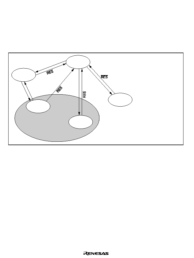
Rev. 1.0, 02/00, page 126 of 1141
7.2.3
Flash Memory Operating Modes
Mode Transitions
When each mode pin and the FWE pin are set in the reset state and a reset-start is executed, the
MCU enters one of the operating modes shown in figure 7.3. In user mode, flash memory can be
read but not programmed or erased.
Flash memory can be programmed and erased in boot mode, user program mode, and writer mode.
Boot mode
On-board program mode
User
program
mode
User mode
Reset state
Writer mode
FWE = 1, MD0 = 0,
P12 = P13 = P14 = 1
MD0 = 0,
P12 = P13 = 1, P14 = 0
= 0
= 0
FWE = 1
SWE = 1
FWE = 0
or
SWE = 0
= 0
MD1 = 1, FWE = 0 or 1
= 0
Only make a transition between user mode
and user program mode when the CPU is not
accessing the flash memory.
Note:
Figure 7.3 Flash Memory Mode Transitions
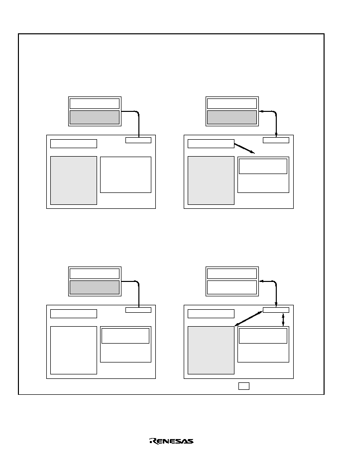
Rev. 1.0, 02/00, page 127 of 1141
On-Board Programming Modes
∑
Boot mode
<Flash memory>
<This LSI>
<RAM>
<Host>
Programming control
program
SCI
Application
program
(old version)
�
New application
program
Programming control
program
Programming control
program
<This LSI>
<RAM>
<Host>
SCI
Boot program area
<This LSI>
<RAM>
<Host>
SCI
Flash memory erase
<This LSI>
Program execution state
<RAM>
<Host>
SCI
New application
program
"
!
"
1. Initial state
2. Writing control program transfer
3. Flash memory initialization
4. Writing new application program
Boot program
<Flash memory>
Application
program
(old version)
Boot program
<Flash memory>
Boot program
<Flash memory>
Boot program
Boot program area
Programming control
program
The flash memory is in the erased state when the
device is shipped. The description here applies to
the case where the old program version or data is
being rewritten. The user should prepare the
programming control program and new application
program beforehand in the host.
When boot mode is entered, the boot program in
this LSI chip (originally incorporated in the chip) is
started, and SCI communication check is carried
out, and the boot program required for flash memory
erasing is automatically transferred to the RAM boot
program area.
The erase program in the boot program area (in
RAM) is executed, and the flash memory is
initialized (to H'FF). In boot mode, entire flash
memory erasure is performed, without regard to
blocks.
The programming control program transferred from
the host to RAM by SCI communication is executed,
and the new application program in the host is
written into the flash memory.
New application
program
New application
program
Figure 7.4 Boot Mode
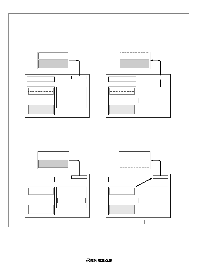
Rev. 1.0, 02/00, page 128 of 1141
∑
User program mode
<Flash memory>
<This LSI>
<RAM>
<Host>
Programming/erase control program
SCI
Boot program
New application
program
<This LSI>
<RAM>
<Host>
SCI
<Flash memory>
<This LSI>
<RAM>
<Host>
SCI
Flash memory erase
Boot program
New application
program
<This LSI>
Program execution state
<RAM>
<Host>
SCI
Programming/erase
control program
1. Initial state
2. Programming/erase control program transfer
3. Flash memory initialization
4. Writing new application program
FWE assessment program
Transfer program
Application
program
(old version)
,
FWE assessment program
Transfer program
Programming/erase control program
Programming/erase control program
<Flash memory>
New application
program
Boot program
FWE assessment program
Transfer program
(1) The FWE assessment program that confirms that
the FWE pin has been driven high, and (2) the
program that will transfer the programming/erase
control program from the flash memory to on-chip RAM
should be written into the flash memory by the user
beforehand. (3) The programming/erase control
program should be prepared in the host or in the flash
memory.
When the FWE pin is driven high, user software
confirms this fact, executes the transfer program in the
flash memory, and transfers the programming/erase
control program to RAM.
The programming/erase control program in RAM is
executed, and the flash memory is initialized (to H'FF).
Erasing can be performed in block units, but not in byte
units.
Next, the new application program in the host is written
into the erased flash memory blocks. Do not write to
unerased blocks.
New application
program
<Flash memory>
Boot program
FWE assessment program
Transfer program
Application
program
(old version)
Figure 7.5 User Program Mode (Example)

Rev. 1.0, 02/00, page 129 of 1141
Differences between Boot Mode and User Program Mode
Boot Mode
User Program Mode
Entire memory erase
Yes
Yes
Block erase
No
Yes
Programming control program
*
Program/program-verify
Erase/erase-verify
Program/program-verify
Note:
*
To be provided by the user, in accordance with the recommended algorithm.
Block Configuration
The main ROM area is divided into three 64-kbyte blocks, one 32-kbyte block, and eight 4-kbyte
blocks. The OSD ROM area is divided into two 1-kbyte blocks, one 2-kbyte block, and one 28-
kbyte block.
Address H'00000
Address H'3FFFF
256 kbytes
64 kbytes
64 kbytes
64 kbytes
32 kbytes
4 kbytes 8
Address H'40000
Address H'47FFF
32 kbytes
OSD ROM area
Main ROM area
28 kbytes
2 kbytes
1 kbyte
1 kbyte
Figure 7.6 Flash Memory Block Configuration

Rev. 1.0, 02/00, page 130 of 1141
7.2.4
Pin Configuration
The flash memory is controlled by means of the pins shown in table 7.1.
Table 7.1
Flash Memory Pins
Pin Name
Abbreviation
I/O
Function
Reset
5(6
Input
Reset
Flash write enable
FWE
Input
Flash program/erase protection by hardware
Mode 0
MD0
Input
Sets this LSI operating mode
Port 12
P12
Input
Sets this LSI operating mode when MD0 = 0
Port 13
P13
Input
Sets this LSI operating mode when MD0 = 0
Port 14
P14
Input
Sets this LSI operating mode when MD0 = 0
Transmit data
SO1
Output
Serial transmit data output
Receive data
SI1
Input
Serial receive data input
7.2.5
Register Configuration
Table 7.2 shows the registers used to control the flash memory when enabled.
In order for these registers to be accessed, the FLSHE bit must be set to 1 in STCR.
Table 7.2
Flash Memory Registers
Register Name
Abbreviation
R/W
Initial Value
Address
*
1
Flash memory control register 1
FLMCR1
*
5
R/W
*
2
H'00
*
3
H'FFF8
Flash memory control register 2
FLMCR2
*
5
R/W
*
2
H'00
*
4
H'FFF9
Erase block register 1
EBR1
*
5
R/W
*
2
H'00
*
4
H'FFFA
Erase block register 2
EBR2
*
5
R/W
*
2
H'00
*
4
H'FFFB
Serial timer control register
STCR
R/W
H'00
H'FFEE
Notes: 1. Lower 16 bits of the address.
2. When the FWE bit in FLMCR1 is not set at 1, writes are disabled.
3. When a high level is input to the FWE pin, the initial value is H'80.
4. When a low level is input to the FWE pin, or if a high level is input and the SWE bit in
FLMCR1 is not set, these registers are initialized to H'00.
5. FLMCR1, FLMCR2, EBR1, and EBR2 are 8-bit registers. Only byte accesses are valid
for these registers, the access requiring 2 states.

Rev. 1.0, 02/00, page 131 of 1141
7.3
Flash Memory Register Descriptions
7.3.1
Flash Memory Control Register 1 (FLMCR1)
7
FWE
--*
R
6
SWE1
0
R/W
5
ESU1
0
R/W
4
PSU1
0
R/W
3
EV1
0
R/W
0
P1
0
R/W
2
PV1
0
R/W
1
E1
0
R/W
Bit
Initial value
R/W
:
:
:
Note: * Determined by the state of the FWE pin.
FLMCR1 is an 8-bit register used for flash memory operating mode control. With addresses
H'00000 to H'3FFFF, program-verify mode or erase-verify mode is entered by setting SWE to 1
when FWE = 1, then setting the PV1 bit and EV1 bit. Program mode is entered by setting SWE1
when FWE = 1, then setting the SWE1 bit and PSU1, and finally setting the P1 bit. With
addresses H'00000 to H'3FFFF, erase mode is entered by setting SWE1 when FWE = 1, then
setting the ESU1 bit, and finally setting the E1 bit. FLMCR1 is initialized by a reset, and in
standby mode. Its initial value is H'80 when a high level is input to the FWE pin, and H'00 when a
low level is input. When on-chip flash memory is disabled, a read will return H'00, and writes are
invalid.
Writes to the SWE1 bit in FLMCR1 are enabled only when FWE = 1; writes to the ESU1, PSU1,
EV1 and PV1 bits only when FWE = 1 and SWE1 = 1; writes to the E1 bit only when FWE = 1,
SWE1 = 1, and ESU1 = 1; and writes to the P1 bit only when FWE = 1, SWE1 = 1, and PSU1 = 1.
Bit 7
Flash Write Enable (FWE): Sets hardware protection against flash memory
programming/erasing.
Bit 7
FWE
Description
0
When a low level is input to the FWE pin (hardware-protected state)
1
When a high level is input to the FWE pin

Rev. 1.0, 02/00, page 132 of 1141
Bit 6
Software Write Enable (SWE): Enables or disables flash memory programming. SWE
should be set before setting bits 5 to 0, bits 7 to 0 in EBR1, and bits 3 to 0 in EBR2.
Bit 6
SWE1
Description
0
Writes are disabled
(Initial value)
1
Writes are enabled
[Setting condition]
Setting is available when FWE = 1 is selected
Bit 5
Erase Set-Up 1 (ESU1): Prepares for erase mode. ESU1 should be set to 1 before setting
the E1 bit in FLMCR1 to 1. Do not set the SWE1, PSU1, EV1, PV1, E1, or P1 bit at the same
time.
Bit 5
ESU1
Description
0
Erase set-up cleared
(Initial value)
1
Transition to erase set-up mode
[Setting condition]
Setting is available when FWE = 1 and SWE = 1 are selected
Bit 4
Program Set-Up 1 (PSU1): Prepares for program mode. PSU1 should be set to 1 before
setting the P1 bit in FLMCR1 to 1. Do not set the SWE1, ESU1, EV1, PV1, E1 or P1 bit at the
same time.
Bit 4
PSU1
Description
0
Program set-up cleared
(Initial value)
1
Transition to program set-up mode
[Setting condition]
Setting is available when FWE = 1 and SWE = 1 are selected

Rev. 1.0, 02/00, page 133 of 1141
Bit 3
Erase-Verify (EV1): Selects erase-verify mode transition or clearing. Do not set the
SWE1, ESU1, PSU1, PV1, E1, or P1 bit at the same time.
Bit 3
EV1
Description
0
Erase-verify mode cleared
(Initial value)
1
Transition to erase-verify mode
[Setting condition]
Setting is available when FWE = 1 and SWE = 1 are selected
Bit 2
Program-Verify (PV1): Selects program-verify mode transition or clearing. Do not set
the SWE1, ESU1, PSU1, EV1, E1, or P1 bit at the same time.
Bit 2
PV1
Description
0
Program-verify mode cleared
(Initial value)
1
Transition to program-verify mode
[Setting condition]
Setting is available when FWE = 1 and SWE = 1 are selected
Bit 1
Erase (E1): Selects erase mode transition or clearing. Do not set the SWE1, ESU1, PSU1,
EV1, PV1, or P1 bit at the same time.
Bit 1
E1
Description
0
Erase mode cleared
(Initial value)
1
Transition to erase mode
[Setting condition]
Setting is available when FWE = 1, SWE = 1, and ESU = 1 are selected
Bit 0
Program (P1): Selects program mode transition or clearing. Do not set the SWE1, PSU1,
ESU1, EV1, PV1, or E1 bit at the same time.
Bit 0
P1
Description
0
Program mode cleared
(Initial value)
1
Transition to program mode
[Setting condition]
Setting is available when FWE = 1, SWE = 1, and PSU = 1 are selected

Rev. 1.0, 02/00, page 134 of 1141
7.3.2
Flash Memory Control Register 2 (FLMCR2)
7
FLER
0
R
6
SWE2
0
R/W
5
ESU2
0
R/W
4
PSU2
0
R/W
3
EV2
0
R/W
0
P2
0
R/W
2
PV2
0
R/W
1
E2
0
R/W
Bit
Initial value
R/W
:
:
:
FLMCR2 is an 8-bit register used for flash memory operating control mode.
With addresses H'40000 to H'47FFF, program-verify mode and erase-verify mode is entered by
setting SWE2 when FWE (FLMCR1) = 1, then setting the EV2 bit and the PV2 bit. Program mode
is entered by setting SWE2 when FWE (FLMCR1) = 1, then setting the SWE2 bit and PSU2 bit,
and finally setting the P2 bit.
With addresses H'40000 to H'47FFF, erase mode is entered by setting SWE2 when FWE
(FLMCR1) = 1, then setting the ESU2 bit , and finally setting the E2 bit. FLMCR2 is initialized to
H'00 by a reset, in standby mode, when a low level is input to the FWE pin, and when a high level
is input to the FWE pin and the SWE2 bit in FLMCR2 is not set. FLER can be initialized only by
a reset.
Writes to the SWE2 bit in the FLMCR2 are enabled only when FWE (FLMCR1) = 1; writes to the
ESU2, PSV2, EV2, and PV2 bits only when FWE (FLMCR1) = 1 and SWE2 = 1; writes to the E2
bit only when FWE (FLMCR1) = 1, SW2 = 1, and ESU2 = 1; writes to the P2 bit only when FWE
(FLMCR1) = 1, SWE2 = 1, and PSU2 = 1.
Bit 7
Flash Memory Error (FLER): Indicates that an error has occurred during an operation
on flash memory (programming or erasing). When FLER is set to 1, flash memory goes to the
error-protection state.
Bit 7
FLER
Description
0
Flash memory is operating normally
Flash memory program/erase protection (error protection) is disabled
[Clearing condition]
Reset or hardware standby mode
(Initial value)
1
An error has occurred during flash memory programming/erasing
Flash memory program/erase protection (error protection) is enabled
[Setting condition]
See section 7.6.3, Error Protection

Rev. 1.0, 02/00, page 135 of 1141
Bit 6
Software Write Enable 2 (SWE2): Enables or disables flash memory programming
(target address range: H'40000 to H'47FFF). SW2 should be set when setting bits 5 to 0 and bits 7
to 4 in EBR2.
Bit 6
SWE2
Description
0
Writes are disabled
(Initial value)
1
Writes are enabled
[Setting condition]
Setting is available when FWE=1 is selected
Bit 5
Erase Set-up 2 (ESU2): Prepares for erase mode. (Target address range: H'40000 to
H'47FFF). Do not set the PSU2, EV2, PV2, W2, P2 bits at the same time.
Bit 5
ESU2
Description
0
Erase set-up cleared
(Initial value)
1
Transition to erase set-up mode
[Setting condition]
Setting is enabled when FWE=1 and SW2=1 are selected
Bit 4
Program Set-up 2 (PSU2): Prepares for program mode (Target address rang: H'40000 to
H'47FFF). Do not set the ESU2, EV2, PV2, E2, P2 bits at the same time.
Bit 4
PSU2
Description
0
Program set-up cleared
(Initial value)
1
Transition to program set-up mode
[Setting condition]
Setting is enabled when FWE=1 and SW2=1 are selected
Bit 3
Erase-Verify 2 (EV2): Selects erase-verify mode transition or clearing (target address
range H'40000 to H'47FFF). Do not set the ESU2, PSU2, PV2, E2, P2 bits at the same time.
Bit 3
EV2
Description
0
Erase-verify mode cleared
(Initial value)
1
Transition to erase-verify mode
[Setting condition]
Setting is available when FWE=1 and SWE2=1 are selected

Rev. 1.0, 02/00, page 136 of 1141
Bit 2
Program-Verify 2 (PV2): Selects program-verify mode transition or clearing (target
address range: H'40000 to H'47FFF). Do not set the ESU2, PSU2, EV2, E2, and P2 bits at the
same time.
Bit 2
PV2
Description
0
Program-verify mode cleared
1
Transition to program-verify mode
[Setting condition]
Setting is available when FWE=1 and SWE2=1 are selected
Bit 1
Erase 2 (E2): Selects erase mode transition or clearing (target address range: H'40000 to
H'47FFF, do not set the ESU2, PSU2, EV2, PV2, and P2 bits at the same time.
Bit 1
E2
Description
0
Erase mode cleared
1
Transition to erase mode
[Setting condition]
Setting is available when FWE=1, SWE2=1, and ESU=1 are selected
Bit 0
Program 2 (P2): Selects program mode transition or clearing (target address range:
H'40000 to H'47FFF). Do not set the ESU2, PSU2, EV2, PV2, and E2 bits at the same time.
Bit 0
P2
Description
0
Program mode cleared
1
Transition to program mode
[Setting condition]
Setting is available when FWE=1, SW2=1, and PSU2=1 are selected

Rev. 1.0, 02/00, page 137 of 1141
7.3.3
Erase Block Register 1 (EBR1)
7
EB7
0
R/W
6
EB6
0
R/W
5
EB5
0
R/W
4
EB4
0
R/W
3
EB3
0
R/W
0
EB0
0
R/W
2
EB2
0
R/W
1
EB1
0
R/W
Bit
EBR2
Initial value
R/W
:
:
:
:
EBR1 is an 8-bit register that specify the flash memory erase area block by block.
EBR1 is initialized to H'00 by a reset, in standby mode, when a low level is input to the FWE pin,
and when a high level is input to the FWE pin and the SWE1 bit in FLMCR1 is not set. When a bit
in EBR1 is set to 1, the corresponding block can be erased. Other blocks are erase-protected. Set
only one bit in EBR1 and EBR2. More than one bit cannot be set. If set, all bits are cleared to 0.
Table 7.3 shows the flash memory block configuration.
7.3.4
Erase Block Register 2 (EBR2)
7
EB15
0
R/W
6
EB14
0
R/W
5
EB13
0
R/W
4
EB12
0
R/W
3
EB11
0
R/W
0
EB8
0
R/W
2
EB10
0
R/W
1
EB9
0
R/W
Bit
EBR2
Initial value
R/W
:
:
:
:
EBR2 is an 8-bit register that specify the flash memory erase area block by block; EBR2 is
initialized to H'00 by a reset, is standby mode, and when a low level is input to the FWE pin. Bits
3 to 0 are initialized to 0 when a high level is input to the FWE pin and the SWE1 in FLMCR1 is
not set. Bits7 to 4 are initialized to 0 when the SWE2 in FLMCR2 is not set. When a bit in EBR2
is set to 1, the corresponding block can be erased. Other blocks are erase-protected.
Set only one bit in EBR1 and EBR2. More than one bit cannot be set. If set, all bits are cleared to
0.
The flash memory block configuration is shown in table 7.3.

Rev. 1.0, 02/00, page 138 of 1141
Table 7.3
Flash Memory Erase Blocks
Block (Size)
Address
EB0 (4 kbytes)
H'000000 to H'000FFF
EB1 (4 kbytes)
H'001000 to H'001FFF
EB2 (4 kbytes)
H'002000 to H'002FFF
EB3 (4 kbytes)
H'003000 to H'003FFF
EB4 (4 kbytes)
H'004000 to H'004FFF
EB5 (4 kbytes)
H'005000 to H'005FFF
EB6 (4 kbytes)
H'006000 to H'006FFF
EB7 (4 kbytes)
H'007000 to H'007FFF
EB8 (32 kbytes)
H'008000 to H'00FFFF
EB9 (64 kbytes)
H'010000 to H'01FFFF
EB10 (64 kbytes)
H'020000 to H'02FFFF
EB11 (64 kbytes)
H'030000 to H'03FFFF
EB12 (1 kbyte)
H'040000 to H'0403FF
EB13 (1 kbyte)
H'040400 to H'0407FF
EB14 (2 kbytes)
H'040800 to H'040FFF
EB15 (28 kbytes)
H'041000 to H'047FFF
7.3.5
Serial/Timer Control Register (STCR)
7
--
0
--
6
IICX1
0
R/W
5
IICX0
0
R/W
4
--
0
--
3
FLSHE
0
R/W
0
--
0
--
2
OSROME
0
R/W
1
--
0
--
Bit
Initial value
R/W
:
:
:
STCR is an 8-bit read/write register that controls the I
2
C bus interface operating mode, on-chip
flash memory (in F-ZTAT versions), and OSD ROM. For details on IIC bus interface, refer to
section 23, I
2
C Bus Interface. If a module controlled by STCR is not used, do not write 1 to the
corresponding bit. STCR is initialized to H'00 by a reset.
Bits 6 to 5
I
2
C Control (IICX1, IICX0): These bits control the operation of the I
2
C bus
interface. For details, see section 23, I
2
C Bus Interface.

Rev. 1.0, 02/00, page 139 of 1141
Bit 3
Flash Memory Control Register Enable (FLSHE): Setting the FLSHE bit to 1 enables
read/write access to the flash memory control registers. If FLSHE is cleared to 0, the flash
memory control registers are deselected. In this case, the flash memory control register contents
are retained.
Bit 3
FLSHE
Description
0
Flash memory control registers deselected
(Initial value)
1
Flash memory control registers selected
Bit 2
OSD ROM Enable (OSROME): Controls the OSD character data ROM (OSDROM)
access. When this bit is set to 1, the OSDROM can be accessed by the CPU, and when this bit is
cleared to 0, the OSDROM cannot be accessed by the CPU but accessed by the OSD module.
Before writing to or erasing the OSDROM in the F-ZTAT version, be sure to set this bit to 1.
Note:
During OSD display, the OSDROM cannot be accessed by the CPU. Before accessing the
OSDROM by the CPU, be sure to clear the OSDON bit in the screen control register to 0
then set the OSROME bit to 1. If the OSROME bit is set to 1 during OSD display, the
character data ROM cannot be accessed correctly by CPU.
Bit 2
OSROME
Description
0
OSD ROM is accessed by the OSD
(Initial value)
1
OSD ROM is accessed by the CPU
Bits 7, 4, 1 and 0
Reserved: Always read as 0. If 1 is written to, correct operation cannot be
guaranteed.

Rev. 1.0, 02/00, page 140 of 1141
7.4
On-Board Programming Modes
When pins are set to on-board programming mode, program/erase/verify operations can be
performed on the on-chip flash memory. There are two on-board programming modes: boot mode
and user program mode. The pin settings for transition to each of these modes are shown in table
7.4. For a diagram of the transitions to the various flash memory modes, see figure 7.3.
Table 7.4
Setting On-Board Programming Modes
Mode
Pin
Mode Name
FWE
MD0
P12
P13
P14
Boot mode
1
0
1
*
2
1
*
2
1
*
2
User program mode
1
*
1
1
Notes: 1. In user program mode, the FWE pin should not be constantly set to 1. Set FWE to 1 to
make a transition to user program mode before performing a program/erase/verify
operation.
2. Can be used as I/O ports after boot mode is initiated.
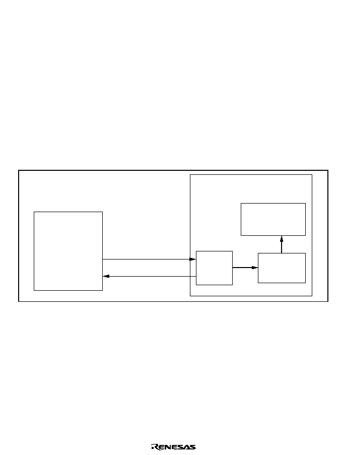
Rev. 1.0, 02/00, page 141 of 1141
7.4.1
Boot Mode
When boot mode is used, the flash memory programming control program must be prepared in the
host beforehand. The channel 1 SCI to be used is set to asynchronous mode.
When a reset-start is executed after the LSI's pins have been set to boot mode, the boot program
built into the MCU is started and the programming control program prepared in the host is serially
transmitted to the LSI via the SCI. In the LSI, the programming control program received via the
SCI is written into the programming control program area in on-chip RAM. After the transfer is
completed, control branches to the start address of the programming control program area and the
programming control program execution state is entered (flash memory programming is
performed).
The transferred programming control program must therefore include coding that follows the
programming algorithm given later.
Figure 7.7 shows the system configuration in boot mode. Figure 7.8 shows the boot program mode
execution procedure.
SI1
SO1
SCI1
This LSI
Flash memory
Write data reception
Verify data
transmission
Host
On-chip RAM
Figure 7.7 System Configuration in Boot Mode
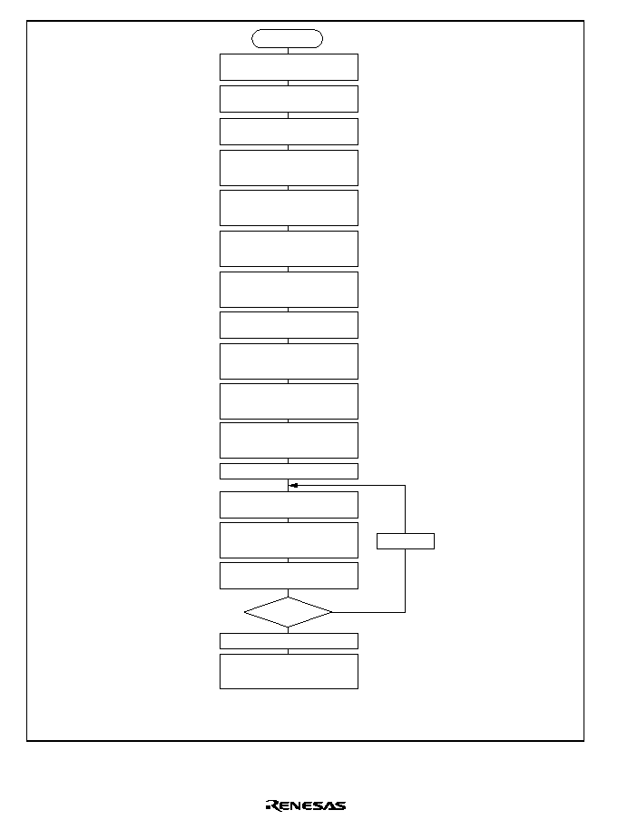
Rev. 1.0, 02/00, page 142 of 1141
Start
Set pins to boot mode and
execute reset-start
Host transfers data (H'00)
continuously at prescribed bit rate
Host transmits user program
sequentially in byte units
Transfer received programming
control program to on-chip RAM
This LSI calculates bit rate and
sets value in bit rate register
Host transmits number of user
program bytes (N), upper byte
followed by lower byte
This LSI transmits received user
program to host as verify data
(echo-back)
n = 1
End of transmission
n = N?
n+1
n
Note :
Yes
No
This LSI measures low period of
H'00 data transmitted by host
After bit rate adjustment, transmits
one H'00 data byte to host to
indicate end of adjustment
Upon receiving H'55, this LSI
sends part of the boot program to
RAM
Host confirms normal reception of
bit rate adjustment end indication
(H'00) and transmits one H'55
data byte
After confirming that all flash
memory data has been erased,
this LSI transmits one H'AA data
byte to host
Transmit one H'AA data byte to
host, and execute programming
control program transferred to on-
chip RAM
Check flash memory data, and if
data has already been written,
erase all blocks
This LSI transmits received
number of bytes to host as verify
data (echo-back)
If a memory cell does not operate normally and cannot be erased, one
H'FF byte is transmitted as an erase error, and the erase operation and
subsequent operations are halted.
Figure 7.8 Boot Mode Execution Procedure (Preliminary)
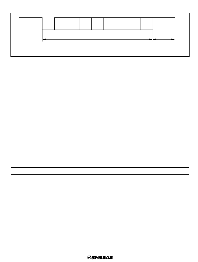
Rev. 1.0, 02/00, page 143 of 1141
Automatic SCI Bit Rate Adjustment
Start
bit
Stop
bit
D0
D1
D2
D3
D4
D5
D6
D7
Low period (9 bits) measured (H'00 data)
High period
(1 or more bits)
Figure 7.9 Automatic SCI Bit Rate Adjustment
When boot mode is initiated, the LSI measures the low period of the asynchronous SCI
communication data (H'00) transmitted continuously from the host. The SCI transmit/receive
format should be set as follows: 8-bit data, 1 stop bit, no parity. The LSI calculates the bit rate of
the transmission from the host from the measured low period, and transmits one H'00 byte to the
host to indicate the end of bit rate adjustment. The host should confirm that this adjustment end
indication (H'00) has been received normally, and transmit one H'55 byte to the LSI. If reception
cannot be performed normally, initiate boot mode again (reset), and repeat the above operations.
Depending on the host's transmission bit rate and the MCU's system clock frequency, there will be
a discrepancy between the bit rates of the host and the LSI. To ensure correct SCI operation, the
host's transfer bit rate should be set to (2400, 4800, or 9600) bps.
Table 7.5 shows typical host transfer bit rates and system clock frequencies for which automatic
adjustment of the LSI's bit rate is possible. The boot program should be executed within this
system clock range.
Table 7.5
System Clock Frequencies for which Automatic Adjustment of This LSI Bit
Rate Is Possible
Host Bit Rate (bps)
System Clock Frequency
9600
8 MHz to 10 MHz (T.B.D.)
4800
4 MHz to 10 MHz (T.B.D.)
2400
2 MHz to 10 MHz (T.B.D.)

Rev. 1.0, 02/00, page 144 of 1141
On-Chip RAM Area Divisions in Boot Mode: In boot mode, the TBD-byte area from TBD to
TBD is reserved for use by the boot program, as shown in figure 7.10. The area to which the
programming control program is transferred is TBD to TBD (TBD bytes). The boot program area
can be used when the programming control program transferred into RAM enters the execution
state. A stack area should be set up as required.
TBD
TBD
Programming
control program
area
(TBD bytes)
TBD
Boot program
area*
(TBD bytes)
Note: * The boot program area cannot be used until a transition is made to the execution
state for the programming control program transferred to RAM. Note that the boot
program reamins stored in this area after a branch is made to the programming
control program.
Figure 7.10 RAM Areas in Boot Mode

Rev. 1.0, 02/00, page 145 of 1141
Notes on Use of Boot Mode:
1. When the chip comes out of reset in boot mode, it measures the low period of the input at the
SCI's SI1 pin. The reset should end with SI1 pin high. After the reset ends, it takes about 100
states for the chip to get ready to measure the low period of the SI1 pin input.
2. In boot mode, if any data has been programmed into the flash memory (if all data is not 1), all
flash memory blocks are erased. Boot mode is for use when user program mode is
unavailable, such as the first time on-board programming is performed, or if the program
activated in user program mode is accidentally erased.
3. Interrupts cannot be used while the flash memory is being programmed or erased.
4. The SI1 and SO1 pins should be pulled up on the board.
5. Before branching to the programming control program (RAM area TBD), the chip terminates
transmit and receive operations by the on-chip SCI (channel 1) (by clearing the RE and TE bits
in SCR to 0), but the adjusted bit rate value remains set in BRR. The transmit data output pin,
SO1, goes to the high-level output state (P21PCR = 1, P21PDR = 1).
The contents of the CPU's internal general registers are undefined at this time, so these
registers must be initialized immediately after branching to the programming control program.
In particular, since the stack pointer (SP) is used implicitly in subroutine calls, etc., a stack
area must be specified for use by the programming control program.
The initial values of other on-chip registers are not changed.
6. Boot mode can be entered by making the pin settings shown in table 7.4 and executing a reset-
start.
When the chip detects the boot mode setting at reset release
*1
, it retains that state internally.
Boot mode can be cleared by driving the reset pin low, waiting at least 20 states, then setting
the FWE pin and mode pins, and executing reset release
*1
. Boot mode can also be cleared by a
WDT overflow reset.
If the mode pin input levels are changed in boot mode, the boot mode state will be maintained
in the microcomputer, and boot mode continued, unless a reset occurs. However, the FWE pin
must not be driven low while the boot program is running or flash memory is being
programmed or erased.
Notes: 1. Mode pin and FWE pin input must satisfy the mode programming setup time (t
MDS
= 4
states) with respect to the reset release timing.
Rev. 1.0, 02/00, page 146 of 1141
7.4.2
User Program Mode
When set to user program mode, the chip can program and erase its flash memory by executing a
user program/erase control program. Therefore, on-board reprogramming of the on-chip flash
memory can be carried out by providing on-board means of FWE control and supply of
programming data, and storing a program/erase control program in part of the program area as
necessary.
In this mode, the chip starts up in mode 1 and applies a high level to the FWE pin.
The flash memory itself cannot be read while the SWE bit is set to 1 to perform programming or
erasing, so the control program that performs programming and erasing should be run in on-chip
RAM or external memory.
Figure 7.11 shows the procedure for executing the program/erase control program when
transferred to on-chip RAM.
Clear FWE
FWE = high
Branch to flash memory
application program
Branch to program/erase control
program in RAM area
Execute program/erase control
program (flash memory rewriting)
Transfer program/erase
control program to RAM
MD0 = 1
Reset start
Write the FWE assessment program and
transfer program (and the program/erase
control program if necessary) beforehand
Note:
Do not apply a constant high level to the FWE pin. Apply a high level to the FWE pin only
when the flash memory is programmed or erased. Also, while a high level is applied to the
FWE pin, the watchdog timer should be activated to prevent overprogramming or
overerasing due to program runaway, etc.
Figure 7.11 User Program Mode Execution Procedure (Preliminary)

Rev. 1.0, 02/00, page 147 of 1141
7.5
Programming/Erasing Flash Memory
In the on-board programming modes, flash memory programming and erasing is performed by
software, using the CPU. There are four flash memory operating modes: program mode, erase
mode, program-verify mode, and erase-verify mode. With addresses H'00000 to H'3FFFF,
transitions to these modes can be made by setting the PSU1, ESU1, P1, E1, PV1 and EV1 bits in
FLMCR1. With addresses H'40000 to H'47FFF, transitions to these modes can be made by setting
the PSU2, ESU2, P2, E2, PV2, and EV2 bits in the FLMCR2.
The flash memory cannot be read while being programmed or erased. Therefore, the program that
controls flash memory programming/erasing (the programming control program) should be
located and executed in on-chip RAM or external memory.
Notes: 1. Operation is not guaranteed if setting/resetting of the SWE1, ESU1, PSU1, EV1, PV1,
E1, and P1 bits in FLMCR1, and the SWE2, ESU2, PSU2, EV2, PV2, E2, and P2 in
FLMCR2, is executed by a program in flash memory.
2. When programming or erasing, set FWE to 1 (programming/erasing will not be
executed if FWE = 0).
3. Perform programming in the erased state. Do not perform additional programming on
previously programmed addresses.
4. Do not write to addresses H'00000 to H'3FFFF and H'40000 to H'47FFF at the same
time. Otherwise operation cannot be guaranteed.
5. Do not operate the OSD when writing or erasing addresses H'40000 to H'47FFF. Do
not set the OSROME in STCR to 1 before manipulating the flash control register.
7.5.1
Program Mode (n=1 when the target address range is H'00000 to H'3FFFF and
n=2 when the target address range is H'40000 to H'47FFF)
Follow the procedure shown in the program/program-verify flowchart in figure 7.12 to write data
or programs to flash memory. Performing program operations according to this flowchart will
enable data or programs to be written to flash memory without subjecting the device to voltage
stress or sacrificing program data reliability. Programming should be carried out 128 bytes at a
time.
Following the elapse of 1.0
µ
s or more after the SWEn bit is set to 1 in flash memory control
register n (FLMCRn), 128-byte program data is stored in the program data area and reprogram
data area, and the 128-byte data in the reprogram data area written consecutively to the write
addresses. The lower 8 bits of the start address written to must be H'00, or H'80. One hundred
and twenty-eight consecutive byte data transfers are performed. The program address and
program data are latched in the flash memory. A 128-byte data transfer must be performed even if
writing fewer than 128 bytes; in this case, H'FF data must be written to the extra addresses.
Next, the watchdog timer is set to prevent overprogramming in the event of program runaway, etc.
Set 6.6 ms as the WDT overflow period. After this, preparation for program mode (program
setup) is carried out by setting the PSUn bit in FLMCRn, and after the elapse of 50
µ
s or more, the
operating mode is switched to program mode by setting the Pn bit in FLMCRn. The time during

Rev. 1.0, 02/00, page 148 of 1141
which the Pn bit is set is the flash memory programming time. Make a program setting for one
programming operation using the table in the programming flowchart.
7.5.2
Program-Verify Mode
In program-verify mode, the data written in program mode is read to check whether it has been
correctly written in the flash memory.
After the elapse of a given programming time, the programming mode is exited (the P bit in
FLMCR1 is cleared, then the PSU bit in FLMCR2 is cleared at least 5
µ
s later). The watchdog
timer is cleared after the elapse of 5
µ
s or more, and the operating mode is switched to program-
verify mode by setting the PVn bit in FLMCRn. Before reading in program-verify mode, a
dummy write of H'FF data should be made to the addresses to be read. The dummy write should
be executed after the elapse of 4
µ
s or more. When the flash memory is read in this state (verify
data is read in 16-bit units), the data at the latched address is read. Wait at least 2
µ
s after the
dummy write before performing this read operation. Next, the originally written data is compared
with the verify data, and reprogram data is computed (see figure 7.12) and transferred to the
reprogram data area. After 128 bytes of data have been verified, exit program-verify mode, wait
for at least TBD
µ
s, then clear the SWEn bit in FLMCRn. If reprogramming is necessary, set
program mode again, and repeat the program/program-verify sequence as before. However,
ensure that the program/program-verify sequence is not repeated more than 1,000 times on the
same bits.
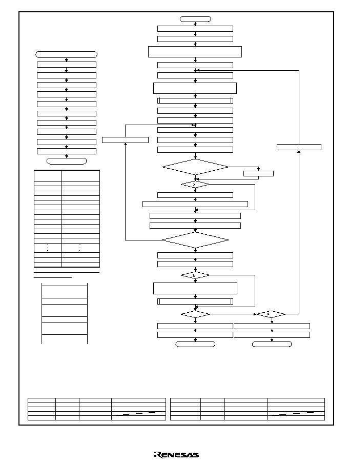
Rev. 1.0, 02/00, page 149 of 1141
Programming pulse apply subroutine
Start
Set SWE1 (2) bit in FLMCR(2)
Set PV1(2) bit in FLMCR1(2)
Clear PV1(2) bit in FLMCR1(2)
Clear SWE1(2) bit in FLMCR1(2)
Write pulse additional program pulse 10 µs
Store 128-byte program data in program
data area and reprogram data area
Write 128-byte program data in RAM reprogram
data area consecutevely to flash memory
Write 128-byte program data in RAM additional
data area consecutively to flash memory
Wait 1 µs
Wait 4 µs
Wait 2 µs
Wait 2 µs
Wait 100 µs
End of programming
Programming pulse 30 µs or 200 µs
H'FF dummy write to verify address
Read verify data
Calculate additional program data
Calculate reprogram data
Complete 128-byte
data verification?
Transfer additional program data to additional program data area
Transfer reprogram data to reprogram data area
Program data= verify data?
Refer to note
*
6
for the pulse width
*
1
*
2
*5
*
4
*
3
*
4
*
1
NG
NG
NG
NG
NG
OK
OK
OK
OK
OK
6 n?
n
n+1
6 n ?
m= 0?
Clear SWE1 (2) bit in FLMCR1(2)
Wait 100 µs
Programming Failure
NG
OK
n 1000?
m= 1
*
4
Call subroutine
n= 1
m= 0
Enable WDT
Set PSU1 (2) bit in FLMCR1 (2)
Set P1 (2) bit in FLMCR1 (2)
Clear P1(2) bit in FLMCR1 (2)
Clear PSU1(2) bit in FLMCR1 (2)
Wait 50 µs
Wait 5 µs
Wait 5 µs
Disable WDT
End of subroutine
Note: 6. Programming pulse width
Number of times
of programming
Programming
time (z) µsec
The programming pulse must be 10 µs in
additional programming
Perform programming after erasing data. Do not perform additional programming to addresses that have already been written to.
Notes: 1. Data transfer is performed by byte transfer. The lower eight bits of the start address must be H'00 or H'80. A 128-byte data transfer must be performed even if writing
fewer than 128 bytes: in this case, H'FF must be written to the extra addresses.
2. Verify data is read in 16-bit (word) units.
3. Even in case of the bit which is already-programmed in the 128-byte programming loop, perform additional programming if the bit fails at the next verify.
4. An area for storing program data (128 bytes), reprogram data (128 bytes), and additional program (128bytes) must be provided in RAM. The contents of the reprogram
and additional program areas are rewritten as programming processes.
5. A 30 µs or 200 µs programming pulse must be applied.
For details on programming pulse, refer to Notes*6.
To perform additional data programming, apply a programming pulse of 10 µs. Reprogram data X' is the reprogram data after program pulse is applied.
Program data storage are
(128 bytes)
Reprogram data storage
area (128 bytes)
Additional program data
storage area (128 bytes)
Reprogram Data Calculation Table
Additiona l program data calculation table
Increment address
Wait for 10 µs, 30 µs or 200 µs
1
2
3
4
5
6
7
8
9
10
11
12
13
998
999
1000
30
30
30
30
30
30
200
200
200
200
200
200
200
200
200
200
RAM
Source Data (D)
0
0
1
1
Reprogram data (X)
1
0
1
1
Additional program data (Y)
0
1
1
1
Reprogram data (X')
0
0
1
1
Comments
Verify data (V)
0
1
0
1
Verify data (V)
0
1
0
1
Programming completed
Programming incomplete; reprogram
Still in erased state; no action
Comments
Additional programming performed
Additional programming not performed
Additional programming not performed
Figure 7.12 Program/Program-Verify Flowchart

Rev. 1.0, 02/00, page 150 of 1141
7.5.3
Erase Mode (n = 1 when the target address range is H'00000 to H'3FFFF and n = 2
when the target address range is H'40000 to H'47FFF)
Flash memory erasing should be performed block by block following the procedure shown in the
erase/erase-verify flowchart (single-block erase) shown in figure 7.13.
To perform data or program erasure, make a 1 bit setting for the flash memory area to be erased in
erase block register 1 or 2 (EBR1 or EBR2) at least 1
µ
s after setting the SWEn bit to 1 in flash
memory control register n (FLMCRn). Next, the watchdog timer is set to prevent overerasing in
the event of program runaway, etc.
Set more than 19.8 ms as the WDT overflow period. After this, preparation for erase mode (erase
setup) is carried out by setting the ESUn bit in FLMCRn, and after a elapse of 100
µ
s or more, the
operating mode is switched to erase mode by setting the En bit in FLMCRn. The time during
which the En bit is set is the flash memory erase time. Ensure that erase time does not exceed 10
ms.
Note:
With flash memory erasing, preprogramming (setting all data in the memory to be erased
to 0) is not necessary before starting the erase procedure.
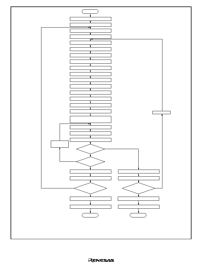
Rev. 1.0, 02/00, page 151 of 1141
End of erasing
START
Set SWE bit in FLMCR1
Set ESU1 (2) bit in FLMCR1 (2)
Set E1 (2) bit in FLMCR1 (2)
Wait 1 µs
Wait 100 µs
n = 1
Set EBR1 (2)
Enable WDT
*
3
Wait 10 ms
Wait 10 µs
Wait 10 µs
Wait 6 µs
Set block start address to
verify address
Wait 2 µs
Wait 4 µs
*
2
*
4
Start of erase
Clear E1 (2) bit in FLMCR1 (2)
Clear ES1 (2) bit in FLMCR1 (2)
Set EV1 (2) bit in FLMCR1 (2)
H'FF dummy write to verify address
Read verify data
Clear EV1 (2) bit in FLMCR1 (2)
Wait 4 µs
Clear EV1 (2) bit in FLMCR1 (2)
Clear SWE bit in FLMCR1
Disable WDT
Halt erase
*
1
Verify data =
all 1?
Wait 100 µs
Wait 100 µs
End of erasing of
all erase blocks?
Erase failure
Clear SWE bit in FLMCR1
n
100?
NO
NO
NO
NO
YES
YES
YES
YES
Notes: 1.
2.
3.
4.
Increment
address
n
n+1
Last address
of block?
Preprogramming (setting erase block data to all 0) is not necessary.
Verify data is read in 16-bit (word) units.
Set only one bit in EBR. More than two bit cannot be set.
Erasing is performed in block units. To erase a number of blocks, the individual blocks must be erased sequentially.
Figure 7.13 Erase/Erase-Verify Flowchart

Rev. 1.0, 02/00, page 152 of 1141
7.5.4
Erase-Verify Mode (n = 1 when the target address range is H'00000 to H'3FFFF
and n = 2 when the target address range is H'40000 to H'47FFF)
In erase-verify mode, data is read after memory has been erased to check whether it has been
correctly erased.
After the elapse of the erase time, erase mode is exited (the En bit in FLMCRn is cleared, then the
ESUn bit is cleared at least 10
µ
s later), the watchdog timer is cleared after the elapse of 10
µ
s or
more, and the operating mode is switched to erase-verify mode by setting the EVn bit in
FLMCRn. Before reading in erase-verify mode, a dummy write of H'FF data should be made to
the addresses to be read. The dummy write should be executed after the elapse of 6.0
µ
s or more.
When the flash memory is read in this state (verify data is read in 16-bit units), the data at the
latched address is read. Wait at least 2
µ
s after the dummy write before performing this read
operation. If the read data has been erased (all 1), a dummy write is performed to the next
address, and erase-verify is performed. If the read data has not been erased, set erase mode again,
and repeat the erase/erase-verify sequence in the same way. However, ensure that the erase/erase-
verify sequence is not repeated more than 100 times. When verification is completed, exit erase-
verify mode, and wait for at least 4
µ
s. If erasure has been completed on all the erase blocks, clear
the SWEn bit in FLMCRn. If there are any unerased blocks, make a 1 bit setting for the flash
memory area to be erased, and repeat the erase/erase-verify sequence in the same way.

Rev. 1.0, 02/00, page 153 of 1141
7.6
Flash Memory Protection
There are three kinds of flash memory program/erase protection: hardware protection, software
protection, and error protection.
7.6.1
Hardware Protection
Hardware protection refers to a state in which programming/erasing of flash memory is forcibly
disabled or aborted. Hardware protection is reset by settings in flash memory control registers 1
and 2 (FLMCR1, FLMCR2) and erase block registers 1 and 2 (EBR1, EBR2). (See table 7.6.)
In error protected state, the FLMCR1, FLMCR2, EBR1, and EBR2 settings are maintained.
Table 7.6
Hardware Protection
Functions
Item
Description
Program
Erase
FWE pin
protection
∑
When a low level is input to the FWE pin, FLMCR1,
FLMCR2 (excluding the FLER bit), EBR1, and EBR2
are initialized, and the program/erase-protected state
is entered
Yes
Yes
Reset/standby
protection
∑
In a reset (including a WDT overflow reset) and in
standby mode, FLMCR1, FLMCR2, EBR1, and EBR2
are initialized, and the program/erase-protected state
is entered
∑
In a reset via the
5(6
pin, the reset state is not
entered unless the
5(6
pin is held low until oscillation
stabilizes after powering on. In the case of a reset
during operation, hold the
5(6
pin low for the
5(6
pulse width specified in the AC characteristics
Yes
Yes

Rev. 1.0, 02/00, page 154 of 1141
7.6.2
Software Protection
Software protection can be implemented by setting the SWE1 bit in FLMCR1 and SWE2 bit in
FLMCR2 and erase block registers 1 and 2 (EBR1, EBR2). When software protection is in effect,
setting the P1 or E1 bit in flash memory control register 1 (FLMCR1) or P2 or E2 bit in flash
memory control register 2 (FLMCR2) does not cause a transition to program mode or erase mode.
(See table 7.7.)
Table 7.7
Software Protection
Functions
Item
Description
Program
Erase
SWE bit
protection
∑
Clearing the SWE bit to 0 in FLMCR1 sets the
program/erase-protected state for all blocks
(Execute in on-chip RAM or external memory)
Yes
Yes
Block
specification
protection
∑
Erase protection can be set for individual blocks by
settings in erase block registers 1 and 2 (EBR1, EBR2)
∑
Setting EBR1 and EBR2 to H'00 places all blocks in
the erase-protected state
-
Yes
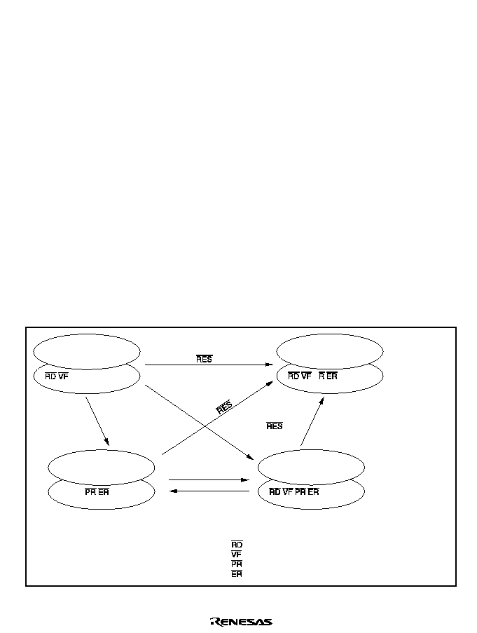
Rev. 1.0, 02/00, page 155 of 1141
7.6.3
Error Protection
In error protection, an error is detected when MCU runaway occurs during flash memory
programming/erasing, or operation is not performed in accordance with the program/erase
algorithm, and the program/erase operation is aborted. Aborting the program/erase operation
prevents damage to the flash memory due to overprogramming or overerasing.
If the MCU malfunctions during flash memory programming/erasing, the FLER bit is set to 1 in
FLMCR2 and the error protection state is entered. The FLMCR1, FLMCR2, EBR1, and EBR2
settings are retained, but program mode or erase mode is aborted at the point at which the error
occurred. Program mode or erase mode cannot be re-entered by re-setting the P or E bit.
However, PV1, PV2, EV1 and EV2 bit setting is enabled, and a transition can be made to verify
mode.
FLER bit setting conditions are as follows:
∑
When flash memory is read during programming/erasing (including a vector read or instruction
fetch)
∑
Immediately after exception handling (excluding a reset) during programming/erasing
∑
When a SLEEP instruction (including standby) is executed during programming/erasing
Error protection is released only by a reset and in hardware standby mode.
Figure 7.14 shows the flash memory state transition diagram.
: Memory read possible
: Verify-read possible
: Programming possible
: Erasing possible
RD
VF
PR
ER
[Legend]
: Memory read impossible
: Verify-read impossible
: Programming impossible
: Erasing impossible
PR ER FLER = 0
Error occurrence
Error occurrence
Power-down mode
= 0
= 0
= 0
P
FLER = 0
Program mode
Erase mode
Reset
(hardware protection)
RD VF
FLER = 1
FLER = 1
Error protection mode
Error protection
mode (power-down mode)
Power-down mode
FLMCR1, FLMCR2 (except FLER bit), EBR1, EBR2
initialization state
FLMCR1, FLMCR2,
EBR1, EBR2 initialization
state
Power-down mode release
Figure 7.14 Flash Memory State Transitions

Rev. 1.0, 02/00, page 156 of 1141
7.7
Interrupt Handling when Programming/Erasing Flash Memory
All interrupts, including NMI input is disabled when flash memory is being programmed or erased
(when the P1 or E1 bit is set in FLMCR1, or the P2 or E2 bit is set in FLMR2), and while the boot
program is executing in boot mode
*1
, to give priority to the program or erase operation. There are
three reasons for this:
∑
Interrupt during programming or erasing might cause a violation of the programming or
erasing algorithm, with the result that normal operation could not be assured.
∑
In the interrupt exception handling sequence during programming or erasing, the vector would
not be read correctly
*2
, possibly resulting in MCU runaway.
∑
If interrupt occurred during boot program execution, it would not be possible to execute the
normal boot mode sequence.
For these reasons, in on-board programming mode alone there are conditions for disabling
interrupt, as an exception to the general rule. However, this provision does not guarantee normal
erasing and programming or MCU operation. All requests, including NMI input, must therefore
be disabled inside and outside the MCU during FWE application. Interrupt is also disabled in the
error-protection state while the P1 or E1 bit remains set in FLMCR1, or P2 or E2 bit remains set in
FLMCR2.
Notes: 1. Interrupt requests must be disabled inside and outside the MCU until data write by the
write control program (vector table and NMI processing program) is complete.
2. The vector may not be read correctly in this case for the following two reasons:
∑
If flash memory is read while being programmed or erased (while the P or E bit is set
in FLMCR1), correct read data will not be obtained (undetermined values will be
returned).
∑
If the interrupt entry in the NMI vector table has not been programmed yet, interrupt
exception handling will not be executed correctly.

Rev. 1.0, 02/00, page 157 of 1141
7.8
Flash Memory Writer Mode
7.8.1
Writer Mode Setting
Programs and data can be written and erased in writer mode as well as in the on-board
programming modes. In writer mode, flash memory read mode, auto-program mode, auto-erase
mode, and status read mode are supported with these device types. In auto-program mode, auto-
erase mode, and status read mode, a status polling procedure is used, and in status read mode,
detailed internal signals are output after execution of an auto-program or auto-erase operation.
7.8.2
Socket Adapters and Memory Map
In writer mode, a socket adapter is mounted on the writer programmer. The socket adapter
product codes are listed in table 7.8.
Figure 7.15 shows the memory map in writer mode.
Table 7.8
Socket Adapter Product Codes
Product Codes
Package
Socket Adapter Product Code
HD64F2199
112-pin QFP
TBD
H8S/2199
H'000000
MCU mode
Writer mode
H'47FFF
H'00000
H'47FFF
On-chip ROM area
Figure 7.15 Memory Map in Writer Mode

Rev. 1.0, 02/00, page 158 of 1141
7.8.3
Writer Mode Operation
Table 7.9 shows how the different operating modes are set when using writer mode, and table 7.10
lists the commands used in writer mode. Details of each mode are given below.
∑
Memory Read Mode: Memory read mode supports byte reads.
∑
Auto-Program Mode: Auto-program mode supports programming of 128 bytes at a time.
Status polling is used to confirm the end of auto-programming.
∑
Auto-Erase Mode: Auto-erase mode supports automatic erasing of the entire flash memory.
Status polling is used to confirm the end of auto-erasing.
∑
Status Read Mode: Status polling is used for auto-programming and auto-erasing, and normal
termination can be confirmed by reading the IO6 signal. In status read mode, error
information is output if an error occurs.
Table 7.9
Settings for Each Operating Mode in Writer Mode
Pin Names
Mode
FWE
&(
&(
2(
2(
:(
:(
IO0 to IO7
A0 to A17
Read
H or L
L
L
H
Data output
Ain
Output disable
H or L
L
H
H
Hi-z
X
Command write
H or L
*
3
L
H
L
Data input
Ain
*
2
Chip disable
*
1
H or L
H
X
X
Hi-z
X
Notes: 1. Chip disable is not a standby state; internally, it is an operation state.
2. Ain indicates that there is also address input in auto-program mode.
3. For command writes when making a transition to auto-program or auto-erase mode,
input a high level to the FWE pin.
Table 7.10
Writer Mode Commands
1st Cycle
2nd Cycle
Command Name
Number of
Cycles
Mode
Address
Data
Mode
Address
Data
Memory read mode
1 + n
write
X
H'00
Read
RA
Dout
Auto-program mode
129
write
X
H'40
write
WA
Din
Auto-erase mode
2
write
X
H'20
write
X
H'20
Status read mode
2
write
X
H'71
write
X
H'71
Notes: 1. In auto-program mode. 129 cycles are required for command writing by a simultaneous
128-byte write.
2. In memory read mode, the number of cycles depends on the number of address write
cycles (n).
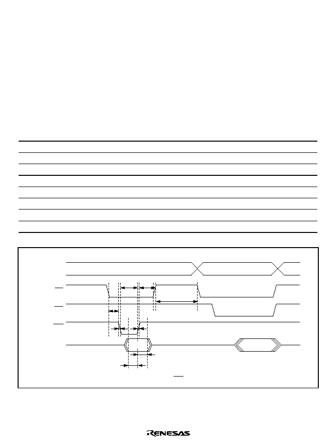
Rev. 1.0, 02/00, page 159 of 1141
7.8.4
Memory Read Mode
∑
After the end of an auto-program, auto-erase, or status read operation, the command wait state
is entered. To read memory contents, a transition must be made to memory read mode by
means of a command write before the read is executed.
∑
Command writes can be performed in memory read mode, just as in the command wait state.
∑
Once memory read mode has been entered, consecutive reads can be performed.
∑
After power-on, memory read mode is entered.
Table 7.11
AC Characteristics in Memory Read Mode (1)
-
Preliminary
-
Conditions: V
CC
= 5.0 V
±
10%, V
SS
= 0 V, Ta = 25
∞
C
±
5
∞
C
Item
Symbol
Min
Max
Unit
Notes
Command write cycle
t
nxtc
20
µ
s
&(
hold time
t
ceh
0
ns
&(
setup time
t
ces
0
ns
Data hold time
t
dh
50
ns
Data setup time
t
ds
50
ns
Write pulse width
t
wep
70
ns
:(
rise time
t
r
30
ns
:(
fall time
t
f
30
ns
CE
A18 to A0
IO7 to IO0
DATA
OE
WE
Command write
t
wep
t
ceh
t
dh
t
ds
t
f
t
r
t
nxtc
Note: Data is latched on the rising edge of WE.
t
ces
Memory read mode
ADDRESS STABLE
DATA
Figure 7.16 Memory Read Mode Timing Waveforms after Command Write
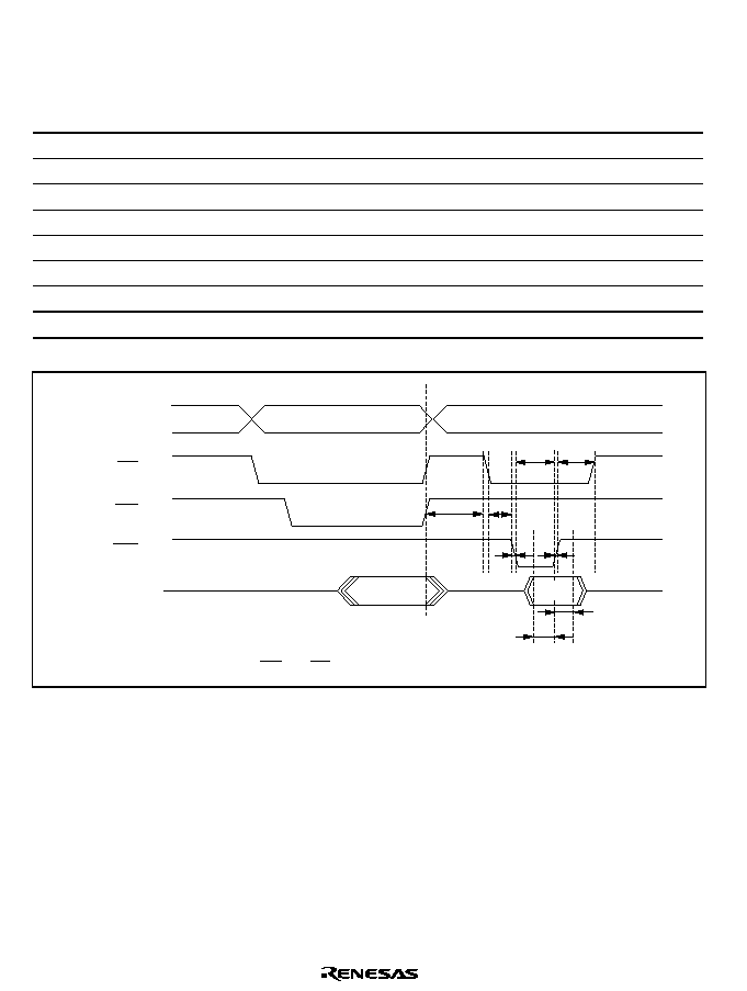
Rev. 1.0, 02/00, page 160 of 1141
Table 7.12
AC Characteristics when Entering Another Mode from Memory Read Mode
-
Preliminary
-
Conditions: V
CC
= 5.0 V
±
10%, V
SS
= 0 V, Ta = 25
∞
C
±
5
∞
C
Item
Symbol
Min
Max
Unit
Notes
Command write cycle
t
nxtc
20
µ
s
&(
hold time
t
ceh
0
ns
&(
setup time
t
ces
0
ns
Data hold time
t
dh
50
ns
Data setup time
t
ds
50
ns
Write pulse width
t
wep
70
ns
:(
rise time
t
r
30
ns
:(
fall time
t
f
30
ns
CE
A18 to A0
IO7 to IO0
H'XX
OE
WE
XX mode command write
t
wep
t
ceh
t
dh
t
ds
t
nxtc
Note: Do not enable WE and OE at the same time.
t
ces
ADDRESS STABLE
DATA
t
f
t
r
Figure 7.17 Timing Waveforms when Entering Another Mode from Memory Read Mode
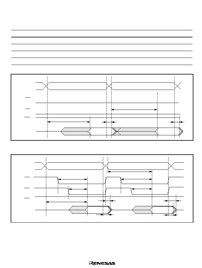
Rev. 1.0, 02/00, page 161 of 1141
Table 7.13
AC Characteristics in Memory Read Mode (2)
-
Preliminary
-
Conditions: V
CC
= 5.0 V
±
10%, V
SS
= 0 V, Ta = 25
∞
C
±
5
∞
C
Item
Symbol
Min
Max
Unit
Notes
Access time
t
acc
20
µ
s
&(
output delay time
t
ce
150
ns
2(
output delay time
t
oe
150
ns
Output disable delay time
t
df
100
ns
Data output hold time
t
oh
5
ns
CE
A18 to A0
IO7 to IO0
VIL
VIL
VIH
OE
WE
t
acc
t
oh
t
oh
t
acc
ADDRESS STABLE
ADDRESS STABLE
DATA
DATA
Figure 7.18 Timing Waveforms for
/
Enable State Read
CE
A18 to A0
IO7 to IO0
VIH
OE
WE
t
ce
t
acc
t
oe
t
oh
t
oh
t
df
t
ce
t
acc
t
oe
ADDRESS STABLE
ADDRESS STABLE
DATA
DATA
t
df
Figure 7.19 Timing Waveforms for
/
Clocked Read

Rev. 1.0, 02/00, page 162 of 1141
7.8.5
Auto-Program Mode
AC Characteristics
Table 7.14
AC Characteristics in Auto-Program
-
Preliminary
-
Conditions: V
CC
= 5.0 V
±
10%, V
SS
= 0 V, Ta = 25
∞
C
±
5
∞
C
Item
Symbol
Min
Max
Unit
Notes
Command write cycle
t
nxtc
20
µ
s
&(
hold time
t
ceh
0
ns
&(
setup time
t
ces
0
ns
Data hold time
t
dh
50
ns
Data setup time
t
ds
50
ns
Write pulse width
t
wep
70
ns
Status polling start time
t
wsts
1
ms
Status polling access time
t
spa
150
ns
Address setup time
t
as
0
ns
Address hold time
t
ah
60
ns
Memory write time
t
write
1
3000
ms
:(
rise time
t
r
30
ns
:(
fall time
t
f
30
ns
Write setup time
t
pns
100
ns
Write end setup time
t
pnh
100
ns
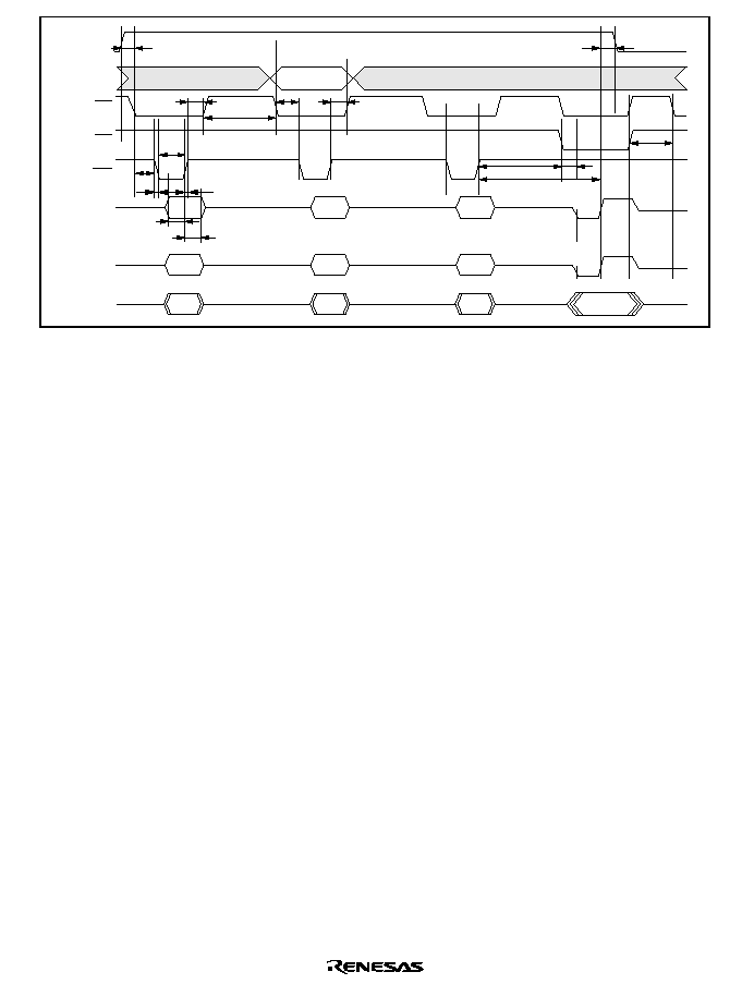
Rev. 1.0, 02/00, page 163 of 1141
CE
FWE
A18 to A0
IO7
OE
WE
t
nxtc
t
wsts
t
spa
t
nxtc
t
ces
t
ds
t
dh
t
wep
t
as
t
pnh
t
pns
t
ah
t
ceh
ADDRESS STABLE
Data transfer
1 byte to 128 bytes
IO6
Programming wait
DATA
IO5 to IO0
H'40
DATA
H'00
t
f
t
r
t
write
(1 to 3,000 ms)
Programming operation
end identification signal
Programming normal end
identification signal
Figure 7.20 Auto-Program Mode Timing Waveforms
Notes on Use of Auto-Program Mode
∑
In auto-program mode, 128 bytes are programmed simultaneously. This should be carried out
by executing 128 consecutive byte transfers.
∑
A 128-byte data transfer is necessary even when programming fewer than 128 bytes. In this
case, H'FF data must be written to the extra addresses.
∑
The lower 8 bits of the transfer address must be H'00 or H'80. If a value other than an effective
address is input, processing will switch to a memory write operation but a write error will be
flagged.
∑
Memory address transfer is performed in the second cycle (figure 7.20). Do not perform
transfer after the second cycle.
∑
Do not perform a command write during a programming operation.
∑
Perform one auto-programming operation for a 128-byte block for each address.
Characteristics are not guaranteed for two or more programming operations.
∑
Confirm normal end of auto-programming by checking IO6. Alternatively, status read mode
can also be used for this purpose (IO7 status polling uses the auto-program operation end
identification pin).
∑
The status polling IO6 and IO7 pin information is retained until the next command write.
Until the next command write is performed, reading is possible by enabling
and .
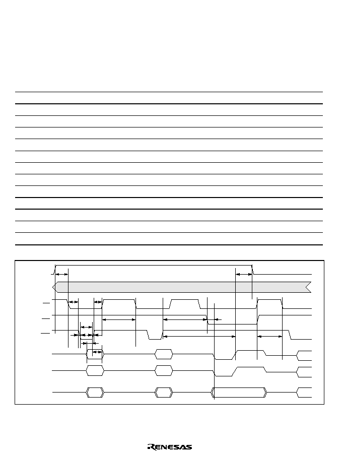
Rev. 1.0, 02/00, page 164 of 1141
7.8.6
Auto-Erase Mode
AC Characteristics
Table 7.15
AC Characteristics in Auto-Erase Mode
-
Preliminary
-
Conditions: V
CC
= 5.0 V
±
10%, V
SS
= 0 V, Ta = 25
∞
C
±
5
∞
C
Item
Symbol
Min
Max
Unit
Notes
Command write cycle
t
nxtc
20
µ
s
&(
hold time
t
ceh
0
ns
&(
setup time
t
ces
0
ns
Data hold time
t
dh
50
ns
Data setup time
t
ds
50
ns
Write pulse width
t
wep
70
ns
Status polling start time
t
ests
1
ms
Status polling access time
t
spa
150
ns
Memory erase time
t
erase
100
40000
ms
:(
rise time
t
r
30
ns
:(
fall time
t
f
30
ns
Erase setup time
t
ens
100
ns
Erase end setup time
t
enh
100
ns
CE
FWE
A18 to A0
IO5 to IO0
IO6
IO7
OE
WE
t
erase
(100 to 40000ms)
t
ests
t
spa
t
nxtc
t
nxtc
t
ces
t
ceh
t
dh
CL
in
DL
in
t
ds
t
wep
t
ens
H'00
H'20
H'20
t
enh
Erase end
identification signal
Erase normal end
identification signal
t
f
t
r
Figure 7.21 Auto-Erase Mode Timing Waveforms

Rev. 1.0, 02/00, page 165 of 1141
Notes on Use of Erase-Program Mode
∑
Auto-erase mode supports only entire memory erasing.
∑
Do not perform a command write during auto-erasing.
∑
Confirm normal end of auto-erasing by checking IO6. Alternatively, status read mode can also
be used for this purpose (IO7 status polling uses the auto-erase operation end identification
pin).
∑
The status polling IO6 and IO7 pin information is retained until the next command write.
Until the next command write is performed, reading is possible by enabling
and .
7.8.7
Status Read Mode
Status read mode is used to identify what type of abnormal end has occurred. Use this mode when
an abnormal end occurs in auto-program mode or auto-erase mode.
The return code is retained until a command write for other than status read mode is performed.
Table 7.16
AC Characteristics in Status Read Mode
-
Preliminary
-
Conditions: V
CC
= 5.0 V
±
10%, V
SS
= 0 V, Ta = 25
∞
C
±
5
∞
C
Item
Symbol
Min
Max
Unit
Notes
Command write cycle
t
nxtc
20
µ
s
&(
hold time
t
ceh
0
ns
&(
setup time
t
ces
0
ns
Data hold time
t
dh
50
ns
Data setup time
t
ds
50
ns
Write pulse width
t
wep
70
ns
2(
output delay time
t
oe
150
ns
Disable delay time
t
df
100
ns
&(
output delay time
t
ce
150
ns
:(
rise time
t
r
30
ns
:(
fall time
t
f
30
ns
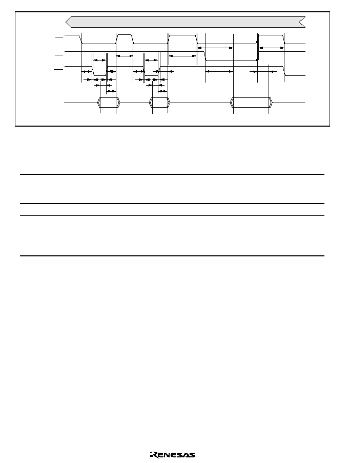
Rev. 1.0, 02/00, page 166 of 1141
CE
A18 to A0
IO7 to IO0
OE
WE
t
ces
t
nxtc
t
nxtc
t
df
Note: IO2 and IO3 are undefined.
t
ces
t
dh
t
ceh
t
ds
t
wep
t
wep
DATA
t
dh
t
ceh
t
ds
t
oe
t
ce
t
nxtc
H'71
H'71
t
f
t
r
t
f
t
r
Figure 7.22 Status Read Mode Timing Waveforms
Table 7.17
Status Read Mode Return Commands
Pin Name
IO7
IO6
IO5
IO4
IO3
IO2 IO1
IO0
Attribute
Normal end
identification
Command
error
Programming
error
Erase error
Programming
or erase count
exceeded
Effective
address
error
Initial value 0
0
0
0
0
0
0
0
Indications
Normal
end: 0
Abnormal
end: 1
Command
error: 1
Otherwise: 0
Programming
error: 1
Otherwise: 0
Erase error: 1
Otherwise: 0
Count
exceeded: 1
Otherwise: 0
Effective
address
error: 1
Otherwise: 0
Note: IO2 and IO3 are undefined.

Rev. 1.0, 02/00, page 167 of 1141
7.8.8
Status Polling
The IO7 status polling flag indicates the operating status in auto-program or auto-erase mode.
The IO6 status polling flag indicates a normal or abnormal end in auto-program or auto-erase
mode.
Table 7.18
Status Polling Output Truth Table
Pin Names
Internal Operation
in Progress
Abnormal End
Normal End
IO7
0
1
0
1
IO6
0
0
1
1
IO0 to IO5
0
0
0
0
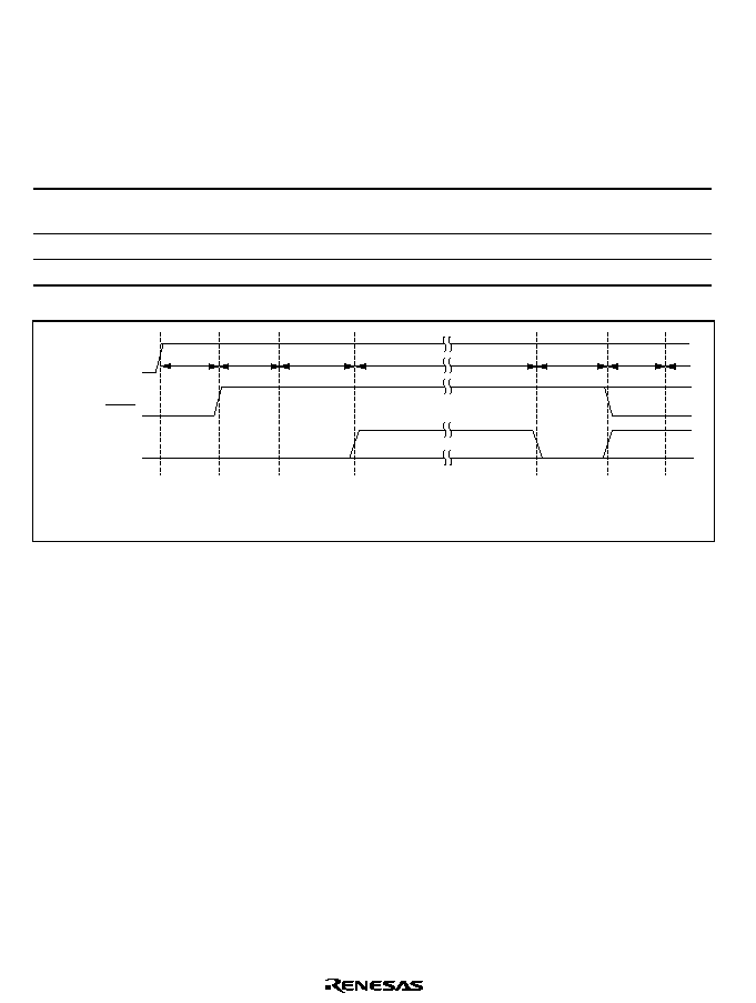
Rev. 1.0, 02/00, page 168 of 1141
7.8.9
Writer Mode Transition Time
Commands cannot be accepted during the oscillation stabilization period or the writer mode setup
period. After the writer mode setup time, a transition is made to memory read mode.
Table 7.19
Command Wait State Transition Time Specifications
Item
Symbol
Min
Max
Unit
Notes
Standby release
(oscillation stabilization time)
t
osc1
10
ms
Writer mode setup time
t
bmv
10
ms
V
CC
hold time
t
dwn
0
ms
V
CC
RES
FWE
Memory read
mode
Command wait
state
Command
wait state
Normal/abnormal
end identifica-
tion
Auto-program mode
Auto-erase mode
t
osc1
t
bmv
t
dwn
Note: Except in auto-program mode and auto-erase mode, drive the FWE input pin low.
Don't care
Don't care
Figure 7.23 Oscillation Stabilization Time,
Boot Program Transfer Time, and Power Supply Fall Sequence
7.8.10
Notes on Memory Programming
∑
When programming addresses which have previously been programmed, carry out auto-
erasing before auto-programming.
∑
When performing programming using writer mode on a chip that has been programmed/erased
in an on-board programming mode, auto-erasing is recommended before carrying out auto-
programming.
Notes: 1. The flash memory is initially in the erased state when the device is shipped by Hitachi.
For other chips for which the erasure history is unknown, it is recommended that auto-
erasing be executed to check and supplement the initialization (erase) level.
2. Auto-programming should be performed once only on the same address block.

Rev. 1.0, 02/00, page 169 of 1141
7.9
Notes when Converting the F≠ZTAT Application Software to the
Mask-ROM Versions
Please note the following when converting the F-ZTAT application software to the mask-ROM
versions.
The values read from the internal registers for the flash ROM of the mask-ROM version and
F≠ZTAT version differ as follows.
Status
Register
Bit
F≠ZTAT Version
Mask-ROM Version
FLMCR1
FWE
0: Application software
running
1: Programming
0: Is not read out
1: Application software
running
Note: This difference applies to all the F-ZTAT versions and all the mask-ROM versions that have
different ROM size.
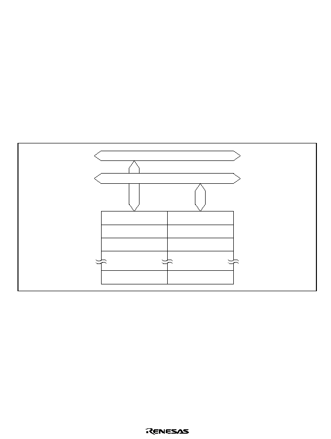
Rev. 1.0, 02/00, page 171 of 1141
Section 8 RAM
8.1
Overview
The H8S/2199, H8S/2198, H8S/2197, and H8S/2196 have 3 kbytes of on-chip high-speed static
RAM, and the H8S/2199 F-ZTAT has 8 kbytes. The on-chip RAM is connected to the CPU by a
16-bit data bus, enabling both byte data and word data to be accessed in one state. This makes it
possible to perform fast word data transfer.
8.1.1
Block Diagram
Figure 8.1 shows a block diagram of the on-chip RAM.
Internal data bus (upper 8 bits)
Internal data bus (lower 8 bits)
H'FFE3B0
H'FFE3B2
H'FFE3B4
H'FFFFAE
H'FFE3B1
H'FFE3B3
H'FFE3B5
H'FFFFAF
Figure 8.1 Block Diagram of RAM (H8S/2199)
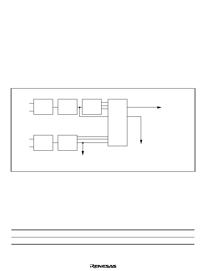
Rev. 1.0, 02/00, page 173 of 1141
Section 9 Clock Pulse Generator
9.1
Overview
This LSI has a built-in clock pulse generator (CPG) that generates the system clock (
), the bus
master clock, and internal clocks.
The clock pulse generator consists of a system clock oscillator, a duty adjustment circuit, clock
selection circuit, medium-speed clock divider, subclock oscillator, and subclock division circuit.
9.1.1
Block Diagram
Figure 9.1 shows a block diagram of the clock pulse generator.
System
clock
oscillator
Duty
adjustment
circuit
Clock
selection
circuit
Medium-
speed clock
divider
Subclock
oscillator
Subclock
division
circuit
OSC1
OSC2
X1
X2
/16,
/32,
/64
w/2,
w/4,
w/8
SUB
or
SUB
Timer A
count clock
Internal clock
To supporting modules
Bus master clock
To CPU
SUB (
w/2,
w/4,
w/8)
Figure 9.1 Block Diagram of Clock Pulse Generator
9.1.2
Register Configuration
The clock pulse generator is controlled by SBYCR and LPWRCR. Table 9.1 shows the register
configuration.
Table 9.1
CPG Registers
Name
Abbreviation
R/W
Initial Value
Address
*
Standby control register
SBYCR
R/W
H'00
H'FFEA
Low-power control register
LPWRCR
R/W
H'00
H'FFEB
Note:
*
Lower 16 bits of the address.

Rev. 1.0, 02/00, page 174 of 1141
9.2
Register Descriptions
9.2.1
Standby Control Register (SBYCR)
7
SSBY
0
R/W
6
STS2
0
R/W
5
STS1
0
R/W
4
STS0
0
R/W
3
--
0
--
0
SCK0
0
R/W
2
--
0
--
1
SCK1
0
R/W
Bit
Initial value
R/W
:
:
:
SBYCR is an 8-bit readable/writable register that performs power-down mode control.
Only bits 0 and 1 are described here. For a description of the other bits, see section 4.2.1, Standby
Control Register (SBYCR). SBYCR is initialized to H'00 by a reset.
Bits 1 and 0
System Clock Select 1 and 0 (SCK1, SCK0): These bits select the bus master
clock for high-speed mode and medium-speed mode.
Bit 1
Bit 0
SCK1
SCK0
Description
0
Bus master is in high-speed mode
(Initial value)
0
1
Medium-speed clock is
/16
0
Medium-speed clock is
/32
1
1
Medium-speed clock is
/64

Rev. 1.0, 02/00, page 175 of 1141
9.2.2
Low-Power Control Register (LPWRCR)
7
DTON
0
R/W
6
LSON
0
R/W
5
NESEL
0
R/W
4
--
0
--
3
--
0
--
0
SA0
0
R/W
2
--
0
--
1
SA1
0
R/W
Bit
Initial value
R/W
:
:
:
LPWRCR is an 8-bit readable/writable register that performs power-down mode control.
Only bit 1 and 0 is described here. For a description of the other bits, see section 4.2.2, Low-
Power Control Register (LPWRCR).
LPWRCR is initialized to H'00 by a reset.
Bits 1 and 0
Subactive Mode Clock Select (SA1, SA0): Selects CPU clock for subactive mode.
In subactive mode, writes are disabled.
Bit 1
Bit 0
SA1
SA0
Description
0
CPU operating clock is
w/8
(Initial value)
0
1
CPU operating clock is
w/4
1
*
CPU operating clock is
w/2
Note:
*
Don't care
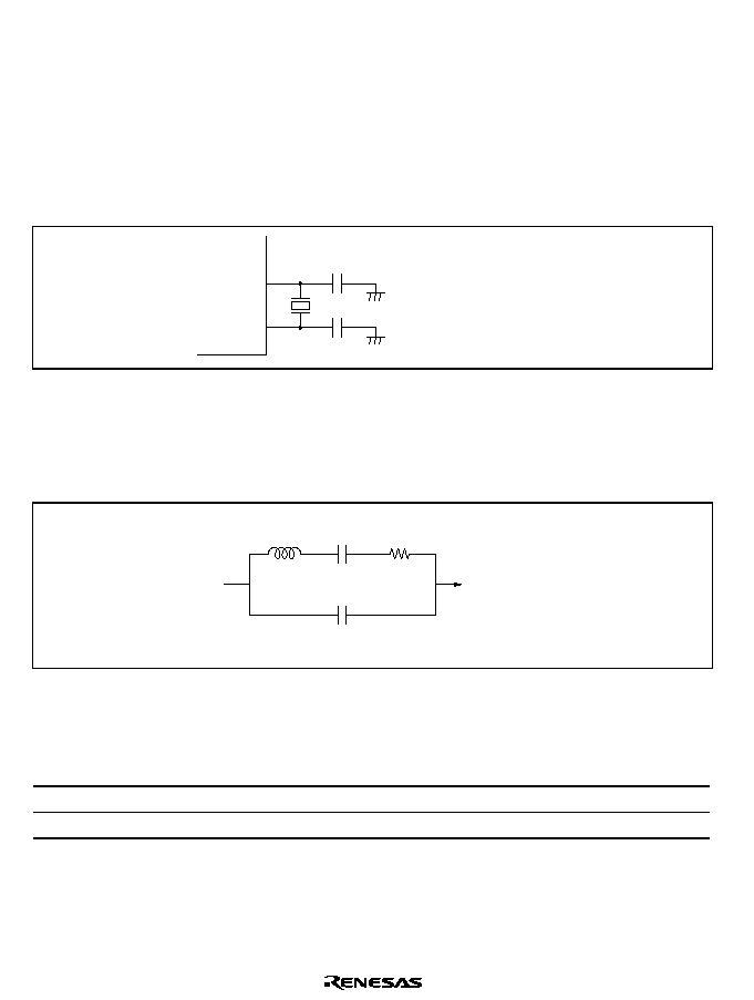
Rev. 1.0, 02/00, page 176 of 1141
9.3
Oscillator
Clock pulses can be supplied by connecting a crystal resonator, or by input of an external clock.
9.3.1
Connecting a Crystal Resonator
Circuit Configuration: A crystal resonator can be connected as shown in the example in figure
9.2. An AT-cut parallel-resonance crystal should be used.
OSC1
OSC2
C
L2
C
L1
C
L1 =
C
L2
= 10 to 22pF
Figure 9.2 Connection of Crystal Resonator (Example)
Crystal Resonator: Figure 9.3 shows the equivalent circuit of the crystal resonator. Use a crystal
resonator that has the characteristics shown in table 9.2 and the same frequency as the system
clock (
).
OSC1
C
L
AT-cut parallel-resonance type
OSC2
C
0
L
R
s
Figure 9.3 Crystal Resonator Equivalent Circuit
Table 9.2
Crystal Resonator Parameters
Frequency (MHz)
8
10
R
S
max (
)
80
60
C
O
max (pF)
7
7
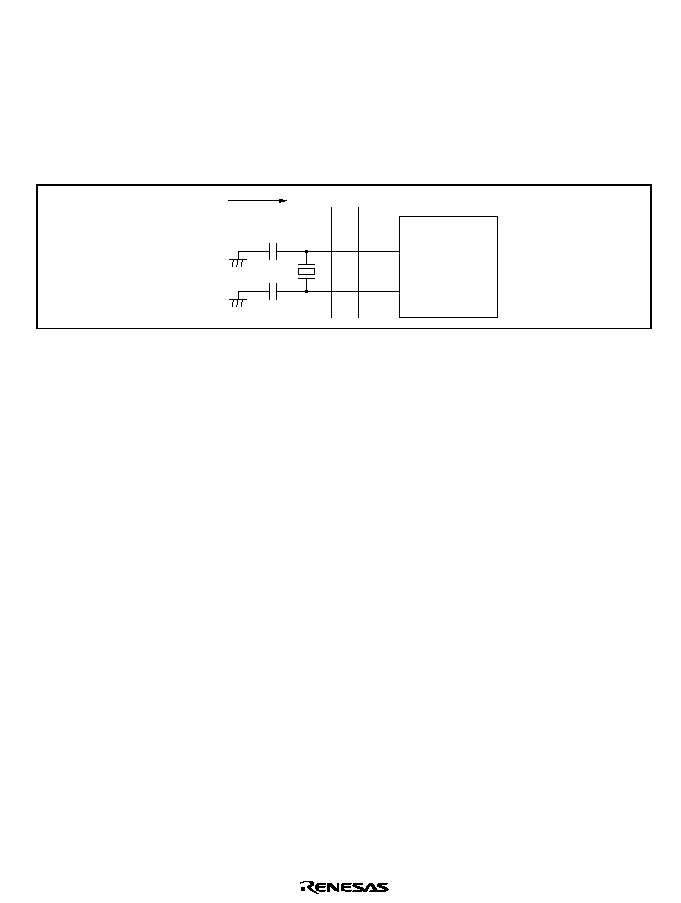
Rev. 1.0, 02/00, page 177 of 1141
Note on Board Design: When a crystal resonator is connected, the following points should be
noted.
Other signal lines should be routed away from the oscillator circuit to prevent induction from
interfering with correct oscillation. See figure 9.4.
When designing the board, place the crystal resonator and its load capacitors as close as possible
to the OSC1 and OSC2 pins.
C
L2
Signal A Signal B
C
L1
This chip
OSC1
OSC2
Avoid
Figure 9.4 Example of Incorrect Board Design
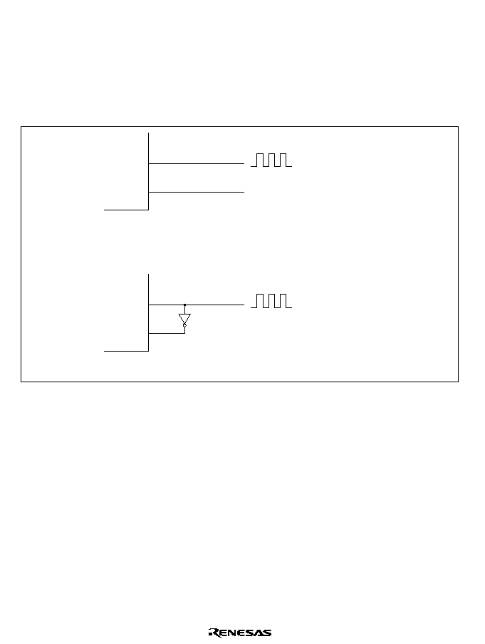
Rev. 1.0, 02/00, page 178 of 1141
9.3.2
External Clock Input
Circuit Configuration: An external clock signal can be input as shown in the examples in figure
9.5. If the OSC2 pin is left open, make sure that stray capacitance is no more than 10 pF.
In example (b), make sure that the external clock is held high in standby mode, subactive mode,
subsleep mode, and watch mode.
OSC1
OSC2
External clock input
Open
(a) OSC2 pin left open
OSC1
OSC2
External clock input
(b) Inverted-phase clock input at OSC2 pin
Figure 9.5 External Clock Input (Examples)
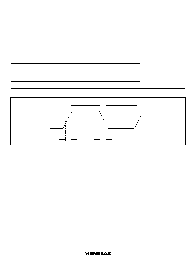
Rev. 1.0, 02/00, page 179 of 1141
External Clock: The external clock signal should have the same frequency as the system clock
(
).
Table 9.3 and figure 9.6 show the input conditions for the external clock.
Table 9.3
External Clock Input Conditions
V
CC
= 4.0 to 5.5 V
Item
Symbol
Min
Max
Unit
Test Conditions
External clock input low
pulse width
t
EXL
40
ns
External clock input high
pulse width
t
EXH
40
ns
External clock rise time
t
EXr
10
ns
External clock fall time
t
EXf
10
ns
Figure 9.6
t
EXH
t
EXL
t
EXr
t
EXf
OSC1
Figure 9.6 External Clock Input Timing
Table 9.4 shows the external clock output settling delay time, and figure 9.7 shows the external
clock output settling delay timing. The oscillator and duty adjustment circuit have a function for
adjusting the waveform of the external clock input at the OSC1 pin. When the prescribed clock
signal is input at the OSC1 pin, internal clock signal output is fixed after the elapse of the external
clock output settling delay time (t
DEXT
). As the clock signal output is not fixed during the t
DEXT
period, the reset signal should be driven low to maintain the reset state.
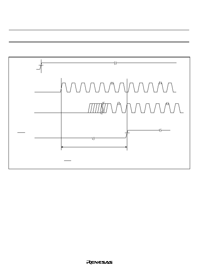
Rev. 1.0, 02/00, page 180 of 1141
Table 9.4
External Clock Output Settling Delay Time
Conditions: V
CC
= 4.0 V to 5.5 V, AV
CC
= 4.0 V to 5.5 V, V
SS
= AV
SS
= 0 V
Item
Symbol
Min
Max
Unit
Notes
External clock output settling
delay time
t
DEXT
*
500
µ
s
Figure 9.7
Note:
*
t
DEXT
includes 20 t
CYC
of
#$
pulse width (t
RESW
).
t
DEXT
*
RES
(Internal)
OSC1
V
CC
4.0 V
Note: * t
DEXT
includes 20 t
cyc
of RES pulse width (t
RESW
).
Figure 9.7 External Clock Output Settling Delay Timing

Rev. 1.0, 02/00, page 181 of 1141
9.4
Duty Adjustment Circuit
When the oscillator frequency is 5 MHz or higher, the duty adjustment circuit adjusts the duty
cycle of the clock signal from the oscillator to generate the system clock (
).
9.5
Medium-Speed Clock Divider
The medium-speed divider divides the system clock to generate
/16,
/32, and
/64 clocks.
9.6
Bus Master Clock Selection Circuit
The bus master clock selection circuit selects the system clock (
) or one of the medium-speed
clocks (
/16,
/32 or
/64) to be supplied to the bus master (CPU), according to the settings of bits
SCK2 to SCK0 in SBYCR.
Rev. 1.0, 02/00, page 182 of 1141
9.7
Subclock Oscillator Circuit
9.7.1
Connecting 32.768 kHz Crystal Resonator
When using a subclock, connect a 32.768 kHz crystal resonator to X1 and X2 pins as shown in
figure 9.8.
For precautions on connecting, see Note on Board Design, in section 9.3.1 Connecting a Crystal
Resonator.
X1
X2
C
2
C
1
C
1
= C
2
= 15 pF (Typ)
Figure 9.8 Connecting a 32.768 kHz Crystal Resonator (Example)
Figure 9.9 shows a crystal resonator equivalent circuit.
X1
C
S
C
0
= 1.5 pF (Typ)
R
S
= 14 k
(Typ)
f
W
= 32.768 kHz
Type: MX38T (Nihon Denpa Kogyo Co., Ltd.)
Note: Values shown are the reference values.
X2
C
0
L
s
R
s
Figure 9.9 32.768 kHz Crystal Resonator Equivalent Circuit
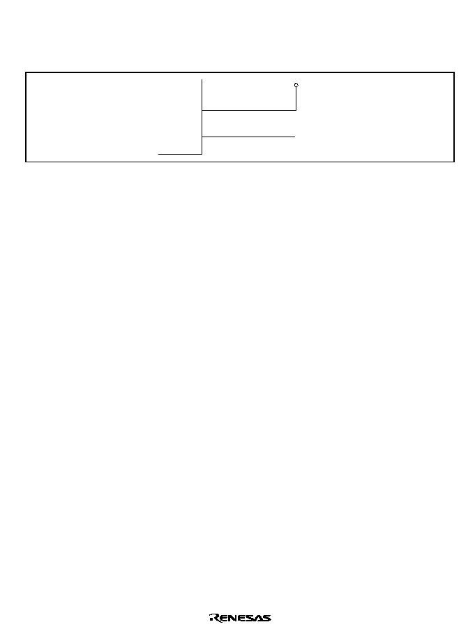
Rev. 1.0, 02/00, page 183 of 1141
9.7.2
When Subclock is not Needed
Connect X1 pin to V
CL
, and X2 pin should remain open as shown in figure 9.10.
X1
X2
V
CL
Open
Figure 9.10 Terminal When Subclock is not Needed
9.8
Subclock Waveform Shaping Circuit
To eliminate noise in the subclock input from the X1 pin, this circuit samples the clock using a
clock obtained by dividing the
clock. The sampling frequency is set with the NESEL bit in
LPWRCR. For details, see section 4.2.2, Low-Power Control Register (LPWRCR). The clock is
not sampled in subactive mode, subsleep mode, or watch mode.
9.9
Notes on the Resonator
Resonator characteristics are closely related to the user board design. Perform appropriate
assessment of resonator connection, mask version and F-ZTAT
TM
, by referring to the connection
example given in this section. The resonator circuit rate differs depending on the free capacity of
the resonator and the execution circuit, so consult with the resonator manufacturer before
determination. Make sure the voltage applied to the resonator pin does not exceed the maximum
rated voltage.

Rev. 1.0, 02/00, page 185 of 1141
Section 10 I/O Port
10.1
Overview
10.1.1
Port Functions
This LSI has seven 8-bit I/O ports (including one CMOS high-current port), and one 8-bit input
port. Table 10.1 shows the functions of each port. Each I/O part a port control register (PCR) that
controls an input and output and a port data register (PDR) for storing output data. The input and
output can be controlled in a unit of bit. The pin whose peripheral function is used both as an
alternative function can set the pin function in a unit of bit by a port mode register (PMR).
10.1.2
Port Input
∑
Reading a Port
When a general port of PCR = 0 (input) is read, the pin level is read.
When a general port of PCR = 1 (output) is read, the value of the corresponding PDR bit is
read.
When the pins (excluding AN7 to AN0 and RPB7 to RP0 pins) set to the peripheral
function are read, the results are as given in items (1) and (2) according to the PCR value.
∑
Processing Input Pins
The general input port or general I/O port is gated by read signals. Unused pins can be left
open if they are not read. However, if an open pin is read, a feedthrough current may apply
during the read period according to an intermediate level. The read period is about one-state.
Relevant ports: P0, P1, P2, P3, P4, P5, P6, P7, and P8
When an alternative pin is set to an alternative function other than the general I/O, always set
the pin level to a high or low level. If the pin is left open, a feedthrough current applies
according to an intermediate level, which adversely affects reliability, causes malfunctions,
and in the worst case may damage the pin.
Because the PMR is not initialized in low power consumption mode, pay attention to the pin
input level after the mode has been shifted to the low power consumption mode.
Relevant pins:
,&, ,54 to ,54, SCK1, SI1, SDA1, SCL1, SDA0, SCL0, SYNCI, FTIA,
FTIB, FTIC, FTID, RPTRG, TMBI,
$'75*, EXCTL, COMP, DPG, EXCAP, and EXTTRG

Rev. 1.0, 02/00, page 186 of 1141
Table 10.1
Port Functions
Port
Description
Pins
Alternative Functions
Function
Switching
Register
Port 0
P07 to P00 input-
only ports
P07/AN7 to
P00/AN0
Analog data input channels 7 to 0
PMR0
P17/TMOW
Prescalar unit frequency division clock
output
P16/
,&
Prescalar unit input capture input
Port 1
P17 to P10 I/O ports
(Built-in MOS pull-up
transistors)
P15/
,54
to
P10/
,54
External interrupt request input
PMR1
P27/SYNCI
Formatless serial clock input
P26/SCL0
I
2
C bus interface clock I/O
P25/SDA0
I
2
C bus interface data I/O
STCR
ICCR
P24/SCL1
I
2
C bus interface clock I/O
P23/SDA1
I
2
C bus interface data I/O
P22/SCK1
SCI1 clock I/O
P21/SO1
SCI1 transmit data output
Port 2
P27 to P20 I/O ports
(Built-in MOS pull-up
transistors)
P20/SI1
SCI1 receive data input
SMR
SCR
P37/TMO
Timer J timer output
P36/BUZZ
Timer J buzzer output
P35/PWM3 to
P32/PWM0
8-bit PWM output
P31/SV2
Servo monitor output
Port 3
P37 to P30 I/O ports
(Built-in MOS pull-up
transistors)
P30/SV1
PMR3
P47/RPTRG
Realtime output port trigger input
P46/FTOB
Timer X output compare B output
P45/FTOA
Timer X output compare A output
TOCR
P44/FTID
Timer X input capture D input
P43/FTIC
Timer X input capture C input
P42/FTIB
Timer X input capture B input
P41/FTIA
Timer X input capture A input
Port 4
P47 to P40 I/O ports
P40/PWM14
14-bit PWM output
PMR4
Realtime output port
P67/RP7/
TMBI
Timer B event output
Realtime output port
P66/RP6/
ADTRG
A/D conversion start external trigger
input
Port 6
P63 to P60 I/O ports
P65/RP5 to
P60/RP0
Realtime output port
PMR6
PMRA
PPG output
P77/PPG7/
RPB to P74/
PPG4/RP8
Realtime output port
Port 7
P77 to P70 I/O ports
P73/PPG3 to
P70/PPG0
PPG output
PMR7
PMRB

Rev. 1.0, 02/00, page 187 of 1141
Port
Description
Pins
Alternative Functions
Function
Switching
Register
P87/DPG
DPG signal input
P86/EXTTRG
External trigger signal input
Pre-amplifier output result signal
input
P85/COMP/B
Color signal output (B)
Pre-amplifier output select signal
input
P84/H.AMP
SW/G
Color signal output (G)
Control signal output for
processing color signals
P83/C.Rotary/
R
Color signal output (R)
P82/EXCTL
External CTL signal input
External capstan signal input
P81/EXCAP/
YBO
OSD character position output
Port 8
P87 to P80 I/O ports
P80/YCO
OSD character data output
PMR8
PMRC
Note: This LSI does not have port 5.
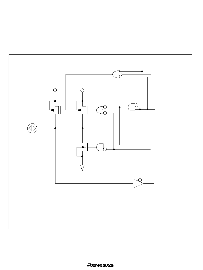
Rev. 1.0, 02/00, page 188 of 1141
10.1.3
MOS Pull-Up Transistors
The MOS pull-up transistors in ports 1 to 3 can be switched on or off by the MOS pull-up select
registers 1 to 3 (PUR1 to PUR3) in units of bits. Settings in PUR1 to PUR3 are valid when the pin
function is set to an input by PCR1 to PCR3. If the pin function is set to an output, the MOS pull-
up transistor is turned off. Figure 10.1 shows the circuit configuration of a pin with a MOS pull-
up transistor.
V
CC
PUR
STBY
LPWRM
Legend
PCR
PDR
PUR
PCR
PDR
: Low power consumption mode signal
(The pull-up MOS transistor is turned off by the STBY signal in low power
consumption mode except for sleep mode)
: MOS pull-up select register
: Port control register
: Port data register
Input data
V
CC
V
SS
Figure 10.1 Circuit Configuration of Pin with MOS Pull-Up Transistor

Rev. 1.0, 02/00, page 189 of 1141
10.2
Port 0
10.2.1
Overview
Port 0 is an 8-bit input-only port. Table 10.2 shows the port 0 configuration.
Port 0 consists of pins that are used both as standard input ports (P07 to P00) and analog input
channels (AN7 to AN0). It is switched by port mode register 0 (PMR0).
Table 10.2
Port 0 Configuration
Port
Function
Alternative Function
P07 (standard input port)
AN7 (analog input channel)
P06 (standard input port)
AN6 (analog input channel)
P05 (standard input port)
AN5 (analog input channel)
P04 (standard input port)
AN4 (analog input channel)
P03 (standard input port)
AN3 (analog input channel)
P02 (standard input port)
AN2 (analog input channel)
P01 (standard input port)
AN1 (analog input channel)
Port 0
P00 (standard input port)
AN0 (analog input channel)
Rev. 1.0, 02/00, page 190 of 1141
10.2.2
Register Configuration
Table 10.3 shows the port 0 register configuration.
Table 10.3
Port 0 Register Configuration
Name
Abbrev.
R/W
Size
Initial Value
Address
*
Port mode register 0
PMR0
R/W
Byte
H'00
H'FFCD
Port data register 0
PDR0
R
Byte
H'FFC0
Note:
*
Lower 16 bits of the address.
(1) Port Mode Register 0 (PMR0)
0
0
1
0
R/W
2
0
R/W
3
0
4
0
R/W
0
R/W
5
0
7
0
R/W
R/W
R/W
R/W
6
PMR04
PMR03
PMR02
PMR01
PMR00
PMR07
PMR06
PMR05
Bit :
Initial value :
R/W :
Port mode register 0 (PMR0) controls switching of each pin function of port 0. The switching is
specified in a unit of bit.
PMR0 is an 8-bit read/write enable register. When reset, PMR0 is initialized to H'00.
Bits 7 to 0
P07/AN7 to P00/AN0 Pin Switching (PMR07 to PMR00): PMR07 to PMR00 sets
whether the P0n/ANn pin is used as a P0n input pin or an ANn pin for the analog input channel of
an A/D converter.
Bit n
PMR0n
Description
0
The P0n/ANn pin functions as a P0n input pin
(Initial value)
1
The P0n/ANn pin functions as an ANn input pin
(n = 7 to 0)

Rev. 1.0, 02/00, page 191 of 1141
(2) Port Data Register 0 (PDR0)
0
1
R
2
R
3
4
R
R
5
7
PDR04
PDR03
PDR02
PDR01
PDR00
R
PDR07
R
R
R
PDR06
PDR05
6
--
--
--
--
--
--
--
--
Initial value :
R/W :
Bit
@:
Port data register 0 (PDR0) reads the port states. When the corresponding bit of PMR0 is 0
(general input port), the pin state is read if PDR0 is read. When the corresponding bit of PMR0 is
1 (analog input channel), 1 is read if PDR0 is read.
PDR0 is an 8-bit read-only register. When PDR0 is reset, its values become undefined.
10.2.3
Pin Functions
This section describes the pin functions of port 0 and their selection methods.
P07/AN7 to P00/AN0: P07/AN7 to P00/AN0 are switched according to the PMR0n bit of PMR0
as shown below.
PMR0n
Pin Function
0
P0n input pin
1
ANn input pin
(n = 7 to 0)
10.2.4
Pin States
Table 10.4 shows the pin 0 states in each operation mode.
Table 10.4
Port 0 Pin States
Pins
Reset
Active
Sleep
Standby
Watch
Subactive
Subsleep
P07/AN7 to
P00/AN0
High-
impedance
High-
impedance
High-
impedance
High-
impedance
High-
impedance
High-
impedance
High-
impedance

Rev. 1.0, 02/00, page 192 of 1141
10.3
Port 1
10.3.1
Overview
Port 1 is an 8-bit I/O port. Table 10.5 shows the port 1 configuration.
Port 1 consists of pins that are used both as standard I/O ports (P17 to P10) and frequency division
clock output (TMOW), input capture input (
,&), or external interrupt request inputs (,54 to
,54). It is switched by port mode register 1 (PMR1) and port control register 1 (PCR1).
Port 1 can select the functions of MOS pull-up transistors.
Table 10.5
Port 1 Configuration
Port
Function
Alternative Function
P17 (standard I/O port)
TMOW (frequency division clock output)
P16 (standard I/O port)
,&
(input capture input)
P15 (standard I/O port)
,54
(external interrupt request input)
P14 (standard I/O port)
,54
(external interrupt request input)
P13 (standard I/O port)
,54
(external interrupt request input)
P12 (standard I/O port)
,54
(external interrupt request input)
P11 (standard I/O port)
,54
(external interrupt request input)
Port 1
P10 (standard I/O port)
,54
(external interrupt request input)
10.3.2
Register Configuration
Table 10.6 shows the port 1 register configuration.
Table 10.6
Port 1 Register Configuration
Name
Abbrev.
R/W
Size
Initial Value
Address
*
Port mode register 1
PMR1
R/W
Byte
H'00
H'FFCE
Port control register 1
PCR1
W
Byte
H'00
H'FFD1
Port data register 1
PDR1
R/W
Byte
H'00
H'FFC1
MOS pull-up select
register 1
PUR1
R/W
Byte
H'00
H'FFE1
Note:
*
Lower 16 bits of the address.

Rev. 1.0, 02/00, page 193 of 1141
Port Mode Register 1 (PMR1)
0
0
1
0
R/W
2
0
R/W
3
0
4
0
R/W
0
R/W
5
0
7
0
R/W
R/W
R/W
R/W
6
PMR14
PMR13
PMR12
PMR11
PMR10
PMR17
PMR16
PMR15
Bit :
Initial value :
R/W :
Port mode register 1 (PMR1) controls switching of each pin function of port 1. The switching is
specified in a unit of bit.
PMR1 is an 8-bit read/write enable register. When reset, PMR1 is initialized to H'00.
Note the following items when the pin functions are switched by PMR1.
∑
If port 1 is set to an
,& input pin and ,54 to ,54 by PMR1, the pin level needs be set to the
high or low level regardless of the active mode and low power consumption mode. The pin
level must not be set to an intermediate level.
∑
When the pin functions of P16/
,& and P15/,34 to P10/,54 are switched by PMR1, they are
incorrectly recognized as edge detection according to the state of a pin signal and a detection
signal may be generated. To prevent this, perform the operation in the following procedure.
Before switching the pin functions, inhibit an interrupt enable flag from being interrupted.
After having switched the pin functions, clear the relevant interrupt request flag to 0 by a
single instruction.
Program Example:
:
MOV.B ROL,@IENR
Interrupt disabled
MOV.B R1L,@PMR1
Pin function change
NOP
Optional instruction
BCLR m @IRQR
Applicable interrupt clear
MOV.B R1L,@IENR
Interrupt enabled
:
Rev. 1.0, 02/00, page 194 of 1141
Bit 7
P17/TMOW Pin Switching (PMR17): PMR17 sets whether the P17/TMOW pin is used
as a P17 I/O pin or a TMOW pin for the frequency division clock output.
Bit 7
PMR17
Description
0
The P17/TMOW pin functions as a P17 I/O pin
(Initial value)
1
The P17/TMOW pin functions as a TMOW output pin
Bit 6
P16/
,
,&& Pin Switching (PMR16): PMR16 sets whether the P16/,& pin as a P16 I/O pin or
an
,& pin for the input capture input of the prescalar unit. The ,& pin has a built-in noise cancel
circuit. See section 21, Prescalar Unit.
Bit 6
PMR16
Description
0
The P16/
,&
pin functions as a P16 I/O pin
(Initial value)
1
The P16/
,&
pin functions as an
,&
input pin
Bits 5 to 0
P15/
,54
,54 to P10/,,54
54 Pin Switching (PMR15 to PMR10): PMR15 to PMR10 set
whether the P1n/
,54Q pin is used as a P1n I/O pin or an ,54Q pin for the external interrupt
request input.
Bit n
PMR1n
Description
0
The P1n/
,54Q
pin functions as a P1n I/O pin
(Initial value)
1
The P1n/
,54Q
pin functions as an
,54Q
input pin
(n = 5 to 0)
Port Control Register 1 (PCR1)
0
0
1
0
W
2
0
W
3
0
4
0
W
0
W
5
0
7
0
W
W
W
W
6
PCR14
PCR13
PCR12
PCR11
PCR10
PCR17
PCR16
PCR15
Bit :
Initial value :
R/W :
Port control register 1 (PCR1) controls the I/Os of pins P17 to P10 of port 1 in a unit of bit.
When PCR1 is set to 1, the corresponding P17 to P10 pins become output pins, and when it is set
to 0, they become input pins. When the relevant pin is set to a general I/O by PMR1, settings of
PCR1 and PDR1 become valid.
PCR1 is an 8-bit write-only register. When PCR1 is read, 1 is read. When reset, PCR1 is
initialized to H'00.
Rev. 1.0, 02/00, page 195 of 1141
Bits 7 to 0
P17 to P10 Pin Switching (PCR17 toPCR10)
Bit n
PCR1n
Description
0
The P1n pin functions as an input pin
(Initial value)
1
The P1n pin functions as an output pin
(n = 7 to 0)
Port Data Register 1 (PDR1)
0
0
1
0
R/W
2
0
R/W
3
0
4
0
R/W
0
R/W
5
0
7
0
R/W
R/W
R/W
R/W
6
PDR14
PDR13
PDR12
PDR11
PDR10
PDR17
PDR16
PDR15
Bit :
Initial value :
R/W :
Port data register 1 (PDR1) stores the data for the pins P17 to P10 of port 1. When PCR1 is 1
(output), the PDR1 values are directly read if port 1 is read. Accordingly, the pin states are not
affected. When PCR1 is 0 (input), the pin states are read if port 1 is read.
PDR1 is an 8-bit read/ write enable register. When reset, PDR1 is initialized to H'00.
MOS Pull-Up Select Register 1 (PUR1)
0
0
1
0
R/W
2
0
R/W
3
0
4
0
R/W
0
R/W
5
0
7
0
R/W
R/W
R/W
R/W
6
PUR14
PUR13
PUR12
PUR11
PUR10
PUR17
PUR16
PUR15
Bit :
Initial value :
R/W :
MOS pull-up selector register 1 (PUR1) controls the on and off of the MOS pull-up transistor of
port 1. Only the pin whose corresponding bit of PCR1 was set to 0 (input) becomes valid. When
the corresponding bit of PCR1 is set to 1 (output), the corresponding bit of PUR1 becomes invalid
and the MOS pull-up transistor is turned off.
PUR1 is an 8-bit read/ write enable register. When reset, PUR1 is initialized to H'00.
Bits 7 to 0
P17 to P10 MOS Pull-Up Control (PCR17 to PCR10)
Bit n
PUR1n
Description
0
The P1n pin has no MOS pull-up transistor
(Initial value)
1
The P1n pin has a MOS pull-up pin
(n = 7 to 0)

Rev. 1.0, 02/00, page 196 of 1141
10.3.3
Pin Functions
This section describes the port 1 pin functions and their selection methods.
P17/TMOW: P17/TMOW is switched as shown below according to the PMR17 bit in PMR1 and
the PCR17 bit in PCR1.
PMR17
PCR17
Pin Function
0
P17 input pin
0
1
P17 output pin
1
*
TMOW output pin
Note:
*
Don't care
P16/
,
,&&: P16/,& is switched as shown below according to the PMR16 bit in PMR1, the NC on/off
bit in prescalar unit control/status register (PCSR), and the PCR16 bit in PCR1.
PMR16
PCR16
NC on/off
Pin Function
0
P16 input pin
0
1
P16 output pin
0
Noise cancel invalid
1
*
1
,&
input pin
Noise cancel valid
Note:
*
Don't care
P15/
,54
,54 to P10/,54
,54: P15/,54 to P10/,54 are switched as shown below according to the
PMR1n bit in PMR1 and the PCR1n bit in PCR1.
PMR1n
PCR1n
Pin Function
0
P1n input pin
0
1
P1n output pin
1
*
,54Q
input pin
(n = 5 to 0)
Notes: 1.
*
Don't care.
2. The
,54
to
,54
input pins can select the leading or falling edge as an edge sense
(the
,54
pin can select both edges). See section 6.2.4, IRQ Edge Select Register
(IEGR).
3.
,54
or
,54
can be used as a timer J event input and
,54
can be used as a timer R
input capture input. For details, see section 13, Timer J or section 15, Timer R.

Rev. 1.0, 02/00, page 197 of 1141
10.3.4
Pin States
Table 10.7 shows the port 1 pin states in each operation mode.
Table 10.7
Port 1 Pin States
Pins
Reset
Active
Sleep
Standby
Watch
Subactive
Subsleep
P17/TMOW
P16/
,&
P15/
,54
to
P10/
,54
High-
impedance
Operation
Holding
High-
impedance
High-
impedance
Operation
Holding
Note: If the
,&
input pin and
,54
to
,54
input pins are set, the pin level need be set to the high
or low level regardless of the active mode and low power consumption mode. Note that the
pin level must not reach an intermediate level.

Rev. 1.0, 02/00, page 198 of 1141
10.4
Port 2
10.4.1
Overview
Port 2 is an 8-bit I/O port. Table 10.8 shows the port 2 configuration.
Port 2 consists of pins that are used both as standard I/O ports (P27 to P20) and SCI clock I/O
(SCK1), receive data input (SI1), send data output (SO1), I
2
C bus interface clock I/O (SCL0,
SCL1), or data I/O (SDA0, SDA1). It is switched by serial mode register (SMR), serial control
register (SCR), and port control register 2 (PCR2).
Port 2 can select the MOS pull-up function.
Table 10.8
Port 2 Configuration
Port
Function
Alternative Function
P27 (standard I/O port)
SYNCI (Formatless serial clock input)
P26 (standard I/O port)
SCL0 (I
2
C bus interface clock I/O)
P25 (standard I/O port)
SDA0 (I
2
C bus interface data I/O)
P24 (standard I/O port)
SCL1 (I
2
C bus interface clock I/O)
P23 (standard I/O port)
SDA1 (I
2
C bus interface data I/O)
P22 (standard I/O port)
SCK1 (SCI1 clock I/O)
P21 (standard I/O port)
SO1 (SCI1 transmit data output)
Port 2
P20 (standard I/O port)
SI1 (SCI1 receive data input)
10.4.2
Register Configuration
Table 10.9 shows the port 2 register configuration.
Table 10.9
Port 2 Register Configuration
Name
Abbrev.
R/W
Size
Initial Value
Address
*
Port control register 2
PCR2
W
Byte
H'00
H'FFD2
Port data register 2
PDR2
R/W
Byte
H'00
H'FFC2
MOS pull-up select
register 2
PUR2
R/W
Byte
H'00
H'FFE2
Note:
*
Lower 16 bits of the address.
Rev. 1.0, 02/00, page 199 of 1141
Port Control Register 2 (PCR2)
0
0
1
0
W
2
0
W
3
0
4
0
W
0
W
5
0
7
0
W
W
W
W
6
PCR24
PCR23
PCR22
PCR21
PCR20
PCR27
PCR26
PCR25
Bit :
Initial value :
R/W :
Port control register 2 (PCR2) controls the I/Os of pins P27 to P20 of port 2 in a unit of bit.
When PCR2 is set to 1, the corresponding P27 to P20 pins become output pins, and when it is set
to 0, they become input pins. When the relevant pin is set to a general I/O, settings of PCR2 and
PDR2 are valid.
PCR2 is an 8-bit write-only register. When PCR2 is read, 1 is read. When reset, PCR2 is
initialized to H'00.
Bits 7 to 0
P27 to P20 Pin Switching (PCR27 to PCR20)
Bit n
PCR2n
Description
0
The P2n pin functions as an input pin
(Initial value)
1
The P2n pin functions as an output pin
(n = 7 to 0)
Port Data Register 2 (PDR2)
0
0
1
0
R/W
2
0
R/W
3
0
4
0
R/W
0
R/W
5
0
7
0
R/W
R/W
R/W
R/W
6
PDR24
PDR23
PDR22
PDR21
PDR20
PDR27
PDR26
PDR25
Bit :
Initial value :
R/W :
Port data register 2 (PDR2) stores the data for the pins P27 to P20 of port 2. When PCR2 is 1
(output), the PDR2 values are directly read if port 2 is read. Accordingly, the pin states are not
affected. When PCR2 is 0 (input), the pin states are read if port 2 is read.
PDR2 is an 8-bit read/write enable register. When reset, PDR2 is initialized to H'00.

Rev. 1.0, 02/00, page 200 of 1141
MOS Pull-Up Select Register 2 (PUR2)
0
0
1
0
R/W
2
0
R/W
3
0
4
0
R/W
0
R/W
5
0
7
0
R/W
R/W
R/W
R/W
6
PUR24
PUR23
PUR22
PUR21
PUR20
PUR27
PUR26
PUR25
Bit :
Initial value :
R/W :
MOS pull-up selector register 2 (PUR2) controls the ON and OFF of the MOS pull-up transistor
of port 2. Only the pin whose corresponding bit of PCR2 was set to 0 (input) becomes valid. If
the corresponding bit of PCR2 is set to 1 (output), the corresponding bit of PUR2 becomes invalid
and the MOS pull-up transistor is turned off.
PUR2 is an 8-bit read/write enable register. When reset, PUR2 is initialized to H'00.
Bits 7 to 0
P27 to P20 Pull-Up MOS Control (PUR27 to PUR20)
Bit n
PUR2n
Description
0
The P2n pin has no MOS pull-up transistor
(Initial value)
1
The P2n pin has a MOS pull-up transistor
(n = 7 to 0)

Rev. 1.0, 02/00, page 201 of 1141
10.4.3
Pin Functions
This section describes the port 2 pin functions and their selection methods.
P27/SYNCI: P27/SYNCI is switched as shown below according to the PCR27 bit in PCR2.
PCR
Pin Function
0
P27 input pin
1
P27 output pin
Note:
Because the SYNCI always functions, the alternative pin need always be set to the high or
low level regardless of active mode or low power consumption mode.
P26/SCL0: P26/SCL0 is switched as shown below according to the PCR26 bit in PCR2 and the
II0CE bit in the I
2
C Bus control register (ICCR0).
II0CE
PCR26
Pin Function
0
P26 input pin
0
1
P26 output pin
1
*
SCL0 I/O pin
Note:
*
Don't care
P25/SDA0: P25/SDA0 is switched as shown below according to the PCR25 bit in PCR2 and the
II0CE bit in the I
2
C Bus control register (ICCR0).
II0CE
PCR25
Pin Function
0
P25 input pin
0
1
P25 output pin
1
*
SDA0 I/O pin
Note:
*
Don't care
P24/SCL1: P24/SCL1 is switched as shown below according to the PCR24 bit in PCR2 and the
II1CE bit in the I
2
C Bus control register (ICCR1).
II1CE
PCR24
Pin Function
0
P24 input pin
0
1
P24 output pin
1
*
SCL1 I/O pin
Note:
*
Don't care

Rev. 1.0, 02/00, page 202 of 1141
P23/SDA1: P23/SDA1 is switched as shown below according to the PCR23 bit in PCR2 and the
II1CE bit in the I
2
C Bus control register (ICCR1).
II1CE
PCR23
Pin Function
0
P23 input pin
0
1
P23 output pin
1
*
SDA1 I/O pin
Note:
*
Don't care
P22/SCK1: P22/SCK1 is switched as shown below according to the PCR22 bit in PCR2, the C/
bit in SMR, and the CKE1 and CKE0 bits in SCR.
CKE1
C/
CKE0
PCR22
Pin Function
0
P22 input pin
0
1
P22 output pin
0
1
0
1
SCK1 output pin
1
*
*
*
SCK1 input pin
Note:
*
Don't care
P21/SO1: P21/SO1 is switched as shown below according to the PCR21 bit in PCR2 and the TE
bit in SCR.
TE
PCR21
Pin Function
0
P21 input pin
0
1
P21 output pin
1
*
SO1 output pin
Note:
*
Don't care
P20/SI1: P20/SI1 is switched as shown below according to the PCR20 bit in PCR2 and the RE bit
in SCR.
RE
PCR20
Pin Function
0
P20 input pin
0
1
P20 output pin
1
*
SI1 input pin
Note:
*
Don't care

Rev. 1.0, 02/00, page 203 of 1141
10.4.4
Pin States
Table 10.10 shows the port 2 pin states in each operation mode.
Table 10.10 Port 2 Pin States
Pins
Reset
Active
Sleep
Standby
Watch
Subactive
Subsleep
P27/SYNCI
P26/SCL0
P25/SDA0
P24/SCL1
P23/SDA1
P22/SCK1
P21/SO1
P20/SI1
High-
impedance
Operation
Holding
High-
impedance
High-
impedance
Operation
Holding
Note: Because the SYNCI, SCL0, SDA0, SCL1, and SDA1 always function, the alternative pin
need always be set to the high or low level regardless of active mode or low power
consumption mode.
If the SCK1, and SI1 input pins are set, the pin level needs be set to the high or low level
regardless of the active mode and low power consumption mode. Note that the pin level
must not reach an intermediate level.

Rev. 1.0, 02/00, page 204 of 1141
10.5
Port 3
10.5.1
Overview
Port 3 is an 8-bit I/O port. Table 10.11 shows the port 3 configuration.
Port 3 consists of pins that are used both as standard I/O ports (P37 to P30) and timer J timer
output (TMO), buzzer output (BUZZ), 8-bit PWM outputs (PWM3 to PWM0), SCI2 strobe output
(STRB), or chip select input (
$). It is switched by port mode register 3 (PMR3) and port control
register 3 (PCR3).
Port 3 can select the MOS pull-up function.
Table 10.11 Port 3 Configuration
Port
Function
Alternative Function
P37 (standard I/O port)
TMO (timer J timer output)
P36 (standard I/O port)
BUZZ (timer J buzzer output)
P35 (standard I/O port)
PWM3 (8-bit PWM output)
P34 (standard I/O port)
PWM2 (8-bit PWM output)
P33 (standard I/O port)
PWM1 (8-bit PWM output)
P32 (standard I/O port)
PWM0 (8-bit PWM output)
P31 (standard I/O port)
SV2 (servo monitor output)
Port 3
P30 (standard I/O port)
SV1 (servo monitor output)
10.5.2
Register Configuration
Table 10.12 shows the port 3 register configuration.
Table 10.12 Port 3 Register Configuration
Name
Abbrev.
R/W
Size
Initial Value
Address
*
Port mode register 3
PMR3
R/W
Byte
H'00
H'FFD0
Port control register 3
PCR3
W
Byte
H'00
H'FFD3
Port data register 3
PDR3
R/W
Byte
H'00
H'FFC3
MOS pull-up select
register 3
PUR3
R/W
Byte
H'00
H'FFE3
Note:
*
Lower 16 bits of the address.

Rev. 1.0, 02/00, page 205 of 1141
Port Mode Register 3 (PMR3)
0
0
1
0
R/W
2
0
R/W
3
0
4
0
R/W
0
R/W
5
0
7
0
R/W
R/W
R/W
R/W
6
PMR34
PMR33
PMR32
PMR31
PMR30
PMR37
PMR36
PMR35
Bit :
Initial value :
R/W :
Port mode register 3 (PMR3) controls switching of each pin function of port 3. The switching is
specified in a unit of bit.
PMR3 is an 8-bit read/write enable register. When reset, PMR3 is initialized to H'00.
Bit 7
P37/TMO Pin Switching (PMR37): PMR37 sets whether the P37/TMO pin is used as a
P37 I/O pin or a TMO pin for the timer J output timer.
Bit 7
PMR37
Description
0
The P37/TMO pin functions as a P37 I/O pin
(Initial value)
1
The P37/TMO pin functions as a TMO output pin
Note: If the TMO pin is used for remote control sending, a careless timer output pulse may be
output when the remote control mode is set after the output has been switched to the TMO
output. Perform the switching and setting in the following order.
1. Set the remote control mode.
2. Set the TMJ-1 and 2 counter data of the timer J.
3. Switch the P37/TMO pin to the TMO output pin.
4. Set the ST bit to 1.
Bit 6
P36/BUZZ Pin Switching (PMR36): PMR36 sets whether the P36/BUZZ pin as a P36
I/O pin or an BUZZ pin for the timer J buzzer output. For the selection of the BUZZ output, see
13.2.2, Timer J Control Register (TMJC).
Bit 6
PMR36
Description
0
The P36/BUZZ pin functions as a P36 I/O pin
(Initial value)
1
The P36/BUZZ pin functions as a BUZZ output pin

Rev. 1.0, 02/00, page 206 of 1141
Bits 5 to 2
P35/PWM3 to P32/PWM0 Pin Switching (PMR35 to PMR32): PMR35 to PMR32
set whether the P3n/PWMm pin is used as a P3n I/O pin or a PWMm pin for the 8-bit PWM
output.
Bit n
PMR3n
Description
0
The P3n/PWMm pin functions as a P3n I/O pin
(Initial value)
1
The P3n/PWMm pin functions as a PWMm output pin
(n = 5 to 2, m = 3 to 0)
Bit 1
P31/SV2 Pin Switching (PMR31): PMR31 sets whether the P31/SV2 pin is used as a P31
I/O pin or an SV2 pin for the servo monitor output.
Bit 1
PMR31
Description
0
The P31/SV2 pin functions as a P31 I/O pin
(Initial value)
1
The P31/SV2 pin functions as an SV2 output pin
Bit 0
P30/SV1 Pin Switching (PMR30)
PMR30 sets whether the P30/SV1 pin is used as a P30 I/O pin or an SV1 pin for servo monitor
output.
Bit 0
PMR30
Description
0
The P30/SV1 pin functions as a P30 I/O pin
(Initial value)
1
The P30/SV1 pin functions as an SV1 output pin

Rev. 1.0, 02/00, page 207 of 1141
Port Control Register 3 (PCR3)
0
0
1
0
W
2
0
W
3
0
4
0
W
0
W
5
0
7
0
W
W
W
W
6
PCR34
PCR33
PCR32
PCR31
PCR30
PCR37
PCR36
PCR35
Bit :
Initial value :
R/W :
Port control register 3 (PCR3) controls the I/Os of pins P37 to P30 of port 3 in a unit of bit.
When PCR3 is set to 1, the corresponding P37 to P30 pins become output pins, and when it is set
to 0, they become input pins. When the relevant pin is set to a general I/O by PMR3, settings of
PCR3 and PDR3 become valid.
PCR3 is an 8-bit write-only register. When PCR3 is read, 1 is read. When reset, PCR3 is
initialized to H'00.
Bits 7 to 0
Pin 37 to P30 Pin Switching (PCR37 to PCR30)
Bit n
PCR3n
Description
0
The P3n pin functions as an input pin
(Initial value)
1
The P3n pin functions as an output pin
(n = 7 to 0)
Port Data Register 3 (PDR3)
0
0
1
0
R/W
2
0
R/W
3
0
4
0
R/W
0
R/W
5
0
7
0
R/W
R/W
R/W
R/W
6
PDR34
PDR33
PDR32
PDR31
PDR30
PDR37
PDR36
PDR35
Bit :
Initial value :
R/W :
Port data register 3 (PDR3) stores the data for the pins P37 to P30 of port 3. When PCR3 is 1
(output), the PDR3 values are directly read if port 3 is read. Accordingly, the pin states are not
affected. When PCR3 is 0 (input), the pin states are read if port 3 is read.
PDR3 is an 8-bit read/write enable register. When reset, PDR3 is initialized to H'00.

Rev. 1.0, 02/00, page 208 of 1141
MOS Pull-Up Select Register 3 (PUR3)
0
0
1
0
R/W
2
0
R/W
3
0
4
0
R/W
0
R/W
5
0
7
0
R/W
R/W
R/W
R/W
6
PUR34
PUR33
PUR32
PUR31
PUR30
PUR37
PUR36
PUR35
Bit :
Initial value :
R/W :
MOS pull-up selector register 3 (PUR3) controls the ON and OFF of the MOS pull-up transistor
of port 3. Only the pin whose corresponding bit of PCR3 was set to 0 (input) becomes valid. If
the corresponding bit of PCR3 is set to 1 (output), the corresponding bit of PUR3 becomes invalid
and the MOS pull-up transistor is turned off.
PUR3 is an 8-bit read/write enable register. When reset, PUR3 is initialized to H'00.
Bits 7 to 0
P37 to P30 MOS Pull-Up Control (PUR37 to PUR30)
Bit n
PCR3n
Description
0
The P3n pin has no MOS pull-up transistor
(Initial value)
1
The P3n pin has a MOS pull-up transistor
(n = 7 to 0)
10.5.3
Pin Functions
This section describes the port 3 pin functions and their selection methods.
P37/TMO: P37/TMO is switched as shown below according to the PMR37 bit in PMR3 and the
PCR37 bit in PCR3.
PMR37
PCR37
Pin Function
0
P37 input pin
0
1
P37 output pin
1
*
TMO output pin
Note:
*
Don't care

Rev. 1.0, 02/00, page 209 of 1141
P36/BUZZ: P36/BUZZ is switched as shown below according to the PMR36 bit in PMR3 and the
PCR36 bit in PCR3.
PMR36
PCR36
Pin Function
0
P36 input pin
0
1
P36 output pin
1
*
BUZZ output pin
Note:
*
Don't care
P35/PWM3: P35/PWM3 is switched as shown below according to the PMR3n bit in PMR3 and
the PCR3n bit in PCR3.
PMR35
PCR35
Pin Function
0
P35 input pin
0
1
P35 output pin
1
*
PWM3 output pin
Note:
*
Don't care
P34/PMW2: P34/PMW2 is switched as shown below according to the PMR34 bit in PCR3 and
the PCR34 bit in PCR3.
PMR34
PCR34
Pin Function
0
P34 input pin
0
1
P34 output pin
1
*
PWM2 output pin
Note:
*
Don't care
P33/PWM1: P33/PWM1 is switched as shown below according to the PMR33 bit in PMR3 and
the PCR33 bit in PCR3.
PMR33
PCR33
Pin Function
0
P33 input pin
0
1
P33 output pin
1
*
PWM1 input pin
Note:
*
Don't care

Rev. 1.0, 02/00, page 210 of 1141
P32/PWM0: P32/PWM0 is switched as shown below according to the PMR32 bit in PMR3 and
the PCR32 bit in PCR.
PMR32
PCR32
Pin Function
0
P32 input pin
0
1
P32 output pin
1
*
PWM0 output pin
P31/SV2: P31/SV2 is switched as shown below according to the PMR31 bit in PMR3 and the
PCR31 bit in PCR3.
PMR31
PCR3
Pin Function
0
P31 input pin
0
1
P31 output pin
1
*
SV2 output pin
P30/SV1: P30/SV1 is switched as shown below according to the PMR30 bit in PMR3 and the
PCR30 bit in PCR3.
PMR30
PCR30
Pin Function
0
P30 input pin
0
1
P30 output pin
1
*
SV1 output pin
Note:
*
Don't care

Rev. 1.0, 02/00, page 211 of 1141
10.5.4
Pin States
Table 10.13 shows the port 3 pin states in each operation mode.
Table 10.13 Port 3 Pin States
Pins
Reset
Active
Sleep
Standby
Watch
Subactive
Subsleep
P37/TMO
P36/BUZZ
P35/PWM3
to
P32/PWM0
P31/SV2
P30/SV1
High-
impedance
Operation
Holding
High-
impedance
High-
impedance
Operation
Holding

Rev. 1.0, 02/00, page 212 of 1141
10.6
Port 4
10.6.1
Overview
Port 4 is an 8-bit I/O port. Table 10.14 shows the port 4 configuration.
Port 4 consists of pins that are used both as standard I/O ports (P47 to P40) and output compare
output (FTOA, FTOB), input capture input (FTIA, FTIB, FTIC, FTID) or 14-bit PWM output
(PWM14). It is switched by port mode register 4 (PRM4), timer output compare control register
(TOCR), and port control register 4 (PCR4).
Table 10.14 Port 4 Configuration
Port
Function
Alternative Function
P47 (standard I/O port)
RPTRG (realtime output port trigger input)
P46 (standard I/O port)
FTOB (timer X1 output compare output)
P45 (standard I/O port)
FTOA (timer X1 output compare output)
P44 (standard I/O port)
FTID (timer X1 input capture input)
P43 (standard I/O port)
FTIC (timer X1 input capture input)
P42 (standard I/O port)
FTIB (timer X1 input capture input)
P41 (standard I/O port)
FTIA (timer X1 input capture input)
Port 4
P40 (standard I/O port)
PWM14 (14-bit PWM output)
10.6.2
Register Configuration
Table 10.15 shows the port 4 register configuration.
Table 10.15 Port 4 Register Configuration
Name
Abbrev.
R/W
Size
Initial Value
Address
*
Port mode register 4
PMR4
R/W
Byte
H'7E
H'FFDB
Port control register 4
PCR4
W
Byte
H'00
H'FFD4
Port data register 4
PDR4
R/W
Byte
H'00
H'FFC4
Note:
*
Lower 16 bits of the address.

Rev. 1.0, 02/00, page 213 of 1141
Port Mode Register 4 (PMR4)
0
0
1
1
2
1
3
1
4
1
1
5
1
7
0
R/W
6
--
--
--
--
--
PMR47
--
--
--
--
--
--
R/W
--
PMR40
Bit :
Initial value :
R/W :
Port mode register 4 (PMR4) controls switching of the P47/RPTRG pin and the P40/PWM14 pin
function. The switchings of the P46/FTOB and P45/FTOA functions are controlled by TOCR.
See section 16, Timer X1. The FTIA, FTIB, FTIC, and FTID inputs always function.
PMR4 is an 8-bit read/write enable register. When reset, PMR4 is initialized to H'7E.
Because the RPTRG input always function, the alternative pin need always be set to the high or
low level regardless of the active mode and low power consumption mode. Note that the pin level
must not reach an intermediate level.
Because the FTIA, FTIB, FTIC, and FTID inputs always function, each input uses the input edge
to the alternative general I/O pins P44, P43, P42, and P41 as input signals.
Bit 7
P47/RPTRG Pin Switching (PMR47): PMR47 sets whether the P47/RPTRG pin is used
as a P40 I/O pin or a RPTRG pin for the realtime output port trigger input.
Bit 7
PMR47
Description
0
The P47/RPTRG pin functions as a P47 I/O pin
(Initial value)
1
The P47/RPTRG pin functions as a RPTRG I/O pin
Bits 6 to 1
Reserved Bits: Reserved bits. When the bits are read, 1 is always read. The write
operation is invalid.
Bit 0
P40/PWM14 Pin Switching (PMR40): PMR40 sets whether the P40/PWM14 pin is used
as a P40 I/O pin or a PWM14 pin for the 14-bit PWM square wave output.
Bit 0
PMR40
Description
0
The P40/PWM14 pin functions as a P40 I/O pin
(Initial value)
1
The P40/PWM14 pin functions as a PWM14 output pin
Rev. 1.0, 02/00, page 214 of 1141
Port Control Register 4 (PCR4)
0
0
1
0
W
2
0
W
3
0
4
0
W
0
W
5
0
7
0
W
W
W
W
6
PCR44
PCR43
PCR42
PCR41
PCR40
PCR47
PCR46
PCR45
Bit :
Initial value :
R/W :
Port control register 4 (PCR4) controls the I/Os of pins P47 to P40 of port 4 in a unit of bit.
When PCR4 is set to 1, the corresponding P47 to P40 pins become output pins, and when it is set
to 0, they become input pins. When the relevant pin is set to a general I/O by PMR4, settings of
PCR4 and PDR4 become valid.
PCR4 is an 8-bit write-only register. When PCR4 is read, 1 is read. When reset, PCR4 is
initialized to H'00.
Bits 7 to 0
P47 to P40 Pin Switching (PCR47 to PCR40)
Bit n
PCR4n
Description
0
The P4n pin functions as an input pin
(Initial value)
1
The P4n pin functions as an output pin
(n = 7 to 0)
Port Data Register 4 (PDR4)
0
0
1
0
R/W
2
0
R/W
3
0
4
0
R/W
0
R/W
5
0
7
0
R/W
R/W
R/W
R/W
6
PDR44
PDR43
PDR42
PDR41
PDR40
PDR47
PDR46
PDR45
Bit :
Initial value :
R/W :
Port data register 4 (PDR4) stores the data for the pins P47 to P40 of port 4. When PCR4 is 1
(output), the PDR4 values are directly read if port 4 is read. Accordingly, the pin states are not
affected. When PCR4 is 0 (input), the pin states are read if port 4 is read.
PDR4 is an 8-bit read/write enable register. When reset, PDR4 is initialized to H'00.

Rev. 1.0, 02/00, page 215 of 1141
10.6.3
Pin Functions
This section describes the port 4 pin functions and their selection methods.
P47/RPTRG: P47/RPTRG is switched as shown below according to the PMR47 bit in PMR4 and
the PMR47 bit in PMR4 and the PCR47 bit in PCR4.
PMR47
PCR47
Pin Function
0
0
P47 input pin
1
P47 output pin
1
*
RPTRG input pin
P46/FTOB: P46/FTOB is switched as shown below according to the PCR46 bit in PCR4 and the
OEB bit in TOCR.
OEB
PCR46
Pin Function
0
P46 input pin
0
1
P46 output pin
1
*
FTOB output pin
Note:
*
Don't care
P45/FTOA: P45/FTOA is switched as shown below according to the PCR45 bit in PCR4 and the
OEA bit in TOCR.
OEA
PCR45
Pin Function
0
P45 input pin
0
1
P45 output pin
1
*
FTOA output pin
Note:
*
Don't care
P44/FTID: P44/FTID is switched as shown below according to the PCR44 bit in PCR4.
PCR44
Pin Function
0
P44 input pin
1
P44 output pin
FTID input pin

Rev. 1.0, 02/00, page 216 of 1141
P43/FTIC: P43/FTIC is switched as shown below according to the PCR43 bit in PCR4.
PCR43
Pin Function
0
P43 input pin
1
P43 output pin
FTIC input pin
P42/FTIB: P42/FTIB is switched as shown below according to the PCR42 bit in PCR4.
PCR42
Pin Function
0
P42 input pin
1
P42 output pin
FTIB input pin
P41/FTIA: P41/FTIA is switched as shown below according to the PCR41 bit in PCR4.
PCR41
Pin Function
0
P41 input pin
1
P41 output pin
FTIA input pin
P40/PWM14: P40/PWM14 is switched as shown below according to the PMR40 bit in PMR4 and
the PCR40 bit in PCR4.
PMR40
PCR40
Pin Function
0
P40 input pin
0
1
P40 output pin
1
*
PWM14 input pin
Note:
*
Don't care

Rev. 1.0, 02/00, page 217 of 1141
10.6.4
Pin States
Table 10.16 shows the port 4 pin states in each operation mode.
Table 10.16 Port 4 Pin States
Pins
Reset
Active
Sleep
Standby
Watch
Subactive
Subsleep
P47
P46/FTOB
P45/FTOA
P44/FTID
P43/FTIC
P42/FTIB
P41/FTIA
P40/
PWM14
High-
impedance
Operation
Holding
High-
impedance
High-
impedance
Operation
Holding
Note: If the RPTRG input pin is set, the pin level must be set to the high or low level regardless of
the active mode or low power consumption mode. Note that the pin level must not reach an
intermediate level.
Because the FTIA, FTIB, FTIC, and FTID inputs always function, the alternative pin need be
set to the high or low level regardless of the active mode and low power consumption
mode.

Rev. 1.0, 02/00, page 218 of 1141
10.7
Port 6
10.7.1
Overview
Port 6 is an 8-bit I/O port. Table 10.17 shows the port 6 configuration. Port 6 is a large current I/O
port.
The synchronous current is 20 mA maximum (VOL=1.5 V) and four pins can be turned on at the
same time. Port 6 consists of pins that are used as large current I/O ports (P67 to 67) and realtime
output ports (RP7 to RP0). It is switched by port mode register 6 (PMR6), port mode register A
(PMRA), and port control register 6 (PCR6).
The realtime output function can instantaneously switch the output data by an external or internal
trigger port.
Table 10.17 Port 6 Configuration
Port
Function
Alternative Function
P67 (large current I/O port)
RP7/TMBI (timer B event input)
P66 (large current I/O port)
RP6/
$'75*
(A/D conversion start external
trigger input)
P65 (large current I/O port)
RP5 (realtime output port pin)
P64 (large current I/O port)
RP4 (realtime output port pin)
P63 (large current I/O port)
RP3 (realtime output port pin)
P62 (large current I/O port)
RP2 (realtime output port pin)
P61 (large current I/O port)
RP1 (realtime output port pin)
Port 6
P60 (large current I/O port)
RP0 (realtime output port pin)

Rev. 1.0, 02/00, page 219 of 1141
10.7.2
Register Configuration
Table 10.18 shows the port 6 register configuration.
Table 10.18 Port 6 Register Configuration
Name
Abbrev.
R/W
Size
Initial Value
Address
*
Port mode register 6
PMR6
R/W
Byte
H'00
H'FFDD
Port mode register A
PMRA
R/W
Byte
H'3F
H'FFD9
Port control register 6
PCR6
W
Byte
H'00
H'FFD6
Port data register 6
PDR6
R/W
Byte
H'00
H'FFC6
Realtime output trigger
select register 1
RTPSR1
R/W
Byte
H'00
H'FFE5
Realtime output trigger
edge select register
RTPEGR
*
2
R/W
Byte
H'FC
H'FFE4
Port control register slave
6
PCRS6
Byte
H'00
Port data register slave 6
PDRS6
Byte
H'00
Notes: 1. Lower 16 bits of the address.
2. RTPEGR is also used by port 7.
Port Mode Register 6 (PMR6)
0
0
1
0
R/W
2
0
R/W
3
0
4
0
R/W
0
R/W
5
6
0
7
PMR64
PMR63
PMR62
PMR61
PMR60
0
R/W
PMR67
R/W
R/W
R/W
PMR66
PMR65
Bit :
Initial value :
R/W :
Port mode register 6 (PMR6) controls switching of each pin function of port 6. The switching is
specified in units of bits.
PMR6 is an 8-bit read/write enable register. When reset, PMR6 is initialized to H'00.
Bits 7 to 0
P67/RP7 to P60/RP0 Pin Switching (PMR67 to PMR60): PMR67 to PMR60 set
whether the P6n/RPn pin is used as a P6n I/O pin or an RPn pin for the realtime output port.
Bit n
PMR6n
Description
0
The P6n/RPn pin functions as a P6n I/O pin
(Initial value)
1
The P6n/RPn pin functions as an RPn output pin
(n = 7 to 0)

Rev. 1.0, 02/00, page 220 of 1141
Port Mode Register A (PMRA)
0
1
1
1
--
2
1
--
3
1
4
1
--
1
--
5
0
7
0
R/W
--
--
R/W
6
--
--
--
--
--
PMRA7
PMRA6
--
Bit :
Initial value :
R/W :
Port mode register A (PMRA) switches the pin functions in port 6. Switching is specified in a unit
of bit. PMR6 is an 8-bit read/write register.
When reset, PMRA is initialized to H'3F.
Bit 7
P67/RP7/TMBI Pin Switching (PMRA7): PMRA7 can be used as a P6n I/O pin or a
TMBI pin for timer B event input.
Bit 7
PMRA7
Description
0
P67/RP7/TMBI pin functions as a P67/RP7 I/O pin
(Initial value)
1
P67/RP7/TMBI pin functions as a TMBI pin
Bit 6
Timer B Event Input Edge Switching (PMRA6): PMRA6 selects the TMBI edge sense.
Bit 6
PMRA6
Description
0
Timer B event input detects falling edge
1
Timer B event input detects rising edge

Rev. 1.0, 02/00, page 221 of 1141
Port Control Register 6 (PCR6)
0
0
1
0
W
2
0
W
3
0
4
0
W
0
W
5
6
0
7
PCR64
PCR63
PCR62
PCR61
PCR60
0
W
PCR67
W
W
W
PCR66
PCR65
Bit :
Initial value :
R/W :
Port control register 6 (PCR6) selects the general I/O of port 6 and controls the realtime output in
a unit of bit together with PMR6.
When PMR6 = 0, the corresponding P67 to P60 pins become general output pins if PCR6 is set to
1, and they become general input pins if it is set to 0.
When PMR6 = 1, PCR6 controls the corresponding RP7 to RP0 realtime output pins. For details,
see section 10.8.4, Operation.
PCR6 is an 8-bit write-only register. When PCR6 is read, 1 is read. When reset, PCR6 is
initialized to H'00.
PMR6
PCR6
Bit n
Bit n
PMR6n
PCR6n
Description
0
The P6n/RPn pin functions as a P6n general I/O input pin
(Initial value)
0
1
The P6n/RPn pin functions as a P6n general output pin
1
*
The P6n/RPn pin functions as an RPn realtime output pin
Note:
*
Don't care
(n = 7 to 0)
Port Data Register 6 (PDR6)
0
0
1
0
R/W
2
0
R/W
3
0
4
0
R/W
0
R/W
5
6
0
7
PDR64
PDR63
PDR62
PDR61
PDR60
0
R/W
PDR67
R/W
R/W
R/W
PDR66
PDR65
Bit :
Initial value :
R/W :
Port data register 6 (PDR6) stores the data for the pins P67 to P60 of port 6.
For PMR6 = 0, when PCR6 is 1 (output), the PDR6 values are directly read if port 6 is read.
Accordingly, the pin states are not affected. When PCR6 is 0 (input), the pin states are read if port
6 is read.
For PMR6 = 1, port 6 becomes a realtime output pin. For details, see section 10.7.4, Operation.
PDR6 is an 8-bit read/write enable register. When reset, PDR6 is initialized to H'00.

Rev. 1.0, 02/00, page 222 of 1141
Realtime Output Trigger Select Register (RTPSR1)
0
0
1
0
R/W
2
0
R/W
3
0
4
0
R/W
0
R/W
5
6
0
7
RTPSR14 RTPSR13 RTPSR12 RTPSR11 RTPSR10
0
R/W
RTPSR17
R/W
R/W
R/W
RTPSR16 RTPSR15
Bit :
Initial value :
R/W :
The realtime output trigger select register (RTPSR1) sets whether the external trigger (RPTRG pin
input) or the internal trigger (HSW) is used as an trigger input for the realtime output in a unit of
bit. For the internal trigger HSW, see section 26.4, HSW Timing Generation Circuit.
RTPSR is an 8-bit read/write enable register. When reset, RTPSR is initialized to H'00.
Bits 7 to 0
RP7 to RP0 Trigger Switching
Bit n
RTPSR1n
Description
0
Selects the external trigger (RPTRG pin input) as a trigger input
(Initial value)
1
Selects the internal trigger (HSW) a trigger input
(n = 7 to 0)

Rev. 1.0, 02/00, page 223 of 1141
Real Time Output Trigger Edge Select Register (RTPEGR)
0
0
1
0
R/W
2
1
3
1
4
1
1
5
6
1
7
--
--
--
--
--
--
--
--
--
--
--
--
RTPEGR1 RTPEGR0
1
R/W
Bit :
Initial value :
R/W :
The realtime output trigger edge select register (RTPEGR) specifies the edge sense of the external
or internal trigger input for the realtime output.
RTPEGR is an 8-bit read/write enable register. When reset, RTPEGR is initialized to H'FC.
Bits 7 to 2
Reserved Bits: Reserved bits. When the bits are read, 1 is always read. The write
operation is invalid.
Bits 1 and 0
Realtime Output Trigger Edge Select (RTPEGR1, RTPEGR0): RTPEGR1 and
RTPEGR0 select the edge sense of the external or internal trigger input for the realtime output.
Bit 1
Bit 0
RTPEGR1
RTPEGR0
Description
0
Inhibits a trigger input
(Initial value)
0
1
Selects the rising edge of a trigger input
0
Selects the falling edge of a trigger input
1
1
Selects both the leading and falling edges of a trigger input

Rev. 1.0, 02/00, page 224 of 1141
10.7.3
Pin Functions
This section describes the port 6 pin functions and their selection methods.
P67/RP7/TMBI: P67/RP7/TMBI is switched as shown below according to the PMRA7 bit in
PMRA, PMR67 bit in PMR6, and PCR67 bit in PCR6.
PMRA7
PMR67
PCR67
Pin Function
Output Value
Value When PDR6n
Was Read
0
P67 input pin
P67 pin
0
1
P67 output pin
PDR67
PDR67
0
Hi-Z
*
1,
*
2
0
1
1
RP7 output pin
PDRS67
*
2
PDR67
0
P67 pin
1
*
1
TMBI input pin
PDR67
Notes: 1. Hi-Z: High impedance
2. When PMR67=1 (realtime output pin), indicates the state after the PCR67 setup value
has been transferred to PCRS67 by a trigger input.
P66/RP6/
'
'75*
75*: P66/RP6/'75* is switched as shown below according to the PMR66 bit in
PMR6 and PCR66 bit in PCR6. The
$'75* pin function switching is controlled by the ADTSR.
For details, refer to section 24, A/D converter.
PMR66
PCR66
Pin Function
Output Value
Value When PDR66 Was Read
0
P66 input pin
P67 pin
0
1
P66 output pin
PDR66
PDR66
0
Hi-Z
*
1,
*
2
1
1
RP6 output pin
PDRS66
*
2
PDR66
Notes: 1. Hi-Z: High impedance
2. When PMR66=1 (realtime output pin), indicates the state after the PCR66 setup value
has been transferred to PCRS66 by a trigger input.

Rev. 1.0, 02/00, page 225 of 1141
P65/RP5 to P60/RPD: P65/RP5 to P60/RPD are switched below according to the PMRAn bit in
PMRA, PMR6n bit in PMR6, and PCR6n bit in PCR6.
PMR6n
PCR6n
Pin Function
Output Value
Value When PDR6n Was Read
0
P6n input pin
P6n pin
0
1
P6n output pin
PDR6n
PDR6n
0
RPn output pin
Hi-Z
*
1,
*
2
1
1
RPn output pin
PDRS6n
*
2
PDR6n
(n = 5 to 0)
Notes: 1. Hi-Z: High impedance
2. When PMR6n=1 (realtime output pin), indicates the state after the PCR6n setup value
has been transferred to PCRS6n by a trigger input.
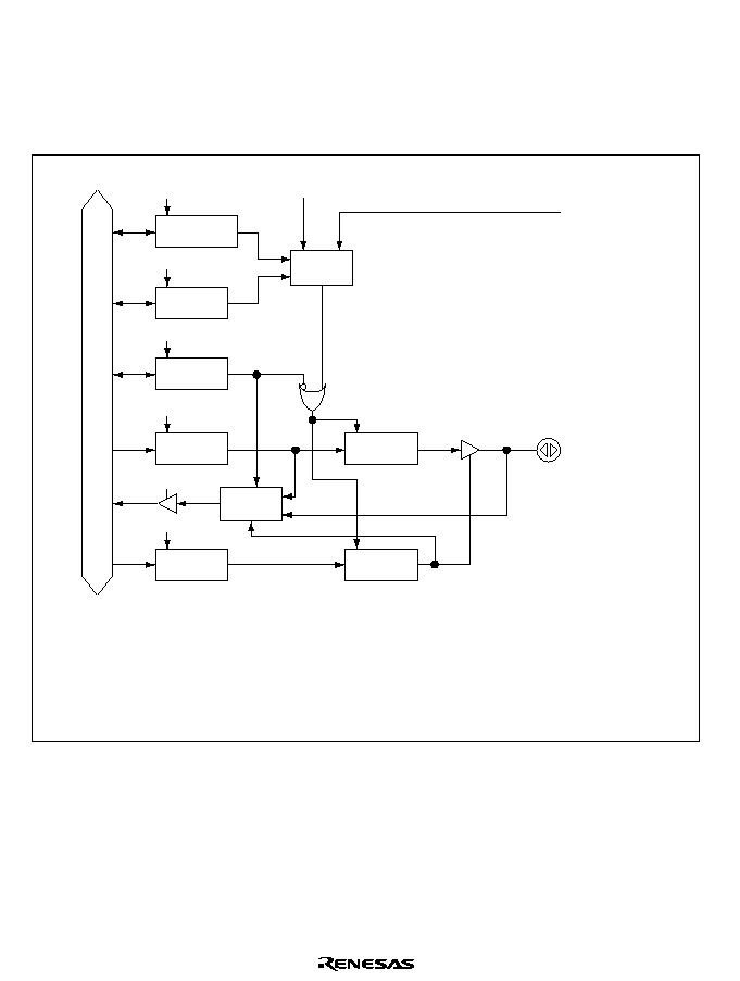
Rev. 1.0, 02/00, page 226 of 1141
10.7.4
Operation
Port 6 can be used as a realtime output port or general I/O output port by PMR6. Port 6 functions
as a realtime output port when PMR6 = 1 and as a general I/O port when PMR6 = 0. The
operation per port 6 function is shown below. (See figure 10.2.)
P6/RP
RTPEGR write
[Legend]
PMR6
PCR6
PDR6
PCRS6
PDRS6
RTPSR1
RTPEGR
HSW
RPTRG
: Port mode register 6
: Port control register 6
: Port data register 6
: Port control register slave 6
: Port data register slave 6
: Realtime output trigger select register
: Realtime output trigger edge select register
: Internal trigger signal
: External trigger pin
RTPSR write
RMR6 write
RDR6 write
RCR6 write
RDR6 read
RTPEGR
Selection
circuit
Selection
circuit
Internal data bus
External trigger
RPTRG
Internal trigger
HSW
CK
RTPSR
CK
PMR6
CK
PDR6
CK
PCR6
CK
RDRS6
CK
RCRS6
CK
Figure 10.2 Port 6 Function Block Diagram

Rev. 1.0, 02/00, page 227 of 1141
∑
Operation of the Realtime Output Port (PMR6 = 1)
When PMR6 is 1, it operates as a realtime output port. When a trigger is input, the PDR6 data
is transferred to PDRS6 and the PCR6 is transferred data to PCRS6, respectively. In this case,
when PCRS6 is 1, the PDRS6 data of the corresponding bit is output to the RP pin. When
PCRS6 is 0, the RP pin of the corresponding bit is output to the high-impedance state. In other
words, the pin output state (high or low) or high-impedance state can instantaneously be
switched by a trigger input.
Adversely, when PDR6 is read, the PDR6 values are read regardless of the PCR6 and PCRS6
values.
∑
Operation of the general I/O port (PMR6 = 0)
When PMR6 is 0, it operates as a general I/O port. When data is written to PDR6, the same
data is also written to PDRS6. Accordingly, because both PDR6 and PDRS6 and both PCR6
and PCRS6 can be handled as one register, respectively, they can be used in the same way as a
normal general I/O port. In other words, if PCR6 is 1, the PDR6 data of the corresponding bit
is output to the P6 pin. If PCR6 is 0, the P6 pin of the corresponding bit becomes an input.
Adversely, assuming that PDR6 is read, the PDR6 values are read when PCR6 is 1 and the pin
values are read when PCR6 is 0.
10.7.5
Pin States
Table 10.19 shows the port 6 pin states in each operation mode.
Table 10.19 Port 6 Pin States
Pins
Reset
Active
Sleep
Standby
Watch
Subactive
Subsleep
P67/RP7 to
P60/RP0
P66/RP6/
$'75*
P65/RP5 to
P60/RP0
High-
impedance
Operation
Holding
High-
impedance
High-
impedance
Operation
Holding
Note: If the TMBI and
'75*
input pins are set, the pin level must be set to the high or low level
regardless of the active mode or low power consumption mode. Note that pin level must not
reach an intermediate level.

Rev. 1.0, 02/00, page 228 of 1141
10.8
Port 7
10.8.1
Overview
Port 7 is an 8-bit I/O port. Table 10.20 shows the port 7 configuration.
Port 7 consists of pins that are used both as standard I/O ports (P77 to P70) and HSW timing
generation circuit (programmable pattern generator: PPG) outputs (PPG7 to PPG0). It is switched
by port mode register 7 (PMR7) and port control register 7 (PCR7).
For the programmable generator (PPG), see section 26.4, HSW (Head-switch) Timing Generation
Circuit.
Table 10.20 Port 7 Configuration
Port
Function
Alternative Function
PPG7 (HSW timing output)
P77 (standard I/O port)
RPB (realtime output port)
PPG6 (HSW timing output)
P76 (standard I/O port)
RPA (realtime output port)
PPG5 (HSW timing output)
P75 (standard I/O port)
RP9 (realtime output port)
PPG4 (HSW timing output)
P74 (standard I/O port)
RP8 (realtime output port)
P73 (standard I/O port)
PPG3 (HSW timing output)
P72 (standard I/O port)
PPG2 (HSW timing output)
P71 (standard I/O port)
PPG1 (HSW timing output)
Port 7
P70 (standard I/O port)
PPG0 (HSW timing output)

Rev. 1.0, 02/00, page 229 of 1141
10.8.2
Register Configuration
Table 10.21 shows the port 7 register configuration.
Table 10.21 Port 7 Register Configuration
Name
Abbrev.
R/W
Size
Initial Value
Address
*
Port mode register 7
PMR7
R/W
Byte
H'00
H'FFDE
Port mode register B
PMRB
R/W
Byte
H'0F
H'FFDA
Port control register 7
PCR7
W
Byte
H'00
H'FFD7
Port data register 7
PDR7
R/W
Byte
H'00
H'FFC7
Realtime output trigger
select register 2
RTPSR2
R/W
Byte
H'0F
H'FFE6
Realtime output trigger
edge select register
RTPEGR
R/W
Byte
H'FC
H'FFE4
Port control register slave
7
PCRS7
Byte
H'00
Port data register slave 7
PDRS7
Byte
H'00
Note:
*
Lower 16 bits of the address.

Rev. 1.0, 02/00, page 230 of 1141
Port Mode Register 7 (PMR7)
0
0
1
0
R/W
2
0
R/W
3
0
4
0
R/W
0
R/W
5
6
0
7
PMR74
PMR73
PMR72
PMR71
PMR70
0
R/W
PMR77
R/W
R/W
R/W
PMR76
PMR75
Bit :
Initial value :
R/W :
Port mode register 7 (PMR7) controls switching of each pin function of port 7. The switching is
specified in a unit of bit.
PMR7 is an 8-bit read/write enable register. When reset, PMR7 is initialized to H'00.
Bits 7 to 0
P77/PPG7 to P70/PPG0 Pin Switching (PMR77 to PMR70): PMR77 to PMR70
set whether the P7n/PPGn pin is used as a P7n I/O pin or a PPGn pin for the HSW timing
generation circuit output.
Bit n
PMR7n
Description
0
The P7n/PPGn pin functions as a P7n I/O pin
(Initial value)
1
The P7n/PPGn pin functions as a PPGn output pin
(n = 7 to 0)
Port Mode Register B (PMRB)
0
1
1
1
2
1
3
1
4
--
--
--
PMRB4
--
--
--
R/W
0
0
R/W
5
0
7
0
R/W
--
R/W
6
--
PMRB7
PMRB6
PMRB5
Bit :
Initial value :
R/W :
Port mode register B (PMRB) controls switching of each pin function of port 7. The switching is
specified in a unit of bit.
PMRB is an 8-bit read/write enable register. When reset, PMRB is initialized to H'0F.
Rev. 1.0, 02/00, page 231 of 1141
Bits 7 to 4
P77/RP7B to P74/RP8 Pin Switching (PMRB7 to PMRB4): P77/RP7B to
P74/RP8 set whether the P7n/RPm pin is used as a P7n I/O pin or a RPm pin for the realtime
output port. (n= 7 to 4 and m= B, A, 9, or 8)
Bit n
PMRBn
Description
0
P7n/RPm pin functions as a P7n I/O pin
(Initial value)
1
P7n/RPm pin functions as a RPm I/O pin
(n = 7 to 4 and m = B, A, 9, and 8)
Bits 3 to 0
Reserved Bits: Reserved bits. When the bits are read, 1 is always read. The write
operation is invalid.
Port Control Register 7 (PCR7)
0
0
1
0
W
2
0
W
3
0
4
0
W
0
W
5
6
0
7
PCR74
PCR73
PCR72
PCR71
PCR70
0
W
PCR77
W
W
W
PCR76
PCR75
Bit :
Initial value :
R/W :
Port control register 7, together with PMRB, enable the general-purpose input/output of port 7 and
controls realtime output in bit units.
For details, refer to section 10.8.4. Operation.
PCR7 is an 8-bit write-only register. When the PCR7 is read, 1 is always read. When reset, PCR7
is initialized to H'00.
Bits 7 to 0
P77 to P70 Pin I/O Switching (PCR77 to PCR70)
PMRB
PCR7
Bitn
Bitn
PMRBn
PCR7n
Description
0
P7n/RPm pin functions as a P7n general input pin
(Initial Value)
0
1
P7n/RPm pin functions as a P7n general output pin
1
*
P7n/RPm pin functions as a RPm realtime output pin
(n = 7 to 4 and m = B, A, 9, and 8)
Note:
*
Don't care

Rev. 1.0, 02/00, page 232 of 1141
Port Data Register 7 (PDR7)
0
0
1
0
R/W
2
0
R/W
3
0
4
0
R/W
0
R/W
5
6
0
7
PDR74
PDR73
PDR72
PDR71
PDR70
0
R/W
PDR77
R/W
R/W
R/W
PDR76
PDR75
Bit :
Initial value :
R/W :
Port data register 7 (PDR7) stores the data for the pins P77 to P70 of port 7.
If PCR7 is 1 (output) when PMRB=0, the PDR7 values are directly read when port 7 is read.
Accordingly, the pin states are not affected. When PCR7 is 0 (input), the pin states are read if port
7 is read. When PMRB=1, port 7 pin functions as a realtime output pin. For details, refer to
section 10.8.4, Operation.
PDR7 is an 8-bit read/write enable register. When reset, PDR7 is initialized to H'00.
Realtime Output Trigger Select Register 2 (RTPSR2)
0
1
1
1
--
2
1
--
3
1
4
0
R/W
0
R/W
5
6
0
7
RTPSR24
--
--
--
--
0
R/W
RTPSR27
--
--
R/W
RTPSR26 RTPSR25
Bit :
Initial value :
R/W :
Realtime output trigger select register (RTPSR2) selects whether to use an external trigger
(RPTRG pin input) or internal trigger (HSW) for the realtime output trigger input by specifying a
unit of bit. For details on internal trigger HSW, refer to section 26.4, HSW (Head-switch) Timing
Generator.
RTPSR2 is an 8-bit read/write enable register.
When reset, RTPSR2 is initialized to H'0F.
Rev. 1.0, 02/00, page 233 of 1141
Bits 7 to 4
RPB to RP8 Pin Trigger Switching (RTPSR27 to RTPSR24)
Bit7
RTPSR2n
Description
0
Selects external trigger (RPTRG pin input) for trigger input
(Initial value)
1
Selects internal trigger (HSW) for trigger input
(n = 7 to 4)
Realtime Output Trigger Edge Selection Register (RTPEGR)
0
0
1
0
R/W
2
1
3
1
4
1
1
5
6
1
7
--
--
--
--
--
--
--
--
--
--
--
--
RTPEGR1 RTPEGR0
1
R/W
Bit :
Initial value :
R/W :
The realtime output trigger edge selection register (RTPEGR) specifies the sensed edge(s) of
external or internal trigger input for realtime output.
RTPEGR is an 8-bit readable/writable register. In a reset, RTPEGR is initialized to H'FC.
Bits 7 to 2--Reserved: These bits are always read as 1 and cannot be modified.
Bits 1 and 0--Realtime Output Trigger Edge Select (RTPEGR1, RTPEGR0): These bits
select the sensed edge(s) of external or internal trigger input for realtime output.
Bit 1
Bit 0
RTPEGR1
RTPEGR0
Description
0
Disables trigger input
(Initial value)
0
1
Selects trigger input rising edge
0
Selects trigger input falling edge
1
1
Selects trigger input rising and falling edges

Rev. 1.0, 02/00, page 234 of 1141
10.8.3
Pin Functions
This section describes the port 7 pin functions and their selection methods.
P77/PPG7/RPB to P74/PPG4/RP8: P77/PPG7/RPB to P74/PPG4/RP8 are switched as shown
below according to the PMRBn bit in PMRB and the PCR7n bit in PCR7.
PMRBn
PMR7n
PCR7n
Pin Function
Output Value
Value Returned when
PDR7n is Read
0
P7n input pin
P7n pin
0
0
1
P7n output pin
PDR7n
PDR7n
0
P7n pin
0
1
1
PPGn output pin
PPGn
PDR7n
0
Hi-Z
*
1
*
1
RPm output pin
PDRS7n
*
PDR7n
(n = 7 to 4, m = B, A, 9, 8)
Notes:
*
Don't care
1. When PMRBn = 1 (realtime output pin), the state indicated is that after the PCR7n set
value has been transferred to PCRS7n by trigger input.
Hi-Z: High impedance
P73/PPG to P70/PPG0: P73/PPG to P70/PPG0 are switched as shown below according to the
PMR7n bit in PMR7 and the PCR7n bit in PCR7.
PMR7n
PCR7n
Pin Function
Output Value
Value Returned when PDR7n
is Read
0
P7n input pin
P7n pin
0
1
P7n output pin
PDR7n
PDR7n
0
P7n pin
1
1
PPGn output pin
PPGn
PDR7n
(n = 3 to 0)
Rev. 1.0, 02/00, page 235 of 1141
10.8.4
Operation
Port 7 can be used by the PMRB as a realtime output port or an I/O port.
Port 7 functions as a realtime output port when PMRB=1 and functions as an I/O port when
PMRB=0. Figure 10.3 show the block diagram of port 7.
P7/RP
RTPEGR write
RTPSR2 write
PMRA write
PDR7 write
PCR7 write
PDR7 read
RTPEGR
Select
Select
External trigger
RPTRG
Internal
trigger HSW
CK
RTPSR2
CK
PMRB:
Port mode register B
PCR7:
Port control register 7
PDR7:
Port data register 7
PCRS7:
Port control register slave 7
PDRS7:
Port data register slave 7
[Legend]
RTPSR2:
Realtime output trigger select register
RTPEGR:
Realtime output trigger edge select register
HSW:
Internal trigger signal
RPTRG:
External trigger pin
Internal data bus
PMRB
CK
PDR7
CK
PCR7
CK
PDRS7
CK
PCRS7
CK
Figure 10.3 Block Diagram of Port 7

Rev. 1.0, 02/00, page 236 of 1141
Port 7 functions as follows:
1. Realtime output port function (PMRB=1)
Port function as a realtime output port when PMRB is 1. After a trigger input, the PDR7 data
is transferred to PDRS7 and PCR7 data is transferred to PCRS7. In this case, when PCRS7 is
1, the PDRS7 data of the corresponding bit is output from the RP pin. When PCRS7 is 0, the
RP pin of the corresponding bit enters high-impedance state. In other words, the realtime
output port function can instantaneously switch the pin output state (High or Low) or high-
impedance by a trigger input.
2. I/O port function (PMRB=0)
Port 7 functions as an I/O port when PMRB is 0. After data is written to PDR7, the same data
is written to PDRS7. After data is written to PCR7, the same data is written to PCRS7. Since
PDR and PDRS7, and PCR7 and PCRS7 can be used as one register, the registers can be used
as the I/O ports. In other words, if PCR7 is 1, the PDR7 data of the corresponding bit is output
from the P7 pin. If PCR is 0, the P7 pin of the corresponding bit is an input pin. If PD7 is read,
the PDR7 value is read when PCR7 is 1 and the pin value is read when PCR7 is 0.
10.8.5
Pin States
Table 10.22 shows the port 7 pin states in each operation mode.
Table 10.22 Port 6 Pin States
Pins
Reset
Active
Sleep
Standby
Watch
Subactive Subsleep
P77/PPG7/RPB
to
P74/PPG4/RP8
P73/PPG3
to
P70/PPG0
High-
impedance
Operation Holding High-
impedance
High-
impedance
Operation Holding

Rev. 1.0, 02/00, page 237 of 1141
10.9
Port 8
10.9.1
Overview
Port 8 is an 8-bit I/O port. Table 10.23 shows the port 8 configuration.
Port 8 consists of pins that are used both as standard-current I/O ports (P87 to P80) and an external
CTL signal input (EXCTL), a pre-amplifier output result signal input (COMP), color signal
outputs (R, G, and B), a pre-amplifier output selection signal output (H.Amp SW), a control signal
output for processing color signal (C.Rotary), a DPG signal input (DPG), a capstan external sync
signal input (EXCAP), an OSD character display position output (YB0), an OSD character data
output (YC0), and an external reference signal input (EXTTRG). It is switched by port mode
register 8 (PMR8), port mode register C (PMRC), and port control register 8 (PCR8).
Table 10.23 Port 8 Configuration
Port
Function
Alternative Function
P87 (standard I/O port)
DPG signal input
P86 (standard I/O port)
External reference signal input
Pre-amplifier output result signal input
P85 (standard I/O port)
Color signal output
Pre-amplifier output selection signal output
P84 (standard I/O port)
Color signal output
Control signal output for processing color signal
P83 (standard I/O port)
Color signal output
P82 (standard I/O port)
External CTL signal input
Capstan external sync signal input
P81 (standard I/O port)
OSD character display position output
Port 8
P80 (standard I/O port)
OSD character data output

Rev. 1.0, 02/00, page 238 of 1141
10.9.2
Register Configuration
Table 10.24 shows the port 8 register configuration.
Table 10.24 Port 8 Register Configuration
Name
Abbrev.
R/W
Size
Initial Value
Address
*
Port mode register 8
PMR8
R/W
Byte
H'00
H'FFDF
Port mode register C
PMRC
R/W
Byte
H'C5
H'FFE0
Port control register 8
PCR8
W
Byte
H'00
H'FFD8
Port data register 8
PDR8
R/W
Byte
H'00
H'FFC8
Note:
*
The address indicates the low-order 16 bits.

Rev. 1.0, 02/00, page 239 of 1141
Port Mode Register 8 (PMR8)
0
0
1
0
R/W
2
0
R/W
3
0
4
0
0
5
6
0
7
PMR84
PMR85
PMR86
PMR87
R/W
R/W
R/W
R/W
PMR83
PMR82
PMR81
PMR80
0
R/W
R/W
Bit :
Initial value :
R/W :
Port mode register 8 (PMR8) controls switching of each pin function of port 8. The switching is
specified in a unit of bit.
PMR8 is an 8-bit read/write enable register. When reset, PMR8 is initialized to H'F0.
If the EXCTL, COMP, DPG and EXTTRG input pins are set, the pin level need always be set to
the high or low level regardless of the active mode and low power consumption mode. Note that
the pin level must not reach an intermediate level.
Bit 7
P87/DPG Pin Switching (PMR87): PMR87 sets whether the P87/DPG pin is used as a
P87 I/O pin or a DPG signal input pin.
Bit 7
PMR87
Description
0
P87/DPG pin functions as a P87 I/O pin
(Drum control signals are input as an overlapped signal)
(Initial value)
1
P87/DPG pin functions as a DPG input pin
(Drum control signals are input as separate signals)
Bit 6
P86/EXTTRG Pin Switching (PMR86): PMR86 sets whether the P86/EXTTRG pin is
used as a P86 I/O pin or an external trigger signal input pin.
Bit 6
PMR86
Description
0
P86/EXTTRG pin functions as a P86 I/O pin
(Initial value)
1
P86/EXTTRG pin functions as a EXTTRG input pin
Bit 5
P85/COMP Pin Switching (PMR85): PMR85 sets whether the P85/COMP pin is used as
a P85 I/O pin or a COMP input pin of the preamplifier output result signal.
Bit 5
PMR85
Description
0
P85/COMP pin functions as a P85 I/O pin
(Initial value)
1
P85/COMP pin functions as a COMP input pin

Rev. 1.0, 02/00, page 240 of 1141
Bit 4
P84/H.Amp SW Pin Switching (PMR84): PMR84 sets whether the P84/H.Amp SW pin
is used as a P84 I/O pin or H.Amp SW pin of the preamplifier output select signal output.
Bit 4
PMR84
Description
0
P84/H.Amp SW pin functions as a P84 I/O pin
(Initial value)
1
P84/H.Amp SW pin functions as a H.Amp SW output pin
Bit 3
P83/C. Rotary Pin Switching (PMR83): PMR83 sets whether the P83/C. Rotary pin is
used as a P83 I/O pin or a C.Rotary pin of a control signal output for processing color signal.
Bit 3
PMR83
Description
0
P83/C.Rotary pin functions as a P83 I/O pin
(Initial value)
1
P83/C.Rotary pin functions as a C.Rotary output pin
Bit 2
P82/EXCTL Pin Switching (PMR82): PMR82 sets whether the P82/EXCTL pin
functions as a P82 I/O pin or a EXCTL input pin of external CTL signal input.
Bit 2
PMR82
Description
0
P82/EXCTL pin functions as a P82 I/O pin
(Initial value)
1
P82/EXCTL pin functions as a EXCTL input pin
Bit 1
P81/EXCAP Pin Switching (PMR81): PMR81 sets whether the P81/EXCAP pin
functions as a P81 I/O pin or a EXCAP pin of capstan external synchronous signal input.
Bit 1
PMR81
Description
0
P81/EXCAP pin functions as a P81 I/O pin
(Initial value)
1
P81/EXCAP pin functions as a EXCAP input pin
Bit 0
P80/YC0 Pin Switching (PMR80): PMR80 sets whether the P80/YC0 pin functions as a
P80 I/O pin or a YC0 pin of OSD character data output.
Bit 0
PMR80
Description
0
P80/YC0 pin functions as a P80 I/O pin
(Initial value)
1
P80/YC0 pin functions as a YC0 output pin

Rev. 1.0, 02/00, page 241 of 1141
Port Mode Register C (PMRC)
0
1
1
0
R/W
2
1
--
3
0
4
0
R/W
0
R/W
5
6
1
7
PMRC4
PMRC3
--
PMRC1
--
1
--
--
--
R/W
--
--
PMRC5
Bit :
Initial value :
R/W :
Port mode register C (PMRC) controls switching of each pin function of port 8. The switching is
specified in a unit of a bit.
PMRC is an 8-bit read/write enable register. When reset, PMRC is initialized to H'C5.
Bits 7, 6, 2, and 0
Reserved Bits: Reserved bits. When the bits are read, 1 is always read. The
write operation is invalid.
Bit 5
P85/B Pin Switching (PMRC5): PMRC5 sets whether to use the P85/B pin as a P85 I/O
pin or a B pin of the OSD color signal output.
Bit 5
PMRC5
Description
0
P85/B pin functions as a P85 pin
(Initial value)
1
P85/B pin functions as a B output pin
Bit 4
P84/G Pin Switching (PMRC4): PMRC4 sets whether to use the P84/G pin as a P84 I/O
pin or a G pin of the OSD color signal output.
Bit 4
PMRC4
Description
0
P84/G pin functions as a P84 I/O pin
(Initial value)
1
P84/G pin functions as a G output pin
Bit 3
P83/R Pin Switching (PMRC3): PMRC3 sets whether to use the P83/R pin as a P83 I/O
pin or a R pin of the OSD color signal output.
Bit 3
PMRC3
Description
0
P83/R pin functions as a P83 I/O pin
(Initial value)
1
P83/R pin functions as a R output pin
Rev. 1.0, 02/00, page 242 of 1141
Bit 1
P81/YB0 Pin Switching (PMRC1): PMRC1 sets whether to use the P81/YB0 pin as a
P81 I/O pin or a YB0 pin of the OSD character display position output.
Bit7
PMR1
Description
0
P81/YB0 pin functions as a P81 I/O pin
(Initial value)
1
P81/YB0 pin functions as a YB0 output pin
Port Control Register 8 (PCR8)
0
0
1
0
W
2
0
W
3
0
4
0
W
0
W
5
6
0
7
PCR84
PCR83
PCR82
PCR81
PCR80
0
W
PCR87
W
W
W
PCR86
PCR85
Bit :
Initial value :
R/W :
Port control register 8 (PCR8) controls I/O of pins P87 to P80 of port 8. The I/O is specified in a
unit of bit.
When PCR8 is set to 1, the corresponding P87 to P80 pins become output pins, and when it is set
to 0, they become input pins.
When the pins are set as general I/O pins, the settings of PCR8 and PDR8 become valid.
PCR8 is an 8-bit write-only register. When PCR8 is read, 1 is read. When reset PCR8 is initialized
to H'00.
Bits 7 to 0
P87 to P80 Pin I/O Switching
Bit n
PCR8n
Description
0
P8n pin functions as an input pin
(Initial value)
1
P8n pin functions as an output pin
(n = 7 to 0)

Rev. 1.0, 02/00, page 243 of 1141
Port Data Register 8 (PDR8)
0
0
1
0
R/W
2
0
R/W
3
0
4
0
R/W
0
R/W
5
6
0
7
PDR784
PDR83
PDR82
PDR81
PDR80
0
R/W
PDR87
R/W
R/W
R/W
PDR86
PDR85
Bit :
Initial value :
R/W :
Port data register 8 (PDR8) stores the data of pins P87 to P80 port 8. When PCR is 1 (output), the
pin states are read is port 8 is read. Accordingly, the pin states are not affected. When PCR8 is 0
(input), the pin states are read it port 8 is read.
PDR8 is an 8-bit read/write enable register. When reset, PDR8 is initialized to H'00.

Rev. 1.0, 02/00, page 244 of 1141
10.9.3
Pin Functions
This section describes the port 8 pin functions and their selection methods.
P87/DPG: P87/DPG is switched as shown below according to the PMR87 bit in PMR8 and
PCR87 bit in PCR8.
PMR87
PCR87
Pin Function
0
P87 input pin
0
1
P87 output pin
1
*
DPG input pin
P86/EXTTRG: P86/EXTTRG is switched as shown below according to the PMR86 bit in PMR8
and PCR86 bit in PCR8.
PMR86
PCR86
Pin Function
0
P86 input pin
0
1
P86 output pin
1
*
EXTTRG input pin
P85/COMP/B: P85/COMP/B is switched as shown below according to the PMR85 bit in PMR8,
PMRC5 bit in PMRC, and PCR85 bit in PCR8.
PMRC5
PMR85
PCR85
Pin Function
0
P85 input pin
0
0
1
P85 output pin
*
1
*
COMP input pin
1
0
*
B output pin
P84/H.Amp SW/G: P84/H.Amp SW/G is switched as shown below according to the PMR84 bit
in PMR, PMRC4 bit in PMRC, and PCR84 bit in PCR8.
PMRC4
PMR84
PCR84
Pin Function
0
P84 input pin
0
0
1
P84 output pin
*
1
*
H.Amp SW output pin
1
0
*
G output pin

Rev. 1.0, 02/00, page 245 of 1141
P83/C.Rotary/R: P83/C.Rotary/R is switched as shown below according to the PMR83bit in
PMR8, PMRC3 bit in PMRC, and PCR83 bit in PCR8.
PMRC3
PMR83
PCR83
Pin Function
0
P83 input pin
0
0
1
P83 output pin
*
1
*
C.Rotary output pin
1
0
*
R output pin
P82/EXCTL: P82/EXCTL is switched as shown below according to the PMR82 bit in PMR8 and
PCR82 bit in PCR8.
PMR82
PCR82
Pin Function
0
P82 input pin
0
1
P82 output pin
1
*
EXCTL input pin
P81/EXCAP/YB0: P81/EXCAP/YB0 is switched as shown below according to the PMR81 bit in
PMR8, PMRC1 bit in PMRC, and PCR81 bit in PCR8.
PMRC1
PMR81
PCR81
Pin Function
0
P81 input pin
0
0
1
P81 output pin
*
1
*
EXCAP output pin
1
0
*
YB0 output pin
P80/YC0: P80/YC0 is switched as shown below according to the PMR80 bit in PMR8 and PCR80
bit in PCR
PMR80
PCR80
Pin Function
0
P80 input pin
0
1
P80 output pin
1
*
YC0 output pin
Note:
*
Don't care

Rev. 1.0, 02/00, page 246 of 1141
10.9.4
Pin States
Table 10.25 shows the port 8 pin states in each operation mode.
Table 10.25 Port 8 Pin States
Pins
Reset
Active
Sleep
Standby
Watch
Subactive
Subsleep
P87/DPG
P86/
EXTTRG
P85/COMP/
B
P84/H.Amp
SW/G
P83/
C.Rotary/R
P82/EXCTL
P81/
EXCAP/
YB0
P80/YC0
High-
impedance
Operation
Holding
High-
impedance
High-
impedance
Operation
Holding
Notes: 1. If the EXCTL, COMP, and EXTTRG input pins are set, the pin level need always be set
to the high or low level regardless of the active mode and low power consumption
mode. Note that the pin level must not reach an intermediate level.
2. As the DPG always functions, a high or low pin level must be input to the multiplexed
pins regardless of whether active mode or power-down mode is in effect.

Rev. 1.0, 02/00, page 247 of 1141
Section 11 Timer A
11.1
Overview
Timer A is an 8-bit interval timer. It can be used as a clock timer when connected to a 32.768 kHz
crystal oscillator.
11.1.1
Features
Features of timer A are as follows:
∑
Choices of eight different types of internal clocks (
/16384,
/8192,
/4096,
/1024,
/512,
/256,
/64 and
/16) are available for your selection.
∑
Four different overflowing cycles (1s, 0.5s, 0.25s and 0.03125s) are selectable as a clock timer.
(When using a 32.768 kHz crystal oscillator.)
∑
Requests for interrupt will be output when the counter overflows.
Rev. 1.0, 02/00, page 248 of 1141
11.1.2
Block Diagram
Figure 11.1 shows a block diagram of timer A.
[Legend]
TMA
32 kHz
Crystal oscillator
Overflowing of
the interval
timer
System
clock
w
w/128
/16384,
/8192,
/4096,
/1024,
/512,
/256,
/64,
/16
TCA
: Timer mode register A
: Timer counter A
Note: * Selectable only when the prescaler W output (
w/128) is
working as the input clock to the TCA.
Prescaler S
(PSS)
Interrupting
circuit
Prescaler unit
Prescaler W
(PSW)
TCA
1/4
TMA
Interrupt
requests
Internal data bus
˜
8
*
˜
64
*
˜
128
*
˜
256
*
Figure 11.1 Block Diagram of Timer A
11.1.3
Register Configuration
Table 11.1 shows the register configuration of timer A.
Table 11.1
Register Configuration
Name
Abbrev.
R/W
Size
Initial Value
Address*
Timer mode register A
TMA
R/W
Byte
H'30
H'FFBA
Timer counter A
TCA
R
Byte
H'00
H'FFBB
Note:
*
Lower 16 bits of the address.

Rev. 1.0, 02/00, page 249 of 1141
11.2
Register Descriptions
11.2.1
Timer Mode Register A (TMA)
0
0
1
0
R/W
2
0
R/W
3
0
4
1
5
--
--
--
--
1
6
0
7
R/W
R/W
R/W
TMAIE
0
R/(W)*
TMAOV
TMA3
TMA2
TMA1
TMA0
Note: * Only 0 can be written to clear the flag.
Bit :
Initial value :
R/W :
The timer mode register A (TMA) works to control the interrupts of timer A and to select the input
clock.
TMA is an 8-bit read/write register. When reset, the TMA will be initialized to H'30.
Bit 7
Timer A Overflow Flag (TMAOV): This is a status flag indicating the fact that the TCA
is overflowing (H'FF
H'00).
Bit 7
TMAOV
Description
0
[Clearing conditions]
(Initial value)
When 0 is written to the TMAOV flag after reading the TMAOV flag under the status
where TMAOV = 1
1
[Setting conditions]
When the TCA overflows
Bit 6
Enabling Interrupt of the Timer A (TMAIE): This bit works to permit/prohibit
occurrence of interrupt of the Timer A (TMAI) when the TCA overflows and when the TMAOV
of the TMA is set to 1.
Bit 6
TMAIE
Description
0
Prohibits occurrence of interrupt of the Timer A (TMAI)
(Initial value)
1
Permits occurrence of interrupt of the Timer A (TMAI)
Bits 5 and 4
Reserved: These bits cannot be modified and are always read as 1.

Rev. 1.0, 02/00, page 250 of 1141
Bit 3
Selection of the Clock Source and Prescaler (TMA3): This bit works to select the PSS
or PSW as the clock source for the Timer A.
Bit 3
TMA3
Description
0
Selects the PSS as the clock source for the Timer A
(Initial value)
1
Selects the PSW as the clock source for the Timer A
Bits 2 to 0
Clock Selection (TMA2 to TMA0): These bits work to select the clock to input to
the TCA. In combination with the TMA3 bit, the choices are as follows:
Bit 3
Bit 2
Bit 1
Bit 0
TMA3
TMA2
TMA1
TMA0
Prescaler Division Ratio (Interval Timer)
or Overflow Cycle (Time Base)
Operation
Mode
0
PSS,
/16384 (Initial value)
0
1
PSS,
/8192
0
PSS,
/4096
0
1
1
PSS,
/1024
0
PSS,
/512
0
1
PSS,
/256
0
PSS,
/64
0
1
1
1
PSS,
/16
Interval
timer mode
0
1s
0
1
0.5s
0
0.25s
0
1
1
0.03125s
0
0
1
0
1
1
1
1
Works to clear the PSW and TCA to H'00
Clock time
base mode
Note:
= f osc
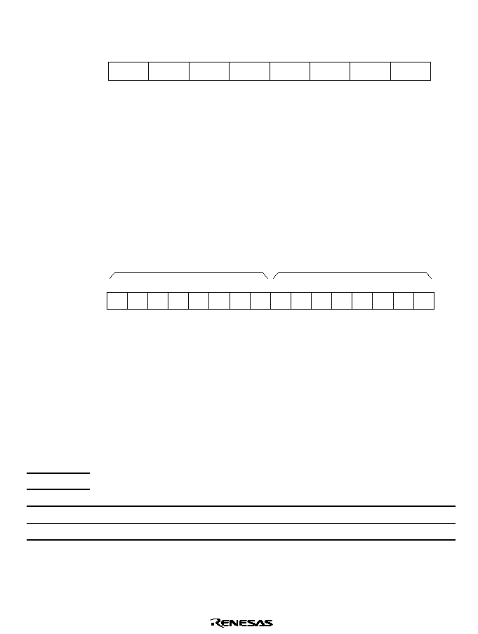
Rev. 1.0, 02/00, page 251 of 1141
11.2.2
Timer Counter A (TCA)
0
0
1
0
R
2
0
R
3
0
4
5
6
7
R
R
TCA3
0
R
TCA4
0
R
TCA5
0
R
TCA6
0
R
TCA7
TCA2
TCA1
TCA0
Bit :
Initial value :
R/W :
The timer counter A (TCA) is an 8-bit up-counter that counts up on inputs from the internal clock.
The inputting clock can be selected by TMA3 to TMA0 bits of the TMA
When the TCA overflows, the TMAOV bit of the TMA is set to 1.
The TCA can be cleared by setting the TMA3 and TMA2 bits of the TMA to 11.
The TCA is always readable. When reset, the TCA will be initialized into H'00.
11.2.3
Module Stop Control Register (MSTPCR)
7
1
MSTP15
R/W
MSTPCRH
6
1
MSTP14
R/W
5
1
MSTP13
R/W
4
1
MSTP12
R/W
3
1
MSTP11
R/W
2
1
MSTP10
R/W
1
1
MSTP9
R/W
0
1
MSTP8
R/W
7
1
MSTP7
R/W
6
1
MSTP6
R/W
5
1
MSTP5
R/W
4
1
MSTP4
R/W
3
1
MSTP3
R/W
2
1
MSTP2
R/W
1
1
MSTP1
R/W
0
1
MSTP0
R/W
MSTPCRL
Initial value :
R/W :
Bit :
The MSTPCR are 8-bit read/write twin registers which work to control the module stop mode.
When the MSTP15 bit is set to 1, the Timer A stops its operation at the ending point of the bus
cycle to shift to the module stop mode. For more information, see section 4.5, Module Stop
Mode. When reset, the MSTPCR will be initialized into H'FFFF.
Bit 7
Module Stop (MSTP15): This bit works to designate the module stop mode for the Timer
A.
MSTPCRH
Bit 7
MSTP15
Description
0
Cancels the module stop mode of the Timer A
1
Sets the module stop mode of the Timer A
(Initial value)

Rev. 1.0, 02/00, page 252 of 1141
11.3
Operation
Timer A is an 8-bit interval timer. It can be used as a clock timer when connected to a 32.768 kHz
crystal oscillator.
11.3.1
Operation as the Interval Timer
When the TMA3 bit of the TMA is cleared to 0, timer A works as an 8-bit interval timer.
After reset, the TCA is cleared to H'00 and as the TMA3 bit is cleared to 0, the Timer A continues
counting up as the interval counter without interrupts right after resetting.
As the operation clock for timer A, selection can be made from eight different types of internal
clocks being output from the PSS by the TMA2 to TMA0 bits of the TMA.
When the clock signal is input after the reading of the TCA reaches H'FF, timer A overflows and
the TMAOV bit of the TMA will be set to 1. An interrupt occurs when the TMAIE bit of the
TMA is 1.
When overflowing occurs, the reading of the TCA returns to H'00 before resuming counting up.
Consequently, it works as the interval timer to produce overflow outputs periodically at every 256
input clocks.
11.3.2
Operation as Clock Timer
When the TMA3 bit of the TMA is set to 1, timer A works as a time base for the clock.
As the overflow cycles for timer A, selection can be made from four different types by counting
the clock being output from the PSW by the TMA1 bit and TMA0 bit of the TMA.
11.3.3
Initializing the Counts
When the TMA3 and TMA2 bits are set to 11, the PSW and TCA will be cleared to H'00 to come
to a stop.
At this state, writing 10 to the TMA3 bit and TMA2 bit makes timer A start counting from H'00 in
the time base mode for clocks.
After clearing the PSW and TCA using the TMA3 and TMA2 bits, writing 00 or 01 to the TMA3
bit and TMA2 bit to make timer A start counting from H'00 in the interval timer mode. However,
the period to the first count is not constant, since the PSS is not cleared.
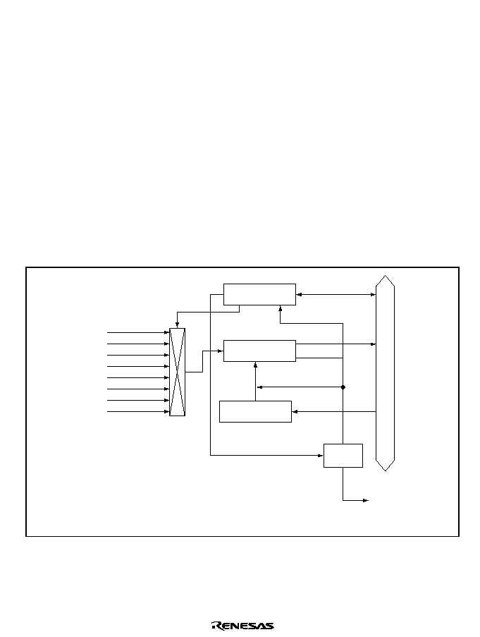
Rev. 1.0, 02/00, page 253 of 1141
Section 12 Timer B
12.1
Overview
Timer B is an 8-bit up-counter. Timer B is equipped with two different types of functions namely,
the interval function and the auto reloading function.
12.1.1
Features
∑
Seven different types of internal clocks (
/16384,
/4096,
/1024,
/512,
/128,
/32 and
/8)
or an of external clock can be selected.
∑
When the counter overflows, a interrupt request will be issued.
12.1.2
Block Diagram
Figure 12.1 shows a block diagram of timer B.
[Legend]
TMB
/16384
/4096
/1024
/512
/128
/32
/8
TMBI
TCB
: Timer mode register B
: Timer counter B
TLB
TMBI
: Timer re-loading register B
: Event input terminal of the Timer B
Re-loading
Clock sources
Overflowing
Timer B
Interrupt requests
Internal data bus
TCB
TMB
TLB
Interrupting
circuit
Figure 12.1 Block Diagram of Timer B

Rev. 1.0, 02/00, page 254 of 1141
12.1.3
Pin Configuration
Table 12.1 shows the pin configuration of timer B.
Table 12.1
Pin Configuration
Name
Abbrev.
I/O
Function
Event inputs to timer B
TMBI
Input
Event input pin for inputs to the TCB
12.1.4
Register Configuration
Table 12.2 shows the register configuration of timer B.
The TCB and TLB are being allocated to the same address. Reading or writing determines the
accessing register.
Table 12.2
Register Configuration
Name
Abbrev.
R/W
Size
Initial Value
Address*
Timer mode register B
TMB
R/W
Byte
H'18
H'D110
Timer counter B
TCB
R
Byte
H'00
H'D111
Timer load register B
TLB
W
Byte
H'00
H'D111
Port mode register A
PMRA
R/W
Byte
H'3F
H'FFD9
Note:
*
Lower 16 bits of the address.

Rev. 1.0, 02/00, page 255 of 1141
12.2
Register Descriptions
12.2.1
Timer Mode Register B (TMB)
0
0
1
0
R/W
2
0
R/W
3
1
4
--
--
--
--
1
5
0
6
0
7
R/W
R/W
TMBIE
R/(W)*
TMBIF
0
R/W
TMB17
TMB12
TMB11
TMB10
Note:
*
Only 0 can be written to clear the flag.
Bit :
Initial value :
R/W :
The TMB is an 8-bit read/write register which works to control the interrupts, to select the auto
reloading function and to select the input clock.
When reset, the TMB is initialized to H'18.
Bit 7
Selecting the Auto Reloading Function (TMB17): This bit works to select the auto
reloading function of the Timer B.
Bit 7
TMB17
Description
0
Selects the interval function
(Initial value)
1
Selects the auto reloading function
Bit 6
Interrupt Requesting Flag for the Timer B (TMBIF): This is an interrupt requesting
flag for the Timer B. It indicates the fact that the TCB is overflowing.
Bit 6
TMBIF
Description
0
[Clearing conditions]
(Initial value)
When 0 is written after reading 1
1
[Setting conditions]
When the TCB overflows

Rev. 1.0, 02/00, page 256 of 1141
Bit 5
Enabling Interrupt of the Timer B (TMBIE): This bit works to permit/prohibit
occurrence of interrupt of timer B when the TCB overflows and when the TMBIF is set to 1.
Bit 5
TMBIE
Description
0
Prohibits interrupt of timer B
(Initial value)
1
Permits interrupt of timer B
Bits 4 and 3
Reserved: These bits cannot be modified and are always read as 1.
Bits 2 to 0
Clock Selection (TMB12 to TMB10): These bits work to select the clock to input to
the TCB. Selection of the rising edge or the falling edge is workable with the external event
inputs.
Bit 2
Bit 1
Bit 0
TMB12
TMB11
TMB10
Descriptions
0
0
0
Internal clock: Counts at
/16384
(Initial value)
0
0
1
Internal clock: Counts at
/4096
0
1
0
Internal clock: Counts at
/1024
0
1
1
Internal clock: Counts at
/512
1
0
0
Internal clock: Counts at
/128
1
0
1
Internal clock: Counts at
/32
1
1
0
Internal clock: Counts at
/8
1
1
1
Counts at the rising edge and the falling edge of external
event inputs (TMBI) *
Note:
*
The edge selection for the external event inputs is made by setting the PMRA6 of the
port mode register A (PMRA). See section 12.2.4, Port Mode Register A (PMRA).

Rev. 1.0, 02/00, page 257 of 1141
12.2.2
Timer Counter B (TCB)
0
0
1
0
R
2
0
R
3
4
5
0
6
0
7
R
R
TCB15
0
R
TCB14
0
R
TCB13
R
TCB16
0
R
TCB17
TCB12
TCB11
TCB10
Bit :
Initial value :
R/W :
The TCB is an 8-bit readable register which works to count up by the internal clock inputs and
external event inputs. The input clock can be selected by the TMB12 to TMB10 of the TMB.
When the TCB overflows (H'FF
H'00 or H'FF
TLB setting), a interrupt request of the Timer
B will be issued.
When reset, the TCB is initialized to H'00.
12.2.3
Timer Load Register B (TLB)
0
0
1
0
W
2
0
W
3
4
5
0
6
0
7
W
W
TLB15
0
W
TLB14
0
W
TLB13
W
TLB16
0
W
TLB17
TLB12
TLB11
TLB10
Bit :
Initial value :
R/W :
The TLB is an 8-bit write only register which works to set the reloading value of the TCB.
When the reloading value is set to the TLB, the value will be simultaneously loaded to the TCB
and the TCB starts counting up from the set value. Also, during an auto reloading operation, when
the TCB overflows, the value of the TLB will be loaded to the TCB. Consequently, the
overflowing cycle can be set within the range of 1 to 256 input clocks.
When reset, the TLB is initialized to H'00.
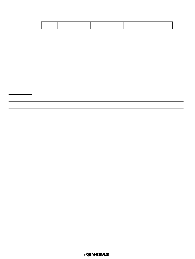
Rev. 1.0, 02/00, page 258 of 1141
12.2.4
Port Mode Register A (PMRA)
0
1
1
--
2
1
--
3
4
1
5
6
7
--
--
PMRA6
PMRA7
--
--
--
--
R/W
R/W
--
1
--
--
--
1
1
0
0
Bit :
Initial value :
R/W :
The port mode register A (PMRA) works to changeover the pin functions of the port 6 and to
designate the edge sense of the event inputs of timer B (TMBI).
The PMRA is an 8-bit read/write register. When reset, the PMRA will be initialized to H'3F.
See section 10.7, Port 6 for other information than bit 6.
Bit 6
Selecting the Edges of the Event Inputs to the Timer B (PMRA6): This bit works to
select the input edge sense of the TMBI pins.
Bit 6
PMRA6
Description
0
Detects the falling edge of the event inputs to the Timer B
(Initial value)
1
Detects the rising edge of the event inputs to the Timer B

Rev. 1.0, 02/00, page 259 of 1141
12.2.5
Module Stop Control Register (MSTPCR)
7
1
MSTP15
R/W
MSTPCRH
6
1
MSTP14
R/W
5
1
MSTP13
R/W
4
1
MSTP12
R/W
3
1
MSTP11
R/W
2
1
MSTP10
R/W
1
1
MSTP9
R/W
0
1
MSTP8
R/W
7
1
MSTP7
R/W
6
1
MSTP6
R/W
5
1
MSTP5
R/W
4
1
MSTP4
R/W
3
1
MSTP3
R/W
2
1
MSTP2
R/W
1
1
MSTP1
R/W
0
1
MSTP0
R/W
MSTPCRL
Initial value :
R/W :
Bit :
The MSTPCR are 8-bit read/write twin registers which work to control the module stop mode.
When the MSTP14 bit is set to 1, the Timer B stops its operation at the ending point of the bus
cycle to shift to the module stop mode. For more information, see section 4.5, Module stop mode.
When reset, the MSTPCR is initialized to H'FFFF.
Bit 6
Module Stop (MSTP14): This bit works to designate the module stop mode for the Timer
B.
MSTPCRH
Bit 6
MSTP14
Description
0
Cancels the module stop mode of the Timer B
1
Sets the module stop mode of the Timer B
(Initial value)

Rev. 1.0, 02/00, page 260 of 1141
12.3
Operation
12.3.1
Operation as the Interval Timer
When the TMB17 bit of the TMB is set to 0, timer B works as an 8-bit interval timer.
When reset, since the TCB is cleared to H'00 and as the TMB17 bit is cleared to 0, timer B
continues counting up as the interval timer without interrupts right after resetting.
As the clock source for timer B, selection can be made from seven different types of internal
clocks being output from the prescaler unit by the TMB12 to TMB10 bits of the TMB or an
external clock through the TMBI input pin can be chosen instead.
When the clock signal is input after the reading of the TCB reaches H'FF, timer B overflows and
the TMBIF bit of the TMB will be set to 1. At this time, when the TMBIE bit of the TMB is 1,
interrupt occurs.
When overflowing occurs, the reading of the TCB returns to H'00 before resuming counting up.
When a value is set to the TLB while the interval timer is in operation, the value which has been
set to the TLB will be loaded to the TCB simultaneously.
12.3.2
Operation as the Auto Reload Timer
When the TMB17 of the TMB is set to 1, the Timer B works as an 8-bit auto reload timer.
When a reload value is set in the TLB, the value is loaded onto the TCB at the same time, and the
TCB starts counting up from the value.
When the clock signal is input after the reading of the TCB reaches H'FF, timer B overflows and
the TLB value is loaded onto the TCB, then the TCB continues counting up from the loaded value.
Accordingly, overflow interval can be set within the range of 1 to 256 clocks depending on the
TLB value.
Clock source and interrupts in the auto reload operation are the same as those in the interval
operation. When the TLB value is re-set while the auto reload timer is in operation, the value
which has been set to the TLB will be loaded onto the TCB simultaneously.
12.3.3
Event Counter
Timer B works as an event counter using the TMBI pin as the event input pin. When the TMB12
to TMB10 are set to 111, the external event will be selected as the clock source and the TCB
counts up at the leading edge or the trailing edge of the TMBI pin inputs.

Rev. 1.0, 02/00, page 261 of 1141
Section 13 Timer J
13.1
Overview
Timer J consists of twin counters. It carries different operation modes such as reloading and event
counting.
13.1.1
Features
Timer J consists of an 8-bit reloading timer and an 8-bit/16-bit selectable reloading timer. It has
various functions as listed below. The two timers can be used separately, or they can be connected
together to operate as a single timer.
∑
Reloading timers
∑
Event counters
∑
Remote-controlled transmissions
∑
Takeup/Supply reel pulse division
13.1.2
Block Diagram
Figure 13.1 is a block diagram of timer J. Timer J consists of two reload timers namely, TMJ-1
and TMJ-2.
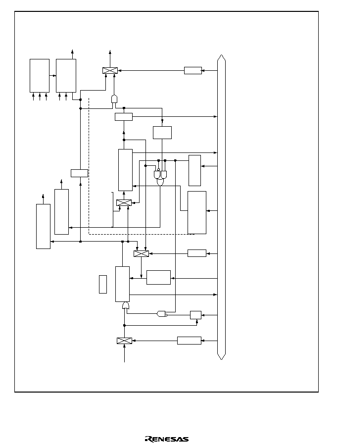
Rev. 1.0, 02/00, page 262 of 1141
[Legend]
TCJ
Note: * At the Low level under the timer mode.
TLJ
: Timer counter J
: Timer load register J
TCK
TLK
: Timer counter K
: Timer load register K
TMO
REMOout
: TMJ-1 timer output
: TMJ-2 toggle output
(Remote controller
transmission data)
BUZZ
Reloading register
(Burst/space
width register
PS22, 21,20
EXN
: Buzzer output
TGL
: TMJ-2 toggle flag
PS22, 21,20
ST
: TMJ-2 input clock selection
: Starting the remote controlled operation
PS11,10
: TMJ-1 input clock selection
8/16
T/R
EXN
: 8-bit/16-bit operation changeover
: Timer output/Remote controller output changeover
: Expansion function switching
Internal data bus
Edge
detection
Toggle
T/R
Down-counter
(8/16-bit)
BUSS
Output
Control
Monitor
Output
Control
Toggle
Reloading
register
8/16
ST
PS11,10
Down-
counter (8-bit)
Under–
flow
Under-
flow
TCJ
TMJ-1
TMJ-2
TCK
PB/REC-CTL
DVCTL
TCA7
/4096
/8192
TGL
REMOout
TMO
TMO
BUZZ
Clock sources
IRQ2
/64
/128
/1024
/2048
/16384
Clock sources
IRQ1
/4
/256
/512
*
Synchronization
TLJ
Reloading
Reloading
TLK
TMJ-1
Interrupting circuit
Interrupt request
by the TMJ1I
Interrupt request
by the TMJ2I
TMJ-2
Interrupting circuit
Figure 13.1 Block Diagram of timer J

Rev. 1.0, 02/00, page 263 of 1141
13.1.3
Pin Configuration
Table 13.1 shows the pin configuration of timer J.
Table 13.1
Pin Configuration
Name
Abbrev.
I/O
Function
Event input pin
,54
Input
Event inputs to the TMJ-1
Event input pin
,54
Input
Event inputs to the TMJ-2
13.1.4
Register Configuration
Table 13.2 shows the register configuration of timer J.
The TCJ and TLJ or the TCK and TLK are being allocated to the same address respectively.
Reading or writing determines the accessing register.
Table 13.2
Register Configuration
Name
Abbrev.
R/W
Size
Initial Value
Address
*2
Timer mode register J
TMJ
R/W
Byte
H'00
H'D13A
Timer J control register
TMJC
R/W
Byte
H'09
H'D13B
Timer J status register
TMJS
R/(W)
*1
Byte
H'3F
H'D13C
Timer counter J
TCJ
R
Byte
H'FF
H'D139
Timer counter K
TCK
R
Byte
H'FF
H'D138
Timer load register J
TLJ
W
Byte
H'FF
H'D139
Timer load register K
TLK
W
Byte
H'FF
H'D138
Notes: 1. Only 0 can be written to clear the flag.
2. Lower 16 bits of the address.

Rev. 1.0, 02/00, page 264 of 1141
13.2
Register Descriptions
13.2.1
Timer Mode Register J (TMJ)
0
0
1
0
R
2
0
R/W
3
0
4
0
R/W
5
0
6
0
7
R/W
R/W
R/W
ST
R/W
PS10
0
R/W
PS11
8/16
PS21
PS20
TGL
T/R
Bit :
Initial value :
R/W :
The timer mode register J (TMJ) works to select the inputting clock for the TMJ-1 and TMJ-2 and
to set the operation mode.
The TMJ is an 8-bit register and bit 1 is for read only. All the remaining bits are applicable to
read/write.
When reset, the TMJ is initialized to H'00.
Under all other modes than the remote controlling mode, writing into the TMJ works to initialize
the counters (TCJ and TCK) to H'FF.
Bits 7 and 6
Selecting the Inputting Clock to the TMJ-1 (PS11 and PS10): These bits work
to select the clock to input to the TMJ-1. When the external clock is selected, the counted edge
(rising or falling) can also be selected.
Bit 7
Bit 6
PS11
PS10
Description
0
Counting by the PSS,
/512
(Initial value)
0
1
Counting by the PSS,
/256
0
Counting by the PSS,
/4
1
1
Counting at the rising edge or the falling edge of the external clock
inputs (
,54
) *
Note:
*
The edge selection for the external clock inputs is made by setting the IRQ edge select
register (IEGR). See section 6.2.4, IRQ Edge Select Register (IEGR) for more
information.
When using an external clock under the remote controlling mode, set the opposite edge
with the IRQ1 and the IRQ2 when using an external clock under the remote controlling
mode. (When IRQ1 falling, select IRQ2 rising and when IRQ1 rising, select IRQ2
falling)

Rev. 1.0, 02/00, page 265 of 1141
Bit 5
Starting the Remote Controlled Operation (ST): This bit works to start the remote
controlled operations.
When this bit is set to 1, clock signal is supplied to the TMJ-1 to start signal transmissions.
When this bit is cleared to 0, clock supply stops to discontinue the operation. The ST bit will be
valid under the remote controlling mode, namely, when bit 0 (T/R bit) is 1 and bit 4 (8/16 bit) is 0.
Under other modes than the remote controlling mode, it will be fixed to 0. When a shift to the low
power consumption mode is made during remote controlled operation, the ST bit will be cleared to
0. When resuming operation after returning to the active mode, write 1.
Bit 5
ST
Description
0
Works to stop clock signal supply to the TMJ-1 under the remote controlling mode
(Initial value)
1
Works to supply clock signal to the TMJ-1 under the remote controlling mode
Bit 4
Switching Over Between 8-bit/16-bit Operations (8/16): This bit works to choose if
using timer J as two units of 8-bit timer/counter or if using it as a single unit of 16-bit
timer/counter. Even under 16-bit operations, TMJ1I interrupt requests from the TMJ-1 will be
valid.
Bit 4
8/16
Description
0
Makes the TMJ-1 and TMJ-2 operate separately
(Initial value)
1
Makes the TMJ-1 and TMJ-2 operate altogether as 16-bit timer/counter
Bits 3 and 2
Selecting the Inputting Clock for the TMJ-2 (PS21 and PS20): These bits,
together with the PS22 bit in the timer J control register (TMJC), work to select the clock for the
TMJ-2. When the external clock is selected, the counted edge (rising or falling) can also be
selected. For details, refer to section 13.2.2, Timer J Control Register (TMJC).
Bit 1
TMJ-2 Toggle Flag (TGL): This flag indicates the toggled status of the underflowing
with the TMJ-2. Reading only is workable.
It will be cleared to 0 under the low power consumption mode.
Bit 1
TGL
Description
0
The toggle output of the TMJ-2 is 0
(Initial value)
1
The toggle output of the TMJ-2 is 1

Rev. 1.0, 02/00, page 266 of 1141
Bit 0
Switching Over Between Timer Output/Remote Controlling Output (T/R): This bit
works to select if using the timer outputs from the TMJ-1 as the output signal through the TMO
pin or if using the toggle outputs (remote controlled transmission data) from the TMJ-2 as the
output signal through the TMO pin.
Bit 0
T/R
Description
0
Timer outputs from the TMJ-1
(Initial value)
1
Toggle outputs from the TMJ-2 (remote controlled transmission data)
Selecting the Operation Mode
The operating mode of timer J is determined by bit 3 (EXN) of the timer J control register (TMJC)
and bits 4 (8/16) and 0 (T/R) of the timer mode register J (TMJ).
TMJC
TMJ
Bit 3
Bit 4
Bit 0
EXN
8/16
T/R
Description
0
0
0
8-bit timer + 16-bit timer
1
Remote-controlling mode (TMJ-2 works as a 16-bit timer)
1
*
24-bit timer
1
0
0
Two 8-bit timers
(Initial value)
1
Remote-controlling mode (TMJ-2 works as an 8-bit timer)
1
*
16-bit timer
Note:
*
Don't care
Writing to the TMJ in timer mode initializes the counters (TCJ and TCK) (H'FF). Consequently,
write to the reloading registers (TLJ an TLK) after finishing settings with the TMJ.
Under the remote controlling mode, although the TLJ and the TLK will not be initialized even
when writing is made into the TMJ, follow the sequence listed below when starting a remote
controlling operation:
1. Make setting to the remote controlling mode with the TMJ.
2. Write the data into the TLJ and TLK.
3. Start the remote controlled operation by use of the TMJ. (ST bit = 1).
Even under 16-bit operations, TMJ1I interrupt requests from the TMJ-1 will be valid.

Rev. 1.0, 02/00, page 267 of 1141
13.2.2
Timer J Control Register (TMJC)
0
1
0
2
0
R/W
3
PS22
EXN
R/W
R/W
4
0
R/W
5
0
6
0
7
R/W
R/W
MON1
R/W
BUZZ0
0
R/W
BUZZ1
MON0
TMJ2IE
TMJ1IE
1
1
Bit :
Initial value :
R/W :
The timer J control register (TMJC) works to select the buzzer output frequency and to control
permission/prohibition of interrupts.
The TMJC is an 8-bit read/write register.
When reset, the TMJC is initialized to H'09.
Bits 7 and 6
Selecting the Buzzer Output (BUZZ1 or BUZZ0): This bit works to select if
using the buzzer outputs as the output signal through the BUZZ pin or if using the monitor signals
as the output signal through the BUZZ pin.
When setting is made to the monitor signals, choose the monitor signal using the MON1 bit and
MON0 bit.
Bit 7
Bit 6
BUZZ1
BUZZ0
Description
Frequency when
= 10 MHz
0
/4096
(Initial value)
2.44 kHz
0
1
/8192
1.22 kHz
0
Works to output monitor signals
1
1
Works to output BUZZ signals from timer J

Rev. 1.0, 02/00, page 268 of 1141
Bits 5 and 4
Selecting the Monitor Signals (MON1 or MON0): These bits work to select the
type of signals being output through the BUZZ pin for monitoring purpose. These settings are
valid only when the BUZZ1 and BUZZ0 bits are being set to 10.
When PB-CTL or REC-CTL is chosen, signal duties will be output as they are.
In case of DVCTL signals, signals from the CTL dividing circuit will be toggled before being
output. Signal waveforms divided by the CTL dividing circuit into n-divisions will further be
divided into halves. (Namely, 2n divisions, 50% duty waveform).
In case of TCA7, Bit 7 of the counter of the Timer A will be output. (50% duty)
When prescaler W is being used with the Timer A, 1 Hz outputs are available.
Bit 5
Bit 4
MON1
MON0
Description
0
PB or REC-CTL
(Initial value)
0
1
DVCTL
1
*
Outputs TCA7
Note:
*
Don't care.
Bit 3
Expansion Function Control Bit (EXN): This bit enables or disables the expansion
function of TMJ-2. When the expansion function is enabled, TMJ-2 works as a 16-bit counter, and
further input clock sources and types can be selected.
Bit 3
EXN
Description
0
Enables the TMJ-2 expansion function
1
Disables the TMJ-2 expansion function
(Initial value)
Bit 2
Enabling Interrupt of the TMJ2I (TMJ2IE): This bit works to permit/prohibit
occurrence of TMJ2I interrupt of the TMJS in 1-set of the TMJ2I.
Bit 2
TMJ2IE
Description
0
Prohibits occurrence of TMJ2I interrupt
(Initial value)
1
Permits occurrence of TMJ2I interrupt

Rev. 1.0, 02/00, page 269 of 1141
Bit 1
Enabling Interrupt of the TMJ1I (TMJ1IE): This bit works to permit/prohibit
occurrence of TMJ1I interrupt of the TMJS in 1-set of the TMJ1I.
Bit 1
TMJ1IE
Description
0
Prohibits occurrence of TMJ1I interrupt
(Initial value)
1
Permits occurrence of TMJ1I interrupt
Bit 0
TMJ-2 Input Clock Selection (PS22): This bit, together with the PS21 and PS20 bits of
the timer mode register J (TMJ), selects the TMJ-2 input clock source.
TMJC
TMJ
Bit 3
Bit 0
Bit 3
Bit 2
EXN
PS22
PS21
PS20
Description
0
1
0
0
PSS; count at
/128
1
PSS; count at
/64
1
0
Count at TMJ-1 underflow
1
External clock (IRQ2); count at rising or falling edge*
1
0
*
*
Reserved
1
1
0
0
PSS; count at
/16384 (Initial value)
1
PSS; count at
/2048
1
0
Count at TMJ-1 underflow
1
External clock (IRQ2); count at rising or falling edge*
1
0
0
0
PSS; count at
/1024
1
PSS;
/1024
1
0
Count at TMJ-1 underflow
1
External clock (IRQ2); count at rising or falling edge*
1
Note:
*
Don't care
1. The external clock edge can be selected by the IRQ edge select register (IEGR). For
details, refer to section 6.2.4, IRQ Edge Select Registers (IEGR).

Rev. 1.0, 02/00, page 270 of 1141
13.2.3
Timer J Status Register (TMJS)
0
1
2
3
4
5
--
--
--
--
--
--
--
--
--
--
--
--
6
0
7
R/(W)*
TMJ1I
0
R/(W)*
TMJ2I
1
1
1
1
1
1
Note: * Only 0 can be written to clear the flag.
Bit :
Initial value :
R/W :
The timer J status register (TMJS) works to indicate issuance of the interrupt request of timer J.
The TMJS is an 8-bit read/write register. When reset, the TMJS is initialized to H'3F.
Bit 7
TMJ2I Interrupt Requesting Flag (TMJ2I)
Bit 7
TMJ2I
Description
0
[Clearing conditions]
(Initial value)
When 0 is written after reading 1
1
[Setting conditions]
When the TMJ-2 underflows
Bit 6
TMJ1I Interrupt Requesting Flag (TMJ1I): This is the TMJ1I interrupt requesting flag.
This flag is set out when the TMJ-1 underflows.
TMJ1I interrupt requests will also be made under a 16-bit operation.
Bit 6
TMJ1I
Description
0
[Clearing conditions]
(Initial value)
When 0 is written after reading 1
1
[Setting conditions]
When the TMJ-1 underflows
Bits 5 to 0
Reserved: These bits cannot be modified and are always read as 1.

Rev. 1.0, 02/00, page 271 of 1141
13.2.4
Timer Counter J (TCJ)
0
1
1
1
R
2
1
R
3
1
4
1
R
5
1
6
1
7
R
R
R
TDR15
R
TDR16
1
R
TDR17
TDR14
TDR13
TDR12
TDR11
TDR10
Bit :
Initial value :
R/W :
The timer counter J (TCJ) is an 8-bit readable down-counter which works to count down by the
internal clock inputs or external clock inputs. The inputting clock can be selected by the PS11 and
PS10 bits of the TMJ. TCJ values can be readout always. Nonetheless, when the EXN bit in
TMJC and the 8/16 bit in TMJ are both set to 1, (means when setting is made to 16-bit operation),
reading is possible under the word command only.
At this time, the TCK of the TMJ-2 can be read by the upper 8 bits and the TCJ can be read by the
lower 8 bits. When the EXN bit in TMJC is 0, TCJ can be read only in byte units.
When the TCJ underflows (H'00
Reloading value), regardless of the operation mode setting of
the 8/16 bit, the TMJ1I bit of the TMJS will be set to 1 bit. The TCJ and TLJ are being allocated
to the same address.
When reset, the TCJ is initialized to H'FF.
13.2.5
Timer Counter K (TCK)
0
1
1
1
R
2
1
R
3
1
4
1
R
5
1
6
1
7
R
R
R
TDR25
R
TDR26
1
R
TDR27
TDR24
TDR23
TDR22
TDR21
TDR20
Bit :
Initial value :
R/W :
The timer counter K (TCK) is an 8-bit or a 16-bit readable down-counter which works to count
down by the internal clock inputs or external clock inputs. The inputting clock can be selected by
the EXN and PS2 bits of the TMIC, and the PS21 and PS20 bits of the TMJ. TCK values can be
readout always. Nonetheless, when the EXN bit in TMJC and the 8/16 bit in TMJ are both set to
1, (means when setting is made to 16-bit operation), reading is possible under the word command
only.
At this time, the TCK can be read by the upper 8 bits and the TCJ of the TMJ-1 can be read by the
lower 8 bits. When the EXN bit in TMJC is 0, TCK works as a 16-bit counter and can be read only
in word units.
When the TCK underflows (H'00
Reloading value), the TMJ2I bit of the TMJS will be set to 1.
The TCK and TLK are being allocated to the same address.
When reset, the TCK is initialized to H'FF.

Rev. 1.0, 02/00, page 272 of 1141
13.2.6
Timer Load Register J (TLJ)
0
1
1
1
W
2
1
W
3
1
4
1
W
5
1
6
1
7
W
W
W
TLR15
W
TLR16
1
W
TLR17
TLR14
TLR13
TLR12
TLR11
TLR10
Bit :
Initial value :
R/W :
The timer load register J (TLJ) is an 8-bit write only register which works to set the reloading
value of the TCJ.
When the reloading value is set to the TLJ, the value will be simultaneously loaded to the TCJ and
the TCJ starts counting down from the set value. Also, during an auto reloading operation, when
the TCJ underflows, the value of the TLJ will be loaded to the TCJ. Consequently, the
underflowing cycle can be set within the range of 1 to 256 input clocks. Nonetheless, when the
EXN bit in TMJC and the 8/16 bit in TMJ are both set to 1, (means when setting is made to 16-bit
operation), writing is possible under the word command only.
At this time, the upper 8 bits can be written into the TLK of the TMJ-2 and the lower 8 bits can be
written into the TLJ. When the EXN bit in TMJC is 0, TLJ can be written to only in byte units; an
8-bit reload value is written to TLJ.
The TLJ and TCJ are being allocated to the same address.
When reset, the TLJ is initialized to H'FF.
13.2.7
Timer Load Register K (TLK)
0
1
1
1
W
2
1
W
3
1
4
1
W
5
1
6
1
7
W
W
W
TLR25
W
TLR26
1
W
TLR27
TLR24
TLR23
TLR22
TLR21
TLR20
Bit :
Initial value :
R/W :
The timer load register K (TLK) is an 8-bit or a 16-bit write only register which works to set the
reloading value of the TCK.
When the reloading value is set to the TLK, the value will be simultaneously loaded to the TCK
and the TCK starts counting down from the set value. Also, during an auto reloading operation,
when the TCK underflows, the value of the TLK will be loaded to the TCK. Consequently, the
underflowing cycle can be set within the range of 1 to 256 input clocks. Nonetheless, when the
EXN bit in TMJC and the 8/16 bit in TMJ are both set to 1, (means when setting is made to 16-bit
operation), writing is possible under the word command only. At this time, the upper 8 bits can be
written into the TLK and the lower 8 bits can be written into the TLJ of the TMJ-1. When the
EXN bit in TMJC is 0, TLK can be written to only in word units; a 16-bit reload value is written
to TLK. The TLK and TCK are being allocated to the same address.
When reset, the TLK is initialized to H'FF.

Rev. 1.0, 02/00, page 273 of 1141
13.2.8
Module Stop Control Register (MSTPCR)
7
1
MSTP15
R/W
MSTPCRH
6
1
MSTP14
R/W
5
1
MSTP13
R/W
4
1
MSTP12
R/W
3
1
MSTP11
R/W
2
1
MSTP10
R/W
1
1
MSTP9
R/W
0
1
MSTP8
R/W
7
1
MSTP7
R/W
6
1
MSTP6
R/W
5
1
MSTP5
R/W
4
1
MSTP4
R/W
3
1
MSTP3
R/W
2
1
MSTP2
R/W
1
1
MSTP1
R/W
0
1
MSTP0
R/W
MSTPCRL
Initial value :
R/W :
Bit :
The MSTPCR are 8-bit read/write twin registers which work to control the module stop mode.
When the MSTP13 bit is set to 1, timer J stops its operation at the ending point of the bus cycle to
shift to the module stop mode. For more information, see section 4.5, Module Stop Mode.
When reset, the MSTPCR is initialized to H'FFFF.
Bit 5
Module Stop (MSTP13): This bit works to designate the module stop mode for the Timer
J.
MSTPCRH
Bit 5
MSTP13
Description
0
Cancels the module stop mode of timer J
1
Sets the module stop mode of timer J
(Initial value)

Rev. 1.0, 02/00, page 274 of 1141
13.3
Operation
13.3.1
8-bit Reload Timer (TMJ-1)
The TMJ-1 is an 8-bit reload timer. As the clock source, dividing clock or edge signals through
the
,54 pin are being used. By selecting the edge signals through the ,54 pin, it can also be
used as an event counter. While it is working as an event counter, its reloading function is
workable simultaneously. When data are written into the reloading register, these data will be
written into the counters (event counter, timer counter) simultaneously. Also, when the event
counter underflows, the event counter value is reset to the reload register value, and a TMJ1I
interrupt request occurs. Every time the counter underflows, the output level toggles. This output
can be used as a buzzer or the carrier frequency at remote-controlled transmission by selecting an
appropriate divided clock.
The TMJ-1 and TMJ-2, in combination, can be used as a 16-bit or a 24-bit reload timer.
Nonetheless, when they are being used, in combination, as a 16-bit timer, word command only is
valid and the TCK works as the down counter for the upper 8 bits and the TCJ works as the down
counter for the lower 8 bits, means a reloading register of total 16 bits.
When data are written into a 16-bit reloading register, the same data will be written into the 16-bit
down counter.
Also, when the 16-bit down counter underflow signals, the data of the 16-bit reloading register
will be reloaded into the down counter. When the EXN bit of TMJC is set to 0, the expansion
function of TMJ-2 is enabled, that is, TMJ-2 works as a 16-bit reloading timer, and it can be
connected to TMJ-1 to be a 24-bit reloading timer. In this case, TCK works as the upper 16-bit
part and TCJ works as the lower 8-bit part of a 24-bit down counter, and TLK works as the upper
16-bit part and TLJ works as the lower 8-bit part of a 24-bit reloading register.
Even when they are making a 16-bit or a 24-bit operation, the TMJ1I interrupt requests of the
TMJ-1 and BUZZER outputs are effective. In case these functions are not necessary, make them
invalid by programming.
The TMJ-1 and TMJ-2, in combination, can be used for remote controlled data transmission.
Regarding the remote controlled data transmission, see section 13.3.3, Remote Controlled Data
Transmission.
13.3.2
8-bit Reload Timer (TMJ-2)
The TMJ-2 is an 8-bit or a 16-bit down-counting reload timer. As the clock source, dividing
clock, edge signals through the
,54 pin or the underflow signals from the TMJ-1 are being used.
By selecting the edge signals through the
,54 pin, it can also be used as an event counter. While
it is working as an event counter, its reloading function is workable simultaneously.
When data are written into the reloading register, these data will be written into the counter
simultaneously. Also, when the counter underflows, reloading will be made to the data counter of
the reloading register.
When the counter underflows, TMJ2I interrupt requests will be issued.
The TMJ-2 and TMJ-1, in combination, can be used as a 16-bit or a 24-bit reload timer. For more
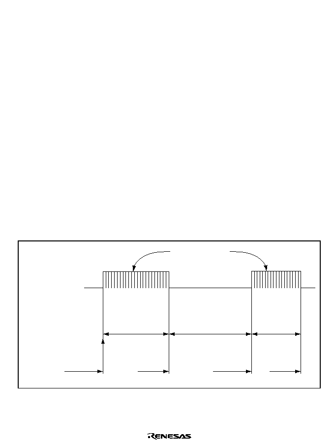
Rev. 1.0, 02/00, page 275 of 1141
information on the 16-bit or 24-bit reload timer, see section 13.3.1, 8-bit Reload Timer (TMJ-1).
The TMJ-2 and TMJ-1, in combination, can be operated by remote controlled data transmission.
Regarding the remote controlled data transmission, see section 13.3.3, Remote Controlled Data
Transmission.
13.3.3
Remote Controlled Data Transmission
The Timer J is capable of making remote controlled data transmission. The carrier frequencies for
the remote controlled data transmission can be generated by the TMJ-1 and the burst width
duration and the space width duration can be setup by the TMJ-2.
The data having been written into the reloading register TMJ-1 and into the burst/space duration
register (TLK) of the TMJ-2 will be loaded to the counter at the same time as the remote
controlled data transmission starts. (Remote controlled data transmission starting bit (ST)
1)
While remote controlled data transmission is being made, the contents of the burst/space duration
register will be loaded to the counter only while reloading is being made by underflow signals.
Even when a writing is made to the burst/space duration register while remote controlled data
transmission is being made, reloading operation will not be made until an underflow signal is
issued. The TMJ-2 issues TMJ2I interrupt requests by the underflow signals. The TMJ-1
performs normal reloading operation (including the TMJ1I interrupt requests).
Figure 13.2 shows the output waveform for the remote controlled data transmission function.
When a shift to the low power consumption mode is effected while remote controlled data
transmission is being made, the ST bit will be cleared to 0. When resuming the remote controlled
data transmission after returning to the active mode, write 1.
Burst width
Space width
Burst width
TMJ-2 toggle output
= 1
TMJ-2 toggle output
= 0
TMJ-2 toggle
output = 1
Setting the
space width
Setting the
burst width
Setting the
space width
ST bit
1
Underflow
Underflow
Underflow
TMJ-1 can generate
the carrier frequencies
Remote controlled data
transmission outputs
Setting the remote
controlled mode
Setting the burst width
Figure 13.2 Remote Controlled Data Transmission Output Waveform
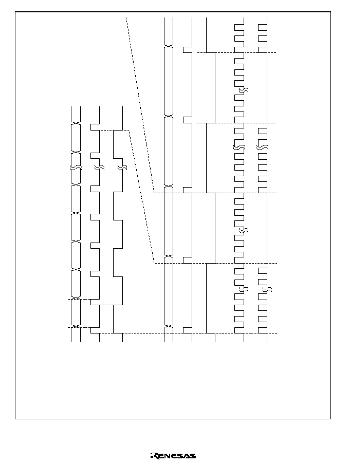
Rev. 1.0, 02/00, page 276 of 1141
TMJ-1
UDF
TMO
(BUZZ)
TMJ-2
UDF
REMOout
TMO
Remote controlled data
transmission output
Figure 13.3 Timer Output Timing
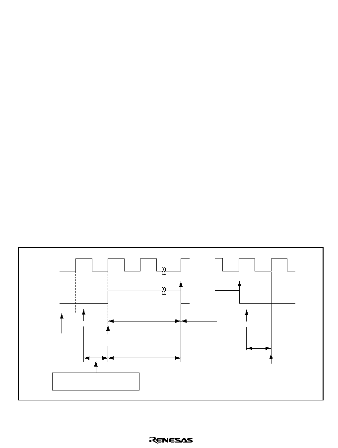
Rev. 1.0, 02/00, page 277 of 1141
When the Timer J is set to the remote controlled operation mode, since the start bit (ST) is being
set or cleared in synchronization with the inputting clock to the TMJ-2, a delay upto a cycle of the
inputting clock at the maximum occurs, namely, after the ST bit has been set to 1 until the remote
controlled data transmission starts. Consequently, when the TLK is updated during the period
after setting the ST bit to 1 until the next cycle of the inputting clock comes, the initial burst width
will be changed as shown in figure 13.4.
Therefore, when making remote controlled data transmission, determine I/O of the TGL bit at the
time of the first burst width control operation without fail. (Or, set the space width to the TLK
after waiting for a cycle of the inputting clock.)
After that, operations can be continued by interrupts.
Similarly, pay attention to the control works when ending remote controlled data transmission.
Example:
1) Set the burst width with the TLK.
2) ST bit
1.
3) Execute the procedure 4) if the TGL flag = 1.
4) Set the space width with the TLK under the status where the TGL flag = 1.
5) Make TMJ-2 interrupt.
6) Set the burst width with the TLK.
:
n) After making TMJ-2 interrupt, make setting of the ST
0 under the status where the TGL
flag = 0.
The period during which the
space width settig can be
made. (S)
Delay
Interrupt
Interrupt
TLK setting
(Burst width)
(B)
Burst width
according to (B)
Space width
according to (S)
Stopping the remote controlled
data transmission
TGL flag
Inputting clock
to the TMJ-2
ST
0
Delay
ST
1
Remote controlled data
transmission starts here.
If an updating is made with the
TLK during this period, the burst
width will be changed.
Figure 13.4 Controls of the Remote Controlled Data Transmission

Rev. 1.0, 02/00, page 278 of 1141
13.3.4
TMJ-2 Expansion Function
The TMJ-2 expansion function is enabled by setting the EXN bit in the timer J control register
(TMJC) to 0. This function makes TMJ-2, which usually works as an 8-bit counter, work as a 16-
bit counter. When this function is selected, timer counter K (TCK) and timer load register K
(TLK) must be accessed as follows:
TCK Read: To read TCK, use the word-length MOV instruction. In this case, the upper 8 bits of
TCK are read out to the lower byte of the on-chip data bus, and the lower 8 bits are read out to the
upper byte of the on-chip data bus. That is, when MOV.W @TCK, Rn is executed, the lower 8
bits of TCK are stored in RnH and the upper 8 bits are stored in RnL.
TLK Write: To write to TLK, use the word-length MOV instruction. In this case, the upper 8 bits
are written to the lower byte of TLK, and the lower 8 bits are written to the upper byte of TLK.
That is, when MOV.W Rn, @TLK is executed, the RnH data is written to the lower byte of TLK,
and the RnL data is written to the upper byte of TLK.

Rev. 1.0, 02/00, page 279 of 1141
Section 14 Timer L
14.1
Overview
Timer A is an 8-bit up/down counter using the control pulses or the CFG division signals as the
clock source.
14.1.1
Features
Features of timer L are as follows:
∑
Two types of internal clocks (
/128 and
/64), DVCFG2 (CFG division signal 2), PB and
REC-CTL (control pulses) are available for your selection.
--
When the PB-CTL is not available, such as when reproducing un-recorded tapes, tape
count can be made by the DVCFG2.
--
Selection of the leading edge or the trailing edge is workable with the CTL pulse counting.
∑
Interrupts occur when the counter overflows or underflows and at occurrences of compare
match clear.
∑
Capable to switch over between the up-counting and down-counting functions with the
counter.
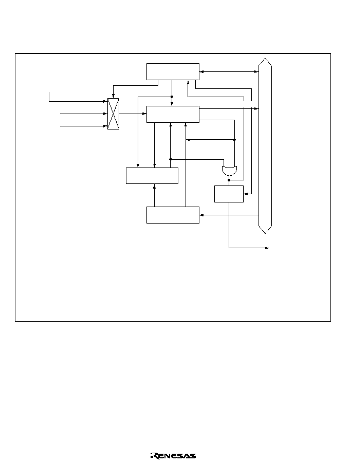
Rev. 1.0, 02/00, page 280 of 1141
14.1.2
Block Diagram
Figure 14.1 shows a block diagram of timer L.
[Legend]
Internal data bus
DVCFG2 : Division signal 2 of the CFG
PB and REC-CTL : Control pluses necessary when making
reproduction and storage
LMR : Timer L mode register
LTC : Linear time counter
RCR : Reload/compare match register
OVF : Overflow
UDF : Underflow
LMR
LTC
RCR
Comparator
Write
OVF/UDF
Reloading
Match clear
Interrupt request
Interrupting
circuit
DVCFG2
PB and
REC-CTL
INTERNAL CLOCK
/128
/64
Read
Figure 14.1 Block Diagram of Timer L

Rev. 1.0, 02/00, page 281 of 1141
14.1.3
Register Configuration
Table 14.1 shows the register configuration of timer L. The linear time counter (LTC) and the
reload compare patch register (RCR) are being allocated to the same address.
Reading or writing determines the accessing register.
Table 14.1
Register Configuration
Name
Abbrev.
R/W
Size
Initial Value
Address*
Timer L mode register
LMR
R/W
Byte
H'30
H'D112
Linear time counter
LTC
R
Byte
H'00
H'D113
Reload/compare match
register
RCR
W
Byte
H'00
H'D113
Note:
*
Lower 16 bits of the address.

Rev. 1.0, 02/00, page 282 of 1141
14.2
Register Descriptions
14.2.1
Timer L Mode Register (LMR)
0
0
1
0
R/W
2
0
R/W
3
0
4
1
5
--
--
--
--
1
6
0
7
R/W
R/W
R/W
LMIE
0
R /(W)*
LMIF
LMR3
LMR2
LMR1
LMR0
Note: * Only 0 can be written to clear the flag.
Bit :
Initial value :
R/W :
The timer L mode register A (LMR) is an 8-bit read/write register which works to control the
interrupts, to select between up-counting and down-counting and to select the clock source. When
reset, the LMR is initialized to H'30.
Bit 7
Timer L Interrupt Requesting Flag (LMIF): This is the Timer L interrupt requesting
flag. It indicates occurrence of overflow or underflow of the LTC or occurrence of compare
match clear.
Bit 7
LMIF
Description
0
[Clearing conditions]
(Initial value)
When 0 is written after reading 1
1
[Setting conditions]
When the LTC overflows, underflows or when compare match clear has occurred
Bit 6
Enabling Interrupt of the Timer L (LMIE): This bit works to permit/prohibit
occurrence of interrupt of timer L when the LTC overflows, underflows or when compare match
clear has occurred.
Bit 6
LMIE
Description
0
Prohibits occurrence of interrupt of Timer L
(Initial value)
1
Permits occurrence of interrupt of Timer L
Bits 5 and 4
Reserved: These bits cannot be modified and are always read as 1.
Bit 3
Up-Count/Down-Count Control (LMR3): This bit is for selection if timer L is to be
controlled to the up-counting function or down-counting function.

Rev. 1.0, 02/00, page 283 of 1141
1. When Controlled to the Up-Counting Function
When any other values than H'00 are input to the RCR, the LTC will be cleared to H'00
before starting counting up. When the LTC value and the RCR value match, the LTC will
be cleared to H'00. Also, interrupt requests will be issued by the match signal. (Compare
patch clear function)
When H'00 is set to the RCR, the counter makes 8-bit interval timer operation to issue a
interrupt request when overflowing occurs. (Interval timer function)
2. When Controlled to the Down-Counting Function
When a value is set to the RCR, the set value is reloaded to the LTC and counting down
starts from that value. When the LTC underflows, the value of the RCR will be reloaded to
the LTC. Also, when the LTC underflows, a interrupt request will be issued. (Auto reload
timer function)
Bit 3
LMR3
Description
0
Controlling to the up-counting function
(Initial value)
1
Controlling to the down-counting function
Bits 2 to 0
Clock Selection (LMR2 to LMR0)
The bits LMR2 to LMR0 work to select the clock to input to timer L. Selection of the leading
edge or the trailing edge is workable for counting by the PB and the REC-CTL.
Bit 2
Bit 1
Bit 0
R2
LMR1
LMR0
Description
0
Counts at the rising edge of the PB and REC-CTL
(Initial value)
0
1
Counts at the falling edge of the PB and REC-CTL
0
1
*
Counts the DVCFG2
0
*
Counts at
/128 of the internal clock
1
1
*
Counts at
/64 of the internal clock
Note:
*
Don't care.

Rev. 1.0, 02/00, page 284 of 1141
14.2.2
Linear Time Counter (LTC)
0
0
1
0
R
2
0
3
0
4
5
6
0
7
R
R
R
R
LTC6
0
R
LTC5
0
R
LTC4
0
R
LTC7
LTC3
LTC2
LTC1
LTC0
Bit :
Initial value :
R/W :
The linear time counter (LTC) is a readable 8-bit up/down-counter. The inputting clock can be
selected by the LMR2 to LMR0 bits of the LMR.
When reset, the LTC is initialized to H'00.
14.2.3
Reload/Compare Match Register (RCR)
0
0
1
0
W
2
0
3
0
4
5
6
0
7
W
W
W
W
RCR6
0
W
RCR5
0
W
RCR4
0
W
RCR7
RCR3
RCR2
RCR1
RCR0
Bit :
Initial value :
R/W :
The reload/compare match register (RCR) is an 8-bit write only register.
When timer L is being controlled to the up-counting function, when a compare match value is set
to the RCR, the LTC will be cleared at the same time and the LTC will then start counting up from
the initial value (H'00).
While, when the Timer L is being controlled to the down-counting function, when a reloading
value is set to the RCR, the same value will be loaded to the LTC at the same time and the LTC
will then start counting up from said value. Also, when the LTC underflows, the value of the RCR
will be reloaded to the LTC.
When reset, the RCR is initialized to H'00.

Rev. 1.0, 02/00, page 285 of 1141
14.2.4
Module Stop Control Register (MSTPCR)
7
1
MSTP15
R/W
MSTPCRH
6
1
MSTP14
R/W
5
1
MSTP13
R/W
4
1
MSTP12
R/W
3
1
MSTP11
R/W
2
1
MSTP10
R/W
1
1
MSTP9
R/W
0
1
MSTP8
R/W
7
1
MSTP7
R/W
6
1
MSTP6
R/W
5
1
MSTP5
R/W
4
1
MSTP4
R/W
3
1
MSTP3
R/W
2
1
MSTP2
R/W
1
1
MSTP1
R/W
0
1
MSTP0
R/W
MSTPCRL
Bit :
Initial value :
R/W :
The MSTPCR are 8-bit read/write twin registers which work to control the module stop mode.
When the MSTP12 bit is set to 1, timer L stops its operation at the ending point of the bus cycle to
shift to the module stop mode. For more information, see section 4.5, Module Stop Mode.
When reset, the MSTPCR is initialized to H'FFFF.
Bit 4
Module Stop (MSTP12): This bit works to designate the module stop mode for timer L.
MSTPCRH
Bit 4
MSTP12
Description
0
Cancels the module stop mode of timer L
1
Sets the module stop mode of timer L
(Initial value)
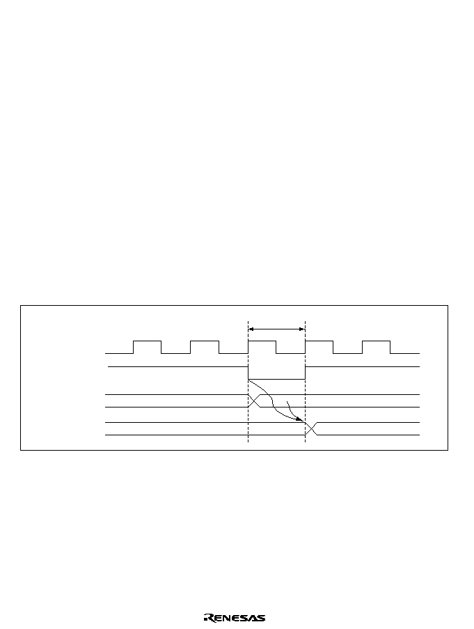
Rev. 1.0, 02/00, page 286 of 1141
14.3
Operation
Timer L is an 8-bit up/down counter.
The inputting clock for Timer L can be selected by the LMR2 to LMR0 bits of the LMR from the
choices of the internal clock (
/128 and
/64), DVCDG2, PB and REC-CTL.
Timer L is provided with three different types of operation modes, namely, the compare match
clear mode when controlled to the up-counting function, the auto reloading mode when controlled
to the down-counting function and the interval timer mode.
Respective operation modes and operation methods will be explained below.
14.3.1
Compare Match Clear Operation
When the LMR3 bit of the LMR is cleared to 0, timer L will be controlled to the up-counting
function.
When any other values than H'00 are written into the RCR, the LTC will be cleared to H'00
simultaneously before starting counting up.
Figure 14.2 shows RCR writing and LTC clearing timing. When the LTC value and the RCR
value match (compare match), the LTC readings will be cleared to H'00 to resume counting from
H'00.
Figure 14.3 indicated on the next page shows the compare match clear timing.
RCR
LTC
Write signal
1 state
N
H' 00
Figure 14.2 RCR Writing and LTC Clearing Timing Chart
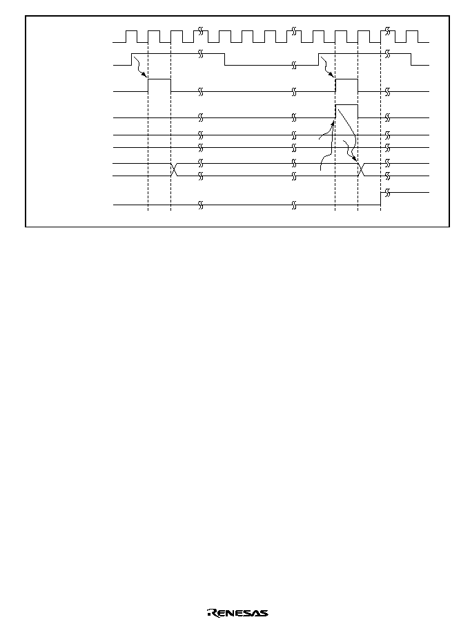
Rev. 1.0, 02/00, page 287 of 1141
LTC
RCR
N
H' 00
N-1
N
Interrupt
request
Count-up
signal
Compare match
clear signal
PB-CTL
Figure 14.3 Compare Match Clearing Timing Chart
(In case the rising edge of the PB-CTL is selected)

Rev. 1.0, 02/00, page 289 of 1141
Section 15 Timer R
15.1
Overview
Timer R consists of triple 8-bit down-counters. It carries VCR mode identification function and
slow tracking function in addition to the reloading function and event counter function.
15.1.1
Features
The Timer R consists of triple 8-bit reloading timers. By combining the functions of three units of
reloading timers/counters and by combining three units of timers, it can be used for the following
applications:
∑
Applications making use of the functions of three units of reloading timers.
∑
For identification of the VCR mode.
∑
For reel controls.
∑
For acceleration and braking of the capstan motor when being applied to intermittent
movements.
∑
Slow tracking mono-multi applications.
15.1.2
Block Diagram
Timer R consists of three units of reload timer counters, namely, two units of reload timer
counters equipped with capturing function (TMRU-1 and TMRU-2) and a unit of reload timer
counter (TMRU-3).
Figure 15.1 is a block diagram of timer R.
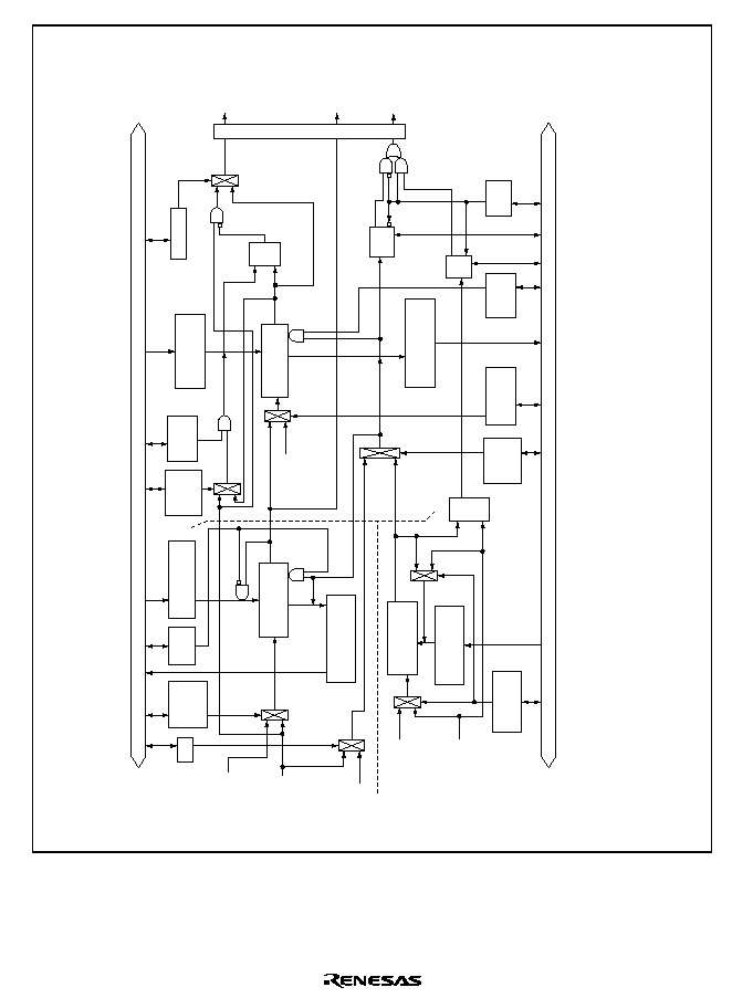
Rev. 1.0, 02/00, page 290 of 1141
Notes:
Internal bus
Internal bus
Clock sources
DVCTL
CFG
Clock
selection (2 bits)
Reloading register
(8 bits)
Down-counter
(8 bits)
Capture register
(8 bits)
TMRI2
Interrupt request
TMRI1
Interrupt
request
TMRI3
Interrupt
request
TMRU-1
TMRCP1
*2
Under≠
flow
TMRU-3
Underflow
*1
TMRL3
PS31,30
External signals
IRQ3
/1024
/2048
/4096
Clock source
/64
/128
/256
Clock sources
/4
/256
/512
Down-counter
(8 bits)
Latch
clock
selection
Clock
selection (2 bits)
Resetting Available/
Not
available
CP/
SLM
SLW
CAPF
Capture register
(8 bits)
Down-counter
(8 bits)
Reloading register
(8 bits)
Acceleration/
braking
Reloading Available/
not
available
Reloading
clock
selection
Reloading register
(8 bits)
RLD/
CAP
Clock
selection
(2 bits)
CPS
LAT
PS21,20
CLR2
Res
Res
TMRCP2
Under≠
flow
TMRU-2
CFG mask F/F
R
S
Q
R
S
Q
Acceleration
braking
AC/BR
TMRL2
RLD
RLCK
TMRL1
PS11,10
Interrupting circuit
1.
When the DVCTL is being used as the clock source, reloading will be made when the counter underflows and when
the dividing clock is being used as the clock source, reloading will be made by the DVCTL.
2.
When the LAT bit = 0, the capture signal against the TMRU-1 will not be output.
Figure 15.1 Block Diagram of Timer R

Rev. 1.0, 02/00, page 291 of 1141
15.1.3
Pin Configuration
Table 15.1 shows the pin configuration of timer R.
Table 15.1
Pin Configuration
Name
Abbrev.
I/O
Function
Input capture inputting pin
,54
Input
Input capture inputting for the Timer R
15.1.4
Register Configuration
Table 15.2 shows the register configuration of timer R.
Table 15.2
Register Configuration
Name
Abbrev.
R/W
Size
Initial Value
Address
Timer R mode register 1
TMRM1
R/W
Byte
H'00
H'D118
Timer R mode register 2
TMRM2
R/W
Byte
H'00
H'D119
Timer R control/status
register
TMRCS
R/W
Byte
H'03
H'D11F
Timer R capture register 1
TMRCP1
R
Byte
H'FF
H'D11A
Timer R capture register 2
TMRCP2
R
Byte
H'FF
H'D11B
Timer R load register 1
TMRL1
W
Byte
H'FF
H'D11C
Timer R load register 2
TMRL2
W
Byte
H'FF
H'D11D
Timer R load register 3
TMRL3
W
Byte
H'FF
H'D11E
Note: Memories of respective registers will be preserved even under the low power consumption
mode. Nonetheless, the CAPF flag and SLW flag of the TMRM2 will be cleared to 0.

Rev. 1.0, 02/00, page 292 of 1141
15.2
Register Descriptions
15.2.1
Timer R Mode Register 1 (TMRM1)
0
0
1
0
R/W
2
0
R/W
3
0
4
0
R/W
5
0
6
0
7
R/W
R/W
R/W
RLD
R/W
AC/BR
0
R/W
CLR2
RLCK
PS21
PS20
RLD/CAP
CPS
Bit :
Initial value :
R/W :
The timer R mode register 1 (TMRM1) works to control the acceleration and braking processes
and to select the inputting clock for the TMRU-2. This is an 8-bit read/write register.
When reset, the TMRM1 is initialized to H'00.
Bit 7
Selecting Clearing/Not Clearing of TMRU-2 (CLR2): This bit is used for selecting if
the TMRU-2 counter reading is to be cleared or not as it is captured.
Bit 7
CLR2
Description
0
TMRU-2 counter reading is not to be cleared as soon as it is captured. (Initial value)
1
TMRU-2 counter reading is to be cleared as soon as it is captured
Bit 6
Acceleration/Braking Processing (AC/BR): This bit works to control occurrences of
interrupt requests to detect completion of acceleration or braking while the capstan motor is
making intermittent revolutions.
For more information, see section 15.3.6, Acceleration and Braking Processes of the Capstan
Motor.
Bit 6
AC/BR
Description
0
Braking
(Initial value)
1
Acceleration

Rev. 1.0, 02/00, page 293 of 1141
Bit 5
Using/Not Using the TMRU-2 for Reloading (RLD): This bit is used for selecting if the
TMRU-2 reload function is to be turned on or not.
Bit 5
RLD
Description
0
Not using the TMRU-2 as the reload timer
(Initial value)
1
Using the TMRU-2 as the reload timer
Bit 4
Reloading Timing for the TMRU-2 (RLCK): This bit works to select if the TMRU-2 is
reloading by the CFG or by underflowing of the TMRU-2 counter. This choice is valid only when
the bit 5 (RLD) is being set to 1.
Bit 4
RLCK
Description
0
Reloading at the rising edge of the CFG
(Initial value)
1
Reloading by underflowing of the TMRU-2
Bits 3 and 2
Clock Source for the TMRU-2 (PS21 and PS20): These bits work to select the
inputting clock to the TMRU-2.
Bit 3
Bit 2
PS21
PS20
Description
0
Counting by underflowing of the TMRU-1
(Initial value)
0
1
Counting by the PSS,
/256
0
Counting by the PSS,
/128
1
1
Counting by the PSS,
/64
Bit 1
Operation Mode of the TMRU-1 (RLD/CAP): This bit works to select if the operation
mode of the TMRU-1 is reload timer mode or capture timer mode.
Under the capture timer mode, reloading operation will not be made. Also, the counter reading
will be cleared as soon as capture has been made.
Bit 1
RLD/CAP
Description
0
The TMRU-1 works as the reloading timer
(Initial value)
1
The TMRU-1 works as the capture timer

Rev. 1.0, 02/00, page 294 of 1141
Bit 0
Capture Signals of the TMRU-1 (CPS): In combination with the LAT bit (Bit 7) of the
TMR2, this bit works to select the capture signals of the TMRU-1. This bit becomes valid when
the LAT bit is being set to 1. It will also become valid when the RLD/CAP bit (Bit 1) is being set
to 1. Nonetheless, it will be invalid when the RLD/CAP bit (Bit 1) is being set to 0.
Bit 0
CPS
Description
0
Capture signals at the rising edge of the CFG
(Initial value)
1
Capture signals at the edge of the IRQ3
15.2.2
Timer R Mode Register 2 (TMRM2)
0
0
1
0
R/(W)*
2
0
R/W
3
0
4
0
R/W
5
0
6
0
7
R/(W)*
R/W
R/W
PS10
R/W
PS11
0
R/W
LAT
PS31
PS30
CP/SLM
CAPF
SLW
Bit :
Initial value :
R/W :
The timer R mode register 2 (TMRM2) is an 8-bit read/write register which works to identify the
operation mode and to control the slow tracking processing.
When reset, the TMRM2 is initialized to H'00.
Note: *
The CAPF bit and the SLW bit, respectively, works to latch the interrupt causes and
writing 0 only is valid. Consequently, when these bits are being set to 1, respective
interrupt requests will not be issued. Therefore, it is necessary to check these bits
during the course of the interrupt processing routine to have them cleared.
Also, priority is given to the set and, when an interrupt cause occur while the a clearing
command (BCLR, MOV, etc.) is being executed, the CAPF bit and the SLW bit will
not be cleared respectively and it thus becomes necessary to pay attention to the
clearing timing.

Rev. 1.0, 02/00, page 295 of 1141
Bit 7
Capture Signals of the TMRU-2 (LAT): In combination with the CPS bit (Bit 0) of the
TMRM1, this bit works to select the capture signals of the TMRU-2.
TMRM2
TMRM1
Bit 7
Bit 0
LAT
CPS
Description
0
*
Captures when the TMRU-3 underflows
(Initial value)
0
Captures at the rising edge of the CFG
1
1
Captures at the edge of the IRQ3
Note:
*
Don't care.
Bits 6 and 5
Clock Source for the TMRU-1 (PS11 and PS10): These bits work to select the
inputting clock to the TMRU-1.
Bit 6
Bit 5
PS11
PS10
Description
0
Counting at the rising edge of the CFG
(Initial value)
0
1
Counting by the PSS,
/4
0
Counting by the PSS,
/256
1
1
Counting by the PSS,
/512
Bits 4 and 3
Clock Source for the TMRU-3 (PS31 and PS30)
These bits work to select the inputting clock to the TMRU-3.
Bit 4
Bit 3
PS31
PS30
Description
0
Counting at the rising edge of the DVCTL from the dividing circuit.
(Initial value)
0
1
Counting by the PSS,
/4096
0
Counting by the PSS,
/2048
1
1
Counting by the PSS,
/1024

Rev. 1.0, 02/00, page 296 of 1141
Bit 2
Interrupt Causes (CP/SLM): This bit works to select the interrupt causes for the TMRI3.
Bit 2
CP/SLM
Description
0
Makes interrupt requests upon the capture signals of the TMRU-2 valid (Initial value)
1
Makes interrupt requests upon ending of the slow tracking mono-multi valid
Bit 1
Capture Signal Flag (CAPF): This is a flag being set out by the capture signal of the
TMRU-2. Although both reading/writing are possible, 0 only is valid for writing.
Also, priority is being given to the set and, when the capture signal and writing 0 occur
simultaneously, this flag bit remains being set to 1 and the interrupt request will not be issued and
it is necessary to be attentive about this fact.
When the CP/SLM bit (bit 2) is being set to 1, this CAPF bit should always be set to 0.
The CAPF flag is cleared to 0 under the low power consumption mode.
Bit 1
CAPF
Description
0
[Clearing conditions]
(Initial value)
When 0 is written after reading 1
1
[Setting conditions]
At occurrences of the TMRU-2 capture signals while the CP/SLM bit is set to 0
Bit 0
Slow Tracking Mono-multi Flag (SLW): This is a flag being set out when the slow
tracking mono-multi processing ends. Although both reading/writing are possible, 0 only is valid
for writing.
Also, priority is being given to the set and, when ending of the slow tracking mono-multi
processing and writing 0 occur simultaneously, this flag bit remains being set to 1 and the interrupt
request will not be issued and it is necessary to be attentive about this fact.
When the CP/SLM bit (bit 2) is being set to 0, this SLW bit should always be set to 0.
The SLW flag is cleared to 0 under the low power consumption mode.
Bit 0
SLW
Description
0
[Clearing conditions]
(Initial value)
When 0 is written after reading 1
1
[Setting conditions]
When the slow tracking mono-multi processing ends while the CP/SLM bit is set to 1

Rev. 1.0, 02/00, page 297 of 1141
15.2.3
Timer R Control/Status Register (TMRCS)
0
1
1
--
--
--
--
1
2
0
R/(W)*
3
0
4
0
R/(W)*
5
0
6
0
7
R/(W)*
R/W
TMRI1E
R/W
TMRI2E
0
R/W
TMRI3E
TMRI3
TMRI2
TMRI1
Note: * Only 0 can be written to clear the flag.
Bit :
Initial value :
R/W :
The timer R control/status register (TMRCS) works to control the interrupts of timer R.
The TMRCS is an 8-bit read/write register. When reset, the TMRCS is initialized to H'03.
Bit 7
Enabling the TMRI3 Interrupt (TMRI3E): This bit works to permit/prohibit occurrence
of the TMRI3 interrupt when an interrupt cause being selected by the CP/SLM bit of the TMRM2
has occurred, such as occurrences of the TMRU-2 capture signals or when the slow tracking
mono-multi processing ends, and the TMRI3 has been set to 1.
Bit 7
TMRI3E
Description
0
Prohibits occurrences of TMRI3 interrupts
(Initial value)
1
Permits occurrences of TMRI3 interrupts
Bit 6
Enabling the TMRI2 Interrupt (TMRI2E): This bit works to permit/prohibit occurrence
of the TMRI2 interrupt when the TMRI2 has been set to 1 by issuance of the underflow signal of
the TMRU-2 or by ending of the slow tracking mono-multi processing.
Bit 6
TMRI2E
Description
0
Prohibits occurrences of TMRI2 interrupts
(Initial value)
1
Permits occurrences of TMRI2 interrupts

Rev. 1.0, 02/00, page 298 of 1141
Bit 5
Enabling the TMRI1 Interrupt (TMRI1E): This bit works to permit/prohibit occurrence
of the TMRI1 interrupt when the TMRI1 has been set to 1 by issuance of the underflow signal of
the TMRU-1.
Bit 5
TMRI1E
Description
0
Prohibits occurrences of TMRI1 interrupts
(Initial value)
1
Permits occurrences of TMRI1 interrupts
Bit 4
TMRI3 Interrupt Requesting Flag (TMRI3): This is the TMRI3 interrupt requesting
flag.
It indicates occurrence of an interrupt cause being selected by the CP/SLM bit of the TMRM2,
such as occurrences of the TMRU-2 capture signals or ending of the slow tracking mono-multi
processing.
Bit 4
TMRI3
Description
0
[Clearing conditions]
(Initial value)
When 0 is written after reading 1
1
[Setting conditions]
At occurrence of the interrupt cause being selected by the CP/SLM bit of the TMRM2
Bit 3
TMRI2 Interrupt Requesting Flag (TMRI2): This is the TMRI2 interrupt requesting
flag.
It indicates occurrences of the TMRU-2 underflow signals or ending of the acceleration/braking
processing of the capstan motor.
Bit 3
TMRI2
Description
0
[Clearing conditions]
(Initial value)
When 0 is written after reading 1
1
[Setting conditions]
At occurrences of the TMRU-2 underflow signals or ending of the acceleration
/braking processing of the capstan motor

Rev. 1.0, 02/00, page 299 of 1141
Bit 2
TMRI1 Interrupt Requesting Flag (TMRI1): This is the TMRI1 interrupt requesting
flag.
It indicates occurrences of the TMRU-1 underflow signals.
Bit 2
TMRI1
Description
0
[Clearing conditions]
(Initial value)
When 0 is written after reading 1.
1
[Setting conditions]
When the TMRU-1 underflows.
Bits 1 and 0
Reserved: These bits cannot be modified and are always read as 1.
15.2.4
Timer R Capture Register 1 (TMRCP1)
0
1
1
1
2
1
3
1
4
1
5
1
6
1
7
1
R
TMRC17
R
TMRC16
R
TMRC15
R
TMRC14
R
TMRC13
R
TMRC12
R
TMRC11
R
TMRC10
Bit :
Initial value :
R/W :
The timer R capture register 1 (TMRCP1) works to store the captured data of the TMRU-1.
During the course of the capturing operation, the TMRU-1 counter readings are captured by the
TMRCP1 at the CFG edge or the IRQ3 edge. The capturing operation of the TMRU-1 is
performed using 16 bits, in combination with the capturing operation of the TMRU-2.
The TMRCP1 is an 8-bit read only register. When reset, the TMRCS is initialized to H'FF.
Notes: 1. When the TMRCP1 is readout while the capture signal is being received, the reading
data become unstable. Pay attention to the timing for reading out.
2. When a shift to the low power consumption mode is made while the capturing
operating is in progress, the counter reading becomes unstable. After returning to the
active mode, always write H'FF into the TMRL1 to initialize the counter.

Rev. 1.0, 02/00, page 300 of 1141
15.2.5
Timer R Capture Register 2 (TMRCP2)
0
1
1
1
2
1
3
1
4
1
5
1
6
1
7
1
R
TMRC27
R
TMRC26
R
TMRC25
R
TMRC24
R
TMRC23
R
TMRC22
R
TMRC21
R
TMRC20
Bit :
Initial value :
R/W :
The timer R capture register 2 (TMRCP2) works to store the capture data of the TMRU-2. At
each CFG edge, IRQ3 edge, or at occurrence of underflow of the TMRU-3, the TMRU-2 counter
readings are captured by the TMRCP2.
The TMRCP2 is an 8-bit read only register. When reset, the TMRCS will be initialized into H'FF.
Notes: 1. When the TMRCP2 is readout while the capture signal is being received, the reading
data become unstable. Pay attention to the timing for reading out.
2. When a shift to the low power consumption mode is made, the counter reading
becomes unstable. After returning to the active mode, always write H'FF into the
TMRL2 to initialize the counter.
15.2.6
Timer R Load Register 1 (TMRL1)
0
1
1
1
2
1
3
1
4
1
5
1
6
1
7
1
W
TMR17
W
TMR16
W
TMR15
W
TMR14
W
TMR13
W
TMR12
W
TMR11
W
TMR10
Bit :
Initial value :
R/W :
The timer R load register 1 (TMRL1) is an 8-bit write-only register which works to set the load
value of the TMRU-1.
When a load value is set to the TMRL1, the same value will be set to the TMRU-1 counter
simultaneously and the counter starts counting down from the set value. Also, when the counter
underflows during the course of the reload timer operation, the TMRL1 value will be set to the
counter.
When reset, the TMRL1 is initialized to H'FF.

Rev. 1.0, 02/00, page 301 of 1141
15.2.7
Timer R Load Register 2 (TMRL2)
0
1
1
1
2
1
3
1
4
1
5
1
6
1
7
1
W
TMR27
W
TMR26
W
TMR25
W
TMR24
W
TMR23
W
TMR22
W
TMR21
W
TMR20
Bit :
Initial value :
R/W :
The timer R load register 2 (TMRL2) is an 8-bit write only register which works to set the load
value of the TMRU-2.
When a load value is set to the TMRL2, the same value will be set to the TMRU-2 counter
simultaneously and the counter starts counting down from the set value. Also, when the counter
underflows or a CFG edge is detected during the course of the reload timer operation, the TMRL2
value will be set to the counter.
When reset, the TMRL2 is initialized to H'FF.
15.2.8
Timer R Load Register 3 (TMRL3)
0
1
1
1
2
1
3
1
4
1
5
1
6
1
7
1
W
TMR37
W
TMR36
W
TMR35
W
TMR34
W
TMR33
W
TMR32
W
TMR31
W
TMR30
Bit :
Initial value :
R/W :
The timer R load register 3 (TMRL3) is an 8-bit write only register which works to set the load
value of the TMRU-3.
When a load value is set to the TMRL3, the same value will be set to the TMRU-3 counter
simultaneously and the counter starts counting down from the set value. Also, when the counter
underflows or a DVCTL edge is detected, the TMRL2 value will be set to the counter. (Reloading
will be made by the underflowing signals when the DVCTL signal is selected as the clock source,
and reloading will be made by the DVCTL signals when the dividing clock is selected as the clock
source.)
When reset, the TMRL3 is initialized to H'FF.

Rev. 1.0, 02/00, page 302 of 1141
15.2.9
Module Stop Control Register (MSTPCR)
7
1
MSTP15
R/W
MSTPCRH
6
1
MSTP14
R/W
5
1
MSTP13
R/W
4
1
MSTP12
R/W
3
1
MSTP11
R/W
2
1
MSTP10
R/W
1
1
MSTP9
R/W
0
1
MSTP8
R/W
7
1
MSTP7
R/W
6
1
MSTP6
R/W
5
1
MSTP5
R/W
4
1
MSTP4
R/W
3
1
MSTP3
R/W
2
1
MSTP2
R/W
1
1
MSTP1
R/W
0
1
MSTP0
R/W
MSTPCRL
Bit :
Initial value :
R/W :
The MSTPCR are 8-bit read/write twin registers which work to control the module stop mode.
When the MSTP11 bit is set to 1, timer R stops its operation at the ending point of the bus cycle to
shift to the module stop mode. For more information, see section 4.5, Module Stop Mode.
When reset, the MSTPCR is initialized to H'FFFF.
Bit 3
Module Stop (MSTP11): This bit works to designate the module stop mode for the Timer
R.
MSTPCRH
Bit 3
MSTP11
Description
0
Cancels the module stop mode of timer R
1
Sets the module stop mode of timer R
(Initial value)

Rev. 1.0, 02/00, page 303 of 1141
15.3
Operation
15.3.1
Reload Timer Counter Equipped with Capturing Function TMRU-1
TMRU-1 is a reload timer counter equipped with capturing function. It consists of an 8-bit down-
counter, a reloading register and a capture register.
The clock source can be selected from among the leading edge of the CFG signals and three types
of dividing clocks. It is also selectable whether using it as a reload counter or as a capture counter.
Even when the capturing function is selected, the counter readings can be updated by writing the
values into the reloading register.
When the counter underflows, the TMRI1 interrupt request will be issued.
The initial values of the TMRU-1 counter, reloading register and capturing register are all H'FF.
∑
Operation of the Reload Timer
When a value is written into to the reloading register, the same value will be written into the
counter simultaneously. Also, when the counter underflows, the reloading register value will
be reloaded to the counter. The TMRU-1 is a dividing circuit for the CFG. In combination
with the TMRU-2 and TMRU-3, it can also be used for the mode identification purpose.
∑
Capturing Operation
Capturing operation is carried out in combination with the TMRU-2 using the combined 16
bits. It can be so programmed that the counter may be cleared by the capture signal. The CFG
edges or IRQ3 edges are used as the capture signals. It is possible to issue the TMRI3
interrupt request by the capture signal.
In addition to the capturing function being worked out in combination with the TMRU-2, the
TMRU-1 can be used as a 16-bit CFG counter. Selecting the IRQ3 as the capture signal, the
CFG within the duration of the reel pulse being input into the
,54 pin can be counted by the
TMRU-1.

Rev. 1.0, 02/00, page 304 of 1141
15.3.2
Reload Timer Counter Equipped with Capturing Function TMRU-2
TMRU-2 is a reload timer counter equipped with capturing function. It consists of an 8-bit down-
counter, a reloading register and a capture register.
The clock source can be selected from among the undedrflowing signal of the TMRU-1 and three
types of dividing clocks. Also, although the reloading function is workable during its capturing
operation, equipping or not of the reloading function is selectable. Even when without-reloading-
function is chosen, the counter reading can be updated by writing the values to the reloading
register.
When the counter underflows, the TMRI2 interrupt request will be issued.
The initial values of the TMRU-2 counter, reloading register and capturing register are all H'FF.
∑
Operation of the Reload Timer
When a value is written into to the reloading register, the same value will be written into the
counter, simultaneously. Also, when the counter underflows or when a CFG edge is detected,
the reloading register value will be reloaded to the counter.
The TMRU-2 can make acceleration and braking work for the capstan motor using the reload
timer operation.
∑
Capturing Operation
Using the capture signals, the counter reading can be latched into the capturing register. As the
capture signal, you can choose from among edges of the CFG, edges of the IRQ3 or the
underflow signals of the TMRU-3. It is possible to issue the TMRI3 interrupt request by the
capture signal.
The capturing function (stopping the reloading function) of the TMRU-2, in combination with
the TMRU-1 and TMRU-3, can also be used for the mode identification purpose.
15.3.3
Reload Counter Timer TMRU-3
The reload counter timer TMRU-3 consists of an 8-bit down-counter and a reloading register. Its
clock source can be selected from between the undedrflowing signal of the counter and the edges
of the DVCTL signals. (When the DVCTL signal is selected as the clock source, reloading will be
effected by the underflowing signals and when the dividing clock is selected as the clock source,
reloading will be effected by the DVCTL signals.) The reloading signal works to reload the
reloading register value into the counter. Also, when a value is written into to the reloading
register, the same value will be written into the counter, simultaneously.
The initial values of the counter and the reloading register are H'FF.
The underflowing signals can be used as the capturing signal for the TMRU-2.
The TMRU-3 can also be used as a dividing circuit for the DVCTL. Also, in combination with
the TMRU-1 and TMRU-2 (capturing function), the TMRU-3 can be used for the mode
identification purpose. Since the divided signals of the DVCTL are being used as the clock
source, CTL signals (DVCTL) conforming to the double speed can be input when making

Rev. 1.0, 02/00, page 305 of 1141
searches. These DVCTL signals can also be used for phase controls of the capstan motor.
Also, by selecting the dividing clock as the clock source, it is possible to make a delay with the
edges of the DVCTL to provide the slow tracking mono-multi function.
15.3.4
Mode Identification
When making mode identification (2/4/6 identification) of the SP/LP/EP modes of reproducing
tapes, the TMRU-1 (CFG dividing circuit), TMRU-2 (capturing function/without reloading
function) and TMRU-3 (DVCTL dividing circuit) of timer R should be used.
Timer R will become to the aforementioned status after a reset.
Under the aforementioned status, the divided CFG should be written into the reloading register of
the TMRU-1 and divided DVCTL should be written into the reloading register of the TMRU-3.
When the TMRU-3 underflows, the counter value of the TMRU-2 is captured. Such capturing
register value represents the number of the CFG within the DVCTL cycle.
As aforementioned, the Timer R can work to count the number of the CFG corresponding to n
times of DVCTL's or to identify the mode being searched.
For register settings, see section 15.5.1, Mode Identification.
15.3.5
Reeling Controls
CFG counts can be captured by making 16-bit capturing operation combining the TMRU-1 and
TMRU-2. Choosing the IRQ3 as the capture signal and counting the CFG within the duration of
the reel pulse being input through the
,54 pin affect reeling controls. For register settings, see
section 15.5.2, Reeling Controls.
15.3.6
Acceleration and Braking Processes of the Capstan Motor
When making intermittent movements such as those for slow reproductions or for still
reproductions, it is necessary to conduct quick accelerations and abrupt stoppings of the capstan
motor. The acceleration and braking processes functions to check if the revolution of a capstan
motor has reached the prescribed rate when accelerated or braked. For this purpose, the TMRU-2
(reloading function) should be used.
When making accelerations:
∑
Set the AC/BR bit of the TMRM1 to acceleration (set to 1). Also, use the rising edge of the
CFG as the reloading signal.
∑
Set the prescribed time on the CFG frequency to determine if the acceleration has been
finished, into the reloading register.
∑
The TMRU-2 will work to down-count the reloading data.
∑
In case the acceleration has not been finished (in case the CFG signal is not input even when
the prescribed time has elapsed = underflowing of down-counting has occurred), such

Rev. 1.0, 02/00, page 306 of 1141
underflowing works to set to CFG mask F/F (masking movement) and the reload timer will be
cleared by the CFG.
∑
When the acceleration has been finished (when the CFG signal is input before the prescribed
time has elapsed = reloading movement has been made before the down counter underflows),
an interrupt request will be issued because of the CFG.
When making breaking:
∑
Set the AC/BR bit of the TMRM1 to braking (clear to 0). Also, use the rising edge of the CFG
as the reloading signal.
∑
Set the prescribed time on the CFG frequency to determine if the braking has been finished,
into the reloading register.
∑
The TMRU-2 will work to down-count the reloading data.
∑
If the braking has not finished (when the CFG signal is input before the prescribed time has
elapsed and reloading movement has been made before the down counter underflows), the
reload timer movement will continue.
∑
When the acceleration has finished (when the CFG signal is not input even when the
prescribed time has elapsed and underflowing of down-counting has occurred), interrupt
request will be issued because of the underflowing signal.
The acceleration and braking processes should be employed when making special reproductions,
in combination with the slow tracking mono-multi function outlined in section 15.3.7.
For register settings, see section 15.5.4, Acceleration and Braking Processes of the Capstan Motor.
15.3.7
Slow Tracking Mono-Multi Function
When performing slow reproductions or still reproductions, the braking timing for the capstan
motor is determined by use of the edge of the DVCTL signal. The slow tracking mono-multi
function works to measure the time from the rising edge of the DVCTL signal down to the desired
point to issue the interrupt request. In actual programming, this interrupt should be used to
activate the brake of the capstan motor. The TMRU-3 should be used to perform time
measurements for the slow tracking mono-multi function. Also, the braking process can be made
using the TMRU-2. Figure 15.2 shows the time series movements when a slow reproduction is
being performed.
For register settings, see section 15.5.3, Slow Tracking Mono-Multi Function.
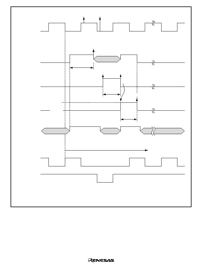
Rev. 1.0, 02/00, page 307 of 1141
HSW
FG acceleration detection
Compensation for vertical vibrations
(Supplementary V-pulse)
DVCTL
Interrupt
Reloading
Reverse
rotation
Frame feeds
Compensation for
horizontal vibrations
Compensation for
horizontal vibrations
Braking
process
Acceleration
process
Slow tracking
delay
C.Rotary
H.AmpSW
Accelerating the
capstan motor
Braking the
drum motor
Slow tracking
mono-multi
Braking the
capstan motor
Servo
Hi-Z
[Legend]
Hi-Z : High impedance state
In case of 4-head SP mode.
In case of 2-head application, H.AmpSW and
C.Rotary should be "Low".
FG stopping detection
Forward
rotation
Figure 15.2 Time Series Movements when a Slow Reproduction
Is Being Performed

Rev. 1.0, 02/00, page 308 of 1141
15.4
Interrupt Cause
In timer R, bits TMRI1 to TMRI3 of the timer R control/status register cause interrupts. The
following are descriptions of the interrupts.
1. Interrupts caused by the underflowing of the TMRU-1 (TMRI1)
These interrupts will constitute the timing for reloading with the TMRU-1.
2. Interrupts caused by the underflowing of the TMRU-2 or by an end of the acceleration or
braking process (TMRI2)
When interrupts occur at the reload timing of the TMRU-2, clear the AC/BR
(acceleration/braking) bit of the timer R mode register 1 (TMRM1) to 0.
3. Interrupts caused by the capture signals of the TMRU-2 and by ending the slow tracking
mono-multi process (TMRI3)
Since these two interrupt causes are constituting the OR, it becomes necessary to determine
which interrupt cause is occurring using the software.
Respective interrupt causes are being set to the CAPF flag or the SLW flag of the timer R
mode register 2 (TMRM2), have the software determine which.
Since the CAPF flag and the SLW flag will not be cleared automatically, program the software
to clear them. (Writing 0 only is valid for these flags.) Unless these flags are cleared,
detection of the next cause becomes unworkable. Also, if the CP/SLM bit is changed leaving
these flags uncleared as they are, these flags will get cleared.

Rev. 1.0, 02/00, page 309 of 1141
15.5
Settings for Respective Functions
15.5.1
Mode Identification
When making mode identification (2/4/6 identification) of the SP/LP/EP modes of reproducing
tapes, the TMRU-1 (CFG dividing circuit), TMRU-2 (capturing function/without reloading
function) and TMRU-3 (DVCTL dividing circuit) of the timer R should be used.
Timer R will be initialized to this mode identification status after a reset.
Under this status, the divided CFG should be written into the reloading register of the TMRU-1
and divided DVCTL should be written into the reloading register of the TMRU-3. When the
TMRU-3 underflows, the counter value of the TMRU-2 is captured. Such capturing register value
represents the number of the CFG within the DVCTL cycle.
Thus, timer R can work to count the number of the CFG corresponding to n times of DVCTL's or
to identify the mode being searched.
Settings
∑
Setting the timer R mode register 1 (TMRM1)
CLR2 bit (bit 7) = 1: Works to clear after making the TMRU-2 capture.
RLD bit (bit 5) = 0: Sets the TMRU-3 without reloading function.
PS21 and PS20 (bits 3 and 2) = (0 and 0): The underflowing signals of the TMRU-1 are to
be used as the clock source for the TMRU-2.
RLD/CAP bit (bit 1) = 0: The TMRU-1 has been set to make the reload timer operation.
∑
Setting the timer R mode register 2 (TMRM2)
LAT bit (bit 7) = 0: The underflowing signals of the TMRU-3 are to be used as the capture
signal for the TMRU-2.
PS11 and PS10 (bits 6 and 5) = (0 and 0): The leading edge of the CFG signal is to be used
as the clock source for the TMRU-1.
PS31 and PS30 (bits 4 and 3) = (0 and 0): The leading edge of the DVCTL signal is to be
used as the clock source for the TMRU-3.
CP/SLM bit (bit 2) = 0: The capture signal is to work to issue the TMRI3 interrupt request.
∑
Setting the timer R load register 1 (TMRL1)
Set the dividing value for the CFG. The set value should become (n
-
1) when divided by
n.
∑
Setting the timer R load register 3 (TMRL3)
Set the dividing value for the DVCTL. The set value should become (n
-
1) when divided
by n.

Rev. 1.0, 02/00, page 310 of 1141
15.5.2
Reeling Controls
CFG counts can be captured by making 16-bit capturing operation combining the TMRU-1 and
TMRU-2. By choosing the IRQ3 as the capture signal, and by counting the CFG within the
duration of the reel pulse being input through the
,54 pin, reeling controls, etc. can be effected.
Settings
∑
Setting P13/
,54 pin as the ,54 pin
Set the PMR13 bit (bit 3) of the port mode register 1 (PMR1) to 1. See section 10.3.2, Port
Mode Register (PMR1).
∑
Setting the timer R mode register 1 (TMRM1)
CLR2 bit (bit 7) = 1: Works to clear after making the TMRU-2 capture.
PS21 and PS20 (bits 3 and 2) = (0 and 0): The underflowing signals of the TMRU-1 are to
be used as the clock source for the TMRU-2.
RLD/CAP bit (bit 1) = 1: The TMRU-1 has been set to make the capturing operation.
CPS bit (bit 0) = 1: The edge of the IRQ3 signal is to be used as the capture signal for the
TMRU-1 and TMRU-2.
∑
Setting the timer R mode register 2 (TMRM2)
LAT bit (bit 7) = 1: The edge of the IRQ3 signal is to be used as the capture signal for the
TMRU-1 and TMRU-2.
PS11 and PS10 (bits 6 and 5) = (0 and 0): The rising edge of the CFG signal is to be used
as the clock source for the TMRU-1.
CP/SLM bit (bit 2) = 0: The capture signal is to work to issue the TMRI3 interrupt request.
15.5.3
Slow Tracking Mono-Multi Function
When performing slow reproductions or still reproductions, the braking timing for the capstan
motor is determined by use of the edge of the DVCTL signal. The slow tracking mono-multi
function works to measure the time from the leading edge of the DVCTL signal down to the
desired point to issue the interrupt request. In actual programming, this interrupt should be used to
activate the brake of the capstan motor. The TMRU-3 should be used to perform time
measurements for the slow tracking mono-multi function. Also, the braking process can be made
using the TMRU-2.

Rev. 1.0, 02/00, page 311 of 1141
Settings
∑
Setting the timer R mode register 2 (TMRM2)
PS31 and PS30 (bits 4 and 3) = Other than (0, 0): The dividing clock is to be used as the
clock source for the TMRU-3.
CP/SLM bit (bit 2) = 1: The slow tracking delay signal is to work to issue the TMRI3
interrupt request.
∑
Setting the timer R load register 3 (TMRL3)
Set the slow tracking delay value. When the delay count is n, the set value should be
(n - 1).
Regarding the delaying duration, see figure 15.2.
15.5.4
Acceleration and Braking Processes of the Capstan Motor
When making intermittent movements such as those for slow reproductions or for still
reproductions, it is necessary to conduct quick accelerations and abrupt stoppings of the capstan
motor. The acceleration and braking processes will function to check if the revolution of a capstan
motor has reached the prescribed rate when accelerated or braked. For this purpose, the TMRU-2
(reloading function) should be used.
The acceleration and braking processes should be employed when making special reproductions,
in combination with the slow tracking mono-multi function.
Settings for the acceleration process
∑
Setting the timer R mode register 1 (TMRM1)
AC/BR bit (bit 6) = 1: Acceleration process
RLD bit (bit 5) = 1: The TMRU-2 is to be used as the reload timer.
RLCK bit (bit 4) = 0: The TMRU-2 is to reload at the rising edge of the CFG.
PS21 and PS20 (bits 3 and 2) = Other than (0, 0): The dividing clock is to be used as the
clock source for the TMRU-2.
∑
Setting the timer R load register 2 (TMRL2)
Set the count reading for the duration until the acceleration process finishes. When the
count is n, the set value should be (n
-
1).
Regarding the duration until the acceleration process finishes, see figure 15.2.
Settings for the braking process
∑
Setting the timer R mode register 1 (TMRM1)
AC/BR bit (bit 6) = 0: Braking process
RLD bit (bit 5) = 1: The TMRU-2 is to be used as the reload timer.
RLCK bit (bit 4) = 0: The TMRU-2 is to reload at the rising edge of the CFG.

Rev. 1.0, 02/00, page 312 of 1141
PS21 and PS20 (bits 3 and 2) = Other than (0, 0): The dividing clock is to be used as the
clock source for the TMRU-2.
∑
Setting the timer R load register 2 (TMRL2)
Set the count reading for the duration until the braking process finishes. When the count is
n, the set value should be (n - 1).
Regarding the duration until the braking process finishes, see figure 15.2.

Rev. 1.0, 02/00, page 313 of 1141
Section 16 Timer X1
16.1
Overview
Timer X1 is capable of outputting two different types of independent waveforms using a 16-bit
free running counter (FRC) as the basic means and it is also applicable to measurements of the
durations of input pulses and the cycles external clocks.
16.1.1
Features
Timer X1 has the following features:
∑
Four different types of counter inputting clocks.
Three different types of internal clocks (
/4,
/16 and
/64) and the DVCFG.
∑
Two independent output comparing functions
Capable of outputting two different types of independent waveforms.
∑
Four independent input capturing functions
The rising edge or falling edge can be selected for use. The buffer operation can also be
designated.
∑
Counter clearing designation is workable.
The counter readings can be cleared by compare match A.
∑
Seven types of interrupt causes
Comparing match
◊
2 causes, input capture
◊
4 causes and overflow
◊
1 cause are available for
use and they can make respective interrupt requests independently.
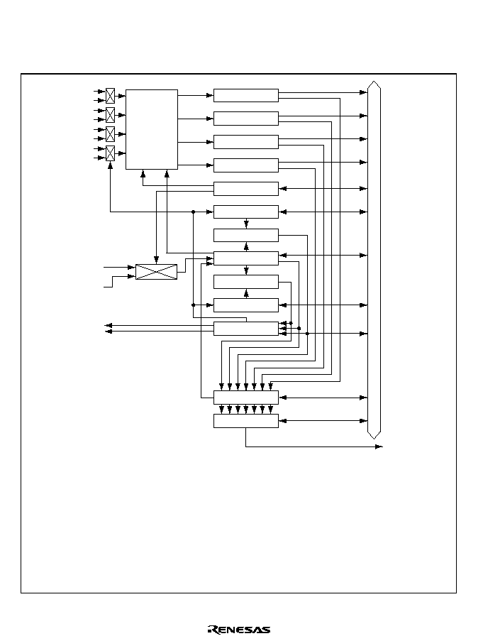
Rev. 1.0, 02/00, page 314 of 1141
16.1.2
Block Diagram
Figure 16.1 shows a block diagram of the Timer X1.
Internal data bus
[Legend]
TIER
ICRA
ICRB
ICRC
ICRD
TCRX
OCRB
Comparison circuit
FRC
Comparison circuit
OCRA
TOCR
TCSRX
TIER
Input
capture
control
Output comparing output
Interrupt
request
◊
7
FTOA
FTOB
FTIA*
(HSW)
FTIB*
(VD)
FTIC*
(DVCTL)
FTID*
(NHSW)
(DVCFG)
/ 4
/ 16
/ 64
TCSRX
FRC
OCRA
OCRB
TCRX
TOCR
ICRA
ICRB
ICRC
ICRD
: Timer interrupt enabling register
: Timer control/status register X
: Free running counter
: Output comparing register A
: Output comparing register B
: Timer control register X
: Output comparing control register
: Input capture register A
: Input capture register B
: Input capture register C
: Input capture register D
Note: * stands for the external terminal.
( ) stands for the internal signal.
Figure 16.1 Block Diagram of Timer X1

Rev. 1.0, 02/00, page 315 of 1141
16.1.3
Pin Configuration
Table 16.1 shows the pin configuration of timer X1.
Table 16.1
Pin Configuration
Name
Abbrev.
I/O
Function
Output comparing A output-pin
FTOA
Output
Output pin for the output comparing A
Output comparing B output-pin
FTOB
Output
Output pin for the output comparing B
Input capture A input-pin
FTIA
Input
Input-pin for the input capture A
Input capture B input-pin
FTIB
Input
Input-pin for the input capture B
Input capture C input-pin
FTIC
Input
Input-pin for the input capture C
Input capture D input-pin
FTID
Input
Input-pin for the input capture D

Rev. 1.0, 02/00, page 316 of 1141
16.1.4
Register Configuration
Table 16.2 shows the register configuration of timer X1.
Table 16.2
Register Configuration
Name
Abbrev.
R/W
Initial Value
Address
*3
Timer interrupt enabling register
TIER
R/W
H'00
H'D100
Timer control/status register X
TCSRX
R/ (W)
*1
H'00
H'D101
Free running counter H
FRCH
R/W
H'00
H'D102
Free running counter L
FRCL
R/W
H'00
H'D103
Output comparing register AH
OCRAH
R/W
H'FF
H'D104
*2
Output comparing register AL
OCRAL
R/W
H'FF
H'D105
*2
Output comparing register BH
OCRBH
R/W
H'FF
H'D104
*2
Output comparing register BL
OCRBL
R/W
H'FF
H'D105
*2
Timer control register X
TCRX
R/W
H'00
H'D106
Timer output comparing control register
TOCR
R/W
H'00
H'D107
Input capture register AH
ICRAH
R
H'00
H'D108
Input capture register AL
ICRAL
R
H'00
H'D109
Input capture register BH
ICRBH
R
H'00
H'D10A
Input capture register BL
ICRBL
R
H'00
H'D10B
Input capture register CH
ICRCH
R
H'00
H'D10C
Input capture register CL
ICRCL
R
H'00
H'D10D
Input capture register DH
ICRDH
R
H'00
H'D10E
Input capture register DL
ICRDL
R
H'00
H'D10F
Notes: 1. Only 0 can be written to clear the flag for Bits 7 to 1. Bit 0 is readable/writable.
2. The addresses of the OCRA and OCRB are the same. Changeover between them are
to be made by use of the TOCR bit and OCRS bit.
3. Lower 16 bits of the address.
Rev. 1.0, 02/00, page 317 of 1141
16.2
Register Descriptions
16.2.1
Free Running Counter (FRC)
Free running counter H (FRCH)
Free running counter L (FRCL)
0
3
0
R/W
5
0
R/W
7
0
9
0
R/W
11
0
13
0
15
R/W
R/W
R/W
0
R/W
R/W
1
0
2
0
R/W
4
0
R/W
6
0
8
0
R/W
10
0
12
0
14
FRC
FRCH
FRCL
R/W
R/W
R/W
R/W
0
R/W
0
Bit :
Initial value :
R/W :
The FRC is a 16-bit read/write up-counter which counts up by the inputting internal clock/external
clock. The inputting clock is to be selected from the CKS1 and CKS0 of the TCRX.
By the setting of the CCLRA bit of the TCSRX, the FRC can be cleared by comparing match A.
When the FRC overflows (H'FFFF
H'0000), the OVF of the TCSRX will be set to 1.
At this time, when the OVIE of the TIER is being set to 1, an interrupt request will be issued to the
CPU.
Reading/writing can be made from and to the FRC through the CPU at 8-bit or 16-bit.
The FRC is initialized to H'0000 when reset or under the standby mode, watch mode, subsleep
mode, module stop mode or subactive mode.
Rev. 1.0, 02/00, page 318 of 1141
16.2.2
Output Comparing Registers A and B (OCRA and OCRB)
Output comparing register AH and BH (OCRAH and OCRBH)
Output comparing register AL and BL (OCRAL and OCRBL)
1
3
1
R/W
5
1
R/W
7
1
9
1
R/W
11
1
13
1
15
R/W
R/W
R/W
1
R/W
R/W
1
1
2
1
R/W
4
1
R/W
6
1
8
1
R/W
10
1
12
1
14
OCRA, OCRB
OCRAH, OCRBH
OCRAL, OCRBL
R/W
R/W
R/W
R/W
1
R/W
0
Bit :
Initial value :
R/W :
The OCR consists of twin 16-bit read/write registers (OCRA and OCRB). The contents of the
OCR are always being compared with the FRC and, when the value of these two match, the OCFA
and OCRB of the TCSRX will be set to 1. At this time, if the OCIAE and OCIB of the TIER are
being set to 1, an interrupt request will be issued to the CPU.
When performing compare matching, if the OEA and OEB of the TOCR are set to 1, the level
value set to the OLVLA and OLVLB of the TOCR will be output through the FTOA and FTOB
pins. After resetting, 0 will be output through the FTOA and FTOB pins until the first compare
matching occurs.
Reading/writing can be made from and to the OCR through the CPU at 8-bit or 16-bit.
The OCR is cleared to H'FFFF when reset or under the standby mode, watch mode, subsleep
mode, module stop mode or subactive mode.
Rev. 1.0, 02/00, page 319 of 1141
16.2.3
Input Capture Registers A Through D (ICRA Through ICRD)
Input capture register AH to DH (ICRAH to ICRDH)
Input capture register AL to DL (ICRAL to ICRDL)
0
3
0
R
5
0
R
7
0
9
0
R
11
0
13
0
15
R
R
R
0
R
R
1
0
2
0
R
4
0
R
6
0
8
0
R
10
0
12
0
14
ICRA, ICRB, ICRC, ICRD
ICRAH, ICRBH, ICRCH, ICRDH
ICRAL, ICRBL, ICRCL, ICRDL
R
R
R
R
0
R
0
Bit :
Initial value :
R/W :
The ICR consists of four 16-bit read-only registers (ICRA through ICRD).
When the falling edge of the input capture input signal is detected, the value is transferred to the
ICRA through ICRD. The ICFA through ICFD of the TCSRX are set to 1 simultaneously. If the
IDIAE through IDIDE of the TCRX are all set to 1, an interrupt request will be issued to the CPU.
The edge of the input signal can be selected by setting the IEDGA through IEDGD of the TCRX.
The ICRC and ICRD can also be used as the buffer register, of the ICRA and ICRB, respectively
by setting the BUFEA and BUFEB of the TCRX to perform buffer operations. Figure 16.2 shows
the connections necessary when using the ICRC as the buffer register of the ICRA. (BUFEA = 1)
When the ICRC is used as the buffer of the ICRA, by setting IEDGA
IEDGC, both of the rising
and falling edges can be designated for use. In case of IEDGA = IEDGC, either one of the rising
edge or the falling edge only is usable. Regarding selection of the input signal edge, see table
16.3.
Note:
Transference from the FRC to the ICR will be performed regardless of the value of the
ICF.
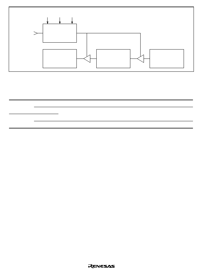
Rev. 1.0, 02/00, page 320 of 1141
Edge detection and
capture signal
generating circuit.
BUFEA
IEDGA
FTIA
IEDGC
ICRC
ICRA
FRC
Figure 16.2 Buffer Operation (Example)
Table 16.3
Input Signal Edge Selection when Making Buffer Operation
IEDGA
IEDGC
Selection of the Input Signal Edge
0
Captures at the falling edge of the input capture input A (Initial value)
0
1
0
Captures at both rising and falling edges of the input capture input A
1
1
Captures at the rising edge of the input capture input A
Reading can be made from the ICR through the CPU at 8-bit or 16-bit.
For stable input capturing operation, maintain the pulse duration of the input capture input signals
at 1.5 system clock (
) or more in case of single edge capturing and at 2.5 system clock (
) or
more in case of both edge capturing.
The ICR is initialized to H'0000 when reset or under the standby mode, watch mode, subsleep
mode, module stop mode or subactive mode.

Rev. 1.0, 02/00, page 321 of 1141
16.2.4
Timer Interrupt Enabling Register (TIER)
0
0
1
0
R/W
2
0
R/W
3
0
4
0
R/W
5
0
6
0
7
R/W
R/W
R/W
ICICE
R/W
ICIBE
0
R/W
ICIAE
ICIDE
OCIAE
OCIBE
OVIE
ICSA
Bit :
Initial value :
R/W :
The TIER is an 8-bit read/write register that controls permission/prohibition of interrupt requests.
The TIER is initialized to H'00 when reset or under the standby mode, watch mode, subsleep
mode, module stop mode or subactive mode.
Bit 7
Enabling the Input Capture Interrupt A (ICIAE): This bit works to permit/prohibit
interrupt requests (ICIA) by the ICFA when the ICFA of the TCSRX is being set to 1.
Bit 7
ICIAE
Description
0
Prohibits interrupt requests (ICIA) by the ICFA
(Initial value)
1
Permits interrupt requests (ICIA) by the ICFA
Bit 6
Enabling the Input Capture Interrupt B (ICIBE): This bit works to permit/prohibit
interrupt requests (ICIB) by the ICFB when the ICFB of the TCSRX is being set to 1.
Bit 6
ICIBE
Description
0
Prohibits interrupt requests (ICIB) by the ICFB
(Initial value)
1
Permits interrupt requests (ICIB) by the ICFB
Bit 5
Enabling the Input Capture Interrupt C (ICICE): This bit works to permit/prohibit
interrupt requests (ICIC) by the ICFC when the ICFC of the TCSRX is being set to 1.
Bit 5
ICICE
Description
0
Prohibits interrupt requests (ICIC) by the ICFC
(Initial value)
1
Permits interrupt requests (ICIC) by the ICFC

Rev. 1.0, 02/00, page 322 of 1141
Bit 4
Enabling the Input Capture Interrupt D (ICIDE): This bit works to permit/prohibit
interrupt requests (ICID) by the ICFD when the ICFD of the TCSRX is being set to 1.
Bit 4
ICIDE
Description
0
Prohibits interrupt requests (ICID) by the ICFD
(Initial value)
1
Permits interrupt requests (ICID) by the ICFD
Bit 3
Enabling the Output Comparing Interrupt A (OCIAE): This bit works to
permit/prohibit interrupt requests (OCIA) by the OCFA when the OCFA of the TCSRX is being
set to 1.
Bit 3
OCIAE
Description
0
Prohibits interrupt requests (OCIA) by the OCFA
(Initial value)
1
Permits interrupt requests (OCIA) by the OCFA
Bit 2
Enabling the Output Comparing Interrupt B (OCIBE): This bit works to
permit/prohibit interrupt requests (OCIB) by the OCFB when the OCFB of the TCSRX is being
set to 1.
Bit 2
OCIBE
Description
0
Prohibits interrupt requests (OCIB) by the OCFB
(Initial value)
1
Permits interrupt requests (OCIB) by the OCFB
Bit 1
Enabling the Timer Overflow Interrupt (OVIE): This bit works to permit/prohibit
interrupt requests (FOVI) by the OVF when the OVF of the TCSRX is being set to 1.
Bit 1
OVIE
Description
0
Prohibits interrupt requests (FOVI) by the OVF
(Initial value)
1
Permits interrupt requests (FOVI) by the OVF

Rev. 1.0, 02/00, page 323 of 1141
Bit 0
Selecting the Input Capture A Signals (ICSA): This bit works to select the input capture
A signals.
Bit 0
ICSA
Description
0
Selects the FTIA pin for inputting of the input capture A signals
(Initial value)
1
Selects the HSW for inputting of the input capture A signals

Rev. 1.0, 02/00, page 324 of 1141
16.2.5
Timer Control/Status Register X (TCSRX)
0
0
1
0
2
0
3
0
4
0
5
0
6
0
7
R/W
R/(W)*
ICFB
0
R/(W)*
ICFA
R/(W)*
ICFD
R/(W)*
ICFC
R/(W)*
OCFB
R/(W)*
OCFA
CCLRA
R/(W)*
OVF
Note: * Only 0 can be written to clear the flag for Bits 7 to 1.
Bit :
Initial value :
R/W :
The TCSRX is an 8-bit register which works to select counter clearing timing and to control
respective interrupt requesting signals. The TCSRX is initialized to H'00 when reset or under the
standby mode, watch mode, subsleep mode, module stop mode or subactive mode.
Meanwhile, as for the timing, see section 16.3, Operation.
The FTIA through FTID pins are for fixed inputs inside the LSI under the low power consumption
mode excluding the sleep mode. Consequently, when such shifts as active mode
low power
consumption mode
active mode are made, wrong edges may be detected depending on the pin
status or on the type of the detecting edge.
To avoid such error, clear the interrupt requesting flag once immediately after shifting to the
active mode from the low power consumption mode.
Bit 7
Input Capture Flag A (ICFA): This is a status flag indicating the fact that the value of
the FRC has been transferred to the ICRA by the input capture signals.
When the BUFEA of the TCRX is being set to 1, the ICFA indicates the status that the FRC value
has been transferred to the ICRA by the input capture signals and that the ICRA value before
being updated has been transferred to the ICRC.
This flag should be cleared by use of of the software. Such setting should only be made by use of
the hardware. It is not possible to make this setting using a software.
Bit 7
ICFA
Description
0
[Clearing conditions]
(Initial value)
When 0 is written into the ICFA after reading the ICFA under the setting of ICFA = 1
1
[Setting conditions]
When the value of the FRC has been transferred to the ICRA by the input capture
signals

Rev. 1.0, 02/00, page 325 of 1141
Bit 6
Input Capture Flag B (ICFB): This status flag indicates the fact that the value of the
FRC has been transferred to the ICRB by the input capture signals.
When the BUFEB of the TCRX is being set to 1, the ICFB indicates the status that the FRC value
has been transferred to the ICRB by the input capture signals and that the ICRB value before being
updated has been transferred to the ICRC.
This flag should be cleared by use of the software. Such setting should only be made by use of the
hardware. It is not possible to make this setting using a software.
Bit 6
ICFB
Description
0
[Clearing conditions]
(Initial value)
When 0 is written into the ICFB after reading the ICFB under the setting of ICFB = 1
1
[Setting conditions]
When the value of the FRC has been transferred to the ICRB by the input capture
signals
Bit 5
Input Capture Flag C (ICFC): This status flag indicates the fact that the value of the
FRC has been transferred to the ICRC by the input capture signals.
When an input capture signal occurs while the BUFEA of the TCRX is being set to 1, although the
ICFC will be set out, data transference to the ICRC will not be performed.
Therefore, in buffer operation, the ICFC can be used as an external interrupt by setting the ICICE
bit to 1.
This flag should be cleared by use of the software. Such setting should only be made by use of the
hardware. It is not possible to make this setting using a software.
Bit 5
ICFC
Description
0
[Clearing conditions]
(Initial value)
When 0 is written into the ICFC after reading the ICFC under the setting of ICFC = 1
1
[Setting conditions]
When the input capture signal has occurred

Rev. 1.0, 02/00, page 326 of 1141
Bit 4
Input Capture Flag D (ICFD): This status flag indicates the fact that the value of the
FRC has been transferred to the ICRD by the input capture signals.
When an input capture signal occurs while the BUFEB of the TCRX is being set to 1, although the
ICFD will be set out, data transference to the ICRD will not be performed.
Therefore, in buffer operation, the ICFD can be used as an external interrupt by setting the ICIDE
bit to 1.
This flag should be cleared by use of the software. Such setting should only be made by use of the
hardware. It is not possible to make this setting using a software.
Bit 4
ICFD
Description
0
[Clearing conditions]
(Initial value)
When 0 is written into the ICFD after reading the ICFD under the setting of ICFD = 1
1
[Setting conditions]
When the input capture signal has occurred
Bit 3
Output Comparing Flag A (OCFA): This status flag indicates the fact that the FRC and
the OCRA have come to a comparing match.
This flag should be cleared by use of the software. Such setting should only be made by use of the
hardware. It is not possible to make this setting using a software.
Bit 3
OCFA
Description
0
[Clearing conditions]
(Initial value)
When 0 is written into the OCFA after reading the OCFA under the setting of OCFA =
1
1
[Setting conditions]
When the FRC and the OCRA have come to the comparing match

Rev. 1.0, 02/00, page 327 of 1141
Bit 2
Output Comparing Flag B (OCFB): This status flag indicates the fact that the FRC and
the OCRB have come to a comparing match.
This flag should be cleared by use of the software. Such setting should only be made by use of the
hardware. It is not possible to make this setting using a software.
Bit 2
OCFB
Description
0
[Clearing conditions]
(Initial value)
When 0 is written into the OCFB after reading the OCFB under the setting of OCFB =
1
1
[Setting conditions]
When the FRC and the OCRB have come to the comparing match
Bit 1
Time Over Flow (OVF): This is a status flag indicating the fact that the FRC overflowed.
(H'FFFF
H'0000).
This flag should be cleared by use of the software. Such setting should only be made by use of the
hardware. It is not possible to make this setting using a software.
Bit 1
OVF
Description
0
[Clearing conditions]
(Initial value)
When 0 is written into the OVF after reading the OVF under the setting of OVF = 1
1
[Setting conditions]
When the FRC value has become H'FFFF
H'0000
Bit 0
Counter Clearing (CCLRA): This bit works to select if or not to clear the FRC by
occurrence of comparing match A (matching signal of the FRC and OCRA).
Bit 0
CCLRA
Description
0
Prohibits clearing of the FRC by occurrence of comparing match A
(Initial value)
1
Permits clearing of the FRC by occurrence of comparing match A

Rev. 1.0, 02/00, page 328 of 1141
16.2.6
Timer Control Register X (TCRX)
0
0
1
0
2
0
3
0
4
0
5
0
6
0
7
R/W
R/W
IEDGB
0
R/W
IEDGA
R/W
IEDGD
R/W
IEDGC
R/W
BUFEB
R/W
BUFEA
CKS0
R/W
CKS1
Bit :
Initial value :
R/W :
The TCRX is an 8-bit read/write register that selects the input capture signal edge, designates the
buffer operation, and selects the inputting clock for the FRC.
The TCRX is initialized to H'00 when reset or under the standby mode, watch mode, subsleep
mode, module stop mode or subactive mode.
Bit 7
Input Capture Signal Edge Selection A (IEDGA): This bit works to select the rising
edge or falling edge of the input capture signal A (FTIA).
Bit 7
IEDGA
Description
0
Captures the falling edge of the input capture signal A
(Initial value)
1
Captures the rising edge of the input capture signal A
Bit 6
Input Capture Signal Edge Selection B (IEDGB): This bit works to select the rising
edge or falling edge of the input capture signal B (FTIB).
Bit 6
IEDGB
Description
0
Captures the falling edge of the input capture signal B
(Initial value)
1
Captures the rising edge of the input capture signal B
Bit 5
Input Capture Signal Edge Selection C (IEDGC): This bit works to select the rising
edge or falling edge of the input capture signal C (FTIC). However, when the DVCTL has been
selected as the signal for the input capture signal edge selection C, this bit will not influence the
operation.
Bit 5
IEDGC
Description
0
Captures the falling edge of the input capture signal C
(Initial value)
1
Captures the rising edge of the input capture signal C

Rev. 1.0, 02/00, page 329 of 1141
Bit 4
Input Capture Signal Edge Selection D (IEDGD): This bit works to select the rising
edge or falling edge of the input capture signal D (FTID).
Bit 4
IEDGD
Description
0
Captures the falling edge of the input capture signal D
(Initial value)
1
Captures the rising edge of the input capture signal D
Bit 3
Buffer Enabling A (BUFEA): This bit works to select whether or not to use the ICRC as
the buffer register for the ICRA.
Bit 3
BUFEA
Description
0
Not using the ICRC as the buffer register for the ICRA
(Initial value)
1
Using the ICRC as the buffer register for the ICRA
Bit 2
Buffer Enabling B (BUFEB): This bit works to select whether or not to use the ICRD as
the buffer register for the ICRB.
Bit 2
BUFEB
Description
0
Not using the ICRD as the buffer register for the ICRB
(Initial value)
1
Using the ICRD as the buffer register for the ICRB
Bits 1 and 0
Clock Select (CKS1, 0): These bits work to select the inputting clock to the FRC
from among three types of internal clocks and the DVCFG.
The DVCFG is the edge detecting pulse selected by the CFG dividing timer.
Bit 1
Bit 0
CKS1
CKS0
Description
0
0
Internal clock: Counts at
/4
(Initial value)
0
1
Internal clock: Counts at
/16
1
0
Internal clock: Counts at
/64
1
1
DVCFG: The edge detecting pulse selected by the CFG dividing timer

Rev. 1.0, 02/00, page 330 of 1141
16.2.7
Timer Output Comparing Control Register (TOCR)
0
0
1
0
2
0
3
0
4
0
5
0
6
0
7
R/W
R/W
ICSC
0
R/W
ICSB
R/W
OSRS
R/W
ICSD
R/W
OEB
R/W
OEA
OLVLB
R/W
OLVLA
Bit :
Initial value :
R/W :
The TOCR is an 8-bit read/write register that select input capture signals and output comparing
output level, permits output comparing outputs, and controls switching over of the access of the
OCRA and OCRB. See section 16.2.4, Timer Interrupt Enabling Register (TIER) regarding the
input capture inputs A.
The TOCR is initialized to H'00 when reset or under the standby mode, watch mode, subsleep
mode, module stop mode or subactive mode.
Bit 7
Selecting the Input Capture B Signals (ICSB): This bit works to select the input capture
B signals.
Bit 7
ICSB
Description
0
Selects the FTIB pin for inputting of the input capture B signals
(Initial value)
1
Selects the VD as the input capture B signals
Bit 6
Selecting the Input Capture C Signals (ICSC): This bit works to select the input capture
C signals. The DVCTL is the edge detecting pulse selected by the CTL dividing timer.
Bit 6
ICSC
Description
0
Selects the FTIC pin for inputting of the input capture C signals
(Initial value)
1
Selects the DVCTL as the input capture C signals
Bit 5
Selecting the Input Capture D Signals (ICSD): This bit works to select the input capture
D signals.
Bit 5
ICSD
Description
0
Selects the FTID pin for inputting of the input capture D signals
(Initial value)
1
Selects the NHSW as the input capture D signals

Rev. 1.0, 02/00, page 331 of 1141
Bit 4
Selecting the Output Comparing Register (OCRS): The addresses of the OCRA and
OCRB are the same. The OCRS works to control which register to choose when reading/writing
this address. The choice will not influence the operation of the OCRA and OCRB.
Bit 4
OCRS
Description
0
Selects the OCRA register
(Initial value)
1
Selects the OCRB register
Bit 3
Enabling the Output A (OEA): This bit works to control the output comparing A signals.
Bit 3
OEA
Description
0
Prohibits the output comparing A signal outputs
(Initial value)
1
Permits the output comparing A signal outputs
Bit 2
Enabling the Output B (OEB): This bit works to control the output comparing B signals.
Bit 2
OEB
Description
0
Prohibits the output comparing B signal outputs
(Initial value)
1
Permits the output comparing B signal outputs
Bit 1
Output Level A (OLVLA): This bit works to select the output level to output through the
FTOA pin by use of the comparing match A (matching signal between the FRC and OCRA).
Bit 1
OLVLA
Description
0
Low level
(Initial value)
1
High level
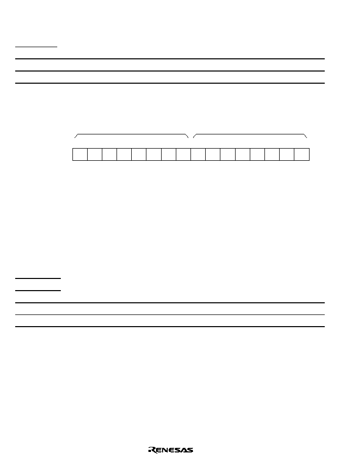
Rev. 1.0, 02/00, page 332 of 1141
Bit 0
Output Level B (OLVLB): This bit works to select the output level to output through the
FTOB pin by use of the comparing match B (matching signal between the FRC and OCRB).
Bit 0
OLVLB
Description
0
Low level
(Initial value)
1
High level
16.2.8
Module Stop Control Register (MSTPCR)
7
0
MSTP15
R/W
MSTPCRH
6
0
MSTP14
R/W
5
1
MSTP13
R/W
4
1
MSTP12
R/W
3
1
MSTP11
R/W
2
1
MSTP10
R/W
1
1
MSTP9
R/W
0
1
MSTP8
R/W
7
1
MSTP7
R/W
6
1
MSTP6
R/W
5
1
MSTP5
R/W
4
1
MSTP4
R/W
3
1
MSTP3
R/W
2
1
MSTP2
R/W
1
1
MSTP1
R/W
0
1
MSTP0
R/W
MSTPCRL
Initial value :
R/W :
Bit :
The MSTPCR consists of twin 8-bit read/write registers that control the module stop mode.
When the MSTP10 bit is set to 1, the Timer X1 stops its operation at the ending point of the bus
cycle to shift to the module stop mode. For more information, see section 4.5, Module Stop
Mode.
When reset, the MSTPCR is initialized to H'FFFF.
Bit 2
Module Stop (MSTP10): This bit works to designate the module stop mode for timer X1.
MSTPCRH
Bit 2
MSTP10
Description
0
Cancels the module stop mode of the Timer X1
1
Sets the module stop mode of the Timer X1
(Initial value)

Rev. 1.0, 02/00, page 333 of 1141
16.3
Operation
16.3.1
Operation of Timer X1
∑
Output Comparing Operation
Right after resetting, the FRC is initialized to H'0000 to start counting up. The inputting clock
can be selected from among three different types of internal clocks or the external clock by
setting the CKS1 and CKS0 of the TCRX.
The contents of the FRC are always being compared with the OCRA and OCRB and, when
the value of these two match, the level set by the the OLVLA and OLVLB of the TOCR is
output through the FTOA pin and FTOB pin.
After resetting, 0 will be output through the FTOA and FTOB pins until the first compare
matching occurs.
Also, when the CCLRA of the TCSRX is being set to 1, the FRC will be cleared to H'0000
when the comparing match A occurs.
∑
Input Capturing Operation
Right after resetting, the FRC is initialized to H'0000 to start counting up. The inputting clock
can be selected from among three different types of internal clocks or the external clock by
setting the CKS1 and CKS0 of the TCRX.
The inputs are transferred to the IEDGA through IEDGD of the TCRX through the FTIA
through FTID pins and, at the same time, the ICFA through ICFD of the TCSRX are set to 1.
At this time, if the ICIAE through ICIED of the TIER are being set to 1, due interrupt request
will be issued to the CPU.
When the BUFEA and BUFEB of the TCRX are set to 1, the ICRC and ICRD work as the
buffer register, respectively, of the ICRA and ICRB. When the edge selected by setting the
IEDGA through IEDGD of the TCRX is input through the FTIA and FTIB pins, the value at
the time of the FRC is transferred to the ICRA and ICRB and, at the same time, the values of
the ICRA and ICRB before updating are transferred to the ICRC and ICRD. At this time,
when the ICFA and ICFB are being set to 1 and if the ICIAE and ICIBE of the TIER are being
set to 1, due interrupt request will be issued to the CPU.
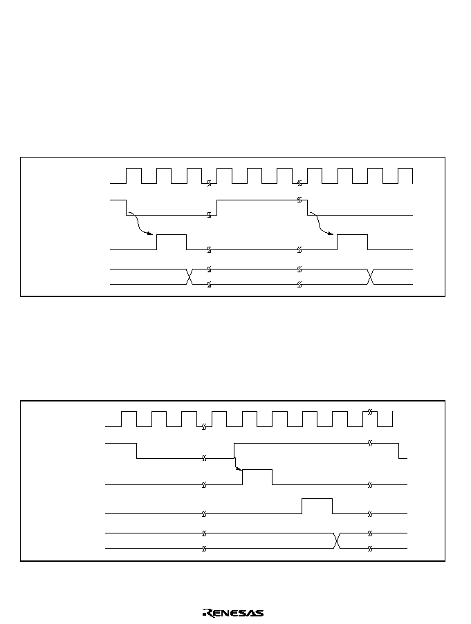
Rev. 1.0, 02/00, page 334 of 1141
16.3.2
Counting Timing of the FRC
The FRC is counted up by the inputting clock. By setting the CKS1 and CKS0 of the TCRX, the
inputting clock can be selected from among three different types of clocks (
/4,
/16 and
/64)
and the DVCFG.
∑
Internal Clock Operation
By setting the CKS1 and CKS0 bits of the TCRX, three types of internal clocks (
/4,
/16 and
/64), generated by dividing the system clock (
) can be selected. Figure 16.3 shows the
timing chart.
FRC
Internal clock
FRC input
clock
N
N-1
N+1
Figure 16.3 Count Timing for Internal Clock Operation
∑
DVCFG Clock Operation
By setting the CKS1 and CKS0 bits of the TCRX to 1, DVCFG clock input can be selected.
The DVCFG clock makes counting by use of the edge detecting pulse being selected by the
CFG dividing timer.
Figure 16.4 shows the timing chart.
FRC
CFG
FRC input
clock
N
N+1
DVCFG
Figure 16.4 Count Timing for CFG Clock Operation
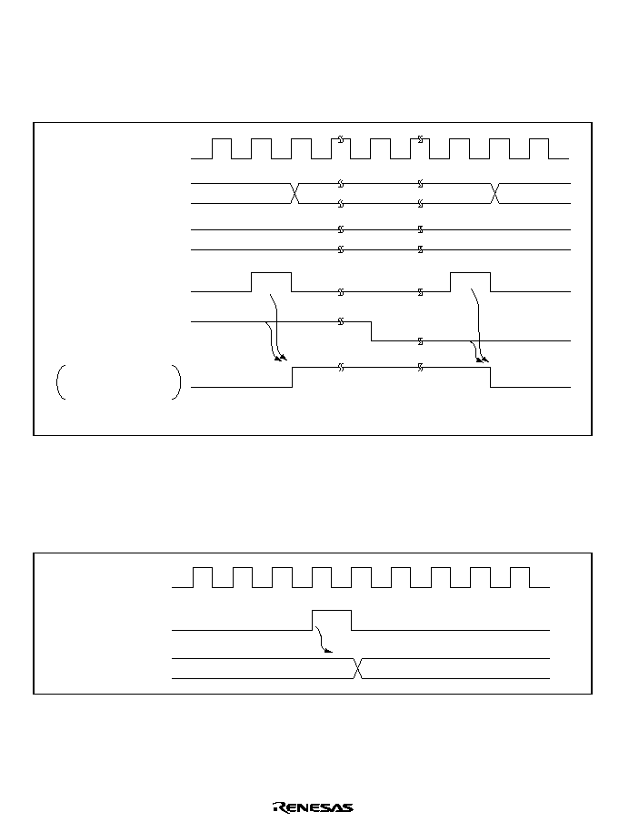
Rev. 1.0, 02/00, page 335 of 1141
16.3.3
Output Comparing Signal Outputting Timing
When a comparing match occurs, the output level having been set by the OLVL of the TOCR is
output through the output comparing signal outputting pins (FTOA and FTOB).
Figure 16.5 shows the timing chart for the output comparing signal outputting A.
FRC
OLVLA
FTOA
Output comparing
signal outputting
A pin
N
N
Clearing
*1
N
N
N+1
N+1
Comparing match
signal
OCRA
Note: 1. Execution of the command is to be designated by the software.
Figure 16.5 Output Comparing Signal Outputting A Timing
16.3.4
FRC Clearing Timing
The FRC can be cleared when the comparing match A occurs. Figure 16.6 shows the timing chart.
FRC
Comparing match
A signal
N
H' 0000
Figure16.6 Clearing Timing by Occurrence of the Comparing Match A
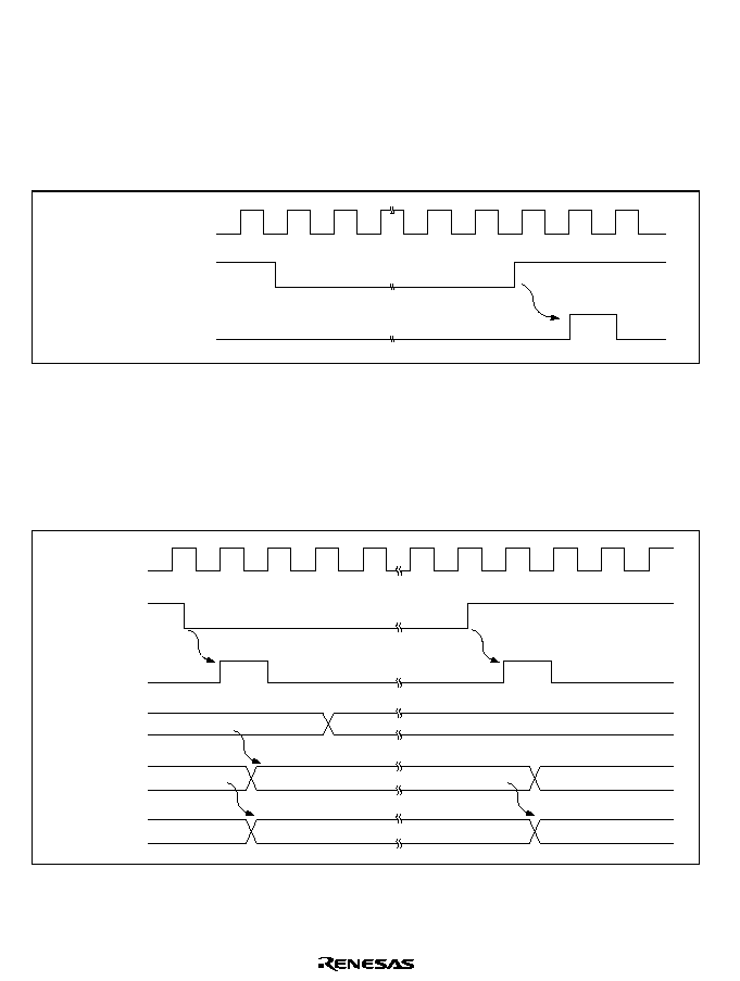
Rev. 1.0, 02/00, page 336 of 1141
16.3.5
Input Capture Signal Inputting Timing
∑
Input Capture Signal Inputting Timing
As for the input capture signal inputting, rising or falling edge is selected by settings of the
IEDGA through IEDGD bits of the TCRX.
Figure 16.7 shows the timing chart when the rising edge is selected (IEDGA through IEDGD =
1).
Input capture signal
inputting pin
Input capture signal
Figure 16.7 Input Capture Signal Inputting Timing (under normal state)
∑
Input Capture Signal Inputting Timing when Making Buffer Operation
Buffer operation can be made using the ICRA or ICRD as the buffer of the ICRA or ICRB.
Figure 16.8 shows the input capture signal inputting timing chart in case both of the rising and
falling edges are designated (IEDGA = 1 and IEDGC = 0, or IEDGA = 0 and IEDGC = 1),
using the ICRC as the buffer register for the ICRA (BUFEA = 1).
Input capture
signal
FTIA
FRC
ICRA
ICRC
n
n+1
N
M
n
m
M
n
M
N
n
Figure 16.8 Input Capture Signal Inputting Timing Chart Under the Buffer Mode
(under normal state)
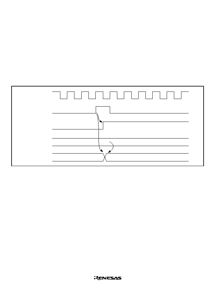
Rev. 1.0, 02/00, page 337 of 1141
Even when the ICRC or ICRD is used as the buffer register, the input capture flag will be set up
corresponding to the designated edge change of respective input capture signals.
For example, when using the ICRC as the buffer register for the ICRA, when an edge change
having been designated by the IEDGC bit is detected with the input capture signals C and if the
ICIEC bit is duly set, an interrupt request will be issued.
However, in this case, the FRC value will not be transferred to the ICRC.
16.3.6
Input Capture Flag (ICFA through ICFD) Setting Up Timing
The input capture signal works to set the ICFA through ICFD to 1 and, simultaneously, the FRC
value is transferred to the corresponding ICRA through ICRD. Figure 16.9 shows the timing
chart.
Input capture
signal
ICFA to ICFD
ICRA to ICRD
FRC
N
N
Figure 16.9 ICFA through ICFD Setting Up Timing
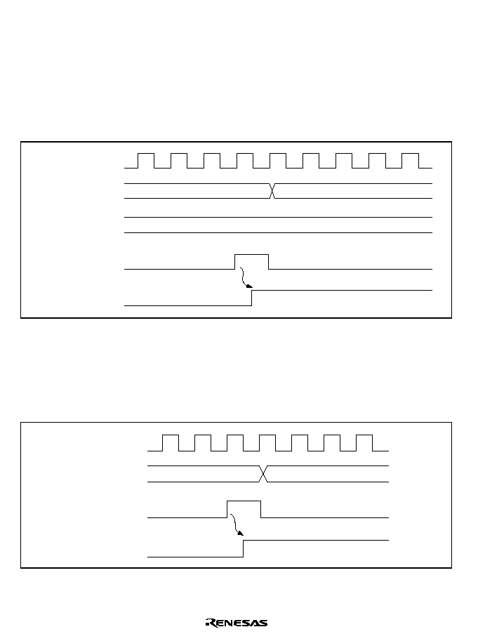
Rev. 1.0, 02/00, page 338 of 1141
16.3.7
Output Comparing Flag (OCFA and OCFB) Setting Up Timing
The OCFA and OCFB are being set to 1 by the comparing match signal being output when the
values of the OCRA, OCRB and FRC match. The comparing match signal is generated at the last
state of the value match (the timing of the FRC's updating the matching count reading).
After the values of the OCRA, OCRB and FRC match, up until the count up clock signal is
generated, the comparing match signal will not be issued. Figure 16.10 shows the OCFA and
OCFB setting timing chart.
Comparing match
signal
OCFA, OCFB
OCRA, OCRB
FRC
N
N
N+1
Figure 16.10 OCF Setting Up Timing
16.3.8
Overflow Flag (CVF) Setting Up Timing
The OVF is set to when the FRC overflows (H'FFFF
H'0000). Figure 16.11 shows the timing
chart.
Overflowing
signal
FRC
H'FFFF
H'0000
OVF
Figure 16.11 OVF Setting Up Timing

Rev. 1.0, 02/00, page 339 of 1141
16.4
Operation Mode of Timer X1
Table 16.4 indicated below shows the operation mode of Timer X1.
Table 16.4
Operation Mode of Timer X1
Operation
Mode
Reset
Active
Sleep
Watch
Subactive
Standby
Subsleep
Module
Stop
FRC
Reset
Functions
Functions
Reset
Reset
Reset
Reset
Reset
OCRA, OCRB
Reset
Functions
Functions
Reset
Reset
Reset
Reset
Reset
ICRA to ICRD
Reset
Functions
Functions
Reset
Reset
Reset
Reset
Reset
TIER
Reset
Functions
Functions
Reset
Reset
Reset
Reset
Reset
TCRX
Reset
Functions
Functions
Reset
Reset
Reset
Reset
Reset
TOCR
Reset
Functions
Functions
Reset
Reset
Reset
Reset
Reset
TCSRX
Reset
Functions
Functions
Reset
Reset
Reset
Reset
Reset
Rev. 1.0, 02/00, page 340 of 1141
16.5
Interrupt Causes
Total seven interrupt causes exist with Timer X1, namely, ICIA through ICID, OCIA, OCIB and
FOVI. Table 16.5 lists the contents of interrupt causes. Interrupt requests can be permitted or
prohibited by setting interrupt enabling bits of the TIER. Also, independent vector addresses are
allocated to respective interrupt causes.
Table 16.5
Interrupt Causes of Timer X1
Abbreviations of the Interrupt Causes
Priority Degree
Contents
ICIA
Interrupt request by the ICFA
ICIB
Interrupt request by the ICFB
ICIC
Interrupt request by the ICFC
ICID
Interrupt request by the ICFD
OCIA
Interrupt request by the OCFA
OCIB
Interrupt request by the OCFB
FOVI
Interrupt request by the OVF
High
Low
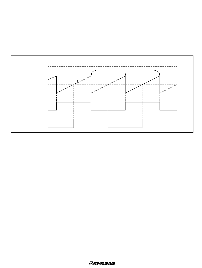
Rev. 1.0, 02/00, page 341 of 1141
16.6
Exemplary Uses of Timer X1
Figure 16.12 shows an example of outputting at optional phase difference of the pulses of the 50%
duty. For this setting, follow the procedures listed below.
1. Set the CCLRA bit of the TCSRX to 1.
2. Each time a comparing match occurs, the OLVIA bit and the OLVLB bit are reversed by use
of the software.
H'FFFF
OCRA
OCRB
H'0000
FTOA
FTOB
Clearing the
counter
FRC
Figure 16.12 Pulse Outputting Example
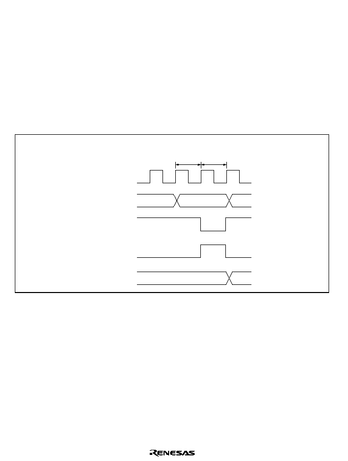
Rev. 1.0, 02/00, page 342 of 1141
16.7
Precautions when Using Timer X1
Pay great attention to the fact that the following competitions and operations occur during
operation of timer X1.
16.7.1
Competition between Writing and Clearing with the FRC
When a counter clearing signal is issued under the T2 state where the FRC is under the writing
cycle, writing into the FRC will not be effected and the priority will be given to clearing of the
FRC.
Figure 16.13 shows the timing chart.
Address
FRC address
Internal writing
signal
Counter clearing
signal
FRC
N
H'0000
T1
T2
Writing cycle with the FRC
Figure 16.13 Competition between Writing and Clearing with the FRC
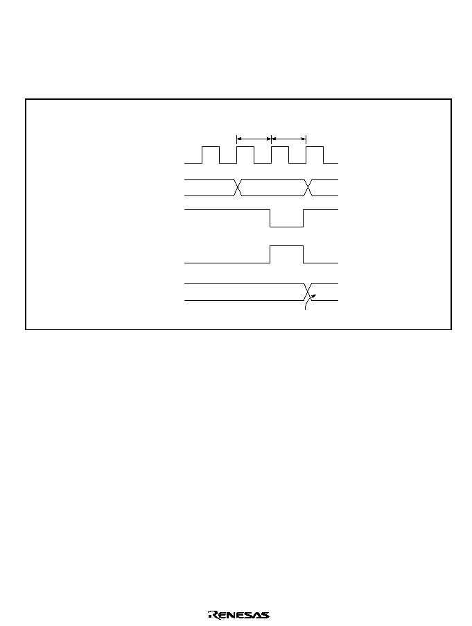
Rev. 1.0, 02/00, page 343 of 1141
16.7.2
Competition between Writing and Counting Up with the FRC
When a counting up cause occurs under the T2 state where the FRC is under the writing cycle, the
counting up will not be effected and the priority will be given to count writing.
Figure 16.14 shows the timing chart.
Address
FRC address
Internal writing
signal
Inputting clock
to the FRC
Writing data
FRC
N
M
T1
T2
Writing cycle with the FRC
Figure 16.14 Competition between Writing and Counting Up with the FRC
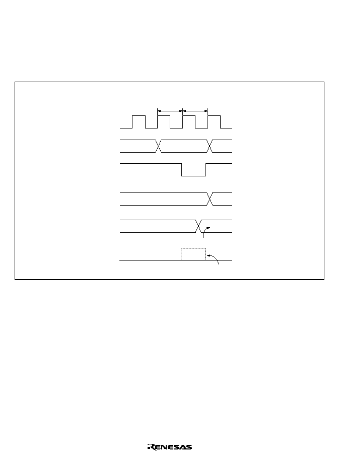
Rev. 1.0, 02/00, page 344 of 1141
16.7.3
Competition between Writing and Comparing Match with the OCR
When a comparing match occurs under the T2 state where the OCRA and OCRB are under the
writing cycle, the priority will be given to writing of the OCR and the comparing match signal will
be prohibited.
Figure 16.15 shows the timing chart.
Address
OCR address
Internal writing
signal
Comparing match
signal
FRC
Writing data
Will be prohibited
OCR
N
M
N
N+1
T1
T2
Writing cycle with the OCR
Figure 16.15 Competition between Writing and Comparing Match with the OCR
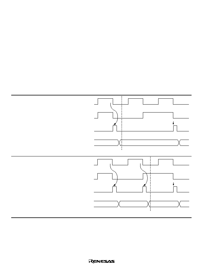
Rev. 1.0, 02/00, page 345 of 1141
16.7.4
Changing Over the Internal Clocks and Counter Operations
Depending on the timing of changing over the internal clocks, the FRC may count up. Table 16.6
shows the relations between the timing of changing over the internal clocks (Re-writing of the
CKS1 and CKS0) and the FRC operations.
When using an internal clock, the counting clock is being generated detecting the falling edge of
the internal clock dividing the system clock (
). For this reason, like Item No. 3 of table 16.6,
count clock signals are issued deeming the timing before the changeover as the falling edge to
have the FRC to count up.
Also, when changing over between an internal clock and the external clock, the FRC may count
up.
Table 16.6
Changing Over the Internal Clocks and the FRC Operation
No.
Rewriting Timing for
the CKS1 and CKS0
FRC Operation
1
Low
low level
changeover
Clock before
the changeover
Clock after
the changeover
Count
clock
FRC
Rewriting of the CKS1 and CKS0
N
N+1
2
Low
High level
changeover
Clock before
the changeover
Clock after
the changeover
Count
clock
FRC
Rewriting of the CKS1 and CKS0
N
N+1
N+2
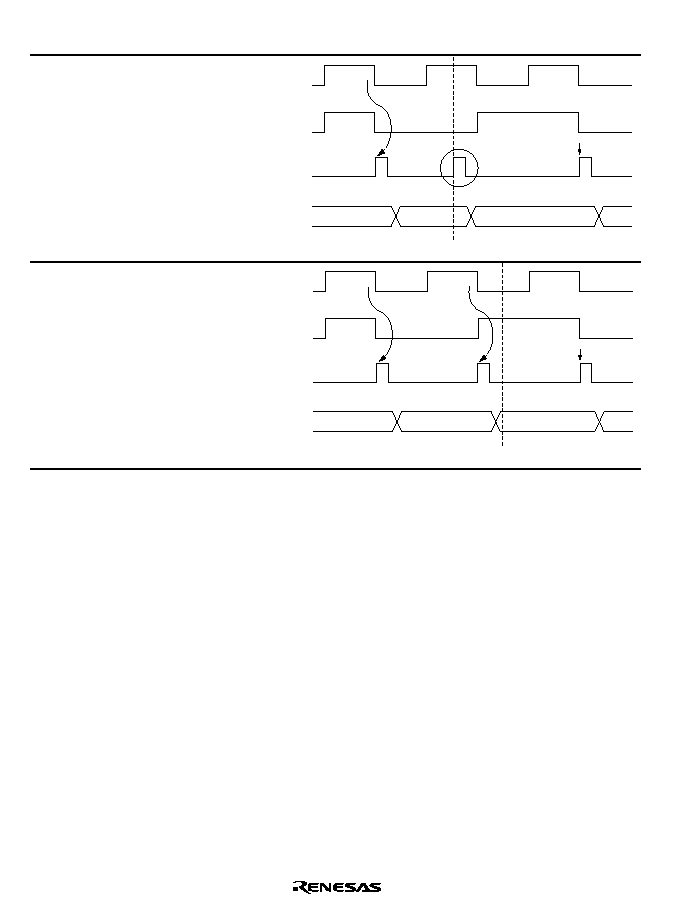
Rev. 1.0, 02/00, page 346 of 1141
No.
Rewriting Timing for
the CKS1 and CKS0
FRC Operation
3
High
low level
changeover
Clock before
the changeover
Clock after
the changeover
Count
clock
FRC
Rewriting of the CKS1 and CKS0
N
*
N+1
N+2
4
High
high level
changeover
Clock before
the changeover
Clock after
the changeover
Count
clock
FRC
Rewriting of the CKS1 and CKS0
N
N+1
N+2
Note:
*
The count clock signals are issued determining the changeover timing as the falling
edge to have the FRC to count up.

Rev. 1.0, 02/00, page 347 of 1141
Section 17 Watchdog Timer (WDT)
17.1
Overview
This LSI has an on-chip watchdog timer with one channel (WDT) for monitoring system
operation. The WDT outputs an overflow signal if a system crash prevents the CPU from writing
to the timer counter, allowing it to overflow. At the same time, the WDT can also generate an
internal reset signal or internal NMI interrupt signal.
When this watchdog function is not needed, the WDT can be used as an interval timer. In interval
timer mode, an interval timer interrupt is generated each time the counter overflows.
17.1.1
Features
WDT features are listed below.
∑
Switchable between watchdog timer mode and interval timer mode
WOVI interrupt generation in interval timer mode
∑
Internal reset or internal interrupt generated when the timer counter overflows
Choice of internal reset or NMI interrupt generation in watchdog timer mode
∑
Choice of 8 counter input clocks
Maximum WDT interval: system clock period
◊
131072
◊
256
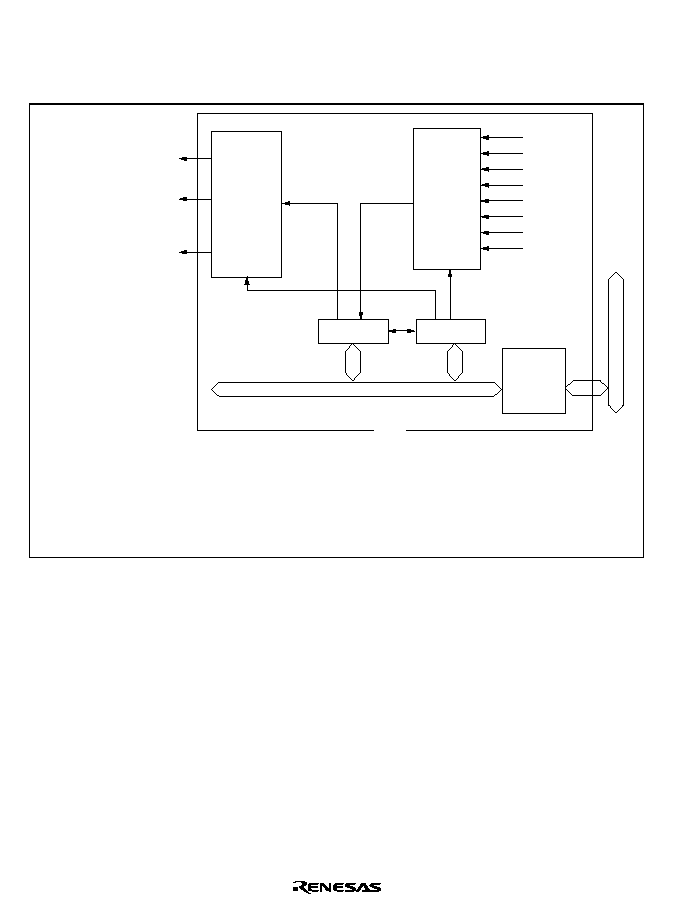
Rev. 1.0, 02/00, page 348 of 1141
17.1.2
Block Diagram
Figure 17.1 shows block diagram of WDT.
Overflow
Interrupt
control
∑
Reset
control
WOVI
(Interrupt request signal)
Internal reset signal*
WTCNT
WTCSR
/ 2
/ 64
/ 128
/ 512
/ 2048
/ 8192
/ 32768
/ 131072
Clock
Clock
select
Internal clock
source
Bus
interface
Module bus
WTCSR
WTCNT
Note: * The internal reset signal can be generated by means of a register setting.
: Timer control/status register
: Timer counter
Internal bus
WDT
[Legend]
Internal NMI
interrupt request signal
Figure 17.1 Block Diagram of WDT

Rev. 1.0, 02/00, page 349 of 1141
17.1.3
Register Configuration
The WDT has two registers, as described in table 17.1. These registers control clock selection,
WDT mode switching, the reset signal, etc.
Table 17.1
WDT Registers
Address
*1
Name
Abbrev.
R/W
Initial Value
Write
*2
Read
Watchdog timer
control/status register
WTCSR
R/ (W)
*3
H'00
H'FFBC
H'FFBC
Watchdog timer counter
WTCNT
R/W
H'00
H'FFBC
H'FFBD
System control register
SYSCR
R/W
H'09
H'FFE8
H'FFE8
Notes: 1. Lower 16 bits of the address.
2. For details of write operations, see section 17.2.4, Notes on Register Access.
3. Only 0 can be written in bit 7, to clear the flag.
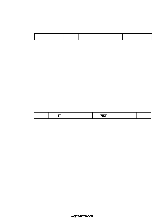
Rev. 1.0, 02/00, page 350 of 1141
17.2
Register Descriptions
17.2.1
Watchdog Timer Counter (WTCNT)
7
0
R/W
6
0
R/W
5
0
R/W
4
0
R/W
3
0
R/W
0
0
R/W
2
0
R/W
1
0
R/W
Bit :
Initial value :
R/W :
TCNT is an 8-bit readable/writable* up-counter.
When the TME bit is set to 1 in WTCSR, WTCNT starts counting pulses generated from the
internal clock source selected by bits CKS2 to CKS0 in WTCSR. When the count overflows
(changes from H'FF to H'00), the OVF flag in WTCSR is set to 1.
WTCNT is initialized to H'00 by a reset, or when the TME bit is cleared to 0.
Note: *
WTCNT is write-protected by a password to prevent accidental overwriting. For
details see section 17.2.4, Notes on Register Access.
17.2.2
Watchdog Timer Control/Status Register (WTCSR)
7
OVF
0
R/(W)*
6
WT/
0
R/W
5
TME
0
R/W
4
--
0
--
3
RST/
0
R/W
0
CKS0
0
R/W
2
CKS2
0
R/W
1
CKS1
0
R/W
Note: * Only 0 can be written to clear the flag.
Bit :
Initial value :
R/W :
WTCSR is an 8-bit readable/writable* register. Its functions include selecting the clock source to
be input to WTCNT, and the timer mode.
WTCSR is initialized to H'00 by a reset.
Note: *
WTCSR is write-protected by a password to prevent accidental overwriting. For
details see section 17.2.4, Notes on Register Access.

Rev. 1.0, 02/00, page 351 of 1141
Bit 7
Overflow Flag (OVF): A status flag that indicates that WTCNT has overflowed from
H'FF to H'00.
Bit 7
OVF
Description
0
[Clearing conditions]
(Initial value)
1. Write 0 in the TME bit
2. Read WTCSR when OVF = 1, then write 0 in OVF
1
[Setting condition]
When WTCNT overflows (changes from H'FF to H'00)
When internal reset request generation is selected in watchdog timer mode, OVF is
cleared automatically by the internal reset
Bit 6
Timer Mode Select (WT/
,7
,7): Selects whether the WDT is used as a watchdog timer or
interval timer. If used as an interval timer, the WDT generates an interval timer interrupt request
(WOVI) when TCNT overflows. If used as a watchdog timer, the WDT generates a reset or NMI
interrupt when TCNT overflows.
Bit 6
WT/
,7
,7
Description
0
Interval timer mode: Sends the CPU an interval timer interrupt request (WOVI) when
WTCNT overflows
(Initial value)
1
Watchdog timer mode: Sends the CPU a reset or NMI interrupt request when
WTCNT overflows
Bit 5
Timer Enable (TME): Selects whether WTCNT runs or is halted.
Bit 5
TME
Description
0
WTCNT is initialized to H'00 and halted
(Initial value)
1
WTCNT counts
Bit 4
Reserved: This bit should not be set to 1.

Rev. 1.0, 02/00, page 352 of 1141
Bit 3
Reset or NMI (RST/
10,
10,): Specifies whether an internal reset or NMI interrupt is
requested on WTCNT overflow in watchdog timer mode.
Bit 3
RST/
1
10
0,,
Description
0
An NMI interrupt request is generated
(Initial value)
1
An internal reset request is generated
Bits 2 to 0
Clock Select 2 to 0 (CKS2 to CKS0): These bits select an internal clock source,
obtained by dividing the system clock (
) for input to WTCNT.
WDT Input Clock Selection
Bit 2
Bit 1
Bit 0
Description
CSK2
CSK1
CSK0
Clock
Overflow Period* (when
= 10 MHz)
0
/2 (Initial
value)
51.2
µ
s
0
1
/64
1.6 ms
0
/128
3.3 ms
0
1
1
/512
13.1 ms
0
/2048
52.4 ms
0
1
/8192
209.7 ms
0
/32768
838.9 ms
1
1
1
/131072
3.36 s
Note:
*
The overflow period is the time from when WTCNT starts counting up from H'00 until
overflow occurs.
Rev. 1.0, 02/00, page 353 of 1141
17.2.3
System Control Register (SYSCR)
7
--
0
--
6
--
0
--
5
INTM1
0
R
4
INTM0
0
R/W
3
XRST
1
R
0
--
1
--
2
--
0
--
1
--
0
--
Bit :
Initial value :
R/W :
Only bit 3 is described here. For details on functions not related to the watchdog timer, see
sections 3.2.2 and 6.2.1, System Control Register (SYSCR), and the descriptions of the relevant
modules.
Bit 3
External Reset (XRST): Indicates the reset source. When the watchdog timer is used, a
reset can be generated by watchdog timer overflow in addition to external reset input. XRST is a
read-only bit. It is set to 1 by an external reset, and cleared to 0 by watchdog timer overflow.
Bit 3
XRST
Description
0
Reset is generated by watchdog timer overflow
1
Reset is generated by external reset input
(Initial value)

Rev. 1.0, 02/00, page 354 of 1141
17.2.4
Notes on Register Access
The watchdog timer's WTCNT and WTCSR registers differ from other registers in being more
difficult to write to. The procedures for writing to and reading these registers are given below.
∑
Writing to WTCNT and WTCSR
These registers must be written to by a word transfer instruction. They cannot be written to
with byte transfer instructions.
Figure 17.2 shows the format of data written to WTCNT and WTCSR. WTCNT and WTCSR
both have the same write address. For a write to WTCNT, the upper byte of the written word
must contain H'5A and the lower byte must contain the write data. For a write to WTCSR, the
upper byte of the written word must contain H'A5 and the lower byte must contain the write
data. This transfers the write data from the lower byte to WTCNT or WTCSR.
<WTCNT write>
<WTCSR write>
Address : H'FFBC
Address : H'FFBC
H'5A
Write data
15
8 7
0
0
H'A5
Write data
15
8 7
0
0
Figure 17.2 Format of Data Written to WTCNT and WTCSR
∑
Reading WTCNT and WTCSR
These registers are read in the same way as other registers. The read addresses are H'FFBC for
WTCSR, and H'FFBD for WTCNT.
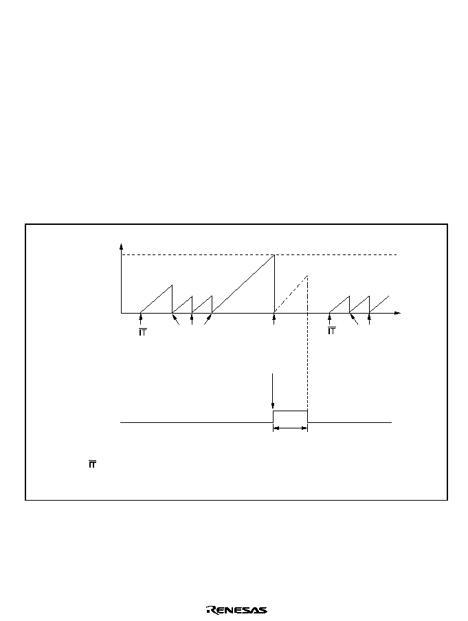
Rev. 1.0, 02/00, page 355 of 1141
17.3
Operation
17.3.1
Watchdog Timer Operation
To use the WDT as a watchdog timer, set the WT/
,7 and TME bits in WTCSR to 1. Software
must prevent WTCNT overflows by rewriting the WTCNT value (normally by writing H'00)
before overflow occurs. This ensures that WTCNT does not overflow while the system is
operating normally. If WTCNT overflows without being rewritten because of a system crash or
other error, the chip is reset, or an NMI interrupt is generated, for 518 system clock periods (518
). This is illustrated in figure 17.3.
An internal reset request from the watchdog timer and reset input from the
5(6 pin are handled
via the same vector. The reset source can be identified from the value of the XRST bit in SYSCR.
If a reset caused by an input signal from the
5(6 pin and a reset caused by WDT overflow occur
simultaneously, the
5(6 pin reset has priority, and the XRST bit in SYSCR is set to 1.
WTCNT value
H'00
Time
H'FF
WT/ =1
TME=1
H'00 written
to WTCNT
WT/ =1
TME=1
H'00 written
to WTCNT
518 system clock period
Internal reset
signal
WT/
TME
[Legend]
Overflow
Internal reset
generated
OVF=1*
: Timer mode select bit
: Timer enable bit
Note: * Cleared to 0 by an internal reset when OVF is set to 1. XRST is cleared to 0.
Figure 17.3 Operation in Watchdog Timer Mode (when Reset)
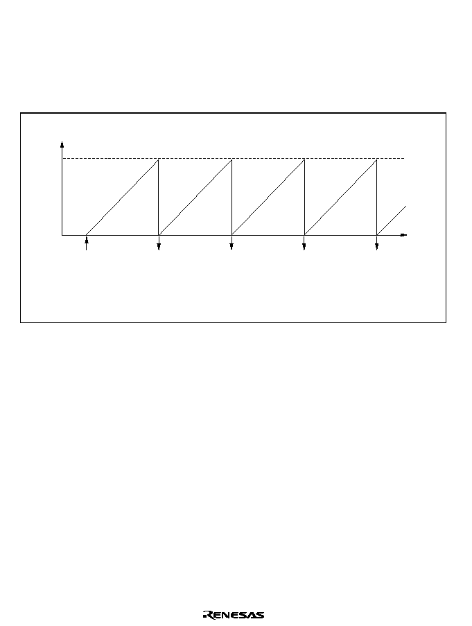
Rev. 1.0, 02/00, page 356 of 1141
17.3.2
Interval Timer Operation
To use the WDT as an interval timer, clear the WT/
,7 bit in WTCSR to 0 and set the TME bit to
1. An interval timer interrupt (WOVI) is generated each time WTCNT overflows, provided that
the WDT is operating as an interval timer, as shown in figure 17.4. This function can be used to
generate interrupt requests at regular intervals.
WTCNT value
H'00
Time
H'FF
WT/IT=0
TME=1
WOVI
Overflow
Overflow
Overflow
Overflow
WOVI : Interval timer interrupt request generation
WOVI
WOVI
WOVI
Figure 17.4 Operation in Interval Timer Mode
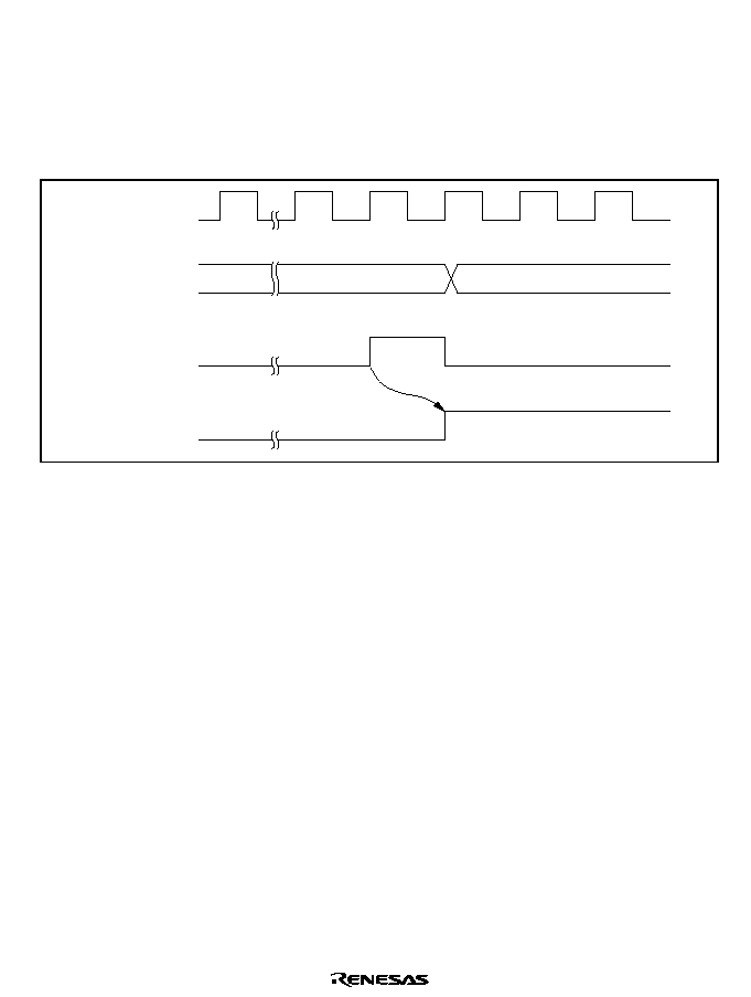
Rev. 1.0, 02/00, page 357 of 1141
17.3.3
Timing of Setting of Overflow Flag (OVF)
The OVF bit in WTCSR is set to 1 if WTCNT overflows during interval timer operation. At the
same time, an interval timer interrupt (WOVI) is requested. This timing is shown in figure 17.5.
If NMI request generation is selected in watchdog timer mode, when WTCNT overflows the OVF
bit in WTCSR is set to 1 and at the same time an NMI interrupt is requested.
CK
WTCNT
H'FF
H'00
Overflow signal
(internal signal)
OVF
Figure 17.5 Timing of OVF Setting
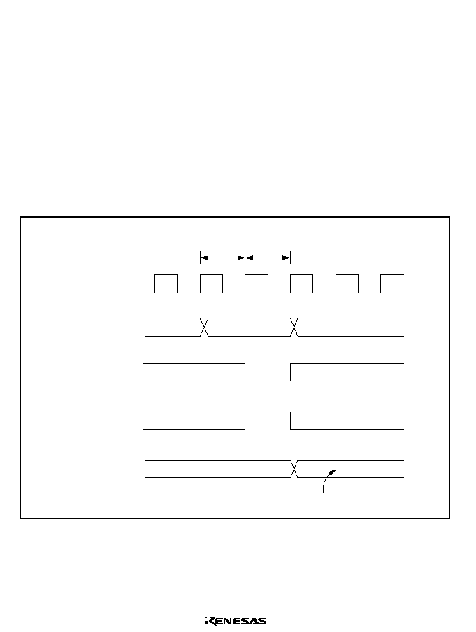
Rev. 1.0, 02/00, page 358 of 1141
17.4
Interrupts
During interval timer mode operation, an overflow generates an interval timer interrupt (WOVI).
The interval timer interrupt is requested whenever the OVF flag is set to 1 in WTCSR. OVF must
be cleared to 0 in the interrupt handling routine. When NMI interrupt request generation is
selected in watchdog timer mode, an overflow generates an NMI interrupt request.
17.5
Usage Notes
17.5.1
Contention between Watchdog Timer Counter (WTCNT) Write and Increment
If a timer counter clock pulse is generated during the T2 state of a WTCNT write cycle, the write
takes priority and the timer counter is not incremented. Figure 17.6 shows this operation.
Internal address
Internal
Internal write
signal
WTCNT input
clock
WTCNT
N
M
T
1
T
2
WTCNT write cycle
Counter write data
Figure 17.6 Contention between WTCNT Write and Increment

Rev. 1.0, 02/00, page 359 of 1141
17.5.2
Changing Value of CKS2 to CKS0
If bits CKS2 to CKS0 in WTCSR are written to while the WDT is operating, errors could occur in
the incrementation. Software must stop the watchdog timer (by clearing the TME bit to 0) before
changing the value of bits CKS2 to CKS0.
17.5.3
Switching between Watchdog Timer Mode and Interval Timer Mode
If the mode is switched from watchdog timer to interval timer, or vice versa, while the WDT is
operating, correct operation cannot be guaranteed. Software must stop the watchdog timer (by
clearing the TME bit to 0) before switching the mode.
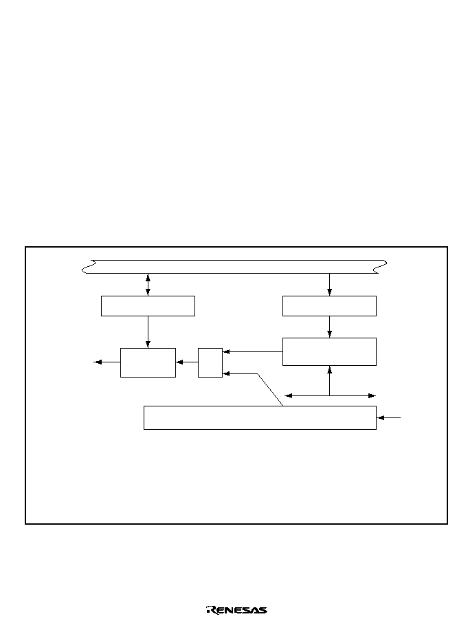
Rev. 1.0, 02/00, page 361 of 1141
Section 18 8-Bit PWM
18.1
Overview
The 8-bit PWM incorporates 4 channels of the duty control method. Its outputs can be used to
control a reel motor or loading motor.
18.1.1
Features
∑
Conversion period: 256-state
∑
Duty control method
18.1.2
Block Diagram
Figure 18.1 shows a block diagram of the 8-bit PWM (1 channel).
PWMn
(n=3 to 0)
2
0
2
7
OVF
Match signal
[Legend]
PWRn
PW8CR
: 8-bit PWM data register n
: 8-bit PWM control register
PWMn
OVF
: 8-bit PWM square-wave output pin n
: Overflow signal from FRC lower 8-bit
PWRn
Free-running counter (FRC)
Comparator
PW8CR
Polarity
specification
Internal data bus
R
S
Q
Figure 18.1 Block Diagram of 8-Bit PWM (1 channel)

Rev. 1.0, 02/00, page 362 of 1141
18.1.3
Pin Configuration
Table 18.1 shows the 8-bit PWM pin configuration.
Table 18.1
Pin Configuration
Name
Abbrev.
I/O
Function
8-bit PWM square-wave output pin 0
PWM0
Output
8-bit PWM square-wave output 0
8-bit PWM square-wave output pin 1
PWM1
Output
8-bit PWM square-wave output 1
8-bit PWM square-wave output pin 2
PWM2
Output
8-bit PWM square-wave output 2
8-bit PWM square-wave output pin 3
PWM3
Output
8-bit PWM square-wave output 3
18.1.4
Register Configuration
Table 18.2 shows the 8-bit PWM register configuration.
Table 18.2
8-Bit PWM Registers
Name
Abbrev.
R/W
Size
Initial Value
Address*
8-bit PWM data register 0
PWR0
W
Byte
H'00
H'D126
8-bit PWM data register 1
PWR1
W
Byte
H'00
H'D127
8-bit PWM data register 2
PWR2
W
Byte
H'00
H'D128
8-bit PWM data register 3
PWR3
W
Byte
H'00
H'D129
8-bit PWM control register
PW8CR
R/W
Byte
H'F0
H'D12A
Port mode register 3
PMR3
R/W
Byte
H'00
H'FFD0
Note:
*
Lower 16 bits of the address.

Rev. 1.0, 02/00, page 363 of 1141
18.2
Register Descriptions
18.2.1
8-bit PWM Data Registers 0, 1, 2 and 3 (PWR0, PWR1, PWR2, PWR3)
PWR0
0
0
1
0
W
2
0
W
3
0
4
0
W
0
W
5
6
0
7
PW04
PW03
PW02
PW01
PW00
0
W
PW07
W
W
W
PW06
PW05
Bit :
Initial value :
R/W :
PWR1
0
0
1
0
W
2
0
W
3
0
4
0
W
0
W
5
6
0
7
PW14
PW13
PW12
PW11
PW10
0
W
PW17
W
W
W
PW16
PW15
Bit :
Initial value :
R/W :
PWR2
0
0
1
0
W
2
0
W
3
0
4
0
W
0
W
5
6
0
7
PW24
PW23
PW22
PW21
PW20
0
W
PW27
W
W
W
PW26
PW25
Bit :
Initial value :
R/W :
PWR3
0
0
1
0
W
2
0
W
3
0
4
0
W
0
W
5
6
0
7
PW34
PW33
PW32
PW31
PW30
0
W
PW37
W
W
W
PW36
PW35
Bit :
Initial value :
R/W :
8-bit PWM data registers 0, 1, 2 and 3 (PWR0, PWR1, PWR2, PWR3) control the duty cycle at 8-
bit PWM pins. The data written in PWR0, PWR1, PWR2 and PWR3 correspond to the high-level
width of one PWM output waveform cycle (256 states).
When data is set in PWR0, PWR1, PWR2 and PWR3, the contents of the data are latched in the
PWM waveform generators, updating the PWM waveform generation data.
PWR0, PWR1, PWR2 and PWR3 are 8-bit write-only registers. When read, all bits are always
read as 1.
PWR0, PWR1, PWR2 and PWR3 are initialized to H'00 by a reset.

Rev. 1.0, 02/00, page 364 of 1141
18.2.2
8-bit PWM Control Register (PW8CR)
0
0
1
0
R/W
2
0
R/W
3
0
4
5
6
7
--
--
--
--
--
--
--
--
PWC3
PWC2
PWC1
PWC0
R/W
R/W
1
1
1
1
Bit :
Initial value :
R/W :
The 8-bit PWM control register (PW8CR) is an 8-bit readable/writable register that controls PWM
functions. PW8CR is initialized to H'00 by a reset.
Bits 7 to 4
Reserved: These bits cannot be modified and are always read as 1.
Bits 3 to 0
Output Polarity Select (PWC3 to PWC0): These bits select the output polarity of
PWMn pin between positive or negative (reverse).
Bit n
PWCn
Description
0
PWMn pin output has positive polarity
(Initial value)
1
PWMn pin output has negative polarity
(n = 3 to 0)

Rev. 1.0, 02/00, page 365 of 1141
18.2.3
Port Mode Register 3 (PMR3)
0
0
1
0
R/W
2
0
R/W
3
0
4
0
R/W
0
R/W
5
6
0
7
PMR34
PMR33
PMR32
PMR31
PMR30
0
R/W
PMR37
R/W
R/W
R/W
PMR36
PMR35
Bit :
Initial value :
R/W :
The port mode register 3 (PMR3) controls function switching of each pin in the port 3. Switching
is specified for each bit.
The PMR3 is a 8-bit readable/writable register and is initialized to H'00 by a reset.
For bits other than 5 to 2, see section 10.5, Port 3.
Bits 5 to 2
P35/PWM3 to P32/PWM0 Pin Switching (PMR35 to PMR32): These bits set
whether the P3n/PWMn pin is used as I/O pin or it is used as 8-bit PWM output PWMm pin.
Bit n
PMR3n
Description
0
P3n/PMWm pin functions as P3n I/O pin
(Initial value)
1
P3n/PMWm pin functions as PWMm output pin
(n = 5 to 2, m = 3 to 0)

Rev. 1.0, 02/00, page 366 of 1141
18.2.4
Module Stop Control Register (MSTPCR)
7
1
MSTP15
R/W
MSTPCRH
6
1
MSTP14
R/W
5
1
MSTP13
R/W
4
1
MSTP12
R/W
3
1
MSTP11
R/W
2
1
MSTP10
R/W
1
1
MSTP9
R/W
0
1
MSTP8
R/W
7
1
MSTP7
R/W
6
1
MSTP6
R/W
5
1
MSTP5
R/W
4
1
MSTP4
R/W
3
1
MSTP3
R/W
2
1
MSTP2
R/W
1
1
MSTP1
R/W
0
1
MSTP0
R/W
MSTPCRL
Bit :
Initial value :
R/W :
The MSTPCR consists of two 8-bit readable/writable registers that control module stop mode.
When MSTP4 bit is set to 1, the 8-bit PWM stops its operation upon completion of the bus cycle
and transits to the module stop mode. For details, see section 4.5, Module Stop Mode.
The MSTPCR is initialized to H'FFFF by a reset.
Bit 4
Module Stop (MSTP4): This bit sets the module stop mode of the 8-bit PWM.
MSTPCRL
Bit 4
MSTP4
Description
0
8-bit PWM module stop mode is released
1
8-bit PWM module stop mode is set
(Initial value)
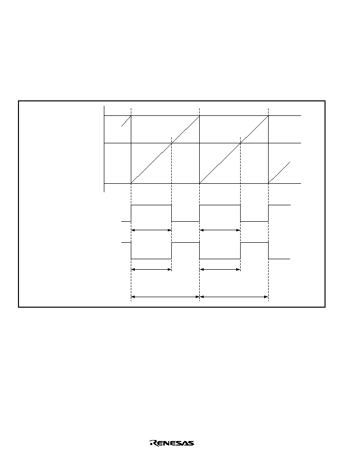
Rev. 1.0, 02/00, page 367 of 1141
18.3
8-Bit PWM Operation
The 8-bit PWM outputs PWM pulses having a cycle length of 256 states and a pulse width
determined by the data registers (PWR).
The output PWM pulse can be converted to a DC voltage through integration in a low-pass filter.
Figure 18.2 shows the output waveform example of 8-bit PWM. The pulse width (Twidth) can be
obtained by the following expression:
Twidth = (1/
)
◊
(PWR setting value)
T width
Pulse width
T width
Pulse cycle
(256 states)
T width
Pulse width
T width
Pulse cycle
(256 states)
H'00
PWRn setting
value
H'FF
FRC lower
8-bit value
PWRn pin
output
(Positive
polarity)
(n=3 to 0)
(Negative
polarity)
Figure 18.2 8-bit PWM Output Waveform (Example)

Rev. 1.0, 02/00, page 369 of 1141
Section 19 12-Bit PWM
19.1
Overview
The 12-bit PWM incorporates 2 channels of the pulse pitch control method and functions as the
drum and capstan motor controller.
19.1.1
Features
Two on-chip 12-bit PWM signal generators are provided to control motors. These PWMs use the
pulse-pitch control method (periodically overriding part of the output). This reduces low-
frequency components in the pulse output, enabling a quick response without increasing the clock
frequency. The pitch of the PWM signal is modified in response to error data (representing lead
or lag in relation to a preset speed and phase).
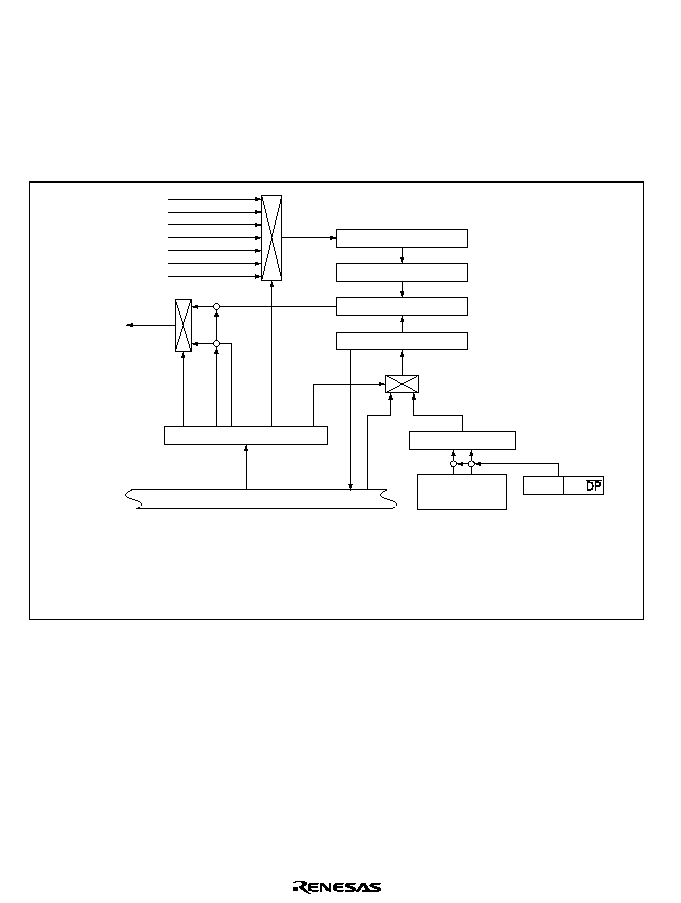
Rev. 1.0, 02/00, page 370 of 1141
19.1.2
Block Diagram
Figure 19.1 shows a block diagram of the 12-bit PWM (1 channel). The PWM signal is generated
by combining quantizing pulses from a 12-bit pulse generator with quantizing pulses derived from
the contents of a data register. Low-frequency components are reduced because the two
quantizing pulses have different frequencies. The error data is represented by an unsigned 12-bit
binary number.
Internal data bus
[Legend]
Note:
*
Refer to section 26, Servo Circuit.
CAPPWM
or
DRMPWM
CAPPWM
/2
/4
/8
/16
/32
/64
/128
DRMPWM
: Capstan mix pin
: Drum mix pin
PWM control register
Digital filter
circuit
Error data
PTON
PWM data register
Output control circuit
Pulse generator
Counter
DFUCR
CP/
Figure 19.1 Block Diagram of 12-Bit PWM (1 channel)

Rev. 1.0, 02/00, page 371 of 1141
19.1.3
Pin Configuration
Table 19.1 shows the 12-bit PWM pin configuration.
Table 19.1
Pin Configuration
Name
Abbrev.
I/O
Function
Capstan mix
CAPPWM
Drum mix
DRMPWM
Output
12-bit PWM square-wave output
19.1.4
Register Configuration
Table 19.2 shows the 12-bit PWM register configuration.
Table 19.2
12-Bit PWM Registers
Name
Abbrev.
R/W
Size
Initial Value
Address*
CPWCR
W
Byte
H'42
H'D07B
12-bit PWM control register
DPWCR
W
Byte
H'42
H'D07A
CPWDR
R/W
Word
H'F000
H'D07C
12-bit PWM data register
DPWDR
R/W
Word
H'F000
H'D078
Note:
*
Lower 16 bits of the address.

Rev. 1.0, 02/00, page 372 of 1141
19.2
Register Descriptions
19.2.1
12-Bit PWM Control Registers (CPWCR, DPWCR)
CPWCR
0
0
1
1
W
2
0
W
3
0
4
0
W
0
W
5
6
1
7
CH/L
CSF/DF
CCK2
CCK1
CCK0
0
W
CPOL
W
W
W
CDC
CHiZ
Bit :
Initial value :
R/W :
DPWCR
0
0
1
1
W
2
0
W
3
0
4
0
W
0
W
5
6
1
7
DH/L
DSF/DF
DCK2
DCK1
DCK0
0
W
DPOL
W
W
W
DDC
DHiZ
Bit :
Initial value :
R/W :
CPWCR is the PWM output control register for the capstan motor. DPWCR is the PWM output
control register for the drum motor. Both are 8-bit writable registers.
CPWCR and DPWCR are initialized to H'42 by a reset, or when in standby or module-stop mode.
Bit 7
Polarity Invert (POL): This bit can invert the polarity of the modulated PWM signal for
noise suppression and other purposes. This bit is invalid when fixed output is selected (when bit
DC is set to 1).
Bit 7
POL
Description
0
Output with positive polarity
(Initial value)
1
Output with inverted polarity
Bit 6
Output Select (DC): Selects either PWM modulated output, or fixed output controlled by
the pin output bits (bits 5 and 4).

Rev. 1.0, 02/00, page 373 of 1141
Bits 5 and 4
PWM Pin Output (HiZ, H/L): When bit DC is set to 1, the 12-bit PWM output
pins (CAPPWM, DRMPWM) output a value determined by the HiZ and H/L bits. The output is
not affected by bit POL.
In power-down modes, the 12-bit PWM circuit and pin statuses are retained. Before making a
transition to a power-down mode, first set bits 6 (DC), 5 (HiZ), and 4 (H/L) of the 12-bit PWM
control registers (CPWCR and DPWCR) to select a fixed output level. Choose one of the
following settings:
Bit 6
Bit 5
Bit 4
DC
HiZ
H/L
Output state
0
Low output
(Initial value)
0
1
High output
1
1
*
High-impedance
0
*
*
Modulation signal output
Note:
*
Don't care
Bit 3
Output Data Select (SF/DF): Selects whether the data to be converted to PWM output is
taken from the data register or from the digital filter circuit.
Bit 3
SF/DF
Description
0
Modulation by error data from the digital filter circuit
(Initial value)
1
Modulation by error data written in the data register
Note: When PWMs output data from the digital filter circuit, the data consisting of the speed and
phase filtering results are modulated by PWMs and output from the CAPPWM and
DRMPWM pins. However, it is possible to output only drum phase filter results from
CAPPWM pin and only capstan phase filter result from DRMPWM pin, by DFUCR settings
of the digital filter circuit. See section 26.11, Digital Filters.

Rev. 1.0, 02/00, page 374 of 1141
Bits 2 to 0
Carrier Frequency Select (CK2 to CK0): Selects the carrier frequency of the PWM
modulated signal. Do not set them to 111.
Bit 2
Bit 1
Bit 0
CK2
CK1
CK0
Description
0
2
0
1
4
0
8
(Initial value)
0
1
1
16
0
32
0
1
64
0
128
1
1
1
(Do not set)

Rev. 1.0, 02/00, page 375 of 1141
19.2.2
12-Bit PWM Data Registers (DPWDR, CPWDR)
CPWDR
1
0
R/W
CPWDR1
0
0
R/W
CPWDR0
3
0
R/W
CPWDR3
2
0
R/W
CPWDR2
5
0
R/W
CPWDR5
4
0
R/W
CPWDR4
7
0
R/W
CPWDR7
6
0
R/W
CPWDR6
9
0
R/W
CPWDR9
8
0
R/W
CPWDR8
11
0
R/W
CPWDR11
10
0
R/W
CPWDR10
12
1
13
1
14
1
15
--
--
--
--
--
--
--
--
1
Bit :
Initial value :
R/W :
DPWDR
1
0
R/W
DPWDR1
0
0
R/W
DPWDR0
3
0
R/W
DPWDR3
2
0
R/W
DPWDR2
5
0
R/W
DPWDR5
4
0
R/W
DPWDR4
7
0
R/W
DPWDR7
6
0
R/W
DPWDR6
9
0
R/W
DPWDR9
8
0
R/W
DPWDR8
11
0
R/W
DPWDR11
10
0
R/W
DPWDR10
12
1
13
1
14
1
15
1
--
--
--
--
--
--
--
--
Bit :
Initial value :
R/W :
The 12-bit PWM data registers (DPWDR and CPWDR) are 12-bit readable/writable registers
in which the data to be converted to PWM output is written.
The data in these registers is converted to PWM output only when bit SF/DF of the
corresponding control register is set to 1. When the SF/DF bit is 0, the error data from the
digital filter circuit is written in the data register, and then modulated by PWM. At this time,
the error data from the digital filter circuit can be monitored by reading the data register.
These registers can be accessed by word only, and cannot be accessed by byte. Byte access
gives unassured results.
Both registers are initialized to H'F000 by a reset.

Rev. 1.0, 02/00, page 376 of 1141
19.3
Operation
19.3.1
Output Waveform
The PWM signal generator combines the error data with the output from an internal pulse
generator to produce a pulse-width modulated signal.
When Vcc/2 is set as the reference value, the following conditions apply:
1. When the motor is running at the correct speed and phase, the PWM signal is output with a
50% duty cycle.
2. When the motor is running behind the correct speed or phase, it is corrected by periodically
holding part of the PWM signal low. The part held low depends on the size of the error.
3. When the motor is running ahead of the correct speed or phase, it is corrected by periodically
holding part of the PWM signal high. The part held high depends on the size of the error.
When the motor is running at the correct speed and phase, the error data is a 12-bit value
representing 1/2 (1000 0000 0000), and the PWM output has the same frequency as the selected
division clock.
After the error data has been converted into a PWM signal, the PWM signal can be smoothed into
a DC voltage by an external low-pass filter (LPF). The smoothe error data can be used to control
the motor.
Figure 19.2 shows sample waveform outputs.
The 12-bit PWM pin outputs a low-level signal upon reset, in power-down mode or at module-
stop.
Rev. 1.0, 02/00, page 377 of 1141
1
Counter
Pulse Generator
PWM data register
C10
C11
C12
C13
Corresponds to Pwr3=1
Corresponds to Pwr2=1
Corresponds to Pwr1=1
Corresponds to Pwr0=1
0 0 0 0
0 0 0 1
0 0 1 0
0 0 1 1
0 1 0 0
0 1 0 1
0 1 1 0
0 1 1 1
1 0 0 0
1 0 0 1
1 0 1 0
1 0 1 1
1 1 0 0
1 1 0 1
1 1 1 0
1 1 1 1
Pwr3 2 1 0
"L"
2
3
4
5
6
7
8
9
1
0
1
1
1
2
1
3
1
4
1
5
1
6
1
2
3
4
5
6
7
8
9
10
11
12
13
14
15
16
1
2
3
4
5
6
7
8
9
1
0
1
1
1
2
Figure 19.2 Sample Waveform Output by 12-Bit PWM (4 Bits)

Rev. 1.0, 02/00, page 379 of 1141
Section 20 14-Bit PWM
20.1
Overview
The 14-bit PWM is a pulse division type PWM that can be used for electronic tuner control, etc.
20.1.1
Features
Features of the 14-bit PWM are given below:
∑
Choice of two conversion periods
A conversion period of 32768/
with a minimum modulation width of 2/
, or a conversion
period of 16384/
with a minimum modulation width of 1/
, can be selected.
∑
Pulse division method for less ripple
Rev. 1.0, 02/00, page 380 of 1141
20.1.2
Block Diagram
Figure 20.1 shows a block diagram of the 14-bit PWM.
[Legend]
PWCR
/4
/2
PWDRL
: PWM control register
: PWM data register L
PWDRU
PWM14
: PWM data register U
: PWM14 output pin
Internal data bus
PWCR
PWDRL
PWDRU
PWM waveform
generator
PWM14
Figure 20.1 Block Diagram of 14-Bit PWM
20.1.3
Pin Configuration
Table 20.1 shows the 14-bit PWM pin configuration.
Table 20.1
Pin Configuration
Name
Abbrev.
I/O
Function
PWM 14-bit square-wave output pin
PWM14*
Output
14-bit PWM square-wave output
Note:
*
This pin also functions as P40 general I/O pin. When using this pin, set the pin function
by the port mode register 4 (PMR4). For details, see section 10.6, Port 4.

Rev. 1.0, 02/00, page 381 of 1141
20.1.4
Register Configuration
Table 20.2 shows the 14-bit PWM register configuration.
Table 20.2
14-Bit PWM Registers
Name
Abbrev.
R/W
Size
Initial Value
Address*
PWM control register
PWCR
R/W
Byte
H'FE
H'D122
PWM data register U
PWDRU
W
Byte
H'00
H'D121
PWM data register L
PWDRL
W
Byte
H'00
H'D120
Note:
*
Lower 16 bits of the address.

Rev. 1.0, 02/00, page 382 of 1141
20.2
Register Descriptions
20.2.1
PWM Control Register (PWCR)
0
0
1
1
2
1
3
1
4
1
5
1
6
1
7
--
--
--
--
--
--
--
--
--
--
--
--
--
--
R/W
PWCR0
1
Bit :
Initial value :
R/W :
The PWM control register (PWCR) is an 8-bit read/write register that controls the 14-bit PWM
functions. PWCR is initialized to H'FE by a reset.
Bits 7 to 1
Reserved: These bits cannot be modified and are always read as 1.
Bit 0
Clock Select (PWCR0): Selects the clock supplied to the 14-bit PWM.
Bit 0
PWCR0
Description
0
The input clock is
/2 (t
= 2/
)
(Initial value)
The conversion period is 16384/
, with a minimum modulation width of 1/
1
The input clock is
/4 (t
= 4/
)
The conversion period is 32768/
, with a minimum modulation width of 2/
Note: t/
: Period of PWM clock input

Rev. 1.0, 02/00, page 383 of 1141
20.2.2
PWM Data Registers U and L (PWDRU, PWDRL)
PWDRU
0
0
1
0
2
0
3
0
4
0
5
0
6
1
7
--
--
--
--
W
PWDRU0
W
PWDRU1
W
PWDRU2
W
PWDRU3
W
PWDRU4
W
PWDRU5
1
Bit :
Initial value :
R/W :
PWDRL
0
0
1
0
2
0
3
0
4
0
5
0
6
7
W
PWDRL0
W
PWDRL1
W
PWDRL2
W
PWDRL3
W
PWDRL4
W
PWDRL5
0
W
PWDRL6
W
PWDRL7
0
Bit :
Initial value :
R/W :
PWM data registers U and L (PWDRU and PWDRL) indicate high level width in one PWN
waveform cycle.
PWDRU and PWDRL form a 14-bit write-only register, with the upper 6 bits assigned to PWDRU
and the lower 8 bits to PWDRL. The value written in PWDRU and PWDRL gives the total high-
level width of one PWM waveform cycle. Both PWDRU and PWDRL are accessible by byte
access only. Word access gives unassured results.
When 14-bit data is written in PWDRU and PWDRL, the contents are latched in the PWM
waveform generator and the PWM waveform generation data is updated. When writing the 14-bit
data, follow these steps:
1. Write the lower 8 bits to PWDRL.
2. Write the upper 6 bits to PWDRU.
Write the data first to PWDRL and then to PWDRU.
PWDRU and PWDRL are write-only registers. When read, all bits always read 1.
PWDRU and PWDRL are initialized to H'C000 by a reset.

Rev. 1.0, 02/00, page 384 of 1141
20.2.3
Module Stop Control Register (MSTPCR)
7
1
MSTP15
R/W
MSTPCRH
6
1
MSTP14
R/W
5
1
MSTP13
R/W
4
1
MSTP12
R/W
3
1
MSTP11
R/W
2
1
MSTP10
R/W
1
1
MSTP9
R/W
0
1
MSTP8
R/W
7
1
MSTP7
R/W
6
1
MSTP6
R/W
5
1
MSTP5
R/W
4
1
MSTP4
R/W
3
1
MSTP3
R/W
2
1
MSTP2
R/W
1
1
MSTP1
R/W
0
1
MSTP0
R/W
MSTPCRL
Bit :
Initial value :
R/W :
The module stop control register (MSTPCR) consists of two 8-bit readable/writable registers that
control the module stop mode functions.
When the MSTP5 bit is set to 1, the 14-bit PWM operation stops at the end of the bus cycle and a
transition is made to module stop mode. For details, see section 4.5, Module Stop Mode.
MSTPCR is initialized to H'FFFF by a reset.
Bit 5
Module Stop (MSTP5): Specifies the module stop mode of the 14-bit PWM.
MSTPCRL
Bit 5
MSTP5
Description
0
14-bit PWM module stop mode is released
1
14-bit PWM module stop mode is set
(Initial value)
Rev. 1.0, 02/00, page 385 of 1141
20.3
14-Bit PWM Operation
When using the 14-bit PWM, set the registers in this sequence:
1. Set bit PWM40 to 1 in port mode register 4 (PMR4) so that pin P40/PWM14 is designated for
PWM output.
2. Set bit PWCR0 in the PWM control register (PWCR) to select a conversion period of either
32768/
(PWCR0 = 1) or 16384/
(PWCR0 = 0).
3. Set the output waveform data in PWM data registers U and L (PWDRU, PWDRL). Be sure to
write byte data first to PWDRL and then to PWDRU. When the data is written in PWDRU,
the contents of these registers are latched in the PWM waveform generator, and the PWM
waveform generation data is updated in synchronization with internal signals.
One conversion period consists of 64 pulses, as shown in figure 20.2. The total high-level width
during this period (T
H
) corresponds to the data in PWDRU and PWDRL. This relation can be
expressed as follows:
T
H
= (data value in PWDRU and PWDRL + 64)
◊
t
/2
where to is the period of PWM clock input: 2/
(bit PWCR0 = 0) or 4/
(bit PWCR0 = 1).
If the data value in PWDRU and PWDRL is from H'3FC0 to H'3FFF, the PWM output stays high.
When the data value is H'0000, T
H
is calculated as follows:
T
H
= 64
◊
t
/2 = 32
t
t H64
t H63
t H3
t H2
t H1
T H = t H1 + t H2 + t H3 + ... + t H64
t f1 = t f2 = t f3 = ... = t f64
t f1
t f2
t f63
t f64
1 conversion period
Figure 20.2 Waveform Output by 14-Bit PWM

Rev. 1.0, 02/00, page 387 of 1141
Section 21 Prescalar Unit
21.1
Overview
The prescalar unit (PSU) has a 18-bit free running counter (FRC) that uses
as a clock source and
a 5-bit counter that uses
W as a clock source.
21.1.1
Features
∑
Prescalar S (PSS)
Generates frequency division clocks that are input to peripheral functions.
∑
Prescalar W (PSW)
When a timer A is used as a clock time base, the PSW frequency-divides subclocks and
generates input clocks.
∑
Stable oscillation wait time count
During the return from the low power consumption mode excluding the sleep mode, the FRC
counts the stable oscillation wait time.
∑
8-bit PWM
The lower 8 bits of the FRC is used as 8-bit PWM cycle and duty cycle generation counters.
(Conversion cycle: 256 states)
∑
8-bit input capture by
,& pins
Catches the 8 bits of 2
15
to 2
8
of the FRC according to the edge of the
,& pin for remote control
receiving.
∑
Frequency division clock output
Can output the frequency division clock for the system clock or the frequency division clock
for the subclock from the frequency division clock output pin (TMOW).
Rev. 1.0, 02/00, page 388 of 1141
21.1.2
Block Diagram
Figure 21.1 shows a block diagram of the prescalar unit.
PWM3
ICR1
PCSR
18-bit free running counter (FRC)
w/128
Prescalar W
/131072 to
/2
Prescalar S
Internal data bus
MSB
LSB
w/4
w/8
w/16
w/32
/32
/16
/8
/4
Interrupt
request
5-bit counter
pin
Stable oscillation
wait time count output
2
12
2
15
2
8
2
7
2
7
2
0
TMOW
pin
MSB
LSB
8 bits
6 bits
8 bits
PWM2
PWM1
PWM0
[Legend]
ICR1
PCSR
: Input capture register 1
: Prescalar unit control/status register
TMOW
: Input capture input pin
: Frequency division clock output pin
Figure 21.1 Block Diagram of Prescalar Unit

Rev. 1.0, 02/00, page 389 of 1141
21.1.3
Pin Configuration
Table 21.1 shows the pin configuration of the prescalar unit.
Table 21.1
Pin Configuration
Name
Abbrev.
I/O
Function
Input capture input
,&
Input
Prescalar unit input capture input pin
Frequency division clock
output
TMOW
Output
Prescalar unit frequency division clock
output pin
21.1.4
Register Configuration
Table 21.2 shows the register configuration of the prescalar unit.
Table 21.2
Register Configuration
Name
Abbrev.
R/W
Size
Initial Value
Address*
Input capture register 1
ICR1
R
Byte
H'00
H'D12C
Prescalar unit
control/status register
PCSR
R/W
Byte
H'08
H'D12D
Note:
*
Lower 16 bits of the address.

Rev. 1.0, 02/00, page 390 of 1141
21.2
Registers
21.2.1
Input Capture Register 1 (ICR1)
0
0
1
0
R
2
0
R
3
0
4
0
R
0
R
5
6
0
7
ICR14
ICR13
ICR12
ICR11
ICR10
0
R
ICR17
R
R
R
ICR16
ICR15
Bit :
Initial value :
R/W :
Input capture register 1 (ICR1) captures 8-bit data of 2
15
to 2
8
of the FRC according to the edge of
the
,& pin.
ICR1 is an 8-bit read-only register. The write operation becomes invalid. The ICR1 values are
undefined until the first capture is generated after the mode has been set to the standby mode,
watch mode, subactive mode, and subsleeve mode. When reset, ICR1 is initialized to H'00.
21.2.2
Prescalar Unit Control/Status Register (PCSR)
0
0
1
0
R/W
2
0
R/W
3
--
--
1
4
0
R/W
5
0
6
0
7
R/W
R/W
ICEG
R/W
ICIE
0
R/(W)*
ICIF
NCon/off
DCS2
DCS1
DCS0
Note: * Only 0 can be written to clear the flag.
Bit :
Initial value :
R/W :
The prescalar unit control/status register (PCSR) controls the input capture function and selects the
frequency division clock that is output from the TMOW pin.
PCSR is an 8-bit read/write enable register. When reset, PCSR is initialized to H'08.
Bit 7
Input Capture Interrupt Flag (ICIF): Input capture interrupt request flag. This indicates
that the input capture was performed according to the edge of the
,& pin.
Bit 7
ICIF
Description
0
[Clear condition]
(Initial value)
When 0 is written after 1 has been read
1
[Set condition]
When the input capture was performed according to the edge of the
,&
pin

Rev. 1.0, 02/00, page 391 of 1141
Bit 6
Input Capture Interrupt Enable (ICIE): When ICIF was set to 1 by the input capture
according to the edge of the
,& pin, ICIE enables and disables the generation of an input capture
interrupt.
Bit 6
ICIE
Description
0
Disables the generation of an input capture interrupt
(Initial value)
1
Enables the generation of an input capture interrupt
Bit 5
,
,&& Pin Edge Select (ICEG): ICEG selects the input edge sense of the ,& pin.
Bit 5
ICEG
Description
0
Detects the falling edge of the
,&
pin input
(Initial value)
1
Detects the rising edge of the
,&
pin input
Bit 4
Noise Cancel ON/OFF (NCon/off): NCon/off selects enable/disable of the noise cancel
function of the
,& pin. For the noise cancel function, see section 21.3, Noise Cancel Circuit.
Bit 4
NCon/off
Description
0
Disables the noise cancel function of the
,&
pin
(Initial value)
1
Enables the noise cancel function of the
,&
pin
Bit 3
Reserved: This bit cannot be modified and is always read as 1.

Rev. 1.0, 02/00, page 392 of 1141
Bits 2 to 0
Frequency Division Clock Output Select (DCS2 to DCS0): DCS2 to DCS0 select
eight types of frequency division clocks that are output from the TMOW pin.
Bit 2
Bit 1
Bit 0
DCS2
DCS1
DCS0
Description
0
Outputs PSS,
/32
(Initial value)
0
1
Outputs PSS,
/16
0
Outputs PSS,
/8
0
1
1
Outputs PSS,
/4
0
Outputs PSW,
W/32
0
1
Outputs PSW,
W/16
0
Outputs PSW,
W/8
1
1
1
Outputs PSW,
W/4

Rev. 1.0, 02/00, page 393 of 1141
21.2.3
Port Mode Register 1 (PMR1)
7
PMR17
0
R/W
6
PMR16
0
R/W
5
PMR15
0
R/W
4
PMR14
0
R/W
3
PMR13
0
R/W
0
PMR10
0
R/W
2
PMR12
0
R/W
1
PMR11
0
R/W
Bit :
Initial value :
R/W :
The port mode register 1 (PMR1) controls switching of each pin function of port 1. The switching
is specified in a unit of bit.
PMR1 is an 8-bit read/write enable register. When reset, PMR1 is initialized to H'00. For details,
refer to Port Mode Register 1 in section 10.3.2 Register Configuration.
Bit 7
P17/TMOW Pin Switching (PMR17): PMR17 sets whether the P17/TMOW pin is used
as a P17 I/O pin or a TMOW pin for division clock output.
Bit 7
PMR17
Description
0
The P17/TMOW pin functions as a P17 I/O pin
(Initial value)
1
The P17/TMOW pin functions as a TMOW output function
Bit 6
P16/
,
,&& Pin Switching (PMR16): PMR16 sets whether the P16/,& pin is used as a P16 I/O
pin or an
,& pin for the input capture input of the prescalar unit.
Bit 6
PMR16
Description
0
The P16/
,&
pin functions as a P16 I/O pin
(Initial value)
1
The P16/
,&
pin functions as an
,&
input function

Rev. 1.0, 02/00, page 394 of 1141
21.3
Noise Cancel Circuit
The
,& pin has a built-in a noise cancel circuit. The circuit can be used for noise protection such
as remote control receiving. The noise cancel circuit samples the input values of the
,& pin twice
at an interval of 256 states. If the input values are different, they are assumed to be noise.
The
,& pin can specify enable/disable of the noise cancel function according to the bit 4
(NCon/off) of the prescalar unit control/status register (PCSR).
21.4
Operation
21.4.1
Prescalar S (PSS)
The PSS is a 17-bit counter that uses the system clock (
=fosc) as an input clock and generates the
frequency division clocks (
/131072 to
/2) of the peripheral function. The low-order 17 bits of
the 18-bit free running counter (FRC) correspond to the PSS. The FRC is incremented by one
clock. The PSS output is shared by the timer and serial communication interface (SCI), and the
frequency division ratio can independently be set by each built-in peripheral function.
When reset, the FRC is initialized to H'00000, and starts increment after reset has been released.
Because the system clock oscillator is stopped in standby mode, watch mode, subactive mode, and
subsleep mode, the PSS operation is also stopped. In this case, the FCR is also initialized to
H'00000.
The FRC cannot be read and written from the CPU.
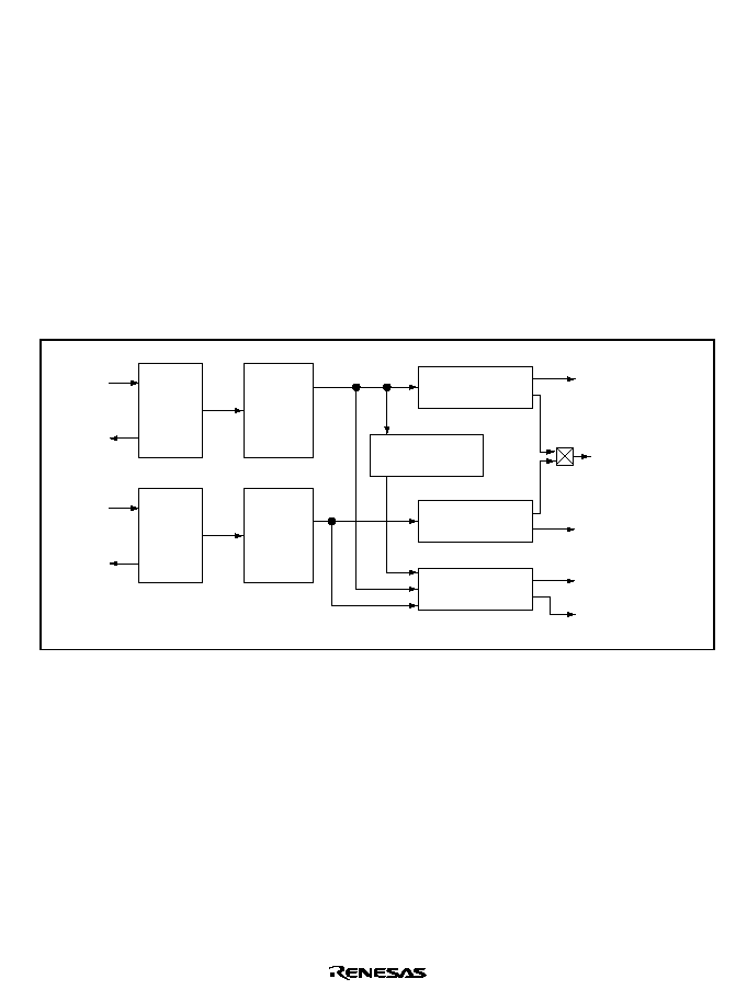
Rev. 1.0, 02/00, page 395 of 1141
21.4.2
Prescalar W (PSW)
PSW is a counter that uses the subclock as an input clock. The PSW also generates the input
clock of the timer A. In this case, the timer A functions as a clock time base.
When reset, the PSW is initialized to H'00, and starts increment after reset has been released.
Even if the mode has been shifted to the standby mode *, watch mode *, subactive mode *, and
subsleep mode *, the PSW continues the operation as long as the clocks are supplied by the X1
and X2 pins.
The PSW can also be initialized to H'00 by setting the TMA3 and TMA2 bits of the timer mode
register A (TMA) to 11.
Note: *
When the timer A is in module stop mode, the operation is stopped.
Figure 21.2 shows the supply of the clocks to the peripheral function by the PSS and PSW.
/131072 to
/2
Timer
SCI
OSC1
fosc
OSC2
w/128
w/4
w
Timer A
Prescalar S
X1
(fx)
X2
CPU
ROM
RAM
TMOW pin
Peripheral register
I/O port
Intermediate
speed clock
frequency divider
Prescalar W
System clock
selection
Subclock
frequency
dividers
(1/2, 1/4, and 1/8)
Subclock
oscillator
System
clock
oscillator
System
clock
duty
correction
circuit
Figure 21.2 Clock Supply
21.4.3
Stable Oscillation Wait Time Count
For the count of the stable oscillation stable wait time during the return from the low power
consumption mode excluding the sleep mode, see section 4, Power-Down State.

Rev. 1.0, 02/00, page 396 of 1141
21.4.4
8-bit PWM
This 8-bit PWM controls the duty control PWM signal in the conversion cycle 256 states. It
counts the cycle and the duty cycle at 2
7
to 2
0
of the FRC. It can be used for controlling reel
motors and loading motors. For details, see section 18, 8-Bit PWM.
21.4.5
8-bit Input Capture Using
,&
,& Pin
This function catches the 8-bit data of 2
15
to 2
8
of the FRC according to the edge of the
,& pin. It
can be used for remote control receiving.
For the edge of the
,& pin, the rising and falling edges can be selected.
The
,& pin has a built-in noise cancel circuit. See section 21.3, Noise Cancel Circuit.
An interrupt request is generated due to the input capture using the
,& pin.
Note:
Rewriting the ICEG bit, NCon/off bit, or PMR16 bit is incorrectly recognized as edge
detection according to the combinations between the state and detection edge of the
,& pin
and the ICIF bit may be set after up to 384
seconds.
21.4.6
Frequency Division Clock Output
The frequency division clock can be output from the TMOW pin. For the frequency division
clock, eight types of clocks can be selected according to the DCS2 to DCS0 bits in PCSR.
The clock in which the system clock was frequency-divided is output in active mode and sleep
mode and the clock in which the subclock was frequency-divided is output in active mode*, sleep
mode*, and subactive mode.
Note: *
When timer A is in module stop mode, no clock is output.

Rev. 1.0, 02/00, page 397 of 1141
Section 22 Serial Communication Interface 1 (SCI1)
22.1
Overview
The serial communication interface (SCI) can handle both asynchronous and clocked synchronous
serial communication. A function is also provided for serial communication between processors
(multiprocessor communication function).
22.1.1
Features
SCI1 features are listed below.
∑
Choice of asynchronous or synchronous serial communication mode
Asynchronous mode
∑
Serial data communication is executed using an asynchronous system in which
synchronization is achieved character by character
Serial data communication can be carried out with standard asynchronous
communication chips such as a Universal Asynchronous Receiver/Transmitter (UART)
or Asynchronous Communication Interface Adapter (ACIA)
∑
A multiprocessor communication function is provided that enables serial data
communication with a number of processors
∑
Choice of 12 serial data transfer formats
Data length: 7 or 8 bits
Stop bit length: 1 or 2 bits
Parity: Even, odd, or none
Multiprocessor bit: 1 or 0
∑
Receive error detection: Parity, overrun, and framing errors
∑
Break detection: Break can be detected by reading the SI1 pin level directly in case of a
framing error
Clock synchronous mode
∑
Serial data communication is synchronized with a clock
Serial data communication can be carried out with other chips that have a synchronous
communication function
∑
One serial data transfer format
Data length: 8 bits
∑
Receive error detection: Overrun errors detected

Rev. 1.0, 02/00, page 398 of 1141
∑
Full-duplex communication capability
The transmitter and receiver are mutually independent, enabling transmission and reception
to be executed simultaneously
Double-buffering is used in both the transmitter and the receiver, enabling continuous
transmission and continuous reception of serial data
∑
Built-in baud rate generator allows any bit rate to be selected
∑
Choice of serial clock source: internal clock from baud rate generator or external clock from
SCK1 pin
∑
Four interrupt sources
Four interrupt sources (transmit-data-empty, transmit-end, receive-data-full, and receive
error) that can issue requests independently
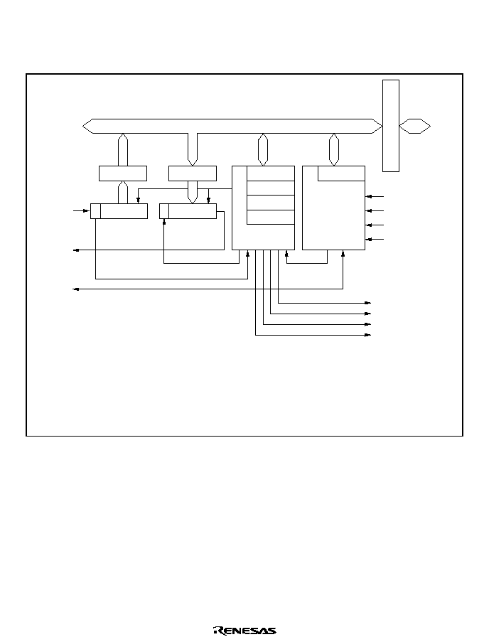
Rev. 1.0, 02/00, page 399 of 1141
22.1.2
Block Diagram
Figure 22.1 shows a block diagram of the SCI.
SI1
SO1
SCK1
Clock
External clock
/4
/16
/64
TEI
TXI
RXI
ERI
RSR1
RDR1
TSR1
TDR1
SMR1
SCR1
SSR1
SCMR1
BRR1
: Receive shift register 1
: Receive data register 1
: Transmit shift register 1
: Transmit data register 1
: Serial mode register 1
: Serial control register 1
: Serial status register 1
: Serial interface mode register 1
: Bit rate register 1
SCMR1
SSR1
SCR1
SMR1
Transmission/
reception
control
Baud rate
generator
BRR1
Module data bus
Bus interface
Internal data bus
RDR1
TSR1
RSR1
Parity generation
Parity check
[Legend]
TDR1
Figure 22.1 Block Diagram of SCI

Rev. 1.0, 02/00, page 400 of 1141
22.1.3
Pin Configuration
Table 22.1 shows the serial pins used by the SCI.
Table 22.1
SCI Pins
Channel
Pin Name
Symbol
I/O
Function
Serial clock pin 1
SCK1
I/O
SCI1 clock input/output
Receive data pin 1
SI1
Input
SCI1 receive data input
1
Transmit data pin 1
SO1
Output
SCI1 transmit data output
22.1.4
Register Configuration
The SCI1 has the internal registers shown in table 22.2. These registers are used to specify
asynchronous mode or synchronous mode, the data format, and the bit rate, and to control the
transmitter/receiver.
Table 22.2
SCI Registers
Channel
Name
Abbrev.
R/W
Initial Value
Address
*1
Serial mode register 1
SMR1
R/W
H'00
H'D148
Bit rate register 1
BRR1
R/W
H'FF
H'D149
Serial control register 1
SCR1
R/W
H'00
H'D14A
Transmit data register 1
TDR1
R/W
H'FF
H'D14B
Serial status register 1
SSR1
R/(W)*
2
H'84
H'D14C
Receive data register 1
RDR1
R
H'00
H'D14D
1
Serial interface mode register 1
SCMR1
R/W
H'F2
H'D14E
MSTPCRH
R/W
H'FF
H'FFEC
Common
Module stop control register
MSTPCRL
R/W
H'FF
H'FFED
Notes: 1. Lower 16 bits of the address.
2. Only 0 can be written, to clear flags.

Rev. 1.0, 02/00, page 401 of 1141
22.2
Register Descriptions
22.2.1
Receive Shift Register 1 (RSR1)
7
--
6
--
5
--
4
--
3
--
0
--
2
--
1
--
Bit :
R/W :
RSR1 is a register used to receive serial data.
The SCI sets serial data input from the SI1 pin in RSR1 in the order received, starting with the
LSB (bit 0), and converts it to parallel data. When one byte of data has been received, it is
transferred to RDR automatically.
RSR1 cannot be directly read or written to by the CPU.
22.2.2
Receive Data Register 1 (RDR1)
7
0
R
6
0
R
5
0
R
4
0
R
3
0
R
0
0
R
2
0
R
1
0
R
Bit :
Initial value :
R/W :
RDR1 is a register that stores received serial data.
When the SCI has received one byte of serial data, it transfers the received serial data from RSR1
to RDR1 where it is stored, and completes the receive operation. After this, RSR1 is receive-
enabled.
Since RSR1 and RDR1 function as a double buffer in this way, continuous receive operations can
be performed.
RDR1 is a read-only register, and cannot be written to by the CPU.
RDR1 is initialized to H'00 by a reset, and in standby mode, watch mode, subactive mode,
subsleep mode, and module stop mode.

Rev. 1.0, 02/00, page 402 of 1141
22.2.3
Transmit Shift Register 1 (TSR1)
7
--
6
--
5
--
4
--
3
--
0
--
2
--
1
--
Bit :
R/W :
TSR1 is a register used to transmit serial data.
To perform serial data transmission, the SCI first transfers transmit data from TDR1 to TSR1, then
sends the data to the SO1 pin starting with the LSB (bit 0).
When transmission of one byte is completed, the next transmit data is transferred from TDR1 to
TSR1, and transmission started, automatically. However, data transfer from TDR1 to TSR1 is not
performed if the TDRE bit in SSR1 is set to 1.
TSR1 cannot be directly read or written to by the CPU.
22.2.4
Transmit Data Register 1 (TDR1)
7
1
R/W
6
1
R/W
5
1
R/W
4
1
R/W
3
1
R/W
0
1
R/W
2
1
R/W
1
1
R/W
Bit :
Initial value :
R/W :
TDR1 is an 8-bit register that stores data for serial transmission.
When the SCI detects that TSR is empty, it transfers the transmit data written in TDR1 to TSR1
and starts serial transmission. Continuous serial transmission can be carried out by writing the
next transmit data to TDR1 during serial transmission of the data in TSR1.
TDR1 can be read or written to by the CPU at all times.
TDR1 is initialized to H'FF by a reset, and in standby mode, watch mode, subactive mode,
subsleep mode, and module stop mode.

Rev. 1.0, 02/00, page 403 of 1141
22.2.5
Serial Mode Register 1 (SMR1)
7
C/A
0
R/W
6
CHR
0
R/W
5
PE
0
R/W
4
O/E
0
R/W
3
STOP
0
R/W
0
CKS0
0
R/W
2
MP
0
R/W
1
CKS1
0
R/W
Bit :
Initial value :
R/W :
SMR1 is an 8-bit register used to set the SCI's serial transfer format and select the baud rate
generator clock source.
SMR1 can be read or written to by the CPU at all times.
SMR1 is initialized to H'00 by a reset, and in standby mode, watch mode, subactive mode,
subsleep mode, and module stop mode.
Bit 7
Communication Mode (C/
): Selects asynchronous mode or clock synchronous mode as
the SCI operating mode.
Bit 7
C/
Description
0
Asynchronous mode
(Initial value)
1
Clock synchronous mode
Bit 6
Character Length (CHR): Selects 7 or 8 bits as the data length in asynchronous mode.
In synchronous mode, a fixed data length of 8 bits is used regardless of the CHR setting.
Bit 6
CHR
Description
0
8-bit data
(Initial value)
1
7-bit data*
Note:
*
When 7-bit data is selected, the MSB (bit 7) of TDR1 is not transmitted, and LSB-
first/MSB-first selection is not available.

Rev. 1.0, 02/00, page 404 of 1141
Bit 5
Parity Enable (PE): In asynchronous mode, selects whether or not parity bit addition is
performed in transmission, and parity bit checking in reception. In synchronous mode, or when a
multiprocessor format is used, parity bit addition and checking is not performed, regardless of the
PE bit setting.
Bit 5
PE
Description
0
Parity bit addition and checking disabled
(Initial value)
1
Parity bit addition and checking enabled*
Note:
*
When the PE bit is set to 1, the parity (even or odd) specified by the O/
bit is added to
transmit data before transmission. In reception, the parity bit is checked for the parity
(even or odd) specified by the O/
bit.
Bit 4
Parity Mode (O/
): Selects either even or odd parity for use in parity addition and
checking.
The O/
bit setting is only valid when the PE bit is set to 1, enabling parity bit addition and
checking, in asynchronous mode. The O/
bit setting is invalid in synchronous mode, when parity
bit addition and checking is disabled in asynchronous mode, and when a multiprocessor format is
used.
Bit 4
O/
Description
0
Even parity
*1
(Initial value)
1
Odd parity
*2
Notes: 1. When even parity is set, parity bit addition is performed in transmission so that the total
number of 1 bits in the transmit character plus the parity bit is even. In reception, a
check is performed to see if the total number of 1 bits in the receive character plus the
parity bit is even.
2. When odd parity is set, parity bit addition is performed in transmission so that the total
number of 1 bits in the transmit character plus the parity bit is odd. In reception, a
check is performed to see if the total number of 1 bits in the receive character plus the
parity bit is odd.

Rev. 1.0, 02/00, page 405 of 1141
Bit 3
Stop Bit Length (STOP): Selects 1 or 2 bits as the stop bit length in asynchronous mode.
The STOP bit setting is only valid in asynchronous mode. If synchronous mode is set the STOP
bit setting is invalid since stop bits are not added.
Bit 3
STOP
Description
0
1 stop bit
*1
(Initial value)
1
2 stop bits
*2
Notes: 1. In transmission, a single 1 bit (stop bit) is added to the end of a transmit character
before it is sent.
2. In transmission, two 1 bits (stop bits) are added to the end of a transmit character
before it is sent.
In reception, only the first stop bit is checked, regardless of the STOP bit setting. If the second
stop bit is 1, it is treated as a stop bit; if it is 0, it is treated as the start bit of the next transmit
character.
Bit 2
Multiprocessor Mode (MP): Selects multiprocessor format. When multiprocessor format
is selected, the PE bit and O/
bit parity settings are invalid. The MP bit setting is only valid in
asynchronous mode; it is invalid in synchronous mode.
For details of the multiprocessor communication function, see section 22.3.3, Multiprocessor
Communication Function.
Bit 2
MP
Description
0
Multiprocessor function disabled
(Initial value)
1
Multiprocessor format selected
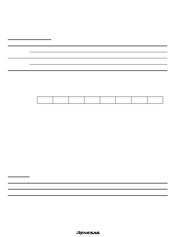
Rev. 1.0, 02/00, page 406 of 1141
Bits 1 and 0
Clock Select 1 and 0 (CKS1, CKS0): These bits select the clock source for the
baud rate generator. The clock source can be selected from
,
/4,
/16, and
/64, according to
the setting of bits CKS1 and CKS0.
For the relation between the clock source, the bit rate register setting, and the baud rate, see
section 22.2.8, Bit Rate Register 1.
Bit 1
Bit 0
CKS1
CKS0
Description
0
clock
(Initial value)
0
1
/4 clock
0
/16 clock
1
1
/64 clock
22.2.6
Serial Control Register 1 (SCR1)
7
TIE
0
R/W
6
RIE
0
R/W
5
TE
0
R/W
4
RE
0
R/W
3
MPIE
0
R/W
0
CKE0
0
R/W
2
TEIE
0
R/W
1
CKE1
0
R/W
Bit :
Initial value :
R/W :
SCR1 is a register that performs enabling or disabling of SCI transfer operations, serial clock
output in asynchronous mode, and interrupt requests, and selection of the serial clock source.
SCR1 can be read or written to by the CPU at all times.
SCR1 is initialized to H'00 by a reset, and in standby mode, watch mode, subactive mode,
subsleep mode, and module stop mode.
Bit 7
Transmit Interrupt Enable (TIE): Enables or disables transmit-data-empty interrupt
(TXI) request generation when serial transmit data is transferred from TDR1 to TSR1 and the
TDRE flag in SSR1 is set to 1.
Bit 7
TIE
Description
0
Transmit-data-empty interrupt (TXI) request disabled*
(Initial value)
1
Transmit-data-empty interrupt (TXI) request enabled
Note:
*
TXI interrupt request cancellation can be performed by reading 1 from the TDRE flag,
then clearing it to 0, or clearing the TIE bit to 0.

Rev. 1.0, 02/00, page 407 of 1141
Bit 6
Receive Interrupt Enable (RIE): Enables or disables receive-data-full interrupt (RXI)
request and receive-error interrupt (ERI) request generation when serial receive data is transferred
from RSR1 to RDR1 and the RDRF flag in SSR1 is set to 1.
Bit 6
RIE
Description
0
Receive-data-full interrupt (RXI) request and receive-error interrupt (ERI) request
disabled*
(Initial value)
1
Receive-data-full interrupt (RXI) request and receive-error interrupt (ERI) request
enabled
Note:
*
RXI and ERI interrupt request cancellation can be performed by reading 1 from the
RDRF, FER, PER, or ORER flag, then clearing the flag to 0, or clearing the RIE bit to 0.
Bit 5
Transmit Enable (TE): Enables or disables the start of serial transmission by the SCI.
Bit 5
TE
Description
0
Transmission disabled
*1
(Initial value)
1
Transmission enabled
*2
Notes: 1. The TDRE flag in SSR1 is fixed at 1.
2. In this state, serial transmission is started when transmit data is written to TDR1 and the
TDRE flag in SSR1 is cleared to 0.
SMR1 setting must be performed to decide the transmission format before setting the
TE bit to 1.
Bit 4
Receive Enable (RE): Enables or disables the start of serial reception by the SCI.
Bit 4
RE
Description
0
Reception disabled
*1
(Initial value)
1
Reception enabled
*2
Notes: 1. Clearing the RE bit to 0 does not affect the RDRF, FER, PER, and ORER flags, which
retain their states.
2. Serial reception is started in this state when a start bit is detected in asynchronous
mode or serial clock input is detected in synchronous mode.
SMR1 setting must be performed to decide the reception format before setting the RE
bit to 1.

Rev. 1.0, 02/00, page 408 of 1141
Bit 3
Multiprocessor Interrupt Enable (MPIE): Enables or disables multiprocessor interrupts.
The MPIE bit setting is only valid in asynchronous mode when receiving with the MP bit in
SMR1 set to 1.
The MPIE bit setting is invalid in clock synchronous mode or when the MP bit is cleared to 0.
Bit 3
MPIE
Description
0
Multiprocessor interrupts disabled (normal reception performed)
(Initial value)
[Clearing conditions]
1. When the MPIE bit is cleared to 0
2. When data with MPB = 1 is received
1
Multiprocessor interrupts enabled*
Receive interrupt (RXI) requests, receive-error interrupt (ERI) requests, and setting of
the RDRF, FER, and ORER flags in SSR1 are disabled until data with the
multiprocessor bit set to 1 is received.
Note:
*
When receive data including MPB = 0 is received, receive data transfer from RSR1 to
RDR1, receive error detection, and setting of the RDRF, FER, and ORER flags in
SSR1, is not performed. When receive data with MPB = 1 is received, the MPB bit in
SSR1 is set to 1, the MPIE bit is cleared to 0 automatically, and generation of RXI and
ERI interrupts (when the TIE and RIE bits in SCR are set to 1) and FER and ORER flag
setting is enabled.
Bit 2
Transmit End Interrupt Enable (TEIE): Enables or disables transmit-end interrupt
(TEI) request generation if there is no valid transmit data in TDR when the MSB is transmitted.
Bit 2
TEIE
Description
0
Transmit-end interrupt (TEI) request disabled*
(Initial value)
1
Transmit-end interrupt (TEI) request enabled*
Note:
*
TEI cancellation can be performed by reading 1 from the TDRE flag in SSR1, then
clearing it to 0 and clearing the TEND flag to 0, or clearing the TEIE bit to 0.

Rev. 1.0, 02/00, page 409 of 1141
Bits 1 and 0
Clock Enable 1 and 0 (CKE1, CKE0): These bits are used to select the SCI clock
source and enable or disable clock output from the SCK pin. The combination of the CKE1 and
CKE0 bits determines whether the SCK pin functions as an I/O port, the serial clock output pin, or
the serial clock input pin.
The setting of the CKE0 bit, however, is only valid for internal clock operation (CKE1 = 0) in
asynchronous mode. The CKE0 bit setting is invalid in synchronous mode, and in the case of
external clock operation (CKE1 = 1). Note that the SCI's operating mode must be decided using
SMR1 before setting the CKE1 and CKE0 bits.
For details of clock source selection, see table 22.9 in section 22.3, Operation.
Bit 1
Bit 0
CKE1
CKE0
Description
Asynchronous mode
Internal clock/SCK pin functions as I/O port
*1
0
Clock synchronous
mode
Internal clock/SCK pin functions as serial
clock output
*1
Asynchronous mode
Internal clock/SCK pin functions as clock
output
*2
0
1
Clock synchronous
mode
Internal clock/SCK pin functions as serial
clock output
Asynchronous mode
External clock/SCK pin functions as clock
input
*3
0
Clock synchronous
mode
External clock/SCK pin functions as serial
clock input
Asynchronous mode
External clock/SCK pin functions as clock
input
*3
1
1
Clock synchronous
mode
External clock/SCK pin functions as serial
clock input
Notes: 1. Initial value.
2. Outputs a clock of the same frequency as the bit rate.
3. Inputs a clock with a frequency 16 times the bit rate.

Rev. 1.0, 02/00, page 410 of 1141
22.2.7
Serial Status Register 1 (SSR1)
7
TDRE
1
R/(W)*
6
RDRF
0
R/(W)*
5
ORER
0
R/(W)*
4
FER
0
R/(W)*
3
PER
0
R/(W)*
0
MPBT
0
R/W
2
TEND
1
R
1
MPB
0
R
Note: * Only 0 can be written to clear the flag.
Bit :
Initial value :
R/W :
SSR1 is an 8-bit register containing status flags that indicate the operating status of the SCI, and
multiprocessor bits.
SSR1 can be read or written to by the CPU at all times. However, 1 cannot be written to flags
TDRE, RDRF, ORER, PER, and FER. Also note that in order to clear these flags they must be
read as 1 beforehand. The TEND flag and MPB flag are read-only flags and cannot be modified.
SSR1 is initialized to H'84 by a reset, and in standby mode, watch mode, subactive mode, subsleep
mode, and module stop mode.
Bit 7
Transmit Data Register Empty (TDRE): Indicates that data has been transferred from
TDR1 to TSR1 and the next serial data can be written to TDR1.
Bit 7
TDRE
Description
0
[Clearing conditions]
When 0 is written in TDRE after reading TDRE = 1
1
[Setting conditions]
(Initial value)
1. When the TE bit in SCR is 0
2. When data is transferred from TDR1 to TSR1 and data can be written to TDR1
Bit 6
Receive Data Register Full (RDRF): Indicates that the received data is stored in RDR1.
Bit 6
RDRF
Description
0
[Clearing conditions]
(Initial value)
When 0 is written in RDRF after reading RDRF = 1
1
[Setting conditions]
When serial reception ends normally and receive data is transferred from RSR to
RDR
Note: RDR1 and the RDRF flag are not affected and retain their previous values when an error is
detected during reception or when the RE bit in SCR1 is cleared to 0.
If reception of the next data is completed while the RDRF flag is still set to 1, an overrun
error will occur and the receive data will be lost.

Rev. 1.0, 02/00, page 411 of 1141
Bit 5
Overrun Error (ORER): Indicates that an overrun error occurred during reception,
causing abnormal termination.
Bit 5
ORER
Description
0
[Clearing conditions]
(Initial value)
*1
When 0 is written in ORER after reading ORER = 1
*1
1
[Setting conditions]
When the next serial reception is completed while RDRF = 1
*2
Notes: 1. The ORER flag is not affected and retains its previous state when the RE bit in SCR1 is
cleared to 0.
2. The receive data prior to the overrun error is retained in RDR1, and the data received
subsequently is lost. Also, subsequent serial reception cannot be continued while the
ORER flag is set to 1. In synchronous mode, serial transmission cannot be continued,
either.
Bit 4
Framing Error (FER): Indicates that a framing error occurred during reception in
asynchronous mode, causing abnormal termination.
Bit 4
FER
Description
0
[Clearing conditions]
(Initial value)
*1
When 0 is written in FER after reading FER = 1
*1
1
[Setting conditions]
When the SCI checks the stop bit at the end of the receive data when reception ends,
and the stop bit is 0
*2
Notes: 1. The FER flag is not affected and retains its previous state when the RE bit in SCR1 is
cleared to 0.
2. In 2-stop-bit mode, only the first stop bit is checked for a value of 1; the second stop bit
is not checked. If a framing error occurs, the receive data is transferred to RDR1 but
the RDRF flag is not set. Also, subsequent serial reception cannot be continued while
the FER flag is set to 1. In synchronous mode, serial transmission cannot be
continued, either.

Rev. 1.0, 02/00, page 412 of 1141
Bit 3
Parity Error (PER): Indicates that a parity error occurred during reception using parity
addition in asynchronous mode, causing abnormal termination.
Bit 4
PER
Description
0
[Clearing conditions]
(Initial value)
When 0 is written in PER after reading PER = 1
*1
1
[Setting conditions]
When, in reception, the number of 1 bits in the receive data plus the parity bit does
not match the parity setting (even or odd) specified by the O/
bit in SMR1
*2
Notes: 1. The PER flag is not affected and retains its previous state when the RE bit in SCR1 is
cleared to 0.
2. If a parity error occurs, the receive data is transferred to RDR1 but the RDRF flag is not
set. Also, subsequent serial reception cannot be continued while the PER flag is set to
1. In synchronous mode, serial transmission cannot be continued, either.
Bit 2
Transmit End (TEND): Indicates that there is no valid data in TDR when the last bit of
the transmit character is sent, and transmission has been ended.
The TEND flag is read-only and cannot be modified.
Bit 2
TEND
Description
0
[Clearing conditions]
When 0 is written in TDRE after reading TDRE = 1
1
[Setting conditions]
(Initial value)
1. When the TE bit in SCR1 is 0
2. When TDRE = 1 at transmission of the last bit of a 1-byte serial transmit character
Bit 1
Multiprocessor Bit (MPB): When reception is performed using a multiprocessor format
in asynchronous mode, MPB stores the multiprocessor bit in the receive data.
MPB is a read-only bit, and cannot be modified.
Bit 1
MPB
Description
0
[Clearing conditions]
(Initial value)*
When data with a 0 multiprocessor bit is received
1
[Setting conditions]
When data with a 1 multiprocessor bit is received
Note:
*
Retains its previous state when the RE bit in SCR1 is cleared to 0 with multiprocessor
format.

Rev. 1.0, 02/00, page 413 of 1141
Bit 0
Multiprocessor Bit Transfer (MPBT): When transmission is performed using a
multiprocessor format in asynchronous mode, MPBT stores the multiprocessor bit to be added to
the transmit data.
The MPBT bit setting is invalid when a multiprocessor format is not used, when not transmitting,
and in synchronous mode.
Bit 0
MPBT
Description
0
Data with a 0 multiprocessor bit is transmitted
(Initial value)
1
Data with a 1 multiprocessor bit is transmitted
22.2.8
Bit Rate Register 1 (BRR1)
7
1
R/W
6
1
R/W
5
1
R/W
4
1
R/W
3
1
R/W
0
1
R/W
2
1
R/W
1
1
R/W
Bit :
Initial value :
R/W :
BRR1 is an 8-bit register that sets the serial transfer bit rate in accordance with the baud rate
generator operating clock selected by bits CKS1 and CKS0 in SMR.
BRR1 can be read or written to by the CPU at all times.
BRR1 is initialized to H'FF by a reset, and in standby mode, watch mode, subactive mode,
subsleep mode, and module stop mode.
Table 22.3 shows sample BRR1 settings in asynchronous mode, and table 22.4 shows sample
BRR1 settings in synchronous mode.

Rev. 1.0, 02/00, page 414 of 1141
Table 22.3
BRR1 Settings for Various Bit Rates (Asynchronous Mode)
Operating Frequency
(MHz)
2
2.097152
2.4576
3
Bit Rate
(bits/s)
n
N
Error
(%)
n
N
Error
(%)
n
N
Error
(%)
n
N
Error
(%)
110
1
141
0.03
1
148
-
0.04
1
174
-
0.26
1
212
0.03
150
1
103
0.16
1
108
0.21
1
127
0.00
1
155
0.16
300
0
207
0.16
0
217
0.21
0
255
0.00
1
77
0.16
600
0
103
0.16
0
108
0.21
0
127
0.00
0
155
0.16
1200
0
51
0.16
0
54
-
0.70
0
63
0.00
0
77
0.16
2400
0
25
0.16
0
26
1.14
0
31
0.00
0
38
0.16
4800
0
12
0.16
0
13
-
2.48
0
15
0.00
0
19
-
2.34
9600
0
6
-
2.48
0
7
0.00
0
9
-
2.34
19200
0
3
0.00
0
4
-
2.34
31250
0
1
0.00
0
0
2
0.00
38400
0
1
0.00
Operating Frequency
(MHz)
3.6864
4
4.9152
5
Bit Rate
(bits/s)
n
N
Error
(%)
n
N
Error
(%)
n
N
Error
(%)
n
N
Error
(%)
110
2
64
0.70
2
70
0.03
2
86
0.31
2
88
-
0.25
150
1
191
0.00
1
207
0.16
1
255
0.00
2
64
0.16
300
1
95
0.00
1
103
0.16
1
127
0.00
1
129
0.16
600
0
191
0.00
0
207
0.16
0
255
0.00
1
64
0.16
1200
0
95
0.00
0
103
0.16
0
127
0.00
0
129
0.16
2400
0
47
0.00
0
51
0.16
0
63
0.00
0
64
0.16
4800
0
23
0.00
0
25
0.16
0
31
0.00
0
32
-
1.36
9600
0
11
0.00
0
12
0.16
0
15
0.00
0
15
1.73
19200
0
5
0.00
0
7
0.00
0
7
1.73
31250
0
3
0.00
0
4
-
1.70
0
4
0.00
38400
0
2
0.00
0
3
0.00
0
3
1.73

Rev. 1.0, 02/00, page 415 of 1141
Operating Frequency
(MHz)
6
6.144
7.3728
8
Bit Rate
(bits/s)
n
N
Error
(%)
n
N
Error
(%)
n
N
Error
(%)
n
N
Error
(%)
110
2
106
-
0.44
2
108
0.08
2
130
-
0.07
2
141
0.03
150
2
77
0.16
2
79
0.00
2
95
0.00
2
103
0.16
300
1
155
0.16
1
159
0.00
1
191
0.00
1
207
0.16
600
1
77
0.16
1
79
0.00
1
95
0.00
1
103
0.16
1200
0
155
0.16
0
159
0.00
0
191
0.00
0
207
0.16
2400
0
77
0.16
0
79
0.00
0
95
0.00
0
103
0.16
4800
0
38
0.16
0
39
0.00
0
47
0.00
0
51
0.16
9600
0
19
-
2.34
0
19
0.00
0
23
0.00
0
25
0.16
19200
0
9
-
2.34
0
9
0.00
0
11
0.00
0
12
0.16
31250
0
5
0.00
0
5
2.40
0
7
0.00
38400
0
4
-
2.34
0
4
0.00
0
5
0.00
Operating Frequency
(MHz)
9.8304
10
Bit Rate
(bits/s)
n
N
Error
(%)
n
N
Error
(%)
110
2
174
-
0.26
2
177
-
0.25
150
2
127
0.00
2
129
0.16
300
1
255
0.00
2
64
0.16
600
1
127
0.00
1
129
0.16
1200
0
255
0.00
1
64
0.16
2400
0
127
0.00
0
129
0.16
4800
0
63
0.00
0
64
0.16
9600
0
31
0.00
0
32
-
1.36
19200
0
15
0.00
0
15
1.73
31250
0
9
-
1.70
0
9
0.00
38400
0
7
0.00
0
7
1.73

Rev. 1.0, 02/00, page 416 of 1141
Table 22.4
BRR1 Settings for Various Bit Rates (Synchronous Mode)
Operating Frequency
(MHz)
2
4
8
10
Bit Rate
(bits/s)
n
N
n
N
n
N
n
N
110
3
70
250
2
124
2
249
3
124
500
1
249
2
124
2
249
1 k
1
124
1
249
2
124
2.5 k
0
199
1
99
1
199
1
249
5 k
0
99
0
199
1
99
1
124
10 k
0
49
0
99
0
199
0
249
25 k
0
19
0
39
0
79
0
99
50 k
0
9
0
19
0
39
0
49
100 k
0
4
0
9
0
19
0
24
250 k
0
1
0
3
0
7
0
9
500 k
0
0*
0
1
0
3
0
4
1 M
0
0*
0
1
2.5 M
0
0*
5 M
Note: As far as possible, the setting should be made so that the error is no more than 1%.
Legend:
Blank: Cannot be set.
--:
Can be set, but there will be a degree of error.
*:
Continuous transfer is not possible.

Rev. 1.0, 02/00, page 417 of 1141
The BRR1 setting is found from the following equations.
∑
Asynchronous mode:
N =
◊
10
6
-
1
64
◊
2
2n
-
1
◊
B
∑
Synchronous mode:
N =
◊
10
6
-
1
8
◊
2
2n
-
1
◊
B
Where
B:
Bit rate (bits/s)
N:
BRR1 setting for baud rate generator (0
N
255)
:
Operating frequency (MHz)
n:
Baud rate generator input clock (n = 0 to 3)
(See the table below for the relation between n and the clock.)
SMR1 Setting
n
Clock
CKS1
CKS0
0
0
0
1
/4
0
1
2
/16
1
0
3
/64
1
1
The bit rate error in asynchronous mode is found from the following equation:
Error (%) = {
◊
10
6
-
1 }
◊
100
(N + 1)
◊
B
◊
64
◊
2
2n
-
1
Table 22.5 shows the maximum bit rate for each frequency in asynchronous mode. Tables 22.6
and 22.7 show the maximum bit rates with external clock input.

Rev. 1.0, 02/00, page 418 of 1141
Table 22.5
Maximum Bit Rate for Each Frequency (Asynchronous Mode)
(MHz)
Maximum Bit Rate (bits/s)
n
N
2
62500
0
0
2.097152
65536
0
0
2.4576
76800
0
0
3
93750
0
0
3.6864
115200
0
0
4
125000
0
0
4.9152
153600
0
0
5
156250
0
0
6
187500
0
0
6.144
192000
0
0
7.3728
230400
0
0
8
250000
0
0
9.8304
307200
0
0
10
312500
0
0

Rev. 1.0, 02/00, page 419 of 1141
Table 22.6
Maximum Bit Rate with External Clock Input (Asynchronous Mode)
(MHz)
External Input Clock (MHz)
Maximum Bit Rate (bits/s)
2
0.5000
31250
2.097152
0.5243
32768
2.4576
0.6144
38400
3
0.7500
46875
3.6864
0.9216
57600
4
1.0000
62500
4.9152
1.2288
76800
5
1.2500
78125
6
1.5000
93750
6.144
1.5360
96000
7.3728
1.8432
115200
8
2.0000
125000
9.8304
2.4576
153600
10
2.5000
156250
Table 22.7
Maximum Bit Rate with External Clock Input (Synchronous Mode)
(MHz)
External Input Clock (MHz)
Maximum Bit Rate (bits/s)
2
0.3333
333333.3
4
0.6667
666666.7
6
1.0000
1000000.0
8
1.3333
1333333.3
10
1.6667
1666666.7

Rev. 1.0, 02/00, page 420 of 1141
22.2.9
Serial Interface Mode Register 1 (SCMR1)
7
--
1
--
6
--
1
--
5
--
1
--
4
--
1
--
3
SDIR
0
R/W
0
SMIF
0
R/W
2
SINV
0
R/W
1
--
1
--
Bit :
Initial value :
R/W :
SCMR1 is an 8-bit readable/writable register used to select SCI functions.
SCMR1 is initialized to H'F2 by a reset, and in standby mode, watch mode, subactive mode,
subsleep mode, and module stop mode.
Bits 7 to 4
Reserved: These bits cannot be modified and are always read as 1.
Bit 3
Data Transfer Direction (SDIR): Selects the serial/parallel conversion format.
Bit 3
SDIR
Description
0
TDR contents are transmitted LSB-first
(Initial value)
Receive data is stored in RDR1 LSB-first
1
TDR contents are transmitted MSB-first
Receive data is stored in RDR1 MSB-first
Bit 2
Data Invert (SINV): Specifies inversion of the data logic level. The SINV bit does not
affect the logic level of the parity bit(s): parity bit inversion requires inversion of the O/
bit in
SMR1.
Bit 2
SINV
Description
0
TDR1 contents are transmitted without modification
(Initial value)
Receive data is stored in RDR1 without modification
1
TDR1 contents are inverted before being transmitted
Receive data is stored in RDR1 in inverted form
Bit 1
Reserved: This bit cannot be modified and is always read as 1.
Bit 0
Reserved: 1 should not be written in this bit.

Rev. 1.0, 02/00, page 421 of 1141
22.2.10
Module Stop Control Register (MSTPCR)
7
1
R/W
6
1
R/W
5
1
R/W
4
1
R/W
3
1
R/W
2
1
R/W
1
1
R/W
0
1
R/W
7
1
R/W
6
1
R/W
5
1
R/W
4
1
R/W
3
1
R/W
2
1
R/W
1
1
R/W
0
1
R/W
MSTPCRH
MSTPCRL
MSTP15 MSTP14 MSTP13 MSTP12 MSTP11 MSTP10 MSTP9 MSTP8
MSTP7
MSTP6 MSTP5
MSTP4
MSTP3
MSTP2
MSTP1
MSTP0
Bit :
Initial value :
R/W :
MSTPCR, comprising two 8-bit readable/writable registers, performs module stop mode control.
When bit MSTP8 is set to 1, SCI1 operation stops at the end of the bus cycle and a transition is
made to module stop mode. For details, see section 4.5, Module Stop Mode.
MSTPCR is initialized to H'FFFF by a reset.
Bit 0
Module Stop (MSTP8): Specifies the SCI1 module stop mode.
MSTPCRH
Bit 0
MSTP8
Description
0
SCI1 module stop mode is cleared
1
SCI2 module stop mode is set
(Initial value)

Rev. 1.0, 02/00, page 422 of 1141
22.3
Operation
22.3.1
Overview
The SCI can carry out serial communication in two modes: asynchronous mode in which
synchronization is achieved character by character, and synchronous mode in which
synchronization is achieved with clock pulses.
Selection of asynchronous or synchronous mode and the transmission format is made using SMR1
as shown in table 22.8. The SCI clock is determined by a combination of the C/
bit in SMR1
and the CKE1 and CKE0 bits in SCR1, as shown in table 22.9.
∑
Asynchronous Mode
Data length: Choice of 7 or 8 bits
Choice of parity addition, multiprocessor bit addition, and addition of 1 or 2 stop bits (the
combination of these parameters determines the transfer format and character length)
Detection of framing, parity, and overrun errors, and breaks, during reception
Choice of internal or external clock as SCI clock source
∑
When internal clock is selected:
The SCI operates on the baud rate generator clock and a clock with the same frequency
as the bit rate can be output
∑
When external clock is selected:
A clock with a frequency of 16 times the bit rate must be input (the built-in baud rate
generator is not used)
∑
Clock Synchronous Mode
Transfer format: Fixed 8-bit data
Detection of overrun errors during reception
Choice of internal or external clock as SCI clock source
∑
When internal clock is selected:
The SCI operates on the baud rate generator clock and a serial clock is output off-chip
∑
When external clock is selected:
The built-in baud rate generator is not used, and the SCI operates on the input serial
clock

Rev. 1.0, 02/00, page 423 of 1141
Table 22.8
SMR1 Settings and Serial Transfer Format Selection
SMR1 Settings
SCI Transfer Format
Bit 7
Bit 6
Bit 2
Bit 5
Bit 3
C/
CHR
MP
PE
STOP
Mode
Data
Length
Multiproc-
essor Bit
Parity
Bit
Stop Bit
Length
0
1 bit
0
1
No
2 bits
0
1 bit
0
1
1
8-bit
data
Yes
2 bits
0
1 bit
0
1
No
2 bits
0
1 bit
1
0
1
1
Asynchro-
nous mode
7-bit
data
No
Yes
2 bits
0
1 bit
0
1
8-bit
data
2 bits
0
1 bit
0
1
1
1
Asynchro-
nous mode
(multi-
processor
format)
7-bit
data
Yes
2 bits
1
Clock
synchronous
mode
8-bit
data
No
No
Table 22.9
SMR1 and SCR1 Settings and SCI Clock Source Selection
SMR1 SCR1 Setting
Bit 7
Bit 1
Bit 0
SCI Transfer Clock
C/
CKE1
CKE0
Mode
Clock Source
SCK Pin Function
0
SCI does not use SCK pin
0
1
Internal
Outputs clock with same frequency
as bit rate
0
0
1
1
Asynchronous
mode
External
Inputs clock with frequency of 16
times the bit rate
0
0
1
Internal
Outputs serial clock
0
1
1
1
Clock
synchronous
mode
External
Inputs serial clock
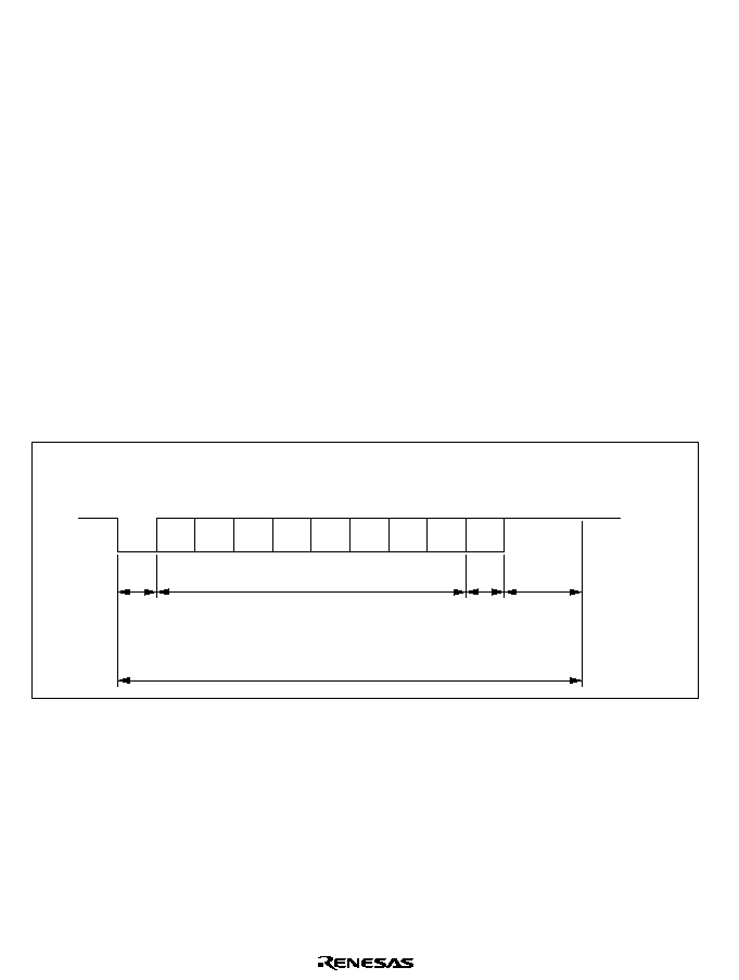
Rev. 1.0, 02/00, page 424 of 1141
22.3.2
Operation in Asynchronous Mode
In asynchronous mode, characters are sent or received, each preceded by a start bit indicating the
start of communication and followed by one or two stop bits indicating the end of communication.
Serial communication is thus carried out with synchronization established on a character-by-
character basis.
Inside the SCI, the transmitter and receiver are independent units, enabling full-duplex
communication. Both the transmitter and the receiver also have a double-buffered structure, so
that data can be read or written during transmission or reception, enabling continuous data
transfer.
Figure 22.2 shows the general format for asynchronous serial communication.
In asynchronous serial communication, the transmission line is usually held in the mark state (high
level). The SCI monitors the transmission line, and when it goes to the space state (low level),
recognizes a start bit and starts serial communication.
One serial communication character consists of a start bit (low level), followed by data (in LSB-
first order), a parity bit (high or low level), and finally one or two stop bits (high level).
In asynchronous mode, the SCI performs synchronization at the falling edge of the start bit in
reception. The SCI samples the data on the 8th pulse of a clock with a frequency of 16 times the
length of one bit, so that the transfer data is latched at the center of each bit.
LSB
Start
bit
MSB
Idle state
(mark state)
Stop
bit(s)
0
Transmit/receive data
D0
D1
D2
D3
D4
D5
D6
D7
0/1
1
1
1
1
Serial
data
Parity
bit
1 bit
1 or 2 bits
7 or 8 bits
1 bit,
or none
One unit of transfer data (character or frame)
Figure 22.2 Data Format in Asynchronous Communication
(Example with 8-Bit Data, Parity, Two Stop Bits)
Rev. 1.0, 02/00, page 425 of 1141
∑
Data Transfer Format
Table 22.10 shows the data transfer formats that can be used in asynchronous mode. Any of
12 transfer formats can be selected by settings in SMR1.
Table 22.10 Serial Transfer Formats (Asynchronous Mode)
PE
0
0
1
1
0
0
1
1
--
--
--
--
S
8-bit data
STOP
S
7-bit data
STOP
S
8-bit data
STOP STOP
S
8-bit data
P STOP
S
7-bit data
STOP
P
S
8-bit data
MPB STOP
S
8-bit data
MPB STOP STOP
S
7-bit data
STOP
MPB
S
7-bit data
STOP
MPB
STOP
S
7-bit data
STOP
STOP
CHR
0
0
0
0
1
1
1
1
0
0
1
1
MP
0
0
0
0
0
0
0
0
1
1
1
1
STOP
0
1
0
1
0
1
0
1
0
1
0
1
SMR1 Settings
1
2
3
4
5
6
7
8
9
10
11
12
Serial Transfer Format and Frame Length
STOP
S
8-bit data
P STOP
S
7-bit data
STOP
P
STOP
[Legend]
S
STOP
P
MPB
: Start bit
: Stop bit
: Parity bit
: Multiprocessor bit
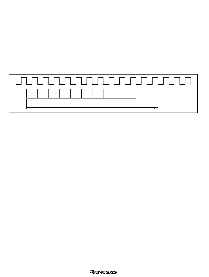
Rev. 1.0, 02/00, page 426 of 1141
∑
Clock
Either an internal clock generated by the built-in baud rate generator or an external clock input
at the SCK pin can be selected as the SCI's serial clock, according to the setting of the C/
bit
in SMR1 and the CKE1 and CKE0 bits in SCR1. For details of SCI clock source selection, see
table 22.9.
When an external clock is input at the SCK pin, the clock frequency should be 16 times the bit
rate used.
When the SCI is operated on an internal clock, the clock can be output from the SCK pin. The
frequency of the clock output in this case is equal to the bit rate, and the phase is such that the
rising edge of the clock is at the center of each transmit data bit, as shown in figure 22.3.
0
1 frame
D0
D1
D2
D3
D4
D5
D6
D7
0/1
1
1
Figure 22.3 Relation between Output Clock and Transfer Data Phase
(Asynchronous Mode)
Rev. 1.0, 02/00, page 427 of 1141
∑
Data Transfer Operations
SCI Initialization (Asynchronous Mode)
Before transmitting and receiving data, first clear the TE and RE bits in SCR1 to 0, then
initialize the SCI as described below.
When the operating mode, transfer format, etc., is changed, the TE and RE bits must be
cleared to 0 before making the change using the following procedure. When the TE bit is
cleared to 0, the TDRE flag is set to 1 and TSR1 is initialized. Note that clearing the RE
bit to 0 does not change the contents of the RDRF, PER, FER, and ORER flags, or the
contents of RDR1.
When an external clock is used the clock should not be stopped during operation, including
initialization, since operation is uncertain.
Figure 22.4 shows a sample SCI initialization flowchart.
Wait
<Initialization completed>
Start initialization
Set data transfer format
in SMR1 and SCMR1
[1]
Set CKE1 and CKE0 bits in SCR1
(TE, RE bits 0)
No
Yes
Set value in BRR1
Clear TE and RE bits in SCR1 to 0
[2]
[3]
Set TE and RE bits in SCR1 to 1,
and set RIE, TIE, TEIE,
and MPIE bits
[4]
1-bit interval elapsed?
Set the clock selection in SCR1.
Be sure to clear bits RIE, TIE, TEIE, and
MPIE, and bits TE and RE, to 0.
When the clock is selected in
asynchronous mode, it is output
immediately after SCR1 settings are made.
Set the data transfer format in SMR1 and
SCMR1.
Write a value corresponding to the bit rate
to BRR1. This is not necessary if an
external clock is used.
Wait at least one bit interval, then set the
TE bit or RE bit in SCR1 to 1. Also set the
RIE, TIE, TEIE, and MPIE bits.
Setting the TE and RE bits enables the
SO1 and SI1 pins to be used.
[1]
[2]
[3]
[4]
Figure 22.4 Sample SCI Initialization Flowchart
Rev. 1.0, 02/00, page 428 of 1141
Serial Data Transmission (Asynchronous Mode)
Figure 22.5 shows a sample flowchart for serial transmission.
The following procedure should be used for serial data transmission.
No
< End >
[1]
Yes
Initialization
Start transmission
Read TDRE flag in SSR1
[1]
Write transmit data to TDR1 and
clear TDRE flag in SSR to 0
No
Yes
No
Yes
Read TEND flag in SSR1
[3]
No
Yes
[4]
Clear PDR to 0
and set PCR to 1
Clear TE bit in SCR1 to 0
TDRE=1
All data transmitted?
TEND=1
Break output?
SCI initialization:
The SO1 pin is automatically designated as
the transmit data output pin.
SCI status check and transmit data write:
Read SSR and check that the TDRE flag is
set to 1, then write transmit data to TDR1
and clear the TDRE flag to 0.
Serial transmission continuation procedure:
To continue serial transmission, read 1
from the TDRE flag to confirm that writing is
possible, then write data to TDR1, and then
clear the TDRE flag to 0.
Break output at the end of serial
transmission:
To output a break in serial transmission, set
PCR for the port corresponding to the SO1
pin to 1, clear PDR to 0, then clear the TE
bit in SCR1 to 0.
[1]
[2]
[3]
[4]
Figure 22.5 Sample Serial Transmission Flowchart

Rev. 1.0, 02/00, page 429 of 1141
In serial transmission, the SCI operates as described below.
1. The SCI monitors the TDRE flag in SSR1, and if it is 0, recognizes that data has been written
to TDR1, and transfers the data from TDR1 to TSR1.
2. After transferring data from TDR1 to TSR1, the SCI sets the TDRE flag to 1 and starts
transmission.
If the TIE bit is set to 1 at this time, a transmit data empty interrupt (TXI) is generated.
The serial transmit data is sent from the SO1 pin in the following order.
a. Start bit:
One 0-bit is output.
b. Transmit data:
8-bit or 7-bit data is output in LSB-first order.
c. Parity bit or multiprocessor bit:
One parity bit (even or odd parity), or one multiprocessor bit is output.
A format in which neither a parity bit nor a multiprocessor bit is output can also be
selected.
d. Stop bit(s):
One or two 1-bits (stop bits) are output.
e. Mark state:
1 is output continuously until the start bit that starts the next transmission is sent.
3. The SCI checks the TDRE flag at the timing for sending the stop bit.
If the TDRE flag is cleared to 0, the data is transferred from TDR1 to TSR1, the stop bit is
sent, and then serial transmission of the next frame is started.
If the TDRE flag is set to 1, the TEND flag in SSR1 is set to 1, the stop bit is sent, and then the
mark state is entered in which 1 is output continuously. If the TEIE bit in SCR1 is set to 1 at
this time, a TEI interrupt request is generated.

Rev. 1.0, 02/00, page 430 of 1141
Figure 22.6 shows an example of the operation for transmission in asynchronous mode.
TDRE
TEND
0
1 frame
D0
D1
D7
0/1
1
0
D0
D1
D7
0/1
1
1
1
Data
Start
bit
Parity
bit
Stop
bit
Start
bit
Data
Parity
bit
Stop
bit
TXI interrupt
request
generated
Data written to TDR1 and
TDRE flag cleared to 0
in TXI interrupt handling
routine
TEI interrupt request
generated
Idle state
(mark state)
TXI interrupt request
generated
Figure 22.6 Example of Operation in Transmission in Asynchronous Mode
(Example with 8-Bit Data, Parity, One Stop Bit)
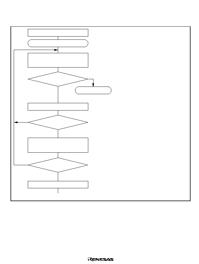
Rev. 1.0, 02/00, page 431 of 1141
Serial Data Reception (Asynchronous Mode)
Figures 22.7 and 22.8 show sample flowcharts for serial reception.
The following procedure should be used for serial data reception.
Yes
< End >
[1]
No
Initialization
Start reception
[2]
No
Yes
Read RDRF flag in SSR1
[4]
[5]
Clear RE bit in SCR1 to 0
Read ORER, PER,
FER flags in SSR1
Error handling
(Continued on next page)
[3]
Read receive data in RDR1, and clear
RDRF flag in SSR1 to 0
No
Yes
PER
FER
ORER=1
RDRF=1
All data received?
SCI initialization:
The SI1 pin is automatically designated as
the receive data input pin.
Receive error handling and break
detection:
If a receive error occurs, read the ORER,
PER, and FER flags in SSR to identify the
error. After performing the appropriate
error handling, ensure that the PERE, PER,
and FER flags are all cleared to 0.
Reception cannot be resumed if any of
these flags are set to 1. In the case of a
framing error, a break can be detected by
reading the value of the input port
corresponding to the SI1 pin.
SCI status check and receive data read:
Read SSR and check that RDRF = 1, then
read the receive data in RDR1 and clear
the RDRF flag to 0. Transition of the RDRF
flag from 0 to 1 can also be identified by an
RXI interrupt.
Serial reception continuation procedure:
To continue serial reception, before the
stop bit for the current frame is received,
read the RDRF flag, read RDR1, and clear
the RDRF flag to 0.
[1]
[2][3]
[4]
[5]
Figure 22.7 Sample Serial Reception Data Flowchart (1)
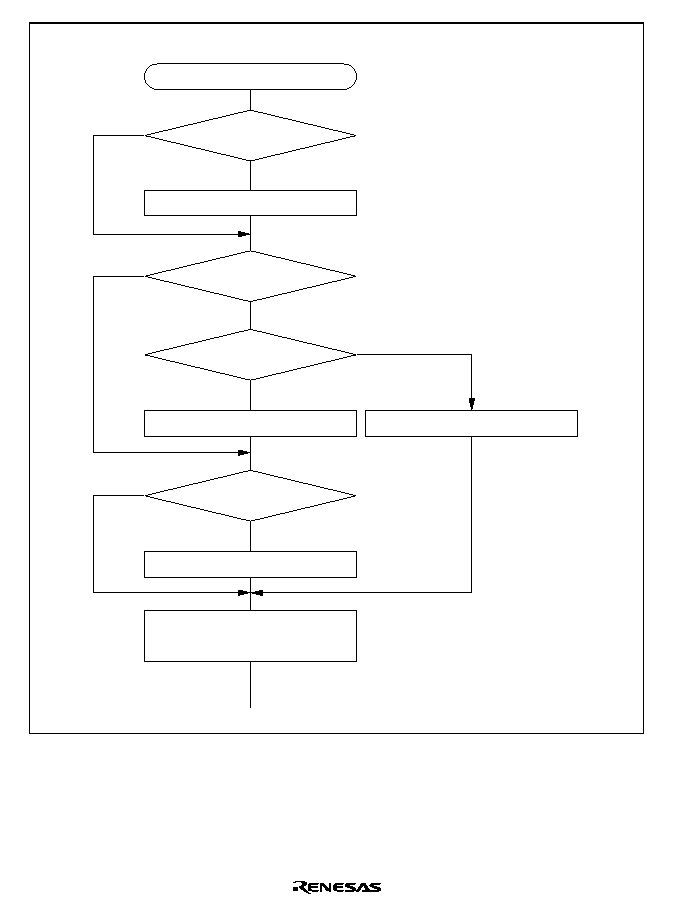
Rev. 1.0, 02/00, page 432 of 1141
< End >
[3]
Error handling
Parity error handling
Yes
No
Clear ORER, PER, and FER
flags in SSR1 to 0
No
Yes
No
Yes
Framing error handling
No
Yes
Overrun error handling
ORER=1
FER=1
Break?
PER=1
Clear RE bit in SCR1 to 0
Figure 22.8 Sample Serial Reception Data Flowchart (2)

Rev. 1.0, 02/00, page 433 of 1141
In serial reception, the SCI operates as described below.
1. The SCI monitors the transmission line, and if a 0 stop bit is detected, performs internal
synchronization and starts reception.
2. The received data is stored in RSR1 in LSB-to-MSB order.
3. The parity bit and stop bit are received.
After receiving these bits, the SCI carries out the following checks.
a. Parity check:
The SCI checks whether the number of 1 bits in the receive data agrees with the parity
(even or odd) set in the O/
bit in SMR1.
b. Stop bit check:
The SCI checks whether the stop bit is 1.
If there are two stop bits, only the first is checked.
c. Status check:
The SCI checks whether the RDRF flag is 0, indicating that the receive data can be
transferred from RSR1 to RDR1.
If all the above checks are passed, the RDRF flag is set to 1, and the receive data is stored
in RDR1.
If a receive error* is detected in the error check, the operation is as shown in table 22.11.
Note: *
Subsequent receive operations cannot be performed when a receive error has occurred.
Also note that the RDRF flag is not set to 1 in reception, and so the error flags must be
cleared to 0.
4. If the RIE bit in SCR1 is set to 1 when the RDRF flag changes to 1, a receive-data-full
interrupt (RXI) request is generated.
Also, if the RIE bit in SCR1 is set to 1 when the ORER, PER, or FER flag changes to 1, a
receive-error interrupt (ERI) request is generated.
Table 22.11 Receive Errors and Conditions for Occurrence
Receive Error
Abbrev.
Occurrence Condition
Data Transfer
Overrun error
ORER
When the next data reception is
completed while the RDRF flag
in SSR1 is set to 1
Receive data is not transferred
from RSR1 to RDR1
Framing error
FER
When the stop bit is 0
Receive data is transferred from
RSR1 to RDR1
Parity error
PER
When the received data differs
from the parity (even or odd) set
in SMR1
Receive data is transferred from
RSR1 to RDR1
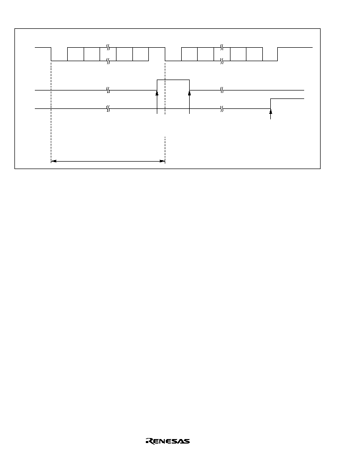
Rev. 1.0, 02/00, page 434 of 1141
Figure 22.9 shows an example of the operation for reception in asynchronous mode.
RDRF
FER
0
1 frame
D0
D1
D7
0/1
1
0
D0
D1
D7
0/1
0
1
1
Data
Start
bit
Parity
bit
Stop
bit
Start
bit
Data
Parity
bit
Stop
bit
ERI interrupt request
generated by framing
error
Idle state
(mark state)
RDR1 data read
and RDRF flag
cleared to 0 in
RXI interrupt
handling routine
RXI interrupt
request
generation
Figure 22.9 Example of SCI Operation in Reception
(Example with 8-Bit Data, Parity, One Stop Bit)
22.3.3
Multiprocessor Communication Function
The multiprocessor communication function performs serial communication using a
multiprocessor format, in which a multiprocessor bit is added to the transfer data, in asynchronous
mode. Use of this function enables data transfer to be performed among a number of processors
sharing transmission lines.
When multiprocessor communication is carried out, each receiving station is addressed by a
unique ID code.
The serial communication cycle consists of two component cycles: an ID transmission cycle
which specifies the receiving station, and a data transmission cycle. The multiprocessor bit is used
to differentiate between the ID transmission cycle and the data transmission cycle.
The transmitting station first sends the ID of the receiving station with which it wants to perform
serial communication as data with a 1 multiprocessor bit added. It then sends transmit data as data
with a 0 multiprocessor bit added.
The receiving station skips the data until data with a 1 multiprocessor bit is sent.
When data with a 1 multiprocessor bit is received, the receiving station compares that data with its
own ID. The station whose ID matches then receives the data sent next. Stations whose ID does
not match continue to skip the data until data with a 1 multiprocessor bit is again received. In this
way, data communication is carried out among a number of processors.
Figure 22.10 shows an example of inter-processor communication using a multiprocessor format.
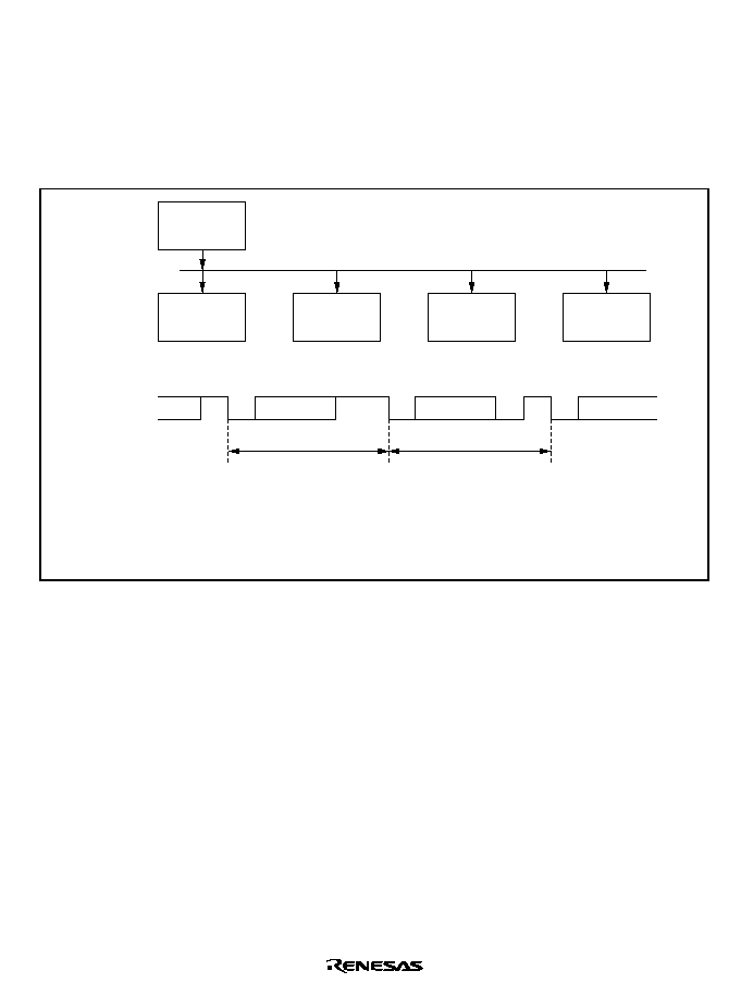
Rev. 1.0, 02/00, page 435 of 1141
1. Data Transfer Format
There are four data transfer formats.
When a multiprocessor format is specified, the parity bit specification is invalid.
For details, see table 22.10.
2. Clock
See the section on asynchronous mode.
Transmitting
station
Receiving
station A
(ID=01)
Receiving
station B
(ID=02)
Receiving
station C
(ID=03)
Receiving
station D
(ID=04)
Serial communication line
Serial
data
ID transmission cycle:
receiving station
specification
Data transmission cycle:
data transmission to
receiving station
specified by ID
(MPB=1)
(MPB=0)
H'01
H'AA
[Legend] MPB : Multiprocessor bit
Figure 22.10 Example of Inter-Processor Communication Using Multiprocessor Format
(Transmission of Data H'AA to Receiving Station A)
3. Data Transfer Operations
a. Multiprocessor Serial Data Transmission
Figure 22.11 shows a sample flowchart for multiprocessor serial data transmission.
The following procedure should be used for multiprocessor serial data transmission.
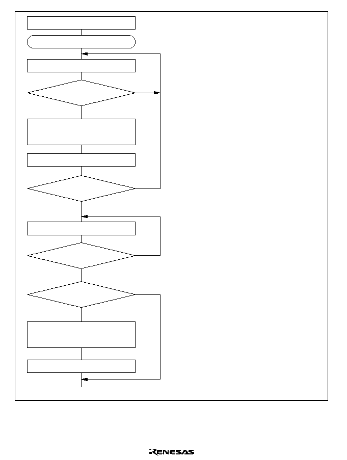
Rev. 1.0, 02/00, page 436 of 1141
No
< End >
[1]
Yes
Initialization
Start transmission
Read TDRE flag in SSR1
[2]
Write transmit data to TDR1
and set MPBT bit in SSR1
No
Yes
No
Yes
Read TEND flag in SSR1
[3]
No
Yes
[4]
Clear PDR to 0 and set PCR to 1
Clear TE bit in SCR1 to 0
TDRE=1
Transmission end?
TEND=1
Break output?
Clear TDRE flag to 0
SCI initialization:
The SO2 pin is automatically designated as
the transmit data output pin.
SCI status check and transmit data write:
Read SSR and check that the TDRE flag is
set to 1, then write transmit data to TDR1.
Set the MPBT bit in SSR1 to 0 or 1.
Finally, clear the TDRE flag to 0.
Serial transmission continuation procedure:
To continue serial transmission, be sure to
read 1 from the TDRE flag to confirm that
writing is possible, then write data to TDR1,
and then clear the TDRE flag to 0.
Break output at the end of serial
transmission:
To output a break in serial transmission, set
the port PCR to 1, clear PDR to 0, then
clear the TE bit in SCR1 to 0.
[1]
[2]
[3]
[4]
Figure 22.11 Sample Multiprocessor Serial Transmission Flowchart

Rev. 1.0, 02/00, page 437 of 1141
In serial transmission, the SCI operates as described below.
1. The SCI monitors the TDRE flag in SSR1, and if it is 0, recognizes that data has been written
to TDR1, and transfers the data from TDR1 to TSR1.
2. After transferring data from TDR1 to TSR1, the SCI sets the TDRE flag to 1 and starts
transmission.
If the TIE bit is set to 1 at this time, a transmit-data-empty interrupt (TXI) is generated.
The serial transmit data is sent from the SO2 pin in the following order.
a. Start bit:
One 0-bit is output.
b. Transmit data:
8-bit or 7-bit data is output in LSB-first order.
c. Multiprocessor bit
One multiprocessor bit (MPBT value) is output.
d. Stop bit(s):
One or two 1-bits (stop bits) are output.
e. Mark state:
1 is output continuously until the start bit that starts the next transmission is sent.
3. The SCI checks the TDRE flag at the timing for sending the stop bit.
If the TDRE flag is cleared to 0, data is transferred from TDR1 to TSR1, the stop bit is sent,
and then serial transmission of the next frame is started.
If the TDRE flag is set to 1, the TEND flag in SSR1 is set to 1, the stop bit is sent, and then the
mark state is entered in which 1 is output continuously. If the TEIE bit in SCR1 is set to 1 at
this time, a transmit-end interrupt (TEI) request is generated.
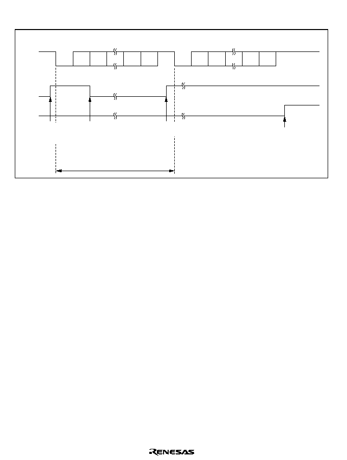
Rev. 1.0, 02/00, page 438 of 1141
Figure 22.12 shows an example of SCI operation for transmission using a multiprocessor format.
TDRE
TEND
0
1 frame
D0
D1
D7
0/1
1
0
D0
D1
D7
0/1
1
1
Data
Data
TXI interrupt
request
general
Data written to TDR1 and
TDRE flag cleared to 0
in TXI interrupt handling
routine
TEI interrupt
request
generated
Idle state
(mark state)
TXI interrupt request
generated
Start
bit
Multi-
processor
bit
Stop
bit
Start
bit
Stop
bit 1
Multi-
processor
bit
Figure 22.12 Example of SCI Operation in Transmission
(Example with 8-Bit Data, Multiprocessor Bit, One Stop Bit)
b. Multiprocessor Serial Data Reception
Figure 22.13 shows sample flowcharts for multiprocessor serial reception.
The following procedure should be used for multiprocessor serial data reception.
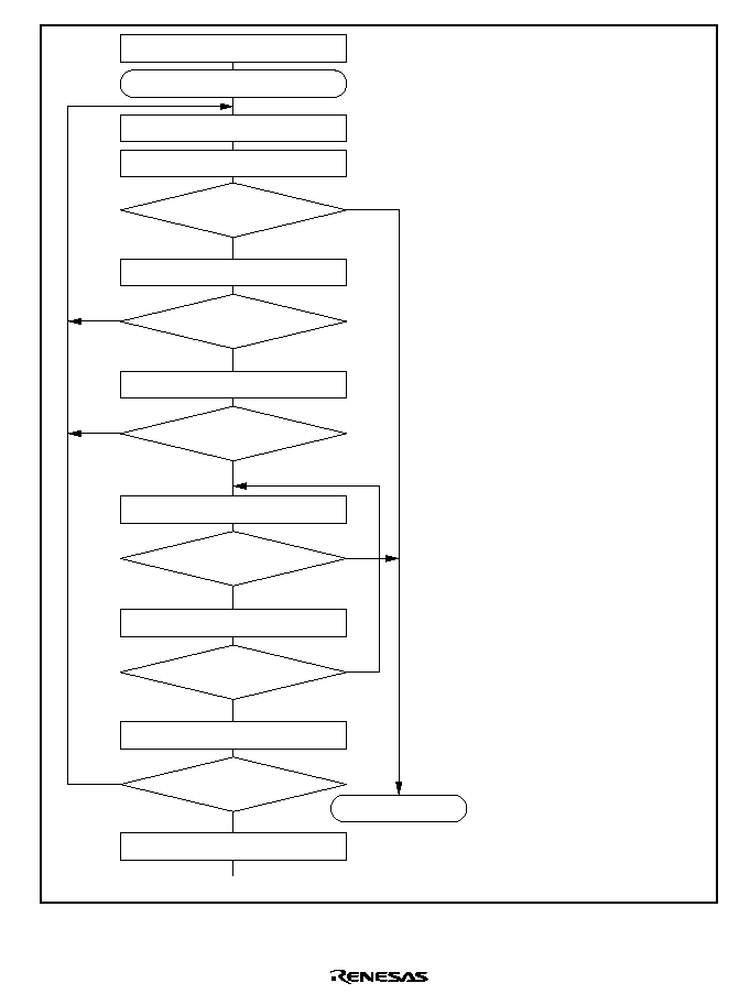
Rev. 1.0, 02/00, page 439 of 1141
Yes
< End >
[1]
No
Initialization
Start reception
No
Yes
[4]
Clear RE bit in SCR1 to 0
Error handling
(Continued on
next page)
[5]
No
Yes
FER
ORER=1
RDRF=1
All data received?
Set MPIE bit in SCR1 to 1
[2]
Read ORER and FER flags in SSR1
Read RDRF flag in SSR1
[3]
Read receive data in RDR1
No
Yes
This station's ID?
Read ORER and FER flags in SSR1
Yes
No
Read RDRF flag in SSR1
No
Yes
FER
ORER=1
Read receive data in RDR1
RDRF=1
SCI initialization:
The SI1 pin is automatically designated as
the receive data input pin.
ID reception cycle:
Set the MPIE bit in SCR1 to 1.
SCI status check, ID reception and
comparison:
Read SSR and check that the RDRF flag is
set to 1, then read the receive data in
RDR1 and compare it with this station's ID.
If the data is not this station's ID, set the
MPIE bit to 1 again, and clear the RDRF
flag to 0.
If the data is this station's ID, clear the
RDRF flag to 0.
SCI status check and data reception:
Read SSR1 and check that the RDRF flag
is set to 1, then read the data in RDR1.
Receive error handling and break
detectioon:
If a receive error occurs, read the ORER
and FER flags in SSR1 to identify the error.
After performing the appropriate error
handling, ensure that the ORER and FER
flags are both cleared to 0.
Reception cannot be resumed if either of
these flags is set to 1.
In the case of a framing error, a break can
be detected by reading the SI1 in value.
[1]
[2]
[3]
[4]
[5]
Figure 22.13 Sample Multiprocessor Serial Reception Flowchart (1)
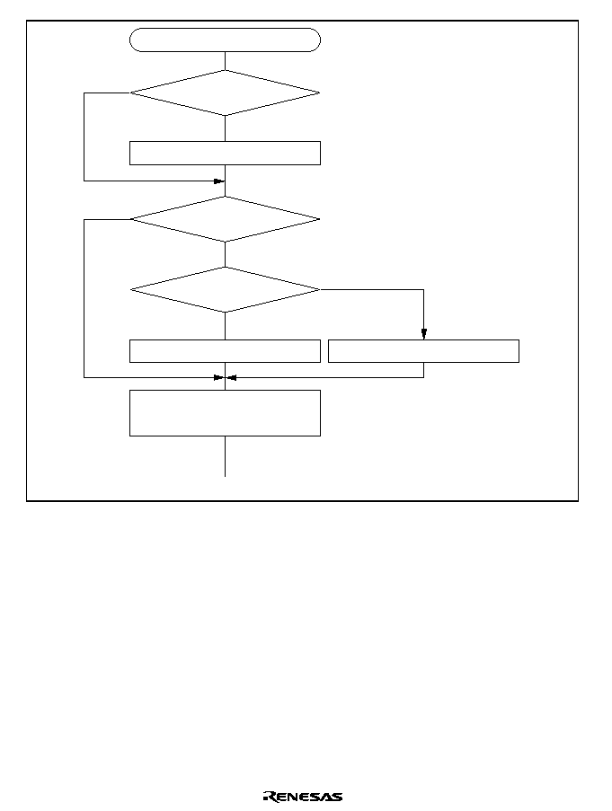
Rev. 1.0, 02/00, page 440 of 1141
< End >
Error handling
Yes
No
Clear ORER, PER, and FER
flags in SSR1 to 0
No
Yes
No
Yes
Framing error handling
Overrun error handling
ORER=1
FER=1
Break?
Clear RE bit in SCR1 to 0
[5]
Figure 22.14 Sample Multiprocessor Serial Reception Flowchart (2)
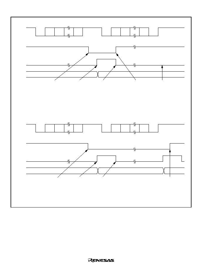
Rev. 1.0, 02/00, page 441 of 1141
Figure 22.15 shows an example of SCI operation for multiprocessor format reception.
MPIE
RDR1
value
0
D0
D1
D7
1
1
0
D0
D1
D7
0
1
1
1
Data (ID1)
Start
bit
MPB
Stop
bit
Start
bit
Data (Data 1)
MPB
Stop
bit
RXI interrupt
request (multi-
processor
interrupt)
generated
Idle state
(mark state)
RDRF
RDR1 data read
and RDRF flag
cleared to 0 in
RXI interrupt
handling routine
If not this station's
ID, MPIE bit is set
to 1 again
RXI interrupt request
is not generated, and
RDR1 retains its state
ID1
(a) Data does not match station's ID
MPIE
RDR1
value
0
D0
D1
D7
1
1
0
D0
D1
D7
0
1
1
1
Data (ID2)
Start
bit
MPB
Stop
bit
Start
bit
Data (Data 2)
MPB
Stop
bit
RXI interrupt
request (multi-
processor
interrupt)
generated
Idle state
(mark state)
RDRF
RDR1 data read and
RDRF flag cleared
to 0 in RXI interrupt
handling routine
Matches this station's
ID, so reception continues,
and data is received in RXI
interrupt handling routine
MPIE bit set
to 1 again
ID2
(b) Data matches station's ID
Data2
ID1
MPIE=0
MPIE=0
Figure 22.15 Example of SCI Operation in Reception
(Example with 8-Bit Data, Multiprocessor Bit, One Stop Bit)
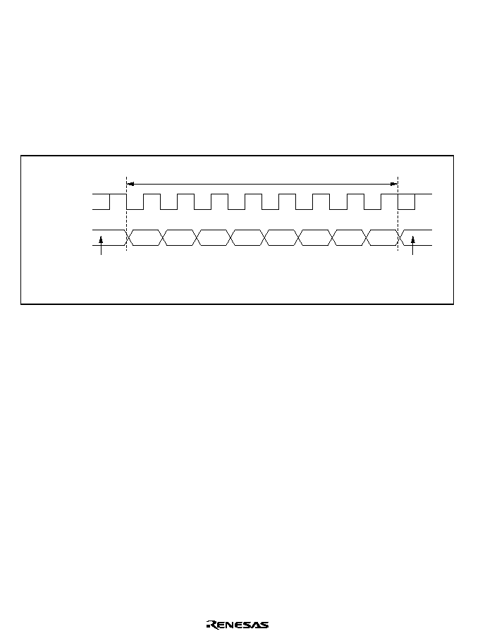
Rev. 1.0, 02/00, page 442 of 1141
22.3.4
Operation in Synchronous Mode
In synchronous mode, data is transmitted or received in synchronization with clock pulses, making
it suitable for high-speed serial communication.
Inside the SCI, the transmitter and receiver are independent units, enabling full-duplex
communication by use of a common clock. Both the transmitter and the receiver also have a
double-buffered structure, so that data can be read or written during transmission or reception,
enabling continuous data transfer.
Figure 22.16 shows the general format for synchronous serial communication.
Don't care
Don't care
One unit of transfer data (character or frame)
Bit 0
Serial
data
Synchronous
clock
Bit 1
Bit 3
Bit 4
Bit 5
LSB
MSB
Bit 2
Bit 6
Bit 7
*
*
Note: * High except in continuous transfer
Figure 22.16 Data Format in Synchronous Communication
In synchronous serial communication, data on the transmission line is output from one falling edge
of the serial clock to the next. Data is guaranteed valid at the rising edge of the serial clock.
In synchronous serial communication, one character consists of data output starting with the LSB
and ending with the MSB. After the MSB is output, the transmission line holds the MSB state.
In synchronous mode, the SCI receives data in synchronization with the rising edge of the serial
clock.
∑
Data Transfer Format
A fixed 8-bit data format is used.
No parity or multiprocessor bits are added.
∑
Clock
Either an internal clock generated by the built-in baud rate generator or an external serial clock
input at the SCK pin can be selected, according to the setting of the C/
bit in SMR1 and the
CKE1 and CKE0 bits in SCR1. For details on SCI clock source selection, see table 22.9.
When the SCI is operated on an internal clock, the serial clock is output from the SCK pin.
Eight serial clock pulses are output in the transfer of one character, and when no transfer is
performed the clock is fixed high. When only receive operations are performed, however, the
serial clock is output until an overrun error occurs or the RE bit is cleared to 0. To perform
receive operations in units of one character, select an external clock as the clock source.
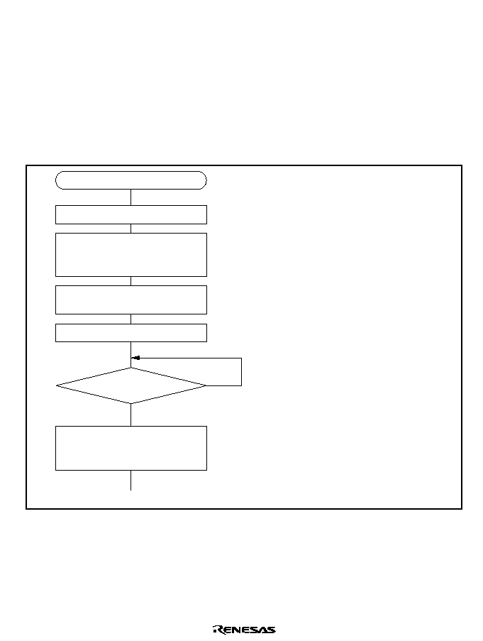
Rev. 1.0, 02/00, page 443 of 1141
∑
Data Transfer Operations
SCI Initialization (Synchronous Mode)
Before transmitting and receiving data, first clear the TE and RE bits in SCR1 to 0, then
initialize the SCI as described below.
When the operating mode, transfer format, etc., is changed, the TE and RE bits must be
cleared to 0 before making the change using the following procedure. When the TE bit is
cleared to 0, the TDRE flag is set to 1 and TSR1 is initialized. Note that clearing the RE
bit to 0 does not change the settings of the RDRF, PER, FER, and ORER flags, or the
contents of RDR1.
Figure 22.17 shows a sample SCI initialization flowchart.
Wait
<Transfer start>
Start initialization
Set data transfer format
in SMR1 and SCMR
No
Yes
Set value in BRR1
Clear TE and RE bits in SCR1 to 0
[2]
[3]
Set TE and RE bits in SCR1 to 1,
and set RIE, TIE, TEIE, and MPIE
bits
[4]
1-bit interval elapsed?
Set CKE1 and CKE0 bits in
SCR1 (TE, RE bits 0)
[1]
Set the clock selection in SCR1. Be sure to
clear bits RIE, TIE, TEIE, and MPIE, TE
and RE, to 0.
Set the data transfer format in SMR1 and
SCMR1.
Write a value corresponding to the bit rate
to BRR1. This is not necessary if an
external clock is used.
Wait at least one bit interval, then set the
TE bit or RE bit in SCR1 to 1.
Also set the RIE, TIE, TEIE, and MPIE bits.
Setting the TE and RE bits enables the
SO1 and SI1 pins to be used.
[1]
[2]
[3]
[4]
Figure 22.17 Sample SCI Initialization Flowchart
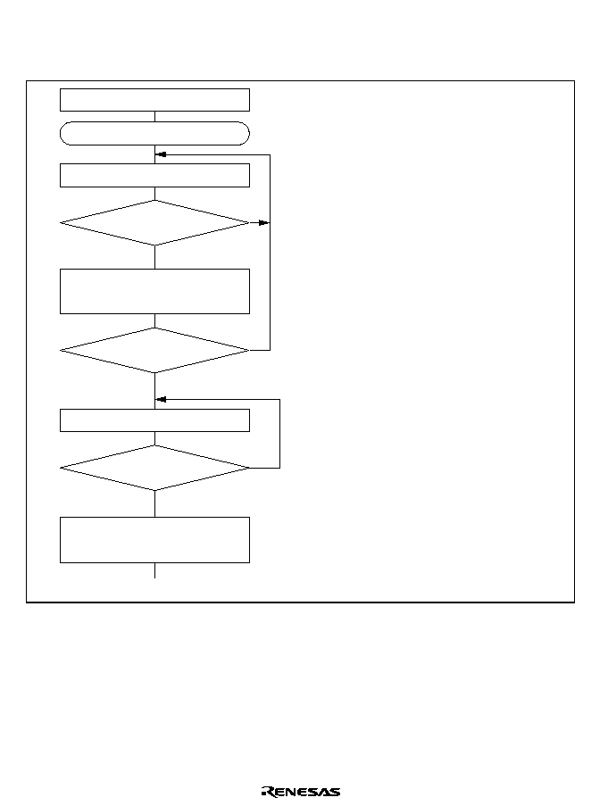
Rev. 1.0, 02/00, page 444 of 1141
Serial Data Transmission (Synchronous Mode)
Figure 22.18 shows a sample flowchart for serial transmission.
The following procedure should be used for serial data transmission.
No
< End >
[1]
Yes
Initialization
Start transmission
Read TDRE flag in SSR1
[2]
Write transmit data to TDR1 and
clear TDRE flag in SSR1 to 0
No
Yes
No
Yes
Read TEND flag in SSR1
[3]
Clear TE bit in
SCR1 to 0
TDRE=1
All data transmitted?
TEND=1
SCI initialization:
The SO2 pin is automatically designated as
the transmit data output pin.
SCI status check and transmit data write:
Read SSR1 and check that the TDRE flag
is set to 1, then write transmit data to TDR1
and clear the TDRE flag to 0.
Serial transmission continuation procedure:
To continue serial transmission, be sure to
read 1 from the TDRE flag to confirm that
writing is possible, then write data to TDR1,
and then clear the TDRE flag to 0.
[1]
[2]
[3]
Figure 22.18 Sample Serial Transmission Flowchart
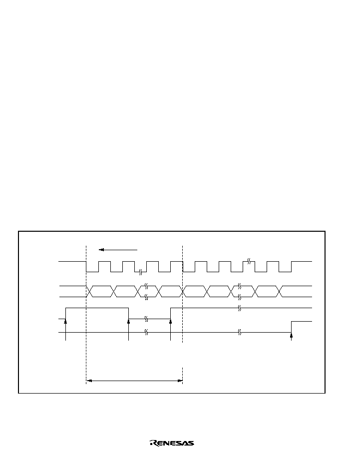
Rev. 1.0, 02/00, page 445 of 1141
In serial transmission, the SCI operates as described below.
1. The SCI monitors the TDRE flag in SSR1, and if it is 0, recognizes that data has been written
to TDR1, and transfers the data from TDR1 to TSR1.
2. After transferring data from TDR1 to TSR1, the SCI sets the TDRE flag to 1 and starts
transmission. If the TIE bit is set to 1 at this time, a transmit-data-empty interrupt (TXI) is
generated.
When clock output mode has been set, the SCI outputs 8 serial clock pulses. When use of an
external clock has been specified, data is output synchronized with the input clock.
The serial transmit data is sent from the SO1 pin starting with the LSB (bit 0) and ending with
the MSB (bit 7).
3. The SCI checks the TDRE flag at the timing for sending the MSB (bit 7).
If the TDRE flag is cleared to 0, data is transferred from TDR1 to TSR1, and serial
transmission of the next frame is started.
If the TDRE flag is set to 1, the TEND flag in SSR1 is set to 1, the MSB (bit 7) is sent, and the
SO1 pin maintains its state.
If the TEIE bit in SCR1 is set to 1 at this time, a transmit-end interrupt (TEI) request is
generated.
4. After completion of serial transmission, the SCK pin is held in a constant state.
Figure 22.19 shows an example of SCI operation in transmission.
Transfer
direction
Bit 0
Serial
data
Synchronous
clock
1 frame
TDRE
TEND
Data written to TDR1
and TDRE flag cleared
to 0 in TXI interrupt
handling routine
TXI interrupt
request
generated
Bit 1
Bit 7
Bit 0
Bit 1
Bit 6
Bit 7
TXI interrupt
request
generated
TEI interrupt
request
generated
Figure 22.19 Example of SCI Operation in Transmission

Rev. 1.0, 02/00, page 446 of 1141
Serial Data Reception (Synchronous Mode)
Figure 22.20 shows a sample flowchart for serial reception.
The following procedure should be used for serial data reception.
When changing the operating mode from asynchronous to synchronous, be sure to check
that the ORER, PER, and FER flags are all cleared to 0.
The RDRF flag will not be set if the FER or PER flag is set to 1, and neither transmit nor
receive operations will be possible.
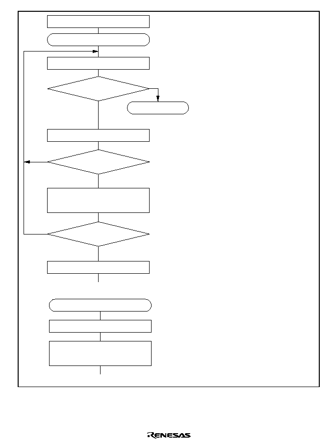
Rev. 1.0, 02/00, page 447 of 1141
Yes
< End >
[1]
No
Initialization
Start reception
[2]
No
Yes
Read RDRF flag in SSR1
[4]
[5]
Clear RE bit in SCR1 to 0
Error handling
(Continued below)
[3]
Read receive data in RDR1,
and clear RDRF flag in SSR1 to 0
No
Yes
ORER=1
RDRF=1
All data received?
Read ORER flag in SSR1
< End >
Error handling
Clear ORER flag in
SSR1 to 0
Overrun error handling
[3]
SCI initialization:
The SI1 pin is automatically designated as
the receive data input pin.
Receive error handling:
IF a receive error occurs, read the ORER
flag in SSR1, and after performing the
appropriate error handling, clear the ORER
flag to 0. Transfer cannot be resumed if
the ORER flag is set to 1.
SCI status check and receive data read:
Read SSR1 and check that the RDRF flag
is set to 1, then read the receive data in
RDR1 and clear the RDRF flag to 0.
Transition of the RDRF flag from 0 to 1 can
also be identified by and RXI interrupt.
Serial reception continuation procedure:
To continue serial reception, before the
MSB (bit 7) of the current frame is received,
finish reading the RDRF flag, reading
RDR1, and clearing the RDRF flag to 0.
[1]
[2][3]
[4]
[5]
Figure 22.20 Sample Serial Reception Flowchart
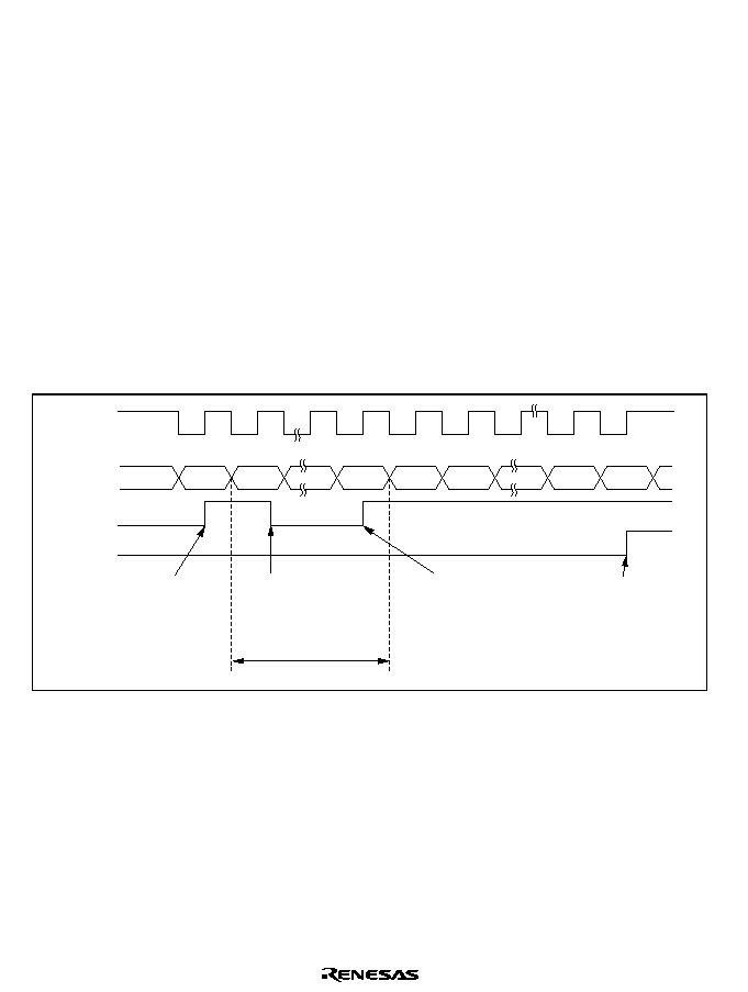
Rev. 1.0, 02/00, page 448 of 1141
In serial reception, the SCI operates as described below.
1. The SCI performs internal initialization in synchronization with serial clock input or output.
2. The received data is stored in RSR1 in LSB-to-MSB order.
After reception, the SCI checks whether the RDRF flag is 0 and the receive data can be
transferred from RSR1 to RDR1.
If this check is passed, the RDRF flag is set to 1, and the receive data is stored in RDR1. If a
receive error is detected in the error check, the operation is as shown in table 22.11.
Neither transmit nor receive operations can be performed subsequently when a receive error
has been found in the error check.
3. If the RIE bit in SCR1 is set to 1 when the RDRF flag changes to 1, a receive-data-full
interrupt (RXI) request is generated.
Also, if the RIE bit in SCR1 is set to 1 when the ORER flag changes to 1, a receive-error
interrupt (ERI) request is generated.
Figure 22.21 shows an example of SCI operation in reception.
Bit 7
Serial
data
Synchronous
clock
1 frame
RDRF
ORER
ERI interrupt request
generated by
overrun error
RXI interrupt
request
generated
RDR1 data read and
RDRF flag cleared to 0
in RXI interrupt
handling routine
RXI interrupt
request
generated
Bit 0
Bit 7
Bit 0
Bit 1
Bit 6
Bit 7
Figure 22.21 Example of SCI Operation in Reception
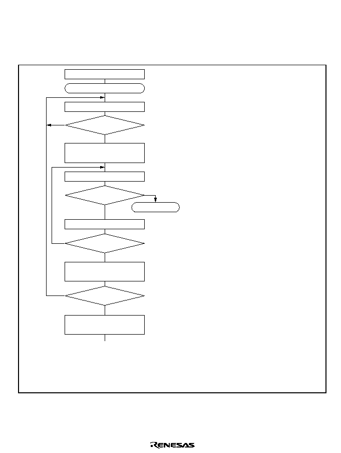
Rev. 1.0, 02/00, page 449 of 1141
Simultaneous Serial Data Transmission and Reception (Synchronous Mode)
Figure 22.22 shows a sample flowchart for simultaneous serial transmit and receive
operations.
The following procedure should be used for simultaneous serial data transmit and receive
operations.
Yes
< End >
[1]
No
Initialization
Start transfer
[5]
Error handling
[3]
Read receive data in RDR1, and
clear RDRF flag in SSR1 to 0
No
Yes
ORER=1
All data received?
[2]
Read TDRE flag in SSR1
No
Yes
TDRE=1
Write transmit data to TDR1 and
clear TDRE flag in SSR1 to 0
No
Yes
RDR=1
Read ORER flag in SSR1
[4]
Read RDRF flag in SSR1
Clear TE and RE
bits in SCR1 to 0
Note: When switching from transmit or receive operation
to simultaneous transmit and receive operations, first
clear the TE bit and RE bit to 0, then set both these
bits to 1 simultaneously.
SCI initialization:
The SO2 pin is designated as the transmit
data output pin, and the SI1 pin is
designated as the receive data input pin,
enabling simultaneous transmit and receive
operations.
SCI status check and transmit data write:
Read SSR1 and check that the TDRE flag
is set to 1, then write transmit data to TDR1
and clear the TDRE flag to 0.
Transition of the TDRE flag from 0 to 1 can
also be identified by a TXI interrupt.
Receive error handling:
If a receive error occurs, read the ORER
flag in SSR1, and after performing the
appropriate error handling, clear the ORER
flag to 0. Transmission/reception cannot
be resumed if the ORER flag is set to 1.
SCI status check and receive data read:
Read SSR1 and check that the RDRF flag
is set to 1, then read the receive data in
RDR1 and clear the RDRF flag to 0.
Transition of the RDRF flag from 0 to 1 can
also be identified by an RXI interrupt.
Serial transmission/reception continuation
procedure:
To continue serial transmission/reception,
before the MSB (bit 7) of the current frame
is received, finish reading the RDRF flag,
reading RDR1, and clearing the RDRF flag
to 0. Also before the MSB (bit 7) of the
current frame is transmitted, read 1 from
the TDRE flag to confirm that writing is
possible, then write data to TDR1 and clear
the TDRE flag to 0.
[1]
[2]
[3]
[4]
[5]
Figure 22.22 Sample Flowchart of Simultaneous Serial Transmit and Receive Operations

Rev. 1.0, 02/00, page 450 of 1141
22.4
SCI Interrupts
The SCI has four interrupt sources: the transmit-end interrupt (TEI) request, receive-error interrupt
(ERI) request, receive-data-full interrupt (RXI) request, and transmit-data-empty interrupt (TXI)
request. Table 22.12 shows the interrupt sources and their relative priorities. Individual interrupt
sources can be enabled or disabled with the TIE, RIE, and TEIE bits in SCR1. Each kind of
interrupt request is sent to the interrupt controller independently.
When the TDRE flag in SSR1 is set to 1, a TXI interrupt request is generated. When the TEND
flag in SSR1 is set to 1, a TEI interrupt request is generated.
When the RDRF flag in SSR1 is set to 1, an RXI interrupt request is generated. When the ORER,
PER, or FER flag in SSR1 is set to 1, an ERI interrupt request is generated.
Table 22.12 SCI Interrupt Sources
Channel
Interrupt Source
Description
Priority*
ERI
Interrupt by receive error (ORER, FER, or PER)
RXI
Interrupt by receive data register full (RDRF)
TXI
Interrupt by transmit data register empty (TDRE)
1
TEI
Interrupt by transmit end (TEND)
High
Low
The TEI interrupt is requested when the TEND flag is set to 1 while the TEIE bit is set to 1. The
TEND flag is cleared at the same time as the TDRE flag. Consequently, if a TEI interrupt and a
TXI interrupt are requested simultaneously, the TXI interrupt will have priority for acceptance,
and the TDRE flag and TEND flag may be cleared. Note that the TEI interrupt will not be
accepted in this case.

Rev. 1.0, 02/00, page 451 of 1141
22.5
Usage Notes
The following points should be noted when using the SCI.
∑
Relation between Writes to TDR1 and the TDRE Flag
The TDRE flag in SSR1 is a status flag that indicates that transmit data has been transferred
from TDR1 to TSR1. When the SCI transfers data from TDR1 to TSR1, the TDRE flag is set
to 1.
Data can be written to TDR1 regardless of the state of the TDRE flag. However, if new data is
written to TDR1 when the TDRE flag is cleared to 0, the data stored in TDR1 will be lost since
it has not yet been transferred to TSR1. It is therefore essential to check that the TDRE flag is
set to 1 before writing transmit data to TDR1.
∑
Operation when Multiple Receive Errors Occur Simultaneously
If a number of receive errors occur at the same time, the state of the status flags in SSR1 is as
shown in table 22.13. If there is an overrun error, data is not transferred from RSR1 to RDR1,
and the receive data is lost.
Table 22.13 State of SSR1 Status Flags and Transfer of Receive Data
SSR1 Status Flags
Receive Data Transfer
RDRF
ORER
FER
PER
RSR1 to RDR1
Receive Error Status
1
1
0
0
X
Overrun error
0
0
1
0
Framing error
0
0
0
1
Parity error
1
1
1
0
X
Overrun error + framing error
1
1
0
1
X
Overrun error + parity error
0
0
1
1
Framing error + parity error
1
1
1
1
X
Overrun error + framing error +
parity error
Notes:
: Receive data is transferred from RSR1 to RDR1.
X: Receive data is not transferred from RSR1 to RDR1.

Rev. 1.0, 02/00, page 452 of 1141
∑
Break Detection and Processing
When framing error (FER) detection is performed, a break can be detected by reading the SI1
pin value directly. In a break, the input from the SI1 pin becomes all 0s, and so the FER flag is
set, and the parity error flag (PER) may also be set.
Note that, since the SCI continues the receive operation after receiving a break, even if the
FER flag is cleared to 0, it will be set to 1 again.
∑
Sending a Break
The SO1 pin has a dual function as an I/O port whose direction (input or output) is determined
by DR and DDR. This can be used to send a break.
Between serial transmission initialization and setting of the TE bit to 1, the mark state is
replaced by the value of PDR (the pin does not function as the SO1 pin until the TE bit is set to
1). Consequently, PCR and PDR for the port corresponding to the SO1 pin are first set to 1.
To send a break during serial transmission, first clear PDR to 0, then clear the TE bit to 0.
When the TE bit is cleared to 0, the transmitter is initialized regardless of the current
transmission state, the SO1 pin becomes an I/O port, and 0 is output from the SO1 pin.
∑
Receive Error Flags and Transmit Operations (Clocked Synchronous Mode Only)
Transmission cannot be started when a receive error flag (ORER, PER, or FER) is set to 1,
even if the TDRE flag is cleared to 0. Be sure to clear the receive error flags to 0 before
starting transmission.
Note also that receive error flags cannot be cleared to 0 even if the RE bit is cleared to 0.
∑
Receive Data Sampling Timing and Reception Margin in Asynchronous Mode
In asynchronous mode, the SCI operates on a basic clock with a frequency of 16 times the
transfer rate.
In reception, the SCI samples the falling edge of the start bit using the basic clock, and
performs internal synchronization. Receive data is latched internally at the rising edge of the
8th pulse of the basic clock. This is illustrated in figure 22.23.

Rev. 1.0, 02/00, page 453 of 1141
Internal basic
clock
16 clocks
8 clocks
Receive data
Synchronization
sampling timing
Start bit
D0
D1
Data sampling
timing
15 0
7
15 0
0
7
Figure 22.23 Receive Data Sampling Timing in Asynchronous Mode
Thus the reception margin in asynchronous mode is given by formula (1) below.
M = | (0.5 ≠
1
2N
) ≠ (L ≠ 0.5) F ≠
| D ≠ 0.5 |
N
(1 + F) |
◊
100%
... Formula (1)
Where M : Reception margin (%)
N : Ratio of bit rate to clock (N = 16)
D : Clock duty (D = 0 to 1.0)
L : Frame length (L = 9 to 12)
F
: Absolute value of clock rate deviation
Assuming values of F = 0 and D = 0.5 in formula (1), a reception margin of 46.875% is given by
formula (2) below.
When D = 0.5 and F = 0,
M = (0.5 ≠
1
2
◊
16
) ◊
100%
= 46.875%
... Formula (2)
However, this is only the computed value, and a margin of 20% to 30% should be allowed in
system design.

Rev. 1.0, 02/00, page 454 of 1141
∑
Operation in Case of Mode Transition
Transmission
Operation should be stopped (by clearing TE, TIE, and TEIE to 0) before making a module
stop mode, standby mode, watch mode, subactive mode, or subsleep mode transition.
TSR1, TDR1, and SSR1 are reset. The output pin states in module stop mode, standby
mode, watch mode, subactive mode, or subsleep mode depend on the port settings, and
becomes high-level output after the relevant mode is cleared. If a transition is made during
transmission, the data being transmitted will be undefined. When transmitting without
changing the transmit mode after the relevant mode is cleared, transmission can be started
by setting TE to 1 again, and performing the following sequence: SSR1 read
∆ TDR1
write
∆ TDRE clearance. To transmit with a different transmit mode after clearing the
relevant mode, the procedure must be started again from initialization. Figure 22.24 shows
a sample flowchart for mode transition during transmission. Port pin states are shown in
figures 22.25 and 22.26.
Reception
Receive operation should be stopped (by clearing RE to 0) before making a module stop
mode, standby mode, watch mode, subactive mode, or subsleep mode transition. RSR1,
RDR1, and SSR1 are reset. If a transition is made without stopping operation, the data
being received will be invalid. To continue receiving without changing the reception mode
after the relevant mode is cleared, set RE to 1 before starting reception. To receive with a
different receive mode, the procedure must be started again from initialization.
Figure 22.27 shows a sample flowchart for mode transition during reception.
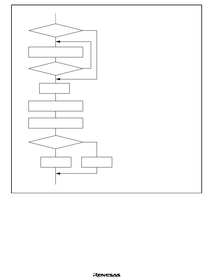
Rev. 1.0, 02/00, page 455 of 1141
Read TEND flag in SSR1
TE= 0
Transition to standby
mode, etc.
Exit from standby
mode, etc.
Change
operating mode?
No
All data
transmitted?
TEND = 1
Yes
Yes
Yes
<Transmission>
No
No
[1]
[3]
[2]
TE= 1
Initialization
<Start of transmission>
[1] Data being transmitted is interrupted.
After exiting software standby
mode, etc., normal CPU transmis-
sion is possible by setting TE to 1,
reading SSR1, writing TDR1, and
clearing TDRE to 0.
[2] If TIE and TEIE are set to 1, clear
them to 0 in the same way.
[3] Includes module stop mode, watch
mode, subactive mode, and sub-
sleep mode.
Figure 22.24 Sample Flowchart for Mode Transition during Transmission
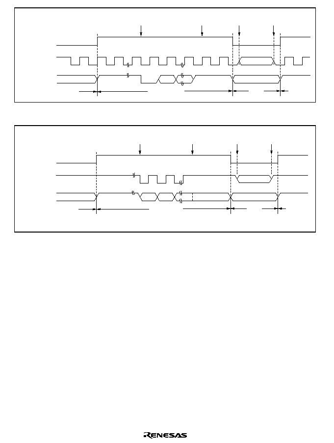
Rev. 1.0, 02/00, page 456 of 1141
SCK1 output pin
TE bit
SO1 output pin
Port input/output
High output
Port input/output
High output
Start
Stop
Start of transmission
End of
transmission
Port input/output
SCI TxD output
Port
SCI TxD
output
Port
Transition
to standby
Exit from
standby
Figure 22.25 Asynchronous Transmission Using Internal Clock
Port input/output
Last TxD bit held
High output
*
Port input/output
Marking output
Port input/output
SCI TxD output
Port
Port
Note:
*
Initialized by software standby.
SCK1 output pin
TE bit
SO1 output pin
SCI TxD
output
Start of transmission
End of
transmission
Transition
to standby
Exit from
standby
Figure 22.26 Synchronous Transmission Using Internal Clock

Rev. 1.0, 02/00, page 457 of 1141
RE= 0
Transition to standby
mode, etc.
Read receive data in RDR1
Read RDRF flag in SSR1
Exit from standby
mode, etc.
Change
operating mode?
No
RDRF= 1
Yes
Yes
<Reception>
No
[1]
[2]
[1]
[2]
RE= 1
Initialization
<Start of reception>
Receive data being received
becomes invalid.
Includes module stop mode,
watch mode, subactive mode,
and subsleep mode.
Figure 22.27 Sample Flowchart for Mode Transition during Reception

Rev. 1.0, 02/00, page 459 of 1141
Section 23 I
2
C Bus Interface (IIC)
23.1
Overview
This LSI incorporates a 2-channel I
2
C bus interface.
The I
2
C bus interface conforms to and provides a subset of the Philips I
2
C bus (inter-IC bus)
interface functions. The register configuration that controls the I
2
C bus differs partly from the
Philips configuration, however.
Each I
2
C bus interface channel uses only one data line (SDA) and one clock line (SCL) to transfer
data, saving board and connector space.
23.1.1
Features
∑
Selection of addressing format or non-addressing format
I
2
C bus format: addressing format with acknowledge bit, for master/slave operation
Serial format: non-addressing format without acknowledge bit, for master operation only
∑
Conforms to Philips I
2
C bus interface (I
2
C bus format)
∑
Two ways of setting slave address (I
2
C bus format)
∑
Start and stop conditions generated automatically in master mode (I
2
C bus format)
∑
Selection of acknowledge output levels when receiving (I
2
C bus format)
∑
Automatic loading of acknowledge bit when transmitting (I
2
C bus format)
∑
Wait function in master mode (I
2
C bus format)
A wait can be inserted by driving the SCL pin low after data transfer, excluding
acknowledgement. The wait can be cleared by clearing the interrupt flag.
∑
Wait function in slave mode (I
2
C bus format)
A wait request can be generated by driving the SCL pin low after data transfer, excluding
acknowledgement. The wait request is cleared when the next transfer becomes possible.
∑
Three interrupt sources
Data transfer end (including transmission mode transition with I
2
C bus format and address
reception after loss of master arbitration)
Address match: when any slave address matches or the general call address is received in
slave receive mode (I
2
C bus format)
Stop condition detection
∑
Selection of 16 internal clocks (in master mode)
∑
Direct bus drive (with SCL and SDA pins)
Four pins P26/SCL0, P25/SDA0, P24/SCL1 and P23/SDA1 (normally CMOS pins)
function as NMOS-only outputs when the bus drive function is selected.
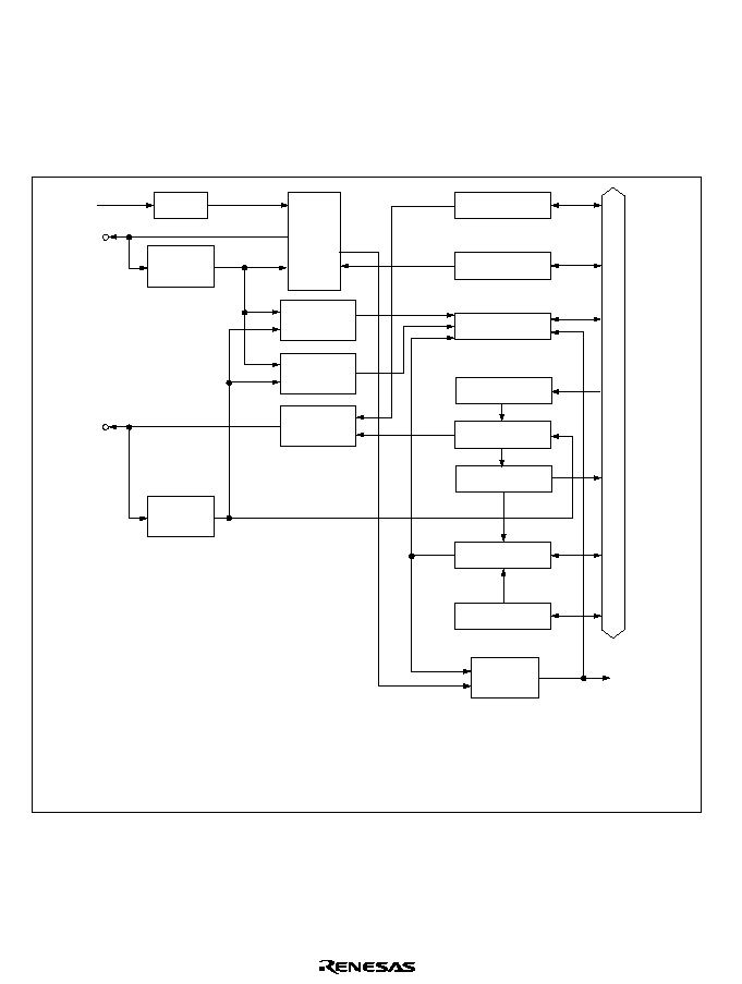
Rev. 1.0, 02/00, page 460 of 1141
23.1.2
Block Diagram
Figure 23.1 shows a block diagram of the I
2
C bus interface.
Figure 23.2 shows an example of I/O pin connections to external circuits. I/O pins are driven only
by NMOS and apparently function as NMOS open-drain outputs. However, applicable voltages to
input pins depend on the power (Vcc) voltage of this LSI.
SCL
PS
Noise
canceller
Bus state
decision
circuit
Output data
control
circuit
ICCR
Clock
control
ICMR
ICSR
ICDRS
Address
comparator
Arbitration
decision
circuit
SAR, SARX
SDA
Noise
canceler
Interrupt
generator
Interrupt
request
Internal data bus
[Legend]
ICCR
ICMR
ICSR
ICDR
SAR
SARX
PS
: I
2
C control register
: I
2
C mode register
: I
2
C status register
: I
2
C data register
: Slave address register
: Slave address register X
: Prescaler
ICDRR
ICDRT
Figure 23.1 Block Diagram of I
2
C Bus Interface
Rev. 1.0, 02/00, page 461 of 1141
V
CC
SCL
in
out
SCL
SDA
in
out
(Master)
This chip
SDA
SCL
SDA
SCL
in
out
SCL
SDA
in
out
(Slave 1)
SDA
SCL
in
out
SCL
SDA
in
out
(Slave 2)
SDA
Figure 23.2 I
2
C Bus Interface Connections (Example: This Chip as Master)
23.1.3
Pin Configuration
Table 23.1 summarizes the input/output pins used by the I
2
C bus interface.
Table 23.1
I
2
C Bus Interface Pins
Channel
Name
Abbrev.* I/O
Function
Serial clock pin
SCL0
Input/output
IIC0 serial clock input/output
Serial data pin
SDA0
Input/output
IIC0 serial data input/output
0
Formatless serial clock pin
SYNCI
Input
IIC0 formatless serial clock input
Serial clock pin
SCL1
Input/output
IIC1 serial clock input/output
1
Serial data pin
SDA1
Input/output
IIC1 serial data input/output
Note:
*
In this section, channel numbers in the abbreviated register names are omitted; SCL0
and SCL1 are collectively referred to as SCL, and SDA0 and SDA1 as SDA.

Rev. 1.0, 02/00, page 462 of 1141
23.1.4
Register Configuration
Table 23.2 summarizes the registers of the I
2
C bus interface.
Table 23.2
Register Configuration
Channel
Name
Abbrev.
R/W
Initial Value
Address
*1
0
I
2
C bus control register
ICCR0
R/W
H'01
H'D0E8
I
2
C bus status register
ICSR0
R/W
H'00
H'D0E9
I
2
C bus data register
ICDR0
R/W
H'D0EE*
2
I
2
C bus mode register
ICMR0
R/W
H'00
H'D0EF*
2
Slave address register
SAR0
R/W
H'00
H'D0EF*
2
Second slave address register
SARX0
R/W
H'01
H'D0EE*
2
1
I
2
C bus control register
ICCR1
R/W
H'01
H'D158
I
2
C bus status register
ICSR1
R/W
H'00
H'D159
I
2
C bus data register
ICDR1
R/W
H'D15E*
2
I
2
C bus mode register
ICMR1
R/W
H'00
H'D15F*
2
Slave address register
SAR1
R/W
H'00
H'D15F*
2
Second slave address register
SARX1
R/W
H'01
H'D15E*
2
0 and 1
DDC switch register
DDCSWR
R/W
H'0F
H'D0E5
Module stop control register
MSTPCRH
MSTPCRL
R/W
H'FF
H'FF
H'FFEC
H'FFED
Notes: 1. Lower 16 bits of the address.
2. The registers that can be read from or written to depend on the ICE bit in the I
2
C bus
control register. The slave address registers can be accessed when ICE = 0, and the
I
2
C bus mode registers can be accessed when ICE = 1.

Rev. 1.0, 02/00, page 463 of 1141
23.2
Register Descriptions
23.2.1
I
2
C Bus Data Register (ICDR)
7
ICDR7
--
R/W
6
ICDR6
--
R/W
5
ICDR5
--
R/W
4
ICDR4
--
R/W
3
ICDR3
--
R/W
0
ICDR0
--
R/W
2
ICDR2
--
R/W
1
ICDR1
--
R/W
Bit :
Initial value :
R/W :
ICDRR
7
ICDRR7
--
R
6
ICDRR6
--
R
5
ICDRR5
--
R
4
ICDRR4
--
R
3
ICDRR3
--
R
0
ICDRR0
--
R
2
ICDRR2
--
R
1
ICDRR1
--
R
Bit :
Initial value :
R/W :
ICDRS
7
ICDRS7
--
--
6
ICDRS6
--
--
5
ICDRS5
--
--
4
ICDRS4
--
--
3
ICDRS3
--
--
0
ICDRS0
--
--
2
ICDRS2
--
--
1
ICDRS1
--
--
Bit :
Initial value :
R/W :
ICDRT
7
ICDRT7
--
W
6
ICDRT6
--
W
5
ICDRT5
--
W
4
ICDRT4
--
W
3
ICDRT3
--
W
0
ICDRT0
--
W
2
ICDRT2
--
W
1
ICDRT1
--
W
Bit :
Initial value :
R/W :
TDRE, RDRF (Internal flag)
--
RDRF
0
--
--
TDRE
0
--
Bit :
Initial value :
R/W :

Rev. 1.0, 02/00, page 464 of 1141
ICDR is an 8-bit readable/writable register that is used as a transmit data register when
transmitting and a receive data register when receiving. ICDR is divided internally into a shift
register (ICDRS), receive buffer (ICDRR), and transmit buffer (ICDRT). ICDRS cannot be read
or written by the CPU, ICDRR is read-only, and ICDRT is write-only. Data transfers among the
three registers are performed automatically in coordination with changes in the bus state, and
affect the status of internal flags such as TDRE and RDRF.
If IIC is in transmit mode and the next data is in ICDRT (the TDRE flag is 0) following
transmission/reception of one frame of data using ICDRS, data is transferred automatically from
ICDRT to ICDRS. If IIC is in receive mode and no previous data remains in ICDRR (the RDRF
flag is 0) following transmission/reception of one frame of data using ICDRS, data is transferred
automatically from ICDRS to ICDRR.
If the number of bits in a frame, excluding the acknowledge bit, is less than 8, transmit data and
receive data are stored differently. Transmit data should be written justified toward the MSB side
when MLS = 0, and toward the LSB side when MLS = 1. Receive data bits read from the LSB
side should be treated as valid when MLS = 0, and bits read from the MSB side when MLS = 1.
ICDR is assigned to the same address as SARX, and can be written and read only when the ICE
bit is set to 1 in ICCR.
The value of ICDR is undefined after a reset.
The TDRE and RDRF flags are set and cleared under the conditions shown below. Setting the
TDRE and RDRF flags affects the status of the interrupt flags.

Rev. 1.0, 02/00, page 465 of 1141
TDRE
Description
0
The next transmit data is in ICDR (ICDRT), or transmission cannot be started
[Clearing conditions]
(Initial value)
1. When transmit data is written in ICDR (ICDRT) in transmit mode (TRS = 1)
2. When a stop condition is detected in the bus line state after a stop condition is
issued with the I
2
C bus format or serial format selected
3. When a stop condition is detected with the I
2
C bus format selected
4. In receive mode (TRS = 0)
(A 0 write to TRS during transfer is valid after reception of a frame containing an
acknowledge bit)
1
The next transmit data can be written in ICDR (ICDRT)
[Setting conditions]
1. In transmit mode (TRS = 1), when a start condition is detected in the bus line state
after a start condition is issued in master mode with the I
2
C bus format or serial
format selected
2. In transmit mode (TRS = 1) when formatless transfer is selected
3. When data is transferred from ICDRT to ICDRS
(Data transfer from ICDRT to ICDRS when TRS = 1 and TDRE = 0, and ICDRS is
empty)
4. When a switch is made from receive mode (TRS = 0) to transmit mode (TRS = 1)
after detection of a start condition
RDRF
Description
0
The data in ICDR (ICDRR) is invalid
(Initial value)
[Clearing condition]
When ICDR (ICDRR) receive data is read in receive mode
1
The ICDR (ICDRR) receive data can be read
[Setting condition]
When data is transferred from ICDRS to ICDRR
(Data transfer from ICDRS to ICDRR in case of normal termination with TRS = 0 and
RDRF = 0)

Rev. 1.0, 02/00, page 466 of 1141
23.2.2
Slave Address Register (SAR)
7
SVA6
0
R/W
6
SVA5
0
R/W
5
SVA4
0
R/W
4
SVA3
0
R/W
3
SVA2
0
R/W
0
FS
0
R/W
2
SVA1
0
R/W
1
SVA0
0
R/W
Bit :
Initial value :
R/W :
SAR is an 8-bit readable/writable register that stores the slave address and selects the
communication format. When the chip is in slave mode (and the addressing format is selected), if
the upper 7 bits of SAR match the upper 7 bits of the first frame received after a start condition,
the chip operates as the slave device specified by the master device. SAR is assigned to the same
address as ICMR, and can be written and read only when the ICE bit is cleared to 0 in ICCR.
SAR is initialized to H'00 by a reset.
Bits 7 to 1
Slave Address (SVA6 to SVA0): Set a unique address in bits SVA6 to SVA0,
differing from the addresses of other slave devices connected to the I
2
C bus.

Rev. 1.0, 02/00, page 467 of 1141
Bit 0
Format Select (FS): Used together with the FSX bit in SARX and the SW bit in
DDCSWR to select the communication format.
∑
I
2
C bus format: addressing format with acknowledge bit
∑
Synchronous serial format: non-addressing format without acknowledge bit, for master
mode only
∑
Formatless transfer (only for channel 0): non-addressing with or without an acknowledge
bit and without detection of start or stop condition, for slave mode only.
The FS bit also specifies whether or not SAR slave address recognition is performed in slave
mode.
DDCSWR
Bit 6
SAR
Bit 0
SARX
Bit 0
SW
FS
FSX
Operating Mode
0
I
2
C bus format
∑
SAR and SARX slave addresses recognized
0
1
I
2
C bus format
(Initial value)
∑
SAR slave address recognized
∑
SARX slave address ignored
0
I
2
C bus format
∑
SAR slave address ignored
∑
SARX slave address recognized
0
1
1
Synchronous serial format
∑
SAR and SARX slave addresses ignored
0
0
1
Formatless transfer (start and stop conditions are not
detected)
∑
With acknowledge bit
0
1
1
1
Formatless transfer* (start and stop conditions are not
detected)
∑
Without acknowledge bit
Note:
*
Do not use this setting when automatically switching the mode from formatless transfer
to I
2
C bus format by setting DDCSWR.

Rev. 1.0, 02/00, page 468 of 1141
23.2.3
Second Slave Address Register (SARX)
7
SVAX6
0
R/W
6
SVAX5
0
R/W
5
SVAX4
0
R/W
4
SVAX3
0
R/W
3
SVAX2
0
R/W
0
FSX
1
R/W
2
SVAX1
0
R/W
1
SVAX0
0
R/W
Bit :
Initial value :
R/W :
SARX is an 8-bit readable/writable register that stores the second slave address and selects the
communication format. When the chip is in slave mode (and the addressing format is selected), if
the upper 7 bits of SARX match the upper 7 bits of the first frame received after a start condition,
the chip operates as the slave device specified by the master device. SARX is assigned to the
same address as ICDR, and can be written and read only when the ICE bit is cleared to 0 in ICCR.
SARX is initialized to H'01 by a reset and in hardware standby mode.
Bits 7 to 1
Second Slave Address (SVAX6 to SVAX0): Set a unique address in bits SVAX6 to
SVAX0, differing from the addresses of other slave devices connected to the I
2
C bus.
Bit 0
Format Select X (FSX): Used together with the FSX bit in SARX and the SW bit in
DDCSWR to select the communication format.
∑
I
2
C bus format: addressing format with acknowledge bit
∑
Synchronous serial format: non-addressing format without acknowledge bit, for master mode
only
∑
Formatless transfer: non-addressing with or without an acknowledge bit and without detection
of start or stop condition, for slave mode only.
The FSX bit also specifies whether or not SARX slave address recognition is performed in slave
mode. For details, see the description of the FS bit in section 23.2.2, Slave Address Register
(SAR).

Rev. 1.0, 02/00, page 469 of 1141
23.2.4
I
2
C Bus Mode Register (ICMR)
7
MLS
0
R/W
6
WAIT
0
R/W
5
CKS2
0
R/W
4
CKS1
0
R/W
3
CKS0
0
R/W
0
BC0
0
R/W
2
BC2
0
R/W
1
BC1
0
R/W
Bit :
Initial value :
R/W :
ICMR is an 8-bit readable/writable register that selects whether the MSB or LSB is transferred
first, performs master mode wait control, and selects the master mode transfer clock frequency and
the transfer bit count. ICMR is assigned to the same address as SAR. ICMR can be written and
read only when the ICE bit is set to 1 in ICCR.
ICMR is initialized to H'00 by a reset.
Bit 7
MSB-First/LSB-First Select (MLS): Selects whether data is transferred MSB-first or
LSB-first.
If the number of bits in a frame, excluding the acknowledge bit, is less than 8, transmit data and
receive data are stored differently. Transmit data should be written justified toward the MSB side
when MLS = 0, and toward the LSB side when MLS = 1. Receive data bits read from the LSB
side should be treated as valid when MLS = 0, and bits read from the MSB side when MLS = 1.
Do not set this bit to 1 when the I
2
C bus format is used.
Bit 7
MLS
Description
0
MSB-first
(Initial value)
1
LSB-first

Rev. 1.0, 02/00, page 470 of 1141
Bit 6
Wait Insertion Bit (WAIT)
Selects whether to insert a wait between the transfer of data and the acknowledge bit, in master
mode with the I
2
C bus format. When WAIT is set to 1, after the fall of the clock for the final data
bit, the IRIC flag is set to 1 in ICCR, and a wait state begins (with SCL at the low level). When
the IRIC flag is cleared to 0 in ICCR, the wait ends and the acknowledge bit is transferred. If
WAIT is cleared to 0, data and acknowledge bits are transferred consecutively with no wait
inserted.
The IRIC flag in ICCR is set to 1 on completion of the acknowledge bit transfer, regardless of the
WAIT setting.
The setting of this bit is invalid in slave mode.
Bit 6
WAIT
Description
0
Data and acknowledge bits transferred consecutively
(Initial value)
1
Wait inserted between data and acknowledge bits

Rev. 1.0, 02/00, page 471 of 1141
Bits 5 to 3
Transfer Clock Select (CKS2 to CKS0): These bits, together with the IICX1 bit
(for channel 1) or IICX0 bit (for channel 0) in STCR, select the serial clock frequency in master
mode. They should be set according to the required transfer rate.
STCR
Bits 5, 6
Bit 5
Bit 4
Bit 3
Transfer Rate
IICX
CKS2
CKS1
CKS0
Clock
= 8 MHz
= 10 MHz
0
/28
286 kHz
357 kHz
0
1
/40
200 kHz
250 kHz
0
/48
167 kHz
208 kHz
0
1
1
/64
125 kHz
156 kHz
0
/80
100 kHz
125 kHz
0
1
/100
80.0 kHz
100 kHz
0
/112
71.4 kHz
89.3 kHz
0
1
1
1
/128
62.5 kHz
78.1 kHz
0
/56
143 kHz
179 kHz
0
1
/80
100 kHz
125 kHz
0
/96
83.3 kHz
104 kHz
0
1
1
/128
62.5 kHz
78.1 kHz
0
/160
50.0 kHz
62.5 kHz
0
1
/200
40.0 kHz
50.0 kHz
0
/224
35.7 kHz
44.6 kHz
1
1
1
1
/256
31.3 kHz
39.1 kHz

Rev. 1.0, 02/00, page 472 of 1141
Bits 2 to 0
Bit Counter (BC2 to BC0): Bits BC2 to BC0 specify the number of bits to be
transferred next. With the I
2
C bus format (when the FS bit in SAR or the FSX bit in SARX is 0),
the data is transferred with one addition acknowledge bit. Bit BC2 to BC0 settings should be
made during an interval between transfer frames. If bits BC2 to BC0 are set to a value other than
000, the setting should be made while the SCL line is low.
The bit counter is initialized to 000 by a reset and when a start condition is detected. The value
returns to 000 at the end of a data transfer, including the acknowledge bit.
Bit 2
Bit 1
Bit 0
Bits/Frame
BC2
BC1
BC0
Synchronous Serial Format
I
2
C Bus Format
0
8
9 (Initial value)
0
1
1
2
0
2
3
0
1
1
3
4
0
4
5
0
1
5
6
0
6
7
1
1
1
7
8

Rev. 1.0, 02/00, page 473 of 1141
23.2.5
I
2
C Bus Control Register (ICCR)
7
ICE
0
R/W
6
IEIC
0
R/W
5
MST
0
R/W
4
TRS
0
R/W
3
ACKE
0
R/W
0
SCP
1
W
2
BBSY
0
R/W
1
IRIC
0
R/(W)*
Note: * Only 0 can be written to clear the flag.
Bit :
Initial value :
R/W :
ICCR is an 8-bit readable/writable register that enables or disables the I
2
C bus interface, enables or
disables interrupts, selects master or slave mode and transmission or reception, enables or disables
acknowledgement, confirms the I
2
C bus interface bus status, issues start/stop conditions, and
performs interrupt flag confirmation.
ICCR is initialized to H'01 by a reset.
Bit 7
I
2
C Bus Interface Enable (ICE): Selects whether or not the I
2
C bus interface is to be
used. When ICE is set to 1, port pins function as SCL and SDA input/output pins and transfer
operations are enabled. When ICE is cleared to 0, the IIC stops and its internal status is initialized.
The SAR and SARX registers can be accessed when ICE is 0. The ICMR and ICDR registers can
be accessed when ICE is 1.
Bit 7
ICE
Description
0
I
2
C bus interface module disabled, with SCL and SDA signal pins set to port function
The internal status of the IIC is initialized
SAR and SARX can be accessed
(Initial value)
1
I
2
C bus interface module enabled for transfer operations (pins SCL and SCA are
driving the bus)
ICMR and ICDR can be accessed
Bit 6
I
2
C Bus Interface Interrupt Enable (IEIC): Enables or disables interrupts from the I
2
C
bus interface to the CPU.
Bit 6
IEIC
Description
0
Interrupts disabled
(Initial value)
1
Interrupts enabled

Rev. 1.0, 02/00, page 474 of 1141
Bits 5 and 4
Master/Slave Select (MST) and Transmit/Receive Select (TRS): MST selects
whether the I
2
C bus interface operates in master mode or slave mode.
TRS selects whether the I
2
C bus interface operates in transmit mode or receive mode.
In master mode with the I
2
C bus format, when arbitration is lost, MST and TRS are both reset by
hardware, causing a transition to slave receive mode. In slave receive mode with the addressing
format (FS = 0 or FSX = 0), hardware automatically selects transmit or receive mode according to
the R/W bit in the first frame after a start condition.
Modification of the TRS bit during transfer is deferred until transfer of the frame containing the
acknowledge bit is completed, and the changeover is made after completion of the transfer.
MST and TRS select the operating mode as follows.
Bit 5
Bit 4
MST
TRS
Description
0
Slave receive mode
(Initial value)
0
1
Slave transmit mode
0
Master receive mode
1
1
Master transmit mode
Bit 5
MST
Description
0
Slave mode
(Initial value)
[Clearing conditions]
1. When 0 is written by software
2. When bus arbitration is lost after transmission is started in I
2
C bus format master
mode
1
Master mode
[Setting conditions]
1. When 1 is written by software (in cases other than clearing condition 2)
2. When 1 is written in MST after reading MST = 0 (in case of clearing condition 2)

Rev. 1.0, 02/00, page 475 of 1141
Bit 4
TRS
Description
0
Receive mode
(Initial value)
[Clearing conditions]
1. When 0 is written by software (in cases other than setting condition 3)
2. When 0 is written in TRS after reading TRS = 1 (in case of setting condition 3)
3. When bus arbitration is lost after transmission is started in I
2
C bus format master
mode
4. When the SW bit in DDCSWR changes from 1 to 0
1
Transmit mode
[Setting conditions]
1. When 1 is written by software (in cases other than clearing conditions 3)
2. When 1 is written in TRS after reading TRS = 0 (in case of clearing conditions 3)
3. When a 1 is received as the R/W bit of the first frame in I
2
C bus format slave mode
Bit 3
Acknowledge Bit Judgement Selection (ACKE): Specifies whether the value of the
acknowledge bit returned from the receiving device when using the I
2
C bus format is to be ignored
and continuous transfer is performed, or transfer is to be aborted and error handling, etc.,
performed if the acknowledge bit is 1. When the ACKE bit is 0, the value of the received
acknowledge bit is not indicated by the ACKB bit, which is always 0.
When the ACKE bit is 0, the TDRE, IRIC, and IRTR flags are set on completion of data
transmission, regardless of the value of the acknowledge bit. When the ACKE bit is 1, the TDRE,
IRIC, and IRTR flags are set on completion of data transmission when the acknowledge bit is 0,
and the IRIC flag alone is set on completion of data transmission when the acknowledge bit is 1.
Depending on the receiving device, the acknowledge bit may be significant, in indicating
completion of processing of the received data, for instance, or may be fixed at 1 and have no
significance.
Bit 3
ACKE
Description
0
The value of the acknowledge bit is ignored, and continuous transfer is performed
(Initial value)
1
If the acknowledge bit is 1, continuous transfer is interrupted

Rev. 1.0, 02/00, page 476 of 1141
Bit 2
Bus Busy (BBSY): The BBSY flag can be read to check whether the I
2
C bus (SCL, SDA)
is busy or free. In master mode, this bit is also used to issue start and stop conditions.
A high-to-low transition of SDA while SCL is high is recognized as a start condition, setting
BBSY to 1. A low-to-high transition of SDA while SCL is high is recognized as a stop condition,
clearing BBSY to 0.
To issue a start condition, use a MOV instruction to write 1 in BBSY and 0 in SCP. A retransmit
start condition is issued in the same way. To issue a stop condition, use a MOV instruction to
write 0 in BBSY and 0 in SCP.
It is not possible to write to BBSY in slave mode; the I
2
C bus interface must be set to master
transmit mode before issuing a start condition. MST and TRS should both be set to 1 before
writing 1 in BBSY and 0 in SCP.
Bit 2
BBSY
Description
0
Bus is free
(Initial value)
[Clearing condition]
When a stop condition is detected
1
Bus is busy
[Setting condition]
When a start condition is detected
Bit 1
I
2
C Bus Interface Interrupt Request Flag (IRIC): Indicates that the I
2
C bus interface has
issued an interrupt request to the CPU. IRIC is set to 1 at the end of a data transfer, when a slave
address or general call address is detected in slave receive mode, when bus arbitration is lost in
master transmit mode, and when a stop condition is detected. IRIC is set at different times
depending on the FS bit in SAR and the WAIT bit in ICMR. See section 23.3.6, IRIC Setting
Timing and SCL Control. The conditions under which IRIC is set also differ depending on the
setting of the ACKE bit in ICCR.
IRIC is cleared by reading IRIC after it has been set to 1, then writing 0 in IRIC.
When the DTC is used, IRIC is cleared automatically and transfer can be performed continuously
without CPU intervention.

Rev. 1.0, 02/00, page 477 of 1141
Bit 1
IRIC
Description
0
Waiting for transfer, or transfer in progress
(Initial value)
[Clearing condition]
When 0 is written in IRIC after reading IRIC = 1
(1)
Interrupt requested
[Setting conditions]
∑
I
2
C bus format master mode
1. When a start condition is detected in the bus line state after a start condition is
issued
(when the TDRE flag is set to 1 because of first frame transmission)
2. When a wait is inserted between the data and acknowledge bit when WAIT = 1
3. At the end of data transfer
(when the TDRE or RDRF flag is set to 1)
4. When a slave address is received after bus arbitration is lost
(when the AL flag is set to 1)
5. When 1 is received as the acknowledge bit when the ACKE bit is 1
(when the ACKB bit is set to 1)
∑
I
2
C bus format slave mode
1. When the slave address (SVA, SVAX) matches
(when the AAS and AASX flags are set to 1)
and at the end of data transfer up to the subsequent retransmission start condition
or stop condition detection
(when the TDRE or RDRF flag is set to 1)
2. When the general call address is detected
(when the ADZ flag is set to 1)
and at the end of data transfer up to the subsequent retransmission start condition
or stop condition detection
(when the TDRE or RDRF flag is set to 1)
3. When 1 is received as the acknowledge bit when the ACKE bit is 1
(when the ACKB bit is set to 1)
4. When a stop condition is detected
(when the STOP or ESTP flag is set to 1)
∑
Synchronous serial format
1. At the end of data transfer
(when the TDRE or RDRF flag is set to 1)
2. When a start condition is detected with serial format selected
∑
When a condition, other than the above, that sets the TDRE or RDRF flag to 1 is
detected

Rev. 1.0, 02/00, page 478 of 1141
When, with the I
2
C bus format selected, IRIC is set to 1 and an interrupt is generated, other flags
must be checked in order to identify the source that set IRIC to 1. Although each source has a
corresponding flag, caution is needed at the end of a transfer.
When the TDRE or RDRF internal flag is set, the readable IRTR flag may or may not be set. The
IRTR flag (the DTC start request flag) is not set at the end of a data transfer up to detection of a
retransmission start condition or stop condition after a slave address (SVA) or general call address
match in I
2
C bus format slave mode.
Even when the IRIC flag and IRTR flag are set, the TDRE or RDRF internal flag may not be set.
The IRIC and IRTR flags are not cleared at the end of the specified number of transfers in
continuous transfer using the DTC. The TDRE or RDRF flag is cleared, however, since the
specified number of ICDR reads or writes have been completed.
Table 23.3 shows the relationship between the flags and the transfer states.
Note: *
This LSI does not incorporate DTC.

Rev. 1.0, 02/00, page 479 of 1141
Table 23.3
Flags and Transfer States
MST
TRS
BBSY ESTP
STOP IRTR
AASX AL
AAS
ADZ
ACKB State
1/0
1/0
0
0
0
0
0
0
0
0
0
Idle state (flag clearing
required)
1
1
0
0
0
0
0
0
0
0
0
Start condition
issuance
1
1
1
0
0
1
0
0
0
0
0
Start condition
established
1
1/0
1
0
0
0
0
0
0
0
0/1
Master mode wait
1
1/0
1
0
0
1
0
0
0
0
0/1
Master mode
transmit/receive end
0
0
1
0
0
0
1/0
1
1/0
1/0
0
Arbitration lost
0
0
1
0
0
0
0
0
1
0
0
SAR match by first
frame in slave mode
0
0
1
0
0
0
0
0
1
1
0
General call address
match
0
0
1
0
0
0
1
0
0
0
0
SARX match
0
1/0
1
0
0
0
0
0
0
0
0/1
Slave mode
transmit/receive end
(except after SARX
match)
0
0
1/0
1
1
1
0
0
0
0
1
0
1
1
0
0
0
0
0
0
0
1
Slave mode
transmit/receive end
(after SARX match)
0
1/0
0
1/0
1/0
0
0
0
0
0
0/1
Stop condition
detected
Bit 0
Start Condition/Stop Condition Prohibit (SCP): Controls the issuing of start and stop
conditions in master mode. To issue a start condition, write 1 in BBSY and 0 in SCP. A
retransmit start condition is issued in the same way. To issue a stop condition, write 0 in BBSY
and 0 in SCP. This bit is always read as 1. If 1 is written, the data is not stored.
Bit 0
SCP
Description
0
Writing 0 issues a start or stop condition, in combination with the BBSY flag
1
Reading always returns a value of 1
(Initial value)
Writing is ignored

Rev. 1.0, 02/00, page 480 of 1141
23.2.6
I
2
C Bus Status Register (ICSR)
7
ESTP
0
R/(W)*
6
STOP
0
R/(W)*
5
IRTR
0
R/(W)*
4
AASX
0
R/(W)*
3
AL
0
R/(W)*
0
ACKB
0
R/W
2
AAS
0
R/(W)*
1
ADZ
0
R/(W)*
Note: * Only 0 can be written to clear the flag.
Bit :
Initial value :
R/W :
ICSR is an 8-bit readable/writable register that performs flag confirmation and acknowledge
confirmation and control.
ICSR is initialized to H'00 by a reset.
Bit 7
Error Stop Condition Detection Flag (ESTP): Indicates that a stop condition has been
detected during frame transfer in I
2
C bus format slave mode.
Bit 7
ESTP
Description
0
No error stop condition
(Initial value)
[Clearing condition]
1. When 0 is written in ESTP after reading ESTP = 1
2. When the IRIC flag is cleared to 0
1
∑
In I
2
C bus format slave mode: Error stop condition detected
[Setting condition]
When a stop condition is detected during frame transfer
∑
In other modes: No meaning

Rev. 1.0, 02/00, page 481 of 1141
Bit 6
Normal Stop Condition Detection Flag (STOP): Indicates that a stop condition has been
detected after completion of frame transfer in I
2
C bus format slave mode.
Bit 6
STOP
Description
0
No normal stop condition
(Initial value)
[Clearing condition]
1. When 0 is written in STOP after reading STOP = 1
2. When the IRIC flag is cleared to 0
1
∑
In I
2
C bus format slave mode: Error stop condition detected
[Setting condition]
When a stop condition is detected after completion of frame transfer
∑
In other modes:No meaning
Bit 5
I
2
C Bus Interface Continuous Transmission/Reception Interrupt Request Flag
(IRTR): Indicates that the I
2
C bus interface has issued an interrupt request to the CPU, and the
source is completion of reception/transmission of one frame in continuous transmission/reception
for which DTC activation is possible. When the IRTR flag is set to 1, the IRIC flag is also set to 1
at the same time.
IRTR flag setting is performed when the TDRE or RDRF flag is set to 1. IRTR is cleared by
reading IRTR after it has been set to 1, then writing 0 in IRTR. IRTR is also cleared automatically
when the IRIC flag is cleared to 0.
Note: *
This LSI does not incorporate DTC.
Bit 5
IRTR
Description
0
Waiting for transfer, or transfer in progress
(Initial value)
[Clearing condition]
1. When 0 is written in IRTR after reading IRTR = 1
2. When the IRIC flag is cleared to 0
1
Continuous transfer state
[Setting condition]
∑
In I
2
C bus interface slave mode: When the TDRE or RDRF flag is set to 1 when
AASX = 1
∑
In other modes: When the TDRE or RDRF flag is set to 1

Rev. 1.0, 02/00, page 482 of 1141
Bit 4
Second Slave Address Recognition Flag (AASX): In I
2
C bus format slave receive mode,
this flag is set to 1 if the first frame following a start condition matches bits SVAX6 to SVAX0 in
SARX.
AASX is cleared by reading AASX after it has been set to 1, then writing 0 in AASX. AASX is
also cleared automatically when a start condition is detected.
Bit 4
AASX
Description
0
Second slave address not recognized
(Initial value)
[Clearing condition]
1. When 0 is written in AASX after reading AASX = 1
2. When a start condition is detected
3. In master mode
1
Second slave address recognized
[Setting condition]
When the second slave address is detected in slave receive mode
Bit 3
Arbitration Lost (AL): This flag indicates that arbitration was lost in master mode. The
I
2
C bus interface monitors the bus. When two or more master devices attempt to seize the bus at
nearly the same time, if the I
2
C bus interface detects data differing from the data it sent, it sets AL
to 1 to indicate that the bus has been taken by another master.
AL is cleared by reading AL after it has been set to 1, then writing 0 in AL. In addition, AL is
reset automatically by write access to ICDR in transmit mode, or read access to ICDR in receive
mode.
Bit 3
AL
Description
0
Bus arbitration won (Initial value)
[Clearing conditions]
1. When ICDR data is written (transmit mode) or read (receive mode)
2. When 0 is written in AL after reading AL = 1
1
Arbitration lost
[Setting conditions]
1. If the internal SDA and SDA pin disagree at the rise of SCL in master transmit
mode
2. If the internal SCL line is high at the fall of SCL in master transmit mode

Rev. 1.0, 02/00, page 483 of 1141
Bit 2
Slave Address Recognition Flag (AAS): In I
2
C bus format slave receive mode, this flag is
set to 1 if the first frame following a start condition matches bits SVA6 to SVA0 in SAR, or if the
general call address (H'00) is detected.
AAS is cleared by reading AAS after it has been set to 1, then writing 0 in AAS. In addition, AAS
is reset automatically by write access to ICDR in transmit mode, or read access to ICDR in receive
mode.
Bit 2
AAS
Description
0
Slave address or general call address not recognized
(Initial value)
[Clearing conditions]
1. When ICDR data is written (transmit mode) or read (receive mode)
2. When 0 is written in AAS after reading AAS = 1
3. In master mode
1
Slave address or general call address recognized
[Setting condition]
When the slave address or general call address is detected when FS = 0 in slave
receive mode
Bit 1
General Call Address Recognition Flag (ADZ): In I
2
C bus format slave receive mode,
this flag is set to 1 if the first frame following a start condition is the general call address (H'00).
ADZ is cleared by reading ADZ after it has been set to 1, then writing 0 in ADZ. In addition,
ADZ is reset automatically by write access to ICDR in transmit mode, or read access to ICDR in
receive mode.
Bit 1
ADZ
Description
0
General call address not recognized
(Initial value)
[Clearing conditions]
1. When ICDR data is written (transmit mode) or read (receive mode)
2. When 0 is written in ADZ after reading ADZ = 1
3. In master mode
1
General call address recognized
[Setting condition]
If the general call address is detected when FSX = 0 or FS = 0 is selected in the
slave receive mode.

Rev. 1.0, 02/00, page 484 of 1141
Bit 0
Acknowledge Bit (ACKB): Stores acknowledge data. In transmit mode, after the
receiving device receives data, it returns acknowledge data, and this data is loaded into ACKB. In
receive mode, after data has been received, the acknowledge data set in this bit is sent to the
transmitting device.
When this bit is read, in transmission (when TRS = 1), the value loaded from the bus line
(returned by the receiving device) is read. In reception (when TRS = 0), the value set by internal
software is read.
Bit 0
ACKB
Description
0
Receive mode: 0 is output at acknowledge output timing
(Initial value)
Transmit mode: Indicates that the receiving device has acknowledged the data
(signal is 0)
1
Receive mode: 1 is output at acknowledge output timing
Transmit mode: Indicates that the receiving device has not acknowledged the data
(signal is 1)
23.2.7
Serial/Timer Control Register (STCR)
7
--
0
--
6
IICX1
0
R/W
5
IICX0
0
R/W
4
--
0
--
3
FLSHE
0
R/W
0
--
0
--
2
OSROME
0
R/W
1
--
0
--
Bit :
Initial value :
R/W :
STCR is an 8-bit readable/writable register that controls the IIC operating mode.
STCR is initialized to H'00 by a reset.
Bit 7
Reserved: This bit cannot be modified and is always read as 0.
Bits 6 and 5
I
2
C Transfer Select 1, 0 (IICX1, 0): These bits, together with bits CKS2 to CKS0
in ICMR of IIC, select the transfer rate in master mode. For details, see section 23.2.4, I
2
C Bus
Mode Register (ICMR).
Bit 3
Flash Memory Control Resister Enable (FLSHE): This bit selects the control resister of
the flash memory. For details, refer to section 7.3.5, Serial Timer Control Resister (STCR).
Bit 2
OSD ROM Enable (OSROME): This bit controls the OSD ROM. For details, refer to
section 7, ROM.
Bits 4 and 2 to 0
Reserved: These bits cannot be modified and are always read as 0.

Rev. 1.0, 02/00, page 485 of 1141
23.2.8
DDC Switch Register (DDCSWR)
7
SWE
0
R/W
6
SW
0
R/W
5
IE
0
R/W
4
IF
0
R/(W)
*
1
3
CLR3
1
W
*
2
0
CLR0
1
W
*
2
2
CLR2
1
W
*
2
1
CLR1
1
W
*
2
Notes: 1.
2.
Only 0 can be written to clear the flag.
Always read as 1.
Bit :
Initial value :
R/W :
DDCSWR is an 8-bit read/write register that controls automatic format switching for IIC channel
0 and IIC internal latch clearing. DDCSWR is initialized to H'0F by a reset or in hardware standby
mode.
Bit 7
DDC Mode Switch Enable (SWE): Enables or disables automatic switching from
formatless transfer to I
2
C bus format transfer for IIC channel 0.
Bit 7
SWE
Description
0
Disables automatic switching from formatless transfer to I
2
C bus format transfer for
IIC channel 0.
(Initial value)
1
Enables automatic switching from formatless transfer to I
2
C bus format transfer for IIC
channel 0.
Bit 6
DDC Mode Switch (SW): Selects formatless transfer or I
2
C bus format transfer for IIC
channel 0.
Bit 6
SW
Description
0
I
2
C bus format is selected for IIC channel 0.
(Initial value)
[Clearing conditions]
1. When 0 is written by software
2. When an SCL falling edge is detected when SWE = 1
1
Formatless transfer is selected for IIC channel 0.
[Setting condition]
When 1 is written after SW = 0 is read

Rev. 1.0, 02/00, page 486 of 1141
Bit 5
DDC Mode Switch Interrupt Enable Bit (IE): Enables or disables an interrupt request to
the CPU when the format for IIC channel 0 is automatically switched.
Bit 5
IE
Description
0
Disables an interrupt at automatic format switching
(Initial value)
1
Enables an interrupt at automatic format switching
Bit 4
DDC Mode Switch Interrupt Flag (IF): Indicates the interrupt request to the CPU when
the format for IIC channel 0 is automatically switched.
Bit 4
IF
Description
0
Interrupt has not been requested
(Initial value)
[Clearing condition]
When 0 is written after IF = 1 is read
1
Interrupt has been requested
[Setting condition]
When an SCL falling edge is detected when SWE = 1
Bits 3 to 0
IIC Clear 3 to 0 (CLR3 to CLR0): Control the IIC0 and IIC1 initialization. These
are write-only bits and are always read as 1.
Writing to these bits generates a clearing signal for the internal latch circuit which initializes the
IIC status.
The data written to these bits are not held. When initializing the IIC, be sure to use the MOV
instruction to write to all the CLR3 to CLR0 bits at the same time; do not use bit manipulation
instructions such as BCLR.
When reinitializing the module status, the CLR3 to CLR0 bits must be rewritten.

Rev. 1.0, 02/00, page 487 of 1141
Bit 3
Bit 2
Bit 1
Bit 0
CLR3
CLR2
CLR1
CLR0
Description
0
This setting must not be used
0
This setting must not be used
0
1
IIC0 internal latch cleared
0
IIC1 internal latch cleared
0
1
1
1
IIC 0 and IIC1 internal latches cleared
1
This setting is invalid

Rev. 1.0, 02/00, page 488 of 1141
23.2.9
Module Stop Control Register (MSTPCR)
7
1
MSTP15
R/W
MSTPCRH
6
1
MSTP14
R/W
5
1
MSTP13
R/W
4
1
MSTP12
R/W
3
1
MSTP11
R/W
2
1
MSTP10
R/W
1
1
MSTP9
R/W
0
1
MSTP8
R/W
7
1
MSTP7
R/W
6
1
MSTP6
R/W
5
1
MSTP5
R/W
4
1
MSTP4
R/W
3
1
MSTP3
R/W
2
1
MSTP2
R/W
1
1
MSTP1
R/W
0
1
MSTP0
R/W
MSTPCRL
Bit :
Initial value :
R/W :
MSTPCR comprises two 8-bit readable/writable registers, and is used to perform module stop
mode control.
When the corresponding bit in MSTPCR is set to 1, operation of the corresponding IIC channel is
halted at the end of the bus cycle, and a transition is made to module stop mode. For details, see
section 4.5, Module Stop Mode.
MSTPCR is initialized to H'FFFF by a reset. It is not initialized in standby mode.
MSTPCRL Bit 7
Module Stop (MSTP7): Specifies the module stop mode for IIC channel 0.
MSTPCRL
Bit 7
MSTP7
Description
0
Module stop mode for IIC channel 0 is cleared
1
Module stop mode for IIC channel 0 is set
(Initial value)
MSTPCRL Bit 6
Module Stop (MSTP6): Specifies the module stop mode for IIC channel 1.
MSTPCRL
Bit 6
MSTP6
Description
0
Module stop mode for IIC channel 1 is cleared
1
Module stop mode for IIC channel 1 is set
(Initial value)
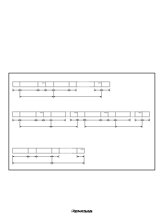
Rev. 1.0, 02/00, page 489 of 1141
23.3
Operation
23.3.1
I
2
C Bus Data Format
The I
2
C bus interface has serial and I
2
C bus formats.
The I
2
C bus formats are addressing formats with an acknowledge bit. These are shown in figures
23.3(1) and (2). The first frame following a start condition always consists of 8 bits. Formatless
transfer can be selected only for IIC channel 0. The formatless transfer data is shown in figure
23.3 (3).
The serial format is a non-addressing format with no acknowledge bit. This is shown in figure
23.4.
Figure 23.5 shows the I
2
C bus timing.
The symbols used in figures 23.3 to 23.5 are explained in table 23.4.
S
A
SLA
7
n
R/W
DATA
A
1
1
m
1
1
1
A/A
1
P
1
Transfer bit count
(n = 1 to 8)
Transfer frame count
(m = 1 or above)
S
SLA
7
n1
7
R/W
A
DATA
1
1
1
m1
1
A/A
1
S
1
SLA
R/W
1
1
m2
A
1
DATA
n2
A/A
1
P
1
Upper: Transfer bit count (n1 and N2 = 1 to 8)
Lower: Transfer frame count (m1 and m2 = 1 or above)
(1) FS = 0 or FSX = 0
A
n
DATA
DATA
A
1
m
1
8
1
A/A
1
Transfer bit count
(n = 1 to 8)
Transfer frame count
(m = 1 or above)
(3) Formatless (IIC channel 0 only, FS = 0 or FSX = 0)
(2) Start condition transmission, FS = 0 or FSX = 0
Figure 23.3 I
2
C Bus Data Formats (I
2
C Bus Formats)
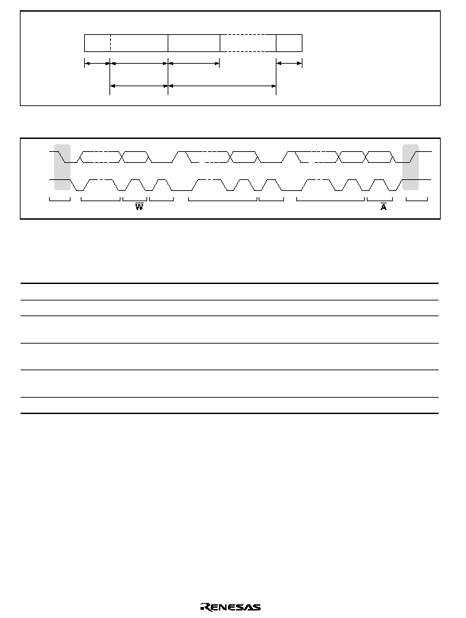
Rev. 1.0, 02/00, page 490 of 1141
S
DATA
8
n
DATA
1
1
m
P
1
Transfer bit count
(n = 1 to 8)
Transfer frame count
(m = 1 or above)
FS = 1 and FSX = 1
Figure 23.4 I
2
C Bus Data Format (Serial Format)
SDA
SCL
S
SLA
R/
A
9
8
1-7
9
8
1-7
9
8
1-7
DATA
A
DATA
A/
P
Figure 23.5 I
2
C Bus Timing
Table 23.4
I
2
C Bus Data Format Symbols
Symbol
Description
S
Start condition. The master device drives SDA from high to low while SCL is hig
SLA
Slave address, by which the master device selects a slave device
R/
:
Indicates the direction of data transfer: from the slave device to the master device
when R/
:
is 1, or from the master device to the slave device when R/
:
is 0
A
Acknowledge. The receiving device (the slave in master transmit mode, or the
master in master receive mode) drives SDA low to acknowledge a transfer
DATA
Transferred data. The bit length is set by bits BC2 to BC0 in ICMR. The MSB-first
or LSB-first format is selected by bit MLS in ICMR
P
Stop condition. The master device drives SDA from low to high while SCL is high
23.3.2
Master Transmit Operation
In master transmit mode, the master device outputs the transmit clock and transmit data, and the
slave device returns an acknowledge signal. The transmit procedure and operations in master
transmit mode are described below.
1. Set bit ICE in ICCR to 1. Set bits MLS, WAIT, and CKS2 to CKS0 in ICMR, and bit IICX in
STCR, according to the operating mode.
2. Read the BBSY flag in ICCR, check that the bus is free, then set MST and TRS to 1 in ICCR
to select master transmit mode. After that, write 1 in BBSY and 0 in SCP. This generates a
start condition by causing a high-to-low transition of SDA while SCL is high. As a result, the

Rev. 1.0, 02/00, page 491 of 1141
TDRE internal flag is set to 1 and the IRIC and IRTR flags are also set to 1. If IEIC is set to 1
in ICCR, a CPU interrupt is requested.
3. If bit FS is 0 in SAR or bit FSX is 0 in SARX, the first frame following the start condition
contains a 7-bit slave address and indicates the transmit/receive direction. Write data (slave
address + R/
:) to ICDR. At this time, the TDRE internal flag is cleared to 0. The written
address data is transferred to ICDRS, and the TDRE internal flag is set to 1 again. Clear IRIC
flag to 0 so that the end of transfer can be determined. The master device outputs the written
data together with a sequence of transmit clock pulses at the timing shown in figure 23.6. The
selected slave device (the device with the matching slave address) drives SDA low at the ninth
transmit clock pulse to acknowledge the data.
4. When one frame of data has been transmitted, the IRIC flag is set to 1 in ICCR at the rise of
the ninth transmit clock pulse. After one frame has been transferred, if the TDRE internal flag
is 1, SCL is automatically brought to the low level in synchronization with the internal clock
and held low.
5. When another data is to be sent, write it in ICDR. After making sure that the data has been
sent to ICDRS and the TDRE flag is set to 1, clear the IRIC flag to 0. Transmission of the next
frame is turned on in synchronization with the internal clock.
Steps 4 and 5 can be repeated to transmit data continuously. To end the transmission, clear IRIC,
write dummy data in ICDR after making sure that the last data has been sent (the next
transmission date is not present on ICDRT yet). Then, write 0 in BBSY and 0 in ICCR when IRIC
is set again. This generates a stop condition by causing a low-to-high transition of SDA while
SCL is high.
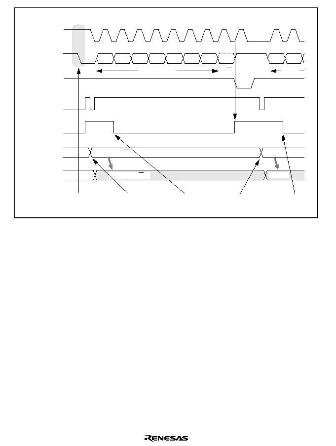
Rev. 1.0, 02/00, page 492 of 1141
SDA
(Master output)
SDA
(Slave output)
2
1
2
1
4
3
6
5
8
7
9
Bit 7
Bit 6
Bit 7
Bit 6
Bit 5
Bit 4
Bit 3
Bit 2
Bit 1
Bit 0
IRIC
ICDRT
ICDRS
TDRE
SCL
(Master output)
Start condition
issuance
Interrupt
request
generated
Interrupt request
generated
Data 1
Address + RW
Data 1
Address + RW
Write BBSY=1 and
SCP=0 (Start
condition issuance)
User processing
Slave address
Data 1
R/W
[4]
A
[2]
Write ICDR
[3]
Clear IRIC
[3]
Write ICDR
[5]
Clear IRIC
[5]
Figure 23.6 Example of Timing in Master Transmit Mode (MLS = WAIT = 0)
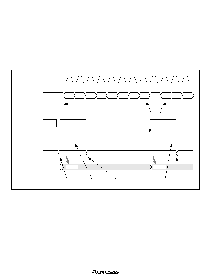
Rev. 1.0, 02/00, page 493 of 1141
When continuously transmitting data,
6. Clear IRIC flag to 0 before startup of the 9th transmit clock of the data being transmitted, and
then write the next transmit data in ICDR.
7. 1 frame data transmission ends, and upon startup of the 9th transmit clock, IRIC flag in ICCR
is set to 1. At the same time, the next transmit data written in ICDR (ICDRT) is transferred to
ICDRS, the flag in TDRE is set to 1, then the next frame transmission is executed, being
synchronized with the internal clock.
Steps 6 and 7 can be repeated to transmit data continuously. (See figure 23.7.)
SDA
(Master output)
SDA
(Slave output)
2
1
2
3
1
4
3
6
5
8
7
9
Bit 7
Bit 6
Bit 5
Bit 7
Bit 6
Bit 5
Bit 4
Bit 3
Bit 2
Bit 1
Bit 0
IRIC
ICDRT
ICDRS
TDRE
SCL
(Master output)
Interrupt
request
generated
Data 2
Data 1
[6] Write ICDR
Write ICDR
[6] Write ICDR
[6] Clear IRIC
[6] Clear IRIC
User processing
Data 1
Data 1
Data 2
Data 3
Data 2
[7]
[7]
A
Figure 23.7 Example of Continuous Transmission Timing in Master Transmit Mode
(MLS = WAIT = 0)

Rev. 1.0, 02/00, page 494 of 1141
23.3.3
Master Receive Operation
In master receive mode, the master device outputs the receive clock, receives data, and returns an
acknowledge signal. The slave device transmits the data. The receive procedure and operations in
master receive mode are described below.
1. Clear TRS to 0 in ICCR to switch from transmit mode to receive mode.
2. Read ICDR to start receiving (dummy data read). When ICDR is read, a receive clock is
output in synchronization with the internal clock, and data is received.
At the ninth clock pulse the master device drives SDA low to acknowledge the data.
3. When one frame of data has been received, the IRIC flag is set to 1 in ICCR at the rise of the
ninth receive clock pulse. If IEIC is set to 1 in ICCR, a CPU interrupt is requested. If the
RDRF internal flag is 0 at this time, it is set to 1, and continuous reception is performed. If
reception of the next frame is completed before the ICDR read and IRIC flag clearing in step 4,
SCL is automatically brought to the low level in synchronization with the internal clock and
held low.
4. Read ICDR and clear IRIC to 0 in ICCR. At this time, RDRF flag is cleared to 0.
Steps 3 and 4 can be repeated to receive data continuously. At the time the mode is first switched
from master transmit mode to master receive mode and reception has just started, RDRF internal
flag is cleared to 0, therefore data reception of the next frame is automatically started. To stop
receiving, TRS bit must be set to 1 before startup of the next frame receive clock.
To stop receiving, set TRS to 1, read ICDR, then write 0 in BBSY and 0 in SCP in ICCR. This
generates a stop condition by causing a low-to-high transition of SDA while SCL is high.
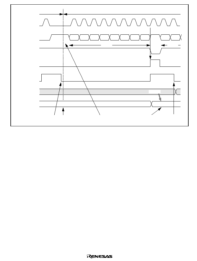
Rev. 1.0, 02/00, page 495 of 1141
SDA
(Master output)
SDA
(Slave output)
2
1
2
1
4
3
6
5
8
7
9
9
Bit 7
Bit 6
Bit 5
Bit 7
Bit 6
Bit 4
Bit 3
Bit 2
Bit 1
Bit 0
IRIC
ICDRS
ICDRR
RDRF
SCL
(Master output)
Interrupt
request
generated
Interrupt
request
generated
Master transmit
mode
Master receive
mode
Data 2
[1]Clear TRS to 0
[2]Read ICDR
(dummy read)
[4] Read ICDR
[4] Clear IRIC
Clear
IRIC
User
processing
Data 1
Data 1
Data 2
[3]
A
A
Figure 23.8 Example of Timing in Master Receive Mode (MLS = WAIT = ACKB = 0)

Rev. 1.0, 02/00, page 496 of 1141
23.3.4
Slave Receive Operation
In slave receive mode, the master device outputs the transmit clock and transmit data, and the
slave device returns an acknowledge signal. The receive procedure and operations in slave receive
mode are described below.
1. Set bit ICE in ICCR to 1. Set bits MLS in ICMR and bits MST and TRS in ICCR according to
the operating mode.
2. A start condition output by the master device sets the BBSY flag to 1 in ICCR.
3. After the slave device detects the start condition, if the first frame matches its slave address, it
functions as the slave device designated as the master device. If the 8th bit data (R/
:) is 0,
TRS bit in ICCR remains 0 and executes slave receive operation.
4. At the ninth clock pulse of the receive frame, the slave device drives SDA low to acknowledge
the transfer. At the same time, the IRIC flag is set to 1 in ICCR. If IEIC is 1 in ICCR, a CPU
interrupt is requested. If the RDRF internal flag is 0, it is set to 1 and continuous reception is
performed. If the RDRF internal flag is 1, the slave device holds SCL low from the fall of the
receive clock until it has read the data in ICDR.
5. Read ICDR and clear IRIC to 0 in ICCR. At this time, the RDFR flag is cleared to 0.
Steps 4 and 5 can be repeated to receive data continuously. When a stop condition is detected (a
low-to-high transition of SDA while SCL is high), the BBSY flag is cleared to 0 in ICCR.
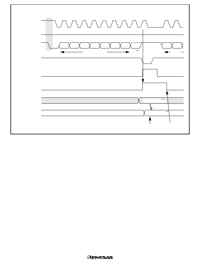
Rev. 1.0, 02/00, page 497 of 1141
SDA
(Master output)
SDA
(Slave output)
2
1
2
1
4
3
6
5
8
7
9
Bit 7
Bit 6
Bit 7
Bit 6
Bit 5
Bit 4
Bit 3
Bit 2
Bit 1
Bit 0
IRIC
ICDRS
ICDRR
RDRF
SCL
(Master output)
Start condition
issurance
SCL
(Slave output)
Interrupt request
generated
Address + R/W
Address + R/W
[5] Read ICDR
[5] Clear IRIC
User processing
Slave address
Data 1
[4]
A
R/W
Figure 23.9 Example of Timing in Slave Receive Mode (MLS = ACKB = 0)
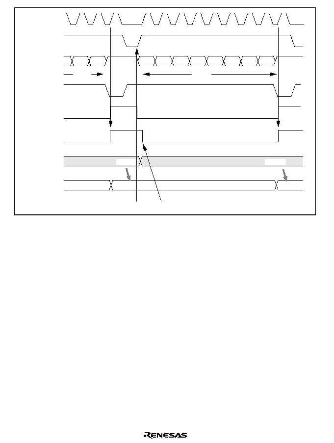
Rev. 1.0, 02/00, page 498 of 1141
SDA
(Master output)
SDA
(Slave output)
2
1
4
3
6
5
8
7
9
8
7
9
Bit 7
Bit 6
Bit 5
Bit 4
Bit 3
Bit 2
Bit 1
Bit 0
Bit 1
Bit 0
IRIC
ICDRS
ICDRR
RDRF
SCL
(Master output)
SCL
(Slave output)
Interrupt
request
generated
Interrupt
request
generated
Data 2
Data 2
Data 1
Data 1
[5] Read ICDR
[5] Clear IRIC
User processing
Data 2
Data 1
[4]
[4]
A
A
Figure 23.10 Example of Timing in Slave Receive Mode (MLS = ACKB = 0)

Rev. 1.0, 02/00, page 499 of 1141
23.3.5
Slave Transmit Operation
In slave transmit mode, the slave device outputs the transmit data, and the master device outputs
the transmit clock and returns an acknowledge signal. The transmit procedure and operations in
slave transmit mode are described below.
1. Set bit ICE in ICCR to 1. Set bits MLS in ICMR and bits MST and TRS in ICCR according to
the operating mode.
2. After the slave device detects a start condition, if the first frame matches its slave address, at
the ninth clock pulse the slave device drives SDA low to acknowledge the transfer. At the
same time, the IRIC flag is set to 1 in ICCR, and if the IEIC bit in ICCR is set to 1 at this time,
an interrupt request is sent to the CPU. If the eighth data bit (R/
:) is 1, the TRS bit is set to 1
in ICCR, automatically causing a transition to slave transmit mode. The slave device holds
SCL low from the fall of the transmit clock until data is written in ICDR.
3. Clear the IRIC flag to 0, then write data in ICDR. The written data is transferred to ICDRS,
and the TDRE internal flag and the IRIC and IRTR flags are set to 1 again. Clear IRIC to 0,
then write the next data in ICDR. The slave device outputs the written data serially in step
with the clock output by the master device, with the timing shown in figure 23.11.
4. When one frame of data has been transmitted, at the rise of the ninth transmit clock pulse IRIC
is set to 1 in ICCR. If the TDRE internal flag is 1, the slave device holds SCL low from the
fall of the transmit clock until data is written in ICDR. The master device drives SDA low at
the ninth clock pulse to acknowledge the data. The acknowledge signal is stored in the ACKB
bit in ICSR, and can be used to check whether the transfer was carried out normally. If TDRE
internal flag is set to 0, the data written in ICDR is transferred to ICDRS, then transmission
starts and TDRE internal flag and IRIC and IRTR flags are all set to 1 again.
5. To continue transmitting, clear IRIC to 0, then write the next transmit data in ICDR. At this
time, the TDRE internal flag is cleared to 0.
Steps 4 and 5 can be repeated to transmit continuously. To end the transmission, write H'FF in
ICDR. When a stop condition is detected (a low-to-high transition of SDA while SCL is high), the
BBSY flag will be cleared to 0 in ICCR.
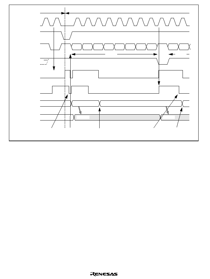
Rev. 1.0, 02/00, page 500 of 1141
SDA
(Slave output)
SDA
(Master output)
SCL
(Slave output)
2
1
2
1
4
3
6
5
8
7
9
9
8
Bit 7
Bit 6
Bit 5
Bit 7
Bit 6
Bit 4
Bit 3
Bit 2
Bit 1
Bit 0
IRIC
ICDRS
ICDRT
TDRE
SCL
(Master output)
Interrupt
request
generated
Interrupt
request
generated
Interrupt
request
generated
Slave receive mode
Slave transmit mode
Data 1
Data 2
[3] Clear IRIC
[5] Clear IRIC
[3] Write ICDR
[3] Write ICDR
[5] Write ICDR
User
processing
Data 1
Data 1
Data 2
Data 2
A
R/W
A
[3]
[2]
Figure 23.11 Example of Timing in Slave Transmit Mode (MLS = 0)
23.3.6
IRIC Setting Timing and SCL Control
The interrupt request flag (IRIC) is set at different times depending on the WAIT bit in ICMR, the
FS bit in SAR, and the FSX bit in SARX. If the TDRE or RDRF internal flag is set to 1, SCL is
automatically held low after one frame has been transferred; this timing is synchronized with the
internal clock. Figure 23.12 shows the IRIC set timing and SCL control.
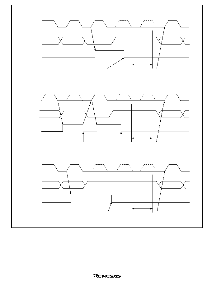
Rev. 1.0, 02/00, page 501 of 1141
SCL
SDA
IRIC
User
processing
Clear
IRIC
Write to ICDR (transmit) or
read ICDR (receive)
1
A
8
7
1
9
8
7
SCL
SDA
IRIC
User
processing
Clear IRIC Write to ICDR (transmit) or
read ICDR (receive)
1
A
8
1
9
8
Clear IRIC
SCL
SDA
IRIC
User
processing
Clear IRIC
Write to ICDR (transmit) or
read ICDR (receive)
1
8
7
1
8
7
(a) When WAIT = 0, and FS = 0 or FSX = 0 (I
2
C bus format, no wait)
(b) When WAIT = 1, and FS = 0 or FSX = 0 (I
2
C bus format, wait inserted)
(c) When FS = 1 and FSX = 1 (synchronous serial format)
Figure 23.12 IRIC Setting Timing and SCL Control

Rev. 1.0, 02/00, page 502 of 1141
23.3.7
Automatic Switching from Formatless Transfer to I
2
C Bus Format Transfer
Setting the SW bit in DDCSWR to 1 selects the IIC0 formatless transfer operation. When an SCL
falling edge is detected, the operating mode automatically switches from formatless transfer to I
2
C
bus format transfer (slave mode). For automatic switching to be possible, the following four
conditions must be observed:
1. The same data pin (SDA) is used in common for formatless transfer and I
2
C bus format
transfer.
2. Separate clock pins are used for formatless transfer and I
2
C bus format transfer (SYNC1 for
formatless, and SCL for I
2
C bus format)
3. The SCL pin is kept high during formatless transfer.
4. Register bits other than the TRS bit in ICCR are set to appropriate values so that I
2
C bus
format transfer can be performed.
The operating mode is automatically switched from formatless transfer to I
2
C bus format transfer
when an SCL falling edge is detected and the SW bit in DDCSWR is automatically cleared to 0.
To switch the mode from I
2
C bus format transfer to formatless transfer, set the SW bit to 1 by
software.
During formatless transfer, do not modify the bits that control the I
2
C bus interface operating
mode, such as the MSL or TRS bit. When switching from the I
2
C bus format transfer to formatless
transfer, specify the formatless transfer direction (transmit or receive) by setting or clearing the
TRS bit, then set the SW bit to 1. After the automatic switching from formatless transfer to I
2
C bus
format transfer (slave mode), the TRS bit is automatically cleared to 0 to enter the slave address
receive wait state.
If an SCL falling edge is detected during formatless transfer, the IIC does not wait for the stop
condition but switches the operating mode immediately.
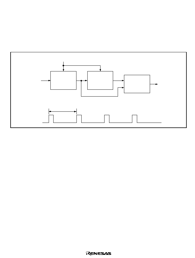
Rev. 1.0, 02/00, page 503 of 1141
23.3.8
Noise Canceler
The logic levels at the SCL and SDA pins are routed through noise cancelers before being latched
internally. Figure 23.13 shows a block diagram of the noise canceler circuit.
The noise canceler consists of two cascaded latches and a match detector. The SCL (or SDA)
input signal is sampled on the system clock, but is not passed forward to the next circuit unless the
outputs of both latches agree. If they do not agree, the previous value is held.
SCL or SDA
input signal
Internal SCL
or SDA signal
Sampling clock
Sampling
clock
System clock
period
C
Latch
Q
D
C
Latch
Q
D
Match
detector
Figure 23.13 Block Diagram of Noise Canceler
23.3.9
Sample Flowcharts
Figures 23.14 to 23.17 show sample flowcharts for using the I
2
C bus interface in each mode.
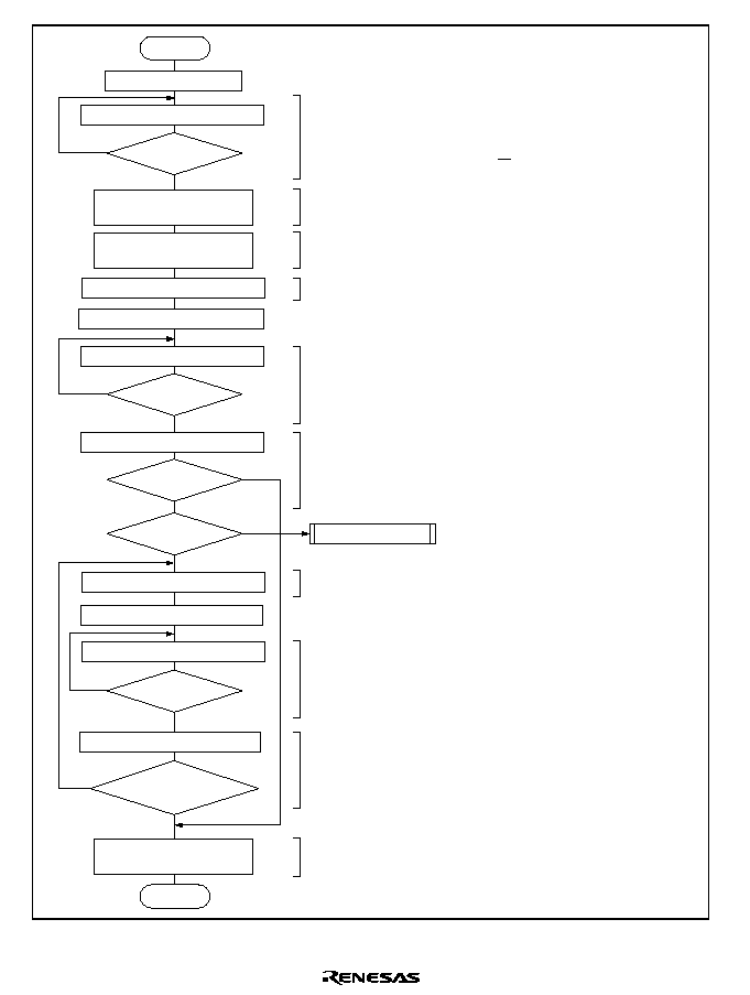
Rev. 1.0, 02/00, page 504 of 1141
Start
End
Initialize
Read BBSY flag in ICCR
Read IRIC flag in ICCR
Read ACKB bit in ICSR
Read ACKB bit in ICSR
Clear IRIC flag in ICCR
Read IRIC flag in ICCR
Write transmit data in ICDR
Master receive mode
Write transmit data in ICDR
Set MST=1 and
TRS=1 in ICCR
Write BBSY=0 and
SCP=0 in ICCR
Write BBSY=1 and
SCP=0 in ICCR
BBSY=0?
No
IRIC=1?
ACKB=0?
No
No
Yes
Yes
Yes
Transmit
mode?
IRIC=1?
End of transmission
(ACKB = 1)?
No
No
No
Yes
Yes
Yes
[1]
[2]
[3]
[4]
[7]
[5]
[6]
[8]
[9]
[10]
Clear IRIC flag in ICCR
Test the status of the SCL and SDA lines.
Select master transmit mode.
Generate a start condition.
Set transmit data for the first byte (slave
address +R/W)
Wait for 1 byte to be transmitted.
Test for acknowledgement by the
designated slave device.
Set transmit data for the second and
subsequent bytes.
Wait for 1 byte to be transmitted.
Test for end of transfer.
Generate a stop condition.
[1]
[2]
[3]
[4]
[5]
[6]
[7]
[8]
[9]
[10]
Figure 23.14 Flowchart for Master Transmit Mode (Example)
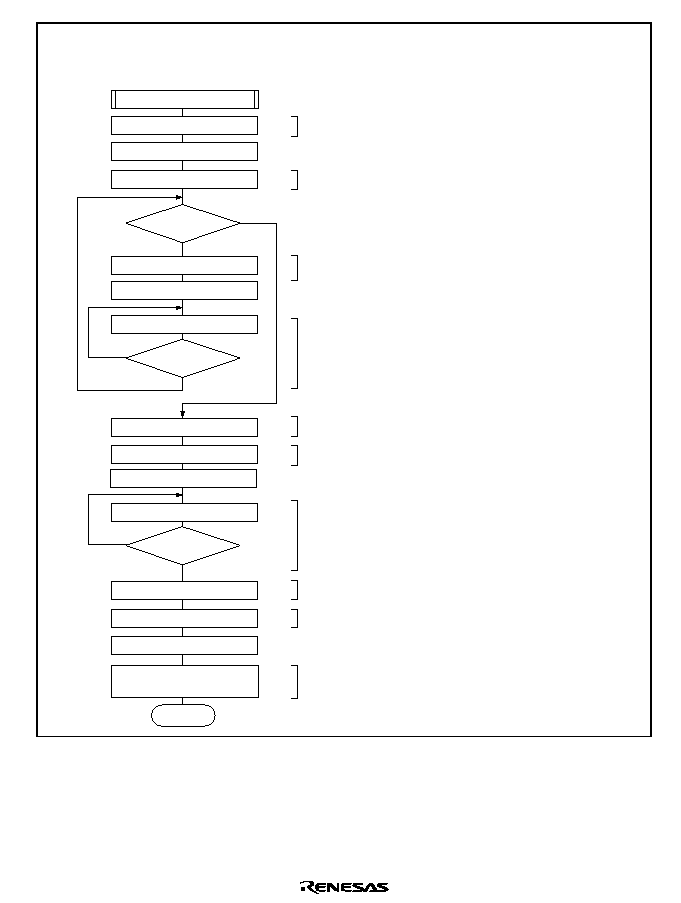
Rev. 1.0, 02/00, page 505 of 1141
End
Set TRS=0 in ICCR
Clear IRIC flag in ICCR
Set ACKB=1 in ICSR
Set TRS=1 in ICCR
Read ICDR
Read IRIC flag in ICCR
Clear IRIC flag in ICCR
Set ACKB=0 in ICSR
Write BBSY=0 and
SCP=0 in ICCR
Last receive?
IRIC=1?
No
No
Yes
Yes
Read ICDR
Read ICDR
Read IRIC flag in ICCR
Clear IRIC flag in ICCR
Clear IRIC flag in ICCR
IRIC=1?
No
Yes
[3]
[1]
[2]
[5]
[6]
[4]
[7]
[8]
[9]
[10 ]
Master receive mode
Select receive mode.
Set acknowledge data.
Start receiving. The first read is a dummy
read.
Wait for 1 byte to be received.
Set acknowledge data for the last receive.
Start the last receive.
Wait for 1 byte to be received.
Select transmit mode.
Read the last receive data (if ICDR is read
without selecting transmit mode, receive
operations will resume).
Generate a stop condition.
[1]
[2]
[3]
[4]
[5]
[6]
[7]
[8]
[9]
[10]
Figure 23.15 Flowchart for Master Receive Mode (Example)
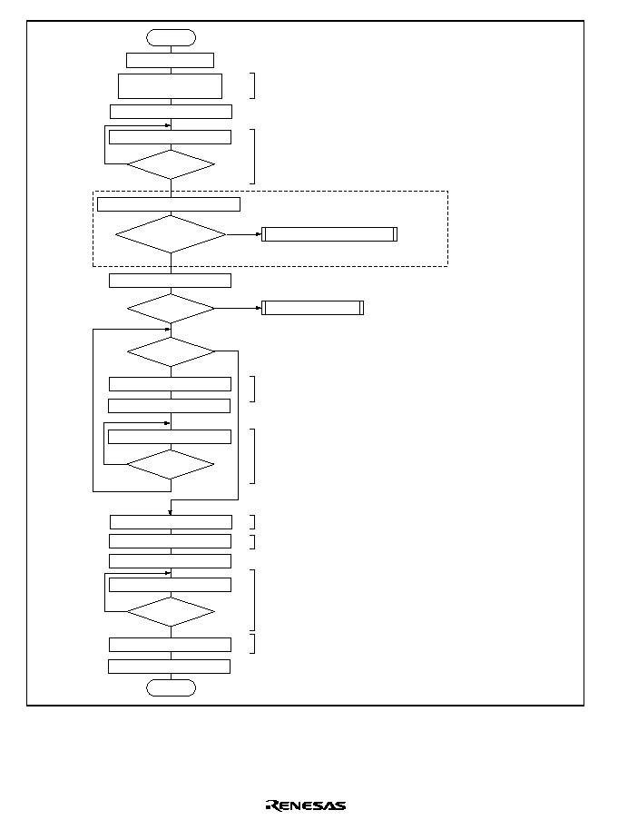
Rev. 1.0, 02/00, page 506 of 1141
Start
End
Initialize
Read IRIC flag in ICCR
Read AAS and ADZ flags in ICSR
Read TRS bit in ICCR
Read IRIC flag in ICCR
Clear IRIC flag in ICCR
Clear IRIC flag in ICCR
Clear IRIC flag in ICCR
Read ICDR
Read ICDR
Read ICDR
Set ACKB=0 in ICSR
General call address processing
*Description omitted
Set MST=0 and
TRS=0 in ICCR
IRIC=1?
No
Yes
Read IRIC flag in ICCR
Set ACKB=0 in ICSR
IRIC=1?
No
Yes
TRS=0?
IRIC=1?
No
No
Yes
Yes
Yes
AAS=1 and
ADZ=0?
[2]
[1]
[3]
[8]
[5]
[6]
[4]
[7]
Slave transmit mode
Last receive?
No
No
Yes
Select slave receive mode.
Wait for 1 byte to be received (slave
address)
Start receiving. The first read is a dummy
read.
Wait for the transfer to end.
Set acknowledge data for the last receive.
Start the last receive.
Wait for the transfer to end.
Read the last receive data.
[1]
[2]
[3]
[4]
[5]
[6]
[7]
[8]
Figure 23.16 Flowchart for Slave Transmit Mode (Example)
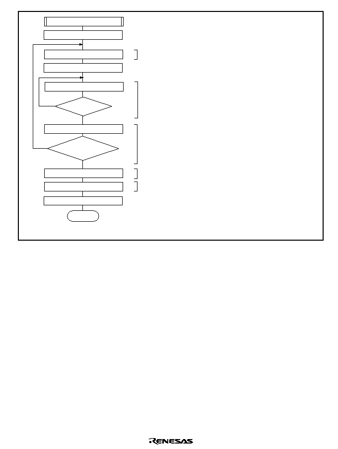
Rev. 1.0, 02/00, page 507 of 1141
End
Write transmit data in ICDR
Clear IRIC flag in ICCR
Clear IRIC flag in ICCR
Read ACKB bit in ICSR
Set TRS=0 in ICCR
Read ICDR
Read IRIC flag in ICCR
IRIC=1?
Yes
Yes
No
No
[1]
[4]
[5]
[2]
[3]
Slave transmit mode
End of transmission
(ACKB=1)?
Clear IRIC in ICCR
Set transmit data for the second and
subsequent bytes.
Wait for 1 byte to be transmitted.
Test for end of transfer.
Select slave receive mode.
Dummy read (to release the SCL line).
[1]
[2]
[3]
[4]
[5]
Figure 23.17 Flowchart for Slave Receive Mode (Example)
23.3.10
Initializing Internal Status
The IIC can forcibly initialize the IIC internal status when a dead lock occurs during
communication. Initialization is enabled by (1) setting the CLR3 to CLR0 bits in DDCSWR, or (2)
clearing the ICE bit. For details on CLR3 to CLR0 settings, refer to section 23.2.8, DDC Switch
Register (DDCSWR).
(1) Initialized Status
This function initializes the following:
∑
TDRE and RDRF internal flags
∑
Transmit/receive sequencer and internal clock counter
∑
Internal latches (wait, clock, or data output) which holds the levels output from the SCL and
SDA pins
This function does not initialize the following:
∑
Register contents (ICDR, SAR, SARX, ICMR, ICCR, ICSR, DDCSWR, and STCR)

Rev. 1.0, 02/00, page 508 of 1141
∑
Internal latches which holds the register read information to set or clear the flags in ICMR,
ICCR, ICSR, and DDCSWR
∑
Bit counter (BC2 to BC0) value in ICMR
∑
Sources of interrupts generated (interrupts that has been transferred to the interrupt
controller)
(2) Notes on Initialization
∑
Interrupt flags and interrupt sources are not cleared; clear them by software if necessary.
∑
Other register flags cannot be assumed to be cleared, either; clear them by software if
necessary.
∑
When initialization is specified by the DDCSWR settings, the data written to the CLR3 to
CLR0 bits are not held. When initializing the IIC, be sure to use the MOV instruction to
write to all the CLR3 to CLR0 bits at the same time; do not use bit manipulation
instructions such as BCLR. When reinitializing the module status, all the CLR3 to CLR0
bits must be rewritten to at the same time.
∑
If a flag is cleared during transfer, the IIC module stops transfer immediately, and releases
the control of the SCL and SDA pins. Before starting again, set the registers to appropriate
values to make a correct communication if necessary.
This module initializing function does not modify the BBSY bit value, but in some cases,
depending on the SCL and SDA pin status and the release timing, the signal waveforms at the
SCL and SDA pins may indicate the stop condition, and accordingly the BBSY bit may be
cleared. Other bits or flags may be affected in the same way by module initialization.
To avoid these problems, take the following procedure to initialize the IIC:
1. Initialize the IIC by setting the CLR3 to CLR0 bits or the ICE bit.
2. Execute a stop condition issuing instruction to clear the BBSY bit to 0 (writing 0 to BBSY and
SCP), and wait for two cycles of the transfer clock.
3. Initialize the IIC again by setting the CLR3 to CLR0 bits or the ICE bit.
4. Set the registers in IIC to appropriate values.

Rev. 1.0, 02/00, page 509 of 1141
23.4
Usage Notes
1. In master mode, if an instruction to generate a start condition is immediately followed by an
instruction to generate a stop condition, neither condition will be output correctly. To output
consecutive start and stop conditions, after issuing the instruction that generates the start
condition, read the relevant ports, check that SCL and SDA are both low, then issue the
instruction that generates the stop condition. Note that the SCL may briefly remain at a high
level immediately after BBSY is cleared to 0.
2. Either of the following two conditions will start the next transfer. Pay attention to these
conditions when reading or writing to ICDR.
a. Write access to ICDR when ICE = 1 and TRS = 1 (including automatic transfer from
ICDRT to ICDRS)
b. Read access to ICDR when ICE = 1 and TRS = 0 (including automatic transfer from
ICDRS to ICDRR)
3. Table 23.5 shows the timing of SCL and SDA output in synchronization with the internal
clock. Timings on the bus are determined by the rise and fall times of signals affected by the
bus load capacitance, series resistance, and parallel resistance.
Table 23.5
I
2
C Bus Timing (SCL and SDA Output)
Item
Symbol
Output Timing
Unit
Notes
SCL output cycle time
t
SCLO
28t
cyc
to 256t
cyc
ns
SCL output high pulse width
t
SCLHO
0.5t
SCLO
ns
SCL output low pulse width
t
SCLLO
0.5t
SCLO
ns
SDA output bus free time
t
BUFO
0.5t
SCLO
-1t
cyc
ns
Start condition output hold time
t
STAHO
0.5t
SCLO
-1t
cyc
ns
Retransmission start condition
output setup time
t
STASO
1t
SCLO
ns
Stop condition output setup time
t
STOSO
0.5t
SCLO
+2t
cyc
ns
Data output setup time (master)
1t
SCLLO
-3t
cyc
ns
Data output setup time (slave)
t
SDASO
1t
SCLL
- (6t
cyc
or 12t
cyc
*)
ns
Data output hold time
t
SDAHO
3t
cyc
ns
Figure 30.9
(reference)
Note:
*
6t
cyc
when IICX is 0, 12t
cyc
when 1.
4. SCL and SDA input is sampled in synchronization with the internal clock. The AC timing
therefore depends on the system clock cycle t
cyc
, as shown in table 30.6 in section 30, Electrical
Characteristics. Note that the I
2
C bus interface AC timing specifications will not be met with a
system clock frequency of less than 5 MHz.

Rev. 1.0, 02/00, page 510 of 1141
5. The I
2
C bus interface specification for the SCL rise time t
sr
is under 1000 ns (300 ns for high-
speed mode). In master mode, the I
2
C bus interface monitors the SCL line and synchronizes
one bit at a time during communication. If t
sr
(the time for SCL to go from low to V
IH
) exceeds
the time determined by the input clock of the I
2
C bus interface, the high period of SCL is
extended. The SCL rise time is determined by the pull-up resistance and load capacitance of
the SCL line. To insure proper operation at the set transfer rate, adjust the pull-up resistance
and load capacitance so that the SCL rise time does not exceed the values given in table 23.6.
Table 23.6
Permissible SCL Rise Time (t
sr
) Values
Time Indication [ns]
IICX
t
cyc
Indication
I
2
C Bus
Specification
(Max.)
= 8 MHz
= 10 MHz
Normal mode
1000
937
750
0
7.5t
cyc
High-speed mode
300
Normal mode
1000
1
17.5t
cyc
High-speed mode
300
6. The I
2
C bus interface specifications for the SCL and SDA rise and fall times are under 1000 ns
and 300 ns. The I
2
C bus interface SCL and SDA output timing is prescribed by t
Scyc
, as shown
in table 23.5. However, because of the rise and fall times, the I
2
C bus interface specifications
may not be satisfied at the maximum transfer rate. Table 23.7 shows output timing
calculations for different operating frequencies, including the worst-case influence of rise and
fall times.
t
BUFO
fails to meet the I
2
C bus interface specifications at any frequency. The solution is either
(a) to provide coding to secure the necessary interval (approximately 1
µ
s) between issuance of
a stop condition and issuance of a start condition, or (b) to select devices whose input timing
permits this output timing for use as slave devices connected to the I
2
C bus.
t
SCLLO
in high-speed mode and t
STASO
in standard mode fail to satisfy the I
2
C bus interface
specifications for worst-case calculations of t
Sr
/t
Sf
. Possible solutions that should be
investigated include (a) adjusting the rise and fall times by means of a pull-up resistor and
capacitive load, (b) reducing the transfer rate to meet the specifications, or (c) selecting devices
whose input timing permits this output timing for use as slave devices connected to the I
2
C
bus.
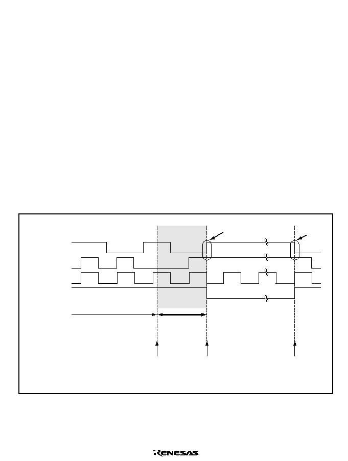
Rev. 1.0, 02/00, page 511 of 1141
7. Precautions on reading ICDR at the end of master receive mode
When terminating the master receive mode, set TRS bit to 1, and select "write" for ICCR
BBSY = 0 and SCP = 0. This forces to move SDA from low to high level when SCL is at high
level, thereby generating the stop condition.
Now you can read received data from ICDR. If, however, any data is remaining on the buffer,
received data on ICDRS is not transferred to ICDR, thus you won't be able to read the second
byte data.
When it is required to read the second byte data, issue the stop condition from the master
receive state (TRS bit is 0).
Before reading data from ICDR register, make sure that BBSY bit on ICCR register is 0, stop
condition is generated and bus is made free.
If you try to read received data after the stop condition issue instruction (setting ICCR's BBSY
= 0 and SCP = 0 to write) has been executed but before the actual stop condition is generated,
clock may not be appropriately signaled when the next master sending mode is turned on.
Thus, reasonable care is needed for determining when to read the received data.
After the master receive is complete, if you want to re-write IIC control bit (such as clearing MST
bit) for switching the sending/receiving mode or modifying settings, it must be done during period
(a) indicated in figure 23.18 (after making sure ICCR register BBSY bit is cleared to 0).
SDA
SCL
Internal clock
BBSY bit
Bit 0
A
(a)
8
9
Stop condition
Start
condition
Start condition
is issued
Generation of the stop
condition is checked
(BBSY = 0 is set to read)
The stop condition
issue instruction
(BBSY = 0 and SCP = 0
set to write) is executed
Master receive mode
ICDR read
inhibit period
Figure 23.18 Precautions on Reading the Master Receive Data

Rev. 1.0, 02/00, page 512 of 1141
Table 23.7
I
2
C Bus Timing (with Maximum Influence of t
Sr
/t
Sf
)
Time Indication (at Maximum Transfer Rate) [ns]
Item
t
cyc
Indication
t
Sr
/t
Sf
Influence
(Max.)
I
2
C Bus
Specification
(Min.)
= 8 MHz
= 10 MHz
Normal mode
-
1000
4000
t
SCLHO
0.5t
SCLO
(-t
Sr
)
High-speed
mode
-
300
600
Normal mode
-
250
4700
t
SCLLO
0.5t
SCLO
(-t
Sf
)
High-speed
mode
-
250
1300
Normal mode
-
1000
4700
3875
*1
3900
*1
t
BUFO
0.5t
SCLO
-1t
cyc
(-t
Sr
)
High-speed
mode
-
300
1300
825
*1
850
*1
Normal mode
-
250
4000
4625
4650
t
STAHO
0.5t
SCLO
-1t
cyc
(-t
Sf
)
High-speed
mode
-
250
600
875
900
Normal mode
-
1000
4700
9000
9000
t
STASO
1t
SCLO
(-t
Sr
)
High-speed
mode
-
300
600
2200
2200
Normal mode
-
1000
4000
4250
4200
t
STOSO
0.5t
SCLO
+2t
cyc
(-t
Sr
)
High-speed
mode
-
300
600
1200
1150
Normal mode
-
1000
250
3325
3400
t
SDASO
(master)
1t
SCLLO
*
3
-3t
cyc
(-t
Sr
)
High-speed
mode
-
300
100
625
700
Normal mode
-
1000
250
2200
2500
t
SDASO
(slave)
1t
SCLL
*
3
-12t
cyc
*
2
(-t
Sr
)
High-speed
mode
-
300
100
-
500
*1
-
200
*1
Normal mode
0
0
375
300
t
SDAHO
3t
cyc
High-speed
mode
0
0
Notes: 1. Does not meet the I
2
C bus interface specification. Remedial action such as the
following is necessary: (a) secure a start/stop condition issuance interval; (b) adjust the
rise and fall times by means of a pull-up resistor and capacitive load; (c) reduce the
transfer rate; (d) select slave devices whose input timing permits this output timing.
The values in the above table will vary depending on the settings of the IICX bit and bits
CKS0 to CKS2. Depending on the frequency it may not be possible to achieve the
maximum transfer rate; therefore, whether or not the I
2
C bus interface specifications are
met must be determined in accordance with the actual setting conditions.
2. Value when the IICX bit is set to 1. When the IICX bit is cleared to 0, the value is (t
SCLL
-
6t
cyc
).
3. Calculated using the I
2
C bus specification values (standard mode: 4700 ns min.; high-
speed mode: 1300 ns min.).

Rev. 1.0, 02/00, page 513 of 1141
Section 24 A/D Converter
24.1
Overview
This LSI incorporates a 10-bit successive-approximations A/D converter that allows up to 12
analog input channels to be selected.
24.1.1
Features
A/D converter has the following features.
∑
10-bit resolution
∑
12 input channels
∑
Sample and hold function
∑
Choice of software, hardware (internal signal) triggering or external triggering for A/D
conversion start.
∑
A/D conversion end interrupt request generation
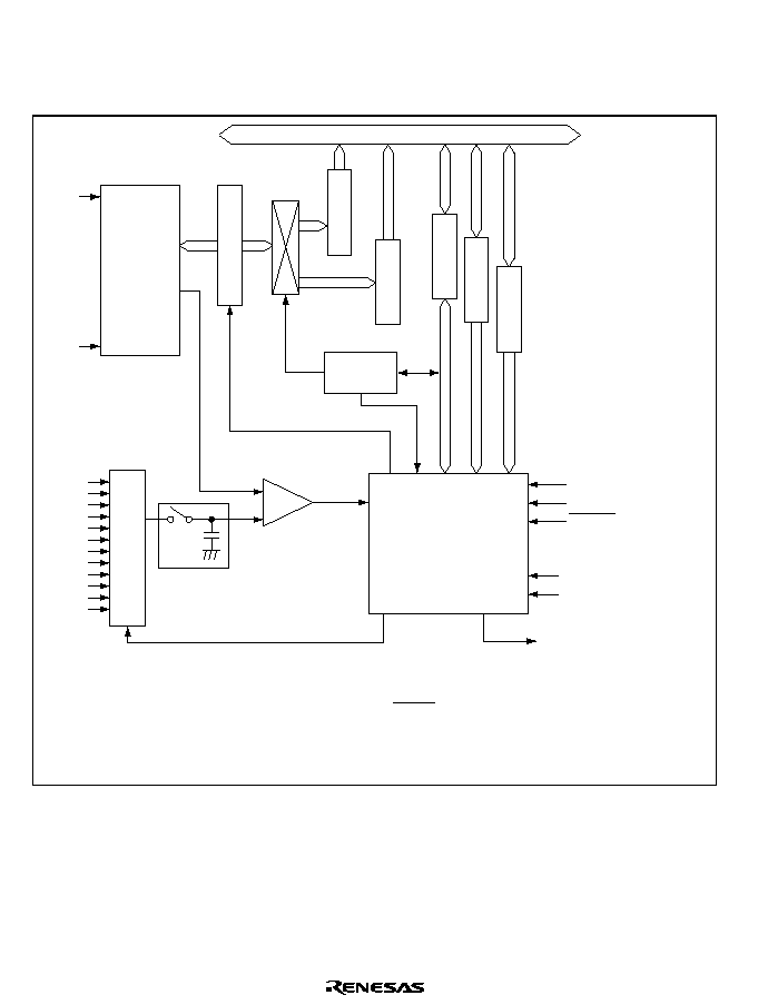
Rev. 1.0, 02/00, page 514 of 1141
24.1.2
Block Diagram
Figure 24.1 shows a block diagram of the A/D converter.
/2
/4
ADTRG
Interrupt request
AN0
Vref
AV
CC
AV
SS
Reference Voltage
Sample-and-
hold circuit
Chopper type
comparator
AN1
AN2
AN3
AN4
AN5
AN6
AN7
AN8
AN9
ANA
ANB
DFG
ADTRG
(HSW timing generator)
Internal data bus
[Legend]
ADR
AHR
: Software trigger A/D result register
: Hardware trigger A/D result register
ADTRG, DFG
ADTRG
: Hardware trigger
: A/D external trigger input
ADCR
ADCSR
: A/D control register
: A/D control/status register
ADTSR: A/D trigger selection register
-
+
10-bit
D/A
Hardware
control
circuit
Control circuit
Analog multiplexer
Successive
approximation register
A
D
R
A
H
R
A
D
C
S
R
A
D
C
R
A
D
T
S
R
Figure 24.1 Block Diagram of A/D Converter

Rev. 1.0, 02/00, page 515 of 1141
24.1.3
Pin Configuration
Table 24.1 summarizes the input pins used by the A/D converter.
Table 24.1
A/D Converter Pins
Name
Abbrev.
I/O
Function
Analog power supply pin
AV
CC
Input
Analog block power supply and A/D
conversion reference voltage
Analog ground pin
AV
SS
Input
Analog block ground and A/D conversion
reference voltage
Analog input pin 0
AN0
Input
Analog input channel 0
Analog input pin 1
AN1
Input
Analog input channel 1
Analog input pin 2
AN2
Input
Analog input channel 2
Analog input pin 3
AN3
Input
Analog input channel 3
Analog input pin 4
AN4
Input
Analog input channel 4
Analog input pin 5
AN5
Input
Analog input channel 5
Analog input pin 6
AN6
Input
Analog input channel 6
Analog input pin 7
AN7
Input
Analog input channel 7
Analog input pin 8
AN8
Input
Analog input channel 8
Analog input pin 9
AN9
Input
Analog input channel 9
Analog input pin A
ANA
Input
Analog input channel A
Analog input pin B
ANB
Input
Analog input channel B
A/D external trigger input pin
$'75*
Input
External trigger input for starting A/D
conversion

Rev. 1.0, 02/00, page 516 of 1141
24.1.4
Register Configuration
Table 24.2 summarizes the registers of the A/D converter.
Table 24.2
A/D Converter Registers
Name
Abbrev.
R/W
Size
Initial Value
Address
*2
Software trigger A/D
result register H
ADRH
R
Byte
H'00
H'D130
Software trigger A/D
result register L
ADRL
R
Byte
H'00
H'D131
Hardware trigger A/D
result register H
AHRH
R
Byte
H'00
H'D132
Hardware trigger A/D
result register L
AHRL
R
Byte
H'00
H'D133
A/D control register
ADCR
R/W
Byte
H'40
H'D134
A/D control/status
register
ADCSR
R (W)
*1
Byte
H'01
H'D135
A/D trigger selection
register
ADTSR
R/W
Byte
H'FC
H'D136
Port mode register 0
PMR0
R/W
Byte
H'00
H'FFCD
Notes: 1. Only 0 can be written in bits 7 and 6, to clear the flag. Bits 3 to 1 are read-only.
2. Lower 16 bits of the address.

Rev. 1.0, 02/00, page 517 of 1141
24.2
Register Descriptions
24.2.1
Software-Triggered A/D Result Register (ADR)
ADRH
ADRL
1
0
3
2
5
4
--
--
--
--
--
--
--
--
--
--
--
--
7
0
R
6
0
R
9
0
R
8
0
R
11
0
R
10
0
R
0
R
0
R
0
R
ADR9 ADR8 ADR7 ADR6 ADR5 ADR4 ADR3 ADR2 ADR1 ADR0
0
R
12
13
14
15
0
0
0
0
0
0
Bit :
Initial value :
R/W :
The software-triggered A/D result register (ADR) is a register that stores the result of an A/D
conversion started by software.
The A/D-converted data is 10-bit data. Upon completion of software-triggered A/D conversion,
the 10-bit result data is transferred to ADR and the data is retained until the next software-
triggered A/D conversion completion. The upper 8 bits of the data are stored in the upper bytes
(bits 15 to 8) of ADR, and the lower 2 bits are stored in the lower bytes (bits 7 and 6). Bits 5 to 0
are always read as 0.
ADR can be read by the CPU at any time, but the ADR value during A/D conversion is not fixed.
The upper bytes can always be read directly, but the data in the lower bytes is transferred via a
temporary register (TEMP). For details, see section 24.3, Interface to Bus Master.
ADR is a 16-bit read-only register which is initialized to H'0000 at a reset, and in module stop
mode, standby mode, watch mode, subactive mode and subsleep mode.
24.2.2
Hardware-Triggered A/D Result Register (AHR)
AHRH
AHRL
1
0
3
2
5
4
--
--
--
--
--
--
--
--
--
--
--
--
7
0
R
6
0
R
9
0
R
8
0
R
11
0
R
10
0
R
0
R
0
R
0
R
AHR9 AHR8 AHR7 AHR6 AHR5 AHR4 AHR3 AHR2 AHR1 AHR0
0
R
12
13
14
15
0
0
0
0
0
0
Bit :
Initial value :
R/W :
The hardware-triggered A/D result register (AHR) is a register that stores the result of an A/D
conversion started by hardware (internal signal: ADTRG and DFG) or by external trigger input
(
$'75*).
The A/D-converted data is 10-bit data. Upon completion of hardware- or external-triggered A/D
conversion, the 10-bit result data is transferred to AHR and the data is retained until the next
hardware- or external- triggered A/D conversion completion. The upper 8 bits of the data are
stored in the upper bytes (bits 15 to 8) of AHR, and the lower 2 bits are stored in the lower bytes
(bits 7 and 6). Bits 5 to 0 are always read as 0.
Rev. 1.0, 02/00, page 518 of 1141
AHR can be read by the CPU at any time, but the AHR value during A/D conversion is not fixed.
The upper bytes can always be read directly, but the data in the lower bytes is transferred via a
temporary register (TEMP). For details, see section 24.3, Interface to Bus Master.
AHR is a 16-bit read-only register which is initialized to H'0000 at a reset, and in module stop
mode, standby mode, watch mode, subactive mode and subsleep mode.
24.2.3
A/D Control Register (ADCR)
0
0
1
0
R/W
2
0
R/W
3
0
4
0
R/W
5
0
6
--
--
1
7
R/W
R/W
R/W
HCH1
0
R/W
CK
HCH0
SCH3
SCH2
SCH1
SCH0
Bit :
Initial value :
R/W :
ADCR is a register that sets A/D conversion speed and selects analog input channel. When
executing ADCR setting, make sure that the SST and HST flags in ADCSR is set to 0.
ADCR is an 8-bit readable/writable register that is initialized to H'40 by a reset, and in module
stop mode, standby mode, watch mode, subactive mode and subsleep mode.
Bit 7
Clock Select (CK): Sets A/D conversion speed.
Bit 7
CK
Description
0
Conversion frequency is 266 states
(Initial value)
1
Conversion frequency is 134 states
Note: A/D conversion starts when 1 is written in SST, or when HST is set to 1. The conversion
period is the time from when this start flag is set until the flag is cleared at the end of
conversion. Actual sample-and-hold takes place (repeatedly) during the conversion
frequency shown in figure 24.2.
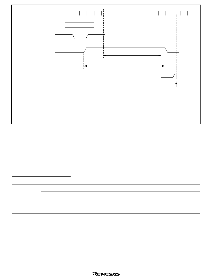
Rev. 1.0, 02/00, page 519 of 1141
Conversion frequency
Note: IRQ sampling;
Conversion period (134 or 266 states)
Interrupt request flag
IRQ sampling
(CPU)
States
Instruction execution
MOV.B
WRITE
Start flag
When conversion ends, the start flag is cleared and the interrupt request flag is
set. The CPU recognizes the interrupt in the last execution state of an instruction,
and executes interrupt exception handling after completing the instruction.
Figure 24.2 Internal Operation of A/D Converter
Bit 6
Reserved: This bit cannot be modified and is always read as 1.
Bits 5 and 4
Hardware Channel Select (HCH1, HCH0): These bits select the analog input
channel that is converted by hardware triggering or triggering by an external input. Only channels
AN8 to ANB are available for hardware- or external-triggered conversion.
Bit 5
Bit 4
HCH1
HCH0
Analog Input Channel
0
AN8
(Initial value)
0
1
AN9
0
ANA
1
1
ANB

Rev. 1.0, 02/00, page 520 of 1141
Bits 3 to 0
Software Channel Select (SCH3 to SCH0): These bits select the analog input
channel that is converted by software triggering.
When channels AN0 to AN7 are used, appropriate pin settings must be made in port mode register
0 (PMR0). For pin settings, see section 24.2.6, Port Mode Register 0 (PMR0).
Bit 3
Bit 2
Bit 1
Bit 0
SCH3
SCH2
SCH1
SCH0
Analog Input Channel
0
AN0
(Initial value)
0
1
AN1
0
AN2
0
1
1
AN3
0
AN4
0
1
AN5
0
AN6
0
1
1
1
AN7
0
AN8
0
1
AN9
0
ANA
0
1
1
ANB
1
1
*
*
No channel selected for software-triggered conversion
Notes: 1. If conversion is started by software when SCH3 to SCH0 are set to 11**, the conversion
result is undetermined. Hardware- or external-triggered conversion, however, will be
performed on the channel selected by HCH1 and HCH0.
2. * Don't care.

Rev. 1.0, 02/00, page 521 of 1141
24.2.4
A/D Control/Status Register (ADCSR)
0
--
--
0
1
0
R
2
0
R
3
0
4
0
R/W
5
0
6
7
R/(W)*
R
R/W
ADIE
0
R/(W)*
SEND
SST
HST
BUSY
SCNL
HEND
1
Bit :
Initial value :
R/W :
Note: * Only 0 can be written to bits 7 and 6, to clear the flag.
The A/D status register (ADCSR) is an 8-bit register that can be used to start or stop A/D
conversion, or check the status of the A/D converter.
A/D conversion starts when 1 is written in SST flag. A/D conversion can also start by setting HST
flag to 1 by hardware- or external-triggering.
For ADTRG start by HSW timing generator in hardware triggering, see section 26.4, HSW (Head-
switch) Timing Generator.
When conversion ends, the converted data is stored in the software-triggered A/D result register
(ADR) or hardware-triggered A/D result register (AHR), and the SST or HST bit is cleared to 0.
If software-triggering and hardware- or external-triggering are generated at the same time, priority
is given to hardware- or external-triggering.
ADCSR is an 8-bit register which is initialized to H'01 by a reset, and in module stop mode,
standby mode, watch mode, subactive mode and subsleep mode.
Bit 7
Software A/D End Flag (SEND): Indicates the end of A/D conversion.
Bit 7
SEND
Description
0
[Clearing Conditions]
(Initial value)
0 is written after reading 1
1
[Setting Conditions]
Software-triggered A/D conversion has ended
Bit 6
Hardware A/D End Flag (HEND): Indicates that hardware- or external-triggered A/D
conversion has ended.
Bit 6
HEND
Description
0
[Clearing Conditions]
(Initial value)
0 is written after reading 1
1
[Setting Conditions]
Hardware- or external-triggered A/D conversion has ended

Rev. 1.0, 02/00, page 522 of 1141
Bit 5
A/D Interrupt Enable (ADIE): Selects enable or disable of interrupt (ADI) generation
upon A/D conversion end.
Bit 5
ADIE
Description
0
Interrupt (ADI) upon A/D conversion end is disabled
(Initial value)
1
Interrupt (ADI) upon A/D conversion end is enabled
Bit 4
Software A/D Start Flag (SST): Indicates or controls the start and end of software-
triggered A/D conversion. This bit remains 1 during software-triggered A/D conversion.
When 0 is written in this bit, software-triggered A/D conversion operation can forcibly be aborted.
Bit 4
SST
Description
Read: Indicates that software-triggered A/D conversion has ended or been stopped
(Initial value)
0
Write: Software-triggered A/D conversion is aborted
Read: Indicates that software-triggered A/D conversion is in progress
1
Write: Starts software-triggered A/D conversion
Bit 3
Hardware A/D Status Flag (HST): Indicates the status of hardware- or external-triggered
A/D conversion. When 0 is written in this bit, A/D conversion is aborted regardless of whether it
was hardware-triggered or external-triggered.
Bit 5
HST
Description
Read: Hardware- or external-triggered A/D conversion is not in progress
(Initial value)
0
Write: Hardware- or external-triggered A/D conversion is aborted
1
Hardware- or external-triggered A/D conversion is in progress

Rev. 1.0, 02/00, page 523 of 1141
Bit 2
Busy Flag (BUSY): During hardware- or external-triggered A/D conversion, if software
attempts to start A/D conversion by writing to the SST bit, the SST bit is not modified and instead
the BUSY flag is set to 1.
This flag is cleared when the hardware-triggered A/D result register (AHR) is read.
Bit 2
BUSY
Description
0
No contention for A/D conversion
(Initial value)
1
Indicates an attempt to execute software-triggered A/D conversion while hardware- or
external-triggered A/D conversion was in progress
Bit 1
Software-Triggered Conversion Cancel Flag (SCNL): Indicates that software-triggered
A/D conversion was canceled by the start of hardware-triggered A/D conversion.
This flag is cleared when A/D conversion is started by software.
Bit 1
SCNL
Description
0
No contention for A/D conversion
(Initial value)
1
Indicates that software-triggered A/D conversion was canceled by the start of
hardware-triggered A/D conversion
Bit 0
Reserved: This bit cannot be modified and is always read as 1.

Rev. 1.0, 02/00, page 524 of 1141
24.2.5
Trigger Select Register (ADTSR)
0
1
2
3
0
4
R/W
5
6
7
--
--
--
--
--
--
--
--
--
--
--
--
TRGS1
0
R/W
TRGS0
1
1
1
1
1
1
Bit :
Initial value :
R/W :
The trigger select register (ADTSR) selects hardware- or external-triggered A/D conversion start
factor.
ADTSR is an 8-bit readable/writable register that is initialized to H'FC by a reset, and in module
stop mode, standby mode, watch mode, subactive mode and subsleep mode.
Bits 7 to 2
Reserved: These bits cannot be modified and are always read as 1.
Bits 1 and 0
Trigger Select (TRGS1, TRGS0): These bits select hardware- or external-
triggered A/D conversion start factor. Set these bits when A/D conversion is not in progress.
Bit 1
Bit 0
TRGS1
TRGS0
Description
0
Hardware- or external-triggered A/D conversion is disabled
(Initial value)
0
1
Hardware-triggered (ADTRG) A/D conversion is selected
0
Hardware-triggered (DFG) A/D conversion is selected
1
1
External-triggered (
$'75*
) A/D conversion is selected
24.2.6
Port Mode Register 0 (PMR0)
0
0
1
0
R/W
2
0
R/W
3
0
4
0
R/W
0
R/W
5
6
0
7
PMR04
PMR03
PMR02
PMR01
PMR00
0
R/W
PMR07
R/W
R/W
R/W
PMR06
PMR05
Bit :
Initial value :
R/W :
Port mode register 0 (PMR0) controls switching of each pin function of port 0. Switching is
specified for each bit.
PMR0 is an 8-bit readable/writable register and is initialized to H'00 by a reset.
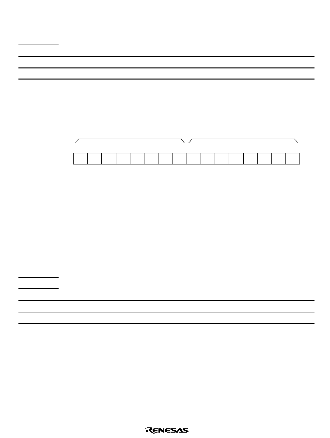
Rev. 1.0, 02/00, page 525 of 1141
Bits 7 to 0
P07/AN7 to P00/AN0 Pin Switching (PMR07 to PMR00): These bits set the
P0n/ANn pin as the input pin for P0n or as the ANn pin for A/D conversion analog input channel.
Bit n
PMR0n
Description
0
P0n/ANn functions as a general-purpose input port
(Initial value)
1
P0n/ANn functions as an analog input channel
(n = 7 to 0)
24.2.7
Module Stop Control Register (MSTPCR)
7
1
MSTP15
R/W
MSTPCRH
6
1
MSTP14
R/W
5
1
MSTP13
R/W
4
1
MSTP12
R/W
3
1
MSTP11
R/W
2
1
MSTP10
R/W
1
1
MSTP9
R/W
0
1
MSTP8
R/W
7
1
MSTP7
R/W
6
1
MSTP6
R/W
5
1
MSTP5
R/W
4
1
MSTP4
R/W
3
1
MSTP3
R/W
2
1
MSTP2
R/W
1
1
MSTP1
R/W
0
1
MSTP0
R/W
MSTPCRL
Bit :
Initial value :
R/W :
MSTPCR consists of 8-bit readable/writable registers and performs module stop mode control.
When the MSTP2 bit in MSTPCR is set to 1, A/D converter operation stops at the end of the bus
cycle and a transition is made to module stop mode. For details, see section 4.5, Module Stop
Mode.
MSTPCR is initialized to H'FFFF by a reset
Bit 2
Module Stop (MSTP2): Specifies the A/D converter module stop mode.
MSTPCRL
Bit 2
MSTP2
Description
0
A/D converter module stop mode is cleared
1
A/D converter module stop mode is set
(Initial value)
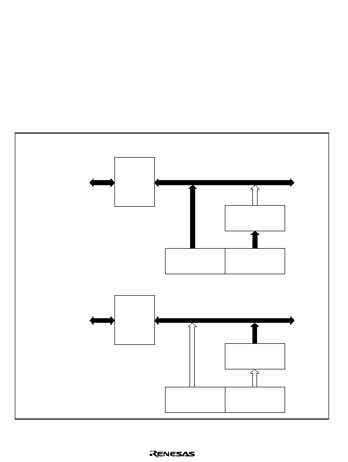
Rev. 1.0, 02/00, page 526 of 1141
24.3
Interface to Bus Master
ADR and AHR are 16-bit registers, but the data bus to the bus master is only 8 bits wide.
Therefore, in accesses by the bus master, the upper byte is accessed directly, but the lower byte is
accessed via a temporary register (TEMP).
A data reading from ADR and AHR is performed as follows. When the upper byte is read, the
upper byte value is transferred to the CPU and the lower byte value is transferred to TEMP. Next,
when the lower byte is read, the TEMP contents are transferred to the CPU.
When reading ADR and AHR, always read the upper byte before the lower byte. It is possible to
read only the upper byte, but if only the lower byte is read, incorrect data may be obtained.
Figure 24.3 shows the data flow for ADR access. The data flow for AHR access is the same.
Bus master
(H'AA)
ADRH
(H'AA)
ADRL
(H'40)
Lower byte read
Bus master
(H'40)
ADRH
(H'AA)
ADRL
(H'40)
TEMP
(H'40)
TEMP
(H'40)
Module data bus
Module data bus
Bus
interface
Bus
interface
Upper byte read
Figure 24.3 ADR Access Operation (Reading H'AA40)

Rev. 1.0, 02/00, page 527 of 1141
24.4
Operation
The A/D converter operates by successive approximations with 10-bit resolution.
24.4.1
Software-Triggered A/D Conversion
A/D conversion starts when software sets the software A/D start flag (SST bit) to 1. The SST bit
remains set to 1 during A/D conversion, and is automatically cleared to 0 when conversion ends.
Conversion can be software-triggered on any of the 12 channels provided by analog input pins
AN0 to ANB. Bits SCH3 to SCH0 in ADCR select the analog input pin used for software-
triggered A/D conversion. Pins AN8 to ANB are also available for hardware- or external-
triggered conversion.
When conversion ends, SEND flag in ADCSR bit is set to 1. If ADIE bit in ADCSR is also set to
1, an A/D conversion end interrupt occurs.
If the conversion time or input channel selection in ADCR needs to be changed during A/D
conversion, to avoid malfunctions, first clear the SST bit to 0 to halt A/D conversion.
If software writes 1 in the SST bit to start software-triggered conversion while hardware- or
external-triggered conversion is in progress, the hardware- or external-triggered conversion has
priority and the software-triggered conversion is not executed. At this time, BUSY flag in
ADCSR is set to 1. The BUSY flag is cleared to 0 when the hardware-triggered A/D result
register (AHR) is read. If conversion is triggered by hardware while software-triggered
conversion is in progress, the software-triggered conversion is immediately canceled and the SST
flag is cleared to 0, and SCNL flag in ADCSR is set to 1. The SCNL flag is cleared when
software writes 1 in the SST bit to start conversion after the hardware-triggered conversion ends.

Rev. 1.0, 02/00, page 528 of 1141
24.4.2
Hardware- or External-Triggered A/D Conversion
The system contains the hardware trigger function that allows to turn on A/D conversion at a
specified timing by use of the hardware trigger (internal signals: ADTRG and DFG) and the
incoming external trigger (
$'75*). This function can be used to measure an analog signal that
varies in synchronization with an external signal at a fixed timing.
To execute hardware- or external-triggered A/D conversion, select appropriate start factor in
TRGS1 and TRGS0 bits in ADTSR. When the selected triggering occurs, HST flag in ADCSR is
set to 1 and A/D conversion starts. The HST flag remains 1 during A/D conversion, and is
automatically cleared to 0 when conversion ends. For ADTRG start by HSW timing generator in
hardware triggering, see section 26.4, HSW Timing Generator. Setting of the analog input pins on
four channels from AN8 to ANB can be modified with the hardware trigger or the incoming
external trigger. Setting is done from HCH1 and HCH0 bits on ADCR. Pins AN8 to ANB are
also available for software-triggered conversion.
When conversion ends, HEND flag in ADCSR is set to 1. If ADIE bit in ADCSR is also set to 1,
an A/D conversion end interrupt occurs.
If the conversion time or input channel selection in ADCR needs to be changed during A/D
conversion, to avoid malfunctions, first clear the HST flag to 0 to halt A/D conversion.
If software writes 1 in the SST bit to start software-triggered conversion while hardware- or
external-triggered conversion is in progress, the hardware- or external-triggered conversion has
priority and the software-triggered conversion is not executed. At this time, BUSY flag in
ADCSR is set to 1. The BUSY flag is cleared to 0 when the hardware-triggered A/D result
register (AHR) is read.
If conversion is triggered by hardware while software-triggered conversion is in progress, the
software-triggered conversion is immediately canceled and the SST flag is cleared to 0, and SCNL
flag in ADCSR is set to 1 (the SCNL flag is cleared when software writes 1 in the SST bit to start
conversion after the hardware-triggered conversion ends). The analog input channel changes
automatically from the channel that was undergoing software-triggered conversion (selected by
bits SCH3 to SCH0 in ADCR) to the channel selected by bits HCH1 and HCH0 in ADCR for
hardware- or external-triggered conversion. After the hardware- or external-triggered conversion
ends, the channel reverts to the channel selected by the software-triggered conversion channel
select bits in ADCR.
Hardware- or external-triggered conversion has priority over software-triggered conversion, so the
A/D interrupt-handling routine should check the SCNL and BUSY flags when it processes the
converted data.
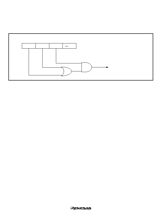
Rev. 1.0, 02/00, page 529 of 1141
24.5
Interrupt Sources
When A/D conversion ends, SEND or HEND flag in ADCSR is set to 1. The A/D conversion end
interrupt (ADI) can be enabled or disabled by ADIE bit in ADCSR.
Figure 24.4 shows the block diagram of A/D conversion end interrupt.
A/D conversion end
interrupt (ADI)
To interrupt controller
A/D control/status register (ADCSR)
SEND
HEND
ADIE
Figure 24.4 Block Diagram of A/D Conversion End Interrupt
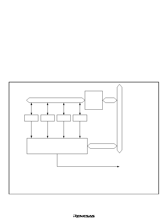
Rev. 1.0, 02/00, page 531 of 1141
Section 25 Address Trap Controller (ATC)
25.1
Overview
The address trap controller (ATC) is capable of generating interrupt by setting an address to trap,
when the address set appears during bus cycle.
25.1.1
Features
Address to trap can be set independently at three points.
25.1.2
Block Diagram
Figure 25.1 shows a block diagram of the address trap controller.
TRCR
[Legend]
TAR0 to 2
Interrupt request
Modules bus
Internal bus
ATCR
TAR0
TAR1
TAR2
Trap condition comparator
Bus
interface
: Trap control register
: Trap address register 0 to 2
Figure 25.1 Block Diagram of ATC
Rev. 1.0, 02/00, page 532 of 1141
25.1.3
Register Configuration
Table 25.1
Register List
Name
Abbrev.
R/W
Initial Value
Address *
Address trap control register
ATCR
R/W
H'F8
H'FFB9
Trap address register 0
TAR0
R/W
H'F00000
H'FFB0 to H'FFB2
Trap address register 1
TAR1
R/W
H'F00000
H'FFB3 to H'FFB5
Trap address register 2
TAR2
R/W
H'F00000
H'FFB6 to H'FFB8
Note:
*
Lower 16 bits of the address.
25.2
Register Descriptions
25.2.1
Address Trap Control Register (ATCR)
0
0
1
0
R/W
2
0
R/W
3
1
4
1
5
1
6
1
7
--
--
--
--
--
--
--
--
--
--
R/W
TRC2
TRC1
TRC0
1
Bit :
Initial value :
R/W :
Bits 7 to 3
Reserved: These bits cannot be modified and are always read as 1.
Bit 2
Trap Control 2 (TRC2): Sets ON/OFF operation of the address trap function 2.
Bit 2
TRC2
Description
0
Address trap function 2 disabled
(Initial value)
1
Address trap function 2 enabled

Rev. 1.0, 02/00, page 533 of 1141
Bit 1
Trap Control 1 (TRC1): Sets ON/OFF operation of the address trap function 1.
Bit 1
TRC1
Description
0
Address trap function 1 disabled
(Initial value)
1
Address trap function 1 enabled
Bit 0
Trap Control 0 (TRC0): Sets ON/OFF operation of the address trap function 0.
Bit 0
TRC0
Description
0
Address trap function 0 disabled
(Initial value)
1
Address trap function 0 enabled

Rev. 1.0, 02/00, page 534 of 1141
25.2.2
Trap Address Register 2 to 0 (TAR2 to TAR0)
0
0
1
0
R/W
2
0
R/W
3
4
5
6
7
R/W
A18
A17
A16
0
0
R/W
0
R/W
R/W
A23
A22
A21
0
0
R/W
R/W
A20
A19
0
0
1
0
R/W
2
0
R/W
3
4
5
6
7
R/W
A10
A9
A8
0
0
R/W
0
R/W
R/W
A15
A14
A13
0
0
R/W
R/W
A12
A11
0
--
--
1
0
R/W
2
0
R/W
3
4
5
6
7
A2
A1
0
0
R/W
0
R/W
R/W
A7
A6
A5
0
0
R/W
R/W
A4
A3
0
Bit :
Initial value :
R/W :
Bit :
Initial value :
R/W :
Bit :
Initial value :
R/W :
The TAR is composed of three 8-bit readable/writable registers (TARnA, B, and C)(n = 2 to 0)
The TAR sets the address to trap. The function of the TAR2 to TAR0 is the same.
The TAR is initialized to H'00 by a reset.
TARA bits 7 to 0: Addresses 23 to 16 (A23 to A16)
TARB bits 7 to 0: Addresses 15 to 8 (A15 to A8)
TARC bits 7 to 0: Addresses 7 to 1 (A7 to A1)
If the value installed in this register and internal address buses A23 to A1 match as a result of
comparison, an interruption occurs.
For the address to trap, set to the address where the first byte of an instruction exists. In the case
of other addresses, it may not be considered that the condition has been satisfied.
Bit 0 of this register is fixed at 0. The address to trap becomes an even address.
The range where comparison is made is H'000000 to H'FFFFFE.
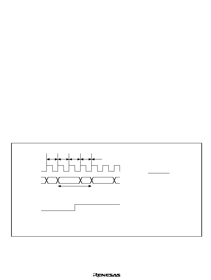
Rev. 1.0, 02/00, page 535 of 1141
25.3
Precautions in Usage
Address trap interrupt arises 2 states after prefetching the trap address. Trap interrupt may occur
after the trap instruction has been executed, depending on a combination of instructions
immediately preceding the setting up of the address trap.
If the instruction to trap immediately follows the branch instruction or the conditional branch
instruction, operation may differ, depending on whether the condition was satisfied or not, or the
address to be stacked may be located at the branch. Figures 25.2 to 25.22 show specific
operations.
For information as to where the next instruction prefetch occurs during the execution cycle of the
instruction, see appendix A.5 of this manual or section 2.7 Bus State during Execution of
Instruction of the H8S/2600 and H8S/2000 Series Programming Manual. (R:W NEXT is the next
instruction prefetch.)
25.3.1
Basic Operations
After terminating the execution of the instruction being executed in the second state from the trap
address prefetch, the address trap interrupt exception handling is started.
1. Figure 25.2 shows the operation when the instruction immediately preceding the trap address
is that of 3 states or more of the execution cycle and the next instruction prefetch occurs in the
state before the last 2 states. The address to be stacked is 0260.
Address bus
Interrupt
request
signal
MOV
execution
MOV
instruc-
tion
pre-fetch
NOP
instruc-
tion
pre-fetch
Internal
opera-
tion
Data
read
Start of exception
handling
Immediately
preceding
Instruction
Address
025E MOV.B @ER3+,R2L
0260 NOP
(ER3 = H'0000)
0262 NOP
0264 NOP
025E
0260
0000
0262
*
* Trap setting address
The underlines address is the
one to be actually stacked.
Note:
In the figure above, the NOP instruction is used as the typical example of instruction with
execution cycle of 1 state. Other instructions with the execution cycle of 1 state also apply
(Ex. MOV.B, Rs, Rd).
Figure 25.2 Basic Operations (1)
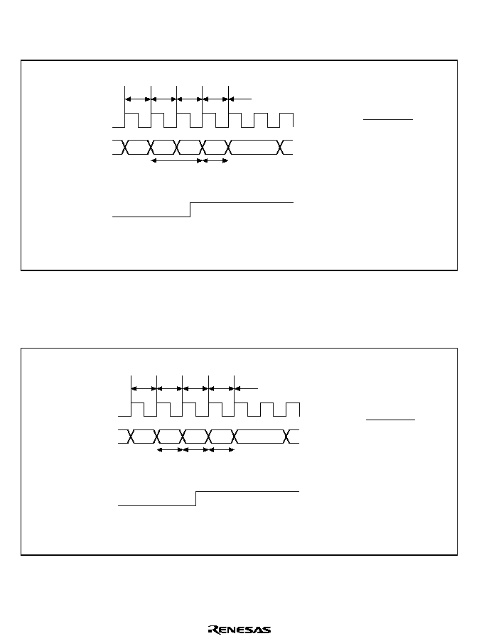
Rev. 1.0, 02/00, page 536 of 1141
2. Figure 25.3 shows the operation when the instruction immediately preceding the trap address
is that of 2 states or more of the execution cycle and the next instruction prefetch occurs in the
second state from the last. The address to be stacked is 0268.
Address bus
Interrupt
request
signal
MOV
execution
NOP
execution
Start of exception
handling
Immediately
preceding
instruction
Address
0266 MOV.B
R2L, @0000
0268 NOP
026A NOP
026C NOP
*
0266
026A
0268 0000
026C
Data
read
MOV
instruc-
tion
pre-fetch
NOP
instruc-
tion
pre-fetch
NOP
instruc-
tion
pre-fetch
Note:
*
Trap setting address
The underlines address is the one to be actually stacked.
Figure 25.3 Basic Operations (2)
3. Figure 25.4 shows the operation when the instruction immediately preceding the trap address
is that of 1 state or 2 states or more and the prefetch occurs in the last state. The address to be
stacked is 025C.
Address bus
Interrupt
request
signal
NOP
execu-
tion
NOP
execu-
tion
NOP
execu-
tion
Start of
exception
handling
Immediately
preceding
instruction
Address
0256 NOP
0258 NOP
025A NOP
025C NOP
025E NOP
*
0256
025C
0258 025A
025E
NOP
instruc-
tion
pre-fetch
NOP
instruc-
tion
pre-fetch
NOP
instruc-
tion
pre-fetch
NOP
instruc-
tion
pre-fetch
Note:
*
Trap setting address
The underlines address is the one to be actually stacked.
Figure 25.4 Basic Operations (3)
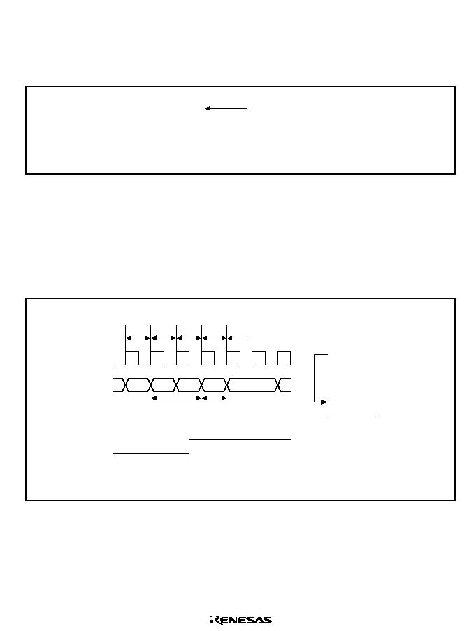
Rev. 1.0, 02/00, page 537 of 1141
25.3.2
Enabling
The address trap function becomes valid after executing one instruction following the setting of
the enable bit of the address trap control register (TRCR) to 1.
029C BSET #0, @TRCR
*
029E MOV.W R0, R1
02A0 MOV.B R1L, R3H
02A2 NOP
02A4 CMP.W R0, R1
02A6 NOP
After executing the MOV instruction,
the address trap interrupt does not
arise, and the next instruction is
executed.
Note:
*
Trap setting address
Figure 25.5 Enabling
25.3.3
Bcc Instruction
1. When the condition is satisfied by Bcc instruction (8-bit displacement)
If the trap address is the next instruction to the Bcc instruction and the condition is satisfied by
the Bcc instruction and then branched, transition is made to the address trap interrupt after
executing the instruction at the branch. The address to be stacked is 02A8.
Address bus
Interrupt
request
signal
BEQ
execu-
tion
CMP
execu-
tion
029C
02A8
029E 02A6
02AA
029C BEQ NEXT:8
029E NOP
02A0 NOP
02A2 NOP
02A4 NOP
02A6 CMP.W R0, R1
02A8 NOP
(NEXT = H'02A6)
*
Start of
exception
handling
BEQ
instruc-
tion
pre-fetch
NOP
instruc-
tion
pre-fetch
NOP
instruc-
tion
pre-fetch
CMP
instruc-
tion
pre-fetch
Note:
*
Trap setting address
The underlines address is the one to be actually stacked.
Figure 25.6 When the Condition Satisfied by Bcc Instruction (8-bit Displacement)
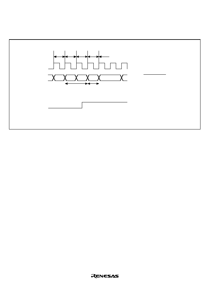
Rev. 1.0, 02/00, page 538 of 1141
2. When the condition is not satisfied by Bcc instruction (8-bit displacement)
If the trap address is the next instruction to the Bcc instruction and the condition is not satisfied
by the Bcc instruction and thus it fails to branch, transition is made to the address trap interrupt
after executing the trap address instruction and prefetching the next instruction. The address to
be stacked is 02A2.
Address bus
Interrupt
request
signal
029E
02A2
02A0 02A8
02A4
029E BEQ NEXT:8
02A0 NOP
02A2 NOP
02A4 NOP
02A6 NOP
02A8 CMP.W R0, R1
02AA NOP
(NEXT = H'02A8)
*
BEQ
execu-
tion
NOP
execu-
tion
Start of
exception
handling
BEQ
instruc-
tion
pre-fetch
NOP
instruc-
tion
pre-fetch
NOP
instruc-
tion
pre-fetch
CMP
instruc-
tion
pre-fetch
NEXT:
Note:
*
Trap setting address
The underlines address is the one to be actually stacked.
Figure 25.7 When the Condition Not Satisfied by Bcc Instruction (8-bit Displacement)
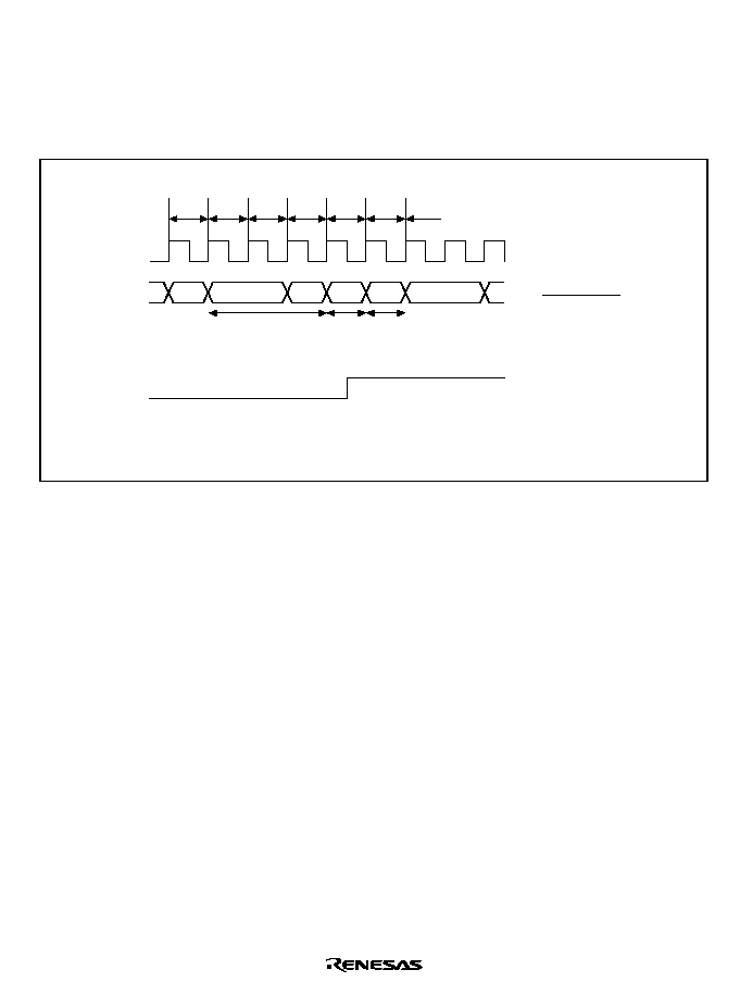
Rev. 1.0, 02/00, page 539 of 1141
3. When condition is not satisfied by Bcc instruction (16-bit displacement)
If the trap address is the next instruction to the Bcc instruction and the condition is not satisfied
by the Bcc instruction and thus it fails to branch, transition is made to the address trap interrupt
after executing the trap address instruction (if the trap address instruction is that of 2 states or
more. If the instruction is that of 1 state, after executing two instructions). The address to be
stacked is 02C0.
Address bus
Interrupt
request
signal
Start of
exception handling
02B8
02C0
02BC 02BE
02C2
02BA
02B8 BEQ NEXT:16
02BC NOP
02BE NOP
02C0 NOP
02C2 NOP
02C4 NOP
(NEXT = H'02C4)
*
BEQ
execution
NOP
execu-
tion
NOP
execu-
tion
Data
fetch
Internal
opera-
tion
BEQ
instruc-
tion
pre-fetch
NOP
instruc-
tion
pre-fetch
NOP
instruc-
tion
pre-fetch
NOP
instruc-
tion
pre-fetch
NEXT:
Note:
*
Trap setting address
The underlines address is the one to be actually stacked.
Figure 25.8 When the Condition Not Satisfied by Bcc Instruction (16-bit Displacement)
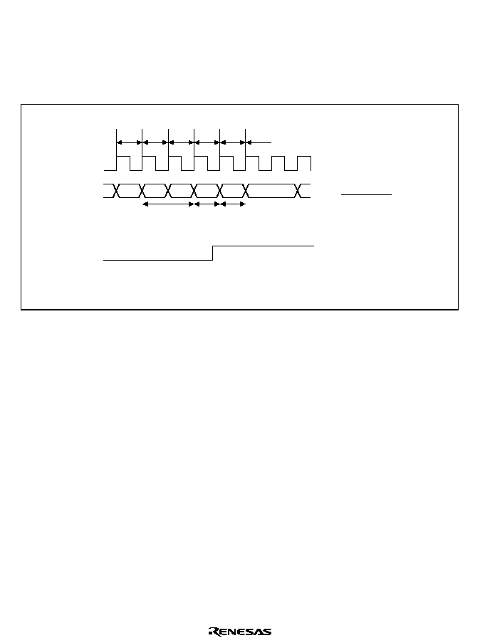
Rev. 1.0, 02/00, page 540 of 1141
4. When the condition is not satisfied by Bcc instruction (Trap address at branch)
When the trap address is at the branch of the Bcc instruction and the condition is not satisfied
by the Bcc instruction and thus it fails to branch, transition is made into the address trap
interrupt after executing the next instruction (if the next instruction is that of 2 states or more.
If the next instruction is that of 1 state, after executing two instructions). The address to be
stacked is 0262.
Address bus
Interrupt
request
signal
Start of
exception
handling
025C
0262
0266
025E
0260
0264
025C BEQ NEXT:8
025E NOP
0260 NOP
0262 NOP
0264 NOP
0266 CMP.W R0, R1
0268 NOP
(NEXT = H'0266)
BEQ
execution
NOP
execu-
tion
NOP
execu-
tion
*
BEQ
instruc-
tion
pre-fetch
NOP
instruc-
tion
pre-fetch
NOP
instruc-
tion
pre-fetch
NOP
instruc-
tion
pre-fetch
CMP
instruc-
tion
pre-fetch
NEXT:
Note:
*
Trap setting address
The underlines address is the one to be actually stacked.
Figure 25.9 When the Condition Not Satisfied by Bcc Instruction
(Trap Address at Branch)
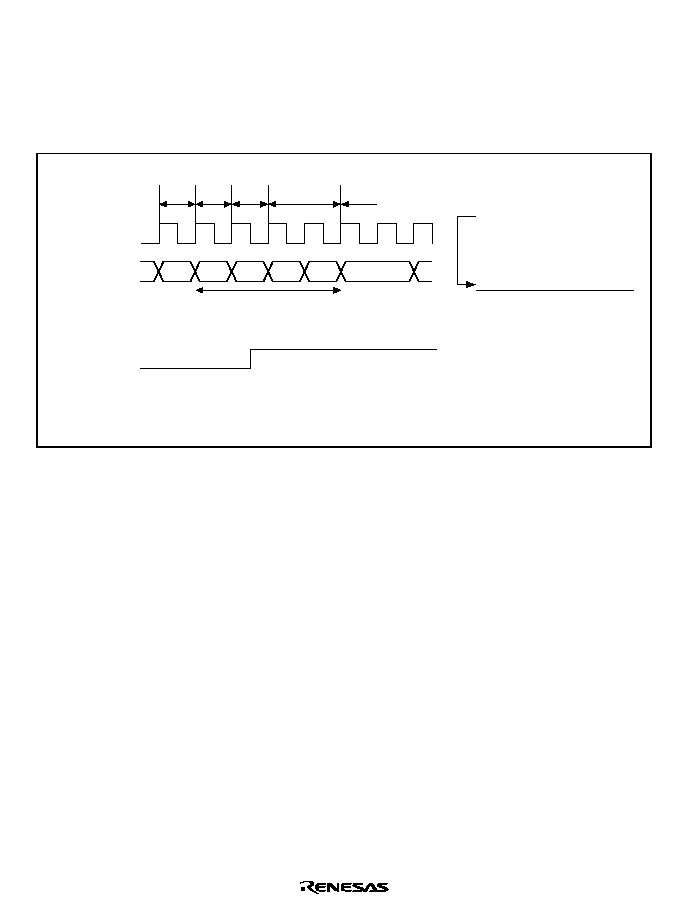
Rev. 1.0, 02/00, page 541 of 1141
25.3.4
BSR Instruction
1. BSR Instruction (8-bit displacement)
When the trap address is the next instruction to the BSR instruction and the addressing mode is
an 8-bit displacement, transition is made to the address trap interrupt after prefetching the
instruction at the branch. The address to be stacked is 02C2.
Address bus
Interrupt
request
signal
BSR execution
Stack
saving
0294
SP-4
02C2
0296
SP-2
02C4
0294 BSR @ER0
0296 NOP
0298 NOP
02C2 MOV.W R4, @OUT
02C4 NOP
: :
(@ER0 = H'02C2)
*
Start of
exception handling
BSR
instruc-
tion
pre-fetch
NOP
instruc-
tion
pre-fetch
MOV
instruc-
tion
pre-fetch
Note:
*
Trap setting address
The underlines address is the one to be actually stacked.
Figure 25.10 BSR Instruction (8-bit Displacement)

Rev. 1.0, 02/00, page 542 of 1141
25.3.5
JSR Instruction
1. JSR Instruction (Register indirect)
When the trap address is the next instruction to the JSR instruction and the addressing mode is
a register indirect, transition is made to the address trap interrupt after prefetching the
instruction at the branch. The address to be stacked is 02C8.
Address bus
Interrupt
request
signal
JSRexecution
Stack
saving
Start of
exception
handling
029A
SP-4
02C8
029C
SP-2
02CA
029A JSR @ER0
029C NOP
029E NOP
02C8 MOV.W R4, @OUT
02CE NOP
: :
(@ER0 = H'02C8)
*
JSR
instruc-
tion
pre-fetch
NOP
instruc-
tion
pre-fetch
MOV
instruc-
tion
pre-fetch
Note:
*
Trap setting address
The underlines address is the one to be actually stacked.
Figure 25.11 JSR Instruction (Register Indirect)
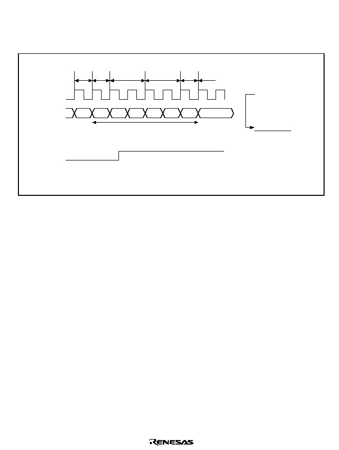
Rev. 1.0, 02/00, page 543 of 1141
2. JSR Instruction (Memory indirect)
When the trap address is the next instruction to the JSR instruction and the addressing mode is
memory indirect, transition is made to the address trap interrupt after prefetching the
instruction at the branch. The address to be stacked is 02EA.
Address bus
Interrupt
request
signal
JSR execution
Stack
saving
Start of
exception
handling
0294
SP-2 SP-4 02EA
006C
0296
006E
02EC
0294 JSR @@H'6C:8
0296 NOP
0298 NOP
02EA NOP
02EC NOP
: :
006C H'02EA
: :
*
Data
fetch
JSR
instruc-
tion
pre-fetch
NOP
instruc-
tion
pre-fetch
NOP
instruc-
tion
pre-fetch
Note:
*
Trap setting address
The underlines address is the one to be actually stacked.
Figure 25.12 JSR Instruction (Memory Indirect)
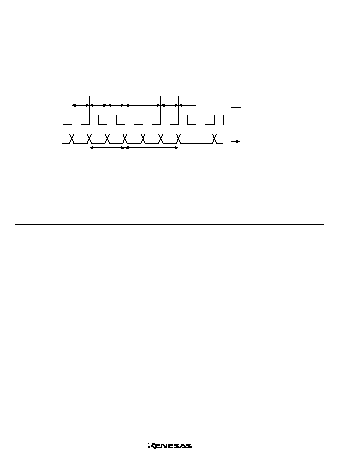
Rev. 1.0, 02/00, page 544 of 1141
25.3.6
JMP Instruction
1. JMP Instruction (Register indirect)
When the trap address is the next instruction to the JMP instruction and the addressing mode is
a register indirect, transition is made to the address trap interrupt after prefetching the
instruction at the branch. The address to be stacked is 02AA.
Address bus
Interrupt
request
signal
JMP
execution
MOV.L
execution
Data
fetch
Start of
exception
handling
029A
02A8 02AA
02A4
029C
02A6
02AC
029A JMP @ER0
029C NOP
029E NOP
02A0 NOP
02A2 NOP
02A4 MOV.L #DATA, ER1
02AA NOP
(@ER0 = H'02A4)
*
JMP
instruc-
tion
pre-fetch
NOP
instruc-
tion
pre-fetch
NOP
instruc-
tion
pre-fetch
MOV
instruc-
tion
pre-fetch
Note:
*
Trap setting address
The underlines address is the one to be actually stacked.
Figure 25.13 JMP Instruction (Register Indirect)
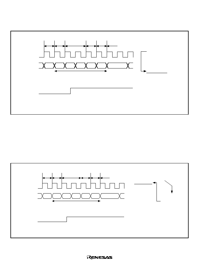
Rev. 1.0, 02/00, page 545 of 1141
2. JMP Instruction (Memory indirect)
When the trap address is the next instruction to the JMP instruction and the addressing mode is
memory indirect, transition is made to the address trap interrupt after prefetching the
instruction at the branch. The address to be stacked is 02E4.
Address bus
Interrupt
request
signal
JMP execution
Start of
exception
handling
0294
006C 02E4
006C
0296
006E
02E6
0294 JMP @@H'6C:8
0296 NOP
0298 NOP
02E4 NOP
02E6 NOP
: :
006C H'02E4
: :
*
Data
fetch
Internal
opera-
tion
JMP
instruc-
tion
pre-fetch
NOP
instruc-
tion
pre-fetch
NOP
instruc-
tion
pre-fetch
Note:
*
Trap setting address
The underlines address is the one to be actually stacked.
Figure 25.14 JMP Instruction (Memory Indirect)
25.3.7
RTS Instruction
When the trap address is the next instruction to the RTS instruction, transition is made to the
address trap interrupt after reading the CCR and PC from the stack and prefetching the instruction
at the return location. The address to be stacked is 0298.
Address bus
Break interrupt
request signal
RTS execution
Start of
exception
handling
02AC
SP
0298
SP
02AE
SP+2
029A
Stack
saving
0296 BSR SUB
0298 NOP
029A NOP
02AC RTS
(@ER0 = H'02C8)
02AE NOP
*
: :
Internal
opera-
tion
RTS
instruc-
tion
pre-fetch
NOP
instruc-
tion
pre-fetch
NOP
instruc-
tion
pre-fetch
Note:
*
Trap setting address
The underlines address is the one to be actually stacked.
Figure 25.15 RTS Instruction
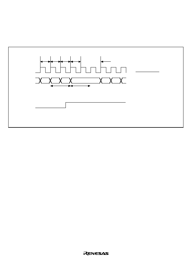
Rev. 1.0, 02/00, page 546 of 1141
25.3.8
SLEEP Instruction
1. SLEEP Instruction 1
When the trap address is the SLEEP instruction and the instruction execution cycle
immediately preceding the SLEEP instruction is that of 2 states or more and prefetch does not
occur in the last state, the SLEEP instruction is not executed and transition is made to the
address trap interrupt without going into SLEEP mode. The address to be stacked is 0274.
Address bus
Interrupt
request
signal
Start of
exception
handling
0272
FFF9
0274
SP-4
SP-2
0276
0272 MOV.B R2L, @FFF8
0274 SLEEP
0276 NOP
0278 NOP
: :
*
Data
write
MOV
execution
SLEEP
cancel
MOV
instruc-
tion
pre-fetch
NOP
instruc-
tion
pre-fetch
SLEEP
instruc-
tion
pre-fetch
Note:
*
Trap setting address
The underlines address is the one to be actually stacked.
Figure 25.16 SLEEP Instruction (1)
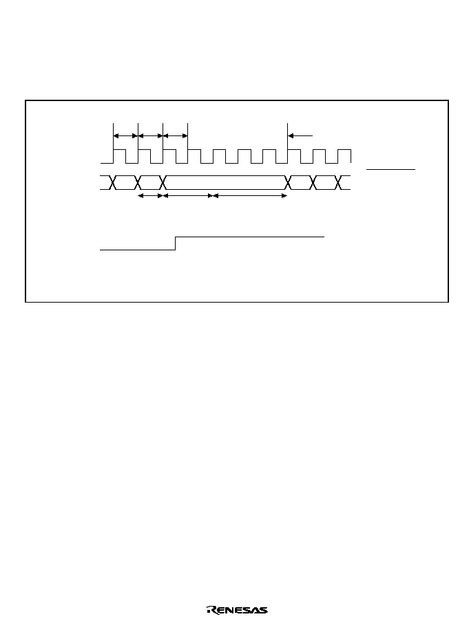
Rev. 1.0, 02/00, page 547 of 1141
2. SLEEP Instruction 2
When the trap address is the SLEEP instruction and the instruction execution cycle
immediately preceding the SLEEP instruction is that of 1 state 2 states or more and prefetch
occurs in the last state, this puts in the SLEEP mode after execution of the SLEEP instruction,
and the SLEEP mode is cancelled by the address trap interrupt and transition is made to the
exception handling. The address to be stacked is 0264.
Address bus
Interrupt
request
signal
Start of
exception
handling
0260 0262
SP-2 SP-4
0264
0260 NOP
0262 SLEEP
0264 NOP
0266 NOP
: :
*
NOP
execution
SLEEP
execution
SLEEP
mode
NOP
instruc-
tion
pre-fetch
SLEEP
instruc-
tion
pre-fetch
NOP
instruc-
tion
pre-fetch
Note:
*
Trap setting address
The underlines address is the one to be actually stacked.
Figure 25.17 SLEEP Instruction (2)
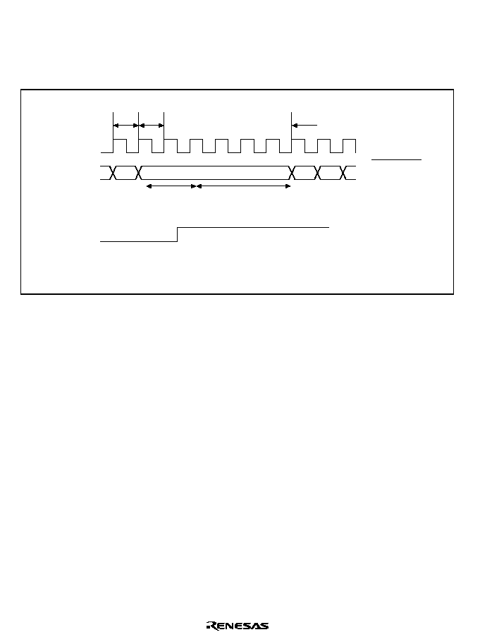
Rev. 1.0, 02/00, page 548 of 1141
3. SLEEP Instruction 3
When the trap address is the next instruction to the SLEEP instruction, this puts in the SLEEP
mode after execution of the SLEEP instruction, and the SLEEP mode is cancelled by the
address trap interrupt and transition is made to the exception handling. The address to be
stacked is 0282.
Address bus
Interrupt
request
signal
Start of
exception
handling
0280
SP-2 SP-4
0282
027E NOP
0280 SLEEP
0282 NOP
0284 NOP
: :
*
SLEEP
execution
SLEEP mode
SLEEP
instruc-
tion
pre-fetch
NOP
instruc-
tion
pre-fetch
Note:
*
Trap setting address
The underlines address is the one to be actually stacked.
Figure 25.18 SLEEP Instruction (3)
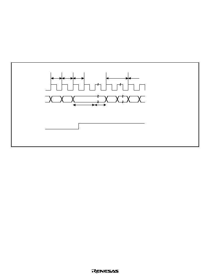
Rev. 1.0, 02/00, page 549 of 1141
4. SLEEP Instruction 4 (Standby or Watch Mode Setting)
When the trap address is the SLEEP instruction and the instruction immediately preceding the
SLEEP instruction is that of 1 state or 2 states or more and prefetch occurs in the last state, this
puts in the standby (watch) mode after execution of the SLEEP instruction. After that, if the
standby (watch) mode is cancelled by the NMI interrupt, transition is made to NMI interrupt
following the CCR and PC (at the address of 0266) stack saving and vector reading. However,
if the address trap interrupt arises before starting execution of the NMI interrupt processing,
transition is made to the address trap exception handling. The address to be stacked is the
starting address of the NMI interrupt processing.
Address bus
Interrupt
request
signal
Address trap
interruption
0262 0264
0266
SP-2
SPCA
SP-2
0262 NOP
0264 SLEEP
0266 NOP
*
SLEEP
execution
NMI
interrupt
Standby
mode
NOP
instruc-
tion
pre-fetch
NOP
instruc-
tion
pre-fetch
SLEEP
instruc-
tion
pre-fetch
Note:
*
Trap setting address
Figure 25.19 SLEEP Instruction (4) (Standby or Watch Mode Setting)
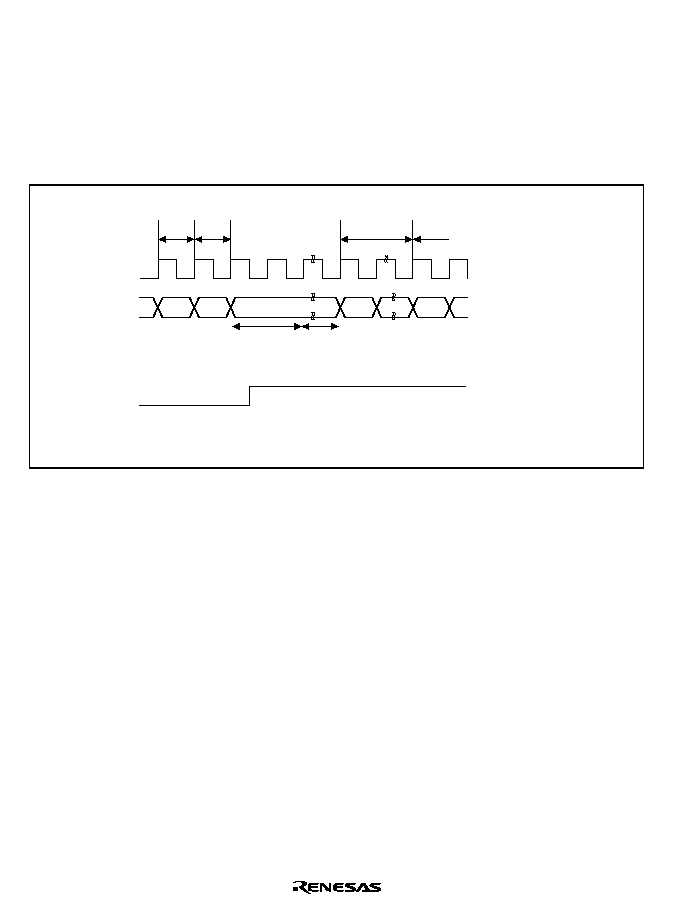
Rev. 1.0, 02/00, page 550 of 1141
5. SLEEP Instruction 5 (Standby or Watch Mode Setting)
When the trap address is the next instruction to the SLEEP instruction, this puts in the standby
(watch) mode after execution of the SLEEP instruction. After that, if the standby (watch)
mode is cancelled by the NMI interruption, transition is made to the NMI interrupt following
the CCR and PC (at the address of 0266) stack saving and vector reading. However, if the
address trap interrupt arises before starting execution of the NMI interrupt processing,
transition is made to the address trap exception handling. The address to be stacked is the
starting address of the NMI interrupt processing.
Address bus
Interrupt
request
signal
Address trap
interrupt
0280 0282
0284
SP-2
SPCA
SP-2
0280 NOP
0282 SLEEP
0284 NOP
*
SLEEP
execution
NMI
interruption
Standby
mode
NOP
instruc-
tion
pre-fetch
SLEEP
instruc-
tion
pre-fetch
Note:
*
Trap setting address
Figure 25.20 SLEEP Instruction (5) (Standby or Watch Mode Setting)
25.3.9
Competing Interrupt
1. General Interrupt (Interrupt other than NMI)
When the ATC interrupt request is made at the timing in (1) (A) against the general interrupt
request, the interruption appears to take place in the ATC at the timing earlier than usual,
because higher priority is assigned to the ATC interrupt processing (Simultaneous interrupt
with the general interrupt has no effect on processing). The address to be stacked is 029E.
For comparison, the case where the trap address is set at 02A0 if no general interrupt request
was made is shown in (2). The address to be stacked is 02A4.
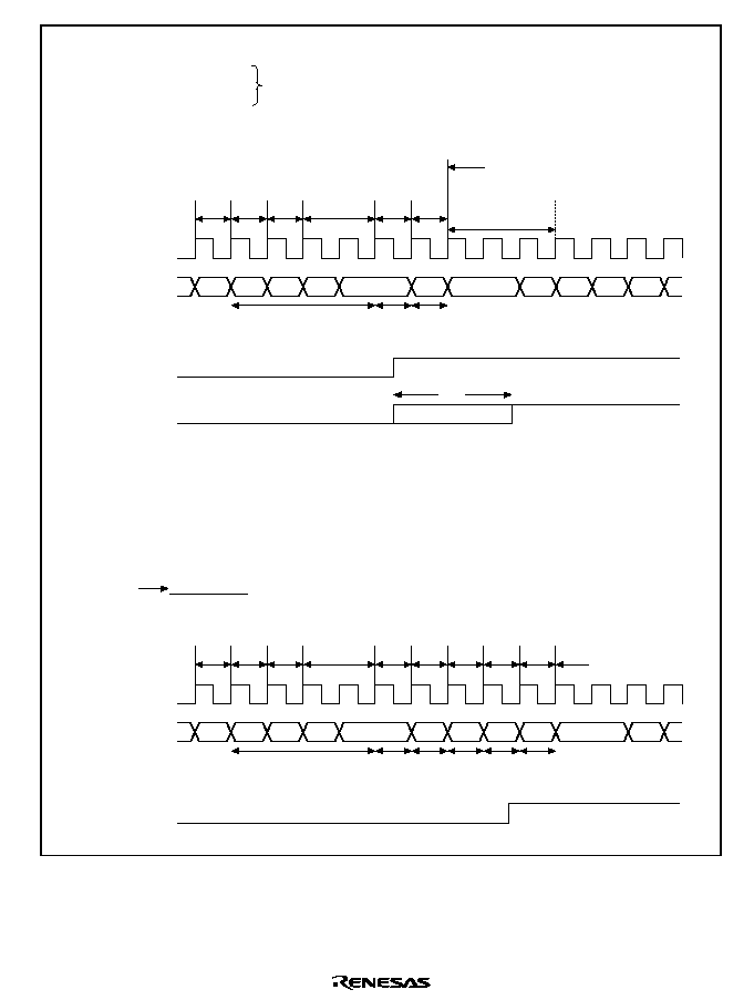
Rev. 1.0, 02/00, page 551 of 1141
Address bus
General Interrupt
request signal
Interrupt
request signal
MOV execution
Data
write
Data
write
Start of general
interrupt processing
Range of start of ATC
interrupt processing
(1)
029C NOP
0296 MOV.B R2L, @Port
029A NOP
029E NOP
02A0 NOP
02A2 NOP
02A4 NOP
0296
Port
029E
SP-2 SP-4 Vector Vector
0298
NOP
execu-
tion
NOP
execu-
tion
MOV execution
NOP
execu-
tion
NOP
execu-
tion
NOP
execu-
tion
NOP
execu-
tion
NOP
execu-
tion
029A
029C
02A0
Address bus
Interrupt
request
signal
Data
read
Data
read
Start of ATC interrupt
processing
Set one of these to the
trap address
(2)
029C NOP
0296 MOV.B R2L, @Port
029A NOP
029E NOP
02A0 NOP Trap address
02A2 NOP
02A4 NOP
0296
Port
029E
0298
02A0 02A2 02A4
SP-2
029A
029C
02A6
(A)
MOV
instruc-
tion
pre-fetch
MOV
instruc-
tion
pre-fetch
NOP
instruc-
tion
pre-fetch
NOP
instruc-
tion
pre-fetch
NOP
instruc-
tion
pre-fetch
NOP
instruc-
tion
pre-fetch
NOP
instruc-
tion
pre-fetch
NOP
instruc-
tion
pre-fetch
NOP
instruc-
tion
pre-fetch
NOP
instruc-
tion
pre-fetch
NOP
instruc-
tion
pre-fetch
Address
to be
stacked
Figure 25.21 Competing Interrupt (General Interrupt)

Rev. 1.0, 02/00, page 552 of 1141
2. In case of NMI
When the NMI interruption request is made at the timing in (1) (A) against the ATC interrupt
request, the interrupt appears to take place in NMI at the timing earlier than usual, because
higher priority is assigned to the NMI interrupt processing. The ATC interrupt processing
starts after fetching the instruction at the starting address of the NMI interrupt processing. The
address to be stacked is 02E0 for the NMI and 340 for the ATC.
When the ATC interrupt request is made at the timing in (2) (B) against the NMI interrupt
request, the ATC interrupt processing starts after fetching the instruction at the starting address
of the NMI interrupt processing. The address to be stacked is 02E6 for the NMI and 0340 for
the ATC.
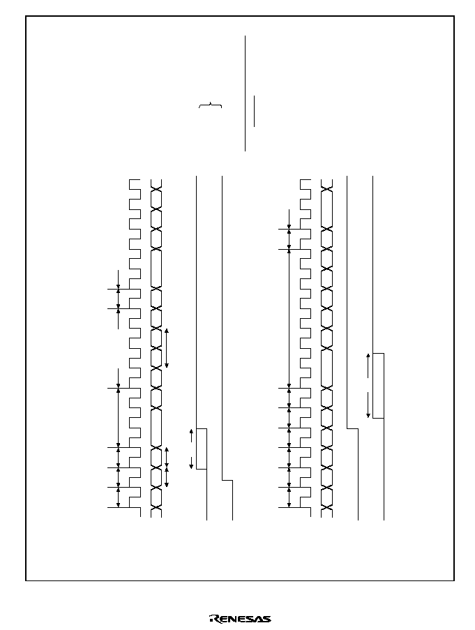
Rev. 1.0, 02/00, page 553 of 1141
Address bus
NMI interrupt
request signal
ATC interrupt
request signal
Start of ATC inter-
rupt processing
(1)
02E0 NOP
02DC NOP
02DE NOP
02E2 NOP
02E4 NOP
02E6 NOP
02E8 NOP
02DC
SP-4
0340
SP-6
SP-8
Vector
Vector
Vector
Vector
02DE
NMI vector
read
02E0
0342
SP-2
02E2
(2) Set one of these to
the trap address
(1) Set to the trap address
*
NMI interrupt
processing
Start of ATC interrupt processing
Address bus
NMI interrupt
request signal
ATC interrupt
request signal
Start of ATC
Interrupt processing
(2)
02DC
02E2
02E4
SP-4
SP-2
0340
Vector
Vector
Vector
02DE
02E0
0342
02E6
02E8
(B)
(A)
NMI interrupt
processing
: :
0340 The starting address of NMI
interrupt
: :
NOP execu-
tion
NOP execu-
tion
NOP
instruc-
tion
pre-fetch
NOP
instruc-
tion
pre-fetch
NOP
instruc-
tion
pre-fetch
NOP
instruc-
tion
pre-fetch
NOP
instruc-
tion
pre-fetch
NOP
instruc-
tion
pre-fetch
NOP
instruc-
tion
pre-fetch
NOP
instruc-
tion
pre-fetch
NOP
instruc-
tion
pre-fetch
NOP
instruc-
tion
pre-fetch
NOP
instruc-
tion
pre-fetch
Figure 25.22 Competing Interrupt (In Case of NMI)

Rev. 1.0, 02/00, page 555 of 1141
Section 26 Servo Circuits
26.1
Overview
26.1.1
Functions
Servo circuits for a video cassette recorder are included on-chip.
The functions of the servo circuits can be divided into four groups, as listed in table 26.1.
Table 26.1
Servo Circuit Functions
Group
Function
Description
CTL I/O amplifier
Gain variable input amplifier
Output amplifier with rewrite mode
CFGDuty compensation
input
Duty accuracy: 50
±
2%
(Zero cross type comparator)
DFG, DPG
separation/overlap input
Overlap input available: Three-level input method, DFG
noise mask function
Reference signal
generators
V compensation, field detection, external signal sync, V
sync in REC mode, REF30 signal output to outside
HSW timing generator
Head-switching signals, FIFO 20 stages
Compatible with DFG counter soft-reset
Four-head high-speed
switching circuit for special
playback
Chroma-rotary/head-amplifier switching output
12-bit PWM
Improved speed of carrier frequency
Frequency division circuit
With CFG mask, no CFG for phase or CTL mask
(1) Input and output
circuits
Sync detection circuit
Noise count, field discrimination, Hsync compensation,
Hsync detection noise mask
Drum speed error detector
Lock detector function, pause at the counter overflow,
R/W error latch register, limiter function
Drum phase error detector
Latch signal selectable, R/W error latch register
Capstan speed error
detector
Lock detector function, pause at the counter overflow,
R/W error latch register, limiter function
Capstan phase error
detector
R/W error latch register
(2) Error detectors
X-value adjustment and
tracking adjustment circuit
(Separate setting available)
(3) Phase and gain
compensation
Digital filter computation
circuit
Computations performed automatically by hardware
Output gain variable:
◊
2 to
◊
64 (exponents of 2)
(Partial write in Z
-1
(high-order 8 bits) available)
Additional V signal circuit
Valid in special playback
(4) Other circuits
CTL circuit
Duty discrimination circuit, CTL head R/W control,
compatible with wide aspect
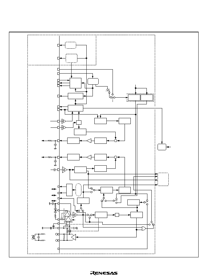
Rev. 1.0, 02/00, page 556 of 1141
26.1.2
Block Diagram
Figure 26.1 shows a block diagram of the servo circuits.
4-head
special
playback
controller
- +
SV1(P30)
EXCAP(P81)
( )
SV2(P31)
( )
EXCTL(P82)
)
+
+
+
+
+
- +
- +
-
CTL
Head
CTL Amp
CTL
Head
CFG
CAP
PWM
DRM
PWM
DFG
DPG(P87)
VIDEOFF
AUDIOFF
Vpulse
H.Amp SW(P84)
C.ROTARY(P83)
COMP(P85)
Csync
EXTTRG(P86)
OSCH
REC:ON
ADTRIG
(HSW)
Ep
PWM
Es
Es
Ep
REC
REC
PB.ASM
CTLFB
PB.CTL
PB.
ASM
(NTSC)
DVCTL
Gain control
by register
setting
REF30,REF30X,CREF,
CTLMONI,DVCFG,
DFG,DPG,DFG,etc
Internal signal
monitor controller
(PAL)
REF30X
REC-CTL
DutyI/O
(Duty deter-
minator)
(Assemble
recording)
DVCFG
DVCFG2
Gain up.
XE:ON
VD
RP0 to 7/
(P60 to 67,
P74 to 77)
Sync
separator
REC-CTL
generator
VISS
circuit
Noise
Det.
A/D
converter
Timer X1
Timer L
Timer R
AN pins
PWM
X-value
adjustment
Gain up.
RP0 to 7/
(P60 to 67,
P74 to 77)
PPG0 to 7/
(P70 to 77)
PPG0 to 7/
(P70 to 77)
REF30P(PB:30Hz,REC:1/2VD)
CREF
Res
System
clock
Additional
V pulse
generator
Head-switch
timing
generator
Drum system
reference
signal
Capstan
system
reference
signal
Phase
error
detector
Phase
error
detector
Digital
filter
Digital
filter
Digital
filter
Digital
filter
Frequency
divider
Frequency
divider
Speed
error
detector
Speed
error
detector
Figure 26.1 Block Diagram of Servo Circuits
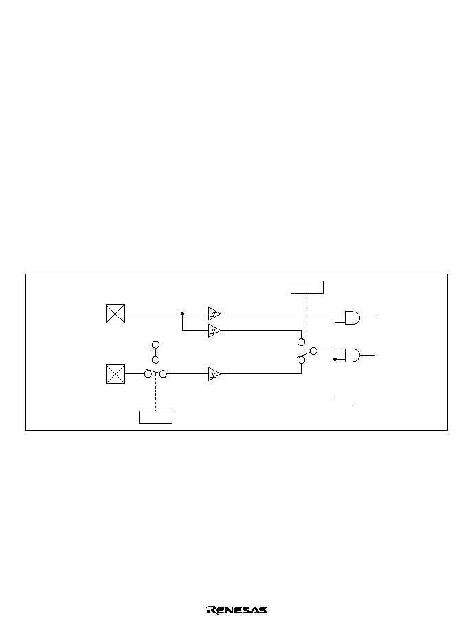
Rev. 1.0, 02/00, page 557 of 1141
26.2
Servo Port
26.2.1
Overview
This LSI is equipped with seventeen pins dedicated to the servo circuit and twenty-five pins
multiplexed with general-purpose ports. It also has an input amplifier to amplify CTL signals, a
CTL output amplifier, a CTL Schmitt comparator, and a CFG zero cross type comparator. The
CTL input amplifier allows gain adjustment by software. DFG and DPG signals, which control
the drum, can be input as separate signals or an overlapped signal.
SV1 and SV2 pins allow internal signals of the servo circuit to be output for monitoring. The
signals to be output can be selected out of eight kinds of signals. See the description of Servo
Monitor Control Register (SVMCR) in section 26.2.5, Register Description.
26.2.2
Block Diagram
1. DFG and DPG Input Circuit
The DFG and DPG input pins have on-chip Schmit circuits. Figure 26.2 shows the input
circuit of DFG and DPG.
DPG SW
DFG
DPG
DFG
DPG
DPG SW
Res+LPM
Figure 26.2 Input Circuit of DFG and DPG
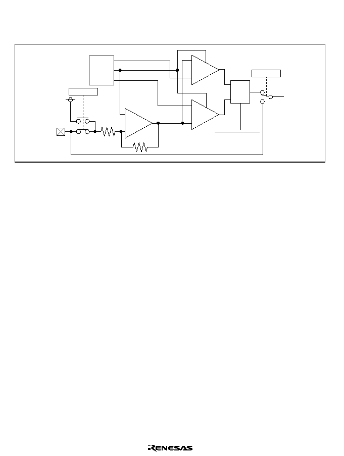
Rev. 1.0, 02/00, page 558 of 1141
2. CFG Input Circuit
The CFG input pin has an amplifier and a zero cross type comparator. Figure 26.3 shows the
input circuit of CFG.
+
-
+
-
+
-
CFGCOMP
CFGCOMP
P250
REF
M250
S
R
F/F O
stp
VREF
VREF
CFG
BIAS
CFG
Res+ModuleSTOP
Figure 26.3 CFG Input Circuit
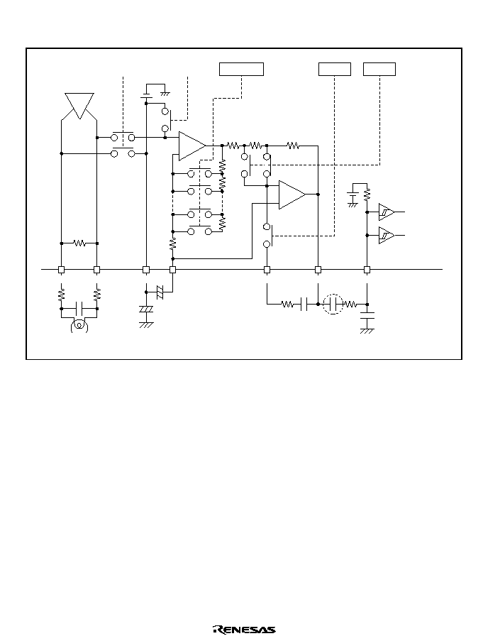
Rev. 1.0, 02/00, page 559 of 1141
3. CTL Input Circuit
The CTL input pin has an amplifier. Figure 26.4 shows the input circuit of CTL.
-
+
+
-
CTLFB
CTLSMT(i)
CTLFB
CTLREF
CTLBias
CTLGR0
CTLGR3 to 1
AMPSHORT
(REC-CTL)
PB-CTL(+)
Note: Be sure to connect a capacitor between CTLAmp (o) and CTLSMT (i)
Note
PB-CTL(-)
AMPON
(PB-CTL)
- +
CTLAmp(o)
CTL(+)
CTL(
-
)
Figure 26.4 CTL Input Circuit

Rev. 1.0, 02/00, page 560 of 1141
26.2.3
Pin Configuration
Table 26.2 shows the pin configuration of the servo circuit. P30, P31, and P81 to P87 are general-
purpose ports. As for P3, P6, P7, and P8, see section 10, I/O Port.
Table 26.2
Pin Configuration
Name
Abbrev.
I/O
Function
Servo V
cc
pin
SV
CC
Input
Power source pin for servo circuit
Servo V
ss
pin
SV
SS
Input
Power source pin for servo circuit
Audio head switching pin
Audio FF
Output
Audio head switching signal output
Video head switching pin
Video FF
Output
Video head switching signal output
Capstan mix pin
CAPPWM
Output
12-bit PWM square wave output
Drum mix pin
DRMPWM
Output
12-bit PWM square wave output
Additional V pulse pin
Vpulse
Output
Additional V signal output
Color rotary signal output pin
P83/C.Rotary
I/O,
Output
General-purpose port/control signal output
port for processing color signals
Head amplifier switching pin
P84/H.Amp
SW
I/O,
Output
General-purpose port/pre-amplifier output
selection signal input
Compare signal input pin
P85/COMP
I/O, Input
General-purpose port/pre-amplifier output
result signal input
CTL (+) I/O pin
CTL (+)
I/O
CTL signal input/output
CTL (
-
) I/O pin
CTL (-)
I/O
CTL signal input/output
CTL Bias input pin
CTLBias
Input
CTL primary amplifier bias supply
CTL Amp (O) output pin
CTLAMP (O)
Output
CTL amplifier output
CTL SMT (i) input pin
CTLSMT (I)
Input
CTL Schmitt amplifier input
CTL FB input pin
CTLFB
Input
CTL amplifier high-range characteristics
control
CTL REF output pin
CTLREF
Output
CTL amplifier reference voltage output
Capstan FG amplifier input pin
CFG
Input
CFG signal amplifier input
Drum FG input pin
DFG
Input
DFG signal input
Drum PG input pin
P87/DPG
I/O, Input
General-purpose port/DPG signal input
External CTL signal input pin
P82/EXCTL
I/O, Input
General-purpose port/external CTL signal
input/
Composite sync signal input pin
Csync
Input
Composite sync signal input
External reference signal input
pin
P86/EXTTRG
I/O, input
General-purpose port/external reference
signal input
External capstan signal input pin
P81/EXCAP
I/O, input
General-purpose port/external capstan
signal input
Servo monitor signal output pin
1
P30/SV1
I/O, output
General-purpose port/servo monitor signal
output
Servo monitor signal output pin
2
P31/SV2
I/O, output
General-purpose port/servo monitor signal
output
PPG output pin
P7n/PPGn
I/O, output
General-purpose port/PPG output
RTP output pin
P6n/RPn,
P7n/RPn
I/O, output
General-purpose port/RTP output

Rev. 1.0, 02/00, page 561 of 1141
26.2.4
Register Configuration
Table 26.3 shows the register configuration of the servo port section.
Table 26.3
Register Configuration
Name
Abbrev.
R/W
Size
Initial Value
Address
Servo port mode register
SPMR
R/W
Byte
H'5F
H'D0A0
Servo monitor control register
SVMCR
R/W
Byte
H'C0
H'D0A3
CTL gain control register
CTLGR
R/W
Byte
H'C0
H'D0A4
26.2.5
Register Description
Servo Port Mode Register (SPMR)
0
1
1
1
2
1
3
1
4
1
0
R/W
5
6
7
0
R/W
CTLSTOP
CFGCOMP
1
Bit :
Initial value :
R/W :
SPMR is an 8-bit read/write register that switches the CFG input system.
It is initialized to H'5F by a reset or in stand-by mode.
Bit 7
CTLSTOP Bit (CTLSTOP) : Controls whether the CTL circuit is operated or stopped.
Bit 7
CTLSTOP
Description
0
CTL circuit operates
(Initial value)
1
CTL circuit stops operation
Bit 6
Reserved: Cannot be modified and is always read as 1.
Bit 5
CFG Input System Switching Bit (CFGCOMP) : Selects whether the CFG input signal
system is set to the zero cross type comparator system or digital signal input system.
Bit 5
CFGCOMP
Description
0
CFG signal input system is set to the zero cross type comparator system.
(Initial value)
1
CFG signal input system is set to the digital signal input system.
Bits 4 to 0
Reserved: Cannot be modified and are always read as 1.

Rev. 1.0, 02/00, page 562 of 1141
Servo Monitor Control Register (SVMCR)
0
0
1
0
2
0
3
0
4
0
5
6
7
--
--
--
--
SVMCR4 SVMCR3 SVMCR2 SVMCR1 SVMCR0
1
1
R/W
R/W
R/W
0
SVMCR5
R/W
R/W
R/W
Bit :
Initial value :
R/W :
SVMCR is an 8-bit read/write register that selects the monitor signal output from the SV1 and
SV2 pins when the P30/SV1 pin is used as the SV1 monitor output pin or when the P31/SV2 pin is
used as the SV2 monitor output pin. It is initialized to H'C0 by a reset or in stand-by mode.
Bits 7 and 6
Reserved: Cannot be modified and are always read as 1.
Bits 5 to 3
SV2 Pin Servo Monitor Output Control(SVMCR5 to SVMCR3): select the servo
monitor signal output from the SV2 pin.
Bit 5
Bit 4
Bit 3
SVMCR5
SVMCR4
SVMCR3
Description
0
Outputs REF30 signal to SV2 output pin.
(Initial value)
0
1
Outputs CAPREF30 signal to SV2 output pin.
0
Outputs CREF signal to SV2 output pin.
0
1
1
Outputs CTLMONI signal to SV2 output pin.
0
Outputs DVCFG signal to SV2 output pin.
0
1
Outputs CFG signal to SV2 output pin.
0
Outputs DFG signal to SV2 output pin.
1
1
1
Outputs DPG signal to SV2 output pin.
Rev. 1.0, 02/00, page 563 of 1141
Bits 2 to 0
SV1 Pin Servo Monitor Output Control (SVMCR2 to SVMCR0): Select the
servo monitor signal output from the SV1 pin.
Bit 2
Bit 1
Bit 0
SVMCR2
SVMCR1
SVMCR0
Description
0
Outputs REF30 signal to SV1 output pin.
(Initial value)
0
1
Outputs CAPREF30 signal to SV1 output pin.
0
Outputs CREF signal to SV1 output pin.
0
1
1
Outputs CTLMONI signal to SV1 output pin.
0
Outputs DVCFG signal to SV1 output pin.
0
1
Outputs CFG signal to SV1 output pin.
0
Outputs DFG signal to SV1 output pin.
1
1
1
Outputs DPG signal to SV1 output pin.
CTL Gain Control Register (CTLGR)
0
0
1
0
2
0
3
0
4
0
5
6
7
--
--
--
--
CTLFB
CTLGR3
CTLGR2
CTLGR1
CTLGR0
1
1
R/W
R/W
R/W
0
CTLE/A
R/W
R/W
R/W
Bit :
Initial value :
R/W :
CTLGR is an 8-bit read/write register that turns on or off the CTLFB switch in the CTL amplifier
circuit and specifying the CTL amplifier gain. It is initialized to H'C0 by a reset or in stand-by
mode.
Bits 7 and 6
Reserved: Cannot be modified and are always read as 1.
Bit 5
CTL Selection Bit (CTLE/
$
$): Controls whether the amplifier output or EXCTL is used
as the CTLP signal supplied to the CTL circuit.
Bit 5
CTLE/
Description
0
AMP output
(Initial value)
1
EXCTL

Rev. 1.0, 02/00, page 564 of 1141
Bit 4
SW Bit of the Feedback Section of CTL Amplifier (CTLFB): Turns on or off the switch
of the feedback section to adjust the gain. See figure 26.4.
Bit 4
CTLFB
Description
0
Turns off CTLFB SW
(Initial value)
1
Turns on CTLFB SW
Bits 3 to 0
CTL Amplifier Gain Setting Bits (CTLGR3 to CTLGR0): Set the output gain of
the CTL amplifier.
Bit 3
Bit 2
Bit 1
Bit 0
CTLGR3
CTLGR2
CTLGR1
CTLGR0
CTL Output Gain
0
35.0 dB
(Initial value)
0
1
37.5 dB
0
40.0 dB
0
1
1
42.5 dB
0
45.0 dB
0
1
47.5 dB
0
50.0 dB
0
1
1
1
52.5 dB
0
55.0 dB
0
1
57.5 dB
0
60.0 dB
0
1
1
62.5 dB
0
65.0 dB*
0
1
67.5 dB*
0
70.0 dB*
1
1
1
1
72.5 dB*
Note:
*
With a setting of 65.0 dB or more, the CTLAMP is in a very sensitive status. When
configuring the set board, take a countermeasure against noise around the control head
signal input port. Also, consider well the setting of the filter between the CTLAMP and
the CTLSMT.
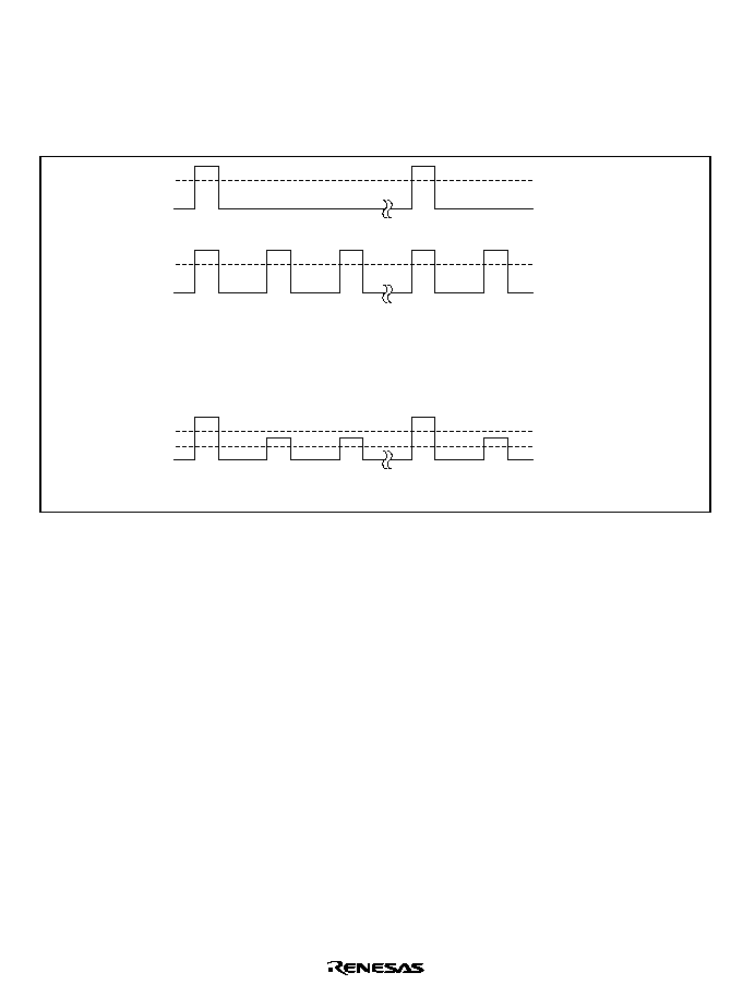
Rev. 1.0, 02/00, page 565 of 1141
26.2.6
DFG/DPG Input Signals
DFG and DPG signals can be input either as separate signals or as an overlapped signal. When the
latter is selected (PMR87 = 1), take care to control the input levels of DFG and DPG. Figure 26.5
shows DFG/DPG input signals.
DPG
DPG Schmitt level
3.45/3.55
V
IL
/V
IH
DFG Schmitt level
1.85/1.95
V
IL
/V
IH
DFG
(1) DPG/DFG separate input (PMR87=0)
DPG Schmitt level
DFG/DPG
(2) DPG/DFG overlapped input (PMR87=1)
DFG Schmitt level
Figure 26.5 DFG/DPG Input Signals

Rev. 1.0, 02/00, page 566 of 1141
26.3
Reference Signal Generators
26.3.1
Overview
The reference signal generators consist of a REF30 signal generator and a CREF signal generator
and create the reference signals (REF30 and CREF signals) used in phase comparison, etc. The
REF30 signal is used to control the phase of the drum and capstan. The CREF signal is used if
REF30 signal cannot be used as the reference signal to control the phase of the capstan in REC
mode. Each signal generator consists of a 16-bit counter which uses the servo clock
s/2 (or
s/4) as its clock source, a reference period register, and a comparator.
The value set in the reference period register should be 1/2 of the desired reference signal period.
26.3.2
Block Diagram
Figure 26.6 shows the block diagram of REF30 signal generator. Figure 26.7 shows that of CREF
signal generator.
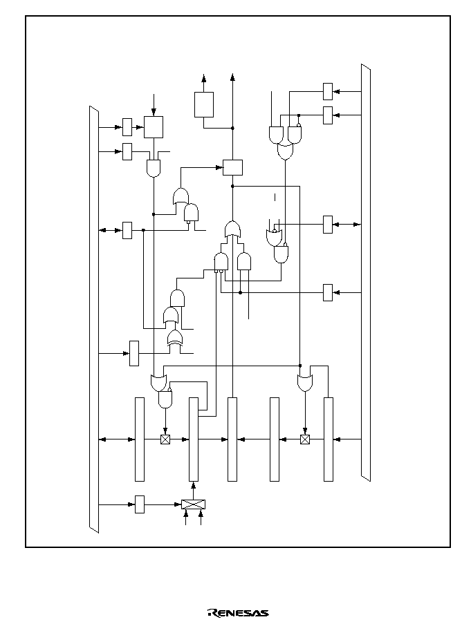
Rev. 1.0, 02/00, page 567 of 1141
s = fosc/2
s/2
s/4
Dummy read
External
frequency
signal
(EXTTRG)
Field
detection
signal
W
W
R/W
W
W
WW
PB
REC
PB
,
ASM
REC/PB
V noise detection signal
REF30
REF30P
Video FF
VD
Match
Mask
Clear
W
R/W
W
Internal bus
R/W
Internal bus
Toggle
RCS
REF30 counter register (16 bits)
OD/EV
VST
FDS
VEG
Edge
detec-
tion
Edge
detec-
tion
VNA
CVS
REX
TBC
Reference period buffer 1 (16 bits)
Reference period register 1 (16 bits)
Comparator (16 bits)
Counter (16 bits)
Figure 26.6 REF30 Signal Generator
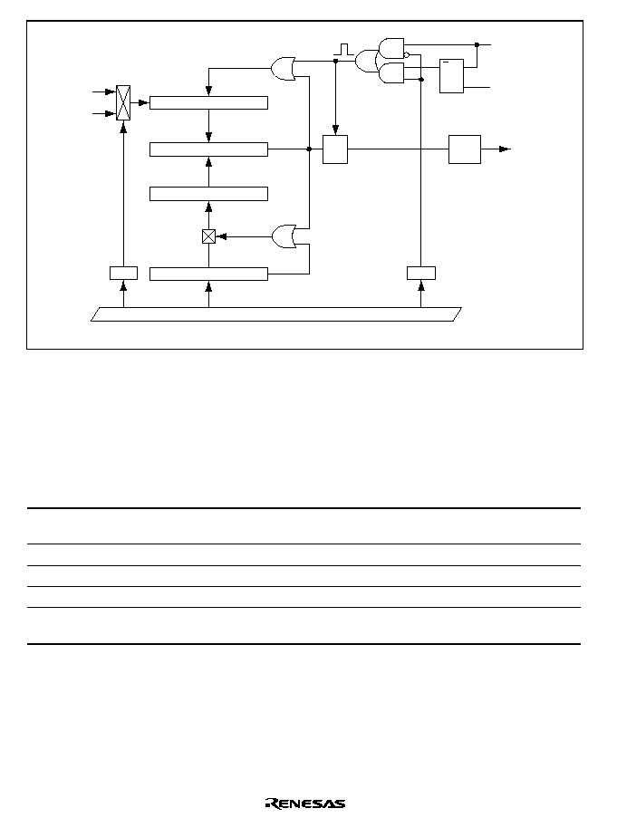
Rev. 1.0, 02/00, page 568 of 1141
s/2
s/4
W
W
CREF
DVCFG2
PB(ASM)
REC
Match
Clear
Counter clear
Toggle
Edge
detection
CRD
W
RCS
Reference period register 2 (16 bits)
Reference period buffer 2 (16 bits)
Comparator (16 bits)
Counter (16 bits)
Internal bus
S
R
Q
Dummy read
s = fosc/2
Figure 26.7 Block Diagram of CREF Signal Generator
26.3.3
Register Configuration
Table 26.4 shows the register configuration of the reference signal generators.
Table 26.4
Register Configuration
Name
Abbrev.
R/W
Size
Initial Value
Address
Reference period mode
register
RFM
W
Byte
H'00
H'D096
Reference period register 1
RFD
W
Word
H'FFFF
H'D090
Reference period register 2
CRF
W
Word
H'FFFF
H'D092
REF30 counter register
RFC
R/W
Word
H'0000
H'D094
Reference period mode
register 2
RFM2
R/W
Byte
H'FE
H'D097

Rev. 1.0, 02/00, page 569 of 1141
26.3.4
Register Description
Reference Period Mode Register (RFM)
0
0
1
0
W
2
0
W
3
0
4
0
W
0
W
5
6
0
7
REX
CRD
OD/EV
VST
VEG
0
W
RCS
W
W
W
VNA
CVS
Bit :
Initial value :
R/W :
RFM is an 8-bit write-only register which determines the operational state of the reference signal
generators. If a read is attempted, an undetermined value is read out.
It is initialized to H'00 by a reset and in stand-by and module stop modes.
RFM is accessible in byte units only. If accessed by a word, correct operation is not guaranteed.
Bit 7
Clock Source Selection Bit (RCS): Selects the clock source supplied to the counter.
(
s = fosc/2)
Bit 7
RCS
Description
0
s/2
(Initial value)
1
s/4
Bit 6
Mode Selection Bit (VNA): Selects the mode for controlling transition to free-run
operation when the REF30 signal is generated synchronously with the VD signal in REC mode:
automatic mode which controls the transition by the V noise detection signal detected by the sync
signal detection circuit, or manual mode which controls the transition by software.
Bit 6
VNA
Description
0
Manual mode
(Initial value)
1
Automatic mode

Rev. 1.0, 02/00, page 570 of 1141
Bit 5
Manual Selection Bit (CVS): Selects whether the REF30 signal is generated synchrously
with VD or it is operated in free-run state in the manual mode (VNA = 0). (This selection is
ignored in PB mode except in TBC mode.)
Bit 5
CVS
Description
0
Synchronous with VD
(Initial value)
1
Free-run operation
Bit 4
External Signals Sync Selection Bit (REX): Selects whether the REF30 signal is
generated synchronously with VD, in free-run state or synchronously with the external signal.
(Valid in both PB and REC modes.)
Bit 4
REX
Description
0
VD signal or free-run
(Initial value)
1
Synchronous with external signal
Bit 3
DVCFG2 Sync Selection Bit (CRD): Selects whether the reset timing in the CREF signal
generation is immediately after switching the mode or it is synchronous with the DVCFG2 signal
immediately after the mode switching.
Bit 3
CRD
Description
0
On switching the mode
(Initial value)
1
Synchronous with DVCFG2 signal
Bit 2
ODD/EVEN Edge Switching Selection Bit (OD/EV): Selects whether the REF30P signal
is generated by the rising edge (even) or falling edge (odd) of the field signal in REC mode.
Bit 2
OD/EV
Description
0
Generated at the rising edge of the field signal
(Initial value)
1
Generated at the falling edge of the field signal

Rev. 1.0, 02/00, page 571 of 1141
Bit 1
Video FF Counter Set (VST): Selects whether the REF30 counter register value is set on
or off by the Video FF signal when the drum phase is in FIX on in the PB mode.
Bit 1
VST
Description
0
Counter set off by Video FF signal
(Initial value)
1
Counter set on by Video FF signal
Bit 0
Video FF Edge Selection Bit (VEG): Selects the edge at which REF30 counter is set
(VST = 1) by the Video FF signal.
Bit 0
VEG
Description
0
Set at the rising edge of Video FF signal
(Initial value)
1
Set at the falling edge of Video FF signal
Reference Period Register 1 (RFD)
15
1
REF15
W
14
1
REF14
W
13
1
REF13
W
12
1
REF12
W
11
1
REF11
W
10
1
REF10
W
9
1
REF9
W
8
1
REF8
W
7
1
REF7
W
6
1
REF6
W
5
1
REF5
W
4
1
REF4
W
3
1
REF3
W
2
1
REF2
W
1
1
REF1
W
0
1
REF0
W
Bit :
Initial value :
R/W :
The reference period register 1 (RFD) is a buffer register which generates the reference signal
(REF30) for playback, VD compensation for recording, and the reference signals for free-running.
It is an 16-bit write-only register accessible in word units only. If a read is attempted, an
undetermined value is read out.
The value set in RFD should be 1/2 of the desired reference signal period. Care is required when
VD is unstable, such as when the field is weak (synchronization with VD cannot be acquired if a
value less than 1/2 is set in REC). When data is written in RFD, it is stored in the buffer once, and
then fetched into RFD by a match signal of the comparator. (The data which generates the
reference signal is updated by the match signal.) A forcible write, such as initial setting, etc.,
should be done by a dummy read of RFD.
If a byte-write in RFD is attempted, correct operation is not guaranteed. RFD is initialized to
H'FFFF by a reset, and in stand-by and module stop modes.
Use bit 7 (ASM) and bit 6 (REC/PB) in the CTL mode register (CTLM) in the CTL circuit to
switch between record and playback modes. Use bit 4 (CR/RF bit) in the capstan phase error
detection control register (CPGCR) to switch between REF30 and CREF for capstan phase
control.

Rev. 1.0, 02/00, page 572 of 1141
Reference Period Register 2 (CRF)
15
1
CRF15
W
14
1
CRF14
W
13
1
CRF13
W
12
1
CRF12
W
11
1
CRF11
W
10
1
CRF10
W
9
1
CRF9
W
8
1
CRF8
W
7
1
CRF7
W
6
1
CRF6
W
5
1
CRF5
W
4
1
CRF4
W
3
1
CRF3
W
2
1
CRF2
W
1
1
CRF1
W
0
1
CRF0
W
Bit :
Initial value :
R/W :
The reference period register 2 (CRF) is an 16-bit write-only buffer register which generates the
reference signals to control the capstan phase (CREF). CRF is accessible in word units only. If a
read is attempted, an undetermined value is read out. The value set in CRF should be 1/2 of the
desired reference signal period.
When data is written in CRF, it is stored in the buffer once, and then fetched into CRF by a match
signal of the comparator. (The data which generates the reference signal is updated by the match
signal.) A forcible write, such as initial setting, etc., should be done by a dummy read of CRF.
If a byte-write in CRF is attempted, correct operation is not guaranteed. CRF is initialized to
H'FFFF by a reset and in stand-by and module stop modes.
Use bit 4 (CR/RF bit) in the capstan phase error detection control register (CPGCR) to switch
between REF30 and CREF for capstan phase control. See section 26.9, Capstan Phase Error
Detector.
REF30 Counter Register (RFC)
15
0
RFC15
14
0
RFC14
13
0
RFC13
12
0
RFC12
11
0
RFC11
10
0
RFC10
9
0
RFC9
8
0
RFC8
7
0
RFC7
6
0
RFC6
5
0
RFC5
4
0
RFC4
3
0
RFC3
2
0
RFC2
1
0
RFC1
0
0
RFC0
R/W R/W R/W R/W R/W R/W R/W R/W R/W R/W R/W R/W R/W R/W R/W R/W
Bit :
Initial value :
R/W :
The REF30 counter register (RFC) is a register which determines the initial value of the free-run
counter when it generates REF30 signals in playback. When data is written in RFC, its value is
written in the counter by a match signal of the comparator. If the bit 1 (VST) of RFM is set to 1,
the counter is set by the Video FF signal when the drum phase is in FIX ON. The counter setting
by the Video FF signal should be done by setting bit 1 (VST) and bit 0 (VEG) of the RFM. Do
not set the RFC to a value greater than 1/2 of the reference period register 1 (RFD) value.
RFC is a read/write register. If a read is attempted, the value of the counter is read out. If a byte-
access is attempted, correct operation is not guaranteed. RFC is initialized to H'0000 by a reset
and in stand-by and module stop modes.

Rev. 1.0, 02/00, page 573 of 1141
Reference Period Mode Register 2 (RFM2)
0
0
1
1
2
1
3
1
4
1
5
6
7
TBC
R/W
FDS
1
1
1
R/W
Bit :
Initial value :
R/W :
REM2 is an 8-bit read/write register which determines the operational state of the reference signal
generators.
It is initialized to H'FE by a reset and in stand-by and module stop modes. RFM2 is a byte access-
only register; if accessed by a word, correct operation is not guaranteed.
Bit 7
TBC Selection Bit (TBC): Selects whether the reference signal in PB mode is generated
by the VD signal or by the free-run counter.
Bit 7
TBC
Description
0
Generated by the VD signal
1
Generated by the free-run counter
(Initial value)
Bits 6 to 1
Reserved: Cannot be modified and are always read as 1.
Bit 0
Field Selection Bit (FDS): Determines whether selection between ODD or EVEN is made
for the field signal when PB mode was switched over to REC mode, or these signals are
synchronized with VD signals within a phase error of 90
∞
immediately after the switching over.
Bit 0
FDS
Description
0
Generated by the VD signal of ODD or EVEN selected
(Initial value)
1
Generated by the VD signal within mode transition phase error of 90
∞

Rev. 1.0, 02/00, page 574 of 1141
26.3.5
Operation
∑
Operation of REF30 Signal Generator
The REF30 signal generator generates the reference signals required to control the phase of
the drum and capstan.
To generate the REF30 signal, set the 1/2 the reference period to the reference period
register 1 (RFD) corresponding to the 50 percent duty cycle. In playback mode, the REF30
signal is generated by free-running the REF30 signal generator. The generator has the
external signal synchronization function, and if the bit 4 (REX) of the reference period
mode register (RFM) is set to 1, it generates the REF30 signal from the external signal
(EXTTGR).
In record mode, the reference signal is generated from the VD signal generated in the sync
detector. Any VD drop-out caused by weak field intensity, etc., is compensated by a value
set in RFD. To cope with the VD noises, the generator automatically masks the VD for a
period about 75% of the RFD setting after REF30 signal was changed due to VD. In
record mode, the generation of the reference signal either by VD or free-run operation can
be controlled automatically using the V noise detection signal detected in the sync signal
detection circuit or manually by software. Select which is used by setting bit 6 (VNA) or 5
(CVS) of RFM.
The phase of the toggle output of the REF30 signal is cleared to L level when the mode
shifts from PB to REC (ASM). Also the frame servo function can be set, allowing for
control of the phase of REF30 signals with the field signal detected in the sync signal
detection circuit. Use bit 2 (OD/EV) of RFM for such control.
See the description of CTL mode register (CTLM) in section 26.13.5, Register Description,
as for switching over between PB, ASM and REC.
∑
Operation of the Mask Circuit
The REF30 signal generator has a toggle mask circuit and a counter mask (counter set
signal mask) circuit built-in. Each mask circuit masks irregular VD signals which may
occur when the VD signal is unstable because of weak field intensity, etc., in record mode.
The toggle mask and counter mask circuits mask the VD automatically for about 75% of
double the period set in the reference period register 1 (RFD) after VD signal was detected
(see figure 26.9). If a VD signal dropped out and V was compensated, the toggle mask
circuit begins masking, but the counter mask circuit does not begin masking for about 25%
of the period. If VD signal was detected during such a period, the circuit does masking for
about 75% of the period after the VD detection. If not detected, it does masking for about
75% of the period after V was compensated (see figures 26.10 and 26.11).
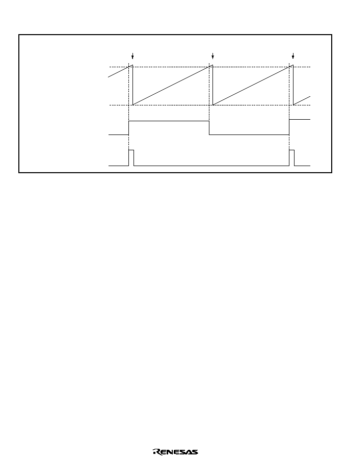
Rev. 1.0, 02/00, page 575 of 1141
∑
Timing of the REF30 Signal Generation
Figures 26.8 to 26.12 show the timing of the generation of REF30 and REF30P signals.
Counter set
Counter set
Counter set
Value set in reference
period register 1 (RFD)
Counter
Value set in REF30
counter register (RFC)
REF30
REF30P
Figure 26.8 REF30 Signals in Playback Mode
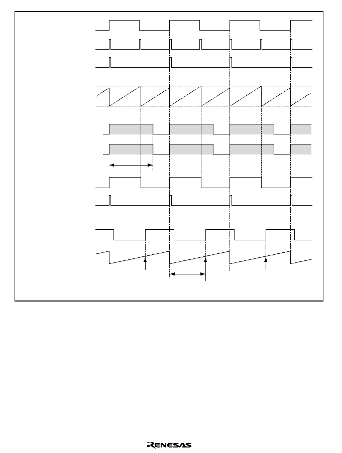
Rev. 1.0, 02/00, page 576 of 1141
Sampling
Sampling
Sampling
Value set in reference
period register 1 (RFD)
Selected VD
(OD/EV=0)
Counter mask
(clear signal mask)
Counter
Value set in REF30
counter register (RFC)
REF30
VD
Toggle mask
Field signal
REF30P
HSW
Drum phase counter
T
About 75%
Masking
period
Masking
period
Figure 26.9 Generation of Reference Signal in Record Mode (Normal Operation)
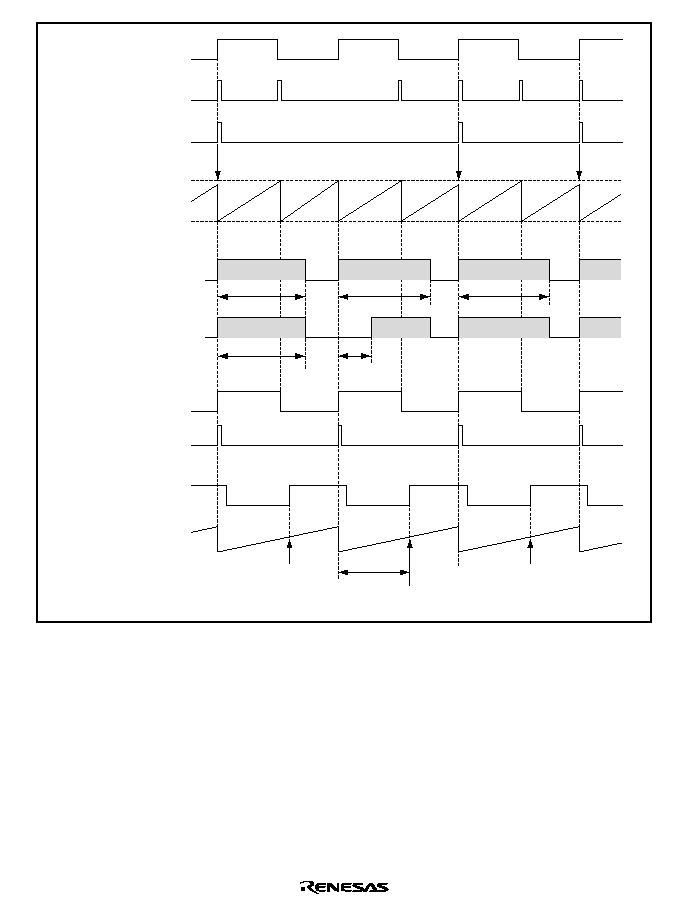
Rev. 1.0, 02/00, page 577 of 1141
Sampling
Cleared
Cleared
Cleared
Drop-out of V
Value set in reference
period register 1 (RFD)
Selected VD
(OD/EV=0)
Counter mask
(clear signal mask)
Counter
Value set in REF30
counter register (RFC)
REF30
VD
Toggle mask
Field signal
REF30P
HSW
Drum phase counter
Sampling
T
Sampling
About 75%
About 75%
About 75%
About 75%
About
25%
Masking
period
Masking
period
Figure 26.10 Generation of the Reference Signal when in REC (V Dropped Out)
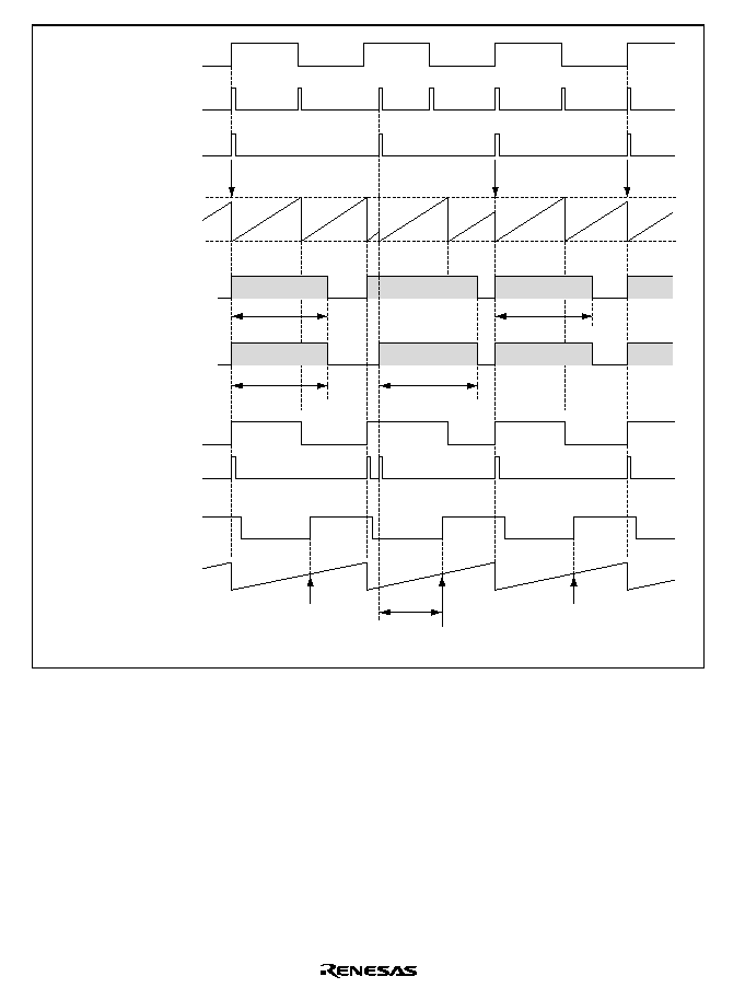
Rev. 1.0, 02/00, page 578 of 1141
Sampling
Cleared
Cleared
Cleared
Dislocation of V
Value set in reference
period register 1 (RFD)
Selected VD
(OD/EV=0)
Counter mask
(clear signal mask)
Counter
Value set in REF30
counter register (RFC)
REF30
VD
Toggle mask
Field signal
REF30P
HSW
Drum phase counter
Sampling
T
Sampling
About 75%
About 75%
About 75%
About 75%
Masking
period
Masking
period
Figure 26.11 Generation of the Reference Signal when in REC (V Dislocated)
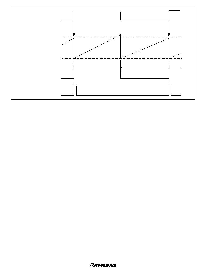
Rev. 1.0, 02/00, page 579 of 1141
Cleared
Cleared
Reset
Value set in reference
period register 1 (RFD)
Counter
Value set in REF30
counter register (RFC)
External sync
signal
REF30
REF30P
Figure 26.12 Generation of REF30 Signal by the External Sync Signal
∑
CREF Signal Generator
The CREF signal generator generates the CREF signal which is the reference signal to
control the phase of capstan.
To generate the CREF signal, set the 1/2 the reference period to the reference period
register 2 (CRF). If the set value matches the counter value, a toggle waveform is
generated corresponding to the 50 percent duty cycle, and a one-shot pulse is output at each
rising edge of the waveform. The counter of CREF signal generator is initialized to H'0000
and the phase of the toggle is cleared to L level when the mode shifts from PB (ASM) to
REC. The timing of clearing is selectable between immediately after the transition from
PB (ASM) to REC and the timing of DVCFG2 after the transition. Use bit 3 (CRD) of the
reference period mode register (RFM) for this selection.
In the capstan phase error detection circuit, either REF30 signal or CREF signal can be
selected for the reference signal. Use either of them according to the use of the system.
Use the CREF signal to control the phase of the capstan at a period which is different from
the period used to control the phase of the drum. For the switching between REF30 and
CREF in the capstan phase control, see the description of capstan phase error detection
control register (CPGCR) in section 26.9.4, Register Description.
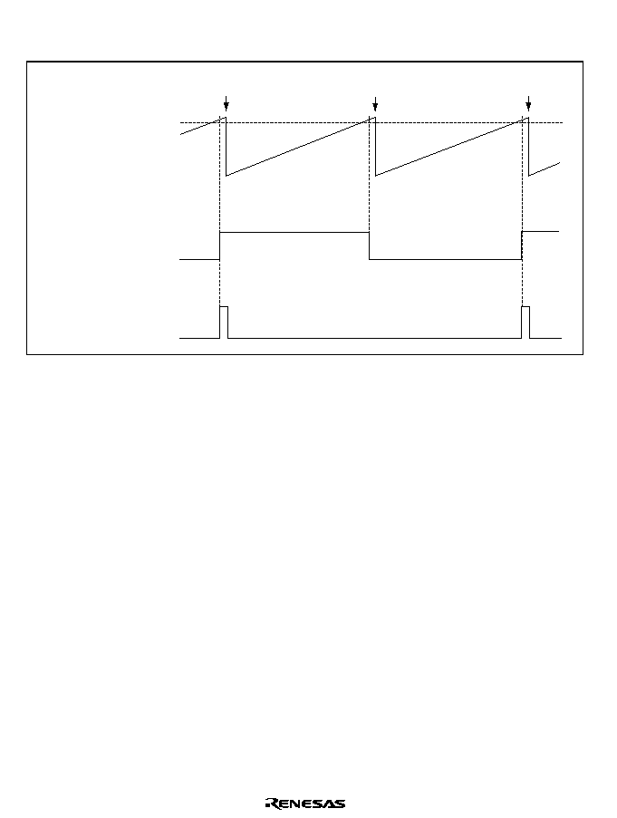
Rev. 1.0, 02/00, page 580 of 1141
∑
Timing Chart of the CREF Signal Generation
Figures 26.13 to 26.15 show the generation of CREF signal.
Cleared
Cleared
Cleared
Value set in reference
period register 2 (CRF)
Counter
Toggle signal
CREF
Figure 26.13 Generation of CREF Signal
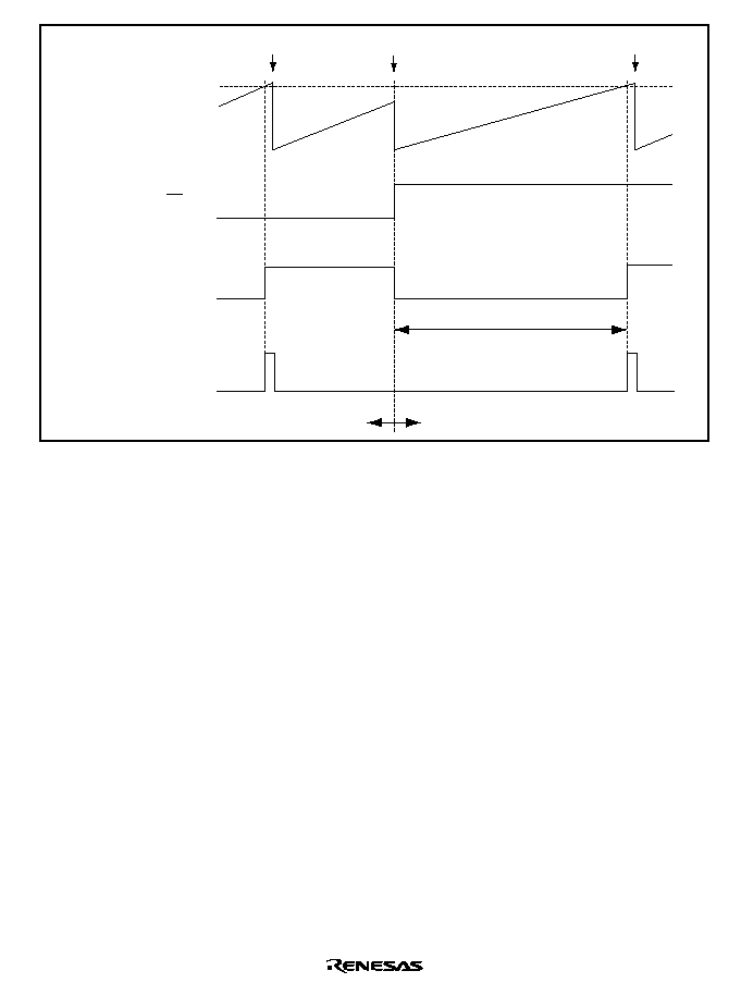
Rev. 1.0, 02/00, page 581 of 1141
Cleared
Cleared
Cleared
Value set in reference
period register 2 (CRF)
Counter
Period set in CRF
REC
PB(ASM)
Toggle signal
REC/PB
CREF
Figure 26.14 CREF Signal when PB is Switched to REC (when CRD Bit = 0)
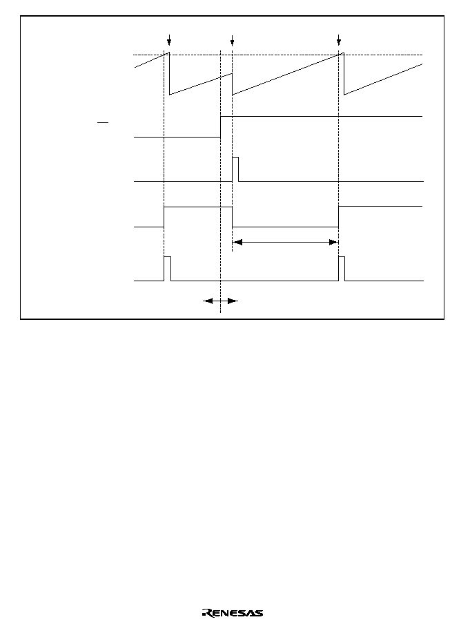
Rev. 1.0, 02/00, page 582 of 1141
Cleared
Cleared
Cleared
Value set in reference
period register 2 (CRF)
Counter
Period set in CRF
Toggle signal
REC/PB
CREF
DVCFG2
REC
PB(ASM)
Figure 26.15 CREF Signal when PB is Switched to REC (when CRD Bit = 1)
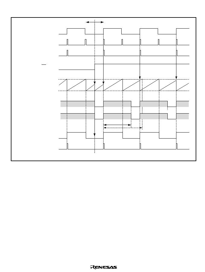
Rev. 1.0, 02/00, page 583 of 1141
Figures 26.16 and 26.17 show REF30 (REF30P) when PB is switched to REC.
Cleared
Cleared
Cleared
Cleared
Cleared
Value set in reference
period register 1 (RFD)
Selected VD*
(OD/EV=0)
Note: In the field discrimination mode
Counter mask
(Clear signal mask)
Counter
Value set in REF30
counter register (RFC)
REF30
VD (except in PB)
REC(ASM)
PB
Toggle mask
Field signal
REC/PB
REF30P
About 75%
Masking
period
Masking
period
Figure 26.16 Generation of the Reference Signal when PB is Switched to REC (1)
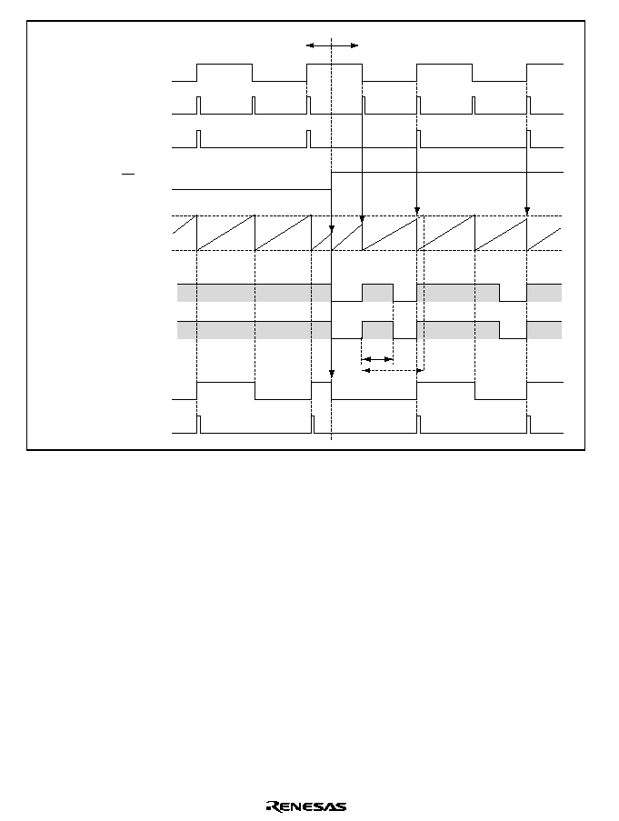
Rev. 1.0, 02/00, page 584 of 1141
Value set in reference
period register 1 (RFD)
Selected VD
(OD/EV=0)
Counter mask
(Clear signal mask)
Counter
Value set in REF30
counter register (RFC)
REF30
VD (except in PB)
REC(ASM)
PB
Toggle mask
Field signal
REC/PB
REF30P
About
50%
Cleared
Cleared
Cleared
Cleared
Masking
period
Masking
period
Figure 26.17 Generation of the Reference Signal when PB is Switched to REC (2)
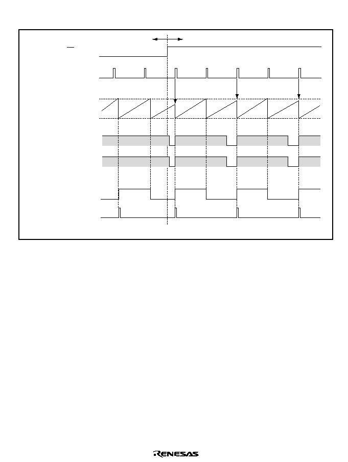
Rev. 1.0, 02/00, page 585 of 1141
Figures 26.18 to 26.21 show REF30 (REF30P) when PB is switched to REC (where FDS bit = 1).
Cleared
Cleared
Cleared
Value set in reference
period register 1 (RFD)
FDS bit = 1
Counter mask
(Clear signal mask)
Counter
Value set in REF30
counter register (RFC)
REF30
VD (except in PB)
REC(ASM)
PB
Toggle mask
REC/PB
REF30P
Masking
period
Masking
period
Figure 26.18 Generation of the Reference Signal when PB is Switched to REC
where RFD Bit is 1 (1)
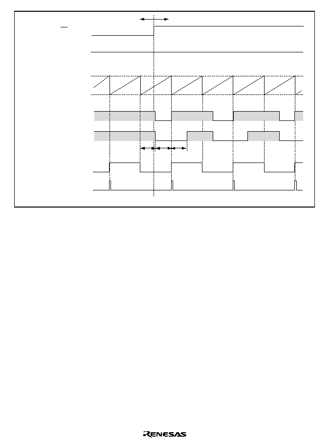
Rev. 1.0, 02/00, page 586 of 1141
Value set in reference
period register 1 (RFD)
FDS bit = 1
Counter mask
(Clear signal mask)
Counter
Value set in REF30
counter register (RFC)
REF30
VD (except in PB)
REC(ASM)
PB
Toggle mask
REC/PB
REF30P
Masking
period
Masking
period
25%
25%
25%
Figure 26.19 Generation of the Reference Signal when PB is Switched to REC
where RFD Bit is 1 (when VD Signal is Not Detected) (2)
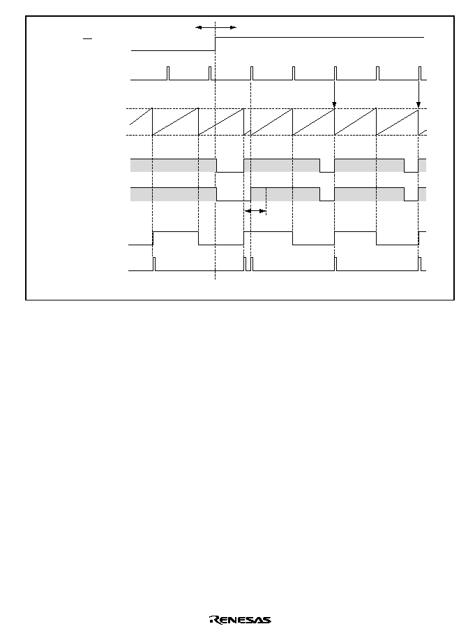
Rev. 1.0, 02/00, page 587 of 1141
Cleared
Cleared
Value set in reference
period register 1 (RFD)
FDS bit = 1
Counter mask
(Clear signal mask)
Counter
Value set in REF30
counter register (RFC)
REF30
VD (except in PB)
REC(ASM)
PB
Toggle mask
REC/PB
REF30P
Masking
period
Masking
period
25% max.
Figure 26.20 Generation of the Reference Signal when PB is Switched to REC
where RFD Bit is 1 (3)
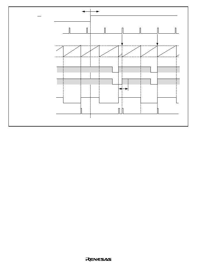
Rev. 1.0, 02/00, page 588 of 1141
Cleared
Cleared
Value set in reference
period register 1 (RFD)
FDS bit = 1
Counter mask
(Clear signal mask)
Counter
Value set in REF30
counter register (RFC)
REF30
VD (except in PB)
REC(ASM)
PB
Toggle mask
REC/PB
REF30P
Masking
period
Masking
period
25% max.
Figure 26.21 Generation of the Reference Signal when PB is Switched to REC
where RFD Bit is 1 (4)

Rev. 1.0, 02/00, page 589 of 1141
26.4
HSW (Head-switch) Timing Generator
26.4.1
Overview
The HSW timing generator consists of a 5-bit DFG counter, a 16-bit timer counter, a matching
circuit, and two 31-bit 10-stage FIFOs.
The 5-bit counter counts the DFG pulses following a DPG pulse. Each of them determines the
timing to reset the 16-bit timer counter for each field. The 16-bit timer counter is a timer clocked
by a
s/4 clock source, and can be used as a programmable pattern generator (PPG) as well as a
free-running counter (FRC). If used as a free-running counter, it is cleared by overflow of the 19-
bit FRC. Accordingly, two FRCs operate synchronously. The matching circuit compares the
timing data in the most significant 16 bits of FIFO with the 16-bit timer counter, and controls the
output of the pattern data set in the least significant 15 bits of FIFO.
26.4.2
Block Diagram
Figure 26.22 shows a block diagram of the HSW timing generator.
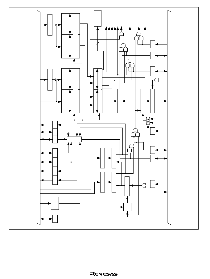
Rev. 1.0, 02/00, page 590 of 1141
R
W
W
R/W
R/W
W
R/W
R/W
STRIG
IRRHSW2
ISEL2
AudioFF
VideoFF
HSW
NHSW
Mlevel
Vpulse
ADTRG
IRRHSW1
R
VD
PB
W
R/W
R/W
Cleared
Cleared
CLK
W
R
,
NCDFG
FRCOVF
DPG
CKSL
VFF/NFF
Internal bus
W
FPDRA
FPDRB
FTPRA
FTPRB
W
ISEL1
OFG
FIFO output pattern
register 1
FIFO output pattern
register 2
SOFG
LOP
R/W
R/W
R
R
WW
CLRA,B
OVWA,B
EMPA,B
FLA,B
R/W
R/W
HSM2
HSM1
HSLP
EDG
HSW loop stage
number setting
register
Internal bus
FGR20FF
FRT
CCLR
Edge
detector
Control
circuit
FIFO 1
(31 bits
◊
10 stages)
15 bits
P77 to 70
(PPG output)
FIFO timing pattern
register 1
FIFO timing pattern
register 2
16 bits
FIFO2
(31 bits
◊
10 stages)
15 bits
16 bits
FIFO output selector & output buffer
15 bits
16 bits
DFCRB
DFCRA
DFCRA
HSM2
HSM2
Capture
HSM2
DFCRA
DFCRA
DFG reference
register 1
Comparator
(5 bits)
Comparator
(5 bits)
DFG reference
register 2
DFCTR
5-bit counter
Compare circuit (16 bits)
FTCTR (16 bits)
16-bit timer counter
s/4
s/8
Figure 26.22 Block Diagram of the HSW Timing Generator

Rev. 1.0, 02/00, page 591 of 1141
26.4.3
HSW Timing Generator Configuration
The HSW timing generator is composed of the elements shown in table 26.5.
Table 26.5
Configuration of the HSW Timing Generator
Element
Function
HSW mode register 1 (HSM1)
Confirmation/determination of this circuits' operating
status
HSW mode register 2 (HSM2)
Confirmation/determination of this circuits' operating
status
HSW loop stage number setting register
(HSLP)
Setting of number of loop stages in loop mode
FIFO output pattern register 1 (FPDRA)
Output pattern register of FIFO1
FIFO output pattern register 2 (FPDRB)
Output pattern register of FIFO2
FIFO timing pattern register 1 (FTPRA)
Output timing register of FIFO1
FIFO timing pattern register 2 (FTPRB)
Output timing register of FIFO2
DFG reference register 1 (DFCRA)
Setting of reference DFG edge for FIFO1
DFG reference register 2 (DFCRB)
Setting of reference DFG edge for FIFO2
FIFO timer capture register (FTCTR)
Capture register of timer counter
DFG reference count register (DFCTR)
DFG edge count
FIFO control circuit
FIFO status control
DFG count compare circuit (
◊
2)
Detection of match between DFCR and DFG counters
16-bit timer counter
16-bit free-run timer counter
31-bit x 20 stage FIFO
First In First Out data buffer
31-bit FIFO data buffer
Data storing buffer for the first stage of FIFO
16-bit compare circuit
Detection of match between timer counter and FIFO
data buffer
FPDRA and FPDRB are intermediate buffers; an FTPRA and FTPRB write results in
simultaneous writing of all 31 bits to the FIFO. The FIFO has two 31-bit x 10-stage data buffers;
its operating status is controlled by HSM1 and HSM2. Data is stored in the 31-bit data buffer.
The values of FTPRA/FTPRB and the timer counter are compared, and if they match, the 15-bit
pattern data is output to each function. AudioFF, VideoFF, and PPG (P70 to P77) are outputs
from the corresponding pins, ADTRG is the A/D converter hardware start signal, Vpulse and
Mlevel signals are the signals for generating the additional V pulses, and HSW and NHSW signals
are the same as VideoFF signals used for the phase control of the drum. The 16-bit timer counter
is initialized by the overflow of the 19-bit free-run counter in the free-run mode (FRT bit of HSM2
= 1), or by a signal indicating a match between DFCRA/DFCRB and the 5-bit DFG counter in
DFG reference mode.

Rev. 1.0, 02/00, page 592 of 1141
26.4.4
Register Configuration
Table 26.6 shows the register configuration of the HSW timing generator.
Table 26.6
Register Configuration
Name
Abbrev.
R/W
Size
Initial Value
Address
HSW mode register 1
HSM1
R/W
Byte
H'30
H'D060
HSW mode register 2
HSM2
R/W
Byte
H'00
H'D061
HSW loop stage number setting
register
HSLP
R/W
Byte
Undetermined
H'D062
FIFO output pattern register 1
FPDRA
W
Word
Undetermined
H'D064
FIFO timing pattern register 1*
FTPRA
W
Word
Undetermined
H'D066
FIFO output pattern register 2
FPDRB
W
Word
Undetermined
H'D068
FIFO timing pattern register 2
FTPRB
W
Word
H'FFFF
H'D06A
DFG reference register 1*
DFCRA
W
Byte
Undetermined
H'D06C
DFG reference register 2
DFCRB
W
Byte
Undetermined
H'D06D
FIFO timer capture register*
FTCTR
R
Word
H'0000
H'D066
DFG reference count register*
DFCTR
R
Byte
H'E0
H'D06C
Note:
*
FTPRA and FTCTR, as well as DFCRA and DFCTR, are allocated to the same
addresses.
26.4.5
Register Description
HSW Mode Register 1 (HSM1)
0
0
1
0
R/W
2
0
R/(W)*
3
0
4
1
R
1
R
5
6
0
7
EMPA
OVWB
OVWA
CLRB
CLRA
0
R
FLB
R/W
R/(W)*
R
FLA
EMPB
Bit :
Initial value :
R/W :
Note: * Only 0 can be written
HSM1 is an 8-bit register which confirms and determines the operational state of the HSW timing
generator.
Bits 7 to 4 are read-only bits, and write is disabled. All the other bits accept both read and write.
It is initialized to H'30 by a reset or in stand-by mode.

Rev. 1.0, 02/00, page 593 of 1141
Bit 7
FIFO2 Full Flag (FLB): When the FLB bit is 1, it indicates that the FIFO2 is full of the
timing pattern data and the output pattern data. If a write is attempted in this state, the write
operation becomes invalid, an interrupt is generated, the OVWB flag (bit 3) is set to 1, and the
write data is lost. Wait until space becomes available in the FIFO2, then write again.
Bit 7
FLB
Description
0
FIFO2 is not full, and can accept data input.
(Initial value)
1
FIFO2 is full of data.
Bit 6
FIFO1 Full Flag (FLA): When the FLA bit is 1, it indicates that the FIFO1 is full of the
timing pattern data and the output pattern data. If a write is attempted in this state, the write
operation becomes invalid, an interrupt is generated, the OVWA flag (bit 2) is set to 1, and the
write data is lost. Wait until space becomes available in the FIFO1, then write again.
Bit 6
FLA
Description
0
FIFO1 is not full, and can accept data input.
(Initial value)
1
FIFO1 is full of data.
Bit 5
FIFO2 Empty Flag (EMPB): Indicates that FIFO2 has no data, or that all the data has
been output in single mode.
Bit 5
EMPB
Description
0
FIFO2 contains data.
1
FIFO2 contains no data.
(Initial value)
Bit 4
FIFO1 Empty Flag (EMPA): Indicates that FIFO1 has no data, or that all the data has
been output in single mode.
Bit 4
EMPA
Description
0
FIFO1 contains data.
1
FIFO1 contains no data.
(Initial value)

Rev. 1.0, 02/00, page 594 of 1141
Bit 3
FIFO2 Overwrite Flag (OVWB): If a write is attempted when the FIFO2 is full of the
timing pattern data and the output pattern data (FLB bit = 1), the write operation becomes invalid,
an interrupt is generated, the OVWB flag is set to 1, and the write data is lost. Wait until space
becomes available in the FIFO2, then write again.
Write 0 to clear the OVWB flag, because it is not cleared automatically.
Bit 3
OVWB
Description
0
Normal operation.
(Initial value)
1
Indicates that a write in FIFO2 was attempted when FIFO2 was full of data. Clear
this flag by writing 0 to this bit.
Bit 2
FIFO1 Overwrite Flag (OVWA): If a write is attempted when the FIFO1 is full of the
timing pattern data and the output pattern data (FLA bit = 1), the write operation becomes invalid,
an interrupt is generated, the OVWA flag is set to 1, and the write data is lost. Wait until space
becomes available in the FIFO1, then write again.
Write 0 to clear the OVWA flag, because it is not cleared automatically.
Bit 2
OVWA
Description
0
Normal operation.
(Initial value)
1
Indicates that a write in FIFO1 was attempted when FIFO1 was full. Clear this
flag by writing 0 to this bit.
Bit 1
FIFO2 Pointer Clear (CLRB): Clears the FIFO2 write position pointer. After 1 is
written, the bit immediately reverts to 0. Writing 0 in this bit has no effect.
Bit 1
CLRB
Description
0
Normal operation.
(Initial value)
1
Clears the FIFO2 pointer.
Bit 0
FIFO1 Pointer Clear (CLRA): Clears the FIFO1 write position pointer. After 1 is
written, the bit immediately reverts to 0. Writing 0 in this bit has no effect.
Bit 0
CLRA
Description
0
Normal operation
(Initial value)
1
Clears the FIFO1 pointer

Rev. 1.0, 02/00, page 595 of 1141
HSW Mode Register 2 (HSM2)
0
0
1
0
R
2
0
R/W
3
0
4
0
R/W
0
R/W
5
6
0
7
EDG
ISEL1
SOFG
OFG
VFF/NFF
0
R/W
FRT
W
R/W
R
FGR2OFF
LOP
Bit :
Initial value :
R/W :
HSM2 is an 8-bit register which confirms and determines the operational state of the HSW timing
generator.
Bit 1 is a read-only bit, and write is disabled. Bit 0 is a write-only bit, and if a read is attempted,
an undetermined value is read out. All the other bits accept both read and write. It is initialized to
H'00 by a reset or in stand-by mode.
Bit 7
Free-run Bit (FRT): Selects whether the matching timing is determined by the DPG
counter and timer, or by the FRC.
Bit 7
FRT
Description
0
5-bit DFG counter + 16-bit timer counter
(Initial value)
1
16-bit FRC
Bit 6
FRG2 Clear Stop Bit (FGR2OFF): Disables clearing of the counter by the DFG register
2. The FIFO group, including both FIFO1 and FIFO2, is available.
Bit 6
FGR2OFF
Description
0
Enables clearing of the16-bit timer counter by DFG register 2
(Initial value)
1
Disables clearing of the16-bit timer counter by DFG register 2
Bit 5
Mode Selection Bit (LOP): Selects the output mode of FIFO. If the loop mode is
selected, LOB3 to LOB0 bits and LOA3 to LOA0 bits become valid. If the LOP bit is modified,
the pointer which counts the writing position of FIFO is cleared. In this case, the last output data
is kept.
Bit 5
LOP
Description
0
Single mode
(Initial value)
1
Loop mode

Rev. 1.0, 02/00, page 596 of 1141
Bit 4
DFG Edge Selection Bit (EDG): Selects the edge by which to count DFG pulses.
Bit 4
EDG
Description
0
Counts by the rising edge of DFG
(Initial value)
1
Counts by the falling edge of DFG
Bit 3
Interrupt Selection Bit (ISEL1): Selects the interrupt source. (IRRHSW1)
Bit 3
ISEL1
Description
0
Generates an interrupt request by the rising edge of the STRIG signal of FIFO
(Initial value)
1
Generates an interrupt request by the matching signal of FIFO
Bit 2
FIFO Output Group Selection Bit (SOFG): Selects whether 20 stages of FIFO1 +
FIFO2 or only 10 stages of FIFO1 are used.
If 20-stage output mode is used in single mode, data must be written to FIFO1 and FIFO2.
Monitor the output FIFO group flag (OFG) and control data writing by software. All the data of
FIFO1 is output, then all the data of FIFO2 is output. These steps are repeated. If 10-stage output
mode is used, the data of FIFO2 is not reflected.
Modifying the SOFG bit from 0 to 1, then again to 0 initializes the control signal of the FIFO
output stage to the FIFO1 side.
Bit 2
SOFG
Description
0
20-stage output of FIFO1 + FIFO2
(Initial value)
1
10-stage output of FIFO1 only
Bit 1
Output FIFO Group Flag (OFG): Indicates the FIFO group which is outputting.
Bit 1
OFG
Description
0
Pattern is being output by FIFO1
(Initial value)
1
Pattern is being output by FIFO2

Rev. 1.0, 02/00, page 597 of 1141
Bit 0
Output Switching Bit Between VideoFF and NarrowFF (VFF/NFF): Switches the
signal output from the VideoFF pin.
Bit 0
VFF/NFF
Description
0
VideoFF output
(Initial value)
1
NarrowFF output
HSW Loop Stage Number Setting Register (HSLP)
0
*
1
*
R/W
2
*
R/W
3
*
4
*
R/W
5
*
6
*
7
R/W
R/W
R/W
LOB1
R/W
LOB2
*
R/W
LOB3
LOB0
LOA3
LOA2
LOA1
LOA0
Bit :
Initial value :
R/W :
HSLP is an 8-bit read/write register that sets the number of the loop stages when the HSW timing
generator is in loop mode. It is valid when bit 5 (LOP) of HSM2 is 1. Bits 7 to 4 set the number
of FIFO2 stages. Bits 3 to 0 set the number of FIFO1 stages.
It is not initialized by a reset or in stand-by or module stop mode; accordingly be sure to set the
number of the stages when the loop mode is used.

Rev. 1.0, 02/00, page 598 of 1141
Bits 7 to 4
FIFO2 Stage Number Setting Bits (LOB3 to LOB0): Set the number of FIFO2
stages in loop mode. They are valid only when the loop mode is set (LOP bit of HSM2 is 1).
HSM2
HSLP
Bit 5
Bit 7
Bit 6
Bit 5
Bit 4
LOP
LOB3
LOB2
LOB1
LOB0
Description
0
*
*
*
*
Single mode
(Initial value)
0
Only 0th stage of FIFO2 is output
0
1
0th and 1st stages of FIFO2 are output
0
0th to 2nd stages of FIFO2 are output
0
1
1
0th to 3rd stages of FIFO2 are output
0
0th to 4th stages of FIFO2 are output
0
1
0th to 5th stages of FIFO2 are output
0
0th to 6th stages of FIFO2 are output
0
1
1
1
0th to 7th stages of FIFO2 are output
0
0th to 8th stages of FIFO2 are output
1
1
0
0
1
0th to 9th stages of FIFO2 are output
0
1
1
0
0
1
0
1
1
1
Setting prohibited
Note:
*
Don't care.

Rev. 1.0, 02/00, page 599 of 1141
Bits 3 to 0
FIFO1 Stage Number Setting Bits (LOA3 to LOA0): Set the number of FIFO1
stages in loop mode. They are valid only when the loop mode is set (LOP bit of HSM2 is 1).
HSM2
HSLP
Bit 5
Bit 3
Bit 2
Bit 1
Bit 0
LOP
LOA3
LOA2
LOA1
LOA0
Description
0
*
*
*
*
Single mode
(Initial value)
0
Only 0th stage of FIFO1 is output
0
1
0th and 1st stages of FIFO1 are output
0
0th to 2nd stages of FIFO1 are output
0
1
1
0th to 3rd stages of FIFO1 are output
0
0th to 4th stages of FIFO1 are output
0
1
0th to 5th stages of FIFO1 are output
0
0th to 6th stages of FIFO1 are output
0
1
1
1
0th to 7th stages of FIFO1 are output
0
0th to 8th stages of FIFO1 are output
1
1
0
0
1
0th to 9th stages of FIFO1 are output
0
1
1
0
0
1
0
1
1
1
Setting prohibited
Note:
*
Don't care.

Rev. 1.0, 02/00, page 600 of 1141
FIFO Output Pattern Register 1 (FPDRA)
8
*
9
*
W
10
*
W
11
*
12
*
W
*
W
13
14
*
15
--
--
NarrowFFA
VFFA
AFFA
VpulseA
MlevelA
1
W
W
W
ADTRGA
STRIGA
0
*
1
*
W
2
*
W
3
*
4
*
W
*
W
5
6
*
7
PPGA4
PPGA3
PPGA2
PPGA1
PPGA0
*
W
PPGA7
W
W
W
PPGA6
PPGA5
Bit :
Initial value :
R/W :
Bit :
Initial value :
R/W :
Note : * Don't care
FPDRA is a buffer register for the FIFO1 output pattern register. The output pattern data written
in FPDRA is written at the same time to the position of the FIFO1 pointed by the buffer pointer.
Be sure to write the output pattern data in FPDRA before writing it in FTPRA.
FPDRA is an 16-bit write-only register. Only a word access is valid. If a byte access is
attempted, correct operation is not guaranteed. No read is valid. If a read is attempted, an
undetermined value is read out. It is not initialized by a reset, or in stand-by or module stop mode;
accordingly be sure to write data before use.
Bit 15
Reserved: Cannot be read or modified.
Bit 14
A/D Trigger A Bit (ADTRGA): Indicates a hardware trigger signal for the A/D
converter.
Bit 13
S-TRIGA Bit (STRIGA): Indicates a signal that generates an interrupt. When the
STRIGA is selected by the ISEL, modifying this bit from 0 to 1 generates an interrupt.
Bit 12
NarrowFFA Bit (NarrowFFA): Controls the narrow video head.
Bit 11
VideoFFA Bit (VFFA): Controls the video head.
Bit 10
AudioFFA Bit (AFFA): Controls the audio head.
Bit 9
VpulseA Bit (VpulseA): Used for generating an additional V signal. For details, refer to
section 26.12, Additional V Signal Generator.
Bit 8
MlevelA Bit (MlevelA): Used for generating an additional V signal. For details, refer to
section 26.12, Additional V Signal Generator.
Bits 7 to 0
PPG Output Signal A Bits (PPGA7 to PPGA0): Used for outputting a timing
control signal from port 7 (PPG).

Rev. 1.0, 02/00, page 601 of 1141
FIFO Output Pattern Register 2 (FPDRB)
8
*
9
*
W
10
*
W
11
*
12
*
W
*
W
13
14
*
15
--
--
NarrowFFB
VFFB
AFFB
VpulseB
MlevelB
1
W
W
W
ADTRGB
STRIGB
0
*
1
*
W
2
*
W
3
*
4
*
W
*
W
5
6
*
7
PPGB4
PPGB3
PPGB2
PPGB1
PPGB0
*
W
PPGB7
W
W
W
PPGB6
PPGB5
Bit :
Initial value :
R/W :
Bit :
Initial value :
R/W :
Note : * Don't care
FPDRB is a buffer register for the FIFO2 output pattern register. The output pattern data written
in FPDRB is written at the same time to the position of the FIFO2 pointed by the buffer pointer.
Be sure to write the output pattern data in FPDRB before writing it in FTPRB.
FPDRB is an 16-bit write-only register. Only a word access is valid. If a byte access is attempted,
correct operation is not guaranteed. No read is valid. If a read is attempted, an undetermined
value is read out. It is not initialized by a reset, or in stand-by or module stop mode; accordingly
be sure to write data before use.
Bit 15
Reserved: Cannot be read or modified.
Bit 14
A/D Trigger B Bit (ADTRGB): Indicates a hardware trigger signal for the A/D
converter.
Bit 13
S-TRIGB Bit (STRIGB): Indicates a signal that generates an interrupt. When the
STRIGA is selected by the ISEL, modifying this bit from 0 to 1 generates an interrupt.
Bit 12
NarrowFFB Bit (NarrowFFB): Controls the narrow video head.
Bit 11
VideoFFB Bit (VFFB): Controls the video head.
Bit 10
AudioFFB Bit (AFFB): Controls the audio head.
Bit 9
VpulseB Bit (VpulseB): Used for generating an additional V signal. For details, refer to
section 26.12, Additional V Signal Generator.
Bit 8
MlevelB Bit (MlevelB): Used for generating an additional V signal. For details, refer to
section 26.12, Additional V Signal Generator.
Bits 7 to 0
PPG Output Signal B Bits (PPGB7 to PPGB0): Used for outputting a timing
control signal from port 7 (PPG).

Rev. 1.0, 02/00, page 602 of 1141
FIFO Timing Pattern Register 1 (FTPRA)
8
*
9
*
W
10
*
W
11
*
12
*
W
*
W
13
14
*
15
FTPRA12 FTPRA11 FTPRA10 FTPRA9
FTPRA8
*
W
FTPRA15
W
W
W
FTPRA14 FTPRA13
Bit :
Initial value :
R/W :
0
*
1
*
W
2
*
W
3
*
4
*
W
*
W
5
6
*
7
FTPRA4
FTPRA3
FTPRA2
FTPRA1
FTPRA0
*
W
FTPRA7
W
W
W
FTPRA6
FTPRA5
Bit :
Initial value :
R/W :
Note : * Don't care
FTPRA is a register to write the timing pattern data of FIFO1. The timing data written in FPDRA
is written at the same time to the position of the FIFO1 pointed by the buffer pointer together with
the buffer data of FPDRA.
FTPRA is an 16-bit write-only register. Only a word access is valid. If a byte access is attempted,
correct operation is not guaranteed. It is not initialized by a reset or in stand-by or module stop
mode; accordingly be sure to write data before use.
Note:
The same address is assigned to the FTPRA and the FIFO timer capture register (FTCTR).
Accordingly, the value of FTCTR is read out if a read is attempted.
FIFO Timing Pattern Register 2 (FTPRB)
8
*
9
*
W
10
*
W
11
*
12
*
W
*
W
13
14
*
15
FTPRB12 FTPRB11 FTPRB10 FTPRB9
FTPRB8
*
W
FTPRB15
W
W
W
FTPRB14 FTPRB13
Bit :
Initial value :
R/W :
0
*
1
*
W
2
*
W
3
*
4
*
W
*
W
5
6
*
7
FTPRB4
FTPRB3
FTPRB2
FTPRB1
FTPRB0
*
W
FTPRB7
W
W
W
FTPRB6
FTPRB5
Bit :
Initial value :
R/W :
Note : * Don't care
FTPRB is a register to write the timing pattern data of FIFO2. The timing data written in FPDRB
is written at the same time to the position of the FIFO2 pointed by the buffer pointer together with
the buffer data of FPDRB.
FTPRB is an 16-bit write-only register. Only a word access is valid. If a byte access is attempted,
correct operation is not guaranteed. If a read is attempted, an undetermined value is read out. It is
not initialized by a reset or in stand-by or module stop mode; accordingly be sure to write data
before use.

Rev. 1.0, 02/00, page 603 of 1141
DFG Reference Register 1 (DFCRA)
0
*
1
*
W
2
*
W
3
*
4
*
W
0
W
5
6
0
7
DFCRA4
DFCRA3
DFCRA2
DFCRA1
DFCRA0
0
W
ISEL2
W
W
W
CCLR
CKSL
Bit :
Initial value :
R/W :
Note : * Don't care
DFCRA is a register which determines the operation of the HSW timing generator as well as the
starting point of the timing of FIFO1.
DFCRA is an 8-bit write-only register. It is not initialized by a reset or in stand-by or module stop
mode; accordingly be sure to write data before use.
Note:
The same address is assigned to the DFCRA and the DFG reference counter register
(DFCTR). Accordingly, the value of DFCTR is read out in the low-order five bits if a
read is attempted.
Bit 7
Interrupt Selection Bit (ISEL2): Selects the interrupt source. (IRRHSW2)
Bit 7
ISEL2
Description
0
Generates an interrupt request by the clear signal of the 16-bit timer counter
(Initial value)
1
Generates an interrupt request by the VD signal in PB mode
Bit 6
DFG Counter Clear Bit (CCLR): Forcibly clears the 5-bit DFG counter by software.
After 1 is written, the bit immediately reverts to 0. Writing 0 in this bit has no effect.
Bit 6
CCLR
Description
0
Normal operation
(Initial value)
1
Clears the 5-bit DFG counter

Rev. 1.0, 02/00, page 604 of 1141
Bit 5
16-bit Timer Counter Clock Source Selection Bit (CKSL): Selects the clock source of
the 16-bit timer counter.
Bit 5
CKSL
Description
0
s/4
(Initial value)
1
s/8
Bits 4 to 0
FIFO1 Output Timing Setting Bits (DFCRA4 to DFCRA0): Determines the
starting point of the timing of FIFO1. The initial value is undetermined. Be sure to set a value
after a reset or stand-by. It is valid only if bit 7 (FRT bit) of HSM2 is 0.
DFG Reference Register 2 (DFCRB)
0
*
1
*
W
2
*
W
3
*
4
*
W
5
6
1
7
DFCRB4
DFCRB3
DFCRB2
DFCRB1
DFCRB0
W
W
1
1
Bit :
Initial value :
R/W :
Note : * Don't care
DFCRB is a register which determines the starting point of the timing of FIFO2.
DFCRB is an 8-bit write-only register. If a read is attempted, an undetermined value is read out.
Bits 7 to 5 are reserved; they cannot be modified and are always read as 1. It is not initialized by
a reset or in stand-by or module stop mode; accordingly be sure to write data before use.
Bits 4 to 0
FIFO2 Output Timing Setting Bits (DFCRB4 to DFCRB0): Sets the starting point
of the timing of FIFO2. The value after reset or after stand-by mode is entered is undetermined;
be sure to write data before use.
It is valid only if bit 7 (FRT bit) of HSM2 is 0.

Rev. 1.0, 02/00, page 605 of 1141
FIFO Timer Capture Register (FTCTR)
8
0
9
0
R
10
0
R
11
0
12
0
R
0
R
13
14
0
15
FTCTR12 FTCTR11 FTCTR10 FTCTR9
FTCTR8
0
R
FTCTR15
R
R
R
FTCTR14 FTCTR13
Bit :
Initial value :
R/W :
0
0
1
0
R
2
0
R
3
0
4
0
R
0
R
5
6
0
7
FTCTR4
FTCTR3
FTCTR2
FTCTR1
FTCTR0
0
R
FTCTR7
R
R
R
FTCTR6
FTCTR5
Bit :
Initial value :
R/W :
FTCRT is a register to display the count of the 16-bit timer counter.
FTCRT is an 16-bit read-only register. It captures the counter value when the VD signal is
detected in PB mode. Only a word access is accepted. If a byte access is attempted, correct
operation is not guaranteed. It is initialized to H'0000 by a reset or in stand-by mode.
Note:
The same address is assigned to the FTCTR and the FIFO timing pattern register 1
(FTPRA). Accordingly, if a write is attempted, the value is written in FTPRA.
DFG Reference Count Register (DFCTR)
0
*
1
*
R
2
*
R
3
*
4
*
R
5
6
1
7
DFCTR4
DFCTR3
DFCTR2
DFCTR1
DFCTR0
R
R
1
1
Bit :
Initial value :
R/W :
Note : * Don't care
DFCTR is a register to count DFG pulses.
DFCTR is an 8-bit read-only register. Bits 7 to 5 are reserved; they cannot be modified and are
always read as 1. It is initialized to H'E0 by a reset or in stand-by mode.
Note:
The same address is assigned to the DFCTR and the DFG reference register 1 (DFCRA).
Accordingly, if a write is attempted, the value is written in DFCRA.
Bits 4 to 0--DFG Pulse Count Bits (DFCTR4 to DFCTR0): These bits count DFG pulses.

Rev. 1.0, 02/00, page 606 of 1141
26.4.6
Operation
5-Bit DFG Counter: The 5-bit DFG counter increments the count at the DFG edges selected by
the EDG bit of HSW Mode Register 2. The DFG counter is cleared by a DPG rising edge, or by
writing to the CCLR bit of the DFG reference register 1.
16-Bit Timer Counter: The 16-bit timer counter can operate in DFG reference mode or in free-
running mode.
∑
DFG Reference Mode
The timer counter operates by referencing the DFG signal. When the 5-bit DFG counter value
matches the value specified in the DFG reference register 1 or 2, the 16-bit timer counter is
initialized; this is the start point of the FIFO output timing.
In DFG reference mode, the start point specifying method can be selected by the FGR2OFF bit
of the HSW mode register 2: one way is to specify both FIFO1 and FIFO2 by only one register
(DFG reference register 1), and the other is to specify FIFO1 and FIFO2 by DFG reference
registers 1 and 2, respectively. When only the DFG reference register 1 is used, the continuous
values must be set to FIFO1 and FIFO2 as the timing patters.
∑
Free-Running Mode
The timer counter operates in association with the prescaler unit. When the 18-bit free-running
counter in the prescaler unit overflows, the 16-bit timer counter in the HSW timing generator
is initialized; this is the start point of the FIFO output timing.
Compare Circuit: The compare circuit compares the 16-bit timer counter value with the FIFO
timing pattern, and when they match, the compare circuit generates a trigger signal for outputting
the next-stage FIFO data.
FIFO: The FIFO generates a head switch signal for VCR and patterns for servo control. Data is
set to FIFO by using the FIFO timing pattern registers 1 and 2, and FIFO output pattern registers 1
and 2.
The FIFO operates in single mode and loop mode. In these two modes, the number of output
stages can be selected by the FIFO output group selection bit: 20-stage output using both FIFO1
and FIFO2 or 10-stage output using only FIFO1.
∑
Single Mode
The output pattern data is output when the timing pattern matches the counter value. The data,
once output, is lost, and the internal pointer is decrementd by 1. After the last data is output,
the FIFO stops operation until data is written again. When 20-stage output is used, writing in
FIFO1 and FIFO2 must be controlled by software.

Rev. 1.0, 02/00, page 607 of 1141
∑
Loop Mode
The data output cycle is repeated from stage 0 to the final stage selected in the HSW loop
number setting register. As in single mode, the output pattern data is output when the timing
pattern matches the counter value. In loop mode, the FIFO data is retained.
Data in each FIFO group can be modified in loop mode. The FIFO group currently outputting
data can be checked by the OFG bit of the HSW mode register 2; after checking the outputting
FIFO group, clear the FIFO group which is not outputting data, then write new data to it.
Writing new data must be completed before the FIFO group starts operation. The FIFO cannot
be modified partially because the write pointer is outside the loop stages.
Figures 26.23 and 26.24 show examples of the timing waveform and operation of the HSW timing
generator.
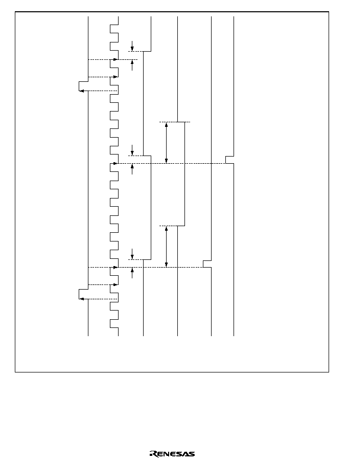
Rev. 1.0, 02/00, page 608 of 1141
DPG
01
tA1
tA2
tB1
tA3
tA1
234567891
0
1
1
0
12
V.FF
A.FF
Clear A
Clear B
Example of setting: DFCR=H'02, DFCRB=H'08, HSLP=H'21, DFG falling edge
DFG
Figure 26.23 Example of Timing Waveform of HSW (for 12 DFG Pulses)
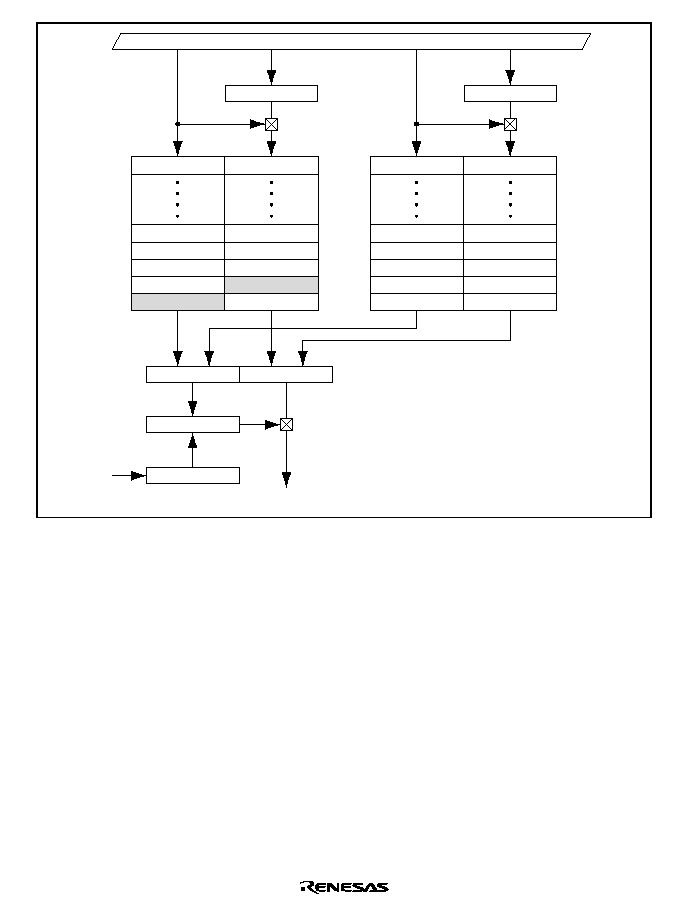
Rev. 1.0, 02/00, page 609 of 1141
Output pattern data
s/4
W
W
FTPRB
FIFO2
tB0
PB9
tB5
PB4
tB4
PB3
tB3
PB2
tB2
PB1
tB1
PB0
W
W
FPDRA
Output select buffer Output data buffer
Comparator
FTPRA
FIFO1
tA0
PA9
tA5
PA4
tA4
PA3
tA3
PA2
tA2
PA1
tA1
PA0
Internal bus
FPDRB
Timer counter
Figure 26.24 Example of Operation of the HSW Timing Generator

Rev. 1.0, 02/00, page 610 of 1141
∑
Example of operation in single mode (20 stages of FIFO used)
1
Set to single mode (LOP = 0)
2
Write the output pattern data (PA0) to FPDRA.
3
Write the output timing (t
A1
) to FTPRA. t
A1
is written in FIFO1 together with PA0. This
initializes the output pattern data to PA0.
4
Repeat the steps in the same way, until PA1, PA2, etc., are set.
5
Write the output pattern data (PB0) to FPDRB.
6
Write the output timing (t
B1
) to FTPRB. t
B1
is written in FIFO2 together with PB0. This
initializes the output pattern data to PB0.
7
Repeat these steps in the same way, until PB1, PB2, etc., are set.
By step 3, the pattern data of PA0 is output.
If t
A1
matches with the timer counter, the pattern data of PA1 is output.
If t
A2
matches with the timer counter, the pattern data of PA2 is output.
.
.
.
After this sequence is repeated and all the pattern data set in FIFO1 is output, the pattern data of
FIFO2 is output. After the pattern data is output, the pointer is decremented by 1. Care is
required, however, because matching of t
A0
is not detected until data is written in FIFO2.
Matching of t
B0
also is not detected until data is written in FIFO1 again.

Rev. 1.0, 02/00, page 611 of 1141
∑
Example of the operation in loop mode mode
1
Set the number of loop stages in HSLP register (e.g. HSLP = H'44)
2
Write the output pattern data (PA0) to FPDRA.
3
Write the output timing (t
A1
) to FTPRA. t
A1
is written in FIFO1 together with PA0. This
initializes the output pattern data to PA0.
4
Repeat the steps in the same way, until PA1, PA2, etc., are set.
5
Write the output pattern data (PB0) to FPDRB.
6
Write the output timing (t
B1
) to FTPRB. t
B1
is written in FIFO2 together with PB0. This
initializes the output pattern data to PB0.
7
Repeat the steps in the same way, until PB1, PB2, etc., are set.
By step 3, the pattern data PA0 is output.
If t
A1
matches the timer counter, the pattern data PA1 is output.
If t
A2
matches the timer counter, the pattern data PA2 is output.
.
.
.
If t
A4
matches the timer counter, the pattern data PA4 is output.
If t
A5
matches the timer counter, the pattern data PB0 is output.
If t
B1
matches the timer counter, the pattern data PB1 is output.
.
.
.
If t
B4
matches the timer counter, the pattern data PB4 is output.
If t
B5
matches the timer counter, the pattern data PA0 is output.
.
.
.

Rev. 1.0, 02/00, page 612 of 1141
26.4.7
Interrupts
The HSW timing generator generates interrupts under the following conditions.
1
IRRHSW1 occurs when pattern data is written (OVWA, OVWB = 1) while FIFO is full
(FULL).
2
IRRHSW1 occurs when matching is detected while the STRIG bit of FIFO is 1.
3
IRRHSW1 occurs when the values of the 16-bit timer counter and 16-bit timing pattern
register match.
4
IRRHSW2 occurs when the 16-bit timer counter is cleared.
5
IRRHSW2 occurs when a VD signal (capture signal of the timer capture register) is received in
PB mode.
Condition 2 or 3, as well as 4 or 5, are selected by ISEL1 and ISEL2.
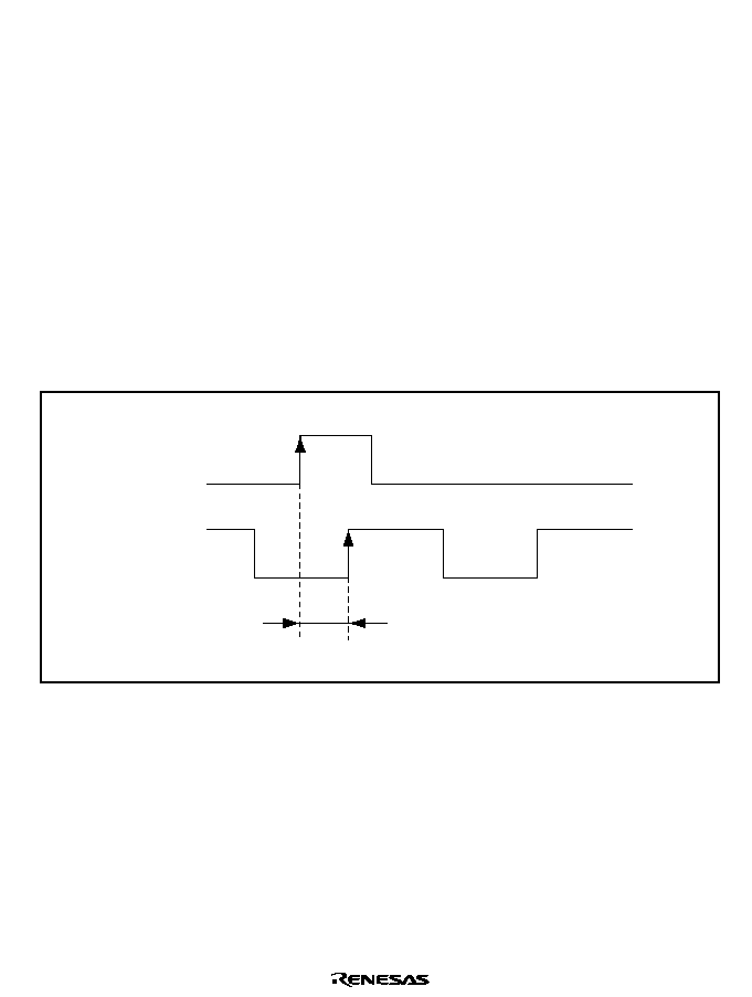
Rev. 1.0, 02/00, page 613 of 1141
26.4.8
Cautions
∑
When both the 5-bit DFG counter and 16-bit timer counter are operating, the latter is not
cleared if input of DPG and DFG signals is stopped. This leads to free-running of the 16-bit
timer counter, and periodical detection of matching by the 16-bit timer counter. In such a case,
the period of the output from the HSW timing generator is independent from DPG or DFG.
∑
Specify the mode setting bit (LOP) of the HSW mode register 2 (HSM2) immediately before
writing the FIFO data.
∑
Input the rising edge of DPG and DFG count edge at different timings. If they are input at the
same timing, counting up DFG and clearing the 5-bit DFG counter occur simultaneously. In
this case, the latter will take precedence. This leads to the DFG counter lag by 1. Figure 26.25
shows the input timing of DPG and DFG.
∑
If stop of the drum system is required when FIFO output is being used in the 20-stage output
mode, modify the SOFG bit of HSM2 register from 0 to 1, then again to 0 by software, and be
sure to initialize the FIFO output stage to the FIFO1 side. Also clear and rewrite the data of
FIFO1 and FIFO2.
DPG
I ± Tp ∑ FG | >
(1 state)
Tp ∑ FG
DFG
Note: When the 5-bit DFG counter increments count at the rising edge of DFG
Figure 26.25 Input Timing of DPG and DFG
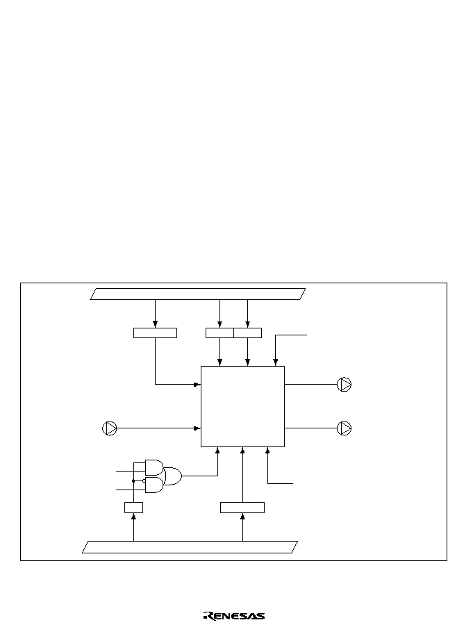
Rev. 1.0, 02/00, page 614 of 1141
26.5
High-Speed Switching Circuit for Four-Head Special Playback
26.5.1
Overview
This high-speed switching circuit generates a color rotary signal (C.Rotary) and head-amplifier
switching signal (H.Amp SW) for use in four-head special playback.
A pre-amplifier output comparison result signal is input from the COMP pin. The signal output to
the C.Rotary pin is a chroma signal processing control signal. The signal output at the H.Amp SW
pin is a pre-amplifier output select signal. To reduce the width of noise bars, the C.Rotary and
H.Amp SW signals are synchronized to the horizontal sync signal (OSCH). OSCH is made by
adding supplemented H, which has been separated from Csync signal in the sync signal detector
circuit. For more details of OSCH, see section 26.15, Sync Signal Detector.
If the VCR system does not require this circuit, C.Rotary, H.Amp SW, and COMP pins can be
used as the I/O port.
26.5.2
Block Diagram
Figure 26.26 shows the block diagram of this circuit.
W
W
Synchronization
control
CHCR
W
CHCR
RTP0
H.Amp SW
C.Rotary
OSCH
(Synchronization)
COMP
NarrowFF
VideoFF
W
CHCR
Internal bus
Internal bus
HAH
CRH
W
CHCR
SIG3 to 0
HSWPOL
V/N
Decoding circuit
Figure 26.26 High-Speed Switching Circuit for Four-Head Special Playback

Rev. 1.0, 02/00, page 615 of 1141
26.5.3
Pin Configuration
Table 26.7 summarizes the pin configuration of the high-speed switching circuit for four-head
special playback. If this circuit is not used, the pins can be used as I/O port. See section 26.2,
Servo Port.
Table 26.7
Pin Configuration
Name
Abbrev.
I/O
Function
Compare input pin
COMP
Input
Input of pre-amplifier output result signal
Color rotary signal output pin
C.Rotary
Output
Output of chroma processing control
signal
Head amplifier switch pin
H.Amp SW
Output
Output of pre-amplifier output select
signal
26.5.4
Register Description
Register Configuration
Table 26.8 shows the register configuration of the high-speed switching circuit for four-head
special playback.
Table 26.8
Register Configuration
Name
Abbrev.
R/W
Size
Initial Value
Address
Special playback control
register
CHCR
W
Byte
H'00
H'D06E

Rev. 1.0, 02/00, page 616 of 1141
Special Playback Control Register (CHCR)
0
0
1
0
W
2
0
W
3
0
4
0
W
0
W
5
6
0
7
HAH
SIG3
SIG2
SIG1
SIG0
0
W
V/N
W
W
W
HSWPOL
CRH
Bit :
Initial value :
R/W :
CHCR is an 8-bit write-only register. It cannot be read. It is initialized to H'00 by a reset, or in
standby or module stop mode.
Bits 7
HSW Signal Select Bit (V/N): Selects the HSW signal to be used at special playback.
Bit 7
V/N
Description
0
Video FF signal output
(Initial value)
1
Narrow FF signal output
Bit 6
COMP Polarity Select Bit (HSWPOL): Selects the polarity of the COMP signal.
Bit 6
HSWPOL
Description
0
Positive
(Initial value)
1
Negative
Bit 5
C.Rotary Synchronization Control Bit (CRH): Synchronizes C.Rotary signal with the
OSCH signal.
Bit 5
CRH
Description
0
Synchronous
(Initial value)
1
Asynchronous

Rev. 1.0, 02/00, page 617 of 1141
Bit 4
H.AmpSW Synchronization Control Bit (HAH): Synchronizes H.AmpSW signal with
the OSCH signal.
Bit 4
HAH
Description
0
Synchronous
(Initial value)
1
Asynchronous
Bits 3 to 0
Signal Control (SIG3 to SIG0): These bits, combined with the state of the COMP
input pin, control the outputs at the C.Rotary and H.AmpSW pins.
Bit 3
Bit 2
Bit 1
Bit 0
Output pins
SIG3
SIG2
SIG1
SIG0
C.Rotary
H.Amp SW
0
*
*
L
L
(Initial value)
0
HSW
L
0
1
HSW
H
0
L
HSW
0
1
1
1
H
+6:
0
HSW EX-OR
COMP
COMP
0
1
HSW EX-NOR
COMP
COMP
0
HSW E-OR RTP0
RTP0
1
1
1
*
HSW EX-NOR
RTP0
RTP0
Note:
*
Don't care.

Rev. 1.0, 02/00, page 618 of 1141
26.6
Drum Speed Error Detector
26.6.1
Overview
Drum speed error control holds the drum at a constant revolution speed, by measuring the period
of the DFG signal. A digital counter detects the speed error against a preset value. The speed
error data is processed and added to phase error data in a digital filter. This filter controls a pulse-
width modulated (PWM) output, which controls the revolution speed and phase of the drum.
The DFG input signal is reshaped into a square wave by a reshaping circuit, and sent to the speed
error detector as the DFG signal.
The speed error detector uses the system clock to measure the period of the DFG signal, and
detects the error against a preset data value. The preset data is the value that results from
measuring the DFG signal period with the clock signal when the drum motor is running at the
correct speed.
The error detector operates by latching a counter value when it detects an edge of the DFG signal.
The latched count provides 16 bits of speed error data for the digital filter to operate on. The
digital filter processes and adds the speed error data to phase error data from the drum phase
control system, then sends the result to the PWM as drum error data.
26.6.2
Block Diagram
Figure 26.27 shows a block diagram of the drum speed error detector.
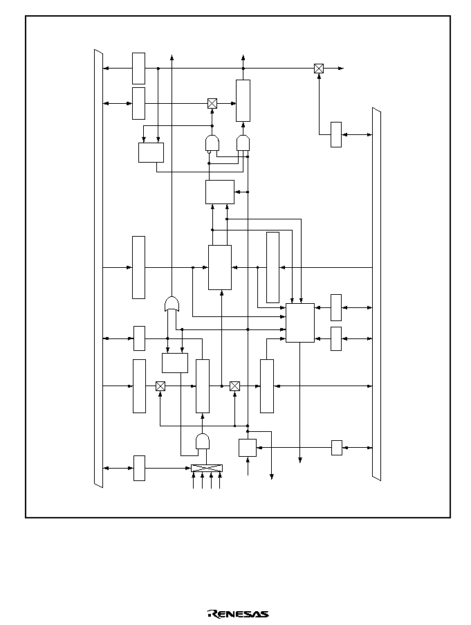
Rev. 1.0, 02/00, page 619 of 1141
W
W
R
UDF
OVF
Lock 2 up
Clear
Latch
Preset
DFVCR
DFRLOR
DFVCR
DFPR
DFVCR
DFVCR
DFVCR
DFUCR
FGCR
DFER
DFRVCR
Error data
(16 bits)
To DFU
ADDFGN
NCDFG
DFRUDR
Internal bus
W
R/W
Internal bus
R/W
W
R/W
R/W
R/W
R/W
(R)/W
Lock 1 up
S
R
F/F
Q
S
R
F/F
DFRCS1,0
DF-R/UNR
Lock counter
(2 bits)
Q
S
R
F/F
Q
Lock range
detector
Lock range data 1 (16bit)
DPCNT
Error data
limiter
control circuit
DFEFON
DFESS
DRF
Edge
detector
,
Error data (16 bits)
Counter (16 bits)
DFOVF
IRRDRM2
IRRDRM1
To DROCKON
DFU
Preset data
(16 bits)
Lock range data 2
(16 bits)
DFCS1,0
s
s/2
s/4
s/8
Figure 26.27 Block Diagram of the Drum Speed Error Detector

Rev. 1.0, 02/00, page 620 of 1141
26.6.3
Register Configuration
Table 26.9 shows the register configuration of the drum speed error detector.
Table 26.9
Register Configuration
Name
Abbrev.
R/W
Size
Initial Value
Address
Specified DFG speed
preset data register
DFPR
W
Word
H'0000
H'D030
DFG speed error data
register
DFER
R/W
Word
H'0000
H'D032
DFG lock upper data
register
DFRUDR
W
Word
H'7FFF
H'D034
DFG lock lower data
register
DFRLDR
W
Word
H'8000
H'D036
Drum speed error
detection control register
DFVCR
R/W
Byte
H'00
H'D038

Rev. 1.0, 02/00, page 621 of 1141
26.6.4
Register Description
Specified DFG Speed Preset Data Register (DFPR)
8
0
9
0
W
10
0
W
11
0
12
0
W
0
W
13
14
0
15
DFPR12
DFPR11
DFPR10
DFPR9
DFPR8
0
W
DFPR15
W
W
W
DFPR14
DFPR13
Bit :
Initial value :
R/W :
0
0
1
0
W
2
0
W
3
0
4
0
W
0
W
5
6
0
7
DFPR4
DFPR3
DFPR2
DFPR1
DFPR0
0
W
DFPR7
W
W
W
DFPR6
DFPR5
Bit :
Initial value :
R/W :
The DFG speed preset data is set in DFPR. When data is written, the 16-bit preset data is sent to
the preset circuit. The preset data can be calculated from the following equation by using H'8000*
as the reference value.
s/n
Specified DFG speed preset data = H'8000
-
(
-
2)
DFG frequency
s:
Servo clock frequency (fosc/2) in Hz
DFG frequency: In Hz
Constant 2 is the presetting interval (see Figure 26.28).
s/n
Clock source of the selected counter
DFPR is a 16-bit write-only register. Only a word access is valid. If a byte access is attempted,
correct operation is not guaranteed. DFPR cannot be read. If a read is attempted, an
undetermined value is read. DFPR is initialized to H'0000 by a reset, and in standby mode and
module stop mode.
Note: The preset data value is calculated so that the counter will reach H'8000 when the error is
zero. When the counter value is latched as error data in the DFG speed error data register
(DFER), however, it is converted to a value referenced to H'0000.

Rev. 1.0, 02/00, page 622 of 1141
DFG Speed Error Data Register (DFER)
8
0
9
0
R*/W
10
0
R*/W
11
0
12
0
R*/W
0
R*/W
13
14
0
15
DFER12
DFER11
DFER10
DFER9
DFER8
0
R*/W
DFER15
R*/W
R*/W
R*/W
DFER14
DFER13
Bit :
Initial value :
R/W :
Note: Note that only detected error data can be read.
0
0
1
0
R*/W
2
0
R*/W
3
0
4
0
R*/W
0
R*/W
5
6
0
7
DFER4
DFER3
DFER2
DFER1
DFER0
0
R*/W
DFER7
R*/W
R*/W
R*/W
DFER6
DFER5
Bit :
Initial value :
R/W :
DFER is a 16-bit read/write register that stores 16-bit DFG speed error data. When the drum
motor speed is correct, the data latched in DFER is H'0000. Negative data will be latched if the
speed is faster than the specified speed, and positive data if the speed is slower than the specified
speed. The DFER value is sent to the digital filter either automatically or by software.
Only a word access is valid. If a byte access is attempted, correct operation is not guaranteed.
DFER is initialized to H'0000 by a reset, and in standby mode and module stop mode.
Refer to the note Specified DFG Speed Preset Data Register (DFPR) in 26.6.4 Register
Description.
DFG Lock Upper Data Register (DFRUDR)
8
1
9
1
W
10
1
W
11
1
12
1
W
1
W
13
14
1
15
DFRUDR12 DFRUDR11 DFRUDR10 DFRUDR9 DFRUDR8
0
W
DFRUDR15
W
W
W
DFRUDR14 DFRUDR13
Bit :
Initial value :
R/W :
0
1
1
1
W
2
1
W
3
1
4
1
W
1
W
5
6
1
7
DFRUDR4 DFRUDR3 DFRUDR2 DFRUDR1 DFRUDR0
1
W
DFRUDR7
W
W
W
DFRUDR6 DFRUDR5
Bit :
Initial value :
R/W :
DFRUDR is a 16-bit write-only register used to set the lock range on the UPPER side when drum
speed lock is detected, and to set the limit value on the UPPER side when limiter function is in
use. Set a signed data to DFRUDR (bit 15 is a sign-setting bit).
When lock is being detected, if the drum speed is detected within the lock range, the lock counter
which has been set by DFRCS 1 and 0 bits of DFVCR register decrements the count. If the set
value of DFRCS 1 and 0 matches the number of times of occurrence of locking, the computation
of the digital filter in the drum phase system can be controlled automatically. Also, if the DFG
speed error data exceeds the DFRUDR value within the limiter function is in use, the DFRUDR
value can be used as the data for computation by the digital filter.
Only a word access is valid. If a byte access is attempted, correct operation is not guaranteed. No
read is valid. If a read is attempted, an undetermined value is read out. It is initialized to H'7FFF
by a reset, or in stand-by or module-stop mode.

Rev. 1.0, 02/00, page 623 of 1141
DFG Lock LOWER Data Register (DFRLDR)
8
0
9
0
W
10
0
W
11
0
12
0
W
0
W
13
14
0
15
DFRLDR12 DFRLDR11 DFRLDR10 DFRLDR9 DFRLDR8
1
W
DFRLDR15
W
W
W
DFRLDR14 DFRLDR13
Bit :
Initial value :
R/W :
0
0
1
0
W
2
0
W
3
0
4
0
W
0
W
5
6
0
7
DFRLDR4 DFRLDR3 DFRLDR2 DFRLDR1 DFRLDR0
0
W
DFRLDR7
W
W
W
DFRLDR6 DFRLDR5
Bit :
Initial value :
R/W :
DFRLDR is a 16-bit write-only register used to set the lock range on the LOWER side when drum
speed lock is detected, and to set the limit value on LOWER side when limiter function is in use.
Set a signed data to DFRLDR (bit 15 is a sign-setting bit).
When lock is being detected, if the drum speed is detected within the lock range, the lock counter
which has been set by DFRCS 1 and 0 bits of DFVCR register decrements the count. If the set
value of DFRCS 1 and 0 matches the number of times of occurrence of locking, the computation
of the digital filter in the drum phase system can be controlled automatically. Also, if the DFG
speed error data is under the DFRLDR value when the limiter function is in use, the DFRLDR
value can be used as the data for computation by the digital filter.
Only a word access is valid. If a byte access is attempted, correct operation is not guaranteed. No
read is valid. If a read is attempted, an undetermined value is read out. It is initialized to H'8000
by a reset, or in stand-by or module-stop mode.
Drum Speed Error Detection Control Register (DFVCR)
0
0
1
0
(R)
*2
/W
2
0
R/W
3
0
4
0
R/W
0
R/(W)
*1
5
6
0
7
DFRFON DF-R/UNR
DPCNT
DFRCS1
DFRCS0
0
R/W
DFCS1
(R)
*2
/W
R
R/W
DFCS0
DFOVF
Notes:
Bit :
Initial value :
R/W :
1. Only 0 can be written.
2. If read-accessed, the counter value is read out.
DFVCR is an 8-bit read/write register that controls the operation of drum speed error detection.
Bit 3 accepts only read, and bit 5 accepts only read and 0 write. It is initialized to H'00 by a reset,
or in stand-by or module-stop mode.

Rev. 1.0, 02/00, page 624 of 1141
Bits 7 and 6
Clock Source Selection Bits (DFCS1, DFCS0): DFCS1 and DFCS0 select the
clock to be supplied to the counter. (
s = fosc/2)
Bit 7
Bit 6
DFCS1
DFCS0
Description
0
s
(Initial value)
0
1
s/2
0
s/4
1
1
s/8
Bit 5
Counter Overflow Flag (DFOVF): DFOVF flag indicates the overflow of the 16-bit
timer counter. It is cleared by writing 0. Write 0 after reading 1. Setting has the highest priority
in this flag. If a flag set and 0 write occurs simultaneously, the latter is invalid.
Bit 5
DFOVF
Description
0
Normal state.
(Initial value)
1
Indicates that overflow has occurred in the counter.
Bit 4
Error Data Limit Function Selection Bit (DFRFON): Enables the error data limit
function. (Limit values are the values set in the lock range data registers (DFRUDR and
DFRLDR)).
Bit 4
DFRFON
Description
0
Disables limit function.
(Initial value)
1
Enables limit function.
Bit 3
Drum Lock Flag (DF-R/UNR): Sets a flag if an underflow occurred in the drum lock
counter.
Bit 3
DF-R/UNR
Description
0
Indicates that the drum speed system is not locked.
(Initial value)
1
Indicates that the drum speed system is locked.

Rev. 1.0, 02/00, page 625 of 1141
Bit 2
Drum Phase System Filter Computation Automatic Start Bit (DPCNT): Enables the
filter computation of the phase system if an underflow occurred in the drum lock counter.
Bit 2
DPCNT
Description
0
Disables the filter computation by detection of the drum lock.
(Initial value)
1
Enables the filter computation of the phase system when drum lock is
detected.
Bits 1 and 0
Drum Lock Counter Setting Bits (DFRCS1, DFRCS0): Sets the number of times
to detect drum locks (which means the number of times DFG is detected in the range set by the
lock range data register). The drum lock flag is set when the specified number of drum locks is
detected. If the NCDFG signal is detected outside the lock range after data is written in DFRCS1
and DFRCS0, the data will be stored in the lock counter.
Note:
If DFRCS1 or DFRCS0 is read-accessed, the counter value is read out. If bit 3 (drum lock
flag) is 1 and the drum lock counter's value is 3, it indicates that the drum speed system is
locked. The drum lock counter stops until lock is released after underflow.
Bit 1
Bit 0
DFRCS1
DFRCS0
Description
0
Underflow occurs after lock was detected once.
(Initial value)
0
1
Underflow occurs after lock was detected twice.
0
Underflow occurs after lock was detected three times.
1
1
Underflow occurs after lock was detected four times.

Rev. 1.0, 02/00, page 626 of 1141
26.6.5
Operation
The drum speed error detector detects the speed error based on the reference value set in the DFG
specified speed preset register (DFPR). The reference value set in DFPR is preset in the counter
by NCDFG signal, and the counter decrements the count by the selected clock. The timing of the
counter presetting and the error data latching can be selected between the rising or falling edge of
NCDFG signal. See section 26.14.4, FG Control Register (FGCR) in 26.14.4 DFG Noise
Removal Circuit. The error data detected is sent to the digital filter circuit. The error data is
signed binaries. The data takes a positive number (+) if the speed is slower than the specified
speed, a negative number (-) if the speed is faster, or 0 if it had no error (revolving at the specified
speed). Figure 26.28 shows an example of operation to detect the drum speed.
∑
Setting the error data limit
A limit can be set to the error data sent to the digital filter circuit using the DFG lock data
register (DFRUDR, DFRLDR). Set the upper limit of the error data in DFRUDR and the
lower limit in DFRLDR, and write 1 in DFRFON bit. If the error data is outside the limit
range, the DFRLDR value is sent to the digital filter circuit if a negative number is latched, or
the DFRUDR value if a positive number is latched, as a limit value. Be sure to turn off the
limit setting (DFRFON = 0) when you set the limit value. If the limit was set with the limit
setting on (DFRFON = 1), result of computation is not assured.
∑
Lock detection
If an error data is detected within the lock range set in the lock data register, the drum lock flag
(DF-R/UNR) is set by the number of the times of locking set by DFRCS1 and DFRCS0 bits,
and an interrupt is requested (IRRDRM2) at the same time. The number of the occurrence of
locking (once to 4 times) before the flag is set can be specified. Use DFRCS1 and DFRCS0
bits for this purpose. The on/off status of the phase system digital filter computation can be
controlled automatically by the status of lock detection when bit 5 (DPHA bit) of the drum
system digital filter control register (DFIC) is 0 (phased system digital filter computation off)
and DPCNT bit is 1.
∑
Drum system speed error detection counter
The drum system speed error detection counter stops the counter and sets the overflow flag
(DFOVF) when an overflow occurs. At the same time, it generates an interrupt request
(IRRDRM1). To clear DFOVF, write 0 after reading 1. If setting the flag and writing 0 take
place simultaneously, the latter is invalid.
Rev. 1.0, 02/00, page 627 of 1141
∑
Interrupt request
IRRDRM1 is generated by the NCDFG signal latch and the overflow of the error detection
counter. IRRDRM2 is generated by detection of lock (after the detection of the specified
number of times of locking).
≠value+value
Specified speed value
Latch data 0
(no error)
Preset value
Preset period
(2 counts)
Counter
NCDFG signal
Error data latch
signal (DFG
)
Preset data
load signal
Figure 26.28 Example of the Drum Speed Error Detection
(When the Rising Edge of DFG is Selected)

Rev. 1.0, 02/00, page 628 of 1141
26.6.6
f
H
Correction in Trick Play Mode
In trick play mode, the tape speed relative to the video head changes. This change alters the
horizontal sync signal (f
H
), causing skew. To correct the skew, the drum motor speed must be
shifted to a different speed in each trick play mode, so as to obtain the normal horizontal sync
frequency. To shift the drum motor speed, software should modify the value written in the
specified DFG speed preset data register in the speed error detector.
This f
H
correction can be expressed in terms of the basic frequency f
F
of the drum as follows.
N
0
f
F
=
◊
f
F0
N
0
+
H
(1
-
n)
Legend:
n:
Speed multiplier (FWD = positive, REV = negative)
H
:
H alignment (1.5H in standard mode, 0.75H in 2x mode, and 0.5H in 3x mode for VHS
and
systems; 1H for an 8-mm VCR)
N
0
:
Standard H numbers within field
f
F0
:
Field frequency
NTSC: N
0
= 262.5, f
F0
= 59.94
PAL:
N
0
= 312.5, f
F0
= 50.00

Rev. 1.0, 02/00, page 629 of 1141
26.7
Drum Phase Error Detector
26.7.1
Overview
The drum phase control system must start after the drum motor has reached the specified
revolution speed by the speed control system. Drum phase control works as follows in record and
playback mode.
∑
Record Mode: Phase is controlled so that the vertical blanking intervals of the video signal to
be recorded will line up along the bottom edge of the tape.
∑
Playback Mode: Phase is controlled so as to trace the recorded tracks accurately.
A counter detects the phase error against a preset value. The phase error data is processed and
added to speed error data in a digital filter. This filter controls a pulse-width modulated
(PWM) output, which controls the revolution phase and speed of the drum.
The DPG signal from the drum motor is reshaped into a square wave by a reshaping circuit,
and sent to the phase error detector.
The phase error detector compares the phase of the DPG pulse (tach pulse), which contains
video head phase information, with a reference signal. In the actual circuit, the comparison is
carried out by comparing the head-switching (HSW) signal, which is delayed by a counter that
is reset by DPG, with a reference signal value. The reference signal is the REF30 signal,
which differs between record and playback as follows:
∑
Record: Vsync signal extracted from the video signal to be recorded (frame rate signal,
actually 1/2 Vsync).
∑
Playback: 30 Hz or 25 Hz signal divided from the system clock.
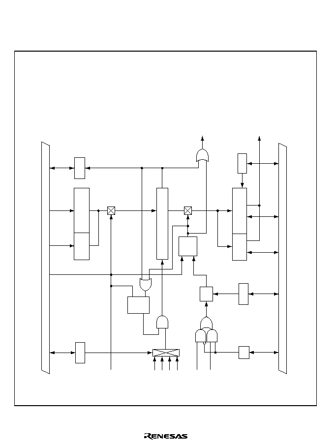
Rev. 1.0, 02/00, page 630 of 1141
26.7.2
Block Diagram
Figure 26.29 shows a block diagram of the drum phase error detector.
R/W
R/W
R/W
R/W
R/W
R/W
REF30P
HSW
(Video FF)
NHSW
(Narrow FF)
DPGCR
DPGCR
DPGCR
DFUCR
DPGCR
DPPR1
DPPR2
R/(W)
S
R
F/F
Q
W
W
Internal bus
Internal bus
OVF
LSB
MSB
DPER1
DPER2
LSB
MSB
DPOVF
DFEPS
HSWES
N/V
Latch
Preset
Error data (20 bits)
To DFU
Edge
detector
Sequence
controller
,
Error data
(16 bits)
Error data
(4 bits)
Preset data
(16 bits)
Preset data
(4 bits)
Counter (20 bits)
IRRDRM3
DPCS1,0
s
s/2
s/4
s/8
s = fosc/2
Figure 26.29 Block Diagram of Drum Phase Error Detector

Rev. 1.0, 02/00, page 631 of 1141
26.7.3
Register Configuration
Table 26.10 shows the register configuration of the drum phase error detector.
Table 26.10 Register Configuration
Name
Abbrev.
R/W
Size
Initial Value
Address
Specified drum phase
preset data register 1
DPPR1
W
Byte
H'F0
H'D03C
Specified drum phase
preset data register 2
DPPR2
W
Word
H'0000
H'D03A
Drum phase error data
register 1
DPER1
R/W
Byte
H'F0
H'D03D
Drum phase error data
register 2
DPER2
R/W
Word
H'0000
H'D03E
Drum phase error
detection control register
DPGCR
R/W
Byte
H'07
H'D039

Rev. 1.0, 02/00, page 632 of 1141
26.7.4
Register Description
Drum Phase Preset Data Registers (DPPR1, DPPR2)
DPPR1
0
0
1
0
W
2
0
W
3
DPPR16
DPPR17
DPPR18
DPPR19
0
4
1
5
1
6
1
7
--
--
--
--
--
--
--
--
W
W
1
Bit :
Initial value :
R/W :
DPPR2
8
0
9
0
W
10
0
W
11
DPPR8
DPPR9
DPPR10
DPPR11
0
12
0
13
0
14
0
15
DPPR12
DPPR13
DPPR14
DPPR15
W
W
W
W
W
W
0
Bit :
Initial value :
R/W :
0
0
1
0
W
2
0
W
3
DPPR0
DPPR1
DPPR2
DPPR3
0
4
0
5
0
6
0
7
DPPR4
DPPR5
DPPR6
DPPR7
W
W
W
W
W
W
0
Bit :
Initial value :
R/W :
The 20-bit preset data that defines the specified drum phase is set in DPPR1 and DPPR2. The 20
bits are weighted as follows: bit 3 of DPPR1 is the MSB, and bit 0 of DPPR2 is the LSB. When
data is written to DPPR2, the 20-bit preset data, including DPPR1, is loaded into the preset circuit.
Write to DPPR1 first, and DPPR2 next. The preset data can be calculated from the following
equation by using H'8000* as the reference value.
Target phase difference = (reference signal frequency/2)
-
6.5H
Drum phase preset data = H'80000 - (
s/n
◊
target phase difference)
s:
Servo clock frequency in Hz (fosc/2)
s/n:
Clock source of selected counter
Only a word access is valid. If a byte access is attempted, correct operation is not guaranteed. No
read is valid. If a read is attempted, an undetermined value is read out. DPPR1 and DPPR2 are
initialized to H'F0 and H'0000 by a reset, and in standby mode.
Note: The preset data value is calculated so that the counter will reach H'80000 when the error
value is zero. When the counter value is latched as error data in the drum phase error data
registers (DPER1 and DPER2), however, it is converted to a value referenced to H'00000.
Rev. 1.0, 02/00, page 633 of 1141
Drum Phase Error Data Registers (DPER1, DPER2)
DPER1
0
0
1
0
R*/W
2
0
R*/W
3
DPER16
DPER17
DPER18
DPER19
0
4
1
5
1
6
1
7
--
--
--
--
--
--
--
--
R*/W
R*/W
1
Bit :
Initial value :
R/W :
DPER2
8
0
9
0
R*/W
10
0
R*/W
11
DPER8
DPER9
DPER10
DPER11
0
12
0
13
0
14
0
15
DPER12
DPER13
DPER14
DPER15
R*/W
R*/W
R*/W
R*/W
R*/W
R*/W
0
Bit :
Initial value :
R/W :
Note: * Note that only detected error data can be read.
0
0
1
0
R*/W
2
0
R*/W
3
DPER0
DPER1
DPER2
DPER3
0
4
0
5
0
6
0
7
DPER4
DPER5
DPER6
DPER7
R*/W
R*/W
R*/W
R*/W
R*/W
R*/W
0
Bit :
Initial value :
R/W :
DPER1 and DPER2 constitute a 20-bit drum phase error data register. The 20 bits are weighted as
follows: bit 3 of DPER1 is the MSB, and bit 0 of DPER2 is the LSB. When the rotational phase is
correct, the data H'00000 is latched. Negative data will be latched if the drum leads the correct
phase, and positive data if it lags. Values in DPER1 and DPER 2 are transferred to the digital
filter circuit.
DPER1 and DPER are 20-bit read/write registers. When writing data to DPER 1 and DPER2,
write to DPER1 first, and then write to DPER2. Only a word access is valid. If a byte access is
attempted, correct operation is not guaranteed. DPER1 and DPER2 are initialized to H'F0 and
H'0000 by a reset, and in standby mode.
See the note on the drum phase preset data registers (DPPR1 and DPPR2).

Rev. 1.0, 02/00, page 634 of 1141
Drum Phase Error Detection Control Register (DPGCR)
0
1
1
2
--
--
--
--
--
--
1
3
0
4
0
R/W
R/W
5
0
6
0
7
R/(W)*
DPOVF
R/W
DPCS0
0
R/W
DPCS1
N/V
HSWES
1
Bit :
Initial value :
R/W :
Note: Only 0 can be written.
DPGCR is an 8-bit read/write register that controls the operation of drum phase error detection.
Bits 2-0 are reserved, bit 5 accepts only read and 0 write.
It is initialized to H'07 by a reset or in stand-by mode.
Bits 7 and 6
Clock Source Selection Bit (DPCS1, DPCS0): These bits select the clock
supplied to the counter. (
s = fosc/2)
Bit 7
Bit 6
DPCS1
DPCS0
Description
0
s
(Initial value)
0
1
s/2
0
s/4
1
1
s/8
Bit 5
Counter Overflow Flag (DPOVF): DPOVF flag indicates the overflow of the 20-bit
counter. It is cleared by writing 0. Write 0 after reading 1. Setting has the highest priority in this
flag. If a flag set and 0 write occurs simultaneously, the latter is invalid.
Bit 5
DPOVF
Description
0
Normal state
(Initial value)
1
Indicates that a overflow has occurred in the counter
Bit 4
Error Data Latch Signal Selection Bit (N/V): Selects the latch signal of error data.
Bit 4
N/V
Description
0
HSW (VideoFF) signal
(Initial value)
1
NHSW (NarrowFF) signal

Rev. 1.0, 02/00, page 635 of 1141
Bit 3
Edge Selection Bit (HSWES): Selects the edge of the error data latch signal (HSW or
NHSW).
Bit 3
HSWES
Description
0
Latches at the rising edge
(Initial value)
1
Latches at the falling edge
Bits 2 to 0
Reserved: Cannot be modified and are always read as 1.
26.7.5
Operation
The drum phase error detector detects the phase error based on the reference value set in the drum
specified phase preset data registers 1 and 2 (DPPR1 and DPPR2). The reference values set in
DPPR1 and DPPR2 are preset in the counter by REF30P signal, and counted up by the clock
selected. The latch of the error data can be selected between the rising or falling edge of HSW
(NHSW). The error data detected in the error data automatic transmission mode (DFEPS bit of
DFUCR = 0) is sent to the digital filter circuits automatically. In soft transmission mode (DFEPS
bit of DFUCR = 1), the data written in DPER1 and DPER2 is sent to the digital filter circuit. The
error data is signed binary. It takes a positive number (+) if the phase is behind the specified
phase, a negative number (-) if in advance of the specified phase, or 0 if it had no phase error
(revolving at the specified phase). Figures 26.30 and 26.31 show examples of operation to detect
a drum phase error.
Drum Phase Error Detection Counter: The drum phase error detection counter stops counting
when an overflow or latch occurs. At the same time, it generates an interrupt request
(IRRDRM3), and sets the overflow flag (DPOVF) if an overflow occurred. To clear DPOVF,
write 0 after reading 1. If setting the flag and writing 0 take place simultaneously, the latter is
invalid.
Interrupt Request: IRRDRM3 is generated by the HSW (NHSW) signal latch and the overflow
of the error detection counter.
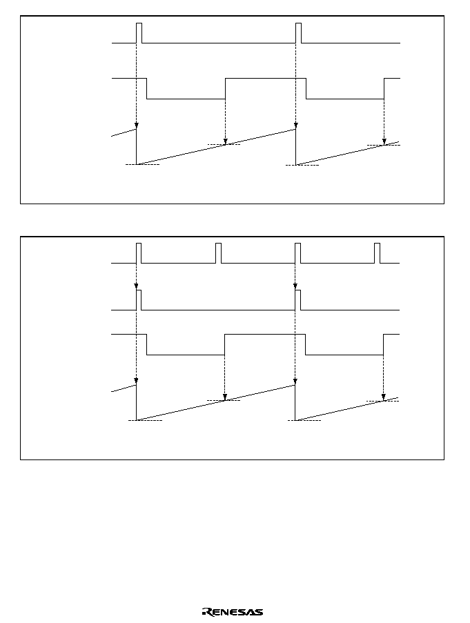
Rev. 1.0, 02/00, page 636 of 1141
Latch
Latch
Preset value
Counter
HSW (NHSW)*
REF30P
Preset value
Preset
Note: Edge selectable
Preset
Figure 26.30 Drum Phase Control in Playback Mode (HSW Rising Edge Selected)
Latch
Latch
Preset value
Counter
HSW (NHSW)*
VD
REF30P
Preset value
Preset
Note: Edge selectable
Preset
Reset
Reset
Figure 26.31 Drum Phase Control in Record Mode (HSW Rising Edge Selected)

Rev. 1.0, 02/00, page 637 of 1141
26.7.6
Phase Comparison
The phase comparison circuit measures the difference of time between the reference signal and the
comparing signal with a digital counter. REF30 signal is used for the reference signal, and HSW
signal (VideoFF) or NHSW signal (NarrowFF) from the HSW timing generator is used for the
comparing signal. In record mode, however, the phase of REF30 signal is the same as that of the
vertical sync signal (Vsync) because the reference signal generator (REF30 generator) is reset by
the vertical sync signal (Vsync) in the video signals.
The error detection counter latches data at the rising or falling edge of HSW signal. The digital
filter circuit performs computation using this data as 20-bit phase error data. After processing and
adding the phase error data and the speed error data from the drum speed control system, the
digital filter circuit sends the data as the error data of the drum system to the PWM modulation
circuit.

Rev. 1.0, 02/00, page 638 of 1141
26.8
Capstan Speed Error Detector
26.8.1
Overview
Capstan speed control holds the capstan motor at a constant revolution speed, by measuring the
period of the CFG signal. A digital counter detects the speed error against a preset value. The
speed error data is added to phase error data in a digital filter. This filter controls a pulse-width
modulated (PWM) output, which controls the revolution speed and phase of the capstan motor.
The CFG input signal is downloaded by the comparator circuit, then reshaped into a square wave
by a reshaping circuit, divided by the CFG divider, and sent to the speed error detector as the
DVCFG signal.
The speed error detector uses the system clock to measure the period of the DVCFG signal, and
detects the error against a preset data value. The preset data is the value that results from
measuring the DVCFG signal period with the clock signal when the capstan motor is running at
the correct speed.
The error detector operates by latching a counter value when it detects an edge of the DVCFG
signal. The latched count provides 16 bits of speed error data for the digital filter to operate on.
The digital filter adds the speed error data to phase error data from the capstan phase control
system, then sends the result to the PWM as capstan error data.
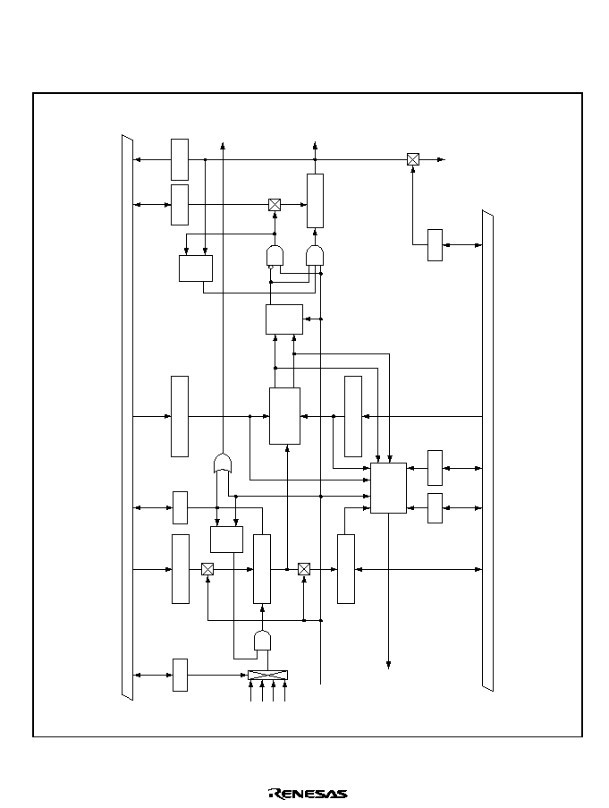
Rev. 1.0, 02/00, page 639 of 1141
26.8.2
Block Diagram
Figure 26.32 shows a block diagram of the capstan speed error detector.
W
W
R
UDF
OVF
Lock 2 up
Clear
Latch
Preset
CFVCR
CFRLDR
CFVCR
CFPR
CFVCR
CFVCR
CFVCR
CFUCR
CFER
CFRVCR
Error data
(16 bits)
To DFU
DVCFG
CFRUDR
Internal bus
R/W
Internal bus
R/W
W
R/W
R/W
R/W
R/W
(R)/W
Lock 1 up
S
R
F/F
Q
S
R
F/F
CFRCS1,0
CF-R/UNR
Lock counter
(2 bits)
Q
S
R
F/F
Q
Lock range
detector
Lock range data (16 bits)
Lock range data (16 bits)
CPCNT
Error data
limiter
control
circuit
CFRFON
CFESS
Error data (16 bits)
Counter (16 bits)
CFOVF
IRRCAP2
IRRCAP1
CROCKON
To DFU
Preset data (16 bits)
CFCS1,0
s
s/2
s/4
s/8
Figure 26.32 Block Diagram of Capstan Speed Error Detector

Rev. 1.0, 02/00, page 640 of 1141
26.8.3
Register Configuration
Table 26.11 shows the register configuration of the capstan speed error detector.
Table 26.11 Register Configuration
Name
Abbrev.
R/W
Size
Initial Value
Address
Specified CFG speed
preset data register
CFPR
W
Word
H'0000
H'D050
CFG speed error data
register
CFER
R/W
Word
H'0000
H'D052
CFG lock upper data
register
CFRUDR
W
Word
H'7FFF
H'D054
CFG lock lower data
register
CFRLDR
W
Word
H'8000
H'D056
Capstan speed error
detection control register
CFVCR
R/W
Byte
H'00
H'D058

Rev. 1.0, 02/00, page 641 of 1141
26.8.4
Register Description
Specified CFG Speed Preset Data Register (CFPR)
8
0
9
0
W
10
0
W
11
0
12
0
W
0
W
13
14
0
15
CFPR12
CFPR11
CFPR10
CFPR9
CFPR8
0
W
CFPR15
W
W
W
CFPR14
CFPR13
Bit :
Initial value :
R/W :
0
0
1
0
W
2
0
W
3
0
4
0
W
0
W
5
6
0
7
CFPR4
CFPR3
CFPR2
CFPR1
CFPR0
0
W
CFPR7
W
W
W
CFPR6
CFPR5
Bit :
Initial value :
R/W :
The 16-bit preset data that defines the specified CFG speed is set in CFPR. When data is written,
the 16-bit preset data is sent to the preset circuit. The preset data can be calculated from the
following equation by using H'8000* as the reference value.
s/n
CFG speed preset data = H'8000
-
(
-
2)
DVCFG frequency
s:
Servo clock frequency in Hz (f
OSC
/2)
DVCFG frequency: In Hz
The constant 2 is the preset interval (see figure 26.33).
s/n:
Clock source of the selected counter
CFPR is a 16-bit write-only register. Only a word acces is valid. If a byte access is attempted,
correct operation is not guaranteed. CFPR is initialized to H'0000 by a reset.
Note: The preset data value is calculated so that the counter will reach H'8000 when the error is
zero. When the counter value is latched as error data in the CFG speed error data register
(CFER), however, it is converted to a value referenced to H'0000.

Rev. 1.0, 02/00, page 642 of 1141
CFG Speed Error Data Register (CFER)
8
0
9
0
R*/W
10
0
R*/W
11
0
12
0
R*/W
0
R*/W
13
14
0
15
CFER12
CFER11
CFER10
CFER9
CFER8
0
R*/W
CFER15
R*/W
R*/W
R*/W
CFER14
CFER13
Bit :
Initial value :
R/W :
Note: Note that only detected error data can be read.
0
0
1
0
R*/W
2
0
R*/W
3
0
4
0
R*/W
0
R*/W
5
6
0
7
CFER4
CFER3
CFER2
CFER1
CFER0
0
R*/W
CFER7
R*/W
R*/W
R*/W
CFER6
CFER5
Bit :
Initial value :
R/W :
CFER is a 16-bit read/write register that stores 16-bit CFG speed error data. When the speed of
the capstan motor is correct, the data latched in CFER is H'0000. Negative data will be latched if
the speed is faster than the specified speed, and positive data if the speed is slower than the
specified speed. The CFER value is sent to the digital filter either automatically or by software.
Only a word access is valid. If a byte access is attempted, correct operation is not guaranteed.
CFER is initialized to H'0000 by a reset, and in module stop mode and standby mode.
See the note on the specified CFG speed preset data register (CFPR) in section 26.8.4.
CFG Lock UPPER Data Register (CFRUDR)
8
1
9
1
W
10
1
W
11
1
12
1
W
1
W
13
14
1
15
CFRUDR12 CFRUDR11 CFRUDR10 CFRUDR9 CFRUDR8
0
W
CFRUDR15
W
W
W
CFRUDR14 CFRUDR13
Bit :
Initial value :
R/W :
0
1
1
1
W
2
1
W
3
1
4
1
W
1
W
5
6
1
7
CFRUDR4 CFRUDR3 CFRUDR2 CFRUDR1 CFRUDR0
1
W
CFRUDR7
W
W
W
CFRUDR6 CFRUDR5
Bit :
Initial value :
R/W :
CFRUDR is a 16-bit write-only register used to set the lock range on the UPPER side when
capstan speed lock is detected, and to set the limit value on the UPPER side when limiter function
is in use.
When lock is being detected, if the capstan speed is detected within the lock range, the lock
counter which has been set by CFRCS1 and CFRCS0 bits of CFVCR register decrements the
count. If the set value of CFRCS1 and CFRCS0 matches the number of times of occurrence of
locking, the computation of the digital filter in the capstan phase system can be controlled
automatically. Also, if the CFG speed error data exceeds the CFRUDR value when the limiter
function is in use, the DFRUDR value can be used as the data for computation by the digital filter.
Only a word access is valid. If a byte access is attempted, correct operation is not guaranteed. A
read is invalid. If a read is attempted, an undetermined value is read out. It is initialized to
H'7FFF by a reset, or in stand-by or module-stop mode.

Rev. 1.0, 02/00, page 643 of 1141
CFG Lock LOWER Data Register (CFRLDR)
8
0
9
0
W
10
0
W
11
0
12
0
W
0
W
13
14
0
15
CFRLDR12 CFRLDR11 CFRLDR10 CFRLDR9 CFRLDR8
1
W
CFRLDR15
W
W
W
CFRLDR14 CFRLDR13
Bit :
Initial value :
R/W :
0
0
1
0
W
2
0
W
3
0
4
0
W
0
W
5
6
0
7
CFRLDR4 CFRLDR3 CFRLDR2 CFRLDR1 CFRLDR0
0
W
CFRLDR7
W
W
W
CFRLDR6 CFRLDR5
Bit :
Initial value :
R/W :
CFRLDR is a 16-bit write-only register used to set the lock range on the LOWER side when
capstan speed lock is detected, and to set the limit value on LOWER side when limiter function is
in use.
When lock is being detected, if the drum speed is detected within the lock range, the lock counter
that has been set by CFRCS 1 and 0 bits of CFVCR register decrements the count. If the set value
of CFRCS 1 and 0 matches the number of times of occurrence of locking, the computation of the
digital filter in the drum phase system can be controlled automatically. Also, if the CFG speed
error data is under the CFRLDR value when the limiter function is in use, the CFRLDR value can
be used as the data for computation by the digital filter.
Only a word access is valid. If a byte access is attempted, correct operation is not guaranteed. No
read is valid. If a read is attempted, an undetermined value is read out. It is initialized to H'8000
by a reset, or in stand-by or module-stop mode.
Capstan Speed Error Detection Control Register (CFVCR)
0
0
1
0
(R)
*2
/W
2
0
R/W
3
0
4
0
R/W
0
R/(W)
*1
5
6
0
7
CFRFON CF-R/UNR CPCNT
CFRCS1
CFRCS0
0
R/W
CFCS1
(R)
*2
/W
R
R/W
CFCS0
CFOVF
Notes:
Bit :
Initial value :
R/W :
1. Only 0 can be written.
2. If read-accessed, the counter value is read out.
CFVCR is an 8-bit read/write register that controls the operation of capstan speed error detection.
Bit 3 accepts only read, and bit 5 accepts only read and 0 write. It is initialized to H'00 by a reset,
or in stand-by or module-stop mode.

Rev. 1.0, 02/00, page 644 of 1141
Bits 7 and 6
Clock Source Selection Bits (CFCS1, CFCS0): CFCS1 and CFCS0 select the
clock to be supplied to the counter. (
s = fosc/2)
Bit 7
Bit 6
CFCS1
CFCS0
Description
0
s
(Initial value)
0
1
s/2
0
s/4
1
1
s/8
Bit 5
Counter Overflow Flag (CFOVF): CFOVF flag indicates overflow of the 16-bit counter.
It is cleared by writing 0. Write 0 after reading 1. Setting has the highest priority in this flag. If a
flag set and 0 write occurs simultaneously, the latter is invalid.
Bit 5
CFOVF
Description
0
Normal state.
(Initial value)
1
Indicates that a overflow has occurred in the counter.
Bit 4
Error Data Limit Function Selection Bit (CFRFON): Enables the error data limit
function. (Limit values are the values set in the lock range data register (CFRUDR, CFRLDR)).
Bit 4
CFRFON
Description
0
Disables limit function.
(Initial value)
1
Enables limit function.
Bit 3
Capstan Lock Flag (CF-R/UNR): Sets a flag if an underflow occurred in the capstan lock
counter.
Bit 3
CF-R/UNR
Description
0
Indicates that the capstan speed system is not locked.
(Initial value)
1
Indicates that the capstan speed system is locked.

Rev. 1.0, 02/00, page 645 of 1141
Bit 2
Capstan Phase System Filter Computation Automatic Start Bit (CPCNT): Enables the
filter computation of the phase system if an underflow occurred in the capstan lock counter.
Bit 2
CPCNT
Description
0
Disables the filter computation by detection of the capstan lock.
(Initial value)
1
Enables the filter computation of the phase system when capstan lock is
detected.
Bits 1 and 0
Capstan Lock Counter Setting Bits (CFRCS1, CFRCS0): Sets the number of
times to detect capstan locks (DVCFG has been detected in the rage set by the lock range data
register). The capstan lock flag is set when the specified number of capstan lock is detected. If the
DVCFG signal is detected outside the lock range after data is written in CFRCS1 and CFRCS0,
the data will be stored in the lock counter.
Note:
If CFRCS1 or CFRCS0 is read-accessed, the counter value is read out. If bit 3 (capstan
lock flag) is 1 and the capstan lock counter's value is 3, it indicates that the capstan speed
system is locked. The capstan lock counter stops until lock is released after underflow.
Bit 1
Bit 0
CFRCS1
CFRCS0
Description
0
Underflow occurs after lock was detected once
(Initial value)
0
1
Underflow occurs after lock was detected twice
0
Underflow occurs after lock was detected three times
1
1
Underflow occurs after lock was detected four times

Rev. 1.0, 02/00, page 646 of 1141
26.8.5
Operation
The capstan speed error detector detects the speed error based on the reference value set in the
CFG specified speed preset register (CFPR). The reference value set in CFPR is preset in the
counter by the DVCFG signal, and the counter decrements the count by the selected clock. The
timing of the counter presetting and the error data latching can be selected between the rising or
falling edge of DVCFG signal. See DVCFG Control Register (CDVC) in section 26.14.3, CFG
Frequency Divider. The error data detected is sent to digital filter circuit. The error data is signed
binaries. The data takes a positive number (+) if the speed is slower than the specified speed, a
negative number (-) if the speed is faster, or 0 if it had no error (revolving at the specified speed).
Figure 26.33 shows an example of operation to detect the capstan speed.
Setting the Error Data Limit: A limit can be set to the error data sent to the digital filter circuit
using the CFG lock data register (CFRUDR, CFRLDR). Set the upper limit of the error data in
CFRUDR and the lower limit in CFRLDR, and write 1 in CFRFON bit. If the error data is outside
the limit range, the CFRLDR value is sent to the digital filter circuit if a negative number is
latched, or the CFRUDR value if a positive number is latched, as a limit value. Be sure to turn off
the limit setting (CFRFON = 0) when you set the limit value. If the limit was set with the limit
setting on (CFRFON = 1), result of computation is not assured.
Lock Detection: If an error data is detected within the lock range set in the lock data register, the
capstan lock flag (CF-R/UNR) is set by the number of the times of locking set by CFRCS1 and
CFRCS0 bits, and an interrupt is requested (IRRCAP2) at the same time. The number of the
occurrence of locking (once to 4 times) before the flag is set can be specified. Use CFRCS1 and
CFRCS0 bits for this purpose. The on/off state of the phase system digital filter computation can
be controlled automatically by the status of lock detection when bit 5 (CPHA bit) of the capstan
system digital filter control register (CFIC) is 0 (phased system digital filter computation off) and
DPCNT bit is 1.
Capstan System Speed Error Detection Counter: The capstan system speed error detection
counter stops the counter and sets the overflow flag (CFOVF) when an overflow occurs. At the
same time, it generates an interrupt request (IRRCAP1). To clear CFOVF, write 0 after reading 1.
If setting the flag and writing 0 take place simultaneously, the latter is invalid.
Interrupt Request: IRRCAP1 is generated by the DVCFG signal latch and the overflow of the
error detection counter. IRRCAP2 is generated by detection of lock (after the detection of the
specified number of times of locking).
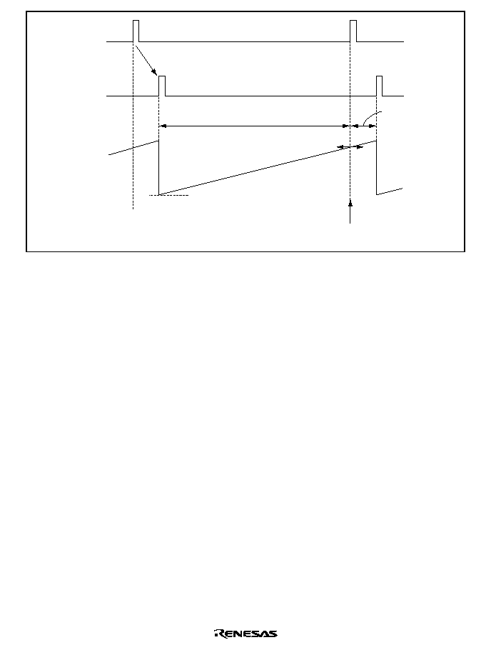
Rev. 1.0, 02/00, page 647 of 1141
≠value +value
Specified speed value
Latch data 0
(no error)
Preset value
Preset period
(2 counts)
Counter
Error data
latch signal
(DVCFG)
Preset data
load signal
Figure 26.33 Example of the Capstan Speed Error Detection

Rev. 1.0, 02/00, page 648 of 1141
26.9
Capstan Phase Error Detector
26.9.1
Overview
The capstan phase control system must start operation after the capstan motor has reached the
specified speed by the speed control system. The capstan phase control system operates as
follows in record/playback mode:
∑
Record mode: Controls the tape running so that it may run at a specified speed together with
the speed control system.
∑
Playback mode: Controls the tape running so that the recorded track may be traced correctly.
Any error deviated from the reference phase is detected by the digital counter. This phase error
data and the speed error data is processed and added by the digital filter circuit to control the
PWM output. The phase and speed of the capstan, in turn, is control this PWM output.
The control signal of the capstan phase control in the record mode differ from that in playback
mode. In record mode, the control is performed by the DVCFG2 signal which is generated by
dividing the frequencies of the reference signal (REF30P or CREF) and the CFG signal. In
playback mode, it is performed by divided rising signal (DVCTL) of the reference signal
(CAPREF30) and the playback control pulse (PB-CTL).
The reference signal in record and playback modes are as follows:
∑
Record mode: 1/2Vsync signal extracted from the video signal to be recorded.
∑
Playback mode: Signal generated by dividing the PB-CTL signal (DVCTL) at its rising edge.
26.9.2
Block Diagram
Figure 26.34 shows the block diagram of the capstan phase error detector.
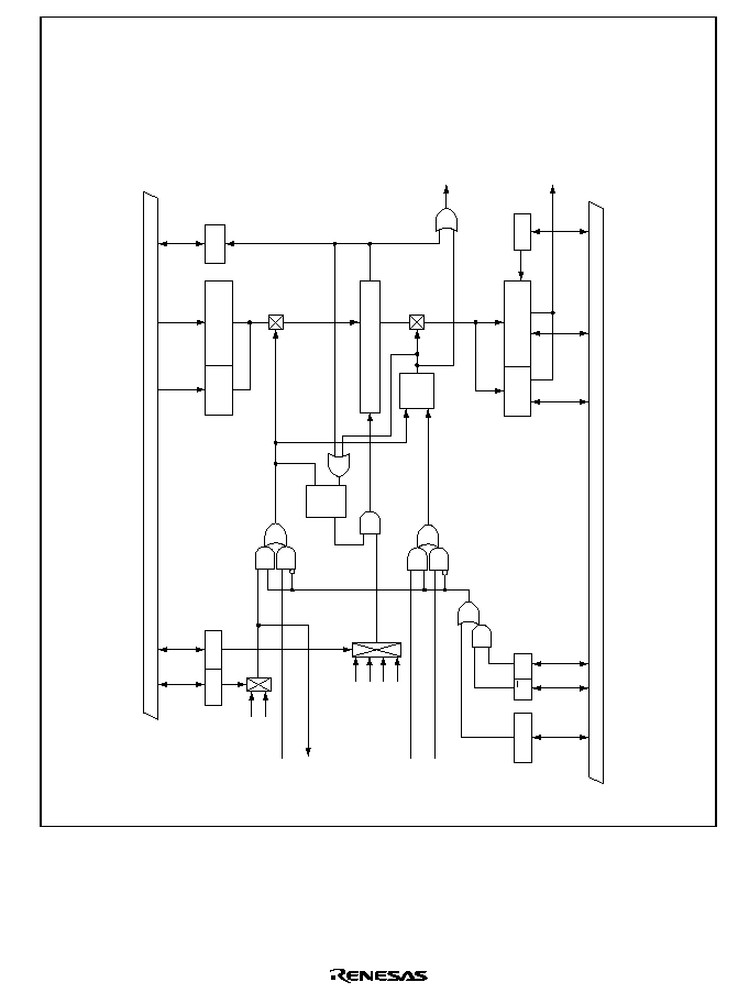
Rev. 1.0, 02/00, page 649 of 1141
R/W
R/W
R/W
R/W
R/W
R/W
CREF
REF30P
CAPREF30
RECREF
DVCFG2
DVCTL
CPGCR
R/W
CR/RF
CPGCR
DFUCR
CPGCR
CPPR1
CPPR2
R/(W)
S
R
F/F
Q
W
W
Internal bus
Internal bus
OVF
LSB
MSB
CPER1
CPER2
LSB
MSB
CPOVF
CFEPS
SELCFG2
R/W
CTLM
R/P
ASM
Latch
Preset
Error data (20 bits)
To DFU
Sequence
controller
Error data
(16 bits)
Error data
(4 bits)
Preset data
(16 bits)
Preset
PB: X value + TRK value = CAPREF30
REC: REF30P or CREF
Latch
PB : DVCTL
REC : DVCFG2
Preset data
(4 bits)
Counter (20 bits)
IRRCAP3
CPCS1,0
s
s/2
s/4
s/8
s = fosc/2
Figure 26.34 Block Diagram of Capstan Phase Error Detector

Rev. 1.0, 02/00, page 650 of 1141
26.9.3
Register Configuration
Table 26.12 shows the register configuration of the capstan phase error detector.
Table 26.12 Register Configuration
Name
Abbrev.
R/W
Size
Initial Value
Address
Specified Capstan phase
preset data register 1
CPPR1
W
Byte
H'F0
H'D05C
Specified Capstan phase
preset data register 2
CPPR2
W
Word
H'0000
H'D05A
Capstan phase error data
register 1
CPER1
R/W
Byte
H'F0
H'D05D
Capstan phase error data
register 2
CPER2
R/W
Word
H'0000
H'D05E
Capstan phase error
detection control register
CPGCR
R/W
Byte
H'07
H'D059
Rev. 1.0, 02/00, page 651 of 1141
26.9.4
Register Description
Specified Capstan Phase Preset Data Registers (CPPR1, CPPR2)
CPPR1
0
0
1
0
W
2
0
W
3
0
4
1
5
1
6
1
7
--
CPPR19
CPPR18
CPPR17
CPPR16
--
--
--
--
--
--
--
W
W
1
Bit :
Initial value :
R/W :
CPPR2
8
0
9
0
W
10
0
W
11
CPPR8
CPPR9
CPPR10
CPPR11
0
12
0
13
0
14
0
15
CPPR12
CPPR13
CPPR14
CPPR15
W
W
W
W
W
W
0
Bit :
Initial value :
R/W :
0
0
1
0
W
2
0
W
3
CPPR0
CPPR1
CPPR2
CPPR3
0
4
0
5
0
6
0
7
CPPR4
CPPR5
CPPR6
CPPR7
W
W
W
W
W
W
0
Bit :
Initial value :
R/W :
The 20-bit preset data that defines the specified capstan phase is set in CPPR1 and CPPR2. The
20 bits are weighted as follows: bit 3 of CPPR1 is the MSB. Bit 0 of CPPR2 is the LSB. When
CPPR2 is written to, the 20-bit preset data, including CPPR1, is loaded into the preset circuit.
Write to CPPR1 first, and CPPR2 next. The preset data can be calculated from the following
equation by using H'80000* as the reference value.
Target phase difference = Reference signal frequency/2
Capstan phase preset data = H'80000
-
(
s/n
◊
target phase difference)
s:
Servo clock frequency in Hz (fosc/2)
s/n:
Clock source of selected counter
Only a word access is valid. If a byte access is attempted, correct operation is not guaranteed. No
read is valid. If a read is attempted, an undetermined value is read out. CPPR1 and CPPR2 are
initialized to H'F0 and H'0000 by a reset, and in standby mode.
Note: The preset data value is calculated so that the counter will reach H'80000 when the error is
zero. When the counter value is latched as error data in the capstan phase error data
registers (CPER1 and CPER2), however, it is converted to a value referenced to H'00000.
Rev. 1.0, 02/00, page 652 of 1141
Capstan Phase Error Data Registers (CPER1, CPER2)
0
0
1
0
R*/W
2
0
R*/W
3
0
4
1
5
1
6
1
7
--
--
--
--
--
--
--
--
R*/W
R*/W
1
Bit :
Initial value :
R/W :
CPER19
CPER18
CPER17
CPER16
8
0
9
0
R*/W
10
0
R*/W
11
CPER8
CPER9
CPER10
CPER11
0
12
0
13
0
14
0
15
CPER12
CPER13
CPER14
CPER15
R*/W
R*/W
R*/W
R*/W
R*/W
R*/W
0
Bit :
Initial value :
R/W :
Note: Note that only detected error data can be read.
0
0
1
0
R*/W
2
0
R*/W
3
CPER0
CPER1
CPER2
CPER3
0
4
0
5
0
6
0
7
CPER4
CPER5
CPER6
CPER7
R*/W
R*/W
R*/W
R*/W
R*/W
R*/W
0
Bit :
Initial value :
R/W :
CPER1 and CPER2 constitute a 20-bit capstan phase error data register. The 20 bits are weighted
as follows: bit 3 of CPER1 is the MSB. Bit 0 of CPER2 is the LSB. When the rotational phase is
correct, the data H'00000 is latched. Negative data will be latched if the phase leads the correct
phase, and positive data if it lags. Values in CPER1 and CPER 2 are transferred to the digital
filter circuit.
CPER1 and CPER are 20-bit read/write registers. When writing data to CPER 1 and CPER2,
write to CPER1 first, and then write to CPER2. Only a word access is valid. If a byte access is
attempted, correct operation is not guaranteed. CPER1 and CPER2 are initialized to H'F0 and
H'0000 by a reset, and in standby mode.
See the note on the capstan phase preset data registers (CPPR1 and CPPR2) in section 26.9.4.

Rev. 1.0, 02/00, page 653 of 1141
Capstan Phase Error Detection Control Register (CPGCR)
0
1
1
2
--
--
--
--
--
--
1
3
0
4
0
R/W
5
0
6
0
7
R/W
R/(W)*
CPOVF
R/W
CPCS0
0
R/W
CPCS1
CR/RF
SELCFG2
1
Note: Only 0 can be written
Bit :
Initial value :
R/W :
CPGCR is an 8-bit read/write register that controls the operation of capstan phase error detection.
Bits 2-0 are reserved, and bit 5 accepts only read and 0 write.
It is initialized to H'07 by a reset or in stand-by mode.
Bits 7 and 6
Clock Source Selection Bit (CPCS1, CPCS0): These bits select the clock
supplied to the counter. (
s = fosc/2)
Bit 7
Bit 6
CPCS1
CPCS0
Description
0
s
(Initial value)
0
1
s/2
0
s/4
1
1
s/8
Bit 5
Counter Overflow Flag (CPOVF): CPOVF flag indicates the overflow of the 20-bit
counter. It is cleared by writing 0. Write 0 after reading 1. Setting has the highest priority in this
flag. If a flag set and 0 write occurs simultaneously, the latter is invalid.
Bit 5
CPOVF
Description
0
Normal state
(Initial value)
1
Indicates that a overflow has occurred in the counter
Bit 4
Preset Signal Selection Bit (CR/RF): Selects the preset signal.
Bit 4
CR/RF
Description
0
Presets REF30P
(Initial value)
1
Presets CREF signal

Rev. 1.0, 02/00, page 654 of 1141
Bit 3
Latch Signal Selection Bit (SELCFG2): Selects the counter preset signal and the error
data latch signal data in PB (ASM) mode.
Bit 3
SELCFG2
Description
0
Presets CAPREF30 signal; latches DVCTL signal
(Initial value)
1
Presets REF30P (CREF) signal; latches DVCFG2 signal
Bits 2 to 0
Reserved: Cannot be modified and are always read as 1.
26.9.5
Operation
The capstan phase error detector detects the phase error based on the reference value set in the
capstan specified phase preset data registers 1 and 2 (CPPR1 and CPPR2). The reference values
set in CPPR1 and CPPR2 are preset in the counter by REF30P (CREF) signal or CAPREF signal,
and counted up by the clock selected. The latching of the error data is performed by DVCTL or
DVCFG2.
The error data detected in the error data automatic transmission mode (CFEPS bit of DFUCR = 0)
is sent to the digital filter circuit automatically. In soft transmission mode (CFEPS bit of DFUCR
= 1), the data written in CPER1 and CPPR2 is sent to the digital filter circuit. The error data is
signed binary. It takes a positive number (+) if the phase is behind the specified phase, a negative
number (-) if in advance of the specified phase, or 0 if it had no phase error (revolving at the
specified phase). Figures 26.35 and 26.36 show examples of operation to detect a capstan phase
error.
Capstan Phase Error Detection Counter: The capstan phase error detection counter stops
counting when an overflow or latch occurs. At the same time, it generates an interrupt request
(IRRCAP3), and sets the overflow flag (CPOVF) if overflow occurred. To clear CPOVF, write 0
after reading 1. If setting the flag and writing 0 take place simultaneously, the latter is invalid.
Interrupt Request: IRRCAP3 is generated by the DVCTL or DVCFG2 signal latch and the
overflow of the error detection counter.
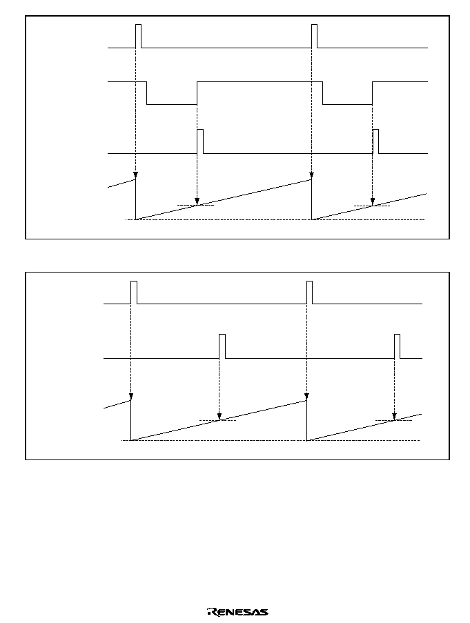
Rev. 1.0, 02/00, page 655 of 1141
Latch
Latch
Preset value
Counter
PB-CTL
CAPREF30
DVCTL
or
DVCFG2
Preset
Preset
Figure 26.35 Capstan Phase Control in Playback Mode
Latch
Latch
Preset value
Counter
DVCFG2
REF30P
or
CREF
Preset
Preset
Figure 26.36 Capstan Phase Control in Record Mode

Rev. 1.0, 02/00, page 656 of 1141
26.10
X-Value and Tracking Adjustment Circuit
26.10.1
Overview
To maintain compatibility with other VCRs, an on-chip adjustment circuit adjusts the phase of the
reference signal (internal reference signal (REF30) or external reference signal (EXCAP)) during
playback. Because of manufacturing tolerances, the physical distance between the video head and
control head (the X-value: 79.244 mm) may vary from set to set, so when a tape that was recorded
on a different set is played back, the phase of the reference signal may need to be adjusted. The
adjustment can be made by a register setting. The same setting can adjust the rotational phase of
the capstan motor to maintain positional alignment (tracking alignment) of the video head with the
recorded tracks in autotracking, or when tracks that were recorded with an EP head are traced by a
wider head. These tracking adjustments can be made by the acquisition of the envelope signal by
the A/D converter.
26.10.2
Block Diagram
The adjustment circuit consists of a 10-bit counter clocked by the system clock (
s or
s/2), and
two down-counters with load registers. Individual setting of X-value adjustment can be made by
X-value data register (XDR) and tracking adjustment by TRK data register (TRDR). The
reference signal clears the 10-bit counter and sets the load register value in the down-counter with
two load registers. After the adjusted reference signal is generated, clock supply stops and the
circuit halts until the next reference signal is input. REF30 signal can be divided as necessary.
Figure 26.37 shows a block diagram.
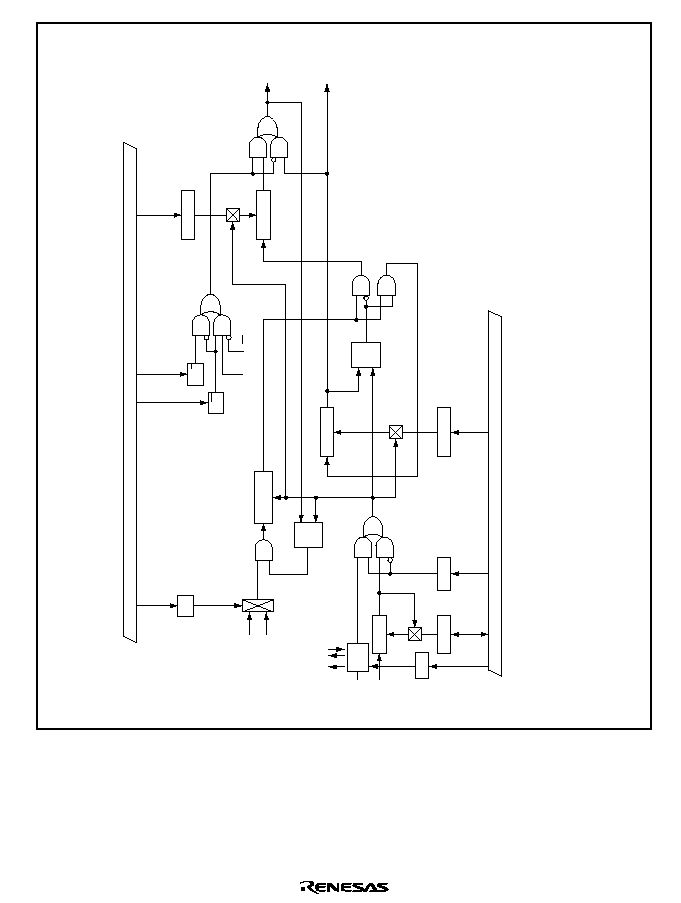
Rev. 1.0, 02/00, page 657 of 1141
R*/W
Note:
When DVREF1 and DVREF0 are read, values in the down counter (2 bits) are readout.
s = fosc/2
s
s /2
EXCAP
REF30P
XTCR
W
W
XCS
XTCR
W
AT/MU
ASM
REC/PB
XTCR
W
TRK/X
S
R
Q
S
R
Q
Internal bus
Internal bus
DVREF1, 0
CAPRF
EXC/REF
W
W
XTCR
XTCR
Down counter
Edge
selection
,
(2 bits)
Counter
(10bit)
CAPREF30
REF30X
W
X-value data
register
XDR
(12 bits)
TRK value data
register
TRDR
(12 bits)
Down counter
(12 bits)
(12 bits)
Down counter
Figure 26.37 Block Diagram of X-Value Adjustment Circuit
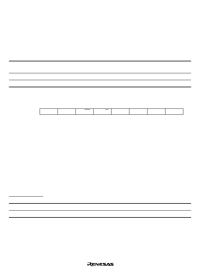
Rev. 1.0, 02/00, page 658 of 1141
26.10.3
Register Description
Register Configuration
Table 26.13 shows the register configuration of X-value correction and tracking correction
circuits.
Table 26.13 Register Configuration
Name
Abbrev.
R/W
Size
Initial Value
Address
X-value and TRK-value
control register
XTCR
R/W
Byte
H'80
H'D074
X-value data register
XDR
W
Word
H'F000
H'D070
TRK-value data register
TRDR
W
Word
H'F000
H'D072
X-Value and TRK-Value Control Register (XTCR)
0
0
1
0
R*/W
2
0
W
3
0
4
0
W
5
0
6
0
7
--
--
R*/W
W
W
AT/MU
W
CAPRF
TRK/X
EXC/REF
XCS
DVREF1
DVREF0
1
Bit :
Initial value :
R/W :
XTCR is an 8-bit register to determine the X-value and TRK-value correction circuits. Bits 6 to 2
are write-only bits. No read is valid. If a read is attempted, an undetermined value is read out.
Bits 1 and 0 are read/write bits. Only a byte access is valid for XTCR. If a word access is
attempted, correct operation is not guaranteed.
It is initialized to H'80 by a reset, or in stand-by or module stop mode.
Bit 7
Reserved: Cannot be modified and is always read as 1.
Bit 6
External Sync Signal Edge Selection Bit (CAPRF): Selects the EXCAP edge when a
selection is made to generate external sync signals.
Bit 6
CAPRF
Description
0
Signal generated at the rising edge of EXCAP.
(Initial value)
1
Signal generated at both edges of EXCAP.

Rev. 1.0, 02/00, page 659 of 1141
Bit 5
Capstan Phase Correction Auto/Manual Selection Bit (AT/
08
08): Selects whether the
generation of the correction reference signal (CAPREF30) for capstan phase control is controlled
automatically or manually depending on the status of the ASM and REC/
! bits of CTL mode
register.
Bit 5
AT/
&
&
Description
0
Manual mode
(Initial value)
1
Auto mode
Bit 4
Capstan Phase Correction Register Selection Bit (TRK/
;
;): Determines the method to
generate the CAPREF30 signal when AT/
08 bit is 0.
Bit 4
TRK/
;
;
Description
0
Generates CAPREF30 only by the set value of XDR.
(Initial value)
1
Generates CAPREF30 by the set value of XDR and TRDR.
Bit 3
Reference Signal Selection Bit (EXC/REF): Selects the reference signal to generate the
correction reference signal (CAPREF30).
Bit 3
EXC/REF
Description
0
Generates the signal based on REF30P.
(Initial value)
1
Generates the signal based on the external reference signal.
Bit 2
Clock Source Selection Bit (XCS): Selects the clock source to be supplied to the 10-bit
counter.
Bit 2
XCS
Description
0
s
(Initial value)
1
s/2
Rev. 1.0, 02/00, page 660 of 1141
Bits 1 and 0
REF30P Division Ratio Selection Bit (DVREF1, DVREF0): Selects the division
value of REF30P. If it is read-accessed, the counter value is read out. (The selected division
value is set by the UDF of the counter.)
Bit 1
Bit 0
DVREF1
DVREF0
Description
0
Division in 1
(Initial value)
0
1
Division in 2
0
Division in 3
1
1
Division in 4
X-Value Data Register (XDR)
1
13
1
14
1
15
1
0
3
2
5
4
7
0
W
6
0
W
9
0
W
8
0
W
11
0
W
10
0
W
1
W
W
W
W
W
W
12
--
--
--
--
--
--
--
--
XD1
XD0
XD3
XD2
XD5
XD4
XD7
XD6
XD9
XD8
XD11 XD10
0
0
0
0
0
0
Bit :
Initial value :
R/W :
The X-value data register (XDR) is an 16-bit write-only register. No read is valid. If a read is
attempted, an undetermined value is read out. Only a word access is valid. If a byte access is
attempted, correct operation is not guaranteed.
Set an X-value correction data to XDR, except a value which is beyond the cycle of the CTL
pulse. If AT/
08 = 0, TRK/; = 0 is set, CAPREF30 can be generated only by setting the XDR.
Set an X-value and TRK correction value in PB mode, and X- value in REC mode.
It is initialized to H'F000 by a reset, or in stand-by or module stop mode.
TRK-Value Data Register (TRDR)
1
13
1
14
1
15
1
0
3
2
5
4
7
0
W
6
0
W
9
0
W
8
0
W
11
0
W
10
0
W
1
W
W
W
W
W
W
12
--
--
--
--
--
--
--
--
TRD1 TRD0
TRD3 TRD2
TRD5 TRD4
TRD7 TRD6
TRD9 TRD8
TRD11 TRD10
0
0
0
0
0
0
Bit :
Initial value :
R/W :
The TRK-value data register (TRDR) is an 16-bit write-only register. No read is valid. If a read is
attempted, an undetermined value is read out. Only a word access is valid. If a byte access is
attempted, correct operation is not guaranteed.
Set an TRK-value correction data to TRDR, except a value which is beyond the cycle of the CTL
pulse. It is initialized to H'F000 by a reset, or in stand-by or module stop mode.

Rev. 1.0, 02/00, page 661 of 1141
26.11
Digital Filters
26.11.1
Overview
The digital filters required in servo control make extensive use of multiply-accumulate operations
on signed integers (error data) and coefficients. A filter computation circuit (digital filter
computation circuit) is provided in on-chip hardware to reduce the load on software, and to
improve processing efficiency. Figure 26.38 shows a block diagram of the filter circuit
configuration.
The filter circuit includes a high-speed 24-bit
◊
16-bit multiplier-accumulator, an arithmetic
buffer, and an I/O processor. The digital filter computations are carried out by the high-speed
multiplier-accumulator. The arithmetic buffer stores coefficients and gain constants needed in the
filter computations, which are referenced by the high-speed multiplier-accumulator.
The I/O processor is activated by a frequency generator signal, and determines what operation is
carried out. When activated, it reads the speed error and phase error from the speed and phase
error detectors and sends them to the accumulator.
When the filter computation is completed, the I/O processor reads the result from the accumulator
and sends it to a 12-bit PWM. At this time, the accumulation result gain can be controlled.
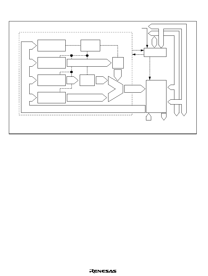
Rev. 1.0, 02/00, page 662 of 1141
26.11.2
Block Diagram
Data bus
Accumulator
End
Start
Error latch signal
Error data
(from the error detector)
Motor control data
(to PWM circuit)
Buffer/
register
select &
R/W
Address bus
Error check
Accumulation
controller
LA (16 bits),
lower accumulator
UA (32 bits),
upper accumulator
MD (32 bits),
multiplied data
Data
shifter
Accumulation
sequence circuit
Buffer circuit
A, B, G, etc.
Write-only
Read-only
Accumu-
lator
Calculation buffer Coefficient register Constant register
Sign
controller
Figure 26.38 Block Diagram of Digital Filter Circuit
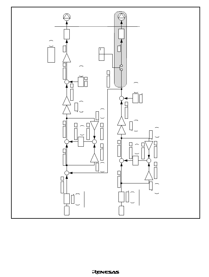
Rev. 1.0, 02/00, page 663 of 1141
16
24
8
Z
-1
-+
*
Usn-1
GKs
+
+
Ofs
+
-
+
+
24
8
Ws
24
8
VBs
14
4
24
8
XAs
24
8
XSn
24
8
VSn
24
8
DFUout
12
24
8
Es
Error detector
· Add 0s to 8 bits after the decimal point
· Add the same 8-bit value as MSB
Right-bit shift of the decimal point
along with Go
PWM
Note: Go =
◊
64,
◊
32 are optional.
Go =
◊
64,
◊
32,
◊
16,
◊
8,
◊
4,
◊
2
24
8
Usn
16
DZs11 to 0
CZs11 to 0
DBs15 to 0
CBs15 to 0
16
DGKs15 to 0
CGKs15 to 0
DOfs15 to 0
COfs15 to 0
DFIC
CFIC
DFER15 to 0
CFER15 to 0
DAs15 to 0
CAs15 to 0
Bs
As
GS
KS
Go
16
Es
PWM
Digital filter
control register
Speed system
24
8
Z
-1
-+
*
1
Upn-1
GKp
+
+
OfP
+
-
24
8
Tp
24
8
VBp
24
8
XAp
24
8
VPn
24
8
Y
Phase direct test output
Notes 1. See figure 26.42, Z
-1
initialization circuit.
12
24
8
Ep
Error detector
· Add 0s to 8 bits after the decimal point
· Add the same 8-bit value as MSB
PWM
24
8
Upn
DZp11 to 0
CZp11 to 0
DBp15 to 0
CBp15 to 0
16
16
DGKp15 to 0
CGKp15 to 0
DOfp15 to 0
COfp15 to 0
DPER19 to 0
CPER19 to 0
DAp15 to 0
CAp15 to 0
BP
AP
GP
KP
20
16
16
Ep
PWM
PION
*2
·
DFUCR
·
OPTION
CP/DP
Phase system
Overflows during accumulation are ignored, and
values below the decimal point are always omitted.
2. Gain control is disabled during phase output.
Figure 26.39 Digital Filter Representation
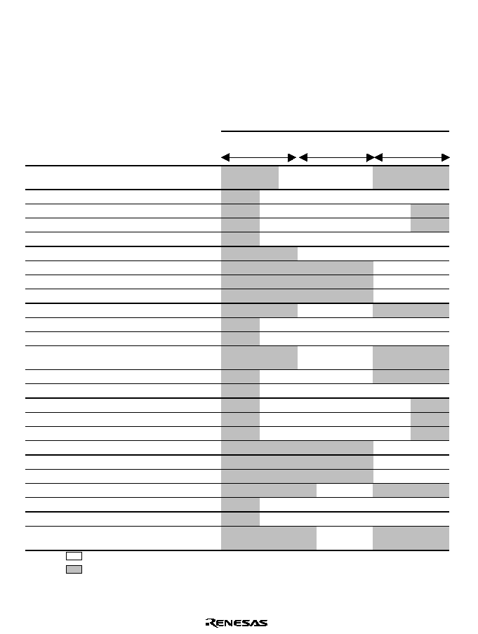
Rev. 1.0, 02/00, page 664 of 1141
26.11.3
Arithmetic Buffer
This buffer stores computational data used in the digital filters. See table 26.14. Write access is
limited to the gain and coefficient data (Z
-1
). The other data is used by hardware. None of the data
can be read.
Table 26.14 Arithmetic Buffer Register Configuration
Buffer Data Length
Arithmetic
Data
Gain or
Coefficient
Processing
Data
16 bits
16 bits
16 bits
Phase
system
Ep
Upn
Upn-1 (Zp
-1
)
Vpn
Tp
Y
Ap
Bp
GKp
Ofp
Ap
◊
Epn
Bp
◊
Vpn
Speed
system
Es
Xsn
Usn
Usn-1 (Zs
-1
)
Vsn
Ws
As
Bs
GKs
Ofs
As
◊
Xsn
Bs
◊
Vsn
Error
output
PWM
Legend:
Valid bits
Non-existent bits
Decimal point

Rev. 1.0, 02/00, page 665 of 1141
26.11.4
Register Configuration
Table 26.15 shows the register configuration of the digital circuit.
Table 26.15 Register Configuration
Name
Abbrev.
R/W
Size
Initial Value
Address
Capstan phase gain
constant
CGKp
W
Word
Undetermined
H'D010
Capstan speed gain
constant
CGKs
W
Word
Undetermined
H'D012
Capstan phase coefficient A
CAp
W
Word
Undetermined
H'D014
Capstan phase coefficient B
CBp
W
Word
Undetermined
H'D016
Capstan speed coefficient A
CAs
W
Word
Undetermined
H'D018
Capstan speed coefficient B
CBs
W
Word
Undetermined
H'D01A
Capstan phase offset
COfp
W
Word
Undetermined
H'D01C
Capstan speed offset
COfs
W
Word
Undetermined
H'D01E
Drum phase gain constant
DGKp
W
Word
Undetermined
H'D000
Drum speed gain constant
DGKs
W
Word
Undetermined
H'D002
Drum phase coefficient A
DAp
W
Word
Undetermined
H'D004
Drum phase coefficient B
DBp
W
Word
Undetermined
H'D006
Drum speed coefficient A
DAs
W
Word
Undetermined
H'D008
Drum speed coefficient B
DBs
W
Word
Undetermined
H'D00A
Drum phase offset
DOfp
W
Word
Undetermined
H'D00C
Drum speed offset
DOfs
W
Word
Undetermined
H'D00E
Drum system speed delay
initialization register
DZs
W
Word
H'F000
H'D020
Drum system phase delay
initialization register
DZp
W
Word
H'F000
H'D022
Capstan system speed delay
initialization register
CZs
W
Word
H'F000
H'D024
Capstan system phase delay
initialization register
CZp
W
Word
H'F000
H'D026
Drum system digital filter
control register
DFIC
R/W
Byte
H'80
H'D028
Capstan system digital filter
control register
CFIC
R/W
Byte
H'80
H'D029
Digital filter control register
DFUCR
R/W
Byte
H'C0
H'D02A

Rev. 1.0, 02/00, page 666 of 1141
26.11.5
Register Description
Gain Constants (DGKp, DGKs, CGKp, CGKs)
*
W
13
*
W
14
*
W
15
1
0
3
2
5
4
7
*
W
6
*
W
9
*
W
8
*
W
11
*
W
10
*
W
*
W
W
W
W
W
W
W
12
*
*
*
*
*
*
Bit :
Initial value :
R/W :
Note: * Initial value is uncertain.
These registers are 16-bit write-only buffers that set accumulation gain of the digital filter. Only a
word access is valid. Accumulation gain can be set to gain 1 value as maximum value. If a byte
access is attempted, correct operation is not guaranteed. If a read is attempted, an undetermined
value is read out.
These registers are not initialized by a reset or in standby mode. Be sure to write data in them
before processing starts.
In the digital filter, output gain and accumulation gain can be adjusted separately. Take output
gain into account when setting accumulation gain.
Coefficients (DAp, DBp, DAs, DBs, CAp, CBp, CAs, CBs)
*
W
13
*
W
14
*
W
15
1
0
3
2
5
4
7
*
W
6
*
W
9
*
W
8
*
W
11
*
W
10
*
W
*
W
W
W
W
W
W
W
12
*
*
*
*
*
*
Bit :
Initial value :
R/W :
Note: * Initial value is uncertain.
These registers are 16-bit write-only buffers that determine the cutoff frequency f1 and f2. Only a
word access is valid. If a byte access is attempted, correct operation is not guaranteed. If a read is
attempted, an undetermined value is read out.
These registers are not initialized by a reset or in standby mode. Be sure to write data in them
before processing starts.
In the digital filter, output gain and accumulation gain can be adjusted separately. Take output
gain into account when setting accumulation gain.

Rev. 1.0, 02/00, page 667 of 1141
Offset (DOfp, DOfs, COfp, COfs)
*
W
13
*
W
14
*
W
15
1
0
3
2
5
4
7
*
W
6
*
W
9
*
W
8
*
W
11
*
W
10
*
W
*
W
W
W
W
W
W
W
12
*
*
*
*
*
*
Bit :
Initial value :
R/W :
Note: * Initial value is uncertain.
These registers are 16-bit write-only buffers that set offset level of digital filter output. Only a
word access is valid. If a byte access is attempted, correct operation is not guaranteed. If a read is
attempted, an undetermined value is read out.
These registers are not initialized by a reset or in standby mode. Be sure to write data in them
before processing starts.
In this digital filter, output gain adjustment (
◊
1, 2, 4, 8 ,16, 32, 64) after offset adding is enabled.
Take output gain into account when setting accumulation gain.
Delay Initialization Register (CZp, CZs, DZp, DZs)
13
14
15
1
0
3
2
5
4
7
0
W
6
0
W
9
0
W
8
0
W
11
0
W
10
0
W
W
W
W
W
W
W
12
0
0
0
0
0
0
1
1
1
1
--
--
--
--
Bit :
Initial value :
R/W :
The delay initialization register is a 16-bit write-only register. Only a word access is valid. If a
byte access is attempted, correct operation is not guaranteed. If a read is attempted, an
undetermined value is read out.
It is initialized to H'F000 by a reset, or in stand-by or module stop mode. The MSB of 12-bit data
(bit 11) is a sign bit.
Loading to Z
-1
is performed automatically by bits 4 and 3 of CFIC and DFIC (CZPON, CZSON,
DZPON, DZSON). Writing in register is always available, but loading in Z
-1
is not possible when
the digital filter is performing computation in relation to such register. In such a case, loading to
Z
-1
will be done the next time computation begins.

Rev. 1.0, 02/00, page 668 of 1141
Drum System Digital Filter Control Register (DFIC)
0
0
1
0
R/W
2
0
R/W
3
0
4
0
R/W
5
0
6
0
7
--
--
R/W
R/W
R/(W)
DPHA
R/(W)*
DROV
DZPON
DZSON
DSG2
DSG1
DSG0
1
Note: * Only 0 can be written
Bit :
Initial value :
R/W :
DFIC is an 8-bit read/write register that controls the status of the drum digital filter and operating
mode. Only a byte access is valid. If a word access is attempted, correct operation is not
guaranteed. DFIC is initialized to H'80 by a reset, and in standby mode and module stop mode.
Bit 7
Reserved: Cannot be modified and is always read as 1.
Bit 6
Drum System Range Over Flag (DROV): This flag is set to 1 when the result of a filter
computation exceeds 12 bits in width. To clear this flag, write 0 after reading 1.
Bit 6
DROV
Description
0
Indicates that the filter computation result did not exceed 12 bits
(Initial value)
1
Indicates that the filter computation result exceeded 12 bits
Bit 5
Drum Phase System Filter Computation Start Bit (DPHA): Starts or stops filter
processing for drum phase system.
Bit 5
DPHA
Description
0
Phase system filter computations are disabled
Phase computation result (Y) is not added to Es (see figure 26.34)
(Initial value)
1
Phase system filter computations are enabled

Rev. 1.0, 02/00, page 669 of 1141
Bit 4
Drum Phase System Z
-1
Initialization Bit (DZPON): Reflects the DZp value on Z
-1
of the
phase system when computation processing of the drum phase system begins. If 1 is written, it is
reflected on the computation, and then cleared to 0. Set this bit after writing data to DZp.
Bit 4
DZPON
Description
0
DZp value is not reflected on Z
-1
of the phase system
(Initial value)
1
DZp value is reflected on Z
-1
of the phase system
Bit 3
Drum Speed System Z
-1
Initialization Bit (DZSON): Reflects the DZs value on Z
-1
of the
speed system when computation processing of the drum speed system begins. If 1 is written, it is
reflected on the computation, and then cleared to 0. Set this bit after writing data to DZs.
Bit 3
DZSON
Description
0
DZs value is not reflected on Z
-1
of the speed system
(Initial value)
1
DZs value is reflected on Z
-1
of the speed system
Bits 2 to 0
Drum System Output Gain Control Bits (DSG2 to DSG0): Control the gain output
to DRMPWM.
Bit 2
Bit 1
Bit 0
DSG2
DSG1
DSG0
Description
0
◊
1
(Initial value)
0
1
◊
2
0
◊
4
0
1
1
◊
8
0
◊
16
0
1
(
◊
32)*
0
(
◊
64)*
1
1
1
Invalid (Do not use this setting)
Note: * Setting optional.

Rev. 1.0, 02/00, page 670 of 1141
Capstan System Digital Filter Control Register (CFIC)
0
0
1
0
R/W
2
0
R/W
3
0
4
0
R/W
5
0
6
0
7
--
--
R/W
R/W
R/(W)
CPHA
R/(W)*
CROV
CZPON
CZSON
CSG2
CSG1
CSG0
1
Note: * Only 0 can be written
Bit :
Initial value :
R/W :
CFIC is an 8-bit read/write register that controls the status of the capstan digital filter and
operating mode. Only a byte access is valid. If a word access is attempted, correct operation is not
guaranteed. CFIC is initialized to H'80 by a reset, and in standby mode and module stop mode.
Bit 7
Reserved: Cannot be modified and is always read as 1.
Bit 6
Capstan System Range Over Flag (CROV): This flag is set to 1 when the result of a
filter computation exceeds 12 bits in width. To clear this flag, write 0 after reading 1.
Bit 6
DROV
Description
0
Indicates that the filter computation result did not exceed 12 bits.
(Initial value)
1
Indicates that the filter computation result exceeded 12 bits.
Bit 5
Capstan Phase System Filter Start (CPHA): Starts or stops filter processing for capstan
phase system.
Bit 5
CPHA
Description
0
Phase filter computations are disabled.
Phase computation result (Y) is not added to Es (see figure 26.39).
(Initial value)
1
Phase filter computations are enabled.

Rev. 1.0, 02/00, page 671 of 1141
Bit 4
Capstan Phase System Z
-1
Initialization Bit (CZPON): Reflects the CZp value on Z
-1
of
the capstan phase system when computation processing of the phase system begins. If 1 is
written, it is reflected on the computation, and then cleared to 0. Set this bit after writing data to
CZp.
Bit 4
CZPON
Description
0
CZp value is not reflected on Z
-1
of the phase system
(Initial value)
1
CZp value is reflected on Z
-1
of the phase system
Bit 3
Capstan Speed System Z
-1
Initialization Bit (CZSON): Reflects the CZs value on Z
-1
of
the capstan speed system when computation processing of the speed system begins. If 1 is
written, it is reflected on the computation, and then cleared to 0. Set this bit after writing data to
CZs.
Bit 3
CZSON
Description
0
CZs value is not reflected on Z
-1
of the speed system
(Initial value)
1
CZs value is reflected on Z
-1
of the speed system
Bits 2 to 0
Capstan System Gain Control Bits (CSG2 to CSG0): Control the gain output to
CAPPWM.
Bit 1
Bit 2
Bit 0
CSG2
CSG1
CSG0
Description
0
◊
1
(Initial value)
0
1
◊
2
0
◊
4
0
1
1
◊
8
0
◊
16
0
1
(
◊
32)*
0
(
◊
64)*
1
1
1
Invalid (Do not use this setting)
Note: * Setting optional

Rev. 1.0, 02/00, page 672 of 1141
Digital Filter Control Register (DFUCR)
0
0
1
0
R/W
2
0
R/W
3
0
4
0
R/W
5
0
6
7
--
--
--
--
R/W
R/W
R/W
PTON
CP/DP
CFEPS
DFEPS
CFESS
DFESS
1
1
Bit :
Initial value :
R/W :
DFUCR is an 8-bit read/write register which controls the operation of the digital filter. Only a byte
access is valid. If a word access is attempted, correct operation is not guaranteed. It is initialized
to H'00 by a reset, or in stand-by or module stop mode.
Bits 7 and 6
Reserved: Cannot be modified and are always read as 1.
Bit 5
Phase System Computation Result PWM Output Bit (PTON): Outputs the computation
results of only the phase system to PWM. (The computation results of the drum phase system is
output to CAPPWM pin, and that of the capstan phase system is output to DRMPWM pin.)
Bit 5
PTON
Description
0
Outputs the results of ordinary computation of the filter to PWM pin
(Initial value)
1
Outputs the computation results of only the phase system to PWM pin
Bit 4
PWM Output Selection Bit (CP/
!
!): Selects whether the phase system computation
results when PTON was set to 1 is output to the drum or capstan. The PWM of the selected side
outputs ordinary filter computation results (speed system of MIX).
Bit 4
CP/
'3
'3
Description
0
Outputs the drum phase system computation results (DRMPWM)
(Initial value)
1
Outputs the capstan phase system computation results (CAPPWM)

Rev. 1.0, 02/00, page 673 of 1141
Bit 3
Capstan Phase System Error Data Transfer Bit (CFEPS): Transfers the capstan phase
system error data to the digital filter when the data write is enforced.
Bit 3
CFEPS
Description
0
Error data is transferred by DVCFG2 signal latching.
(Initial value)
1
Error data is transferred when the data is written.
Bit 2
Drum Phase System Error Data Transfer Bit (DFEPS): Transfers the drum phase
system error data to the digital filter when the data write is enforced.
Bit 2
DFEPS
Description
0
Error data is transferred by HSW (NHSW) signal latching.
(Initial value)
1
Error data is transferred when the data is written.
Bit 1
Capstan Speed System Error Data Transfer Bit (CFESS): Transfers the capstan phase
system error data to the digital filter when the data write is enforced.
Bit 1
CFESS
Description
0
Error data is transferred by DVCFG signal latching.
(Initial value)
1
Error data is transferred when the data is written.
Bit 0
Drum Speed System Error Data Transfer Bit (DFESS): Transfers the drum speed
system error data to the digital filter when the data write is enforced.
Bit 0
DFESS
Description
0
Error data is transferred by NCDFG signal latching.
(Initial value)
1
Error data is transferred when the data is written.
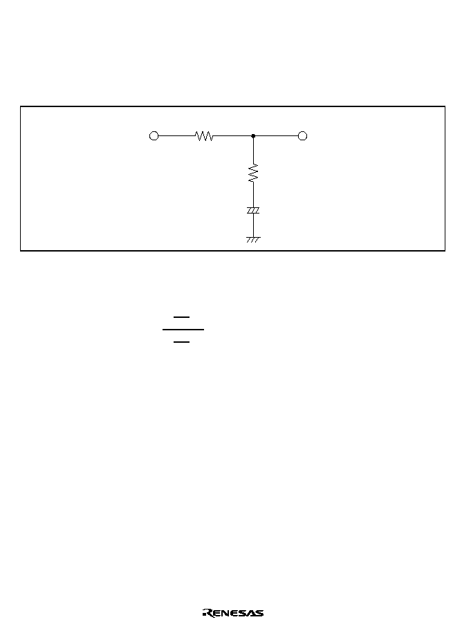
Rev. 1.0, 02/00, page 674 of 1141
26.11.6
Filter Characteristics
∑
Lag-Lead Filter
A filter required for a servo loop is built in the hardware. This filter uses IIR (infinite impulse
response) type digital filter (another type of the digital filter is FIR, i.e. finite impulse response
type). This digital filter circuit implements a lag-lead filter, as shown in figure 26.40.
R1
R2
C
+
INPUT
OUTPUT
Figure 26.40 Lag-Lead Filter
The transfer function is expressed by the following equation:
S
1+
2
f
2
Transfer function G (S) =
S
1+
2
f
1
f
1
=1/2
C (R1+ R2)
f
2
=1/2
CR2
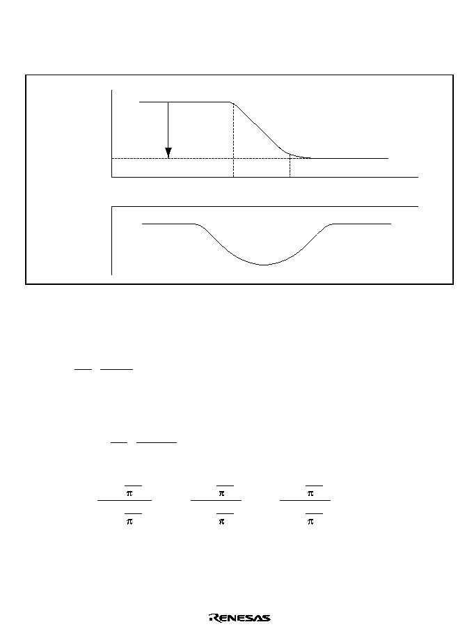
Rev. 1.0, 02/00, page 675 of 1141
∑
Frequency Characteristics
The computation circuit repeats computation of the function, which is obtained by s-z
conversion according to bi-linear approximation of the transfer function on the s-plane. Figure
26.41 shows the frequency characteristics of the lag-lead filter.
f1
0
f2
Frequency (Hz)
20log(f1/f2)
gain(dB)
phase(deg)
Figure 26.41 Frequency Characteristics of the Lag-Lead Filter
The pulse transfer function G (Z) is obtained by the bi-linear approximation of the transfer G (S).
In the transfer G (S),
S =
∑
2
Ts
1≠Z
≠1
1+Z
≠1
Where, assumed that Z
-1
= e
-j
Ts
,
G (Z) = G
∑
∑
2
Ts
1+AZ
≠1
1+BZ
≠1
G (Z) =
Ts +
1
f
2
Ts +
1
f
1
A =
Ts ≠
1
f
2
Ts +
1
f
2
B =
Ts ≠
1
f
1
Ts +
1
f
1
Ts: Sampling cycle (sec)
Rev. 1.0, 02/00, page 676 of 1141
26.11.7
Operations in Case of Transient Response
In case of transient response when the motor is activated, the digital filter computation circuit
must prevent computation due to a large error. The convergence of the computations becomes
slow and servo retraction deteriorates if a large error is input to the filter circuit when it is
performing repeated computations. To prevent them from occurring, operate the filter (set
constants A and B) after pulling in the speed and phase within a certain range of error, initialize
the Z
-1
(set initial values in CZp, CZs, DZp, DZs)(see section 26.11.8, Initialization of Z
-1
), or use
the error data limit function (see section 26.6, Drum Speed Error Detector, and section 26.8,
Capstan Speed Error Detector).
26.11.8
Initialization of Z
-1
Z
-1
can be initialized by its delay initialization register (CZp, CZs, DZp, DZs). Loading to Z
-1
is
performed automatically by bits 4 and 3 of CFIC and DFIC (CZPON, CZSON, DZPON,
DZSON). Writing in register is always available, but loading in Z
-1
is not possible when the
digital filter is performing computation in relation to such register. In such a case, loading to Z
-1
will be done when the next time computation begins. Figure 26.42 shows the initialization circuit
of Z
-1
.
The delay initialization register sets 12-bit data. The MSB (bit 11) is a sign bit. Z
-1
has 24 bits for
integrals and 8 bits for decimals. Accordingly, the same value as the sign bit should be set in the
13 bits on the MSB side of Z
-1
, and 0 in the entire decimal section.
Example: Value set for the delay initialization register
Value set for Z
-1
MSB
0
MSB
Set here the value in the
sign bit
Fixed
1
0 0 0 0 0 0 0 0 0 0
1 1 1 1 1 1 1 1 1 1 1 1 1
0
0
0
0
0
0
0
0
0
0
0
0 0 0 0 0 0 0 0
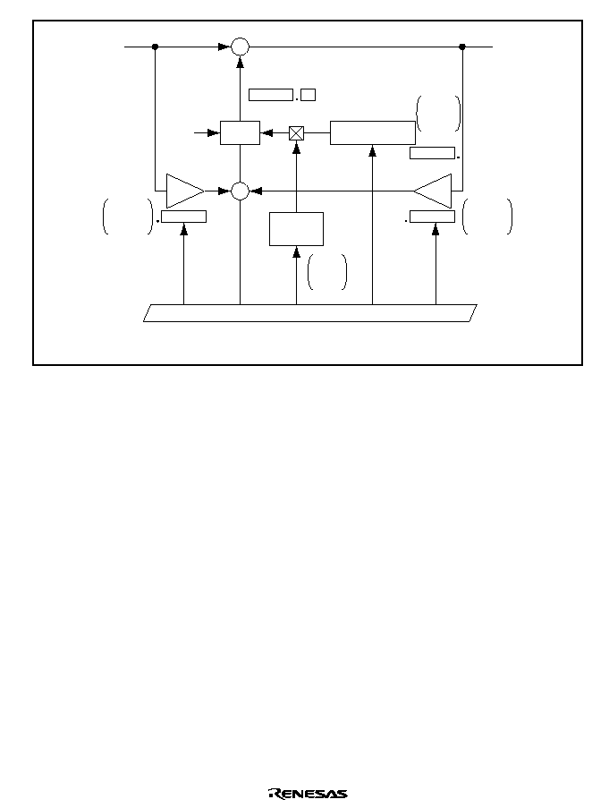
Rev. 1.0, 02/00, page 677 of 1141
W
W
Internal bus
Z
-1
initiali-
zation bit
DZSON
DZPON
CZSON
CZSON
W
16
16
12
24
8
W
Delay initialization
register
Z
-1
USn
-
+
Res
Note: MSB of 12-bit data to be written in the delay initialization register is a sign bit.
Usn-1
+
+
Xn
Vn
DBs15 to 0
DBp15 to 0
CBs15 to 0
CBp15 to 0
DZs11 to 0
DZp11 to 0
CZs11 to 0
CZp11 to 0
DAs15 to 0
DAp15 to 0
CAs15 to 0
CAp15 to 0
A
B
Figure 26.42 Z
-1
Initialization Circuit
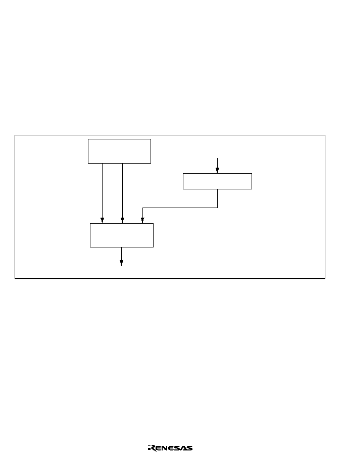
Rev. 1.0, 02/00, page 678 of 1141
26.12
Additional V Signal Generator
26.12.1
Overview
The additional V signal generator outputs an additional vertical sync signal to take the place of
Vsync in special playback. It is activated at both edges of the HSW signal output by the head-
switch timing generator. The head-switch timing generator also outputs a V pulse signal
containing the additional vertical sync pulse itself, and an M level signal that defines the width of
the additional vertical sync signal including the equalizing pulses.
The additional V signal is output at a three-level output pin (V pulse).
Figure 26.43 shows the additional V signal control circuit.
Csync
Additional V pulse
OSCH
Vpulse signal
Mlevel signal
Sync signal detector
HSW timing
generator
Additional V
pulse generator
Figure 26.43 Additional V Pulse Control Circuit
HSW Timing Generator: This circuit generates signals that are synchronized with head
switching. It should be programmed to generate the Mlevel and Vpulse signals at edges of the
HSW signal (VideoFF). For details, see section 26.4, HSW (Head-switch) Timing Generator.
Sync Signal Detector: This circuit detects pulses of the width specified by VTR or HTR from the
signal input at the Csync pin and generates an internal horizontal sync signal (OSCH). The sync
signal detector has an interpolation function, so OSCH has a regular period even if there are
horizontal sync dropouts in the signal received at the pin. For details, see section 26.15, Sync
Signal Detector.

Rev. 1.0, 02/00, page 679 of 1141
26.12.2
Pin Configuration
Table 26.16 summarizes the pin configuration of the additional V signal.
Table 26.16 Pin Configuration
Name
Abbrev.
I/O
Function
Additional V pulse pin
Vpulse
Output
Output of additional V signal synchronized to
video FF
26.12.3
Register Configuration
Table 26.17 summarizes the register that controls the additional V signal.
Table 26.17 Register Configuration
Name
Abbrev.
R/W
Size
Initial Value
Address
Additional V control register
ADDVR
R/W
Byte
H'E0
H'D06F
26.12.4
Register Description
Additional V Control Register (ADDVR)
0
0
1
0
R/W
2
0
R/W
3
0
4
0
R/W
5
1
6
7
--
--
--
--
--
--
R/W
R/W
HMSK
HiZ
CUT
VPOM
POL
1
1
Bit :
Initial value :
R/W :
ADDVR is an 8-bit read/write register. It is initialized to H'E0 by a reset, and in standby mode.
Bits 7 to 5
Reserved: Cannot be modified and are always read as 1.
Bit 4
OSCH Mask (HMSK): Masks the OSCH signal in the additional V signal.
Bit 4
HMSK
Description
0
OSCH is added in
(Initial value)
1
OSCH is not added in

Rev. 1.0, 02/00, page 680 of 1141
Bit 3
High Impedance (HiZ): Set to 1 when the intermediate level is generated by an external
circuit.
Bit 3
HiZ
Description
0
Vpulse is a three-level output pin
(Initial value)
1
Vpulse is a three-state output pin (high, low, or high-impedance)
Bits 2 to 0
Additional V Output Control (CUT, VPON, POL): These bits control the output
at the additional V pin.
Bit 2
Bit 1
Bit 0
CUT
VPON
POL
Description
0
*
Low level
(Initial value)
0
Negative polarity (see figure 26.46)
0
1
1
Positive polarity (see figure 26.45)
0
Intermediate level (high impedance if HiZ bit = 1)
1
*
1
High level
Note:
*
Don't care.
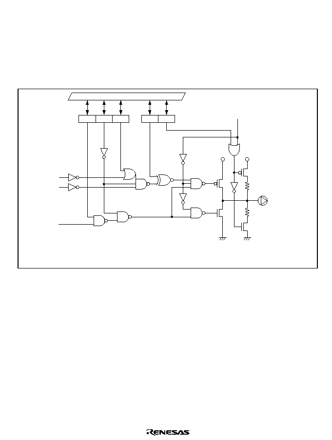
Rev. 1.0, 02/00, page 681 of 1141
26.12.5
Additional V Pulse Signal
Figure 26.44 shows the additional V pulse signal. The M level and V pulse signals are generated
by the head-switch timing generator. The OSCH signal is combined with these to produce
equalizing pulses. The polarity can be selected by the POL bit in the additional V control register
(ADDVR). V pulse pin outputs a low level by a reset, and in standby mode and module stop
mode.
R/W
R/W
· ADDVR
· ADDVR
R/W
Internal bus
R/W
R/W
CUT
VPON
HMSK
POL
HiZ
STBY
V
CC
V
CC
V
SS
V
SS
Rs
Rs
V pulse pin
OSCH
V pulse
M level
Note:
STBY : Power-down mode
V pulse, M level : Signal from the HSW timing generator
Rs : Voltage division resistance (20 k
: reference value)
Figure 26.44 Additional V Pulse Pin
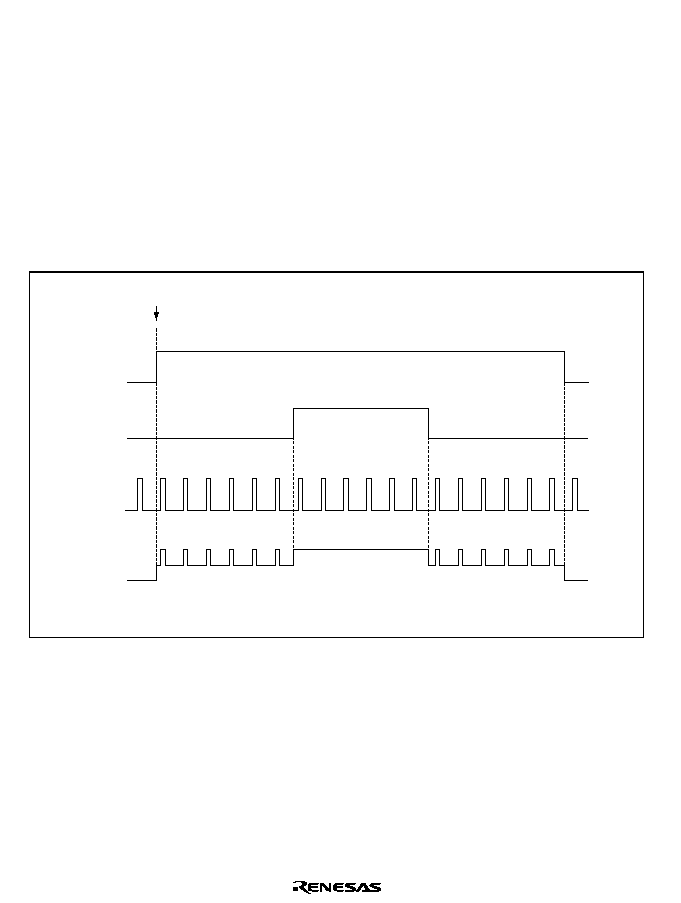
Rev. 1.0, 02/00, page 682 of 1141
Additional V Pulses When Sync Signal is Not Detected: With additional V pulses, the pulse
signal (OSCH) detected by the sync signal detector is superimposed on the V pulse and Mlevel
signals generated by the head-switch timing generator. If there is a lot of noise in the input sync
signal (Csync), or a pulse is missing, OSCH will be a complementary pulse, and therefore an H
pulse of the period set in HRTR and HPWR will be superimposed. In this case, there may be
slight timing drift compared with the normal sync signal, depending on the HRTR and HPWR
setting, with resultant discontinuity.
If no sync signal is input, the additional V pulse is generated as a complementary pulse. Set the
sync signal detector registers and activate the sync signal detector by manipulating the SYCT bit
in the sync signal control register (SYNCR). See section 26.15.7, Activation of the Sync Signal
Detector.
Figures 26.45 and 26.46 show the additional V pulse timing charts.
HSW signal edge
OSCH
VPON=1, CUT=0, POL=1
Additional
V pulse
Vpulse
signal
Mlevel
signal
Figure 26.45 Additional V Pulse when Positive Polarity Is Specified
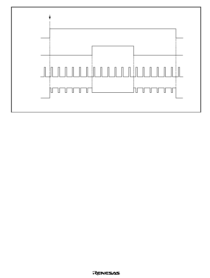
Rev. 1.0, 02/00, page 683 of 1141
HSW signal edge
OSCH
VPON=1, CUT=0, POL=0
Additional
V pulse
V pulse
signal
M level
signal
Figure 26.46 Additional V Pulse When Negative Polarity Is Specified

Rev. 1.0, 02/00, page 684 of 1141
26.13
CTL Circuit
26.13.1
Overview
The CTL circuit includes a Schmitt amplifier that amplifies and reshapes the CTL input, then
outputs it as the PB-CTL signal to the servo, linear time counter, and other circuits.
The PB-CTL signal is also sent to a duty discriminator in the CTL circuit that detects and records
VISS, ASM, and VASS marks. A REC-CTL amplifier is included in the record circuits.
Detection and recording whether the CTL pulse pattern is long or short can also be enabled to
correspond to the wide-aspect.
The following operating modes can be selected by settings in the CTL mode register:
∑
Duty discrimination
VISS detect, ASM detect, VASS detect, L/S bit pattern detect
∑
CTL record
VISS record, ASM record, VASS record, L/S bit pattern record
∑
Rewrite
Trapezoid waveform generator
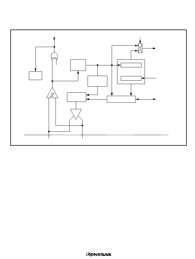
Rev. 1.0, 02/00, page 685 of 1141
26.13.2
Block Diagram
Figure 26.47 shows a block diagram of the CTL circuit.
+ -
PB-CTL
FW/RV
CTL(-)
CTL(+)
Schmitt
amplifier
CTL mode
CTL
detector
Duty dis-
criminator
Bit pattern
register
VISS detect
VISS
control circuit
VISS write
Duty I/O flag
Write control
circuit
REC-
CTL amplifier
Internal bus
REF30X
IRRCTL
Figure 26.47 Block Diagram of CTL Circuit

Rev. 1.0, 02/00, page 686 of 1141
26.13.3
Pin Configuration
Table 26.18 summarizes the pin configuration of the CTL circuit.
Table 26.18 Pin Configuration
Name
Abbrev.
I/O
Function
CTL (+) I/O pin
CTL (+)
I/O
CTL signal input/output
CTL (≠) I/O pin
CTL (≠)
I/O
CTL signal input/output
CTL bias input pin
CTL Bias
Input
CTL primary amplifier bias supply
CTL Amp (O) output pin
CTLAmp (O)
Output
CTL amplifier output
CTL SMT (i) input pin
CTLSMT (i)
Input
CTL Schmitt amplifier input
CTL FB input pin
CTL FB
Input
CTL amplifier high-range characteristics
control
CTL REF output pin
CTL REF
Output
CTL amplifier reference voltage output
26.13.4
Register Configuration
Table 26.19 shows the register configuration of the CTL circuit.
Table 26.19 Register Configuration
Name
Abbrev.
R/W
Size
Initial Value
Address
CTL control register
CTCR
R/W
Byte
H'30
H'D080
CTL mode register
CTLM
R/W
Byte
H'00
H'D081
REC-CTL duty data
register 1
RCDR1
W
Word
H'F000
H'D082
REC-CTL duty data
register 2
RCDR2
W
Word
H'F000
H'D084
REC-CTL duty data
register 3
RCDR3
W
Word
H'F000
H'D086
REC-CTL duty data
register 4
RCDR4
W
Word
H'F000
H'D088
REC-CTL duty data
register 5
RCDR5
W
Word
H'F000
H'D08A
Duty I/O register
DI/O
R/W
Byte
H'F1
H'D08C
Bit pattern register
BTPR
R/W
Byte
H'FF
H'D08D

Rev. 1.0, 02/00, page 687 of 1141
26.13.5
Register Description
CTL Control Register (CTCR)
0
0
1
0
R
2
0
W
3
0
4
1
W
5
1
6
0
7
W
W
W
FSLB
W
FSLC
0
W
NT/PL
FSLA
CCS
LCTL
UNCTL
SLWM
Bit :
Initial value :
R/W :
CTCR is an 8-bit read/write register that controls PB-CTL rewrite and sets the slow mode. When
CTL pulse cannot be detected with the input amplifier gain set at the CTL gain control register
(CTLGR) in PB-CTL circuit, bit 1 (UNCTL) of CTCR is set to 1. It is automatically cleared to 0
when CTL pulse is detected.
Bit 1 is read-only, and the rest are write-only. If a read is attempted to a write-only bit, an
undetermined value is read out.
CTCR is initialized to H'30 by a reset, and in standby and module stop mode.
Bit 7
NTSC/PAL Select (NT/PL): Selects the period of the rewrite circuit.
Bit 7
NT/PL
Description
0
NTSC mode (frame rate: 30 Hz)
(Initial value)
1
PAL mode (frame rate: 25 Hz)
Bits 6 to 4
Frequency Select (FSLA, FSLB, FSLC); These bits select the operating frequency
of the CTL write circuit. They should be set according to fOSC.
Bit 1
Bit 0
Bit 0
FSLC
FSLB
FSLA
Description
0
Reserved (do not use this setting)
0
1
Reserved (do not use this setting)
0
fosc = 8 MHz
0
1
1
fosc = 10 MHz
(Initial value)
1
*
*
Reserved (do not use this setting)
Note:
*
Don't care.

Rev. 1.0, 02/00, page 688 of 1141
Bits 3
Clock Source Select Bit (CCS): Selects clock source of CTL.
Bit 3
CCS
Description
0
s
(Initial value)
1
s/2
Bit 2
Long CTL Bit (LCTL): Sets the long CTL detection mode.
Bit 2
LCTL
Description
0
Clock source (CCS) operates at the setting value
(Initial value)
1
Clock source (CCS) operates for further 8-division after operating at the setting
value
Bit 1
CTL Undetected Bit (UNCTL): Indicates the CTL pulse detection status at the CTL
input amplifier sensitivity set at the CTL gain control register.
Bit 1
UNCTL
Description
0
Detected
(Initial value)
1
Undetected
Bit 0
Mode Select Bit (SLWM): Selects CTL mode.
Bit 0
SLWM
Description
0
Normal mode
(Initial value)
1
Slow mode

Rev. 1.0, 02/00, page 689 of 1141
CTL Mode Register (CTLM)
0
0
1
0
R/W
2
0
R/W
3
0
4
0
R/W
5
0
6
0
7
R/W
R/W
R/W
FW/RV
R/W
REC/PB
0
R/W
ASM
MD4
MD3
MD2
MD1
MD0
Bit :
Initial value :
R/W :
CTLM is an 8-bit read/write register that controls the operating state of the CTL circuit. If 1 is
written in bits MD3 and MD2, they will be cleared to 0 one cycle (
) later.
CTLM is initialized to H'00 by a reset, and in standby mode and module stop mode. When CTL is
being stopped, only bits 7, 6 and 5 operate.
Note:
Do not set any value other than the setting value for each mode (see table 26.20, CTL
Mode Functions).
Bits 7 and 6
Record/Playback Mode Bits (ASM, REC/
!
!): These bits switch between record
and playback. Combined with bits 4 to 0 (MD4 to MD0), they support the VISS, VASS, and
ASM mark functions.
Bit 7
Bit 6
ASM
REC/
3%
3%
Description
0
Playback mode
(Initial value)
0
1
Record mode
0
Assemble mode
1
1
Invalid (do not set)
Bit 5
Direction (FW/RV): Selects the direction in playback. Clear this bit to 0 during record.
Figure 26.48 shows the PB-CTL signal.
Bit 5
FW/RV
Description
0
Forward
(Initial value)
1
Reverse

Rev. 1.0, 02/00, page 690 of 1141
CTL input
PB-CTL
FWD
REV
Figure 26.48 Internal PB-CTL Signal in Forward and Reverse
Bits 4 to 0
CTL Mode Select (MD4 to MD0): These bits select the detect, record, and rewrite
modes for VISS, VASS, and ASM marks. If 1 is written in bits MD3 and MD2, they will be
cleared to 0 one cycle (
) later.
The 5 bits from MD4 to MD0 are used in combination with bits 7 and 6 (ASM and REC/
3%).
Table 26.20 describes the modes.
Table 26.20 CTL Mode Functions
Bit
ASM
R/
!
!
F/R
MD4
MD3
MD2
MD1
MD0
Mode
Description
0
0
0/1
0
0
0
0
0
VASS
detect
(duty
detect)
PB-CTL duty discrimination
(Initial value)
∑
Duty I/O flag is set to 1 if duty
44% is detected
∑
Duty I/O flag is cleared to 0 if
duty < 44% is detected
∑
Interrupt request is generated
when one CTL pulse has been
detected
0
1
0
0
0
0
0
0
VASS
record
∑
If 0 is written in the duty I/O flag,
REC-CTL is generated and
recorded with the duty cycle set
by register RCDR2 or RCDR3
∑
If 1 is written in the duty I/O flag,
REC-CTL is generated and
recorded with the duty cycle set
by register RCDR4 or RCDR5
0
0
0
1
0
0
1
0
VASS
rewrite
Same as above (VASS record);
trapezoid waveform circuit
operation

Rev. 1.0, 02/00, page 691 of 1141
Bit
ASM
R/
!
!
F/R
MD4
MD3
MD2
MD1
MD0
Mode
Description
0
0
0/1
0
1
0
0
1
VISS
detect
(index
detect)
∑
The duty I/O flag is set to 1 at
the point of write access to
register CTLM
∑
The 1 pulses recognized by the
duty discrimination circuit are
counted in the VISS control
circuit
∑
The duty I/O flag is cleared to 0,
indicating VISS detection, when
the value set at VCTR register is
repeatedly detected
∑
An interrupt request is
generated when VISS is
detected
0
1
0
0
0
1
0
1
VISS
record
(index
record)
∑
64 pulse data with 0 pulse data
at both edge are written (index
record)
∑
The index bit string is written
through the duty I/O flag
∑
An interrupt request is
generated at the end of VISS
recording
0
0
0
0
0
1
0
1
VISS
rewrite
Same as above (VISS record;
trapezoid waveform circuit
operation)
0
0
0
1
0
0
0
0
VISS
initialize
VISS write is forcibly aborted
1
0
0/1
0
0
0
0
0
ASM
mark
detect
ASM mark detection
∑
The duty I/O flag is cleared to 0
when PB-CTL duty
66% is
detected
∑
An interrupt request is
generated when an ASM mark is
detected
0
1
0
1
0
0
0
0
ASM
mark
record
∑
An ASM mark is recorded by
writing 0 in the duty I/O flag
∑
An interrupts is requested for
every one CTL pulse
∑
REC-CTL is generated and
recorded with the duty cycle set
by register RCDR3

Rev. 1.0, 02/00, page 692 of 1141
REC-CTL Duty Data Register 1 (RCDR1)
13
14
15
1
0
3
2
5
4
7
6
9
8
11
10
CMT11
W
12
1
1
1
1
--
--
--
--
--
--
--
--
0
CMT10
W
0
CMT13
W
0
CMT12
W
0
CMT15
W
0
CMT14
W
0
CMT17
W
0
CMT16
W
0
CMT19
W
0
CMT18
W
0
CMT1B
W
0
CMT1A
W
0
Bit :
Initial value :
R/W :
RCDR1 is a 12-bit write-only register that sets the REC-CTL rising timing. This setting is valid
only for recording and rewriting, and is not used in detection.
Only a word access is valid. If a byte access is attempted, correct operation is not guaranteed. If a
read is attempted, an undetermined value is read out. Bits 15 to 12 are reserved and are not
affected by write access.
RCDR1 is initialized to H'F000 by a reset, and in standby mode, module stop mode and CTL stop
mode.
The value to set in RCDR1 can be calculated from the transition timing T1 and the servo clock
frequency
s by the equation given below. See figure 26.60, REC-CTL Signal Generation
Timing. Any transition timing can be set. The timing should be selected with attention to
playback tracking compensation and the latch timing for phase control.
RCDR1 = T1
◊
s/64
s is the servo clock frequency (= f
OSC
/2) in Hz, and T1 is the set timing (s).
Note:
0 cannot be set to RCDR1. Set a value 1 or above.

Rev. 1.0, 02/00, page 693 of 1141
REC-CTL Duty Data Register 2 (RCDR2)
1
1
1
1
13
14
15
1
0
3
2
5
4
7
6
9
8
11
10
CMT21
W
12
--
--
--
--
--
--
--
--
0
CMT20
W
0
CMT23
W
0
CMT22
W
0
CMT25
W
0
CMT24
W
0
CMT27
W
0
CMT26
W
0
CMT29
W
0
CMT28
W
0
CMT2B
W
0
CMT2A
W
0
Bit :
Initial value :
R/W :
RCDR2 is a 12-bit write-only register that sets 1 pulse (short) falling timing of REC-CTL at
recording and rewriting, and detects long/short pulses at detecting.
Only a word access is valid. If a byte access is attempted, correct operation is not guaranteed. If a
read is attempted, an undetermined value is read out. Bits 15 to 12 are reserved and are not
affected by write access.
RCDR2 is initialized to H'F000 by a reset, and in standby mode, module stop mode, and CTL stop
mode.
At recording, the value to set in RCDR2 can be calculated from the transition timing T2 and the
servo clock frequency
s by the equation given below, and the set value should be 25% of the duty
obtained by the equation. See figure 26.60, REC-CTL Signal Generation Timing.
RCDR2 = T2
◊
s/64
s is the servo clock frequency (= f
OSC
/2) in Hz, and T2 is the set timing (s).
At bit pattern detection, set the 1 pulse long/short threshold value at FWD. See figure 26.56, Duty
Discriminator.
RCDR2 = T2'
◊
s/64
s is the servo clock frequency (= f
OSC
/2) in Hz, and T2' is the 1 pulse long/short threshold value at
FWD (s).

Rev. 1.0, 02/00, page 694 of 1141
REC-CTL Duty Data Register 3 (RCDR3)
1
1
1
1
13
14
15
1
0
3
2
5
4
7
6
9
8
11
10
CMT31
W
12
--
--
--
--
--
--
--
--
0
CMT30
W
0
CMT33
W
0
CMT32
W
0
CMT35
W
0
CMT34
W
0
CMT37
W
0
CMT36
W
0
CMT39
W
0
CMT38
W
0
CMT3B
W
0
CMT3A
W
0
Bit :
Initial value :
R/W :
RCDR3 is a 12-bit write-only register that sets 1 pulse (long) and assemble mark falling timing of
REC-CTL at recording and rewriting, and detects long/short pulses at detecting.
Only a word access is valid. If a byte access is attempted, correct operation is not guaranteed. If a
read is attempted, an undetermined value is read out. Bits 15 to 12 are reserved and are not
affected by write access.
RCDR3 is initialized to H'F000 by a reset, and in standby mode, module stop mode, and CTL stop
mode.
At recording, the value to set in RCDR3 can be calculated from the transition timing T3 and the
servo clock frequency
s by the equation given below. The set value should be 30 percent of the
duty when the RCDR3 is used for REC-CTL 1 pulse, and 67 to 70 percent when used for assemble
mark. The set value must not exceed the frequency of REF30X. See figure 26.60, REC-CTL
Signal Generation Timing.
RCDR3 = T3
◊
s/64
s is the servo clock frequency (= f
OSC
/2) in Hz, and T3 is the set timing (s).
At bit pattern detection, set the 0 pulse long/short threshold value at FWD. See figure 26.56, Duty
Discriminator.
RCDR3 = T3'
◊
s/64
s is the servo clock frequency (= f
OSC
/2) in Hz, and T3' is the 0 pulse long/short threshold value at
FWD (s).

Rev. 1.0, 02/00, page 695 of 1141
REC-CTL Duty Data Register 4 (RCDR4)
1
1
1
1
13
14
15
1
0
3
2
5
4
7
6
9
8
11
10
CMT41
W
12
--
--
--
--
--
--
--
--
0
CMT40
W
0
CMT43
W
0
CMT42
W
0
CMT45
W
0
CMT44
W
0
CMT47
W
0
CMT46
W
0
CMT49
W
0
CMT48
W
0
CMT4B
W
0
CMT4A
W
0
Bit :
Initial value :
R/W :
RCDR4 is a 12-bit write-only register that sets the timing of falling edge of the 0 pulse (short) of
REC-CTL in record or rewrite mode. In detection mode, it is used to detect the long/short pulse.
Only a word access is valid. If a byte access is attempted, correct operation is not guaranteed. If a
read is attempted, an undetermined value is read out. Bits 15 to 12 are reserved, and no write in
them is valid.
It is initialized to H'F000 by a reset, stand-by or module stop.
In record mode, set a value with the 57.5 percent duty cycle obtained from the set time T4
corresponding to the frequency
s according to the following equation. See figure 26.60, REC-
CTL Signal Generation Timing.
RCDR4 = T4
◊
s/64
is the servo clock frequency (= f
OSC
/2) in Hz, and T4 is the set timing (s).
At bit pattern detection, set the 0 pulse long/short threshold value at REV. See figure 26.56, Duty
Discriminator.
RCDR4 = H'FFF
-
(T4'
◊
s/80)
s is the servo clock frequency (= f
OSC
/2) in Hz, and T4' is the 0 pulse long/short threshold value at
REV (s).

Rev. 1.0, 02/00, page 696 of 1141
REC-CTL Duty Data Register 5 (RCDR5)
1
1
1
1
13
14
15
1
0
3
2
5
4
7
6
9
8
11
10
CMT51
W
12
--
--
--
--
--
--
--
--
0
CMT50
W
0
CMT53
W
0
CMT52
W
0
CMT55
W
0
CMT54
W
0
CMT57
W
0
CMT56
W
0
CMT59
W
0
CMT58
W
0
CMT5B
W
0
CMT5A
W
0
Bit :
Initial value :
R/W :
RCDR5 is a 12-bit write-only register that sets the timing of falling edge of the 0 pulse (short) of
REC-CTL in record or rewrite mode. In detection mode, it is used to detect the long/short pulse.
Only a word access is valid. If a byte access is attempted, correct operation is not guaranteed. If a
read is attempted, an undetermined value is read out. Bits 15 to 12 are reserved, and no write in
them is valid.
It is initialized to H'F000 by a reset, stand-by or module stop.
In record mode, set a value with the 62.5 percent duty cycle obtained from the set time T5
corresponding to the frequency
s according to the following equation. See figure 26.60, REC-
CTL Signal Generation Timing.
RCDR5 = T5
◊
s/64
is the servo clock frequency (= f
OSC
/2) in Hz, and T5 is the set timing (s).
At bit pattern detection, set the 1 pulse long/short threshold value at REV. See figure 26.56, Duty
Discriminator.
RCDR5 = H'FFF
-
(T5'
◊
s/80)
s is the servo clock frequency (= f
OSC
/2) in Hz, and T5' is the 1 pulse long/short threshold value at
REV (s).

Rev. 1.0, 02/00, page 697 of 1141
Duty I/O Register (DI/O)
0
1
1
0
R/(W)*
2
0
W
3
0
4
--
--
5
1
6
7
R/W
W
W
VCTR0
1
W
VCTR1
1
W
VCTR2
BPON
BPS
BPF
DI/O
1
Note: * Only 0 can be written
Bit :
Initial value :
R/W :
DI/O is an 8-bit register that confirms and determines the operating status of the CTL circuit.
It is initialized to H'F1 by a reset, and in standby mode, module stop mode, and CTL stop mode.
Bits 7 to 5
VISS Interrupt Setting Bit (VCTR2 to VCTR0): Combination of VCTR2, VCTR1
and VCTR0 sets number of 1 pulse detection in VISS detection mode. Detecting the set number
of pulse detection is considered as VISS detection, and an interrupt request is generated.
Note:
When changing the detection pulse number during VISS detection, initialize VISS first,
then resume the VISS detection setting.
Bit 7
Bit 6
Bit 5
VCTR2
VCTR1
VCTR0
Number of 1-Pulse for Detection
0
2
0
1
4 (SYNC mark)
0
6
0
1
1
8 (mark A, short)
0
12 (mark A, long)
0
1
16
0
24 (mark B)
1
1
1
32
Bit 4
Reserved: Cannot be modified and is always read as 1.

Rev. 1.0, 02/00, page 698 of 1141
Bit 3
Bit Pattern Detection ON/OFF Bit (BPON): Determines ON or OFF of bit pattern
detection.
Note:
When writing 1 to BPON bit, be sure to set appropriate data to RCDR 2 to 5 beforehand.
Bit 3
BPON
Description
0
Bit pattern detection off
(Initial value)
1
Bit pattern detection on
Bit 2
Bit Pattern Detection Start Bit (BPS): Starts 8-bit bit pattern detection. When 1 is
written to this bit, it returns to 0 after one cycle. Writing 0 to this bit does not affect operation.
Bit 2
BPS
Description
0
Normal status
(Initial value)
1
Starts 8-bit bit pattern detection
Bit 1
Bit Pattern Detection Flag (BPF): Sets flag every time 8-bit PB-CTL is detected in PB or
ASM mode. To clear flag, write 0 after reading 1.
Bit 1
BPF
Description
0
Bit pattern (8-bit) is not detected
(Initial value)
1
Bit pattern (8-bit) is detected
Bit 0
Duty I/O Register (DI/O): This flag has different functions for record and playback.
In VISS detect mode, VASS detect mode, and ASM mark detect mode, this flag indicates the
detection result.
In VISS record or rewrite mode, this flag controls the write control circuit so as to write an index
code, operating according to a control signal from the VISS control circuit.
In VASS record or rewrite mode and ASM mark record mode, this flag is used for write control,
one CTL pulse at a time.
This bit can always be written to, but this does not affect the write control circuit in modes other
than VISS record, rewrite, and ASM record.

Rev. 1.0, 02/00, page 699 of 1141
∑
VISS Detect Mode and VASS Detect Mode: The duty I/O flag indicates the result of duty
discrimination. The duty I/O flag is 1 when the duty cycle of the PB-CTL signal is above 44%
(a 0 pulse in the CTL signal). The duty I/O flag is 0 when the duty cycle of the PB-CTL signal
is below 44% (a 1 pulse in the CTL signal).
∑
ASM Mark Detect Mode: The duty I/O flag indicates the result of duty discrimination. The
duty I/O flag is 0 when the duty cycle of the PB-CTL signal is above 66% (when an ASM
mark is detected).
∑
VISS Record Mode and VISS Rewrite Mode: The duty I/O flag operates according to a control
signal from the VISS control circuit, and controls the write control circuit so as to write an
index code. The write timing is set in the REC-CTL duty data registers (RCDR1 to RCDR5).
For VISS recording, registers RCDR1 to RCDR5 are set with reference to REF30X. For VISS
rewrite, RCDR2 to RCDR5 are set with reference to the low-to-high transition of the
previously recorded CTL signal, and the write is carried out through the trapezoid waveform
generator.
Set the duty timing for a 1 pulse (short) in RCDR2, for a 1 pulse (long) in RCDR3, for a 0
pulse (short) in RCDR4, and for a 0 pulse (long) in RCDR5.
While an index code is being written, the value of the bit being written can be read by reading
the duty I/O flag. If the CTL signal currently being written is a 0 pulse, the duty I/O flag will
read 1. If the CTL signal currently being written is a 1 pulse, the duty I/O flag will read 0.
∑
VASS Record Mode and VASS Rewrite Mode: The duty I/O flag is used for write control, one
CTL pulse at a time. The write timing is set in the REC-CTL duty data registers (RCDR1 to
RCDR5). For VASS recording, registers RCDR1 to RCDR5 are set with reference to
REF30X. For VASS rewrite, RCDR2 to RCDR5 are set with reference to the low-to-high
transition of the previously recorded CTL signal, and the write is carried out through the
trapezoid waveform generator.
Set the duty timing for a 1 pulse (short) in RCDR2, for a 1 pulse (long) in RCDR3, for a 0
pulse (short) in RCDR4, and for 0 pulse (long) in RCDR5.
If 0 is written in the duty I/O flag, a CTL pulse will be written with a duty cycle set in RCDR2
and RCDR3, referenced to the immediately following REF30X. If 1 is written in the duty I/O
flag, a CTL pulse will be written with a duty cycle set in RCDR4 and RCDR5, referenced to
the immediately following REF30X.
∑
ASM Record Mode: The duty I/O flag is used for write control, one CTL pulse at a time. The
write timing is set in the REC-CTL duty data registers (RCDR1 and RCDR3). If 0 is written
in the duty I/O flag, a CTL pulse will be written with a duty cycle of 67% to 70% as set in
RCDR3, referenced to the immediately following REF30X.

Rev. 1.0, 02/00, page 700 of 1141
Bit Pattern Register (BTPR)
0
1
1
1
R/W*
2
1
R/W*
3
1
4
5
1
6
7
R/W*
R/W*
R/W*
LSP5
1
R/W*
LSP4
1
R/W*
LSP6
1
R/W*
LSP7
LSP3
LSP2
LSP1
LSP0
Note: * Write is prohibited when bit pattern detection is selected.
Bit :
Initial value :
R/W :
BTPR is an 8-bit shift register which detects and records the bit pattern of the CTL pulses. If a
CTL pulse is detected in PB or ASM mode, the register is shifted leftward at the rising edge of
PB-CTL, and reflects the determined result of long/short on the bit 0 (long pulse = 1, short pulse =
0).
If BPON bit is set to 1 in PB mode, the register starts detection of bit pattern immediately after the
CTL pulse. To exit the bit pattern detection, set the BPON bit at 0.
If 1 was written in the BPS bit when the bit pattern is being detected, the BPF bit is set at 1 when
an 8-bit bit pattern was detected. If continuous detection of 8-bits is required, write 0 in the BPF
bit, and then write 1 in BPS bit.
At the time of VISS detection, the bit pattern detection is disabled. Set the BPON bit to 0 at the
time of VISS detection.
In REC mode, the register record the long/shorts in the bit pattern set in BTPR. The pulse in
record mode is determined always by bit 7 (LSP7) of BTPR. BTPR records one pulse, shifts
leftward, and stores the data of bit 7 to bit 0.
BTPR is initialized to H'FF by a reset, in stand-by, module stop, or CTL stop mode.
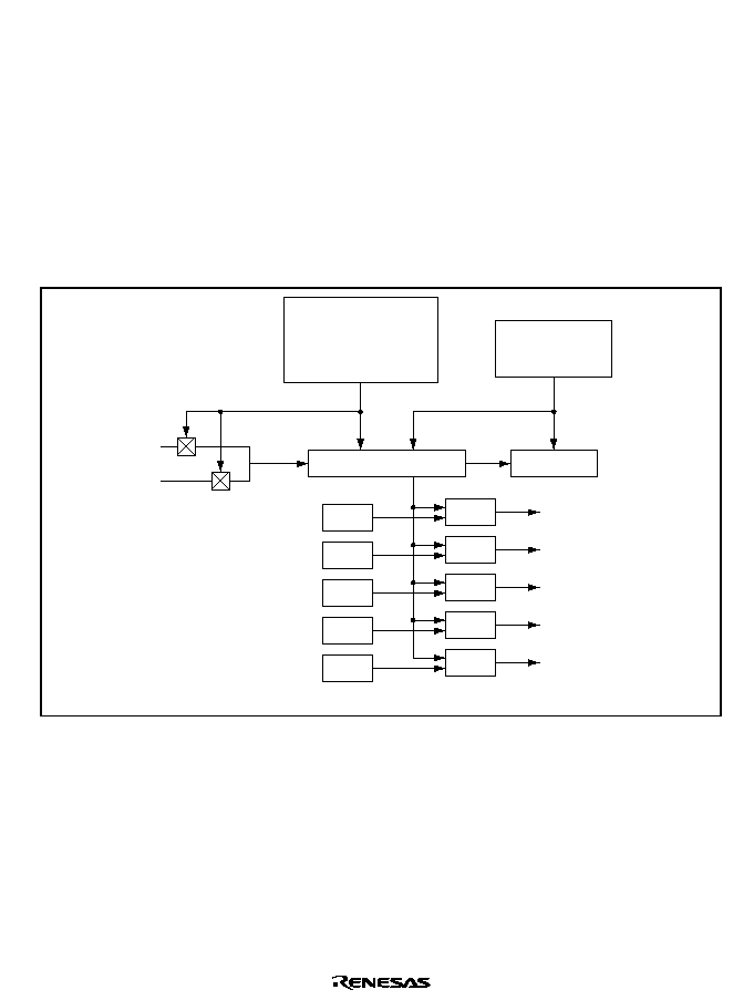
Rev. 1.0, 02/00, page 701 of 1141
26.13.6
Operation
CTL Circuit Operation: As shown in figure 26.49, the CTL discrimination/record circuit is
composed of a 16-bit up/down counter and 12-bit registers (
◊
5).
In playback (PB) mode, the 16-bit up/down counter counts on a
s/4 clock when the PB-CTL
pulse is high, and on a
s/5 clock when low. In record or slow mode, this counter increments the
count on a
s/4 clock. In ASM mode, this counter increments the count on a
s/8 clock when the
pulse is high, and on a
s/4 clock when low.
This counter always counts up in record and slow modes.
In playback or slow mode, it is cleared on the rise of PB-CTL signal. In record mode, it is cleared
on the rise of REF30X signal.
s/4
(
s/8)
s/5
(
s/4)
REC-CTL
(L0)
RCDR5
REC-CTL
(S0)
RCDR4
REC-CTL
(L1and ASM)
RCDR3
REC-CTL
(S1)
RCDR2
REC-CTL
Match
detection
Match
detection
Match
detection
Match
detection
Match
detection
RCDR1
12-bit register
UDF:
DOWN
UDF
Upper 12 bits
UP
UP/DOWN counter (16 bits)
Duty
detection
Counter clear signal
REF30X
(REC)
PB-CTL
(PB, ASM)
Up/Down control signal
REC: UP
PB, ASM:
UP when PB-CTL is high
Down when PB-CTL is low
Underflows when PB-CTL
duty is 44% or less
Figure 26.49 CTL Discrimination/Record Circuit
CTL Mode Register (CTLM) Switchover Timing: CTLM is enabled immediately after data is
written to the register. Care must be taken with changes in the operating state.
Capstan phase control is performed by the VD sync REF30X (X-value + tracking value) and PB-
CTL in ASM mode, and by the REF30P or CREF and CFG division signal (DVCFG2) in REC
mode. If CAPREF30 signal to be used for capstan phase control is always generated by XDR, the
value of XDR must be overwritten when switching between PB and REC modes. Figures 26.50
and 26.51 show examples of switch timing of CTLM and XDR.
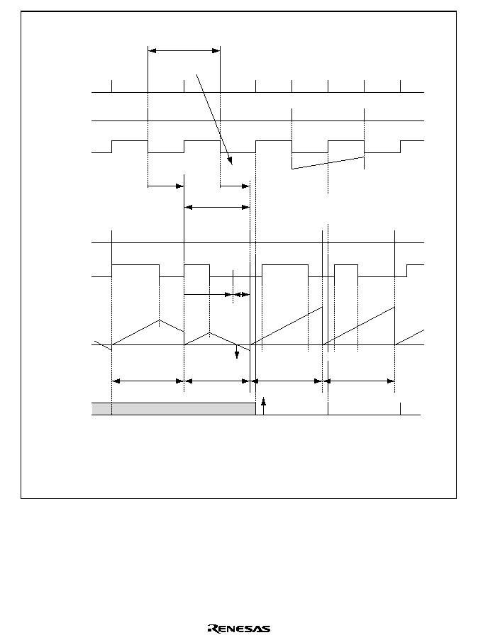
Rev. 1.0, 02/00, page 702 of 1141
VD
DVCFG2
REF30X
16bit
UP/DOWN
counter
HSW
CTL
Tx
Latch
Preset
The X-value is updated by REF30P. Modification of XDR must be performed
before REF30P in the cycle in which the X-value is changed.
X-value
X-value
after
change
RCDR3
RCDR1
RCDR2
REF30P
Ta
PB-CTL
Tb
1 pulse
UDF
0 pulse
0 pulse
CDIVR2
Register write
Ta is the interval calculated from RDCR3.
Tb is the interval in which switchover is performed
from ASM mode to REC mode.
Tx is the cycle in which the REF30X period is
shortened due to the change of XDR.
1 pulse
X-value (XDR) is
rewritten in this
cycle
RCDR1
Capstan phase control
ASM mode, PB mode : REF30X-PB-CTL
REC mode : REF30P-DVCFG2
/4
/5
/4
REC-CTL
Notes: 1.
2.
3.
Figure 26.50 Example of CTLM Switchover Timing
(When Phase Control Is Performed by REF30P and DVCFG2 in REC Mode)
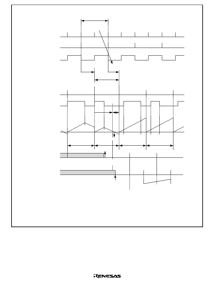
Rev. 1.0, 02/00, page 703 of 1141
VD
CREF
REF30X
16bit
UP/DOWN
counter
HSW
CTL
Tx
Latch
Preset
The X-value is updated by REF30P. Modification of XDR must be performed
before REF30P in the cycle in which the X-value is changed.
X value
X-value after
change
RCDR3
RCDR1
RCDR2
REF30P
Ta
PB-CTL
Tb
1 pulse
0 pulse
0 pulse
ASM-REC
switchover
Ta is the interval calculated from RDCR3.
Tb is the interval in which switchover is
performed from ASM mode to REC mode.
Tx is the cycle in which the REF30X period
is shortened due to the change of XDR.
With CREF and DVCFG2 phase alignment,
the frequency need not be 25 Hz or 30 Hz.
1 pulse
X-value (XDR) is
rewritten in this
cycle
DVCFG2
RCDR1
Capstan phase control
ASM mode, PB mode: REF30X-PB-CTL
Capstan phase control
REC mode : CREF30P-DVCFG2
/4
/5
/4
REC-CTL
CDIVR2
Register write
UDF
Notes: 1.
2.
3.
4.
Figure 26.51 Example of CTLM Switchover Timing
(When Phase Control Is Performed by CREF and DVCFG2 in Rec Mode)
Rev. 1.0, 02/00, page 704 of 1141
26.13.7
CTL Input Section
The CTL input section consists of an input amplifier of which gain can be controlled by the
register setting and a Schmitt amplifier. Figure 26.52 shows a block diagram of the CTL input
section.
Trivial CTL pulse signal is received from the CTL head, amplified by the input amplifier,
reshaped into a square wave by the Schmitt amplifier, and sent to the servo circuits, and the Timer
L as the PB-CTL signal. Control the CTL input amplifier gain by bits 3 to 0 in CTL gain control
register (CTLGR) of the servo port.
–
+
+
–
CTLFB
CTLSMT(i)
CTLFB
CTLREF
CTLBias
CTLGR0
CTLGR3 to 1
AMPSHORT
(REC-CTL)
PB-CTL(+)
Note : Be sure to set a capacitor between CTLAmp (o) and CTLSMT (i).
Note
PB-CTL(-)
AMPON
(PB-CTL)
– +
CTLAmp(o)
CTL(+)
CTL(-)
Figure 26.52 Block Diagram of CTL Input Amplifier
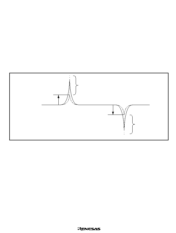
Rev. 1.0, 02/00, page 705 of 1141
CTL Detector: If the CTL detector fails to detect a CTL pulse, it sets the CTL control register
(CTCR) bit 1 to 1 indicating that the pulse has not been detected. If a CTL pulse is detected after
that, the bit is automatically cleared to 0. Duration used for determining detection or non-
detection of the pulse depends on magnitude of phase shift of the last detected pulse from the
reference phase (phase difference between REF30 and CTL signal). Typically, detection or non-
detection is determined within 3 to 4 cycles of the reference period.
If settings of the CTL gain control register are maintained in a table format, you can refer to it
when the CTL detector failed to detect CTL pulses. From the table, you can control amplifier gain
of the CTL according to state of UNCTL bit, thereby selecting an optimum CTL amplifier gain
depending on state of the pulse recorded.
Figure 26.53 illustrates concept of gain control for detecting the CTL input pulse.
*
V+TH (fixed)
*
V-TH (fixed)
Note: * CTL input sensitivity is variable depending on CTL
gain control register (CTLGR) setting.
Figure 26.53 CTL Input Pulse Gain Control
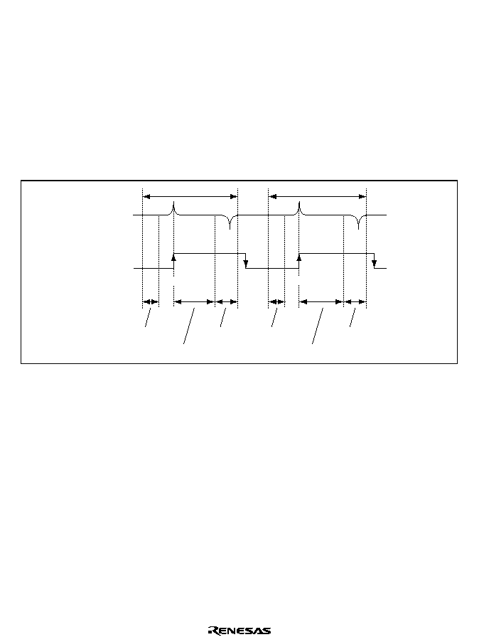
Rev. 1.0, 02/00, page 706 of 1141
PB-CTL Waveform Shaper in Slow Mode Operation: If bit 0 in CTL control register (CTCR)
is set to slow mode, slow reset function is activated. In slow mode, if falling edge is not detected
within the specified time from rising edge detection, PB-CTL is forcibly shut down (slow reset).
The time T
FS
(s) until the signal falls is the following interval after the rising edge of the internal
CTL signal is detected:
T
FS
= 16384
◊
4/
s
(
s = f
OSC
/2)
When f
OSC
= 10 MHz, T
FS
= 13.1 ms.
Figure 26.54 shows the PB-CTL waveform in slow mode.
CTL
waveform
Internal
CTL signal
1 frame
1 frame
Slow tracking delay
Slow tracking delay
Acceleration
Acceleration
Deceleration Deceleration
Slow
reset
Stop
Stop
CTLP
CTLP
Figure 26.54 PB-CTL Waveform in Slow Mode Operation

Rev. 1.0, 02/00, page 707 of 1141
26.13.8
Duty Discriminator
The duty discriminator circuit measures the period of the control signal recorded on the tape (PB-
CTL signal) and discriminates its duty cycle. In VISS or VASS detection, the duty I/O flag is set
or cleared according to the result of duty discrimination. The duty I/O flag is set to 1 when the
duty cycle of the PB-CTL signal is above 44%, and is cleared to 0 when the duty cycle is below
44%.
In ASM detection, an ASM mark is recognized (and the duty I/O flag is cleared to 0) when the
duty cycle is above 66%. When the duty cycle is below 66%, no ASM mark is recognized and the
duty I/O flag is set to 1.
The detection direction can be switched between forward and reverse by bit 5 (FW/RV) in the
CTL mode register.
Long or short pulse can be detected by comparing REC-CTL duty data register (RCDR2 to
RCDR5) and UP/DOWN counter. Long or short pulse is discriminated at PB-CTL signal falling.
Discrimination result is stored in bit 0 of bit pattern register (BTPR). At the same time, BTPR is
shifted to the left. LSP0 indicates 0 when short pulse is detected, and 1 when long pulse is
detected.
Set the threshold value of long/short pulse in RCDR2 to RCDR5. See the description on the
detection of the long/short pulse.
Figure 26.55 shows the duty cycle of the PB-CTL signal.
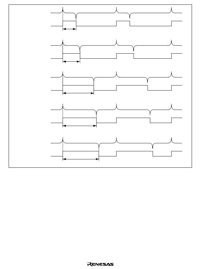
Rev. 1.0, 02/00, page 708 of 1141
Input signal
Short 1 pulse
25±0.5%
PB-CTL
Input signal
Long 1 pulse
30±0.5%
PB-CTL
Input signal
Short 0 pulse
57.5±0.5%
62.5±0.5%
PB-CTL
Input signal
Long 0 pulse
PB-CTL
Input signal
ASM mark
67 to 70%
PB-CTL
Figure 26.55 PB-CTL Signal Duty Cycle
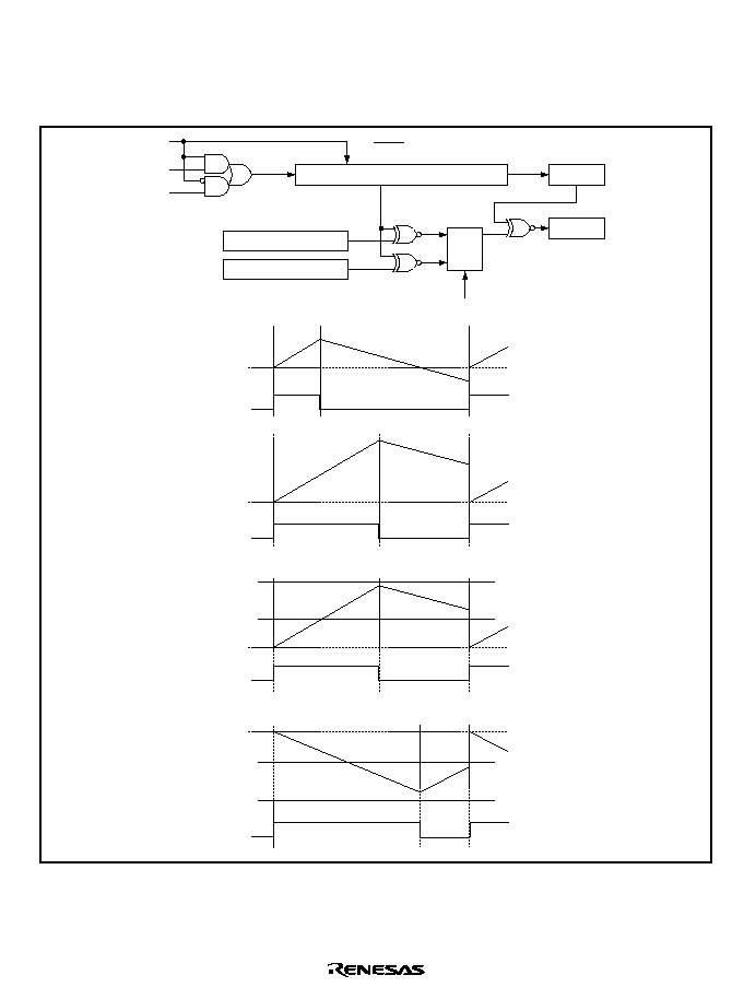
Rev. 1.0, 02/00, page 709 of 1141
Figure 26.56 shows the duty discrimination circuit. A 44% duty cycle is discriminated by
counting with the 16-bit up/down counter, using a
s/4 clock for the up-count and a
s/5 clock for
the down-count. An up-count is performed when the PB-CTL signal is high, and a down-count
when low. Long or short pulse is discriminated by comparing with RCDR2 to RCDR5.
Counter
PB-CTL
1 pulse
PB-CTL
PB-CTL
s/4
s/5
Counter
PB-CTL
0 pulse
s/4
s/5
Counter
FWD
PB-CTL
Short pulse
(0 pulse)
s/4
s/5
RCDR3
RCDR2
0 pulse L/S threshold value
1 pulse L/S threshold value
Counter
REV
PB-CTL
Long pulse
(1 pulse)
s/5
s/4
RCDR4
RCDR5
0 pulse L/S threshold value
1 pulse L/S threshold value
UP/DOWN
Comparison of upper
12-bit
UP/DOWN counter (16 bits)
* RCDR2or4 (12bit)
* FWD : Discriminated by RCDR2 and RCDR3
REV : Discriminated by RCDR4 and RCDR5
* RCDR3or5 (12bit)
0/1
discrimination
UDF
Clear
R
S
Q
s/4
s/5
L/S
discrimination
Figure 26.56 Duty Discriminator
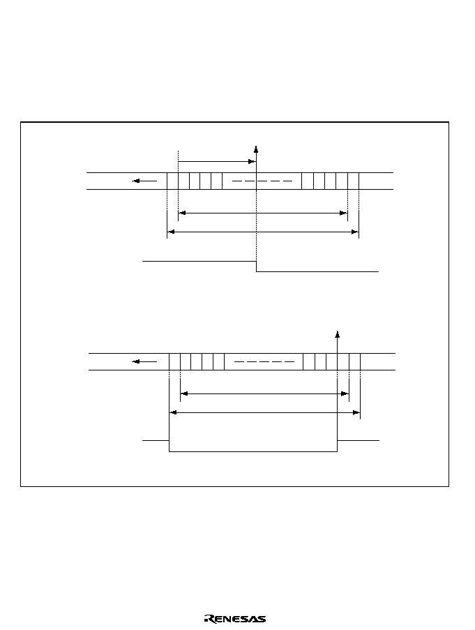
Rev. 1.0, 02/00, page 710 of 1141
VISS (Index) Detect Mode: VISS detection is carried out by the VISS control circuit, which
counts 1 pulses in the PB-CTL signal. If the pulse count detects any value set in the VISS
interrupt setting bits (bits 5, 6, or 7 in the duty I/O register), an interrupt request is generated and
the duty I/O flag is cleared to 0.
At VISS record or rewrite, INDEX code is automatically written. INDEX code is composed of 0
continuous 62-bit data with 0 pulse data at both edge.
Examples of bit strings and the duty I/O flag at VISS detection/record is illustrated in figure 26.57.
0
Tape direction
Duty I/O flag
(a) VISS detection (INDEX: Thirty-two 1 pulse setting)
1
1
1
1
61±3 bits
Thirty-two 1 pulses
detected
IRRCTL
63±3 bits
Start
1
1
1
1
0
0
Tape direction
Duty I/O flag
(b) VISS record
1
1
1
1
62 bits
IRRCTL
64 bits
Start
1
1
1
1
0
1
2
3
62 63 64
Figure 26.57 Examples of VISS Bit Strings and Duty I/O Flag
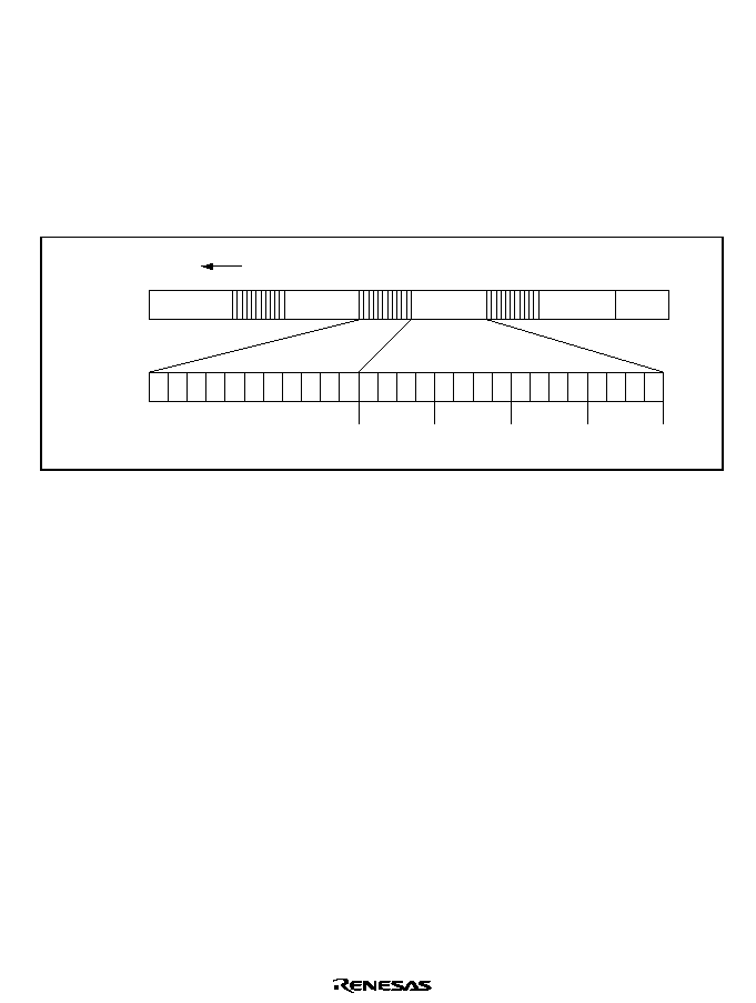
Rev. 1.0, 02/00, page 711 of 1141
Duty Detection Mode (VASS): VASS detection is carried out by the duty discriminator.
Software can detect index sequences by reading the duty I/O flag at each CTL pulse.
At each CTL pulse, the duty discriminator sends the result of duty discrimination to the duty I/O
flag, and simultaneously generates an interrupt request. The duty I/O flag is cleared to 0 if the
CTL pulse is a 1 (duty cycle below 44%), and is set to 1 if the CTL pulse is a 0 (duty cycle above
44%).
The duty I/O flag is modified at each CTL pulse. It should be read by the interrupt-handling
routine within the period of the PB-CTL signal. VASS detection format is illustrated in figure
26.58.
1
Tape direction
Written three times
1 1 1 1 1 1 1 1 1 1
M
S
B
L
S
B
L
S
B
M
S
B
M
S
B
L
S
B
L
S
B
M
S
B
Thousands
Header (11 bits)
Hundreds
Data (16 bits: 4 digits of 4-bit BCD)
Tens
Ones
Figure 26.58 VASS (Index) Format
Assemble (ASM) Mark Detect Mode: ASM mark detection is carried out by the duty
discriminator. If the duty discriminator detects that the duty cycle of the PB-CTL signal is 66% or
higher, it generates an interrupt request, and simultaneously clears the duty I/O flag to 0.
The duty I/O flag is updated at every CTL pulse. It should be read by the interrupt-handling
routine within the period of the PB-CTL signal.
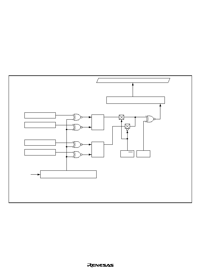
Rev. 1.0, 02/00, page 712 of 1141
Detection of the Long/Short Pulse: The long/short pulse is detected in PB mode by the L/S
determination based on the comparison of the REC-CTL duty register (RCDR2 to RCDR5) with
the up/down counter and the results of the duty I/O flag. The results of the determination is stored
in bit 0 (LSP0) of the bit pattern register (BTPR) at the rising edge of PB-CTL, shifting at the
same time BTPR leftward.
RCDR2-5 set the L/S thresholds for each of FWD/REV. Set to RCDR2 a threshold of 1 pulse L/S
for FWD, to RCDR3 a threshold of 0 pulse L/S for FWD, to RCDR4 a threshold of 0 pulse L/S for
REV, and to RCDR5 a threshold of 1 pulse L/S for REV. Figure 26.59 shows the detection of
long/short pulse.
Also, the bit pattern of 8-bit can be detected by BTPR. Check that an 8-bit detection has been
done by bit 1 (BPF bit) of the duty I/O register, and then read BTPR.
Bit patter register (8 bits)
Up/Down counter (16-bit)
RCDR2 (12bit)
High-order 12-bit data
L/S is determined at the rising edge of PB-CTL.
After the determination, bit pattern register is
shifted leftward, and the results of the determination
is stored in the LSB.
RCDR3 (12bit)
Internal bus
LSB
FW/RV
DI/O
Shift left-ward
BTPR
R
R
S
Q
RCDR4 (12bit)
RCDR5 (12bit)
R
S
Q
s/4
Note:
Figure 26.59 Detection of Long/Short Pulse

Rev. 1.0, 02/00, page 713 of 1141
26.13.9
CTL Output Section
An on-chip control head amplifier is provided for writing the REC-CTL signal generated by the
write control circuit onto the tape.
The write control circuit controls the duty cycle of the REC-CTL signal in the writing of VISS and
VASS sequences and ASM marks and the rewriting of VISS and VASS sequences. The duty
cycle of the REC-CTL signal is set in REC-CTL duty data registers 1 to 5 (RCDR1 to RCDR5).
Times calculated in terms of
s (= f
OSC
/2) should be converted to appropriate data to be set in these
registers. In VISS or VASS mode, set RCDR2 for a duty cycle of 25%
±
0.5%, RCDR3 for a duty
cycle of 30%
±
0.5%, RCDR4 for a duty cycle of 57.5
±
0.5%, and RCDR5 for a duty cycle of 62.5
±
0.5%. When 1 is written in the duty I/O flag, the REC-CTL signal will be written on the tape
with a 25%
±
0.5% duty cycle when 0 is written in bit 7 (LSP7) in the bit pattern register (BTPR)
and with a 30
±
0.5% duty cycle when 1 is written. Table 26.21 shows the relationship between
the REC-CTL duty register and CTL outputs.
In ASM mark write mode, set RCDR3 for a duty cycle of 67% to 70%. An ASM mark will be
written when 0 is written in the duty I/O flag.
An interrupt request is generated at the rise of the reference signal after one CTL pulse has been
written. The reference signal is derived from the output signal (REF30X) of the X-value
adjustment circuit, and has a period of one frame.
Figure 26.60 shows the timings that generate the REC-CTL signal.
Table 26.21 REC-CTL Duty Register and CTL Outputs
MODE
D/IO
LSP7
Pulse
RCDR
Duty
0
S1
RCDR2
25
±
0.5%
0
1
L1
RCDR3
30
±
0.5%
0
S0
RCDR4
57.5
±
0.5%
VISS, VASS modes
1
1
L0
RCDR5
65.5
±
0.5%
ASM mode
0
*
RCDR3
60 to 70%
Note:
*
Don't care.
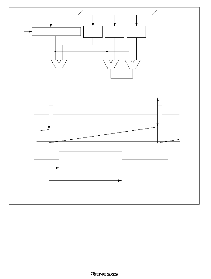
Rev. 1.0, 02/00, page 714 of 1141
W
Internal bus
RCDR2or4
(12 bits)
W
RCDR1
(12 bits)
UP/DOWN counter (12 bits)
Counter
REF30X
REC-CTL
Counter
reset
Match detection
Match detection
End of writing of one CTL
pulse (except VISS) IRRCTL
RCDR2 (VISS/VASS S1 pulse)
RCDR3 (VISS/VASS L1 pulse, or ASM)
RCDR4 (VISS/VASS S0 pulse)
RCDR5 (VISS/VASS L0 pulse)
RCDR1
Clear
Upper 12 bits
REC-CTL 0 pulse fall
timing
REC-CTL rise timing
REC-CTL1 pulse,
ASM fall timing
RESET
REF30X
W
RCDR3or5
(12 bits)
s/4
Compare
Compare
Compare
Figure 26.60 REC-CTL Signal Generation Timing
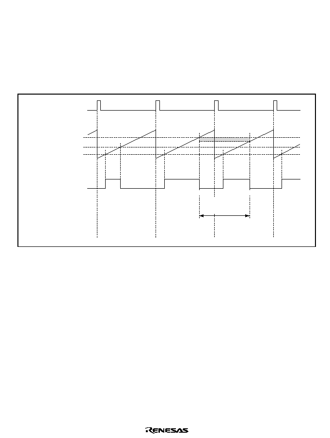
Rev. 1.0, 02/00, page 715 of 1141
The 16-bit counter in the REC-CTL circuit continues counting on a clock derived by dividing the
system clock
s (= f
OSC
/2) by 4. The counter is cleared on the rise of REF30X in record mode, and
on the rise of PB-CTL in rewrite mode. REC-CTL match detection is carried out by comparing
the counter value with each RCDR value.
RCDR1 to RCDR5 can be written to by software at all times. If RCDR is changed before the
respective match detection is performed, match detection is performed using the new value. The
value changed after match detection becomes valid on the rise of REF30X following the change.
Figure 26.61 shows examples of RCDR change timing.
REF30X
REC-CTL
RCDR1 RCDR2
RCDR1
1 pulse (Short)
0 pulse (Short)
Rewritten 0 pulse
(Short)
RCDR1
RCDR1
Counter
RCDR4
RCDR2
RCDR1
RCDR4
RCDR4
RCDR4
Interval in which
RCDR4 can be
written to
Figure 26.61 Example of RCDR Change Timing (Example Showing RCDR4)

Rev. 1.0, 02/00, page 716 of 1141
26.13.10 Trapezoid Waveform Circuit
In rewriting, the trapezoid waveform circuit leaves the rising edge of the already-recorded PB-
CTL signal intact, but changes the duty cycle.
In rewriting, the CTL pulse is written with reference to the rise of PB-CTL. The CTL duty cycle
for a rewrite is set in the REC-CTL duty data registers (RCDR2 to RCDR5). Time values T2 to
T5 are referenced to the rise of PB-CTL.
Figure 26.62 shows the rewrite waveform.
W
Internal bus
RCDR3or5
(12 bits)
W
Not used when
rewriting
RCDR2or4
(12 bits)
Up/Down counter (16 bits)
Clear
Upper 12 bits
REC-CTL 0 pulse
fall timing
REC-CTL 1 pulse
fall timing
RESET
PB-CTL
W
T
2
to T
5
Eliminated
pulse
High-impedance
interval
End of writing of one
CTL pulse (except
VISS) IRRCTL
RCDR1
(12 bits)
s/4
Compare
Compare
RCDR2 (BISS/VASS S1 pulse)
RCDR3 (VISS/VASS L1 pulse)
RCDR4 (VISS/VASS S0 pulse)
RCDR5 (VISS/VASS L0 pulse)
PB-CTL
REC-CTL when
rewriting
New pulse
Figure 26.62 Relationship between REC-CTL and RCDR2 to RCDR5 when Rewriting

Rev. 1.0, 02/00, page 717 of 1141
26.13.11 Note on CTL Interrupt
After a reset, the CTL circuit is in the VISS discrimination input mode.
Depending on the CTL pin states, a false PB-CTL input pulse may be recognized and an interrupt
request generated. If the interrupt request will be enabled, first clear the CTL interrupt request
flag.
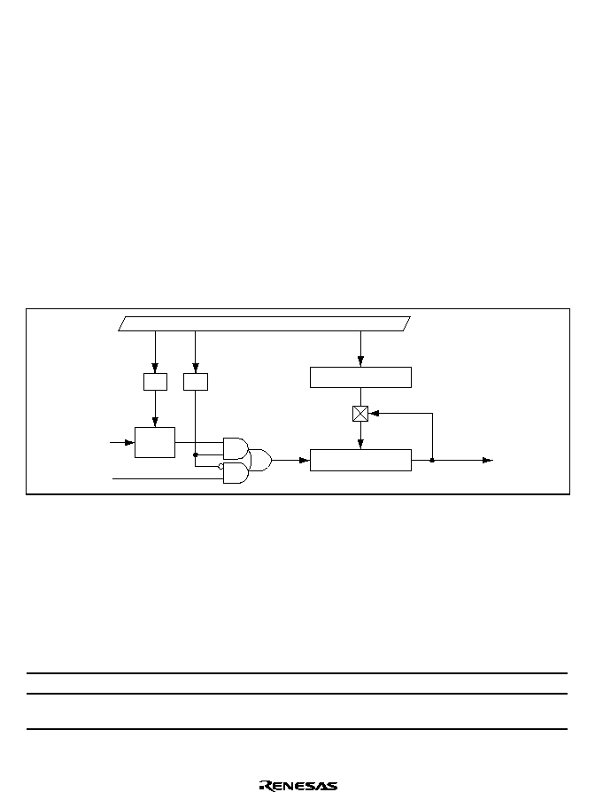
Rev. 1.0, 02/00, page 718 of 1141
26.14
Frequency Dividers
26.14.1
Overview
On-chip frequency dividers are provided for the pulse signal picked up from the control track
during playback (the PB-CTL signal), and the pulse signal received from the capstan motor (CFG
signal). The CTL frequency divider generates a CTL divided control signal (DVCTL) from the
PB-CTL signal, for use in capstan phase control during high-speed search, for example. The CFG
frequency divider generates two divided CFG signals (DVCFG for speed control and DVCFG2 for
phase control) from the CFG signal. The DFG noise canceller is a circuit which considers signal
less than 2
as noise and mask it.
26.14.2
CTL Frequency Divider
Block Diagram: Figure 26.63 shows a block diagram of the CTL frequency divider.
EXCTL
PB-CTL
,
DVCTL
UDF
R/W
W
(8 bits)
R/W
Internal bus
CEX
CTL division register
Down counter (8 bits)
CEG
Edge
detector
CTVC
CTLR
CTVC
Figure 26.63 CTL Frequency Divider
Register Description
-
Register configuration
Table 26.22 shows the register configuration of the CTL frequency dividers.
Table 26.22
Register Configuration
Name
Abbrev.
R/W
Size
Initial Value
Address
DVCTL control register
CTVC
R/W
Byte
Undefined
H'D098
CTL frequency division
register
CTLR
W
Byte
H'00
H'D099

Rev. 1.0, 02/00, page 719 of 1141
DVCTL Control Register (CTVC)
0
*
1
*
R
2
*
R
3
4
5
6
7
R
CFG
HSW
0
W
0
W
CEX
CEG
CTL
1
1
1
Bit :
Initial value :
R/W :
CTVC consists of the external input signal selection bits and the flags which show the CFG,
HSW, and CTL levels.
Note:
It has an undetermined value by a reset or in stand-by mode.
Bit 7
DVCTL Signal Generation Selection Bit (CEX): Selects which of the PB-CTL signal or
the external input signal is used to generate the DVCTL signal.
Bit 7
CEX
Description
0
Generates DVCTL signal with PB-CTL signal
(Initial value)
1
Generates DVCTL signal with external input signal
Bit 6
External Sync Signal Edge Selection Bit (CEG): Selects the edge of the external signal
at which the frequency division is made when the external signal was selected to generate DVCTL
signal.
Bit 6
CEG
Description
0
Rising edge
(Initial value)
1
Falling edge
Bits 5 to 3
Reserved: Cannot be modified and are always read as 1.
Bit 2
CFG Flag (CFG): Shows the CFG level.
Bit 2
CFG
Description
0
CFG is at low level
(Initial value)
1
CFG is at high level
Rev. 1.0, 02/00, page 720 of 1141
Bit 1
HSW Flag (HSW): Shows the level of the HSW signal selected by the VFF/NFF bit of the
HSW mode register 2 (HSM2).
Bit 1
HSW
Description
0
HSW is at low level
(Initial value)
1
HSW is at high level
Bit 0
CTL Flag (CTL): Shows the CTL level.
Bit 0
CTL
Description
0
REC or PB-CTL is at low level
(Initial value)
1
REC or PB-CTL is at high level
CTL Frequency Division Register (CTLR)
0
0
1
0
W
2
0
W
3
0
4
0
W
0
W
5
6
0
7
CTL4
CTL3
CTL2
CTL1
CTL0
0
W
CTL7
W
W
W
CTL6
CTL5
Bit :
Initial value :
R/W :
CTLR is an 8-bit write-only register to set the frequency dividing value (N-1 if divided by N) for
PB-CTL. If a read is attempted, an undetermined value is read out.
PB-CTL is divided by N at its rising edge. If the register value is 0, no division operation is
performed, and the DVCTL signal with the same cycle with PB-CTL is output. It is initialized by
a reset or in stand-by mode.
Rev. 1.0, 02/00, page 721 of 1141
Operation: During playback, control pulses recorded on the tape are picked up by the control
head and input to the CTL pin. The control pulse signal is amplified by a Schmitt amplifier,
reshaped, then input to the CTL frequency divider as the PB-CTL signal.
This circuit is employed when the control pulse (PB-CTL signal) is used for phase control of the
capstan motor. The divided signal is sent as the DVCTL signal to the capstan phase system in the
servo circuits and timer R.
The CTL frequency divider is an 8-bit reload timer consisting of a reload register and a down-
counter. Frequency division is obtained by setting frequency-division data in bits 7 to 0 in the
CTL frequency division register (CTLR), which is the reload register. When a frequency division
value is written in this reload register, it is also written into the down-counter. The down-counter
is decremented on rising edges of the PB-CTL signal.
Figure 26.64 shows examples of the PB-CTL and DVCTL waveforms.
CTL input signal
CTLR: CTL frequency division register
PB-CTL or external
sync signal
CTLR=00
CTLR=01
CTLR=02
Figure 26.64 CTL Frequency Division Waveforms
Rev. 1.0, 02/00, page 722 of 1141
26.14.3
CFG Frequency Divider
Block Diagram: Figure 26.65 shows a block diagram of the 7-bit CFG frequency divider and its
mask timer.
W
R/W
W
W
W
W
W
R
W
Internal bus
CMN
CRF
UDF
UDF
UDF
CFG
DVCFG
DVCFG2
,
MCGin
Internal bus
CPS1,
CPS0
CTMR(6 bits)
CDIVR2(7 bits)
DVTRG
PB(ASM)
REC
s = fosc/2
s/1024
s/512
s/256
s/128
Down counter (6 bits)
CDIVR(7 bits)
CMK
S
R
Edge
select
CDVC
CDVC
CDVC
CDVC
CDVC
Down counter (7 bits)
Down counter (7 bits)
Figure 26.65 CFG Frequency Divider

Rev. 1.0, 02/00, page 723 of 1141
Register Description:
∑
Register configuration
Table 26.23 shows the register configuration of the CFG frequency division circuit.
Table 26.23 Register Configuration
Name
Abbrev.
R/W
Size
Initial Value
Address
DVCFG control register
CDVC
R/W
Byte
H'60
H'D09A
CFG frequency division
register 1
CDIVR1
W
Byte
H'80
H'D09B
CFG frequency division
register 2
CDIVR2
W
Byte
H'80
H'D09C
DVCFG mask period
register
CTMR
W
Byte
H'FF
H'D09D
DVCFG Control Register (CDVC)
0
0
1
0
W
2
0
W
3
4
0
W
5
1
6
--
--
1
7
W
R
CMK
CMN
W
DVTRG
0
R/W*
MCGin
CRF
CPS1
CPS0
0
Note: * Only 0 can be written
Bit :
Initial value :
R/W :
CDVC is an 8-bit register to control the capstan frequency division circuit.
It is initialized to H'60 by a reset, or in stand-by or module stop mode.
Bit 7
Mask CFG Flag (MCGin): MCGin is a flag to indicate occurrence of a frequency
division signal during the mask timer's mask period. To clear it by software, write 0 after reading
1. Also, setting has the highest priority in this flag. If a condition setting the flag and 0 write
occur simultaneously, the latter is invalid.
Bit 7
MCGin
Description
0
CFG is in normal operation
(Initial value)
1
Shows that DVCFG was detected during masking (runaway detected)
Bit 6
Reserved: Cannot be modified and is always read as 1.

Rev. 1.0, 02/00, page 724 of 1141
Bit 5
CFG Mask Status Bit (CMK): Indicates the status of the mask. It is initialized to 1 by a
reset, or in stand-by or module stop mode.
Bit 5
CMK
Description
0
Indicates that the capstan mask timer has released masking
1
Indicates that the capstan mask timer is currently masking
(Initial value)
Bit 4
CFG Mask Selection Bit (CMN): Selects the turning on/off of the mask function.
Bit 4
CMN
Description
0
Capstan mask timer function on.
(Initial value)
1
Capstan mask timer function off.
Bit 3
PB (ASM)
REC Transition Timing Sync ON/OFF Selection Bit (DVTRG): Selects
the On/Off of the timing sync of the transition from PB (ASM) to REC when the DVCFG2 signal
is generated.
Bit 3
DVTRG
Description
0
PB (ASM)
REC transition timing sync on.
(Initial value)
1
PB (ASM)
REC transition timing sync off.
Bit 2
CFG Frequency Division Edge Selection Bit (CRF): Selects the edge of the CFG signal
to be divided.
Bit 2
CRF
Description
0
Performs frequency division at the rising edge of CFG.
(Initial value)
1
Performs frequency division at both edges of CFG.

Rev. 1.0, 02/00, page 725 of 1141
Bits 1 and 0
CFG Mask Timer Clock Selection Bits (CPS1, CPS0): Selects the clock source
for the CFG mask timer. (
s = fosc/2)
Bit 1
Bit 0
CPS1
CPS0
Description
0
s/1024
(Initial value)
0
1
s/512
0
s/256
1
1
s/128
CFG Frequency Division Register 1 (CDIVR1)
0
0
1
0
W
2
0
W
3
4
0
W
5
0
6
7
--
--
W
W
CDV15
CDV14
0
W
CDV16
0
W
CDV13
CDV12
CDV11
CDV10
1
Bit :
Initial value :
R/W :
CDIVR1 is an 8-bit write-only register to set the division value. If a read is attempted, an
undetermined value is read out. Bit 7 is reserved.
The frequency division value is written in the reload register and the down counter at the same
time.
CFG's frequency is divided by N at its rising edge or both edges If the register value is 0, no
division operation is performed, and the DVCFG signal with the same input cycle with CFG
signal is output. The DVCFG signal is sent to the capstan speed error detector. It is initialized to
H'80 by a reset or in stand-by mode together with the capstan frequency division register and the
down counter.

Rev. 1.0, 02/00, page 726 of 1141
CFG Frequency Division Register 2 (CDIVR2)
0
0
1
0
W
2
0
W
3
4
0
W
5
0
6
7
--
--
W
W
CDV25
CDV24
0
W
CDV26
0
W
CDV23
CDV22
CDV21
CDV20
1
Bit :
Initial value :
R/W :
CDIVR2 is an 8-bit write-only register to set the division value. If a read is attempted, an
undetermined value is read out. Bit 7 is reserved.
The frequency division value is written in the reload register and the down counter at the same
time.
CFG's frequency is divided by N at its rising edge or both edges If the register value was 0, no
division operation is performed, and the DVCFG signal with the same input cycle with CFG is
output. The DVCFG2 signal is sent to the capstan speed error detector and the Timer L.
The DVCFG2 circuit has no mask timer function.
The frequency division counter starts its division operation at the point data was written in
CDIVR2. If synchronization is required for phase matching, for example, do it by writing in
CDIVR2. If the DVTRG bit of the CDVC register is 0, the register synchronizes with the
switching timing from PB (ASM) to REC.
It is initialized to H'80 by a reset or in stand-by mode together with the capstan frequency division
register and the down counter.
DVCFG Mask Period Register (CTMR)
0
1
1
1
W
2
1
W
3
4
1
W
5
1
6
7
--
--
--
--
W
W
CPM5
CPM4
1
W
CPM3
CPM2
CPM1
CPM0
1
1
Bit :
Initial value :
R/W :
CTMR is an 8-bit write-only register. If a read is attempted, an undetermined value is read out.
CTMR is a reload register for the mask timer (down counter). Set in it the mask period of CFG.
The mask period is determined by the clock specified by the bits 1 and 0 of CDVC and the set
value (N - 1). If data is written in CTMR, it is written also in the mask timer at the same time.
It is initialized to H'FF by a reset, or in stand-by or module stop mode.
Mask period = N
◊
clock cycle

Rev. 1.0, 02/00, page 727 of 1141
Operation:
∑
Frequency divider
The CFG pulses output from the capstan motor are sent to internal circuitry as the CFG signal
via the zero-cross type comparator. The CFG signal, shaped into a rectangular waveform by a
reshaping circuit, is divided by the CFG frequency dividers, and used in servo control. The
rising edge or both edges of the CFG signal can be selected for the frequency divider.
The CFG frequency divider consists of a 7-bit frequency divider with a mask timer for capstan
speed control (DVCFG signal generator) and a 7-bit frequency divider for capstan phase
control (DVCFG2 signal generator).
The DVCFG signal generator consists of a 7-bit reload register (CFG frequency division
register1: CDIVR1), a 7-bit down-counter, and a 6-bit mask timer (with settable mask
interval). Frequency division is performed by setting the frequency-division value in 7-bit
CDIVR1. When the frequency-division value is written in CDIVR1, it is also written in the
down-counter. After frequency-division of a CFG signal for which the edge has been selected,
the signal is sent via the mask timer to the capstan speed error detector as the DVCFG signal.
The DVCFG2 signal generator consists of a 7-bit reload register (CFG frequency division
register 2: CDIVR2) and a 7-bit down-counter. The 7-bit frequency divider does not have a
mask timer. Frequency division is performed by setting the frequency-division value in
CDIVR2. When the frequency-division value is written in CDVIR2, it is also written in the
down-counter. After frequency division of a CFG signal for which the edge has been selected,
the signal is sent to the capstan speed error detector and timer L as the DVCFG2 signal.
Frequency division starts when the frequency-division value is written.
When DVTRG bit in CDVC register is set to 0, reloading is executed with the switch over
timing from PB (ASM) mode to REC mode. To switch from REF30 to CREF, change the
settings of bit 4 (CR/RF bit) in the capstan phase error detection control register (CPGCR). If
synchronization is necessary for phase control, this can be provided by writing the frequency-
division value in CDIVR2.
The down-counters are decremented on rising edges of the CFG signal when the CRF bit is 0
in the DVCFG control register (CDVC), and on both edges when the CRF bit is 1.
Figure 26.66 shows examples of CFG frequency division waveforms.
Rev. 1.0, 02/00, page 728 of 1141
CFG
CRF bit=1
CDIVR=00
CRF bit=0
CDIVR=00
CRF bit=0
CDIVR=01
CRF bit=0
CDIVR=02
Figure 26.66 CFG Frequency Division Waveforms
Rev. 1.0, 02/00, page 729 of 1141
∑
Mask timer
The capstan mask timer is a 6-bit reload timer that uses a prescaled clock as a clock source.
The mask timer is used for masking DVCFG signal intended for controlling the capstan speed.
The capstan mask timer prevents edge detection to be carried out for an unnecessarily long
duration by masking the edge detection for a certain period. The above trouble can result from
abnormal revolution (runout) of the capstan motor because its revolution has to cover a wide
range speeds from the low/still up to the high speed search.
The capstan mask timer is started by a pulse edge in the divided CFG signal (DVCFG). While
the timer is running, a mask signal disables the output of further DVCFG pulses. The mask
signal is shown in figure 26.67.
The mask timer status can be monitored by reading the CMK flag in the DVCFG control
register (CDVC).
Mask
DVCFG
Mask timer
underflow
Figure 26.67 Mask Signal
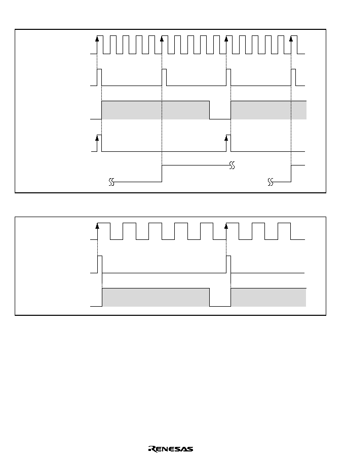
Rev. 1.0, 02/00, page 730 of 1141
Figures 26.68 and 26.69 show examples of CFG mask timer operations.
CFG (racing)
Edge detect
Cleared by wiring 0
after reading 1
Capstan motor
mask timer
Mask interval
Mask interval
DVCFG
MCGin flag
Figure 26.68 CFG Mask Timer Operation (When Capstan Motor is Racing)
CFG
Edge detect
Capstan motor
mask timer
Mask interval
Mask interval
Figure 26.69 CFG Mask Timer Operation (When Capstan Motor is Operating Normally)
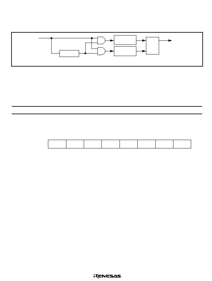
Rev. 1.0, 02/00, page 731 of 1141
26.14.4
DFG Noise Removal Circuit
Block Diagram: Figure 26.70 shows the block diagram of the DFG noise removal circuit.
Rising edge
detection
Delay circuit
DFG
S
Q
R
NCDFG
delay = 2
Falling edge
detection
Figure 26.70 DFG Noise Removal Circuit
Register Description: Table 26.24 shows the register configuration of the DFG mask circuit.
Table 26.24 Register Configuration
Name
Abbrev.
R/W
Size
Initial Value
Address
FG control register
FGCR
W
Byte
H'FE
H'D09E
FG Control Register (FGCR)
0
0
1
1
2
1
3
1
4
1
5
1
6
1
7
--
--
--
--
--
--
--
--
--
--
--
--
--
--
W
DRF
1
Bit :
Initial value :
R/W :
FGCR selects the edge of the DFG noise removal signal (NCDFG) to be sent to the drum speed
error detector. If a read is attempted, an undetermined value is read out.
It is initialized to H'FE by a reset, or in stand-by or module stop mode.
The edge selection circuit is located in the drum speed error detector, and outputs the register
output to the drum speed error detector.
Bits 7 to 1
Reserved: Cannot be modified and are always read as 1.
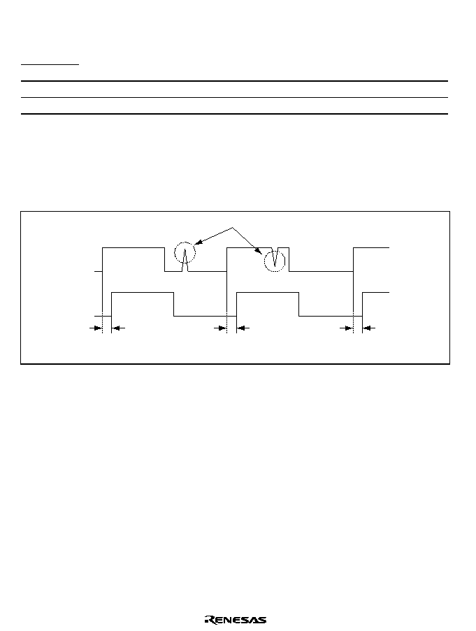
Rev. 1.0, 02/00, page 732 of 1141
Bit 0
DFG Edge Selection Bit (DRF): Selects the edge of the NCDFG signal used in the drum
speed error detector.
Bit 0
DRF
Description
0
Selects the rising edge of NCDFG signal
(Initial value)
1
Selects the falling edge of NCDFG signal
Operation
The DFG noise removal circuit generates a signal (NCDFG signal) as a result of removing noise
(signal fluctuation smaller than 2
) from the DFG signal. The resulted NCDFG signal is behind
the time when the DFG signal was detected by 2
. Figure 26.71 shows the NCDFG signal.
DFG
NCDFG
Noise
2
2
2
= fosc
Figure 26.71 NCDFG Signal

Rev. 1.0, 02/00, page 733 of 1141
26.15
Sync Signal Detector
26.15.1
Overview
This block performs detection of the horizontal sync signal (Hsync) and vertical sync signal
(Vsync) from the composite sync signal (Csync), noise counting, and field detection.
It detects the horizontal and vertical sync signals by setting threshold in the register and based on
the servo clock (
s = fosc/2). Noise masking is possible during the detection of the horizontal
sync signals, and if any Hsync pulse is missing, it can be supplemented. Also, if total volume of
the noise detected in one frame of Csync amounted over a specified volume, the detector generates
a noise detection interrupt.
Note:
This circuit detects a pulse with a specific width set by the threshold register. It does not
classify or restore the sync signal to a formal one.
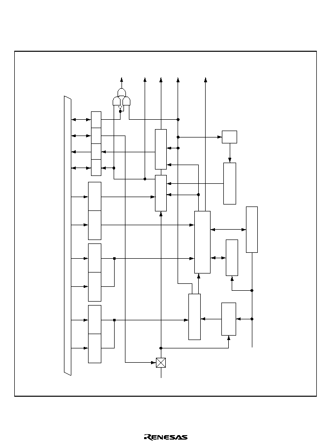
Rev. 1.0, 02/00, page 734 of 1141
26.15.2
Block Diagram
Figure 26.72 shows the block diagram of the sync signal detector.
W
H threshold
register
W
V threshold
register
(6 bits)
(4 bits)
HTR
VTR
W
W
H complement
start time register
Complementary
H pulse width
register
(8 bits)
(4 bits)
HPWR
HRTR
W
W
(6 bits)
(8 bits)
NDR
R/W
R/W
R/(W)
R
NOIS
H counter (8 bits)
Noise detector
Complement control &
nozzle mask control circuit
Up/Down
counter (6 bits)
SEPH
Selection of
polarity
Noise detection
window
Noise detection interrupt
VD interrupt
Csync
Sync signal detector
H reload counter (8 bits)
Field detector
Noise counter (10 bits)
Toggle
circuit
Clear
FLD
SYCT
VD(SEPV)
FIELD
NOISE
IRRSNC
OSCH
NIS/VD
SYNCR
NWR
Internal bus
s = fosc/2
s/2
Noise detection
window register
Noise
detection register
Figure 26.72 Block Diagram of the Sync Signal Detector

Rev. 1.0, 02/00, page 735 of 1141
26.15.3
Pin Configuration
Table 26.25 shows the pin configuration of the sync signal detector.
Table 26.25 Pin Configuration
Name
Abbrev.
I/O
Function
Composite sync signal input pin
Csync
Input
Composite sync signal input
26.15.4
Register Configuration
Table 26.26 shows the register configuration of the sync signal detector.
Table 26.26 Register Configuration
Name
Abbrev.
R/W
Size
Initial Value
Address
Vertical sync signal
threshold register
VTR
W
Byte
H'C0
H'D0B0
Horizontal sync signal
threshold register
HTR
W
Byte
H'F0
H'D0B1
H complement start time
setting register
HRTR
W
Byte
H'00
H'D0B2
Complement H pulse
width setting register
HPWR
W
Byte
H'F0
H'D0B3
Noise detection window
setting register
NWR
W
Byte
H'C0
H'D0B4
Noise detector
NDR
W
Byte
H'00
H'D0B5
Sync signal control
register
SYNCR
R/W
Byte
H'F8
H'D0B6

Rev. 1.0, 02/00, page 736 of 1141
26.15.5
Register Description
Vertical Sync Signal Threshold Register (VTR)
0
0
1
0
W
2
0
W
3
0
4
0
W
5
0
6
1
7
--
--
--
--
W
W
W
VTR5
VTR4
VTR3
VTR2
VTR1
VTR0
1
Bit :
Initial value :
R/ W :
VTR is an 8-bit write-only register that sets the threshold for the vertical sync signal when the
signal is detected from the composite sync signal. The threshold is set by bits 5 to 0 (VTR5 to
VTR0). Bits 7 and 6 are reserved. If a read is attempted, an undetermined value is read out. It is
initialized to H'C0 by a reset, or in stand-by or module stop mode.
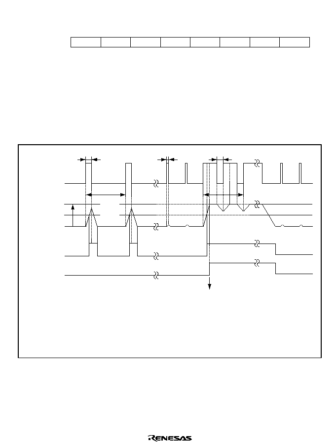
Rev. 1.0, 02/00, page 737 of 1141
Horizontal Sync Signal Threshold Register (HTR)
0
0
1
0
W
2
0
W
3
0
4
5
6
1
7
--
--
--
--
--
--
--
--
W
W
HTR3
HTR2
HTR1
HTR0
1
1
1
Bit :
Initial value :
R/W :
HTR is an 8-bit write-only register that sets the threshold for the horizontal sync signal when the
signal is detected from the composite sync signal. The threshold is set by bits 3 to 0 (HTR3 to
HTR0). Bits 7 and 4 are reserved. If a read is attempted, an undetermined value is read out. It is
initialized to H'F0 by a reset, or in stand-by or module stop mode.
Figure 26.73 shows the threshold values and separated sync signals.
[Legend]
TH
Hpuls
T H
SEPV
Hpuls
: Period of the horizontal sync signal (NTSC: 63.6, PAL: 64 [
µ
s])
: Pulse width of the horizontal sync signal (NTSC, PAL: 4.7 [
µ
s])
VVTH
HVTH
: Value set as the threshold of the vertical sync signal
: Value set as the threshold of the horizontal sync signal
SEPV
SEPH
: Detected vertical sync signal
: Detected horizontal sync signal (before complement)
T H
SEPH
Csync
H'00
Counter value
1/2 Hpuls
VD interrupt
Hpuls
VVTH
HVTH
Figure 26.73 Threshold Values and Separated Sync Signals

Rev. 1.0, 02/00, page 738 of 1141
Example
The values set to detect the vertical and horizontal sync signals (SEPV, SEPH) from Csync
are required to meet the following conditions. Assumed that the set values in VTHR
register were VVTH and HVTH,
(VVTH-1)
◊
2/
s > Hpulse
(HVTH-2)
◊
2/
s
Hpulse/2 < (HVTH-1)
◊
2/
s
Where, Hpulse is pulse width (
µ
s) of the horizontal sync signal, and
s is servo clock
(fosc/2).
Thus, if
s = 5 MHz, NTSC system is used,
(VVTH-1)
◊
0.4
µ
s > 4.7
µ
s
VVTH
H'D
(VVTH-2)
◊
0.4
µ
s
2.35
µ
s < (HVTH-1)
◊
0.4
µ
s
VVTH
H'7
Note:
This circuit detects the pulse with the width set in VTHR. If a noise pulse with the width
greater than the set value is input, the circuit regards it as a sync signal.

Rev. 1.0, 02/00, page 739 of 1141
H Complement Start Time Setting Register (HRTR)
0
0
1
0
W
2
0
W
3
0
4
0
W
0
W
5
6
0
7
HRTR4
HRTR3
HRTR2
HRTR1
HRTR0
0
W
HRTR7
W
W
W
HRTR6
HRTR5
Bit :
Initial value :
R/W :
HRTR is an 8-bit write-only register that sets the timing to generate a complementary pulse if a
pulse of the horizontal sync signal is missing.
If a read is attempted, an undetermined value is read out. It is initialized to H'00 by a reset, or in
stand-by or module stop mode.
((Value of HRTR7-0) + 1)
◊
2/
s = TH
where, TH is the period of the horizontal sync signal (
µ
s), and
s is the servo clock (fosc/2).
Whether the horizontal sync signal exists or not is determined one clock before the
complementary pulse is generated. Accordingly, set to HRTR7 to HRTR0 a value obtained from
the equation shown above plus one.
Also, HRTR7-HRTR0 sets the noise mask period. If the horizontal sync signal has the normal
pulses, it is masked in the mask period.
The start and the end of the mask period are computed frm the rising edge of OSCH and SEPH,
respectively. See figure 26.75.
Complementary H Pulse Width Setting Register (HPWR)
0
0
1
0
W
2
0
W
3
0
4
5
6
1
7
--
--
--
--
--
--
--
--
W
W
HPWR3
HPWR2
HPWR1
HPWR0
1
1
1
Bit :
Initial value :
R/W :
HRWR is an 8-bit write-only register that sets the pulse width of the complementary pulse which
is generated if a pulse of the horizontal sync signal is missing. Bits 7 to 4 are reserved.
If a read is attempted, an undetermined value is read out. It is initialized to H'F0 by a reset or in
stand-by mode.
((Value of HPWR3-0) + 1)
◊
2/
s = Hpulse
Where, Hpuls is the pulse width of the horizontal sync signal (
µ
s), and
s is the servo clock
(fosc/2).

Rev. 1.0, 02/00, page 740 of 1141
Noise Detection Window Setting Register (NWR)
0
0
1
0
W
2
0
W
3
0
4
0
W
5
0
6
1
7
--
--
--
--
W
W
W
NWR5
NWR4
NWR3
NWR2
NWR1
NWR0
1
Bit :
Initial value :
R/W :
NWR is an 8-bit write-only register that sets the period (window) when the drop-out of the
horizontal sync signal pulse is detected and the noise is counted. Set the timing of the noise
detection window in bits 5 to 0. Bits 7 and 6 are reserved.
If a read is attempted, an undetermined value is read out. It is initialized to H'C0 by a reset, or in
stand-by or module stop mode.
Set the value of the noise detection window timing according to the following equation.
((Value of NWR5-0) + 1)
◊
2/
s = 1/4
◊
TH
Where, TH is the pulse width of the horizontal sync signal (
µ
s), and
s is the servo clock (fosc/2).
It is recommended that this timing value is set at about 1/4 of the cycle of the horizontal sync
signal.
Noise Detection Register (NDR)
0
0
1
0
W
2
0
W
3
0
4
0
W
0
W
5
6
0
7
NDR4
NDR3
NDR2
NDR1
NDR0
0
W
NDR7
W
W
W
NDR6
NDR5
Bit :
Initial value :
R/W :
NDR is an 8-bit write-only register that sets the noise detection level when the noise of the
horizontal sync signal is detected (when NWR is set). Set the noise detection level in bits 7 to 0.
No read is valid. If a read is attempted, an undetermined value is read out. It is initialized to H'00
by a reset, or in stand-by or module stop mode.
The noise detector takes counts of the drop-outs of the horizontal sync signal pulses and the noise
within the pulses, and if they amount to a count greater than four times of the value set in NDR7-
NDR0, the detector sets the NOIS flag in the sync signal control register (SYNCR). Set the noise
detection level at 1/4 of the noise counts in one frame.
The noise counter is cleared whenever Vsync is detected twice.
See section 26.15.6, Noise Detection for the details of the noise detection window and the noise
detection level.

Rev. 1.0, 02/00, page 741 of 1141
Sync Signal Control Register (SYNCR)
0
0
1
0
R
2
0
R/(W)*
3
1
4
5
6
1
7
--
--
--
--
--
--
--
--
R/W
R/W
NIS/VD
NOIS
FLD
SYCT
1
1
1
Note: * Only 0 can be written
Bit :
Initial value :
R/W :
SYNCR is an 8-bit register that controls the noise detection, field detection, polarity of the sync
signal input, etc.
It is initialized to H'F8 by a reset, or in stand-by mode. Bits 7 to 4 are reserved. No write is valid.
Bit 1 is read-only.
Bits 7 to 4
Reserved: Cannot be modified and are always read as 1.
Bit 3
Interrupt Selection Bit (NIS/VD): Selects whether an interrupt request is generated by
noise level detection or VD signal detection.
Bit 3
NIS/VD
Description
0
Interrupt at the noise level
1
Interrupt at VD
(Initial value)
Bit 2
Noise Detection Flag (NOIS): NOIS is a status flag indicating that the noise counts
reached at more than four times of the value set in NDR. The flag is cleared only by writing 0
after reading 1. Care is required because it is not cleared automatically.
Bit 2
NOIS
Description
0
Noise count is smaller than four times of the value set in NDR
(Initial value)
1
Noise count is the same or greater than four times of the value set in NDR
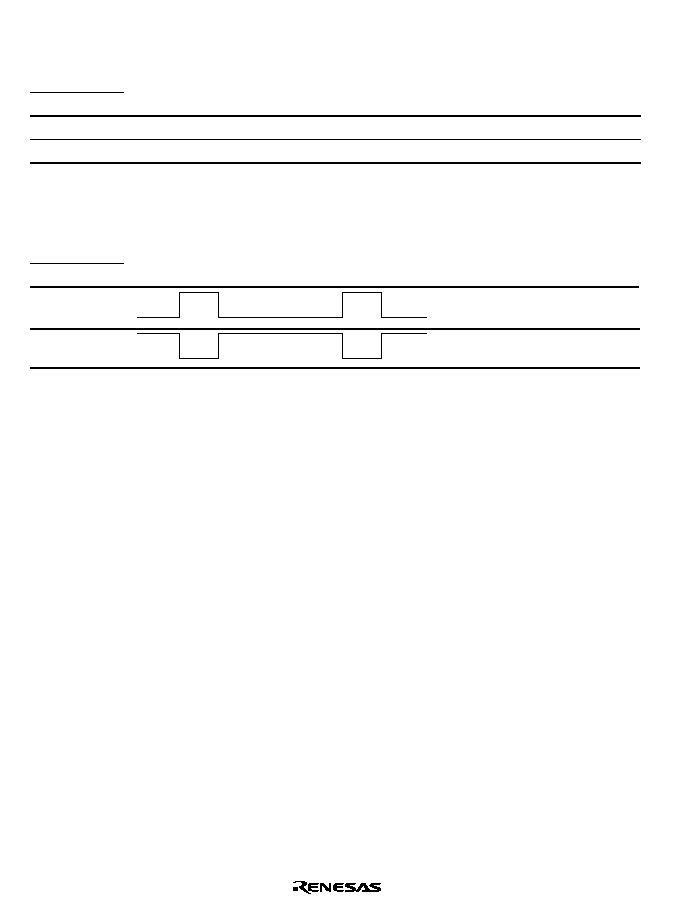
Rev. 1.0, 02/00, page 742 of 1141
Bit 1
Field Detection Flag (FLD): Indicates whether the field currently being scanned is even
or odd. See figure 26.74.
Bit 1
FLD
Description
0
Odd field
(Initial value)
1
Even field
Bit 0
Sync Signal Polarity Selection Bit (SYCT): Selects the polarity of the sync signal
(Csync) to be input.
Bit 0
SYCT
Description
Polarity
0
(Initial value)
Positive
1
Negative
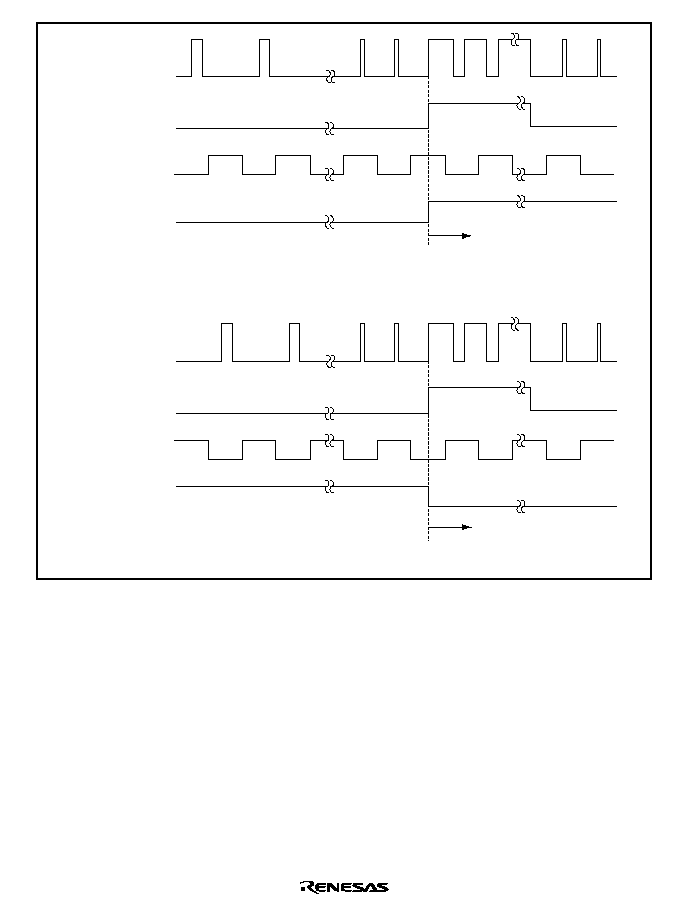
Rev. 1.0, 02/00, page 743 of 1141
Field detection
flag (FLD)
SEPV
Noise detection
window
Composite sync
signal
Even field
(a) Even field
Field detection
flag (FLD)
SEPV
Noise detection
window
Composite sync
signal
Odd field
(b) Odd field
Figure 26.74 Field Detection

Rev. 1.0, 02/00, page 744 of 1141
26.15.6
Noise Detection
If a pulse of the horizontal sync signal is missing, a complementary pulse is set at the timing set in
HPWR and with the set pulse width.
Set the noise detection window with HWR of about 1/4 of the horizontal sync signal, and the pulse
with equal high and low periods will be obtained.
Example of Setting: Assumed that a complementary pulse is set when fosc = 10MHz under the
conditions
s = 5 MHz, NTSC:TH = 63.6 (
µ
s) and Hpuls = 4.7 (
µ
s), the set values of the
complementary pulse timing (HRTR7-0), complementary pulse width (HPWR3-0), and noise
detection window timing (NWR5-0) are expressed by the following equations.
(Value of HRTR7-0)
◊
2/
s = TH
((Value of HPWR3-0) + 1)
◊
2/
s = Hpuls
((Value of NWR5-0) + 1)
◊
2/
s = 1/4
◊
TH
Where, TH is the cycle of the horizontal sync signal (
µ
s), Hpuls is the pulse width of the
horizontal sync signal (
µ
s) and
s is the servo clock (Hz) (fosc/2).
Accordingly,
(Value of HRTR7-0)
◊
0.4 (
µ
s) = 63.6 (
µ
s)
HRTR7-0=H'9F
((Value of HPWR3-0) + 1)
◊
0.4 (
µ
s) = 4.7 (
µ
s)
HRTR3-0=H'B
((Value of NWR5-0) + 1)
◊
0.4 (
µ
s) = 16 (
µ
s)
NWR5-0=H'27
Also, the noise mask period is computed as follows.
((Value of HRTR7-0) + 1)
-
24)
◊
2/
s = 54 (
µ
s)
Where, 24 is a constant required for a structural reason.
Figure 26.75 shows the set period for HRTR, HPWR, and NWR.

Rev. 1.0, 02/00, page 745 of 1141
[Legend]
SEPH
Noise detection
window
Noise mask for
OSCH
OSCH
Noise mask for
H counter
H reload
counter
H counter
SEPH
c
OSCH
: Horizontal sync signal after detection
: Horizontal sync signal after complement
a
b
: Value set for the noise detection window (NWR5 to NWR0)
: Value set for the pulse width of the horizontal sync signal (NPWR3 to NPWR0)
c
a, b, c
: Value set for complement timing (HRTR7 to HRTR0)
: Complements of 1 of a,b,c, respectively
H ' E 8
TH
:Complement of 2 of multiplier 24 in the equation for the noise mask period
(The noise mask period ends 24 counts before the overflow of H reload counter.)
: Cycle of the horizontal sync signal
(NTSC:63.6 [ms], PAL:64[ms])
TM : Timing at which the noise mask period ends.
A horizontal sync
pulse is missing
The pulse in the mask
period is ignored
TH
a
b
H'00
OVF
H'E8
c
a
Mask
period
Period determined
by NWR5 to NWR0
Mask
period
TM
Mask
period
Mask
period
Mask
period
Mask
period
Mask
period
Mask
period
TH
Don't mask
immediately
after
complement.
period deter-
mined
by a and a
Period determined
by HRTR7 to HRTR0
period determined
by c and H'E8
Period determined
by HPWR3 to HPER0
period
determined
by b
Do mask also im-
mediately after
complement.
Figure 26.75 Set Period for HRTR, HPWR, and NWR

Rev. 1.0, 02/00, page 746 of 1141
Noise Detection Operation: The noise detector considers an irregular pulse of the composite sync
signal (Csync) and a chip of a horizontal sync signal pulse within a frame as noise. The noise
counter takes counts of the irregular pulses during the high period of the noise detection window
and the chips and drop-outs of the horizontal sync signal pulses during the low period. The noise
detector counts more than one irregular pulses as one. The noise counter is cleared at every frame
(Vsync is detected twice).
The equalizing pulse contained in 9H of the vertical sync signal is counted also as an irregular
pulse.
The noise detection flag (NOIS) in the sync signal control register (SYNCR) is set to 1 if the count
of the irregular pulses + the count of the pulse chips and drop-outs of the horizontal sync signal >
4
◊
(value of NDR7 to 0).
See the description on the sync signal control register (SYNCR) is section 26.15.5, Register
Description, for the NOIS bit.
Figure 26.76 shows the operation of the noise detection.
Csync
Noise detection
window
Noise detection
flag (NOIS)
Noise counter
Noise detection
level
Noise detection
flag is set.
NOIS : Bit 3 of the sync signal control register (SYNCR)
Noise
Figure 26.76 Operation of the Noise Detection

Rev. 1.0, 02/00, page 747 of 1141
26.15.7
Activation of the Sync Signal Detector
After release of reset or transition from the power down mode to the active mode, the sync signal
detector starts operation by a sync signal input after release of module stop. The pulse of the
polarity specified by the SYCT bit of the sync signal control register (SYNCR) is input to the
detector. The detector starts operation even if this pulse is a noise pulse with a width smaller than
the regular width. The minimum pulse width which can activate the detector is not constant
depending on the internal operation of the input circuit. Accordingly, if the assured activation of
the detector is required, input a pulse with a width greater than 4/
s (
s = fosc/2 (Hz)). In such a
case, care is required to noise, because even a pulse with a width smaller than 4
/s may cause
activation.

Rev. 1.0, 02/00, page 748 of 1141
26.16
Servo Interrupt
26.16.1
Overview
The interrupt exception processing of the servo module is started by one of ten factors, i.e. the
drum speed error detector (
◊
2), drum phase error detector, capstan speed error detector (
◊
2),
capstan phase error detector, HSW timing generator (
◊
2), sync detector, and CTL circuit. For
these interrupt factors, see each of their circuit sections of this manual.
For details of exception processing, see section 5, Exception Handling.
26.16.2
Register Configuration
Table 26.27 shows the list of the registers which control the interrupt of the servo section.
Table 26.27 Registers which Control the Interrupt of the Servo Section
Name
Abbrev.
R/W
Size
Initial Value
Address
Servo interrupt
enable register 1
SIENR1
R/W
Byte
H'00
H'D0B8
Servo interrupt
enable register 2
SIENR2
R/W
Byte
H'FC
H'D0B9
Servo interrupt request
register 1
SIRQR1
R/W
Byte
H'00
H'D0BA
Servo interrupt request
register 2
SIRQR2
R/W
Byte
H'FC
H'D0BB
26.16.3
Register Description
Servo Interrupt Enable Register 1 (SIENR1)
0
0
1
0
R/W
2
0
R/W
3
0
4
0
R/W
0
R/W
5
6
0
7
IECAP3
IECAP2
IECAP1
IEHSW2
IEHSW1
0
R/W
IEDRM3
R/W
R/W
R/W
IEDRM2
IEDRM1
Bit :
Initial value :
R/W :
SIENR1 is an 8-bit read/write register that enables or disables interrupts in the servo section. It is
initialized to H'00 by a reset, or in stand-by or module stop mode.

Rev. 1.0, 02/00, page 749 of 1141
Bit 7
Drum Phase Error Detection Interrupt Enable Bit (IEDRM3)
Bit 7
IEDRM3
Description
0
Disables the request of the interrupt by IRRDRM3
(Initial value)
1
Enables the request of the interrupt by IRRDRM3
Bit 6
Drum Speed Error Detection (Lock Detection) Interrupt Enable Bit (IEDRM2)
Bit 6
IEDRM2
Description
0
Disables the request of the interrupt by IRRDRM2
(Initial value)
1
Enables the request of the interrupt by IRRDRM2
Bit 5
Drum Speed Error Detection (OVF, Latch) Interrupt Enable Bit (IEDRM1)
Bit 5
IEDRM1
Description
0
Disables the request of the interrupt by IRRDRM1
(Initial value)
1
Enables the request of the interrupt by IRRDRM1
Bit 4
Capstan Phase Error Detection Interrupt Enable Bit (IECAP3)
Bit 4
IECAP3
Description
0
Disables the request of the interrupt by IRRCAP3
(Initial value)
1
Enables the request of the interrupt by IRRCAP3
Bit 3
Capstan Speed Error Detection (Lock Detection) Interrupt Enable Bit (IECAP2)
Bit 3
IECAP2
Description
0
Disables the request of the interrupt by IRRCAP2
(Initial value)
1
Enables the request of the interrupt by IRRCAP2

Rev. 1.0, 02/00, page 750 of 1141
Bit 2
Capstan Speed Error Detection (OVF, Latch) Interrupt Enable Bit (IECAP1)
Bit 2
IECAP1
Description
0
Disables the request of the interrupt by IRRCAP1
(Initial value)
1
Enables the request of the interrupt by IRRCAP1
Bit 1
HSW Timing Generation (counter clear, capture) Interrupt Enable Bit (IEHSW2)
Bit 1
IEHSW2
Description
0
Disables the request of the interrupt by IRRHSW2
(Initial value)
1
Enables the request of the interrupt by IRRHSW2
Bit 0
HSW Timing Generation (OVW, Matching, STRIG) Interrupt Enable Bit (IEHSW1)
Bit 0
IEHSW1
Description
0
Disables the request of the interrupt by IRRHSW1
(Initial value)
1
Enables the request of the interrupt by IRRHSW1

Rev. 1.0, 02/00, page 751 of 1141
Servo Interrupt Enable Register 2 (SIENR2)
0
0
1
0
R/W
2
3
4
5
6
1
7
--
--
--
--
--
--
--
--
--
--
--
--
R/W
IESNC
IECTL
1
1
1
1
1
Bit :
Initial value :
R/W :
SIENR2 is an 8-bit read/write register that enables or disables interrupts in the servo section. It is
initialized to H'FC by a reset, stand-by or module stop.
Bits 7 to 2
Reserved: Cannot be modified and are always read as 1.
Bit 1
Vertical Sync Signal Interrupt Enable Bit (IESNC)
Bit 1
IESNC
Description
0
Disables the request of the interrupt (interrupt to the vertical sync signal) by
IRRSNC
(Initial value)
1
Enables the request of the interrupt by IRRSNC
Bit 0
CTL Interrupt Enable Bit (IECTL)
Bit 0
IECTL
Description
0
Disables the request of the interrupt by IRRCTL
(Initial value)
1
Enables the request of the interrupt by IRRCTL

Rev. 1.0, 02/00, page 752 of 1141
Servo Interrupt Request Register 1 (SIRQR1)
0
0
1
0
R/(W)*
2
0
R/(W)*
3
0
4
0
R/(W)*
0
R/(W)*
5
6
0
7
IRRCAP3 IRRCAP2 IRRCAP1 IRRHSW2 IRRHSW1
0
R/(W)*
IRRDRM3
R/(W)*
R/(W)*
R/(W)*
IRRDRM2 IRRDRM1
Note: * Only 0 can be written to clear the flag.
Bit :
Initial value :
R/W :
SIRQR1 is an 8-bit read/write register that indicates interrupt request in the servo section. If the
interrupt request has occurred, the corresponding bit is set to 1.
Only 0 can be written to clear the flag. It is initialized to H'00 by a reset, or in stand-by or module
stop mode.
Bit 7
Drum Phase Error Detector Interrupt Request Bit (IRRDRM3)
Bit 7
IRRDRM3
Description
0
No interrupt request from the drum phase error detector.
(Initial value)
1
Interrupt requested from the drum phase error detector.
Bit 6
Drum Speed Error Detector (Lock Detection) Interrupt Request Bit (IRRDRM2)
Bit 6
IRRDRM2
Description
0
No interrupt request from the drum speed error detector (lock detection).
(Initial value)
1
Interrupt requested from the drum speed error detector (lock detection).
Bit 5
Drum Speed Error Detector (OVF, Latch) Interrupt Request Bit (IRRDRM1)
Bit 5
IRRDRM1
Description
0
No interrupt request from the drum speed error detector (OVF, latch).
(Initial value)
1
Interrupt requested from the drum speed error detector (OVF, latch).

Rev. 1.0, 02/00, page 753 of 1141
Bit 4
Capstan Phase Error Detector Interrupt Request Bit (IRRCAP3)
Bit 4
IRRCAP3
Description
0
No interrupt request from the capstan phase error detector.
(Initial value)
1
Interrupt requested from the capstan phase error detector.
Bit 3
Capstan Speed Error Detector (Lock Detection) Interrupt Request Bit (IRRCAP2)
Bit 3
IRRCAP2
Description
0
No interrupt request from the capstan speed error detector (lock detection).
(Initial value)
1
Interrupt requested from the drum speed error detector (lock detection).
Bit 2
Drum Speed Error Detector (OVF, Latch) Interrupt Request Bit (IRRCAP1)
Bit 2
IRRCAP1
Description
0
No interrupt request from the capstan speed error detector (OVF, latch).
(Initial value)
1
Interrupt requested from the capstan speed error detector (OVF, latch).
Bit 1
HSW Timing Generator (Counter Clear, Capture) Interrupt Permission Bit
(IRRHSW2)
Bit 1
IRRHSW2
Description
0
No interrupt request from the HSW timing generator (counter clear, capture).
(Initial value)
1
Interrupt requested from the HSW timing generator (counter clear, capture).

Rev. 1.0, 02/00, page 754 of 1141
Bit 0
HSW Timing Generator (OVW, Matching, STRIG) Interrupt Permission Bit
(IRRHSW1)
Bit 0
IRRHSW1
Description
0
No interrupt request from the HSW timing generator (OVW, matching, STRIG).
(Initial value)
1
Interrupt requested from the HSW timing generator (OVW, matching, STRIG).

Rev. 1.0, 02/00, page 755 of 1141
Servo Interrupt Request Register 2 (SIRQR2)
0
0
1
0
R/(W)*
2
3
4
5
6
1
7
--
--
--
--
--
--
--
--
--
--
--
--
R/(W)*
IRRSNC
IRRCTL
1
1
1
1
1
Note: * Only 0 can be written to clear the flag.
Bit :
Initial value :
R/W :
SIRQR2 is an 8-bit read/write register that indicates interrupt request in the servo section. If the
interrupt request has occurred, the corresponding bit is set to 1.
Writing 0 after reading 1 is allowed; no other writing is allowed. It is initialized to H'FC by a
reset, or in stand-by or module stop mode.
Bits 7 to 2
Reserved: Cannot be modified and are always read as 1.
Bit 1
Vertical Sync Signal Interrupt Request Bit (IRRSNC)
Bit 1
IRRSNC
Description
0
No interrupt request from the sync signal detector (VD, noise)
(Initial value)
1
Interrupt requested from the sync signal detector (VD, noise)
Bit 0
CTL Signal Interrupt Request Bit (IRRCTL)
Bit 0
IRRCTL
Description
0
No interrupt request from CTL
(Initial value)
1
Interrupt requested from CTL

Rev. 1.0, 02/00, page 757 of 1141
Section 27 Sync Separator for OSD and Data Slicer
27.1
Overview
The sync separator separates the horizontal sync signal and vertical sync signal from the
composite video signal input from the CVin2 terminal and sends the sync signals to the on screen
display (OSD) module and data slicer.
The sync separator has an automatic frequency controller (AFC), which generates a reference
clock at 576 or 448 times the horizontal sync signal frequency. This reference clock is used to
separate the horizontal sync signal from the composite video signal. The AFC receives the Hsync
signal processed by the H complement and mask counter. The H complement and mask counter
removes noise and equalizing pulses from the Hsync signal and interpolates necessary pulses for
the Hsync signal.
The sync separator separates the vertical sync signal from the composite video signal through the
counting operation of the V complement and mask counter. The V complement and mask counter
increments the count at double the frequency of the horizontal sync signal to mask the Vsync
noise and to generate complementary pulses for the Vsync signal according to the register settings.
Through the above functions, the sync signals can be separated correctly against noise input to the
CVin2 terminal, motor skew due to VCR tape playback or special-function playback, and
abnormal noise in a weak field.
In addition, the sync separator provides the field detection function necessary for the data slicer,
and the noise detection function necessary for tuner detection (detecting the tuning status).
As the AFC reference clock is also used as the dot clock of the OSD, switching the reference clock
can change the dot width of the display. When the text display mode of the OSD is used, refer to
section 27.3.6, Automatic Frequency Controller (AFC).
In addition to the CVin2 video signal, the following signals can be selected as sources of sync
separation through the external circuit and register settings: the Csync composite sync signal input
from the Csync/Hsync terminal, and the separate Vsync and Hsync signals input from the
VLPF/Vsync and Csync/Hsync terminals, respectively.

Rev. 1.0, 02/00, page 758 of 1141
27.1.1
Features
∑
Horizontal sync signal separation: Stable separation is provided by the AFC, and complement
and mask functions are available.
∑
AFC reference clock frequency: 576 or 448 times the frequency of the horizontal sync signal
can be selected.
∑
Vertical sync signal separation: The masking and complement functions are available through
the V complement and mask counter.
∑
The source for sync separation can be selected from three signals (five methods).
1. Composite video signal input from the CVin2 terminal (two methods)
2. Csync signal input from the Csync/Hsync terminal (two methods)
3. Vsync and Hsync signals that are input from the VLPF/Vsync and Csync/Hsync terminals,
respectively (one method)
∑
Csync separation comparator: The slice level can be selected by register settings.
∑
Polarity of the Csync/Hsync terminal input: The signal detection polarity can be selected.
∑
Polarity of the VLPF/Vsync terminal input: The signal detection polarity can be selected.
∑
Noise detection: Noise during one frame is counted and a noise detection interrupt is
generated when the count reaches the specified value.
∑
Noise detection counter: The count is readable and is reset every other vertical sync signal
input.
∑
Field detection: The odd or even field for interlace scanning is distinguished.
∑
Reference Hsync signal for the AFC: The reference Hsync signal can be selected.
∑
V complement and mask counter: The source for the counter clock (twice the frequency of the
horizontal sync signal) can be selected.
∑
Internal Csync generator: The clock source for the internal Csync generator can be selected.
27.1.2
Block Diagram
Figure 27.1 shows the block diagram of the sync separator.
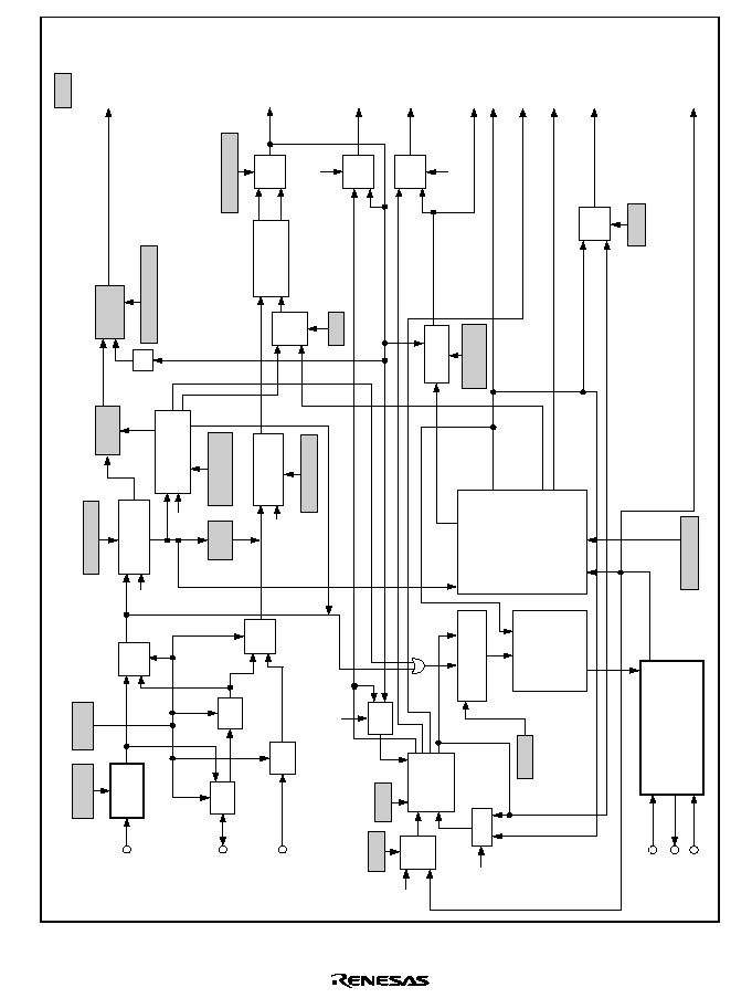
Rev. 1.0, 02/00, page 759 of 1141
Slicing v
oltage
control
Separ
ation
method
Digital H
separ
ation
counter
Vvth register
Selecting 576 or 448
as the division r
atio
Digital
LPF ON
Switching
Switching
Ref
erence
Hsync
Inter
nally gener
ated
Hsync
Exter
nal
Hsync
Switching
Switching
F
requency-dividing
counter
Complement and
mask setting register
Switching
Switching
Reset
f
or V
Reset
f
or H
TV f
o
r
mat
in H
(Self-
r
unning)
Inter
nal Csync
gener
ator
AFC error output
circuit
(compar
ator)
When the data slicer is used and the te
xt
displa
y mode is selected in the OSD
,
the AFC cloc
k is selected;
the cloc
k is
also used as the dot cloc
k.
When the data slicer is not used
and the te
xt displa
y mode is
selected in the OSD
, the
self-r
unning signal is selected.
Switching
Switching
Switching
Switching
Switching
Ref
erence cloc
k
Masking
Complement
and mask
Complement enab
le bit
(Self-r
unning)
Field detection windo
w
Field detection
Field detection
windo
w register
Hvth register
Noise
detection
Noise detection
windo
w
Noise
counter
Noise detection
interr
upt
:
Register
V complement enab
led:
Complemented and
mask
ed V
V complement disab
led:
Mask
ed V
Exter
nal Vsync
(data
slicer)
Exter
nal Vsync
interr
upt
Field signal (data slicer)
Exter
nal Hsync
(data slicer)
Detection windo
w
signals f
or data slicer
(data slicer)
Inter
nally gener
ated
sync signal (OSD)
Cloc
k r
un-in per
iod and star
t bit per
iod
AFCH
Dot cloc
k (OSD)
Noise detection le
v
el register
Csync
separ
ation
compar
ator
I/O
s
witching
P
olar
ity
s
witching
P
olar
ity
s
witching
CVin2
Hsync
Vsync
Si/TEXT
HCKSEL
(TE)
(0)
(1)
(Si)
SEPH
1/2
U/D
inV
HHK
C
H complement and
mask counter
(complement and
mask functions)
R
OSCH
AFCV
Si/TEXT
SEPV
OSC2H
C
R
C
C
R
Digital V
separ
ation
counter
U/D
C
/2
/2
/2
Csync/Hsync
Vsync/VLPF
(1)
(0)
(TE)
OSDFLD
OSD
V (OSD)
Si = AFCV
TEXT = inV
OSDH (OSD)
Field signal (OSD)
Si = AFCFLD
TEXT = inFLD
(TE)
(0)
(1)
inFLD
AFCFLD
(Si)
(Si)
Si/TEXT
HCKSEL
VCKSL
AFC2H 2
◊
fh
4/2fsc
Si/TEXT
AFCosc
AFCpc
AFCLPF
AFC
(Si)
AFCH
AFC oscillator
HSEL
(TE)
V complement and
mask counter
(complement and
mask functions)
R
C
Figure 27.1 Sync Separator Block Diagram

Rev. 1.0, 02/00, page 760 of 1141
27.1.3
Pin Configuration
Table 27.1 shows the pin configuration of the sync separator.
Table 27.1
Sync Separator Pin Configuration
Name
Abbrev.
I/O
Function
Sync signal
input/output
Csync/Hsync
Input/output
Composite sync signal input/output or
horizontal sync signal input
VLPF/Vsync
Input
Pin for connecting external LPF for
vertical sync signal or input pin for
vertical sync signal
AFCosc
Input/output
AFC oscillation signal
AFC oscillation
signals
AFCpc
Input/output
AFC by-pass capacitor connecting pin
LPF for AFC
AFCLPF
Input/output
External LPF connecting pin for AFC
Composite video
signal
CVin2
Input
Composite video signal input (2 Vpp,
with a sync tip clamp circuit)
27.1.4
Register Configuration
Table 27.2 shows the sync separator registers.
Table 27.2
Sync Separator Registers
Name
Abbrev.
R/W
Size
Initial
Value
Address
*
1
Sync separation input mode register
SEPIMR
R/W
Byte
H'00
H'D240
Sync separation control register
SEPCR
R/(W)
*
2
Byte
H'00
H'D241
Sync separation AFC control register
SEPACR
R/(W)
*
2
Byte
H'10
H'D242
Horizontal sync signal threshold register
HVTHR
W
Byte
H'E0
H'D243
Vertical sync signal threshold register
VVTHR
W
Byte
H'00
H'D244
Field detection window register
FWIDR
W
Byte
H'F0
H'D245
H complement and mask register
HCMMR
W
Word
H'0000
H'D246
Noise detection counter
NDETC
R
Byte
H'00
H'D248
Noise detection level register
NDETR
W
Byte
H'00
H'D248
Data slicer detection window register
DDETWR
W
Byte
H'00
H'D249
Internal sync signal frequency register
INFRQR
W
Byte
H'10
H'D24A
Notes: 1. Lower 16 bits of the address.
2. Only 0 can be written to clear the flag.
Rev. 1.0, 02/00, page 761 of 1141
27.2
Register Description
27.2.1
Sync Separation Input Mode Register (SEPIMR)
0
0
0
0
0
0
0
0
7
R/W
FRQSEL
0
R/W
CCMPV1
6
R/W
CCMPV0
5
R/W
COMPSL
4
R/W
SYNCT
3
R/W
VSEL
2
R/W
DLPFON
1
--
--
Bit :
Initial value :
R/W :
The SEPIMR is an 8-bit read/write register for selecting the source signals for sync separation. In
addition to the internal switches controlled by this register setting, the external circuits are used to
select the sources of the Hsync and Vsync signals to be supplied to the digital H separation
counter and the digital V separation counter, respectively. Figure 27.2 and table 27.3 show the
source signal selection. The SEPIMR also specifies the slicing voltage of the Csync separation
comparator, switches the polarity of the signals input from the Csync/Hsync and VLPF/Vsync
terminals, turns on or off the digital LPF, and switches the reference clock frequency for the AFC.
For details on the source signals for sync separation, refer to section 27.3.1, Selecting Source
Signals for Sync Separation. When reset, the SEPIMR is initialized to H'00.
CVin2
Csync
a
1
1
0
0
b
a
b
Hsync
Vsync
VLPF
VLPF/Vsync
Csync/Hsync
Hsync
Vsync
DLPFON
External
SW3
Internal
SW5
Internal
SW6
External
SW2
External
SW1
Reference
voltage switch
Register
control
I/O
switch
I/O
switch
Polarity
switch
Sync tip
clamp
Digital V
separation
counter
Csync polarity
Schmitt circuit
Vsync polarity
Schmitt circuit
External circuit
Inside LSI
Csync
separation
comparator
External
SW4
CVin2
≠
+
CCMPSL
CCMPV0, 1
SYNCT
VSEL
SEPV
SEPH
Digital H
separation
counter
Polarity
switch
Figure 27.2 Diagram of the Circuit for Selecting the Source Signals for Sync Separation

Rev. 1.0, 02/00, page 762 of 1141
Table 27.3
Source Signals for Sync Separation
Input
Source
Vsync
Detector
External
SW1
External
SW2
External
SW3
External
SW4
CCMPSL
(Internal
SW5)
VSEL
(Internal
SW6)
Csync/
Hsync
Terminal
CVin2
input
Vsync
Schmitt
Off
On
a
a
0
0
Output
Csync
Schmitt
Off
Off
Open
Input
fixed to
OVss
0
1
Output
Csync
input
Vsync
Schmitt
On
On
a
a
1
0
Input
Csync
Schmitt
On
Off
a
Input
fixed to
OVss
1
1
Input
Hsync/
Vsync
input
Vsync
Schmitt
Off
Off
b
b
1
0
Input
Bits 7 and 6
Csync Separation Comparator Slicing Voltage Select
(CCMPV1 and CCMPV0): Select the slicing voltage for the Csync separation comparator. The
value set by these bits is the slicing level against the sync tip level (≠40 IRE). Note that this slicing
level is used only for reference.
Bit 7
Bit 6
CCMPV1
CCMPV0
Description
0
0
The Csync slicing level is 10 IRE
(Initial value)
1
The Csync slicing level is 5 IRE
1
0
The Csync slicing level is 15 IRE
1
The Csync slicing level is 20 IRE

Rev. 1.0, 02/00, page 763 of 1141
Bit 5
Csync Separation Comparator Input Select (CCMPSL): Controls internal switch SW5
to select whether to use the Csync separation comparator input or Csync Schmitt input. Writing 0
to this bit selects the Csync separation comparator input, and writing 1 selects the Csync Schmitt
input. This bit also controls the input/output status of the Csync/Hsync terminal. Writing 0 to this
bit makes the Csync/Hsync an output terminal, and writing 1 makes it an input terminal. Note that
the Csync/Hsync terminal enters a high-impedance state at reset and in sleep, subactive, subsleep,
watch, standby, and module stop modes.
Bit 5
CCMPSL
Description
0
The Csync separation comparator input is selected
The Csync/Hsync terminal operates as an output terminal
(Initial value)
1
The Csync Schmitt input is selected
The Csync/Hsync terminal operates as an input terminal
Bit 4
Sync Signal Polarity Select (SYNCT): This bit selects the polarity of the Csync/Hsync
and VLPF/Vsync input signals. When using the CVin2 input signal, be sure to write 0 to this bit to
select the positive polarity.
Bit 4
SYNCT
Description
0
(Initial value)
1
Bit 3
Vsync Input Signal Select (VSEL): Controls internal switch SW6 to select the Vsync
input signal. Writing 0 to this bit selects the Vsync Schmitt input, and writing 0 selects the Csync
Schmitt input.
Bit 3
VSEL
Description
0
Vsync Schmitt input
(Initial value)
1
Csync Schmitt input

Rev. 1.0, 02/00, page 764 of 1141
Bit 2
Digital LPF Control (DLPFON): Specifies the digital LPF function, which masks noise
components of the Vsync signal in a weak field. The digital LPF logically ORs the Csync signal
(Vsync signal) and the SEPH signal that is separated by the digital H separation counter, then
inputs the ORed result to the digital V separation counter. This function prevents Vsync detection
delay and Vsync detection miss in a weak field. For the timing, refer to section 27.2.5, Vertical
Sync Signal Threshold Register (VVTHR).
Bit 2
DLPFON
Description
0
The digital LPF does not operate
(Initial value)
1
The digital LPF operates
Bit 1
Reserved: Cannot be modified and is always read as 0. When 1 is written to this bit,
correct operation is not guaranteed.
Bit 0
Reference Clock Frequency Select (FRQSEL): Selects the frequency of the reference
clock for the AFC: 576 times or 448 times the horizontal sync signal frequency. To obtain a
desired reference clock frequency, connect an external circuit of a value suitable for the desired
frequency to the AFCosc and AFCpc terminals, and select the division ratio of the frequency
dividing counter with this bit. This AFC reference clock is also used as the dot clock for the OSD;
change this frequency to adjust the dot width of the display characters. Note, however, that the
data slicer will not operate when 448 times the horizontal sync frequency is selected. For details,
refer to section 27.3.6, Automatic Frequency Controller (AFC).
Bit 0
FRQSEL
Description
0
576 times the horizontal sync frequency
(Initial value)
1
448 times the horizontal sync frequency

Rev. 1.0, 02/00, page 765 of 1141
27.2.2
Sync Separation Control Register (SEPCR)
0
0
0
0
0
0
0
0
7
R
FLD
0
R/W
AFCVIE
6
R/(W)
*
AFCVIF
5
R/W
VCKSL
4
R/W
VCMPON
3
R/W
HCKSEL
2
R/W
HHKON
1
--
--
Bit :
Initial value :
R/W :
Note:
*
Only 0 can be written to clear the flag.
The SEPCR is an 8-bit read/write register for controlling the external Vsync interrupt, enabling or
disabling the V complement function, selecting the clock source for the V complement and mask
counter, selecting the clock source for the internal Csync generator, and indicating the field
detected by the AFC. When reset, the SEPCR is initialized to H'00.
Bit 7
External Vsync Interrupt Enable (AFCVIE): Enables or disables the external Vsync
interrupt to be requested when the AFCVIF is set to 1.
Bit 7
AFCVIE
Description
0
The external Vsync interrupt is disabled
(Initial value)
1
The external Vsync interrupt is enabled
Bit 6
External Vsync Interrupt Flag (AFCVIF): This flag is set to 1 when the V complement
and mask counter detects the external Vsync signal (the AFCV signal). For the Vsync interrupt
generated in the OSD, refer to section 29, On Screen Display (OSD).
Bit 6
AFCVIF
Description
0
[Clearing condition]
1 is read, then 0 is written
(Initial value)
1
[Setting condition]
The V complement and mask counter detects the external Vsync signal (AFCV
signal)

Rev. 1.0, 02/00, page 766 of 1141
Bit 5
V Complement and Mask Counter Clock Source Select (VCKSL): Selects the clock
source for the V complement and mask counter: double the frequency of the horizontal sync signal
for the AFC (AFCH signal) or that for the H complement and mask counter (OSCH signal). When
the text display mode is selected for the OSD and internally generated Hsync signal is selected as
the reference Hsync signal for the AFC by setting the HSEL bit (bit 5) of the SEPACR, setting this
VCKSL bit to 1 enables the external Vsync signal to be detected irrespectively of the text display
mode operation.
Bit 5
VCKSL
Description
0
Double the frequency of the horizontal sync signal (AFCH signal) for the AFC
(Initial value)
1
Double the frequency of the horizontal sync signal (OSCH signal) for the H
complement and mask counter
Bit 4
V Complement Function Control (VCMPON): Enables or disables the V complement
function of the V complement and mask counter. The V complement function prevents the Vsync
detection being delayed and missed in a weak field. For the timing, refer to section 27.2.5, Vertical
Sync Signal Threshold Register (VVTHR).
Bit 4
VCMPON
Description
0
The V complement function is disabled
(Initial value)
1
The V complement function is enabled
Bit 3
Internal Csync Generator Clock Source Select (HCKSEL): Selects the clock source for
the internal Csync generator: the 4/2 fsc clock or the AFC reference clock. When the text display
mode is selected for the OSD and the external Hsync signal is selected as the reference Hsync
signal for the AFC, set this HCKSEL bit to 1 to generate the internal Csync signal from the AFC
reference clock. In this case, however, the Hsync and Vsync signals must be dedicated separation
inputs, with both signals having equal cycles and pulse widths. When setting the HCKSEL bit to
1, clear the FRQSEL bit and set the AFC circuit reference clock frequency to 576 times the
horizontal cycle signal. Note that the OSD module will not operate if the HCKSEL bit and
FRQSEL bit are both set to 1.
Bit 3
HCKSEL
Description
0
4/2 fsc clock
(Initial value)
1
AFC reference clock

Rev. 1.0, 02/00, page 767 of 1141
Bit 2
HHK Forcibly Turned On (HHKON): Forcibly operates the half Hsync killer (HHK)
function when the H complement and mask counter interpolates complementary pulses three
successive times. When the HVTHR is set within the range from 2.35
µ
s to 4.7
µ
s to remove
equalizing pulses by using the digital H separation counter, the HHK function prevents Hsync-
Vsync phase-difference errors during the V blanking period. For the timing, refer to section
27.2.4, Horizontal Sync Signal Threshold Register (HVTHR).
Bit 2
HHKON
Description
0
The HHK is not operated when complementary pulses are interpolated three
successive times
(Initial value)
1
The HHK is forcibly operated when complementary pulses are interpolated three
successive times
Bit 1
Reserved: Cannot be modified and is always read as 0. When 1 is written to this bit,
correct operation is not guaranteed.
Bit 0
Field Detection Flag (FLD): Indicates the field status determined by the status of the field
detection window signal generated by the AFC when the external Vsync signal (AFCV signal)
rises. This flag is invalid when the internally generated Hsync signal is selected as the AFC
reference Hsync signal. For the timing, refer to section 27.2.6, Field Detection Window Register
(FWIDR).
Bit 0
FLD
Description
0
Even field
(Initial value)
1
Odd field

Rev. 1.0, 02/00, page 768 of 1141
27.2.3
Sync Separation AFC Control Register (SEPACR)
0
0
0
0
0
1
0
0
7
--
--
0
R/W
NDETIE
6
R/(W)
*
NDETIF
5
R/W
HSEL
4
--
--
3
--
--
2
R/W
ARST
1
--
--
Bit :
Initial value :
R/W :
Note:
*
Only 0 can be written to clear the flag.
The SEPACR is an 8-bit read/write register for controlling the AFC. The AFC generates a
reference clock of 576 or 448 times the frequency of the horizontal sync signal. From this
reference clock, several signals such as the horizontal sync signal (AFCH signal), clock run-in
detection window signal, or start bit detection window signal are generated. The reference clock is
also used as the dot clock for the OSD. The AFC reference Hsync signal can be switched between
the external Hsync signal and the internally generated Hsync signal. In addition, the SEPACR has
a function for controlling the noise detection interrupt and enabling or disabling the AFC reset
function. When reset, the SEPACR is initialized to H'10.
Bit 7
Noise Detection Interrupt Enable (NDETIE): Enables or disables the noise detection
interrupt to be requested when the NDETIF is set to 1.
Bit 7
NDETIF
Description
0
The noise detection interrupt is disabled
(Initial value)
1
The noise detection interrupt is enabled
Bit 6
Noise Detection Interrupt Flag (NDETIF): This flag is set to 1 when the noise detection
counter value matches the noise detection level register value.
Bit 6
NDETIF
Description
0
[Clearing condition]
1 is read, then 0 is written
(Initial value)
1
[Setting condition]
The noise detection counter value matches the noise detection level register value

Rev. 1.0, 02/00, page 769 of 1141
Bit 5
Reference Hsync Signal Select (HSEL): Selects the reference Hsync signal for the AFC:
the external Hsync signal or the internally generated Hsync signal. When using the data slicer,
select the external Hsync signal. When not using the data slicer but using the text display mode for
the OSD, select the internally generated Hsync signal. Before this bit setting is modified, the OSD
display should be turned off.
Bit 5
HSEL
Description
0
The external Hsync signal is selected
(Initial value)
1
The internally generated Hsync signal is selected
Bit 4
Blank Bit: Cannot be read or modified.
Bit 3
Reserved: Cannot be modified and is always read as 0. When 1 is written to this bit,
correct operation is not guaranteed.
Bit 2
AFC Reset Control (ARST): Enables or disables the AFC reset function. When a VCR
motor skew occurs or the channel is switched, and if the Hsync signal (AFCH signal) output from
the AFC differs in phase from the reference Hsync signal input to the AFC, the AFC is reset to
eliminate the phase difference and to lock the AFCH signal phase to that of the reference signal.
Bit 2
ARST
Description
0
The reset function is disabled
(Initial value)
1
The reset function is enabled
Bits 1 and 0
Reserved: Cannot be modified and are always read as 0. When 1 is written to these
bits, correct operation is not guaranteed.
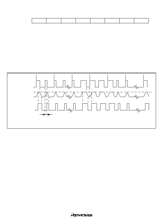
Rev. 1.0, 02/00, page 770 of 1141
27.2.4
Horizontal Sync Signal Threshold Register (HVTHR)
0
0
0
0
0
0
1
1
7
W
HVTH0
1
--
--
6
--
--
5
--
--
4
W
HVTH4
3
W
HVTH3
2
W
HVTH2
1
W
HVTH1
Bit :
Initial value :
R/W :
The HVTHR is a 5-bit write-only register for specifying the threshold value for the digital H
separation counter; this value is used to generate the SEPH signal from the Csync signal. The
SEPH signal is set to 1 when the digital H separation counter value matches the HVTHR value
while the Csync is high, and is reset to 0 when the digital H separation counter value becomes 00
while the Csync is low. When reset, the HVTHR is initialized to H'E0.
Figures 27.3 and 27.4 show the HVTHR value and the SEPH signal generation timing.
Csync
HVTH
SEPH
Digital H separation
counter
About
1.6
µ
s to 2.0
µ
s
Figure 27.3 HVTHR Value and SEPH Generation Timing
When Equalizing Pulses Are Detected
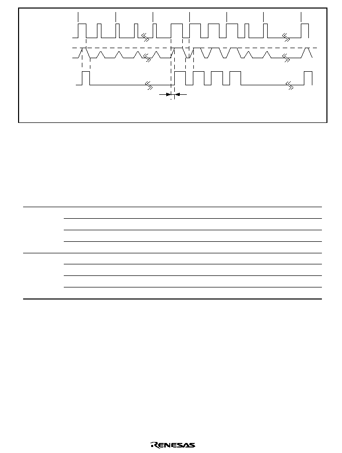
Rev. 1.0, 02/00, page 771 of 1141
Csync
HVTH
SEPH
Digital H separation
counter
About
3.2
µ
s to 2.0
µ
s
Figure 27.4 HVTH Value and SEPH Generation Timing
When Equalizing Pulses Are Not Detected
The following shows examples of HVTHR settings.
Condition:
(HVTHR ≠ 1)
◊
(2/OSC) > 1.6
µ
s or 3.2
µ
s
System clock OSC = 10 MHz
2/OSC = 5 MHz = 0.2
µ
s
Example 1: To detect equalizing pulses
Hsync detection threshold value: 1.6
µ
s
1.6
µ
s / 0.2
µ
s = 8
HVTHR value = H'8 (8)
Example 2: To not detect equalizing pulses
Hsync detection threshold value: 3.2
µ
s
3.2
µ
s / 0.2
µ
s = 16
HVTHR value = H'10 (16)
In general, to detect Hsync pulses continuously, set the HVTHR value so that 2.35-
µ
s equalizing
pulses can be detected. However, if an equalizing pulse at an Hsync pulse position is lost in a
weak field, a Hsync-Vsync phase-difference error will occur, and the field will not be detected
correctly. In such a weak field, this error can be prevented by eliminating 2.35-
µ
s equalizing
pulses. Figure 27.5 shows the timing when a phase-difference error occurs.
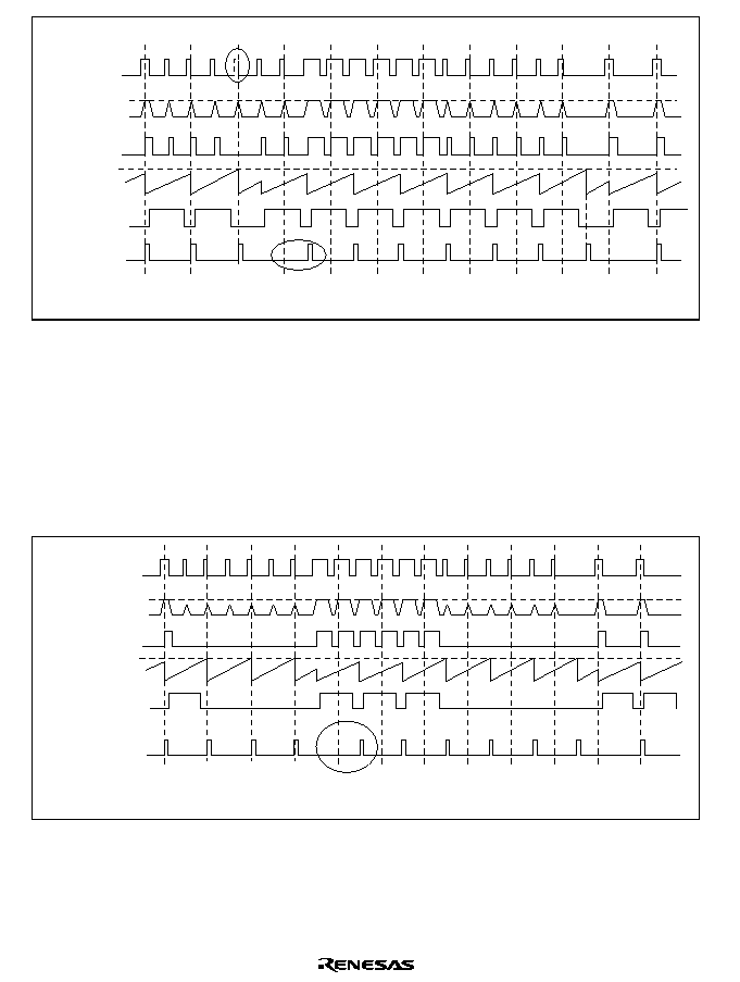
Rev. 1.0, 02/00, page 772 of 1141
Csync
HVTH
SEPH
HHK
OSCH
HC
Digital H separation
counter
Hsync-Vsync
phase-difference
error
Pulse
lost
H complement
and mask counter
Comple-
ment
Comple-
ment
Figure 27.5 Timing of Hsync-Vsync Phase-Difference Error
When Equalizing Pulse Lost at Hsync Pulse Position
Note:
When 2.35-
µ
s equalizing pulses are eliminated, the complement function operates for the
eliminated period. Accordingly, the rising edge of the Vsync signal for the even field is
detected as an Hsync pulse. Therefore, to not generate an Hsync pulse at this position, set
the HHKON bit (bit 2) of the SEPCR to 1 so that the HHK function is forcibly operated
when complementary pulses are inserted three successive times. Figures 27.6 and 27.7
show this timing.
Csync
HVTH
SEPH
HHK
OSCH
HC
Digital H separation
counter
Comple-
ment
Comple-
ment
Comple-
ment
Comple-
ment
Phase-difference
error
H complement and
mask counter
Comple-
ment
Comple-
ment
Comple-
ment
Figure 27.6 Timing of Hsync-Vsync Phase-Difference Error
When Equalizing Pulse Not Detected
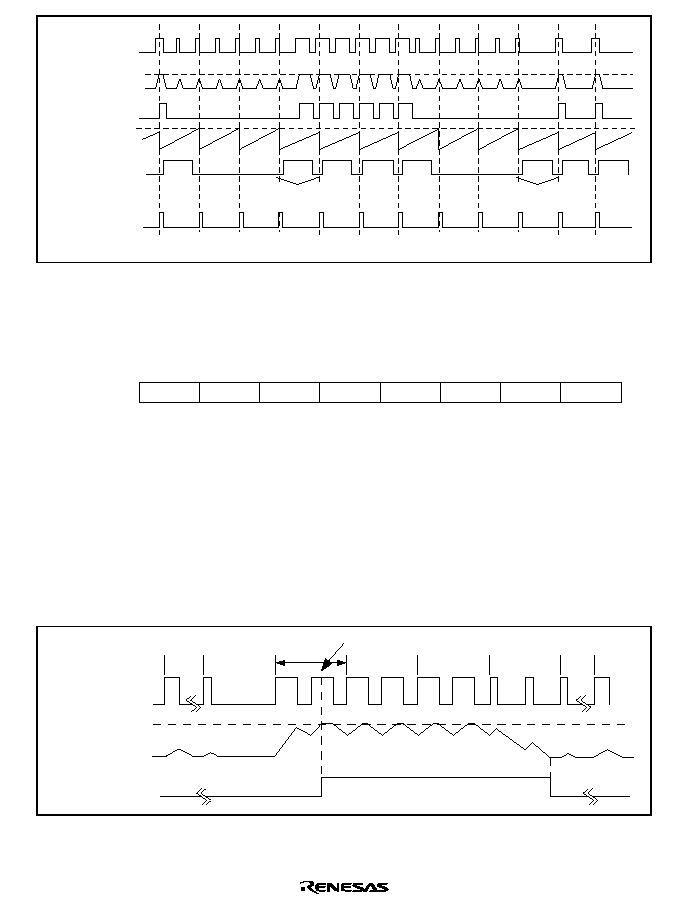
Rev. 1.0, 02/00, page 773 of 1141
Csync
HVTH
SEPH
HHK
OSCH
HC
Digital H separation
counter
H complement and
mask counter
Forcible HHK
operation
Forcible HHK
operation
Comple-
ment
Comple-
ment
Comple-
ment
Comple-
ment
Comple-
ment
Comple-
ment
Figure 27.7 Timing of HHK Operation
When Complementary Pulses Inserted Three Successive Times While HHKON = 1
27.2.5
Vertical Sync Signal Threshold Register (VVTHR)
0
0
0
0
0
0
0
0
7
W
VVTH0
0
W
VVTH7
6
W
VVTH6
5
W
VVTH5
4
W
VVTH4
3
W
VVTH3
2
W
VVTH2
1
W
VVTH1
Bit :
Initial value :
R/W :
The VVTHR is an 8-bit write-only register for specifying the threshold value for the digital V
separation counter; this value is used to generate the SEPV signal from the Csync signal. The
SEPV signal is set to 1 when the digital V separation counter value matches the VVTHR value
while the Csync is high, and reset to 0 when the digital V separation counter value becomes 00
while the Csync is low. Set the VVTHR value so that the SEPV signal goes high 1/2H or more
after the Vsync start point. When reset, the VVTHR is initialized to H'E0.
Figure 27.8 shows the VVTHR value and the SEPV signal generation timing.
Csync
1/2 H or more
VVTH
H
SEPV
Digital V separation
counter
Figure 27.8 VVTHR Value and SEPV Generation Timing
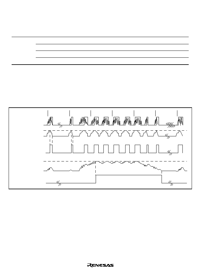
Rev. 1.0, 02/00, page 774 of 1141
The following shows an example of VVTHR settings.
Condition:
(VVTHR ≠ 1)
◊
(2/OSC) > (Hsync period / 2 ≠ 4.7
µ
s)
◊
1.5 = 41
µ
s
System clock OSC = 10 MHz
2/OSC = 5 MHz = 0.2
µ
s
Example 1: To detect 41-
µ
s pulses
Vsync detection threshold value: 41
µ
s
41
µ
s / 0.2
µ
s = 205
HVTHR value = H'CE (206)
The noise component of the Csync signal in a weak field is usually large, and will cause the Vsync
detection delay or miss. In such a case, set the DLPFON (bit 2) of the SEPIMR to 1; the SEPH
signal detected by the digital H separation counter is logically ORed with the Csync signal
(Vsync), then the result is input to the digital V separation counter. This will prevent the Vsync
detection delay or miss in a weak field. Figure 27.9 shows this timing.
Csync + SEPH
HVTH
SEPH
SEPV
VVTH
Digital H separation
counter
Digital V separation
counter
Figure 27.9 VVTHR Value and SEPV Generation Timing
When Digital LPF Is Enabled
Alternatively, set the VCMPON (bit 4) of the SEPCR to 1 when the Vsync detection delay or miss
may occur in a weak field; the external Vsync detection signal (AFCV signal) will be generated by
the V complement and mask counter. Figure 27.10 shows this timing.
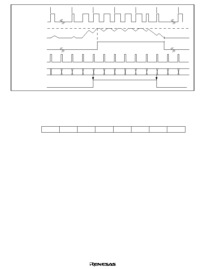
Rev. 1.0, 02/00, page 775 of 1141
Csync
VVTH
SEPV
521
522
523
524
0
1
2
3
4
5
6
7
8
AFCV
1/2 AFCH
(V sampling clock)
Digital H separation
counter
V complement and
mask counter
Figure 27.10 AFCV Generation Timing When V Complement Function Is Enabled
(for NTSC)
27.2.6
Field Detection Window Register (FWIDR)
0
0
0
0
0
1
1
1
7
W
FWID0
1
--
--
6
--
--
5
--
--
4
--
--
3
W
FWID3
2
W
FWID2
1
W
FWID1
Bit :
Initial value :
R/W :
The FWIDR is a 4-bit write-only register for specifying the field detection window timing in units
of 16
◊
fh (fh: horizontal sync signal frequency). The field detection window signal is reset to 0
when the AFC dividing counter value matches the FWIDR value, and the signal is again set to 1
when 1/2 the Hsync signal period has passed. At a rising edge of the AFCV signal while the field
detection window signal is 1, the field is determined as an odd one, and the field detection flag
(FLD) is set to 1. At a rising edge of the AFCV signal while the field detection window signal is 0,
the field is determined as an even one, and the FLD is cleared to 0. The value set to the FWIDR
depends on the setting of the V complement function control (VCMPON) bit (bit 4) of the
SEPCR. When the VCMPON is cleared to 0, that is, when the V complement function is not
operating, the FWIDR must be set so that the rising edge of the SEPV signal, which is generated
when the V separation counter value reaches the specified threshold value, comes to the center of
the field detection window period. When the VCMPON is set to 1, that is, when the V
complement function is operating, the FWIDR must be set so that the dividing counter overflow
timing comes to the center of the field detection window period. When reset, the FWIDR is
initialized to H'F0.
(1) Bit 0 of SEPACR Register
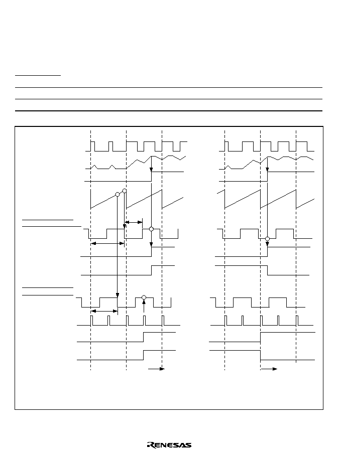
Rev. 1.0, 02/00, page 776 of 1141
Bit 0
Field Detection Flag (FLD): Indicates the field determined by the status of the field
detection window signal generated by the AFC when the external Vsync signal (AFCV signal)
rises. This flag is invalid when the internally generated Hsync signal is selected as the AFC
reference Hsync signal. For the timing, refer to section 27.2.6, Field Detection Window Register
(FWIDR).
Bit 0
LD
Description
0
Even field
(Initial value)
1
Odd field
Csync
SEPV
AFCV
FLD
AFCV
T
F
*
T
F
*
Note:
*
T
F
: Field detection window register value
FLD
Digital V separation
counter
V complement and
mask counter clock
When V complement
function is not operating:
AFC frequency-
dividing counter
H/2
µ
s
Field detection
window signal
Field detection
window signal
Odd field
Odd field timing
Even field timing
When V complement
function is operating:
Even field
Figure 27.11 Field Detection Timing

Rev. 1.0, 02/00, page 777 of 1141
27.2.7
H Complement and Mask Timing Register (HCMMR)
15
0
HC8 HC7 HC6 HC5 HC4 HC3 HC2 HC1 HC0 HM6 HM5 HM4 HM3 HM2 HM1 HM0
W
14
0
W
13
12
0
W
0
W
11
0
W
10
0
W
9
0
W
8
0
W
7
0
W
6
0
W
5
0
W
4
0
W
3
0
W
2
0
W
1
0
W
0
0
W
Bit :
Initial value :
R/W :
The HCMMR is a 16-bit write-only register for specifying the timing (Th: Hsync frequency) for
generating a complementary pulse when a pulse in the Hsync signal is lost, and the timing (Tm
and Tm2) for clearing the HHK (masking period).
The HC8 to HC0 bits specify the timing for generating a complementary pulse; if no Hsync pulse
is input within this specified time, a complementary pulse is generated from the H complement
and mask counter. When a supplementary pulse is generated, the HHK function, provided for
resetting the H supplement mask counter, remains cleared, and the H supplement mask counter is
synchronized with the Hsync signal at the next Hsync pulse input. The HHK2 operation for
generating the Hsync signal (OSCH) for the AFC circuit is performed when a supplementary pulse
is generated.
The HM6 to HM0 bits specify the timing for clearing the HHK function. Set the HHK clearing
timing to about 85% of the Hsync period starting from the SEPH rising edge to eliminate
equalizing pulses and copy-guard signals.
Figure 27.12 shows the complement and mask timing. The HHK signal is set to 1 about 5
µ
s after
the SEPH rising edge, and the HHK2 signal is set to 1 immediately after the H complement and
mask counter is reset. The HHK signal is also used for the noise detection window. For details on
the noise detection, refer to section 27.2.8, Noise Detection Counter (NDETC).
When reset, the HCMMR is initialized to H'0000.
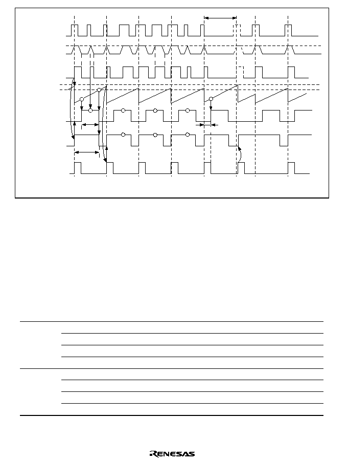
Rev. 1.0, 02/00, page 778 of 1141
Csync
HVTH
SEPH
OSCH
Tm2
Tm
Th
5
µ
s
HC
HM
Digital H separation
counter
Noise
Killer
Killer
Killer
Killer
Killer
Killer
Killer
Killer
Pulse
lost
Comple-
mentary
pulse
H complement and
mask counter
HHK
(for counter reset)
HHK2
(for OSCH generation)
Figure 27.12 Complement and Mask Timing of the H Complement and Mask Counter
Bits 15 to 7
H Complementary Pulse Setting (HC8 to HC0): Specify the timing for
generating a complementary pulse when an Hsync pulse is lost. If no Hsync pulse is input within
the specified time, a complementary pulse is generated from the H complement and mask counter
and interpolated to the OSCH signal.
The following shows examples of HC8 to HC0 settings.
Condition:
(HC + 1)
◊
(2/OSC) > 63.5
µ
s (PAL: 64
µ
s)
System clock OSC = 10 MHz
2/OSC: 5 MHz (0.2
µ
s
)
Example 1: To set the timing for NTSC
NTSC: 63.5
µ
s
63.5
µ
s / 0.2
µ
s = 317.5
HC8 to HC0 value = H'13E (318)
Example 2: To set the timing for PAL
PAL: 64
µ
s
64
µ
s / 0.2
µ
s = 320
HC8 to HC0 value = H'141 (321)
Rev. 1.0, 02/00, page 779 of 1141
Bits 6 to 0
HHK Period Setting (HM6 to HM0): Specify the timing for clearing the HHK
(masking period) for the Hsync signal. The H complement and mask counter starts counting at a
rising edge of the SEPH signal; the HHK period specified by these bits starts at this timing. This
value is also used as the timing for resetting the noise detection window signal. Note that the
setting precision is the upper six bits of the H complement and mask counter: the lower two bits of
the counter are ignored.
The following shows an example of HM6 to HM0 settings.
Condition:
(HM + 1)
◊
(8/OSC) > 54
µ
s (about 85% of the Hsync period
)
System clock OSC = 10 MHz
8/OSC: 1.25 MHz (0.8
µ
s
)
Example:
To set the timing to 54
µ
s
54
µ
s / 0.8
µ
s = 67.5
HM6 to HM0 value = H'44 (67)
27.2.8
Noise Detection Counter (NDETC)
0
0
0
0
0
0
0
0
7
R
NC0
0
R
NC7
6
R
NC6
5
R
NC5
4
R
NC4
3
R
NC3
2
R
NC2
1
R
NC1
Bit :
Initial value :
R/W :
The NDETC is a 10-bit read-only counter of which the upper eight bits can be read. This counter
counts the number of Hsync cycles in which an Hsync pulse (noise H) is input while the noise
detection window signal is 1, and counts the number of Hsync cycles in which no Hsync pulse is
input while the noise detection window signal is 0. When this counter value matches the noise
detection level, the noise detection interrupt request flag is set. The counter is reset at every other
vertical sync signal (AFCV signal) input; that is, the noise status for one field can be monitored.
The NDETC value can be read by the CPU; the noise status can be monitored by the read value.
When reset, the NDETC is initialized to H'00. The NDETC is assigned to the same address as the
NDETR. Figure 27.13 shows the timing for noise detection.
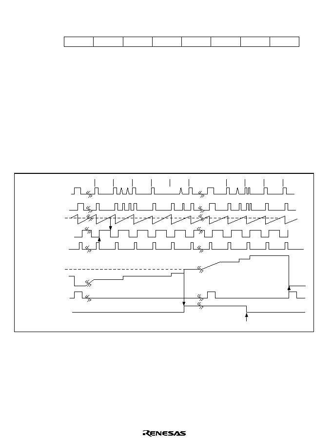
Rev. 1.0, 02/00, page 780 of 1141
27.2.9
Noise Detection Level Register (NDETR)
0
0
0
0
0
0
0
0
7
W
NR0
0
W
NR7
6
W
NR6
5
W
NR5
4
W
NR4
3
W
NR3
2
W
NR2
1
W
NR1
Bit :
Initial value :
R/W :
The NDETR is an 8-bit write-only register for specifying the noise detection level. The set value
must be 1/4 of the actual noise detection level. The noise detection window signal is set to 1 at a
falling edge of the OSCH signal, and reset to 0 after the time specified by the HHK period setting
bits has passed. The OSCH signal falls about 5
µ
s after a rising edge of the SEPH signal.
When the noise detection counter value matches the specified noise detection level, the noise
detection interrupt request flag is set to 1. When reset, the NDETR is initialized to H'00. The
NDETR is assigned to the same address as the NDETC.
Figure 27.13 shows the timing for noise detection.
Csync
AFCV
NDETC
NDETR
SEPH
OSCH
NDETIF
HM
H complement and
mask counter
Cleared to 0 by CPU
Noise detection window
Noise
Noise
Noise
Noise
Noise counter
cleared
Noise
Comple-
ment
Comple-
ment
Noise
Pulse
lost
Pulse
lost
Figure 27.13 Noise Detection Window Setting and Noise Counting Timing
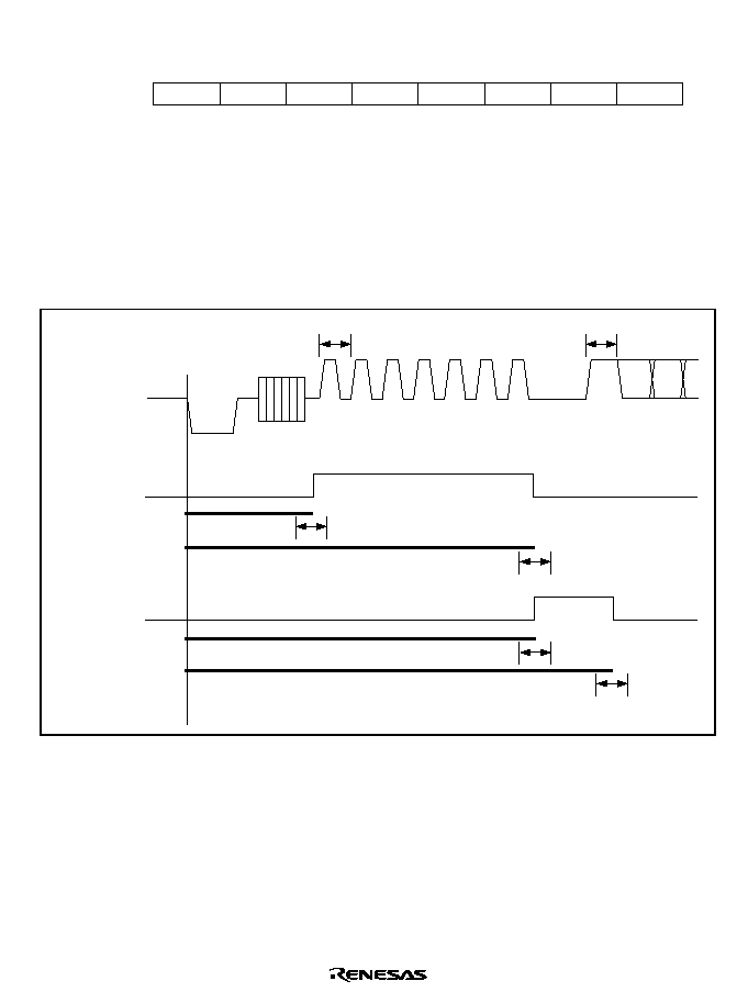
Rev. 1.0, 02/00, page 781 of 1141
27.2.10
Data Slicer Detection Window Register (DDETWR)
0
0
0
0
0
0
0
0
7
W
CRWDS0
0
W
SRWDE1
6
W
SRWDE0
5
W
SRWDS1
4
W
SRWDS0
3
W
CRWDE1
2
W
CRWDE0
1
W
CRWDS1
Bit :
Initial value :
R/W :
The DDETWR is an 8-bit write-only register for specifying the timing of the clock run-in
detection window signal and start bit detection window signal supplied to the data slicer. Figure
27.14 shows the timing of the signals. When reset, the DDETWR is initialized to H'00.
These detection window signals can be monitored through terminals. For details, refer to section
29.7.3, Digital Output Specification Register.
C.video
32
◊
fh = 2
µ
s
32
◊
fh = 2
µ
s
10.5
µ
s
±
0.5
µ
s
±
0.5
µ
s
±
0.5
µ
s
±
0.5
µ
s
23.5
µ
s
23.5
µ
s
29.5
µ
s
Clock run-in
detection
window signal
Start bit detection
window signal
Figure 27.14 Timing for Generating Clock Run-in Detection Window Signal and
Start Bit Detection Window Signal

Rev. 1.0, 02/00, page 782 of 1141
Bits 7 and 6
Start Bit Detection Window Signal Falling Timing Setting
(SRWDE1 and SRWDE0): Specifies the falling timing (end timing) of the start bit detection
window signal.
Bit 1
Bit 0
SRWDE1
SRWDE0
Description
0
0
The detection ends about 29.5
µ
s after the slicer start point
(Initial value)
1
The detection ends about 29.0
µ
s after the slicer start point
1
0
The detection ends about 30.0
µ
s after the slicer start point
1
This setting must not be used
Bits 5 and 4
Start Bit Detection Window Signal Rising Timing Setting
(SRWDS1 and SRWDS0): Specifies the rising timing (start timing) of the start bit detection
window signal.
Bit 1
Bit 0
SRWDS1
SRWDS0
Description
0
0
The detection starts about 23.5
µ
s after the slicer start point
(Initial value)
1
The detection starts about 23.0
µ
s after the slicer start point
1
0
The detection starts about 24.0
µ
s after the slicer start point
1
This setting must not be used
Bits 3 and 2
Clock Run-in Detection Window Signal Falling Timing Setting
(CRWDE1 and CRWDE0): Specifies the falling timing (end timing) of the clock run-in
detection window signal.
Bit 1
Bit 0
CRWDE1
CRWDE0
Description
0
0
The detection ends about 23.5
µ
s after the slicer start point
(Initial value)
1
The detection ends about 23.0
µ
s after the slicer start point
1
0
The detection ends about 24.0
µ
s after the slicer start point
1
This setting must not be used
Rev. 1.0, 02/00, page 783 of 1141
Bits 1 and 0
Clock Run-in Detection Window Signal Rising Timing Setting
(CRWDS1 and CRWDS0): Specifies the rising timing (start timing) of the clock run-in detection
window signal.
Bit 1
Bit 0
CRWDS1
CRWDS0
Description
0
0
The detection starts about 10.5
µ
s after the slicer start point
(Initial value)
1
The detection starts about 10.0
µ
s after the slicer start point
1
0
The detection starts about 11.0
µ
s after the slicer start point
1
This setting must not be used
27.2.11
Internal Sync Frequency Register (INFRQR)
0
0
0
0
0
1
0
0
7
--
--
0
W
VFS2
6
W
VFS1
5
W
HFS
4
--
--
3
--
--
2
--
--
1
--
--
Bit :
Initial value :
R/W :
The INFRQR is an 8-bit write-only register for modifying the internally generated Hsync and
Vsync frequency to reduce the color-bleeding or jitter of OSD in PAL, MPAL, or NPAL mode or
when the non-interlaced text display mode is selected in the OSD. When reset, the INFRQR is
initialized to H'10.
Bits 7 and 6
Vsync Frequency Selection (VFS2 and VFS1): Select the Vsync frequency. Here,
fh indicates the Hsync frequency in each TV format.
Bit 7
Bit 6
Description
VFS2
VFS1
PAL
MPAL
NPAL
0
0
fh/313 (Initial value)
fh/263 (Initial value)
fh/313 (Initial value)
1
fh/314
fh/266
fh/314
1
0
fh/310
fh/262
fh/310
1
fh/312
fh/264
fh/312

Rev. 1.0, 02/00, page 784 of 1141
Bit 5
Hsync Frequency Selection (HFS): Selects the Hsync frequency. Here, fsc indicates the
color subcarrier signal frequency in each TV format. Note that this setting is ignored when the
HCKSEL bit (bit 3) of the SEPCR is set to 1 to select the AFC clock as the internal Csync
generator clock source and when the FSCIN bit (bit 12) of the DFORM in the OSD is set to 1 to
select the 2fsc clock.
Bit 5
Description
HFS
PAL
MPAL
NPAL
0
fsc/283.75 (Initial value)
fsc/227.25 (Initial value)
fsc/229.25 (Initial value)
1
fsc/283.5
fsc/227.5
fsc/229.5
Bit 4
Blank Bit: Cannot be read or modified.
Bits 3 to 0
Reserved: Cannot be modified and are always read as 0. When 1 is written to these
bits, correct operation is not guaranteed.
27.3
Operation
27.3.1
Selecting Source Signals for Sync Separation
The source for sync separation can be selected from three signals (five methods):
1. Composite video signal input from the CVin2 terminal (two methods)
2. Csync signal input from the Csync/Hsync terminal (two methods)
3. Vsync and Hsync signals that are input from the VLPF/Vsync and Csync/Hsync terminals,
respectively (one method)
For the composite video signal and the Csync signal, two methods are available for processing the
Vsync component.
(1) Inputting the Composite Video Signal as the Source
When the composite video signal is selected as the source, the Vsync component can be
processed in two methods: using the Vsync Schmitt circuit or using the Csync Schmitt circuit.
(a) Using the Vsync Schmitt Circuit
The composite video signal input to the CVin2 terminal is selected as the source, and the
Csync separation comparator separates the composite sync signal from the source signal.
Of the composite sync signal, the Hsync component is input to the digital H separation
counter, and the Vsync component is output from the Csync/Hsync terminal, goes through
the external LPF circuit, then is input again through the Vsync/VLPF terminal and the
Vsync Schmitt circuit to the digital V separation counter. The initial value of the SEPIMR
specifies this method. Figure 27.15 shows this method.
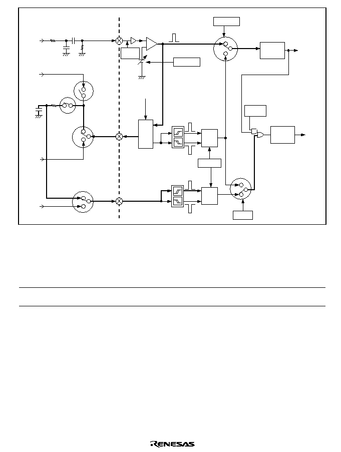
Rev. 1.0, 02/00, page 785 of 1141
CVin2
Csync
a
1
1
0
0
b
a
b
Hsync
Vsync
VLPF
Vsync/VLPF
Csync/Hsync
Hsync
Vsync
External
SW3
Internal
SW5
Internal
SW6
External
SW2
External
SW1
Reference
voltage switch
Register
control
I/O switch
I/O
switch
Polarity
switch
Polarity
switch
Digital H
separation
counter
DLPFON
Digital V
separation
counter
Csync polarity
Schmitt circuit
Vsync polarity
Schmitt circuit
External circuit
Inside LSI
Csync
separation
comparator
External
SW4
CVin2
CCMPSL
CCMPV0, 1
SYNCT
VSEL
SEPV
SEPH
≠
+
Sync tip
clamp
Figure 27.15 Sync Source Selection When Using the CVin2 Signal and
the Vsync Schmitt Circuit
Source
Signal
Vsync
Detection
External
SW1
External
SW2
External
SW3
External
SW4
CCMPSL
(Internal
SW5)
VSEL
(Internal
SW6)
Csync/
Hsync
Terminal
I/O
CVin2
input
Vsync
Schmitt
Off
On
a
a
0
0
Output
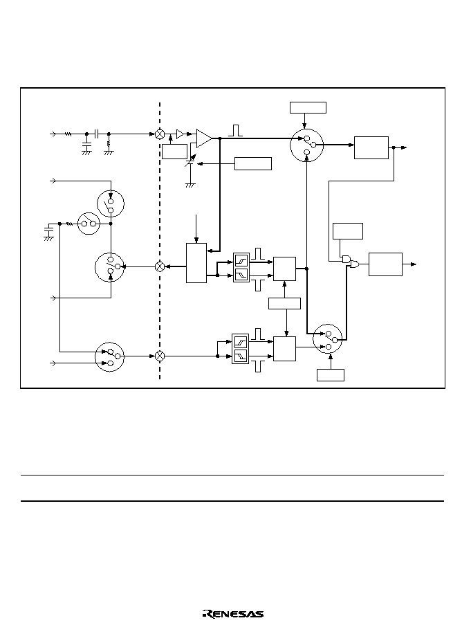
Rev. 1.0, 02/00, page 786 of 1141
(b) Using the Csync Schmitt Circuit
The Hsync component is processed in the same way as described in (a), but the Vsync
component is processed differently; the Csync/Hsync terminal is left open and the
separated Vsync component is input through the Csync Schmitt circuit to the digital V
separation counter. Figure 27.16 shows this method.
CVin2
Csync
a
1
1
0
0
b
a
b
Hsync
Vsync
VLPF
Vsync/VLPF
Csync/Hsync
Hsync
Vsync
External
SW3
Internal
SW5
Internal
SW6
External
SW2
External
SW1
Reference
voltage switch
Register
control
I/O switch
I/O
switch
Polarity
switch
Polarity
switch
Digital H
separation
counter
Digital V
separation
counter
DLPFON
Csync polarity
Schmitt circuit
Vsync polarity
Schmitt circuit
External circuit
Inside LSI
Csync
separation
comparator
External
SW4
CVin2
≠
+
CCMPSL
CCMPV0, 1
SYNCT
VSEL
SEPV
SEPH
Sync tip
clamp
Figure 27.16 Sync Source Selection When Using the CVin2 Signal and
the Csync Schmitt Circuit
Source
Signal
Vsync
Detection
External
SW1
External
SW2
External
SW3
External
SW4
CCMPSL
(Internal
SW5)
VSEL
(Internal
SW6)
Csync/
Hsync
Terminal
I/O
CVin2
input
Csync
Schmitt
Off
Off
Open
Fixed to
0 or 1
0
1
Output
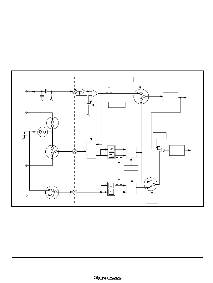
Rev. 1.0, 02/00, page 787 of 1141
(2) Inputting the Csync Signal as the Source
When the Csync signal is selected as the source, the Vsync component can be processed in two
methods: using the Vsync Schmitt circuit or using the Csync Schmitt circuit.
(a) Using the Vsync Schmitt Circuit
The Csync signal having the polarity selected by the SYNCT bit (bit 4) of the SEPIMR is
input to the Csync/Hsync terminal. The Hsync component is input through the Csync
Schmitt circuit to the digital H separation counter; the Vsync component goes through the
external LPF circuit, then is input through the Vsync/VLPF terminal and the Vsync
Schmitt circuit to the digital V separation counter. Figure 27.17 shows this method.
CVin2
Csync
a
1
1
0
0
b
a
b
Hsync
Vsync
VLPF
Vsync/VLPF
Csync/Hsync
Hsync
Vsync
External
SW3
Internal
SW5
External
SW2
External
SW1
Reference
voltage switch
Register
control
I/O switch
I/O
switch
Polarity
switch
Polarity
switch
Digital H
separation
counter
Digital V
separation
counter
DLPFON
Csync polarity
Schmitt circuit
Vsync polarity
Schmitt circuit
External circuit
Inside LSI
Csync
separation
comparator
External
SW4
CVin2
≠
+
CCMPSL
CCMPV0, 1
SYNCT
VSEL
SEPV
SEPH
Sync tip
clamp
Internal
SW6
Figure 27.17 Sync Source Selection When Using the Csync Signal and
the Vsync Schmitt Circuit
Source
Signal
Vsync
Detection
External
SW1
External
SW2
External
SW3
External
SW4
CCMPSL
(Internal
SW5)
VSEL
(Internal
SW6)
Csync/
Hsync
Terminal
I/O
Csync
input
Vsync
Schmitt
On
On
a
a
1
0
Input
Rev. 1.0, 02/00, page 788 of 1141
(b) Using the Csync Schmitt Circuit
The Hsync component is processed in the same way as described in (a), but the Vsync
component is processed differently; the Vsync component is input through the Csync
Schmitt circuit to the digital V separation counter. Figure 27.18 shows this method.
CVin2
Csync
a
1
1
0
0
b
a
b
Hsync
Vsync
VLPF
Vsync/VLPF
Csync/Hsync
Hsync
Vsync
External
SW3
Internal
SW5
Internal
SW6
External
SW2
External
SW1
Reference
voltage switch
Register
control
I/O switch
I/O
switch
Polarity
switch
Polarity
switch
Digital H
separation
counter
Digital V
separation
counter
DLPFON
Csync polarity
Schmitt circuit
Vsync polarity
Schmitt circuit
External circuit
Inside LSI
Csync
separation
comparator
External
SW4
CVin2
≠
+
CCMPSL
CCMPV0, 1
SYNCT
VSEL
SEPV
SEPH
Sync tip
clamp
Figure 27.18 Sync Source Selection When Using the Csync Signal and
the Csync Schmitt Circuit
Source
Signal
Vsync
Detection
External
SW1
External
SW2
External
SW3
External
SW4
CCMPSL
(Internal
SW5)
VSEL
(Internal
SW6)
Csync/
Hsync
Terminal
I/O
Csync
input
Csync
Schmitt
On
Off
a
Fixed to
0 or 1
1
1
Input
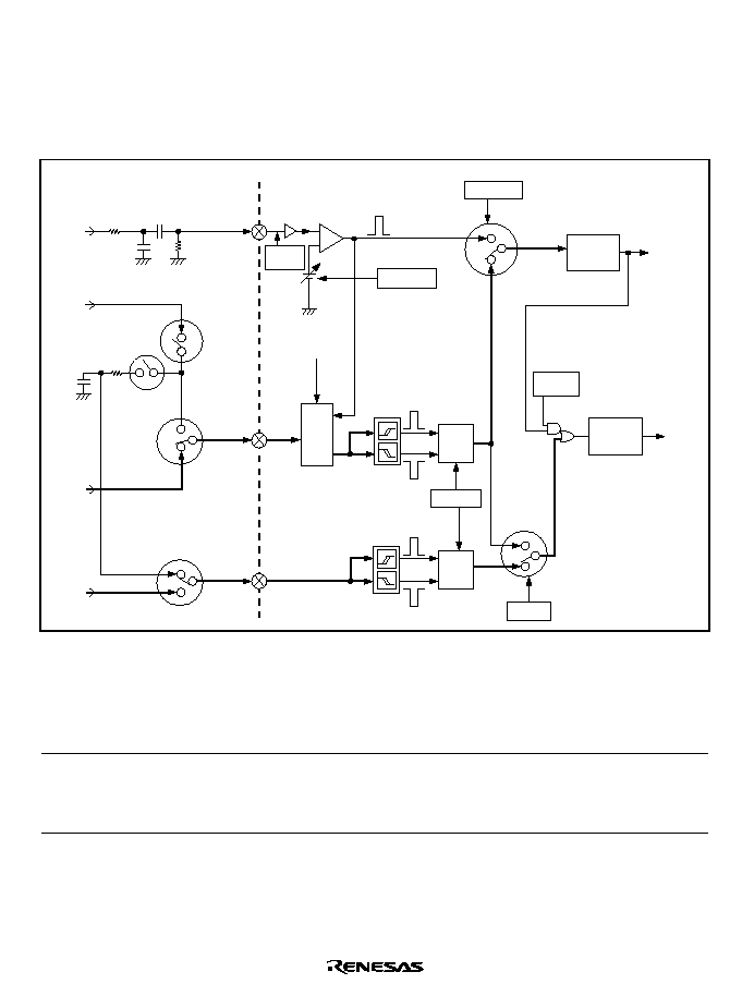
Rev. 1.0, 02/00, page 789 of 1141
(3) Inputting the Hsync and Vsync Signals Separately as Sources
The Hsync signal having the polarity selected by the SYNCT bit (bit 4) of the SEPIMR is
input to the Csync/Hsync terminal, and is input through the Csync Schmitt circuit to the digital
H separation counter; the Vsync signal having the polarity selected by the SYNCT bit is input
to the Vsync/VLPF terminal, and is sent through the Vsync Schmitt circuit to the digital V
separation counter. Figure 27.19 shows this method.
CVin2
Csync
a
1
1
0
0
b
a
b
Hsync
Vsync
VLPF
Vsync/VLPF
Csync/Hsync
Hsync
Vsync
External
SW3
Internal
SW5
Internal
SW6
External
SW2
External
SW1
Reference
voltage switch
Register
control
I/O switch
I/O
switch
Polarity
switch
Polarity
switch
Digital H
separation
counter
Digital V
separation
counter
DLPFON
Csync polarity
Schmitt circuit
Vsync polarity
Schmitt circuit
External circuit
Inside LSI
Csync
separation
comparator
External
SW4
CVin2
≠
+
CCMPSL
CCMPV0, 1
SYNCT
VSEL
SEPV
SEPH
Sync tip
clamp
Figure 27.19 Sync Source Selection When Using the Hsync and Vsync Signals Separately
Source
Signal
Vsync
Detection
External
SW1
External
SW2
External
SW3
External
SW4
CCMPSL
(Internal
SW5)
VSEL
(Internal
SW6)
Csync/
Hsync
Terminal
I/O
Hsync
and
Vsync
input
Vsync
Schmitt
Off
Off
b
b
1
0
Input

Rev. 1.0, 02/00, page 790 of 1141
27.3.2
Vsync Separation
The Hsync separator separates the Vsync signal from the Csync signal by using the digital V
separation counter, which is an 8-bit up-/down-counter, and the VVTHR register, which holds the
threshold value. The digital V separation counter increments the count when the Csync signal is
high, and decrements the count when the Csync is low. When the count reaches the VVTHR value
while the count is incremented, the SEPV signal is set to 1 and the counter stops until the Csync
signal goes low. When the Csync signal goes low, the counter starts to decrement the count. When
the count reaches H'00, the SEPV signal is reset to 0 and the counter stops until the Csync signal
goes high. Set the VVTHR value so that the SEPV signal goes high 1/2 or more after the Vsync
start position to correctly separate the Vsync signal against the signal disturbance in a weak field
or the motor skew during video tape playback.
The obtained SEPV signal is sent to the V complement and mask counter. The V complement and
mask counter is reset to 0 when the SEPV signal is input, and increments the count at twice the
frequency (2
◊
fh) of the horizontal sync signal for the Vsync signal (SEPV signal) cycle period.
This counter masks the reset signal (SEPV) for about 85% (NTSC) or 72% (PAL) of the period
from a reset to the next reset; even if a SEPV signal generated by noise is input to the counter
during this period, the counter is not reset. If no SEPV signal is input after the mask period ends,
the mask is left cleared; the next SEPV signal input resets the counter, and the counter is
synchronized with the SEPV signal. When the counter is reset by the SEPV signal, the external
Vsync detection signal (AFCV) is generated and the external Vsync interrupt flag is set to 1.
The Vsync separation function includes the digital LPF function and the Vsync complement
function, which reduce the chance of the Vsync detection being delayed or missed due to the
Vsync disturbance in a weak field.
(1) Digital LPF Function
This function logically ORs the Csync (Vsync) signal and the SEPH signal separated by the
digital H counter to mask the noise component due to loss of a Vsync pulse. The digital V
separation counter increment the count when the resultant signal is input. Loss of a Vsync
pulse in a weak field causes SEPV signal detection to be delayed or missed, which will result
in incorrect detection of fields or lines. To enable this function, set the DLPFON bit (bit 2) of
the SEPIMR to 1. For the timing, refer to figure 27.9.
(2) Vsync Complement Function
This function makes the V complement and mask counter increment the count at a clock
having twice the frequency (2
◊
fh) of the horizontal sync signal (AFCH), and generates the
AFCV signal (Vsync signal) from the count if a Vsync pulse is lost.
The count value is decoded in different ways depending on the TV format. The source of the
clock for the V complement and mask counter can be switched between the AFC or the H
complement and mask counter. This function can reduce the chance of the SEPV signal
detection being delayed and missed in a weak field. To enable this function, set the VCMPON
bit (bit 4) of the SEPCR to 1. For the timing, refer to figure 27.10.

Rev. 1.0, 02/00, page 791 of 1141
27.3.3
Hsync Separation
The Hsync separator separates the Hsync signal from the Csync signal by using the digital H
separation counter, which is a 5-bit up-/down-counter, and the HVTHR register, which holds the
threshold value. The digital H separation counter increments the count when the Csync signal is
high, and decrements the count when the Csync is low. When the count reaches the HVTHR value
while the count is incremented, the SEPH signal is set to 1 and the counter stops until the Csync
signal goes low. When the Csync signal goes low, the counter starts to decrement the count. When
the count reaches H'00, the SEPH signal is reset to 0 and the counter stops until the Csync signal
goes high. Set the HVTHR value so that 2.35-
µ
s equalizing pulses can be detected; that is, that the
Hsync pulses can be continuously detected.
The obtained SEPH signal is sent to the H complement and mask counter. The H complement and
mask counter is reset to 0 when the SEPH signal is input, and increments the count at a frequency
of
/2 for the SEPH signal cycle period to generate the OSCH signal, HHK signal, and noise
detection window signal. The HHK period is specified by the HM6 to HM0 bits of the HCMMR.
Even if a SEPH signal is input to the counter during this HHK period, the SEPH signal is masked
and the counter is not reset; noise pulses and equalizing pulses during the V blanking period are
eliminated by this function.
The H complement and mask counter has the complement function. If no SEPH signal is input
during the period specified by the HC8 to HC0 bits of the HCMMR, the complement function
generates a complementary pulse and inserts the pulse into the OSCH signal. In this case, the
counter is reset by the complementary pulse, but no HHK signal is generated; the next SEPH
signal input resets the counter, and the counter is synchronized with the SEPH signal. For the
timing, refer to figure 27.12.
Note:
In a weak field, equalizing pulses are not detected in some cases because the pulses have a
short duration of 2.35
µ
s. If equalizing pulses, which are input at the same timing as the
Hsync pulses, are not detected, a phase-difference error between the Hsync and Vsync
occurs at a rising edge of the Vsync signal. Such an error will cause incorrect field
detection in the sync separator and incorrect line detection by the OSD or data slicer. In
such a weak field, adjust the HVTHR value so that equalizing pulses are not detected.
Note that while equalizing pulses are not detected, complementary pulses are inserted
repeatedly and an Hsync-Vsync phase-difference error occurs at a rising edge of the
Vsync signal, even in a field that is not weak. To avoid this, set the HHKON bit (bit 2) of
the SEPCR to 1 to operate the HHK function when complementary pulses are generated
three successive times. For the timing, refer to figure 27.6.

Rev. 1.0, 02/00, page 792 of 1141
27.3.4
Field Detection
The sync separator detects whether the current field is an even field or an odd field from the 1/2H
phase difference between the Hsync and Vsync by using the AFCV signal generated by the V
complement and mask counter and the field detection window signal generated by the AFC. The
timing of the field detection window signal can be adjusted by the FWIDR setting so that it is
suitable for comparison with the AFCV signal. When a rising edge of the AFCV signal is detected
while the field detection window signal is high, the current field is determined as an odd field;
when a rising edge of the AFCV signal is detected while the field detection window signal is low,
the current field is determined as an even field. The field detection status can be monitored from
the CPU by reading the FLD bit (bit 0) of the SEPACR. This function will not operate when the
internally generated Hsync signal is selected as the reference Hsync signal for the AFC, because
the AFC is not synchronized with the external Hsync signal in this case. For the timing, refer to
figure 27.11.
27.3.5
Noise Detection
The noise detection function is necessary for tuned status detection. The sync separator detects
noise by using the Csync signal and the noise detection window signal generated by the H
complement and mask counter. The noise detection window signal is set to 1 at a falling edge of
the OSCH signal generated by the H complement and mask counter, and reset to 0 at the HHK
clearing timing specified by bits 6 to 0 of the HCMMR. Noise is detected by comparing the noise
counter value with the noise detection level register value. The noise counter counts the number of
Hsync cycles in which an Hsync signal is input (noise H) while the noise detection window signal
is high and the number of Hsync cycles in which no Hsync signal is input while the noise
detection window signal is low. When the counted value reaches the noise detection level, the
noise detection interrupt request flag is set. The noise counter can be read from the CPU, and the
noise detection status can be monitored. The noise detection counter is reset every other Vsync
signal input. Accordingly, the noise input during one field can be detected. When the internally
generated Hsync signal is selected as the reference Hsync signal for the AFC and the text display
mode is used in the OSD, the noise counter reset operation can be enabled by setting the VCKSL
bit (bit 5) of the SEPCR to 1. For the timing, refer to figure 27.13.
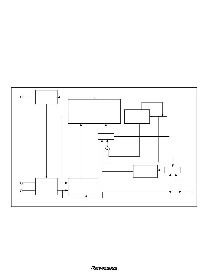
Rev. 1.0, 02/00, page 793 of 1141
27.3.6
Automatic Frequency Controller (AFC)
The AFC averages the Hsync signal fluctuation of the video signal. Figure 27.20 shows the AFC
configuration. The AFC generates a reference clock having 576 or 448 times the frequency (576
◊
fh or 448
◊
fh) of the Hsync signal. From this clock, several clocks are generated, such as the
horizontal sync signal (AFCH signal), clock run-in detection window signal, start bit detection
window signal, V complement and mask counter clock when the V complement function is
selected, and the field detection window signal. The reference clock is also used as the dot clock
for the OSD; modifying the reference clock frequency can change the dot width of the character
display. To change the frequency, connect a circuit having a value suitable for the desired
frequency to the AFCosc and AFCpc terminals, and select the division ratio for the frequency-
dividing counter through the setting of the FRQSEL bit in SEPIMR. Note that the data slicer will
not operate when 448
◊
fh is selected as the reference clock.
AFCLPF
R
C
VCO
AFCpc
AFCosc
HHK
HSEL
HCKSEL
Masking H
FSC
AFCH
AFC error output circuit
(comparator)
Internal Csync
generator
H complement
and mask
counter
External Hsync
Error signal
Switching
Switching
Reference clock
FRQSEL
Masking and
complementing H
Reference
Hsync signal
Internally generated
Hsync
External Hsync
Signals such
as dot clock
Low pass
filter
Frequency-
dividing counter
(Divided by
576 or 448)
R
Figure 27.20 AFC Configuration

Rev. 1.0, 02/00, page 794 of 1141
(1) AFC Oscillator
The AFCosc terminal, which is the oscillation signal terminal of the voltage controlled
oscillator (VCO), oscillates at 576 times the frequency (576
◊
fh) of the Hsync signal when the
Hsync signal is input at a certain phase and frequency. The difference in phase or frequency is
detected between the reference Hsync signal and the Hsync signal (AFCH signal) obtained by
dividing the 576
◊
fh signal, the error signal is converted to a voltage by a low pass filter
through the AFC error output circuit, and the voltage is used to control the VCO.
The VCO control voltage (the AFCLPF terminal voltage) is within a range from about 1.0 V to
4.0 V. The oscillating capacitance should be set so that the AFCosc oscillating frequency
becomes 576
◊
fh at the center (about 2.5 V) of the control voltage range. To set the oscillating
frequency to 448
◊
fh, change the values of the external circuits connected to the AFCpc and
AFCosc terminals and modify the FRQSEL bit in SEPIMR.
(2) AFCLPF
The AFC error output circuit detects the difference in phase or frequency between the
reference Hsync signal and the Hsync signal (AFCH signal) obtained by dividing the 576
◊
fh
or 448
◊
fh signal, and generates a pulse corresponding to the error. Connect a low pass filter
(LPF) to the AFCLPF terminal to average these error pulses. If the cut-off frequency is too
low, the oscillation stabilizing time (the pull-in time) needed to reach 576
◊
fh or 448
◊
fh
becomes long when a large error is detected or after the power is turned on; a high cut-off
frequency will cause jitter or an unstable display.
Connect a suitable LPF by referring to the external circuit examples shown in figures 27.21
and 27.22. When the Hsync signal includes a large disturbance, for example during special
playback operation, the AFC circuit may operate incorrectly.
(3) Reference Hsync Signal for AFC
The AFC reference clock is also used as the dot clock for the OSD. Accordingly, select the
reference Hsync signal depending on whether the OSD operates in the super-imposed mode or
text display mode. Refer to table 27.4, Reference Hsync Signal for AFC.
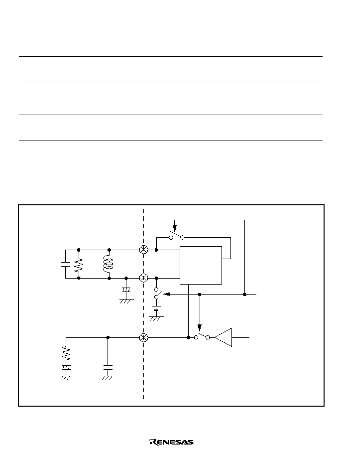
Rev. 1.0, 02/00, page 795 of 1141
Table 27.4
Reference Hsync Signal for AFC
AFC
Reference
Hsync
Signal
Data Slicer
Operation
OSD
Operation
Field
Detection
V Comple-
ment and
Mask
Counter
HCKSEL
HSEL
VCKSL
External
Hsync
signal
Operates/
Stops
Super-
imposed
mode
Operates
Twice the
frequency of
the AFCH
0
0
0
Internally
generated
Hsync
signal
Stops
Text
display
mode
Stops
Twice the
frequency of
the OSCH
0
1
1
External
Hsync
signal
*
Operates
Text
display
mode
Operates
Twice the
frequency of
the AFCH
1
0
0
Note:
*
In this case, the Hsync and Vsync signals must be dedicated separation inputs, with both
signals having equal cycles and pulse widths. The FRQSEL bit in the SEPIMR register
must be cleared to 0.
(4) External Circuit Examples
Figures 27.21 and 27.22 show external circuit examples of the AFC.
10pF
AFCosc
AFCpc
AFCLPF
6.8
µ
H
0.01
µ
F
1/2OVcc
VCO
0.01
µ
F
4.7
µ
F
+
+
470
2.4k
Note: Reference values are shown.
Phase error signal
Reset, active,
or sleep
Figure 27.21 Circuit Example for a 576
◊
fh Reference Clock
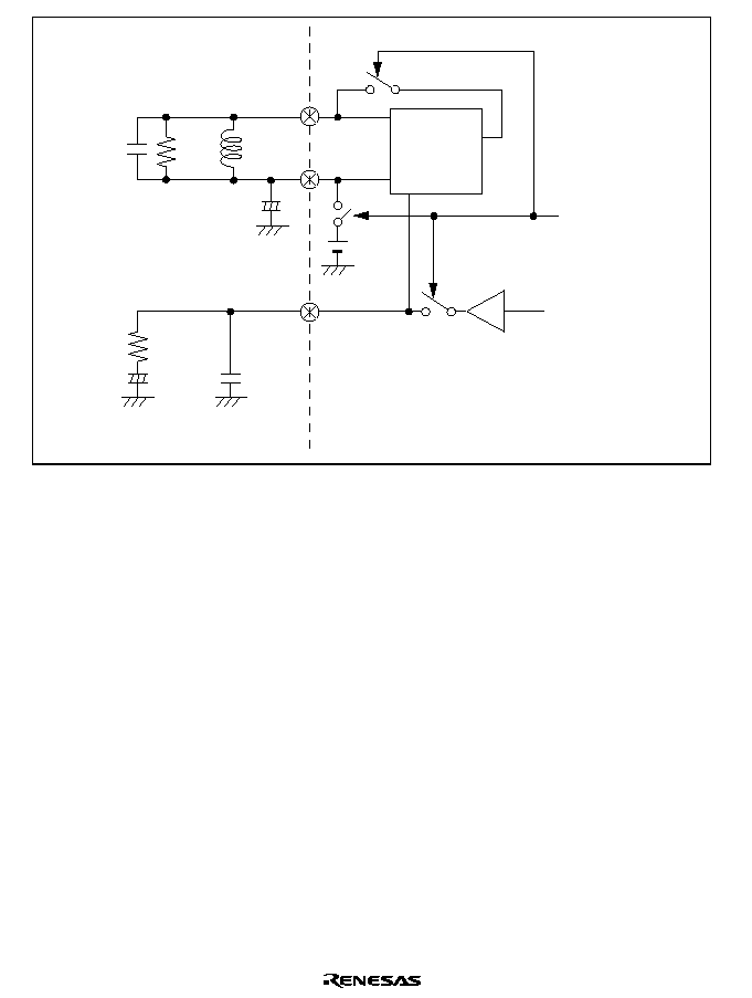
Rev. 1.0, 02/00, page 796 of 1141
12pF
AFCosc
AFCpc
AFCLPF
12
µ
H
0.01
µ
F
1/2OVcc
VCO
0.01
µ
F
4.7
µ
F
+
+
470
2.4k
Note: Reference values are shown.
Phase error signal
Reset, active,
or sleep
Figure 27.22 Circuit Example for a 448
◊
fh Reference Clock

Rev. 1.0, 02/00, page 797 of 1141
27.3.7
Module Stop Control Register (MSTPCR)
7
1
R/W
6
1
R/W
5
4
1
R/W
1
R/W
3
1
R/W
2
1
R/W
1
1
R/W
0
1
R/W
7
1
R/W
6
1
R/W
5
1
R/W
4
1
R/W
3
1
R/W
2
1
R/W
1
1
R/W
0
1
R/W
Bit :
Initial value :
MSTP15 MSTP14 MSTP13 MSTP12 MSTP11 MSTP10 MSTP9 MSTP8 MSTP7 MSTP6 MSTP5 MSTP4
MSTP3 MSTP2 MSTP1 MSTP0
R/W :
MSTPCRH
MSTPCRL
The MSTPCR is a 16-bit read/write register for controlling the module stop mode. Writing 0 to the
MSTP9 bit starts the sync separator; setting the MSTP9 bit to 1 stops the sync separator at the end
of a bus cycle and the module stop mode is entered.
The AFC oscillator operates in reset, active, and sleep modes. Accordingly, after the reset state is
cleared, the AFC oscillator operates but the AFC error output circuit (comparator) does not
operate. Clear the module stop mode of the sync separator and set the sync separator registers to
the desired values. The AFC error output circuit (comparator) will stop in standby, sleep, watch,
subactive, subsleep, and module stop modes. When these modes are cleared, wait for the
oscillation to stabilize, that is, for the AFC frequency to reach 576
◊
fh or 448
◊
fh.
The registers cannot be read or written to in module stop mode. For details, refer to section 4.5,
Module Stop Mode.
Bit 9
Module Stop (MSTP9): Specifies the module stop mode of the sync separator.
Bit 9
MSTP9
Description
0
Clears the module stop mode of the sync separator
1
Specifies the module stop mode of the sync separator
(Initial value)

Rev. 1.0, 02/00, page 799 of 1141
Section 28 Data Slicer
28.1
Overview
The data slicer extracts signals for closed caption signal in the U.S. This function can be used to
extract caption data superimposed on the vertical blanking interval of TV video signals.
A high-performance internal sync separator enables reliable caption data extraction.
The data slicer will not operate when 448 times the horizontal sync frequency is selected for the
AFC reference clock frequency. For details, refer to section 27.3.6, Automatic Frequency
Controller (AFC).
28.1.1
Features
∑
Slice lines: 4 lines
∑
Slice levels: 7 levels
∑
Sampling clock: Generated by AFC
∑
Slice interrupt: A slice completion interrupt is generated at the end of all slices in a field
∑
Error detection: Clock run-in, start bit, and data end
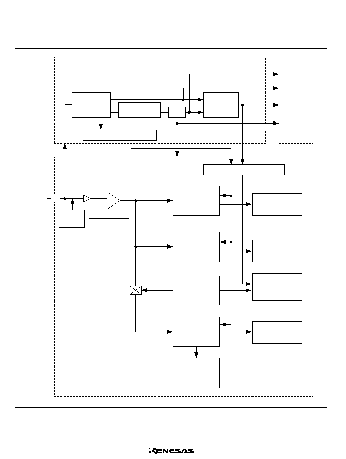
Rev. 1.0, 02/00, page 800 of 1141
28.1.2
Block Diagram
Figure 28.1 shows the block diagram of the data slicer.
Sync separator
Sync signal
generation
Field determination circuit
Slice voltage
generator
Clock run-in
detector
Start bit
detector
Data sampling
clock generator
Shift register
Slice data
register
Data end flag
Slice
completion
interrupt
Start bit
detection flag
Clock run-in
detection flag
Slice line specification circuit
Line counting
Field
Line
counter
Reference clock
CVin2
+
≠
H complement
and mask
AFC
V
H
H
OSD
V
Dot clock
Sync tip
clamp
Figure 28.1 Data Slicer Block Diagram

Rev. 1.0, 02/00, page 801 of 1141
28.1.3
Pin Configuration
Table 28.1 shows the pin configuration for the data slicer.
Table 28.1
Data Slicer Pin Configuration
Block
Name
Abbrev.
I/O
Function
Csync/Hsync
Input/output
Composite sync signal input/output
or horizontal sync signal input
Sync signal
input/output
VLPF/Vsync
Input
Pin for connecting external LPF for
vertical sync signal or input pin for
vertical sync signal
AFCosc
Input/output
AFC oscillation signal
AFC
oscillation
AFCpc
Input/output
AFC by-pass capacitor connecting
pin
LPF for AFC
AFCLPF
Input/output
External LPF connecting pin for
AFC
4fsc/2fscin
Input
4fsc or 2fsc input
Sync
separator
fsc oscillation
4fsc/2fscout
Output
4fsc or 2fsc output
Data slicer
Composite
video signal
Cvin2
Input
Composite video signal input
(2 Vpp, with a sync tip clamp
circuit)

Rev. 1.0, 02/00, page 802 of 1141
28.1.4
Register Configuration
Table 28.2 shows the data slicer registers.
Table 28.2
Register Configuration
Name
Abbrev.
R/W
Size
Initial Value
Address
*
3
Slice even-field mode register
SEVFD
R/(W)
*
1
Word/byte
H'2000
H'D220
Slice odd-field mode register
SODFD
R/(W)
*
1
Word/byte
H'2000
H'D222
Slice line setting register 1
SLINE1
R/W
Word/byte
H'20
H'D224
Slice line setting register 2
SLINE2
R/W
Word/byte
H'20
H'D225
Slice line setting register 3
SLINE3
R/W
Word/byte
H'20
H'D226
Slice line setting register 4
SLINE4
R/W
Word/byte
H'20
H'D227
Slice detection register 1
SDTCT1
R/(W)
*
2
Word/byte
H'10
H'D228
Slice detection register 2
SDTCT2
R/(W)
*
2
Word/byte
H'10
H'D229
Slice detection register 3
SDTCT3
R/(W)
*
2
Word/byte
H'10
H'D22A
Slice detection register 4
SDTCT4
R/(W)
*
2
Word/byte
H'10
H'D22B
Slice data register 1
SDATA1
R
Word/byte
Undefined
H'D22C
Slice data register 2
SDATA2
R
Word/byte
Undefined
H'D22E
Slice data register 3
SDATA3
R
Word/byte
Undefined
H'D230
Slice data register 4
SDATA4
R
Word/byte
Undefined
H'D232
Notes: 1. Only 0 can be written to clear the flag (bit 14).
2. Bits 7 to 0 are cleared when 1 is written to bit 7 of the corresponding slice line setting
register.
3. Lower 16 bits of the address.
28.1.5
Data Slicer Use Conditions
Table 28.3 indicates the conditions of use of the data slicer.
Table 28.3
Data Slicer Use Conditions
Sync Signal Input for Sync Separation
Data Slicer
Sync separation signal input from CVin2
Usable
Sync separation signal input from Csync
Usable
Hsync or Vsync separation signals
Usable
Rev. 1.0, 02/00, page 803 of 1141
28.2
Register Description
28.2.1
Slice Even- (Odd-) Field Mode Register (SEVFD, SODFD)
(1) Slice even-field mode register
8
0
9
STBE1
R/W
0
10
STBE2
R/W
0
11
STBE3
R/W
0
12
STBE4
R/W
0
1
13
--
--
0
15
14
EVNIF
R/(W)
*
R/W
STBE0
0
R/W
EVNIE
Bit:
Initial value:
R/W:
0
0
1
DLYE1
R/W
0
2
DLYE2
R/W
0
3
DLYE3
R/W
0
4
DLYE4
R/W
0
0
5
SLVLE0
R/W
0
7
6
SLVLE1
R/W
R/W
DLYE0
0
R/W
SLVLE2
Bit:
Initial value:
R/W:
(2) Slice odd-field mode register
8
0
9
STBO1
R/W
0
10
STBO2
R/W
0
11
STBO3
R/W
0
12
STBO4
R/W
0
1
13
--
--
0
15
14
ODDIF
R/(W)
*
R/W
STBO0
0
R/W
ODDIE
Bit:
Initial value:
R/W:
0
0
1
DLYO1
R/W
0
2
DLYO2
R/W
0
3
DLYO3
R/W
0
4
DLYO4
R/W
0
0
5
SLVLO0
R/W
0
7
6
SLVLO1
R/W
R/W
DLYO0
0
R/W
SLVLO2
Bit:
Initial value:
R/W:
Note:
*
Only 0 can be written to clear the flag.
The SEVFD and SODFD control the start bit detection starting position, slice voltage level, data
sampling delay time, and interrupts. The SEVFD holds settings for even fields, and the SODFD
holds settings for odd fields. When reset, when the module is stopped, in sleep mode, in standby
mode, in watch mode, in subactive mode, or in subsleep mode, the SEVFD and SODFD are both
initialized to H'2000.
The SEVFD and SODFD are 16-bit read/write registers; however, rewriting of SEVFD or SODFD
should be performed after output of an even- (odd-) field slice completion interrupt. During data
slice operations, if SEVFD or SODFD is rewritten, a malfunction will result; do not perform
rewriting during data slice operation.

Rev. 1.0, 02/00, page 804 of 1141
Bit 15
Even- (Odd-) Field Slice Completion Interrupt Enable Flag (EVNIE, ODDIE):
Enables or disables the generation of even- (odd-) field slice completion interrupts.
Bit 15
EVNIE
ODDIE
Description
0
Disables even- (odd-) field slice completion interrupt
(Initial value)
1
Enables even- (odd-) field slice completion interrupt
Bit 14
Even- (Odd-) Field Slice Interrupt Completion Flag (EVNIF, ODDIF): Set when data
slicing for all specified lines of even (odd) field is completed.
Bit 14
EVNIF
ODDIF
Description
0
[Clearing condition]
When 0 is written after reading 1
(Initial value)
1
[Setting condition]
When data slicing is completed for all specified lines of even (odd) field
Bit 13
Reserved: Cannot be modified and is always read as 1.
Bits 12 to 8
Start Bit Detection Starting Position Bits:
(STBE4 to STBE0) (STBO4 to STBO0): Set the starting position for start bit detection in even
(odd) fields.
The base point for the data slicer is the falling edge of the horizontal sync signal (slicer base point
H) synchronized within the LSI; the starting position for start bit detection can be set using STBE4
to STBE 0 (STBO4 to STBO0) in 288
◊
fh (where fh is the horizontal sync signal frequency)
clock units from approximately 23.5
µ
s after the data slicer base point.
The start bit detection end position is at approximately 29.5
µ
s after the data slicer base point.
In start bit detection, the presence of the rising edge of start bits in the interval between these
starting and ending positions is detected. Further, the start bit detection window signal, which
becomes the base point for the start bit detection starting position, can be adjusted by means of the
data slicer detection window register of the sync separator. For details, refer to section 27.2.10,
Data Slicer Detection Window Register (DDETWR).
Figure 28.2 shows the data slicer base point and start bit detection starting position.
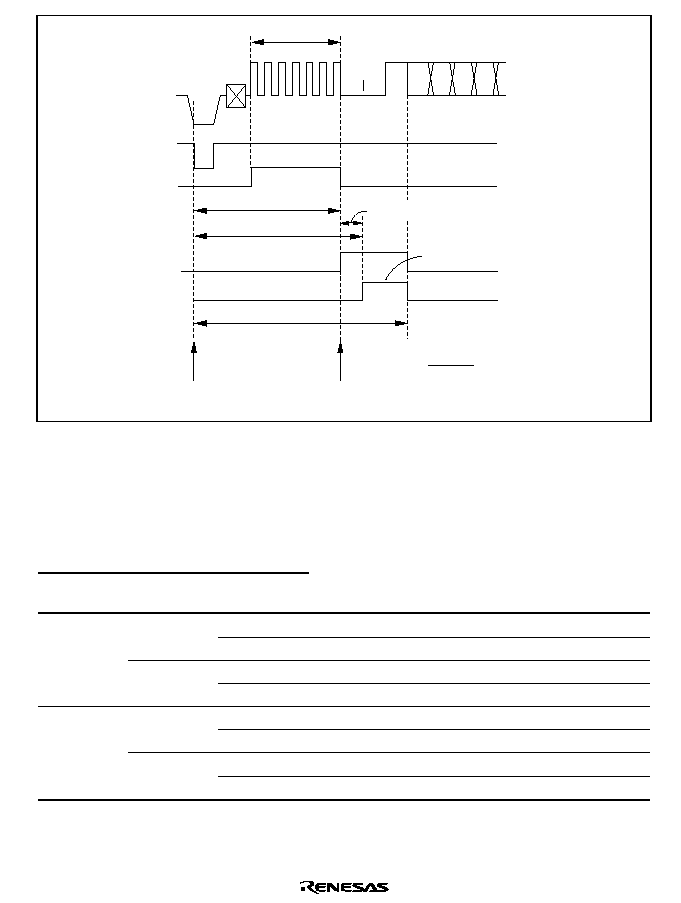
Rev. 1.0, 02/00, page 805 of 1141
Clock run-in
Data slicer base point
Clock run-in detection
window signal
Start bit detection
window signal
Data slicer
base point
Base point for start bit
detection starting position
Approx. 23.5
µ
s
Start bit detectable
period
TS
Te = Approx. 29.5
µ
s
1
288
◊
fh
TS = 23.5
µ
s +
µ
s
◊
(Set by STB4 to STB0)
C.video
S1 S2 S3
Start
bit
Set by STB
Figure 28.2 Data Slicer Base Point and Start Bit Detection Starting Position
Bits 7 to 5--Slice Level Setting Bits (SLVLE2 to SLVLE0) (SLVLO2 to SLVLO0): Specify
the even (odd) field data slice level.
The data slice level is common to clock line detection, start bit detection, and 16-bit data slicing.
Bit 7
Bit 6
Bit 5
SLVLE2
SLVLO2
SLVLE1
SLVLO1
SLVLE0
SLVLO0
Description
0
Slice level is 0 IRE
(Initial value)
0
1
Slice level is 5 IRE
0
Slice level is 15 IRE
0
1
1
Slice level is 20 IRE
0
Slice level is 25 IRE
0
1
Slice level is 35 IRE
0
Slice level is 40 IRE
1
1
1
Must not be specified
Note: All slice levels are with reference to the pedestal level (5 IRE). Slice level values are
provided for reference.
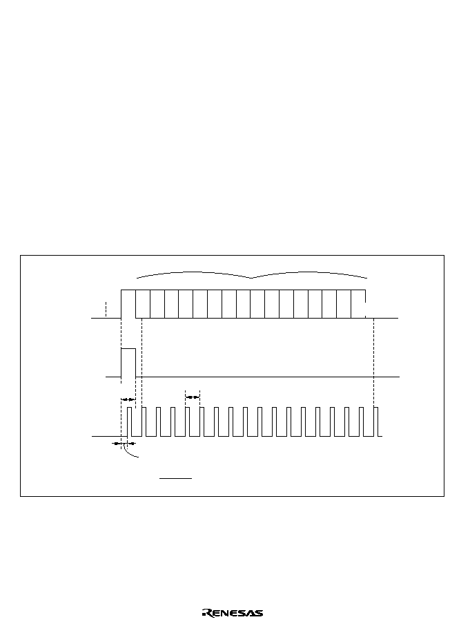
Rev. 1.0, 02/00, page 806 of 1141
Bits 4 to 0
Data Sampling Delay Time Setting Bits (DLYE4 to DLYE0) (DLYO4 to
DLYO0): Set the even (odd) field data sampling clock delay time.
Figure 28.3 explains the data sampling clock.
The data sampling clock is a clock with period 32
◊
fh, used for slicing 16-bit closed caption data.
The data sampling clock is generated after the rising edge of the start bit is detected and the time
set by the DLY bit is passed. The delay time setting can be adjusted in units of 576
◊
fh, so that
sampling is possible at a phase optimal for the slice data. The data sampling delay time (TD)
should be set based on the calculation indicated below. Eighteen pulses of data sampling clock are
output in total for start bit detection, slice data, and end data detection. In order to make the
sampling phase even more optimal, the slice data (analog comparator output) and sampling clock
can be output from the port. For details of monitor output, refer to section 28.2.6, Monitor Output
Setting Register (DOUT).
TD = 111.1 ns (1/576
◊
fh)
◊
[setting in bits DLY4 to DLY0 + 2]
fh: Horizontal sync signal frequency
Start
bit
Slice data
1st character
S1 S2
32
◊
fh
S3
b7 b6 b5 b4 b3 b2 b1 b0 b7 b6 b5 b4 b3 b2 b1 b0
LSB
2nd character
Detected start
bit
Data sampling
clock
32
◊
fh
TD: Data sampling delay time specified by DLYE4 to DLYE0 (DLYO4 to DLYO0)
TD = ns
◊
[setting in bits DLY4 to DLY0 + 2]
MSB
1
576
◊
fh
Figure 28.3 Data Sampling Clock Description

Rev. 1.0, 02/00, page 807 of 1141
28.2.2
Slice Line Setting Registers 1 to 4 (SLINE1 to SLINE4)
0
0
1
0
R/W
2
0
R/W
3
0
4
0
R/W
1
--
5
6
0
7
SLINEn4
SLINEn3
SLINEn2
SLINEn1
SLINEn0
0
R/W
SENBLn
R/W
R/W
R/W
SFLDn
--
Bit:
Initial value:
R/W:
The slice line setting registers 1 to 4 (SLINE1 to SLINE4) specify slice fields and lines. Up to four
slice lines can be specified; these are specified in the slice line setting registers 1 to 4 respectively.
These are 8-bit read/write registers. Rewrites of SLINE should be performed after an even (odd)
field slice completion interrupt is output, or after module stop mode has been set, registers have
been initialized, and module stop mode has been cleared again. If SLINE is rewritten during a data
slice operation, a malfunction will result; do not perform rewriting during data slice operation.
When reset, when the module is stopped, in sleep mode, in standby mode, in watch mode, in
subactive mode, or in subsleep mode, the registers are initialized to H'20.
Bit 7
Slice Enable Bit (SENBLn n=1 to 4): Enables or disables data slice operations for the
line specified by SFLDn and SLINEn4 to SLINEn1.
When data slicing for a given line is completed, this bit is reset to 0, and slicing is not again
performed until it is set to 1. This bit is set at the rising edge of the Vsync signal; hence data
slicing settings become valid from the rising edge of the next Vsync signal after this bit has been
set. When 1 is written to this bit, the corresponding slice detection register is cleared, and so
caution should be exercised.
Bit 7
SENBLn
Description
0
When read: Disables data slice operation for the specified lines
[Clearing condition]
When the data slice operation for the line has been completed
1
Enables data slice operation for the specified lines
Bit 6
Field Setting Bit (SFLDn n=1 to 4): Specifies the field of the slice line. For information
on field discrimination, refer to section 27.2.6, Field Detection Window Register (FWIDR).
Bit 6
SFLDn
Description
0
Even field
(Initial value)
1
Odd field
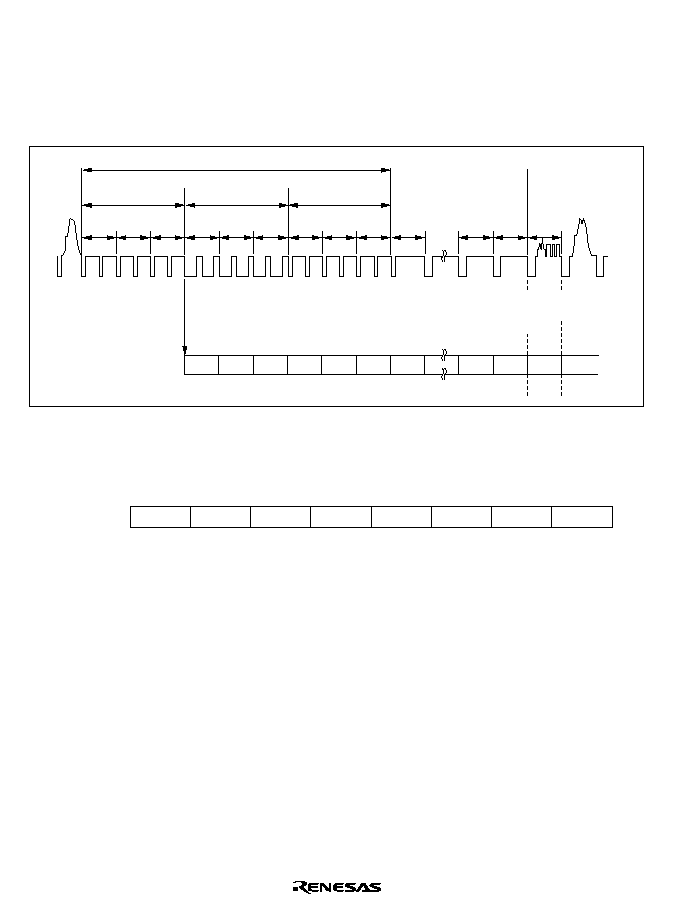
Rev. 1.0, 02/00, page 808 of 1141
Bit 5
Reserved: Cannot be modified and is always read as 1.
Bits 4 to 0
Slice Line Setting Bits (SLINE4 to SLINE0): Specify the data slice line. Slice lines
up to H'1F (31) can be specified.
Figure 28.4 explains the line count.
9-line vertical sync pulse period
Pre-equalizing
period
Sync separation
base point
0
1
1
2
3
4
5
6
7
8
9
10
19
20
21
H'11
2
3
4
5
6
15
16
17
18
Line count
Clear
Post-equalizing
period
Vertical synchro-
nization period
Line count specified by
SLINEn4 to SLINEn0
(n = 1 to 4)
Figure 28.4 Line Count
28.2.3
Slice Detection Registers 1 to 4 (SDTCT1 to SDTCT4)
0
0
1
0
R
2
0
R
3
0
4
1
--
0
R
5
6
0
7
--
CRICn3
CRICn2
CRICn1
CRICn0
0
R
CRDFn
R
R
R
SBDFn
ENDFn
Bit:
Initial value:
R/W:
The slice detection registers 1 to 4 (SDTCT1 to SDTCT4) store information on data slice results.
Data slice result information includes the clock run-in detection flag, start bit detection flag, data
end detection flag, and run-in pulse count for the clock run-in period.
This information is useful for optimal positioning of the data slicer slice level, start bit detection
timing, and sampling clock generation timing.
There are four slice detection registers; data slice information results are stored in them on
completion of data slicing for each line specified by the slice line setting registers 1 to 4. Data is
stored not in slicing order, but in the corresponding registers. For information on the slice line
sequence, refer to section 28.3.2, Slice Sequence.
Rev. 1.0, 02/00, page 809 of 1141
Slice line setting register n
Line m
Slice detection register n
Data slice result information
for line m
Figure 28.5 Relationship between Slice Line Setting Register and Slice Detection Register
SDTCT is an 8-bit read-only register. SDTCT read operations should be performed after an even
(odd) field slice completion interrupt. If SDTCT is read during a data slice operation, an
indeterminate value may be read; the register should not be read during operation.
If 1 is written to bit 7 (SENBL) of slice line setting registers 1 to 4, the corresponding slice
detection register is automatically cleared, so caution should be exercised.
When reset, when the module is stopped, in sleep mode, in standby mode, in watch mode, in
subactive mode, or in subsleep mode, the registers are initialized to H'10.
Bit 7
Clock Run-In Detection Flag (CRDFn n=1 to 4): Set when, during the clock run-in
period, the count is concluded in the range 3 to 7 pulses, and clock run-in is detected. When 16 or
more pulses are counted, further input pulses are not counted in order to prevent erroneous
detection, and an overflow state is maintained. Further, the clock run-in detection window signal
indicating the clock run-in period can be adjusted using the DDETWR register of the sync
separator. For details, refer to section 27.2.10, Data Slicer Detection Window Register
(DDETWR).
Bit 7
CRDFn
Description
0
Clock run-in not detected for line for data slicing
(Initial value)
1
Clock run-in detected for line for data slicing
Bit 6
Start Bit Detection Flag (SBDFn, n=1 to 4): Set when the start bit for a line for data
slicing is detected.
Bit 6
SBDFn
Description
0
Start bit not detected for line for data slicing
(Initial value)
1
Start bit detected for line for data slicing
When the start bit is not detected, the data sampling clock is generated after the time set as the
data sampling delay time (DLY4 to DLY0) has elapsed from the phase of the start bit detection
end position.
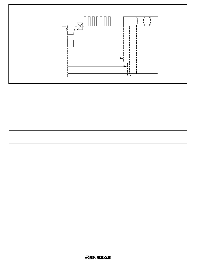
Rev. 1.0, 02/00, page 810 of 1141
Data slicer base
point
Data sampling
clock
Start bit detection starting position
Start bit detection end position
C.video
Delay
Start
bit
Figure 28.6 Data Sampling Clock When Start Bit is not Detected
Bit 5
Data End Detection Flag (ENDFn n=1 to 4): Shows whether or not slice data is input at
the 18th sampling clock pulse. This flag is set when the slice data is 0, that is, when data slicing is
regarded as having been completed normally.
Bit 5
ENDFn
Description
0
Data end not detected for line for data slicing
(Initial value)
1
Data end detected for line for data slicing
Bit 4
Reserved: Cannot be modified and is always read as 1.
Bits 3 to 0
Clock Run-in Count Value (CRICn3 to CRICn0): Count result for run-in pulses
during the clock run-in period. When 16 or more pulses are input, further input pulses are not
counted in order to prevent erroneous detection, and an overflow state is maintained. Further, the
clock run-in detection window signal indicating the clock run-in period can be adjusted using the
DDETWR register of the sync separator. For details, refer to section 27.2.10, Data Slicer
Detection Window Register (DDETWR).
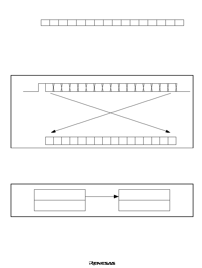
Rev. 1.0, 02/00, page 811 of 1141
28.2.4
Slice Data Registers 1 to 4 (SDATA1 to SDATA4)
15
*
R
14
*
R
13
*
R
12
*
R
11
*
R
10
*
R
9
*
R
8
*
R
7
*
R
6
*
R
5
*
R
4
*
R
3
*
R
2
*
R
1
*
R
0
*
R
Bit:
Initial value:
R/W:
*:
Unefined
The slice data registers 1 to 4 (SDATA1 to SDATA4) are registers in which the slice results are
stored. The data is stored in LSB-first fashion, in order from the LSB side near the start bit. Figure
28.7 shows how to store the slice data.
15
b20
14
b21
13
b22
12
b23
11
b24
10
b25
9
b26
8
b27
7
b10
6
b11
5
b12
4
b13
3
b14
2
b15
1
b16
0
b17
b17
S3
S2
S1
b16 b15
b14
b13
b12 b11 b10 b27 b26
b25 b24 b23 b22 b21 b20
LSB
MSB
Bit
Slice data
register
Slice data
Figure 28.7 Relationship between Slice Data and Slice Data Register
There are four slice data registers, in which are stored slice results when data slicing is completed
for each line specified by the slice line setting registers. At this time data is stored in the
corresponding registers, rather than in the slicing order.
Slice line setting register n
Line m
Slice data register n
Data slice result for line m
Figure 28.8 Relationship between Slice Line Setting Register and Slice Data Register
These are 16-bit read-only registers. SDATA read operations should be performed after an even
(odd) field slice completion interrupt. If an SDATA register is read during a data slice operation,
an indeterminate value may be read; the register should not be read during operation.

Rev. 1.0, 02/00, page 812 of 1141
When reset, when the module is stopped, in sleep mode, in standby mode, in watch mode, in
subactive mode, or in subsleep mode, the SDATA register values are indeterminate.
28.2.5
Module Stop Control Register (MSTPCR)
7
1
R/W
MSTP
15
MSTP
14
MSTP
13
MSTP
12
MSTP
11
MSTP
10
MSTP
9
MSTP
8
MSTP
7
MSTP
6
MSTP
5
MSTP
4
MSTP
4
MSTP MSTP
1
MSTP
0
6
1
R/W
5
4
1
R/W
MSTPCRH
MSTPCRL
1
R/W
3
1
R/W
2
1
R/W
1
1
R/W
0
1
R/W
7
1
R/W
6
1
R/W
5
1
R/W
4
1
R/W
3
1
R/W
2
1
R/W
1
1
R/W
0
1
R/W
Bit:
Initial value:
R/W:
The MSTPCR consists of two 8-bit read/write registers for controlling the module stop mode.
Writing 0 to the MSTP3 bit starts the data slicer; setting the MSTP3 bit to 1 stops the data slicer at
the end of a bus cycle and the module stop mode is entered. Before writing 0 to this bit, set the
MSTP9 bit to 0, to operate the sync separator.
The registers cannot be read or written to in module stop mode. For details, refer to section 4.5,
Module Stop Mode.
Bit 3
Module Stop (MSTP3): Specifies the module stop mode for the data slicer.
Bit 3
MSTP3
Description
0
Clears the module stop mode for the data slicer
1
Specifies the module stop mode for the data slicer
(Initial value)

Rev. 1.0, 02/00, page 813 of 1141
28.2.6
Monitor Output Setting Register (DOUT)
0
1
1
1
--
2
0
R/W
3
0
4
1
R/W
0
R/W
5
6
0
7
DOBC
DSEL
CRSEL
--
--
0
--
--
--
R/W
R/W
RGBC
YCOC
Bit:
Initial value:
R/W:
The internal signals used by the data slicer can be monitored through the R, G, B, YCO, and YBO
pins. For the bits other than bits 2 and 3, refer to section 29.7.3, Digital Output Specification
Register (DOUT).
Bit 3
Bit to Select Functions for R, G, B, YCO, YBO Pins (DSEL): Selects whether the
digital output pins output R, G, B, YCO, and YBO signals, or output data slicer internal monitor
signals.
Bit 3
DSEL
Description
0
R, G, B, YCO, and YBO signals selected
(Initial value)
1
Data slicer monitor signals selected
Pin R: Signal selected by bit 2 (CRSEL)
Pin G: Slice data signal analog-compared with Cvin2
Pin B: Sampling clock generated within data slicer
Pin YCO: External Hsync signal (AFCH) synchronized in the LSI
Pin YBO: External Vsync signal (AFCV) synchronized in the LSI
Bit 2
Monitor Signal Select Bit (CRSEL): Selects whether the clock run-in detection window
signal is output, or the start bit detection window signal is output. This bit is valid when DSEL is
set to 1 to select data slicer internal monitor signal output.
Bit 2
CRSEL
Description
0
Clock run-in detection window signal output selected
(Initial value)
1
Start bit detection window signal output selected

Rev. 1.0, 02/00, page 814 of 1141
28.3
Operation
28.3.1
Slice Line Specification
Up to four slice lines can be specified using the slice line setting registers 1 to 4. For information
on field discrimination, refer to section 27.2.6, Field Detection Window Register (FWIDR).
After completion of data slicing for all lines specified by registers, a slice completion interrupt is
output; the slice results and slice information should then be read.
Slice information includes clock run-in detection, start bit detection, and data end detection to
determine whether data sampling was performed normally; this information is stored in slice
detection registers 1 to 4.
After completion of slicing for specified lines, the slice enable bit for the slice line setting register
is reset to 0. The next time the data slicer is operated, the slice enable bit of the slice line setting
register should be set to 1. At this time, the corresponding slice detection register is cleared. The
slice enable bit is sampled at the rising edge of the Vsync signal. Hence enabling of slice operation
is valid until the next Vsync signal after reset of the slice enable bit.
Figures 28.9 and 28.10 show examples of slice line specification and operation. For details, refer
to section 28.2.2, Slice Line Setting Registers 1 to 4.
Rev. 1.0, 02/00, page 815 of 1141
The data slicer initialization and operation for one specification example are shown in figure 28.9.
Reset the slice enable bit
Reset the slice enable bit
Generate an even field slice completion
interrupt
Contents of slice line setting registers
Slice Line Setting Register
Register No.
1
2
3
4
1
1
1
0
Even
Odd
Even
d > c
b > a
Odd
Enable Field
Line
Start
Initialize the data slicer
Reset the slice enable bit
Generate an odd field slice completion
interrupt
Even field
Odd field
Line c
Line b
Line d
Line a
Set the slice (even and odd)
field mode registers
Set the slice line setting
registers 1 to 4
(except the enable bits)
An external Vsync interrupt
occurs
Execute slicing for line b
An external Vsync interrupt
occurs
Execute slicing for line d
Execute slicing for line c
An external Vsync interrupt
occurs
Set the enable bits of
the slice line setting
registers 1 through 3 to 1
Note: Data slice operation is not performed for line a, because the enable bit = 0. Further, when the same line
is specified within the same field, erroneous operation results; do not specify the same line in the same
field. For details on the external Vsync interrupt, refer to section 27.2.2, Sync Separation Control
Register (SEPCR).
Figure 28.9 Example of Slice Line Specification and Operation (1)
Rev. 1.0, 02/00, page 816 of 1141
Operation for data slicer resetting for a second specification is shown in figure 28.10.
a
<
b
<
c
<
d
Start
Respecification
Even field
Contents of slice line setting registers
Slice Line Setting Register
Register No.
1
2
3
4
1
1
1
1
Even
Even
Even
Even
Enable Field
Line
Line a
Line b
Line d
Line c
e
<
f
<
g
<
h
Contents of slice line setting registers
Slice Line Setting Register
Register No.
1
2
3
4
1
1
1
1
Odd
Odd
Odd
Odd
Enable Field
Line
Line e
Line h
Line f
Line g
An external Vsync interrupt
occurs
Execute slicing for line a
Execute slicing for line b
Reset the slice enable bit
Reset the slice enable bit
Execute slicing for line c
Reset the slice enable bit
Execute slicing for line d
Reset the slice enable bit
Generate an even field slice completion
interrupt
Read each slice detection
register and slice data register.
Respecify slice lines and
set the slice enable bit.
Odd field
An external Vsync interrupt
occurs
Execute slicing for line e
Execute slicing for line f
Reset the slice enable bit
Reset the slice enable bit
Execute slicing for line g
Reset the slice enable bit
Execute slicing for line h
Reset the slice enable bit
Generate an odd field slice completion
interrupt
Read each slice detection
register and slice data register.
Respecify slice lines and
set the slice enable bit.
An external Vsync interrupt
occurs
Figure 28.10 Example of Slice Line Specification and Operation (2)
Rev. 1.0, 02/00, page 817 of 1141
28.3.2
Slice Sequence
Figure 28.11 shows the slice sequence.
Yes
No
Is it the last
line in the field to be
sliced?
∑ Line detection
The specified slice line and field match the line
count and detected field
∑ Clock run-in detection
Count the number of clock run-in pulses in clock
run-in period
∑ Start bit detection
Initiate start bit detection according to the start
bit detection starting position specified by
the register
∑ Data sampling
Data is stored in the 16-bit shift register at a data
sampling clock of 32xfh generated after the time
specified by the register from the start bit
detection
Store data in the
16-bit shift register
to the slice data
register
∑ Data end detection
Detect whether or
not slice data is input
at the 17th data
sampling clock pulse
Set the clock run-in count
Set the start bit detection flag
(Enable the start bit detection)
Set clock run-in detection flag
(Enable the clock run-in detection)
Set the slice completion interrupt
flag
Read the slice detection register
and slice data register
Write the slice line setting
register
Set the slice line enable bit
Set the data end detection flag
(Data end: No data detected at
the 17th data sampling clock
pulse)
Reset the slice enable bit
Figure 28.11 Slice Sequence

Rev. 1.0, 02/00, page 819 of 1141
Section 29 On-Screen Display (OSD)
29.1
Overview
OSD (on-screen display) is a function for superimposing arbitrary characters or display patterns on
a TV image signal.
The display screen consists of up to 32 characters
◊
12 rows; a single character consists of 12 dots
◊
18 lines. Up to 384 different character types can be registered, and each character display can be
connected to the top, bottom, right, and left of another character. Hence in addition to
alphanumerics and kanji characters, graphics can also be displayed.
Text display and superimposed display are supported, and there are composite video signal output
and digital outputs.
There are a wealth of ornamental features as well, including blinking display, borders, cursors,
halftone display, buttons, and enlarged display.
Analog functions (video amp, analog switch) peripheral to OSD are also incorporated. The sync
separator has an AFC circuit built-in, for stable display.
OSD can be used in data encoding in the U.S. closed caption format.
29.1.1
Features
∑
Screen configuration: 32 characters
◊
12 rows
∑
Character size: 12 dots
◊
18 lines
∑
Character types: 384 types*
1
∑
Supports text display and superimposed display
∑
Display enlargement: 1
◊
1, 2
◊
2 (line units, vertical
◊
horizontal)
∑
Blinking: Can be set in single character units
Blinking period can be set to either 32/fV or 64/fV (for the entire screen)
(fV: vertical sync signal frequency)
∑
Border function: Single-dot borders in each of eight directions
Border color:
In text mode, white or black, and brightness fixed
In superimposed mode, black, and brightness fixed
∑
Supported TV formats: NTSC, PAL, SECAM
∑
Display position: Horizontal and vertical direction leading positions are set, and line intervals
can be set
∑
Digital outputs: R, G, B; output of YCO (character data bit strings) and YBO (character
display positions)

Rev. 1.0, 02/00, page 820 of 1141
∑
Background colors: Eight hues*
2
Background brightness, chroma saturation: Four brightness levels, two chroma levels
∑
Character colors: Text display: Eight hues (character units)*
2
Superimposed display: White
Character brightness, chroma saturation: Four brightness levels, two chroma levels
∑
Cursor: Character background colored during text display (character units)
∑
Cursor colors: Eight hues (line units)*
2
Cursor brightness, chroma saturation: Two brightness levels, two chroma levels
∑
Halftone display: Feature for reducing the brightness/chroma saturation of the image signal in
the text background during superimposed display to render it semi-transparent, so that
characters appear to float above the background (character units)
∑
Halftone gray shades: Two levels (row units)
∑
Button display: Two types
Notes: 1. Includes blank character as character code H'000.
2. Background colors, character colors, cursor colors: the background, character, and
cursor colors in text display include black and white. In SECAM, only black and white
are supported. For details, refer to section 29.1.5, TV Formats and Display Modes.

Rev. 1.0, 02/00, page 821 of 1141
29.1.2
Block Diagram
A block diagram of the OSD appears in figure 29.1.
Sync separator
TV format
4/2fsc
Dot
clock
4/2fsc in
CVin1
4/2fsc out
H
V
Horizontal
display
position
control
Display data RAM
Vertical
display
position
control
Button control
Shift register
Border control
4/2fsc
oscillator
CVout
Halftone
control
Sync tip
clamp
SECAM
character
control
Switch-
ing
Color burst
Character, back-
ground, and cursor
color generation
Display control
Character, border,
cursor, button, and
background
R
G
B
YCO
YBO
Character data ROM
Figure 29.1 OSD Block Diagram

Rev. 1.0, 02/00, page 822 of 1141
29.1.3
Pin Configuration
The OSD pin configuration is shown in table 29.1. Even when not using the data slicer, the
composite video signal should be input to Cvin2 in order to perform sync separation from the
composite video signal.
Table 29.1
OSD Pin Configuration
Block
Name
Abbrev.
I/O
Function
Csync/Hsync
Input/output
Composite sync signal input/output or
horizontal sync signal input
Sync signal
input/output
VLPF/Vsync
Input
Pin for connecting external LPF for
vertical sync signal or input pin for
vertical sync signal
AFCosc
Input/output
AFC oscillation signal
AFC
oscillation
AFCpc
Input/output
AFC by-pass capacitor connecting pin
Sync
separator
LPF for AFC
AFCLPF
Input/output
External LPF connecting pin for AFC
OSD analog
power
OVcc
Input
Analog power for OSD, data slicer,
and sync separator
OSD analog
ground
OVss
Input
Analog ground for OSD, data slicer,
and sync separator
Composite
video signal
input
CVin1
Input
Composite video signal input (2 Vpp,
with a sync tip clamp circuit)
Composite
video signal
output
CVout
Output
Composite video signal output (2 Vpp)
4fsc/2fscin
Input
4fsc or 2fsc input
fsc oscillation
4fsc/2fscout
Output
4fsc or 2fsc output
R
Output
Color signal output (R) for character,
border, cursor, background, and
button, or a port
G
Output
Color signal output (G) for character,
border, cursor, background, and
button, or a port
Color signal
output
B
Output
Color signal output (B) for character,
border, cursor, background, and
button, or a port
YCO
Output
Character data output (digital output),
or a port
OSD
Character
data output
YBO
Output
Character display position output
(digital output), or a port

Rev. 1.0, 02/00, page 823 of 1141
Block
Name
Abbrev.
I/O
Function
Data
slicer
Composite
video signal
Cvin2
Input
Composite video signal input (2 Vpp,
with a sync tip clamp circuit)
29.1.4
Register Configuration
Table 29.2 shows the OSD registers.
Table 29.2
Register Configuration
Name
Abbrev.
R/W
Size
Initial
Value
Address
*
1
Character data ROM
OSDROM
--
24576 bytes
--
H'040000
Display data RAM (Master)
OSDRAM
R/W
768 bytes
Undefined
H'D800
Display data RAM (Slave)
--
768 bytes
Undefined
--
Row register 1
CLINE1
R/W
Byte
H'00
H'D200
Row register 2
CLINE2
R/W
Byte
H'00
H'D201
Row register 3
CLINE3
R/W
Byte
H'00
H'D202
Row register 4
CLINE4
R/W
Byte
H'00
H'D203
Row register 5
CLINE5
R/W
Byte
H'00
H'D204
Row register 6
CLINE6
R/W
Byte
H'00
H'D205
Row register 7
CLINE7
R/W
Byte
H'00
H'D206
Row register 8
CLINE8
R/W
Byte
H'00
H'D207
Row register 9
CLINE9
R/W
Byte
H'00
H'D208
Row register 10
CLINE10
R/W
Byte
H'00
H'D209
Row register 11
CLINE11
R/W
Byte
H'00
H'D20A
Row register 12
CLINE12
R/W
Byte
H'00
H'D20B
Vertical display position
register
VPOS
R/W
Word
H'F000
H'D20C
Horizontal display position
register
HPOS
R/W
Byte
H'00
H'D20E
Digital output specification
register
DOUT
R/W
Byte
H'02
H'D20F
Screen control register
DCNTL
R/W
Word
H'0000
H'D210
OSD format register
DFORM
R/(W)
*
2
Word
H'00F8
H'D212
Notes: 1. Lower 16 bits of the address. (excluding character data ROM)
2. Only 0 can be written to bits 8 and 0 to clear the flags.

Rev. 1.0, 02/00, page 824 of 1141
29.1.5
TV Formats and Display Modes
Table 29.3 indicates support for different TV formats in each display mode. Operation is not
guaranteed if a frequency resulting from division by 4 or 2 from the 4fsc/2fsc input pin is not one
of those listed in table 29.3.
Table 29.3
TV Formats and Display Modes
TV Format
fsc (MHz)
Text Display
Superimposed Mode
M/NTSC
3.579545
8 colors
Supported
4.43-NTSC
4.43361875
8 colors
Supported
M/PAL
3.57561149
8 colors
Supported
N/PAL
3.58205625
8 colors
Supported
B.G.H/PAL, I/PAL,
D.K/PAL
4.43361875
8 colors
Supported
SECAM
4.43361875
White/black
Supported
29.2
Description of Display Functions
29.2.1
Superimposed Mode and Text Display Mode
There are two types of OSD display: superimposed and text display.
(1) Superimposed Mode
In superimposed mode, the state of operation of a VCR, the current time, and other text and
graphics are displayed on an ordinary TV image. In doing so, there is no mixing of the background
image and the display character colors. There is an internal AFC circuit, enabling reliable text
display. In addition, a halftone function, in which the brightness and chroma saturation of the
background screen in the character display area is reduced to make characters appear to "float"
above the background, is also available. Other features include a character border function.
(2) Text Display Mode
In text display mode, characters and graphic data can be displayed in synchronous with the
internal sync signal generated by the internal Csync generator circuit in the sync separator. The
background color for display can be selected from among eight hues. There are plentiful
ornamental functions, including functions for displaying cursors and buttons; cursor and text
colors can be selected from among eight hues, making this function ideal for use in programming
VCR recording and setting modes.
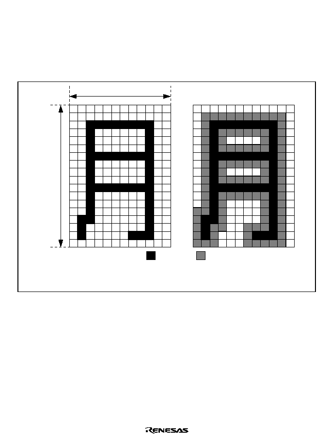
Rev. 1.0, 02/00, page 825 of 1141
29.2.2
Character Configuration
Displayed characters and patterns consist of 12 dots
◊
18 lines per character. There are notes on
creation of OSD fonts. For details, refer to section 29.8, Notes on OSD Font Creation.
An example of a character configuration appears in figure 29.2. An example of an enlarged
character appears in figure 29.3.
12 dots
18 lines
Characters
Borders
(1) Character configuration example
(2) Character configuration example
(with borders outside character)
Figure 29.2 Character Configuration Examples
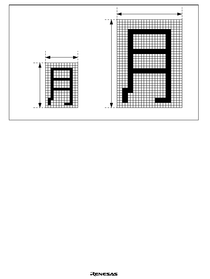
Rev. 1.0, 02/00, page 826 of 1141
12 dots
24 dots
18 lines
36 lines
(1) Standard character size
(2) Enlarged character size
Figure 29.3 Enlarged Character Example
29.2.3
On-Screen Display Configuration
The on-screen display area consists of 12 horizontal rows each containing up to 32 characters.
The correspondence between display data RAM and the screen display is indicated in figure 29.4.
The starting position for display can be set freely by using the display position registers to set the
horizontal starting display position, vertical starting display position, and row interval. Even when
the frequency of the AFC reference clock (dot clock) is modified, the display configuration (12
horizontal rows each containing 32 characters) will not change; characters in the region protruding
outside the display area should be blank characters.
For information on the display position registers, refer to section 29.5.1, Display Positions, and
section 29.5.8, Display Position Registers (HPOS, VPOS).
Rev. 1.0, 02/00, page 827 of 1141
Row 1
Row 2
Row 11
Row 12
1st
character
D800
D840
DA80
DAC0
DA82
DAC2
DA84
DAC4
DA86
DAC6
DABE
DAFE
D802
D842
D804
D844
D806
D846
D83E
D87E
Note: D800 to DAFF indicate the lower 16 bits of addresses in the on-screen display RAM.
32nd
character
2nd
character
3rd
character
4th
character
Figure 29.4 Correspondence between Display Data RAM and On-Screen Display
29.3
Settings in Character Units
The following items can be set in character units by using the display data RAM.
29.3.1
Character Configuration
Characters can be set freely by writing, to the display data RAM, the character data ROM address
(character code) at which the character to be displayed is stored.
For explanations of the character data ROM and display data RAM, refer to section 29.3.6,
Character Data ROM (OSDROM), and section 29.3.7, Display Data RAM (OSDRAM).
29.3.2
Character Colors
Character colors in text display mode can be set in character units through the character color
specification bit in display data RAM.
Table 29.4 shows the correspondence between character color code settings and color output
signals.
For details on display data RAM, refer to section 29.3.7, Display Data RAM (OSDRAM).
In the SECAM TV format, only black and white can be used in text display mode, and in
superimposed mode characters are white, with a faint background color.

Rev. 1.0, 02/00, page 828 of 1141
Table 29.4
Correspondence between Character Color Code Settings and Color Output
Signals
R
1
1
1
1
0
0
0
0
G
1
1
0
0
1
1
0
0
B
Display
Data RAM
Settings
*
1
0
1
0
1
0
1
0
R, G, or B port
output
White
Yellow
Magenta
Red
Cyan
Green
Blue
Black
C.Video output
(NTSC)
White
Same
phase
3
/4
/2
3
/2
7
/4
Black
C.Video output
(PAL)
White
±0
±3
/4
±
/2
±3
/2
±7
/4
±
Black
Note:
*
Can be specified in character units.
29.3.3
Halftones/Cursors
(1) Halftones
The halftone function reduces the brightness and chroma saturation of the image signal in the
character background to make it semi-transparent, so that characters appear to float above the
background. By specifying halftone in the display data RAM, halftone can be toggled in character
units. Here the halftone levels are specified in the row register.
In the SECAM format, use of halftones is recommended.
(2) Cursors
The cursor function colors the background area of a character. By specifying the cursor in display
data RAM, cursor display can be toggled in character units. The cursor color and brightness are
specified in the row register; within a given row, the same color and brightness are used. The
chroma saturation can be set for the entire screen.
Note:
Cursor display is a function for use in text display mode only; halftones are a function for
use in superimposed mode only. The display data RAM halftone/cursor specification bit is
dual-purpose, so that depending on the display mode, function may switch automatically
between halftone/cursor.
Figure 29.5 shows examples of halftone and cursor display. For details on display data RAM, refer
to section 29.3.7, Display Data RAM (OSDRAM). For an explanation of each register, refer to
section 29.4.5, Row Registers (CLINEn, n= rows 1 to 12).
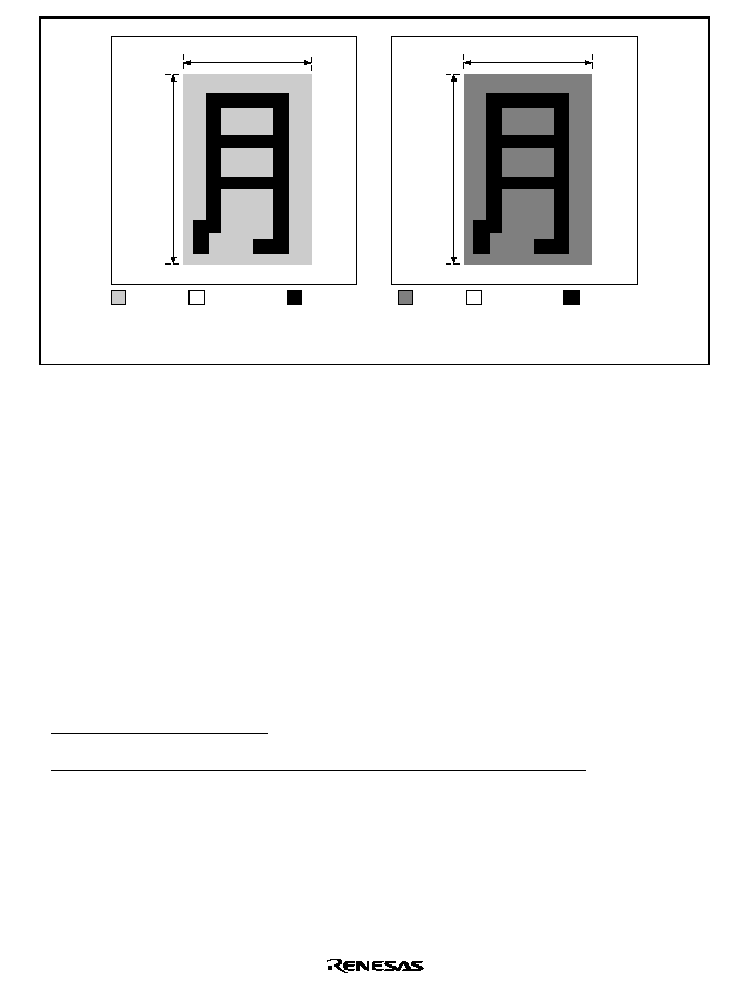
Rev. 1.0, 02/00, page 829 of 1141
18 lines
12 dots
Cursor
(1) Halftone display
(Supported in superimposed mode)
(2) Cursor display
(Supported in text display mode)
Background
Character
12 dots
Halftone
Background
Character
18 lines
Figure 29.5 Halftone and Cursor Display Examples
29.3.4
Blinking
Blinking is a function in which displayed characters are displayed intermittently. By specifying
blinking in display data RAM, text can be made to blink in character units. The blinking period
can be chosen from two values through the screen control register. Blinking is supported both in
superimposed mode and text display mode.
Digital outputs (YCO, R, G, and B) can be made to blink or not blink through the digital output
specification register. The YBO digital output cannot be made to blink.
For details on display data RAM, refer to section 29.3.7, Display Data RAM (OSDRAM).
For an explanation of each register, refer to section 29.5.9, Screen Control Register (DCNTL), and
section 29.7.3, Digital Output Specification Register (DOUT).
Buttons cannot be made to blink.
For notes on blinking, refer to section 29.8.3, Note 3 on Font Creation (Blinking).

Rev. 1.0, 02/00, page 830 of 1141
29.3.5
Button Display
Button display is a function in which a frame is drawn around a character string; buttons can be set
in character units in display data RAM. There are two types of button: one type of button appears
to be raised or floating, and the other type appears to be lowered or sunken. By switching from the
raised button type to the lowered button type, the button appears to have been depressed; such
displays are ideal for screens on which various settings are to be made.
Button displays can be used simultaneously with the blinking function, but blinking can only be
used for characters; buttons cannot be made to blink.
When used with enlarged characters, the button width is enlarged to two dots by two lines.
Buttons are horizontal rectangles; vertical-rectangle buttons cannot be created.
In order to create a button with three or more characters, a button display (start) character and a
button display (end) character should be specified.
Multiple buttons can be created in a single row, but the button pattern in a given row is the same
for all buttons in that row.
The button pattern can be set in row units; white brightness is 75IRE, and black brightness is 15
IRE. Both are values relative to the pedestal (5 IRE). These brightness values are for reference.
Figure 29.6 shows examples of button display.
For details on display data RAM, refer to section 29.3.7, Display Data RAM (OSDRAM). For an
explanation of each register, refer to section 29.4.5, Row Registers (CLINEn, n= rows 1 to 12).
In a button display, the button pattern replaces the outer periphery of the 12 dot
◊
18 line character
region; this should be born in mind when creating character fonts. Refer to section 29.8.4, Note 4
on Font Creation (Buttons).
Rev. 1.0, 02/00, page 831 of 1141
BPTn
BON1
BON0
BPTn
BON1
BON0
0
0
0
0
0
1
0
1
0
0
0
0
0
0/1*
0/1*
0
1
1
Note:
*
Do not set (start) or (end).
1
0
0
1
0
0
1
0
0
1
0
1
1
1
0
1
1
1
Figure 29.6 Button Display Examples
29.3.6
Character Data ROM (OSDROM)
The character data ROM (OSDROM) contains 384 character types, each consisting of 12 dots by
18 lines. User programs can write individual character data sets. However, character code H'000 is
fixed as a blank character, and a new character pattern for this code cannot be set by the user.
The character data ROM (OSDROM) is referenced by character codes in the display data RAM,
and dots of display character data are read for each scanning line.
This character data ROM can be accessed by the CPU as part of user ROM. For details, refer to
section 29.11, Character Data ROM (OSDROM) Access by CPU.
The memory map appears in figure 29.7. An example of configuration for a single character
appears in figure 29.8.
Rev. 1.0, 02/00, page 832 of 1141
Memory map
Bit data for character
code H'000
(blank character display)
*
Note: Character code H'000 is reserved for blank character display and is not available for the user. All bit data
of this character code must be 0, as shown below.
Line 1,
bits 11 to 8
OSD ROM
Internal I/O registers
Internal I/O registers
OSD RAM
000000
040000
040040
040041
040042
040043
040044
040045
040062
040063
040064
04007F
04013F
045FC0
045FFF
04003F
040040
04007F
040080
0400BF
0400C0
0400FF
040100
040000
045FFF
CPU program
FFFFFF
H' F
H' F
H' F
H' F
H' FF
H' FF
040000 : FH'F0
040001 : FH'00
040002 : FH'F0
040003 : FH'00
040022 : FH'F0
040023 : FH'00
040024 : FH'FF
04003F : FH'FF
:
:
:
:
Bit data for character
code H'001
Bit data for character
code H'002
Bit data for character
code H'003
Bit data for character
code H'004
Bit data for character
code H'17F
Line 1,
bits 7 to 0
Line 2,
bits 7 to 0
Line 3,
bits 7 to 0
Line 2,
bits 11 to 8
Line 3,
bits 11 to 8
Line 18,
bits 7 to 0
Line 18,
bits 11 to 8
) Line 1
) Line 2
) Line 18
Figure 29.7 OSD ROM Map
Rev. 1.0, 02/00, page 833 of 1141
Line number
Data
1
2
3
4
5
6
7
8
9
10
11
12
13
14
15
16
17
18
19
32
F000
F000
F3FC
F3FC
F300
F300
F300
F300
F3F0
F3F0
F300
F300
F300
F300
F300
F300
F000
F000
FFFF
FFFF
11109 8 7 6 5 4 3 2 1
1
2
3
4
5
6
7
8
9
10
11
12
13
14
15
16
17
18
0
Line
12 dots
18 dots
32 words
16 bits
Bit
Unused area
Figure 29.8 OSDROM Data Configuration (for the letter "F")
Note:
OSDROM consists of 12 dots
◊
18 lines per character. When character data is written to
flash memory, addresses are written in a 16-bit
◊
32-word area as shown in figure 29.8.
Data in the unused area should be set to 1. In addition, character data for blank display
should always be set to 0.
29.3.7
Display Data RAM (OSDRAM)
8
*
9
*
R/W
10
*
R/W
11
*
12
*
R/W
*
R/W
13
15
BON0
CR
CG
CB
C8
*
R/W
BLNK
14
*
R/W
HT/CR
R/W
R/W
BON1
Bit:
Initial value:
R/W:
0
*
1
*
R/W
2
*
R/W
3
*
4
*
R/W
*
R/W
5
7
C4
C3
C2
C1
C0
*
R/W
C7
6
*
R/W
C6
R/W
R/W
C5
Bit:
Initial value:
R/W:
*
: Undefined
Display data RAM for OSD (OSDRAM) contains 12 rows of 32 characters each, or 384 characters
(384 words), and consists of master RAM and slave RAM. Master RAM can be read and written
by the CPU; slave RAM is accessed by the OSD.

Rev. 1.0, 02/00, page 834 of 1141
The OSD display changes when the data written to master RAM is transferred to the slave RAM.
Data is transferred from the master RAM to the slave RAM by setting the LDREQ bit in the OSD
format register to 1. At this time, when the DTMV bit is 0, transfer is performed at the moment the
LDREQ bit is set to 1; when the DTMV bit is 1, transfer is performed in synchronous with the
Vsync signal after the LDREQ bit is set to 1. After transfer, the LDREQ bit is cleared to 0. During
transfer, the LDREQ bit remains set to 1; master RAM should be accessed only after confirming
that the LDREQ bit has been cleared to 0. If the CPU accesses master RAM during transfer, the
access is invalid and the VACS bit in the OSD format register is set to 1. The master RAM can be
accessed by the CPU even in the module stop mode.
After power-down mode is cancelled, the OSDRAM must be initialized. For details on the OSD
format register, refer to section 29.6.6, OSD Format Register (DFDRM).
Bit 15
Blinking Specification Bit (BLNK): Turns blinking (intermittent display) on and off for
characters in character units. Blinking for digital outputs (YCO, R, G, and B) is set by the digital
output specification register. Digital output (YBO) cannot be set to blink.
OSDRAM
Bit 15
Description
BLNK
C.Video Output
0
Blinking is off
1
Blinking is on
DOUT
OSDRAM
Bit 4
Bit 15
Description
DOBC
BLNK
Digital Output (YCO, R, G, B)
0
Blinking is off
0
1
Blinking is off
0
Blinking is off
1
1
Blinking is on

Rev. 1.0, 02/00, page 835 of 1141
Bit 14
Halftone/Cursor Display Specification Bit (HT/CR): Turns halftone/cursor display on
and off in character units. The superimposed/text display mode switching bit of the screen control
register is used for switching between halftone and cursor display.
In digital outputs (R, G, and B), when the RGBC bit of the digital output specification register is
set to 1 in either superimposed or text display mode to select output of display data for all of
characters/borders/cursor/background/button display, the cursor color data specified by the cursor
color specification bit of the row register is output. In SECAM TV format, it is recommended that
halftone display be used.
DCNTL
OSDRAM
Bit 14
Bit 14
Description
DISPM
HT/CR
C.Video Output
0
Halftone is off
0
1
Halftone is on
0
Cursor display is off
1
1
Cursor display is on
DOUT
OSDRAM
Bit 6
Bit 14
Description
RGBC
HT/CR
Digital Output (R, G, B)
0
0/1
Character is output (halftone/cursor specification invalid)
0
Character is output (halftone/cursor display off)
1
1
Cursor color data specified by the cursor color specification bit of row
register is output
Rev. 1.0, 02/00, page 836 of 1141
Bits 13 and 12
Button Specification Bits (BON1 and BON0): Set buttons in character units in
conjunction with the BPTNn bit of the row register. To create a button with three or more
characters, no-button display characters or button display (one character) must be specified
between a button display (start) character and a button display (end) character. For details, refer to
figure 29.6, Button Display Example.
CLINEn
OSDRAM
Bit 7
Bit 13
Bit 12
BPTNn
BON1
BON0
Description
Display
0
No button is displayed
0
1
Button is displayed (start)
0
Button is displayed (end)
0
1
1
Button is displayed (one character)
0
No button is displayed
0
1
Button is displayed (start)
0
Button is displayed (end)
1
1
1
Button is displayed (one character)

Rev. 1.0, 02/00, page 837 of 1141
Bits 11 to 9
Character Color Specification Bits (CR, CG, and CB): Specify character colors
in character units.
In superimposed mode, the only character color is white, and register settings are invalid.
For digital outputs (R, G, and B), character color data specified by the character color
specification bits for both superimposed and text display modes is output.
Character Color
Bit 11
Bit 10
Bit 9
C.Video Output
CR
CG
CB
NTSC
PAL
R,G,B Outputs
0
Black
Black
Black
0
1
±
Blue
0
7
/4
±7
/4
Green
0
1
1
3
/2
±3
/2
Cyan
0
/2
±
/2
Red
0
1
3
/4
±3
/4
Magenta
0
Same phase
±0
Yellow
1
1
1
White
White
White
Bits 8 to 0
Character Codes (C8 to C0): Set character codes (H'000 to H'17F) to be displayed.
Note: Character code H'000 is defined as blank (nothing displayed).
Character display is not guaranteed if character codes from H'180 to H'1FF are specified.

Rev. 1.0, 02/00, page 838 of 1141
29.4
Settings in Row Units
The following items can be set in row units by using the row registers.
29.4.1
Button Patterns
Characters can be set freely by writing, to display data RAM, the character data ROM address
(character code) at which the character to be displayed is stored.
For information on character data ROM and display data RAM, refer to section 29.3.6, Character
Data ROM (OSDROM), and section 29.3.7, Display Data RAM (OSDRAM).
The button pattern specification bit of the row registers can be used to select the button pattern
(raised or lowered pattern) in row units.
29.4.2
Display Enlargement
The size of characters can be selected in row units by using the character size specification bit of
the row register. When selecting enlarged characters, the border width and button width also
change to accommodate the character size.
29.4.3
Character Brightness
Character brightness can be set in row units using the character brightness specification bit of the
row register. Four different character brightnesses can be selected.
29.4.4
Cursor Color, Brightness, Halftone Levels
(1) Cursor Color
Cursor colors can be set in row units using the cursor color specification bit of the row register.
Table 29.5 shows the correspondence between cursor color code settings and color output signals.
Cursor display functions in text display mode only.
For details on row registers, refer to section 29.4.5, Row Registers (CLINEn, n=rows 1 to 12).

Rev. 1.0, 02/00, page 839 of 1141
Table 29.5
Correspondence between Cursor Color Code Settings and Color Output Signals
R
1
0
G
1
0
1
0
B
Row
Register
Settings
*
1
0
1
0
1
0
1
0
R, G, or B port
output
White
Yellow
Magenta
Red
Cyan
Green
Blue
Black
C.Video output
(NTSC)
White
Same
phase
3
/4
/2
3
/2
7
/4
Black
C.Video output
(PAL)
White
±0
±3
/4
±
/2
±3
/2
±7
/4
±
Black
Note:
*
Can be set in display block units.
(2) Cursor Brightness
Cursor brightness can be set in row units using the cursor brightness specification bit of the row
register. Two different brightness levels can be selected.
For details on row registers, refer to section 29.4.5, Row Registers (CLINEn, n=rows 1 to 12).
(3) Halftone Levels
Halftone levels can be set in row units using the cursor brightness specification bit of the row
register. Two different halftone levels can be selected.
Figure 29.9 shows examples of a halftone level.
Halftone settings function only in superimposed mode.
For details on row registers, refer to section 29.4.5, Row Registers (CLINEn, n = rows 1 to 12).
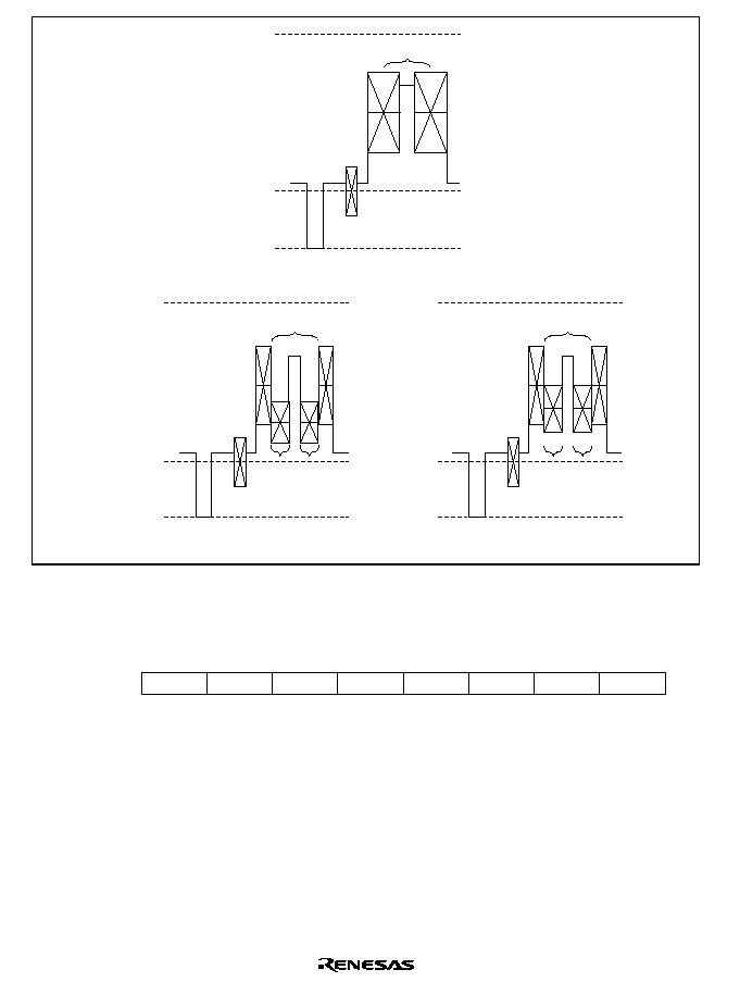
Rev. 1.0, 02/00, page 840 of 1141
100IRE
0IRE
≠40IRE
100IRE
0IRE
≠40IRE
100IRE
0IRE
≠40IRE
White char
acter
50% halftone
Cursor region
Cursor region
Cursor region
(b) 50% halftone
(a) No halftone
(c) 30% halftone
30% halftone
White char
acter
White char
acter
Figure 29.9 Halftone Level Examples (C.Video)
29.4.5
Row Registers (CLINEn, n = rows 1 to 12)
0
0
1
0
R/W
2
0
R/W
3
0
4
0
R/W
0
R/W
5
7
CLUn2
KRn
KGn
KBn
KLUn
0
R/W
BPTNn
6
0
R/W
SZn
R/W
R/W
CLUn1
Bit:
Initial value:
R/W:
There are a total of 12 row registers (CLINEn), for use with rows 1 to 12.
Row register n is used in conjunction with display data RAM to set the character size, button
pattern, cursor color, etc., for the nth row. Each of these is an 8-bit read/write register.
When reset, when the module is stopped, in sleep mode, in standby mode, in watch mode, in
subactive mode, or in subsleep mode, the registers are initialized to H'00.

Rev. 1.0, 02/00, page 841 of 1141
All of the row registers 1 to 12 have the same specifiable format.
When the OSD display update timing control bit (DTMV) is 1, the OSD display is updated to the
row register settings in synchronous with the Vsync signal (OSDV).
Bit 7
Button Pattern Specification Bit (BPTNn n=1 to 12): Sets the button pattern for the nth
row. For button specification, refer to section 29.3.7, Display Data RAM (OSDRAM).
Bit 7
BPTNn
Description
0
Pattern causing buttons in the nth row to appear to be raised
AA
(Initial value)
1
Pattern causing buttons in the nth row to appear to be lowered
AA
Bit 6
Character Size Specification Bit (SZn, n =1 to 12): Sets the size of characters. The
border width and button width also change according to the character size. These settings are
common to superimposed and text display modes and to C.Video output and digital outputs.
Bit 6
SZn
Description
0
Character display size: single height
◊
single width
(Initial value)
1
Character display size: double height
◊
double width

Rev. 1.0, 02/00, page 842 of 1141
Bits 5 and 4
Character Brightness Specification Bits (CLUn1 and CLUn0, n = 1 to 12): Set
the character brightness. The character brightness differs with the character color.
In superimposed mode, white is the only character color.
This setting has no effect on digital outputs (YCO, YBO, R, G, and B).
Bit 5
Bit 4
CLUn1
CLUn0
Character Color
Character Brightness Level
0
0 IRE
(Initial value)
0
1
10 IRE
0
20 IRE
1
1
Black
30 IRE
0
25 IRE
(Initial value)
0
1
45 IRE
0
55 IRE
1
1
Blue, green, cyan, red,
yellow, magenta
65 IRE
0
45 IRE
(Initial value)
0
1
70 IRE
0
80 IRE
1
1
White
90 IRE
Note: All brightness levels are with reference to the pedestal level (5 IRE). Brightness levels are
reference values.

Rev. 1.0, 02/00, page 843 of 1141
Bits 3 to 1
Cursor Color Specification Bits (KRn, KGn, and KBn, n = 1 to 12): Set the
cursor color in row units. C.Video output in superimposed mode uses halftone display, so that
cursor color specifications are invalid.
∑
Cursor Colors in Text Display Mode
Cursor Color
Bit 3
Bit 2
Bit 1
C.Video Output
KRn
KGn
KBn
NTSC
PAL
R, G, B Outputs
0
Black
Black
Black
(Initial value)
0
1
±
Blue
0
7
/4
±7
/4
Green
0
1
1
3
/2
±3
/2
Cyan
0
/2
±
/2
Red
0
1
3
/4
±3
/4
Magenta
0
Same
phase
±0
Yellow
1
1
1
White
White
White
∑
Cursor Colors in Superimposed Mode
Bit 3
Bit 2
Bit 1
Cursor Color
KRn
KGn
KBn
C.Video Output
R, G, B Outputs
0
Black
(Initial value)
0
1
Blue
0
Green
0
1
1
Cyan
0
Red
0
1
Magenta
0
Yellow
1
1
1
Specification invalid
(Halftone display in
superimposed mode)
White

Rev. 1.0, 02/00, page 844 of 1141
Bit 0
Cursor Brightness/Halftone Level Specification Bit (KLUn, n = 1 to 12): Sets the
cursor brightness/halftone level in row units. Cursor brightness differs for different cursor colors.
This setting has no effect on digital outputs (YCO, YBO, R, G, and B).
∑
Cursor Brightness in Text Display Mode
Bit 0
KLU
Cursor Color
Cursor Brightness Level
0
0 IRE
(Initial value)
1
Black
25 IRE
0
25 IRE
(Initial value)
1
Blue, green, cyan, red,
yellow, magenta
45 IRE
0
45 IRE
(Initial value)
1
White
55 IRE
Note: All brightness levels are with reference to the pedestal level (5IRE). Brightness levels are
reference values.
∑
Halftone Levels in Superimposed Mode
Bit 0
KLU
Description (Halftone Levels)
0
50% halftone
(Initial value)
1
30% halftone
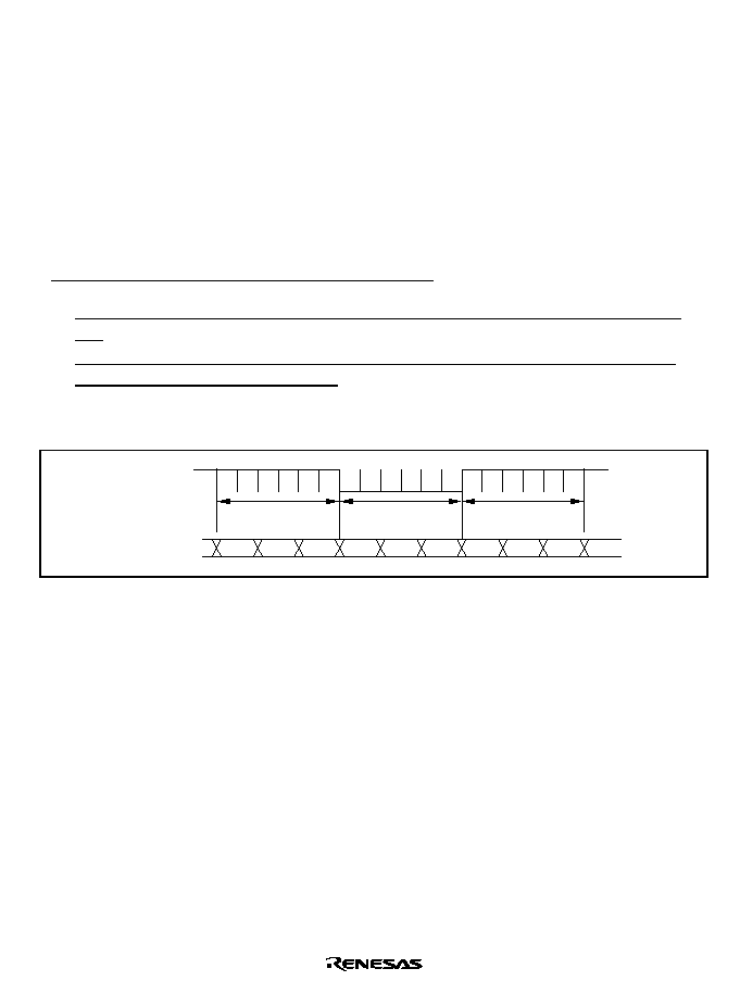
Rev. 1.0, 02/00, page 845 of 1141
29.5
Settings in Screen Units
The following items can be set in screen units by using vertical display position register,
horizontal display position register, and screen control register.
29.5.1
Display Positions
(1) Vertical Display Start Position
The vertical display start position can be set in single scanning line units using the vertical
position specification bits of the vertical display position register.
In setting display positions, the following should be noted.
∑
Settings should be chosen to ensure that the display does not overlap with the vertical retrace
line.
∑
When the display protrudes outside the screen, characters in the protruding region should be
blank characters (character code H'000).
The base point for display start positions is shown in figure 29.10.
Pre-equalizing
period
Post-equalizing
period
Vertical synchro-
nization period
Line counter
0
1
2
3
4
5
6
Figure 29.10 Base Point for Vertical Display Start Positions
(2) Vertical Display Interval
The vertical display interval can be set in single scanning line units using the line interval
specification bit of the vertical display position register.
∑
When the display protrudes outside the screen, characters in the protruding region should be
blank characters (character code H'000).
(3) Horizontal Display Start Position
The horizontal display start position can be set in units equal to double the dot clock cycle using
the horizontal position specification bit of the horizontal display position register.
The base point for the horizontal display start position is the center of the horizontal sync signal.
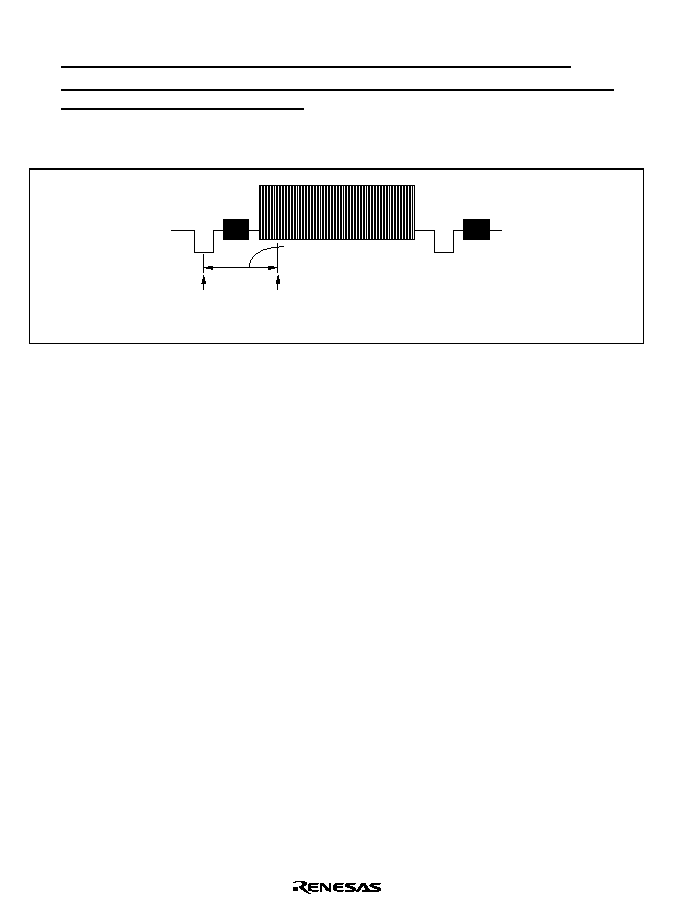
Rev. 1.0, 02/00, page 846 of 1141
Note the following when choosing display position settings.
∑
Settings should be chosen such that the display does not overlap with the color burst.
∑
When the display protrudes outside the screen, characters in the protruding region should be
blank characters (character code H'000).
The base point for the horizontal display start position is shown in figure 29.11.
Horizontal display
start position
Set by the display
position specification
register
OSD display
base point
Figure 29.11 Base Point for Horizontal Display Start Position
29.5.2
Turning the OSD Display On and Off
The OSD display can be turned on and off using the display on/off bit of the screen control
register.
29.5.3
Display Method
Display can be switched between text display mode and superimposed mode, and while in text
display mode the display can be switched between interlaced and noninterlaced display, using the
display mode specification bit of the screen control register.
29.5.4
Blinking Period
A blinking period of either approximately 0.5 sec (32/fV) or approximately 1 sec (64/fV) can be
selected using the blinking period specification bit of the screen control register.

Rev. 1.0, 02/00, page 847 of 1141
29.5.5
Borders
Borders on the periphery of characters can be set using the border specification bit of the screen
control register. For an example of border display, see figure 29.2, Character Configuration
Examples.
The border color can be set in screen units using the border color specification bit of the screen
control register. In text display mode, the border color can be selected from either white or black.
In superimposed mode, all borders are black only.
The horizontal size of borders is one dot (the same as one dot in a character), but for enlarged
characters is two dots.
The vertical size of borders is one line (the same as one line in a character), but for enlarged
characters is two lines.
For an explanation of the screen control register, refer to section 29.5.9, Screen Control Register
(DCNTL).
There are notes on borders; refer to section 29.8, Notes on OSD Font Creation.
Bordering is recommended with the SECAM TV format.
29.5.6
Background Color and Brightness
In text display mode, the background color can be selected from among eight hues, and the
brightness from among four levels, using the background color specification bits and background
brightness select bits of the screen control register.
29.5.7
Character, Cursor, and Background Chroma Saturation
In text display mode, the chroma saturation of the character, cursor, and background can each be
selected from among two levels using the character chroma specification bit, cursor chroma
specification bit, and background chroma specification bit of the screen control register,
respectively.

Rev. 1.0, 02/00, page 848 of 1141
29.5.8
Display Position Registers (HPOS and VPOS)
The HPOS and VPOS include the horizontal display position register and the vertical display
position register.
(1) Horizontal Display Position Register (HPOS)
0
1
R/W
2
R/W
3
4
R/W
R/W
5
7
HP4
0
HP3
0
HP2
0
HP1
0
HP0
0
R/W
HP7
0
R/W
R/W
R/W
HP6
0
HP5
0
6
Bit:
Initial value:
R/W:
The horizontal display position register is used to set the horizontal display start position for
characters. It is an 8-bit read/write register. When reset, when the module is stopped, in sleep
mode, in standby mode, in watch mode, in subactive mode, or in subsleep mode, the horizontal
display position register is initialized to H'00. When the OSD display update timing control bit
(DTMV) is 1, the OSD display is updated to the horizontal display position register settings
synchronously with the Vsync signal (OSDV).
Bits 7 to 0
Horizontal Display Start Position Specification Bits (HP7 to HP0): Set the
display start position in the horizontal direction. Setting units are twice the dot clock cycle. Refer
to the base point for the horizontal display start position in figure 29.11.
If the horizontal display start position is Hs (
µ
s), then Hs is given by 2
◊
tc
◊
(value of HP7 to
HP0), where tc is the dot clock cycle.
(2) Vertical Display Position Register (VPOS)
8
9
R/W
10
R/W
11
12
--
--
13
15
--
1
VSPC2
0
VSPC1
0
VSPC0
0
VP8
0
--
--
1
R/W
R/W
--
--
1
--
1
14
Bit:
Initial value:
R/W:
0
1
R/W
2
R/W
3
4
R/W
R/W
5
7
VP4
0
VP3
0
VP2
0
VP1
0
VP0
0
R/W
VP7
0
R/W
R/W
R/W
VP6
0
VP5
0
6
Bit:
Initial value:
R/W:
The vertical display position register is a 16-bit read/write register used to set the character size,
vertical display start position, and vertical-direction row interval. When reset, when the module is
stopped, in sleep mode, in standby mode, in watch mode, in subactive mode, or in subsleep mode,
the vertical display position register is initialized to H'F000. When the OSD display update timing
control bit (DTMV) is 1, the OSD display is updated to the vertical display position register
settings synchronously with the Vsync signal (OSDV).

Rev. 1.0, 02/00, page 849 of 1141
Bits 15 to 12
Reserved: Cannot be modified and are always read as 1.
Bits 11 to 9
Vertical Row Interval Specification Bits (VSPC2 to VSPC0): Set the row
interval in the vertical direction. They can be set in single scanning line units.
Bit 11
Bit 10
Bit 9
VSPC2
VSPC1
VSPC0
Description
0
No row interval
(Initial value)
0
1
Row interval: One scanning line
0
Row interval: Two scanning lines
0
1
1
Row interval: Three scanning lines
0
Row interval: Four scanning lines
0
1
Row interval: Five scanning lines
0
Row interval: Six scanning lines
1
1
1
Row interval: Seven scanning lines
Bits 8 to 0
Vertical Display Start Position Specification Bits (VP8 to VP0): Set the display
start position in the vertical direction. The vertical display start position can be set in single
scanning line units. The base point of the display start position is the vertical sync signal. Refer to
the base point for the vertical display start position in figure 29.10.
If the vertical display start position is Vs (
µ
s), then Vs is given by Vs = tH
◊
(value of VP8 to
VP0), where tH is the horizontal sync signal period (
µ
s), corresponding to a single horizontal
scanning line.

Rev. 1.0, 02/00, page 850 of 1141
29.5.9
Screen Control Register (DCNTL)
8
9
R/W
10
--
11
12
R/W
R/W
13
15
BLKS
0
OSDON
0
--
0
EDGE
0
EDGC
0
R/W
CDSPON
0
R/W
R/W
R/W
DISPM
0
LACEM
0
14
Bit:
Initial value:
R/W
0
1
R/W
2
R/W
3
4
R/W
R/W
5
7
BLU1
0
BLU0
0
CAMP
0
KAMP
0
BAMP
0
R/W
BR
0
R/W
R/W
R/W
BG
0
BB
0
6
Bit:
Initial value:
R/W
The DCNTL is a 16-bit read/write register used to switch between superimposed and text display
modes, set the background and color for text display mode in screen units, and turn OSD display
on and off.
When reset, when the module is stopped, in sleep mode, in standby mode, in watch mode, in
subactive mode, or in subsleep mode, the DCNTL is initialized to H'0000.
When the OSD display update timing control bit (DTMV) is 1, the OSD display is updated to the
screen control register settings except the setting in bit 13 (LACEM bit) synchronously with the
Vsync signal (OSDV).
Bit 15
OSD C. Video Display Enable Bit (CDSPON): Turns OSDC C.Video display output on
and off.
Bit 15
CDSPON
Description
0
OSD C.Video display is off
(Initial value)
1
OSD C.Video display is on
Bit 14
Superimposed/Text Display Mode Select Bit (DISPM): Selects superimposed mode or
text display mode.
When selecting a display mode, the dot clock also serves as the AFC circuit reference clock, and
so the AFC circuit reference Hsync signal must be switched. For details, refer to section 27.3.6,
Automatic Frequency Controller (AFC).
Bit 14
DISPM
Description
0
Superimposed mode is selected
(Initial value)
1
Text display mode is selected

Rev. 1.0, 02/00, page 851 of 1141
Bit 13
Interlaced/Noninterlaced Display Select Bit (LACEM): Selects interlaced or
noninterlaced text display mode. When noninterlaced text display is selected, the internally
generated Hsync and Vsync frequency can be modified. For details, refer to section 27.2.11,
Internal Sync Frequency Register (INFRQR).
Bit 13
LACEM
Description
0
Noninterlaced display is selected
(Initial value)
1
Interlaced display is selected
Bit 12
Blinking Period Select Bit (BLKS): Selects the character blinking period. The duty is
50%. The blinking period differs somewhat depending on the TV format selected by the TVM2 bit
of the OSD format register (either a 525-line system or a 625-line system).
DFORM
DCNTL
Bit 15
Bit 12
TVM2
BLKS
Description (Blinking Period)
0
Approx. 0.5 sec (32/fv = 0.53 sec)
(Initial value)
0
1
Approx. 1.0 sec (64/fv = 1.07 sec)
0
Approx. 0.5 sec (32/fv = 0.64 sec)
(Initial value)
1
1
Approx. 1.0 sec (64/fv = 1.28 sec)
Note: fv is the vertical sync signal frequency.
Bit 11
OSD Display Start Bit (OSDON): Starts OSD display. When the OSD display start bit
is 0, the OSD internal display circuit stops operation. In conjunction with the OSD C.Video
display enable bit (bit 15), changes operation as follows. When accessing character data ROM
(OSDROM) from the CPU, this bit should always be cleared to 0. If this bit is set to 1, access by
the CPU is not guaranteed.
Bit 15
Bit 11
CDSPON
OSDON
Description
0/1
0
OSD display is stopped (C.Video output and digital output both off)
(Initial value)
0
1
OSD display is started (digital output only)
1
1
OSD display is started (both C.Video output and digital output
enabled)

Rev. 1.0, 02/00, page 852 of 1141
Bit 10
Reserved: Cannot be modified and is always read as 0. When 1 is written to this bit,
correct operation is not guaranteed.
Bit 9
Border Specification Bit (EDGE): Sets the border for characters for the entire screen.
Bit 9
EDGE
Description
0
No character border
(Initial value)
1
Character border
Bit 8
Border Color Specification Bit (EDGC): Selects the border color. Border color
specifications for C.Video output are invalid in superimposed mode.
Border brightness levels are 0 IRE for black and 90 IRE for white.
Note:
Brightness levels are with reference to the pedestal level (5IRE). Brightness levels are
reference values.
∑
Border Color in Text Display Mode
Bit 8
Border Color
EDGC
C.Video Output
R, G, B Outputs
0
Black
Black
(Initial value)
1
White
White
∑
Border Color in Superimposed Mode
Bit 8
Border Color
EDGC
C.Video Output
R, G, B Outputs
0
Black
(Initial value)
1
Specification invalid (black)
White

Rev. 1.0, 02/00, page 853 of 1141
Bits 7 to 5
Background Color Specification Bits (BR, BG, and BB): Used to select the
background color in text display mode. Background color specifications for C.Video output are
invalid in superimposed mode.
∑
Background Colors in Text Display Mode
Background Color
Bit 7
Bit 6
Bit 5
C.Video Output
BR
BG
BB
NTSC
PAL
R, G, B Outputs
0
Black
Black
Black
(Initial value)
0
1
±
Blue
0
7
/4
±7
/4
Green
0
1
1
3
/2
±3
/2
Cyan
0
/2
±
/2
Red
0
1
3
/4
±3
/4
Magenta
0
Same
phase
±0
Yellow
1
1
1
White
White
White
∑
Background Colors in Superimposed Mode
Bit 7
Bit 6
Bit 5
Background Color
BR
BG
BB
C.Video Output
R, G, B Outputs
0
Black
(Initial value)
0
1
Blue
0
Green
0
1
1
Cyan
0
Red
0
1
Magenta
0
Yellow
1
1
1
Specification invalid
White

Rev. 1.0, 02/00, page 854 of 1141
Bits 4 and 3
Background Brightness Select Bits (BLU1 and BLU0): Select the background
brightness in text display mode. These settings have no effect on digital outputs (YCO, YBO, R,
G, and B).
Bit 4
Bit 3
BUL1
BUL0
Background Brightness
0
10 IRE
(Initial value)
0
1
30 IRE
0
50 IRE
1
1
70 IRE
Note: Brightness levels are with reference to the pedestal level (5IRE). Brightness levels are
reference values.
Bit 2
Character Chroma Select Bit (CAMP): Selects the character chroma amplitude in text
display mode. This setting has no effect on digital outputs (YCO, YBO, R, G, and B).
Bit 2
CAMP
Description
0
Character chroma amplitude: 60 IRE
(Initial value)
1
Character chroma amplitude: 80 IRE
Note: Amplitudes are reference values.
Bit 1
Cursor Chroma Select Bit (KAMP): Selects the cursor chroma amplitude in text display
mode. This setting has no effect on digital outputs (YCO, YBO, R, G, and B).
Bit 1
KAMP
Description
0
Cursor chroma amplitude: 60 IRE
(Initial value)
1
Cursor chroma amplitude: 80 IRE
Note: Amplitudes are reference values.
Bit 0
Background Chroma Select Bit (BAMP): Selects the background chroma amplitude in
text display mode. This setting has no effect on digital outputs (YCO, YBO, R, G, and B).
Bit 0
BAMP
Description
0
Background chroma amplitude: 60 IRE
(Initial value)
1
Background chroma amplitude: 80 IRE
Note: Amplitudes are reference values.

Rev. 1.0, 02/00, page 855 of 1141
29.6
Other Settings
29.6.1
TV Format
The OSD supports M/NTSC, 4.43-NTSC, M/PAL, N/PAL, B, G, H/PAL, I/PAL, D, K/PAL, and
SECAM formats. See table 29.3, TV Formats and Display Modes.
29.6.2
Display Data RAM Control
The OSD display data RAM consists of master RAM and slave RAM. The master RAM can be
read and written by the CPU; the slave RAM is accessed by the OSD.
The data written to master RAM is transferred to slave RAM to switch the OSD display.
The DTMV bit can be used to switch between timing the transfer of data to occur when the
LDREQ bit is set to 1, or to occur synchronously with the Vsync signal after LDREQ is set to 1.
For details, refer to section 29.6.6, OSD Format Register (DFORM).
29.6.3
Timing of OSD Display Updates Using Register Rewriting
It is possible to switch the timing of OSD display updates to occur simultaneously with register
rewrites, or to occur synchronously with the Vsync signal (OSDV) after a register rewrite. For
details, refer to section 29.6.6, OSD Format Register (DFORM).
29.6.4
4fsc/2fsc
For a 4fsc/2fsc signal, either an external clock signal is input, or a crystal oscillator can be
connected. If an external clock signal is input, the signal must be amplified using a dedicated
amplifier circuit; this is set using the register.
Either 4fsc or 2fsc input can be selected.
If a 2fsc signal is input, some colors cannot be displayed. For details, see table 29.7, OSD Display
Colors for 2fsc Signal Input.
29.6.5
OSDV Interrupts
Interrupts triggered by the Vsync signal input to the OSD (OSDV interrupts) can be generated. In
superimposed mode, interrupts are triggered by the external Vsync signal, and in text display
mode, they are triggered by the internal Vsync signal generated in the sync separator.

Rev. 1.0, 02/00, page 856 of 1141
29.6.6
OSD Format Register (DFORM)
8
9
R/W
10
R/W
11
12
R/W
R/W
13
15
FSCIN
0
FSCEXT
0
--
0
OSDVE
0
OSDVF
0
R/W
TVM2
0
R/(W)
*
R/W
R/W
TVM1
0
TMV0
0
14
Bit:
Initial value:
R/W:
0
1
R/W
2
R/W
3
4
--
--
5
7
--
1
--
1
DTMV
0
LDREQ
0
VACS
0
--
--
1
R/(W)
*
--
--
--
1
--
1
6
Bit:
Initial value:
R/W:
Note:
*
Only 0 can be written to clear the flag.
The DFORM is used to set the TV format and control display data RAM.
The DFORM is a 16-bit read/write register. When reset, when the module is stopped, in sleep
mode, in standby mode, in watch mode, in subactive mode, or in subsleep mode, it is initialized to
H'00F8.

Rev. 1.0, 02/00, page 857 of 1141
Bits 15 to 13
TV Format Select Bits (TVM2 to 0): Select the TV format. The specified clock
signal should always be input.
Bit 15
Bit 14
Bit 13
Bit 12
Description
TVM2
TVM1
TVM0
FSCIN
TV Format
4fsc (MHz)
2fsc (MHz)
0
14.31818
--
Initial value
0
0
0
1
M/NTSC
--
7.15909
0
0
1
0
4.43-NTSC
17.734475
(17.734476)
--
1
--
8.8672375
(8.867238)
0
1
0
0
M/PAL
14.302446
(14.302444)
--
1
--
7.15122298
0
1
1
0/1
Must not be specified.
0
14.328225
(14.328224)
--
1
0
0
1
N/PAL
--
7.1641125
1
0
1
0/1
Must not be specified.
0
17.734475
(17.734476)
--
1
1
0
1
B, G, H/PAL,
I/PAL, D, K/PAL
--
8.8672375
(8.867238)
0
17.734475
(17.734476)
--
1
1
1
1
B, G,
H/SECAM,
L/SECAM, D,
K, K1/SECAM
--
8.8672375
(8.867238)
Note: The 4fsc and 2fsc frequencies for SECAM do not conform to the SECAM TV format
specifications.
Bit 12
4/2fsc Input Select Bit (FSCIN): Selects 4fsc or 2fsc input.
Bit 12
FSCIN
Description
0
4fsc input is selected
(Initial value)
1
2fsc input is selected

Rev. 1.0, 02/00, page 858 of 1141
Bit 11
4/2fsc External Input Select Bit (FSCEXT): Selects 4fsc or 2fsc input.
Bit 11
FSCEXT
Description
0
4/2fsc oscillator uses a crystal oscillator
(Initial value)
1
4/2fsc uses a dedicated amplifier circuit for external clock signal input
Bit 10
Reserved: Always read as 0. When 1 is written to this bit, correct operation is not
guaranteed.
Bit 9
OSDV Interrupt Enable Bit (OSDVE): Enables or disables OSDV interrupts.
Bit 9
OSDVE
Description
0
The OSDV interrupt is disabled
(Initial value)
1
The OSDV interrupt is enabled
Bit 8
OSDV Interrupt Flag (OSDVF): Set when the OSD detects the Vsync signal. The timing
for setting this flag differs depending on the OSD display mode. In superimposed mode, it is set
on the external Vsync signal; in text display mode it is set on the internally generated Vsync
signal.
Bit 8
OSDVF
Description
0
[Clearing condition]
When 0 is written after reading 1
(Initial value)
1
[Setting condition]
When OSD detects the Vsync signal
Bits 7 to 3
Reserved: Always read as 1. When 0 is written to these bits, correct operation is not
guaranteed.

Rev. 1.0, 02/00, page 859 of 1141
Bit 2
OSD Display Update Timing Control Bit (DTMV): Selects the timing for transfer of
data from master RAM to slave RAM and for OSD display update by register overwriting.
Bit 2
DTMV
Description
0
After the LDREQ bit is written to 1, data is transferred from master RAM to slave
RAM regardless of the Vsync signal (OSDV). The OSD display is updated
simultaneously with register
*
rewriting.
Note:
*
When transferring data using this setting, do not have the OSD display data
(Initial value)
1
After the LDREQ bit is written to 1, data is transferred from master RAM to slave
RAM synchronously with the Vsync signal (OSDV). After rewriting the register, the
OSD display is updated synchronously with the Vsync signal (OSDV).
Note: The registers and register bits whose settings are reflected in the OSD display are the row
registers (CLINE), vertical display position register (VPOS), horizontal display position
register (HPOS), screen control register (DCNTL) except bit 13, and the RGBC, YCOC, and
DOBC bits of the digital output specification register (DOUT).
Bit 1
Master-Slave RAM Transfer Request and State Bit (LDREQ): Requests transfer of
data from master RAM to slave RAM. After this bit is written to 1, a transfer request is issued
with timing selected by the DTMV bit. When read, this bit indicates the state of data transfer from
master RAM to slave RAM.
Note:
To abort data transfer after writing this bit to 1, write it to 0. However, once data transfer
begins it cannot be aborted.
∑
Writing
Bit 1
LDREQ
Description
0
Requests abort of data transfer from master RAM to slave RAM
1
Requests transfer of data from master RAM to slave RAM. After transfer is
completed, this bit is cleared to 0
∑
Reading
Bit 1
LDREQ
Description
0
Data is not being transferred from master RAM to slave RAM
(Initial value)
1
Data is being transferred from master RAM to slave RAM, or is being prepared for
transfer. After transfer is completed, this bit is cleared to 0

Rev. 1.0, 02/00, page 860 of 1141
Bit 0
Master-Slave RAM Transfer State Bit (VACS): Is set to 1 if the CPU accesses
OSDRAM during transfer of data from master RAM to slave RAM; the access is invalid. This bit
is not cleared automatically, and so should be cleared by writing 0.
Bit 0
VACS
Description
0
The CPU did not access OSDRAM during data transfer
(Initial value)
1
The CPU accessed OSDRAM during data transfer; the access is invalid
29.7
Digital Output
29.7.1
R, G, and B Outputs
R, G, and B outputs consist of display data in dot units for characters, background, cursors and
other display elements.
Either of two output methods can be selected by the R, G, B digital output specification bit:
characters only, or output of display data for all elements, including characters, borders, cursors,
background, and buttons. Here data for borders and buttons is output as white-equivalent (R=1,
G=1, B=1) or as black-equivalent (R=0, G=0, B=0) data.
The digital output blink control bit is used to select blinking for R, G, and B. The R, G, and B
outputs are multiplexed with port 8 inputs/outputs. For details on pin function selection, refer to
section 10.9, Port 8.
Display data RAM and the screen control register settings are output as display data output for
characters, cursors and background in superimposed mode; this differs from the output data from
the CVout pin.
Examples of R, G, B output are shown in figures 29.12 and 29.13.
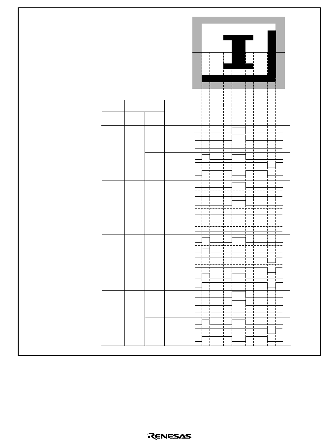
Rev. 1.0, 02/00, page 861 of 1141
!
"
C
D
P
U
V
W
Z
a
b
S
T
Z
_
`
a
!
"
C
D
P
U
V
W
Z
a
b
S
T
Z
_
`
a
!
"
C
D
P
U
V
W
Z
a
b
S
T
Z
_
`
a
!
"
C
D
P
U
V
W
Z
a
b
S
T
Z
_
`
a
!
"
C
D
P
U
V
W
Z
a
b
S
T
Z
_
`
a
!
"
C
D
P
U
V
W
Z
a
b
S
T
Z
_
`
a
!
"
C
D
P
U
V
W
Z
a
b
S
T
Z
_
`
a
!
"
C
D
P
U
V
W
Z
a
b
S
T
Z
_
`
a
!
"
C
D
P
U
V
W
Z
a
b
S
T
Z
_
`
a
!
"
C
D
P
U
V
W
Z
a
b
S
T
Z
_
`
a
!
"
C
D
P
U
V
W
Z
a
b
S
T
Z
_
`
a
!
"
C
D
P
U
V
W
Z
a
b
S
T
Z
_
`
a
!
"
C
D
P
U
V
W
Z
a
b
S
T
Z
_
`
a
!
"
C
D
P
U
V
W
Z
a
b
S
T
Z
_
`
a
!
"
C
D
P
U
V
W
Z
a
b
S
T
Z
_
`
a
!
"
C
D
P
U
V
W
Z
a
b
S
T
Z
_
`
a
!
"
C
D
P
U
V
W
Z
a
b
S
T
Z
_
`
a
!
"
C
D
P
U
V
W
Z
a
b
S
T
Z
_
`
a
!
"
C
D
P
U
V
W
Z
a
b
S
T
Z
_
`
a
!
"
C
D
P
U
V
W
Z
a
b
S
T
Z
_
`
a
!
"
C
D
P
U
V
W
Z
a
b
S
T
Z
_
`
a
!
"
C
D
P
U
V
W
Z
a
b
S
T
Z
_
`
a
!
"
C
D
P
U
V
W
Z
a
b
S
T
Z
_
`
a
!
"
C
D
P
U
V
W
Z
a
b
S
T
Z
_
`
a
!
"
C
D
P
U
V
W
Z
a
b
S
T
Z
_
`
a
!
"
C
D
P
U
V
W
Z
a
b
S
T
Z
_
`
a
!
"
C
D
P
U
V
W
Z
a
b
S
T
Z
_
`
a
!
"
C
D
P
U
V
W
Z
a
b
S
T
Z
_
`
a
!
"
C
D
P
U
V
W
Z
a
b
S
T
Z
_
`
a
!
"
C
D
P
U
V
W
Z
a
b
S
T
Z
_
`
a
!
"
C
D
P
U
V
W
Z
a
b
S
T
Z
_
`
a
!
"
C
D
P
U
V
W
Z
a
b
S
T
Z
_
`
a
!
"
C
D
P
U
V
W
Z
a
b
S
T
Z
_
`
a
!
"
C
D
P
U
V
W
Z
a
b
S
T
Z
_
`
a
!
"
C
D
P
U
V
W
Z
a
b
S
T
Z
_
`
a
!
"
C
D
P
U
V
W
Z
a
b
S
T
Z
_
`
a
!
"
C
D
P
U
V
W
Z
a
b
S
T
Z
_
`
a
!
"
C
D
P
U
V
W
Z
a
b
S
T
Z
_
`
a
!
"
C
D
P
U
V
W
Z
a
b
S
T
Z
_
`
a
!
"
C
D
P
U
V
W
Z
a
b
S
T
Z
_
`
a
!
"
C
D
P
U
V
W
Z
a
b
S
T
Z
_
`
a
!
"
C
D
P
U
V
W
Z
a
b
S
T
Z
_
`
a
!
"
C
D
P
U
V
W
Z
a
b
S
T
Z
_
`
a
!
"
C
D
P
U
V
W
Z
a
b
S
T
Z
_
`
a
!
"
C
D
P
U
V
W
Z
a
b
S
T
Z
_
`
a
!
"
C
D
P
U
V
W
Z
a
b
S
T
Z
_
`
a
!
"
C
D
P
U
V
W
Z
a
b
S
T
Z
_
`
a
!
"
C
D
P
U
V
W
Z
a
b
S
T
Z
_
`
a
!
"
C
D
P
U
V
W
Z
a
b
S
T
Z
_
`
a
!
"
C
D
P
U
V
W
Z
a
b
S
T
Z
_
`
a
!
"
C
D
P
U
V
W
Z
a
b
S
T
Z
_
`
a
!
"
C
D
P
U
V
W
Z
a
b
S
T
Z
_
`
a
!
"
C
D
P
U
V
W
Z
a
b
S
T
Z
_
`
a
!
"
C
D
P
U
V
W
Z
a
b
S
T
Z
_
`
a
!
"
C
D
P
U
V
W
Z
a
b
S
T
Z
_
`
a
!
"
C
D
P
U
V
W
Z
a
b
S
T
Z
_
`
a
!
"
C
D
P
U
V
W
Z
a
b
S
T
Z
_
`
a
!
"
C
D
P
U
V
W
Z
a
b
S
T
Z
_
`
a
!
"
C
D
P
U
V
W
Z
a
b
S
T
Z
_
`
a
!
"
C
D
P
U
V
W
Z
a
b
S
T
Z
_
`
a
!
"
C
D
P
U
V
W
Z
a
b
S
T
Z
_
`
a
!
"
C
D
P
U
V
W
Z
a
b
S
T
Z
_
`
a
!
"
C
D
P
U
V
W
Z
a
b
S
T
Z
_
`
a
!
"
C
D
P
U
V
W
Z
a
b
S
T
Z
_
`
a
!
"
C
D
P
U
V
W
Z
a
b
S
T
Z
_
`
a
!
"
C
D
P
U
V
W
Z
a
b
S
T
Z
_
`
a
0
RAM
DOUT
BLNK
DOBC RGBC
0
R
G
B
(Low)
(Low)
(Low)
(Low)
(Low)
R
G
B
R
G
B
R
G
B
R
(Blinking)
G
(Blinking)
B
(Blinking)
R
(Blinking)
G
(Blinking)
B
(Blinking)
1
0
0/1
1
0
1
0
1
1
1
1
1
Bac
kg
round
Output Example 1
Character color:
Yellow (CR = 1, CG = 1, CB = 0)
Cursor color:
Cyan (KR = 0, KG = 1, KB = 1)
Background color: Green (BR = 0, BG = 1, BB = 0)
Border:
None (EDGE = 0)
Button:
Displayed (pattern 1)
Button
Cursor
Border
Char
acter
Border
Cursor
Button
Bac
kg
round
Figure 29.12 RGB Output Example (1)
Rev. 1.0, 02/00, page 862 of 1141
0
RAM
DOUT
BLNK
DOBC RGBC
0
R
G
B
(Low)
(Low)
(Low)
(Low)
(Low)
(Low)
(High)
(Low)
(Low)
(Low)
(Low)
(Low)
R
G
B
R
G
B
R
G
B
R
(Blinking)
G
(Blinking)
B
(Blinking)
R
(Blinking)
G
(Blinking)
B
(Blinking)
1
0
0/1
1
0
1
0
1
1
1
1
1
Output Example 2
Character color:
Yellow (CR = 1, CG = 1, CB = 0)
Cursor color:
None (HT/CR = 0)
Background color: Green (BR = 0, BG = 1, BB = 0)
Border:
Black (EDGE = 1, EDGC = 0)
Button:
None
Button
Cursor
Border
Char
acter
Border
Cursor
Button
Bac
kg
round
Bac
kg
round
Figure 29.13 RGB Output Example (2)

Rev. 1.0, 02/00, page 863 of 1141
29.7.2
YCO and YBO Outputs
YCO output consists of character and border data in dot units. Either of two YCO output methods
can be selected by the YCO digital output specification bit: output of characters only, or
combined output of character and border data. The digital output blink control bit can be used to
select blinking for YCO output. The YCO data output specification bit must be reset to 0 when
bordering is not performed, and must be set to 1 when bordering is performed. YBO output is data
for the character display area. 32 characters' worth of data is output starting from the start position
set by the horizontal-direction start position specification bit of the display position register. Here
blank-character intervals have no character display, and so there is no output. In addition, YBO
output cannot be made to blink.
The YCO and YBO outputs are multiplexed with port 8 inputs/outputs. For details on pin function
selection, refer to section 10.9, Port 8.
An example of YCO output and that of YBO output appear in figures 29.14 and 29.15,
respectively.
0
RAM
DOUT
BLNK DOBC YCOBC
0
1
0
1
0
1
YCO
YCO
YCO
YCO
YCO
(Blinking)
YCO
(Blinking)
(Low)
(Low)
0/1
0
1
1
Output Example
Character color:
Yellow (CR = 1, CG = 1, CB = 0)
Cursor color:
None (HT/CR = 0)
Background color: Green (BR = 0, BG = 1, BB = 0)
Border:
Black (EDGE = 1, EDGC = 0)
Button:
None
Button
Cursor
Border
Char
acter
Border
Cursor
Button
Bac
kg
round
Bac
kg
round
Figure 29.14 YCO Output Example
Rev. 1.0, 02/00, page 864 of 1141
Horizontal display position
Display block
Character display
position
Blank character
Row 1
YBO
1 2 3 4 5 6 7
29
32
.......................................................................
.....
Figure 29.15 YBO Output Example
29.7.3
Digital Output Specification Register (DOUT)
0
1
--
2
R/W
3
4
R/W
R/W
5
7
DOBC
0
DSEL
0
CRSEL
0
--
1
--
0
--
--
0
--
R/W
R/W
RGBC
0
YCOC
0
6
Bit:
Initial value:
R/W:
The DOUT is used to choose settings for digital output.
The DOUT is an 8-bit read/write register. When reset, when the module is stopped, in sleep mode,
in standby mode, in watch mode, in subactive mode, or in subsleep mode, it is initialized to H'02.
When the OSD display update timing control bit is 1, the OSD display is updated to the RGBC,
YCOC and DOBC bit settings synchronously with the Vsync signal (OSDV).
The R, G, B, YCO, and YBO outputs are multiplexed with port 8 inputs/outputs. For details on pin
function selection, refer to section 10.9, Port 8.
Bit 7
Reserved: Always read as 0. When 1 is written to this bit, correct operation is not
guaranteed.
Bit 6
R, G, B Digital Output Specification Bit (RGBC): Specifies the R, G, B digital output
format.
Bit 6
RGBC
Description
0
Character output is specified
(Initial value)
1
Combined character, border, cursor, background, and button output is specified

Rev. 1.0, 02/00, page 865 of 1141
Bit 5
YCO Digital Output Specification Bit (YCOC): Specifies the YCO digital output
format. This bit must be reset to 0 when bordering is not performed, and must be set to 1 when
bordering is performed.
Bit 5
YCOC
Description
0
Character output is specified
(Initial value)
1
Combined character and border output is specified
Bit 4
Digital Output Blink Control Bit (DOBC): Turns blinking on and off for digital outputs
(YCO, R, G, and B). Digital output YBO cannot be made to blink.
OSDRAM
DOUT
Bit 15
Bit 4
BLNK
DOBC
Description
0
Does not blink
(Initial value)
0
1
Does not blink
0
Does not blink
1
1
Blinks
Bit 3
R, G, B, YCO, YBO Pin Function Select Bit (DSEL): Selects the R, G, B, YCO, and
YBO pins to function either as digital output pins, or as data slicer internal monitor signal pins.
Bit 3
DSEL
Description
0
R, G, B, YCO, YBO output function is selected
(Initial value)
1
Data slicer monitor output function is selected
R pin = Signal selected by bit 2 (CRSEL)
G pin = Slice data signal analog-compared with Cvin2
B pin = Sampling clock generated within data slicer
YCO pin = External Hsync signal (AFCH) synchronized within the LSI
YBO pin = External Vsync signal (AFCV) synchronized within the LSI
Rev. 1.0, 02/00, page 866 of 1141
Bit 2
Monitor Signal Switching Bit (CRSEL): Selects whether a clock run-in detection
window signal or a start bit detection window signal is output. This bit setting is valid when DSEL
is 1, so that pins are used as data slicer internal monitor signal outputs.
Bit 2
CRSEL
Description
0
Clock run-in detection window signal output is selected
(Initial value)
1
Start bit detection window signal output is selected
For information on slice data and the sampling clock, refer to section 28.2.2, Slice Line Setting
Registers 1 to 4. For details on the clock run-in detection window signal, start bit detection
window signal, external Hsync signal (AFCH), and external Vsync signal (AFCV), refer to section
27, Sync Separator for OSD and Data Slicer.
Bit 1
Reserved: Cannot be modified and is always read as 1.
Bit 0
Reserved: Always read as 0. When 1 is written to this bit, correct operation is not
guaranteed.
29.7.4
Module Stop Control Register (MTSTPCR)
7
1
R/W
MSTP
15
MSTP
14
MSTP
13
MSTP
12
MSTP
11
MSTP
10
MSTP
9
MSTP
8
MSTP
7
MSTP
6
MSTP
5
MSTP
4
MSTP
3
MSTP
2
MSTP
1
MSTP
0
6
1
R/W
5
4
1
R/W
MSTPCRH
MSTPCRL
1
R/W
3
1
R/W
2
1
R/W
1
1
R/W
0
1
R/W
7
1
R/W
6
1
R/W
5
1
R/W
4
1
R/W
3
1
R/W
2
1
R/W
1
1
R/W
0
1
R/W
Bit:
Initial value:
R/W:
The MSTPCR consists of two 8-bit read/write registers for controlling the module stop mode.
Writing 0 to the MSTP0 bit starts the OSD module; setting the MSTP0 bit to 1 stops the OSD
module at the end of a bus cycle and the module stop mode is entered. At this time, the CVout and
digital outputs also stop. Before writing 0 to this bit, set the MSTP9 bit to 0, to operate the sync
separator.
The registers cannot be read or written to in module stop mode. However, character data ROM
(OSDROM) and display data RAM (OSDRAM) can be read and written. For details, refer to
section 4.5, Module Stop Mode.

Rev. 1.0, 02/00, page 867 of 1141
Bit 0
Module Stop (MSTP0): Specifies the module stop mode for the OSD module.
Bit 0
MSTP0
Description
0
Clears the module stop mode for the OSD module
1
Specifies the module stop mode for the OSD module
(Initial value)
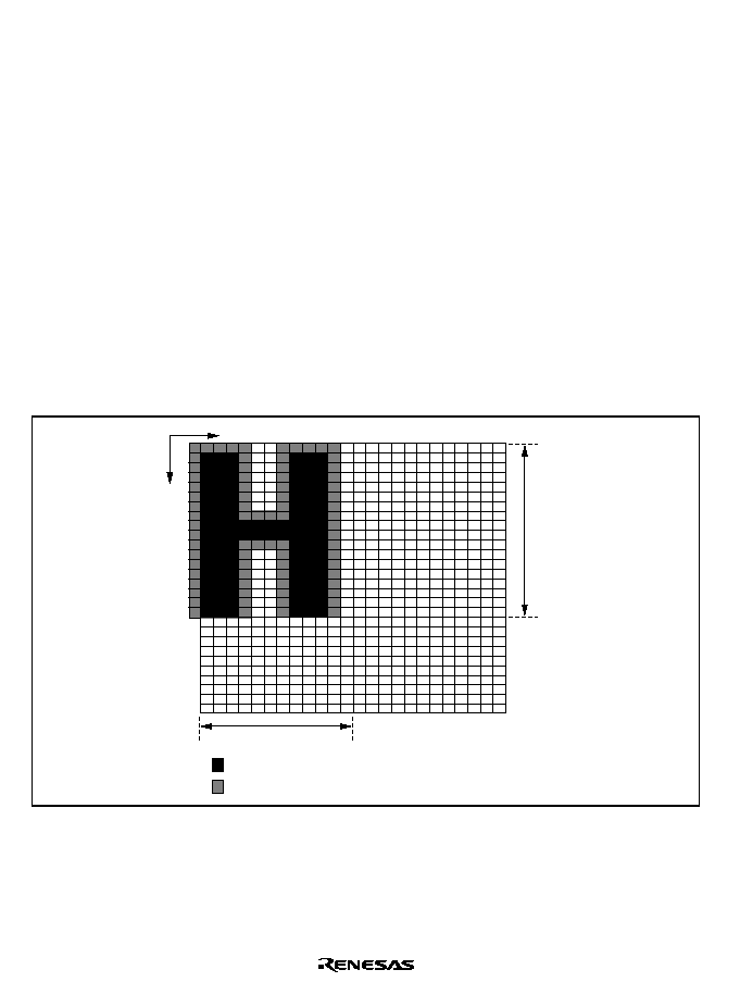
Rev. 1.0, 02/00, page 868 of 1141
29.8
Notes on OSD Font Creation
29.8.1
Note 1 on Font Creation (Font Width)
In OSD display, vertical and diagonal lines in fonts that are one dot wide may appear to be narrow
due to a shift of 0.5H. Display fonts should be created with liberal thicknesses.
29.8.2
Note 2 on Font Creation (Borders)
Borders extend beyond the character display frame in the X-direction, but no borders extend
beyond the display frame in the Y-direction. Moreover, when borders are to the right or left of
blank characters (H'000), borders extend beyond the display frame, but for the first and the 32nd
characters in a displayed row (16th character when the character size is enlarged to double height
◊
double width), no borders extend beyond the display frame.
Examples of borders which extend beyond the display frame appear in figures 29.16 through
figure 29.18.
X-direction
Y
-direction
12 dots
Characters
Borders
18 dots
Figure 29.16 Border Extending beyond the Display Frame (Example)
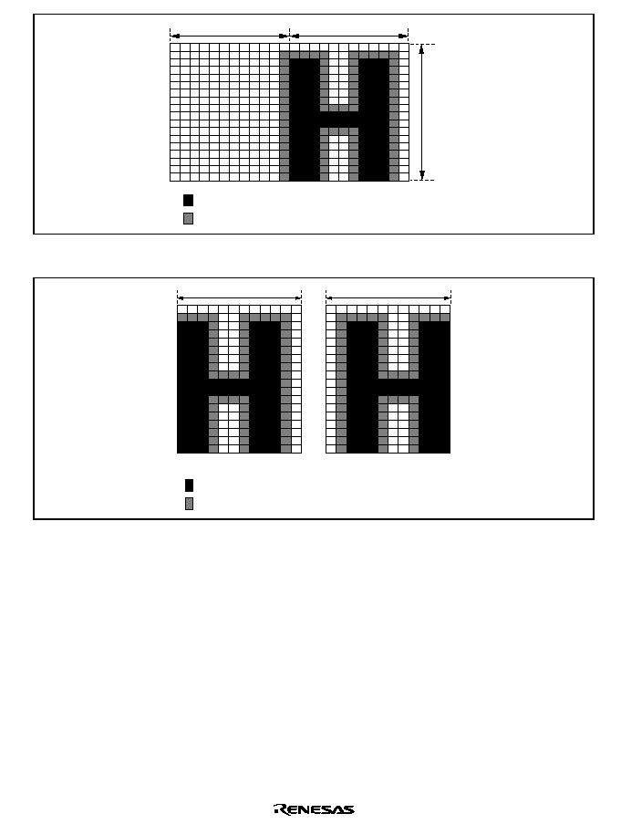
Rev. 1.0, 02/00, page 869 of 1141
12 dots
Characters
Borders
18 dots
Blank display
Figure 29.17 Border Neighboring a Blank Character (Example)
12 dots
(a) 1st character
(b) 32nd character
12 dots
Characters
Borders
Figure 29.18 Examples of Characters at the Starting and Ending Positions in a Row
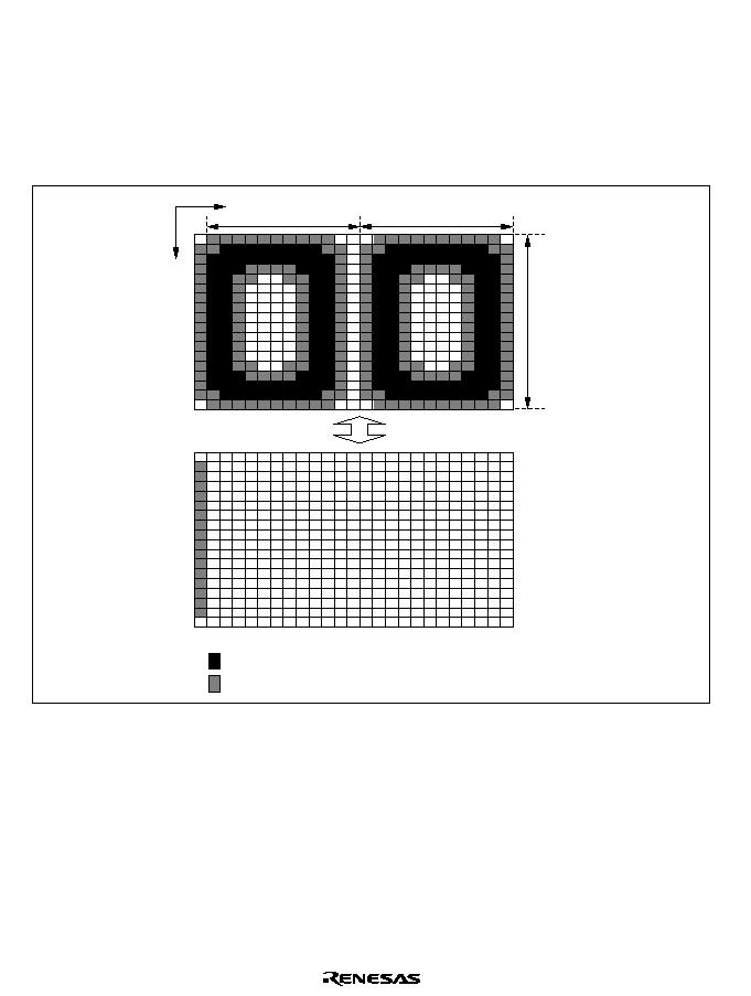
Rev. 1.0, 02/00, page 870 of 1141
29.8.3
Note 3 on Font Creation (Blinking)
Blinking involves intermittent display within a specified display frame only. When blinking is
necessary, font data should not be set to the first or twelfth dots in the X-direction.
Figure 29.19 shows an example of blinking for characters with borders extending beyond the
display frame.
12 dots
X-direction
Y
-direction
12 dots
18 dots
Characters
Borders
Figure 29.19 Example of Blinking with Borders Extending beyond the Display Frame
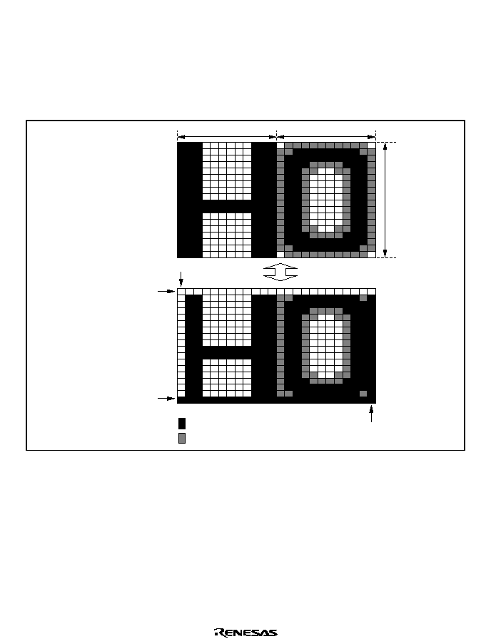
Rev. 1.0, 02/00, page 871 of 1141
29.8.4
Note 4 on Font Creation (Buttons)
Buttons replace the outermost perimeter of the character display area with a button pattern. It
should be remembered that the button pattern display takes priority over display of the font and
border, if any.
Figure 29.20 shows an example of button pattern display that takes priority over font and border.
12 dots
Button pattern: White
12 dots
18 dots
Characters
Borders
Button pattern: White
Button pattern: Black
Button pattern: Black
Figure 29.20 Example of Button Pattern Display Taking Priority over Font and Border

Rev. 1.0, 02/00, page 872 of 1141
29.9
OSD Oscillator, AFC, and Dot Clock
In order to use the OSD, sync signals and a 4/2fsc clock signal are required.
29.9.1
Sync Signals
The sync signal for text display mode is a signal created from a 4/2fsc clock or an AFC reference
clock. In superimposed mode, sync signals may be selected from one of the following three types.
1. Horizontal/vertical sync signals separated by the sync separator from the composite video
signal (Cvin2)
2. Horizontal/vertical sync signals separated by the sync separator from the composite sync signal
(Csync)
3. Hsync and Vsync signals input separately
For details, refer to section 27, Sync Separator for OSD and Data Slicer.
29.9.2
AFC Circuit
The AFC circuit averages the "fluctuation" in the horizontal sync signal (Hsync) during normal
VCR playback, reducing OSD display jitter. In addition, the AFC circuit generates the dot clock.
Be sure that an external circuit is connected. For details, refer to section 27.3.6, Automatic
Frequency Controller (AFC).
29.9.3
Dot Clock
The dot clock is a clock used for X-direction (horizontal direction) OSD display; it is
synchronized with the horizontal sync signal generated by the AFC circuit. The dot clock
frequency is 576 or 448 times the horizontal sync signal frequency (576
◊
fh or 448
◊
fh). The size
of one dot in the horizontal direction of the OSD display appearing on the screen is the equivalent
of one dot clock cycle. Accordingly, modifying the FRQSEL bit in the sync separator to change
the horizontal sync signal frequency can adjust the dot size. The dot clock cycle is the same in
superimposed mode and text display mode; it is also the same for both interlaced and
noninterlaced displays. It changes somewhat depending on the TV format. The relation between
TV format and dot clock cycle is shown in table 29.6.
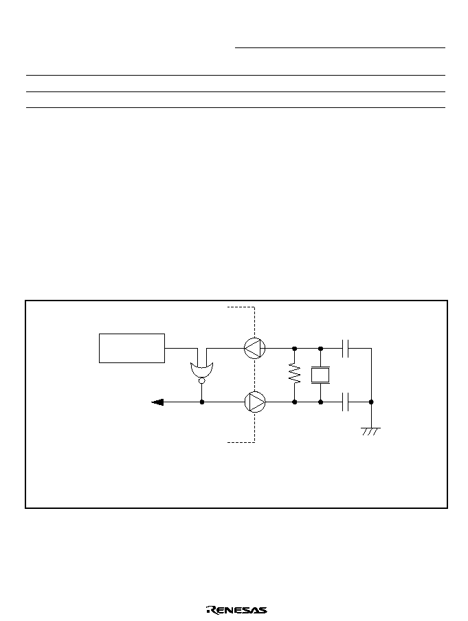
Rev. 1.0, 02/00, page 873 of 1141
Table 29.6
Dot Clock Cycle
Dot Clock Cycle
TV Format
Reference Clock:
576
◊
fh
Reference Clock:
448
◊
fh
M/NTSC, 4.43-NTSC, M/PAL, N/PAL
110 ns (9.06 MHz)
142 ns (7.06 MHz)
B, G, H/PAL, I/PAL, D, K/PAL, SECAM
111 ns (9.00 MHz)
143 ns (7.00 MHz)
29.9.4
4/2fsc
1. 4/2fsc Oscillator
The 4/2fsc oscillator generates color signals for text display mode, and also generates the
internal sync signal. A crystal oscillator can be connected, or an external clock can be input.
The 4/2fsc frequency should be appropriate for the TV format. If an inappropriate frequency is
used, or if no 4/2fsc signal is input, OSD operation is not guaranteed.
Circuit constants should be chosen such that frequency deviation, including temperature
effects, is within
±
30 ppm.
An example of connection of a crystal oscillator appears in figure 29.21; an example of input
of an external clock is shown in figure 29.22.
Power-down
mode controller
4/2fsc in
Rf
Crystal
C2
C1
Note: Rf = 1 M
typ.
Crystal should be at a frequency appropriate for the TV format.
C1, C2 should be specified such that frequency deviation, including temperature effects, is less than
±30 ppm.
Figure 29.21 Example of Connection of a 4/2fsc Crystal Oscillator

Rev. 1.0, 02/00, page 874 of 1141
Power-down
mode controller
External clock
Duty: 47 to 53%
4/2fsc in
C
R
(OPEN)
Note: C = 1000 pF typ
When the external clock amplitude is 1 Vp-p or larger, connect a resistor in series with capacitor C.
External clock select
Figure 29.22 Example of Input of a 4/2fsc External Clock
2. For information on OSD display colors for a 2fsc signal input, refer to table 29.7. In NTSC
format, some colors cannot be displayed. In PAL format, because alternating display is used,
color muddiness, flickering and other problems may arise.
Table 29.7
OSD Display Colors for 2fsc Signal Input
Character, Cursor,
and Background
Color Settings
NTSC
PAL
*
RGB
Digital Output
Yellow (Same phase)
Yellow (Same phase)
Yellow (3
/2, ≠
/2)
Yellow
Cyan (3
/2)
Cyan (3
/2)
Cyan (
, 0)
Cyan
Green (7
/4)
Cannot be specified
Green (≠
/2, 0)
Green
Magenta (3
/4)
Cannot be specified
Magenta (+
/2, ≠
)
Magenta
Red (
/2)
Red (
/2)
Red (+
/2, ≠
/2)
Red
Blue (
)
Blue (
)
Blue (
/2, ≠3
/2)
Blue
White
White
White
White
Black
Black
Black
Black
Note:
*
The PAL color burst phase angle is
±
/4 rad for 4fsc input, but is 0 rad or ≠
/2 rad for 2fsc,
so that colors may differ from the color settings.

Rev. 1.0, 02/00, page 875 of 1141
29.10
OSD Operation in CPU Operation Modes
Table 29.8 shows the OSD CVout pin status for different CPU operating modes.
During a transition to power-down mode, registers are initialized, and so register settings must be
restored on return to active mode.
Table 29.8
OSD Operation for Different CPU Operating Modes
Operating Mode
Module Stop Bit
DISPM Bit
CVout Pin
Reset
1
0
No output
0
Chroma-through and
OSD display
Active
0
1
Text display
Module stop
1
0
No output
Sleep, standby, watch,
subactive, or subsleep
Retained
0
No output

Rev. 1.0, 02/00, page 876 of 1141
29.11
Character Data ROM (OSDROM) Access by CPU
The character data ROM can be accessed by the CPU as part of user ROM. Before accessing the
character data ROM by the CPU, clear the OSDON bit in the screen control register to 0 to stop
OSD display, then set the OSROME bit in the serial timer register to 1. The character data ROM
can be accessed even in the module stop mode.
If the OSROME bit is set to 1 during OSD display, the character data ROM cannot be accessed
correctly by CPU.
For details on OSROME bit setting, refer to section 29.5.9, Screen Control Register (DCNTL).
29.11.1
Serial Timer Control Register (STCR)
0
0
1
0
2
0
3
0
4
0
5
0
6
0
7
--
OSROME
FLSHE
--
IICX0
IICX1
--
--
R/W
R/W
--
R/W
R/W
--
--
--
0
Bit :
Initial value :
R/W :
Bit 2
OSD ROM Enable (OSROME): Controls the OSD character data ROM (OSDROM)
access. When this bit is set to 1, the OSDROM can be accessed by the CPU, and when this bit is
cleared to 0, the OSDROM cannot be accessed by the CPU but accessed by the OSD module.
Before writing to or erasing the OSDROM in the F-ZTAT version, be sure to set this bit to 1.
Note:
During OSD display, the OSDROM cannot be accessed by the CPU. Before accessing the
OSDROM by the CPU, be sure to clear the OSDON bit in the screen control register to 0
then set the OSROME bit to 1. If the OSROME bit is set to 1 during OSD display, the
character data ROM cannot be accessed correctly by CPU.
Bit 2
OSROME
Description
0
OSDROM is accessed by the OSD
(Initial value)
1
OSDROM is accessed by the CPU

Rev. 1.0, 02/00, page 877 of 1141
Section 30 Electrical Characteristics
30.1
Absolute Maximum Ratings
Table 30.1 lists the absolute maximum ratings.
Table 30.1
Absolute Maximum Ratings
Item
Symbol
Value
Unit
Power supply voltage
Vcc
-
0.3 to +7.0
V
Input voltage (ports other than port 0)
Vin
-
0.3 to Vcc+0.3
V
Input voltage (port 0)
Vin
-
0.3 to AVcc+0.3
V
A/D converter power supply voltage
AVcc
-
0.3 to +7.0
V
A/D converter input voltage
AVin
-
0.3 to AVcc+0.3
V
Servo power supply voltage
SVcc
-
0.3 to +7.0
V
Servo amplifier input voltage
Vin
-
0.3 to SVcc + 0.3
V
OSD power supply voltage
OVcc
-
0.3 to +7.0
V
Operating temperature
Topr
-
20 to +75
∞
C
Operating temperature (At Flash memory
program/erase)
Topr
0 to +75
∞
C
Storage temperature
Tstr
-
55 to +125
∞
C
Notes: 1. Permanent damage may occur to the chip if absolute maximum ratings are exceeded.
Normal operation should be under the conditions specified in Electrical Characteristics.
Exceeding these values can result in incorrect operation and reduced reliability.
2. All voltages are relative to Vss = SVss = OVss = AVss = 0.0 V.

Rev. 1.0, 02/00, page 878 of 1141
30.2
Electrical Characteristics of HD6432199, HD6432198, HD6432197,
and HD6432196
30.2.1
DC Characteristics of HD6432199, HD6432198, HD6432197, and HD6432196
Table 30.2
DC Characteristics of HD6432199, HD6432198, HD6432197, and HD6432196
(Conditions: Vcc = AVcc = 4.0 V to 5.5 V*
1
, Vss = 0.0 V, Ta = ≠20 to +75
∞
C unless otherwise
specified.)
Values
Item
Symbol
Applicable Pins
Test
Conditions
Min
Typ
Max
Unit
Notes
MD0
Vcc=2.5 V to
5.5V
0.9 Vcc
Vcc+0.3
0.8 Vcc
Vcc+0.3
5(6
, FWE, IC, IRQ0
to IRQ5
Vcc=2.5 V to
5.5V
0.9 Vcc
Vcc+0.3
SCK1, SI1, FTIA,
FTIB, FTIC, FTID,
TRIG, TMBI,
$'75*
0.8 Vcc
Vcc+0.3
Vcc≠0.5
Vcc+0.3
OSC1
Vcc=2.5 V to
5.5V
Vcc≠0.3
Vcc+0.3
0.7 Vcc
Vcc+0.3
P00 to P07,
P10 to P17,
P20 to P27,
P30 to P37,
P40 to P47,
P60 to P67,
P70 to P77,
P80 to P87
Vcc=2.5 V to
5.5V
0.8 Vcc
Vcc+0.3
Input high
voltage
V
IH
Csync
0.7 Vcc
Vcc+0.3
V

Rev. 1.0, 02/00, page 879 of 1141
Values
Item
Symbol
Applicable Pins
Test
Conditions
Min
Typ
Max
Unit
Notes
MD0
Vcc=2.5 V to
5.5 V
≠0.3
0.1 Vcc
-
0.3
0.2 Vcc
5(6
, FWE, IC,
IRQ0 to IRQ5
Vcc=2.5 V to
5.5 V
-
0.3
0.1 Vcc
SCK1, SI1, FTIA, FTIB,
FTIC, FTID, TRIG,
TMBI,
$'75*
-
0.3
0.2 Vcc
-
0.3
0.5
OSC1
Vcc=2.5 V to
5.5 V
-
0.3
0.3
-
0.3
0.3 Vcc
P00 to P07,
P10 to P17,
P20 to P27,
P30 to P37,
P40 to P47,
P60 to P67,
P70 to P77,
P80 to P87
Vcc=2.5 V to
5.5 V
-
0.3
0.2 Vcc
Input low
voltage
V
IL
Csync
-
0.3
0.2 Vcc
V

Rev. 1.0, 02/00, page 880 of 1141
Values
Item
Symbol
Applicable Pins
Test
Conditions
Min
Typ
Max
Unit
Notes
-
I
OH
=1.0mA
Vcc≠1.0
V
-
I
OH
=0.5mA
Vcc≠
0.5
V
Refer-
ence
value
Output
high
voltage
V
OH
SO1, SCK1, PWM1,
PWM2, PWM3,
PWM4, PWM14,
BUZZ, TMO, TMOW,
FTOA, FTOB, PPG0 to
PPG7,
RP0 to RP7,
RP8 to RPB,
P10 to P17,
P20 to P27,
P30 to P37,
P40 to P47,
P60 to P67,
P70 to P77,
P80 to P87,
SV1, SV2, R, G, B,
YCO, YBO
-
I
OH
=0.1mA
Vcc=2.5V to
5.5V
Vcc≠0.5
V
I
OL
=1.6mA
0.6
V
SO1, SCK1, PWM1,
PWM2, PWM3,
PWM4, PWM14,
BUZZ, TMO, TMOW,
FTOA, FTOB, PPG0 to
PPG7,
RP0 to RP7,
RP8 to RPB,
P10 to P17,
P20 to P27,
P30 to P37,
P40 to P47,
P70 to P77,
P80 to P87, SV1, SV2,
R, G, B, YCO, YBO
I
OL
=0.4mA
Vcc=2.5 V to
5.5V
0.4
V
I
OL
=20mA
1.5
V
I
OL
=1.6mA
0.6
V
Output
low
voltage
V
OL
P60 to P67,
I
OL
=0.4mA
Vcc=2.5 V to
5.5V
0.4
V

Rev. 1.0, 02/00, page 881 of 1141
Values
Item
Symbol
Applicable Pins
Test
Conditions
Min
Typ
Max
Unit
Notes
MD0, FWE
Vin=0.5 to
Vcc≠0.5V
1.0
5(6
,
,54
to
,54
,
,&
Vin=0.5 to
Vcc≠0.5V
1.0
SCK1, SI1, SDA0,
SCL0, SDA1, SCL1,
FTIA, FTIB, FTIC, FTID,
TRIG, TMBI,
$'75*
Vin=0.5 to
Vcc≠0.5V
1.0
OSC1
Vin=0.5 to
Vcc
-
0.5V
1.0
Input
/output
leakage
current
I
IL
P10 to P17,
P20 to P27,
P30 to P37,
P40 to P47,
P60 to P67,
P70 to P77,
P80 to P87,
Vin=0.5 to
Vcc≠0.5V
1.0
µ
A
P00 to P07,
AN8 to ANB
Vin=0.5 to
AVcc≠0.5V
1.0
Pull-up
MOS
current
-
Ip
P10 to P17,
P20 to P27,
P30 to P37
Vcc=5.0V,
Vin=0V
50
300
µ
A
*
2
Input
capacity
Cin
All input pins except
power supply pins
P23, P24, P25, and
P26, and analog pins
fin=1 MHz,
Vin=0V,
Ta=25
∞
C
15
pF
P23, P24, P25, P26
fin=1 MHz,
Vin=0V,
Ta=25
∞
C
20
pF

Rev. 1.0, 02/00, page 882 of 1141
Values
Item
Symbol
Applicable
Pins
Test
Conditions
Min
Typ
Max
Unit
Notes
Vcc=5V,
f
OSC
=10 MHz,
High-speed
mode
TBD
mA
*
3
Active
mode
current
dissipa-
tion (CPU
operating)
I
OPE
Vcc
Vcc=5V,
f
OSC
=10 MHz,
Medium-speed
mode (1/64)
TBD
mA
Reference value
Active
mode
current
dissipa-
tion
(reset)
I
RES
Vcc
Vcc=5V,
f
OSC
=10 MHz
--
TBD
mA
*
3
Sleep
mode
current
dissipa-
tion
I
SLEEP
Vcc
Vcc=5V,
f
OSC
=10 MHz
High-speed
mode
TBD
mA
*
3
Vcc=2.5V,
32kHz
With crystal
oscillator
(
sub=
w/2)
TBD
*
3
Subactive
mode
current
dissipa-
tion
I
SUB
Vcc
Vcc=2.5V,
32kHz
With crystal
oscillator
(
sub=
w/8)
TBD
µ
A
Reference value
*
3
Vcc=2.5V,
32kHz
With crystal
oscillator
(
sub=
w/2)
TBD
*
3
Subsleep
mode
current
dissipa-
tion
I
SUBSLP
Vcc
Vcc=2.5V,
32kHz
With crystal
oscillator
(
sub=
w/8)
TBD
µ
A
Reference value
*
3

Rev. 1.0, 02/00, page 883 of 1141
Values
Item
Symbol
Applicable Pins
Test
Conditions
Min
Typ
Max
Unit
Notes
Vcc=2.5V,
32kHz
With crystal
oscillator
TBD
µ
A
*
3
Watch
mode
current
dissipa-
tion
I
WATCH
Vcc
Vcc=5.0V,
32kHz
With crystal
oscillator
TBD
µ
A
Reference
value
*
3
Standby
mode
current
dissipa-
tion
I
STBY
Vcc
X1=V
CL
, 32kHz
Without crystal
oscillator
5
µ
A
*
3
RAM data
retaining
voltage in
standby
mode
V
STBY
2.0
V
Notes: 1. Do not open the AVcc and Avss pin even when the A/D converter is not in use.
2. Current value when the relevant bit of the pull-up MOS select register (PUR1 to PUR3)
is set to 1.
3. The current on the pull-up MOS or the output buffer excluded.
Table 30.3
Pin Status at Current Dissipation Measurement
Mode
#$
#$
pin
Internal State
Pin
Oscillator Pin
Active mode
High-speed, medium-
speed
Vcc
Operating
Vcc
Sleep mode
High-speed, medium-
speed
Vcc
Only CPU and
servo circuits
halted
Vcc
Reset
Vss
Reset
Vcc
Standby mode
Vcc
All circuits halted
Vcc
Main clock:
Crystal oscillator
Sub clock:
X1 pin = V
CL
Subactive mode
Vcc
Only CPU and
timer A operating
Vcc
Subsleep mode
Vcc
Only timer A
operating
Vcc
Watch mode
Vcc
Only timer A
operating
Vcc
Main clock:
Crystal oscillator
Sub clock:
Crystal oscillator

Rev. 1.0, 02/00, page 884 of 1141
Table 30.4
Bus Drive Characteristics of HD6432199, HD6432198, HD6432197, and
HD6432196
(Conditions: Vcc = AVcc = 4.0 V to 5.5 V, Vss = 0.0 V, Ta = ≠20 to +75
∞
C)
Applicable pin: SCL0, SCL1, SDA0, SDA1
Values
Item
Symbol
Applicable Pins
Test
Conditions
Min
Typ
Max
Unit
Notes
V
T
-
0.3Vcc
V
V
T
+
0.7Vcc
V
Schmitt
trigger
input
V
T
+
≠V
T
-
SCL0, SDA0,
SCL1, SDA1
0.05Vcc
V
Input high
level
voltage
V
IH
SCL0, SDA0,
SCL1, SDA1
0.7Vcc
Vcc+0.5
V
Input low
level
voltage
V
IL
SCL0, SDA0,
SCL1, SDA1
-
0.5
0.3Vcc
V
I
OL
=8mA
0.5
Output
low level
voltage
V
OL
SCL0, SDA0,
SCL1, SDA1
I
OL
=3mA
0.4
V
SCL and
SDA
output fall
time
t
of
SCL0, SDA0,
SCL1, SDA1
20+
0.1Cb
250
ns

Rev. 1.0, 02/00, page 885 of 1141
30.2.2
Allowable Output Currents of HD6432199, HD6432198, HD6432197, and
HD6432196
The specifications for the digital pins are shown below.
Table 30.5
Allowable Output Currents of HD6432199, HD6432198, HD6432197, and
HD6432196
(Conditions: Vcc = 2.5 V to 5.5 V, Vss = 0.0 V, Ta = ≠20 to +75
∞
C)
Item
Symbol
Value
Unit
Notes
Allowable input current (to chip)
I
O
2
mA
1
Allowable input current (to chip)
I
O
22
mA
2
Allowable input current (to chip)
I
O
10
mA
3
Allowable output current (from chip)
-
I
O
2
mA
4
Total allowable input current (to chip)
I
O
80
mA
5
Total allowable output current (from chip)
-
I
O
50
mA
6
Notes: 1. The allowable input current is the maximum value of the current flowing from each I/O
pin to V
SS
(except for port 6, SCL0, SDA0, SCL1 and SDA1).
2. The allowable input current is the maximum value of the current flowing from each I/O
pin to V
SS
. This applies to port 6.
3. The allowable input current is the maximum value of the current flowing from each I/O
pin to V
SS
. This applies to SCL0, SDA0, SCL1 and SDA1.
4. The allowable output current is the maximum value of the current flowing from V
CC
to
each I/O pin.
5. The total allowable input current is the sum of the currents flowing from all I/O pins to
V
SS
simultaneously.
6. The total allowable output current is the sum of the currents flowing from V
CC
to all I/O
pins.

Rev. 1.0, 02/00, page 886 of 1141
30.2.3
AC Characteristics of HD6432199, HD6432198, HD6432197, and HD6432196
Table 30.6
AC Characteristics of HD6432199, HD6432198, HD6432197, and HD6432196
-
Preliminary
-
(Conditions: Vcc = AVcc = 4.0 V to 5.5 V, Vss = 0.0 V, Ta = ≠20 to +75
∞
C unless otherwise
specified.)
Values
Item
Symbol
Applicable
Pins
Test
Conditions
Min
Typ
Max
Unit
Notes
Clock oscillation
frequency
f
OSC
OSC1, OSC2
8
10
MHz
Clock cycle time
t
cyc
OSC1, OSC2
100
125
ns
Figure 30.1
Subclock
oscillation
frequency
f
X
X1, X2
Vcc = 2.5 V to
5.5 V
32.768
kHz
Subclock cycle
time
t
subcyc
X1, X2
Vcc = 2.5 V to
5.5 V
30.518
µ
s
Figure 30.2
OSC1, OSC2
Crystal oscillator
10
ms
Oscillation
stabilization time
t
rc
X1, X2
32kHz crystal
oscillator
2
s
External clock high
width
t
CPH
OSC1
40
ns
External clock low
width
t
CPL
OSC1
40
ns
External clock rise
time
t
CPr
OSC1
10
ns
External clock fall
time
t
CPf
OSC1
10
ns
Figure 30.1
External clock
stabilization delay
time
t
DEXT
OSC1
500
µ
s
Figure 30.3
Subclock input low
level pulse width
t
EXCLL
X1
Vcc = 2.5 V to
5.5 V
15.26
µ
s
Subclock input
high level pulse
width
t
EXCLH
X1
Vcc = 2.5 V to
5.5 V
15.26
µ
s
Subclock input rise
time
t
EXCLr
X1
Vcc = 2.5 V to
5.5 V
10
ns
Subclock input fall
time
t
ECXLf
X1
Vcc = 2.5 V to
5.5 V
10
ns
Figure 30.2
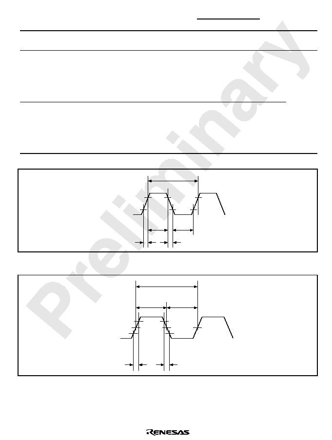
Rev. 1.0, 02/00, page 887 of 1141
Values
Item
Symbol
Applicable
Pins
Test
Conditions
Min
Typ
Max
Unit
Figure
5(6
pin low level
width
t
REL
5(6
Vcc = 2.5 V to
5.5 V
20
t
cyc
Figure
30.4
Input pin high level
width
t
IH
,54
to
,54
,
,&
,
$'75*
,
TMBI, FTIA,
FTIB, FTIC,
FTID,
RPTRIG
Vcc = 2.5 V to
5.5 V
2
t
cyc
t
subcyc
Input pin low level
width
t
IL
,54
to
,54
,
,&
,
$'75*
,
TMBI, FTIA,
FTIB, FTIC,
FTID,
RPTRIG
Vcc = 2.5 V to
5.5 V
2
t
cyc
t
subcyc
Figure
30.5
t
cyc
t
CPH
V
IL
V
IH
OSC1
t
CPL
t
CPf
t
CPr
Figure 30.1 System Clock Timing
t
EXCLf
t
subcyc
t
EXCLH
t
EXCLL
t
EXCLr
V
IL
V
IH
X1
Vcc
◊
0.5
Figure 30.2 Subclock Input Timing
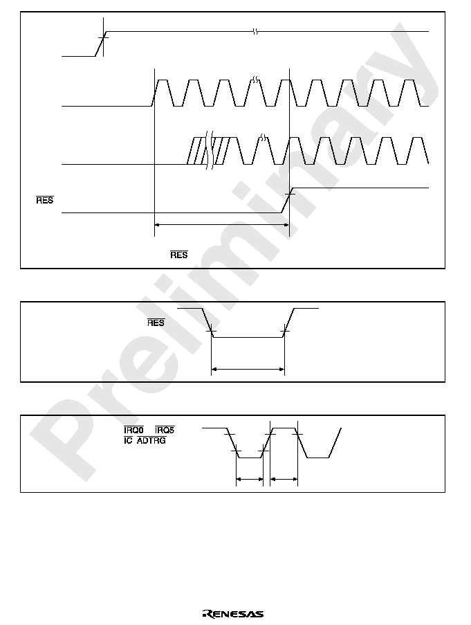
Rev. 1.0, 02/00, page 888 of 1141
Vcc
OSC1
t
DEXT
*
(Internal)
4.0V
The t
DEXT
includes the
pin Low level width 20 t
cyc
.
Note:
Figure 30.3 External Clock Stabilization Delay Timing
V
IL
t
REL
Figure 30.4 Reset Input Timing
t
IL
t
IH
V
IH
to
,
,
,
TMBI, FTIA,
FTIB, FTIC,
FTID, RPTRIG
V
IL
Figure 30.5 Input Timing
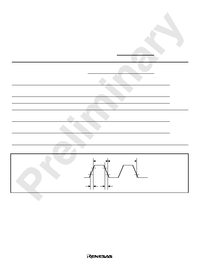
Rev. 1.0, 02/00, page 889 of 1141
30.2.4
Serial Interface Timing of HD6432199, HD6432198, HD6432197, and HD6432196
Table 30.7
Serial Interface Timing of HD6432199, HD6432198, HD6432197, and
HD6432196
-
Preliminary
-
(Conditions: Vcc = AVcc = 4.0 V to 5.5 V, Vss = 0.0 V, Ta = ≠20 to +75
∞
C unless otherwise
specified.)
Values
Item
Symbol
Applicable
Pins
Test
Conditions
Min
Typ
Max
Unit
Figure
Asynchroniza-
tion
4
Input clock cycle
t
scyc
SCK1
Clock
synchronization
6
t
cyc
Input clock pulse
width
t
SCKW
SCK1
0.4
0.6
t
scyc
Input clock rise time
t
SCKr
SCK1
1.5
t
cyc
Input clock fall time
t
SCKf
SCK1
1.5
t
cyc
Figure
30.6
Transmit data delay
time (clock sync)
t
TXD
SO1
100
ns
Receive data setup
time (clock sync)
t
RXS
SI1
100
ns
Receive data hold
time (clock sync)
t
RXH
SI1
100
ns
Figure
30.7
t
SCKf
t
SCKr
V
IL
or V
OL
V
IH
or V
OH
SCK1
t
SCKW
t
scyc
Figure 30.6 SCK1 Clock Timing
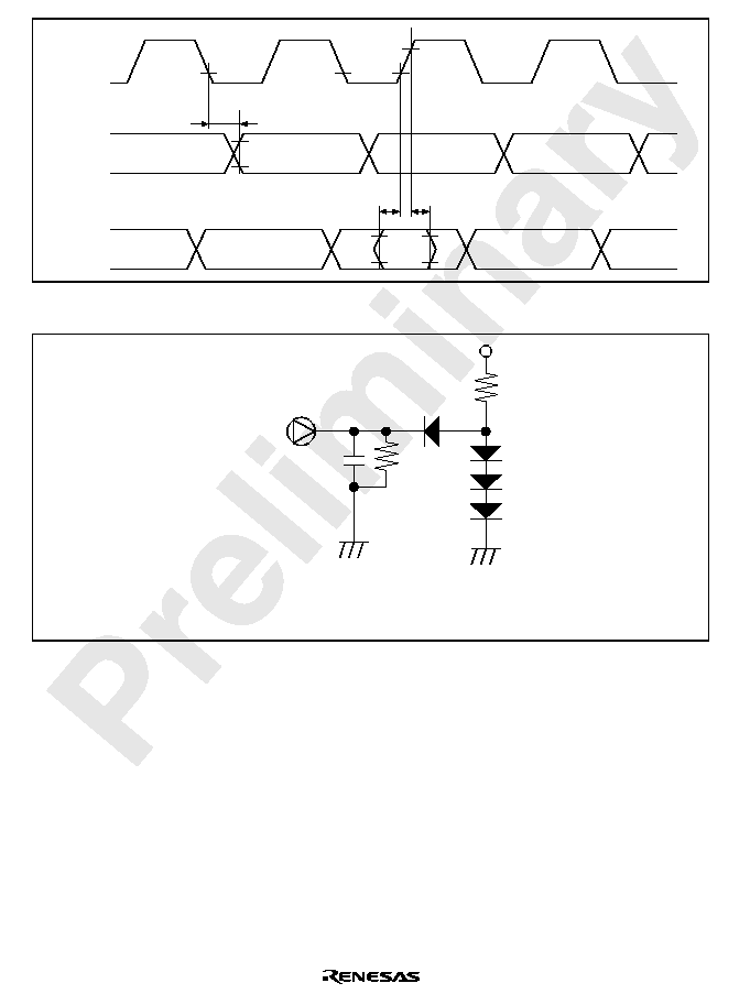
Rev. 1.0, 02/00, page 890 of 1141
V
IL
V
IH
t
TXD
SCK1
SO1
SI1
t
RXS
t
RXH
V
OH
V
OL
Figure 30.7 SCI I/O Timing/Clock Synchronization Mode
LSI output pin
Timing reference level
V
OH
: 2.0 V
V
OL
: 0.8 V
30 pF
12 k
2.4 k
Vcc
Figure 30.8 Output Load Conditions

Rev. 1.0, 02/00, page 891 of 1141
Table 30.8
I
2
C Bus Interface Timing of HD6432199, HD6432198, HD6432197, and
HD6432196
(Conditions: Vcc = AVcc = 4.0 V to 5.5 V, Vss = 0.0 V, Ta = ≠20 to +75
∞
C unless otherwise
specified.)
Values
Item
Symbol
Test
Conditions
Min
Typ
Max
Unit
Figure
SCL input cycle time
t
SCL
12
t
cyc
SCL input high pulse width
t
SCLH
3
t
cyc
SCL input low pulse width
t
SCLL
5
t
cyc
SCL, SDA input rise time
t
sr
7.5
*
t
cyc
SCL, SDA input fall time
t
sf
300
ns
SCL, SDA input spike pulse
removal time
t
sp
1
t
cyc
SDA input bus free time
t
BUF
5
t
cyc
Start condition input hold time
t
STAS
3
t
cyc
Re-transmit start condition
input setup time
t
STAH
3
t
cyc
Stop condition input setup
time
t
STOS
3
t
cyc
Data input setup time
t
SDAS
0.5
t
cyc
Data input hold time
t
SDAH
0
ns
SCL, SDA capacity load
C
b
400
pF
Figure 30.9
Note: Can also be set to 17.5 t
cyc
depending on the selection of clock to be used by the I
2
C
module.
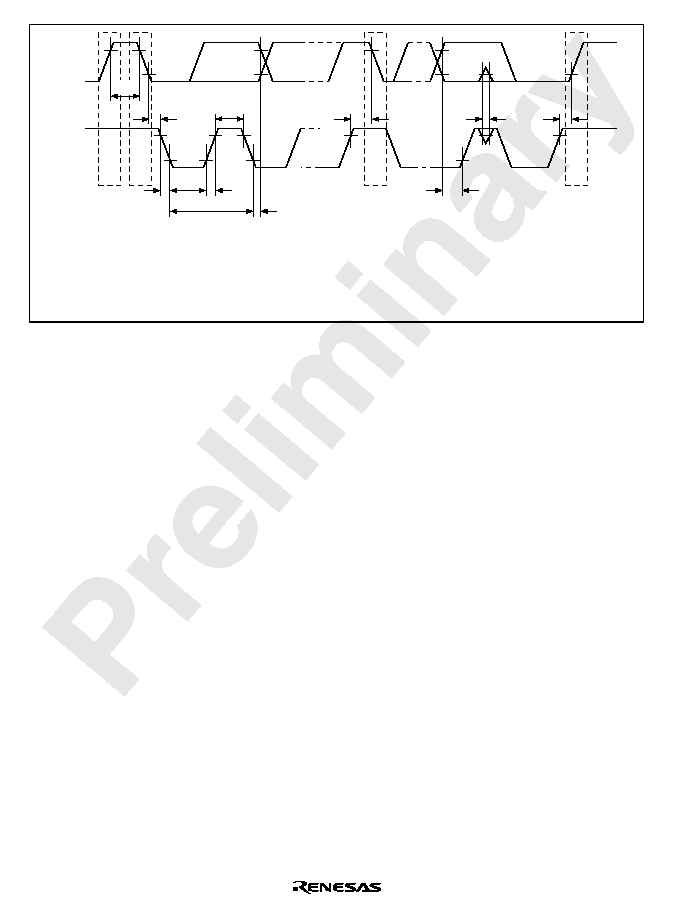
Rev. 1.0, 02/00, page 892 of 1141
t
STAH
t
Sr
t
SDAH
t
SCL
t
SCLL
t
SCLH
t
Sf
t
STAS
t
SP
t
STOS
t
SDAS
V
IL
V
IH
SDA
SCL
P*
S*
Sr*
P*
S, P and Sr denote the following:
S : Start conditions
P : Stop conditions
Sr: Re-transmit start conditions
Note:
t
BUF
Figure 30.9 I
2
C Bus Interface I/O Timing

Rev. 1.0, 02/00, page 893 of 1141
30.2.5
A/D Converter Characteristics of HD6432199, HD6432198, HD6432197, and
HD6432196
Table 30.9
A/D Converter Characteristics of HD6432199, HD6432198, HD6432197, and
HD6432196
(Conditions: Vcc = AVcc = 4.0 V to 5.5 V, Vss = AVss = 0.0 V, Ta = ≠20 to +75
∞
C unless
otherwise specified.)
Values
Item
Symbol
Applicable
Pins
Test Conditions
Min
Typ
Max
Unit
Note
Analog power
supply voltage
AVcc
AVcc
Vcc
-
0.3
Vcc
Vcc+
0.3
V
Analog input
voltage
A
VIN
AN0 to AN7,
AN8 to ANB
AVss
AVcc
V
A
ICC
AVcc
AVcc = 5.0V
2.0
mA
Analog power
supply current
A
ISTOP
AVcc
Vcc = 2.5 V to
5.5 V
At reset and in
power-down mode
10
µ
A
Analog input
capacitance
C
AIN
AN0 to AN7,
AN8 to ANB
30
pF
Allowable signal
source impedance
R
AIN
AN0 to AN7,
AN8 to ANB
10
k
Resolution
10
Bit
Absolute accuracy
Vcc = AVcc =
5.0 V
±
4
LSB
Vcc = AVcc =
4.0 V to 5.0 V
±
4
LSB
Reference
value
Conversion time
13.4
26.6
µ
s
Note: Do not open the AVcc and AVss pin even when the A/D converter is not in use. Set AVcc =
Vcc and AVss = Vss.

Rev. 1.0, 02/00, page 894 of 1141
30.2.6
Servo Section Electrical Characteristics of HD6432199, HD6432198, HD6432197,
and HD6432196
Table 30.10 Servo Section Electrical Characteristics of HD6432199, HD6432198,
HD6432197, and HD6432196 (reference values)
(Conditions: Vcc = SVcc = 5.0 V, Vss = SVss = 0.0 V, Ta = 25
∞
C unless otherwise specified.)
Reference Values
Item
Symbol
Applicable
Pins
Test Conditions
Min
Typ
Max
Unit
Note
CTLGR3 = 0, CTLRG2 = 0, CTLRG1 =
0, CTLRG0 = 0, f = 10kHz
33.0
35.0
37.0
CTLGR3 = 0, CTLRG2 = 0, CTLRG1 =
0, CTLRG0 = 1, f = 10kHz
35.5
37.5
39.5
CTLGR3 = 0, CTLRG2 = 0, CTLRG1 =
1, CTLRG0 = 0, f = 10kHz
38.0
40.0
42.0
CTLGR3 = 0, CTLRG2 = 0, CTLRG1 =
1, CTLRG0 = 1, f = 10kHz
40.5
42.5
44.5
CTLGR3 = 0, CTLRG2 = 1, CTLRG1 =
0, CTLRG0 = 0, f = 10kHz
43.0
45.0
47.0
CTLGR3 = 0, CTLRG2 = 1, CTLRG1 =
0, CTLRG0 = 1, f = 10kHz
45.5
47.5
49.5
CTLGR3 = 0, CTLRG2 = 1, CTLRG1 =
1, CTLRG0 = 0, f = 10kHz
48.0
50.0
52.0
CTLGR3 = 0, CTLRG2 = 1, CTLRG1 =
1, CTLRG0 = 1, f = 10kHz
50.5
52.5
54.5
CTLGR3 = 1, CTLRG2 = 0, CTLRG1 =
0, CTLRG0 = 0, f = 10kHz
53.0
55.0
57.0
CTLGR3 = 1, CTLRG2 = 0, CTLRG1 =
0, CTLRG0 = 1, f = 10kHz
55.5
57.5
59.5
CTLGR3 = 1, CTLRG2 = 0, CTLRG1 =
1, CTLRG0 = 0, f = 10kHz
58.0
60.0
62.0
CTLGR3 = 1, CTLRG2 = 0, CTLRG1 =
1, CTLRG0 = 1, f = 10kHz
60.5
62.5
64.5
CTLGR3 = 1, CTLRG2 = 1, CTLRG1 =
0, CTLRG0 = 0, f = 10kHz
63.0
65.0
67.0
CTLGR3 = 1, CTLRG2 = 1, CTLRG1 =
0, CTLRG0 = 1, f = 10kHz
65.5
67.5
69.5
CTLGR3 = 1, CTLRG2 = 1, CTLRG1 =
1, CTLRG0 = 0, f = 10kHz
68.0
70.0
72.0
PB-CTL
input
amplifier
voltage
gain
CTL (+)
CTLGR3 = 1, CTLRG2 = 1, CTLRG1 =
1, CTLRG0 = 1, f = 10kHz
70.5
72.5
74.5
dB
V+TH
AC coupling,
C = 0.1
µ
F Typ (non pol)
250
PB-CTL
Schmitt
input
V
-
TH
CTLSMT (i)
AC coupling,
C = 0.1
µ
F Typ (non pol)
-
250
mVp
Analog
switch ON
resistance
REB
CTLFB
150
CTL (+)
12
REC-CTL
output
current
ICTL
CTL (
-
)
Series resistance = 0
12
mA
REC-CTL
pin-to-pin
resistance
RCTL
10
k
CTL
reference
output
voltage
CTLREF
1/2
SVcc
V

Rev. 1.0, 02/00, page 895 of 1141
Reference Values
Item
Symbol
Applicable
Pins
Test Conditions
Min
Typ
Max
Unit
Note
CFG pin bias
voltage
CFG
1/2
SV
CC
V
CFG input level
CFG
AC coupling,
C = 1
µ
F Typ
1.0
Vpp
CFG input
impedance
CFG
10
k
V+THCF
Rise threshold
level
2.25
CFG input
threshold value
V
-
THCF
CFG
Fall threshold level
2.75
V
V+THDF
Rising edge
Schmitt level
1.95
DFG Schmitt input
V
-
THDF
DFG
Falling edge
Schmitt level
1.85
V
V+THDP
Rising edge
Schmitt level
3.55
DPG Schmitt input
V
-
THDP
DPG
Falling edge
Schmitt level
3.45
V
V
OH
-
I
OH
= 0.1 mA
4.0
V
OM
No load, Hiz = 1
2.5
3-level output
voltage
V
OL
Vpulse
I
OL
= 0.1 mA
1.0
V
3-level output pin
divided voltage
resistance
Vpulse
15
k
Digital input high
level
V
IH
0.8
Vcc
Vcc+
0.3
Digital input low
level
V
IL
COMP,
EXCTL,
EXCAP,
EXTTRG
-
0.3
0.2
Vcc
V
Digital output high
level
V
OH
-
I
OH
= 1 mA
Vcc
≠1.0
Digital output low
level
V
OL
H.AmpSW,
C.Rotary,
VIDEOFF,
AUDIOFF,
DRMPWM,
CAPPWM,
SV1, SV2
I
OL
= 1.6 mA
0.6
V
Current dissipation
I
CCSV
SVcc
At no load
5
10
mA

Rev. 1.0, 02/00, page 896 of 1141
30.2.7
OSD Electrical Characteristics of HD6432199, HD6432198, HD6432197, and
HD6432196
Table 30.11 OSD Electrical Characteristics of HD6432199, HD6432198, HD6432197, and
HD6432196 (Reference Value)
(Conditions: Vcc = OVcc = 5.0 V, Vss = OVss = 0.0 V, Ta = 25
∞
C unless otherwise specified)
Values
Item
Symbol
Applicable
Pins
Test
Conditions
Min
Typ
Max
Unit
Note
Composite video input
voltage
V
CVIN
C
Vin1
C
Vin2
2
V
PP
V
CL1
CV
in1
1.2
1.4
1.6
Clamp voltage
V
CL2
CV
in2
1.8
2
2.2
V
C.Video gain
G
CVC
CV
in1
CV
out
At chroma-
through
f = 3.58 MHz
V
IN
=500 mVpp
-
3
-
2
0
dB
Pedestal bias
V
PED
CV
out
45
IRE
*
1
Color burst bias
V
BST
40
IRE
*
1
V
BL1
10
V
BL2
30
V
BL3
50
Background
bias
Black, blue,
green,
cyan, red,
magenta,
yellow, white V
BL4
70
IRE
*
2
V
KBL1
0
Black
V
KBL2
25
V
KOL1
25
Blue, green,
cyan, red,
magenta,
yellow
V
KOL2
45
V
KCL1
45
Cursor bias
White
V
KCL2
55
IRE
*
2

Rev. 1.0, 02/00, page 897 of 1141
Values
Item
Symbol
Applicable
Pins
Test
Conditions
Min
Typ
Max
Unit
Note
V
CBL1
CV
out
0
V
CBL2
10
V
CBL3
20
Black
V
CBL4
30
V
COL1
25
V
COL2
45
V
COL3
55
Blue, green,
cyan, red,
magenta,
yellow
V
COL4
65
V
CCL1
45
V
CCL2
70
V
CCL3
80
Character
bias
White
V
CCL4
90
IRE
*
2
V
EDG1
0
Edge brightness level
V
EDG2
90
IRE
IRE
*
2
V
BTN1
15
Button brightness level
V
BTN2
75
IRE
*
2
Color burst chroma
amplitude
V
BSTA
40
IRE
V
CRA1
60
Chroma
amplitude
(background,
cursor,
character)
Blue, green,
cyan, red,
magenta,
yellow
V
CRA2
80
IRE
Colorburst
BSTN
0
Blue
BLUN
Green
GRNN
7
/4
Cyan
CYNN
3
/2
Red
REDN
/2
Magenta
MZTN
3
/4
Chroma hue
angle
(background,
cursor,
character)
(NTSC)
Yellow
YETN
0
rad
*
3

Rev. 1.0, 02/00, page 898 of 1141
Values
Item
Symbol
Applicable
Pins
Test
Conditions
Min
Typ
Max
Unit
Note
Colorburst
BSTP
CVout
±
/4
Blue
BLUP
±
Green
GRNP
±
7
/4
Cyan
CYNP
±
3
/2
Red
REDP
±
/2
Magenta
MZTP
±
3
/4
Chroma hue
angle
(background,
cursor,
character)
(PAL)
Yellow
YELP
0
rad
*
3
CCMP1
CVin2
5
CCMP2
10
CCMP3
15
Csync separation
comparator
CCMP4
20
IRE
*
1
ECMP1
CVin2
0
ECMP2
5
ECMP3
15
ECMP4
20
ECMP5
25
ECMP6
35
EDS separation
comparator
ECMP7
40
IRE
*
2
V
iH
0.85
OVcc
OVcc
+0.3
V
Input high level
V
iHT
Csync/Hsync
V
LPF
/Vsync
0.7
OVcc
OVcc
+0.3
V
V
iL
-
0.3
0.3
OVcc
V
Input low level
V
iLT
Csync/Hsync
VLPF/Vsync
-
0.3
0.15
OVcc
V
Output high level
V
OH
Csync/Hsync
-
I
OH
=0.4mA
OVcc
-
1.4
V
Output low level
V
OL
Csync/Hsync I
OL
=0.4mA
1.4
V

Rev. 1.0, 02/00, page 899 of 1141
Values
Item
Symbol
Applicable
Pins
Test
Conditions
Min
Typ
Max
Unit
Note
Oscillation
stabilizing time
t
rc
4/2fscin
4/2fscout
Crystal
oscillator
40
ms
M/NTSC
14.31818
MHz
4/2fscin
4/2fscout
B,G,H/PAL
I/PAL
D,K/PAL
4.43-NTSC
B,G,H/SECAM
L/SECAM
D,K,K1/SECAM
17.734475
(17.734476)
MHz
N/PAL
14.328225
MHz
4
fsc
M/PAL
14.30244596
MHz
2
fsc
M/NTSC
7.15909
MHz
4/2fscin
4/2fscout
B,G,H/PAL
I/PAL
D,K/PAL
4.43-NTSC
B,G,H/SECAM
L/SECAM
D,K,K2/SECAM
8.8672375
(8.867238)
MHz
N/PAL
7.1641125
MHz
Oscillating
frequency
M/PAL
7.15122298
MHz
V
fsc
4/2fscin
4/2fscout
AC coupling
C=1
µ
F typ
0.3
Vcc+0.3 Vpp
V
IH
4/2fscin
0.7Vcc
Vcc+0.3
External clock
input level
V
IL
-
0.3
0.3Vcc
V
External clock
duty
4/2fscin
4/2fscout
47
50
53
%
6.3
9
11.7
MHz
AFC reference
clock (dot clock)
AFC
OSC
AFC
OSC
LC oscillation
4.9
7
9.1
Current
dissipation
I
CCOSD
OVcc
At no signal
TBD
mA
Notes:
∑
IRE: Units for video amplitude; 0.714 V video level is specified as 100 IRE
∑
4fsc and 2fsc must be adjusted within
±
30 ppm, including temperature dependency.
1. Bias from the sync tip clamp level (reference value after
-
6 dB).
2. Bias from the pedestal level (reference value after
-
6 dB).
3. At 4fsc input.

Rev. 1.0, 02/00, page 900 of 1141
30.3
Electrical Characteristics of HD64F2199
30.3.1
DC Characteristics of HD64F2199
Table 30.12
DC Characteristics of HD64F2199
(Conditions: Vcc = AVcc = 4.0 V to 5.5 V*
1
, Vss = 0.0 V, Ta = ≠20 to +75
∞
C unless otherwise
specified.)
Values
Item
Symbol
Applicable Pins
Test
Conditions
Min
Typ
Max
Unit
Notes
MD0
Vcc=2.7 V to
5.5V
0.9 Vcc
Vcc+0.3
0.8 Vcc
Vcc+0.3
5(6
, FWE, IC, IRQ0
to IRQ5
Vcc=2.7 V to
5.5V
0.9 Vcc
Vcc+0.3
SCK1, SI1, FTIA,
FTIB, FTIC, FTID,
TRIG, TMBI,
$'75*
0.8 Vcc
Vcc+0.3
Vcc≠0.5
Vcc+0.3
OSC1
Vcc=2.7 V to
5.5V
Vcc≠0.3
Vcc+0.3
0.7 Vcc
Vcc+0.3
P00 to P07,
P10 to P17,
P20 to P27,
P30 to P37,
P40 to P47,
P60 to P67,
P70 to P77,
P80 to P87
Vcc=2.7 V to
5.5V
0.8 Vcc
Vcc+0.3
Input high
voltage
V
IH
Csync
0.7 Vcc
Vcc+0.3
V

Rev. 1.0, 02/00, page 901 of 1141
Values
Item
Symbol
Applicable Pins
Test
Conditions
Min
Typ
Max
Unit
Notes
MD0
Vcc=2.7 V to
5.5
≠0.3
0.1 Vcc
-
0.3
0.2 Vcc
5(6
, FWE, IC,
IRQ0 to IRQ5
Vcc=2.7 V to
5.5
-
0.3
0.1 Vcc
SCK1, SI1, FTIA, FTIB,
FTIC, FTID, TRIG,
TMBI,
$'75*
-
0.3
0.2 Vcc
-
0.3
0.5
OSC1
Vcc=2.7 V to
5.5
-
0.3
0.3
-
0.3
0.3 Vcc
P00 to P07,
P10 to P17,
P20 to P27,
P30 to P37,
P40 to P47,
P60 to P67,
P70 to P77,
P80 to P87
Vcc=2.7 V to
5.5
-
0.3
0.2 Vcc
Input low
voltage
V
IL
Csync
-
0.3
0.2 Vcc
V

Rev. 1.0, 02/00, page 902 of 1141
Values
Item
Symbol
Applicable Pins
Test
Conditions
Min
Typ
Max
Unit
Notes
-
I
OH
=1.0mA
Vcc≠1.0
V
-
I
OH
=0.5mA
Vcc≠
0.5
V
Refer-
ence
value
Output
high
voltage
V
OH
SO1, SCK1, PWM1,
PWM2, PWM3,
PWM4, PWM14,
BUZZ, TMO, TMOW,
FTOA, FTOB, PPG0 to
PPG7,
RP0 to RP7,
RP8 to RPB,
P10 to P17,
P20 to P27,
P30 to P37,
P40 to P47,
P60 to P67,
P70 to P77,
P80 to P87,
SV1, SV2, R, G, B,
YCO, YBO
-
I
OH
=0.1mA
Vcc=2.7 V to
5.5V
Vcc≠0.5
V
I
OL
=1.6mA
0.6
V
SO1, SCK1, PWM1,
PWM2, PWM3,
PWM4, PWM14,
BUZZ, TMO, TMOW,
FTOA, FTOB, PPG0 to
PPG7,
RP0 to RP7,
RP8 to RPB,
P10 to P17,
P20 to P27,
P30 to P37,
P40 to P47,
P70 to P77,
P80 to P87, SV1, SV2,
R, G, B, YCO, YBO
I
OL
=0.4mA
Vcc=2.7 V to
5.5V
0.4
V
I
OL
=20mA
1.5
V
I
OL
=1.6mA
0.6
V
Output
low
voltage
V
OL
P60 to P67,
I
OL
=0.4mA
Vcc=2.7 V to
5.5V
0.4
V

Rev. 1.0, 02/00, page 903 of 1141
Values
Item
Symbol
Applicable Pins
Test
Conditions
Min
Typ
Max
Unit
Notes
MD0, FWE
Vin=0.5 to
Vcc≠0.5V
1.0
5(6
,
,54
to
,54
,
,&
Vin=0.5 to
Vcc≠0.5V
1.0
SCK1, SI1, SDA0,
SCL0, SDA1, SCL1,
FTIA, FTIB, FTIC, FTID,
TRIG, TMBI,
$'75*
Vin=0.5 to
Vcc≠0.5V
1.0
OSC1
Vin=0.5 to
Vcc
-
0.5V
1.0
Input
/output
leakage
current
I
IL
P10 to P17,
P20 to P27,
P30 to P37,
P40 to P47,
P60 to P67,
P70 to P77,
P80 to P87,
Vin=0.5 to
Vcc≠0.5V
1.0
µ
A
P00 to P07,
AN8 to ANB
Vin=0.5 to
AVcc≠0.5V
1.0
Pull-up
MOS
current
-
Ip
P10 to P17,
P20 to P27,
P30 to P37
Vcc=5.0V,
Vin=0V
50
300
µ
A
*
2
Input
capacity
Cin
All input pins except
power supply pins
P23, P24, P25, and
P26, and analog pins
fin=1 MHz,
Vin=0V,
Ta=25
∞
C
15
pF
P23, P24, P25, P26
fin=1 MHz,
Vin=0V,
Ta=25
∞
C
20
pF

Rev. 1.0, 02/00, page 904 of 1141
Values
Item
Symbol
Applicable
Pins
Test
Conditions
Min
Typ
Max
Unit
Notes
Vcc=5V,
f
OSC
=10 MHz,
High-speed
mode
TBD
mA
*
3
Active
mode
current
dissipa-
tion (CPU
operating)
I
OPE
Vcc
Vcc=5V,
f
OSC
=10 MHz,
Medium-speed
mode (1/64)
TBD
mA
Reference value
Active
mode
current
dissipa-
tion
(reset)
I
RES
Vcc
Vcc=5V,
f
OSC
=10 MHz
--
TBD
mA
*
3
Sleep
mode
current
dissipa-
tion
I
SLEEP
Vcc
Vcc=5V,
f
OSC
=10 MHz
High-speed
mode
TBD
mA
*
3
Vcc=2.7V,
32kHz
With crystal
oscillator
(
sub=
w/2)
TBD
*
3
Subactive
mode
current
dissipa-
tion
I
SUB
Vcc
Vcc=2.7V,
32kHz
With crystal
oscillator
(
sub=
w/8)
TBD
µ
A
Reference value
*
3
Vcc=2.7V,
32kHz
With crystal
oscillator
(
sub=
w/2)
TBD
*
3
Subsleep
mode
current
dissipa-
tion
I
SUBSLP
Vcc
Vcc=2.7V,
32kHz
With crystal
oscillator
(
sub=
w/8)
TBD
µ
A
Reference value
*
3

Rev. 1.0, 02/00, page 905 of 1141
Values
Item
Symbol
Applicable Pins
Test
Conditions
Min
Typ
Max
Unit
Notes
Vcc=2.7V,
32kHz
With crystal
oscillator
TBD
µ
A
*
3
Watch
mode
current
dissipa-
tion
I
WATCH
Vcc
Vcc=5.0V,
32kHz
With crystal
oscillator
TBD
µ
A
Reference
value
*
3
Standby
mode
current
dissipa-
tion
I
STBY
Vcc
X1=V
CL
, 32kHz
Without crystal
oscillator
5
µ
A
*
3
RAM data
retaining
voltage in
standby
mode
V
STBY
2.0
V
Notes: 1. Do not open the AVcc and AVss pin even when the A/D converter is not in use.
2. Current value when the relevant bit of the pull-up MOS select register (PUR1 to PUR3)
is set to 1.
3. The current on the pull-up MOS or the output buffer excluded.
Table 30.13 Pin Status at Current Dissipation Measurement
Mode
#$
#$
pin
Internal State
Pin
Oscillator Pin
Active mode
High-speed, medium-
speed
Vcc
Operating
Vcc
Sleep mode
High-speed, medium-
speed
Vcc
Only CPU and
servo circuits
halted
Vcc
Reset
Vss
Reset
Vcc
Standby mode
Vcc
All circuits halted
Vcc
Main clock:
Crystal oscillator
Sub clock:
X1 pin = V
CL
Subactive mode
Vcc
CPU and timer A
operating
Vcc
Subsleep mode
Vcc
Timer A operating
Vcc
Watch mode
Vcc
Timer A operating
Vcc
Main clock:
Crystal oscillator
Sub clock:
Crystal oscillator

Rev. 1.0, 02/00, page 906 of 1141
Table 30.14 Bus Drive Characteristics of HD64F2199
(Conditions: Vcc = AVcc = 4.0 V to 5.5 V, Vss = 0.0 V, Ta = ≠20 to +75
∞
C.)
Applicable pin: SCL0, SCL1, SDA0, SDA1
Values
Item
Symbol
Applicable Pins
Test
Conditions
Min
Typ
Max
Unit
Notes
V
T
-
0.3Vcc
V
V
T
+
0.7Vcc
V
Schmitt
trigger
input
V
T
+
≠V
T
-
SCL0, SDA0,
SCL1, SDA1
0.05Vcc
V
Input high
level
voltage
V
IH
SCL0, SDA0,
SCL1, SDA1
0.7Vcc
Vcc+0.5
V
Input low
level
voltage
V
IL
SCL0, SDA0,
SCL1, SDA1
-
0.5
0.3Vcc
V
I
OL
=8mA
0.5
Output
low level
voltage
V
OL
SCL0, SDA0,
SCL1, SDA1
I
OL
=3mA
0.4
V
SCL and
SDA
output fall
time
t
of
SCL0, SDA0,
SCL1, SDA1
20+
0.1Cb
250
ns

Rev. 1.0, 02/00, page 907 of 1141
30.3.2
Allowable Output Currents of HD64F2199
The specifications for the digital pins are shown below.
Table 30.15 Allowable Output Currents of HD64F2199
(Conditions: Vcc = 2.7 V to 5.5 V, Vss = 0.0 V, Ta = ≠20 to +75
∞
C)
Item
Symbol
Value
Unit
Notes
Allowable input current (to chip)
I
O
2
mA
*
1
Allowable input current (to chip)
I
O
22
mA
*
2
Allowable input current (to chip)
I
O
10
mA
*
3
Allowable output current (from chip)
-
I
O
2
mA
*
4
Total allowable input current (to chip)
I
O
80
mA
*
5
Total allowable output current (from chip)
-
I
O
50
mA
*
6
Notes: 1. The allowable input current is the maximum value of the current flowing from each I/O
pin to V
SS
(except for port 6, SCL0, SDA0, SCL1 and SDA1).
2. The allowable input current is the maximum value of the current flowing from each I/O
pin to V
SS
. This applies to port 6.
3. The allowable input current is the maximum value of the current flowing from each I/O
pin to V
SS
. This applies to SCL0, SDA0, SCL1 and SDA1.
4. The allowable output current is the maximum value of the current flowing from V
CC
to
each I/O pin.
5. The total allowable input current is the sum of the currents flowing from all I/O pins to
V
SS
simultaneously.
6. The total allowable output current is the sum of the currents flowing from V
CC
to all I/O
pins.

Rev. 1.0, 02/00, page 908 of 1141
30.3.3
AC Characteristics of HD64F2199
Table 30.16 AC Characteristics of HD64F2199
(Conditions: Vcc = AVcc = 4.0 V to 5.5 V, Vss = 0.0 V, Ta = ≠20 to +75
∞
C unless otherwise
specified.)
Values
Item
Symbol
Applicable
Pins
Test
Conditions
Min
Typ
Max
Unit
Notes
Clock oscillation
frequency
f
OSC
OSC1, OSC2
8
10
MHz
Clock cycle time
t
cyc
OSC1, OSC2
100
125
ns
Figure
30.10
Subclock
oscillation
frequency
f
X
X1, X2
Vcc = 2.7 V to
5.5 V
32.768
kHz
Subclock cycle
time
t
subcyc
X1, X2
Vcc = 2.7 V to
5.5 V
30.518
µ
s
Figure
30.11
OSC1, OSC2
Crystal oscillator
10
ms
Oscillation
stabilization time
t
rc
X1, X2
32kHz crystal
oscillator
2
s
External clock high
width
t
CPH
OSC1
40
ns
External clock low
width
t
CPL
OSC1
40
ns
External clock rise
time
t
CPr
OSC1
10
ns
External clock fall
time
t
CPf
OSC1
10
ns
Figure
30.10
External clock
stabilization delay
time
t
DEXT
OSC1
500
µ
s
Figure
30.12
Subclock input low
level pulse width
t
EXCLL
X1
Vcc = 2.7 V to
5.5 V
15.26
µ
s
Subclock input
high level pulse
width
t
EXCLH
X1
Vcc = 2.7 V to
5.5 V
15.26
µ
s
Subclock input rise
time
t
EXCLr
X1
Vcc = 2.7 V to
5.5 V
10
ns
Subclock input fall
time
t
ECXLf
X1
Vcc = 2.7 V to
5.5 V
10
ns
Figure
30.11
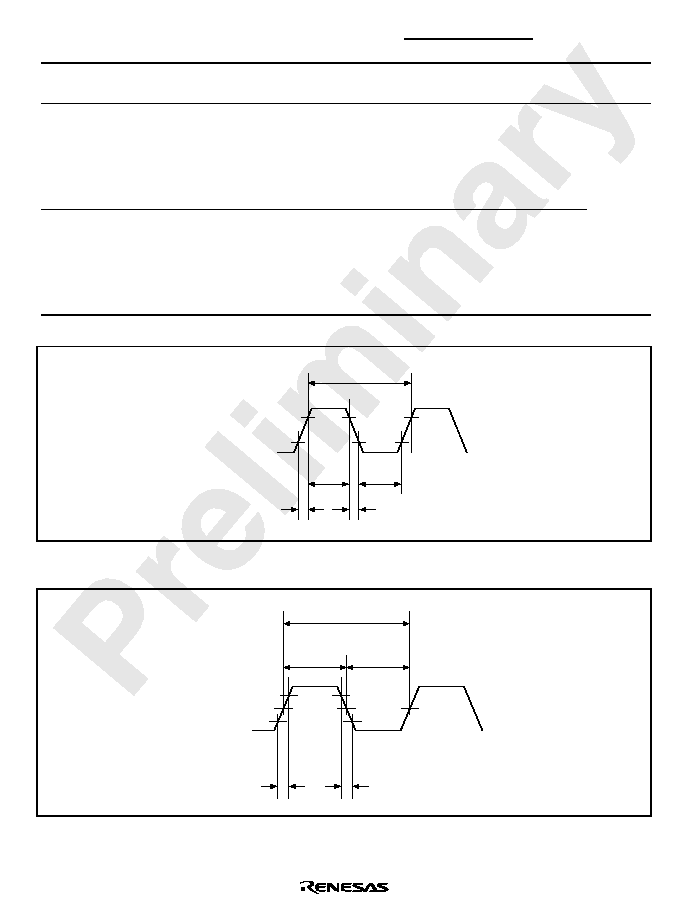
Rev. 1.0, 02/00, page 909 of 1141
Values
Item
Symbol
Applicable
Pins
Test
Conditions
Min
Typ
Max
Unit
Figure
5(6
pin low level
width
t
REL
5(6
Vcc = 2.7 V to
5.5 V
20
t
cyc
Figure
30.13
Input pin high level
width
t
IH
,54
to
,54
,
,&
,
$'75*
,
TMBI, FTIA,
FTIB, FTIC,
FTID,
RPTRIG
Vcc = 2.7 V to
5.5 V
2
t
cyc
t
subcyc
Input pin low level
width
t
IL
,54
to
,54
,
,&
,
$'75*
,
TMBI, FTIA,
FTIB, FTIC,
FTID,
RPTRIG
Vcc = 2.7 V to
5.5 V
2
t
cyc
t
subcyc
Figure
30.14
t
cyc
t
CPH
V
IL
V
IH
OSC1
t
CPL
t
CPf
t
CPr
Figure 30.10 System Clock Timing
t
EXCLf
t
subcyc
t
EXCLH
t
EXCLL
t
EXCLr
V
IL
V
IH
X1
Vcc
◊
0.5
Figure 30.11 Subclock Input Timing
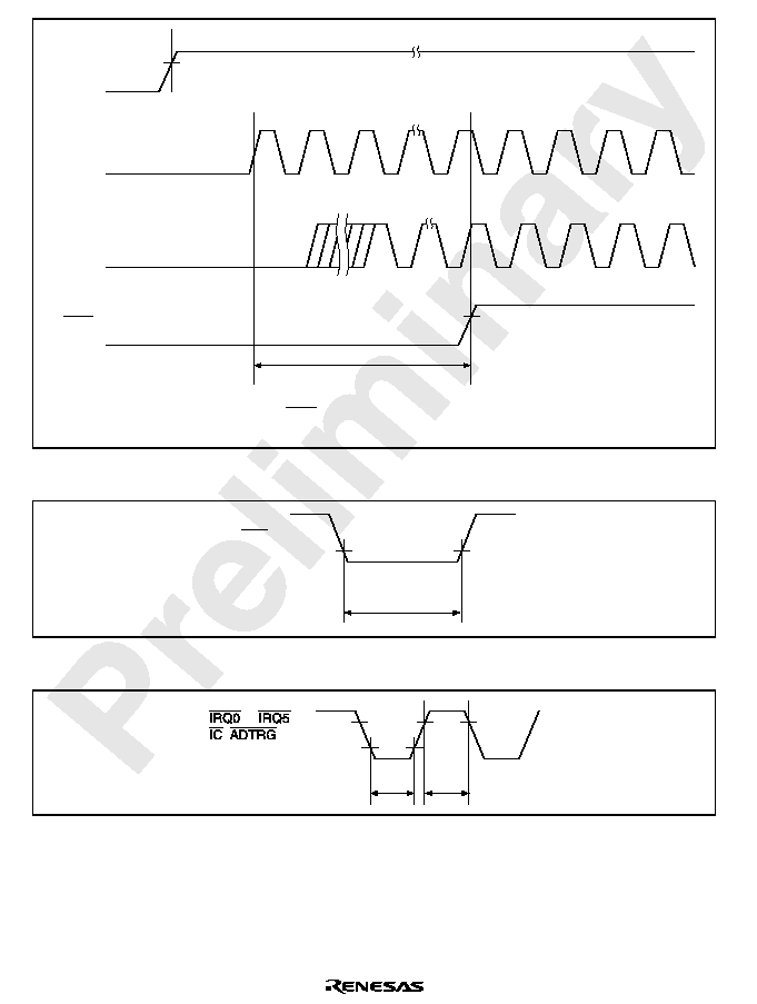
Rev. 1.0, 02/00, page 910 of 1141
Vcc
OSC1
t
DEXT
*
RES
(Internal)
4.0V
The t
DEXT
includes the RES pin Low level width 20 t
cyc
.
Note: *
Figure 30.12 External Clock Stabilization Delay Timing
RES
V
IL
t
REL
Figure 30.13 Reset Input Timing
t
IL
t
IH
V
IH
V
IL
to
,
,
,
TMBI, FTIA,
FTIB, FTIC,
FTID, RPTRIG
Figure 30.14 Input Timing
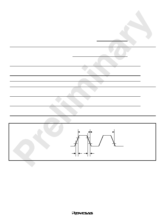
Rev. 1.0, 02/00, page 911 of 1141
30.3.4
Serial Interface Timing of HD64F2199
Table 30.17 Serial Interface Timing of HD64F2199
(Conditions: Vcc = AVcc = 4.0 V to 5.5 V, Vss = 0.0 V, Ta = ≠20 to +75
∞
C unless otherwise
specified.)
Values
Item
Symbol
Applicable
Pins
Test
Conditions
Min
Typ
Max
Unit
Figure
Asynchroniza-
tion
4
Input clock cycle
t
scyc
SCK1
Clock
synchronization
6
t
cyc
Input clock pulse
width
t
SCKW
SCK1
0.4
0.6
t
scyc
Input clock rise time
t
SCKr
SCK1
1.5
t
cyc
Input clock fall time
t
SCKf
SCK1
1.5
t
cyc
Figure
30.15
Transmit data delay
time (clock sync)
t
TXD
SO1
100
ns
Receive data setup
time (clock sync)
t
RXS
SI1
100
ns
Receive data hold
time (clock sync)
t
RXH
SI1
100
ns
Figure
30.16
t
SCKf
t
SCKr
V
IL
or V
OL
V
IH
or V
OH
SCK1
t
SCKW
t
scyc
Figure 30.15 SCK1 Clock Timing
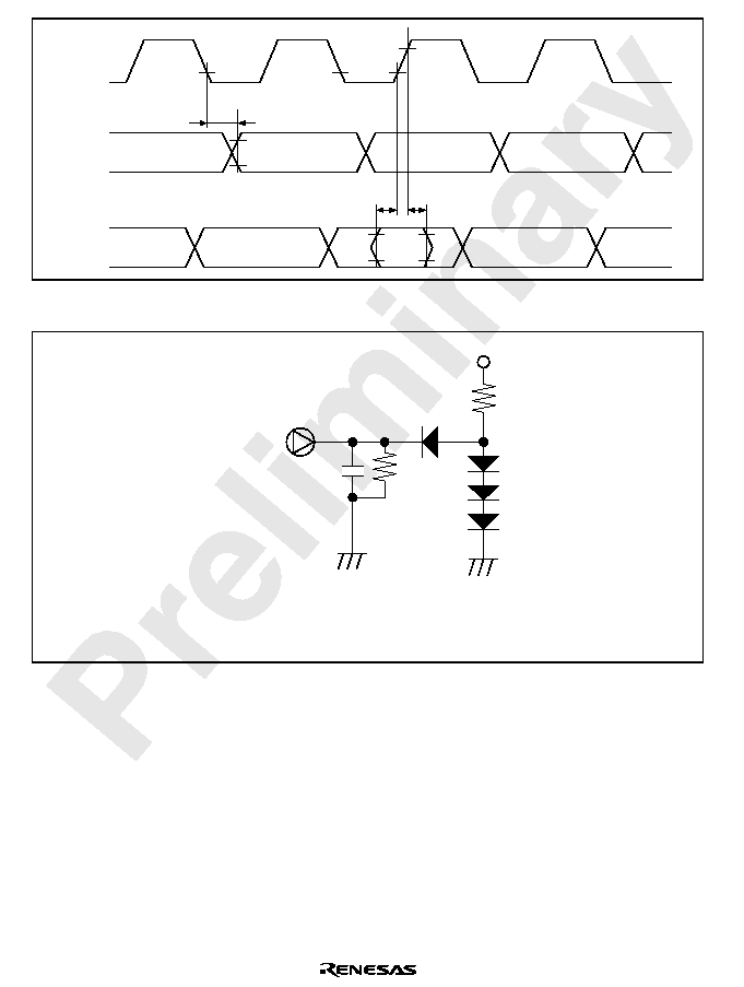
Rev. 1.0, 02/00, page 912 of 1141
V
IL
V
IH
t
TXD
SCK1
SO1
SI1
t
RXS
t
RXH
V
OH
V
OL
Figure 30.16 SCI I/O Timing/Clock Synchronization Mode
LSI output pin
Timing reference level
V
OH
: 2.0V
V
OL
: 0.8V
30pF
12k
2.4k
Vcc
Figure 30.17 Output Load Conditions

Rev. 1.0, 02/00, page 913 of 1141
Table 30.18 I
2
C Bus Interface Timing of HD64F2199
(Conditions: Vcc = AVcc = 4.0 V to 5.5 V, Vss = 0.0 V, Ta = ≠20 to +75
∞
C unless otherwise
specified.)
Values
Item
Symbol
Test
Conditions
Min
Typ
Max
Unit
Figure
SCL input cycle time
t
SCL
12
t
cyc
SCL input high pulse width
t
SCLH
3
t
cyc
SCL input low pulse width
t
SCLL
5
t
cyc
SCL, SDA input rise time
t
sr
7.5
*
t
cyc
SCL, SDA input fall time
t
sf
300
ns
SCL, SDA input spike pulse
removal time
t
sp
1
t
cyc
SDA input bus free time
t
BUF
5
t
cyc
Start condition input hold time
t
STAS
3
t
cyc
Re-transmit start condition
input setup time
t
STAH
3
t
cyc
Stop condition input setup
time
t
STOS
3
t
cyc
Data input setup time
t
SDAS
0.5
t
cyc
Data input hold time
t
SDAH
0
ns
SCL, SDA capacity load
C
b
400
pF
Figure
30.18
Note: Can also be set to 17.5 t
cyc
depending on the selection of clock to be used by the I
2
C
module.

Rev. 1.0, 02/00, page 914 of 1141
t
STAH
t
Sr
t
SDAH
t
SCL
t
SCLL
t
SCLH
t
Sf
t
STAS
t
SP
t
STOS
t
SDAS
V
IL
V
IH
SDA
SCL
P*
S*
Sr*
P*
S, P and Sr denote the following:
S : Start conditions
P : Stop conditions
Sr: Re-transmit start conditions
Note: *
t
BUF
Figure 30.18 I
2
C Bus Interface I/O Timing

Rev. 1.0, 02/00, page 915 of 1141
30.3.5
A/D Converter Characteristics of HD64F2199
Table 30.19 A/D Converter Characteristics of HD64F2199
(Conditions: Vcc = AVcc = 4.0 V to 5.5 V, Vss = AVss = 0.0 V, Ta = ≠20 to +75
∞
C unless
otherwise specified.)
Values
Item
Symbol
Applicable
Pins
Test Conditions
Min
Typ
Max
Unit
Note
Analog power
supply voltage
AVcc
AVcc
Vcc
-
0.3
Vcc
Vcc+
0.3
V
Analog input
voltage
A
VIN
AN0 to AN7,
AN8 to ANB
AVss
AVcc
V
A
ICC
AVcc
AVcc = 5.0V
2.0
mA
Analog power
supply current
A
ISTOP
AVcc
Vcc = 2.7 V to 5.5 V
At reset and in
power-down mode
10
µ
A
Analog input
capacitance
C
AIN
AN0 to AN7,
AN8 to ANB
30
pF
Allowable signal
source impedance
R
AIN
AN0 to AN7,
AN8 to ANB
10
k
Resolution
10
Bit
Absolute accuracy
Vcc = AVcc =
5.0 V
±
4
LSB
Vcc = AVcc =
4.0 V to 5.0 V
±
4
LSB
Reference
value
Conversion time
13.4
26.6
µ
s
Note: Do not open the AVcc and AVss pin even when the A/D converter is not in use. Set AVcc =
Vcc and AVss = Vss.

Rev. 1.0, 02/00, page 916 of 1141
30.3.6
Servo Section Electrical Characteristics of HD64F2199
Table 30.20 Servo Section Electrical Characteristics of HD64F2199 (reference values)
(Conditions: Vcc = SVcc = 5.0 V, Vss = SVss = 0.0 V, Ta = 25
∞
C unless otherwise specified.)
Reference Values
Item
Symbol
Applicable
Pins
Test Conditions
Min
Typ
Max
Unit
Note
CTLGR3 = 0, CTLRG2 = 0, CTLRG1 =
0, CTLRG0 = 0, f = 10kHz
33.0
35.0
37.0
CTLGR3 = 0, CTLRG2 = 0, CTLRG1 =
0, CTLRG0 = 1, f = 10kHz
35.5
37.5
39.5
CTLGR3 = 0, CTLRG2 = 0, CTLRG1 =
1, CTLRG0 = 0, f = 10kHz
38.0
40.0
42.0
CTLGR3 = 0, CTLRG2 = 0, CTLRG1 =
1, CTLRG0 = 1, f = 10kHz
40.5
42.5
44.5
CTLGR3 = 0, CTLRG2 = 1, CTLRG1 =
0, CTLRG0 = 0, f = 10kHz
43.0
45.0
47.0
CTLGR3 = 0, CTLRG2 = 1, CTLRG1 =
0, CTLRG0 = 1, f = 10kHz
45.5
47.5
49.5
CTLGR3 = 0, CTLRG2 = 1, CTLRG1 =
1, CTLRG0 = 0, f = 10kHz
48.0
50.0
52.0
CTLGR3 = 0, CTLRG2 = 1, CTLRG1 =
1, CTLRG0 = 1, f = 10kHz
50.5
52.5
54.5
CTLGR3 = 1, CTLRG2 = 0, CTLRG1 =
0, CTLRG0 = 0, f = 10kHz
53.0
55.0
57.0
CTLGR3 = 1, CTLRG2 = 0, CTLRG1 =
0, CTLRG0 = 1, f = 10kHz
55.5
57.5
59.5
CTLGR3 = 1, CTLRG2 = 0, CTLRG1 =
1, CTLRG0 = 0, f = 10kHz
58.0
60.0
62.0
CTLGR3 = 1, CTLRG2 = 0, CTLRG1 =
1, CTLRG0 = 1, f = 10kHz
60.5
62.5
64.5
CTLGR3 = 1, CTLRG2 = 1, CTLRG1 =
0, CTLRG0 = 0, f = 10kHz
63.0
65.0
67.0
CTLGR3 = 1, CTLRG2 = 1, CTLRG1 =
0, CTLRG0 = 1, f = 10kHz
65.5
67.5
69.5
CTLGR3 = 1, CTLRG2 = 1, CTLRG1 =
1, CTLRG0 = 0, f = 10kHz
68.0
70.0
72.0
PB-CTL
input
amplifier
voltage
gain
CTL (+)
CTLGR3 = 1, CTLRG2 = 1, CTLRG1 =
1, CTLRG0 = 1, f = 10kHz
70.5
72.5
74.5
dB
V+TH
AC coupling,
C = 0.1
µ
F Typ (non pol)
250
PB-CTL
Schmitt
input
V
-
TH
CTLSMT (i)
AC coupling,
C = 0.1
µ
F Typ (non pol)
-
250
mVp
Analog
switch ON
resistance
REB
CTLFB
150
CTL (+)
12
REC-CTL
output
current
ICTL
CTL (
-
)
Series resistance = 0
12
mA
REC-CTL
pin-to-pin
resistance
RCTL
10
k
CTL
reference
output
voltage
CTLREF
1/2
SVcc
V

Rev. 1.0, 02/00, page 917 of 1141
Reference Values
Item
Symbol
Applicable
Pins
Test Conditions
Min
Typ
Max
Unit
Note
CFG pin bias
voltage
CFG
1/2
SV
CC
V
CFG input level
CFG
AC coupling,
C = 1
µ
F Typ
1.0
Vpp
CFG input
impedance
CFG
10
k
V+THCF
Rise threshold
level
2.25
CFG input
threshold value
V
-
THCF
CFG
Fall threshold level
2.75
V
V+THDF
Rising edge
Schmitt level
1.95
DFG Schmitt input
V
-
THDF
DFG
Falling edge
Schmitt level
1.85
V
V+THDP
Rising edge
Schmitt level
3.55
DPG Schmitt input
V
-
THDP
DPG
Falling edge
Schmitt level
3.45
V
V
OH
-
I
OH
= 0.1 mA
4.0
V
OM
No load, Hiz = 1
2.5
3-level output
voltage
V
OL
Vpulse
I
OL
= 0.1 mA
1.0
V
3-level output pin
divided voltage
resistance
Vpulse
15
k
Digital input high
level
V
IH
0.8
Vcc
Vcc+
0.3
Digital input low
level
V
IL
COMP,
EXCTL,
EXCAP,
EXTTRG
-
0.3
0.2
Vcc
V
Digital output high
level
V
OH
-
I
OH
= 1 mA
Vcc
≠1.0
Digital output low
level
V
OL
H.AmpSW,
C.Rotary,
VIDEOFF,
AUDIOFF,
DRMPWM,
CAPPWM,
SV1, SV2
I
OL
= 1.6 mA
0.6
V
Current dissipation
I
CCSV
SVcc
At no load
5
10
mA

Rev. 1.0, 02/00, page 918 of 1141
30.3.7
OSD Electrical Characteristics of HD64F2199
Table 30.21 OSD Electrical Characteristics of HD64F2199 (Reference Value)
(Conditions: Vcc = OVcc = 5.0 V, Vss = OVss = 0.0 V, Ta = 25
∞
C unless otherwise specified)
Values
Item
Symbol
Applicable
Pins
Test
Conditions
Min
Typ
Max
Unit
Note
Composite video input
voltage
V
CVIN
C
Vin1
C
Vin2
2
V
PP
V
CL1
CV
in1
1.2
1.4
1.6
Clamp voltage
V
CL2
CV
in2
1.8
2
2.2
V
C.Video gain
G
CVC
CV
in1
CV
out
At chroma-
through
f = 3.58 MHz
V
IN
=500 mVpp
-
3
-
2
0
dB
Pedestal bias
V
PED
CV
out
45
IRE
*
1
Color burst bias
V
BST
40
IRE
*
1
V
BL1
10
V
BL2
30
V
BL3
50
Background
bias
Black, blue,
green,
cyan, red,
magenta,
yellow, white V
BL4
70
IRE
*
2
V
KBL1
0
Black
V
KBL2
25
V
KOL1
25
Blue, green,
cyan, red,
magenta,
yellow
V
KOL2
45
V
KCL1
45
Cursor bias
White
V
KCL2
55
IRE
*
2

Rev. 1.0, 02/00, page 919 of 1141
Values
Item
Symbol
Applicable
Pins
Test
Conditions
Min
Typ
Max
Unit
Note
V
CBL1
CV
out
0
V
CBL2
10
V
CBL3
20
Black
V
CBL4
30
V
COL1
25
V
COL2
45
V
COL3
55
Blue, green,
cyan, red,
magenta,
yellow
V
COL4
65
V
CCL1
45
V
CCL2
70
V
CCL3
80
Character
bias
White
V
CCL4
90
IRE
*
2
V
EDG1
0
Edge brightness level
V
EDG2
90
IRE
IRE
*
2
V
BTN1
15
Button brightness level
V
BTN2
75
IRE
*
2
Color burst chroma
amplitude
V
BSTA
40
IRE
V
CRA1
60
Chroma
amplitude
(background,
cursor,
character)
Blue, green,
cyan, red,
magenta,
yellow
V
CRA2
80
IRE
Colorburst
BSTN
0
Blue
BLUN
Green
GRNN
7
/4
Cyan
CYNN
3
/2
Red
REDN
/2
Magenta
MZTN
3
/4
Chroma hue
angle
(background,
cursor,
character)
(NTSC)
Yellow
YETN
0
rad
*
3

Rev. 1.0, 02/00, page 920 of 1141
Values
Item
Symbol
Applicable
Pins
Test
Conditions
Min
Typ
Max
Unit
Note
Colorburst
BSTP
CVout
±
/4
Blue
BLUP
±
Green
GRNP
±
7
/4
Cyan
CYNP
±
3
/2
Red
REDP
±
/2
Magenta
MZTP
±
3
/4
Chroma hue
angle
(background,
cursor,
character)
(PAL)
Yellow
YELP
0
rad
*
3
CCMP1
CVin2
5
CCMP2
10
CCMP3
15
Csync separation
comparator
CCMP4
20
IRE
*
1
ECMP1
CVin2
0
ECMP2
5
ECMP3
15
ECMP4
20
ECMP5
25
ECMP6
35
EDS separation
comparator
ECMP7
40
IRE
*
2
V
iH
0.85
OVcc
OVcc
+0.3
V
Input high level
V
iHT
Csync/Hsync
V
LPF
/Vsync
0.7
OVcc
OVcc
+0.3
V
V
iL
-
0.3
0.3
OVcc
V
Input low level
V
iLT
Csync/Hsync
VLPF/Vsync
-
0.3
0.15
OVcc
V
Output high level
V
OH
Csync/Hsync
-
I
OH
=0.4mA
OVcc
-
1.4
V
Output low level
V
OL
Csync/Hsync I
OL
=0.4mA
1.4
V

Rev. 1.0, 02/00, page 921 of 1141
Values
Item
Symbol
Applicable
Pins
Test
Conditions
Min
Typ
Max
Unit
Note
Oscillation
stabilizing time
t
rc
4/2fscin
4/2fscout
Crystal
oscillator
40
ms
M/NTSC
14.31818
MHz
4/2fscin
4/2fscout
B,G,H/PAL
I/PAL
D,K/PAL
4.43-NTSC
B,G,H/SECAM
L/SECAM
D,K,K1/SECAM
17.734475
(17.734476)
MHz
N/PAL
14.328225
MHz
4
fsc
M/PAL
14.30244596
MHz
2
fsc
M/NTSC
7.15909
MHz
4/2fscin
4/2fscout
B,G,H/PAL
I/PAL
D,K/PAL
4.43-NTSC
B,G,H/SECAM
L/SECAM
D,K,K2/SECAM
8.8672375
(8.867238)
MHz
N/PAL
7.1641125
MHz
Oscillating
frequency
M/PAL
7.15122298
MHz
V
fsc
4/2fscin
4/2fscout
AC coupling
C=1
µ
F typ
0.3
Vcc+0.3 Vpp
V
IH
4/2fscin
0.7Vcc
Vcc+0.3
External clock
input level
V
IL
-
0.3
0.3Vcc
V
External clock
duty
4/2fscin
4/2fscout
47
50
53
%
6.3
9
11.7
MHz
AFC reference
clock (dot clock)
AFC
OSC
AFC
OSC
LC oscillation
4.9
7
9.1
MHz
Current
dissipation
I
CCOSD
OVcc
At no signal
TBD
mA
Notes:
∑
IRE: Units for video amplitude; 0.714 V video level is specified as 100 IRE
∑
4fsc and 2fsc must be adjusted within
±
30 ppm, including temperature dependency.
1. Bias from the sync tip clamp level (reference value after
-
6 dB).
2. Bias from the pedestal level (reference value after
-
6 dB).
3. At 4fsc input.

Rev. 1.0, 02/00, page 923 of 1141
Appendix A Instruction Set
A.1
Instructions
Operation Notation
Rd
General register (destination)
*
1
Rs
General register (source)
*
1
Rn
General register
*
1
ERn
General register (32-bit register)
MAC
Multiplication-Addition register (32-bit register)
*
2
(EAd)
Destination operand
(EAs)
Source operand
EXR
Extend register
CCR
Condition code register
N
N (negative flag) in CCR
Z
Z (zero) flag in CCR
V
V (overflow) flag in CCR
C
C (carry) flag in CCR
PC
Program counter
SP
Stack pointer
#IMM
Immediate data
disp
Displacement
+
Addition
-
Subtraction
◊
Multiplication
˜
Division
Logical AND
Logical OR
Exclusive logical OR
Move from the left to the right
Logical complement
( ) <>
Contents of operand
:8/:16/:24/:32
8/16/24/32 bit length
Notes: 1. General register is 8-bit (R0H to R7H, R0L to R7L), 16-bit (R0 to R7) or 32-bit (ER0 to
ER7).
2. MAC register cannot be used in this LSI.

Rev. 1.0, 02/00, page 924 of 1141
Condition Code Notation
Symbol
Description
Modified according to the instruction result
*
Not fixed (value not guaranteed)
0
Always cleared to 0
1
Always set to 1
-
Not affected by the instruction execution result
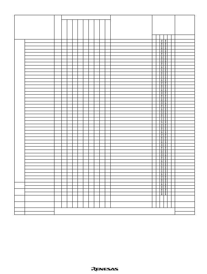
Rev. 1.0, 02/00, page 925 of 1141
Table A.1
Data Transfer Instruction
MOV.B #xx:8,Rd
MOV.B Rs,Rd
MOV.B @ERs,Rd
MOV.B @(d:16,ERs),Rd
MOV.B @(d:32,ERs),Rd
MOV.B @ERs+,Rd
MOV.B @aa:8,Rd
MOV.B @aa:16,Rd
MOV.B @aa:32,Rd
MOV.B Rs,@ERd
MOV.B Rs,@(d:16,ERd)
MOV.B Rs,@(d:32,ERd)
MOV.B Rs,@-ERd
MOV.B Rs,@aa:8
MOV.B Rs,@aa:16
MOV.B Rs,@aa:32
MOV.W #xx:16,Rd
MOV.W Rs,Rd
MOV.W @ERs,Rd
MOV.W @(d:16,ERs),Rd
MOV.W @(d:32,ERs),Rd
MOV.W @ERs+,Rd
MOV.W @aa:16,Rd
MOV.W @aa:32,Rd
MOV.W Rs,@ERd
MOV.W Rs,@(d:16,ERd)
MOV.W Rs,@(d:32,ERd)
MOV.W Rs,@-ERd
MOV.W Rs,@aa:16
MOV.W Rs,@aa:32
MOV.L #xx:32,ERd
MOV.L ERs,ERd
MOV.L @ERs,ERd
MOV.L @(d:16,ERs),ERd
MOV.L @(d:32,ERs),ERd
MOV.L @ERs+,ERd
MOV.L @aa:16,ERd
MOV.L @aa:32,ERd
MOV.L ERs,@ERd
MOV.L ERs,@(d:16,ERd)
MOV.L ERs,@(d:32,ERd)
MOV.L ERs,@-ERd
MOV.L ERs,@aa:16
MOV.L ERs,@aa:32
POP.W Rn
POP.L ERn
PUSH.W Rn
PUSH.L ERn
LDM @SP+,(ERm-ERn)
STM (ERm-ERn),@-SP
MOVFPE @aa:16,Rd
MOVTPE Rs,@aa:16
B
B
B
B
B
B
B
B
B
B
B
B
B
B
B
B
W
W
W
W
W
W
W
W
W
W
W
W
W
W
L
L
L
L
L
L
L
L
L
L
L
L
L
L
W
L
W
L
L
L
2
4
6
2
2
2
2
2
2
2
4
4
4
8
4
8
4
8
4
8
6
10
6
10
2
2
2
2
4
4
2
4
6
2
4
6
4
6
4
6
6
8
6
8
MOV
POP
PUSH
LDM
STM
MOVFPE
MOVTPE
Mnemonic
Size
Addressing Mode and Instruction Length (Bytes)
#xx
Rn
@ERn
@(d,ERn)
@-ERn/@ERn+
@aa
@(d,PC)
@@aa
#xx:8
Rd8
Rs8
Rd8
@ERs
Rd8
@(d:16,ERs)
Rd8
@(d:32,ERs)
Rd8
@ERs
Rd8,ERs32+1
ERs32
@aa:8
Rd8
@aa:16
Rd8
@aa:32
Rd8
Rs8
@ERd
Rs8
@(d:16,ERd)
Rs8
@(d:32,ERd)
ERd32-1
ERd32,Rs8
@ERd
Rs8
@aa:8
Rs8
@aa:16
Rs8
@aa:32
#xx:16
Rd16
Rs16
Rd16
@ERs
Rd16
@(d:16,ERs)
Rd16
@(d:32,ERs)
Rd16
@ERs
Rd16,ERs32+2
ERs32
@aa:16
Rd16
@aa:32
Rd16
Rs16
@ERd
Rs16
@(d:16,ERd)
Rs16
@(d:32,ERd)
ERd32-2
ERd32,Rs16
@ERd
Rs16
@aa:16
Rs16
@aa:32
#xx:32
ERd32
ERs32
ERd32
@ERs
ERd32
@(d:16,ERs)
ERd32
@(d:32,ERs)
ERd32
@ERs
ERd32,ERs32+4
ERs32
@aa:16
ERd32
@aa:32
ERd32
ERs32
@ERd
ERs32
@(d:16,ERd)
ERs32
@(d:32,ERd)
ERd32-4
ERd32,ERs32
@ERd
ERs32
@aa:16
ERs32
@aa:32
@SP
Rn16,SP+2
SP
@SP
ERn32,SP+4
SP
SP-2
SP,Rn16
@SP
SP-4
SP,ERn32
@SP
(@SP
ERn32,SP+4
SP)
Repeat for the number of returns
(SP-4
SP,ERn32
@SP)
Repeat for the number of returns
Operation
Condition
Code
No of
Execution
States
*1
I
H N Z V C
Advanced Mode
2
4
2
4
4
4
0
0
0
0
0
0
0
0
0
0
0
0
0
0
0
0
0
0
0
0
0
0
0
0
0
0
0
0
0
0
0
0
0
0
0
0
0
0
0
0
0
0
0
0
0
0
0
0
--
--
1
1
2
3
5
3
2
3
4
2
3
5
3
2
3
4
2
1
2
3
5
3
3
4
2
3
5
3
3
4
3
1
4
5
7
5
5
6
4
5
7
5
5
6
3
5
3
5
7/9/11 [1]
7/9/11 [1]
[2]
[2]
--
--
--
--
--
--
--
--
--
--
--
--
--
--
--
--
--
--
--
--
--
--
--
--
--
--
--
--
--
--
--
--
--
--
--
--
--
--
--
--
--
--
--
--
--
--
--
--
--
--
--
--
--
--
--
--
--
--
--
--
--
--
--
--
--
--
--
--
--
--
--
--
--
--
--
--
--
--
--
--
--
--
--
--
--
--
--
--
--
--
--
--
--
--
--
--
--
--
--
--
--
--
--
--
--
--
--
--
--
--
--
--
--
--
--
--
--
--
--
--
--
--
--
--
--
--
--
--
--
--
--
--
--
--
--
--
--
--
--
--
--
--
--
--
--
--
--
--
--
--
Cannot be used in this LSI
--
--
--
--
--
Rev. 1.0, 02/00, page 926 of 1141
Table A.2
Arithmetic Instructions
ADD.B #xx:8,Rd
ADD.B Rs,Rd
ADD.W #xx:16,Rd
ADD.W Rs,Rd
ADD.L #xx:32,ERd
ADD.L ERs,ERd
ADDX #xx:8,Rd
ADDX Rs,Rd
ADDS #1,ERd
ADDS #2,ERd
ADDS #4,ERd
INC.B Rd
INC.W #1,Rd
INC.W #2,Rd
INC.L #1,ERd
INC.L #2,ERd
DAA Rd
SUB.B Rs,Rd
SUB.W #xx:16,Rd
SUB.W Rs,Rd
SUB.L #xx:32,ERd
SUB.L ERs,ERd
SUBX #xx:8,Rd
SUBX Rs,Rd
SUBS #1,ERd
SUBS #2,ERd
SUBS #4,ERd
DEC.B Rd
DEC.W #1,Rd
DEC.W #2,Rd
DEC.L #1,ERd
DEC.L #2,ERd
DAS Rd
MULXU.B Rs,Rd
MULXU.W Rs,ERd
MULXS.B Rs,Rd
MULXS.W Rs,ERd
DIVXU.B Rs,Rd
DIVXU.W Rs,ERd
DIVXS.B Rs,Rd
DIVXS.W Rs,ERd
CMP.B #xx:8,Rd
CMP.B Rs,Rd
CMP.W #xx:16,Rd
CMP.W Rs,Rd
CMP.L #xx:32,ERd
CMP.L ERs,ERd
NEG.B Rd
NEG.W Rd
NEG.L ERd
EXTU.W Rd
EXTU.L ERd
EXTS.W Rd
EXTS.L ERd
TAS @ERd
MAC @ERn+,@ERm+
CLRMAC
LDMAC ERs,MACH
LDMAC ERs,MACL
STMAC MACH,ERd
STMAC MACL,ERd
B
B
W
W
L
L
B
B
L
L
L
B
W
W
L
L
B
B
W
W
L
L
B
B
L
L
L
B
W
W
L
L
B
B
W
B
W
B
W
B
W
B
B
W
W
L
L
B
W
L
W
L
W
L
B
2
4
6
2
4
6
2
2
4
6
2
2
2
2
2
2
2
2
2
2
2
2
2
2
2
2
2
2
2
2
2
2
2
2
2
2
2
2
4
4
2
2
4
4
2
2
2
2
2
2
2
2
2
2
ADD
ADDX
ADDS
INC
DAA
SUB
SUBX
SUBS
DEC
DAS
MULXU
MULXS
DIVXU
DIVXS
CMP
NEG
EXTU
EXTS
TAS
MAC
CLRMAC
LDMAC
STMAC
Mnemonic
Size
#xx
Rn
@ERn
@(d,ERn)
@-ERn/@ERn+
@aa
@(d,PC)
@@aa
--
Rd8+#xx:8
Rd8
Rd8+Rs8
Rd8
Rd16+#xx:16
Rd16
Rd16+Rs16
Rd16
ERd32+#xx:32
ERd32
ERd32+ERs32
ERd32
Rd8+#xx:8+C
Rd8
Rd8+Rs8+C
Rd8
ERd32+1
ERd32
ERd32+2
ERd32
ERd32+4
ERd32
Rd8+1
Rd8
Rd16+1
Rd16
Rd16+2
Rd16
ERd32+1
ERd32
ERd32+2
ERd32
Rd8 10 Decimal adjust
Rd8
Rd8-Rs8
Rd8
Rd16-#xx:16
Rd16
Rd16-Rs16
Rd16
ERd32-#xx:32
ERd32
ERd32-ERs32
ERd32
Rd8-#xx:8-C
Rd8
Rd8-Rs8-C
Rd8
ERd32-1
ERd32
ERd32-2
ERd32
ERd32-4
ERd32
Rd8-1
Rd8
Rd16-1
Rd16
Rd16-2
Rd16
ERd32-1
ERd32
ERd32-2
ERd32
Rd8 10 Decimal adjust
Rd8
Rd8
◊
Rs8
Rd16(Multiplication w/o sign)
Rd16
◊
Rs16
ERd32
(Multiplication w/o sign)
Rd8
◊
Rs8
Rd16(Multiplication w/o sign)
Rd16
◊
Rs16
ERd32
(Multiplication w/o sign)
Rd16
˜
Rs8
Rd16 (RdH: Remainder, RdL:
Quatient)(Division w/o sign)
ERd32
˜
Rs16
ERd32 (Ed:Remainder,
Rd: Quatient)(Division with sign)
Rd16
˜
Rs8
Rd16(RdH: Remainder, RdL:
Quatient)(Division w/o sign)
ERd32
˜
Rs16
ERd32 (Ed:Remainder,
Rd: Quatient)(Division with sign)
Rd8-#xx:8
Rd8-Rs8
Rd16-#xx:16
Rd16-Rs16
ERd32-#xx:32
ERd32-ERs32
0-Rd8
Rd8
0-Rd16
Rd16
0-ERd32
ERd32
0
(<Bits 15 to 8> of Rd16)
0
(<Bits 31 to 16> of ERd32)
(<Bit7> of Rd16)
(<Bits 15 to 8> of Rd16)
(<Bit15> of ERd32)
(<Bits31 to 16> of ERd32)
@ERd-0
CCR set, (1)
(<Bit7> of @ERd)
Operation
Condition
Code
I
H N Z V C
Advanced Mode
4
--
--
--
*
1
1
2
1
3
1
1
1
1
1
1
1
1
1
1
1
1
1
2
1
3
1
1
1
1
1
1
1
1
1
1
1
1
12
20
13
21
12
20
13
21
1
1
2
1
3
1
1
1
1
1
1
1
1
4
--
--
--
--
--
--
--
--
--
--
--
--
--
--
--
--
--
--
--
--
--
--
--
--
--
--
--
--
--
--
--
--
--
--
--
--
--
--
--
--
--
--
--
--
--
--
--
--
--
--
--
--
--
--
--
[3]
[3]
[4]
[4]
--
--
--
--
--
--
--
--
*
[3]
[3]
[4]
[4]
--
--
--
--
--
--
--
--
*
--
--
--
--
--
--
--
--
[3]
[3]
[4]
[4]
--
--
--
--
--
--
--
--
--
--
--
--
--
[6]
[6]
[8]
[8]
0
0
[5]
[5]
--
--
--
[5]
[5]
--
--
--
--
--
[7]
[7]
[7]
[7]
--
--
--
--
--
--
--
--
--
--
--
--
--
--
--
--
--
--
--
--
--
--
--
--
--
--
--
--
*
--
--
--
--
--
--
--
--
0
0
0
0
0
--
--
--
--
--
Cannot be used in this LSI
[2]
Addressing Mode and Instruction Length (Bytes)
No of
Execution
States
*1
Rev. 1.0, 02/00, page 927 of 1141
Table A.3
Logic Operations Instructions
AND.B #xx:8,Rd
AND.B Rs,Rd
AND.W #xx:16,Rd
AND.W Rs,Rd
AND.L #xx:32,ERd
AND.L ERs,ERd
OR.B #xx:8,Rd
OR.B Rs,Rd
OR.W #xx:16,Rd
OR.W Rs,Rd
OR.L #xx:32,ERd
OR.L ERs,ERd
XOR.B #xx:8,Rd
XOR.B Rs,Rd
XOR.W #xx:16,Rd
XOR.W Rs,Rd
XOR.L #xx:32,ERd
XOR.L ERs,ERd
NOT.B Rd
NOT.W Rd
NOT.L ERd
B
B
W
W
L
L
B
B
W
W
L
L
B
B
W
W
L
L
B
W
L
2
4
6
2
4
6
2
4
6
2
2
4
2
2
4
2
2
4
2
2
2
AND
OR
XOR
NOT
Mnemonic
Size
#xx
Rn
@ERn
@(d,ERn)
@-ERn/@ERn+
@aa
@(d,PC)
@@aa
--
Rd8
#xx:8
Rd8
Rd8
Rs8
Rd8
Rd16
#xx:16
Rd16
Rd16
Rs16
Rd16
ERd32
#xx:32
ERd32
ERd32
ERs32
ERd32
Rd8
#xx:8
Rd8
Rd8
Rs8
Rd8
Rd16
#xx:16
Rd16
Rd16
Rs16
Rd16
ERd32
#xx:32
ERd32
ERd32
ERs32
ERd32
Rd8
#xx:8
Rd8
Rd8
Rs8
Rd8
Rd16
#xx:16
Rd16
Rd16
Rs16
Rd16
ERd32
#xx:32
ERd32
ERd32
ERs32
ERd32
~Rd8
Rd8
~Rd16
Rd16
~ERd32
ERd32
Operation
Condition
Code
I
H N Z V C
Advanced Mode
1
1
2
1
3
2
1
1
2
1
3
2
1
1
2
1
3
2
1
1
1
--
--
--
--
--
--
--
--
--
--
--
--
--
--
--
--
--
--
--
--
--
--
--
--
--
--
--
--
--
--
--
--
--
--
--
--
--
--
--
--
--
--
0
0
0
0
0
0
0
0
0
0
0
0
0
0
0
0
0
0
0
0
0
--
--
--
--
--
--
--
--
--
--
--
--
--
--
--
--
--
--
--
--
--
Addressing Mode and Instruction Length (Bytes)
No of
Execution
States
*1
Rev. 1.0, 02/00, page 928 of 1141
Table A.4
Shift Instructions
SHAL.B Rd
SHAL.B #2,Rd
SHAL.W Rd
SHAL.W #2,Rd
SHAL.L ERd
SHAL.L #2,ERd
SHAR.B Rd
SHAR.B #2,Rd
SHAR.W Rd
SHAR.W #2,Rd
SHAR.L ERd
SHAR.L #2,ERd
SHLL.B Rd
SHLL.B #2,Rd
SHLL.W Rd
SHLL.W #2,Rd
SHLL.L ERd
SHLL.L #2,ERd
SHLR.B Rd
SHLR.B #2,Rd
SHLR.W Rd
SHLR.W #2,Rd
SHLR.L ERd
SHLR.L #2,ERd
ROTXL.B Rd
ROTXL.B #2,Rd
ROTXL.W Rd
ROTXL.W #2,Rd
ROTXL.L ERd
ROTXL.L #2,ERd
ROTXR.B Rd
ROTXR.B #2,Rd
ROTXR.W Rd
ROTXR.W #2,Rd
ROTXR.L ERd
ROTXR.L #2,ERd
ROTL.B Rd
ROTL.B #2,Rd
ROTL.W Rd
ROTL.W #2,Rd
ROTL.L ERd
ROTL.L #2,ERd
ROTR.B Rd
ROTR.B #2,Rd
ROTR.W Rd
ROTR.W #2,Rd
ROTR.L ERd
ROTR.L #2,ERd
B
B
W
W
L
L
B
B
W
W
L
L
B
B
W
W
L
L
B
B
W
W
L
L
B
B
W
W
L
L
B
B
W
W
L
L
B
B
W
W
L
L
B
B
W
W
L
L
2
2
2
2
2
2
2
2
2
2
2
2
2
2
2
2
2
2
2
2
2
2
2
2
2
2
2
2
2
2
2
2
2
2
2
2
2
2
2
2
2
2
2
2
2
2
2
2
SHAL
SHAR
SHLL
SHLR
ROTXL
ROTXR
ROTL
ROTR
Mnemonic
Size
#xx
Rn
@ERn
@(d,ERn)
@-ERn/@ERn+
@aa
@(d,PC)
@@aa
--
Operation
Condition
Code
I
H N Z V C
Advanced Mode
0
0
0
0
0
0
0
0
0
0
0
0
0
0
0
0
0
0
0
0
0
0
0
0
0
0
0
0
0
0
0
0
0
0
0
0
0
0
0
0
0
0
1
1
1
1
1
1
1
1
1
1
1
1
1
1
1
1
1
1
1
1
1
1
1
1
1
1
1
1
1
1
1
1
1
1
1
1
1
1
1
1
1
1
1
1
1
1
1
1
--
--
--
--
--
--
--
--
--
--
--
--
--
--
--
--
--
--
--
--
--
--
--
--
--
--
--
--
--
--
--
--
--
--
--
--
--
--
--
--
--
--
--
--
--
--
--
--
--
--
--
--
--
--
--
--
--
--
--
--
--
--
--
--
--
--
--
--
--
--
--
--
--
--
--
--
--
--
--
--
--
--
--
--
--
--
--
--
--
--
--
--
--
--
--
--
0
0
0
0
0
0
C
0
MSB
LSB
C MSB
LSB
C MSB
LSB
C
MSB
LSB
C
MSB
LSB
C
0
MSB
LSB
C
0
MSB
LSB
C
MSB
LSB
Addressing Mode and Instruction Length (Bytes)
No of
Execution
States
*1

Rev. 1.0, 02/00, page 929 of 1141
Table A.5
Bit Manipulation Instructions
BSET #xx:3,Rd
BSET #xx:3,@ERd
BSET #xx:3,@aa:8
BSET #xx:3,@aa:16
BSET #xx:3,@aa:32
BSET Rn,Rd
BSET Rn,@ERd
BSET Rn,@aa:8
BSET Rn,@aa:16
BSET Rn,@aa:32
BCLR #xx:3,Rd
BCLR #xx:3,@ERd
BCLR #xx:3,@aa:8
BCLR #xx:3,@aa:16
BCLR #xx:3,@aa:32
BCLR Rn,Rd
BCLR Rn,@ERd
BCLR Rn,@aa:8
BCLR Rn,@aa:16
BCLR Rn,@aa:32
BNOT #xx:3,Rd
BNOT #xx:3,@ERd
BNOT #xx:3,@aa:8
BNOT #xx:3,@aa:16
BNOT #xx:3,@aa:32
BNOT Rn,Rd
BNOT Rn,@ERd
BNOT Rn,@aa:8
BNOT Rn,@aa:16
BNOT Rn,@aa:32
BTST #xx:3,Rd
BTST #xx:3,@ERd
BTST #xx:3,@aa:8
BTST #xx:3,@aa:16
BTST #xx:3,@aa:32
BTST Rn,Rd
BTST Rn,@ERd
BTST Rn,@aa:8
BTST Rn,@aa:16
BTST Rn,@aa:32
BLD #xx:3,Rd
BLD #xx:3,@ERd
BLD #xx:3,@aa:8
BLD #xx:3,@aa:16
BLD #xx:3,@aa:32
BILD #xx:3,Rd
BILD #xx:3,@ERd
BILD #xx:3,@aa:8
BILD #xx:3,@aa:16
BILD #xx:3,@aa:32
BST #xx:3,Rd
BST #xx:3,@ERd
BST #xx:3,@aa:8
BST #xx:3,@aa:16
BST #xx:3,@aa:32
BIST #xx:3,Rd
BIST #xx:3,@ERd
BIST #xx:3,@aa:8
BIST #xx:3,@aa:16
BIST #xx:3,@aa:32
BAND #xx:3,Rd
BAND #xx:3,@ERd
BAND #xx:3,@aa:8
BAND #xx:3,@aa:16
BAND #xx:3,@aa:32
B
B
B
B
B
B
B
B
B
B
B
B
B
B
B
B
B
B
B
B
B
B
B
B
B
B
B
B
B
B
B
B
B
B
B
B
B
B
B
B
B
B
B
B
B
B
B
B
B
B
B
B
B
B
B
B
B
B
B
B
B
B
B
B
B
2
2
2
2
2
2
2
2
2
2
2
2
2
4
4
4
4
4
4
4
4
4
4
4
4
4
4
6
8
4
6
8
4
6
8
4
6
8
4
6
8
4
6
8
4
6
8
4
6
8
4
6
8
4
6
8
4
6
8
4
6
8
4
6
8
BSET
BCLR
BNOT
BTST
BLD
BILD
BST
BIST
BAND
Mnemonic
Size
#xx
Rn
@ERn
@(d,ERn)
@-ERn/@ERn+
@aa
@(d,PC)
@@aa
--
(#xx:3 of Rd8)
1
(#xx:3 of @ERd)
1
(#xx:3 of @aa:8)
1
(#xx:3 of @aa:16)
1
(#xx:3 of @aa:32)
1
(Rn8 of Rd8)
1
(Rn8 of @ERd)
1
(Rn8 of @aa:8)
1
(Rn8 of @aa:16)
1
(Rn8 of @aa:32)
1
(#xx:3 of Rd8)
0
(#xx:3 of @ERd)
0
(#xx:3 of @aa:8)
0
(#xx:3 of @aa:16)
0
(#xx:3 of @aa:32)
0
(Rn8 of Rd8)
0
(Rn8 of @ERd)
0
(Rn8 of @aa:8)
0
(Rn8 of @aa:16)
0
(Rn8 of @aa:32)
0
(#xx:3 of Rd8)
[~(#xx:3 of Rd8)]
(#xx:3 of @ERd)
[~(#xx:3 of @ERd)]
(#xx:3 of @aa:8)
[~(#xx:3 of @aa:8)]
(#xx:3 of @aa:16)
[~(#xx:3 of @aa:16)]
(#xx:3 of @aa:32)
[~(#xx:3 of @aa:32)]
(Rn8 of Rd8)
[~(Rn8 of Rd8)]
(Rn8 of @ERd)
[~(Rn8 of @ERd)]
(Rn8 of @aa:8)
[~(Rn8 of @aa:8)]
(Rn8 of @aa:16)
[~(Rn8 of @aa:16)]
(Rn8 of @aa:32)
[~(Rn8 of @aa:32)]
~(#xx:3 of Rd8)
Z
~(#xx:3 of @ERd)
Z
~(#xx:3 of @aa:8)
Z
~(#xx:3 of @aa:16)
Z
~(#xx:3 of @aa:32)
Z
~(Rn8 of Rd8)
Z
~(Rn8 of @ERd)
Z
~(Rn8 of @aa:8)
Z
~(Rn8 of @aa:16)
Z
~(Rn8 of @aa:32)
Z
(#xx:3 of Rd8)
C
(#xx:3 of @ERd)
C
(#xx:3 of @aa:8)
C
(#xx:3 of @aa:16)
C
(#xx:3 of @aa:32)
C
~(#xx:3 of Rd8)
C
~(#xx:3 of @ERd)
C
~(#xx:3 of @aa:8)
C
~(#xx:3 of @aa:16)
C
~(#xx:3 of @aa:32)
C
C
(#xx:3 of Rd8)
C
(#xx:3 of @ERd)
C
(#xx:3 of @aa:8)
C
(#xx:3 of @aa:16)
C
(#xx:3 of @aa:32)
~C
(#xx:3 of Rd8)
~C
(#xx:3 of @ERd)
~C
(#xx:3 of @aa:8)
~C
(#xx:3 of @aa:16)
~C
(#xx:3 of @aa:32)
C
(#xx:3 of Rd8)
C
C
(#xx:3 of @ERd)
C
C
(#xx:3 of @aa:8)
C
C
(#xx:3 of @aa:16)
C
C
(#xx:3 of @aa:32)
C
Operation
Condition
Code
I
H N Z V C
Advanced Mode
--
--
--
--
--
--
--
--
--
--
--
--
--
--
--
--
--
--
--
--
--
--
--
--
--
--
--
--
--
--
--
--
--
--
--
--
--
--
--
--
--
--
--
--
--
--
--
--
--
--
--
--
--
--
--
--
--
--
--
--
--
--
--
--
--
1
4
4
5
6
1
4
4
5
6
1
4
4
5
6
1
4
4
5
6
1
4
4
5
6
1
4
4
5
6
1
3
3
4
5
1
3
3
4
5
1
3
3
4
5
1
3
3
4
5
1
4
4
5
6
1
4
4
5
6
1
3
3
4
5
--
--
--
--
--
--
--
--
--
--
--
--
--
--
--
--
--
--
--
--
--
--
--
--
--
--
--
--
--
--
--
--
--
--
--
--
--
--
--
--
--
--
--
--
--
--
--
--
--
--
--
--
--
--
--
--
--
--
--
--
--
--
--
--
--
--
--
--
--
--
--
--
--
--
--
--
--
--
--
--
--
--
--
--
--
--
--
--
--
--
--
--
--
--
--
--
--
--
--
--
--
--
--
--
--
--
--
--
--
--
--
--
--
--
--
--
--
--
--
--
--
--
--
--
--
--
--
--
--
--
--
--
--
--
--
--
--
--
--
--
--
--
--
--
--
--
--
--
--
--
--
--
--
--
--
--
--
--
--
--
--
--
--
--
--
--
--
--
--
--
--
--
--
--
--
--
--
--
--
--
--
--
--
--
--
--
--
--
--
--
--
--
--
--
--
--
--
--
--
--
--
--
--
--
--
--
--
--
--
--
--
--
--
--
--
--
--
--
--
--
--
--
--
--
--
--
--
--
--
--
--
--
--
--
--
--
--
--
--
--
--
--
--
--
--
--
--
--
--
--
--
--
--
--
--
--
--
--
--
--
--
--
--
--
--
--
--
--
--
--
--
--
--
--
--
--
--
--
--
--
--
--
--
--
--
--
--
--
--
--
--
--
--
--
--
--
--
--
--
--
Addressing Mode and Instruction Length (Bytes)
No of
Execution
States
*1
Rev. 1.0, 02/00, page 930 of 1141
BIAND #xx:3,Rd
BIAND #xx:3,@ERd
BIAND #xx:3,@aa:8
BIAND #xx:3,@aa:16
BIAND #xx:3,@aa:32
BOR #xx:3,Rd
BOR #xx:3,@ERd
BOR #xx:3,@aa:8
BOR #xx:3,@aa:16
BOR #xx:3,@aa:32
BIOR #xx:3,Rd
BIOR #xx:3,@ERd
BIOR #xx:3,@aa:8
BIOR #xx:3,@aa:16
BIOR #xx:3,@aa:32
BXOR #xx:3,Rd
BXOR #xx:3,@ERd
BXOR #xx:3,@aa:8
BXOR #xx:3,@aa:16
BXOR #xx:3,@aa:32
BIXOR #xx:3,Rd
BIXOR #xx:3,@ERd
BIXOR #xx:3,@aa:8
BIXOR #xx:3,@aa:16
BIXOR #xx:3,@aa:32
B
B
B
B
B
B
B
B
B
B
B
B
B
B
B
B
B
B
B
B
B
B
B
B
B
BIAND
BOR
BIOR
BXOR
BIXOR
Mnemonic
Size
#xx
Rn
@ERn
@(d,ERn)
@-ERn/@ERn+
@aa
@(d,PC)
@@aa
--
C
[~(#xx:3 of Rd8)]
C
C
[~(#xx:3 of @ERd)]
C
C
[~(#xx:3 of @aa:8)]
C
C
[~(#xx:3 of @aa:16)]
C
C
[~(#xx:3 of @aa:32)]
C
C
(#xx:3 of Rd8)
C
C
(#xx:3 of @ERd)
C
C
(#xx:3 of @aa:8)
C
C
(#xx:3 of @aa:16)
C
C
(#xx:3 of @aa:32)
C
C
[~(#xx:3 of Rd8)]
C
C
[~(#xx:3 of @ERd)]
C
C
[~(#xx:3 of @aa:8)]
C
C
[~(#xx:3 of @aa:16)]
C
C
[~(#xx:3 of @aa:32)]
C
C
(#xx:3 of Rd8)
C
C
(#xx:3 of @ERd)
C
C
(#xx:3 of @aa:8)
C
C
(#xx:3 of @aa:16)
C
C
(#xx:3 of @aa:32)
C
C
[~(#xx:3 of Rd8)]
C
C
[~(#xx:3 of @ERd)]
C
C
[~(#xx:3 of @aa:8)]
C
C
[~(#xx:3 of @aa:16)]
C
C
[~(#xx:3 of @aa:32)]
C
Operation
I
H N Z V C
Advanced Mode
2
2
2
2
2
4
4
4
4
4
4
6
8
4
6
8
4
6
8
4
6
8
4
6
8
1
3
3
4
5
1
3
3
4
5
1
3
3
4
5
1
3
3
4
5
1
3
3
4
5
--
--
--
--
--
--
--
--
--
--
--
--
--
--
--
--
--
--
--
--
--
--
--
--
--
--
--
--
--
--
--
--
--
--
--
--
--
--
--
--
--
--
--
--
--
--
--
--
--
--
--
--
--
--
--
--
--
--
--
--
--
--
--
--
--
--
--
--
--
--
--
--
--
--
--
--
--
--
--
--
--
--
--
--
--
--
--
--
--
--
--
--
--
--
--
--
--
--
--
--
--
--
--
--
--
--
--
--
--
--
--
--
--
--
--
--
--
--
--
--
--
--
--
--
--
Condition
Code
Addressing Mode and Instruction Length (Bytes)
No of
Execution
States
*1
Rev. 1.0, 02/00, page 931 of 1141
Table A.6
Branch Instructions
BRA d:8(BT d:8)
BRA d:16(BT d:16)
BRN d:8(BF d:8)
BRN d:16(BF d:16)
BHI d:8
BHI d:16
BLS d:8
BLS d:16
BCC d:8(BHS d:8)
BCC d:16(BHS d:16)
BCS d:8(BLO d:8)
BCS d:16(BLO d:16)
BNE d:8
BNE d:16
BEQ d:8
BEQ d:16
BVC d:8
BVC d:16
BVS d:8
BVS d:16
BPL d:8
BPL d:16
BMI d:8
BMI d:16
BGE d:8
BGE d:16
BLT d:8
BLT d:16
Bcc
Mnemonic
Size
#xx
Rn
@ERn
@(d,ERn)
@-ERn/@ERn+
@aa
@(d,PC)
@@aa
--
Operation
I
Branch
Condition
H N Z V C
Advanced Mode
2
4
2
4
2
4
2
4
2
4
2
4
2
4
2
4
2
4
2
4
2
4
2
4
2
4
2
4
Always
Never
C
Z=0
C
Z=1
C=0
C=1
Z=0
Z=1
V=0
V=1
N=0
N=1
N
V=0
N
V=1
if condition is true then
PC
PC+d
else next;
2
3
2
3
2
3
2
3
2
3
2
3
2
3
2
3
2
3
2
3
2
3
2
3
2
3
2
3
--
--
--
--
--
--
--
--
--
--
--
--
--
--
--
--
--
--
--
--
--
--
--
--
--
--
--
--
--
--
--
--
--
--
--
--
--
--
--
--
--
--
--
--
--
--
--
--
--
--
--
--
--
--
--
--
--
--
--
--
--
--
--
--
--
--
--
--
--
--
--
--
--
--
--
--
--
--
--
--
--
--
--
--
--
--
--
--
--
--
--
--
--
--
--
--
--
--
--
--
--
--
--
--
--
--
--
--
--
--
--
--
--
--
--
--
--
--
--
--
--
--
--
--
--
--
--
--
--
--
--
--
--
--
--
--
--
--
--
--
--
--
--
--
--
--
--
--
--
--
--
--
--
--
--
--
--
--
--
--
--
--
--
--
--
--
--
--
--
--
--
--
--
--
--
--
--
--
--
--
--
--
--
--
--
--
--
--
--
--
--
--
--
--
--
--
Operation
Code
BGT d:8
BGT d:16
BLE d:8
BLE d:16
JMP @ERn
JMP @aa:24
JMP @@aa:8
BSR d:8
BSR d:16
JSR @ERn
JSR @aa:24
JSR @@aa:8
RTS
JMP
BSR
JSR
RTS
PC
ERn
PC
aa:24
PC
@aa:8
PC
@-SP,PC
PC+d:8
PC
@-SP,PC
PC+d:16
PC
@-SP,PC
ERn
PC
@-SP,PC
aa:24
PC
@-SP,PC
@aa:8
PC
@SP+
2
2
4
4
2
4
2
4
2
4
2
2
2
2
3
2
3
2
3
--
--
--
--
--
--
--
--
--
--
--
--
--
--
--
--
--
--
--
--
--
--
--
--
--
--
--
--
--
--
--
--
--
--
--
--
--
--
--
--
--
--
--
--
--
--
--
--
--
--
--
--
--
--
--
--
--
--
--
--
--
--
--
--
--
--
--
--
--
--
--
--
--
--
--
--
--
--
--
--
--
--
--
--
--
--
--
--
--
--
--
Z
(N
V)=0
Z
(N
V)=1
5
4
5
4
5
6
5
Addressing Mode and Instruction Length (Bytes)
No of
Execution
States
*1
Rev. 1.0, 02/00, page 932 of 1141
Table A.7
System Control Instructions
TRAPA #x:2
RTE
SLEEP
LDC #xx:8,CCR
LDC #xx:8,EXR
LDC Rs,CCR
LDC Rs,EXR
LDC @ERs,CCR
LDC @ERs,EXR
LDC @(d:16,ERs),CCR
LDC @(d:16,ERs),EXR
LDC @(d:32,ERs),CCR
LDC @(d:32,ERs),EXR
LDC @ERs+,CCR
LDC @ERs+,EXR
LDC @aa:16,CCR
LDC @aa:16,EXR
LDC @aa:32,CCR
LDC @aa:32,EXR
STC.B CCR,Rd
STC.B EXR,Rd
STC.W CCR,@ERd
STC.W EXR,@ERd
STC.W CCR,@(d:16,ERd)
STC.W EXR,@(d:16,ERd)
STC.W CCR,@(d:32,ERd)
STC.W EXR,@(d:32,ERd)
STC.W CCR,@-ERd
STC.W EXR,@-ERd
STC.W CCR,@aa:16
STC.W EXR,@aa:16
STC.W CCR,@aa:32
STC.W EXR,@aa:32
ANDC #xx:8,CCR
ANDC #xx:8,EXR
ORC #xx:8,CCR
ORC #xx:8,EXR
XORC #xx:8,CCR
XORC #xx:8,EXR
NOP
--
--
--
B
B
B
B
W
W
W
W
W
W
W
W
W
W
W
W
B
B
W
W
W
W
W
W
W
W
W
W
W
W
B
B
B
B
B
B
--
TRAPA
RTE
SLEEP
LDC
STC
ANDC
ORC
XORC
NOP
Mnemonic
Size
#xx
Rn
@ERn
@(d,ERn)
@-ERn/@ERn+
@aa
@(d,PC)
@@aa
--
PC
@-SP,CCR
@-SP,
EXR
@-SP,<Vector>
PC
EXR
@SP+,CCR
@SP+,
PC
@SP+
Transition to power-down state
#xx:8
CCR
#xx:8
EXR
Rs8
CCR
Rs8
EXR
@ERs
CCR
@ERs
EXR
@(d:16,ERs)
CCR
@(d:16,ERs)
EXR
@(d:32,ERs)
CCR
@(d:32,ERs)
EXR
@ERs
CCR,ERs32+2
ERs32
@ERs
EXR,ERs32+2
ERs32
@aa:16
CCR
@aa:16
EXR
@aa:32
CCR
@aa:32
EXR
CCR
Rd8
EXR
Rd8
CCR
@ERd
EXR
@ERd
CCR
@(d:16,ERd)
EXR
@(d:16,ERd)
CCR
@(d:32,ERd)
EXR
@(d:32,ERd)
ERd32-2
ERd32,CCR
@ERd
ERd32-2
ERd32,EXR
@ERd
CCR
@aa:16
EXR
@aa:16
CCR
@aa:32
EXR
@aa:32
CCR
#xx:8
CCR
EXR
#xx:8
EXR
CCR
#xx:8
CCR
EXR
#xx:8
EXR
CCR
#xx:8
CCR
EXR
#xx:8
EXR
PC
PC+2
Operation
I
H N Z V C
Advanced Mode
2
4
2
4
2
4
2
4
2
2
2
2
4
4
4
4
6
6
10
10
6
6
10
10
4
4
4
4
6
6
8
8
6
6
8
8
2
5 [9]
2
1
2
1
1
3
3
4
4
6
6
4
4
4
4
5
5
1
1
3
3
4
4
6
6
4
4
4
4
5
5
1
2
1
2
1
2
1
1
--
--
--
--
--
--
--
--
--
--
--
--
--
--
--
--
--
--
--
--
--
--
--
--
--
--
--
--
--
--
--
--
--
--
--
--
--
--
--
--
--
--
--
--
--
--
--
--
--
--
--
--
--
--
--
--
--
--
--
--
--
--
--
--
--
--
--
--
--
--
--
--
--
--
--
--
--
--
--
--
--
--
--
--
--
--
--
--
--
--
--
--
--
--
--
--
--
--
--
--
--
--
--
--
--
--
--
--
--
--
--
--
--
--
--
--
--
--
--
--
--
--
--
--
--
--
--
--
--
--
--
--
--
--
--
--
--
--
--
--
--
--
--
--
--
--
--
--
--
--
--
--
--
--
--
--
--
--
--
--
--
--
--
--
--
--
--
8 [9]
Condition
Code
Addressing Mode and Instruction Length (Bytes)
No of
Execution
States
*1
Rev. 1.0, 02/00, page 933 of 1141
Table A.8
Block Transfer Instructions
EEPMOV.B
EEPMOV.W
--
--
EEPMOV
Mnemonic
Size
#xx
Rn
@ERn
@(d,ERn)
@-ERn/@ERn+
@aa
@(d,PC)
@@aa
--
Operation
I
H N Z V C
Advanced Mode
4
4
4+2n *
2
4+2n *
2
--
--
--
--
--
--
--
--
--
--
--
--
Condition
Code
if R4L
0
Repeat @ER5
@ER6
ER5+1
ER5
ER6+1
ER6
R4L-1
R4L
Until R4L=0
else next;
if R4
0
Repeat @ER5
@ER6
ER5+1
ER5
ER6+1
ER6
R4-1
R4
Until R4=0
else next;
Addressing Mode and Instruction Length (Bytes)
No of
Execution
States
*1
Notes: 1. The values indicated in the column of number of execution states apply when
instruction code and operand exist in the on-chip memory.
2. n is the initial setting value of R4L or R4.
[1] 7 states when the number of return/retract registers is 2, 9 states when the number
of registers is 3, and 11 states when the number of registers is 4.
[2] Cannot be used in this LSI.
[3] Set to 1 when a carry or borrow occurs at bit 11, otherwise cleared to 0.
[4] Set to 1 when a carry or borrow occurs at bit 27, otherwise cleared to 0.
[5] Retains the value before computation when the computation result is 0, otherwise
cleared to 0.
[6] Set to 1 when the divisor is negative, otherwise cleared to 0.
[7] Set to 1 when the divisor is 0, otherwise cleared to 0.
[8] Set to 1 when the quotient is negative, otherwise cleared to 0.
[9] 1 is added to the number of execution states when EXR is valid.
Rev. 1.0, 02/00, page 934 of 1141
A.2
Instruction Codes
Table A.9 Instruction Codes
ADD
ADDS
ADDX
AND
ANDC
BAND
Bcc
ADD.B #xx:8,Rd
ADD.B Rs,Rd
ADD.W #xx:16,Rd
ADD.W Rs,Rd
ADD.L #xx:32,ERd
ADD.L ERs,ERd
ADDS #1,ERd
ADDS #2,ERd
ADDS #4,ERd
ADDX #xx:8,Rd
ADDX Rs,Rd
AND.B #xx:8,Rd
AND.B Rs,Rd
AND.W #xx:16,Rd
AND.W Rs,Rd
AND.L #xx:32,ERd
AND.L ERs,ERd
ANDC #xx:8,CCR
ANDC #xx:8,EXR
BAND #xx:3,Rd
BAND #xx:3,@ERd
BAND #xx:3,@aa:8
BAND #xx:3,@aa:16
BAND #xx:3,@aa:32
BRA d:8 (BT d:8)
BRA d:16 (BT d:16)
BRN d:8 (BF d:8)
BRN d:16 (BF d:16)
BHI d:8
BHI d:16
BLS d:8
BLS d:16
BCC d:8 (BHS d:8)
BCC d:16 (BHS d:16)
BCS d:8 (BLO d:8)
BCS d:16 (BLO d:16)
BNE d:8
BNE d:16
BEQ d:8
BEQ d:16
BVC d:8
BVC d:16
BVS d:8
BVS d:16
Mnemonic
Instruction Format
1st byte
B
B
W
W
L
L
L
L
L
B
B
B
B
W
W
L
L
B
B
B
B
B
B
B
--
--
--
--
--
--
--
--
--
--
--
--
--
--
--
--
--
--
--
--
8
0
7
0
7
0
0
0
0
9
0
E
1
7
6
7
0
0
0
7
7
7
6
6
4
5
4
5
4
5
4
5
4
5
4
5
4
5
4
5
4
5
4
5
rd
8
9
9
A
A
B
B
B
rd
E
rd
6
9
6
A
1
6
1
6
C
E
A
A
0
8
1
8
2
8
3
8
4
8
5
8
6
8
7
8
8
8
9
8
rs
1
rs
1
1 ers
0
8
9
rs
rs
6
rs
6
F
4
0 IMM
0 erd
1
3
0
1
2
3
4
5
6
7
8
9
IMM
IMM
IMM
IMM
abs
disp
disp
disp
disp
disp
disp
disp
disp
disp
disp
rd
rd
rd
0 erd
0 erd
0 erd
0 erd
0 erd
rd
rd
rd
rd
0 erd
0
1
rd
0
0
0
0
0
0
0
0
0
0
0
0
0
0 IMM
0 IMM
0
0
6
0
7
7
IMM
IMM
abs
disp
disp
disp
disp
disp
disp
disp
disp
disp
disp
IMM
IMM
abs
6
6
6
6
0 IMM
0
7
6
0 IMM
0
7
6
2nd byte
3rd byte
4th byte
5th byte
6th byte
7the byte
8th byte
9th byte
10th byte
Size
Instruction
0 ers
0 erd
IMM
Rev. 1.0, 02/00, page 935 of 1141
Bcc
(Cont.)
BCLR
BIAND
BILD
BIOR
BIST
BPL d:8
BPL d:16
BMI d:8
BMI d:16
BGE d:8
BGE d:16
BLT d:8
BLT d:16
BGT d:8
BGT d:16
BLE d:8
BLE d:16
BCLR #xx:3,Rd
BCLR #xx:3,@ERd
BCLR #xx:3,@aa:8
BCLR #xx:3,@aa:16
BCLR #xx:3,@aa:32
BCLR Rn,Rd
BCLR Rn,@ERd
BCLR Rn,@aa:8
BCLR Rn,@aa:16
BCLR Rn,@aa:32
BIAND #xx:3,Rd
BIAND #xx:3,@ERd
BIAND #xx:3,@aa:8
BIAND #xx:3,@aa:16
BIAND #xx:3,@aa:32
BILD #xx:3,Rd
BILD #xx:3,@ERd
BILD #xx:3,@aa:8
BILD #xx:3,@aa:16
BILD #xx:3,@aa:32
BIOR #xx:3,Rd
BIOR #xx:3,@ERd
BIOR #xx:3,@aa:8
BIOR #xx:3,@aa:16
BIOR #xx:3,@aa:32
BIST #xx:3,Rd
BIST #xx:3,@ERd
BIST #xx:3,@aa:8
BIST #xx:3,@aa:16
BIST #xx:3,@aa:32
Mnemonic
Instruction Format
1st byte
--
--
--
--
--
--
--
--
--
--
--
--
B
B
B
B
B
B
B
B
B
B
B
B
B
B
B
B
B
B
B
B
B
B
B
B
B
B
B
B
B
B
4
5
4
5
4
5
4
5
4
5
4
5
7
7
7
6
6
6
7
7
6
6
7
7
7
6
6
7
7
7
6
6
7
7
7
6
6
6
7
7
6
6
A
8
B
8
C
8
D
8
E
8
F
8
2
D
F
A
A
2
D
F
A
A
6
C
E
A
A
7
C
E
A
A
4
C
E
A
A
7
D
F
A
A
A
B
C
D
E
F
0 IMM
0 erd
1
3
rn
0 erd
1
3
1 IMM
0 erd
1
3
1 IMM
0 erd
1
3
1 IMM
0 erd
1
3
1 IMM
0 erd
1
3
disp
disp
disp
disp
disp
disp
abs
abs
abs
abs
abs
abs
0
0
0
0
0
0
rd
0
8
8
rd
0
8
8
rd
0
0
0
rd
0
0
0
rd
0
0
0
rd
0
8
8
7
7
6
6
7
7
7
7
7
7
6
6
disp
disp
disp
disp
disp
disp
2
2
abs
2
2
abs
6
6
abs
7
7
abs
4
4
abs
7
7
abs
0 IMM
0 IMM
rn
rn
1 IMM
1 IMM
1 IMM
1 IMM
1 IMM
1 IMM
1 IMM
1 IMM
0
0
abs
0
0
abs
0
0
abs
0
0
abs
0
0
abs
0
0
abs
7
6
7
7
7
6
2
2
6
7
4
7
0 IMM
rn
1 IMM
1 IMM
1 IMM
1 IMM
0
0
0
0
0
0
7
6
7
7
7
6
2
2
6
7
4
7
0 IMM
rn
1 IMM
1 IMM
1 IMM
1 IMM
0
0
0
0
0
0
2nd byte
3rd byte
4th byte
5th byte
6th byte
7th byte
8th byte
9th byte
10th byte
Size
Instruction

Rev. 1.0, 02/00, page 936 of 1141
BIXOR
BLD
BNOT
BOR
BSET
BSR
BST
BIXOR #xx:3,Rd
BIXOR #xx:3,@ERd
BIXOR #xx:3,@aa:8
BIXOR #xx:3,@aa:16
BIXOR #xx:3,@aa:32
BLD #xx:3,Rd
BLD #xx:3,@ERd
BLD #xx:3,@aa:8
BLD #xx:3,@aa:16
BLD #xx:3,@aa:32
BNOT #xx:3,Rd
BNOT #xx:3,@ERd
BNOT #xx:3,@aa:8
BNOT #xx:3,@aa:16
BNOT #xx:3,@aa:32
BNOT Rn,Rd
BNOT Rn,@ERd
BNOT Rn,@aa:8
BNOT Rn,@aa:16
BNOT Rn,@aa:32
BOR #xx:3,Rd
BOR #xx:3,@ERd
BOR #xx:3,@aa:8
BOR #xx:3,@aa:16
BOR #xx:3,@aa:32
BSET #xx:3,Rd
BSET #xx:3,@ERd
BSET #xx:3,@aa:8
BSET #xx:3,@aa:16
BSET #xx:3,@aa:32
BSET Rn,Rd
BSET Rn,@ERd
BSET Rn,@aa:8
BSET Rn,@aa:16
BSET Rn,@aa:32
BSR d:8
BSR d:16
BST #xx:3,Rd
BST #xx:3,@ERd
BST #xx:3,@aa:8
BST #xx:3,@aa:16
BST #xx:3,@aa:32
Mnemonic
Instruction Format
1st byte
B
B
B
B
B
B
B
B
B
B
B
B
B
B
B
B
B
B
B
B
B
B
B
B
B
B
B
B
B
B
B
B
B
B
B
--
--
B
B
B
B
B
7
7
7
6
6
7
7
7
6
6
7
7
7
6
6
6
7
7
6
6
7
7
7
6
6
7
7
7
6
6
6
7
7
6
6
5
5
6
7
7
6
6
5
C
E
A
A
7
C
E
A
A
1
D
F
A
A
1
D
F
A
A
4
C
E
A
A
0
D
F
A
A
0
D
F
A
A
5
C
7
D
F
A
A
1 IMM
0 erd
abs
1
3
0 IMM
0 erd
abs
1
3
0 IMM
0 erd
abs
1
3
rn
0 erd
abs
1
3
0 IMM
0 erd
abs
1
3
0 IMM
0 erd
abs
1
3
rn
0 erd
abs
1
3
disp
0
0 IMM
0 erd
abs
1
3
rd
0
0
0
rd
0
0
0
rd
0
8
8
rd
0
8
8
rd
0
0
0
rd
0
8
8
rd
0
8
8
0
rd
0
8
8
7
7
7
7
7
7
6
6
7
7
7
7
6
6
6
6
5
5
abs
7
7
abs
1
1
abs
1
1
abs
4
4
abs
0
0
abs
0
0
abs
disp
7
7
abs
1 IMM
1 IMM
0 IMM
0 IMM
0 IMM
0 IMM
rn
rn
0 IMM
0 IMM
0 IMM
0 IMM
rn
rn
0 IMM
0 IMM
0
0
abs
0
0
abs
0
0
abs
0
0
abs
0
0
abs
0
0
abs
0
0
abs
0
0
abs
7
7
7
6
7
7
6
6
5
7
1
1
4
0
0
7
1 IMM
0 IMM
0 IMM
rn
0 IMM
0 IMM
rn
0 IMM
0
0
0
0
0
0
0
0
7
7
7
6
7
7
6
6
5
7
1
1
4
0
0
7
1 IMM
0 IMM
0 IMM
rn
0 IMM
0 IMM
rn
0 IMM
0
0
0
0
0
0
0
0
2nd byte
3rd byte
4th byte
5th byte
6th byte
7th byte
8th byte
9th byte
10th byte
Size
Instruction

Rev. 1.0, 02/00, page 937 of 1141
BTST
BXOR
CLRMAC
CMP
DAA
DAS
DEC
DIVXS
DIVXU
EEPMOV
EXTS
EXTU
BTST #xx:3,Rd
BTST #xx:3,@ERd
BTST #xx:3,@aa:8
BTST #xx:3,@aa:16
BTST #xx:3,@aa:32
BTST Rn,Rd
BTST Rn,@ERd
BTST Rn,@aa:8
BTST Rn,@aa:16
BTST Rn,@aa:32
BXOR #xx:3,Rd
BXOR #xx:3,@ERd
BXOR #xx:3,@aa:8
BXOR #xx:3,@aa:16
BXOR #xx:3,@aa:32
CLRMAC
CMP.B #xx:8,Rd
CMP.B Rs,Rd
CMP.W #xx:16,Rd
CMP.W Rs,Rd
CMP.L #xx:32,ERd
CMP.L ERs,ERd
DAA Rd
DAS Rd
DEC.B Rd
DEC.W #1,Rd
DEC.W #2,Rd
DEC.L #1,ERd
DEC.L #2,ERd
DIVXS.B Rs,Rd
DIVXS.W Rs,ERd
DIVXU.B Rs,Rd
DIVXU.W Rs,ERd
EEPMOV.B
EEPMOV.W
EXTS.W Rd
EXTS.L ERd
EXTU.W Rd
EXTU.L ERd
Mnemonic
Instruction Format
1st byte
Cannot be used in the H8S/2199 Series
B
B
B
B
B
B
B
B
B
B
B
B
B
B
B
--
B
B
W
W
L
L
B
B
B
W
W
L
L
B
W
B
W
--
--
W
L
W
L
7
7
7
6
6
6
7
7
6
6
7
7
7
6
6
A
1
7
1
7
1
0
1
1
1
1
1
1
0
0
5
5
7
7
1
1
1
1
3
C
E
A
A
3
C
E
A
A
5
C
E
A
A
rd
C
9
D
A
F
F
F
A
B
B
B
B
1
1
1
3
B
B
7
7
7
7
0 IMM
0 erd
abs
1
3
rn
0 erd
abs
1
3
0 IMM
0 erd
abs
1
3
IMM
rs
2
rs
2
1 ers
0
0
0
5
D
7
F
D
D
rs
rs
5
D
D
F
5
7
rd
0
0
0
rd
0
0
0
rd
0
0
0
rd
rd
rd
0 erd
0 erd
rd
rd
rd
rd
rd
0 erd
0 erd
0
0
rd
0 erd
C
4
rd
0 erd
rd
0 erd
7
7
6
6
7
7
5
5
5
5
3
3
abs
3
3
abs
5
5
abs
IMM
1
3
9
9
0 IMM
0 IMM
rn
rn
0 IMM
0 IMM
rs
rs
8
8
0
0
abs
0
0
abs
0
0
abs
IMM
rd
0 erd
F
F
7
6
7
3
3
5
0 IMM
rn
0 IMM
0
0
0
7
6
7
3
3
5
0 IMM
rn
0 IMM
0
0
0
2nd byte
3rd byte
4th byte
5th byte
6th byte
7th byte
8th byte
9th byte
10th byte
Size
Instruction
Rev. 1.0, 02/00, page 938 of 1141
INC
JMP
JSR
LDC
LDM
LDMAC
MAC
MOV
INC.B Rd
INC.W #1,Rd
INC.W #2,Rd
INC.L #1,ERd
INC.L #2,ERd
JMP @ERn
JMP @aa:24
JMP @@aa:8
JSR @ERn
JSR @aa:24
JSR @@aa:8
LDC #xx:8,CCR
LDC #xx:8,EXR
LDC Rs,CCR
LDC Rs,EXR
LDC @ERs,CCR
LDC @ERs,EXR
LDC @(d:16,ERs),CCR
LDC @(d:16,ERs),EXR
LDC @(d:32,ERs),CCR
LDC @(d:32,ERs),EXR
LDC @ERs+,CCR
LDC @ERs+,EXR
LDC @aa:16,CCR
LDC @aa:16,EXR
LDC @aa:32,CCR
LDC @aa:32,EXR
LDM.L @SP+, (ERn-ERn+1)
LDM.L @SP+, (ERn-ERn+2)
LDM.L @SP+, (ERn-ERn+3)
LDMAC ERs,MACH
LDMAC ERs,MACL
MAC @ERn+,@ERm+
MOV.B #xx:8,Rd
MOV.B Rs,Rd
MOV.B @ERs,Rd
MOV.B @(d:16,ERs),Rd
MOV.B @(d:32,ERs),Rd
MOV.B @ERs+,Rd
MOV.B @aa:8,Rd
MOV.B @aa:16,Rd
MOV.B @aa:32,Rd
MOV.B Rs,@ERd
MOV.B Rs,@(d:16,ERd)
MOV.B Rs,@(d:32,ERd)
Mnemonic
Instruction Format
Cannot be used in the H8S/2199 Series
1st byte
B
W
W
L
L
--
--
--
--
--
--
B
B
B
B
W
W
W
W
W
W
W
W
W
W
W
W
L
L
L
L
L
--
B
B
B
B
B
B
B
B
B
B
B
B
0
0
0
0
0
5
5
5
5
5
5
0
0
0
0
0
0
0
0
0
0
0
0
0
0
0
0
0
0
0
F
0
6
6
7
6
2
6
6
6
6
7
A
B
B
B
B
9
A
B
D
E
F
7
1
3
3
1
1
1
1
1
1
1
1
1
1
1
1
1
1
1
rd
C
8
E
8
C
rd
A
A
8
E
8
0
5
D
7
F
0 ern
abs
0 ern
abs
IMM
4
0
1
4
4
4
4
4
4
4
4
4
4
4
4
1
2
3
IMM
rs
0 ers
0 ers
0 ers
0 ers
abs
0
2
1 erd
1 erd
0 erd
rd
rd
rd
0 erd
0 erd
0
0
1
rs
rs
0
1
0
1
0
1
0
1
0
1
0
1
0
0
0
rd
rd
rd
0
rd
rd
rd
rs
rs
0
abs
abs
0
6
6
6
6
7
7
6
6
6
6
6
6
6
6
6
6
6
7
9
9
F
F
8
8
D
D
B
B
B
B
D
D
D
disp
A
abs
disp
A
IMM
0 ers
0 ers
0 ers
0 ers
0 ers
0 ers
0 ers
0 ers
0
0
2
2
7
7
7
2
A
0
0
0
0
0
0
0
0
0
0
0
0
0 ern+1
0 ern+2
0 ern+3
rd
abs
rs
6
6
disp
disp
B
B
abs
abs
2
2
0
0
abs
abs
disp
disp
disp
disp
2nd byte
3rd byte
4th byte
5th byte
6th byte
7th byte
8th byte
9th byte
10 byte
Size
Instruction
Rev. 1.0, 02/00, page 939 of 1141
MOV
(Cont.)
MOVFPE
MOVTPE
MULXS
MULXU
NEG
NOP
MOV.B Rs,@-ERd
MOV.B Rs,@aa:8
MOV.B Rs,@aa :16
MOV.B Rs,@aa:32
MOV.W #xx:16,Rd
MOV.W Rs,Rd
MOV.W @ERs,Rd
MOV.W @(d:16,ERs),Rd
MOV.W @(d:32,ERs),Rd
MOV.W @ERs+,Rd
MOV.W @aa:16,Rd
MOV.W @aa:32,Rd
MOV.W Rs,@ERd
MOV.W Rs,@(d:16,ERd)
MOV.W Rs,@(d:32,ERd)
MOV.W Rs,@-ERd
MOV.W Rs,@aa:16
MOV.W Rs,@aa:32
MOV.L #xx:32,Rd
MOV.L ERs,ERd
MOV.L @ERs,ERd
MOV.L @(d:16,ERs),ERd
MOV.L @(d:32,ERs),ERd
MOV.L @ERs+,ERd
MOV.L @aa:16 ,ERd
MOV.L @aa:32 ,ERd
MOV.L ERs,@ERd
MOV.L ERs,@(d:16,ERd)
MOV.L ERs,@(d:32,ERd) *
MOV.L ERs,@-ERd
MOV.L ERs,@aa:16
MOV.L ERs,@aa:32
MOVFPE @aa:16,Rd
MOVTPE Rs,@aa:16
MULXS.B Rs,Rd
MULXS.W Rs,ERd
MULXU.B Rs,Rd
MULXU.W Rs,ERd
NEG.B Rd
NEG.W Rd
NEG.L ERd
NOP
Mnemonic
Instruction Format
1st byte
Cannot be used in the H8S/2199 Series
B
B
B
B
W
W
W
W
W
W
W
W
W
W
W
W
W
W
W
L
L
L
L
L
L
L
L
L
L
L
L
L
B
B
B
W
B
W
B
W
L
--
6
3
6
6
7
0
6
6
7
6
6
6
6
6
7
6
6
6
7
0
0
0
0
0
0
0
0
0
0
0
0
0
0
0
5
5
1
1
1
0
C
rs
A
A
9
D
9
F
8
D
B
B
9
F
8
D
B
B
A
F
1
1
1
1
1
1
1
1
1
1
1
1
1
1
0
2
7
7
7
0
1 erd
abs
8
A
0
rs
0 ers
0 ers
0 ers
0 ers
0
2
1 erd
1 erd
0 erd
1 erd
8
A
0
1 ers
0
0
0
0
0
0
0
0
0
0
0
0
C
C
rs
rs
8
9
B
0
rs
rs
rs
rd
rd
rd
rd
0
rd
rd
rd
rs
rs
0
rs
rs
rs
0 erd
0 erd
0
0
0
0
0
0
0
0
0
0
0
0
0
0
rd
0 erd
rd
rd
0 erd
0
6
6
6
6
7
6
6
6
6
6
7
6
6
6
5
5
abs
IMM
disp
B
abs
disp
B
abs
9
F
8
D
B
B
9
F
8
D
B
B
0
2
2
A
0 ers
0 ers
0 ers
0 ers
0
2
1 erd
1 erd
0 erd
1 erd
8
A
rs
rs
abs
rd
abs
rs
abs
IMM
0 erd
0 erd
0
0 erd
0 erd
0 erd
0 ers
0 ers
0
0 ers
0 ers
0 ers
rd
0 erd
6
6
disp
B
abs
disp
B
abs
2
A
disp
disp
0 erd
abs
0 ers
abs
disp
disp
2nd byte
3rd byte
4th byte
5th byte
6th byte
7th byte
8th byte
9th byte
10th byte
Size
Instruction
Rev. 1.0, 02/00, page 940 of 1141
NOT
OR
ORC
POP
PUSH
ROTL
ROTR
ROTXL
ROTXR
RTE
RTS
NOT.B Rd
NOT.W Rd
NOT.L ERd
OR.B #xx:8,Rd
OR.B Rs,Rd
OR.W #xx:16,Rd
OR.W Rs,Rd
OR.L #xx:32,ERd
OR.L ERs,ERd
ORC #xx:8,CCR
ORC #xx:8,EXR
POP.W Rn
POP.L ERn
PUSH.W Rn
PUSH.L ERn
ROTL.B Rd
ROTL.B #2, Rd
ROTL.W Rd
ROTL.W #2, Rd
ROTL.L ERd
ROTL.L #2, ERd
ROTR.B Rd
ROTR.B #2, Rd
ROTR.W Rd
ROTR.W #2, Rd
ROTR.L ERd
ROTR.L #2, ERd
ROTXL.B Rd
ROTXL.B #2, Rd
ROTXL.W Rd
ROTXL.W #2, Rd
ROTXL.L ERd
ROTXL.L #2, ERd
ROTXR.B Rd
ROTXR.B #2, Rd
ROTXR.W Rd
ROTXR.W #2, Rd
ROTXR.L ERd
ROTXR.L #2, ERd
RTE
RTS
Mnemonic
Instruction Format
1st byte
B
W
L
B
B
W
W
L
L
B
B
W
L
W
L
B
B
W
W
L
L
B
B
W
W
L
L
B
B
W
W
L
L
B
B
W
W
L
L
--
--
1
1
1
C
1
7
6
7
0
0
0
6
0
6
0
1
1
1
1
1
1
1
1
1
1
1
1
1
1
1
1
1
1
1
1
1
1
1
1
5
5
7
7
7
rd
4
9
4
A
1
4
1
D
1
D
1
2
2
2
2
2
2
3
3
3
3
3
3
2
2
2
2
2
2
3
3
3
3
3
3
6
4
0
1
3
IMM
rs
4
rs
4
F
IMM
4
7
0
F
0
8
C
9
D
B
F
8
C
9
D
B
F
0
4
1
5
3
7
0
4
1
5
3
7
7
7
rd
rd
0 erd
rd
rd
rd
0 erd
0
1
rn
0
rn
0
rd
rd
rd
rd
0 erd
0 erd
rd
rd
rd
rd
0 erd
0 erd
rd
rd
rd
rd
0 erd
0 erd
rd
rd
rd
rd
0 erd
0 erd
0
0
6
0
6
6
IMM
4
4
D
D
0 ers
IMM
7
F
IMM
0 erd
0 ern
0 ern
2nd byte
3rd byte
4th byte
5th byte
6th byte
7th byte
8th byte
9th byte
10th byte
Size
Instruction
Rev. 1.0, 02/00, page 941 of 1141
SHAL
SHAR
SHLL
SHLR
SLEEP
STC
STM
STMAC
SHAL.B Rd
SHAL.B #2, Rd
SHAL.W Rd
SHAL.W #2, Rd
SHAL.L ERd
SHAL.L #2, ERd
SHAR.B Rd
SHAR.B #2, Rd
SHAR.W Rd
SHAR.W #2, Rd
SHAR.L ERd
SHAR.L #2, ERd
SHLL.B Rd
SHLL.B #2, Rd
SHLL.W Rd
SHLL.W #2, Rd
SHLL.L ERd
SHLL.L #2, ERd
SHLR.B Rd
SHLR.B #2, Rd
SHLR.W Rd
SHLR.W #2, Rd
SHLR.L ERd
SHLR.L #2, ERd
SLEEP
STC.B CCR,Rd
STC.B EXR,Rd
STC.W CCR,@ERd
STC.W EXR,@ERd
STC.W CCR,@(d:16,ERd)
STC.W EXR,@(d:16,ERd)
STC.W CCR,@(d:32,ERd)
STC.W EXR,@(d:32,ERd)
STC.W CCR,@-ERd
STC.W EXR,@-ERd
STC.W CCR,@aa:16
STC.W EXR,@aa:16
STC.W CCR,@aa:32
STC.W EXR,@aa:32
STM.L(ERn-ERn+1) , @-SP
STM.L (ERn-ERn+2) , @-SP
STM.L (ERn-ERn+3) , @-SP
STMAC MACH,ERd
STMAC MACL,ERd
Mnemonic
Instruction Format
1st byte
B
B
W
W
L
L
B
B
W
W
L
L
B
B
W
W
L
L
B
B
W
W
L
L
--
B
B
W
W
W
W
W
W
W
W
W
W
W
W
L
L
L
L
L
1
1
1
1
1
1
1
1
1
1
1
1
1
1
1
1
1
1
1
1
1
1
1
1
0
0
0
0
0
0
0
0
0
0
0
0
0
0
0
0
0
0
0
0
0
0
0
0
1
1
1
1
1
1
0
0
0
0
0
0
1
1
1
1
1
1
1
2
2
1
1
1
1
1
1
1
1
1
1
1
1
1
1
1
8
C
9
D
B
F
8
C
9
D
B
F
0
4
1
5
3
7
0
4
1
5
3
7
8
0
1
4
4
4
4
4
4
4
4
4
4
4
4
1
2
3
rd
rd
rd
rd
0 erd
0 erd
rd
rd
rd
rd
0 erd
0 erd
rd
rd
rd
rd
0 erd
0 erd
rd
rd
rd
rd
0 erd
0 erd
0
rd
rd
0
1
0
1
0
1
0
1
0
1
0
1
0
0
0
6
6
6
6
7
7
6
6
6
6
6
6
6
6
6
9
9
F
F
8
8
D
D
B
B
B
B
D
D
D
1 erd
1 erd
1 erd
1 erd
0 erd
0 erd
1 erd
1 erd
8
8
A
A
F
F
F
0
0
0
0
0
0
0
0
0
0
0
0
0 ern
0 ern
0 ern
6
6
disp
disp
B
B
abs
abs
A
A
0
0
abs
abs
disp
disp
2nd byte
3rd byte
4th byte
5th byte
6th byte
7th byte
8th byte
9th byte
10th byte
Size
Instruction
Cannot be used in this LSI
Rev. 1.0, 02/00, page 942 of 1141
SUB
SUBS
SUBX
TAS
TRAPA
XOR
XORC
SUB.B Rs,Rd
SUB.W #xx:16,Rd
SUB.W Rs,Rd
SUB.L #xx:32,ERd
SUB.L ERs,ERd
SUBS #1,ERd
SUBS #2,ERd
SUBS #4,ERd
SUBX #xx:8,Rd
SUBX Rs,Rd
TAS @ERd
TRAPA #x:2
XOR.B #xx:8,Rd
XOR.B Rs,Rd
XOR.W #xx:16,Rd
XOR.W Rs,Rd
XOR.L #xx:32,ERd
XOR.L ERs,ERd
XORC #xx:8,CCR
XORC #xx:8,EXR
Mnemonic
Instruction Format
1st byte
B
W
W
L
L
L
L
L
B
B
B
--
B
B
W
W
L
L
B
B
1
7
1
7
1
1
1
1
B
1
0
5
D
1
7
6
7
0
0
0
8
9
9
A
A
B
B
B
rd
E
1
7
rd
5
9
5
A
1
5
1
rs
3
rs
3
1 ers
0
8
9
IMM
rs
E
IMM
IMM
rs
5
rs
5
F
IMM
4
rd
rd
rd
0 erd
0 erd
0 erd
0 erd
0 erd
rd
0
0
rd
rd
rd
0 erd
0
1
7
6
0
IMM
B
IMM
5
5
0 erd
0 ers
IMM
IMM
C
IMM
0 erd
2nd byte
3rd byte
4th byte
5th byte
6th byte
7th byte
8th byte
9th byte
10th byte
Size
Instruction
Notes: *
Either 1 or 0 can be set to bit 7 in 4th byte of MOV.L Ers, @(d: 32, Erd) instruction.
IMM
: Immediate data (2, 3, 8, 16, 32 bits)
abs
: Absolute address (8, 16, 24, 32 bits)
disp
: Displacement (8, 16, 32 bits)
rs, rd, rn
: Register fields (8-bit register or 16-bit register is selected in 4 bits. rs, rd and rn correspond to the operand t
ype Rs, Rd, and Rn respectively.)
ers, erd, ern, erm
: Register fields (address register or 32-bit register is selected in 3 bits. ers, erd ern and erm correspond
to the operand type ERs,
ERd, ERn and Rm respectively.)
00

Rev. 1.0, 02/00, page 943 of 1141
The following table shows the correspondence between the register field and the general
register.
Address Register, 32-bit
Register
16-bit Register
8-bit Register
Register
Field
General
Register
Register
Field
General
Register
Register
Field
General
Register
000
001
:
:
:
:
111
ER0
ER1
:
:
:
:
ER7
0000
0001
:
:
:
:
0111
1000
1001
:
:
:
:
1111
R0
R1
:
:
:
:
R7
E0
E1
:
:
:
:
E7
0000
0001
:
:
:
:
0111
1000
1001
:
:
:
:
1111
R0H
R1H
:
:
:
:
R7H
R0L
R1L
:
:
:
:
R7L
Rev. 1.0, 02/00, page 944 of 1141
A.3
Operation Code Map
Table A.10 shows an operation code map.
Instruction code:
1st byte
2nd byte
AH
AL
BH
BL
BH highest bit is set to 0.
BH highest bit is set to 1
0
NOP
BRA
MULXU
BSET
AH
AL
0
1
2
3
4
5
6
7
8
9
A
B
C
D
E
F
1
BRN
DIVXU
BNOT
2
BHI
MULXU
BCLR
3
BLS
DIVXU
BTST
STC
STMAC
LDC
LDMAC
4
ORC
OR
BCC
RTS
OR
BOR
BIOR
6
ANDC
AND
BNE
RTE
AND
5
XORC
XOR
BCS
BSR
XOR
BXOR
BIXOR
BAND
BIAND
7
LDC
BEQ
TRAPA
BST
BIST
BLD
BILD
8
BVC
MOV
9
BVS
A
BPL
JMP
B
BMI
EEPMOV
C
BGE
BSR
D
BLT
MOV
E
ADDX
SUBX
BGT
JSR
F
BLE
MOV.B
ADD
ADDX
CMP
SUBX
OR
XOR
AND
MOV
ADD
SUB
MOV
MOV
CMP
Table
A.2
**
Note: * Cannot be used in this LSI
Table A.2
Table A.2
Table A.2
Table A.2
Table A.2
Table A.2
TableA.2
Table A.2
Table A.2
Table A.2
Table A.2
Table A.2
Table A.2
Table A.2
Table A.2
Table A.2
Table A.10 Operation Code Map
Rev. 1.0, 02/00, page 945 of 1141
Instruction code:
1st byte
2nd byte
AH
AL
BH
BL
01
0A
0B
0F
10
11
12
13
17
1A
1B
1F
58
6A
79
7A
0
MOV
INC
ADDS
DAA
DEC
SUBS
DAS
BRA
MOV
MOV
MOV
SHLL
SHLR
ROTXL
ROTXR
NOT
1
LDM
BRN
ADD
ADD
2
BHI
MOV
CMP
CMP
3
STM
NOT
BLS
SUB
SUB
4
SHLL
SHLR
ROTXL
ROTXR
BCC
MOVFPE
OR
OR
5
INC
EXTU
DEC
BCS
XOR
XOR
6
MAC
BNE
AND
AND
7
INC
SHLL
SHLR
ROTXL
ROTXR
EXTU
DEC
BEQ
LDC
STC
8
SLEEP
BVC
MOV
ADDS
SHAL
SHAR
ROTL
ROTR
NEG
SUBS
9
BVS
A
CLRMAC
BPL
MOV
B
NEG
BMI
ADD
MOV
SUB
CMP
C
SHAL
SHAR
ROTL
ROTR
BGE
MOVTPE
D
INC
EXTS
DEC
BLT
E
TAS
BGT
F
INC
SHAL
SHAR
ROTL
ROTR
EXTS
DEC
BLE
BH
AH AL
*
*
Note: * Cannot be used in this LSI
*
*
Table A.2
Table A.2
Table A.2
Table A.2
Table A.2
Rev. 1.0, 02/00, page 946 of 1141
Instruction code:
1st byte
2nd byte
AH
AL
BH
BL
3rd byte
4th byte
CH
CL
DH
DL
r is the register specification section.
Absolute address is set at aa.
DH highest bit is set to 0.
DH highest bit is set to 1.
Notes:
AH AL BH BL CH
CL
01C05
01D05
01F06
7Cr06 *
1
7Cr07 *
1
7Dr06 *
1
7Dr07 *
1
7Eaa6 *
2
7Eaa7 *
2
7Faa6 *
2
7Faa7 *
2
0
MULXS
BSET
BSET
BSET
BSET
1
DIVXS
BNOT
BNOT
BNOT
BNOT
2
MULXS
BCLR
BCLR
BCLR
BCLR
3
DIVXS
BTST
BTST
BTST
BTST
4
OR
5
XOR
6
AND
789
A
B
C
D
E
F
1.
2.
BOR
BIOR
BXOR
BIXOR
BAND
BIAND
BLD
BILD
BST
BIST
BOR
BIOR
BXOR
BIXOR
BAND
BIAND
BLD
BILD
BST
BIST
Rev. 1.0, 02/00, page 947 of 1141
Instruction code:
1st byte
2nd byte
AH
AL
BH
BL
3th byte
4th byte
CH
CL
DH
DL
FH highest bit is set to 0.
FH highest bit is set to 1.
5th byte
6th byte
EH
EL
FH
FL
Instruction code:
1st byte
2nd byte
AH
AL
BH
BL
3rd byte
4th byte
CH
CL
DH
DL
HH highest bit is set to 0.
HH highest bit is set to 1.
Note: * Absolute address is set at aa.
5th byte
6th byte
EH
EL
FH
FL
7th byte
8th byte
GH
GL
HH
HL
6A10aaaa6*
6A10aaaa7*
6A18aaaa6*
6A18aaaa7*
AHALBHBLCHCLDHDLEH
EL
0
BSET
1
BNOT
2
BCLR
3
BTST
BOR
BIOR
BXOR
BIXOR
BAND
BIAND
BLD
BILD
BST
BIST
456789
A
B
C
D
E
F
6A30aaaaaaaa6
*
6A30aaaaaaaa7
*
6A38aaaaaaaa6
*
6A38aaaaaaaa7
*
AHALBHBL ... FHFLGH
GL
0
BSET
1
BNOT
2
BCLR
3
BTST
BOR
BIOR
BXOR
BIXOR
BAND
BIAND
BLD
BILD
BST
BIST
456789
A
B
C
D
E
F

Rev. 1.0, 02/00, page 948 of 1141
A.4
Number of Execution States
This section explains execution state and how to calculate the number of execution states for
each instruction of the H8S/2000 CPU.
Table A.12 indicates number of cycles of instruction fetch and data read/write during instruction
execution, and table A.11 indicates number of states required for each instruction size.
The number of execution states can be obtained from the equation below.
Number of execution states = I
S
I
+ J
S
J
+ K
S
K
+ L
S
L
+ M
S
M
+ N
S
N
Examples of Execution State Number Calculation
The conditions are as follows: In advanced mode, program and stack areas are set in the on-chip
memory, a wait is inserted every 2 states in the on-chip supporting module access with 8-bit bus
width.
1. BSET #0, @FFFFC7:8
From Table A.12,
I = L = 2, J = K = M = N = 0
From Table A.11,
S
I
= 1, S
L
= 2
Number of execution states = 2
◊
1 + 2
◊
2 = 6
2. JSR @@30
From Table A.12,
I = J = K = 2, L = M = N = 0
From Table A.11,
S
I
= S
J
= S
K
= 1
Number of execution states = 2
◊
1 + 2
◊
1 + 2
◊
1 = 6

Rev. 1.0, 02/00, page 949 of 1141
Table A.11 Number of States Required for Each Execution Status (Cycle)
Target of Access
On-Chip Supporting Module
Execution Status (Cycle)
On-Chip Memory
8-bit bus
16-bit bus
Instruction fetch S
I
Branch address read S
J
Stack operation S
K
--
--
Byte data access S
L
2
2
Word data access S
M
1
4
Internal operation S
N
1

Rev. 1.0, 02/00, page 950 of 1141
Table A.12 Instruction Execution Status (Number of Cycles)
Instruction
Fetch
Branch
Address
Read
Stack
Operation
Byte Data
Access
Word Data
Access
Internal
Operation
Instruction Mnemonic
I
J
K
L
M
N
ADD
ADD.B #xx:8,Rd
ADD.B Rs, Rd
ADD.W #xx:16,Rd
ADD.W Rs,Rd
ADD L #xx:32,ERd
ADD.L ERs,ERd
1
1
2
1
3
1
ADDS
ADDS #1/2/4,ERd
1
ADDX
ADDX #xx:8,Rd
ADDX Rs,Rd
1
1
AND
AND.B #xx:8,Rd
AND.B Rs,Rd
AND.W #xx.16,Rd
AND.W Rs,Rd
AND L #xx:32,ERd
AND.L ERs,ERd
1
1
2
1
3
2
ANDC
ANDC #xx:8,CCR
ANDC #xx:8,EXR
1
2
BAND
BAND #xx:3,Rd
BAND #xx:3,@ERd
BAND #xx:3@aa:8
BAND #xx:3@aa:16
BAND #xx:3@aa:32
1
2
2
3
4
1
1
1
1
Bcc
BRA d:8 (BT d:8)
BRN d:8 (BF d:8)
BHI d:8
BLS d:8
BCC d:8 (BHS d:8)
BCS d:8 (BLO d:8)
BNE d:8
BEQ d:8
BVC d:8
BVS d:8
BPL d:8
BMI d:8
BGE d:8
BLT d:8
BGT d:8
BLE d:8
BRA d:16 (BT d:16)
BRN d:16 (BF d:16)
BHI d:16
BLS d:16
BCC d:16 (BHS d:16)
BCS d:16 (BLO d:16)
BNE d:16
BEQ d:16
BVC d:16
BVS d:16
BPL d:16
BMI d:16
BGE d:16
BLT d:16
2
2
2
2
2
2
2
2
2
2
2
2
2
2
2
2
2
2
2
2
2
2
2
2
2
2
2
2
2
2
1
1
1
1
1
1
1
1
1
1
1
1
1
1

Rev. 1.0, 02/00, page 951 of 1141
Instruction
Fetch
Branch
Address
Read
Stack
Operation
Byte Data
Access
Word Data
Access
Internal
Operation
Instruction Mnemonic
I
J
K
L
M
N
Bcc
BGT d:16
BLE d:16
2
2
1
1
BCLR
BCLR #xx:3,Rd
BCLR #xx:3,@ERd
BCLR #xx:3,@aa:8
BCLR #xx:3,@aa:16
BCLR #xx:3,@aa:32
BCLR Rn,Rd
BCLR Rn,@ERd
BCLR Rn,@aa:8
BCLR Rn,@aa:16
BCLR Rn,@aa:32
1
2
2
3
4
1
2
2
3
4
2
2
2
2
2
2
2
2
BIAND
BIAND #xx:3,Rd
BIAND #xx:3,@ERd
BIAND #xx:3,@aa:8
BIAND #xx:3,@aa:16
BIAND #xx:3,@aa:32
1
2
2
3
4
1
1
1
1
BILD
BILD #xx:3,Rd
BILD #xx:3,@ERd
BILD #xx:3,@aa:8
BILD #xx:3,@aa:16
BILD #xx:3,@aa:32
1
2
2
3
4
1
1
1
1
BIOR
BIOR #xx:8,Rd
BIOR #xx:8,@ERd
BIOR #xx:8,@aa:8
BIOR #xx:8,@aa:16
BIOR #xx:8,@aa:32
1
2
2
3
4
1
1
1
1
BIST
BIST #xx:3,Rd
BIST #xx:3,@ERd
BIST #xx:3,@aa:8
BIST #xx:3,@aa:16
BIST #xx:3,@aa:32
1
2
2
3
4
2
2
2
2
BIXOR
BIXOR #xx:3,Rd
BIXOR #xx:3,@ERd
BIXOR #xx:3,@aa:8
BIXOR #xx:3,@aa:16
BIXOR #xx:3,@aa:32
1
2
2
3
4
1
1
1
1
BLD
BLD #xx:3,Rd
BLD #xx:3,@ERd
BLD #xx:3,@aa:8
BLD #xx:3,@aa:16
BLD #xx:3,@aa:32
1
2
2
3
4
1
1
1
1
BNOT
BNOT #xx:3,Rd
BNOT #xx:3,@ERd
BNOT #xx:3,@aa:8
BNOT #xx:3,@aa:16
BNOT #xx:3,@aa:32
BNOT Rn,Rd
BNOT Rn,@ERd
BNOT Rn,@aa:8
BNOT Rn,@aa:16
1
2
2
3
4
1
2
2
3
2
2
2
2
2
2
2

Rev. 1.0, 02/00, page 952 of 1141
Instruction
Fetch
Branch
Address
Read
Stack
Operation
Byte Data
Access
Word Data
Access
Internal
Operation
Instruction Mnemonic
I
J
K
L
M
N
BNOT
BNOT Rn,@aa:32
4
2
BOR
BOR #xx:3,Rd
BOR #xx:3,@ERd
BOR #xx:3,@aa:8
BOR #xx:3,@aa:16
BOR #xx:3,@aa:32
1
2
2
3
4
1
1
1
1
BSET
BSET #xx:3,Rd
BSET #xx:3,@ERd
BSET #xx:3,@aa:8
BSET #xx:3,@aa:16
BSET #xx:3,@aa:32
BSET Rn,Rd
BSET Rn,@ERd
BSET Rn,@aa:8
BSET Rn,@aa:16
BSET Rn,@aa:32
1
2
2
3
4
1
2
2
3
4
2
2
2
2
2
2
2
2
BSR
BSR d:8
2
2
BSR d:16
2
2
1
BST
BST #xx:3,Rd
BST #xx:3,@ERd
BST #xx:3,@aa:8
BST #xx:3,@aa:16
BST #xx:3,@aa:32
1
2
2
3
4
2
2
2
2
BTST
BTST #xx:3,Rd
BTST #xx:3,@ERd
BTST #xx:3,@aa:8
BTST #xx:3,@aa:16
BTST #xx:3,@aa:32
BTST Rn,Rd
BTST Rn,@ERd
BTST Rn,@aa:8
BTST Rn,@aa:16
BTST Rn,@aa:32
1
2
2
3
4
1
2
2
3
4
1
1
1
1
1
1
1
1
BXOR
BXOR #xx:3,Rd
BXOR #xx:3,@ERd
BXOR #xx:3,@aa:8
BXOR #xx:3,@aa:16
BXOR #xx:3,@aa:32
1
2
2
3
4
1
1
1
1
CLRMAC
CLRMAC
Cannot be used in this LSI.
CMP
CMP.B #xx:8,Rd
CMP.B Rs,Rd
CMP.W #xx:16,Rd
CMP.W Rs,Rd
CMP.L #xx:32,ERd
CMP.L ERs,ERd
1
1
2
1
3
1
DAA
DAA Rd
1
DAS
DAS Rd
1

Rev. 1.0, 02/00, page 953 of 1141
Instruction
Fetch
Branch
Address
Read
Stack
Operation
Byte Data
Access
Word Data
Access
Internal
Operation
Instruction Mnemonic
I
J
K
L
M
N
DEC
DEC.B Rd
DEC.W #1/2,Rd
DEC.L #1/2 ERd
1
1
1
DIVXS
DIVXS.B Rs,Rd
DIVXS.W Rs,ERd
2
2
11
19
DIVXU
DIVXU.B Rs,Rd
DIVXU.W Rs,ERd
1
1
11
19
EEPMOV
EEPMOV.B
EEPMOV.W
2
2
2n+2
*2
2n+2
*2
EXTS
EXTS.W Rd
EXTS.L ERd
1
1
EXTU
EXTU.W Rd
EXTU.L ERd
1
1
INC
INC.B Rd
INC.W #1/2,Rd
INC.L #1/2,ERd
1
1
1
JMP
JMP @ERN
JMP @aa:24
2
2
1
JMP @@aa:8
2
2
1
JSR
JSR @ERn
2
2
JSR @aa:24
2
2
1
JSR @@aa:8
2
2
2
LDC
LDC #xx:8,CCR
LDC #xx:8,EXR
LDC Rs,CCR
LDC Rs,EXR
LDC @ERs,CCR
LDC @ERs,EXR
LDC @(d:16,ERs),CCR
LDC @(d:16,ERs),EXR
LDC @(d:32,ERs),CCR
LDC @(d:32,ERs),EXR
LDC @ERs+,CCR
LDC @ERs+,EXR
LDC @aa:16,CCR
LDC @aa:16,EXR
LDC @aa:32,CCR
LDC @aa:32,EXR
1
2
1
1
2
2
3
3
5
5
2
2
3
3
4
4
1
1
1
1
1
1
1
1
1
1
1
1
1
1
LDM
LDM.L
@SP+,(ERn
-
ERn+1)
LDM.L
@SP+,(ERn
-
ERn+2)
LDM.L
@SP+,(ERn
-
ERn+3)
2
2
2
4
6
8
1
1
1
LDMAC
LDMAC ERs,MACH
LDMAC ERs,MACL
MAC
MAC @ERn+,@ERm+
Cannot be used in this LSI.

Rev. 1.0, 02/00, page 954 of 1141
Instruction
Fetch
Branch
Address
Read
Stack
Operation
Byte Data
Access
Word Data
Access
Internal
Operation
Instruction Mnemonic
I
J
K
L
M
N
MOV
MOV.B #xx:8,Rd
MOV.B Rs,Rd
MOV.B @ERs,Rd
MOV.B @(d:16,ERs),Rd
MOV.B @(d:32,ERs),Rd
MOV.B @ERs+,Rd
MOV.B @aa:8,Rd
MOV.B @aa:16,Rd
MOV.B @aa:32,Rd
MOV.B Rs,@ERd
MOV.B Rs,@(d:16,ERd)
MOV.B Rs,@(d:32,ERd)
MOV.B Rs,@-ERd
MOV.B Rs,@aa:8
MOV.B Rs,@aa:16
MOV.B Rs,@aa:32
MOV.W #xx:16,Rd
MOV.W Rs,Rd
MOV.W @ERs,Rd
MOV.W @(d:16,ERs),Rd
MOV.W @(d:32,ERs),Rd
MOV.W @ERs+,Rd
MOV.W @aa:16,Rd
MOV.W @aa:32,Rd
MOV.W Rs,@ERd
MOV.W Rs,@(d:16,ERd)
MOV.W Rs,@(d:32,ERd)
MOV.W Rs,@-ERd
MOV.W Rs,@aa:16
MOV.W Rs,@aa:32
MOV.L #xx:32,ERd
MOV.L ERs,ERd
MOV.L @ERs,ERd
MOV.L @(d:16,ERs),ERd
MOV.L @(d:32,ERs),ERd
MOV.L @ERs+,ERd
MOV.L @aa:16,ERd
MOV.L @aa:32,ERd
MOV.L ERs,@ERd
MOV.L ERs,@(d:16,ERd)
MOV.L ERs,@(d:32,ERd)
MOV.L ERs,@-ERd
MOV.L ERs,@aa:16
MOV.L ERs,@aa:32
1
1
1
2
4
1
1
2
3
1
2
4
1
1
2
3
2
1
1
2
4
1
2
3
1
2
4
1
2
3
3
1
2
3
5
2
3
4
2
3
5
2
3
4
1
1
1
1
1
1
1
1
1
1
1
1
1
1
1
1
1
1
1
1
1
1
1
1
1
1
2
2
2
2
2
2
2
2
2
2
2
2
1
1
1
1
1
1
MOVFPE
MOVFPE @:aa:16,Rd
MOVTPE
MOVTPE Rs,@:aa:16
Cannot be used in this LSI.
MULXS
MULXS.B Rs,Rd
2
11
MULXS.W Rs,ERd
2
19
MULXU
MULXU.B Rs,Rd
1
11
MULXU.W Rs,ERd
1
19

Rev. 1.0, 02/00, page 955 of 1141
Instruction
Fetch
Branch
Address
Read
Stack
Operation
Byte Data
Access
Word Data
Access
Internal
Operation
Instruction Mnemonic
I
J
K
L
M
N
NEG
NEG.B Rd
NEG.W Rd
NEG.L ERd
1
1
1
NOP
NOP
1
NOT
NOT.B Rd
NOT.W Rd
NOT.L ERd
1
1
1
OR
OR.B #xx:8,Rd
OR.B Rs,Rd
OR.W #xx:16,Rd
OR.W Rs,Rd
OR.L #xx:32,ERd
OR.L ERs,ERd
1
1
2
1
3
2
ORC
ORC #xx:8,CCR
ORC #xx:8,EXR
1
2
POP
POP.W Rn
POP.L ERn
1
2
1
2
1
1
PUSH
PUSH.W Rn
PUSH.L ERn
1
2
1
2
1
1
ROTL
ROTL.B Rd
ROTL.B #2,Rd
ROTL.W Rd
ROTL.W #2,Rd
ROTL.L ERd
ROTL.L #2,ERd
1
1
1
1
1
1
ROTR
ROTR.B Rd
ROTR.B #2,Rd
ROTR.W Rd
ROTR.W #2,Rd
ROTR.L ERd
ROTR.L #2,ERd
1
1
1
1
1
1
ROTXL
ROTXL.B Rd
ROTXL.B #2,Rd
ROTXL.W Rd
ROTXL.W #2,Rd
ROTXL.L ERd
ROTXL.L #2,ERd
1
1
1
1
1
1
ROTXR
ROTXR.B Rd
RPTXR.B #2,Rd
ROTXR.W Rd
ROTXR.W #2,Rd
ROTXR.L ERd
ROTXR.L #2,ERd
1
1
1
1
1
1
RTE
RTE
2
2/3
*1
1
RTS
RTS
2
2
1

Rev. 1.0, 02/00, page 956 of 1141
Instruction
Fetch
Branch
Address
Read
Stack
Operation
Byte Data
Access
Word Data
Access
Internal
Operation
Instruction Mnemonic
I
J
K
L
M
N
SHAL
SHAL.B Rd
SHAL.B #2,Rd
SHAL.W Rd
SHAL.W #2,Rd
SHAL.L ERd
SHAL.L #2,ERd
1
1
1
1
1
1
SHAR
SHAR.B Rd
SHAR.B #2,Rd
SHAR.W Rd
SHAR.W #2,Rd
SHAR.L ERd
SHAR.L #2,ERd
1
1
1
1
1
1
SHLL
SHLL.B Rd
SHLL.B #2,Rd
SHLL.W Rd
SHLL.W #2,Rd
SHLL.L ERd
SHLL.L #2,ERd
1
1
1
1
1
1
SHLR
SHLR.B Rd
SHLR.B #2,Rd
SHLR.W Rd
SHLR.W #2,Rd
SHLR.L ERd
SHLR.L #2,ERd
1
1
1
1
1
1
SLEEP
SLEEP
1
1
STC
STC.B CCR.Rd
STC.B EXR,Rd
STC.W CCR,@ERd
STC.W EXR,@ERd
STC.W CCR,@(d:16,ERd)
STC.W EXR,@(d:16,ERd)
STC.W CCR,@(d:32,ERd)
STC.W EXR,@(d:32,ERd)
STC.W CCR,@-ERd
STC.W EXR,@-ERd
STC.W CCR,@aa:16
STC.W EXR,@aa:16
STC.W CCR,@aa:32
STC.W EXR,@aa:32
1
1
2
2
3
3
5
5
2
2
3
3
4
4
1
1
1
1
1
1
1
1
1
1
1
1
1
1
STM
STM.L (ERn-ERn+1),
@-Sp
STM.L (ERn-ERn+2),
@-Sp
STM.L (ERn-ERn+3),
@-Sp
2
2
2
4
6
8
1
1
1
STMAC
STMAC MACH,ERd
STMAC MACL,ERd
Cannot be used in this LSI.
SUB
SUB.B Rs,Rd
SUB.W #xx:16,Rd
SUB.W Rs,Rd
SUB.L #xx:32,ERd
SUB.L ERs,ERd
1
2
1
3
1
SUBS
SUBS #1/2/4,ERd
1

Rev. 1.0, 02/00, page 957 of 1141
Instruction
Fetch
Branch
Address
Read
Stack
Operation
Byte Data
Access
Word Data
Access
Internal
Operation
Instruction Mnemonic
I
J
K
L
M
N
SUBX
SUBX #xx:8,Rd
SUBX Rs,Rd
1
1
TAS
TAS @ERd
2
2
TRAPA
TRAPA #x:2
2
2
2/3
*1
2
XOR
XOR.B #xx:8,Rd
XOR.B Rs,Rd
XOR.W #xx:16,Rd
XOR.W Rs,Rd
XOR.L #xx:32,ERd
XOR.L ERs,ERd
1
1
2
1
3
2
XORC
XORC #xx:8,CCR
XORC #xx:8,EXR
1
2
Notes: 1. 3 applies when EXR is valid, and 2 applies when invalid.
2. Applies when the transfer data is n bytes.
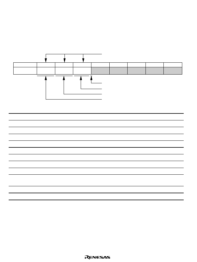
Rev. 1.0, 02/00, page 958 of 1141
A.5
Bus Status during Instruction Execution
Table A.13 indicates execution status of each instruction available in this LSI. For the number
of states required for each execution status, see table A.11, Number of States Required for Each
Execution Status (Cycle).
Interpreting the Table
Instruction
JMP@aa:24
R:W 2nd
Internal operation
1 state
R:W EA
1
2
3
4
5
6
7
8
End of instruction
Order of execution
Effective address is read by word.
Read/write not executed
The 2nd word of the instruction currently being
executed is read by word.
R : B
Read by byte
R : W
Read by word
W : B
Write by byte
W : W
Write by word
: M
Bus not transferred immediately after this cycle
2nd
Address of the 2nd word (3rd and 4th bytes)
3rd
Address of the 3rd word (5th and 6th bytes)
4th
Address of the 4th word (7th and 8th bytes)
5th
Address of the 5th word (9th and 10th bytes)
NEXT
The head address of the instruction immediately after the instruction
currently being executed
EA
Execution address
VEC
Vector address
Rev. 1.0, 02/00, page 959 of 1141
Table A.13 Instruction Execution Status
Instruction
1
2
3
4
5
6
7
8
9
ADD.B #xx:8,Rd
R:W NEXT
ADD.B Rs,Rd
R:W NEXT
ADD.W #xx:16,Rd
R:W 2nd
R:W NEXT
ADD.W Rs,Rd
R:W NEXT
ADD.L #xx:32,ERd
R:W 2nd
R:W 3rd
R:W NEXT
ADD.L ERs,ERd
R:W NEXT
ADDS #1/2/4,ERd
R:W NEXT
ADDX #xx:8,Rd
R:W NEXT
ADDX Rs,Rd
R:W NEXT
AND.B #xx:8,Rd
R:W NEXT
AND.B Rs,Rd
R:W NEXT
AND.W #xx:16,Rd
R:W 2nd
R:W NEXT
AND.W Rs,Rd
R:W NEXT
AND.L #xx:32,ERd
R:W 2nd
R:W 3rd
R:W NEXT
AND.L ERs,ERd
R:W 2nd
R:W NEXT
ANDC #xx:8,CCR
R:W NEXT
ANDC #xx:8,EXR
R:W 2nd
R:W NEXT
BAND #xx:3,Rd
R:W NEXT
BAND #xx:3,@ERd R:W 2nd
R:B EA
R:W:M
NEXT
BAND #xx:3,@aa:8 R:W 2nd
R:B EA
R:W:M
NEXT
BAND
#xx:3,@aa:16
R:W 2nd
R:W 3rd
R:B EA
R:W:M
NEXT
BAND
#xx:3,@aa:32
R:W 2nd
R:W 3rd
R:W 4th
R:B EA
R:W:M
NEXT
BRA d:8 (BT d:8)
R:W NEXT R:W EA
BRN d:8 (BF d:8)
R:W NEXT R:W EA
BHI d:8
R:W NEXT R:W EA
BLS d:8
R:W NEXT R:W EA
BCC d:8 (BHS d:8) R:W NEXT R:W EA
BCS d:8 (BLO d:8) R:W NEXT R:W EA
BNE d:8
R:W NEXT R:W EA
BEQ d:8
R:W NEXT R:W EA
BVC d:8
R:W NEXT R:W EA
BVS d:8
R:W NEXT R:W EA
BPL d:8
R:W NEXT R:W EA
BMI d:8
R:W NEXT R:W EA
BGE d:8
R:W NEXT R:W EA

Rev. 1.0, 02/00, page 960 of 1141
Instruction
1
2
3
4
5
6
7
8
9
BLT d:8
R:W NEXT R:W EA
BGT d:8
R:W NEXT R:W EA
BLE d:8
R:W NEXT R:W EA
BRA d:16 (BT d:16) R:W 2nd
Internal
operation
1 state
R:W EA
BRN d:16 (BF d:16) R:W 2nd
Internal
operation
1 state
R:W EA
BHI d:16
R:W 2nd
Internal
operation
1 state
R:W EA
BLS d:16
R:W 2nd
Internal
operation
1 state
R:W EA
BCC d:16
(BHS d:16)
R:W 2nd
Internal
operation
1 state
R:W EA
BCS d:16
(BLO d:16)
R:W 2nd
Internal
operation
1 state
R:W EA
BNE d:16
R:W 2nd
Internal
operation
1 state
R:W EA
BEQ d:16
R:W 2nd
Internal
operation
1 state
R:W EA
BVC d:16
R:W 2nd
Internal
operation
1 state
R:W EA
BVS d:16
R:W 2nd
Internal
operation
1 state
R:W EA
BPL d:16
R:W 2nd
Internal
operation
1 state
R:W EA
BMI d:16
R:W 2nd
Internal
operation
1 state
R:W EA
BGE d:16
R:W 2nd
Internal
operation
1 state
R:W EA
BLT d:16
R:W 2nd
Internal
operation
1 state
R:W EA
BGT d:16
R:W 2nd
Internal
operation
1 state
R:W EA
Rev. 1.0, 02/00, page 961 of 1141
Instruction
1
2
3
4
5
6
7
8
9
BLE d:16
R:W 2nd
Internal
operation
1 state
R:W EA
BCLR #xx:3,Rd
R:W NEXT
BCLR #xx:3,@ERd R:W 2nd
R:B:M EA
R:W:M
NEXT
W:B EA
BCLR #xx:3,@aa:8 R:W 2nd
R:B:M EA
R:W:M
NEXT
W:B EA
BCLR
#xx:3,@aa:16
R:W 2nd
R:W 3rd
R:B:M EA
R:W:M
NEXT
W:B EA
BCLR
#xx:3,@aa:32
R:W 2nd
R:W 3rd
R:W 4th
R:B:M EA
R:W:M
NEXT
W:B EA
BCLR Rn,Rd
R:W NEXT
BCLR Rn,@ERd
R:W 2nd
R:B:M EA
R:W:M
NEXT
W:B EA
BCLR Rn,@aa:8
R:W 2nd
R:B:M EA
R:W:M
NEXT
W:B EA
BCLR Rn,@aa:16
R:W 2nd
R:W 3rd
R:B:M EA
R:W:M
NEXT
W:B EA
BCLR Rn,@aa:32
R:W 2nd
R:W 3rd
R:W 4th
R:B:M EA
R:W:M
NEXT
W:B EA
BIAND #xx:3,Rd
R:W NEXT
BIAND #xx:3,ERd
R:W 2nd
R:B EA
R:W:M
NEXT
BIAND #xx:3,@aa:8 R:W 2nd
R:B EA
R:W:M
NEXT
BIAND
#xx:3,@aa:16
R:W 2nd
R:W 3rd
R:B EA
R:W:M
NEXT
BIAND
#xx:3,@aa:32
R:W 2nd
R:W 3rd
R:W 4th
R:B EA
R:W:M
NEXT
BILD #xx:3,Rd
R:W NEXT
BILD #xx:3,@ERd
R:W 2nd
R:B EA
R:W:M
NEXT
BILD #xx:3,@aa:8
R:W 2nd
R:B EA
R:W:M
NEXT
BILD #xx:3,@aa:16 R:W 2nd
R:W 3rd
R:B EA
R:W:M
NEXT
BILD #xx:3,@aa:32 R:W 2nd
R:W 3rd
R:W 4th
R:B EA
R:W:M
NEXT
BIOR #xx:3,Rd
R:W NEXT
BIOR #xx:3,@ERd
R:W 2nd
R:B EA
R:W:M
NEXT
BOIR #xx:3,@aa:8
R:W 2nd
R:B EA
R:W:M
NEXT
Rev. 1.0, 02/00, page 962 of 1141
Instruction
1
2
3
4
5
6
7
8
9
BOIR #xx:3,@aa:16 R:W 2nd
R:W 3rd
R:B EA
R:W:M
NEXT
BOIR #xx:3,@aa:32 R:W 2nd
R:W 3rd
R:W 4th
R:B EA
R:W:M
NEXT
BIST #xx:3,Rd
R:W NEXT
BIST #xx:3,@ERd
R:W 2nd
R:B:M EA
R:W:M
NEXT
W:B EA
BIST #xx:3,@aa:8
R:W 2nd
R:B:M EA
R:W:M
NEXT
W:B EA
BIST #xx:3,@aa:16 R:W 2nd
R:W 3rd
R:B:M EA
R:W:M
NEXT
W:B EA
BIST #xx:3,@aa:32 R:W 2nd
R:W 3rd
R:W 4th
R:B:M EA
R:W:M
NEXT
W:B EA
BIXOR #xx:3,Rd
R:W NEXT
BIXOR #xx:3,@ERd R:W 2nd
R:B EA
R:W:M
NEXT
BIXOR #xx:3,@aa:8 R:W 2nd
R:B EA
R:W:M
NEXT
BIXOR
#xx:3,@aa:16
R:W 2nd
R:W 3rd
R:B EA
R:W:M
NEXT
BIXOR
#xx:3,@aa:32
R:W 2nd
R:W 3rd
R:W 4th
R:B EA
R:W:M
NEXT
BLD #xx:3,Rd
R:W NEXT
BLD #xx:3,@ERd
R:W 2nd
R:B EA
R:W:M
NEXT
BLD #xx:3,@aa:8
R:W 2nd
R:B EA
R:W:M
NEXT
BLD #xx:3,@aa:16
R:W 2nd
R:W 3rd
R:B EA
R:W:M
NEXT
BLD #xx:3,@aa:32
R:W 2nd
R:W 3rd
R:W 4th
R:B EA
R:W:M
NEXT
BNOT #xx:3,Rd
R:W NEXT
BNOT #xx:3,ERd
R:W 2nd
R:B:M EA
R:W:M
NEXT
W:B EA
BNOT #xx:3,@aa:8 R:W 2nd
R:B:M EA
R:W:M
NEXT
W:B EA
BNOT
#xx:3,@aa:16
R:W 2nd
R:W 3rd
R:B:M EA
R:W:M
NEXT
W:B EA
BNOT
#xx:3,@aa:32
R:W 2nd
R:W 3rd
R:W 4th
R:B:M EA
R:W:M
NEXT
W:B EA
BNOT Rn,Rd
R:W NEXT
BNOT Rn,@ERd
R:W 2nd
R:B:M EA
R:W:M
NEXT
W:B EA
BNOT Rn @aa:8
R:W 2nd
R:B:M EA
R:W:M
NEXT
W:B EA
Rev. 1.0, 02/00, page 963 of 1141
Instruction
1
2
3
4
5
6
7
8
9
BNOT Rn @aa:16
R:W 2nd
R:W 3rd
R:B:W EA R:W:M
NEXT
W:B EA
BNOT Rn @aa:32
R:W 2nd
R:W 3rd
R:W 4th
R:B:M EA
R:W:M
NEXT
W:B EA
BOR #xx:3,Rd
R:W NEXT
BOR #xx:3,ERd
R:W 2nd
R:B EA
R:W:M
NEXT
BOR #xx:3,@aa:8
R:W 2nd
R:B EA
R:W:M
NEXT
BOR #xx:3,@aa:16 R:W 2nd
R:W 3rd
R:B EA
R:W:M
NEXT
BOR #xx:3,@aa:32 R:W 2nd
R:W 3rd
R:W 4th
R:B EA
R:W NEXT
BSET #xx:3,Rd
R:W NEXT
BSET #xx:3,@ERd R:W 2nd
R:B:M EA
R:W:M
NEXT
W:B EA
BSET #xx:3,@aa:8 R:W 2nd
R:B:M EA
R:W:M
NEXT
W:B EA
BSET #xx:3,@aa:16 R:W 2nd
R:W 3rd
R:B:M EA
R:W:M
NEXT
W:B EA
BSET #xx:3,@aa:32 R:W 2nd
R:W 3rd
R:W 4th
R:B:M EA
R:W:M
NEXT
W:B EA
BSET Rn,Rd
R:W NEXT
BSET Rn,@ERd
R:W 2nd
R:B:M EA
R:W:M
NEXT
W:B EA
BSET Rn,@aa:8
R:W 2nd
R:B:M EA
R:W:M
NEXT
W:B EA
BSET Rn,@aa:16
R:W 2nd
R:W 3rd
R:B:M EA
R:W:M
NEXT
W:B EA
BSET Rn,@aa:32
R:W 2nd
R:W 3rd
R:W 4th
R:B:M EA
R:W:M
NEXT
W:B EA
BSR d:8
R:W NEXT R:W EA
W:W:M
stack(H)
W:W
stack(L)
BSR d:16
R:W 2nd
Internal
operation
1 state
R:W EA
W:W:M
stack(H)
W:W
stack(L)
BST #xx:3,Rd
R:W NEXT
BST #xx:3,@ERd
R:W 2nd
R:B:M EA
R:W:M
NEXT
W:B EA
BST #xx:3,@aa:8
R:W 2nd
R:B:M EA
R:W:M
NEXT
W:B EA
BST #xx:3,@aa:16
R:W 2nd
R:W 3rd
R:B:M EA
R:W:M
NEXT
W:B EA
BST #xx:3,@aa:32
R:W 2nd
R:W 3rd
R:W 4th
R:B:M EA
R:W:M
NEXT
W:B EA
BTST #xx:3,Rd
R:W NEXT
Rev. 1.0, 02/00, page 964 of 1141
Instruction
1
2
3
4
5
6
7
8
9
BTST #xx:3,@ERd R:W 2nd
R:B EA
R:W:M
NEXT
BTST #xx:3,@aa:8 R:W 2nd
R:B EA
R:W:M
NEXT
BTST #xx:3,@aa:16 R:W 2nd
R:W 3rd
R:B EA
R:W:M
NEXT
BTST #xx:3,@aa:32 R:W 2nd
R:W 3rd
R:W 4th
R:B EA
R:W:M
NEXT
BTST Rn,Rd
R:W NEXT
BTST Rn,@ERd
R:W 2nd
R:B EA
R:W:M
NEXT
BTST Rn,@aa:8
R:W 2nd
R:B EA
R:W:M
NEXT
BTST Rn,@aa:16
R:W 2nd
R:W 3rd
R:B EA
R:W:M
NEXT
BTST Rn,@aa:32
R:W 2nd
R:W 3rd
R:W 4th
R:B EA
R:W:M
NEXT
BOXR #xx:3,Rd
R:W NEXT
BOXR #xx:3,@ERd R:W 2nd
R:B EA
R:W:M
NEXT
BOXR #xx:3,@aa:8 R:W 2nd
R:B EA
R:W:M
NEXT
BOXR
#xx:3,@aa:16
R:W 2nd
R:W 3rd
R:B EA
R:W:M
NEXT
BOXR
#xx:3,@aa:32
R:W 2nd
R:W 3rd
R:W 4th
R:B EA
R:W:M
NEXT
CLRMAC
Cannot be used in this LSI.
CMP.B #xx:8,Rd
R:W NEXT
CMP.B Rs,Rd
R:W NEXT
CMP.W #xx:16,Rd
R:W 2nd
R:W NEXT
CMP.W Rs,Rd
R:W NEXT
CMP.L #xx:32,ERd R:W 2nd
R:W 3rd
R:W NEXT
CMP.L ERs,ERd
R:W NEXT
DAA Rd
R:W NEXT
DAS Rd
R:W NEXT
DEC.B Rd
R:W NEXT
DEC.W #1/2,Rd
R:W NEXT
DEC.W #1/2,ERd
R:W NEXT
DIVXS.B Rs,Rd
R:W 2nd
R:W NEXT Internal operation 11 state
DIVXS.W Rs,ERd
R:W 2nd
R:W NEXT Internal operation 19 state
Rev. 1.0, 02/00, page 965 of 1141
Instruction
1
2
3
4
5
6
7
8
9
DIVXU.B Rs,Rd
R:W NEXT Internal operation 11 state
DIVXU.W Rs,ERd
R:W NEXT Internal operation 19 state
EEPMOV.B
R:W 2nd
R:B EAs
*1
R:B EAd
*1
R:B EAs
*2
W:B EAd
*2
R:W NEXT
EEPMOV.W
R:W 2nd
R:B EAs
*1
R:B EAd
*1
R:B EAs
*2
W:B EAd
*2
R:W NEXT
EXTS.W Rd
R:W NEXT
Repeat n times
*2
EXTS.L ERd
R:W NEXT
EXTU.W Rd
R:W NEXT
EXTU.L ERd
R:W NEXT
INC.B Rd
R:W NEXT
INC.W #1/2,Rd
R:W NEXT
INC.L #1/2,ERd
R:W NEXT
JMP @ERn
R:W NEXT R:W EA
JMP @aa:24
R:W 2nd
Internal
operation
1 state
R:W EA
JMP @@aa:8
R:W NEXT R:W:M
aa:8
R:W:M
aa:8
Internal
operation
1 state
R:W EA
JSR @ERn
R:W NEXT R:W EA
W:W:M
stack(H)
W:W
stack (L)
JSR @aa:24
R:W 2nd
Internal
operation
1 state
R:W EA
W:W:M
stack(H)
W:W
stack (L)
JSR @@aa:8
R:W NEXT R:W:M
aa:8
R:W aa:8 W:W:M
stack(H)
W:W
stack (L)
R:W EA
LDC #xx.8,CCR
R:W NEXT
LDC #xx.8,EXR
R:W 2nd
R:W NEXT
LDC Rs,CCR
R:W NEXT
LDC Rs,EXR
R:W NEXT
LDC @ERs,CCR
R:W 2nd
R:W NEXT R:W EA
LDC @ERs,EXR
R:W 2nd
R:W NEXT R:W EA
LDC
@(d:16,ERs),CCR
R:W 2nd
R:W 3rd
R:W NEXT R:W EA
LDC
@(d:16,ERs),EXR
R:W 2nd
R:W 3rd
R:W NEXT R:W EA
LDC
@(d:32,ERs),CCR
R:W 2nd
R:W 3rd
R:W 4th
R:W 5th
R:W NEXT R:W EA
LDC
@(d:32,ERs),EXR
R:W 2nd
R:W 3rd
R:W 4th
R:W 5th
R:W NEXT R:W EA
LDC @ERs+,CCR
R:W 2nd
R:W NEXT Internal
operation
1 state
R:W EA
Rev. 1.0, 02/00, page 966 of 1141
Instruction
1
2
3
4
5
6
7
8
9
LDC @ERs+,EXR
R:W 2nd
R:W NEXT Internal
operation
1 state
R:W EA
LDC @aa:16,CCR
R:W 2nd
R:W 3rd
R:W NEXT R:W EA
LDC @aa:16,EXR
R:W 2nd
R:W 3rd
R:W NEXT R:W EA
LDC @aa:32,CCR
R:W 2nd
R:W 3rd
R:W 4th
R:W NEXT R:W EA
LDC @aa:32,EXR
R:W 2nd
R:W 3rd
R:W 4th
R:W NEXT R:W EA
LDM.L @SP+,
(ERn-ERn+1)
R:W 2nd
R:W:M
NEXT
Internal
operation
1 state
R:W:M
stack(H)
*3
R:W
stack(L)
*3
LDM.L @SP+,
(ERn-ERn+2)
R:W 2nd
R:W:M
NEXT
Internal
operation
1 state
R:W:M
stack(H)
*3
R:W
stack(L)
*3
LDM.L @SP+,
(ERn-ERn+3)
R:W 2nd
R:W:M
NEXT
Internal
operation
1 state
R:W:M
stack(H)
*3
R:W
stack(L)
*3
LDMAC ERs,MACH Cannot be used in this LSI.
LDMAC ERs,MACL
MAC
@ERn+,@ERm+
MOV.B #xx:8,Rd
R:W NEXT
MOV.B Rs,Rd
R:W NEXT
MOV.B @ERs,Rd
R:W NEXT R:B EA
MOV.B
@(d:16,ERs),Rd
R:W 2nd
R:W NEXT R:B EA
MOV.B
@(d:32,ERs),Rd
R:W 2nd
R:W 3rd
R:W 4th
R:W NEXT R:B EA
MOV.B @ERs+,Rd R:W NEXT Internal
operation
1 state
R:B EA
MOV.B @aa:8,Rd
R:W NEXT R:B EA
MOV.B @aa:16,Rd R:W 2nd
R:W NEXT R:B EA
MOV.B @aa:32,Rd R:W 2nd
R:W 3rd
R:W NEXT R:B EA
MOV.B Rs,@ERd
R:W NEXT W:B EA
MOV.B
Rs,@(d:16,ERd)
R:W 2nd
R:W NEXT W:B EA
MOV.B
Rs,@(d:32,ERd)
R:W 2nd
R:W 3rd
R:W 4th
R:W NEXT W:B EA
MOV.B Rs,@-ERd
R:W NEXT Internal
operation
1 state
W:B EA
MOV.B Rs,@aa:8
R:W NEXT W:B EA
MOV.B Rs,@aa:16 R:W 2nd
R:W NEXT W:B EA
MOV.B Rs,@aa:32 R:W 2nd
R:W 3rd
R:W NEXT W:B EA
MOV.W #xx:16,Rd
R:W 2nd
R:W NEXT
Rev. 1.0, 02/00, page 967 of 1141
Instruction
1
2
3
4
5
6
7
8
9
MOV.W Rs,Rd
R:W NEXT
MOV.W @ERs,Rd
R:W NEXT R:W EA
MOV.W
@(d:16,ERs),Rd
R:W 2nd
R:W NEXT R:W EA
MOV.W
@(d:32,ERs),Rd
R:W 2nd
R:W 3rd
R:W 4th
R:W NEXT R:W EA
MOV.W @ERs+,Rd R:W NEXT Internal
operation
1 state
R:W EA
MOV.W @aa:16,Rd R:W 2nd
R:W NEXT R:W EA
MOV.W @aa:32,Rd R:W 2nd
R:W 3rd
R:W NEXT R:B EA
MOV.W Rs,@ERd
R:W NEXT W:W EA
MOV.W
Rs,@(d:16,ERd)
R:W 2nd
R:W NEXT W:W EA
MOV.W
Rs,@(d:32,ERd)
R:W 2nd
R:W 3rd
R:W 4th
R:W NEXT W:W EA
MOV.W Rs,@-ERd R:W NEXT Internal
operation
1 state
W:W EA
MOV.W Rs,@aa:16 R:W 2nd
R:W NEXT W:W EA
MOV.W Rs,@aa:32 R:W 2nd
R:W 3rd
R:W NEXT W:W EA
MOV.L #xx:32,ERd R:W 2nd
R:W 3rd
R:W NEXT
MOV.L ERs,ERd
R:W NEXT
MOV.L @ERs,ERd R:W 2nd
R:W:M
NEXT
R:W:M EA R:W EA+2
MOV.L
@(d:16,ERs),ERd
R:W 2nd
R:W:M 3rd R:W NEXT R:W:M EA R:W EA+2
MOV.L
@(d:32,ERs),ERd
R:W 2nd
R:W:M 3rd R:W:M 4th R:W 5th
R:W NEXT R:W:M EA R:W EA+2
MOV.L @ERs+,ERd R:W 2nd
R:W:M
NEXT
Internal
operation
1 state
R:W:M EA R:W EA+2
MOV.L @aa:16,ERd R:W 2nd
R:W:M 3rd R:W NEXT R:W:M EA R:W EA+2
MOV.L @aa:32,ERd R:W 2nd
R:W:M 3rd R:W 4th
R:W NEXT R:W:M EA R:W EA+2
MOV.L ERs,@ERd R:W 2nd
R:W:M
NEXT
W:W:M EA W:W EA+2
MOV.L
ERs,@(d:16,ERd)
R:W 2nd
R:W:M 3rd R:W NEXT W:W:M EA W:W EA+2
MOV.L
ERs,@(d:32,ERd)
R:W 2nd
R:W:W 3rd R:W:M 4th R:W 5th
R:W NEXT W:W:M EA W:W EA+2
MOV.L ERs,@-ERd R:W 2nd
R:W:M
NEXT
Internal
operation
1 state
W:W:M EA W:W EA+2
Rev. 1.0, 02/00, page 968 of 1141
Instruction
1
2
3
4
5
6
7
8
9
MOV.L ERs,@aa:16 R:W 2nd
R:W:M 3rd R:W NEXT W:W:M EA W:W EA+2
MOV.L ERs,@aa:32 R:W 2nd
R:W:M 3rd R:W 4th
R:W NEXT W:W:M EA W:W EA+2
MOVFPE
@aa:16,Rd
Cannot be used in this LSI.
MOVTPE
Rs,@aa:16
MULXS.B Rs,Rd
R:W 2nd
R:W NEXT Internal operation 11 state
MULXS.W Rs,Rd
R:W 2nd
R:W NEXT Internal operation 19 state
MULXU.B Rs,Rd
R:W NEXT Internal operation 11 state
MULXU.W Rs,Rd
R:W NEXT Internal operation 19 state
NEG.B Rd
R:W NEXT
NEG.W Rd
R:W NEXT
NEG.L ERd
R:W NEXT
NOP
R:W NEXT
NOT.B Rd
R:W NEXT
NOT.W Rd
R:W NEXT
NOT.L ERd
R:W NEXT
OR.B #xx:8,Rd
R:W NEXT
OR.B Rs,Rd
R:W NEXT
OR.W #xx:16,Rd
R:W 2nd
R:W NEXT
OR.W Rs,Rd
R:W NEXT
OR.L #xx:32,ERd
R:W 2nd
R:W 3rd
R:W NEXT
OR.L ERs,ERd
R:W 2nd
R:W NEXT
ORC #xx:8,CCR
R:W NEXT
ORC #xx:8,EXR
R:W 2nd
R:W NEXT
POP.W Rn
R:W NEXT Internal
operation
1 state
R:W EA
POP.L ERn
R:W 2nd
R:W:M
NEXT
Internal
operation
1 state
R:W:M EA R:W EA+2
PUSH.W Rn
R:W NEXT Internal
operation
1 state
W:W EA
PUSH.L ERn
R:W 2nd
R:W:M
NEXT
Internal
operation
1 state
W:W:M EA W:W EA+2
ROTL.B Rd
R:W NEXT
ROTL.B #2,Rd
R:W NEXT
ROTL.W Rd
R:W NEXT
ROTL.W #2,Rd
R:W NEXT
ROTL.L ERd
R:W NEXT
ROTL.L #2, ERd
R:W NEXT
Rev. 1.0, 02/00, page 969 of 1141
Instruction
1
2
3
4
5
6
7
8
9
ROTR.B Rd
R:W NEXT
ROTR.B #2,Rd
R:W NEXT
ROTR.W Rd
R:W NEXT
ROTR.W #2,Rd
R:W NEXT
ROTR.L ERd
R:W NEXT
ROTR.L #2,ERd
R:W NEXT
ROTXL.B Rd
R:W NEXT
ROTXL.B #2.Rd
R:W NEXT
ROTXL.W Rd
R:W NEXT
ROTXL.W #2,Rd
R:W NEXT
ROTXL.L ERd
R:W NEXT
ROTXL.L #2,ERd
R:W NEXT
ROTXR.B Rd
R:W NEXT
ROTXR.B #2,Rd
R:W NEXT
ROTXR.W Rd
R:W NEXT
ROTXR.W #2,Rd
R:W NEXT
ROTXR.L ERd
R:W NEXT
ROTXR.L #2.ERd
R:W NEXT
RTE
R:W NEXT R:W stack
(EXR)
R:W
stack(H)
R:W
stack(L)
Internal
operation
1 state
R:W
*4
RTS
R:W NEXT R:W:M
stack(H)
R:W
stack(L)
Internal
operation
1 state
R:W
*4
SHAL.B Rd
R:W NEXT
SHAL B #2,Rd
R:W NEXT
SHAL.W Rd
R:W NEXT
SHAL.W #2,Rd
R:W NEXT
SHAL.L ERd
R:W NEXT
SHAL.L #2,ERd
R:W NEXT
SHAR.B Rd
R:W NEXT
SHAR.B #2,Rd
R:W NEXT
SHAR.W Rd
R:W NEXT
SHAR.W #2,Rd
R:W NEXT
SHAR.L ERd
R:W NEXT
SHAR.L #2,ERd
R:W NEXT
SHLL.B Rd
R:W NEXT
SHLL.B #2,Rd
R:W NEXT
SHLL.W Rd
R:W NEXT
SHLL.W #2,Rd
R:W NEXT
SHLL.L ERd
R:W NEXT
Rev. 1.0, 02/00, page 970 of 1141
Instruction
1
2
3
4
5
6
7
8
9
SHLL.L #2,ERd
R:W NEXT
SHLR.B Rd
R:W NEXT
SHLR.B #2,Rd
R:W NEXT
SHLR.W Rd
R:W NEXT
SHLR.W #2,Rd
R:W NEXT
SHLR.L ERd
R:W NEXT
SHLR.L #2,ERd
R:W NEXT
SLEEP
R:W NEXT Internal
operation:
M
STC.B CCR,Rd
R:W NEXT
STC.B EXR,Rd
R:W NEXT
STC.W CCR,@ERd R:W 2nd
R:W NEXT W:W EA
STC.W EXR,@ERd R:W 2nd
R:W NEXT W:W EA
STC.W
CCR,@(d:16,ERd)
R:W 2nd
R:W 3rd
R:W NEXT W:W EA
STC.W
EXR,@(d:16,ERd)
R:W 2nd
R:W 3rd
R:W NEXT W:W EA
STC.W
CCR,@(d:32,ERd)
R:W 2nd
R:W 3rd
R:W 4th
R:W 5th
R:W NEXT W:W EA
STC.W
EXR,@(d:32,ERd)
R:W 2nd
R:W 3rd
R:W 4th
R:W 5th
R:W NEXT W:W EA
STC.W CCR,@-
ERd
R:W 2nd
R:W NEXT Internal
operation
1 state
W:W EA
STC.W EXR,@-ERd R:W 2nd
R:W NEXT Internal
operation
1 state
W:W EA
STC.W
CCR,@aa:16
R:W 2nd
R:W 3rd
R:W NEXT W:W EA
STC.W
EXR,@aa:16
R:W 2nd
R:W 3rd
R:W NEXT W:W EA
STC.W
CCR,@aa:32
R:W 2nd
R:W 3rd
R:W 4th
R:W NEXT W:W EA
STC.W
EXR,@aa:32
R:W 2nd
R:W 3rd
R:W 4th
R:W NEXT W:W EA
STM.L (ERn-
ERn+1),@-SP
R:W 2nd
R:W:M
NEXT
Internal
operation
1 state
W:W:M
stack (H)
*3
W:W
stack (L)
*3
STM.L (ERn-
ERn+2),@-SP
R:W 2nd
R:W:M
NEXT
Internal
operation
1 state
W:W:M
stack (H)
*3
W:W
stack (L)
*3
STM.L (ERn-
ERn+3),@-SP
R:W 2nd
R:W:M
NEXT
Internal
operation
1 state
W:W:M
stack (H)
*3
W:W
stack (L)
*3
Rev. 1.0, 02/00, page 971 of 1141
Instruction
1
2
3
4
5
6
7
8
9
STMAC MACH,ERd Cannot be used in this LSI.
STMAC MACL,ERd
SUB.B Rs,Rd
R:W NEXT
SUB.W #xx:16,Rd
R:W 2nd
R:W NEXT
SUB.W Rs,Rd
R:W NEXT
SUB.L #xx:32,ERd
R:W 2nd
R:W 3nd
R:W NEXT
SUB.L ERs,ERd
R:W NEXT
SUB #1/2/4,ERd
R:W NEXT
SUBX #xx:8,Rd
R:W NEXT
SUBX Rs,Rd
R:W NEXT
TAS @ERd
R:W 2nd
R:W NEXT R:B:M EA
W:B EA
TRAPA #x:2
R:W NEXT Internal
operation
1 state
W:W
stack(L)
W:W
stack(H)
W:W
stack(EXR)
R:W:M
VEC
R:W
VEC+2
Internal
operation
1 state
R:W
*7
XOR.B #xx:8,Rd
R:W NEXT
XOR.B Rs,Rd
R:W NEXT
XOR.W #xx:16,Rd
R:W 2nd
R:W NEXT
XOR.W Rs,Rd
R:W NEXT
XOR.L #xx:32,ERd R:W 2nd
R:W 3rd
R:W NEXT
XOR.L ERs,ERd
R:W 2nd
R:W NEXT
XORC #xx:8,CCR
R:W NEXT
XORC #xx:8,EXR
R:W 2nd
R:W NEXT
Reset exception
handling
R:W:M
VEC
R:W
VEC+2
Internal
operation
1 state
R:W
*5
Interrupt exception
handling
R:W
*6
Internal
operation
1 state
W:W
stack(L)
W:W
stack(H)
W:W
stack(EXR)
R:W:M
VEC
R:W
VEC+2
Internal
operation
1 state
R:W
*7
Notes: 1. EAs is the contents of ER5, and EAd is the contents of ER6.
2. 1 is added to EAs and EAd after execution. n is the initial value of R4L or R4. When
0 is set to n, R4L or R4 is not executed.
3. Repeated twice for 2-unit retract/return, three times for 3-unit retract/return, and four
times for 4-retract/return.
4. Head address after return.
5. Start address of the program.
6. Pre-fetch address obtained by adding 2 to the PC to be retracted.
When returning from sleep mode, standby mode or watch mode, internal operation is
executed instead of read operation.
7. Head address of the interrupt process routine.

Rev. 1.0, 02/00, page 972 of 1141
A.6
Change of Condition Codes
This section explains change of condition codes after instruction execution of the CPU. Legend
of the following tables is as follows.
m = 31: Longword size
m = 15: Word size
m = 7:
Byte size
Si:
Bit i of source operand
Di:
Bit i of destination operand
Ri:
Bit i of result
Dn:
Specified bit of destination operand
-
:
No affection
:
Changes depending on execution result
0:
Always cleared to 0
1:
Always set to 1
*:
Value undetermined
Z':
Z flag before execution
C':
C flag before execution
Rev. 1.0, 02/00, page 973 of 1141
Table A.14 Change of Condition Code
Instruc-
tion
H
N
Z
V
C
Definition
ADD
H=Sm-4
Dm-4+Dm-4
5P
+Sm-4
5P
N=Rm
Z=
5P
5P
RRRRRR
5
V=Sm
Dm
5P
+
6P
'P
Rm
C=Sm
Dm+Dm
5P
+Sm
5P
ADDS
-
-
-
-
-
ADDX
H=Sm-4
Dm-4+Dm-4
5P
+Sm-4
5P
N=Rm
Z=Z'
5P
RRRRRR
5
V=Sm
Dm
5P
+
6P
'P
Rm
C=Sm
Dm+Dm
5P
+Sm
5P
AND
-
0
-
N=Rm
Z=
5P
5P
RRRRRR
5
ANDC
Value in the bit corresponding to execution
result is stored.
No flag change when EXR.
BAND
-
-
-
-
C=C'
Dn
Bcc
-
-
-
-
-
BCLR
-
-
-
-
-
BIAND
-
-
-
-
C=C'
'Q
BILD
-
-
-
-
C=
'Q
BIOR
-
-
-
-
C=C'+
'Q
BIST
-
-
-
-
-
BIXOR
-
-
-
-
C=C'
Dn+
&
'Q
BLD
-
-
-
-
C=Dn
BNOT
-
-
-
-
-
BOR
-
-
-
-
C=C'+Dn
BSET
-
-
-
-
-
BSR
-
-
-
-
-
BST
-
-
-
-
-
BTST
-
-
-
-
Z=
'Q
BXOR
-
-
-
-
C=C'
'Q
+
&
Dn
CLRMAC
Cannot be used in this LSI.
Rev. 1.0, 02/00, page 974 of 1141
Instruc-
tion
H
N
Z
V
C
Definition
CMP
H=Sm-4
'P
+
'P
Rm-4+Sm-4
Rm-4
N=Rm
Z=
5P
5P
RRRRRR
5
V=
6P
Dm
5P
+Sm
'P
Rm
C=Sm
'P
+
'P
Rm+Sm
Rm
DAA
*
*
N=Rm
Z=
5P
5P
RRRRRR
5
C: Decimal addition carry
DAS
*
*
N=Rm
Z=
5P
5P
RRRRRR
5
C: Decimal subtraction borrow
DEC
-
-
N=Rm
Z=
5P
5P
RRRRRR
5
V=Dm
5P
DIVXS
-
-
-
N=Sm
'P
+
6P
Dm
Z=
6P
6P
RRRRRR
6
DIVXU
-
-
-
N=Sm
Z=
6P
6P
RRRRRR
6
EEPMOV
-
-
-
-
-
EXTS
-
0
-
N=Rm
Z=
5P
5P
RRRRRR
5
EXTU
-
0
0
-
Z=
5P
5P
RRRRRR
5
INC
-
-
N=Rm
Z=
5P
5P
RRRRRR
5
V=
'P
5P
JMP
-
-
-
-
-
JSR
-
-
-
-
-
LDC
Value in the bit corresponding to execution
result is stored.
No flag change when EXR.
LDM
-
-
-
-
-
LDMAC
MAC
Cannot be used in this LSI.
MOV
-
0
-
N=Rm
Z=
5P
5P
RRRRRR
5
Rev. 1.0, 02/00, page 975 of 1141
Instruc-
tion
H
N
Z
V
C
Definition
MOVFPE
MOVTPE
Cannot be used in this LSI.
MULXS
-
-
-
N=R2m
Z=
5P
5P
RRRRRR
5
MULXU
-
-
-
-
-
NEG
H=Dm-4+Rm-4
N=Rm
Z=
5P
5P
RRRRRR
5
V=Dm
Rm
C=Dm+Rm
NOP
-
-
-
-
-
NOT
-
0
-
N=Rm
Z=
5P
5P
RRRRRR
5
OR
-
0
-
N=Rm
Z=
5P
5P
RRRRRR
5
ORC
Value in the bit corresponding to execution
result is stored. No flag change when EXR.
POP
-
0
-
N=Rm
Z=
5P
5P
RRRRRR
5
PUSH
-
0
-
N=Rm
Z=
5P
5P
RRRRRR
5
ROTL
-
0
N=Rm
Z=
5P
5P
RRRRRR
5
C=Dm(In case of 1 bit), C=Dm-1(In case of 2
bits)
ROTR
-
0
N=Rm
Z=
5P
5P
RRRRRR
5
C=D0
(In case of 1 bit)
, C=D-1
(In case of 2 bits)
ROTXL
-
0
N=Rm
Z=
5P
5P
RRRRRR
5
C=Dm
(In case of 1 bit)
, C=Dm-1
(In case of 2 bits)
ROTXR
-
0
N=Rm
Z=
5P
5P
RRRRRR
5
C=D0
(In case of 1 bit)
, C=D1
(In case of 2 bits)
RTE
Value in the bit corresponding to execution
result is stored.
RTS
-
-
-
-
-
Rev. 1.0, 02/00, page 976 of 1141
Instruc-
tion
H
N
Z
V
C
Definition
SHAL
-
N=Rm
Z=
5P
5P
RRRRRR
5
V=Dm
Dm-1+
'P
'P
(In case of 1 bit)
V=Dm
Dm-1
Dm-2
'P
'P
'P
(In case of 2bits)
C=Dm
(In case of 1 bit)
, C=Dm-1
(In case of 2 bits)
SHAR
-
0
N=Rm
Z=
5P
5P
RRRRRR
5
C=D0
(In case of 1 bit)
, C=D1
(In case of 2 bits)
SHLL
-
0
N=Rm
Z=
5P
5P
RRRRRR
5
C=Dm
(In case of 1 bit)
, C=Dm-1
(In case of 2 bits)
SHLR
-
0
0
N=Rm
Z=
5P
5P
RRRRRR
5
C=D0
(In case of 1 bit)
, C=D1
(In case of 2 bits)
SLEEP
-
-
-
-
-
STC
-
-
-
-
-
STM
-
-
-
-
-
STMAC
Cannot be used in this LSI.
SUB
H=Sm-4
'P
+
'P
Rm-4+Sm-4
Rm-4
N=Rm
Z=
5P
5P
RRRRRR
5
V=
6P
Dm
5P
+Sm
'P
Rm
C=Sm
'P
+
'P
Rm+Sm
Rm
SUBS
-
-
-
-
-
SUBX
H=Sm-4
'P
+
'P
Rm-4+Sm-4
Rm-4
N=Rm
Z=Z'
5P
RRRRRR
5
V=
6P
Dm
5P
+Sm
'P
Rm
C=Sm
'P
+
'P
Rm+Sm
Rm
TAS
-
0
-
N=Dm
Z=
'P
'P
RRRRRR
'
TRAPA
-
-
-
-
-
XOR
-
0
-
N=Rm
Z=
5P
5P
RRRRRR
5
XORC
Value in the bit corresponding to execution
result is stored. No flag change when EXR.

Rev. 1.0, 02/00, page 977 of 1141
Appendix B Internal I/O Registers
B.1
Addresses
Table B.1
Addresses
Address*
1
Register
Name
R/W
Access
Bus
Width
7
6
5
4
3
2
1
0
Module
Name
H'0000
to
H'CFFF
H'D000
DGKp
W
16
16
DGKp15
DGKp14
DGKp13
DGKp12
DGKp11
DGKp10
DGKp9
DGKp8
H'D001
DGKp7
DGKp6
DGKp5
DGKp4
DGKp3
DGKp2
DGKp1
DGKp0
H'D002
DGKs
W
16
16
DGKs15
DGKs14
DGKs13
DGKs12
DGKs11
DGKs10
DGKs9
DGKs8
H'D003
DGKs7
DGKs6
DGKs5
DGKs4
DGKs3
DGKs2
DGKs1
DGKs0
H'D004
DAp
W
16
16
DAp15
DAp14
DAp13
DAp12
DAp11
DAp10
DAp9
DAp8
H'D005
DAp7
DAp6
DAp5
DAp4
DAp3
DAp2
DAp1
DAp0
H'D006
DBp
W
16
16
DBp15
DBp14
DBp13
DBp12
DBp11
DBp10
DBp9
DBp8
H'D007
DBp7
DBp6
DBp5
DBp4
DBp3
DBp2
DBp1
DBp0
H'D008
DAs
W
16
16
DAs15
DAs14
DAs13
DAs12
DAs11
DAs10
DAs9
DAs8
H'D009
DAs7
DAs6
DAs5
DAs4
DAs3
DAs2
DAs1
DAs0
H'D00A
DBs
W
16
16
DBs15
DBs14
DBs13
DBs12
DBs11
DBs10
DBs9
DBs8
H'D00B
DBs7
DBs6
DBs5
DBs4
DBs3
DBs2
DBs1
DBs0
H'D00C
DOfp
W
16
16
DOfp15
DOfp14
DOfp13
DOfp12
DOfp11
DOfp10
DOfp9
DOfp8
H'D00D
DOfp7
DOfp6
DOfp5
DOfp4
DOfp3
DOfp2
DOfp1
DOfp0
H'D00E
DOfs
W
16
16
DOfs15
DOfs14
DOfs13
DOfs12
DOfs11
DOfs10
DOfs9
DOfs8
H'D00F
DOfs7
DOfs6
DOfs5
DOfs4
DOfs3
DOfs2
DOfs1
DOfs0
Drum digital
filter
H'D010
CGKp
W
16
16
CGKp15
CGKp14
CGKp13
CGKp12
CGKp11
CGKp10
CGKp9
CGKp8
H'D011
CGKp7
CGKp6
CGKp5
CGKp4
CGKp3
CGKp2
CGKp1
CGKp0
H'D012
CGKs
W
16
16
CGKs15
CGKs14
CGKs13
CGKs12
CGKs11
CGKs10
CGKs9
CGKs8
H'D013
CGKs7
CGKs6
CGKs5
CGKs4
CGKs3
CGKs2
CGKs1
CGKs0
H'D014
CAp
W
16
16
CAp15
CAp14
CAp13
CAp12
CAp11
CAp10
CAp9
CAp8
H'D015
CAp7
CAp6
CAp5
CAp4
CAp3
CAp2
CAp1
CAp0
H'D016
CBp
W
16
16
CBp15
CBp14
CBp13
CBp12
CBp11
CBp10
CBp9
CBp8
H'D017
CBp7
CBp6
CBp5
CBp4
CBp3
CBp2
CBp1
CBp0
H'D018
CAs
W
16
16
CAs15
CAs14
CAs13
CAs12
CAs11
CAs10
CAs9
CAs8
H'D019
CAs7
CAs6
CAs5
CAs4
CAs3
CAs2
CAs1
CAs0
H'D01A
CBs
W
16
16
CBs15
CBs14
CBs13
CBs12
CBs11
CBs10
CBs9
CBs8
H'D01B
CBs7
CBs6
CBs5
CBs4
CBs3
CBs2
CBs1
CBs0
H'D01C
COfp
W
16
16
COfp15
COfp14
COfp13
COfp12
COfp11
COfp10
COfp9
COfp8
H'D01D
COfp7
COfp6
COfp5
COfp4
COfp3
COfp2
COfp1
COfp0
H'D01E
COfs
W
16
16
COfs15
COfs14
COfs13
COfs12
COfs11
COfs10
COfs9
COfs8
H'D01F
COfs7
COfs6
COfs5
COfs4
COfs3
COfs2
COfs1
COfs0
Capstan
digital filter
H'D020
DZs
W
16
16
DZs11
DZs10
DZs9
DZs8
H'D021
DZs7
DZs6
DZs5
DZs4
DZs3
DZs2
DZs1
DZs0
H'D022
DZp
W
16
16
DZp11
DZp10
DZp9
DZp8
H'D023
DZp7
DZp6
DZp5
DZp4
DZp3
DZp2
DZp1
DZp0
H'D024
CZs
W
16
16
CZs11
CZs10
CZs9
CZs8
H'D025
CZs7
CZs6
CZs5
CZs4
CZs3
CZs2
CZs1
CZs0
H'D026
CZp
W
16
16
CZp11
CZp10
CZp9
CZp8
H'D027
CZp7
CZp6
CZp5
CZp4
CZp3
CZp2
CZp1
CZp0
Digital filter

Rev. 1.0, 02/00, page 978 of 1141
Address*
1
Register
Name
R/W
Access
Bus
Width
7
6
5
4
3
2
1
0
Module
Name
H'D028
DFIC
R/W
8
16
DROV
DPHA
DZPON
DZSON
DSG2
DSG1
DSG0
H'D029
CFIC
R/W
8
CROV
CPHA
CZPON
CZSON
CSG2
CSG1
CSG0
H'D02A
DFUCR
R/W
8
16
PTON
CP/
'3
CFEPS
DFEPS
CFESS
DFESS
Digital filter
H'D030
DFPR
W
16
16
DFPR15
DFPR14
DFPR13
DFPR12
DFPR11
DFPR10
DFPR9
DFPR8
H'D031
DFPR7
DFPR6
DFPR5
DFPR4
DFPR3
DFPR2
DFPR1
DFPR0
H'D032
DFER
R/W
16
16
DFER15
DFER14
DFER13
DFER12
DFER11
DFER10
DFER9
DFER8
H'D033
DFER7
DFER6
DFER5
DFER4
DFER3
DFER2
DFER1
DFER0
H'D034
DFRUDR
W
16
16
DFRUDR15 DFRUDR14 DFRUDR13 DFRUDR12 DFRUDR11 DFRUDR10 DFRUDR9
DFRUDR8
H'D035
DFRUDR7
DFRUDR6
DFRUDR5
DFRUDR4
DFRUDR3
DFRUDR2
DFRUDR1
DFRUDR0
H'D036
DFRLDR
W
16
16
DFRLDR15 DFRLDR14 DFRLDR13 DFRLDR12 DFRLDR11 DFRLDR10 DFRLDR9
DFRLDR8
H'D037
DFRLDR7
DFRLDR6
DFRLDR5
DFRLDR4
DFRLDR3
DFRLDR2
DFRLDR1
DFRLDR0
H'D038
DFVCR
R/W
8
16
DFCS1
DFCS0
DFOVF
DFRFON
DF-R/UNR
DPCNT
DFRCS1
DFRCS0
H'D039
DPGCR
R/W
8
16
DPCS1
DPCS0
DPOVF
N/V
HSWES
H'D03A
DPPR2
W
16
16
DPPR15
DPPR14
DPPR13
DPPR12
DPPR11
DPPR10
DPPR9
DPPR8
H'D03B
DPPR7
DPPR6
DPPR5
DPPR4
DPPR3
DPPR2
DPPR1
DPPR0
H'D03C
DPPR1
W
8
16
DPPR19
DPPR18
DPPR17
DPPR16
H'D03D
DPER1
W
8
16
DPER19
DPER18
DPER17
DPER16
H'D03E
DPER15
DPER14
DPER13
DPER12
DPER11
DPER10
DPER9
DPER8
H'D03F
DPER2
W
16
16
DPER7
DPER6
DPER5
DPER4
DPER3
DPER2
DPER1
DPER0
Drum error
detector
H'D040
to
H'D04F
H'D050
CFPR
W
16
16
CFPR15
CFPR14
CFPR13
CFPR12
CFPR11
CFPR10
CFPR9
CFPR8
H'D051
CFPR7
CFPR6
CFPR5
CFPR4
CFPR3
CFPR2
CFPR1
CFPR0
H'D052
CFER
R/W
16
16
CFER15
CFER14
CFER13
CFER12
CFER11
CFER10
CFER9
CFER8
H'D053
CFER7
CFER6
CFER5
CFER4
CFER3
CFER2
CFER1
CFER0
H'D054
CFRUDR
W
16
16
CFRUDR15 CFRUDR14 CFRUDR13 CFRUDR12 CFRUDR11 CFRUDR10 CFRUDR9
CFRUDR8
H'D055
CFRUDR7
CFRUDR6
CFRUDR5
CFRUDR4
CFRUDR3
CFRUDR2
CFRUDR1
CFRUDR0
H'D056
CFRLDR
W
16
16
CFRLDR15 CFRLDR14 CFRLDR13 CFRLDR12 CFRLDR11 CFRLDR10 CFRLDR9
CFRLDR8
H'D057
CFRLDR7
CFRLDR6
CFRLDR5
CFRLDR4
CFRLDR3
CFRLDR2
CFRLDR1
CFRLDR0
H'D058
CFVCR
R/W
8
CFCS1
CFCS0
CFOVF
CFRFON
CF-R/UNR
CPCNT
CFRCS1
CFRCS0
H'D059
CPGCR
R/W
8
16
CPCS1
CPCS0
CPOVF
CR/RF
SELCFG2
H'D05A
CPPR2
W
16
16
CPH15
CPH14
CPH13
CPH12
CPH11
CPH10
CPH9
CPH8
H'D05B
CPH7
CPH6
CPH5
CPH4
CPH3
CPH2
CPH1
CPH0
H'D05C
CPPR1
W
8
16
CPH19
CPH18
CPH17
CPH16
H'D05D
CPER1
W
8
16
CPER19
CPER18
CPER17
CPER16
H'D05E
CPER2
W
16
16
CPER15
CPER14
CPER13
CPER12
CPER11
CPER10
CPER9
CPER8
H'D05F
CPER7
CPER6
CPER5
CPER4
CPER3
CPER2
CPER1
CPER0
Capstan error
detector
H'D060
HSM1
R/W
8
16
FLB
FLA
EMPB
EMPA
OVWB
OVWA
CLRB
CLRA
H'D061
HSM2
R/W
8
FRT
FGR2OFF
LOP
EDG
ISEL1
SOFG
OFG
VFF/NFF
H'D062
HSLP
R/W
8
16
LOB3
LOB2
LOB1
LOB0
LOA3
LOA2
LOA1
LOA0
H'D063
H'D064
FPDRA
W
16
16
ADTRGA
STRIGA
NarrowFFA VFFA
AFFA
VpulseA
MlevelA
H'D065
PPGA7
PPGA6
PPGA5
PPGA4
PPGA3
PPGA2
PPGA1
PPGA0
H'D066
FTPRA*
2
W
16
16
FTPRA15
FTPRA14
FTPRA13
FTPRA12
FTPRA11
FTPRA10
FTPRA9
FTPRA8
H'D066
FTCTR*
2
R
16
FTCTR15
FTCTR14
FTCTR13
FTCTR12
FTCTR11
FTCTR10
FTCTR9
FTCTR8
H'D067
FTPRA*
2
W
16
16
FTPRA7
FTPRA6
FTPRA5
FTPRA4
FTPRA3
FTPRA2
FTPRA1
FTPRA0
H'D067
FTCTR*
2
R
16
FTCTR7
FTCTR6
FTCTR5
FTCTR4
FTCTR3
FTCTR2
FTCTR1
FTCTR0
H'D068
FPDRB
W
16
16
ADTRGB
STRIGB
NarrowFFB VFFB
AFFB
VpulseB
MlevelB
H'D069
PPGB7
PPGB6
PPGB5
PPGB4
PPGB3
PPGB2
PPGB1
PPGB0
H'D06A
FTPRB
W
16
16
FTPRB15
FTPRB14
FTPRB13
FTPRB12
FTPRB11
FTPRB10
FTPRB9
FTPRB8
H'D06B
FTPRB7
FTPRB6
FTPRB5
FTPRB4
FTPRB3
FTPRB2
FTPRB1
FTPRB0
HSW timing
generator

Rev. 1.0, 02/00, page 979 of 1141
Address*
1
Register
Name
R/W
Access
Bus
Width
7
6
5
4
3
2
1
0
Module
Name
H'D06C
DFCRA*
2
W
8
16
ISEL2
CCLR
CKSL
DFCRA4
DFCRA3
DFCRA2
DFCRA1
DFCRA0
H'D06C
DFCTR*
2
R
8
DFCTR4
DFCTR3
DFCTR2
DFCTR1
DFCTR0
H'D06D
DFCRB
W
8
16
DFCRB4
DFCRB3
DFCRB2
DFCRB1
DFCRB0
HSW timing
generator
H'D06E
CHCR
W
8
16
V/N
HSWPOL
CRH
HAH
SIG3
SIG2
SIG1
SIG0
4 head
special-
effects
playback
H'D06F
ADDVR
R/W
8
HMSK
HIZ
CUT
VPON
POL
Additional V
H'D070
XDR
W
16
16
XD11
XD10
XD9
XD8
H'D071
XD7
XD6
XD5
XD4
XD3
XD2
XD1
XD0
H'D072
TRDR
W
16
16
TRD11
TRD10
TRD9
TRD8
H'D073
TRD7
TRD6
TRD5
TRD4
TRD3
TRD2
TRD1
TRD0
H'D074
XTCR
R/W
8
16
CAPRF
AT/
08
TRK/
;
EXC/REF
XCS
DVREF1
DVREF0
X-value, TRK-
value
H'D075
to
H'D077
H'D078
DPWDR
R/W
16
16
DPWDR11
DPWDR10
DPWDR9
DPWDR8
H'D079
DPWDR7
DPWDR6
DPWDR5
DPWDR4
DPWDR3
DPWDR2
DPWDR1
DPWDR0
H'D07A
DPWCR
W
8
16
DPOL
DDC
DHIZ
DH/L
DSF/DF
DCK2
DCK1
DCK0
Drum 12-bit
PWM
H'D07B
CPWCR
W
8
CPOL
CDC
CHIZ
CH/L
CSF/DF
CCK2
CCK1
CCK0
H'D07C
CPWDR
R/W
16
16
CPWDR11
CPWDR10
CPWDR9
CPWDR8
H'D07D
CPWDR7
CPWDR6
CPWDR5
CPWDR4
CPWDR3
CPWDR2
CPWDR1
CPWDR0
Capstan 12-
bit PWM
H'D07E
to
H'D07F
H'D080
CTCR
W
8
16
NT/PL
FSLC
FSLB
FSLA
CCS
LCTL
UNCTL
SLWM
H'D081
CTLM
R/W
8
ASM
REC/
3%
FW/RV
MD4
MD3
MD2
MD1
MD0
H'D082
RCDR1
W
16
16
CMT1B
CMT1A
CMT19
CMT18
H'D083
CMT17
CMT16
CMT15
CMT14
CMT13
CMT12
CMT11
CMT10
H'D084
RCDR2
W
16
16
CMT2B
CMT2A
CMT29
CMT28
H'D085
CMT27
CMT26
CMT25
CMT24
CMT23
CMT22
CMT21
CMT20
H'D086
RCDR3
W
16
16
CMT3B
CMT3A
CMT39
CMT38
H'D087
CMT37
CMT36
CMT35
CMT34
CMT33
CMT32
CMT31
CMT30
H'D088
RCDR4
W
16
16
CMT4B
CMT4A
CMT49
CMT48
H'D089
CMT47
CMT46
CMT45
CMT44
CMT43
CMT42
CMT41
CMT40
H'D08A
RCDR5
W
16
16
CMT5B
CMT5A
CMT59
CMT58
H'D08B
CMT57
CMT56
CMT55
CMT54
CMT53
CMT52
CMT51
CMT50
H'D08C
DI/O
R/W
8
16
VCTR2
VCTR1
VCTR0
BPON
BPS
BPF
DI/O
H'D08D
BTPR
R/W
8
LSP7
LSP6
LSP5
LSP4
LSP3
LSP2
LSP1
LSP0
CTL circuit
H'D08E
to
H'D08F
H'D090
RFD
W
16
16
REF15
REF14
REF13
REF12
REF11
REF10
REF9
REF8
H'D091
REF7
REF6
REF5
REF4
REF3
REF2
REF1
REF0
H'D092
CRF
W
16
16
CRF15
CRF14
CRF13
CRF12
CRF11
CRF10
CRF9
CRF8
H'D093
CRF7
CRF6
CRF5
CRF4
CRF3
CRF2
CRF1
CRF0
H'D094
RFC
R/W
16
16
RFC15
RFC14
RFC13
RFC12
RFC11
RFC10
RFC9
RFC8
H'D095
RFC7
RFC6
RFC5
RFC4
RFC3
RFC2
RFC1
RFC0
H'D096
RFM
R/W
8
16
RCS
VNA
CVS
REX
CRD
OD/EV
VST
VEG
H'D097
RFM2
R/W
8
FDS
Reference
signal
generator

Rev. 1.0, 02/00, page 980 of 1141
Address*
1
Register
Name
R/W
Access
Bus
Width
7
6
5
4
3
2
1
0
Module
Name
H'D098
CTVC
R/W
8
16
CEX
CEG
CFG
HSW
CTL
H'D099
CTLR
W
8
CTL7
CTL6
CTL5
CTL4
CTL3
CTL2
CTL1
CTL0
H'D09A
CDVC
R/W
8
16
MCGin
CMK
CMN
DVTRG
CRF
CPS1
CPS0
H'D09B
CDIVR1
W
8
CDV16
CDV15
CDV14
CDV13
CDV12
CDV11
CDV10
H'D09C
CDIVR2
W
8
16
CDV26
CDV25
CDV24
CDV23
CDV22
CDV21
CDV20
H'D09D
CTMR
W
8
CPM5
CPM4
CPM3
CPM2
CPM1
CPM0
H'D09E
FGCR
W
8
16
DRF
Frequency
divider
H'D09F
H'D0A0
SPMR
R/W
8
8
CTLSTOP
CFGCOMP
H'D0A1
to
H'D0A2
H'D0A3
SVMCR
R/W
8
8
SVMCR5
SVMCR4
SVMCR3
SVMCR2
SVMCR1
SVMCR0
H'D0A4
CTLGR
R/W
8
8
CTLE/
$
CTLFB
CTLGR3
CTLGR2
CTLGR1
CTLGR0
Servo port
control
H'D0A5
to
H'D0AF
H'D0B0
VTR
W
8
16
VTR5
VTR4
VTR3
VTR2
VTR1
VTR0
H'D0B1
HTR
W
8
16
HTR3
HTR2
HTR1
HTR0
H'D0B2
HRTR
W
8
16
HRTR7
HRTR6
HRTR5
HRTR4
HRTR3
HRTR2
HRTR1
HRTR0
H'D0B3
HPWR
W
8
16
HPWR3
HPWR2
HPWR1
HPWR0
H'D0B4
NWR
W
8
16
NWR5
NWR4
NWR3
NWR2
NWR1
NWR0
H'D0B5
NDR
W
8
16
NDR7
NDR6
NDR5
NDR4
NDR3
NDR2
NDR1
NDR0
H'D0B6
SYNCR
R/W
8
16
NIS/VD
NOIS
FLD
SYCT
Sync detector
(servo)
H'D0B7
H'D0B8
SIENR1
R/W
8
16
IEDRM3
IEDRM2
IEDRM1
IECAP3
IECAP2
IECAP1
IEHSW2
IEHSW1
H'D0B9
SIENR2
R/W
8
16
IESNC
IECTL
H'D0BA
SIRQR1
R/W
8
16
IRRDRM3
IRRDRM2
IRRDRM1
IRRCAP3
IRRCAP2
IRRCAP1
IRRHSW2
IRRHSW1
H'D0BB
SIRQR2
R/W
8
16
IRRSNC
IRRCTL
H'D0BC
to
H'D0E4
Servo
interrupt
control
H'D0E5
DDCSWR
R/W
8
8
SWE
SW
IE
IF
H'D0E8
ICCR0
R/W
8
8
ICE
IEIC
MST
TRS
ACKE
BBSY
IRIC
SCP
H'D0E9
ICSR0
R/W
8
8
ESTP
STOP
IRTR
AASX
AL
AAS
ADZ
ACKB
H'D0EE
ICDR0*
3
R/W
8
8
ICDR7
ICDR6
ICDR5
ICDR4
ICDR3
ICDR2
ICDR1
ICDR0
H'D0EE
SARX0*
3
SVAX6
SVAX5
SVAX4
SVAX3
SVAX2
SVAX1
SVAX0
FSX
H'D0EF
ICMR0*
3
MLS
WAIT
CKS2
CKS1
CKS0
BC2
BC1
BC0
H'D0EF
SAR0*
3
SVA6
SVA5
SVA4
SVA3
SVA2
SVA1
SVA0
FS
H'D0F0
to
H'D0FF
I
2
C interface
H'D100
TIER
R/W
8
16
ICIAE
ICIBE
ICICE
ICIDE
OCIAE
OCIBE
OVIE
ICSA
H'D101
TCSRX
R/W
8
16
ICFA
ICFB
ICFC
ICFD
OCFA
OCFB
OVF
CCLRA
H'D102
FRCH
R/W
8/16
16
H'D103
FRCL
H'D104
OCRAH*
4
R/W
8/16
16
H'D105
OCRAL*
4
H'D104
OCRBH*
4
R/W
8/16
16
H'D105
OCRBL*
4
H'D106
TCRX
R/W
8
16
IEDGA
IEDGB
IEDGC
IEDGD
BUFEA
BUFEB
CKS1
CKS0
H'D107
TOCR
R/W
8
16
ICSB
ICSC
ICSD
OCRS
OEA
OEB
OLVLA
OLVLB
H'D108
ICRAH
R
8/16
16
H'D109
ICRAL
Timer X1

Rev. 1.0, 02/00, page 981 of 1141
Address*
1
Register
Name
R/W
Access
Bus
Width
7
6
5
4
3
2
1
0
Module
Name
H'D10A
ICRBH
R
8/16
16
H'D10B
ICRBL
H'D10C
ICRCH
R
8/16
16
H'D10D
ICRCL
H'D10E
ICRDH
R
8/16
16
H'D10F
ICRDL
Timer X1
H'D110
TMB
R/W
8
8
TMB17
TMBIF
TMBIE
TMB12
TMB11
TMB10
H'D111
TCB
R
8
8
TCB17
TCB16
TCB15
TCB14
TCB13
TCB12
TCB11
TCB10
H'D111
TLB
W
8
8
TLB17
TLB16
TLB15
TLB14
TLB13
TLB12
TLB11
TLB10
Timer B
H'D112
LMR
R/W
8
8
LMIF
LMIE
LMR3
LMR2
LMR1
LMR0
H'D113
LTC
R
8
8
LTC7
LTC6
LTC5
LTC4
LTC3
LTC2
LTC1
LTC0
H'D113
RCR
W
8
8
RCR7
RCR6
RCR5
RCR4
RCR3
RCR2
RCR1
RCR0
Timer L
H'D114
to
H'D117
H'D118
TMRM1
R/W
8
8
CLR2
AC/BR
RLD
RLCK
PS21
PS20
RLD/CAP
CPS
H'D119
TMRM2
R/W
8
8
LAT
PS11
PS10
PS31
PS30
CP/SLM
CAPF
SLW
H'D11A
TMRCP1
R
8
8
TMRC17
TMRC16
TMRC15
TMRC14
TMRC13
TMRC12
TMRC11
TMRC10
H'D11B
TMRCP2
R
8
8
TMRC27
TMRC26
TMRC25
TMRC24
TMRC23
TMRC22
TMRC21
TMRC20
H'D11C
TMRL1
W
8
8
TMR17
TMR16
TMR15
TMR14
TMR13
TMR12
TMR11
TMR10
H'D11D
TMRL2
W
8
8
TMR27
TMR26
TMR25
TMR24
TMR23
TMR22
TMR21
TMR20
H'D11E
TMRL3
W
8
8
TMR37
TMR36
TMR35
TMR34
TMR33
TMR32
TMR31
TMR30
H'D11F
TMRCS
R/W
8
8
TMRI3E
TMRI2E
TMRI1E
TMRI3
TMRI2
TMRI1
Timer R
H'D120
PWDRL
W
8
8
PWDRL7
PWDRL6
PWDRL5
PWDRL4
PWDRL3
PWDRL2
PWDRL1
PWDRL0
H'D121
PWDRU
W
8
8
PWDRU5
PWDRU4
PWDRU3
PWDRU2
PWDRU1
PWDRU0
H'D122
PWCR
R/W
8
8
PWMCR0
14-bit PWM
H'D123
to
H'D125
H'D126
PWR0
W
8
8
PW 07
PW06
PW05
PW04
PW03
PW02
PW01
PW00
H'D127
PWR1
W
8
8
PW17
PW16
PW15
PW14
PW13
PW12
PW11
PW10
H'D128
PWR2
W
8
8
PW 27
PW26
PW25
PW24
PW23
PW22
PW21
PW20
H'D129
PWR3
W
8
8
PW 37
PW36
PW35
PW34
PW33
PW32
PW31
PW30
H'D12A
PW8CR
R/W
8
8
PWC3
PWC2
PWC1
PWC0
8-bit PWM
H'D12B
H'D12C
ICR1
R
8
8
ICR17
ICR16
ICR15
ICR14
ICR13
ICR12
ICR11
ICR10
H'D12D
PCSR
R/W
8
8
ICIF
ICIE
ICEG
NCon/off
DCS2
DCS1
DCS0
PSU
H'D12E
to
H'D12F
H'D130
ADRH
R
16
8
ADR9
ADR8
ADR7
ADR6
ADR5
ADR4
ADR3
ADR2
H'D131
ADRL
ADR1
ADR0
H'D132
AHRH
R
16
AHR9
AHR8
AHR7
AHR6
AHR5
AHR4
AHR3
AHR2
H'D133
AHRL
AHR1
AHR0
H'D134
ADCR
R/W
8
CK
HCH1
HCH0
SCH3
SCH2
SCH1
SCH0
H'D135
ADCSR
R/W
8
SEND
HEND
ADIE
SST
HST
BUSY
SCNL
H'D136
ADTSR
R/W
8
TRGS1
TRGS0
A/D
H'D137
H'D138
TLK
W
8/16
16
TLR27
TLR26
TLR25
TLR24
TLR23
TLR22
TLR21
TLR20
H'D138
TCK
R
8/16
TDR27
TDR26
TDR25
TDR24
TDR23
TDR22
TDR21
TDR20
H'D139
TLJ
W
8/16
TLR17
TLR16
TLR15
TLR14
TLR13
TLR12
TLR11
TLR10
H'D139
TCJ
R
8/16
TDR17
TDR16
TDR15
TDR14
TDR13
TDR12
TDR11
TDR10
H'D13A
TMJ
R/W
8/16
PS11
PS10
ST
8/16
PS21
PS20
TGL
T/R
Timer J

Rev. 1.0, 02/00, page 982 of 1141
Address*
1
Register
Name
R/W
Access
Bus
Width
7
6
5
4
3
2
1
0
Module
Name
H'D13B
TMJC
R/W
8/16
16
BUZZ1
BUZZ0
MON1
MON0
EXN
TMJ2IE
TMJ1IE
PS22
H'D13C
TMJS
R/W
8/16
TMJ2I
TMJ1I
Timer J
H'D13D
to
H'D147
H'D148
SMR1
R/W
8
8
C/
$
CHR
PE
O/
(
STOP
MP
CKS1
CKS0
H'D149
BRR1
R/W
8
H'D14A
SCR1
R/W
8
TIE
RIE
TE
RE
MPIE
TEIE
CKE1
CKE0
H'D14B
TDR1
R/W
8
H'D14C
SSR1
R/W
8
TDRE
RDRF
ORER
FER
PER
TEND
MPB
MPBT
H'D14D
RDR1
R
8
H'D14E
SCMR1
R/W
8
SDIR
SINV
SMIF
Clock
synchronous/
asynchronou
s SCI
H'D14F
to
H'D157
H'D158
ICCR1
R/W
8
8
ICE
IEIC
MST
TRS
ACKE
BBSY
IRIC
SCP
H'D159
ICSR1
R/W
8
ESTP
STOP
IRTR
AASX
AL
AAS
ADZ
ACKB
H'D15A
to
H'D15D
H'D15E
ICDR1*
3
R/W
8
8
ICDR7
ICDR6
ICDR5
ICDR4
ICDR3
ICDR2
ICDR1
ICDR0
H'D15E
SARX1*
3
R/W
8
SVAX6
SVAX5
SVAX4
SVAX3
SVAX2
SVAX1
SVAX0
FSX
H'D15F
ICMR1*
3
R/W
8
MLS
WAIT
CKS2
CKS1
CKS0
BC2
BC1
BC0
H'D15F
SAR1*
3
R/W
8
SVA6
SVA5
SVA4
SVA3
SVA2
SVA1
SVA0
FS
I
2
C interface
H'D160
to
H'D1FF
H'D200
CLINE1
R/W
8/16
16
BPTN1
SZ1
CLU11
CLU12
KR1
KG1
KB1
KLU1
OSD
H'D201
CLINE2
R/W
8/16
16
BPTN2
SZ2
CLU21
CLU22
KR2
KG2
KB2
KLU2
H'D202
CLINE3
R/W
8/16
16
BPTN3
SZ3
CLU31
CLU32
KR3
KG3
KB3
KLU3
H'D203
CLINE4
R/W
8/16
16
BPTN4
SZ4
CLU41
CLU42
KR4
KG4
KB4
KLU4
H'D204
CLINE5
R/W
8/16
16
BPTN5
SZ5
CLU51
CLU52
KR5
KG5
KB5
KLU5
H'D205
CLINE6
R/W
8/16
16
BPTN6
SZ6
CLU61
CLU62
KR6
KG6
KB6
KLU6
H'D206
CLINE7
R/W
8/16
16
BPTN7
SZ7
CLU71
CLU72
KR7
KG7
KB7
KLU7
H'D207
CLINE8
R/W
8/16
16
BPTN8
SZ8
CLU81
CLU82
KR8
KG8
KB8
KLU8
H'D208
CLINE9
R/W
8/16
16
BPTN9
SZ9
CLU91
CLU92
KR9
KG9
KB9
KLU9
H'D209
CLINE10
R/W
8/16
16
BPTN10
SZ10
CLU101
CLU102
KR10
KG10
KB10
KLU10
H'D20A
CLINE11
R/W
8/16
16
BPTN11
SZ11
CLU111
CLU112
KR11
KG11
KB11
KLU11
H'D20B
CLINE12
R/W
8/16
16
BPTN12
SZ12
CLU121
CLU122
KR12
KG12
KB12
KLU12
H'D20C
VPOSH
R/W
8/16
16
VSPC2
VSPC1
VSPC0
VP8
H'D20D
VPOSL
R/W
8/16
16
VP7
VP6
VP5
VP4
VP3
VP2
VP1
VP0
H'D20E
HPOS
R/W
8/16
16
HP7
HP6
HP5
HP4
HP3
HP2
HP1
HP0
H'D20F
DOUT
R/W
8/16
16
RGBC
YCOC
DOBC
DSEL
CRSEL
H'D210
DCNTLH
R/W
8/16
16
CDSPON
DISPM
LACEM
BLKS
OSDON
EDGE
EDGC
H'D211
DCNTLL
R/W
8/16
16
BR
BG
BB
BLU1
BLU0
CAMP
KAMP
BAMP
H'D212
DFORMH
R/W
8/16
16
TVM2
TVM1
TVM0
FSCIN
FSCEXT
OSDVE
OSDVF
H'D213
DFORML
R/W
8/16
16
DTMV
LDREQ
VACS
H'D214
to
H'D21F
H'D220
SEVFD
R/W
8/16
16
EVNIE
EVNIF
STBE4
STBE3
STBE2
STBE1
STBE0
Data slicer
H'D221
SLVLE2
SLVLE1
SLVLE0
DLYE4
DLYE3
DLYE2
DLYE1
DLYE0
H'D222
SODFD
R/W
8/16
ODDIE
ODDIF
STBO4
STBO3
STBO2
STBO1
STBO0
H'D223
SLVL02
SLVL01
SLVL00
DLYO4
DLYO3
DLYO2
DLYO1
DLYO0
H'D224
SLINE1
R/W
8/16
SENBL1
SFLD1
SLINE14
SLINE13
SLINE12
SLINE11
SLINE10

Rev. 1.0, 02/00, page 983 of 1141
Address*
1
Register
Name
R/W
Access
Bus
Width
7
6
5
4
3
2
1
0
Module
Name
H'D225
SLINE2
R/W
8/16
16
SENBL2
SFLD2
SLINE24
SLINE23
SLINE22
SLINE21
SLINE20
H'D226
SLINE3
R/W
8/16
SENBL3
SFLD3
SLINE34
SLINE33
SLINE32
SLINE31
SLINE30
H'D227
SLINE4
R/W
8/16
SENBL4
SFLD4
SLINE44
SLINE43
SLINE42
SLINE41
SLINE40
H'D228
SDTCT1
R
8/16
CRDF1
SBDF1
ENDF1
CRIC13
CRIC12
CRIC11
CRIC10
H'D229
SDTCT2
R
8/16
CRDF2
SBDF2
ENDF2
CRIC23
CRIC22
CRIC21
CRIC20
H'D22A
SDTCT3
R
8/16
CRDF3
SBDF3
ENDF3
CRIC33
CRIC32
CRIC31
CRIC30
H'D22B
SDTCT4
R
8/16
CRDF4
SBDF4
ENDF4
CRIC43
CRIC42
CRIC41
CRIC40
H'D22C
SDATA1
R
8/16
H'D22D
H'D22E
SDATA2
R
8/16
H'D22F
H'D230
SDATA3
R
8/16
H'D231
H'D232
SDATA4
R
8/16
H'D233
Data slicer
H'D234
to
H'D23F
H'D240
SEPIMR
R/W
8
16
CCMPV1
CCMPV0
CCMPSL
SYNCT
VSEL
DLPFON
FRQSEL
H'D241
SEPCR
R/W
8
AFCVIE
AFCVIF
VCKSL
VCMPON
HCKSEL
HHKON
FLD
H'D242
SEPACR
R/W
8
NDETIE
NDETIF
HSEL
ARST
H'D243
HVTHR
W
8
HVTH4
HVTH3
HVTH2
HVTH1
HVTH0
H'D244
VVTHR
W
8
VVTH7
VVTH6
VVTH5
VVTH4
VVTH3
VVTH2
VVTH1
VVTH0
H'D245
FWIDR
W
8
FWID3
FWID2
FWID1
FWID0
H'D246
HCMMR
W
16
HC8
HC7
HC6
HC5
HC4
HC3
HC2
HC1
H'D247
HC0
HM6
HM5
HM4
HM3
HM2
HM1
HM0
NDETC
R
8
NC7
NC6
NC5
NC4
NC3
NC2
NC1
NC0
H'D248
NDETR
W
8
NR7
NR6
NR5
NR4
NR3
NR2
NR1
NR0
H'D249
DDETWR
W
8
SRWDE1
SRWDE0
SRWDS1
SRWDS0
CRWDE1
CRWDE0
CRWDS1
CRWDS0
H'D24A
INFRQR
W
8
VFS2
VFS1
HFS
Sync
separator
H'D24B
to
H'FFAF
H'FFB0
TAR0
R/W
8
8
A23
A22
A21
A20
A19
A18
A17
A16
H'FFB1
A15
A14
A13
A12
A11
A10
A9
A8
H'FFB2
A7
A6
A5
A4
A3
A2
A1
H'FFB3
TAR1
R/W
8
A23
A22
A21
A20
A19
A18
A17
A16
H'FFB4
A15
A14
A13
A12
A11
A10
A9
A8
H'FFB5
A7
A6
A5
A4
A3
A2
A1
H'FFB6
TAR2
R/W
8
A23
A22
A21
A20
A19
A18
A17
A16
H'FFB7
A15
A14
A13
A12
A11
A10
A9
A8
H'FFB8
A7
A6
A5
A4
A3
A2
A1
H'FFB9
ATCR
R/W
8
-
TRC2
TRC1
TRC0
ATC
H'FFBA
TMA
R/W
8
8
TMAOV
TMAIE
TMA3
TMA2
TMA1
TMA0
H'FFBB
TCA
R
8
TCA7
TCA6
TCA5
TCA4
TCA3
TCA2
TCA1
TCA0
Timer A
H'FFBC
WTCSR
R/W
8/16
16
OVF
WT/
,7
TME
RST/
10,
CKS2
CKS1
CKS0
H'FFBD
WTCNT*
5
R/W
8/16
WDT
H'FFBE
to
H'FFBF
H'FFC0
PDR0
R
8
8
PDR07
PDR06
PDR05
PDR04
PDR03
PDR02
PDR01
PDR00
H'FFC1
PDR1
R/W
8
PDR17
PDR16
PDR15
PDR14
PDR13
PDR12
PDR11
PDR10
H'FFC2
PDR2
R/W
8
PDR27
PDR26
PDR25
PDR24
PDR23
PDR22
PDR21
PDR20
Port data
register

Rev. 1.0, 02/00, page 984 of 1141
Address*
1
Register
Name
R/W
Access
Bus
Width
7
6
5
4
3
2
1
0
Module
Name
H'FFC3
PDR3
R/W
8
PDR37
PDR36
PDR35
PDR34
PDR33
PDR32
PDR31
PDR30
H'FFC4
PDR4
R/W
8
8
PDR47
PDR46
PDR45
PDR44
PDR43
PDR42
PDR41
PDR40
Port data
register
H'FFC5
H'FFC6
PDR6
R/W
8
PDR67
PDR66
PDR65
PDR64
PDR63
PDR62
PDR61
PDR60
H'FFC7
PDR7
R/W
8
PDR77
PDR76
PDR75
PDR74
PDR73
PDR72
PDR71
PDR70
H'FFC8
PDR8
R/W
8
8
PDR87
PDR86
PDR85
PDR84
PDR83
PDR82
PDR81
PDR80
H'FFC9
to
H'FFCC
H'FFCD
PMR0
R/W
8
8
PMR07
PMR06
PMR05
PMR04
PMR03
PMR02
PMR01
PMR00
H'FFCE
PMR1
R/W
8
PMR17
PMR16
PMR15
PMR14
PMR13
PMR12
PMR11
PMR10
Port mode
register
H'FFCF
H'FFD0
PMR3
R/W
8
8
PMR37
PMR36
PMR35
PMR34
PMR33
PMR32
PMR31
PMR30
H'FFD1
PCR1
W
8
8
PCR17
PCR16
PCR15
PCR14
PCR13
PCR12
PCR11
PCR10
H'FFD2
PCR2
W
8
PCR27
PCR26
PCR25
PCR24
PCR23
PCR22
PCR21
PCR20
Port control
register
H'FFD3
PCR3
W
8
PCR37
PCR36
PCR35
PCR34
PCR33
PCR32
PCR31
PCR30
H'FFD4
PCR4
W
8
PCR47
PCR46
PCR45
PCR44
PCR43
PCR42
PCR41
PCR40
H'FFD5
H'FFD6
PCR6
W
8
8
PCR67
PCR66
PCR65
PCR64
PCR63
PCR62
PCR61
PCR60
H'FFD7
PCR7
W
8
PCR77
PCR76
PCR75
PCR74
PCR73
PCR72
PCR71
PCR70
H'FFD8
PCR8
W
8
PCR87
PCR86
PCR85
PCR84
PCR83
PCR82
PCR81
PCR80
H'FFD9
PMRA
R/W
8
8
PMRA7
PMRA6
H'FFDA
PMRB
R/W
8
PMRB7
PMRB6
PMRB5
PMRB4
H'FFDB
PMR4
R/W
8
PMR47
PMR40
H'FFDC
H'FFDD
PMR6
R/W
8
8
PMR67
PMR66
PMR65
PMR64
PMR63
PMR62
PMR61
PMR60
H'FFDE
PMR7
R/W
8
PMR77
PMR76
PMR75
PMR74
PMR73
PMR72
PMR71
PMR70
H'FFDF
PMR8
R/W
8
PMR87
PMR86
PMR85
PMR84
PMR83
PMR82
PMR81
PMR80
H'FFE0
PMRC
R/W
8
PMRC5
PMRC4
PMRC3
PMRC1
Port mode
register
H'FFE1
PUR1
R/W
8
8
PUR17
PUR16
PUR15
PUR14
PUR13
PUR12
PUR11
PUR10
H'FFE2
PUR2
R/W
8
PUR27
PUR26
PUR25
PUR24
PUR23
PUR22
PUR21
PUR20
H'FFE3
PUR3
R/W
8
PUR37
PUR36
PUR35
PUR34
PUR33
PUR32
PUR31
PUR30
Port pull-up
select
register
H'FFE4
RTPEGR
R/W
8
RTPEGR1
RTPEGR0
H'FFE5
RTPSR1
R/W
8
RTPSR17
RTPSR16
RTPSR15
RTPSR14
RTPSR13
RTPSR12
RTPSR11
RTPSR10
H'FFE6
RTPSR2
R/W
8
RTPSR27
RTPSR26
RTPSR25
RTPSR24
Realtime port
H'FFE7
H'FFE8
SYSCR
R/W
8
8
INTM1
INTM0
XRST
H'FFE9
MDCR
R
8
MDS0
H'FFEA
SBYCR
R/W
8
SSBY
STS2
STS1
STS0
SCK1
SCK0
H'FFEB
LPWRCR
R/W
8
DTON
LSON
NESEL
SA1
SA0
H'FFEC
MSTPCRH
R/W
8
MSTP15
MSTP14
MSTP13
MSTP12
MSTP11
MSTP10
MSTP9
MSTP8
H'FFED
MSTPCRL
R/W
8
MSTP7
MSTP6
MSTP5
MSTP4
MSTP3
MSTP2
MSTP1
MSTP0
H'FFEE
STCR
R/W
8
IICX1
IICX0
FLSHE
OSROME
System
control
register
H'FFEF
H'FFF0
IEGR
R/W
8
8
IRQ5EG
IRQ4EG
IRQ3EG
IRQ2EG
IRQ1EG
IRQ0EG1
IRQ0EG0
IRQ edge
H'FFF1
IENR
R/W
8
IRQ5E
IRQ4E
IRQ3E
IRQ2E
IRQ1E
IRQ0E
IRQ enable
H'FFF2
IRQR
R/W
8
IRQ5F
IRQ4F
IRQ3F
IRQ2F
IRQ1F
IRQ0F
IRQ status
H'FFF3
ICRA
R/W
8
ICRA7
ICRA6
ICRA5
ICRA4
ICRA3
ICRA2
ICRA1
ICRA0
H'FFF4
ICRB
R/W
8
ICRB7
ICRB6
ICRB5
ICRB4
ICRB3
ICRB2
ICRB1
ICRB0
H'FFF5
ICRC
R/W
8
ICRC7
ICRC6
ICRC5
ICRC4
ICRC3
ICRC2
ICRC1
ICRC0
IRQ priority
control
H'FFF6
ICRD
R/W
8
ICRD7
ICRD6
ICRD5
ICRD4
ICRD3
ICRD2
ICRD1
ICRD0
H'FFF7

Rev. 1.0, 02/00, page 985 of 1141
Address*
1
Register
Name
R/W
Access
Bus
Width
7
6
5
4
3
2
1
0
Module
Name
H'FFF8
FLMCR1
R/W
8
8
FWE
SWE1
ESU1
PSU1
EV1
PV1
E1
P1
H'FFF9
FLMCR2
R/W
8
8
FLER
SWE2
ESU2
PSU2
EV2
PV2
E2
P2
H'FFFA
EBR1
R/W
8
8
EB7
EB6
EB5
EB4
EB3
EB2
EB1
EB0
H'FFFB
EBR2
R/W
8
8
EB15
EB14
EB13
EB12
EB11
EB10
EB9
EB8
Flash
memory
H'FFFC
H'FFFD
H'FFFE
H'FFFF
Notes:
1.
Lower 16bits of the address.
2.
Assigned to the same address.
3.
Access varies depending on the ICE bit.
4.
OCRA and OCRB address are the same, which can be switched by the OCSR bit in TOCR.
5.
The address is H'FFBC when written to. WTCNT and WTCSR are assigned to the same address. Refer to section 17.2.4, Notes
on Register Access.
Rev. 1.0, 02/00, page 986 of 1141
B.2
Function List
H'D000 to H'D001: Drum Phase Gain Constant DGKp: Drum Digital Filter
Bit
Initial value
R/W
*
W
13
*
W
14
*
W
15
1
0
3
2
5
4
7
*
W
6
*
W
9
*
W
8
*
W
11
*
W
10
*
W
*
W
W
W
W
W
W
W
12
*
*
*
*
*
*
:
:
:
DGKp15 DGKp14 DGKp13 DGKp12 DGKp11 DGKp10 DGKp9 DGKp8 DGKp7 DGKp6 DGKp5 DGKp4 DGKp3 DGKp2 DGKp1 DGKp0
H'D002 to H'D003: Drum Speed Gain Constant DGKs: Drum Digital Filter
*
W
13
*
W
14
*
W
15
1
0
3
2
5
4
7
*
W
6
*
W
9
*
W
8
*
W
11
*
W
10
*
W
*
W
W
W
W
W
W
W
12
*
*
*
*
*
*
DGKs15 DGKs14 DGKs13 DGKs12 DGKs11 DGKs10 DGKs9 DGKs8 DGKs7 DGKs6 DGKs5 DGKs4 DGKs3 DGKs2 DGKs1 DGKs0
Bit
Initial value
R/W
:
:
:
H'D004 to H'D005: Drum Phase Coefficient A DAp: Drum Digital Filter
*
W
13
*
W
14
*
W
15
1
0
3
2
5
4
7
*
W
6
*
W
9
*
W
8
*
W
11
*
W
10
*
W
*
W
W
W
W
W
W
W
12
*
*
*
*
*
*
DAp15 DAp14 DAp13 DAp12 DAp11 DAp10 DAp9 DAp8 DAp7 DAp6 DAp5 DAp4 DAp3 DAp2 DAp1 DAp0
Bit
Initial value
R/W
:
:
:
H'D006 to H'D007: Drum Phase Coefficient B DBp: Drum Digital Filter
*
W
13
*
W
14
*
W
15
1
0
3
2
5
4
7
*
W
6
*
W
9
*
W
8
*
W
11
*
W
10
*
W
*
W
W
W
W
W
W
W
12
*
*
*
*
*
*
DBp15 DBp14 DBp13 DBp12 DBp11 DBp10 DBp9 DBp8 DBp7 DBp6 DBp5 DBp4 DBp3 DBp2 DBp1 DBp0
Bit
Initial value
R/W
:
:
:
H'D008 to H'D009: Drum Speed Coefficient A DAs: Drum Digital Filter
*
W
13
*
W
14
*
W
15
1
0
3
2
5
4
7
*
W
6
*
W
9
*
W
8
*
W
11
*
W
10
*
W
*
W
W
W
W
W
W
W
12
*
*
*
*
*
*
DAs15 DAs14 DAs13 DAs12 DAs11 DAs10 DAs9 DAs8
DAs7
DAs6 DAs5
DAs4 DAs3 DAs2
DAs1 DAs0
Bit
Initial value
R/W
:
:
:

Rev. 1.0, 02/00, page 987 of 1141
H'D00A to H'D00B: Drum Speed Coefficient B DBs: Drum Digital Filter
*
W
13
*
W
14
*
W
15
1
0
3
2
5
4
7
*
W
6
*
W
9
*
W
8
*
W
11
*
W
10
*
W
*
W
W
W
W
W
W
W
12
*
*
*
*
*
*
DBs15 DBs14 DBs13 DBs12 DBs11 DBs10 DBs9 DBs8
DBs7 DBs6 DBs5
DBs4 DBs3 DBs2 DBs1 DBs0
Bit
Initial value
R/W
:
:
:
H'D00C to H'D00D: Drum Phase Offset DOfp: Drum Digital Filter
*
W
13
*
W
14
*
W
15
1
0
3
2
5
4
7
*
W
6
*
W
9
*
W
8
*
W
11
*
W
10
*
W
*
W
W
W
W
W
W
W
12
*
*
*
*
*
*
DOfp15 DOfp14 DOfp13 DOfp12 DOfp11 DOfp10 DOfp9
DOfp8
DOfp7
DOfp6
DOfp5
DOfp4
DOfp3
DOfp2
DOfp1
DOfp0
Bit
Initial value
R/W
:
:
:
H'D00E to H'D00F: Capstan Speed Offset DOfs: Drum Digital Filter
*
W
13
*
W
14
*
W
15
1
0
3
2
5
4
7
*
W
6
*
W
9
*
W
8
*
W
11
*
W
10
*
W
*
W
W
W
W
W
W
W
12
*
*
*
*
*
*
DOfs15 DOfs14 DOfs13 DOfs12 DOfs11 DOfs10 DOfs9
DOfs8
DOfs7
DOfs6
DOfs5
DOfs4
DOfs3
DOfs2
DOfs1
DOfs0
Bit
Initial value
R/W
:
:
:
H'D010 to H'D011: Capstan Phase Gain Constant CGKp: Capstan Digital Filter
*
W
13
*
W
14
*
W
15
1
0
3
2
5
4
7
*
W
6
*
W
9
*
W
8
*
W
11
*
W
10
*
W
*
W
W
W
W
W
W
W
12
*
*
*
*
*
*
CGKp15 CGKp14 CGKp13 CGKp12 CGKp11 CGKp10 CGKp9 CGKp8 CGKp7 CGKp6 CGKp5 CGKp4 CGKp3 CGKp2 CGKp1 CGKp0
Bit
Initial value
R/W
:
:
:
H'D012 to H'D013: Capstan Speed Gain Constant CGKs: Capstan Digital Filter
*
W
13
*
W
14
*
W
15
1
0
3
2
5
4
7
*
W
6
*
W
9
*
W
8
*
W
11
*
W
10
*
W
*
W
W
W
W
W
W
W
12
*
*
*
*
*
*
CGKs15 CGKs14 CGKs13 CGKs12 CGKs11 CGKs10 CGKs9 CGKs8 CGKs7 CGKs6 CGKs5 CGKs4 CGKs3 CGKs2 CGKs1 CGKs0
Bit
Initial value
R/W
:
:
:
H'D014 to H'D015: Capstan Phase Coefficient A CAp: Capstan Digital Filter
*
W
13
*
W
14
*
W
15
1
0
3
2
5
4
7
*
W
6
*
W
9
*
W
8
*
W
11
*
W
10
*
W
*
W
W
W
W
W
W
W
12
*
*
*
*
*
*
CAp15 CAp14 CAp13 CAp12 CAp11 CAp10 CAp9 CAp8 CAp7 CAp6 CAp5 CAp4 CAp3 CAp2 CAp1 CAp0
Bit
Initial value
R/W
:
:
:

Rev. 1.0, 02/00, page 988 of 1141
H'D016 to H'D017: Capstan Phase Coefficient B CBp: Capstan Digital Filter
*
W
13
*
W
14
*
W
15
1
0
3
2
5
4
7
*
W
6
*
W
9
*
W
8
*
W
11
*
W
10
*
W
*
W
W
W
W
W
W
W
12
*
*
*
*
*
*
CBp15 CBp14 CBp13 CBp12 CBp11 CBp10 CBp9 CBp8 CBp7 CBp6 CBp5 CBp4 CBp3 CBp2 CBp1 CBp0
Bit
Initial value
R/W
:
:
:
H'D018 to H'D019: Capstan Speed Coefficient A CAs: Capstan Digital Filter
*
W
13
*
W
14
*
W
15
1
0
3
2
5
4
7
*
W
6
*
W
9
*
W
8
*
W
11
*
W
10
*
W
*
W
W
W
W
W
W
W
12
*
*
*
*
*
*
CAs15 CAs14 CAs13 CAs12 CAs11 CAs10 CAs9 CAs8
CAs7 CAs6 CAs5
CAs4 CAs3 CAs2 CAs1 CAs0
Bit
Initial value
R/W
:
:
:
H'D01A to H'D01B: Capstan Speed Coefficient B CBs: Capstan Digital Filter
*
W
13
*
W
14
*
W
15
1
0
3
2
5
4
7
*
W
6
*
W
9
*
W
8
*
W
11
*
W
10
*
W
*
W
W
W
W
W
W
W
12
*
*
*
*
*
*
CBs15 CBs14 CBs13 CBs12 CBs11 CBs10 CBs9 CBs8
CBs7 CBs6 CBs5
CBs4 CBs3 CBs2 CBs1 CBs0
Bit
Initial value
R/W
:
:
:
H'D01C to H'D01D: Capstan Phase Offset COfp: Capstan Digital Filter
*
W
13
*
W
14
*
W
15
1
0
3
2
5
4
7
*
W
6
*
W
9
*
W
8
*
W
11
*
W
10
*
W
*
W
W
W
W
W
W
W
12
*
*
*
*
*
*
COfp15 COfp14 COfp13 COfp12 COfp11 COfp10 COfp9
COfp8
COfp7
COfp6
COfp5
COfp4
COfp3
COfp2
COfp1
COfp0
Bit
Initial value
R/W
:
:
:
H'D01E to H'D01F: Capstan Speed Offset COfs: Capstan Digital Filter
*
W
13
*
W
14
*
W
15
1
0
3
2
5
4
7
*
W
6
*
W
9
*
W
8
*
W
11
*
W
10
*
W
*
W
W
W
W
W
W
W
12
*
*
*
*
*
*
COfs15 COfs14 COfs13 COfs12 COfs11 COfs10 COfs9
COfs8
COfs7
COfs6
COfs5
COfs4
COfs3
COfs2
COfs1
COfs0
Bit
Initial value
R/W
:
:
:
H'D020 to H'D021: Drum System Speed Delay Initialization Register DZs: Digital filter
1
--
13
1
--
14
1
--
15
1
0
3
2
5
4
7
0
W
6
0
W
9
0
W
8
0
W
11
0
W
10
0
W
1
--
W
W
W
W
W
W
12
0
0
0
0
0
0
DZs15 DZs14 DZs13 DZs12 DZs11 DZs10 DZs9 DZs8
DZs7
DZs6 DZs5
DZs4 DZs3
DZs2
DZs1 DZs0
Bit
Initial value
R/W
:
:
:
Rev. 1.0, 02/00, page 989 of 1141
H'D022 to H'D023: Drum System Phase Delay Initialization Register DZp: Digital filter
1
--
13
1
--
14
1
--
15
1
0
3
2
5
4
7
0
W
6
0
W
9
0
W
8
0
W
11
0
W
10
0
W
1
--
W
W
W
W
W
W
12
0
0
0
0
0
0
DZp15 DZp14 DZp13 DZp12 DZp11 DZp10 DZp9 DZp8
DZp7 DZp6 DZp5
DZp4 DZp3 DZp2 DZp1 DZp0
Bit
Initial value
R/W
:
:
:
H'D024 to H'D025: Capstan System Speed Delay Initialization Register CZs: Digital filter
1
--
13
1
--
14
1
--
15
1
0
3
2
5
4
7
0
W
6
0
W
9
0
W
8
0
W
11
0
W
10
0
W
1
--
W
W
W
W
W
W
12
0
0
0
0
0
0
CZs15 CZs14 CZs13 CZs12 CZs11 CZs10 CZs9 CZs8
CZs7
CZs6 CZs5
CZs4 CZs3 CZs2
CZs1 CZs0
Bit
Initial value
R/W
:
:
:
H'D026 to H'D027: Capstan System Phase Delay Initialization Register CZp: Digital
filter
1
--
13
1
--
14
1
--
15
1
0
3
2
5
4
7
0
W
6
0
W
9
0
W
8
0
W
11
0
W
10
0
W
1
--
W
W
W
W
W
W
12
0
0
0
0
0
0
CZp15 CZp14 CZp13 CZp12 CZp11 CZp10 CZp9 CZp8
CZp7 CZp6 CZp5
CZp4 CZp3 CZp2 CZp1 CZp0
Bit
Initial value
R/W
:
:
:
Rev. 1.0, 02/00, page 990 of 1141
H'D028: Drum System Digital Filter Control Register DFIC: Digital Filter
0
0
1
0
R/W
2
0
R/W
3
0
4
0
R/W
5
0
6
0
7
R/W
R/W
R/(W)
DPHA
R/(W)*
1
DROV
DZPON
DZSON
DSG2
DSG1
DSG0
1
Notes: 1. Only 0 can be written.
2. Optional
Drum system range over flag
0 Filter computation result does not exceed 12 bits.
(Initial value)
1 Filter computation result exceeds 12 bits.
Drum phase system filter computation start bit
0 Phase system filter computation is OFF.
(Initial value)
Phase system computation result Y is not added to Es.
1 Phase system filter computation is ON
Drum phase system Z
-1
initialization bit
0 Phase system Z
-1
does not reflect DZp value. (Initial value)
1 Phase system Z
-1
reflects DZp value
Drum speed system Z
-1
initialization bit
0 Speed system Z
-1
does not reflect DZs value. (Initial value)
1 Speed system Z
-1
reflects DZs value.
Drum system gain control bit
DSG2 DSG1 DSG0 Description
0 0 0 x 1
(Initial value)
1 x 2
1 0 x 4
1 x 8
1 0 0 x 16
1 (x 32)*
2
1 0 (x 64)*
2
1 Invalid (do not set)
Bit :
Initial value :
R/W :
--
--
Rev. 1.0, 02/00, page 991 of 1141
H'D029: Capstan System Digital Filter Control Register CFIC: Digital Filter
0
0
1
0
R/W
2
0
R/W
3
0
4
0
R/W
5
0
6
0
7
R/W
R/W
R/(W)
CPHA
R/(W)*
1
CROV
CZPON
CZSON
CSG2
CSG1
CSG0
1
Notes: 1. Only 0 can be written.
2. Optional.
Capstan system range over flag
0 Filter computation result does not exceed 12 bits. (Initial value)
1 Filter computation result exceeds 12 bits.
Capstan phase system filter computation start bit
0 Phase system filter computation is OFF.
(Initial value)
Phase system computation result Y is not added to Es.
1 Phase system filter computation is ON.
Capstan phase system Z
-1
initialization bit
0 Phase system Z
-1
does not reflect CZs value. (Initial value)
1 Phase system Z
-1
reflects CZs value.
Capstan speed system Z
-1
initialization bit
0 Speed system Z
-1
does not reflect CZs value. (Initial value)
1 Speed system Z
-1
reflects CZs value.
Capstan system gain control bit
CSG2 CSG1 CSG0 Description
0 0 0 x 1
(Initial value)
1 x 2
1 0 x 4
1 x 8
1 0 0 x 16
1 (x 32)*
2
1 0 (x 64)*
2
1 Invalid (do not set)
Bit :
Initial value :
R/W :
--
--
Rev. 1.0, 02/00, page 992 of 1141
H'D02A: Digital Filter Control Register DFUCR: Digital Filter
0
0
1
0
R/W
2
0
R/W
3
0
4
0
R/W
5
0
6
7
R/W
R/W
R/W
PTON
CP/DP
CFEPS
DFEPS
CFESS
DFESS
1
1
Phase system computation result PWM output bit
0 Output normal filter computation result to PWM pin. (Initial value)
1 Output only phase system computation result to PWM pin.
PWM output select bit
0 Output drum phase system computation result (CAPPWM) (Initial value)
1 Output capstan phase system computation result (DRMPWM)
Drum phase system error data transfer bit
0 Transfer data by HSW (NHSW) signal latch. (Initial value)
1 Transfer data at the time of error data write.
Capstan phase system error data transfer bit
0 Transfer data by DVCFG2 signal latch. (Initial value)
1 Transfer data at the time of error data write.
Capstan speed system error data transfer bit
0 Transfer data by DVCFG signal latch. (Initial value)
1 Transfer data at the time of error data write.
Drum speed system error data transfer bit
0 Transfer data by NCDFG signal latch. (Initial value)
1 Transfer data at the time of error data
write.
Bit :
Initial value :
R/W :
--
--
--
--

Rev. 1.0, 02/00, page 993 of 1141
H'D030 to H'D031: Specified DFG Speed Preset Data Register
DFPR: Drum Speed Error Detector
0
W
13
0
W
14
0
W
15
1
0
3
2
5
4
7
0
W
6
0
W
9
0
W
8
0
W
11
0
W
10
0
W
0
W
W
W
W
W
W
W
12
0
0
0
0
0
0
DFPR15 DFPR14 DFPR13 DFPR12 DFPR11 DFPR10 DFPR9 DFPR8 DFPR7 DFPR6 DFPR5 DFPR4 DFPR3 DFPR2 DFPR1 DFPR0
Bit
Initial value
R/W
:
:
:
H'D032 to H'D033: DFG Speed Error Data Register
DFER: Drum Speed Error Detector
0
*
R/W
13
0
*
R/W
14
0
*
R/W
15
1
0
3
2
5
4
7
0
*
R/W
6
0
*
R/W
9
0
*
R/W
8
0
*
R/W
11
0
*
R/W
10
0
*
R/W
0
*
R/W
*
R/W
*
R/W
*
R/W
*
R/W
*
R/W
*
R/W
12
0
0
0
0
0
0
DFER15 DFER14 DFER13 DFER12 DFER11 DFER10 DFER9 DFER8 DFER7 DFER6 DFER5 DFER4 DFER3 DFER2 DFER1 DFER0
Bit
Initial value
R/W
:
:
:
Note: * Only the detected error data can be read.
H'D034 to H'D035: DFG Lock Upper Data Register
DFRUDR: Drum Speed Error Detector
1
W
13
1
W
14
0
W
15
1
0
3
2
5
4
7
1
W
6
1
W
9
1
W
8
1
W
11
1
W
10
1
W
1
W
W
W
W
W
W
W
12
1
1
1
1
1
1
DFRUDR15 DFRUDR14 DFRUDR13 DFRUDR12 DFRUDR11 DFRUDR10 DFRUDR9 DFRUDR8 DFRUDR7 DFRUDR6 DFRUDR5 DFRUDR4 DFRUDR3 DFRUDR2 DFRUDR1 DFRUDR0
Bit
Initial value
R/W
:
:
:
H'D036 to H'D037: DFG Lock Lower Data Register
DFRLDR: Drum Speed Error Detector
0
W
13
0
W
14
1
W
15
1
0
3
2
5
4
7
0
W
6
0
W
9
0
W
8
0
W
11
0
W
10
0
W
0
W
W
W
W
W
W
W
12
0
0
0
0
0
0
DFRLDR15 DFRLDR14 DFRLDR13 DFRLDR12 DFRLDR11 DFRLDR10 DFRLDR9 DFRLDR8 DFRLDR7 DFRLDR6 DFRLDR5 DFRLDR4 DFRLDR3 DFRLDR2
DFRLDR1 DFRLDR0
Bit
Initial value
R/W
:
:
:

Rev. 1.0, 02/00, page 994 of 1141
H'D038: Drum Speed Error Detection Control Register
DFVCR: Drum Speed Error Detector
0
0
1
0
(R)/W
*2
2
0
R/W
3
0
4
0
R/W
0
R/(W)
*1
5
6
0
7
DFRFON DF-R/UNR
DPCNT
DFRCS1
DFRCS0
0
R/W
DFCS1
(R)/W
*2
R
R/W
DFCS0
DFOVF
Notes:
Clock source select bit
DFCS1 DFCS0
0 0
s (Initial value)
1
s/2
1 0
s/4
1
s/8
Counter overflow flag
0 Normal status (Initial value)
1 Counter overflows.
Error data limit function select bit
0 Limit function OFF (Initial value)
1 Limit function ON
Drum lock flag
0 Drum speed system is not locked. (Initial value)
1 Drum speed system is locked.
Drum phase system filter computation auto start bit
0 Filter computation by drum lock detection is not excuted. (Initial value)
1 Filter computation of phase system is executed at the time of
drum lock detection.
Drum lock counter setting bit
DFRCS1 DFRCS0 Description
0 0 Underflow by 1 lock detection (Initial value)
1 Underflow by 2 lock detections
1 0 Underflow by 3 lock detections
1 Underflow by 4 lock detections
Description
Bit :
Initial value :
R/W :
1. Only 0 can be written.
2. When read, counter value is read.
Rev. 1.0, 02/00, page 995 of 1141
H'D039: Drum Phase Error Detection Control Register
DPGCR: Drum Phase Error Detector
0
1
1
2
1
3
0
4
0
R/W
5
0
6
0
7
R/W
R/(W)*
DPOVF
R/W
DPCS0
0
R/W
DPCS1
N/V
HSWES
1
Note:
*
Only 0 can be written.
Error data latch signal select bit
0 HSW (VideoFF) signal (Initial value)
1 NHSW (NarrowFF) signal
Edge select bit
0 Latch at rising edge (Initial value)
1 Latch at falling edge
Bit :
Initial value :
R/W :
Clock source select bit
DPCS1 DPCS0
0 0
s (Initial value)
1
s/2
1 0
s/4
1
s/8
Counter overflow flag
0 Normal status (Initial value)
1 Counter overflows.
Description
--
--
--
--
--
--

Rev. 1.0, 02/00, page 996 of 1141
H'D03A to H'D03B: Specified Drum Phase Preset Data Register 2
DPPR2: Drum Phase Error Detector
0
W
13
0
W
14
0
W
15
1
0
3
2
5
4
7
0
W
6
0
W
9
0
W
8
0
W
11
0
W
10
0
W
0
W
W
W
W
W
W
W
12
0
0
0
0
0
0
DPPR15 DPPR14 DPPR13 DPPR12 DPPR11 DPPR10 DPPR9 DPPR8 DPPR7 DPPR6 DPPR5 DPPR4 DPPR3 DPPR2 DPPR1 DPPR0
Bit
Initial value
R/W
:
:
:
H'D03C: Specified Drum Phase Preset Data Register 1
DPPR1: Drum Phase Error Detector
0
0
1
0
W
2
0
W
3
0
4
1
5
1
6
1
7
W
W
1
Bit :
Initial value :
R/W :
--
--
--
--
DPPR19
DPPR18
DPPR17
DPPR16
--
--
--
--
H'D03D: Drum Phase Error Data Register 1 DPER1: Drum Phase Error Detector
0
0
1
0
*
R/W
2
0
*
R/W
3
0
4
--
--
1
5
--
--
1
6
--
--
1
7
--
--
*
R/W
*
R/W
1
DPER19
DPER18
DPER17
DPER16
Bit
Initial value
R/W
:
:
:
Note: * Only the detected error data can be read.
H'D03E to H'D03F: Drum Phase Error Data Register 2
DPER2: Drum Phase Error Detector
0
*
R/W
13
0
*
R/W
14
0
*
R/W
15
1
0
3
2
5
4
7
0
*
R/W
6
0
*
R/W
9
0
*
R/W
8
0
*
R/W
11
0
*
R/W
10
0
*
R/W
0
*
R/W
*
R/W
*
R/W
*
R/W
*
R/W
*
R/W
*
R/W
12
0
0
0
0
0
0
DPER15 DPER14 DPER13 DPER12 DPER11 DPER10 DPER9 DPER8 DPER7 DPER6 DPER5 DPER4 DPER3 DPER2 DPER1 DPER0
Bit
Initial value
R/W
:
:
:
Note: * Only the detected error data can be read.
H'D050 to H'D051: Specified CFG Speed Preset Data Register
CFPR: Capstan Speed Error Detector
0
W
13
0
W
14
0
W
15
1
0
3
2
5
4
7
0
W
6
0
W
9
0
W
8
0
W
11
0
W
10
0
W
0
W
W
W
W
W
W
W
12
0
0
0
0
0
0
CFPR15 CFPR14 CFPR13 CFPR12 CFPR11 CFPR10 CFPR9 CFPR8 CFPR7 CFPR6 CFPR5 CFPR4 CFPR3 CFPR2 CFPR1 CFPR0
Bit
Initial value
R/W
:
:
:

Rev. 1.0, 02/00, page 997 of 1141
H'D052 to H'D053: CFG Speed Error Data Register
CFER: Capstan Speed Error Detector
0
*
R/W
13
0
*
R/W
14
0
*
R/W
15
1
0
3
2
5
4
7
0
*
R/W
6
0
*
R/W
9
0
*
R/W
8
0
*
R/W
11
0
*
R/W
10
0
*
R/W
0
*
R/W
*
R/W
*
R/W
*
R/W
*
R/W
*
R/W
*
R/W
12
0
0
0
0
0
0
CFER15 CFER14 CFER13 CFER12 CFER11 CFER10 CFER9 CFER8 CFER7 CFER6 CFER5 CFER4 CFER3 CFER2 CFER1 CFER0
Bit
Initial value
R/W
:
:
:
Note: * Only the detected error data can be read.
H'D054 to H'D055: CFG Lock Upper Data Register
CFRUDR: Capstan Speed Error Detector
1
W
13
1
W
14
0
W
15
1
0
3
2
5
4
7
1
W
6
1
W
9
1
W
8
1
W
11
1
W
10
1
W
1
W
W
W
W
W
W
W
12
1
1
1
1
1
1
CFRUDR15 CFRUDR14 CFRUDR13 CFRUDR12 CFRUDR11 CFRUDR10 CFRUDR9 CFRUDR8 CFRUDR7 CFRUDR6 CFRUDR5 CFRUDR4 CFRUDR3 CFRUDR2 CFRUDR1 CFRUDR0
Bit
Initial value
R/W
:
:
:
H'D056 to H'D057: CFG Lock Lower Data Register
CFRLDR: Capstan Speed Error Detector
0
W
13
0
W
14
1
W
15
1
0
3
2
5
4
7
0
W
6
0
W
9
0
W
8
0
W
11
0
W
10
0
W
0
W
W
W
W
W
W
W
12
0
0
0
0
0
0
CFRLDR15 CFRLDR14 CFRLDR13 CFRLDR12 CFRLDR11 CFRLDR10 CFRLDR9 CFRLDR8 CFRLDR7 CFRLDR6 CFRLDR5 CFRLDR4 CFRLDR3 CFRLDR2
CFRLDR1 CFRLDR0
Bit
Initial value
R/W
:
:
:
Rev. 1.0, 02/00, page 998 of 1141
H'D058: Capstan Speed Error Detection Control Register
CFVCR: Capstan Speed Error Detector
0
0
1
0
(R)/W
*2
2
0
R/W
3
0
4
0
R/W
0
R/(W)
*1
5
6
0
7
CFRFON CF-R/UNR CPCNT
CFRCS1
CFRCS0
0
R/W
CFCS1
(R)/W
*2
R
R/W
CFCS0
CFOVF
Notes:
Capstan phase system filter computation auto start bit
0 Filter computation by capstan lock detection is not excuted. (Initial value)
1 Filter computation of phase system is executed at the time of
drum lock detection.
Bit :
Initial value :
R/W :
Capstan lock counter setting bit
CFRCS1 CFRCS0 Description
0 0 Underflow by 1 lock detection (Initial value)
1 Underflow by 2 lock detections
1 0 Underflow by 3 lock detections
1 Underflow by 4 lock detections
Clock source select bit
CFCS1 CFCS0
0 0
s (Initial value)
1
s/2
1 0
s/4
1
s/8
Counter overflow flag
0 Normal status (Initial value)
1 Counter overflows.
Error data limit function select bit
0 Limit function OFF (Initial value)
1 Limit function ON
Capstan lock flag
0 Capstan speed system is not locked. (Initial value)
1 Capstan speed system is locked.
Description
1. Only 0 can be written.
2. When read, counter value is read.
Rev. 1.0, 02/00, page 999 of 1141
H'D059: Capstan Phase Error Detection Control Register
CPGCR: Capstan Phase Error Detector
0
1
1
2
1
3
0
4
0
R/W
5
0
6
0
7
R/W
R/(W)*
CPOVF
R/W
CPCS0
0
R/W
CPCS1
CR/RF
SELCFG2
1
Note:
*
Only 0 can be written.
Preset signal select bit
0 Preset by REF30P signal (Initial value)
1 Preset by CREF signal
Preset, latch signal select bit
0 Preset by CAPREF30 signal and latch by DVCTL signal (Initial value)
1 Preset by REF30P (CREF) signal and latch by DVCFG2 signal
Bit :
Initial value :
R/W :
Clock source select bit
CPCS1 CPCS0
0 0
s (Initial value)
1
s/2
1 0
s/4
1
s/8
Counter overflow flag
0 Normal status (Initial value)
1 Counter overflows.
Description
--
--
--
--
--
--

Rev. 1.0, 02/00, page 1000 of 1141
H'D05A to H'D05B: Specified Capstan Phase Preset Data Register 2
CPPR2: Capstan Phase Error Detector
0
W
13
0
W
14
0
W
15
1
0
3
2
5
4
7
0
W
6
0
W
9
0
W
8
0
W
11
0
W
10
0
W
0
W
W
W
W
W
W
W
12
0
0
0
0
0
0
CPPR15 CPPR14 CPPR13 CPPR12 CPPR11 CPPR10 CPPR9 CPPR8 CPPR7 CPPR6 CPPR5 CPPR4 CPPR3 CPPR2 CPPR1 CPPR0
Bit
Initial value
R/W
:
:
:
H'D05C: Specified Capstan Phase Preset Data Register 1
CPPR1: Capstan Phase Error Detector
0
0
1
0
W
2
0
W
3
0
4
--
--
1
5
--
--
1
6
--
--
1
7
--
--
W
W
1
CPPR19
CPPR18
CPPR17
CPPR16
Bit
Initial value
R/W
:
:
:
H'D05D: Capstan Phase Error Data Register 1 CPER1: Capstan Phase Error Detector
0
0
1
0
*
R/W
2
0
*
R/W
3
0
4
--
--
1
5
--
--
1
6
--
--
1
7
--
--
*
R/W
*
R/W
1
Bit
Note:
*
Only the detected error data can be read.
Initial value
R/W
:
:
:
CPER19
CPER18
CPER17
CPER16
H'D05E to H'D05F: Capstan Phase Error Data Register 2
CPER2: Capstan Phase Error Detector
0
*
R/W
13
0
*
R/W
14
0
*
R/W
15
1
0
3
2
5
4
7
0
*
R/W
6
0
*
R/W
9
0
*
R/W
8
0
*
R/W
11
0
*
R/W
10
0
*
R/W
0
*
R/W
*
R/W
*
R/W
*
R/W
*
R/W
*
R/W
*
R/W
12
0
0
0
0
0
0
CPER15 CPER14 CPER13 CPER12 CPER11 CPER10 CPER9 CPER8 CPER7 CPER6 CPER5 CPER4 CPER3 CPER2 CPER1 CPER0
Bit
Note:
*
Only the detected error data can be read.
Initial value
R/W
:
:
:
Rev. 1.0, 02/00, page 1001 of 1141
H'D060: HSW Mode Register 1 HSM1: HSW Timing Generator
0
0
1
0
R/W
2
0
R/(W)*
3
0
4
1
R
1
R
5
6
0
7
EMPA
OVWB
OVWA
CLRB
CLRA
0
R
FLB
R/W
R/(W)*
R
FLA
EMPB
Note:
*
Only 0 can be written.
FIFO2 full flag
0 FIFO2 is not full
(Initial value)
1 FIFO2 is full
FIFO1 full flag
0 FIFO1 is not full
(Initial value)
1 FIFO1 is full
FIFO2 empty flag
0 Data remains in FIFO2
1 FIFO2 is empty
(Initial value)
FIFO1 empty flag
0 Data remains in FIFO1
1 FIFO1 is empty
(Initial value)
FIFO2 overwrite flag
0 Normal operation
(Initial value)
1 Data is written to FIFO2 while it is full. Write 0 to clear the flag.
FIFO1 overwrite flag
0 Normal operation
(Initial value)
1 Data is written to FIFO1 while it is full. Write 0 to clear the flag.
FIFO2 pointer clear
0 Normal operation
(Initial value)
1 Clear FIFO2 pointer
FIFO1 pointer clear
0 Normal operation
(Initial value)
1 Clear FIFO1 pointer
Bit :
Initial value :
R/W :
Rev. 1.0, 02/00, page 1002 of 1141
H'D061: HSW Mode Register 2 HSM2: HSW Timing Generator
0
0
1
0
R
2
0
R/W
3
0
4
0
R/W
0
R/W
5
6
0
7
EDG
ISEL1
SOFG
OFG
VFF/NFF
0
R/W
FRT
R/W
R/W
R/W
FGR20FF
LOP
Free-run bit
0 5-bit DFG counter and 16-bit timer counter
(Initial value)
1 16-bit FRC
FRG2 clear stop bit
0 16-bit timer counter clearing by DFG reference register 2 is enabled
(Initial value)
1 16-bit timer counter clearing by DFG reference register 2 is disabled
Mode select bit
0 Signal mode
(Initial value)
1 Loop mode
DFG edge select bit
0 Calculated by DFG rising edge
(Initial value)
1 Calculated by DFG falling edge
Interrupt select bit
0 Interrupt request is generated by rising of FIFO STRIG signal
(Initial value)
1 Interrupt request is generated by FIFO match signal
FIFO output group select bit
0 20-stage output by FIFO1 and FIFO2
(Initial value)
1 10-stage output by FIFO1 only
Output FIFO group flag
0 Outputting pattern by FIFO1 (Initial value)
1 Outputting pattern by FIFO2
VideoFF/NallowFF output switchover bit
0 VideoFF output
(Initial value)
1 NarrowFF output
Bit :
Initial value :
R/W :
Rev. 1.0, 02/00, page 1003 of 1141
H'D062: HSW Loop Stage Setting Register HSLP: HSW Timing Generator
0
*
1
*
R/W
2
*
R/W
3
*
4
*
R/W
5
*
6
*
7
R/W
R/W
R/W
LOB1
R/W
LOB2
*
R/W
LOB3
LOB0
LOA3
LOA2
LOA1
LOA0
FIFO1 stage setting bit
HSM2 HSLP Description
Bit 5 Bit 3 Bit 2 Bit 1 Bit 0
LOP LOA3 LOA2 LOA1 LOA0
0 * * * * Single mode
(Initial value)
1 0 0 0 0 Output stage 0 of FIFO1
1 Output stage 0 and 1 of FIFO1
1 0 Output stage 0 to 2 of FIFO1
1 Output stage 0 to 3 of FIFO1
1 0 0 Output stage 0 to 4 of FIFO1
1 Output stage 0 to 5 of FIFO1
1 0 Output stage 0 to 6 of FIFO1
1 Output stage 0 to 7 of FIFO1
1 0 0 0 Output stage 0 to 8 of FIFO1
1 Output stage 0 to 9 of FIFO1
1 0 Setting disabled
1
1 0 0
1
1 0
1
Note: * Don't care.
FIFO2 stage setting bit
HSM2 HSLP Description
Bit 5 Bit 7 Bit 6 Bit 5 Bit 4
LOP LOB3 LOB2 LOB1 LOB0
0 * * * * Single mode
(Initial value)
1 0 0 0 0 Output stage 0 of FIFO2
1 Output stage 0 and 1 of FIFO2
1 0 Output stage 0 to 2 of FIFO2
1 Output stage 0 to 3 of FIFO2
1 0 0 Output stage 0 to 4 of FIFO2
1 Output stage 0 to 5 of FIFO2
1 0 Output stage 0 to 6 of FIFO2
1 Output stage 0 to 7 of FIFO2
1 0 0 0 Output stage 0 to 8 of FIFO2
1 Output stage 0 to 9 of FIFO2
1 0 Setting disabled
1
1 0 0
1
1 0
1
Note: * Don't care.
Bit
Initial value
R/W
:
:
:
Rev. 1.0, 02/00, page 1004 of 1141
H'D064 to H'D065: FIFO Output Pattern Register 1 FPDRA: HSW Timing Generator
8
*
9
*
W
10
*
W
11
*
12
*
W
*
W
13
14
*
15
NarrowFFA
VFFA
AFFA
VpulseA
MlevelA
1
W
MlevelA bit
Used for generating an additional
V signal. For details, refer to section
26.12, Additional V Signal Generator.
VpulseA bit
Used for generating an additional
V signal. For details, refer to section
26.12, Additional V Signal Generator.
AudioFFA bit
Controls the audio head.
VideoFFA bit
Controls the video head.
NarrowFFA bit
Controls the narrow video head.
A/D Trigger A bit
Indicates a hardware trigger signal for the A/D converter.
Reserved
Cannot be read or modified
S-TRIGA bit
Indicates a signal that generates an interrupt.
When the STRIGA is selected by the ISEL,
modifying this bit from 0 to 1 generates an interrupt.
MlevelA bit
Used for generating an additional
V signal. For details, refer to section
26.12, Additional V Signal Generator.
VpulseA bit
Used for generating an additional
V signal. For details, refer to section
26.12, Additional V Signal Generator.
AudioFFA bit
Controls the audio head.
VideoFFA bit
Controls the video head.
NarrowFFA bit
Controls the narrow video head.
A/D Trigger A bi
Indicates a hardware trigger signal for the A/D converter.
Reserved
Cannot be read or modified
S-TRIGA bit
Indicates a signal that generates an interrupt.
When the STRIGA is selected by the ISEL,
modifying this bit from 0 to 1 generates an interrupt.
W
W
ADTRGA
STRIGA
Bit
Initial value
R/W
Bit
Initial value
R/W
0
*
1
*
W
2
*
W
3
*
4
*
W
*
W
5
6
*
7
PPGA4
PPGA3
PPGA2
PPGA1
PPGA0
*
W
PPGA7
W
W
W
PPGA6
PPGA5
:
:
:
:
:
:
PPG output signal A bits
Used for outputting a timing
control signal from port 7 (PPG).
Rev. 1.0, 02/00, page 1005 of 1141
H'D066 to H'D067: FIFO Timing Pattern Register 1 FTPRA: HSW Timing Generator
8
*
9
*
W
10
*
W
11
*
12
*
W
*
W
13
14
*
15
FTPRA12
FTPRA11
FTPRA10
FTPRA9
FTPRA8
W
W
W
*
W
FTPRA14
FTPRA15
FTPRA13
Bit
Initial value
R/W
:
:
:
0
*
1
*
W
2
*
W
3
*
4
*
W
*
W
5
6
*
7
FTPRA4
FTPRA3
FTPRA2
FTPRA1
FTPRA0
W
W
W
*
W
FTPRA6
FTPRA7
FTPRA5
Bit
Initial value
R/W
:
:
:
Note: FTPRA and FTCTR are assigned to the same address.
H'D066 to H'D067: FIFO Timer Capture Register 1 FTCTR: HSW Timing Generator
8
9
10
11
12
13
14
15
FTCTR12
FTCTR11
FTCTR10
FTCTR9
FTCTR8
FTCTR14
FTCTR15
FTCTR13
Bit
Initial value
R/W
:
:
:
0
R
0
R
0
R
0
R
0
R
0
R
0
R
0
R
0
1
2
3
4
5
6
7
FTCTR4
FTCTR3
FTCTR2
FTCTR1
FTCTR0
FTCTR6
FTCTR7
FTCTR5
Bit
Initial value
Note: FTPRA and FTCTR are assigned to the same address.
R/W
:
:
:
0
R
0
R
0
R
0
R
0
R
0
R
0
R
0
R
Rev. 1.0, 02/00, page 1006 of 1141
H'D068 to H'D069: FIFO Output Pattern Register 2 FPDRB: HSW Timing Generator
8
*
9
*
W
10
*
W
11
*
12
*
W
*
W
13
14
*
15
--
1
--
NarrowFFB
VFFB
AFFB
VpulseB
MlevelB
W
W
W
ADTRGB
STRIGB
0
*
1
*
W
2
*
W
3
*
4
*
W
*
W
5
6
*
7
PPGB4
PPGB3
PPGB2
PPGB1
PPGB0
*
PPGB7
W
W
W
W
PPGB6
PPGB5
:
:
:
:
:
:
Bit
Initial value
R/W
Bit
Initial value
R/W
PPG output signal B bits
Used for outputting a timing
control signal from port 7 (PPG).
MlevelB bit
Used for generating an additional
V signal. For details, refer to section
26.12, Additional V Signal Generator.
VpulseB bit
Used for generating an additional
V signal. For details, refer to section
26.12, Additional V Signal Generator.
AudioFFB bit
Controls the audio head.
VideoFFB bit
Controls the video head.
NarrowFFB bit
Controls the narrow video head.
A/D Trigger B bit
Indicates a hardware trigger signal for the A/D converter.
Reserved
Cannot be read or modified
S-TRIGB bit
Indicates a signal that generates an interrupt.
When the STRIGA is selected by the ISEL,
modifying this bit from 0 to 1 generates an interrupt.
Rev. 1.0, 02/00, page 1007 of 1141
H'D06A to H'D06B: FIFO Timing Pattern Register 2 FTPRB: HSW Timing Generator
8
*
9
*
W
10
*
W
11
*
12
*
W
*
W
13
14
*
15
FTPRB12
FTPRB11
FTPRB10
FTPRB9
FTPRB8
W
W
W
*
W
FTPRB14
FTPRB15
FTPRB13
Bit
Initial value
R/W
:
:
:
8
*
9
*
W
10
*
W
11
*
12
*
W
*
W
13
14
*
15
FTPRB12
FTPRB11
FTPRB10
FTPRB9
FTPRB8
W
W
W
*
W
FTPRB14
FTPRB15
FTPRB13
Bit
Initial value
R/W
:
:
:
H'D06C: DFG Reference Register 1 DFCRA: HSW Timing Generator
0
*
1
*
W
2
*
W
3
*
4
*
W
0
W
5
6
0
7
DFCRA4
DFCRA3
DFCRA2
DFCRA1
DFCRA0
0
W
ISEL2
W
W
W
CCLR
CKSL
Interrupt select bit
Note: DFCRA and DFCTR are assigned to the same address.
0 Interrupt request is generated by clear signal of 16-bit timer counter
(Initial value)
1 Interrupt request is generated by VD signal in PB mode
DFG counter clear bit
0 Normal operation (Initial value)
1 5-bit DFG counter is cleared
16-bit counter clock source select bit
0
s/4
(Initial value)
1
s/8
Bit
Initial value
R/W
:
:
:
FIFO1 output timing setting
bits (DFCRA4 to DFCRA0)
These bits determine the
start point of FIFO1 timing.

Rev. 1.0, 02/00, page 1008 of 1141
H'D06C: DFG Reference Count Register DFCTR: HSW Timing Generator
0
*
1
*
R
2
*
R
3
*
4
*
R
5
6
1
7
DFCTR4
DFCTR3
DFCTR2
DFCTR1
DFCTR0
R
R
1
1
--
--
--
--
--
--
Note: DFCRA and DFCTR are assigned to the same address.
Bit
Initial value
R/W
:
:
:
DFG pulse count bits (DFCTR4 to DFCTR0)
These bits count DFG pulses.
H'D06D: DFG Reference Register 2 DFCRB: HSW Timing Generator
0
*
1
*
W
2
*
W
3
*
4
*
W
5
6
1
7
DFCRB4
DFCRB3
DFCRB2
DFCRB1
DFCRB0
W
W
1
1
--
--
--
--
--
--
Bit
Initial value
R/W
:
:
:
FIFO2 output timing setting bits (DFCRB4 to DFCRB0)
These bits determine the start point of FIFO2 timing.
Rev. 1.0, 02/00, page 1009 of 1141
H'D06E: Special Playback Control Register CHCR: 4-Head Special Playback Circuit
0
0
1
0
W
2
0
W
3
0
4
0
W
0
W
5
6
0
7
HAH
SIG3
SIG2
SIG1
SIG0
0
W
V/N
W
W
W
HSWPOL
CRH
HSW output signal select bit
0 VideoFF signal output
(Initial value)
1 Nallow FF signal output
COMP polarity select bit
0 Positive
(Initial value)
1 Negative
C.Rotary synchronization control bit
0 Synchronous
(Initial value)
1 Asynchronous
H.AmpSW synchronization control bit
0 Synchronous
(Initial value)
1 Asynchronous
Signal control bits
SIG3 SIG2 SIG1 SIG0 Output pin
C.Rotary H.Amp SW
0 0 * * L L
(Initial value)
1 0 0 HSW
L
1 HSW H
1 0 L HSW
1 H HSW
1 0 0 * HSW EX-OR COMP COMP
1 HSW EX-NOR COMP COMP
1 0 HSW EX-OR RTP0 RTP0
1 HSW EX-NOR RTP0 RTP0
Note: * Don't care.
Bit :
Initial value :
R/W :
Rev. 1.0, 02/00, page 1010 of 1141
H'D06F: Additional V Control Register ADDVR: Additional V Signal Generator
0
0
1
0
R/W
2
0
R/W
3
0
4
0
R/W
5
1
6
7
R/W
R/W
HMSK
HiZ
CUT
VPOM
POL
1
1
Note: * Don't care.
OSCH mask bit
0 OSCH added
(Initial value)
1 OSCH not added
High impedance bit
0 3-level output from Vpulse pin
(Initial value)
1 Vpulse pin is set as 3-state (H/L/HiZ) pin
Additional V output control bits
CUT VPON POL Description
0 0 * Low level
(Initial value)
1 0 Negative polarity
1 Positive polarity
1 * 0 Immediate level
(high-impedance when HiZ bit = 1)
1 High level
--
--
--
--
--
--
Bit
Initial value
R/W
:
:
:
H'D070 to H'D071: X-Value Data Register
XDR: X-Value, TRK-Value Adjustment Circuit
1
13
1
14
1
15
1
0
3
2
5
4
7
0
W
6
0
W
9
0
W
8
0
W
11
0
W
10
0
W
1
W
W
W
W
W
W
12
XD1
XD0
XD3
XD2
XD5
XD4
XD7
XD6
XD9
XD8
XD11 XD10
0
0
0
0
0
0
Bit
Initial value
R/W
:
:
:
--
--
--
--
--
--
--
--
H'D072 to H'D073: TRK-Value Data Register
TRDR: X-Value, TRK-Value Adjustment Circuit
1
13
1
14
1
15
1
0
3
2
5
4
7
0
W
6
0
W
9
0
W
8
0
W
11
0
W
10
0
W
1
W
W
W
W
W
W
12
TRD1 TRD0
TRD3 TRD2
TRD5 TRD4
TRD7 TRD6
TRD9 TRD8
TRD11 TRD10
0
0
0
0
0
0
:
:
:
Bit
Initial value
R/W
--
--
--
--
--
--
--
--
Rev. 1.0, 02/00, page 1011 of 1141
H'D074: X-Value/TRK-Value Control Register
XTCR: X-Value, TRK-Value Adjustment Circuit
0
0
1
0
R/W
2
0
W
3
0
4
0
W
5
0
6
0
7
R/W
W
W
AT/MU
W
CAPRF
TRK/X
EXC/REF
XCS
DVREF1
DVREF0
1
Capstan phase adjustment auto/manual select bit
0 Manual mode
(Initial value)
1 Auto mode
External sync signal edge select bit
0 Generated at EXCAP rising edge
(Initial value)
1 Generated at EXCAP rising and falling edge
Capstan phase adjustment register select bit
0 CAPREF30 is generated only by XDR setting value (Initial value)
1 CAPREF30 is generated by XDR and TRDR setting values
Reference signal select bit
0 Generated by REF30P signal (Initial value)
1 Generated by external referece signal
Clock source select bit
0
s
(Initial value)
1
s/2
REF30P frequency division rate select bit
DVREF1 DVREF0 Description
0 0 1-division
(Initial value)
1 2-division
1 0 3-division
1 4-division
--
--
Bit
Initial value
R/W
:
:
:
H'D078: Drum 12-Bit PWM Data Register DPWDR: Drum 12-Bit PWM
1
0
R/W
DPWDR1
0
0
R/W
DPWDR0
3
0
R/W
DPWDR3
2
0
R/W
DPWDR2
5
0
R/W
DPWDR5
4
0
R/W
DPWDR4
7
0
R/W
DPWDR7
6
0
R/W
DPWDR6
9
0
R/W
DPWDR9
8
0
R/W
DPWDR8
11
0
R/W
DPWDR11
10
0
R/W
DPWDR10
12
1
13
1
14
1
15
1
:
:
:
Bit
Initial value
R/W
--
--
--
--
--
--
--
--
Rev. 1.0, 02/00, page 1012 of 1141
H'D07A: Drum 12-Bit PWM Control Registor DPWCR: Drum 12-Bit PWM
0
0
1
1
W
2
0
W
3
0
4
0
W
0
W
5
6
1
7
DH/L
DSF/DF
DCK2
DCK1
DCK0
0
W
DPOL
W
W
W
DDC
DHiZ
Positive polarity output
(Initial value)
Negative polarity output
0
1
Polarity switchover bit
Fixed output bit, PWM pin output bit
0
1
0
Low level output from PWM pin
(Initial value)
DHiZ
DH/L
DDC
Description
1
High level output form PWM pin
1
0
*
High impedance from PWM pin
*
*
PWM modulated signal output
Note: * Don't care.
Modulate error data from digital filter circuit
(Initial value)
Modulate data written in data register
0
1
Output data select bit
Note: When PWMs output data from the digital filter circuit, the data consisting of the speed and phase
filtering results are modulated by PWMs and output from the DRMPWM pin.
However, it is possible to output only capstan phase filter result from DRMPWM pin,
by DFUCR settings of the digital filter circuit.
See the section explaining the digital filter computation circuit.
Carrier frequency select bits
Description
0
0
0
Carrier frequency is
/2
DCK1
DCK0
DCK2
1
Carrier frequency is
/4
1
0
Carrier frequency is
/8
(Initial value)
1
Carrier frequency is
/16
0
1
0
Carrier frequency is
/32
1
Carrier frequency is
/64
1
0
Carrier frequency is
/128
1
(Do not set)
Bit
Initial value
R/W
:
:
:
Rev. 1.0, 02/00, page 1013 of 1141
H'D07B: Capstan 12-Bit PWM Control Registor CPWCR: Capstan 12-Bit PWM
0
0
1
1
W
2
0
W
3
0
4
0
W
0
W
5
6
1
7
CH/L
CSF/DF
CCK2
CCK1
CCK0
0
W
CPOL
W
W
W
CDC
CHiZ
Positive polarity
(Initial value)
Negative polarity output
0
1
Polarity switchover bit
Fixed output bit, PWM pin output bit
0
1
0
Low level output from PWM pin
(Initial value)
CHiZ
CH/L
CDC
Description
1
High level output form PWM pin
1
0
*
High impedance from PWM pin
*
*
PWM modulated signal output
Note: * Don't care.
Modulate error data from digital filter circuit
(Initial value)
Modulate data written in data register
0
1
Output data select bit
Note: When PWMs output data from the digital filter circuit, the data consisting of the speed and phase
filtering results are modulated by PWMs and output from the CAPPWM pin.
However, it is possible to output only drum phase filter results from CAPPWM pin,
by DFUCR settings of the digital filter circuit.
See the section explaining the digital filter computation circuit.
Carrier frequency select bits
Description
0
0
0
Carrier frequency is
/2
CCK1
CCK0
CCK2
1
Carrier frequency is
/4
1
0
Carrier frequency is
/8
(Initial value)
1
Carrier frequency is
/16
0
1
0
Carrier frequency is
/32
1
Carrier frequency is
/64
1
0
Carrier frequency is
/128
1
(Do not set)
Bit
Initial value
R/W
:
:
:
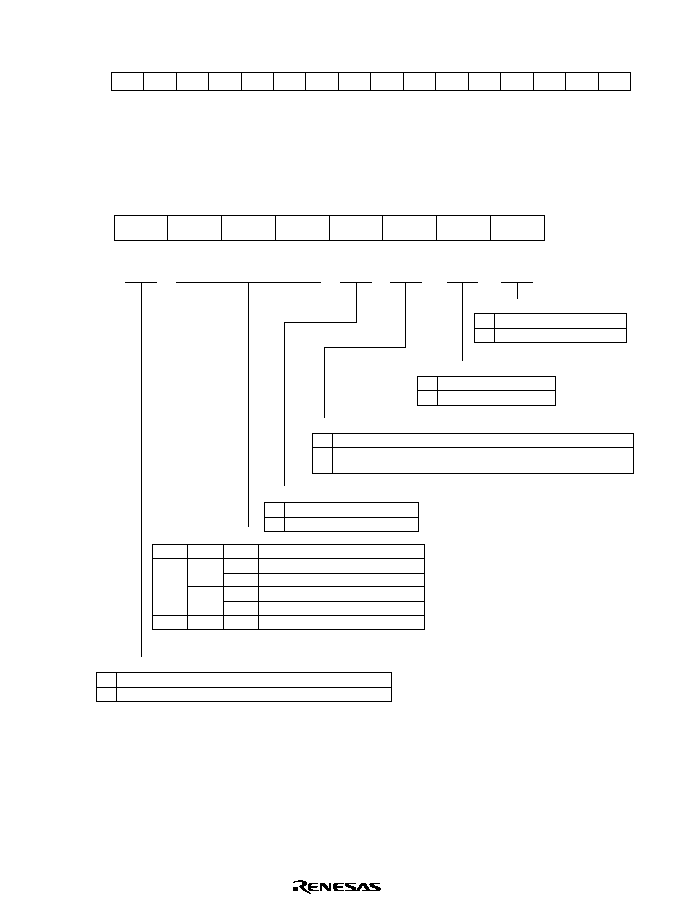
Rev. 1.0, 02/00, page 1014 of 1141
H'D07C: Capstan 12-Bit PWM Data Register CPWDR: Capstan 12-Bit PWM
1
0
R/W
CPWDR1
0
0
R/W
CPWDR0
3
0
R/W
CPWDR3
2
0
R/W
CPWDR2
5
0
R/W
CPWDR5
4
0
R/W
CPWDR4
7
0
R/W
CPWDR7
6
0
R/W
CPWDR6
9
0
R/W
CPWDR9
8
0
R/W
CPWDR8
11
0
R/W
CPWDR11
10
0
R/W
CPWDR10
12
1
13
1
14
1
15
1
:
:
:
Bit
Initial value
R/W
--
--
--
--
--
--
--
--
H'D080: CTL Control Register CTCR: CTL Circuit
0
0
1
0
R
2
0
W
3
0
4
1
W
5
1
6
0
7
W
W
W
FSLB
W
FSLC
0
W
NT/PL
FSLA
CCS
LCTL
UNCTL
SLWM
NTSC/PAL select bit
0 NTSC mode (frame rate: 30 Hz)
(Initial value)
1 PAL mode (frame rate: 25 Hz)
Long CTL bit
0 Clock source (CCS) operates at the setting value
(Initial value)
1 Clock source (CCS) operates for further 8-division after
operating at the setting value
CTL undetected bit
0 Detected
(Initial value)
1 Undetected
Mode select bit
0 Normal mode (Initial value)
1 Slow mode
Clock source select bit
0
s
(Initial value)
1
s/2
Operating frequency select bits
FSLC FSLB FSLA Description
0 0 0 Reserved (do not set)
1 Reserved (do not set)
1 0 fosc = 8 MHz
1 fosc = 10 MHz
(Initial value)
1 * * Reserved (do not set)
Note: * Don't care.
Bit
Initial value
R/W
:
:
:
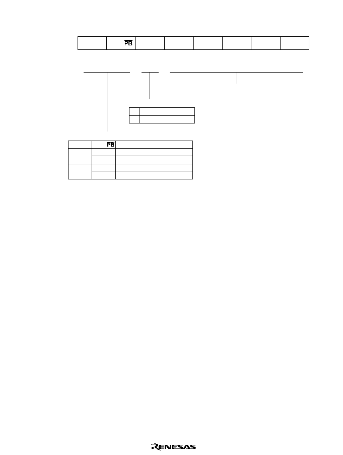
Rev. 1.0, 02/00, page 1015 of 1141
H'D081: CTL Mode Register CTLM: CTL Circuit
0
0
1
0
R/W
2
0
R/W
3
0
4
0
R/W
5
0
6
0
7
R/W
R/W
R/W
FW/RV
R/W
REC/
0
R/W
ASM
MD4
MD3
MD2
MD1
MD0
Note: * Refer to the description of the CTL mode register in section 26.13.5, Register Description.
ASM REC/
Description
0 0 Playback mode (Initial value)
1 Record mode
1 0 Assemble mode
1 Invalid (do not set)
Direction bit
0 Forward (Initial value)
1 Reverse
CTL mode select bits*
Bit
Initial value
R/W
:
:
:
Record /playback mode bits

Rev. 1.0, 02/00, page 1016 of 1141
H'D082 to H'D083: REC-CTL Duty Data Register 1 RCDR1: CTL Circuit
1
1
1
1
13
14
15
1
0
3
2
5
4
7
6
9
8
11
10
CMT11
W
12
0
CMT10
W
0
CMT13
W
0
CMT12
W
0
CMT15
W
0
CMT14
W
0
CMT17
W
0
CMT16
W
0
CMT19
W
0
CMT18
W
0
CMT1B
W
0
CMT1A
W
0
:
:
:
Bit
Initial value
R/W
--
--
--
--
--
--
--
--
H'D084 to H'D085: REC-CTL Duty Data Register 2 RCDR2: CTL Circuit
1
1
1
1
13
14
15
1
0
3
2
5
4
7
6
9
8
11
10
CMT21
W
12
0
CMT20
W
0
CMT23
W
0
CMT22
W
0
CMT25
W
0
CMT24
W
0
CMT27
W
0
CMT26
W
0
CMT29
W
0
CMT28
W
0
CMT2B
W
0
CMT2A
W
0
:
:
:
Bit
Initial value
R/W
--
--
--
--
--
--
--
--
H'D086 to H'D087: REC-CTL Duty Data Register 3 RCDR3: CTL Circuit
1
1
1
1
13
14
15
1
0
3
2
5
4
7
6
9
8
11
10
CMT31
W
12
0
CMT30
W
0
CMT33
W
0
CMT32
W
0
CMT35
W
0
CMT34
W
0
CMT37
W
0
CMT36
W
0
CMT39
W
0
CMT38
W
0
CMT3B
W
0
CMT3A
W
0
:
:
:
Bit
Initial value
R/W
--
--
--
--
--
--
--
--
H'D088 to H'D089: REC-CTL Duty Data Register 4 RCDR4: CTL Circuit
1
1
1
1
13
14
15
1
0
3
2
5
4
7
6
9
8
11
10
CMT41
W
12
0
CMT40
W
0
CMT43
W
0
CMT42
W
0
CMT45
W
0
CMT44
W
0
CMT47
W
0
CMT46
W
0
CMT49
W
0
CMT48
W
0
CMT4B
W
0
CMT4A
W
0
:
:
:
Bit
Initial value
R/W
--
--
--
--
--
--
--
--
H'D08A to H'D08B: REC-CTL Duty Data Register 5 RCDR5: CTL Circuit
1
1
1
1
13
14
15
1
0
3
2
5
4
7
6
9
8
11
10
CMT51
W
12
0
CMT50
W
0
CMT53
W
0
CMT52
W
0
CMT55
W
0
CMT54
W
0
CMT57
W
0
CMT56
W
0
CMT59
W
0
CMT58
W
0
CMT5B
W
0
CMT5A
W
0
Bit :
Initial value :
R / W :
--
--
--
--
--
--
--
--
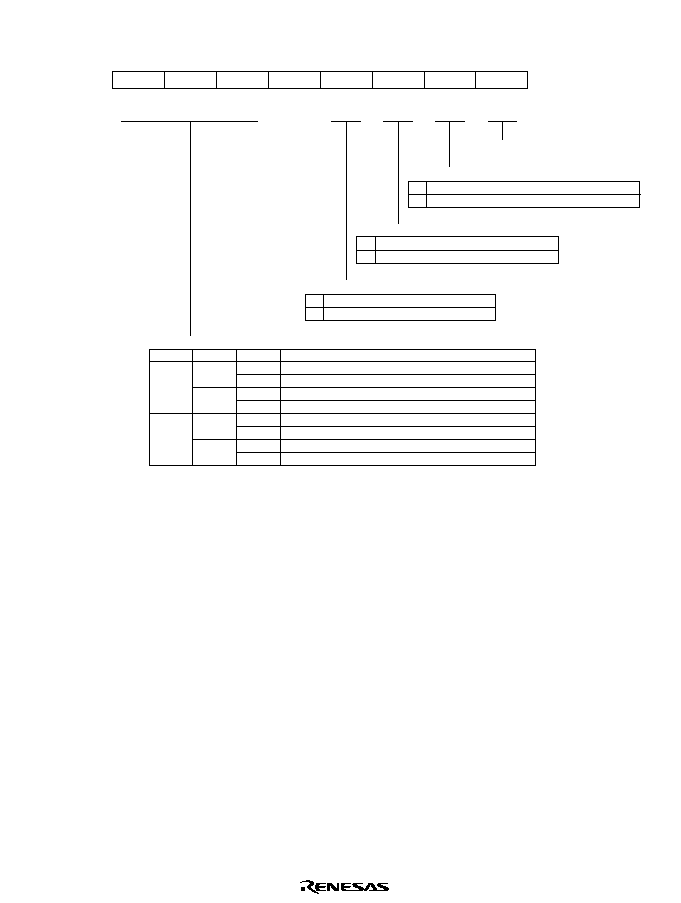
Rev. 1.0, 02/00, page 1017 of 1141
H'D08C: Duty I/O Register DI/O: CTL Circuit
0
1
1
0
R/(W)*
1
2
0
W
3
0
4
5
1
6
7
R/W
W
W
VCTR0
1
W
VCTR1
1
W
VCTR2
BPON
BPS
BPF
DI/O
1
Notes: 1. Only 0 can be written.
2. Refer to the description of the duty I/O register in section 26.13.5, Register Description.
Bit pattern detection ON/OFF bit
0 Bit pattern detection OFF
(initial value)
1 Bit pattern detection ON
Bit pattern detection start bit
0 Normal status
(initial value)
1 Starts 8-bit bit pattern detection
Duty I/O register
*
2
Bit pattern detection flag
0 Bit pattern (8-bit) is not detected
(initial value)
1 Bit pattern (8-bit) is detected
VCTR2 VCTR1 VCTR0
Description
0 0 0 Number of 1-pulse for detection = 2
1 Number of 1-pulse for detection = 4 (SYNC mark)
1 0 Number of 1-pulse for detection = 6
1 Number of 1-pulse for detection = 8 (mark A, short)
1 0 0 Number of 1-pulse for detection = 12 (mark A, long)
1 Number of 1-pulse for detection = 16
1 0 Number of 1-pulse for detection = 24 (mark B)
1 Number of 1-pulse for detection = 32
(initial value)
VISS interrupt setting bits
--
--
Bit
Initial value
R/W
:
:
:

Rev. 1.0, 02/00, page 1018 of 1141
H'D08D: Bit Pattern Register BTPR: CTL Circuit
0
1
1
1
R*/W
2
1
R*/W
3
1
4
5
1
6
7
R*/W
R*/W
R*/W
LSP5
1
R*/W
LSP4
1
R*/W
LSP6
1
R*/W
LSP7
LSP3
LSP2
LSP1
LSP0
Note: * Writes are disabled during bit pattern detection.
Bit
Initial value
R/W
:
:
:
H'D090 to H'D091: Reference Frequency Register 1 RFD: Reference Signal Generator
15
1
REF15
W
14
1
REF14
W
13
1
REF13
W
12
1
REF12
W
11
1
REF11
W
10
1
REF10
W
9
1
REF9
W
8
1
REF8
W
7
1
REF7
W
6
1
REF6
W
5
1
REF5
W
4
1
REF4
W
3
1
REF3
W
2
1
REF2
W
1
1
REF1
W
0
1
REF0
W
Bit :
Initial value :
R/W :
H'D092 to H'D093: Reference Frequency Register 2 CRF: Reference Signal Generator
15
1
CRF15
W
14
1
CRF14
W
13
1
CRF13
W
12
1
CRF12
W
11
1
CRF11
W
10
1
CRF10
W
9
1
CRF9
W
8
1
CRF8
W
7
1
CRF7
W
6
1
CRF6
W
5
1
CRF5
W
4
1
CRF4
W
3
1
CRF3
W
2
1
CRF2
W
1
1
CRF1
W
0
1
CRF0
W
Bit :
Initial value :
R/W :
H'D094 to H'D095: REF30 Counter Register RFC: Reference Signal Generator
15
0
RFC15
14
0
RFC14
13
0
RFC13
12
0
RFC12
11
0
RFC11
10
0
RFC10
9
0
RFC9
8
0
RFC8
7
0
RFC7
6
0
RFC6
5
0
RFC5
4
0
RFC4
3
0
RFC3
2
0
RFC2
1
0
RFC1
0
0
RFC0
R/W R/W R/W R/W R/W R/W R/W R/W R/W R/W R/W R/W R/W R/W R/W R/W
Bit :
Initial value :
R/W :
Rev. 1.0, 02/00, page 1019 of 1141
H'D096: Reference Frequency Mode Register RFM: Reference Signal Generator
0
0
1
0
W
2
0
W
3
0
4
0
W
0
W
5
6
0
7
REX
CRD
OD/EV
VST
VEG
0
W
RCS
W
W
W
VNA
CVS
Clock source select bit
0
s/2
(Initial value)
1
s/4
Mode select bit
0 Manual mode
(Initial value)
1 Auto mode
Manual select bit
0 VD sync
(Initial value)
1 Free-run
External signal synchronization select bit
0 VD signal or free-run
(Initial value)
1 External signal sync
DVCFG2 synchronization select bit
0 At mode switching
(initial value)
1 DVCFG2 signal synchronized
ODD/EVEN edge switchoverselect bit
0 Generated at field signal rising (even)
(Initial value)
1 Generated at field signal rising (odd)
VideoFF counter set
0 VideoFF signal turns counter set off
(Initial value)
1 VideoFF signal turns counter set on
VideoFF edge select bit
0 Set at VideoFF signal rising
(Initial value)
1 Set at VideoFF signal falling
Bit
Initial value
R/W
:
:
:
H'D097: Reference Frequency Mode Register 2 RFM2: Reference Signal Generator
0
0
1
1
2
1
3
1
4
1
5
6
7
FDS
1
1
1
R/W
Field select bit
0 Generated by selected ODD or EVEN VD
signal
(Initial value)
1 Generated by VD signal within mode transition
phase error of 90∞
TBC select bit
0 Reference signal is generated by VD
signal
1 Reference signal is generated by free-running
counter
TBC
--
--
--
--
--
--
R/W
--
--
--
--
--
--
Bit
Initial value
R/W
:
:
:
Rev. 1.0, 02/00, page 1020 of 1141
H'D098: DVCTL Control Register CTVC: Frequency Divider
0
*
1
*
R
2
*
R
3
4
5
6
7
R
CFG
HSW
0
W
0
W
CEX
CEG
CTL
1
1
1
DVCTL signal generation select bit
0 Generated by PB-CTL signal (Initial value)
1 Generated by external input signal
External sync signal edge select bit
0 Rising edge
(Initial value)
1 Falling edge
CFG flag
0 CFG level is low
(Initial value)
1 CFG level is high
HSW flag
0 HSW level is low
(Initial value)
1 HSW level is high
CTL flag
0 REC or PB-CTL level is low
(Initial value)
1 REC or PB-CTL level is high
--
--
--
--
--
--
Bit
Initial value
R/W
:
:
:
H'D099: CTL Frequency Division Register CTLR: Frequency Divider
0
0
1
0
W
2
0
W
3
0
4
0
W
0
W
5
6
0
7
CTL4
CTL3
CTL2
CTL1
CTL0
0
W
CTL7
W
W
W
CTL6
CTL5
Bit
Initial value
R/W
:
:
:
Rev. 1.0, 02/00, page 1021 of 1141
H'D09A: DVCFG Control Register CDVC: Frequency Divider
0
0
1
0
W
2
0
W
3
4
0
W
5
1
6
1
7
W
R
CMK
CMN
W
DVTRG
0
R/W*
MCGin
CRF
CPS1
CPS0
0
Note: * Only 0 can be written
Mask CFG flag
0 CFG normal operation
(Initial value)
1 DVCFG is detected while mask is set (race detection)
CFG mask status bit
0 Mask is released by capstan mask timer
1 Mask is set by capstan mask timer
(Initial value)
CFG mask select bit
0 Capstan mask timing function ON
(Initial value)
1 Capstan mask timing function OFF
PB (ASM)-to-REC transition timing sync ON/OFF select bit
0 PB (ASM)-to-REC transition timing sync ON
(Initial value)
1 PB (ASM)-to-REC transition timing sync OFF
CFG frequency division edge select bit
0 Execute frequency division operation at CFG rising edge
(Initial value)
1 Execute frequency division operation at CFG rising
CFG mask timer clock select bit
CPS1 CPS0 Description
0 0
s/1024
(Initial value)
1
s/512
1 0
s/256
1
s/128
--
--
Bit
Initial value
R/W
:
:
:
H'D09B: CFG Frequency Division Register 1 CDIVR1: Frequency Divider
0
0
1
0
W
2
0
W
3
4
0
W
5
0
6
7
W
W
CDV15
CDV14
0
W
CDV16
0
W
CDV13
CDV12
CDV11
CDV10
1
Bit :
Initial value :
R/W :
--
--
H'D09C: CFG Frequency Division Register 2 CDIVR2: Frequency Divider
0
0
1
0
W
2
0
W
3
4
0
W
5
0
6
7
W
W
CDV25
CDV24
0
W
CDV26
0
W
CDV23
CDV22
CDV21
CDV20
1
Bit :
Initial value :
R/W :
--
--
Rev. 1.0, 02/00, page 1022 of 1141
H'D09D: DVCFG Mask Interval Register CTMR: Frequency Divider
0
1
1
1
W
2
1
W
3
4
1
W
5
1
6
7
W
W
CPM5
CPM4
1
W
CPM3
CPM2
CPM1
CPM0
1
1
Bit :
Initial value :
R/W :
--
--
--
--
H'D09E: FG Control Register FGCR: Frequency Divider
0
0
1
1
2
1
3
1
4
1
5
1
6
1
7
W
DRF
1
DFG edge select bit
0 NCDFG signal rising edge is selected
(Initial value)
1 NCDFG signal falling edge is selected
Bit :
Initial value :
R/W :
--
--
--
--
--
--
--
--
--
--
--
--
--
--
H'D0A0: Servo Port Mode Register SPMR: Servo Port
0
1
1
1
--
2
1
--
3
1
4
1
--
0
R/W
5
6
7
--
--
--
--
--
0
R/W
CTLSTOP
--
--
CFGCOMP
1
CFG input method switch bit
0 Zero cross type comparator method for CFG signal input
(Initial value)
1 Digital signal input method for CFG signal input
CTLSTOP bit
0 CTL circuit operates
(Initial value)
1 CTL circuit does not operate
Bit :
Initial value :
R/W :
--
--
Rev. 1.0, 02/00, page 1023 of 1141
H'D0A3: Servo Monitor Control Register SVMCR: Servo Port
0
0
1
0
2
0
3
0
4
0
5
6
7
SVMCR4 SVMCR3 SVMCR2 SVMCR1 SVMCR0
1
1
R/W
R/W
R/W
0
SVMCR5
R/W
R/W
R/W
SVMCR5 SVMCR4 SVMCR3 Description
0 0 0 REF30 signal is output from SV2 output pin
(Initial value)
1 CAPREF30 signal is output from SV2 output pin
1 0 CREF signal is output from SV2 output pin
1 CTLMONI signal is output from SV2 output pin
1 0 0 DVCFG signal is output from SV2 output pin
1 CFG signal is output from SV2 output pin
1 0 DFG signal is output from SV2 output pin
1 DPG signal is output from SV2 output pin
SVMCR2 SVMCR1 SVMCR0 Description
0 0 0 REF30 signal is output from SV1 output pin
(Initial value)
1 CAPREF30 signal is output from SV1 output pin
1 0 CREF signal is output from SV1 output pin
1 CTLMONI signal is output from SV1 output pin
1 0 0 DVCFG signal is output from SV1 output pin
1 CFG signal is output from SV1 output pin
1 0 DFG signal is output from SV1 output pin
1 DPG signal is output from SV1 output pin
--
--
--
--
SV2 pin servo monitor output control
SV1 pin servo monitor output control
Bit
Initial value
R/W
:
:
:
Rev. 1.0, 02/00, page 1024 of 1141
H'D0A4: CTL Gain Control Register CTLGR: Servo Port
0
0
1
0
2
0
3
0
4
0
5
6
7
CTLFB
CTLGR3
CTLGR2
CTLGR1
CTLGR0
1
1
R/W
R/W
R/W
0
CTLE/A
R/W
R/W
R/W
CTL select bit
0 AMP output
1 EXCTL
CTL amp feedback SW bit
0 CTLFB SW is OFF
1 CTLFB SW is ON
CTL amp gain setting bit
CTLGR3 CTLGR2 CTLGR1 CTLGR0 CTL outpu gain
0 0 0 0 35.0 dB
(Initial value)
1 37.5 dB
1 0 40.0 dB
1 42.5 dB
1 0 0 45.0 dB
1 47.5 dB
1 0 50.0 dB
1 52.5 dB
1 0 0 0 55.0 dB
1 57.5 dB
1 0 60.0 dB
1 62.5 dB
1 0 0 65.0 dB
1 67.5 dB
1 0 70.0 dB
1 72.5 dB
--
--
--
--
Bit
Initial value
R/W
:
:
:
H'D0B0: Vertical Sync Signal Threshold Value Register VTR: Sync Detector (Servo)
0
0
1
0
W
2
0
W
3
0
4
0
W
5
0
6
1
7
W
W
W
VTR5
VTR4
VTR3
VTR2
VTR1
VTR0
1
Initial value :
--
--
--
--
Bit
R/W
:
:
:
H'D0B1: Horizontal Sync Signal Threshold Value Register HTR: Sync Detector (Servo)
0
0
1
0
W
2
0
W
3
0
4
5
6
1
7
W
W
HTR3
HTR2
HTR1
HTR0
1
1
1
Initial value :
--
--
--
--
--
--
--
--
Bit
R/W
:
:
:

Rev. 1.0, 02/00, page 1025 of 1141
H'D0B2: H Pulse Adjustment Start Time Setting Register HRTR: Sync Detector (Servo)
0
0
1
0
W
2
0
W
3
0
4
0
W
0
W
5
6
0
7
HRTR4
HRTR3
HRTR2
HRTR1
HRTR0
0
W
HRTR7
W
W
W
HRTR6
HRTR5
Bit :
Initial value :
R/W :
H'D0B3: H Pulse Width Setting Register HPWR: Sync Detector (Servo)
0
0
1
0
W
2
0
W
3
0
4
5
6
1
7
W
W
HPWR3
HPWR2
HPWR1
HPWR0
1
1
1
Bit :
Initial value :
R/W :
--
--
--
--
--
--
--
--
H'D0B4: Noise Detection Window Setting Register NWR: Sync Detector (Servo)
0
0
1
0
W
2
0
W
3
0
4
0
W
5
0
6
1
7
W
W
W
NWR5
NWR4
NWR3
NWR2
NWR1
NWR0
1
Bit :
Initial value :
R/W :
--
--
--
--
H'D0B5: Noise Detection Register NDR: Sync Detector (Servo)
0
0
1
0
W
2
0
W
3
0
4
0
W
0
W
5
6
0
7
NDR4
NDR3
NDR2
NDR1
NDR0
0
W
NDR7
W
W
W
NDR6
NDR5
Bit :
Initial value :
R/W :
Rev. 1.0, 02/00, page 1026 of 1141
H'D0B6: Sync Signal Control Register SYNCR: Sync Detector (Servo)
0
0
1
0
R
2
0
R/(W)*
3
1
4
5
6
1
7
R/W
R/W
NIS/VD
NOIS
FLD
SYCT
1
1
1
Note: * Only 0 can be written.
Interrupt select bit
0 Noise level interrupt
1 VD interrupt
(Initial value)
Noise detection flag
0 Noise count is less than four times of NDR setting value
(Initial value)
1 Noise count is equal to or greater than four times of NDR setting value
Field detection flag
0 Odd field
(Initial value)
1 Even field
Sync signal polarity select bit
SYCT Description Polarity
0 Positive
1 Negative
Initial value :
--
--
--
--
--
--
--
--
Bit
R/W
:
:
(Initial value)
Rev. 1.0, 02/00, page 1027 of 1141
H'D0B8: Servo Interrupt Enable Register 1 SIENR1: Servo Interrupt
0
0
1
0
R/W
2
0
R/W
3
0
4
0
R/W
0
R/W
5
6
0
7
IECAP3
IECAP2
IECAP1
IEHSW2
IEHSW1
0
R/W
IEDRM3
R/W
R/W
R/W
IEDRM2
IEDRM1
Drum phase error detection interrupt enable bit
0 Interrupt request is disabled by IRRDRM3
(Initial value)
1 Interrupt request is enabled by IRRDRM3
Drum speed error detection (lock detection)
interrupt enable bit
0 Interrupt request is disabled by IRRDRM2 (Initial value)
1 Interrupt request is enabled by IRRDRM2
Drum speed error detection (OVF, latch)
interrupt enable bit
0 Interrupt request is disabled by IRRDRM1 (Initial value)
1 Interrupt request is enabled by IRRDRM1
Capstan phase error detection interrupt enable bit
0 Interrupt request is disabled by IRRCAP3 (Initial value)
1 Interrupt request is enabled by IRRCAP3
Capstan speed error detection (lock detection)
interrupt enable bit
0 Interrupt request is disabled by IRRCAP2 (Initial value)
1 Interrupt request is enabled by IRRCAP2
Capstan speed error detection (OVF, latch)
interrupt enable bit
0 Interrupt request is disabled by IRRCAP1 (Initial value)
1 Interrupt request is enabled by IRRCAP1
HSW timing generation (counter clear, capture)
interrupt enable bit
0 Interrupt request is disabled by IRRHSW2 (Initial value)
1 Interrupt request is enabled by IRRHSW2
HSW timing generator (OVW, match, STRIG)
interrupt enable bit
0 Interrupt request is disabled by IRRHSW1
(Initial value)
1 Interrupt request is enabled by IRRHSW1
Initial value :
Bit
R/W
:
:
:
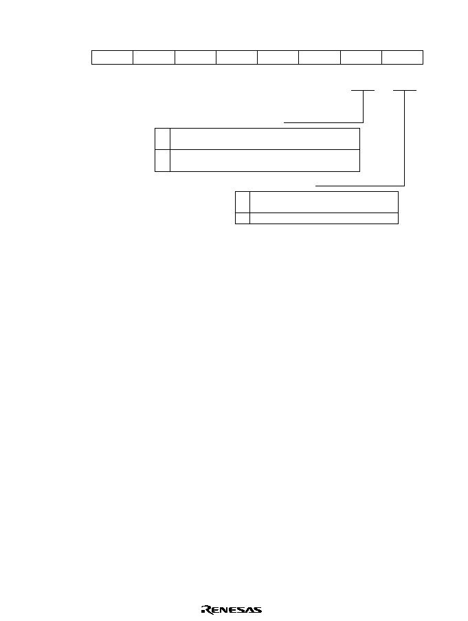
Rev. 1.0, 02/00, page 1028 of 1141
H'D0B9: Servo Interrupt Enable Register 2 SIENR2: Servo Interrupt
0
0
1
0
R/W
2
3
4
5
6
1
7
R/W
IESNC
IECTL
1
1
1
1
1
Vertical sync signal interrupt enable bit
0 Interrupt (vertical sync signal interrupt) request is disabled
by IRRSNC
(Initial value)
1 Interrupt (vertical sync signal interrupt) request is enabled
by IRRSNC
CTL interrupt enable bit
0 Interrupt request is disabled by IRRCTL
(Initial value)
1 Interrupt request is enabled by IRRCTL
Initial value :
--
--
--
--
--
--
--
--
--
--
--
--
Bit
R/W
:
:
:
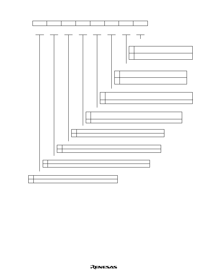
Rev. 1.0, 02/00, page 1029 of 1141
H'D0BA: Servo Interrupt Request Register 1 SIRQR1: Servo Interrupt
0
0
1
0
R/(W)*
2
0
R/(W)*
3
0
4
0
R/(W)*
0
R/(W)*
5
6
0
7
IRRCAP3 IRRCAP2 IRRCAP1 IRRHSW2 IRRHSW1
0
R/(W)*
IRRDRM3
R/(W)*
R/(W)*
R/(W)*
IRRDRM2 IRRDRM1
Note: * Only 0 can be written to clear the flag.
Drum phase error detector interrupt request bit
0 Drum phase error detector interrupt request is not generated (Initial value)
1 Drum phase error detector interrupt request is generated
Drum speed error detector (lock detection) interrupt request bit
0 Drum speed error detector (lock detection) interrupt request is not generated (Initial value)
1 Drum speed error detector (lock detection) interrupt request is generated
Drum speed error detector (OVF, latch) interrupt request bit
0 Drum speed error detector (OVF, latch) interrupt request is not generated (Initial value)
1 Drum speed error detector (OVF, latch) interrupt request is generated
Capstan phase error detector interrupt request bit
0 Capstan phase error detector interrupt request is not generated (Initial value)
1 Capstan phase error detector interrupt request is generated
Capstan speed error detector (lock detection) intrerrupt request bit
0 Capstan speed error detector (lock detection) interrupt request is not generated
(Initial value)
1 Capstan speed error detector (lock detection) interrupt request is generated
Capstan speed error detector (OVF, latch) interrupt request bit
0 Capstan speed error detector (OVF, latch) interrupt request in not generated
(Initial value)
1 Capstan speed error detector (OVF, latch) interrupt request is generated
HSW timing generator (counter clear, capture)
interrupt request bit
0 HSW timing generator (counter clear, capture) interrupt
request is not generated
(Initial value)
0 HSW timing generator (counter clear, capture) interrupt
request is generated
HSW timing generator (OVW, match, STRIG)
interrupt request bit
0 HSW timing generator (OVM, match, STRIG)
interrupt request is not generated
(Initial value)
1 HSW timing generator (OVM, match, STRIG)
interrupt request is generated
Bit
Initial value
R/W
:
:
:
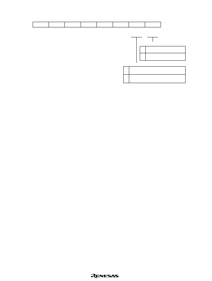
Rev. 1.0, 02/00, page 1030 of 1141
H'D0BB: Servo Interrupt Request Register 2 SIRQR2: Servo Interrupt
0
0
1
0
R/(W)*
2
3
4
5
6
1
7
R/(W)*
IRRSNC
IRRCTL
1
1
1
1
1
Note: * Only 0 can be written to clear the flag.
Vertical sync signal interrupt request bit
0 Sync signal detector (VD, noise) interrupt
request is not generated
(Initial value)
1 Sync signal detector (VD, noise) interrupt
request is generated
CTL interrupt request bit
0 CTL interrupt request is not
generated
(Initial value)
1 CTL interrupt request is
generated
--
--
--
--
--
--
--
--
--
--
--
--
Bit
Initial value
R/W
:
:
:
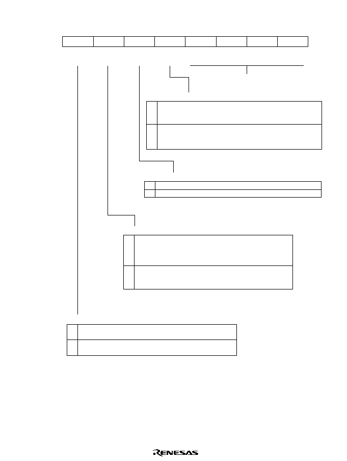
Rev. 1.0, 02/00, page 1031 of 1141
H'D0E5: DDC Switch Register DDCSWR: I
2
C Bus Interface
0
1
1
1
W
*
2
2
1
W
*
2
3
1
4
0
R/(W)
*
1
0
R/W
5
7
IF
CLR3
CLR2
CLR1
CLR0
0
R/W
SWE
6
0
R/W
SW
W
*
2
W
*
2
IE
DDC mode switch interrupt enable bit
0
Disables an interrupt at automatic format switching (Initial value)
1
Enables an interrupt at automatic format switching
DDC mode switch
0
I
2
C bus format is selected for IIC channel 0. (Initial value)
[Clearing condition]
(1) When 0 is written by software
(2) When an SCL falling edge is detected when SWE = 1
1
Formatless transfer is selected for IIC channel 0.
[Setting condition]
When 1 is written after SW = 0 is read
DDC mode switch enable
0
Disables automatic switching from formatless transfer to I
2
C bus
format transfer for IIC channel 0.
(Initial value)
1
Enables automatic switching from formatless transfer to I
2
C bus
format transfer for IIC channel 0.
DDC mode switch interrupt flag
0
Interrupt has not been requested
(Initial value)
[Clearing condition]
When 0 is written after IF = 1 is read
1
Interrupt has been requested
[Setting condition]
When an SCL falling edge is detected when SWE = 1
:
:
:
Bit
Initial value
R/W
Notes: 1. Only 0 can be written to clear the flag.
2. Always read as 1.
I
2
C clear control
Rev. 1.0, 02/00, page 1032 of 1141
H'D0E8: I
2
C Bus Control Register ICCR0: I
2
C Bus Interface
7
ICE
0
R/W
6
IEIC
0
R/W
5
MST
0
R/W
4
TRS
0
R/W
3
ACKE
0
R/W
0
SCP
1
W
2
BBSY
0
R/W
1
IRIC
0
R/(W)*
Note: * Only 0 can be written to clear the flag.
I
2
C bus interface enable
0 I
2
C bus interface module disabled, with SCL and SDA signal pins
(Initial value)
set to port function. SAR and SARX can be accessed.
1 I
2
C bus interface module enabled for transfer operation (pins SCL
and SCA are driving the bus). ICMR and ICDR can be accessed.
I
2
C bus interface interrupt enable
0 Interrupt request is disabled
(Initial value)
1 Interrupt request is enabled
Acknowledge bit judgment selection
0 The value of the acknowledge bit is ignored, and continuous transfer is performed
(Initial value)
1 If the acknowledge bit is 1, continuous transfer is interrupted
Bus busy
0 Bus is free
(Initial value)
[Clearing conditions] When a stop condition is detected
1 Bus is busy
[Setting conditions] When a start condition is detected
I
2
C bus interface interrupt request flag
0 Waiting for transfer, or transfer in progress
(Initial value)
[Clearing conditions]
(1) When 0 is written in IRIC after reading IRIC = 1
1 Interrupt requested
[Setting conditions]
∑ I
2
C bus format master mode
-- When a start condition is detected in the bus line state after a start condition is
issued (when the TDRE flag is set to 1 because of first frame transmission)
-- When a wait is inserted between the data and acknowledge bit when WAIT = 1
-- At the end of data transfer
(when the TDRE or RDRF flag is set to 1)
-- When a slave address is received after bus arbitration is lost
(when the AL flag is set to 1)
-- When 1 is received as the acknowledge bit when the ACKE bit is 1
(when the ACKB bit is set to 1)
∑ I
2
C bus format slave mode
-- When the slave address (SVA, SVAX) matches
(when the AAS and AASX flags are set to 1) and at the end of data transfer up
to the subsequent retransmission start condition or stop condition detection
(when the TDRE or RDRF flag is set to 1)
-- When the general call address is detected
(when the ADZ flag is set to 1) and at the end of data transfer up to the
subsequent retransmission start condition or stop condition detection
(when the TDRE or RDRF flag is set to 1)
-- When 1 is received as the acknowledge bit when the ACKE bit is 1
(when the ACKB bit is set to 1)
-- When a stop condition is detected
(when the STOP or ESTP flag is set to 1)
∑ Synchronous serial format
-- At the end of data transfer (when the TDRE or RDRF flag is set to 1)
-- When a start condition is detected with serial format selected
-- When a condition, other than the above, that sets the TDRE or RDRF flag to 1 is
detected
Start condition/stop condition prohibit
0 Writing 0 issues a start or stop condition, in combination
with the BBSY flag
1 Reading always returns a value of 1
(Initial value)
Writing is ignored
Master/slave select
Transmit/receive select
MST TRS
Description
0 0 Slave receive mode
(Initial value)
1 Slave transmit mode
1 0 Master receive mode
1 Master transmit mode
Bit :
Initial value :
R/W :
Rev. 1.0, 02/00, page 1033 of 1141
H'D0E9: I
2
C Bus Status Register ICSR0: I
2
C Bus Interface
7
ESTP
0
R/(W)*
6
STOP
0
R/(W)*
5
IRTR
0
R/(W)*
4
AASX
0
R/(W)*
3
AL
0
R/(W)*
0
ACKB
0
R/W
2
AAS
0
R/(W)*
1
ADZ
0
R/(W)*
Note: * Only 0 can be written to clear the flag.
Error stop condition detection flag
0 No error stop condition
(Initial value)
[Clearing conditions]
(1) When 0 is written in ESTP after reading ESTP = 1
(2) When the IRIC flag is cleared to 0
1 ∑ In I
2
C bus format slave mode
Error stop condition detected
[Setting conditions]
≠ When a stop condition is detected during frame transfer
∑ In other mode
No meaning
Normal stop condition detection flag
0 No normal stop condition
(Initial value)
[Clearing conditions]
(1) When 0 is written in STOP after reading STOP = 1
(2) When the IRIC flag is cleared to 0
1 ∑ In I
2
C bus format slave mode
Normal stop condition detected
[Setting conditions]
≠ When a stop condition is detected after completion of frame transfer
∑ In other mode
No meaning
I
2
C bus interface continuous transmission/reception interrupt request flag
0 Waiting for transfer, or transfer in progress
(Initial value)
[Clearing conditions]
(1) When 0 is written in IRTR after reading IRTR = 1
(2) When the IRIC flag is cleared to 0
1 Continuous transfer state
[Setting conditions]
∑ In I
2
C bus interface slave mode
≠ When the TDRE or RDRF flag is set to 1 when AASX = 1
∑ In other mode
≠ When the TDRE or RDRF flag is set to 1
Second slave address recognition flag
0 Second slave address not recognized
(Initial value)
[Clearing conditions]
(1) When 0 is written in AASX after reading AASX = 1
(2) When a start condition is detected
(3) In master mode
1 Second slave address recognized
[Setting conditions]
≠ When the second slave address is detected in slave receive mode
Arbitration lost flag
0 Bus arbitration won
(Initial value)
[Clearing conditions]
(1) When ICDR data is written (transmit mode) or read (receive mode)
(2) When 0 is written in AL after reading AL = 1
1 Arbitration lost
[Setting conditions]
(1) If the internal SDA and SDA pin disagree at the rise of SCL in master transmit mode
(2) If the internal SCL line is high at the fall of SCL in master transmit mode
Slave address recognition flag
0 Slave address or general call address not recognized
(Initial value)
[Clearing conditions]
(1) When ICDR data is written (transmit mode) or read (receive mode)
(2) When 0 is written in AAS after reading AAS = 1
(3) In master mode
1 Slave address or general call address recognized
[Setting conditions]
≠ When the slave address or general call address is detected when FS = 0 in slave receive mode
General call address recognition flag
0 General call address not recognized (Initial
value)
[Clearing conditions]
(1) When ICDR data is written (transmit mode) or read (receive mode)
(2) When 0 is written in ADZ after reading ADZ = 1
(3) In master mode
1 General call address recognized
[Setting conditions]
≠ When the general call address is detected when FSX = 0 or FS = 0 in slave receive mode
Acknowledge bit
0 Receive mode: 0 is output at acknowledge output timing
(Initial value)
Transmit mode: Indicates that the receiving device has acknowldeged the data (signal is 0)
1 Receive mode; 1 is output at acknowledge output timing
Transmit mode: Indicates that the receiving device has not acknowldeged the data (signal is 1)
Bit
Initial value
R/W
:
:
:

Rev. 1.0, 02/00, page 1034 of 1141
H'D0EE: I
2
C Bus Data Register ICDR0: I
2
C Bus Interface
7
ICDR7
--
R/W
6
ICDR6
--
R/W
5
ICDR5
--
R/W
4
ICDR4
--
R/W
3
ICDR3
--
R/W
0
ICDR0
--
R/W
2
ICDR2
--
R/W
1
ICDR1
--
R/W
Initial value :
Note: Refer to section 23.2.1, I
2
C Bus Data Register (ICDR).
Bit
R/W
:
:
H'D0EE: Second Slave Address Register SARX0: I
2
C Bus Interface
7
SVAX6
0
R/W
6
SVAX5
0
R/W
5
SVAX4
0
R/W
4
SVAX3
0
R/W
3
SVAX2
0
R/W
0
FSX
1
R/W
2
SVAX1
0
R/W
1
SVAX0
0
R/W
Format select
Used combined FS bit in SAR.
Initial value :
Note: Refer to section 23.2.3, Second Slave Address Register (SARX), and section 23.2.2, Slave Address Register (SAR).
Bit
R/W
:
:
Rev. 1.0, 02/00, page 1035 of 1141
H'D0EF: I
2
C Bus Mode Register ICMR0: I
2
C Bus Interface
7
MLS
0
R/W
6
WAIT
0
R/W
5
CKS2
0
R/W
4
CKS1
0
R/W
3
CKS0
0
R/W
0
BC0
0
R/W
2
BC2
0
R/W
1
BC1
0
R/W
MSB-first/LSB-first select
Note: * See bit 6 in the serial timer control register (STCR)
0 MSB-first
(Initial value)
1 LSB-first
Wait insertion bit
0 Data and acknowledge bits transferred consecutively
(Initial value)
1 Wait inserted between data and acknowledge bits
Transfer clock select bits
Bit counter
Bit/frame
BC2 BC1 BC0 Clock sync I
2
C bus format
serial format
0 0 0 8 9
(Initial value)
1 1 2
1 0 2 3
1 3 4
0 0 0 4 5
1 5 6
1 0 6 7
1 7 8
IICX* CKS2 CKS1 CKS0 Clock Transfer rate
=8 MHz
=10 MHz
0 0 0 0
/28
286 kHz
357 kHz
1
/40
200 kHz
250 kHz
1 0
/48
167 kHz
208 kHz
1
/64
125 kHz
156 kHz
1 0 0
/80
100 kHz
125 kHz
1
/100
80.0 kHz
100 kHz
1 0
/112
71.4 kHz
89.3 kHz
1
/128
62.5 kHz
78.1 kHz
1 0 0 0
/56
143 kHz
179 kHz
1
/80
100 kHz
125 kHz
1 0
/96
83.3 kHz
104 kHz
1
/128
62.5 kHz
78.1 kHz
1 0 0
/160
50.0 kHz
62.5 kHz
1
/200
40.0 kHz
50.0 kHz
1 0
/224
35.7 kHz
44.6 kHz
1
/256
31.3 kHz
39.1 kHz
Bit
Initial value
R/W
:
:
:
Rev. 1.0, 02/00, page 1036 of 1141
H'D0EF: Slave Address Register SAR0: I
2
C Bus Interface
7
SVA6
0
R/W
6
SVA5
0
R/W
5
SVA4
0
R/W
4
SVA3
0
R/W
3
SVA2
0
R/W
0
FS
0
R/W
2
SVA1
0
R/W
1
SVA0
0
R/W
Format select bit
DDCSWR
SAR
SARX
Format select
Bit 6
Bit 0
Bit 0
SW
FS
FX
0
0
0
I
2
C bus format
∑
SAR and SARX slave addresses recognized
1
I
2
C bus format
(Initial value)
∑
SAR slave address recognized
∑
SARX slave address ignored
1
0
I
2
C bus format
∑
SAR slave address ignored
∑
SARX slave address recognized
1
I
2
C bus format
∑
SAR and SARX slave addresses ignored
1
0
0
Formatless transfer (start and stop conditions
are not detected)
1
∑
With acknowledge bit
0
0
Formatless
transfer
*
(start and stop conditions
are not detected)
1
∑
Without acknowledge bit
Bit
Initial value
R/W
:
:
:
Note: * Do not use this setting when automatically switching the made from
formatless transfer to I
2
C bus format by setting DDCSWR.
Rev. 1.0, 02/00, page 1037 of 1141
H'D100: Timer Interrupt Enable Register TIER: Timer X1
0
0
1
0
R/W
2
0
R/W
3
0
4
0
R/W
5
0
6
0
7
R/W
R/W
R/W
ICICE
R/W
ICIBE
0
R/W
ICIAE
ICIDE
OCIAE
OCIBE
OVIE
ICSA
ICFA interrupt request (ICIA) is disabled
(Initial value)
ICFA interrupt request (ICIA) is enabled
0
1
Input capture A interrupt enable bit
FTIA pin input is selected
for input capture A input
(Initial value)
HSW is selected for input
capture A input
0
1
Input capture input select A bit
ICFB interrupt request (ICIB) is disabled
(Initial value)
ICFB interrupt request (ICIB) is enabled
0
1
Input capture B interrupt enable bit
ICFC interrupt request (ICIC) is disabled
(Initial value)
ICFC interrupt request (ICIC) is enabled
0
1
Input capture C interrupt enable bit
ICFD interrupt request (ICID) is disabled
(Initial value)
ICFD interrupt request (ICID) is enabled
0
1
Input capture D interrupt enable bit
Interrupt request (FOVI) is
disabled
(Initial value)
Interrupt request (FOVI) is enabled
0
1
Timeout overflow interrupt enable bit
0
OCFB interrupt request (OCIB) is disabled
(Initial value)
OCFB interrupt request (OCIB) is enabled
1
Output compare interrupt B enable bit
OCFA interrupt request (OCIA) is disabled
(Initial value)
OCFA interrupt request (OCIA) is enabled
0
1
Output compare interrupt A enable bit
Bit
Initial value
R/W
:
:
:
Rev. 1.0, 02/00, page 1038 of 1141
H'D101: Timer Control/Status Register X TCSRX: Timer X1
0
0
1
0
2
0
3
0
4
0
5
0
6
0
7
R/ W
R/(W)*
ICFB
0
R/(W)*
ICFA
R/(W)*
ICFD
R/(W)*
ICFC
R/(W)*
OCFB
R/(W)*
OCFA
CCLRA
R/(W)*
OVF
Note: * Only 0 can be written to bits 7 to 1 to clear the flags.
Output compare flag A
[Clearing conditions]
When 0 is written to OCFA after reading
OCFA = 1
(Initial value)
[Setting conditions]
When FRC = OCRA
0
1
Output compare flag B
[Clearing conditions]
When 0 is written to OCFB after reading
OCFB = 1
(Initial value)
[Setting conditions]
When FRC = OCRB
0
1
Timer overflow
[Clearing conditions]
When 0 is written to OVF after reading
OVF = 1
(Initial value)
[Setting conditions]
When FRC changes from H'FFFF to
H'0000
0
1
Input capture flag D
[Clearing conditions]
When 0 is written to ICFD after reading
ICFD = 1
(Initial value)
[Setting conditions]
When input capture signal is generated
0
1
Input capture flag C
[Clearing conditions]
When 0 is written to ICFC after reading
ICFC = 1
(Initial value)
[Setting conditions]
When input capture signal is generated
0
1
Input capture flag B
[Clearing conditions]
When 0 is written to ICFB after reading
ICFB = 1
(Initial value)
[Setting conditions]
When FRC value is transferred to ICRB by
input capture signal
0
1
Input capture flag A
[Clearing conditions]
When 0 is written to ICFA after reading
ICFA = 1
(Initial value)
[Setting conditions]
When FRC value is transferred to ICRA by
input capture signal
0
1
Counter clear
FRC clearing is disabled
(Initial value)
FRC clearing is enabled
0
1
Initial value :
Bit
R/W
:
:
Rev. 1.0, 02/00, page 1039 of 1141
H'D102: Free Running Counter H FRCH: Timer X1
H'D103: Free Running Counter L FRCL: Timer X1
0
3
0
R/W
5
0
R/W
7
0
9
0
R/W
11
0
13
0
15
R/W
R/W
R/W
0
R/W
R/W
1
0
2
0
R/W
4
0
R/W
6
0
8
0
R/W
10
0
12
0
14
FRC
FRCH
FRCL
R/W
R/W
R/W
R/W
0
R/W
0
Bit :
Initial value :
R/W :
H'D104: Output Compare Register AH, BH OCRAH, OCRBH: Timer X1
H'D105: Output Compare Register AL, BL OCRAL, OCRBL: Timer X1
1
3
1
R/W
5
1
R/W
7
1
9
1
R/W
11
1
13
1
15
R/W
R/W
R/W
1
R/W
R/W
1
1
2
1
R/W
4
1
R/W
6
1
8
1
R/W
10
1
12
1
14
OCRA, OCRB
OCRAH, OCRBH
OCRAL, OCRBL
R/W
R/W
R/W
R/W
1
R/W
0
Bit :
Initial value :
R/W :
Rev. 1.0, 02/00, page 1040 of 1141
H'D106: Timer Control Register X TCRX: Timer X1
0
0
1
0
2
0
3
0
4
0
5
0
6
0
7
R/W
R/W
IEDGB
0
R/W
IEDGA
R/W
IEDGD
R/W
IEDGC
R/W
BUFEB
R/W
BUFEA
CKS0
R/W
CKS1
Capture at falling edge of input capture input A
(Initial value)
Capture at rising edge of input capture input A
0
1
Input capture edge select A
Capture at falling edge of input capture input B
(Initial value)
Capture at rising edge of input capture input B
0
1
Input capture edge select B
Capture at falling edge of input capture input C
(Initial value)
Capture at rising edge of input capture input C
0
1
Input capture edge select C
Capture at falling edge of input capture input D
(Initial value)
Capture at rising edge of input capture input D
0
1
Input capture edge select D
ICRC is not used as buffer register for ICRB
(Initial value)
ICRC is used as buffer register for ICRB
0
1
Buffer enable B
ICRC is not used as buffer register for ICRA
(Initial value)
ICRC is used as buffer register for ICRA
0
1
Buffer enable A
Clock selct bit
Clock select
0
0
CKS0
CKS1
1
0
0
1
Internal clock: count at
/4
(Initial value)
Internal clock: count at
/16
Internal clock: count at
/64
1
1
DVCFG: Edge detection
pulse selected by CFG
frequency division timer
Bit
Initial value
R/W
:
:
:
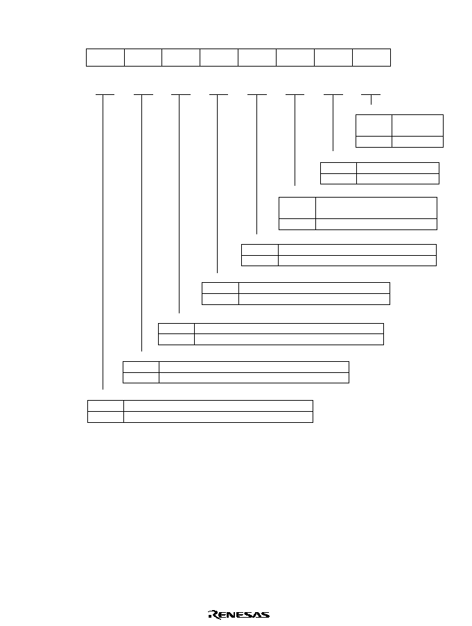
Rev. 1.0, 02/00, page 1041 of 1141
H'D107: Timer Output Compare Control Register TOCR: Timer X1
0
0
1
0
2
0
3
0
4
0
5
0
6
0
7
R/W
R/W
ICSC
0
R/W
ICSB
R/W
OSRS
R/W
ICSD
R/W
OEB
R/W
OEA
OLVLB
R/W
OLVLA
FTIB pin is selected for input capture B input (Initial value)
VD is selected for input capture B input
0
1
Input capture input select B
Low level
(Initial value)
High level
0
1
Output level B
FTIC pin is selected for input capture C input (Initial value)
DVCTL is selected for input capture C input
0
1
Input capture input select C
FTID pin is selected for input capture D input (Initial value)
NHSW is selected for input capture D input
0
1
Input capture input select D
OCRA register is selected
(Initial value)
OCRB register is selected
0
1
Output compare register select
Low level
(Initial value)
High level
0
1
Output level A
Output compare A output is disabled (Initial value)
Output compare A output is enabled
0
1
Output enable A
Initial value :
0
1
Output enable B
Output compare B output is disabled
(Initial value)
Output compare B output is enabled
Bit
R/W
:
:
Rev. 1.0, 02/00, page 1042 of 1141
H'D108: Input Capture Register AH ICRAH: Timer X1
H'D109: Input Capture Register AL ICRAL: Timer X1
H'D10A: Input Capture Register BH ICRBH: Timer X1
H'D10B: Input Capture Register BL ICRBL: Timer X1
H'D10C: Input Capture Register CH ICRCH: Timer X1
H'D10D: Input Capture Register CL ICRCL: Timer X1
H'D10E: Input Capture Register DH ICRDH: Timer X1
H'D10F: Input Capture Register DL ICRDL: Timer X1
0
3
0
R
5
0
R
7
0
9
0
R
11
0
13
0
15
R
R
R
0
R
R
1
0
2
0
R
4
0
R
6
0
8
0
R
10
0
12
0
14
ICRA, ICRB, ICRC, ICRD
ICRAH, ICRBH, ICRCH, ICRDH
ICRAL, ICRBL, ICRCL, ICRDL
R
R
R
R
0
R
0
Bit :
Initial value :
R/W :
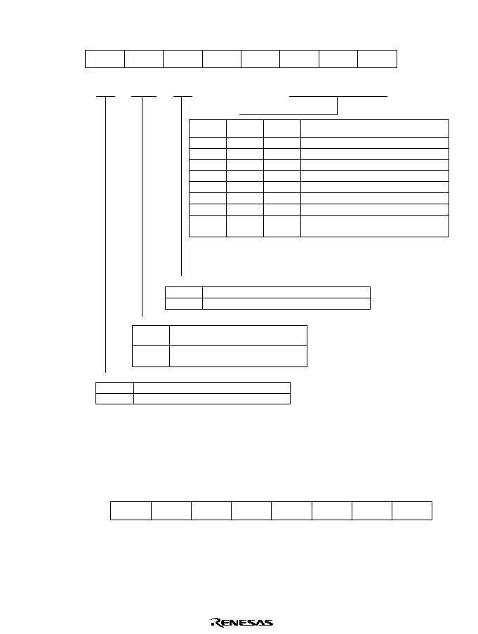
Rev. 1.0, 02/00, page 1043 of 1141
H'D110: Timer Mode Register B TMB: Timer B
0
0
1
0
R/W
2
0
R/W
3
1
4
1
5
0
6
0
7
R/W
R/W
TMBIE
R/(W)*
TMBIF
0
R/W
TMB17
TMB12
TMB11
TMB10
Note: * Only 0 can be written to clear the flag.
Interval function is selected
(Initial value)
Auto reload function is selected
0
1
Auto reload function select bit
[Setting conditions]
When TCB overflows
[Clearing conditions]
(Initial value)
When 0 is written after reading 1
0
1
Timer B interrupt request flag
Timer B interrupt request is disabled
(Initial value)
Timer B interrupt request is enabled
0
1
Timer B interrupt enable bit
0
0
0
Internal clock: Count at
/16384 (Initial value)
TMB11
TMB10
TMB12
Clock select
0
1
Internal clock: Count at
/4096
1
0
0
0
0
Internal clock: Count at
/1024
1
1
Internal clock: Count at
/512
0
1
0
Internal clock: Count at
/128
0
1
Internal clock: Count at
/32
1
1
1
1
0
Internal clock: Count at
/8
1
1
Count at rising/falling edge of external
event (TMBI)*
Note: * External event edge selection is set at PMRA6 in port mode register A
(PMRA).
See section 12.2.4, Port Register A (PMRA).
Clock select bit
Initial value :
--
--
--
--
Bit
R/W
:
:
H'D111: Timer Counter B TCB: Timer B
0
0
1
0
R
2
0
R
3
4
5
0
6
0
7
R
R
TCB15
0
R
TCB14
0
R
TCB13
R
TCB16
0
R
TCB17
TCB12
TCB11
TCB10
Bit :
Initial value :
R/W :
Rev. 1.0, 02/00, page 1044 of 1141
H'D111: Timer Load RegisterB TLB: TimerB
0
0
1
0
W
2
0
W
3
4
5
0
6
0
7
W
W
TLB15
0
W
TLB14
0
W
TLB13
W
TLB16
0
W
TLB17
TLB12
TLB11
TLB10
Bit :
Initial value :
R/W :
H'D112: Timer L Mode Register LMR: Timer L
0
0
1
0
R/W
2
0
R/W
3
0
4
1
5
1
6
0
7
R/W
R/W
R/W
LMIE
0
R/(W)*
LMIF
LMR3
LMR2
LMR1
LMR0
Note: * Only 0 can be written to clear the flag.
Timer L interrupt request flag
[Clearing conditions]
(Initial value)
When 0 is written after reading 1
[Setting conditions]
When LTC overflow, underflow or compare
match clear occurs
0
1
Timer L interrupt enable bit
Timer L interrupt request is disabled
(Initial value)
Timer L interrupt request is enabled
0
1
Up count control
(Initial value)
Down count control
0
1
Up/down count control
Clock select bit
Clock select
0
0
0
Count at rising edge of PB and REC-CTL
(Initial value)
LMR1
LMR0
LMR2
1
Count at falling edge of PB and REC-CTL
1
*
Count DVCFG2
0
1
*
Internal clock: Count at
/128
1
*
Internal clock: Count at
/64
Note: * Don't care.
--
--
--
--
Bit
Initial value
R/W
:
:
:

Rev. 1.0, 02/00, page 1045 of 1141
H'D113: Linear Time Counter LTC: Timer L
0
0
1
0
R
2
0
3
0
4
5
6
0
7
R
R
R
R
LTC6
0
R
LTC5
0
R
LTC4
0
R
LTC7
LTC3
LTC2
LTC1
LTC0
Bit :
Initial value :
R/W :
H'D113: Reload/Compare Match Register RCR: Timer L
0
0
1
0
W
2
0
3
0
4
5
6
0
7
W
W
W
W
RCR6
0
W
RCR5
0
W
RCR4
0
W
RCR7
RCR3
RCR2
RCR1
RCR0
Bit :
Initial value :
R/W :
Rev. 1.0, 02/00, page 1046 of 1141
H'D118: Timer R Mode Register 1 TMRM1: Timer R
0
0
1
0
R/W
2
0
R/W
3
0
4
0
R/W
5
0
6
0
7
R/W
R/W
R/W
RLD
R/W
AC/BR
0
R/W
CLR2
RLCK
PS21
PS20
RLD/CAP
CPS
TMRU-2 is not cleard at the time of capture
(Initial value)
TMRU-2 is cleard at the time of capture
0
1
TMRU-2 clear select bit
Deceleration
(Initial value)
Acceleration
0
1
Acceleration/deceleration select bit
TMRU-2 is not used as reload timer
(Initial value)
TMRU-2 is used as reload timer
0
1
Execution/non-execution of reload by TMRU-2
Reload at CFG rising edge
(Initial value)
Reload at TMRU-2 underflow
0
1
TMRU-2 reload timing select bit
0
0
Count at TMRU-1 underflow
(Initial value)
PS20
PS21
1
PSS, count at
/256
0
1
PSS, count at
/128
PSS, count at
/64
1
TMRU-2 clock source select bits
Description
Capture signal at CFG rising edge
(Initial value)
Capture signal at IRQ3 edge
0
1
TMRU-1 capture signal select bit
TMRU-1 functions as reload timer (Initial value)
TMRU-1 functions as capture timer
0
1
TMRU-1 operation mode select bit
Initial value :
Bit
R/W
:
:
Rev. 1.0, 02/00, page 1047 of 1141
H'D119: Timer R Mode Register 2 TMRM2: Timer R
0
0
1
0
R/(W)*
2
0
R/W
3
0
4
0
R/W
5
0
6
0
7
R/(W)*
R/W
R/W
PS10
R/W
PS11
0
R/W
LAT
PS31
PS30
CP/SLM
CAPF
SLW
TMRU-1 clock source select bits
Description
0
0
Count at CFG rising edge
(Initial value)
PS10
PS11
1
PSS, count at
/4
0
1
PSS, count at
/256
1
PSS, count at
/512
TMRU-3 clock source select bits
Description
0
0
Count at rising edge of DVCTL from frequency divider
(Initial value)
PS30
PS31
1
PSS, count at
/4096
0
1
PSS, count at
/2048
1
PSS, count at
/1024
Interrupt select bit
Interrupt request by TMRU-2 capture signal is enabled
(Initial value)
Interrupt request by slow tracking mono-multi end is enabled
0
1
Capture signal flag
[Clearing conditions]
(Initial value)
When 0 is written after reading 1
[Setting conditions]
When TMRU-2 capture signal is generated while CP/SLM bit = 0
0
1
Slow tracking mono-multi flag
[Clearing conditions]
(Initial value)
When 0 is written after reading 1
[Setting conditions]
When slow tracking mono-multi ends while
CP/SLM bit = 1
0
1
TMRU-2 captrue signal select bits
*
0
Capture at TMRU-3 underflow
(Initial value)
CPS
LAT
0
1
Capture at CFG rising edge
1
Capture at IRQ3 edge
Description
Note: * Don't care.
Initial value :
Bit
R/W
:
:
Note: * The CAPF bit and the SLW bit, respectively, works to latch the interrupt causes and writing 0
only is valid. Consequently, when these bits are being set to 1, respective interrupt requests
will not be issued. Therefore, it is necessary to check these bits during the course of the
interrupt processing routine to have them cleared.
Also priority is given to the set and, when an interrupt cause occur while the a clearing
command (BCLR, MOV, etc.) is being executed, the CAPF bit and the SLW bit will not be
cleared respectively and it thus becomes necessary to pay attention to the clearing timing.

Rev. 1.0, 02/00, page 1048 of 1141
H'D11A: Timer R Capture Register 1 TMRCP1: Time R
0
1
1
1
2
1
3
1
4
1
5
1
6
1
7
1
R
TMRC17
R
TMRC16
R
TMRC15
R
TMRC14
R
TMRC13
R
TMRC12
R
TMRC11
R
TMRC10
Bit :
Initial value :
R/W :
H'D11B: Timer R Capture Register 2 TMRCP2: Time R
0
1
1
1
2
1
3
1
4
1
5
1
6
1
7
1
R
TMRC27
R
TMRC26
R
TMRC25
R
TMRC24
R
TMRC23
R
TMRC22
R
TMRC21
R
TMRC20
Bit :
Initial value :
R/W :
H'D11C: Timer R Load Register 1 TMRL1: Timer R
0
1
1
1
2
1
3
1
4
1
5
1
6
1
7
1
W
TMR17
W
TMR16
W
TMR15
W
TMR14
W
TMR13
W
TMR12
W
TMR11
W
TMR10
Bit :
Initial value :
R/W :
H'D11D: Timer R Load Register 2 TMRL2: Timer R
0
1
1
1
2
1
3
1
4
1
5
1
6
1
7
1
W
TMR27
W
TMR26
W
TMR25
W
TMR24
W
TMR23
W
TMR22
W
TMR21
W
TMR20
Bit :
Initial value :
R/W :
H'D11E: Timer R Load Register 3 TMRL3: Timer R
0
1
1
1
2
1
3
1
4
1
5
1
6
1
7
1
W
TMR37
W
TMR36
W
TMR35
W
TMR34
W
TMR33
W
TMR32
W
TMR31
W
TMR30
Bit :
Initial value :
R/W :
Rev. 1.0, 02/00, page 1049 of 1141
H'D11F: Timer R Control/Status Register TMRCS: Timer R
0
1
1
1
2
0
R/(W)*
3
0
4
0
R/(W)*
5
0
6
0
7
R/(W)*
R/W
TMRI1E
R/W
TMRI2E
0
R/W
TMRI3E
TMRI3
TMRI2
TMRI1
Note: * Only 0 can be written to clear the flag.
TMRI3 interrupt request is disabled
(Initial value)
TMRI3 interrupt request is enabled
0
1
TMRI3 interrupt enable bit
TMRI2 interrupt request is disabled
(Initial value)
TMRI2 interrupt request is enabled
0
1
TMRI2 interrupt enable bit
TMRI1 interrupt request is disabled
(Initial value)
TMRI1 interrupt request is enabled
0
1
TMRI1 interrupt enable bit
TMRI1 interrupt request flag
[Clearing conditions]
(Initial value)
When 0 is written after reading 1
[Setting conditions]
When TMRU-1 underflows
0
1
TMRI2 interrupt request flag
[Clearing conditions]
(Initial value)
When 0 is written after reading 1
[Setting conditions]
When TMRU-2 underflows or when capstan motor
acceleration/deceleration operation ends
0
1
TMRI3 interrupt request flag
[Clearing conditions]
(Initial value)
When 0 is written after reading 1
[Setting conditions]
When interrupt source selected at CP/SLM bit in
TMRM2 is generated
0
1
Initial value :
--
--
--
--
Bit
R/W
:
:
Rev. 1.0, 02/00, page 1050 of 1141
H'D120: PWM Data Register L PWDRL: 14-Bit PWM
0
0
1
0
2
0
3
0
4
0
5
0
6
7
W
PWDRL0
W
PWDRL1
W
PWDRL2
W
PWDRL3
W
PWDRL4
W
PWDRL5
0
W
PWDRL6
W
PWDRL7
0
Bit :
Initial value :
R/W :
H'D121: PWM Data Register U PWDRU: 14-Bit PWM
0
0
1
0
2
0
3
0
4
0
5
0
6
1
7
W
PWDRU0
W
PWDRU1
W
PWDRU2
W
PWDRU3
W
PWDRU4
W
PWDRU5
1
Bit :
Initial value :
R/W :
--
--
--
--
H'D122: PWM Control Register PWCR: 14-Bit PWM
0
0
1
1
2
1
3
1
4
1
5
1
6
1
7
R/W
PWCR0
1
Clock select bit
Note: t
: PWM input clock frequency
Input clock is
/2 (t
= 2/
)
(Initial value)
Generate PWM waveform with conversion frequency of
16384/
and minimum pulse width of 1/
Input clock is
/4 (t
= 4/
)
Generate PWM waveform with conversion frequency of
32768/
and minimum pulse width of 2/
0
1
Initial value :
--
--
--
--
--
--
--
--
--
--
--
--
--
--
Bit
R/W
:
:
H'D126: 8-Bit PWM Data Register 0 PWR0: 8-Bit PWM
0
0
1
0
W
2
0
W
3
0
4
0
W
0
W
5
6
0
7
PW04
PW03
PW02
PW01
PW00
0
W
PW07
W
W
W
PW06
PW05
Bit :
Initial value :
R/W :
Rev. 1.0, 02/00, page 1051 of 1141
H'D127: 8-Bit PWM Data Register 1 PWR1: 8-Bit PWM
0
0
1
0
W
2
0
W
3
0
4
0
W
0
W
5
6
0
7
PW14
PW13
PW12
PW11
PW10
0
W
PW17
W
W
W
PW16
PW15
Bit :
Initial value :
R/W :
H'D128: 8-Bit PWM Data Register 2 PWR2: 8-Bit PWM
0
0
1
0
W
2
0
W
3
0
4
0
W
0
W
5
6
0
7
PW24
PW23
PW22
PW21
PW20
0
W
PW27
W
W
W
PW26
PW25
Bit :
Initial value :
R/W :
H'D129: 8-Bit PWM Data Register 3 PWR3: 8-Bit PWM
0
0
1
0
W
2
0
W
3
0
4
0
W
0
W
5
6
0
7
PW34
PW33
PW32
PW31
PW30
0
W
PW37
W
W
W
PW36
PW35
Bit :
Initial value :
R/W :
H'D12A: 8-Bit PWM Control Register PW8CR: 8-Bit PWM
0
0
1
0
R/W
2
0
R/W
3
0
4
5
6
7
PWC3
PWC2
PWC1
PWC0
R/W
R/W
1
1
1
1
Output polarity select bits
Positive polarity
(Initial value)
Negative polarity
0
1
(n = 3 to 0)
Bit :
Initial value :
R/W :
--
--
--
--
--
--
--
--
H'D12C: Input Capture Register 1 ICR1: PSU
0
0
1
0
R
2
0
R
3
0
4
0
R
0
R
5
6
0
7
ICR14
ICR13
ICR12
ICR11
ICR10
0
R
ICR17
R
R
R
ICR16
ICR15
Bit :
Initial value :
R/W :
Rev. 1.0, 02/00, page 1052 of 1141
H'D12D: Prescaler Unit Control/Status Register PCSR: PSU
0
0
1
0
R/W
2
0
R/W
3
1
4
0
R/W
5
0
6
0
7
R/W
R/W
ICEG
R/W
ICIE
0
R/(W)*
ICIF
NCon/off
DCS2
DCS1
DCS0
Note: * Only 0 can be written to clear the flag.
Interrupt request by input capture is disabled (Initial value)
Interrupt request by input capture is enabled
0
1
Input capture interrupt enable bit
Frequency division clock output select bits
Description
0
0
0
PSS, output
/32
(Initial value)
DCS1
DCS0
DCS2
1
PSS, output
/16
1
0
PSS, output
/8
1
PSS, output
/4
0
1
0
PSW, output
W/32
1
PSW, output
W/16
1
0
PSW, output
W/8
1
PSW, output
W/4
Input capture interrupt flag
[Clearing conditions]
(Initial value)
When 0 is written after reading 1
[Setting conditions]
When input capture is executed at IC pin edge
0
1
Noise cancel function of IC pin is disabled (Initial value)
Noise cancel function of IC pin is enabled
0
1
Noise cancel ON/OFF bit
IC pin edge select bit
Falling edge of IC pin input is detected
(Initial value)
Rising edge of IC pin input is detected
0
1
Initial value :
--
--
Bit
R/W
:
:
Rev. 1.0, 02/00, page 1053 of 1141
H'D130: Software Trigger A/D Result Register H ADRH: A/D Converter
H'D131: Software Trigger A/D Result Register L ADRL: A/D Converter
ADRH
ADRL
1
0
3
2
5
4
7
0
R
6
0
R
9
0
R
8
0
R
11
0
R
10
0
R
0
R
0
R
0
R
ADR9 ADR8 ADR7 ADR6 ADR5 ADR4 ADR3 ADR2 ADR1 ADR0
0
R
12
13
14
15
0
0
0
0
0
0
Bit :
Initial value :
R/W :
--
--
--
--
--
--
--
--
--
--
--
--
H'D132: Hardware Trigger A/D Result Register H AHRH: A/D Converter
H'D133: Hardware Trigger A/D Result Register L AHRL: A/D Converter
AHRH
AHRL
1
0
3
2
5
4
7
0
R
6
0
R
9
0
R
8
0
R
11
0
R
10
0
R
0
R
0
R
0
R
AHR9 AHR8 AHR7 AHR6 AHR5 AHR4 AHR3 AHR2 AHR1 AHR0
0
R
12
13
14
15
0
0
0
0
0
0
Bit :
Initial value :
R/W :
--
--
--
--
--
--
--
--
--
--
--
--
Rev. 1.0, 02/00, page 1054 of 1141
H'D134: A/D Control Register ADCR: A/D Converter
0
0
1
0
R/W
2
0
R/W
3
0
4
0
R/W
5
0
6
1
7
R/W
R/W
R/W
HCH1
0
R/W
CK
HCH0
SCH3
SCH2
SCH1
SCH0
Clock select
0 Conversion frequency = 266 states
(Initial value)
1 Conversion frequency = 134 states
Hardware channel select bits
HCH1 HCH2 Analog input channel
0 0 AN8
(Initial value)
1 AN9
1 0 ANA
1 ANB
Software channel select bits
SCH3 SCH2 SCH1 SCH0 Analog input channel
0 0 0 0 AN0
(Initial value)
1 AN1
1 0 AN2
1 AN3
1 0 0 AN4
1 AN5
1 0 AN6
1 AN7
1 0 0 0 AN8
1 AN9
1 0 ANA
1 ANB
1 * * Software-triggered conversion
channel is not selected
Notes: 1. If conversion is started by software when SCH3 to
SCH0 are set to 11xx, the conversion result is
undetermined. Hardware- or external-triggered
conversion, however, will be performed on the channel
selected by HCH1 and HCH0.
2. * Don't care.
Initial value :
--
--
Bit
R/W
:
:
Rev. 1.0, 02/00, page 1055 of 1141
H'D135: A/D Control/Status Register ADCSR: A/D Converter
0
0
1
0
R
2
0
R
3
0
4
0
R/W
5
0
6
7
R/(W)*
R
R/W
ADIE
0
R/(W)*
SEND
SST
HST
BUSY
SCNL
HEND
1
A/D interrupt enable bit
0 Interrupt (ADI) upon A/D conversion end is disabled
(Initial value)
1 Interrupt (ADI) upon A/D conversion end is enabled
Software A/D start flag
0 Read: Indicates that software-triggered A/D conversion
has ended or been stopped
(Initial value)
Write: Software-triggered A/D conversion is aborted
1 Read: Indicates that software-triggered A/D conversion
is in progress
Write: Starts software-triggered A/D conversion
Busy flag
0 No contention for A/D conversion
(Initial value)
1 Indicates an attempt to execute software-triggered
A/D conversion while hardware- or external-triggered
A/D conversion was in progress.
Software-triggered A/D conversion cancel flag
0 No contention for A/D conversion
(Initial value)
1 Indicates that software-triggered A/D
conversion was canceled by the start of
hardware-triggered A/D conversion.
Hardware A/D status flag
0 Read: Hardware- or external -triggered A/D conversion is
not in progress
(Initial value)
Write: Hardware- or external-triggered A/D conversion is
aborted
1 Hardware- or external-triggered A/D conversion is in
progress.
Software A/D end flag
0 [Clearing conditions]
(Initial value)
When 0 is written after reading 1
1 [Setting conditions]
When software-triggered A/D conversion has ended
Hardware A/D end flag
0 [Clearing conditions]
(Initial value)
When 0 is written after reading 1
1 [Setting conditions]
When hardware- or external-triggered A/D
conversion has ended
Initial value :
--
--
Note: * Only 0 can be written to clear the flag.
Bit
R/W
:
:
Rev. 1.0, 02/00, page 1056 of 1141
H'D136: A/D Trigger Select Register ADTSR: A/D Converter
0
1
2
3
0
4
R/W
5
6
7
TRGS1
0
R/W
TRGS0
1
1
1
1
1
1
Trigger select bits
TRGS1 TRGS0
0 0 Hardware- or external-triggered A/D
conversion is disabled
(Initial value)
1 Hardware-triggered (ADTRG) A/D conversion
is selected
1 0 Hardware-triggered (DFG) A/D conversion
is selected
1 External-triggered (ADTRG) A/D conversion
is selected
Initial value :
--
--
--
--
--
--
--
--
--
--
--
--
Bit
R/W
:
:
H'D138: Timer Load Register K TLK: Timer J
0
1
1
1
W
2
1
W
3
1
4
1
W
5
1
6
1
7
W
W
W
TLR25
W
TLR26
1
W
TLR27
TLR24
TLR23
TLR22
TLR21
TLR20
Bit :
Initial value :
R/W :
H'D138: Timer Counter K TCK: Timer J
0
1
1
1
R
2
1
R
3
1
4
1
R
5
1
6
1
7
R
R
R
TDR25
R
TDR26
1
R
TDR27
TDR24
TDR23
TDR22
TDR21
TDR20
Bit :
Initial value :
R/W :
H'D139: Timer Load Register J TLJ: Timer J
0
1
1
1
W
2
1
W
3
1
4
1
W
5
1
6
1
7
W
W
W
TLR15
W
TLR16
1
W
TLR17
TLR14
TLR13
TLR12
TLR11
TLR10
Bit :
Initial value :
R/W :
Rev. 1.0, 02/00, page 1057 of 1141
H'D139: Timer Counter J TCJ: Timer J
0
1
1
1
R
2
1
R
3
1
4
1
R
5
1
6
1
7
R
R
R
TDR15
R
TDR16
1
R
TDR17
TDR14
TDR13
TDR12
TDR11
TDR10
Bit :
Initial value :
R/W :
H'D13A: Timer Mode Register J TMJ: Timer J
0
0
1
0
R
2
0
R/W
3
0
4
0
R/W
5
0
6
0
7
R/W
R/W
R/W
ST
R/W
PS10
0
R/W
PS11
8/16
PS21
PS20
TGL
T/R
TMJ-2 toggle flag
TMJ-2 toggle output is 0 (Initial value)
TMJ-2 toggle output is 1
0
1
Timer output/remote-controller output
select bit
TMJ-1 timer output
(Initial value)
TMJ-1 toggle output (data
transmitted from remote
controller)
0
1
TMJ-1 and TMJ-2 operate separately
(Initial value)
TMJ-1 and TMJ-2 operate together as 16-bit
0
1
8-bit/16-bit operation select bit
Stop TMJ-1 clock supply in remote control mode
(Initial value)
Start TMJ-1 clock supply in remote control mode
0
1
Remote-controlled operation start bit
Note: * External clock edge selection is set in the IRQ edge select register (IEGR).
See section 6.2.4, IRQ Edge Select Register (IEGR).
When using external clock in remote control mode, set opposite edges for IRQ1 and IRQ2 edges
(eg. When falling edge is set for IRQ1, set rising edge for IRQ2. When rising edge is set for IRQ1,
set falling edge for IRQ2).
0
0
PS10
PS11
1
0
1
PSS, count at
/512
(Initial value)
PSS, count at
/256
PSS, count at
/4
1
Count at rising/falling edge of external clock (
)*
TMJ-1 input clock select bits
Description
Note: * External clock edge selection is set in the IRQ edge select register (IEGR).
See section 6.2.4, IRQ Edge Select Register (IEGR).
0
0
PS20
PS21
1
0
1
PSS, count at
/16384
(Initial value)
PSS, count at
/2048
Count at TMJ-1 underflow
1
Count at rising/falling edge of external clock (
) *
TMJ-2 input clock select bits
Description
Initial value :
Bit
R/W
:
:
Rev. 1.0, 02/00, page 1058 of 1141
H'D13B: Timer J Control Register TMJC: Timer J
0
1
0
2
0
R/W
3
4
0
R/W
5
0
6
0
7
R/W
R/W
MON1
R/W
BUZZ0
0
R/W
BUZZ1
MON0
TMJ2IE
TMJ1IE
1
1
/4096
(Initial value)
BUZZ0
Output signal
BUZZ1
Frequency when
= 10 MHz
/8192
2.44 kHz
1.22 kHz
Output monitor signal
0
0
1
1
0
1
Output timer J BUZZ signal
Buzzer output select bits
TMJ2I interrupt request is disabled (Initial value)
TMJ2I interrupt request is enabled
0
1
TMJ2I interrupt enable bit
PS22
Used in combination with bits PS21
and PS20 to select the TMJ-2
input clock.
TMJ1I interrupt request is disabled
(Initial value)
TMJ1I interrupt request is enabled
0
1
TMJ1I interrupt enable bit
PB or REC-CTL
(Initial value)
MON0
MON1
DVCTL
Output TCA7
0
0
1
1
*
Monitor output select bits
Monitor output select
Note: * Don't care.
TMJ-2 expansion function is enabled
EXN
TMJ-2 expansion function is disabled (Initial value)
0
1
Expansion function control bit
Description
Initial value :
EXN
PS22
R/W
R/W
Bit
R/W
:
:
Rev. 1.0, 02/00, page 1059 of 1141
H'D13C: Timer J Status Register TMJS: Timer J
0
1
2
3
4
5
6
0
7
R/(W)*
TMJ1I
0
R/(W)*
TMJ2I
1
1
1
1
1
1
Note: * Only 0 can be written to clear the flag.
TMJ1I interrupt request flag
[Clearing conditions]
(Initial value)
When 0 is written after reading 1
[Setting conditions]
When TMJ-1 underflows
0
1
TMJ2I interrupt request flag
[Clearing conditions]
(Initial value)
When 0 is written after reading 1
[Setting conditions]
When TMJ-2 underflows
0
1
Initial value :
--
--
--
--
--
--
--
--
--
--
--
--
Bit
R/W
:
:
Rev. 1.0, 02/00, page 1060 of 1141
H'D148: Serial Mode Register SMR1: SCI1
7
C/
0
R/W
6
CHR
0
R/W
5
PE
0
R/W
4
O/
0
R/W
3
STOP
0
R/W
0
CKS0
0
R/W
2
MP
0
R/W
1
CKS1
0
R/W
Asynchronous mode
(Initial value)
Clock synchronous mode
0
1
Communication mode
Multiprocessor function is disabled
(Initial value)
Multiprocessor format is selected
0
1
Multiprocessor mode
Clock select
Clock select
0
0
CKS0
CKS1
1
0
1
clock
(Initial value)
/4 clock
/16 clock
1
/64 clock
8-bit data
7-bit data*
0
1
Character length
Note: * When 7-bit data is selected, the MSB (bit 7) of TDR is not transmitted,
and LSB-first/MSB-first selection is not available.
Even parity*
1
Odd parity*
2
0
1
Parity mode
Notes: 1. When even parity is set, parity bit addition is performed in transmission
so that the total number of 1 bits in the transmit character plus the parity
bit is even. In reception, a check is performed to see if the total number
of 1 bits in the receive character plus the parity bit is even.
2. When odd parity is set, parity bit addition is performed in transmission
so that the total number of 1 bits in the transmit character plus the parity
bit is odd. In reception, a check is performed to see if the total number
of 1 bits in the receive character plus the parity bit is odd.
1 stop bits*
1
2 stop bits*
2
0
1
Stop bit length
Notes: 1. In transmission, a single 1 bit (stop bit) is added to the end
of a transmit character before it is sent.
2. In transmission, two 1 bits (stop bits) are added to the end
of a transmit character before it is sent.
Parity bit addition and checking disabled
Parity bit addition and checking enabled*
0
1
Parity enable
Note: * When the PE bit is set to 1, the parity (even or odd) specified by the O/ bit
is added to transmit data before transmission. In reception, the parity bit is
checked for the parity (even or odd) specified by the O/ bit.
Initial value :
(Initial value)
(Initial value)
(Initial value)
(Initial value)
Bit
R/W
:
:

Rev. 1.0, 02/00, page 1061 of 1141
H'D149: Bit Rate Register BRR1: SCI1
7
1
R/W
6
1
R/W
5
1
R/W
4
1
R/W
3
1
R/W
0
1
R/W
2
1
R/W
1
1
R/W
Bit :
Initial value :
R/W :

Rev. 1.0, 02/00, page 1062 of 1141
H'D14A: Serial Control Register SCR1: SCI1
7
TIE
0
R/W
6
RIE
0
R/W
5
TE
0
R/W
4
RE
0
R/W
3
MPIE
0
R/W
0
CKE0
0
R/W
2
TEIE
0
R/W
1
CKE1
0
R/W
Transmit-data-empty interrupt (TXI) request is disabled*
(Initial value)
Transmit-data-empty interrupt (TXI) request is enabled
0
1
Transmit interrupt enable bit
Note: * TXI interrupt request cancellation can be performed by reading 1 from the TDRE flag, then clearing it to 0,
or clearing the TIE bit to 0.
Receive-data-full interrupt (RXI) request and receive-error interrupt (ERI) request is disabled*
(Initial value)
Receive-data-full interrupt (RXI) request and receive-error interrupt (ERI) request is enabled
0
1
Receive interrupt enable bit
Note: * RXI and ERI interrupt request cancellation can be performed by reading 1 from the RDRF, FER, PER, or ORER flag,
then clearing the flag to 0, or clearing the RIE bit to 0.
Transmission is disabled
*1
(Initial value)
Transmission is enabled
*2
0
1
Transmit enable bit
Notes: 1. The TDRE flag in SSR is fixed at 1.
2. In this state, serial transmission is started when transmit data is written to TDR and TDRE flag in SSR
is cleared to 0.
SMR setting must be performed to decide the transmission format before setting the TE bit to 1.
Reception is disabled
*1
(Initial value)
Reception is enabled
*2
0
1
Receive enable bit
Notes: 1. Clearing the RE bit to 0 does not affect the RDRF, FER, PER, and ORER flags, which retain their states.
2. Serial reception is started in this state when a start bit is detected in asynchronous mode or serial
clock input is detected in synchronous mode.
SMR setting must be performed to decide the reception format before setting the RE bit to 1.
Multiprocessor interrupts are disabled (normal reception performed)
(Initial value)
[Clearing conditions]
(1) When the MPIE bit is cleared to 0
(2) When data with MPB = 1 is received
Multiprocessor interrupt are enabled*
Receive interrupt (RXI) requests, receive-error interrupt (ERI) requests, and setting of the RDRF,
FER, and ORER flags in SSR1 are disabled until data with the multiprocessor bit set to 1 is received.
0
1
Multiprocessor interrupt enable bit
Note: * When receive data including MPB = 0 is received, receive data transfer from RSR to RDR, receive error detection, and
setting of the RDRF, FER, and ORER flags in SSR, is not performed. When receive data with MPB = 1 is received,
the MPB bit in SSR is set to 1, the MPIE bit is cleared to 0 automatically, and generation of RXI and ERI interrupts
(when the TIE and RIE bits in SCR are set to 1) and FER and ORER flag setting is enabled.
Clock enable bits
Notes: 1. Initial value
2. Outputs a clock of the same frequency as the bit rate.
3. Inputs a clock with a frequency 16 times the bit rate.
Clock select
0
0
Internal clock/SCK pin functions as I/O port
*1
(Initial value)
CKE0
CKE1
Internal clock/SCK pin functions as synchronous clock output
*1
1
Internal clock/SCK pin functions as clock output
*2
Internal clock/SCK pin functions as synchronous clock output
0
1
External clock/SCK pin functions as clock input
*3
External clock/SCK pin functions as synchronous clock input
1
External clock/SCK pin functions as clock input
*3
Asynchronous mode
Clock synchronous mode
Asynchronous mode
Clock synchronous mode
Asynchronous mode
Clock synchronous mode
Asynchronous mode
Clock synchronous mode External clock/SCK pin functions as synchronous clock input
Transmit-end interrupt (TEI) request is disabled*
(Initial value)
Transmit-end interrupt (TEI) request is enabled*
0
1
Transmit end interrupt enable bit
Note: * TEI cancellation can be performed by reading 1 from the TDRE flag in SSR, then clearing it
to 0 and clearing the TEND flag to 0, or clearing the TEIE bit to 0.
Bit :
Initial value :
R/W :

Rev. 1.0, 02/00, page 1063 of 1141
H'D14B: Transmit Data Register TDR1: SCI1
7
1
R/W
6
1
R/W
5
1
R/W
4
1
R/W
3
1
R/W
0
1
R/W
2
1
R/W
1
1
R/W
Bit :
Initial value :
R/W :
Rev. 1.0, 02/00, page 1064 of 1141
H'D14C: Serial Status Register SSR1: SCI1
Data with a 0 multiprocessor bit is transmitted (Initial value)
Data with a 1 multiprocessor bit is transmitted
0
1
Multiprocessor bit transfer
Transmit data register empty
[Clearing conditions]
When 0 is written in TDRE after reading TDRE = 1
[Setting conditions]
(1) When the TE bit in SCR1 is 0
(2) When data is transferred from TDR1 to TSR1 and data can be written to TDR1
0
1
Transmit end
0
[Clearing conditions]
(1) When 0 is written in TDRE after reading TDRE = 1
[Setting conditions]
(1) When the TE bit in SCR1 is 0
(2) When TDRE = 1 at trasmission of the last bit of a 1-byte serial
transmit character
1
7
TDRE
1
R/(W)*
6
RDRF
0
R/(W)*
5
ORER
0
R/(W)*
4
FER
0
R/(W)*
3
PER
0
R/(W)*
0
MPBT
0
R/W
2
TEND
1
R
1
MPB
0
R
Multiprocessor bit
0
[Clearing conditions]*
When data with a 0 multiprocessor bit is received
[Setting conditions]
When data with a 1 multiprocessor bit is reveived
1
Note: * Retains its previous state when the RE bit in SCR1 is cleared to 0 with
multiprocessor format.
[Clearing conditions]
When 0 is written in PER after reading PER = 1
*1
[Setting conditions]
When, in reception, the number of 1 bits in the receive data plus the parity bit
does not match the parity setting (even or odd) specified by the O/ bit in SMR
*2
0
1
Parity error
Notes: 1. The PER flag is not affected and retains its previous state when the RE bit in SCR1 is cleared to 0.
2. If a parity error occurs, the receive data is transferred to RDR1 but the RDRF flag is not set. Also,
subsequent serial reception cannot be continued while the PER flag is set to 1. In synchronous
mode, serial transmission cannot be continued, either.
Receive data register full
[Clearing conditions]
When 0 is written in RDRF after reading RDRF = 1
[Setting conditions]
When serial reception ends normally and receive data is transferred from RSR to RDR
0
1
Note: RDR and the RDRF flag are not affected and retain their previous values when an error is detected during reception
or when the RE bit in SCR1 is cleared to 0. If reception of the next data is completed while the RDRF flag is still set
to 1, an overrun error will occur and the receive data will be lost.
Overrun error
[Clearing conditions]
When 0 is written in ORER after reading ORER = 1
*1
[Setting conditions]
When the next serial reception is completed while RDRF = 1
*2
0
1
Notes: 1. The ORER flag is not affected and retains its previous state when the RE bit in SCR1 is cleared to 0.
2. The receive data prior to the overrun error is retained in RDR1, and the data received subsequently is lost.
Also, subsequent serial reception cannot be continued while the ORER flag is set to 1. In synchronous
mode, serial transmission cannot be continued, either.
Framing error
[Clearing conditions]
When 0 is written in FER after reading FER = 1
*1
[Setting conditions]
When the SCI checks the stop bit at the end of the receive data when reception
ends, and the stop bit is 0.
*2
0
1
Notes: 1. The FER flag is not affected and retains its previous state when the RE bit in SCR1 is cleared to 0.
2. In 2-stop-bit mode, only the first stop bit is checked for a value of 1; the second stop bit is not checked.
If a framing error occurs, the receive data is transferred to RDR1 but the RDRF flag is not set.
Also, subsequent serial reception cannot be continued while the FER flag is set to 1. In synchronous
mode, serial transmission cannot be continued, either.
Initial value :
Note: * Only 0 can be written to clear the flag.
(Initial value)
(Initial value)
(Initial value)
(Initial value)
(Initial value)
(Initial value)
(Initial value)
Bit
R/W
:
:
Rev. 1.0, 02/00, page 1065 of 1141
H'D14D: Receive Data Register RDR1: SCI1
7
0
R
6
0
R
5
0
R
4
0
R
3
0
R
0
0
R
2
0
R
1
0
R
Bit :
Initial value :
R/W :
H'D14E: Serial Interface Mode Register SCMR1: SCI1
7
--
1
--
6
--
1
--
5
--
1
--
4
--
1
--
3
SDIR
0
R/W
0
--
0
--
2
SINV
0
R/W
1
--
1
--
Data inversion
TDR contents are transmitted
(Initial value)
without modification.
Receive data is stored in RDR
without modification.
TDR contents are inverted before
being transmitted.
Receive data is stored in RDR1
in inverted form.
0
1
TDR contents are transmitted LSB-first.
(Initial value)
Receive data is stored in RDR LSB-first.
TDR contents are transmitted MSB-first.
Receive data is stored in RDR MSB-first.
0
1
Data transfer direction
Initial value :
Bit
R/W
:
:
Rev. 1.0, 02/00, page 1066 of 1141
H'D158: I
2
C Bus Control Register ICCR1: I
2
C Bus Interface
7
ICE
0
R/W
6
IEIC
0
R/W
5
MST
0
R/W
4
TRS
0
R/W
3
ACKE
0
R/W
0
SCP
1
W
2
BBSY
0
R/W
1
IRIC
0
R/(W)*
Note: * Only 0 can be written to clear the flag.
I
2
C bus interface enable
0 I
2
C bus interface module disabled, with SCL and SDA signal pins
(Initial value)
set to port function. SAR and SARX can be accessed.
1 I
2
C bus interface module enabled for transfer operation (pins SCL
and SCA are driving the bus). ICMR and ICDR can be accessed.
I
2
C bus interface interrupt enable
0 Interrupt request is disabled
(Initial value)
1 Interrupt request is enabled
Acknowledge bit judgment selection
0 The value of the acknowledge bit is ignored, and continuous transfer is performed
(Initial value)
1 If the acknowledge bit is 1, continuous transfer is interrupted
Bus busy
0 Bus is free
(Initial value)
[Clearing conditions] When a stop condition is detected
1 Bus is busy
[Setting conditions] When a start condition is detected
I
2
C bus interface interrupt request flag
0 Waiting for transfer, or transfer in progress
(Initial value)
[Clearing conditions]
(1) When 0 is written in IRIC after reading IRIC = 1
1 Interrupt requested
[Setting conditions]
∑ I
2
C bus format master mode
-- When a start condition is detected in the bus line state after a start condition is
issued (when the TDRE flag is set to 1 because of first frame transmission)
-- When a wait is inserted between the data and acknowledge bit when WAIT = 1
-- At the end of data transfer
(when the TDRE or RDRF flag is set to 1)
-- When a slave address is received after bus arbitration is lost
(when the AL flag is set to 1)
-- When 1 is received as the acknowledge bit when the ACKE bit is 1
(when the ACKB bit is set to 1)
∑ I
2
C bus format slave mode
-- When the slave address (SVA, SVAX) matches
(when the AAS and AASX flags are set to 1) and at the end of data transfer up
to the subsequent retransmission start condition or stop condition detection
(when the TDRE or RDRF flag is set to 1)
-- When the general call address is detected
(when the ADZ flag is set to 1) and at the end of data transfer up to the
subsequent retransmission start condition or stop condition detection
(when the TDRE or RDRF flag is set to 1)
-- When 1 is received as the acknowledge bit when the ACKE bit is 1
(when the ACKB bit is set to 1)
-- When a stop condition is detected
(when the STOP or ESTP flag is set to 1)
∑ Synchronous serial format
-- At the end of data transfer (when the TDRE or RDRF flag is set to 1)
-- When a start condition is detected with serial format selected
-- When a condition, other than the above, that sets the TDRE or RDRF flag to 1 is
detected
Start condition/stop condition prohibit
0 Writing 0 issues a start or stop condition, in combination with the BBSY flag
1 Reading always returns a value of 1
(Initial value)
Writing is ignored
Master/slave select
Transmit/receive select
MST TRS
Description
0 0 Slave reveive mode
(Initial value)
1 Slave transmit mode
1 0 Master receive mode
1 Master transmit mode
Bit :
Initial value :
R/W :
Rev. 1.0, 02/00, page 1067 of 1141
H'D159: I
2
C Bus Status Register ICSR1: I
2
C Bus Interface
7
ESTP
0
R/(W)*
6
STOP
0
R/(W)*
5
IRTR
0
R/(W)*
4
AASX
0
R/(W)*
3
AL
0
R/(W)*
0
ACKB
0
R/W
2
AAS
0
R/(W)*
1
ADZ
0
R/(W)*
Note: * Only 0 can be written to clear the flag.
Error stop condition detection flag
0 No error stop condition
(Initial value)
[Clearing conditions]
(1) When 0 is written in ESTP after reading ESTP = 1
(2) When the IRIC flag is cleared to 0
1 ∑ In I
2
C bus format slave mode
Error stop condition detected
[Setting conditions]
≠ When a stop condition is detected during frame transfer
∑ In other mode
No meaning
Normal stop condition detection flag
0 No normal stop condition
(Initial value)
[Clearing conditions]
(1) When 0 is written in STOP after reading STOP = 1
(2) When the IRIC flag is cleared to 0
1 ∑ In I
2
C bus format slave mode
Normal stop condition detected
[Setting conditions]
≠ When a stop condition is detected after completion of frame transfer
∑ In other mode
No meaning
I
2
C bus interface continuous transmission/reception interrupt request flag
0 Waiting for transfer, or transfer in progress
(Initial value)
[Clearing conditions]
(1) When 0 is written in IRTR after reading IRTR = 1
(2) When the IRIC flag is cleared to 0
1 Continuous transfer state
[Setting conditions]
∑ In I
2
C bus interface slave mode
≠ When the TDRE or RDRF flag is set to 1 when AASX = 1
∑ In other mode
≠ When the TDRE or RDRF flag is set to 1
Second slave address recognition flag
0 Second slave address not recognized
(Initial value)
[Clearing conditions]
(1) When 0 is written in AASX after reading AASX = 1
(2) When a start condition is detected
(3) In master mode
1 Second slave address recognized
[Setting conditions]
When the second slave address is detected in slave receive mode
Arbitration lost flag
0 Bus arbitration won
(Initial value)
[Clearing conditions]
(1) When ICDR data is written (transmit mode) or read (receive mode)
(2) When 0 is written in AL after reading AL = 1
1 Arbitration lost
[Setting conditions]
(1) If the internal SDA and SDA pin disagree at the rise of SCL in master transmit mode
(2) If the internal SCL line is high at the fall of SCL in master transmit mode
Slave address recognition flag
0 Slave address or general call address not recognized
(Initial value)
[Clearing conditions]
(1) When ICDR data is written (transmit mode) or read (receive mode)
(2) When 0 is written in AAS after reading AAS = 1
(3) In master mode
1 Slave address or general call address recognized
[Setting conditions]
When the slave address or general call address is detected when FS = 0 in slave receive mode
General call address recognition flag
0 General call address not recognized (Initial
value)
[Clearing conditions]
(1) When ICDR data is written (transmit mode) or read (receive mode)
(2) When 0 is written in ADZ after reading ADZ = 1
(3) In master mode
1 General call address recognized
[Setting conditions]
When the general call address is detected when FSX = 0 or FS = 0 in slave receive mode
Acknowledge bit
0 Receive mode: 0 is output at acknowledge output timing
(Initial value)
Transmit mode: Indicates that the receiving device has acknowldeged the data (signal is 0)
1 Receive mode; 1 is output at acknowledge output timing
Transmit mode: Indicates that the receiving device has not acknowldeged the data (signal is 1)
Bit
Initial value
R/W
:
:
:

Rev. 1.0, 02/00, page 1068 of 1141
H'D15E: I
2
C Bus Data Register ICDR1: I
2
C Bus Interface
7
ICDR7
--
R/W
6
ICDR6
--
R/W
5
ICDR5
--
R/W
4
ICDR4
--
R/W
3
ICDR3
--
R/W
0
ICDR0
--
R/W
2
ICDR2
--
R/W
1
ICDR1
--
R/W
:
:
:
Bit
Note: Refer to section 23.2.1, I
2
C Bus Data Register (ICDR).
Initial value
R/W
H'D15E: Second Slave Address Register SARX1: I
2
C Bus Interface
7
SVAX6
0
R/W
6
SVAX5
0
R/W
5
SVAX4
0
R/W
4
SVAX3
0
R/W
3
SVAX2
0
R/W
0
FSX
1
R/W
2
SVAX1
0
R/W
1
SVAX0
0
R/W
:
:
:
Bit
Note: Refer to section 23.2.3, Second Slave Address Register (SARX),
and section 23.2.2, Slave Address Register (SAR)
Initial value
R/W
Format select
Used combined with FS bit in SAR.

Rev. 1.0, 02/00, page 1069 of 1141
H'D15F: I
2
C Bus Mode Register ICMR1: I
2
C Bus Interface
7
MLS
0
R/W
6
WAIT
0
R/W
5
CKS2
0
R/W
4
CKS1
0
R/W
3
CKS0
0
R/W
0
BC0
0
R/W
2
BC2
0
R/W
1
BC1
0
R/W
MSB-first/LSB-first select
0 MSB-first
(initial value)
1 LSB-first
Wait insertion bit
0 Data and acknowledge bits transferred consecutively
(initial value)
1 Wait inserted between data and acknowledge bits
Transfer clock select bits
Bit counter
Bit/frame
BC2 BC1 BC0 Clock sync I
2
C bus format
serial format
0 0 0 8 9 (Initial value)
1 1 2
1 0 2 3
1 3 4
0 0 0 4 5
1 5 6
1 0 6 7
1 7 8
Bit :
Initial value :
R/W :
Note: * See bit 6 in STCR.
IICX* CKS2 CKS1 CKS0 Clock Transfer rate
=8 MHz
=10 MHz
0 0 0 0
/28
286 kHz
357 kHz
1
/40
200 kHz
250 kHz
1 0
/48
167 kHz
208 kHz
1
/64
125 kHz
156 kHz
1 0 0
/80
100 kHz
125 kHz
1
/100
80.0 kHz
100 kHz
1 0
/112
71.4 kHz
89.3 kHz
1
/128
62.5 kHz
78.1 kHz
1 0 0 0
/56
143 kHz
179 kHz
1
/80
100 kHz
125 kHz
1 0
/96
83.3 kHz
104 kHz
1
/128
62.5 kHz
78.1 kHz
1 0 0
/160
50.0 kHz
62.5 kHz
1
/200
40.0 kHz
50.0 kHz
1 0
/224
35.7 kHz
44.6 kHz
1
/256
31.3 kHz
39.1 kHz
Rev. 1.0, 02/00, page 1070 of 1141
H'D15F: Slave Address Register SAR1: I
2
C Bus Interface
7
SVA6
0
R/W
6
SVA5
0
R/W
5
SVA4
0
R/W
4
SVA3
0
R/W
3
SVA2
0
R/W
0
FS
0
R/W
2
SVA1
0
R/W
1
SVA0
0
R/W
Format select bit
DDCSWR
SAR
SARX
Format select
Bit 6
Bit 0
Bit 0
SW
FS
FX
0
0
0
I
2
C bus format
∑
SAR and SARX slave addresses recognized
1
I
2
C bus format
(Initial value)
∑
SAR slave address recognized
∑
SARX slave address ignored
1
0
I
2
C bus format
∑
SAR slave address ignored
∑
SARX slave address recognized
1
I
2
C bus format
∑
SAR and SARX slave addresses ignored
1
0
0
Formatless transfer (start and stop conditions
are not detected)
1
∑
With acknowledge bit
1
0
Formatless transfer* (start and stop conditions
are not detected)
1
∑
Without acknowledge bit
Bit
Initial value
R/W
:
:
:
Note: Do not use this setting when automatically switching the made from
formatless transfer to I
2
C bus format by setting DDCSWR.
Rev. 1.0, 02/00, page 1071 of 1141
H'D200 to H'D20B: Row Registers 1 to 12 CLINE1 to CLINE12: OSD
0
0
1
0
R/W
2
0
R/W
3
0
4
0
R/W
0
R/W
5
7
CLUn2
KRn
KGn
KBn
KLUn
0
R/W
BPTNn
6
0
R/W
SZn
R/W
R/W
CLUn1
Bit
Initial value
R/W
Character size specification bit
0
Character display size: single height
◊
single width
(Initial value)
1
Character display size: double height
◊
double width
Button pattern specification bit
0
Pattern causing buttons in the nth row to appear to be raised
(Initial value)
1
Pattern causing buttons in the nth row to appear to be lowered
Cursor brightness/halftone level specification bit
(Cursor Colors in Text Display Mode)
(Cursor Brightness in Text Display Mode)
(Cursor Colors in Superimposed Mode)
Character brightness specification bits
Bit 0
Cursor Color
Cursor Brightness Level
KLUn
0
Black
1
0
Blue, green, cyan,
1 red, yellow, magenta
0
White
1
Bit 5
Bit 4
Character Color Character Brightness Level
CLUn1
CLUn0
0 0 Black
1
1 0
1
0 0 Blue, green,
1 cyan, red,
1 0 yellow,
1 magenta
0 0 White
1
1 0
1
Bit 0
Character Brightness Level
KLUn
0
1
:
:
:
Note: All brightness levels are with reference to the pedestal level (5 IRE).
Brightness levels are reference values.
Note: All brightness levels are with reference to the pedestal level (5 IRE).
Brightness levels are reference values.
(Halftone Levels in Superimposed Mode)
Cursor color specification bits
Bit 3
Bit 2
Bit 1
Character Brightness Level
KRn
KGn
KBn
Cursor Color (C.Video Output) Cursor Color (R, G, B Output)
0
0
0
1
1
0
Specification invalid
1
(Halftone display in
1
0
0
superimposed mode)
1
1
0
1
(n = 1 to 12)
(n = 1 to 12)
Bit 3
Bit 2
Bit 1
Character Brightness Level
KRn KGn KBn
Cursor Color (C.Video Output) Cursor Color (R, G, B Output)
NTSC PAL
0 0 0
Black
Black
Black (Initial
value)
1
±
Blue
1 0
7
/4
±7
/4
1 3
/2
±3
/2
1 0 0
/2
±
/2
0 3
/4
±3
/4
1 0
Same phase
±0
0 IRE
(Initial value)
10 IRE
20 IRE
30 IRE
25 IRE
(Initial value)
45 IRE
55 IRE
65 IRE
45 IRE
(Initial value)
70 IRE
80 IRE
90 IRE
Green
Cyan
Red
Magenta
Yellow
White
Black (Initial
value)
Blue
Green
Cyan
Red
Magenta
Yellow
White
0 IRE
(Initial value)
25 IRE
25 IRE
(Initial value)
45 IRE
45 IRE
(Initial value)
55 IRE
50% halftone
(Initial value)
30% halftone
1 White White
Rev. 1.0, 02/00, page 1072 of 1141
H'D20C: Vertical Display Position Register VPOS: OSD
8
0
9
0
R/W
10
0
R/W
11
0
12
1
--
1
--
13
15
--
VSPC2
VSPC1
VSPC0
VP8
1
--
--
14
1
--
--
R/W
R/W
--
Bit
Initial value
R/W
Vertical row interval specification bits
Vertical display start position specification bits
VSPC2 VSPC1 VSPC0
Description
0
0
0
No row interval
1
Row interval: One scanning line
1
0
Row interval: Two scanning lines
1
Row interval: Three scanning lines
1
0
0
Row interval: Four scanning lines
1
Row interval: Five scanning lines
1
0
Row interval: Six scanning lines
1
Row interval: Seven scanning lines
:
:
:
0
0
1
0
R/W
2
0
R/W
3
0
4
0
R/W
0
R/W
5
7
VP4
VP3
VP2
VP1
VP0
0
R/W
VP7
6
0
R/W
VP6
R/W
R/W
VP5
Bit
Initial value
R/W
:
:
:
H'D20E: Horizontal Display Position Register HPOS: OSD
0
0
1
0
R/W
2
0
R/W
3
0
4
0
R/W
0
R/W
5
7
HP4
HP3
HP2
HP1
HP0
0
R/W
HP7
6
0
R/W
HP6
R/W
R/W
HP5
Bit
Initial value
R/W
:
:
:
Horizontal display start position specification bits
Rev. 1.0, 02/00, page 1073 of 1141
H'D20F: Digital Output Specification Register DOUT: OSD
0
0
1
1
--
2
0
R/W
3
0
4
0
R/W
0
R/W
5
7
DOBC
DSEL
CRSEL
--
--
0
--
--
6
0
R/W
RGBC
--
R/W
YCOC
R, G, B digital output specification bit
0
1
YCO digital output specification bit
0
1
Monitor signal switching bit
0
1
Digital output blink control bit
RAM
DOUT
Description
Bit 15
Bit 4
@
BLNK
@ @
DOBC
0
0
Does not blink (Initial value)
1
Does not blink
1
0
Does not blink
1
Blinks
:
:
:
R, G, B, YCO, YBO pin function select bit
0
R, G, B, YCO, YBO output function is selected
(Initial value)
1
Data slicer monitor output function is selected
Bit
Initial value
R/W
Character output is specified
(Initial value)
Combined character, border, cursor, background, and button output is specified
Character output is specified
(Initial value)
Combined character and border output is specified
R pin = Signal selected by bit 2 (CRSEL)
G pin = Slice data signal analog-compared with Cvin2
B pin = Sampling clock generated within data slicer
YCO pin = External Hsync signal (AFCH) synchronized within the LSI
YBO pin = External Vsync signal (AFCV) synchronized within the LSI
Clock run-in detection window signal output is selected (Initial value)
Start bit detection window signal output is selected
Rev. 1.0, 02/00, page 1074 of 1141
H'D210: Screen Control Register DCNTL: OSD
8
0
9
0
R/W
10
0
--
11
0
12
0
R/W
0
R/W
13
14
15
BLKS
OSDON
--
EDGE
EDGC
0
R/W
R/W
CDSPON
DISPM
R/W
R/W
LACEM
0
OSD display start bit
CDSPON
OSDON
Description
0/1
0
0
1
1
1
OSD C. video display enable bit
0
OSD C.Video display is off
(Initial value)
1
OSD C.Video display is on
Border specification bit
0
No character border (Initial value)
1
Character border
Superimposed/text display mode select bit
0
Superimposed mode is selected
(Initial value)
1
Text display mode is selected
Blinking period select bit
TVM2
BLKS
Description
0
0
1
1
0
1
Interlaced/noninterlaced display select bit
0
0 Noninterlaced display is selected (Initial value)
1
Interlaced display is selected
Border color specification bit
Bit 8
Border Color (in text display mode)
EDGC
Border Color (C.Video output)
Border Color (R,G,B Output)
0
Black
Black (Initial value)
1
White
White
Bit 8
Border Color (in superimposed mode)
EDGC
C.Video output
R,G,B Output
0
Specification invalid (Black)
Black (Initial value)
1
White
:
:
:
(TVM2 is bit15 in DFORM)
Approx. 0.5 sec (32/fv = 0.53 sec) (Initial value)
Approx. 1.0 sec (64/fv = 1.07 sec)
Approx. 0.5 sec (32/fv = 0.64 sec)
Approx. 1.0 sec (64/fv = 1.28 sec)
OSD display is stopped (C.Video output and digital output both off) (Initial value)
OSD display is started (digital output only)
OSD display is started (both C.Video output and digital output enabled)
Bit
Initial value
R/W
Rev. 1.0, 02/00, page 1075 of 1141
H'D211: Screen Control Register DCNTL: OSD
0
0
1
0
R/W
2
0
R/W
3
0
4
0
R/W
0
R/W
5
7
BLU1
BLU0
CAMP
KAMP
BAMP
0
R/W
BR
6
0
R/W
BG
R/W
R/W
BB
Background chroma select bit
0
1
Cursor chroma select bit
0
1
Character chroma select bit
0
Character chroma amplitude: 60 IRE (Initial value)
1
Character chroma amplitude: 80 IRE
Background brightness select bits
BUL1 BUL0
Description
0
0
Background Brightness, 10IRE
(Initial value)
1
Background Brightness, 30IRE
1
0
Background Brightness, 50IRE
1
Background Brightness, 70IRE
:
:
:
Background color specification
(Background Colors in Text Display Mode)
(Background Colors in Superimposed Mode)
Bit 7
Bit 6
Bit 5
Description
BR BG BB Background color (C.Video Output) Background color (R, G, B Outputs)
0
0
0
1
1
0
1
Specification
1
0
0
invalid
1
1
0
1
Bit 7
Bit 6
Bit5 Description
BR BG BB Background color (C.Video Output) Background color (R, G, B Outputs)
NTSC PAL
0 0 0 Black Black
1
±
1 0 7
/4 ±7
/4
1 3
/2
±3
/2
1 0 0
/2 ±
/2
1 3
/4 ±3
/4
1 0
Same phase ±0
1
White
White
Black
(Initial value)
Blue
Green
Cyan
Red
Magenta
Yellow
White
Black
(Initial value)
Blue
Green
Cyan
Red
Magenta
Yellow
White
Cursor chroma amplitude: 60 IRE (Initial value)
Cursor chroma amplitude: 80 IRE
Background chroma amplitude: 60 IRE (Initial value)
Background chroma amplitude: 80 IRE
Bit
Initial value
R/W
Rev. 1.0, 02/00, page 1076 of 1141
H'D212: OSD Format Register DFORM: OSD
8
0
9
0
R/W
10
0
--
11
0
12
0
R/W
0
R/W
13
15
FSCIN
FSCEXT
--
OSDVE
OSDVF
0
R/W
TVM2
14
0
R/W
TVM1
R/(W)*
1
R/W
TVM0
Notes: 1. Only 0 can be written to clear the flag.
2. The 4fsc and 2fsc frequencies for SECAM do not conform to the SECAM TV format
specifications.
Bit 15
Bit 14
Bit 13
Bit 12
Description
TVM2
TVM1
TVM0
FSCIN
TV Format
4fsc (MHz) 2fsc (MHz)
0
0
0
0
M/NTSC
14.31818
--
1
--
--
7.15909
0
17.734475
0
0
1
4.43-NTSC
(17.734470)
1
--
8.867235
(8.867238)
0
1
0
0
M/PAL
14.302446
--
(14.302444)
1
--
7.15122298
0
1
1
0/1
Must not be specified
1
0
0
0
N/PAL
14.328225
(14.28244) --
1
--
7.1641125
1
0
1
0/1
Must not be specified
0
B,G,H/PAL
17.734475
--
1
1
0
I/PAL
(17.734476)
1
D,K/PAL
--
8.867235
(8.867238)
0
B,G,H/SECAM*
2
17.734475
--
1
1
1
L/SECAM
(17.734470)
1
D,K,K1/SECAM
--
8.867235
(8.867238)
OSDV interrupt enable bit
0
1
4/2fsc external input select bit
0
1
4/2fsc input select bit
TV format select bits
0
1
OSDV interrupt flag
:
:
:
0
1
Bit
Initial value
R/W
--
4fsc input is selected (Initial value)
2fsc input is selected
4/2fsc oscillator uses a crystal oscillator (Initial value)
4/2fsc uses a dedicated amplifier circuit for external clock signal input
The OSDV interrupt is disabled (Initial value)
The OSDV interrupt is enabled
[Clearing condition]
When 0 is written after reading 1 (Initial value)
[Setting condition]
When OSD detects the Vsync signal
Rev. 1.0, 02/00, page 1077 of 1141
H'D213: OSD Format Register DFORM: OSD
0
0
1
0
R/W
2
0
R/W
3
1
4
1
--
1
--
5
7
--
--
DTMV
LDREQ
VACS
1
--
--
6
1
--
--
R/(W)*
--
--
Writing:
0
1
Reading:
0
1
OSD display update timing control bit
0
1
:
:
:
Master slave RAM transfer state bit
Master slave RAM transfer state bit
0
1
After the LDREQ bit is written to 1, data is transferred from master RAM to slave RAM
regardless of the Vsync signal (OSDV). The OSD display is updated simultaneously
with register* rewriting.
Note: * When transferring data using this setting, do not have the OSD display data
(Initial value)
After the LDREQ bit is written to 1, data is transferred from master RAM to slave RAM
synchronously with the Vsync signal (OSDV). After rewriting the register, the OSD
display is updated synchronously with the Vsync signal (OSDV).
Note: * The registers and register bits whose settings are reflected in the OSD display are the
row registers (CLINE), vertical display position register (VPOS), horizontal display
position register (HPOS), screen control register (DCNTL) except bit 13, and the RGBC,
YCOC, and DOBC bits of the digital output specification register (DOUT).
Data is not being transferred from master RAM to slave RAM (Initial value)
Data is being transferred from master RAM to slave RAM, or is being
prepared for transfer. After transfer is completed, this bit is cleared to 0
Requests abort of data transfer from master RAM to slave RAM
Requests transfer of data from master RAM to slave RAM.
After transfer is completed, this bit is cleared to 0
The CPU did not access OSDRAM during data transfer (Initial value)
The CPU accessed OSDRAM during data transfer; the access is invalid
Bit
Initial value
R/W
Rev. 1.0, 02/00, page 1078 of 1141
H'D800 to H'DAFF: Display Data RAM OSDRAM: OSD
8
*
9
*
R/W
10
*
R/W
11
*
12
*
R/W
*
R/W
13
15
BON0
CR
CG
CB
C8
*
R/W
BLNK
14
*
R/W
HT/CR
R/W
R/W
BON1
Halftone/cursor display specification bit
DISPM
HT/CR
0
0
1
1
0
1
Button specification bits
BPTNn
BON1
BON0
Description
0
0
0
1
1
0
1
1
0
0
1
1
0
1
:
:
:
Character color specification bits
Character codes specification
CR
CG
CB
Character Color (C.Video Output) Character Color (R, G, B Output)
NTSC
PAL
0
0
0
Black Black
Black
1
Blue
1
0
7
/4
7
/4 Green
1
3
/2
3
/2 Cyan
1
0
0
/2
/2 Red
1
3
/4
3
/4 Magenta
1
0
Same phase
0 Yellow
1
White White
White
RGBC
HT/CR
0
0/1
1
0
1
Blinking specification bit
0
1
DOBC
BLNK
0
0
1
1
0
1
(DOBC is bit 4 in DOUT)
(RGBC is bit 6 in DOUT)
(DISPM is bit 14 in DCNTL)
Bit
Initial value
R/W
0
*
1
*
R/W
2
*
R/W
3
*
4
*
R/W
*
R/W
5
7
C4
C3
C2
C1
C0
*
R/W
C7
6
*
R/W
C6
R/W
R/W
C5
:
:
:
Character Codes
Bit
Initial value
R/W
Blinking is off
Blinking is on
Digital Output (YCO, R, G, B)
Blinking is off
Blinking is off
Blinking is off
Blinking is on
C.Video Output
Halftone is off
Halftone is on
Cursor display is off
Cursor display is on
Digital Output (R, G, B)
Character is output (halftone/cursor specification invalid)
Character is output (halftone/cursor display off)
Cursor color data specified by the cursor color specification bit of row register is output
No button is displayed
Button is displayed (start)
Button is displayed (end)
Button is displayed (one character)
No button is displayed
Button is displayed (start)
Button is displayed (end)
Button is displayed (one character)
Rev. 1.0, 02/00, page 1079 of 1141
H'D220: Slice Even-Field Mode Register SEVFD: Data Slicer
8
0
9
0
R/W
10
0
R/W
11
0
12
0
R/W
1
--
13
15
STBE4
STBE3
STBE2
STBE1
STBE0
0
R/W
EVNIE
14
0
R/(W)*
EVNIF
R/W
R/W
--
Even field slice completion interrupt enable flag
0
1
Even field slice interrupt completion flag
0
1
:
:
:
Start bit detection starting position bits
0
0
1
0
R/W
2
0
R/W
3
0
4
0
R/W
0
R/W
5
7
DLYE4
DLYE3
DLYE2
DLYE1
DLYE0
0
R/W
SLVLE2
6
0
R/W
SLVLE1
R/W
R/W
SLVLE0
Slice Level Setting Bits
SLVLE2 SLVLE1 SLVLE0
Description
0
0
0
1
1
0
1
1
0
0
1
1
0
1
:
:
:
Even field data sampling clock delay time
Slice level is 0 IRE (Initial value)
Slice level is 5 IRE
Slice level is 15 IRE
Slice level is 20 IRE
Slice level is 25 IRE
Slice level is 35 IRE
Slice level is 40 IRE
Must not be specified
Note: All slice levels are with reference to the pedestal level (5 IRE).
Slice level values are provided for reference.
Note: * Only 0 can be written to clear the flag.
Bit
Initial value
R/W
Bit
Initial value
R/W
Disables even-field slice completion interrupt
(Initial value)
Enables even-field slice completion interrupt
[Clearing condition]
When 0 is written after reading 1 (Initial value)
[Setting condition]
When data slicing is completed for all specified lines of even field
Rev. 1.0, 02/00, page 1080 of 1141
H'D222: Slice Odd-Field Mode Register SODFD: Data Slicer
8
0
9
0
R/W
10
0
R/W
11
0
12
0
R/W
1
--
13
15
STBO4
STBO3
STBO2
STBO1
STBO0
0
R/W
ODDIE
14
0
R/(W)*
ODDIF
R/W
R/W
--
0
1
0
1
:
:
:
0
0
1
0
R/W
2
0
R/W
3
0
4
0
R/W
0
R/W
5
7
DLYO3
DLYO3
DLYO2
DLYO1
DLYO0
0
R/W
SLVLO2
6
0
R/W
SLVLO1
R/W
R/W
SLVLO0
:
:
:
ODD field data sampling clock delay time
Start bit detection starting position bits
Slice level setting bits
SLVLO2 SLVLO1 SLVLO0
Description
0
0
0
1
1
0
1
1
0
0
1
1
0
1
Note: *Only 0 can be written to clear the flag.
Note: All slice levels are with reference to the pedestal level (5 IRE).
Slice level values are provided for reference.
Bit
Initial value
R/W
Slice level is 0 IRE (Initial value)
Slice level is 5 IRE
Slice level is 15 IRE
Slice level is 20 IRE
Slice level is 25 IRE
Slice level is 35 IRE
Slice level is 40 IRE
Must not be specified
Odd field slice completion interrupt enable flag
Odd field slice interrupt completion flag
Disables odd field slice completion interrupt (Initial value)
Enables even-odd field slice completion interrupt
[Clearing condition]
When 0 is written after reading 1 (Initial value)
[Setting condition]
When data slicing is completed for all specified lines of odd field
Bit
Initial value
R/W
Rev. 1.0, 02/00, page 1081 of 1141
H'D224 to H'D227: Slice Line Setting Registers 1 to 4 SLINE1 to SLINE4: Data Slicer
0
0
1
0
R/W
2
0
R/W
3
0
4
0
R/W
1
--
5
7
SLINEn4
SLINEn3
SLINEn2
SLINEn1
SLINEn0
0
R/W
SENBLn
6
0
R/W
SFLDn
R/W
R/W
--
Field setting bit
0
1
Slice enable bit
0
1
:
:
:
Slice line setting bit
(n = 1 to 4)
Bit
Initial value
R/W
[When read] Disables data slice operation for the specified lines
[Clearing condition]
When the data slice operation for the line has been completed
Enables data slice operation for the specified lines
Even field
(Initial value)
Odd field

Rev. 1.0, 02/00, page 1082 of 1141
H'D228 to H'D22B: Slice Detection Registers 1 to 4 SDTCT1 to SDTCT4: Data Slicer
0
0
1
0
R
2
0
R
3
0
4
1
--
0
R
5
7
--
CRICn3
CRICn2
CRICn1
CRICn0
0
R
CRDFn
6
0
R
SBDFn
R
R
ENDFn
Data end detection flag
0
1
Start bit detection flag
0
1
Clock run-in detection flag
0
1
:
:
:
Clock run-in count value
(n = 1 to 4)
Bit
Initial value
R/W
Clock run-in not detected for line for data slicing
(Initial value)
Clock run-in detected for line for data slicing
Start bit not detected for line for data slicing
(Initial value)
Start bit detected for line for data slicing
Data end not detected for line for data slicing
(Initial value)
Data end detected for line for data slicing
H'D22C to H'D232: Slice Data Registers 1 to 4 SDATA1 to SDATA4: Data Slicer
15
*
Note: *Undetermined
R
14
*
R
13
*
R
12
*
R
11
*
R
10
*
R
9
*
R
8
*
R
7
*
R
6
*
R
5
*
R
4
*
R
3
*
R
2
*
R
1
*
R
0
*
R
:
:
:
Bit
Initial value
R/W
Rev. 1.0, 02/00, page 1083 of 1141
H'D240: Sync Separation Input Mode Register SEPIMR: Sync Separator
0
0
1
0
R/W
2
0
R/W
3
0
4
5
6
0
7
R/W
R/W
VSEL
CCMPV1
R/W
R/W
CCMPV0
R/W
CCMPSL
R/W
SYNCT
DLPFON
--
FRQSEL
0
0
0
Digital LPF control
0
1
Reference clock frequency select
0
1
Vsync input signal select
0
1
Csync separation comparator input select
0
1
0
(Initial value)
1
Sync signal polarity select
:
:
:
Csync separation comparator slicing voltage select
Description
0
0
CCMPV1
CCMPV0
1
0
1
1
Bit
Initial value
R/W
The Csync slicing level is 10 IRE (Initial value)
The Csync slicing level is 5 IRE
The Csync slicing level is 15 IRE
The Csync slicing level is 20 IRE
The Csync separation comparator input is selected
The Csync/Hsync terminal operates as an output terminal (Initial value)
The Csync Schmitt input is selected
The Csync/Hsync terminal operates as an input terminal
Vsync Schmitt input (Initial value)
Csync Schmitt input
The digital LPF does not operate (Initial value)
The digital LPF operates
576 times the horizontal sync frequency
(Initial value)
448 times the horizontal sync frequency
Rev. 1.0, 02/00, page 1084 of 1141
H'D241: Sync Separation Control Register SEPCR: Sync Separator
0
0
1
0
R/W
2
0
R/W
3
0
4
5
6
0
7
R
R/W
HCKSEL
R/W
AFCVIE
R/(W)*
AFCVIF
R/W
VCKSL
R/W
VCMPON
HHKON
--
FLD
0
0
0
HHK forcibly turned on
0
1
Field detection flag
0
1
Internal csync generator clock source select
0
1
V complement function control
0
1
V complement and mask counter clock source select
0
1
:
:
:
External Vsync interrupt flag
0
1
External Vsync interrupt enable
0
1
Bit
Initial value
R/W
Note: *Only 0 can be written to clear the flag
The external Vsync interrupt is disabled (Initial value)
The external Vsync interrupt is enabled
[Clearing condition]
1 is read, then 0 is written
(Initial value)
[Setting condition]
The V complement and mask counter detects the external Vsync signal (AFCV signal)
Double the frequency of the horizontal sync signal (AFCH signal) for the AFC (Initial value)
Double the frequency of the horizontal sync signal (OSCH signal) for the
H complement and mask counter
The V complement function is disabled (Initial value)
The V complement function is enabled
4/2 fsc clock (Initial value)
AFC reference clock
The HHK is not operated when complementary
pulses are interpolated three successive times
(Initial value)
The HHK is forcibly operated when complementary
pulses are interpolated three successive times
Even field (Initial value)
Odd field
Rev. 1.0, 02/00, page 1085 of 1141
H'D242: Sync Separation AFC Control Register SEPACR: Sync Separator
0
0
1
0
--
2
0
R/W
3
0
4
5
6
0
7
--
--
--
R/W
NDETIE
R/(W)*
NDETIF
R/W
HSEL
--
--
ARST
--
--
0
1
0
AFC reset control
0
1
Reference Hsync signal select
0
1
:
:
:
Noise detection interrupt flag
0
1
Noise detection interrupt enable
0
1
Bit
Initial value
R/W
Note: *Only 0 can be written to clear the flag
The noise detection interrupt is disabled (Initial value)
The noise detection interrupt is enabled
[Clearing condition]
1 is read, then 0 is written (Initial value)
[Setting condition]
The noise detection counter value matches the noise detection level register value
The external Hsync signal is selected (Initial value)
The internally generated Hsync signal is selected
The reset function is disabled (Initial value)
The reset function is enabled
H'D243: Horizontal Sync Signal Threshold Register HVTHR: Sync Separator
0
1
2
HVTH2
3
HVTH3
0
4
HVTH4
W
W
W
W
5
--
--
6
--
--
7
--
--
HVTH1
0
W
HVTH0
1
1
1
0
0
0
Horizontal sync signal threshold
:
:
:
Bit
Initial value
R/W
Note: Refer to section 27.2.4, Horizontal Sync Signal Threshold Register (HVTHR)
Rev. 1.0, 02/00, page 1086 of 1141
H'D244: Vertical Sync Signal Threshold Register VVTHR: Sync Separator
0
1
2
VVTH2
3
VVTH3
0
4
VVTH4
W
W
W
W
W
W
W
5
VVTH5
6
VVTH6
7
VVTH7
VVTH1
0
W
VVTH0
0
0
0
0
0
0
:
:
:
Vertical sync signal threshold
Note: Refer to section 27.2.5, Vertical Sync Signal Threshold Register (VVTHR)
Bit
Initial value
R/W
H'D245: Field Detection Window Register FWIDR: Sync Separator
0
1
2
FWID2
3
FWID3
0
4
--
--
W
W
W
5
--
--
6
--
--
7
--
--
FWID1
0
W
FWID0
1
1
1
1
0
0
:
:
:
Field detection window timing
Note: Refer to section 27.2.6, Field Detection Window Register (FWIDR)
Bit
Initial value
R/W
H'D246: H Complement and Mask Timing Register HCMMR: Sync Separator
1
0
3
2
5
4
7
0
W
6
0
W
9
0
W
8
0
W
11
0
W
10
0
W
0
W
0
W
0
W
HC8
HC7
HC6
HC5
HC4
HC3
HC2
HC1
HC0
HM6
W
HM5
W
HM4
W
HM3
W
HM2
W
HM1
W
HM0
0
W
12
13
14
15
0
0
0
0
0
0
:
:
:
HHK clearing timing
Complementary pulse
generation timing
Note: Refer to section 27.2.7, H Complement and Mask Timing Register (HCMMR)
Bit
Initial value
R/W
Rev. 1.0, 02/00, page 1087 of 1141
H'D248: Noise Detection Counter NDETC: Sync Separator
0
1
2
NC2
3
NC3
0
4
NC4
R
R
R
R
R
R
R
5
NC5
6
NC6
7
NC7
NC1
0
R
NC0
0
0
0
0
0
0
:
:
:
Note: Refer to section 27.2.8, Noise Detection Counter (NDETC)
Bit
Initial value
R/W
H'D248: Noise Detection Level Register NDETR: Sync Separator
0
1
2
NR2
3
NR3
0
4
NR4
W
W
W
W
W
W
W
5
NR5
6
NR6
7
NR7
NR1
0
W
NR0
0
0
0
0
0
0
Noise detection level
:
:
:
Note: Refer to section 27.2.9, Noise Detection Level Register (NDETR)
Bit
Initial value
R/W
Rev. 1.0, 02/00, page 1088 of 1141
H'D249: Data Slicer Detection Window Register DDETWR: Sync Separator
0
0
1
0
W
2
0
W
3
0
4
5
6
0
7
W
W
CRWDE1
W
SRWDE1
W
SRWDE0
W
SRWDS1
W
SRWDS0
CRWDE0 CRWDS1 CRWDS0
0
0
0
:
:
:
Start bit detection window signal falling timing setting
Start bit detection window signal rising timing setting
Clock run-in detection window signal falling timing setting
Clock run-in detection window signal rising timing setting
Description
0
0
SRWDE1 SRWDE0
1
0
1
1
Description
0
0
SRWDS1 SRWDS0
1
0
1
1
Description
0
0
CRWDE1 CRWDE0
1
0
1
1
Description
0
0
CRWDS1 CRWDS0
1
0
1
1
Bit
Initial value
R/W
The detection ends about 29.5
µ
s after the slicer start point (Initial value)
The detection ends about 29.0
µ
s after the slicer start point
The detection ends about 30.0
µ
s after the slicer start point
This setting must not be used
The detection ends about 23.5
µ
s after the slicer start point (Initial value)
The detection ends about 23.0
µ
s after the slicer start point
The detection ends about 24.0
µ
s after the slicer start point
This setting must not be used
The detection starts about 23.5
µ
s after the slicer start point (Initial value)
The detection starts about 23.0
µ
s after the slicer start point
The detection starts about 24.0
µ
s after the slicer start point
This setting must not be used
The detection starts about 10.5
µ
s after the slicer start point (Initial value)
The detection starts about 10.0
µ
s after the slicer start point
The detection starts about 11.0
µ
s after the slicer start point
This setting must not be used
Rev. 1.0, 02/00, page 1089 of 1141
H'D24A: Internal Sync Frequency Register INFRQR: Sync Separator
0
0
1
0
--
2
0
--
3
0
4
5
6
0
7
--
--
--
W
VFS2
W
VFS1
W
HFS
--
--
--
--
--
0
0
0
:
:
:
Hsync frequency selection bit
Description
PAL
HFS
Bit 5
fsc/283.75 (Initial value)
fsc/283.5
MPAL
fsc/227.25 (Initial value)
fsc/227.5
NPAL
fsc/229.25 (Initial value)
fsc/229.5
0
1
Vsync frequency selection bit
VFS2
Bit 7
0
Description
PAL
VFS1
Bit 6
fh/313 (Initial value)
fh/314
MPAL
fh/263 (Initial value)
fh/266
NPAL
fh/313 (Initial value)
fh/314
0
1
fh/310
fh/262
fh/310
1
0
fh/312
fh/264
fh/312
1
Bit
Initial value
R/W

Rev. 1.0, 02/00, page 1090 of 1141
H'FFB0 to H'FFB2: Trap Address Register 0 TAR0: ATC
H'FFB3 to H'FFB5: Trap Address Register 1 TAR1: ATC
H'FFB6 to H'FFB8: Trap Address Register 2 TAR2: ATC
0
0
1
0
R/W
2
0
R/W
3
4
5
6
7
R/W
A18
A17
A16
0
0
R/W
0
R/W
R/W
A23
A22
A21
0
0
R/W
R/W
A20
A19
0
0
1
0
R/W
2
0
R/W
3
4
5
6
7
R/W
A10
A9
A8
0
0
R/W
0
R/W
R/W
A15
A14
A13
0
0
R/W
R/W
A12
A11
0
1
0
R/W
2
0
R/W
3
4
5
6
7
A2
A1
0
0
R/W
0
R/W
R/W
A7
A6
A5
0
0
R/W
R/W
A4
A3
0
Bit :
Initial value :
R/W :
Bit :
Initial value :
R/W :
Bit :
Initial value :
R/W :
--
--
Rev. 1.0, 02/00, page 1091 of 1141
H'FFB9: Address Trap Control Register ATCR: ATC
0
0
1
0
R/W
2
0
R/W
3
1
4
1
5
1
6
1
7
R/W
TRC2
TRC1
TRC0
1
Trap control 0
0 Address trap function 0 is
disabled
(Initial value)
1 Address trap function 0 is
enabled
Trap control 1
0 Address trap function 1 is
disabled
(Initial value)
1 Address trap function 1 is
enabled
Trap control 2
0 Address trap function 2 is
disabled
(Initial value)
1 Address trap function 2 is
enabled
Bit :
Initial value :
R/W :
--
--
--
--
--
--
--
--
--
--
Rev. 1.0, 02/00, page 1092 of 1141
H'FFBA: Timer Mode Register A TMA: Timer A
0
0
1
0
R/W
2
0
R/W
3
0
4
1
5
1
6
0
7
R/W
R/W
R/W
TMAIE
0
R/(W)*
TMAOV
TMA3
TMA2
TMA1
TMA0
Note: * Only 0 can be written to clear the flag.
[Clearing conditions]
(Initial value)
When 0 is written to TMAOV after reading
TMAOV = 1
[Setting conditions]
When TCA overflows
0
1
Timer A overflow flag
Interrupt request by Timer A (TMAI) is disabled (Initial value)
Interrupt request by Timer A (TMAI) is enabled
0
1
Timer A interrupt enable bit
Timer A clock source is PSS (Initial value)
Timer A clock source is PSW
0
1
Clock source, prescaler select bit
PSS,
/16384
(Initial value)
TMA1
TMA0
TMA2
Prescaler frequency division rate (interval timer)
or overflow frequency (time-base)
Operation mode
PSS,
/8192
PSS,
/4096
PSS,
/1024
0
TMA3
PSS,
/512
PSS,
/256
PSS,
/64
PSS,
/16
1 s
Interval timer
mode
Clock time
base mode
0.5 s
0.25 s
0.03125 s
0
1
0
1
1
Clear PSW and TCA to H'00
0
1
0
1
0
1
0
1
0
1
0
1
0
1
0
1
0
1
0
1
0
1
0
1
Clock select bits
Note:
= f osc
Bit :
Initial value :
R/W :
--
--
--
--
Rev. 1.0, 02/00, page 1093 of 1141
H'FFBB: Timer Counter A TCA: TimerA
0
0
1
0
R
2
0
R
3
0
4
5
6
7
R
R
TCA3
0
R
TCA4
0
R
TCA5
0
R
TCA6
0
R
TCA7
TCA2
TCA1
TCA0
Bit :
Initial value :
R/W :
H'FFBC: Watchdog Timer Control/Status Register WTCSR: WDT
7
OVF
0
R/(W)*
6
WT/IT
0
R/W
5
TME
0
R/W
4
--
0
--
3
RST/NMI
0
R/W
0
CKS0
0
R/W
2
CKS2
0
R/W
1
CKS1
0
R/W
Note: * Only 0 can be written to clear the flag.
Overflow flag
WTCNT is initialized to H'00 and halted
(Initial value)
WTCNT counts
0
1
NMI interrupt request is generated
(Initial value)
Internal reset request is generated
0
1
Timer mode select bit
Timer enable bit
Reset or NMI
Interval timer mode: Sends the CPU an interval timer interrupt
request (WOVI) when WTCNT overflows
(Initial value)
Watchdog timer mode: Sends the CPU a reset or NMI interrupt
request when WTCNT overflows
0
1
[Clearing conditions]
(1) Write 0 in the TME bit
(Initial value)
(2) Read WTCSR when OVF = 1, then write 0 in OVF
[Setting conditions]
When WTCNT overflows (changes from H'FF to H'00)
(When internal reset request generation is selected in watchdog timer mode,
OVF is cleared automatically by the internal reset.)
0
1
Bit :
Initial value :
R/W :

Rev. 1.0, 02/00, page 1094 of 1141
H'FFBD: Watchdog Timer Counter WTCNT: WDT
7
0
R/W
6
0
R/W
5
0
R/W
4
0
R/W
3
0
R/W
0
0
R/W
2
0
R/W
1
0
R/W
Bit :
Initial value :
R/W :
H'FFC0: Port Data Register 0 PDR0: I/O Port
0
1
R
2
R
3
4
R
R
5
7
PDR04
PDR03
PDR02
PDR01
PDR00
R
PDR07
R
R
R
PDR06
PDR05
6
Bit :
Initial value :
R/W :
--
--
--
--
--
--
--
--
H'FFC1: Port Data Register 1 PDR1: I/O Port
0
0
1
0
R/W
2
0
R/W
3
0
4
0
R/W
0
R/W
5
0
7
0
R/W
R/W
R/W
R/W
6
PDR14
PDR13
PDR12
PDR11
PDR10
PDR17
PDR16
PDR15
Bit :
Initial value :
R/W :
H'FFC2: Port Data Register 2 PDR2: I/O Port
0
0
1
0
R/W
2
0
R/W
3
0
4
0
R/W
0
R/W
5
0
7
0
R/W
R/W
R/W
R/W
6
PDR24
PDR23
PDR22
PDR21
PDR20
PDR27
PDR26
PDR25
Bit :
Initial value :
R/W :
H'FFC3: Port Data Register 3 PDR3: I/O Port
0
0
1
0
R/W
2
0
R/W
3
0
4
0
R/W
0
R/W
5
0
7
0
R/W
R/W
R/W
R/W
6
PDR34
PDR33
PDR32
PDR31
PDR30
PDR37
PDR36
PDR35
Bit :
Initial value :
R/W :
Rev. 1.0, 02/00, page 1095 of 1141
H'FFC4: Port Data Register 4 PDR4: I/O Port
0
0
1
0
R/W
2
0
R/W
3
0
4
0
R/W
0
R/W
5
0
7
0
R/W
R/W
R/W
R/W
6
PDR44
PDR43
PDR42
PDR41
PDR40
PDR47
PDR46
PDR45
Bit :
Initial value :
R/W :
H'FFC6: Port Data Register 6 PDR6: I/O Port
0
0
1
0
R/W
2
0
R/W
3
0
4
0
R/W
0
R/W
5
6
0
7
PDR64
PDR63
PDR62
PDR61
PDR60
0
R/W
PDR67
R/W
R/W
R/W
PDR66
PDR65
Bit :
Initial value :
R/W :
H'FFC7: Port Data Register 7 PDR7: I/O Port
0
0
1
0
R/W
2
0
R/W
3
0
4
0
R/W
0
R/W
5
6
0
7
PDR74
PDR73
PDR72
PDR71
PDR70
0
R/W
PDR77
R/W
R/W
R/W
PDR76
PDR75
Bit :
Initial value :
R/W :
H'FFC8: Port Data Register 8 PDR8: I/O Port
0
0
1
0
R/W
2
0
R/W
3
0
4
0
R/W
0
R/W
5
6
0
7
PDR84
PDR83
PDR82
PDR81
PDR80
0
R/W
PDR87
R/W
R/W
R/W
PDR86
PDR85
Bit :
Initial value :
R/W :
Rev. 1.0, 02/00, page 1096 of 1141
H'FFCD: Port Mode Register 0 PMR0: I/O Port
0
0
1
0
R/W
2
0
R/W
3
0
4
0
R/W
0
R/W
5
0
7
0
R/W
R/W
R/W
R/W
6
PMR04
PMR03
PMR02
PMR01
PMR00
PMR07
PMR06
PMR05
P07/AN7 to P00/IRQ0 rin function select bits
P0n/ANn pin functions as P0n input port
(initial value)
P0n/ANn pin functions as ANn input port
0
1
(n = 7 to 0)
Bit :
Initial value :
R/W :
H'FFCE: Port Mode Register 1 PMR1: I/O Port
0
0
1
0
R/W
2
0
R/W
3
0
4
0
R/W
0
R/W
5
0
7
0
R/W
R/W
R/W
R/W
6
PMR14
PMR13
PMR12
PMR11
PMR10
PMR17
PMR16
PMR15
P17/TMOW pin functions as P17 I/O port
(initial value)
P17/TMOW pin functions as TMOW output port
0
1
P17/TMOW pin function select bit
P1n/IRQn pin functions as P1n I/O port
(Initial value)
P1n/IRQn pin functions as IRQn input port
0
1
P15/IRQ5 to P10/IRQ0 pin function select bits
(n = 5 to 0)
P16/IC pin functions as P16 I/O port
(Initial value)
P16/IC pin functions as IC input port
0
1
P16/IC pin function select bit
Bit :
Initial value :
R/W :
Rev. 1.0, 02/00, page 1097 of 1141
H'FFD0: Port Mode Register 3 PMR3: I/O Port
0
0
1
0
R/W
2
0
R/W
3
0
4
0
R/W
0
R/W
5
0
7
0
R/W
R/W
R/W
R/W
6
PMR34
PMR33
PMR32
PMR31
PMR30
PMR37
PMR36
PMR35
P3n/PWMm pin functions as P3n I/O port (Initial value)
P3n/PWMm pin functions as PWMm output port
0
1
P36/BUZZ pin functions as P36 I/O port (Initial value)
P36/BUZZ pin functions as BUZZ output port
0
1
P37/TMO pin functions as P37 I/O port (Initial value)
P37/TMO pin functions as TMO output port
0
1
P37/TMO pin function select bit
Notes: If the TMO pin is used for remote control sending, a careless timer output
pulse may be output when the remote control mode is set after the output
has been switched to the TMO output. Perform the switching and setting in
the following order.
[1] Set the remote control mode.
[2] Set the TMJ-1 and 2 counter data of the timer J.
[3] Switch the P37/TMO pin to the TMO output pin.
[4] Set the ST bit to 1.
P36/BUZZ pin function select bit
P35/PWM3 to P32/PWM0 pin function select bit
P31/SV2 pin functions as P31 I/O port (Initial value)
P31/SV2 pin functions as SV2 output port
0
1
P31/SV2 pin function select bit
(n = 5 to 2, m = 3 to 0)
P30/SV1 pin functions as P30 I/O port (Initial value)
P30/SV1 pin functions as SV1 output port
0
1
P30/SV1 pin function select bit
Bit :
Initial value :
R/W :
H'FFD1: Port Control Register 1 PCR1: I/O Port
0
0
1
0
W
2
0
W
3
0
4
0
W
0
W
5
0
7
0
W
W
W
W
6
PCR14
PCR13
PCR12
PCR11
PCR10
PCR17
PCR16
PCR15
P1n pin functions as input port
(Initial value)
P1n pin functions as output port
0
1
(n = 7 to 0)
Bit
Initial value
R/W
:
:
:
Rev. 1.0, 02/00, page 1098 of 1141
H'FFD2: Port Control Register 2 PCR2: I/O Port
0
0
1
0
W
2
0
W
3
0
4
0
W
0
W
5
0
7
0
W
W
W
W
6
PCR24
PCR23
PCR22
PCR21
PCR20
PCR27
PCR26
PCR25
P2n pin functions as input port
(Initial value)
P2n pin functions as output port
0
1
(n = 7 to 0)
Bit
Initial value
R/W
:
:
:
H'FFD3: Port Control Register 3 PCR3: I/O Port
0
0
1
0
W
2
0
W
3
0
4
0
W
0
W
5
0
7
0
W
W
W
W
6
PCR34
PCR33
PCR32
PCR31
PCR30
PCR37
PCR36
PCR35
P3n pin functions as input port
(Initial value)
P3n pin functions as output port
0
1
(n = 7 to 0)
Bit
Initial value
R/W
:
:
:
Rev. 1.0, 02/00, page 1099 of 1141
H'FFD4: Port Control Register 4 PCR4: I/O Port
0
0
1
0
W
2
0
W
3
0
4
0
W
0
W
5
0
7
0
W
W
W
W
6
PCR44
PCR43
PCR42
PCR41
PCR40
PCR47
PCR46
PCR45
P4n pin functions as input port
(Initial value)
P4n pin functions as output port
0
1
(n = 7 to 0)
Bit
Initial value
R/W
:
:
:
H'FFD6: Port Control Register 6 PCR6: I/O Port
0
0
1
0
W
2
0
W
3
0
4
0
W
0
W
5
6
0
7
PCR64
PCR63
PCR62
PCR61
PCR60
0
W
PCR67
W
W
W
PCR66
PCR65
0
0
P6n/RPn pin functions as P6n general purpose input port
(Initial value)
PCR6n
PMR6n
1
P6n/RPn pin functions as P6n general purpose output port
*
1
P6n/RPn pin functions as RPn realtime output port
Description
Note: * Don't care.
(n = 7 to 0)
Bit
Initial value
R/W
:
:
:
Rev. 1.0, 02/00, page 1100 of 1141
H'FFD7: Port Control Register 7 PCR7: I/O Port
0
0
1
0
W
2
0
W
3
0
4
0
W
0
W
5
6
0
7
PCR74
PCR73
PCR72
PCR71
PCR70
0
W
PCR77
W
W
W
PCR76
PCR75
P7n pin functions as input port
(Initial value)
P7n pin functions as output port
0
1
(n = 7 to 0)
Bit
Initial value
R/W
:
:
:
H'FFD8: Port Control Register 8 PCR8: I/O Port
0
0
1
0
W
2
0
W
3
0
4
0
W
0
W
5
6
0
7
PCR84
PCR83
PCR82
PCR81
PCR80
0
W
PCR87
W
W
W
PCR86
PCR85
P8n pin functions as input port
(Initial value)
P8n pin functions as output port
0
1
(n = 7 to 0)
Bit
Initial value
R/W
:
:
:
H'FFD9: Port Mode Register A PMRA: I/O Port
0
1
1
1
--
2
1
--
3
1
4
1
--
1
--
5
7
--
--
--
--
--
0
R/W
PMRA7
6
0
R/W
PMRA6
--
--
--
Timer B event input edge switching
0
Timer B event input falling edge is detected. (Initial value)
1
Timer B event input rising edge is detected.
P67/RP7/TMBI pin switching
0
P67/RP7/TMBI pin functions as a P67/RP7 I/O pin. (Initial value)
1
P67/RP7/TMBI pin functions as a TMBI output pin.
:
:
:
Bit
Initial value
R/W
Rev. 1.0, 02/00, page 1101 of 1141
H'FFDA: Port Mode Register B PMRB: I/O Port
0
1
1
1
2
1
3
1
4
0
R/W
0
R/W
5
7
PMRB4
--
--
--
--
--
--
--
--
0
R/W
PMRB7
6
0
R/W
PMRB6
PMRB5
P77/RPB to P74/RPB pin switching
0
P7n/RPm pin functions as a P7n I/O pin. (Initial value)
1
P7n/RPm pin functions as a RPm output pin.
:
:
:
Bit
Initial value
R/W
(n = 7 to 4, m = B, A, 9, 8)
Rev. 1.0, 02/00, page 1102 of 1141
H'FFDB: Port Mode Register 4: PMR4: I/O Port
0
0
1
1
2
1
3
1
4
1
1
5
1
7
1
R/W
6
PMR40
P40/PWM14 pin functions as P40 I/O port
(Initial value)
P40/PWM14 pin functions as PWM14 output port
0
1
P40/PWM14 pin function select bit
P47/RPTRG pin functions as P47 I/O port
(Initial value)
P47/RPTRG pin functions as RPTRG I/O pin
0
1
P47/RPTRG pin function select bit
PMR47
--
--
--
--
--
--
R/W
--
--
--
--
--
--
Bit
Initial value
R/W
:
:
:
H'FFDD: Port Mode Register 6 PMR6: I/O Port
0
0
1
0
R/W
2
0
R/W
3
0
4
0
R/W
0
R/W
5
6
0
7
PMR64
PMR63
PMR62
PMR61
PMR60
0
R/W
PMR67
R/W
R/W
R/W
PMR66
PMR65
P6n/RPn pin functions as P6n I/O port
(Initial value)
P6n/RPn pin functions as RPn output port
0
1
P67/RP7 to P60/RP0 pin function select bit
(n = 7 to 0)
Bit
Initial value
R/W
:
:
:
H'FFDE: Port Mode Register 7 PMR7: I/O Port
0
0
1
0
R/W
2
0
R/W
3
0
4
0
R/W
0
R/W
5
6
0
7
PMR74
PMR73
PMR72
PMR71
PMR70
0
R/W
PMR77
R/W
R/W
R/W
PMR76
PMR75
P77/PPG7 to P70/PPG0 pin function select bit
P7n/PPGn pin functions as P7n I/O port
(Initial value)
P7n/PPGn pin functions as PPGn output port
0
1
(n = 7 to 0)
Bit
Initial value
R/W
:
:
:

Rev. 1.0, 02/00, page 1103 of 1141
H'FFDF: Port Mode Register 8 PMR8: I/O Port
0
0
1
0
R/W
2
0
R/W
3
0
4
0
R/W
0
R/W
5
7
PMR84
PMR83
PMR82
PMR81
PMR80
0
R/W
PMR87
6
0
R/W
PMR86
R/W
R/W
PMR85
P81/EXCAP pin function select bit
0 P81/EXCAP pin functions as P81 I/O pin (Initial value)
1 P81/EXCAP pin functions as EXCAP input pin
P80/YCO pin function select bit
0 P80/YCO pin functions as P80 I/O pin (Initial value)
1 P80/YCO pin functions as YCO input pin
P83/C.Rotary pin function select bit
0 P83/C.Rotary pin functions as P83 I/O pin (Initial value)
1 P83/C.Rotary pin functions as C.Rotary output pin
P82/EXCTL pin function select bit
0 P82/EXCTL pin functions as P82 I/O pin (Initial value)
1 P82/EXCTL pin functions as EXCTL input pin
P84/H.Amp.SW pin function select bit
0 P84/H.Amp SW pin functions as P84 I/O pin (Initial value)
1 P84/H.Amp SW pin functions as H.Amp SW output pin
P85/COMP pin function select bit
0 P85/COMP pin functions as P85 I/O pin (Initial value)
1 P85/COMP pin functions as COMP input pin
P86/EXTTRG pin function select bit
0 P86/EXTTRG pin functions as P86 I/O pin (Initial value)
1 P86/EXTTRG pin functions as EXTTRG input pin
P87/DPG pin function select bit
0 P87/DPG pin functions as P87 I/O pin (Initial value)
(Drum control signals are input as an overlapped signal)
1 P87/DPG pin functions as a DPG input pin
(Drum control signals are input as separate signal)
:
:
:
Bit
Initial value
R/W
Rev. 1.0, 02/00, page 1104 of 1141
H'FFE0: Port Mode Register C PMRC: I/O Port
0
1
1
0
R/W
2
1
3
0
4
0
R/W
0
R/W
5
6
7
PMRC4
PMRC3
PMRC1
1
1
R/W
PMRC5
P81/YBO pin function select bit
0
P81/YBO pin functions as P81 I/O port (Initial value)
1
P81/YBO pin functions as YBO output pin
P83/R pin function select bit
0
P83/R pin functions as P83 I/O port (Initial value)
1
P83/R pin functions as R output pin
P84/B pin function select bit
0
P84/G pin functions as P84 I/O port (Initial value)
1
P84/G pin functions as G output pin
P85/B pin function select bit
0
P85/B pin functions as P85 I/O port (Initial value)
1
P85/B pin functions as B output pin
:
:
:
Bit
Initial value
R/W
--
--
--
--
--
--
--
--
H'FFE1: Pull-Up MOS Select Register 1 PUR1: I/O Port
0
0
1
0
R/W
2
0
R/W
3
0
4
0
R/W
0
R/W
5
0
7
0
R/W
R/W
R/W
R/W
6
PUR14
PUR13
PUR12
PUR11
PUR10
PUR17
PUR16
PUR15
P1n pin has no pull-up MOS transistor
(Initial value)
P1n pin has pull-up MOS transistor
0
1
(n = 7 to 0)
Bit :
Initial value :
R/W :
Rev. 1.0, 02/00, page 1105 of 1141
H'FFE2: Pull-Up MOS Select Register 2 PUR2: I/O Port
0
0
1
0
R/W
2
0
R/W
3
0
4
0
R/W
0
R/W
5
0
7
0
R/W
R/W
R/W
R/W
6
PUR24
PUR23
PUR22
PUR21
PUR20
PUR27
PUR26
PUR25
P2n pin has no pull-up MOS transistor
(Initial value)
P2n pin has pull-up MOS transistor
0
1
(n = 7 to 0)
Bit
Initial value
R/W
:
:
:
H'FFE3: Pull-Up MOS Select Register 3 PUR3: I/O Port
0
0
1
0
R/W
2
0
R/W
3
0
4
0
R/W
0
R/W
5
0
7
0
R/W
R/W
R/W
R/W
6
PUR34
PUR33
PUR32
PUR31
PUR30
PUR37
PUR36
PUR35
P3n pin has no pull-up MOS transistor
(Initial value)
P3n pin has pull-up MOS transistor
0
1
(n = 7 to 0)
Bit
Initial value
R/W
:
:
:
H'FFE4: Realtime Output Trigger Edge Select Register RTPEGR: I/O Port
0
0
1
0
R/W
2
1
3
1
4
1
1
5
6
1
7
RTPEGR1 RTPEGR0
1
R/W
0
0
Trigger input is disabled
(Initial value)
RTPEGR0
RTPEGR1
1
Rising edge of trigger input is selected
0
1
Rising and falling edges of trigger input is selected
1
Falling edge of trigger input is selected
Realtime output trigger edge select bit
Description
Bit
Initial value
R/W
:
:
:
--
--
--
--
--
--
--
--
--
--
--
--
Rev. 1.0, 02/00, page 1106 of 1141
H'FFE5: Realtime Output Trigger Select Register RTPSR: I/O Port
0
0
1
0
R/W
2
0
R/W
3
0
4
0
R/W
0
R/W
5
6
0
7
RTPSR4
RTPSR3
RTPSR2
RTPSR1
RTPSR0
0
R/W
RTPSR7
R/W
R/W
R/W
RTPSR6
RTPSR5
External trigger (RPTRG pin) input is selected
(Initial value)
Internal triggfer (HSW) input is selected
0
1
(n = 7 to 0)
Bit
Initial value
R/W
:
:
:
H'FFE6: Realtime Output Trigger Select Register RTPSR2: I/O Port
0
1
1
1
--
2
1
--
3
1
4
0
R/W
0
R/W
5
7
RTPSR24
--
--
--
--
0
R/W
RTPSR27
6
0
R/W
RTPSR26
--
--
RTPSR25
:
:
:
External trigger RPTRG input is selected
(Initial value)
Internal trigger HSW input is selected
0
1
Bit
Initial value
R/W
H'FFE8: System Control Register SYSCR: System Control
0
1
1
0
2
0
3
1
4
0
R/W
5
0
6
0
7
R
R
INTM1
INTM0
XRST
--
--
0
0
0
0
Interrupt is controlled by I bit
INTM0
INTM1
Interrupt
control mode
Interrupt control
1
1
Interrupt is controlled by I and UI bits and ICR
0
1
2
Cannot be used in the H8S/2199 Series
1
3
Cannot be used in the H8S/2199 Series
Reset is generated by watchdog timer overflow
Reset is generaed by external reset input
0
1
Interrupt control mode
External reset
--
--
--
--
--
--
--
--
Bit
Initial value
R/W
:
:
:

Rev. 1.0, 02/00, page 1107 of 1141
H'FFE9: Mode Control Register MDCR: System Control
0
--
*
1
0
2
0
3
0
4
0
5
0
6
0
7
R
MDS0
0
Note: * Determined by MD0 pin.
Mode select 0
--
--
--
--
--
--
--
--
--
--
--
--
--
--
Bit
Initial value
R/W
:
:
:
Rev. 1.0, 02/00, page 1108 of 1141
H'FFEA: Standby Control Register SBYCR: System Control
0
0
1
0
R/W
2
0
3
0
4
0
R/W
5
0
6
0
7
R/W
R/W
STS1
R/W
STS2
0
R/W
SSBY
STS0
SCK1
SCK0
Transition to sleep mode after execution of SLEEP instruction in
high-speed mode or medium-speed mode
Transition to subsleep mode after execution of SLEEP
instruction in subactive mode
Transition to stadby mode, subactive mode, or watch mode after
execution of SLEEP instruction in high-speed mode or medium-
speed mode
Transition to watch mode or high-speed mode after execution of
SLEEP instruction in subactive mode
0
1
Software standby
System clock select
System clock select
0
0
SCK0
SCK1
1
0
1
Bus master is in high-speed mode
Medium-speed clock is
/16
Medium-speed clock is
/32
1
Medium-speed clock is
/64
0
0
STS1
STS2
1
Standby timer select bits
0
STS0
1
0
Standby time
8192 states
16384 states
32768 states
0
1
1
0
1
65536 states
1
*
Reserved
131072 states
262144 states
Note: *Don't care.
--
--
--
--
Bit
Initial value
R/W
:
:
:
Rev. 1.0, 02/00, page 1109 of 1141
H'FFEB: Low-Power Control Register LPWRCR: System Control
0
0
1
0
R/W
2
0
3
0
4
0
5
0
6
0
7
R/W
R/W
NESEL
R/W
LSON
0
R/W
DTON
SA1
SA0
Low-speed on flag
Noise elimination sampling frequency select
Subactive mode clock select
Subactive mode clock select
Sampling at
divided by 16
Sampling at
divided by 4
0
1
∑ When a SLEEP instruction is executed in high-speed mode or medium-speed mode,
a transition is made to sleep mode, standby mode, or watch mode
∑ When a SLEEP instruction is executed in subactive mode, a transition is made to watch
mode, or directly to high-speed mode
∑ When a SLEEP instruction is executed in high-speed mode or medium-speed mode,
a transition is made directly to subactive mode*, or a transition is made to sleep mode
or standby mode
∑ When a SLEEP instruction is executed in subactive mode, a transition is made
directily to high-speed mode, or a transition is made to subsleep mode
0
1
Direct transfer on flag
∑ When a SLEEP instruction is executed in high-speed mode or medium-speed mode,
a transition is made to sleep mode, standby mode, or watch mode
∑ When a SLEEP instruction is executed in subactive mode, a transition is made to watch
mode, or directly to high-speed mode
∑ After watch mode is cleared, a transition is made to high-speed mode
∑ When a SLEEP instruction is executed in high-speed mode a transition is made to
watch mode, subactive mode, sleep mode or standby mode.
∑ When a SLEEP instruction is executed in subactive mode, a transition is made to
subsleep mode or watch mode.
∑ After watch mode is cleared, a transition is made to subactive mode
0
1
Note: * Don't care.
0
0
SA0
SA1
1
0
*
1
Operating clock of CPU is
w/8
Operating clock of CPU is
w/4
Operating clock of CPU is
w/2
--
--
--
--
--
--
Bit
Initial value
R/W
:
:
:
Rev. 1.0, 02/00, page 1110 of 1141
H'FFEC: Module Stop Control Register MSTPCRH: System Control
H'FFED: Module Stop Control Register MSTPCRL: System Control
7
1
MSTP15
R/W
MSTPCRH
6
1
MSTP14
R/W
5
1
MSTP13
R/W
4
1
MSTP12
R/W
3
1
MSTP11
R/W
2
1
MSTP10
R/W
1
1
MSTP9
R/W
0
1
MSTP8
R/W
7
1
MSTP7
R/W
6
1
MSTP6
R/W
5
1
MSTP5
R/W
4
1
MSTP4
R/W
3
1
MSTP3
R/W
2
1
MSTP2
R/W
1
1
MSTP1
R/W
0
1
MSTP0
R/W
MSTPCRL
Module stop
Module stop mode is released
Module stop mode is set
(Initial value)
0
1
Bit
Initial value
R/W
:
:
:
H'FFEE: Serial Timer Control Register STCR: System Control
7
--
0
--
6
IICX1
0
R/W
5
IICX0
0
R/W
4
--
0
--
3
FLSHE
0
R/W
2
OSROME
0
R/W
1
--
0
--
0
--
0
--
Flash memory control register enable bit
OSD ROM enable
I
2
C control
Used combined with CKS2 to CKS0 in ICMR0
Note: * Refer to section 23.2.4, I
2
C Bus Mode Register (ICMR)
OSD ROM is accessed by OSD
(Initial value)
OSD ROM is accessed by CPU
0
1
Flash memory control register is not selected (Initial value)
Flash memory control register is selected
0
1
Bit
Initial value
R/W
:
:
:
Rev. 1.0, 02/00, page 1111 of 1141
H'FFF0: IRQ Edge Select Register IEGR: Interrupt Controller
0
0
1
0
R/W
2
0
R/W
3
0
4
0
R/W
5
0
0
7
R/W
R/W
R/W
IRQ4EG
R/W
IRQ5EG
IRQ3EG
IRQ2EG
IRQ1EG IRQ0EG1 IRQ0EG2
0
6
IRQ0 pin detected dege select bits
Description
0
0
Interrupt request generaed at falling edge of IRQ0 pin input
(Initial value)
IRQ0EG0
IRQ0EG1
1
0
Interrupt request generaed at rising edge of IRQ0 pin input
*
1
Interrupt request generaed at bath falling and rising edge of IRQ0 pin input
Note: * Don't care.
IRQ5 to IRQ1 pins detected edge select bits
Interrupt request generated at falling edge of IRQn pin input
(Initial value)
Interrupt request generated at rising edge of IRQn pin input
0
1
(n = 5 to 1)
:
Bit
Initial value :
R/W
:
H'FFF1: IRQ Enable Register IENR: Interrupt Controller
0
0
1
0
R/W
2
0
R/W
3
0
4
0
R/W
5
0
0
7
R/W
R/W
R/W
IRQ5E
IRQ4E
IRQ3E
IRQ2E
IRQ1E
IRQ0E
0
6
IRQ5 to IRQ0 enable bits
IRQn interrupt is disabled
(Initial value)
IRQn interrupt is enabled
0
1
(n = 5 to 0)
Bit
Initial value
R/W
:
:
:
Rev. 1.0, 02/00, page 1112 of 1141
H'FFF2: IRQ Status Register IRQR: Interrupt Controller
0
0
1
0
R/(W)*
2
0
R/(W)*
3
0
4
0
R/(W)*
5
0
0
7
R/(W)*
R/(W)*
R/(W)*
IRQ5F
IRQ4F
IRQ3F
IRQ2F
IRQ1F
IRQ0F
0
6
Note: * Only 0 can be written to clear the flag.
IRQ5 to IRQ0 flag
[Clearing conditions]
Cleared by reading IRQnF set to 1, then writing 0 in IRQnF
When IRQn interrupt exception handling is executed
[Setting conditions]
(1) When a falling edge occurs in IRQn input while falling edge detection is set (IRQnEG = 0)
(2) When a rising edge occurs in IRQn input while rising edge detection is set (IRQnEG = 0)
(3) When a falling or rising edge occurs in IRQ0 input while both-edge detection is set (IRQ0EG1 = 1)
0
1
(n = 5 to 0)
Bit
Initial value
R/W
:
:
:
(Initial value)
--
--
--
--
H'FFF3: Interrupt Control Register A ICRA: Interrupt Controller
H'FFF4: Interrupt Control Register B ICRB: Interrupt Controller
H'FFF5: Interrupt Control Register C ICRC: Interrupt Controller
H'FFF6: Interrupt Control Register D ICRD: Interrupt Controller
0
0
1
0
R/W
2
0
R/W
3
0
4
0
R/W
0
R/W
5
0
7
ICR4
ICR3
ICR2
ICR1
ICR0
0
R/W
ICR7
R/W
R/W
R/W
ICR6
ICR5
6
Interrupt control level
Corresponding interrupt source is control level 0 (non-priority)
(Initial value)
Corresponding interrupt source is control level 1 (priority)
0
1
(n = 7 to 0)
Bit
Initial value
R/W
:
:
:
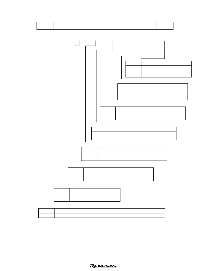
Rev. 1.0, 02/00, page 1113 of 1141
H'FFF8: Flash Memory Control Register 1 FLMCR1: FLASH ROM
7
FWE
--
*
R
6
SWE1
0
R/W
5
ESU1
0
R/W
4
PSU1
0
R/W
3
EV1
0
R/W
0
P1
0
R/W
2
PV1
0
R/W
1
E1
0
R/W
Note: * Determined by the state of the FWE pin.
Program1
Software write enable
Writes are disabled
(Initial value)
Writes are enabled
[Setting condition] When FWE = 1
0
1
Flash write enable
When a low level is input to the FWE pin (hardware-protected state)
When a high level is input to the FWE pin
0
1
Erase-verify1
Erase-verify mode cleared
(Initial value)
Transition to erase-verify mode
[Setting condition] When FWE = 1 and SWE1 = 1
0
1
Program-verify1
Program-verify mode cleared
(Initial value)
Transition to program-verufy mode
[Setting condition] When FWE = 1 and SWE1 = 1
0
1
Program set-up1
Program set-up cleared
(Initial value)
Transition to program set-up status
[Setting condition] When FWE = 1 and SWE1 = 1
0
1
Erase set-up1
Erase set-up cleared
(Initial value)
Transition to erase set-up status
[Setting condition] When FWE = 1 and SWE1 = 1
0
1
Erase1
Erase mode cleared
(Initial value)
Transition to erase mode
[Setting condition] When FWE = 1,
SWE1 = 1, and ESU1 = 1
0
1
Program mode cleared (Initial value)
Transition to program mode
[Setting condition] When FWE = 1,
SWE1 = 1, and PSU1 = 1
0
1
Bit
Initial value
R/W
:
:
:
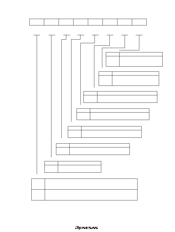
Rev. 1.0, 02/00, page 1114 of 1141
H'FFF9: Flash Memory Control Register 2 FLMCR2: FLASH ROM
Flash memory error
Flash memory is operating normally
Flash memory program/erase protection (error protection) is disabled
[Clearing condition] Reset
(Initial value)
An error has occurred during flash memeory programming/erasing
Flash memory program/erase protection (error protection) is enabled
[Setting condition] See section 7.6.3, Error Protection
0
1
7
FLER
0
R
6
SWE2
0
R/W
5
ESU2
0
R/W
4
PSU2
0
R/W
3
EV2
0
R/W
0
P2
0
R/W
2
PV2
0
R/W
1
E2
0
R/W
Program2
Software write enable2
Writes are disabled
(Initial value)
Writes are enabled
[Setting condition] When FWE = 1
0
1
Erase-verify2
Erase-verify mode cleared
(Initial value)
Transition to erase-verify mode
[Setting condition] When FWE = 1 and SWE2 = 1
0
1
Program-verify2
Program-verify mode cleared
(Initial value)
Transition to program-verufy mode
[Setting condition] When FWE = 1 and SWE2 = 1
0
1
Program set-up2
Program set-up cleared
(Initial value)
Transition to program set-up status
[Setting condition] When FWE = 1 and SWE2 = 1
0
1
Erase set-up2
Erase set-up cleared
(Initial value)
Transition to erase set-up status
[Setting condition] When FWE = 1 and SWE2 = 1
0
1
Erase2
Erase mode cleared
(Initial value)
Transition to erase mode
[Setting condition] When FWE = 1,
SWE2 = 1, and ESU2 = 1
0
1
Program mode cleared (Initial value)
Transition to program mode
[Setting condition] When FWE = 1,
SWE2 = 1, and PSU2 = 1
0
1
Bit
Initial value
R/W
:
:
:

Rev. 1.0, 02/00, page 1115 of 1141
H'FFFA: Erase Block Select Register 1 EBR1: FLASH ROM
7
EB7
0
R/W
6
EB6
0
R/W
5
EB5
0
R/W
4
EB4
0
R/W
3
EB3
0
R/W
0
EB0
0
R/W
2
EB2
0
R/W
1
EB1
0
R/W
Bit
:
Initial value
:
R/W
:
H'FFFB: Erase Block Select Register 2 EBR2: FLASH ROM
7
EB15
0
R/W
6
EB14
0
R/W
5
EB13
0
R/W
4
EB12
0
R/W
3
EB11
0
R/W
0
EB8
0
R/W
2
EB10
0
R/W
1
EB9
0
R/W
Bit
Initial value
R/W
:
:
:
Rev. 1.0, 02/00, page 1116 of 1141
Appendix C Pin Circuit Diagrams
C.1
Pin Circuit Diagrams
Circuit diagrams for all pins except power supply pins are shown in table C.1.
Legend
OUT
G
IN
OUT
G
IN
PMOS
NMOS
Clocked gate
Signal transmitted
when G = 1
Signal transmitted
when G = 0
Table C.1
Pin Circuit Diagrams
Pin States
Pin Names
Circuit Diagram
At Reset
Sleep
Mode
Power-Down
Modes Other
Than Sleep
Mode
P00/AN0 to
P07/AN7
∑ RD
SCH3 to SCH0
Hi-Z
Retained Hi-Z
AN8 to ANB
HCH1
A
HCH0
Hi-Z
Retained Hi-Z
Rev. 1.0, 02/00, page 1117 of 1141
Pin States
Pin Names
Circuit Diagram
At Reset
Sleep
Mode
Power-Down
Modes Other
Than Sleep
Mode
Retained Pull-up MOS:
OFF
Subactive mode:
Functions
Other modes:
Hi-Z
P10/
,54
to
P15/
,54
P16/
,&
PUR1n ∑
RD
PDR1n
PMR1n
PCR1n
INT
INT =
to
,
n = 0 to 6
PMR1n
Hi-Z
When
,54
to
,54
and
,&
are selected, pin input
should be fixed high or low.
P17/TMOW
PUR17∑
TMOW
PDR17
PMR17
PCR17
RD
Hi-Z
Retained Pull-up MOS:
OFF
Subactive mode:
Functions
Other modes:
Hi-Z
Retained Pull-up MOS:
OFF
Subactive mode:
Functions
Other modes:
Hi-Z
P20/SI1
PUR20∑
RD
PDR20
RXE
PCR20
SI1
RXE
RXE: Input control signal determined
by SCR and SMR
Hi-Z
When SI1 is selected, pin
input should be fixed high
or low.
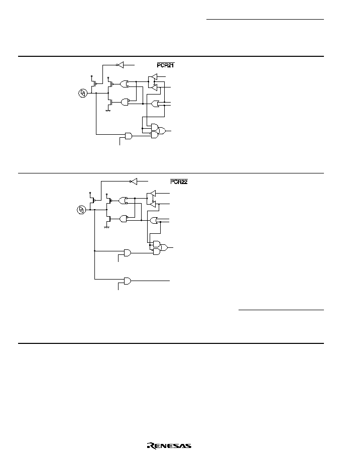
Rev. 1.0, 02/00, page 1118 of 1141
Pin States
Pin Names
Circuit Diagram
At Reset
Sleep
Mode
Power-Down
Modes Other
Than Sleep
Mode
P21/SO1
PUR21∑
SO1
PDR21
TXE
PCR21
RD
TXE: Output control signal determined
by SCR and SMR
Hi-Z
Retained Pull-up MOS:
OFF
Subactive mode:
Functions
Other modes:
Hi-Z
Retained Pull-up MOS:
OFF
Subactive mode:
Functions
Other modes:
Hi-Z
P22/SCK1
PUR22∑
SCKO
SCKI
PDR22
CKOE
PCR22
RD
CKIE
SCKO:
Transfer clock output
SCKI:
Transfer clock input
CKOE:
Transfer clock output control signal
determined by SMR and SCR
CKIE:
Transfer clock input control signal
determined by SMR and SCR
Hi-Z
When SCK1 is selected,
pin input should be fixed
high or low.
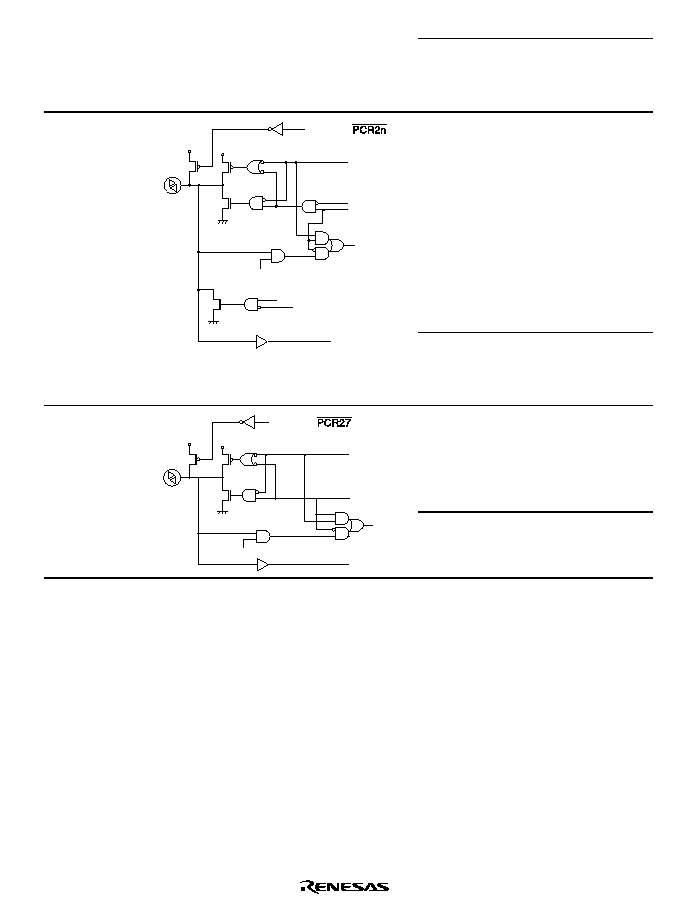
Rev. 1.0, 02/00, page 1119 of 1141
Pin States
Pin Names
Circuit Diagram
At Reset
Sleep
Mode
Power-Down
Modes Other
Than Sleep
Mode
Hi-Z
Retained Pull-up MOS:
OFF
Subactive mode:
Functions
Other modes:
Hi-Z
P23/SDA1
P24/SCL1
P25/SDA0
P26/SCL0
PUR2n ∑
SDA/SCL
PDR2n
IICE
PCR2n
RD
IICE
SDA/SCL
IICE = I
2
C bus enable signal
n = 3, 4, 5, 6
As SDA and SCL always function, a
high level or a low level should
always be input to the pins.
Hi-Z
Retained Pull-up MOS:
OFF
Subactive mode:
Functions
Other modes:
Hi-Z
P27/SYNCI
PUR27 ∑
PDR27
RD
PCR27
SYNCI
As SYNCI always functions, a high
level or a low level should always be
input to the pin.
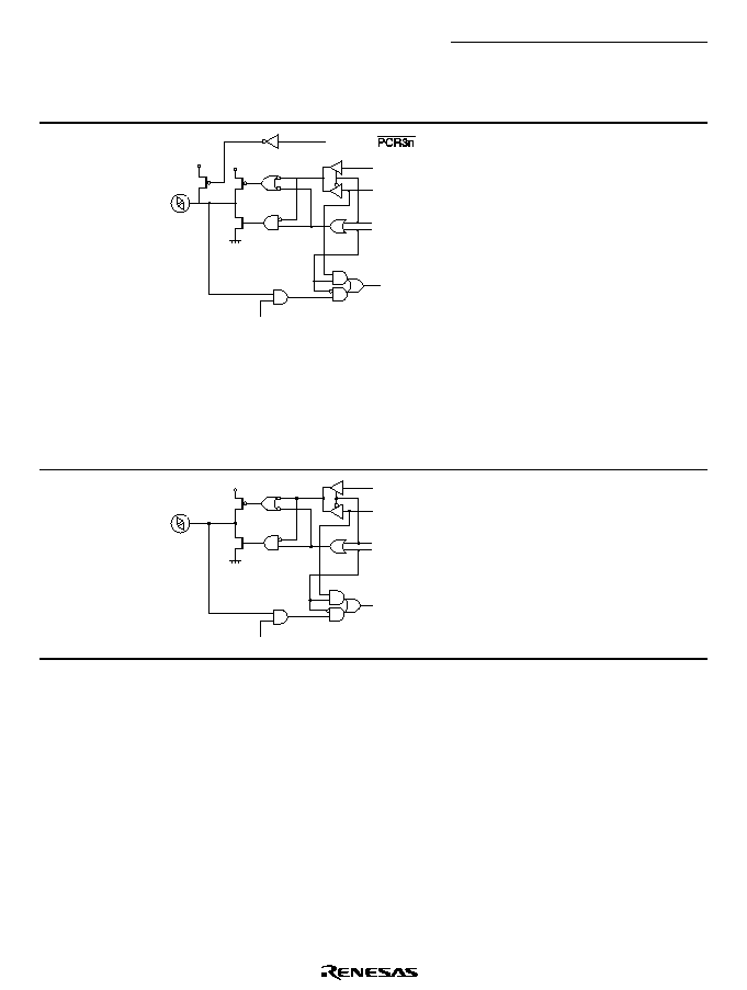
Rev. 1.0, 02/00, page 1120 of 1141
Pin States
Pin Names
Circuit Diagram
At Reset
Sleep
Mode
Power-Down
Modes Other
Than Sleep
Mode
P30/SVI
P31/SV2
P32/PWM0
P33/PWM1
P34/PWM2
P35/PWM3
P36/BUZZ
P37/TMO
PUR3n ∑
OUT
PDR3n
PMR3n
PCR3n
n = 1 to 7
RD
OUT:
P30/SV1:
Servo monitor output
P31/SV2:
Servo monitor output
P32/PWM0: 8 bit PWM0 output
P33/PWM1: 8 bit PWM1 output
P34/PWM2: 8 bit PWM2 output
P35/PWM3: 8 bit PWM3 output
P36/BUZZ:
Timer J buzzer output
P37/TMO:
Timer J timer output
Hi-Z
Retained Pull-up MOS:
OFF
Subactive mode:
Functions
Other modes:
Hi-Z
P40/PWM14
OUT
PDR40
PMR40
PCR40
OUT PWM14
RD
Hi-Z
Retained Subactive mode:
Functions
Other modes:
Hi-Z
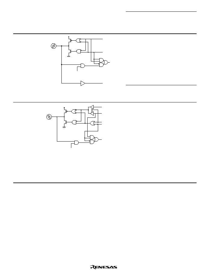
Rev. 1.0, 02/00, page 1121 of 1141
Pin States
Pin Names
Circuit Diagram
At Reset
Sleep
Mode
Power-Down
Modes Other
Than Sleep
Mode
Hi-Z
Retained Subactive mode:
Functions
Other modes:
Hi-Z
P41/FTIA
P42/PTIB
P43/FTIC
P44/FTID
RD
PDR4n
PCR4n
IN = FTIA, FTIB, FTIC, FTID
n = 1 to 4
IN
As FTIA to FTID always function, a
high level or a low level should
always be input to the pins.
P45/FTOA
P46/PTOB
OUT
PDR4n
TOE
PCR4n
RD
n = 5, 6
OUT:
P45/FTOA: Timer X1 output compare
output FTOA
P46/FTOB: Timer X1 output compare
output FTOB
TOE:
Output control signal determined
by TOCR
Hi-Z
Retained Subactive mode:
Functions
Other modes:
Hi-Z
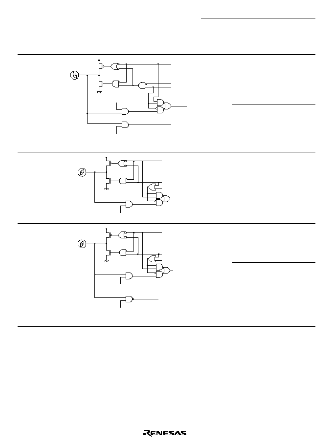
Rev. 1.0, 02/00, page 1122 of 1141
Pin States
Pin Names
Circuit Diagram
At Reset
Sleep
Mode
Power-Down
Modes Other
Than Sleep
Mode
Hi-Z
Retained Subactive mode:
Functions
Other modes:
Hi-Z
P47/RPTRG
RD
PDR47
PMR47
PCR47
RPTRG
PMR47
When RPTRG is selected,
pin input should be fixed
high or low.
P60/RP0 to
P65/RP5
RD
n = 0 to 5
PDRS6n
PCRS6n
PMR6n
Hi-Z
Retained Subactive mode:
Functions
Other modes:
Hi-Z
Hi-Z
Retained Subactive mode:
Functions
Other modes:
Hi-Z
P66/RP6/
$'75*
RD
TRGE
TRGE: A/D trigger input control signal
PDRS66
PCRS66
PMR66
ADTRG
When
$'75*
is selected,
pin input should be fixed
high or low.
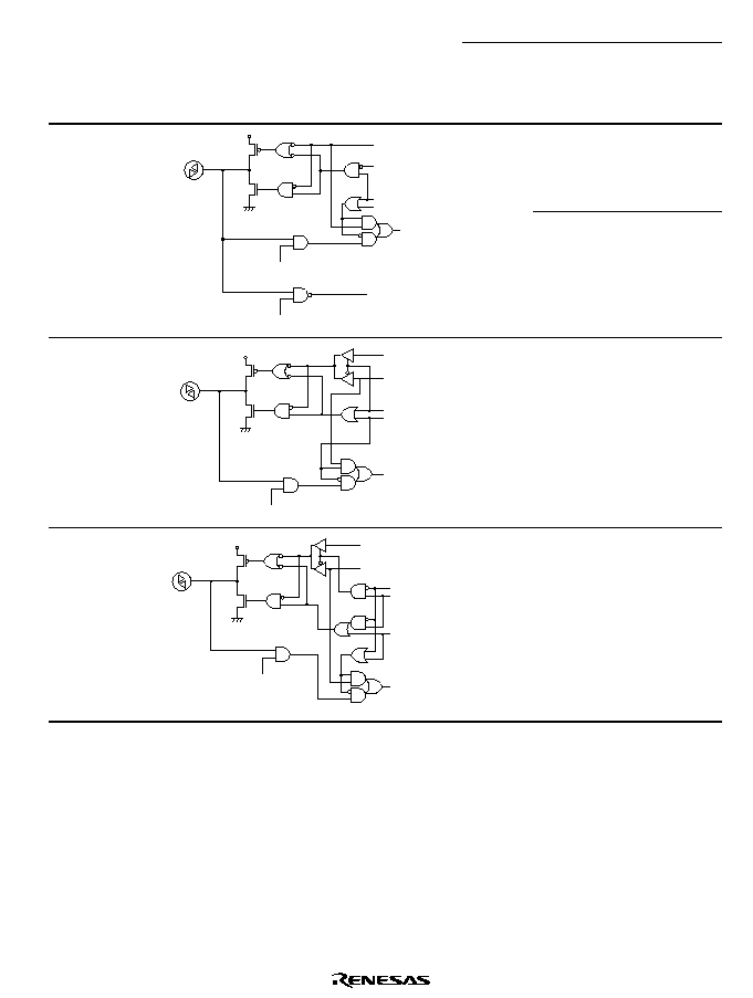
Rev. 1.0, 02/00, page 1123 of 1141
Pin States
Pin Names
Circuit Diagram
At Reset
Sleep
Mode
Power-Down
Modes Other
Than Sleep
Mode
Hi-Z
Retained Subactive mode:
Functions
Other modes:
Hi-Z
P67/RP7/
TMBI
RD
PMRA7
PDRS67
PMRA7
PCRS67
PMR67
TMBI
When TMBI is selected,
pin input should be fixed
high or low.
P70/PPG0 to
P73/PPG3
PPGn
PDR7n
PMR7n
PCR7n
RD
n = 0 to 3
Hi-Z
Retained Subactive mode:
Functions
Other modes:
Hi-Z
P74/PPG4/
RP8 to P77/
PPG7/RP8
PPGn
PDRS7n
PMRBn
PMR7n
PCRS7n
RD
n = 4 to 7
Hi-Z
Retained Subactive mode:
Functions
Other modes:
Hi-Z

Rev. 1.0, 02/00, page 1124 of 1141
Pin States
Pin Names
Circuit Diagram
At Reset
Sleep
Mode
Power-Down
Modes Other
Than Sleep
Mode
P80/YCO
YCO
PDR80
PMR80
PCR80
RD
Hi-Z
Retained Subactive mode:
Functions
Other modes:
Hi-Z
P83/
C.Rotary/R
P84/H.Amp
SW/G
OUT1
OUT1:
OUT2:
n = 3, 4
C.Rotary, H.Amp SW
R, G
OUT2
PDR8n
PMRCn
PMR8n
PCR8n
RD
Hi-Z
Retained Subactive mode:
Functions
Other modes:
Hi-Z
Hi-Z
Retained Subactive mode:
Functions
Other modes:
Hi-Z
P82/EXCTL
P86/
EXTTRG
PMR8n
IN = EXCTL, EXTTRG
RD
n = 2, 6
PDR8n
PMR8n
PCR8n
IN
When EXCTL and
EXTTRG are selected, pin
input should be fixed high
or low.
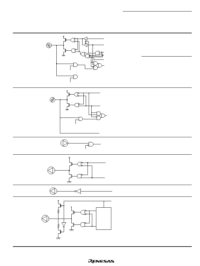
Rev. 1.0, 02/00, page 1125 of 1141
Pin States
Pin Names
Circuit Diagram
At Reset
Sleep
Mode
Power-Down
Modes Other
Than Sleep
Mode
Hi-Z
Retained Subactive mode:
Functions
Other modes:
Hi-Z
P85/COMP/
B
P81/EXCAP/
YBO
OUT
PDR8n
PMRCn
PMR8n
PCR8n
IN
RD
PMR8n
n= 1, 5
IN=EXCAP, COMP
OUT= YBO, B
When EXCAP COMP is
selected, pin input should
be fixed high or low.
P87/DPG
RD
PDR87
PCR87
DPG
Hi-Z
Retained Subactive mode:
Functions
Other modes:
Hi-Z
Csync
Module STOP
Pin input should be fixed high or low.
AUDIOFF
VIDEOFF
OUT
LPM
Hi-Z
Hi-Z
Hi-Z
CAPPWM
DRMPWM
Low
output
Low
output
Low output
Vpulse
LPM
3-level
controller
15k
Typ
Note: Resistance values are
reference values.
15k
Typ
Low
output
Low
output
Low output
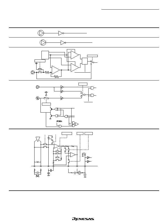
Rev. 1.0, 02/00, page 1126 of 1141
Pin States
Pin Names
Circuit Diagram
At Reset
Sleep
Mode
Power-Down
Modes Other
Than Sleep
Mode
5(6
RST
Low input (High)
(High)
MD0
FWE
CFG
+
-
+
-
+
-
CFGCOMP
CFGCOMP
P250
REF
M250
S
R
F/F O
stp
VREF
VREF
CFG
BIAS
Res+ModuleSTOP
DFG
DPG
RD ∑
PDRn
DFG
DPG
PMRn
PCRn
DPG SW
DPG SW
Pes+LPM
DFG
DPG
Hi-Z
Hi-Z
CTL (+)
CTL (
-
)
CTLREF
CTLBias
CTLFB
CTLAmp (O)
CTLSMT (I)
+
-
-
+
+ -
CTLGR3 to 1
CTLFB
CTLGR0
AMPSHORT
(REC-CTL)
AMPON
(PB-CTL)
PB-CTL (+)
PB-CTL (–)
CTLSMT (i)
CTLREF
CTL (+)
CTL (-)
CTLBias
CTLFB CTLAmp(o)
*
Note: * Connect a capacitor between
CTLAmp (o), CTLSMT (i)
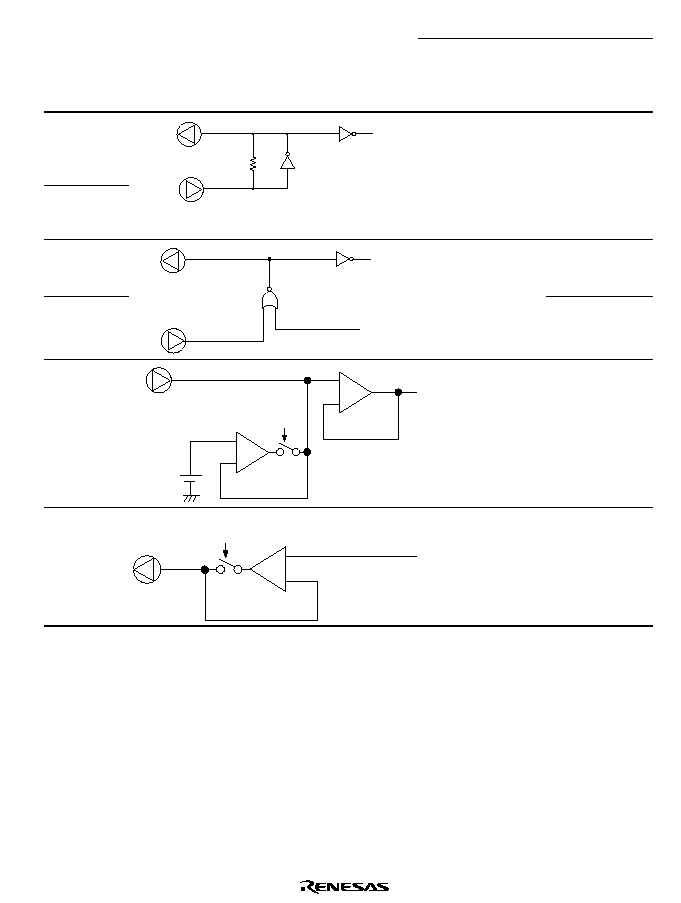
Rev. 1.0, 02/00, page 1127 of 1141
Pin States
Pin Names
Circuit Diagram
At Reset
Sleep
Mode
Power-Down
Modes Other
Than Sleep
Mode
X2
X1
10M
Typ
Note: The resistance value is a
reference value.
Oscil-
lation
Oscil-
lation
Oscillation
OSC2
Low output
OSC1
LPM
Oscil-
lation
Oscil-
lation
CVin1
Sync tip
i
1.4V
j
LPM
+
≠
+
≠
Hi-Z
Hi-Z
Hi-Z
CVout
+
≠
LPM
Hi-Z
Hi-Z
Hi-Z
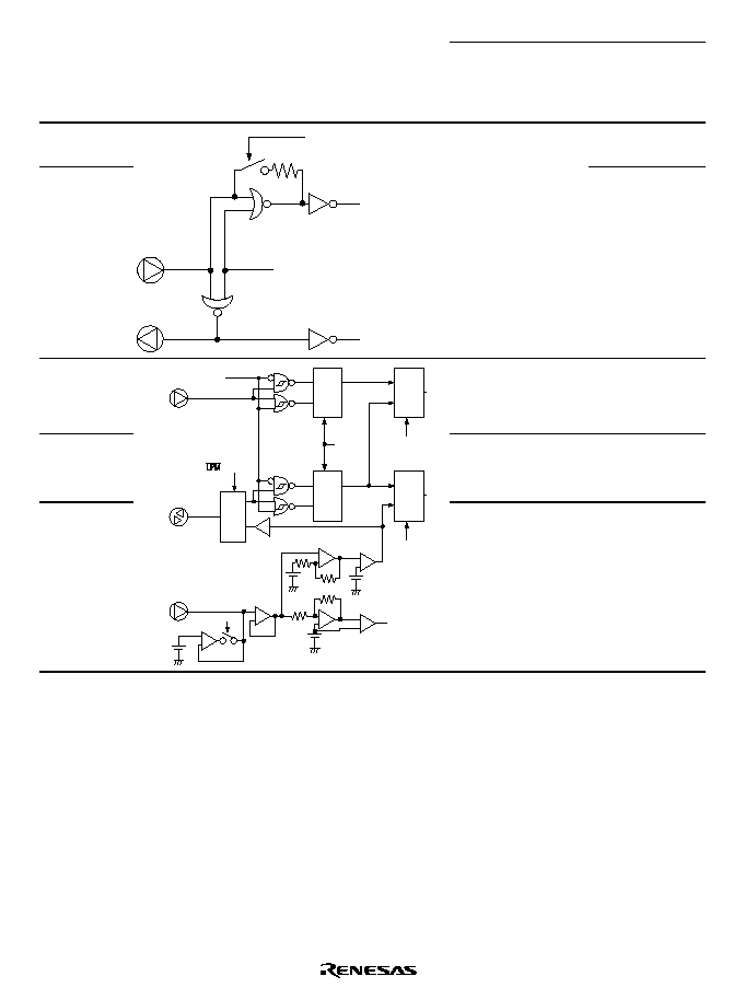
Rev. 1.0, 02/00, page 1128 of 1141
Pin States
Pin Names
Circuit Diagram
At Reset
Sleep
Mode
Power-Down
Modes Other
Than Sleep
Mode
4/2fsc in
Oscilla-
tion
Oscilla-
tion
4/2fsc out
LPM
4/2fsc in
(External input)
4/2fsc in
External clock select
Low output
(Oscillation
stopped)
VLPF/Csync
Pin input should be fixed high or low
Csync/
Hsync
Hi-Z
Hi-Z
Hi-Z
CVin2
+
≠
+
≠
+
≠
+
≠
+
≠
+
≠
Polarity
switch
Signal
selection
Polarity
switch
I/O
switch
Sync tip
(2.0V)
Signal
selection
Vsync
Hsync
VSEL
SYNCT
LPM
∑ CCMPSL
CCMPSL
EDS
LPM
Hi-Z
Hi-Z
Hi-Z
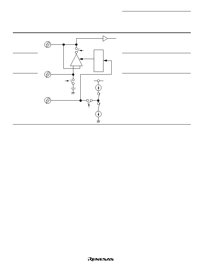
Rev. 1.0, 02/00, page 1129 of 1141
Pin States
Pin Names
Circuit Diagram
At Reset
Sleep
Mode
Power-Down
Modes Other
Than Sleep
Mode
AFCOSC
Oscilla-
tion
Oscilla-
tion
Hi-Z
Oscillation
stopped
AFCPC
1/2 OV
CC
1/2 OV
CC
AFCLPF
1/2 OV
CC
LPM
UP
+
DOWN
LPM
LPM
≠
Phase
gain
control
Retained Retained
Legend
RD:
Read signal
RST:
Reset signal
LPM:
Power-down mode signal (1 in standby, watch, subactive, and subsleep modes)
Hi-Z:
High impedance
SLEEP: Sleep mode signal
Note: Numbers given for resistance values, etc., are reference values.

Rev. 1.0, 02/00, page 1130 of 1141
Appendix D Port States in Each Processing State
D.1
Pin Circuit Diagrams
Table D.1
Port States Overview
Port
Reset
Active
Sleep
Standby
Watch
Subactive
Subsleep
P07 to
P00
High
imped-
ance
High
imped-
ance
High
imped-
ance
High
imped-
ance
High
imped-
ance
High
impedance
High
impedance
P17 to
P10
High
imped-
ance
Functions
Retained
High
imped-
ance
High
imped-
ance
Functions
Retained
P27 to
P20
High
imped-
ance
Functions
Retained
High
imped-
ance
High
imped-
ance
Functions
Retained
P37 to
P30
High
imped-
ance
Functions
Retained
High
imped-
ance
High
imped-
ance
Functions
Retained
P47 to
P40
High
imped-
ance
Functions
Retained
High
imped-
ance
High
imped-
ance
Functions
Retained
P67 to
P60
High
imped-
ance
Functions
Retained
High
imped-
ance
High
imped-
ance
Functions
Retained
P77 to
P70
High
imped-
ance
Functions
Retained
High
imped-
ance
High
imped-
ance
Functions
Retained
P87 to
P80
High
imped-
ance
Functions
Retained
High
imped-
ance
High
imped-
ance
Functions
Retained
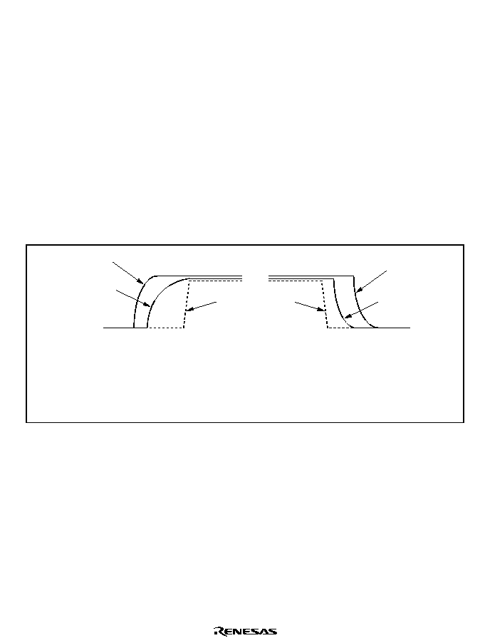
Rev. 1.0, 02/00, page 1131 of 1141
Appendix E Usage Notes
E.1
Power Supply Rise and Fall Order
Figure E.1 shows the order in which the power supply pins rise when the chip is powered on, and
the order in which they fall when the chip is powered down. If the power supply voltages cannot
rise and fall simultaneously, power supply operations should be carried out in this order.
∑
At power-on, wait until the microcomputer section power supply (V
CC
) has risen to the
prescribed voltage, then raise the other analog power supplies.
∑
At power-down, drop the analog power supplies first, followed by the microcomputer section
power supply (V
CC
).
When powering up and down, the voltage applied to the pins should not exceed the respective
power supply voltage.
V
CC
, AV
CC
V
CC
AV
CC
SV
CC
OSD
Vin
: Microcomputer section power supply voltage
: A/D converter power supply voltage
: Servo section power supply voltage
: Section power supply voltage
: Pin applied voltage
SV
CC
, OV
CC
V
CC
, AV
CC
SV
CC
Vin
Vin
Figure E.1 Power Supply Rise and Fall Order
In power-down modes (except sleep mode), the analog power supplies can be controlled at the
V
SS
level to reduce current dissipation. When the microcomputer section power supply (V
CC
) is
dropped to the backup voltage in a power-down mode, the order shown in figure E.2 should be
followed. Make sure that the voltage applied to the pins does not exceed the respective power
supply voltage.
The A/D converter power supply (AV
CC
) should be set to the same potential as the
microcomputer section power supply (V
CC
). In all power-down modes except sleep mode, AV
CC
is turned off inside the device. At this time, the AV
CC
current dissipation is defined as AISTOP.
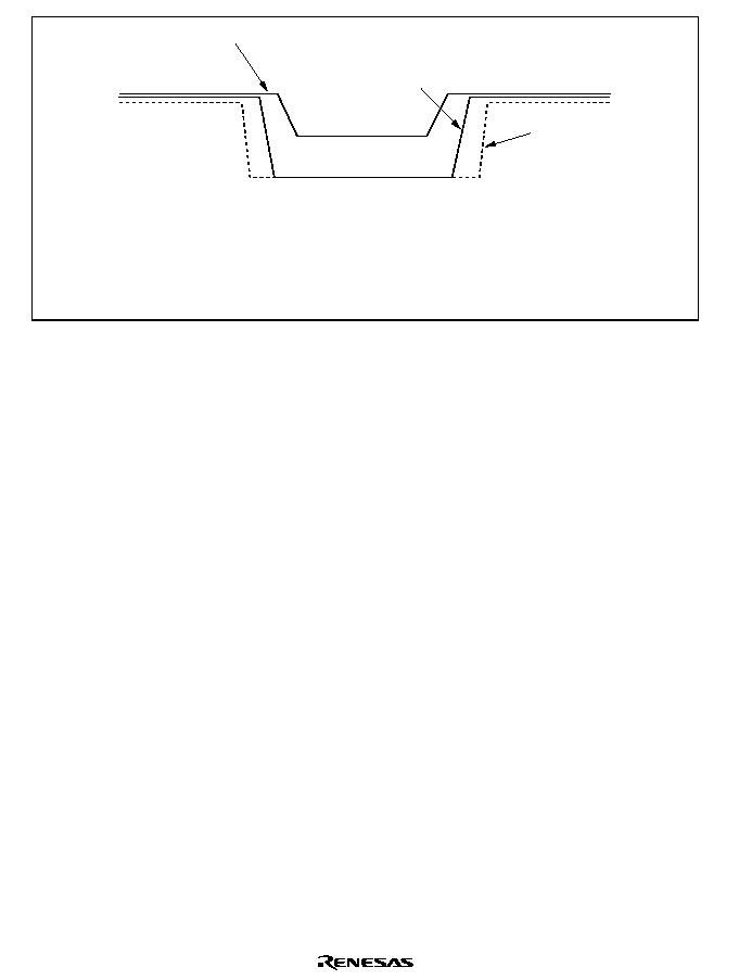
Rev. 1.0, 02/00, page 1132 of 1141
V
CC
AV
CC
SV
CC
OV
CC
Vin
5 V
2.7 V
: Microcomputer section power supply voltage
: A/D converter power supply voltage
: Servo section power supply voltage
: OSD Section power supply
: Pin applied voltage
V
CC
, AV
CC
SV
CC
, OV
CC
Vin
Figure E.2 Power Supply Control in Power-Down Modes
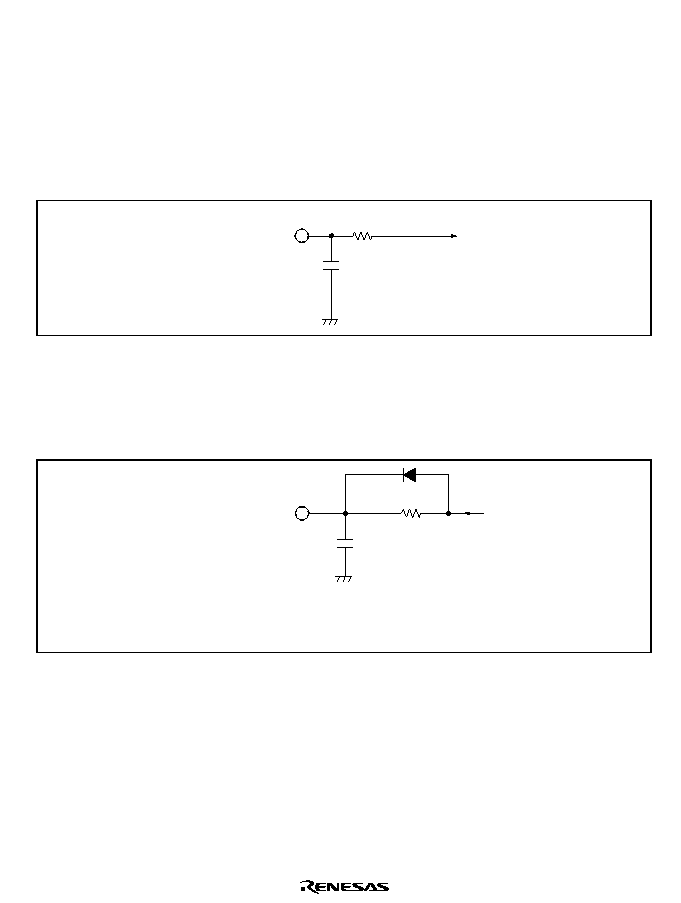
Rev. 1.0, 02/00, page 1133 of 1141
E.2
Sample External Circuits
Examples of external circuits for the servo section, and sync signal detection circuit are shown in
figures E.3, E.4.
1. Servo Section
An example of the external circuit for the DRMPWM output and CAPPWM output pins is
shown in figure E.3.
R
1
DRMPWM
CAPPWN
C
1
Figure E.3 Sample External Circuit for Servo Section
2. Sync Signal Detection Circuit Section in Servo Circuit
Figure E.4 shows an example of the external circuit for the sync signal detection circuit section
in the servo circuit.
33 k
Csync
Note: Reference values are shown.
The board floating capacitance and wiring resistance must also
be taken into consideration in determining the values.
10 pF
Figure E.4 Example of External Circuit for Sync Signal Detection Circuit Section
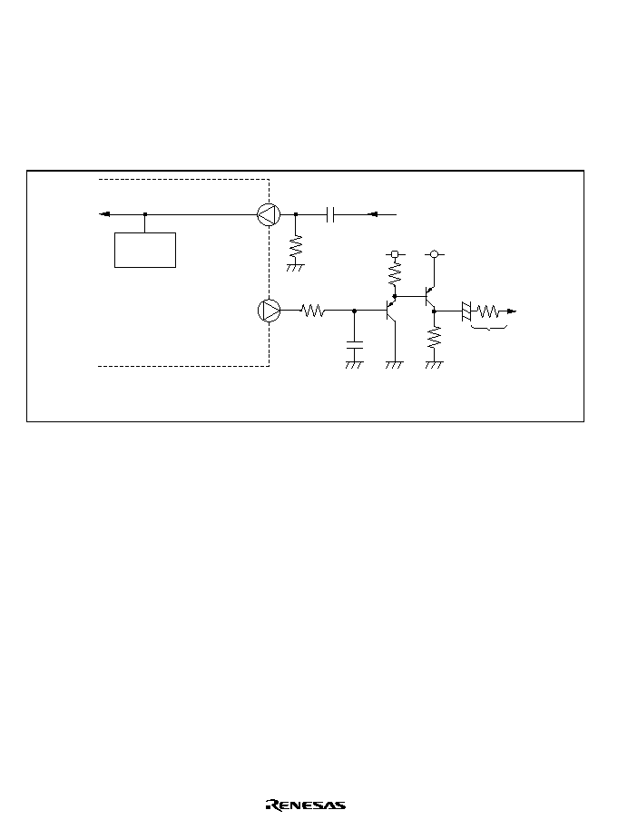
Rev. 1.0, 02/00, page 1134 of 1141
3. OSD
An example of the external circuit for the OSD is shown in figure E.5.
The circuit configuration and values for the filter section will vary according to the wiring
capacitance, impedance, etc.
When designing the board, an appropriate filter should be configured, taking account of the
wiring load. Noise prevention measures also need to be taken when designing the board.
Clamp
(=1.4Vtyp)
Note: Reference values are shown.
The board floating capacitance and wiring resistance must also
be taken into consideration in determining the values.
C.Vin1
C.Vout
4.7
µ
F
470
µ
F
+
68
75
driver
1k
2.7k
470k
120
5pF
Figure E.5 Example of External Circuit for OSD
4. Sync Separator and Data Slicer
Examples of the external circuits for the sync separator and data slicer are shown in figures E.6
to E.8.
The sync signal separation sources can be selected from the following three: (1) CVin2, (2)
Csync, and (3) separate Hsync and Vsync signals. The external circuit configuration will vary
depending on the separation source.
When the data slicer is used, CVin2 is recommended as the separation source. When Csync or
Hsync and Vsync are selected as the source, connect to CVin2 the same external circuit as when
CVin2 is selected as the separation source.
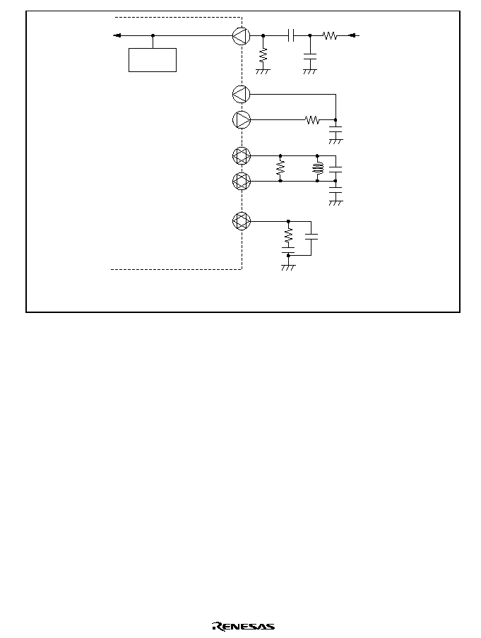
Rev. 1.0, 02/00, page 1135 of 1141
4.7
µ
F
4.7
µ
F
6.8
µ
H/12
µ
H
0.01
µ
F
0.01
µ
F
330pF
680pF
10pF/12pF
C.Vin2
VLPF/Vsync
Csync/Hsync
AFCOSC
AFCPC
AFCLPF
330
470k
10k
470
2.4k
Clamp 2
(=2.0Vtyp)
Note:
Reference values are shown.
The board floating capacitance and wiring resistance
must also be taken into consideration in determining the values.
Figure E.6 Example of External Circuit for Sync Separator and Data Slicer
((1) Separation from CVin2)
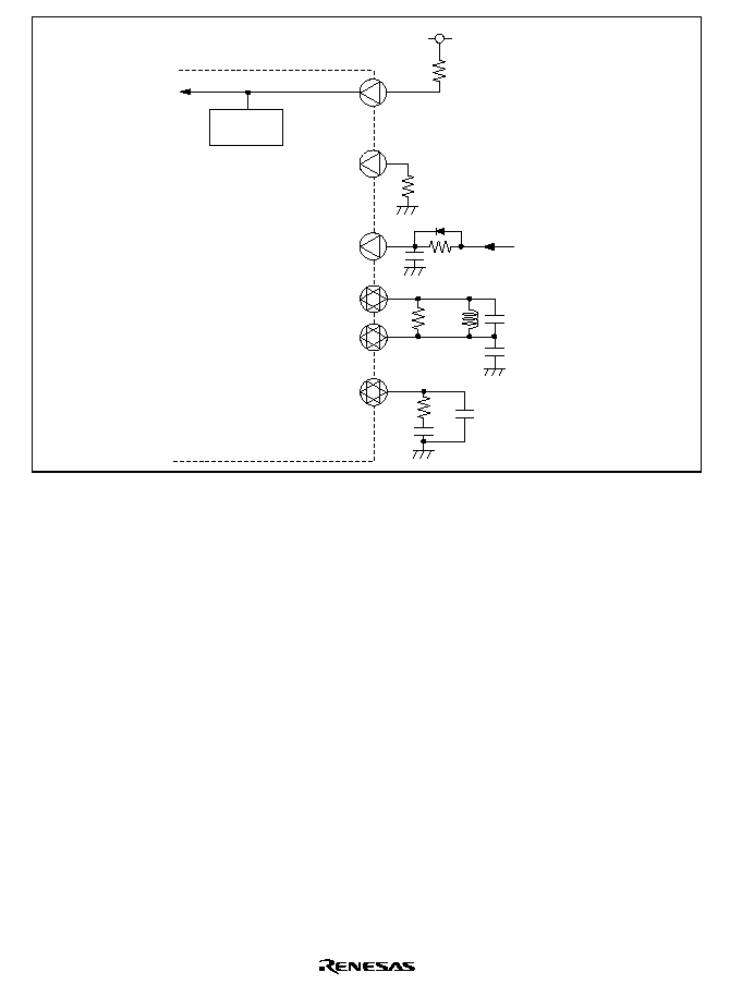
Rev. 1.0, 02/00, page 1136 of 1141
4.7
µ
F
0.01
µ
F
0.01
µ
F
10PF
C.Vin2
VLPF/Vsync
Csync/Hsync
AFCOSC
AFCPC
AFCLPF
10k
10k
33k
2.4k
Clamp 2
(=2.0Vtyp)
6.8
µ
H/12
µ
H
10pF/12pF
470
OV
CC
Figure E.7 Example of External Circuit for Sync Separator and Data Slicer
((2) Separation from Csync)
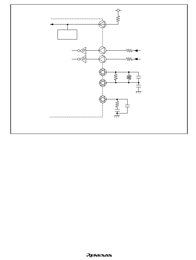
Rev. 1.0, 02/00, page 1137 of 1141
4.7
µ
F
4.7
µ
F
0.01
µ
F
C.Vin2
VLPF/Vsync
Csync/Hsync
AFCLPF
AFCOSC
2.4k
Clamp 2
(=2.0Vtyp)
6.8
µ
H/12
µ
H
10pF/12pF
470
Note:
Reference values are shown.
The board floating capacitance and wiring resistance
must also be taken into consideration in determining the values.
10k
OV
CC
Figure E.8 Example of External Circuit for Sync Separator and Data Slicer
((3) Separation from Hsync and Vsync)

Rev. 1.0, 02/00, page 1138 of 1141
E.3
Handling of Pins When OSD Is Not Used
Table E.2 shows the handling of pins when the OSD, sync separator, or data slicer is not used.
Table E.2
Handling of Pins When OSD Is Not Used
Conditions
Pin Handling
OSD
Used
Not used
Not used
Not used
Not used
Data slicer
Not used
Used
Not used
Not used
Not used
Module used
or not used
Sync
separator
Used
Used
Used
Not used
Not used
OSDV
CC
V
CC
V
CC
V
CC
V
CC
V
SS
OSDV
SS
V
SS
V
SS
V
SS
V
SS
V
SS
Csync/Hsync Csync/Hsync Csync/Hsync Csync/Hsync 10 k
to V
SS
V
SS
VLPF/Vsync VLPF/Vsync VLPF/Vsync VLPF/Vsync 10 k
to V
SS
V
SS
AFCOSC
AFCOSC
AFCOSC
AFCOSC
10 k
to V
SS
V
SS
AFCPC
AFCPC
AFCPC
AFCPC
OPEN
V
SS
AFCLPF
AFCLPF
AFCLPF
AFCLPF
10 k
to V
SS
V
SS
CVin1
CVin1
10 k
to V
SS
10 k
to V
SS
10 k
to V
SS
V
SS
CVout
CVout
OPEN
OPEN
OPEN
V
SS
4fsc in
4fsc in
V
SS
V
SS
V
SS
V
SS
4fsc out
4fsc out
OPEN
OPEN
OPEN
OPEN
Pins
CVin2
CVin2 or 10
k
to V
SS
CVin2 or 10
k
to V
SS
CVin2 or 10
k
to V
SS
10 k
to V
SS
V
SS
Note
The registers
in the OSD,
sync
separator,
and data
slicer must
not be
accessed.

Rev. 1.0, 02/00, page 1139 of 1141
Table E.3
Pin Handling When Using OSD and Sync Separation, and Not Using CVin1
and CVin2
Conditions
Pin Handling
OSD
Used
Module used or not used
Sync separator
Used
CVin1
10 K
to OVcc
Unused pins
CVin2
10 K
to OVcc

Rev. 1.0, 02/00, page 1140 of 1141
Appendix F Product Lineup
Table F.1
Product Lineup of H8S/2199 Series
Product Type
Product
Code
Mark Code
Package
(Hitachi
Package Code)
Mask ROM
version
HD6432199
HD6432199 (***)F
112-pin FP
(FP-112)
H8S/2199
F-ZTAT
version
HD64F2199
HD64F2199F
112-pin FP
(FP-112)
H8S/2198
Mask ROM
version
HD6432198
HD6432198 (***)F
112-pin FP
(FP-112)
H8S/2197
Mask ROM
version
HD6432197
HD6432197 (***)F
112-pin FP
(FP-112)
H8S/2199
Series
H8S/2196
Mask ROM
version
HD6432196
HD6432196 (***)F
112-pin FP
(FP-112)
Note: (***) is the ROM code.
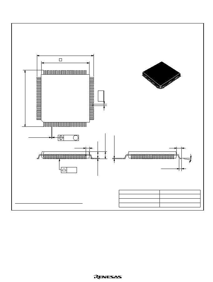
Rev. 1.0, 02/00, page 1141 of 1141
Appendix G Package Dimensions
Hitachi Code
JEDEC
EIAJ
Weight (reference value)
FP-112
--
Conforms
2.4 g
Unit: mm
*Dimension including the plating thickness
Base material dimension
0.10
23.2
±
0.3
*0.32
±
0.08
0.65
1.6
0.8
±
0.3
*0.17
±
0.05
3.05 Max
23.2
±
0.3
84
57
56
29
112
1
28
20
85
2.70
0
∞
≠ 8
∞
0.13 M
0.10
+0.15 ≠0.10
1.23
0.30
±
0.06
0.15
±
0.04
Figure G.1 Package Dimensions (FP-112)

H8S/2199 Series, H8S/2199F-ZTATTM Hardware Manual
Publication Date: 1st Edition, February 2000
Published by:
Electronic Devices Sales & Marketing Group
Semiconductor & Integrated Circuits
Hitachi, Ltd.
Edited by:
Technical Documentation Group
Hitachi Kodaira Semiconductor Co., Ltd.
Copyright © Hitachi, Ltd., 2000. All rights reserved. Printed in Japan.