 | ÐлекÑÑоннÑй компоненÑ: HD6432211 | СкаÑаÑÑ:  PDF PDF  ZIP ZIP |
H8S/2218 Series, H8S/2212 Series Hardware Manual

Regarding the change of names mentioned in the document, such as Hitachi
Electric and Hitachi XX, to Renesas Technology Corp.
The semiconductor operations of Mitsubishi Electric and Hitachi were transferred to Renesas
Technology Corporation on April 1st 2003. These operations include microcomputer, logic, analog
and discrete devices, and memory chips other than DRAMs (flash memory, SRAMs etc.)
Accordingly, although Hitachi, Hitachi, Ltd., Hitachi Semiconductors, and other Hitachi brand
names are mentioned in the document, these names have in fact all been changed to Renesas
Technology Corp. Thank you for your understanding. Except for our corporate trademark, logo and
corporate statement, no changes whatsoever have been made to the contents of the document, and
these changes do not constitute any alteration to the contents of the document itself.
Renesas Technology Home Page: http://www.renesas.com
Renesas Technology Corp.
Customer Support Dept.
April 1, 2003
To all our customers

Cautions
Keep safety first in your circuit designs!
1. Renesas Technology Corporation puts the maximum effort into making semiconductor products better
and more reliable, but there is always the possibility that trouble may occur with them. Trouble with
semiconductors may lead to personal injury, fire or property damage.
Remember to give due consideration to safety when making your circuit designs, with appropriate
measures such as (i) placement of substitutive, auxiliary circuits, (ii) use of nonflammable material or
(iii) prevention against any malfunction or mishap.
Notes regarding these materials
1. These materials are intended as a reference to assist our customers in the selection of the Renesas
Technology Corporation product best suited to the customer's application; they do not convey any
license under any intellectual property rights, or any other rights, belonging to Renesas Technology
Corporation or a third party.
2. Renesas Technology Corporation assumes no responsibility for any damage, or infringement of any
third-party's rights, originating in the use of any product data, diagrams, charts, programs, algorithms, or
circuit application examples contained in these materials.
3. All information contained in these materials, including product data, diagrams, charts, programs and
algorithms represents information on products at the time of publication of these materials, and are
subject to change by Renesas Technology Corporation without notice due to product improvements or
other reasons. It is therefore recommended that customers contact Renesas Technology Corporation
or an authorized Renesas Technology Corporation product distributor for the latest product information
before purchasing a product listed herein.
The information described here may contain technical inaccuracies or typographical errors.
Renesas Technology Corporation assumes no responsibility for any damage, liability, or other loss
rising from these inaccuracies or errors.
Please also pay attention to information published by Renesas Technology Corporation by various
means, including the Renesas Technology Corporation Semiconductor home page
(http://www.renesas.com).
4. When using any or all of the information contained in these materials, including product data, diagrams,
charts, programs, and algorithms, please be sure to evaluate all information as a total system before
making a final decision on the applicability of the information and products. Renesas Technology
Corporation assumes no responsibility for any damage, liability or other loss resulting from the
information contained herein.
5. Renesas Technology Corporation semiconductors are not designed or manufactured for use in a device
or system that is used under circumstances in which human life is potentially at stake. Please contact
Renesas Technology Corporation or an authorized Renesas Technology Corporation product distributor
when considering the use of a product contained herein for any specific purposes, such as apparatus or
systems for transportation, vehicular, medical, aerospace, nuclear, or undersea repeater use.
6. The prior written approval of Renesas Technology Corporation is necessary to reprint or reproduce in
whole or in part these materials.
7. If these products or technologies are subject to the Japanese export control restrictions, they must be
exported under a license from the Japanese government and cannot be imported into a country other
than the approved destination.
Any diversion or reexport contrary to the export control laws and regulations of Japan and/or the
country of destination is prohibited.
8. Please contact Renesas Technology Corporation for further details on these materials or the products
contained therein.

Hitachi 16-bit Single-Chip Microcomputer
H8S/2218 Series
H8S/2212 Series
H8S/2218
HD64F2218, HD64F2218U, HD6432217
H8S/2212
HD64F2212, HD64F2212U,
HD6432211, HD6432210
Hardware Manual
ADE-602-310
Rev. 1.0
02/27/03
Hitachi Ltd.

Rev. 1.0, 02/03, page ii of xxxvi
Cautions
1. Hitachi neither warrants nor grants licenses of any rights of Hitachi's or any third party's
patent, copyright, trademark, or other intellectual property rights for information contained in
this document. Hitachi bears no responsibility for problems that may arise with third party's
rights, including intellectual property rights, in connection with use of the information
contained in this document.
2. Products and product specifications may be subject to change without notice. Confirm that you
have received the latest product standards or specifications before final design, purchase or
use.
3. Hitachi makes every attempt to ensure that its products are of high quality and reliability.
However, contact Hitachi's sales office before using the product in an application that demands
especially high quality and reliability or where its failure or malfunction may directly threaten
human life or cause risk of bodily injury, such as aerospace, aeronautics, nuclear power,
combustion control, transportation, traffic, safety equipment or medical equipment for life
support.
4. Design your application so that the product is used within the ranges guaranteed by Hitachi
particularly for maximum rating, operating supply voltage range, heat radiation characteristics,
installation conditions and other characteristics. Hitachi bears no responsibility for failure or
damage when used beyond the guaranteed ranges. Even within the guaranteed ranges,
consider normally foreseeable failure rates or failure modes in semiconductor devices and
employ systemic measures such as fail-safes, so that the equipment incorporating Hitachi
product does not cause bodily injury, fire or other consequential damage due to operation of
the Hitachi product.
5. This product is not designed to be radiation resistant.
6. No one is permitted to reproduce or duplicate, in any form, the whole or part of this document
without written approval from Hitachi.
7. Contact Hitachi's sales office for any questions regarding this document or Hitachi
semiconductor products.

Rev. 1.0, 02/03, page iii of xxxvi
General Precautions on the Handling of Products
1. Treatment of NC Pins
Note:
Do not connect anything to the NC pins.
The NC (not connected) pins are not connected to any of the internal circuitry; they are
used as test pins or to reduce noise. If something is connected to the NC pins, the operation
of the LSI is not guaranteed.
2. Treatment of Unused Input Pins
Note:
Fix all unused input pins to high or low level.
Generally, the input pins of CMOS products are high-impedance input pins. If unused pins
are in their open states, intermediate levels are induced by noise in the vicinity, a pass-
through current flows internally, and a malfunction may occur.
3. Processing before Initialization
Note:
When power is first supplied, the product's state is undefined. The states of internal
circuits are undefined until full power is supplied throughout the chip and a low level is
input on the reset pin. During the period where the states are undefined, the register
settings and the output state of each pin are also undefined. Design your system so that it
does not malfunction because of processing while it is in this undefined state. For those
products which have a reset function, reset the LSI immediately after the power supply has
been turned on.
4. Prohibition of access to undefined or reserved address
Note:
Access to undefined or reserved addresses is prohibited.
The undefined or reserved addresses may be used to expand functions, or test registers
may have been be allocated to these address. Do not access these registers: the system's
operation is not guaranteed if they are accessed.

Rev. 1.0, 02/03, page iv of xxxvi
Configuration of this Manual
This manual comprises the following items:
1. Precautions in Relation to this Product
2. Configuration of this Manual
3. Overview
4. Table of Contents
5. Summary
6. Description of Functional Modules
·
CPU and System-Control Modules
·
On-chip Peripheral Modules
The configuration of the functional description of each module differs according to the module.
However, the generic style includes the following items:
i) Features
ii) I/O pins
iii) Description of Registers
iv) Description of Operation
v) Usage: Points for Caution
When designing an application system that includes this LSI, take the points for caution into
account. Each section includes points for caution in relation to the descriptions given, and points
for caution in usage are given, as required, as the final part of each section.
7. List of Registers
8. Electrical Characteristics
9. Appendix
10. Main Revisions and Additions in this Edition (only for revised versions)
The list of revisions is a summary of points that have been revised or added to earlier versions.
This does not include all of the revised contents. For details, see the actual locations in this
manual.
11. Index

Rev. 1.0, 02/03, page v of xxxvi
Preface
This LSI is a high-performance microcomputer (MCU) made up of the H8S/2000 CPU with
Hitachi's original architecture as its core, and the peripheral functions required to configure a
system.
The H8S/2000 CPU has an internal 32-bit configuration, sixteen 16-bit general registers, and a
simple and optimized instruction set for high-speed operation. The H8S/2000 CPU can handle a
16-Mbyte linear address space.
This LSI is equipped with ROM, RAM, a direct memory access controller (DMAC), a bus master,
a 16-bit timer pulse unit (TPU), a watchdog timer (WDT), a realtime clock (RTC) a universal
serial bus (USB), two types of serial communication interfaces (SCIs), an A/D converter, and I/O
ports as on-chip peripheral modules for system configuration.
A single-power flash memory (F-ZTAT
*) version and masked ROM version are available for
this LSI's ROM. The F-ZTAT version provides flexibility as it can be reprogrammed in no time to
cope with all situations from the early stages of mass production to full-scale mass production.
This is particularly applicable to application devices with specifications that will most probably
change.
This manual describes this LSI's hardware.
Note: * F-ZTAT
TM
is a trademark of Hitachi, Ltd.
Target Users:
This manual was written for users who will be using the H8S/2218 Series and
H8S/2212 Series in the design of application systems. Target users are expected to
understand the fundamentals of electrical circuits, logical circuits, and
microcomputers.
Objective:
This manual was written to explain the hardware functions and electrical
characteristics of the H8S/2218 Series and H8S/2212 Series to the target users.
Refer to the H8S/2600 Series, H8S/2000 Series Programming Manual for a
detailed description of the instruction set.
Notes on reading this manual:
· In order to understand the overall functions of the chip
Read the manual according to the contents. This manual can be roughly categorized into parts
on the CPU, system control functions, peripheral functions and electrical characteristics.
· In order to understand the details of the CPU's functions
Read the H8S/2600 Series, H8S/2000 Series Programming Manual.

Rev. 1.0, 02/03, page vi of xxxvi
· In order to understand the details of a register when its name is known
Read the index that is the final part of the manual to find the page number of the entry on the
register. The addresses, bits, and initial values of the registers are summarized in section 21,
List of Registers.
Examples:
Register name:
The following notation is used for cases when the same or a
similar function, e.g. 16-bit timer pulse unit or serial
communication, is implemented on more than one channel:
XXX_N (XXX is the register name and N is the channel
number)
Bit order:
The MSB is on the left and the LSB is on the right.
Number notation: Binary is B'xxxx, hexadecimal is H'xxxx.
Signal notation:
An overbar is added to a low-active signal:
xxxx
Related Manuals:
The latest versions of all related manuals are available from our web site.
Please ensure you have the latest versions of all documents you require.
http://www.hitachisemiconductor.com/
H8S/2218 Series, H8S/2212 Series manuals:
Manual Title
ADE No.
H8S/2218 Series, H8S/2212 Series Hardware Manual
This manual
H8S/2600 Series, H8S/2000 Series Programming Manual
ADE-602-083
User's manuals for development tools:
Manual Title
ADE No.
H8S, H8/300 Series C/C++ Compiler, Assembler, Optimizing Linkage
Editor User's Manual
ADE-702-247
H8S, H8/300 Series Simulator Debugger (for Windows) Users Manual
ADE-702-085
H8S, H8/300 Series Hitachi Embedded Workshop, Hitachi Debugging
Interface Tutorial
ADE-702-231
Hitachi Embedded Workshop User's Manual
ADE-702-201

Rev. 1.0, 02/03, page vii of xxxvi
Contents
Section 1 Overview............................................................................................1
1.1
Overview........................................................................................................................... 1
1.2
Internal Block Diagram..................................................................................................... 3
1.3
Pin Arrangement ............................................................................................................... 5
1.4
Pin Functions in Each Operating Mode ............................................................................ 7
1.5
Pin Functions .................................................................................................................... 12
Section 2 CPU....................................................................................................21
2.1
Features ............................................................................................................................. 21
2.1.1
Differences between H8S/2600 CPU and H8S/2000 CPU .................................. 22
2.1.2
Differences from H8/300 CPU ............................................................................ 23
2.1.3
Differences from H8/300H CPU.......................................................................... 23
2.2
CPU Operating Modes ...................................................................................................... 24
2.2.1
Normal Mode....................................................................................................... 24
2.2.2
Advanced Mode ................................................................................................... 26
2.3
Address Space ................................................................................................................... 28
2.4
Register Configuration...................................................................................................... 29
2.4.1
General Registers ................................................................................................. 30
2.4.2
Program Counter (PC) ......................................................................................... 31
2.4.3
Extended Control Register (EXR) ....................................................................... 31
2.4.4
Condition-Code Register (CCR) .......................................................................... 32
2.4.5
Initial Register Values.......................................................................................... 33
2.5
Data Formats ..................................................................................................................... 33
2.5.1
General Register Data Formats ............................................................................ 33
2.5.2
Memory Data Formats ......................................................................................... 35
2.6
Instruction Set ................................................................................................................... 36
2.6.1
Table of Instructions Classified by Function ....................................................... 37
2.6.2
Basic Instruction Formats .................................................................................... 46
2.7
Addressing Modes and Effective Address Calculation ..................................................... 47
2.7.1
Register Direct--Rn............................................................................................. 48
2.7.2
Register Indirect--@ERn .................................................................................... 48
2.7.3
Register Indirect with Displacement--@(d:16, ERn) or @(d:32, ERn).............. 48
2.7.4
Register Indirect with Post-Increment or Pre-Decrement--@ERn+ or @-ERn .. 48
2.7.5
Absolute Address--@aa:8, @aa:16, @aa:24, or @aa:32.................................... 49
2.7.6
Immediate--#xx:8, #xx:16, or #xx:32 ................................................................. 49
2.7.7
Program-Counter Relative--@(d:8, PC) or @(d:16, PC).................................... 50
2.7.8
Memory Indirect--@@aa:8 ................................................................................ 50
2.7.9
Effective Address Calculation ............................................................................. 51
2.8
Processing States............................................................................................................... 53

Rev. 1.0, 02/03, page viii of xxxvi
2.9
Usage Notes.......................................................................................................................55
2.9.1
Note on TAS Instruction Usage ...........................................................................55
2.9.2
STM/LTM Instruction Usage ...............................................................................55
2.9.3
Note on Bit Manipulation Instructions .................................................................55
Section 3 MCU Operating Modes......................................................................57
3.1
Operating Mode Selection.................................................................................................57
3.2
Register Descriptions.........................................................................................................58
3.2.1
Mode Control Register (MDCR)..........................................................................58
3.2.2
System Control Register (SYSCR) ......................................................................59
3.3
Operating Mode Descriptions............................................................................................60
3.3.1
Mode 4 (Supported Only by the H8S/2218 Series) ..............................................60
3.3.2
Mode 5 (Supported Only by the H8S/2218 Series) ..............................................60
3.3.3
Mode 6 (Supported Only by the H8S/2218 Series) ..............................................61
3.3.4
Mode 7 .................................................................................................................61
3.3.5
Pin Functions........................................................................................................62
3.4
Memory Map in Each Operating Mode.............................................................................63
Section 4 Exception Handling ...........................................................................67
4.1
Exception Handling Types and Priority ............................................................................67
4.2
Exception Sources and Exception Vector Table ...............................................................67
4.3
Reset ..................................................................................................................................69
4.3.1
Reset Types ..........................................................................................................69
4.3.2
Reset Exception Handling ....................................................................................70
4.3.3
Interrupts after Reset ............................................................................................72
4.3.4
State of On-Chip Peripheral Modules after Reset Release ...................................72
4.4
Traces ................................................................................................................................73
4.5
Interrupts ...........................................................................................................................73
4.6
Trap Instruction .................................................................................................................74
4.7
Stack Status after Exception Handling ..............................................................................75
4.8
Notes on Use of the Stack .................................................................................................76
Section 5 Interrupt Controller ............................................................................77
5.1
Features .............................................................................................................................77
5.2
Input/Output Pins ..............................................................................................................79
5.3
Register Descriptions.........................................................................................................79
5.3.1
Interrupt Priority Registers A to G, J, K, M
(IPRA to IPRG, IPRJ, IPRK, IPRM) ...................................................................80
5.3.2
IRQ Enable Register (IER)...................................................................................81
5.3.3
IRQ Sense Control Registers H and L (ISCRH, ISCRL) .....................................82
5.3.4
IRQ Status Register (ISR) ....................................................................................84
5.4
Interrupt Sources ...............................................................................................................85
5.4.1
External Interrupts................................................................................................85

Rev. 1.0, 02/03, page ix of xxxvi
5.4.2
Internal Interrupts................................................................................................. 86
5.5
Interrupt Exception Handling Vector Table...................................................................... 86
5.6
Interrupt Control Modes and Interrupt Operation ............................................................. 88
5.6.1
Interrupt Control Mode 0 ..................................................................................... 88
5.6.2
Interrupt Control Mode 2 ..................................................................................... 90
5.6.3
Interrupt Exception Handling Sequence .............................................................. 92
5.6.4
Interrupt Response Times .................................................................................... 93
5.6.5
DMAC Activation by Interrupt............................................................................ 94
5.7
Usage Notes ...................................................................................................................... 96
5.7.1
Contention between Interrupt Generation and Disabling..................................... 96
5.7.2
Instructions that Disable Interrupts ...................................................................... 97
5.7.3
Times when Interrupts are Disabled .................................................................... 97
5.7.4
Interrupts during Execution of EEPMOV Instruction.......................................... 97
Section 6 Bus Controller....................................................................................99
6.1
Features ............................................................................................................................. 99
6.2
Input/Output Pins .............................................................................................................. 101
6.3
Register Descriptions ........................................................................................................ 102
6.3.1
Bus Width Control Register (ABWCR)............................................................... 102
6.3.2
Access State Control Register (ASTCR) ............................................................. 103
6.3.3
Wait Control Registers H and L (WCRH, WCRL).............................................. 104
6.3.4
Bus Control Register H (BCRH).......................................................................... 108
6.3.5
Bus Control Register L (BCRL) .......................................................................... 109
6.3.6
Pin Function Control Register (PFCR) ................................................................ 110
6.4
Bus Control ....................................................................................................................... 111
6.4.1
Area Divisions ..................................................................................................... 111
6.4.2
Bus Specifications................................................................................................ 112
6.4.3
Bus Interface for Each Area................................................................................. 113
6.4.4
Chip Select Signals .............................................................................................. 114
6.5
Basic Timing ..................................................................................................................... 114
6.5.1
On-Chip Memory (ROM, RAM) Access Timing ................................................ 114
6.5.2
On-Chip Peripheral Module Access Timing........................................................ 115
6.5.3
External Address Space Access Timing .............................................................. 116
6.6
Basic Bus Interface ........................................................................................................... 117
6.6.1
Data Size and Data Alignment (Supported Only by the H8S/2218 Series) ......... 117
6.6.2
Valid Strobes........................................................................................................ 118
6.6.3
Basic Timing........................................................................................................ 119
6.6.4
Wait Control ........................................................................................................ 128
6.7
Burst ROM Interface......................................................................................................... 130
6.7.1
Basic Timing........................................................................................................ 130
6.7.2
Wait Control ........................................................................................................ 132
6.8
Idle Cycle .......................................................................................................................... 132
6.9
Bus Release ....................................................................................................................... 135

Rev. 1.0, 02/03, page x of xxxvi
6.10
Bus Arbitration ..................................................................................................................137
6.10.1 Operation..............................................................................................................137
6.10.2 Bus Transfer Timing ............................................................................................137
6.10.3 External Bus Release Usage Note ........................................................................138
6.11
Resets and the Bus Controller ...........................................................................................138
Section 7 DMA Controller.................................................................................139
7.1
Features .............................................................................................................................139
7.2
Register Configuration ......................................................................................................141
7.3
Register Descriptions.........................................................................................................143
7.3.1
Memory Address Registers (MAR)......................................................................143
7.3.2
I/O Address Register (IOAR)...............................................................................143
7.3.3
Execute Transfer Count Register (ETCR)............................................................144
7.3.4
DMA Control Register (DMACR) .......................................................................145
7.3.5
DMA Band Control Register (DMABCR) ...........................................................151
7.4
Operation...........................................................................................................................158
7.4.1
Transfer Modes ....................................................................................................158
7.4.2
Sequential Mode...................................................................................................159
7.4.3
Idle Mode .............................................................................................................162
7.4.4
Repeat Mode ........................................................................................................164
7.4.5
Normal Mode .......................................................................................................167
7.4.6
Block Transfer Mode ...........................................................................................170
7.4.7
DMAC Activation Sources ..................................................................................175
7.4.8
Basic DMAC Bus Cycles .....................................................................................176
7.4.9
DMAC Bus Cycles (Dual Address Mode) ...........................................................177
7.4.10 DMAC Multi-Channel Operation.........................................................................182
7.4.11 Relation between the DMAC and External Bus Requests....................................183
7.4.12 NMI Interrupts and DMAC ..................................................................................183
7.4.13 Forced Termination of DMAC Operation ............................................................184
7.4.14 Clearing Full Address Mode ................................................................................184
7.5
Interrupts ...........................................................................................................................185
7.6
Usage Notes.......................................................................................................................186
7.6.1
DMAC Register Access during Operation ...........................................................186
7.6.2
Module Stop .........................................................................................................187
7.6.3
Medium-Speed Mode ...........................................................................................187
7.6.4
Activation Source Acceptance .............................................................................188
7.6.5
Internal Interrupt after End of Transfer: ...............................................................188
7.6.6
Channel Re-Setting ..............................................................................................188
Section 8 I/O Ports .............................................................................................189
8.1
Port 1 .................................................................................................................................194
8.1.1
Port 1 Data Direction Register (P1DDR) .............................................................194
8.1.2
Port 1 Data Register (P1DR) ................................................................................195

Rev. 1.0, 02/03, page xi of xxxvi
8.1.3
Port 1 Register (PORT1)...................................................................................... 195
8.1.4
Pin Functions ....................................................................................................... 196
8.2
Port 3................................................................................................................................. 201
8.2.1
Port 3 Data Direction Register (P3DDR)............................................................. 201
8.2.2
Port 3 Data Register (P3DR)................................................................................ 202
8.2.3
Port 3 Register (PORT3)...................................................................................... 202
8.2.4
Port 3 Open-Drain Control Register (P3ODR) .................................................... 203
8.2.5
Pin Functions ....................................................................................................... 203
8.3
Port 4................................................................................................................................. 204
8.3.1
Port 4 Register (PORT4)...................................................................................... 204
8.3.2
Pin Function......................................................................................................... 204
8.4
Port 7................................................................................................................................. 205
8.4.1
Port 7 Data Direction Register (P7DDR)............................................................. 205
8.4.2
Port 7 Data Register (P7DR)................................................................................ 206
8.4.3
Port 7 Register (PORT7)...................................................................................... 207
8.4.4
Pin Functions ....................................................................................................... 208
8.5
Port 9................................................................................................................................. 209
8.5.1
Port 9 Register (PORT9)...................................................................................... 209
8.5.2
Pin Function......................................................................................................... 209
8.6
Port A ................................................................................................................................ 210
8.6.1
Port A Data Direction Register (PADDR) ........................................................... 210
8.6.2
Port A Data Register (PADR) .............................................................................. 211
8.6.3
Port A Register (PORTA) .................................................................................... 211
8.6.4
Port A Pull-Up MOS Control Register (PAPCR) ................................................ 212
8.6.5
Port A Open-Drain Control Register (PAODR) .................................................. 212
8.6.6
Pin Functions ....................................................................................................... 213
8.6.7
Port A Input Pull-Up MOS States........................................................................ 215
8.7
Port B (H8S/2218 Series Only)......................................................................................... 216
8.7.1
Port B Data Direction Register (PBDDR)............................................................ 216
8.7.2
Port B Data Register (PBDR) .............................................................................. 217
8.7.3
Port B Register (PORTB) .................................................................................... 217
8.7.4
Port B Pull-Up MOS Control Register (PBPCR)................................................. 218
8.7.5
Port B Open-Drain Control Register (PBODR) ................................................... 218
8.7.6
Pin Functions ....................................................................................................... 219
8.7.7
Port B Input Pull-Up MOS States ........................................................................ 221
8.8
Port C (H8S/2218 Series Only)......................................................................................... 221
8.8.1
Port C Data Direction Register (PCDDR)............................................................ 222
8.8.2
Port C Data Register (PCDR) .............................................................................. 222
8.8.3
Port C Register (PORTC) .................................................................................... 223
8.8.4
Port C Pull-Up MOS Control Register (PCPCR)................................................. 223
8.8.5
Port C Open-Drain Control Register (PCODR) ................................................... 224
8.8.6
Pin Functions ....................................................................................................... 224
8.8.7
Port C Input Pull-Up MOS States ........................................................................ 226

Rev. 1.0, 02/03, page xii of xxxvi
8.9
Port D (H8S/2218 Series Only) .........................................................................................226
8.9.1
Port D Data Direction Register (PDDDR) ...........................................................227
8.9.2
Port D Data Register (PDDR) ..............................................................................227
8.9.3
Port D Register (PORTD) ....................................................................................228
8.9.4
Port D Pull-Up MOS Control Register (PDPCR).................................................228
8.9.5
Pin Functions........................................................................................................229
8.9.6
Port D Input Pull-Up MOS States ........................................................................230
8.10
Port E.................................................................................................................................231
8.10.1 Port E Data Direction Register (PEDDR) ............................................................231
8.10.2 Port E Data Register (PEDR) ...............................................................................232
8.10.3 Port E Register (PORTE) .....................................................................................232
8.10.4 Port E Pull-Up MOS Control Register (PEPCR) .................................................233
8.10.5 Pin Functions........................................................................................................233
8.10.6 Port E Input Pull-Up MOS States.........................................................................236
8.11
Port F .................................................................................................................................237
8.11.1 Port F Data Direction Register (PFDDR).............................................................237
8.11.2 Port F Data Register (PFDR)................................................................................238
8.11.3 Port F Register (PORTF)......................................................................................238
8.11.4 Pin Functions........................................................................................................239
8.12
Port G ................................................................................................................................241
8.12.1 Port G Data Direction Register (PGDDR) ...........................................................242
8.12.2 Port G Data Register (PGDR) ..............................................................................243
8.12.3 Port G Register (PORTG) ....................................................................................243
8.12.4 Pin Functions........................................................................................................244
Section 9 16-Bit Timer Pulse Unit (TPU)..........................................................247
9.1
Features .............................................................................................................................247
9.2
Input/Output Pins ..............................................................................................................251
9.3
Register Descriptions.........................................................................................................252
9.3.1
Timer Control Register (TCR) .............................................................................253
9.3.2
Timer Mode Register (TMDR) ............................................................................256
9.3.3
Timer I/O Control Register (TIOR) .....................................................................258
9.3.4
Timer Interrupt Enable Register (TIER) ..............................................................267
9.3.5
Timer Status Register (TSR) ................................................................................268
9.3.6
Timer Counter (TCNT) ........................................................................................271
9.3.7
Timer General Register (TGR).............................................................................271
9.3.8
Timer Start Register (TSTR) ................................................................................271
9.3.9
Timer Synchro Register (TSYR)..........................................................................272
9.4
Interface to Bus Master .....................................................................................................273
9.4.1
16-Bit Registers....................................................................................................273
9.4.2
8-Bit Registers......................................................................................................273
9.5
Operation...........................................................................................................................275
9.5.1
Basic Functions ....................................................................................................275

Rev. 1.0, 02/03, page xiii of xxxvi
9.5.2
Synchronous Operation........................................................................................ 279
9.5.3
Buffer Operation .................................................................................................. 281
9.5.4
PWM Modes ........................................................................................................ 284
9.5.5
Phase Counting Mode .......................................................................................... 288
9.6
Interrupts ........................................................................................................................... 293
9.6.1
Interrupt Source and Priority ............................................................................... 293
9.6.2
DMAC Activation................................................................................................ 294
9.6.3
A/D Converter Activation.................................................................................... 294
9.7
Operation Timing.............................................................................................................. 295
9.7.1
Input/Output Timing ............................................................................................ 295
9.7.2
Interrupt Signal Timing........................................................................................ 299
9.8
Usage Notes ...................................................................................................................... 302
Section 10 Watchdog Timer ..............................................................................309
10.1
Features ............................................................................................................................. 309
10.2
Register Descriptions ........................................................................................................ 310
10.2.1 Timer Counter (TCNT)........................................................................................ 310
10.2.2 Timer Control/Status Register (TCSR) ................................................................ 310
10.2.3 Reset Control/Status Register (RSTCSR) ............................................................ 312
10.3
Operation .......................................................................................................................... 313
10.3.1 Watchdog Timer Mode ........................................................................................ 313
10.3.2 Timing of Setting of Watchdog Timer Overflow Flag (WOVF) ......................... 314
10.3.3 Interval Timer Mode ............................................................................................ 314
10.3.4 Timing of Setting of Overflow Flag (OVF) ......................................................... 315
10.4
Interrupts ........................................................................................................................... 315
10.5
Usage Notes ...................................................................................................................... 316
10.5.1 Notes on Register Access..................................................................................... 316
10.5.2 Contention between Timer Counter (TCNT) Write and Increment ..................... 317
10.5.3 Changing Value of CKS2 to CKS0...................................................................... 318
10.5.4 Switching between Watchdog Timer Mode and Interval Timer Mode................ 318
10.5.5 Internal Reset in Watchdog Timer Mode............................................................. 318
Section 11 Realtime Clock (RTC) .....................................................................319
11.1
Features ............................................................................................................................. 319
11.2
Input/Output Pin................................................................................................................ 320
11.3
Register Descriptions ........................................................................................................ 320
11.3.1 Second Data Register/Free Running Counter Data Register (RSECDR)............. 320
11.3.2 Minute Data Register (RMINDR)........................................................................ 321
11.3.3 Hour Data Register (RHRDR) ............................................................................. 322
11.3.4 Day-of-Week Data Register (RWKDR) .............................................................. 323
11.3.5 RTC Control Register 1 (RTCCR1)..................................................................... 324
11.3.6 RTC Control Register 2 (RTCCR2)..................................................................... 325
11.3.7 Clock Source Select Register (RTCCSR) ............................................................ 326

Rev. 1.0, 02/03, page xiv of xxxvi
11.3.8 Extended Module Stop Register (EXMDLSTP) ..................................................327
11.4
Operation...........................................................................................................................327
11.4.1 Initial Settings of Registers after Power-On.........................................................327
11.4.2 Resetting Procedure..............................................................................................328
11.4.3 Data Reading Procedure.......................................................................................329
11.5
Interrupt Source.................................................................................................................330
11.6
Operating State in Each Mode...........................................................................................332
Section 12 Serial Communication Interface ......................................................333
12.1
Features .............................................................................................................................333
12.1.1 Block Diagram .....................................................................................................334
12.2
Input/Output Pins ..............................................................................................................337
12.3
Register Descriptions.........................................................................................................337
12.3.1 Receive Shift Register (RSR)...............................................................................338
12.3.2 Receive Data Register (RDR) ..............................................................................338
12.3.3 Transmit Data Register (TDR) .............................................................................338
12.3.4 Transmit Shift Register (TSR)..............................................................................338
12.3.5 Serial Mode Register (SMR) ................................................................................339
12.3.6 Serial Control Register (SCR) ..............................................................................342
12.3.7 Serial Status Register (SSR).................................................................................346
12.3.8 Smart Card Mode Register (SCMR) ....................................................................352
12.3.9 Serial Extended Mode Register A_0 (SEMRA_0)...............................................353
12.3.10 Serial Extended Mode Register B_0 (SEMRB_0) ...............................................355
12.3.11 Bit Rate Register (BRR).......................................................................................362
12.4
Operation in Asynchronous Mode.....................................................................................369
12.4.1 Data Transfer Format ...........................................................................................370
12.4.2 Receive Data Sampling Timing and Reception Margin
in Asynchronous Mode ........................................................................................371
12.4.3 Clock ....................................................................................................................372
12.4.4 SCI Initialization (Asynchronous Mode) .............................................................372
12.4.5 Data Transmission (Asynchronous Mode) ...........................................................373
12.4.6 Serial Data Reception (Asynchronous Mode) ......................................................375
12.5
Multiprocessor Communication Function .........................................................................378
12.5.1 Multiprocessor Serial Data Transmission.............................................................379
12.5.2 Multiprocessor Serial Data Reception..................................................................380
12.6
Operation in Clocked Synchronous Mode.........................................................................383
12.6.1 Clock ....................................................................................................................383
12.6.2 SCI Initialization (Clocked Synchronous Mode) .................................................384
12.6.3 Serial Data Transmission (Clocked Synchronous Mode).....................................385
12.6.4 Serial Data Reception (Clocked Synchronous Mode) ..........................................387
12.6.5 Simultaneous Serial Data Transmission and Reception
(Clocked Synchronous Mode).............................................................................388

Rev. 1.0, 02/03, page xv of xxxvi
12.7
Operation in Smart Card Interface .................................................................................... 390
12.7.1 Pin Connection Example...................................................................................... 390
12.7.2 Data Format (Except for Block Transfer Mode).................................................. 390
12.7.3 Block Transfer Mode ........................................................................................... 392
12.7.4 Receive Data Sampling Timing and Reception Margin....................................... 392
12.7.5 Initialization ......................................................................................................... 393
12.7.6 Serial Data Transmission (Except for Block Transfer Mode).............................. 394
12.7.7 Serial Data Reception (Except for Block Transfer Mode) ................................... 397
12.7.8 Clock Output Control........................................................................................... 398
12.8
SCI Select Function .......................................................................................................... 400
12.9
Interrupts ........................................................................................................................... 402
12.9.1 Interrupts in Normal Serial Communication Interface Mode .............................. 402
12.9.2 Interrupts in Smart Card Interface Mode ............................................................. 403
12.10 Usage Notes ...................................................................................................................... 403
12.10.1 Break Detection and Processing (Asynchronous Mode Only)............................. 403
12.10.2 Mark State and Break Detection (Asynchronous Mode Only) ............................ 403
12.10.3 Receive Error Flags and Transmit Operations
(Clocked Synchronous Mode Only) .................................................................... 404
12.10.4 Restrictions on Use of DMAC ............................................................................. 404
12.10.5 Operation in Case of Mode Transition................................................................. 405
12.10.6 Switching from SCK Pin Function to Port Pin Function: .................................... 407
Section 13 Boundary Scan Function..................................................................409
13.1
Features ............................................................................................................................. 409
13.2
Pin Configuration.............................................................................................................. 410
13.3
Register Descriptions ........................................................................................................ 411
13.3.1 Instruction Register (INSTR)............................................................................... 411
13.3.2 IDCODE Register (IDCODE) ............................................................................. 413
13.3.3 BYPASS Register (BYPASS) ............................................................................. 413
13.3.4 Boundary Scan Register (BSCANR) ................................................................... 413
13.4
Boundary Scan Function Operation .................................................................................. 421
13.4.1 TAP Controller .................................................................................................... 421
13.5
Usage Notes ...................................................................................................................... 422
Section 14 Universal Serial Bus (USB) .............................................................425
14.1
Features ............................................................................................................................. 425
14.2
Input/Output Pins .............................................................................................................. 427
14.3
Register Descriptions ........................................................................................................ 428
14.3.1 USB Control Register (UCTLR).......................................................................... 429
14.3.2 USB DMAC Transfer Request Register (UDMAR)............................................ 431
14.3.3 USB Device Resume Register (UDRR)............................................................... 432
14.3.4 USB Trigger Register 0 (UTRG0) ....................................................................... 433
14.3.5 USB FIFO Clear Register 0 (UFCLR0)............................................................... 434

Rev. 1.0, 02/03, page xvi of xxxvi
14.3.6 USB Endpoint Stall Register 0 (UESTL0) ...........................................................435
14.3.7 USB Endpoint Stall Register 1 (UESTL1) ...........................................................436
14.3.8 USB Endpoint Data Register 0s (UEDR0s) .........................................................437
14.3.9 USB Endpoint Data Register 0i (UEDR0i) ..........................................................437
14.3.10 USB Endpoint Data Register 0o (UEDR0o) ........................................................437
14.3.11 USB Endpoint Data Register 3 (UEDR3) ............................................................438
14.3.12 USB Endpoint Data Register 1 (UEDR1) ............................................................438
14.3.13 USB Endpoint Data Register 2 (UEDR2) ............................................................438
14.3.14 USB Endpoint Receive Data Size Register 0o (UESZ0o)....................................439
14.3.15 USB Endpoint Receive Data Size Register 2 (UESZ2)........................................439
14.3.16 USB Interrupt Flag Register 0 (UIFR0) ...............................................................439
14.3.17 USB Interrupt Flag Register 1 (UIFR1) ...............................................................441
14.3.18 USB Interrupt Flag Register 3 (UIFR3) ...............................................................442
14.3.19 USB Interrupt Enable Register 0 (UIER0) ...........................................................443
14.3.20 USB Interrupt Enable Register 1 (UIER1) ...........................................................444
14.3.21 USB Interrupt Enable Register 3 (UIER3) ...........................................................444
14.3.22 USB Interrupt Select Register 0 (UISR0).............................................................445
14.3.23 USB Interrupt Select Register 1 (UISR1).............................................................445
14.3.24 USB Interrupt Select Register 3 (UISR3).............................................................446
14.3.25 USB Data Status Register (UDSR) ......................................................................446
14.3.26 USB Configuration Value Register (UCVR) .......................................................447
14.3.27 USB Test Register 0 (UTSTR0)...........................................................................448
14.3.28 USB Test Register 1 (UTSTR1)...........................................................................449
14.3.29 USB Test Registers 2 and A to F (UTSTR2, UTSTRA to UTSTRF) ..................451
14.3.30 Module Stop Control Register B (MSTPCRB) ....................................................451
14.3.31 Extended Module Stop Register (EXMDLSTAP) ...............................................452
14.4
Interrupt Sources ...............................................................................................................453
14.5
Communication Operation ................................................................................................455
14.5.1 Initialization .........................................................................................................455
14.5.2 USB Cable Connection/Disconnection ................................................................456
14.5.3 Suspend and Resume Operations .........................................................................460
14.5.4 Control Transfer ...................................................................................................463
14.5.5 Interrupt-In Transfer: (Endpoint 3) ......................................................................469
14.5.6 Bulk-In Transfer (Dual FIFOs): (Endpoint 1) ......................................................470
14.5.7 Bulk-Out Transfer (Dual FIFOs): (Endpoint 2) ...................................................471
14.5.8 Processing of USB Standard Commands and Class/Vendor Commands.............472
14.5.9 Stall Operations ....................................................................................................473
14.6
DMA Transfer Specifications............................................................................................476
14.6.1 Overview ..............................................................................................................476
14.6.2 On-Chip DMAC Settings .....................................................................................476
14.6.3 EP1 DMA Transfer ..............................................................................................476
14.6.4 EP2 DMA Transfer ..............................................................................................476
14.6.5 EP1PKTE and EP2RDFN Bits in UTRG0 ...........................................................477

Rev. 1.0, 02/03, page xvii of xxxvi
14.7
USB External Circuit Example ......................................................................................... 478
14.8
Usage Notes ...................................................................................................................... 480
14.8.1 E6000 Usage Notes.............................................................................................. 480
14.8.2 Operating Frequency............................................................................................ 480
14.8.3 Bus Interface ........................................................................................................ 480
14.8.4 Setup Data Reception........................................................................................... 480
14.8.5 FIFO Clear ........................................................................................................... 481
14.8.6
IRQ6 Interrupt......................................................................................................481
14.8.7 Data Register Overread or Overwrite .................................................................. 481
14.8.8 Reset..................................................................................................................... 482
14.8.9 EP0 Interrupt Sources Assignment ...................................................................... 482
14.8.10 Level Shifter for VBUS and
IRQx Pins...............................................................482
14.8.11 Read and Write to USB Endpoint Data Register ................................................. 483
14.8.12 Restrictions on Entering and Canceling Power-Down Mode .............................. 483
14.8.13 USB External Circuit Example ............................................................................ 485
Section 15 A/D Converter..................................................................................487
15.1
Features ............................................................................................................................. 487
15.2
Input/Output Pins .............................................................................................................. 489
15.3
Register Descriptions ........................................................................................................ 489
15.3.1 A/D Data Registers A to D (ADDRA to ADDRD).............................................. 490
15.3.2 A/D Control/Status Register (ADCSR) ............................................................... 490
15.3.3 A/D Control Register (ADCR) ............................................................................ 492
15.4
Interface to Bus Master ..................................................................................................... 493
15.5
Operation .......................................................................................................................... 494
15.5.1 Single Mode......................................................................................................... 494
15.5.2 Scan Mode ........................................................................................................... 495
15.5.3 Input Sampling and A/D Conversion Time ......................................................... 496
15.5.4 External Trigger Input Timing............................................................................. 497
15.6
Interrupts ........................................................................................................................... 498
15.7
A/D Conversion Precision Definitions.............................................................................. 498
15.8
Usage Notes ...................................................................................................................... 500
15.8.1 Permissible Signal Source Impedance ................................................................. 500
15.8.2 Influences on Absolute Precision......................................................................... 500
15.8.3 Range of Analog Power Supply and Other Pin Settings ...................................... 501
15.8.4 Notes on Board Design ........................................................................................ 501
Section 16 RAM ................................................................................................503
Section 17 Flash Memory (F-ZTAT Version) ...................................................505
17.1
Features ............................................................................................................................. 505
17.2
Mode Transitions .............................................................................................................. 507
17.3
Block Configuration.......................................................................................................... 510

Rev. 1.0, 02/03, page xviii of xxxvi
17.4
Input/Output Pins ..............................................................................................................511
17.5
Register Descriptions.........................................................................................................511
17.5.1 Flash Memory Control Register 1 (FLMCR1) .....................................................512
17.5.2 Flash Memory Control Register 2 (FLMCR2) .....................................................513
17.5.3 Erase Block Register 1 (EBR1)............................................................................514
17.5.4 Erase Block Register 2 (EBR2)............................................................................514
17.5.5 RAM Emulation Register (RAMER) ...................................................................515
17.5.6 Flash Memory Power Control Register (FLPWCR) ............................................516
17.5.7 Serial Control Register X (SCRX) .......................................................................516
17.6
On-Board Programming Modes ........................................................................................517
17.6.1 SCI Boot Mode (HD64F2218 and HD64F2212) .................................................517
17.6.2 USB Boot Mode (HD64F2218U and HD64F2212U) ..........................................521
17.6.3 Programming/Erasing in User Program Mode .....................................................525
17.7
Flash Memory Emulation in RAM....................................................................................526
17.8
Flash Memory Programming/Erasing ...............................................................................528
17.8.1 Program/Program-Verify......................................................................................528
17.8.2 Erase/Erase-Verify ...............................................................................................530
17.9
Program/Erase Protection..................................................................................................532
17.9.1 Hardware Protection.............................................................................................532
17.9.2 Software Protection ..............................................................................................532
17.9.3 Error Protection ....................................................................................................532
17.10 Interrupt Handling when Programming/Erasing Flash Memory .......................................533
17.11 Programmer Mode.............................................................................................................533
17.12 Power-Down States for Flash Memory .............................................................................534
17.13 Flash Memory Programming and Erasing Precautions .....................................................535
17.14 Note on Switching from F-ZTAT Version to Masked ROM Version...............................537
Section 18 Masked ROM...................................................................................539
18.1
Features .............................................................................................................................539
Section 19 Clock Pulse Generator .....................................................................541
19.1
Register Descriptions.........................................................................................................542
19.1.1 System Clock Control Register (SCKCR)............................................................542
19.1.2 Low Power Control Register (LPWRCR) ............................................................543
19.2
System Clock Oscillator ....................................................................................................545
19.2.1 Connecting a Crystal Resonator ...........................................................................545
19.2.2 Inputting External Clock ......................................................................................546
19.3
Duty Adjustment Circuit ...................................................................................................547
19.4
Medium-Speed Clock Divider...........................................................................................547
19.5
Bus Master Clock Selection Circuit ..................................................................................547
19.6
Subclock Oscillator ...........................................................................................................548
19.6.1 Connecting 32.768kHz Crystal Resonator ...........................................................548
19.6.2 Handling Pins When Subclock Not Required ......................................................548

Rev. 1.0, 02/03, page xix of xxxvi
19.7
Subclock Waveform Generation Circuit ........................................................................... 549
19.8
PLL Circuit for USB ......................................................................................................... 549
19.9
Usage Notes ...................................................................................................................... 549
19.9.1 Note on Crystal Resonator ................................................................................... 549
19.9.2 Note on Board Design.......................................................................................... 549
19.9.3 Note on Switchover of External Clock ................................................................ 550
Section 20 Power-Down Modes ........................................................................553
20.1
Register Descriptions ........................................................................................................ 557
20.1.1 Standby Control Register (SBYCR) .................................................................... 557
20.1.2 Timer Control/Status Register (TCSR_1) ............................................................ 559
20.1.3 Module Stop Control Registers A to C (MSTPCRA to MSTPCRC)................... 560
20.1.4 Extended Module Stop Register (EXMDLSTP) .................................................. 561
20.2
Medium-Speed Mode........................................................................................................ 562
20.3
Sleep Mode ....................................................................................................................... 563
20.3.1 Transition to Sleep Mode..................................................................................... 563
20.3.2 Exiting Sleep Mode ............................................................................................. 563
20.4
Software Standby Mode.................................................................................................... 563
20.4.1 Transition to Software Standby Mode ................................................................. 563
20.4.2 Clearing Software Standby Mode ........................................................................ 564
20.4.3 Setting Oscillation Stabilization Time after Clearing Software Standby Mode... 564
20.4.4 Software Standby Mode Application Example.................................................... 565
20.5
Hardware Standby Mode .................................................................................................. 566
20.5.1 Transition to Hardware Standby Mode ................................................................ 566
20.5.2 Clearing Hardware Standby Mode....................................................................... 566
20.5.3 Hardware Standby Mode Timing......................................................................... 567
20.5.4 Hardware Standby Mode Timings ....................................................................... 567
20.6
Module Stop Mode ........................................................................................................... 568
20.7
Watch Mode...................................................................................................................... 569
20.7.1 Transition to Watch Mode ................................................................................... 569
20.7.2 Exiting Watch Mode ............................................................................................ 569
20.8
Sub-Sleep Mode................................................................................................................ 570
20.8.1 Transition to Sleep Mode..................................................................................... 570
22.8.2 Exiting Sub-Sleep Mode ...................................................................................... 570
20.9
Sub-Active Mode .............................................................................................................. 571
20.9.1 Transition to Sub-Active Mode............................................................................ 571
22.9.2 Exiting Sub-Active Mode .................................................................................... 571
20.10 Direct Transitions.............................................................................................................. 572
20.10.1 Direct Transitions from High-Speed Mode to Sub-Active Mode ........................ 572
20.10.2 Direct Transitions from Sub-Active Mode to High-Speed Mode ........................ 572
20.11
Clock Output Disabling Function ..................................................................................572
20.12 Usage Notes ...................................................................................................................... 573
20.12.1 I/O Port Status...................................................................................................... 573

Rev. 1.0, 02/03, page xx of xxxvi
20.12.2 Current Dissipation during Oscillation Stabilization Wait Period........................573
20.12.3 DMAC Module Stop ............................................................................................573
20.12.4 On-Chip Peripheral Module Interrupt ..................................................................573
Section 21 List of Registers ...............................................................................575
21.1
Register Addresses (Address Order) .................................................................................576
21.2
Register Bits ......................................................................................................................583
21.3
Register States in Each Operating Mode ...........................................................................591
Section 22 Electrical Characteristics .................................................................599
22.1
Absolute Maximum Ratings..............................................................................................599
22.2
Power Supply Voltage and Operating Frequency Range ..................................................600
22.3
DC Characteristics.............................................................................................................601
22.4
AC Characteristics.............................................................................................................604
22.4.1 Clock Timing .......................................................................................................605
22.4.2 Control Signal Timing..........................................................................................607
22.4.3 Bus Timing...........................................................................................................609
22.4.4 Timing of On-Chip Supporting Modules .............................................................615
22.5
UBS Characteristics...........................................................................................................619
22.6
A/D Conversion Characteristics ........................................................................................620
22.7
Flash Memory Characteristics ...........................................................................................621
22.8
Usage Note ........................................................................................................................622
Appendix
..........................................................................................................623
A.
I/O Port States in Each Processing State ...........................................................................623
B.
Product Model Lineup.......................................................................................................627
C.
Package Dimensions..........................................................................................................628
Index
..........................................................................................................631

Rev. 1.0, 02/03, page xxi of xxxvi
Figures
Section 1 Overview
Figure 1.1 Internal Block Diagram of H8S/2218 Series .................................................................3
Figure 1.2 Internal Block Diagram of H8S/2212 Series .................................................................4
Figure 1.3 Pin Arrangement of H8S/2218 Series (TFP-100G) .......................................................5
Figure 1.4 Pin Arrangement of H8S/2212 Series (FP-64E)............................................................6
Section 2 CPU
Figure 2.1 Exception Vector Table (Normal Mode) .....................................................................25
Figure 2.2 Stack Structure in Normal Mode .................................................................................25
Figure 2.3 Exception Vector Table (Advanced Mode) .................................................................26
Figure 2.4 Stack Structure in Advanced Mode .............................................................................27
Figure 2.5 Memory Map...............................................................................................................28
Figure 2.6 CPU Registers .............................................................................................................29
Figure 2.7 Usage of General Registers .........................................................................................30
Figure 2.8 Stack ............................................................................................................................31
Figure 2.9 General Register Data Formats (1) ..............................................................................34
Figure 2.9 General Register Data Formats (2) ..............................................................................34
Figure 2.10 Memory Data Formats...............................................................................................35
Figure 2.11 Instruction Formats (Examples) ................................................................................47
Figure 2.12 Branch Address Specification in Memory Indirect Mode .........................................50
Figure 2.13 State Transitions ........................................................................................................54
Section 3 MCU Operating Modes
Figure 3.1 Memory Map in Each Operating Mode for HD64F2218 and HD64F2218U ..............63
Figure 3.2 Memory Map in Each Operating Mode for HD6432217.............................................64
Figure 3.3 Memory Map in Each Operating Mode for
HD64F2212, HD64F2212U, HD6432211, and HD6432210.......................................65
Section 4 Exception Handling
Figure 4.1 Reset Sequence (Modes 2 and 3: Not available in this LSI)........................................71
Figure 4.2 Reset Sequence (Mode 4) ............................................................................................72
Figure 4.3 Stack Status after Exception Handling ........................................................................75
Figure 4.4 Operation when SP Value Is Odd................................................................................76
Section 5 Interrupt Controller
Figure 5.1 Block Diagram of Interrupt Controller ........................................................................78
Figure 5.2 Block Diagram of Interrupts IRQ7 to IRQ0 ................................................................85
Figure 5.3 Flowchart of Procedure Up to Interrupt Acceptance in Interrupt Control Mode 0.....89
Figure 5.4 Flowchart of Procedure Up to Interrupt Acceptance in Interrupt Control Mode 2.....91
Figure 5.5 Interrupt Exception Handling ......................................................................................92
Figure 5.6 Interrupt Control for DMAC .......................................................................................94
Figure 5.7 Contention between Interrupt Generation and Disabling ............................................96

Rev. 1.0, 02/03, page xxii of xxxvi
Section 6 Bus Controller
Figure 6.1 Block Diagram of Bus Controller.............................................................................. 100
Figure 6.2 Overview of Area Divisions...................................................................................... 111
Figure 6.3 CSn Signal Output Timing (n = 0 to 5) ..................................................................... 114
Figure 6.4 On-Chip Memory Access Cycle................................................................................ 115
Figure 6.5 Pin States during On-Chip Memory Access.............................................................. 115
Figure 6.6 On-Chip Peripheral Module Access Cycle................................................................ 116
Figure 6.7 Pin States during On-Chip Peripheral Module Access .............................................. 116
Figure 6.8 Access Sizes and Data Alignment Control (8-Bit Access Space) ............................. 117
Figure 6.9 Access Sizes and Data Alignment Control (16-Bit Access Space) ........................... 118
Figure 6.10 Bus Timing for 8-Bit 2-State Access Space in the H8S/2218 Series ...................... 119
Figure 6.11 Bus Timing for 8-Bit 3-State Access Space (Except Area 6).................................. 120
Figure 6.12 Bus Timing for Area 6 and RTC ............................................................................. 121
Figure 6.13 Bus Timing for 16-Bit 2-State Access Space (1) (Even Address Byte Access) ...... 122
Figure 6.14 Bus Timing for 16-Bit 2-State Access Space (2) (Odd Address Byte Access) ....... 123
Figure 6.15 Bus Timing for 16-Bit 2-State Access Space (3) (Word Access)............................ 124
Figure 6.16 Bus Timing for 16-Bit 3-State Access Space (1) (Even Address Byte Access) ...... 125
Figure 6.17 Bus Timing for 16-Bit 3-State Access Space (2) (Odd Address Byte Access) ....... 126
Figure 6.18 Bus Timing for 16-Bit 3-State Access Space (3) (Word Access)............................ 127
Figure 6.19 Example of Wait State Insertion Timing ................................................................. 129
Figure 6.20 Example of Burst ROM Access Timing (When AST0 = BRSTS1 = 1).................. 131
Figure 6.21 Example of Burst ROM Access Timing (When AST0 = BRSTS1 = 0).................. 131
Figure 6.22 Example of Idle Cycle Operation (1) ...................................................................... 132
Figure 6.23 Example of Idle Cycle Operation (2) ...................................................................... 133
Figure 6.24 Relationship between Chip Select (CS) and Read (RD).......................................... 134
Figure 6.25 Bus-Released State Transition Timing .................................................................... 136
Section 7 DMA Controller
Figure 7.1 Block Diagram of DMAC ......................................................................................... 140
Figure 7.2 Operation in Sequential Mode................................................................................... 160
Figure 7.3 Example of Sequential Mode Setting Procedure ....................................................... 161
Figure 7.4 Operation in Idle Mode ............................................................................................. 162
Figure 7.5 Example of Idle Mode Setting Procedure.................................................................. 163
Figure 7.6 Operation in Repeat mode ......................................................................................... 165
Figure 7.7 Example of Repeat Mode Setting Procedure............................................................. 166
Figure 7.8 Operation in Normal Mode ....................................................................................... 168
Figure 7.9 Example of Normal Mode Setting Procedure............................................................ 169
Figure 7.10 Operation in Block Transfer Mode (BLKDIR = 0) ................................................. 171
Figure 7.11 Operation in Block Transfer Mode (BLKDIR = 1) ................................................. 172
Figure 7.12 Operation Flow in Block Transfer Mode ................................................................ 173
Figure 7.13 Example of Block Transfer Mode Setting Procedure.............................................. 174
Figure 7.14 Example of DMA Transfer Bus Timing.................................................................. 176
Figure 7.15 Example of Short Address Mode Transfer .............................................................. 177

Rev. 1.0, 02/03, page xxiii of xxxvi
Figure 7.16 Example of Full Address Mode (Cycle Steal) Transfer...........................................178
Figure 7.17 Example of Full Address Mode (Burst Mode) Transfer..........................................178
Figure 7.18 Example of Full Address Mode (Block Transfer Mode) Transfer...........................179
Figure 7.19 Example of DREQ Level Activated Normal Mode Transfer ..................................180
Figure 7.20 Example of DREQ Level Activated Block Transfer Mode Transfer.......................181
Figure 7.21 Example of Multi-Channel Transfer........................................................................182
Figure 7.22 Example of Procedure for Continuing Transfer on Channel Interrupted
by NMI Interrupt......................................................................................................183
Figure 7.23 Example of Procedure for Forcibly Terminating DMAC Operation .......................184
Figure 7.24 Example of Procedure for Clearing Full Address Mode .........................................184
Figure 7.25 Block Diagram of Transfer End/Transfer Break Interrupt ......................................185
Figure 7.26 DMAC Register Update Timing..............................................................................186
Figure 7.27 Contention between DMAC Register Update and CPU Read.................................187
Section 9 16-Bit Timer Pulse Unit (TPU)
Figure 9.1 Block Diagram of TPU..............................................................................................248
Figure 9.2 16-Bit Register Access Operation [Bus Master
TCNT (16 Bits)] ........................273
Figure 9.3 8-Bit Register Access Operation [Bus Master
TCR (Upper 8 Bits)]....................273
Figure 9.4 8-Bit Register Access Operation [Bus Master
TMDR (Lower 8 Bits)]................274
Figure 9.5 8-Bit Register Access Operation [Bus Master
TCR and TMDR (16 Bits)]..........274
Figure 9.6 Example of Counter Operation Setting Procedure ....................................................275
Figure 9.7 Free-Running Counter Operation ..............................................................................276
Figure 9.8 Periodic Counter Operation .......................................................................................276
Figure 9.9 Example of Setting Procedure for Waveform Output by Compare Match................277
Figure 9.10 Example of 0 Output/1 Output Operation ...............................................................277
Figure 9.11 Example of Toggle Output Operation .....................................................................278
Figure 9.12 Example of Input Capture Operation Setting Procedure .........................................278
Figure 9.13 Example of Input Capture Operation.......................................................................279
Figure 9.14 Example of Synchronous Operation Setting Procedure...........................................280
Figure 9.15 Example of Synchronous Operation........................................................................281
Figure 9.16 Compare Match Buffer Operation ...........................................................................281
Figure 9.17 Input Capture Buffer Operation...............................................................................282
Figure 9.18 Example of Buffer Operation Setting Procedure .....................................................282
Figure 9.19 Example of Buffer Operation (1).............................................................................283
Figure 9.20 Example of Buffer Operation (2).............................................................................283
Figure 9.21 Example of PWM Mode Setting Procedure ............................................................285
Figure 9.22 Example of PWM Mode Operation (1) ...................................................................285
Figure 9.23 Example of PWM Mode Operation (2) ...................................................................286
Figure 9.24 Example of PWM Mode Operation (3) ...................................................................287
Figure 9.25 Example of Phase Counting Mode Setting Procedure.............................................288
Figure 9.26 Example of Phase Counting Mode 1 Operation ......................................................289
Figure 9.27 Example of Phase Counting Mode 2 Operation ......................................................290
Figure 9.28 Example of Phase Counting Mode 3 Operation ......................................................291

Rev. 1.0, 02/03, page xxiv of xxxvi
Figure 9.29 Example of Phase Counting Mode 4 Operation ...................................................... 292
Figure 9.30 Count Timing in Internal Clock Operation.............................................................. 295
Figure 9.31 Count Timing in External Clock Operation ............................................................ 295
Figure 9.32 Output Compare Output Timing ............................................................................. 296
Figure 9.33 Input Capture Input Signal Timing.......................................................................... 296
Figure 9.34 Counter Clear Timing (Compare Match) ................................................................ 297
Figure 9.35 Counter Clear Timing (Input Capture) .................................................................... 297
Figure 9.36 Buffer Operation Timing (Compare Match)............................................................ 298
Figure 9.37 Buffer Operation Timing (Input Capture) ............................................................... 298
Figure 9.38 TGI Interrupt Timing (Compare Match) ................................................................. 299
Figure 9.39 TGI Interrupt Timing (Input Capture) ..................................................................... 299
Figure 9.40 TCIV Interrupt Setting Timing................................................................................ 300
Figure 9.41 TCIU Interrupt Setting Timing................................................................................ 300
Figure 9.42 Timing for Status Flag Clearing by CPU ................................................................ 301
Figure 9.43 Timing for Status Flag Clearing by DMAC Activation .......................................... 301
Figure 9.44 Phase Difference, Overlap, and Pulse Width in Phase Counting Mode .................. 302
Figure 9.45 Contention between TCNT Write and Clear Operations......................................... 303
Figure 9.46 Contention between TCNT Write and Increment Operations ................................. 303
Figure 9.47 Contention between TGR Write and Compare Match............................................. 304
Figure 9.48 Contention between Buffer Register Write and Compare Match............................ 304
Figure 9.49 Contention between TGR Read and Input Capture ................................................. 305
Figure 9.50 Contention between TGR Write and Input Capture ................................................ 305
Figure 9.51 Contention between Buffer Register Write and Input Capture................................ 306
Figure 9.52 Contention between Overflow and Counter Clearing.............................................. 306
Figure 9.53 Contention between TCNT Write and Overflow..................................................... 307
Section 10 Watchdog Timer
Figure 10.1 Block Diagram of WDT .......................................................................................... 309
Figure 10.2 Operation in Watchdog Timer Mode....................................................................... 313
Figure 10.3 Timing of WOVF Setting ........................................................................................ 314
Figure 10.4 Operation in Interval Timer Mode .......................................................................... 314
Figure 10.5 Timing of OVF Setting............................................................................................ 315
Figure 10.6 Format of Data Written to TCNT and TCSR .......................................................... 316
Figure 10.7 Format of Data Written to RSTCSR (Example of WDT0) ..................................... 317
Figure 10.8 Contention between TCNT Write and Increment.................................................... 317
Section 11 Realtime Clock (RTC)
Figure 11.1 Block Diagram of RTC ........................................................................................... 319
Figure 11.2 Definition of Time Expression ................................................................................ 324
Figure 11.3 Initial Setting Procedure .......................................................................................... 327
Figure 11.4 Resetting Procedure................................................................................................. 328
Figure 11.5 Example: Reading of Inaccurate Time Data............................................................ 329
Figure 11.6 Initializing Procedure in Using RTC Interrupt ........................................................ 331
Figure 11.7 Example of RTC Interrupt Handling Routine ......................................................... 331

Rev. 1.0, 02/03, page xxv of xxxvi
Section 12 Serial Communication Interface
Figure 12.1 Block Diagram of SCI_0 .........................................................................................335
Figure 12.2 Block Diagram ofSCI_2 ..........................................................................................336
Figure 12.3 Examples of Base Clock when Average Transfer Rate is Selected (1) ...................357
Figure 12.3 Examples of Base Clock when Average Transfer Rate is Selected (2) ...................358
Figure 12.3 Examples of Base Clock when Average Transfer Rate is Selected (3) ...................359
Figure 12.4 Example of Base Clock when TPU Clock is Input (1) ............................................360
Figure 12.4 Example of Base Clock when TPU Clock is Input (2) ............................................361
Figure 12.5 Data Format in Asynchronous Communication
(Example with 8-Bit Data, Parity, Two Stop Bits) ..................................................369
Figure 12.6 Receive Data Sampling Timing in Asynchronous Mode ........................................371
Figure 12.7 Relationship between Output Clock and Transfer Data Phase
(Asynchronous Mode) .............................................................................................372
Figure 12.8 Sample SCI Initialization Flowchart .......................................................................373
Figure 12.9 Example of Operation in Transmission in Asynchronous Mode
(Example with 8-Bit Data, Parity, One Stop Bit).....................................................374
Figure 12.10 Sample Serial Transmission Flowchart .................................................................374
Figure 12.11 Example of SCI Operation in Reception
(Example with 8-Bit Data, Parity, One Stop Bit)...................................................375
Figure 12.12 Sample Serial Reception Data Flowchart (1) ........................................................376
Figure 12.12 Sample Serial Reception Data Flowchart (2) ........................................................377
Figure 12.13 Example of Communication Using Multiprocessor Format
(Transmission of Data H'AA to Receiving Station A) ...........................................378
Figure 12.14 Sample Multiprocessor Serial Transmission Flowchart ........................................379
Figure 12.15 Example of SCI Operation in Reception
(Example with 8-Bit Data, Multiprocessor Bit, One Stop Bit) ...............................380
Figure 12.16 Sample Multiprocessor Serial Reception Flowchart (1)........................................381
Figure 12.16 Sample Multiprocessor Serial Reception Flowchart (2)........................................382
Figure 12.17 Data Format in Synchronous Communication (For LSB-First).............................383
Figure 12.18 Sample SCI Initialization Flowchart .....................................................................384
Figure 12.19 Sample SCI Transmission Operation in Clocked Synchronous Mode ..................385
Figure 12.20 Sample Serial Transmission Flowchart .................................................................386
Figure 12.21 Example of SCI Operation in Reception ...............................................................387
Figure 12.22 Sample Serial Reception Flowchart.......................................................................388
Figure 12.23 Sample Flowchart of Simultaneous Serial Transmit and Receive Operations ......389
Figure 12.24 Schematic Diagram of Smart Card Interface Pin Connections..............................390
Figure 12.25 Normal Smart Card Interface Data Format............................................................391
Figure 12.26 Direct Convention (SDIR = SINV = O/E = 0) ......................................................391
Figure 12.27 Inverse Convention (SDIR = SINV = O/E = 1).....................................................391
Figure 12.28 Receive Data Sampling Timing in Smart Card Mode
(Using Clock of 372 Times the Transfer Rate) ......................................................393
Figure 12.29 Retransfer Operation in SCI Transmit Mode.........................................................395
Figure 12.30 TEND Flag Generation Timing in Transmission Operation..................................395

Rev. 1.0, 02/03, page xxvi of xxxvi
Figure 12.31 Example of Transmission Processing Flow.......................................................... 396
Figure 12.32 Retransfer Operation in SCI Receive Mode .......................................................... 397
Figure 12.33 Example of Reception Processing Flow ................................................................ 398
Figure 12.34 Timing for Fixing Clock Output Level.................................................................. 398
Figure 12.35 Clock Halt and Restart Procedure ......................................................................... 399
Figure 12.36 Example of Communication Using the SCI Select Function................................. 400
Figure 12.37 Example of Communication Using the SCI Select Function................................. 401
Figure 12.38 Example of Clocked Synchronous Transmission by DMAC ................................ 404
Figure 12.39 Sample Flowchart for Mode Transition during Transmission............................... 405
Figure 12.40 Port Pin State of Asynchronous Transmission Using Internal Clock .................... 406
Figure 12.41 Port Pin State of Synchronous Transmission Using Internal Clock ...................... 406
Figure 12.42 Sample Flowchart for Mode Transition during Reception .................................... 407
Figure 12.43 Operation when Switching from SCK Pin Function to Port Pin Function ............ 408
Figure 12.44 Operation when Switching from SCK Pin Function to Port Pin Function
(Example of Preventing Low-Level Output) ......................................................... 408
Section 13 Boundary Scan Function
Figure 13.1 Block Diagram of Boundary Scan Function............................................................ 409
Figure 13.2 Boundary Scan Register Configuration ................................................................... 414
Figure 13.3 TAP Controller Status Transition ............................................................................ 421
Figure 13.4 Recommended Reset Signal Design........................................................................ 422
Figure 13.5 Serial Data Input/Output ......................................................................................... 422
Section 14 Universal Serial Bus (USB)
Figure 14.1 Block Diagram of USB ........................................................................................... 426
Figure 14.2 USB Initialization.................................................................................................... 455
Figure 14.3 USB Cable Connection
(When USB Module Stop or Power-Down Mode is not Used) ............................... 456
Figure 14.4 USB Cable Connection
(When USB Module Stop or Power-Down Mode is Used) ..................................... 457
Figure 14.5 USB Cable Disconnection
(When USB Module Stop or Power-Down Mode is not Used) ............................... 458
Figure 14.6 USB Cable Disconnection
(When USB Module Stop or Power-Down Mode is Used) ..................................... 459
Figure 14.7 Suspend Operation .................................................................................................. 460
Figure 14.8 Resume Operation from Up-Stream ........................................................................ 461
Figure 14.9 Remote-Wakeup...................................................................................................... 462
Figure 14.10 Control Transfer Stage Configuration ................................................................... 463
Figure 14.11 Setup Stage Operation ........................................................................................... 464
Figure 14.12 Data Stage Operation (Control-In) ........................................................................ 465
Figure 14.13 Data Stage Operation (Control-Out)...................................................................... 466
Figure 14.14 Status Stage Operation (Control-In) ...................................................................... 467
Figure 14.15 Status Stage Operation (Control-Out) ................................................................... 468
Figure 14.16 EP3 Interrupt-In Transfer Operation ..................................................................... 469

Rev. 1.0, 02/03, page xxvii of xxxvi
Figure 14.17 EP1 Bulk-In Transfer Operation............................................................................470
Figure 14.18 EP2 Bulk-Out Transfer Operation .........................................................................471
Figure 14.19 Forcible Stall by Firmware ....................................................................................474
Figure 14.20 Automatic Stall by USB Function Module............................................................475
Figure 14.21 EP1PKTE Operation in UTRG0............................................................................477
Figure 14.22 EP2RDFN Operation in UTRG0 ...........................................................................478
Figure 14.23 USB External Circuit in Bus-Powered Mode ........................................................478
Figure 14.24 USB External Circuit in Self-Powered Mode........................................................479
Figure 14.25 Flowchart...............................................................................................................484
Figure 14.26 Timing Chart .........................................................................................................485
Section 15 A/D Converter
Figure 15.1 Block Diagram of A/D Converter ...........................................................................488
Figure 15.2 Access to ADDR (When Reading H'AA40)............................................................493
Figure 15.3 A/D Conversion Timing (Single-Chip Mode, Channel 1 Selected) ........................494
Figure 15.4 A/D Conversion Timing (Scan Mode, Channels AN0 to AN3 Selected)................495
Figure 15.5 A/D Conversion Timing ..........................................................................................496
Figure 15.6 External Trigger Input Timing ................................................................................497
Figure 15.7 A/D Conversion Precision Definitions (1) ..............................................................499
Figure 15.8 A/D Conversion Precision Definitions (2) ..............................................................499
Figure 15.9 Example of Analog Input Circuit ............................................................................500
Figure 15.10 Analog Input Pin Equivalent Circuit .....................................................................501
Section 17 Flash Memory (F-ZTAT Version)
Figure 17.1 Block Diagram of Flash Memory ...........................................................................506
Figure 17.2 Flash Memory State Transitions..............................................................................507
Figure 17.3 Boot Mode (Sample) ...............................................................................................508
Figure 17.4 User Program Mode (Sample).................................................................................509
Figure 17.5 Flash Memory Block Configuration........................................................................510
Figure 17.6 System Configuration in Boot Mode.......................................................................518
Figure 17.7 System Configuration Diagram when Using USB Boot Mode ...............................522
Figure 17.8 Programming/Erasing Flowchart Example In User Program Mode ........................525
Figure 17.9 Flowchart for Flash Memory Emulation in RAM ...................................................526
Figure 17.10 Example of RAM Overlap Operation....................................................................527
Figure 17.11 Program/Program-Verify Flowchart......................................................................529
Figure 17.12 Erase/Erase-Verify Flowchart ...............................................................................531
Figure 17.13 Memory Map in Programmer Mode......................................................................533
Section 18 Masked ROM
Figure 18.1 Block Diagram of On-Chip Masked ROM (64 kbytes)..........................................539
Section 19 Clock Pulse Generator
Figure 19.1 Block Diagram of Clock Pulse Generator ...............................................................541
Figure 19.2 Connection of Crystal Resonator (Example) ...........................................................545
Figure 19.3 Crystal Resonator Equivalent Circuit ......................................................................545

Rev. 1.0, 02/03, page xxviii of xxxvi
Figure 19.4 External Clock Input (Examples) ............................................................................ 546
Figure 19.5 External Clock Input Timing................................................................................... 547
Figure 19.6 Example Connection of 32.768kHz Quartz Oscillator ............................................ 548
Figure 19.7 Equivalence Circuit for 32.768kHz Oscillator ........................................................ 548
Figure 19.8 Pin Handling When Subclock Not Required ........................................................... 548
Figure 19.9 Note on Board Design of Oscillator Circuit ............................................................ 550
Figure 19.10 Example of External Clock Switching Circuit ...................................................... 550
Figure 19.11 Example of External Clock Switchover Timing.................................................... 551
Section 20 Power-Down Modes
Figure 20.1 Mode Transition Diagram ....................................................................................... 555
Figure 20.2 Medium-Speed Mode Transition and Clearance Timing ........................................ 562
Figure 20.3 Software Standby Mode Application Example ....................................................... 565
Figure 20.4 Hardware Standby Mode Timing (Example) .......................................................... 567
Figure 20.5 Timing of Transition to Hardware Standby Mode .................................................. 567
Figure 20.6 Timing of Recovery from Hardware Standby Mode ............................................... 568
Section 22 Electrical Characteristics
Figure 22.1 Power Supply Voltage and Operating Ranges......................................................... 600
Figure 22.2 Output Load Circuit................................................................................................. 604
Figure 22.3 System Clock Timing .............................................................................................. 606
Figure 22.4 Oscillation Stabilization Timing.............................................................................. 606
Figure 22.5 Reset Input Timing.................................................................................................. 608
Figure 22.6 Interrupt Input Timing............................................................................................. 608
Figure 22.7 Basic Bus Timing (Two-State Access).................................................................... 611
Figure 22.8 Basic Bus Timing (Three-State Access).................................................................. 612
Figure 22.9 Basic Bus Timing (Three-State Access with One Wait State) ................................ 613
Figure 22.10 Burst ROM Access Timing (Two-State Access)................................................... 614
Figure 22.11 External Bus Release Timing ................................................................................ 614
Figure 22.12 I/O Port Input/Output Timing................................................................................ 617
Figure 22.13 TPU Input/Output Timing ..................................................................................... 617
Figure 22.14 TPU Clock Input Timing....................................................................................... 617
Figure 22.15 SCK Clock Input Timing ...................................................................................... 617
Figure 22.16 SCI Input/Output Timing (Clock Synchronous Mode) ......................................... 618
Figure 22.17 A/D Converter External Trigger Input Timing...................................................... 618
Figure 22.18 Boundary Scan TCK Input Timing ....................................................................... 618
Figure 22.19 Boundary Scan TRST Input Timing (At Reset Hold) ........................................... 618
Figure 22.20 Boundary Scan Data Transmission Timing........................................................... 618
Figure 22.21 Data Signal Timing ............................................................................................... 619
Figure 22.22 Test Load Circuit................................................................................................... 620
Appendix
Figure C.1 TFP-100 Package Dimensions.................................................................................. 628
Figure C.2 FP-64E Package Dimensions.................................................................................... 629

Rev. 1.0, 02/03, page xxix of xxxvi
Tables
Section 1 Overview
Table 1.1
Pin functions in Each Operating Mode for H8S/2218 Series........................................ 7
Table 1.2
Pin functions in Each Operating Mode for H8S/2212 Series...................................... 10
Section 2 CPU
Table 2.1
Instruction Classification ............................................................................................ 36
Table 2.2
Operation Notation ..................................................................................................... 37
Table 2.3
Data Transfer Instructions........................................................................................... 38
Table 2.4
Arithmetic Operations Instructions (1) ....................................................................... 39
Table 2.4
Arithmetic Operations Instructions (2) ....................................................................... 40
Table 2.5
Logic Operations Instructions..................................................................................... 41
Table 2.6
Shift Instructions......................................................................................................... 41
Table 2.7
Bit Manipulation Instructions (1)................................................................................ 42
Table 2.7
Bit Manipulation Instructions (2)................................................................................ 43
Table 2.8
Branch Instructions ..................................................................................................... 44
Table 2.9
System Control Instruction ......................................................................................... 45
Table 2.10
Block Data Transfer Instruction.............................................................................. 46
Table 2.11
Addressing Modes .................................................................................................. 47
Table 2.12
Absolute Address Access Ranges ........................................................................... 49
Table 2.13
Effective Address Calculation (1)........................................................................... 51
Table 2.13
Effective Address Calculation (2)........................................................................... 52
Section 3 MCU Operating Modes
Table 3.1
MCU Operating Mode Selection ................................................................................ 57
Table 3.2
Pin Functions in Each Operating Mode ...................................................................... 62
Section 4 Exception Handling
Table 4.1
Exception Types and Priority...................................................................................... 67
Table 4.2
Exception Handling Vector Table............................................................................... 68
Table 4.3
Reset Types................................................................................................................. 69
Table 4.4
Status of CCR and EXR after Trace Exception Handling .......................................... 73
Table 4.5
Status of CCR and EXR after Trap Instruction Exception Handling.......................... 74
Section 5 Interrupt Controller
Table 5.1
Pin Configuration........................................................................................................ 79
Table 5.2
Interrupt Sources, Vector Addresses, and Interrupt Priorities..................................... 86
Table 5.3
Interrupt Control Modes ............................................................................................. 88
Table 5.4
Interrupt Response Times ........................................................................................... 93
Table 5.5
Number of States in Interrupt Handling Routine Execution Statuses ......................... 94
Table 5.6
Interrupt Source Selection and Clearing Control ........................................................ 95
Section 6 Bus Controller
Table 6.1
Pin Configuration...................................................................................................... 101

Rev. 1.0, 02/03, page xxx of xxxvi
Table 6.2
Bus Specifications for Each Area (Basic Bus Interface) ...........................................113
Table 6.3
Data Buses Used and Valid Strobes ..........................................................................118
Table 6.4
Pin States in Idle Cycle .............................................................................................134
Table 6.5
Pin States in Bus Released State ...............................................................................135
Section 7 DMA Controller
Table7.1
Short Address Mode and Full Address Mode
(For 1 Channel: Example of Channel 0)...................................................................142
Table 7.2
DMAC Transfer Modes ............................................................................................158
Table 7.3
Register Functions in Sequential Mode.....................................................................159
Table 7.4
Register Functions in Idle Mode ...............................................................................162
Table 7.5
Register Functions in Repeat Mode ..........................................................................164
Table 7.6
Register Functions in Normal Mode .........................................................................167
Table 7.7
Register Functions in Block Transfer Mode .............................................................170
Table 7.8
DMAC Activation Sources .......................................................................................175
Table 7.9
DMAC Channel Priority Order .................................................................................182
Table 7.10
Interrupt Source Priority Order .............................................................................185
Section 8 I/O Ports
Table 8.1
Port Functions of H8S/2218 Series ...........................................................................189
Table 8.2
Port Functions of H8S/2212 Series ...........................................................................192
Table 8.3
P17 Pin Function .......................................................................................................196
Table 8.4
P16 Pin Function .......................................................................................................196
Table 8.5
P15 Pin Function .......................................................................................................196
Table 8.6
P14 Pin Function .......................................................................................................197
Table 8.7
P13 Pin Function .......................................................................................................197
Table 8.8
P12 Pin Function .......................................................................................................197
Table 8.9
P11 Pin Function .......................................................................................................198
Table 8.10
P10 Pin Function ...................................................................................................198
Table 8.11
P17 Pin Function ...................................................................................................198
Table 8.12
P16 Pin Function ...................................................................................................199
Table 8.13
P15 Pin Function ...................................................................................................199
Table 8.14
P14 Pin Function ...................................................................................................199
Table 8.15
P13 Pin Function ...................................................................................................200
Table 8.16
P12 Pin Function ...................................................................................................200
Table 8.17
P11 Pin Function ...................................................................................................200
Table 8.18
P10 Pin Function ...................................................................................................200
Table 8.19
P36 Pin Function ...................................................................................................203
Table 8.20
P32 Pin Function ...................................................................................................203
Table 8.21
P31 Pin Function ...................................................................................................204
Table 8.22
P30 Pin Function ...................................................................................................204
Table 8.23
P74 Pin Function ...................................................................................................208
Table 8.24
P71 Pin Function ...................................................................................................208
Table 8.25
P70 Pin Function ...................................................................................................208

Rev. 1.0, 02/03, page xxxi of xxxvi
Table 8.26
P77 Pin Function................................................................................................... 208
Table 8.27
P76 Pin Function................................................................................................... 209
Table 8.28
P75 Pin Function................................................................................................... 209
Table 8.29
PA3 Pin Function.................................................................................................. 213
Table 8.30
PA2 Pin Function.................................................................................................. 213
Table 8.31
PA1 Pin Function.................................................................................................. 214
Table 8.32
PA0 Pin Function.................................................................................................. 214
Table 8.33
PA3 Pin Function.................................................................................................. 214
Table 8.34
PA2 Pin Function.................................................................................................. 215
Table 8.35
PA1 Pin Function.................................................................................................. 215
Table 8.36
Input Pull-Up MOS States (Port A) ...................................................................... 215
Table 8.37
PB7 Pin Function .................................................................................................. 219
Table 8.38
PB6 Pin Function .................................................................................................. 219
Table 8.39
PB5 Pin Function .................................................................................................. 219
Table 8.40
PB4 Pin Function .................................................................................................. 219
Table 8.41
PB3 Pin Function .................................................................................................. 220
Table 8.42
PB2 Pin Function .................................................................................................. 220
Table 8.43
PB1 Pin Function .................................................................................................. 220
Table 8.44
PB0 Pin Function .................................................................................................. 220
Table 8.45
Input Pull-Up MOS States (Port B) ...................................................................... 221
Table 8.46
PC7 Pin Function .................................................................................................. 224
Table 8.47
PC6 Pin Function .................................................................................................. 224
Table 8.48
PC5 Pin Function .................................................................................................. 224
Table 8.49
PC4 Pin Function .................................................................................................. 225
Table 8.50
PC3 Pin Function .................................................................................................. 225
Table 8.51
PC2 Pin Function .................................................................................................. 225
Table 8.52
PC1 Pin Function .................................................................................................. 225
Table 8.53
PC0 Pin Function .................................................................................................. 225
Table 8.54
Input Pull-Up MOS States (Port C) ...................................................................... 226
Table 8.55
PD7 Pin Function.................................................................................................. 229
Table 8.56
PD6 Pin Function.................................................................................................. 229
Table 8.57
PD5 Pin Function.................................................................................................. 229
Table 8.58
PD4 Pin Function.................................................................................................. 229
Table 8.59
PD3 Pin Function.................................................................................................. 229
Table 8.60
PD2 Pin Function.................................................................................................. 229
Table 8.61
PD1 Pin Function.................................................................................................. 230
Table 8.62
PD0 Pin Function.................................................................................................. 230
Table 8.63
Input Pull-Up MOS States (Port D) ...................................................................... 230
Table 8.64
PE7 Pin Function .................................................................................................. 233
Table 8.65
PE6 Pin Function .................................................................................................. 233
Table 8.66
PE5 Pin Function .................................................................................................. 234
Table 8.67
PE4 Pin Function .................................................................................................. 234
Table 8.68
PE3 Pin Function .................................................................................................. 234

Rev. 1.0, 02/03, page xxxii of xxxvi
Table 8.69
PE2 Pin Function...................................................................................................234
Table 8.70
PE1 Pin Function...................................................................................................234
Table 8.71
PE0 Pin Function...................................................................................................235
Table 8.72
PE7 Pin Function...................................................................................................235
Table 8.73
PE6 Pin Function...................................................................................................235
Table 8.74
PE5 Pin Function...................................................................................................235
Table 8.75
PE4 Pin Function...................................................................................................235
Table 8.76
PE3 Pin Function...................................................................................................235
Table 8.77
PE2 Pin Function...................................................................................................236
Table 8.78
PE1 Pin Function...................................................................................................236
Table 8.79
PE0 Pin Function...................................................................................................236
Table 8.80
Input Pull-Up MOS States (Port E) .......................................................................236
Table 8.81
PF7 Pin Function...................................................................................................239
Table 8.82
PF6 Pin Function...................................................................................................239
Table 8.83
PF5 Pin Function...................................................................................................239
Table 8.84
PF4 Pin Function...................................................................................................239
Table 8.85
PF3 Pin Function...................................................................................................240
Table 8.86
PF2 Pin Function...................................................................................................240
Table 8.87
PF1 Pin Function...................................................................................................240
Table 8.88
PF0 Pin Function...................................................................................................240
Table 8.89
PF7 Pin Function...................................................................................................241
Table 8.90
PF3 Pin Function...................................................................................................241
Table 8.91
PF0 Pin Function...................................................................................................241
Table 8.92
PG4 Pin Function ..................................................................................................244
Table 8.93
PG3 Pin Function ..................................................................................................244
Table 8.94
PG2 Pin Function ..................................................................................................244
Table 8.95
PG1 Pin Function ..................................................................................................244
Table 8.96
PG1 Pin Function ..................................................................................................245
Table 8.97
PG0 Pin Function ..................................................................................................245
Section 9 16-Bit Timer Pulse Unit (TPU)
Table 9.1
TPU Functions ..........................................................................................................249
Table 9.2
Pin Configuration ......................................................................................................251
Table 9.3
CCLR2 to CCLR0 (channel 0)..................................................................................254
Table 9.4
CCLR2 to CCLR0 (channels 1 and 2).......................................................................254
Table 9.5
TPSC2 to TPSC0 (channel 0)....................................................................................255
Table 9.6
TPSC2 to TPSC0 (channel 1)....................................................................................255
Table 9.7
TPSC2 to TPSC0 (channel 2)....................................................................................256
Table 9.8
MD3 to MD0.............................................................................................................257
Table 9.9
TIORH_0 (channel 0)................................................................................................259
Table 9.10
TIORH_0 (channel 0)............................................................................................260
Table 9.11
TIORL_0 (channel 0) ............................................................................................261
Table 9.12
TIORL_0 (channel 0) ............................................................................................262

Rev. 1.0, 02/03, page xxxiii of xxxvi
Table 9.13
TIOR_1 (channel 1) .............................................................................................. 263
Table 9.14
TIOR_1 (channel 1) .............................................................................................. 264
Table 9.15
TIOR_2 (channel 2) .............................................................................................. 265
Table 9.16
TIOR_2 (channel 2) .............................................................................................. 266
Table 9.17
Register Combinations in Buffer Operation ......................................................... 281
Table 9.18
PWM Output Registers and Output Pins .............................................................. 284
Table 9.19
Phase Counting Mode Clock Input Pins ............................................................... 288
Table 9.20
Up/Down-Count Conditions in Phase Counting Mode 1...................................... 289
Table 9.21
Up/Down-Count Conditions in Phase Counting Mode 2...................................... 290
Table 9.22
Up/Down-Count Conditions in Phase Counting Mode 3...................................... 291
Table 9.23
Up/Down-Count Conditions in Phase Counting Mode 4...................................... 292
Table 9.24
TPU Interrupts ...................................................................................................... 293
Section 10 Watchdog Timer
Table 10.1
WDT Interrupt Source .......................................................................................... 315
Section 11 Realtime Clock (RTC)
Table 11.1
Pin Configuration.................................................................................................. 320
Table 11.2
Interrupt Source .................................................................................................... 330
Table 11.3
Operating State in Each Mode .............................................................................. 332
Section 12 Serial Communication Interface
Table 12.1
Pin Configuration.................................................................................................. 337
Table 12.2
Relationships between the N Setting in BRR and Bit Rate B ............................... 362
Table 12.3
BRR Settings for Various Bit Rates (Asynchronous Mode) (1) ........................... 363
Table 12.3
BRR Settings for Various Bit Rates (Asynchronous Mode) (2) ........................... 364
Table 12.3
BRR Settings for Various Bit Rates (Asynchronous Mode) (3) ........................... 365
Table 12.4
Maximum Bit Rate for Each Frequency (Asynchronous Mode) .......................... 366
Table 12.5
Maximum Bit Rate with External Clock Input (Asynchronous Mode) ................ 366
Table 12.6
BRR Settings for Various Bit Rates (Clocked Synchronous Mode)..................... 367
Table 12.7
Maximum Bit Rate with External Clock Input (Clocked Synchronous Mode) .... 367
Table 12.8
BRR Settings for Various Bit Rates
(Smart Card Interface Mode, when n = 0 and S = 372) ........................................ 368
Table 12.9
Maximum Bit Rate at Various Frequencies
(Smart Card Interface Mode, when S = 372) ........................................................ 368
Table 12.10
Serial Transfer Formats (Asynchronous Mode).................................................... 370
Table 12.11
SSR Status Flags and Receive Data Handling ...................................................... 376
Table 12.12
SCI Interrupt Sources............................................................................................ 402
Table 12.13
Interrupt Sources in Smart Card Interface Mode .................................................. 403
Section 13 Boundary Scan Function
Table 13.1
Pin Configuration.................................................................................................. 410
Table 13.2
Instruction configuration....................................................................................... 411
Table 13.3
IDCODE Register Configuration.......................................................................... 413
Table 13.4
Correspondence between LSI Pins and Boundary Scan Register ......................... 414

Rev. 1.0, 02/03, page xxxiv of xxxvi
Section 14 Universal Serial Bus (USB)
Table 14.1
Pin Configuration ..................................................................................................427
Table 14.2
Relationship between UTSTR0 Setting and Pin Output........................................448
Table 14.3
Relationship between Pin Input and UTSTR1 Monitoring Value.........................450
Table 14.4
Interrupt Sources ...................................................................................................453
Table 14.5
Command Decoding by Firmware ........................................................................472
Section 15 A/D Converter
Table 15.1
Pin Configuration ..................................................................................................489
Table 15.2
Analog Input Channels and Corresponding ADDR Registers...............................490
Table 15.3
A/D Conversion Time (Single Mode) ...................................................................497
Table 15.4
A/D Conversion Time (Scan Mode)......................................................................497
Table 15.5
A/D Converter Interrupt Source ............................................................................498
Table 15.6
Analog Pin Specifications .....................................................................................501
Section 17 Flash Memory (F-ZTAT Version)
Table 17.1
Differences between Boot Mode and User Program Mode...................................507
Table 17.2
Pin Configuration ..................................................................................................511
Table 17.3
Setting On-Board Programming Modes ................................................................517
Table 17.4
Boot Mode Operation............................................................................................520
Table 17.5
System Clock Frequencies for which Automatic Adjustment of
LSI Bit Rate is Possible.........................................................................................520
Table 17.6
Enumeration Information ......................................................................................521
Table 17.7
USB Boot Mode Operation ...................................................................................523
Table 17.8
Flash Memory Operating States ............................................................................534
Table 17.9
Registers Present in F-ZTAT Version but Absent in Masked ROM Version .......537
Section 19 Clock Pulse Generator
Table 19.1
Damping Resistance Value ...................................................................................545
Table 19.2
Crystal Resonator Characteristics..........................................................................545
Table 19.3
External Clock Input Conditions ...........................................................................546
Table 19.4
External Clock Input Conditions when Duty Adjustment Circuit is not Used ......547
Section 20 Power-Down Modes
Table 20.1
LSI Internal States in Each Mode..........................................................................554
Table 20.2
Transition Conditions of Power-Down Modes......................................................556
Table 20.3
Oscillation Stabilization Time Settings .................................................................565
Table 20.4
Pin State in Each Processing State .....................................................................572
Section 22 Electrical Characteristics
Table 22.1
Absolute Maximum Ratings..................................................................................599
Table 22.2
DC Characteristics.................................................................................................601
Table 22.3
Permissible Output Currents .................................................................................604
Table 22.4
Clock Timing ........................................................................................................605
Table 22.5
Control Signal Timing...........................................................................................607
Table 22.6
Bus Timing............................................................................................................609

Rev. 1.0, 02/03, page xxxv of xxxvi
Table 22.7
Timing of On-Chip Supporting Modules .............................................................. 615
Table 22.8
USB Characteristics (USD+ and USD- pins)
when On-Chip USB Transceiver Is Used ............................................................. 619
Table 22.9
A/D Conversion Characteristics............................................................................ 620
Table 22.10
Flash Memory Characteristics .............................................................................. 621

Rev. 1.0, 02/03, page xxxvi of xxxvi

Rev. 1.0, 02/03, page 1 of 634
Section 1 Overview
1.1
Overview
· High-speed H8S/2000 central processing unit with 16-bit architecture
Upward-compatible with H8/300 and H8/300H CPUs on an object level
Sixteen 16-bit general registers
65 basic instructions
· Various peripheral functions
DMA controller (DMAC)
16-bit timer-pulse unit (TPU)
Watchdog timer (WDT)
Realtime clock (RTC)
Serial communication interface (SCI)
Boundary scan
Universal serial bus (USB)
10-bit A/D converter
Hitachi user debugging interface (H-UDI)
Clock pulse generator
· On-chip memory
ROM
Product
Code
ROM
RAM
Package
Remarks
HD64F2218
128 kbytes
12 kbytes
TQFP-100
SCI boot
mode
HD64F2218U
128 kbytes
12 kbytes
TQFP-100
USB boot
mode
HD64F2212
128 kbytes
12 kbytes
LQFP-64
SCI boot
mode
Flash memory
Version
HD64F2212U
128 kbytes
12 kbytes
LQFP-64
USB boot
mode
HD6432217
64 kbytes
8 kbytes
TQFP-100
HD6432211
64 kbytes
8 kbytes
LQFP-64
Masked ROM
Version
HD6432210
32 kbytes
4 kbytes
LQFP-64
· General I/O ports
I/O pins: 69 for the H8S/2218 Series, 37 for the H8S/2212 Series

Rev. 1.0, 02/03, page 2 of 634
· Supports various power-down states
· Compact package
Package
(Code)
Body Size
Pin Pitch
Remarks
TQFP-100
TFP-100G
12.0
× 12.0 mm
0.4 mm
H8S/2218 Series
LQFP-64
FP-64E
10.0
× 10.0 mm
0.5 mm
H8S/2212 Series
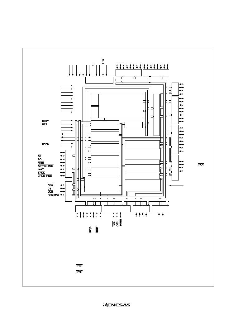
Rev. 1.0, 02/03, page 3 of 634
1.2
Internal Block Diagram
PE7
/
D
7
PE6
/
D
6
PE5
/
D
5
PE4
/
D
4
PE3
/
D
3
PE2
/
D
2
PE1
/
D
1
PE0
/
D
0
PD7
/
D15
PD6
/
D14
PD5
/
D13
PD4
/
D12
PD3
/
D11
PD2
/
D10
PD1
/
D
9
PD0
/
D
8
VCC
VCC
VSS
VSS
DrVCC
DrVSS
EMLE/NC
*
2
TDO/NC
*
2
TCK/NC
*
2
TMS/NC
*
2
/NC
*
2
TDI/NC
*
2
PA3 / A19/SCK2
PA2 / A18/RxD2
PA1 / A17/TxD2
PA0 / A16
PB7 / A15
PB6 / A14
PB5 / A13
PB4 / A12
PB3 / A11
PB2 / A10
PB1 / A9
PB0 / A8
PC7 / A7
PC6 / A6
PC5 / A5
PC4 / A4
PC3 / A3
PC2 / A2
PC1 / A1
PC0 / A0
P36 (PUPD+)
P32 / SCK0/
P31 / RxD0
P30 / TxD0
P10
/
T
IOCA0
/A20
P11
/
T
IOCB0
/A21
P12
/
T
IOCC0
/
TCLKA/A22
P13
/
T
IOCD0
/
TCLKB/A23
P14
/
T
IOCA1/
P15
/
T
IOCB1
/
TCLKC
P16
/
T
IOCA2/
P17
/
T
IOCB2/
TCLKD
P70/
P71/
P74
/
PG4 /
PG3 /
PG2 /
PG1 /
/
PF7 /
PF6 /
PF5 /
PF4 /
PF3 /
/
PF2 /
PF1 /
PF0 /
/
MD2
MD1
MD0
EXTAL
XTAL
PLLVCC
PLLVSS
OSC1
OSC2
P96/AN14
P97/AN15
Vref
H8S/2000 CPU
WDT
DMAC
USB
P40/AN0
P41/AN1
P42/AN2
P43/AN3
The FWE pin is provided only in the HD64F2218 and HD64F2218U.
HD64F2218, HD64F2218U:
When EMLE = 0, boundary scan is available and the pins function as
TDO, TCK, TMS,
, and TDI, respectively.
When EMLE = 1, H-UDI function is available and the pins function as
TDO, TCK, TMS,
, and TDI, respectively.
HD6432217:
All pins function as NC.
Boundary scan and H-UDI function are not available.
SCI2
NMI
FWE*
1
USPND/TMOW
USD+
USD-
VBUS
Notes: 1.
2.
ROM
RAM
RTC
Peripheral data bus
Peripheral address bus
Internal address bus
Internal data bus
Port D
Boundary scan/H-UDI*
2
TPU (3 channels)
Interrupts controller
Port E
Port A
Port B
Bus controller
Port C
Port 3
Port F
Port G
Port 9
Port 4
Port 1
Port 7
SCI0 (1 channel, high speed UART)
A/D converter (6 channels)
Main clock
pulse
generator
Sub-clock
pulse
generator
Figure 1.1 Internal Block Diagram of H8S/2218 Series
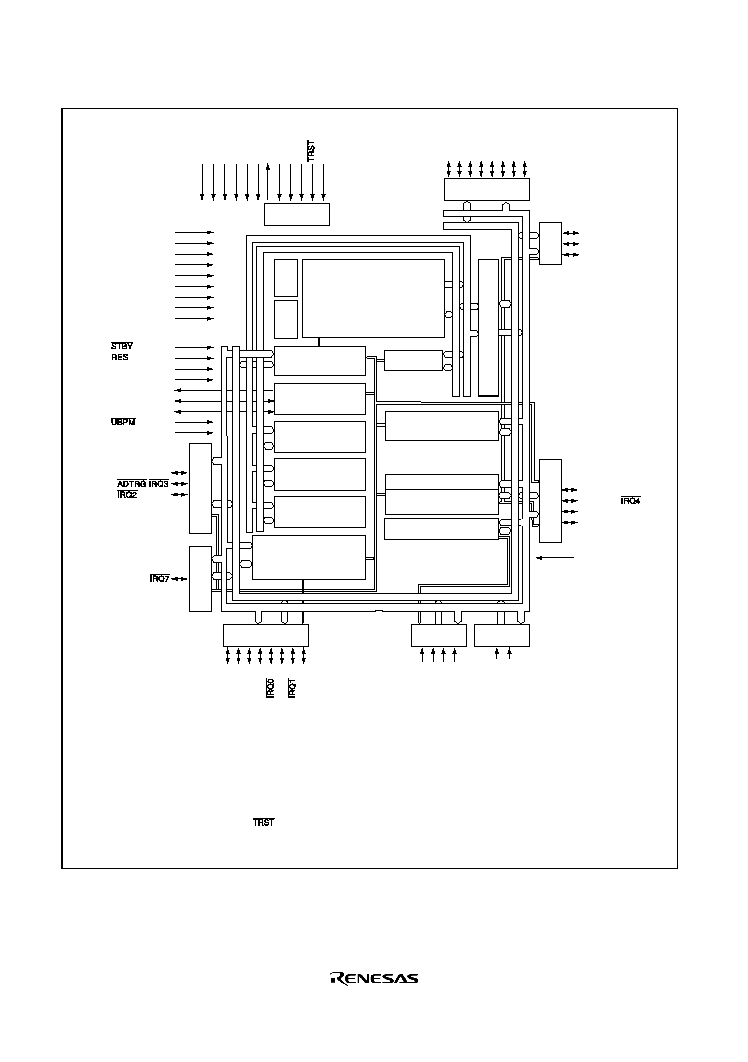
Rev. 1.0, 02/03, page 4 of 634
PE7
PE6
PE5
PE4
PE3
PE2
PE1
PE0
VCC
VCC
VSS
VSS
DrVCC
DrVSS
PA3 /SCK2
PA2 /RxD2
PA1 /TxD2
P36 (PUPD+)
P32 / SCK0/
P31 / RxD0
P30 / TxD0
P10
/
T
IOCA0
P11
/
T
IOCB0
P12
/
T
IOCC0
/
TCLKA
P13
/
T
IOCD0
/
TCLKB
P14
/
T
IOCA1/
P15
/
T
IOCB1
/
TCLKC
P16
/
T
IOCA2/
P17
/
T
IOCB2/
TCLKD
PG1 /
PF7 /
PF3 /
/
PF0 /
MD2
MD1
MD0
EXTAL
XTAL
PLLVCC
PLLVSS
OSC1
OSC2
P96/AN14
P97/AN15
Vref
H8S/2000 CPU
WDT
DMAC
USB
P40/AN0
P41/AN1
P42/AN2
P43/AN3
SCI2
NMI
FWE*
1
USPND/TMOW
USD+
USD-
VBUS
ROM
RAM
RTC
EMLE/NC
*
2
TDO/P77
*
2
TCK/P76
*
2
TMS/P75
*
2
/NC
*
2
TDI/PG0
*
2
The FWE pin is provided only in the HD64F2212 and HD64F2212U.
HD64F2212, HD64F2212U:
When EMLE = 0, port function is available and the pins function as
P77, P76, P75, NC, and PG0, respectively.
When EMLE = 1, H-UDI function is available and the pins function as
TDO, TCK, TMS,
, and TDI, respectively.
HD6432211, HD6432210:
Port function is available and the pins function as
NC, P77, P76, P75, NC, and PG0, respectively.
Notes: 1.
2.
Peripheral data bus
Peripheral address bus
H-UDI/ports
7 and G*
2
TPU (3 channels)
Interrupts controller
Port E
Port A
Port 3
Port F
Port G
Port 9
Port 4
Port 1
Main clock
pulse
generator
Sub-clock
pulse
generator
SCI0 (1 channel, high speed UART)
A/D converter (6 channels)
Internal address bus
Internal data bus
Bus controller
Figure 1.2 Internal Block Diagram of H8S/2212 Series
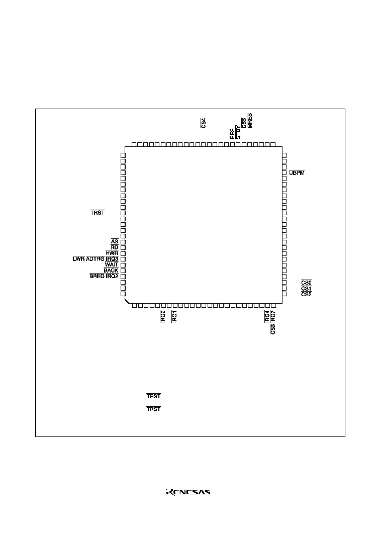
Rev. 1.0, 02/03, page 5 of 634
1.3
Pin Arrangement
The pin arrangements of H8S/2218 Series and H8S/2212 are shown in figure 1.3 and figure1.4
respectively.
TFP-100G
(Pin Arrangement)
The FWE pin is provided only in the HD64F2218 and HD64F2218U.
HD64F2218, HD64F2218U:
When EMLE = 0, boundary scan is available and the pins function as
TDO, TCK, TMS,
, and TDI, respectively.
When EMLE = 1, H-UDI function is available and the pins function as
TDO, TCK, TMS,
, and TDI, respectively.
HD6432217:
All pins function as NC.
Boundary scan and H-UDI function are not available.
Notes: 1.
2.
PD4/D12
PD5/D13
PD6/D14
PD7/D15
FWE*
1
NMI
EMLE/NC*
2
TDO/NC*
2
TCK/NC*
2
TMS/NC*
2
/NC*
2
TDI/NC*
2
VCC
PF7/
VSS
PF6/
PF5/
PF4/
PF3/
/
/
PF2/
PF1/
PF0/
/
PA3/A19/SCK2
PA2/A18/RxD2
PA1/A17/TxD2
PB5/A13
PB4/A12
PLLVCC
PLLVSS
P40/AN0
P41/AN1
P42/AN2
P43/AN3
Vref
PB3/A11
PB2/A10
PB1/A9
PB0/A8
P96/AN14
P97/AN15
DrVSS
USD-
USD+
DrVCC
P36(PUPD+)
VBUS
PG4/
PG3/
PG2/
76
77
78
79
80
81
82
83
84
85
86
87
88
89
90
91
92
93
94
95
96
97
98
99
100
50
49
48
47
46
45
44
43
42
41
40
39
38
37
36
35
34
33
32
31
30
29
28
27
26
75
74
73
72
71
70
69
68
67
66
65
64
63
62
61
60
59
58
57
56
55
54
53
52
51
1
2
3
4
5
6
7
8
9
10
11
12
13
14
15
16
17
18
19
20
21
22
23
24
25
PA0/A16
P10/TIOCA0/A20
P11/TIOCB0/A21
P12/TIOCC0/TCLKA/A22
P13/TIOCD0/TCLKB/A23
P14/TIOCA1/
P15/TIOCB1/TCLKC
P16/TIOCA2/
P17/TIOCB2/TCLKD
PC0/A0
PC1/A1
PC2/A2
PC3/A3
MD0
MD1
MD2
PC4/A4
PC5/A5
PC6/A6
PC7/A7
USPND/TMOW
P30/TxD0
P31/RxD0
P32/SCK0/
PG1/
/
PD3/D11
PD2/D10
PD1/D9
PD0/D8
PE7/D7
PE6/D6
PE5/D5
PE4/D4
PE3/D3
PE2/D2
PE1/D1
PE0/D0
P70/
VCC
EXTAL
XTAL
VSS
P71/
P74/
OSC1
OSC2
PB7/A15
PB6/A14
Figure 1.3 Pin Arrangement of H8S/2218 Series (TFP-100G)
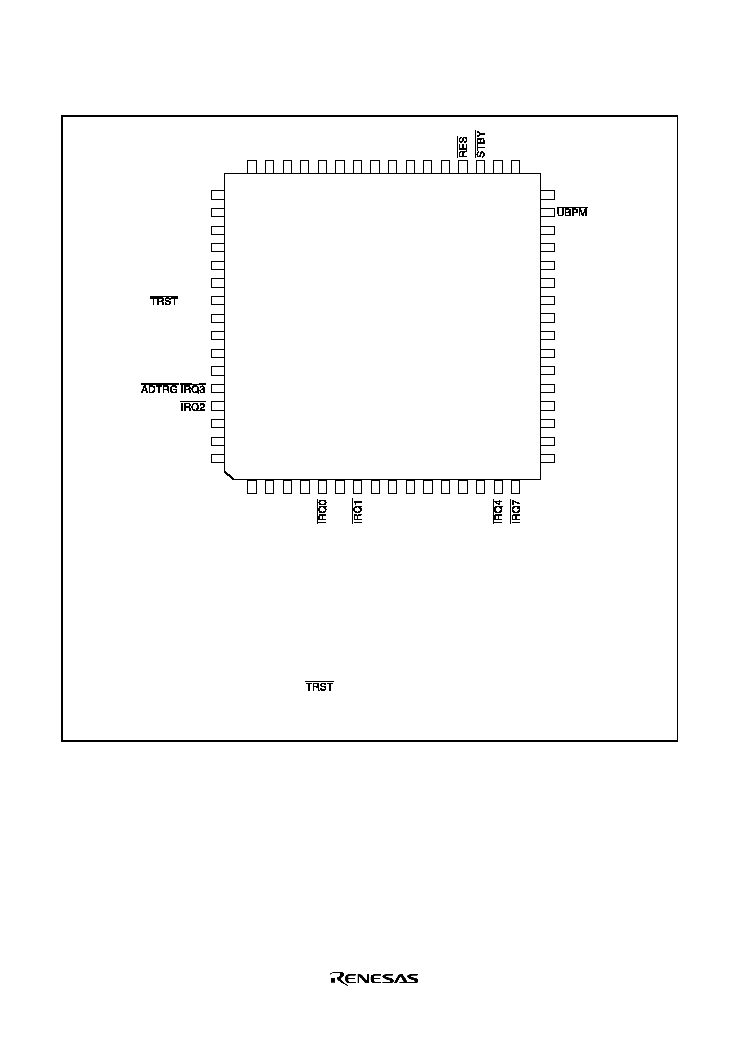
Rev. 1.0, 02/03, page 6 of 634
The FWE pin is provided only in the HD64F2212 and HD64F2212U.
HD64F2212, HD64F2212U:
When EMLE = 0, port function is available and the pins function as
P77, P76, P75, NC, and PG0, respectively.
When EMLE = 1, H-UDI function is available and the pins function as
TDO, TCK, TMS,
, and TDI, respectively.
HD6432211, HD6432210:
Port function is available and the pins function as
NC, P77, P76, P75, and PG0, respectively.
Notes: 1.
2.
P10/TIOCA0
P11/TIOCB0
P12/TIOCC0/TCLKA
P13/TIOCD0/TCLKB
P14/TIOCA1/
P15/TIOCB1/TCLKC
P16/TIOCA2/
P17/TIOCB2/TCLKD
MD0
MD1
MD2
USPND/TMOW
P30/TxD0
P31/RxD0
P32/SCK0/
PG1/
1
2
3
4
5
6
7
8
9 10 11 12 13 14 15 16
48 47 46 45 44 43 42 41 40 39 38 37 36 35 34 33
PE7
PE6
PE5
PE4
PE3
PE2
PE1
PE0
VCC
EXTAL
XTAL
VSS
OSC1
OSC2
32
31
30
29
28
27
26
25
24
23
22
21
20
19
18
17
49
50
51
52
53
54
55
56
57
58
59
60
61
62
63
64
FWE*
1
NMI
EMLE/NC*
2
TDO/P77*
2
TCK/P76*
2
TMS/P75*
2
/NC*
2
TDI/PG0*
2
VCC
PF7/
VSS
PF3/
/
PF0/
PA3/SCK2
PA2/RXD2
PA1/TXD2
PLLVCC
PLLVSS
P40/AN0
P41/AN1
P42/AN2
P43/AN3
Vref
P96/AN14
P97/AN15
DrVSS
USD-
USD+
DrVCC
P36 (PUPD+)
VBUS
FP-64E
(Top View)
Figure 1.4 Pin Arrangement of H8S/2212 Series (FP-64E)

Rev. 1.0, 02/03, page 7 of 634
1.4
Pin Functions in Each Operating Mode
Table 1.1 shows the pin functions in each operating mode for the H8S/2218 Series, and table 1.2
shows that for the H8S/2212 Series.
Table 1.1
Pin functions in Each Operating Mode for H8S/2218 Series
Pin No.
Pin Name
TFP-100G Modes 4, 5
Mode 6
Mode 7
Programmer Mode
1
PA0/A16
PA0/A16
PA0
NC
2
P10/TIOCA0/A20
P10/TIOCA0/A20
P10/TIOCA0
A2
3
P11/TIOCB0/A21
P11/TIOCB0/A21
P11/TIOCB0
A3
4
P12/TIOCC0/TCLKA/A22
P12/TIOCC0/TCLKA/A22
P12/TIOCC0/TCLKA
A4
5
P13/TIOCD0/TCLKB/A23
P13/TIOCD0/TCLKB/A23
P13/TIOCD0/TCLKB
A5
6
P14/TIOCA1/
IRQ0
P14/TIOCA1/
IRQ0
P14/TIOCA1/
IRQ0
VSS
7
P15/TIOCB1/TCLKC
P15/TIOCB1/TCLKC
P15/TIOCB1/TCLKC
WE
8
P16/TIOCA2/
IRQ1
P16/TIOCA2/
IRQ1
P16/TIOCA2/
IRQ1
VSS
9
P17/TIOCB2/TCLKD
P17/TIOCB2/TCLKD
P17/TIOCB2/TCLKD
CE
10
A0
PC0/A0
PC0
NC
11
A1
PC1/A1
PC1
NC
12
A2
PC2/A2
PC2
NC
13
A3
PC3/A3
PC3
NC
14
MD0
MD0
MD0
VSS
15
MD1
MD1
MD1
VSS
16
MD2
MD2
MD2
VSS
17
A4
PC4/A4
PC4
NC
18
A5
PC5/A5
PC5
NC
19
A6
PC6/A6
PC6
NC
20
A7
PC7/A7
PC7
NC
21
USPND/TMOW
USPND/TMOW
USPND/TMOW
NC
22
P30/TxD0
P30/TxD0
P30/TxD0
A10
23
P31/RxD0
P31/RxD0
P31/RxD0
A11
24
P32/SCK0/
IRQ4
P32/SCK0/
IRQ4
P32/SCK0/
IRQ4
A12
25
PG1/
CS3/IRQ7
PG1/
CS3/IRQ7
PG1/
IRQ7
A15
26
PG2/
CS2
PG2/
CS2
PG2
NC
27
PG3/
CS1
PG3/
CS1
PG3
NC
28
PG4/
CS0
PG4/
CS0
PG4
NC

Rev. 1.0, 02/03, page 8 of 634
Pin No.
Pin Name
TFP-100G Modes 4, 5
Mode 6
Mode 7
Programmer Mode
29
VBUS
VBUS
VBUS
VSS
30
P36 (PUDP+)
P36 (PUDP+)
P36 (PUDP+)
A16
31
DrVCC
DrVCC
DrVCC
VCC
32
USD+
USD+
USD+
NC
33
USD-
USD-
USD-
NC
34
DrVSS
DrVSS
DrVSS
VSS
35
P97/AN15
P97/AN15
P97/AN15
A7
36
P96/AN14
P96/AN14
P96/AN14
A6
37
PB0/A8
PB0/A8
PB0
NC
38
PB1/A9
PB1/A9
PB1
NC
39
PB2/A10
PB2/A10
PB2
NC
40
PB3/A11
PB3/A11
PB3
NC
41
Vref
Vref
Vref
VCC
42
P43/AN3
P43/AN3
P43/AN3
A14
43
P42/AN2
P42/AN2
P42/AN2
A13
44
P41/AN1
P41/AN1
P41/AN1
A9
45
P40/AN0
P40/AN0
P40/AN0
A8
46
PLLVSS
PLLVSS
PLLVSS
VSS
47
UBPM
UBPM
UBPM
A17
48
PLLVCC
PLLVCC
PLLVCC
VCC
49
PB4/A12
PB4/A12
PB4
NC
50
PB5/A13
PB5/A13
PB5
NC
51
PB6/A14
PB6/A14
PB6
NC
52
PB7/A15
PB7/A15
PB7
NC
53
OSC2
OSC2
OSC2
NC
54
OSC1
OSC1
OSC1
VCC
55
P74/
MRES
P74/
MRES
P74/
MRES
NC
56
P71/
CS5
P71/
CS5
P71
NC
57
STBY
STBY
STBY
VCC
58
RES
RES
RES
RES
59
VSS
VSS
VSS
VSS
60
XTAL
XTAL
XTAL
XTAL

Rev. 1.0, 02/03, page 9 of 634
Pin No.
Pin Name
TFP-100G Modes 4, 5
Mode 6
Mode 7
Programmer Mode
61
EXTAL
EXTAL
EXTAL
EXTAL
62
VCC
VCC
VCC
VCC
63
P70/
CS4
P70/
CS4
P70
NC
64
PE0/D0
PE0/D0
PE0
D0
65
PE1/D1
PE1/D1
PE1
D1
66
PE2/D2
PE2/D2
PE2
D2
67
PE3/D3
PE3/D3
PE3
D3
68
PE4/D4
PE4/D4
PE4
D4
69
PE5/D5
PE5/D5
PE5
D5
70
PE6/D6
PE6/D6
PE6
D6
71
PE7/D7
PE7/D7
PE7
D7
72
D8
D8
PD0
NC
73
D9
D9
PD1
NC
74
D10
D10
PD2
NC
75
D11
D11
PD3
NC
76
D12
D12
PD4
NC
77
D13
D13
PD5
NC
78
D14
D14
PD6
NC
79
D15
D15
PD7
NC
80
FWE
FWE
FWE
FWE
81
NMI
NMI
NMI
VCC
82
EMLE/NC
EMLE/NC
EMLE/NC
VSS
83
TDO/NC
TDO/NC
TDO/NC
NC
84
TCK/NC
TCK/NC
TCK/NC
VCC
85
TMS/NC
TMS/NC
TMS/NC
VCC
86
TRST/NC
TRST/NC
TRST/NC
RES
87
TDI/NC
TDI/NC
TDI/NC
VSS
88
VCC
VCC
VCC
VCC
89
PF7/
PF7/
PF7/
NC
90
VSS
VSS
VSS
VSS
91
AS
AS
PF6
NC
92
RD
RD
PF5
NC
93
HWR
HWR
PF4
NC

Rev. 1.0, 02/03, page 10 of 634
Pin No.
Pin Name
TFP-100G Modes 4, 5
Mode 6
Mode 7
Programmer Mode
94
PF3/
LWR/ADTRG/IRQ3
PF3/
LWR/ADTRG/IRQ3
PF3/
ADTRG/IRQ3
VCC
95
PF2/
WAIT
PF2/
WAIT
PF2
NC
96
PF1/
BACK
PF1/
BACK
PF1
NC
97
PF0/
BREQ/IRQ2
PF0/
BREQ/IRQ2
PF0/
IRQ2
VCC
98
PA3/A19/SCK2
PA3/A19/SCK2
PA3/SCK2
A1
99
PA2/A18/RxD2
PA2/A18/RxD2
PA2/RxD2
A0
100
PA1/A17/TxD2
PA1/A17/TxD2
PA1/TxD2
OE
Table 1.2
Pin functions in Each Operating Mode for H8S/2212 Series
Pin No.
Pin Name
FP-64E
Mode 7
Programmer Mode
1
P10/TIOCA0
A2
2
P11/TIOCB0
A3
3
P12/TIOCC0/TCLKA
A4
4
P13/TIOCD0/TCLKB
A5
5
P14/TIOCA1/
IRQ0
VSS
6
P15/TIOCB1/TCLKC
WE
7
P16/TIOCA2/
IRQ1
VSS
8
P17/TIOCB2/TCLKD
CE
9
MD0
VSS
10
MD1
VSS
11
MD2
VSS
12
USPND/TMOW
NC
13
P30/TxD0
A10
14
P31/RxD0
A11
15
P32/SCK0/
IRQ4
A12
16
PG1/
IRQ7
A15
17
VBUS
VSS
18
P36(PD+)
A16
19
DrVCC
VCC
20
USD+
NC
21
USD-
NC
22
DrVSS
VSS

Rev. 1.0, 02/03, page 11 of 634
Pin No.
Pin Name
FP-64E
Mode 7
Programmer Mode
23
P97/AN15
A7
24
P96/AN14
A6
25
Vref
VCC
26
P43/AN3
A14
27
P42/AN2
A13
28
P41/AN1
A9
29
P40/AN0
A8
30
PLLVSS
VSS
31
UBPM
A17
32
PLLVCC
VCC
33
OSC2
NC
34
OSC1
VCC
35
STBY
VCC
36
RES
RES
37
VSS
VSS
38
XTAL
XTAL
39
EXTAL
EXTAL
40
VCC
VCC
41
PE0
D0
42
PE1
D1
43
PE2
D2
44
PE3
D3
45
PE4
D4
46
PE5
D5
47
PE6
D6
48
PE7
D7
49
FWE
FWE
50
NMI
VCC
51
EMLE/NC
VSS
52
TDO/P77
NC
53
TCK/P76
VCC
54
TMS/P75
VCC
55
TRST/NC
RES

Rev. 1.0, 02/03, page 12 of 634
Pin No.
Pin Name
FP-64E
Mode 7
Programmer Mode
56
TDI/PG0
VSS
57
VCC
VCC
58
PF7/
NC
59
VSS
VSS
60
PF3/
ADTRG/IRQ3
VCC
61
PF0/
IRQ2
VCC
62
PA3/SCK2
A1
63
PA2/RxD2
A0
64
PA1/TxD2
OE
1.5
Pin Functions
Pin No.
Type
Symbol
TFP-100G FP-64E
I/O
Function
VCC
Input
62
88
40
57
Power supply pins. Connect all
these pins to the system power
supply.
VSS
Input
59
90
37
59
Ground pins. Connect all these pins
to the system power supply (0 V).
PLLVCC
48
32
Input
Power supply pin for an on-chip PLL
oscillator. Connect this pin to the
system power supply.
Power supply
PLLVSS
46
30
Input
Ground pin for an on-chip PLL
oscillator
XTAL
60
38
Input
For connection to a crystal
resonator. For examples of crystal
resonator connection and external
clock input, see section 19, Clock
Pulse Generator.
Clock
EXTAL
61
39
Input
For connection to a crystal
resonator. An external clock can be
supplied from the EXTAL pin. For
examples of crystal resonator
connection and external clock input,
see section 19, Clock Pulse
Generator.

Rev. 1.0, 02/03, page 13 of 634
Pin No.
Type
Symbol
TFP-100G FP-64E
I/O
Function
Clock
OSC1
OSC2
54
53
34
33
Input
For connection to a 32.768-kHz
crystal resonator. For examples of
crystal resonator connection, see
section 19, Clock Pulse Generator.
89
58
Output
Supplies the system clock to
external devices.
Operating
mode control
MD2
MD1
MD0
16
15
14
11
10
9
Input
Set the operating mode. Inputs at
these pins cannot be modified
during operation.
RES
58
36
Input
Reset pin. When this pin is driven
low, the chip is reset.
STBY
57
35
Input
When this pin is driven low, a
transition is made to hardware
standby mode.
MRES
55
Input
When this pin is driven low, a
transition is made to manual reset
mode. (Supported only by the
H8S/2218 Series)
BREQ
97
Input
Used by an external bus master to
issue a bus request to this LSI
(Supported only by the H8S/2218
Series)
BACK
96
Output
Indicates that the bus has been
released to an external bus master.
(Supported only by the H8S/2218
Series)
FWE
80
49
Input
Pin for use by flash memory. This
pin is only used in the flash memory
version.
System
control
EMLE
82
51
Input
Emulator enable
Connect this pin to the system
power supply (0 V).
Interrupts
NMI
81
50
Input
Nonmaskable interrupt pin. If this
pin is not used, it should be fixed
high.

Rev. 1.0, 02/03, page 14 of 634
Pin No.
Type
Symbol
TFP-100G FP-64E
I/O
Function
Interrupts
IRQ7
IRQ4
IRQ3
IRQ2
IRQ1
IRQ0
25
24
94
97
8
6
16
15
60
61
7
5
Input
These pins request a maskable
interrupt.
Address bus
A23
A22
A21
A20
A19
A18
A17
A16
A15
A14
A13
A12
A11
A10
A9
A8
A7
A6
A5
A4
A3
A2
A1
A0
5
4
3
2
98
99
100
1
52
51
50
49
40
39
38
37
20
19
18
17
13
12
11
10
Output
These pins output an address.
(Supported only by the H8S/2218
Series)

Rev. 1.0, 02/03, page 15 of 634
Pin No.
Type
Symbol
TFP-100G FP-64E
I/O
Function
Data bus
D15
D14
D13
D12
D11
D10
D9
D8
D7
D6
D5
D4
D3
D2
D1
D0
79
78
77
76
75
74
73
72
71
70
69
68
67
66
65
64
I/O
These pins constitute a bi-directional
data bus. (Supported only by the
H8S/2218 Series)
Bus control
CS5
CS4
CS3
CS2
CS1
CS0
56
63
25
26
27
28
Output
Signals for selecting areas 5 to 0 in
the external address space.
(Supported only by the H8S/2218
Series)
AS
91
Output
When this pin is low, it indicates that
address output on the address bus is
enabled. (Supported only by the
H8S/2218 Series)
RD
92
Output
When this pin is low, it indicates that
the external address space can be
read. (Supported only by the
H8S/2218 Series)
HWR
93
Output
A strobe signal that writes to external
address space and indicates that the
upper half (D15 to D8) of the data bus
is enabled. (Supported only by the
H8S/2218 Series)

Rev. 1.0, 02/03, page 16 of 634
Pin No.
Type
Symbol
TFP-100G FP-64E
I/O
Function
LWR
94
Output
A strobe signal that writes to
external address space and
indicates that the lower half (D7 to
D0) of the data bus is enabled.
(Supported only by the H8S/2218
Series)
Bus control
WAIT
95
Input
Requests insertion of a wait state in
the bus cycle when accessing
external 3-state address space.
(Supported only by the H8S/2218
Series)
TCLKA
TCLKB
TCLKC
TCLKD
4
5
7
9
3
4
6
8
Input
TPU external clock input pins
TIOCA0
TIOCB0
TIOCC0
TIOCD0
2
3
4
5
1
2
3
4
I/O
The TGRA_0 to TGRD_0 input
capture input/output compare
output/PWM output pins
TIOCA1
TIOCB1
6
7
5
6
I/O
The TGRA_1 and TGRB_1 input
capture input/output compare
output/PWM output pins
16-bit timer
pulse unit
(TPU)
TIOCA2
TIOCB2
8
9
7
8
I/O
The TGRA_2 and TGRB_2 input
capture input/output compare
output/PWM output pins
Realtime clock
(RTC)
TMOW
21
12
Output
The divided clock output pin
TxD2
TxD0
100
22
64
13
Output
Data output pins
RxD2
RxD0
99
23
63
14
Input
Data input pins
Serial
communica-
tion interface
(SCI)
SCK2
SCK0
98
24
62
15
I/O
Clock input/output pins

Rev. 1.0, 02/03, page 17 of 634
Pin No.
Type
Symbol
TFP-100G FP-64E
I/O
Function
AN15
AN14
AN3
AN2
AN1
AN0
35
36
42
43
44
45
23
24
26
27
28
29
Input
Analog input pins for the A/D
converter
ADTRG
94
60
Input
Pin for input of an external trigger to
start A/D conversion
A/D converter
Vref
41
25
Input
The reference voltage input pin for
the A/D converter. When the A/D
converter is not used, this pin should
be connected to the system power
supply (VCC).
TMS
85
54
Input
Control signal input pin for the
boundary scan
TCK
84
53
Input
Clock input pin for the boundary
scan
TDO
83
52
Output
Data output pin for the boundary
scan
TDI
87
56
Input
Data input pin for the boundary scan
Boundary scan
(Supported
only by the
HD64F2218
and
HF64F2218U.)
TRST
86
55
Input
Reset pin for the TAP controller
USB
DrVCC
31
19
Input
Power supply pin for the on-chip
transceiver. Connect this pin to the
system power supply.
DrVSS
34
22
Input
Ground pin for the on-chip
transceiver.
USD+
USD-
32
33
20
21
I/O
USB data I/O pin
VBUS
29
17
Input
Connection/disconnection detecting
input/output pin for the USB cable
USPND
21
12
Output
USB suspend output
This pin is driven high when a
transition is made to suspend state.

Rev. 1.0, 02/03, page 18 of 634
Pin No.
Type
Symbol
TFP-100G FP-64E
I/O
Function
USB
UBPM
47
31
Input
Bus power/self power mode setting
Input
When the USB is used in bus power
mode, this input pin must be fixed
low.
When the USB is used in self power
mode, this input pin must be fixed
high.
P36
(PUPD+)
30
18
I/O
Use as D+ signal pull-up control pin.
P17
P16
P15
P14
P13
P12
P11
P10
9
8
7
6
5
4
3
2
8
7
6
5
4
3
2
1
I/O
8-bit I/O pins
P36
P32
P31
P30
30
24
23
22
18
15
14
13
I/O
4-bit I/O pins
(Use P36 as D+ signal pull-up
control pin of USB.)
P43
P42
P41
P40
42
43
44
45
26
27
28
29
Input
4-bit input pins
I/O port
P77
P76
P75
P74
P71
P70
55
56
63
52
53
54
I/O
3-bit I/O pins
P97
P96
35
36
23
24
Input
2-bit input pins

Rev. 1.0, 02/03, page 19 of 634
Pin No.
Type
Symbol
TFP-100G FP-64E
I/O
Function
I/O port
PA3
PA2
PA1
PA0
98
99
100
1
62
63
64
I/O
4-bit I/O pins for the H8S/2218
Series. 3-bit I/O pins for the
H8S/2212 Series.
PB7
PB6
PB5
PB4
PB3
PB2
PB1
PB0
52
51
50
49
40
39
38
37
I/O
8-bit I/O pins (Supported only by the
H8S/2218 Series)
PC7
PC6
PC5
PC4
PC3
PC2
PC1
PC0
20
19
18
17
13
12
11
10
I/O
8-bit I/O pins (Supported only by the
H8S/2218 Series)
PD7
PD6
PD5
PD4
PD3
PD2
PD1
PD0
79
78
77
76
75
74
73
72
I/O
8-bit I/O pins (Supported only by the
H8S/2218 Series)

Rev. 1.0, 02/03, page 20 of 634
Pin No.
Type
Symbol
TFP-100G FP-64E
I/O
Function
I/O port
PE7
PE6
PE5
PE4
PE3
PE2
PE1
PE0
71
70
69
68
67
66
65
64
48
47
46
45
44
43
42
41
I/O
8-bit I/O pins
PF7
PF6
PF5
PF4
PF3
PF2
PF1
PF0
89
91
92
93
94
95
96
97
58
60
61
I/O
8-bit I/O pins for the H8S/2218
Series. 3-bit I/O pins for the
H8S/2212 Series.
PG4
PG3
PG2
PG1
PG0
28
27
26
25
16
56
I/O
4-bit I/O pins for the H8S/2218
Series. 2-bit I/O pins for the
H8S/2212 Series.

CPUS211A_010020011200
Rev. 1.0, 02/03, page 21 of 634
Section 2 CPU
The H8S/2000 CPU is a high-speed central processing unit with an internal 32-bit architecture that
is upward compatible with the H8/300 and H8/300H CPUs. The H8S/2000 CPU has sixteen 16-bit
general registers, can address a 16-Mbyte linear address space, and is ideal for realtime control.
This section describes the H8S/2000 CPU. The usable modes and address spaces differ depending
on the product. For details on each product, refer to section 3, MCU Operating Modes.
2.1
Features
· Upward-compatible with H8/300 and H8/300H CPUs
Can execute H8/300 and H8/300H CPU object programs
· General-register architecture
Sixteen 16-bit general registers also usable as sixteen 8-bit registers or eight 32-bit registers
· Sixty-five basic instructions
8/16/32-bit arithmetic and logic instructions
Multiply and divide instructions
Powerful bit-manipulation instructions
· Eight addressing modes
Register direct [Rn]
Register indirect [@ERn]
Register indirect with displacement [@(d:16,ERn) or @(d:32,ERn)]
Register indirect with post-increment or pre-decrement [@ERn+ or @ERn]
Absolute address [@aa:8, @aa:16, @aa:24, or @aa:32]
Immediate [#xx:8, #xx:16, or #xx:32]
Program-counter relative [@(d:8,PC) or @(d:16,PC)]
Memory indirect [@@aa:8]
· 16-Mbyte address space
Program: 16 Mbytes
Data: 16 Mbytes
· High-speed operation
All frequently-used instructions execute in one or two states
8/16/32-bit register-register add/subtract: 1 state
8 × 8-bit register-register multiply: 12 states
16 ÷ 8-bit register-register divide: 12 states
16 × 16-bit register-register multiply: 20 states
32 ÷ 16-bit register-register divide: 20 states

Rev. 1.0, 02/03, page 22 of 634
· Two CPU operating modes
Normal mode*
Advanced mode
Note: * Normal mode is not available in this LSI.
· Power-down state
Transition to power-down state by SLEEP instruction
CPU clock speed selection
2.1.1
Differences between H8S/2600 CPU and H8S/2000 CPU
The differences between the H8S/2600 CPU and the H8S/2000 CPU are as shown below.
· Register configuration
The MAC register is supported only by the H8S/2600 CPU.
· Basic instructions
The four instructions MAC, CLRMAC, LDMAC, and STMAC are supported only by the
H8S/2600 CPU.
· The number of execution states of the MULXU and MULXS instructions
Execution States
Instruction
Mnemonic
H8S/2600
H8S/2000
MULXU
MULXU.B Rs, Rd
3
12
MULXU.W Rs, ERd
4
20
MULXS
MULXS.B Rs, Rd
4
13
MULXS.W Rs, ERd
5
21
In addition, there are differences in address space, CCR and EXR register functions, power-down
modes, etc., depending on the model.

Rev. 1.0, 02/03, page 23 of 634
2.1.2
Differences from H8/300 CPU
In comparison to the H8/300 CPU, the H8S/2000 CPU has the following enhancements.
· More general registers and control registers
Eight 16-bit extended registers, and one 8-bit and two 32-bit control registers, have been
added.
· Extended address space
Normal mode supports the same 64-kbyte address space as the H8/300 CPU.
Advanced mode supports a maximum 16-Mbyte address space.
· Enhanced addressing
The addressing modes have been enhanced to make effective use of the 16-Mbyte address
space.
· Enhanced instructions
Addressing modes of bit-manipulation instructions have been enhanced.
Signed multiply and divide instructions have been added.
Two-bit shift instructions have been added.
Instructions for saving and restoring multiple registers have been added.
A test and set instruction has been added.
· Higher speed
Basic instructions execute twice as fast.
2.1.3
Differences from H8/300H CPU
In comparison to the H8/300H CPU, the H8S/2000 CPU has the following enhancements.
· Additional control register
One 8-bit control registers have been added.
· Enhanced instructions
Addressing modes of bit-manipulation instructions have been enhanced.
Two-bit shift instructions have been added.
Instructions for saving and restoring multiple registers have been added.
A test and set instruction has been added.
· Higher speed
Basic instructions execute twice as fast.

Rev. 1.0, 02/03, page 24 of 634
2.2
CPU Operating Modes
The H8S/2000 CPU has two operating modes: normal and advanced. Normal mode supports a
maximum 64-kbyte address space. Advanced mode supports a maximum 16-Mbyte total address
space. The mode is selected by the mode pins.
2.2.1
Normal Mode
The exception vector table and stack have the same structure as in the H8/300 CPU.
· Address Space
A maximum address space of 64 kbytes can be accessed.
· Extended Registers (En)
The extended registers (E0 to E7) can be used as 16-bit registers, or as the upper 16-bit
segments of 32-bit registers. When En is used as a 16-bit register it can contain any value, even
when the corresponding general register (Rn) is used as an address register. If the general
register is referenced in the register indirect addressing mode with pre-decrement (@Rn) or
post-increment (@Rn+) and a carry or borrow occurs, however, the value in the corresponding
extended register (En) will be affected.
· Instruction Set
All instructions and addressing modes can be used. Only the lower 16 bits of effective
addresses (EA) are valid.
· Exception Vector Table and Memory Indirect Branch Addresses
In normal mode the top area starting at H'0000 is allocated to the exception vector table. One
branch address is stored per 16 bits. The exception vector table in normal mode is shown in
figure 2.1. For details of the exception vector table, see section 4, Exception Handling.
The memory indirect addressing mode (@@aa:8) employed in the JMP and JSR instructions
uses an 8-bit absolute address included in the instruction code to specify a memory operand
that contains a branch address. In normal mode the operand is a 16-bit (word) operand,
providing a 16-bit branch address. Branch addresses can be stored in the top area from H'0000
to H'00FF. Note that this area is also used for the exception vector table.
· Stack Structure
When the program counter (PC) is pushed onto the stack in a subroutine call, and the PC,
condition-code register (CCR), and extended control register (EXR) are pushed onto the stack
in exception handling, they are stored as shown in figure 2.2. EXR is not pushed onto the stack
in interrupt control mode 0. For details, see section 4, Exception Handling.
Note: Normal mode is not available in this LSI.
Rev. 1.0, 02/03, page 25 of 634
H'0000
H'0001
H'0002
H'0003
H'0004
H'0005
H'0006
H'0007
H'0008
H'0009
H'000A
H'000B
Reset exception vector
(Reserved for system use)
Exception vector 1
Exception vector 2
Exception
vector table
(Reserved for system use)
Figure 2.1 Exception Vector Table (Normal Mode)
(a) Subroutine Branch
(b) Exception Handling
PC
(16 bits)
EXR*
1
Reserved*
1
,*
3
CCR
CCR*
3
PC
(16 bits)
SP
SP
Notes: 1.
2.
3.
When EXR is not used, it is not stored on the stack.
SP when EXR is not used.
Ignored when returning.
( SP*
2
)
Figure 2.2 Stack Structure in Normal Mode
Rev. 1.0, 02/03, page 26 of 634
2.2.2
Advanced Mode
· Address Space
Linear access is provided to a 16-Mbyte maximum address space.
· Extended Registers (En)
The extended registers (E0 to E7) can be used as 16-bit registers, or as the upper 16-bit
segments of 32-bit registers or address registers.
· Instruction Set
All instructions and addressing modes can be used.
· Exception Vector Table and Memory Indirect Branch Addresses
In advanced mode the top area starting at H'00000000 is allocated to the exception vector table
in units of 32 bits. In each 32 bits, the upper 8 bits are ignored and a branch address is stored in
the lower 24 bits (figure 2.3). For details of the exception vector table, see section 4, Exception
Handling.
H'00000000
H'00000003
H'00000004
H'0000000B
H'0000000C
H'00000010
H'00000008
H'00000007
Reserved
Reserved
Reserved
Reset exception vector
(Reserved for system use)
Exception vector table
Exception vector 1
(Reserved for system use)
Figure 2.3 Exception Vector Table (Advanced Mode)
Rev. 1.0, 02/03, page 27 of 634
The memory indirect addressing mode (@@aa:8) employed in the JMP and JSR instructions
uses an 8-bit absolute address included in the instruction code to specify a memory operand
that contains a branch address. In advanced mode the operand is a 32-bit longword operand,
providing a 32-bit branch address. The upper 8 bits of these 32 bits are a reserved area that is
regarded as H'00. Branch addresses can be stored in the area from H'00000000 to H'000000FF.
Note that the first part of this range is also the exception vector table.
· Stack Structure
In advanced mode, when the program counter (PC) is pushed onto the stack in a subroutine
call, and the PC, condition-code register (CCR), and extended control register (EXR) are
pushed onto the stack in exception handling, they are stored as shown in figure 2.4. When
EXR is invalid, it is not pushed onto the stack. For details, see section 4, Exception Handling.
PC
(24 bits)
EXR*
1
Reserved*
1
, *
3
CCR
PC
(24 bits)
Reserved
(a) Subroutine Branch
(b) Exception Handling
When EXR is not used, it is not stored on the stack.
SP when EXR is not used.
Ignored when returning.
SP
SP
Notes: 1.
2.
3.
( SP*
2
)
Figure 2.4 Stack Structure in Advanced Mode
Rev. 1.0, 02/03, page 28 of 634
2.3
Address Space
Figure 2.5 shows a memory map of the H8S/2000 CPU. The H8S/2000 CPU provides linear
access to a maximum 64-kbyte address space in normal mode, and a maximum 16-Mbyte
(architecturally 4-Gbyte) address space in advanced mode. The usable modes and address spaces
differ depending on the product. For details on each product, refer to section 3, MCU Operating
Modes.
H'0000
H'FFFF
H'00000000
H'FFFFFFFF
H'00FFFFFF
64-kbyte
16-Mbyte
Not available
in this LSI.
Program area
Data area
(b) Advanced Mode
(a) Normal Mode *
Note : * Not available in this LSI.
Figure 2.5 Memory Map
Rev. 1.0, 02/03, page 29 of 634
2.4
Register Configuration
The H8S/2000 CPU has the internal registers shown in figure 2.6. There are two types of registers:
general registers and control registers. Control registers are a 24-bit program counter (PC), an 8-bit
extended control register (EXR), and an 8-bit condition code register (CCR).
T
I2 I1 I0
EXR
7 6 5 4 3 2 1 0
PC
23
0
15
0 7
0 7
0
E0
E1
E2
E3
E4
E5
E6
E7
R0H
R1H
R2H
R3H
R4H
R5H
R6H
R7H
R0L
R1L
R2L
R3L
R4L
R5L
R6L
R7L
SP
PC
EXR
T
I2 to I0
CCR
I
UI
: Stack pointer
: Program counter
: Extended control register
:Trace bit
: Interrupt mask bits
: Condition-code register
: Interrupt mask bit
:User bit or interrupt mask bit
*
: Half-carry flag
: User bit
: Negative flag
: Zero flag
: Overflow flag
: Carry flag
ER0
ER1
ER2
ER3
ER4
ER5
ER6
ER7 (SP)
I UI H U N Z V C
CCR
7 6 5 4 3 2 1 0
H
U
N
Z
V
C
General Registers (Rn) and Extended Registers (En)
Control Registers (CR)
Legend
- - - -
Note: * Cannot be used as an interrupt mask bit in this LSI.
Figure 2.6 CPU Registers
Rev. 1.0, 02/03, page 30 of 634
2.4.1
General Registers
The H8S/2000 CPU has eight 32-bit general registers. These general registers are all functionally
alike and can be used as both address registers and data registers. When a general register is used
as a data register, it can be accessed as a 32-bit, 16-bit, or 8-bit register. Figure 2.7 illustrates the
usage of the general registers. When the general registers are used as 32-bit registers or address
registers, they are designated by the letters ER (ER0 to ER7).
The ER registers divide into 16-bit general registers designated by the letters E (E0 to E7) and R
(R0 to R7). These registers are functionally equivalent, providing a maximum sixteen 16-bit
registers. The E registers (E0 to E7) are also referred to as extended registers.
The R registers divide into 8-bit general registers designated by the letters RH (R0H to R7H) and
RL (R0L to R7L). These registers are functionally equivalent, providing a maximum sixteen 8-bit
registers.
The usage of each register can be selected independently.
General register ER7 has the function of stack pointer (SP) in addition to its general-register
function, and is used implicitly in exception handling and subroutine calls. Figure 2.8 shows the
stack.
· Address registers
· 32-bit registers
· 16-bit registers
· 8-bit registers
ER registers
(ER0 to ER7)
E registers (extended registers)
(E0 to E7)
R registers
(R0 to R7)
RH registers
(R0H to R7H)
RL registers
(R0L to R7L)
Figure 2.7 Usage of General Registers

Rev. 1.0, 02/03, page 31 of 634
SP (ER7)
Free area
Stack area
Figure 2.8 Stack
2.4.2
Program Counter (PC)
This 24-bit counter indicates the address of the next instruction the CPU will execute. The length
of all CPU instructions is two bytes (one word), so the least significant PC bit is ignored. (When
an instruction is fetched, the least significant PC bit is regarded as 0.)
2.4.3
Extended Control Register (EXR)
EXR is an 8-bit register that manipulates the LDC, STC, ANDC, ORC, and XORC instructions.
When these instructions except for the STC instruction is executed, all interrupts including NMI
will be masked for three states after execution is completed.
Bit
Bit Name
Initial Value R/W
Description
7
T
0
R/W
Trace Bit
When this bit is set to 1, a trace exception is generated
each time an instruction is executed. When this bit is
cleared to 0, instructions are executed in sequence.
6 to3
1
Reserved
These bits are always read as 1.
2 to 0 I2 to I0
1
R/W
These bits designate the interrupt mask level (0 to 7).
For details, refer to section 5, Interrupt Controller.

Rev. 1.0, 02/03, page 32 of 634
2.4.4
Condition-Code Register (CCR)
This 8-bit register contains internal CPU status information, including an interrupt mask bit (I) and
half-carry (H), negative (N), zero (Z), overflow (V), and carry (C) flags.
Operations can be performed on the CCR bits by the LDC, STC, ANDC, ORC, and XORC
instructions. The N, Z, V, and C flags are used as branching conditions for conditional branch
(Bcc) instructions.
Bit
Bit Name
Initial Value
R/W Description
7
I
1
R/W Interrupt Mask Bit
Masks interrupts other than NMI when set to 1. NMI is
accepted regardless of the I bit setting. The I bit is set to 1
by hardware at the start of an exception-handling
sequence. For details, refer to section 5, Interrupt
Controller.
6
UI
undefined
R/W User Bit or Interrupt Mask Bit
Can be written and read by software using the LDC, STC,
ANDC, ORC, and XORC instructions. This bit cannot be
used as an interrupt mask bit in this LSI.
5
H
undefined
R/W Half-Carry Flag
When the ADD.B, ADDX.B, SUB.B, SUBX.B, CMP.B or
NEG.B instruction is executed, this flag is set to 1 if there is
a carry or borrow at bit 3, and cleared to 0 otherwise. When
the ADD.W, SUB.W, CMP.W, or NEG.W instruction is
executed, the H flag is set to 1 if there is a carry or borrow
at bit 11, and cleared to 0 otherwise. When the ADD.L,
SUB.L, CMP.L, or NEG.L instruction is executed, the H flag
is set to 1 if there is a carry or borrow at bit 27, and cleared
to 0 otherwise.
4
U
undefined
R/W User Bit
Can be written and read by software using the LDC, STC,
ANDC, ORC, and XORC instructions.
3
N
undefined
R/W Negative Flag
Stores the value of the most significant bit of data as a sign
bit.
2
Z
undefined
R/W Zero Flag
Set to 1 to indicate zero data, and cleared to 0 to indicate
non-zero data.

Rev. 1.0, 02/03, page 33 of 634
Bit
Bit Name
Initial Value
R/W Description
1
V
undefined
R/W Overflow Flag
Set to 1 when an arithmetic overflow occurs, and cleared to
0 at other times.
0
C
undefined
R/W Carry Flag
Set to 1 when a carry occurs, and cleared to 0 otherwise.
Used by:
· Add instructions, to indicate a carry
· Subtract instructions, to indicate a carry
· Shift and rotate instructions, to indicate a carry
They carry flag is also used as a bit accumulator by bit
manipulation instructions.
2.4.5
Initial Register Values
Reset exception handling loads the CPU's program counter (PC) from the vector table, clears the
trace bit in EXR to 0, and sets the interrupt mask bits in CCR and EXR to 1. The other CCR bits
and the general registers are not initialized. In particular, the stack pointer (ER7) is not initialized.
The stack pointer should therefore be initialized by an MOV.L instruction executed immediately
after a reset.
2.5
Data Formats
The H8S/2000 CPU can process 1-bit, 4-bit (BCD), 8-bit (byte), 16-bit (word), and 32-bit
(longword) data. Bit-manipulation instructions operate on 1-bit data by accessing bit n (n = 0, 1, 2,
..., 7) of byte operand data. The DAA and DAS decimal-adjust instructions treat byte data as two
digits of 4-bit BCD data.
2.5.1
General Register Data Formats
Figure 2.9 shows the data formats in general registers.
Rev. 1.0, 02/03, page 34 of 634
7
0
7
0
MSB
LSB
MSB
LSB
7
0
4 3
Don't care
Don't care
Don't care
7
0
4 3
7
0
Don't care
6 5 4 3 2
7
1 0
7
0
Don't care
6 5 4 3 2
7
1 0
Don't care
Data Type
Register Number
Data Image
Byte data
Byte data
4-bit BCD data
4-bit BCD data
1-bit data
1-bit data
RnH
RnL
RnH
RnL
RnH
RnL
Upper
Lower
Upper
Lower
Figure 2.9 General Register Data Formats (1)
15
0
MSB
LSB
15
0
MSB
LSB
31
16
MSB
15
0
LSB
En
Rn
ERn
En
Rn
RnH
RnL
MSB
LSB
: General register ER
: General register E
: General register R
: General register RH
: General register RL
: Most significant bit
: Least significant bit
Data Type
Data Image
Register Number
Word data
Word data
Rn
En
Longword data
Legend
ERn
Figure 2.9 General Register Data Formats (2)
Rev. 1.0, 02/03, page 35 of 634
2.5.2
Memory Data Formats
Figure 2.10 shows the data formats in memory. The H8S/2000 CPU can access word data and
longword data in memory, but word or longword data must begin at an even address. If an attempt
is made to access word or longword data at an odd address, no address error occurs but the least
significant bit of the address is regarded as 0, so the access starts at the preceding address. This
also applies to instruction fetches.
When SP (ER7) is used as an address register to access the stack, the operand size should be word
size or longword size.
7
0
7
6
5
4
3
2
1
0
MSB
LSB
MSB
MSB
LSB
LSB
Data Type
Address
1-bit data
Byte data
Word data
Address L
Address L
Address 2M
Address 2M+1
Longword data
Address 2N
Address 2N+1
Address 2N+2
Address 2N+3
Data Image
Figure 2.10 Memory Data Formats

Rev. 1.0, 02/03, page 36 of 634
2.6
Instruction Set
The H8S/2000 CPU has 65 types of instructions. The instructions are classified by function in
table 2.1.
Table 2.1
Instruction Classification
Function
Instructions
Size
Types
MOV
B/W/L
5
POP*
1
, PUSH*
1
W/L
LDM, STM
L
Data transfer
MOVFPE*
3
, MOVTPE*
3
B
ADD, SUB, CMP, NEG
B/W/L
19
ADDX, SUBX, DAA, DAS
B
INC, DEC
B/W/L
ADDS, SUBS
L
MULXU, DIVXU, MULXS, DIVXS
B/W
EXTU, EXTS
W/L
Arithmetic
operations
TAS*
4
B
Logic operations
AND, OR, XOR, NOT
B/W/L
4
Shift
SHAL, SHAR, SHLL, SHLR, ROTL, ROTR, ROTXL,
ROTXR
B/W/L
8
Bit manipulation
BSET, BCLR, BNOT, BTST, BLD, BILD, BST, BIST, BAND,
BIAND, BOR, BIOR, BXOR, BIXOR
B
14
Branch
BCC*
2
, JMP, BSR, JSR, RTS
5
System control
TRAPA, RTE, SLEEP, LDC, STC, ANDC, ORC, XORC,
NOP
9
Block data transfer EEPMOV
1
Total: 65
Notes: B: byte size; W:word size; L:longword size.
1. POP.W Rn and PUSH.W Rn are identical to MOV.W @SP+, Rn and MOV.W Rn, @-
SP. POP.L ERn and PUSH.L ERn are identical to MOV.L @SP+, ERn and MOV.L ERn,
@-SP.
2. Bcc is the general name for conditional branch instructions.
3. Cannot be used in this LSI.
4. Only register ER0, ER1, ER4, or ER5 should be used when using the TAS instruction.

Rev. 1.0, 02/03, page 37 of 634
2.6.1
Table of Instructions Classified by Function
Tables 2.3 to 2.10 summarizes the instructions in each functional category. The notation used in
tables 2.3 to 2.10 is defined below.
Table 2.2
Operation Notation
Symbol
Description
Rd
General register (destination)*
Rs
General register (source) *
Rn
General register*
ERn
General register (32-bit register)
(EAd)
Destination operand
(EAs)
Source operand
EXR
Extended control register
CCR
Condition-code register
N
N (negative) flag in CCR
Z
Z (zero) flag in CCR
V
V (overflow) flag in CCR
C
C (carry) flag in CCR
PC
Program counter
SP
Stack pointer
#IMM
Immediate data
disp
Displacement
+
Addition
Subtraction
×
Multiplication
÷
Division
Logical AND
Logical OR
Logical exclusive OR
Move
NOT (logical complement)
:8/:16/:24/:32
8-, 16-, 24-, or 32-bit length
Note: * General registers include 8-bit registers (R0H to R7H, R0L to R7L), 16-bit registers (R0 to
R7, E0 to E7), and 32-bit registers (ER0 to ER7).

Rev. 1.0, 02/03, page 38 of 634
Table 2.3
Data Transfer Instructions
Instruction
Size
*
1
Function
MOV
B/W/L
(EAs)
Rd, Rs (EAd)
Moves data between two general registers or between a general register
and memory, or moves immediate data to a general register.
MOVFPE
B
Cannot be used in this LSI.
MOVTPE
B
Cannot be used in this LSI.
POP
W/L
@SP+
Rn
Pops a general register from the stack. POP.W Rn is identical to MOV.W
@SP+, Rn. POP.L ERn is identical to MOV.L @SP+, ERn
PUSH
W/L
Rn
@-SP
Pushes a general register onto the stack. PUSH.W Rn is identical to
MOV.W Rn, @-SP. PUSH.L ERn is identical to MOV.L ERn, @-SP.
LDM*
2
L
@SP+
Rn (register list)
Pops two or more general registers from the stack.
STM*
2
L
Rn (register list)
@-SP
Pushes two or more general registers onto the stack.
Notes: 1. Size refers to the operand size.
B: Byte
W: Word
L: Longword
2. ER7 is used as a stack pointer in STM and LDM instructions. ER7, therefore, should not
be used as a saving (STM) or restoring (LDM) register.

Rev. 1.0, 02/03, page 39 of 634
Table 2.4
Arithmetic Operations Instructions (1)
Instruction Size
*
Function
ADD
SUB
B/W/L
Rd ± Rs
Rd, Rd ± #IMM Rd
Performs addition or subtraction on data in two general registers, or on
immediate data and data in a general register. (Immediate byte data
cannot be subtracted from byte data in a general register. Use the SUBX
or ADD instruction.)
ADDX
SUBX
B
Rd ± Rs ± C
Rd, Rd ± #IMM ± C Rd
Performs addition or subtraction with carry or borrow on byte data in two
general registers, or on immediate data and data in a general register.
INC
DEC
B/W/L
Rd ± 1
Rd, Rd ± 2 Rd
Increments or decrements a general register by 1 or 2. (Byte operands
can be incremented or decremented by 1 only.)
ADDS
SUBS
L
Rd ± 1
Rd, Rd ± 2 Rd, Rd ± 4 Rd
Adds or subtracts the value 1,2, or 4 to or from data in a 32-bit register.
DAA
DAS
B
Rd (decimal adjust)
Rd
Decimal-adjusts an addition or subtraction result in a general register by
referring to the OCR to produce 4-bit BCD data.
MULXU
B/W
Rd
× Rs Rd
Performs unsigned multiplication on data in two general registers: either
8 bits
× 8 bits 16 bits or 16 bits × 16 bits 32 bits.
MULXS
B/W
Rd
× Rs Rd
Performs signed multiplication on data in two general registers: either 8
bits
× 8 bits 16 bits or 16 bits × 16 bits 32 bits.
DIVXU
B/W
Rd
÷ Rs Rd
Performs unsigned division on data in two general registers: either 16
bits
÷ 8 bits 8-bit quotient and 8-bit remainder or 32 bits ÷ 16 bits
16-bit quotient and 16-bit remainder.
Note: * Size refers to the operand size.
B: Byte
W: Word
L: Longword

Rev. 1.0, 02/03, page 40 of 634
Table 2.4
Arithmetic Operations Instructions (2)
Instruction Size
*
1
Function
DIVXS
B/W
Rd
÷ Rs Rd
Performs signed division on data in two general registers: either 16 bits
÷
8 bits
8-bit quotient and 8-bit remainder or 32 bits ÷ 16 bits 16-bit
quotient and 16-bit remainder.
CMP
B/W/L
Rd Rs, Rd #IMM
Compares data in a general register with data in another general register
or with immediate data, and sets CCR bits according to the result.
NEG
B/W/L
0 Rd
Rd
Takes the two's complement (arithmetic complement) of data in a
general register.
EXTU
W/L
Rd (zero extension)
Rd
Extends the lower 8 bits of a 16-bit register to word size, or the lower 16
bits of a 32-bit register to longword size, by padding with zeros on the
left.
EXTS
W/L
Rd (sign extension)
Rd
Extends the lower 8 bits of a 16-bit register to word size, or the lower 16
bits of a 32-bit register to longword size, by extending the sign bit.
TAS*
2
B
@ERd 0, 1
(<bit 7> of @ERd)
Tests memory contents, and sets the most significant bit (bit 7) to 1.
Notes: 1. Size refers to the operand size.
B: Byte
W: Word
L: Longword
2. Only register ER0, ER1, ER4, or ER5 should be used when using the TAS instruction.

Rev. 1.0, 02/03, page 41 of 634
Table 2.5
Logic Operations Instructions
Instruction Size
*
Function
AND
B/W/L
Rd
Rs Rd, Rd #IMM Rd
Performs a logical AND operation on a general register and another
general register or immediate data.
OR
B/W/L
Rd
Rs Rd, Rd #IMM Rd
Performs a logical OR operation on a general register and another
general register or immediate data.
XOR
B/W/L
Rd
Rs Rd, Rd #IMM Rd
Performs a logical exclusive OR operation on a general register and
another general register or immediate data.
NOT
B/W/L
Rd Rd
Takes the one's complement (logical complement) of general register
contents.
Note: * Size refers to the operand size.
B: Byte
W: Word
L: Longword
Table 2.6
Shift Instructions
Instruction Size
*
Function
SHAL
SHAR
B/W/L
Rd (shift)
Rd
Performs an arithmetic shift on general register contents. 1-bit or 2 bit
shift is possible.
SHLL
SHLR
B/W/L
Rd (shift)
Rd
Performs an logical shift on general register contents. 1-bit or 2 bit shift is
possible.
ROTL
ROTR
B/W/L
Rd (rotate)
Rd
Rotates general register contents. 1-bit or 2 bit rotation is possible.
ROTXL
ROTXR
B/W/L
Rd (rotate)
Rd
Rotates general register contents through the carry flag. 1-bit or 2 bit
rotation is possible.
Note: * Size refers to the operand size.
B: Byte
W: Word
L: Longword

Rev. 1.0, 02/03, page 42 of 634
Table 2.7
Bit Manipulation Instructions (1)
Instruction Size
*
Function
BSET
B
1
(<bit-No.> of <EAd>)
Sets a specified bit in a general register or memory operand to 1. The bit
number is specified by 3-bit immediate data or the lower three bits of a
general register.
BCLR
B
0
(<bit-No.> of <EAd>)
Clears a specified bit in a general register or memory operand to 0. The
bit number is specified by 3-bit immediate data or the lower three bits of
a general register.
BNOT
B
(<bit-No.> of <EAd>) (<bit-No.> of <EAd>)
Inverts a specified bit in a general register or memory operand. The bit
number is specified by 3-bit immediate data or the lower three bits of a
general register.
BTST
B
(<bit-No.> of <EAd>) Z
Tests a specified bit in a general register or memory operand and sets or
clears the Z flag accordingly. The bit number is specified by 3-bit
immediate data or the lower three bits of a general register.
BAND
B
C
(<bit-No.> of <EAd>) C
ANDs the carry flag with a specified bit in a general register or memory
operand and stores the result in the carry flag.
BIAND
B
C
(<bit-No.> of <EAd>) C
ANDs the carry flag with the inverse of a specified bit in a general
register or memory operand and stores the result in the carry flag. The
bit number is specified by 3-bit immediate data.
BOR
B
C
(<bit-No.> of <EAd>) C
ORs the carry flag with a specified bit in a general register or memory
operand and stores the result in the carry flag.
BIOR
B
C
( <bit-No.> of <EAd>) C
ORs the carry flag with the inverse of a specified bit in a general register
or memory operand and stores the result in the carry flag. The bit
number is specified by 3-bit immediate data.
Note:* Size refers to the operand size.
B: Byte

Rev. 1.0, 02/03, page 43 of 634
Table 2.7
Bit Manipulation Instructions (2)
Instruction
Size
*
Function
BXOR
B
C
(<bit-No.> of <EAd>) C
Exclusive-ORs the carry flag with a specified bit in a general register or
memory operand and stores the result in the carry flag.
BIXOR
B
C
(<bit-No.> of <EAd>) C
Exclusive-ORs the carry flag with the inverse of a specified bit in a
general register or memory operand and stores the result in the carry
flag. The bit number is specified by 3-bit immediate data.
BLD
B
(<bit-No.> of <EAd>)
C
Transfers a specified bit in a general register or memory to the carry
flag.
BILD
B
(<bit-No.> of <EAd>) C
Transfers the inverse of a specified bit in a general register or memory
operand to the carry flag. The bit number is specified by 3-bit immediate
data.
BST
B
C
(<bit-No.> of <EAd>)
Transfers the carry flag value to a specified bit in a general register or
memory operand.
BIST
B
C (<bit-No.>. of <EAd>)
Transfers the inverse of the carry flag value to a specified bit in a
general register or memory operand. The bit number is specified by 3-
bit immediate data.
Note:* Size refers to the operand size.
B: Byte

Rev. 1.0, 02/03, page 44 of 634
Table 2.8
Branch Instructions
Instruction
Size
Function
Bcc
Branches to a specified address if a specified condition is true. The
branching conditions are listed below.
Mnemonic
Description
Condition
BRA (BT)
Always (true)
Always
BRN (BF)
Never (false)
Never
BHI
High
C
Z = 0
BLS
Low or same
C
Z = 1
BCC (BHS)
Carry clear
(high or same)
C = 0
BCS (BLO)
Carry set (low)
C = 1
BNE
Not equal
Z = 0
BEQ
Equal
Z = 1
BVC
Overflow clear
V = 0
BVS
Overflow set
V = 1
BPL
Plus
N = 0
BMI
Minus
N = 1
BGE
Greater or equal
N
V = 0
BLT
Less than
N
V = 1
BGT
Greater than
Z
(N V) = 0
BLE
Less or equal
Z
(N V) = 1
JMP
Branches unconditionally to a specified address.
BSR
Branches to a subroutine at a specified address
JSR
Branches to a subroutine at a specified address
RTS
Returns from a subroutine

Rev. 1.0, 02/03, page 45 of 634
Table 2.9
System Control Instruction
Instruction
Size
*
Function
TRAPA
Starts trap-instruction exception handling.
RTE
Returns from an exception-handling routine.
SLEEP
Causes a transition to a power-down state.
LDC
B/W
(EAs)
CCR, (EAs) EXR
Moves the source operand contents or immediate data to CCR or EXR.
Although CCR and EXR are 8-bit registers, word-size transfers are
performed between them and memory. The upper 8 bits are valid.
STC
B/W
CCR
(EAd), EXR (EAd)
Transfers CCR or EXR contents to a general register or memory.
Although CCR and EXR are 8-bit registers, word-size transfers are
performed between them and memory. The upper 8 bits are valid.
ANDC
B
CCR
#IMM CCR, EXR #IMM EXR
Logically ANDs the CCR or EXR contents with immediate data.
ORC
B
CCR
#IMM CCR, EXR #IMM EXR
Logically ORs the CCR or EXR contents with immediate data.
XORC
B
CCR
#IMM CCR, EXR #IMM EXR
Logically exclusive-ORs the CCR or EXR contents with immediate data.
NOP
PC + 2
PC
Only increments the program counter.
Note:* Size refers to the operand size.
B: Byte
W: Word

Rev. 1.0, 02/03, page 46 of 634
Table 2.10
Block Data Transfer Instruction
Instruction
Size
*
Function
EEPMOV.B
if R4L
0 then
Repeat @ER5+
@ER6+
R4L1
R4L
Until R4L = 0
else next:
EEPMOV.W
if R4
0 then
Repeat @ER5+
@ER6+
R41
R4
Until R4 = 0
else next:
Transfer a data block. Starting from the address set in ER5, transfers
data for the number of bytes set in R4L or R4 to the address location
set in ER6.
Execution of the next instruction begins as soon as the transfer is
completed.
2.6.2
Basic Instruction Formats
The H8S/2000 CPU instructions consist of 2-byte (1-word) units. An instruction consists of an
operation field (op), a register field (r), an effective address extension (EA), and a condition field
(cc).
Figure 2.11 shows examples of instruction formats.
· Operation Field
Indicates the function of the instruction, the addressing mode, and the operation to be carried
out on the operand. The operation field always includes the first four bits of the instruction.
Some instructions have two operation fields.
· Register Field
Specifies a general register. Address registers are specified by 3 bits, data registers by 3 bits or
4 bits. Some instructions have two register fields. Some have no register field.
· Effective Address Extension
8, 16, or 32 bits specifying immediate data, an absolute address, or a displacement.
· Condition Field
Specifies the branching condition of Bcc instructions.
Rev. 1.0, 02/03, page 47 of 634
op
op
r n
r m
NOP, RTS, etc.
ADD.B Rn, Rm, etc.
MOV.B @(d:16, Rn), Rm, etc.
r n
r m
op
EA(disp)
op
cc
EA(disp)
BRA d:16, etc.
(1) Operation field only
(2) Operation field and register fields
(3) Operation field, register fields, and effective address extension
(4) Operation field, effective address extension, and condition field
Figure 2.11 Instruction Formats (Examples)
2.7
Addressing Modes and Effective Address Calculation
The H8S/2000 CPU supports the eight addressing modes listed in table 2.11. Each instruction uses
a subset of these addressing modes. Arithmetic and logic instructions can use the register direct
and immediate modes. Data transfer instructions can use all addressing modes except program-
counter relative and memory indirect. Bit manipulation instructions use register direct, register
indirect, or absolute addressing mode to specify an operand, and register direct (BSET, BCLR,
BNOT, and BTST instructions) or immediate (3-bit) addressing mode to specify a bit number in
the operand.
Table 2.11
Addressing Modes
No. Addressing Mode
Symbol
1
Register direct
Rn
2
Register indirect
@ERn
3
Register indirect with displacement
@(d:16,ERn)/@(d:32,ERn)
4
Register indirect with post-increment
Register indirect with pre-decrement
@ERn+
@ERn
5
Absolute address
@aa:8/@aa:16/@aa:24/@aa:32
6
Immediate
#xx:8/#xx:16/#xx:32
7
Program-counter relative
@(d:8,PC)/@(d:16,PC)
8
Memory indirect
@@aa:8

Rev. 1.0, 02/03, page 48 of 634
2.7.1
Register Direct--Rn
The register field of the instruction specifies an 8-, 16-, or 32-bit general register containing the
operand. R0H to R7H and R0L to R7L can be specified as 8-bit registers. R0 to R7 and E0 to E7
can be specified as 16-bit registers. ER0 to ER7 can be specified as 32-bit registers.
2.7.2
Register Indirect--@ERn
The register field of the instruction code specifies an address register (ERn) which contains the
address of the operand on memory. If the address is a program instruction address, the lower 24
bits are valid and the upper 8 bits are all assumed to be 0 (H'00).
2.7.3
Register Indirect with Displacement--@(d:16, ERn) or @(d:32, ERn)
A 16-bit or 32-bit displacement contained in the instruction is added to an address register (ERn)
specified by the register field of the instruction, and the sum gives the address of a memory
operand. A 16-bit displacement is sign-extended when added.
2.7.4
Register Indirect with Post-Increment or Pre-Decrement--@ERn+ or @-ERn
Register indirect with post-increment--@ERn+: The register field of the instruction code
specifies an address register (ERn) which contains the address of a memory operand. After the
operand is accessed, 1, 2, or 4 is added to the address register contents and the sum is stored in the
address register. The value added is 1 for byte access, 2 for word transfer instruction, or 4 for
longword transfer instruction. For word or longword transfer instruction, the register value should
be even.
Register indirect with pre-decrement--@-ERn: The value 1, 2, or 4 is subtracted from an
address register (ERn) specified by the register field in the instruction code, and the result
becomes the address of a memory operand. The result is also stored in the address register. The
value subtracted is 1 for byte access, 2 for word transfer instruction, or 4 for longword transfer
instruction. For word or longword transfer instruction, the register value should be even.

Rev. 1.0, 02/03, page 49 of 634
2.7.5
Absolute Address--@aa:8, @aa:16, @aa:24, or @aa:32
The instruction code contains the absolute address of a memory operand. The absolute address
may be 8 bits long (@aa:8), 16 bits long (@aa:16), 24 bits long (@aa:24), or 32 bits long
(@aa:32). Table 2.12 indicates the accessible absolute address ranges.
To access data, the absolute address should be 8 bits (@aa:8), 16 bits (@aa:16), or 32 bits
(@aa:32) long. For an 8-bit absolute address, the upper 24 bits are all assumed to be 1 (H'FFFF).
For a 16-bit absolute address the upper 16 bits are a sign extension. A 32-bit absolute address can
access the entire address space.
A 24-bit absolute address (@aa:24) indicates the address of a program instruction. The upper 8
bits are all assumed to be 0 (H'00).
Table 2.12
Absolute Address Access Ranges
Absolute Address
Normal Mode
*
Advanced Mode
Data address
8 bits (@aa:8)
H'FF00 to H'FFFF
H'FFFF00 to H'FFFFFF
16 bits (@aa:16)
H'0000 to H'FFFF
H'000000 to H'007FFF,
H'FF8000 to H'FFFFFF
32 bits (@aa:32)
H'000000 to H'FFFFFF
Program instruction
address
24 bits (@aa:24)
Note:
* Not available in this LSI.
2.7.6
Immediate--#xx:8, #xx:16, or #xx:32
The instruction contains 8-bit (#xx:8), 16-bit (#xx:16), or 32-bit (#xx:32) immediate data as an
operand.
The ADDS, SUBS, INC, and DEC instructions contain immediate data implicitly. Some bit
manipulation instructions contain 3-bit immediate data in the instruction code, specifying a bit
number. The TRAPA instruction contains 2-bit immediate data in its instruction code, specifying a
vector address.
Rev. 1.0, 02/03, page 50 of 634
2.7.7
Program-Counter Relative--@(d:8, PC) or @(d:16, PC)
This mode is used in the Bcc and BSR instructions. An 8-bit or 16-bit displacement contained in
the instruction is sign-extended and added to the 24-bit PC contents to generate a branch address.
Only the lower 24 bits of this branch address are valid; the upper 8 bits are all assumed to be 0
(H'00). The PC value to which the displacement is added is the address of the first byte of the next
instruction, so the possible branching range is 126 to +128 bytes (63 to +64 words) or 32766 to
+32768 bytes (16383 to +16384 words) from the branch instruction. The resulting value should
be an even number.
2.7.8
Memory Indirect--@@aa:8
This mode can be used by the JMP and JSR instructions. The instruction code contains an 8-bit
absolute address specifying a memory operand. This memory operand contains a branch address.
The upper bits of the absolute address are all assumed to be 0, so the address range is 0 to 255
(H'0000 to H'00FF in normal mode*, H'000000 to H'0000FF in advanced mode). In normal mode
the memory operand is a word operand and the branch address is 16 bits long. In advanced mode
the memory operand is a longword operand, the first byte of which is assumed to be H'00.
Note that the first part of the address range is also the exception vector area. For further details,
refer to section 4, Exception Handling.
If an odd address is specified in word or longword memory access, or as a branch address, the
least significant bit is regarded as 0, causing data to be accessed or instruction code to be fetched
at the address preceding the specified address. (For further information, see section 2.5.2, Memory
Data Formats.)
Note:
* Not available in this LSI.
Specified
by @aa:8
Specified
by @aa:8
Branch address
Branch address
Reserved
(a) Normal Mode*
(b) Advanced Mode
Note: * Normal mode is not available in this LSI.
Figure 2.12 Branch Address Specification in Memory Indirect Mode
Rev. 1.0, 02/03, page 51 of 634
2.7.9
Effective Address Calculation
Table 2.13 indicates how effective addresses are calculated in each addressing mode. In normal
mode the upper 8 bits of the effective address are ignored in order to generate a 16-bit address.
Table 2.13
Effective Address Calculation (1)
No
1
Offset
1
2
4
r
op
31
0
31
23
2
3
Register indirect with displacement
@(d:16,ERn) or @(d:32,ERn)
4
r
op
disp
r
op
rm
op
rn
31
0
31
0
r
op
Don't care
31
23
31
0
Don't care
31
0
disp
31
0
31
0
31
23
31
0
Don't care
31
23
31
0
Don't care
24
24
24
24
Addressing Mode and Instruction Format
Effective Address Calculation
Effective Address (EA)
Register direct (Rn)
General register contents
General register contents
General register contents
General register contents
Sign extension
Register indirect (@ERn)
Register indirect with post-increment or
pre-decrement
·Register indirect with post-increment @ERn+
·Register indirect with pre-decrement @-ERn
1, 2, or 4
1, 2, or 4
Operand Size
Byte
Word
Longword
Operand is general register contents.
Rev. 1.0, 02/03, page 52 of 634
Table 2.13
Effective Address Calculation (2)
No
5
op
31
23
31
0
Don't care
abs
@aa:8
7
H'FFFF
op
31
23
31
0
Don't care
@aa:16
op
@aa:24
@aa:32
abs
15
16
31
23
31
0
Don't care
31
23
31
0
Don't care
abs
op
abs
6
op
IMM
#xx:8/#xx:16/#xx:32
8
24
24
24
24
Addressing Mode and Instruction Format
Absolute address
Immediate
Effective Address Calculation
Effective Address (EA)
Sign extension
Operand is immediate data.
31
23
7
Program-counter relative
@(d:8,PC)/@(d:16,PC)
Memory indirect @@aa:8
· Normal mode*
· Advanced mode
31
0
Don't care
23
0
disp
0
31
23
31
0
Don't care
disp
op
23
op
8
abs
31
0
abs
H'000000
7
8
0
15
31
23
31
0
Don't care
15
H'00
16
op
abs
31
0
abs
H'000000
7
8
0
31
24
24
24
Note: * Normal mode is not available in this LSI.
PC contents
Sign
extension
Memory contents
Memory contents

Rev. 1.0, 02/03, page 53 of 634
2.8
Processing States
The H8S/2000 CPU has five main processing states: the reset state, exception handling state,
program execution state, bus-released state, and program stop state. Figure 2.13 indicates the state
transitions.
· Reset State
In this state the CPU and internal peripheral modules are all initialized and stop. When the
RES input goes low all current processing stops and the CPU enters the reset state. All
interrupts are masked in the reset state. Reset exception handling starts when the
RES signal
changes from low to high. For details, refer to section 4, Exception Handling.
The reset state can also be entered by a watchdog timer overflow.
· Exception-Handling State
The exception-handling state is a transient state that occurs when the CPU alters the normal
processing flow due to an exception source, such as, a reset, trace, interrupt, or trap instruction.
The CPU fetches a start address (vector) from the exception vector table and branches to that
address. For further details, refer to section 4, Exception Handling.
· Program Execution State
In this state the CPU executes program instructions in sequence.
· Bus-Released State
In a product which has a bus master other than the CPU, such as a direct memory access
controller (DMAC) and a data transfer controller (DTC), the bus-released state occurs when
the bus has been released in response to a bus request from a bus master other than the CPU.
While the bus is released, the CPU halts operations.
· Program Stop State
This is a power-down state in which the CPU stops operating. The program stop state occurs
when a SLEEP instruction is executed or the CPU enters hardware standby mode. For details,
refer to section 20, Power-Down Modes.
Rev. 1.0, 02/03, page 54 of 634
Program execution state
Exception handling state
Program halt state*
2
Bus-released state
Reset state*
1
End of bus
request
Bus
request
Interrupt
request
SLEEP instruction
Notes: 1.
2.
From any state except hardware standby mode, a transition to the power-on reset
state occurs whenever
goes low. From any state except hardware standby more or
power-on reset state, a transition to the manual reset state occurs whenever
goes low.
A transition can also be made to the reset state when the watchdog timer overflows.
From any state, a transition to hardware standby mode occurs when
goes low.
Bus
request
End of
bus request
Request for
exception
handling
End of
exception
handling
= High,
= Low
= High
= High
Figure 2.13 State Transitions

Rev. 1.0, 02/03, page 55 of 634
2.9
Usage Notes
2.9.1
Note on TAS Instruction Usage
Only register ER0, ER1, ER4, or ER5 should be used when using the TAS instruction. The TAS
instruction is not generated by the Hitachi H8S and H8/300 series C/C++ compilers. If the TAS
instruction is used as a user-defined intrinsic function, ensure that only register ER0, ER1, ER4, or
ER5 is used.
2.9.2
STM/LTM Instruction Usage
With the STM or LDM instruction, the ER7 register is used as the stack pointer, and thus cannot
be used as a register that allows save (STM) or restore (LDM) operation.
With a single STM or LDM instruction, two to four registers can be saved or restored. The
available registers are as follows:
For two registers: ER0 and ER1, ER2 and ER3, or ER4 and ER5
For three registers: ER0 to ER2, or ER4 to ER6
For four registers: ER0 to ER3
For the Hitachi H8S or H8/300 Series C/C++ Compiler, the STM/LDM instruction including ER7
is not created.
2.9.3
Note on Bit Manipulation Instructions
Bit manipulation instructions such as BSET, BCLR, BNOT, BST, and BIST read data in byte
units, perform bit manipulation, and write data in byte units. Thus, care must be taken when these
bit manipulation instruction are executed for a register or port including write-only bits.
In addition, the BCLR instruction can be used to clear the flag of the internal I/O register. In this
case, if the flag to be cleared has been set by an interrupt processing routine, the flag need not be
read before executing the BCLR instruction.

Rev. 1.0, 02/03, page 56 of 634

Rev. 1.0, 02/03, page 57 of 634
Section 3 MCU Operating Modes
3.1
Operating Mode Selection
This LSI supports four operating modes (modes 4 to 7). These modes enable selection of the CPU
operating mode, enabling/disabling of on-chip ROM, and the initial bus width setting, by setting
the mode pins (MD2 to MD0) as show in table 3.1. Do not change the mode pin settings during
operation. Only mode 7 is available in the H8S/2212 Series.
Table 3.1
MCU Operating Mode Selection
External Data Bus
MCU
Operating
Mode
MD2 MD1 MD0
CPU Operating
Mode
Description
On-chip
ROM
Initial Value
Maximum
Value
4
1
0
0
Advanced mode
On-chip ROM
disabled, extended
mode
Disabled
16 bits
16 bits
5
1
0
1
Advanced mode
On-chip ROM
disabled, extended
mode
Disabled
8 bits
16 bits
6
1
1
0
Advanced mode
On-chip ROM
enabled, extended
mode
Enabled
8 bits
16 bits
7
1
1
1
Advanced mode
Single-chip mode
Enabled
Notes: When using the E6000 emulator
1.
Mode 7 is not available in the H8S/2218 Series. (The E6000 emulator does not support
mode 7.)
2.
Note following restrictions to use the RTC and USB in mode 6.
Specify PFCR so that A9 and A8 are output on the PB1 and PB0 pins.
Set H'FF in PCDDR so that A7 to A0 are output on the PC7 to PC0 pins.

Rev. 1.0, 02/03, page 58 of 634
3.2
Register Descriptions
The following registers are related to the operating mode.
· Mode control register (MDCR)
· System control register (SYSCR)
3.2.1
Mode Control Register (MDCR)
MDCR is used to monitor the current operating mode of this LSI. MDCR should not be modified.
Bit
Bit Name
Initial Value R/W
Description
7 to 3
Undefined
Reserved
These bits are always read as undefined value and
cannot be modified.
2
1
0
MDS2
MDS1
MDS0
*
1
*
1
*
1
R
R
R
Mode Select 2 to 0
These bits indicate the input levels at pins MD2 to
MD0 (the current operating mode). Bits MDS2 to
MDS0 correspond to MD2 to MD0. MDS2 to MDS0
are read-only bits and they cannot be written to. The
mode pin (MD2 to MD0) input levels are latched into
these bits when MDCR is read.
These latches are canceled by a power-on reset, but
maintained at manual reset*
2
.
Notes: 1. Determined by the MD2 to MD0 pin settings.
2. Supported only by the H8S/2218 Series.

Rev. 1.0, 02/03, page 59 of 634
3.2.2
System Control Register (SYSCR)
SYSCR is used to select the interrupt control mode and the detected edge for NMI, select the
MRES input pin* enable or disable, and enables or disables on-chip RAM.
Bit
Bit Name
Initial Value R/W
Description
7
0
R/W
Reserved
The write value should always be 0.
6
0
Reserved
This bit is always read as 0 and cannot be modified.
5
4
INTM1
INTM0
0
0
R/W
R/W
These bits select the control mode of the interrupt
controller. For details of the interrupt control modes,
see section 5.6, Interrupt Control Modes and Interrupt
Operation.
00: Interrupt control mode 0
01: Setting prohibited
10: Interrupt control mode 2
11: Setting prohibited
3
NMIEG
0
R/W
NMI Edge Select
Selects the valid edge of the NMI interrupt input.
0: An interrupt is requested at the falling edge of NMI
input
1: An interrupt is requested at the rising edge of NMI
input
2
MRESE
0
R/W
Manual Reset Select
Enables or disables the
MRES pin* input.
0: Manual reset is disabled
1: Manual reset is enabled
The
MRES input pin* can be used.
1
0
Reserved
This bit is always read as 0 and cannot be modified.
0
RAME
1
R/W
RAM Enable
Enables or disables the on-chip RAM. The RAME bit
is initialized when the reset status is released.
0: On-chip RAM is disabled
1: On-chip RAM is enabled
Note:
* Supported only by the H8S/2218 Series.

Rev. 1.0, 02/03, page 60 of 634
3.3
Operating Mode Descriptions
3.3.1
Mode 4 (Supported Only by the H8S/2218 Series)
The CPU can access a 16-Mbyte address space in advanced mode. The on-chip ROM is disabled.
Pins P13 to P10, and ports A, B, and C function as an address bus, ports D and E function as a data
bus, and part of port F carries bus control signals.
Pins P13 to P11 function as input ports immediately after a reset. Pin 10 and ports A and B
function as address (A20 to A8) outputs immediately after a reset. Address (A23 to A21) output
can be enabled or disabled by bits AE3 to AE0 in the pin function control register (PFCR)
regardless of the corresponding data direction register (DDR) values. Pins for which address
output is disabled among pins P13 to P10 and in ports A and B become port outputs when the
corresponding DDR bits are set to 1.
Port C always has an address (A7 to A0) output function.
The initial bus mode after a reset is 16 bits, with 16-bit access to all areas. However, note that if 8-
bit access is designated by the bus controller for all areas, the bus mode switches to 8 bits.
3.3.2
Mode 5 (Supported Only by the H8S/2218 Series)
The CPU can access a 16-Mbyte address space in advanced mode. The on-chip ROM is disabled.
Pins P13 to P10, and ports A, B, and C function as an address bus, ports D and E function as a data
bus, and part of port F carries bus control signals.
Pins P13 to P11 function as input ports immediately after a reset. Pin 10 and ports A and B
function as address (A20 to A8) outputs immediately after a reset. Address (A23 to A21) output
can be enabled or disabled by bits AE3 to AE0 in the pin function control register (PFCR)
regardless of the corresponding data direction register (DDR) values. Pins for which address
output is disabled among pins P13 to P10 and in ports A and B become port outputs when the
corresponding DDR bits are set to 1.
Port C always has an address (A7 to A0) output function.
The initial bus mode after a reset is 8 bits, with 8-bit access to all areas. However, note that if 16-
bit access is designated by the bus controller for any area, the bus mode switches to 16 bits and
port E becomes a data bus.

Rev. 1.0, 02/03, page 61 of 634
3.3.3
Mode 6 (Supported Only by the H8S/2218 Series)
The CPU can access a 16-Mbyte address space in advanced mode. The on-chip ROM is enabled.
Pins P13 to P10, and ports A, B and C function as input ports immediately after a reset. Address
(A23 to A8) output can be enabled or disabled by bits AE3 to AE0 in the pin function control
register (PFCR) regardless of the corresponding data direction register (DDR) values. Pins for
which address output is disabled among pins P13 to P10 and in ports A and B become port outputs
when the corresponding DDR bits are set to 1.
Port C is an input port immediately after a reset. Addresses A7 to A0 are output by setting the
corresponding DDR bits to 1.
Ports D and E function as a data bus, and part of port F carries data bus signals.
The initial bus mode after a reset is 8 bits, with 8-bit access to all areas. However, note that if 16-
bit access is designated by the bus controller for any area, the bus mode switches to 16 bits and
port E becomes a data bus.
3.3.4
Mode 7
The CPU can access a 16-Mbyte address space in advanced mode. The on-chip ROM is enabled,
but external addresses cannot be accessed.
All I/O ports are available for use as input-output ports.

Rev. 1.0, 02/03, page 62 of 634
3.3.5
Pin Functions
The pin functions of ports 1, and A to F vary depending on the operating mode. Table 3.2 shows
their functions in each operating mode.
Table 3.2
Pin Functions in Each Operating Mode
Port
Mode 4
Mode 5
Mode 6
Mode 7
Port 1
P13 to P11
P*/A
P*/A
P*/A
P
P10
P/A*
P/A*
P*/A
P
Port A
PA3 to PA0
P/A*
P/A*
P*/A
P
Port B
P/A*
P/A*
P*/A
P
Port C
A
A
P*/A
P
Port D
D
D
D
P
Port E
P/D*
P*/D
P*/D
P
Port F
PF7
P/C*
P/C*
P/C*
P*/C
PF6 to PF4
C
C
C
P
PF3
P/C*
P*/C
P*/C
PF2 to PF0
P*/C
P*/C
P*/C
Legend
P: I/O port
A: Address bus output
D: Data bus I/O
C: Control signals, clock I/O
*: After reset
Rev. 1.0, 02/03, page 63 of 634
3.4
Memory Map in Each Operating Mode
Figures 3.1 to 3.3 show the memory map in each operation mode, respectively.
External address
space
Notes: 1.
2.
3.
Though RTC and USB registers are provided inside the chip, ASN, RDN, and WRN are asserted and
the addresses are output when these areas are accessed.
Therefore, care should be taken when connecting memory externally.
The reserved area of H'FEE800 to H'FFBFFF should not be accessed.
The external address can be used instead, by clearing the RAME bit in SYSCR to 0.
External address
space
On-chip RAM*
3
USB registers*
1
Internal I/O registers*
1
Reserved*
2
On-chip RAM*
3
External address
space
External address
space
On-chip RAM*
3
On-chip ROM
On-chip ROM
USB registers*
1
Internal I/O registers*
1
Reserved*
2
Reserved*
2
On-chip RAM*
3
External address
space
External address
space
On-chip RAM*
3
USB registers*
1
Internal I/O registers
On-chip RAM*
3
H'000000
H'01FFFF
H'020000
H'E00000
H'FEE800
H'C00000
H'000000
H'000000
H'FFC000
H'FEE800
H'FFC000
H'E00000
H'FEE800
H'C00000
H'FFC000
H'FFEFBF
H'FFFFC0
H'FFFFC0
H'FFFFC0
H'FFFFFF
H'FFFFFF
H'FFFFFF
H'FFEFC0
H'FFEFC0
H'FFF800
H'FFF800
H'FFF800
H'DFFFFF
H'C00000
Modes 4 and 5
(advanced extended modes
with on-chip ROM desabled)
Mode 6
(advanced extended mode
with on-chip ROM enabled)
Mode 7
(advanced single-chip mode)
RAM: 12 kbytes
ROM: 128 kbytes
RAM: 12 kbytes
ROM: 128 kbytes
RAM: 12 kbytes
Figure 3.1 Memory Map in Each Operating Mode for HD64F2218 and HD64F2218U
Rev. 1.0, 02/03, page 64 of 634
External address
space
Notes: 1.
2.
3.
Though RTC and USB registers are provided inside the chip, ASN, RDN, and WRN are asserted and
the addresses are output when these areas are accessed.
Therefore, care should be taken when connecting memory externally.
The reserved area of H'FEE800 to H'FFCFFF should not be accessed.
The external address can be used instead, by clearing the RAME bit in SYSCR to 0.
External address
space
On-chip RAM*
3
USB registers*
1
Internal I/O registers*
1
Reserved*
2
On-chip RAM*
3
On-chip RAM*
3
On-chip RAM*
3
External address
space
External address
space
On-chip RAM*
3
On-chip ROM
On-chip ROM
USB registers*
1
USB registers*
1
Internal I/O registers*
1
Reserved*
2
Reserved*
2
Reserved
External address
space
External address
space
On-chip RAM*
3
Internal I/O registers
Modes 4 and 5
(advanced extended modes
with on-chip ROM desabled)
Mode 6
(advanced extended mode
with on-chip ROM enabled)
Mode 7
(advanced single-chip mode)
RAM: 8 kbytes
ROM: 64 kbytes
RAM: 8 kbytes
ROM: 64 kbytes
RAM: 8 kbytes
H'00FFFF
H'000000
H'000000
H'020000
H'010000
H'E00000
H'FEE800
H'C00000
H'000000
H'00FFFF
H'FFD000
H'FEE800
H'FFD000
H'E00000
H'FEE800
H'C00000
H'FFD000
H'FFEFBF
H'FFFFC0
H'FFFFC0
H'FFFFC0
H'FFFFFF
H'FFFFFF
H'FFFFFF
H'FFEFC0
H'FFEFC0
H'FFF800
H'FFF800
H'FFF800
H'DFFFFF
H'C00000
Figure 3.2 Memory Map in Each Operating Mode for HD6432217
Rev. 1.0, 02/03, page 65 of 634
Notes: 1.
2.
The reserved area should not be accessed.
The external address can be used instead, by clearing the RAME bit in SYSCR to 0.
Mode 7
(advanced single-chip mode)
Mode 7
(advanced single-chip mode)
Mode 7
(advanced single-chip mode)
ROM: 128 kbytes
RAM: 12 kbytes
ROM: 64 kbytes
RAM: 8 kbytes
ROM: 32 kbytes
RAM: 4 kbytes
H'007FFF
H'000000
H'00FFFF
H'000000
H'FEE800
H'FFD000
H'FFEFBF
H'FFFFC0
H'FFFFFF
H'FFF800
H'DFFFFF
H'C00000
H'FEE800
H'FFE000
H'FFEFBF
H'FFFFC0
H'FFFFFF
H'FFF800
H'DFFFFF
H'C00000
H'01FFFF
H'000000
H'FEE800
H'FFC000
H'FFEFBF
H'FFFFC0
H'FFFFFF
H'FFF800
H'DFFFFF
H'C00000
On-chip RAM*
2
On-chip RAM*
2
On-chip RAM*
2
On-chip RAM*
2
On-chip RAM*
2
On-chip RAM*
2
On-chip ROM
On-chip ROM
On-chip ROM
USB registers
USB registers
USB registers
Internal I/O registers
Internal I/O registers
Internal I/O registers
Reserved*
1
Reserved*
1
Reserved*
1
D64F2212, D64F2212U
D6432211
D6432210
Figure 3.3 Memory Map in Each Operating Mode for HD64F2212, HD64F2212U,
HD6432211, and HD6432210

Rev. 1.0, 02/03, page 66 of 634

Rev. 1.0, 02/03, page 67 of 634
Section 4 Exception Handling
4.1
Exception Handling Types and Priority
As table 4.1 indicates, exception handling may be caused by a reset, trace, trap instruction, or
interrupt. Exception handling is prioritized as shown in table 4.1. If two or more exceptions occur
simultaneously, they are accepted and processed in order of priority. Exception sources, the stack
structure, and operation of the CPU vary depending on the interrupt control mode. For details on
the interrupt control mode, refer to section 5, Interrupt Controller.
Table 4.1
Exception Types and Priority
Priority
Exception Type
Start of Exception Handling
High
Reset
Starts immediately after a low-to-high transition at the
RES or
MRES* pin, or when the watchdog timer overflows. The CPU
enters the reset state when the
RES pin is low. The CPU enters
the manual reset state when the
MRES pin* is low.
Trace
Starts when execution of the current instruction or exception
handling ends, if the trace (T) bit in the EXR is set to 1. This is
enabled only in trace interrupt control mode 2. Trace exception
processing is not performed after RTE instruction execution.
Interrupt
Starts when execution of the current instruction or exception
handling ends, if an interrupt request has been issued. Note that
after executing the ANDC, ORC, XORC, or LDC instruction or at
the completion of reset exception processing, no interrupt is
detected.
Low
Trap instruction
(TRAPA)
Started by execution of a trap instruction (TRAPA). Trap exception
processing is always accepted in program execution state.
Note:
*
Supported only by the H8S/2218 Series.
4.2
Exception Sources and Exception Vector Table
Different vector addresses are assigned to different exception sources. Table 4.2 lists the exception
sources and their vector addresses. Since the usable modes differ depending on the product, for
details on each product, refer to section 3, MCU Operating Modes.

Rev. 1.0, 02/03, page 68 of 634
Table 4.2
Exception Handling Vector Table
Vector Address
*
1
Exception Source
Vector Number
Normal Mode
*
4
Advanced Mode
Power-on reset
0
H'0000 to H'0001
H'0000 to H'0003
Manual reset
1
H'0002 to H'0003
H'0004 to H'0007
2
H'0004 to H'0005
H'0008 to H'000B
3
H'0006 to H'0007
H'000C to H'000F
Reserved for system use
4
H'0008 to H'0019
H'0010 to H'0013
Trace
5
H'000A to H000B
H'0014 to H0017
Direct transitions*
2
6
H'000C to H000D
H'0018 to H001B
External interrupt (NMI)
7
H'000E to H'000F
H'001C to H'001F
#0
8
H'0010 to H'0011
H'0020 to H'0023
#1
9
H'0012 to H'0013
H'0024 to H'0027
#2
10
H'0014 to H'0015
H'0028 to H'002B
Trap instruction
#3
11
H'0016 to H'0017
H'002C to H'002F
12
H'0018 to H'0019
H'0030 to H'0033
13
H'001A to H'001B
H'0034 to H'0037
14
H'001C to H'001D
H'0038 to H'003B
Reserved for system use
15
H'001E to H'001F
H'003C to H'003F
External interrupt
IRQ0
16
H'0020 to H'0021
H'0040 to H'0043
External interrupt
IRQ1
17
H'0022 to H'0023
H'0044 to H'0047
External interrupt
IRQ2
18
H'0024 to H'0025
H'0048 to H'004B
External interrupt
IRQ3
19
H'0026 to H'0027
H'004C to H'004F
External interrupt
IRQ4
20
H'0028 to H'0029
H'0050 to H'0053
RTC interrupt
IRQ5
21
H'002A to H'002B
H'0054 to H'0057
USB interrupt
IRQ6
22
H'002C to H'002D
H'0058 to H'005B
External interrupt
IRQ7
23
H'002E to H'002F
H'005C to H'005F
24
H'0030 to H'0031
H'0060 to H'0063
Internal interrupt*
3
127
H'00FE to H'00FF
H'01FC to H'01FF
Notes: 1. Lower 16 bits of the address.
2. For direct transfer, see section 20.10, Direct Transitions.
3. For details of internal interrupt vectors, see section 5.5, Interrupt Exception Handling
Vector Table.
4. Not available in this LSI.

Rev. 1.0, 02/03, page 69 of 634
4.3
Reset
A reset has the highest exception priority.
When the
RES or MRES* pin goes low, all processing halts and this LSI enters the reset state. To
ensure that this LSI is reset, hold the
RES or MRES* pin low for at least 20 ms at power-up or
hold the
RES or MRES* pin low for at least 20 states during operation.
A reset initializes the internal state of the CPU and the registers of on-chip peripheral modules.
This LSI can also be reset by overflow of the watchdog timer. For details, see section 10,
Watchdog Timer.
Immediately after a reset, interrupt control mode 0 is set.
4.3.1
Reset Types
A reset can be of either of two types for the H8S/ 2218 Series: a power-on reset or a manual reset.
A reset for the H8S/2212 Series is power-on reset. Reset types are shown in table 4.3. A power-on
reset should be used when powering on.
The internal state of the CPU is initialized by either type of reset. A power-on reset also initializes
all the registers in the on-chip peripheral modules, while a manual reset initializes all the registers
in the on-chip peripheral modules except for the bus controller and I/O ports, which retain their
previous states.
With a manual reset, since the on-chip peripheral modules are initialized, ports used as on-chip
peripheral module I/O pins are switched to I/O ports controlled by DDR and DR.
Table 4.3
Reset Types
Reset Transition Condition
Internal State
Type
MRES
MRES
MRES
MRES
RES
RES
RES
RES
CPU
On-Chip Peripheral Modules
Power-on reset *
Low
Initialized
Initialized
Manual reset
Low
High
Initialized
Initialized, except for bus controller
and I/O ports
Note: * Don't care

Rev. 1.0, 02/03, page 70 of 634
A reset caused by the watchdog timer can also be of either of two types: a power-on reset or a
manual reset.
When the
MRES pin* is used, MRES pin* input must be enabled by setting the MRESE bit to 1 in
SYSCR.
Note:* Supported only by the H8S/2218 Series.
4.3.2
Reset Exception Handling
When the
RES or MRES* pin goes high after being held low for the necessary time, this LSI starts
reset exception handling as follows:
1. The internal state of the CPU and the registers of the on-chip peripheral modules are
initialized, the T bit is cleared to 0 in EXR, and the I bit is set to 1 in EXR and CCR.
2. The reset exception handling vector address is read and transferred to the PC, and program
execution starts from the address indicated by the PC.
Note:* Supported only by the H8S/2218 Series.
Figures 4.1 and 4.2 show examples of the reset sequence.
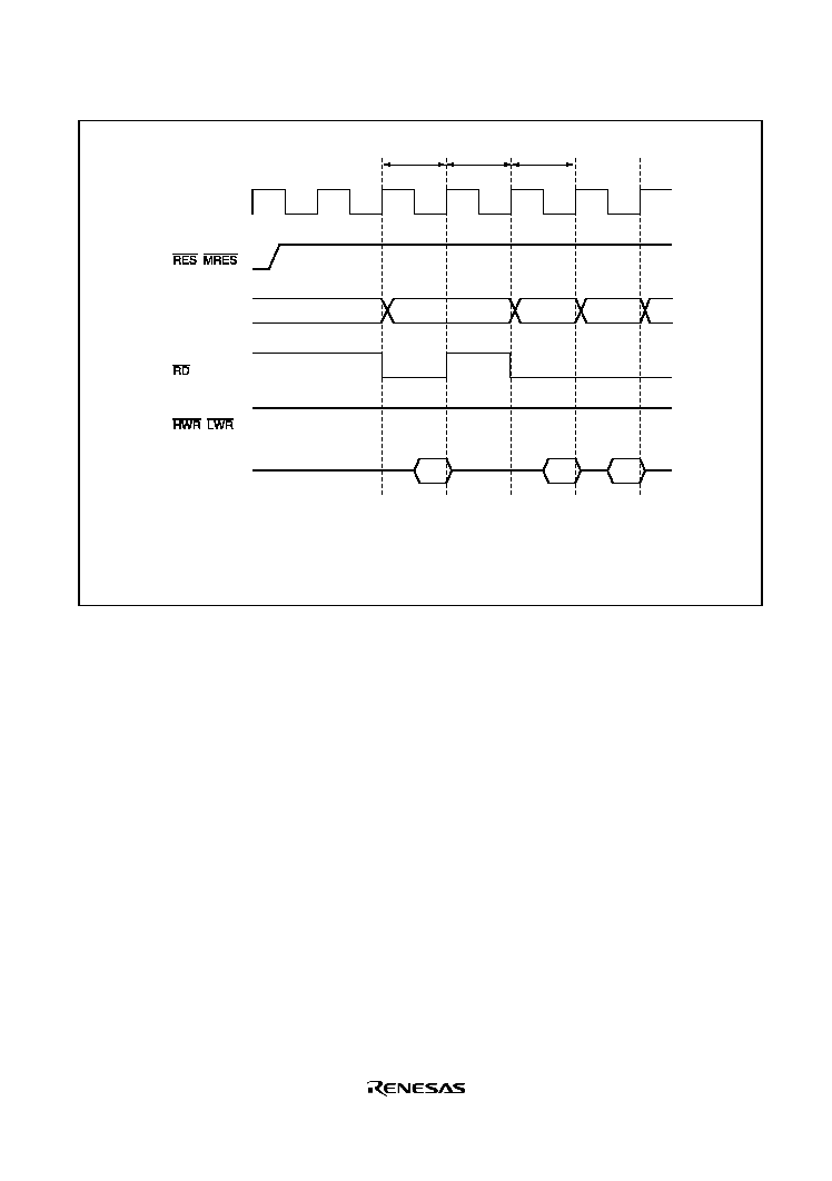
Rev. 1.0, 02/03, page 71 of 634
(1)
(2)
(3)
(4)
: Reset exception handling vector address (for a power-on reset, (1) = H'000000
for a manual reset, (1) = H'000002)
: Start address (contents of reset exceptiion handling vector address)
: Start address ((3) = (2))
: First program instruction
,
Address bus
,
D15 to D0
Vector
fetch
(1)
(3)
High
Internal
processing
Prefetch of first program
instruction
(4)
(2)
Figure 4.1 Reset Sequence (Modes 2 and 3: Not available in this LSI)
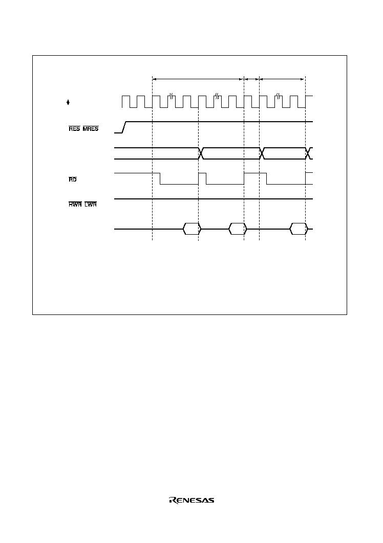
Rev. 1.0, 02/03, page 72 of 634
(1) (3)
(2) (4)
(5)
(6)
Note: * Three program wait states are inserted.
Reset exception handling vector address (for power-on reset, (1) = H'000000,
(3) = H'000002; for manual reset, (1) = H'000004, (3) = H'000006)
Start address (contents of reset exception handling vector address)
Start address ((5) = (2) (4))
First program instruction
,
Address bus
,
D15 to D0
(1)
(3)
High
(2)
(4)
(5)
(6)
*
*
*
Vector fetch
Internal
processing
Prefetch of first
program instruction
Figure 4.2 Reset Sequence (Mode 4)
4.3.3
Interrupts after Reset
If an interrupt is accepted after a reset but before the stack pointer (SP) is initialized, the PC and
CCR will not be saved correctly, leading to a program crash. To prevent this, all interrupt requests,
including NMI, are disabled immediately after a reset. Since the first instruction of a program is
always executed immediately after the reset state ends, make sure that this instruction initializes
the stack pointer (example: MOV.L #xx SP).
4.3.4
State of On-Chip Peripheral Modules after Reset Release
After reset release, MSTPCRA to MSTPCRC are initialized to H'3F, H'FF, and H'FF, respectively,
and all modules except the DMAC enter module stop mode. Consequently, on-chip peripheral
module registers cannot be read from or written to. Register reading and writing is enabled when
module stop mode is exited.

Rev. 1.0, 02/03, page 73 of 634
4.4
Traces
Traces are enabled in interrupt control mode 2. Trace mode is not activated in interrupt control
mode 0, irrespective of the state of the T bit. For details of interrupt control modes, see section 5,
Interrupt Controller.
If the T bit in EXR is set to 1, trace mode is activated. In trace mode, a trace exception occurs on
completion of each instruction. Trace mode is not affected by interrupt masking. Table 4.4 shows
the state of CCR and EXR after execution of trace exception handling. Trace mode is canceled by
clearing the T bit in EXR to 0. The T bit saved on the stack retains its value of 1, and when control
is returned from the trace exception handling routine by the RTE instruction, trace mode resumes.
Trace exception handling is not carried out after execution of the RTE instruction.
Interrupts are accepted even within the trace exception handling routine.
Table 4.4
Status of CCR and EXR after Trace Exception Handling
CCR
EXR
Interrupt Control Mode
I
UI
I2 to I0
T
0
Trace exception handling cannot be used.
2
1
0
Legend:
1: Set to 1
0: Cleared to 0
: Retains value prior to execution.
4.5
Interrupts
Interrupts are controlled by the interrupt controller. The interrupt controller has two interrupt
control modes and can assign interrupts other than NMI to eight priority/mask levels to enable
multiplexed interrupt control. The source to start interrupt exception handling and the vector
address differ depending on the product. For details, refer to section 5, Interrupt Controller.
The interrupt exception handling is as follows:
1. The values in the program counter (PC), condition code register (CCR), and extended control
register (EXR) are saved in the stack.
2. The interrupt mask bit is updated and the T bit is cleared.
3. A vector address corresponding to the interrupt source is generated, the start address is loaded
from the vector table to the PC, and program execution starts from that address.

Rev. 1.0, 02/03, page 74 of 634
4.6
Trap Instruction
Trap instruction exception handling starts when a TRAPA instruction is executed. Trap instruction
exception handling can be executed at all times in the program execution state.
The trap instruction exception handling is as follows:
1. The values in the program counter (PC), condition code register (CCR), and extended control
register (EXR) are saved in the stack.
2. The interrupt mask bit is updated and the T bit is cleared.
3. A vector address corresponding to the interrupt source is generated, the start address is loaded
from the vector table to the PC, and program execution starts from that address.
The TRAPA instruction fetches a start address from a vector table entry corresponding to a vector
number from 0 to 3, as specified in the instruction code.
Table 4.5 shows the status of CCR and EXR after execution of trap instruction exception handling.
Table 4.5
Status of CCR and EXR after Trap Instruction Exception Handling
CCR
EXR
Interrupt Control Mode
I
UI
I2 to I0
T
0
1
2
1
0
Legend
1: Set to 1
0: Cleared to 0
: Retains value prior to execution.
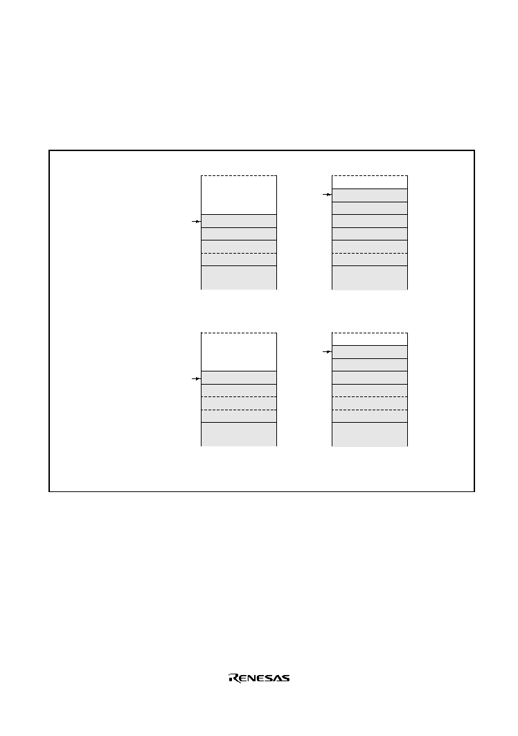
Rev. 1.0, 02/03, page 75 of 634
4.7
Stack Status after Exception Handling
Figure 4.3 shows the stack after completion of trap instruction exception handling and interrupt
exception handling.
CCR
CCR*
1
PC (16 bits)
SP
EXR
Reserved*
1
CCR
CCR*
1
PC (16 bits)
SP
CCR
PC (24 bits)
SP
EXR
Reserved*
1
CCR
PC (24 bits)
SP
(a) Normal Modes*
2
(b) Advanced Modes
Interrupt control mode 0
Interrupt control mode 2
Interrupt control mode 0
Interrupt control mode 2
Notes: 1.
2.
Ignored on return.
Normal modes are not available in this LSI.
Figure 4.3 Stack Status after Exception Handling
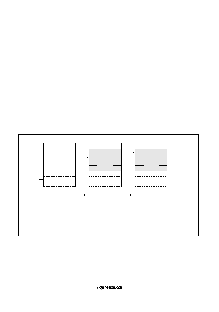
Rev. 1.0, 02/03, page 76 of 634
4.8
Notes on Use of the Stack
When accessing word data or longword data, this LSI assumes that the lowest address bit is 0. The
stack should always be accessed by word transfer instruction or longword transfer instruction, and
the value of the stack pointer (SP, ER7) should always be kept even. Use the following
instructions to save registers:
PUSH.W Rn (or MOV.W Rn, @-SP)
PUSH.L ERn (or MOV.L ERn, @-SP)
Use the following instructions to restore registers:
POP.W Rn (or MOV.W @SP+, Rn)
POP.L ERn (or MOV.L @SP+, ERn)
Setting SP to an odd value may lead to a malfunction. Figure 4.4 shows an example of what
happens when the SP value is odd.
SP
CCR
PC
R1L
SP
: Condition code register
: Program counter
: General register R1L
: Stack pointer
CCR
SP
SP
R1L
H'FFFEFA
H'FFFEFB
H'FFFEFC
H'FFFEFD
H'FFFEFE
H'FFFEFF
PC
PC
TRAPA instruction executed
SP set to H'FFFEFF
Data saved above SP
MOV.B R1L, @-ER7 executed
Contents of CCR lost
Address
Legend
Note: This diagram illustrates an example in which the interrupt control mode is 0, in advanced mode.
Figure 4.4 Operation when SP Value Is Odd

Rev. 1.0, 02/03, page 77 of 634
Section 5 Interrupt Controller
5.1
Features
· Two interrupt control modes
Any of two interrupt control modes can be set by means of the INTM1 and INTM0 bits in
the system control register (SYSCR).
· Priorities settable with IPR
An interrupt priority register (IPR) is provided for setting interrupt priorities. Eight priority
levels can be set for each module for all interrupts except NMI. NMI is assigned the
highest priority level of 8, and can be accepted at all times.
· Independent vector addresses
All interrupt sources are assigned independent vector addresses, making it unnecessary for
the source to be identified in the interrupt handling routine.
· Seven external interrupts (NMI, IRQ7, and IRQ4 to IRQ0)
NMI is the highest-priority interrupt, and is accepted at all times. Rising edge or falling
edge can be selected for NMI. Falling edge, rising edge, or both edge detection, or level
sensing, can be selected for
IRQ7 and IRQ5 to IRQ0. IRQ6 is an interrupt only for the on-
chip USB.
IRQ5 is an interrupt only for the on-chip RTC.
· DMAC control
DMAC activation is performed by means of interrupts.
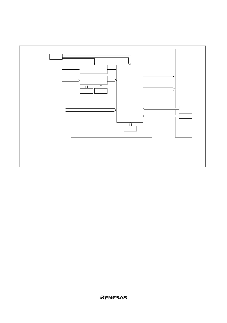
Rev. 1.0, 02/03, page 78 of 634
A block diagram of the interrupt controller is shown in figure 5.1.
SYSCR
NMI input
IRQ input
Internal interrupt
request
WOVI to EXIRQ1
INTM1, INTM0
NMIEG
NMI input unit
IRQ input unit
ISR
ISCR
IER
IPR
Interrupt controller
Priority
determination
Interrupt
request
Vector number
I
I2 to I0
CCR
EXR
CPU
ISCR
IER
ISR
IPR
SYSCR
: IRQ sense control register
: IRQ enable register
: IRQ status register
: Interrupt priority register
: System control register
Legend
Figure 5.1 Block Diagram of Interrupt Controller

Rev. 1.0, 02/03, page 79 of 634
5.2
Input/Output Pins
Table 5.1 summarizes the pins of the interrupt controller.
Table 5.1
Pin Configuration
Name
I/O
Function
NMI
Input
Nonmaskable external interrupt; rising or falling edge can be selected
IRQ7
Input
IRQ4
Input
IRQ3
Input
IRQ2
Input
IRQ1
Input
IRQ0
Input
Maskable external interrupts; rising, falling, or both edges, or level
sensing can be selected (
IRQ6 is an interrupt signal only for the on-chip
USB.
IRQ5 is an interrupt signal only for the on-chip RTC.)
5.3
Register Descriptions
The interrupt controller has the following registers. For details on the system control register, refer
to section 3.2.2, System Control Register (SYSCR).
· The interrupt controller has the following registers.
· System control register (SYSCR)
· IRQ sense control register H (ISCRH)
· IRQ sense control register L (ISCRL)
· IRQ enable register (IER)
· IRQ status register (ISR)
· Interrupt priority register A (IPRA)
· Interrupt priority register B (IPRB)
· Interrupt priority register C (IPRC)
· Interrupt priority register D (IPRD)
· Interrupt priority register E (IPRE)
· Interrupt priority register F (IPRF)
· Interrupt priority register G (IPRG)
· Interrupt priority register J (IPRJ)
· Interrupt priority register K (IPRK)
· Interrupt priority register M (IPRM)

Rev. 1.0, 02/03, page 80 of 634
5.3.1
Interrupt Priority Registers A to G, J, K, M (IPRA to IPRG, IPRJ, IPRK, IPRM)
The IPR registers set priorities (levels 7 to 0) for interrupts other than NMI.
The correspondence between interrupt sources and IPR settings is shown in table 5.2 (Interrupt
Sources, Vector Addresses, and Interrupt Priorities). Setting a value in the range from H'0 to H'7
in the 3-bit groups of bits 6 to 4 and 2 to 0 sets the priority of the corresponding interrupt.
Bit
Bit Name
Initial Value
R/W
Description
7
0
Reserved
This bit is always read as 0 and cannot be modified.
6
5
4
IPR6
IPR5
IPR4
1
1
1
R/W
R/W
R/W
These bits set the priority of the corresponding
interrupt source.
000: Priority level 0 (Lowest)
001: Priority level 1
010: Priority level 2
011: Priority level 3
100: Priority level 4
101: Priority level 5
110: Priority level 6
111: Priority level 7 (Highest)
3
0
Reserved
This bit is always read as 0 and cannot be modified.
2
1
0
IPR2
IPR1
IPR0
1
1
1
R/W
R/W
R/W
These bits set the priority of the corresponding
interrupt source.
000: Priority level 0 (Lowest)
001: Priority level 1
010: Priority level 2
011: Priority level 3
100: Priority level 4
101: Priority level 5
110: Priority level 6
111: Priority level 7 (Highest)

Rev. 1.0, 02/03, page 81 of 634
5.3.2
IRQ Enable Register (IER)
IER controls enabling and disabling of interrupt requests IRQ7 to IRQ0.
Bit
Bit Name
Initial Value
R/W
Description
7
IRQ7E
0
R/W
IRQ7 Enable
The IRQ7 interrupt request is enabled when this bit is 1.
6
IRQ6E
0
R/W
IRQ6 Enable*
1
The IRQ6 interrupt request is enabled when this bit is 1.
5
IRQ5E
0
R/W
IRQ5 Enable*
2
The IRQ5 interrupt request is enabled when this bit is 1.
4
IRQ4E
0
R/W
IRQ4 Enable
The IRQ4 interrupt request is enabled when this bit is 1.
3
IRQ3E
0
R/W
IRQ3 Enable
The IRQ3 interrupt request is enabled when this bit is 1.
2
IRQ2E
0
R/W
IRQ2 Enable
The IRQ2 interrupt request is enabled when this bit is 1.
1
IRQ1E
0
R/W
IRQ1 Enable
The IRQ1 interrupt request is enabled when this bit is 1.
0
IRQ0E
0
R/W
IRQ0 Enable
The IRQ0 interrupt request is enabled when this bit is 1.
Notes: 1. IRQ6 is an interrupt only for the on-chip USB.
2. IRQ5 is an interrupt only for the on-chip RTC.

Rev. 1.0, 02/03, page 82 of 634
5.3.3
IRQ Sense Control Registers H and L (ISCRH, ISCRL)
The ISCR registers select the source that generates an interrupt request at pins
IRQ7 to IRQ0.
Bit
Bit Name
Initial Value
R/W
Description
15
14
IRQ7SCB
IRQ7SCA
0
0
R/W
R/W
IRQ7 Sense Control B
IRQ7 Sense Control A
00: Interrupt request generated at
IRQ7 input low level
01: Interrupt request generated at falling edge of
IRQ7
input
10: Interrupt request generated rising edge of
IRQ7
input
11: Interrupt request generated at both falling and
rising edges of
IRQ7 input
13
12
IRQ6SCB
IRQ6SCA
0
0
R/W
R/W
IRQ6*
1
Sense Control B
IRQ6*
1
Sense Control A
00: Setting prohibited when using on-chip USB
suspend or resume interrupt
01: Interrupt request generated at falling edge of
IRQ6
input
1x: Setting prohibited
11
10
IRQ5SCB
IRQ5SCA
0
0
R/W
R/W
IRQ5*
2
Sense Control B
IRQ5*
2
Sense Control A
00: Interrupt request generated at
IRQ5 input low level
01: Interrupt request generated at falling edge of
IRQ5
input
10: Interrupt request generated at rising edge of
IRQ5
input
11: Interrupt request generated at both falling and
rising edges of
IRQ5 input
9
8
IRQ4SCB
IRQ4SCA
0
0
R/W
R/W
IRQ4 Sense Control B
IRQ4 Sense Control A
00: Interrupt request generated at
IRQ4 input low level
01: Interrupt request generated at falling edge of
IRQ4
input
10: Interrupt request generated at rising edge of
IRQ4
input
11: Interrupt request generated at both falling and
rising edges of
IRQ4 input

Rev. 1.0, 02/03, page 83 of 634
Bit
Bit Name
Initial Value
R/W
Description
7
6
IRQ3SCB
IRQ3SCA
0
0
R/W
R/W
IRQ3 Sense Control B
IRQ3 Sense Control A
00: Interrupt request generated at
IRQ3 input low level
01: Interrupt request generated at falling edge of
IRQ3
input
10: Interrupt request generated at rising edge of
IRQ3
input
11: Interrupt request generated at both falling and
rising edges of
IRQ3 input
5
4
IRQ2SCB
IRQ2SCA
0
0
R/W
R/W
IRQ2 Sense Control B
IRQ2 Sense Control A
00: Interrupt request generated at
IRQ2 input low level
01: Interrupt request generated at falling edge of
IRQ2
input
10: Interrupt request generated at rising edge of
IRQ2
input
11: Interrupt request generated at both falling and
rising edges of
IRQ2 input
3
2
IRQ1SCB
IRQ1SCA
0
0
R/W
R/W
IRQ1 Sense Control B
IRQ1 Sense Control A
00: Interrupt request generated at
IRQ1 input low level
01: Interrupt request generated at falling edge of
IRQ1
input
10: Interrupt request generated at rising edge of
IRQ1
input
11: Interrupt request generated at both falling and rising
edges of
IRQ1 input
1
0
IRQ0SCB
IRQ0SCA
0
0
R/W
R/W
IRQ0 Sense Control B
IRQ0 Sense Control A
00: Interrupt request generated at
IRQ0 input low level
01: Interrupt request generated at falling edge of
IRQ0
input
10: Interrupt request generated at rising edge of
IRQ0
input
11: Interrupt request generated at both falling and
rising edges of
IRQ0 input
Notes: 1. IRQ6 is an interrupt only for the on-chip USB.
2. IRQ5 is an interrupt only for the on-chip RTC.
X: Don't care

Rev. 1.0, 02/03, page 84 of 634
5.3.4
IRQ Status Register (ISR)
ISR indicates the status of IRQ7 to IRQ0 interrupt requests. Only 0 should be written to these bits
for clearing the flag.
Bit
Bit Name
Initial Value R/W
Description
7
IRQ7F
0
R/(W)*
6
IRQ6F
0
R/(W)*
5
IRQ5F
0
R/(W)*
4
IRQ4F
0
R/(W)*
3
IRQ3F
0
R/(W)*
2
IRQ2F
0
R/(W)*
1
IRQ1F
0
R/(W)*
0
IRQ0F
0
R/(W)*
[Setting condition]
When the interrupt source selected by the ISCR
registers occurs
[Clearing conditions]
· Cleared by reading IRQnF flag when IRQnF = 1,
then writing 0 to IRQnF flag
· When interrupt exception handling is executed
when low-level detection is set and ,
IRQn input is
high
· When IRQn interrupt exception handling is executed
when falling, rising, or both-edge detection is set
Note: * Only 0 can be written, to clear flags.
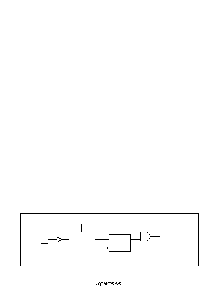
Rev. 1.0, 02/03, page 85 of 634
5.4
Interrupt Sources
5.4.1
External Interrupts
There are seven external interrupts: NMI, IRQ7, and IRQ4 to IRQ0. These interrupts can be used
to restore this LSI from software standby mode. IRQ6 is an interrupt only for the on-chip USB.
However, IRQ6 is functionally same as IRQ7 restore this LSI from software standby mode. Both
IRQ5 and IRQ6 are functionally same as IRQ7 and IRQ4 to IRQ0.
NMI Interrupt: NMI is the highest-priority interrupt, and is always accepted by the CPU
regardless of the interrupt control mode or the status of the CPU interrupt mask bits. The NMIEG
bit in SYSCR can be used to select whether an interrupt is requested at a rising edge or a falling
edge on the NMI pin.
IRQ7 to IRQ0 Interrupts: Interrupts IRQ7 to IRQ0 are requested by an input signal at pins
IRQ7
to
IRQ0. Interrupts IRQ7 to IRQ0 have the following features:
· Using ISCR, it is possible to select whether an interrupt is generated by a low level, falling
edge, rising edge, or both edges, at pins
IRQ7 to IRQ0
· Enabling or disabling of interrupt requests IRQ7 to IRQ0 can be selected with IER.
· The interrupt priority level can be set with IPR.
· The status of interrupt requests IRQ7 to IRQ0 is indicated in ISR. ISR flags can be cleared to 0
by software.
Detection of IRQ7 to IRQ0 interrupts does not depend on whether the relevant pin has been set for
input or output. However, when a pin is used as an external interrupt input pin, do not clear the
corresponding DDR to 0 and use the pin as an I/O pin for another function. Since interrupt request
flags IRQ7F to IRQ0F are set when the setting condition is satisfied, regardless of the IER setting,
only the necessary flags should be referenced.
A block diagram of interrupts IRQ7 to IRQ0 is shown in figure 5.2.
IRQn interrupt
request
IRQnE
IRQnF
S
R
Q
Clear signal
Edge / level
detection curcuit
IRQnSCA, IRQnSCB
IRQn input
Note: n: 7 to 0
Figure 5.2 Block Diagram of Interrupts IRQ7 to IRQ0

Rev. 1.0, 02/03, page 86 of 634
5.4.2
Internal Interrupts
The sources for internal interrupts from on--chip peripheral modules have the following features:
· For each on--chip peripheral module there are flags that indicate the interrupt request status,
and enable bits that select enabling or disabling of these interrupts. If both of these are set to 1
for a particular interrupt source, an interrupt request is issued to the interrupt controller.
· The interrupt priority level can be set by means of IPR.
· The DMAC can be activated by a TPU, SCI, or other interrupt request.
· When the DMAC is activated by an interrupt request, it is not affected by the interrupt control
mode or CPU interrupt mask bit.
5.5
Interrupt Exception Handling Vector Table
Table 5.2 shows interrupt exception handling sources, vector addresses, and interrupt priorities.
For default priorities, the lower the vector number, the higher the priority. Priorities among
modules can be set by means of the IPR. Modules set at the same priority will conform to their
default priorities. Priorities within a module are fixed.
Table 5.2
Interrupt Sources, Vector Addresses, and Interrupt Priorities
Vector Address
*
Interrupt
Source
Origin of Interrupt
Source
Vector
Number
Advanced Mode
IPR
Priority
External pins
NMI
7
H'001C
High
IRQ0
16
H'0040
IPRA6 to IPRA4
IRQ1
17
H'0044
IPRA2 to IPRA0
IRQ2
18
H'0048
IPRB6 to IPRB4
IRQ3
19
H'004C
IRQ4
20
H'0050
IPRB2 to IPRB0
RTC
IRQ5
21
H'0054
USB
IRQ6
22
H'0058
IPRC6 to IPRC4
External pins
IRQ7
23
H'005C
Watchdog Timer WOVI
25
H'0064
IPRD6 to IPRD4
A/D
ADI
28
H'0070
IPRE2 to IPRE0
Low
Rev. 1.0, 02/03, page 87 of 634
Interrupt
Source
Origin of Interrupt
Source
Vector
Number
Vector Address
*
IPR
Priority
TGI0A
32
H'0080
High
TGI0B
33
H'0084
TGI0C
34
H'0088
TGI0D
35
H'008C
TPU channel 0
TGI0V
36
H'0090
IPRF6 to IPRF4
TGI1A
40
H'00A0
TGI1B
41
H'00A4
TGI1V
42
H'00A8
TPU channel 1
TGI1U
43
H'00AC
IPRF2 to IPRF0
TGI2A
44
H'00B0
TGI2B
45
H'00B4
TGI2V
46
H'00B8
TPU channel 2
TGI2U
47
H'00BC
IPRG6 to IPRG4
DEND0A
72
H'0120
DEND0B
73
H'0124
DEND1A
74
H'0128
DMAC
DEND1B
75
H'012C
IPRJ6 to IPRJ4
ERI0
80
H'0140
RXI0
81
H'0144
TXI0
82
H'0148
SIC channel 0
TEI0
83
H'014C
IPRJ2 to IPRJ0
ERI2
88
H'0160
RXI2
89
H'0164
TXI2
90
H'0168
SIC channel 2
TEI2
91
H'016C
IPRK2 to IPRK0
EXIRQ0
104
H'01A0
USB
EXIRQ1
105
H'01A4
IPRM6 to IPRM4
Low
Note: * Lower 16 bits of the start address.

Rev. 1.0, 02/03, page 88 of 634
5.6
Interrupt Control Modes and Interrupt Operation
The interrupt controller has two modes: interrupt control mode 0 and interrupt control mode 2.
Interrupt operations differ depending on the interrupt control mode. The interrupt control mode is
selected by SYSCR. Table 5.3 shows the differences between interrupt control mode 0 and
interrupt control mode 2.
Table 5.3
Interrupt Control Modes
Interrupt
Control Mode
Priority Setting
Register
Interrupt Mask
Bits
Description
0
Default
I
The priority of interrupt sources are fixed at
the default settings.
Interrupt sources except for NMI is marked by
the I bit.
2
IPR
I2 to I0
8-level interrupt mask control is performed by
bits I2 to I0.
8 priority levels other than NMI can be set with
IPR.
5.6.1
Interrupt Control Mode 0
In interrupt control mode 0, interrupt requests except for NMI is masked by the I bit of CCR in the
CPU. Figure 5.3 shows a flowchart of the interrupt acceptance operation in this case.
1. If an interrupt source occurs when the corresponding interrupt enable bit is set to 1, an
interrupt request is sent to the interrupt controller.
2. If the I bit is set to 1, only an NMI interrupt is accepted, and other interrupt requests are held
pending. If the I bit is cleared, an interrupt request is accepted.
3. Interrupt requests are sent to the interrupt controller, the highest-ranked interrupt according to
the priority system is accepted, and other interrupt requests are held pending.
4. When the CPU accepts an interrupt request, it starts interrupt exception handling after
execution of the current instruction has been completed.
5. The PC and CCR are saved to the stack area by interrupt exception handling. The PC saved on
the stack shows the address of the first instruction to be executed after returning from the
interrupt handling routine.
6. Next, the I bit in CCR is set to 1. This masks all interrupts except NMI.
7. The CPU generates a vector address for the accepted interrupt and starts execution of the
interrupt handling routine at the address indicated by the contents of the vector address in the
vector table.
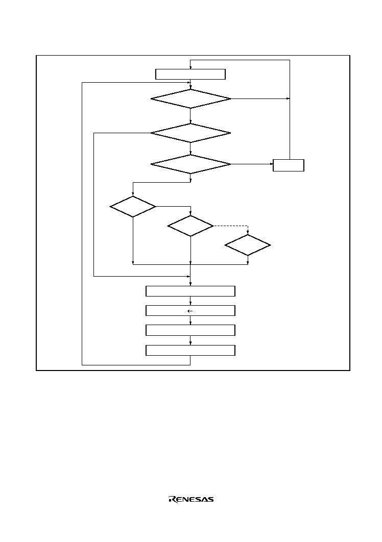
Rev. 1.0, 02/03, page 89 of 634
Program execution status
Interrupt generated?
NMI
IRQ0
IRQ1
EXIRQ1
I = 0
Save PC and CCR
I
1
Read vector address
Branch to interrupt handling routine
Yes
No
Yes
Yes
Yes
No
No
No
Yes
Yes
No
Hold
pending
Figure 5.3 Flowchart of Procedure Up to Interrupt Acceptance
in Interrupt Control Mode 0

Rev. 1.0, 02/03, page 90 of 634
5.6.2
Interrupt Control Mode 2
In interrupt control mode 2, mask control is done in eight levels for interrupt requests except for
NMI by comparing the EXR interrupt mask level (I2 to I0 bits) in the CPU and the IPR setting.
Figure 5.4 shows a flowchart of the interrupt acceptance operation in this case.
1. If an interrupt source occurs when the corresponding interrupt enable bit is set to 1, an
interrupt request is sent to the interrupt controller.
2. When interrupt requests are sent to the interrupt controller, the interrupt with the highest
priority according to the interrupt priority levels set in IPR is selected, and lower-priority
interrupt requests are held pending. If a number of interrupt requests with the same priority are
generated at the same time, the interrupt request with the highest priority according to the
priority system shown in table 5.2 is selected.
3. Next, the priority of the selected interrupt request is compared with the interrupt mask level set
in EXR. An interrupt request with a priority no higher than the mask level set at that time is
held pending, and only an interrupt request with a priority higher than the interrupt mask level
is accepted.
4. When the CPU accepts an interrupt request, it starts interrupt exception handling after
execution of the current instruction has been completed.
5. The PC, CCR, and EXR are saved to the stack area by interrupt exception handling. The PC
saved on the stack shows the address of the first instruction to be executed after returning from
the interrupt handling routine.
6. The T bit in EXR is cleared to 0. The interrupt mask level is rewritten with the priority level of
the accepted interrupt.
If the accepted interrupt is NMI, the interrupt mask level is set to H'7.
7. The CPU generates a vector address for the accepted interrupt and starts execution of the
interrupt handling routine at the address indicated by the contents of the vector address in the
vector table.
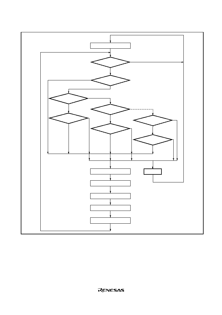
Rev. 1.0, 02/03, page 91 of 634
Yes
Program execution status
Interrupt generated?
NMI
Level 6 interrupt?
Mask level 5
or below?
Level 7 interrupt?
Mask level 6
or below?
Save PC, CCR, and EXR
Clear T bit to 0
Update mask level
Read vector address
Branch to interrupt handling routine
Level 1 interrupt?
Mask level 0?
Yes
Yes
No
Yes
Yes
Yes
No
Yes
Yes
No
No
No
No
No
No
Hold
pending
Figure 5.4 Flowchart of Procedure Up to Interrupt Acceptance in
Interrupt Control Mode 2
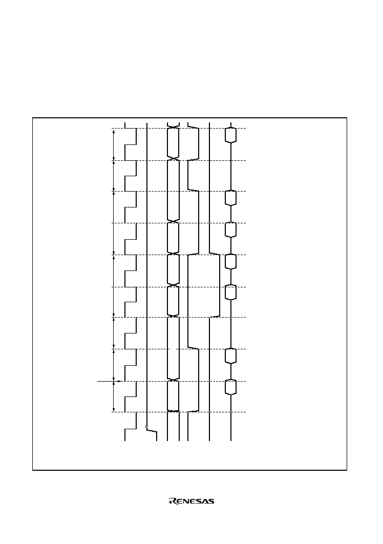
Rev. 1.0, 02/03, page 92 of 634
5.6.3
Interrupt Exception Handling Sequence
Figure 5.5 shows the interrupt exception handling sequence. The example shown is for the case
where interrupt control mode 0 is set in advanced mode, and the program area and stack area are
in on-chip memory.
(14)
(12)
(10)
(6)
(4)
(2)
(1)
(
5)
(7)
(9)
(11)
(13)
Interrupt service
routine instruction
prefetch
Internal
operation
Vector fetch
stack
Instruction
prefetch
Internal
operation
Interrupt
acceptance
Interrupt level determination
Wait for end of instruction
Interrupt
request signal
Internal
address bus
Internal
read signal
Internal
write signal
Internal
data bus
(3)
(1)
(2) (4)
(3)
(5)
(7)
Instruction prefetch address (Not executed.
This is the contents of the saved PC, the return address.)
Instruction code (Not executed.)
Instruction prefetch address (Not executed.)
SP-2
SP-4
Saved PC and saved CCR
Vector address
Interrupt handling routine start address (Vector address contents)
Interrupt handling routine start address ((13) = (10) (12))
First instruction of interrupt handling routine
(6) (8)
(9) (11)
(10) (12)
(13)
(14)
(8)
Figure 5.5 Interrupt Exception Handling

Rev. 1.0, 02/03, page 93 of 634
5.6.4
Interrupt Response Times
Table 5.4 shows interrupt response times
the interval between generation of an interrupt request
and execution of the first instruction in the interrupt handling routine. The execution status
symbols used in table 5.4 are explained in table 5.5.
This LSI is capable of fast word transfer to on-chip memory, and have the program area in on-chip
ROM and the stack area in on-chip RAM, enabling high-speed processing.
Table 5.4
Interrupt Response Times
Normal Mode
*
5
Advanced Mode
No.
Execution State
Interrupt
Control
Mode 0
Interrupt
Control
Mode 2
Interrupt
Control
Mode 0
Interrupt
Control
Mode 2
1
Interrupt priority determination*
1
3
3
3
3
2
Number of wait states until
executing instruction ends*
2
1 to 19+2,S
I
1 to 19+2·S
I
1 to 19+2·S
I
1 to 19+2·S
I
3
PC, CCR, EXR stack save
2·S
K
3·S
K
2·S
K
3·S
K
4
Vector fetch
S
I
S
I
2·S
I
2·S
I
5
Instruction fetch*
3
2·S
I
2·S
I
2·S
I
2·S
I
6
Internal processing*
4
2
2
2
2
Total (using on-chip memory)
11 to 31
12 to 32
12 to 32
13 to 33
Notes: 1. Two states in case of internal interrupt.
2. Refers to MULXS and DIVXS instructions.
3. Prefetch after interrupt acceptance and interrupt handling routine prefetch.
4. Internal processing after interrupt acceptance and internal processing after vector fetch.
5. Not available in this LSI.
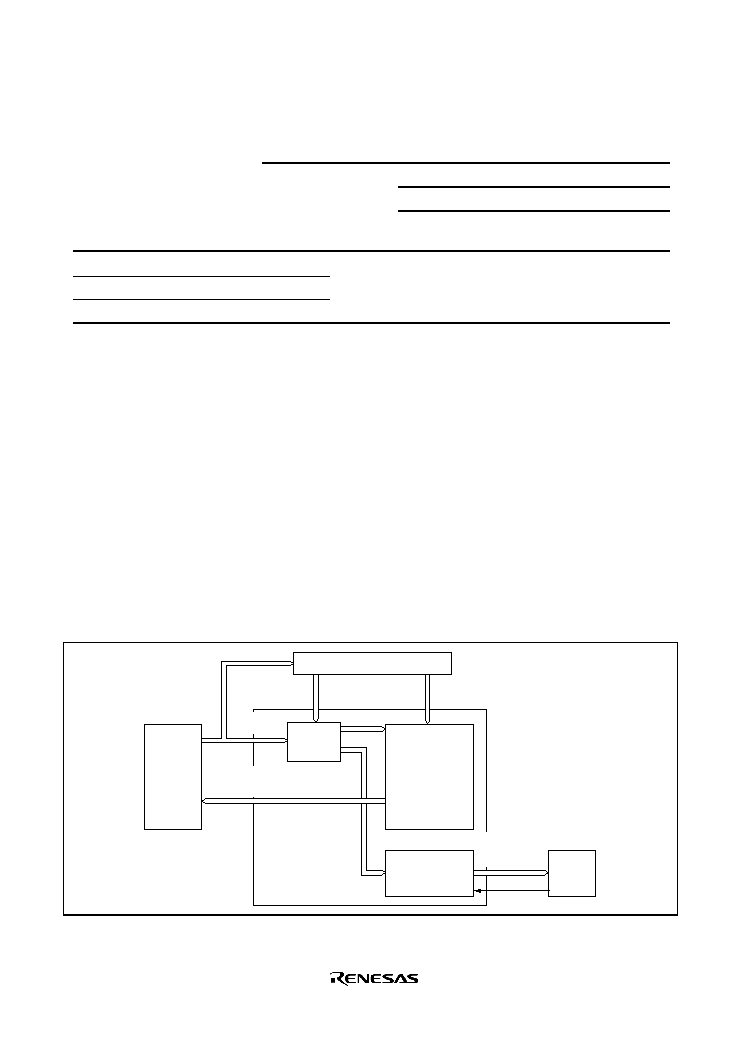
Rev. 1.0, 02/03, page 94 of 634
Table 5.5
Number of States in Interrupt Handling Routine Execution Statuses
Object of Access
External Device
8-Bit Bus
16-Bit Bus
Symbol
Internal
Memory
2-State
Access
3-State
Access
2-State
Access
3-State
Access
Instruction fetch
S
I
1
4
6 + 2m
2
3 + m
Branch address read
S
J
Stack manipulation
S
K
Legend:
m: Number of wait states in an external device access.
5.6.5
DMAC Activation by Interrupt
The DMAC can be activated by an interrupt. In this case, the following options are available:
· Interrupt request to CPU
· Activation request to DMAC
· Selection of a number of the above
For details of interrupt requests that can be used with to activate the DMAC, see section 7, DMA
Controller.
Figure 5.6 shows a block diagram of the interrupt controller of DMAC.
CPU
I, I2 to I0
DMAC
IRQ
interrupt
On-chip
peripheral
module
Interrupt source
clear signal
Interrupt
request
Disenable
signal
Clear
signal
Selection
circuit
CPU interrupt
request vector
number
Interrupt controller
Determination of
priority
Control logic
Figure 5.6 Interrupt Control for DMAC

Rev. 1.0, 02/03, page 95 of 634
Selection of Interrupt Source: An activation factor is directly input to each channel of the
DMAC. The activation factors for each channel of the DMAC are selected by the DTF3 to DTF0
bits of DMACR. The DTA bit of DMABCR can be used to select whether the selected activation
factors are managed by the DMAC. By setting the DTA bit to 1, the interrupt factor which was the
activation factor for that DMAC cannot act as the CPU interrupt factor.
Interrupt factors other than the interrupts managed by the DMAC is CPU interrupt request.
Determination of Priority: The activation source is directly input to each channel of DMAC.
Operation Order: If the same interrupt is selected as the DMAC activation factor or CPU
interrupt factor, these operate independently. They operate in accordance with the respective
operating states and bus priorities.
Table 5.6 shows the interrupt factor clear control and selection of interrupt factors by specification
of the DTA bit of DMAC's DMABCR.
Table 5.6
Interrupt Source Selection and Clearing Control
Settings
DMAC
Interrupt Sources Selection/Clearing Control
DTA
DMAC
CPU
0
1
X
Legend
: The relevant interrupt is used. Interrupt source clearing is performed.
(The CPU should clear the source flag in the interrupt handling routine.)
: The relevant interrupt is used. The interrupt source is not cleared.
X: The relevant bit cannot be used.
Notes on Use: The SCI interrupt source is cleared when the DMAC reads or writes to the
prescribed register, and is not dependent upon the DTA bit.
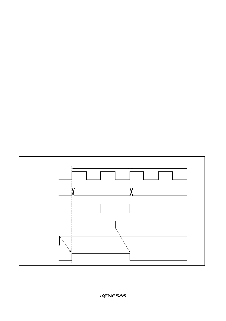
Rev. 1.0, 02/03, page 96 of 634
5.7
Usage Notes
5.7.1
Contention between Interrupt Generation and Disabling
When an interrupt enable bit is cleared to 0 to disable interrupts, the disabling becomes effective
after execution of the instruction.
When an interrupt enable bit is cleared to 0 by an instruction such as BCLR or MOV, if an
interrupt is generated during execution of the instruction, the interrupt concerned will still be
enabled on completion of the instruction, and so interrupt exception handling for that interrupt will
be executed on completion of the instruction. However, if there is an interrupt request of higher
priority than that interrupt, interrupt exception handling will be executed for the higher-priority
interrupt, and the lower-priority interrupt will be ignored.
The same also applies when an interrupt source flag is cleared to 0.
Figure 5.7 shows an example in which the TGIEA bit in the TPU's TIER_0 is cleared to 0.
The above contention will not occur if an enable bit or interrupt source flag is cleared to 0 while
the interrupt is masked.
Internal
address bus
Internal
write signal
TGIEA
TGFA
TGI0A
Interrupt signal
TIER0 write cycle by CPU
TGI0A exception handling
TIER_0 address
Figure 5.7 Contention between Interrupt Generation and Disabling

Rev. 1.0, 02/03, page 97 of 634
5.7.2
Instructions that Disable Interrupts
Instructions that disable interrupts are LDC, ANDC, ORC, and XORC. After any of these
instructions is executed, all interrupts including NMI are disabled and the next instruction is
always executed. When the I bit is set by one of these instructions, the new value becomes valid
two states after execution of the instruction ends.
5.7.3
Times when Interrupts are Disabled
There are times when interrupt acceptance is disabled by the interrupt controller.
The interrupt controller disables interrupt acceptance for a 3-state period after the CPU has
updated the mask level with an LDC, ANDC, ORC, or XORC instruction.
5.7.4
Interrupts during Execution of EEPMOV Instruction
Interrupt operation differs between the EEPMOV.B instruction and the EEPMOV.W instruction.
With the EEPMOV.B instruction, an interrupt request (including NMI) issued during the transfer
is not accepted until the move is completed.
With the EEPMOV.W instruction, if an interrupt request is issued during the transfer, interrupt
exception handling starts at a break in the transfer cycle. The PC value saved on the stack in this
case is the address of the next instruction.
Therefore, if an interrupt is generated during execution of an EEPMOV.W instruction, the
following coding should be used.
L1: EEPMOV.W
MOV.W R4, R4
BNE L1

Rev. 1.0, 02/03, page 98 of 634

BSCS207A_010020020100
Rev. 1.0, 02/03, page 99 of 634
Section 6 Bus Controller
This LSI has a built-in bus controller (BSC) that manages the external address space divided into
eight areas. The bus controller also has a bus arbitration function, and controls the operation of the
internal bus masters: the CPU and DMA controller (DMAC).
6.1
Features
· Manages external address space in area units
Manages the external space as 8 areas of 2-Mbytes
Bus specifications can be set independently for each area
Burst ROM interface can be set
· Basic bus interface*
1
Chip select (CS0 to CS5) can be output for areas 0 to 5*
2
8-bit access or 16-bit access can be selected for each area
2-state access or 3-state access can be selected for each area
Program wait states can be inserted for each area
· Burst ROM interface*
2
Burst ROM interface can be selected for area 0
One or two states can be selected for the burst cycle
· Idle cycle insertion
Idle cycle can be inserted between consecutive read accesses to different areas
Idle cycle can be inserted before a write access to an external area immediately after a read
access to an external area
· Bus arbitration
The on-chip bus arbiter arbitrates bus mastership among CPU and DMAC.
· Other features
External bus release function*
2
Notes: 1. Chip select
CS6 in area 6 is for the on-chip USB. Therefore it cannot be used as an
external area. 8-bit bus mode, 3-state access, and no program wait state should be set
for area 6. Access to the RTC related registers (address: H'FFFF40 to H'FFFF5F)
follows the specification of area 7. 8-bit access, 3-state access, and no program wait
state should be set for area 7.
2. These functions are not available in the H8S/2212 Series.
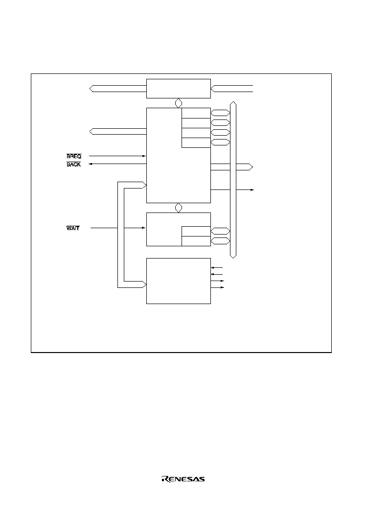
Rev. 1.0, 02/03, page 100 of 634
Figure 6.1 shows a block diagram of the bus controller.
Area decorder
Bus
controller
ABWCR
ASTCR
BCRH
BCRL
Internal
address bus
External bus control signals
Chip select signals
*
*
Internal control
signals
Wait
controller
WCRH
WCRL
Bus mode signal
Internal data bus
Bus arbiter
CPU bus acknowledge signal
DMAC bus acknowledge signal
DMAC bus request signal
CPU bus request signal
*
Note: * Supported only by the H8S/2218 Series.
Legend
ABWCR
ASTCR
WCRH, WCRL
BCRH, BCRL
: Bus width control register
: Access state control register
: Waite control registers H, L
: Bus control registers H, L
Figure 6.1 Block Diagram of Bus Controller

Rev. 1.0, 02/03, page 101 of 634
6.2
Input/Output Pins
Table 6.1 summarizes the pins of the bus controller.
These pins are supported only by the H8S/2218 Series.
Table 6.1
Pin Configuration
Name
Symbol
I/O
Function
Address strove
AS
Output
Strobe signal indicating that address output on
address bus is enabled.
Read
RD
Output
Strobe signal indicating that external space is being
read.
High write
HWR
Output
Strobe signal indicating that external space is to be
written, and upper half (D15 to D8) of data bus is
enabled.
Low write
LWR
Output
Strobe signal indicating that external space is to be
written, and lower half (D7 to D0) of data bus is
enabled.
Chip select 0 to 5
CS0 to CS5 Output
Strobe signal indicating that areas 0 to 5 are selected.
Wait
WAIT
Input
Wait request signal when accessing external 3-state
access space.
Bus request
BREQ
Input
Request signal that releases bus to external device.
Bus request
acknowledge
BACK
Output
Acknowledge signal indicating that bus has been
released.

Rev. 1.0, 02/03, page 102 of 634
6.3
Register Descriptions
The following shows the registers of the bus controller.
· Bus width control register (ABWCR)
· Access state control register (ASTCR)
· Wait control register H (WCRH)
· Wait control register L (WCRL)
· Bus control register H (BCRH)
· Bus control register L (BCRL )
· Pin function control register (PFCR)
6.3.1
Bus Width Control Register (ABWCR)
ABWCR designates each area for either 8-bit access or 16-bit access.
ABWCR sets the data bus width for the external memory space. The bus width for on-chip
memory and internal I/O registers except for the on-chip USB and RTC is fixed regardless of the
settings in ABWCR.
Bit
Bit Name
Initial Value
R/W
Description
7
6
5
4
3
2
1
0
ABW7*
2
ABW6*
2
ABW5
ABW4
ABW3
ABW2
ABW1
ABW0
1/0*
1
1/0*
1
1/0*
1
1/0*
1
1/0*
1
1/0*
1
1/0*
1
1/0*
1
R/W
R/W
R/W
R/W
R/W
R/W
R/W
R/W
Area 7 to 0 Bus Width Control:
These bits select whether the corresponding area is to
be designated for 8-bit access or 16-bit access.
0: Area n is designated for 16-bit access
1: Area n is designated for 8-bit access
Legend:
n: 7 to 0
Notes: 1
In modes 5 to 7, initial value of each bit is 1. In mode 4, initial value of each bit is 0.
These bits should be set to 1 in the H8S/2212 Series.
2. The on-chip USB and on-chip RTC are allocated to area 6 and area 7, respectively.
Therefore, these bits should be set to 1.

Rev. 1.0, 02/03, page 103 of 634
6.3.2
Access State Control Register (ASTCR)
ASTCR designates each area as either a 2-state access space or a 3-state access space.
ASTCR sets the number of access states for the external memory space. The number of access
states for on-chip memory and internal I/O registers except for the on-chip USB is fixed regardless
of the settings in ASTCR.
Bit
Bit Name
Initial Value
R/W
Description
7
6
5
4
3
2
1
0
AST7*
AST6*
AST5
AST4
AST3
AST2
AST1
AST0
1
1
1
1
1
1
1
1
R/W
R/W
R/W
R/W
R/W
R/W
R/W
R/W
Area 7 to 0 Access State Control:
These bits select whether the corresponding area is to
be designated as a 2-state access space or a 3-state
access space. Wait state insertion is enabled or disabled
at the same time.
0: Area n is designated for 2-state access
Wait state insertion in area n external space is
disabled
1: Area n is designated for 3-state access
Wait state insertion in area n external space is
enabled
Legend:
n: 7 to 0
Note: * The on-chip USB and on-chip RTC are allocated to area 6 and area 7, respectively.
Therefore, these bits should be set to 1.

Rev. 1.0, 02/03, page 104 of 634
6.3.3
Wait Control Registers H and L (WCRH, WCRL)
WCRH and WCRL select the number of program wait states for each area.
Program waits are not inserted in the case of on-chip memory or internal I/O registers except for
the on-chip USB.
· WCRH
Bit
Bit Name
Initial Value R/W
Description
7
6
W71*
W70*
1
1
R/W
R/W
Area 7 Wait Control 1 and 0
These bits select the number of program wait states
when area 7 in external space is accessed while the
AST7 bit in ASTCR is set to 1.
00: Program wait not inserted when external space area
7 is accessed
01: 1 program wait state inserted when external space
area 7 is accessed
10: 2 program wait states inserted when external space
area 7 is accessed
11: 3 program wait states inserted when external space
area 7 is accessed
5
4
W61*
W60*
1
1
R/W
R/W
Area 6 Wait Control 1 and 0
These bits select the number of program wait states
when area 6 in external space is accessed while the
AST6 bit in ASTCR is set to 1.
00: Program wait not inserted when external space area
6 is accessed
01: 1 program wait state inserted when external space
area 6 is accessed
10: 2 program wait states inserted when external space
area 6 is accessed
11: 3 program wait states inserted when external space
area 6 is accessed

Rev. 1.0, 02/03, page 105 of 634
Bit
Bit Name
Initial Value R/W
Description
3
2
W51
W50
1
1
R/W
R/W
Area 5 Wait Control 1 and 0
These bits select the number of program wait states
when area 5 in external space is accessed while the
AST5 bit in ASTCR is set to 1.
00: Program wait not inserted when external space area
5 is accessed
01: 1 program wait state inserted when external space
area 5 is accessed
10: 2 program wait states inserted when external space
area 5 is accessed
11: 3 program wait states inserted when external space
area 5 is accessed
1
0
W41
W40
1
1
R/W
R/W
Area 4 Wait Control 1 and 0
These bits select the number of program wait states
when area 4 in external space is accessed while the
AST4 bit in ASTCR is set to 1.
00: Program wait not inserted when external space area
4 is accessed
01: 1 program wait state inserted when external space
area 4 is accessed
10: 2 program wait states inserted when external space
area 4 is accessed
11: 3 program wait states inserted when external space
area 4 is accessed
Note: * The on-chip USB and on-chip RTC are allocated to area 6 and area 7, respectively.
Therefore, these bits should be set to 0.

Rev. 1.0, 02/03, page 106 of 634
· WCRL
Bit
Bit Name
Initial Value R/W
Description
7
6
W31
W30
1
1
R/W
R/W
Area 3 Wait Control 1 and 0
These bits select the number of program wait states
when area 3 in external space is accessed while the
AST3 bit in ASTCR is set to 1.
00: Program wait not inserted when external space area
3 is accessed
01: 1 program wait state inserted when external space
area 3 is accessed
10: 2 program wait states inserted when external space
area 3 is accessed
11: 3 program wait states inserted when external space
area 3 is accessed
5
4
W21
W20
1
1
R/W
R/W
Area 2 Wait Control 1 and 0
These bits select the number of program wait states
when area 2 in external space is accessed while the
AST2 bit in ASTCR is set to 1.
00: Program wait not inserted when external space area
2 is accessed
01: 1 program wait state inserted when external space
area 2 is accessed
10: 2 program wait states inserted when external space
area 2 is accessed
11: 3 program wait states inserted when external space
area 2 is accessed

Rev. 1.0, 02/03, page 107 of 634
Bit
Bit Name
Initial Value R/W
Description
3
2
W11
W10
1
1
R/W
R/W
Area 1 Wait Control 1 and 0
These bits select the number of program wait states
when area 1 in external space is accessed while the
AST1 bit in ASTCR is set to 1.
00: Program wait not inserted when external space area
1 is accessed
01: 1 program wait state inserted when external space
area 1 is accessed
10: 2 program wait states inserted when external space
area 1 is accessed
11: 3 program wait states inserted when external space
area 1 is accessed
1
0
W01
W00
1
1
R/W
R/W
Area 0 Wait Control 1 and 0
These bits select the number of program wait states
when area 0 in external space is accessed while the
AST0 bit in ASTCR is set to 1.
00: Program wait not inserted when external space area
0 is accessed
01: 1 program wait state inserted when external space
area 0 is accessed
10: 2 program wait states inserted when external space
area 0 is accessed
11: 3 program wait states inserted when external space
area 0 is accessed

Rev. 1.0, 02/03, page 108 of 634
6.3.4
Bus Control Register H (BCRH)
BCRH selects enabling or disabling of idle cycle insertion, and the memory interface for area 0.
This register should be set initial value and not be modified in the H8S/2212 Series.
Bit
Bit Name
Initial Value R/W
Description
7
ICIS1
1
R/W
Idle Cycle Insert 1:
Selects whether or not one idle cycle state is to be
inserted between bus cycles when successive external
read cycles are performed in different areas.
0: Idle cycle not inserted in case of successive external
read cycles in different areas
1: Idle cycle inserted in case of successive external read
cycles in different areas
6
ICIS0
1
R/W
Idle Cycle Insert 0:
Selects whether or not one idle cycle state is to be
inserted between bus cycles when successive external
read and write cycles are performed.
0: Idle cycle not inserted in case of successive external
read and write cycles
1: Idle cycle inserted in case of successive external read
and write cycles
5
BRSTRM
0
R/W
Burst ROM enable:
Selects whether area 0 is used as a burst ROM interface.
0: Area 0 is basic bus interface
1: Area 0 is burst ROM interface
4
BRSTS1
1
R/W
Burst Cycle Select 1:
Selects the number of burst cycles for the burst ROM
interface.
0: Burst cycle comprises 1 state
1: Burst cycle comprises 2 states
3
BRSTS0
0
R/W
Burst Cycle Select 0:
Selects the number of words that can be accessed in a
burst ROM interface burst access.
0: Max. 4 words in burst access
1: Max. 8 words in burst access
2 to
0
0
R/W
Reserved
The write value should always be 0.

Rev. 1.0, 02/03, page 109 of 634
6.3.5
Bus Control Register L (BCRL)
BCRL performs selection of the external bus-released state protocol, and enabling or disabling of
WAIT pin input.
The functions selected by this register are available only in the H8S/2218 Series. This register
should not be modified in the H8S/2212 Series.
Bit
Bit Name
Initial Value R/W
Description
7
BRLE*
0
R/W
Bus Release Enable
Enables or disables external bus release.
0: External bus release is disabled.
BREQ and BACK
can be used as I/O ports.
1: External bus release is enabled.
6
0
R/W
Reserved
The write value should always be 0.
5
0
Reserved
This bit is always read as 0 and cannot be modified.
4
0
R/W
Reserved
The write value should always be 0.
3
1
R/W
Reserved
The write value should always be 1.
2
1
0
0
R/W
R/W
Reserved
The write value should always be 0.
0
WAITE*
0
R/W
WAIT Pin Enable
Selects enabling or disabling of wait input by the
WAIT
pin.
0: Wait input by
WAIT pin disabled. WAIT pin can be
used as I/O port.
1: Wait input by
WAIT pin enabled.
Note:
*
These bits should be set to 0 in the H8S/2212 Series.

Rev. 1.0, 02/03, page 110 of 634
6.3.6
Pin Function Control Register (PFCR)
PFCR performs address output control in external extended mode. The AE3 to AE0 are set to
0010 in the H8S/2212 Series. When using the emulator (E6000), USB can not be used without
enabling the A8 and A9 output.
Bit
Bit Name
Initial Value R/W
Description
7 to
4
Undefined
R/W
Reserved
The write value should always be 0.
3
2
1
0
AE3
AE2
AE1
AE0
1/0*
1/0*
0
1/0*
R/W
R/W
R/W
R/W
Address Output Enable 3 to 0
These bits select enabling or disabling of address
outputs A8 to A23 in ROMless extended mode and
modes with ROM.
When a pin is enabled for address output, the address is
output regardless of the corresponding DDR setting.
When a pin is disabled for address output, it becomes an
output port when the corresponding DDR bit is set to 1.
0000:
A8 to A23 output disabled (initial value of mode 6 and
7)
0001:
A8 output enabled; A9 to A23 output disabled
0010:
A8, A9 output enabled; A10 to A23 output disabled
0011:
A8 to A10 output enabled; A11 to A23 output disabled
0100:
A8 to A11 output enabled; A12 to A23 output disabled
0101:
A8 to A12 output enabled; A13 to A23 output disabled
0110:
A8 to A13 output enabled; A14 to A23 output disabled
0111:
A8 to A14 output enabled; A15 to A23 output disabled
1000:
A8 t o A15 output enabled; A16 to A23 output disabled
1001:
A8 to A16 output enabled; A17 to A23 output disabled
1010:
A8 to A17 output enabled; A18 to A23 output disabled
1011:
A8 to A18 output enabled; A19 to A23 output disabled
1100:
A8 to A19 output enabled; A20 to A23 output disabled
1101:
A8 to A20 output enabled; A21 to A23 output disabled
(initial value of mode 4 and 5)
1110:
A8 to A21 output enabled; A22, A23 output disabled
1111:
A8 to A23 output enabled
Note: * In modes 4 and 5, initial value of each bit is 1. In modes 6 and 7, initial value of each bit is
0.
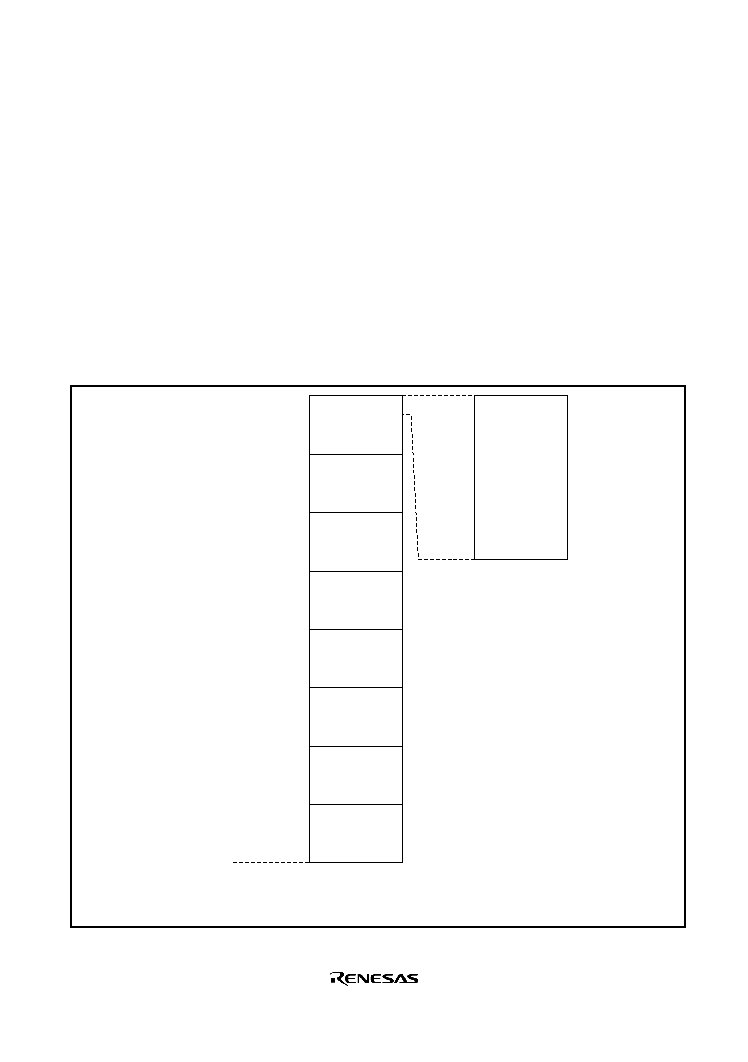
Rev. 1.0, 02/03, page 111 of 634
6.4
Bus Control
6.4.1
Area Divisions
In advanced mode, the bus controller partitions the 16 Mbytes address space into eight areas, 0 to
7, in 2-Mbyte units, and performs bus control for external space in area units. In normal mode*, it
controls a 64-kbyte address space comprising part of area 0.
Figure 6.2 shows an outline of the memory map.
Chip select signals (
CS0 to CS5) can be output for areas 0 to 5.
Note: * Not available in this LSI.
Area 0
(2 Mbytes)
H'000000
H'FFFFFF
(1)
(2)
H'0000
H'1FFFFF
H'200000
Area 1
(2 Mbytes)
H'3FFFFF
H'400000
Area 2
(2 Mbytes)
H'5FFFFF
H'600000
Area 3
(2 Mbytes)
H'7FFFFF
H'800000
Area 4
(2 Mbytes)
H'9FFFFF
H'A00000
Area 5
(2 Mbytes)
H'BFFFFF
H'C00000
Area 6
(2 Mbytes)
H'DFFFFF
H'E00000
Area 7
(2 Mbytes)
H'FFFF
Advanced mode
Normal mode*
1
Notes: 1. Not available in this LSI.
2. This area is allocated to the on-chip USB in this LSI.
*
2
Figure 6.2 Overview of Area Divisions

Rev. 1.0, 02/03, page 112 of 634
6.4.2
Bus Specifications
The external space bus specifications consist of three elements: bus width, number of access
states, and number of program wait states.
The bus width and number of access states for memory and internal I/O registers except for the
on-chip USB and RTC are fixed, and are not affected by the bus controller.
· Bus Width
A bus width of 8 or 16 bits can be selected with ABWCR. An area for which an 8-bit bus is
selected functions as an 8-bit access space, and an area for which a 16-bit bus is selected
functions as a16-bit access space.
If all areas are designated for 8-bit access, 8-bit bus mode is set; if any area is designated for
16-bit access, 16-bit bus mode is set. When the burst ROM interface is designated, 16-bit bus
mode is always set. 8-bit bus mode should be set for area 6 and area 7 in this LSI.
· Number of Access States
Two or three access states can be selected with ASTCR.
An area for which 2-state access is selected functions as a 2-state access space, and an area for
which 3-state access is selected functions as a 3-state access space.
With the burst ROM interface, the number of access states may be determined without regard
to ASTCR.
When 2-state access space is designated, wait insertion is disabled.
Area 6 and area 7 should be set to function as a 3-state access space in this LSI.
· Number of Program Wait States
When 3-state access space is designated by ASTCR, the number of program wait states to be
inserted automatically is selected with WCRH and WCRL.
From 0 to 3 program wait states can be selected.
The number of program wait states in area 6 and area 7 should be set to 0 in this LSI.

Rev. 1.0, 02/03, page 113 of 634
Table 6.2
Bus Specifications for Each Area (Basic Bus Interface)
ABWCR
ASTCR
WCRH, WCRL
Bus Specifications (Basic Bus Interface)
ABWn
ASTn
Wn1
Wn0
Bus Width
Number of
Access States
Number of
Program Wait States
0
0
16
2
0
1
0
0
3
0
1
1
1
0
2
1
3
1
0
8
2
0
1
0
0
3
0
1
1
1
0
2
1
3
6.4.3
Bus Interface for Each Area
The initial state of each area is basic bus interface, 3-state access space. The initial bus width is
selected according to the operating mode. The bus specifications described here cover basic items
only, and the sections on each memory interface (6.6 and 6.7) should be referred to for further
details. Note that the ROM is always enabled and no external extended mode in the H8S/2212
Series.
· Area 0
Area 0 includes on-chip ROM, and in ROM-disabled extended mode, all of area 0 is external
space. In ROM-enabled extended mode, the space excluding on-chip ROM is external space.
When area 0 external space is accessed, the
CS0 signal can be output.
Either basic bus interface or burst ROM interface can be selected for area 0.
· Areas 1 to 6
In external extended mode, all of areas 1 to 6 is external space. When area 1 to 5 external
space is accessed, the
CS1 to CS5 pin signals respectively can be output. Only the basic bus
interface can be used for areas 1 to 5. Area 6 is only for the on-chip USB. For details, see
section 14, Universal Serial Bus (USB).
· Area 7
Area 7 includes the on-chip RAM and internal l/O registers. In external extended mode, the
space excluding the reserved area (for details, see section3.4, Memory Map in Each Operating
Mode) the on-chip RAM and internal l/O registers except on-chip RTC, is external space. The
on-chip RAM is enabled when the RAME bit in the system control register (SYSCR) is set to
1; when the RAME bit is cleared to 0, the on-chip RAM is disabled and the corresponding
space becomes external space.
Only the basic bus interface can be used for the area 7.
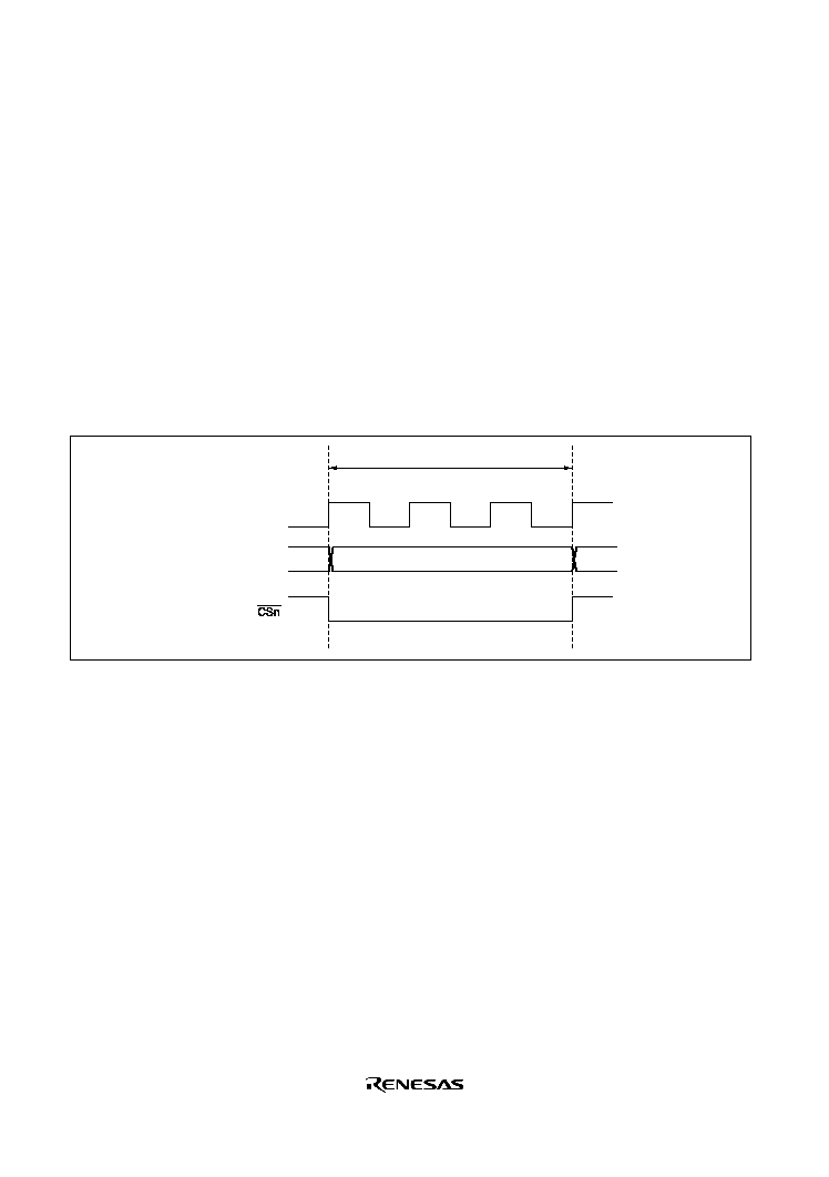
Rev. 1.0, 02/03, page 114 of 634
6.4.4
Chip Select Signals
In the H8S/2218 Series chip select signals (
CS0 to CS5) can be output to areas 0 to 5, the signal
being driven low when the corresponding external space area is accessed. Figure 6.3 shows an
example of
CSn (n = 0 to 5) output timing. Enabling or disabling of the CSn signal is performed
by setting the data direction register (DDR) for the port corresponding to the particular
CSn pin.
In ROM-disabled extended mode, the
CS0 pin is placed in the output state after a power-on reset.
Pins
CS1 to CS5 are placed in the input state after a power-on reset, and so the corresponding
DDR should be set to 1 when outputting signals
CS1 to CS5.
In ROM-enabled extended mode, pins
CS0 to CS5 are all placed in the input state after a power-on
reset, and so the corresponding DDR should be set to 1 when outputting signals
CS0 to CS5. For
details, see section 8, I/O Ports.
Bus cycle
T
1
T
2
T
3
Area n external address
Address bus
Figure 6.3
CSn
CSn
CSn
CSn Signal Output Timing (n = 0 to 5)
6.5
Basic Timing
The CPU is driven by a system clock (
), denoted by the symbol . The period from one rising
edge of
to the next is referred to as a "state." The memory cycle or bus cycle consists of one,
two, or three states. Different methods are used to access on-chip memory, on-chip peripheral
modules, and the external address space.
6.5.1
On-Chip Memory (ROM, RAM) Access Timing
On-chip memory is accessed in one state. The data bus is 16 bits wide, permitting both byte and
word transfer instruction. Figure 6.4 shows the on-chip memory access cycle. Figure 6.5 shows the
pin states.
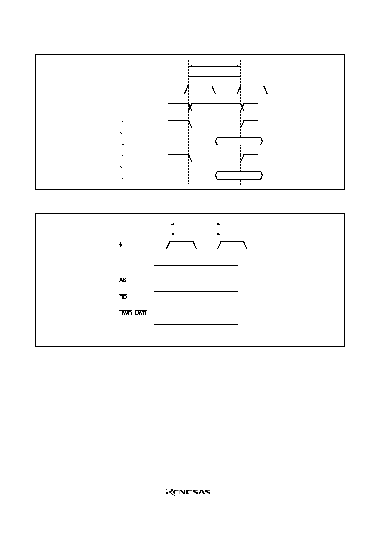
Rev. 1.0, 02/03, page 115 of 634
T
1
Internal address bus
Bus cycle
Address
Read data
Write data
Internal read signal
Internal data bus
Internal write signal
Internal data bus
Read
access
Write
access
Figure 6.4 On-Chip Memory Access Cycle
Bus cycle
T
1
Unchanged
Address bus*
*
*
,
*
Data bus*
Note: * Supported only by the H8S/2218 Series.
High
High
High
High-impedance state
Figure 6.5 Pin States during On-Chip Memory Access
6.5.2
On-Chip Peripheral Module Access Timing
The on-chip peripheral modules are accessed in two states except on-chip USB and RTC. The data
bus is either 8 bits or 16 bits wide, depending on the particular internal I/O register being accessed.
Figure 6.6 shows the access timing for the on-chip peripheral modules. Figure 6.7 shows the pin
states.
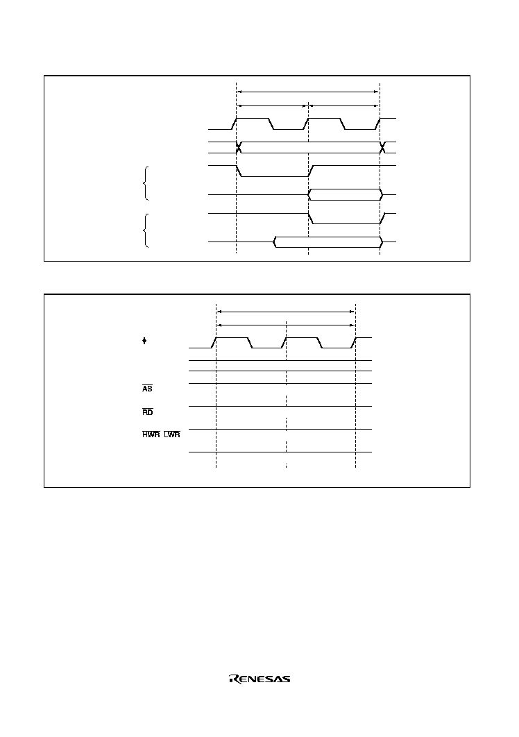
Rev. 1.0, 02/03, page 116 of 634
T
1
T
2
Internal address bus
Bus cycle
Address
Read data
Write data
Internal read signal
Internal data bus
Internal write signal
Internal data bus
Read
access
Write
access
Figure 6.6 On-Chip Peripheral Module Access Cycle
T
1
T
2
Bus cycle
Unchanged
Address bus*
*
*
,
*
Data bus*
Note: * Supported only by the H8S/2218 Series.
High
High
High
High-impedance state
Figure 6.7 Pin States during On-Chip Peripheral Module Access
6.5.3
External Address Space Access Timing
The external address space is accessed with an 8-bit or 16-bit data bus width in a two-state or
three-state bus cycle. In three-state access, wait states can be inserted. For further details, refer to
section 6.6.3, Basic Timing.
Rev. 1.0, 02/03, page 117 of 634
6.6
Basic Bus Interface
The basic bus interface enables direct connection of ROM, SRAM, and so on.
6.6.1
Data Size and Data Alignment (Supported Only by the H8S/2218 Series)
Data sizes for the CPU and other internal bus masters are byte, word, and longword. The bus
controller has a data alignment function, and when accessing external space, controls whether the
upper data bus (D15 to D8) or lower data bus (D7 to D0) is used according to the bus
specifications for the area being accessed (8-bit access space or 16-bit access space) and the data
size.
8-Bit Access Space: Figure 6.8 illustrates data alignment control for the 8-bit access space. With
the 8-bit access space, the upper data bus (D15 to D8) is always used for accesses. The amount of
data that can be accessed at one time is one byte: a word transfer instruction is performed as two-
byte accesses, and a longword transfer instruction, as four-byte accesses.
D15
D8 D7
D0
Upper data bus
Lower data bus
Byte size
Word size
1st bus cycle
2nd bus cycle
Longword
size
1st bus cycle
2nd bus cycle
3rd bus cycle
4th bus cycle
Figure 6.8 Access Sizes and Data Alignment Control (8-Bit Access Space)
16-Bit Access Space: Figure 6.9 illustrates data alignment control for the 16-bit access space.
With the 16-bit access space, the upper data bus (D15 to D8) and lower data bus (D7 to D0) are
used for accesses. The amount of data that can be accessed at one time is one byte or one word,
and a longword transfer instruction is executed as two word transfer instructions.
In byte access, whether the upper or lower data bus is used is determined by whether the address is
even or odd. The upper data bus is used for an even address, and the lower data bus for an odd
address.
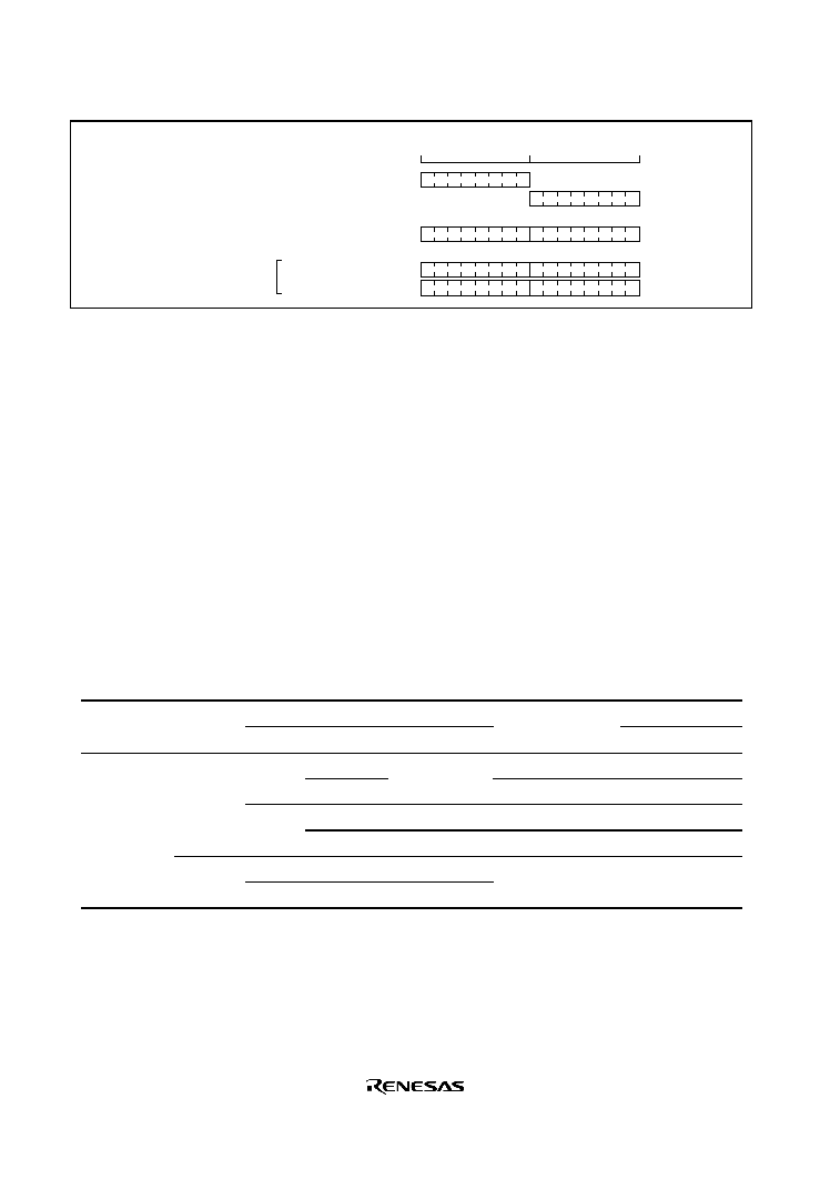
Rev. 1.0, 02/03, page 118 of 634
D15
D8 D7
D0
Upper data bus
Lower data bus
Byte size
Word size
1st bus cycle
2nd bus cycle
Longword
size
· Even address
Byte size
· Odd address
Figure 6.9 Access Sizes and Data Alignment Control (16-Bit Access Space)
6.6.2
Valid Strobes
Table 6.3 shows the data buses used and valid strobes for the access spaces in the H8S/2218
Series.
In a read, the
RD signal is valid without discrimination between the upper and lower halves of the
data bus.
In a write, the
HWR signal is valid for the upper half of the data bus, and the LWR signal for the
lower half.
The
RD, HWR, and LWR signals are not available in the H8S/2212 Series.
Table 6.3
Data Buses Used and Valid Strobes
Area
Access
Size
Read/
Write
Address
Valid Strobe
Upper Data Bus
(D15 to D8)
Lower Data Bus
(D7 to D0)
Byte
Read
RD
Valid
Invalid
8-bit access
space
Write
HWR
Hi-Z
Byte
Read
Even
RD
Valid
Invalid
Odd
Invalid
Valid
Write
Even
HWR
Valid
Hi-Z
Odd
LWR
Hi-Z
Valid
Word
Read
RD
Valid
Valid
16-bit
access
space
Write
HWR, LWR
Legend
Hi-Z: High impedance.
Invalid: Input state: input value is ignored.
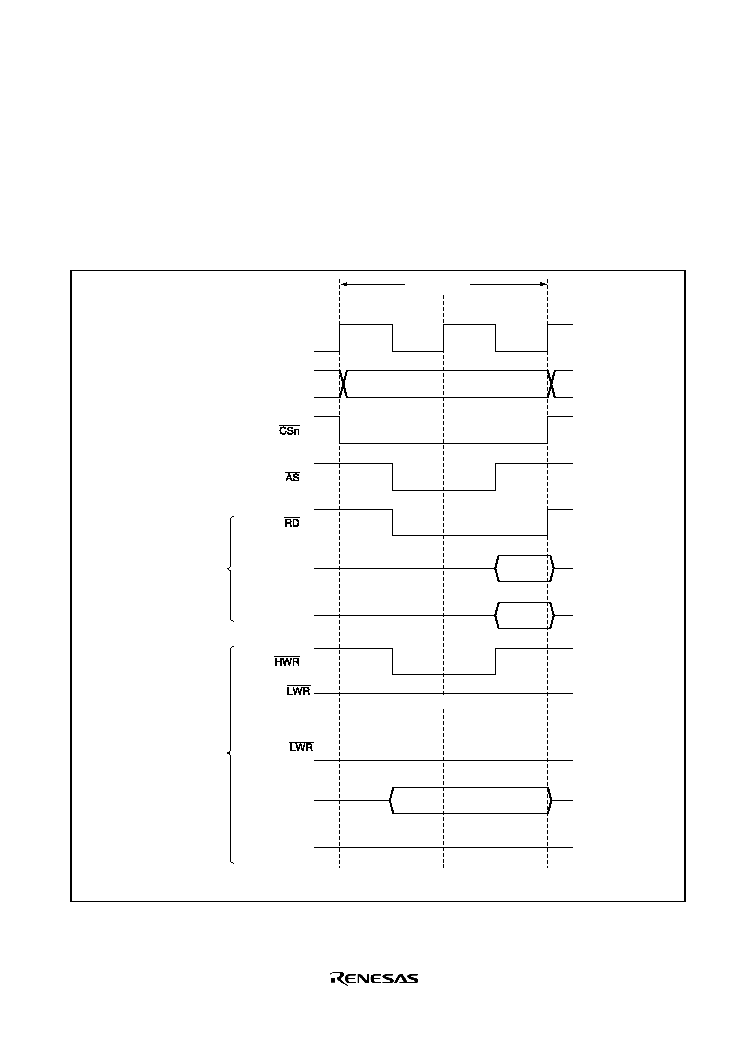
Rev. 1.0, 02/03, page 119 of 634
6.6.3
Basic Timing
8-Bit 2-State Access Space: Figure 6.10 shows the bus timing for an 8-bit 2-state access space in
the H8S/2218 Series. When an 8-bit access space is accessed, the upper half (D15 to D8) of the
data bus is used.
Wait states cannot be inserted.
Bus cycle
T
1
T
2
Address bus
D15 to D8
Valid
D7 to D0
Invalid
Read
(16-bit bus
mode)
D15 to D8
Valid
D7 to D0
High impedance
High impedance
Write
High
Note: n = 0 to 5
(8-bit bus
mode)
Figure 6.10 Bus Timing for 8-Bit 2-State Access Space in the H8S/2218 Series
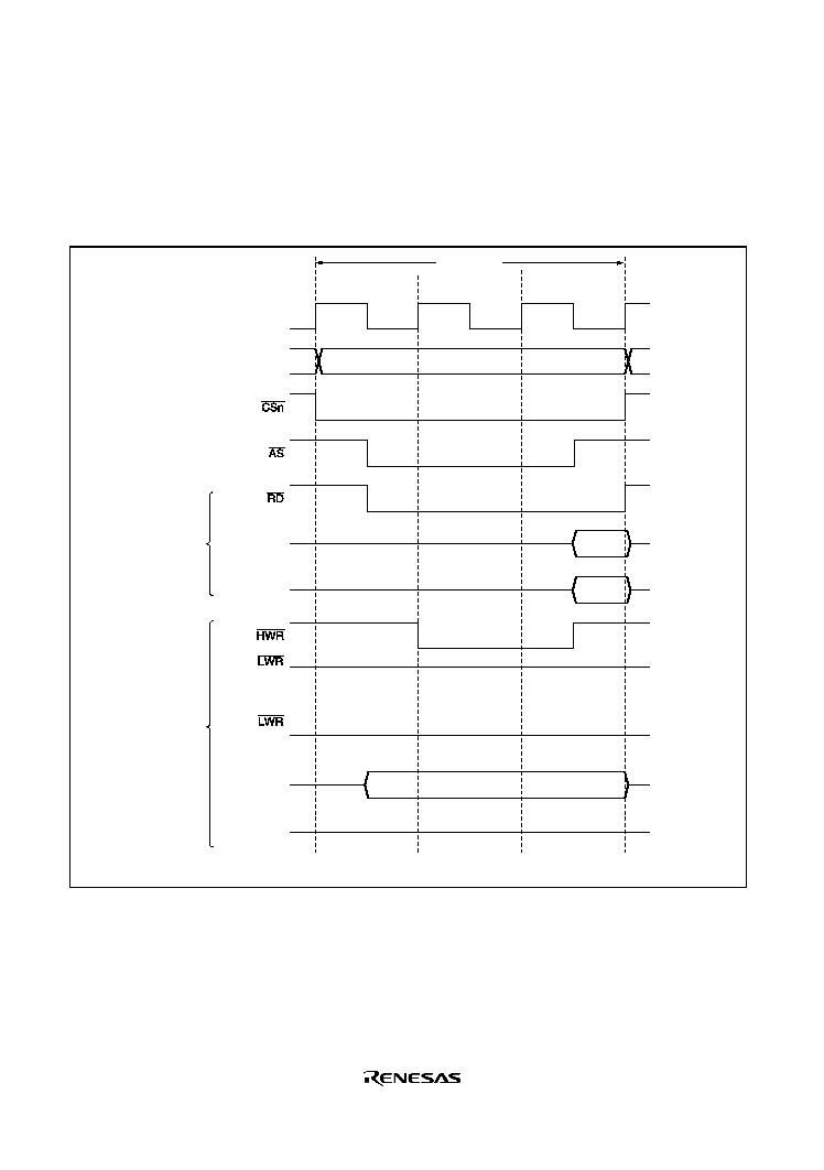
Rev. 1.0, 02/03, page 120 of 634
8-Bit 3-State Access Space (Except Area 6): Figure 6.11 shows the bus timing for an 8-bit 3-
state access space in the H8S/2218 Series. When an 8-bit access space is accessed, the upper half
(D15 to D8) of the data bus is used.
Wait states can be inserted.
Bus cycle
T
1
T
2
Address bus
D15 to D8
Valid
D7 to D0
Invalid
Read
(16-bit bus
mode)
D15 to D8
Valid
D7 to D0
Write
High
Note: n = 0 to 5
T
3
High impedance
High impedance
(8-bit bus
mode)
Figure 6.11 Bus Timing for 8-Bit 3-State Access Space (Except Area 6)
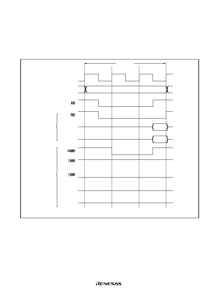
Rev. 1.0, 02/03, page 121 of 634
8-Bit 3-State Access Space (Area 6): Figure 6.12 shows the bus timing for area 6 and RTC area
(address = H'FFFF40 to H'FFFF5F). When the areas are accessed, the data bus cannot be used.
Wait states cannot be inserted.
T
1
T
2
*
*
D15 to D8*
D7 to D0*
*
*
(16-bit bus
mode)
*
(8-bit bus
mode)
D15 to D8*
D7 to D0*
Write
Invalid
Invalid
High
High impedance
High impedance
High impedance
Read
T
3
Bus cycle
Address bus*
Note: * Supported only by the H8S/2218 Series.
Figure 6.12 Bus Timing for Area 6 and RTC
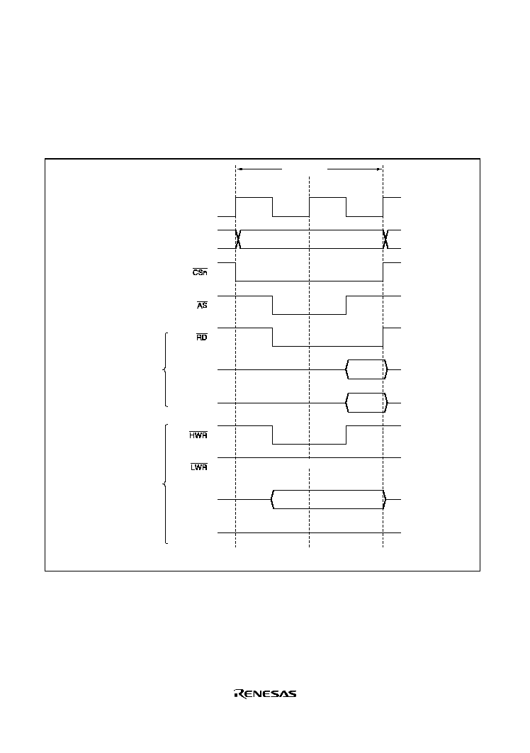
Rev. 1.0, 02/03, page 122 of 634
16-Bit 2-State Access Space: Figures 6.13 to 6.15 show bus timings for a 16-bit 2-state access
space in the H8S/2218 Series. When a 16-bit access space is accessed, the upper half (D15 to D8)
of the data bus is used for the even address, and the lower half (D7 to D0) for the odd address.
Wait states cannot be inserted.
Bus cycle
T
1
T
2
Address bus
D15 to D8
Valid
D7 to D0
Invalid
Read
D15 to D8
Valid
D7 to D0
Write
High
Note: n = 0 to 5
High impedance
Figure 6.13 Bus Timing for 16-Bit 2-State Access Space (1) (Even Address Byte Access)
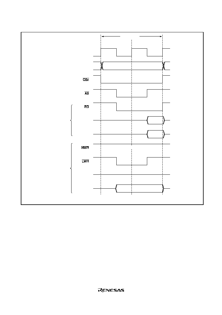
Rev. 1.0, 02/03, page 123 of 634
Bus cycle
T
1
T
2
Address bus
D15 to D8
Invalid
D7 to D0
Valid
Read
D15 to D8
D7 to D0
Valid
Write
Note: n = 0 to 5
High
High impedance
Figure 6.14 Bus Timing for 16-Bit 2-State Access Space (2) (Odd Address Byte Access)
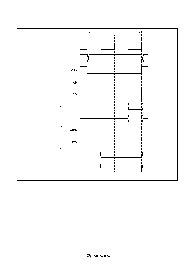
Rev. 1.0, 02/03, page 124 of 634
Bus cycle
T
1
T
2
Address bus
D15 to D8
Valid
D7 to D0
Valid
Read
D15 to D8
Valid
D7 to D0
Valid
Write
Note: n = 0 to 5
Figure 6.15 Bus Timing for 16-Bit 2-State Access Space (3) (Word Access)
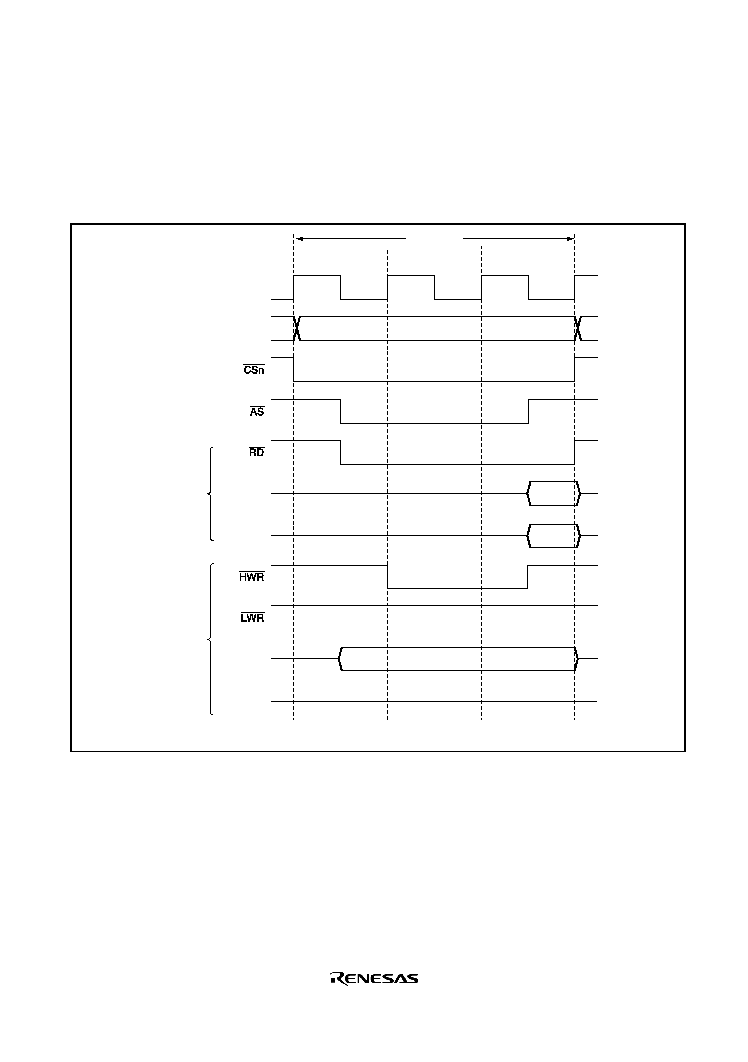
Rev. 1.0, 02/03, page 125 of 634
16-Bit 3-State Access Space: Figures 6.16 to 6.18 show bus timings for a 16-bit 3-state access
space in the H8S/2218 Series. When a 16-bit access space is accessed , the upper half (D15 to D8)
of the data bus is used for the even address, and the lower half (D7 to D0) for the odd address.
Wait states can be inserted.
Bus cycle
T
1
T
2
Address bus
D15 to D8
Valid
D7 to D0
Invalid
Read
D15 to D8
Valid
D7 to D0
Write
High
Note: n = 0 to 5
T
3
High impedance
Figure 6.16 Bus Timing for 16-Bit 3-State Access Space (1) (Even Address Byte Access)

Rev. 1.0, 02/03, page 126 of 634
Bus cycle
T
1
T
2
Address bus
D15 to D8
Invalid
D7 to D0
Valid
Read
D15 to D8
D7 to D0
Valid
Write
High
Note: n = 0 to 5
T
3
High impedance
Figure 6.17 Bus Timing for 16-Bit 3-State Access Space (2) (Odd Address Byte Access)
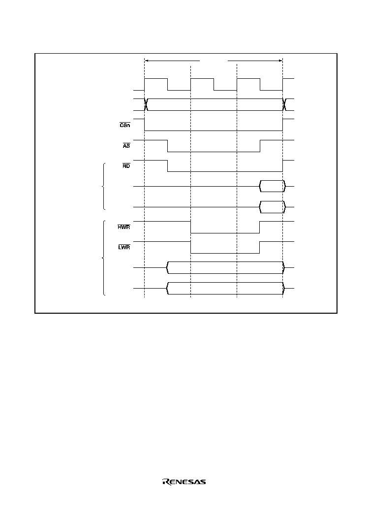
Rev. 1.0, 02/03, page 127 of 634
Bus cycle
T
1
T
2
Address bus
D15 to D8
Valid
D7 to D0
Valid
Read
D15 to D8
Valid
D7 to D0
Valid
Write
Note: n = 0 to 5
T
3
Figure 6.18 Bus Timing for 16-Bit 3-State Access Space (3) (Word Access)

Rev. 1.0, 02/03, page 128 of 634
6.6.4
Wait Control
When accessing external space, this LSI can extend the bus cycle by inserting one or more wait
states (Tw). There are two ways of inserting wait states: program wait insertion and pin wait
insertion using the
WAIT pin.
1. Program Wait Insertion
From 0 to 3 wait states can be inserted automatically between the T
2
state and T
3
state on an
individual area basis in 3-state access space, according to the settings of WCRH and WCRL.
2. Pin Wait Insertion
Setting the WAITE bit in BCRH to 1 enables wait insertion by means of the
WAIT pin in the
H8S/2218 Series. When external space is accessed in this state, program wait insertion is first
carried out according to the settings in WCRH and WCRL. Then, if the
WAIT pin is low at the
falling edge of
in the last T
2
or T
W
state, a T
W
state is inserted. If the
WAIT pin is held low,
T
W
states are inserted until it goes high.
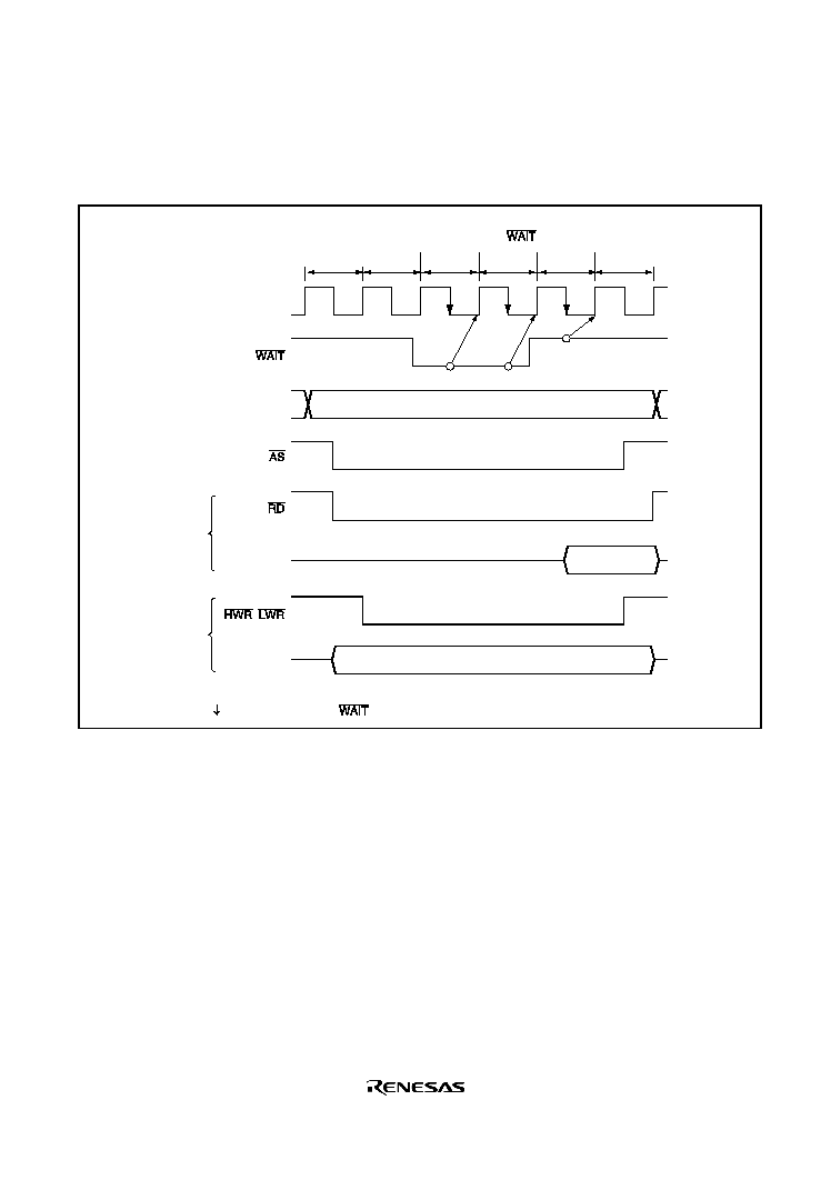
Rev. 1.0, 02/03, page 129 of 634
Figure 6.19 shows an example of wait state insertion timing.
In the H8S/2212 Series, the WAITE bit in BCRH should not be set to 1.
By program
wait
T
1
Address bus
Data bus
Read data
Read
,
Write data
Write
Note: indicates the timing of
pin sampling.
Data bus
T
2
T
w
T
w
T
w
T
3
By
pin
Figure 6.19 Example of Wait State Insertion Timing

Rev. 1.0, 02/03, page 130 of 634
6.7
Burst ROM Interface
With the H8S/2218 Series, external space area 0 can be designated as burst ROM space, and burst
ROM interfacing can be performed. The burst ROM space interface enables 16-bit configuration
ROM with burst access capability to be accessed at high speed.
Area 0 can be designated as burst ROM space by means of the BRSTRM bit in BCRH.
Consecutive burst accesses of a maximum of 4 words or 8 words can be performed for CPU
instruction fetches only. One or two states can be selected for burst access.
6.7.1
Basic Timing
The number of states in the initial cycle (full access) of the burst ROM interface is in accordance
with the setting of the AST0 bit in ASTCR. Also, when the AST0 bit is set to 1, wait state
insertion is possible. One or two states can be selected for the burst cycle, according to the setting
of the BRSTS1 bit in BCRH. Wait states cannot be inserted. When area 0 is designated as burst
ROM space, it becomes 16-bit access space regardless of the setting of the ABW0 bit in ABWCR.
When the BRSTS0 bit in BCRH is cleared to 0, burst access of up to 4 words is performed; when
the BRSTS0 bit is set to 1, burst access of up to 8 words is performed.
The basic access timing for burst ROM space is shown in figures 6.20 and 6.21. The timing shown
in figure 6.20 is for the case where the AST0 and BRSTS1 bits are both set to 1, and that in figure
6.21 is for the case where both these bits are cleared to 0.
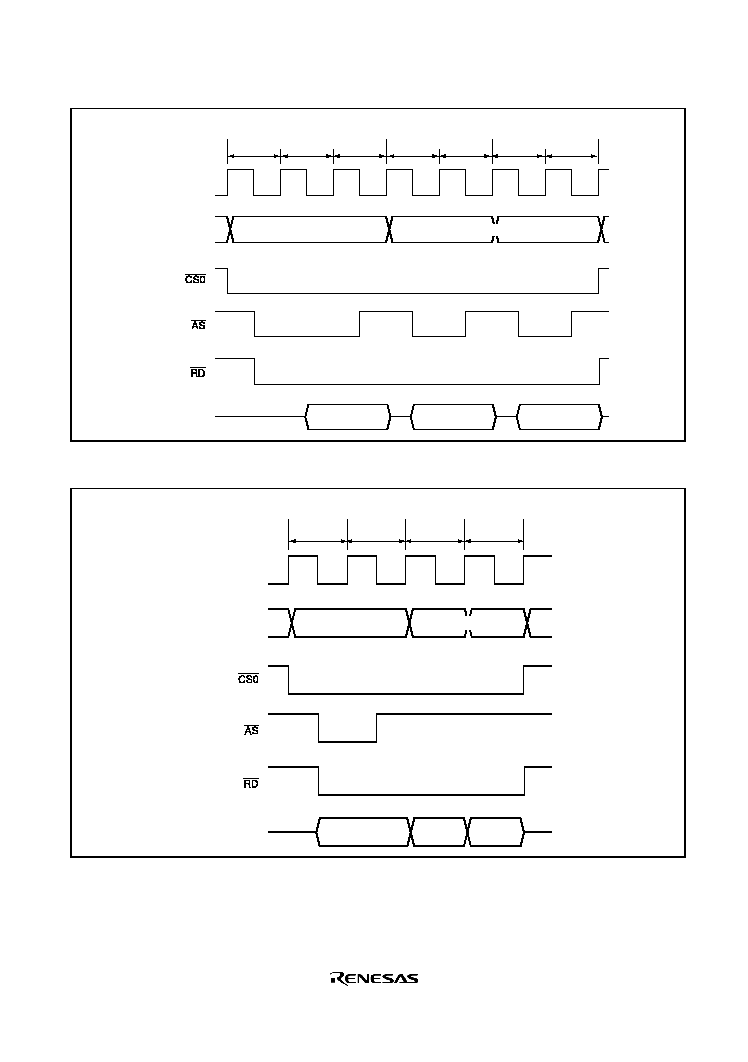
Rev. 1.0, 02/03, page 131 of 634
T
1
Address bus
Data bus
T
2
T
3
T
1
T
2
T
1
Full access
T
2
Burst access
Only lower address changed
Read data
Read data
Read data
Figure 6.20 Example of Burst ROM Access Timing (When AST0 = BRSTS1 = 1)
T
1
T
2
T
1
T
1
Address bus
Data bus
Full access
Burst access
Only lower address changed
Read data
Read data Read data
Figure 6.21 Example of Burst ROM Access Timing (When AST0 = BRSTS1 = 0)
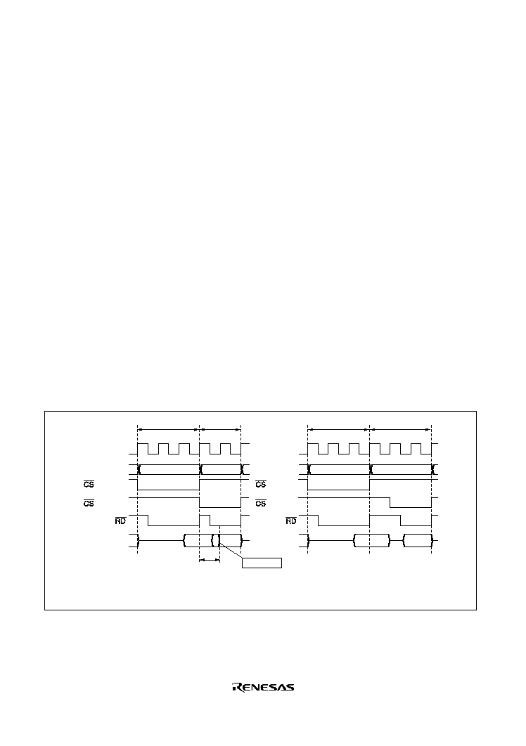
Rev. 1.0, 02/03, page 132 of 634
6.7.2
Wait Control
As with the basic bus interface, either program wait insertion or pin wait insertion using the
WAIT
pin can be used in the initial cycle (full access) of the burst ROM interface. See section 6.6.4, Wait
Control.
Wait states cannot be inserted in a burst cycle.
6.8
Idle Cycle
When the H8S/2218 Series accesses external space, it can insert a 1-state idle cycle (T
I
) between
bus cycles in the following two cases: (1) when read accesses between different areas occur
consecutively, and (2) when a write cycle occurs immediately after a read cycle. By inserting an
idle cycle it is possible, for example, to avoid data collisions between ROM, with a long output
floating time, and high-speed memory, I/O interfaces, and so on.
1. Consecutive Reads between Different Areas
If consecutive reads between different areas occur while the ICIS1 bit in BCRH is set to 1, an
idle cycle is inserted at the start of the second read cycle.
Figure 6.22 shows an example of the operation in this case. In this example, bus cycle A is a
read cycle from ROM with a long output floating time, and bus cycle B is a read cycle from
SRAM, each being located in a different area. In (a), an idle cycle is not inserted, and a
collision occurs in cycle B between the read data from ROM and that from SRAM. In (b), an
idle cycle is inserted, and a data collision is prevented.
T
1
Address bus
Bus cycle A
;
;
Data bus
T
2
T
3
T
1
T
2
Bus cycle B
Long output floating time
Data collision
(a) Idle cycle not inserted
(ICIS1 = 0)
T
1
Address bus
Bus cycle A
Data bus
T
2
T
3
T
I
T
1
Bus cycle B
(b) Idle cycle inserted
(Initial value ICIS1 = 1)
T
2
(area A)
(area B)
(area A)
(area B)
Figure 6.22 Example of Idle Cycle Operation (1)
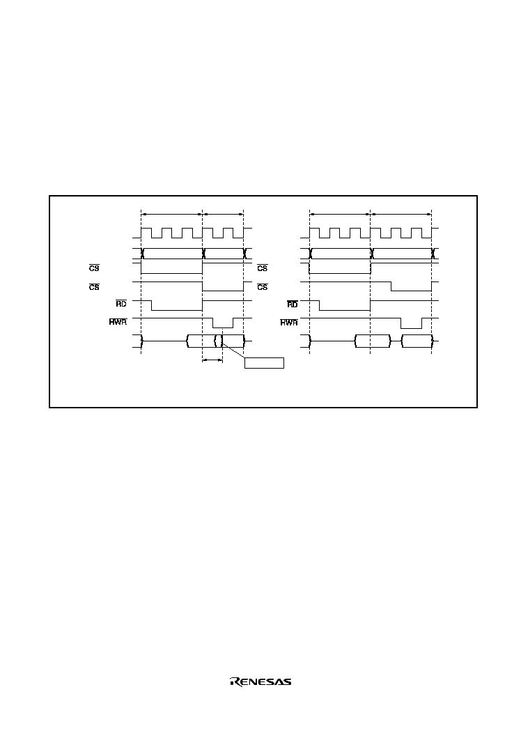
Rev. 1.0, 02/03, page 133 of 634
2. Write after Read
If an external write occurs after an external read while the ICIS0 bit in BCRH is set to 1, an
idle cycle is inserted at the start of the write cycle.
Figure 6.23 shows an example of the operation in this case. In this example, bus cycle A is a
read cycle from ROM with a long output floating time, and bus cycle B is a CPU write cycle.
In (a), an idle cycle is not inserted, and a collision occurs in cycle B between the read data
from ROM and the CPU write data. In (b), an idle cycle is inserted, and a data collision is
prevented.
T
1
;
T
2
T
3
T
1
T
2
T
1
T
2
T
3
T
I
T
1
T
2
Address bus
Bus cycle A
Data bus
Bus cycle B
Long output floating time
Data collision
(a) Idle cycle not inserted
(ICIS0 = 0)
Address bus
Bus cycle A
Data bus
Bus cycle B
(b) Idle cycle inserted
(Initial value ICIS0 = 1)
(area A)
(area B)
(area A)
(area B)
Figure 6.23 Example of Idle Cycle Operation (2)
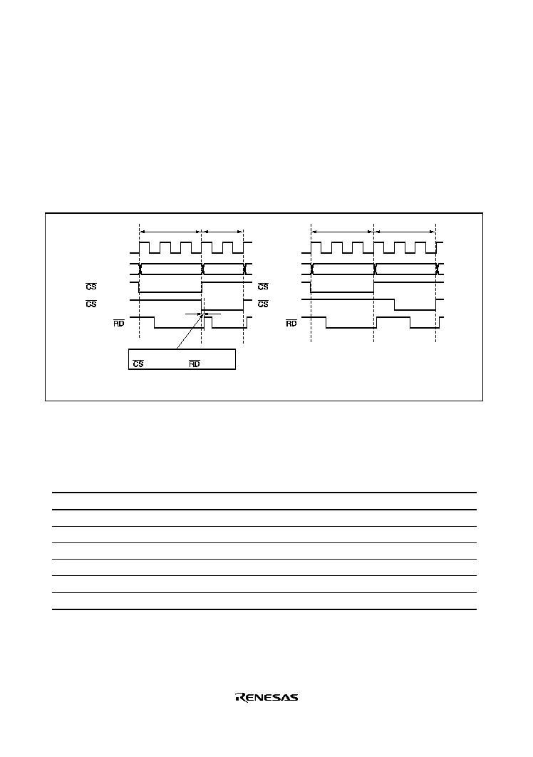
Rev. 1.0, 02/03, page 134 of 634
3. Relationship between Chip Select (
CS
CS
CS
CS) Signal and Read (RD
RD
RD
RD) Signal
Depending on the system's load conditions, the
RD signal may lag behind the CS signal. An
example is shown in figure 6.24.
In this case, with the setting for no idle cycle insertion (a), there may be a period of overlap
between the bus cycle A
RD signal and the bus cycle B CS signal.
Setting idle cycle insertion, as in (b), however, will prevent any overlap between the
RD and
CS signals.
In the initial state after reset release, idle cycle insertion (b) is set.
T
1
T
2
T
3
T
1
T
2
T
1
T
2
T
3
T
I
T
1
T
2
Address bus
Bus cycle A
Bus cycle B
(a) Idle cycle not inserted
(ICIS1 = 0)
Possibility of overlap between
(area B) and
Address bus
Bus cycle A
Bus cycle B
(b) Idle cycle inserted
(Initial value ICIS1 = 1)
(area A)
(area B)
(area A)
(area B)
Figure 6.24 Relationship between Chip Select (
CS
CS
CS
CS) and Read (RD
RD
RD
RD)
Table 6.4 shows pin states in an idle cycle.
Table 6.4
Pin States in Idle Cycle
Pins
Pin State
A23 to A0
Contents of next bus cycle
D15 to D0
High impedance
CSn
High
AS
High
RD
High
HWR
High
LWR
High

Rev. 1.0, 02/03, page 135 of 634
6.9
Bus Release
The H8S/2218 Series can release the external bus in response to a bus request from an external
device. In the external bus released state, the internal bus master continues to operate as long as
there is no external access.
In external extended mode, the bus can be released to an external device by setting the BRLE bit
in BCRL to 1. Driving the
BREQ pin low issues an external bus request to this LSI. When the
BREQ pin is sampled, at the prescribed timing the BACK pin is driven low, and the address bus,
data bus, and bus control signals are placed in the high-impedance state, establishing the external
bus-released state.
In the external bus released state, an internal bus master can perform accesses using the internal
bus. When an internal bus master wants to make an external access, it temporarily defers
activation of the bus cycle, and waits for the bus request from the external bus master to be
dropped.
When the
BREQ pin is driven high, the BACK pin is driven high at the prescribed timing and the
external bus released state is terminated.
In the event of simultaneous external bus release request and external access request generation,
the order of priority is as follows:
(High) External bus release > Internal bus master external access (Low)
Table 6.5 shows pin states in the external bus released state.
In the H8S/2212 Series, the BRLE bit in BCRL should not be set to 1.
Table 6.5
Pin States in Bus Released State
Pins
Pin State
A23 to A0
High impedance
D15 to D0
High impedance
CSn
High impedance
AS
High impedance
RD
High impedance
HWR
High impedance
LWR
High impedance
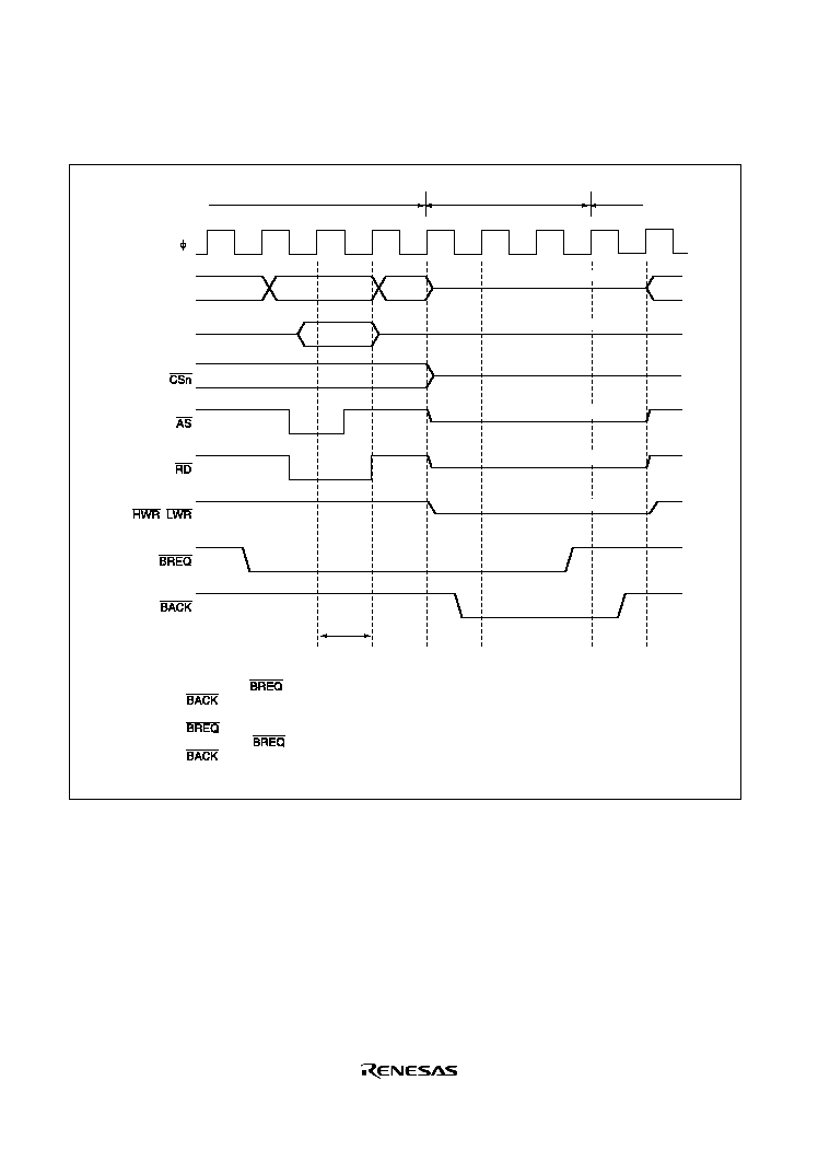
Rev. 1.0, 02/03, page 136 of 634
Figure 6.25 shows the timing for transition to the bus-released state.
CPU
cycle
Address
Minimum
1 state
T
0
T
1
T
2
,
High impedance
High impedance
High impedance
High impedance
High impedance
High impedance
Data bus
Address bus
[1]
[2]
[3]
[4]
[5]
[1]
Low level of
pin is sampled at rise of T
2
state.
[2]
pin is driven low at end of CPU read cycle, releasing bus to external bus
master.
[3]
pin state is still sampled in external bus released state.
[4]
High level of
pin is sampled.
[5]
pin is driven high, ending bus release cycle.
CPU cycle
External bus released state
Note : n = 0 to 5
Figure 6.25 Bus-Released State Transition Timing

Rev. 1.0, 02/03, page 137 of 634
6.10
Bus Arbitration
This LSI has a bus arbiter that arbitrates bus master operations.
There are two bus masters, the CPU and DMAC, which perform read/write operations when they
have possession of the bus. Each bus master requests the bus by means of a bus request signal. The
bus arbiter determines priorities at the prescribed timing, and permits use of the bus by means of a
bus request acknowledge signal. The selected bus master then takes possession of the bus and
begins its operation.
6.10.1
Operation
The bus arbiter detects the bus masters' bus request signals, and if the bus is requested, sends a bus
request acknowledge signal to the bus master making the request. If there are bus requests from
more than one bus master, the bus request acknowledge signal is sent to the one with the highest
priority. When a bus master receives the bus request acknowledge signal, it takes possession of the
bus until that signal is canceled.
The order of priority of the bus masters is as follows:
(High) DMAC > CPU (Low)
An internal bus access by an internal bus master, and external bus release, can be executed in
parallel in the H8S/2218 Series.
In the event of simultaneous external bus release request, and internal bus master external access
request generation, the order of priority is as follows:
(High) External bus release > Internal bus master external access (Low)
The H8S/2212 Series does not have the external bus release function.
6.10.2
Bus Transfer Timing
Even if a bus request is received from a bus master with a higher priority than that of the bus
master that has acquired the bus and is currently operating, the bus is not necessarily transferred
immediately. There are specific times at which each bus master can relinquish the bus.
CPU: The CPU is the lowest-priority bus master, and if a bus request is received from the DMAC,
the bus arbiter transfers the bus to the bus master that issued the request. The timing for transfer of
the bus is as follows:

Rev. 1.0, 02/03, page 138 of 634
· The bus is transferred at a break between bus cycles. However, if a bus cycle is executed in
discrete operations, as in the case of a longword-size access, the bus is not transferred between
the operations.
· If the CPU is in sleep mode, it transfers the bus immediately.
DMAC: The DMAC sends the bus arbiter a request for the bus when an activation request is
generated.
In the case of a USB request in short address mode or normal mode, and in cycle steal mode, the
DMAC releases the bus after a single transfer.
In block transfer mode, it releases the bus after transfer of one block, and in burst mode, after
completion of the transfer.
6.10.3
External Bus Release Usage Note
External bus release can be performed on completion of an external bus cycle in the H8S/2218
Series. The
CS signal remains low until the end of the external bus cycle. Therefore, when
external bus release is performed, the
CS signal may change from the low level to the high-
impedance state.
6.11
Resets and the Bus Controller
In a power-on reset, this LSI, including the bus controller, enters the reset state at that point, and
an executing bus cycle is discontinued.
In a manual reset*, the bus controller's registers and internal state are maintained, and an executing
external bus cycle is completed. In this case,
WAIT input is ignored and write data is not
guaranteed.
Note:* Supported only by the H8S/2218 Series.

Rev. 1.0, 02/03, page 139 of 634
Section 7 DMA Controller
This LSI has a built-in DMA controller (DMAC) which can carry out data transfer on up to 4
channels.
7.1
Features
The features of the DMAC are listed below.
· Choice of short address mode or full address mode
· Short address mode
Maximum of 4 channels can be used
Choice of dual address mode
In dual address mode, one of the two addresses, transfer source and transfer destination, is
specified as 24 bits and the other as16 bits
Choice of sequential mode, idle mode, or repeat mode for dual address mode
· Full address mode
Maximum of 2 channels can be used
Transfer source and transfer destination address specified as 24 bits
Choice of normal mode or block transfer mode
· 16-Mbyte address space can be specified directly
· Byte or word can be set as the transfer unit
· Activation sources: internal interrupt, USB request, auto-request (depending on transfer mode)
16-bit timer-pulse unit (TPU) compare match/input capture interrupts
Serial communication interface (SCI_0) transmission complete interrupt, reception
complete interrupt
A/D conversion end Interrupt
USB request
Auto-request
· Module stop mode can be set
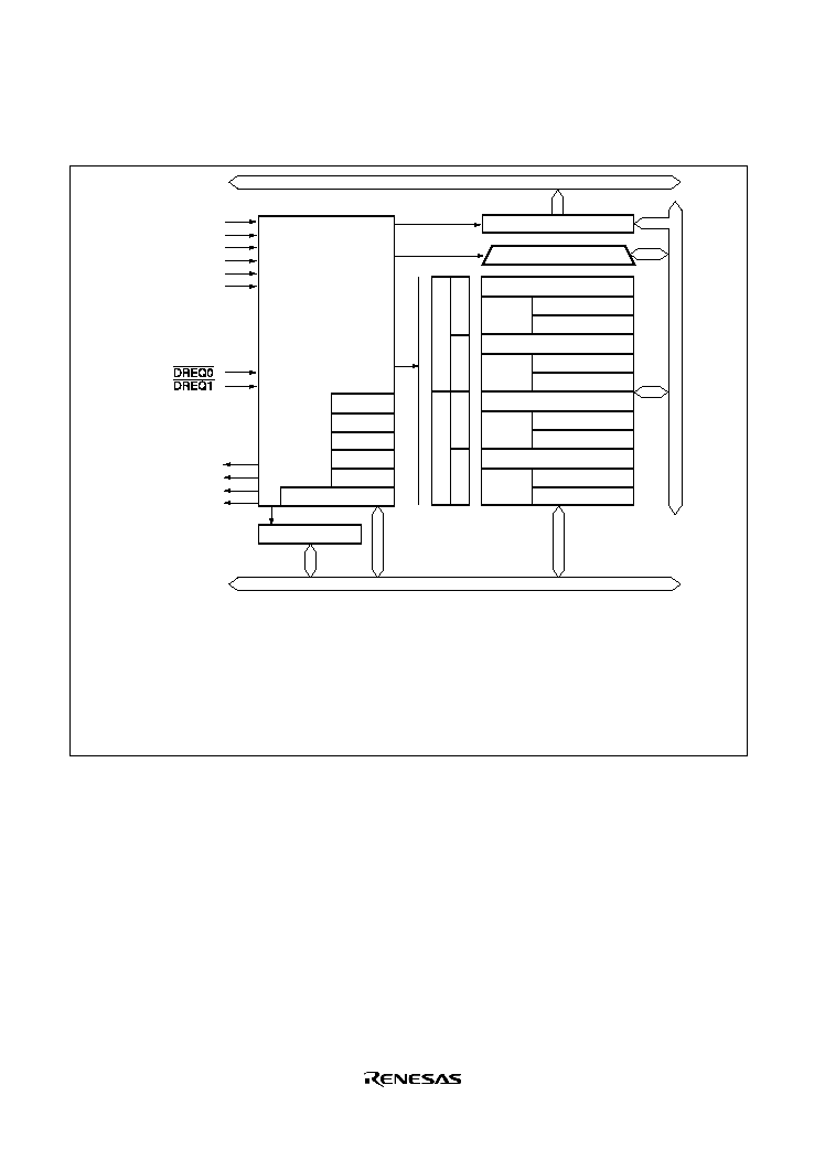
Rev. 1.0, 02/03, page 140 of 634
A block diagram of the DMAC is shown in figure 7.1.
Internal address bus
Addres buffer
Processor
Internal interrupts
TGI0A
TGI1A
TGI2A
TXI0
RXI0
ADI
USB request signals
Interrupt signals
DEND0A
DEND0B
DEND1A
DEND1B
Control logic
DMACR1B
DMACR1A
DMACR0B
DMACR0A
DMATCR
DMABCR
Data buffer
Internal address bus
MAR0A
IOAR0A
ETCR0A
MAR0B
IOAR0B
ETCR0B
MAR1A
IOAR1A
ETCR1A
MAR1B
IOAR1B
ETCR1B
Legend
DMATCR
DMABCR
DMACR
MAR
IOAR
ETCR
: DMA terminal control register *
: DMA band control register (for all channels)
: DMA control register
: Memory address register
: I/O address register
: Executive transfer counter register
Note: * Reserved register
Channel 0
Module data bus
Channel 0A
Channel 0B
Channel 1A
Channel 1B
Channel 1
Figure 7.1 Block Diagram of DMAC

Rev. 1.0, 02/03, page 141 of 634
7.2
Register Configuration
The DMAC registers are listed below.
· Memory address register 0A (MAR0A)
· I/O address register 0A (IOAR0A)
· Transfer count register 0A (ETCR0A)
· Memory address register 0B (MAR0B)
· I/O address register 0B (IOAR0B)
· Transfer count register 0B (ETCR0B)
· Memory address register 1A (MAR1A)
· I/O address register 1A (IOAR1A)
· Transfer count register 1A (ETCR1A)
· Memory address register 1B (MAR1B)
· I/O address register 1B (IOAR1B)
· Transfer count register 1B (ETCR1B)
· DMA control register 0A (DMACR0A)
· DMA control register 0B (DMACR0B)
· DMA control register 1A (DMACR1A)
· DMA control register 1B (DMACR1B)
· DMA band control register (DMABCR)
The DMAC register functions differs depending on the address modes: short address mode and
full address mode. The DMAC register functions are described in each address mode. Short
address mode or full address mode can be selected for channels 1 and 0 independently by means
of bits FAE1 and FAE0.
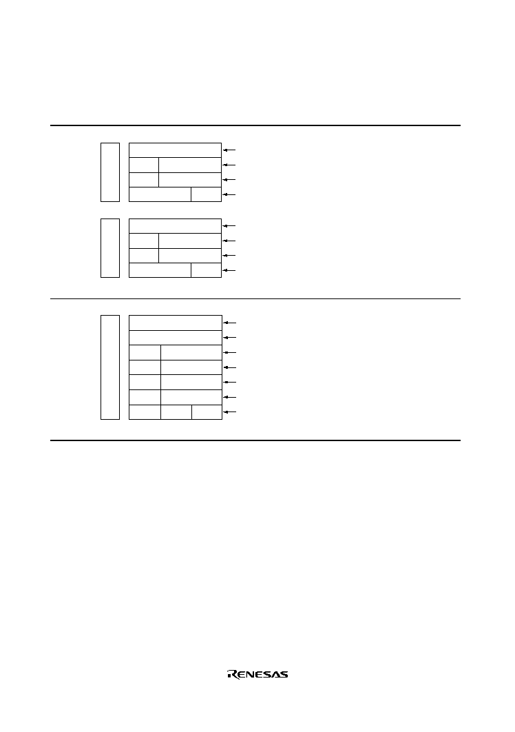
Rev. 1.0, 02/03, page 142 of 634
Table7.1
Short Address Mode and Full Address Mode (For 1 Channel: Example of
Channel 0)
FAE0
Description
0
MAR0A
Specifies transfer source/transfer destination address
Specifies transfer destination/transfer source address
Specifies number of transfers
Specifies transfer size, mode, activation source, etc.
Short address mode specified (channels A and B operate independently)
Specifies transfer source/transfer destination address
Specifies transfer destination/transfer source address
Specifies number of transfers
Specifies transfer size, mode, activation source, etc.
Channel 0A
Channel 0B
IOAR0A
ETCR0A
DMACR0A
MAR0B
IOAR0B
ETCR0B
DMACR0B
1
MAR0A
IOAR0A
ETCR0A
DMACR0A
MAR0B
IOAR0B
ETCR0B
DMACR0B
Specifies transfer source address
Specifies transfer destination address
Not used
Not used
Specifies number of transfers
Specifies number of transfers (used in block transfer mode only)
Specifies transfer size, mode, activation source, etc.
Full address mode specified (channels A and B operate combination)
Channel 0

Rev. 1.0, 02/03, page 143 of 634
7.3
Register Descriptions
7.3.1
Memory Address Registers (MAR)
Short Address Mode:
MAR is a 32-bit readable/writable register that specifies the transfer source address or destination
address. The upper 8 bits of MAR are reserved: they are always read as 0, and cannot be modified.
Whether MAR functions as the source address register or as the destination address register can be
selected by means of the DTDIR bit in DMACR.
MAR is incremented or decremented each time a byte or word transfer is executed, so that the
address specified by MAR is constantly updated. For details, see section 7.3.4, DMA Control
Register (DMACR). MAR is not initialized by a reset or in standby mode.
Full Address Mode:
MAR is a 32-bit readable/writable register; MARA functions as the transfer source address
register, and MARB as the destination address register.
MAR is composed of two 16-bit registers, MARH and MARL. The upper 8 bits of MARH are
reserved: they are always read as 0, and cannot be modified. MAR is incremented or decremented
each time a byte or word transfer is executed, so that the source or destination memory address
can be updated automatically. For details, see section 7.3.4, DMA Control Register (DMACR).
MAR is not initialized by a reset or in standby mode.
7.3.2
I/O Address Register (IOAR)
Short Address Mode:
IOAR is a 16-bit readable/writable register that specifies the lower 16 bits of the transfer source
address or destination address. The upper 8 bits of the transfer address are automatically set to
H'FF. Whether IOAR functions as the source address register or as the destination address register
can be selected by means of the DTDIR bit in DMACR.
IOAR is not incremented or decremented each time a transfer is executed, so that the address
specified by IOAR is fixed. IOAR is not initialized by a reset or in standby mode.
Full Address Mode:
IOAR is not used in full address mode transfer.

Rev. 1.0, 02/03, page 144 of 634
7.3.3
Execute Transfer Count Register (ETCR)
Short Address Mode:
ETCR is a 16-bit readable/writable register that specifies the number of transfers. The setting of
this register is different for sequential mode and idle mode on the one hand, and for repeat mode
on the other.
1. Sequential Mode and Idle Mode
In sequential mode and idle mode, ETCR functions as a 16-bit transfer counter (with a count
range of 1 to 65536). ETCR is decremented by 1 each time a transfer is performed, and when
the count reaches H'0000, the DTE bit in DMABCR is cleared, and transfer ends.
2. Repeat Mode
In repeat mode, ETCR functions as transfer counter ETCRL (with a count range of 1 to 256)
and transfer number storage register ETCRH. ETCRL is decremented by 1 each time a transfer
is performed, and when the count reaches H'00, ETCRL is loaded with the value in ETCRH.
At this point, MAR is automatically restored to the value it had when the count was started.
The DTE bit in DMABCR is not cleared, and so transfers can be performed repeatedly until
the DTE bit is cleared by the user.
ETCR is not initialized by a reset or in standby mode.
Full Address Mode:
ETCR is a 16-bit readable/writable register that specifies the number of transfers. The function of
this register is different in normal mode and in block transfer mode. ETCR is not initialized by a
reset or in standby mode.
1. Normal Mode
A. ETCRA
In normal mode, ETCRA functions as a 16-bit transfer counter. ETCRA is decremented by
1 each time a transfer is performed, and transfer ends when the count reaches H'0000.
B. ETCRB
ETCRB is not used in normal mode.
2. Block Transfer Mode
A. ETCRA
In block transfer mode, ETCRAL functions as an 8-bit block size counter and ETCRAH
holds the block size. ETCRAL is decremented each time a 1-byte or 1-word transfer is
performed, and when the count reaches H'00, ETCRAL is loaded with the value in
ETCRAH. So by setting the block size in ETCRAH and ETCRAL, it is possible to
repeatedly transfer blocks consisting of any desired number of bytes or words.

Rev. 1.0, 02/03, page 145 of 634
B. ETCRB
ETCRB functions in block transfer mode, as a 16-bit block transfer counter. ETCRB is
decremented by 1 each time a block is transferred, and transfer ends when the count
reaches H'0000.
7.3.4
DMA Control Register (DMACR)
DMACR controls the operation of each DMAC channel.
· Short Address Mode (common to DMACRA and DMACRB)
Bit Bit Name Initial Value
R/W
Description
7
DTSZ
0
R/W
Data Transfer Size
Selects the size of data to be transferred at one time.
0: Byte-size transfer
1: Word-size transfer
6
DTID
0
R/W
Data Transfer Increment/Decrement
Selects incrementing or decrementing of MAR every data
transfer in sequential mode or repeat mode.
In idle mode, MAR is neither incremented nor decremented.
0: MAR is incremented after a data transfer
· When DTSZ = 0, MAR is incremented by 1 after a
transfer
· When DTSZ = 1, MAR is incremented by 2 after a
transfer
1: MAR is decremented after a data transfer
· When DTSZ = 0, MAR is decremented by 1 after a
transfer
· When DTSZ = 1, MAR is decremented by 2 after a
transfer

Rev. 1.0, 02/03, page 146 of 634
Bit Bit Name Initial Value
R/W
Description
5
RPE
0
R/W
Repeat Enable
Used in combination with the DTIE bit in DMABCR to select
the mode (sequential, idle, or repeat) in which transfer is to
be performed.
RPE
DTIE
0
0:
Transfer in sequential mode (no transfer end
interrupt)
0
1:
Transfer in sequential mode (with transfer end
interrupt)
1
0:
Transfer in repeat mode (no transfer end
interrupt)
1
1:
Transfer in idle mode (with transfer end
interrupt)
Note: For details of operation in sequential, idle, and repeat
mode, see section 7.4.2, Sequential Mode, section 7.4.3, Idle
Mode, and section 7.4.4, Repeat Mode.
4
DTDIR
0
R/W
Data Transfer Direction
Specifies the data transfer direction (source or destination).
0: Transfer with MAR as source address and IOAR as
destination address
1: Transfer with IOAR as source address and MAR as
destination address

Rev. 1.0, 02/03, page 147 of 634
Bit Bit Name Initial Value
R/W
Description
3
2
1
0
DTF3
DTF2
DTF1
DTF0
0
0
0
0
R/W
R/W
R/W
R/W
Data Transfer Factor
These bits select the data transfer factor (activation source).
0000:
0001: Activated by A/D conversion end interrupt
0010:
0011:
0100: Activated by SCI channel 0 transmission complete
interrupt
0101: Activated by SCI channel 0 reception complete
interrupt
0110:
0111:
1000: Activated by TPU channel 0 compare match/input
capture A interrupt
1001: Activated by TPU channel 1 compare match/input
capture A interrupt
1010: Activated by TPU channel 2 compare match/input
capture A interrupt
1011:
1100:
1101:
1110:
1111:
The same factor can be selected for more than one channel. In this case, activation starts with the
highest-priority channel according to the relative channel priorities. For relative channel priorities,
see section 7.4.10, DMAC Multi-Channel Operation.

Rev. 1.0, 02/03, page 148 of 634
· Full Address Mode (DMACRA)
Bit Bit Name Initial Value
R/W
Description
15 DTSZ
0
R/W
Data Transfer Size
Selects the size of data to be transferred at one time.
0: Byte-size transfer
1: Word-size transfer
14
13
SAID
SAIDE
0
0
R/W
R/W
Source Address Increment/Decrement
Source Address Increment/Decrement Enable
These bits specify whether source address register MARA is
to be incremented, decremented, or left unchanged, when
data transfer is performed.
00: MARA is fixed
01: MARA is incremented after a data transfer
· When DTSZ = 0, MARA is incremented by 1 after a
transfer
· When DTSZ = 1, MARA is incremented by 2 after a
transfer
10: MARA is fixed
11: MARA is decremented after a data transfer
· When DTSZ = 0, MARA is decremented by 1 after a
transfer
· When DTSZ = 1, MARA is decremented by 2 after a
transfer
12
11
BLKDIR
BLKE
0
0
R/W
R/W
Block Direction
Block Enable
These bits specify whether normal mode or block transfer
mode is to be used. If block transfer mode is specified, the
BLKDIR bit specifies whether the source side or the
destination side is to be the block area.
00: Transfer in normal mode
01: Transfer in block transfer mode, destination side is block
area
10: Transfer in normal mode
11: Transfer in block transfer mode, source side is block area
For operation in normal mode and block transfer mode, see
section 7.4, Operation.
10
to
8
0
R/W
Reserved
These bits can be read from or written to. The write value
should always be 0.

Rev. 1.0, 02/03, page 149 of 634
· Full Address Mode (DMACRB)
Bit Bit Name Initial Value
R/W
Description
7
0
R/W
Reserved
This bit can be read from or written to. The write value should
always be 0.
6
5
DAID
DAIDE
0
0
R/W
R/W
Destination Address Increment/Decrement
Destination Address Increment/Decrement Enable
These bits specify whether destination address register
MARB is to be incremented, decremented, or left unchanged,
when data transfer is performed.
00: MARB is fixed
01: MARB is incremented after a data transfer
· When DTSZ = 0, MARB is incremented by 1 after a
transfer
· When DTSZ = 1, MARB is incremented by 2 after a
transfer
10: MARB is fixed
11: MARB is decremented after a data transfer
· When DTSZ = 0, MARB is decremented by 1 after a
transfer
· When DTSZ = 1, MARB is decremented by 2 after a
transfer
4
0
R/W
Reserved
This bit can be read from or written to. The write value should
always be 0.

Rev. 1.0, 02/03, page 150 of 634
Bit Bit Name Initial Value
R/W
Description
3
2
1
0
DTF3
DTF2
DTF1
DTF0
0
0
0
0
R/W
R/W
R/W
R/W
Data Transfer Factor
These bits select the data transfer factor (activation source).
In normal mode:
0000:
0001:
0010:
0011: Activated by
DREQ signal's low level input from USB
(USB request)
010*:
0110: Auto-request (cycle steal)
0111: Auto-request (burst)
1***:
In block transfer mode:
0000:
0001: Activated by A/D conversion end interrupt
0010:
0011: Activated by
DREQ signal's low level input from USB
(USB request)
0100: Activated by SCI channel 0 transmission complete
interrupt
0101: Activated by SCI channel 0 reception complete
interrupt
0110:
0111:
1000: Activated by TPU channel 0 compare match/input
capture A interrupt
1001: Activated by TPU channel 1 compare match/input
capture A interrupt
1010: Activated by TPU channel 2 compare match/input
capture A interrupt
1011:
11**:
The same factor can be selected for more than one channel.
In this case, activation starts with the highest-priority channel
according to the relative channel priorities. For relative
channel priorities, see section 7.4.10, DMAC Multi-Channel
Operation.
Note: *: Don't care

Rev. 1.0, 02/03, page 151 of 634
7.3.5
DMA Band Control Register (DMABCR)
DMABCR controls the operation of each DMAC channel.
· Short Address Mode
Bit Bit Name Initial Value
R/W
Description
15 FAE1
0
R/W
Full Address Enable 1
Specifies whether channel 1 is to be used in short address
mode or full address mode.
0: Short address mode
1: Full address mode
In short address mode, channels 1A and 1B are used as
independent channels.
14 FAE0
0
R/W
Full Address Enable 0
Specifies whether channel 0 is to be used in short address
mode or full address mode.
0: Short address mode
1: Full address mode
In short address mode, channels 0A and 0B are used as
independent channels.
13
R/W
Reserved
This bit is invalid in full address mode.
12
R/W
Reserved
This bit is invalid in full address mode.
11
10
9
8
DTA1B
DTA1A
DTA0B
DTA0A
0
0
0
0
R/W
R/W
R/W
R/W
Data Transfer Acknowledge
These bits enable or disable clearing, when DMA transfer is
performed, of the internal interrupt source selected by the
data transfer factor setting.
When DTE = 1 and DTA = 1, the internal interrupt source
selected by the data transfer factor setting is cleared
automatically by DMA transfer. When DTE = 1 and DTA = 1,
the internal interrupt source selected by the data transfer
factor setting does not issue an interrupt request to the CPU.
When DTE = 1 and DTA = 0, the internal interrupt source
selected by the data transfer factor setting is not cleared
when a transfer is performed, and can issue an interrupt
request to the CPU in parallel. In this case, the interrupt
source should be cleared by the CPU.
When DTE = 0, the internal interrupt source selected by the
data transfer factor setting issues an interrupt request to the
CPU regardless of the DTA bit setting.
0: Clearing of selected internal interrupt source at time of
DMA transfer is disabled
1: Clearing of selected internal interrupt source at time of
DMA transfer is enabled

Rev. 1.0, 02/03, page 152 of 634
Bit Bit Name Initial Value
R/W
Description
7
6
5
4
DTE1B
DTE1A
DTE0B
DTE0A
0
0
0
0
R/W
R/W
R/W
R/W
Data Transfer Enable
When DTE = 0, data transfer is disabled and the activation
source selected by the data transfer factor setting is ignored.
If the activation source is an internal interrupt, an interrupt
request is issued to the CPU. If the DTIE bit is set to 1when
DTE = 0, the DMAC regards this as indicating the end of a
transfer, and issues a transfer end interrupt request to the
CPU.
The conditions for the DTE bit being cleared to 0 are as
follows:
· When initialization is performed
· When the specified number of transfers have been
completed in a transfer mode other than repeat mode
· When 0 is written to the DTE bit to forcibly abort the
transfer, or for a similar reason
When DTE = 1, data transfer is enabled and the DMAC waits
for a request by the activation source selected by the data
transfer factor setting. When a request is issued by the
activation source, DMA transfer is executed. The condition for
the DTE bit being set to 1 is as follows:
· When 1 is written to the DTE bit after the DTE bit is read
as 0
0: Data transfer disabled
1: Data transfer enabled
3
2
1
0
DTIE1B
DTIE1A
DTIE0B
DTIE0A
0
0
0
0
R/W
R/W
R/W
R/W
Data Transfer End Interrupt Enable
These bits enable or disable an interrupt to the CPU when
transfer ends. If the DTIE bit is set to 1 when DTE = 0, the
DMAC regards this as indicating the end of a transfer, and
issues a transfer end interrupt request to the CPU.
A transfer end interrupt can be canceled either by clearing
the DTIE bit to 0 in the interrupt handling routine, or by
performing processing to continue transfer by setting the
transfer counter and address register again, and then setting
the DTE bit to 1.
0: Transfer end interrupt disabled
1: Transfer end interrupt enabled

Rev. 1.0, 02/03, page 153 of 634
· Full Address Mode
Bit
Bit Name
Initial Value R/W
Description
15
FAE1
0
R/W
Full Address Enable 1
Specifies whether channel 1 is to be used in short
address mode or full address mode.
In full address mode, channels 1A and 1B are used
together as a single channel.
0: Short address mode
1: Full address mode
14
FAE0
0
R/W
Full Address Enable 0
Specifies whether channel 0 is to be used in short
address mode or full address mode.
In full address mode, channels 0A and 0B are used
together as a single channel.
0: Short address mode
1: Full address mode
13,12 --
All 0
R/W
Reserved
These bits can be read from or written to. The write value
should always be 0.

Rev. 1.0, 02/03, page 154 of 634
Bit Bit Name Initial Value
R/W
Description
11 DTA1
0
R/W
Data Transfer Acknowledge
Enables or disables clearing, when DMA transfer is
performed, of the internal interrupt source selected by the
data transfer factor setting.
When DTE = 1 and DTA = 1, the internal interrupt source
selected by the data transfer factor setting is cleared
automatically by DMA transfer. When DTE = 1 and DTA = 1,
the internal interrupt source selected by the data transfer
factor setting does not issue an interrupt request to the CPU.
When DTE = 1 and DTA = 0, the internal interrupt source
selected by the data transfer factor setting is not cleared
when a transfer is performed, and can issue an interrupt
request to the CPU in parallel. In this case, the interrupt
source should be cleared by the CPU transfer.
When DTE = 0, the internal interrupt source selected by the
data transfer factor setting issues an interrupt request to the
CPU regardless of the DTA bit setting.
The state of the DTME bit does not affect the above
operations.
Data transfer acknowledge 1:
Enables or disables clearing, when DMA transfer is
performed, of the internal interrupt source selected by the
channel 1 data transfer factor setting.
0: Clearing of selected internal interrupt source at time of
DMA transfer is disabled
1: Clearing of selected internal interrupt source at time of
DMA transfer is enabled
10
0
R/W
Reserved
This bit can be read from or written to. The write value should
always be 0.
9
DTA0
0
R/W
Data Transfer Acknowledge 0
Enables or disables clearing, when DMA transfer is
performed, of the internal interrupt source selected by the
channel 0 data transfer factor setting.
0: Clearing of selected internal interrupt source at time of
DMA transfer is disabled
1: Clearing of selected internal interrupt source at time of
DMA transfer is enabled
8
0
R/W
Reserved
This bit can be read from or written to.

Rev. 1.0, 02/03, page 155 of 634
Bit Bit Name Initial Value
R/W
Description
7
DTME1
0
R/W
Data Transfer Master Enable
Together with the DTE bit, this bit controls enabling or
disabling of data transfer on the relevant channel. When both
the DTME bit and the DTE bit are set to 1, transfer is enabled
for the channel. If the relevant channel is in the middle of a
burst mode transfer when an NMI interrupt is generated, the
DTME bit is cleared, the transfer is interrupted, and bus
mastership passes to the CPU. When the DTME bit is
subsequently set to 1 again, the interrupted transfer is
resumed. In block transfer mode, however, the DTME bit is
not cleared by an NMI interrupt, and transfer is not
interrupted.
The conditions for the DTME bit being cleared to 0 are as
follows
· When initialization is performed
· When NMI is input in burst mode
· When 0 is written to the DTME bit
The condition for DTME being set to 1 is as follows:
· When 1 is written to DTME after DTME is read as 0
Data Transfer Master Enable 1:
Enables or disables data transfer on channel 1
0: Data transfer disabled. In burst mode, cleared to 0 by an
NMI interrupt
1: Data transfer enabled

Rev. 1.0, 02/03, page 156 of 634
Bit Bit Name Initial Value
R/W
Description
6
DTE1
0
R/W
Data Transfer Enable
When DTE = 0, data transfer is disabled and the activation
source selected by the data transfer factor setting is ignored.
If the activation source is an internal interrupt, an interrupt
request is issued to the CPU. If the DTIE bit is set to 1 when
DTE = 0, the DMAC regards this as indicating the end of a
transfer, and issues a transfer end interrupt request to the
CPU.
The conditions for the DTE bit being cleared to 0 are as
follows:
· When initialization is performed
· When the specified number of transfers have been
completed
· When 0 is written to the DTE bit to forcibly abort the
transfer, or for a similar reason
When DTE = 1 and DTME = 1, data transfer is enabled and
the DMAC waits for a request by the activation source
selected by the data transfer factor setting. When a request is
issued by the activation source, DMA transfer is executed.
The condition for the DTE bit being set to 1 is as follows:
· When 1 is written to the DTE bit after the DTE bit is read
as 0
Data Transfer Enable 1:
Enables or disables data transfer on channel 1.
0: Data transfer disabled
1: Data transfer enabled
5
DTME0
0
R/W
Data Transfer Master Enable 0
Enables or disables data transfer on channel 0.
0: Data transfer disabled. In burst mode, cleared to 0 by an
NMI interrupt
1: Data transfer enabled
4
DTE0
0
R/W
Data Transfer Enable 0
Enables or disables data transfer on channel 0.
0: Data transfer disabled
1: Data transfer enabled

Rev. 1.0, 02/03, page 157 of 634
Bit Bit Name Initial Value
R/W
Description
3
DTIE1B
0
R/W
Data Transfer Interrupt Enable B:
Enables or disables an interrupt to the CPU when transfer is
interrupted. If the DTIEB bit is set to 1 when DTME = 0, the
DMAC regards this as indicating a break in the transfer, and
issues a transfer break interrupt request to the CPU. A
transfer break interrupt can be canceled either by clearing the
DTIEB bit to 0 in the interrupt handling routine, or by
performing processing to continue transfer by setting the
DTME bit to 1.
Data Transfer Interrupt Enable 1B:
Enables or disables the channel 1 transfer break interrupt.
0: Transfer break interrupt disabled
1: Transfer break interrupt enabled
2
DTIE1A
0
R/W
Data Transfer End Interrupt Enable A:
Enables or disables an interrupt to the CPU when transfer
ends. If the DTIEA bit is set to 1 when DTE = 0, the DMAC
regards this as indicating the end of a transfer, and issues a
transfer end interrupt request to the CPU. A transfer end
interrupt can be canceled either by clearing the DTIEA bit to 0
in the interrupt handling routine, or by performing processing
to continue transfer by setting the DTE bit to 1.
Data Transfer End Interrupt Enable 1A:
Enables or disables the channel 1 transfer end interrupt.
0: Transfer end interrupt disabled
1: Transfer end interrupt enabled
1
DTIE0B
0
R/W
Data Transfer Interrupt Enable 0B
Enables or disables the channel 0 transfer break interrupt.
0: Transfer break interrupt disabled
1: Transfer break interrupt enabled
0
DTIE0A
0
R/W
Data Transfer End Interrupt Enable 0A
Enables or disables the channel 0 transfer end interrupt.
0: Transfer end interrupt disabled
1: Transfer end interrupt enabled

Rev. 1.0, 02/03, page 158 of 634
7.4
Operation
7.4.1
Transfer Modes
Table 7.2 lists the DMAC modes.
Table 7.2
DMAC Transfer Modes
Transfer Mode
Transfer Source
Remarks
Short
address
mode
Dual
address
mode
(1) Sequential mode
(2) Idle mode
(3) Repeat Mode
· TPU channel 0 to 2
compare match/input
capture A interrupt
· SCI transmission
complete interrupt
· SCI reception
complete interrupt
· A/D conversion end
interrupt
· Up to 4 channels can
operate
independently
Full
address
mode
(4) Normal mode
· USB request
· Auto-request
· Max. 2-channel
operation, combining
channels A and B
(5) Block transfer
mode
· TPU channel 0 to 2
compare match/input
capture A interrupt
· SCI transmission
complete interrupt
· SCI reception
complete interrupt
· A/D conversion end
interrupt
· USB request
· With auto-request,
burst mode transfer
or cycle steal transfer
can be selected
Rev. 1.0, 02/03, page 159 of 634
7.4.2
Sequential Mode
Sequential mode can be specified by clearing the RPE bit in DMACR to 0. In sequential mode,
MAR is updated after each byte or word transfer in response to a single transfer request, and this is
executed the number of times specified in ETCR. One address is specified by MAR, and the other
by IOAR. The transfer direction can be specified by the DTDIR bit in DMACR. Table 7.3
summarizes register functions in sequential mode.
Table 7.3
Register Functions in Sequential Mode
Function
Register
DTDIR = 0
DTDIR = 1
Initial Setting
Operation
23
0
MAR
Source
address
register
Destination
address
register
Start address of
transfer destination
or transfer source
Incremented/decrem
ented every transfer
23
15
0
IOAR
H'FF
Destination
address
register
Source
address
register
Start address of
transfer source or
transfer destination
Fixed
0
15
ETCR
Transfer counter
Number of transfers Decremented every
transfer, transfer
ends when cunt
reaches H'0000
MAR specifies the start address of the transfer source or transfer destination as 24 bits. MAR is
incremented or decremented by 1 or 2 each time a byte or word is transferred. IOAR specifies the
lower 16 bits of the other address. The 8 bits above IOAR have a value of H'FF. Figure 7.2
illustrates operation in sequential mode.
Rev. 1.0, 02/03, page 160 of 634
Address T
Address B
Transfer
IOAR
1 byte or word transfer performed in
response to 1 transfer request
Legend:
Address
Address
Where:
T = L
B = L + (1)
DTID
· (2
DTSZ
· (N1))
L = Value set in MAR
N = Value set in ETCR
Figure 7.2 Operation in Sequential Mode
The number of transfers is specified as 16 bits in ETCR. ETCR is decremented by 1 each time a
transfer is executed, and when its value reaches H'0000, the DTE bit is cleared and transfer ends.
If the DTIE bit is set to 1 at this time, an interrupt request is sent to the CPU. The maximum
number of transfers, when H'0000 is set in ETCR, is 65,536. Transfer requests (activation sources)
consist of A/D conversion end interrupt, SCI transmission complete and reception complete
interrupts, and TPU channel 0 to 2 compare match/input capture A interrupts. Figure 7.3 shows an
example of the setting procedure for sequential mode.
Rev. 1.0, 02/03, page 161 of 634
Sequential mode
setting
Set DMABCRH
Set transfer source
and transfer destination
addresses
Set number of transfers
Set DMACR
Read DMABCRL
Set DMABCRL
Sequential mode
[1]
[2]
[3]
[4]
[5]
[6]
[1] Set each bit in DMABCRH.
· Clear the FAE bit to 0 to select short address mode.
· Specify enabling or disabling of internal interrupt
clearing with the DTA bit.
[2] Set the transfer source address and transfer
destination address in MAR and IOAR.
[3] Set the number of transfers in ETCR.
[4] Set each bit in DMACR.
· Set the transfer data size with the DTSZ bit.
· Specify whether MAR is to be incremented or
decremented with the DTID bit.
· Clear the RPE bit to 0 to select sequential mode.
· Specify the transfer direction with the DTDIR bit.
· Select the activation source with bits DTF3 to DTF0.
[5] Read the DTE bit in DMABCRL as 0.
[6] Set each bit in DMABCRL.
· Specify enabling or disabling of transfer
andinterrupts with the DTIE bit.
· Set the DTE bit to 1 to enable transfer.
Figure 7.3 Example of Sequential Mode Setting Procedure
Rev. 1.0, 02/03, page 162 of 634
7.4.3
Idle Mode
Idle mode can be specified by setting the RPE bit and DTIE bit in DMACR to 1. In idle mode, one
byte or word is transferred in response to a single transfer request, and this is executed the number
of times specified in ETCR. One address is specified by MAR, and the other by IOAR. The
transfer direction can be specified by the DTDIR bit in DMACR. Table 7.4 summarizes register
functions in idle mode.
Table 7.4
Register Functions in Idle Mode
Function
Register
DTDIR = 0
DTDIR = 1
Initial Setting
Operation
23
0
MAR
Source
address
register
Destination
address
register
Start address of
transfer destination
or transfer source
Fixed
23
15
0
IOAR
H'FF
Destination
address
register
Source
address
register
Start address of
transfer source or
transfer destination
Fixed
0
15
ETCR
Transfer counter
Number of transfers Decremented every
transfer, transfer
ends when cunt
reaches H'0000
MAR specifies the start address of the transfer source or transfer destination as 24 bits. MAR is
neither incremented nor decremented each time a byte or word is transferred. IOAR specifies the
lower 16 bits of the other address. The 8 bits above IOAR have a value of H'FF. Figure 7.4
illustrates operation in idle mode.
Transfer
IOAR
1 byte or word transfer performed in
response to 1 transfer request
MAR
Figure 7.4 Operation in Idle Mode
The number of transfers is specified as 16 bits in ETCR. ETCR is decremented by 1 each time a
transfer is executed, and when its value reaches H'0000, the DTE bit is cleared and transfer ends.
If the DTIE bit is set to 1 at this time, an interrupt request is sent to the CPU. The maximum
number of transfers, when H'0000 is set in ETCR, is 65,536.
Rev. 1.0, 02/03, page 163 of 634
Transfer requests (activation sources) consist of A/D conversion end interrupt, SCI transmission
complete and reception complete interrupts, and TPU channel 0 to 2 compare match/input capture
A interrupts. Figure 7.5 shows an example of the setting procedure for idle mode.
Idle mode setting
Set DMABCRH
Set transfer source
and transfer destination
addresses
Set number of transfers
Set DMACR
Read DMABCRL
Set DMABCRL
Idle mode
[1]
[2]
[3]
[4]
[5]
[6]
[1] Set ech bit in DMABCRH.
· Clear the FAE bit to 0 to select short address
mode.
· Specify enabling or disabling of internal
interrupt clearing with the DTA bit.
[2] Set the transfer source address and transfer
destinatiln address in MAR and IOAR.
[3] Set the number of transfers in ETCR.
[4] Set each bit in DMACR.
· Set the transfer data size with the DTSZ bit.
· Specify whether MAR is to be incremented or
decremented with the DTID bit.
· Set the RPE bit to 1.
· Specify the transfer direction with the DTDIR
bit.
· Select the activation source with bits DTF3 to
DTF0.
[5] Read the DTE bit in DMABCRL as 0.
[6] Set each bit in DMABCRL.
· Set the DTIE bit to 1.
· Set the DTE bit to 1 to enable transfer.
Figure 7.5 Example of Idle Mode Setting Procedure
Rev. 1.0, 02/03, page 164 of 634
7.4.4
Repeat Mode
Repeat mode can be specified by setting the RPE bit in DMACR to 1, and clearing the DTIE bit to
0. In repeat mode, MAR is updated after each byte or word transfer in response to a single transfer
request, and this is executed the number of times specified in ETCR. On completion of the
specified number of transfers, MAR and ETCRL are automatically restored to their original
settings and operation continues. One address is specified by MAR, and the other by IOAR. The
transfer direction can be specified by the DTDIR bit in DMACR. Table 7.5 summarizes register
functions in repeat mode.
Table 7.5
Register Functions in Repeat Mode
Function
Register
DTDIR = 0
DTDIR = 1
Initial Setting
Operation
23
0
MAR
Source
address
register
Destination
address
register
Start address of
transfer destination
or transfer source
Incremented/decrem
ented every transfer.
Initial setting is
restored when value
reaches H'0000
23
15
0
IOAR
H'FF
Destination
address
register
Source
address
register
Start address of
transfer source or
transfer destination
Fixed
0
ETCRH
7
Holds number of transfers
Number of transfers Fixed
0
ETCRL
7
Transfer counter
Number of transfers Decremented every
transfer. Loaded
with ETCRH value
when count reaches
H'00
MAR specifies the start address of the transfer source or transfer destination as 24 bits. MAR is
incremented or decremented by 1 or 2 each time a byte or word is transferred. IOAR specifies the
lower 16 bits of the other address. The 8 bits above IOAR have a value of H'FF. The number of
transfers is specified as 8 bits by ETCRH and ETCRL. The maximum number of transfers, when
H'00 is set in both ETCRH and ETCRL, is 256.
Rev. 1.0, 02/03, page 165 of 634
In repeat mode, ETCRL functions as the transfer counter, and ETCRH is used to hold the number
of transfers. ETCRL is decremented by 1 each time a transfer is executed, and when its value
reaches H'00, it is loaded with the value in ETCRH. At the same time, the value set in MAR is
restored in accordance with the values of the DTSZ and DTID bits in DMACR. The MAR
restoration operation is as shown below.
MAR = MAR (1)
DTID
· 2
DTSZ
· ETCRH
The same value should be set in ETCRH and ETCRL.
In repeat mode, operation continues until the DTE bit is cleared. To end the transfer operation,
therefore, you should clear the DTE bit to 0. A transfer end interrupt request is not sent to the
CPU. By setting the DTE bit to 1 again after it has been cleared, the operation can be restarted
from the transfer after that terminated when the DTE bit was cleared. Figure 7.6 illustrates
operation in repeat mode.
Address T
Address B
Transfer
IOAR
1 byte or word transfer performed in
rewponse to 1 transfer request
Legend:
Address
Address
Where:
T = L
B = L + (1)
DTID
· (2
DTSZ
· (N1))
L = Value set in MAR
N = Value set in ETCR
Figure 7.6 Operation in Repeat mode
Rev. 1.0, 02/03, page 166 of 634
Transfer requests (activation sources) consist of A/D conversion end interrupt, SCI transmission
complete and reception complete interrupts, and TPU channel 0 to 2 compare match/input capture
A interrupts. Figure 7.7 shows an example of the setting procedure for repeat mode.
Repeat mode
setting
Read DMABCRH
Set transfer source
and transfer destination
addresses
Set number of transfers
Set DMACR
Read DMABCRL
Set DMABCRL
Repeat mode
[1]
[2]
[3]
[4]
[5]
[6]
[1] Set each bit in DMABCRH.
· Clear the FAE bit to 0 to select short address
mode.
· Specify enabling or disabling of internal interrupt
clearing with the DTA bit.
[2] Set the transfer source address and transfer
destination address in MAR and IOAR.
[3] Set the number of transfers in ETCR.
[4] Set each bit in DMACR.
· Set the transfer data size with the DTSZ bit.
· Specify whether MAR is to be incremented or
decremented with the DTID bit.
· Set the RPE bit to 1.
· Specify the transfer direction with the DTDIR bit.
· Select the activation source with bits DTF3 to
DTF0.
[5] Read the DTE bit in DMABCRL as 0.
[6] Set each bit in DMABCRL.
· Clear the DTIE bit to 1.
· Set the DTE bit to 1 to enable transfer.
Figure 7.7 Example of Repeat Mode Setting Procedure
Rev. 1.0, 02/03, page 167 of 634
7.4.5
Normal Mode
In normal mode, transfer is performed with channels A and B used in combination. Normal mode
can be specified by setting the FAE bit in DMABCR to 1 and clearing the BLKE bit in DMACRA
to 0. In normal mode, MAR is updated after each byte or word transfer in response to a single
transfer request, and this is executed the number of times specified in ETCRA. The transfer source
is specified by MARA, and the transfer destination by MARB. Table 7.6 summarizes register
functions in normal mode.
Table 7.6
Register Functions in Normal Mode
Register
Function
Initial Setting
Operation
23
0
MARA
Source address
register
Start address of
transfer source
Incremented/decremented
every transfer, or fixed
23
0
MARB
Destination address
register
Start address of
transfer destination
Incremented/decremented
every transfer, or fixed
15
0
ETCRA
Transfer counter
Number of transfers Decremented every
transfer; transfer ends
when count reaches
H'0000
MARA and MARB specify the start addresses of the transfer source and transfer destination,
respectively, as 24 bits. MAR can be incremented or decremented by 1 or 2 each time a byte or
word is transferred, or can be fixed. Incrementing, decrementing, or holding a fixed value can be
set separately for MARA and MARB.
The number of transfers is specified by ETCRA as 16 bits. ETCRA is decremented each time a
transfer is performed, and when its value reaches H'0000 the DTE bit is cleared and transfer ends.
If the DTIE bit is set to 1 at this time, an interrupt request is sent to the CPU. The maximum
number of transfers, when H'0000 is set in ETCRA, is 65,536.
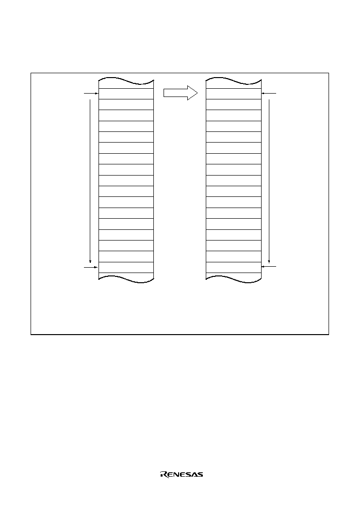
Rev. 1.0, 02/03, page 168 of 634
Figure 7.8 illustrates operation in normal mode.
Address T
A
Address B
A
Transfer
Address T
B
Legend:
Address T
A
= L
A
Address T
B
= L
B
Address B
A
= L
A
+ SAIDE · (1)
SAID
· (2
DTSZ
· (N1))
Address B
B
= L
B
+ DAIDE · (1)
DAID
· (2
DTSZ
· (N1))
L
A
= Value set in MARA
L
B
= Value set in MARB
N = Value set in ETCRA
Address B
B
Figure 7.8 Operation in Normal Mode
Transfer requests (activation sources) are external requests and auto-requests. With auto-request,
the DMAC is only activated by register setting, and the specified number of transfers are
performed automatically. With auto-request, cycle steal mode or burst mode can be selected. In
cycle steal mode, the bus is released to another bus master each time a transfer is performed. In
burst mode, the bus is held continuously until transfer ends. For setting details, see section 7.3.4,
DMA Controller Register (DMACR).
Rev. 1.0, 02/03, page 169 of 634
Figure 7.9 shows an example of the setting procedure for normal mode.
Normal mode
setting
Set DMABCRH
Set transfer source
and transfer destination
addresses
Set number of transfers
Set DMACR
Read DMABCRL
Set DMABCRL
Normal mode
[1]
[2]
[3]
[4]
[5]
[6]
[1] Set each bit in DMABCRH.
· Set the FAE bit to 1 to select full address
mode.
· Specify enabling or disabling of internal
interrupt clearing with the DTA bit.
[2] Set the transfer source address in MARA, and
the transfer destination address in MARB.
[3] Set the number of transfers in ETCRA.
[4] Set each bit in DMACRA and DMACRB.
· Set the transfer data size with the DTSZ bit.
· Specify whether MARA is to be
incremented, decremented, or fixed, with
the SAID and SAIDE bits.
· Clear the BLKE bit to 0 to select normal
mode.
· Specify whether MARB is to be
incremented, decremented, or fixed, with
the DAID and DAIDE bits.
· Select the activation source with bits DTF3
to DTF0.
[5] Read the DTE = 0 and DTME = 0 in
DMABCRL.
[6] Set each bit in DMABCRL.
· Specify enabling or desabling of transfer
end interrupts with the DTIE bit.
· Set both the DTME bit and the DTE bit to 1
to enable transfer.
Figure 7.9 Example of Normal Mode Setting Procedure
Rev. 1.0, 02/03, page 170 of 634
7.4.6
Block Transfer Mode
In block transfer mode, transfer is performed with channels A and B used in combination. Block
transfer mode can be specified by setting the FAE bit in DMABCR and the BLKE bit in
DMACRA to 1. In block transfer mode, a transfer of the specified block size is carried out in
response to a single transfer request, and this is executed the specified number of times. The
transfer source is specified by MARA, and the transfer destination by MARB. Either the transfer
source or the transfer destination can be selected as a block area (an area composed of a number of
bytes or words). Table 7.7 summarizes register functions in block transfer mode.
Table 7.7
Register Functions in Block Transfer Mode
Register
Function
Initial Setting
Operation
23
0
MARA
Source address
register
Start address of
transfer source
Incremented/decremented
every transfer, or fixed
23
0
MARB
Description address
register
Start address of
transfer destination
Incremented/decremented
every transfer, or fixed
0
ETCRAH
7
Holds block size
Block size
Fixed
0
ETCRAL
7
Block size counter
Block size
decremented every
transfer; ETCRH value
copied when count reaches
H'00
0
15
ETCRB
Block transfer
counter
Number of block
transfers
Decremented every block
transfer; transfer ends
when count reaches
H'0000
MARA and MARB specify the start addresses of the transfer source and transfer destination,
respectively, as 24 bits. MAR can be incremented or decremented by 1 or 2 each time a byte or
word is transferred, or can be fixed. Incrementing, decrementing, or holding a fixed value can be
set separately for MARA and MARB. Whether a block is to be designated for MARA or for
MARB is specified by the BLKDIR bit in DMACRA.
To specify the number of transfers, if M is the size of one block (where M = 1 to 256) and N
transfers are to be performed (where N = 1 to 65,536), M is set in both ETCRAH and ETCRAL,
and N in ETCRB.
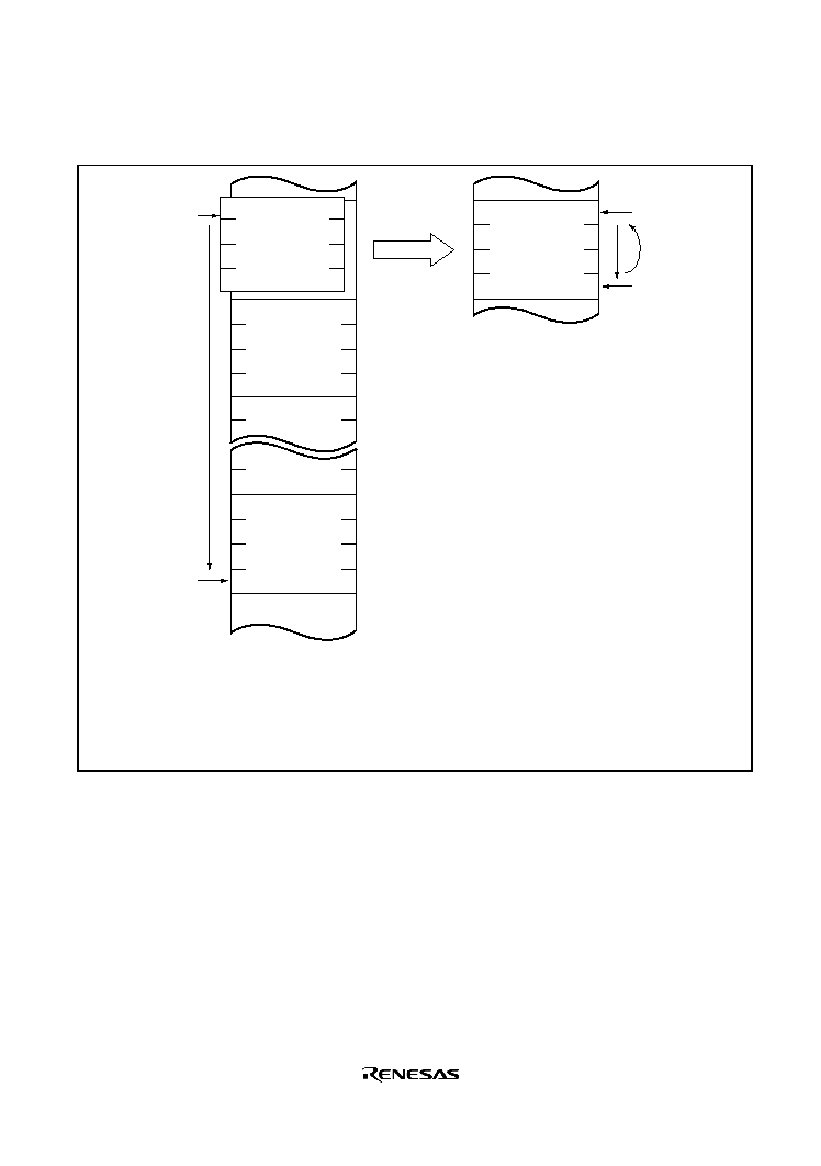
Rev. 1.0, 02/03, page 171 of 634
Figure 7.10 illustrates operation in block transfer mode when MARB is designated as a block area.
Address T
A
Address B
A
Transfer
Address T
B
Legend
Address T
A
= L
A
Address T
B
= L
B
Address B
A
= L
A
+ SAIDE · (1)
SAID
· (2
DTSZ
· (M · N1))
Address B
B
= L
B
+ DAIDE · (1)
DAID
· (2
DTSZ
· (N1))
L
A
= Value set in MARA
L
B
= Value set in MARB
N = Value set in ETCRA
M = Value set in ETCRAH and ETCRAL
Address B
B
1st block
2nd block
Nth block
Block area
Consecutive transfer
of M bytes or words
is performed in
response to one
request
Figure 7.10 Operation in Block Transfer Mode (BLKDIR = 0)
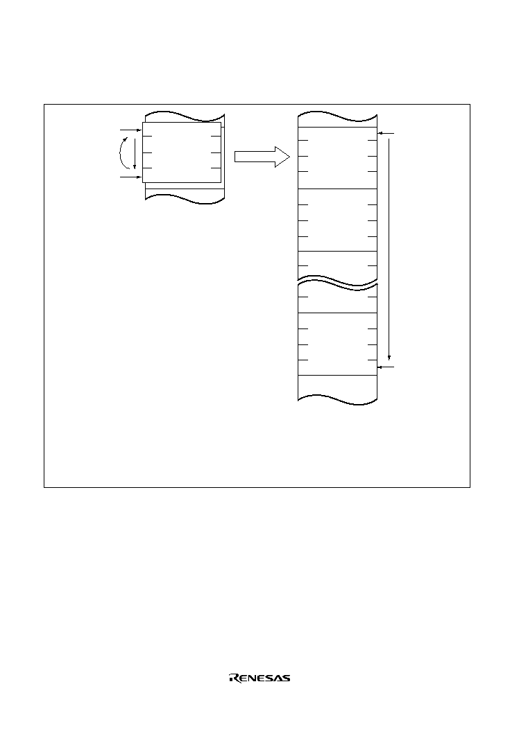
Rev. 1.0, 02/03, page 172 of 634
Figure 7.11 illustrates operation in block transfer mode when MARA is designated as a block area.
Address T
B
Address B
B
Transfer
Address T
A
Legend
Address T
A
= L
A
Address T
B
= L
B
Address B
A
= L
A
+ SAIDE · (1)
SAID
· (2
DTSZ
· (N1))
Address B
B
= L
B
+ DAIDE · (1)
DAID
· (2
DTSZ
· (M · N1))
LA = Value set in MARA
LB = Value set in MARB
N = Value set in ETCRB
M = Value set in ETCRAH and ETCRAL
Address B
A
1st block
2nd block
Nth block
Block area
Consecutive transfer
of M bytes or words
is performed in
response to one
request
Figure 7.11 Operation in Block Transfer Mode (BLKDIR = 1)
ETCRAL is decremented by 1 each time a byte or word transfer is performed. In response to a
single transfer request, burst transfer is performed until the value in ETCRAL reaches H'00.
ETCRAL is then loaded with the value in ETCRAH. At this time, the value in the MAR register
for which a block designation has been given by the BLKDIR bit in DMACRA is restored in
accordance with the DTSZ, SAID/DAID, and SAIDE/DAIDE bits in DMACR.
ETCRB is decremented by 1 every block transfer, and when the count reaches H'0000 the DTE bit
is cleared and transfer ends. If the DTIE bit is set to 1 at this point, an interrupt request is sent to
the CPU. Figure 7.12 shows the operation flow in block transfer mode.
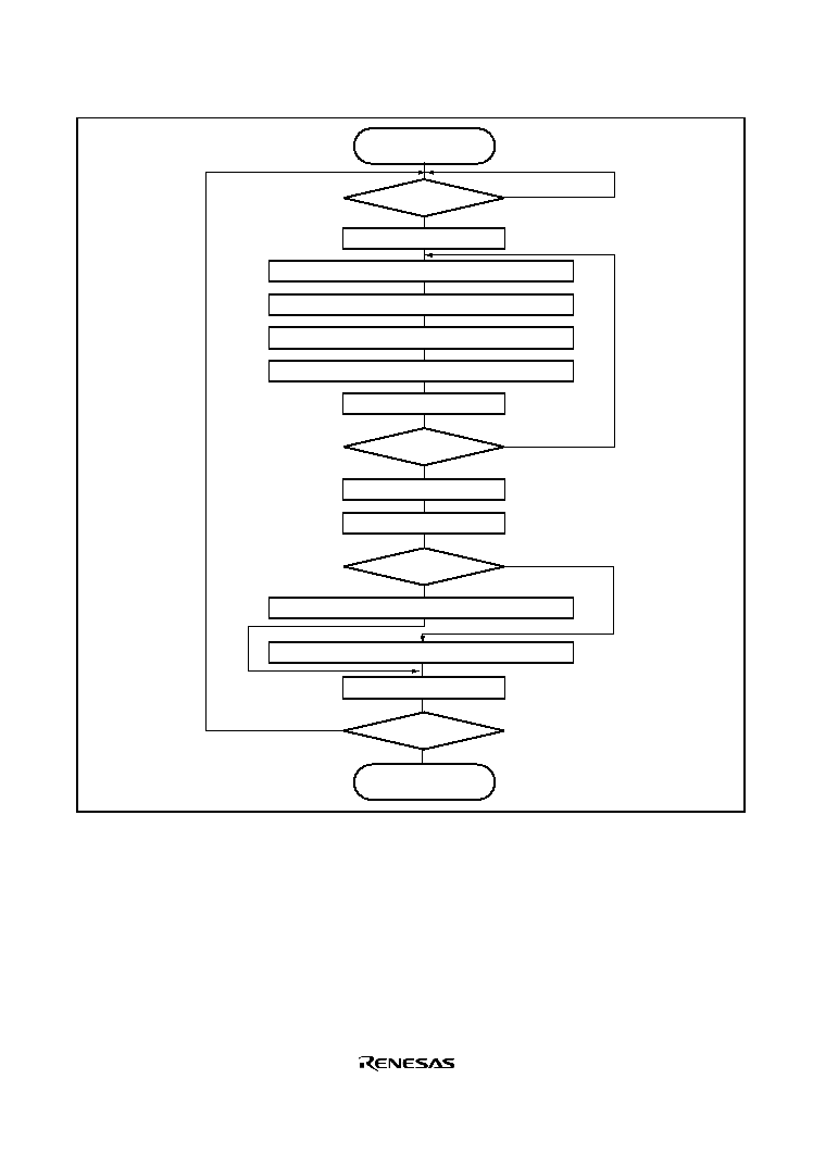
Rev. 1.0, 02/03, page 173 of 634
Start
(DTE = DTME = 1)
MARA = MARA SAIDE · (1)
SAID
· 2
DTSZ
· ETCRAH
No
Yes
No
Yes
No
Yes
No
Yes
Clear DTE bit to
to end transfer
Acquire bus
ETCRAL = ETCRAL1
Transfer request?
ETCRAL = H'00
Release bus
BLKDIR = 0
ETCRAL = ETCRAH
ETCRB = ETCRB 1
ETCRB = H'0000
Read address specified by MARA
MARA = MARA + SAIDE · (1)
SAID
· 2
DTSZ
Write to address specified by MARB
MARB = MARB + DAIDE · (1)
DAID
· 2
DTSZ
MARB = MARB DAIDE · (1)
DAID
· 2
DTSZ
· ETCRAH
Figure 7.12 Operation Flow in Block Transfer Mode
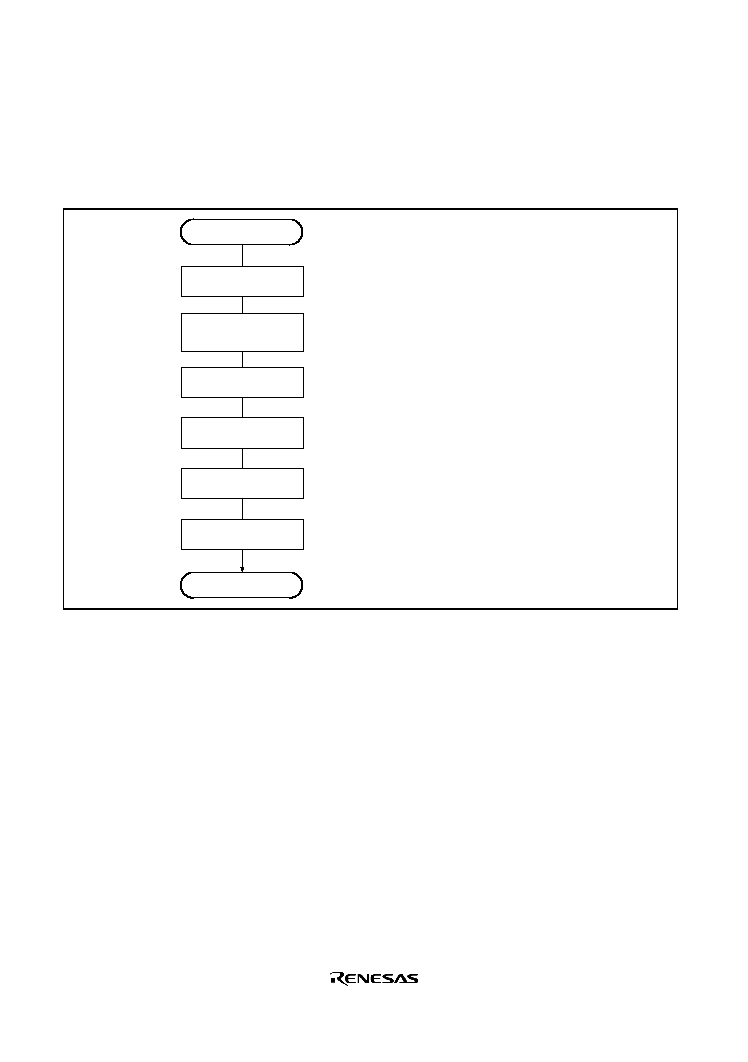
Rev. 1.0, 02/03, page 174 of 634
Transfer requests (activation sources) consist of A/D conversion end interrupt, SCI transmission
complete and reception complete interrupts, and TPU channel 0 to 2 compare match/input capture
A interrupts. For details, see section 7.3.4, DMA Control Register (DMACR). Figure 7.13 shows
an example of the setting procedure for block transfer mode.
Block transfer
mode setting
Set DMABCRH
Set transfer source
and transfer destination
addresses
Set number of transfers
Set DMACR
Read DMABCRL
Set DMABCRL
Block transfermode
[1]
[2]
[3]
[4]
[5]
[6]
[1] Set each bit in DMABCRH.
· Set the FAE bit to 1 to select full address
mode.
· Specify enabling or disabling of internal
interrupt clearing with the DTA bit.
[2] Set the transfer source address in MARA, and
the transfer destination address in MARB.
[3] Set the transfer source address in ETCRAH
and ETCRAL. Set the number of transfers in
ETCRB.
[4] Set each bit in DMACRA and DMACRB.
· Set the transfer data size with the DTSZ bit.
· Specify whether MARA is to be
incremented, decremented, or fixed, with
the SAID and SAIDE bits.
· Set the BLKE bit to 1 to select block
transfer mode.
· Specify whether the transfer source or the
transfer destination is a block area with the
BLKDIR bit.
· Select the activation source with bits DTF3
to DTF0.
[5] Read the DTE = 0 and DTME = 0 in
DMABCRL.
[6] Set each bit in DMABCRL.
· Specify enabling or desabling of transfer
end interrupts to the CPU with the DTIE bit.
Figure 7.13 Example of Block Transfer Mode Setting Procedure

Rev. 1.0, 02/03, page 175 of 634
7.4.7
DMAC Activation Sources
DMAC activation sources consist of internal interrupts, external requests, and auto-requests. The
activation sources that can be specified depend on the transfer mode, as shown in table 7.8.
Table 7.8
DMAC Activation Sources
Full Address Mode
Activation
Source
Short Address
Mode
Normal Mode
Block Transfer
Mode
Internal
ADI
x
Interrupt
TXI0
x
RXI0
x
TGI0A
x
TGI1A
x
TGI2A
x
USB request Low level input of the
DREQ
signal
x
Auto-request
x
x
Legend
O: Can be specified
X: Cannot be specified
Activation by Internal Interrupt: An interrupt request selected as a DMAC activation source
can be sent simultaneously to the CPU. For details, see section 5, Interrupt Controller.
With activation by an internal interrupt, the DMAC accepts the request independently of the
interrupt controller. Consequently, interrupt controller priority settings are not accepted.
If the DMAC is activated by an interrupt request that is not used as a CPU interrupt source (DTA
= 1), the interrupt source flag is cleared automatically by the DMA transfer. With ADI, TXI, and
RXI interrupts, however, the interrupt source flag is not cleared unless the prescribed register is
accessed in a DMA transfer. If the same interrupt is used as an activation source for more than one
channel, the interrupt request flag is cleared when the highest-priority channel is activated first.
Transfer requests for other channels are held pending in the DMAC, and activation is carried out
in order of priority.
When DTE = 0, such as after completion of a transfer, a request from the selected activation
source is not sent to the DMAC, regardless of the DTA bit. In this case, the relevant interrupt
request is sent to the CPU. In case of overlap with a CPU interrupt source (DTA = 0), the interrupt
request flag is not cleared by the DMAC.
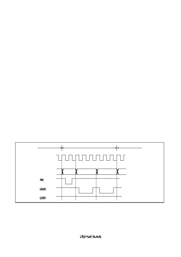
Rev. 1.0, 02/03, page 176 of 634
Activation by USB Request: The USB request (
DREQ signal) is specified as a DMAC activation
source. The USB request is generated by the level sense. In full-address normal mode, the USB
request is carried out as follows.
While the
DREQ signal is kept high, the DMAC waits for the transfer request. While the DREQ
signal is kept low, the DMAC releases the bus each time a byte or word is transferred and the
transfer is performed continuously. When the
DREQ signal is driven high during the transfer, the
transfer is halted and the DMAC waits for the transfer request.
Activation by Auto-Request: Auto-request activation is performed by register setting only, and
transfer continues to the end. With auto-request activation, cycle steal mode or burst mode can be
selected.
In cycle steal mode, the DMAC releases the bus to another bus master each time a byte or word is
transferred. DMA and CPU cycles usually alternate. In burst mode, the DMAC keeps possession
of the bus until the end of the transfer, and transfer is performed continuously.
7.4.8
Basic DMAC Bus Cycles
An example of the basic DMAC bus cycle timing is shown in figure 7.14. In this example, word-
size transfer is performed from 16-bit, 2-state access space to 8-bit, 3-state access space. When the
bus is transferred from the CPU to the DMAC, a source address read and destination address write
are performed. The bus is not released in response to another bus request, etc., between these read
and write operations. As with CPU cycles, DMA cycles conform to the bus controller settings.
DMAC cycle (1-word transfer)
CPU cycle
CPU cycle
T
1
T
2
T
1
T
2
T
3
T
1
T
2
T
3
Source
address
Destination address
Address bus
Figure 7.14 Example of DMA Transfer Bus Timing
The address is not output to the external address bus in an access to on-chip memory or an internal
I/O register.
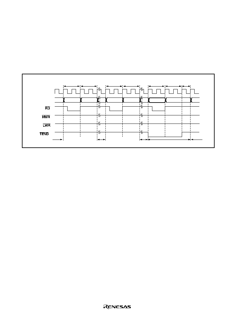
Rev. 1.0, 02/03, page 177 of 634
7.4.9
DMAC Bus Cycles (Dual Address Mode)
Short Address Mode: Figure 7.15 shows a transfer example in which
TEND* output is enabled
and byte-size short address mode transfer (sequential/idle/repeat mode) is performed from external
8-bit, 2-state access space to internal I/O space.
DMA read
*
DMA write
DMA read DMA write
DMA read
DMA write
DMA
dead
Address bus
Bus release
Bus release
Bus release
Bus release
Last transfer cycle
Figure 7.15 Example of Short Address Mode Transfer
A one-byte or one-word transfer is performed for one transfer request, and after the transfer the
bus is released. While the bus is released one or more bus cycles are inserted by the CPU.
In the transfer end cycle (the cycle in which the transfer counter reaches 0), a one-state DMA dead
cycle is inserted after the DMA write cycle.
In repeat mode, when
TEND* output is enabled, TEND* output goes low in the transfer cycle in
which the transfer counter reaches 0.
Note: * This LSI does not support
TEND output.
Full Address Mode (Cycle Steal Mode): Figure 7.16 shows a transfer example in which
TEND*
output is enabled and word-size full address mode transfer (cycle steal mode) is performed from
external 16-bit, 2-state access space to external 16-bit, 2-state access space.
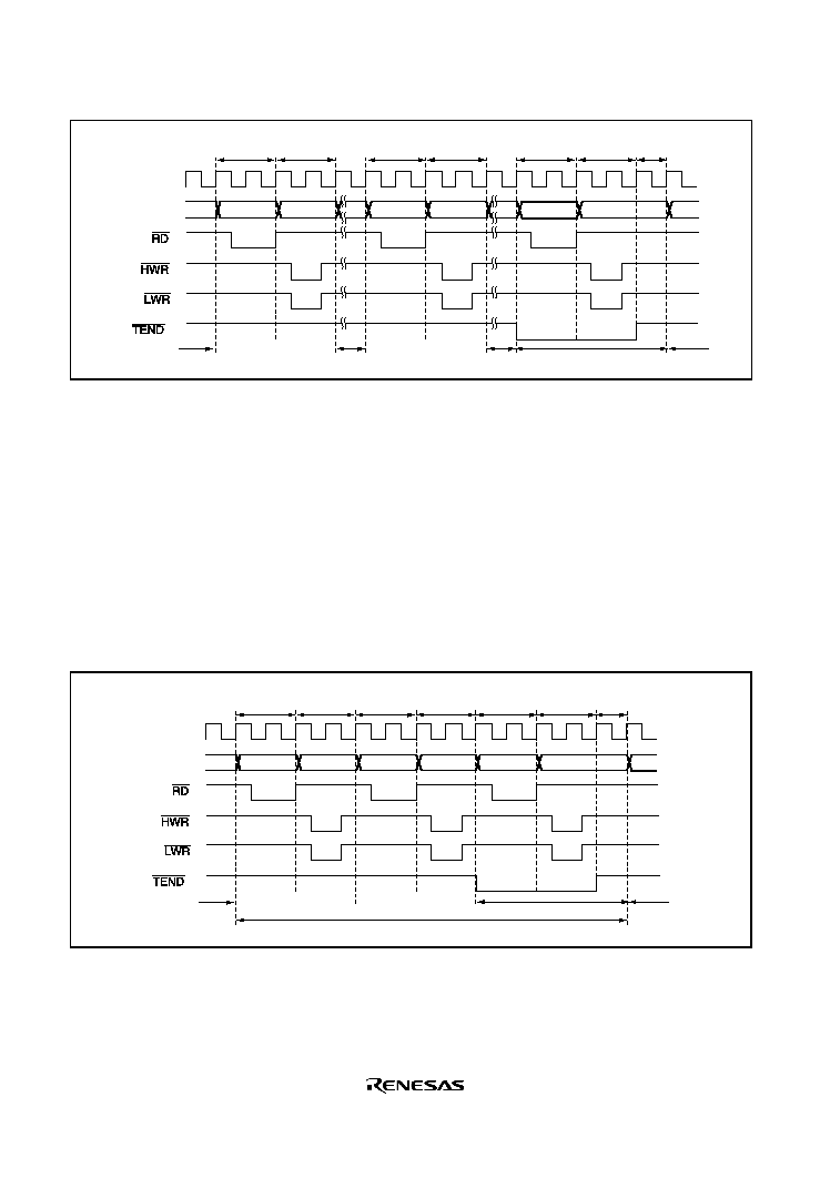
Rev. 1.0, 02/03, page 178 of 634
DMA read
*
DMA write
DMA read DMA write
DMA read DMA write
DMA
dead
Address bus
Bus release
Bus release
Bus release
Bus release
Last transfer cycle
Figure 7.16 Example of Full Address Mode (Cycle Steal) Transfer
A one-byte or one-word transfer is performed, and after the transfer the bus is released. While the
bus is released one bus cycle is inserted by the CPU.
In the transfer end cycle (the cycle in which the transfer counter reaches 0), a one-state DMA dead
cycle is inserted after the DMA write cycle.
Full Address Mode (Burst Mode): Figure 7.17 shows a transfer example in which
TEND*
output is enabled and word-size full address mode transfer (burst mode) is performed from
external 16- bit, 2-state access space to external 16-bit, 2-state access space.
Note: * This LSI does not support
TEND output.
DMA read
*
DMA write DMA read
DMA write DMA read DMA write
DMA
dead
Address bus
Bus release
Bus release
Last transfer cycle
Burst transfer
Figure 7.17 Example of Full Address Mode (Burst Mode) Transfer
In burst mode, one-byte or one-word transfers are executed consecutively until transfer ends. In
the transfer end cycle (the cycle in which the transfer counter reaches 0), a one-state DMA dead
cycle is inserted after the DMA write cycle.
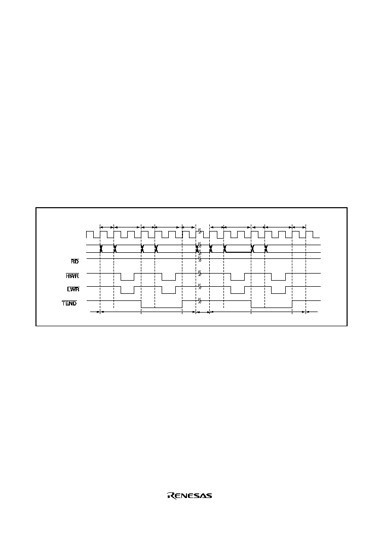
Rev. 1.0, 02/03, page 179 of 634
If a request from another higher-priority channel is generated after burst transfer starts, that
channel has to wait until the burst transfer ends.
If an NMI is generated while a channel designated for burst transfer is in the transfer enabled state,
the DTME bit is cleared and the channel is placed in the transfer disabled state. If burst transfer
has already been activated inside the DMAC, the bus is released on completion of a one-byte or
one-word transfer within the burst transfer, and burst transfer is suspended. If the last transfer
cycle of the burst transfer has already been activated inside the DMAC, execution continues to the
end of the transfer even if the DTME bit is cleared.
Full Address Mode (Block Transfer Mode): Figure 7.18 shows a transfer example in which
TEND* output is enabled and word-size full address mode transfer (block transfer mode) is
performed from internal 16-bit, 1-state access space to external 16-bit, 2-state access space.
Note: * This LSI does not support
TEND output.
DMA
read
*
DMA
write
DMA
dead
Address bus
Bus release
Bus release
Bus release
Last block transfer
DMA
read
Block transfer
DMA
write
DMA
read
DMA
write
DMA
dead
DMA
read
DMA
write
Figure 7.18 Example of Full Address Mode (Block Transfer Mode) Transfer
A one-block transfer is performed for one transfer request, and after the transfer the bus is
released. While the bus is released, one or more bus cycles are inserted by the CPU.
In the transfer end cycle of each block (the cycle in which the transfer counter reaches 0), a one-
state DMA dead cycle is inserted after the DMA write cycle.
One block is transmitted without interruption. NMI generation does not affect block transfer
operation.
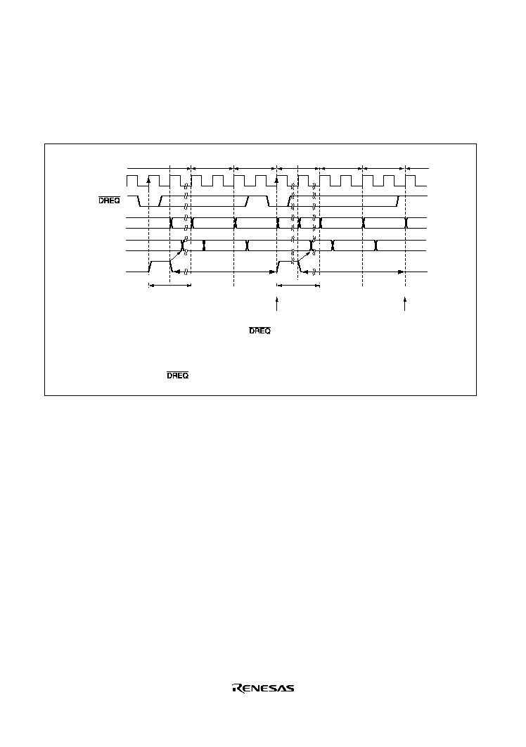
Rev. 1.0, 02/03, page 180 of 634
DREQ
DREQ
DREQ
DREQ Signal Level Activation Timing (Normal Mode): Set the DTA bit for the channel for
which the
DREQ signal is selected to 1.
Figure 7.19 shows an example of
DREQ level activated normal mode transfer.
Bus release
Idle
Idle
Idle
Read
Request clear period
Acceptance resumes
Acceptance resumes
Minimum of 2 cycles
Minimum of 2 cycles
Request clear period
Request
Request
Transfer
source
Transfer
source
Transfer
destination
Transfer
destination
Read
Write
Write
Address bus
DMA control
Channel
DMA
read
DMA
write
Bus
release
DMA
read
DMA
write
Bus
release
[1]
[2]
[3]
[4]
[5]
[6]
[7]
Acceptance after transfer enabling; the
signal low level is sampled on the rising
edge of f, and the request is held.
The request is cleared at the next bus break, and activation is started in the DMAC.
Start of DMA cycle.
Acceptance is resumed after the write cycle is completed.
(As in [1], the
signal low level is sampled on the rising edge of f, and the request
is held.)
[1]
[2] [5]
[3] [6]
[4] [7]
Figure 7.19 Example of
DREQ
DREQ
DREQ
DREQ Level Activated Normal Mode Transfer
DREQ signal sampling is performed every cycle, with the rising edge of the next cycle after the
end of the DMABCR write cycle for setting the transfer enabled state as the starting point.
When the
DREQ signal low level is sampled while acceptance by means of the DREQ signal is
possible, the request is held in the DMAC. Then, when activation is initiated in the DMAC, the
request is cleared. Acceptance resumes after the end of the write cycle,
DREQ signal low level
sampling is performed again, and this operation is repeated until the transfer ends.
Note: The
DREQ signal of this chip is an internal signal of chip, so it is not output from the pin.
Figure 7.20 shows an example of
DREQ level activated block transfer mode transfer.
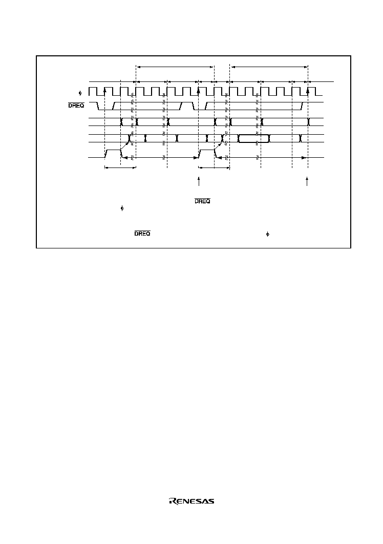
Rev. 1.0, 02/03, page 181 of 634
Bus release
1 block transfer
1 block transfer
Request clear period
Acceptance resumes
Acceptance resumes
Minimum of 2 cycles
Minimum of 2 cycles
Request clear period
Request
Request
Transfer
source
Transfer
source
Transfer
destination
Transfer
destination
Idle
Idle
Idle
Read
Read
Write
Dead
Dead
Write
Address bus
DMA control
Channel
DMA
read
DMA
write
Bus
release
DMA
dead
DMA
read
DMA
write
Bus
release
[1]
[2]
[3]
[4]
[5]
[6]
[7]
Acceptance after transfer enabling; the
signal low level is sampled on the rising
edge of , and the request is held.
The request is cleared at the next bus break, and activation is started in the DMAC.
Start of DMA cycle.
Acceptance is resumed after the dead cycle is completed.
(As in [1], the
signal low level is sampled on the rising edge of , and the request
is held.)
[1]
[2] [5]
[3] [6]
[4] [7]
Figure 7.20 Example of
DREQ
DREQ
DREQ
DREQ Level Activated Block Transfer Mode Transfer
DREQ signal sampling is performed every cycle, with the rising edge of the next cycle after the
end of the DMABCR write cycle for setting the transfer enabled state as the starting point.
When the
DREQ signal low level is sampled while acceptance by means of the DREQ signal is
possible, the request is held in the DMAC. Then, when activation is initiated in the DMAC, the
request is cleared. Acceptance resumes after the end of the dead cycle,
DREQ signal low level
sampling is performed again, and this operation is repeated until the transfer ends.
Note: The
DREQ signal of this chip is an internal signal of chip, so it is not output from the pin.
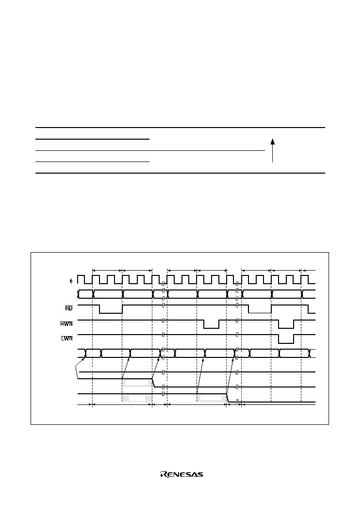
Rev. 1.0, 02/03, page 182 of 634
7.4.10
DMAC Multi-Channel Operation
The DMAC channel priority order is: channel 0 > channel 1, and channel A > channel B. Table
7.9 summarizes the priority order for DMAC channels.
Table 7.9
DMAC Channel Priority Order
Short Address Mode
Full Address Mode
Priority
Channel 0A
Channel 0
High
Channel 0B
Channel 1A
Channel 1
Channel 1B
Low
If transfer requests are issued simultaneously for more than one channel, or if a transfer request for
another channel is issued during a transfer, when the bus is released the DMAC selects the
highest-priority channel from among those issuing a request according to the priority order shown
in table 7.14. During burst transfer, or when one block is being transferred in block transfer, the
channel will not be changed until the end of the transfer. Figure 7.21 shows a transfer example in
which transfer requests are issued simultaneously for channels 0A, 0B, and 1.
DMA read
DMA write
DMA read
DMA write
DMA read
DMA write
DMA
read
Address bus
DMA control
Channel 0A
Channel 0B
Channel 1
Idle
Write
Idle
Read
Write
Idle
Read
Write
Read
Request clear
Request
hold
Request
hold
Request clear
Request clear
Bus
release
Channel 0A
transfer
Bus
release
Channel 0B
transfer
Channel 1 transfer
Bus
release
Request
hold
Read
Selection
Non-
selection
Selection
Figure 7.21 Example of Multi-Channel Transfer
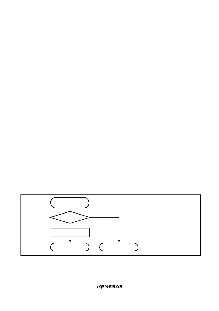
Rev. 1.0, 02/03, page 183 of 634
7.4.11
Relation between the DMAC and External Bus Requests
There can be no break between a DMA cycle read and a DMA cycle write. This means that an
external bus release cycle is not generated between the external read and external write in a DMA
cycle.
In the case of successive read and write cycles, such as in burst transfer or block transfer, an
external bus released state may be inserted after a write cycle.
When DMA cycle reads or writes are accesses to on-chip memory or internal I/O registers, these
DMA cycles can be executed at the same time as refresh cycles or external bus release. However,
simultaneous operation may not be possible when a write buffer is used.
7.4.12
NMI Interrupts and DMAC
When an NMI interrupt is requested, burst mode transfer in full address mode is interrupted. An
NMI interrupt does not affect the operation of the DMAC in other modes.
In full address mode, transfer is enabled for a channel when both the DTE bit and the DTME bit
are set to 1. With burst mode setting, the DTME bit is cleared when an NMI interrupt is requested.
If the DTME bit is cleared during burst mode transfer, the DMAC discontinues transfer on
completion of the 1-byte or 1-word transfer in progress, then releases the bus, which passes to the
CPU.
The channel on which transfer was interrupted can be restarted by setting the DTME bit to 1
again. Figure 7.22 shows the procedure for continuing transfer when it has been interrupted by an
NMI interrupt on a channel designated for burst mode transfer.
Resumption of
transfer on interrupted
channel
Set DTME bit to 1
Transfer continues
[1]
[2]
DTE= 1
DTME= 0
Transfer ends
No
Yes
[1]
[2]
Check that DTE = 1 and
DTME = 0 in DMABCRL
Write 1 to the DTME bit.
Figure 7.22 Example of Procedure for Continuing Transfer on Channel Interrupted by
NMI Interrupt
Rev. 1.0, 02/03, page 184 of 634
7.4.13
Forced Termination of DMAC Operation
If the DTE bit for the channel currently operating is cleared to 0, the DMAC stops on completion
of the 1-byte or 1-word transfer in progress. DMAC operation resumes when the DTE bit is set to
1 again. In full address mode, the same applies to the DTME bit. Figure 7.23 shows the procedure
for forcibly terminating DMAC operation by software.
Forced termination
of DMAC
Clear DTE bit to 0
Forced termination
[1]
[1]
Clear the DTE bit in DMABCRL to 0.
If you want to prevent interrupt generation after
forced termination of DMAC operation, clear the
DTIE bit to 0 at the same time.
Figure 7.23 Example of Procedure for Forcibly Terminating DMAC Operation
7.4.14
Clearing Full Address Mode
Figure 7.24 shows the procedure for releasing and initializing a channel designated for full address
mode. After full address mode has been cleared, the channel can be set to another transfer mode
using the appropriate setting procedure.
Clearing full
address mode
Stop the channel
Initialize DMACR
Clear FAE bit to 0
Initialization;
operation halted
[1]
[2]
[3]
[1] Clear both the DTE bit and the DTME bit in
DMABCRL to 0; or wait until the transfer ends
and the DTE bit is cleared to 0, then clear the
DTME bit to 0.
Also clear the corresponding DTIE bit to 0 at the
same time.
[2] Clear all bits in DMACRA and DMACRB to 0.
[3] Clear the FAE bit in DMABCRH to 0.
Figure 7.24 Example of Procedure for Clearing Full Address Mode
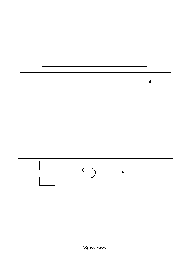
Rev. 1.0, 02/03, page 185 of 634
7.5
Interrupts
The sources of interrupts generated by the DMAC are transfer end and transfer break. Table 7.10
shows the interrupt sources and their priority order.
Table 7.10
Interrupt Source Priority Order
Interrupt Source
Interrupt
Name
Short Address Mode
Full Address Mode
Interrupt
Priority Order
DEND0A
Interrupt due to end of transfer
on channel 0A
Interrupt due to end of transfer
on channel 0
High
DEND0B
Interrupt due to end of transfer
on channel 0B
Interrupt due to break in transfer
on channel 0
DEND1A
Interrupt due to end of transfer
on channel 1A
Interrupt due to end of transfer
on channel 1
DEND1B
Interrupt due to end of transfer
on channel 1B
Interrupt due to break in transfer
on channel 1
Low
Enabling or disabling of each interrupt source is set by means of the DTIE bit for the
corresponding channel in DMABCR, and interrupts from each source are sent to the interrupt
controller independently. The relative priority of transfer end interrupts on each channel is decided
by the interrupt controller, as shown in table 7.10.
Figure 7.25 shows a block diagram of a transfer end/transfer break interrupt. An interrupt is
always generated when the DTIE bit is set to 1 while DTE bit is cleared to 0.
DTE/
DTME
DTIE
Transfer end/transfer
break interrupt
Figure 7.25 Block Diagram of Transfer End/Transfer Break Interrupt
In full address mode, a transfer break interrupt is generated when the DTME bit is cleared to 0
while DTIEB bit is set to 1. In both short address mode and full address mode, DMABCR should
be set so as to prevent the occurrence of a combination that constitutes a condition for interrupt
generation during setting.
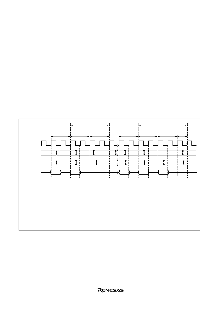
Rev. 1.0, 02/03, page 186 of 634
7.6
Usage Notes
7.6.1
DMAC Register Access during Operation
Except for forced termination, the operating (including transfer waiting state) channel setting
should not be changed. The operating channel setting should only be changed when transfer is
disabled. Also, the DMAC register should not be written to in a DMA transfer.
DMAC register reads during operation (including the transfer waiting state) are described below.
1. DMAC control starts one cycle before the bus cycle, with output of the internal address.
Consequently, MAR is updated in the bus cycle before DMAC transfer.
Figure 7.26 shows an example of the update timing for DMAC registers in dual address
transfer mode.
[1]
Transfer source address register MAR operation (incremented/decremented/fixed)
Transfer counter ETCR operation (decremented)
Block size counter ETCR operation (decremented in block transfer mode)
[2]
Transfer destination address register MAR operation (incremented/decremented/fixed)
[2']
Transfer destination address register MAR operation (incremented/decremented/fixed)
Block transfer counter ETCR operation (decremented, in last transfer cycle of
a block in block transfer mode)
[3]
Transfer address register MAR restore operation (in block or repeat transfer mode)
Transfer counter ETCR restore (in repeat transfer mode)
Block size counter ETCR restore (in block transfer mode)
[3]
[2']
[2]
[1]
[1]
DMA transfer cycle
DMA read
DMA read
DMA write
DMA write
DMA
dead
DMA Internal
address
DMA control
DMA register
operation
DMA last transfer cycle
Transfer
destination
Transfer
destination
Transfer
source
Transfer
source
Idle
Idle
Idle
Read
Read
Dead
Write
Write
Figure 7.26 DMAC Register Update Timing
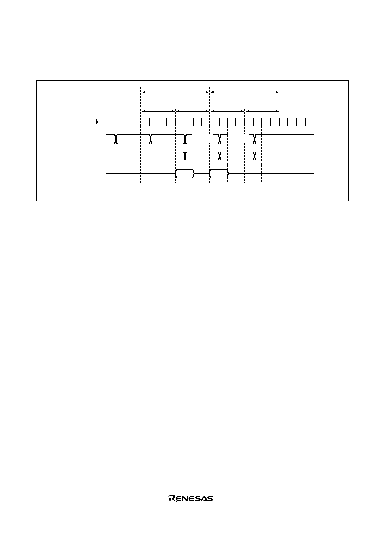
Rev. 1.0, 02/03, page 187 of 634
2. If a DMAC transfer cycle occurs immediately after a DMAC register read cycle, the DMAC
register is read as shown in figure 7.27.
[1]
[2]
Note:
The lower word of MAR is the updated value after the operation in [1].
CPU longword read
DMA transfer cycle
MAR upper
word read
MAR lower
word read
DMA read
DMA write
DMA internal
address
DMA control
DMA register
operation
Idle
Read
Write
Idle
Transfer
source
Transfer
destination
Figure 7.27 Contention between DMAC Register Update and CPU Read
7.6.2
Module Stop
When the MSTPA7 bit in MSTPCR is set to 1, the DMAC clock stops, and the module stop state
is entered. However, 1 cannot be written to the MSTPA7 bit if any of the DMAC channels is
enabled. This setting should therefore be made when DMAC operation is stopped.
When the DMAC clock stops, DMAC register accesses can no longer be made. Since the
following DMAC register settings are valid even in the module stop state, they should be
invalidated, if necessary, before a module stop.
·
Transfer end/suspend interrupt (DTE = 0 and DTIE = 1)
7.6.3
Medium-Speed Mode
When the DTA bit is 0, internal interrupt signals specified as DMAC transfer sources are edge-
detected. In medium-speed mode, the DMAC operates on a medium-speed clock, while on-chip
peripheral modules operate on a high-speed clock.
Consequently, if the period in which the relevant interrupt source is cleared by the CPU or another
DMAC channel, and the next interrupt is generated, is less than one state with respect to the
DMAC clock (bus master clock), edge detection may not be possible and the interrupt may be
ignored.

Rev. 1.0, 02/03, page 188 of 634
7.6.4
Activation Source Acceptance
At the start of activation source acceptance, a low level is detected in both
DREQ signal falling
edge sensing and low level sensing. Similarly, in the case of an internal interrupt, the interrupt
request is detected. Therefore, a request is accepted from an internal interrupt or
DREQ pin low
level that occurs before execution of the DMABCRL write to enable transfer.
When the DMAC is activated, take any necessary steps to prevent an internal interrupt or DREQ
signal low level remaining from the end of the previous transfer, etc.
7.6.5
Internal Interrupt after End of Transfer:
When the DTE bit is cleared to 0 by the end of transfer or an abort, the selected internal interrupt
request will be sent to the CPU even if DTA is set to 1.
Also, if internal DMAC activation has already been initiated when operation is aborted, the
transfer is executed but flag clearing is not performed for the selected internal interrupt even if
DTA is set to 1.
An internal interrupt request following the end of transfer or an abort should be handled by the
CPU as necessary.
7.6.6
Channel Re-Setting
To reactivate a number of channels when multiple channels are enabled, use exclusive handling of
transfer end interrupts, and perform DMABCR control bit operations exclusively. Note, in
particular, that in cases where multiple interrupts are generated between reading and writing of
DMABCR, and a DMABCR operation is performed during new interrupt handling, the DMABCR
write data in the original interrupt handling routine will be incorrect, and the write may invalidate
the results of the operations by the multiple interrupts. Ensure that overlapping DMABCR
operations are not performed by multiple interrupts, and that there is no separation between read
and write operations by the use of a bit-manipulation instruction. Also, when the DTE and DTME
bits are cleared by the DMAC or are written with 0, they must first be read while cleared to 0
before the CPU can write a 1 to them.

Rev. 1.0, 02/03, page 189 of 634
Section 8 I/O Ports
Table 8.1 and table 8.2 summarize the port functions of the H8S/2218 Series and H8S/2212 Series
respectively. The pins of each port also have other functions such as input/output or external
interrupt input pins of on-chip peripheral modules. Each I/O port includes a data direction register
(DDR) that controls input/output, a data register (DR) that stores output data, and a port register
(PORT) used to read the pin states. The input-only ports do not have DR and DDR.
Ports A to E have an on-chip input pull-up MOS and a input pull-up MOS control register (PCR)
to control the on/off state of the input pull-up MOS. Ports 3 and A to C include an open-drain
control register (ODR) that controls the on/off state of the output buffer PMOS.
All the I/O ports can drive a single TTL load and 30-pF capacitive load.
Table 8.1
Port Functions of H8S/2218 Series
Port
Description
Modes 4 and 5
Mode 6
Mode 7
Input/Output
Type
P17/TIOCB2/TCLKD
P16/TIOCA2/
IRQ1
P15/TIOCB1/TCLKC
P14/TIOCA1/
IRQ0
P13/TIOCD0/TCLKB/A23
P13/TIOCD0/TCLKB
P12/TIOCC0/TCLKA/A22
P12/TIOCC0/TCLKA
P11/TIOCB0/A21
P11/TIOCB0
Port 1
General I/O port
also functioning
as TPU I/O pins,
interrupt input
pins, and address
bus output pins
P10/TIOCA0/A20
P10/TIOCA0
Schmitt trigger
input
(
IRQ1, IRQ0)
Port 3
General I/O port
also functioning
as SCI_0 I/O pins
and interrupt
input pins
P36
P32/SCK0/
IRQ4
P31/RxD0
P30/TxD0
Open-drain
output
Schmitt trigger
input (
IRQ4)
Port 4
General input
port also
functioning as
A/D converter
analog input pins
P43/AN3
P42/AN2
P41/AN1
P40/AN0
Port 7
General I/O port
also functioning
as bus control
output pins and
manual reset
input pins
P74/
MRES
P71/
CS5
P70/
CS4
P74/
MRES
P71
P70

Rev. 1.0, 02/03, page 190 of 634
Port
Description
Modes 4 and 5
Mode 6
Mode 7
Input/Output
Type
Port 9
General input
port also
functioning as
A/D converter
analog input pins
P97/AN15
P96/AN14
Port A
General I/O port
also functioning
as SCI_2 I/O pins
and address bus
output pins
PA3/A19/SCK2
PA2/A18/RxD2
PA1/A17/TxD2
PA0/A16
PA3/SCK2
PA2/RxD2
PA1/TxD2
PA0
On-chip input
pull-up MOS
Open-drain
output
Port B
General I/O port
also functioning
as address bus
output pins
PB7/A15
PB6/A14
PB5/A13
PB4/A12
PB3/A11
PB2/A10
PB1/A9
PB0/A8
PB7
PB6
PB5
PB4
PB3
PB2
PB1
PB0
On-chip input
pull-up MOS
Open-drain
output
A7
When DDR = 0: PC7
When DDR = 1: A7
PC7
A6
When DDR = 0: PC6
When DDR = 1: A6
PC6
Port C
General I/O port
also functioning
as address bus
output pins
A5
When DDR = 0: PC5
When DDR = 1: A5
PC5
On-chip input
pull-up MOS
Open-drain
output
A4
When DDR = 0: PC4
When DDR = 1: A4
PC4
A3
When DDR = 0: PC73
When DDR = 1: A3
PC3
A2
When DDR = 0: PC2
When DDR = 1: A2
PC2
A1
When DDR = 0: PC1
When DDR = 1: A1
PC1
A0
When DDR = 0: PC0
When DDR = 1: A0
PC0
Port D
General I/O port
also functioning
as data bus I/O
pins
D15
D14
D13
D12
D11
D10
D9
D8
PD7
PD6
PD5
PD4
PD3
PD2
PD1
PD0
On-chip input
pull-up MOS

Rev. 1.0, 02/03, page 191 of 634
Port
Description
Modes 4 and 5
Mode 6
Mode 7
Input/Output
Type
8-bit bus mode: PE7
16-bit bus mode: D7
PE7
8-bit bus mode: PE6
16-bit bus mode: D6
PE6
8-bit bus mode: PE5
16-bit bus mode: D5
PE5
8-bit bus mode: PE4
16-bit bus mode: D4
PE4
8-bit bus mode: PE3
16-bit bus mode: D3
PE3
Port E
General I/O port
also functioning as
data bus I/O pins
8-bit bus mode: PE2
16-bit bus mode: D2
PE2
On-chip input
pull-up MOS
8-bit bus mode: PE1
16-bit bus mode: D1
PE1
8-bit bus mode: PE0
16-bit bus mode: D0
PE0
When DDR = 0: PF7
When DDR = 1 (after
reset):
When DDR = 0
(after reset): PF7
When DDR = 1:
AS
PF6
RD
PF5
HWR
PF4
8-bit bus mode:
PF3/
ADTRG/IRQ3
16-bit bus mode:
LWR
PF3/
ADTRG/IRQ3
When WAITE = 0
(after reset): PF2
When WAITE = 1:
WAIT
PF2
When BRLE = 0
(after reset): PF1
When BRLE = 1:
BACK
PF1
Port F
General I/O port
also functioning as
bus control signal
I/O pins and
interrupt input pins
When BRLE = 0
(after reset): PF0/
IRQ2
When BRLE = 1:
BREQ/IRQ2
PF0/
IRQ2
Schmitt trigger
input
(
IRQ3, IRQ2)

Rev. 1.0, 02/03, page 192 of 634
Port
Description
Modes 4 and 5
Mode 6
Mode 7
Input/Output
Type
When DDR = 0 (after reset in mode 6):
PG4
When DDR = 1 (after reset in mode 4, 5):
CS0
PG4
When DDR = 0: PG3
When DDR = 1:
CS1
PG3
When DDR = 0: PG2
When DDR = 1:
CS2
PG2
Port G
General I/O port
also functioning
as bus control
output pins and
interrupt Input
pins
When DDR = 0: PG1/
IRQ7
When DDR = 1:
CS3/IRQ7
PG1/
IRQ7
Schmitt trigger
input
(
IRQ7)
Table 8.2
Port Functions of H8S/2212 Series
Port
Description
Mode 7
Input/Output
Type
Port 1
General I/O port
also functioning
as TPU I/O pins
and interrupt
input pins
P17/TIOCB2/TCLKD
P16/TIOCA2/
IRQ1
P15/TIOCB1/TCLKC
P14/TIOCA1/
IRQ0
P13/TIOCD0/TCLKB
P12/TIOCC0/TCLKA
P11/TIOCB0
P10/TIOCA0
Schmitt trigger
input
(
IRQ1, IRQ0)
Port3
General I/O port
also functioning
as SCI_0 I/O pins
and interrupt
input pins
P36
P32/SCK0/
IRQ4
P31/RxD0
P30/TxD0
Open-drain
output
Schmitt trigger
input
(
IRQ4)
Port 4
General input
port also
functioning as
A/D converter
analog input pins
P43/AN3
P42/AN2
P41/AN1
P40/AN0
Port 7
General I/O port
P77*
P76*
P75*
Port 9
General input
port also
functioning as
A/D converter
analog input pins
P97/AN15
P96/AN14

Rev. 1.0, 02/03, page 193 of 634
Port
Description
Mode 7
Input/Output
Type
Port A
General I/O port
also functioning
as SCI_2 I/O pins
PA3/SCK2
PA2/RxD2
PA1/TxD2
On-chip input
pull-up MOS
Open-drain
output
Port E
General I/O port
PE7
PE6
PE5
PE4
PE3
PE2
PE1
PE0
On-chip input
pull-up MOS
When DDR = 0 (after reset): PF7
When DDR = 1:
Port F
General I/O port
also functioning
as interrupt input
pins
PF3/
ADTRG/IRQ3
PF0/
IRQ2
Schmitt trigger
input
(
IRQ3, IRQ2)
Port G
General I/O port
also functioning
as interrupt input
pins
PG1/
IRQ7
PG0
*
Schmitt trigger
input
(
IRQ7)
Note: * These pins are available only when EMLE = 0. These pins are not available when the
H-UDI is used.

Rev. 1.0, 02/03, page 194 of 634
8.1
Port 1
In the H8S/2218 Series, the port 1 is an 8-bit I/O port also functioning as address bus pins, TPU
I/O pins, and external interrupt input pins. In the H8S/2212 Series, the port 1 is an 8-bit I/O port
also functioning as TPU I/O pins and external interrupt input pins. The port 1 has the following
registers.
· Port 1 data direction register (P1DDR)
· Port 1 data register (P1DR)
· Port 1 register (PORT1)
8.1.1
Port 1 Data Direction Register (P1DDR)
P1DDR specifies input or output for the pins of the port 1.
Since P1DDR is a write-only register, the bit manipulation instructions must not be used to write
P1DDR.
Bit
Bit Name Initial Value
R/W
Description
7
6
5
4
3
2
1
0
P17DDR
P16DDR
P15DDR
P14DDR
P13DDR
P12DDR
P11DDR
P10DDR
0
0
0
0
0
0
0
0
W
W
W
W
W
W
W
W
(H8S/2218 Series)
Modes 4 to 6:
If address output is enabled by the setting of bits AE3 to
AE0 in PFCR, pins P13 to P10 are address outputs. Pins
P17 to P14, and pins P13 to P10 when address output is
disabled, are output ports when the corresponding
P1DDR bits are set to 1, and input ports when the
corresponding P1DDR bits are cleared to 0.
Mode 7:
Setting a P1DDR bit to 1 makes the corresponding port 1
pin an output port, while clearing the bit to 0 makes the
pin an input port.
(H8S/2212 Series)
Setting a P1DDR bit to 1 makes the corresponding port 1
pin an output port, while clearing the bit to 0 makes the
pin an input port.

Rev. 1.0, 02/03, page 195 of 634
8.1.2
Port 1 Data Register (P1DR)
P1DR stores output data for the port 1 pins.
Bit
Bit Name Initial Value
R/W
Description
7
6
5
4
3
2
1
0
P17DR
P16DR
P15DR
P14DR
P13DR
P12DR
P11DR
P10DR
0
0
0
0
0
0
0
0
R/W
R/W
R/W
R/W
R/W
R/W
R/W
R/W
Store output data for a pin that functions as a general
output port.
8.1.3
Port 1 Register (PORT1)
PORT1 indicates the pin states of the port 1.
Bit
Bit Name Initial Value
R/W
Description
7
6
5
4
3
2
1
0
P17
P16
P15
P14
P13
P12
P11
P10
*
*
*
*
*
*
*
*
R
R
R
R
R
R
R
R
If the port 1 is read while P1DDR bits are set to 1, the
P1DR value is read. If the port 1 is read while P1DDR bits
are cleared to 0, the pin states are read.
Note: * Determined by the states of pins P17 to P10.
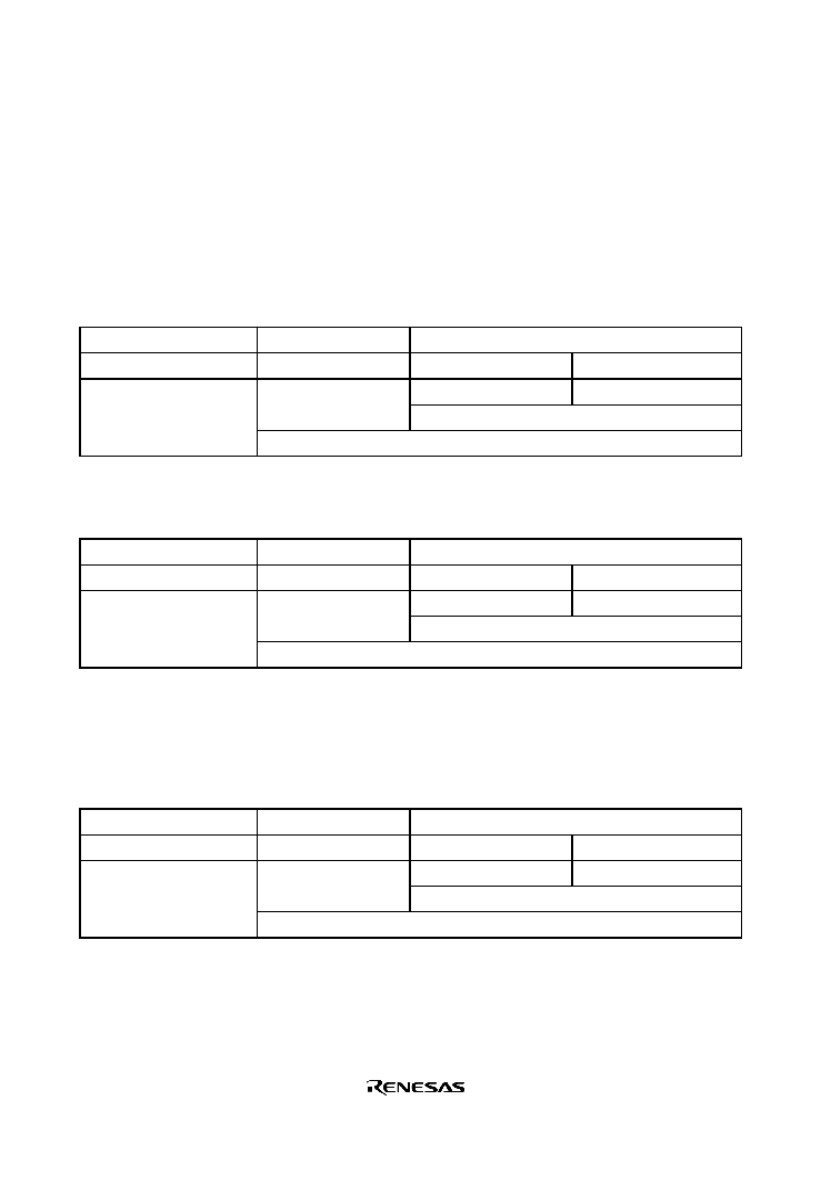
Rev. 1.0, 02/03, page 196 of 634
8.1.4
Pin Functions
Pin Functions of H8S/2218 Series
Port 1 pins also function as address bus (A23 to A20) output pins, TPU I/O pins, and external
interrupt input (
IRQ0 and IRQ1) pins. The correspondence between the register specification and
the pin functions is shown below.
Table 8.3
P17 Pin Function
TPU Channel 2 Setting*
Output Setting
Input Setting or Initial Value
P17DDR
0
1
P17 input pin
P17 output pin
TIOCB2 output pin
TIOCB2 input pin
Pin Function
TCLKD input pin
Note: * For details on the TPU channel setting, refer to section 9, 16-Bit Timer Pulse Unit (TPU).
Table 8.4
P16 Pin Function
TPU Channel 2 Setting*
1
Output Setting
Input Setting or Initial Value
P16DDR
0
1
P16 input pin
P16 output pin
TIOCA2 output pin
TIOCA2 input pin
Pin Function
IRQ1 input pin*
2
Notes: 1. For details on the TPU channel setting, refer to section 9, 16-Bit Timer Pulse Unit
(TPU).
2. When this pin is used as an external interrupt pin, this pin must not be used for another
function.
Table 8.5
P15 Pin Function
TPU Channel 1 Setting*
Output Setting
Input Setting or Initial Value
P15DDR
0
1
P15 input pin
P15 output pin
TIOCB1 output pin
TIOCB1 input pin
Pin Function
TCLKC input pin
Note: * For details on the TPU channel setting, refer to section 9, 16-Bit Timer Pulse Unit (TPU).
Rev. 1.0, 02/03, page 197 of 634
Table 8.6
P14 Pin Function
TPU Channel 1 Setting*
1
Output Setting
Input Setting or Initial Value
P14DDR
0
1
P14 input pin
P14 output pin
TIOCA1 output pin
TIOCA1 input pin
Pin Function
IRQ0 input pin*
2
Notes: 1. For details on the TPU channel setting, refer to section 9, 16-Bit Timer Pulse Unit
(TPU).
2. When this pin is used as an external interrupt pin, this pin must not be used for another
function.
Table 8.7
P13 Pin Function
AE3 to AE0*
2
Other than B'1111
B'1111
TPU Channel 0 Setting*
1
Output Setting
Input Setting or Initial Value
P13DDR
0
1
P13 input pin
P13 output pin
TIOCD0 output pin
TIOCD0 input pin
Pin Function
TCLKB input pin
A23 output
pin*
2
Notes: 1. For details on the TPU channel setting, refer to section 9, 16-Bit Timer Pulse Unit
(TPU).
2. Valid in modes 4, 5, and 6.
Table 8.8
P12 Pin Function
AE3 to AE0*
2
Other than B'1111
B'1111
TPU Channel 0 Setting*
1
Output Setting
Input Setting or Initial Value
P12DDR
0
1
P12 input pin
P12 output pin
TIOCC0 output pin
TIOCC0 input pin
Pin Function
TCLKA input pin
A22 output
pin*
2
Notes: 1. For details on the TPU channel setting, refer to section 9, 16-Bit Timer Pulse Unit
(TPU).
2. Valid in modes 4, 5, and 6.
Rev. 1.0, 02/03, page 198 of 634
Table 8.9
P11 Pin Function
AE3 to AE0*
2
Other than B'1110 to B'1111
B'1110 to
B'1111
TPU Channel 0 Setting*
1
Output Setting
Input Setting or Initial Value
P11DDR
0
1
P11 input pin
P11 output pin
Pin Function
TIOCB0 output pin
TIOCB0 input pin
A21 output
pin*
2
Notes: 1. For details on the TPU channel setting, refer to section 9, 16-Bit Timer Pulse Unit
(TPU).
2. Valid in modes 4, 5, and 6.
Table 8.10
P10 Pin Function
AE3 to AE0*
2
Other than B'1101 to B'1111
B'1101 to
B'1111
TPU Channel 0 Setting*
1
Output Setting
Input Setting or Initial Value
P10DDR
0
1
P10 input pin
P10 output pin
Pin Function
TIOCA0 output pin
TIOCA0 input pin
A21 output
pin*
2
Notes: 1. For details on the TPU channel setting, refer to section 9, 16-Bit Timer Pulse Unit
(TPU).
2. Valid in modes 4, 5, and 6.
Pin Functions of H8S/2212 Series
Port 1 pins also function as TPU I/O pins and external interrupt input (
IRQ0 and IRQ1) pins. The
correspondence between the register specification and the pin functions is shown below.
Table 8.11
P17 Pin Function
TPU Channel 2 Setting*
Output Setting
Input Setting or Initial Value
P17DDR
0
1
P17 input pin
P17 output pin
TIOCB2 output pin
TIOCB2 input pin
Pin Function
TCLKD input pin
Note: * For details on the TPU channel setting, refer to section 9, 16-Bit Timer Pulse Unit (TPU).
Rev. 1.0, 02/03, page 199 of 634
Table 8.12
P16 Pin Function
TPU Channel 2 Setting*
1
Output Setting
Input Setting or Initial Value
P16DDR
0
1
P16 input pin
P16 output pin
TIOCA2 output pin
TIOCA2 input pin
Pin Function
IRQ1 input pin*
2
Notes: 1. For details on the TPU channel setting, refer to section 9, 16-Bit Timer Pulse Unit
(TPU).
2. When this pin is used as an external interrupt pin, this pin must not be used for another
function.
Table 8.13
P15 Pin Function
TPU Channel 1 Setting*
Output Setting
Input Setting or Initial Value
P15DDR
0
1
P15 input pin
P15 output pin
TIOCB1 output pin
TIOCB1 input pin
Pin Function
TCLKC input pin
Note: * For details on the TPU channel setting, refer to section 9, 16-Bit Timer Pulse Unit (TPU).
Table 8.14
P14 Pin Function
TPU Channel 1 Setting*
1
Output Setting
Input Setting or Initial Value
P14DDR
0
1
P14 input pin
P14 output pin
TIOCA1 output pin
TIOCA1 input pin
Pin Function
IRQ0 input pin*
2
Notes: 1. For details on the TPU channel setting, refer to section 9, 16-Bit Timer Pulse Unit
(TPU).
2. When this pin is used as an external interrupt pin, this pin must not be used for another
function.
Rev. 1.0, 02/03, page 200 of 634
Table 8.15
P13 Pin Function
TPU Channel 0 Setting*
Output Setting
Input Setting or Initial Value
P13DDR
0
1
P13 input pin
P13 output pin
TIOCD0 output pin
TIOCD0 input pin
Pin Function
TCLKB input pin
Note: * For details on the TPU channel setting, refer to section 9, 16-Bit Timer Pulse Unit (TPU).
Table 8.16
P12 Pin Function
TPU Channel 0 Setting*
Output Setting
Input Setting or Initial Value
P12DDR
0
1
P12 input pin
P12 output pin
TIOCC0 output pin
TIOCC0 input pin
Pin Function
TCLKA input pin
Note: * For details on the TPU channel setting, refer to section 9, 16-Bit Timer Pulse Unit (TPU).
Table 8.17
P11 Pin Function
TPU Channel 0 Setting*
Output Setting
Input Setting or Initial Value
P11DDR
0
1
P11 input pin
P11 output pin
Pin Function
TIOCB0 output pin
TIOCB0 input pin
Note: * For details on the TPU channel setting, refer to section 9, 16-Bit Timer Pulse Unit (TPU).
Table 8.18
P10 Pin Function
TPU Channel 0 Setting*
Output Setting
Input Setting or Initial Value
P10DDR
0
1
P10 input pin
P10 output pin
Pin Function
TIOCA0 output pin
TIOCA0 input pin
Note: * For details on the TPU channel setting, refer to section 9, 16-Bit Timer Pulse Unit (TPU).

Rev. 1.0, 02/03, page 201 of 634
8.2
Port 3
The port 3 is a 4-bit I/O port also functioning as the SCI I/O pins and external interrupt input
(
IRQ4) pins. The port 3 of the H8S/2218 Series has the same function as that of the H8S/2212
Series. The port 3 has the following registers.
· Port 3 data direction register (P3DDR)
· Port 3 data register (P3DR)
· Port 3 register (PORT3)
· Port 3 open-drain control register (P3ODR)
8.2.1
Port 3 Data Direction Register (P3DDR)
P3DDR specifies input or output for the pins of the port 3.
Since P3DDR is a write-only register, the bit manipulation instructions must not be used to write
P3DDR.
Bit
Bit Name Initial Value
R/W
Description
7
Undefined
Reserved
This bit is undefined and cannot be modified.
6
P36DDR
0
W
Setting a P3DDR bit to 1 makes the corresponding port 3
pin an output pin, while clearing the bit to 0 makes the pin
an input pin.
5 to
3
Undefined
Reserved
These bits are undefined and cannot be modified.
2
1
0
P32DDR
P31DDR
P30DDR
0
0
0
W
W
W
Setting a P3DDR bit to 1 makes the corresponding port 3
pin an output pin, while clearing the bit to 0 makes the pin
an input pin.

Rev. 1.0, 02/03, page 202 of 634
8.2.2
Port 3 Data Register (P3DR)
P3DR stores output data for the port 3 pins.
Bit
Bit Name Initial Value
R/W
Description
7
Undefined
Reserved
This bit is undefined and cannot be modified.
6
P36DR
0
R/W
Stores output data for a pin that functions as a general
output port.
5 to
3
Undefined
Reserved
These bits are undefined.
2
1
0
P32DR
P31DR
P30DR
0
0
0
R/W
R/W
R/W
Store output data for a pin that functions as a general
output port.
8.2.3
Port 3 Register (PORT3)
PORT3 indicates the pin states of the port 3.
Bit
Bit Name Initial Value
R/W
Description
7
Undefined
Reserved
This bit is undefined.
6
P36
*
R
If the port 3 is read while P3DDR bits are set to 1, the
P3DR value is read. If the port 3 is read while P3DDR bits
are cleared to 0, the pin states are read.
5 to
3
Undefined
Reserved
These bits are undefined.
2
1
0
P32
P31
P30
*
*
*
R
R
R
If the port 3 is read while P3DDR bits are set to 1, the
P3DR value is read. If the port 3 is read while P3DDR bits
are cleared to 0, the pin states are read.
Note: * Determined by the states of pins P36 and P32 to P30.
Rev. 1.0, 02/03, page 203 of 634
8.2.4
Port 3 Open-Drain Control Register (P3ODR)
P3ODR controls the PMOS on/off state for each port 3 pin.
Bit
Bit Name Initial Value
R/W
Description
7
Undefined
Reserved
This bit is undefined and cannot be modified.
6
P36ODR
0
R/W
Setting a P3ODR bit to 1 makes the corresponding port 3
pin an NMOS open-drain output pin, while clearing the bit
to 0 makes the pin a CMOS output pin.
5 to
3
Undefined
Reserved
These bits are undefined and cannot be modified.
2
1
0
P32ODR
P31ODR
P30ODR
0
0
0
R/W
R/W
R/W
Setting a P3ODR bit to 1 makes the corresponding port 3
pin an NMOS open-drain output pin, while clearing the bit
to 0 makes the pin a CMOS output pin.
8.2.5
Pin Functions
Port 3 pins also function as SCI I/O pins and external interrupt input (
IRQ4) pins. The
correspondence between the register specification and the pin functions is shown below. The P36
pin must be used as the D+ pull-up control output pin of the USB. For details, refer to section 14,
Universal Serial Bus (USB).
Table 8.19
P36 Pin Function
P36DDR
0
1
Pin Function
P36 input pin
P36 output pin
(D+ pull-up control output pin of USB)
Table 8.20
P32 Pin Function
CKE1 in SCR_0
0
1
C/
A in SMR_0
0
1
CKE0 in SCR_0
0
1
P32DDR
0
1
P32 input pin
P32 output pin
SCK0 output pin
SCK0 output pin
SCK0 input pin
Pin Function
IRQ4 input pin*
Note: * When this pin is used as an external interrupt pin, this pin must not be used for another
function.
Rev. 1.0, 02/03, page 204 of 634
Table 8.21
P31 Pin Function
RE in SCR_0
0
1
P31DDR
0
1
Pin Function
P31 input pin
P31 output pin
RxD0 input pin
Table 8.22
P30 Pin Function
TE in SCR_0
0
1
P30DDR
0
1
Pin Function
P30 input pin
P30 output pin
TxD0 output pin
8.3
Port 4
The port 4 is a 4-bit input port also functioning as A/D converter analog input pins. The port 4 of
the H8S/2218 Series has the same function as that of the H8S/2212 Series. The port 4 has the
following register.
· Port 4 register (PORT4)
8.3.1
Port 4 Register (PORT4)
PORT4 indicates the pin states of the port 4.
Bit
Bit Name Initial Value
R/W
Description
7 to
4
Undefined
Reserved
These bits are undefined.
3
2
1
0
P43
P42
P41
P40
*
*
*
*
R
R
R
R
The pin states are always read when these bits are read.
Note: * Determined by the states of pins P43 to P40.
8.3.2
Pin Function
The port 4 also functions as A/D converter analog input (AN3 to AN0) pins.

Rev. 1.0, 02/03, page 205 of 634
8.4
Port 7
In the H8S/2218 Series, the port 7 is a 3-bit I/O port also functioning as bus control output pins
and manual reset input pins. In the H8S/2212 Series, the port 7 is a 3-bit I/O port also functioning
as H-UDI pins. The port 7 has the following registers.
· Port 7 data direction register (P7DDR)
· Port 7 data register (P7DR)
· Port 7 register (PORT7)
8.4.1
Port 7 Data Direction Register (P7DDR)
P7DDR specifies input or output for the pins of the port 7.
Since P7DDR is a write-only register, the bit manipulation instructions must not be used to write
P7DDR.
Bit
Bit Name
Initial Value R/W
Description
7
6
5
P77DDR
P76DDR
P75DDR
0
0
0
W
W
W
(H8S/2218 Series)
Reserved
These bits are undefined and cannot be modified.
(H8S/2212 Series)
When EMLE = 1: Pins P77 to P75 function as the H-UDI
pins.
When EMLE = 0: If a P7DDR bit is set to 1, pins P77 to
P75 function as output ports. If a P7DDR bit is cleared to
0, pins P77 to P75 function as input ports.
4
P74DDR
0
W
(H8S/2218 Series)
Setting a P7DDR bit to 1 makes the corresponding port 7
pin an output pin, while clearing the bit to 0 makes the pin
an input pin.
(H8S/2212 Series)
Reserved
This bit is undefined and cannot be modified.
3, 2
Undefined
Reserved
These bits are undefined and cannot be modified.

Rev. 1.0, 02/03, page 206 of 634
Bit
Bit Name
Initial Value R/W
Description
1
0
P71DDR
P70DDR
0
0
W
W
(H8S/2218 Series)
Setting a P7DDR bit to 1 makes the corresponding port
7 pin an output pin, while clearing the bit to 0 makes the
pin an input pin.
(H8S/2212 Series)
Reserved
These bits are undefined and cannot be modified.
8.4.2
Port 7 Data Register (P7DR)
P7DR stores output data for the port 7 pins.
Bit
Bit Name
Initial Value R/W
Description
7
6
5
P77DR
P76DR
P75DR
0
0
0
R/W
R/W
R/W
(H8S/2218 Series)
Reserved
These bits are undefined and cannot be modified.
(H8S/2212 Series)
Store output data for the port 7 pins.
4
P74DR
0
R/W
(H8S/2218 Series)
Stores output data for the port 7 pins.
(H8S/2212 Series)
Reserved
This bit is undefined and cannot be modified.
3, 2
Undefined
Reserved
These bits are undefined and cannot be modified.
1
0
P71DR
P70DR
0
0
R/W
R/W
(H8S/2218 Series)
Store output data for the port 7 pins.
(H8S/2212 Series)
Reserved
These bits are undefined and cannot be modified.

Rev. 1.0, 02/03, page 207 of 634
8.4.3
Port 7 Register (PORT7)
PORT7 indicates the pin states of the port 7.
Bit
Bit Name
Initial Value
R/W
Description
7
6
5
P77
P76
P75
*
*
*
(H8S/2218 Series)
Reserved
These bits are undefined and cannot be modified.
(H8S/2212 Series)
If P7DDR bits are set to 1, the P7DR value is read. If
P7DDR bits are cleared to 0, the pin states are read.
4
P74
*
R
(H8S/2218 Series)
If the port 7 is read while P7DDR bits are set to 1, the
P7DR value is read. If the port 7 is read while P7DDR
bits are cleared to 0, the pin states are read.
(H8S/2212 Series)
Reserved
This bit is undefined and cannot be modified.
3, 2
Undefined
Reserved
These bits are undefined and cannot be modified.
1
0
P71
P70
*
*
R
R
(H8S/2218 Series)
If the port 7 is read while P7DDR bits are set to 1, the
P7DR value is read. If the port 7 is read while P7DDR
bits are cleared to 0, the pin states are read.
(H8S/2212 Series)
Reserved
These bits are undefined and cannot be modified.
Note: * Determined by the states of pins P77 to P74, P71, and P70.
Rev. 1.0, 02/03, page 208 of 634
8.4.4
Pin Functions
Pin Functions of H8S/2218 Series
Port 7 pins also function as bus control output pins and manual reset input pins. The
correspondence between the register specification and the pin functions is shown below.
Table 8.23
P74 Pin Function
MRESE
0
1
P74DDR
0
1
Pin Function
P74 input pin
P74 output pin
MRES input pin
Table 8.24
P71 Pin Function
Operating Mode
Modes 4 to 6
Mode 7
P71DDR
0
1
0
1
Pin Function
P71 input pin
CS5 output pin
P71 input pin
P71 output pin
Table 8.25
P70 Pin Function
Operating Mode
Modes 4 to 6
Mode 7
P70DDR
0
1
0
1
Pin Function
P70 input pin
CS4 output pin
P70 input pin
P70 output pin
Pin Functions of H8S/2212 Series
Port 7 pins also function as H-UDI pins. The correspondence between the register specification
and the pin functions is shown below.
Table 8.26
P77 Pin Function
EMLE
0
1
P77DDR
0
1
Pin Function
P77 input pin
P77 output pin
TDO output pin
Rev. 1.0, 02/03, page 209 of 634
Table 8.27
P76 Pin Function
EMLE
0
1
P76DDR
0
1
Pin Function
P76 input pin
P76 output pin
TCK input pin
Table 8.28
P75 Pin Function
EMLE
0
1
P75DDR
0
1
Pin Function
P75 input pin
P75 output pin
TMS input pin
8.5
Port 9
The port 9 is a 2-bit input port also functioning as A/D converter analog input pins. The port 9 of
the H8S/2218 Series has the same function as that of the H8S/2212 Series.
· Port 9 register (PORT9)
8.5.1
Port 9 Register (PORT9)
PORT9 indicates the pin states of the port 9.
Bit
Bit Name Initial Value
R/W
Description
7
6
P97
P96
*
*
R
R
The pin states are always read when these bits are read.
5 to
0
Undefined
Reserved
These bits are undefined.
Note:
* Determined by the states of pins P97 and P96.
8.5.2
Pin Function
The port 9 also functions as A/D converter analog input (AN15 and AN14) pins.

Rev. 1.0, 02/03, page 210 of 634
8.6
Port A
In the H8S/2218 Series, the port A is a 4-bit I/O port also functioning as address bus (A19 to A16)
output pins and SCI I/O pins. In the H8S/2212 Series, the port A is a 3-bit I/O port also
functioning as SCI I/O pins. The port A has the following registers.
· Port A data direction register (PADDR)
· Port A data register (PADR)
· Port A register (PORTA)
· Port A pull-up MOS control register (PAPCR)
· Port A open-drain control register (PAODR)
8.6.1
Port A Data Direction Register (PADDR)
PADDR specifies input or output for the pins of the port A.
Since PADDR is a write-only register, the bit manipulation instructions must not be used to write
PADDR.
Bit
Bit Name Initial Value
R/W
Description
7 to
4
Undefined
Reserved
These bits are undefined and cannot be modified.
3
2
1
0
PA3DDR
PA2DDR
PA1DDR
PA0DDR*
0
0
0
0
W
W
W
W
(H8S/2218 Series)
Mode 7:
Setting a PADDR bit to 1 makes the corresponding port A
pin an output port, while clearing the bit to 0 makes the
pin an input port.
Modes 4 to 6:
If address output is enabled by the setting of bits AE3 to
AE0 in PFCR, the corresponding port A pins are address
outputs. When address output is disabled, setting a
PADDR bit to 1 makes the corresponding port A pin an
output port, while clearing the bit to 0 makes the pin an
input port.
(H8S/2212 Series)
Setting a PADDR bit to 1 makes the corresponding port A
pin an output port, while clearing the bit to 0 makes the
pin an input port.
Note: * Reserved in the H8S/2212 Series. If this bit is read, an undefined value will be read. This bit
cannot be modified.

Rev. 1.0, 02/03, page 211 of 634
8.6.2
Port A Data Register (PADR)
PADR stores output data for the port A pins.
Bit
Bit Name Initial Value
R/W
Description
7 to
4
Undefined
Reserved
These bits are undefined and cannot be modified.
3
2
1
0
PA3DR
PA2DR
PA1DR
PA0DR*
0
0
0
0
R/W
R/W
R/W
R/W
Store output data for a pin that functions as a general
output port.
Note: * Reserved in the H8S/2212 Series. If this bit is read, an undefined value will be read. This bit
cannot be modified.
8.6.3
Port A Register (PORTA)
PORTA indicates the pin states of the port A.
Bit
Bit Name Initial Value
R/W
Description
7 to
4
Undefined
Reserved
These bits are undefined.
3
2
1
0
PA3
PA2
PA1
PA0*
2
*
1
*
1
*
1
*
1
R
R
R
R
If the port A is read while PADDR bits are set to 1, the
PADR value is read. If the port A is read while PADDR
bits are cleared to 0, the pin states are read.
Notes: 1. Determined by the states of pins PA3 to PA0.
2. Reserved in the H8S/2212 Series. If this bit is read, an undefined value will be read.

Rev. 1.0, 02/03, page 212 of 634
8.6.4
Port A Pull-Up MOS Control Register (PAPCR)
PAPCR controls the on/off state of the port A input pull-up MOS. PAPCR is valid for port input
and SCI input pins.
Bit
Bit Name Initial Value
R/W
Description
7 to
4
Undefined
Reserved
These bits are undefined and cannot be modified.
3
2
1
0
PA3PCR
PA2PCR
PA1PCR
PA0PCR*
0
0
0
0
R/W
R/W
R/W
R/W
When a pin functions as an input port, setting the
corresponding bit to 1 turns on the input pull-up MOS for
that pin.
Note: * Reserved in the H8S/2212 Series. If this bit is read, an undefined value will be read. This bit
cannot be modified.
8.6.5
Port A Open-Drain Control Register (PAODR)
PAODR specifies an output type of the port A. PAODR is valid for port output and SCI output
pins.
Bit
Bit Name Initial Value
R/W
Description
7 to
4
Undefined
Reserved
These bits are undefined and cannot be modified.
3
2
1
0
PA3ODR
PA2ODR
PA1ODR
PA0ODR*
0
0
0
0
R/W
R/W
R/W
R/W
Setting a PAODR bit to 1 makes the corresponding port A
pin an NMOS open-drain output pin, while clearing the bit
to 0 makes the pin a CMOS output pin.
Note: * Reserved in the H8S/2212 Series. If this bit is read, an undefined value will be read. This bit
cannot be modified.
Rev. 1.0, 02/03, page 213 of 634
8.6.6
Pin Functions
Pin Functions of H8S/2218 Series
Port A pins also function as address bus (A19 to A16) output pins and SCI_2 I/O pins. The
correspondence between the register specification and the pin functions is shown below.
Table 8.29
PA3 Pin Function
Operating
Mode
Modes 4 to 6
Mode 7
AE3 to AE0
B'11xx
Other than B'11xx
--
CKE1
--
0
1
0
1
C/
A
--
0
1
--
0
1
--
CKE0
--
0
1
--
--
0
1
--
--
PA3DDR
--
0
1
--
--
--
0
1
--
--
--
Pin
Function
A19
output
pin
PA3
input
pin
PA3
output
pin
SCK2
output
pin
SCK2
output
pin
SCK2
input
pin
PA3
input
pin
PA3
output
pin
SCK2
output
pin
SCK2
output
pin
SCK2
input
pin
Table 8.30
PA2 Pin Function
Operating mode
Modes 4 to 6
Mode 7
AE3 to AE0
B'1011 or
B'11xx
Other than B'1011 or B'11xx
--
RE in SCR2
--
0
1
0
1
PA2DDR
--
0
1
--
0
1
--
Pin Function
A18
output pin
PA2
input pin
PA2
output pin
RxD2
input pin
PA2
input pin
PA2
output pin
RxD2
input pin
Legend x: Don't care.
Rev. 1.0, 02/03, page 214 of 634
Table 8.31
PA1 Pin Function
Operating mode
Modes 4 to 6
Mode 7
AE3 to AE0
B'101x or
B'11xx
Other than B'101x or B'11xx
--
TE in SCR2
--
0
1
0
1
PA1DDR
--
0
1
--
0
1
--
Pin Function
A17
output pin
PA1
input pin
PA1
output pin
TxD2
output pin
PA1
input pin
PA1
output pin
TxD2
output pin
Table 8.32
PA0 Pin Function
Operating
mode
Modes 4 to 6
Mode 7
AE3 to AE0
Other than
B'0xxx or B'1000
B'0xxx or B'1000
--
PA0DDR
--
0
1
0
1
Pin Function
A16 output pin
PA0 input pin
PA0 output pin
PA0 input pin PA0 output pin
Legend x: Don't care.
Pin Functions of H8S/2212 Series
Port A pins also function as SCI_2 I/O pins. The correspondence between the register specification
and the pin functions is shown below.
Table 8.33
PA3 Pin Function
CKE1
0
1
C/
A
0
1
CKE0
0
1
PA3DDR
0
1
Pin Function
PA3 input pin PA3 output pin SCK2 output pin SCK2 output pin SCK2 input pin
Rev. 1.0, 02/03, page 215 of 634
Table 8.34
PA2 Pin Function
RE in SCR2
0
1
PA2DDR
0
1
Pin Function
PA2 input pin
PA2 output pin
RxD2 input pin
Table 8.35
PA1 Pin Function
TE in SCR2
0
1
PA1DDR
0
1
Pin Function
PA1 input pin
PA1 output pin
TxD2 output pin
8.6.7
Port A Input Pull-Up MOS States
The port A has an on-chip input pull-up MOS function that can be controlled by software. The
input pull-up MOS can be specified as the on or off state for individual bits.
Table 8.36 summarizes the input pull-up MOS states.
Table 8.36
Input Pull-Up MOS States (Port A)
Pins
Power-On
Reset
Hardware
Standby
Mode
Manual
Reset
Software
Standby
Mode
In Other
Operations
Address output, port
output, SCI output
Off
Port input, SCI input
Off
On/Off
Legend
Off: Input pull-up MOS is always off.
On/Off: On when PADDR = 0 and PAPCR = 1; otherwise off.

Rev. 1.0, 02/03, page 216 of 634
8.7
Port B (H8S/2218 Series Only)
The port B is an 8-bit I/O port also functioning as address bus (A15 to A8) output pins. The port B
has the following registers.
Note:
When the USB is used while the E6000 emulator is used, the AE3 to AE0 bits in PFCR
must be set so that the PB1 and PB0 pins output addresses A9 and A8. This note applies to
both the H8S/2218 and H8S/2212 Series.
· Port B data direction register (PBDDR)
· Port B data register (PBDR)
· Port B register (PORTB)
· Port B pull-up MOS control register (PBPCR)
· Port B open-drain control register (PBODR)
8.7.1
Port B Data Direction Register (PBDDR)
PBDDR specifies input or output for the pins of the port B.
Since PBDDR is a write-only register, the bit manipulation instructions must not be used to write
PBDDR.
Bit
Bit Name Initial Value
R/W
Description
7
6
5
4
3
2
1
0
PB7DDR
PB6DDR
PB5DDR
PB4DDR
PB3DDR
PB2DDR
PB1DDR
PB0DDR
0
0
0
0
0
0
0
0
W
W
W
W
W
W
W
W
Modes 4 to 6:
If address output is enabled by the setting of bits AE3 to
AE0 in PFCR, the corresponding port B pins are address
outputs. When address output is disabled, setting a
PBDDR bit to 1 makes the corresponding port B pin an
output port, while clearing the bit to 0 makes the pin an
input port.
Mode 7:
Setting a PBDDR bit to 1 makes the corresponding port B
pin an output port, while clearing the bit to 0 makes the
pin an input port.

Rev. 1.0, 02/03, page 217 of 634
8.7.2
Port B Data Register (PBDR)
PBDR stores output data for the port B pins.
Bit
Bit Name Initial Value
R/W
Description
7
6
5
4
3
2
1
0
PB7DR
PB6DR
PB5DR
PB4DR
PB3DR
PB2DR
PB1DR
PB0DR
0
0
0
0
0
0
0
0
R/W
R/W
R/W
R/W
R/W
R/W
R/W
R/W
Store output data for a pin that functions as a general
output port.
8.7.3
Port B Register (PORTB)
PORTB indicates the pin states of the port B.
Bit
Bit Name Initial Value
R/W
Description
7
6
5
4
3
2
1
0
PB7
PB6
PB5
PB4
PB3
PB2
PB1
PB0
*
*
*
*
*
*
*
*
R
R
R
R
R
R
R
R
If the port B is read while PBDDR bits are set to 1, the
PBDR value is read. If the port B is read while PBDDR
bits are cleared to 0, the pin states are read.
Note: * Determined by the states of pins PB7 to PB0.

Rev. 1.0, 02/03, page 218 of 634
8.7.4
Port B Pull-Up MOS Control Register (PBPCR)
PBPCR controls the on/off state of the port B input pull-up MOS. PBPCR is valid for port input
pins.
Bit
Bit Name Initial Value
R/W
Description
7
6
5
4
3
2
1
0
PB7PCR
PB6PCR
PB5PCR
PB4PCR
PB3PCR
PB2PCR
PB1PCR
PB0PCR
0
0
0
0
0
0
0
0
R/W
R/W
R/W
R/W
R/W
R/W
R/W
R/W
When a pin functions as an input port, setting the
corresponding bit to 1 turns on the input pull-up MOS for
that pin.
8.7.5
Port B Open-Drain Control Register (PBODR)
PBODR specifies an output type of the port B. PBODR is valid for port output pins.
Bit
Bit Name Initial Value
R/W
Description
7
6
5
4
3
2
1
0
PB7ODR
PB6ODR
PB5ODR
PB4ODR
PB3ODR
PB2ODR
PB1ODR
PB0ODR
0
0
0
0
0
0
0
0
R/W
R/W
R/W
R/W
R/W
R/W
R/W
R/W
Setting a PBODR bit to 1 makes the corresponding port B
pin an NMOS open-drain output pin, while clearing the bit
to 0 makes the pin a CMOS output pin.
Rev. 1.0, 02/03, page 219 of 634
8.7.6
Pin Functions
Port B pins also function as address bus (A15 to A9) output pins. The correspondence between the
register specification and the pin functions is shown below.
Table 8.37
PB7 Pin Function
Operating mode
Modes 4 to 6
Mode 7
AE3 to AE0
B'1xxx
Other than B'1xxx
--
PB7DDR
--
0
1
0
1
Pin Function
A15
output pin
PB7
input pin
PB7
output pin
PB7
input pin
PB7
output pin
Table 8.38
PB6 Pin Function
Operating mode
Modes 4 to 6
Mode 7
AE3 to AE0
B'0111 or B'1xxx
Other than B'0111 or
B'1xxx
--
PB6DDR
--
0
1
0
1
Pin Function
A14
output pin
PB6
input pin
PB6
output pin
PB6
input pin
PB6
output pin
Table 8.39
PB5 Pin Function
Operating mode
Modes 4 to 6
Mode 7
AE3 to AE0
B'011x or B'1xxx
Other than B'011x or
B'1xxx
--
PB5DDR
--
0
1
0
1
Pin Function
A13
output pin
PB5
input pin
PB5
output pin
PB5
input pin
PB5
output pin
Table 8.40
PB4 Pin Function
Operating mode
Modes 4 to 6
Mode 7
AE3 to AE0
Other than B'0100
or B'00xx
B'0100 or B'00xx
--
PB4DDR
--
0
1
0
1
Pin Function
A12
output pin
PB4
input pin
PB4
output pin
PB4
input pin
PB4
output pin
Rev. 1.0, 02/03, page 220 of 634
Table 8.41
PB3 Pin Function
Operating mode
Modes 4 to 6
Mode 7
AE3 to AE0
Other than B'00xx
B'00xx
--
PB3DDR
--
0
1
0
1
Pin Function
A11
output pin
PB3
input pin
PB3
output pin
PB3
input pin
PB3
output pin
Table 8.42
PB2 Pin Function
Operating mode
Modes 4 to 6
Mode 7
AE3 to AE0
Other than B'0010
or B'000x
B'0010 or B'000x
--
PB2DDR
--
0
1
0
1
Pin Function
A10
output pin
PB2
input pin
PB2
output pin
PB2
input pin
PB2
output pin
Table 8.43
PB1 Pin Function
Operating mode
Modes 4 to 6
Mode 7
AE3 to AE0
Other than B'000x
B'000x
--
PB1DDR
--
0
1
0
1
Pin Function
A9
output pin
PB1
input pin
PB1
output pin
PB1
input pin
PB1
output pin
Note:
When the E6000 emulator is used, this pin must be set as an A9 output pin in order to
access the USB.
Table 8.44
PB0 Pin Function
Operating mode
Modes 4 to 6
Mode 7
AE3 to AE0
Other than B'0000
B'0000
--
PB0DDR
--
0
1
0
1
Pin Function
A8
output pin
PB0
input pin
PB0
output pin
PB0
input pin
PB0
output pin
Note:
When the E6000 emulator is used, this pin must be set as an A8 output pin in order to
access the USB.
Legend x: Don't care.

Rev. 1.0, 02/03, page 221 of 634
8.7.7
Port B Input Pull-Up MOS States
The port B has an on-chip input pull-up MOS function that can be controlled by software. The
input pull-up MOS can be specified as the on or off state for individual bits.
Table 8.45 summarizes the input pull-up MOS states.
Table 8.45
Input Pull-Up MOS States (Port B)
Pins
Power-On
Reset
Hardware
Standby
Mode
Manual
Reset
Software
Standby
Mode
In Other
Operations
Address output, port
output
Off
Port input
Off
On/Off
Legend
Off: Input pull-up MOS is always off.
On/Off: On when PBDDR = 0 and PBPCR = 1; otherwise off.
8.8
Port C (H8S/2218 Series Only)
The port C is an 8-bit I/O port also functioning as address bus (A7 to A0) output pins. The port C
has the following registers.
Note:
When the RTC and USB are used while the E6000 emulator is used, the PC7DDR to
PC0DDR bits in PCDDR must be set so that the PC7 to PC0 pins output addresses A7 to
A0. This note applies to both the H8S/2218 and H8S/2212 Series.
· Port C data direction register (PCDDR)
· Port C data register (PCDR)
· Port C register (PORTC)
· Port C pull-up MOS control register (PCPCR)
· Port C open-drain control register (PCODR)

Rev. 1.0, 02/03, page 222 of 634
8.8.1
Port C Data Direction Register (PCDDR)
PCDDR specifies input or output for the pins of the port C.
Since PCDDR is a write-only register, the bit manipulation instructions must not be used to write
PCDDR.
Bit
Bit Name Initial Value
R/W
Description
7
6
5
4
3
2
1
0
PC7DDR
PC6DDR
PC5DDR
PC4DDR
PC3DDR
PC2DDR
PC1DDR
PC0DDR
0
0
0
0
0
0
0
0
W
W
W
W
W
W
W
W
Modes 4 and 5:
Port C pins are address output pins.
Mode 6:
Setting a PCDDR bit to 1 makes the corresponding port C
pin an address output pin, while clearing the bit to 0
makes the pin an input port.
Mode 7:
Setting a PCDDR bit to 1 makes the corresponding port C
pin an output port, while clearing the bit to 0 makes the
pin an input port.
8.8.2
Port C Data Register (PCDR)
PCDR stores output data for the port C pins.
Bit
Bit Name Initial Value
R/W
Description
7
6
5
4
3
2
1
0
PC7DR
PC6DR
PC5DR
PC4DR
PC3DR
PC2DR
PC1DR
PC0DR
0
0
0
0
0
0
0
0
R/W
R/W
R/W
R/W
R/W
R/W
R/W
R/W
Store output data for a pin that functions as a general
output port.

Rev. 1.0, 02/03, page 223 of 634
8.8.3
Port C Register (PORTC)
PORTC indicates the pin states of the port C.
Bit
Bit Name Initial Value
R/W
Description
7
6
5
4
3
2
1
0
PC7
PC6
PC5
PC4
PC3
PC2
PC1
PC0
*
*
*
*
*
*
*
*
R
R
R
R
R
R
R
R
If the port C is read while PCDDR bits are set to 1, the
PCDR value is read. If the port C is read while PCDDR
bits are cleared to 0, the pin states are read.
Note: * Determined by the states of pins PC7 to PC0.
8.8.4
Port C Pull-Up MOS Control Register (PCPCR)
PCPCR controls the on/off state of the port C input pull-up MOS.
Bit
Bit Name Initial Value
R/W
Description
7
6
5
4
3
2
1
0
PC7PCR
PC6PCR
PC5PCR
PC4PCR
PC3PCR
PC2PCR
PC1PCR
PC0PCR
0
0
0
0
0
0
0
0
R/W
R/W
R/W
R/W
R/W
R/W
R/W
R/W
When a pin functions as an input port, setting the
corresponding bit to 1 turns on the input pull-up MOS for
that pin.
Rev. 1.0, 02/03, page 224 of 634
8.8.5
Port C Open-Drain Control Register (PCODR)
PCODR specifies an output type of the port C. PCODR is valid for port output pins.
Bit
Bit Name Initial Value
R/W
Description
7
6
5
4
3
2
1
0
PC7ODR
PC6ODR
PC5ODR
PC4ODR
PC3ODR
PC2ODR
PC1ODR
PC0ODR
0
0
0
0
0
0
0
0
R/W
R/W
R/W
R/W
R/W
R/W
R/W
R/W
Setting a PCODR bit to 1 makes the corresponding port C
pin an NMOS open-drain output pin, while clearing the bit
to 0 makes the pin a CMOS output pin.
8.8.6
Pin Functions
Port C pins also function as address bus (A7 to A0) output pins. The correspondence between the
register specification and the pin functions is shown below.
Table 8.46
PC7 Pin Function
Operating Mode
Modes 4 and 5
Mode 6*
Mode 7
PC7DDR
1
0
1
0
Pin Function
A7
output pin
A7
output pin
PC7
input pin
PC7
output pin
PC7
input pin
Table 8.47
PC6 Pin Function
Operating Mode
Modes 4 and 5
Mode 6*
Mode 7
PC6DDR
1
0
1
0
Pin Function
A6
output pin
A6
output pin
PC6
input pin
PC6
output pin
PC6
input pin
Table 8.48
PC5 Pin Function
Operating Mode
Modes 4 and 5
Mode 6*
Mode 7
PC5DDR
1
0
1
0
Pin Function
A5
output pin
A5
output pin
PC5
input pin
PC5
output pin
PC5
input pin
Rev. 1.0, 02/03, page 225 of 634
Table 8.49
PC4 Pin Function
Operating Mode
Modes 4 and 5
Mode 6*
Mode 7
PC4DDR
1
0
1
0
Pin Function
A4
output pin
A4
output pin
PC4
input pin
PC4
output pin
PC4
input pin
Table 8.50
PC3 Pin Function
Operating Mode
Modes 4 and 5
Mode 6*
Mode 7
PC3DDR
1
0
1
0
Pin Function
A3
output pin
A3
output pin
PC3
input pin
PC3
output pin
PC3
input pin
Table 8.51
PC2 Pin Function
Operating Mode
Modes 4 and 5
Mode 6*
Mode 7
PC2DDR
1
0
1
0
Pin Function
A2
output pin
A2
output pin
PC2
input pin
PC2
output pin
PC2
input pin
Table 8.52
PC1 Pin Function
Operating Mode
Modes 4 and 5
Mode 6*
Mode 7
PC1DDR
1
0
1
0
Pin Function
A1
output pin
A1
output pin
PC1
input pin
PC1
output pin
PC1
input pin
Table 8.53
PC0 Pin Function
Operating Mode
Modes 4 and 5
Mode 6*
Mode 7
PC0DDR
1
0
1
0
Pin Function
A0
output pin
A0
output pin
PC0
input pin
PC0
output pin
PC0
input pin
Note:
When the on-chip RTC and USB is used in mode 6, bits PC7DDR to PC0DDR should be
set to H'FF so that the pins output A7 to A0.

Rev. 1.0, 02/03, page 226 of 634
8.8.7
Port C Input Pull-Up MOS States
The port C has an on-chip input pull-up MOS function that can be controlled by software. The
input pull-up MOS can be used in modes 6 and 7, and can be specified as the on or off state for
individual bits.
Table 8.54 summarizes the input pull-up MOS states.
Table 8.54
Input Pull-Up MOS States (Port C)
Pins
Power-On
Reset
Hardware
Standby
Mode
Manual
Reset
Software
Standby
Mode
In Other
Operations
Address output (modes 4 and 5),
port output (modes 6 and 7)
Off
Port input (modes 6 and 7)
Off
On/Off
Legend
Off: Input pull-up MOS is always off.
On/Off: On when PCDDR = 0 and PCPCR = 1; otherwise off.
8.9
Port D (H8S/2218 Series Only)
The port D is an 8-bit I/O port also functioning as data bus (D15 to D8) I/O pins. The port D has
the following registers.
· Port D data direction register (PDDDR)
· Port D data register (PDDR)
· Port D register (PORTD)
· Port D pull-up MOS control register (PDPCR)

Rev. 1.0, 02/03, page 227 of 634
8.9.1
Port D Data Direction Register (PDDDR)
PDDDR specifies input or output for the pins of the port D.
Since PDDDR is a write-only register, the bit manipulation instructions must not be used to write
PDDDR.
Bit
Bit Name Initial Value
R/W
Description
7
6
5
4
3
2
1
0
PD7DDR
PD6DDR
PD5DDR
PD4DDR
PD3DDR
PD2DDR
PD1DDR
PD0DDR
0
0
0
0
0
0
0
0
W
W
W
W
W
W
W
W
Modes 4 to 6:
Port D pins automatically function as data input/output
pins.
Mode 7:
Setting a PDDDR bit to 1 makes the corresponding port D
pin an output port, while clearing the bit to 0 makes the
pin an input port.
8.9.2
Port D Data Register (PDDR)
PDDR stores output data for the port D pins.
Bit
Bit Name Initial Value
R/W
Description
7
6
5
4
3
2
1
0
PD7DR
PD6DR
PD5DR
PD4DR
PD3DR
PD2DR
PD1DR
PD0DR
0
0
0
0
0
0
0
0
R/W
R/W
R/W
R/W
R/W
R/W
R/W
R/W
Store output data for a pin that functions as a general
output port.

Rev. 1.0, 02/03, page 228 of 634
8.9.3
Port D Register (PORTD)
PORTD indicates the pin states of the port D.
Bit
Bit Name Initial Value
R/W
Description
7
6
5
4
3
2
1
0
PD7
PD6
PD5
PD4
PD3
PD2
PD1
PD0
*
*
*
*
*
*
*
*
R
R
R
R
R
R
R
R
If the port D is read while PDDDR bits are set to 1, the
PDDR value is read. If the port D is read while PDDDR
bits are cleared to 0, the pin states are read.
Note: * Determined by the states of pins PD7 to PD0.
8.9.4
Port D Pull-Up MOS Control Register (PDPCR)
PDPCR controls the on/off state of the port D input pull-up MOS.
Bit
Bit Name Initial Value
R/W
Description
7
6
5
4
3
2
1
0
PD7PCR
PD6PCR
PD5PCR
PD4PCR
PD3PCR
PD2PCR
PD1PCR
PD0PCR
0
0
0
0
0
0
0
0
R/W
R/W
R/W
R/W
R/W
R/W
R/W
R/W
When a pin functions as an input port, setting the
corresponding bit to 1 turns on the input pull-up MOS for
that pin.
Rev. 1.0, 02/03, page 229 of 634
8.9.5
Pin Functions
Port D pins also function as data bus (D15 to D8) I/O pins. The correspondence between the
register specification and the pin functions is shown below.
Table 8.55
PD7 Pin Function
Operating Mode
Modes 4 to 6
Mode 7
PD7DDR
0
1
Pin Function
D15 input/output pin
PD7 input pin
PD7 output pin
Table 8.56
PD6 Pin Function
Operating Mode
Modes 4 to 6
Mode 7
PD6DDR
0
1
Pin Function
D14 input/output pin
PD6 input pin
PD6 output pin
Table 8.57
PD5 Pin Function
Operating Mode
Modes 4 to 6
Mode 7
PD5DDR
0
1
Pin Function
D13 input/output pin
PD5 input pin
PD5 output pin
Table 8.58
PD4 Pin Function
Operating Mode
Modes 4 to 6
Mode 7
PD4DDR
0
1
Pin Function
D12 input/output pin
PD4 input pin
PD4 output pin
Table 8.59
PD3 Pin Function
Operating Mode
Modes 4 to 6
Mode 7
PD3DDR
0
1
Pin Function
D11 input/output pin
PD3 input pin
PD3 output pin
Table 8.60
PD2 Pin Function
Operating Mode
Modes 4 to 6
Mode 7
PD2DDR
0
1
Pin Function
D10 input/output pin
PD2 input pin
PD2 output pin
Rev. 1.0, 02/03, page 230 of 634
Table 8.61
PD1 Pin Function
Operating Mode
Modes 4 to 6
Mode 7
PD1DDR
0
1
Pin Function
D9 input/output pin
PD1 input pin
PD1 output pin
Table 8.62
PD0 Pin Function
Operating Mode
Modes 4 to 6
Mode 7
PD0DDR
0
1
Pin Function
D8 input/output pin
PD0 input pin
PD0 output pin
8.9.6
Port D Input Pull-Up MOS States
The port D has an on-chip input pull-up MOS function that can be controlled by software. The
input pull-up MOS can be used in mode 7, and can be specified as the on or off state for individual
bits.
Table 8.63 summarizes the input pull-up MOS states.
Table 8.63
Input Pull-Up MOS States (Port D)
Pins
Power-
On Reset
Hardware
Standby
Mode
Manual
Reset
Software
Standby
Mode
In Other
Operations
Data input/output (modes 4 to 6),
port output (mode 7)
Off
Port input (mode 7)
Off
On/Off
Legend
Off: Input pull-up MOS is always off.
On/Off: On when PDDDR = 0 and PDPCR = 1; otherwise off.

Rev. 1.0, 02/03, page 231 of 634
8.10
Port E
The port E is an 8-bit I/O port also functioning as data bus (D7 to D0) I/O pins. The port E has the
following registers.
· Port E data direction register (PEDDR)
· Port E data register (PEDR)
· Port E register (PORTE)
· Port E pull-up MOS control register (PEPCR)
8.10.1
Port E Data Direction Register (PEDDR)
PEDDR specifies input or output for the pins of the port E.
Since PEDDR is a write-only register, the bit manipulation instructions must not be used to write
PEDDR.
Bit
Bit Name Initial Value
R/W
Description
7
6
5
4
3
2
1
0
PE7DDR
PE6DDR
PE5DDR
PE4DDR
PE3DDR
PE2DDR
PE1DDR
PE0DDR
0
0
0
0
0
0
0
0
W
W
W
W
W
W
W
W
(H8S/2218 Series)
Modes 4 to 6:
When 8-bit bus mode is selected, port E functions as an
I/O port. Setting a PEDDR bit to 1 makes the
corresponding port E pin an output port, while clearing the
bit to 0 makes the pin an input port.
When 16-bit bus mode is selected, the input/output
direction settings in PEDDR are ignored, and port E pins
automatically function as data input/output pins.
For details on 8-bit/16-bit bus mode, refer to section 6,
Bus Controller.
Mode 7:
Setting a PEDDR bit to 1 makes the corresponding port E
pin an output port, while clearing the bit to 0 makes the
pin an input port.
(H8S/2212 Series)
Setting a PEDDR bit to 1 makes the corresponding port E
pin an output port, while clearing the bit to 0 makes the
pin an input port.

Rev. 1.0, 02/03, page 232 of 634
8.10.2
Port E Data Register (PEDR)
PEDR stores output data for the port E pins.
Bit
Bit Name Initial Value
R/W
Description
7
6
5
4
3
2
1
0
PE7DR
PE6DR
PE5DR
PE4DR
PE3DR
PE2DR
PE1DR
PE0DR
0
0
0
0
0
0
0
0
R/W
R/W
R/W
R/W
R/W
R/W
R/W
R/W
Store output data for a pin that functions as a general
output port.
8.10.3
Port E Register (PORTE)
PORTE indicates the pin states of the port E.
Bit
Bit Name Initial Value
R/W
Description
7
6
5
4
3
2
1
0
PE7
PE6
PE5
PE4
PE3
PE2
PE1
PE0
*
*
*
*
*
*
*
*
R
R
R
R
R
R
R
R
If the port E is read while PEDDR bits are set to 1, the
PEDR value is read. If the port E is read while PEDDR
bits are cleared to 0, the pin states are read.
Note: * Determined by the states of pins PE7 to PE0.
Rev. 1.0, 02/03, page 233 of 634
8.10.4
Port E Pull-Up MOS Control Register (PEPCR)
PEPCR controls the on/off state of the port E input pull-up MOS.
Bit
Bit Name Initial Value
R/W
Description
7
6
5
4
3
2
1
0
PE7PCR
PE6PCR
PE5PCR
PE4PCR
PE3PCR
PE2PCR
PE1PCR
PE0PCR
0
0
0
0
0
0
0
0
R/W
R/W
R/W
R/W
R/W
R/W
R/W
R/W
When a pin functions as an input port, setting the
corresponding bit to 1 turns on the input pull-up MOS for
that pin.
8.10.5
Pin Functions
Pin Functions of H8S/2218 Series
Port E pins also function as data bus (D7 to D0) I/O pins. The correspondence between the register
specification and the pin function is shown below.
Table 8.64
PE7 Pin Function
Operating Mode
Modes 4 to 6
Mode 7
Bus Mode
8-bit bus mode
16-bit bus mode
PE7DDR
1
0
1
0
Pin Function
PE7
output pin
PE7
input pin
D7
input/output pin
PE7
output pin
PE7
input pin
Table 8.65
PE6 Pin Function
Operating Mode
Modes 4 to 6
Mode 7
Bus Mode
8-bit bus mode
16-bit bus mode
PE6DDR
1
0
1
0
Pin Function
PE6
output pin
PE6
input pin
D6
input/output pin
PE6
output pin
PE6
input pin
Rev. 1.0, 02/03, page 234 of 634
Table 8.66
PE5 Pin Function
Operating Mode
Modes 4 to 6
Mode 7
Bus Mode
8-bit bus mode
16-bit bus mode
PE5DDR
1
0
1
0
Pin Function
PE5
output pin
PE5
input pin
D5
input/output pin
PE5
output pin
PE5
input pin
Table 8.67
PE4 Pin Function
Operating Mode
Modes 4 to 6
Mode 7
Bus Mode
8-bit bus mode
16-bit bus mode
PE4DDR
1
0
1
0
Pin Function
PE4
output pin
PE4
input pin
D4
input/output pin
PE4
output pin
PE4
input pin
Table 8.68
PE3 Pin Function
Operating Mode
Modes 4 to 6
Mode 7
Bus Mode
8-bit bus mode
16-bit bus mode
PE3DDR
1
0
1
0
Pin Function
PE3
output pin
PE3
input pin
D3
input/output pin
PE3
output pin
PE3
input pin
Table 8.69
PE2 Pin Function
Operating Mode
Modes 4 to 6
Mode 7
Bus Mode
8-bit bus mode
16-bit bus mode
PE2DDR
1
0
1
0
Pin Function
PE2
output pin
PE2
input pin
D2
input/output pin
PE2
output pin
PE2
input pin
Table 8.70
PE1 Pin Function
Operating Mode
Modes 4 to 6
Mode 7
Bus Mode
8-bit bus mode
16-bit bus mode
PE1DDR
1
0
1
0
Pin Function
PE1
output pin
PE1
input pin
D1
input/output pin
PE1
output pin
PE1
input pin
Rev. 1.0, 02/03, page 235 of 634
Table 8.71
PE0 Pin Function
Operating Mode
Modes 4 to 6
Mode 7
Bus Mode
8-bit bus mode
16-bit bus mode
PE0DDR
1
0
1
0
Pin Function
PE0
output pin
PE0
input pin
D0
input/output pin
PE0
output pin
PE0
input pin
Pin Functions of H8S/2212 Series
The port E function as a general I/O port. The correspondence between the register specification
and the pin function is shown below.
Table 8.72
PE7 Pin Function
PE7DDR
1
0
Pin Function
PE7 output pin
PE7 input pin
Table 8.73
PE6 Pin Function
PE6DDR
1
0
Pin Function
PE6 output pin
PE6 input pin
Table 8.74
PE5 Pin Function
PE5DDR
1
0
Pin Function
PE5 output pin
PE5 input pin
Table 8.75
PE4 Pin Function
PE4DDR
1
0
Pin Function
PE4 output pin
PE4 input pin
Table 8.76
PE3 Pin Function
PE3DDR
1
0
Pin Function
PE3 output pin
PE3 input pin
Rev. 1.0, 02/03, page 236 of 634
Table 8.77
PE2 Pin Function
PE2DDR
1
0
Pin Function
PE2 output pin
PE2 input pin
Table 8.78
PE1 Pin Function
PE1DDR
1
0
Pin Function
PE1 output pin
PE1 input pin
Table 8.79
PE0 Pin Function
PE0DDR
1
0
Pin Function
PE0 output pin
PE0 input pin
8.10.6
Port E Input Pull-Up MOS States
The port E has an on-chip input pull-up MOS function that can be controlled by software. The
input pull-up MOS can be used in modes 4 to 6 and in 8-bit bus mode, or in mode 7, and can be
specified as the on or off state for individual bits.
Table 8.80 summarizes the input pull-up MOS states.
Table 8.80
Input Pull-Up MOS States (Port E)
Pins
Power-On
Reset
Hardware
Standby
Mode
Manual
Reset
Software
Standby
Mode
In Other
Operations
Data input/output (16-bit
bus mode in modes 4 to
6), port output (8-bit bus
mode in modes 4 to 6,
mode 7)
Off
Port input (8-bit bus
mode in modes 4 to 6,
mode 7)
Off
On/Off
Legend
Off: Input pull-up MOS is always off.
On/Off: On when PEDDR = 0 and PEPCR = 1; otherwise off.

Rev. 1.0, 02/03, page 237 of 634
8.11
Port F
In the H8S/2218 Series, the port F is an 8-bit I/O port also functioning as external interrupt input
(
IRQ2, IRQ3) pins, bus control signal I/O pins, and system clock output pins. In the H8S/2212
Series, the port F is a 3-bit I/O port also functioning as external interrupt input (
IRQ2, IRQ3) pins
and system clock output pins. The port F has the following registers.
· Port F data direction register (PFDDR)
· Port F data register (PFDR)
· Port F register (PORTF)
8.11.1
Port F Data Direction Register (PFDDR)
PFDDR specifies input or output for the pins of the port F.
Since PFDDR is a write-only register, the bit manipulation instructions must not be used to write
PFDDR.
Bit
Bit Name
Initial Value
R/W
Description
7
6
5
4
3
2
1
0
PF7DDR
PF6DDR*
2
PF5DDR*
2
PF4DDR*
2
PF3DDR
PF2DDR*
2
PF1DDR*
2
PF0DDR
1/0*
1
0
0
0
0
0
0
0
W
W
W
W
W
W
W
W
(H8S/2218 Series)
Modes 4 to 6:
Pin PF7 functions as the
output pin when the PF7DDR
bit is set to 1, and as an input port when the bit is cleared
to 0. Pins PF6 to PF3 are automatically designated as bus
control output pins. Pins PF2 to PF0 are made bus control
input/output pins by bus controller settings. Otherwise,
setting a PFDDR bit to 1 makes the corresponding pin an
output port, while clearing the bit to 0 makes the pin an
input port.
Mode 7
Setting a PFDDR bit to 1 makes the corresponding port F
pin PF6 to PF0 an output port, or in the case of pin PF7,
the
output pin. Clearing the bit to 0 makes the pin an
input port.
(H8S/2212 Series)
Setting a PFDDR bit to 1 makes the corresponding port F
pin PF6 to PF0 an output port, or in the case of pin PF7,
the
output pin. Clearing the bit to 0 makes the pin an
input port.
Notes: 1. The initial value becomes 1 in modes 4 to 6 and 0 in mode 7.
2. Reserved in the H8S/2212 Series. If this bit is read, an undefined value will be read.
This bit cannot be modified.

Rev. 1.0, 02/03, page 238 of 634
8.11.2
Port F Data Register (PFDR)
PFDR stores output data for the port F pins.
Bit
Bit Name Initial Value
R/W
Description
7
6
5
4
3
2
1
0
PF7DR
PF6DR*
PF5DR*
PF4DR*
PF3DR
PF2DR*
PF1DR*
PF0DR
0
0
0
0
0
0
0
0
R/W
R/W
R/W
R/W
R/W
R/W
R/W
R/W
Store output data for a pin that functions as a general
output port.
Note: * Reserved in the H8S/2212 Series. If this bit is read, an undefined value will be read. This bit
cannot be modified.
8.11.3
Port F Register (PORTF)
PORTF indicates the pin states of the port F.
Bit
Bit Name Initial Value
R/W
Description
7
6
5
4
3
2
1
0
PF7
PF6*
2
PF5*
2
PF4*
2
PF3
PF2*
2
PF1*
2
PF0
*
1
*
1
*
1
*
1
*
1
*
1
*
1
*
1
R
R
R
R
R
R
R
R
If the port F is read while PFDDR bits are set to 1, the
PFDR value is read. If the port F is read while PFDDR bits
are cleared to 0, the pin states are read.
Notes: 1. Determined by the states of pins PF7 to PF0.
2. Reserved in the H8S/2212 Series. If this bit is read, an undefined value will be read.
Rev. 1.0, 02/03, page 239 of 634
8.11.4
Pin Functions
Pin Functions of H8S/2218 Series
The port F is an 8-bit I/O port. Port F pins also function as external interrupt input (
IRQ2, IRQ3)
pins, bus control signal I/O pins, and system clock output (
) pins. The correspondence between
the register specification and the pin functions is shown below.
Table 8.81
PF7 Pin Function
PF7DDR
0
1
Pin Function
PF7 input pin
output pin
Table 8.82
PF6 Pin Function
Operating Mode
Modes 4 to 6
Mode 7
PF6DDR
0
1
Pin Function
AS output pin
PF6 input pin
PF6 output pin
Table 8.83
PF5 Pin Function
Operating Mode
Modes 4 to 6
Mode 7
PF5DDR
0
1
Pin Function
RD output pin
PF5 input pin
PF5 output pin
Table 8.84
PF4 Pin Function
Operating Mode
Modes 4 to 6
Mode 7
PF4DDR
0
1
Pin Function
HWR output pin
PF4 input pin
PF4 output pin
Rev. 1.0, 02/03, page 240 of 634
Table 8.85
PF3 Pin Function
Operating Mode
Modes 4 to 6
Mode 7
Bus Mode
16-bit bus
mode
8-bit bus mode
PF3DDR
0
1
0
1
PF3
input pin
PF3
output pin
PF3
input pin
PF3
output pin
ADTRG input pin*
1
Pin Function
LWR
output pin
IRQ3 input pin*
2
Notes: 1
ADTRG input pin when TRGS0 = TRGS1 = 1.
2. When this pin is used as an external interrupt input pin, this pin must not be used as an
I/O pin for another function.
Table 8.86
PF2 Pin Function
Operating Mode
Modes 4 to 6
Mode 7
WAITE
0
1
PF2DDR
0
1
0
1
Pin Function
PF2
input pin
PF2
output pin
WAIT
input pin
PF2
input pin
PF2
output pin
Table 8.87
PF1 Pin Function
Operating Mode
Modes 4 to 6
Mode 7
BRLE
0
1
PF1DDR
0
1
0
1
Pin Function
PF1
input pin
PF1
output pin
BACK
output pin
PF1
input pin
PF1
output pin
Table 8.88
PF0 Pin Function
Operating Mode
Modes 4 to 6
Mode 7
BRLE
0
1
PF0DDR
0
1
0
1
PF0
input pin
PF0
output pin
BREQ
input pin
PF0
input pin
PF0
output pin
Pin Function
IRQ2 input pin*
Note: * When this pin is used as an external interrupt input pin, this pin must not be used as an I/O
pin for another function.
Rev. 1.0, 02/03, page 241 of 634
Pin Functions of H8S/2212 Series
The port F is a 3-bit I/O port. Port F pins also function as external interrupt input (
IRQ2, IRQ3)
pins and system clock output (
) pins. The correspondence between the register specification and
the pin functions is shown below.
Table 8.89
PF7 Pin Function
PF7DDR
0
1
Pin Function
PF7 input pin
output pin
Table 8.90
PF3 Pin Function
PF3DDR
0
1
PF3 input pin
PF3 output pin
ADTRG input pin*
1
Pin Function
IRQ3 input pin*
2
Notes: 1
ADTRG input pin when TRGS0 = TRGS1 = 1.
2. When this pin is used as an external interrupt input pin, this pin must not be used as an
I/O pin for another function.
Table 8.91
PF0 Pin Function
PF0DDR
0
1
PF0 input pin
PF0 output pin
Pin Function
IRQ2 input pin*
Note: * When this pin is used as an external interrupt input pin, this pin must not be used as an I/O
pin for another function.
8.12
Port G
In the H8S/2218 Series, the port G is a 4-bit I/O port also functioning as external interrupt input
(
IRQ7) pins and bus control output (CS0 to CS3) pins. In the H8S/2212 Series, the port G is a 2-
bit I/O port also functioning as external interrupt input (
IRQ7) pins and H-UDI (TDI) pins. The
port G has the following registers.
· Port G data direction register (PGDDR)
· Port G data register (PGDR)
· Port G register (PORTG)

Rev. 1.0, 02/03, page 242 of 634
8.12.1
Port G Data Direction Register (PGDDR)
PGDDR specifies input or output for the pins of the port G.
Since PGDDR is a write-only register, the bit manipulation instructions must not be used to write
PGDDR.
Bit
Bit Name
Initial Value
R/W
Description
7 to
5
Undefined
Reserved
These bits are undefined and cannot be modified.
4
3
2
1
PG4DDR*
2
PG3DDR*
2
PG2DDR*
2
PG1DDR
0/1*
1
0
0
0
W
W
W
W
(H8S/2218 Series)
Modes 4 to 6:
Setting a PGDDR bit to 1 makes the PG4 to PG1 pins bus
control signal output pins, while clearing the bit to 0
makes the pins input ports.
Mode 7:
Setting a PGDDR bit to 1 makes the corresponding port G
pin an output port, while clearing the bit to 0 makes the
pin an input port.
(H8S/2212 Series)
Setting a PG1DDR bit to 1 makes the corresponding port
G pin an output port, while clearing the bit to 0 makes the
pin an input port.
0
PG0DDR
0
W
(H8S/2218 Series)
Reserved
This bit is undefined and cannot be modified.
(H8S/2212 Series)
When EMLE = 1: Pin PG0 function as the H-UDI pin.
When EMLE = 0: If a PG0DDR bit is set to 1, pin PG0
function as output ports. If a PG0DDR bit is cleared to 0,
pin PG0 function as input ports.
Setting a PG0DDR bit to 1 makes the corresponding port
G pin an output port, while clearing the bit to 0 makes the
pin an input port.
Notes: 1. The initial value becomes 1 in modes 4 and 5 and 0 in modes 6 and 7.
2. Reserved in the H8S/2212 Series. If this bit is read, an undefined value will be read.

Rev. 1.0, 02/03, page 243 of 634
8.12.2
Port G Data Register (PGDR)
PGDR stores output data for the port G pins.
Bit
Bit Name Initial Value
R/W
Description
7 to
5
Undefined
Reserved
These bits are undefined and cannot be modified.
4
3
2
1
0
PG4DR*
1
PG3DR*
1
PG2DR*
1
PG1DR
PG0DR*
2
0
0
0
0
0
R/W
R/W
R/W
R/W
R/W
Store output data for a pin that functions as a general
output port.
Notes: 1. Reserved in the H8S/2212 Series. If this bit is read, an undefined value will be read.
This bit cannot be modified.
2. Reserved in the H8S/2218 Series. If this bit is read, an undefined value will be read.
This bit cannot be modified.
8.12.3
Port G Register (PORTG)
PORTG indicates the pin states of the port G.
Bit
Bit Name Initial Value
R/W
Description
7 to
5
Undefined
Reserved
These bits are undefined.
4
3
2
1
0
PG4*
2
PG3*
2
PG2*
2
PG1
PG0*
3
*
1
*
1
*
1
*
1
*
1
R
R
R
R
R
If the port G is read while PGDDR bits are set to 1, the
PGDR value is read. If the port G is read while PGDDR
bits are cleared to 0, the pin states are read.
Notes: 1. Determined by the states of pins PG4 to PG0.
2. Reserved in the H8S/2212 Series. If this bit is read, an undefined value will be read.
3. Reserved in the H8S/2218 Series. If this bit is read, an undefined value will be read.
This bit cannot be modified.
Rev. 1.0, 02/03, page 244 of 634
8.12.4
Pin Functions
Pin Functions of H8S/2218 Series
Port G pins also function as external interrupt input (
IRQ7) pins and bus control signal output
(
CS0 to CS3) pins. The correspondence between the register specification and the pin functions is
shown below.
Table 8.92
PG4 Pin Function
Operating Mode
Modes 4 to 6
Mode 7
PG4DDR
0
1
0
1
Pin Function
PG4 input pin
CS0 output pin
PG4 input pin
PG4 output pin
Table 8.93
PG3 Pin Function
Operating Mode
Modes 4 to 6
Mode 7
PG3DDR
0
1
0
1
Pin Function
PG3 input pin
CS1 output pin
PG3 input pin
PG3 output pin
Table 8.94
PG2 Pin Function
Operating Mode
Modes 4 to 6
Mode 7
PG2DDR
0
1
0
1
Pin Function
PG2 input pin
CS2 output pin
PG2 input pin
PG2 output pin
Table 8.95
PG1 Pin Function
Operating Mode
Modes 4 to 6
Mode 7
PG1DDR
0
1
0
1
PG1 input pin
CS3 output pin
PG1 input pin
PG1 output pin
Pin Function
IRQ7 input pin*
Note: * When this pin is used as an external interrupt input pin, this pin must not be used as an I/O
pin for another function.
Rev. 1.0, 02/03, page 245 of 634
Pin Functions of H8S/2212 Series
Port G pins also function as external interrupt input (
IRQ7) pins and H-UDI (TDI) pins. The
correspondence between the register specification and the pin functions is shown below.
Table 8.96
PG1 Pin Function
PG1DDR
0
1
PG1 input pin
PG1 output pin
Pin Function
IRQ7 input pin*
Note: * When this pin is used as an external interrupt input pin, this pin must not be used as an I/O
pin for another function.
Table 8.97
PG0 Pin Function
EMLE
0
1
PG0DDR
0
1
Pin Function
PG0 input pin
PG0 output pin
TDI input pin

Rev. 1.0, 02/03, page 246 of 634

TIMTPU2C_000020020900
Rev. 1.0, 02/03, page 247 of 634
Section 9 16-Bit Timer Pulse Unit (TPU)
This LSI has an on-chip 16-bit timer pulse unit (TPU) that comprises three 16-bit timer channels.
The function list of the 16-bit timer unit and its block diagram are shown in Table 9.1 and Figure
9.1, respectively.
9.1
Features
· Maximum 8-pulse input/output
· Selection of 8 counter input clocks for each channel
· The following operations can be set for each channel:
Waveform output at compare match
Input capture function
Counter clear operation
Synchronous operation:
Multiple timer counters (TCNT) can be written to simultaneously
Simultaneous clearing by compare match and input capture possible
Register simultaneous input/output possible by counter synchronous operation
Maximum of 7-phase PWM output possible by combination with synchronous operation
· Buffer operation settable for channel 0
· Phase counting mode settable independently for each of channels 1 and 2
· Fast access via internal 16-bit bus
· 13 interrupt sources
· Automatic transfer of register data
· A/D converter conversion start trigger can be generated
· Module stop mode can be set
· Baud rate clock for the SCI0 can be generated by channels 1 and 2
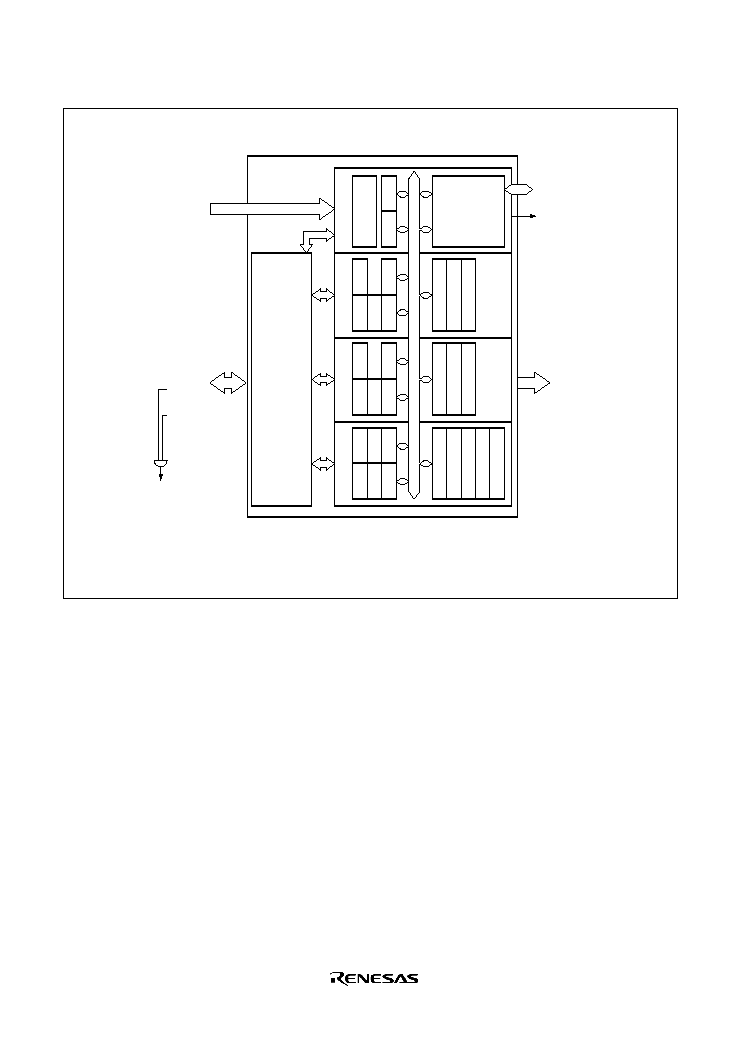
Rev. 1.0, 02/03, page 248 of 634
Channel 2
TMDR
TSR
TCR
TIOR
TIER
TGRA
TCNT
TGRB
TGRC
Channel 1
TMDR
TSR
TCR
TIOR
TIER
TGRA
TCNT
TGRB
Channel 0
Control logic for channel 0 to 2
TGRA
TCNT
TGRB
TGRD
Bus
interface
Common
TSYR
Control logic
TSTR
/1
/4
/16
/64
/256
/1024
TCLKA
TCLKB
TCLKC
TCLKD
Legend
TSTR
TSYR
TCR
TMDR
: Timer start register
: Timer synchro register
: Timer control register
: Timer mode register
: Timer I/O control registers (H, L)
: Timer interrupt enable register
: Timer status register
: TImer general registers (A, B, C, D)
TIOCA0
TIOCB0
TIOCC0
TIOCD0
TIOCA1
TIOCB1
TIOCA2
TIOCB2
Interrupt request signals
Channel 0:
Channel 1:
Channel 2:
Internal data bus
A/D converter convertion
start signal
Module data bus
TGI0A
TGI0B
TGI0C
TGI0D
TCI0V
TGI1A
TGI1B
TCI1V
TCI1U
TGI2A
TGI2B
TCI2V
TCI2U
TMDR
TSR
TCR
TIORH
TIER
TIORL
Input/output pins
SCK0 (to SCI0)
Channel 0:
Channel 1:
Channel 2:
Clock input
Internal clock:
External clock:
TIOR(H, L)
TIER
TSR
TGR(A, B, C, D)
Figure 9.1 Block Diagram of TPU

Rev. 1.0, 02/03, page 249 of 634
Table 9.1
TPU Functions
Item
Channel 0
Channel 1
Channel 2
Count clock
/1
/4
/16
/64
TCLKA
TCLKB
TCLKC
TCLKD
/1
/4
/16
/64
/256
TCLKA
TCLKB
/1
/4
/16
/64
/1024
TCLKA
TCLKB
TCLKC
General registers
TGRA_0
TGRB_0
TGRA_1
TGRB_1
TGRA_2
TGRB_2
General registers/buffer
registers
TGRC_0
TGRC_0
I/O pins
TIOCA0
TIOCB0
TIOCC0
TIOCD0
TIOCA1
TIOCB1
TIOCA2
TIOCB2
Counter clear function
TGR compare match
or input capture
TGR compare match
or input capture
TGR compare match or
input capture
0 output
O
O
O
1 output
O
O
O
Compare
match
output
Toggle
output
O
O
O
Input capture function
O
O
O
Synchronous operation O
O
O
PWM mode
O
O
O
Phase counting mode
O
O
Buffer operation
O

Rev. 1.0, 02/03, page 250 of 634
Item
Channel 0
Channel 1
Channel 2
A/D converter trigger
TGRA_0 compare
match or input capture
TGRA_1 compare
match or input capture
TGRA_2 compare
match or input capture
PPG trigger
TGRA_0/TGRB_0
compare match or input
capture
TGRA_1/TGRB_1
compare match or input
capture
TGRA_2/TGRB_2
compare match or
input capture
Interrupt sources
5 sources
· Compare match or
input capture 0A
· Compare match or
input capture 0B
· Compare match or
input capture 0C
· Compare match or
input capture 0D
· Overflow
4 sources
· Compare match or
input capture 1A
· Compare match or
input capture 1B
· Overflow
· Underflow
4 sources
· Compare match or
input capture 2A
· Compare match or
input capture 2B
· Overflow
· Underflow
Legend
O: Possible
: Not possible

Rev. 1.0, 02/03, page 251 of 634
9.2
Input/Output Pins
Table 9.2
Pin Configuration
Channel
Symbol
I/O
Function
TCLKA
Input
External clock A input pin
(Channel 1 phase counting mode A phase input)
TCLKB
Input
External clock B input pin
(Channel 1 phase counting mode B phase input)
TCLKC
Input
External clock C input pin
(Channel 2 phase counting mode A phase input)
All
TCLKD
Input
External clock D input pin
(Channel 2 phase counting mode B phase input)
TIOCA0
I/O
TGRA_0 input capture input/output compare
output/PWM output pin
TIOCB0
I/O
TGRB_0 input capture input/output compare
output/PWM output pin
TIOCC0
I/O
TGRC_0 input capture input/output compare
output/PWM output pin
0
TIOCD0
I/O
TGRD_0 input capture input/output compare
output/PWM output pin
TIOCA1
I/O
TGRA_1 input capture input/output compare
output/PWM output pin
1
TIOCB1
I/O
TGRB_1 input capture input/output compare
output/PWM output pin
TIOCA2
I/O
TGRA_2 input capture input/output compare
output/PWM output pin
2
TIOCB2
I/O
TGRA_2 input capture input/output compare
output/PWM output pin

Rev. 1.0, 02/03, page 252 of 634
9.3
Register Descriptions
The TPU has the following registers.
· Timer control register_0 (TCR_0)
· Timer mode register_0 (TMDR_0)
· Timer I/O control register H_0 (TIORH_0)
· Timer I/O control register L_0 (TIORL_0)
· Timer interrupt enable register_0 (TIER_0)
· Timer status register_0 (TSR_0)
· Timer counter_0 (TCNT_0)
· Timer general register A_0 (TGRA_0)
· Timer general register B_0 (TGRB_0)
· Timer general register C_0 (TGRC_0)
· Timer general register D_0 (TGRD_0)
· Timer control register_1 (TCR_1)
· Timer mode register_1 (TMDR_1)
· Timer I/O control register _1 (TIOR_1)
· Timer interrupt enable register_1 (TIER_1)
· Timer status register_1 (TSR_1)
· Timer counter_1 (TCNT_1)
· Timer general register A_1 (TGRA_1)
· Timer general register B_1 (TGRB_1)
· Timer control register_2 (TCR_2)
· Timer mode register_2 (TMDR_2)
· Timer I/O control register_2 (TIOR_2)
· Timer interrupt enable register_2 (TIER_2)
· Timer status register_2 (TSR_2)
· Timer counter_2 (TCNT_2)
· Timer general register A_2 (TGRA_2)
· Timer general register B_2 (TGRB_2)
Common Registers
· Timer start register (TSTR)
· Timer synchro register (TSYR)

Rev. 1.0, 02/03, page 253 of 634
9.3.1
Timer Control Register (TCR)
The TCR registers control the TCNT operation for each channel. The TPU has a total of three
TCR registers, one for each channel (channel 0 to 2). TCR register settings should be made only
when TCNT operation is stopped.
Bit
Bit Name Initial value
R/W
Description
7
6
5
CCLR2
CCLR1
CCLR0
0
0
0
R/W
R/W
R/W
Counter Clear 2 to 0
These bits select the TCNTcounter clearing source. See
tables 9.3 and 9.4 for details.
4
3
CKEG1
CKEG0
0
0
R/W
R/W
Clock Edge 1 and 0
These bits select the input clock edge. When the input
clock is counted using both edges, the input clock 1 and
2,
/4 both edges = /2 rising edge). If phase counting
mode is used on channels 1, 2, 4, and 5, this setting is
ignored and the phase counting mode setting has priority.
Internal clock edge selection is valid when the input clock
is
/4 or slower. This setting is ignored if the input clock is
/1, or when overflow/underflow of another channel is
selected.
00: Count at rising edge
01: Count at falling edge
1x: Count at both edges
Legend x: Don't care
2
1
0
TPSC2
TPSC1
TPSC0
0
0
0
R/W
R/W
R/W
Time Prescaler 2 to 0
These bits select the TCNT counter clock. The clock
source can be selected independently for each channel.
See tables 9.5 to 9.7 for details.

Rev. 1.0, 02/03, page 254 of 634
Table 9.3
CCLR2 to CCLR0 (channel 0)
Channel
Bit 7
CCLR2
Bit 6
CCLR1
Bit 5
CCLR0
Description
0
TCNT clearing disabled (Initial value)
0
1
TCNT cleared by TGRA compare
match/input capture
0
TCNT cleared by TGRB compare
match/input capture
0
1
1
TCNT cleared by counter coearing for
another channel performing
synchronous/clearing synchronous
operation*
1
0
TCNT clearing disabled
0
1
TCNT cleared by TGRC compare
match/input capture*
2
0
TCNT cleared by TGRD compare
match/input capture*
2
0, 3
1
1
1
TCNT cleared by counter clearing for
another channel performing synchronous
clearing/synchronous operation*
1
Notes: 1. Synchronous operation setting is performed by setting the SYNC bit in TSYR to 1.
2. When TGRC or TGRD is used as a buffer register. TCNT is not cleared because the
buffer register setting has priority, and compare match/input capture dose not occur.
Table 9.4
CCLR2 to CCLR0 (channels 1 and 2)
Channel
Bit 7
Reserved
*
Bit 6
CCLR1
Bit 5
CCLR0
Description
0
TCNT clearing disabled
0
1
TCNT cleared by TGRA compare
match/input capture
0
TCNT cleared by TGRB compare
match/input capture
1, 2
0
1
1
TCNT cleared by counter clearing for
another channel performing synchronous
clearing/synchronous operation*
1
Notes: 1. Synchronous operation setting is performed by setting the SYNC bit in TSYR to 1.
2. Bit 7 is reserved in channels 1 and 2. It is always read as 0 and cannot be modified.

Rev. 1.0, 02/03, page 255 of 634
Table 9.5
TPSC2 to TPSC0 (channel 0)
Channel
Bit 2
TPSC2
Bit 1
TPSC1
Bit 0
TPSC0
Description
0
Internal clock: counts on
/1
0
1
Internal clock: counts on
/4
0
Internal clock: counts on
/16
0
1
1
Internal clock: counts on
/64
0
External clock: counts on TCLKA pin input
0
1
External clock: counts on TCLKB pin input
0
External clock: counts on TCLKC pin input
1
1
1
1
External clock: counts on TCLKD pin input
Table 9.6
TPSC2 to TPSC0 (channel 1)
Channel
Bit 2
TPSC2
Bit 1
TPSC1
Bit 0
TPSC0
Description
0
Internal clock: counts on
/1
0
1
Internal clock: counts on
/4
0
Internal clock: counts on
/16
0
1
1
Internal clock: counts on
/64
0
External clock: counts on TCLKA pin input
0
1
External clock: counts on TCLKB pin input
0
Internal clock: counts on
/256
1
1
1
1
Counts on TCNT2 overflow/underflow
Note:
This setting is ignored when channel 1 is in phase counting mode.

Rev. 1.0, 02/03, page 256 of 634
Table 9.7
TPSC2 to TPSC0 (channel 2)
Channel
Bit 2
TPSC2
Bit 1
TPSC1
Bit 0
TPSC0
Description
0
Internal clock: counts on
/1
0
1
Internal clock: counts on
/4
0
Internal clock: counts on
/16
0
1
1
Internal clock: counts on
/64
0
External clock: counts on TCLKA pin input
0
1
External clock: counts on TCLKB pin input
0
External clock: counts on TCLKC pin input
2
1
1
1
Internal clock: counts on
/1024
Note:
This setting is ignored when channel 1 is in phase counting mode.
9.3.2
Timer Mode Register (TMDR)
The TMDR registers are used to set the operating mode for each channel. The TPU has three
TMDR registers, one for each channel. TMDR register settings should be made only when TCNT
operation is stopped.
Bit
Bit Name
Initial value
R/W
Description
7, 6
--
All 1
--
Reserved
These bits are always read as 1 and cannot be modified.
5
BFB
0
R/W
Buffer Operation B
Specifies whether TGRB is to operate in the normal way,
or TGRB and TGRD are to be used together for buffer
operation. When TGRD is used as a buffer register.
TGRD input capture/output compare is not generation. In
channels 1 and 2, which have no TGRD, bit 5 is reserved.
It is always read as 0 and cannot be modified.
0: TGRB operates normally
1: TGRB and TGRD used together for buffer operation

Rev. 1.0, 02/03, page 257 of 634
Bit
Bit Name Initial value
R/W
Description
4
BFA
0
R/W
Buffer Operation A
Specifies whether TGRA is to operate in the normal way,
or TGRA and TGRC are to be used together for buffer
operation. When TGRC is used as a buffer register,
TGRC input capture/output compare is not generated. In
channels 1 and 2, which have no TGRC, bit 4 is reserved.
It is always read as 0 and cannot be modified.
0: TGRA operates normally
1: TGRA and TGRC used together for buffer operation
3
2
1
0
MD3
MD2
MD1
MD0
0
0
0
0
R/W
R/W
R/W
R/W
Modes 3 to 0
These bits are used to set the timer operating mode.
MD3 is a reserved bit. In a write, the write value should
always be 0. See table 9.8, MD3 to MD0 for details.
Table 9.8
MD3 to MD0
Bit 3
MD3
*
1
Bit2
MD2
*
2
Bit 1
MD1
Bit 0
MD0
Description
0
Normal operation
0
1
Reserved
0
PWM mode 1
0
1
1
PWM mode 2
0
Phase counting mode 1
0
1
Phase counting mode 2
0
Phase counting mode 3
0
1
1
1
Phase counting mode 4
1
×
×
×
--
Legend x: Don't care
Notes: 1. MD3 is reserved bit. In a write, it should be written with 0.
2. Phase counting mode cannot be set for channels 0 and 3. In this case, 0 should always
be written to MD2.

Rev. 1.0, 02/03, page 258 of 634
9.3.3
Timer I/O Control Register (TIOR)
The TIOR registers control the TGR registers. The TPU has eight TIOR registers, two each for
channels 0, and one each for channels 1 and 2. Care is required since TIOR is affected by the
TMDR setting. The initial output specified by TIOR is valid when the counter is stopped (the CST
bit in TSTR is cleared to 0). Note also that, in PWM mode 2, the output at the point at which the
counter is cleared to 0 is specified. When TGRC or TGRD is designated for buffer operation, this
setting is invalid and the register operates as a buffer register.
·
·
·
· TIORH_0, TIOR_1, TIOR_2
Bit
Bit Name Initial value
R/W
Description
7
6
5
4
IOB3
IOB2
IOB1
IOB0
0
0
0
0
R/W
R/W
R/W
R/W
I/O Control B3 to B0
Specify the function of TGRB.
3
2
1
0
IOA3
IOA2
IOA1
IOA0
0
0
0
0
R/W
R/W
R/W
R/W
I/O Control A3 to A0
Specify the function of TGRA.
·
·
·
· TIORL_0
Bit
Bit Name Initial value
R/W
Description
7
6
5
4
IOD3
IOD2
IOD1
IOD0
0
0
0
0
R/W
R/W
R/W
R/W
I/O Control D3 to D0
Specify the function of TGRD.
3
2
1
0
IOC3
IOC2
IOC1
IOC0
0
0
0
0
R/W
R/W
R/W
R/W
I/O Control C3 to C0
Specify the function of TGRC.

Rev. 1.0, 02/03, page 259 of 634
Table 9.9
TIORH_0 (channel 0)
Description
Bit 7
IOB3
Bit 6
IOB2
Bit 5
IOB1
Bit 4
IOB0
TGRB_0
Function
TIOCB0 Pin Function
0
Output disabled
0
1
Initial output is 0 output
0 output at compare match
0
Initial output is 0 output
1 output at compare match
0
1
1
Initial output is 0 output
Toggle output at compare match
0
Output disabled
0
1
Initial output is 1 output
0 output at compare match
0
Initial output is 1 output
1 output at compare match
0
1
1
1
Output
compare
register
Initial output is 1 output
Toggle output at compare match
0
Capture input source is TIOCB0 pin
Input capture at rising edge
0
1
Capture input source is TIOCB0 pin
Input capture at falling edge
0
1
×
Capture input source is TIOCB0 pin
Input capture at both edges
1
1
×
×
Input capture
register
Setting prohibited
Legend x : Don't care

Rev. 1.0, 02/03, page 260 of 634
Table 9.10
TIORH_0 (channel 0)
Description
Bit 3
IOA3
Bit 2
IOA2
Bit 1
IOA1
Bit 0
IOA0
TGRA_0
Function
TIOCA0 Pin Function
0
Output disabled
0
1
Initial output is 0 output
0 output at compare match
0
Initial output is 0 output
1 output at compare match
0
1
1
Initial output is 0 output
Toggle output at compare match
0
Output disabled
0
1
Initial output is 1 output
0 output at compare match
0
Initial output is 1 output
1 output at compare match
0
1
1
1
Output
compare
register
Initial output is 1 output
Toggle output at compare match
0
Capture input source is TIOCA0 pin
Input capture at rising edge
0
1
Capture input source is TIOCA0 pin
Input capture at falling edge
0
1
×
Capture input source is TIOCA0 pin
Input capture at both edges
1
1
×
×
Input capture
register
Setting prohibited
Legend x : Don't care

Rev. 1.0, 02/03, page 261 of 634
Table 9.11
TIORL_0 (channel 0)
Description
Bit 7
IOD3
Bit 6
IOD2
Bit 5
IOD1
Bit 4
IOD0
TGRA_0
Function
TIOCD0 Pin Function
0
Output disabled
0
1
Initial output is 0 output
0 output at compare match
0
Initial output is 0 output
1 output at compare match
0
1
1
Initial output is 0 output
Toggle output at compare match
0
Output disabled
0
1
Initial output is 1 output
0 output at compare match
0
Initial output is 1 output
0
1
1
1
Output
Compare
register*
Initial output is 1 output
Toggle output at compare match
0
Capture input source is TIOCD0 pin
Input capture at rising edge
0
1
Capture input source is TIOCD0 pin
Input capture at falling edge
0
1
×
Capture input source is TIOCD0 pin
Input capture at both edges
1
1
×
×
Input capture
register*
Setting prohibited
Legend x: Don't care
Note: When the BFB bit in TMDR_0 is set to 1 and TGRD_0 is used as a buffer register, this
setting is invalid and input capture/output compare is not generated.

Rev. 1.0, 02/03, page 262 of 634
Table 9.12
TIORL_0 (channel 0)
Description
Bit 3
IOC3
Bit 2
IOC2
Bit 1
IOC1
Bit 1
IOC0
TGRC_0
Function
TIOCA0 Pin Function
0
Output disabled
0
1
Initial output is 0 output
0 output at compare match
0
Initial output is 0 output
1 output at compare match
0
1
1
Initial output is 0 output
Toggle output at compare match
0
Output disabled
0
1
Initial output is 1 output
0 output at compare match
0
Initial output is 1 output
1 output at compare match
0
1
1
1
Output
compare
register
Initial output is 1 output
Toggle output at compare match
0
Capture input source is TIOCA0 pin
Input capture at rising edge
0
1
Capture input source is TIOCA0 pin
Input capture at falling edge
0
1
×
Capture input source is TIOCA0 pin
Input capture at both edges
1
1
×
×
Input capture
register
Setting prohibited
Legend x : Don't care
Note: * When the BFA bit in TMDR_0 is set to 1and TGRC_0 is used as a buffer register, this
setting is invalid and input capture/output compare is not generated.

Rev. 1.0, 02/03, page 263 of 634
Table 9.13
TIOR_1 (channel 1)
Description
Bit 7
IOB3
Bit 6
IOB2
Bit 5
IOB1
Bit 4
IOB0
TGRB_1
Function
TIOCB1 Pin Function
0
Output disabled
0
1
Initial output is 0 output
0 output at compare match
0
Initial output is 0 output
1 output at compare match
0
1
1
Initial output is 0 output
Toggle output at compare match
0
Output disabled
0
1
Initial output is 1 output
0 output at compare match
0
Initial output is 1 output
1 output at compare match
0
1
1
1
Output
compare
register
Initial output is 1 output
Toggle output at compare match
0
Capture input source is TIOCB1 pin
Input capture at rising edge
0
1
Capture input source is TIOCB1 pin
Input capture at falling edge
0
1
×
Capture input source is TIOCB1 pin
Input capture at both edges
1
1
×
×
Input capture
register
Setting prohibited
Legend x : Don't care

Rev. 1.0, 02/03, page 264 of 634
Table 9.14
TIOR_1 (channel 1)
Description
Bit 3
IOA3
Bit 2
IOA2
Bit 1
IOA1
Bit 0
IOA0
TGRA_1
Function
TIOCA0 Pin Function
0
Output disabled
0
1
Initial output is 0 output
0 output at compare match
0
Initial output is 0 output
1 output at compare match
0
1
1
Initial output is 0 output
Toggle output at compare match
0
Output disabled
0
1
Initial output is 1 output
0 output at compare match
0
Initial output is 1 output
1 output at compare match
0
1
1
1
Output
compare
register
Initial output is 1 output
Toggle output at compare match
0
Capture input source is TIOCA0 pin
Input capture at rising edge
0
1
Capture input source is TIOCA0 pin
Input capture at falling edge
0
1
×
Capture input source is TIOCA0 pin
Input capture at both edges
1
1
×
×
Input capture
register
Setting prohibited
Legend
× : Don't care

Rev. 1.0, 02/03, page 265 of 634
Table 9.15
TIOR_2 (channel 2)
Description
Bit 7
IOB3
Bit 6
IOB2
Bit 5
IOB1
Bit 4
IOB0
TGRB_2
Function
TIOCB2 Pin Function
0
Output disabled
0
1
Initial output is 0 output
0 output at compare match
0
Initial output is 0 output
1 output at compare match
0
1
1
Initial output is 0 output
Toggle output at compare match
0
Output disabled
0
1
Initial output is 1 output
0 output at compare match
0
Initial output is 1 output
1 output at compare match
0
1
1
1
Output
compare
register
Initial output is 1 output
Toggle output at compare match
0
Capture input source is TIOCB2 pin
Input capture at rising edge
0
1
Capture input source is TIOCB2 pin
Input capture at falling edge
1
×
1
×
Input capture
register
Capture input source is TIOCB2 pin
Input capture at both edges
Legend x : Don't care

Rev. 1.0, 02/03, page 266 of 634
Table 9.16
TIOR_2 (channel 2)
Description
Bit 3
IOA3
Bit 2
IOA2
Bit 1
IOA1
Bit 0
IOA0
TGRA_2
Function
TIOCA2 Pin Function
0
Output disabled
0
1
Initial output is 0 output
0 output at compare match
0
Initial output is 0 output
1 output at compare match
0
1
1
Initial output is 0 output
Toggle output at compare match
0
Output disabled
0
1
Initial output is 1 output
0 output at compare match
0
Initial output is 1 output
1 output at compare match
0
1
1
1
Output
compare
register
Initial output is 1 output
Toggle output at compare match
0
Capture input source is TIOCA2 pin
Input capture at rising edge
0
1
Capture input source is TIOCA2 pin
Input capture at falling edge
1
×
1
×
Input capture
register
Capture input source is TIOCA2 pin
Input capture at both edges
Legend x : Don't care

Rev. 1.0, 02/03, page 267 of 634
9.3.4
Timer Interrupt Enable Register (TIER)
The TIER registers control enabling or disabling of interrupt requests for each channel. The TPU
has three TIER registers, one for each channel.
Bit
Bit Name Initial value
R/W
Description
7
TTGE
0
R/W
A/D Conversion Start Request Enable
Enables or disables generation of A/D conversion start
requests by TGRA input capture/compare match.
0: A/D conversion start request generation disabled
1: A/D conversion start request generation enabled
6
1
Reserved
This bit is always read as 1 and cannot be modified.
5
TCIEU
0
R/W
Underflow Interrupt Enable
Enables or disables interrupt requests (TCU) by the TCFU
flag when the TCFU flag in TSR is set to 1 in channels 1
and 2. In channel 0, bit 5 is reserved.
0: Interrupt requests (TCIU) by TCFU disabled
1: Interrupt requests (TCIU) by TCFU enabled
4
TCIEV
0
R/W
Overflow Interrupt Enable
Enables or disables interrupt requests (TCIV) by the
TCFV flag when the TCFV flag in TSR is set to 1.
0: Interrupt requests (TCIV) by TCFV disabled
1: Interrupt requests (TCIV) by TCFV enabled
3
TGIED
0
R/W
TGR Interrupt Enable D
Enables or disables interrupt requests (TGID) by the
TGFD bit when the TGFD bit in TSR is set to 1 in channel
0. In channels 1 and 2, bit 3 is reserved. It is always read
as 0 and cannot be modified.
0: Interrupt requests (TGID) by TGFD disabled
1: Interrupt requests (TGID) by TGFD enabled.
2
TGIEC
0
R/W
TGR Interrupt Enable C
Enables or disables interrupt requests (TGIC) by the
TGFC bit when the TGFC bit in TSR is set to 1 in channel
0. In channels 1 and 2, bit 2 is reserved. It is always read
as 0 and cannot be modified.
0: Interrupt requests (TGIC) by TGFC disabled
1: Interrupt requests (TGIC) by TGFC enabled

Rev. 1.0, 02/03, page 268 of 634
Bit
Bit Name Initial value
R/W
Description
1
TGIEB
0
R/W
TGR Interrupt Enable B
Enables or disables interrupt requests (TGIB) by the
TGFB bit when the TGFB bit in TSR is set to 1.
0: Interrupt requests (TGIB) by TGFB disabled
1: Interrupt requests (TGIB) by TGFB enabled
0
TGIEA
0
R/W
TGR Interrupt Enable A
Enables or disables interrupt requests (TGIA) by the
TGFA bit when the TGFA bit in TSR is set to 1.
0: Interrupt requests (TGIA) by TGFA disabled
1: Interrupt requests (TGIA) by TGFA enabled
9.3.5
Timer Status Register (TSR)
The TSR registers indicate the status of each channel. The TPU has three TSR registers, one for
each channel.
Bit
Bit Name Initial value
R/W
Description
7
TCFD
1
R
Count Direction Flag
Status flag that shows the direction in which TCNT counts
in channel 1 and 2. In channel 0, bit 7 is reserved. It is
always read as 0 and cannot be modified.
0: TCNT counts down
1: TCNT counts up
6
1
Reserved
This bit is always read as 1 and cannot be modified.
5
TCFU
0
R/(W)* Underflow Flag
Status flag that indicates that TCNT underflow has
occurred when channels 1 and 2 are set to phase
counting mode. The write value should always be 0 to
clear this flag. In channel 0, bit 5 is reserved.
[Setting condition]
When the TCNT value underflows (change from H'0000
to H'FFFF)
[Clearing condition]
When 0 is written to TCFU after reading TCFU = 1

Rev. 1.0, 02/03, page 269 of 634
Bit
Bit Name Initial value
R/W
Description
4
TCFV
0
R/(W)* Overflow Flag
Status flag that indicates that TCNT overflow has
occurred. The write value should always be 0 to clear this
flag.
[Setting condition]
When the TCNT value overflows (change from H'FFFF
to H'0000)
[Clearing condition]
When 0 is written to TCFV after reading TCFV = 1
3
TGFD
0
R/(W)* Input Capture/Output Compare Flag D
Status flag that indicates the occurrence of TGRD input
capture or compare match in channel 0. The write value
should always be 0 to clear this flag. In channels 1 and 2,
bit 3 is reserved. It is always read as 0 and cannot be
modified.
[Setting conditions]
· When TCNT = TGRD while TGRD is functioning as
output compare register
· When TCNT value is transferred to TGRD by input
capture signal while TGRD is functioning as input
capture register
[Clearing condition]
· When 0 is written to TGFD after reading TGFD = 1
2
TGFC
0
R/(W)* Input Capture/Output Compare Flag C
Status flag that indicates the occurrence of TGRC input
capture or compare match in channel 0. The write value
should always be 0 to clear this flag. In channels 1 and 2,
bit 2 is reserved. It is always read as 0 and cannot be
modified.
[Setting conditions]
· When the TCNT = TGRC while TGRC is functioning
as output compare register
· When TCNT value is transferred to TGRC by input
capture signal while TGRC is functioning as input
capture register
[Clearing condition]
· When 0 is written to TGFC after reading TGFC = 1

Rev. 1.0, 02/03, page 270 of 634
Bit
Bit Name Initial value
R/W
Description
1
TGFB
0
R/(W)* Input Capture/Output Compare Flag B
Status flag that indicates the occurrence of TGRB input
capture or compare match. The write value should always
be 0 to clear this flag.
[Setting conditions]
· When TCNT = TGRB while TGRB is functioning as
output compare register
· When TCNT value is transferred to TGRB by input
capture signal while TGRB is functioning as input
capture register
[Clearing condition]
· When 0 is written to TGFB after reading TGFB = 1
0
TGFA
0
R/(W)* Input Capture/Output Compare Flag A
Status flag that indicates the occurrence of TGRA input
capture or compare match. The write value should always
be 0 to clear this flag.
[Setting conditions]
· When TCNT = TGRA while TGRA is functioning as
output compare register
· When TCNT value is transferred to TGRA by input
capture signal while TGRA is functioning as input
capture register
[Clearing conditions]
· When DMAC is activated by TGIA interrupt while DTA
bit of DMABCR in DMAC is 1
· When 0 is written to TGFA after reading TGFA = 1
Note:
*
Only 0 can be written to clear the flags.

Rev. 1.0, 02/03, page 271 of 634
9.3.6
Timer Counter (TCNT)
The TCNT registers are 16-bit counters. The TPU has three TCNT counters, one for each channel.
The TCNT counters are initialized to H'0000 by a reset, and in hardware standby mode. The
TCNT counters cannot be accessed in 8-bit units; they must always be accessed as a 16-bit unit.
9.3.7
Timer General Register (TGR)
The TGR registers are 16-bit registers with a dual function as output compare and input capture
registers. The TPU has 16 TGR registers, four each for channel 0 and two each for channels 1 and
2. TGRC and TGRD for channel 0 can also be designated for operation as buffer registers. The
TGR registers cannot be accessed in 8-bit units; they must always be accessed as a 16-bit unit.
TGR buffer register combinations are TGRA--TGRC and TGRB--TGRD.
9.3.8
Timer Start Register (TSTR)
TSTR is an 8-bit readable/writable register that selects operation/stoppage for channels 0 to 2.
When setting the operating mode in TMDR or setting the count clock in TCR, first stop the TCNT
counter.
Bit
Bit Name Initial Value
R/W
Description
7 to
3
0
Reserved
The write value should always be 0.
2
1
0
CST2
CST1
CST0
0
0
0
R/W
R/W
R/W
Counter Start 2 to 0 (CST2 to CST0)
These bits select operation or stoppage for TCNT.
If 0 is written to the CST bit during operation with the
TIOC pin designated for output, the counter stops but the
TIOC pin output compare output level is retained.
If TIOR is written to when the CST bit is cleared to 0, the
pin output level will be changed to the set initial output
value.
0: TCNT_2 to TCNT_0 count operation is stopped
1: TCNT_2 to TCNT_0 performs count operation

Rev. 1.0, 02/03, page 272 of 634
9.3.9
Timer Synchro Register (TSYR)
TSYR selects independent operation or synchronous operation for the channel 0 to 2 TCNT
counters. A channel performs synchronous operation when the corresponding bit in TSYR is set to
1.
Bit
Bit Name Initial Value
R/W
Description
7 to
3
0
Reserved
The write value should always be 0.
2
1
0
SYNC2
SYNC 1
SYNC 0
0
0
0
R/W
R/W
R/W
Timer Synchro 2 to 0
These bits select whether operation is independent of or
synchronized with other channels.
When synchronous operation is selected, synchronous
presetting of multiple channels, and synchronous clearing
through counter clearing on another channel are possible.
To set synchronous operation, the SYNC bits for at least
two channels must be set to 1. To set synchronous
clearing, in addition to the SYNC bit, the TCNT clearing
source must also be set by means of bits CCLR2 to
CCLR0 in TCR.
0: TCNT_2 to TCNT_0 operates independently
(TCNT presetting /clearing is unrelated to other
channels)
1: TCNT_2 to TCNT_0 performs synchronous operation
TCNT synchronous presetting/synchronous clearing is
possible
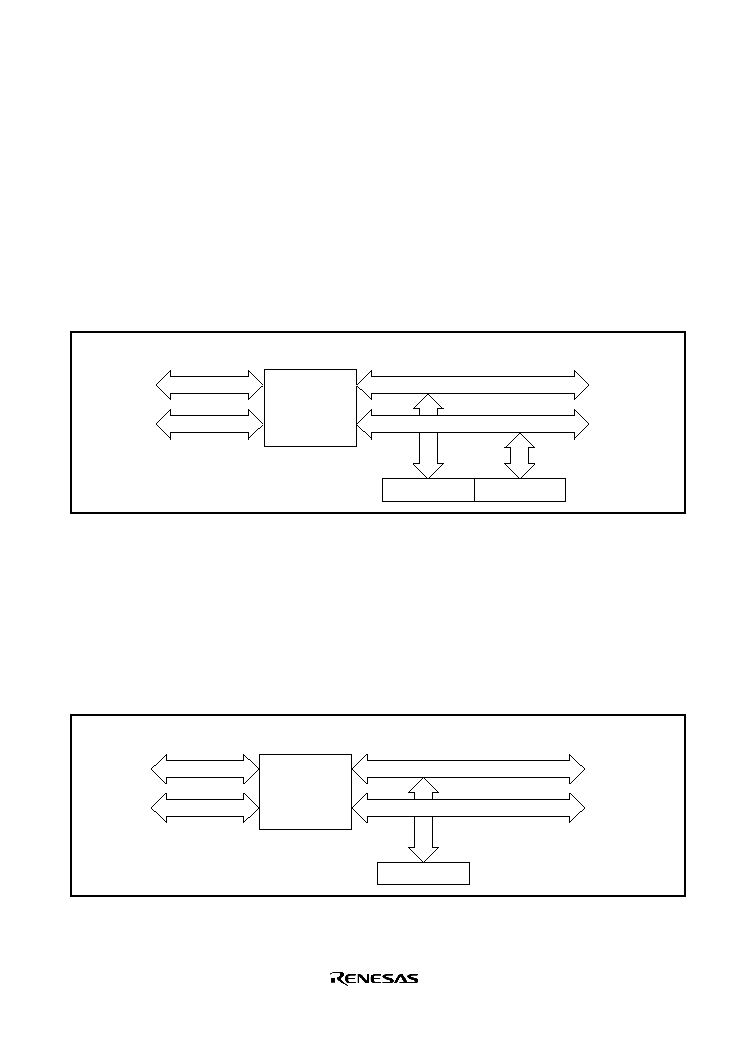
Rev. 1.0, 02/03, page 273 of 634
9.4
Interface to Bus Master
9.4.1
16-Bit Registers
TCNT and TGR are 16-bit registers. As the data bus to the bus master is 16 bits wide, these
registers can be read and written to in 16-bit units.
These registers cannot be read from or written to in 8-bit units; 16-bit access must always be used.
An example of 16-bit register access operation is shown in figure 9.2.
H
L
TCNTH
TCNTL
Internal data bus
Bus interface
Module
data bus
Bus
master
Figure 9.2 16-Bit Register Access Operation [Bus Master
TCNT (16 Bits)]
9.4.2
8-Bit Registers
Registers other than TCNT and TGR are 8-bit. As the data bus to the CPU is 16 bits wide, these
registers can be read and written to in 16-bit units. They can also be read and written to in 8-bit
units.
Examples of 8-bit register access operation are shown in figures 9.3, 9.4, and 9.5.
H
L
TCR
Internal data bus
Bus interface
Module
data bus
Bus
master
Figure 9.3 8-Bit Register Access Operation [Bus Master
TCR (Upper 8 Bits)]
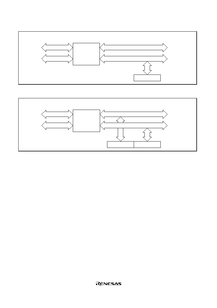
Rev. 1.0, 02/03, page 274 of 634
H
L
TMDR
Internal data bus
Bus interface
Module
data bus
Bus
master
Figure 9.4 8-Bit Register Access Operation [Bus Master
TMDR (Lower 8 Bits)]
H
L
TCR
TMDR
Internal data bus
Bus interface
Module
data bus
Bus
master
Figure 9.5 8-Bit Register Access Operation [Bus Master
TCR and TMDR (16 Bits)]
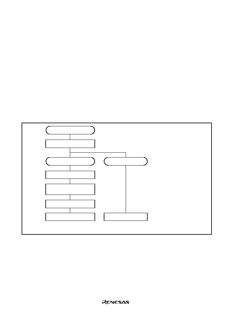
Rev. 1.0, 02/03, page 275 of 634
9.5
Operation
9.5.1
Basic Functions
Each channel has a TCNT and TGR. TCNT performs up-counting, and is also capable of free-
running operation, synchronous counting, and external event counting. Each TGR can be used as
an input capture register or output compare register.
Counter Operation: When one of bits CST0 to CST2 is set to 1 in TSTR, the TCNT counter for
the corresponding channel starts counting. TCNT can operate as a free-running counter, periodic
counter, and so on.
1. Example of count operation setting procedure Figure 9.6 shows an example of the count
operation setting procedure.
Operation selection
Select counter clock
Periodic counter
Select counter clearing source
Select output compare register
Set period
Free-running counter
Start count operation
<Free-running counter>
<Periodic counter>
Start count operation
Select the counter
clock with bits
TPSC2 to TPSC0 in
TCR. At the same
time, select the
input clock edge
with bits CKEG1
and CKEG0 in TCR.
For periodic counter
operation, select the
TGR to be used as
the TCNT clearing
source with bits
CCLR2 to CCLR0 in
TCR.
Designate the TGR
selected in [2] as an
output compare
register by means of
TIOR.
Set the periodic
counter cycle in the
TGR selected in [2].
Set the CST bit in
TSTR to 1 to start
the counter
operation.
[1]
[1]
[2]
[2]
[3]
[3]
[4]
[4]
[5]
[5]
Figure 9.6 Example of Counter Operation Setting Procedure
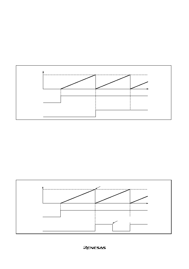
Rev. 1.0, 02/03, page 276 of 634
2. Free-running count operation and periodic count operation
Immediately after a reset, the TPU's TCNT counters are all designated as free-running
counters. When the relevant bit in TSTR is set to 1 the corresponding TCNT counter starts up-
count operation as a free-running counter. When TCNT overflows (from H'FFFF to H'0000),
the TCFV bit in TSR is set to 1. If the value of the corresponding TCIEV bit in TIER is 1 at
this point, the TPU requests an interrupt. After overflow, TCNT starts counting up again from
H'0000. Figure 9.7 illustrates free-running counter operation.
TCNT value
H'FFFF
H'0000
CST bit
TCFV
Time
Figure 9.7 Free-Running Counter Operation
When compare match is selected as the TCNT clearing source, the TCNT counter for the
relevant channel performs periodic count operation. The TGR register for setting the period is
designated as an output compare register, and counter clearing by compare match is selected
by means of bits CCLR2 to CCLR0 in TCR. After the settings have been made, TCNT starts
up-count operation as periodic counter when the corresponding bit in TSTR is set to 1. When
the count value matches the value in TGR, the TGF bit in TSR is set to 1 and TCNT is cleared
to H'0000. If the value of the corresponding TGIE bit in TIER is 1 at this point, the TPU
requests an interrupt. After a compare match, TCNT starts counting up again from H'0000.
Figure 9.8 illustrates periodic counter operation.
TCNT value
TGR
H'0000
CST bit
TGF
Time
Counter cleared by TGR
compare match
Flag cleared by software or
DMAC activation
Figure 9.8 Periodic Counter Operation
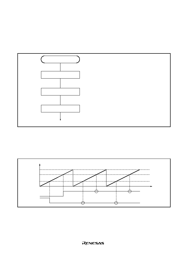
Rev. 1.0, 02/03, page 277 of 634
Waveform Output by Compare Match: The TPU can perform 0, 1, or toggle output from the
corresponding output pin using compare match.
1. Example of setting procedure for waveform output by compare match
Figure 9.9 shows an example of the setting procedure for waveform output by compare match.
Output selection
Select waveform output mode
Set output timing
Start count operation
<Waveform output>
Select initial value 0 output or 1 output, and
compare match output value 0 output, 1 output,
or toggle output, by means of TIOR. The set
initial value is output at the TIOC pin unit the
first compare match occurs.
Set the timing for compare match generation in
TGR.
Set the CST bit in TSTR to 1 to start the count
operation.
[1]
[1]
[2]
[2]
[3]
[3]
Figure 9.9 Example of Setting Procedure for Waveform Output by Compare Match
2. Examples of waveform output operation Figure 9.10 shows an example of 0 output/1 output. In
this example TCNT has been designated as a free-running counter, and settings have been
made so that 1 is output by compare match A, and 0 is output by compare match B. When the
set level and the pin level coincide, the pin level does not change.
TCNT value
H'FFFF
H'0000
TIOCA
TIOCB
Time
TGRA
TGRB
No change
No change
No change
No change
1 output
0 output
Figure 9.10 Example of 0 Output/1 Output Operation
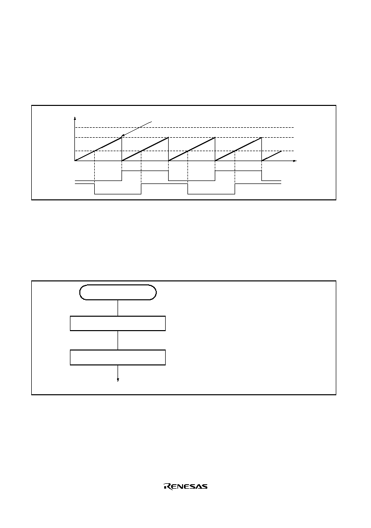
Rev. 1.0, 02/03, page 278 of 634
Figure 9.11 shows an example of toggle output.
In this example TCNT has been designated as a periodic counter (with counter clearing
performed by compare match B), and settings have been made so that output is toggled by both
compare match A and compare match B.
TCNT value
H'FFFF
H'0000
TIOCB
TIOCA
Time
TGRB
TGRA
Toggle output
Toggle output
Counter cleared by TGRB compare match
Figure 9.11 Example of Toggle Output Operation
Input Capture Function: The TCNT value can be transferred to TGR on detection of the TIOC
pin input edge. Rising edge, falling edge, or both edges can be selected as the detected
edge.
1. Example of input capture operation setting procedure Figure 9.12 shows an example of the
input capture operation setting procedure.
Input selection
Select input capture input
Start count
<Input capture operation>
Designate TGR as an input capture register by
means of TIOR, and select rising edge, falling
edge, or both edges as the input capture source
and input signal edge.
Set the CST bit in TSTR to 1 to start the count
operation.
[1]
[2]
[1]
[2]
Figure 9.12 Example of Input Capture Operation Setting Procedure
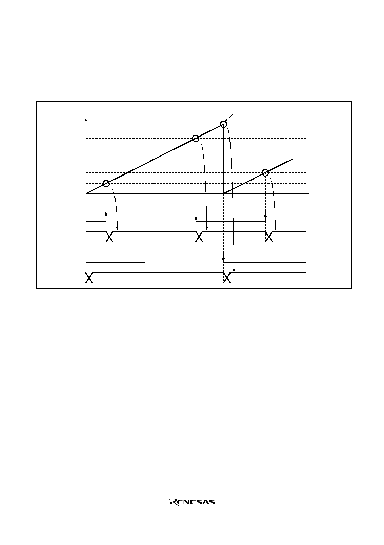
Rev. 1.0, 02/03, page 279 of 634
2. Example of input capture operation Figure 9.13 shows an example of input capture operation.
In this example both rising and falling edges have been selected as the TIOCA pin input
capture input edge, falling edge has been selected as the TIOCB pin input capture input edge,
and counter clearing by TGRB input capture has been designated for TCNT.
TCNT value
H'0180
H'0000
TIOCA
TGRA
H'0010
H'0005
Counter cleared by TIOCB
input (falling edge)
H'0160
H'0005
H'0160
H'0010
TGRB
H'0180
TIOCB
Time
Figure 9.13 Example of Input Capture Operation
9.5.2
Synchronous Operation
In synchronous operation, the values in a number of TCNT counters can be rewritten
simultaneously (synchronous presetting). Also, a number of TCNT counters can be cleared
simultaneously by making the appropriate setting in TCR (synchronous clearing). Synchronous
operation enables TGR to be incremented with respect to a single time base. Channels 0 to 2 can
all be designated for synchronous operation.
Example of Synchronous Operation Setting Procedure: Figure 9.14 shows an example of the
synchronous operation setting procedure.
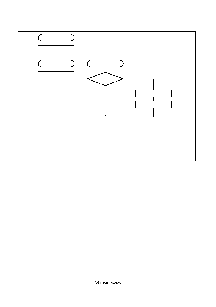
Rev. 1.0, 02/03, page 280 of 634
No
Yes
Synchronous operation
selection
Set synchronous
operation
Synchronous presetting
Set TCNT
<Synchronous presetting>
<Counter clearing>
<Synchronous clearing>
Synchronous clearing
Clearing
source generation
channel?
Select counter
clearing source
Start count
Set synchronous
counter clearing
Start count
Set to 1 the SYNC bits in TSYR corresponding to the channels to be designated for synchronous
operation.
When the TCNT counter of any of the channels designated for synchronous operation is
written to, the same value is simultaneously written to the other TCNT counters.
Use bits CCLR2 to CCLR0 in TCR to specify TCNT clearing by input capture/output compare,
etc.
Use bits CCLR2 to CCLR0 in TCR to designate synchronous clearing for the counter clearing
source.
Set to 1 the CST bits in TSTR for the relevant channels, to start the count operation.
[1]
[2]
[3]
[4]
[5]
[1]
[3]
[4]
[4]
[5]
[2]
Figure 9.14 Example of Synchronous Operation Setting Procedure
Example of Synchronous Operation: Figure 9.15 shows an example of synchronous operation.
In this example, synchronous operation and PWM mode 1 have been designated for channels 0 to
2, TGRB_0 compare match has been set as the channel 0 counter clearing source, and
synchronous clearing has been set for the channel 1 and 2 counter clearing source. Three-phase
PWM waveforms are output from pins TIOC0A, TIOC1A, and TIOC2A. At this time,
synchronous presetting, and synchronous clearing by TGRB_0 compare match, is performed for
channel 0 to 2 TCNT counters, and the data set in TGRB_0 is used as the PWM cycle. For details
of PWM modes, see section 9.5.4, PWM Modes.
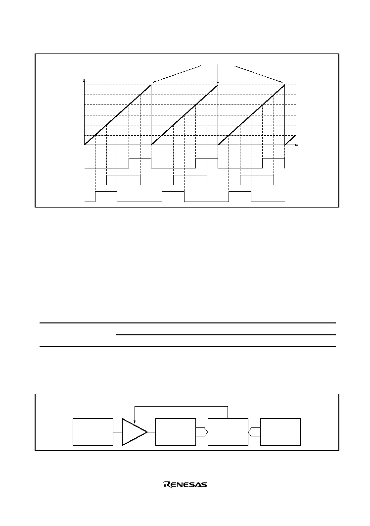
Rev. 1.0, 02/03, page 281 of 634
TCNT0 to TCNT2 values
H'0000
TIOCA_0
TIOCA_1
TGRB_0
Synchronous clearing by TGRB_0 compare match
TGRA_2
TGRA_1
TGRB_2
TGRA_0
TGRB_1
TIOCA_2
Time
Figure 9.15 Example of Synchronous Operation
9.5.3
Buffer Operation
Buffer operation, provided for channels 0 and 3, enables TGRC and TGRD to be used as buffer
registers. Buffer operation differs depending on whether TGR has been designated as an input
capture register or as a compare match register. Table 9.17 shows the register combinations used
in buffer operation.
Table 9.17
Register Combinations in Buffer Operation
Channel
Timer General Register
Buffer Register
0
TGRA_0
TGRC_0
TGRB_0
TGRD_0
· When TGR is an output compare register
When a compare match occurs, the value in the buffer register for the corresponding channel is
transferred to the timer general register. This operation is illustrated in figure 9.16.
Buffer register
Timer general
register
TCNT
Comparator
Compare match signal
Figure 9.16 Compare Match Buffer Operation
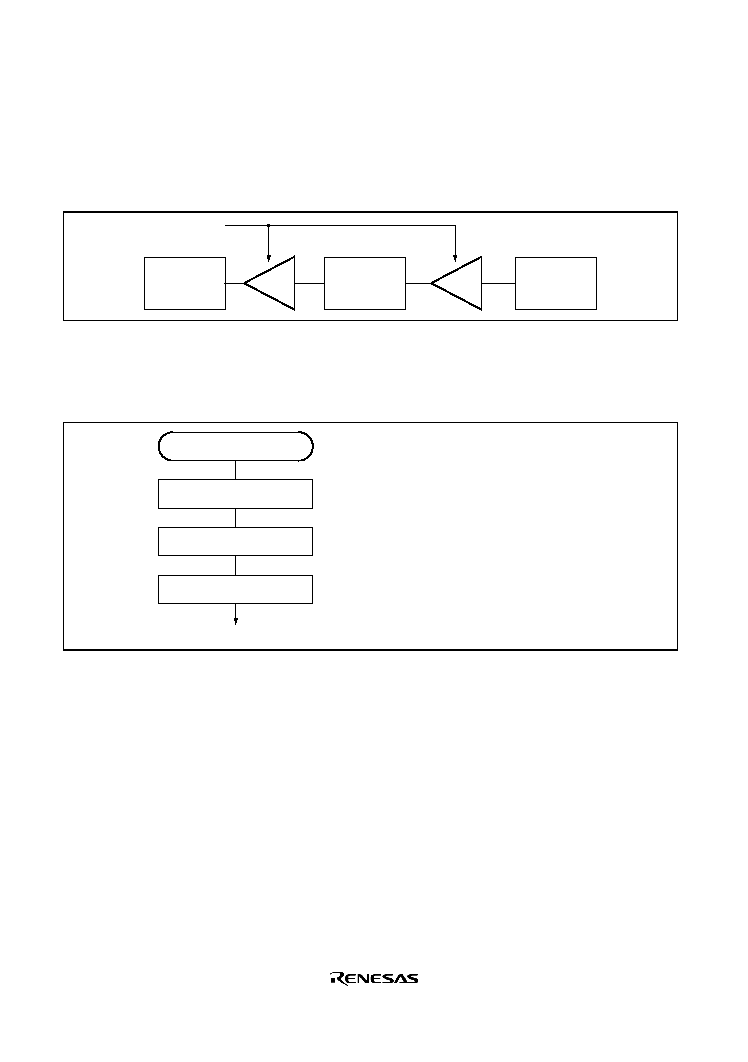
Rev. 1.0, 02/03, page 282 of 634
· When TGR is an input capture register
When input capture occurs, the value in TCNT is transferred to TGR and the value previously
held in the timer general register is transferred to the buffer register. This operation is
illustrated in figure 9.17.
Buffer register
Timer general
register
TCNT
Input capture
signal
Figure 9.17 Input Capture Buffer Operation
Example of Buffer Operation Setting Procedure: Figure 9.18 shows an example of the buffer
operation setting procedure.
Buffer operation
Select TGR function
Set buffer operation
Start count
<Buffer operation>
[1]
[2]
[3]
[1]
[2]
[3]
Designate TGR as an input capture register or
output compare register by means of TIOR.
Designate TGR for buffer operation with bits
BFA and BFB in TMDR.
Set the CST bit in TSTR to 1 start the count
operation.
Figure 9.18 Example of Buffer Operation Setting Procedure
Examples of Buffer Operation
1. When TGR is an output compare register
Figure 9.19 shows an operation example in which PWM mode 1 has been designated for
channel 0, and buffer operation has been designated for TGRA and TGRC. The settings used
in this example are TCNT clearing by compare match B, 1 output at compare match A, and 0
output at compare match B. As buffer operation has been set, when compare match A occurs
the output changes and the value in buffer register TGRC is simultaneously transferred to timer
general register TGRA. This operation is repeated each time compare match A occurs. For
details of PWM modes, see section 9.5.4, PWM Modes.
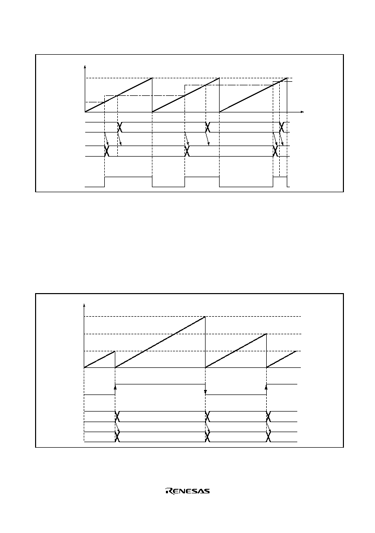
Rev. 1.0, 02/03, page 283 of 634
TCNT value
TGRB_0
H'0000
TGRC_0
TGRA_0
H'0200
H'0520
TIOCA
H'0200
H'0450
H'0520
H'0450
TGRA_0
H'0450
H'0200
Transfer
Time
Figure 9.19 Example of Buffer Operation (1)
2. When TGR is an input capture register
Figure 9.20 shows an operation example in which TGRA has been designated as an input
capture register, and buffer operation has been designated for TGRA and TGRC. Counter
clearing by TGRA input capture has been set for TCNT, and both rising and falling edges have
been selected as the TIOCA pin input capture input edge. As buffer operation has been set,
when the TCNT value is stored in TGRA upon occurrence of input capture A, the value
previously stored in TGRA is simultaneously transferred to TGRC.
TCNT value
H'09FB
H'0000
TGRC
Time
H'0532
TIOCA
TGRA
H'0F07
H'0532
H'0F07
H'0532
H'0F07
H'09FB
Figure 9.20 Example of Buffer Operation (2)

Rev. 1.0, 02/03, page 284 of 634
9.5.4
PWM Modes
In PWM mode, PWM waveforms are output from the output pins. 0, 1, or toggle output can be
selected as the output level in response to compare match of each TGR. Settings of TGR registers
can output a PWM waveform in the range of 0 % to 100 % duty. Designating TGR compare match
as the counter clearing source enables the period to be set in that register. All channels can be
designated for PWM mode independently. Synchronous operation is also possible. There are two
PWM modes, as described below.
· PWM mode 1
PWM output is generated from the TIOCA and TIOCC pins by pairing TGRA with TGRB and
TGRC with TGRD. The output specified by bits IOA3 to IOA0 and IOC3 to IOC0 in TIOR is
output from the TIOCA and TIOCC pins at compare matches A and C, and the output
specified by bits IOB3 to IOB0 and IOD3 to IOD0 in TIOR is output at compare matches B
and D. The initial output value is the value set in TGRA or TGRC. If the set values of paired
TGRs are identical, the output value does not change when a compare match occurs. In PWM
mode 1, a maximum 4-phase PWM output is possible.
· PWM mode 2
PWM output is generated using one TGR as the cycle register and the others as duty registers.
The output specified in TIOR is performed by means of compare matches. Upon counter
clearing by a synchronization register compare match, the output value of each pin is the initial
value set in TIOR. If the set values of the cycle and duty registers are identical, the output
value does not change when a compare match occurs. In PWM mode 2, a maximum 7-phase
PWM output is possible by combined use with synchronous operation. The correspondence
between PWM output pins and registers is shown in table 9.18.
Table 9.18
PWM Output Registers and Output Pins
Output Pins
Channel
Registers
PWM Mode 1
PWM Mode 2
TGRA_0
TIOCA0
TGRB_0
TIOCA0
TIOCB0
TGRC_0
TIOCC0
0
TGRD_0
TIOCC0
TIOCD0
TGRA_1
TIOCA1
1
TGRB_1
TIOCA1
TIOCB1
TGRA_2
TIOCA2
2
TGRB_2
TIOCA2
TIOCB2
Note:
In PWM mode 2, PWM output is not possible for the TGR register in which the period is set.
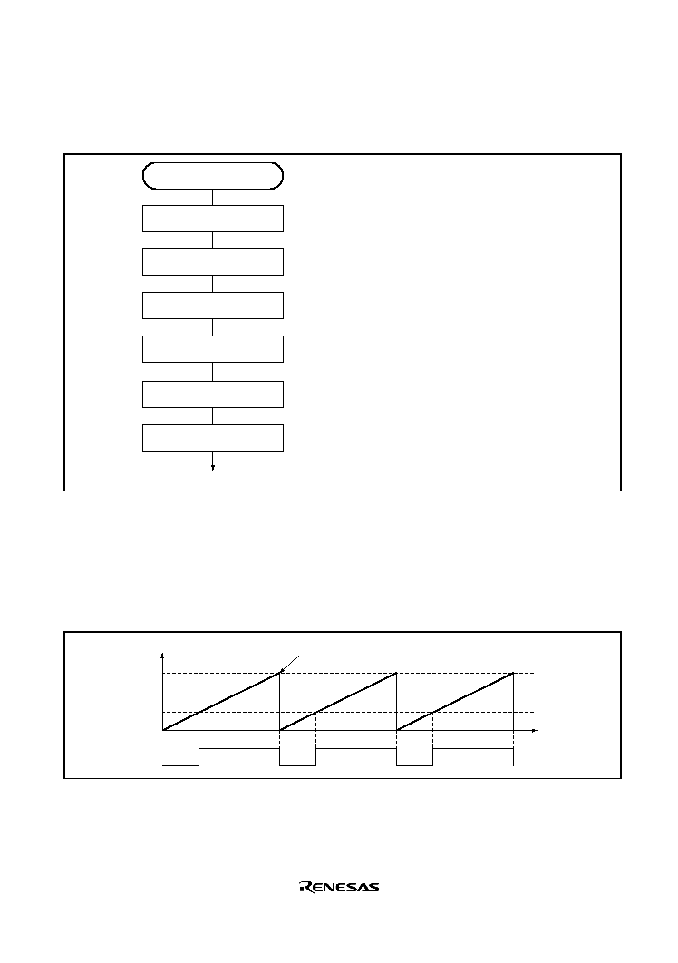
Rev. 1.0, 02/03, page 285 of 634
Example of PWM Mode Setting Procedure: Figure 9.21 shows an example of the PWM mode
setting procedure.
PWM mode
Select counter clock
Select counter clearing source
Select waveform output level
Set TGR
Set PWM mode
Start count
<PWM mode>
Select the counter clock with bits TPSC2 to
TPSC0 in TCR. At the same time, select the
input clock edge with bits CKEG1 and CKEG0
in TCR.
Use bits CCLR2 to CCLR0 in TCR to select the
TGR to be used as the TCNT clearing source.
Use TIOR to designate the TGR as an output
compare register, and select the initial value and
output value.
Set the cycle in the TGR selected in [2], and set
the duty in the other the TGR.
Select the PWM mode with bits MD3 to MD0 in
TMDR.
Set the CST bit in TSTR to 1 start the count
operation.
[1]
[2]
[3]
[4]
[5]
[6]
[1]
[2]
[3]
[4]
[5]
[6]
Figure 9.21 Example of PWM Mode Setting Procedure
Examples of PWM Mode Operation: Figure 9.22 shows an example of PWM mode 1 operation.
In this example, TGRA compare match is set as the TCNT clearing source, 0 is set for the TGRA
initial output value and output value, and 1 is set as the TGRB output value. In this case, the value
set in TGRA is used as the period, and the values set in TGRB registers as the duty.
TCNT value
TGRA
H'0000
TIOCA
Time
TGRB
Counter cleared by
TGRA compare match
Figure 9.22 Example of PWM Mode Operation (1)
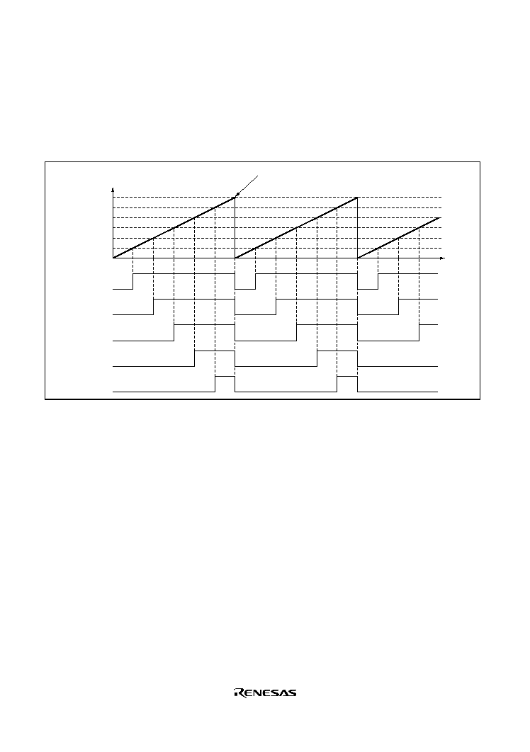
Rev. 1.0, 02/03, page 286 of 634
Figure 9.23 shows an example of PWM mode 2 operation. In this example, synchronous operation
is designated for channels 0 and 1, TGRB_1 compare match is set as the TCNT clearing source,
and 0 is set for the initial output value and 1 for the output value of the other TGR registers
(TGRA_0 to TGRD_0, TGRA_1), to output a 5-phase PWM waveform. In this case, the value set
in TGRB_1 is used as the cycle, and the values set in the other TGRs as the duty.
TCNT value
TGRB_1
H'0000
TIOCA0
Counter cleared by
TGRB_1 compare match
Time
TGRA_1
TGRD_0
TGRC_0
TGRB_0
TGRA_0
TIOCB0
TIOCC0
TIOCD0
TIOCA1
Figure 9.23 Example of PWM Mode Operation (2)
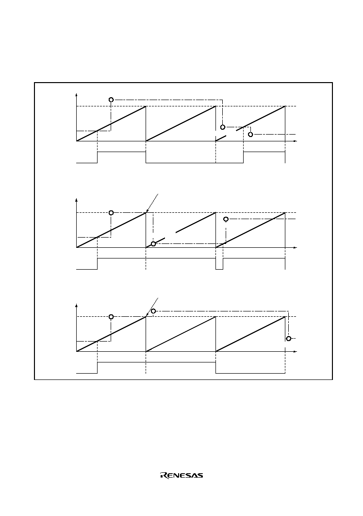
Rev. 1.0, 02/03, page 287 of 634
Figure 9.24 shows examples of PWM waveform output with 0% duty and 100% duty in PWM
mode.
TCNT value
TGRA
H'0000
TIOCA
Time
TGRB
0% duty
TGRB rewritten
TGRB
rewritten
TGRB rewritten
TCNT value
TGRA
H'0000
TIOCA
Time
TGRB
100% duty
TGRB rewritten
TGRB rewritten
TGRB rewritten
Output does not change when cycle register and duty register
compare matches occur simultaneously
TCNT value
TGRA
H'0000
TIOCA
Time
TGRB
100% duty
TGRB rewritten
TGRB rewritten
TGRB rewritten
Output does not change when cycle register and duty
register compare matches occur simultaneously
0% duty
Figure 9.24 Example of PWM Mode Operation (3)
Rev. 1.0, 02/03, page 288 of 634
9.5.5
Phase Counting Mode
In phase counting mode, the phase difference between two external clock inputs is detected and
TCNT is incremented/decremented accordingly. This mode can be set for channels 1 and 2. When
phase counting mode is set, an external clock is selected as the counter input clock and TCNT
operates as an up/down-counter regardless of the setting of bits TPSC2 to TPSC0 and bits CKEG1
and CKEG0 in TCR. However, the functions of bits CCLR1 and CCLR0 in TCR, and of TIOR,
TIER, and TGR are valid, and input capture/compare match and interrupt functions can be used.
This can be used for two-phase encoder pulse input. When overflow occurs while TCNT is
counting up, the TCFV flag in TSR is set; when underflow occurs while TCNT is counting down,
the TCFU flag is set. The TCFD bit in TSR is the count direction flag. Reading the TCFD flag
provides an indication of whether TCNT is counting up or down. Table 9.19 shows the
correspondence between external clock pins and channels.
Table 9.19
Phase Counting Mode Clock Input Pins
External Clock Pins
Channels
A-Phase
B-Phase
When channel 1 is set to phase counting mode
TCLKA
TCLKB
When channel 2 is set to phase counting mode
TCLKC
TCLKD
Example of Phase Counting Mode Setting Procedure: Figure 9.25 shows an example of the
phase counting mode setting procedure.
Phase counting mode
Select phase counting mode
Start count
<Phase counting mode>
Select phase counting mode with bits MD3 to
MD0 in TMDR.
Set the CST bit in TSTR to 1 to start the count
operation.
[1]
[2]
[1]
[2]
Figure 9.25 Example of Phase Counting Mode Setting Procedure
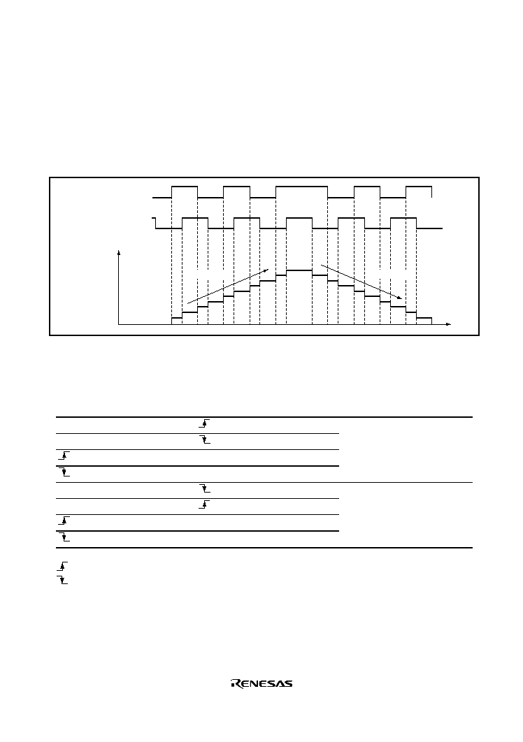
Rev. 1.0, 02/03, page 289 of 634
Examples of Phase Counting Mode Operation: In phase counting mode, TCNT counts up or
down according to the phase difference between two external clocks. There are four modes,
according to the count conditions.
1. Phase counting mode 1
Figure 9.26 shows an example of phase counting mode 1 operation, and table 9.20 summarizes
the TCNT up/down-count conditions.
TCNT value
Time
Down-count
Up-count
TCLKA (channel 1)
TCLKC (channel 2)
TCLKB (channel 1)
TCLKD (channel 2)
Figure 9.26 Example of Phase Counting Mode 1 Operation
Table 9.20
Up/Down-Count Conditions in Phase Counting Mode 1
TCLKA (Channel 1)
TCLKC (Channel 2)
TCLKB (Channel 1)
TCLKD (Channel 2)
Operation
High level
Low level
Low level
High level
Up-count
High level
Low level
High level
Low level
Down-count
Legend
: Rising edge
: Falling edge
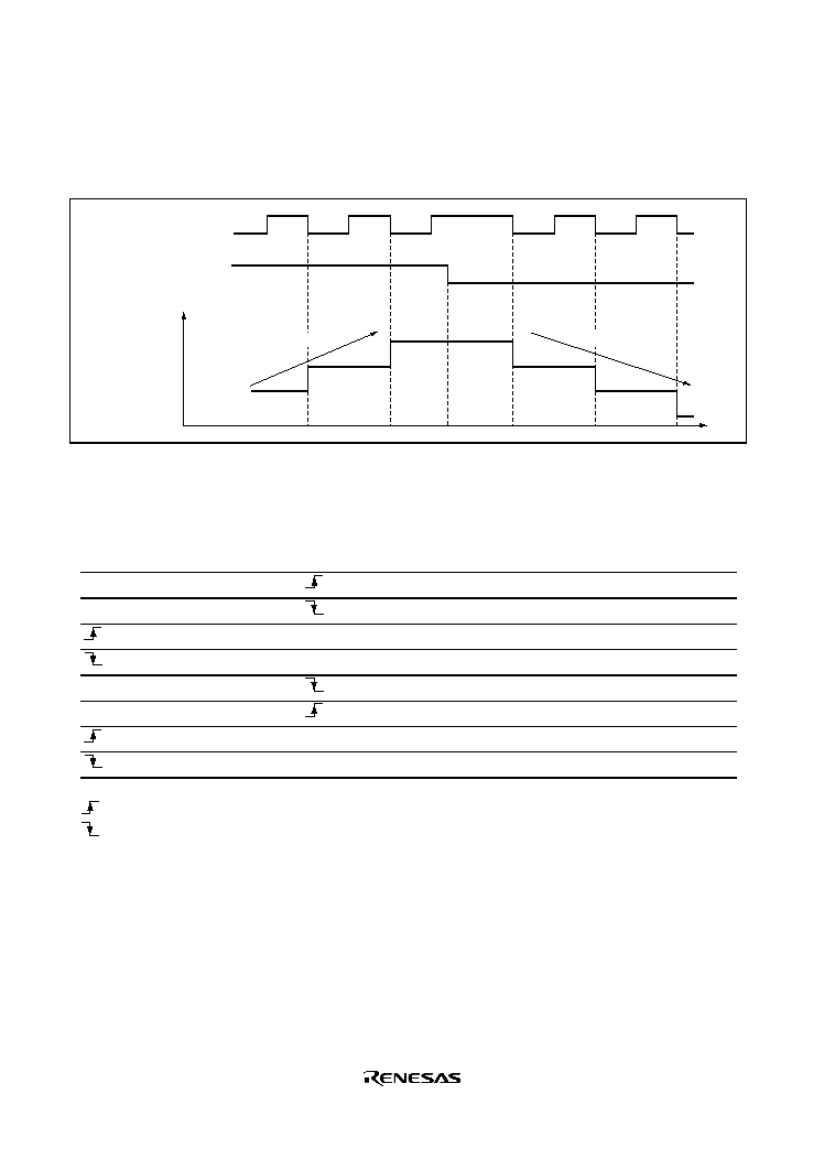
Rev. 1.0, 02/03, page 290 of 634
2. Phase counting mode 2
Figure 9.27 shows an example of phase counting mode 2 operation, and table 9.21 summarizes
the TCNT up/down-count conditions.
Time
Down-count
Up-count
TCNT value
TCLKA (channel 1)
TCLKC (channel 2)
TCLKB (channel 1)
TCLKD (channel 2)
Figure 9.27 Example of Phase Counting Mode 2 Operation
Table 9.21
Up/Down-Count Conditions in Phase Counting Mode 2
TCLKA (Channel 1)
TCLKC (Channel 2)
TCLKB (Channel 1)
TCLKD (Channel 2)
Operation
High level
Don't care
Low level
Don't care
Low level
Don't care
High level
Up-count
High level
Don't care
Low level
Don't care
High level
Don't care
Low level
Down-count
Legend
: Rising edge
: Falling edge
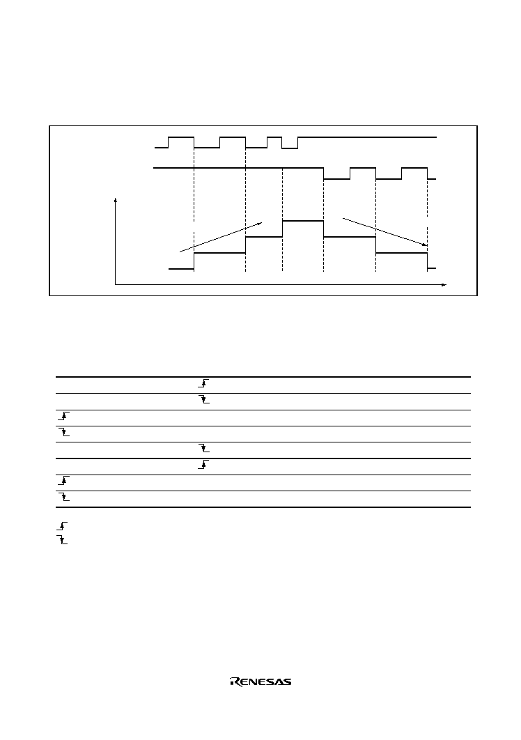
Rev. 1.0, 02/03, page 291 of 634
3. Phase counting mode 3
Figure 9.28 shows an example of phase counting mode 3 operation, and table 9.22 summarizes
the TCNT up/down-count conditions.
Time
Up-count
Down-count
TCNT value
TCLKA (channel 1)
TCLKC (channel 2)
TCLKB (channel 1)
TCLKD (channel 2)
Figure 9.28 Example of Phase Counting Mode 3 Operation
Table 9.22
Up/Down-Count Conditions in Phase Counting Mode 3
TCLKA (Channel 1)
TCLKC (Channel 2)
TCLKB (Channel 1)
TCLKD (Channel 2)
Operation
High level
Don't care
Low level
Don't care
Low level
Don't care
High level
Up-count
High level
Down-count
Low level
Don't care
High level
Don't care
Low level
Don't care
Legend
: Rising edge
: Falling edge
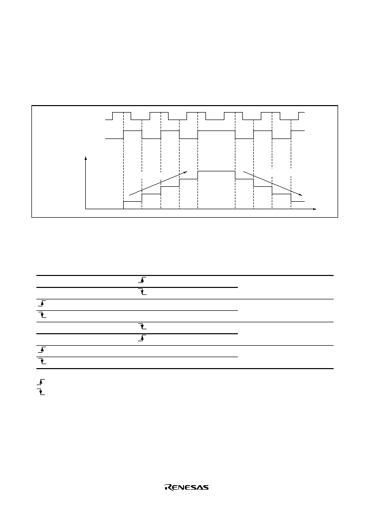
Rev. 1.0, 02/03, page 292 of 634
4. Phase counting mode 4
Figure 9.29 shows an example of phase counting mode 4 operation, and table 9.23 summarizes
the TCNT up/down-count conditions. Figure 9.29 Example of Phase Counting Mode 4
Operation
Time
Up-count
Down-count
TCNT value
TCLKA (channel 1)
TCLKC (channel 2)
TCLKB (channel 1)
TCLKD (channel 2)
Figure 9.29 Example of Phase Counting Mode 4 Operation
Table 9.23
Up/Down-Count Conditions in Phase Counting Mode 4
TCLKA (Channel 1)
TCLKC (Channel 2)
TCLKB (Channel 1)
TCLKD (Channel 2)
Operation
High level
Low level
Up-count
Low level
High level
Don't care
High level
Low level
Down-count
High level
Low level
Don't care
Legend
: Rising edge
: Falling edge

Rev. 1.0, 02/03, page 293 of 634
9.6
Interrupts
9.6.1
Interrupt Source and Priority
There are three kinds of TPU interrupt source: TGR input capture/compare match, TCNT
overflow, and TCNT underflow. Each interrupt source has its own status flag and enable/disabled
bit, allowing generation of interrupt request signals to be enabled or disabled individually. When
an interrupt request is generated, the corresponding status flag in TSR is set to 1. If the
corresponding enable/disable bit in TIER is set to 1 at this time, an interrupt is requested. The
interrupt request is cleared by clearing the status flag to 0. Relative channel priorities can be
changed by the interrupt controller, but the priority order within a channel is fixed. For details, see
section 5, Interrupt Controller. Table 9.24 lists the TPU interrupt sources.
Table 9.24
TPU Interrupts
Channel Name
Interrupt Source
Interrupt Flag
DMAC
Activation
Priority
TGI0A
TGRA_0 input
capture/compare match
TGFA
Possible
High
TGI0B
TGRB_0 input
capture/compare match
TGFB
Not possible
TGI0C
TGRC_0 input
capture/compare match
TGFC
Not possible
TGI0D
TGRD_0 input
capture/compare match
TGFD
Not possible
0
TCI0V
TCNT_0 overflow
TCFV
Not possible
TGI1A
TGRA_1 input
capture/compare match
TGFA
Possible
TGI1B
TGRB_1 input
capture/compare match
TGFB
Not possible
TCI1V
TCNT_1 overflow
TCFV
Not possible
1
TCI1U
TCNT_1 underflow
TCFU
Not possible
TGI2A
TGRA_2 input
capture/compare match
TGFA
Possible
TGI2B
TGRB_2 input
capture/compare match
TGFB
Not possible
TCI2V
TCNT_2 overflow
TCFV
Not possible
2
TCI2U
TCNT_2 underflow
TCFU
Not possible
Low
Note: This table shows the initial state immediately after a reset. The relative channel priorities
can be changed by the interrupt controller.

Rev. 1.0, 02/03, page 294 of 634
Input Capture/Compare Match Interrupt: An interrupt is requested if the TGIE bit in TIER is
set to 1 when the TGF flag in TSR is set to 1 by the occurrence of a TGR input capture/compare
match on a particular channel. The interrupt request is cleared by clearing the TGF flag to 0. The
TPU has 16 input capture/compare match interrupts, four each for channel 0, and two each for
channels 1 and 2.
Overflow Interrupt: An interrupt is requested if the TCIEV bit in TIER is set to 1 when the
TCFV flag in TSR is set to 1 by the occurrence of TCNT overflow on a channel. The interrupt
request is cleared by clearing the TCFV flag to 0. The TPU has three overflow interrupts, one for
each channel.
Underflow Interrupt: An interrupt is requested if the TCIEU bit in TIER is set to 1 when the
TCFU flag in TSR is set to 1 by the occurrence of TCNT underflow on a channel. The interrupt
request is cleared by clearing the TCFU flag to 0. The TPU has two underflow interrupts, one each
for channels 1 and 2.
9.6.2
DMAC Activation
The DMAC can be activated by the TGRA input capture/compare match interrupt for a channel.
For details, see section 7, DMA Controller. With the TPU, a total of three TGRA input
capture/compare match interrupts can be used as DMAC activation sources, one for each channel.
9.6.3
A/D Converter Activation
The A/D converter can be activated by the TGRA input capture/compare match for a channel. If
the TTGE bit in TIER is set to 1 when the TGFA flag in TSR is set to 1 by the occurrence of a
TGRA input capture/compare match on a particular channel, a request to start A/D conversion is
sent to the A/D converter. If the TPU conversion start trigger has been selected on the A/D
converter side at this time, A/D conversion is started. In the TPU, a total of three TGRA input
capture/compare match interrupts can be used as A/D converter conversion start sources, one for
each channel.
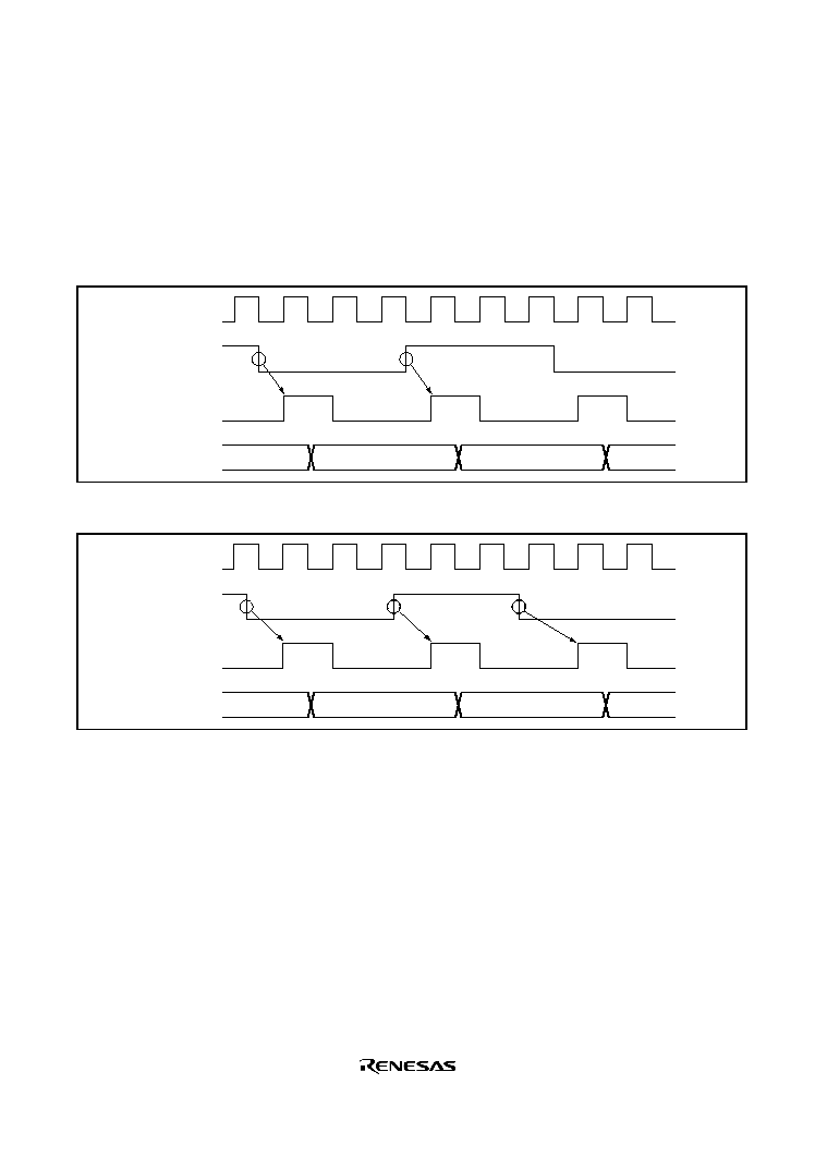
Rev. 1.0, 02/03, page 295 of 634
9.7
Operation Timing
9.7.1
Input/Output Timing
TCNT Count Timing: Figure 9.30 shows TCNT count timing in internal clock operation, and
figure 9.31 shows TCNT count timing in external clock operation.
TCNT
TCNT
input clock
Internal clock
N-1
N
N+1
N+2
Falling edge
Rising edge
Figure 9.30 Count Timing in Internal Clock Operation
TCNT
TCNT
input clock
External clock
N-1
N
N+1
N+2
Falling edge
Rising edge
Falling edge
Figure 9.31 Count Timing in External Clock Operation
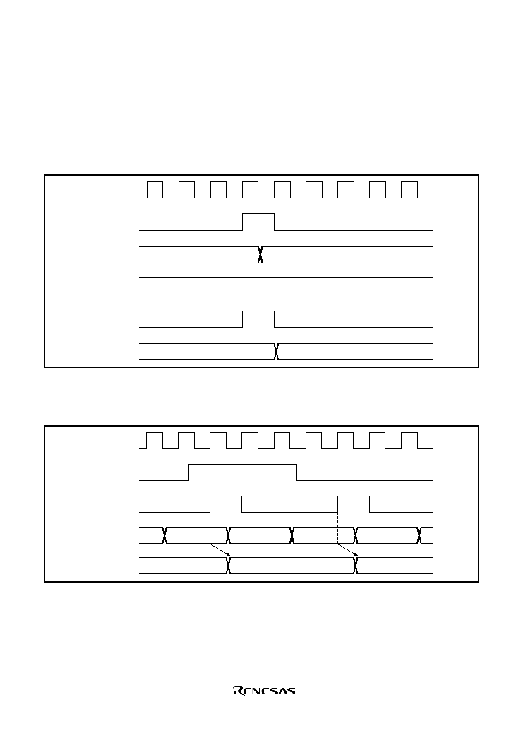
Rev. 1.0, 02/03, page 296 of 634
Output Compare Output Timing: A compare match signal is generated in the final state in
which TCNT and TGR match (the point at which the count value matched by TCNT is updated).
When a compare match signal is generated, the output value set in TIOR is output at the output
compare output pin. After a match between TCNT and TGR, the compare match signal is not
generated until the TCNT input clock is generated. Figure 9.32 shows output compare output
timing.
TGR
TCNT
TCNT
input clock
N
N
N+1
Compare
match signal
TIOC pin
Figure 9.32 Output Compare Output Timing
Input Capture Signal Timing: Figure 9.33 shows input capture signal timing.
TCNT
Input capture
input
N
N+1
N+2
N
N+2
TGR
Input capture
signal
Figure 9.33 Input Capture Input Signal Timing
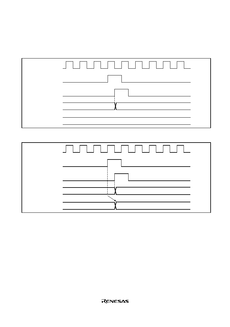
Rev. 1.0, 02/03, page 297 of 634
Timing for Counter Clearing by Compare Match/Input Capture: Figure 9.34 shows the
timing when counter clearing by compare match occurrence is specified, and figure 9.35 shows the
timing when counter clearing by input capture occurrence is specified.
TCNT
Counter
clear signal
Compare
match signal
TGR
N
N
H'0000
Figure 9.34 Counter Clear Timing (Compare Match)
TCNT
Counter clear
signal
Input capture
signal
TGR
N
H'0000
N
Figure 9.35 Counter Clear Timing (Input Capture)
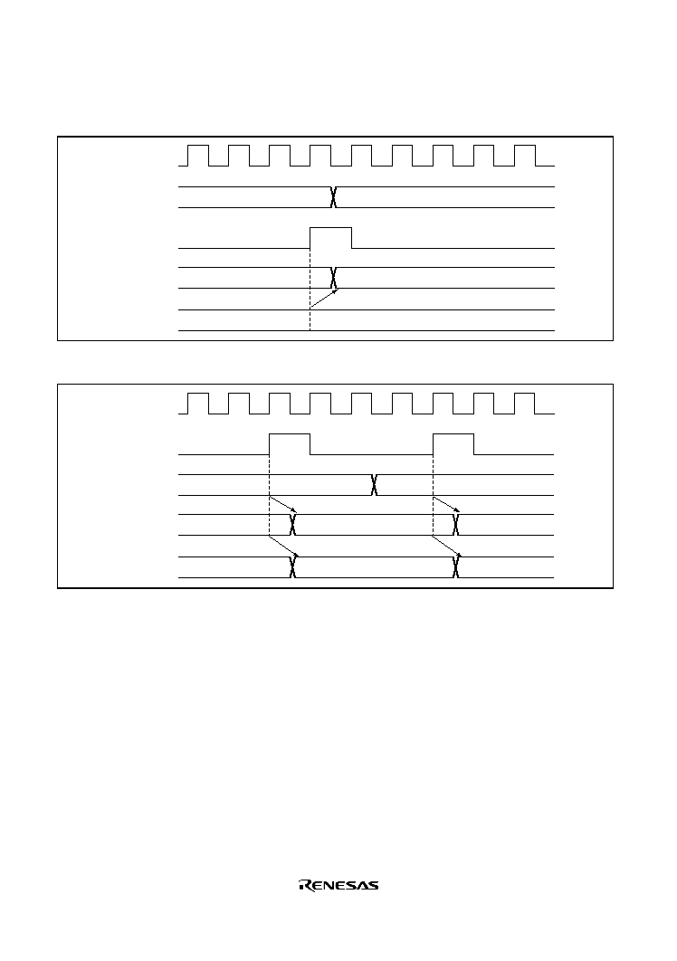
Rev. 1.0, 02/03, page 298 of 634
Buffer Operation Timing: Figures 9.36 and 9.37 show the timing in buffer operation.
TGRA,
TGRB
Compare
match signal
TCNT
TGRC,
TGRD
n
N
N
n
n+1
Figure 9.36 Buffer Operation Timing (Compare Match)
TGRA,
TGRB
TCNT
Input capture
signal
TGRC,
TGRD
N
n
n
N+1
N
N
N+1
Figure 9.37 Buffer Operation Timing (Input Capture)
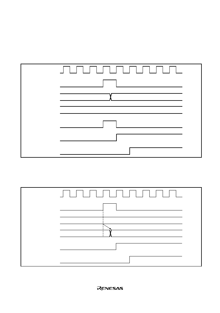
Rev. 1.0, 02/03, page 299 of 634
9.7.2
Interrupt Signal Timing
TGF Flag Setting Timing in Case of Compare Match: Figure 9.38 shows the timing for setting
of the TGF flag in TSR by compare match occurrence, and TGI interrupt request signal timing.
TGR
TCNT
TCNT input
clock
N
N
N+1
Compare
match signal
TGF flag
TGI interrupt
Figure 9.38 TGI Interrupt Timing (Compare Match)
TGF Flag Setting Timing in Case of Input Capture: Figure 9.39 shows the timing for setting of
the TGF flag in TSR by input capture occurrence, and TGI interrupt request signal timing.
TGR
TCNT
Input capture
signal
N
N
TGF flag
TGI interrupt
Figure 9.39 TGI Interrupt Timing (Input Capture)
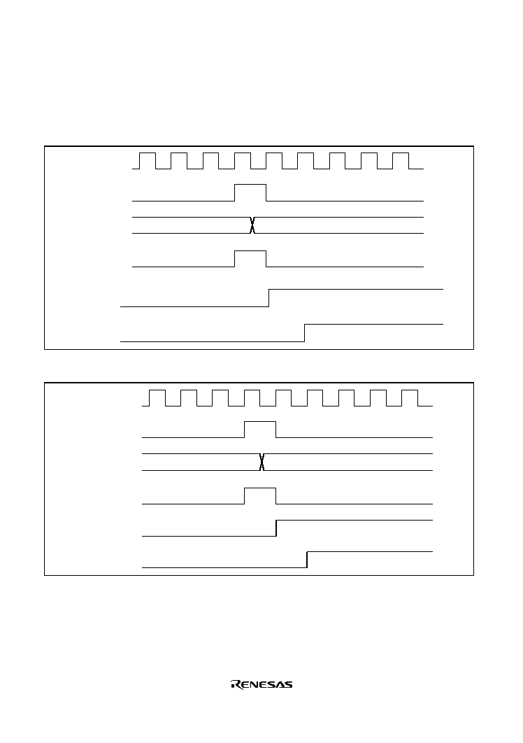
Rev. 1.0, 02/03, page 300 of 634
TCFV Flag/TCFU Flag Setting Timing: Figure 9.40 shows the timing for setting of the TCFV
flag in TSR by overflow occurrence, and TCIV interrupt request signal timing. Figure 9.41 shows
the timing for setting of the TCFU flag in TSR by underflow occurrence, and TCIU interrupt
request signal timing.
Overflow
signal
TCNT
(overflow)
TCNT input
clock
H'FFFF
H'0000
TCFV flag
TCIV interrupt
Figure 9.40 TCIV Interrupt Setting Timing
Underflow
signal
TCNT
(underflow)
TCNT
input clock
H'0000
H'FFFF
TCFU flag
TCIU interrupt
Figure 9.41 TCIU Interrupt Setting Timing
Status Flag Clearing Timing: After a status flag is read as 1 by the CPU, it is cleared by writing
0 to it. When the DMAC is activated, the flag is cleared automatically. Figure 9.42 shows the
timing for status flag clearing by the CPU, and figure 9.43 shows the timing for status flag
clearing by the DMAC.
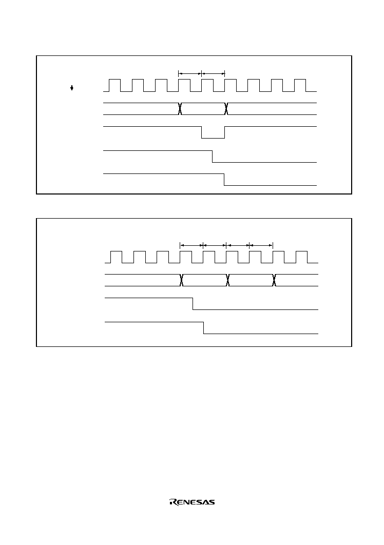
Rev. 1.0, 02/03, page 301 of 634
T
1
T
2
TSR write cycle
TSR address
Address
Write signal
Status flag
Interrupt
request
signal
Figure 9.42 Timing for Status Flag Clearing by CPU
Interrupt
request
signal
Status flag
Address
Source address
DMAC
read cycle
T
1
T
2
Destination
address
T
1
T
2
DMAC
write cycle
Figure 9.43 Timing for Status Flag Clearing by DMAC Activation
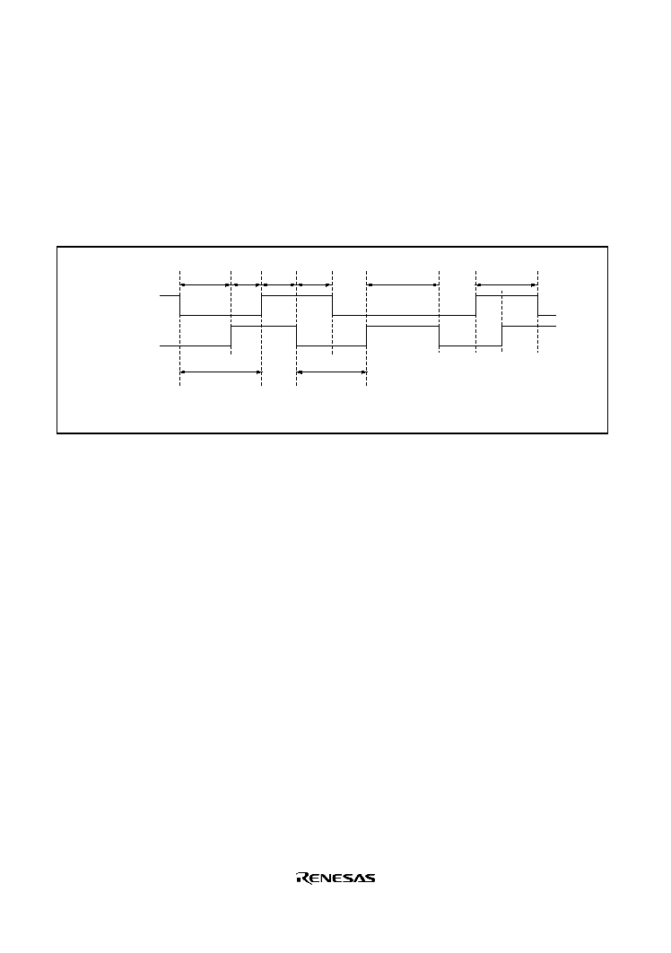
Rev. 1.0, 02/03, page 302 of 634
9.8
Usage Notes
Input Clock Restrictions: The input clock pulse width must be at least 1.5 states in the case of
single-edge detection, and at least 2.5 states in the case of both-edge detection. The TPU will not
operate properly with a narrower pulse width. In phase counting mode, the phase difference and
overlap between the two input clocks must be at least 1.5 states, and the pulse width must be at
least 2.5 states. Figure 9.44 shows the input clock conditions in phase counting mode.
Overlap
Phase
differ-
ence
Phase
differ-
ence
Overlap
TCLKA
(TCLKC)
TCLKB
(TCLKD)
Pulse width
Pulse width
Pulse width
Pulse width
Notes: Phase difference and overlap
Pulse width
: 1.5 states or more
: 2.5 states or more
Figure 9.44 Phase Difference, Overlap, and Pulse Width in Phase Counting Mode
Caution on Period Setting: When counter clearing by compare match is set, TCNT is cleared in
the final state in which it matches the TGR value (the point at which the count value matched by
TCNT is updated). Consequently, the actual counter frequency is given by the following formula:
f = --------
(N + 1)
Where f : Counter frequency
: Operating frequency
N : TGR set value
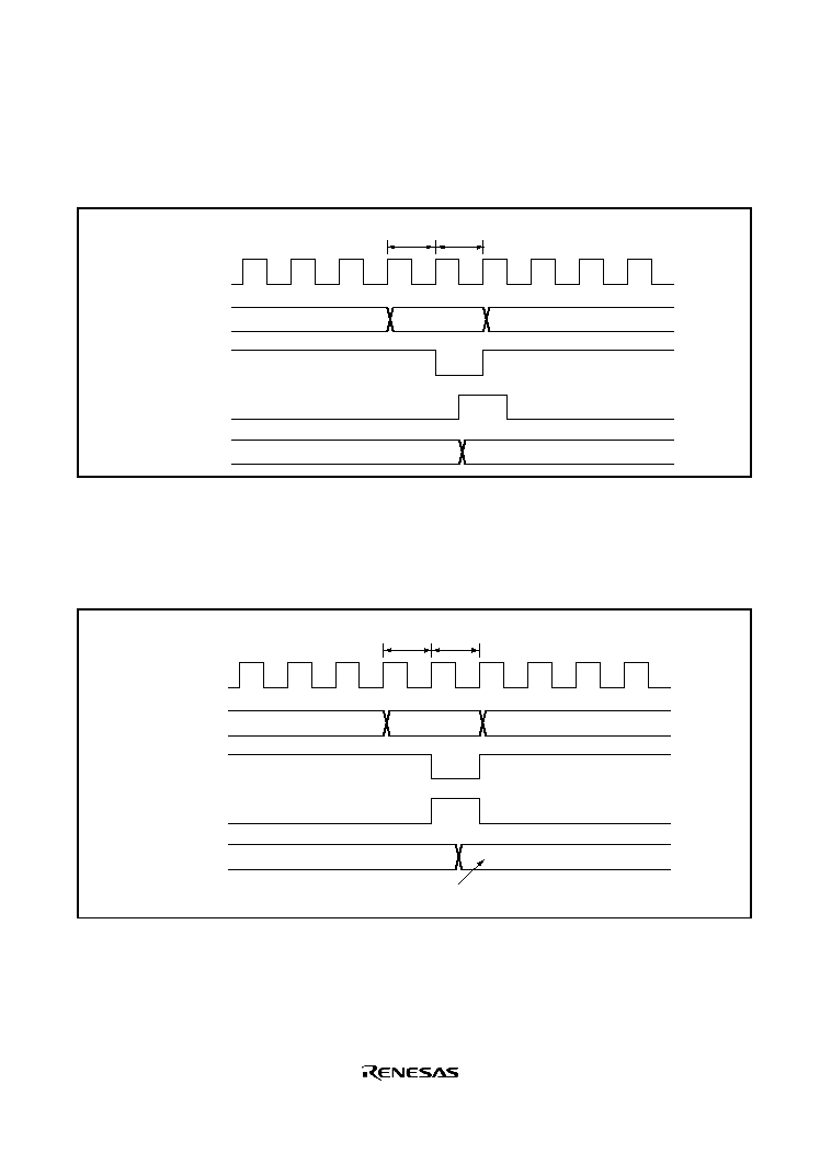
Rev. 1.0, 02/03, page 303 of 634
Contention between TCNT Write and Clear Operations: If the counter clear signal is
generated in the T2 state of a TCNT write cycle, TCNT clearing takes precedence and the TCNT
write is not performed. Figure 9.45 shows the timing in this case.
Counter clear
signal
Write signal
Address
TCNT address
TCNT
TCNT write cycle
T
1
T
2
N
H'0000
Figure 9.45 Contention between TCNT Write and Clear Operations
Contention between TCNT Write and Increment Operations: If incrementing occurs in the T2
state of a TCNT write cycle, the TCNT write takes precedence and TCNT is not incremented.
Figure 9.46 shows the timing in this case.
TCNT input
clock
Write signal
Address
TCNT address
TCNT
TCNT write cycle
T
1
T
2
N
M
TCNT write data
Figure 9.46 Contention between TCNT Write and Increment Operations
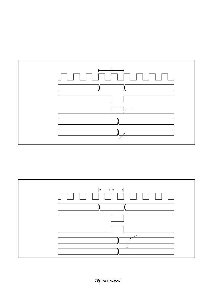
Rev. 1.0, 02/03, page 304 of 634
Contention between TGR Write and Compare Match: If a compare match occurs in the T2
state of a TGR write cycle, the TGR write takes precedence and the compare match signal is
inhibited. A compare match does not occur even if the same value as before is written. Figure 9.47
shows the timing in this case.
Compare
match signal
Write signal
Address
TGR address
TCNT
TGR write cycle
T
1
T
2
N
M
TGR write data
TGR
N
N+1
Inhibited
Figure 9.47 Contention between TGR Write and Compare Match
Contention between Buffer Register Write and Compare Match: If a compare match occurs in
the T2 state of a TGR write cycle, the data transferred to TGR by the buffer operation will be the
data prior to the write. Figure 9.48 shows the timing in this case.
Compare
match signal
Write signal
Address
Buffer register
address
Buffer
register
TGR write cycle
T
1
T
2
N
TGR
N
M
Buffer register write data
Figure 9.48 Contention between Buffer Register Write and Compare Match
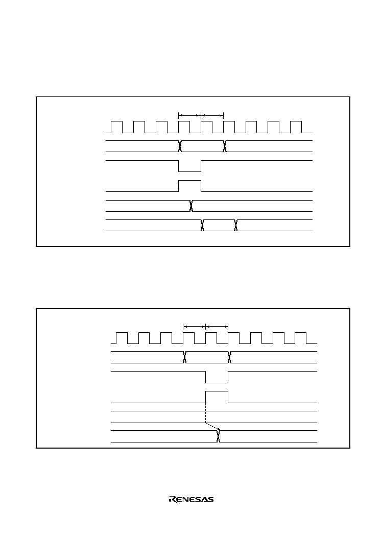
Rev. 1.0, 02/03, page 305 of 634
Contention between TGR Read and Input Capture: If the input capture signal is generated in
the T1 state of a TGR read cycle, the data that is read will be the data after input capture transfer.
Figure 9.49 shows the timing in this case.
Input capture
signal
Read signal
Address
TGR address
TGR
TGR read cycle
T
1
T
2
M
Internal
data bus
X
M
Figure 9.49 Contention between TGR Read and Input Capture
Contention between TGR Write and Input Capture: If the input capture signal is generated in
the T2 state of a TGR write cycle, the input capture operation takes precedence and the write to
TGR is not performed. Figure 9.50 shows the timing in this case.
Input capture
signal
Write signal
Address
TCNT
TGR write cycle
T
1
T
2
M
TGR
M
TGR address
Figure 9.50 Contention between TGR Write and Input Capture
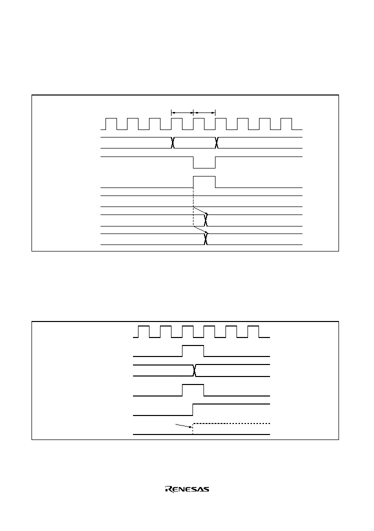
Rev. 1.0, 02/03, page 306 of 634
Contention between Buffer Register Write and Input Capture: If the input capture signal is
generated in the T2 state of a buffer register write cycle, the buffer operation takes precedence and
the write to the buffer register is not performed. Figure 9.51 shows the timing in this case.
Input capture
signal
Write signal
Address
TCNT
Buffer register write cycle
T
1
T
2
N
TGR
N
M
M
Buffer
register
Buffer register
address
Figure 9.51 Contention between Buffer Register Write and Input Capture
Contention between Overflow/Underflow and Counter Clearing: If overflow/underflow and
counter clearing occur simultaneously, the TCFV/TCFU flag in TSR is not set and TCNT clearing
takes precedence. Figure 9.52 shows the operation timing when a TGR compare match is specified
as the clearing source, and H'FFFF is set in TGR.
Counter
clear signal
TCNT input
clock
TCNT
TGF
Disabled
TCFV
H'FFFF
H'0000
Figure 9.52 Contention between Overflow and Counter Clearing
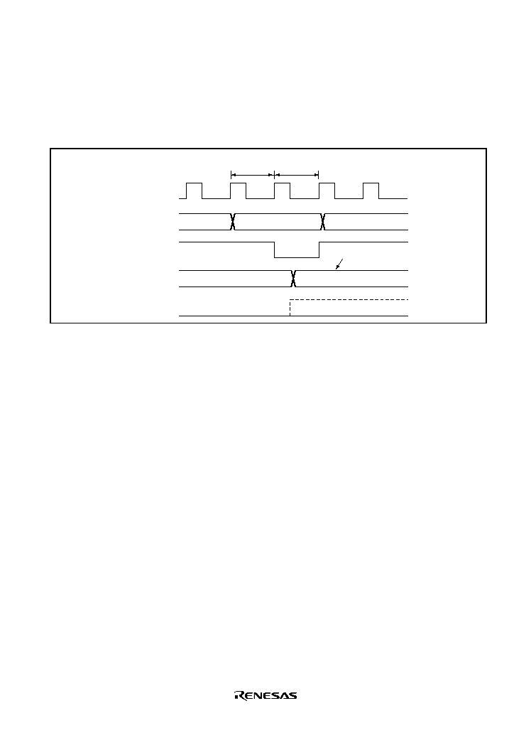
Rev. 1.0, 02/03, page 307 of 634
Contention between TCNT Write and Overflow/Underflow: If there is an up-count or down-
count in the T2 state of a TCNT write cycle, and overflow/underflow occurs, the TCNT write
takes precedence and the TCFV/TCFU flag in TSR is not set. Figure 9.53 shows the operation
timing when there is contention between TCNT write and overflow.
Write signal
Address
TCNT address
TCNT
TCNT write cycle
T
1
T
2
H'FFFF
M
TCNT write data
TCFV flag
Figure 9.53 Contention between TCNT Write and Overflow
Multiplexing of I/O Pins: In this LSI, the TCLKA input pin is multiplexed with the TIOCC0 I/O
pin, the TCLKB input pin with the TIOCD0 I/O pin, the TCLKC input pin with the TIOCB1 I/O
pin, and the TCLKD input pin with the TIOCB2 I/O pin. When an external clock is input,
compare match output should not be performed from a multiplexed pin.
Interrupts in Module Stop Mode: If module stop mode is entered when an interrupt has been
requested, it will not be possible to clear the CPU interrupt source or the DMAC activation source.
Interrupts should therefore be disabled before entering module stop mode.

Rev. 1.0, 02/03, page 308 of 634
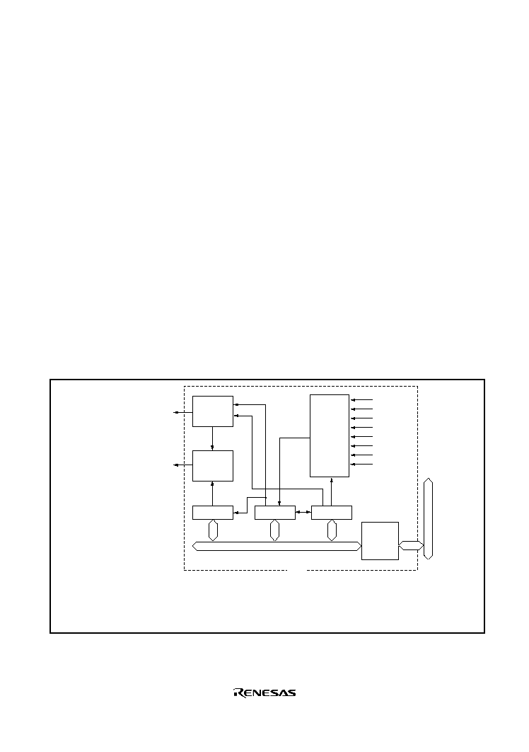
WDT0104A_000020011200
Rev. 1.0, 02/03, page 309 of 634
Section 10 Watchdog Timer
The watchdog timer (WDT) is an 8-bit timer that can generate an internal reset signal for this LSI
if a system crash prevents the CPU from writing to the timer counter, thus allowing it to overflow.
When this watchdog function is not needed, the WDT can be used as an interval timer. In interval
timer operation, an interval timer interrupt is generated each time the counter overflows.
The block diagram of the WDT is shown in Figure 10.1.
10.1
Features
· Selectable from eight counter input clocks.
· Switchable between watchdog timer mode and interval timer mode
In watchdog timer mode:
· If the counter overflows, it is possible to select whether this LSI is internally reset or not.
In interval timer mode:
· If the counter overflows, the WDT generates an interval timer interrupt (WOVI).
Overflow
Interrupt
control
WOVI
(interrupt request
signal)
Internal reset signal*
Reset
control
RSTCSR
TCNT
TSCR
/2
/64
/128
/512
/2048
/8192
/32768
/131072
Clock
Clock
select
Internal clock
sources
Bus
interface
Module bus
TCSR
TCNT
RSTCSR
Note: * The type of internal reset signal depends on a register setting.
: Timer control/status register
: Timer counter
: Reset control/status register
WDT
Legend
Internal bus
Figure 10.1 Block Diagram of WDT

Rev. 1.0, 02/03, page 310 of 634
10.2
Register Descriptions
The WDT has the following three registers. For details, refer to section 21, List of Registers. To
prevent accidental overwriting, TCSR, TCNT, and RSTCSR have to be written to by a different
method to normal registers. For details, refer to section 10.5.1, Notes on Register Access.
· Timer counter (TCNT)
· Timer control/status register (TCSR)
· Reset control/status register (RSTCSR)
10.2.1
Timer Counter (TCNT)
TCNT is an 8-bit readable/writable up-counter. TCNT is initialized to H'00 by a reset, when the
TME bit in TCSR is cleared to 0.
10.2.2
Timer Control/Status Register (TCSR)
TCSR is an 8-bit readable/writable register. Its functions include selecting the clock source to be
input to TCNT, and selecting the timer mode.
Bit
Bit Name
Initial Value
R/W
Description
7
OVF
0
R/(W)*
Overflow Flag
Indicates that TCNT has overflowed. Only a write of
0 is permitted, to clear the flag.
[Setting conditions]
When TCNT overflows (changes from H'FF to H'00)
When internal reset request generation is selected
in watchdog timer mode, OVF is cleared
automatically by the internal reset.
[Clearing condition]
Cleared by reading TCSR when OVF = 1, then
writing 0 to OVF
6
WT/
IT
0
R/W
Timer Mode Select
Selects whether the WDT is used as a watchdog
timer or interval timer.
0: Interval timer mode
1: Watchdog timer mode

Rev. 1.0, 02/03, page 311 of 634
Bit
Bit Name
Initial Value
R/W
Description
5
TME
0
R/W
Timer Enable
When this bit is set to 1, TCNT starts counting.
When this bit is cleared, TCNT stops counting and
is initialized to H'00.
4, 3
--
All 1
--
Reserved
These bits are always read as 1 and cannot be
modified.
2
1
0
CKS2
CKS1
CKS0
0
0
0
R/W
R/W
R/W
Clock Select 0 to 2
Selects the clock source to be input to TCNT. The
overflow frequency for
= 16 MHz is enclosed in
parentheses.
000: Clock
/2 (frequency: 32.0 µs)
001: Clock
/64 (frequency: 1.0 ms)
010: Clock
/128 (frequency: 2.0 ms)
011: Clock
/512 (frequency: 8.2 ms)
100: Clock
/2048 (frequency: 32.8 ms)
101: Clock
/8192 (frequency: 131.1 ms)
110: Clock
/32768 (frequency: 524.3 ms)
111: Clock
/131072 (frequency: 2.1 s)
Note: * The write value should always be 0 to clear this flag.

Rev. 1.0, 02/03, page 312 of 634
10.2.3
Reset Control/Status Register (RSTCSR)
RSTCSR is an 8-bit readable/writable register that controls the generation of the internal reset
signal when TCNT overflows, and selects the type of internal reset signal. RSTCSR is initialized
to H'1F by a reset signal from the
RES pin, and not by the WDT internal reset signal caused by
overflows.
Bit
Bit Name
Initial Value
R/W
Description
7
WOVF
0
R/(W)*
1
Watchdog Overflow Flag
This bit is set when TCNT overflows in watchdog
timer mode. This bit cannot be set in interval timer
mode, and the write value should always be 0.
[Setting condition]
Set when TCNT overflows (changed from H'FF to
H'00) in watchdog timer mode
[Clearing condition]
Cleared by reading RSTCSR when WOVF = 1, and
then writing 0 to WOVF
6
RSTE
0
R/W
Reset Enable
Specifies whether or not a reset signal is generated
in the chip if TCNT overflows during watchdog timer
operation.
0: Reset signal is not generated even if TCNT
overflows
(Though this LSI is not reset, TCNT and TCSR in
WDT are reset)
1: Reset signal is generated if TCNT overflows
5
RSTS
0
R/W
Reset Select
Selects the type of internal reset generated if TCNT
overflows during watchdog timer operation.
0: Power-on reset*
2
1: Setting prohibited
4 to 0 --
1
--
Reserved
These bits are always read as 1 and cannot be
modified.
Notes: 1. The write value should always be 0 to clear this flag.
2. Supported only by the H8S/2218 Series.
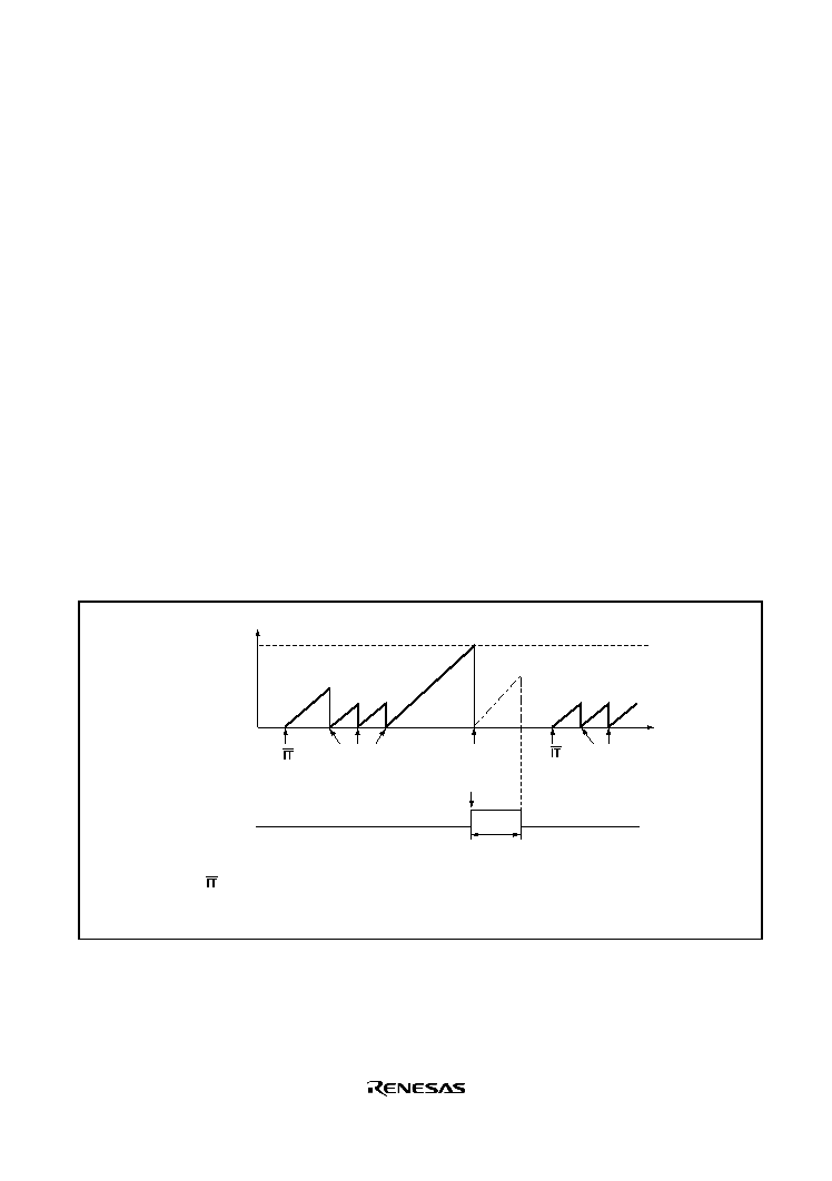
Rev. 1.0, 02/03, page 313 of 634
10.3
Operation
10.3.1
Watchdog Timer Mode
To use the WDT as a watchdog timer, set the WT/
IT bit in TCSR and the TME bit to 1.
TCNT does not overflow while the system is operating normally. Software must prevent TCNT
overflows by rewriting the TCNT value (normally be writing H'00) before overflows occurs.
When the RSTE bit of the RSTCSR is set to 1, and if the TCNT overflows, an internal reset signal
for this LSI is issued. In this case, select power-on reset or manual reset* by setting the RSTS bit
of the RSTCSR to 0.
If a reset caused by a signal input to the
RES pin occurs at the same time as a reset caused by a
WDT overflow, the
RES pin reset has priority and the WOVF bit in RSTCSR is cleared to 0. The
internal reset signal is output for 518 states.
When the TCNT overflows in watchdog timer mode, the WOVF bit of the RSTCSR is set to 1. If
the RSTE bit of the RSTCSR has been set to 1, an internal reset signal for the entire LSI is
generated at TCNT overflow.
Note: * Supported only by the H8S/2218 Series.
TCNT value
H'00
Time
H'FF
WT/
= 1
TME = 1
H'00 written
to TCNT
WT/
= 1
TME = 1
H'00 written
to TCNT
518 states (WDT0)
Internal reset signal*
WT/
TME
Legend
Overflow
WOVF = 1
: Timer mode select bit
: Timer enabl bit
Note: * With WDT0, the internal reset signal is generated only when the RSTE bit is set to 1.
Internal reset
generated
Figure 10.2 Operation in Watchdog Timer Mode
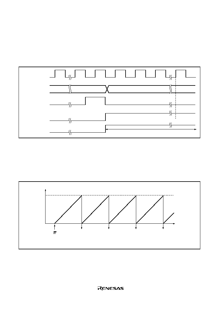
Rev. 1.0, 02/03, page 314 of 634
10.3.2
Timing of Setting of Watchdog Timer Overflow Flag (WOVF)
With WDT0, the WOVF bit in RSTCSR is set to 1 if TCNT overflows in watchdog timer mode.
If TCNT overflows while the RSTE bit in RSTCSR is set to 1, an internal reset signal is generated
for the entire chip. This timing is illustrated in figure 10.3.
TCNT
H'FF
H'00
Overflow signal
(internal signal)
Internal reset
signal
WOVF
518 states (WDT0)
Figure 10.3 Timing of WOVF Setting
10.3.3
Interval Timer Mode
When the WDT is used as an interval timer, an interval timer interrupt (WOVI) is generated each
time the TCNT overflows. Therefore, an interrupt can be generated at intervals.
TCNT count
H'00
Time
H'FF
WT/
= 0
TME = 1
WOVI
Overflow
Overflow
Overflow
Overflow
WOVI: Interval interrupt request generation
Legend
WOVI
WOVI
WOVI
Figure 10.4 Operation in Interval Timer Mode
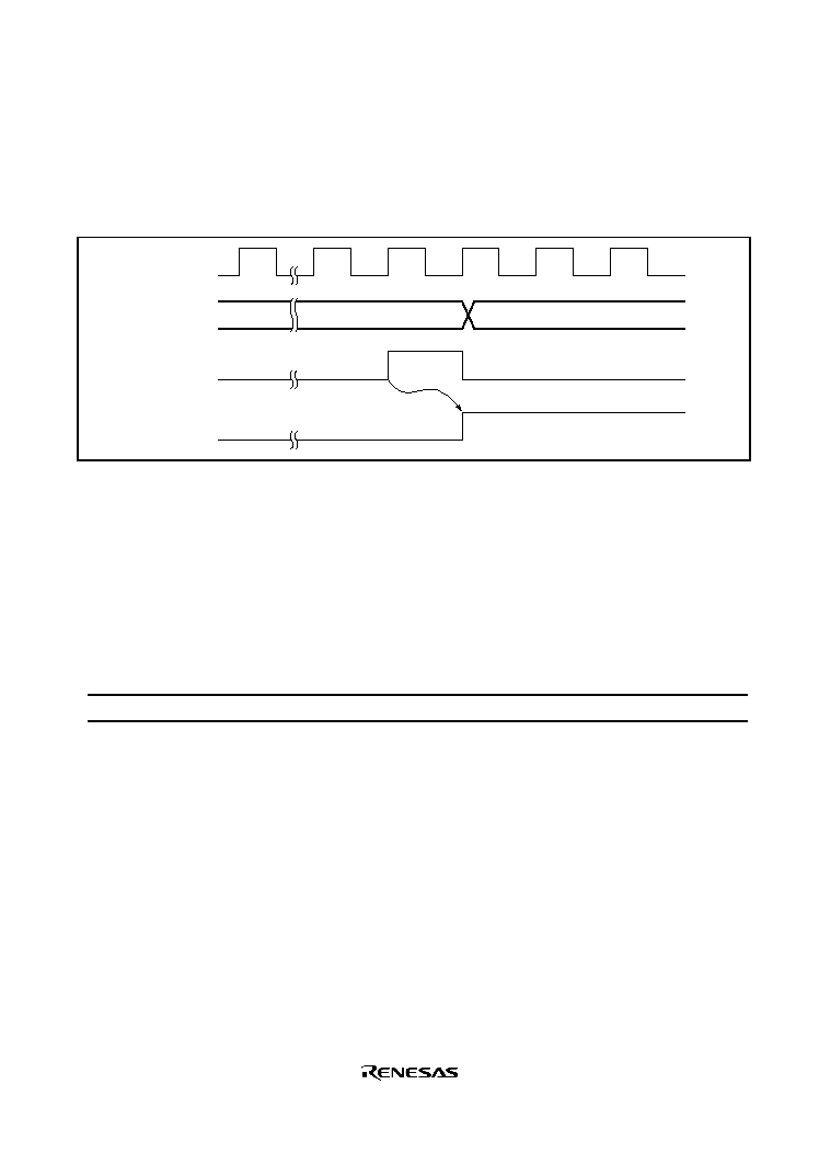
Rev. 1.0, 02/03, page 315 of 634
10.3.4
Timing of Setting of Overflow Flag (OVF)
The OVF flag is set to 1 if TCNT overflows during interval timer operation. At the same time, an
interval timer interrupt (WOVI) is requested. This timing is shown in figure 10.5.
1
1
1
TCNT
H'FF
H'00
Overflow signal
(internal signal)
OVF
Figure 10.5 Timing of OVF Setting
10.4
Interrupts
During interval timer mode operation, an overflow generates an interval timer interrupt (WOVI).
The interval timer interrupt is requested whenever the OVF flag is set to 1 in TCSR. OVF must be
cleared to 0 in the interrupt handling routine.
Table 10.1
WDT Interrupt Source
Name
Interrupt Source
Interrupt Flag
WOVI
TCNT overflow
WOVF
Rev. 1.0, 02/03, page 316 of 634
10.5
Usage Notes
10.5.1
Notes on Register Access
The watchdog timer's TCNT, TCSR, and RSTCSR registers differ from other registers in being
more difficult to write to. The procedures for writing to and reading these registers are given
below.
Writing to TCNT and TCSR
These registers must be written to by a word transfer instruction.
They cannot be written to with byte transfer instructions. Figure 10.6 shows the format of data
written to TCNT and TCSR. TCNT and TCSR both have the same write address. For a write to
TCNT, the upper byte of the written word must contain H'5A and the lower byte must contain the
write data. For a write to TCSR, the upper byte of the written word must contain H'A5 and the
lower byte must contain the write data. This transfers the write data from the lower byte to TCNT
or TCSR.
TCNT write
TCSR write
Address: H'FF74
Address: H'FF74
H'5A
Write data
15
8 7
0
H'A5
Write data
15
8 7
0
Figure 10.6 Format of Data Written to TCNT and TCSR
Writing to RSTCSR
RSTCSR must be written to by a word transfer to address H'FF76. It cannot be written to with
byte instructions. Figure 10.7 shows the format of data written to RSTCSR. The method of writing
0 to the WOVF bit differs from that for writing to the RSTE and RSTS bits.
To write 0 to the WOVF bit, the upper byte of the written word must contain H'A5 and the lower
byte must contain H'00. This clears the WOVF bit to 0, but has no effect on the RSTE and RSTS
bits. To write to the RSTE and RSTS bits, the upper byte must contain H'5A and the lower byte
must contain the write data. This writes the values in bits 6 and 5 of the lower byte into the RSTE
and RSTS bits, but has no effect on the WOVF bit.
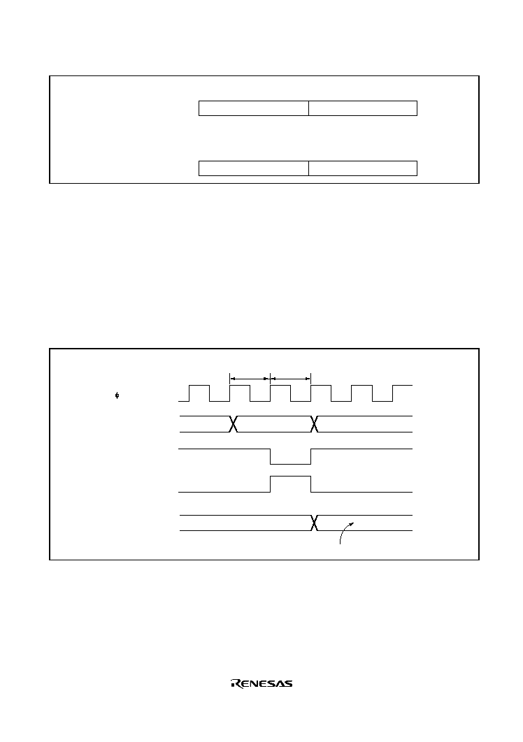
Rev. 1.0, 02/03, page 317 of 634
Writing 0 to WOVF bit
Write to RSTE, RSTS bits
Address: H'FF76
Address: H'FF76
H'A5
H'00
15
8 7
0
H'5A
Write data
15
8 7
0
Figure 10.7 Format of Data Written to RSTCSR (Example of WDT0)
Reading from TCNT, TCSR, and RSTCSR
TCNT, TCSR, and RSTCSR are read by using the same method as for the general registers.
TCSR, TCNT, and RSTCSR are allocated in addresses H'FF74, H'FF75, and H'FF77 respectively.
10.5.2
Contention between Timer Counter (TCNT) Write and Increment
If a timer counter clock pulse is generated during the T2 state of a TCNT write cycle, the write
takes priority and the timer counter is not incremented. Figure 10.8 shows this operation.
Address
Internal write
signal
TCNT input
clock
TCNT
N
M
T1
T2
TCNT write cycle
Counter write data
Figure 10.8 Contention between TCNT Write and Increment

Rev. 1.0, 02/03, page 318 of 634
10.5.3
Changing Value of CKS2 to CKS0
If bits CKS0 to CKS2 in TCSR are written to while the WDT is operating, errors could occur in
the incrementation. Software must be used to stop the watchdog timer (by clearing the TME bit to
0) before changing the value of bits CKS0 to CKS2.
10.5.4
Switching between Watchdog Timer Mode and Interval Timer Mode
If the mode is switched from watchdog timer to interval timer while the WDT is operating, errors
could occur in the incrementation. Software must be used to stop the watchdog timer (by clearing
the TME bit to 0) before switching the mode.
10.5.5
Internal Reset in Watchdog Timer Mode
This LSI is not reset internally if TCNT overflows while the RSTE bit is cleared to 0 during
watchdog timer operation, however TCNT and TCSR of the WDT are reset.
TCNT, TCSR, or RSTCR cannot be written to for 132 states following an overflow. During this
period, any attempt to read the WOVF flag is not acknowledged. Accordingly, wait 132 states
after overflow to write 0 to the WOVF flag for clearing.
RTC3000B_000020020900
Rev. 1.0, 02/03, page 319 of 634
Section 11 Realtime Clock (RTC)
The realtime clock (RTC) is a timer used to count time ranging from a second to a week. Figure
11.1 shows the block diagram of the RTC.
11.1
Features
· Counts seconds, minutes, hours, and day-of-week
· Start/stop function
· Reset function
· Readable/writable counter of seconds, minutes, hours, and day-of-week with BCD codes
· Periodic (seconds, minutes, hours, days, and weeks) interrupts
· 8-bit free running counter
· Selection of clock source
PSS
32-kHz
oscillator
circuit
RTCCSR
RSECDR
RMINDR
RWKDR
Clock count
control circuit
Interrupt
control circuit
Interrupt
RTCCR1
RHRDR
RTCCR2
Internal data bus
1/4
TMOW
Legend
RTCCSR
RSECDR
RMINDR
RHRDR
RWKDR
RTCCR1
RTCCR2
PSS
: Clock source select register
: Second date register/free running counter data register
: Minute date register
: Hour date register
: Day-of-week date register
: RTC control register 1
: RTC control register 2
: Prescaler S
Figure 11.1 Block Diagram of RTC

Rev. 1.0, 02/03, page 320 of 634
11.2
Input/Output Pin
Table 11.1 shows the RTC input/output pin.
Table 11.1
Pin Configuration
Name
Abbreviation I/O
Function
Clock output
TMOW
Output
RTC divided clock output
11.3
Register Descriptions
· Second data register/free running counter data register (RSECDR)
· Minute data register (RMINDR)
· Hour data register (RHRDR)
· Day-of-week data register (RWKDR)
· RTC control register 1 (RTCCR1)
· RTC control register 2 (RTCCR2)
· Clock source select register (RTCCSR)
· Extended module stop register (EXMDLSTP)
11.3.1
Second Data Register/Free Running Counter Data Register (RSECDR)
RSECDR counts the BCD-coded second value. This register is initialized to H'00 by a
STBY
input or the RST bit in RTCCR1, but not initialized by a
RES input. The setting range is decimal
00 to 59. It is an 8-bit read register used as a counter, when it operates as a free running counter.
For more information on reading seconds, minutes, hours, and day-of-week, see section 11.4.3,
Data Reading Procedure.

Rev. 1.0, 02/03, page 321 of 634
Bit
Bit Name
Initial Value
*
R/W
Description
7
BSY
--
R
RTC Busy
This bit is set to 1 when the RTC is updating (operating)
the values of second, minute, hour, and day-of-week data
registers. When this bit is 0, the values of second, minute,
hour, and day-of-week data registers must be adopted.
6
5
4
SC12
SC11
SC10
--
--
--
R/W
R/W
R/W
Counting Ten's Position of Seconds
Counts on 0 to 5 for 60-second counting.
3
2
1
0
SC03
SC02
SC01
SC00
--
--
--
--
R/W
R/W
R/W
R/W
Counting One's Position of Seconds
Counts on 0 to 9 once per second. When a carry is
generated, 1 is added to the ten's position.
Note:* Initial value after
RES.
11.3.2
Minute Data Register (RMINDR)
RMINDR counts the BCD-coded minute value on the carry generated once per minute by the
RSECDR counting. This register is initialized to H'00 a
STBY input or the RST bit in RTCCR1,
but not initialized by a
RES input. The setting range is decimal 00 to 59.
Bit
Bit Name
Initial Value
*
R/W
Description
7
BSY
--
R
RTC Busy
This bit is set to 1 when the RTC is updating (operating)
the values of second, minute, hour, and day-of-week data
registers. When this bit is 0, the values of second, minute,
hour, and day-of-week data registers must be adopted.
6
5
4
MN12
MN11
MN10
--
--
--
R/W
R/W
R/W
Counting Ten's Position of Minutes
Counts on 0 to 5 for 60-minute counting.
3
2
1
0
MN03
MN02
MN01
MN00
--
--
--
--
R/W
R/W
R/W
R/W
Counting One's Position of Minutes
Counts on 0 to 9 once per minute. When a carry is
generated, 1 is added to the ten's position.
Note:* Initial value after
RES.

Rev. 1.0, 02/03, page 322 of 634
11.3.3
Hour Data Register (RHRDR)
RHRDR counts the BCD-coded hour value on the carry generated once per hour by RMINDR.
This register is initialized to H'00 by a
STBY input or the RST bit in RTCCR1, but not initialized
by a
RES input. The setting range is either decimal 0 to 11 or 0 to 23 by the selection of the 12/24
bit in RTCCR1.
Bit
Bit Name
Initial Value
*
R/W
Description
7
BSY
--
R
RTC Busy
This bit is set to 1 when the RTC is updating (operating)
the values of second, minute, hour, and day-of-week data
registers. When this bit is 0, the values of second, minute,
hour, and day-of-week data registers must be adopted.
6
--
0
--
Reserved
This bit is always read as 0.
5
4
HR11
HR10
--
--
R/W
R/W
Counting Ten's Position of Hours
Counts on 0 to 2 for ten's position of hours.
3
2
1
0
HR03
HR02
HR01
HR00
--
--
--
--
R/W
R/W
R/W
R/W
Counting One's Position of Hours
Counts on 0 to 9 once per hour. When a carry is
generated, 1 is added to the ten's position.
Note:* Initial value after
RES.

Rev. 1.0, 02/03, page 323 of 634
11.3.4
Day-of-Week Data Register (RWKDR)
RWKDR counts the BCD-coded day-of-week value on the carry generated once per day by
RHRDR. This register is initialized to H'00 by a
STBY input or the RST bit in RTCCR1, but not
initialized by a
RES input. The setting range is decimal 0 to 6 using bits WK2 to WK0.
Bit
Bit Name
Initial Value
*
R/W
Description
7
BSY
--
R
RTC Busy
This bit is set to 1 when the RTC is updating (operating)
the values of second, minute, hour, and day-of-week data
registers. When this bit is 0, the values of second, minute,
hour, and day-of-week data registers must be adopted.
6 to
3
--
All 0
--
Reserved
These bits are always read as 0.
2
1
0
WK2
WK1
WK0
--
--
--
R/W
R/W
R/W
Day-of-Week Counting
Day-of-week is indicated with a binary code
000: Sunday
001: Monday
010: Tuesday
011: Wednesday
100: Thursday
101: Friday
110: Saturday
111: Reserved (Setting prohibited)
Note:* Initial value after
RES.
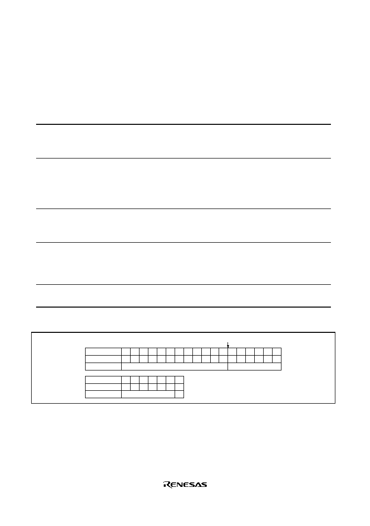
Rev. 1.0, 02/03, page 324 of 634
11.3.5
RTC Control Register 1 (RTCCR1)
RTCCR1 controls start/stop and reset of the clock timer. Bits 7 to 5 of this register are initialized
to H'00 by a
STBY input or the RST bit in RTCCR1, but not initialized by a RES input. For the
definition of time expression, see figure 11.2.
Bit
Bit Name
Initial Value
*
R/W
Description
7
RUN
--
R/W
RTC Operation Start
0: Stops RTC and free running counter operation
1: Starts RTC and free running counter operation
6
12/24
--
R/W
Operating Mode
0: RTC operates in 12-hour mode. RHRDR counts on 0
to 11.
1: RTC operates in 24-hour mode. RHRDR counts on 0
to 23.
5
PM
--
R/W
A.M./P.M.
0: Indicates a.m. when RTC is in the 12-hour mode.
1: Indicates p.m. when RTC is in the 12-hour mode.
4
RST
0
R/W
Reset
0: Normal operation
1: Resets registers and control circuits except RTCCSR
and this bit. Clear this bit to 0 after having been set to 1.
3 to
0
--
All 0
--
Reserved
These bits are always read as 0.
Note:* Initial value after
RES.
24-hour count
0
1
2
3
4
5
6
7
8
9 10 11 12 13 14 15 16 17
12-hour count
0
PM
24-hour count
12-hour count
PM
0 (Morning)
1 (Afternoon)
Noon
1
2
3
4
5
6
7
8
9 10 11 0
1
2
3
4
5
18 19 20 21 22 23 0
6
1 (Afternoon)
0
7
8
9 10 11 0
Figure 11.2 Definition of Time Expression

Rev. 1.0, 02/03, page 325 of 634
11.3.6
RTC Control Register 2 (RTCCR2)
RTCCR2 controls RTC periodic interrupts of weeks, days, hours, minutes, and seconds. This
register is initialized to H'00 by a
STBY input or the RST bit in RTCCR1, but not initialized by a
RES input. Enabling interrupts of weeks, days, hours, minutes, and seconds sets the IRRTA flag to
1 in the interrupt flag register 1 (IRR1) when an interrupt occurs. It also controls an overflow
interrupt of a free running counter when RTC operates as a free running counter.
Bit
Bit Name
Initial Value
*
R/W
Description
7
6
--
--
0
0
--
--
Reserved
These bits are always read as 0.
5
FOIE
--
R/W
Free Running Counter Overflow Interrupt Enable
0: Disables an overflow interrupt
1: Enables an overflow interrupt
4
WKIE
--
R/W
Week Periodic Interrupt Enable
0: Disables a week periodic interrupt
1: Enables a week periodic interrupt
3
DYIE
--
R/W
Day Periodic Interrupt Enable
0: Disables a day periodic interrupt
1: Enables a day periodic interrupt
2
HRIE
--
R/W
Hour Periodic Interrupt Enable
0: Disables an hour periodic interrupt
1: Enables an hour periodic interrupt
1
MNIE
--
R/W
Minute Periodic Interrupt Enable
0: Disables a minute periodic interrupt
1: Enables a minute periodic interrupt
0
SEIE
--
R/W
Second Periodic Interrupt Enable
0: Disables a second periodic interrupt
1: Enables a second periodic interrupt
Note:* Initial value after
RES.

Rev. 1.0, 02/03, page 326 of 634
11.3.7
Clock Source Select Register (RTCCSR)
RTCCSR selects clock source. This register is initialized to H'08 by a
STBY input or RES input.
A free running counter controls start/stop of counter operation by the RUN bit in RTCCR1. When
a clock other than 32.768 MHz is selected, the RTC is disabled and operates as an 8-bit free
running counter. When the RTC operates as an 8-bit free running counter, RSECDR enables
counter values to be read. An interrupt can be generated by setting 1 to the FOIE bit in RTCCR2
and enabling an overflow interrupt of the free running counter. A clock in which the system clock
is divided by 32, 16, 8, or 4 is output in active or sleep mode.
Bit
Bit Name
Initial Value
R/W
Description
7
--
0
--
Reserved
This bit is always read as 0.
6
5
RCS6
RCS5
0
0
R/W
R/W
Clock Output Selection
Selects a clock output from the TMOW pin when the
TMOWE bit in UCTLR is set to 1.
00:
/4
01:
/8
10:
/16
11:
/32
4
--
0
--
Reserved
This bit is always read as 0.
3
2
1
0
RCS3
RCS2
RCS1
RCS0
1
0
0
0
R/W
R/W
R/W
R/W
Clock Source Selection
0000:
/8 Free running counter
0001:
/32 Free running counter operation
0010:
/128 Free running counter operation
0011:
/256 Free running counter operation
0100:
/512 Free running counter operation
0101:
/2048 Free running counter operation
0110:
/4096 Free running counter operation
0111:
/8192 Free running counter operation
1000: 32.768 kHz
RTC operation
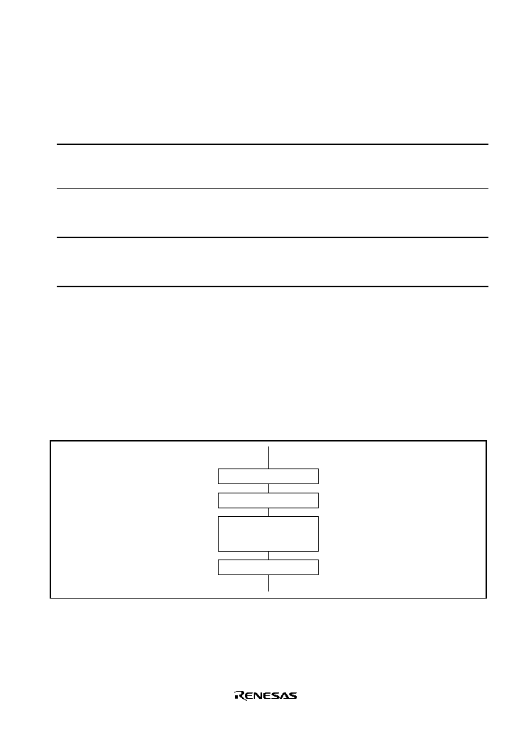
Rev. 1.0, 02/03, page 327 of 634
11.3.8
Extended Module Stop Register (EXMDLSTP)
EXMDLSTP controls the clock supply of the RTC and USB.
Bit
Bit Name
Initial Value
R/W
Module
7 to
2
Undefined
Reserved
These bits are always read as undefined values.
These bits should not to be modified.
1
RTCSTOP
0
R/W
RTC Module Stop
0: RTC module stop cancelled
1: RTC module stop
0
USBSTOP1
0
R/W
USB Module Stop
0: USB module stop partly cancelled
1: USB module completely stop
11.4
Operation
11.4.1
Initial Settings of Registers after Power-On
The RTC registers that store second, minute, hour, and day-of week data are not reset by a
RES
input. Therefore, all registers must be set to their initial values after power-on. Figure 11.3 shows
the initial setting procedure of the RTC. Once the register setting are made, the RTC provides an
accurate time as long as power is supplied regardless of a
RES input.
RST in RTCCR1=1
RST in RTCCR1=0
Set RSECDR, RMINDR,
RHRDR, RWKDR,
12/24 in RTCCR1, and PM
RUN in RTCCR1=1
Figure 11.3 Initial Setting Procedure
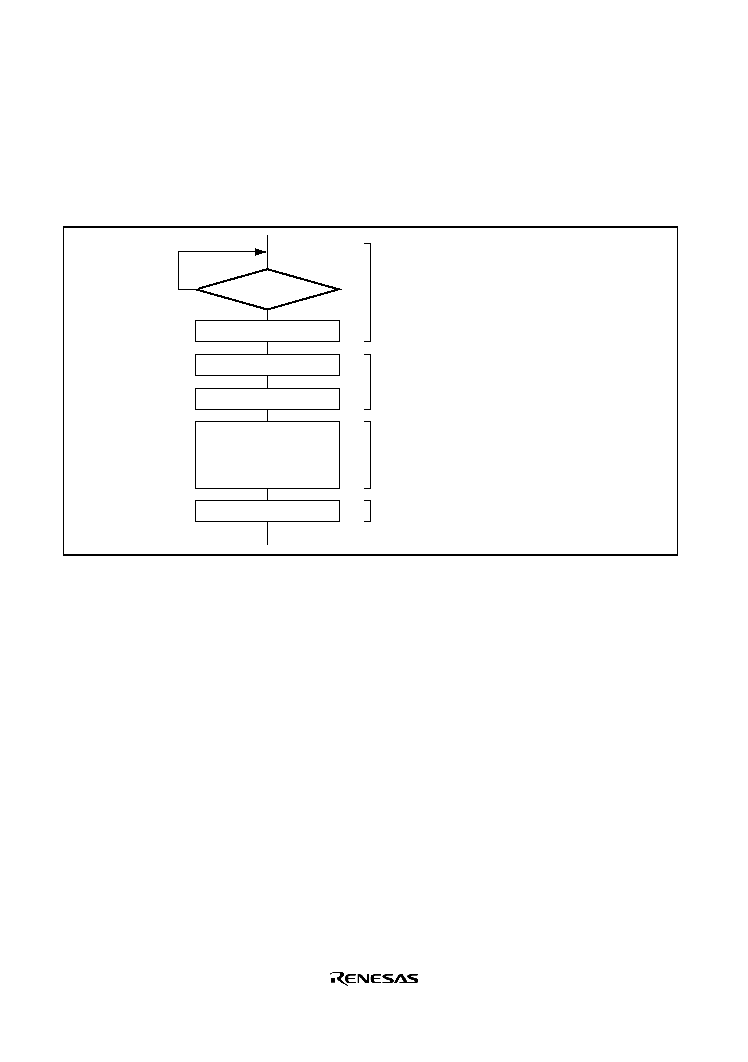
Rev. 1.0, 02/03, page 328 of 634
11.4.2
Resetting Procedure
Figure 11.4 shows the procedure for the resetting of the RTC in operation. To set second, minute,
hour, and day-of-week data, check the setting of the BSY bit, and clear the RUN bit in RTCCR1
to 0 when the BSY bit is 0 to stop operation of the RTC.
RTC operation is stopped.
Clock count controller is reset.
Second, minute, hour, day-of-week,
operating mode, and a.m/p.m are set.
RTC operation is started.
BSY=0?
RUN in RTCCR1=0
RST in RTCCR1=1
RST in RTCCR1=0
Set RSECDR, RMINDR,
RHRDR, RWKDR,
12/24 in RTCCR1,
and PM
RUN in RTCCR1=1
Figure 11.4 Resetting Procedure

Rev. 1.0, 02/03, page 329 of 634
11.4.3
Data Reading Procedure
When the seconds, minutes, hours, or day-of-week datum is updated while time data is being read,
the data obtained may not be correct, and so the time data must be read again. Figure 11.5 shows
an example in which correct data is not obtained. In this example, since only RSECDR is read
after data update, about 1-minute inconsistency occurs.
To avoid reading in this timing, the following processing must be performed.
1. Check the setting of the BSY bit, and when the BSY bit changes from 1 to 0, read from the
second, minute, hour, and day-of-week registers. When about 62.5 ms is passed after the BSY
bit is set to 1, the registers are updated, and the BSY bit is cleared to 0.
2. Making use of interrupts, read from the second, minute, hour, and day-of week registers after
the IRG5F flag in ISR is set to 1 and the BSY bit is confirmed to be 0.
3. Read from the second, minute, hour, and day-of week registers twice in a row, and if there is
no change in the read data, the read data is used.
Before update
RWKDR = H'03, RHDDR = H'13, RMINDR = H'46, RSECDR = H'59
BSY bit = 0
(1) Day-of-week data register read H'03
(2) Hour data register read
H'13
(3) Minute data register read
H'46
BSY bit -> 1 (under data update)
After update
RWKDR = H'03, RHDDR = H'13, RMINDR = H'47, RSECDR = H'00
BSY bit -> 0
(4) Second data register read
H'00
Processing flow
Figure 11.5 Example: Reading of Inaccurate Time Data

Rev. 1.0, 02/03, page 330 of 634
11.5
Interrupt Source
The RTC interrupt sources are listed in table 11.2. There are five kinds of RTC interrupts: week
interrupts, day interrupts, hour interrupts, minute interrupts, and second interrupts.
When using an interrupt, initiate the RTC last after other registers (include ISCRH and IER of
interrupt controller) are set. Do not set multiple interrupt enable bits in RTCCR2 simultaneously
to 1.
When an interrupt request of the RTC occurs, the IRQ5F flag in ISR is set to 1. When clearing the
flag, write 0 after reading the flag = 1.
Figure 11.6 shows the initializing setting procedure in using the RTC interrupt and figure 11.7
shows an example of the RTC interrupt handling routine.
Table 11.2
Interrupt Source
Interrupt Name
Interrupt Source
Interrupt Enable Bit
Overflow interrupt
Occurs when the free running counter is
overflown.
FOIE
Week periodic interrupt
Occurs every week when the day-of-week
date register value becomes 0.
WKIE
Day periodic interrupt
Occurs every day when the day-of-week date
register is counted.
DYIE
Hour periodic interrupt
Occurs every hour when the hour date
register is counted.
HRIE
Minute periodic interrupt
Occurs every minute when the minute date
register is counted.
MNIE
Second periodic interrupt
Occurs every second when the second date
register is counted.
SEIE
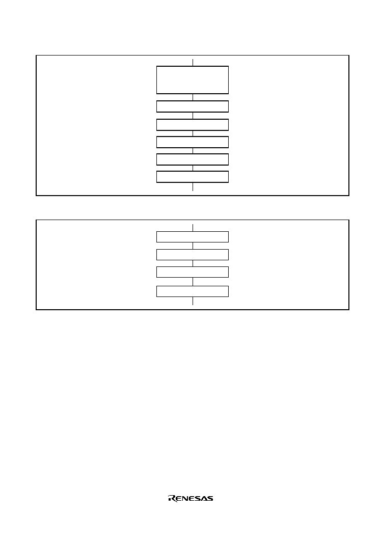
Rev. 1.0, 02/03, page 331 of 634
Write 0 to bit 5 in ISR register
Set RTC register
Write 1 to bit 5 in IER
RUN in RTCCR1 = 1
Set IRQ5SCB = 0 and
IRQ5SCA = 1 in
ISCRH register
Read ISR register
Figure 11.6 Initializing Procedure in Using RTC Interrupt
Write 0 to bit 5 in ISR register
Interrupt handling
RTE
Read ISR register
Figure 11.7 Example of RTC Interrupt Handling Routine

Rev. 1.0, 02/03, page 332 of 634
11.6
Operating State in Each Mode
Table 11.3 shows the operating state in each mode when the RTC is set for clock operation and
free running timer operation. The clock operation is performed continuously even in low power
mode. Therefore, when the clock operation is unnecessary, cancel it by EXMDLSTP.
Table 11.3
Operating State in Each Mode
Function
High-
Speed
Medium-
Speed
Sleep
Module
Stop
Watch
Sub-
Active
Sub-Sleep
Software
Standby
Hard-ware
Standby
Clock operation
Sub-clock
operation
Sub-clock
operation
Sub-clock
operation
Halted
(Retained)
Subclock
operation
Subclock
operation
Subclock
operation
Subclock
operation
Halted
(Reset)
Free running
timer operation
Operating
Operating
Operating
Halted
(Retained)
Halted
(Retained)
Halted
(Retained)
Halted
(Retained)
Halted
(Retained)
Halted
(Reset)

SCI0023C_000020020900
Rev. 1.0, 02/03, page 333 of 634
Section 12 Serial Communication Interface
This LSI has two independent serial communication interface (SCI) channels. The SCI can handle
both asynchronous and clocked synchronous serial communication. Asynchronous serial data
communication can be carried out using standard asynchronous communication chips such as a
Universal Asynchronous Receiver/Transmitter (UART) or an Asynchronous Communication
Interface Adapter (ACIA). A function is also provided for serial communication between
processors (multiprocessor communication function). The SCI also supports the smart card (IC
card) interface based on ISO/IEC 7816-3 (Identification Card) as an enhanced asynchronous
communication function.
12.1
Features
· Choice of asynchronous or clocked synchronous serial communication mode
· Full-duplex communication capability
The transmitter and receiver are mutually independent, enabling transmission and reception to
be executed simultaneously.
Double-buffering is used in both the transmitter and the receiver, enabling continuous
transmission and continuous reception of serial data.
On-chip baud rate generator allows any bit rate to be selected
External clock can be selected as a transfer clock source (except for in Smart Card interface
mode).
· Choice of LSB-first or MSB-first transfer (except in the case of asynchronous mode 7-bit data)
· Four interrupt sources
Transmit-end, transmit-data-empty, receive-data-full, and receive error -- that can issue
requests.
The transmit-data-empty interrupt and receive data full interrupts can be used to activate the
direct memory access controller (DMAC).
· Module stop mode can be set
Asynchronous Mode
· Data length: 7 or 8 bits
· Stop bit length: 1 or 2 bits
· Parity: Even, odd, or none
· Receive error detection: Parity, overrun, and framing errors
· Break detection: Break can be detected by reading the RxD pin level directly in the case of a
framing error

Rev. 1.0, 02/03, page 334 of 634
· Average transfer rate generator (SCI_0):
921.569 kbps, 720 kbps, 460.784 kbps, or 115.196 kbps can be selected at 16 MHz
921.053 kbps, 720 kbps, 460.526 kbps, or 115.132 kbps can be selected at 24 MHz
· A transfer rate clock can be input from the TPU (SCI_0)
· A multiprocessor communication function is provided that enables serial data
communication with a number of processors
Clocked Synchronous Mode
· Data length: 8 bits
· Receive error detection: Overrun errors detected
· SCI select function (SCI_0): TxD0 = high-impedance and SCK0 = fixed high-level input can
selected when IRQ7 = 1)
· Serial data communication can be carried out with other chips that have a synchronous
communication function
Smart Card Interface
· An error signal can be automatically transmitted on detection of a parity error during reception
· Data can be automatically re-transmitted on detection of a error signal during transmission
· Both direct convention and inverse convention are supported
12.1.1
Block Diagram
Figure 12.1 shows the block diagram of the SCI_0. Figure 12.2 shows the block diagram of the
SCI_2.
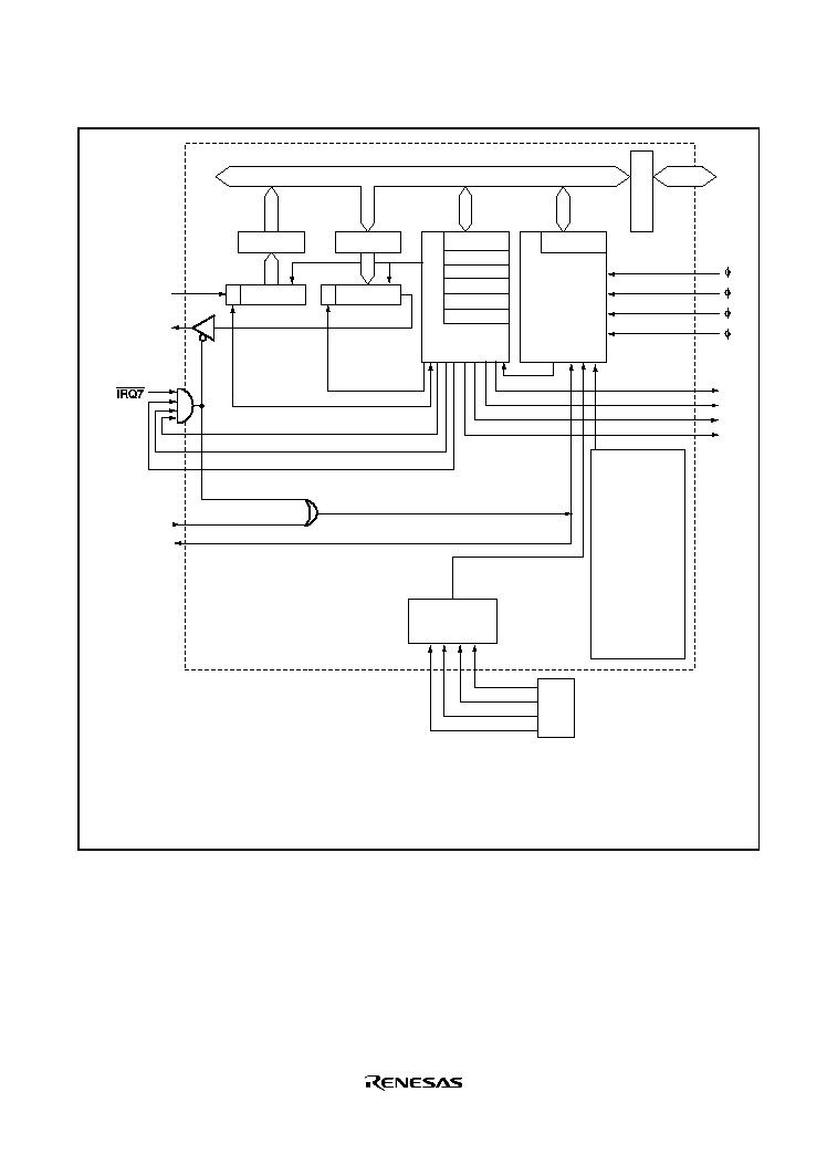
Rev. 1.0, 02/03, page 335 of 634
RxD0
TxD0
PG1/
C/A
CKE1
SSE
SCK0
Clock
External clock
TEI
TXI
RXI
ERI
RSR
RDR
TSR
TDR
SMR
: Receive shift register
: Receive data register
: Transmit shift register
: Transmit data register
: Serial mode register
SCR
SSR
SCMR
BRR
SEMRA_0
SEMRB_0
: Serial control register
: Serial status register
: Smart card mode register
: Bit rate register
: Serial extended mode register A_0
: Serial extended mode register B_0
SCMR
SSR
SCR
SMR
SEMRA_0
SEMRB_0
control
transmission
and reception
Baud rate
generator
Average transfer
rate generator
10.667 MHz
· 115.152 kbps
· 460.606 kbps
16 MHz
· 115.196 kbps
· 460.784 kbps
· 720 kbps
· 921.569 kbps
24 MHz
· 115.132 kbps
· 460.526 kbps
· 720 kbps
· 921.053 kbps
BRR
TPU
TIOCC0
TIOCA1
TIOCA0
TIOCA2
Module data bus
RDR
TSR
RSR
Parity generation
Legend
TDR
SCI transfer
clock generator
in TPU
Parity
check
Internal data bus
Bus interface
/4
/16
/64
Figure 12.1 Block Diagram of SCI_0
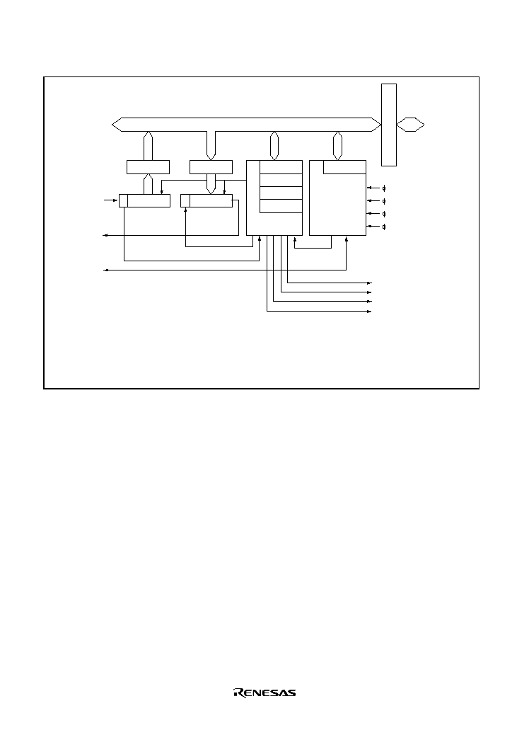
Rev. 1.0, 02/03, page 336 of 634
RxD
TxD
SCK
Clock
External clock
/4
/16
/64
TEI
TXI
RXI
ERI
RSR
RDR
TSR
TDR
SMR
SCR
SSR
SCMR
BRR
: Receive shift register
: Receive data register
: Transmit shift register
: Transmit data register
: Serial mode register
: Serial control register
: Serial status register
: Smart card register
: Bit rate register
SCMR
SSR
SCR
SMR
control
transmission
and reception
Baud rate
generator
BRR
Module data bus
RDR
TSR
RSR
Detecting parity
Parity check
Legend
TDR
Internal data bus
Bus interface
Figure 12.2 Block Diagram ofSCI_2

Rev. 1.0, 02/03, page 337 of 634
12.2
Input/Output Pins
Table 12.1 shows the serial pins for each SCI channel.
Table 12.1
Pin Configuration
Channel
Pin Name
*
I/O
Function
SCK0
I/O
SCI_0 clock input/output
RxD0
Input
SCI_0 receive data input
0
TxD0
Output
SCI_0 transmit data output
SCK2
I/O
SCI_2 clock input/output
RxD2
Input
SCI_2 receive data input
2
TxD2
Output
SCI_2 transmit data output
Note: * Pin names SCK, RxD, and TxD are used in the text for all channels, omitting the channel
designation.
12.3
Register Descriptions
The SCI has the following registers for each channel. Some bits in the serial mode register (SMR),
serial status register (SSR), and serial control register (SCR) have different functions in different
modes
normal serial communication interface mode and smart card interface mode; therefore,
the bits are described separately for each mode in the corresponding register sections.
· Receive shift register (RSR)
· Receive data register (RDR)
· Transmit data register (TDR)
· Transmit shift register (TSR)
· Serial mode register (SMR)
· Serial control register (SCR)
· Serial status register (SSR)
· Smart card mode register (SCMR)
· Serial extended mode register A_0 (SEMRA_0) (only for channel 0)
· Serial extended mode register B_0 (SEMRB_0) (only for channel 0)
· Bit rate register (BRR)

Rev. 1.0, 02/03, page 338 of 634
12.3.1
Receive Shift Register (RSR)
RSR is a shift register that is used to receive serial data input to the RxD pin and convert it into
parallel data. When one byte of data has been received, it is transferred to RDR automatically.
RSR cannot be directly accessed by the CPU.
12.3.2
Receive Data Register (RDR)
RDR is an 8-bit register that stores received data. When the SCI has received one byte of serial
data, it transfers the received serial data from RSR to RDR, where it is stored. After this, RSR is
receive-enabled. As RSR and RDR function as a double buffer in this way, continuous receive
operations are possible. After confirming that the RDRF bit in SSR is set to 1, read RDR only
once. RDR cannot be written to by the CPU.
12.3.3
Transmit Data Register (TDR)
TDR is an 8-bit register that stores data for transmission. When the SCI detects that TSR is empty,
it transfers the transmit data written in TDR to TSR and starts transmission. The double-buffered
structure of TDR and TSR enables continuous serial transmission. If the next transmit data has
already been written to TDR during serial transmission, the SCI transfers the written data to TSR
to continue transmission. Although TDR can be read from or written to by the CPU at all times, to
achieve reliable serial transmission, write transmit data to TDR only once after confirming that the
TDRE bit in SSR is set to 1.
12.3.4
Transmit Shift Register (TSR)
TSR is a shift register that transmits serial data. To perform serial data transmission, the SCI first
transfers transmit data from TDR to TSR, then sends the data to the TxD pin. TSR cannot be
directly accessed by the CPU.

Rev. 1.0, 02/03, page 339 of 634
12.3.5
Serial Mode Register (SMR)
SMR is used to set the SCI's serial transfer format and select the baud rate generator clock source.
Some bits in SMR have different functions in normal mode and smart card interface mode.
· Normal Serial Communication Interface Mode (When SMIF in SCMR is 0)
Bit
Bit Name Initial Value
R/W
Description
7
C/
A
0
R/W
Communication Mode
0: Asynchronous mode
1: Clocked synchronous mode
6
CHR
0
R/W
Character Length (enabled only in asynchronous mode)
0: Selects 8 bits as the data length.
1: Selects 7 bits as the data length. LSB-first is fixed
and the MSB of TDR is not transmitted in
transmission.
In clocked synchronous mode, a fixed data length of 8
bits is used.
5
PE
0
R/W
Parity Enable (enabled only in asynchronous mode)
When this bit is set to 1, the parity bit is added to
transmit data before transmission, and the parity bit is
checked in reception. For a multiprocessor format, parity
bit addition and checking are not performed regardless
of the PE bit setting.
4
O/
E
0
R/W
Parity Mode (enabled only when the PE bit is 1 in
asynchronous mode)
0: Selects even parity.
1: Selects odd parity.
3
STOP
0
R/W
Stop Bit Length (enabled only in asynchronous mode)
Selects the stop bit length in transmission.
0: 1 stop bit
1: 2 stop bits
In reception, only the first stop bit is checked. If the
second stop bit is 0, it is treated as the start bit of the
next transmit character.
2
MP
0
R/W
Multiprocessor Mode (enabled only in asynchronous
mode)
When this bit is set to 1, the multiprocessor
communication function is enabled. The PE bit and O/
E
bit settings are invalid in multiprocessor mode. For
details, see section 12.5, Multi Processor
Communication Function.

Rev. 1.0, 02/03, page 340 of 634
Bit
Bit Name Initial Value
R/W
Description
1
0
CKS1
CKS0
0
0
R/W
R/W
Clock Select 0 and 1:
These bits select the clock source for the baud rate
generator.
00:
clock (n = 0)
01:
/4 clock (n = 1)
10:
/16 clock (n = 2)
11:
/64 clock (n = 3)
For the relationship between the bit rate register setting
and the baud rate, see section 12.3.11, Bit Rate Register
(BRR). n is the decimal representation of the value of n
in BRR (see section 12.3.11, Bit Rate Register (BRR)).
· Smart Card Interface Mode (When SMIF in SCMR is 1)
Bit
Bit Name Initial Value
R/W
Description
7
GM
0
R/W
GS Mode
Setting this bit to 1 allows GSM mode operation. In
GSM mode, the TEND set timing is put forward to 11.0
etu from the start and the clock output control function is
appended. For details, see section 12.7.8, Clock Output
Control.
6
BLK
0
R/W
Setting this bit to 1 allows block transfer mode operation.
For details, see section 12.7.3, Block Transfer Mode.
5
PE
0
R/W
Parity Enable (valid only in asynchronous mode)
When this bit is set to 1, the parity bit is added to
transmit data before transmission, and the parity bit is
checked in reception. Set this bit to 1 in smart card
interface mode.
4
O/
E
0
R/W
Parity Mode (valid only when the PE bit is 1 in
asynchronous mode)
0: Selects even parity
1: Selects odd parity
For details on the usage of this bit in smart card interface
mode, see section 12.7.2, Data Format (Except in Block
Transfer Mode).

Rev. 1.0, 02/03, page 341 of 634
Bit
Bit Name Initial Value
R/W
Description
3
2
BCP1
BCP0
0
0
R/W
R/W
Basic Clock Pulse 1,0
These bits select the number of basic clock cycles in a 1-
bit data transfer time in smart card interface mode.
00: 32 clock cycles (S = 32)
01: 64 clock cycles (S = 64)
10: 372 clock cycles (S = 372)
11: 256 clock cycles (S = 256)
For details, see section 12.7.4, Receive Data Sampling
Timing and Reception Margin. S is described in section
12.3.11, Bit Rate Register (BRR).
1
0
CKS1
CKS0
0
0
R/W
R/W
Clock Select 1,0
These bits select the clock source for the baud rate
generator.
00:
clock (n = 0)
01:
/4 clock (n = 1)
10:
/16 clock (n = 2)
11:
/64 clock (n = 3)
For the relation between the bit rate register setting and
the baud rate, see section 12.3.11, Bit Rate Register
(BRR). n is the decimal display of the value of n in BRR
(see section 12.3.11, Bit Rate Register (BRR)).

Rev. 1.0, 02/03, page 342 of 634
12.3.6
Serial Control Register (SCR)
SCR is a register that enables or disables SCI transfer operations and interrupt requests, and is also
used to selection of the transfer clock source. For details on interrupt requests, refer to section
12.9, Interrupts. Some bits in SCR have different functions in normal mode and smart card
interface mode.
· Normal Serial Communication Interface Mode (When SMIF in SCMR is 0)
Bit
Bit Name Initial Value
R/W
Description
7
TIE
0
R/W
Transmit Interrupt Enable
When this bit is set to 1, the TXI interrupt request is
enabled.
TXI interrupt request cancellation can be performed by
reading 1 from the TDRE flag, then
clearing it to 0, or clearing the TIE bit to 0.
6
RIE
0
R/W
Receive Interrupt Enable
When this bit is set to 1, RXI and ERI interrupt requests
are enabled.
RXI and ERI interrupt request cancellation can be
performed by reading 1 from the RDRF flag, or the FER,
PER, or ORER flag, then clearing the flag to 0, or
clearing the RIE bit to 0.
5
TE
0
R/W
Transmit Enable
When this bit s set to 1, transmission is enabled.
In this state, serial transmission is started when transmit
data is written to TDR and the TDRE flag in SSR is
cleared to 0. SMR setting must be performed to decide
the transfer format before setting the TE bit to 1. The
TDRE flag in SSR is fixed at 1 if transmission is disabled
by clearing this bit to 0.
4
RE
0
R/W
Receive Enable
When this bit is set to 1, reception is enabled.
Serial reception is started in this state when a start bit is
detected in asynchronous mode or serial clock input is
detected in clocked synchronous mode. SMR setting
must be performed to decide the transfer format before
setting the RE bit to 1.
Clearing the RE bit to 0 does not affect the RDRF, FER,
PER, and ORER flags, which retain their states
.

Rev. 1.0, 02/03, page 343 of 634
Bit
Bit Name Initial Value
R/W
Description
3
MPIE
0
R/W
Multiprocessor Interrupt Enable (enabled only when the
MP bit in SMR is 1 in asynchronous mode)
When this bit is set to 1, receive data in which the
multiprocessor bit is 0 is skipped, and setting of the
RDRF, FER, and ORER status flags in SSR is
prohibited. On receiving data in which the multiprocessor
bit is 1, this bit is automatically cleared and normal
reception is resumed. For details, refer to section 12.5,
Multiprocessor Communication Function.
When receive data including MPB = 0 is received,
receive data transfer from RSR to RDR, receive error
detection, and setting of the RDRF, FER, and ORER
flags in SSR, is not performed. When receive data
including MPB = 1 is received, the MPB bit in SSR is set
to 1, the MPIE bit is cleared to 0 automatically, and
generation of RXI and ERI interrupts (when the TIE and
RIE bits in SCR are set to 1) and FER and ORER flag
setting is enabled.
2
TEIE
0
R/W
Transmit End Interrupt Enable
This bit is set to 1, TEI interrupt request is enabled.
TEI
cancellation can be performed by reading 1 from the
TDRE flag in SSR, then clearing it to 0 and clearing the
TEND flag to 0, or clearing the TEIE bit to 0.
1
0
CKE1
CKE0
0
0
R/W
R/W
Clock Enable 0 and 1
Selects the clock source and SCK pin function.
Asynchronous mode
00: Internal baud rate generator
SCK pin functions as I/O port
01: Internal baud rate generator
Outputs a clock of the same frequency as the bit
rate from the SCK pin.
1X: External clock
Inputs a clock with a frequency 16 times the bit rate
from the SCK pin.
Clocked synchronous mode
0X: Internal clock (SCK pin functions as clock output)
1X: External clock (SCK pin functions as clock input)
Legend X: Don't care

Rev. 1.0, 02/03, page 344 of 634
· Smart Card Interface Mode (When SMIF in SCMR is 1)
Bit
Bit Name Initial Value
R/W
Description
7
TIE
0
R/W
Transmit Interrupt Enable
When this bit is set to 1, TXI interrupt request is enabled.
TXI interrupt request cancellation can be performed by
reading 1 from the TDRE flag in SSR, then clearing it to
0, or clearing the TIE bit to 0.
6
RIE
0
R/W
Receive Interrupt Enable
When this bit is set to 1, RXI and ERI interrupt requests
are enabled.
RXI and ERI interrupt request cancellation can be
performed by reading 1 from the RDRF, FER, PER, or
ORER flag in SSR, then clearing the flag to 0, or clearing
the RIE bit to 0.
5
TE
0
R/W
Transmit Enable
When this bit s set to 1, transmission is enabled.
In this state, serial transmission is started when transmit
data is written to TDR and the TDRE flag in SSR is
cleared to 0.
SMR setting must be performed to decide the transfer
format before setting the TE bit to 1. When this bit is
cleared to 0, the transmission operation is disabled, and
the TDRE flag is fixed at 1.
4
RE
0
R/W
Receive Enable
When this bit is set to 1, reception is enabled.
Serial reception is started in this state when a start bit is
detected in asynchronous mode or serial clock input is
detected in clocked synchronous mode.
SMR setting must be performed to decide the reception
format before setting the RE bit to 1.
Clearing the RE bit to 0 does not affect the RDRF,
FER,PER, and ORER flags, which retain their states.
3
MPIE
0
R/W
Multiprocessor Interrupt Enable (enabled only when the MP
bit in SMR is 1 in asynchronous mode)
Write 0 to this bit in Smart Card interface mode.
When receive data including MPB = 0 is received, receive
data transfer from RSR to RDR, receive error detection,
and setting of the RERF, FER, and ORER flags in SSR,
are not performed.
When receive data including MPB = 1 is received, the MPB
bit in SSR is set to 1, the MPIE bit is cleared to 0
automatically, and generation of RXI and ERI interrupts
(when the TIE and RIE bits in SCR are set to 1) and FER
and ORER flag setting are enabled.

Rev. 1.0, 02/03, page 345 of 634
Bit
Bit Name Initial Value
R/W
Description
2
TEIE
0
R/W
Transmit End Interrupt Enable
Write 0 to this bit in Smart Card interface mode.
TEI cancellation can be performed by reading 1 from the
TDRE flag in SSR, then clearing it to 0 and clearing the
TEND flag to 0, or clearing the TEIE bit to 0.
1
0
CKE1
CKE0
0
0
R/W
Clock Enable 0 and 1
Enables or disables clock output from the SCK pin. The
clock output can be dynamically switched in GSM mode.
For details, refer to section 12.7.8, Clock Output Control.
When the GM bit in SMR is 0:
00: Output disabled (SCK pin can be used as an I/O port
pin)
01: Clock output
1X: Reserved
When the GM bit in SMR is 1:
00: Output fixed low
01: Clock output
10: Output fixed high
11: Clock output
Legend X: Don't care

Rev. 1.0, 02/03, page 346 of 634
12.3.7
Serial Status Register (SSR)
SSR is a register containing status flags of the SCI and multiprocessor bits for transfer. 1 cannot be
written to flags TDRE, RDRF, ORER, PER, and FER; they can only be cleared. Some bits in SSR
have different functions in normal mode and smart card interface mode.
· Normal Serial Communication Interface Mode (When SMIF in SCMR is 0)
Bit
Bit Name Initial Value
R/W
Description
7
TDRE
1
R/(W)* Transmit Data Register Empty
Displays whether TDR contains transmit data.
[Setting conditions]
· When the TE bit in SCR is 0
· When data is transferred from TDR to TSR and data
can be written to TDR
[Clearing conditions]
· When 0 is written to TDRE after reading TDRE = 1
· When the DMAC is activated by a TXI interrupt
request and writes data to TDR
6
RDRF
0
R/(W)* Receive Data Register Full
Indicates that the received data is stored in RDR.
[Setting condition]
· When serial reception ends normally and receive
data is transferred from RSR to RDR
[Clearing conditions]
· When 0 is written to RDRF after reading RDRF = 1
· When the DMAC is activated by an RXI interrupt and
transferred data from RDR
RDR and the RDRF flag are not affected and retain their
previous values when the RE bit in SCR is cleared to 0.
The RDRF flag is not affected and retains their previous
values when the RE bit in SCR is cleared to 0.

Rev. 1.0, 02/03, page 347 of 634
Bit
Bit Name Initial Value
R/W
Description
5
ORER
0
R/(W)* Overrun Error
[Setting condition]
· When the next serial reception is completed while
RDRF = 1
The receive data prior to the overrun error is retained
in RDR, and the data received subsequently is lost.
Also, subsequent serial reception cannot be
continued while the ORER flag is set to 1. In clocked
synchronous mode, serial transmission cannot be
continued, either.
[Clearing condition]
· When 0 is written to ORER after reading ORER = 1
The ORER flag is not affected and retains its
previous state when the RE bit in SCR is cleared to
0.
4
FER
0
R/(W)* Framing Error
[Setting condition]
· When the stop bit is 0
In 2-stop-bit mode, only the first stop bit is checked
for a value of 0; the second stop bits not checked. If
a framing error occurs, the receive data is transferred
to RDR but the RDRF flag is not set. Also,
subsequent serial reception cannot be continued
while the FER flag is set to 1. In clocked
synchronous mode, serial transmission cannot be
continued, either.
[Clearing condition]
· When 0 is written to FER after reading FER = 1
The FER flag is not affected and retains its previous
state when the RE bit in SCR is cleared to 0.

Rev. 1.0, 02/03, page 348 of 634
Bit
Bit Name Initial Value
R/W
Description
3
PER
0
R/(W)* Parity Error
[Setting condition]
· When a parity error is detected during reception
If a parity error occurs, the receive data is transferred
to RDR but the RDRF flag is not set. Also,
subsequent serial reception cannot be continued
while the PER flag is set to 1. In clocked
synchronous mode, serial transmission cannot be
continued, either.
[Clearing condition]
· When 0 is written to PER after reading PER = 1
The PER flag is not affected and retains its previous
state when the RE bit in SCR is cleared to 0.
2
TEND
1
R
Transmit End
[Setting conditions]
· When the TE bit in SCR is 0
· When TDRE = 1 at transmission of the last bit of a 1-
byte serial transmit character
[Clearing conditions]
· When 0 is written to TDRE after reading TDRE = 1
· When the DMAC is activated by a TXI interrupt and
writes data to TDR
1
MPB
0
R
Multiprocessor Bit
MPB stores the multiprocessor bit in the receive data.
When the RE bit in SCR is cleared to 0 its previous state
is retained. This bit retains its previous state when the
RE bit in SCR is cleared to 0.
0
MPBT
0
R/W
Multiprocessor Bit Transfer
MPBT stores the multiprocessor bit to be added to the
transmit data.
Note:* The write value should always be 0 to clear the flag.

Rev. 1.0, 02/03, page 349 of 634
· Smart Card Interface Mode (When SMIF in SCMR is 1)
Bit
Bit Name Initial Value R/W
Description
7
TDRE
1
R/(W)* Transmit Data Register Empty
Indicates whether TDR contains transmit data.
[Setting conditions]
· When the TE bit in SCR is 0
· When data is transferred from TDR to TSR and data
can be written to TDR
[Clearing conditions]
· When 0 is written to TDRE after reading TDRE = 1
· When the DMAC is activated by a TXI interrupt
request and writes data to TDR
6
RDRF
0
R/(W)* Receive Data Register Full
Indicates that the received data is stored in RDR.
[Setting condition]
· When serial reception ends normally and receive data
is transferred from RSR to RDR
[Clearing conditions]
· When 0 is written to RDRF after reading RDRF = 1
· When the DMAC is activated by an RXI interrupt and
transferred data from RDR
The RDRF flag is not affected and retains their previous
values when the RE bit in SCR is cleared to 0.
If reception of the next data is completed while the RDRF
flag is still set to 1, an overrun error will occur and the
receive data will be lost.

Rev. 1.0, 02/03, page 350 of 634
Bit
Bit Name Initial Value R/W
Description
5
ORER
0
R/(W)* Overrun Error
Indicates that an overrun error occurred during reception,
causing abnormal termination.
[Setting condition]
· When the next serial reception is completed while
RDRF = 1
The receive data prior to the overrun error is retained in
RDR, and the data received subsequently is lost. Also,
subsequent serial cannot be continued while the ORER
flag is set to 1. In clocked synchronous mode, serial
transmission cannot be continued, either.
[Clearing condition]
· When 0 is written to ORER after reading ORER = 1
The ORER flag is not affected and retains its previous
state when the RE bit in SCR is cleared to 0.
4
ERS
0
R/(W)* Error Signal Status
Indicates that the status of an error, signal 1 returned from
the reception side at reception
[Setting condition]
· When the low level of the error signal is sampled
[Clearing condition]
· When 0 is written to ERS after reading ERS = 1
The ERS flag is not affected and retains its previous state
when the RE bit in SCR is cleared to 0.
3
PER
0
R/(W)* Parity Error
Indicates that a parity error occurred during reception
using parity addition in asynchronous mode, causing
abnormal termination.
[Setting condition]
· When a parity error is detected during reception
If a parity error occurs, the receive data is transferred to
RDR but the RDRF flag is not set. Also, subsequent serial
reception cannot be continued while the PER flag is set to
1. In clocked synchronous mode, serial transmission
cannot be continued, either.
[Clearing condition]
· When 0 is written to PER after reading PER = 1
The PER flag is not affected and retains its previous state
when the RE bit in SCR is cleared to 0.

Rev. 1.0, 02/03, page 351 of 634
Bit
Bit Name Initial Value R/W
Description
2
TEND
1
R
Transmit End
This bit is set to 1 when no error signal has been sent
back from the receiving end and the next transmit data is
ready to be transferred to TDR.
[Setting conditions]
· When the TE bit in SCR is 0 and the ERS bit is also 0
· When the ESR bit is 0 and the TDRE bit is 1 after the
specified interval following transmission of 1-byte data.
The timing of bit setting differs according to the register
setting as follows:
When GM = 0 and BLK = 0, 2.5 etu after transmission
starts
When GM = 0 and BLK = 1, 1.0 etu after transmission
starts
When GM = 1 and BLK = 0, 1.5 etu after transmission
starts
When GM = 1 and BLK = 1, 1.0 etu after transmission
starts
[Clearing conditions]
· When 0 is written to TDRE after reading TDRE = 1
· When the DMAC is activated by a TXI interrupt and
transfers transmission data to TDR
1
MPB
0
R
Multiprocessor Bit
This bit is not used in Smart Card interface mode.
0
MPBT
0
R/W
Multiprocessor Bit Transfer
Write 0 to this bit in Smart Card interface mode.
Note:* The write value should always be 0 to clear the flag.

Rev. 1.0, 02/03, page 352 of 634
12.3.8
Smart Card Mode Register (SCMR)
SCMR selects LSB-first or MSB-first by means of bit SDIR.
Bit
Bit Name Initial Value
R/W
Description
7 to 4 --
1
--
Reserved
These bits are always read as 1.
3
DIR
0
R/W
Smart Card Data Transfer Direction
Selects the serial/parallel conversion format.
0: LSB-first in transfer
1: MSB-first in transfer
The bit setting is valid only when the transfer data format
is 8 bits.
2
INV
0
R/W
Smart Card Data Invert
Specifies inversion of the data logic level. The SINV bit
does not affect the logic level of the parity bit. To invert
the parity bit, invert the O/
E bit in SMR.
0: TDR contents are transmitted as they are. Receive
data is stored as it is in RDR
1: TDR contents are inverted before being transmitted.
Receive data is stored in inverted form in RDR
1
--
1
--
Reserved
This bit is always read as 1.
0
SMIF
0
R/W
Smart Card Interface Mode Select
When this bit is set to 1, smart card interface mode is
selected.
0: Normal asynchronous or clocked synchronous mode
1: Smart card interface mode

Rev. 1.0, 02/03, page 353 of 634
12.3.9
Serial Extended Mode Register A_0 (SEMRA_0)
SEMRA_0 extends the functions of SCI_0. SEMR0 enables selection of the SCI_0 select function
in synchronous mode, base clock setting in asynchronous mode, and also clock source selection
and automatic transfer rate setting. Figure 12.3 shows an example of the internal base clock when
an average transfer rate is selected and figure 12.4 shows as example of the setting when the TPU
clock input is selected.
Bit
Bit Name Initial Value
R/W
Description
7
SSE
0
R/W
SCI_0 Select Enable
Allows selection of the SCI0 select function when an
external clock is input in synchronous mode.
The SSE setting is valid when external clock input is used
(CKE1 = 1 in SCR) in synchronous mode (C/
A = 1 in SMR).
0: SCI_0 select function disabled
1: SCI_0 select function enabled
When the SCI_0 select function is enabled, if 1 is input to
the PG1/
IRQ7 pin, TxD0 output goes to the high-impedance
state, SCK0 input is fixed high.
6
5
4
TCS2
TCS1
TCS0
0
0
0
R/W
R/W
R/W
TPU Clock Select*
1
When the TPU clock is input as the clock source in
asynchronous mode, serial transfer clock is generated
depending on the combination of the TPU clock.
Base Clock
Clock Enable
TCLKA
TCLKB
TCLKC
000
TIOCA1
TIOCA2
Base clock written
in the left column
Pin input
Pin input
001
TIOCA0 | TIOCC0
TIOCA1
Pin input
Base clock written
in the left column
Pin input
010
TIOCA0
TIOCA1 & TIOCA2
Pin input
Base clock written
in the left column
Pin input
011
TIOCA0 | TIOCC0
TIOCA1 & TIOCA2
Pin input
Base clock written
in the left column
Pin input
1**
Reserved (Setting prohibited)
Legend
&: AND (logical multiplication)
I : OR (logical addition)
3
ABCS
0
R/W
Asynchronous Base Clock Select
Selects the 1-bit-interval base clock in asynchronous mode.
The ABCS setting is valid in asynchronous mode (C/
A = 0
in SMR).
0: SCI_0 operates on base clock with frequency of 16
times transfer rate
1: SCI_0 operates on base clock with frequency of 8 times
transfer rate

Rev. 1.0, 02/03, page 354 of 634
Bit
Bit Name Initial Value
R/W
Description
2
1
0
ACS2
ACS1
ACS0
0
0
0
R/W
R/W
R/W
Asynchronous Clock Source Select 2 to 0
These bits select the clock source in asynchronous mode
depending on the combination with the bit 7 (ACS3) in
SEMRB_0 (serial extended mode register B_0). When an
average transfer rate is selected, the base clock is set
automatically regardless of the ABCS value. Note that
average transfer rates support only 10.667 MHz, 16 MHz,
and 24 MHz, and not support other operating frequencies.
ACS 3210
0000: External clock input
0001: 115.152 kbps average transfer rate (for
= 10.667
MHz only) is selected (SCI_0 operates on base clock
with frequency of 16 times transfer rate)
0010: 460.606 kbps average transfer rate (for
= 10.667
MHz only) is selected (SCI_0 operates on base clock
with frequency of eight times transfer rate)
0011: 921.569 kbps average transfer rate (for
= 16 MHz
only) is selected (SCI_0 operates on base clock with
frequency of eight times transfer rate)
0100: TPU clock input
The signal generated by TIOCA0, TIOCC0, TIOCA1,
and TIOCA2, which are the compare match outputs
for TPU_0 to TPU_2 or PWM outputs, is used as a
base clock. Note that
IRQ0 and IRQ1 cannot be
used since TIOCA1 and TIOCA2 are used as
outputs.
0101: 115.196 kbps average transfer rate (for
= 16 MHz
only) is selected (SCI_0 operates on base clock with
frequency of 16 times transfer rate)
0110: 460.784 kbps average transfer rate (for
= 16 MHz
only) is selected (SCI_0 operates on base clock with
frequency of eight times transfer rate)
0111: 720 kbps average transfer rate (for
= 16 MHz only)
is selected (SCI_0 operates on base clock with
frequency of eight times transfer rate)

Rev. 1.0, 02/03, page 355 of 634
Bit
Bit Name Initial Value
R/W
Description
2
1
0
ACS2
ACS1
ACS0
0
0
0
R/W
R/W
R/W
1000: 115.132 kbps average transfer rate (for
= 24 MHz
only) is selected*
2
(SCI_0 operates on base clock
with frequency of 16 times transfer rate)
1001: 460.526 kbps average transfer rate (for
= 24 MHz
only) is selected*
2
(SCI_0 operates on base clock
with frequency of 16 times transfer rate)
1010: 720 kbps average transfer rate (for
= 24 MHz only)
is selected*
2
(SCI_0 operates on base clock with
frequency of eight times transfer rate)
1011: 921.053 kbps average transfer rate (for
= 24 MHz
only) is selected*
2
(SCI_0 operates on base clock
with frequency of eight times transfer rate)
11XX: Reserved (Setting prohibited)
Notes: 1. The functions of bits 6 to 4 are not supported by the E6000 emulator.
2. The average transfer rate select functions for 24 MHz only (ACS3 to ACS0 = 10XX) are
not supported by the E6000 emulator.
12.3.10
Serial Extended Mode Register B_0 (SEMRB_0)
SEMRB_0 enables clock source selection with the combination of SEMRA_0, automatic transfer
rate setting, and control of port 1 pins (P16, P14, P12, and P10) at the transfer clock generation by
TPU.
Bit
Bit Name Initial Value
R/W
Description
7
ACS3
0
R/W
Asynchronous Clock Source Select
Selects the clock source in asynchronous mode
depending on the combination with the ACS2 to ACS0
(bits 2 to 0 in SEMRA_0). For details, see section 12.3.9,
Serial Extended Mode Register A_0 (SEMRA_0).
6 to
4
--
Undefined
--
Reserved
The write value should always be 0.
3
TIOCA2E 1
R/W
TIOCA Output Enable*
Controls the TIOCA2 output on the P16 pin.
When the TIOCA2 in TPU is output to generate the
transfer clock, P16 is used as other function pin by
setting this bit to 0.
0: Disables output of TIOCA2 in TPU
1: Enables output of TIOCA2 in TPU

Rev. 1.0, 02/03, page 356 of 634
Bit
Bit Name Initial Value
R/W
Description
2
TIOCA1E 1
R/W
TIOCA1 Output Enable*
Controls the TIOCA1 output on the P14 pin.
When the TIOCA1 in TPU is output to generate the
transfer clock, P16 is used as other function pin by
setting this bit to 0.
0: Disables output of TIOCA1 in TPU
1: Enables output TIOCA1 in TPU
1
TIOCC0E 1
R/W
TIOCC0 Output Enable*
Controls the TIOCC0 output on the P12 pin.
When the TIOCC0 in TPU is output to generate the
transfer clock, P12 is used as other function pin by
setting this bit to 0.
0: Disables output of TIOCC0 in TPU
1: Enables output of TIOCC0 in TPU
0
TIOCA0E 1
R/W
TIOCA0 Output Enable*
Controls the TIOCA0 output on the P10 pin.
When the TIOCA0 in TPU is output to generate the
transfer clock, P10 is used as other function pin by
setting this bit to 0.
0: Disables output of TIOCA0 in TPU
1: Enables output of TIOCA0 in TPU
Note:* The functions of bits 3 to 0 are not supported by the E6000 emulator.
Rev. 1.0, 02/03, page 357 of 634
123456789
1
0
1
1
123
45
67
8
12
13
14
15
16
17
18
19
20
21
23
22
24
25
26
27
30
31
32
33
34
35
36
37
38
39
40
41
42
43
44
45
46
47
48
49
50
51
52
53
54
55
1
2
3
4
28
29
5.333 MHz
3.6848 MHz
123
123
4
5
6
7
8
9
10
11
12
13
14
15
16
17
18
19
20
21
23
22
4
5
6
7
8
9
10
11
12
13
14
15
16
24
25
26
27
30
31
32
33
34
35
36
37
38
39
40
41
42
43
44
45
46
47
48
49
50
51
52
53
54
55
1
2
3
4
28
29
2.667 MHz
1.8424 MHz
Base clock
10.667 MHz/2 = 5.333 MHz
5.333 MHz
×
(38/55)
= 3.6848 MHz
(Average)
1 bit = base clock
×
8
*
Base clock with 460.606-kbps average transfer rate
Average transfer rate = 3.6848 MHz/8 = 460.606 kbps
Average error with 460.6 kbps = -0.043%
1 bit = Base clock
×
16
*
Base clock
10.667 MHz/4= 2.667 MHz
2.667 MHz
×
(38/55)
= 1.8424 MHz
(Average)
When
= 10.667 MHz
Base clock with 115.152-kbps average transfer rate
Average transfer rate = 1.8424 MHz/16 = 115.152 kbps
Average error with 115.2 kbps = -0.043%
Note:
*
The lengh of one bit varies according to the base clock synchronization.
Figure 12.3 Examples of Base Clock when Average Transfer Rate is Selected (1)
Rev. 1.0, 02/03, page 358 of 634
123456789
10
123
45
67
8
11
12
13
14
15
16
17
18
19
20
21
23
2
2
2
4
2
5
1
2
5
6
7
8
9
1
01
11
21
31
41
5
1
6
1
7
1
8
1
9
2
02
1
2
22
3
2
4
2
5
34
8 MHz
7.3725 MHz
123456789
10
11
12
13
14
15
16
17
123456789
10
11
12
13
14
15
16
18
19
20
21
23
22
24
25
26
27
30
31
32
33
34
35
36
37
38
39
40
41
42
43
44
45
46
47
48
49
50
51
1
2
3
4
5
6
7
8
28
29
8 MHz
8 MHz
7.3725 MHz
123456789
10
11
12
13
14
15
16
17
12345678
18
19
20
21
23
22
24
25
26
27
30
31
32
33
34
35
36
37
38
39
40
41
42
43
44
45
46
47
48
49
50
51
1
2
3
4
5
6
7
8
28
29
5.76 MHz
123
2 MHz
1.8431 MHz
456789
10
11
12
13
14
15
16
17
123456789
10
11
12
13
14
15
16
18
19
20
21
23
22
24
25
26
27
30
31
32
33
34
35
36
37
38
39
40
41
42
43
44
45
46
47
48
49
50
51
1
2
3
4
5
6
7
8
28
29
Base clock
16 MHz/2 = 8 MHz
8 MHz
×
(18/25)
= 5.76 MHz
(Average)
Base clock with 720-kbps average transfer rate
Average transfer rate = 5.76 MHz/8 = 720 kbps
Average error with 720 kbps =
±
0%
Base clock
16 MHz/2 = 8 MHz
8 MHz
×
(47/51)
= 7.3725 MHz
(Average)
Base clock with 921.569-kbps average transfer rate
Average transfer rate = 7.3725 MHz/8 = 921.569 kbps
Average error with 921.6 kbps = -0.003%
Note:
*
The lengh of one bit varies according to the base clock synchronization.
Base clock
16 MHz/2 = 8 MHz
8 MHz
×
(47/51)
= 7.3725 MHz
(Average)
1 bit = base clock
×
16
*
1 bit = base clock
×
8
*
1 bit = base clock
×
8
*
Base clock with 460.784-kbps average transfer rate
Average transfer rate = 7.3725 MHz/16 = 460.784 kbps
Average error with 460.8 kbps = -0.004%
1 bit = base clock
×
16
*
Base clock
16 MHz/8 = 2 MHz
2 MHz
×
(47/51)
= 1.8431 MHz
(Average)
When
= 16 MHz
Base clock with 115.196-kbps average transfer rate
Average transfer rate = 1.8431 MHz/16 = 115.196 kbps
Average error with 115.2 kbps = -0.004%
Figure 12.3 Examples of Base Clock when Average Transfer Rate is Selected (2)
Rev. 1.0, 02/03, page 359 of 634
123456789
1
0
1
1
1
2
1
3
1
4
1
5
1
6
1
7
1
8
1
9
2
0
2
1
2
3
2
2
2
4
2
5
1
2
5
6
7
8
9
1
01
11
21
31
41
5
1
6
1
7
1
8
1
9
2
02
1
2
22
3
2
4
2
5
34
8 MHz
5.76 MHz
123
3 MHz
1.8421 MHz
456789
1
0
1
1
1
2
1
3
1
4
1
5
1
6
1
7
1
18
19
20
21
23
22
24
25
26
23
45
67
8
9
1
0
1
1
1
2
1
4
13
15
16
27
30
31
32
33
34
35
36
37
38
39
40
41
42
43
44
45
46
47
48
49
50
51
52
53
54
55
56
57
1
2
28
29
123
12 MHz
7.3684 MHz
456789
1
0
1
1
1
2
1
3
1
4
1
5
1
6
1
7
1
18
19
20
21
23
22
24
25
26
23
45
67
8
9
1
0
1
1
1
2
1
4
13
15
16
27
30
31
32
33
34
35
36
37
38
39
40
41
42
43
44
45
46
47
48
49
50
51
52
53
54
55
56
57
1
2
28
29
123
12 MHz
7.3684 MHz
456789
1
0
1
1
1
2
1
3
1
4
1
5
1
6
1
7
1
18
19
20
21
23
22
24
25
26
23
45
67
8
27
30
31
32
33
34
35
36
37
38
39
40
41
42
43
44
45
46
47
48
49
50
51
52
53
54
55
56
57
1
2
28
29
Base clock
24 MHz/2 = 12 MHz
12 MHz
×
(12/25)
= 5.76 MHz
(Average)
Base clock with 720-kbps average transfer rate
Average transfer rate = 5.76 MHz/8= 720 kbps
Average error with 720 kbps =
±
0%
Base clock
24 MHz/2 = 12 MHz
12 MHz
×
(35/57)
= 7.3684 MHz
(Average)
Base clock with 921.053-kbps average transfer rate
Average transfer rate = 7.3684 MHz/8= 921.053 kbps
Average error with 921.1 kbps = -0.059%
Note:
*
The lengh of one bit varies according to the base clock synchronization.
Base clock
24 MHz/2 = 12 MHz
12 MHz
×
(35/57)
= 7.3684 MHz
(Average)
1 bit = base clock
×
8
*
1 bit = base clock
×
8
*
1 bit = base clock
×
8
*
Base clock with 460.526-kbps average transfer rate
Average transfer rate = 7.3684 MHz/16 = 460.526 kbps
Average error with 460.6kbps = -0.059%
1 bit = base clock
×
8
*
Base clock
24 MHz/8 = 3 MHz
3 MHz
×
(35/57)
= 1.8421 MHz
(average)
When
= 24 MHz
Base clock with 115.132-kbps average transfer rate
Average transfer rate =1.8421 MHz/16 = 115.132 kbps
Average error with 115.2 kbps = -0.0059%
Figure 12.3 Examples of Base Clock when Average Transfer Rate is Selected (3)
Rev. 1.0, 02/03, page 360 of 634
12
3
12 MHz
7.3684 MHz
Example for 921.6 kbps when
= 16 MHz
TPU clock generation for 923.077-kbps average transfer rate
(1) 8-MHz base clock provided by TPU_1 is multiplied by 12/13 by TPU_2 to generate 7.3846-MHz base clock
(2) By making 1 bit = 8 base clocks, the average transfer will be 7.3846 MHz/8 = 923.077 kbps.
TPU and SCI settings
TMDR_1 = TMDR_2 = H'C2 [PWM mode 1]
TCR_1 = H'20 [TCNT_1 incremented at rising edge of
/1, TCNT_1 cleared by TGRA_1 compare match]
TGRB_1 = H'0000, TGRA_1 = H'0001
TCR_1 = H'21 [1 output on TGRB_1 compare match, 0 as TIOCA1 initial output, 0 output on TGRA_1 compare match]
TCR_2 = H'2C [TCNT_2 incremented at falling edge of TCLKA (TIOCA1), TCNT_2 cleared by TGRA_2 compare match]
TGRB_2 = H'0000, TGRA_2 = H'000C
TCR_2 = H'21 [1 output on TGRB_2 compare match, 0 as TIOCA2 initial output, 0 output on TGRA_2 compare match]
SEMRA_0 = H'0C (ABCS = 1, ACS2 to ACS0 = B'100)
Main clock: 16 MHz
TIOCA1 (TPU_1) output = 8 MHz
TIOCA1 (TPU_1) output = 8 MHz
TIOCA2 (TPU_2) output
Base clock
= 8 MHz
×
12/13
= 7.3846 MHz
1 bit = Base clock
×
8
*
Average transfer rate = 7.3846 MHz/8 = 923.077 kbps
Average error with 923.1 kbps = +0.16 %
Note:
*
The lengh of one bit varies according to the base clock synchronization.
4
5
6
7
8
9
10
11
12
13
1
1
2
3
4
5
6
7
8
9
10
11
12
13
12
3
4
5
6
7
8
23
45
6
7
8
91
0
1
1
1
2
12
3
4
1
1
1
2
3
4
5
6
7
8
9
10
11
12
56
7
8
1
2
3
4
5
6
7
8
1
Figure 12.4 Example of Base Clock when TPU Clock is Input (1)
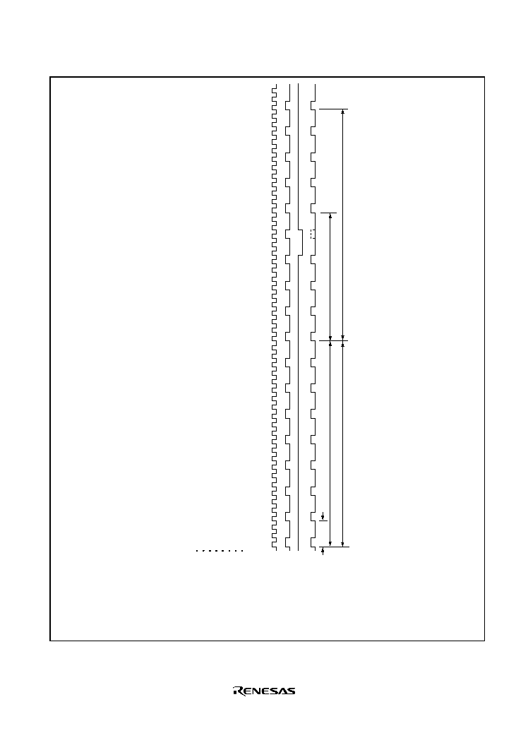
Rev. 1.0, 02/03, page 361 of 634
8 MHz
7.3846 MHz
23
4
5
6
7
8
1
10
11
12
1
2
3
4
5
9
23
4
5
6
7
8
1
2
3
4
5
67
81
1
23
4
5
6
7
8
1
10
11
12
13
1
2
3
4
5
9
Example for 921.6 kbps when
= 24 MHz
TPU clock generation for 923.077-kbps average transfer rate
(1) 8-MHz base clock provided by TPU_1 is multiplied by 12/13 by TPU_2 to generate 7.3846-MHz base clock
(2) By making 1 bit = 8 base clocks, the average transfer will be 7.3846 MHz/8 = 923.077 kbps.
TPU and SCI settings
TMDR_1 = TMDR_2 = H'C2 [PWM mode 1]
TCR_1 = H'20 [TCNT_1 incremented at rising edge of
/1, TCNT_1 cleared by TGRA_1 compare match]
TGRB_1 = H'0003, TGRA_1 = H'0004
TCR_1 = H'21 [1 output on TGRB_1 compare match, 0 as TIOCA1 initial output, 0 output on TGRA_1 compare match]
TCR_2 = H'2C [TCNT_2 incremented at falling edge of TCLKA (TIOCA1), TCNT_2 cleared by TGRA_2 compare match]
TGRB_2 = H'0000, TGRA_2 = H'000C
TCR_2 = H'21 [1 output on TGRB_2 compare match, 0 as TIOCA2 initial output, 0 output on TGRA_2 compare match]
SEMRA_0 = H'0C (ABCS = 1, ACS2 to ACS0 = B'100)
Main clock: 24MHz
TIOCA1 (TPU_1) output = 8 MHz
TIOCA1 (TPU_1) output = 8 MHz
TIOCA2 (TPU_2) output
Base clock
= 8 MHz
×
12/13
= 7.3846 MHz
1 bit = Base clock
×
8
*
Average transfer rate = 7.3846 MHz/8 = 923.077 kbps
Average error with 923.1 kbps = +0.16 %
Note:
*
The lengh of one bit varies according to the base clock synchronization.
Figure 12.4 Example of Base Clock when TPU Clock is Input (2)
Rev. 1.0, 02/03, page 362 of 634
12.3.11
Bit Rate Register (BRR)
BRR is an 8-bit register that adjusts the bit rate. As the SCI performs baud rate generator control
independently for each channel, different bit rates can be set for each channel. Table 12.2 shows
the relationships between the N setting in BRR and bit rate B for normal asynchronous mode,
clocked synchronous mode, and Smart Card interface mode. The initial value of BRR is H'FF, and
it can be read from or written to by the CPU at all times.
Table 12.2
Relationships between the N Setting in BRR and Bit Rate B
Mode
ABCS
Bit Rate
Error
0
B =
64 2
2n-1
(N + 1)
10
6
Error (%) = | 1 | 100
B 64 2
2n-1
(N + 1)
10
6
Asynchronous
mode
1
B =
32 2
2n-1
(N + 1)
10
6
Error (%) = | 1 | 100
B 32 2
2n-1
(N + 1)
10
6
Clocked
synchronous
mode
B =
8 2
2n-1
(N + 1)
10
6
Smart Card
interface mode
B =
S 2
2n-1
(N + 1)
10
6
Error (%) = | 1 | 100
B S 2
2n-1
(N + 1)
10
6
Legend
B: Bit rate (bps)
N: BRR setting for baud rate generator (0
N 255)
: Operating frequency (MHz)
n, S: Determined by the SMR settings shown in the following tables.
SMR Setting
SMR Setting
CKS1
CKS0
Clock Source
n
BCP1
BCP0
S
0
0
0
0
0
32
0
1
/4
1
0
1
64
1
0
/16
2
1
0
372
1
1
/64
3
1
1
256
Table 12.3 shows sample N settings in BRR in normal asynchronous mode. Table 12.4 shows the
maximum bit rate for each frequency in normal asynchronous mode. Table 12.6 shows sample N
settings in BRR in clocked synchronous mode. Table 12.8 shows sample N settings in BRR in
Smart Card interface mode. In Smart Card interface mode, S (the number of basic clock periods in
a 1-bit transfer interval) can be selected. For details, see section 12.7.4, Receive Data Sampling
and Reception Margin. Tables 12.5 and 12.7 show the maximum bit rates with external clock
input.

Rev. 1.0, 02/03, page 363 of 634
When the ABCS bit in SCI_0's serial extended mode register A_0 (SEMRA_0) is set to 1 in
asynchronous mode, the maximum bit rates are twice those shown in table 12.3.
Table 12.3
BRR Settings for Various Bit Rates (Asynchronous Mode) (1
)
Operating Frequency
(MHz)
2
2.097152
2.4576
3
Bit Rate
(bps)
n
N
Error (%)
n
N
Error (%)
n
N
Error (%)
n
N
Error (%)
110
1
141
0.03
1
148
0.04
1
174
0.26
1
212
0.03
150
1
103
0.16
1
108
0.21
1
127
0.00
1
155
0.16
300
0
207
0.16
0
217
0.21
0
255
0.00
1
77
0.16
600
0
103
0.16
0
108
0.21
0
127
0.00
0
155
0.16
1200
0
51
0.16
0
54
0.70
0
63
0.00
0
77
0.16
2400
0
25
0.16
0
26
1.14
0
31
0.00
0
38
0.16
4800
0
12
0.16
0
13
2.48
0
15
0.00
0
19
2.34
9600
--
--
--
--
6
2.48
0
7
0.00
0
9
2.34
19200
--
--
--
--
--
--
0
3
0.00
0
4
2.34
31250
0
1
0.00
--
--
--
--
--
--
0
2
0.00
38400
--
--
--
--
--
--
1
1
0.00
--
--
--
Operating Frequency
(MHz)
3.6864
4
4.9152
5
Bit Rate
(bps)
n
N
Error (%)
n
N
Error (%)
n
N
Error (%)
n
N
Error (%)
110
2
64
0.70
2
70
0.03
2
86
0.31
2
88
0.25
150
1
191
0.00
1
207
0.16
1
255
0.00
2
64
0.16
300
1
95
0.00
1
103
0.16
1
127
0.00
1
129
0.16
600
0
191
0.00
0
207
0.16
0
255
0.00
1
64
0.16
1200
0
95
0.00
0
103
0.16
0
127
0.00
0
129
0.16
2400
0
47
0.00
0
51
0.16
0
63
0.00
0
64
0.16
4800
0
23
0.00
0
25
0.16
0
31
0.00
0
32
1.36
9600
0
11
0.00
0
12
0.16
0
15
0.00
0
15
1.73
19200
0
5
0.00
--
--
--
0
7
0.00
0
7
1.73
31250
--
--
--
0
3
0.00
0
4
1.70
0
4
0.00
38400
0
2
0.00
--
--
--
0
3
0.00
0
3
1.73
Note:
This table shows bit rates when the ABCS bit in SEMRA_0 is cleared to 0.
When the ABCS bit in SEMR0 is set to 1, the bit rates are twice those shown in this table.
In this LSI, operating frequency
must be 6 MHz or greater.

Rev. 1.0, 02/03, page 364 of 634
Table 12.3
BRR Settings for Various Bit Rates (Asynchronous Mode) (2)
Operating Frequency
(MHz)
6
6.144
7.3728
17.2032
Bit Rate
(bps)
n
N
Error (%)
n
N
Error (%) n
N
Error (%)
n
N
Error (%)
110
2
106
0.44
2
108
0.08
2
130
0.07
2
141
0.03
150
2
77
0.16
2
79
0.00
2
95
0.00
2
103
0.16
300
1
155
0.16
1
159
0.00
1
191
0.00
1
207
0.16
600
1
77
0.16
1
79
0.00
1
95
0.00
1
103
0.16
1200
0
155
0.16
0
159
0.00
0
191
0.00
0
207
0.16
2400
0
77
0.16
0
79
0.00
0
95
0.00
0
103
0.16
4800
0
38
0.16
0
39
0.00
0
47
0.00
0
51
0.16
9600
0
19
2.34
0
19
0.00
0
23
0.00
0
25
0.16
19200
0
9
2.34
0
9
0.00
0
11
0.00
0
12
0.16
31250
0
5
0.00
0
5
2.40
--
--
--
0
7
0.00
38400
0
4
2.34
0
4
0.00
0
5
0.00
--
--
--
Operating Frequency
(MHz)
9.8304
10
12
12.288
Bit Rate
(bps)
n
N
Error (%)
n
N
Error (%)
n
N
Error (%)
n
N
Error (%)
110
2
174 0.26
2
177 0.25
2
212 0.03
2
217
0.08
150
2
127 0.00
2
129 0.16
2
155 0.16
2
159
0.00
300
1
255 0.00
2
64
0.16
2
77
0.16
2
79
0.00
600
1
127 0.00
1
129 0.16
1
155 0.16
1
159
0.00
1200
0
255 0.00
1
64
0.16
1
77
0.16
1
79
0.00
2400
0
127 0.00
0
129 0.16
0
155 0.16
0
159
0.00
4800
0
63
0.00
0
64
0.16
0
77
0.16
0
79
0.00
9600
0
31
0.00
0
32
1.36
0
38
0.16
0
39
0.00
19200
0
15
0.00
0
15
1.73
0
19
2.34
0
19
0.00
31250
0
9
1.70
0
9
0.00
0
11
0.00
0
11
2.40
38400
0
7
0.00
0
7
1.73
0
9
2.34
0
9
0.00
Note:
This table shows bit rates when the ABCS bit in SEMRA_0 is cleared to 0.
When the ABCS bit in SEMR0 is set to 1, the bit rates are twice those shown in this table.
In this LSI, operating frequency
must be 6 MHz or greater.

Rev. 1.0, 02/03, page 365 of 634
Table 12.3
BRR Settings for Various Bit Rates (Asynchronous Mode) (3)
Operating Frequency
(MHz)
14
14.7456
16
17.2032
Bit Rate
(bps)
n
N
Error (%)
n
N
Error (%) n
N
Error (%)
n
N
Error (%)
110
2
248
0.17
3
64
0.70
3
70
0.03
3
75
0.48
150
2
181
0.16
2
191
0.00
2
207
0.16
2
223
0.00
300
2
90
0.16
2
95
0.00
2
103
0.16
2
111
0.00
600
1
181
0.16
1
191
0.00
1
207
0.16
1
223
0.00
1200
1
90
0.16
1
95
0.00
1
103
0.16
1
111
0.00
2400
0
181
0.16
0
191
0.00
0
207
0.16
0
223
0.00
4800
0
90
0.16
0
95
0.00
0
103
0.16
0
111
0.00
9600
0
45
0.93
0
47
0.00
0
51
0.16
0
55
0.00
19200
0
22
0.93
0
23
0.00
0
25
0.16
0
27
0.00
31250
0
13
0.00
0
14
1.70
0
15
0.00
0
16
1.20
38400
0
11
0.00
0
12
0.16
0
13
0.00
Operating Frequency
(MHz)
18
19.6608
20
24
Bit Rate
(bps)
n
N
Error (%)
n
N
Error (%)
n
N
Error (%)
n
N
Error (%)
110
3
79
0.12
3
86
0.31
3
88
0.25
3
106
0.44
150
2
233
0.16
2
255
0.00
3
64
0.16
3
77
0.16
300
2
116
0.16
2
127
0.00
2
129
0.16
2
155
0.16
600
1
233
0.16
1
255
0.00
2
64
0.16
2
77
0.16
1200
1
116
0.16
1
127
0.00
1
129
0.16
1
155
0.16
2400
0
233
0.16
0
255
0.00
1
64
0.16
1
77
0.16
4800
0
116
0.16
0
127
0.00
0
129
0.16
0
155
0.16
9600
0
58
0.69
0
63
0.00
0
64
0.16
0
77
0.16
19200
0
28
1.02
0
31
0.00
0
32
1.36
0
38
0.16
31250
0
17
0.00
0
19
0.17
0
19
0.00
0
23
0.00
38400
0
14
2.34
0
15
0.00
0
15
1.73
0
19
2.34
Note:
This table shows bit rates when the ABCS bit in SEMRA_0 is cleared to 0.
When the ABCS bit in SEMR0 is set to 1, the bit rates are twice those shown in this table.
In this LSI, operating frequency
must be 6 MHz or greater.

Rev. 1.0, 02/03, page 366 of 634
Table 12.4
Maximum Bit Rate for Each Frequency (Asynchronous Mode)
Maximum Bit Rate
(kbps)
Maximum Bit Rate
(kbps)
(MHz)
ABCS=0
ABCS=1
n
N
(MHz)
ABCS=0 ABCS=1
n
N
2
62.5
125.0
0
0
9.8304
307.2
614.4
0
0
2.097152
65.536
131.027
0
0
10
312.5
625.0
0
0
2.4576
76.8
153.6
0
0
12
375.0
750.0
0
0
3
93.75
187.5
0
0
12.288
384.0
768.0
0
0
3.6864
115.2
230.4
0
0
14
437.5
875.0
0
0
4
125.0
250.0
0
0
14.7456
460.8
921.6
0
0
4.9152
153.6
307.2
0
0
16
500.0
1000.0
0
0
5
156.25
312.5
0
0
17.2032
537.6
1075.2
0
0
6
187.5
375.0
0
0
18
562.5
1125.0
0
0
6.144
192.0
384.0
0
0
19.6608
614.4
1228.8
0
0
7.3728
230.4
460.8
0
0
20
625.0
1250.0
0
0
8
250.0
500.0
0
0
24
750.0
1500.0
0
0
Table 12.5
Maximum Bit Rate with External Clock Input (Asynchronous Mode)
External
Input
Maximum Bit Rate
(kbps)
External
Input
Maximum Bit Rate
(kbps)
(MHz)
Clock
(MHz)
ABCS=0
ABCS=1
(MHz)
Clock
(MHz)
ABCS=0
ABCS=1
2
0.5000
31.25
62.5
9.8304
2.4576
153.6
307.2
2.097152
0.5243
327.68
65.536
10
2.5000
156.25
312.5
2.4576
0.6144
38.4
76.8
12
3.0000
187.5
375.0
3
0.7500
46.875
93.75
12.288
3.0720
192.0
384.0
3.6864
0.9216
57.6
115.2
14
3.5000
218.75
437.0
4
1.0000
62.5
125.0
14.7456
3.6864
230.4
460.8
4.9152
1.2288
76.8
153.6
16
4.0000
250.0
500.0
5
1.2500
78.125
156.25
17.2032
4.3008
268.8
537.6
6
1.5000
93.75
187.5
18
4.5000
281.25
562.5
6.144
1.5360
96.0
192.0
19.6608
4.9152
307.2
614.4
7.3728
1.8432
115.2
230.4
20
5.0000
312.5
625.0
8
2.0000
125.0
250.0
24
6.0000
375.0
750.0
Note:
In this LSI, operating frequency
must be 6 MHz or greater.

Rev. 1.0, 02/03, page 367 of 634
Table 12.6
BRR Settings for Various Bit Rates (Clocked Synchronous Mode)
Operating Frequency
(MHz)
2
4
6
8
10
16
20
24
Bit Rate
(bps)
n
N
n
N
n
N
n
N
n
N
n
N
n
N
n
N
110
3
70
--
--
250
2
124
2
249
3
124
--
--
3
249
500
1
249
2
124
2
249
--
--
3
124
--
--
--
--
1k
1
124
1
249
2
124
--
--
2
249
--
--
--
--
2.5k
0
199
1
99
1
149
1
199
1
249
2
99
2
124
2
149
5k
0
99
0
199
1
74
1
99
1
124
1
199
1
249
2
74
10k
0
49
0
99
0
149
0
199
0
249
1
99
1
124
1
149
25k
0
19
0
39
0
59
0
79
0
99
0
159
0
199
0
239
50k
0
9
0
19
0
29
0
39
0
49
0
79
0
99
0
119
100k
0
4
0
9
0
14
0
19
0
24
0
39
0
49
0
59
250k
0
1
0
3
0
5
0
7
0
9
0
15
0
19
0
23
500k
0
0*
0
1
0
2
0
3
0
4
0
7
0
9
0
11
1M
0
0*
0
1
0
3
0
4
0
5
2M
0
0*
0
1
0
2
2.5M
0
0*
0
1
--
--
4M
0
0*
5M
0
0*
--
--
6M
0
0*
Legend:
Blank : Cannot be set.
--
: Can be set, but there will be a degree of error.
*
: Continuous transfer is not possible.
Table 12.7
Maximum Bit Rate with External Clock Input (Clocked Synchronous Mode)
(MHz)
External Input
Clock (MHz)
Maximum Bit
Rate (Mbps)
(MHz)
External Input
Clock (MHz)
Maximum Bit
Rate (Mbps)
2
0.333
0.333
14
2.333
2.333
4
0.667
0.667
16
2.667
2.667
6
1.000
1.000
18
3.0000
3.000
8
1.333
1.333
20
3.3333
3.333
10
1.667
1.667
24
4.0000
4.000
12
2.000
2.000
Note:
In this LSI, operating frequency
must be 6 MHz or greater.

Rev. 1.0, 02/03, page 368 of 634
Table 12.8
BRR Settings for Various Bit Rates
(Smart Card Interface Mode, when n = 0 and S = 372)
Operating Frequency
(MHz)
5.00
7.00
7.1424
10.00
10.7136
13.00
Bit Rate
(bps)
N
Error
(%)
N
Error
(%)
N
Error
(%)
N
Error
(%)
N
Error
(%)
N
Error
(%)
6720
0
0.00
1
30
1
28.75
1
0.01
1
7.14
2
13.33
9600
0
0.00
1
30
1
25
1
8.99
Operating Frequency
(MHz)
14.2848
16.00
18.00
20.00
24.00
Bit Rate
(bps)
N
Error
(%)
N
Error
(%)
N
Error
(%)
N
Error
(%)
N
Error
(%)
6720
2
4.76
2
6.67
2
20.01
2
33.34
4
3.99
9600
1
0.00
1
12.01
2
15.99
2
6.66
2
12.01
Table 12.9
Maximum Bit Rate at Various Frequencies
(Smart Card Interface Mode, when S = 372)
(MHz)
Maximum Bit Rate (bps)
N
N
5.00
6720
0
0
7.00
9409
0
0
7.1424
9600
0
0
10.00
13441
0
0
10.7136
14400
0
0
13.00
17473
0
0
14.2848
19200
0
0
16.00
21505
0
0
18.00
24194
0
0
20.00
26882
0
0
24.00
32258
0
0
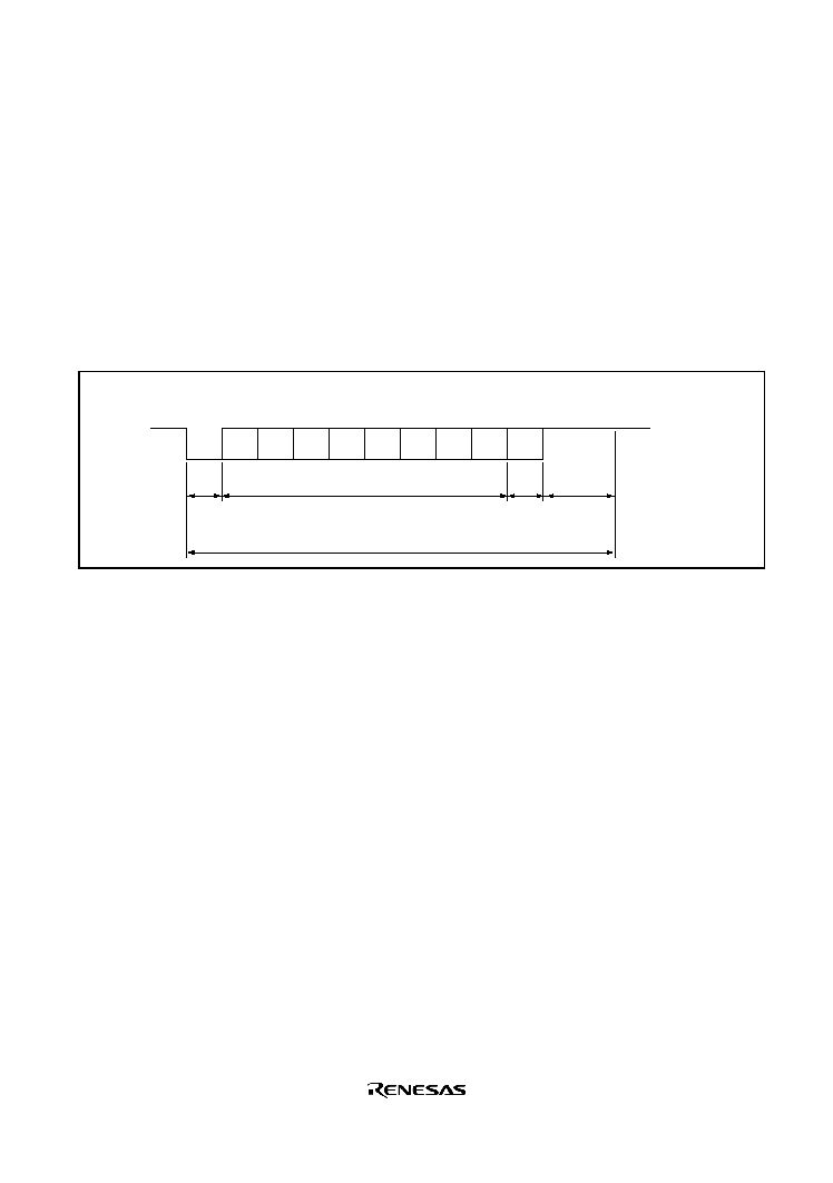
Rev. 1.0, 02/03, page 369 of 634
12.4
Operation in Asynchronous Mode
Figure 12.5 shows the general format for asynchronous serial communication. One frame consists
of a start bit (low level), followed by data (in LSB-first order), a parity bit (high or low level), and
finally stop bits (high level). In asynchronous serial communication, the transmission line is
usually held in the mark state (high level). The SCI monitors the transmission line. When the
transmission line goes to the space state (low level), the SCI recognizes a start bit and starts serial
communication. Inside the SCI, the transmitter and receiver are independent units, enabling full-
duplex. Both the transmitter and the receiver also have a double-buffered structure, so data can be
read from or written during transmission or reception, enabling continuous data transfer.
LSB
Start
bit
MSB
Idle state
(mark state)
Stop bit
0
Transmit/receive data
D0
D1
D2
D3
D4
D5
D6
D7
0/1
1
1
1
1
Serial
data
Parity
bit
1 bit
1 or
2 bits
7 or 8 bits
1 bit,
or none
One unit of transfer data (character or frame)
Figure 12.5 Data Format in Asynchronous Communication
(Example with 8-Bit Data, Parity, Two Stop Bits)
Rev. 1.0, 02/03, page 370 of 634
12.4.1
Data Transfer Format
Table 12.10 shows the data transfer formats that can be used in asynchronous mode. Any of 12
transfer formats can be selected according to the SMR setting. For details on the multiprocessor
bit, refer to section 12.5, Multiprocessor Communication Function.
Table 12.10 Serial Transfer Formats (Asynchronous Mode)
S
8-bit data
STOP
S
7-bit data
STOP
S
8-bit data
STOP STOP
S
8-bit data
P
STOP
S
7-bit data
STOP
P
S
8-bit data
MPB STOP
S
8-bit data
MPB STOP STOP
S
7-bit data
STOP
MPB
S
7-bit data
STOP
MPB
STOP
S
7-bit data
STOP
STOP
SMR Settings
1
2
3
4
5
6
7
8
9
10
11
12
Serial Transfer Format and Frame Length
STOP
S
8-bit data
P
STOP
S
7-bit data
STOP
P
STOP
CHR
PE
MP
STOP
0
0
0
0
0
0
0
1
0
1
0
0
0
1
0
1
1
0
0
0
1
0
0
1
1
1
0
0
1
1
0
1
0
1
0
0
1
1
1
1
0
1
1
1
Legend
S
: Start bit
STOP : Stop bit
P
: Parity bit
MPB
: Multiprocessor bit
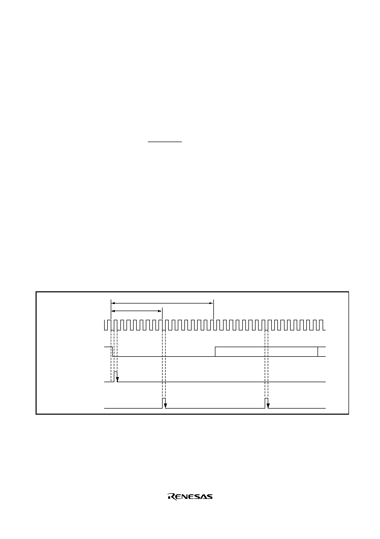
Rev. 1.0, 02/03, page 371 of 634
12.4.2
Receive Data Sampling Timing and Reception Margin in Asynchronous Mode
In asynchronous mode, the SCI operates on a basic clock with a frequency of 16 times the transfer
rate. In reception, the SCI samples the falling edge of the start bit using the basic clock, and
performs internal synchronization. Receive data is latched internally at the rising edge of the 8th
pulse of the basic clock as shown in Figure 12.6. Thus, the reception margin in asynchronous
mode is given by formula (1) below.
M = | (0.5 ) (L 0.5) F (1+ F) |
× 100 [%] ... Formula (1)
2N
1
N
| D 0.5 |
Where M: Reception margin
N: Ratio of bit rate to clock (N = 16)
D: Clock duty (D = 0.5 to 1.0)
L: Frame length (L = 9 to 12)
F: Absolute value of clock rate deviation
Assuming values of F (absolute value of clock rate deviation) = 0 and D (clock duty) = 0.5 N (ratio
of bit rate to clock) in formula (1), the reception margin can be given by the formula.
M = {0.5 1/(2
× 16)} × 100 [%] = 46.875%
However, this is only the computed value, and a margin of 20% to 30% should be allowed for in
system design.
Internal basic
clock
16 clocks *
8 clocks *
Receive data
(RxD)
Synchronization
sampling timing
Start bit
D0
D1
Data sampling
timing
15 0
7
15 0
0
7
Figure 12.6 Receive Data Sampling Timing in Asynchronous Mode
Note:
Figure 12.5 shows an example when the ABCS bit of SEMRA_0 is cleared to 0. When
ABCS is set to 1, the clock frequency of basic clock is 8 times the bit rate and the receive
data is sampled at the rising edge of the 4th pulse of the basic clock.
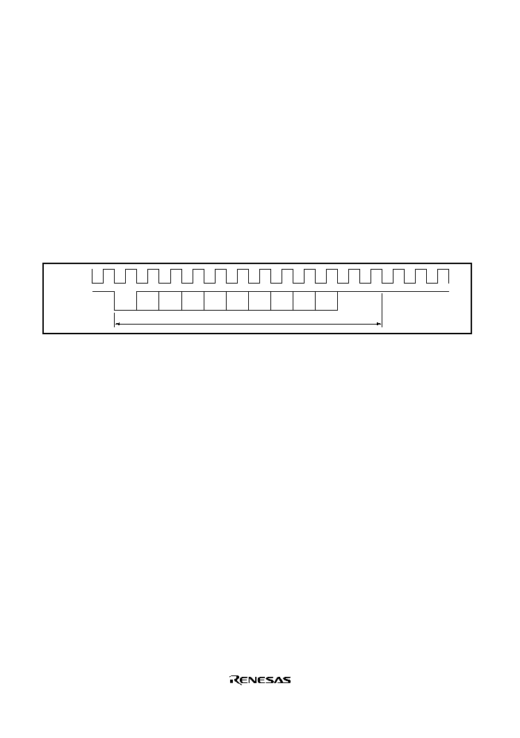
Rev. 1.0, 02/03, page 372 of 634
12.4.3
Clock
Either an internal clock generated by the on-chip baud rate generator or an external clock input at
the SCK pin can be selected as the SCI's serial clock, according to the setting of the C/
A bit in
SMR and the CKE0 and CKE1 bits in SCR. When an external clock is input at the SCK pin, the
clock frequency should be 16 times the bit rate used. When an external clock is selected, the basic
clock of average transfer rate can be selected according to the ACS2 to ACS0 bit setting of
SEMR_0.
When the SCI is operated on an internal clock, the clock can be output from the SCK pin by
setting CKE1 =0 and CKE0=1. The frequency of the clock output in this case is equal to the bit
rate, and the phase is such that the rising edge of the clock is in the middle of the transmit data, as
shown in Figure 12.7.
0
1 frame
D0
D1
D2
D3
D4
D5
D6
D7
0/1
1
1
SCK
TxD
Figure 12.7 Relationship between Output Clock and Transfer Data Phase
(Asynchronous Mode)
12.4.4
SCI Initialization (Asynchronous Mode)
Before transmitting and receiving data, you should first clear the TE and RE bits in SCR to 0, then
initialize the SCI as described in a sample flowchart in Figure 12.8. When the operating mode, or
transfer format, is changed for example, the TE and RE bits must be cleared to 0 before making the
change using the following procedure. When the TE bit is cleared to 0, the TDRE flag is set to 1.
Note that clearing the RE bit to 0 does not initialize the contents of the RDRF, PER, FER, and
ORER flags, or the contents of RDR. When the external clock is used in asynchronous mode, the
clock must be supplied even during initialization.
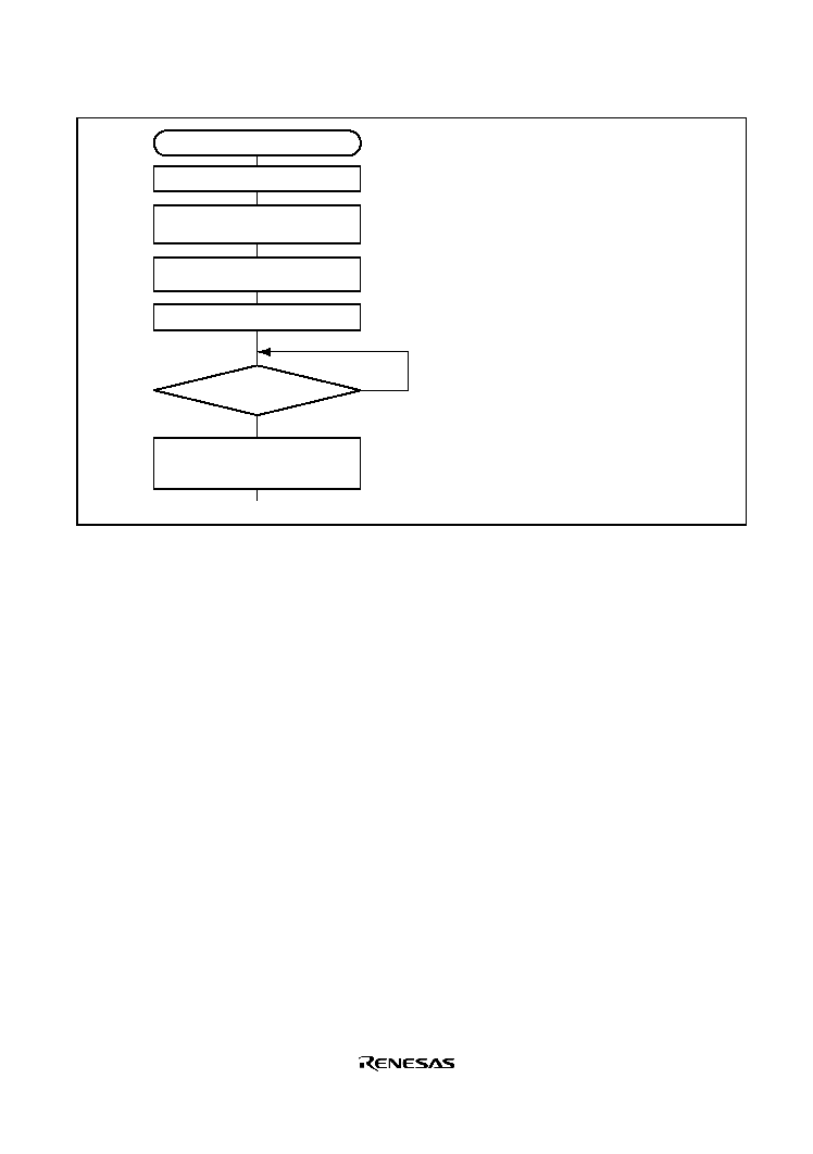
Rev. 1.0, 02/03, page 373 of 634
Wait
<Initialization completion>
Start initialization
Set data transfer format in
SMR, SCMR, and SEMRA_0
[1]
Set CKE1 and CKE0 bits in SCR
(TE, RE bits 0)
No
Yes
Set value in BRR
Clear TE and RE bits in SCR to 0
[2]
[3]
Set TE and RE bits in
SCR to 1, and set RIE, TIE, TEIE,
and MPIE bits
[4]
1-bit interval elapsed?
[1]
Set the clock selection in SCR.
Be sure to clear bits RIE, TIE, TEIE, and
MPIE, and bits TE and RE, to 0.
When the clock is selected in
asynchronous mode, it is output
immediately after SCR settings are
made.
[2]
Set the data transfer format in SMR,
SCMR, and SEMRA_0.
[3]
Write a value corresponding to the bit
rate to BRR. Not necessary if an
external clock or average transfer rate
clock by ACS2 to ACS0 is used.
[4]
Wait at least one bit interval, then set the
TE bit or RE bit in SCR to 1. Also set
the RIE, TIE, TEIE, and MPIE bits.
Figure 12.8 Sample SCI Initialization Flowchart
12.4.5
Data Transmission (Asynchronous Mode)
Figure 12.9 shows an example of operation for transmission in asynchronous mode. In
transmission, the SCI operates as described below.
1. The SCI monitors the TDRE flag in SSR. If the flag is cleared to 0, the SCI recognizes that
data has been written to TDR, and transfers the data from TDR to TSR.
2. After transferring data from TDR to TSR, the SCI sets the TDRE flag to 1 and starts
transmission. If the TIE bit is set to 1 at this time, a transmit data empty interrupt request (TXI)
is generated. Continuous transmission is possible because the TXI interrupt routine writes next
transmit data to TDR before transmission of the current transmit data has been completed.
3. Data is sent from the TxD pin in the following order: start bit, transmit data, parity bit or
multiprocessor bit (may be omitted depending on the format), and stop bit.
4. The SCI checks the TDRE flag at the timing for sending the stop bit.
5. If the TDRE flag is 0, the data is transferred from TDR to TSR, the stop bit is sent, and then
serial transmission of the next frame is started.
6. If the TDRE flag is 1, the TEND flag in SSR is set to 1, the stop bit is sent, and then the "mark
state" is entered, in which 1 is output. If the TEIE bit in SCR is set to 1 at this time, a TEI
interrupt request is generated.
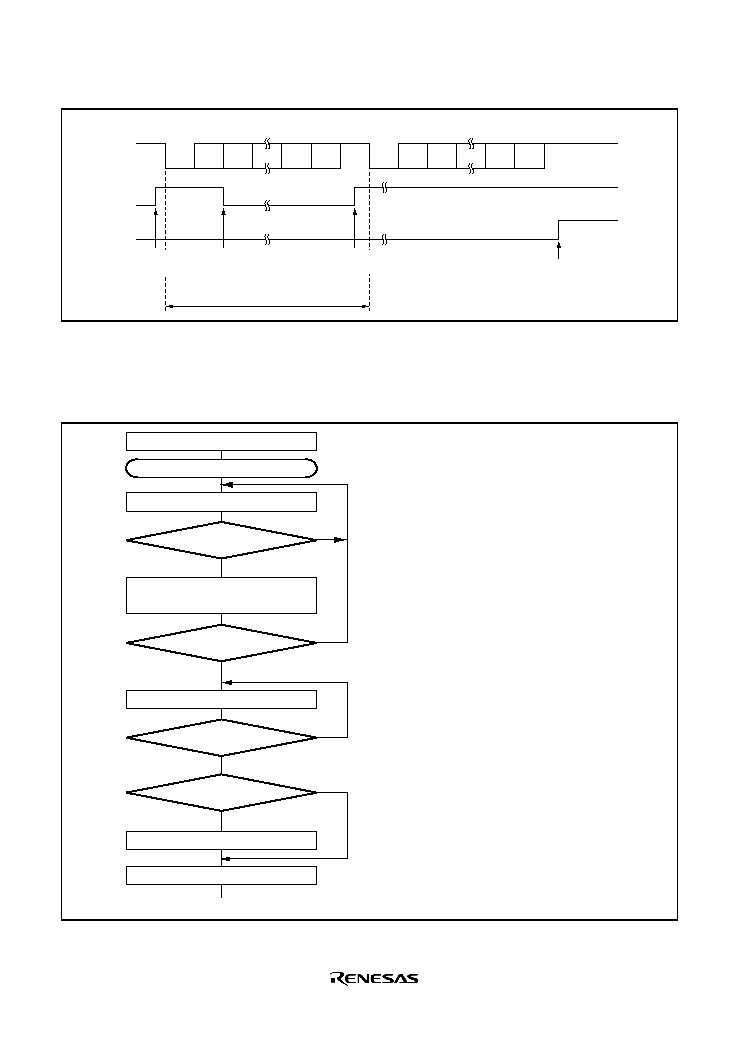
Rev. 1.0, 02/03, page 374 of 634
TDRE
TEND
0
1 frame
D0
D1
D7
0/1
1
0
D0
D1
D7
0/1
1
1
1
Data
Start
bit
Parity
bit
Stop
bit
Start
bit
Data
Parity
bit
Stop
bit
TXI interrupt
request generated
Data written to TDR and
TDRE flag cleared to 0 in
TXI interrupt service routine
TEI interrupt
request generated
Idle state
(mark state)
TXI interrupt
request generated
Figure 12.9 Example of Operation in Transmission in Asynchronous Mode
(Example with 8-Bit Data, Parity, One Stop Bit)
Figure 12.10 shows a sample flowchart for transmission in asynchronous mode.
No
<End>
[1]
Yes
Initialization
Start transmission
Read TDRE flag in SSR
[2]
Write transmit data to TDR
and clear TDRE flag in SSR to 0
No
Yes
No
Yes
Read TEND flag in SSR
[3]
No
Yes
[4]
Clear DR to 0 and set DDR to 1
Clear TE bit in SCR to 0
TDRE = 1
All data transmitted?
TEND = 1
Break output?
[1]
SCI initialization:
The TxD pin is automatically designated
as the transmit data output pin.
After the TE bit is set to 1, a frame of 1s
is output, and transmission is enabled.
[2]
SCI status check and transmit data write:
Read SSR and check that the TDRE flag
is set to 1, then write transmit data to
TDR and clear the TDRE flag to 0.
[3]
Serial transmission continuation
procedure:
To continue serial transmission, read 1
from the TDRE flag to confirm that writing
is possible, then write data to TDR, and
then clear the TDRE flag to 0. Checking
and clearing of the TDRE flag is
automatic when the DMAC is activated
by a transmit data empty interrupt (TXI)
request, and data is written to TDR.
[4]
Break output at the end of serial
transmission:
To output a break in serial transmission,
set DDR for the port corresponding to the
TxD pin to 1, clear DR to 0, then clear the
TE bit in SCR to 0.
Figure 12.10 Sample Serial Transmission Flowchart
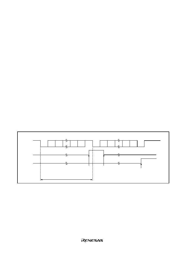
Rev. 1.0, 02/03, page 375 of 634
12.4.6
Serial Data Reception (Asynchronous Mode)
Figure 12.11 shows an example of operation for reception in asynchronous mode. In serial
reception, the SCI operates as described below.
1. The SCI monitors the communication line. If a start bit is detected, the SCI performs internal
synchronization, receives receive data in RSR, and checks the parity bit and stop bit.
2. If an overrun error occurs (when reception of the next data is completed while the RDRF flag
is still set to 1), the ORER bit in SSR is set to 1. If the RIE bit in SCR is set to 1 at this time, an
ERI interrupt request is generated. Receive data is not transferred to RDR. The RDRF flag
remains to be set to 1.
3. If a parity error is detected, the PER bit in SSR is set to 1 and receive data is transferred to
RDR. If the RIE bit in SCR is set to 1 at this time, an ERI interrupt request is generated.
4. If a framing error is detected (when the stop bit is 0), the FER bit in SSR is set to 1 and receive
data is transferred to RDR. If the RIE bit in SCR is set to 1 at this time, an ERI interrupt
request is generated.
5. If reception is completed successfully, the RDRF bit in SSR is set to 1, and receive data is
transferred to RDR. If the RIE bit in SCR is set to 1 at this time, an RXI interrupt request is
generated. Continuous reception is possible because the RXI interrupt routine reads the receive
data transferred to RDR before reception of the next receive data has been completed.
RDRF
FER
0
1 frame
D0
D1
D7
0/1
1
0
D0
D1
D7
0/1
0
1
1
Data
Start
bit
Parity
bit
Stop
bit
Start
bit
Data
Parity
bit
Stop
bit
ERI interrupt request
generated by framing
error
Idle state
(mark state)
RDR data read and RDRF
flag cleared to 0 in RXI
interrupt service routine
RXI interrupt
request
generated
Figure 12.11 Example of SCI Operation in Reception
(Example with 8-Bit Data, Parity, One Stop Bit)
Table 12.11 shows the states of the SSR status flags and receive data handling when a receive error
is detected. If a receive error is detected, the RDRF flag retains its state before receiving data.
Reception cannot be resumed while a receive error flag is set to 1. Accordingly, clear the ORER,
FER, PER, and RDRF bits to 0 before resuming reception. Figure 12.12 shows a sample flow chart
for serial data reception.
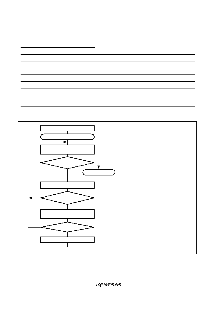
Rev. 1.0, 02/03, page 376 of 634
Table 12.11 SSR Status Flags and Receive Data Handling
SSR Status Flag
RDRF
*
ORER
FER
PER
Receive Data
Receive Error Type
1
1
0
0
Lost
Overrun error
0
0
1
0
Transferred to RDR
Framing error
0
0
0
1
Transferred to RDR
Parity error
1
1
1
0
Lost
Overrun error + framing error
1
1
0
1
Lost
Overrun error + parity error
0
0
1
1
Transferred to RDR
Framing error + parity error
1
1
1
1
Lost
Overrun error + framing error +
parity error
Note: * The RDRF flag retains the state it had before data reception.
Yes
<End>
[1]
No
Initialization
Start reception
[2]
No
Yes
Read RDRF flag in SSR
[4]
[5]
Clear RE bit in SCR to 0
Read ORER, PER, and
FER flags in SSR
Error processing
(Continued on next page)
[3]
Read receive data in RDR, and
clear RDRF flag in SSR to 0
No
Yes
PER
FER ORER = 1
RDRF = 1
All data received?
[1]
SCI initialization:
The RxD pin is automatically designated as
the receive data input pin.
[2]
[3] Receive error processing and break
detection:
If a receive error occurs, read the ORER,
PER, and FER flags in SSR to identify the
error. After performing the appropriate error
processing, ensure that the ORER, PER, and
FER flags are all cleared to 0. Reception
cannot be resumed if any of these flags are
set to 1. In the case of a framing error, a
break can be detected by reading the value
of the input port corresponding to the RxD
pin.
[4]
SCI status check and receive data read:
Read SSR and check that RDRF = 1, then
read the receive data in RDR and clear the
RDRF flag to 0. Transition of the RDRF flag
from 0 to 1 can also be identified by an RXI
interrupt.
[5]
Serial reception continuation procedure:
To continue serial reception, before the end
bit for the current frame is received, reading
the RDRF flag and RDR, and clearing the
RDRF flag to 0 should be finished. The
RDRF flag is cleared automatically when
DMAC is activated by a reception complete
interrupt (RXI) and the RDR value is read.
Figure 12.12 Sample Serial Reception Data Flowchart (1)
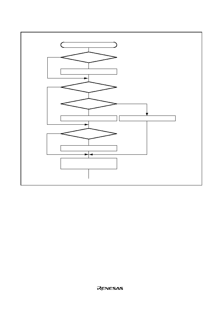
Rev. 1.0, 02/03, page 377 of 634
<End>
[3]
Error processing
Parity error processing
Yes
No
Clear ORER, PER, and
FER flags in SSR to 0
No
Yes
No
Yes
Framing error processing
No
Yes
Overrun error processing
ORER = 1
FER = 1
Break?
PER = 1
Clear RE bit in SCR to 0
Figure 12.12 Sample Serial Reception Data Flowchart (2)
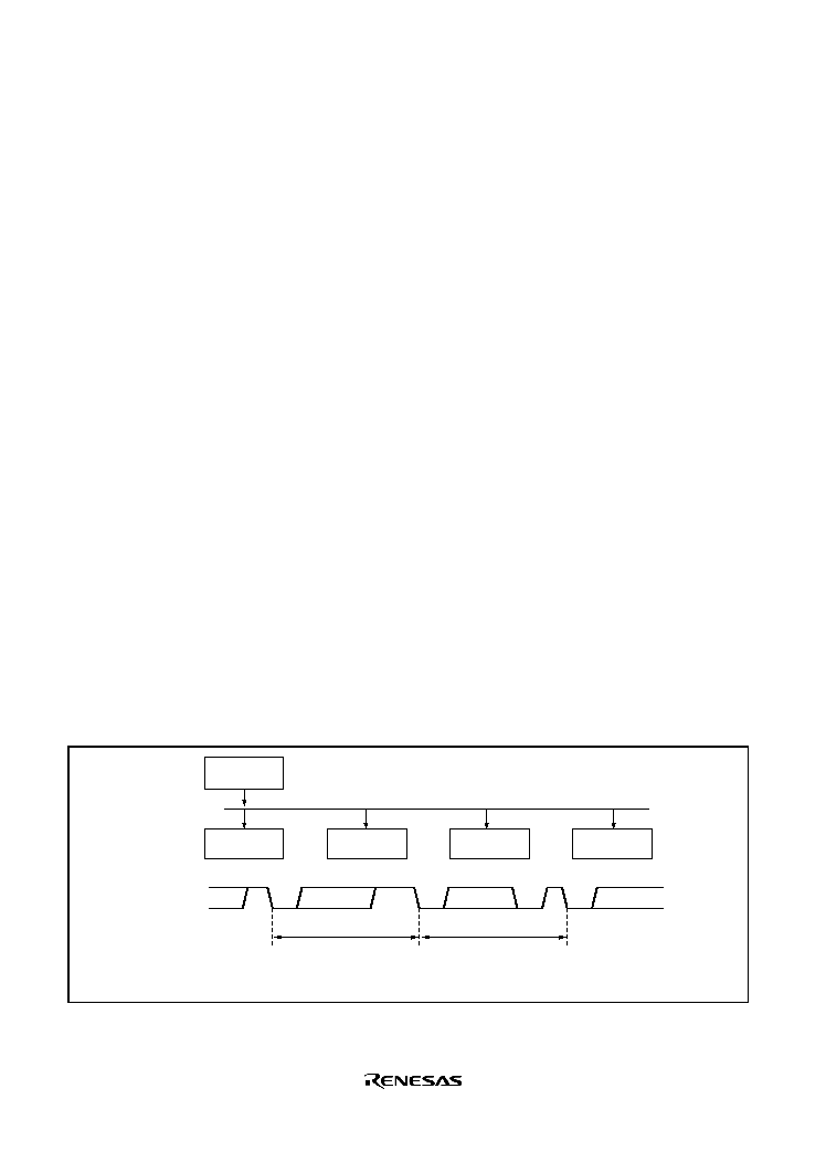
Rev. 1.0, 02/03, page 378 of 634
12.5
Multiprocessor Communication Function
Use of the multiprocessor communication function enables data transfer between a number of
processors sharing communication lines by asynchronous serial communication using the
multiprocessor format, in which a multiprocessor bit is added to the transfer data. When
multiprocessor communication is performed, each receiving station is addressed by a unique ID
code. The serial communication cycle consists of two component cycles; an ID transmission cycle
that specifies the receiving station, and a data transmission cycle. The multiprocessor bit is used to
differentiate between the ID transmission cycle and the data transmission cycle. If the
multiprocessor bit is 1, the cycle is an ID transmission cycle; if the multiprocessor bit is 0, the
cycle is a data transmission cycle. Figure 12.13 shows an example of inter-processor
communication using the multiprocessor format. The transmitting station first sends the ID code of
the receiving station with which it wants to perform serial communication as data with a 1
multiprocessor bit added. It then sends transmit data as data with a 0 multiprocessor bit added.
When data with a 1 multiprocessor bit is received, the receiving station compares that data with its
own ID. The station whose ID matches then receives the data sent next. Stations whose ID do not
match continue to skip data until data with a 1 multiprocessor bit is again received.
The SCI uses the MPIE bit in SCR to implement this function. When the MPIE bit is set to 1,
transfer of receive data from RSR to RDR, error flag detection, and setting the SSR status flags,
RDRF, FER, and ORER to 1, are inhibited until data with a 1 multiprocessor bit is received. On
reception of a receive character with a 1 multiprocessor bit, the MPB bit in SSR is set to 1 and the
MPIE bit is automatically cleared, thus normal reception is resumed. If the RIE bit in SCR is set to
1 at this time, an RXI interrupt is generated.
When the multiprocessor format is selected, the parity bit setting is rendered invalid. All other bit
settings are the same as those in normal asynchronous mode. The clock used for multiprocessor
communication is the same as that in normal asynchronous mode.
Transmitting
station
Receiving
station A
Receiving
station B
Receiving
station C
Receiving
station D
(ID = 01)
(ID = 02)
(ID = 03)
(ID = 04)
Serial transmission line
Serial
data
ID transmission cycle =
receiving station
specification
Data transmission cycle =
Data transmission to
receiving station specified by ID
(MPB = 1)
(MPB = 0)
H'01
H'AA
Legend
MPB: Multiprocessor bit
Figure 12.13 Example of Communication Using Multiprocessor Format
(Transmission of Data H'AA to Receiving Station A)
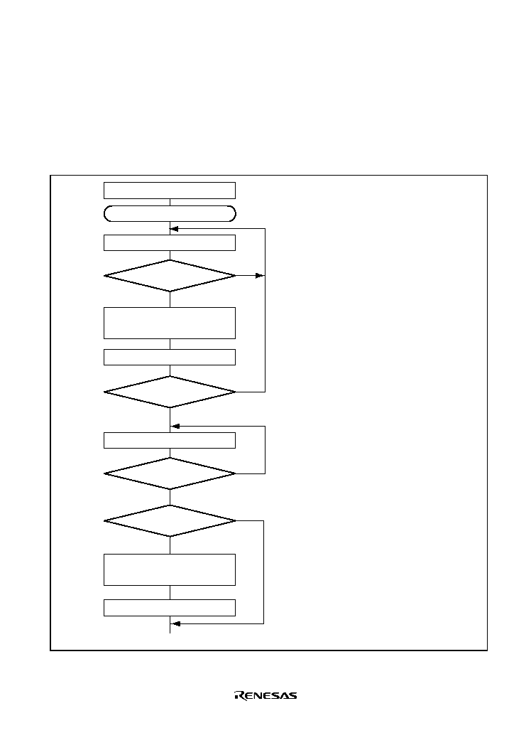
Rev. 1.0, 02/03, page 379 of 634
12.5.1
Multiprocessor Serial Data Transmission
Figure 12.14 shows a sample flowchart for multiprocessor serial data transmission. For an ID
transmission cycle, set the MPBT bit in SSR to 1 before transmission. For a data transmission
cycle, clear the MPBT bit in SSR to 0 before transmission. All other SCI operations are the same
as those in asynchronous mode.
No
<End>
[1]
Yes
Initialization
Start transmission
Read TDRE flag in SSR
[2]
Write transmit data to TDR and
set MPBT bit in SSR
No
Yes
No
Yes
Read TEND flag in SSR
[3]
No
Yes
[4]
Clear DR to 0 and set DDR to 1
Clear TE bit in SCR to 0
TDRE = 1
All data transmitted?
TEND = 1
Break output?
Clear TDRE flag to 0
[1]
SCI initialization:
The TxD pin is automatically
designated as the transmit data
output pin.
After the TE bit is set to 1, a frame of
1s is output, and transmission is
enabled.
[2]
SCI status check and transmit data
write:
Read SSR and check that the TDRE
flag is set to 1, then write transmit
data to TDR. Set the MPBT bit in
SSR to 0 or 1. Finally, clear the
TDRE flag to 0.
[3]
Serial transmission continuation
procedure:
To continue serial transmission, be
sure to read 1 from the TDRE flag to
confirm that writing is possible, then
write data to TDR, and then clear the
TDRE flag to 0. Checking and
clearing of the TDRE flag is automatic
when the DMAC is activated by a
transmit data empty interrupt (TXI)
request, and data is written to TDR.
[4]
Break output at the end of serial
transmission:
To output a break in serial
transmission, set the port DDR to 1,
clear DR to 0, then clear the TE bit in
SCR to 0.
Figure 12.14 Sample Multiprocessor Serial Transmission Flowchart
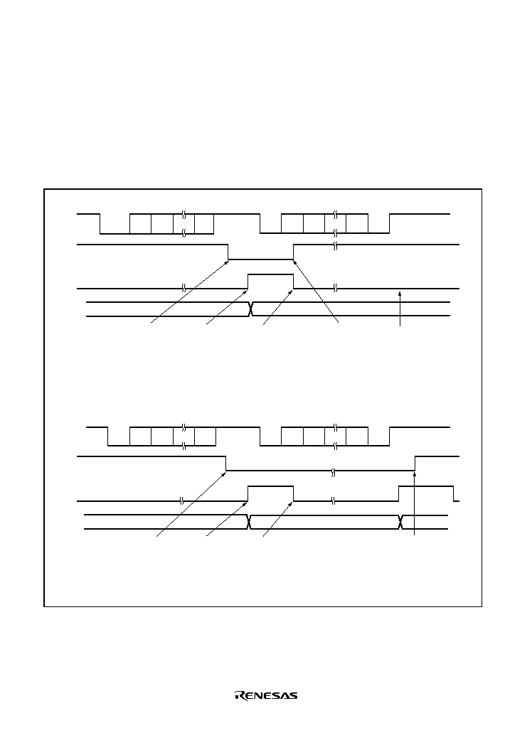
Rev. 1.0, 02/03, page 380 of 634
12.5.2
Multiprocessor Serial Data Reception
Figure 12.16 shows a sample flowchart for multiprocessor serial data reception. If the MPIE bit in
SCR is set to 1, data is skipped until data with a 1 multiprocessor bit is sent. On receiving data
with a 1 multiprocessor bit, the receive data is transferred to RDR. An RXI interrupt request is
generated at this time. All other SCI operations are the same as in asynchronous mode. Figure
12.15 shows an example of SCI operation for multiprocessor format reception.
MPIE
RDR
value
0
D0
D1
D7
1
1
0
D0
D1
D7
0
1
1
1
Data (ID1)
Start
bit
MPB
Stop
bit
Start
bit
Data (Data1)
MPB
Stop
bit
Data (ID2)
Start
bit
Stop
bit
Start
bit
Data (Data2)
Stop
bit
RXI interrupt
request
(multiprocessor
interrupt)
generated
Idle state
(mark state)
RDRF
RDR data read
and RDRF flag
cleared to 0 in
RXI interrupt
service routine
If not this station's ID,
MPIE bit is set to 1
again
RXI interrupt request is
not generated, and RDR
retains its state
ID1
(a) Data does not match station's ID
MPIE
RDR
value
0
D0
D1
D7
1
1
0
D0
D1
D7
0
1
1
1
MPB
MPB
RXI interrupt
request
(multiprocessor
interrupt)
generated
Idle state
(mark state)
RDRF
RDR data read and
RDRF flag cleared
to 0 in RXI interrupt
service routine
Matches this station's ID,
so reception continues, and
data is received in RXI
interrupt service routine
MPIE bit set to 1
again
ID2
(b) Data matches station's ID
Data2
ID1
MPIE = 0
MPIE = 0
Figure 12.15 Example of SCI Operation in Reception
(Example with 8-Bit Data, Multiprocessor Bit, One Stop Bit)
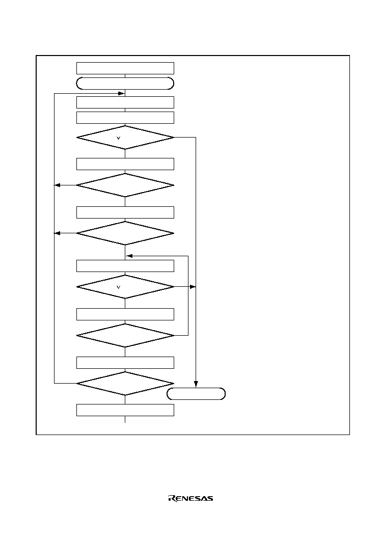
Rev. 1.0, 02/03, page 381 of 634
Yes
<End>
[1]
No
Initialization
Start reception
No
Yes
[4]
Clear RE bit in SCR to 0
Error processing
(Continued on
next page)
[5]
No
Yes
FER ORER = 1
RDRF = 1
All data received?
Read MPIE bit in SCR
[2]
Read ORER and FER flags in SSR
Read RDRF flag in SSR
[3]
Read receive data in RDR
No
Yes
This station's ID?
Read ORER and FER flags in SSR
Yes
No
Read RDRF flag in SSR
No
Yes
FER ORER = 1
Read receive data in RDR
RDRF = 1
[1]
SCI initialization:
The RxD pin is automatically designated as
the receive data input pin.
[2]
ID reception cycle:
Set the MPIE bit in SCR to 1.
[3]
SCI status check, ID reception and
comparison:
Read SSR and check that the RDRF flag is
set to 1, then read the receive data in RDR
and compare it with this station's ID.
If the data is not this station's ID, set the MPIE
bit to 1 again, and clear the RDRF flag to 0.
If the data is this station's ID, clear the RDRF
flag to 0.
[4]
SCI status check and data reception:
Read SSR and check that the RDRF flag is
set to 1, then read the data in RDR.
[5]
Receive error processing and break detection:
If a receive error occurs, read the ORER and
FER flags in SSR to identify the error. After
performing the appropriate error processing,
ensure that the ORER and FER flags are all
cleared to 0.
Reception cannot be resumed if either of
these flags is set to 1.
In the case of a framing error, a break can be
detected by reading the RxD pin value.
Figure 12.16 Sample Multiprocessor Serial Reception Flowchart (1)
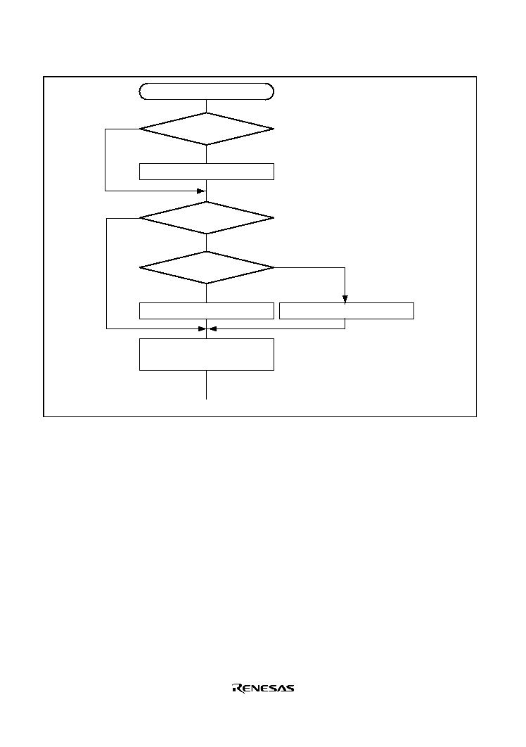
Rev. 1.0, 02/03, page 382 of 634
<End>
Error processing
Yes
No
Clear ORER, PER, and
FER flags in SSR to 0
No
Yes
No
Yes
Framing error processing
Overrun error processing
ORER = 1
FER = 1
Break?
Clear RE bit in SCR to 0
[5]
Figure 12.16 Sample Multiprocessor Serial Reception Flowchart (2)
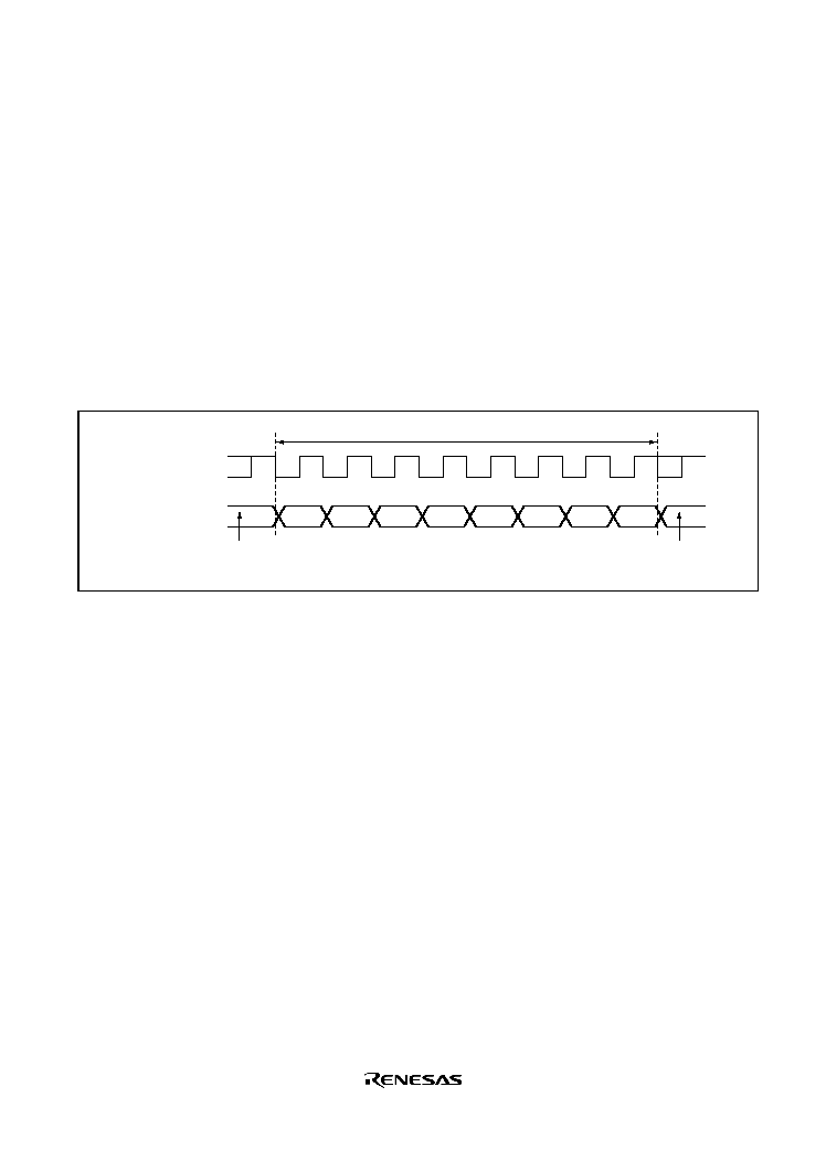
Rev. 1.0, 02/03, page 383 of 634
12.6
Operation in Clocked Synchronous Mode
Figure 12.17 shows the general format for clocked synchronous communication. In clocked
synchronous mode, data is transmitted or received synchronous with clock pulses. In clocked
synchronous serial communication, data on the transmission line is output from one falling edge of
the serial clock to the next. In clocked synchronous mode, the SCI receives data in synchronous
with the rising edge of the serial clock. After 8-bit data is output, the transmission line holds the
MSB state. In clocked synchronous mode, no parity or multiprocessor bit is added. Inside the SCI,
the transmitter and receiver are independent units, enabling full-duplex communication through the
use of a common clock. Both the transmitter and the receiver also have a double-buffered
structure, so data can be read from or written during transmission or reception, enabling
continuous data transfer.
Don't care
Don't care
One unit of transfer data (character or frame)
Bit 0
Serial data
Synchronization
clock
Bit 1
Bit 3
Bit 4
Bit 5
LSB
MSB
Bit 2
Bit 6
Bit 7
*
*
Note: * High except in continuous transfer
Figure 12.17 Data Format in Synchronous Communication (For LSB-First)
12.6.1
Clock
Either an internal clock generated by the on-chip baud rate generator or an external
synchronization clock input at the SCK pin can be selected, according to the setting of CKE0 and
CKE1 bits in SCR. When the SCI is operated on an internal clock, the serial clock is output from
the SCK pin. Eight serial clock pulses are output in the transfer of one character, and when no
transfer is performed the clock is fixed high.
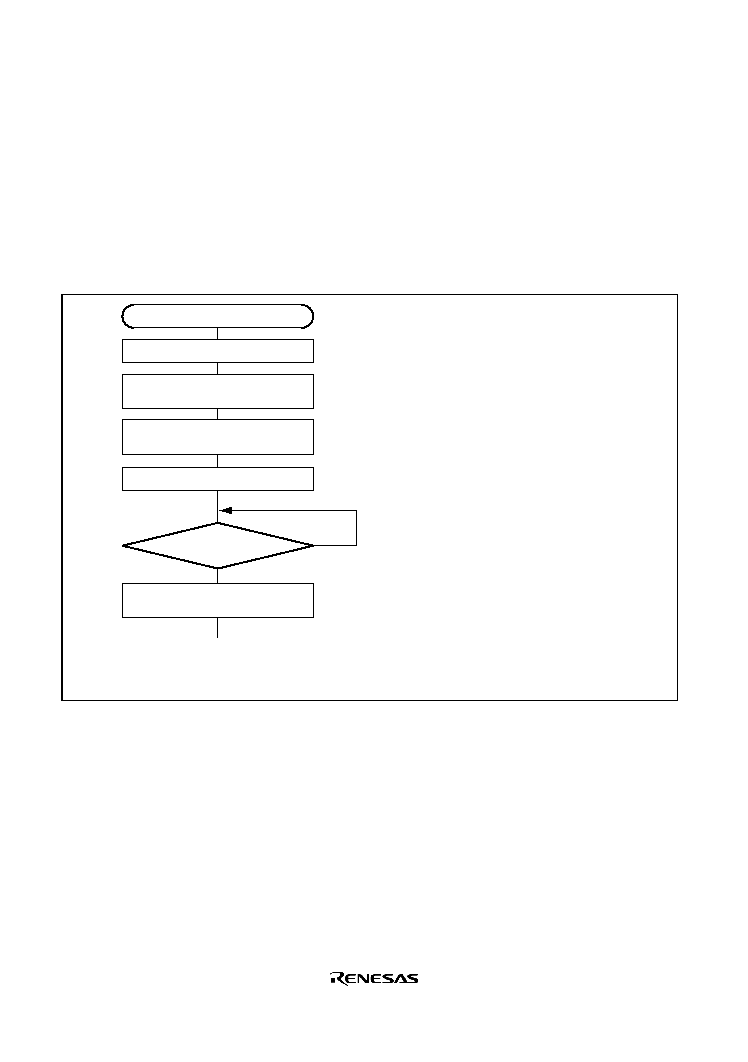
Rev. 1.0, 02/03, page 384 of 634
12.6.2
SCI Initialization (Clocked Synchronous Mode)
Before transmitting and receiving data, the TE and RE bits in SCR should be cleared to 0, then the
SCI should be initialized as described in a sample flowchart in Figure 12.18. When the operating
mode, or transfer format, is changed for example, the TE and RE bits must be cleared to 0 before
making the change using the following procedure. When the TE bit is cleared to 0, the TDRE flag
is set to 1. Note that clearing the RE bit to 0 does not change the contents of the RDRF, PER,
FER, and ORER flags, or the contents of RDR.
Wait
<Transfer start>
Start initialization
Set data transfer format in
SMR and SCMR
No
Yes
Set value in BRR
Clear TE and RE bits in SCR to 0
[2]
[3]
Set TE and RE bits in SCR to 1, and
set RIE, TIE, TEIE, and MPIE bits
[4]
1-bit interval elapsed?
Set CKE1 and CKE0 bits in SCR
(TE, RE bits 0)
[1]
[1]
Set the clock selection in SCR. Be sure to
clear bits RIE, TIE, TEIE, and MPIE, TE and
RE, to 0.
[2]
Set the data transfer format in SMR and
SCMR.
[3]
Write a value corresponding to the bit rate to
BRR. Not necessary if an external clock is
used.
[4]
Wait at least one bit interval, then set the TE
bit or RE bit in SCR to 1.
Also set the RIE, TIE TEIE, and MPIE bits.
Setting the TE and RE bits enables the TxD
and RxD pins to be used.
Note: In simultaneous transmit and receive operations, the TE and RE bits should both be cleared
to 0 or set to 1 simultaneously.
Figure 12.18 Sample SCI Initialization Flowchart
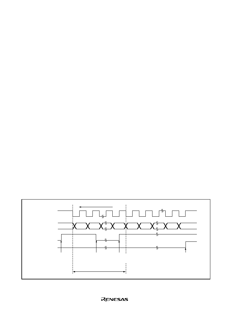
Rev. 1.0, 02/03, page 385 of 634
12.6.3
Serial Data Transmission (Clocked Synchronous Mode)
Figure 12.19 shows an example of SCI operation for transmission in clocked synchronous mode.
In serial transmission, the SCI operates as described below.
1. The SCI monitors the TDRE flag in SSR, and if the flag is 0, the SCI recognizes that data has
been written to TDR, and transfers the data from TDR to TSR.
2. After transferring data from TDR to TSR, the SCI sets the TDRE flag to 1 and starts
transmission. If the TIE bit in SCR is set to 1 at this time, a transmit data empty interrupt
(TXI) is generated. Continuous transmission is possible because the TXI interrupt routine
writes the next transmit data to TDR before transmission of the current transmit data has been
completed.
3. 8-bit data is sent from the TxD pin synchronized with the output clock when output clock mode
has been specified, and synchronized with the input clock when use of an external clock has
been specified.
4. The SCI checks the TDRE flag at the timing for sending the MSB (bit 7).
5. If the TDRE flag is cleared to 0, data is transferred from TDR to TSR, and serial transmission
of the next frame is started.
6. If the TDRE flag is set to 1, the TEND flag in SSR is set to 1, and the TDRE flag maintains the
output state of the last bit. If the TEIE bit in SCR is set to 1 at this time, a TEI interrupt request
is generated. The SCK pin is fixed high.
Figure 12.20 shows a sample flow chart for serial data transmission. Even if the TDRE flag is
cleared to 0, transmission will not start while a receive error flag (ORER, FER, or PER) is set to 1.
Make sure that the receive error flags are cleared to 0 before starting transmission. Note that
clearing the RE bit to 0 does not clear the receive error flags.
Transfer direction
Bit 0
Serial data
Synchronization
clock
1 frame
TDRE
TEND
Data written to TDR and
TDRE flag cleared to 0 in
TXI interrupt service
routine
TXI interrupt request
generated
Bit 1
Bit 7
Bit 0
Bit 1
Bit 6
Bit 7
TXI interrupt request
generated
TEI interrupt request
generated
Figure 12.19 Sample SCI Transmission Operation in Clocked Synchronous Mode
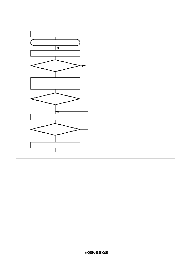
Rev. 1.0, 02/03, page 386 of 634
No
<End>
[1]
Yes
Initialization
Start transmission
Read TDRE flag in SSR
[2]
Write transmit data to TDR and
clear TDRE flag in SSR to 0
No
Yes
No
Yes
Read TEND flag in SSR
[3]
Clear TE bit in SCR to 0
TDRE = 1
All data transmitted?
TEND = 1
[1]
SCI initialization:
The TxD pin is automatically designated as
the transmit data output pin.
[2]
SCI status check and transmit data write:
Read SSR and check that the TDRE flag is
set to 1, then write transmit data to TDR
and clear the TDRE flag to 0.
[3]
Serial transmission continuation procedure:
To continue serial transmission, be sure to
read 1 from the TDRE flag to confirm that
writing is possible, then write data to TDR,
and then clear the TDRE flag to 0.
Checking and clearing of the TDRE flag is
automatic when the DMAC is activated by a
transmit data empty interrupt (TXI) request
and data is written to TDR.
Figure 12.20 Sample Serial Transmission Flowchart
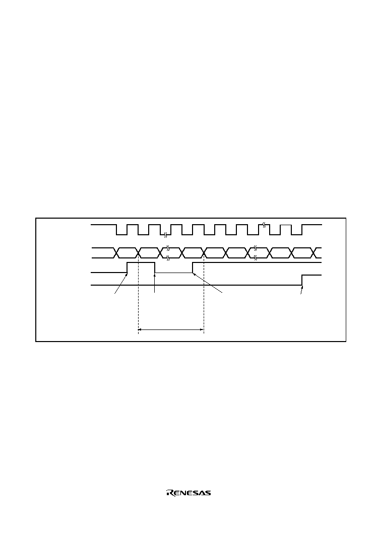
Rev. 1.0, 02/03, page 387 of 634
12.6.4
Serial Data Reception (Clocked Synchronous Mode)
Figure 12.21 shows an example of SCI operation for reception in clocked synchronous mode. In
serial reception, the SCI operates as described below.
1. The SCI performs internal initialization synchronous with a synchronous clock input or output,
starts receiving data, and stores the received data in RSR.
2. If an overrun error occurs (when reception of the next data is completed while the RDRF flag
in SSR is still set to 1), the ORER bit in SSR is set to 1. If the RIE bit in SCR is set to 1 at this
time, an ERI interrupt request is generated, receive data is not transferred to RDR, and the
RDRF flag remains to be set to 1.
3. If reception is completed successfully, the RDRF bit in SSR is set to 1, and receive data is
transferred to RDR. If the RIE bit in SCR is set to 1 at this time, an RXI interrupt request is
generated. Continuous reception is possible because the RXI interrupt routine reads the receive
data transferred to RDR before reception of the next receive data has finished.
Bit 7
Serial data
Synchronization
clock
1 frame
RDRF
ORER
ERI interrupt request
generated by overrun
error
RXI interrupt request
generated
RDR data read and
RDRF flag cleared to 0
in RXI interrupt service
routine
RXI interrupt
request
generated
Bit 0
Bit 7
Bit 0
Bit 1
Bit 6
Bit 7
Figure 12.21 Example of SCI Operation in Reception
Reception cannot be resumed while a receive error flag is set to 1. Accordingly, clear the ORER,
FER, PER, and RDRF bits to 0 before resuming reception. Figure 12.22 shows a sample flow chart
for serial data reception.
When the internal clock is selected during reception, the synchronization clock will be output until
an overrun error occurs or the RE bit is cleared. To receive data in frame units, a dummy data of
one frame must be transmitted simultaneously.
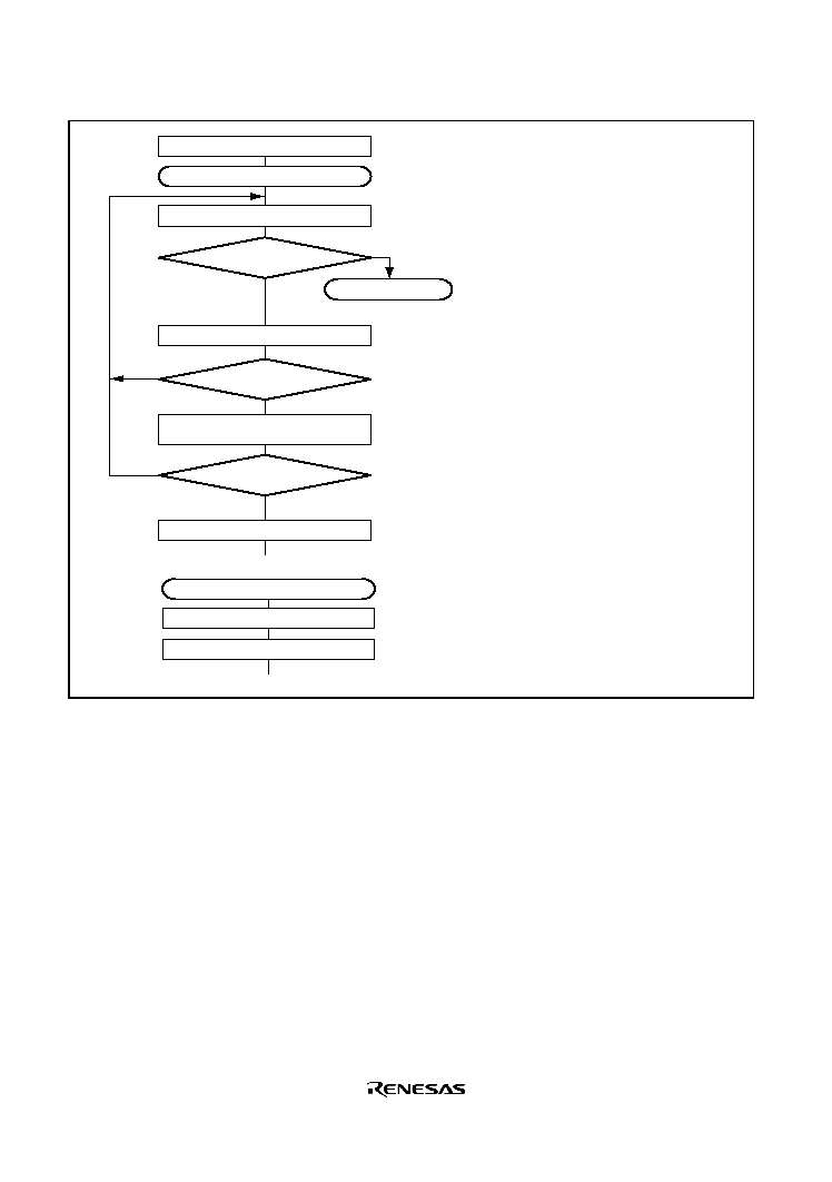
Rev. 1.0, 02/03, page 388 of 634
Yes
<End>
[1]
No
Initialization
Start reception
[2]
No
Yes
Read RDRF flag in SSR
[4]
[5]
Clear RE bit in SCR to 0
Error processing
(Continued below)
[3]
Read receive data in RDR, and
clear RDRF flag in SSR to 0
No
Yes
ORER = 1
RDRF = 1
All data received?
Read ORER flag in SSR
<End>
Error processing
Overrun error processing
Clear ORER flag in SSR to 0
[3]
[1]
SCI initialization:
The RxD pin is automatically designated as
the receive data input pin.
[2]
[3] Receive error processing:
If a receive error occurs, read the ORER
flag in SSR, and after performing the
appropriate error processing, clear the
ORER flag to 0. Transfer cannot be
resumed if the ORER flag is set to 1.
[4]
SCI status check and receive data read:
Read SSR and check that the RDRF flag is
set to 1, then read the receive data in RDR
and clear the RDRF flag to 0.
Transition of the RDRF flag from 0 to 1 can
also be identified by an RXI interrupt.
[5]
Serial reception continuation procedure:
To continue serial reception, before the
MSB (bit 7) of the current frame is received,
reading the RDRF flag, reading RDR, and
clearing the RDRF flag to 0 should be
finished. The RDRF flag is cleared
automatically when the DMAC is activated
by a receive data full interrupt (RXI) request
and the RDR value is read.
Figure 12.22 Sample Serial Reception Flowchart
12.6.5
Simultaneous Serial Data Transmission and Reception
(Clocked Synchronous Mode)
Figure 12.23 shows a sample flowchart for simultaneous serial transmit and receive operations.
The following procedure should be used for simultaneous serial data transmit and receive
operations. To switch from transmit mode to simultaneous transmit and receive mode, after
checking that the SCI has finished transmission and the TDRE and TEND flags are set to 1, clear
TE to 0. Then simultaneously set TE and RE to 1 with a single instruction. To switch from receive
mode to simultaneous transmit and receive mode, after checking that the SCI has finished
reception, clear RE to 0. Then after checking that the RDRF and receive error flags (ORER, FER,
and PER) are cleared to 0, simultaneously set TE and RE to 1 with a single instruction.
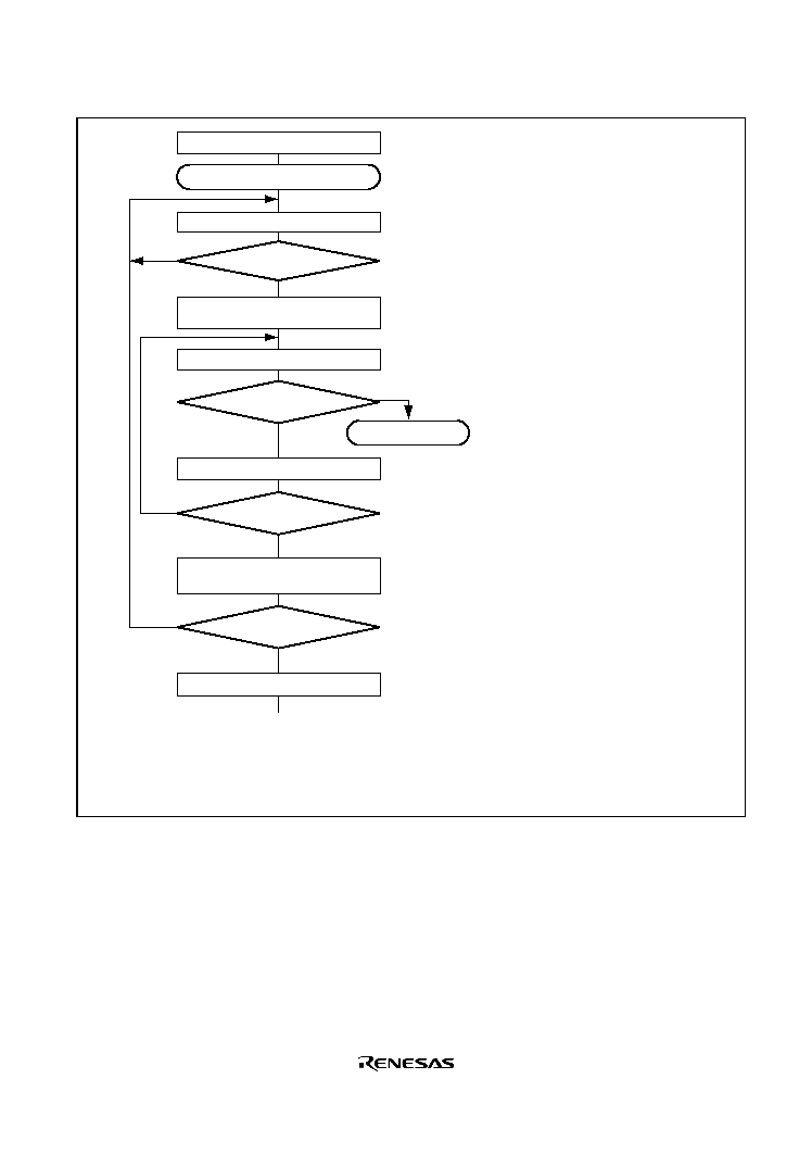
Rev. 1.0, 02/03, page 389 of 634
Yes
<End>
[1]
No
Initialization
Start transmission/reception
[5]
Error processing
[3]
Read receive data in RDR, and
clear RDRF flag in SSR to 0
No
Yes
ORER = 1
All data received?
[2]
Read TDRE flag in SSR
No
Yes
TDRE = 1
Write transmit data to TDR and
clear TDRE flag in SSR to 0
No
Yes
RDRF = 1
Read ORER flag in SSR
[4]
Read RDRF flag in SSR
Clear TE and RE bits in SCR to 0
[1]
SCI initialization:
The TxD pin is designated as the
transmit data output pin, and the RxD pin
is designated as the receive data input
pin, enabling simultaneous transmit and
receive operations.
[2]
SCI status check and transmit data write:
Read SSR and check that the TDRE flag
is set to 1, then write transmit data to
TDR and clear the TDRE flag to 0.
Transition of the TDRE flag from 0 to 1
can also be identified by a TXI interrupt.
[3]
Receive error processing:
If a receive error occurs, read the ORER
flag in SSR, and after performing the
appropriate error processing, clear the
ORER flag to 0. Transmission/reception
cannot be resumed if the ORER flag is
set to 1.
[4]
SCI status check and receive data read:
Read SSR and check that the RDRF flag
is set to 1, then read the receive data in
RDR and clear the RDRF flag to 0.
Transition of the RDRF flag from 0 to 1
can also be identified by an RXI
interrupt.
[5]
Serial transmission/reception
continuation procedure:
To continue serial transmission/
reception, before the MSB (bit 7) of the
current frame is received, finish reading
the RDRF flag, reading RDR, and
clearing the RDRF flag to 0. Also,
before the MSB (bit 7) of the current
frame is transmitted, read 1 from the
TDRE flag to confirm that writing is
possible. Then write data to TDR and
clear the TDRE flag to 0.
Checking and clearing of the TDRE flag
is automatic when the DMAC is activated
by a transmit data empty interrupt (TXI)
request and data is written to TDR.
Also, the RDRF flag is cleared
automatically when the DMAC is
activated by a receive data full interrupt
(RXI) request and the RDR value is
read.
Note: When switching from transmit or receive operation to simultaneous
transmit and receive operations, first clear the TE bit and RE bit to 0,
then set both these bits to 1 simultaneously.
Figure 12.23 Sample Flowchart of Simultaneous Serial Transmit and Receive Operations
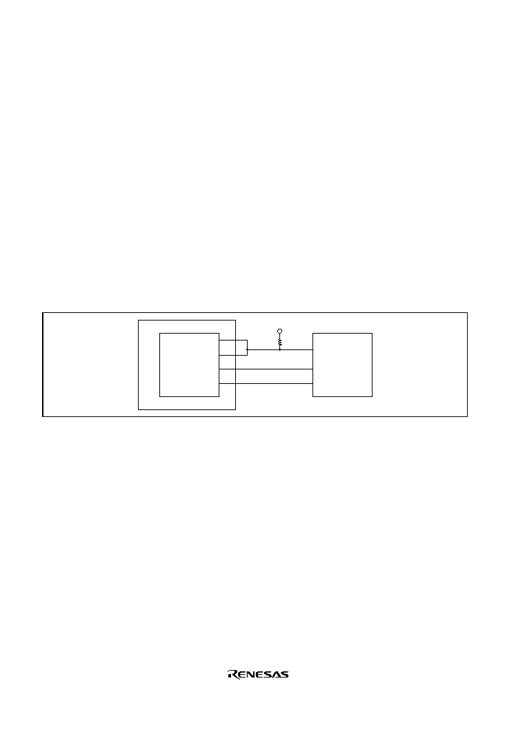
Rev. 1.0, 02/03, page 390 of 634
12.7
Operation in Smart Card Interface
The SCI supports an IC card (Smart Card) interface that conforms to ISO/IEC 7816-3
(Identification Card) as a serial communication interface extension function. Switching between
the normal serial communication interface and the Smart Card interface mode is carried out by
means of a register setting.
12.7.1
Pin Connection Example
Figure 12.24 shows an example of connection with the Smart Card. In communication with an IC
card, as both transmission and reception are carried out on a single data transmission line, the TxD
pin and RxD pin should be connected to the LSI pin. The data transmission line should be pulled
up to the V
CC
power supply with a resistor. If an IC card is not connected, and the TE and RE bits
are both set to 1, closed transmission/reception is possible, enabling self-diagnosis to be carried
out. When the clock generated on the Smart Card interface is used by an IC card, the SCK pin
output is input to the CLK pin of the IC card. This LSI port output is used as the reset signal.
TxD
RxD
This LSI
V
CC
I/O
Connected equipment
IC card
Data line
Clock line
Reset line
CLK
RST
SCK
Rx (port)
Figure 12.24 Schematic Diagram of Smart Card Interface Pin Connections
12.7.2
Data Format (Except for Block Transfer Mode)
Figure 12.25 shows the transfer data format in Smart Card interface mode.
· One frame consists of 8-bit data plus a parity bit in asynchronous mode.
· In transmission, a guard time of at least 2 etu (Elementary Time Unit: the time for transfer of
one bit) is left between the end of the parity bit and the start of the next frame.
· If a parity error is detected during reception, a low error signal level is output for one etu
period, 10.5 etu after the start bit.
If an error signal is sampled during transmission, the same data is retransmitted automatically after
a delay of 2 etu or longer.
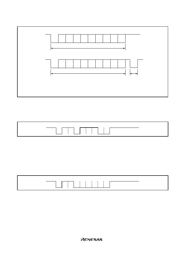
Rev. 1.0, 02/03, page 391 of 634
Ds
D0
D1
D2
D3
D4
D5
D6
D7
Dp
When there is no parity error
Transmitting station output
Ds
D0
D1
D2
D3
D4
D5
D6
D7
Dp
When a parity error occurs
Transmitting station output
DE
Receiving station
output
: Start bit
: Data bits
: Parity bit
: Error signal
Legend
DS
D0 to D7
Dp
DE
Figure 12.25 Normal Smart Card Interface Data Format
Data transfer with other types of IC cards (direct convention and inverse convention) are
performed as described in the following.
Ds
A
Z
Z
A
Z
Z
Z
Z
A
A
(Z)
(Z)
State
D0
D1
D2
D3
D4
D5
D6
D7
Dp
Figure 12.26 Direct Convention (SDIR = SINV = O/
E
E
E
E = 0)
With the direction convention type IC and the above sample start character, the logic 1 level
corresponds to state Z and the logic 0 level to state A, and transfer is performed in LSB-first order.
The start character data above is H'3B. For the direct convention type, clear the SDIR and SINV
bits in SCMR to 0. According to Smart Card regulations, clear the O/
E bit in SMR to 0 to select
even parity mode.
Ds
A
Z
Z
A
A
A
Z
A
A
A
(Z)
(Z)
State
D7
D6
D5
D4
D3
D2
D1
D0
Dp
Figure 12.27 Inverse Convention (SDIR = SINV = O/
E
E
E
E = 1)
With the inverse convention type, the logic 1 level corresponds to state A and the logic 0 level to
state Z, and transfer is performed in MSB-first order. The start character data for the above is
H'3F. For the inverse convention type, set the SDIR and SINV bits in SCMR to 1. According to
Smart Card regulations, even parity mode is the logic 0 level of the parity bit, and corresponds to
state Z. In this LSI, the SINV bit inverts only data bits D0 to D7. Therefore, set the O/
E bit in
SMR to 1 to invert the parity bit for both transmission and reception.

Rev. 1.0, 02/03, page 392 of 634
12.7.3
Block Transfer Mode
Operation in block transfer mode is the same as that in the normal Smart Card interface mode,
except for the following points.
· In reception, though the parity check is performed, no error signal is output even if an error is
detected. However, the PER bit in SSR is set to 1 and must be cleared before receiving the
parity bit of the next frame.
· In transmission, a guard time of at least 1 etu is left between the end of the parity bit and the
start of the next frame.
· In transmission, because retransmission is not performed, the TEND flag is set to 1, 11.5 etu
after transmission start.
· As with the normal Smart Card interface, the ERS flag indicates the error signal status, but
since error signal transfer is not performed, this flag is always cleared to 0.
12.7.4
Receive Data Sampling Timing and Reception Margin
In Smart Card interface mode an internal clock generated by the on-chip baud rate generator can
only be used as a transmission/reception clock. In this mode, the SCI operates on a basic clock
with a frequency of 32, 64, 372, or 256 times the transfer rate (fixed to 16 times in normal
asynchronous mode) as determined by bits BCP1 and BCP0. In reception, the SCI samples the
falling edge of the start bit using the basic clock, and performs internal synchronization. As shown
in figure 12.28, by sampling receive data at the rising-edge of the 16th, 32nd, 186th, or 128th pulse
of the basic clock, data can be latched at the middle of the bit. The reception margin is given by the
following formula.
M = | (0.5 ) (L 0.5) F (1+ F) |
× 100 [%]
2N
1
N
| D 0.5 |
Where
M: Reception margin (%)
N: Ratio of bit rate to clock (N = 32, 64, 372, and 256)
D: Clock duty (D = 0 to 1.0)
L: Frame length (L = 10)
F: Absolute value of clock frequency deviation
Assuming values of F = 0, D = 0.5 and N = 372 in the above formula, the reception margin
formula is as follows.
M = (0.5 1/2
× 372) × 100%
= 49.866%
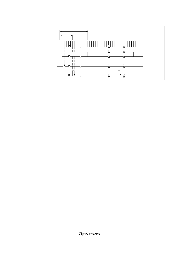
Rev. 1.0, 02/03, page 393 of 634
Internal
basic clock
372 clocks
186 clocks
Receive data
(RxD)
Synchronization
sampling timing
D0
D1
Data sampling
timing
185
371 0
371
185
0
0
Start bit
Figure 12.28 Receive Data Sampling Timing in Smart Card Mode
(Using Clock of 372 Times the Transfer Rate)
12.7.5
Initialization
Before transmitting and receiving data, initialize the SCI as described below. Initialization is also
necessary when switching from transmit mode to receive mode, or vice versa.
1. Clear the TE and RE bits in SCR to 0.
2. Clear the error flags ERS, PER, and ORER in SSR to 0.
3. Set the GM, BLK, O/
E, BCP0, BCP1, CKS0, CKS1 bits in SMR. Set the PE bit to 1.
4. Set the SMIF, SDIR, and SINV bits in SCMR.
When the SMIF bit is set to 1, the TxD and RxD pins are both switched from ports to SCI pins,
and are placed in the high-impedance state.
5. Set the value corresponding to the bit rate in BRR.
6. Set the CKE0 and CKE1 bits in SCR. Clear the TIE, RIE, TE, RE, MPIE, and TEIE bits to 0.
If the CKE0 bit is set to 1, the clock is output from the SCK pin.
7. Wait at least one bit interval, then set the TIE, RIE, TE, and RE bits in SCR. Do not set the TE
bit and RE bit at the same time, except for self-diagnosis.
To switch from receive mode to transmit mode, after checking that the SCI has finished reception,
initialize the SCI, and set RE to 0 and TE to 1. Whether SCI has finished reception or not can be
checked with the RDRF, PER, or ORER flags. To switch from transmit mode to receive mode,
after checking that the SCI has finished transmission, initialize the SCI, and set TE to 0 and RE to
1. Whether SCI has finished transmission or not can be checked with the TEND flag.

Rev. 1.0, 02/03, page 394 of 634
12.7.6
Serial Data Transmission (Except for Block Transfer Mode)
As data transmission in Smart Card interface mode involves error signal sampling and
retransmission processing, the operations are different from those in normal serial communication
interface mode (except for block transfer mode). Figure 12.29 illustrates the retransfer operation
when the SCI is in transmit mode.
1. If an error signal is sent back from the receiving end after transmission of one frame is
complete, the ERS bit in SSR is set to 1. If the RIE bit in SCR is enabled at this time, an ERI
interrupt request is generated. The ERS bit in SSR should be cleared to 0 by the time the next
parity bit is sampled.
2. The TEND bit in SSR is not set for a frame in which an error signal indicating an abnormality
is received. Data is retransferred from TDR to TSR, and retransmitted automatically.
3. If an error signal is not sent back from the receiving end, the ERS bit in SSR is not set.
Transmission of one frame, including a retransfer, is judged to have been completed, and the
TEND bit in SSR is set to 1. If the TIE bit in SCR is enabled at this time, a TXI interrupt
request is generated. Writing transmit data to TDR transfers the next transmit data.
Figure 12.31 shows a flowchart for transmission. A sequence of transmit operations can be
performed automatically by specifying the DTC to be activated with a TXI interrupt source. In a
transmit operation, the TDRE flag is set to 1 at the same time as the TEND flag in SSR is set, and
a TXI interrupt will be generated if the TIE bit in SCR has been set to 1. If the TXI request is
designated beforehand as a DTC activation source, the DTC will be activated by the TXI request,
and transfer of the transmit data will be carried out. The TDRE and TEND flags are automatically
cleared to 0 when data is transferred by the DTC. In the event of an error, the SCI retransmits the
same data automatically. During this period, the TEND flag remains cleared to 0 and the DTC is
not activated. Therefore, the SCI and DTC will automatically transmit the specified number of
bytes in the event of an error, including retransmission. However, the ERS flag is not cleared
automatically when an error occurs, and so the RIE bit should be set to 1 beforehand so that an
ERI request will be generated in the event of an error, and the ERS flag will be cleared.
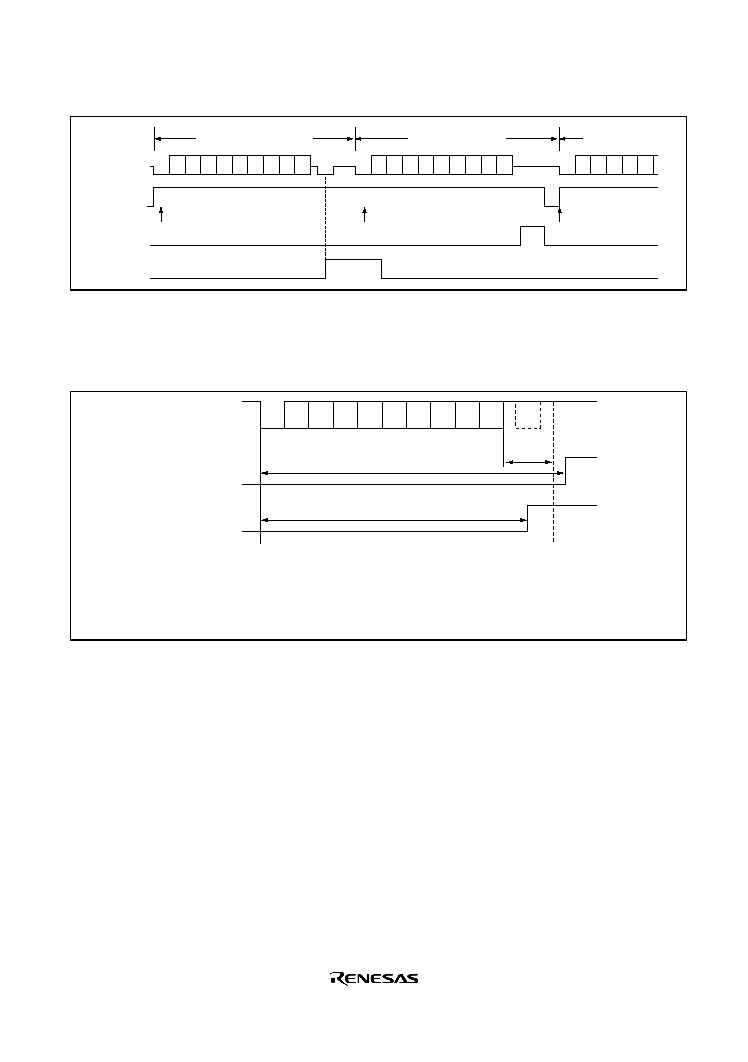
Rev. 1.0, 02/03, page 395 of 634
D0 D1 D2 D3 D4 D5 D6 D7 Dp DE
Ds D0 D1 D2 D3 D4 D5 D6 D7 Dp
(DE)
Ds D0 D1 D2 D3 D4
Ds
Transfer
frame n+1
Retransferred frame
nth transfer frame
TDRE
TEND
FER/ERS
Transfer to TSR from TDR
Transfer to TSR from TDR
Transfer to TSR
from TDR
Figure 12.29 Retransfer Operation in SCI Transmit Mode
The timing for setting the TEND flag depends on the value of the GM bit in SMR. The TEND flag
set timing is shown in figure 12.30.
Ds
D0
D1
D2
D3
D4
D5
D6
D7
Dp
I/O data
12.5etu
TXI
(TEND interrupt)
11.0etu
DE
Guard
time
When GM = 0
When GM = 1
: Start bit
: Data bits
: Parity bit
: Error signal
Legend:
Ds
D0 to D7
Dp
DE
Figure 12.30 TEND Flag Generation Timing in Transmission Operation
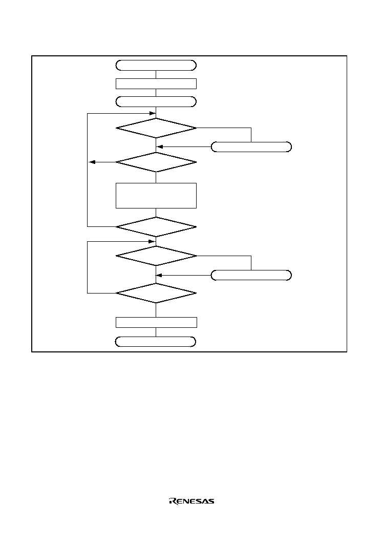
Rev. 1.0, 02/03, page 396 of 634
Initialization
No
Yes
Clear TE bit to 0
Start transmission
Start
No
No
No
Yes
Yes
Yes
Yes
No
End
Write data to TDR,
and clear TDRE flag
in SSR to 0
Error processing
Error processing
TEND = 1?
All data transmitted ?
TEND = 1?
ERS = 0?
ERS = 0?
Figure 12.31 Example of Transmission Processing Flow
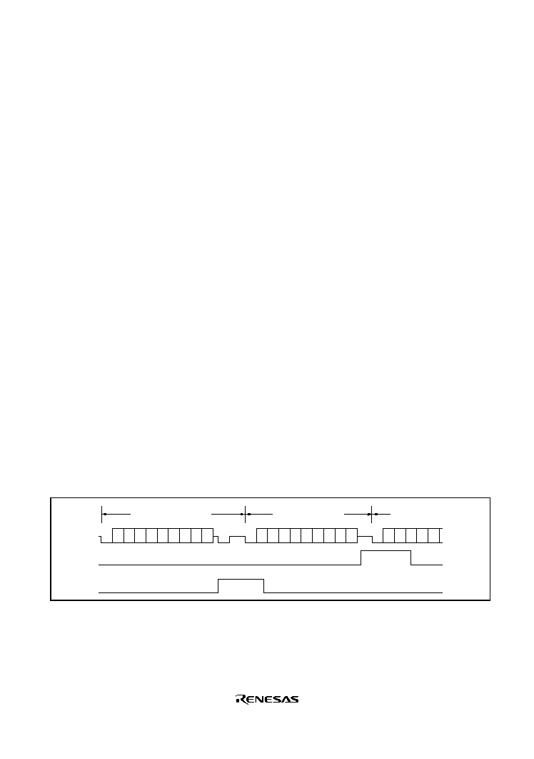
Rev. 1.0, 02/03, page 397 of 634
12.7.7
Serial Data Reception (Except for Block Transfer Mode)
Data reception in Smart Card interface mode uses the same operation procedure as for normal
serial communication interface mode. Figure 12.32 illustrates the retransfer operation when the
SCI is in receive mode.
1. If an error is found when the received parity bit is checked, the PER bit in SSR is automatically
set to 1. If the RIE bit in SCR is set at this time, an ERI interrupt request is generated. The PER
bit in SSR should be kept cleared to 0 until the next parity bit is sampled.
2. The RDRF bit in SSR is not set for a frame in which an error has occurred.
3. If no error is found when the received parity bit is checked, the PER bit in SSR is not set to 1,
the receive operation is judged to have been completed normally, and the RDRF flag in SSR is
automatically set to 1. If the RIE bit in SCR is enabled at this time, an RXI interrupt request is
generated.
Figure 12.33 shows a flowchart for reception. A sequence of receive operations can be performed
automatically by specifying the DTC to be activated using an RXI interrupt source. In a receive
operation, an RXI interrupt request is generated when the RDRF flag in SSR is set to 1. If the RXI
request is designated beforehand as a DTC activation source, the DTC will be activated by the RXI
request, and the receive data will be transferred. The RDRF flag is cleared to 0 automatically when
data is transferred by the DTC. If an error occurs in receive mode and the ORER or PER flag is set
to 1, a transfer error interrupt (ERI) request will be generated. Hence, so the error flag must be
cleared to 0. In the event of an error, the DTC is not activated and receive data is skipped.
Therefore, receive data is transferred for only the specified number of bytes in the event of an
error. Even when a parity error occurs in receive mode and the PER flag is set to 1, the data that
has been received is transferred to RDR and can be read from there.
Note:
For details on receive operations in block transfer mode, refer to section 12.4, Operation
in Asynchronous Mode.
D0 D1 D2 D3 D4 D5 D6 D7 Dp DE
Ds D0 D1 D2 D3 D4 D5 D6 D7 Dp
(DE)
Ds D0 D1 D2 D3 D4
Ds
Transfer
frame n+1
Retransferred frame
nth transfer frame
RDRF
PER
Figure 12.32 Retransfer Operation in SCI Receive Mode
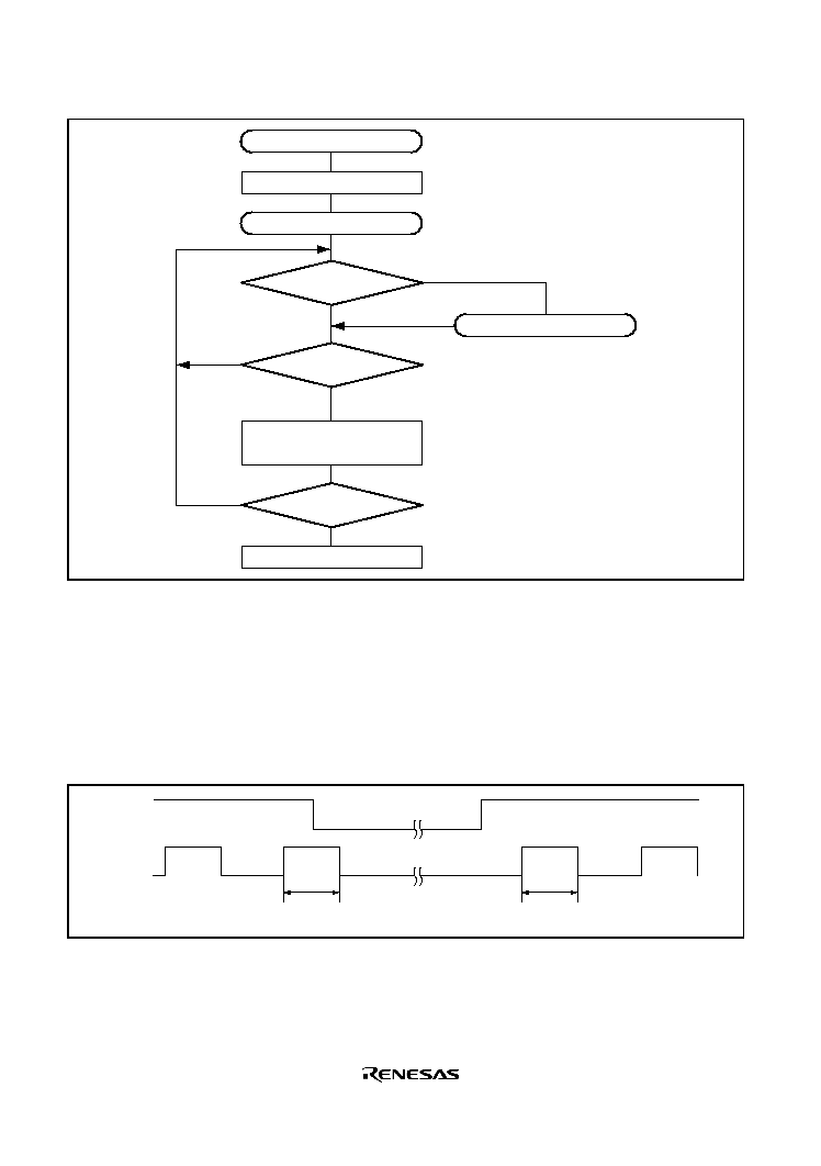
Rev. 1.0, 02/03, page 398 of 634
Initialization
Read RDR and clear
RDRF flag in SSR to 0
Clear RE bit to 0
Start reception
Start
Error processing
No
No
No
Yes
Yes
ORER = 0 and
PER = 0
RDRF = 1?
All data received?
Yes
Figure 12.33 Example of Reception Processing Flow
12.7.8
Clock Output Control
When the GM bit in SMR is set to 1, the clock output level can be fixed with bits CKE0 and CKE1
in SCR. At this time, the minimum clock pulse width can be made the specified width. Figure
12.34 shows the timing for fixing the clock output level. In this example, GM is set to 1, CKE1 is
cleared to 0, and the CKE0 bit is controlled.
Specified pulse width
SCK
CKE0
Specified pulse width
Figure 12.34 Timing for Fixing Clock Output Level
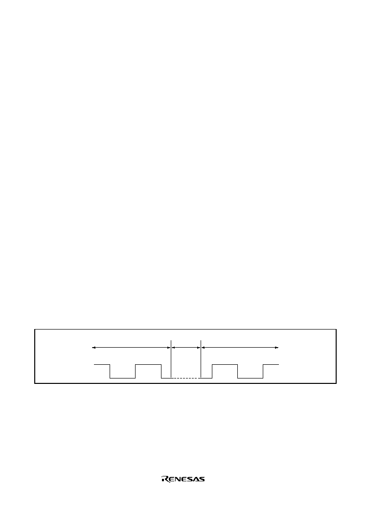
Rev. 1.0, 02/03, page 399 of 634
When turning on the power or switching between Smart Card interface mode and software standby
mode, the following procedures should be followed in order to maintain the clock duty.
Powering On: To secure clock duty from power-on, the following switching procedure should be
followed.
1. The initial state is port input and high impedance. Use a pull-up resistor or pull-down
resistor to fix the potential.
2. Fix the SCK pin to the specified output level with the CKE1 bit in SCR.
3. Set SMR and SCMR, and switch to smart card mode operation.
4. Set the CKE0 bit in SCR to 1 to start clock output.
When changing from smart card interface mode to software standby mode:
1. Set the data register (DR) and data direction register (DDR) corresponding to the SCK pin
to the value for the fixed output state in software standby mode.
2. Write 0 to the TE bit and RE bit in the serial control register (SCR) to halt transmit/receive
operation. At the same time, set the CKE1 bit to the value for the fixed output state in
software standby mode.
3. Write 0 to the CKE0 bit in SCR to halt the clock.
4. Wait for one serial clock period.
During this interval, clock output is fixed at the specified level, with the duty preserved.
5. Make the transition to the software standby state.
When returning to smart card interface mode from software standby mode:
1. Exit the software standby state.
2. Write 1 to the CKE0 bit in SCR and output the clock. Signal generation is started with the
normal duty.
Software
standby
Normal operation
Normal operation
Figure 12.35 Clock Halt and Restart Procedure
Rev. 1.0, 02/03, page 400 of 634
12.8
SCI Select Function
The SCI_0 supports the SCI select function which allows clock synchronous communication
between master LSI and one of multiple slave LSI. Figure 12.36 shows an example of
communication using the SCI select function. Figure 12.37 shows the operation.
The master LSI can communicate with slave LSI_A by bringing
SEL_A and SEL_B signals low
and high, respectively. In this case, the TxD0_B pin of the slave LSI_B is brought high-
impedance state and the internal SCK0_A signal is fixed high. This halts the communication
operation of slave LSI_B. The master LSI can communicate with slave LSI_B by bringing the
SEL_A and SEL_B signals high and low, respectively.
The slave LSI detects the selection by receiving the low level input from the
IRQ7 pin and
immediately executes data transmission/reception processing.
Note: The selection signals (
SEL_A and SEL_B) of the LSI must be switched while the serial
clock (M_SCK) is high after the end bit of the transmit data has been send. Note that one
selection signal can be brought low at the same time.
Interrupt
controller
TSR0_A
RSR0_A
Transmission/
reception
control
Slave LSI_A (This LSI)
Master LSI
SCK0_A
SCK0_B
C/A=CKE1=SSE=1
Slave LSI_B (This LSI)
M_TxD
RxD0_A
TxD0_A
RxD0_B
TxD0_B
SCK0
SCK0
M_RxD
M_SCK
Figure 12.36 Example of Communication Using the SCI Select Function
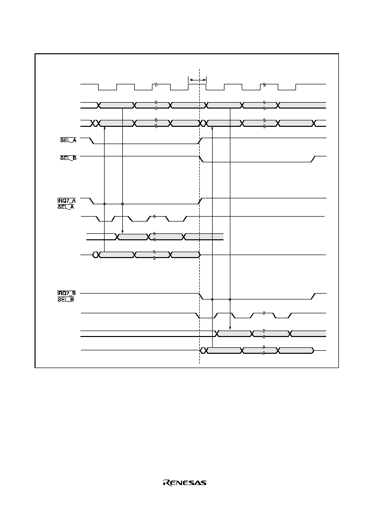
Rev. 1.0, 02/03, page 401 of 634
M_SCK
Master LSI
Slave LSI_A
Communication between master LSI
and slave LSI_A
Communication between master LSI
and slave LSI_B
M_TxD
M_RxD
(
)
Slave LSI_B
(
)
D0
D0
D1
D1
D7
D7
D0
D1
D7
D0
D0
D1
D1
D7
D7
D0
D1
D7
SCK0_A
RSR0_A
TxD0_A
SCK0_B
RSR0_B
TxD0_B
Hi-Z
Hi-Z
Hi-Z
D0
D6
D7
D0
D6
D7
Period of M_SCK
= high
Fixed high level
Fixed high level
Hi-Z
Figure 12.37 Example of Communication Using the SCI Select Function

Rev. 1.0, 02/03, page 402 of 634
12.9
Interrupts
12.9.1
Interrupts in Normal Serial Communication Interface Mode
Table 12.12 shows the interrupt sources in normal serial communication interface mode. A
different interrupt vector is assigned to each interrupt source, and individual interrupt sources can
be enabled or disabled using the enable bits in SCR.
When the TDRE flag in SSR is set to 1, a TXI interrupt request is generated. When the TEND flag
in SSR is set to 1, a TEI interrupt request is generated. A TXI interrupt can activate the DMAC to
perform data transfer. The TDRE flag is cleared to 0 automatically when data is transferred by the
DMAC.
When the RDRF flag in SSR is set to 1, an RXI interrupt request is generated. When the ORER,
PER, or FER flag in SSR is set to 1, an ERI interrupt request is generated. An RXI interrupt
request can activate the DMAC to transfer data. The RDRF flag is cleared to 0 automatically when
data is transferred by the DMAC.
A TEI interrupt is requested when the TEND flag is set to 1 and the TEIE bit is set to 1. If a TEI
interrupt and a TXI interrupt are requested simultaneously, the TXI interrupt has priority for
acceptance. However, if the TDRE and TEND flags are cleared simultaneously by the TXI
interrupt routine, the SCI cannot branch to the TEI interrupt routine later.
Table 12.12 SCI Interrupt Sources
Channel Name
Interrupt Source
Interrupt Flag
DMAC Activation Priority
*
ERI0
Receive Error
ORER, FER, PER
Not possible
High
RXI0
Receive Data Full
RDRF
Possible
TXI0
Transmit Data Empty
TDRE
Possible
0
TEI0
Transmission End
TEND
Not possible
ERI2
Receive Error
ORER, FER, PER
Not possible
RXI2
Receive Data Full
RDRF
Not possible
TXI2
Transmit Data Empty
TDRE
Not possible
2
TEI2
Transmission End
TEND
Not possible
Low
Note:
This table shows the initial state immediately after a reset. The relative channel priorities
can be changed by the interrupt controller.

Rev. 1.0, 02/03, page 403 of 634
12.9.2
Interrupts in Smart Card Interface Mode
Table 12.13 shows the interrupt sources in Smart Card interface mode. The transmit end interrupt
(TEI) request cannot be used in this mode.
Note: In case of block transfer mode, see 12.9.1, Interrupts in Nomal Serial Communication
Interface Mode.
Table 12.13 Interrupt Sources in Smart Card Interface Mode
Channel
Name
Interrupt Source
Interrupt Flag
DMAC
Activation
Priority
*
ERI0
Receive Error, detection
ORER, PER, ERS
Not possible
High
RXI0
Receive Data Full
RDRF
Possible
0
TXI0
Transmit Data Empty
TEND
Possible
ERI2
Receive Error, detection
ORER, PER, ERS
Not possible
RXI2
Receive Data Full
RDRF
Not possible
2
TXI2
Transmit Data Empty
TEND
Not possible
Low
Note:
*
Indicates the initial state immediately after a reset.
Priorities in channels can be changed by the interrupt controller.
12.10
Usage Notes
12.10.1
Break Detection and Processing (Asynchronous Mode Only)
When framing error detection is performed, a break can be detected by reading the RxD pin value
directly. In a break, the input from the RxD pin becomes all 0s, setting the FER flag, and possibly
the PER flag. Note that as the SCI continues the receive operation after receiving a break, even if
the FER flag is cleared to 0, it will be set to 1 again.
12.10.2
Mark State and Break Detection (Asynchronous Mode Only)
When TE is 0, the TxD pin is used as an I/O port whose direction (input or output) and level are
determined by DR and DDR. This can be used to set the TxD pin to mark state (high level) or send
a break during serial data transmission. To maintain the communication line at mark state until TE
is set to 1, set both DDR and DR to 1. As TE is cleared to 0 at this point, the TxD pin becomes an
I/O port, and 1 is output from the TxD pin. To send a break during serial transmission, first set
PCR to 1 and PDR to 0, and then clear TE to 0. When TE is cleared to 0, the transmitter is
initialized regardless of the current transmission state, the TxD pin becomes an I/O port, and 0 is
output from the TxD pin.
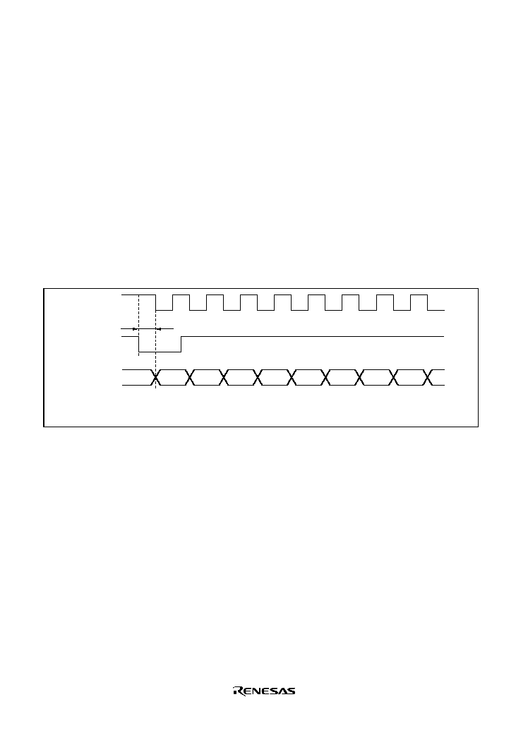
Rev. 1.0, 02/03, page 404 of 634
12.10.3
Receive Error Flags and Transmit Operations (Clocked Synchronous Mode Only)
Transmission cannot be started when a receive error flag (ORER, PER, or FER) is set to 1, even if
the TDRE flag is cleared to 0. Be sure to clear the receive error flags to 0 before starting
transmission. Note also that receive error flags cannot be cleared to 0 even if the RE bit is cleared
to 0.
12.10.4
Restrictions on Use of DMAC
· When an external clock source is used as the serial clock, the transmit clock should not be
input until at least 5
clock cycles after TDR is updated by the DMAC. Misoperation may
occur if the transmit clock is input within 4
clocks after TDR is updated. (figure 12.38)
· When RDR is read by the DMAC, be sure to set the activation source to the relevant SCI
reception end interrupt (RXI).
t
D0
LSB
Serial data
SCK
D1
D3
D4
D5
D2
D6
D7
Note: When operating on an external clock, set t >4 clocks.
TDRE
Figure 12.38 Example of Clocked Synchronous Transmission by DMAC
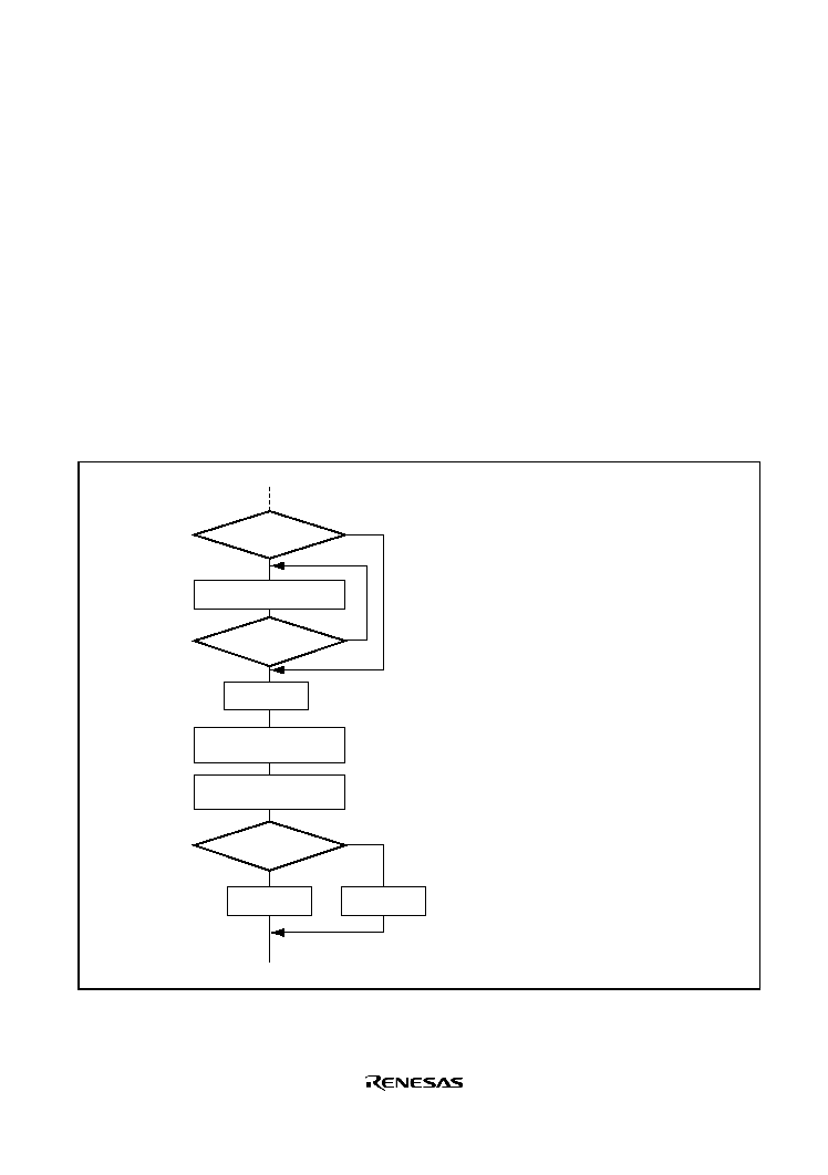
Rev. 1.0, 02/03, page 405 of 634
12.10.5
Operation in Case of Mode Transition
· Transmission
Operation should be stopped (by clearing TE, TIE, and TEIE to 0) before making a module
stop mode, software standby mode, or subsleep mode transition. TSR, TDR, and SSR are reset.
The output pin states in module stop mode, software standby mode, or subsleep mode depend
on the port settings, and becomes high-level output after the relevant mode is cleared. If a
transition is made during transmission, the data being transmitted will be undefined. When
transmitting without changing the transmit mode after the relevant mode is cleared,
transmission can be started by setting TE to 1 again, and performing the following sequence:
SSR read -> TDR write -> TDRE clearance. To transmit with a different transmit mode after
clearing the relevant mode, the procedure must be started again from initialization. Figure
12.39 shows a sample flowchart for mode transition during transmission. Port pin states are
shown in figures 12.40 and 12.41.
Read TEND flag in SSR
TE= 0
Transition to software
standby mode, etc.
Exit from software
standby mode, etc.
Change
operating mode?
No
All data
transmitted?
TEND = 1
Yes
Yes
Yes
<Transmission>
No
No
[1]
[3]
[2]
TE= 1
Initialization
<Start of transmission>
Data being transmitted is interrupted.
After exiting software standby
mode, etc., normal CPU transmission
is possible by setting TE to 1, reading
SSR, writing TDR, and clearing TDRE
to 0.
If TIE and TEIE are set to 1, clear
them to 0 in the same way.
Includes module stop mode.
[1]
[2]
[3]
Figure 12.39 Sample Flowchart for Mode Transition during Transmission
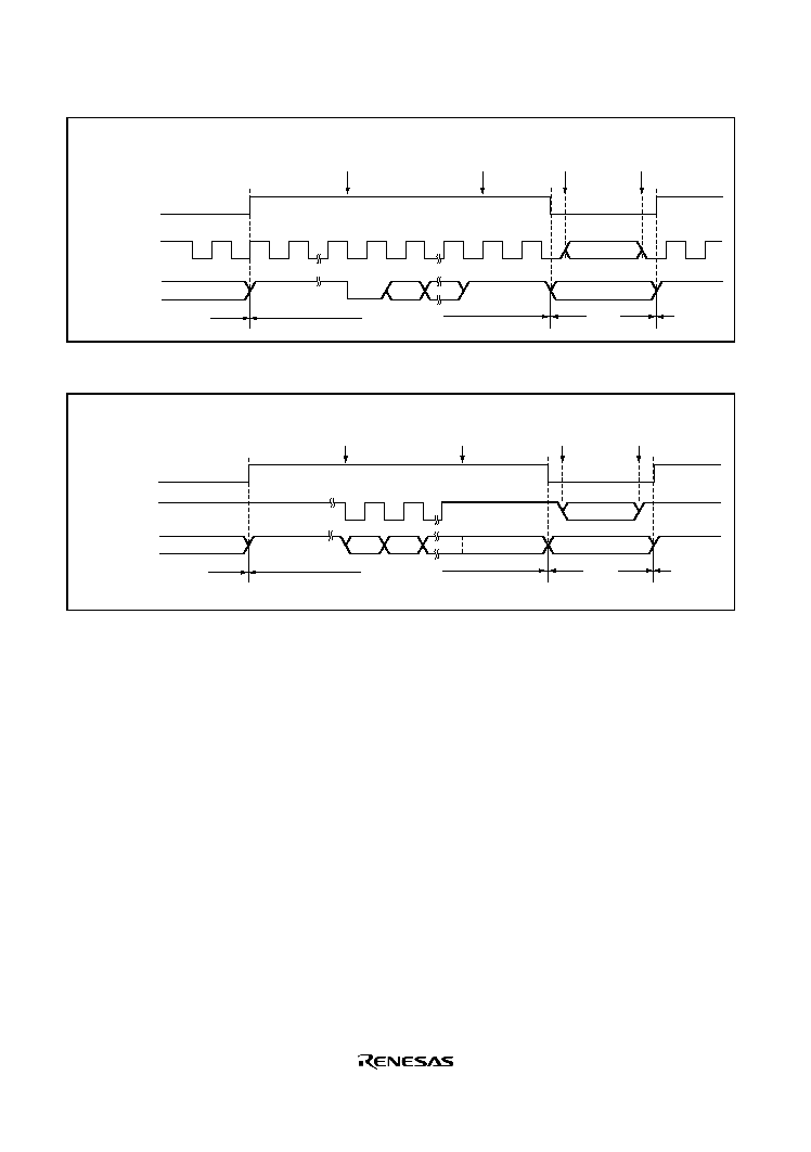
Rev. 1.0, 02/03, page 406 of 634
SCK output pin
TE bit
TxD output pin
Port input/output
High output
Port input/output
High output
Start
Stop
Start of transmission
End of
transmission
Port input/output
SCI TxD output
Port
SCI TxD
output
Port
Transition
to software
standby
Exit from
software
standby
Figure 12.40 Port Pin State of Asynchronous Transmission Using Internal Clock
TE bit
SCK output pin
TxD output pin Port input/output
High output
Final TxD
bit retention
Port input/output
Port
Port
SCI TxD output
SCI TxD
output
High output*
Port input/output
Start of transmission
End of
transmission
Transition
to software
standby
Exit from
software
standby
Note: * Initialized by the software standby.
Figure 12.41 Port Pin State of Synchronous Transmission Using Internal Clock
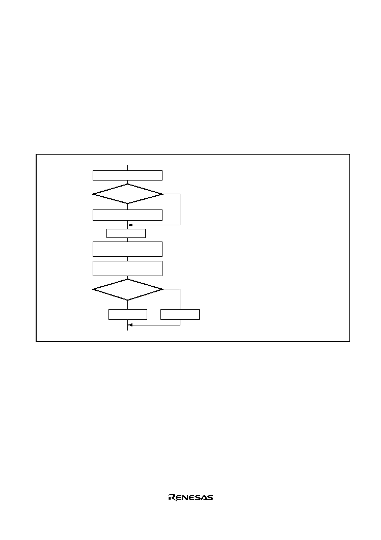
Rev. 1.0, 02/03, page 407 of 634
· Reception
Receive operation should be stopped (by clearing RE to 0) before making a module stop mode,
software standby mode, watch mode, subactive mode, or subsleep mode transition. RSR, RDR,
and SSR are reset. If a transition is made without stopping operation, the data being received
will be invalid.
To continue receiving without changing the reception mode after the relevant mode is cleared,
set RE to 1 before starting reception. To receive with a different receive mode, the procedure
must be started again from initialization.
Figure 12.42 shows a sample flowchart for mode transition during reception.
RE= 0
Transition to software
standby mode, etc.
Read receive data in RDR
Read RDRF flag in SSR
Exit from software
standby mode, etc.
Change
operating mode?
No
RDRF= 1
Yes
Yes
<Reception>
No
[1]
[2]
RE= 1
Initialization
<Start of reception>
Receive data being received
becomes invalid.
Includes module stop mode.
[1]
[2]
Figure 12.42 Sample Flowchart for Mode Transition during Reception
12.10.6
Switching from SCK Pin Function to Port Pin Function:
When switching the SCK pin function to the output port function (high-level output) by making
the following settings while DDR = 1, DR = 1, C/
A = 1, CKE1 = 0, CKE0 = 0, and TE = 1
(synchronous mode), low-level output occurs for one half-cycle.
1. End of serial data transmission
2. TE bit = 0
3. C/
A bit = 0 ... switchover to port output
4. Occurrence of low-level output (see Figure 12.43)
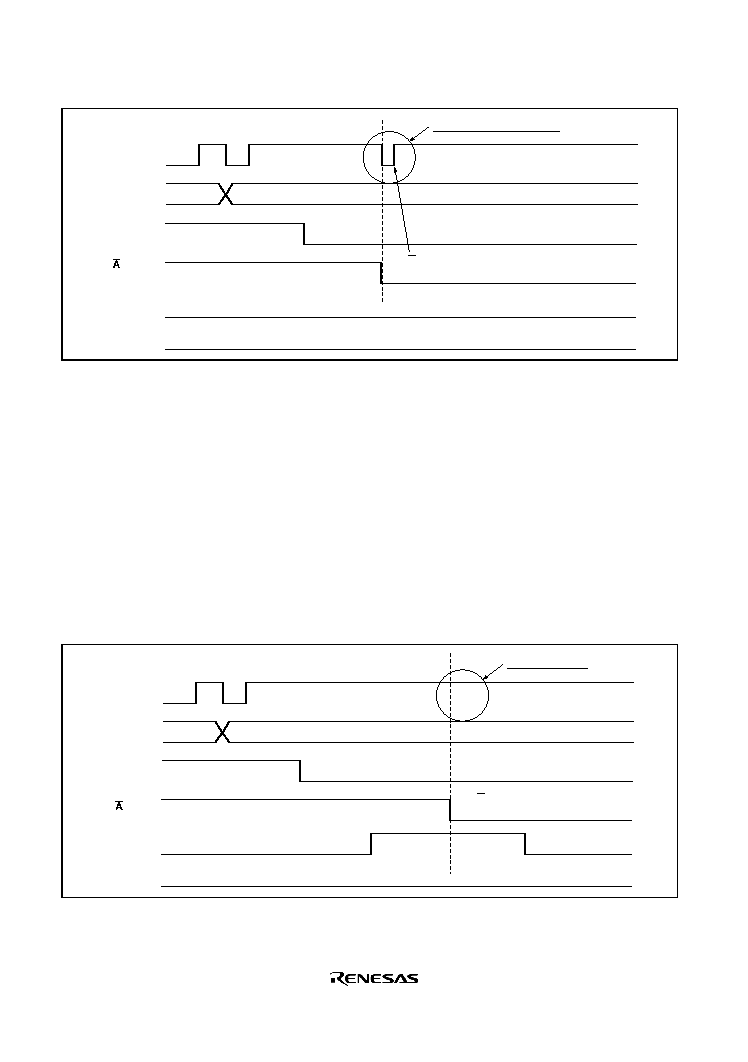
Rev. 1.0, 02/03, page 408 of 634
Bit 7
Bit 6
1. End of transmission
4. Low-level output
3.C/A= 0
2.TE= 0
Half-cycle low-level output
SCK/port
Data
TE
C/
CKE1
CKE0
Figure 12.43 Operation when Switching from SCK Pin Function to Port Pin Function
Sample Procedure for Avoiding Low-Level Output: As this sample procedure temporarily
places the SCK pin in the input state, the SCK/port pin should be pulled up beforehand with an
external circuit.
With DDR = 1, DR = 1, C/
A = 1, CKE1 = 0, CKE0 = 0, and TE = 1, make the following
settings in the order shown.
1. End of serial data transmission
2. TE bit = 0
3. CKE1 bit = 1
4. C/
A bit = 0 ... switchover to port output
5. CKE1 bit = 0
Bit 7
Bit 6
1. End of transmission
3.CKE1= 1
5.CKE1= 0
4.C/A= 0
2.TE= 0
High-level output
SCK/port
Data
TE
C/
CKE1
CKE0
Figure 12.44 Operation when Switching from SCK Pin Function to Port Pin Function
(Example of Preventing Low-Level Output)
Rev. 1.0, 02/03, page 409 of 634
Section 13 Boundary Scan Function
The HD64F2218 and HD64F2218U incorporate a boundary scan function, which is a serial I/O
interface based on the JTAG (Joint Test Action Group, IEEEStd.1149.1 and IEEE Standard Test
Access Port and Boundary Scan Architecture). Figure 13.1 shows the block diagram of the
boundary scan function.
13.1
Features
· Five test signals
TCK, TDI, TDO, TMS, TRST
· Six test modes supported
BYAPASS, SAMPLE/PRELOAD, EXTEST, CLAMP, HIGHZ, IDCODE
· Boundary scan function cannot be performed on the following pins.
Power supply pins: VCC, VSS, Vref, PLLVCC, PLLVSS, DrVCC, DrVSS
Clock signals:
EXTAL, XTAL, OSC2, OSC1
Analog signals:
P40 to P43, P96, P97, USD+, USD-
Boundary scan signals: TCK, TDI, TDO, TMS, TRST
H-UDI control signal: EMLE
IDCODE
BSCANR
(Boundary scan cell chain)
TDO
MUX
TCK
TMS
Legend
BSCANR
IDCODE
BYPASS
INSTR
TAP
: Boundary scan register
: IDCODE register
: BYPASS register
: Instruction register
: Test access port
TDI
BYPASS
INSTR
TAP controller
MUX
Figure 13.1 Block Diagram of Boundary Scan Function

Rev. 1.0, 02/03, page 410 of 634
13.2
Pin Configuration
Table 13.1 shows the I/O pins used in the boundary scan function.
Table 13.1
Pin Configuration
Pin Name
I/O
Function
TMS
Input
Test Mode Select
Controls the TAP controller which is a 16-state Finite State
Machine.
The TMS input value at the rising edge of TCK determines the
status transition direction on the TAP controller.
The TMS is fixed high when the boundary scan function is not
used.
The protocol is based on JTAG standard (IEEE Std.1149.1).
This pin has a pull-up resistor.
TCK
Input
Test Clock
A clock signal for the boundary scan function.
When the boundary scan function is used, input a clock of
50% duty to this pin.
This pin has a pull-up resistor.
TDI
Input
Test Data Input
A data input signal for the boundary scan function.
Data input from the TDI is latched at the rising edge of TCK.
TDI is fixed high when the boundary scan function is not used.
This pin has a pull-up register.
TDO
Output
Test Data Output
A data output signal for the boundary scan function. Data
output from the TDO changes at the falling edge of TCK. The
output driver of the TDO is driven only when it is necessary
only in Shift-IR or Shift-DR states, and is brought to the high-
impedance state when not necessary.
TRST
Input
Test Reset
Asynchronously resets the TAP controller when
TRST is
brought low.
The user must apply power-on reset signal specific to the
boundary scan function when the power is supplied. (For
details on signal design, refer to figure 13.4, Reset Signal
Design Examples.)
TRST is fixed high when the boundary
scan function is not used. This pin has a pull-up resistor.
This pin has a pull-up register.

Rev. 1.0, 02/03, page 411 of 634
13.3
Register Descriptions
The boundary scan function has the following registers. These registers cannot be accessed by the
CPU.
· Instruction register (INSTR)
· IDCODE register (IDCODE)
· BYPASS register (BYPASS)
· Boundary scan register (BSCANR)
13.3.1
Instruction Register (INSTR)
INSTR is a 3-bit register. At initialization, this register is specified to IDCODE mode. When
TRST is pulled low, or when the TAP controller is in the Test-Logic-Reset state, INSTR is
initialized. INSTR can be written by the serial data input from the TDI. If more than three bits of
instruction is input from the TDI, INSTR stores the last three bits of serial data.
If a command reserved in INSTR is used, the correct operation cannot be guaranteed.
Bit
Bit Name
Initial Value R/W
Description
2
TI2
1
--
1
TI1
0
--
0
TI0
1
--
Test Instruction Bits
Instruction configuration is shown in table 13.2.
Table 13.2
Instruction configuration
Bit 2
Bit1
Bit 0
TI2
TI1
TI0
Instruction
0
0
0
EXTEST
0
0
1
SAMPLE/PRELOAD
0
1
0
CLAMP
0
1
1
HIGHZ
1
0
0
Reserved
1
0
1
IDCODE (initial value)
1
1
0
Reserved
1
1
1
BYPASS

Rev. 1.0, 02/03, page 412 of 634
1. EXTEST
The EXTEST instruction is used to test external circuits when this LSI is installed on the print
circuit board. If this instruction is executed, output pins are used to output test data (specified
by the SAMPLE/PRELOAD instruction) from the boundary scan register to the print circuit
board, and input pins are used to input test results.
2. SAMPLE/PRELOAD
The SAMPLE/PRELOAD instruction is used to input data from the LSI internal circuits to the
boundary scan register, output data from scan path, and reload the data to the scan path. While
this instruction is executed, input signals are directly input to the LSI and output signals are
also directly output to the external circuits. The LSI system circuit is not affected by this
instruction.
In SAMPLE operation, the boundary scan register latches the snap shot of data transferred
from input pins to internal circuit or data transferred from internal circuit to output pins. The
latched data is read from the scan path. The scan register latches the snap data at the rising
edge of the TCK in Capture DR state. The scan register latches snap shot without affecting
the LSI normal operation.
In PRELOAD operation, initial value is written from the scan path to the parallel output latch
of the boundary scan register prior to the EXTEST instruction execution. If the EXTEST is
executed without executing this RELOAD operation, undefined values are output from the
beginning to the end (transfer to the output latch) of the EXTEST sequence. (In EXTEST
instruction, output parallel latches are always output to the output pins.)
3. CLAMP
When the CLAMP instruction is selected output pins output the boundary scan register value
which was specified by the SAMPLE/PRELOAD instruction in advance. While the CLAMP
instruction is selected, the status of boundary scan register is maintained regardless of the TAP
controller state. BYPASS is connected between TDI and TDO, the same operation as BYPASS
instruction can be achieved.
4. HIGHZ
When the HIGHZ instruction is selected, all outputs enter high-impedance state. While this
instruction is selected, the status of boundary scan register is maintained regardless of the TAP
controller state. BYPASS resistor is connected between TDI and TDO, the same operation as
BYPASS instruction can be achieved.
5. IDCODE
When the IDCODE instruction is selected, IDCODE register value is output to the TDO in
Shift-DR state of TAP controller. In this case, IDCODE register value is output from the LSB.
During this instruction execution, test circuit does not affect the system circuit. INSTR is
initialized by the IDCODE instruction in Test-Logic-Reset state of TAP controller.

Rev. 1.0, 02/03, page 413 of 634
6. BYPASS
The BYPASS instruction is a standard instruction necessary to operate bypass register. The
BYPASS instruction improves the serial data transfer speed by bypassing the scan path.
During this instruction execution, test circuit does not affect the system circuit.
13.3.2
IDCODE Register (IDCODE)
IDCODE register is a 32-bit register. If INSTR is set to IDCODE mode, IDCODE is connected
between TDI and TDO. The HD64F2218, HD64F2218U output fixed codes H
002A200F from
the TDO. Serial data cannot be written to IDCODE register through TDI. Table 13.3 shows the
IDCODE register configuration.
Table 13.3
IDCODE Register Configuration
Bits
31 to 28
27 to 12
11 to 1
0
HD64F2218,
HD64F2218U codes
0000
0000 0010 1010 0010
0000 0000 111
1
Contents
Version
(4 bits)
Part No.
(16 bits)
Product No.
(11 bits)
Fixed code
(1 bit)
13.3.3
BYPASS Register (BYPASS)
BYPASS is a 1-bit register. If INSTR is specified to BYPASS mode, CLAMP mode, or HIGHZ
mode, BYPASS is connected between TDI and TDO.
13.3.4
Boundary Scan Register (BSCANR)
BSCAN is a 199-bit shift register assigned on the pins to control input/output pins.
The I/O pins consists of three bits (IN, Control, OUT), input pins 1 bit (IN), and output pins 1 bit
(OUT) of shift registers. The boundary scan test based on the JTAG standard can be performed by
using instructions listed in Table 13.2. Table 13.4 shows the correspondence between the LSI pins
and boundary scan registers. (In Table 13.4, Control indicates the high active pin. By specifying
Control to high, the pin is driven by OUT. ) Figure 13.2 shows the boundary scan register
configuration example.
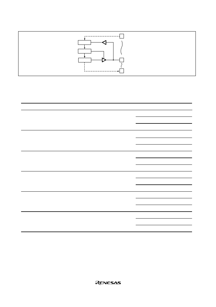
Rev. 1.0, 02/03, page 414 of 634
I/O pin
Control
OUT
IN
TDI pin
TDO pin
Figure 13.2 Boundary Scan Register Configuration
Table 13.4
Correspondence between LSI Pins and Boundary Scan Register
TFP-100G Pin No.
Pin Name
I/O
Bit Name
From TDI
89
PF7/
IN
198
Control
197
OUT
196
91
PF6/
AS
IN
195
Control
194
OUT
193
92
PF5/
RD
IN
192
Control
191
OUT
190
93
PF4/
HWR
IN
189
Control
188
OUT
187
94
PF3/
LWR/ADTRG/IRQ3
IN
186
Control
185
OUT
184
95
PF2/
WAIT
IN
183
Control
182
OUT
181

Rev. 1.0, 02/03, page 415 of 634
TFP-100G
Pin No.
Pin Name
I/O
Bit Name
96
PF1/
BACK
IN
180
Control
179
OUT
178
97
PF0/
BREQ/IRQ2
IN
177
Control
176
OUT
175
98
PA3/A19/SCK2
IN
174
Control
173
OUT
172
99
PA2/A18/RxD2
IN
171
Control
170
OUT
169
100
PA1/A17/TxD2
IN
168
Control
167
OUT
166
1
PA0/A16
IN
165
Control
164
OUT
163
2
P10/TIOCA0/A20
IN
162
Control
161
OUT
160
3
P11/TIOCB0/A21
IN
159
Control
158
OUT
157
4
P12/TIOCC0/TCLKA/A22
IN
156
Control
155
OUT
154
5
P13/TIOCD0/TCLKB/A23
IN
153
Control
152
OUT
151
6
P14/TIOCA1/
IRQ0
IN
150
Control
149
OUT
148

Rev. 1.0, 02/03, page 416 of 634
TFP-100G
Pin No.
Pin Name
I/O
Bit Name
7
P15/TIOCB1/TCLKC
IN
147
Control
146
OUT
145
8
P16/TIOCA2/
IRQ1
IN
144
Control
143
OUT
142
9
P17/TIOCB2/TCLKD
IN
141
Control
140
OUT
139
10
PC0/A0
IN
138
Control
137
OUT
136
11
PC1/A1
IN
135
Control
134
OUT
133
12
PC2/A2
IN
132
Control
131
OUT
130
13
PC3/A3
IN
129
Control
128
OUT
127
14
MD0
IN
126
15
MD1
IN
125
16
MD2
IN
124
17
PC4/A4
IN
123
Control
122
OUT
121
18
PC5/A5
IN
120
Control
119
OUT
118
19
PC6/A6
IN
117
Control
116
OUT
115

Rev. 1.0, 02/03, page 417 of 634
TFP-100G
Pin No.
Pin Name
I/O
Bit Name
20
PC7/A7
IN
114
Control
113
OUT
112
21
USPND/TMOW
OUT
111
22
P30/TxD0
IN
110
Control
109
OUT
108
23
P31/RxD0
IN
107
Control
106
OUT
105
24
P32/SCK0/
IRQ4
IN
104
Control
103
OUT
102
25
PG1/
CS3/IRQ7
IN
101
Control
100
OUT
99
26
PG2/
CS2
IN
98
Control
97
OUT
96
27
PG3/
CS1
IN
95
Control
94
OUT
93
28
PG4/
CS0
IN
92
Control
91
OUT
90
29
VBUS
IN
89
30
P36
IN
88
Control
87
OUT
86
37
PB0/A8
IN
85
Control
84
OUT
83

Rev. 1.0, 02/03, page 418 of 634
TFP-100G
Pin No.
Pin Name
I/O
Bit Name
38
PB1/A9
IN
82
Control
81
OUT
80
39
PB2/A10
IN
79
Control
78
OUT
77
40
PB3/A11
IN
76
Control
75
OUT
74
47
UBPM
IN
73
49
PB4/A12
IN
72
Control
71
OUT
70
50
PB5/A13
IN
69
Control
68
OUT
67
51
PB6/A14
IN
66
Control
65
OUT
64
52
PB7/A15
IN
63
Control
62
OUT
61
55
P74/
MRES
IN
60
Control
59
OUT
58
56
P71/
CS5
IN
57
Control
56
OUT
55
57
STBY
IN
54
58
RES
IN
53
63
P70/
CS4
IN
52
Control
51
OUT
50

Rev. 1.0, 02/03, page 419 of 634
TFP-100G
Pin No.
Pin Name
I/O
Bit Name
64
PE0/D0
IN
49
Control
48
OUT
47
65
PE1/D1
IN
46
Control
45
OUT
44
66
PE2/D2
IN
43
Control
42
OUT
41
67
PE3/D3
IN
40
Control
39
OUT
38
68
PE4/D4
IN
37
Control
36
OUT
35
69
PE5/D5
IN
34
Control
33
OUT
32
70
PE6/D6
IN
31
Control
30
OUT
29
71
PE7/D7
IN
28
Control
27
OUT
26
72
PD0/D8
IN
25
Control
24
OUT
23
73
PD1/D9
IN
22
Control
21
OUT
20

Rev. 1.0, 02/03, page 420 of 634
TFP-100G
Pin No.
Pin Name
I/O
Bit Name
74
PD2/D10
IN
19
Control
18
OUT
17
75
PD3/D11
IN
16
Control
15
OUT
14
76
PD4/D12
IN
13
Control
12
OUT
11
77
PD5/D13
IN
10
Control
9
OUT
8
78
PD6/D14
IN
7
Control
6
OUT
5
79
PD7/D15
IN
4
Control
3
OUT
2
80
FWE
IN
1
81
NMI
IN
0
to TDO
Rev. 1.0, 02/03, page 421 of 634
13.4
Boundary Scan Function Operation
13.4.1
TAP Controller
Figure 13.3 shows the TAP controller status transition diagram, based on the JTAG standard.
1
1
Test-Logic-Reset
1
1
1
1
1
1
1
1
1
0
0
0
0
0
0
0
0
1
1
1
1
0
0
0
0
0
0
0
0
Run-Test/Idle
Select-DR
Capture-DR
Shift-DR
Exit1-DR
Update-DR
Pause-DR
Exit2-DR
Select-IR
Capture-IR
Shift-IR
Exit1-IR
Update-IR
Pause-IR
Exit2-IR
Figure 13.3 TAP Controller Status Transition
Note:
The transition condition is the TMS value at the rising edge of TCK. The TDI value is
sampled at the rising edge of the TCK and shifted at the falling edge of the TCK. The
TDO value changes at the falling edge of the TCK. In addition, TDO is high-impedance
state in a state other than Shift-DR or Shift-IR state. If TRST is 0, Test-Logic-Reset state
is entered asynchronously with the TCK.
Rev. 1.0, 02/03, page 422 of 634
13.5
Usage Notes
1. The
TRST pin must be brought low level at power-on regardless of boundary scan function
usage. If the boundary scan function is used, bring
TRST high and set TCK, TMS and TDI
appropriately. If the boundary scan function is not used, drive
TRST, TCK, TMS, and TDI
high or high-impedance state. These pins are internally pulled up, and care must be taken in
standby mode.
2. The following must be noted on the power-on reset signal applied to the
TRST pin.
· Reset signal must be applied at power-on.
· TRST must be separated in order not to affect the system operation.
· TRST must be separated from the system circuitry in order not to affect the system
operation.
· System circuitry must also be separated from the TRST in order not to affect TRST
operation as shown in figure 13.4.
Board edge pin
System
reset
LSI
Power-on
reset circuit
Figure 13.4 Recommended Reset Signal Design
3. TCK clock speed is 24 MHz at the maximum.
4. In serial communication, data is input or output from the LSB as shown in figure 13.5.
Boundary scan register
Bit n
Bit n-1
Bit 1
Bit 0
TDI
TDO
Figure 13.5 Serial Data Input/Output

Rev. 1.0, 02/03, page 423 of 634
5. If a pin with pull-up function is SAMPLEed with pull-up function enabled, the corresponding
IN register is set to 1. In this case, the corresponding Control register must be cleared to 0.
6. If a pin with open-drain function is SAMPLEed while its open-drain function is enabled and
while the corresponding OUT register is set to 1, the corresponding Control register is cleared
to 0 (the pin status is Hi-Z). If the pin is SAMPLEed while the corresponding OUT register is
cleared to 0, the corresponding Control register is set to 1 (the pin status is 0).
7. If EXTEST, CLAMP, or HIGHZ state is entered, this LSI enters guarded mode such as
hardware standby mode (
RES = STBY = 0). Before entering normal operating mode from
EXTEST, CLAMP, or HIGHZ state, specify
RES, STBY, FWE, and MD2 to MD0 pin to the
designated mode.
8. The EMLE pin must be cleared to 0. When the pin is set to 1, this chip functions as Hitachi
user debugging interface (H-UDI).
EMLE Pin
Chip State
0
Normal operation, boundary scan function
1
Hitachi user debugging interface (H-UDI)

Rev. 1.0, 02/03, page 424 of 634

Rev. 1.0, 02/03, page 425 of 634
Section 14 Universal Serial Bus (USB)
This LSI incorporates a USB function module complying with USB standard version 1.1. Figure
14.1 shows the block diagram of the USB.
14.1
Features
· USB standard version 1.1 compliant
· Bus-powered mode or self-powered mode is selectable via the USB specific pin (UBPM)
· Full speed (12 Mbps) support
· On-chip PLL circuit to generate the USB operation clock (24 MHz × 2 = 48 MHz, 16 MHz × 3
= 48 MHz)
· On-chip bus transceiver
· Standard commands are processed automatically by hardware
Only Set_Descriptor, Get_Descriptor, Class/VendorCommand, and SynchFrame
commands should be processed by software
· Current Configuration value can be checked by Set_Configuration interrupt
· Three transfer modes supported (Control, Bulk, Interrupt)
· Configuration of four endpoints; EP0, EP1, EP2, and EP3
Configuration 1
Interface0
Alternate 0
Total 456-byte FIFO incorporated
EP0s (Control_setup transfer, FIFO 8 bytes)
EP0i (Control_in transfer, FIFO 64 bytes)
EP0o (Control_out tranfer, FIFO 64 bytes)
EP1 (Bulk_in transfer, FIFO 64 bytes
× 2 [dual-buffer confifugraion])
EP2 (Bulk_out transfer, FIFO 64 bytes
× 2 [dual-buffer confifugraion])
EP3 (Interrup_in transfer, FIFO 64 bytes)
· When the USB is not used, the data transfer FIFO area can be used as the on-chip RAM of 512
bytes (address: H'C00200 to H'C003FF)
· 16 kinds of interrupts
Suspend/resume interrupt source can be assigned for IRQ6
Each interrupt source except the suspend/resume interrupt source can be assigned for
EXIRQ0 or EXIRQ1 via registers
· DMA transfer interface
DMA transfer is enabled for the Bulk transfer data of EP1 and EP2
· 8-bit bus (3 cycle access timing) connected to the external bus interface
Internal registers are addressed to a part of area 6 of external address (H'C00000 to
H'DFFFFF)
The area of H'C00400 to H'DFFFFF is reserved for the USB and should not be accessed
Rev. 1.0, 02/03, page 426 of 634
Note: In this section, power-down mode represents watch, subactive, subsleep, and software
standby modes.
Registers
456-byte FIFO
EP3
UDC synchronization
circuit
Interface
[Connection/disconnection]
[Internal bus]
[Main clock]
[Interrupt request signal]
[DMA transfer request signal]
[Power mode selection]
Peripheral data bus
Peripheral address bus
Peripheral bus control
signal
,
,
(12MHz)
(48MHz)
VBUS
UDC core
PLL
curcuit
UDC
EP0s
EP0i
EP0o
: USB Device Controller
: Endpoint 0 setup FIFO
: Endpoint 0 In FIFO
: Endpoint 0 Out FIFO
Legend
EP0o
EP1
EP0s
EP2
EP0i
USB
On-chip
transceiver
[Data]
[Power supply]
DrVSS
Rs
Rs
DrVCC
USPND
USD+
USD-
D+
D-
Figure 14.1 Block Diagram of USB

Rev. 1.0, 02/03, page 427 of 634
14.2
Input/Output Pins
Table 14.1 shows the USB pin configuration.
Table 14.1
Pin Configuration
Pin Name
I/O
Function
USD+
USD-
I/O
I/O pin for USB data
DrVCC
Input
USB internal transceiver power supply pin
DrVSS
Input
USB internal transceiver ground pin
VBUS
Input
USB cable connection/disconnection detection signal pin
UBPM
Input
USB bus-powered/self-powered mode set pin
When USB is used in bus-powered mode,
UBPM must be fixed low.
When USB is used in self-powered mode,
UBPM must be fixed high.
USPND
Output
USB suspend output pin
When USB enters the suspend state, USPND is set to high.

Rev. 1.0, 02/03, page 428 of 634
14.3
Register Descriptions
The USB has the following registers.
· USB control register (UCTLR)
· USB DMAC transfer request register (UDMAR)
· USB device resume register (UDRR)
· USB trigger register 0 (UTRG0)
· USB FIFO clear register 0 (UFCLR0)
· USB endpoint stall register 0 (UESTL0)
· USB endpoint stall register 1 (UESTL1)
· USB endpoint data register 0s (UEDR0s) [for Setup data reception]
· USB endpoint data register 0i (UEDR0i) [for Control_in data transmission]
· USB endpoint data register 0o (UEDR0o) [for Control_out data reception]
· USB endpoint data register 3 (UEDR3) [for Interrupt_in data transmission]
· USB endpoint data register 1 (UEDR1) [for Bulk_in data transmission]
· USB endpoint data register 2 (UEDR2) [for Bulk_out data reception]
· USB endpoint receive data size register 0o (UESZ0o) [for Control _out data reception]
· USB endpoint receive data size register 2 (UESZ2) [for Bulk_out data reception]
· USB interrupt flag register 0 (UIFR0)
· USB interrupt flag register 1 (UIFR1)
· USB interrupt flag register 3 (UIFR3)
· USB interrupt enable register 0 (UIER0)
· USB interrupt enable register 1 (UIER1)
· USB interrupt enable register 3 (UIER3)
· USB interrupt select register 0 (UISR0)
· USB interrupt select register 1 (UISR1)
· USB interrupt select register 3 (UISR3)
· USB data status register (UDSR)
· USB Configuration value register (UCVR)
· USB test register 0 (UTSTR0)
· USB test register 1 (UTSTR1)
· USB test registers 2 and A to F (UTSTR2, UTSTRA to UTSTRF)
· Module stop control register B (MSTPCRB)
· Extended module stop register (EXMDLSTAP)

Rev. 1.0, 02/03, page 429 of 634
14.3.1
USB Control Register (UCTLR)
UCTLR is used to select the USB operation clock and control the USB module internal reset.
UCTLR can be read from or written to even when the USB module stop 2 bit (MSTPB0) in
MSTPCRB is 1. For details on UCTLR setting procedure, refer to section 14.5, Communication
Operations.
Bit
Bit Name
Initial Value
R/W
Description
7
--
0
R/W
Reserved
The write value should always be 0.
6
TMOWE
0
R/W
TMOW Pin Enable
0: The USPND/TMOW pin outputs USPND of USB.
1: The USPND/TMOW pin outputs TMOW of RTC.
5
4
3
2
UCKS3
UCKS2
UCKS1
UCKS0
All 0
R/W
USB Operation Clock Select 3 to 0
These bits control the on-chip PLL, which generates
the USB operation clock (48 MHz). When UCKS3 to
UCKS0 are 0000, the PLL circuit stops and thus the
USB operation clock must be selected according to
the clock source.
The on-chip PLL circuit starts operating after the USB
module stop 2 bit has been cancelled. In addition, the
USB operation clock is supplied to the UDC core after
the USB operating clock stabilization time has been
passed. The completion timing of the USB operating
clock stabilization time can be detected by the
CK48READY flag in UIFR3.
UCKS0 to UCKS3 muse be written while the USB
module stop 2 bit (MSTPB0) is 1.
0000: USB operation clock stops (PLL stops)
0001: Reserved
001x: Reserved
010x: Reserved
0110: Uses a clock (48 MHz) generated by doubling
the 24-MHz main oscillation by the PLL.
0111: Uses a clock (48 MHz) generated by tripling the
16-MHz main oscillation by the PLL.
1xxx: Reserved
The USB operating clock stabilization time is 2 ms.
Legend X: Don't care

Rev. 1.0, 02/03, page 430 of 634
Bit
Bit Name
Initial Value
R/W
Description
1
UIFRST
1
R/W
USB Interface Software Reset
Controls USB module internal reset. When the
UIFRST bit is set to 1, the USB internal modules other
than UCTLR, UIER3, and the CK48READY bit in
UIFR3 are all reset. At initialization, the UIFRST bit
must be cleared to 0 after the USB operating clock (48
MHz) stabilization time has passed following the
clearing of the USB module stop 2 bit.
0: Sets the USB internal modules to the operating
state. (At initialization, this bit must be cleared after
the USB operating clock stabilization time has
passed.)
1: Sets the USB internal modules other than UCTLR,
UIER3, and the CK48READY bit in UIFR3 to the
reset state.
If the UIFRST bit is set to 1 after it is cleared to 0, the
UDCRST bit should also be set to 1 simultaneously.
0
UDCRST
1
R/W
UDC Core Software Reset
Controls reset of the UDC core in the USB module.
When the UDCRST bit is set to 1, the UDC core is
reset and the USB bus synchronization operation
stops. At initialization, UDCRST must be cleared to 0
after D+ pull-up by the port (P36) control following the
clearing of the UIFRST bit. In the suspend state, to
maintain the internal state of the UDC core, enter
power-down mode after setting the USB module stop
2 bit with the UDCRST bit to be maintained to 0. After
VBUS disconnection detection, UDCRST must be set
to 1.
0: Sets the UDC core in the USB module to operating
state. (At initialization, UDCRST must be cleared
to 0 after D+ pull-up by the port control following
the clearing of the UIFRST bit.)
1: Sets the UDC core in the USB module to reset
state. (In the suspend state, UDCRST must not be
set to 1; after VBUS disconnection detection,
UDCRST must be set to 1.)

Rev. 1.0, 02/03, page 431 of 634
14.3.2
USB DMAC Transfer Request Register (UDMAR)
UDMAR is set when data transfer by means of the on-chip DMAC is performed for data registers
UEDR1 and UEDR2 corresponding to EP1 and EP2 respectively used for Bulk transfer. For the
DMAC transfer, set
DREQ0 and DREQ1 separately. If DREQ0 and DREQ1 usage overlaps, the
USB cannot operate correctly. For details on DMAC transfer, refer to section 14.6, DMA Transfer
Specifications.
Bit
Bit Name
Initial Value
R/W
Description
7 to 4 --
0
R
Reserved
These bits are always read as 0 and cannot be
modified.
3
2
EP2T1
EP2T0
All 0
R/W
EP2 DMAC Transfer Request Select 1, 0
00: Does not request EP2 DMAC transfer
01: Reserved
10: Requests EP2 DMAC transfer by
DREQ0
11: Requests EP2 DMAC transfer by
DREQ1
1
0
EP1T1
EP1T0
All 0
R/W
EP1 DMAC Transfer Request Select 1, 0
00: Does not request EP1 DMAC transfer
01: Reserved
10: Requests EP1 DMAC transfer by
DREQ0
11: Requests EP1 DMAC transfer by
DREQ1

Rev. 1.0, 02/03, page 432 of 634
14.3.3
USB Device Resume Register (UDRR)
UDRR indicates the enabled or disabled state of remote wakeup by the host, and executes the
remote wakeup of the USB modules in the suspend state.
Bit
Bit Name
Initial Value
R/W
Description
7 to 2 --
0
R
Reserved
These bits are always read as 0 and cannot be
modified.
1
RWUPs
0
R
Remote Wakeup Status
Indicates the enabled or disabled state of remote
wakeup by the host. This bit is a status bit and cannot
be written to. If the remote wakeup from the host is
disabled by Device_Remote_Wakeup through the
Set_Feature/Clear _Feature request, this bit is cleared
to 0. If the remote wakeup is enabled, this bit is set to
1.
0: Remote wakeup disabled state
1: Remote wakeup enabled state
0
DVR
0
W
Device Resume
Cancels the suspend state (executes the remote
wakeup). This bit can be written to 1 and is always
read as 0. Before executing the remote wakeup,
power-down mode or USB module stop mode must be
cancelled to provide a clock for the USB module.
0: Performs no operation
1: Cancels the suspend state (executes the remote
wakeup)

Rev. 1.0, 02/03, page 433 of 634
14.3.4
USB Trigger Register 0 (UTRG0)
UTRG0 is a one-shot register to generate triggers to the FIFO for each endpoint EP0 to EP3.
Bit
Bit Name
Initial Value
R/W
Description
7, 6
--
All 0
R
Reserved
These bits are always read as 0 and cannot be
modified.
5
EP2RDFN
0
W
EP2 Read Complete
0: Performs no operation.
1: Writes 1 to this bit after reading data for EP2 OUT
FIFO. EP2 has a dual-FIFO configuration. This
trigger is generated to the currently effective FIFO.
4
EP1PKTE
0
W
EP1 Packet Enable
0: Performs no operation.
1: Generates a trigger to enable the transmission to
EP1 IN FIFO. EP1 has a dual-FIFO configuration.
This trigger is generated to the currently effective
FIFO.
3
EP3PKTE
0
W
EP3 Packet Enable
0: Performs no operation.
1: Generates a trigger to enable the transmission to
EP3 IN FIFO.
2
EP0oRDFN 0
W
EP0o Read Complete
0: Performs no operation.
1: Writes 1 to this bit after reading data for EP0o OUT
FIFO. This trigger enables EP0o to receive the
next packet.
1
EP0iPKTE
0
W
EP0i Packet Enable
0: Performs no operation.
1: Generates a trigger to enable the transmission to
EP0i IN FIFO.
0
EP0sRDFN 0
W
EP0s Read Complete
0: Performs no operation. A NAK handshake is
returned in response to transmit/receive requests in
the data stage until 1 is written to this bit.
1: Writes 1 to this bit after reading data for EP0s
command FIFO. After receiving the setup command,
this trigger enables the next packet in the data stage
to be received by EP0i and EP0o. EP0s can always
be overwritten and receive data regardless of this
trigger.

Rev. 1.0, 02/03, page 434 of 634
14.3.5
USB FIFO Clear Register 0 (UFCLR0)
UFCLR0 is a one-shot register used to clear the FIFO for each endpoint EP0 to EP3. Writing 1 to a
bit clears the data in the corresponding FIFO.
For IN FIFO, writing 1 to a bit in UFCLR0 clears the data for which the corresponding PKTE bit
in UTRG0 is not set to 1 after data write, or data that is validated by setting the corresponding
PKTE bit in UTRG0.
For OUT FIFO, writing 1 to a bit in UFCLR0 clears data that has not been fixed during reception
or received data for which the corresponding RDFN bit is not set to 1. Accordingly, care must be
taken not to clear data that is currently being received or transmitted. EP1 and EP2, having a dual-
FIFO configuration, are cleared by entire FIFOs. Note that this trigger does not clear the
corresponding interrupt flag.
Bit
Bit Name
Initial Value
R/W
Description
7, 6
--
All 0
R
Reserved
These bits are always read as 0 and cannot be
modified.
5
EP2CLR
0
W
EP2 Clear
0: Performs no operation.
1: Clears EP2 OUT FIFO.
4
EP1CLR
0
W
EP1 Clear
0: Performs no operation.
1: Clears EP1 IN FIFO.
3
EP3CLR
0
W
EP3 Clear
0: Performs no operation.
1: Clears EP3 IN FIFO.
2
EP0oCLR
0
W
EP0o Clear
0: Performs no operation.
1: Clears EP0o OUT FIFO.
1
EP0iCLR
0
W
EP0i Clear
0: Performs no operation.
1: Clears EP0i IN FIFO.
0
--
0
R
Reserved
This bit is always read as 0 and cannot be modified.

Rev. 1.0, 02/03, page 435 of 634
14.3.6
USB Endpoint Stall Register 0 (UESTL0)
UESTL0 is used to forcibly stall each endpoint EP0 to EP3. When the bit is set to 1, the
corresponding endpoint returns a stall handshake to the host, following from the next transfer.
The stall bit for endpoint 0 is cleared automatically on reception of 8-byte command data for
which decoding is performed by the function, and thus the EP0STL bit is cleared to 0. When the
SetupTS flag in UIFR0 is set to 1, a write of 1 to the EP0STL bit is ignored. For details, refer to
section 14.5.9, Stall Operations.
Bit
Bit Name
Initial Value
R/W
Description
7, 6
--
All 0
R
Reserved
These bits are always read as 0 and cannot be
modified.
5
EP2STL
0
R/W
EP2 Stall
0: Cancels the EP2 stall state.
1: Sets the EP2 stall state.
4
EP1STL
0
R/W
EP1 Stall
0: Cancels the EP1 stall state.
1: Sets the EP1 stall state.
3
EP3STL
0
R/W
EP3 Stall
0: Cancels the EP3 stall state.
1: Sets the EP3 stall state.
2, 1
--
All 0
R
Reserved
These bits are always read as 0 and cannot be
modified.
0
EP0STL
0
R/W
EP0 Stall
0: Cancels the EP0 stall state.
1: Sets the EP0 stall state.

Rev. 1.0, 02/03, page 436 of 634
14.3.7
USB Endpoint Stall Register 1 (UESTL1)
UESTL1 is used to control stall cancellation mode for all endpoints.
Bit
Bit Name
Initial Value
R/W
Description
7
SCME
0
R/W
Stall Cancellation Mode Enable
Controls stall cancellation mode.
When this bit is set to 1, the EPnSTL bit, which has
been set once, is automatically cleared to 0 after
returning a handshake to the host. This bit is common
to all endpoints. The stall cancellation mode cannot be
specified for each endpoint.
When this bit is cleared to 0, the EPnSTL bit, which
has been set once, cannot be cleared automatically.
To cancel the stall state of the EPn, clear the EPnSTL
bit to 0.
0: Disables stall cancellation mode for all endpoints
(EP0 to EP3).
1: Enables stall cancellation mode for all endpoints
(EP0 to EP3).
6 to
0
--
0
R
Reserved
These bits are always read as 0 and cannot be
modified.

Rev. 1.0, 02/03, page 437 of 634
14.3.8
USB Endpoint Data Register 0s (UEDR0s)
UEDR0s stores the setup command for endpoint 0 (for Control_out transfer). UEDR0s stores 8-
byte command data sent from the host in setup stage.
For details on the USB operation when data for the next setup stage is received while data in
UEDR0s is being read, refer to section 14.8, Usage Notes.
UEDR0s is a byte register to which 4-byte address area is assigned. Accordingly, UEDR0s allows
the user to read 2-byte or 4-byte data continuously by word transfer or longword transfer.
Bit
Bit Name
Initial Value
R/W
Description
7 to 0 D7 to D0
--
R
These bits store the setup command for Control_out
transfer
14.3.9
USB Endpoint Data Register 0i (UEDR0i)
UEDR0i is a data register for endpoint 0 (for Control_in transfer). UEDR0i stores data to be sent
to the host. The number of data items to be written continuously must be the maximum packet size
or less.
UEDR0i is a byte register to which 4-byte address area is assigned. Accordingly, UEDR0i allows
the user to write 2-byte or 4-byte data continuously by word transfer or longword transfer.
Bit
Bit Name
Initial Value
R/W
Description
7 to 0 D7 to D0
--
W
These bits store data for Control_in transfer
14.3.10
USB Endpoint Data Register 0o (UEDR0o)
UEDR0o is a data register for endpoint 0 (for Control_out transfer). UEDR0o stores data received
from the host. The number of data items to be read must be the number of bytes specified by
UESZ0o.
UEDR0o is a byte register to which 4-byte address area is assigned. Accordingly, UEDR0o allows
the user to read 2-byte or 4-byte data continuously by word transfer or longword transfer.
Bit
Bit Name
Initial Value
R/W
Description
7 to 0 D7 to D0
--
R
These bits store data for Control_out transfer

Rev. 1.0, 02/03, page 438 of 634
14.3.11
USB Endpoint Data Register 3 (UEDR3)
UEDR3 is a data register for endpoint 3 (for Interrupt_in transfer). UEDR3 stores data to be sent to
the host. The number of data items to be written continuously must be the maximum packet size or
less.
UEDR3 is a byte register to which 4-byte address area is assigned. Accordingly, UEDR3 allows
the user to write 2-byte or 4-byte data continuously by word transfer or longword transfer.
Bit
Bit Name
Initial Value
R/W
Description
7 to 0 D7 to D0
--
W
These bits store data for Interrupt_in transfer
14.3.12
USB Endpoint Data Register 1 (UEDR1)
UEDR1 is a data register for endpoint 1 (for Bulk_in transfer). UEDR1 stores data to be sent to the
host. The number of data items to be written continuously must be the maximum packet size or
less.
UEDR1 is a byte register to which 4-byte address area is assigned. Accordingly, UEDR1 allows
the user to write 2-byte or 4-byte data continuously by word transfer or longword transfer.
Bit
Bit Name
Initial Value
R/W
Description
7 to 0 D7 to D0
--
R
These bits store data for Bulk_in transfer
14.3.13
USB Endpoint Data Register 2 (UEDR2)
UEDR2 is a data register for endpoint 2 (for Bulk_out transfer). UEDR2 stores data received from
the host. The number of data items to be read must be the number of bytes specified by UESZ2.
UEDR2 is a byte register to which 4-byte address area is assigned. Accordingly, UEDR2 allows
the user to read 2-byte or 4-byte data continuously by word transfer or longword transfer.
Bit
Bit Name
Initial Value
R/W
Description
7 to 0 D7 to D0
--
W
These bits store data for Bulk_out transfer

Rev. 1.0, 02/03, page 439 of 634
14.3.14
USB Endpoint Receive Data Size Register 0o (UESZ0o)
UESZ0o is a receive data size register for endpoint 0 (for Control_out transfer). UESZ0o indicates
the number of bytes of data to be received from the host.
Bit
Bit Name
Initial Value
R/W
Description
7
--
--
R
Reserved
6 to 0 D6 to D0
--
R
These bits indicate the size of data to be received in
Control_out transfer
14.3.15
USB Endpoint Receive Data Size Register 2 (UESZ2)
UESZ2 is a receive data size register for endpoint 2 (for Bulk_out transfer). UESZ2 indicates the
number of bytes of data to be received from the host.
The FIFO for endpoint 2 (for Bulk_out transfer) has a dual-FIFO configuration. The data size
indicated by this register refers to the currently selected FIFO.
Bit
Bit Name
Initial Value
R/W
Description
7
--
--
R
Reserved
6 to 0 D6 to D0
--
R
These bits indicate the size of data to be received in
Bulk_out transfer
14.3.16
USB Interrupt Flag Register 0 (UIFR0)
UIFR0 is an interrupt flag register indicating the setup command reception, EP0 and EP3
transmission/reception, and bus reset state. If the corresponding bit is set to 1, the corresponding
EXIRQ0 or EXIRQ1 interrupt is requested to the CPU. A bit in this register can be cleared by
writing 0 to it. Writing 1 to a bit is invalid and causes no operation.

Rev. 1.0, 02/03, page 440 of 634
Bit
Bit Name
Initial Value
R/W
Description
7
BRST
0
R/(W)* Bus Reset
Set to 1 when the bus reset signal is detected on the
USB bus. The corresponding interrupt output is
EXIRQ0 or EXIRQ1.
Note that BRST is also set to 1 if D+ is not pulled-up
during USB cable connection.
6
--
0
R
Reserved
This bit is always read as 0 and cannot be modified.
5
EP3TR
0
R/(W)* EP3 Transfer Request
Set to 1 if there is no valid data in the FIFO when an IN
token is sent from the host to EP3. The corresponding
interrupt output is
EXIRQ0 or EXIRQ1.
4
EP3TS
0
R/(W)* EP3 Transmit Complete
Set to 1 if the data written in EP3 is transmitted to the
host normally and the ACK handshake is returned. The
corresponding interrupt output is
EXIRQ0 or EXIRQ1.
3
EP0oTS
0
R/(W)* EP0o Receive Complete
Set to 1 if EP0o receives data from the host normally
and returns the ACK handshake to the host. The
corresponding interrupt output is
EXIRQ0 or EXIRQ1.
2
EP0iTR
0
R/(W)* EP0i Transfer Request
Set to 1 if there is no valid data in the FIFO when an
IN token is sent from the host to EP0i. The
corresponding interrupt output is
EXIRQ0 or EXIRQ1.
1
EP0iTS
0
R/(W)* EP0i Transmit Complete
Set to 1 if the data written in EP0i is transmitted to the
host normally and the ACK handshake is returned.
The corresponding interrupt output is
EXIRQ0 or
EXIRQ1.
0
SetupTS
0
R/(W)* Setup Command Receive Complete
Set to 1 if EP0s normally receives 8-byte command
data to be decoded by the function from the host and
returns the ACK handshake to the host. The
corresponding interrupt output is
EXIRQ0 or EXIRQ1.
Note:* The write value should always be 0 to clear this flag.

Rev. 1.0, 02/03, page 441 of 634
14.3.17
USB Interrupt Flag Register 1 (UIFR1)
UIFR1 is an interrupt flag register indicating the EP1 and EP2 status. If the corresponding bit is set
to 1, the corresponding
EXIRQ0 or EXIRQ1 interrupt is requested to the CPU. EP1TR flags can
be cleared by writing 0 to them. Writing 1 to them is invalid and causes no operation. However,
EP1EMPTY, EP2READY, and EP1ALLEMPTY are status bits to indicate the EP1, EP2, and
FIFO state respectively, and cannot be cleared.
Bit
Bit Name
Initial Value
R/W
Description
7 to 4 --
All 0
R
Reserved
These bits are always read as 0 and cannot be
modified.
3
EP1ALL
EMPTY
1
R
EP1 FIFO All Empty
EP1 FIFO has a dual-FIFO configuration. This bit is set
to 1 if there is no valid data in both FIFOs. This
corresponds to the negative-electrode signal for the
EP1DE bit in UDSR.
2
EP2READY 0
R
EP2 Data Ready
EP2 FIFO has a dual-FIFO configuration. This bit is set
to 1 if there is valid data at least in either of FIFOs.
This bit is cleared to 0 if there is no valid data in both
FIFOs. This bit is a status bit and cannot be cleared.
The corresponding interrupt output is
EXIRQ0 or
EXIRQ1.
1
EP1TR
0
R/(W)* EP1 Transfer Request
Set to 1 if there is no valid data in both FIFOs when an
IN token is sent from the host to EP1. The
corresponding interrupt output is
EXIRQ0 or EXIRQ1.
0
EP1EMPTY 1
R
EP1 FIFO Empty
EP1 FIFO has a dual-FIFO configuration. This bit is set
to 1 if there is no valid data at least in either of FIFOs.
This bit is cleared to 0 if there is valid data in both
FIFOs. This bit is a status bit and cannot be cleared.
The corresponding interrupt output is
EXIRQ0 or
EXIRQ1.
Note:* The write value should always be 0 to clear this flag.

Rev. 1.0, 02/03, page 442 of 634
14.3.18
USB Interrupt Flag Register 3 (UIFR3)
UIFR3 is an interrupt flag register indicating the USB status. If the corresponding bit is set to 1,
the corresponding
EXIRQ0, EXIRQ1, or IRQ6 interrupt is requested to the CPU. VBUSi, SPRSi,
SETC, SOF, and CK48READY flags can be cleared by writing 0 to them. Writing 1 to them is
invalid and causes no operation. VBUSs and SPRSs are status bits and cannot be modified.
Bit
Bit Name
Initial Value
R/W
Description
7
CK48READY 0
R/(W)* USB Operating Clock (48 MHz) Stabilization Detection
Set to 1when the USB operating clock (48 MHz)
stabilization time has been automatically counted after
USB module stop mode cancellation. The
corresponding interrupt output is
EXIRQ0 or EXIRQ1.
CK48READY can also operate in the USB interface
software reset state (the UIFRST bit in UCTLR is set
to 1).
Note that USB operating clock stabilization time differs
according to the clock source. Refer to the UCKS3 to
UCKS0 bits in section 14.3.1, USB Control Register
(UCTLR).
6
SOF
0
R/(W)* Start of Frame Packet Detection
Set to 1 if the Start of Frame (SOF) packet is
detected. The corresponding interrupt output is
EXIRQ0 or EXIRQ1.
5
SETC
0
R/(W)* Set_Configuration Command Detection
Set to 1 if the Set_Configuration command is
detected. The corresponding interrupt output is
EXIRQ0 or EXIRQ1.
4
--
0
R
Reserved
This bit is always read as 0 and cannot be modified.
3
SPRSs
0
R
Suspend/Resume Status
SPRSs indicates the suspend/resume status.
However, an interrupt cannot be requested by SPRSs.
0: Indicates that the bus is in the normal state.
1: Indicates that the bus is in the suspend state.
2
SPRSi
0
R/(W)* Suspend/Resume Interrupt
Set to 1 if a transition from normal state to suspend
state or suspend state to normal state has occurred.
The corresponding interrupt output is
IRQ6. This bit
can be used to cancel power-down mode at resuming.

Rev. 1.0, 02/03, page 443 of 634
Bit
Bit Name
Initial Value
R/W
Description
1
VBUSs
0
R
VBUS Status
VBUSs is a status bit to indicate the VBUS state by
the USB cable connection or disconnection. However,
an interrupt cannot be requested by VBUSs.
0: Indicates that the VBUS (USB cable) bus is
disconnected.
1: Indicates that the VBUS (USB cable) bus is
connected.
0
VBUSi
0
R/(W)* VBUS Interrupt
Set to 1 if a VBUS state changes by the USB cable
connection or disconnection. The corresponding
interrupt output is
EXIRQ0 or EXIRQ1.
Note:* The write value should always be 0 to clear this flag.
14.3.19
USB Interrupt Enable Register 0 (UIER0)
UIER0 enables the interrupt request indicated in the interrupt flag register 0 (UIFR0). When an
interrupt flag is set while the corresponding bit in UIER0 is set to 1, an interrupt is requested by
asserting the corresponding
EXIRQ0 or EXIRQ1. Either EXIRQ0 or EXIRQ1 must be selected by
the interrupt select register 0 (UISR0).
Bit
Bit Name
Initial Value
R/W
Description
7
BRSTE
0
R/W
Enables the BRST interrupt.
6
--
0
R
Reserved
This bit is always read as 0.
5
EP3TRE
0
R/W
Enables the EP3TR interrupt.
4
EP3TSE
0
R/W
Enables the EP3TS interrupt.
3
EP0oTSE
0
R/W
Enables the EP0oTS interrupt.
2
EP0iTRE
0
R/W
Enables the EP0iTR interrupt.
1
EP0iTSE
0
R/W
Enables the EP0iTS interrupt.
0
SetupTSE
0
R/W
Enables the SetupTS interrupt.

Rev. 1.0, 02/03, page 444 of 634
14.3.20
USB Interrupt Enable Register 1 (UIER1)
UIER1 enables the interrupt request indicated in the interrupt flag register 1 (UIFR1). When an
interrupt flag is set while the corresponding bit in UIER1 is set to 1, an interrupt is requested by
asserting the corresponding
EXIRQ0 or EXIRQ1. Either EXIRQ0 or EXIRQ1 must be selected by
the interrupt select register 1 (UISR1).
Bit
Bit Name
Initial Value
R/W
Description
7 to 4 --
All 0
R
Reserved
These bits are always read as 0.
3
EP1ALL
EMPTYE
0
R/W
Enables the EP1ALLEMPRY interrupt.
2
EP2READYE 0
R/W
Enables the EP2READY interrupt.
1
EP1TRE
0
R/W
Enables the EP1TR interrupt.
0
EP1EMPTYE 0
R/W
Enables the EP1EMPTYE interrupt.
14.3.21
USB Interrupt Enable Register 3 (UIER3)
UIER3 enables the interrupt request indicated in the interrupt flag register 3 (UIFR3). This register
is readable/writable while the USB module stop 2 bit (MSTPB0) in MSTPCRB is 1.
When an interrupt flag is set while the corresponding bit in UIER3 is set to 1, an interrupt is
requested by asserting the corresponding
EXIRQ0 or EXIRQ1. Either EXIRQ0 or EXIRQ1 must
be selected by the interrupt select register 3 (UISR3). Note, however, that the SPRSiE bit is an
interrupt enable bit specific to the
IRQ6 pin and cannot be selected by UISR3.
Bit
Bit Name
Initial Value
R/W
Description
7
CK48READYE 1
R/W
Enables the CK48READY interrupt.
6
SOFE
0
R/W
Enables the SOF interrupt.
5
SETCE
0
R/W
Enables the SETC interrupt.
4, 3
--
All 0
R
Reserved
These bits are always read as 0.
2
SPRSiE
0
R/W
Enables the SPRSi interrupt. (only for
IRQ6)
1
--
0
R
Reserved
This bit is always read as 0.
0
VBUSiE
0
R/W
Enables the VBUSi interrupt.

Rev. 1.0, 02/03, page 445 of 634
14.3.22
USB Interrupt Select Register 0 (UISR0)
UISR0 sets
EXIRQ to output interrupt request indicated in the interrupt flag register 0 (UIFR0).
When a bit in UIER0 corresponding to the UISR0 bit is cleared to 0, an interrupt request is output
from
EXIRQ0. When a bit in UIER0 corresponding to the UISR0 bit is set to 1, an interrupt
request is output from
EXIRQ1.
Bit
Bit Name
Initial Value
R/W
Description
7
BRSTS
0
R/W
Selects the BRST interrupt.
6
--
0
R
Reserved
This bit is always read as 0.
5
EP3TRS
0
R/W
Selects the EP3TR interrupt.
4
EP3TSS
0
R/W
Selects the EP3TS interrupt
3
EP0oTSS
0
R/W
Selects the EP0oTS interrupt.
2
EP0iTRS
0
R/W
Selects the EP0iTR interrupt.
1
EP0iTSS
0
R/W
Selects the EP0iTS interrupt.
0
SetupTSS
0
R/W
Selects the SetupTS interrupt.
14.3.23
USB Interrupt Select Register 1 (UISR1)
UISR1 sets
EXIRQ to output interrupt request indicated in the interrupt flag register 1 (UIFR1).
When a bit in UIER1 corresponding to the UISR1 bit is cleared to 0, an interrupt request is output
from
EXIRQ0. When a bit in UIER1 corresponding to the UISR1 bit is set to 1, an interrupt
request is output from
EXIRQ1.
Bit
Bit Name
Initial Value
R/W
Description
7 to 4 --
All 0
R
Reserved
These bits are always read as 0.
3
EP1ALL
EMPTYS
0
R/W
Selects the EP1ALLEMPTY interrupt.
2
EP2READYS 0
R/W
Selects the EP2READY interrupt.
1
EP1TRS
0
R/W
Selects the EP1TR interrupt.
0
EP1EMPTYS 0
R/W
Selects the EP1EMPTY interrupt.

Rev. 1.0, 02/03, page 446 of 634
14.3.24
USB Interrupt Select Register 3 (UISR3)
UISR3 sets
EXIRQ to output interrupt request indicated in the interrupt flag register 3 (UIFR3).
When a bit in UIER3 corresponding to the UISR3 bit is cleared to 0, an interrupt request is output
from
EXIRQ0. When a bit in UIER3 corresponding to the UISR3 bit is set to 1, an interrupt
request is output from
EXIRQ1.
Bit
Bit Name
Initial Value R/W
Description
7
CK48READYS 0
R/W
Selects the CK48READY interrupt.
6
SOFS
0
R/W
Selects the SOF interrupt.
5
SETCS
0
R/W
Selects the SETC interrupt.
4 to 1 --
All 0
R
Reserved
These bits are always read as 0.
0
VBUSiS
0
R/W
Selects the VBUSi interrupt.
14.3.25
USB Data Status Register (UDSR)
UDSR indicates whether the IN FIFO data registers (EP1, and EP3) contain valid data or not. A bit
in USDR is set when data written to the corresponding IN FIFO becomes valid after the
corresponding PKTE bit in UTRG is set to 1. A bit in USDR is cleared when all valid data is sent
to the host. For EP1, having a dual-FIFO configuration, the corresponding bit in USDR is cleared
to 0 and FIFO becomes empty.

Rev. 1.0, 02/03, page 447 of 634
Bit
Bit Name
Initial Value
R/W
Description
7 to 3 --
All 0
R
Reserved
These bits are always read as 0 and cannot be
modified.
2
EP1DE
0
R
EP1 Data Enable
0: Indicates that the EP1 contains no valid data.
1: Indicates that the EP1 contains valid data.
This bit can output the interrupt as the
EP1ALLEMPTY flag in UIFR1 (corresponds to the
negative-electrode signal for EP1DE).
1
EP3DE
0
R
EP3 Data Enable
0: Indicates that the EP3 contains no valid data.
1: Indicates that the EP3 contains valid data.
0
EP0iDE
0
R
EP0i Data Enable
0: Indicates that the EP0i contains no valid data.
1: Indicates that the EP0i contains valid data.
14.3.26
USB Configuration Value Register (UCVR)
UCVR stores the Configuration value when the Set_Configuration command is received from the
host.
Bit
Bit Name
Initial Value
R/W
Description
7, 6
--
All 0
R
Reserved
These bits are always read as 0 and cannot be
modified.
5
CNFV0
0
R
Configuration Value 0
Stores the Configuration value when the
Set_Configuration command is received. CNFV0 is
modified when the SETC bit in UIFR3 is set to 1.
4 to 0 --
All 0
R
Reserved
These bits are always read as 0 and cannot be
modified.

Rev. 1.0, 02/03, page 448 of 634
14.3.27
USB Test Register 0 (UTSTR0)
UTSTR0 controls the on-chip transceiver output signals. Setting the PTSTE bit to 1 specifies the
transceiver output signals (USD+ and USD-) arbitrarily. Table 14.2 shows the relationship
between UTSTR0 setting and pin output.
Bit
Bit Name
Initial Value
R/W
Description
7
PTSTE
0
R/W
Pin Test Enable
Enables the test control for the on-chip transceiver
output pins (USD+ and USD-) and USPND pin.
6 to 4 --
All 0
R
Reserved
These bits are always read as 0 and cannot be
modified.
3
2
1
0
SUSPEND
OE
FSE0
VPO
0
1
0
0
R/W
R/W
R/W
R/W
On-Chip Transceiver Output Signal Setting
SUSPEND: Sets the USPND pin signal of the on-chip
transceiver.
OE: Sets the output enable (OE) signal of the
on-chip transceiver.
FSE0: Sets the Signal-ended 0 (FSE0) signal of
the on-chip transceiver.
VPO: Sets the USD+ (VPO) signal of the on-
chip transceiver.
Table 14.2
Relationship between UTSTR0 Setting and Pin Output
Register Setting
Pin Output
Pin Input
Register Setting
Pin Output
UCTLR/
USPNDE
PTSTE
SUSPEND
USPND/
TMOW
VBUS
PTSTE
OE
OE
OE
OE
FSE0
VPO
USD+
USD-
0
x
x
--
0
x
x
x
x
Hi-Z
Hi-Z
1
0
x
--
1
0
x
x
x
--
--
1
1
0
0
1
1
0
0
0
0
1
1
1
1
1
1
1
0
0
1
1
0
1
1
0
1
x
0
0
1
1
1
x
x
Hi-Z
Hi-Z
Legend
X: Don't care.
--: Cannot be controlled. Indicates state in normal operation according to the USB operation and
port settings.

Rev. 1.0, 02/03, page 449 of 634
14.3.28
USB Test Register 1 (UTSTR1)
UTSTR1 allows the USB control pin and on-chip transceiver input signals to be monitored. Table
14.3 shows the relationship between pin input and UTSTR1 monitoring value.
Bit
Bit Name
Initial Value
R/W
Description
7
6
VBUS
UBPM
--*
--*
R
R
On-Chip Transceiver Input Signal Monitor
VBUS: Monitors the VBUS pin.
UBPM: Monitors the UBPM pin.
5 to 3 --
All 0
R
Reserved
These bits are always read as 0 and cannot be
modified.
2
1
0
RCV
VP
VM
--*
--*
--*
R
R
R
On-Chip Transceiver Input Signal Monitor
RCV: Monitors the differential input level (RCV)
signal of the on-chip transceiver.
VP: Monitors the USD+ (VP) signal of the on-chip
transceiver.
VM: Monitors the USD- (VM) signal of the on-chip
transceiver.
Note:
* Determined by the state of pins. VBUS,
UBPM, USD+, USD-

Rev. 1.0, 02/03, page 450 of 634
Table 14.3
Relationship between Pin Input and UTSTR1 Monitoring Value
Pin Input
UTSTR1 Monitoring
Value
Register Setting
Pin Input
UTSTR1 Monitoring Value
VBUS
UBPM
UBPM
UBPM
UBPM
VBUS
UBPM
UBPM
UBPM
UBPM
UTSTR0/
PTSTE
UTSTR0/
SUSPEND
VBUS
USD+
USD-
RCV
VP
VM
0/1
x
0/1
x
x
x
0
x
x
0
0
0
x
0/1
x
0/1
0
x
1
0
0
x
0
0
0
x
1
0
1
0
0
1
0
x
1
1
0
1
1
0
0
x
1
1
1
x
1
1
1
0
1
0
0
x
0
0
1
0
1
0
1
0
0
1
1
0
1
1
0
1
1
0
1
0
1
1
1
x
1
1
1
1
1
0
0
0
0
0
1
1
1
0
1
0
0
1
1
1
1
1
0
0
1
0
1
1
1
1
1
0
1
1
Legend
X: Don't care.
0/1: Combination for pin input = UTSTR1 monitoring value.

Rev. 1.0, 02/03, page 451 of 634
14.3.29
USB Test Registers 2 and A to F (UTSTR2, UTSTRA to UTSTRF)
UTSTR2 and UTSRTA to UTSRTF are test registers and cannot be written to.
14.3.30
Module Stop Control Register B (MSTPCRB)
Bit
Bit Name
Initial Value
R/W
Description
7 to 1 MSTPB7
MSTPB6
MSTPB5
MSTPB4
MSTPB3
MSTPB2
MSTPB1
All 1
R/W
Module Stop
For details, refer to section 20.1.3, Module Stop
Control Registers A to C (MSTPCRA to MSTPCRC).
0
MSTPB0
1
R/W
USB Module Stop 2
0: Cancels the stop state of the USB module
completely.
A clock is provided for the USB module completely.
Before clearing this bit, make sure to clear the
USBSTOP1 bit in EXMDLSTP. After this bit has
been cleared, the internal PLL circuit starts
operation. Registers in the USB module must be
accessed after the USB operating clock stabilization
time (the CK48READY bit in UIFR3 is set to 1) has
passed.
1: Places the USB module partly in the stop state.
The internal PLL circuit and the most of the clocks in
the USB module stop operation. However, register
values in the USB module are maintained.

Rev. 1.0, 02/03, page 452 of 634
14.3.31
Extended Module Stop Register (EXMDLSTP)
Bit
Bit Name
Initial Value
R/W
Description
7 to 2 --
Undefined
--
Reserved
These bits are always read as an undefined value and
cannot be modified.
1
RTCSTOP
0
R/W
RTC Module Stop
0: Cancels the RTC module stop.
1: Sets the RTC module stop.
0
USBSTOP1 0
R/W
USB Module Stop 1
0: Cancels the stop state of the USB module partly.
A clock is provided for the USB module partly. After
this bit has been cleared, only the UCTLR and
UIER3 registers in the USB module can be
accessed. To access the other registers, clear the
MSTPB0 bit in MSTPCRB to 0.
1: Places the USB module completely in the stop state.
The clocks in the USB module stop operation
completely. However, register values in the USB
module are maintained.
Note:
For details on USB module stop mode cancellation procedure, refer to section 14.5,
Communication Operation.

Rev. 1.0, 02/03, page 453 of 634
14.4
Interrupt Sources
This module has three interrupt signals. Table 14.4 shows the interrupt sources and their
corresponding interrupt request signals. The
EXIRQ interrupt signals are activated at low level.
The
EXIRQ interrupt requests can only be detected at low level (specified as level sensitive). The
suspend/resume interrupt request
IRQ6 must be specified to be detected at the falling edge
(falling-edge sensitive) by the interrupt controller register.
Table 14.4
Interrupt Sources
Register
Bit
Transfer
Mode
Interrupt
Source
Description
Interrupt
Request
Signal
DMAC
Activation
UIFR0
0
Control transfer
(EP0)
SetupTS*
1
Setup command
receive complete
EXIRQ0 or
EXIRQ1
X
1
EP0iTS*
1
EP0i transfer complete
EXIRQ0 or
EXIRQ1
X
2
EP0iTR*
1
EP0i transfer request
EXIRQ0 or
EXIRQ1
X
3
EP0oTS*
1
EP0o receive
complete
EXIRQ0 or
EXIRQ1
X
4
Interrupt_in transfer
(EP3)
EP3TS
EP3 transfer complete
EXIRQ0 or
EXIRQ1
X
5
EP3TR
EP3 transfer request
EXIRQ0 or
EXIRQ1
X
6
--
Reserved
--
--
--
7
Status
BRST
Bus reset
EXIRQ0 or
EXIRQ1
X
UIFR1
0
Bulk_in transfer
(EP1)
EP1EMPTY
EP1 FIFO empty
EXIRQ0 or
EXIRQ1
DREQ0 or
DREQ1*
2
1
EP1TR
EP1 transfer request
EXIRQ0 or
EXIRQ1
X
2
Bulk_out transfer
(EP2)
EP2READY
EP2 data ready
EXIRQ0 or
EXIRQ1
DREQ0 or
DREQ1*
3
3
Bulk_in transfer
(EP1)
EP1ALLEMPTY EP1 FIFO all empty
EXIRQ0 or
EXIRQ1
X
4
--
Reserved
--
--
--
5
6
7

Rev. 1.0, 02/03, page 454 of 634
Register
Bit
Transfer
Mode
Interrupt
Source
Description
Interrupt
Request
Signal
DMAC
Activation
UIFR3
0
(Status)
VBUSi
VBUS interrupt
EXIRQ0 or
EXIRQ1
X
1
VBUSs
VBUS status
X
X
2
SPRSi
Suspend/resume
interrupt
IRQ6 *
4
X
3
SPRSs
Suspend/resume
status
X
X
4
Reserved
5
SETC
Set_Configuration
detection
EXIRQ0 or
EXIRQ1
X
6
SOF
Start of Frame packet
detection
EXIRQ0 or
EXIRQ1
X
7
CK48READY
USB operating clock
stabilization detection
EXIRQ0 or
EXIRQ1
X
Notes: 1. EP0 interrupts must be assigned to the same interrupt request signal.
2. An EP1 DMA transfer request is specified by the EP1T1 and EP1T0 bits in UDMAR.
3. An EP2 DMA transfer request is specified by the EP2T1 and EP2T0 bits in UDMAR.
4. The suspend/resume interrupt request
IRQ6 must be specified to be detected at the
falling edge (IRQ6SCB and IRQ6SCA in ISCRH = 01) by the interrupt controller register.
· EXIRQ0 signal
The
EXIRQ0 signal requests interrupt sources for which the corresponding bits in interrupt
select registers 0 to 3 (UISR0 to UISR3) are cleared to 0. The
EXIRQ0 is driven low if a
corresponding bit in the interrupt flag register is set to 1.
· EXIRQ1 signal
The
EXIRQ1 signal requests interrupt sources for which the corresponding bits in interrupt
select registers 0 to 3 (UISR0 to UISR3) are cleared to 0. The
EXIRQ1 is driven low if a
corresponding bit in the interrupt flag register is set to 1.
· IRQ6 signal
The
IRQ6 signal is specific to the suspend/resume interrupt request. The falling edge of the
IRQ6 signal is output at the transition from the suspend state or from the resume state.
Rev. 1.0, 02/03, page 455 of 634
14.5
Communication Operation
14.5.1
Initialization
The USB must be initialized as described in the flowchart in figure 14.2.
Cancel power-on reset
USB function
Firmware
No
Yes
Set each interrupt
Start USB operationg clock
oscillation.
USB
operating clock
stabilization time has
passed?
Cancel USB module stop 2
(Clear MSTPB0 in
MSTPCRB to 0)
Clear CK48READY in UIFR3 to 0
USB module stop 2
(Write to 1 MSTPB0 in MSTPCRB)
Wait for USB cable
connection
Yes
Yes
No
No
(Bus powered)
(Self powered)
To USB cable
connecting procedure
Enter power-down mode
(If necessary)
Set each interrupt
Wait for USB operating
clock stabilization
USB interface operation OK
USB operating clock stabilization
detection interrupt occurs.
Cancel USB interface reset
(Clear UIFRST in UCTLR to 0)
Self powered?
System needs to
enter power-down
mode?
Cancel USB module stop 1
(Clear USBSTP1 in
EXMDLSTP to 0)
Select USB operating clock
(Write 1 to UCKS3 to UCK0
in UCTLR)
To 14.5.2 (1)
*
*
*
Note:
Before entering power-down mode, set USB module stop 2 by setting the MSTPB0 bit in MSTPCRB to 1.
Figure 14.2 USB Initialization
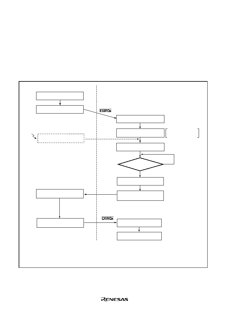
Rev. 1.0, 02/03, page 456 of 634
14.5.2
USB Cable Connection/Disconnection
1. USB Cable Connection (when USB module stop or power-down mode is not used)
If the USB cable enters the connection state from the disconnection state in an application (self
powered) where USB module stop or power-down mode is not used, perform the operation as
shown in figure 14.3. In bus-powered mode, perform the operation according to note 2 in
figure 14.3.
Connect the USB cable
USB function
Firmware
Receive bus reset from the host
Bus reset interrupt occurs.
A VBUS interrupt occurs
Check if VBUSs in UIFR3
is set to 1
Enable D+ pull-up
by port 36 (P36)
Check the USB cable
connection state
Initialize the firmware
Yes
No
Wait for setup interrupt
Cancel UDC core reset
(Clear UDCRST in UCTLR to 0)
Clear all FIFOs
Clear VBUSi in UIFR3
System ready?
Set USB module operation
*
1
*
2
Notes: 1. VBUS interrupts in the USB module cannot be detected in power-down mode or
in the USB module stop state.
2. In bus-powered mode, power is applied after the USB cable has been connected.
Accordingly, immediately after completing the power-on reset, initialization (14.5.1), clearing all FIFOs,
and system preparation, enable the D+ pull-up by the port 36 (P36) and cancel the UDC core reset state.
from 14.5.1
After completing the bus-
powered mode initialization
Figure 14.3 USB Cable Connection
(When USB Module Stop or Power-Down Mode is not Used)
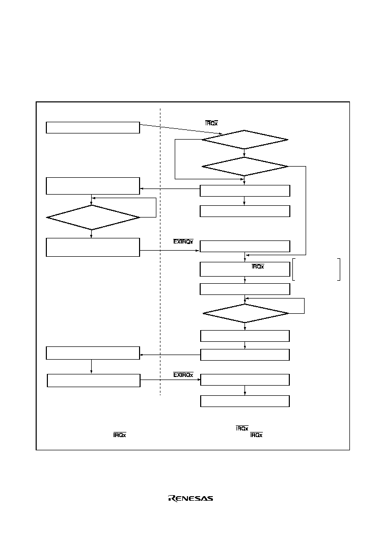
Rev. 1.0, 02/03, page 457 of 634
2. USB Cable Connection (When USB module stop or power-down mode is used)
If the USB cable enters the connection state from the disconnection state in an application (self
powered) where USB module stop or power-down mode is used, perform the operation as
shown in figure 14.4.
Connect the USB cable
USB function
Firmware
No
Yes
Receive bus reset from the host
Bus reset interrupt occurs.
Start USB operating
clock oscillation
USB oprating clock
stabilization time has
passed?
Cancel USB module stop 2
(Clear MSTPB0 in MSTPCRB to 0)
Check whether
= 1
by using the port function of
Clear CK48READY in UIFR3 to 0
Enable D+ pull-up by
port 36 (P36)
Initializa the firmware
Wait for setup interrupt
Yes
Yes
Yes
No
No
No
Cancel UDC core reset
(Clear UDCRST in UCTLR to 0)
Clear all FIFOs
Wait for USB operating clock
stabilization
USB operating clock
stabilization detection
interrupt occurs.
System ready?
Power-down mode?
USB module
stopped?
Start USB module
operation
*
*
External interrupt
*
Note:
VBUS interrupts in the USB module cannot be detected in power-down mode or in the USB module stop state.
Accordingly, in an application (self powered) where power-down mode or USB module stop is used,VBUS
interrupts of the USB must be detected via the external interrupt pin
.
In this case, the
pin must be specified as both-edge sensitive. When
is used, VBUS interrupts in the
USB module need not to be used.
Check the USB
cable connection
state
Figure 14.4 USB Cable Connection
(When USB Module Stop or Power-Down Mode is Used)
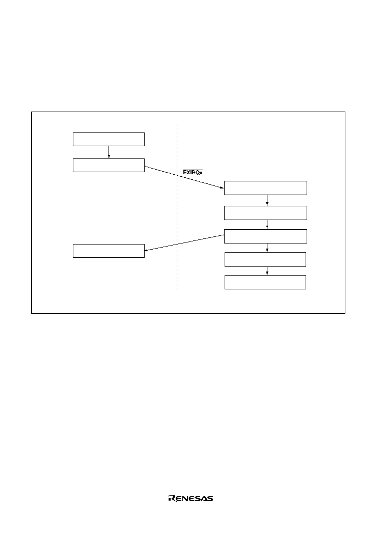
Rev. 1.0, 02/03, page 458 of 634
3. USB Cable Disconnection (When USB module stop or power-down mode is not used)
If the USB cable enters the disconnection state from the connection state in an application (self
powered) where USB module stop or power-down mode is not used, perform the operation as
shown in figure 14.5. In bus-powered mode, the power is automatically turned off when the
USB cable is disconnected and the following processing is not required.
Disconnect the USB cable
VBUS interrupt occurs
USB function
Firmware
Reset the UDC core
Clear VBUSi in UIFR3 to 0
Check if VBUSs in UIFR3
is cleared to 0
Cancel D + pull-up by
port 36 (P36)
Wait for USB cafle connection
Reset the UDC core
Write 1 to UDCRST in UCTLR
*
*
Note:
VBUS interrupts in the USB module cannot be detected in power-down mode
or in the USB module stop state.
Figure 14.5 USB Cable Disconnection
(When USB Module Stop or Power-Down Mode is not Used)
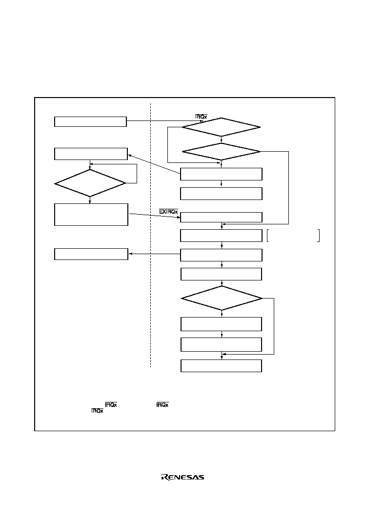
Rev. 1.0, 02/03, page 459 of 634
4. USB Cable Disconnection (When USB module stop or power-down mode is used)
If the USB cable enters the disconnection state from the connection state in an application (self
powered) where USB module stop or power-down mode is used, perform the operation as
shown in figure 14.6.
Disconnect the USB cable
USB function
Firmware
No
Yes
Enable D+ pull-up
by port 36 (P36)
Enter power-down mode
(if necessary)
Wait for USB
cable connection
Yes
Yes
Yes
No
No
No
USB module stop 2
Write 1 to MSTPB0 in MSTPCRB
Reset theUDC core
Write 1 to UDCRST in UCTRL
Rset the UDC core
System needs to
enter power-down
mode?
*
1
*
2
*
2
1.
2.
External interrupt
*
1
Notes:
VBUS interrupts in the USB module cannot be detected in power-down mode or in the USB
module stop state. Accordingly, in an application (self powered) where power-down mode or
USB module stop is used , VBUS interrupts of the USB must bedetected via the external
interrupt pin
. In this case, the
pin must be specified as both edge sensitive.
When
is used, VBUS interrupts in the USB module need not to be used.
Before entering power-down mode, make sure to set USB module stop2 (the MSTPB0 bit of
MSTPCRB = 1).
Check the USB cable
disconnection state
Start USB operating
clock oscillation
USB operating
clock stabilization time
has passed?
USB operating clock
stabilization detection
interrupt occurs.
Powe-down mode ?
USB module
stopped?
Cancel USB module stop 2
(Clear MSTPB0 in MSTPCRB to 0)
Wait for USB operating clock
stabilization
Check whether by using
the port function
Clear CK48READY in UIFR3 to 0
Figure 14.6 USB Cable Disconnection
(When USB Module Stop or Power-Down Mode is Used)
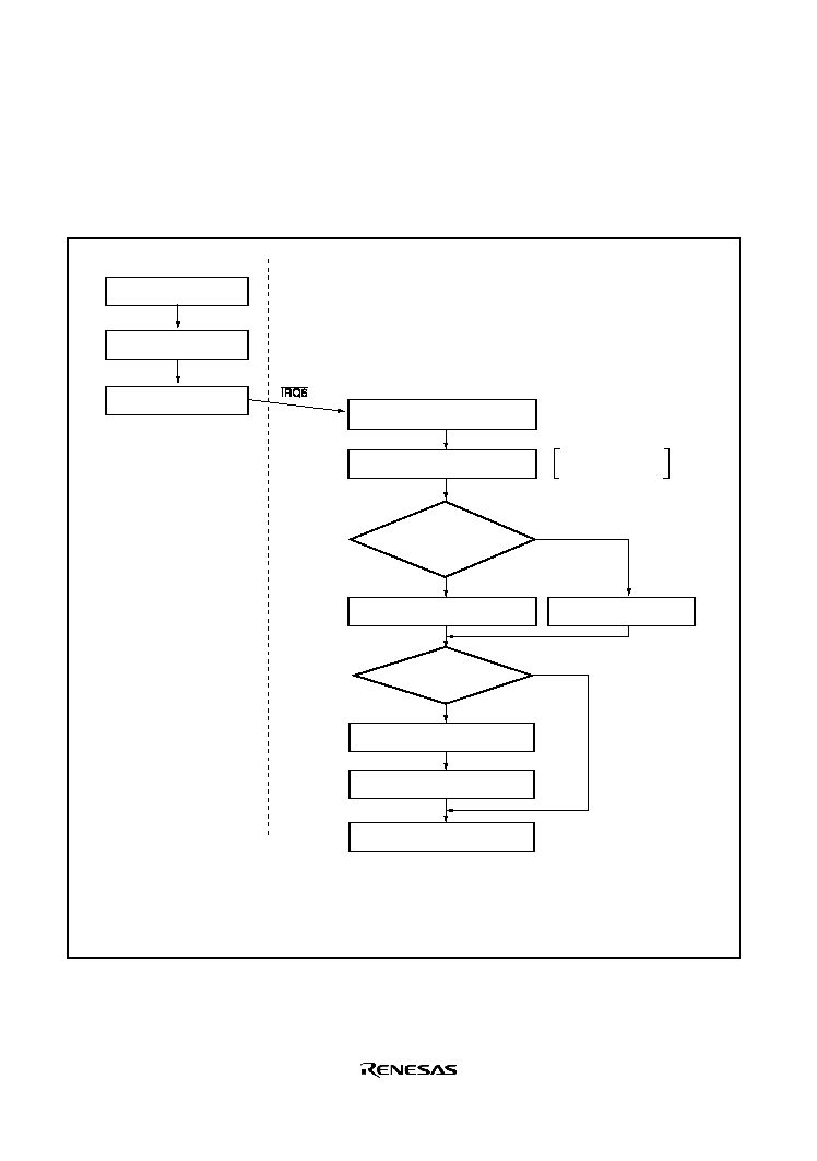
Rev. 1.0, 02/03, page 460 of 634
14.5.3
Suspend and Resume Operations
1. Suspend Operation
If the USB bus enters the suspend state from the non-suspend state, perform the operation as
shown in figure 14.7.
USB cable connected
USB function
Firmware
Suspend/resume
interrupt occurs
Bus idle of 3 ms or
more occurs
Clear SPRSi in UIFR3 to 0
Check if SPRSs in UIFR3
is set to 1
USB module stop 2
Wirte 1 to MSTPB0 in MSTPCRB
Wait for suspend/resume /
interrupt
Yes
Yes
No
No
Enter power-down mode
(if necessary)
Check remote-wakeup
function enabled
System needs to
enter power-down
mode?
Remote
wakeup enabled?
Is RWUPs in UDRR
set to 1?
*
1
*
2
*
2
1.
2.
Notes:
The remote-wakeup function can be used only when it is enabled by the host. Accordingly, before using
the remote-wakeup function, check the RWUPs bit in the UDRR register. In an application that does not
use the remote-wakeup function, whether the remote-wakeup functon is enabled by the host need not be
checked.
Before entering power-down mode, make sure to set USB module stop2 (MSTPB0 bit in MSTPCRB = 1).
Check remote-wakeup
function disabled
Check suspend state
Figure 14.7 Suspend Operation
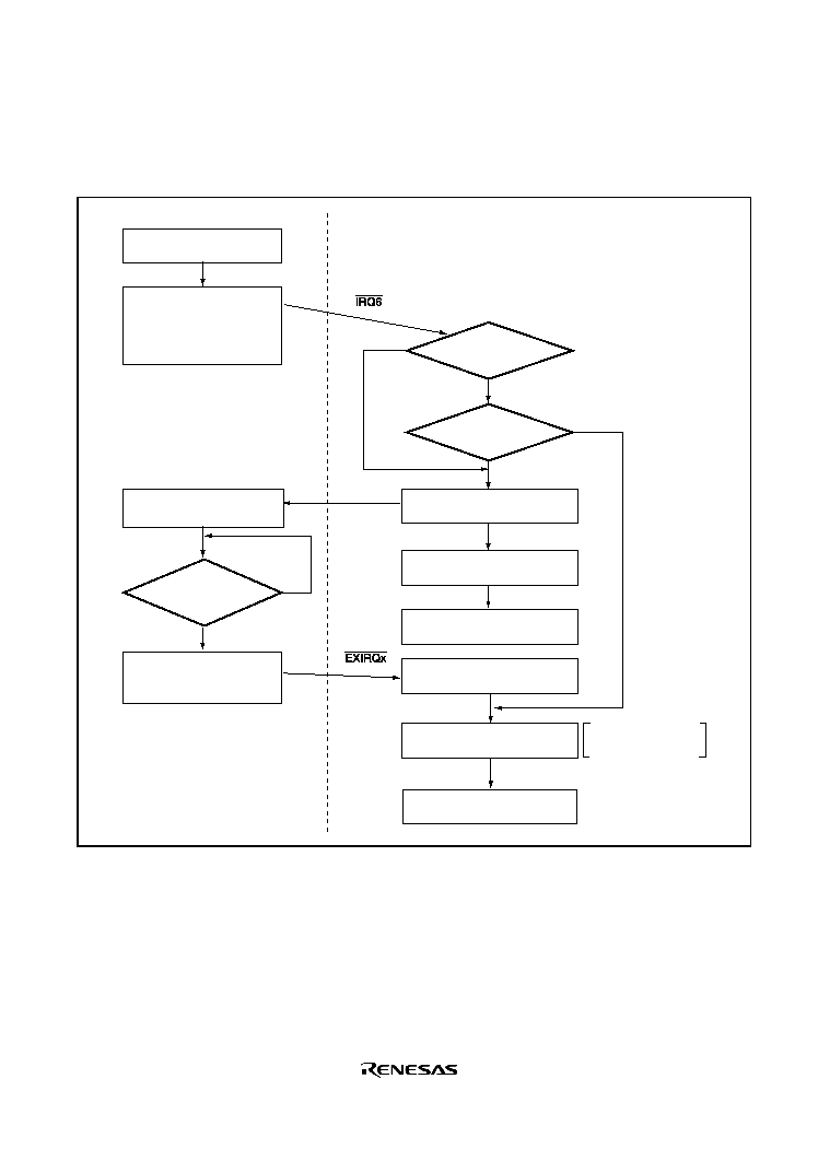
Rev. 1.0, 02/03, page 461 of 634
2. Resume Operation from Up-Stream
If the USB bus enters the non-suspend state from the suspend state by resume signal output
from up-stream, perform the operation as shown in figure 14.8.
USB cable connected
USB bus in suspend state
Resume interrupts is
requested from the
up-stream.
Suspend/resume
interrupt occurs.
USB function
Firmware
No
Yes
Start USB operating
clock oscillation
Check if SPRSs in UIFR3 is
cleared to 0
Clear CK48READY in
UIFR3 to 0
Clear SPRSi in UIFR3 to 0
Return to normal state
Yes
Yes
No
No
Check operating state
USBoperating
clock stabilization
time has passed?
A USB operating clock
stabilization detection
interrupt occurs.
Power down mode?
USB module
stopped?
Cancel USB module stop2
Clear MSTPB0 in MSTPCRB to 0
Wait for USB operating clock
stabilization
Figure 14.8 Resume Operation from Up-Stream
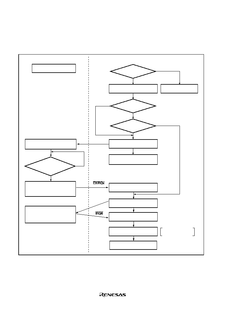
Rev. 1.0, 02/03, page 462 of 634
3. Resume-Wakeup Operation
If the USB bus enters the non-suspend (resume) state from the suspend state by the remote-
wakeup signal output from this function, perform the operation as shown in figure 14.9.
Output resume signal
to the USB bus.
Resume/suspend
interrupt occurs.
USB function
Firmware
No
Yes
Execute remote-wakeup
Write 1 to DVR in UDRR
Clear SPRSi in UIFR3 to 0
Yes
Yes
Yes
No
No
No
Bus wakeup source
occurs. (by system)
Wait for resume from
the up-stream
Remote-wakeup
enabled by the host?
Check operating state
USB cable connected
USB bus in suspend state
Start USB oprating clock oscillation
USB oprating clock
stabilization
time has passed?
USB operating clock
stabilizataion detection
A interrupt occurs.
Power-down mode?
USB module
stopped?
Cancel USB module stop2
Clear MSTPB0 in MSTPCRB to 0
Wait for USB operating clock
stabilization
Clear CK48READY in UIFR3 to 0
Check if SPRSs in UIFR3 is
cleaed to 0
Return to normal state
Figure 14.9 Remote-Wakeup
Rev. 1.0, 02/03, page 463 of 634
14.5.4
Control Transfer
The control transfer consists of three stages; setup, data (sometimes omitted), and status, as shown
in figure 14.10. The data stage consists of multiple bus transactions. Figures 14.11 to 14.15 show
operation flows in each stage.
Control-in
Setup stage
Data stage
Status stage
Control-out
No data
SETUP(0)
DATA0
SETUP(0)
DATA0
SETUP(0)
DATA0
IN(1)
DATA1
OUT(1)
DATA1
IN(0)
DATA0
OUT(0)
. . .
. . .
DATA0
IN(0/1)
DATA0/1
OUT(0/1)
DATA0/1
OUT(1)
DATA1
IN(1)
DATA1
IN(1)
DATA1
Figure 14.10 Control Transfer Stage Configuration
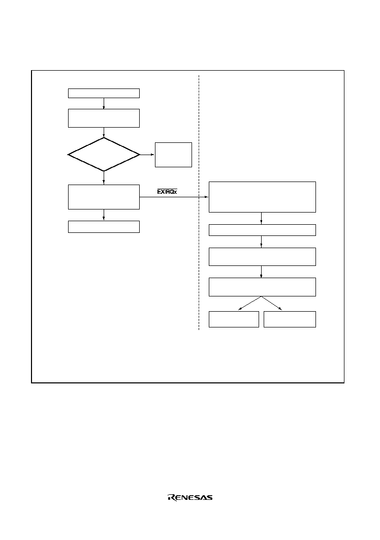
Rev. 1.0, 02/03, page 464 of 634
1. Setup Stage
USB function
Firmware
Receive setup token
Receive 8-byte command
data in UEDR0s
To data stage
Set setup command
recive complete flag
(SetupTS in U1FR0 = 1)
Automatic
processing by
this module
Clear SetupTS flag
(SetupTS in U1FR0 = 0)
Clear EP0i FIFO (EP0iCLR in UFCLR = 1)
Clear EP0o FIFO (EP0oCLR in UFCLR = 1)
Read 8-byte data from UEDR0s
Decode command data
Determine data stage direction*
1
Write 1 to EP0s read complete bit
(EP0s RDFN in UTRG0 in UTRG0 = 1)
To control-in
data stage
To control-out
data stage
Command
to be processed by
firmware?
Yes
No
Notes: 1. In the setup stage, the firmware first analyzes the command data that is sent from the host and
required to be processed by the firmware, and determines subsequent processing.
(For example, the data stage direction.)
2. When the transfer direction is control-out, the EP0i transfer request interrupt that is required in the
status stage should be enabled. When the transfer direction is control-in, this interrupt is not
required and must be disabled.
*
2
Figure 14.11 Setup Stage Operation
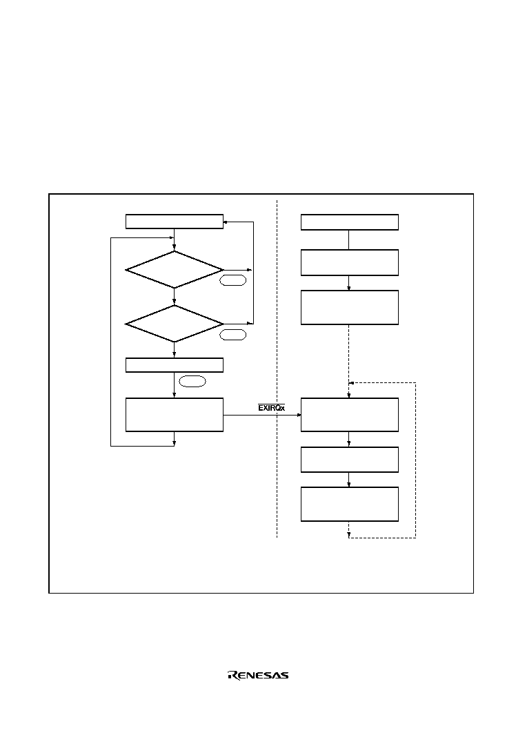
Rev. 1.0, 02/03, page 465 of 634
2. Data Stage (Control-In)
The firmware first analyzes the command data that is sent from the host in the setup stage, and
determines the subsequent data stage direction. If the result of command data analysis is that
the data stage is in-transfer, one packet of data to be sent to the host is written to the FIFO. If
there is more data to be sent, this data is written to the FIFO after the data written first has been
sent to the host (EP0iTS in UIFR0 is set to 1).
The end of the data stage is identified when the host transmits an OUT token and the status
stage is entered.
USB function
Firmware
Receive IN token
Transmit data to host
Set EP0i transmit
complete flag
(EP0iTS in UIFR0 = 1)
From setup stage
Write data to USB endpoint
data register 0i (UEDR0i)
Write 1 to EP0i packet
enable bit
(EP0iPKTE in UTRG0 = 1)
Clear EP0i transmit
complete flag
(EP0iTS in UIFR0 = 0)
Write 1 to EP0i packet
enable bit
(EP0iPKTE in UTRG0 = 1)
Write data to USB endpoint
data register 0i (UEDR0i)
1 written
to EP0sRDFN
in UTRG0?
Valid data
in EP0i FIFO?
NACK
NACK
No
No
Yes
Yes
ACK
Note:
If the size of the data transmitted by the function is smaller than the data size requested by the host,
the function indicates the end of the data stage by returnning to the host a packet shorter than the
maximum packet size. If the size of the data transmitted by the function is an integral multiple of the
maximum packet size, the function indicates the end of the data stage by transmitting a zero-length
packet.
Figure 14.12 Data Stage Operation (Control-In)
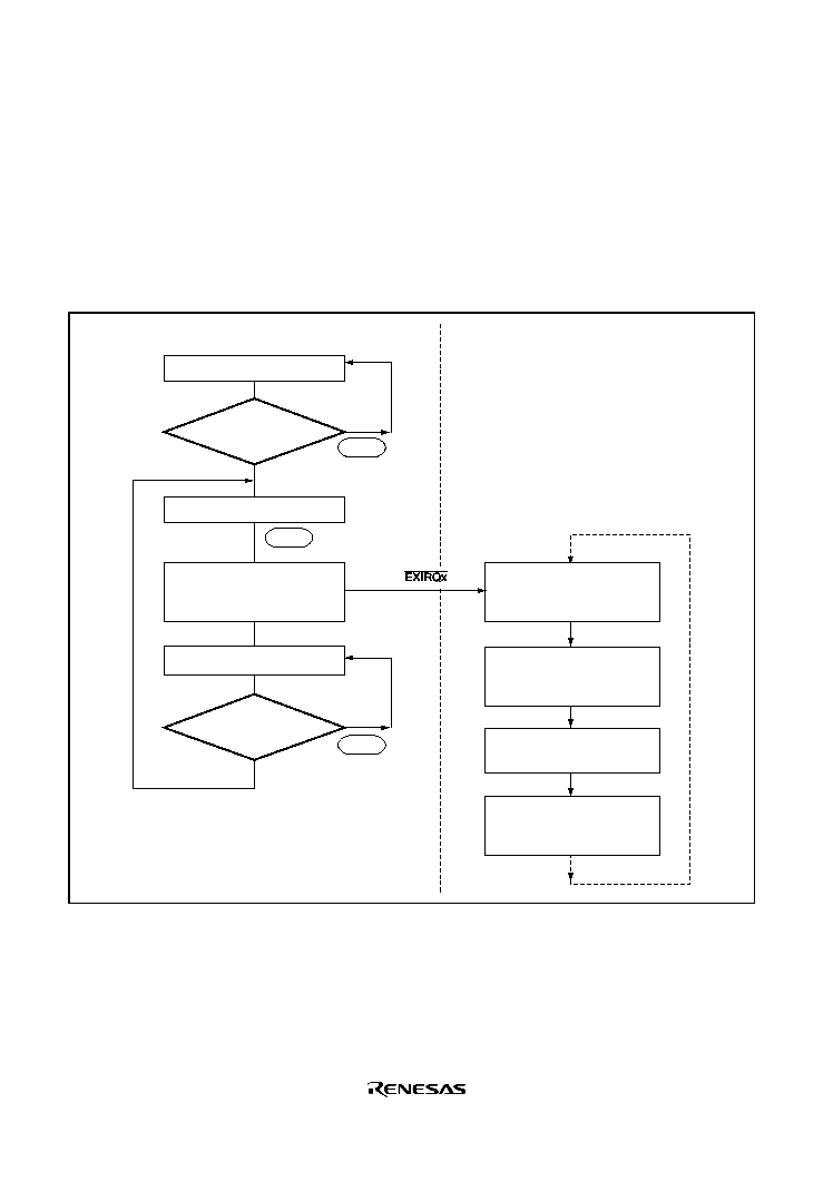
Rev. 1.0, 02/03, page 466 of 634
3. Data Stage (Control-Out)
The firmware first analyzes the command data that is sent from the host in the setup stage, and
determines the subsequent data stage direction. If the result of command data analysis is that
the data stage is out-transfer, data from the host is waited for, and after data is received
(EP0oTS in UIFR0 is set to 1), data is read from the FIFO. Next, the firmware writes 1 to the
EP0o read complete bit, empties the receive FIFO, and waits for reception of the next data.
The end of the data stage is identified when the host transmits an IN token and the status stage
is entered.
USB function
Firmware
Receive OUT token
Receive data reception from host
Receive OUT token
Set EP0o receive
complete flag
(EP0oTS in UIFR0 = 1)
Clear EP0o receive
complete flag
(EP0oTS in UIFR0 = 0)
Read data from USB endpoint
receive data size register 0o
(UESZ0o)
Write 1 to EP0o read
complete bit
(EP0oRDFN in UTRG0 = 1)
Read data from USB endpoint
data register 0o (UEDR0o)
1 written
to EP0sRDFN
in UTRG0?
1 written
to EP0oRDFN
in UTRG0?
NACK
NACK
ACK
No
Yes
No
Yes
Figure 14.13 Data Stage Operation (Control-Out)
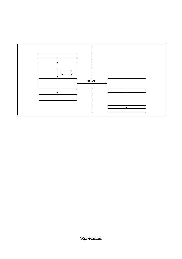
Rev. 1.0, 02/03, page 467 of 634
4. Status Stage (Control-In)
The control-in status stage starts with an OUT token from the host. The firmware receives 0-
byte data from the host, and ends control transfer.
USB function
Firmware
OUT token reception
0-byte reception from host
End of control transfer
Set EP0o reception
complete flag
(UIFR0/EP0o TS = 1)
Clear EP0o reception
complete flag
(UIFR0/EP0o TS = 0)
Write 1 to EP0o read
complete bit
(UTRG0/EP0o RDFN = 1)
End of control transfer
ACK
Figure 14.14 Status Stage Operation (Control-In)
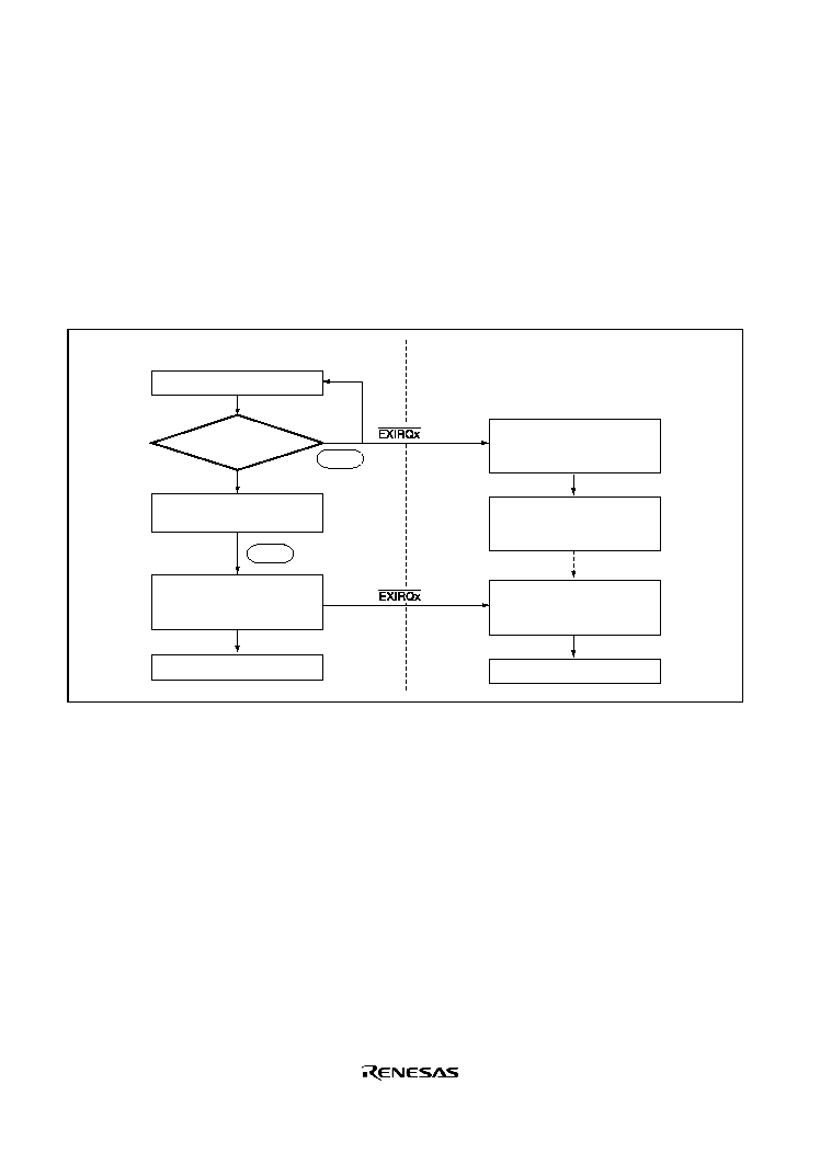
Rev. 1.0, 02/03, page 468 of 634
5. Status Stage (Control-Out)
The control-out status stage starts with an IN token from the host. When an IN-token is
received at the start of the status stage, there is not yet any data in the EP0i FIFO, and so an
EP0i transfer request interrupt is generated. The firmware recognizes from this interrupt that
the status stage has started. Next, in order to transmit 0-byte data to the host, 1 is written to the
EP0i packet enable bit but no data is written to the EP0i FIFO. As a result, the next IN token
causes 0-byte data to be transmitted to the host, and control transfer ends.
After the firmware has finished all processing relating to the data stage, 1 should be written to
the EP0i packet enable bit.
USB function
Firmware
Receive IN token
Transfer 0-byte data to host
End of control transfer
Set EP0i transmit
complete flag
(EP0iTS in UIFR0 = 1)
Clear EP0i transfer
request flag
(EP0iTR in UIFR0 = 0)
Write 1 to EP0i packet
enable bit
(EP0iPKTE in UTRG0 = 1)
Clear EP0i transmit
complete flag
(EP0iTS in UIFR0 = 0)
End of control transfer
Valid data
in EP0i FIFO?
ACK
Yes
No
NACK
Figure 14.15 Status Stage Operation (Control-Out)
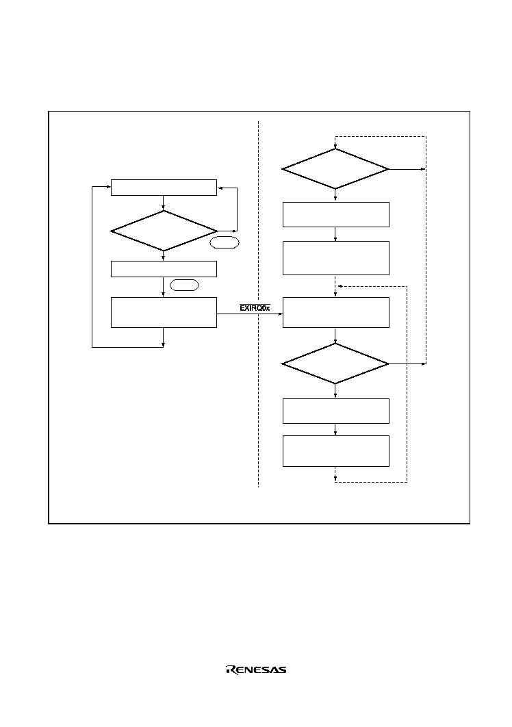
Rev. 1.0, 02/03, page 469 of 634
14.5.5
Interrupt-In Transfer: (Endpoint 3)
USB function
Firmware
Receive IN token
Transmit data to host
Set EP3 transmit
complete flag
(EP3TS in UIFR0 = 1)
Write data to USB endpoint
data register 3 (UEDR3)
Write 1 to EP3 packet
enable bit
(EP3PKTE inUTRG0 = 1)
Clear EP3 transmit
complete flag
(EP3TS in UIFR0 = 0)
Write data to USB endpoint
data register3 (UEDR3)
Write 1 to EP3 packet
enable bit
(EP3PKTE in UTRG0 = 1)
Valid data
in EP3 FIFO?
Is there any data
to be transmitted
to host?
Is there any data
to be transmited
to host?
No
Yes
No
Yes
No
Yes
NACK
ACK
Note:
This flowchart shows just one example of interrupt-in transfer processing. Other possibilities include an
operation flow in which, if there is data to be transmited, the EP3DE bit UDSR is referred to confirm that the
FIFO is empty, and then data is written to the FIFO.
Figure 14.16 EP3 Interrupt-In Transfer Operation
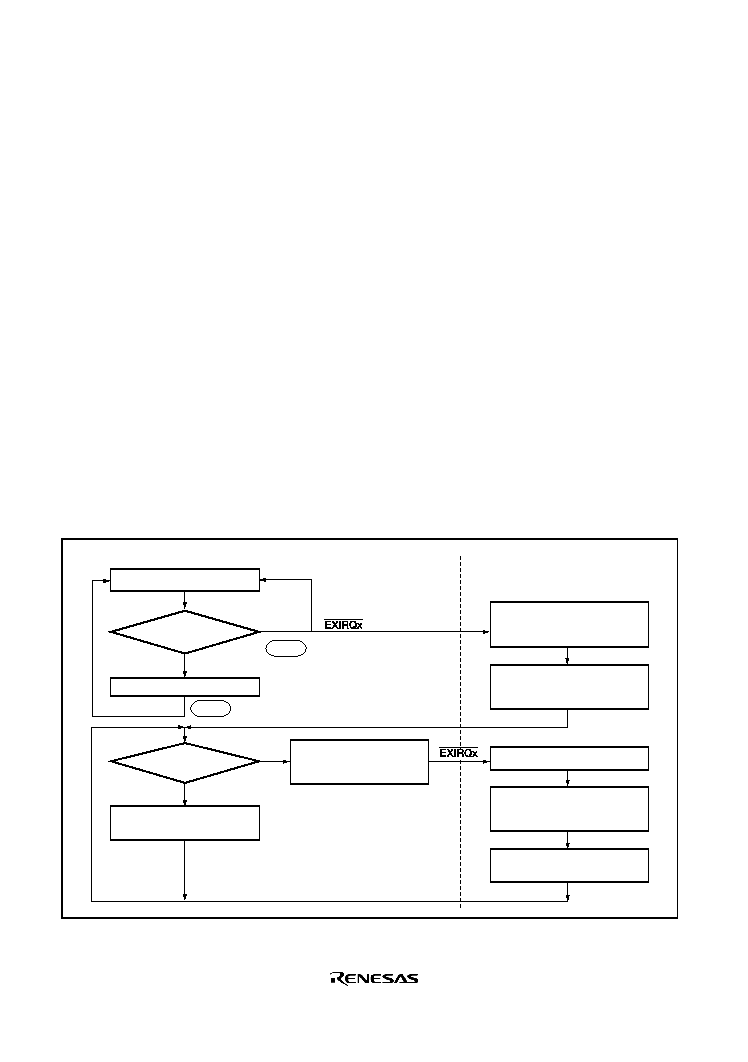
Rev. 1.0, 02/03, page 470 of 634
14.5.6
Bulk-In Transfer (Dual FIFOs): (Endpoint 1)
EP1 has two 64-byte FIFOs, but the user can transmit data and write transmit data without being
aware of this dual-FIFO configuration. However, one data write should be performed for one
FIFO. For example, even if both FIFOs are empty, it is not possible to perform EP1PKTE at one
time after consecutively writing 128 bytes of data. EP1PKTE must be performed for each 64- byte
write.
When performing bulk-in transfer, as there is no valid data in the FIFOs on reception of the first
IN token, a UIFR1/EP1TR interrupt is requested. With this interrupt, 1 is written to the
UIER1/EP1EMPTYE bit, and the EP1 FIFO empty interrupt is enabled. At first, both EP1 FIFOs
are empty, and so an EP1 FIFO empty interrupt is generated immediately. The data to be
transmitted is written to the data register using this interrupt. After the first transmit data write for
one FIFO, the other FIFO is empty, and so the next transmit data can be written to the other FIFO
immediately. When both FIFOs are full, EP1EMPTY is cleared to 0. If at least one FIFO is empty,
UIFR1/EP1EMPTY is set to 1. When ACK is returned from the host after data transmission is
completed, the FIFO used in the data transmission becomes empty. If the other FIFO contains
valid transmit data at this time, transmission can be continued.
When transmission of all data has been completed, write 0 to UIER1/EP1EMPTYE and disable
EXIRQ0 or EXIRQ1 interrupt requests.
USB function
Firmware
Receive IN token
Transmit data to host
Clear EP1 transfer
request flag
(EP1TR in UIFR1 = 0)
Write 1 to EP1 FIFO
empty enable bit
(EP1EMPTYEin UIER1 = 1)
UIFR1/EP1 EMPTY interrupt
Write one packet of data
to USB endpoint data
register1 (UEDR1)
Write 1 to EP1packet enable bit
(EP1PKTE inUTRG0 = 1)
Set EP1 FIF0
empty status bit
(EP1EMPTY in UIFR1= 1)
Valid data
in EP1 FIFO?
NACK
ACK
Yes
No
Clear EP1 FIF0 empty status
(UIFR1/EP1 EMPTY = 0)
Space
in EP1 FIFO?
No
Yes
Figure 14.17 EP1 Bulk-In Transfer Operation
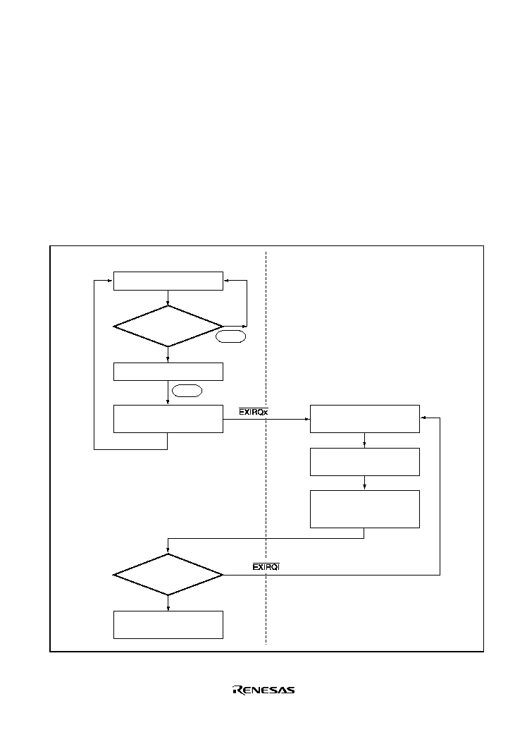
Rev. 1.0, 02/03, page 471 of 634
14.5.7
Bulk-Out Transfer (Dual FIFOs): (Endpoint 2)
EP2 has two 64-byte FIFOs, but the user can receive data and read receive data without being
aware of this dual-FIFO configuration.
When one FIFO is full after reception is completed, the UIFR1/EP2READY bit is set. After the
first receive operation into one of the FIFOs when both FIFOs are empty, the other FIFO is empty,
and so the next packet can be received immediately. When both FIFOs are full, NACK is returned
to the host automatically. When reading of the receive data is completed following data reception,
1 is written to the UTRG0/EP2RDFN bit. This operation empties the FIFO that has just been read,
and makes it ready to receive the next packet.
USB function
Firmware
Recive OUT token
Receive data from host
Set EP2 data ready status bit
(EP2READY in UIFR1 = 1)
Clear EP2 data ready status bit
(EP2READY in UIFR1 = 0)
Read USB endpoint receive
data size register 2 (UESZ2)
Read data from USB endpoint
data register 2 (UEDR2)
Write 1 to EP2o read
complete bit
(EP2RDFN in UTRG0 = 1)
Space
in EP2 FIFO?
No
Yes
Both
EP2 FIFOs empty?
No
Yes
NACK
ACK
Figure 14.18 EP2 Bulk-Out Transfer Operation

Rev. 1.0, 02/03, page 472 of 634
14.5.8
Processing of USB Standard Commands and Class/Vendor Commands
1. Processing of Commands Transmitted by Control Transfer
A command transmitted from the host by control transfer may require decoding and execution
of command processing by the firmware. Whether or not command decoding is required by the
firmware is indicated in table 14.5 below.
Table 14.5
Command Decoding by Firmware
Decoding not Necessary by Firmware
Decoding Necessary by Firmware
Clear Feature
Get Configuration
Get Interface
Get Status
Set Address
Set Configuration
Set Feature
Set Interface
Get Descriptor
Synch Frame
Set Descriptor
Class/Vendor command
If decoding is not necessary by the firmware, command decoding and data stage and status
stage processing are performed automatically. No processing is necessary by the user. An
interrupt is not generated in this case.
If decoding is necessary by the firmware, the USB function module stores the command in the
EP0s FIFO. After normal reception is completed, the SetupTS flag in UIER0 is set and an
interrupt request is generated from the
EXIRQx pin. In the interrupt routine, eight bytes of data
must be read from the EP0s data register (UEDR0s) and decoded by the firmware. The
necessary data stage and status stage processing should then be carried out according to the
result of the decoding operation.

Rev. 1.0, 02/03, page 473 of 634
14.5.9
Stall Operations
1. Overview
This section describes stall operations in the USB function module. There are two cases in
which the USB function module stall function is used:
. When the firmware forcibly stalls an endpoint for some reason
. When a stall is performed automatically within the USB function module due to a USB
specification violation.
The USB function module has internal status bits that hold the status (stall or non-stall) of each
endpoint. When a transaction is sent from the host, the module refers these internal status bits
and determines whether to return a stall to the host. These bits cannot be cleared by the
firmware; they must be cleared with a Clear Feature command from the host. However, the
internal status bit for EP0 is cleared automatically at the reception of the setup command.
2. Forcible Stall by Firmware
The firmware uses the UESTL register to issue a stall request for the USB function module.
When the firmware wishes to stall a specific endpoint, it sets the corresponding EPnSTL bit (1-
1 in figure 14.19). The internal status bits are not changed at this time.
When a transaction is sent from the host for the endpoint for which the EPnSTL bit was set, the
USB function module refers the internal status bit, and if this is not set, refers the
corresponding EPnSTL bit (1-2 in figure 14.19). If the corresponding EPnSTL bit is not set,
the internal status bit is not changed and the transaction is accepted. If the corresponding
EPnSTL bit is set, the USB function module sets the internal status bit and returns a stall
handshake to the host (1-3 in figure 14.19). If the SCME bit in UESTL1 is set at this time, the
EPnSTL bit is automatically cleared (1-4 in figure 14.19).
Once an internal status bit is set, it remains set until cleared by a Clear Feature command from
the host, without regarding to EPnSTL. Even after a bit is cleared by the Clear Feature
command (3-1 in figure 14.19), the USB function module continues to return a stall handshake
while the EPnSTL bit is set, since the internal status bit is set each time a transaction is
executed for the corresponding endpoint (1-2 in figure 14.19). To clear a stall, therefore, it is
necessary for the corresponding EPnSTL bit to be cleared by the firmware (or set the SCME
bit so that the EPnSTL bit is automatically cleared when the USB function module returns a
stall handshake), and also for the internal status bit to be cleared with a Clear Feature command
(2-1, 2-2, and 2-3 in figure 14.19).
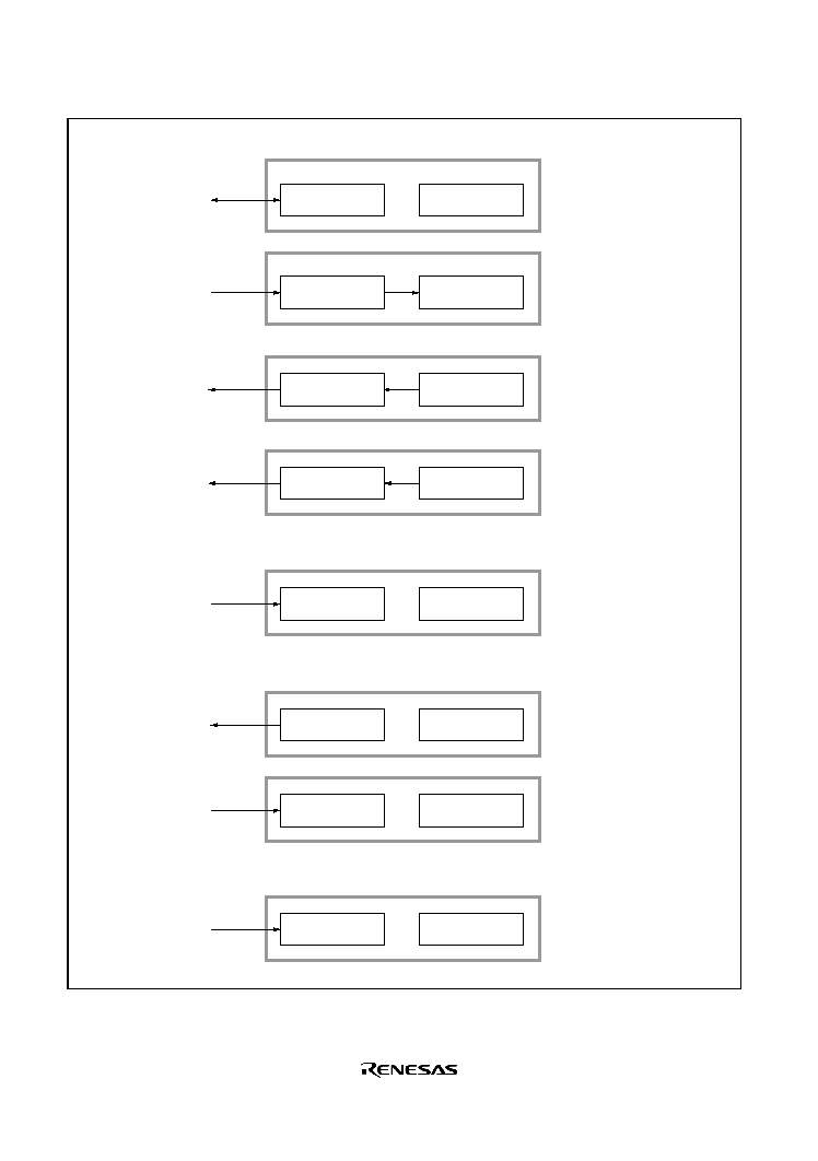
Rev. 1.0, 02/03, page 474 of 634
(1) Transition from normal operation to stall
(1-1)
Transaction request
USB
Reference
USB function module
(1-2)
Stall handshake
Stall
To (2-1) or (3-1)
To (1-3) or (1-4)
Normal status restored
(1-3)
(2) When Clear Feature is sent after EPnSTL has been cleared
(2-1)
Stall handshake
Transaction request
(2-2)
Clear Feature command
Clear Feature command
(2-3)
(3) When Clear Feature is sent before EPnSTL is cleared to 0
(3-1)
1. Set EPnSTL to 1 by
firmware
1. Receive IN/OUT
token from the host
2. Refer to EPnSTL
1. Transmit stall
handshake
1. Clear internal status
bit to 0
1. Clear internal status
bit to 0
2. No change in
EPnSTL bit
1. SCME is set to 1
2. EPnSTL is set to 1
3. Set internal status
bit to 1
4. Transmit stall
handshake
1. Clear EPnSTL to 0
by firmware
2. Receive IN/OUT
token from the host
3. Internal status bit
has been set to 1
4. EPnSTL is not
referred to
5. No change in
internal status bit
To (1-2)
Internal status bit
0
EPnSTL
0
1
Internal status bit
0
EPnSTL
1
Internal status bit
0
1
EPnSTL
1 (SCME = 0)
Stall handshake
Stall
To 2 in (2-1)
(1-4)
1. SCME is set to 1
2. EPnSTL is automatically
cleared to 0
3. Set internal status bit to 1
4. Transmit stall handshake
Internal status bit
0
1
EPnSTL
1
0 (SCME = 1)
Internal status bit
1
EPnSTL
1
0
Internal status bit
1
EPnSTL
0
Internal status bit
1
0
EPnSTL
0
Internal status bit
1
0
EPnSTL
1
Figure 14.19 Forcible Stall by Firmware
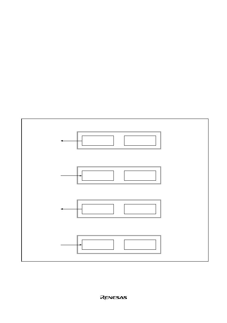
Rev. 1.0, 02/03, page 475 of 634
3. Automatic Stall by USB Function Module
When a stall setting is made with the Set Feature command, when the information of this
module differs from that returned to the host by the Get Descriptor, or in the event of a USB
specification violation, the USB function module automatically sets the internal status bit for
the corresponding endpoint without regarding to EPnSTL, and returns a stall handshake (1-1 in
figure 14.20).
Once an internal status bit is set, it remains set until cleared by a Clear Feature command from
the host, without regarding to EPnSTL. After a bit is cleared by the Clear Feature command,
EPnSTL is referred (3-1 in figure 14.20). The USB function module continues to return a stall
handshake while the internal status bit is set, since the internal status bit is set even if a
transaction is executed for the corresponding endpoint (2-1 and 2-2 in figure 14.20). To clear a
stall, therefore, the internal status bit must be cleared with a Clear Feature command (3-1 in
figure 14.20). If set by the firmware, EPnSTL should also be cleared (2-1 in figure 14.20).
(1)
Transition from normal operation to stall
(2)
When transaction is performed whill internal status bit is set
Stall handshake
Transaction request
Stall handshake
(2-2)
Clear Feature command
(3)
When Clear Feature is sent before transaction is performed
(3-1)
1. In case of USB
specification violation,
USB function module
stalls endpoint
automatically.
1. Transmit stall
handshake
1. Clear the internal
status bit to 0
2. No change in
EPnSTL bit
1. Receive IN/OUT
token from the host
2. Internal status bit has
been set to 1
3. EPnSTL is not
referred to
4. No change internal
status bit
Normal status restored
Internal status bit
0
1
EPnSTL
0
Internal status bit
1
EPnSTL
0
Internal status bit
1
EPnSTL
0
Internal status bit
1
0
EPnSTL
0
Stall status maintained
USB function module
To (2-1) or (3-1)
(1-1)
(1-2)
Figure 14.20 Automatic Stall by USB Function Module

Rev. 1.0, 02/03, page 476 of 634
14.6
DMA Transfer Specifications
14.6.1
Overview
This module incorporates the interface that supports dual-address transfer by means of the on-chip
DMAC. Endpoints that can be transferred by the on-chip DMAC are EP1 and EP2 in Bulk transfer
(corresponding registers are UEDR1 and UEDR2). In DMA transfer, the USB module must be
accessed as an external device in area 6. The USB module cannot be accessed as a device with
external ACK (single-address transfer cannot be performed.). 0-byte data transfer to EP2 is
ignored even if the DMA transfer is enabled by setting the EP2T1 bit in UDMAR to 1.
14.6.2
On-Chip DMAC Settings
The on-chip DMAC must be specified as follows: A USB request (
DREQ signal is used), activated
by low-level input, byte size, full-address mode transfer, and the DTA bit in DMABCR = 1. After
completing the DMA transfer of specified times, the DMAC automatically stops. Note, however,
that the USB module keeps the
DREQ signal low while data to be transferred by the on-chip
DMAC remains regardless of the DMAC status.
14.6.3
EP1 DMA Transfer
The EP1T1 bit in UDMAR enables the DMA transfer. The EP1T0 bit in UDMAR specifies the
DREQ signal to be used by the DMA transfer. When 1 is written to the EP1T1 bit, the DREQ
signal is driven low if at least one of EP1 data FIFOs is empty; the
DREQ signal is driven high if
both EP1 data FIFOs are full.
14.6.4
EP2 DMA Transfer
The EP2T1 bit in UDMAR enables the DMA transfer. The EP2T0 bit in the UDMAR specifies the
DREQ signal to be used by the DMA transfer. When 1 is written to the EP2T1 bit, the DREQ
signal is driven low if at least one of EP2 data FIFOs is full (ready state); the
DREQ signal is
driven high if both EP2 data FIFOs are empty when all receive data items are read.
Rev. 1.0, 02/03, page 477 of 634
14.6.5
EP1PKTE and EP2RDFN Bits in UTRG0
1. EP1PKTE in UTRG0
When DMA transfer is performed on EP1 transmit data, the USB module automatically
performs the same processing as writing 1 to EP1PKTE if one data FIFO (64 bytes) becomes
full. Accordingly, to transfer data of integral multiples of 64 bytes, the user needs not to write 1
to EP1PKTE. To transfer data of less than 64 bytes, the user must write 1 to EP1PKTE using
the DMA transfer end interrupt of the on-chip DMAC. If the user writes 1 to EP1PKTE in
cases other than the case when data of less than 64 bytes is transferred, excess transfer occurs
and correct operation cannot be guaranteed.
Figure 14.21 shows an example for transmitting 150 bytes of data from EP1 to the host. In this
case, internal processing as the same as writing 1 to EP1PKTE is automatically performed
twice. This kind of internal processing is performed when the currently selected data FIFO
becomes full. Accordingly, this processing is automatically performed only when 64-byte data
is sent. This processing is not performed automatically when data less than 64 bytes is sent.
64 bytes
64 bytes
22 bytes
EP1PKTE
(Automatically
performed)
EP1PKTE
(Automatically
performed)
EP1PKTE is
not performed
Executed by DMA transfer
end interrupt (user)
Figure 14.21 EP1PKTE Operation in UTRG0
2. EP2RDFN in UTRG0
When DMA transfer is performed on EP2 receive data, do not write 1 to EP2RDFN after one
data FIFO (64 bytes) has been read. In data transfer other than DMA transfer, the next data
cannot be read after one data FIFO (64 bytes) has been read unless 1 is written to EP2RDFN.
While in DMA transfer, the USB module automatically performs the same processing as
writing 1 to EP2RDFN if the currently selected data FIFO becomes empty. Accordingly, in
DMA transfer, the user needs not to write 1 to EP2RDFN. If the user writes 1 to EP2RDFN in
DMA transfer, excess transfer occurs and correct operation cannot be guaranteed.
Figure 14.22 shows an example of EP2 receiving 150 bytes of data from the host. In this case,
internal processing as the same as writing 1 to EP2RDFN is automatically performed three
times. This kind of internal processing is performed when the currently selected data FIFO
becomes empty. Accordingly, this processing is automatically performed both when 64-byte
data is sent and when data less than 64 bytes is sent.
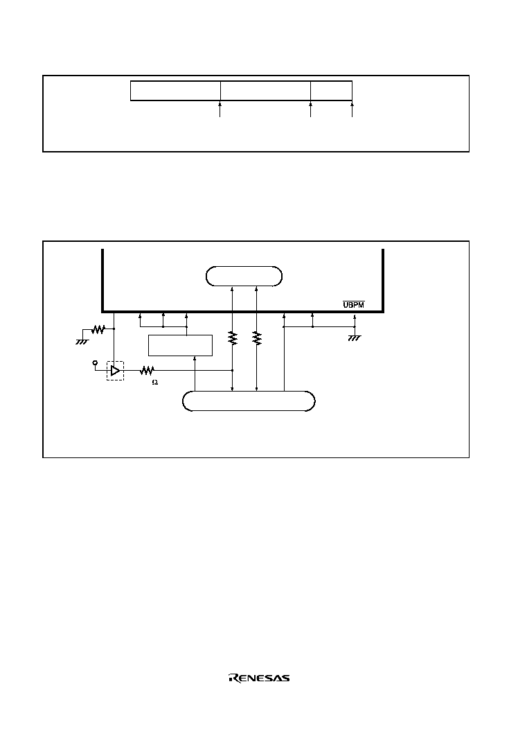
Rev. 1.0, 02/03, page 478 of 634
EP2RDFN
(Automatically
performed)
EP2RDFN
(Automatically
performed)
EP2RDFN
(Automatically
performed)
64 bytes
64 bytes
22 bytes
Figure 14.22 EP2RDFN Operation in UTRG0
14.7
USB External Circuit Example
Figures 14.23 and 14.24 show the USB external circuit examples of this LIS.
Regulator
0: Bus-powered mode
Internal transceiver
VCC
1.5k
DrVCC
(3.3V)
VCC
(3.3V)
VBUS
(5V)
USD+
USD-
D+
D-
DrVSS
GND
VBUS
VCC
(3.3V)
Rs
Rs
VSS
USB connector
*
1
USB
Step-down to the operating voltage VCC (3.3V) of this LSI.
To protect the LSI, voltage applicable IC such as HD74LV-A series must be used
even when the system power is turned off.
Pull-up
control external
circuit for
full speed
1.
2.
Notes:
*
2
P36
Figure 14.23 USB External Circuit in Bus-Powered Mode
Rev. 1.0, 02/03, page 479 of 634
1: Self-powered mode
Internal transceiver
P36
1.5k
DrVCC
(3.3V)
3.3V
VBUS
(5V)
USD+
USD-
D+
D-
Rs
Rs
DrVSS
GND
VBUS
VCC
(3.3V)
VCC
VCC
VSS
USB connector
*
1
*
2
USB
To protect the LSI, voltage applicable IC such as HD74LV-A series must be used
even when the system power is turned off.
To cancel power-down mode by detecting the USB cable connection, theVBUS
signal must be connected to the
pin. Note that power-down mode
state cannot be canceled by the USB interrupt
.
Pull-up control
external circuit
for full speed
1.
2.
Notes:
VCC
*
1
Figure 14.24 USB External Circuit in Self-Powered Mode

Rev. 1.0, 02/03, page 480 of 634
14.8
Usage Notes
14.8.1
E6000 Usage Notes
In the E6000, since the USB module is mounted on the external extended board and accessed as an
external module, there are some restrictions as shown below. In the E10A, however, there are no
such restrictions.
· Mode 7 (single-chip mode) of the H8S/2218 Series is not supported.
· In modes 6 and 7 (on-chip ROM enabled mode), CS6 and A9 to A0 are input pins in the initial
state. Accordingly, before accessing the USB module, set
CS6 and A9 to A0 to output pins by
setting P72DDR = 1, AE3 to AE0 = B
0010, and PC7DDR to PC0DDR = HFF. In modes 4
and 5 (on-chip ROM disabled mode), set
CS6, A9, and A8 to output pins by setting P72DDR =
1 and AE3 to AE0 = B
0010.
14.8.2
Operating Frequency
The main clock of this LSI must be 24 MHz or 16 MHz. This 24-MHz main clock, used as base
clock, is doubled in the on-chip PLL circuit or this 16-MHz main clock, also used as base clock, is
tripled in the on-chip PLL circuit, to generate the 48-MHz USB operating clock. Since the USB
module does not support medium-speed mode, sleep mode, watch mode, subactive mode, and
subsleep mode, make sure to use full-speed mode.
14.8.3
Bus Interface
The USB module's interface is based on the bus specifications of external area 6. Accordingly,
before accessing the USB module, area 6 must be specified as having an 8-bit bus width and 3-
state access using the bus controller register.
14.8.4
Setup Data Reception
The following must be noted for the EP0s FIFO used to receive 8-byte setup data. The USB is
designed to always receive setup commands. Accordingly, write from the UDC has higher priority
than read from the LSI. If the reception of the next setup command starts while the LSI is reading
data after completing reception, this data read from the LSI is forcibly cancelled and the next setup
command write starts. After the next setup command write, data read from the LSI is thus
undefined. Read operation is forcibly disabled because data cannot be guaranteed if DP-RAM used
as FIFO accesses the same address for write and read.

Rev. 1.0, 02/03, page 481 of 634
14.8.5
FIFO Clear
If the USB cable is disconnected during communication, old data may be contained in the FIFO.
Accordingly, FIFOs must be cleared immediately after USB cable connection. In addition, after
bus reset, all FIFOs must also be cleared. Note, however, that FIFOs that are currently used for
data transfer to or from the host must not be cleared.
14.8.6
IRQ6
IRQ6
IRQ6
IRQ6 Interrupt
A suspend/resume interrupt requested by
IRQ6 must be specified as falling-edge sensitive.
14.8.7
Data Register Overread or Overwrite
When the CPU reads or writes to data registers, the following must be noted:
· Transmit data registers (UEDR0i, UEDR3, UEDR1)
Data to be written to the transmit data registers must be within the maximum packet size. For
the transmit data register of EP1 having a dual-FIFO configuration, data to be written at any
time must be within the maximum packet size. In this case, after a data write, the FIFO is
switched to the other FIFO, enabling an further data write, when the PKTE bit in UTRG0 is set
to 1. Accordingly, data of size corresponding to two FIFOs must not be written to the transmit
data registers at a time.
· Receive data registers (UEDR0o, UEDR2)
Receive data registers must not read a data size that is greater than the effective size of the read
data item. In other words, receive data registers must not read data with data size larger than
that specified by the receive data size register. For the receive data register of EP2 having a
dual-FIFO configuration, data to be read at any time must be within the maximum packet size.
In this case, after reading the currently selected FIFO, set the RDFN bit in UTRG to 1. This
switches the FIFO to the other FIFO and updates the receive data size, enabling the next data
read. In addition, if there is no receive data in a FIFO, data must not be read. Otherwise, the
pointer that controls the internal module FIFO is updated and correct operation cannot be
guaranteed.

Rev. 1.0, 02/03, page 482 of 634
14.8.8
Reset
The manual reset during USB communication operations must not be executed, since the LSI may
stop with the state of USD+ and USD- pins maintained.
This USB module uses synchronous reset for some registers. The reset state of these registers must
be cancelled after the clock oscillation stabilization time has passed. At initialization, reset must be
cancelled using the following procedure:
1. Cancel the USB module stop 1: Clear the USBSTOP1 bit in EXMDLSTP to 0.
2. Select the USB operating clock: Write 1 to the UCKS3 to UCKS0 bits in UCTLR.
3. Cancel the USB module stop 2: Clear the MSTPB0 bit in MSTPCRB to 0.
4. Wait for the USB operating clock stabilization: Wait until the CK48READY bit in UIFR3 is
set to 1.
5. Cancel the USB interface reset state: Clear the UIFRST bit in UCTLR to 0.
6. Cancel the UDC core reset state: Clear the UDCRST bit in UCTLR to 0.
For details, see the flowcharts in section 14.5.1, Initialization and section 14.5.2, USB Cable
Connection/Disconnection.
14.8.9
EP0 Interrupt Sources Assignment
EP0 interrupt sources assigned to bits 3 to 0 in UIFR0 must be assigned to the same interrupt
signal (
EXIRQx) by setting UISR0. There are no other restrictions on interrupt sources.
14.8.10
Level Shifter for VBUS and
IRQx
IRQx
IRQx
IRQx Pins
The VBUS and
IRQx pins of this USB module must be connected to the USB connector's VBUS
pin via a level shifter. This is because the USB module has a circuit that operates by detecting
USB cable connection or disconnection.
Even if the power of the device incorporating this USB module is turned off, 5-V power is applied
to the USB connector's VBUS pin while the USB cable is connected to the device set. To protect
the LSI from destruction, use a level shifter such as the HD74LV-A series, which allows voltage
application to the pin even when the power is off.

Rev. 1.0, 02/03, page 483 of 634
14.8.11
Read and Write to USB Endpoint Data Register
To write data to an USB endpoint data register (UEDR0i, UEDR1, or UEDR3) on the transmit
side using a CPU word or longword transfer instruction, the size of data to be written must be
smaller than the size of data that is to be transmitted.
For example, when 7-byte data is transferred to the host, 8-byte data is sent to the host if data is
written twice by the longword transfer instructions or if data is written four times by the word
transfer instructions. To write 7-byte data correctly, data must be written once by a longword
transfer instruction, once by a word transfer instruction, and once by a byte transfer instruction, or
data must be written three times by a word transfer instruction and once by a byte transfer
instruction.
To read data from the USB endpoint data register (UEDR0o or UEDR2) on the receive side, the
correct size of data must be read. In this case, the data size is specified by the USB endpoint
receive size register (UESZ0o or UESZ2).
To execute DMA transfer on data in the USB endpoint data register using the on-chip DMAC,
byte transfer musts be used. In word transfer, odd-byte data cannot be transferred. Word transfer is
thus disabled.
14.8.12
Restrictions on Entering and Canceling Power-Down Mode
Before entering the power-down mode, set the USB module stop 2 state. The UDC core must not
be reset.
To access the USB module after canceling power-down mode, cancel the USB module stop 2 state
and wait for the USB operating clock (48 MHz) stabilization time.
Rev. 1.0, 02/03, page 484 of 634
(1)
(2)
(3)
(4)
(5)
(6)
(7)
(8)
(9)
(10)
(11)
(12)
(13)
(14)
(15)
(16)
(17)
(18)
(19)
(20)
(21)
(22)
(23)
(24)
(25)
Specify
to falling edge sensitive
(Set IRQ6E in IER to 1)
(Write 01 to IRQ6SCB and IRQ6SCA
in ISCRH
Clear IRQ6F in ISR to 0
Cancel USB module stop2 mode
(Clear MSTPB0 in MSTPCR to 0)
Enter USB module stop 2 state
(Weite 1 to MSTPB0 in MSTPCR)
USB communication operations can be
restarted by using various USB registers
Clear SPRSi in UIFR3 to 0
Enter power-down mode
(Execute SLEEP instruction)
= Low (falling edge output)
Set IRQ6F in ISR to 1
Set SPRSi and SPRSs in UIFR3 to 1
Clear IRQ6F in ISR to 0
Clear SPRSi in UIFR3 to 0
Detect USB bus suspend state
USPND pin = High
Procedure to enter power-down mode
Procedure to cancel power-down mode
Detect USB bus resume
USPND pin = Low
All USB module internal clocks stop
USB module intenal clock starts oscillation
Wait for USB operating clock stabiliation time
(Wait for CK48READY in UIFR3 is set to 1)
All LSI internal clocks stop
= High
= High
Cancel power-down mode
Wait for system clock stabilization time
(For external clok: 16 states min.)
(For crystal oscillator clock: 8 ms min.)
Enter active mode
(LSI internal clock starts oscillation)
= Low (falling edge output)
Set IRQ6F in ISR to 1
Set SPRSi of UIFR3 to 1
Clear SPRSs of UIFR3 to 0
Set CK48READY in UIFR3 to 1
(USB operating clock stabilized)
Detect SOF packet
Set SOF of UIFR3 to 1
: Indicates operations to be done
by firmware.
: Indicates operations to be
automatically done by hardware
in this LSI.
Figure 14.25 Flowchart
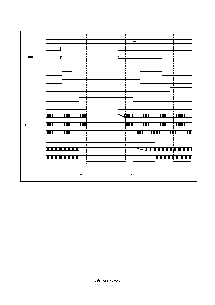
Rev. 1.0, 02/03, page 485 of 634
(1)
(2)
(3)
(3)
(3)
(3)
(4)
(4)
(5)
(6)
(7)
(7)
(7)
Power-down mode Wait for
oscillation
stabilization time
Wait for USB
oprating clock
stabilization time
USB module stop state
USB operation
resumes
(8)
(9)
(9)
(10)
(10)
(11)
(11)
(12)
(13)
(14)
(15)
(16)
(17)
(18)
(19)
(19)
(20)
(21)
(22)
(23)
(24)
(25)
USB bus state
ISR/IRQ6F
UIFR3/SPRSi
USPND
UIFR3/SPRSs
UIFR3/SOF
USB module
stop
power-down mode
System clock
Normal Suspend
Resume
Normal
SOF
USB internal
clock
UIFR3/
CK48READY
CLK48
(48MHz)
USB operating
clock (48MHz)
Figure 14.26 Timing Chart
14.8.13
USB External Circuit Example
The USB external circuit examples are used for reference only. In actual board design, carefully
check the system operation.
In addition, the USB external circuit examples cannot guarantee the correct system operation. The
user must individually take measures against external surges or ESD noise by incorporating
protective diodes or other components if necessary.

Rev. 1.0, 02/03, page 486 of 634

ADCMS34A_000120011200
Rev. 1.0, 02/03, page 487 of 634
Section 15 A/D Converter
This LSI includes a successive approximation type 10-bit A/D converter that allows up to six
analog input channels to be selected. The block diagram of the A/D converter is shown in figure
15.1.
15.1
Features
· 10-bit resolution
· Six input channels
· Conversion time: 8.4 µs per channel (at 16 MHz operation), 11.08 µs per channel (at 24 MHz
operation)
· Two operating modes
Single mode: Single-channel A/D conversion
Scan mode: Continuous A/D conversion on 1 to 4 channels
· Four data registers
Conversion results are held in a 16-bit data register for each channel
· Sample and hold function
· Three methods conversion start
Software
Timer (TPU) conversion start trigger
External trigger signal (ADTRG)
· Interrupt request
An A/D conversion end interrupt request (ADI) can be generated
· Module stop mode can be set
Rev. 1.0, 02/03, page 488 of 634
Module data bus
Bus interf
ace
Multi pre
xa
Control circuit
Internal data bus
10 bit D/A
+
A
D
C
S
R
A
D
C
R
A
D
D
R
D
A
D
D
R
C
A
D
D
R
B
A
D
D
R
A
AN0
AN1
AN2
AN3
AN14
AN15
Legend
ADCR
: A/D control register
ADCSR
: A/D control/status register
ADDRA
: A/D data register A
ADDRB
: A/D data register B
ADDRC
: A/D data register C
ADDRD
: A/D data register D
Time conversion start trigger from TPU
VCC
Vref
VSS
ADI interrupt signal
successiv
e
appro
ximation register
Sample and
hold circuit
Comparator
/2
/4
/8
/16
Figure 15.1 Block Diagram of A/D Converter

Rev. 1.0, 02/03, page 489 of 634
15.2
Input/Output Pins
Table 15.1 summarizes the input pins used by the A/D converter. The AN0 to AN3 and AN14 to
AN15 pins are analog input pins. The VCC and VSS pins are the power supply pins for the
analog block in the A/D converter. The Vref pin is the reference voltage pin for the A/D
conversion.
Table 15.1
Pin Configuration
Pin Name
Symbol
I/O
Function
Power supply pin
VCC
Input
Analog block power supply and reference voltage
(also used for digital block)
Ground pin
VSS
Input
Analog block ground and reference voltage
(also used for digital block)
Reference voltage pin
Vref
Input
Reference voltage pin for A/D conversion
Analog input pin 0
AN0
Input
Analog input pin 1
AN1
Input
Analog input pin 2
AN2
Input
Analog input pin 3
AN3
Input
Analog input pin 14
AN14
Input
Analog input pin 15
AN15
Input
Analog input pins
A/D external trigger
input pin
ADTRG
Input
External trigger input pin for starting A/D
conversion
15.3
Register Descriptions
The A/D converter has the following registers.
· A/D data register A (ADDRA)
· A/D data register B (ADDRB)
· A/D data register C (ADDRC)
· A/D data register D (ADDRD)
· A/D control/status register (ADCSR)
· A/D control register (ADCR)

Rev. 1.0, 02/03, page 490 of 634
15.3.1
A/D Data Registers A to D (ADDRA to ADDRD)
There are four 16-bit read-only ADDR registers; ADDRA to ADDRD, used to store the results of
A/D conversion. The ADDR registers, which store a conversion result for each channel, are
shown in table 15.2.
The converted 10-bit data is stored in bits 6 to 15. The lower 6 bits are always read as 0.
The data bus between the CPU and the A/D converter is 8 bits wide. The upper byte can be read
directly from the CPU, however the lower byte should be read via a temporary register. The
temporary register contents are transferred from the ADDR when the upper byte data is read.
When reading the ADDR, read the upper byte before the lower byte, or read in word unit. The
initial value of the ADDR is H'0000.
Table 15.2
Analog Input Channels and Corresponding ADDR Registers
Analog Input Channel
A/D Data Register to Be Stored the Results of A/D Conversion
AN0
ADDRA
AN1
ADDRB
AN2, AN14
ADDRC
AN3, AN15
ADDRD
15.3.2
A/D Control/Status Register (ADCSR)
ADCSR controls A/D conversion operations.
Bit
Bit Name Initial Value
R/W
Description
7
ADF
0
R/(W)* A/D End Flag
A status flag that indicates the end of A/D conversion.
[Setting conditions]
When A/D conversion ends in single mode
When A/D conversion ends on all channels specified in
scan mode
[Clearing condition]
When 0 is written after reading ADF = 1
6
ADIE
0
R/W
A/D Interrupt Enable
A/D conversion end interrupt (ADI) request enabled
when 1 is set

Rev. 1.0, 02/03, page 491 of 634
Bit
Bit Name Initial Value
R/W
Description
5
ADST
0
R/W
A/D Start
Clearing this bit to 0 stops A/D conversion, and the A/D
converter enters the wait state.
Setting this bit to 1 starts A/D conversion. In single
mode, this bit is cleared to 0 automatically when
conversion on the specified channel is complete. In scan
mode, conversion continues sequentially on the
specified channels until this bit is cleared to 0 by
software, a reset, or a transition to software standby
mode, hardware standby mode or module stop mode.
4
SCAN
0
R/W
Scan Mode
Selects single mode or scan mode as the A/D
conversion operating mode.
0: Single mode
1: Scan mode
3
2
1
0
CH3
CH2
CH1
CH0
0
0
0
0
R/W
R/W
R/W
R/W
Channel Select 3 to 0
Select analog input channels.
When SCAN = 0 When SCAN = 1
0000: AN0
0000: AN0
0001: AN1
0001: AN0 to AN1
0010: AN2
0010: AN0 to AN2
0011: AN3
0011: AN0 to AN3
01xx: Setting prohibited
01xx: Setting prohibited
10xx: Setting prohibited
1xxx: Setting prohibited
11xx: Setting prohibited
1110: AN14
1111: AN15
Legend x: Don't care
Note: * The write value should always be 0 to clear this flag.

Rev. 1.0, 02/03, page 492 of 634
15.3.3
A/D Control Register (ADCR)
The ADCR enables A/D conversion started by an external trigger signal.
Bit
Bit Name Initial Value
R/W
Description
7
6
TRGS1
TRGS0
0
0
R/W
R/W
Timer Trigger Select 0 and 1
Enables the start of A/D conversion by a trigger signal.
Only set bits TRGS0 and TRGS1 while conversion is
stopped (ADST = 0).
00: A/D conversion start by software
01: A/D conversion start by TPU
10: Setting prohibited
11: A/D conversion start by external trigger pin
(
ADTRG)
5, 4
--
All 0
R
Reserved
These bits are always read as 1 cannot be modified.
3
2
CKS1
CKS0
0
0
R/W
R/W
Clock Select 1 and 0
These bits specify the A/D conversion time. The
conversion time should be changed only when ADST =
0.
00:
Conversion time = 530 states (Max.)
01:
Conversion time = 266 states (Max.)
10:
Conversion time = 134 states (Max.)
11:
Conversion time = 68 states (Max.)
The conversion time setting should exceed the
conversion time shown in section 22.6, A/D Converter
Characteristics.
1, 0
--
All 1
R/W
Reserved
These bits are always read as 1 cannot be modified.
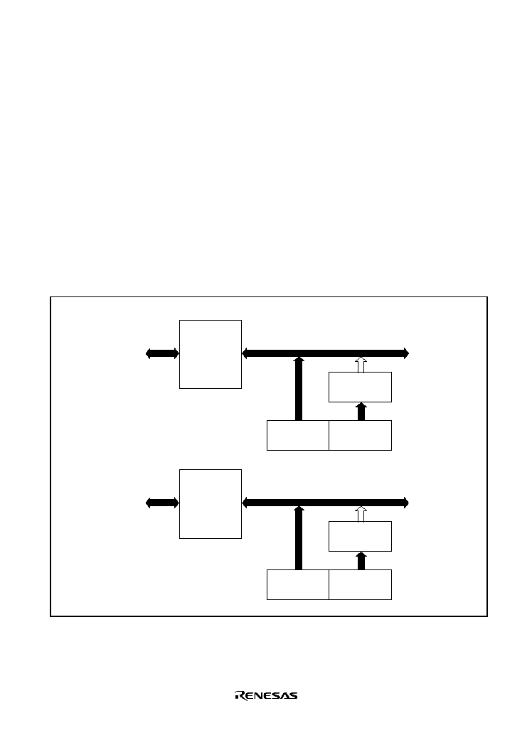
Rev. 1.0, 02/03, page 493 of 634
15.4
Interface to Bus Master
ADDRA to ADDRD are 16-bit registers. As the data bus to the bus master is 8 bits wide, the bus
master accesses to the upper byte of the registers directly while to the lower byte of the registers
via the temporary register (TEMP).
Data in ADDR is read in the following way: When the upper-byte data is read, the upper-byte data
will be transferred to the CPU and the lower-byte data will be transferred to TEMP. Then, when
the lower-byte data is read, the lower-byte data will be transferred to the CPU.
When data in ADDR is read, the data should be read from the upper byte and lower byte in the
order. When only the upper-byte data is read, the data is guaranteed. However, when only the
lower-byte data is read, the data is not guaranteed.
Figure 15.2 shows data flow when accessing to ADDR.
TEMP
(H'40)
ADDRnL
(H'40)
ADDRnH
(H'AA)
TEMP
(H'40)
ADDRnL
(H'40)
ADDRnH
(H'AA)
Read the upper byte
Read the lower byte
(n = A to D)
(n = A to D)
Module data bus
Module data bus
Bus interface
Bus interface
Bus master
(H'40)
Bus master
(H'AA)
Figure 15.2 Access to ADDR (When Reading H'AA40)
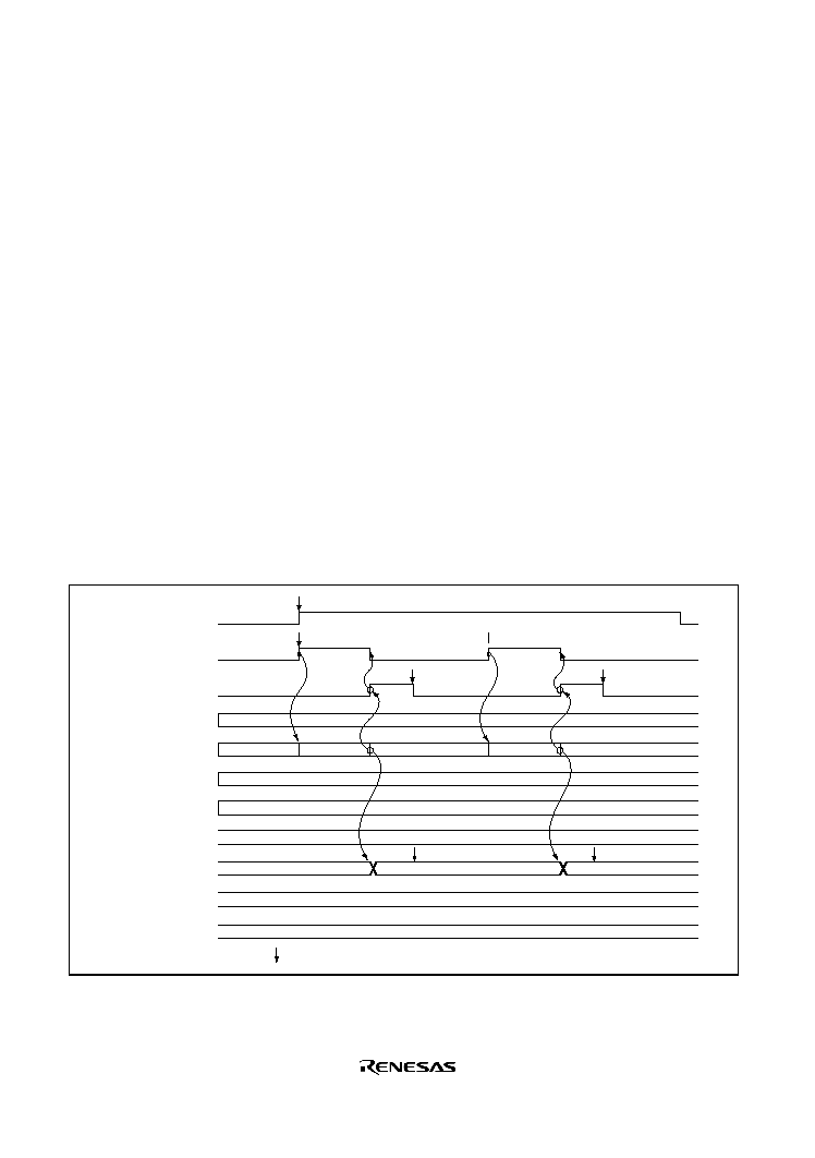
Rev. 1.0, 02/03, page 494 of 634
15.5
Operation
The A/D converter operates by successive approximation with 10-bit resolution. It has two
operating modes; single mode and scan mode. When changing the operating mode or analog input
channel, in order to prevent incorrect operation, first clear the bit ADST to 0 in ADCSR. The
ADST bit can be set at the same time as the operating mode or analog input channel is changed.
15.5.1
Single Mode
In single mode, A/D conversion is to be performed only once on the specified single channel. The
operations are as follows.
1. A/D conversion is started when the ADST bit is set to 1, according to software or external
trigger input.
2. When A/D conversion is completed, the result is transferred to the corresponding A/D data
register to the channel.
3. On completion of conversion, the ADF bit in ADCSR is set to 1. If the ADIE bit is set to 1 at
this time, an ADI interrupt request is generated.
4. The ADST bit remains set to 1 during A/D conversion. When A/D conversion ends, the ADST
bit is automatically cleared to 0 and the A/D converter enters the wait state.
ADIE
ADST
ADF
State of channel 0 (AN0)
A/D
conversion
starts
2
1
ADDRA
ADDRB
ADDRC
ADDRD
State of channel 1 (AN1)
State of channel 2 (AN2)
State of channel 3 (AN3)
Note: * Vertical arrows ( ) indicate instructions executed by software.
Set*
Set*
Clear*
Clear*
A/D conversion result 1
A/D conversion
A/D conversion result 2
Read conversion result
Read conversion result
Idle
Idle
Idle
Idle
Idle
Idle
A/D conversion
Set*
Figure 15.3 A/D Conversion Timing (Single-Chip Mode, Channel 1 Selected)
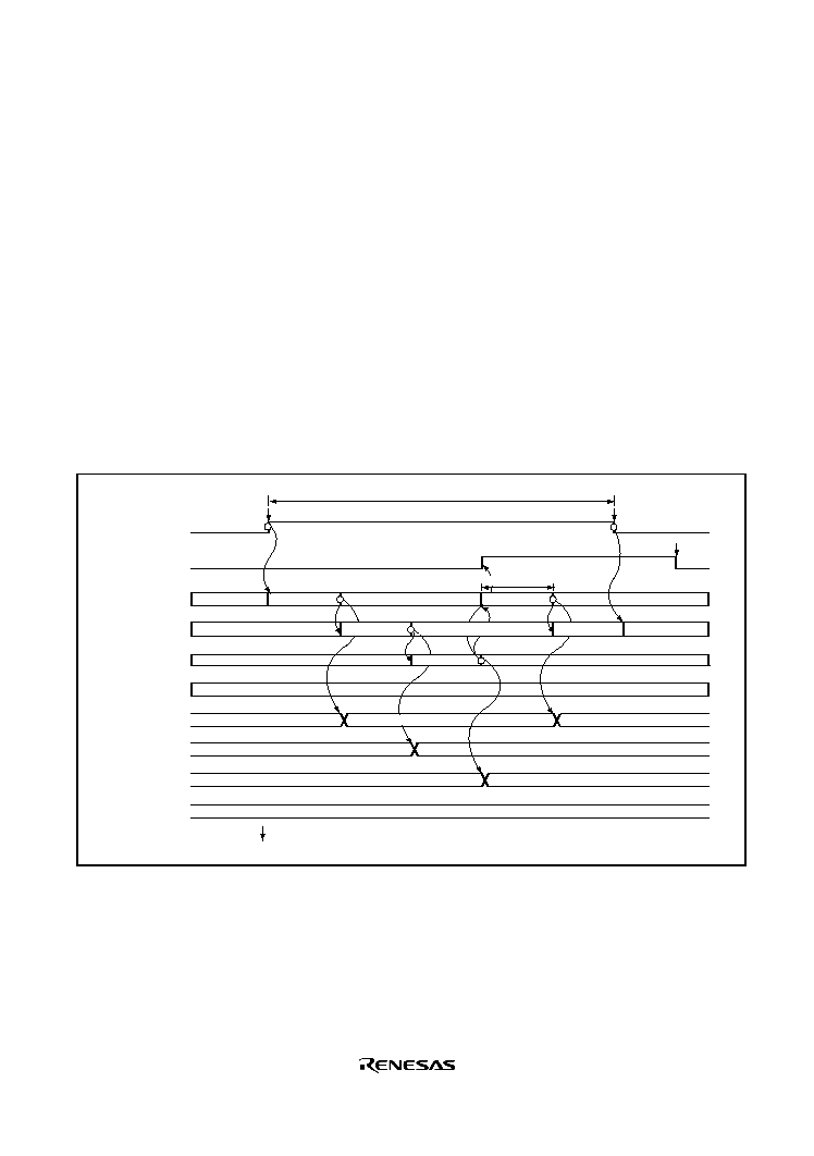
Rev. 1.0, 02/03, page 495 of 634
15.5.2
Scan Mode
In scan mode, A/D conversion is to be performed sequentially on the specified channels (four
channels maximum). The operations are as follows.
1. When the ADST bit is set to 1 by software, TPU or external trigger input, A/D conversion
starts on the first channel in the group (AN0 when CH3 and CH2 = 00, AN4 when CH3 and
CH2 = 01, or AN8 when CH3 and CH2 = 10).
2. When A/D conversion for each channel is completed, the result is sequentially transferred to
the A/D data register corresponding to each channel.
3. When conversion of all the selected channels is completed, the ADF flag is set to 1. If the
ADIE bit is set to 1 at this time, an ADI interrupt is requested after A/D conversion ends.
Conversion of the first channel in the group starts again.
4. Steps [2] to [3] are repeated as long as the ADST bit remains set to 1. When the ADST bit is
cleared to 0, A/D conversion stops.
ADST
ADF
ADDRA
ADDRB
ADDRC
ADDRD
State of
channel 0 (AN0)
State of
channel 1 (AN1)
State of
channel 2 (AN2)
State of
channel 3 (AN3)
Set*
1
Clear*
1
Idle
Notes: 1. Vertical arrows ( ) indicate instructions executed by software.
2. Data currently being converted is ignored.
Clear*
1
Idle
Idle
A/D conversion time
Continuous A/D conversion execution
A/D conversion 1
Idle
Idle
Idle
Idle
Idle
Transfer
A/D conversion 4
A/D conversion result 1
A/D conversion result 2
A/D conversion result 3
A/D conversion result 4
Idle
A/D conversion 5
*
2
A/D conversion 3
A/D conversion 2
Figure 15.4 A/D Conversion Timing (Scan Mode, Channels AN0 to AN3 Selected)
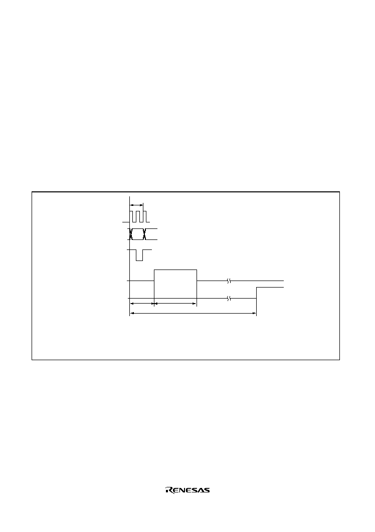
Rev. 1.0, 02/03, page 496 of 634
15.5.3
Input Sampling and A/D Conversion Time
The A/D converter has a built-in sample-and-hold circuit. The A/D converter samples the analog
input when the A/D conversion start delay time (tD) has passed after the ADST bit is set to 1, then
starts conversion. Figure 15.5 shows the A/D conversion timing. Tables 15.3 and 15.4 show the
A/D conversion time.
As indicated in figure 15.5, the A/D conversion time (tCONV) includes tD and the input sampling
time (tSPL). The length of tD varies depending on the timing of the write access to ADCSR. The
total conversion time therefore varies within the ranges indicated in table 15.4.
In scan mode, the values given in table 15.4 apply to the first conversion time. The values given
in table 15.3 apply to the second and subsequent conversions.
(1)
(2)
t
D
t
SPL
t
CONV
Address
Write signal
Input sampling
timing
ADF
Legend
(1)
: ADCSR write cycle
(2)
: ADCSR address
t
D
: A/D conversion start delay
t
SPL
: Input sampling time
t
CONV
: A/D conversion time
Figure 15.5 A/D Conversion Timing
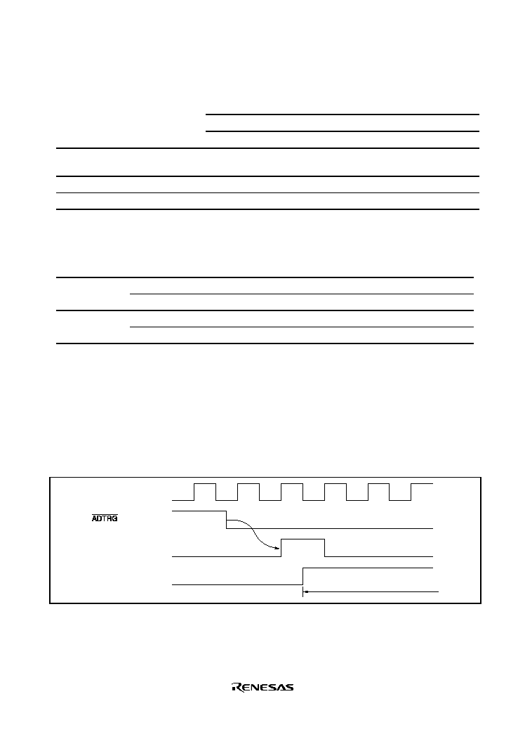
Rev. 1.0, 02/03, page 497 of 634
Table 15.3
A/D Conversion Time (Single Mode)
CKS1 = 0
CKS1 = 1
CKS0 = 0
CKS0 = 1
CKS0 = 0
CKS0 = 1
Item
Symbol
Min. Typ. Max. Min. Typ. Max. Min. Typ. Max. Min. Typ. Max.
A/D conversion start
delay
tD
18
--
33
10
--
17
6
--
9
4
--
5
Input sampling time
tSPL
--
127
--
--
63
--
--
31
--
--
15
--
A/D conversion time
tCONV
515
--
530
259
--
266
131
--
134
67
--
68
Note:
All values represent the number of states.
Table 15.4
A/D Conversion Time (Scan Mode)
CKS1
CKS0
Conversion Time (State)
0
512 (Fixed)
0
1
256 (Fixed)
0
128 (Fixed)
1
1
64 (Fixed)
15.5.4
External Trigger Input Timing
A/D conversion can be externally triggered. When the TRGS0 and TRGS1 bits are set to 11 in
ADCR, external trigger input is enabled at the
ADTRG pin. A falling edge at the ADTRG pin sets
the ADST bit to 1 in ADCSR, starting A/D conversion. Other operations, in both single and scan
modes, are the same as when the bit ADST has been set to 1 by software. Figure 15.6 shows the
timing.
Internal trigger signal
ADST
A/D conversion
Figure 15.6 External Trigger Input Timing

Rev. 1.0, 02/03, page 498 of 634
15.6
Interrupts
The A/D converter generates an A/D conversion end interrupt (ADI) at the end of A/D conversion.
Setting the ADIE bit to 1 enables ADI interrupt requests while the bit ADF in ADCSR is set to 1
after A/D conversion is completed. The DMAC can be activated by an ADI interrupt.
Table 15.5
A/D Converter Interrupt Source
Name
Interrupt Source
Interrupt Source Flag DMAC Activation
ADI
A/D conversion completed ADF
Possible
15.7
A/D Conversion Precision Definitions
This LSI's A/D conversion precision definitions are given below.
· Resolution
The number of A/D converter digital output codes
· Quantization error
The deviation inherent in the A/D converter, given by 1/2 LSB (see figure 15.7).
· Offset error
The deviation of the analog input voltage value from the ideal A/D conversion characteristic
when the digital output changes from the minimum voltage value B'0000000000 (H'000) to
B'0000000001 (H'001) (see figure 15.8).
· Full-scale error
The deviation of the analog input voltage value from the ideal A/D conversion characteristic
when the digital output changes from B'1111111110 (H'3FE) to B'1111111111 (H'3FF) (see
figure 15.8).
· Nonlinearity error
The error with respect to the ideal A/D conversion characteristic between zero voltage and full-
scale voltage. Does not include offset error, full-scale error, or quantization error (see figure
15.8).
· Absolute precision
The deviation between the digital value and the analog input value. Includes offset error, full-
scale error, quantization error, and nonlinearity error.
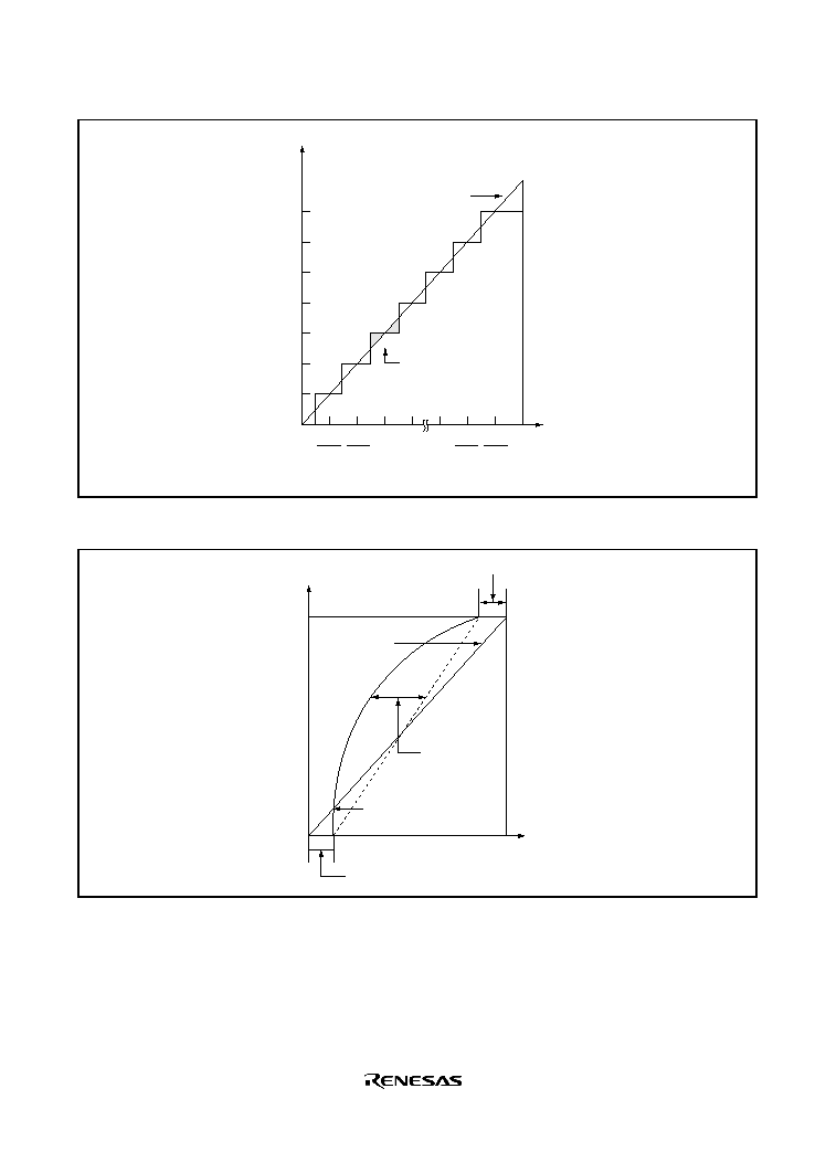
Rev. 1.0, 02/03, page 499 of 634
111
110
101
100
011
010
001
000
1
1024
2
1024
1022
1024
1023
1024
FS
Quantization error
Digital output
Ideal A/D conversion
characteristic
Analog
input voltage
Figure 15.7 A/D Conversion Precision Definitions (1)
FS
Digital output
Ideal A/D conversion
characteristic
Nonlinearity
error
Analog
input voltage
Offset error
Actual A/D conversion
characteristic
Full-scale error
Figure 15.8 A/D Conversion Precision Definitions (2)
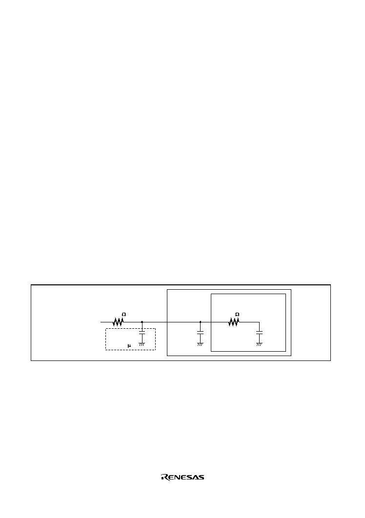
Rev. 1.0, 02/03, page 500 of 634
15.8
Usage Notes
15.8.1
Permissible Signal Source Impedance
This LSI's analog input is designed such that conversion precision is guaranteed for an input signal
for which the signal source impedance is 5 k
or less. This specification is provided to enable the
A/D converter's sample-and-hold circuit input capacitance to be charged within the sampling time;
if the sensor output impedance exceeds 5 k
, charging may be insufficient and it may not be
possible to guarantee A/D conversion precision. However, for A/D conversion in single mode with
a large capacitance provided externally, the input load will essentially comprise only the internal
input resistance of 10 k
, and the signal source impedance is ignored. However, as a low-pass
filter effect is obtained in this case, it may not be possible to follow an analog signal with a large
differential coefficient (e.g., 5 mV/
s or greater) (see figure 15.9). When converting a high-speed
analog signal, a low-impedance buffer should be inserted.
15.8.2
Influences on Absolute Precision
Adding capacitance results in coupling with GND, and therefore noise in GND may adversely
affect absolute precision. Be sure to make the connection to an electrically stable GND such as
AVSS.
Care is also required to insure that filter circuits do not communicate with digital signals on the
mounting board (i.e., acting as antennas).
20 pF
10 k
C
in
=
15 pF
Sensor output
impedance
to 5 k
This LSI
Low-pass
filter
C to 0.1 F
Sensor input
A/D converter
equivalent circuit
Figure 15.9 Example of Analog Input Circuit
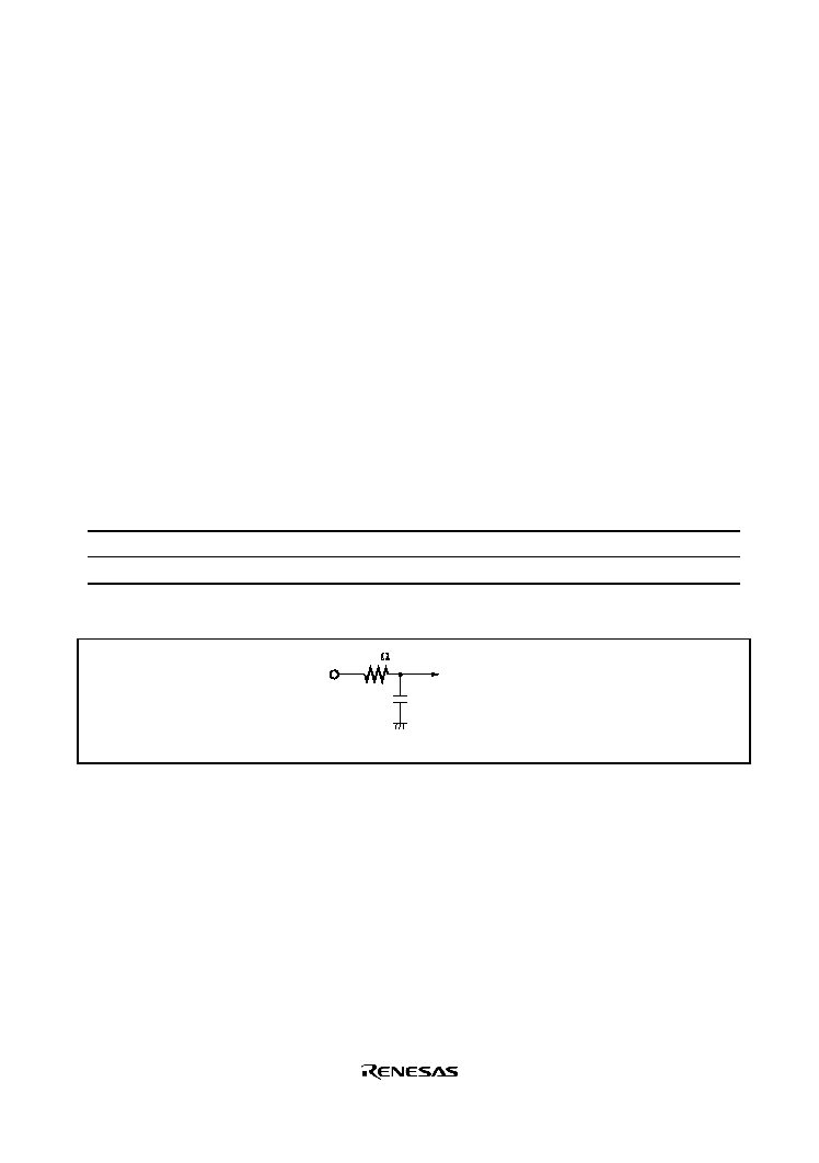
Rev. 1.0, 02/03, page 501 of 634
15.8.3
Range of Analog Power Supply and Other Pin Settings
If the conditions below are not met, the reliability of the device may be adversely affected.
· Analog input voltage range
The voltage applied to analog input pin ANn during A/D conversion should be in the range
VSS
ANn Vref.
· Vref input range
The analog reference voltage input at the Vref pin set is the range Vref
Vcc.
15.8.4
Notes on Board Design
Careful consideration is required in board design for noise countermeasures and in order to
prevent damage due to abnormal voltage, such as an excessive surge at the analog input pins (AN0
to AN3 or AN14 to AN15) and analog reference voltage pin (Vref).
Table 15.6
Analog Pin Specifications
Item
Min.
Max.
Unit
Analog input capacitance
--
20
pF
Permissible signal source impedance
--
5*
k
Note: * Vcc = 2.7 to 3.6 V
20 pF
ANn
Note: Values are reference values.
10 k
To A/D converter
Figure 15.10 Analog Input Pin Equivalent Circuit

Rev. 1.0, 02/03, page 502 of 634

Rev. 1.0, 02/03, page 503 of 634
Section 16 RAM
The H8S/2218 Series and H8S/2212 Series have 12 kbytes of on-chip high-speed static RAM. The
H8S/2217 Series and H8S/2211 Series have 8 kbytes of on-chip high-speed static RAM. The
H8S/2210 Series has 4 kbytes of on-chip high-speed static RAM. The RAM is connected to the
CPU by a 16-bit data bus, enabling one-state access by the CPU to both byte data and word data.
This makes it possible to perform fast word data transfer.
The on-chip RAM can be enabled or disabled by means of the RAM enable bit (RAME) in the
system control register (SYSCR). For details on SYSCR, refer to section 3.2.2, System Control
Register (SYSCR).
Product Class
ROM Type
RAM Size
RAM Address
HD64F2218
HD64F2218U
Flash memory Version
12 kbytes
H'FFC000 to H'FFEFBF
H'FFFFC0 to H'FFFFFF
H8S/2218
Series
HD6432217
Masked ROM Version
8 kbytes
H'FFD000 to H'FFEFBF
H'FFFFC0 to H'FFFFFF
HDF64F2212
HDF64F2212U
Flash memory Version
12 kbytes
H'FFC000 to H'FFEFBF
H'FFFFC0 to H'FFFFFF
HD6432211
Masked ROM Version
8 kbytes
H'FFD000 to H'FFEFBF
H'FFFFC0 to H'FFFFFF
H8S/2212
Series
HD6432210
4 kbytes
H'FFE000 to H'FFEFBF
H'FFFFC0 to H'FFFFFF

Rev. 1.0, 02/03, page 504 of 634

Rev. 1.0, 02/03, page 505 of 634
Section 17 Flash Memory (F-ZTAT Version)
The features of the on-chip flash memory are summarized below. The block diagram of the flash
memory is shown in figure 17.1.
17.1
Features
· Size:
Product Class
ROM Size
ROM Address
H8S/2218 Series
HD64F2218, HD64F2218U
H8S/2212 Series
HD64F2212, HD64F2212U
128 kbytes
H'000000 to H'01FFFF
(mode 6, 7)
· Programming/erase methods
The flash memory is programmed 128 bytes at a time. Erase is performed in single-block
units. The flash memory is configured as follows: 32 kbytes
× 2 blocks, 28 kbytes × 1
block, 16 kbytes
× 8 blocks, 8 kbytes × 1 block, and 1 kbyte × 4 blocks. To erase the entire
flash memory, each block must be erased in turn.
· Reprogramming capability
flash memory can be reprogrammed up to 100 times.
· Two flash memory operating modes
Boot mode
SCI boot mode: HD64F2218 and HD64F2212
USB boot mode: HD64F2218U and HD64F2212U
User program mode
On-board programming/erasing can be done in boot mode in which the boot program built
into the chip is started for erase or programming of the entire flash memory. In normal
user program mode, individual blocks can be erased or programmed.
· Automatic bit rate adjustment
With data transfer in SCI boot mode, this LSI's bit rate can be automatically adjusted to
match the transfer bit rate of the host.
· Programming/erasing protection
Sets software protection against flash memory programming/erasing.
· Programmer mode
Flash memory can be programmed/erased in programmer mode, using a PROM
programmer, as well as in on-board programming mode.
· Flash memory emulation in RAM
Flash memory programming can be emulated in real time by overlapping a part of RAM
onto flash memory.
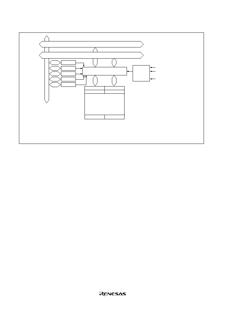
Rev. 1.0, 02/03, page 506 of 634
Module bus
Bus interface/controller
Flash memory
(128 kbytes)
Operating
mode
FLMCR2
Internal address bus (upper 8 bits)
Internal data bus (lower 8 bits)
FWE pin
Mode pins
(MD2 to MD0)
PF3, PF0, P16, P14
EBR1
EBR2
RAMER
FLMCR1
: Flash memory control register 1
: Flash memory control register 2
: Erase block register 1
: Erase block register 2
: RAM emulation register
Legend
FLMCR1
FLMCR2
EBR1
EBR2
RAMER
H'000000
H'000002
H'000001
H'000003
H'01FFFE
H'01FFFF
Figure 17.1 Block Diagram of Flash Memory
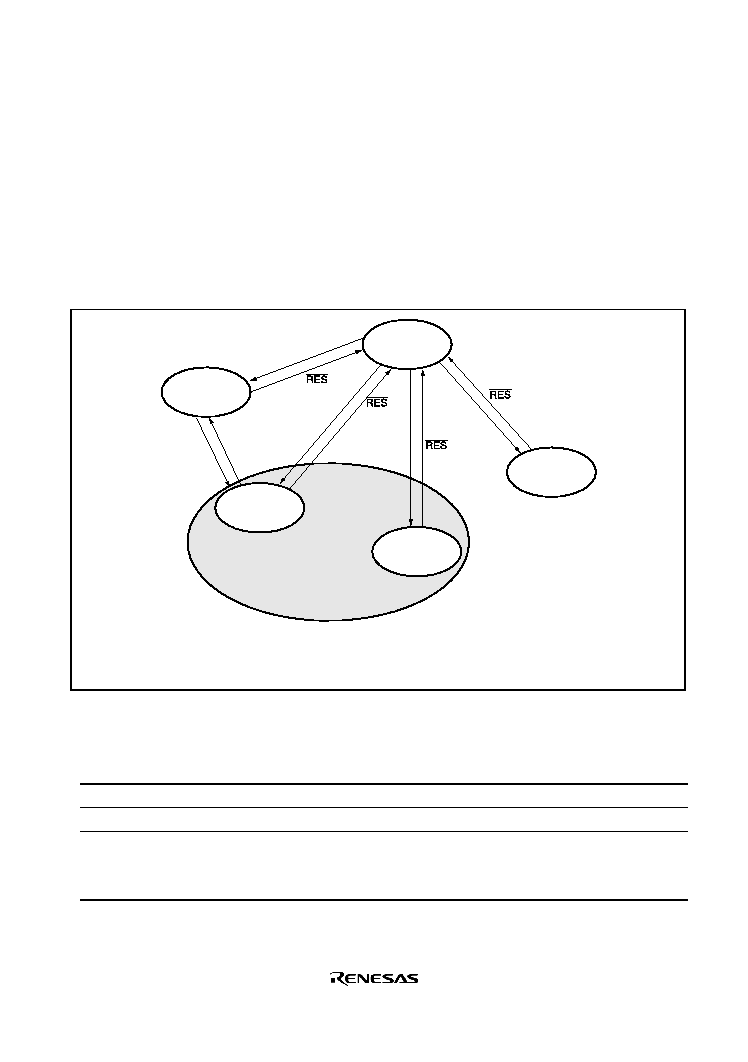
Rev. 1.0, 02/03, page 507 of 634
17.2
Mode Transitions
When the mode pins and the FWE pin are set in the reset state and a reset-start is executed, this
LSI enters an operating mode as shown in Figure 17.2. In user mode, flash memory can be read
but not programmed or erased. The boot and user program modes are provided as modes to write
and erase the flash memory.
The differences between boot mode and user program mode are shown in Table 17.1. Boot mode
and user program mode operations are shown in figures 17.3 and 17.4, respectively.
SCI, USB
boot mode
On-board programming mode
User
program mode
User mode
(on-chip ROM
enabled)
Reset state
Programmer
mode
= 0
FWE = 1
FWE = 0
*
1
*
1
*
2
Notes: Only make a transition between user mode and user program mode when the CPU is
not accessing the flash memory.
1. RAM emulation possible
2. MD2 to MD0 = 000, PF3, PF0, P16, P14 = 1100
= 0
MD2 to 0 = 01x,
FWE = 1
= 0
= 0
MD2 to 0 = 11x,
FWE = 0
MD2 to 0 = 11x,
FWE = 1
Figure 17.2 Flash Memory State Transitions
Table 17.1
Differences between Boot Mode and User Program Mode
SCI, USB Boot Mode
User Program Mode
User Mode
Total erase
Yes
Yes
No
Block erase
No
Yes
No
Programming control
program*
Program/program-verify Erase/erase-verify
Program/program-verify
Emulation
--
Note: * To be provided by the user, in accordance with the recommended algorithm.
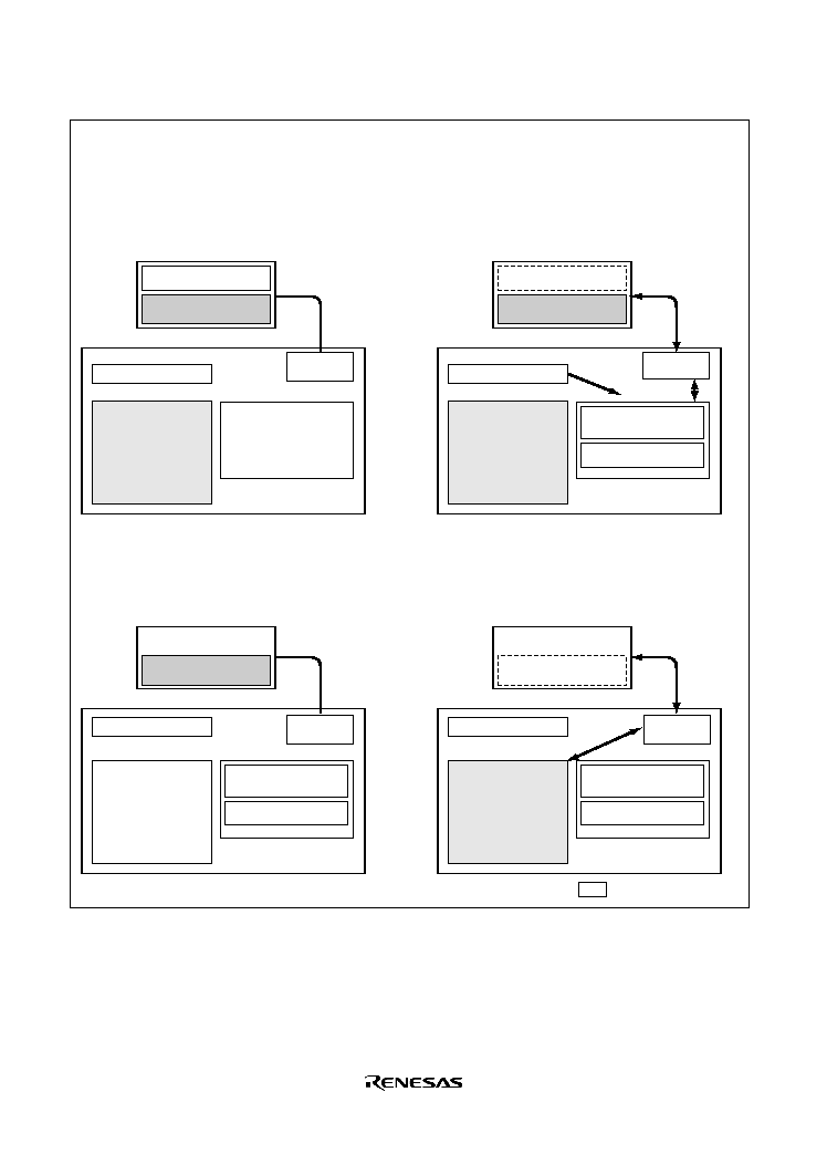
Rev. 1.0, 02/03, page 508 of 634
Flash memory
This LSI
RAM
Host
Programming control
program
Application program
(old version)
;;
New application
program
Flash memory
This LSI
RAM
Host
Application program
(old version)
Boot program area
New application
program
Flash memory
This LSI
RAM
Host
Flash memory
preprogramming
erase
Boot program
New application
program
Flash memory
This LSI
Program execution state
RAM
Host
New application
program
Boot program
Programming control
program
;;
;;;
;
;
;
1. Initial state
The old program version or data remains written
in the flash memory. The user should prepare the
programming control program and new
application program beforehand in the host.
2. Programming control program transfer
When boot mode is entered, the boot program in
this LSI (originally incorporated in the chip) is
started and the programming control program in
the host is transferred to RAM via SCI or USB
communication. The boot program required for
flash memory erasing is automatically transferred
to the RAM boot program area.
3. Flash memory initialization
The erase program in the boot program area (in
RAM) is executed, and the flash memory is
initialized (to H'FF). In boot mode, total flash
memory erasure is performed, without regard to
blocks.
4. Writing new application program
The programming control program transferred
from the host to RAM is executed, and the new
application program in the host is written into the
flash memory.
Programming control
program
Boot program
Boot program
Boot program area
Boot program area
Programming control
program
SCI
or USB
SCI
or USB
SCI
or USB
SCI
or USB
Figure 17.3 Boot Mode (Sample)
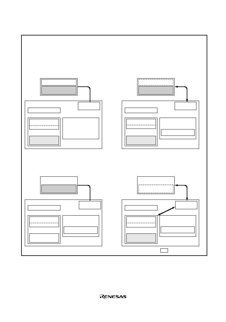
Rev. 1.0, 02/03, page 509 of 634
Flash memory
This LSI
RAM
Host
Programming/
erase control program
Boot program
New application
program
Flash memory
This LSI
RAM
Host
New application
program
Flash memory
This LSI
RAM
Host
Flash memory
erase
Boot program
New application
program
Flash memory
This LSI
Program execution state
RAM
Host
Boot program
;
;
Boot program
FWE assessment
program
Application program
(old version)
;;
;;
New application
program
;;
1. Initial state
The FWE assessment program that confirms that
user program mode has been entered, and the
program that will transfer the programming/erase
control program from flash memory to on-chip
RAM should be written into the flash memory by
the user beforehand. The programming/erase
control program should be prepared in the host
or in the flash memory.
2. Programming/erase control program transfer
When user program mode is entered, user
software confirms this fact, executes transfer
program in the flash memory, and transfers the
programming/erase control program to RAM.
3. Flash memory initialization
The programming/erase program in RAM is
executed, and the flash memory is initialized (to
H'FF). Erasing can be performed in block units,
but not in byte units.
4. Writing new application program
Next, the new application program in the host is
written into the erased flash memory blocks. Do
not write to unerased blocks.
Programming/
erase control program
Programming/
erase control program
Programming/
erase control program
Transfer program
Application program
(old version)
Transfer program
FWE assessment
program
FWE assessment
program
Transfer program
FWE assessment
program
Transfer program
SCI
or USB
SCI
or USB
SCI
or USB
SCI
or USB
Figure 17.4 User Program Mode (Sample)
Rev. 1.0, 02/03, page 510 of 634
17.3
Block Configuration
Figure 17.5 shows the block configuration of 128-kbyte flash memory. The thick lines indicate
erasing units, the narrow lines indicate programming units, and the values are addresses. The
flash memory is divided into one kbyte (four blocks), 28 kbytes (one block), 16 kbytes (one
block), eight kbytes (two blocks), and 32 kbytes (two blocks). Erasing is performed in these
divided units. Programming is performed in 128-byte units starting from an address whose lower
eight bits are H'00 or H'80.
EB0
EB1
EB2
EB3
EB4
EB7
EB8
EB9
EB6
EB5
Erase unit
1 kbyte
Programming unit: 128 bytes
Erase unit
1 kbyte
Erase unit
1 kbyte
Erase unit
1 kbyte
Erase unit
28 kbytes
Erase unit
16 kbytes
Erase unit
8 kbytes
Erase unit
8 kbytes
Erase unit
32 kbytes
Erase unit
32 kbytes
Programming unit: 128 bytes
Programming unit: 128 bytes
Programming unit: 128 bytes
Programming unit: 128 bytes
Programming unit: 128 bytes
Programming unit: 128 bytes
Programming unit: 128 bytes
Programming unit: 128 bytes
Programming unit: 128 bytes
H'000000
H'000001
H'000002
H'00007F
H'0003FF
H'00047F
H'00087F
H'000C7F
H'00107F
H'007FFF
H'00807F
H'00BFFF
H'0007FF
H'000BFF
H'000FFF
H'01FFFF
H'00C07F
H'00DFFF
H'00E07F
H'00FFFF
H'01007F
H'017FFF
H'01807F
H'000400
H'000401
H'000402
H'000800
H'000801
H'000802
H'000C00
H'000C01
H'000C02
H'001000
H'001001
H'001002
H'008000
H'008001
H'008002
H'00C000
H'00C001
H'00C002
H'00E000
H'00E001
H'00E002
H'010000
H'010001
H'010002
H'018000
H'018001
H'018002
H'000380
H'000381
H'000382
H'000780
H'000781
H'000782
H'000B80
H'000B81
H'000B82
H'000F80
H'000F81
H'000F82
H'007F80
H'007F81
H'007F82
H'017F80
H'017F81
H'017F82
H'01FF80
H'01FF81
H'01FF82
H'00BF80
H'00BF81
H'00BF82
H'00DF80
H'00DF81
H'00DF82
H'00FF80
H'00FF81
H'00FF82
Figure 17.5 Flash Memory Block Configuration

Rev. 1.0, 02/03, page 511 of 634
17.4
Input/Output Pins
The flash memory is controlled by means of the pins shown in table 17.2.
Table 17.2
Pin Configuration
Pin Name
I/O
Function
RES
Input
Reset
FWE
Input
Flash program/erase protection by hardware
MD2, MD1, MD0
Input
Sets this LSI's operating mode
PF3, PF0, P16,
P14
Input
Sets this LSI's operating mode in programmer mode
TxD2
Output
Serial transmit data output
RxD2
Input
Serial receive data input
HD64F2218,
HD64F2212
USD
+, USD-
Input/output
USB data input/output
VBUS
Input
USB cable connect/cut detect
UBPM
Input
USB bus power mode/self power mode select
USPND
Output
USB suspend output
P36
Output
D
+ pull-up control
HD64F2218U,
HD64F2212U
17.5
Register Descriptions
The flash memory has the following registers. For details on register addresses and register states
during each processing, refer to section 21, List of Registers.
· Flash memory control register 1 (FLMCR1)
· Flash memory control register 2 (FLMCR2)
· Erase block register 1 (EBR1)
· Erase block register 2 (EBR2)
· RAM emulation register (RAMER)
· Serial control register X ( SCRX)

Rev. 1.0, 02/03, page 512 of 634
17.5.1
Flash Memory Control Register 1 (FLMCR1)
FLMCR1 is a register that makes the flash memory transit to program mode, program-verify
mode, erase mode, or erase-verify mode. For details on register setting, refer to section 17.8,
Flash Memory Programming/Erasing.
Bit
Bit Name Initial Value
R/W
Description
7
FWE
--*
R
Reflects the input level at the FWE pin. It is set to 1
when a low level is input to the FWE pin, and cleared to
0 when a high level is input.
6
SWE1
0
R/W
Software Write Enable
When this bit is set to 1, flash memory
programming/erasing is enabled. When this bit is
cleared to 0, other FLMCR1 register bits and all EBR1,
EBR2 bits cannot be set.
[Setting condition]
When FWE = 1
5
ESU1
0
R/W
Erase Setup
When this bit is set to 1, the flash memory transits to the
erase setup state. When it is cleared to 0, the erase
setup state is cancelled. Set this bit to 1 before setting
the E1 bit in FLMCR1.
[Setting condition]
When FWE = 1 and SWE1 = 1
4
PSU1
0
R/W
Program Setup
When this bit is set to 1, the flash memory transits to the
program setup state. When it is cleared to 0, the
program setup state is cancelled. Set this bit to 1 before
setting the P1 bit in FLMCR1.
[Setting condition]
When FWE = 1 and SWE1 = 1
3
EV1
0
R/W
Erase-Verify
When this bit is set to 1, the flash memory transits to
erase-verify mode. When it is cleared to 0, erase-verify
mode is cancelled.
[Setting condition]
When FWE = 1 and SWE1 = 1

Rev. 1.0, 02/03, page 513 of 634
Bit
Bit Name Initial Value
R/W
Description
2
PV1
0
R/W
Program-Verify
When this bit is set to 1, the flash memory transits to
program-verify mode. When it is cleared to 0, program-
verify mode is cancelled.
[Setting condition]
When FWE = 1 and SWE1 = 1
1
E1
0
R/W
Erase
When this bit is set to 1 while the SWE1 and ESU1 bits
are 1, the flash memory transits to erase mode. When it
is cleared to 0, erase mode is cancelled.
[Setting condition]
When FWE = 1, SWE1 = 1, and ESU1 = 1
0
P1
0
R/W
Program
When this bit is set to 1 while the SWE1 and PSU1 bits
are 1, the flash memory transits to program mode.
When it is cleared to 0, program mode is cancelled.
[Setting condition]
When FWE = 1, SWE1 = 1, and PSU1 = 1
Note: * Set according to the FWE pin state.
17.5.2
Flash Memory Control Register 2 (FLMCR2)
FLMCR2 is a register that displays the state of flash memory programming/erasing. FLMCR2 is a
read-only register, and should not be written to.
Bit
Bit Name Initial Value
R/W
Description
7
FLER
0
R
Indicates that an error has occurred during an operation
on flash memory (programming or erasing). When
FLER is set to 1, flash memory goes to the error-
protection state.
See 17.9.3 Error Protection, for details.
6 to 0 --
0
--
Reserved
These bits are always read as 0.

Rev. 1.0, 02/03, page 514 of 634
17.5.3
Erase Block Register 1 (EBR1)
EBR1 specifies the flash memory erase area block. EBR1 is initialized to H'00 when the SWE1
bit in FLMCR is 0. Do not set more than one bit at a time, as this will cause all the bits in EBR1
and EBR2 to be automatically cleared to 0.
Bit
Bit
Name
Initial
Value
R/W
Description
7
EB7
0
R/W
When this bit is set to 1, 8 kbytes of EB7 (H'00E000 to H'00FFFF)
are to be erased.
6
EB6
0
R/W
When this bit is set to 1, 8 kbytes of EB6 (H'00C000 to H'00DFFF)
are to be erased.
5
EB5
0
R/W
When this bit is set to 1, 16 kbytes of EB5 (H'008000 to H'00BFFF)
are to be erased.
4
EB4
0
R/W
When this bit is set to 1, 28 kbytes of EB4 (H'001000 to H'007FFF)
are to be erased.
3
EB3
0
R/W
When this bit is set to 1, 1 kbyte of EB3 (H'000C00 to H'000FFF) is
to be erased.
2
EB2
0
R/W
When this bit is set to 1, 1 kbyte of EB2 (H'000800 to H'000BFF) is
to be erased.
1
EB1
0
R/W
When this bit is set to 1, 1 kbyte of EB1 (H'000400 to H'0007FF) is
to be erased.
0
EB0
0
R/W
When this bit is set to 4, 1 kbyte of EB0 (H'000000 to H'0003FF) is
to be erased.
17.5.4
Erase Block Register 2 (EBR2)
EBR2 specifies the flash memory erase area block. EBR2 is initialized to H'00 when the SWE1
bit in FLMCR1 is 0. Do not set more than one bit at a time, as this will cause all the bits in EBR1
and EBR2 to be automatically cleared to 0.
Bit
Bit
Name
Initial
Value
R/W
Description
7 to 2 --
0
R/W
Reserved
The write value should always be 0.
1
EB9
0
R/W
When this bit is set to 1, 32 kbytes of EB9 (H'018000 to H'01FFFF)
are to be erased.
0
EB8
0
R/W
When this bit is set to 1, 32 kbytes of EB8 (H'010000 to H'017FFF)
are to be erased.

Rev. 1.0, 02/03, page 515 of 634
17.5.5
RAM Emulation Register (RAMER)
RAMER specifies the area of flash memory to be overlapped with part of RAM when emulating
real-time flash memory programming. RAMER settings should be made in user mode or user
program mode. To ensure correct operation of the emulation function, the ROM for which RAM
emulation is performed should not be accessed immediately after this register has been modified.
Normal execution of an access immediately after register modification is not guaranteed. For
details, refer to section 17.7, Flash Memory Emulation in RAM.
Bit
Bit Name Initial Value
R/W
Description
7 to 5 --
0
--
Reserved
These bits always read as 0.
4
--
0
R/W
Reserved
The write value should always be 0.
3
RAMS
0
R/W
RAM Select
Specifies selection or non-selection of flash memory
emulation in RAM. When RAMS = 1, the flash memory
is overlapped with part of RAM, and all flash memory
block are program/erase-protected.
2
1
0
RAM2
RAM1
RAM0
0
0
0
R/W
R/W
R/W
Flash Memory Area Selection
When the RAMS bit is set to 1, selects one of the
following flash memory areas to overlap the RAM area.
The areas correspond with 1-kbyte erase blocks.
000: H'000000 to H'0003FF (EB0)
001: H'000400 to H'0007FF (EB1)
010: H'000800 to H'000BFF (EB2)
011: H'000C00 to H'000FFF (EB3)
100: Setting prohibited
101: Setting prohibited
110: Setting prohibited
111: Setting prohibited

Rev. 1.0, 02/03, page 516 of 634
17.5.6
Flash Memory Power Control Register (FLPWCR)
FLPWCR enables/disables transition to power-down modes for the flash memory when this LSI
enters sub-active mode.
Bit
Bit Name Initial Value
R/W
Description
7
PDWND
0
R/W
Power Down Disable
Enables/disables transition to power-down modes for the
flash memory when this LSI enters sub-active mode.
0: Transition to power-down modes for the flash memory
enabled.
1: Transition to power-down modes for the flash memory
disabled.
6 to 0 --
All 0
R
Reserved
These bits always read as 0
17.5.7
Serial Control Register X (SCRX)
SCRX performs register access control.
Bit
Bit Name Initial Value
R/W
Description
7 to 4 --
0
R/W
Reserved
The write value should always be 0.
3
FLSHE
0
R/W
Flash Memory Control Register Enable:
Controls CPU access to the flash memory control
registers (FLMCR1, FLMCR2, EBR1, and EBR2).
Setting the FLSHE bit to 1 enables read/write access to
the flash memory control registers. If FLSHE is cleared
to 0, the flash memory control registers are deselected.
In this case, the flash memory control register contents
are retained.
0: Flash control registers deselected in area H'FFFFA8
to H'FFFFAC
1: Flash control registers selected in area H'FFFFA8 to
H'FFFFAC
2 to 0 --
0
R/W
Reserved
The write value should always be 0.

Rev. 1.0, 02/03, page 517 of 634
17.6
On-Board Programming Modes
When pins are set to on-board programming mode and a reset-start is executed, a transition is
made to the on-board programming state in which program/erase/verify operations can be
performed on the on-chip flash memory. There are two on-board programming modes: boot mode
and user program mode. The pin settings for transition to each of these modes are shown in table
17.3. For a diagram of the transitions to the various flash memory modes, see figure 17.2.
Table 17.3
Setting On-Board Programming Modes
Mode
FWE
MD2
MD1
MD0
Advanced: single-chip mode
(24 MHz system clock in USB
boot mode or SCI boot mode)
1
0
1
0
SCI boot mode
(HD64F2212, HD64F2218)
USB boot mode
(HD64F2212U, HD64F2218U)
Advanced: single-chip mode
(16 MHz system clock in USB
boot mode or SCI boot mode)
1
0
1
1
Advanced: on-chip ROM
extended mode
(MCU operating mode 6)
1
1
1
0
User program mode
Advanced: Single-chip mode
(MCU operating mode 7)
1
1
1
1
17.6.1
SCI Boot Mode (HD64F2218 and HD64F2212)
When a reset-start is executed after the LSI's pins have been set to boot mode, the boot program
built into the LSI is started and the programming control program prepared in the host is serially
transmitted to the LSI via the SCI. In the LSI, the programming control program received via the
SCI is written into the programming control program area in on-chip RAM. After the transfer is
completed, control branches to the start address of the programming control program area and the
programming control program execution state is entered (flash memory programming is
performed). The system configuration in boot mode is shown in figure 17.6.
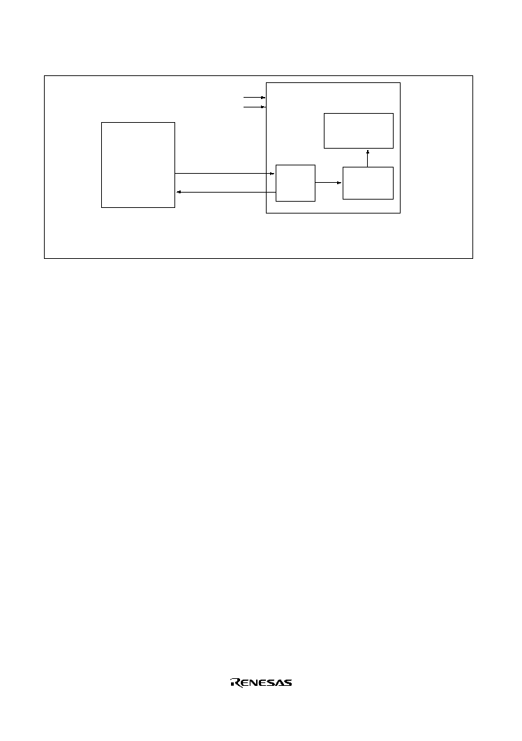
Rev. 1.0, 02/03, page 518 of 634
RxD2
TxD2
SCI_2
This LSI
Flash memory
Write data reception
1
01*
Note: * Mode pin and FWE pin input must satisfy the mode programming setup time (t
MDS
= 200ns)
with respect to the reset release timing.
Legend:
x : Don't care
FWE
MD2 to MD0*
Verify data transmission
Host
On-chip RAM
Figure 17.6 System Configuration in Boot Mode
Table 17.4 shows the boot mode operations between reset end and branching to the programming
control program.
1. When boot mode is used, the flash memory programming control program must be prepared in
the host beforehand. Prepare a programming control program in accordance with the
description in section 17.8, Flash Memory Programming/Erasing. In boot mode, if any data has
been programmed into the flash memory (if all data is not 1), all flash memory blocks are
erased. Boot mode is for use in enforced exit when user program mode is unavailable, such as
the first time on-board programming is performed, or if the program activated in user program
mode is accidentally erased.
2. The SCI_2 should be set to asynchronous mode, and the transfer format as follows: 8-bit data,
1 stop bit, and no parity.
3. When the boot program is initiated, the chip measures the low-level period of asynchronous
SCI communication data (H'00) transmitted continuously from the host. The chip then
calculates the bit rate of transmission from the host, and adjusts the SCI_2 bit rate to match
that of the host. The reset should end with the RxD pin high. The RxD and TxD pins should
be pulled up on the board if necessary. After the reset ends, it takes approximately 100 states
before the chip is ready to measure the low-level period.
4. After matching the bit rates, the chip transmits one H'00 byte to the host to indicate the end of
bit rate adjustment. The host should confirm that this adjustment end indication (H'00) has
been received normally, and transmit one H'55 byte to the chip. If reception could not be
performed normally, initiate boot mode again by a reset. Depending on the host's transfer bit
rate and system clock frequency of this LSI, there will be a discrepancy between the bit rates
of the host and the chip. To operate the SCI properly, set the host's transfer bit rate and system
clock frequency of this LSI within the ranges listed in table 17.5.

Rev. 1.0, 02/03, page 519 of 634
5. In boot mode, a part of the on-chip RAM area (four kbytes) is used by the boot program.
Addresses H'FFE000 to H'FFEFBF is the area to which the programming control program is
transferred from the host. The boot program area cannot be used until the execution state in
boot mode switches to the programming control program.
6. Before branching to the programming control program, the chip terminates transfer operations
by the SCI_2 (by clearing the RE and TE bits in SCR to 0), but the adjusted bit rate value
remains set in BRR. Therefore, the programming control program can still use it for transfer
of write data or verify data with the host. The TxD pin is high. The contents of the CPU
general registers are undefined immediately after branching to the programming control
program. These registers must be initialized at the beginning of the programming control
program, since the stack pointer (SP), in particular, is used implicitly in subroutine calls, etc.
7. Boot mode can be cleared by a reset. End the reset* after driving the reset pin low, waiting at
least 20 states, and then setting the FWE pin and the mode (MD) pins. Boot mode is also
cleared when a WDT overflow occurs.
8. Do not change the MD pin input levels in boot mode. If the mode pin input levels are changed
(for example, from low to high) during a reset, the state of ports with multiplexed address
functions and bus control output pins (
AS, RD, WR) will change according to the change in
the microcomputer's operating mode . Therefore, care must be taken to make pin settings to
prevent these pins from becoming output signal pins during a reset, or to prevent collision
with signals outside the microcomputer.
9. All interrupts are disabled during programming or erasing of the flash memory.
Note:* Mode pin and FWE pin input must satisfy the mode programming setup time (t
MDS
= 200
ns) with respect to the reset release timing.

Rev. 1.0, 02/03, page 520 of 634
Table 17.4
Boot Mode Operation
Item
Host Operation
LSI Operation
Branches to boot program at reset-
start
Continuously transmits data H'00
at specified bit rate
Measures low-level period of
receive data H'00
Calculates bit rate and sets it in
BRR of SCI_2
Bit rate adjustment
Transmits data H'55 when data
H'00 is received error-free
Transmits data H'00 to host as
adjustment end indication
Transmits data H'AA to host when
data H'55 is received
Transmits number of
bytes (N) of programming
control program
Transmits number of bytes (N) of
programming control program to
be transferred as 2-byte data (low-
order byte following high-order
byte)
Echobacks the 2-byte data received
as verification data
Transmits 1-byte of
programming control
program (repeated for N
times)
Transmits 1-byte of programming
control program
Echobacks received data to host
and also transfers it to RAM
Flash memory erase
Checks flash memory data, erases
all flash memory blocks in case of
written data existing, and transmits
data H'AA to host. (If erase could
not be done, transmits data H'FF to
host and aborts operation)
Programming control
program execution
Branches to programming control
program transferred to on-chip RAM
and starts execution
Table 17.5
System Clock Frequencies for which Automatic Adjustment of LSI Bit Rate is
Possible
Host Bit Rate
System Clock Frequency Range of LSI
19,200 bps
8 to 24 MHz
9,600 bps
6 to 24 MHz
4,800 bps
6 to 24 MHz

Rev. 1.0, 02/03, page 521 of 634
17.6.2
USB Boot Mode (HD64F2218U and HD64F2212U)
· Features
Selection of bus-powered mode or self-powered mode
Supports the USB operating clock generation by 16 MHz system clock with PLL3
multiplication (FWE = 1, MD2 to MD0 = 011) or 24 MHz system clock with PLL2
multiplication (FWE = 1, MD2 to MD0 = 010)
D+ pull up control connection supported for P36 pin only
See table 17.6 for enumeration information
Table 17.6
Enumeration Information
USB Standard
Ver.1.1
Transfer modes
Control (in out), Bulk (in out)
Maximum power
Self power mode (
UBPM pin = 1)
100 mA
Bus power mode (
UBPM pin = 0)
500 mA
Endpoint configuration
EP0 Control (in,out) 64Bytes
Configuration 1
Interface Number 0
Alternate Setting 0
EP1 Bulk (in) 64Bytes
EP2 Bulk (out) 64Bytes
· Notes on USB Boot Mode Execution
Specify 16 MHz or 24 MHz system clock and the FWE and MD2 to MD0 pins correctly.
Use the P36 pin for D+ pull-up control connection.
To ensure stable power supply during flash memory programming/erasing, do not use cable
connection via a bus powered HUB.
Note in particular that, in the worst case, the LSI may be permanently damaged if the USB
cable is detached during flash memory programming/erasing.
A transition is not made to software standby mode (a power-down mode) even if the USB
bus enters suspend mode when in bus power mode.
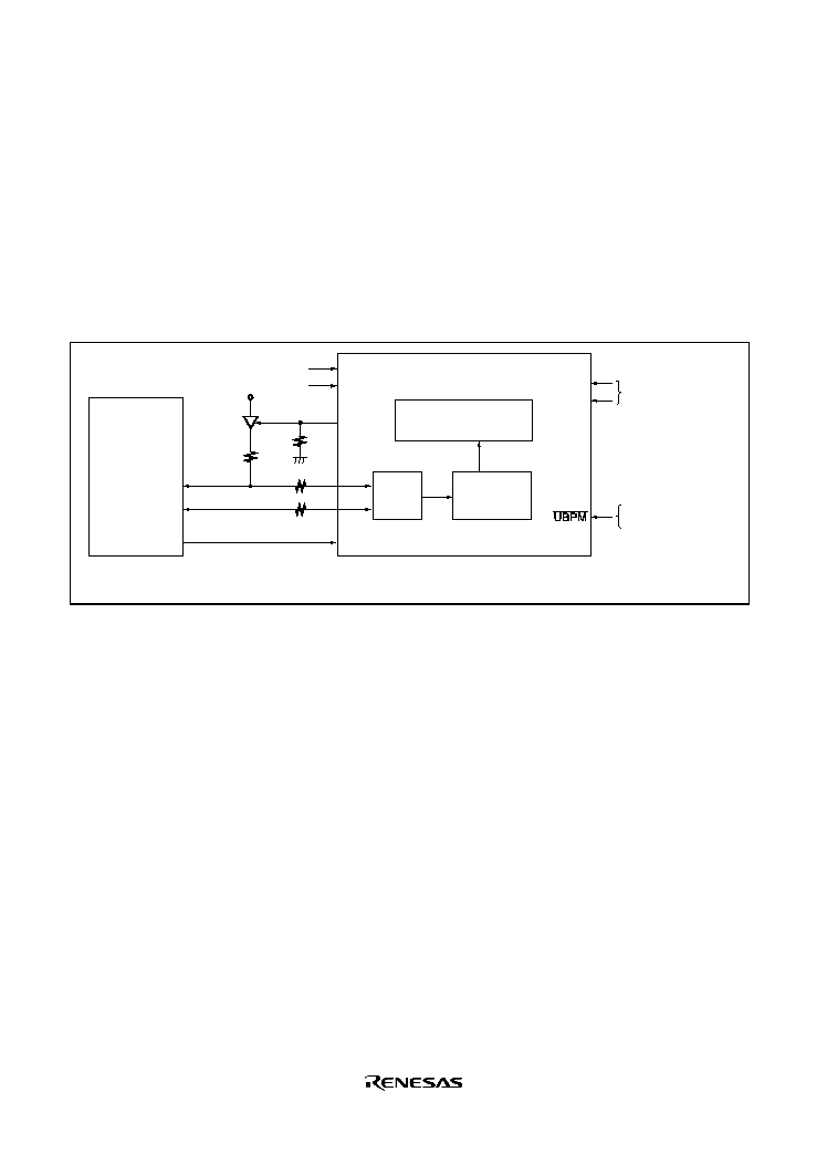
Rev. 1.0, 02/03, page 522 of 634
· Overview
When a reset start preformed after the pins of this LSI have been set to boot mode, a boot
program incorporated in the microcomputer beforehand is activated, and the prepared
programming control program is transmitted sequentially to the host using the USB. With this
LSI, the programming control program received by the USB is written to a programming
control program area in on-chip RAM. After transfer is completed, control branches to the start
address of the programming control program area, and the programming control program
execution state is established (flash memory programming is performed). Figure 17.7 shows a
system configuration diagram when using USB boot mode.
Note: * FWE pin and mode pin input must satisfy the mode programming setup time (t
MDS
= 200ns)
when a reset is released.
VBUS
1: Self power setting
0: Self power setting
Data transmission/reception
This LSI
Flash memory
P36
1.5kW
Rs
Rs
Host or
self-powerd HUB
On-chip RAM
System clock:
16 MHz or 24MHz
FWE*
MD2 to MD0*
1
01x
EXTAL
XTAL
D+
D-
USD+
USD-
USB
Figure 17.7 System Configuration Diagram when Using USB Boot Mode
1. When boot mode is used, the flash memory programming control program must be prepared
in the host beforehand. Prepare a programming control program in accordance with the
description in section 17.8, Flash Memory Programming/Erasing. In boot mode, if any data
has been programmed into the flash memory (if all data is not 1), all flash memory blocks are
erased. Boot mode is for use in enforced exit when user program mode is unavailable, such a
the first time on-board programming control program, or performed, or if the program
activated in user program mode is accidentally erased.
2. When the boot program is activated, enumeration with respect to the host is carried out.
Enumeration information is shown in table 17.6. When enumeration is completed, transmit a
single H'55 byte from the host. If reception has not been preformed normally, restart boot
mode by means of a reset.
3. Set the frequency for transmission from the host as a numeric value in units of MHz
× 100
(ex: 16.00 MHz
H'0640, 24.00 MHz H'0960).
4. In boot mode, the 4-kbyte on-chip RAM area H'FFE000 to H'FFEFBF is used by the boot
program. The programming control program transmitted form the host can be stored in the 8-
kbyte area H'FFC000 to H'FFDFFF. The boot program area cannot be used until program
execution switches to the programming control program. Also note that the boot program
remains in RAM even after control passes to the programming control program.

Rev. 1.0, 02/03, page 523 of 634
5. When a branch is made to the programming control program, the USB remains connected and
can be used immediately for transmission/reception of write data or verify data between the
programming control program and the host. The contents of CPU general registers are
undefined after a branch to the programming control program. Note, in particular, that since
the stack pointer is used implicitly in subroutine calls ad the like, it should be initialized at the
start of the programming control program.
6. Boot mode is by means of a reset. Drive the reset pin low, wait for the elapse of at least 20
states, then set the FWE pin and mode pins to release the reset. Boot mode is also exited in
the event of a WDT overflow reset.
7. Do not change the input level of the mode pins while in boot mode. In the input level of a
mode pin is changed (from low to high) during a reset, the states of ports with a dual function
as address output s, and bus control output signals (
AS, RD, WR), will change due to
switching of the operating mode. Either make pin settings so that these pins do not become
output signal pins during a reset, or take precautions to prevent collisions with external
signals.
8. Interrupt cannot be used during flash memory programming or erasing.
Table 17.7
USB Boot Mode Operation
Item
Host Operation
Operation of this LSI
Branches to boot program
after reset start
Start of USB boot mode
Transmits one H'55 byte on
completion of USB enumeration
Transmits one H'AA byte to
host on reception of H'55
Transfer clock information
Transmits frequency (2 bytes),
number of multiplication
Classification (1 byte), multiplication
ratio (1 byte)
With this LSI, H'0640 or H'0960,
H'01, H'01, are transmitted
If received data are within
respective ranges, transmits
H'AA to host
If any received data is out-of-
ranges, transmits H'FF to host
and halts operation

Rev. 1.0, 02/03, page 524 of 634
Item
Host Operation
Operation of this LSI
Transfer number of bytes
(N) of programming control
program
Performs 2-byte transfer number of
bytes (N) of programming control
program
If received number of bytes is
within ranges, transmits H'AA
to host
If received number of bytes is
out-of- ranges, transmits H'FF
to host and halts operation
Transfer of programming
control program and sum
value
Transmits programming control
program in N-byte divisions.
Transfers received data to on-
chip RAM
Transmits sum value (two's
complement of sum total of
programming control program
(1 byte))
Calculates sum total of
received sum value and 1 byte
units of programming control
program transferred to on-chip
RAM
If sum is 0, transmits H'AA to
host
If sum is not 0, transmits H'FF
to host halts operation
Memory erase
Starts total erase of flash
memory
Transmits total erase status
command (H'3A)
Transmits H'11 to host if total
erase processing is being
executed when total erase
status command is received
Transmits H'06 to host if total
erase of all blocks has been
completed when total erase
status command is received
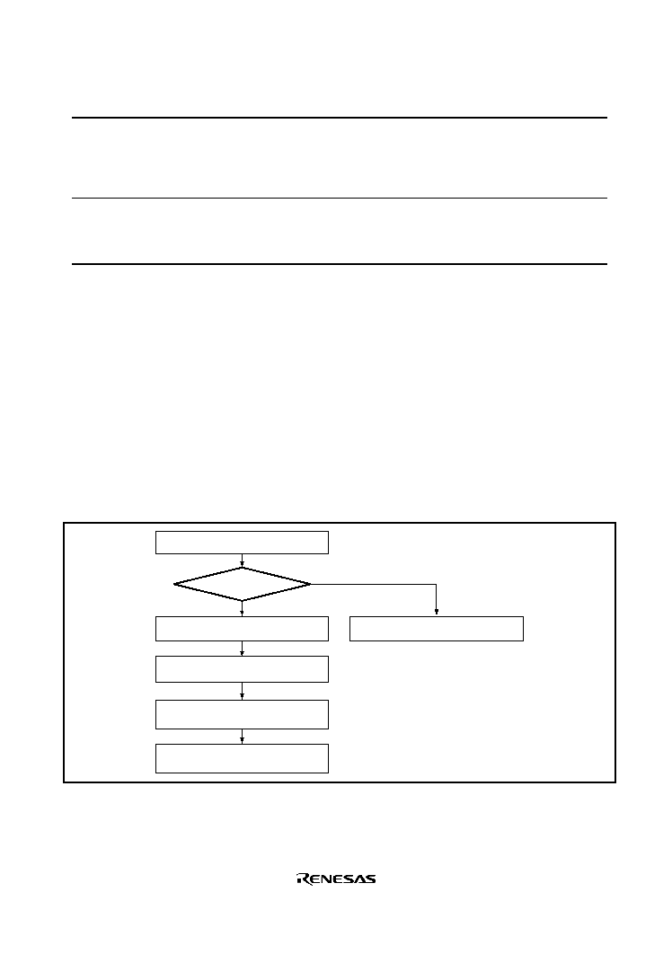
Rev. 1.0, 02/03, page 525 of 634
Item
Host Operation
Operation of this LSI
Memory erase
Transmits total erase status
command (H'3A)
If erase cannot be performed
when total erase status
command is received,
transmits H'EE to host and
halts operation
Execution of programming
control program
Branches to programming
control program transferred to
on-chip RAM and starts
execution.
17.6.3
Programming/Erasing in User Program Mode
On-board programming/erasing of an individual flash memory block can also be performed in user
program mode by branching to a user program/erase control program. The user must set branching
conditions and provide on-board FWE control and supply of programming data, and storing a
program/erase control program in part of the program area as necessary.. The flash memory must
contain the user program/erase control program or a program which provides the user
program/erase control program from external memory. Because the flash memory itself cannot be
read during programming/erasing, transfer the user program/erase control program to on-chip
RAM, as like in boot mode. Figure 17.8 shows a sample procedure for programming/erasing in
user program mode. Prepare a user program/erase control program in accordance with the
description in section 17.8, Flash Memory Programming/Erasing.
Yes
No
Program/erase?
Transfer user program /erase
control program to RAM
Branch to user program/erase
control in RAM
Execute user program/erase
control pogram (flash memory rewrite)
Branch to flash memory
application program
Branch to flash memory
application program
MD2 to MD0 = 110,111 Reset start
Figure 17.8 Programming/Erasing Flowchart Example In User Program Mode
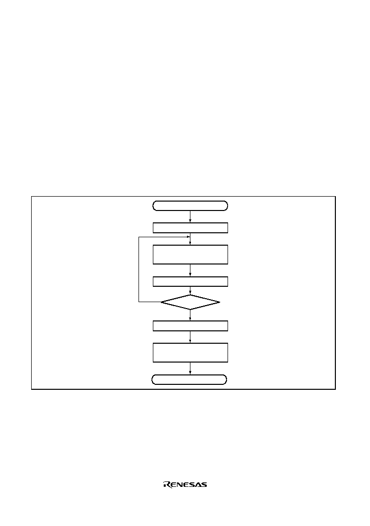
Rev. 1.0, 02/03, page 526 of 634
17.7
Flash Memory Emulation in RAM
Making a setting in the RAM emulation register (RAMER) enables part of RAM to be overlapped
onto the flash memory area so that data to be written to flash memory can be emulated in RAM in
real time. Emulation can be performed in user mode or user program mode. Figure 17.9 shows an
example of emulation of real-time flash memory programming.
1. Set RAMER to overlap part of RAM onto the area for which real-time programming is
required.
2. Emulation is performed using the overlapping RAM.
3. After the program data has been confirmed, the RAMS bit is cleared, thus releasing RAM
overlap.
4. The data written in the overlapping RAM is written into the flash memory space (EB0).
Start of emulation program
Set RAMER
Write tuning data to overlap
RAM
Execute application program
Tuning OK?
Clear RAMER
Write to flash memory
emulation block
End of emulation program
No
Yes
Figure 17.9 Flowchart for Flash Memory Emulation in RAM
Rev. 1.0, 02/03, page 527 of 634
An example in which flash memory block area EB0 is overlapped is shown in figure 17.10.
1. The RAM area to be overlapped is fixed at a 1-kbyte area in the range of H'FFD000 to
H'FFD3FF.
2. The flash memory area to overlap is selected by RAMER from a 1-kbyte area among one of
the EB0 to EB3 blocks.
3. The overlapped RAM area can be accessed from both the flash memory addresses and RAM
addresses.
4. When the RAMS bit in RAMER is set to 1, program/erase protection is enabled for all flash
memory blocks (emulation protection). In this state, setting the P1 or E1 bit in FLMCR1 to 1
does not cause a transition to program mode or erase mode.
5. A RAM area cannot be erased by execution of software in accordance with the erase
algorithm.
6. Block area EB0 contains the vector table. When performing RAM emulation, the vector table
is needed in the overlap RAM.
(EB0)
(EB2)
(EB1)
(EB0)
(EB2)
Flash memory
Flash memory
On-chip RAM
(1 kbyte shadow)
On-chip RAM
(4 kbytes)
On-chip RAM
(1 kbyte)
On-chip RAM
(7 kbyte - 64 bytes)
On-chip RAM (64 bytes)
On-chip RAM
(4 kbytes)
On-chip RAM
(1 kbyte)
On-chip RAM
(7 kbyte - 64 bytes)
On-chip RAM (64 bytes)
Flash memory
Normal memory map
RAM overlap memory map
H'000000
H'000400
H'000800
H'000C00
H'FFD000
H'FFFFFF
H'FFFFC0
H'FFD400
H'FFEFBF
H'FFD3FF
H'FFC000
Figure 17.10 Example of RAM Overlap Operation

Rev. 1.0, 02/03, page 528 of 634
17.8
Flash Memory Programming/Erasing
A software method, using the CPU, is employed to program and erase flash memory in the on-
board programming modes. Depending on the FLMCR1 setting, the flash memory operates in one
of the following four modes: program mode, erase mode, program-verify mode, and erase-verify
mode. The programming control program in boot mode and the user program/erase control
program in user program mode use these operating modes in combination to perform
programming/erasing. Flash memory programming and erasing should be performed in
accordance with the descriptions in section 17.8.1, Program/Program-Verify Mode and section
17.8.2, Erase/Erase-Verify Mode, respectively.
17.8.1
Program/Program-Verify
When writing data or programs to the flash memory, the program/program-verify flowchart shown
in figure 17.11 should be followed. Performing programming operations according to this
flowchart will enable data or programs to be written to the flash memory without subjecting the
chip to voltage stress or sacrificing program data reliability.
1. Programming must be done to an empty address. Do not reprogram an address to which
programming has already been performed.
2. Programming should be carried out 128 bytes at a time. A 128-byte data transfer must be
performed even if writing fewer than 128 bytes. In this case, H'FF data must be written to the
extra addresses.
3. Prepare the following data storage areas in RAM: a 128-byte programming data area, a 128-
byte reprogramming data area, and a 128-byte additional-programming data area. Perform
reprogramming data computation and additional programming data computation according to
figure 17.10.
4. Consecutively transfer 128 bytes of data in byte units from the reprogramming data area or
additional-programming data area to the flash memory. The program address and 128-byte
data are latched in the flash memory. The lower 8 bits of the start address in the flash memory
destination area must be H'00 or H'80.
5. The time during which the P1 bit is set to 1 is the programming time. Figure 17.10 shows the
allowable programming times.
6. The watchdog timer (WDT) is set to prevent overprogramming due to program runaway, etc.
An overflow cycle of approximately (y + z2 +
+ ) µs is allowed.
7. For a dummy write to a verify address, write 1-byte data H'FF to an address whose lower 2 bits
are b'00. Verify data can be read in words from the address to which a dummy write was
performed.
8. The maximum number of repetitions of the program/program-verify sequence to the same bit
is (N1 + N2).
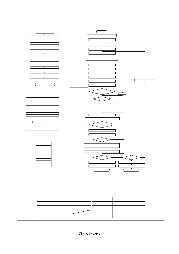
Rev. 1.0, 02/03, page 529 of 634
Write pulse application subroutine
Subroutine Write Pulse
End Sub
Set PSU1 bit in FLMCR2
WDT enable
Disable WDT
Note 7: Write Pulse Width
Wait (y)
µs
Set P1 bit in FLMCR1
Wait (z0), (z1), or (z2)
µs
Clear P1 bit in FLMCR1
Wait (
) µs
Clear PSU1 bit in FLMCR2
Wait (
) µs
*
5
Original Data
(D)
Verify Data
(V)
Reprogram Data
(X)
Comments
Programming completed
Still in erased state; no action
Programming incomplete;
reprogram
RAM
Program data storage
area (128 bytes)
Reprogram data storage
area (128 bytes)
Additional-programming
data storage area
(128 bytes)
Reprogram Data Computation Table
Reprogram Data
(X')
Verify Data
(V)
Additional-
Programming Data (Y)
1
1
1
1
0
1
0
0
0
0
1
1
Comments
Additional programming
to be executed
Additional programming
not to be executed
Additional programming
not to be executed
Additional programming
not to be executed
0
1
1
1
0
1
0
1
0
0
1
1
Additional-Programming Data Computation Table
Notes: 1. Data transfer is performed by byte transfer. The lower 8 bits of the first address written to must be H'00 or H'80.
A 128-byte data transfer must be performed even if writing fewer than 128 bytes; in this case, H'FF data must be written to the extra addresses.
2. Verify data is read in 16-bit (word) units.
3. Reprogram data is determined by the operation shown in the table below (comparison between the data stored in the program data area and the verify data). Bits for
which the reprogram data is 0 are programmed in the next reprogramming loop. Therefore, even bits for which programming has been completed will be subjected to
programming once again if the result of the subsequent verify operation is NG.
4. A 128-byte area for storing program data, a 128-byte area for storing reprogram data, and a 128-byte area for storing additional data must be provided in RAM.
The contents of the reprogram data area and additional data area are modified as programming proceeds.
5. A write pulse of z0 or z1 is applied according to the progress of the programming operation. See Note 7 for details of the pulse widths. When writing of additional-
programming data is executed, a z2 write pulse should be applied. Reprogram data X' means reprogram data when the write pulse is applied.
6. x, y, z0, z1, z2,
, , , , , , and N1 are shown in section 22.7, Flash Memory Characteristics.
START
End of programming
Set SWE1 bit in FLMCR1
Start of programming
Wait (x)
µs
n = 1
m = 0
No
No
No
Yes
Yes
Yes
Wait (
) µs
Wait (
) µs
*
2
*
4
*
1
Wait (
) µs
Apply
Write pulse Z0
µs
OR Z1
µs
Sub-Routine-Call
Set PV1 bit in FLMCR1
H'FF dummy write to verify address
Read verify data
Write data =
verify data?
*
4
*
3
*
1
Transfer reprogram data to reprogram data area
Reprogram data computation
*
4
Transfer additional-programming data to
additional-programming data area
Additional-programming data computation
Clear PV1 bit in FLMCR1
Clear SWE1 bit in FLMCR1
m = 1
Reprogram
See Note 7 for pulse width
m = 0 ?
Increment address
Programming failure
Yes
Clear SWE1 bit in FLMCR1
Wait (
) µs
No
Yes
N1
n?
No
Yes
N1
n ?
Wait (
) µs
n
(N1 + N2)?
n
n + 1
Write 128-byte data in RAM reprogram
data area consecutively to flash memory
Store 128-byte program data in program
data area and reprogram data area
Apply Write Pulse (z2
µs Additional programming)
Sub-Routine-Call
128-byte
data verification completed?
Successively write 128-byte data from additional-
programming data area in RAM to flash memory
Perform programming in the erased state.
Do not perform additional programming
on previously programmed addresses.
P1 bit set time (µs)
1
z2
2
N1-1
N1
N1+1
N1+2
N1+3
N1+N2-1
N1+N2-2
N1+N2
z2
z2
z2
_
_
_
_
_
_
z0
z0
z0
z0
z1
z1
z1
z1
z1
z1
Number of Writes n
Program
Re -program
Figure 17.11 Program/Program-Verify Flowchart

Rev. 1.0, 02/03, page 530 of 634
17.8.2
Erase/Erase-Verify
When erasing flash memory, the erase/erase-verify flowchart shown in figure 17.12 should be
followed.
1. Prewriting (setting erase block data to all 0s) is not necessary.
2. Erasing is performed in block units. Make only a single-bit specification in the erase block
register (EBR1). To erase multiple blocks, each block must be erased in turn.
3. The time during which the E1 bit is set to 1 is the flash memory erase time.
4. The watchdog timer (WDT) is set to prevent overprogramming due to program runaway, etc.
An overflow cycle of approximately (y+z+
+) ms is allowed.
5. For a dummy write to a verify address, write 1-byte data H'FF to an address whose lower two
bits are b'00. Verify data can be read in longwords from the address to which a dummy write
was performed.
6. If the read data is unerased, set erase mode again, and repeat the erase/erase-verify sequence as
before. The maximum number of repetitions of the erase/erase-verify sequence is N.
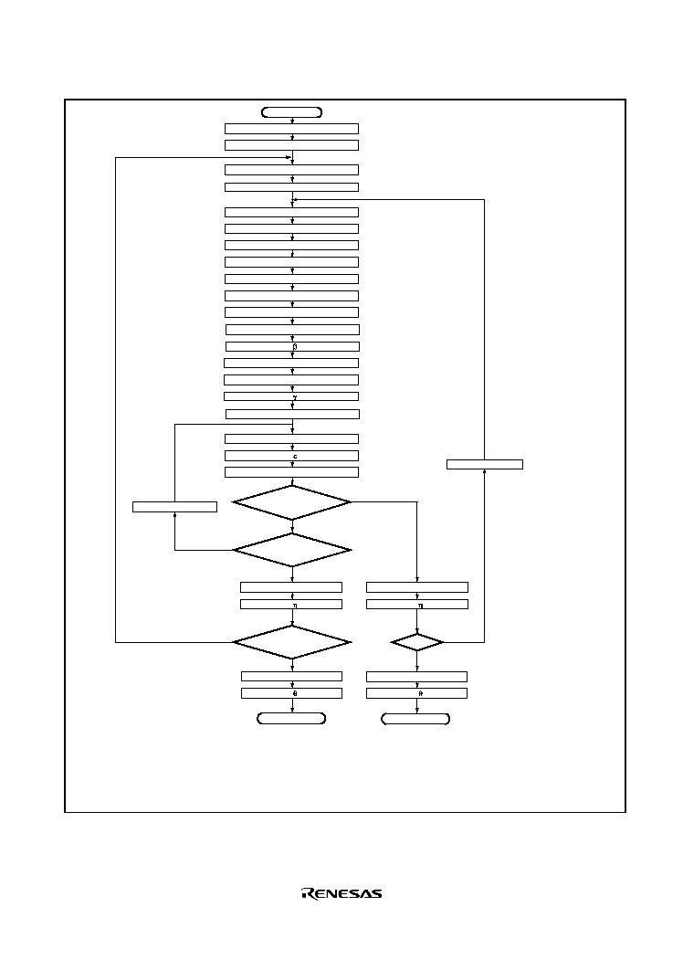
Rev. 1.0, 02/03, page 531 of 634
Start
Set EBR1 (2)
Enable WDT
Disable WDT
Read verify data
Increment address
Verify data = all 1s?
Last address of block?
All erase block erased?
Set block start address as verify address
H'FF dummy write to verify address
Set SWE1 bit in FLMCR1
n =
1
Set ESU1 bit in FLMCR2
Set E1 bit in FLMCR1
Start erasing
Start erasing
Wait (x)
µs
Wait (y)
µs
Clear E1 bit in FLMCR1
Clear EV bit in FLMCR1
Wait (z)
µs
Clear ESU1 bit in FLMCR1
Wait (
)
µs
Wait ( )
µs
Wait ( )
µs
Clear EV1 bit in FLMCR1
n
n + 1
Wait ( )
µs
Clear SWE1 bit in FLMCR1
Wait ( )
µs
Clear EV1 bit in FLMCR1
n
> (N)?
Wait ( )
µs
Clear SWE1 bit in FLMCR1
Wait ( )
µs
Erase failure
End of erasing
Wait ( )
µs
No
No
Yes
Yes
No
No
Yes
Yes
*1
*2
*2
*2
*2
*2
*2
*2
*2
*5
*2
*3
*4
Notes: 1.
2.
3.
4.
5.
Pre-write (clearing data in the block to be erased to 0) isn not required.
x, y, z,
, , , , , , and N are shown in section 22.7, Flash Memory Characteristics.
Veryfy data is read in 16 bits.
Only 1 bit in the EBR register must be set. Two or more bits in EBR cannot be set.
Erasure is performed in block units. To erase multiple blocks, each block must be erased sequentially.
Figure 17.12 Erase/Erase-Verify Flowchart

Rev. 1.0, 02/03, page 532 of 634
17.9
Program/Erase Protection
There are three kinds of flash memory program/erase protection: hardware protection, software
protection, and error protection.
17.9.1
Hardware Protection
Hardware protection refers to a state in which programming/erasing of flash memory is forcibly
disabled or aborted because of a transition to reset or standby mode. Flash memory control
register 1 (FLMCR1), flash memory control register 2 (FLMCR2), and erase block register 1
(EBR1) are initialized. In a reset via the
RES pin, the reset state is not entered unless the RES pin
is held low until oscillation stabilizes after powering on. In the case of a reset during operation,
hold the
RES pin low for the RES pulse width specified in the AC Characteristics section.
17.9.2
Software Protection
Software protection can be implemented against programming/erasing of all flash memory blocks
by clearing the SWE1 bit in FLMCR1. When software protection is in effect, setting the P1 or E1
bit in FLMCR1 does not cause a transition to program mode or erase mode. By setting the erase
block register 1 (EBR1), erase protection can be set for individual blocks. When EBR1 and EBR2
are set to H'00, erase protection is set for all blocks.
17.9.3
Error Protection
In error protection, an error is detected when the CPU's runaway occurs during flash memory
programming/erasing, or operation is not performed in accordance with the program/erase
algorithm, and the program/erase operation is aborted. Aborting the program/erase operation
prevents damage to the flash memory due to overprogramming or overerasing.
When the following errors are detected during programming/erasing of flash memory, the FLER
bit in FLMCR2 is set to 1, and the error protection state is entered.
· When the flash memory of the relevant address area is read during programming/erasing
(including vector read and instruction fetch)
· Immediately after exception handling (excluding a reset) during programming/erasing
· When a SLEEP instruction is executed during programming/erasing
· When the CPU releases the bus mastership to the DMAC during programming/erasing
The FLMCR1, FLMCR2, EBR1 and EBR2 settings are retained, but program mode or erase mode
is aborted at the point at which the error occurred. Program mode or erase mode cannot be re-
entered by re-setting the P1 or E1 bit. However, PV1 and EV1 bit setting is enabled, and a
transition can be made to verify mode.

Rev. 1.0, 02/03, page 533 of 634
17.10
Interrupt Handling when Programming/Erasing Flash Memory
All interrupts, including NMI interrupt is disabled when flash memory is being programmed or
erased (when the P1 or E1 bit is set in FLMCR1), and while the boot program is executing in boot
mode*
1
, to give priority to the program or erase operation. There are three reasons for this:
1. Interrupt during programming or erasing might cause a violation of the programming or
erasing algorithm, with the result that normal operation could not be assured.
2. In the interrupt exception handling sequence during programming or erasing, the vector would
not be read correctly*
2
, possibly resulting in CPU runaway.
3. If interrupt occurred during boot program execution, it would not be possible to execute the
normal boot mode sequence.
Notes: 1. Interrupt requests must be disabled inside and outside the CPU until the programming
control program has completed programming.
2. The vector may not be read correctly in this case for the following two reasons:
· If flash memory is read while being programmed or erased (while the P1 or E1 bit is
set in FLMCR1), correct read data will not be obtained (undetermined values will be
returned).
· If the interrupt entry in the vector table has not been programmed yet, interrupt
exception handling will not be executed correctly.
17.11
Programmer Mode
In programmer mode, a PROM programmer can perform programming/erasing via a socket
adapter, just like for a discrete flash memory. Use a PROM programmer which supports the
Hitachi 128-kbyte flash memory on-chip MCU device type. Memory map in programmer mode is
shown in figure 17.13.
MCU mode
On-chip ROM space
128 kbytes
Programmer mode
H'000000
H'00000
H'01FFFF
H'1FFFF
Figure 17.13 Memory Map in Programmer Mode

Rev. 1.0, 02/03, page 534 of 634
17.12
Power-Down States for Flash Memory
In user mode, the flash memory will operate in either of the following states:
· Normal operating mode
The flash memory can be read and written to.
· Standby mode
All flash memory circuits are halted.
· Power-down state
The flash memory can be read when part of the power supply circuit is halted and the LSI
operates by subclocks.
Table 17.8 shows the correspondence between the operating modes of this LSI and the flash
memory. When the flash memory returns to normal operation from a power-down state, a power
supply circuit stabilization period is needed. When the flash memory returns to its normal
operating state, bits STS2 to STS0 in SBYCR must be set to provide a wait time of at least 100 µs,
even when the external clock is being used and an oscillation stabilization time is not necessary.
Table 17.8
Flash Memory Operating States
LSI Operating State
Flash Memory Operating State
Active mode
Normal operating mode
Sleep mode
Normal operating mode
Watch mode
Standby mode
Standby mode
(Before entering to the normal operation mode, wait time of at least
100 µs is required.)
Subactive mode
Supsleep mode
PDWND = 0: Power-down mode (read only)
PDWND = 1: Normal operating mode (read only)

Rev. 1.0, 02/03, page 535 of 634
17.13
Flash Memory Programming and Erasing Precautions
Precautions concerning the use of on-board programming mode, the RAM emulation function, and
PROM mode are summarized below.
1. Use the specified voltages and timing for programming and erasing
Applied voltages in excess of the rating can permanently damage the device. Use a PROM
programmer that supports the Hitachi microcomputer device type with 128-kbyte on-chip flash
memory (FZTAT128V3A).
Do not select the HN27C4096 setting for the PROM programmer, and only use the specified
socket adapter. Failure to observe these points may result in damage to the device.
2. Powering on and off
Do not apply a high level to the FWE pin until VCC has stabilized. Also, drive the FWE pin
low before turning off VCC. When applying or disconnecting VCC power, fix the FWE pin
low and place the flash memory in the hardware protection state. The power-on and power-off
timing requirements should also be satisfied in the event of a power failure and subsequent
recovery.
3. FWE application/disconnection
FWE application should be carried out when MCU operation is in a stable condition. If MCU
operation is not stable, fix the FWE pin low and set the protection state. The following points
must be observed concerning FWE application and disconnection to prevent unintentional
programming or erasing of flash memory:
· Apply FWE when the VCC voltage has stabilized within its rated voltage range.
· In boot mode, apply and disconnect FWE during a reset.
· In user program mode, FWE can be switched between high and low level regardless of the
reset state. FWE input can also be switched during execution of a program in flash
memory.
· Do not apply FWE if program runaway has occurred.
· Disconnect FWE only when the SWE1, ESU1, EV1, PV1, P1, and E1 bits in FLMCR1 are
cleared. Make sure that the SWE1, ESU1, PSU1, EV1, PV1, P1, and E1 bits are not set by
mistake when applying or disconnecting FWE.
4. Do not apply a constant high level to the FWE pin
Apply a high level to the FWE pin only when programming or erasing flash memory. A
system configuration in which a high level is constantly applied to the FWE pin should be
avoided. Also, while a high level is applied to the FWE pin, the watchdog timer should be
activated to prevent overprogramming or overerasing due to program runaway, etc.

Rev. 1.0, 02/03, page 536 of 634
5. Use the recommended algorithm when programming and erasing flash memory
The recommended algorithm enables programming and erasing to be carried out without
subjecting the device to voltage stress or sacrificing program data reliability. When setting the
P1 or E1 bit in FLMCR1, the watchdog timer should be set beforehand as a precaution against
program runaway, etc.
6. Do not set or clear the SWE1 bit during execution of a program in flash memory
Wait at least
µs* after clearing the SWE1 bit before executing a program or reading data in
flash memory. When the SWE1 bit is set, data in flash memory can be rewritten, but access
flash memory only for verify operations (verification during programming/erasing). Also, do
not clear the SWE1 bit during programming, erasing, or verifying. Similarly, when using
emulation by RAM with a high level applied to the FWE pin, the SWE1 bit should be cleared
before executing a program or reading data in flash memory. However, read/write accesses can
be performed in the RAM area overlapping the flash memory space regardless of whether the
SWE1 bit is set or cleared.
Note: Refer to section 22.7, Flash Memory Characteristics.
7. Do not use interrupts while flash memory is being programmed or erased
All interrupt requests, including NMI, should be disabled during FWE application to give
priority to program/erase operations.
8. Do not perform additional programming. Erase the memory before reprogramming
In on-board programming, perform only one programming operation on a 128-byte
programming unit block. In programmer mode, too, perform only one programming operation
on a 128-byte programming unit block. Programming should be carried out with the entire
programming unit block erased.
9. Before programming, check that the chip is correctly mounted in the PROM programmer
Overcurrent damage to the device can result if the index marks on the PROM programmer
socket, socket adapter, and chip are not correctly aligned.
10. Do not touch the socket adapter or chip during programming
Touching either of these can cause contact faults and write errors.
11. The reset state must be entered after powering on
Apply the reset signal for at least 100 µs during the oscillation setting period.
12. When a reset is applied during operation, this should be done while the SWE1 pin is low.
Wait at least
µs* after clearing the SWE1 bit before applying the reset.
Note: Refer to section 22.7, Flash Memory Characteristics.

Rev. 1.0, 02/03, page 537 of 634
17.14 Note on Switching from F-ZTAT Version to Masked ROM Version
The masked ROM version does not have the internal registers for flash memory control that are
provided in the F-ZTAT version. Table 17.9 lists the registers that are present in the F-ZTAT
version but not in the masked ROM version. If a register listed in Table 17.9 is read in the masked
ROM version, an undefined value will be returned. Therefore, if application software developed
on the F-ZTAT version is switched to a masked ROM version product, it must be modified to
ensure that the registers in Table 17.9 have no effect.
Table 17.9
Registers Present in F-ZTAT Version but Absent in Masked ROM Version
Register
Abbreviation
Address
Flash memory control register 1
FLMCR1
H'FFA8
Flash memory control register 2
FLMCR2
H'FFA9
Erase block register 1
EBR1
H'FFAA
Erase block register 2
EBR2
H'FFAB
RAM emulation register
RAMER
H'FEDB
Flash power control register
FLPWCR
H'FFAC
Serial control register x
SCRX
H'FDB4

Rev. 1.0, 02/03, page 538 of 634

CPG0600B_000020020900
Rev. 1.0, 02/03, page 541 of 634
Section 19 Clock Pulse Generator
This LSI has an on-chip clock pulse generator that generates the system clock (
), the bus master
clock, and internal clocks. The clock pulse generator consists of a main clock oscillator, duty
adjustment circuit, clock select circuit, medium-speed clock divider, bus master clock selection
circuit, subclock oscillator, waveform shaping circuit, PLL (Phase Locked Loop) circuit, and USB
operating clock selection circuit. A block diagram of clock pulse generator is shown in figure
19.1.
Duty
adjustment
circuit
EXTAL
XTAL
Main
clock
oscillator
USB
operation
clock
selection circuit
OSC1
OSC2
Subclock
oscillator
USB
operation
clock
oscillator
Medium-
speed
clock divider
System clock
to
pin
USB operation
clock
to USB
RTC clock
to RTC
Internal clock
to peripheral
modules
Bus master clock
to CPU,
DMAC
USB clock
to USB
/2
to /32
SCK2 to SCK0
UCKS3 to UCKS0
SCKCR
RFCUT
48MHz
LPWRCR
UCTLR
Bus
master
clock
selection
circuit
Clock
selection
circuit
SUB
Legend
LPWRCR : Low power control register
SCKCR
: System clock control register
UCTLR
: USB control register
PLL
circuit
Figure 19.1 Block Diagram of Clock Pulse Generator
The frequency of the main clock oscillator can be changed by software by means of settings in the
low-power control register (LPWRCR) and system clock control register (SCKCR). PLL 48-MHz
clock can be selected by software by means of setting the USB control register (UCTLR). For
details, refer to section 14, Universal Serial Bus (USB).

Rev. 1.0, 02/03, page 542 of 634
19.1
Register Descriptions
The on-chip clock pulse generator has the following registers.
· System clock control register (SCKCR)
· Low-power control register (LPWRCR)
19.1.1
System Clock Control Register (SCKCR)
SCKCR controls
clock output and medium-speed mode.
Bit
Bit Name Initial Value R/W
Description
7
PSTOP
0
R/W
Clock Output Disable
Controls
output. The operation of this bit changes
depending on the operating mode. For details, see section
20.11,
Clock Output Disabling Function.
0:
output, fixed high, or high impedance
1: Fixed high or high impedance
6
--
0
R/W
Reserved
These bits can be read from or written to, but the write
value should always 0.
5, 4 --
All 0
--
Reserved
These bits are always read as 0.
3
--
0
R/W
Reserved
This bit can be read from or written to, but the write value
should always be 0.
2
1
0
SCK2
SCK1
SCK0
0
0
0
R/W
R/W
R/W
System Clock Select 2 to 0
These bits select the bus master clock. To operate in sub-
active mode or watch mode, clear the SCK2 to SCK0 bits
to 0.
000: High-speed mode
001: Medium-speed clock is
/2
010: Medium-speed clock is
/4
011: Medium-speed clock is
/8
100: Medium-speed clock is
/16
101: Medium-speed clock is
/32
11X: Setting prohibited
Legend
X: Don't care
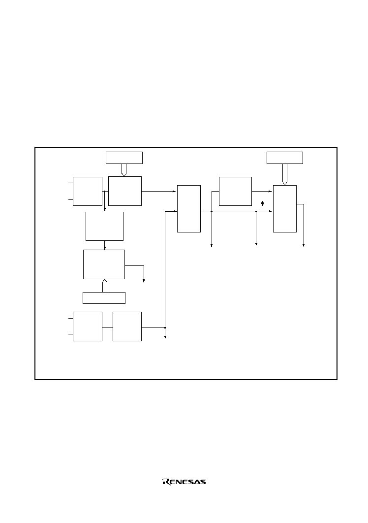

Rev. 1.0, 02/03, page 543 of 634
19.1.2
Low Power Control Register (LPWRCR)
LPWRCR performs power-down mode control, selects sampling frequency for eliminating noise,
performs subclock oscillator control, and selects whether or not built-in feedback resistance and
duty adjustment circuit of the system clock generator used.
Bit
Bit Name Initial Value R/W
Description
7
DTON
0
R/W
Direct Transition ON Flag
0: When the SLEEP instruction is executed in high-speed
mode or medium-speed mode, operation shifts to sleep
mode, software standby mode, or watch mode*.
When the SLEEP instruction is executed in sub-active
mode, operation shifts to sub-sleep mode or watch
mode.
1: When the SLEEP instruction is executed in high-speed
mode or medium-speed mode, operation shifts directly to
sub-active mode, or shifts to sleep mode or software
standby mode.
When the SLEEP instruction is executed in sub-active
mode, operation shifts directly to high-speed mode, or
shifts to sub-sleep mode.
6
LSON
0
R/W
Low Speed ON Flag
0: When the SLEEP instruction is executed in high-speed
mode or medium-speed mode, operation shifts to sleep
mode, software standby mode, or watch mode*.
When the SLEEP instruction is executed in sub-active
mode, operation shifts to watch mode* or shifts directly
to high-speed mode.
Operation shifts to high-speed mode when watch mode
is cancelled.
1: When the SLEEP instruction is executed in high-speed
mode*, operation shifts to watch mode or sub-active
mode*.
When the SLEEP instruction is executed in sub-active
mode, operation shifts to sub-sleep mode or watch
mode.
Operation shifts to sub-active mode when watch mode is
cancelled.

Rev. 1.0, 02/03, page 544 of 634
Bit
Bit Name Initial Value R/W
Description
5
NESEL
0
R/W
Noise Elimination Sampling Frequency Select
This bit selects the sampling frequency of the subclock
(
SUB
) generated by the subclock oscillator is sampled by
the clock (
) generated by the system clock oscillator
0: Sampling using 1/32 x
1: Sampling using 1/4 x
4
SUBSTP
0
R/W
Subclock Enable
This bit enables/disables subclock generation. This bit
should be set to 1 when subclock is not used.
0: Enables subclock generation.
1: Disables subclock generation.
3
RFCUT
0
R/W
Built-in Feedback Resistor Control
Selects whether the oscillator's built-in feedback resistor
and duty adjustment circuit are used with external clock
input. This bit should not be accessed when a crystal
oscillator is used.
After this bit is set when using external clock input, a
transition should initially be made to software standby
mode. Switching between use and non-use of the
oscillator's built-in feedback resistor and duty adjustment
circuit is performed when the transition is made to software
standby mode.
0: Main clock oscillator's built-in feedback resistor and duty
adjustment circuit are used
1: Main clock oscillator's built-in feedback resistor and duty
adjustment circuit are not used
2
0
R/W
Reserved
This bit can be read from or written to, but the write value
should always 0.
1
0
STC1
STC0
0
0
R/W
R/W
Frequency Multiplication Factor
Specify the frequency multiplication factor of the PLL circuit
incorporated into the evaluation chip. The specified
frequency multiplication factor is valid after a transition to
software standby mode.
With this LSI, the STC1 and STC0 bits must both be set to
1. After a reset, the STC1 and STC0 bits are both cleared
to 0, and so they must be set to 1.
00:
× 1
01:
× 2 (Setting prohibited)
10:
× 4 (Setting prohibited)
11: PLL is bypassed
Note:
*
When watch mode or subactive mode is entered, set high-speed mode.
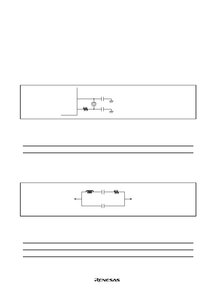
Rev. 1.0, 02/03, page 545 of 634
19.2
System Clock Oscillator
Clock pulses can be supplied by connecting a crystal resonator, or by input of an external clock.
19.2.1
Connecting a Crystal Resonator
A crystal resonator can be connected as shown in the example in figure 19.2. Select the damping
resistance Rd according to table 19.2. An AT-cut parallel-resonance crystal should be used.
EXTAL
XTAL
R
d
C
L2
C
L1
C
L1
= C
L2
= 10 to 22 pF
Figure 19.2 Connection of Crystal Resonator (Example)
Table 19.1
Damping Resistance Value
Frequency (MHz)
2
4
6
8
10
13
16
20
24
Rd (
)
1k
500
300
200
100
0
0
0
0
Figure 19.3 shows the equivalent circuit of the crystal resonator. Use a crystal resonator that has
the characteristics shown in table 19.2. The crystal resonator frequency should not exceed 20
MHz.
XTAL
C
L
AT-cut parallel-resonance type
EXTAL
C
0
L
R
s
Figure 19.3 Crystal Resonator Equivalent Circuit
Table 19.2
Crystal Resonator Characteristics
Frequency (MHz)
2
4
6
8
10
13
16
20
24
RS max (
)
500
120
100
80
60
60
50
40
40
C0 max (pF)
7
7
7
7
7
7
7
7
7
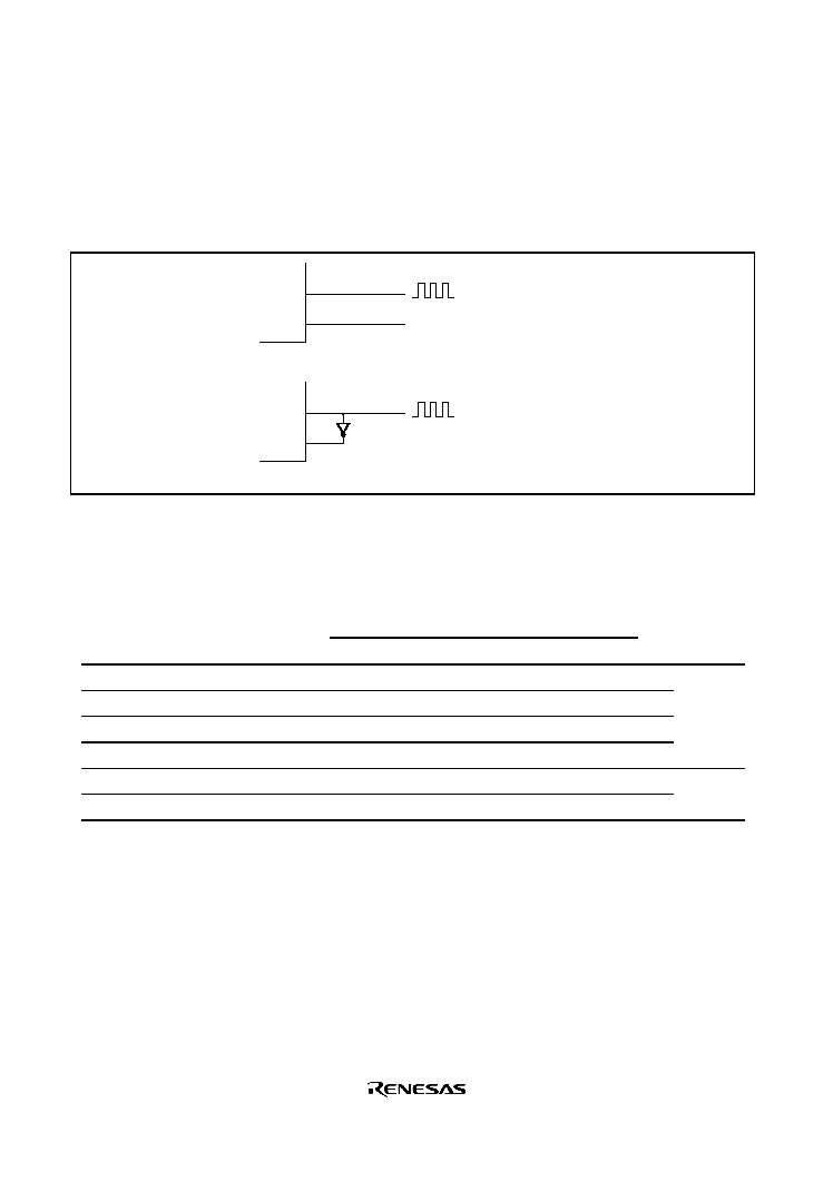
Rev. 1.0, 02/03, page 546 of 634
19.2.2
Inputting External Clock
An external clock signal can be input as shown in an example in figure 19.4. If the XTAL pin is
left open, make sure that stray capacitance is no more than 10 pF. When complementary clock
input to XTAL pin, the external clock input should be fixed high in standby mode.
EXTAL
XTAL
EXTAL
XTAL
External clock input
Open
External clock input
(a) XTAL pin left open
(b) Complementary clock input at XTAL pin
Figure 19.4 External Clock Input (Examples)
Table 19.3 shows the input conditions for the external clock.
Table 19.3
External Clock Input Conditions
VCC= 2.4 to 3.6V
VCC = 2.7 to 3.6V
VCC = 3.0 to 3.6V
Item
Symbol
min
max
Min
max
min
max
Unit
Test
Conditions
External clock input low pulse width
t
EXL
65
--
25
--
15.5
--
ns
External clock input high pulse width
t
EXH
65
--
25
--
15.5
--
ns
External clock rise time
t
EXr
--
15
--
6.25
--
5.25
ns
External clock fall time
t
EXf
--
15
--
6.25
--
5.25
ns
Figure 19.5
Clock low pulse width level
t
CL
0.35
0.65
0.4
0.6
0.4
0.6
tcyc
Clock high pulse width level
t
CH
0.35
0.65
0.4
0.6
0.4
0.6
tcyc
Figure 22.3
The external clock input conditions when the duty adjustment circuit is not used are shown in
table 19.4. When the duty adjustment circuit is not used, note that the maximum operating
frequency depends on the external clock input waveform. For example, if t
EXL
= t
EXH
= 20.8 ns and
T
EXr
= t
EXf
= 5.25 ns, the maximum operating frequency becomes 19.2 MHz depending on the clcok
cycle time of 52.1 ns.
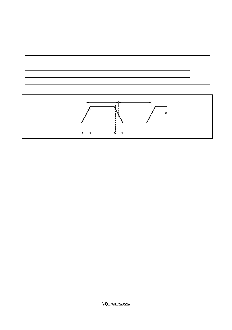
Rev. 1.0, 02/03, page 547 of 634
Table 19.4
External Clock Input Conditions when Duty Adjustment Circuit is not Used
Item
Symbol
min
max
Min
max
min
max
Unit
Test
Conditions
External clock input low pulse width
t
EXL
80
--
31.25
--
20.8
--
ns
External clock input high pulse width
t
EXH
80
--
31.25
--
20.8
--
ns
External clock rise time
t
EXr
--
15
--
6.25
--
5.25
ns
External clock fall time
t
EXf
--
15
--
6.25
--
5.25
ns
Figure 19.5
t
EXH
t
EXL
t
EXr
t
EXf
V
CC
0.5
EXTAL
Figure 19.5 External Clock Input Timing
19.3
Duty Adjustment Circuit
When the oscillator frequency is 5 MHz or higher, the duty adjustment circuit adjusts the duty
cycle of the clock signal from the oscillator to generate the system clock (
).
19.4
Medium-Speed Clock Divider
The medium-speed clock divider divides the system clock to generate
/2, /4, /8, /16, and /32.
19.5
Bus Master Clock Selection Circuit
The bus master clock selection circuit selects the clock supplied to the bus master by setting the
bits SCK2 to SCK0 in SCKCR. The bus master clock can be selected from high-speed mode, or
medium-speed clocks (
/2, /4, /8, /16, /32).
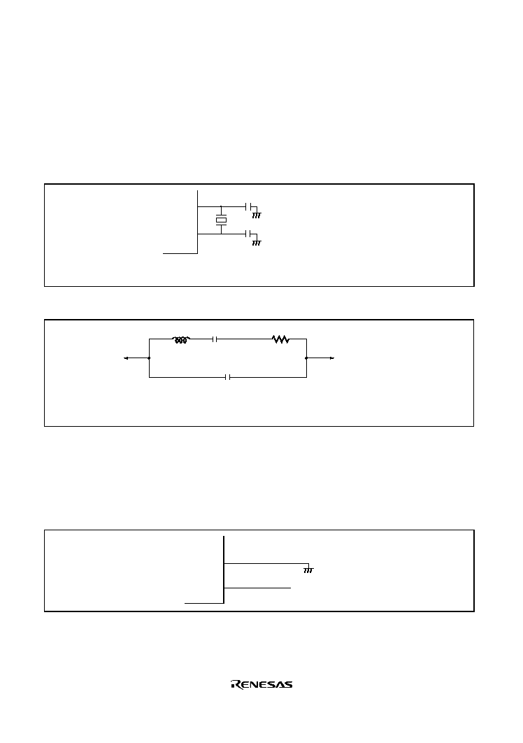
Rev. 1.0, 02/03, page 548 of 634
19.6
Subclock Oscillator
19.6.1
Connecting 32.768kHz Crystal Resonator
supply a clock to the subclock divider, connect a 32.768kHz crystal resonator, as shown in figure
19.6. Figure 19.7 shows the equivalence circuit for a 32.768kHz oscillator.
OSC1
OSC2
Note: C
1
and C
2
are reference values including the floating
capacitance of the board.
C
1
C
2
C
1
= C
2
= 15pF (typ)
Figure 19.6 Example Connection of 32.768kHz Quartz Oscillator
OSC1
OSC2
Cs
Ls
Rs
Co
Co = 1.5pF (typ.)
Rs = 14k
(typ.)
fw = 32.768kHz
Type name = C001R (SEIKO EPSON)
Figure 19.7 Equivalence Circuit for 32.768kHz Oscillator
19.6.2
Handling Pins When Subclock Not Required
If no subclock is required, connect the OSC1 pin to Vss and leave OSC2 open, as shown in figure
19.8. Set the SUBSTP bit of LPWRCR to 1.
OSC1
OSC2
Open state
Figure 19.8 Pin Handling When Subclock Not Required

Rev. 1.0, 02/03, page 549 of 634
19.7
Subclock Waveform Generation Circuit
To eliminate noise from the subclock input to OSCI, the subclock is sampled using the dividing
clock
. The sampling frequency is set using the NESEL bit of LPWRCR. For details, see section
19.1.2, Low Power Control Register (LPWRCR).
No sampling is performed in sub-active mode, sub-sleep mode, or watch mode.
19.8
PLL Circuit for USB
The PLL circuit has the function of doubling or tripling the 16-MHz or 24-MHz clock from the
main oscillator to generate the 48-MHz USB operating clock.
Regardless of the PLL circuit usage, connect the PLLVCC pin and PLLVSS pin to Vcc and
ground (Vss) respectively.
When the PLL circuit is used, set the UCKS3 to UCKS0 bits of UCTLR. For details, refer to
section 14, Universal Serial Bus (USB).
19.9
Usage Notes
19.9.1
Note on Crystal Resonator
Since various characteristics related to the crystal resonator are closely linked to the user's board
design, thorough evaluation is necessary on the user's part, using the resonator connection
examples shown in this section as a guide. As the resonator circuit ratings will depend on the
floating capacitance of the resonator and the mounting circuit, the ratings should be determined in
consultation with the resonator manufacturer. The design must ensure that a voltage exceeding the
maximum rating is not applied to the oscillator pin.
19.9.2
Note on Board Design
When designing the board, place the crystal resonator and its load capacitors as close as possible
to the XTAL or OSC1 and EXTAL or OSC2 pins. Other signal lines should be routed away from
the oscillator circuit to prevent induction from interfering with correct oscillation. See figure 19.9.
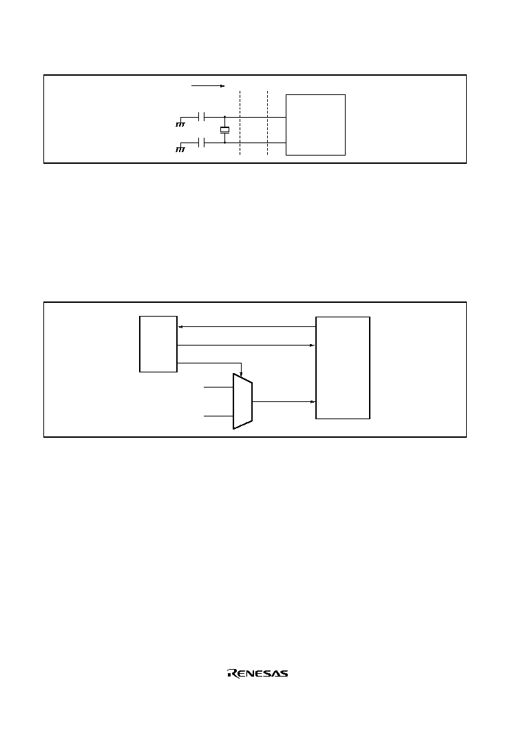
Rev. 1.0, 02/03, page 550 of 634
Prohibit
Signal A Signal B
This LSI
EXTAL or
OSC1
XTAL or
OSC2
C
1
C
2
Figure 19.9 Note on Board Design of Oscillator Circuit
19.9.3
Note on Switchover of External Clock
When two or more external clocks (e.g. 16 MHz and 13 MHz) are used as the system clock,
switchover of the input clock should be carried out in software standby mode.
An example of an external clock switching circuit is shown in figure 19.10, and an example of the
external clock switchover timing in figure 19.11.
This LSI
Ouptut port
External
interrupt
EXTAL
Request switchover of external clock
Interrupted external signal
External clock switchover signal
External clock 1
External clock 2
Control
cycle
Selector
Figure 19.10 Example of External Clock Switching Circuit
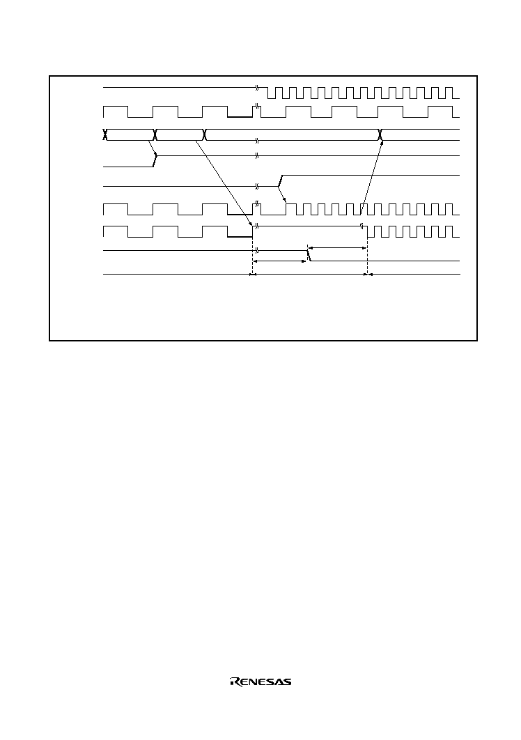
Rev. 1.0, 02/03, page 551 of 634
200 ns or more
(2)
(1)
(2)
(3)
(4)
(5)
Port setting (clock switchover)
Software standby mode transition
External clock switchover
External interrupt generation
(Input interrupt at least 200 ns after transition to software standby mode.)
Interrupt exception handling
(5)
SLEEP instruction
execution
Interrupt exception handling
Operation
External
clock 1
External
clock 2
(1)
Port setting
(3)
External clock
switchover
signal
EXTAL
Internal
clock
(4)
Wait time
External
interrupt
Active (external clock 2)
Software standby mode
Active (external clock 1)
Clock switchover
request
Figure 19.11 Example of External Clock Switchover Timing

Rev. 1.0, 02/03, page 552 of 634

Rev. 1.0, 02/03, page 553 of 634
Section 20 Power-Down Modes
In addition to the normal program execution state, this LSI has five power-down modes in which
operation of the CPU and oscillator is halted and power dissipation is reduced. Low-power
operation can be achieved by individually controlling the CPU, on-chip supporting modules, and
so on.
This LSI's operating modes are high-speed mode and five power down modes:
1. Medium-speed mode
2. Subactive mode
3. Sleep mode
4. Subsleep mode
5. Watch mode
6. Module stop mode
7. Software standby mode
8. Hardware standby mode
1. to 5. are power-down modes. Sleep mode is CPU states, medium-speed mode is a CPU and bus
master state, subactive mode is a CPU, bus master, and on-chip peripheral function state, and
module stop mode is an internal peripheral function (including bus masters other than the CPU)
state. Some of these states can be combined.
After a reset, the LSI is in high-speed mode and module stop mode (other than DMAC).
Table 20.1 and table 20.2 show the LSI internal states in each mode and the transition conditions
of power-down modes respectively. Figure 20.1 shows the diagram of mode transition.

Rev. 1.0, 02/03, page 554 of 634
Table 20.1
LSI Internal States in Each Mode
Function
High-
Speed
Medium-
Speed
Sleep
Module
Stop
Watch
Sub-
active
Subsleep
Software
Standby
Hardware
Standby
System clock pulse generator
Function-
ing
Function-
ing
Function-
ing
Function-
ing
Halted
Halted
Halted
Halted
Halted
Subclock pulse generator
Function-
ing/halted
Function-
ing/halted
Function-
ing/halted
Function-
ing/halted
Function-
ing
Function-
ing
Function-
ing
Function-
ing/halted
Halted
CPU
Instructions
Function-
ing
Medium-
speed
operation
Halted
Function-
ing
Halted
Subclock
operation
Halted
Halted
Halted
Registers
Retained
Retained
Retained
Retained
Undefined
RAM
Function-
ing
Function-
ing
Function-
ing
Function-
ing
Retained
Function-
ing
Retained
Retained
Retained
I/O
Function-
ing
Function-
ing
Function-
ing
Function-
ing
Retained
Function-
ing
Function-
ing
Halted
High
impedance
External
interrupts
NMI
IRQ0 to
IRQ4, IRQ7
Function-
ing
Function-
ing
Function-
ing
Function-
ing
Function-
ing
Function-
ing
Function-
ing
Function-
ing
Halted
Peripheral
functions
DMAC
Function-
ing
Medium-
speed
operation
Function-
ing
Function-
ing/halted
(retained)
Halted
(retained)
Halted
(retained)
Halted
(retained)
Halted
(retained)
Halted
(reset)
WDT
Function-
ing
Function-
ing
Function-
ing
Function-
ing
Halted
(retained)
Subclock
operation
Subclock
operation
Halted
(retained)
Halted
(reset)
RTC
Clock
operation
Subclock
operation
Subclock
operation
Subclock
operation
Halted
(retained)
Subclock
operation
Subclock
operation
Subclock
operation
Subclock
operation
Halted
(reset)
Free-
running
timer
operation
Function-
ing
Function-
ing
Function-
ing
Function-
ing/halted
(retained)
Halted
(retained)
Halted
(retained)
Halted
(retained)
Halted
(retained)
Halted
(reset)
TPU
SCI
Function-
ing
Function-
ing
Function-
ing
Halted
(retained)
Halted
(retained)
Halted
(retained)
Halted
(retained)
Halted
(retained)
Halted
(reset)
A/D
Function-
ing
Function-
ing
Function-
ing
Halted
(reset)
Halted
(reset)
Halted
(reset)
Halted
(reset)
Halted
(reset)
Halted
(reset)
USB
Function-
ing
Function-
ing
Halted
(retained)
Halted
(retained)
Halted
(reset)
PLL
circuit
Function
not
guaranteed
Halted
Function not guaranteed.
Always select module stop mode.
Halted
Notes: "Halted (retained)" means that internal register values are retained. The internal state is
"operation suspended."
"Halted (reset)" means that internal register values and internal states are initialized.
In module stop mode, only modules for which a stop setting has been made are halted
(reset or retained).
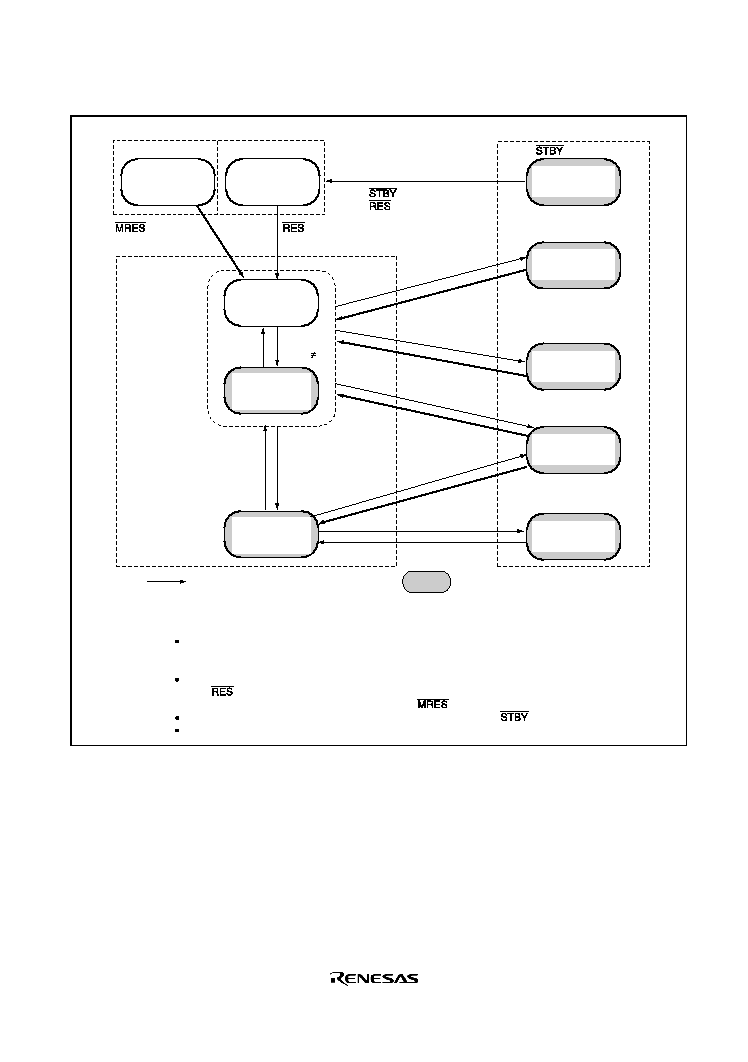
Rev. 1.0, 02/03, page 555 of 634
Program-halted state
Program execution state
Reset execution state
SCK2 to
SCK0 = 0
SCK2 to
SCK0 0
SLEEP instruction
Any interrupt *
1
SLEEP instruction
Interrupt *
2
SLEEP instruction
SLEEP instruction
Interrupt *
3
Interrupt *
2
,
LSON bit = 1
pin = High
pin = Low
pin = Low
SSBY = 0, LSON = 0
SSBY = 1,
PSS = 0, LSON = 0
pin = High
pin = High
: Transition after exception processing
Notes:
1.
2.
3.
All interrupts
NMI and IRQ0 to IRQ4, IRQ7, RTC interrupt, and USB suspend/resume interrupt
NMI and IRQ0 to IRQ4, IRQ7, RTC interrupt, and WDT interrupt
When a transition is made between modes by means of an interrupt, the transition cannot be
made on interrupt source generation alone. Ensure that interrupt handling is performed after
accepting the interrupt request.
From any state except hardware standby mode, a transition to the power-on reset state occurs
when
is driven low. From any state except hardware standby mode and power-on reset,
a transition to the manual reset state occurs when
is driven low.
From any state, a transition to hardware standby mode occurs when
is driven low.
Always select high-speed mode before making a transition to watch mode or sub-active mode.
: Power-down
Power-on
reset state
Manual
reset state
High-speed mode
(main clock)
Hardware
standby mode
Software
standby mode
Sleep mode
(main clock)
SSBY = 1,
PSS = 1, DTON = 0
SSBY = 0,
PSS = 1, LSON = 1
Sub-speed mode
(subclock)
Watch mode
(subclock)
Medium-speed
mode
(main clock)
SLEEP Instruction
SSBY = 1, PSS = 1,
DTON = 1, LSON = 0
After the oscillation
settling time (STS2 to 0),
clock switching exception
processing
SLEEP Instruction
SSBY = 1, PSS = 1,
DTON = 1, LSON = 1
Clock switching
exception processing
Sub-active
mode
(sub clock)
SLEEP instruction
Interrupt *
2
,
LSON bit = 0
Figure 20.1 Mode Transition Diagram

Rev. 1.0, 02/03, page 556 of 634
Table 20.2
Transition Conditions of Power-Down Modes
Status of Control Bit
at Transition
Pre-Transition
State
SSBY PSS
LSON DTON
State after Transition
Invoked by SLEEP
Command
State after Transition Back from
Power-Down Mode Invoked by
Interrupt
0
x
0
x
Sleep
High-speed/Medium-speed
0
x
1
x
--
--
1
0
0
x
Software standby
High-speed/Medium-speed
1
0
1
x
--
--
1
1
0
0
Watch
High-speed
1
1
1
0
Watch
Subactive
1
1
0
1
--
--
High-speed/
Medium-speed
1
1
1
1
Subactive
--
0
0
x
x
--
--
0
1
0
x
--
--
0
1
1
x
Sub sleep
Subactive
1
0
x
x
--
--
1
1
0
0
Watch
High-speed
1
1
1
0
Watch
Subactive
1
1
0
1
High-speed
--
Subactive
1
1
1
1
--
--
Legend x: Don't care
Note: -- : Do not set

Rev. 1.0, 02/03, page 557 of 634
20.1
Register Descriptions
The registers relating to the power down mode are shown below. For details on the low power
control register (LPWRCR), refer to section 19.1.2, Low Power Control Register (LPWRCR). For
details on the system clock control register (SCKCR), refer to section 19.1.1, System Clock
Control Register (SCKCR).
· Standby control register (SBYCR)
· System clock control register (SCKCR)
· Low power control register (LPWRCR)
· Timer control/status register (TCSR_1)
· Module stop control register A (MSTPCRA)
· Module stop control register B (MSTPCRB)
· Module stop control register C (MSTPCRC)
· Extended module stop register (EXMDLSTP)
20.1.1
Standby Control Register (SBYCR)
SBYCR is an 8-bit readable/writable register that performs software standby mode control.
Bit
Bit Name Initial Value
R/W
Description
7
SSBY
0
R/W
Software Standby
This bit specifies the transition mode after executing the
SLEEP instruction
0: Shifts to sleep mode when the SLEEP instruction is
executed in high-speed mode or medium-speed
mode.
Shifts to subsleep mode when the SLEEP instruction
is executed in subactive mode.
1: Shifts to software standby mode, subactive mode, or
watch mode when the SLEEP instruction is executed
in high-speed mode or medium-speed mode.
Shifts to watch mode or high-speed mode when the
SLEEP instruction is executed in subactive mode.
This bit does not change when clearing software standby
mode by using external interrupts and shifting to normal
operation. 0 should be written to this bit for clearing.

Rev. 1.0, 02/03, page 558 of 634
Bit
Bit Name Initial Value
R/W
Description
6
5
4
STS2
STS1
STS0
0
0
0
R/W
R/W
R/W
Standby Timer Select 2 to 0
These bits select the MCU wait time for clock
stabilization when cancel software standby mode, watch
mode, or subactive mode by an external interrupt. With
a crystal oscillator (Table 20.3), select a wait time of 8ms
(oscillation stabilization time) or more, depending on the
operating frequency. With an external clock, there are
no specific wait requirements.
000: Standby time = 8192 states
001: Standby time = 16384 states
010: Standby time = 32768 states
011: Standby time = 65536 states
100: Standby time = 131072 states
101: Standby time = 262144 states
110: Standby time = 2048 states
111: Standby time = 16 states
3
OPE
1
R/W
Output Port Enable
This bit selects whether address bus and bus control
signals (
CS0 to CS7, AS, RD, HWR, and LWR) are
brought to high impedance state or retained in software
standby mode, watch mode, or direct transition.
0: High impedance state
1: Retained
2 to 0 --
0
--
Reserved
These bits are always read as 0, and cannot be
modified.

Rev. 1.0, 02/03, page 559 of 634
20.1.2
Timer Control/Status Register (TCSR_1)
TCSR_1 controls the operation in power-down mode transition.
Bit
Bit Name
Initial Value
R/W
Description
7 to 5
0
Reserved
The write value should always be 0.
4
PSS
0
R/W
Prescaler Select
0: When the SLEEP instruction is executed in high-
speed mode or medium-speed mode, operation
shifts to sleep mode or software standby mode.
1: When the SLEEP instruction is executed in high-
speed mode or medium-speed mode, operation
shifts to sleep mode, watch mode, or subactive
mode.
When the SLEEP instruction is executed in
subactive mode, operation shifts to subsleep
mode, watch mode, or high-speed mode
TCSR_1 differs from other registers in being more
difficult to write to. The procedures for writing to
and reading this register are given below.
Write:
TCSR_1 must be written to by a word transfer
instruction. The upper byte of the written word must
contain H
A5 and the lower byte must contain the
write data. (When the PSS bit is set to 1, the upper
byte of the written word must contain H
A510.)
Read:
TCSR_1 is read by the same procedure as for the
general registers.
3 to 0 --
0
--
Reserved
The write value should always be 0.

Rev. 1.0, 02/03, page 560 of 634
20.1.3
Module Stop Control Registers A to C (MSTPCRA to MSTPCRC)
MSTPCR, comprising three 8-bit readable/writable registers, performs module stop mode control.
Setting a bit to 1, causes the corresponding module to enter module stop mode, while clearing the
bit to 0 clears the module stop mode.
MSTPCRA
Bit
Bit Name
Initial Value
R/W
Module
7
MSTPA7
0
R/W
DMA controller (DMAC)
6
MSTPA6*
0
R/W
5
MSTPA5
1
R/W
16-bit timer pulse unit (TPU)
4
MSTPA4*
1
R/W
3
MSTPA3*
1
R/W
2
MSTPA2*
1
R/W
1
MSTPA1
1
R/W
A/D converter
0
MSTPA0*
1
R/W
MSTPCRB
Bit
Bit Name
Initial Value
R/W
Module
7
MSTPB7
1
R/W
Serial communication interface 0 (SCI_0)
6
MSTPB6*
1
R/W
5
MSTPB5
1
R/W
Serial communication interface 2 (SCI_2)
4
MSTPB4*
1
R/W
3
MSTPB3*
1
R/W
2
MSTPB2*
1
R/W
1
MSTPB1*
1
R/W
0
MSTPB0
1
R/W
USB

Rev. 1.0, 02/03, page 561 of 634
MSTPCRC
Bit
Bit Name
Initial Value
R/W
Module
7
MSTPC7*
1
R/W
6
MSTPC6*
1
R/W
5
MSTPC5*
1
R/W
4
MSTPC4*
1
R/W
3
MSTPC3*
1
R/W
2
MSTPC2*
1
R/W
1
MSTPC1*
0
R/W
Flash memory
0
MSTPC0*
1
R/W
H-UDI
Note: * MSTPA6, MSTPA4 to MSTPA2, MSTPA0, MSTPB6, MSTPB4 to MSTPB1, MSTPC7 to
MSTPC2 are readable/writable bits with an initial value of 1 and should always be written
with 1.
20.1.4
Extended Module Stop Register (EXMDLSTP)
EXMDLSTP controls the clock supply of the RTC and USB.
Bit
Bit Name
Initial Value
R/W
Module
7 to
2
Undefined
Reserved
Read is undefined. These bits should not to be
modified.
1
RTCSTOP
0
R/W
RTC
0
USBSTOP1
0
R/W
USB
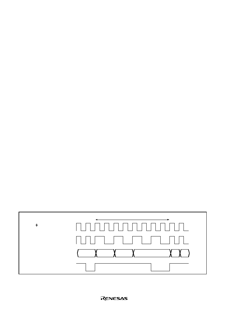
Rev. 1.0, 02/03, page 562 of 634
20.2
Medium-Speed Mode
When the SCK2 to SCK0 bits in SCKCR are set to 1, the operating mode changes to medium-
speed mode as soon as the current bus cycle ends. In medium-speed mode, the CPU operates on
the operating clock (
/2, /4, /8, /16, or /32) specified by the SCK2 to SCK0 bits. The bus
masters other than the CPU (DMAC) also operate in medium-speed mode. On-chip supporting
modules other than the bus masters always operate on the high-speed clock (
).
In medium-speed mode, a bus access is executed in the specified number of states with respect to
the bus master operating clock. For example, if
/4 is selected as the operating clock, on-chip
memory is accessed in 4 states, and internal I/O registers in 8 states.
Medium-speed mode is cleared by clearing all of bits SCK2 to SCK0 to 0. A transition is made to
high-speed mode and medium-speed mode is cleared at the end of the current bus cycle.
If a SLEEP instruction is executed when the SSBY bit in SBYCR and the LSON bit in LPWRCR
are cleared to 0, a transition is made to sleep mode. When sleep mode is cleared by an interrupt,
medium-speed mode is restored.
When the SLEEP instruction is executed with the SSBY bit = 1 and the LSON bit is cleared to 0,
operation shifts to the software standby mode. When software standby mode is cleared by an
external interrupt, medium-speed mode is restored.
When the
RES or MRES pin* is set low and medium-speed mode is cancelled, operation shifts to
the reset state. The same applies in the case of a reset caused by overflow of the watchdog timer.
When the
STBY pin is driven low, a transition is made to hardware standby mode.
Figure 20.2 shows the timing for transition to and clearance of medium-speed mode.
Note: * Supported only by the H8S/2218 Series.
SCKCR
SCKCR
,
supporting module clock
Bus master clock
Internal address bus
Internal write signal
Medium-speed mode
Figure 20.2 Medium-Speed Mode Transition and Clearance Timing

Rev. 1.0, 02/03, page 563 of 634
20.3
Sleep Mode
20.3.1
Transition to Sleep Mode
When the SLEEP instruction is executed when the SSBY bit in SBYCR and the LSON bit in
LPWRCR are cleared to 0, the CPU enters the sleep mode. In sleep mode, CPU operation stops
but the contents of the CPU's internal registers are retained. Other supporting modules do not stop.
20.3.2
Exiting Sleep Mode
Sleep mode is exited by any interrupt, or signals at the
RES, MRES* and STBY pins.
· Exiting Sleep Mode by Interrupts
When an interrupt occurs, sleep mode is exited and interrupt exception processing starts. Sleep
mode is not exited if the interrupt is disabled, or interrupts other than NMI are masked by the
CPU.
· Exiting Sleep Mode by RES or MRES* Pin
Setting the
RES or MRES* pin level Low selects the reset state. After the stipulated reset input
duration, driving the
RES or MRES* pin High starts the CPU performing reset exception
processing.
· Exiting Sleep Mode by STBY Pin
When the
STBY pin level is driven Low, a transition is made to hardware standby mode.
Note: * Supported only by the H8S/2218 Series.
20.4
Software Standby Mode
20.4.1
Transition to Software Standby Mode
A transition is made to software standby mode when the SLEEP instruction is executed when the
SSBY bit in SBYCR is set to 1 and the LSON bit in LPWRCR and the PSS bit in TCSR_1 are
cleared to 0. In this mode, the CPU, on-chip supporting modules, and oscillator all stop. However,
the contents of the CPU's internal registers, RAM data, and the states of on-chip supporting
modules other than the A/D converter, and the states of I/O ports, are retained. In this mode the
oscillator stops, and therefore power dissipation is significantly reduced.

Rev. 1.0, 02/03, page 564 of 634
20.4.2
Clearing Software Standby Mode
Software standby mode is cleared by an external interrupt (NMI pin,
IRQ7 pin, or IRQ0 to IRQ4
pins), RTC interrupt (
IRQ5 signal), or USB suspend/resume interrupt (IRQ6 signal), or by means
of the
RES pin, MRES pin*, or STBY pin.
· Clearing with an interrupt
When an NMI or IRQ0 to IRQ7 interrupt request signal is input, clock oscillation starts, and
after the elapse of the time set in bits STS2 to STS0 in SBYCR, stable clocks are supplied to
the entire chip, software standby mode is cleared, and interrupt exception handling is started.
When clearing software standby mode with an IRQ0 to IRQ7 interrupt, set the corresponding
enable bit to 1 and ensure that no interrupt with a higher priority than interrupts IRQ0 to IRQ5
is generated. Software standby mode cannot be cleared if the interrupt has been masked on the
CPU side.
· Clearing with the RES or MRES* pin
When the
RES or MRES* pin is driven low, clock oscillation is started. At the same time as
clock oscillation starts, clocks are supplied to the entire chip. Note that the
RES or MRES* pin
must be held low until clock oscillation stabilizes. When the
RES or MRES* pin goes high, the
CPU begins reset exception handling.
· Clearing with the STBY pin
When the
STBY pin is driven low, a transition is made to hardware standby mode.
Note: * Supported only by the H8S/2218 Series.
20.4.3
Setting Oscillation Stabilization Time after Clearing Software Standby Mode
Bits STS2 to STS0 in SBYCR should be set as described below.
· Using a Crystal Oscillator:
Set bits STS2 to STS0 so that the standby time is at least 8 ms (the oscillation stabilization
time).
Table 20.3 shows the standby times for different operating frequencies and settings of bits
STS2 to STS0.
· Using an External Clock
Set bits STS2 to STS0 as any value. Usually, minimum value is recommended. A 16-state
standby time cannot be used in the F-ZTAT version; a standby time of 2048 states or longer
should be used.
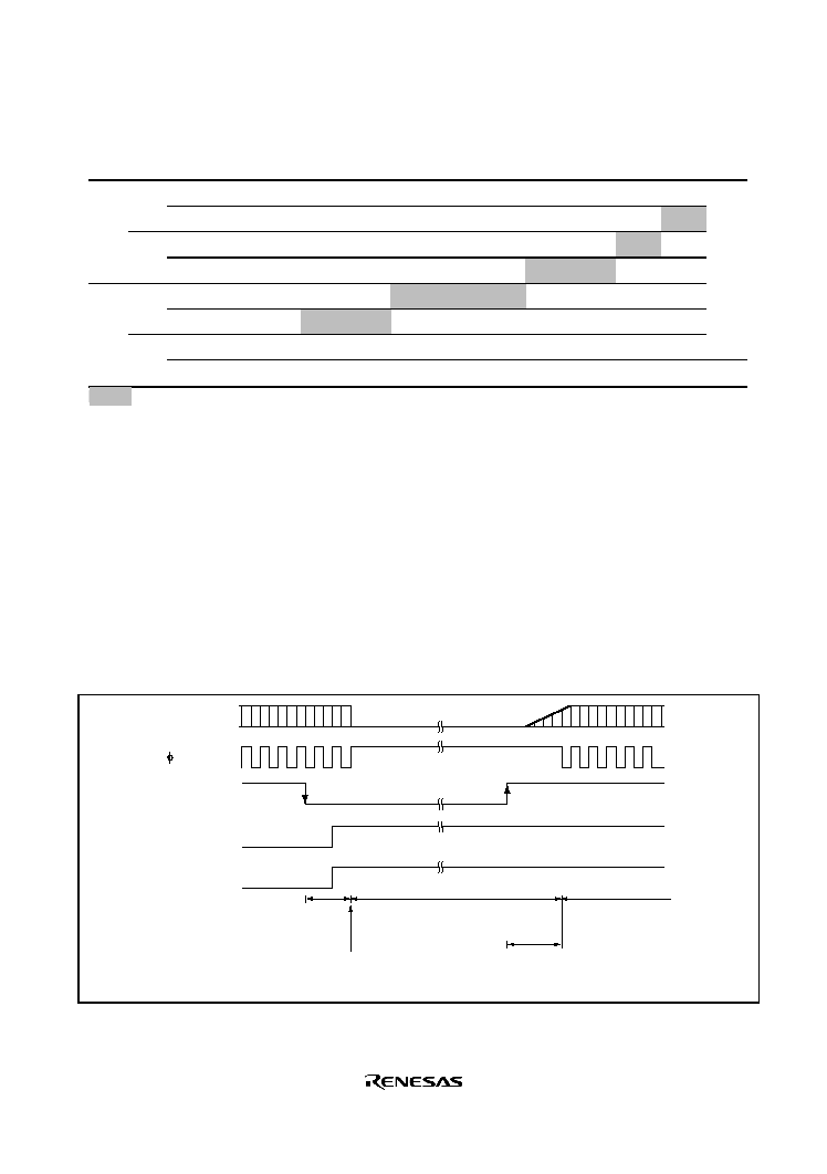
Rev. 1.0, 02/03, page 565 of 634
Table 20.3
Oscillation Stabilization Time Settings
STS2 STS1
STS0
Standby Time
24MHz 20MHz 16MHz 13MHz 10MHz 8MHz
6MHz
4MHz
2MHz
Unit
0
0
0
8192 states
0.3
0.4
0.51
0.6
0.8
1.0
1.3
2.0
4.1
ms
1
16384 states
0.7
0.8
1.0
1.3
1.6
2.0
2.7
4.1
8.2
1
0
32768 states
1.4
1.6
2.0
2.5
3.3
4.1
5.5
8.2
16.4
1
65536 states
2.7
3.3
4.1
5.0
6.6
8.2
10.9
16.4
32.8
1
0
0
131072 states
5.5
6.6
8.2
10.1
13.1
16.4
21.8
32.8
65.5
1
262144 states
10.9
13.1
16.4
20.2
26.2
32.8
43.6
65.6
131.2
1
0
2048 states
0.09
0.1
0.13
0.16
0.2
0.3
0.3
0.5
1.0
1
16 states
0.7
0.8
1.0
1.2
1.6
2.0
1.7
4.0
8.0
µs
: Recommended time setting
20.4.4
Software Standby Mode Application Example
Figure 20.3 shows an example in which a transition is made to software standby mode at the
falling edge on the NMI pin, and software standby mode is cleared at the rising edge on the NMI
pin.
In this example, an NMI interrupt is accepted with the NMIEG bit in SYSCR cleared to 0 (falling
edge specification), then the NMIEG bit is set to 1 (rising edge specification), the SSBY bit is set
to 1, and a SLEEP instruction is executed, causing a transition to software standby mode.
Software standby mode is then cleared at the rising edge on the NMI pin.
Oscillator
NMI
NMIEG
SSBY
NMI exception
handling
NMIEG = 1
SSBY = 1
Oscillation
stabilization
time t
OSC2
Software standby mode
(power-down mode)
NMI exception
handling
SLEEP instruction
Figure 20.3 Software Standby Mode Application Example

Rev. 1.0, 02/03, page 566 of 634
20.5
Hardware Standby Mode
20.5.1
Transition to Hardware Standby Mode
When the
STBY pin is driven low, a transition is made to hardware standby mode from any mode.
In hardware standby mode, all functions enter the reset state and stop operation, resulting in a
significant reduction in power dissipation. As long as the prescribed voltage is supplied, on-chip
RAM data is retained. I/O ports are set to the high-impedance state.
In order to retain on-chip RAM data, the RAME bit in SYSCR should be cleared to 0 before
driving the
STBY pin low.
Do not change the state of the mode pins (MD2 to MD0) while this LSI is in hardware standby
mode.
20.5.2
Clearing Hardware Standby Mode
Hardware standby mode is cleared by means of the
STBY pin and the RES pin. When the STBY
pin is driven high while the
RES pin is low, the reset state is set and clock oscillation is started.
Ensure that the
RES pin is held low until the clock oscillator stabilizes (at least t
osc1
--the
oscillation stabilization time--when using a crystal oscillator). When the
RES pin is subsequently
driven high, a transition is made to the program execution state via the reset exception handling
state.
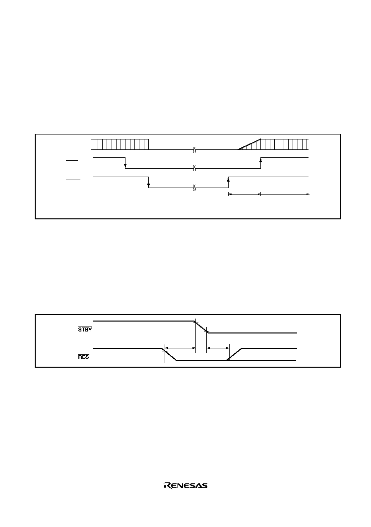
Rev. 1.0, 02/03, page 567 of 634
20.5.3
Hardware Standby Mode Timing
Figure 20.4 shows an example of hardware standby mode timing.
When the
STBY pin is driven low after the RES pin has been driven low, a transition is made to
hardware standby mode. Hardware standby mode is cleared by driving the
STBY pin high, waiting
for the oscillation stabilization time, then changing the
RES pin from low to high.
Oscillator
RES
STBY
Oscillation
stabilization
time t
OSC1
Reset exception
handling
Figure 20.4 Hardware Standby Mode Timing (Example)
20.5.4
Hardware Standby Mode Timings
Timing of Transition to Hardware Standby Mode:
1. To retain RAM contents with the RAME bit set to 1 in SYSCR
Drive the
RES signal low at least 10 states before the STBY signal goes low, as shown in
Figure 20.5. After
STBY has gone low, RES has to wait for at least 0 ns before becoming high.
t
2
0 ns
t
1
10 t
cyc
Figure 20.5 Timing of Transition to Hardware Standby Mode
2. To retain RAM contents with the RAME bit cleared to 0 in SYSCR, or when RAM contents do
not need to be retained
RES does not have to be driven low as in the above case.
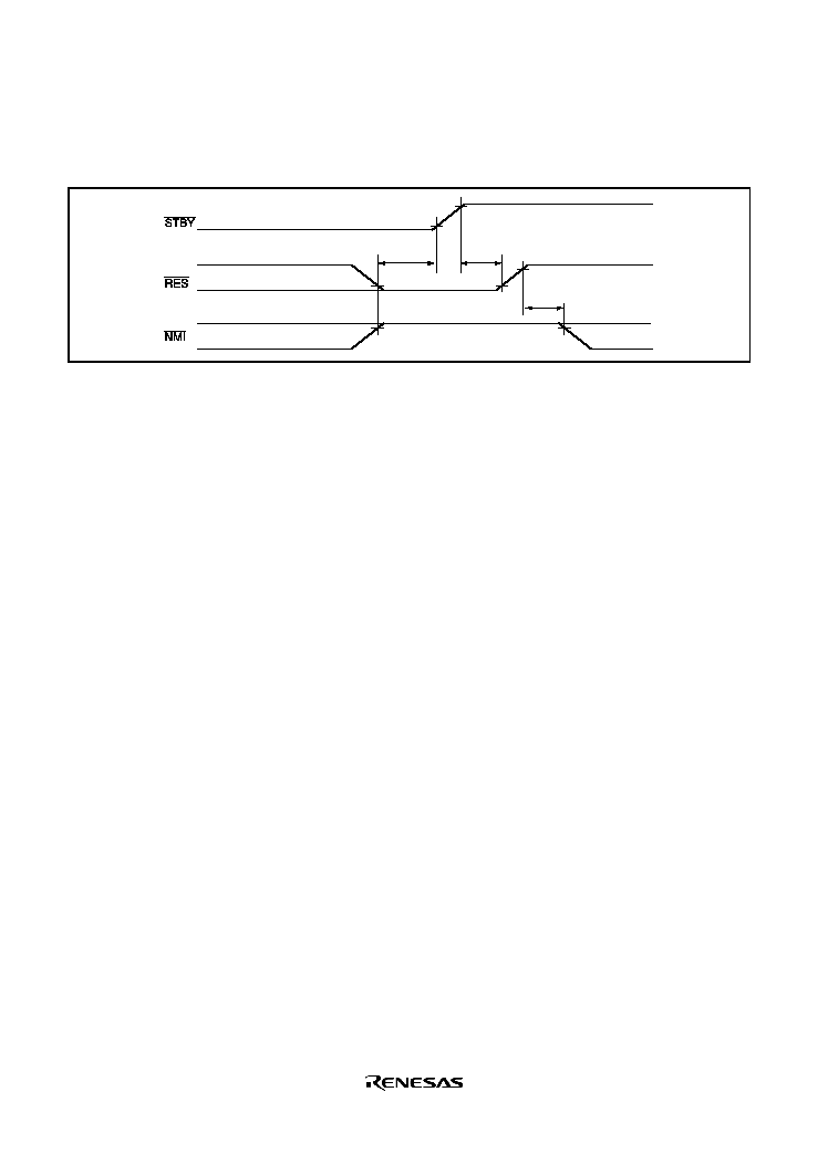
Rev. 1.0, 02/03, page 568 of 634
Timing of Recovery from Hardware Standby Mode:Drive the
RES signal low approximately
100 ns or more before
STBY goes high to execute a power-on reset.
t
OSC
t
NMIRH
t
100 ns
Figure 20.6 Timing of Recovery from Hardware Standby Mode
20.6
Module Stop Mode
Module stop mode can be set for individual on-chip supporting modules.
When the corresponding MSTP bit in MSTPCR is set to 1, module operation stops at the end of
the bus cycle and a transition is made to module stop mode. The CPU continues operating
independently.
When the corresponding MSTP bit is cleared to 0, module stop mode is cleared and the module
starts operating at the end of the bus cycle. In module stop mode, the internal states of modules
other than the A/D converter are retained.
After reset clearance, all modules other than DMAC are in module stop mode.
When an on-chip supporting module is in module stop mode, read/write access to its registers is
disabled.
When a transition is made to sleep mode with all modules stopped, the bus controller and I/O ports
also stop operating, enabling current dissipation to be further reduced.

Rev. 1.0, 02/03, page 569 of 634
20.7
Watch Mode
20.7.1
Transition to Watch Mode
CPU operation makes a transition to watch mode when the SLEEP instruction is executed in high-
speed mode or sub-active mode with SBYCR SSBY=1, LPWRCR DTON = 0, and TCSR_1
PSS = 1.
In watch mode, the CPU is stopped and peripheral modules other than WDT are also stopped. The
contents of the CPU's internal registers, the data in internal RAM, and the statuses of the internal
peripheral modules (excluding the A/D converter) and I/O ports are retained. To make a transition
to watch mode, bits SCK2 to SCK0 in SCKCR must be set to 0.
20.7.2
Exiting Watch Mode
Watch mode is exited by any interrupt (WOVI interrupt, NMI pin, or
IRQ0, to IRQ7), or signals at
the
RES, MRES*, or STBY pins.
· Exiting Watch Mode by Interrupts
When an interrupt occurs, watch mode is exited and a transition is made to high-speed mode or
medium-speed mode when the LPWRCR LSON bit = 0 or to sub-active mode when the LSON
bit = 1. When a transition is made to high-speed mode, a stable clock is supplied to all LSI
circuits and interrupt exception processing starts after the time set in SBYCR STS2 to STS0
has elapsed. In case of IRQ0, to IRQ7 interrupts, no transition is made from watch mode if the
corresponding enable bit/pin function switching bit has been cleared to 0, and, in the case of
interrupts from the internal peripheral modules, the interrupt enable register has been set to
disable the reception of that interrupt, or is masked by the CPU.
See section 20.4.3 Setting, Oscillation Stablization Time after Clearing Software Standby
Mode, for how to set the oscillation settling time when making a transition from watch mode to
high-speed mode.
· Exiting Watch Mode by RES or MRES* pins
For exiting watch mode by the
RES or MRES* pins, see section 20.4.2, Clearing Software
Standby Mode.
· Exiting Watch Mode by STBY pin
When the
STBY pin level is driven low, a transition is made to hardware standby mode.
Note:
* Supported only by the H8S/2218 Series.

Rev. 1.0, 02/03, page 570 of 634
20.8
Sub-Sleep Mode
20.8.1
Transition to Sleep Mode
When the SLEEP instruction is executed with the SBYCR SSBY bit = 0, LPWRCR LSON bit = 1,
and TCSR_1 PSS bit = 1, CPU operation shifts to sub-sleep mode.
In sub-sleep mode, the CPU is stopped. Peripheral modules other WDT are also stopped. The
contents of the CPU's internal registers, the data in internal RAM, and the statuses of the internal
peripheral modules (excluding the A/D converter) and I/O ports are retained.
22.8.2
Exiting Sub-Sleep Mode
Sub-sleep mode is exited by an interrupt (interrupts from internal peripheral modules, NMI pin, or
IRQ0, to IRQ7), or signals at the RES or STBY, MRES* or STBY or pins.
· Exiting Sub-Sleep Mode by Interrupts
When an interrupt occurs, sub-sleep mode is exited and interrupt exception processing starts.
In case of
IRQ0, to IRQ7interrupts, sub-sleep mode is not cancelled if the corresponding
enable bit/pin function switching bit has been cleared to 0, and, in the case of interrupts from
the internal peripheral modules, the interrupt enable register has been set to disable the
reception of that interrupt, or is masked by the CPU.
· Exiting Sub-Sleep Mode by RES or MRES* pins
For exiting sub-sleep mode by the
RES or MRES* pins, see section 20.4.2, Clearing Software
Standby Mode.
· Exiting Sub-Sleep Mode by STBY Pin
When the
STBY pin level is driven low, a transition is made to hardware standby mode.
Note:
* Supported only by the H8S/2218 Series.

Rev. 1.0, 02/03, page 571 of 634
20.9
Sub-Active Mode
20.9.1
Transition to Sub-Active Mode
When the SLEEP instruction is executed in high-speed mode with the SBYCR SSBY bit = 1,
LPWRCR DTON bit = 1, LSON bit = 1, and TCSR_1 PSS bit = 1, CPU operation shifts to sub-
active mode. When an interrupt occurs in watch mode, and if the LSON bit of LPWRCR is 1, a
transition is made to sub-active mode. And if an interrupt occurs in sub-sleep mode, a transition is
made to sub-active mode.
In sub-active mode, the CPU operates at low speed on the subclock, and the program is executed
step by step. Peripheral modules other than WDT are also stopped.
When operating the CPU in sub-active mode, the SCKCR SCK2 to SCK0 bits must be set to 0.
22.9.2
Exiting Sub-Active Mode
Sub-active mode is exited by the SLEEP instruction or the
RES, MRES*, or STBY pins.
· Exiting Sub-Active Mode by SLEEP Instruction
When the SLEEP instruction is executed with the SBYCR SSBY bit = 1, LPWRCR DTON bit
= 0, and TCSR_1 PSS bit = 1, the CPU exits sub-active mode and a transition is made to watch
mode. When the SLEEP instruction is executed with the SBYCR SSBY bit = 0, LPWRCR
LSON bit = 1, and TCSR_1 PSS bit = 1, a transition is made to sub-sleep mode. Finally, when
the SLEEP instruction is executed with the SBYCR SSBY bit = 1, LPWRCR DTON bit = 1,
LSON bit = 0, and TCSR_1 PSS bit = 1, a direct transition is made to high-speed mode (SCK0
to SCK2 all 0).
· Exiting Sub-Active Mode by RES or MRES* pins
For exiting sub-active mode by the
RES or MRES* pins, see section 20.4.2, Clearing Software
Standby Mode.
· Exiting Sub-Active Mode by STBY Pin
When the
STBY pin level is driven low, a transition is made to hardware standby mode.
Note:
* Supported only by the H8S/2218 Series.

Rev. 1.0, 02/03, page 572 of 634
20.10
Direct Transitions
There are three modes, high-speed, medium-speed, and sub-active, in which the CPU executes
programs. When a direct transition is made, there is no interruption of program execution when
shifting between high-speed and sub-active modes. Direct transitions are enabled by setting the
LPWRCR DTON bit to 1, then executing the SLEEP instruction. After a transition, direct
transition interrupt exception processing starts.
20.10.1
Direct Transitions from High-Speed Mode to Sub-Active Mode
Execute the SLEEP instruction in high-speed mode when the SBYCR SSBY bit = 1, LPWRCR
LSON bit = 1, and DTON bit = 1, and TSCR_1 PSS bit = 1 to make a transition to sub-active
mode.
20.10.2
Direct Transitions from Sub-Active Mode to High-Speed Mode
Execute the SLEEP instruction in sub-active mode when the SBYCR SSBY bit = 1, LPWRCR
LSON bit = 0, and DTON bit = 1, and TSCR_1 PSS bit = 1 to make a direct transition to high-
speed mode after the time set in SBYCR STS2 to STS0 has elapsed.
20.11
Clock Output Disabling Function
Output of the
clock can be controlled by means of the PSTOP bit in SCKCR, and DDR for the
corresponding port. When the PSTOP bit is set to 1, the
clock stops at the end of the bus cycle,
and
output goes high. ø clock output is enabled when the PSTOP bit is cleared to 0. When DDR
for the corresponding port is cleared to 0,
clock output is disabled and input port mode is set.
Table 20.4 shows the state of the
pin in each processing state.
Table 20.4
Pin State in Each Processing State
Register Settings
DDR
PSTOP
High-Speed Mode,
Medium-Speed Mode,
Subactive Mode
Sleep Mode, Subsleep
Mode
Software Standby
Mode, Watch Mode,
Direct Transition
Hardware Standby
Mode
0
X
High impedance
High impedance
High impedance
High impedance
1
0
output
output
Fixed high
High impedance
1
1
Fixed high
Fixed high
Fixed high
High impedance
Legend X: Don't care

Rev. 1.0, 02/03, page 573 of 634
20.12
Usage Notes
20.12.1
I/O Port Status
In software standby mode, I/O port states are retained. Therefore, there is no reduction in current
dissipation for the output current when a high-level signal is output.
20.12.2
Current Dissipation during Oscillation Stabilization Wait Period
Current dissipation increases during the oscillation stabilization wait period.
20.12.3
DMAC Module Stop
Depending on the operating status of the DMAC, the MSTPA7 bit may not be set to 1. Setting of
the DMAC module stop mode should be carried out only when the DMAC is not activated.
For details, section 7, DMA Controller (DMAC).
20.12.4
On-Chip Peripheral Module Interrupt
Relevant interrupt operations cannot be performed in module stop mode. Consequently, if module
stop mode is entered when an interrupt has been requested, it will not be possible to clear the CPU
interrupt source or DMAC activation source. Interrupts should therefore be disabled before setting
module stop mode.

Rev. 1.0, 02/03, page 574 of 634

Rev. 1.0, 02/03, page 575 of 634
Section 21 List of Registers
The register list gives information on the on-chip I/O register addresses, how the register bits are
configured, and the register states in each operating mode. The information is given as shown
below.
1. Register Addresses (address order)
· Registers are listed from the lower allocation addresses.
· Registers are classified by functional modules.
· The access size is indicated.
2. Register Bits
· Bit configurations of the registers are described in the same order as the Register Addresses
(address order) above.
· Reserved bits are indicated by in the bit name column.
· The bit number in the bit-name column indicates that the whole register is allocated as a
counter or for holding data.
· 16-bit or 24-bit registers are indicated from the bit on the MSB side.
3. Register States in Each Operating Mode
· Register states are described in the same order as the Register Addresses (address order)
above.
· The register states described here are for the basic operating modes. If there is a specific reset
for an on-chip peripheral module, refer to the section on that on-chip peripheral module.

Rev. 1.0, 02/03, page 576 of 634
21.1
Register Addresses (Address Order)
The data bus width indicates the numbers of bits by which the register is accessed.
The number of access states indicates the number of states based on the specified reference clock.
Register Name
Abbreviation
Number
of Bits
Address
Module
Data Bus
Width
Number
Of Access
States
USB reserved area
H'C00000 to
H'C0007F
USB
USB control register
UCTLR
8
H'C00080
USB
8
3
USB test register A
UTSTRA
8
H'C00081
USB
8
3
USB DMAC transfer request register
UDMAR
8
H'C00082
USB
8
3
USB device resume register
UDRR
8
H'C00083
USB
8
3
USB trigger register 0
UTRG0
8
H'C00084
USB
8
3
USB FIFO clear register 0
UFCLR0
8
H'C00086
USB
8
3
USB endpoint stall register 0
UESTL0
8
H'C00088
USB
8
3
USB endpoint stall register 1
UESTL1
8
H'C00089
USB
8
3
USB endpoint data register 0s
UEDR0s
8
H'C00090 to
H'C00093
USB
8
3
USB endpoint data register 0i
UEDR0i
8
H'C00094 to
H'C00097
USB
8
3
USB endpoint data register 0o
UEDR0o
8
H'C00098 to
H'C0009B
USB
8
3
USB endpoint data register 3
UEDR3
8
H'C0009C to
H'C0009F
USB
8
3
USB endpoint data register 1
UEDR1
8
H'C000A0 to
H'C000A3
USB
8
3
USB endpoint data register 2
UEDR2
8
H'C000A4 to
H'C000A7
USB
8
3

Rev. 1.0, 02/03, page 577 of 634
Register Name
Abbreviation
Number
of Bits
Address
Module
Data Bus
Width
Number
Of Access
States
USB endpoint receive data size register 0o
UESZ0o
8
H'C000BC
USB
8
3
USB endpoint receive data size register 2
UESZ2
8
H'C000BD
USB
8
3
USB interrupt flag register 0
UIFR0
8
H'C000C0
USB
8
3
USB interrupt flag register 1
UIFR1
8
H'C000C1
USB
8
3
USB interrupt flag register 3
UIFR3
8
H'C000C3
USB
8
3
USB interrupt enable register 0
UIER0
8
H'C000C4
USB
8
3
USB interrupt enable register 1
UIER1
8
H'C000C5
USB
8
3
USB interrupt enable register 3
UIER3
8
H'C000C7
USB
8
3
USB interrupt selection register 0
UISR0
8
H'C000C8
USB
8
3
USB interrupt selection register 1
UISR1
8
H'C000C9
USB
8
3
USB interrupt selection register 3
UISR3
8
H'C000CB
USB
8
3
USB data status register
UDSR
8
H'C000CC
USB
8
3
USB configuration value register
UCVR
8
H'C000CF
USB
8
3
USB test register 0
UTSTR0
8
H'C000F0
USB
8
3
USB test register 1
UTSTR1
8
H'C000F1
USB
8
3
USB test register 2
UTSTR2
8
H'C000F2
USB
8
3
USB test register B
UTSTRB
8
H'C000FB
USB
8
3
USB test register C
UTSTRC
8
H'C000FC
USB
8
3
USB test register D
UTSTRD
8
H'C000FD
USB
8
3
USB test register E
UTSTRE
8
H'C000FE
USB
8
3
USB test register F
UTSTRF
8
H'C000FF
USB
8
3
USB reserved area
H'C00100 to
H'C001FF
USB
DPRAM (512 bytes)
8
H'C00200 to
H'C003FF
USB
8
3
USB reserved area
H'C00400 to
H'DFFFFF
USB

Rev. 1.0, 02/03, page 578 of 634
Register Name
Abbreviation
Number
of Bits
Address
Module
Data Bus
Width
Number
Of Access
States
Serial control register X
SCRX
8
H'FDB4
FLASH
8
2
Standby control register
SBYCR
8
H'FDE4
SYSTEM
8
2
System control register
SYSCR
8
H'FDE5
SYSTEM
8
2
System clock control register
SCKCR
8
H'FDE6
SYSTEM
8
2
Mode control register
MDCR
8
H'FDE7
SYSTEM
8
2
Module stop control register A
MSTPCRA
8
H'FDE8
SYSTEM
8
2
Module stop control register B
MSTPCRB
8
H'FDE9
SYSTEM
8
2
Module stop control register C
MSTPCRC
8
H'FDEA
SYSTEM
8
2
Pin function control register
PFCR
8
H'FDEB
BSC
8
2
Low power control register
LPWRCR
8
H'FDEC
SYSTEM
8
2
Serial extended mode register A_0
SEMRA_0
8
H'FDF8
SCI_0
8
2
Serial extended mode register B_0
SEMRB_0
8
H'FDF9
SCI_0
8
2
IRQ sense control register H
ISCRH
8
H'FE12
INT
8
2
IRQ sense control register L
ISCRL
8
H'FE13
INT
8
2
IRQ enable register
IER
8
H'FE14
INT
8
2
IRQ status register
ISR
8
H'FE15
INT
8
2
Port 1 data direction register
P1DDR
8
H'FE30
PORT
8
2
Port 3 data direction register
P3DDR
8
H'FE32
PORT
8
2
Port 7 data direction register
P7DDR
8
H'FE36
PORT
8
2
Port A data direction register
PADDR
8
H'FE39
PORT
8
2
Port B data direction register
PBDDR
8
H'FE3A
PORT
8
2
Port C data direction register
PCDDR
8
H'FE3B
PORT
8
2
Port D data direction register
PDDDR
8
H'FE3C
PORT
8
2
Port E data direction register
PEDDR
8
H'FE3D
PORT
8
2
Port F data direction register
PFDDR
8
H'FE3E
PORT
8
2
Port G data direction register
PGDDR
8
H'FE3F
PORT
8
2
Port A pull-up MOS control register
PAPCR
8
H'FE40
PORT
8
2
Port B pull-up MOS control register
PBPCR
8
H'FE41
PORT
8
2
Port C pull-up MOS control register
PCPCR
8
H'FE42
PORT
8
2
Port D pull-up MOS control register
PDPCR
8
H'FE43
PORT
8
2
Port E pull-up MOS control register
PEPCR
8
H'FE44
PORT
8
2
Port 3 open drain control register
P3ODR
8
H'FE46
PORT
8
2
Port A open drain control register
PAODR
8
H'FE47
PORT
8
2
Port B open drain control register
PBODR
8
H'FE48
PORT
8
2
Port C open drain control register
PCODR
8
H'FE49
PORT
8
2

Rev. 1.0, 02/03, page 579 of 634
Register Name
Abbreviation
Number
of Bits
Address
Module
Data Bus
Width
Number
Of Access
States
Timer start register
TSTR
8
H'FEB0
TPU
16
2
Timer synchro register
TSYR
8
H'FEB1
TPU
16
2
Interrupt priority register A
IPRA
8
H'FEC0
INT
8
2
Interrupt priority register B
IPRB
8
H'FEC1
INT
8
2
Interrupt priority register C
IPRC
8
H'FEC2
INT
8
2
Interrupt priority register D
IPRD
8
H'FEC3
INT
8
2
Interrupt priority register E
IPRE
8
H'FEC4
INT
8
2
Interrupt priority register F
IPRF
8
H'FEC5
INT
8
2
Interrupt priority register G
IPRG
8
H'FEC6
INT
8
2
Interrupt priority register J
IPRJ
8
H'FEC9
INT
8
2
Interrupt priority register K
IPRK
8
H'FECA
INT
8
2
Interrupt priority register M
IPRM
8
H'FECC
INT
8
2
Bus width control register
ABWCR
8
H'FED0
BSC
8
2
Access state control register
ASTCR
8
H'FED1
BSC
8
2
Wait control register H
WCRH
8
H'FED2
BSC
8
2
Wait control register L
WCRL
8
H'FED3
BSC
8
2
Bus control register H
BCRH
8
H'FED4
BSC
8
2
Bus control register L
BCRL
8
H'FED5
BSC
8
2
RAM emulation register
RAMER
8
H'FEDB
FLASH
8
2
Memory address register 0A H
MAR0AH
16
H'FEE0
DMAC
16
2
Memory address register 0A L
MAR0AL
16
H'FEE2
DMAC
16
2
I/O address register 0A
IOAR0A
16
H'FEE4
DMAC
16
2
Transfer count register 0A
ETCR0A
16
H'FEE6
DMAC
16
2
Memory address register 0B H
MAR0BH
16
H'FEE8
DMAC
16
2
Memory address register 0B L
MAR0BL
16
H'FEEA
DMAC
16
2
I/O address register 0B
IOAR0B
16
H'FEEC
DMAC
16
2
Transfer count register 0B
ETCR0B
16
H'FEEE
DMAC
16
2
Memory address register 1A H
MAR1AH
16
H'FEF0
DMAC
16
2
Memory address register 1A L
MAR1AL
16
H'FEF2
DMAC
16
2
I/O address register 1A
IOAR1A
16
H'FEF4
DMAC
16
2
Transfer count register 1A
ETCR1A
16
H'FEF6
DMAC
16
2
Memory address register 1B H
MAR1BH
16
H'FEF8
DMAC
16
2
Memory address register 1B L
MAR1BL
16
H'FEFA
DMAC
16
2
I/O address register 1B
IOAR1B
16
H'FEFC
DMAC
16
2
Transfer count register 1B
ETCR1B
16
H'FEFE
DMAC
16
2

Rev. 1.0, 02/03, page 580 of 634
Register Name
Abbreviation
Number
of Bits
Address
Module
Data Bus
Width
Number
Of Access
States
Port 1 data register
P1DR
8
H'FF00
PORT
8
2
Port 3 data register
P3DR
8
H'FF02
PORT
8
2
Port 7 data register
P7DR
8
H'FF06
PORT
8
2
Port A data register
PADR
8
H'FF09
PORT
8
2
Port B data register
PBDR
8
H'FF0A
PORT
8
2
Port C data register
PCDR
8
H'FF0B
PORT
8
2
Port D data register
PDDR
8
H'FF0C
PORT
8
2
Port E data register
PEDR
8
H'FF0D
PORT
8
2
Port F data register
PFDR
8
H'FF0E
PORT
8
2
Port G data register
PGDR
8
H'FF0F
PORT
8
2
Timer control register_0
TCR_0
8
H'FF10
TPU_0
16
2
Timer mode register_0
TMDR_0
8
H'FF11
TPU_0
16
2
Timer I/O control register H_0
TIORH_0
8
H'FF12
TPU_0
16
2
Timer I/O control register L_0
TIORL_0
8
H'FF13
TPU_0
16
2
Timer interrupt enable register_0
TIER_0
8
H'FF14
TPU_0
16
2
Timer status register_0
TSR_0
8
H'FF15
TPU_0
16
2
Timer counter_0
TCNT_0
16
H'FF16
TPU_0
16
2
Timer general register A_0
TGRA_0
16
H'FF18
TPU_0
16
2
Timer general register B_0
TGRB_0
16
H'FF1A
TPU_0
16
2
Timer general register C_0
TGRC_0
16
H'FF1C
TPU_0
16
2
Timer general register D_0
TGRD_0
16
H'FF1E
TPU_0
16
2
Timer control register_1
TCR_1
8
H'FF20
TPU_1
16
2
Timer mode register_1
TMDR_1
8
H'FF21
TPU_1
16
2
Timer I/O control register _1
TIOR_1
8
H'FF22
TPU_1
16
2
Timer interrupt enable register _1
TIER_1
8
H'FF24
TPU_1
16
2
Timer status register_1
TSR_1
8
H'FF25
TPU_1
16
2
Timer counter_1
TCNT_1
16
H'FF26
TPU_1
16
2
Timer general register A_1
TGRA_1
16
H'FF28
TPU_1
16
2
Timer general register B_1
TGRB_1
16
H'FF2A
TPU_1
16
2
Timer control register_2
TCR_2
8
H'FF30
TPU_2
16
2
Timer mode register_2
TMDR_2
8
H'FF31
TPU_2
16
2
Timer I/O control register 2
TIOR_2
8
H'FF32
TPU_2
16
2
Timer interrupt enable register 2
TIER_2
8
H'FF34
TPU_2
16
2
Timer status register_2
TSR_2
8
H'FF35
TPU_2
16
2
Timer counter_2
TCNT_2
16
H'FF36
TPU_2
16
2

Rev. 1.0, 02/03, page 581 of 634
Register Name
Abbreviation
Number
of Bits
Address
Module
Data Bus
Width
Number
Of Access
States
Timer general register A_2
TGRA_2
16
H'FF38
TPU_2
16
2
Timer general register B_2
TGRB_2
16
H'FF3A
TPU_2
16
2
Extended module stop register
EXMDLSTP
8
H'FF40
SYSTEM
8
2
Second data register/
free running counter data register
RSECDR
8
H'FF48
RTC
8
2
Minute data register
RMINDR
8
H'FF49
RTC
8
2
Hour data register
RHRDR
8
H'FF4A
RTC
8
2
Day-of-week data register
RWKDR
8
H'FF4B
RTC
8
2
RTC control register 1
RTCCR1
8
H'FF4C
RTC
8
2
RTC control register 2
RTCCR2
8
H'FF4D
RTC
8
2
Clock source select register
RTCCSR
8
H'FF4F
RTC
8
2
DMA control register 0A
DMACR0A
8
H'FF62
DMAC
16
2
DMA control register 0B
DMACR0B
8
H'FF63
DMAC
16
2
DMA control register 1A
DMACR1A
8
H'FF64
DMAC
16
2
DMA control register 1B
DMACR1B
8
H'FF65
DMAC
16
2
DMA band control register
DMABCR
16
H'FF66
DMAC
16
2
Timer control/status register
TCSR
8
H'FF74
WDT
16
2
Timer counter
TCNT
8
H'FF74
(write)
WDT
16
2
Timer counter
TCNT
8
H'FF75
(read)
WDT
16
2
Reset control/status register
RSTCSR
8
H'FF76
(write)
WDT
16
2
Reset control/status register
RSTCSR
8
H'FF77
(read)
WDT
16
2
Serial mode register_0
SMR_0
8
H'FF78
SCI_0
8
2
Bit rate register_0
BRR_0
8
H'FF79
SCI_0
8
2
Serial control register_0
SCR_0
8
H'FF7A
SCI_0
8
2
Transmit data register_0
TDR_0
8
H'FF7B
SCI_0
8
2
Serial status register_0
SSR_0
8
H'FF7C
SCI_0
8
2
Receive data register_0
RDR_0
8
H'FF7D
SCI_0
8
2
Smart card mode register_0
SCMR_0
8
H'FF7E
SCI_0
8
2

Rev. 1.0, 02/03, page 582 of 634
Register Name
Abbreviation
Number
of Bits
Address
Module
Data Bus
Width
Number
Of Access
States
Serial mode register_2
SMR_2
8
H'FF88
SCI_2
8
2
Bit rate register_2
BRR_2
8
H'FF89
SCI_2
8
2
Serial control register_2
SCR_2
8
H'FF8A
SCI_2
8
2
Transmit data register_2
TDR_2
8
H'FF8B
SCI_2
8
2
Serial status register_2
SSR_2
8
H'FF8C
SCI_2
8
2
Receive data register_2
RDR_2
8
H'FF8D
SCI_2
8
2
Smart card mode register_2
SCMR_2
8
H'FF8E
SCI_2
8
2
A/D data register AH
ADDRAH
8
H'FF90
A/D
8
2
A/D data register AL
ADDRAL
8
H'FF91
A/D
8
2
A/D data register BH
ADDRBH
8
H'FF92
A/D
8
2
A/D data register BL
ADDRBL
8
H'FF93
A/D
8
2
A/D data register CH
ADDRCH
8
H'FF94
A/D
8
2
A/D data register CL
ADDRCL
8
H'FF95
A/D
8
2
A/D data register DH
ADDRDH
8
H'FF96
A/D
8
2
A/D data register DL
ADDRDL
8
H'FF97
A/D
8
2
A/D control/status register
ADCSR
8
H'FF98
A/D
8
2
A/D control register
ADCR
8
H'FF99
A/D
8
2
Timer control/status register
TCSR_1
8
H'FFA2
SYSTEM
16
2
Flash memory control register 1
FLMCR1
8
H'FFA8
FLASH
8
2
Flash memory control register 2
FLMCR2
8
H'FFA9
FLASH
8
2
Erase block register 1
EBR1
8
H'FFAA
FLASH
8
2
Erase block register 2
EBR2
8
H'FFAB
FLASH
8
2
Flash memory power control register
FLPWCR
8
H'FFAC
FLASH
8
2
Port 1 register
PORT1
8
H'FFB0
PORT
8
2
Port 3 register
PORT3
8
H'FFB2
PORT
8
2
Port 4 register
PORT4
8
H'FFB3
PORT
8
2
Port 7 register
PORT7
8
H'FFB6
PORT
8
2
Port 9 register
PORT9
8
H'FFB8
PORT
8
2
Port A register
PORTA
8
H'FFB9
PORT
8
2
Port B register
PORTB
8
H'FFBA
PORT
8
2
Port C register
PORTC
8
H'FFBB
PORT
8
2
Port D register
PORTD
8
H'FFBC
PORT
8
2
Port E register
PORTE
8
H'FFBD
PORT
8
2
Port F register
PORTF
8
H'FFBE
PORT
8
2
Port G register
PORTG
8
H'FFBF
PORT
8
2

Rev. 1.0, 02/03, page 583 of 634
21.2
Register Bits
Register bit names of the on-chip peripheral modules are described below.
Each line covers eight bits, so 16-bit registers are shown as two lines and 32-bit registers as four
lines.
Register
Name
Bit 7
Bit 6
Bit 5
Bit 4
Bit 3
Bit 2
Bit 1
Bit 0
Module
UCTLR
USPNDE
UCKS3
UCKS2
UCKS1
UCKS0
UIFRST
UDCRST
USB
UTSTRA
UDMAR
EP2T1
EP2T0
EP1T1
EP1T0
UDRR
RWUPs
DVR
UTRG0
EP2RDFN
EP1PKTE
EP3PKTE
EP0oRDFN EP0iPKTE
EP0sRDFN
UFCLR0
EP2CLR
EP1CLR
EP3CLR
EP0oCLR
EP0iCLR
UESTL0
EP2STL
EP1STL
EP3STL
EP0STL
UESTL1
SCME
UEDR0s
D7
D6
D5
D4
D3
D2
D1
D0
UEDR0i
D7
D6
D5
D4
D3
D2
D1
D0
UEDR0o
D7
D6
D5
D4
D3
D2
D1
D0
UEDR3
D7
D6
D5
D4
D3
D2
D1
D0
UEDR1
D7
D6
D5
D4
D3
D2
D1
D0
UEDR2
D7
D6
D5
D4
D3
D2
D1
D0
UESZ0o
D6
D5
D4
D3
D2
D1
D0
UESZ2
D6
D5
D4
D3
D2
D1
D0
UIFR0
BRST
EP3TR
EP3TS
EP0oTS
EP0iTR
EP0iTS
SetupTS
UIFR1
EP1ALL
EMPTY
EP2
READY
EP1TR
EP1
EMPTY
UIFR3
CK48
READY
SOF
SETC
SPRSs
SPRSi
VBUSs
VBUSi
UIER0
BRSTE
EP3TRE
EP3TSE
EP0oTSE
EP0iTRE
EP0iTSE
SetupTSE
UIER1
EP1ALL
EMPTYE
EP2
READYE
EP1TRE
EP1
EMPTYE
UIER3
CK48
READYE
SOFE
SETCE
SPRSiE
VBUSiE
UISR0
BRSTS
EP3TRS
EP3TSS
EP0oTSS
EP0iTRS
EP0iTSS
SetupTSS
UISR1
EP1ALL
EMPTYS
EP2
READYS
EP1TRS
EP1
EMPTYS
UISR3
CK48
READYS
SOFS
SETCS
VBUSiS

Rev. 1.0, 02/03, page 584 of 634
Register
Name
Bit 7
Bit 6
Bit 5
Bit 4
Bit 3
Bit 2
Bit 1
Bit 0
Module
UDSR
EP1DE
EP3DE
EP0iDE
USB
UCVR
CNFV0
UTSTR0
PTSTE
SUSPEND
OE
FSE0
VPO
UTSTR1
VBUS
UBPM
RCV
VP
VM
UTSTR2
UTSTRB
UTSTRC
UTSTRD
UTSTRE
UTSTRF
SCRX
FLSHE
FLASH
SBYCR
SSBY
STS2
STS1
STS0
OPE
SYSTEM
SYSCR
INTM1
INTM0
NMIEG
MRESE
RAME
SCKCR
PSTOP
SCK2
SCK1
SCK0
MDCR
MDS2
MDS1
MDS0
MSTPCRA
MSTPA7
MSTPA6
MSTPA5
MSTPA4
MSTPA3
MSTPA2
MSTPA1
MSTPA0
MSTPCRB
MSTPB7
MSTPB6
MSTPB5
MSTPB4
MSTPB3
MSTPB2
MSTPB1
MSTPB0
MSTPCRC
MSTPC7
MSTPC6
MSTPC5
MSTPC4
MSTPC3
MSTPC2
MSTPC1
MSTPC0
PFCR
AE3
AE2
AE1
AE0
BSC
LPWRCR
DTON
LSON
NESEL
SUBSTP
RFCUT
STC1
STC0
SYSTEM
SEMRA_0
SSE
TCS2
TCS1
TCS0
ABCS
ACS2
ACS1
ACS0
SCI_0
SEMRB_0
ACS3
ISCRH
IRQ7SCB
IRQ7SCA
IRQ6SCB
IRQ6SCA
IRQ5SCB
IRQ5SCA
IRQ4SCB
IRQ4SCA
INT
ISCRL
IRQ3SCB
IRQ3SCA
IRQ2SCB
IRQ2SCA
IRQ1SCB
IRQ1SCA
IRQ0SCB
IRQ0SCA
IER
IRQ7E
IRQ6E
IRQ5E
IRQ4E
IRQ3E
IRQ2E
IRQ1E
IRQ0E
ISR
IRQ7F
IRQ6F
IRQ5F
IRQ4F
IRQ3F
IRQ2F
IRQ1F
IRQ0F
P1DDR
P17DDR
P16DDR
P15DDR
P14DDR
P13DDR
P12DDR
P11DDR
P10DDR
PORT
P3DDR
P36DDR
P32DDR
P31DDR
P30DDR
P7DDR
P77DDR
P76DDR
P75DDR
P74DDR
P71DDR
P70DDR
PADDR
PA3DDR
PA2DDR
PA1DDR
PA0DDR
PBDDR
PB7DDR
PB6DDR
PB5DDR
PB4DDR
PB3DDR
PB2DDR
PB1DDR
PB0DDR
PCDDR
PC7DDR
PC6DDR
PC5DDR
PC4DDR
PC3DDR
PC2DDR
PC1DDR
PC0DDR

Rev. 1.0, 02/03, page 585 of 634
Register
Name
Bit 7
Bit 6
Bit 5
Bit 4
Bit 3
Bit 2
Bit 1
Bit 0
Module
PDDDR
PD7DDR
PD6DDR
PD5DDR
PD4DDR
PD3DDR
PD2DDR
PD1DDR
PD0DDR
PORT
PEDDR
PE7DDR
PE6DDR
PE5DDR
PE4DDR
PE3DDR
PE2DDR
PE1DDR
PE0DDR
PFDDR
PF7DDR
PF6DDR
PF5DDR
PF4DDR
PF3DDR
PF2DDR
PF1DDR
PF0DDR
PGDDR
PG4DDR
PG3DDR
PG2DDR
PG1DDR
PG0DDR
PAPCR
PA3PCR
PA2PCR
PA1PCR
PA0PCR
PBPCR
PB7PCR
PB6PCR
PB5PCR
PB4PCR
PB3PCR
PB2PCR
PB1PCR
PB0PCR
PCPCR
PC7PCR
PC6PCR
PC5PCR
PC4PCR
PC3PCR
PC2PCR
PC1PCR
PC0PCR
PDPCR
PD7PCR
PD6PCR
PD5PCR
PD4PCR
PD3PCR
PD2PCR
PD1PCR
PD0PCR
PEPCR
PE7PCR
PE6PCR
PE5PCR
PE4PCR
PE3PCR
PE2PCR
PE1PCR
PE0PCR
P3ODR
P36ODR
P32ODR
P31ODR
P30ODR
PAODR
PA3ODR
PA2ODR
PA1ODR
PA0ODR
PBODR
PB7ODR
PB6ODR
PB5ODR
PB4ODR
PB3ODR
PB2ODR
PB1ODR
PB0ODR
PCODR
PC7ODR
PC6ODR
PC5ODR
PC4ODR
PC3ODR
PC2ODR
PC1ODR
PC0ODR
TSTR
CST2
CST1
CST0
TPU
TSYR
SYNC2
SYNC1
SYNC0
IPRA
IPRA6
IPRA5
IPRA4
IPRA2
IPRA1
IPRA0
INT
IPRB
IPRB6
IPRB5
IPRB4
IPRB2
IPRB1
IPRB0
IPRC
IPRC6
IPRC5
IPRC4
IPRD
IPRD6
IPRD5
IPRD4
IPRE
IPRE2
IPRE1
IPRE0
IPRF
IPRF6
IPRF5
IPRF4
IPRF2
IPRF1
IPRF0
IPRG
IPRG6
IPRG5
IPRG4
IPRJ
IPRJ6
IPRJ5
IPRJ4
IPRJ2
IPRJ1
IPRJ0
IPRK
IPRK2
IPRK1
IPRK0
IPRM
IPRM6
IPRM5
IPRM4
ABWCR
ABW7
ABW6
ABW5
ABW4
ABW3
ABW2
ABW1
ABW0
BSC
ASTCR
AST7
AST6
AST5
AST4
AST3
AST2
AST1
AST0
WCRH
W71
W70
W61
W60
W51
W50
W41
W40
WCRL
W31
W30
W21
W20
W11
W10
W01
W00
BCRH
ICIS1
ICIS0
BRSTRM
BRSTS1
BRSTS0
RMTS2
RMTS1
RMTS0
BCRL
BRLE
WAITE
RAMER
RAMS
RAM1
RAM0
FLASH

Rev. 1.0, 02/03, page 586 of 634
Register
Name
Bit 7
Bit 6
Bit 5
Bit 4
Bit 3
Bit 2
Bit 1
Bit 0
Module
MAR0A
DMAC
Bit 23
Bit 22
Bit 21
Bit 20
Bit 19
Bit 18
Bit 17
Bit 16
Bit 15
Bit 14
Bit 13
Bit 12
Bit 11
Bit 10
Bit 9
Bit 8
Bit 7
Bit 6
Bit 5
Bit 4
Bit 3
Bit 2
Bit 1
Bit 0
IOAR0A
Bit 15
Bit 14
Bit 13
Bit 12
Bit 11
Bit 10
Bit 9
Bit 8
Bit 7
Bit 6
Bit 5
Bit 4
Bit 3
Bit 2
Bit 1
Bit 0
ETCR0A
Bit 15
Bit 14
Bit 13
Bit 12
Bit 11
Bit 10
Bit 9
Bit 8
Bit 7
Bit 6
Bit 5
Bit 4
Bit 3
Bit 2
Bit 1
Bit 0
MAR0B
Bit 23
Bit 22
Bit 21
Bit 20
Bit 19
Bit 18
Bit 17
Bit 16
Bit 15
Bit 14
Bit 13
Bit 12
Bit 11
Bit 10
Bit 9
Bit 8
Bit 7
Bit 6
Bit 5
Bit 4
Bit 3
Bit 2
Bit 1
Bit 0
IOAR0B
Bit 15
Bit 14
Bit 13
Bit 12
Bit 11
Bit 10
Bit 9
Bit 8
Bit 7
Bit 6
Bit 5
Bit 4
Bit 3
Bit 2
Bit 1
Bit 0
ETCR0B
Bit 15
Bit 14
Bit 13
Bit 12
Bit 11
Bit 10
Bit 9
Bit 8
Bit 7
Bit 6
Bit 5
Bit 4
Bit 3
Bit 2
Bit 1
Bit 0
MAR1A
Bit 23
Bit 22
Bit 21
Bit 20
Bit 19
Bit 18
Bit 17
Bit 16
Bit 15
Bit 14
Bit 13
Bit 12
Bit 11
Bit 10
Bit 9
Bit 8
Bit 7
Bit 6
Bit 5
Bit 4
Bit 3
Bit 2
Bit 1
Bit 0
IOAR1A
Bit 15
Bit 14
Bit 13
Bit 12
Bit 11
Bit 10
Bit 9
Bit 8
Bit 7
Bit 6
Bit 5
Bit 4
Bit 3
Bit 2
Bit 1
Bit 0
ETCR1A
Bit 15
Bit 14
Bit 13
Bit 12
Bit 11
Bit 10
Bit 9
Bit 8
Bit 7
Bit 6
Bit 5
Bit 4
Bit 3
Bit 2
Bit 1
Bit 0
MAR1B
Bit 23
Bit 22
Bit 21
Bit 20
Bit 19
Bit 18
Bit 17
Bit 16
Bit 15
Bit 14
Bit 13
Bit 12
Bit 11
Bit 10
Bit 9
Bit 8
Bit 7
Bit 6
Bit 5
Bit 4
Bit 3
Bit 2
Bit 1
Bit 0
IOAR1B
Bit 15
Bit 14
Bit 13
Bit 12
Bit 11
Bit 10
Bit 9
Bit 8
Bit 7
Bit 6
Bit 5
Bit 4
Bit 3
Bit 2
Bit 1
Bit 0
ETCR1B
Bit 15
Bit 14
Bit 13
Bit 12
Bit 11
Bit 10
Bit 9
Bit 8
Bit 7
Bit 6
Bit 5
Bit 4
Bit 3
Bit 2
Bit 1
Bit 0

Rev. 1.0, 02/03, page 587 of 634
Register
Name
Bit 7
Bit 6
Bit 5
Bit 4
Bit 3
Bit 2
Bit 1
Bit 0
Module
P1DR
P17DR
P16DR
P15DR
P14DR
P13DR
P12DR
P11DR
P10DR
PORT
P3DR
P36DR
P32DR
P31DR
P30DR
P7DR
P77DR
P76DR
P75DR
P74DR
P71DR
P70DR
PADR
PA3DR
PA2DR
PA1DR
PA0DR
PBDR
PB7DR
PB6DR
PB5DR
PB4DR
PB3DR
PB2DR
PB1DR
PB0DR
PCDR
PC7DR
PC6DR
PC5DR
PC4DR
PC3DR
PC2DR
PC1DR
PC0DR
PDDR
PD7DR
PD6DR
PD5DR
PD4DR
PD3DR
PD2DR
PD1DR
PD0DR
PEDR
PE7DR
PE6DR
PE5DR
PE4DR
PE3DR
PE2DR
PE1DR
PE0DR
PFDR
PF7DR
PF6DR
PF5DR
PF4DR
PF3DR
PF2DR
PF1DR
PF0DR
PGDR
PG4DR
PG3DR
PG2DR
PG1DR
PG0DR
TCR_0
CCLR2
CCLR1
CCLR0
CKEG1
CKEG0
TPSC2
TPSC1
TPSC0
TPU_0
TMDR_0
BFB
BFA
MD3
MD2
MD1
MD0
TIORH_0
IOB3
IOB2
IOB1
IOB0
IOA3
IOA2
IOA1
IOA0
TIORL_0
IOD3
IOD2
IOD1
IOD0
IOC3
IOC2
IOC1
IOC0
TIER_0
TTGE
TCIEV
TGIED
TGIEC
TGIEB
TGIEA
TSR_0
TCFV
TGFD
TGFC
TGFB
TGFA
Bit 15
Bit 14
Bit 13
Bit 12
Bit 11
Bit 10
Bit 9
Bit 8
TCNT_0
Bit 7
Bit 6
Bit 5
Bit 4
Bit 3
Bit 2
Bit 1
Bit 0
Bit 15
Bit 14
Bit 13
Bit 12
Bit 11
Bit 10
Bit 9
Bit 8
TGRA_0
Bit 7
Bit 6
Bit 5
Bit 4
Bit 3
Bit 2
Bit 1
Bit 0
Bit 15
Bit 14
Bit 13
Bit 12
Bit 11
Bit 10
Bit 9
Bit 8
TGRB_0
Bit 7
Bit 6
Bit 5
Bit 4
Bit 3
Bit 2
Bit 1
Bit 0
Bit 15
Bit 14
Bit 13
Bit 12
Bit 11
Bit 10
Bit 9
Bit 8
TGRC_0
Bit 7
Bit 6
Bit 5
Bit 4
Bit 3
Bit 2
Bit 1
Bit 0
Bit 15
Bit 14
Bit 13
Bit 12
Bit 11
Bit 10
Bit 9
Bit 8
TGRD_0
Bit 7
Bit 6
Bit 5
Bit 4
Bit 3
Bit 2
Bit 1
Bit 0

Rev. 1.0, 02/03, page 588 of 634
Register
Name
Bit 7
Bit 6
Bit 5
Bit 4
Bit 3
Bit 2
Bit 1
Bit 0
Module
TCR_1
CCLR1
CCLR0
CKEG1
CKEG0
TPSC2
TPSC1
TPSC0
TPU_1
TMDR_1
MD3
MD2
MD1
MD0
TIOR_1
IOB3
IOB2
IOB1
IOB0
IOA3
IOA2
IOA1
IOA0
TIER_1
TTGE
TCIEU
TCIEV
TGIEB
TGIEA
TSR_1
TCFD
TCFU
TCFV
TGFB
TGFA
Bit 15
Bit 14
Bit 13
Bit 12
Bit 11
Bit 10
Bit 9
Bit 8
TCNT_1
Bit 7
Bit 6
Bit 5
Bit 4
Bit 3
Bit 2
Bit 1
Bit 0
Bit 15
Bit 14
Bit 13
Bit 12
Bit 11
Bit 10
Bit 9
Bit 8
TGRA_1
Bit 7
Bit 6
Bit 5
Bit 4
Bit 3
Bit 2
Bit 1
Bit 0
Bit 15
Bit 14
Bit 13
Bit 12
Bit 11
Bit 10
Bit 9
Bit 8
TGRB_1
Bit 7
Bit 6
Bit 5
Bit 4
Bit 3
Bit 2
Bit 1
Bit 0
TCR_2
CCLR1
CCLR0
CKEG1
CKEG0
TPSC2
TPSC1
TPSC0
TPU_2
TMDR_2
MD3
MD2
MD1
MD0
TIOR_2
IOB3
IOB2
IOB1
IOB0
IOA3
IOA2
IOA1
IOA0
TIER_2
TTGE
TCIEU
TCIEV
TGIEB
TGIEA
TSR_2
TCFD
TCFU
TCFV
TGFB
TGFA
Bit 15
Bit 14
Bit 13
Bit 12
Bit 11
Bit 10
Bit 9
Bit 8
TCNT_2
Bit 7
Bit 6
Bit 5
Bit 4
Bit 3
Bit 2
Bit 1
Bit 0
Bit 15
Bit 14
Bit 13
Bit 12
Bit 11
Bit 10
Bit 9
Bit 8
TGRA_2
Bit 7
Bit 6
Bit 5
Bit 4
Bit 3
Bit 2
Bit 1
Bit 0
Bit 15
Bit 14
Bit 13
Bit 12
Bit 11
Bit 10
Bit 9
Bit 8
TGRB_2
Bit 7
Bit 6
Bit 5
Bit 4
Bit 3
Bit 2
Bit 1
Bit 0
EXMDLSTP
RTCSTOP
USBSTOP1 SYSTEM
RSECDR
BSY
SC12
SC11
SC10
SC03
SC02
SC01
SC00
RTC
RMINDR
BSY
MN12
MN11
MN10
MN03
MN02
MN01
MN00
RHRDR
BSY
HR11
HR10
HR03
HR02
HR01
HR00
RWKDR
BSY
WK2
WK1
KWK0
RTCCR1
RUN
12/24
PM
RST
RTCCR2
FOIE
WKIE
DYIE
HRIE
MNIE
SEIE
RTCCSR
RCS6
RCS5
RCS3
RCS2
RCS1
RCS0

Rev. 1.0, 02/03, page 589 of 634
Register
Name
Bit 7
Bit 6
Bit 5
Bit 4
Bit 3
Bit 2
Bit 1
Bit 0
Module
DMACR0A*
1
DTSZ
DTID
RPE
DTDIR
DTF3
DTF2
DTF1
DTF0
DMAC
DMACR0A*
2
DTSZ
SAID
SAIDE
BLKDIR
BLKE
DMACR0B*
1
DTSZ
DTID
RPE
DTDIR
DTF3
DTF2
DTF1
DTF0
DMACR0B*
2
DAID
DAIDE
DTF3
DTF2
DTF1
DTF0
DMACR1A*
1
DTSZ
DTID
RPE
DTDIR
DTF3
DTF2
DTF1
DTF0
DMACR1A*
2
DTSZ
SAID
SAIDE
BLKDIR
BLKE
DMACR1B*
1
DTSZ
DTID
RPE
DTDIR
DTF3
DTF2
DTF1
DTF0
DMACR1B*
2
DAID
DAIDE
DTF3
DTF2
DTF1
DTF0
DMABCR*
1
FAE1
FAE0
DTA1B
DTA1A
DTA0B
DTA0A
DTE1B
DTE1A
DTE0B
DTE0A
DTIE1B
DTIE1A
DTIE0B
DTIE0A
DMABCR*
2
FAE1
FAE0
DTA1
DTA0
DTME1
DTE1
DTME0
DTE0
DTIE1B
DTIE1A
DTIE0B
DTIE0A
TCSR
OVF
WT/
IT
TME
CKS2
CKS1
CKS0
WDT
TCNT
Bit 7
Bit 6
Bit 5
Bit 4
Bit 3
Bit 2
Bit 1
Bit 0
RSTCSR
WOVF
RSTE
RSTS
SMR_0
C/
A
CHR
PE
O/
E
STOP
MP
CKS1
CKS0
SCI_0
SMR_0*
3
GM
BLK
PE
O/
E
BCP1
BCP0
CKS1
CKS0
BRR_0
Bit 7
Bit 6
Bit 5
Bit 4
Bit 3
Bit 2
Bit 1
Bit 0
SCR_0
TIE
RIE
TE
RE
MPIE
TEIE
CKE1
CKE0
TDR_0
Bit 7
Bit 6
Bit 5
Bit 4
Bit 3
Bit 2
Bit 1
Bit 0
SSR_0
TDRE
RDRF
ORER
FER
PER
TEND
MPB
MPBT
SSR_0*
3
TDRE
RDRF
ORER
ERS
PER
TEND
MPB
MPBT
RDR_0
Bit 7
Bit 6
Bit 5
Bit 4
Bit 3
Bit 2
Bit 1
Bit 0
SCMR_0
SDIR
SINV
SMIF
SMR_2
C/
A
CHR
PE
O/
E
STOP
MP
CKS1
CKS0
SCI_2
SMR_2*
3
GM
BLK
PE
O/
E
BCP1
BCP0
CKS1
CKS0
BRR_2
Bit 7
Bit 6
Bit 5
Bit 4
Bit 3
Bit 2
Bit 1
Bit 0
SCR_2
TIE
RIE
TE
RE
MPIE
TEIE
CKE1
CKE0
TDR_2
Bit 7
Bit 6
Bit 5
Bit 4
Bit 3
Bit 2
Bit 1
Bit 0
SSR_2
TDRE
RDRF
ORER
FER
PER
TEND
MPB
MPBT
RDR_2
Bit 7
Bit 6
Bit 5
Bit 4
Bit 3
Bit 2
Bit 1
Bit 0
SCMR_2
SDIR
SINV
SMIF

Rev. 1.0, 02/03, page 590 of 634
Register
Name
Bit 7
Bit 6
Bit 5
Bit 4
Bit 3
Bit 2
Bit 1
Bit 0
Module
ADDRAH
AD9
AD8
AD7
AD6
AD5
AD4
AD3
AD2
A/D
ADDRAL
AD1
AD0
ADDRBH
AD9
AD8
AD7
AD6
AD5
AD4
AD3
AD2
ADDRBL
AD1
AD0
ADDRCH
AD9
AD8
AD7
AD6
AD5
AD4
AD3
AD2
ADDRCL
AD1
AD0
ADDRDH
AD9
AD8
AD7
AD6
AD5
AD4
AD3
AD2
ADDRDL
AD1
AD0
ADCSR
ADF
ADIE
ADST
SCAN
CH2
CH1
CH0
ADCR
TRGS1
TRGS0
CKS1
CKS0
TCSR_1
PSS
SYSTEM
FLMCR1
FWE
SWE1
ESU1
PSU1
EV1
PV1
E1
P1
FLASH
FLMCR2
FLER
EBR1
EB7
EB6
EB5
EB4
EB3
EB2
EB1
EB0
EBR2
EB9
EB8
FLPWCR
PDWND
PORT1
P17
P16
P15
P14
P13
P12
P11
P10
PORT
PORT3
P36
P32
P31
P30
PORT4
P43
P42
P41
P40
PORT7
P77
P76
P75
P74
P71
P70
PORT9
P97
P96
PORTA
PA3
PA2
PA1
PA0
PORTB
PB7
PB6
PB5
PB4
PB3
PB2
PB1
PB0
PORTC
PC7
PC6
PC5
PC4
PC3
PC2
PC1
PC0
PORTD
PD7
PD6
PD5
PD4
PD3
PD2
PD1
PD0
PORTE
PE7
PE6
PE5
PE4
PE3
PE2
PE1
PE0
PORTF
PF7
PF6
PF5
PF4
PF3
PF2
PF1
PF0
PORTG
PG4
PG3
PG2
PG1
PG0
Notes: 1. Short address mode
2. Full address mode
3. Smart card interface

Rev. 1.0, 02/03, page 591 of 634
21.3
Register States in Each Operating Mode
Register
Name
Power-on
Reset
Manual
Reset
High-
Speed
Medium-
Speed
Sleep
Module
Stop
Watch
Sub-Active Sub-Sleep
Software
Standby
Hardware
Standby
Module
UCTLR
Initialized
Initialized
USB
UTSTRA
Initialized
Initialized
UDMAR
Initialized
Initialized
UDRR
Initialized
Initialized
UTRG0
Initialized
Initialized
UFCLR0
Initialized
Initialized
UESTL0
Initialized
Initialized
UESTL1
Initialized
Initialized
UEDR0s
UEDR0i
Initialized
Initialized
UEDR0o
UEDR3
Initialized
Initialized
UEDR1
Initialized
Initialized
UEDR2
UESZ0o
UESZ2
UIFR0
Initialized
Initialized
UIFR1
Initialized
Initialized
UIFR3
Initialized
Initialized
UIER0
Initialized
Initialized
UIER1
Initialized
Initialized
UIER3
Initialized
Initialized
UISR0
Initialized
Initialized
UISR1
Initialized
Initialized
UISR3
Initialized
Initialized
UDSR
Initialized
Initialized
UCVR
Initialized
Initialized

Rev. 1.0, 02/03, page 592 of 634
Register
Name
Power-on
Reset
Manual
Reset
High-
Speed
Medium-
Speed
Sleep
Module
Stop
Watch
Sub-Active Sub-Sleep
Software
Standby
Hardware
Standby
Module
UTSTR0
Initialized
Initialized
USB
UTSTR1
Initialized
Initialized
UTSTR2
Initialized
Initialized
UTSTRB
Initialized
Initialized
UTSTRC
Initialized
Initialized
UTSTRD
Initialized
Initialized
UTSTRE
Initialized
Initialized
UTSTRF
Initialized
Initialized
SCRX
Initialized
Initialized
FLASH
SBYCR
Initialized
Initialized
Initialized
SYSTEM
SYSCR
Initialized
Initialized
Initialized
SCKCR
Initialized
Initialized
Initialized
MDCR
Initialized
Initialized
MSTPCRA
Initialized
Initialized
Initialized
MSTPCRB
Initialized
Initialized
Initialized
MSTPCRC
Initialized
Initialized
Initialized
PFCR
Initialized
Initialized
BSC
LPWRCR
Initialized
Initialized
SYSTEM
SEMRA_0
Initialized
Initialized
Initialized
SCI_0
SEMRB_0
Initialized
Initialized
Initialized
ISCRH
Initialized
Initialized
Initialized
INT
ISCRL
Initialized
Initialized
Initialized
IER
Initialized
Initialized
Initialized
ISR
Initialized
Initialized
Initialized
P1DDR
Initialized
Initialized
PORT
P3DDR
Initialized
Initialized
P7DDR
Initialized
Initialized
PADDR
Initialized
Initialized
PBDDR
Initialized
Initialized
PCDDR
Initialized
Initialized
PDDDR
Initialized
Initialized
PEDDR
Initialized
Initialized
PFDDR
Initialized
Initialized
PGDDR
Initialized
Initialized

Rev. 1.0, 02/03, page 593 of 634
Register
Name
Power-on
Reset
Manual
Reset
High-
Speed
Medium-
Speed
Sleep
Module
Stop
Watch
Sub-Active Sub-Sleep
Software
Standby
Hardware
Standby
Module
PAPCR
Initialized
Initialized
PORT
PBPCR
Initialized
Initialized
PCPCR
Initialized
Initialized
PDPCR
Initialized
Initialized
PEPCR
Initialized
Initialized
P3ODR
Initialized
Initialized
PAODR
Initialized
Initialized
PBODR
Initialized
Initialized
PCODR
Initialized
Initialized
TSTR
Initialized
Initialized
Initialized
TPU
TSYR
Initialized
Initialized
Initialized
IPRA
Initialized
Initialized
Initialized
INT
IPRB
Initialized
Initialized
Initialized
IPRC
Initialized
Initialized
Initialized
IPRD
Initialized
Initialized
Initialized
IPRE
Initialized
Initialized
Initialized
IPRF
Initialized
Initialized
Initialized
IPRG
Initialized
Initialized
Initialized
IPRJ
Initialized
Initialized
Initialized
IPRK
Initialized
Initialized
Initialized
IPRM
Initialized
Initialized
Initialized
ABWCR
Initialized
Initialized
BSC
ASTCR
Initialized
Initialized
WCRH
Initialized
Initialized
WCRL
Initialized
Initialized
BCRH
Initialized
Initialized
BCRL
Initialized
Initialized
RAMER
Initialized
Initialized
FLASH

Rev. 1.0, 02/03, page 594 of 634
Register
Name
Power-on
Reset
Manual
Reset
High-
Speed
Medium-
Speed
Sleep
Module
Stop
Watch
Sub-Active Sub-Sleep
Software
Standby
Hardware
Standby
Module
MAR0A
DMAC
IOAR0A
ETCR0A
MAR0B
IOAR0B
ETCR0B
MAR1A
IOAR1A
ETCR1A
MAR1B
IOAR1B
ETCR1B
P1DR
Initialized
Initialized
PORT
P3DR
Initialized
Initialized
P7DR
Initialized
Initialized
PADR
Initialized
Initialized
PBDR
Initialized
Initialized
PCDR
Initialized
Initialized
PDDR
Initialized
Initialized
PEDR
Initialized
Initialized
PFDR
Initialized
Initialized
PGDR
Initialized
Initialized
TCR_0
Initialized
Initialized
Initialized
TPU_0
TMDR_0
Initialized
Initialized
Initialized
TIORH_0
Initialized
Initialized
Initialized
TIORL_0
Initialized
Initialized
Initialized
TIER_0
Initialized
Initialized
Initialized
TSR_0
Initialized
Initialized
Initialized
TCNT_0
Initialized
Initialized
Initialized
TGRA_0
Initialized
Initialized
Initialized
TGRB_0
Initialized
Initialized
Initialized
TGRC_0
Initialized
Initialized
Initialized
TGRD_0
Initialized
Initialized
Initialized

Rev. 1.0, 02/03, page 595 of 634
Register
Name
Power-on
Reset
Manual
Reset
High-
Speed
Medium-
Speed
Sleep
Module
Stop
Watch
Sub-Active Sub-Sleep
Software
Standby
Hardware
Standby
Module
TCR_1
Initialized
Initialized
Initialized
TPU_1
TMDR_1
Initialized
Initialized
Initialized
TIOR_1
Initialized
Initialized
Initialized
TIER_1
Initialized
Initialized
Initialized
TSR_1
Initialized
Initialized
Initialized
TCNT_1
Initialized
Initialized
Initialized
TGRA_1
Initialized
Initialized
Initialized
TGRB_1
Initialized
Initialized
Initialized
TCR_2
Initialized
Initialized
Initialized
TPU_2
TMDR_2
Initialized
Initialized
Initialized
TIOR_2
Initialized
Initialized
Initialized
TIER_2
Initialized
Initialized
Initialized
TSR_2
Initialized
Initialized
Initialized
TCNT_2
Initialized
Initialized
Initialized
TGRA_2
Initialized
Initialized
Initialized
TGRB_2
Initialized
Initialized
Initialized
EXMDLSTP Initialized
Initialized
SYSTEM
RSECDR
Initialized
RTC
RMINDR
Initialized
RHRDR
Initialized
RWKDR
Initialized
RTCCR1
Initialized
RTCCR2
Initialized
RTCCSR
Initialized
Initialized
DMACR0A
Initialized
Initialized
Initialized
DMAC
DMACR0B
Initialized
Initialized
Initialized
DMACR1A
Initialized
Initialized
Initialized
DMACR1B
Initialized
Initialized
Initialized
DMABCR
Initialized
Initialized
Initialized
TCSR
Initialized
Initialized
Initialized
WDT
TCNT
Initialized
Initialized
Initialized
RSTCSR
Initialized
Initialized
Initialized

Rev. 1.0, 02/03, page 596 of 634
Register
Name
Power-on
Reset
Manual
Reset
High-
Speed
Medium-
Speed
Sleep
Module
Stop
Watch
Sub-Active Sub-Sleep
Software
Standby
Hardware
Standby
Module
SMR_0
Initialized
Initialized
Initialized
SCI_0
BRR_0
Initialized
Initialized
Initialized
SCR_0
Initialized
Initialized
Initialized
TDR_0
Initialized
Initialized
Initialized
Initialized
Initialized
Initialized
Initialized
Initialized
SSR_0
Initialized
Initialized
Initialized
Initialized
Initialized
Initialized
Initialized
Initialized
RDR_0
Initialized
Initialized
Initialized
Initialized
Initialized
Initialized
Initialized
Initialized
SCMR_0
Initialized
Initialized
Initialized
SMR_2
Initialized
Initialized
Initialized
SCI_2
BRR_2
Initialized
Initialized
Initialized
SCR_2
Initialized
Initialized
Initialized
TDR_2
Initialized
Initialized
Initialized
Initialized
Initialized
Initialized
Initialized
Initialized
SSR_2
Initialized
Initialized
Initialized
Initialized
Initialized
Initialized
Initialized
Initialized
RDR_2
Initialized
Initialized
Initialized
Initialized
Initialized
Initialized
Initialized
Initialized
SCMR_2
Initialized
Initialized
Initialized
ADDRAH
Initialized
Initialized
Initialized
Initialized
Initialized
Initialized
Initialized
Initialized
A/D
ADDRAL
Initialized
Initialized
Initialized
Initialized
Initialized
Initialized
Initialized
Initialized
ADDRBH
Initialized
Initialized
Initialized
Initialized
Initialized
Initialized
Initialized
Initialized
ADDRBL
Initialized
Initialized
Initialized
Initialized
Initialized
Initialized
Initialized
Initialized
ADDRCH
Initialized
Initialized
Initialized
Initialized
Initialized
Initialized
Initialized
Initialized
ADDRCL
Initialized
Initialized
Initialized
Initialized
Initialized
Initialized
Initialized
Initialized
ADDRDH
Initialized
Initialized
Initialized
Initialized
Initialized
Initialized
Initialized
Initialized
ADDRDL
Initialized
Initialized
Initialized
Initialized
Initialized
Initialized
Initialized
Initialized
ADCSR
Initialized
Initialized
Initialized
Initialized
Initialized
Initialized
Initialized
Initialized
ADCR
Initialized
Initialized
Initialized
Initialized
Initialized
Initialized
Initialized
Initialized
TCSR_1
Initialized
Initialized
Initialized
SYSTEM
FLMCR1
Initialized
Initialized
Initialized
FLASH
FLMCR2
Initialized
Initialized
Initialized
EBR1
Initialized
Initialized
Initialized
EBR2
Initialized
Initialized
Initialized
FLPWCR
Initialized
Initialized
Initialized

Rev. 1.0, 02/03, page 597 of 634
Register
Name
Power-on
Reset
Manual
Reset
High-
Speed
Medium-
Speed
Sleep
Module
Stop
Watch
Sub-Active Sub-Sleep
Software
Standby
Hardware
Standby
Module
PORT1
PORT
PORT3
PORT4
PORT7
PORT9
PORTA
PORTB
PORTC
PORTD
PORTE
PORTF
PORTG
Note:
: is not initialized.

Rev. 1.0, 02/03, page 598 of 634

Rev. 1.0, 02/03, page 599 of 634
Section 22 Electrical Characteristics
22.1
Absolute Maximum Ratings
Table 22.1 lists the absolute maximum ratings.
Table 22.1
Absolute Maximum Ratings
Item
Symbol
Value
Unit
Power supply voltage
V
CC
, PLLV
CC
,
DrV
CC
0.3 to +4.3
V
Input voltage
V
in
0.3 to V
CC
+0.3
V
Reference voltage
V
ref
0.3 to V
CC
+0.3
V
Analog input voltage
V
AN
0.3 to V
CC
+0.3
V
Operating temperature
T
opr
Regular specifications: 20 to +75
°C
Wide-range specifications: 40 to +85*
°C
Storage temperature
T
stg
55 to +125
°C
Caution: Permanent damage to the chip may result if absolute maximum rating are exceeded.
Note: * The operating temperature ranges for flash memory programming/erasing are T
a
= 20°C
to
+75°C.
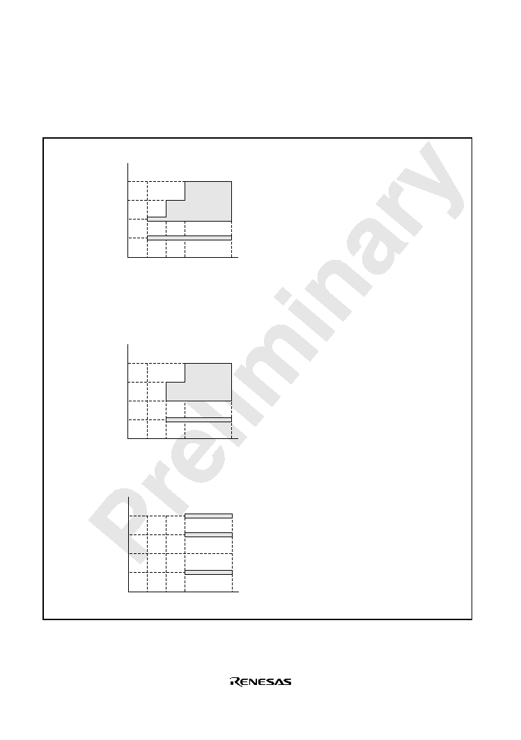
Rev. 1.0, 02/03, page 600 of 634
22.2
Power Supply Voltage and Operating Frequency Range
Power supply voltage and operating frequency ranges (shaded areas) are shown in figure 22.1.
(3) When using the on-chip USB
(2) F-ZTAT version
(1) Mask ROM version
System clock
Sub clock
Sub clock
System clock
System clock
Frequency f
24 MHz
16 MHz
0
2.7
3.0
3.6
Power ssupply voltage Vcc, PLLVcc, DrVcc (V)
Power ssupply voltage Vcc, PLLVcc, DrVcc (V)
Power ssupply voltage Vcc, PLLVcc, DrVcc (V)
6 MHz
32.768 kHz
2.4
Vcc = PLLVcc = DrVcc = 2.4 to 3.6V
Vref = 2.4V to Vcc
Vss = PLLVss = DrVss = 0V
Ta = -20 to +75 (Regular specifications)
Ta = -40 to + 85 (Wide-range specifications)
f = 32.768 kHz, 6 MHz
Condition A:
Condition C:
Condition B:
Condition A:
Condition B:
Condition C:
Vcc = PLLVcc = DrVcc = 2.7 to 3.6V
Vref = 2.7 V to Vcc
Vss = PLLVss = DrVss = 0V
Ta = -20 to +75 (Regular specifications)
Ta = -40 to + 85 (Wide-range specifications)
f = 32.768 kHz, 6 to 16 MHz
Vcc = PLLVcc = DrVcc = 3.0 to 3.6V
Vref = 3.0V to Vcc
Vss = PLLVss = DrVss = 0V
Ta = -20 to +75 (Regular specifications)
Ta = -40 to + 85 (Wide-range specifications)
f = 32.768 kHz, 6 to 24 MHz
None
Vcc = PLLVcc = DrVcc = 2.7 to 3.6V
Vref = 2.7V to Vcc
Vss = PLLVss = DrVss = 0V
Ta = -20 to +75 (Regular specifications)
Ta = -40 to + 85 (Wide-range specifications)
f = 32.768 kHz, 6 to 16 MHz
Vcc = PLLVcc = DrVcc = 3.0 to 3.6V
Vref = 3.0V to Vcc
Vss = PLLVss = DrVss = 0V
Ta = -20 to +75 (Regular specifications)
Ta = -40 to + 85 (Wide-range specifications)
f = 32.768 kHz, 6 to 24 MHz
Frequency f
24 MHz
16 MHz
0
2.7
3.0
3.6
6 MHz
32.768 kHz
2.4
Frequency f
24 MHz
16 MHz
0
2.7
3.0
3.6
6 MHz
32.768 kHz
2.4
System clock
Sub clock
Figure 22.1 Power Supply Voltage and Operating Ranges

Rev. 1.0, 02/03, page 601 of 634
22.3
DC Characteristics
Table 22.2 lists the DC characteristics. Table 22.3 lists the permissible output currents.
Table 22.2
DC Characteristics
Condition A: V
CC
= PLL V
CC
=Dr V
CC
=2.4 V to 3.6 V, Vref=2.4 V to V
CC
, V
SS
= PLLV
SS
=
Dr V
SS
= 0 V, f = 32.768 kHz, 6 MHz, T
a
= 20°C to +75°C (regular specifications),
T
a
= 40°C to +85°C (wide-range specifications)
Condition B: V
CC
= PLL V
CC
=Dr V
CC
=2.7 V to 3.6 V, Vref=2.7 V to V
CC
, V
SS
= PLLV
SS
=
Dr V
SS
= 0 V, f = 32.768 kHz, 6 MHz to 16 MHz, T
a
=
-20°C to +75°C (regular
specifications), T
a
=
-40°C to +85°C (wide-range specifications)
Condition C: V
CC
= PLL V
CC
=Dr V
CC
=3.0 V to 3.6 V, Vref=3.0 V to V
CC
, V
SS
= PLLV
SS
=
Dr V
SS
= 0 V, f = 32.768 kHz, 6 MHz to 24 MHz, T
a
=
-20°C to +75°C (regular
specifications), T
a
=
-40°C to +85°C (wide-range specifications)
Item
Symbol
Min.
Typ.
Max.
Unit
Test
Conditions
Schmitt
IRQ0 to IRQ4 V
T
V
CC
× 0.2
--
--
V
trigger input
IRQ7
V
T
+
--
--
V
CC
× 0.8
V
voltage
V
T
+
V
T
V
CC
× 0.05 --
--
V
Input high
voltage
RES, STBY,
NMI,
MD2 to MD0,
TRST, TCK,
TMS, TDI,
EMLE, VBUS,
UBPM, FWE*
4
V
IH
V
CC
× 0.9
--
V
CC
+ 0.3
V
EXTAL, ports
1, 4, 3, 7, 9,
and A to G
V
CC
× 0.8
--
V
CC
+ 0.3
V
Input low
voltage
RES, STBY,
MD2 to MD0,
TRST, TCK,
TMS, TDI,
EMLE, VBUS,
UBPM, FWE*
4
V
IL
0.3
--
V
CC
× 0.1
V
EXTAL, NMI,
ports 1, 3, 4,
7, 9, and
A to G
0.3
--
V
CC
× 0.2
V

Rev. 1.0, 02/03, page 602 of 634
Item
Symbol
Min.
Typ.
Max.
Unit
Test
Conditions
Output high
All output pins V
OH
V
CC
0.5
--
--
V
I
OH
= 200 µA
voltage
V
CC
1.0
--
--
V
I
OH
= 1 mA
Output low
All output pins V
OL
--
--
0.4
V
I
OH
= 0.4 mA
voltage
--
--
0.4
V
I
OL
= 0.8 mA
Input leakage
current
RES, VBUS,
UBPM, STBY,
NMI, EMLE,
MD2 to MD0,
FWE*
4
,
ports 4, 9
| I
in
|
--
--
1.0
µA
V
in
= 0.5 to
V
CC
0.5 V
Three-state
leakage
current (off
state)
Ports 1, 3, 7,
and A to G
| I
TSI
|
--
--
1.0
µA
V
in
= 0.5 to
V
CC
0.5 V
Input pull-up
MOS current
Ports A to E
I
P
10
--
300
µA
V
in
= 0 V
Input
capacitance
RES, NMI
C
in
--
--
30
pF
All input pins
other than
RES, NMI
--
--
15
pF
V
in
= 0 V
f = 1 MHz
T
a
= 25°C
--
TBD
V
CC
= 3.3 V
TBD
V
CC
= 3.6 V
mA
f = 16 MHz
Current
dissipation*
1
Normal
operation
(USB halts)
I
CC
*
2
--
TBD
V
CC
= 3.3 V
TBD
V
CC
= 3.6 V
mA
f = 24 MHz
--
TBD
V
CC
= 3.3 V
TBD
V
CC
= 3.6 V
mA
f = 16 MHz,
When PLL3 is
used
Normal
operation
(USB
operates)
--
TBD
V
CC
= 3.3 V
TBD
V
CC
= 3.6 V
mA
f = 24 MHz,
When PLL2 is
used
--
TBD
V
CC
= 3.3 V
TBD
V
CC
= 3.6 V
mA
f = 16 MHz,
When
USB and PLL
are halted
Sleep mode
--
TBD
V
CC
= 3.3 V
TBD
V
CC
= 3.6 V
mA
f = 24 MHz,
When
USB and PLL
are halted

Rev. 1.0, 02/03, page 603 of 634
Item
Symbol
Min.
Typ.
Max.
Unit
Test
Conditions
--
TBD
V
CC
= 3.3 V
--
mA
f = 16 MHz
(reference
value)
Current
dissipation*
1
All modules
stopped
--
TBD
V
CC
= 3.3 V
--
mA
f = 24 MHz
(reference
value)
Sub-active
mode
--
TBD
TBD
µA
Sub-sleep
mode
--
TBD
TBD
µA
Watch mode
--
TBD
TBD
µA
Vcc = 3.0 V,
When crystal
resonator
(32.768 kHz)
is used
Standby
--
1.0
10
µA
T
a
50°C
mode*
3
--
--
50
µA
50°C < T
a
Reference
power supply
During A/D
conversion
Al
CC
--
1.3
2.5
mA
V
ref
= 3.3 V
current
Idle
--
0.01
5.0
µA
RAM standby voltage
V
RAM
2.0
--
--
V
Notes: 1. Current dissipation values are for V
IH
min. = V
CC
0.2 V and V
IL
max. = 0.2 V, with all
output pins unloaded and the on-chip MOS pull-up transistors in the off state.
2. I
CC
depends on V
CC
and f as follows:
I
CC
max = TBD (mA) + TBD (mA/(MHz x V))
× V
CC
× f (normal operation, USB halted)
I
CC
max = TBD (mA) + TBD (mA/(MHz x V))
× V
CC
× f (normal operation, USB operated)
I
CC
max = TBD (mA) + TBD (mA/(MHz x V))
× V
CC
× f (sleep mode)
3. The values are for V
RAM
< V
CC
< 2.7 V, V
IH
min. = V
CC
× 0.9, and V
IL
max. = 0.3 V.
4. The FWE pin is effective only in the F-ZTAT version.
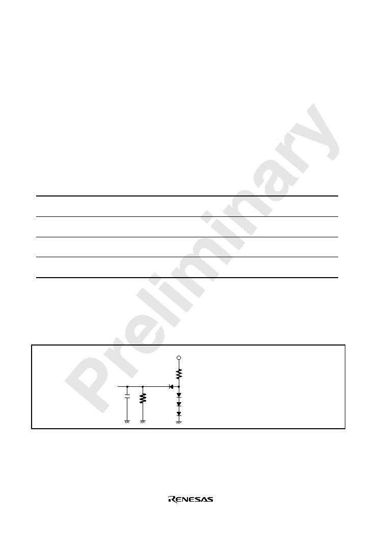
Rev. 1.0, 02/03, page 604 of 634
Table 22.3
Permissible Output Currents
Condition A: V
CC
= PLL V
CC
=Dr V
CC
=2.4 V to 3.6 V, Vref=2.4 V to V
CC
, V
SS
= PLLV
SS
=
Dr V
SS
= 0 V, f = 32.768 kHz, 6 MHz, T
a
= 20°C to +75°C (regular specifications),
T
a
= 40°C to +85°C (wide-range specifications)
Condition B: V
CC
= PLL V
CC
=Dr V
CC
=2.7 V to 3.6 V, Vref=2.7 V to V
CC
, V
SS
= PLLV
SS
=
Dr V
SS
= 0 V, f = 32.768 kHz, 6 MHz to 16 MHz, T
a
= 20°C to +75°C (regular
specifications), T
a
= 40°C to +85°C (wide-range specifications)
Condition C: V
CC
= PLL V
CC
=Dr V
CC
=3.0 V to 3.6 V, Vref=3.0 V to V
CC
, V
SS
= PLLV
SS
=
Dr V
SS
= 0 V, f = 32.768 kHz, 6 MHz to 24 MHz, T
a
= 20°C to +75°C (regular
specifications), T
a
= 40°C to +85°C (wide-range specifications)
Item
Symbol Min.
Typ.
Max.
Unit
Permissible output
low current (per pin)
All output pins
I
OL
--
--
1.0
mA
Permissible output
low current (total)
Total of all output pins
I
OL
--
--
60
mA
Permissible output
high current (per pin)
All output pins
I
OH
--
--
1.0
mA
Permissible output
high current (total)
Total of all output pins
I
OH
--
--
30
mA
Note: * To protect chip reliability, do not exceed the output current values in table 22.3.
22.4
AC Characteristics
Figure 22.2 shows, the test conditions for the AC characteristics.
3V
R
L
R
H
C
LSI output pin
C=30pF
R
L
= 2.4k
R
H
=12
Input/output timing measurement levels
· Low level : 0.8V
· High level : 2.0V (Vcc = 2.7 to 3.6V)
Figure 22.2 Output Load Circuit

Rev. 1.0, 02/03, page 605 of 634
22.4.1
Clock Timing
Table 22.4 lists the clock timing
Table 22.4
Clock Timing
Condition A: V
CC
= PLL V
CC
=Dr V
CC
=2.4 V to 3.6 V, Vref=2.4 V to V
CC
, V
SS
= PLLV
SS
=
Dr V
SS
= 0 V, f = 32.768 kHz, 6 MHz, T
a
= 20°C to +75°C (regular specifications),
T
a
= 40°C to +85°C (wide-range specifications)
Condition B: V
CC
= PLL V
CC
=Dr V
CC
=2.7 V to 3.6 V, Vref=2.7 V to V
CC
, V
SS
= PLLV
SS
=
Dr V
SS
= 0 V, f = 32.768 kHz, 6 MHz to 16 MHz, T
a
= 20°C to +75°C (regular
specifications), T
a
= 40°C to +85°C (wide-range specifications)
Condition C: V
CC
= PLL V
CC
=Dr V
CC
=3.0 V to 3.6 V, Vref=3.0 V to V
CC
, V
SS
= PLLV
SS
=
Dr V
SS
= 0 V, f = 32.768 kHz, 6 MHz to 24 MHz, T
a
= 20°C to +75°C (regular
specifications), T
a
= 40°C to +85°C (wide-range specifications)
Condition A
Condition B
Condition C
Item
Symbol Min.
Max.
Min.
Max.
Min.
Max.
Unit
Test
Conditions
Clock cycle time
t
cyc
166.6
62.5
166.6 41.6
166.6 ns
Figure 22.3
Clock high pulse width t
CH
50
--
20
--
15
--
ns
Clock low pulse width
t
CL
50
--
20
--
15
--
ns
Clock rise time
t
Cr
--
25
--
10
--
5
ns
Clock fall time
t
Cf
--
25
--
10
--
5
ns
Oscillation stabilization
time at reset (crystal)
t
OSC1
40
--
20
--
20
--
ms
Figure 22.4
Oscillation stabilization
time in software
standby (crystal)
t
OSC2
16
--
8
--
8
--
ms
Figure 20.4
External clock output
stabilization delay time
t
DEXT
1000
--
500
--
500
--
µs
Figure 22.4
Sub-clock stabilization
time
t
OSC3
--
4
--
2
--
2
s
Sub-clock oscillator
frequency
f
SUB
32.768
32.768
32.768
kHz
Sub-clock (
SUB
) cycle
time
f
SUB
30.5
30.5
30.5
µs
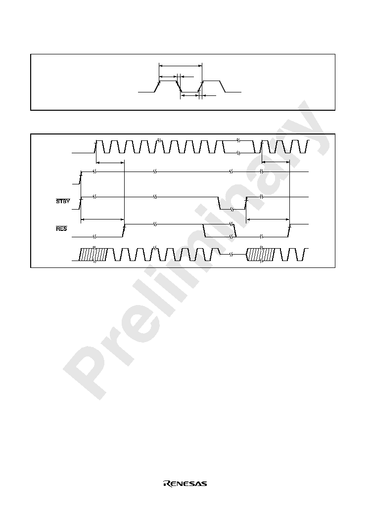
Rev. 1.0, 02/03, page 606 of 634
t
Cr
t
CL
t
Cf
t
CH
t
cyc
Figure 22.3 System Clock Timing
t
OSC1
t
OSC1
EXTAL
V
CC
t
DEXT
t
DEXT
Figure 22.4 Oscillation Stabilization Timing

Rev. 1.0, 02/03, page 607 of 634
22.4.2
Control Signal Timing
Table 22.5 lists the control signal timing.
Table 22.5
Control Signal Timing
Condition A: V
CC
= PLL V
CC
=Dr V
CC
=2.4 V to 3.6 V, Vref=2.4 V to V
CC
, V
SS
= PLLV
SS
=
Dr V
SS
= 0 V, f = 32.768 kHz, 6 MHz, T
a
= 20°C to +75°C (regular specifications),
T
a
= 40°C to +85°C (wide-range specifications)
Condition B: V
CC
= PLL V
CC
=Dr V
CC
=2.7 V to 3.6 V, Vref=2.7 V to V
CC
, V
SS
= PLLV
SS
=
Dr V
SS
= 0 V, f = 32.768 kHz, 6 MHz to 16 MHz, T
a
= 20°C to +75°C (regular
specifications), T
a
= 40°C to +85°C (wide-range specifications)
Condition C: V
CC
= PLL V
CC
=Dr V
CC
=3.0 V to 3.6 V, Vref=3.0 V to V
CC
, V
SS
= PLLV
SS
=
Dr V
SS
= 0 V, f = 32.768 kHz, 6 MHz to 24 MHz, T
a
= 20°C to +75°C (regular
specifications), T
a
= 40°C to +85°C (wide-range specifications)
Condition A
Condition B, C
Item
Symbol Min.
Max.
Min.
Max.
Unit
Test
Conditions
RES setup time
t
RESS
350
--
250
--
ns
Figure 22.5
RES pulse width
t
RESW
20
--
20
--
t
cyc
MRES setup time
T
MRESS
350
--
250
--
ns
MRES pulse width
T
MRESW
20
--
20
--
t
cyc
NMI setup time
t
NMIS
350
--
250
--
ns
Figure 22.6
NMI hold time
t
NMIH
10
--
10
--
ns
NMI pulse width (exiting
software standby mode)
t
NMIW
300
--
200
--
ns
IRQ setup time
t
IRQS
350
--
250
--
ns
IRQ hold time
t
IRQH
10
--
10
--
ns
IRQ pulse width (exiting
software standby mode)
t
IRQW
300
--
200
--
ns
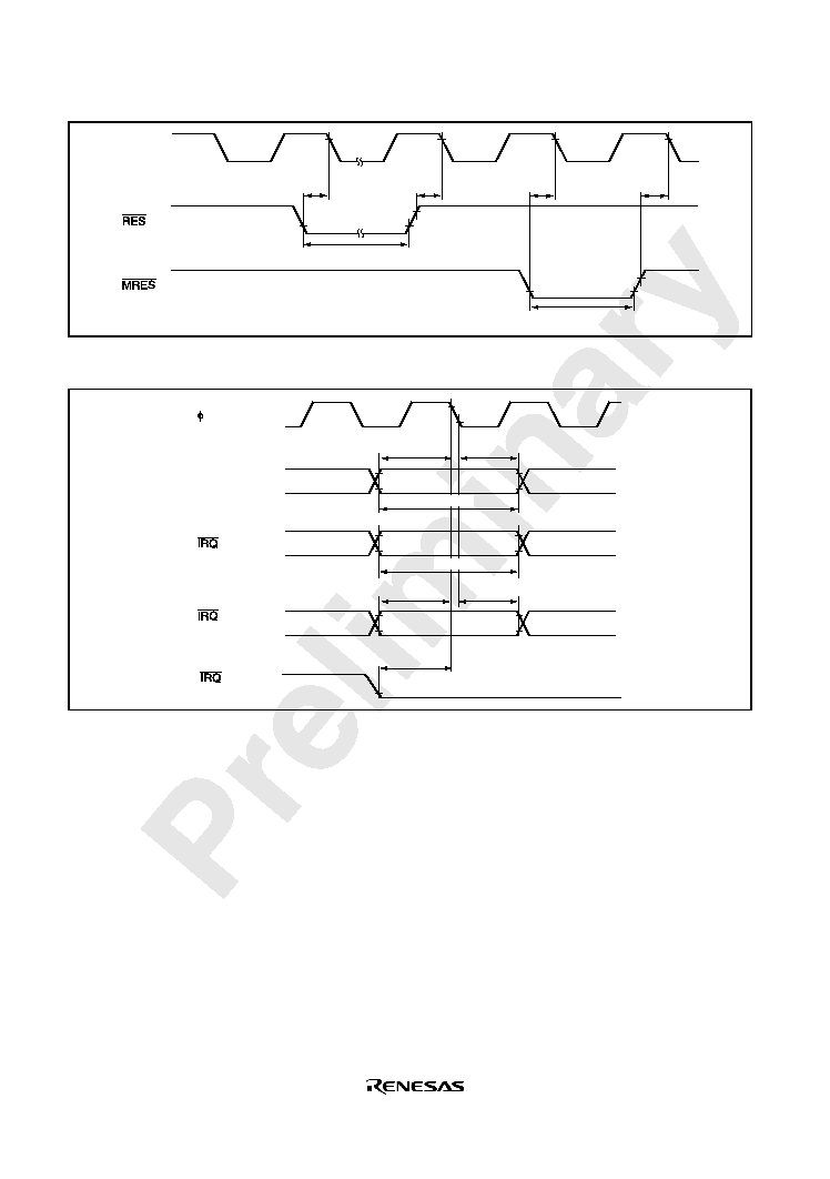
Rev. 1.0, 02/03, page 608 of 634
t
RESW
t
RESS
t
MRESS
t
MRESS
t
MRESW
t
RESS
Figure 22.5 Reset Input Timing
t
IRQS
edge input
t
IRQH
t
NMIS
t
NMIH
t
IRQS
level input
NMI
t
NMIW
t
IRQW
Figure 22.6 Interrupt Input Timing

Rev. 1.0, 02/03, page 609 of 634
22.4.3
Bus Timing
Table 22.6 shows, Bus Timing.
Table 22.6
Bus Timing
Condition A: V
CC
= PLL V
CC
=Dr V
CC
=2.4 V to 3.6 V, Vref=2.4 V to V
CC
, V
SS
= PLLV
SS
=
Dr V
SS
= 0 V, f = 32.768 kHz, 6 MHz, T
a
= 20°C to +75°C (regular specifications),
T
a
= 40°C to +85°C (wide-range specifications)
Condition B: V
CC
= PLL V
CC
=Dr V
CC
=2.7 V to 3.6 V, Vref=2.7 V to V
CC
, V
SS
= PLLV
SS
=
Dr V
SS
= 0 V, f = 32.768 kHz, 6 MHz to 16 MHz, T
a
= 20°C to +75°C (regular
specifications), T
a
= 40°C to +85°C (wide-range specifications)
Condition C: V
CC
= PLL V
CC
=Dr V
CC
=3.0 V to 3.6 V, Vref=3.0 V to V
CC
, V
SS
= PLLV
SS
=
Dr V
SS
= 0 V, f = 32.768 kHz, 6 MHz to 24 MHz, T
a
= 20°C to +75°C (regular
specifications), T
a
= 40°C to +85°C (wide-range specifications)
Condition A
Condition B
Condition C
Test
Item
Symbol Min.
Max.
Min.
Max.
Min.
Max.
Unit Conditions
Address delay time
t
AD
--
90
--
50
--
35
ns
Address setup time
t
AS
0.5
× t
cyc
60
--
0.5
× t
cyc
30
--
0.5
× t
cyc
15
--
ns
Address hold time
t
AH
0.5
× t
cyc
30
--
0.5
× t
cyc
15
--
0.5
× t
cyc
8
--
ns
Figures 22.7,
22.8, 22.10
CS delay time
t
CSD
--
90
--
50
--
35
ns
Figures 22.7,
22.8
AS delay time
t
ASD
--
90
--
50
--
35
ns
Figures 22.7,
22.8, 22.10
RD delay time 1
t
RSD1
--
90
--
50
--
35
ns
Figures 22.7,
22.8
RD delay time 2
t
RSD2
--
90
--
50
--
35
ns
Read data setup time t
RDS
50
--
30
--
25
--
ns
Read data hold time
t
RDH
0
--
0
--
0
--
ns
Figures 22.7,
22.8, 22.10
Read data access
time 2
t
ACC2
--
1.5
× t
cyc
90
--
1.5
× t
cyc
65
--
1.5
× t
cyc
35
ns
Figures 22.7
Read data access
time 3
t
ACC3
--
2.0
× t
cyc
90
--
2.0
× t
cyc
65
--
2.0
× t
cyc
35
ns
Figures 22.7,
22.10

Rev. 1.0, 02/03, page 610 of 634
Condition A
Condition B
Condition C
Test
Item
Symbol Min.
Max.
Min.
Max.
Min.
Max.
Unit Conditions
Read data access
time 4
t
ACC4
--
2.5
× t
cyc
90
--
2.5
× t
cyc
65
--
2.5
× t
cyc
35
ns
Read data access
time 5
t
ACC5
--
3.0
× t
cyc
90
--
3.0
× t
cyc
65
--
3.0
× t
cyc
35
ns
Figure 22.8
WR delay time 1
t
WRD1
--
90
--
50
--
35
ns
Figure 22.8
WR delay time 2
t
WRD2
--
90
--
50
--
35
ns
Figures 22.7,
22.8
WR pulse width 1
t
WSW1
1.0
× t
cyc
60
--
1.0
× t
cyc
30
--
1.0
× t
cyc
20
--
ns
Figure 22.7
WR pulse width 2
t
WSW2
1.5
× t
cyc
60
--
1.5
× t
cyc
30
--
1.5
× t
cyc
20
--
ns
Figure 22.8
Write data delay time t
WDD
--
100
--
50
--
40
ns
Figures 22.7,
22.8
Write data setup time t
WDS
0.5
× t
cyc
80
--
0.5
× t
cyc
30
--
0.5
× t
cyc
20
--
ns
Figure 22.8
Write data hold time
t
WDH
0.5
× t
cyc
60
--
0.5
× t
cyc
15
--
0.5
× t
cyc
10
--
ns
Figures 22.7,
22.8
WAIT setup time
t
WTS
90
--
50
--
35
--
ns
WAIT hold time
t
WTH
10
--
10
--
10
--
ns
Figure 22.9
BREQ setup time
t
BRQS
90
--
50
--
35
--
ns
BACK delay time
t
BACD
--
90
--
50
--
35
ns
Bus-floating time
t
BZD
--
160
--
80
--
50
ns
Figure 22.11
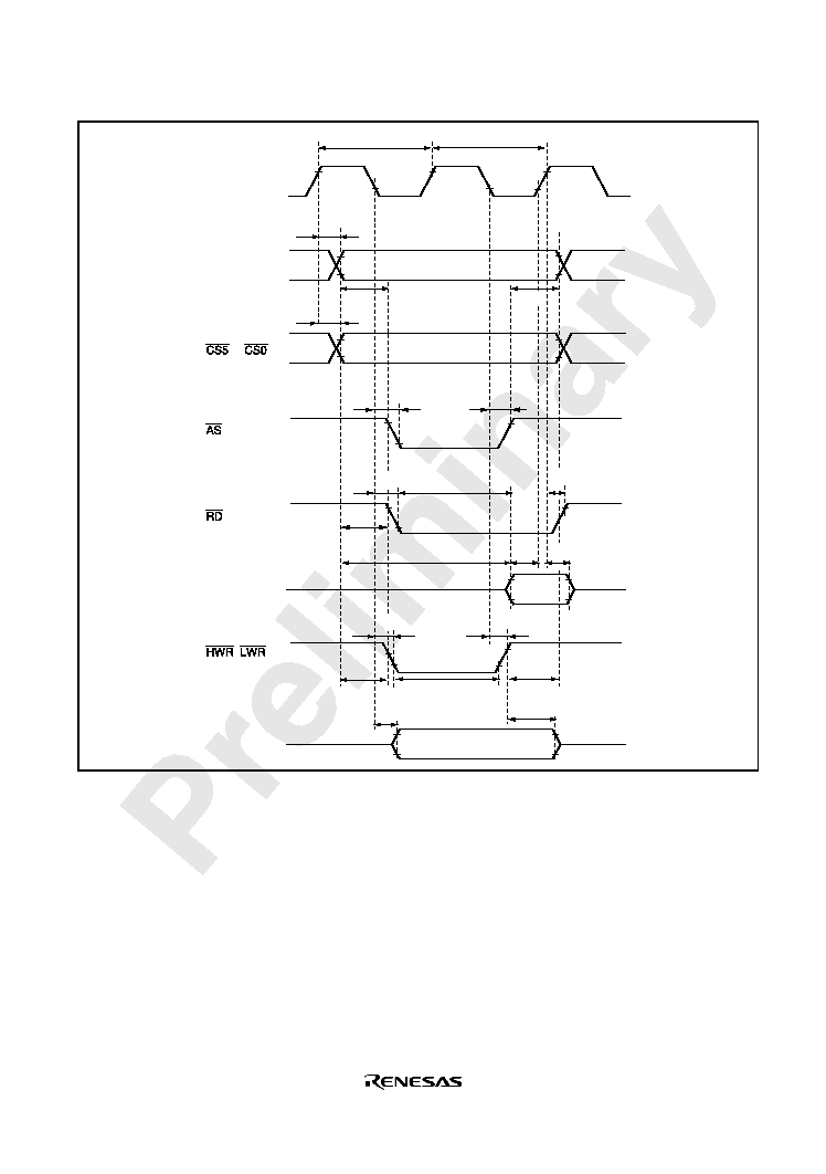
Rev. 1.0, 02/03, page 611 of 634
t
RSD2
T
1
t
AD
A23 to A0
t
ASD
(read)
T
2
t
CSD
t
AS
t
ASD
t
ACC2
t
AS
t
AS
t
RSD1
t
ACC3
t
RDS
t
RDH
t
WRD2
t
WDD
t
WSW1
t
WDH
t
AH
to
D15 to D0
(read)
,
(write)
D15 to D0
(write)
t
AH
t
WRD2
Figure 22.7 Basic Bus Timing (Two-State Access)
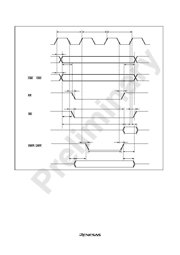
Rev. 1.0, 02/03, page 612 of 634
t
RSD2
T
2
A23 to A0
t
ASD
(read)
T
3
t
AS
t
AH
t
ASD
t
ACC4
t
RSD1
t
ACC5
t
AS
t
RDS
t
RDH
t
WRD1
t
WRD2
t
WDS
t
WSW2
t
WDH
t
AH
to
D15 to D0
(read)
,
(write)
D15 to D0
(write)
T
1
t
CSD
t
WDD
t
AD
Figure 22.8 Basic Bus Timing (Three-State Access)
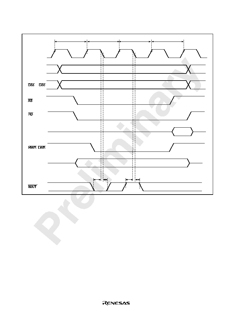
Rev. 1.0, 02/03, page 613 of 634
T
W
A23 to A0
(read)
T
3
to
D15 to D0
(read)
,
(write)
D15 to D0
(write)
T
2
t
WTS
T
1
t
WTH
t
WTS
t
WTH
Figure 22.9 Basic Bus Timing (Three-State Access with One Wait State)
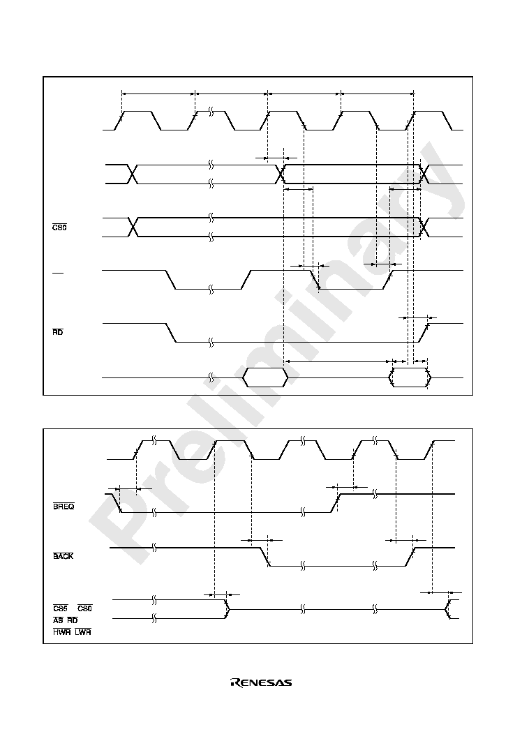
Rev. 1.0, 02/03, page 614 of 634
t
RSD2
T
1
AS
A23 to A0
T
2
t
AH
t
ACC3
t
RDS
D15 to D0
(read)
T
2
or T
3
t
AS
T
1
t
ASD
t
ASD
t
RDH
t
AD
(read)
Figure 22.10 Burst ROM Access Timing (Two-State Access)
A23 to A0,
to
,
t
BRQS
t
BACD
t
BZD
t
BACD
t
BZD
t
BRQS
,
,
,
Figure 22.11 External Bus Release Timing

Rev. 1.0, 02/03, page 615 of 634
22.4.4
Timing of On-Chip Supporting Modules
Table 22.7 lists the timing of on-chip supporting modules.
Table 22.7
Timing of On-Chip Supporting Modules
Condition A: V
CC
= PLL V
CC
=Dr V
CC
=2.4 V to 3.6 V, Vref=2.4 V to V
CC
, V
SS
= PLLV
SS
=
Dr V
SS
= 0 V, f = 32.768 kHz, 6 MHz, T
a
= 20°C to +75°C (regular specifications),
T
a
= 40°C to +85°C (wide-range specifications)
Condition B: V
CC
= PLL V
CC
=Dr V
CC
=2.7 V to 3.6 V, Vref=2.7 V to V
CC
, V
SS
= PLLV
SS
=
Dr V
SS
= 0 V, f = 32.768 kHz, 6 MHz to 16 MHz, T
a
= 20°C to +75°C (regular
specifications), T
a
= 40°C to +85°C (wide-range specifications)
Condition C: V
CC
= PLL V
CC
=Dr V
CC
=3.0 V to 3.6 V, Vref=3.0 V to V
CC
, V
SS
= PLLV
SS
=
Dr V
SS
= 0 V, f = 32.768 kHz, 6 MHz to 24 MHz, T
a
= 20°C to +75°C (regular
specifications), T
a
= 40°C to +85°C (wide-range specifications)
Condition A Condition B Condition C
Item
Symbol Min. Max. Min. Max. Min. Max. Unit
Test
Conditions
I/O port
Output data delay
time
t
PWD
--
150
--
60
--
40
ns
Figure
22.12
Input data setup time t
PRS
80
--
50
--
30
--
Input data hold time
t
PRH
50
--
50
--
30
--
TPU
Timer output delay
time
t
TOCD
--
150
--
60
--
40
ns
Figure
22.13
Timer input setup
time
t
TICS
60
--
40
--
30
--
Timer clock input
setup time
t
TCKS
60
--
40
--
30
--
ns
Figure
22.14
Single
edge
t
TCKWH
1.5
--
1.5
--
1.5
--
t
cyc
Timer
clock
pulse
width
Both
edges
t
TCKWL
2.5
--
2.5
--
2.5
--

Rev. 1.0, 02/03, page 616 of 634
Condition A Condition B Condition C
Item
Symbol Min. Max. Min. Max. Min. Max. Unit
Test
Conditions
SCI
Input
clock
Asynchro-
nous
t
Scyc
4
--
4
--
4
--
t
cyc
Figure
22.15
cycle
Synchro-
nous
6
--
6
--
6
--
Input clock pulse
width
t
SCKW
0.4
0.6
0.4
0.6
0.4
0.6
t
Scyc
Input clock rise time
t
SCKr
--
1.5
--
1.5
--
1.5
t
cyc
Input clock fall time
t
SCKf
--
1.5
--
1.5
--
1.5
Transmit data delay
time
t
TXD
--
150
--
60
--
40
ns
Figure
22.16
Receive data setup
time (synchronous)
t
RXS
150
--
60
--
40
--
Receive data hold
time (synchronous)
t
RXH
150
--
60
--
40
--
A/D
converter
Trigger input setup
time
t
TRGS
60
--
40
--
30
--
ns
Figure
22.17
TCK cycle time
t
Tcyc
166.6
--
62.5 --
41.6 --
ns
Boundary
scan
TCK high level pulse
width
t
TCKH
0.4
0.6
0.4
0.6
0.4
0.6
t
Tcyc
TCK low level pulse
width
t
TCKL
0.4
0.6
0.4
0.6
0.4
0.6
t
Tcyc
Figure
22.18
TRST pulse width
t
TRSW
20
--
20
--
20
--
t
Tcyc
TRST setup time
t
TRSS
350
--
250
--
250
--
ns
Figure
22.19
TDI setup time
t
TDIS
80
--
30
--
20
--
ns
TDI hold time
t
TDIH
10
--
10
--
10
--
TMS setup time
t
TMSS
80
--
30
--
20
--
TMS hold time
t
TMSH
10
--
10
--
10
--
TDO delay time
t
TDOD
--
100
--
40
--
35
Figure
22.20
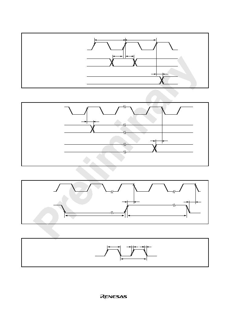
Rev. 1.0, 02/03, page 617 of 634
Ports 1, 3, 4, 7, 9,
A to G(read)
t
PRS
T
1
T
2
t
PWD
t
PRH
Ports 1, 3, 7,
A to G(write)
Figure 22.12 I/O Port Input/Output Timing
t
TICS
t
TOCD
Output compare
output*
Input capture
input*
Note : * TIOCA0 to TIOCA2, TIOCB0 to TIOCB2, TIOCC0, TIOCD0
Figure 22.13 TPU Input/Output Timing
t
TCKS
t
TCKS
TCLKA to TCLKD
t
TCKWH
t
TCKWL
Figure 22.14 TPU Clock Input Timing
t
Scyc
t
SCKr
t
SCKW
SCK0, SCK2
t
SCKf
Figure 22.15 SCK Clock Input Timing
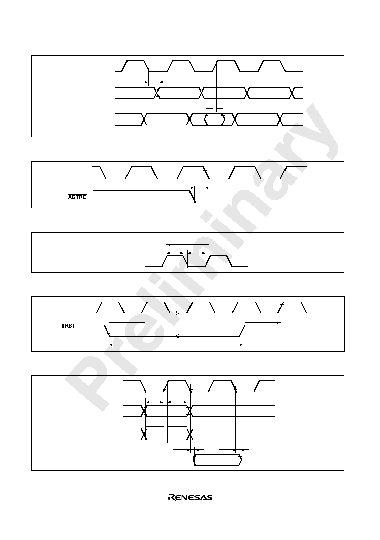
Rev. 1.0, 02/03, page 618 of 634
t
TXD
t
RXH
t
RXS
SCK0, SCK2
TxD0, TxD2
(transmit data)
RxD0, RxD2
(receive data)
Figure 22.16 SCI Input/Output Timing (Clock Synchronous Mode)
t
TRGS
Figure 22.17 A/D Converter External Trigger Input Timing
t
TCKL
t
TCKH
TCK
t
Tcyc
Figure 22.18 Boundary Scan TCK Input Timing
t
TRSW
t
TRSS
TCK
t
TRSS
Figure 22.19 Boundary Scan
TRST
TRST
TRST
TRST Input Timing (At Reset Hold)
t
TDIS
t
TDIH
TCK
TDI
TMS
TDO
t
TMSS
t
TMSH
t
TDOD
t
TDOD
Figure 22.20 Boundary Scan Data Transmission Timing
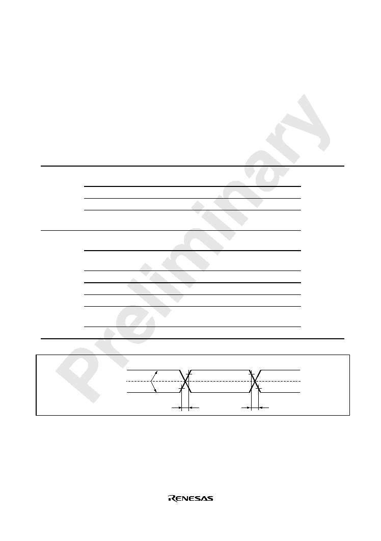
Rev. 1.0, 02/03, page 619 of 634
22.5
UBS Characteristics
Table 22.8 lists the USB characteristics (USD+ and USD- pins) when the on-chip USB transceiver
is used.
Table 22.8
USB Characteristics (USD+ and USD- pins) when On-Chip USB Transceiver Is Used
Conditions: V
CC
= PLL V
CC
=Dr V
CC
=3.0 V to 3.6 V, V
SS
= PLLV
SS
= DrV
SS
= 0 V,
f = 16 MHz,
24 MHz, T
a
= 20°C to +75°C (regular specifications), T
a
= 40°C to +85°C (wide-
range specifications)
Item
Symbol Min.
Max.
Unit
Test Condition
Input
characteristics
Input high level voltage V
IH
2.0
--
V
Figures
22.21,22.22
Input low level voltage V
IL
--
0.8
V
Differential input sense V
DI
0.2
--
V
| (D+)-(D-)|
Differential common
mode range
V
CM
0.8
2.5
V
Output
characteristics
Output high level
voltage
V
OH
2.8
--
V
I
OH
=-200
µA
Output low level
voltage
V
OL
--
0.3
V
I
OL
=2 mA
Crossover voltage
V
CRS
1.3
2.0
V
Rise time
t
R
4
20
ns
Fall time
t
F
4
20
ns
Rise time/fall time
matching
t
RFM
90
111.11 %
(T
R
/ T
F
)
Output resistance
Z
TICS
28
44
Including Rs = 24
tR
USD+, USD-
V
CRS
Differential
Date Lines
90%
10%
10%
Fall Time
Rise Time
90%
tF
Figure 22.21 Data Signal Timing
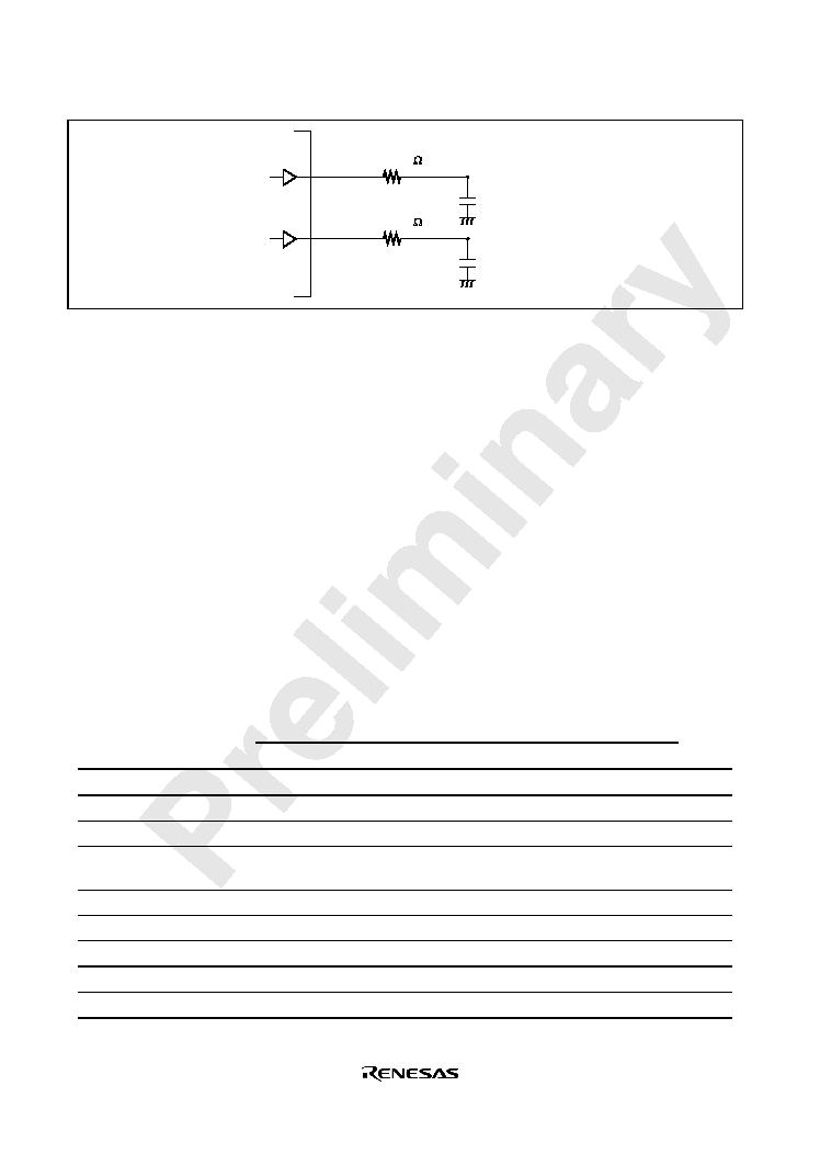
Rev. 1.0, 02/03, page 620 of 634
USD+
Test Point
C
L
= 50pF
Test Point
C
L
= 50pF
USD-
Rs = 24
Rs = 24
Figure 22.22 Test Load Circuit
22.6
A/D Conversion Characteristics
Table 22.9 lists the A/D conversion characteristics.
Table 22.9
A/D Conversion Characteristics
Condition A: V
CC
= PLL V
CC
=Dr V
CC
=2.4 V to 3.6 V, Vref=2.4 V to V
CC
, V
SS
= PLLV
SS
=
Dr V
SS
= 0 V, f = 32.768 kHz, 6 MHz, T
a
= 20°C to +75°C (regular specifications),
T
a
= 40°C to +85°C (wide-range specifications)
Condition B: V
CC
= PLL V
CC
=Dr V
CC
=2.7 V to 3.6 V, Vref=2.7 V to V
CC
, V
SS
= PLLV
SS
=
Dr V
SS
= 0 V, f = 32.768 kHz, 6 MHz to 16 MHz, T
a
= 20°C to +75°C (regular
specifications), T
a
= 40°C to +85°C (wide-range specifications)
Condition C: V
CC
= PLL V
CC
=Dr V
CC
=3.0 V to 3.6 V, Vref=3.0 V to V
CC
, V
SS
= PLLV
SS
=
Dr V
SS
= 0 V, f = 32.768 kHz, 6 MHz to 24 MHz, T
a
= 20°C to +75°C (regular
specifications), T
a
= 40°C to +85°C (wide-range specifications)
Condition A
Condition B
Condition C
Item
Min.
Typ.
Max.
Min.
Typ.
Max.
Min.
Typ.
Max.
Unit
Resolution
10
10
10
10
10
10
10
10
10
bits
Conversion time
22.3
--
--
8.4
--
--
11.08 --
--
µs
Analog input capacitance --
--
20
--
--
20
--
--
20
pF
Permissible signal-source
impedance
--
--
5
--
--
5
--
--
5
k
Nonlinearity error
--
--
±6.0
--
--
±6.0
--
--
±6.0
LSB
Offset error
--
--
±4.0
--
--
±4.0
--
--
±4.0
LSB
Full-scale error
--
--
±4.0
--
--
±4.0
--
--
±4.0
LSB
Quantization
--
--
±0.5
--
--
±0.5
--
--
±0.5
LSB
Absolute accuracy
--
--
±8.0
--
--
±8.0
--
--
±8.0
LSB

Rev. 1.0, 02/03, page 621 of 634
22.7
Flash Memory Characteristics
Table 22.10 lists the flash memory characteristics.
Table 22.10 Flash Memory Characteristics
Conditions: V
CC
= PLLV
CC
=DrV
CC
= 3.0 V to 3.6 V, Vref = 2.7 V to V
CC
,
V
SS
= PLLV
SS
= DrV
SS
= 0 V,
T
a
= 20 to +75°C (Programming / erasing operating temperature range)
Item
Symbol
Min.
Typ.
Max.
Unit
Programming time*
1,
*
2,
*
4
t
P
--
10
200
ms/128 bytes
Erase time*
1,
*
3,
*
5
t
E
--
50
1000
ms/block
Reprogramming count
N
WEC
100*
6
10000*
7
--
Times
Data retention time*
8
t
DRP
10
--
--
Years
Programming
Wait time after PSU1 bit setting*
1
y
50
50
--
µs
Wait time after P1 bit setting*
1,
*
4
z0
28
30
32
µs
z1
198
200
202
µs
z2
8
10
12
µs
Wait time after P1 bit clear*
1
5
5
--
µs
Wait time after PSU1 bit clear*
1
5
5
--
µs
Wait time after PV1 bit setting*
1
4
4
--
µs
Wait time after H'FF dummy write*
1
2
2
--
µs
Wait time after PV1 bit clear*
1
2
2
--
µs
Maximum programming count*
1,
*
4
N1
--
--
6*
4
Times
N2
--
--
994*
4
Times
Common
Wait time after SWE1 bit setting*
1
x
1
1
--
µs
Wait time after SWE1 bit clear*
1
100
100
--
µs
Erase
Wait time after ESU1 bit setting*
1
y
100
100
--
µs
Wait time after E1 bit setting*
1,
*
5
z
10
10
100
ms
Wait time after E1 bit clear*
1
10
10
--
µs
Wait time after ESU1 bit clear*
1
10
10
--
µs
Wait time after EV1 bit setting*
1
20
20
--
µs
Wait time after H'FF dummy write*
1
2
2
--
µs
Wait time after EV1 bit clear*
1
4
4
--
µs
Maximum erase count*
1,
*
5
N
--
--
100
Times
Notes: 1. Make each time setting in accordance with the program/program-verify flowchart or
erase/erase-verify flowchart.
2. Programming time per 128 bytes (Shows the total period for which the P-bit in the flash
memory control register(FLMCR1) is set. It does not include the programming
verification time.)
3. Block erase time (Shows the total period for which the E1-bit FLMCR1 is set. It does not
include the erase verification time.)

Rev. 1.0, 02/03, page 622 of 634
4. Maximum programming time value
t
p
(max) = Wait time after P1 bit set (z) x maximum programming count (N1 +N2)
= (Z0 + Z2) x 6 +Z1 x 994
5. Maximum erasure time value
t
E
(max) = Wait time after E1 bit set (z) x maximum erasure count (N)
6. Minimum times that guarantee all characteristics after programming. (The guaranteed
range is 1 to the minimum value.)
7. Reference value when the temperature is 25°C. (it is reference that reprogramming is
normally enabled up to this value.)
8. Data hold characteristics when reprogramming is performed within the range of
specifications including the minimum value.
22.8
Usage Note
General Notice during Design for Printed Circuit Board: Measures for radiation noise caused
by the transient current in this LSI should be taken into consideration. The examples of the
measures are shown below.
· To use a multilayer printed circuit board which includes layers for Vcc and GND.
· To mount by-pass capacitors (approximately 0.1 µF) between the Vcc and GND (Vss) pins of
this LSI.

Rev. 1.0, 02/03, page 623 of 634
Appendix
A.
I/O Port States in Each Processing State
Port Name
Pin Name
MCU
Operating
Mode
Power-on
Reset
Manual
Reset
Hardware
Standby
Mode
Software
Standby
Mode
Bus Right
Release
State
Program
Execution State
or Sleep Mode
P17 to P14
4 to 7
T
keep
T
keep
keep
I/O port
P13/A23
P12/A22
P11/A21
7
T
keep
T
keep
keep
I/O port
Address output
selected by AEn
bit
4 to 6
T
keep
T
[OPE=0]
T
[OPE=1]
keep
T
Address output
Port selection
4 to 6
T
keep
T
keep
keep
I/O port
P10/A20
7
T
keep
T
keep
keep
I/O port
4 and 5
L
Address output
selected by AEn
bit
6
T
keep
T
[OPE=0]
T
[OPE=1]
keep
T
Address output
Port selection
4 to 6
T*
1
keep
T
keep
keep
I/O port
Port 3
4 to 7
T
keep
T
keep
keep
I/O port
Port 4
4 to 7
T
T
T
T
T
Input port
P77 to P75*
3
7
T
keep
T
keep
keep
I/O port
P74*
2
4 to 7
T
keep
T
keep
keep
I/O port
7
T
keep
T
keep
keep
I/O port
P71/
CS5*
2
P70/
CS4*
2
4 to 6
T
keep
T
[DDR·OPE=0]
T
[DDR·OPE=1]
H
T
[DDR=0]
Input port
[DDR=1]
CS5, CS4
Port 9
4 to 7
T
T
T
[DAOEn=1]
keep
[DAOEn=0]
T
keep
Input port
Port A
7
T
keep
T
keep
keep
I/O port
4 and 5
L
Address output
selected by AEn
bit
6
T
keep
T
[OPE=0]
T
[OPE=1]
keep
T
Address output
Port selection
4 to 6
T*
1
keep
T
keep
keep
I/O port

Rev. 1.0, 02/03, page 624 of 634
Port Name
Pin Name
MCU
Operating
Mode
Power-on
Reset
Manual
Reset
Hardware
Standby
Mode
Software
Standby
Mode
Bus Right
Release
State
Program
Execution State
or Sleep Mode
Port B*
2
7
T
keep
T
keep
keep
I/O port
Address output
selected by AEn
bit
4 and 5
L
6
T
keep
T
[OPE=0]
T
[OPE=1]
keep
T
Address output
Port selection
4 to 6
T*
1
keep
T
keep
keep
I/O port
Port C*
2
4 and5
L
keep
T
[OPE=0]
T
[OPE=1]
keep
T
Address output
6
T
keep
T
[DDR·OPE=0]
T
[DDR·OPE=1]
keep
T
[DDR=0]
Input port
[DDR=1]
Address output
7
T
keep
T
keep
keep
I/O port
Port D*
2
4 to 6
T
T
T
T
T
Data bus
7
T
keep
T
keep
keep
I/O port
8 bit bus
4 to 6
T
keep
T
keep
keep
I/O port
4 to 6
T
T
T
T
T
Data bus
Port E
16 bit bus
7
T
keep
T
keep
keep
I/O port
PF7/
4 to 6
Clock output
[DDR=0]
Input port
[DDR=1]
Clock output
T
[DDR=0]
Input port
[DDR=1]
H
[DDR=0]
Input port
[DDR=1]
Clock output
[DDR=0]
input port
[DDR=1]
Clock output
7
T
keep
T
[DDR=0]
Input port
[DDR=1]
H
[DDR=0]
Input port
[DDR=1]
Clock output
[DDR=0]
Input port
[DDR=1]
Clock output
FA6/
AS*
2
PF5/
RD*
2
PF4/
HWR*
2
4 to 6
H
H
T
[OPE=0]
T
[OPE=1]
H
T
AS, RD, HWR
7
T
keep
T
keep
keep
I/O port

Rev. 1.0, 02/03, page 625 of 634
Port Name
Pin Name
MCU
Operating
Mode
Power-on
Reset
Manual
Reset
Hardware
Standby
Mode
Software
Standby
Mode
Bus Right
Release
State
Program
Execution State
or Sleep Mode
PF3/
LWR
7
T
keep
T
keep
keep
I/O port
8 bit bus
4 to 6
(Mode 4)
H
keep
T
keep
keep
I/O port
16 bit bus
4 to 6
(Mode 5 ,6)
T
H
T
[OPE=0]
T
[OPE=1]
H
T
LWR
PF2/
WAIT*
2
4 to 6
T
keep
T
[WAITE=0]
keep
[WAITE=1]
T
[WAITE=0]
keep
[WAITE=1]
T
[WAITE=0]
I/O port
[WAITE=1]
WAIT
7
T
keep
T
keep
keep
I/O port
PF1/
BACK*
2
4 to 6
T
keep
T
[BRLE=0]
keep
[BRLE=1]
H
L
[BRLE=0]
I/O port
[BRLE=1]
BACK
7
T
keep
T
keep
keep
I/O port
PF0/
BREQ
4 to 6
T
keep
T
[BRLE=0]
keep
[BRLE=1]
T
T
[BRLE=0]
I/O port
[BRLE=1]
BREQ
7
T
keep
T
keep
keep
I/O port
PG4/
CS0*
2
4 and 5
H
6
T
keep
T
[DDR·OPE=0]
T
[DDR·OPE=1]
H
T
[DDR=0]
I/O port
[DDR=1]
CS0
(When sleep
mode)H
7
T
keep
T
keep
keep
I/O port
PG3/
CS1*
2
PG2/
CS2*
2
PG1/
CS3
4 to 6
T
keep
T
[DDR·OPE=0]
T
[DDR·OPE=1]
H
T
[DDR=0]
I/O port
[DDR=1]
CS1 to CS3
7
T
keep
T
keep
keep
I/O port
PG0*
3
4 to 7
T
keep
T
keep
keep
I/O port

Rev. 1.0, 02/03, page 626 of 634
Legend
H: High level
L: Low level
T: High impedance
keep: Input port level is high impedance, and output port level is retained.
DDR: Data direction register
OPE: Output port enable
WAITE: Wait port enable
BRLE: Bus release enable
Note:
1. L (address input) in mode 4 or 5
2. Supported only by the H8S/2218 Series.
3. Supported only by the H8S/2212 Series.

Rev. 1.0, 02/03, page 627 of 634
B.
Product Model Lineup
Product Class
Product Type
Name
Marking
Package (code)
H8S/2218
Flash memory HD64F2218
64F2218TF
100 pin TQFP (TFP-100G)
Version
HD64F2218U
64F2218UTF
100 pin TQFP (TFP-100G)
Masked ROM
Version
HD6432217
6432217(***)TF
100 pin TQFP (TFP-100G)
H8S/2212
Flash memory HD64F2212
64F2212FP
64 pin LQFP (FP-64E)
Version
HD64F2212U
64F2212UFP
64 pin LQFP (FP-64E)
Masked ROM
HD6432211
6432211(***)FP
64 pin LQFP (FP-64E)
Version
HD6432210
6432210(***)FP
64 pin LQFP (FP-64E)
Legend
(***) is ROM code.
Note:
The above list includes products under developing and planning. For the status for each
product, please contact your Hitachi sales agency.
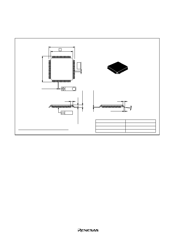
Rev. 1.0, 02/03, page 628 of 634
C.
Package Dimensions
Hitachi Code
JEDEC
JEITA
Mass (reference value)
TFP-100G
--
Conforms
0.4 g
*Dimension including the plating thickness
Base material dimension
14.0
± 0.2
12
0.07
0.10
0.5
± 0.1
14.0
±
0.2
0.4
1.20 Max
*0.17
±
0.05
0
° 8°
75
51
1
25
76
100
26
50
M
*0.18
± 0.05
1.0
1.2
0.16
± 0.04
0.15
±
0.04
1.00
0.10
±
0.10
Figure C.1 TFP-100 Package Dimensions
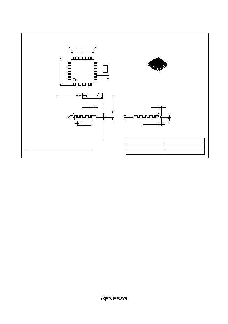
Rev. 1.0, 02/03, page 629 of 634
Hitachi Code
JEDEC
JEITA
Mass (reference value)
FP-64E
--
Conforms
0.4 g
*Dimension including the plating thickness
Base material dimension
M
12.0
± 0.2
10
48
33
1
16
17
32
64
49
*0.22
± 0.05
0.08
0.5
12.0
±
0.2
0.10
1.70 Max
*0.17
±
0.05
0.5
± 0.2
0
° 8°
1.0
1.45
0.10
±
0.10
1.25
0.20
± 0.04
0.15
±
0.04
Figure C.2 FP-64E Package Dimensions

Rev. 1.0, 02/03, page 630 of 634

Rev. 1.0, 02/03, page 631 of 634
Index
16-Bit Timer Pulse Unit.......................... 247
A/D Conversion Time............................. 496
A/D Converter ........................................ 487
A/D Converter Activation....................... 294
Absolute Address...................................... 49
Address Space........................................... 28
Addressing Mode...................................... 47
ADI ......................................................... 498
Advanced Mode........................................ 26
Arithmetic Operations Instructions........... 39
Asynchronous Mode............................... 369
Bcc...................................................... 36, 44
Bit Manipulation Instructions ................... 42
Bit rate .................................................... 362
Block Data Transfer Instruction................ 46
Boot Mode .............................................. 517
Boundary Scan........................................ 409
Branch Instructions................................... 44
Break....................................................... 403
Buffer Operation..................................... 281
Bulk-In Transfer ..................................... 470
Bulk-Out Transfer................................... 471
Bus Arbitration ....................................... 137
Bus cycle................................................. 116
Clock Pulse Generator ............................ 541
Condition Field ......................................... 46
Condition-Code Register .......................... 32
Control Transfer...................................... 463
CPU Operating Modes.............................. 24
Data reading procedure........................... 329
Data Transfer Instructions ........................ 38
DMA Transfer Specifications................. 476
Effective Address................................ 47, 51
Effective Address Extension..................... 46
Emulation................................................ 526
Erase/Erase-Verify.................................. 530
Erasing units ........................................... 510
Error Protection ...................................... 532
Exception Handling .................................. 67
Extended Control Register (EXR) ............ 31
External Trigger ......................................497
Flash Memory .........................................505
Framing error ..........................................375
Free-running count operation..................276
General Registers ......................................30
Hardware Protection ...............................532
Immediate .................................................49
Initial Setting Procedure..........................328
Input Capture Function ...........................278
Instruction Set ...........................................36
Internal bus masters ..................................99
Interrupt Control Mode .............................88
Interrupt Controller ...................................77
Interrupt Exception Handling Vector Table
..................................................................86
Interrupt Mask Bit.....................................32
Interrupt mask level ..................................31
Interrupt priority register...........................77
Interrupt-In Transfer ...............................469
Interrupts ...................................................73
Interval Timer Mode ...............................314
Logic Operations Instructions ...................41
Mark State...............................................403
Mask ROM..............................................539
Memory cycle .........................................114
Memory Indirect .......................................50
Memory Map ............................................63
NMI Interrupt............................................85
Normal Mode ............................................24
On-Board Programming..........................517
Operating Mode Selection.........................57
Operation Field .........................................46
Overflow .................................................315
Overrun error ..........................................375
Parity error ..............................................375
Periodic count operation .........................276
Phase Counting Mode .............................288
PLL Circuit .............................................549
Processing of USB Standard Commands and
Class/Vendor Commands........................472

Rev. 1.0, 02/03, page 632 of 634
Program Counter....................................... 31
Program/Program-Verify ........................ 528
Program-Counter Relative ........................ 50
Programmer Mode .................................. 533
Programming units.................................. 510
Programming/Erasing in User Program
Mode....................................................... 525
PWM Modes........................................... 284
Realtime Clock (RTC) ............................ 319
Register
ABWCR .................. 102, 579, 585, 593
ADCR ...................... 492, 582, 590, 596
ADCSR.................... 490, 582, 590, 596
ADDR...................... 490, 582, 590, 596
ASTCR .................... 103, 579, 585, 593
BCRH ...................... 108, 579, 585, 593
BCRL....................... 109, 579, 585, 593
BRR ......................... 362, 581, 589, 596
BSCANR ......................................... 413
BYPASS .......................................... 413
DMACR .................. 145, 581, 589, 595
EBR1 ....................... 514, 582, 590, 596
EBR2 ....................... 514, 582, 590, 596
ETCR....................... 144, 579, 586, 594
FLMCR1.................. 512, 582, 590, 596
FLMCR2.................. 513, 582, 590, 596
IDCODE .......................................... 413
IER............................. 81, 578, 584, 592
INSTR.............................................. 411
IOAR ....................... 143, 579, 586, 594
IPR............................. 80, 579, 585, 593
ISCR .......................... 82, 578, 584, 592
ISR............................. 84, 578, 584, 592
LPWRCR................. 543, 578, 584, 592
MAR ........................ 143, 579, 586, 594
MDCR ....................... 58, 578, 584, 592
MSTPCR ................. 560, 578, 584, 592
P1DDR .................... 194, 578, 584, 592
P1DR ....................... 195, 580, 587, 594
P3DDR .................... 201, 578, 584, 592
P3DR ....................... 202, 580, 587, 594
P3ODR .................... 203, 578, 585, 593
P7DDR .................... 205, 578, 584, 592
P7DR........................ 206, 580, 587, 594
PADDR.................... 210, 578, 584, 592
PADR....................... 211, 580, 587, 594
PAODR.................... 212, 578, 585, 593
PAPCR..................... 212, 578, 585, 593
PBDDR .................... 216, 578, 584, 592
PBDR....................... 217, 580, 587, 594
PBPCR..................... 218, 578, 585, 593
PCDDR .................... 222, 578, 584, 592
PCDR....................... 222, 580, 587, 594
PCPCR..................... 223, 578, 585, 593
PDDDR.................... 227, 578, 585, 592
PDDR....................... 227, 580, 587, 594
PDPCR..................... 228, 578, 585, 593
PEDDR .................... 231, 578, 585, 592
PEDR ....................... 232, 580, 587, 594
PEPCR ..................... 233, 578, 585, 593
PFCR........................ 110, 578, 584, 592
PFDDR..................... 237, 578, 585, 592
PFDR ....................... 238, 580, 587, 594
PGDDR.................... 242, 578, 585, 592
PGDR....................... 243, 580, 587, 594
PORT1 ..................... 195, 582, 590, 597
PORT3 ..................... 202, 582, 590, 597
PORT4 ..................... 204, 582, 590, 597
PORT7 ..................... 207, 582, 590, 597
PORT9 ..................... 209, 582, 590, 597
PORTA .................... 211, 582, 590, 597
PORTB .................... 217, 582, 590, 597
PORTC .................... 223, 582, 590, 597
PORTD .................... 228, 582, 590, 597
PORTE..................... 232, 582, 590, 597
PORTF..................... 238, 582, 590, 597
PORTG .................... 243, 582, 590, 597
RAMER ................... 515, 579, 585, 593
RDR ......................... 338, 581, 589, 596
RHRDR............................................322
RMINDR ................. 321, 581, 588, 595
RSECDR.................. 320, 581, 588, 595
RSTCSR................... 312, 581, 589, 595
RTCCR1 .................. 324, 581, 588, 595
RTCCR2 .................. 325, 581, 588, 595
RTCCSR .................. 326, 581, 588, 595

Rev. 1.0, 02/03, page 633 of 634
RWKDR .................. 323, 581, 588, 595
SBYCR .................... 557, 578, 584, 592
SCKCR .................... 542, 578, 584, 592
SCMR ...................... 352, 581, 589, 596
SCR.......................... 342, 581, 589, 596
SCRX....................... 516, 578, 584, 592
SEMRA_0 ............... 353, 578, 584, 592
SEMRB_0................ 355, 578, 584, 592
SMR......................... 339, 581, 589, 596
SSR .......................... 346, 581, 589, 596
SYSCR ...................... 59, 578, 584, 592
TCNT...................... 271, 310, 580, 581,
................................ 587, 589, 594, 595
TCR ......................... 253, 580, 587, 594
TCSR ....................... 310, 581, 589, 595
TDR ......................... 338, 581, 589, 596
TGR ......................... 271, 580, 587, 594
TIER ........................ 267, 580, 587, 594
TIOR........................ 258, 580, 587, 594
TMDR...................... 256, 580, 587, 594
TSR.......................... 268, 580, 587, 594
TSTR ....................... 271, 579, 585, 593
TSYR....................... 272, 579, 585, 593
UCTLR .................... 429, 576, 583, 591
UCVR ...................... 447, 577, 584, 591
UDMAR .................. 431, 576, 583, 591
UDRR ...................... 432, 576, 583, 591
UDSR ...................... 446, 577, 584, 591
UEDR0i ................... 437, 576, 583, 591
UEDR0o .................. 437, 576, 583, 591
UEDR0s................... 437, 576, 583, 591
UESTL0................... 435, 576, 583, 591
UESTL1................... 436, 576, 583, 591
UESZ0o ................... 439, 577, 583, 591
UESZ2 ..................... 439, 577, 583, 591
UFCLR0 .................. 434, 576, 583, 591
UIER0...................... 443, 577, 583, 591
UIER1...................... 444, 577, 583, 591
UIER3...................... 444, 577, 583, 591
UIFR0 ...................... 439, 577, 583, 591
UIFR1 ...................... 441, 577, 583, 591
UIFR3 ...................... 442, 577, 583, 591
UISR0 ...................... 445, 577, 583, 591
UISR1 ...................... 445, 577, 583, 591
UISR3 ...................... 446, 577, 583, 591
UTRG0 .................... 433, 576, 583, 591
UTSTR0................... 448, 577, 584, 592
UTSTR1................... 449, 577, 584, 592
WCRH ..................... 104, 579, 585, 593
WCRL...................... 104, 579, 585, 593
Register Direct ..........................................48
Register Field ............................................46
Register Indirect........................................48
Register Indirect with Displacement .........48
Register Indirect with Post-Increment.......48
Register indirect with pre-decrement ........48
Reset..........................................................69
Reset exception handling ..........................70
Scan Mode ..............................................495
Serial Communication Interface..............333
Shift Instructions .......................................41
Single Mode ............................................494
Software Protection.................................532
Stack pointer (SP) .....................................30
Stack Status...............................................75
Stall Operations.......................................473
Suspend and Resume ..............................460
Synchronous Operation...........................279
System Control Instruction .......................45
TCI0V .....................................................293
TCI1U .....................................................293
TCI1V .....................................................293
TCI2U .....................................................293
TCI2V .....................................................293
TGI0A.....................................................293
TGI0B .....................................................293
TGI0C .....................................................293
TGI0D.....................................................293
TGI1A.....................................................293
TGI1B .....................................................293
TGI2A.....................................................293
TGI2B .....................................................293
Toggle output ..........................................278
Trace Bit ...................................................31
Traces........................................................73
Trap Instruction.........................................74

Rev. 1.0, 02/03, page 634 of 634
TRAPA ............................................... 49, 74
Universal Serial Bus ............................... 425
USB Cable Connection/Disconnection... 456
Watchdog timer.......................................309
Waveform Output by Compare Match....277
WOVI......................................................315

H8S/2218 Series H8S/2212 Series Hardware Manual
Publication Date: 1st Edition, February 2003
Published by:
Business Operation Division
Semiconductor & Integrated Circuits
Hitachi, Ltd.
Edited by:
Technical Documentation Group
Hitachi Kodaira Semiconductor Co., Ltd.
Copyright © Hitachi, Ltd., 2003. All rights reserved. Printed in Japan.
Document Outline