 | –≠–ª–µ–∫—Ç—Ä–æ–Ω–Ω—ã–π –∫–æ–º–ø–æ–Ω–µ–Ω—Ç: HD6432242 | –°–∫–∞—á–∞—Ç—å:  PDF PDF  ZIP ZIP |

Regarding the change of names mentioned in the document, such as Hitachi
Electric and Hitachi XX, to Renesas Technology Corp.
The semiconductor operations of Mitsubishi Electric and Hitachi were transferred to Renesas
Technology Corporation on April 1st 2003. These operations include microcomputer, logic, analog
and discrete devices, and memory chips other than DRAMs (flash memory, SRAMs etc.)
Accordingly, although Hitachi, Hitachi, Ltd., Hitachi Semiconductors, and other Hitachi brand
names are mentioned in the document, these names have in fact all been changed to Renesas
Technology Corp. Thank you for your understanding. Except for our corporate trademark, logo and
corporate statement, no changes whatsoever have been made to the contents of the document, and
these changes do not constitute any alteration to the contents of the document itself.
Renesas Technology Home Page: http://www.renesas.com
Renesas Technology Corp.
Customer Support Dept.
April 1, 2003
To all our customers

Cautions
Keep safety first in your circuit designs!
1. Renesas Technology Corporation puts the maximum effort into making semiconductor products better
and more reliable, but there is always the possibility that trouble may occur with them. Trouble with
semiconductors may lead to personal injury, fire or property damage.
Remember to give due consideration to safety when making your circuit designs, with appropriate
measures such as (i) placement of substitutive, auxiliary circuits, (ii) use of nonflammable material or
(iii) prevention against any malfunction or mishap.
Notes regarding these materials
1. These materials are intended as a reference to assist our customers in the selection of the Renesas
Technology Corporation product best suited to the customer's application; they do not convey any
license under any intellectual property rights, or any other rights, belonging to Renesas Technology
Corporation or a third party.
2. Renesas Technology Corporation assumes no responsibility for any damage, or infringement of any
third-party's rights, originating in the use of any product data, diagrams, charts, programs, algorithms, or
circuit application examples contained in these materials.
3. All information contained in these materials, including product data, diagrams, charts, programs and
algorithms represents information on products at the time of publication of these materials, and are
subject to change by Renesas Technology Corporation without notice due to product improvements or
other reasons. It is therefore recommended that customers contact Renesas Technology Corporation
or an authorized Renesas Technology Corporation product distributor for the latest product information
before purchasing a product listed herein.
The information described here may contain technical inaccuracies or typographical errors.
Renesas Technology Corporation assumes no responsibility for any damage, liability, or other loss
rising from these inaccuracies or errors.
Please also pay attention to information published by Renesas Technology Corporation by various
means, including the Renesas Technology Corporation Semiconductor home page
(http://www.renesas.com).
4. When using any or all of the information contained in these materials, including product data, diagrams,
charts, programs, and algorithms, please be sure to evaluate all information as a total system before
making a final decision on the applicability of the information and products. Renesas Technology
Corporation assumes no responsibility for any damage, liability or other loss resulting from the
information contained herein.
5. Renesas Technology Corporation semiconductors are not designed or manufactured for use in a device
or system that is used under circumstances in which human life is potentially at stake. Please contact
Renesas Technology Corporation or an authorized Renesas Technology Corporation product distributor
when considering the use of a product contained herein for any specific purposes, such as apparatus or
systems for transportation, vehicular, medical, aerospace, nuclear, or undersea repeater use.
6. The prior written approval of Renesas Technology Corporation is necessary to reprint or reproduce in
whole or in part these materials.
7. If these products or technologies are subject to the Japanese export control restrictions, they must be
exported under a license from the Japanese government and cannot be imported into a country other
than the approved destination.
Any diversion or reexport contrary to the export control laws and regulations of Japan and/or the
country of destination is prohibited.
8. Please contact Renesas Technology Corporation for further details on these materials or the products
contained therein.

H8S/2245 Series
H8S/2246, H8S/2245, H8S/2244,
H8S/2243, H8S/2242, H8S/2241,
H8S/2240
Hardware Manual
ADE-602-100A
Rev. 2.0
3/7/03
Hitachi, Ltd.
MC-Setsu

Notice
When using this document, keep the following in mind:
1. This document may, wholly or partially, be subject to change without notice.
2. All rights are reserved: No one is permitted to reproduce or duplicate, in any form, the whole
or part of this document without Hitachi's permission.
3. Hitachi will not be held responsible for any damage to the user that may result from accidents
or any other reasons during operation of the user's unit according to this document.
4. Circuitry and other examples described herein are meant merely to indicate the characteristics
and performance of Hitachi's semiconductor products. Hitachi assumes no responsibility for
any intellectual property claims or other problems that may result from applications based on
the examples described herein.
5. No license is granted by implication or otherwise under any patents or other rights of any third
party or Hitachi, Ltd.
6. MEDICAL APPLICATIONS: Hitachi's products are not authorized for use in MEDICAL
APPLICATIONS without the written consent of the appropriate officer of Hitachi's sales
company. Such use includes, but is not limited to, use in life support systems. Buyers of
Hitachi's products are requested to notify the relevant Hitachi sales offices when planning to
use the products in MEDICAL APPLICATIONS.

Preface
The H8S/2245 Series is a series of high-performance microcontrollers with a 32-bit H8S/2000
CPU core, and a set of on-chip peripheral functions required for system configuration.
The H8S/2000 CPU can execute basic instructions in one state, and is provided with sixteen 16-bit
general registers with a 32-bit internal configuration, and a concise and optimized instruction set.
The CPU can handle a 16 Mbyte linear address space (architecturally 4 Gbytes). Programs based
on the high-level language C can also be run efficiently.
The address space is divided into eight areas. The data bus width and access states can be selected
for each of these areas, and various kinds of memory can be connected fast and easily.
On-chip memory consists of large-capacity ROM and RAM. PROM (ZTATTM*) and mask ROM
versions are available, providing a quick and flexible response to conditions from ramp-up through
full-scale volume production, even for applications with frequently changing specifications.
On-chip peripheral functions include a 16-bit timer pulse unit (TPU), 8-bit timers, watchdog timer
(WDT), serial communication interface (SCI), A/D converter, and I/O ports.
In addition, an on-chip data transfer controller (DTC) is provided, enabling high-speed data
transfer without CPU intervention.
Use of the H8S/2245 Series enables compact, high-performance systems to be implemented easily.
This manual describes the hardware of the H8S/2245 Series. Refer to the H8S/2600 Series and
H8S/2000 Series Programming Manual for a detailed description of the instruction set.
Note: * ZTAT is a trademark of Hitachi, Ltd.


Main Revisions and Additions in this Edition
Page
Item
Revision
3, 4
Table 1-1 Overview
Product type names added
67
3.1.1 Operating Mode Selection
Description amended
79, 80
Figure 3-3 H8S/2244 Memory Map in Each Operating
Mode
Figure added
81, 82
Figure 3-4 H8S/2243 Memory Map in Each Operating
Mode
Figure added
87
Figure 3-7 H8S/2240 Memory Map in Each Operating
Mode
Figure added
94
4.2.5 State of On-Chip Supporting Modules after Reset
Release
Added
125
5.6.3 Operation (1) Selection of Interrupt Source
Description amended
140
6.2.5 Bus Control Register L (BCRL), Bit 5
Table amended
144
6.3.4 Advanced Mode, Area 7
Description added
158
Wait Control (2) Pin Wait Insertion Using
WAIT
Pin
Description amended
163, 164
Figures 6-16 and 6-17 Example of Idle Cycle Operation
(1) and (2)
Figure amended
165
6.6.1 Operation
(3) Relationship Between Chip Select (
CS
) Signal
and Read (
RD
) Signal
Added
165
Figure 6-18 Relationship Between Chip Select (
CS
)
and Read (
RD
)
Added
166
Table 6-5 Pin States in Idle Cycle
Contents amended
173
7.1.1 Features
Contents added
174
7.1.2 Block Diagram
Note (
*
) added
180
7.2.7 DTC Enable Register (DTCER)
Description added
191
7.3.6 Repeat Mode
Description added
200
7.5 Usage Notes, DTCE Bit Setting
Added
274
9.1.1 Features
Contents added
320
9.4.5 PWM Modes
Description added
349
9.7 Usage Notes, Interrupts and Module Stop Mode
Added
351
10.1.1 Features
Contents added
362
Figure 10-2 Count Timing for Internal Clock Input
Figure amended
363
Figure 10-3 Count Timing for External Clock Input
Figure amended

Page
Item
Revision
365
Figure 10-7 Timing of External Reset
Figure amended
367
10.4.2 A/D Converter Activation
Added
374
10.6.6 Interrupts and Module Stop Mode
Added
392
12.1.1 Features
Contents added
405, 407
12.2.7 Serial Status Register, Bits 7, 6, 2
Table amended
425
Figure 12-5 Sample Serial Transmission Flowchart
Description added
434
Figure 12-10 Sample Multiprocessor Serial
Transmission Flowchart
Description added
442
Figure 12-15 Sample SCI Initialization Flowchart
Note (
*
) added
464
Figure 13-2 Schematic Diagram of Smart Card
Interface Pin Connections
Figure amended
467
13.3.4 Register Settings, SCR Setting
Description added
469
Table 13-5 Examples of Bit Rate B (bit/s) for Various
BRR Settings
Contents added
470
Table 13-6 Examples of BRR Settings for Bit Rate
B (bits/s)
Contents added
474
Figure 13-5 Relation Between Transmit Operation and
Internal Registers
Figure added
476
Fixing Clock Output Level
Description and figure
added
483
14.1.1 Features
Contents added
499
14.5 Interrupts
Contents and table added
505
15.1 Overview
Type names added
509
16.1 Overview
Type names added
511
16.2.1 Bus Control Register L (BCRL), Bit 5
Table amended
512
Table 16-2 Operating Modes and ROM Area
Contents added
530 to 532
17.3.2 External Clock Input
External Clock, Note on External Clock Switchover
Added
550 to 579
Section 19 Electrical Characteristics
Contents amended
749
Appendix E Pin States at Power-On
Added

i
Contents
Section 1
Overview
...........................................................................................................
1
1.1 Overview............................................................................................................................
1
1.2
Internal Block Diagram .....................................................................................................
5
1.3 Pin
Description ..................................................................................................................
6
1.3.1 Pin
Arrangement ..................................................................................................
6
1.3.2
Pin Functions in Each Operating Mode................................................................
7
1.3.3 Pin
Functions........................................................................................................
12
Section 2
CPU
.....................................................................................................................
19
2.1 Overview............................................................................................................................
19
2.1.1 Features ................................................................................................................
19
2.1.2
Differences between H8S/2600 CPU and H8S/2000 CPU ..................................
20
2.1.3
Differences from H8/300 CPU .............................................................................
21
2.1.4
Differences from H8/300H CPU..........................................................................
21
2.2
CPU Operating Modes ......................................................................................................
22
2.3 Address
Space....................................................................................................................
27
2.4 Register
Configuration ......................................................................................................
28
2.4.1 Overview ..............................................................................................................
28
2.4.2 General
Registers..................................................................................................
29
2.4.3 Control
Registers..................................................................................................
30
2.4.4
Initial Register Values ..........................................................................................
32
2.5 Data
Formats......................................................................................................................
33
2.5.1
General Register Data Formats ............................................................................
33
2.5.2
Memory Data Formats..........................................................................................
35
2.6 Instruction
Set....................................................................................................................
36
2.6.1 Overview ..............................................................................................................
36
2.6.2
Instructions and Addressing Modes .....................................................................
37
2.6.3 Table of Instructions Classified by Function........................................................
39
2.6.4
Basic Instruction Formats.....................................................................................
49
2.6.5
Notes on Use of Bit Manipulation Instructions....................................................
50
2.7
Addressing Modes and Effective Address Calculation .....................................................
50
2.7.1 Addressing
Modes................................................................................................
50
2.7.2
Effective Address Calculation..............................................................................
53
2.8 Processing
States ...............................................................................................................
57
2.8.1 Overview ..............................................................................................................
57
2.8.2 Reset
State ............................................................................................................
58
2.8.3 Exception-Handling
State ....................................................................................
59
2.8.4
Program Execution State ......................................................................................
61
2.8.5 Bus-Released
State ...............................................................................................
61

ii
2.8.6 Power-Down
State................................................................................................
61
2.9 Basic
Timing......................................................................................................................
62
2.9.1 Overview ..............................................................................................................
62
2.9.2
On-Chip Memory (ROM, RAM) .........................................................................
62
2.9.3
On-Chip Supporting Module Access Timing.......................................................
64
2.9.4
External Address Space Access Timing...............................................................
65
Section 3
MCU Operating Modes
................................................................................
67
3.1 Overview............................................................................................................................
67
3.1.1
Operating Mode Selection....................................................................................
67
3.1.2 Register
Configuration .........................................................................................
68
3.2 Register
Descriptions.........................................................................................................
69
3.2.1
Mode Control Register (MDCR)..........................................................................
69
3.2.2
System Control Register (SYSCR) ......................................................................
69
3.3
Operating Mode Descriptions............................................................................................
71
3.3.1 Mode
1..................................................................................................................
71
3.3.2 Mode
2..................................................................................................................
71
3.3.3 Mode
3..................................................................................................................
71
3.3.4 Mode
4..................................................................................................................
72
3.3.5 Mode
5..................................................................................................................
72
3.3.6 Mode
6..................................................................................................................
72
3.3.7 Mode
7..................................................................................................................
73
3.4
Pin Functions in Each Operating Mode.............................................................................
73
3.5
Memory Map in Each Operating Mode.............................................................................
74
Section 4
Exception Handling
........................................................................................
89
4.1 Overview............................................................................................................................
89
4.1.1
Exception Handling Types and Priority ...............................................................
89
4.1.2
Exception Handling Operation .............................................................................
89
4.1.3
Exception Sources and Vector Table ...................................................................
90
4.2 Reset ..................................................................................................................................
92
4.2.1 Overview ..............................................................................................................
92
4.2.2 Reset
Types ..........................................................................................................
92
4.2.3 Reset
Sequence .....................................................................................................
93
4.2.4
Interrupts after Reset ............................................................................................
94
4.2.5
State of On-Chip Supporting Modules after Reset Release .................................
94
4.3 Interrupts............................................................................................................................
95
4.4 Trap
Instruction .................................................................................................................
96
4.5
Stack Status after Exception Handling ..............................................................................
97
4.6
Notes on Use of the Stack..................................................................................................
98
Section 5
Interrupt Controller
........................................................................................
99
5.1 Overview............................................................................................................................
99

iii
5.1.1 Features ................................................................................................................
99
5.1.2 Block
Diagram...................................................................................................... 100
5.1.3 Pin
Configuration ................................................................................................. 101
5.1.4 Register
Configuration ......................................................................................... 101
5.2 Register
Descriptions......................................................................................................... 102
5.2.1
System Control Register (SYSCR) ...................................................................... 102
5.2.2
Interrupt Control Registers A to C (ICRA to ICRC)............................................ 103
5.2.3
IRQ Enable Register (IER) .................................................................................. 104
5.2.4
IRQ Sense Control Registers H and L (ISCRH, ISCRL) ..................................... 104
5.2.5
IRQ Status Register (ISR) .................................................................................... 105
5.3 Interrupt
Sources................................................................................................................ 107
5.3.1 External
Interrupts................................................................................................ 107
5.3.2 Internal
Interrupts ................................................................................................. 108
5.3.3
Interrupt Exception Handling Vector Table ......................................................... 108
5.4 Interrupt
Operation ............................................................................................................ 112
5.4.1
Interrupt Control Modes and Interrupt Operation ................................................ 112
5.4.2
Interrupt Control Mode 0...................................................................................... 115
5.4.3
Interrupt Control Mode 1...................................................................................... 117
5.4.4
Interrupt Exception Handling Sequence .............................................................. 120
5.4.5
Interrupt Response Times..................................................................................... 121
5.5 Usage
Notes ....................................................................................................................... 122
5.5.1
Contention between Interrupt Generation and Disabling ..................................... 122
5.5.2
Instructions that Disable Interrupts ...................................................................... 123
5.5.3
Interrupts during Execution of EEPMOV Instruction.......................................... 123
5.6
DTC Activation by Interrupt ............................................................................................. 124
5.6.1 Overview .............................................................................................................. 124
5.6.2 Block
Diagram...................................................................................................... 124
5.6.3 Operation .............................................................................................................. 125
Section 6
Bus Controller
.................................................................................................. 127
6.1 Overview............................................................................................................................ 127
6.1.1 Features ................................................................................................................ 127
6.1.2 Block
Diagram...................................................................................................... 128
6.1.3 Pin
Configuration ................................................................................................. 129
6.1.4 Register
Configuration ......................................................................................... 130
6.2 Register
Descriptions......................................................................................................... 131
6.2.1
Bus Width Control Register (ABWCR) ............................................................... 131
6.2.2
Access State Control Register (ASTCR) ............................................................ 132
6.2.3
Wait Control Registers H and L (WCRH, WCRL).............................................. 133
6.2.4
Bus Control Register H (BCRH).......................................................................... 137
6.2.5
Bus Control Register L (BCRL)........................................................................... 139
6.3
Overview of Bus Control................................................................................................... 141
6.3.1 Area
Partitioning .................................................................................................. 141

iv
6.3.2 Bus
Specifications ................................................................................................ 142
6.3.3 Memory
Interfaces................................................................................................ 143
6.3.4 Advanced
Mode.................................................................................................... 144
6.3.5
Areas in Normal Mode ......................................................................................... 145
6.3.6
Chip Select Signals............................................................................................... 146
6.4
Basic Bus Interface............................................................................................................ 147
6.4.1 Overview .............................................................................................................. 147
6.4.2
Data Size and Data Alignment ............................................................................. 147
6.4.3 Valid
Strobes ........................................................................................................ 149
6.4.4 Basic
Timing ........................................................................................................ 150
6.4.5 Wait
Control ......................................................................................................... 158
6.5
Burst ROM Interface ......................................................................................................... 160
6.5.1 Overview .............................................................................................................. 160
6.5.2 Basic
Timing ........................................................................................................ 160
6.5.3 Wait
Control ......................................................................................................... 162
6.6 Idle
Cycle........................................................................................................................... 163
6.6.1 Operation .............................................................................................................. 163
6.6.2
Pin States in Idle Cycle ........................................................................................ 166
6.7 Bus
Release........................................................................................................................ 167
6.7.1 Overview .............................................................................................................. 167
6.7.2 Operation .............................................................................................................. 167
6.7.3
Pin States in External Bus Released State............................................................ 168
6.7.4 Transition
Timing ................................................................................................. 169
6.7.5 Usage
Note ........................................................................................................... 170
6.8 Bus
Arbitration .................................................................................................................. 170
6.8.1 Overview .............................................................................................................. 170
6.8.2 Operation .............................................................................................................. 170
6.8.3
Bus Transfer Timing ............................................................................................ 171
6.8.4
External Bus Release Usage Note ........................................................................ 171
6.9
Resets and the Bus Controller............................................................................................ 171
Section 7
Data Transfer Controller
.............................................................................. 173
7.1 Overview............................................................................................................................ 173
7.1.1 Features ................................................................................................................ 173
7.1.2 Block
Diagram...................................................................................................... 174
7.1.3 Register
Configuration ......................................................................................... 175
7.2 Register
Descriptions......................................................................................................... 176
7.2.1
DTC Mode Register A (MRA)............................................................................. 176
7.2.2
DTC Mode Register B (MRB) ............................................................................. 178
7.2.3
DTC Source Address Register (SAR) .................................................................. 179
7.2.4
DTC Destination Address Register (DAR) .......................................................... 179
7.2.5
DTC Transfer Count Register A (CRA) .............................................................. 179
7.2.6
DTC Transfer Count Register B (CRB) ............................................................... 180

v
7.2.7
DTC Enable Registers (DTCER) ......................................................................... 180
7.2.8
DTC Vector Register (DTVECR) ........................................................................ 181
7.2.9
Module Stop Control Register (MSTPCR) .......................................................... 182
7.3 Operation ........................................................................................................................... 183
7.3.1 Overview .............................................................................................................. 183
7.3.2 Activation
Sources................................................................................................ 184
7.3.3
DTC Vector Table ................................................................................................ 186
7.3.4
Location of Register Information in Address Space ............................................ 189
7.3.5 Normal
Mode........................................................................................................ 190
7.3.6 Repeat
Mode ........................................................................................................ 191
7.3.7
Block Transfer Mode............................................................................................ 192
7.3.8 Chain
Transfer...................................................................................................... 194
7.3.9 Operation
Timing ................................................................................................. 195
7.3.10 Number of DTC Execution States........................................................................ 196
7.3.11 Procedures for Using DTC ................................................................................... 198
7.3.12 Examples of Use of the DTC................................................................................ 198
7.4 Interrupts............................................................................................................................ 200
7.5 Usage
Notes ....................................................................................................................... 200
Section 8
I/O Ports
............................................................................................................ 201
8.1 Overview............................................................................................................................ 201
8.2 Port
1.................................................................................................................................. 207
8.2.1 Overview .............................................................................................................. 207
8.2.2 Register
Configuration ......................................................................................... 208
8.2.3 Pin
Functions........................................................................................................ 210
8.3 Port
2.................................................................................................................................. 218
8.3.1 Overview .............................................................................................................. 218
8.3.2 Register
Configuration ......................................................................................... 218
8.3.3 Pin
Functions........................................................................................................ 220
8.4 Port
3.................................................................................................................................. 222
8.4.1 Overview .............................................................................................................. 222
8.4.2 Register
Configuration ......................................................................................... 222
8.4.3 Pin
Functions........................................................................................................ 225
8.5 Port
4.................................................................................................................................. 227
8.5.1 Overview .............................................................................................................. 227
8.5.2 Register
Configuration ......................................................................................... 227
8.5.3 Pin
Functions........................................................................................................ 228
8.6 Port
5.................................................................................................................................. 229
8.6.1 Overview .............................................................................................................. 229
8.6.2 Register
Configuration ......................................................................................... 229
8.6.3 Pin
Functions........................................................................................................ 232
8.7 Port
A................................................................................................................................. 233
8.7.1 Overview .............................................................................................................. 233

vi
8.7.2 Register
Configuration ......................................................................................... 234
8.7.3 Pin
Functions........................................................................................................ 237
8.7.4
MOS Input Pull-Up Function ............................................................................... 238
8.8 Port
B ................................................................................................................................. 239
8.8.1 Overview .............................................................................................................. 239
8.8.2 Register
Configuration ......................................................................................... 240
8.8.3 Pin
Functions........................................................................................................ 242
8.8.4
MOS Input Pull-Up Function ............................................................................... 244
8.9 Port
C ................................................................................................................................. 245
8.9.1 Overview .............................................................................................................. 245
8.9.2 Register
Configuration ......................................................................................... 246
8.9.3 Pin
Functions........................................................................................................ 248
8.9.4
MOS Input Pull-Up Function ............................................................................... 250
8.10 Port
D................................................................................................................................. 251
8.10.1 Overview .............................................................................................................. 251
8.10.2 Register
Configuration ......................................................................................... 252
8.10.3 Pin
Functions........................................................................................................ 254
8.10.4 MOS Input Pull-Up Function ............................................................................... 255
8.11 Port
E ................................................................................................................................. 256
8.11.1 Overview .............................................................................................................. 256
8.11.2 Register
Configuration ......................................................................................... 257
8.11.3 Pin
Functions........................................................................................................ 259
8.11.4 MOS Input Pull-Up Function ............................................................................... 261
8.12 Port
F ................................................................................................................................. 262
8.12.1 Overview .............................................................................................................. 262
8.12.2 Register
Configuration ......................................................................................... 263
8.12.3 Pin
Functions........................................................................................................ 265
8.13 Port
G................................................................................................................................. 268
8.13.1 Overview .............................................................................................................. 268
8.13.2 Register
Configuration ......................................................................................... 269
8.13.3 Pin
Functions........................................................................................................ 271
Section 9
16-Bit Timer Pulse Unit (TPU)
.................................................................. 273
9.1 Overview............................................................................................................................ 273
9.1.1 Features ................................................................................................................ 273
9.1.2 Block
Diagram...................................................................................................... 277
9.1.3 Pin
Configuration ................................................................................................. 278
9.1.4 Register
Configuration ......................................................................................... 279
9.2 Register
Descriptions......................................................................................................... 281
9.2.1
Timer Control Register (TCR) ............................................................................. 281
9.2.2
Timer Mode Register (TMDR) ............................................................................ 285
9.2.3
Timer I/O Control Register (TIOR) ..................................................................... 287
9.2.4
Timer Interrupt Enable Register (TIER) .............................................................. 294

vii
9.2.5
Timer Status Register (TSR) ................................................................................ 297
9.2.6
Timer Counter (TCNT) ........................................................................................ 301
9.2.7
Timer General Register (TGR) ............................................................................ 301
9.2.8
Timer Start Register (TSTR)................................................................................ 302
9.2.9
Timer Synchro Register (TSYR).......................................................................... 303
9.2.10 Module Stop Control Register (MSTPCR) .......................................................... 304
9.3
Interface to Bus Master...................................................................................................... 305
9.3.1 16-Bit
Registers.................................................................................................... 305
9.3.2 8-Bit
Registers...................................................................................................... 305
9.4 Operation ........................................................................................................................... 307
9.4.1 Overview .............................................................................................................. 307
9.4.2 Basic
Functions .................................................................................................... 308
9.4.3 Synchronous
Operation ........................................................................................ 314
9.4.4 Buffer
Operation .................................................................................................. 316
9.4.5 PWM
Modes ........................................................................................................ 320
9.4.6
Phase Counting Mode .......................................................................................... 325
9.5 Interrupts............................................................................................................................ 330
9.5.1
Interrupt Sources and Priorities............................................................................ 330
9.5.2 DTC
Activation .................................................................................................... 331
9.5.3
A/D Converter Activation .................................................................................... 331
9.6 Operation
Timing .............................................................................................................. 332
9.6.1 Input/Output
Timing ............................................................................................ 332
9.6.2
Interrupt Signal Timing ........................................................................................ 336
9.7 Usage
Notes ....................................................................................................................... 340
Section 10 8-Bit Timers
..................................................................................................... 351
10.1 Overview............................................................................................................................ 351
10.1.1 Features ................................................................................................................ 351
10.1.2 Block
Diagram...................................................................................................... 352
10.1.3 Pin
Configuration ................................................................................................. 353
10.1.4 Register
Configuration ......................................................................................... 353
10.2 Register
Descriptions......................................................................................................... 354
10.2.1 Timer Counters 0 and 1 (TCNT0, TCNT1).......................................................... 354
10.2.2 Time Constant Registers A0 and A1 (TCORA0, TCORA1) ............................... 354
10.2.3 Time Constant Registers B0 and B1 (TCORB0, TCORB1) ................................ 355
10.2.4 Time Control Registers 0 and 1 (TCR0, TCR1) .................................................. 355
10.2.5 Timer Control/Status Registers 0 and 1 (TCSR0, TCSR1).................................. 358
10.2.6 Module Stop Control Register (MSTPCR) .......................................................... 361
10.3 Operation ........................................................................................................................... 362
10.3.1 TCNT Incrementation Timing.............................................................................. 362
10.3.2 Compare Match Timing ....................................................................................... 363
10.3.3 Timing of External RESET on TCNT.................................................................. 365
10.3.4 Timing of Overflow Flag (OVF) Setting.............................................................. 365

viii
10.3.5 Operation with Cascaded Connection .................................................................. 366
10.4 Interrupt
Sources................................................................................................................ 367
10.4.1 Interrupt Sources and DTC Activation................................................................. 367
10.4.2 A/D Converter Activation .................................................................................... 367
10.5 Sample
Application ........................................................................................................... 368
10.6 Usage
Notes ....................................................................................................................... 369
10.6.1 Contention between TCNT Write and Clear........................................................ 369
10.6.2 Contention between TCNT Write and Increment ................................................ 370
10.6.3 Contention between TCOR Write and Compare Match ...................................... 371
10.6.4 Contention between Compare Matches A and B ................................................. 372
10.6.5 Switching of Internal Clocks and TCNT Operation............................................. 372
10.6.6 Interrupts and Module Stop Mode........................................................................ 374
Section 11 Watchdog Timer
............................................................................................. 375
11.1 Overview............................................................................................................................ 375
11.1.1 Features ................................................................................................................ 375
11.1.2 Block
Diagram...................................................................................................... 376
11.1.3 Pin
Configuration ................................................................................................. 377
11.1.4 Register
Configuration ......................................................................................... 377
11.2 Register
Descriptions......................................................................................................... 378
11.2.1 Timer Counter (TCNT) ........................................................................................ 378
11.2.2 Timer Control/Status Register (TCSR) ................................................................ 378
11.2.3 Reset Control/Status Register (RSTCSR) ............................................................ 380
11.2.4 Notes on Register Access .................................................................................... 382
11.3 Operation ........................................................................................................................... 384
11.3.1 Watchdog Timer Operation.................................................................................. 384
11.3.2 Interval Timer Operation...................................................................................... 385
11.3.3 Timing of Setting Overflow Flag (OVF) ............................................................. 386
11.3.4 Timing of Setting of Watchdog Timer Overflow Flag (WOVF) ......................... 387
11.4 Interrupts............................................................................................................................ 388
11.5 Usage Notes ....................................................................................................................... 388
11.5.1 Contention between Timer Counter (TCNT) Write and Increment ..................... 388
11.5.2 Changing Value of CKS2 to CKS0...................................................................... 388
11.5.3 Switching between Watchdog Timer Mode and Interval Timer Mode .............. 389
11.5.4 System Reset by
WDTOVF Signal...................................................................... 389
11.5.5 Internal Reset in Watchdog Timer Mode ............................................................. 389
Section 12 Serial Communication Interface (SCI)
.................................................... 391
12.1 Overview............................................................................................................................ 391
12.1.1 Features ................................................................................................................ 391
12.1.2 Block
Diagram...................................................................................................... 393
12.1.3 Pin
Configuration ................................................................................................. 394
12.1.4 Register
Configuration ......................................................................................... 395

ix
12.2 Register
Descriptions......................................................................................................... 396
12.2.1 Receive Shift Register (RSR) ............................................................................... 396
12.2.2 Receive Data Register (RDR) .............................................................................. 396
12.2.3 Transmit Shift Register (TSR).............................................................................. 397
12.2.4 Transmit Data Register (TDR) ............................................................................. 397
12.2.5 Serial Mode Register (SMR)................................................................................ 398
12.2.6 Serial Control Register (SCR).............................................................................. 401
12.2.7 Serial Status Register (SSR) ................................................................................. 404
12.2.8 Bit Rate Register (BRR) ....................................................................................... 408
12.2.9 Smart Card Mode Register (SCMR) .................................................................... 417
12.2.10 Module Stop Control Register (MSTPCR) .......................................................... 418
12.3 Operation ........................................................................................................................... 419
12.3.1 Overview .............................................................................................................. 419
12.3.2 Operation in Asynchronous Mode........................................................................ 421
12.3.3 Multiprocessor Communication Function............................................................ 432
12.3.4 Operation in Clocked Synchronous Mode ........................................................... 440
12.4 SCI
Interrupts .................................................................................................................... 449
12.5 Usage
Notes ....................................................................................................................... 451
Section 13 Smart Card Interface
...................................................................................... 455
13.1 Overview............................................................................................................................ 455
13.1.1 Features ................................................................................................................ 455
13.1.2 Block
Diagram...................................................................................................... 456
13.1.3 Pin
Configuration ................................................................................................. 457
13.1.4 Register
Configuration ......................................................................................... 458
13.2 Register
Descriptions......................................................................................................... 459
13.2.1 Smart Card Mode Register (SCMR) .................................................................... 459
13.2.2 Serial Status Register (SSR) ................................................................................. 460
13.2.3 Serial Mode Register (SMR)................................................................................ 461
13.2.4 Serial Control Register (SCR).............................................................................. 462
13.3
Operation ........................................................................................................................... 463
13.3.1 Overview .............................................................................................................. 463
13.3.2 Pin
Connections.................................................................................................... 464
13.3.3 Data
Format.......................................................................................................... 465
13.3.4 Register
Settings ................................................................................................... 467
13.3.5 Clock .................................................................................................................... 469
13.3.6 Data Transfer Operations ..................................................................................... 471
13.3.7 Operation in GSM Mode...................................................................................... 478
13.4 Usage
Notes ....................................................................................................................... 479
Section 14 A/D Converter
................................................................................................. 483
14.1 Overview............................................................................................................................ 483
14.1.1 Features ................................................................................................................ 483

x
14.1.2 Block
Diagram...................................................................................................... 484
14.1.3 Pin
Configuration ................................................................................................. 485
14.1.4 Register
Configuration ......................................................................................... 486
14.2 Register
Descriptions......................................................................................................... 487
14.2.1 A/D Data Registers A to D (ADDRA to ADDRD).............................................. 487
14.2.2 A/D Control/Status Register (ADCSR)................................................................ 488
14.2.3 A/D Control Register (ADCR) ............................................................................. 490
14.2.4 Module Stop Control Register (MSTPCR) .......................................................... 491
14.3 Interface to Bus Master...................................................................................................... 492
14.4 Operation ........................................................................................................................... 493
14.4.1 Single Mode (SCAN = 0) ..................................................................................... 493
14.4.2 Scan Mode (SCAN = 1) ....................................................................................... 495
14.4.3 Input Sampling and A/D Conversion Time.......................................................... 497
14.4.4 External Trigger Input Timing ............................................................................. 498
14.5 Interrupts............................................................................................................................ 499
14.6 Usage
Notes ....................................................................................................................... 499
Section 15 RAM
................................................................................................................... 505
15.1 Overview............................................................................................................................ 505
15.1.1 Block
Diagram...................................................................................................... 506
15.1.2 Register
Configuration ......................................................................................... 506
15.2 Register
Descriptions......................................................................................................... 507
15.2.1 System Control Register (SYSCR) ...................................................................... 507
15.3 Operation ........................................................................................................................... 507
Section 16 ROM
................................................................................................................... 509
16.1 Overview............................................................................................................................ 509
16.1.1 Block
Diagram...................................................................................................... 510
16.1.2 Register
Configuration ......................................................................................... 510
16.2 Register
Descriptions......................................................................................................... 511
16.2.1 Bus Control Register L (BCRL)........................................................................... 511
16.3 Operation ........................................................................................................................... 512
16.4 PROM
Mode...................................................................................................................... 513
16.4.1 PROM Mode Setting ............................................................................................ 513
16.4.2 Socket Adapter and Memory Map........................................................................ 513
16.5 Programming ..................................................................................................................... 516
16.5.1 Overview .............................................................................................................. 516
16.5.2 Programming and Verification ............................................................................. 516
16.5.3 Programming
Precautions .................................................................................... 521
16.5.4 Reliability of Programmed Data .......................................................................... 522
Section 17 Clock Pulse Generator
.................................................................................. 523
17.1 Overview............................................................................................................................ 523

xi
17.1.1 Block
Diagram...................................................................................................... 523
17.1.2 Register
Configuration ......................................................................................... 524
17.2 Register
Descriptions......................................................................................................... 525
17.2.1 System Clock Control Register (SCKCR) ........................................................... 525
17.2.2 Low Power Control Register (LPWCR) .............................................................. 526
17.3 Oscillator............................................................................................................................ 527
17.3.1 Connecting a Crystal Resonator ........................................................................... 527
17.3.2 External Clock Input ............................................................................................ 529
17.4 Duty Adjustment Circuit.................................................................................................... 534
17.5 Medium-Speed Clock Divider ........................................................................................... 534
17.6 Bus Master Clock Selection Circuit .................................................................................. 534
Section 18 Power-Down Modes
...................................................................................... 535
18.1 Overview............................................................................................................................ 535
18.1.1 Register
Configuration ......................................................................................... 536
18.2
Register Descriptions......................................................................................................... 537
18.2.1 Standby Control Register (SBYCR) .................................................................... 537
18.2.2 System Clock Control Register (SCKCR) ........................................................... 538
18.2.3 Module Stop Control Register (MSTPCR) .......................................................... 539
18.3 Medium-Speed
Mode ........................................................................................................ 540
18.4 Sleep
Mode ........................................................................................................................ 541
18.5 Module Stop Mode ............................................................................................................ 542
18.5.1 Module Stop Mode ............................................................................................... 542
18.5.2 Usage
Notes.......................................................................................................... 543
18.6 Software Standby Mode .................................................................................................... 544
18.6.1 Software Standby Mode ....................................................................................... 544
18.6.2 Clearing Software Standby Mode ........................................................................ 544
18.6.3 Setting Oscillation Stabilization Time after Clearing Software Standby Mode .. 545
18.6.4 Software Standby Mode Application Example .................................................... 545
18.6.5 Usage
Notes.......................................................................................................... 546
18.7 Hardware Standby Mode ................................................................................................... 547
18.7.1 Hardware Standby Mode...................................................................................... 547
18.7.2 Hardware Standby Mode Timing ......................................................................... 547
18.8 ¯ Clock Output Disabling Function................................................................................... 548
Section 19 Electrical Characteristics
.............................................................................. 549
19.1 Absolute Maximum Ratings.............................................................................................. 549
19.2 Power Supply Voltage and Operating Frequency Ranges ................................................ 550
19.3 DC
Characteristics ............................................................................................................. 552
19.4 AC
Characteristics ............................................................................................................. 559
19.4.1 Clock
Timing........................................................................................................ 560
19.4.2 Control Signal Timing.......................................................................................... 562
19.4.3 Bus
Timing ........................................................................................................... 564

xii
19.4.4 Timing of On-Chip Supporting Modules ............................................................. 573
19.5 A/D Conversion Characteristics ........................................................................................ 579
19.6 Usage
Notes ....................................................................................................................... 580
Appendix A
Instruction Set
.............................................................................................. 581
A.1 Instruction
List................................................................................................................... 581
A.2
Operation Code Map.......................................................................................................... 605
A.3
Number of States Required for Instruction Execution ...................................................... 609
Appendix B
Register Field
............................................................................................... 620
B.1 Register
Addresses ............................................................................................................ 620
B.2 Register
Descriptions......................................................................................................... 626
Appendix C
I/O Port Block Diagrams
.......................................................................... 712
C.1
Port 1 Block Diagram ........................................................................................................ 712
C.2
Port 2 Block Diagram ........................................................................................................ 716
C.3
Port 3 Block Diagram ........................................................................................................ 720
C.4
Port 4 Block Diagram ........................................................................................................ 723
C.5
Port 5 Block Diagram ........................................................................................................ 724
C.6
Port A Block Diagram ....................................................................................................... 728
C.7
Port B Block Diagram ....................................................................................................... 729
C.8
Port C Block Diagram ....................................................................................................... 730
C.9
Port D Block Diagram ....................................................................................................... 731
C.10 Port E Block Diagram........................................................................................................ 732
C.11 Port F Block Diagram........................................................................................................ 733
C.12 Port G Block Diagram ....................................................................................................... 741
Appendix D
Pin States
....................................................................................................... 745
D.1
Port States in Each Mode .................................................................................................. 745
Appendix E
Pin States at Power-On
............................................................................. 749
E.1
When Pins Settle from an Indeterminate State at Power-On ............................................ 749
E.2
When Pins Settle from the High-Impedance State at Power-On ....................................... 750
Appendix F
Timing of Transition to and Recovery from Hardware
Standby Mode
.............................................................................................. 751
Appendix G
Product Code Lineup
................................................................................. 752
Appendix H Package Dimensions
.................................................................................. 753

xiii

xiv

1
Section 1 Overview
1.1
Overview
The H8S/2245 Series is a series of microcomputers (MCUs: microcomputer units), built around
the H8S/2000 CPU, employing Hitachi's proprietary architecture, and equipped with peripheral
functions on-chip.
The H8S/2000 CPU has an internal 32-bit architecture, is provided with sixteen 16-bit general
registers and a concise, optimized instruction set designed for high-speed operation, and can
address a 16-Mbyte linear address space. The instruction set is upward-compatible with H8/300
and H8/300H CPU instructions at the object-code level, facilitating migration from the H8/300,
H8/300L, or H8/300H Series.
On-chip peripheral functions required for system configuration include data transfer controller
(DTC) bus masters, ROM and RAM memory, a 16-bit timer-pulse unit (TPU), 8-bit timer,
watchdog timer (WDT), serial communication interface (SCI), A/D converter, and I/O ports.
The on-chip ROM is either PROM (ZTATTM*) or mask ROM, with a capacity of 128 kbytes,
64 kbytes, or 32 kbytes. ROM is connected to the CPU via a 16-bit data bus, enabling both byte
and word data to be accessed in one state. Instruction fetching has been speeded up, and
processing speed increased.
Seven operating modes, modes 1 to 7, are provided, and there is a choice of address space and
single-chip mode or external expansion mode.
The features of the H8S/2245 Series are shown in Table 1-1.
Note: * ZTATTM is a trademark of Hitachi, Ltd.

2
Table 1-1
Overview
Item
Specification
CPU
∑
General-register machine
Sixteen 16-bit general registers (also usable as sixteen 8-bit registers
or eight 32-bit registers)
∑
High-speed operation suitable for realtime control
Maximum clock rate: 20 MHz
High-speed arithmetic operations
8/16/32-bit register-register add/subtract : 50 ns
16
◊
16-bit register-register multiply
: 1000 ns
32 ˜ 16-bit register-register divide
: 1000 ns
∑
Instruction set suitable for high-speed operation
Sixty-five basic instructions
8/16/32-bit move/arithmetic instructions
Unsigned/signed multiply and divide instructions
Powerful bit-manipulation instructions
∑
Two CPU operating modes
Normal mode
: 64-kbyte address space
Advanced mode : 16-Mbyte address space
Bus controller
∑
Address space divided into 8 areas, with bus specifications settable
independently for each area
∑
Chip select output possible for each area
∑
Choice of 8-bit or 16-bit access space for each area (
CS0
to
CS3
)
∑
2-state or 3-state access space can be designated for each area
∑
Number of program wait states can be set for each area
∑
Burst ROM directly connectable
∑
External bus release function
Data transfer
controller (DTC)
∑
Can be activated by internal interrupt or software
∑
Multiple transfers or multiple types of transfer possible for one activation
source
∑
Transfer possible in repeat mode, block transfer mode, etc.
∑
Request can be sent to CPU for interrupt that activated DTC
16-bit timer-pulse
unit (TPU)
∑
3-channel 16-bit timer on-chip
∑
Pulse I/O processing capability for up to 8 pins'
∑
Automatic 2-phase encoder count capability

3
Table 1-1
Overview (cont)
Item
Specification
8-bit timer
2 channels
∑
8-bit up-counter (external event count capability)
∑
Two time constant registers
∑
Two-channel connection possible
Watchdog timer
∑
Watchdog timer or interval timer selectable
Serial
communication
interface (SCI)
3 channels
∑
Asynchronous mode or synchronous mode selectable
∑
Multiprocessor communication function
∑
Smart card interface function
A/D converter
∑
Resolution: 10 bits
∑
Input: 4 channels
∑
Single or scan mode selectable
∑
Sample and hold circuit
∑
A/D conversion can be activated by external trigger or timer trigger
I/O ports
∑
75 I/O pins, 4 input-only pins
Memory
∑
PROM or mask ROM
∑
High-speed static RAM
Product Name
ROM
RAM
H8S/2246
128 kbytes
8 kbytes
H8S/2245
128 kbytes
4 kbytes
H8S/2244
64 kbytes
8 kbytes
H8S/2243
64 kbytes
4 kbytes
H8S/2242
32 kbytes
8 kbytes
H8S/2241
32 kbytes
4 kbytes
H8S/2240
--
4 kbytes
Interrupt controller
∑
Nine external interrupt pins (NMI,
IRQ0
to
IRQ7
)
∑
34 internal interrupt sources
∑
Three priority levels settable
Power-down state
∑
Medium-speed mode
∑
Sleep mode
∑
Module stop mode
∑
Software standby mode
∑
Hardware standby mode

4
Table 1-1
Overview (cont)
Item
Specification
Operating modes
Seven MCU operating modes
CPU
External Data Bus
Mode
Operating
Mode
Description
On-Chip
ROM
Initial
Value
Maximum
Value
1
Normal
On-chip ROM disabled
expansion mode
Disabled 8 bits
16 bits
2
*
On-chip ROM enabled
expansion mode
Enabled 8 bits
16 bits
3
*
Single-chip mode
Enabled --
4
Advanced
On-chip ROM disabled
expansion mode
Disabled 16 bits
16 bits
5
On-chip ROM disabled
expansion mode
Disabled 8 bits
16 bits
6
*
On-chip ROM enabled
expansion mode
Enabled 8 bits
16 bits
7
*
Single-chip mode
Enabled --
Note:
*
Cannot be used in the H8S/2240.
Clock pulse
generator
∑
Built-in duty correction circuit
Packages
∑
100-pin plastic QFP (FP-100B)
∑
100-pin plastic TQFP (TFP-100B)
Product lineup
Model
Mask ROM Version
ZTAT
TM
Version
ROM/RAM (Bytes)
Packages
HD6432246
HD6472246
128 k/8 k
FP-100B
HD6432245
--
128 k/4 k
TFP-100B
HD6432244
--
64 k/8 k
HD6432243
--
64 k/4 k
HD6432242
--
32 k/8 k
HD6432241R
--
32 k/4 k
HD6432240
--
--/4 k
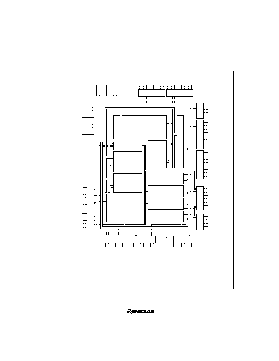
5
1.2
Internal Block Diagram
Figure 1-1 shows an internal block diagram.
PE
7
/D
7
PE
6
/D
6
PE
5
/D
5
PE
4
/D
4
PE
3
/D
3
PE
2
/D
2
PE
1
/D
1
PE
0
/D
0
PD
7
/D
15
PD
6
/D
14
PD
5
/D
13
PD
4
/D
12
PD
3
/D
11
PD
2
/D
10
PD
1
/D
9
PD
0
/D
8
Port D
V
CC
V
CC
V
CC
V
SS
V
SS
V
SS
V
SS
V
SS
V
SS
PC
7
/ A
7
PC
6
/ A
6
PC
5
/ A
5
PC
4
/ A
4
PC
3
/ A
3
PC
2
/ A
2
PC
1
/ A
1
PC
0
/ A
0
PA
3
/ A
19
PA
2
/ A
18
PA
1
/ A
17
PA
0
/ A
16
PB
7
/ A
15
PB
6
/ A
14
PB
5
/ A
13
PB
4
/ A
12
PB
3
/ A
11
PB
2
/ A
10
PB
1
/ A
9
PB
0
/ A
8
P3
5
/ SCK1/
IRQ5
P3
4
/ SCK0/
IRQ4
P3
3
/ RxD1
P3
2
/ RxD0
P3
1
/ TxD1
P3
0
/ TxD0
P5
0
/ TxD2
P5
1
/ RxD2
P5
2
/ SCK2
P5
3
P4
3
/
AN3
P4
2
/
AN2
P4
1
/
AN1
P4
0
/
AN0
V
ref
AV
CC
AV
SS
P2
0
P2
1
P2
2
/
TMRI0
P2
3
/
TMCI0
P2
4
/
TMRI1
P2
5
/
TMCI1
P2
6
/
TMO0
P2
7
/
TMO1
P1
0
/
TIOCA0
/
A
2
0
P1
1
/
TIOCB0
/
A
21
P1
2
/
TIOCC0
/
TCLKA/A
2
2
P1
3
/
TIOCD0
/
TCLKB/A
23
P1
4
/
TIOCA1
P1
5
/
TIOCB1
/
TCLKC
P1
6
/
TIOCA2
P1
7
/
TIOCB2
/
TCLKD
PG
4
/
CS0
PG
3
/
CS1
PG
2
/
CS2
PG
1
/
CS3
/
IRQ7
PG
0
/
ADTRG
/
IRQ6
PF
7
/ ¯
PF
6
/
AS
PF
5
/
RD
PF
4
/
HWR
PF
3
/
LWR
/
IRQ3
PF
2
/
WAIT
/
BREQO
/
IRQ2
PF
1
/
BACK
/
IRQ1
PF
0
/
BREQ
/
IRQ0
Note:
*
There is no ROM in the H8S/2240.
ROM
*
RAM
WDT
TPU
8-bit timer
SCI
A/D converter
MD
2
MD
1
MD
0
EXTAL
XTAL
STBY
RES
WDTOVF
NMI
H8S/2000 CPU
Interrupt controller
DTC
Port E
Port A
Port B
Bus conbtroller
Clock pulse
generator
Port C
Port 3
Port 5
Peripheral address bus
Peripheral data bus
Port 4
Port 2
Port 1
Port G
Port F
Interanal address bus
Internal data bus
Figure 1-1 Block Diagram

6
1.3
Pin Description
1.3.1
Pin Arrangement
Figure 1-2 shows the pin arrangement of the H8S/2245 Series.
1
2
3
4
5
6
7
8
9
10
11
12
13
14
15
16
17
18
19
20
21
22
23
24
25
75
74
73
72
71
70
69
68
67
66
65
64
63
62
61
60
59
58
57
56
55
54
53
52
51
50
49
48
47
46
45
44
43
42
41
40
39
38
37
36
35
34
33
32
31
30
29
28
27
26
PA
0
/A
16
V
SS
PB
7
/A
15
PB
6
/A
14
PB
5
/A
13
PB
4
/A
12
PB
3
/A
11
PB
2
/A
10
PB
1
/A
9
PB
0
/A
8
V
CC
PC
7
/A
7
PC
6
/A
6
PC
5
/A
5
PC
4
/A
4
PC
3
/A
3
PC
2
/A
2
PC
1
/A
1
PC
0
/A
0
V
SS
PD
7
/D
15
PD
6
/D
14
PD
5
/D
13
PD
4
/D
12
PD
3
/D
11
76
77
78
79
80
81
82
83
84
85
86
87
88
89
90
91
92
93
94
95
96
97
98
99
100
PF
0
/
IRQ0
/
BREQ
AV
CC
V
ref
P4
0
/AN0
P4
1
/AN1
P4
2
/AN2
P4
3
/AN3
AV
SS
V
SS
P2
0
P2
1
P2
2
/TMRI0
P2
3
/TMCI0
P2
4
/TMRI1
P2
5
/TMCI1
P2
6
/TMO0
P2
7
/TMO1
PG
0
/
ADTRG
/
IRQ6
PG
1
/
CS3
/
IRQ7
PG
2
/
CS2
PG
3
/
CS1
PG
4
/
CS0
V
CC
P1
0
/TIOCA0/A
20
P1
1
/TIOCB0/A
21
P1
2
/TIOCC0/TCLKA/A
22
P1
3
/TIOCD0/TCLKB/A
23
P1
4
/TIOCA1
P1
5
/TIOCB1/TCLKC
P1
6
/TIOCA2
P1
7
/TIOCB2/TCLKD
V
SS
P3
0
/TxD0
P3
1
/TxD1
P3
2
/RxD0
P3
3
/RxD1
P3
4
/SCK0/
IRQ4
P3
5
/SCK1/
IRQ5
PE
0
/D
0
PE
1
/D
1
PE
2
/D
2
PE
3
/D
3
V
SS
PE
4
/D
4
PE
5
/D
5
PE
6
/D
6
PE
7
/D
7
PD
0
/D
8
PD
1
/D
9
PD
2
/D
10
PF
1
/
BACK
/
IRQ1
PF
2
/
WAIT
/
BREQO
/
IRQ2
PF
3
/
LWR
/
IRQ3
PF
4
/
HWR
PF
5
/
RD
PF
6
/
AS
PF
7
/¯
V
SS
EXTAL
XTAL
V
CC
STBY
NMI
RES
MD
2
WDTOVF
P5
3
MD
1
MD
0
P5
2
/SCK2
P5
1
/RxD2
P5
0
/TxD2
PA
3
/A
19
PA
2
/A
18
PA
1
/A
17
Figure 1-2 H8S/2245 Series Pin Arrangement (FP-100B, TFB-100B: Top View)

7
1.3.2
Pin Functions in Each Operating Mode
Table 1-2 shows the pin functions in each of the operating modes.
Table 1-2
Pin Functions in Each Operating Mode
Pin No.
Pin Name
FP-100B,
TFP-100B Mode 1
Mode 2
*
Mode 3
*
Mode 4
Mode 5
Mode 6
*
Mode 7
*
PROM
Mode
1
P1
2
/
TIOCC0/
TCLKA
P1
2
/
TIOCC0/
TCLKA
P1
2
/
TIOCC0/
TCLKA
P1
2
/
TIOCC0/
TCLKA/A
22
P1
2
/
TIOCC0/
TCLKA/A
22
P1
2
/
TIOCC0/
TCLKA/A
22
P1
2
/
TIOCC0/
TCLKA
NC
2
P1
3
/
TIOCD0/
TCLKB
P1
3
/
TIOCD0/
TCLKB
P1
3
/
TIOCD0/
TCLKB
P1
3
/
TIOCD0/
TCLKB/A
23
P1
3
/
TIOCD0/
TCLKB/A
23
P1
3
/
TIOCD0/
TCLKB/A
23
P1
3
/
TIOCD0/
TCLKB
NC
3
P1
4
/TIOCA1 P1
4
/TIOCA1 P1
4
/TIOCA1 P1
4
/TIOCA1 P1
4
/TIOCA1 P1
4
/TIOCA1 P1
4
/TIOCA1 NC
4
P1
5
/
TIOCB1/
TCLKC
P1
5
/
TIOCB1/
TCLKC
P1
5
/
TIOCB1/
TCLKC
P1
5
/
TIOCB1/
TCLKC
P1
5
/
TIOCB1/
TCLKC
P1
5
/
TIOCB1/
TCLKC
P1
5
/
TIOCB1/
TCLKC
NC
5
P1
6
/
TIOCA2
P1
6
/
TIOCA2
P1
6
/
TIOCA2
P1
6
/
TIOCA2
P1
6
/
TIOCA2
P1
6
/
TIOCA2
P1
6
/
TIOCA2
NC
6
P1
7
/
TIOCB2/
TCLKD
P1
7
/
TIOCB2/
TCLKD
P1
7
/
TIOCB2/
TCLKD
P1
7
/
TIOCB2/
TCLKD
P1
7
/
TIOCB2/
TCLKD
P1
7
/
TIOCB2/
TCLKD
P1
7
/
TIOCB2/
TCLKD
NC
7
V
SS
V
SS
V
SS
V
SS
V
SS
V
SS
V
SS
V
SS
8
P3
0
/TxD0
P3
0
/TxD0
P3
0
/TxD0
P3
0
/TxD0
P3
0
/TxD0
P3
0
/TxD0
P3
0
/TxD0
NC
9
P3
1
/TxD1
P3
1
/TxD1
P3
1
/TxD1
P3
1
/TxD1
P3
1
/TxD1
P3
1
/TxD1
P3
1
/TxD1
NC
10
P3
2
/RxD0
P3
2
/RxD0
P3
2
/RxD0
P3
2
/RxD0
P3
2
/RxD0
P3
2
/RxD0
P3
2
/RxD0
NC
11
P3
3
/RxD1
P3
3
/RxD1
P3
3
/RxD1
P3
3
/RxD1
P3
3
/RxD1
P3
3
/RxD1
P3
3
/RxD1
NC
12
P3
4
/SCK0/
IRQ4
P3
4
/SCK0/
IRQ4
P3
4
/SCK0/
IRQ4
P3
4
/SCK0/
IRQ4
P3
4
/SCK0/
IRQ4
P3
4
/SCK0/
IRQ4
P3
4
/SCK0/
IRQ4
NC
13
P3
5
/SCK1/
IRQ5
P3
5
/SCK1/
IRQ5
P3
5
/SCK1/
IRQ5
P3
5
/SCK1/
IRQ5
P3
5
/SCK1/
IRQ5
P3
5
/SCK1/
IRQ5
P3
5
/SCK1/
IRQ5
NC
14
PE
0
/D
0
PE
0
/D
0
PE
0
PE
0
/D
0
PE
0
/D
0
PE
0
/D
0
PE
0
NC
15
PE
1
/D
1
PE
1
/D
1
PE
1
PE
1
/D
1
PE
1
/D
1
PE
1
/D
1
PE
1
NC
16
PE
2
/D
2
PE
2
/D
2
PE
2
PE
2
/D
2
PE
2
/D
2
PE
2
/D
2
PE
2
NC
Note:
*
Cannot be used in the H8S/2240.

8
Table 1-2
Pin Functions in Each Operating Mode (cont)
Pin No.
Pin Name
FP-100B,
TFP-100B Mode 1
Mode 2
*
Mode 3
*
Mode 4
Mode 5
Mode 6
*
Mode 7
*
PROM
Mode
17
PE
3
/D
3
PE
3
/D
3
PE
3
PE
3
/D
3
PE
3
/D
3
PE
3
/D
3
PE
3
NC
18
V
SS
V
SS
V
SS
V
SS
V
SS
V
SS
V
SS
V
SS
19
PE
4
/D
4
PE
4
/D
4
PE
4
PE
4
/D
4
PE
4
/D
4
PE
4
/D
4
PE
4
NC
20
PE
5
/D
5
PE
5
/D
5
PE
5
PE
5
/D
5
PE
5
/D
5
PE
5
/D
5
PE
5
NC
21
PE
6
/D
6
PE
6
/D
6
PE
6
PE
6
/D
6
PE
6
/D
6
PE
6
/D
6
PE
6
NC
22
PE
7
/D
7
PE
7
/D
7
PE
7
PE
7
/D
7
PE
7
/D
7
PE
7
/D
7
PE
7
NC
23
D
8
D
8
PD
0
D
8
D
8
D
8
PD
0
D
0
24
D
9
D
9
PD
1
D
9
D
9
D
9
PD
1
D
1
25
D
10
D
10
PD
2
D
10
D
10
D
10
PD
2
D
2
26
D
11
D
11
PD
3
D
11
D
11
D
11
PD
3
D
3
27
D
12
D
12
PD
4
D
12
D
12
D
12
PD
4
D
4
28
D
13
D
13
PD
5
D
13
D
13
D
13
PD
5
D
5
29
D
14
D
14
PD
6
D
14
D
14
D
14
PD
6
D
6
30
D
15
D
15
PD
7
D
15
D
15
D
15
PD
7
D
7
31
V
SS
V
SS
V
SS
V
SS
V
SS
V
SS
V
SS
V
SS
32
A
0
PC
0
/A
0
PC
0
A
0
A
0
PC
0
/A
0
PC
0
A
0
33
A
1
PC
1
/A
1
PC
1
A
1
A
1
PC
1
/A
1
PC
1
A
1
34
A
2
PC
2
/A
2
PC
2
A
2
A
2
PC
2
/A
2
PC
2
A
2
35
A
3
PC
3
/A
3
PC
3
A
3
A
3
PC
3
/A
3
PC
3
A
3
36
A
4
PC
4
/A
4
PC
4
A
4
A
4
PC
4
/A
4
PC
4
A
4
37
A
5
PC
5
/A
5
PC
5
A
5
A
5
PC
5
/A
5
PC
5
A
5
38
A
6
PC
6
/A
6
PC
6
A
6
A
6
PC
6
/A
6
PC
6
A
6
39
A
7
PC
7
/A
7
PC
7
A
7
A
7
PC
7
/A
7
PC
7
A
7
40
V
CC
V
CC
V
CC
V
CC
V
CC
V
CC
V
CC
V
CC
41
A
8
PB
0
/A
8
PB
0
A
8
A
8
PB
0
/A
8
PB
0
A
8
42
A
9
PB
1
/A
9
PB
1
A
9
A
9
PB
1
/A
9
PB
1
OE
Note:
*
Cannot be used in the H8S/2240.

9
Table 1-2
Pin Functions in Each Operating Mode (cont)
Pin No.
Pin Name
FP-100B,
TFP-100B Mode 1
Mode 2
*
Mode 3
*
Mode 4
Mode 5
Mode 6
*
Mode 7
*
PROM
Mode
43
A
10
PB
2
/A
10
PB
2
A
10
A
10
PB
2
/A
10
PB
2
A
10
44
A
11
PB
3
/A
11
PB
3
A
11
A
11
PB
3
/A
11
PB
3
A
11
45
A
12
PB
4
/A
12
PB
4
A
12
A
12
PB
4
/A
12
PB
4
A
12
46
A
13
PB
5
/A
13
PB
5
A
13
A
13
PB
5
/A
13
PB
5
A
13
47
A
14
PB
6
/A
14
PB
6
A
14
A
14
PB
6
/A
14
PB
6
A
14
48
A
15
PB
7
/A
15
PB
7
A
15
A
15
PB
7
/A
15
PB
7
A
15
49
V
SS
V
SS
V
SS
V
SS
V
SS
V
SS
V
SS
V
SS
50
PA
0
PA
0
PA
0
A
16
A
16
PA
0
/A
16
PA
0
A
16
51
PA
1
PA
1
PA
1
A
17
A
17
PA
1
/A
17
PA
1
V
CC
52
PA
2
PA
2
PA
2
A
18
A
18
PA
2
/A
18
PA
2
V
CC
53
PA
3
PA
3
PA
3
A
19
A
19
PA
3
/A
19
PA
3
NC
54
P5
0
/TxD2
P5
0
/TxD2
P5
0
/TxD2
P5
0
/TxD2
P5
0
/TxD2
P5
0
/TxD2
P5
0
/TxD2
NC
55
P5
1
/RxD2
P5
1
/RxD2
P5
1
/RxD2
P5
1
/RxD2
P5
1
/RxD2
P5
1
/RxD2
P5
1
/RxD2
NC
56
P5
2
/SCK2
P5
2
/SCK2
P5
2
/SCK2
P5
2
/SCK2
P5
2
/SCK2
P5
2
/SCK2
P5
2
/SCK2
NC
57
MD
0
MD
0
MD
0
MD
0
MD
0
MD
0
MD
0
V
SS
58
MD
1
MD
1
MD
1
MD
1
MD
1
MD
1
MD
1
V
SS
59
P5
3
P5
3
P5
3
P5
3
P5
3
P5
3
P5
3
NC
60
WDTOVF
WDTOVF
WDTOVF
WDTOVF
WDTOVF
WDTOVF
WDTOVF
NC
61
MD
2
MD
2
MD
2
MD
2
MD
2
MD
2
MD
2
V
SS
62
RES
RES
RES
RES
RES
RES
RES
V
PP
63
NMI
NMI
NMI
NMI
NMI
NMI
NMI
A
9
64
STBY
STBY
STBY
STBY
STBY
STBY
STBY
V
SS
65
V
CC
V
CC
V
CC
V
CC
V
CC
V
CC
V
CC
V
CC
66
XTAL
XTAL
XTAL
XTAL
XTAL
XTAL
XTAL
NC
67
EXTAL
EXTAL
EXTAL
EXTAL
EXTAL
EXTAL
EXTAL
NC
68
V
SS
V
SS
V
SS
V
SS
V
SS
V
SS
V
SS
V
SS
Note:
*
Cannot be used in the H8S/2240.

10
Table 1-2
Pin Functions in Each Operating Mode (cont)
Pin No.
Pin Name
FP-100B,
TFP-100B Mode 1
Mode 2
*
Mode 3
*
Mode 4
Mode 5
Mode 6
*
Mode 7
*
PROM
Mode
69
PF
7
/¯
PF
7
/¯
PF
7
/¯
PF
7
/¯
PF
7
/¯
PF
7
/¯
PF
7
/¯
NC
70
AS
AS
PF
6
AS
AS
AS
PF
6
NC
71
RD
RD
PF
5
RD
RD
RD
PF
5
NC
72
HWR
HWR
PF
4
HWR
HWR
HWR
PF
4
NC
73
LWR
LWR
PF
3
/
IRQ3
LWR
LWR
LWR
PF
3
/
IRQ3
NC
74
PF
2
/
WAIT
/
BREQO
/
IRQ2
PF
2
/
WAIT
/
BREQO
/
IRQ2
PF
2
/
IRQ2
PF
2
/
WAIT
/
BREQO
/
IRQ2
PF
2
/
WAIT
/
BREQO
/
IRQ2
PF
2
/
WAIT
/
BREQO
/
IRQ2
PF
2
/
IRQ2
CE
75
PF
1
/
BACK
/
IRQ1
PF
1
/
BACK
/
IRQ1
PF
1
/
IRQ1
PF
1
/
BACK
/
IRQ1
PF
1
/
BACK
/
IRQ1
PF
1
/
BACK
/
IRQ1
PF
1
/
IRQ1
PGM
76
PF
0
/
BREQ
/
IRQ0
PF
0
/
BREQ
/
IRQ0
PF
0
/
IRQ0
PF
0
/
BREQ
/
IRQ0
PF
0
/
BREQ
/
IRQ0
PF
0
/
BREQ
/
IRQ0
PF
0
/
IRQ0
NC
77
AV
CC
AV
CC
AV
CC
AV
CC
AV
CC
AV
CC
AV
CC
V
CC
78
V
ref
V
ref
V
ref
V
ref
V
ref
V
ref
V
ref
V
CC
79
P4
0
/AN0
P4
0
/AN0
P4
0
/AN0
P4
0
/AN0
P4
0
/AN0
P4
0
/AN0
P4
0
/AN0
NC
80
P4
1
/AN1
P4
1
/AN1
P4
1
/AN1
P4
1
/AN1
P4
1
/AN1
P4
1
/AN1
P4
1
/AN1
NC
81
P4
2
/AN2
P4
2
/AN2
P4
2
/AN2
P4
2
/AN2
P4
2
/AN2
P4
2
/AN2
P4
2
/AN2
NC
82
P4
3
/AN3
P4
3
/AN3
P4
3
/AN3
P4
3
/AN3
P4
3
/AN3
P4
3
/AN3
P4
3
/AN3
NC
83
AV
SS
AV
SS
AV
SS
AV
SS
AV
SS
AV
SS
AV
SS
V
SS
84
V
SS
V
SS
V
SS
V
SS
V
SS
V
SS
V
SS
V
SS
85
P2
0
P2
0
P2
0
P2
0
P2
0
P2
0
P2
0
NC
86
P2
1
P2
1
P2
1
P2
1
P2
1
P2
1
P2
1
NC
87
P2
2
/TMRI0 P2
2
/TMRI0 P2
2
/TMRI0 P2
2
/TMRI0 P2
2
/TMRI0 P2
2
/TMRI0 P2
2
/TMRI0 NC
88
P2
3
/TMCI0 P2
3
/TMCI0 P2
3
/TMCI0 P2
3
/TMCI0 P2
3
/TMCI0 P2
3
/TMCI0 P2
3
/TMCI0 NC
89
P2
4
/TMRI1 P2
4
/TMRI1 P2
4
/TMRI1 P2
4
/TMRI1 P2
4
/TMRI1 P2
4
/TMRI1 P2
4
/TMRI1 NC
90
P2
5
/TMCI1 P2
5
/TMCI1 P2
5
/TMCI1 P2
5
/TMCI1 P2
5
/TMCI1 P2
5
/TMCI1 P2
5
/TMCI1 NC
91
P2
6
/TMO0
P2
6
/TMO0
P2
6
/TMO0
P2
6
/TMO0
P2
6
/TMO0
P2
6
/TMO0
P2
6
/TMO0
NC
Note:
*
Cannot be used in the H8S/2240.

11
Table 1-2
Pin Functions in Each Operating Mode (cont)
Pin No.
Pin Name
FP-100B,
TFP-100B Mode 1
Mode 2
*
Mode 3
*
Mode 4
Mode 5
Mode 6
*
Mode 7
*
PROM
Mode
92
P2
7
/TMO1
P2
7
/TMO1
P2
7
/TMO1
P2
7
/TMO1
P2
7
/TMO1
P2
7
/TMO1
P2
7
/TMO1
NC
93
PG
0
/
IRQ6
/
ADTRG
PG
0
/
IRQ6
/
ADTRG
PG
0
/
IRQ6
/
ADTRG
PG
0
/
IRQ6
/
ADTRG
PG
0
/
IRQ6
/
ADTRG
PG
0
/
IRQ6
/
ADTRG
PG
0
/
IRQ6
/
ADTRG
NC
94
PG
1
/
IRQ7
PG
1
/
IRQ7
PG
1
/
IRQ7
PG
1
/
CS3
/
IRQ7
PG
1
/
CS3
/
IRQ7
PG
1
/
CS3
/
IRQ7
PG
1
/
IRQ7
NC
95
PG
2
PG
2
PG
2
PG
2
/
CS2
PG
2
/
CS2
PG
2
/
CS2
PG
2
NC
96
PG
3
PG
3
PG
3
PG
3
/
CS1
PG
3
/
CS1
PG
3
/
CS1
PG
3
NC
97
PG
4
/
CS0
PG
4
/
CS0
PG
4
PG
4
/
CS0
PG
4
/
CS0
PG
4
/
CS0
PG
4
NC
98
V
CC
V
CC
V
CC
V
CC
V
CC
V
CC
V
CC
V
CC
99
P1
0
/
TIOCA0
P1
0
/
TIOCA0
P1
0
/
TIOCA0
P1
0
/
TIOCA0/A
20
P1
0
/
TIOCA0/A
20
P1
0
/
TIOCA0/A
20
P1
0
/
TIOCA0
NC
100
P1
1
/
TIOCB0
P1
1
/
TIOCB0
P1
1
/
TIOCB0
P1
1
/
TIOCB0/A
21
P1
1
/
TIOCB0/A
21
P1
1
/
TIOCB0/A
21
P1
1
/
TIOCB0
NC
Note:
*
Cannot be used in the H8S/2240.

12
1.3.3
Pin Functions
Table 1-3 outlines the pin functions.
Table 1-3
Pin Functions
Pin No.
Type
Symbol
FP-100B, TFP-100B
I/O
Name and Function
Power
V
CC
40, 65, 98
Input
Power supply: All V
CC
pins should be
connected to the system power
supply.
V
SS
7, 18, 31, 49, 68, 84
Input
Ground: All V
SS
pins should be
connected to the system power
supply (0 V).
Clock
XTAL
66
Input
Connects to a crystal oscillator.
See section 17, Clock Pulse
Generator, for typical connection
diagrams for a crystal oscillator and
external clock input.
EXTAL
67
Input
Connects to a crystal oscillator.
The EXTAL pin can also input an
external clock.
See section 17, Clock Pulse
Generator, for typical connection
diagrams for a crystal oscillator and
external clock input.
¯
69
Output System clock: Supplies the system
clock to an external device.

13
Table 1-3
Pin Functions (cont)
Pin No.
Type
Symbol
FP-100B, TFP-100B
I/O
Name and Function
Operating mode
control
MD
2
to
MD
0
61, 58, 57
Input
Mode pins: These pins set the
operating mode.
The relation between the settings of
pins MD
2
to MD
0
and the operating
mode is shown below. These pins
should not be changed while the
H8S/2245 Series is operating.
MD
2
MD
1
MD
0
Operating
Mode
0
0
0
--
1
Mode 1
1
0
Mode 2
*
1
Mode 3
*
1
0
0
Mode 4
1
Mode 5
1
0
Mode 6
*
1
Mode 7
*
Note:
*
Cannot be used in the
H8S/2240.
System control
RES
62
Input
Reset input: When this pin is driven
low, the chip is reset. The type of
reset can be selected according to
the NMI input level. At power-on, the
NMI pin input level should be set
high.
STBY
64
Input
Standby: When this pin is driven low,
a transition is made to hardware
standby mode.
BREQ
76
Input
Bus request: Used by an external
bus master to issue a bus request to
the H8S/2245 Series.
BREQO
74
Output Bus request output: The external bus
request signal used when an internal
bus master accesses external space
in the external bus-released state.
BACK
75
Output Bus request acknowledge: Indicates
that the bus has been released to an
external bus master.

14
Table 1-3
Pin Functions (cont)
Pin No.
Type
Symbol
FP-100B, TFP-100B
I/O
Name and Function
Interrupts
NMI
63
Input
Nonmaskable interrupt: Requests a
nonmaskable interrupt. When this pin
is not used, it should be fixed high.
IRQ7
to
IRQ0*
94, 93, 13, 12,
73 to 76
Input
Interrupt request 7 to 0: These pins
request a maskable interrupt.
Address bus
A
23
to
A
0
2, 1, 100, 99,
53 to 50, 48 to 41,
39 to 32
Output Address bus: These pins output an
address.
Data bus
D
15
to
D
0
30 to 19, 17 to 14
I/O
Data bus: These pins constitute a
bidirectional data bus.
Bus control
CS3
to
CS0
94 to 97
Output Chip select: Signals for selecting
areas 3 to 0.
AS
70
Output Address strobe: When this pin is low,
it indicates that address output on the
address bus is enabled.
RD
71
Output Read: When this pin is low, it
indicates that the external address
space can be read.
HWR
72
Output High write: A strobe signal that writes
to external space and indicates that
the upper half (D
15
to D
8
) of the data
bus is enabled.
LWR
73
Output Low write: A strobe signal that writes
to external space and indicates that
the lower half (D
7
to D
0
) of the data
bus is enabled.
WAIT
74
Input
Wait: Requests insertion of a wait
state in the bus cycle when
accessing external 3-state address
space.
Note:
*
IRQ3
cannot be used in modes 1, 2, 4, 5, and 6, or in the H8S/2240.

15
Table 1-3
Pin Functions (cont)
Pin No.
Type
Symbol
FP-100B, TFP-100B
I/O
Name and Function
16-bit timer-
pulse unit
(TPU)
TCLKD to
TCLKA
6, 4, 2, 1
Input
Clock input D to A: These pins input
an external clock.
TIOCA0,
TIOCB0,
TIOCC0,
TIOCD0
99, 100, 1, 2
I/O
Input capture/output compare match
A0 to D0: The TGR0A to TGR0D
input capture input or output compare
output, or PWM output pins.
TIOCA1,
TIOCB1
3, 4
I/O
Input capture/output compare match
A1 and B1: The TGR1A and TGR1B
input capture input or output compare
output, or PWM output pins.
TIOCA2,
TIOCB2
5, 6
I/O
Input capture/output compare match
A2 and B2: The TGR2A and TGR2B
input capture input or output compare
output, or PWM output pins.
8-bit timer
TMO0,
TMO1
91, 92
Output Compare match output: The compare
match output pins.
TMCI0,
TMCI1
88, 90
Input
Counter external clock input: Input
pins for the external clock input to the
counter.
TMRI0,
TMRI1
87, 89
Input
Counter external reset input: The
counter reset input pins.
Watchdog
timer (WDT)
WDTOVF
60
Output Watchdog timer: The counter
overflow signal output pin in
watchdog timer mode.
Serial
communication
interface (SCI)/
TxD2,
TxD1,
TxD0
54, 9, 8
Output Transmit data (channel 0, 1, 2):
Data output pins.
Smart Card
interface
RxD2,
RxD1,
RxD0
55, 11, 10
Input
Receive data (channel 0, 1, 2):
Data input pins.
SCK2,
SCK1,
SCK0
56, 13, 12
I/O
Serial clock (channel 0, 1, 2):
Clock I/O pins.

16
Table 1-3
Pin Functions (cont)
Pin No.
Type
Symbol
FP-100B, TFP-100B
I/O
Name and Function
A/D converter
AN3 to
AN0
82 to 79
Input
Analog 3 to 0: Analog input pins.
ADTRG
93
Input
A/D conversion external trigger input:
Pin for input of an external trigger to
start A/D conversion.
AV
CC
77
Input
This is the power supply pin for the
A/D converter.
When the A/D converter is not used,
this pin should be connected to the
system power supply (+5 V).
AV
SS
83
Input
This is the ground pin for the A/D
converter.
This pin should be connected to the
system power supply (0 V).
V
ref
78
Input
This is the reference voltage input pin
for the A/D converter.
When the A/D converter is not used,
this pin should be connected to the
system power supply (+5 V).
I/O ports
P1
7
to
P1
0
6 to 1, 100, 99
I/O
Port 1: An 8-bit I/O port. Input or
output can be designated for each bit
by means of the port 1 data direction
register (P1DDR).
P2
7
to
P2
0
92 to 85
I/O
Port 2: An 8-bit I/O port. Input or
output can be designated for each bit
by means of the port 2 data direction
register (P2DDR).
P3
5
to
P3
0
13 to 8
I/O
Port 3: A 6-bit I/O port. Input or
output can be designated for each bit
by means of the port 3 data direction
register (P3DDR).
P4
3
to
P4
0
82 to 79
Input
Port 4: A 4-bit input port.
P5
3
to
P5
0
59, 56 to 54
I/O
Port 5: A 4-bit I/O port. Input or
output can be designated for each bit
by means of the port 5 data direction
register (P5DDR).

17
Table 1-3
Pin Functions (cont)
Pin No.
Type
Symbol
FP-100B, TFP-100B
I/O
Name and Function
I/O ports
PA
3
to
PA
0
*
1
53 to 50
I/O
Port A: A 4-bit I/O port. Input or
output can be designated for each bit
by means of the port A data direction
register (PADDR).
PB
7
to
PB
0
*
2
48 to 41
I/O
Port B: An 8-bit I/O port. Input or
output can be designated for each bit
by means of the port B data direction
register (PBDDR).
PC
7
to
PC
0
*
2
39 to 32
I/O
Port C: An 8-bit I/O port. Input or
output can be designated for each bit
by means of the port C data direction
register (PCDDR).
PD
7
to
PD
0
*
2
30 to 23
I/O
Port D: An 8-bit I/O port. Input or
output can be designated for each bit
by means of the port D data direction
register (PDDDR).
PE
7
to
PE
0
22 to 19, 17 to 14
I/O
Port E: An 8-bit I/O port. Input or
output can be designated for each bit
by means of the port E data direction
register (PEDDR).
PF
7
to
PF
0
*
3
69 to 76
I/O
Port F: An 8-bit I/O port. Input or
output can be designated for each bit
by means of the port F data direction
register (PFDDR).
PG
4
to
PG
0
97 to 93
I/O
Port G: A 5-bit I/O port. Input or
output can be designated for each bit
by means of the port G data direction
register (PGDDR).
Notes: 1. Cannot be used in modes 4 and 5 in the H8S/2240.
2. Cannot be used in the H8S/2240.
3. PF
6
to PF
3
cannot be used in the H8S/2240.

19
Section 2 CPU
2.1
Overview
The H8S/2000 CPU is a high-speed central processing unit with an internal 32-bit architecture that
is upward-compatible with the H8/300 and H8/300H CPUs. The H8S/2000 CPU has sixteen 16-bit
general registers, can address a 16-Mbyte (architecturally 4-Gbyte) linear address space, and is
ideal for realtime control.
2.1.1
Features
The H8S/2000 CPU has the following features.
∑
Upward-compatible with H8/300 and H8/300H CPUs
Can execute H8/300 and H8/300H object programs
∑
General-register architecture
Sixteen 16-bit general registers (also usable as sixteen 8-bit registers or eight 32-bit
registers)
∑
Sixty-five basic instructions
8/16/32-bit arithmetic instructions
Multiply and divide instructions
Powerful bit-manipulation instructions
∑
Eight addressing modes
Register direct [Rn]
Register indirect [@ERn]
Register indirect with displacement [@(d:16,ERn) or @(d:32,ERn)]
Register indirect with post-increment or pre-decrement [@ERn+ or @≠ERn]
Absolute address [@aa:8, @aa:16, @aa:24, or @aa:32]
Immediate [#xx:8, #xx:16, or #xx:32]
Program-counter relative [@(d:8,PC) or @(d:16,PC)]
Memory indirect [@@aa:8]
∑
16-Mbyte address space
Program: 16 Mbytes
Data:
16 Mbytes (4 Gbytes architecturally)

20
∑
High-speed operation
All frequently-used instructions execute in one or two states
Maximum clock rate
: 20 MHz
8/16/32-bit register-register add/subtract : 50 ns
8
◊
8-bit register-register multiply
: 600 ns
16 ˜ 8-bit register-register divide
: 600 ns
16
◊
16-bit register-register multiply
: 1000 ns
32 ˜ 16-bit register-register divide
: 1000 ns
∑
Two CPU operating modes
Normal mode
Advanced mode
∑
Power-down state
Transition to power-down state by SLEEP instruction
CPU clock speed selection
2.1.2
Differences between H8S/2600 CPU and H8S/2000 CPU
The differences between the H8S/2600 CPU and the H8S/2000 CPU are as shown below.
∑
Register configuration
The MAC register is supported only by the H8S/2600 CPU.
∑
Basic instructions
The four instructions MAC, CLRMAC, LDMAC, and STMAC are supported only by the
H8S/2600 CPU.
∑
Number of execution states
The number of execution states of the MULXU and MULXS instructions.
Internal Operation
Instruction
Mnemonic
H8S/2600
H8S/2000
MULXU
MULXU.B Rs, Rd
3
12
MULXU.W Rs, ERd
4
20
MULXS
MULXS.B Rs, Rd
4
13
MULXS.W Rs, ERd
5
21
There are also differences in the address space, EXR register functions, power-down state, etc.,
depending on the product.

21
2.1.3
Differences from H8/300 CPU
In comparison to the H8/300 CPU, the H8S/2000 CPU has the following enhancements.
∑
More general registers and control registers
Eight 16-bit expanded registers, and one 8-bit control registers, have been added.
∑
Expanded address space
Normal mode supports the same 64-kbyte address space as the H8/300 CPU.
Advanced mode supports a maximum 16-Mbyte address space.
∑
Enhanced addressing
The addressing modes have been enhanced to make effective use of the 16-Mbyte address
space.
∑
Enhanced instructions
Addressing modes of bit-manipulation instructions have been enhanced.
Signed multiply and divide instructions have been added.
Two-bit shift instructions have been added.
Instructions for saving and restoring multiple registers have been added.
A test and set instruction has been added.
∑
Higher speed
Basic instructions execute twice as fast.
2.1.4
Differences from H8/300H CPU
In comparison to the H8/300H CPU, the H8S/2000 CPU has the following enhancements.
∑
Additional control register
One 8-bit control register has been added.
∑
Enhanced instructions
Addressing modes of bit-manipulation instructions have been enhanced.
Two-bit shift instructions have been added.
Instructions for saving and restoring multiple registers have been added.
A test and set instruction has been added.
∑
Higher speed
Basic instructions execute twice as fast.

22
2.2
CPU Operating Modes
The H8S/2000 CPU has two operating modes: normal and advanced. Normal mode supports a
maximum 64-kbyte address space. Advanced mode supports a maximum 16-Mbyte total address
space (architecturally a maximum 16-Mbyte program area and a maximum of 4 Gbytes for
program and data areas combined). The mode is selected by the mode pins of the microcontroller.
CPU operating modes
Normal mode
Advanced mode
Maximum 64 kbytes, program
and data areas combined
Maximum 16-Mbytes for
program and data areas
combined
Figure 2-1 CPU Operating Modes
(1) Normal Mode: The exception vector table and stack have the same structure as in the H8/300
CPU.
Address Space: A maximum address space of 64 kbytes can be accessed.
Extended Registers (En): The extended registers (E0 to E7) can be used as 16-bit registers, or as
the upper 16-bit segments of 32-bit registers. When En is used as a 16-bit register it can contain
any value, even when the corresponding general register (Rn) is used as an address register. If the
general register is referenced in the register indirect addressing mode with pre-decrement (@≠Rn)
or post-increment (@Rn+) and a carry or borrow occurs, however, the value in the corresponding
extended register (En) will be affected.
Instruction Set: All instructions and addressing modes can be used. Only the lower 16 bits of
effective addresses (EA) are valid.
23
Exception Vector Table and Memory Indirect Branch Addresses: In normal mode the top area
starting at H'0000 is allocated to the exception vector table. One branch address is stored per 16
bits (figure 2-2). The exception vector table differs depending on the microcontroller. For details
of the exception vector table, see section 4, Exception Handling.
H'0000
H'0001
H'0002
H'0003
H'0004
H'0005
H'0006
H'0007
H'0008
H'0009
H'000A
H'000B
Power-on reset exception vector
Manual reset exception vector
Exception vector 1
Exception vector 2
Exception
vector table
(Reserved for system use)
Figure 2-2 Exception Vector Table (Normal Mode)
The memory indirect addressing mode (@@aa:8) employed in the JMP and JSR instructions uses
an 8-bit absolute address included in the instruction code to specify a memory operand that
contains a branch address. In normal mode the operand is a 16-bit word operand, providing a 16-
bit branch address. Branch addresses can be stored in the top area from H'0000 to H'00FF. Note
that this area is also used for the exception vector table.

24
Stack Structure: When the program counter (PC) is pushed onto the stack in a subroutine call,
and the PC and condition-code register (CCR) are pushed onto the stack in exception handling,
they are stored as shown in figure 2-3. The extended control register (EXR) is not pushed onto the
stack. For details, see section 4, Exception Handling.
(a) Subroutine Branch
(b) Exception Handling
PC
(16 bits)
CCR
CCR
*
PC
(16 bits)
SP
Note:
*
Ignored when returning.
SP
Figure 2-3 Stack Structure in Normal Mode
(2) Advanced Mode
Address Space: Linear access is provided to a 16-Mbyte maximum address space (architecturally
a maximum 16-Mbyte program area and a maximum 4-Gbyte data area, with a maximum of 4
Gbytes for program and data areas combined).
Extended Registers (En): The extended registers (E0 to E7) can be used as 16-bit registers, or as
the upper 16-bit segments of 32-bit registers or address registers.
Instruction Set: All instructions and addressing modes can be used.
25
Exception Vector Table and Memory Indirect Branch Addresses: In advanced mode the top
area starting at H'00000000 is allocated to the exception vector table in units of 32 bits. In each 32
bits, the upper 8 bits are ignored and a branch address is stored in the lower 24 bits (figure 2-4).
For details of the exception vector table, see section 4, Exception Handling.
H'00000000
H'00000003
H'00000004
H'0000000B
H'0000000C
Exception vector table
Reserved
Power-on reset exception vector
(Reserved for system use)
Reserved
Exception vector 1
Reserved
Manual reset exception vector
H'00000010
H'00000008
H'00000007
Figure 2-4 Exception Vector Table (Advanced Mode)
The memory indirect addressing mode (@@aa:8) employed in the JMP and JSR instructions uses
an 8-bit absolute address included in the instruction code to specify a memory operand that
contains a branch address. In advanced mode the operand is a 32-bit longword operand, providing
a 32-bit branch address. The upper 8 bits of these 32 bits are a reserved area that is regarded as
H'00. Branch addresses can be stored in the area from H'00000000 to H'000000FF. Note that the
first part of this range is also the exception vector table.

26
Stack Structure: In advanced mode, when the program counter (PC) is pushed onto the stack in a
subroutine call, and the PC and condition-code register (CCR) are pushed onto the stack in
exception handling, they are stored as shown in figure 2-5. The extended control register (EXR) is
not pushed onto the stack. For details, see section 4, Exception Handling.
(a) Subroutine Branch
(b) Exception Handling
PC
(24 bits)
CCR
PC
(24 bits)
SP
SP
Reserved
Figure 2-5 Stack Structure in Advanced Mode

27
2.3
Address Space
Figure 2-6 shows a memory map of the H8S/2000 CPU. The H8S/2000 CPU provides linear
access to a maximum 64-kbyte address space in normal mode, and a maximum 16-Mbyte
(architecturally 4-Gbyte) address space in advanced mode.
(b) Advanced Mode
H'0000
H'FFFF
H'00000000
H'FFFFFFFF
H'00FFFFFF
(a) Normal Mode
Data area
Program area
Cannot be
used by the
H8S/2245
Series
Figure 2-6 Memory Map
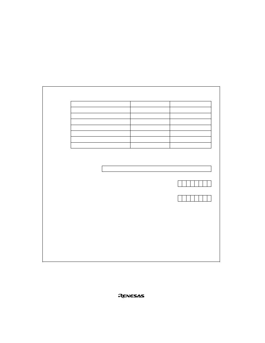
28
2.4
Register Configuration
2.4.1
Overview
The CPU has the internal registers shown in figure 2-7. There are two types of registers: general
registers and control registers.
T -- -- -- -- I2 I1 I0
EXR
*
7 6 5 4 3 2 1 0
PC
23
0
15
07
07
0
E0
E1
E2
E3
E4
E5
E6
E7
R0H
R1H
R2H
R3H
R4H
R5H
R6H
R7H
R0L
R1L
R2L
R3L
R4L
R5L
R6L
R7L
General Registers (Rn) and Extended Registers (En)
Control Registers (CR)
Legend
Stack pointer
Program counter
Extended control register
Trace bit
Interrupt mask bits
Condition-code register
Interrupt mask bit
User bit or interrupt mask bit
SP:
PC:
EXR:
T:
I2 to I0:
CCR:
I:
UI:
Note:
*
This register does not affect operations in the H8S/2245 Series.
ER0
ER1
ER2
ER3
ER4
ER5
ER6
ER7 (SP)
I UI H U N Z V C
CCR
7 6 5 4 3 2 1 0
Half-carry flag
User bit
Negative flag
Zero flag
Overflow flag
Carry flag
H:
U:
N:
Z:
V:
C:
Figure 2-7 CPU Registers

29
2.4.2
General Registers
The CPU has eight 32-bit general registers. These general registers are all functionally alike and
can be used as both address registers and data registers. When a general register is used as a data
register, it can be accessed as a 32-bit, 16-bit, or 8-bit register. When the general registers are used
as 32-bit registers or address registers, they are designated by the letters ER (ER0 to ER7).
The ER registers divide into 16-bit general registers designated by the letters E (E0 to E7) and R
(R0 to R7). These registers are functionally equivalent, providing a maximum sixteen 16-bit
registers. The E registers (E0 to E7) are also referred to as extended registers.
The R registers divide into 8-bit general registers designated by the letters RH (R0H to R7H) and
RL (R0L to R7L). These registers are functionally equivalent, providing a maximum sixteen 8-bit
registers.
Figure 2-8 illustrates the usage of the general registers. The usage of each register can be selected
independently.
∑ Address registers
∑ 32-bit registers
∑ 16-bit registers
∑ 8-bit registers
ER registers
(ER0 to ER7)
E registers (extended registers)
(E0 to E7)
R registers
(R0 to R7)
RH registers
(R0H to R7H)
RL registers
(R0L to R7L)
Figure 2-8 Usage of General Registers
30
General register ER7 has the function of stack pointer (SP) in addition to its general-register
function, and is used implicitly in exception handling and subroutine calls. Figure 2-9 shows the
stack.
Free area
Stack area
SP (ER7)
Figure 2-9 Stack
2.4.3
Control Registers
The control registers are the 24-bit program counter (PC), 8-bit extended control register (EXR),
and 8-bit condition-code register (CCR).
(1) Program Counter (PC): This 24-bit counter indicates the address of the next instruction the
CPU will execute. The length of all CPU instructions is 2 bytes (one word) so the least significant
PC bit is ignored. (When an instruction is read, the least significant PC bit is regarded as 0.)
(2) Extended Control Register (EXR): This 8-bit register does not affect operation in the
H8S/2245 Series.
Bit 7--Trace Bit (T): This bit is reserved. It does not affect operation in the H8S/2245 Series.
Bits 6 to 3--Reserved: These bits are reserved. They are always read as 1.

31
Bits 2 to 0--Interrupt Mask Bits (I2 to I0): These bits are reserved. They do not affect operation
in the H8S/2245 Series.
(3) Condition-Code Register (CCR): This 8-bit register contains internal CPU status
information, including an interrupt mask bit (I) and half-carry (H), negative (N), zero (Z),
overflow (V), and carry (C) flags.
Bit 7--Interrupt Mask Bit (I): Masks interrupts other than NMI when set to 1. (NMI is accepted
regardless of the I bit setting.) The I bit is set to 1 by hardware at the start of an exception-
handling sequence. For details, refer to section 5, Interrupt Controller.
Bit 6--User Bit or Interrupt Mask Bit (UI): Can be written and read by software using the
LDC, STC, ANDC, ORC, and XORC instructions. This bit can also be used as an interrupt mask
bit. For details, refer to section 5, Interrupt Controller.
Bit 5--Half-Carry Flag (H): When the ADD.B, ADDX.B, SUB.B, SUBX.B, CMP.B, or NEG.B
instruction is executed, this flag is set to 1 if there is a carry or borrow at bit 3, and cleared to 0
otherwise. When the ADD.W, SUB.W, CMP.W, or NEG.W instruction is executed, the H flag is
set to 1 if there is a carry or borrow at bit 11, and cleared to 0 otherwise. When the ADD.L,
SUB.L, CMP.L, or NEG.L instruction is executed, the H flag is set to 1 if there is a carry or
borrow at bit 27, and cleared to 0 otherwise.
Bit 4--User Bit (U): Can be written and read by software using the LDC, STC, ANDC, ORC, and
XORC instructions.
Bit 3--Negative Flag (N): Stores the value of the most significant bit (sign bit) of data.
Bit 2--Zero Flag (Z): Set to 1 to indicate zero data, and cleared to 0 to indicate non-zero data.
Bit 1--Overflow Flag (V): Set to 1 when an arithmetic overflow occurs, and cleared to 0 at other
times.
Bit 0--Carry Flag (C): Set to 1 when a carry occurs, and cleared to 0 otherwise. Used by:
∑
Add instructions, to indicate a carry
∑
Subtract instructions, to indicate a borrow
∑
Shift and rotate instructions, to indicate a carry
The carry flag is also used as a bit accumulator by bit manipulation instructions.

32
Some instructions leave some or all of the flag bits unchanged. For the action of each instruction
on the flag bits, refer to Appendix A.1, List of Instructions.
Operations can be performed on the CCR bits by the LDC, STC, ANDC, ORC, and XORC
instructions. The N, Z, V, and C flags are used as branching conditions for conditional branch
(Bcc) instructions.
2.4.4
Initial Register Values
Reset exception handling loads the CPU's program counter (PC) from the vector table, clears the
trace bit in EXR to 0, and sets the interrupt mask bits in CCR and EXR to 1. The other CCR bits
and the general registers are not initialized. In particular, the stack pointer (ER7) is not initialized.
The stack pointer should therefore be initialized by an MOV.L instruction executed immediately
after a reset.

33
2.5
Data Formats
The CPU can process 1-bit, 4-bit (BCD), 8-bit (byte), 16-bit (word), and 32-bit (longword) data.
Bit-manipulation instructions operate on 1-bit data by accessing bit n (n = 0, 1, 2, ..., 7) of byte
operand data. The DAA and DAS decimal-adjust instructions treat byte data as two digits of 4-bit
BCD data.
2.5.1
General Register Data Formats
Figure 2-10 shows the data formats in general registers.
7 6 5 4 3 2 1 0
Don't care
7
0
Don't care
7 6 5 4 3 2 1 0
4 3
7
0
7
0
Don't care
Upper
Lower
LSB
MSB
LSB
Data Type
General Register
Data Image
1-bit data
1-bit data
4-bit BCD data
4-bit BCD data
Byte data
Byte data
RnH
RnL
RnH
RnL
RnH
RnL
MSB
Don't care
Upper
Lower
4 3
7
0
Don't care
7
0
Don't care
7
0
Figure 2-10 General Register Data Formats

34
0
MSB
LSB
15
Word data
Word data
Data Type
General Register
Data Image
Rn
En
0
LSB
15
16
MSB
31
En
Rn
General register ER
General register E
General register R
General register RH
General register RL
Most significant bit
Least significant bit
Legend
ERn:
En:
Rn:
RnH:
RnL:
MSB:
LSB:
0
MSB
LSB
15
Longword data
ERn
Figure 2-10 General Register Data Formats (cont)

35
2.5.2
Memory Data Formats
Figure 2-11 shows the data formats in memory. The CPU can access word data and longword data
in memory, but word or longword data must begin at an even address. If an attempt is made to
access word or longword data at an odd address, no address error occurs but the least significant
bit of the address is regarded as 0, so the access starts at the preceding address. This also applies to
instruction fetches.
7
6
5
4
3
2
1
0
7
0
MSB
LSB
MSB
LSB
MSB
LSB
Data Type
Data image
1-bit data
Byte data
Word data
Longword data
Address
Address L
Address L
Address 2M
Address 2M + 1
Address 2N
Address 2N + 1
Address 2N + 2
Address 2N + 3
Figure 2-11 Memory Data Formats
When SP(ER7) is used as an address register to access the stack, the operand size should be word
size or longword size.

36
2.6
Instruction Set
2.6.1
Overview
The H8S/2000 CPU has 65 types of instructions. The instructions are classified by function in
table 2-1.
Table 2-1
Instruction Classification
Function
Instructions
Size
Types
Data transfer
MOV
BWL
5
POP
*
1
, PUSH
*
1
WL
LDM, STM
L
MOVFPE, MOVTPE
*
3
B
Arithmetic
ADD, SUB, CMP, NEG
BWL
19
operations
ADDX, SUBX, DAA, DAS
B
INC, DEC
BWL
ADDS, SUBS
L
MULXU, DIVXU, MULXS, DIVXS
BW
EXTU, EXTS
WL
TAS
B
Logic operations
AND, OR, XOR, NOT
BWL
4
Shift
SHAL, SHAR, SHLL, SHLR, ROTL, ROTR, ROTXL, ROTXR
BWL
8
Bit manipulation
BSET, BCLR, BNOT, BTST, BLD, BILD, BST, BIST, BAND,
BIAND, BOR, BIOR, BXOR, BIXOR
B
14
Branch
Bcc
*
2
, JMP, BSR, JSR, RTS
--
5
System control
TRAPA, RTE, SLEEP, LDC, STC, ANDC, ORC, XORC, NOP --
9
Block data transfer
EEPMOV
--
1
Total: 65 types
Notes: B-byte size; W-word size; L-longword size.
1. POP.W Rn and PUSH.W Rn are identical to MOV.W @SP+, Rn and MOV.W Rn,
@-SP. POP.L ERn and PUSH.L ERn are identical to MOV.L @SP+, ERn and MOV.L
ERn, @-SP.
2. Bcc is the general name for conditional branch instructions.
3. Cannot be used in the H8S/2245 Series.

37
2.6.2
Instructions and Addressing Modes
Table 2-2 indicates the combinations of instructions and addressing modes that the H8S/2000 CPU
can use.
Table 2-2 Combinations of Instructions and Addressing Modes
Addressing Modes
Function
Data
transfer
Arithmetic
operations
Instruction
MOV
BWL
BWL
BWL
BWL
BWL
BWL
B
BWL
--
BWL
--
--
--
--
POP, PUSH
--
--
--------
--
--
--
--
----
--W
L
LDM, STM
--
--
--------
--
--
--
--
----
--L
ADD, CMP
BWL
BWL
--------
--
--
--
--
----
----
S
U
B
W
L
B
W
L
--------
--
--
--
--
----
----
ADDX, SUBX
B
B
--------
--
--
--
--
----
----
ADDS, SUBS
--
L
--------
--
--
--
--
----
----
INC, DEC
--
BWL
--------
--
--
--
--
----
----
DAA, DAS
--
B
--------
--
--
--
--
----
----
N
E
G
--B
W
L
--------
--
--
--
--
----
----
EXTU, EXTS
--
W
L
--------
--
--
--
--
----
----
T
A
S
----
B
------
--
--
--
--
----
----
Note:
*
Cannot be used in the H8S/2245 Series.
MOVFPE
*
,
--
--
--------
--
B
--
--
----
----
MOVTPE
*
MULXU, --
B
W
--------
--
--
--
--
----
----
DIVXU
MULXS,
--
B
W
--------
--
--
--
--
----
----
DIVXS
#xx
Rn
@ERn
@(d:16,ERn)
@(d:32,ERn)
@≠ERn/@ERn+
@aa:8
@aa:16
@aa:24
@aa:32
@(d:8,PC)
@(d:16,PC)
@@aa:8
--
38
Table 2-2 Combinations of Instructions and Addressing Modes (cont)
Addressing Modes
Function
Logic
operations
System
control
Block data transfer
Shift
Bit manipulation
Branch
Instruction
AND, OR,
BWL
BWL
--------
--
--
--
--
----
----
XOR
ANDC,
B
--
--------
--
--
--
--
----
----
ORC, XORC
Bcc, BSR
--
--
--------
--
--
--
--
----
JMP, JSR
--
--
--------
--
--
--
--
--
--
R
T
S
----
--------
--
--
--
--
----
--
TRAPA
--
--
--------
--
--
--
--
----
--
R
T
E
----
--------
--
--
--
--
----
--
SLEEP
--
--
--------
--
--
--
--
----
--
L
D
C
B
B
WWWW
--
W
--
W
--
--
--
--
S
T
C
--
B
WWWW
--
W
--
W
--
--
--
--
N
O
T
--B
W
L
--------
--
--
--
--
----
----
--B
W
L
--------
--
--
--
--
----
----
--B
B
------
B
B
--
B
----
----
N
O
P
----
--------
--
--
--
--
----
--
----
--------
--
--
--
--
----
--B
W
Legend
B: Byte
W: Word
L: Longword
#xx
Rn
@ERn
@(d:16,ERn)
@(d:32,ERn)
@≠ERn/@ERn+
@aa:8
@aa:16
@aa:24
@aa:32
@(d:8,PC)
@(d:16,PC)
@@aa:8
--

39
2.6.3
Table of Instructions Classified by Function
Tables 2-3 to 2-10 summarize the instructions in each functional category. The notation used in
the tables is defined below.
Operation Notation
Rd
General register (destination)
*
Rs
General register (source)
*
Rn
General register
*
ERn
General register (32-bit register)
(EAd)
Destination operand
(EAs)
Source operand
EXR
Extended control register
CCR
Condition-code register
N
N (negative) flag in CCR
Z
Z (zero) flag in CCR
V
V (overflow) flag in CCR
C
C (carry) flag in CCR
PC
Program counter
SP
Stack pointer
#IMM
Immediate data
disp
Displacement
+
Addition
≠
Subtraction
◊
Multiplication
˜
Division
Logical AND
Logical OR
Logical exclusive OR
Move
¨
NOT (logical complement)
:8/:16/:24/:32
8-, 16-, 24-, or 32-bit length
Note:
*
General registers include 8-bit registers (R0H to R7H, R0L to R7L), 16-bit registers (R0 to
R7, E0 to E7), and 32-bit registers (ER0 to ER7).

40
Table 2-3
Data Transfer Instructions
Instruction
Size
*
Function
MOV
B/W/L
(EAs)
Rd, Rs
(EAd)
Moves data between two general registers or between a general register
and memory, or moves immediate data to a general register.
MOVFPE
B
Cannot be used in the H8S/2245 Series.
MOVTPE
B
Cannot be used in the H8S/2245 Series.
POP
W/L
@SP+
Rn
Pops a register from the stack. POP.W Rn is identical to MOV.W @SP+,
Rn. POP.L ERn is identical to MOV.L @SP+, ERn.
PUSH
W/L
Rn
@≠SP
Pushes a register onto the stack. PUSH.W Rn is identical to MOV.W Rn,
@≠SP. PUSH.L ERn is identical to MOV.L ERn, @≠SP.
LDM
L
@SP+
Rn (register list)
Pops two or more general registers from the stack.
STM
L
Rn (register list)
@≠SP
Pushes two or more general registers onto the stack.
Note:
*
Size refers to the operand size.
B:
Byte
W:
Word
L:
Longword

41
Table 2-4
Arithmetic Operations Instructions
Instruction
Size
*
Function
ADD
SUB
B/W/L
Rd ± Rs
Rd, Rd ± #IMM
Rd
Performs addition or subtraction on data in two general registers, or on
immediate data and data in a general register. (Immediate byte data
cannot be subtracted from byte data in a general register. Use the SUBX
or ADD instruction.)
ADDX
SUBX
B
Rd ± Rs ± C
Rd, Rd ± #IMM ± C
Rd
Performs addition or subtraction with carry or borrow on byte data in two
general registers, or on immediate data and data in a general register.
INC
DEC
B/W/L
Rd ± 1
Rd, Rd ± 2
Rd
Increments or decrements a general register by 1 or 2. (Byte operands
can be incremented or decremented by 1 only.)
ADDS
SUBS
L
Rd ± 1
Rd, Rd ± 2
Rd, Rd ± 4
Rd
Adds or subtracts the value 1, 2, or 4 to or from data in a 32-bit register.
DAA
DAS
B
Rd decimal adjust
Rd
Decimal-adjusts an addition or subtraction result in a general register by
referring to the CCR to produce 4-bit BCD data.
MULXU
B/W
Rd
◊
Rs
Rd
Performs unsigned multiplication on data in two general registers: either
8 bits
◊
8 bits
16 bits or 16 bits
◊
16 bits
32 bits.
MULXS
B/W
Rd
◊
Rs
Rd
Performs signed multiplication on data in two general registers: either 8
bits
◊
8 bits
16 bits or 16 bits
◊
16 bits
32 bits.
DIVXU
B/W
Rd ˜ Rs
Rd
Performs unsigned division on data in two general registers: either 16
bits ˜ 8 bits
8-bit quotient and 8-bit remainder or 32 bits ˜ 16 bits
16-bit quotient and 16-bit remainder.
Note:
*
Size refers to the operand size.
B:
Byte
W:
Word
L:
Longword

42
Table 2-4
Arithmetic Operations Instructions (cont)
Instruction
Size
*
Function
DIVXS
B/W
Rd ˜ Rs
Rd
Performs signed division on data in two general registers: either 16 bits ˜
8 bits
8-bit quotient and 8-bit remainder or 32 bits ˜ 16 bits
16-bit
quotient and 16-bit remainder.
CMP
B/W/L
Rd ≠ Rs, Rd ≠ #IMM
Compares data in a general register with data in another general register
or with immediate data, and sets CCR bits according to the result.
NEG
B/W/L
0 ≠ Rd
Rd
Takes the two's complement (arithmetic complement) of data in a
general register.
EXTU
W/L
Rd (zero extension)
Rd
Extends the lower 8 bits of a 16-bit register to word size, or the lower 16
bits of a 32-bit register to longword size, by padding with zeros on the
left.
EXTS
W/L
Rd (sign extension)
Rd
Extends the lower 8 bits of a 16-bit register to word size, or the lower 16
bits of a 32-bit register to longword size, by extending the sign bit.
TAS
B
@ERd ≠ 0, 1
(<bit 7> of @Erd)
Tests memory contents, and sets the most significant bit (bit 7) to 1.
Note:
*
Size refers to the operand size.
B:
Byte
W:
Word
L:
Longword

43
Table 2-5
Logic Operations Instructions
Instruction
Size
*
Function
AND
B/W/L
Rd
Rs
Rd, Rd
#IMM
Rd
Performs a logical AND operation on a general register and another
general register or immediate data.
OR
B/W/L
Rd
Rs
Rd, Rd
#IMM
Rd
Performs a logical OR operation on a general register and another
general register or immediate data.
XOR
B/W/L
Rd
Rs
Rd, Rd
#IMM
Rd
Performs a logical exclusive OR operation on a general register and
another general register or immediate data.
NOT
B/W/L
¨ (Rd)
(Rd)
Takes the one's complement of general register contents.
Table 2-6
Shift Operations Instructions
Instruction
Size
*
Function
SHAL
SHAR
B/W/L
Rd (shift)
Rd
Performs an arithmetic shift on general register contents.
1-bit or 2-bit shift is possible.
SHLL
SHLR
B/W/L
Rd (shift)
Rd
Performs a logical shift on general register contents.
1-bit or 2-bit shift is possible.
ROTL
ROTR
B/W/L
Rd (rotate)
Rd
Rotates general register contents.
1-bit or 2-bit rotation is possible.
ROTXL
ROTXR
B/W/L
Rd (rotate)
Rd
Rotates general register contents through the carry flag.
1-bit or 2-bit rotation is possible.
Note:
*
Size refers to the operand size.
B:
Byte
W:
Word
L:
Longword

44
Table 2-7
Bit-Manipulation Instructions
Instruction
Size*
Function
BSET
B
1
(<bit-No.> of <EAd>)
Sets a specified bit in a general register or memory operand to 1. The bit
number is specified by 3-bit immediate data or the lower three bits of a
general register.
BCLR
B
0
(<bit-No.> of <EAd>)
Clears a specified bit in a general register or memory operand to 0. The
bit number is specified by 3-bit immediate data or the lower three bits of
a general register.
BNOT
B
¨ (<bit-No.> of <EAd>)
(<bit-No.> of <EAd>)
Inverts a specified bit in a general register or memory operand. The bit
number is specified by 3-bit immediate data or the lower three bits of a
general register.
BTST
B
¨ (<bit-No.> of <EAd>)
Z
Tests a specified bit in a general register or memory operand and sets or
clears the Z flag accordingly. The bit number is specified by 3-bit
immediate data or the lower three bits of a general register.
BAND
BIAND
B
B
C
(<bit-No.> of <EAd>)
C
ANDs the carry flag with a specified bit in a general register or memory
operand and stores the result in the carry flag.
C
¨ (<bit-No.> of <EAd>)
C
ANDs the carry flag with the inverse of a specified bit in a general
register or memory operand and stores the result in the carry flag.
The bit number is specified by 3-bit immediate data.
BOR
BIOR
B
B
C
(<bit-No.> of <EAd>)
C
ORs the carry flag with a specified bit in a general register or memory
operand and stores the result in the carry flag.
C
[¨ (<bit-No.> of <EAd>)]
C
ORs the carry flag with the inverse of a specified bit in a general register
or memory operand and stores the result in the carry flag.
The bit number is specified by 3-bit immediate data.
Note:
*
Size refers to the operand size.
B:
Byte

45
Table 2-7
Bit-Manipulation Instructions (cont)
Instruction
Size*
Function
BXOR
BIXOR
B
B
C
(<bit-No.> of <EAd>)
C
Exclusive-ORs the carry flag with a specified bit in a general register or
memory operand and stores the result in the carry flag.
C
[¨ (<bit-No.> of <EAd>)]
C
Exclusive-ORs the carry flag with the inverse of a specified bit in a
general register or memory operand and stores the result in the carry
flag.
The bit number is specified by 3-bit immediate data.
BLD
BILD
B
B
(<bit-No.> of <EAd>)
C
Transfers a specified bit in a general register or memory operand to the
carry flag.
¨ (<bit-No.> of <EAd>)
C
Transfers the inverse of a specified bit in a general register or memory
operand to the carry flag.
The bit number is specified by 3-bit immediate data.
BST
BIST
B
B
C
(<bit-No.> of <EAd>)
Transfers the carry flag value to a specified bit in a general register or
memory operand.
¨ C
(<bit-No.> of <EAd>)
Transfers the inverse of the carry flag value to a specified bit in a general
register or memory operand.
The bit number is specified by 3-bit immediate data.
Note:
*
Size refers to the operand size.
B:
Byte

46
Table 2-8
Branch Instructions
Instruction
Size
Function
Bcc
--
Branches to a specified address if a specified condition is true. The
branching conditions are listed below.
Mnemonic
Description
Condition
BRA(BT)
Always (true)
Always
BRN(BF)
Never (false)
Never
BHI
High
C
Z = 0
BLS
Low or same
C
Z = 1
BCC(BHS)
Carry clear
(high or same)
C = 0
BCS(BLO)
Carry set (low)
C = 1
BNE
Not equal
Z = 0
BEQ
Equal
Z = 1
BVC
Overflow clear
V = 0
BVS
Overflow set
V = 1
BPL
Plus
N = 0
BMI
Minus
N = 1
BGE
Greater or equal
N
V = 0
BLT
Less than
N
V = 1
BGT
Greater than
Z
(N
V) = 0
BLE
Less or equal
Z
(N
V) = 1
JMP
--
Branches unconditionally to a specified address.
BSR
--
Branches to a subroutine at a specified address.
JSR
--
Branches to a subroutine at a specified address.
RTS
--
Returns from a subroutine

47
Table 2-9
System Control Instructions
Instruction
Size
*
Function
TRAPA
--
Starts trap-instruction exception handling.
RTE
--
Returns from an exception-handling routine.
SLEEP
--
Causes a transition to a power-down state.
LDC
B/W
(EAs)
CCR, (EAs)
EXR
Moves the source operand contents or immediate data to CCR or EXR.
Although CCR and EXR are 8-bit registers, word-size transfers are
performed between them and memory. The upper 8 bits are valid.
STC
B/W
CCR
(EAd), EXR
(EAd)
Transfers CCR or EXR contents to a general register or memory.
Although CCR and EXR are 8-bit registers, word-size transfers are
performed between them and memory. The upper 8 bits are valid.
ANDC
B
CCR
#IMM
CCR, EXR
#IMM
EXR
Logically ANDs the CCR or EXR contents with immediate data.
ORC
B
CCR
#IMM
CCR, EXR
#IMM
EXR
Logically ORs the CCR or EXR contents with immediate data.
XORC
B
CCR
#IMM
CCR, EXR
#IMM
EXR
Logically exclusive-ORs the CCR or EXR contents with immediate data.
NOP
--
PC + 2
PC
Only increments the program counter.
Note:
*
Size refers to the operand size.
B:
Byte
W:
Word

48
Table 2-10 Block Data Transfer Instruction
Instruction
Size
Function
EEPMOV.B
EEPMOV.W
--
--
if R4L
0 then
Repeat @ER5+
@ER6+
R4L ≠ 1
R4L
Until R4L = 0
else next;
if R4
0 then
Repeat @ER5+
@ER6+
R4 ≠ 1
R4
Until R4 = 0
else next;
Transfers a data block according to parameters set in general registers
R4L or R4, ER5, and ER6.
R4L or R4: size of block (bytes)
ER5: starting source address
ER6: starting destination address
Execution of the next instruction begins as soon as the transfer is
completed.

49
2.6.4
Basic Instruction Formats
The H8S/2245 Series instructions consist of 2-byte (1-word) units. An instruction consists of an
operation field (op field), a register field (r field), an effective address extension (EA field), and a
condition field (cc).
Figure 2-12 shows examples of instruction formats.
op
op
rn
rm
NOP, RTS, etc.
ADD.B Rn, Rm, etc.
MOV.B @(d:16, Rn), Rm, etc.
(1) Operation field only
(2) Operation field and register fields
(3) Operation field, register fields, and effective address extension
rn
rm
op
EA (disp)
(4) Operation field, effective address extension, and condition field
op
cc
EA (disp)
BRA d:16, etc
Figure 2-12 Instruction Formats (Examples)
(1) Operation Field: Indicates the function of the instruction, the addressing mode, and the
operation to be carried out on the operand. The operation field always includes the first four bits of
the instruction. Some instructions have two operation fields.
(2) Register Field: Specifies a general register. Address registers are specified by 3 bits, data
registers by 3 bits or 4 bits. Some instructions have two register fields. Some have no register
field.
(3) Effective Address Extension: Eight, 16, or 32 bits specifying immediate data, an absolute
address, or a displacement.
(4) Condition Field: Specifies the branching condition of Bcc instructions.

50
2.6.5
Notes on Use of Bit Manipulation Instructions
The BSET, BCLR, BNOT, BST, and BIST instructions read a byte of data, modify a bit in the
byte, then write the byte back. Care is required when these instructions are used to access registers
with write-only bits, or to access ports.
The BCLR instruction can be used to clear flags in the on-chip registers. In an interrupt-handling
routine, for example, if it is known that the flag is set to 1, it is not necessary to read the flag ahead
of time.
2.7
Addressing Modes and Effective Address Calculation
2.7.1
Addressing Modes
The CPU supports the eight addressing modes listed in table 2-11. Each instruction uses a subset
of these addressing modes. Arithmetic and logic instructions can use the register direct and
immediate modes. Data transfer instructions can use all addressing modes except program-counter
relative and memory indirect. Bit manipulation instructions use register direct, register indirect, or
absolute addressing mode to specify an operand, and register direct (BSET, BCLR, BNOT, and
BTST instructions) or immediate (3-bit) addressing mode to specify a bit number in the operand.
Table 2-11 Addressing Modes
No.
Addressing Mode
Symbol
1
Register direct
Rn
2
Register indirect
@ERn
3
Register indirect with displacement
@(d:16,ERn)/@(d:32,ERn)
4
Register indirect with post-increment
Register indirect with pre-decrement
@ERn+
@≠ERn
5
Absolute address
@aa:8/@aa:16/@aa:24/@aa:32
6
Immediate
#xx:8/#xx:16/#xx:32
7
Program-counter relative
@(d:8,PC)/@(d:16,PC)
8
Memory indirect
@@aa:8
(1) Register Direct--Rn: The register field of the instruction specifies an 8-, 16-, or 32-bit
general register containing the operand. R0H to R7H and R0L to R7L can be specified as 8-bit
registers. R0 to R7 and E0 to E7 can be specified as 16-bit registers. ER0 to ER7 can be specified
as 32-bit registers.

51
(2) Register Indirect--@ERn: The register field of the instruction code specifies an address
register (ERn) which contains the address of the operand on memory. If the address is a program
instruction address, the lower 24 bits are valid and the upper 8 bits are all assumed to be 0 (H'00).
(3) Register Indirect with Displacement--@(d:16, ERn) or @(d:32, ERn): A 16-bit or 32-bit
displacement contained in the instruction is added to an address register (ERn) specified by the
register field of the instruction, and the sum gives the address of a memory operand. A 16-bit
displacement is sign-extended when added.
(4) Register Indirect with Post-Increment or Pre-Decrement--@ERn+ or @-ERn:
∑
Register indirect with post-increment--@ERn+
The register field of the instruction code specifies an address register (ERn) which contains the
address of a memory operand. After the operand is accessed, 1, 2, or 4 is added to the address
register contents and the sum is stored in the address register. The value added is 1 for byte
access, 2 for word transfer instruction, or 4 for longword transfer instruction. For word or
longword transfer instruction, the register value should be even.
∑
Register indirect with pre-decrement--@-ERn
The value 1, 2, or 4 is subtracted from an address register (ERn) specified by the register field
in the instruction code, and the result becomes the address of a memory operand. The result is
also stored in the address register. The value subtracted is 1 for byte access, 2 for word transfer
instruction, or 4 for longword transfer instruction. For word or longword transfer instruction,
the register value should be even.
(5) Absolute Address--@aa:8, @aa:16, @aa:24, or @aa:32: The instruction code contains the
absolute address of a memory operand. The absolute address may be 8 bits long (@aa:8), 16 bits
long (@aa:16), 24 bits long (@aa:24), or 32 bits long (@aa:32).
To access data, the absolute address should be 8 bits (@aa:8), 16 bits (@aa:16), or 32 bits
(@aa:32) long. For an 8-bit absolute address, the upper 24 bits are all assumed to be 1
(H'FFFFFF). For a 16-bit absolute address the upper 16 bits are a sign extension. A 32-bit absolute
address can access the entire address space.
A 24-bit absolute address (@aa:24) indicates the address of a program instruction. The upper 8
bits are all assumed to be 0 (H'00).
Table 2-12 indicates the accessible absolute address ranges.

52
Table 2-12 Absolute Address Access Ranges
Absolute Address
Normal Mode
Advanced Mode
Data address
8 bits (@aa:8)
H'FF00 to H'FFFF
H'FFFF00 to H'FFFFFF
16 bits (@aa:16)
H'0000 to H'FFFF
H'000000 to H'007FFF,
H'FF8000 to H'FFFFFF
32 bits (@aa:32)
H'000000 to H'FFFFFF
Program instruction
address
24 bits (@aa:24)
(6) Immediate--#xx:8, #xx:16, or #xx:32: The instruction contains 8-bit (#xx:8), 16-bit
(#xx:16), or 32-bit (#xx:32) immediate data as an operand.
The ADDS, SUBS, INC, and DEC instructions contain immediate data implicitly. Some bit
manipulation instructions contain 3-bit immediate data in the instruction code, specifying a bit
number. The TRAPA instruction contains 2-bit immediate data in its instruction code, specifying a
vector address.
(7) Program-Counter Relative--@(d:8, PC) or @(d:16, PC): This mode is used in the Bcc and
BSR instructions. An 8-bit or 16-bit displacement contained in the instruction is sign-extended and
added to the 24-bit PC contents to generate a branch address. Only the lower 24 bits of this branch
address are valid; the upper 8 bits are all assumed to be 0 (H'00). The PC value to which the
displacement is added is the address of the first byte of the next instruction, so the possible
branching range is ≠126 to +128 bytes (≠63 to +64 words) or ≠32766 to +32768 bytes (≠16383 to
+16384 words) from the branch instruction. The resulting value should be an even number.
(8) Memory Indirect--@@aa:8: This mode can be used by the JMP and JSR instructions. The
instruction code contains an 8-bit absolute address specifying a memory operand. This memory
operand contains a branch address. The upper bits of the absolute address are all assumed to be 0,
so the address range is 0 to 255 (H'0000 to H'00FF in normal mode, H'000000 to H'0000FF in
advanced mode). In normal mode the memory operand is a word operand and the branch address
is 16 bits long. In advanced mode the memory operand is a longword operand, the first byte of
which is assumed to be all 0 (H'00).
Note that the first part of the address range is also the exception vector area. For further details,
refer to section 4, Exception Handling.

53
(a) Normal Mode
(b) Advanced Mode
Branch address
Specified
by @aa:8
Specified
by @aa:8
Reserved
Branch address
Figure 2-13 Branch Address Specification in Memory Indirect Mode
If an odd address is specified in word or longword memory access, or as a branch address, the
least significant bit is regarded as 0, causing data to be accessed or instruction code to be fetched
at the address preceding the specified address. (For further information, see section 2.5.2, Memory
Data Formats.)
2.7.2
Effective Address Calculation
Table 2-13 indicates how effective addresses are calculated in each addressing mode. In normal
mode the upper 8 bits of the effective address are ignored in order to generate a 16-bit address.
54
Register indirect with post-increment or
pre-decrement
∑ Register indirect with post-increment @ERn+
No.
Addressing Mode and Instruction Format
Table 2-13 Effective Address Calculation
Effective Address Calculation
Effective Address (EA)
1
Register direct (Rn)
op
rm
rn
Operand is general register contents.
Register indirect (@ERn)
2
Register indirect with displacement
@(d:16, ERn) or @(d:32, ERn)
3
∑ Register indirect with pre-decrement @≠ERn
4
General register contents
General register contents
Sign extension
disp
General register contents
1, 2, or 4
General register contents
1, 2, or 4
Byte
Word
Longword
1
2
4
Operand Size
Value added
31
0
31
0
31
0
31
0
31
0
31
0
31
0
31
0
31
0
op
r
r
op
op
r
r
op
disp
24
23
Don't care
24
23
Don't care
24
23
Don't care
24
23
Don't care

55
5
@aa:8
Absolute address
@aa:16
@aa:32
6
Immediate #xx:8/#xx:16/#xx:32
31
0
8 7
Operand is immediate data.
No.
Addressing Mode and Instruction Format
Effective Address Calculation
Effective Address (EA)
@aa:24
31
0
16 15
31
0
24 23
31
0
op
abs
op
abs
abs
op
op
abs
op
IMM
H'FFFF
Don't care
24 23
Don't care
24 23
Don't care
24 23
Don't care
Sign extension
Table 2-13 Effective Address Calculation (cont)
56
31
0
0
0
7
Program-counter relative
@(d:8, PC)/@(d:16, PC)
8
Memory indirect @@aa:8
∑ Normal mode
∑ Advanced mode
0
No.
Addressing Mode and Instruction Format
Effective Address Calculation
Effective Address (EA)
23
23
31
8 7
0
15
0
31
8 7
0
disp
H'000000
abs
H'000000
31
0
24 23
31
0
16 15
31
0
24 23
op
disp
op
abs
op
abs
Sign
extension
PC contents
abs
Memory contents
Memory contents
H'00
Don't care
24 23
Don't care
Don't care
Table 2-13 Effective Address Calculation (cont)
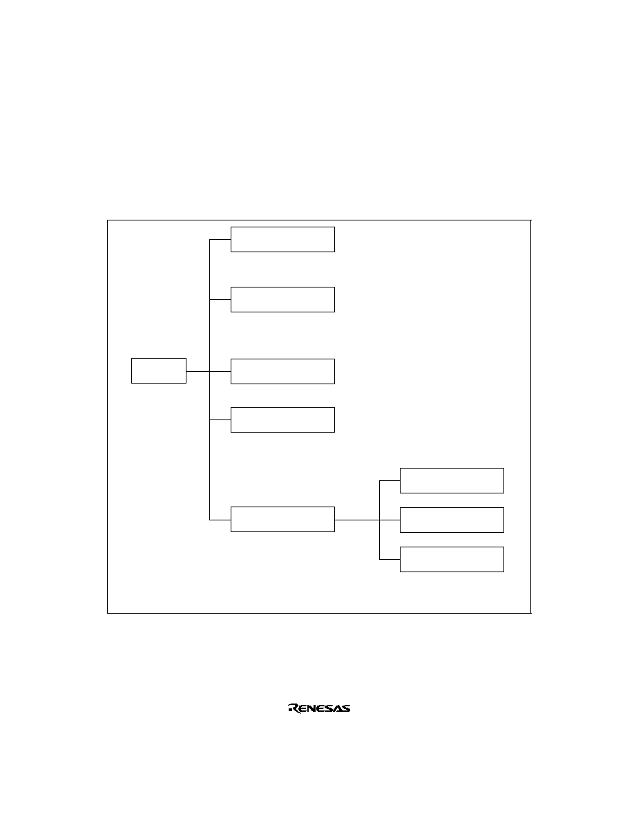
57
2.8
Processing States
2.8.1
Overview
The CPU has five main processing states: the reset state, exception handling state, program
execution state, bus-released state, and power-down state. Figure 2-14 shows a diagram of the
processing states. Figure 2-15 indicates the state transitions.
Reset state
The CPU and all on-chip supporting modules have been
initialized and are stopped.
Exception-handling
state
A transient state in which the CPU changes the normal
processing flow in response to a reset, interrupt, or trap
instruction.
Program execution
state
The CPU executes program instructions in sequence.
Bus-released state
The external bus has been released in response to a bus
request signal from a bus master other than the CPU.
Power-down state
CPU operation is stopped
to conserve power.
*
Sleep mode
Software standby
mode
Hardware standby
mode
Processing
states
Note:
*
The power-down state also includes a medium-speed mode, module stop mode etc.
Figure 2-14 Processing States
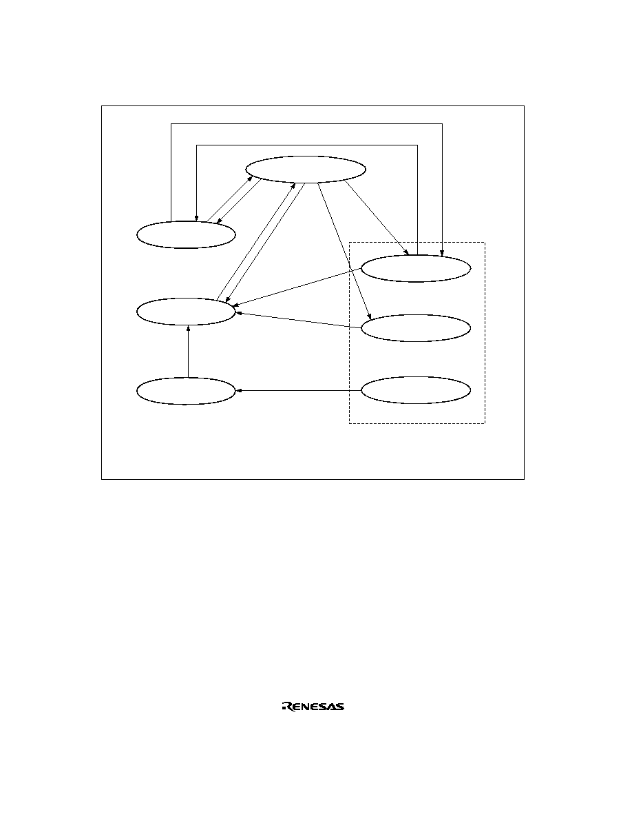
58
End of bus request
Bus request
Program execution
state
Bus-released state
Sleep mode
Exception-handling state
External interrupt
Software standby mode
RES
= high
Reset state
STBY
= high,
RES
= low
Hardware standby mode
*
2
Power-down state
*
1
Notes: 1.
2.
From any state except hardware standby mode, a transition to the reset state occurs whenever
RES
goes low. A transition can also be made to the reset state when the watchdog timer overflows.
From any state, a transition to hardware standby mode occurs when
STBY
goes low.
SLEEP
instruction
with
SSBY = 0
SLEEP
instruction
with
SSBY = 1
Interrupt
request
End of bus
request
Bus
request
Request for
exception
handling
End of
exception
handling
Figure 2-15 State Transitions
2.8.2
Reset State
When the
RES input goes low all current processing stops and the CPU enters the reset state. All
interrupts are masked in the reset state. Reset exception handling starts when the
RES signal
changes from low to high.
The reset state can also be entered by a watchdog timer overflow. For details, refer to section 11,
Watchdog Timer.

59
2.8.3
Exception-Handling State
The exception-handling state is a transient state that occurs when the CPU alters the normal
processing flow due to a reset, interrupt, or trap instruction. The CPU fetches a start address
(vector) from the exception vector table and branches to that address.
(1) Types of Exception Handling and Their Priority
Exception handling is performed for resets, interrupts, and trap instructions. Table 2-14 indicates
the types of exception handling and their priority. Trap instruction exception handling is always
accepted, in the program execution state.
Exception handling and the stack structure depend on the interrupt control mode set in SYSCR.
Table 2-14 Exception Handling Types and Priority
Priority
Type of Exception
Detection Timing
Start of Exception Handling
High
Reset
Synchronized with clock
Exception handling starts
immediately after a low-to-high
transition at the
RES
pin, or
when the watchdog timer
overflows.
Interrupt
End of instruction
execution or end of
exception-handling
sequence
*
1
When an interrupt is requested,
exception handling starts at the
end of the current instruction or
current exception-handling
sequence
Low
Trap instruction
When TRAPA instruction
is executed
Exception handling starts when
a trap (TRAPA) instruction is
executed
*
2
Notes: 1. Interrupts are not detected at the end of the ANDC, ORC, XORC, and LDC instructions,
or immediately after reset exception handling.
2. Trap instruction exception handling is always accepted, in the program execution state.

60
(2) Reset Exception Handling
After the
RES pin has gone low and the reset state has been entered, when RES goes high again,
reset exception handling starts. When reset exception handling starts the CPU fetches a start
address (vector) from the exception vector table and starts program execution from that address.
All interrupts, including NMI, are disabled during reset exception handling and after it ends.
(3) Interrupt Exception Handling and Trap Instruction Exception Handling
When interrupt or trap-instruction exception handling begins, the CPU references the stack pointer
(ER7) and pushes the program counter and other control registers onto the stack. Next, the CPU
alters the settings of the interrupt mask bits in the control registers. Then the CPU fetches a start
address (vector) from the exception vector table and program execution starts from that start
address.
Figure 2-16 shows the stack after exception handling ends.
Note:
*
Ignored when returning.
CCR
PC
(24 bits)
SP
CCR
CCR
*
PC
(16 bits)
SP
Normal mode
Advanced mode
Figure 2-16 Stack Structure after Exception Handling (Examples)

61
2.8.4
Program Execution State
In this state the CPU executes program instructions in sequence.
2.8.5
Bus-Released State
This is a state in which the bus has been released in response to a bus request from a bus master
other than the CPU. While the bus is released, the CPU halts except for internal operations.
There is one bus masters other than the CPU -- the data transfer controller (DTC).
For further details, refer to section 6, Bus Controller.
2.8.6
Power-Down State
The power-down state includes both modes in which the CPU stops operating and modes in which
the CPU does not stop. There are three modes in which the CPU stops operating: sleep mode,
software standby mode, and hardware standby mode. There are also two other power-down
modes: medium-speed mode, and module stop mode. In medium-speed mode the CPU and other
bus masters operate on a medium-speed clock. Module stop mode permits halting of the operation
of individual modules, other than the CPU. For details, refer to section 18, Power-Down State.
Sleep Mode: A transition to sleep mode is made if the SLEEP instruction is executed while the
software standby bit (SSBY) in the standby control register (SBYCR) is cleared to 0. In sleep
mode, CPU operations stop immediately after execution of the SLEEP instruction. The contents of
CPU registers are retained.
Software Standby Mode: A transition to software standby mode is made if the SLEEP
instruction is executed while the SSBY bit in SBYCR is set to 1. In software standby mode, the
CPU and clock halt and all MCU operations stop. As long as a specified voltage is supplied, the
contents of CPU registers and on-chip RAM are retained. The I/O ports also remain in their
existing states.
Hardware Standby Mode: A transition to hardware standby mode is made when the
STBY pin
goes low. In hardware standby mode, the CPU and clock halt and all MCU operations stop. The
on-chip supporting modules are reset, but as long as a specified voltage is supplied, on-chip RAM
contents are retained.

62
2.9
Basic Timing
2.9.1
Overview
The H8S/2000 CPU is driven by a system clock, denoted by the symbol ¯. The period from one
rising edge of ¯ to the next is referred to as a "state." The memory cycle or bus cycle consists of
one, two, or three states. Different methods are used to access on-chip memory, on-chip
supporting modules, and the external address space.
2.9.2
On-Chip Memory (ROM, RAM)
On-chip memory is accessed in one state. The data bus is 16 bits wide, permitting both byte and
word transfer instruction. Figure 2-17 shows the on-chip memory access cycle. Figure 2-18 shows
the pin states.
Internal address bus
Internal read signal
Internal data bus
Internal write signal
Internal data bus
¯
Bus cycle
T1
Address
Read data
Write data
Read
access
Write
access
Figure 2-17 On-Chip Memory Access Cycle

63
Bus cycle
T1
Unchanged
Address bus
AS
RD
HWR
,
LWR
Data bus
¯
High
High
High
High-impedance state
Figure 2-18 Pin States during On-Chip Memory Access
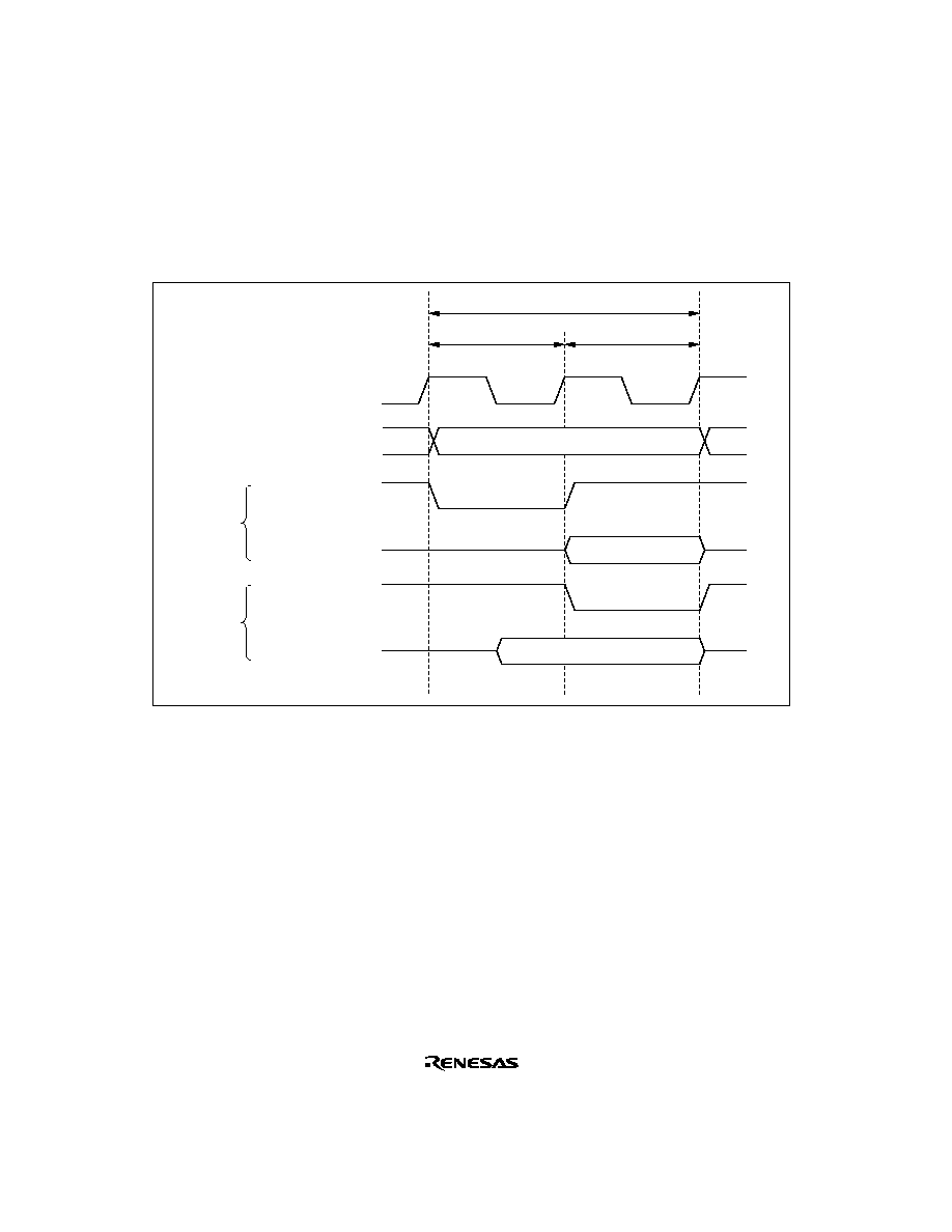
64
2.9.3
On-Chip Supporting Module Access Timing
The on-chip supporting modules are accessed in two states. The data bus is either 8 bits or 16 bits
wide, depending on the particular internal I/O register being accessed. Figure 2-19 shows the
access timing for the on-chip supporting modules. Figure 2-20 shows the pin states.
Bus cycle
T1
T2
Address
Read data
Write data
Internal read signal
Internal data bus
Internal write signal
Internal data bus
Read
access
Write
access
Internal address bus
¯
Figure 2-19 On-Chip Supporting Module Access Cycle
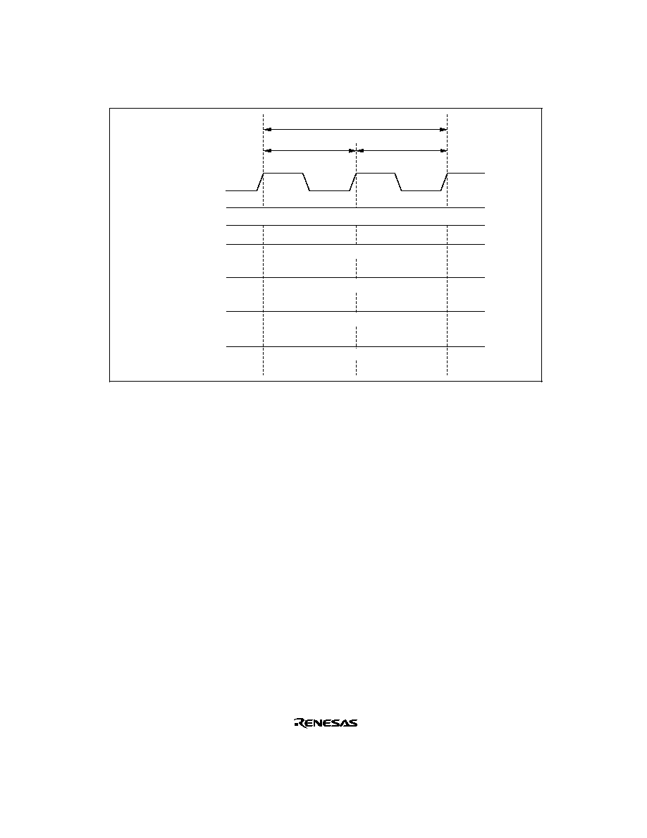
65
Bus cycle
T1
T2
Unchanged
Address bus
AS
RD
HWR
,
LWR
Data bus
¯
High
High
High
High-impedance state
Figure 2-20 Pin States during On-Chip Supporting Module Access
2.9.4
External Address Space Access Timing
The external address space is accessed with an 8-bit or 16-bit data bus width in a two-state or
three-state bus cycle. In three-state access, wait states can be inserted. For further details, refer to
section 6, Bus Controller.

67
Section 3 MCU Operating Modes
3.1
Overview
3.1.1
Operating Mode Selection
Except for the H8S/2240, all H8S/2245 Series products have seven operating modes (modes 1 to
7). The H8S/2240 has three operating modes (modes 1, 4, and 5). These modes enable selection of
the CPU operating mode, enabling/disabling of on-chip ROM, and the initial bus width setting, by
setting the mode pins (MD
2
to MD
0
).
Table 3-1 lists the MCU operating modes.
Table 3-1
MCU Operating Mode Selection
MCU
CPU
External Data Bus
Operating
Mode
MD
2
MD
1
MD
0
Operating
Mode
Description
On-chip
ROM
Initial
Width
Max.
Width
0
0
0
0
--
--
--
--
1
1
Normal
On-chip ROM disabled,
expanded mode
Disabled 8 bits
16 bits
2
*
1
0
On-chip ROM enabled,
expanded mode
Enabled 8 bits
16 bits
3
*
1
Single-chip mode
--
4
1
0
0
Advanced
On-chip ROM disabled,
expanded mode
Disabled 16 bits
16 bits
5
1
8 bits
16 bits
6
*
1
0
On-chip ROM enabled,
expanded mode
Enabled 8 bits
16 bits
7
*
1
Single-chip mode
--
Note:
*
Cannot be used in the H8S/2240.
The CPU's architecture allows for 4 Gbytes of address space, but the H8S/2245 Series actually
accesses a maximum of 16 Mbytes.
Modes 1, 2, and 4 to 6 are externally expanded modes that allow access to external memory and
peripheral devices.
The external expansion modes allow switching between 8-bit and 16-bit bus modes. After program
execution starts, an 8-bit or 16-bit address space can be set for each area, depending on the bus

68
controller setting. If 16-bit access is selected for any one area, 16-bit bus mode is set; if 8-bit
access is selected for all areas, 8-bit bus mode is set.
Note that the functions of each pin depend on the operating mode.
The H8S/2245 Series can be used only in modes 1 to 7. This means that the mode pins must be
set to select one of these modes. Do not change the inputs at the mode pins during operation.
3.1.2
Register Configuration
The H8S/2245 Series has a mode control register (MDCR) that indicates the inputs at the mode
pins (MD
2
to MD
0
), and a system control register (SYSCR) that controls the operation of the
H8S/2245 Series. Table 3-2 summarizes these registers.
Table 3-2
Register Configuration
Name
Abbreviation
R/W
Initial Value
Address
*
Mode control register
MDCR
R
Undetermined
H'FF3B
System control register
SYSCR
R/W
H'01
H'FF39
Note:
*
Lower 16 bits of the address.

69
3.2
Register Descriptions
3.2.1
Mode Control Register (MDCR)
7
--
1
--
6
--
0
--
5
--
0
--
4
--
0
--
3
--
0
--
0
MDS0
--
*
R
2
MDS2
--
*
R
1
MDS1
--
*
R
Note:
*
Determined by pins MD
2
to MD
0
.
Bit
Initial value
R/W
:
:
:
MDCR is an 8-bit read-only register that indicates the current operating mode of the H8S/2245
Series.
Bit 7--Reserved: Read-only bit, always read as 1.
Bits 6 to 3--Reserved: Read-only bits, always read as 0.
Bits 2 to 0--Mode Select 2 to 0 (MDS2 to MDS0): These bits indicate the input levels at pins
MD
2
to MD
0
(the current operating mode). Bits MDS2 to MDS0 correspond to MD
2
to MD
0
.
MDS2 to MDS0 are read-only bits-they cannot be written to. The mode pin (MD
2
to MD
0
) input
levels are latched into these bits when MDCR is read. These latches are canceled by a power-on
reset, but are retained after a manual reset.
3.2.2
System Control Register (SYSCR)
7
--
0
R/W
6
--
0
--
5
INTM1
0
R/W
4
INTM0
0
R/W
3
NMIEG
0
R/W
0
RAME
1
R/W
2
--
0
--
1
--
0
--
Bit
Initial value
R/W
:
:
:
SYSCR is an 8-bit readable/writable register that selects the interrupt control mode, the detected
edge for NMI, and enable or disable the on-chip RAM.
SYSCR is initialized to H'01 by a reset and in hardware standby mode. It is not initialized in
software standby mode.
Bit 7--Reserved: This bit can be read or written, but does not affect operation.
Bit 6--Reserved: Read-only bit, always read as 0.

70
Bits 5 and 4--Interrupt Control Mode 1 and 0 (INTM1, INTM0): These bits select the control
mode of the interrupt controller. For details of the interrupt control modes, see section 5.4.1,
Interrupt Control Modes and Interrupt Operation.
Bit 5
Bit 4
Interrupt
INTM1
INTM0
Control Mode
Description
0
0
0
Control of interrupts by I bit
(Initial value)
1
1
Control of interrupts by I bit, U bit, and ICR
1
0
--
Setting prohibited
1
--
Setting prohibited
Bit 3--NMI Edge Select (NMIEG): Selects the valid edge of the NMI interrupt input.
Bit 3
NMIEG
Description
0
An interrupt is requested at the falling edge of NMI input
(Initial value)
1
An interrupt is requested at the rising edge of NMI input
Bits 2 and 1--Reserved: Read-only bits, always read as 0.
Bit 0--RAM Enable (RAME): Enables or disables the on-chip RAM. The RAME bit is
initialized when the reset status is released. It is not initialized in software standby mode.
Bit 0
RAME
Description
0
On-chip RAM is disabled
1
On-chip RAM is enabled
(Initial value)
Note:
When the DTC is used, the RAME bit should not be cleared to 0.

71
3.3
Operating Mode Descriptions
3.3.1
Mode 1
The CPU can access a 64-kbyte address space in normal mode. The on-chip ROM is disabled, and
8-bit bus mode is set, immediately after a reset.
Ports B and C function as an address bus, port D functions as a data bus, and part of port F carries
bus control signals. However, note that if 16-bit access is designated by the bus controller, the bus
mode switches to 16 bits and port E becomes a data bus.
3.3.2
Mode 2
The CPU can access a 64-kbyte address space in normal mode. The on-chip ROM is enabled, and
8-bit bus mode is set immediately after a reset.
Ports B and C function as input ports immediately after a reset. They can each be set to output
addresses by setting the corresponding bits in the data direction register (DDR) to 1. Port D
functions as a data bus, and part of port F carries bus control signals. However, note that if 16-bit
access is designated by the bus controller, the bus mode switches to 16 bits and port E becomes a
data bus.
The amount of on-chip ROM that can be used on the H8S/2246, H8S/2245, H8S/2244, and
H8S/2243 is limited to 56 kbytes.
Note:
Mode 2 cannot be used in the H8S/2240.
3.3.3
Mode 3
The CPU can access a 64-kbyte address space in normal mode. The on-chip ROM is enabled, but
external addresses cannot be accessed.
All I/O ports are available for use as input-output ports.
The amount of on-chip ROM that can be used on the H8S/2246, H8S/2245, H8S/2244, and
H8S/2243 is limited to 56 kbytes.
Note:
Mode 3 cannot be used in the H8S/2240.

72
3.3.4
Mode 4
The CPU can access a 16-Mbyte address space in advanced mode. The on-chip ROM is disabled.
Pins P1
3
to P1
0
, and ports A, B and C function as an address bus, ports D and E function as a data
bus, and part of port F carries bus control signals. Pins P1
3
to P1
0
function as input ports
immediately after a reset. They can each be set to output address use by setting the corresponding
bits in the data direction register (DDR) to 1.
The initial bus mode after a reset is 16 bits, with 16-bit access to all areas. However, note that if
8-bit access is designated by the bus controller for all areas, the bus mode switches to 8 bits.
3.3.5
Mode 5
The CPU can access a 16-Mbyte address space in advanced mode. The on-chip ROM is disabled.
Pins P1
3
to P1
0
, and ports A, B and C function as an address bus, ports D functions as a data bus,
and part of port F carries bus control signals. Pins P1
3
to P1
0
function as input ports immediately
after a reset. They can each be set to output address use by setting the corresponding bits in the
data direction register (DDR) to 1.
The initial bus mode after a reset is 8 bits, with 8-bit access to all areas. However, note that if at
least one area is designated for 16-bit access by the bus controller, the bus mode switches to 16
bits and port E becomes a data bus.
3.3.6
Mode 6
The CPU can access a 16-Mbyte address space in advanced mode. The on-chip ROM is enabled.
Pins P1
3
to P1
0
, and ports A, B and C function as input ports immediately after a reset. They can
each be set to output addresses by setting the corresponding bits in the data direction register
(DDR) to 1. Port D functions as a data bus, and part of port F carries bus control signals.
The initial bus mode after a reset is 8 bits, with 8-bit access to all areas. However, note that if at
least one area is designated for 16-bit access by the bus controller, the bus mode switches to 16
bits and port E becomes a data bus.
Note:
Mode 6 cannot be used in the H8S/2240.

73
3.3.7
Mode 7
The CPU can access a 16-Mbyte address space in advanced mode. The on-chip ROM is enabled,
but external addresses cannot be accessed.
All I/O ports are available for use as input-output ports.
Note:
Mode 7 cannot be used in the H8S/2240.
3.4
Pin Functions in Each Operating Mode
The pin functions of ports 1, and A to F vary depending on the operating mode. Table 3-3 shows
their functions in each operating mode.
Table 3-3
Pin Functions in Each Mode
Port
Mode 1
Mode 2
*
2
Mode 3
*
2
Mode 4
Mode 5
Mode 6
*
2
Mode 7
*
2
Port 1
P1
3
to P1
0
P
*
1
/T
P
*
1
/T
P
*
1
/T
P
*
1
/T/A
P
*
1
/T/A
P
*
1
/T/A
P
*
1
/T
Port A
PA
3
to PA
0
P
P
P
A
A
P
*
1
/A
P
Port B
A
P
*
1
/A
P
A
A
P
*
1
/A
P
Port C
A
P
*
1
/A
P
A
A
P
*
1
/A
P
Port D
D
D
P
D
D
D
P
Port E
P
*
1
/D
P
*
1
/D
P
P
*
1
/D
P
*
1
/D
P
*
1
/D
P
Port F
PF
7
P/C
*
1
P/C
*
1
P
*
1
/C
P/C
*
1
P/C
*
1
P/C
*
1
P
*
1
/C
PF
6
to PF
3
C
C
P
C
C
C
P
PF
2
to PF
0
P
*
1
/C
P
*
1
/C
P
*
1
/C
P
*
1
/C
P
*
1
/C
Legend
P: I/O port
T: Timer I/O
A: Address bus output
D: Data bus I/O
C: Control signals, clock I/O
Notes: 1. After reset
2. Cannot be used in the H8S/2240.

74
3.5
Memory Map in Each Operating Mode
The H8S/2246, H8S/2245, H8S/2244, H8S/2243, H8S/2242, H8S/2241, and H8S/2240 memory
maps are shown in figures 3-1 to 3-7.
The address space is 64 kbytes in modes 1 to 3 (normal modes), and 16 Mbytes in modes 4 to 7
(advanced modes).
The on-chip ROM size is 128 kbytes in the H8S/2246 and H8S/2245, and 64 kbytes in the
H8S/2244 and H8S/2243, but only 56 kbytes are available in modes 2 and 3 (normal modes).
The on-chip ROM size in the H8S/2242 and H8S/2241 is 32 kbytes.
The address space is divided into eight areas for modes 4 to 6. For details, see section 6, Bus
Controller.

75
Mode 1
(normal expanded mode
with on-chip ROM disabled)
Mode 2
(normal expanded mode
with on-chip ROM enabled)
Mode 3
(normal single-chip mode)
External address
space
On-chip ROM
On-chip RAM
*
Note:
*
External addresses can be accessed by clearing the RAME bit in SYSCR to 0.
Internal I/O registers
On-chip ROM
External address
space
External address
space
On-chip RAM
*
On-chip RAM
Internal I/O registers
Internal I/O registers
Internal I/O registers
Internal I/O registers
External address
space
External address
space
Internal I/O registers
External address
space
H'0000
H'0000
H'0000
H'DFFF
H'DFFF
H'E000
H'E400
H'FBFF
H'FC00
H'FFFF
H'E400
H'FBFF
H'FC00
H'FFFF
H'E400
H'FBFF
H'FFFF
H'FE3F
H'FF08
H'FE3F
H'FF08
H'FE40
H'FF07
H'FF28
H'FF28
H'FF28
Figure 3-1 H8S/2246 Memory Map in Each Operating Mode
76
Modes 4 and 5
(advanced expanded modes
with on-chip ROM disabled)
Mode 6
(advanced expanded mode
with on-chip ROM enabled)
Mode 7
(advanced single-chip mode)
External address
space
On-chip ROM
On-chip RAM
*
3
Notes:
Internal I/O registers
On-chip ROM
External address
space
External address
space
On-chip RAM
*
3
On-chip RAM
Internal I/O registers
Internal I/O registers
Internal I/O registers
Internal I/O registers
External address
space
External address
space
Internal I/O registers
External address
space
H'000000
H'000000
H'000000
H'01FFFF
H'020000
H'FFDC00
H'FFFBFF
H'FFFC00
H'FFFFFF
H'FFDC00
H'FFFBFF
H'FFFC00
H'FFFFFF
H'01FFFF
H'FFDC00
H'FFFBFF
H'FFFFFF
H'FFFF08
H'FFFF08
H'FFFE40
H'FFFF07
H'FFFF28
H'FFFF28
H'FFFF28
On-chip ROM/
external address
space
*
1
On-chip ROM/
reserved area
*
2
H'FFFE3F
H'FFFE3F
H'00FFFF
H'010000
H'00FFFF
H'010000
When the EAE bit in BCRL is set to 1, this area is external address space. When the EAE
bit is cleared to 0, it is on-chip ROM.
This area is reserved when the EAE bit in BCRL is set to 1, and on-chip ROM when
the EAE bit is cleared to 0.
External addresses can be accessed by clearing the RAME bit in SYSCR to 0.
1.
2.
3.
Figure 3-1 H8S/2246 Memory Map in Each Operating Mode (cont)

77
Mode 1
(normal expanded mode
with on-chip ROM disabled)
Mode 2
(normal expanded mode
with on-chip ROM enabled)
Mode 3
(normal single-chip mode)
External address
space
On-chip ROM
On-chip RAM
*
Reserved area
*
Reserved area
*
Note:
*
External addresses can be accessed by clearing the RAME bit in SYSCR to 0.
Internal I/O registers
On-chip ROM
External address
space
External address
space
On-chip RAM
*
On-chip RAM
Internal I/O registers
Internal I/O registers
Internal I/O registers
Internal I/O registers
External address
space
External address
space
Internal I/O registers
External address
space
H'0000
H'0000
H'0000
H'DFFF
H'E400
H'DFFF
H'E000
H'EC00
H'E400
H'FBFF
H'FC00
H'FFFF
H'EC00
H'FBFF
H'FC00
H'FFFF
H'EC00
H'FBFF
H'FFFF
H'FE3F
H'FF08
H'FE3F
H'FF08
H'FE40
H'FF07
H'FF28
H'FF28
H'FF28
Figure 3-2 H8S/2245 Memory Map in Each Operating Mode
78
Modes 4 and 5
(advanced expanded modes
with on-chip ROM disabled)
Mode 6
(advanced expanded mode
with on-chip ROM enabled)
Mode 7
(advanced single-chip mode)
External address
space
On-chip ROM
On-chip RAM
*
3
Notes:
Internal I/O registers
On-chip ROM
External address
space
External address
space
On-chip RAM
*
3
Reserved area
*
3
Reserved area
*
3
On-chip RAM
Internal I/O registers
Internal I/O registers
Internal I/O registers
Internal I/O registers
External address
space
External address
space
Internal I/O registers
External address
space
H'000000
H'000000
H'000000
H'01FFFF
H'020000
H'FFDC00
H'FFFBFF
H'FFFC00
H'FFFFFF
H'FFDC00
H'FFEC00
H'FFEC00
H'FFFBFF
H'FFFC00
H'FFFFFF
H'01FFFF
H'FFEC00
H'FFFBFF
H'FFFFFF
H'FFFF08
H'FFFF08
H'FFFE40
H'FFFF07
H'FFFF28
H'FFFF28
H'FFFF28
On-chip ROM/
external address
space
*
1
On-chip ROM/
reserved area
*
2
H'FFFE3F
H'FFFE3F
H'00FFFF
H'010000
H'00FFFF
H'010000
When the EAE bit in BCRL is set to 1, this area is external address space. When the EAE
bit is cleared to 0, it is on-chip ROM.
This area is reserved when the EAE bit in BCRL is set to 1, and on-chip ROM when
the EAE bit is cleared to 0.
External addresses can be accessed by clearing the RAME bit in SYSCR to 0.
1.
2.
3.
Figure 3-2 H8S/2245 Memory Map in Each Operating Mode (cont)

79
Mode 1
(normal expanded mode
with on-chip ROM disabled)
Mode 2
(normal expanded mode
with on-chip ROM enabled)
Mode 3
(normal single-chip mode)
External address
space
On-chip ROM
On-chip RAM
*
Note:
*
External addresses can be accessed by clearing the RAME bit in SYSCR to 0.
Internal I/O registers
On-chip ROM
External address
space
External address
space
On-chip RAM
*
On-chip RAM
Internal I/O registers
Internal I/O registers
Internal I/O registers
Internal I/O registers
External address
space
External address
space
Internal I/O registers
External address
space
H'0000
H'0000
H'0000
H'DFFF
H'DFFF
H'E000
H'E400
H'FBFF
H'FC00
H'FFFF
H'E400
H'FBFF
H'FC00
H'FFFF
H'E400
H'FBFF
H'FFFF
H'FE3F
H'FF08
H'FE3F
H'FF08
H'FE40
H'FF07
H'FF28
H'FF28
H'FF28
Figure 3-3 H8S/2244 Memory Map in Each Operating Mode

80
Modes 4 and 5
(advanced expanded modes
with on-chip ROM disabled)
Mode 6
(advanced expanded mode
with on-chip ROM enabled)
Mode 7
(advanced single-chip mode)
External address
space
On-chip ROM
On-chip RAM
*
2
Notes:
Internal I/O registers
On-chip ROM
External address
space
External address
space
On-chip RAM
*
2
On-chip RAM
Internal I/O registers
Internal I/O registers
Internal I/O registers
Internal I/O registers
External address
space
External address
space
Internal I/O registers
External address
space
H'000000
H'000000
H'000000
H'01FFFF
H'020000
H'FFDC00
H'FFFBFF
H'FFFC00
H'FFFFFF
H'FFDC00
H'FFFBFF
H'FFFC00
H'FFFFFF
H'FFDC00
H'FFFBFF
H'FFFFFF
H'FFFF08
H'FFFF08
H'FFFE40
H'FFFF07
H'FFFF28
H'FFFF28
H'FFFF28
External address
space/reserved
area
*
1
H'FFFE3F
H'FFFE3F
H'00FFFF
H'00FFFF
H'010000
When the EAE bit in BCRL is set to 1, this area is external address space. When the EAE
bit is cleared to 0, it is reserved.
External addresses can be accessed by clearing the RAME bit in SYSCR to 0.
1.
2.
Figure 3-3 H8S/2244 Memory Map in Each Operating Mode (cont)
81
Mode 1
(normal expanded mode
with on-chip ROM disabled)
Mode 2
(normal expanded mode
with on-chip ROM enabled)
Mode 3
(normal single-chip mode)
External address
space
On-chip ROM
On-chip RAM
*
Reserved area
*
Reserved area
*
Note:
*
External addresses can be accessed by clearing the RAME bit in SYSCR to 0.
Internal I/O registers
On-chip ROM
External address
space
External address
space
On-chip RAM
*
On-chip RAM
Internal I/O registers
Internal I/O registers
Internal I/O registers
Internal I/O registers
External address
space
External address
space
Internal I/O registers
External address
space
H'0000
H'0000
H'0000
H'E400
H'DFFF
H'DFFF
H'E000
H'EC00
H'E400
H'FBFF
H'FC00
H'FFFF
H'EC00
H'FBFF
H'FC00
H'FFFF
H'EC00
H'FBFF
H'FFFF
H'FE3F
H'FF08
H'FE3F
H'FF08
H'FE40
H'FF07
H'FF28
H'FF28
H'FF28
Figure 3-4 H8S/2243 Memory Map in Each Operating Mode
82
Modes 4 and 5
(advanced expanded modes
with on-chip ROM disabled)
Mode 6
(advanced expanded mode
with on-chip ROM enabled)
Mode 7
(advanced single-chip mode)
External address
space
On-chip ROM
On-chip RAM
*
2
Notes:
Internal I/O registers
On-chip ROM
External address
space
External address
space
On-chip RAM
*
2
Reserved area
*
2
Reserved area
*
2
On-chip RAM
Internal I/O registers
Internal I/O registers
Internal I/O registers
Internal I/O registers
External address
space
External address
space
Internal I/O registers
External address
space
H'000000
H'000000
H'000000
H'01FFFF
H'020000
H'FFDC00
H'FFFBFF
H'FFFC00
H'FFFFFF
H'FFDC00
H'FFEC00
H'FFEC00
H'FFFBFF
H'FFFC00
H'FFFFFF
H'FFEC00
H'FFFBFF
H'FFFFFF
H'FFFF08
H'FFFF08
H'FFFE40
H'FFFF07
H'FFFF28
H'FFFF28
H'FFFF28
External address
space/reserved
area
*
1
H'FFFE3F
H'FFFE3F
H'00FFFF
H'00FFFF
H'010000
When the EAE bit in BCRL is set to 1, this area is external address space. When the EAE
bit is cleared to 0, it is reserved.
External addresses can be accessed by clearing the RAME bit in SYSCR to 0.
1.
2.
Figure 3-4 H8S/2243 Memory Map in Each Operating Mode (cont)
83
Mode 1
(normal expanded mode
with on-chip ROM disabled)
Mode 2
(normal expanded mode
with on-chip ROM enabled)
Mode 3
(normal single-chip mode)
External address
space
On-chip ROM
On-chip RAM
*
Note:
*
External addresses can be accessed by clearing the RAME bit in SYSCR to 0.
Internal I/O registers
On-chip ROM
External address
space
External address
space
On-chip RAM
*
On-chip RAM
Internal I/O registers
Reserved area
Internal I/O registers
Internal I/O registers
Internal I/O registers
External address
space
External address
space
Internal I/O registers
External address
space
H'0000
H'0000
H'0000
H'DFFF
H'E000
H'7FFF
H'8000
H'7FFF
H'E400
H'FBFF
H'FC00
H'FFFF
H'E400
H'FBFF
H'FC00
H'FFFF
H'E400
H'FBFF
H'FFFF
H'FE3F
H'FF08
H'FE3F
H'FF08
H'FE40
H'FF07
H'FF28
H'FF28
H'FF28
Figure 3-5 H8S/2242 Memory Map in Each Operating Mode
84
Modes 4 and 5
(advanced expanded modes
with on-chip ROM disabled)
Mode 6
(advanced expanded mode
with on-chip ROM enabled)
Mode 7
(advanced single-chip mode)
External address
space
On-chip ROM
Reserved area
On-chip RAM
*
2
Notes:
Internal I/O registers
On-chip ROM
External address
space
External address
space
On-chip RAM
*
2
On-chip RAM
Internal I/O registers
Internal I/O registers
Internal I/O registers
Internal I/O registers
External address
space
External address
space
Internal I/O registers
External address
space
H'000000
H'000000
H'000000
H'01FFFF
H'020000
H'FFDC00
H'FFFBFF
H'FFFC00
H'FFFFFF
H'FFDC00
H'FFFBFF
H'FFFC00
H'FFFFFF
H'FFDC00
H'FFFBFF
H'FFFFFF
H'FFFF08
H'FFFF08
H'FFFE40
H'FFFF07
H'FFFF28
H'FFFF28
H'FFFF28
External address
space/reserved
area
*
1
H'FFFE3F
H'FFFE3F
H'00FFFF
H'010000
H'007FFF
H'008000
H'007FFF
When the EAE bit in BCRL is set to 1, this area is external address space. When the EAE
bit is cleared to 0, it is reserved.
External addresses can be accessed by clearing the RAME bit in SYSCR to 0.
1.
2.
Figure 3-5 H8S/2242 Memory Map in Each Operating Mode (cont)
85
Mode 1
(normal expanded mode
with on-chip ROM disabled)
Mode 2
(normal expanded mode
with on-chip ROM enabled)
Mode 3
(normal single-chip mode)
External address
space
On-chip ROM
On-chip RAM
*
Reserved area
*
Reserved area
*
Reserved area
Note:
*
External addresses can be accessed by clearing the RAME bit in SYSCR to 0.
Internal I/O registers
On-chip ROM
External address
space
External address
space
On-chip RAM
*
On-chip RAM
Internal I/O registers
Internal I/O registers
Internal I/O registers
Internal I/O registers
External address
space
External address
space
Internal I/O registers
External address
space
H'0000
H'0000
H'0000
H'E400
H'DFFF
H'E000
H'7FFF
H'7FFF
H'8000
H'EC00
H'E400
H'FBFF
H'FC00
H'FFFF
H'EC00
H'FBFF
H'FC00
H'FFFF
H'EC00
H'FBFF
H'FFFF
H'FE3F
H'FF08
H'FE3F
H'FF08
H'FE40
H'FF07
H'FF28
H'FF28
H'FF28
Figure 3-6 H8S/2241 Memory Map in Each Operating Mode
86
Modes 4 and 5
(advanced expanded modes
with on-chip ROM disabled)
Mode 6
(advanced expanded mode
with on-chip ROM enabled)
Mode 7
(advanced single-chip mode)
External address
space
On-chip ROM
Reserved area
On-chip RAM
*
2
Notes:
Internal I/O registers
On-chip ROM
External address
space
External address
space
On-chip RAM
*
2
Reserved area
*
2
Reserved area
*
2
On-chip RAM
Internal I/O registers
Internal I/O registers
Internal I/O registers
Internal I/O registers
External address
space
External address
space
Internal I/O registers
External address
space
H'000000
H'000000
H'000000
H'01FFFF
H'020000
H'FFDC00
H'FFFBFF
H'FFFC00
H'FFFFFF
H'FFDC00
H'FFEC00
H'FFEC00
H'FFFBFF
H'FFFC00
H'FFFFFF
H'FFEC00
H'FFFBFF
H'FFFFFF
H'FFFF08
H'FFFF08
H'FFFE40
H'FFFF07
H'FFFF28
H'FFFF28
H'FFFF28
External address
space/reserved
area
*
1
H'FFFE3F
H'FFFE3F
H'00FFFF
H'010000
H'007FFF
H'007FFF
H'008000
When the EAE bit in BCRL is set to 1, this area is external address space. When the EAE
bit is cleared to 0, it is reserved.
External addresses can be accessed by clearing the RAME bit in SYSCR to 0.
1.
2.
Figure 3-6 H8S/2241 Memory Map in Each Operating Mode (cont)

87
Mode 1
(normal expanded mode
with on-chip ROM disabled)
External address
space
On-chip RAM
*
Reserved area
*
Note:
*
External addresses can be accessed by clearing the RAME bit in SYSCR to 0.
Internal I/O registers
External address
space
Internal I/O registers
External address
space
H'0000
H'EC00
H'E400
H'FBFF
H'FC00
H'FFFF
H'FE3F
H'FF08
H'FF28
Modes 4 and 5
(advanced expanded modes
with on-chip ROM disabled)
External address
space
On-chip RAM
*
Internal I/O registers
Reserved area
*
External address
space
Internal I/O registers
External address
space
H'000000
H'FFDC00
H'FFFBFF
H'FFFC00
H'FFFFFF
H'FFEC00
H'FFFF08
H'FFFF28
H'FFFE3F
Figure 3-7 H8S/2240 Memory Map in Each Operating Mode (Modes 1, 4, and 5 Only)

89
Section 4 Exception Handling
4.1
Overview
4.1.1
Exception Handling Types and Priority
As table 4-1 indicates, exception handling may be caused by a reset, trap instruction, or interrupt.
Exception handling is prioritized as shown in table 4-1. If two or more exceptions occur
simultaneously, they are accepted and processed in order of priority. Trap instruction exceptions
are accepted at all times, in the program execution state. See appendix D.1, Port States in Each
Mode.
Exception handling sources, the stack structure, and the operation of the CPU vary depending on
the interrupt control mode set by the INTM0 and INTM1 bits of SYSCR.
Table 4-1
Exception Handling Types and Priority
Priority
Exception Handling Type
Start of Exception Handling
High
Reset
Starts immediately after a low-to-high transition at the
RES
pin, or when the watchdog timer overflows.
Interrupt
Starts when execution of the current instruction or
exception handling ends, if an interrupt request has
been issued
*
1
Low
Trap instruction (TRAPA)
*
2
Started by execution of a trap instruction (TRAPA)
Notes: 1. Interrupt detection is not performed on completion of ANDC, ORC, XORC, or LDC
instruction execution, or on completion of reset exception handling.
2. Trap instruction exception handling requests are accepted at all times in program
execution state.
4.1.2
Exception Handling Operation
Exceptions originate from various sources. Trap instructions and interrupts are handled as
follows:
1. The program counter (PC) and condition code register (CCR) are pushed onto the stack.
2. The interrupt mask bits are updated.
3. A vector address corresponding to the exception source is generated, and program execution
starts from that address.
For a reset exception, steps 2 and 3 above are carried out.

90
4.1.3
Exception Sources and Vector Table
The exception sources are classified as shown in figure 4-1. Different vector addresses are
assigned to different exception sources.
Table 4-2 lists the exception sources and their vector addresses.
Exception
sources
Reset
Interrupts
Trap instruction
Power-on reset
Manual reset
External interrupts: NMI, IRQ7 to IRQ0
Internal interrupts: 34 interrupt sources in
on-chip supporting modules
Figure 4-1 Exception Sources
In modes 6 and 7, the on-chip ROM available for use on the H8S/2246 and H8S/2245 after a
power-on reset is the 64-kbyte area comprising addresses H'000000 to H'00FFFF. Care is required
when setting vector addresses. In this case, clearing the EAE bit in BCRL enables the 128-kbyte
area comprising addresses H'000000 to H'01FFFF to be used for the on-chip ROM.

91
Table 4-2
Exception Vector Table
Vector Address
*
1
Exception Source
Vector Number
Normal Mode
Advanced Mode
Power-on reset
0
H'0000 to H'0001
H'0000 to H'0003
Manual reset
1
H'0002 to H'0003
H'0004 to H'0007
Reserved for system use
2
H'0004 to H'0006
H'0008 to H'000B
3
H'0006 to H'0007
H'000C to H'000F
4
H'0008 to H'0009
H'0010 to H'0013
5
H'000A to H'000B
H'0014 to H'0017
6
H'000C to H'000D
H'0018 to H'001B
External interrupt
NMI
7
H'000E to H'000F
H'001C to H'001F
Trap instruction (4 sources)
8
H'0010 to H'0011
H'0020 to H'0023
9
H'0012 to H'0013
H'0024 to H'0027
10
H'0014 to H'0015
H'0028 to H'002B
11
H'0016 to H'0017
H'002C to H'002F
Reserved for system use
12
H'0018 to H'0019
H'0030 to H'0033
13
H'001A to H'001B
H'0034 to H'0037
14
H'001C to H'001D
H'0038 to H'003B
15
H'001E to H'001F
H'003C to H'003F
External interrupt
IRQ0
16
H'0020 to H'0021
H'0040 to H'0043
IRQ1
17
H'0022 to H'0023
H'0044 to H'0047
IRQ2
18
H'0024 to H'0025
H'0048 to H'004B
IRQ3
19
H'0026 to H'0027
H'004C to H'004F
IRQ4
20
H'0028 to H'0029
H'0050 to H'0053
IRQ5
21
H'002A to H'002B
H'0054 to H'0057
IRQ6
22
H'002C to H'002D
H'0058 to H'005B
IRQ7
23
H'002E to H'002F
H'005C to H'005F
Internal interrupt
*
2
24
91
H'0030 to H'0031
H'00B6 to H'00B7
H'0060 to H'0063
H'016C to H'016F
Notes: 1. Lower 16 bits of the address.
2. For details of internal interrupt vectors, see section 5.3.3, Interrupt Exception Handling
Vector Table.

92
4.2
Reset
4.2.1
Overview
A reset has the highest exception priority.
When the
RES pin goes low, all processing halts and the H8S/2245 Series enters the reset state. A
reset initializes the internal state of the CPU and the registers of on-chip supporting modules.
Immediately after a reset, interrupt control mode 0 is set.
Reset exception handling begins when the
RES pin changes from low to high.
The level of the NMI pin at reset determines whether the type of reset is a power-on reset or a
manual reset.
The H8S/2245 Series can also be reset by overflow of the watchdog timer. For details see section
11, Watchdog Timer.
4.2.2
Reset Types
A reset can be of either of two types: a power-on reset or a manual reset. Reset types are shown in
table 4-3.
The internal state of the CPU is initialized by either type of reset. A power-on reset also initializes
all the registers in the on-chip peripheral modules, while a manual reset initializes all the registers
in the on-chip supporting modules except for the bus controller and I/O ports, which retain their
previous states.
With a manual reset, since the on-chip supporting modules are initialized, ports used as on-chip
supporting module I/O pins are switched to I/O ports controlled by DDR and DR.
Table 4-3
Reset Types
Reset Transition
Conditions
Internal State
Type
NMI
RES
CPU
On-Chip Supporting Modules
Power-on reset
High
Low
Initialized
Initialized
Manual reset
Low
Low
Initialized
Initialized, except for bus controller
and I/O ports
A reset caused by the watchdog timer can also be of either of two types: a power-on reset or a
manual reset.
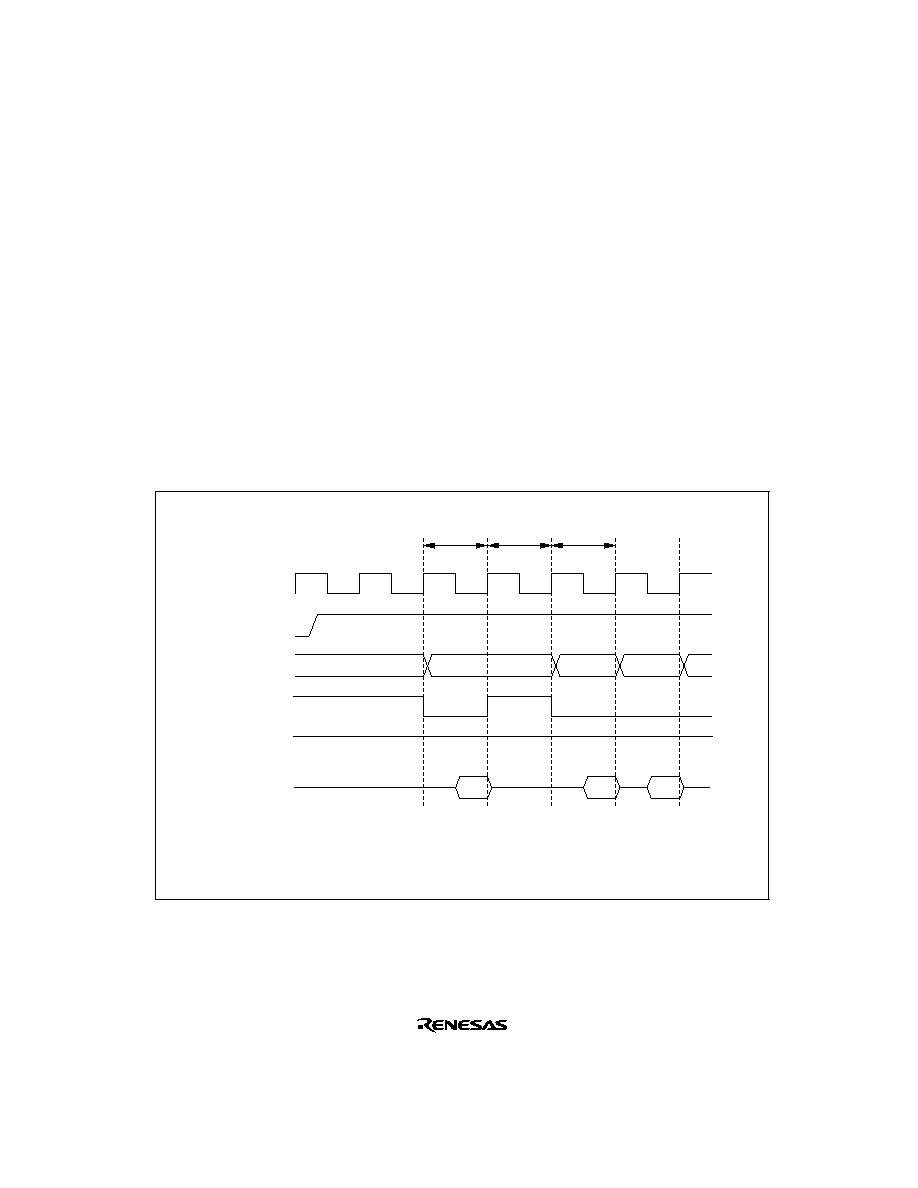
93
4.2.3
Reset Sequence
The H8S/2245 Series enters the reset state when the
RES pin goes low.
To ensure that the H8S/2245 Series is reset, hold the
RES pin low for at least 20 ms at power-up.
To reset the H8S/2245 Series during operation, hold the
RES pin low for at least 20 states. See
appendix D.1, Port States in Each Mode.
When the
RES pin goes high after being held low for the necessary time, the H8S/2245 Series
starts reset exception handling as follows:
1. The internal state of the CPU and the registers of the on-chip supporting modules are
initialized, and the I bit is set to 1 in CCR.
2. The reset exception handling vector address is read and transferred to the PC, and program
execution starts from the address indicated by the PC.
Figures 4-2 and 4-3 show examples of the reset sequence.
Internal
address bus
Internal read
signal
Internal write
signal
Internal data
bus
(1)
(3)
Vector
fetch
Internal
processing
Fetch of first program
instruction
High
(1) Reset exception handling vector address ((1) = H'0000)
(2) Start address (contents of reset exception handling vector address)
(3) Start address ((3) = (2))
(4) First program instruction
(2)
(4)
¯
RES
Figure 4-2 Reset Sequence (Modes 2 and 3)
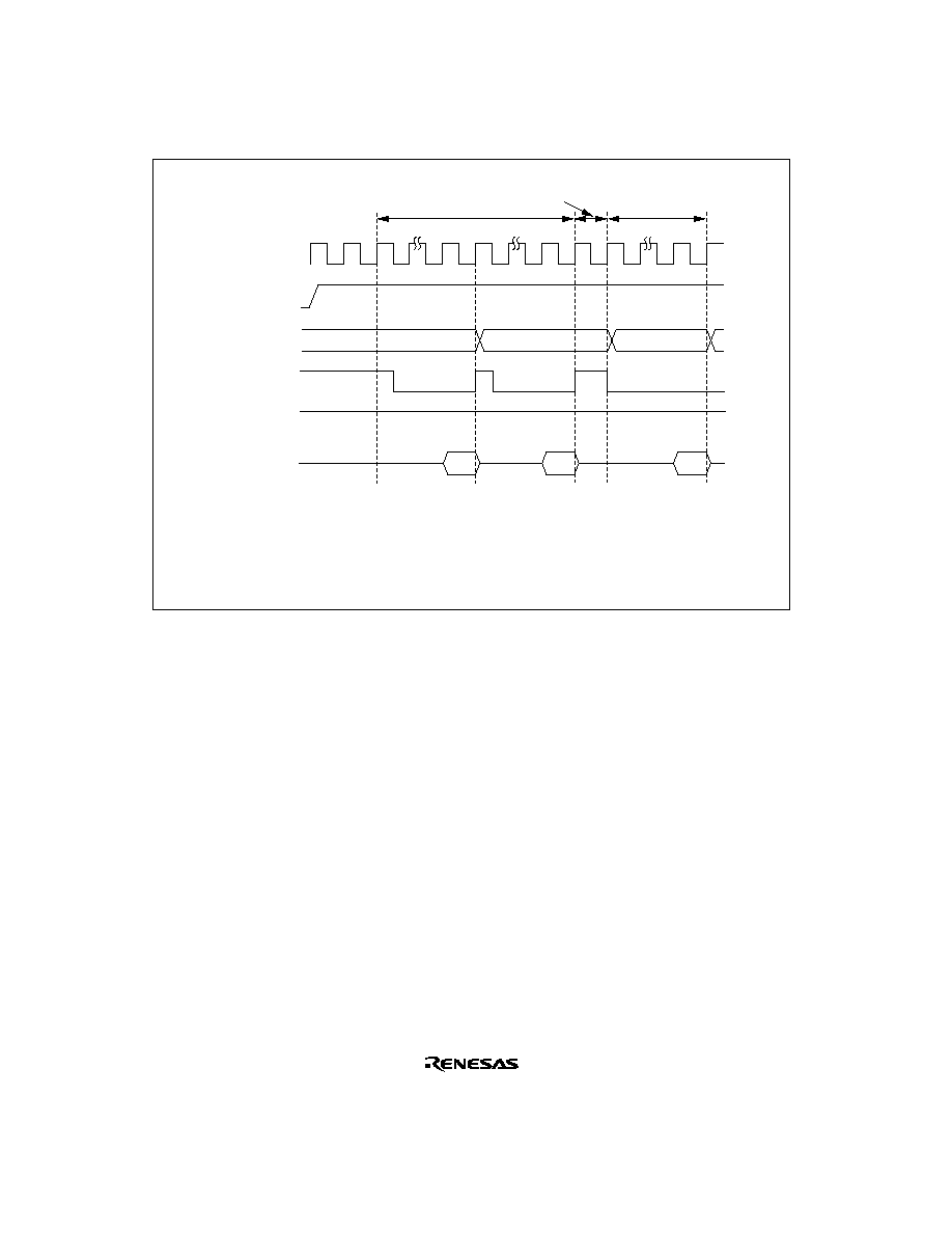
94
Address bus
Vector fetch
Internal
processing
Fetch of first
program instruction
(1) (3) Reset exception handling vector address ((1) = H'000000, (3) = H'000002)
(2) (4) Start address (contents of reset exception handling vector address)
(5) Start address ((5) = (2) (4))
(6) First program instruction
¯
RES
(1)
(5)
High
(2)
(4)
(3)
(6)
RD
HWR
,
LWR
D
15
to D
0
*
Note:
*
3 program wait states are inserted.
*
*
Figure 4-3 Reset Sequence (Mode 4)
4.2.4
Interrupts after Reset
If an interrupt is accepted after a reset but before the stack pointer (SP) is initialized, the PC and
CCR will not be saved correctly, leading to a program crash. To prevent this, all interrupt requests,
including NMI, are disabled immediately after a reset. Since the first instruction of a program is
always executed immediately after the reset state ends, make sure that this instruction initializes
the stack pointer (example: MOV.L #xx: 32, SP).
4.2.5
State of On-Chip Supporting Modules after Reset Release
After reset release, MSTPCR is initialized to H'3FFF and all modules except the DTC enter
module stop mode. Consequently, on-chip supporting module registers cannot be read or written
to. Register reading and writing is enabled when module stop mode is exited.

95
4.3
Interrupts
Interrupt exception handling can be requested by nine external sources (NMI, IRQ7 to IRQ0) and
34 internal sources in the on-chip supporting modules. Figure 4-4 classifies the interrupt sources
and the number of interrupts of each type.
The on-chip supporting modules that can request interrupts include the watchdog timer (WDT),
16-bit timer-pulse unit (TPU), 8-bit timer, serial communication interface (SCI), data transfer
controller (DTC), and A/D converter. Each interrupt source has a separate vector address.
NMI is the highest-priority interrupt. Interrupts are controlled by the interrupt controller. The
interrupt controller has two interrupt control modes and can assign interrupts other than NMI to
three priority/mask levels to enable multiplexed interrupt control.
For details of interrupts, see section 5, Interrupt Controller.
Interrupts
External
interrupts
Internal
interrupts
NMI (1)
IRQ7 to IRQ0 (8)
WDT
*
(1)
TPU (13)
8-bit timer (6)
SCI (12)
DTC (1)
A/D converter (1)
Numbers in parentheses are the numbers of interrupt sources.
*
When the watchdog timer is used as an interval timer, it generates
an interrupt request at each counter overflow.
Notes:
Figure 4-4 Interrupt Sources and Number of Interrupts

96
4.4
Trap Instruction
Trap instruction exception handling starts when a TRAPA instruction is executed. Trap instruction
exception handling can be executed at all times in the program execution state.
The TRAPA instruction fetches a start address from a vector table entry corresponding to a vector
number from 0 to 3, as specified in the instruction code.
Table 4-4 shows the status of CCR after execution of trap instruction exception handling.
Table 4-4
Status of CCR after Trap Instruction Exception Handling
CCR
Interrupt Control Mode
I
UI
0
1
--
1
1
1
Legend
1: Set to 1
--: Retains value prior to execution.

97
4.5
Stack Status after Exception Handling
Figure 4-5 shows the stack after completion of trap instruction exception handling and interrupt
exception handling.
SP
CCR
CCR
*
PC
(16 bits)
Note:
*
Ignored on return.
Figure 4-5 (1) Stack Status after Exception Handling (Normal Modes)
SP
CCR
PC
(24 bits)
Figure 4-5 (2) Stack Status after Exception Handling (Advanced Modes)
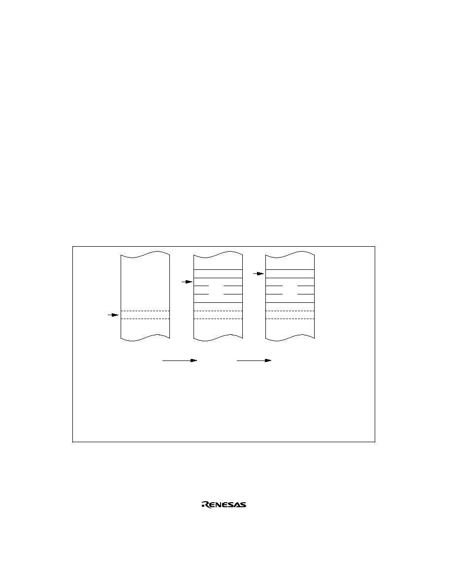
98
4.6
Notes on Use of the Stack
When accessing word data or longword data, the H8S/2245 Series assumes that the lowest address
bit is 0. The stack should always be accessed by word transfer instruction or longword transfer
instruction, and the value of the stack pointer (SP, ER7) should always be kept even. Use the
following instructions to save registers:
PUSH.W Rn (or MOV.W Rn, @-SP)
PUSH.L ERn (or MOV.L ERn, @-SP)
Use the following instructions to restore registers:
POP.W Rn (or MOV.W @SP+, Rn)
POP.L ERn (or MOV.L @SP+, ERn)
Setting SP to an odd value may lead to a malfunction. Figure 4-6 shows an example of what
happens when the SP value is odd.
SP
Legend
Note: This diagram illustrates an example in which the interrupt control mode
is 0, in advanced mode.
SP
SP
CCR
PC
R1L
PC
H'FFFEFA
H'FFFEFB
H'FFFEFC
H'FFFEFD
H'FFFEFF
MOV.B R1L, @≠ER7
SP set to H'FFFEFF
TRAPA instruction executed
Data saved above SP
Contents of CCR lost
CCR: Condition code register
PC: Program counter
R1L: General register R1L
SP: Stack pointer
Figure 4-6 Operation when SP Value is Odd

99
Section 5 Interrupt Controller
5.1
Overview
5.1.1
Features
The H8S/2245 Series controls interrupts by means of an interrupt controller. The interrupt
controller has the following features:
∑
Two interrupt control modes
Either of two interrupt control modes can be set by means of the INTM1 and INTM0 bits in
the system control register (SYSCR).
∑
Priorities settable with ICR
An interrupt control register (ICR) is provided for setting interrupt priorities. Three priority
levels can be set for each module for all interrupts except NMI.
∑
Independent vector addresses
All interrupt sources are assigned independent vector addresses, making it unnecessary for
the source to be identified in the interrupt handling routine.
∑
Nine external interrupts
NMI is the highest-priority interrupt, and is accepted at all times. Rising edge or falling
edge can be selected for NMI.
Falling edge, rising edge, or both edge detection, or level sensing, can be selected for IRQ7
to IRQ0.
∑
DTC control
DTC activation is performed by means of interrupts.
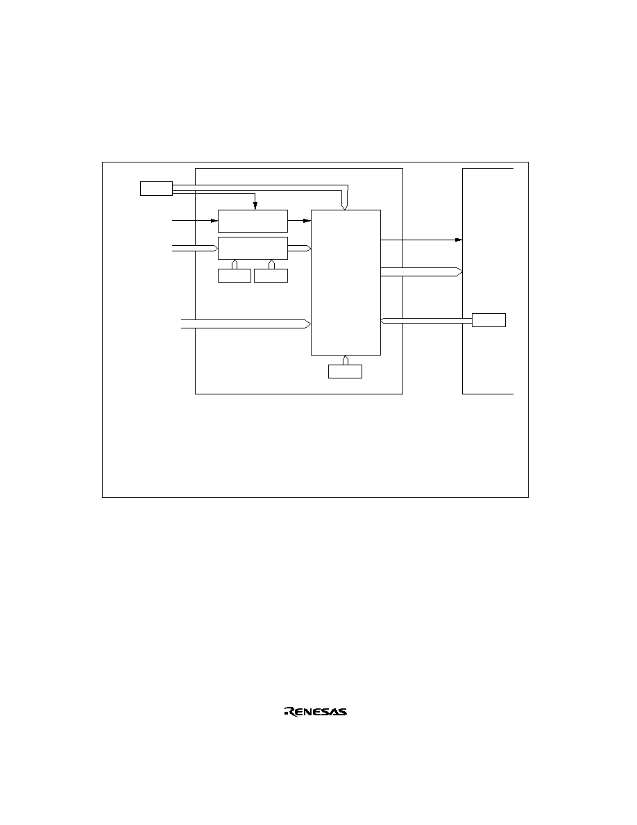
100
5.1.2
Block Diagram
A block diagram of the interrupt controller is shown in Figure 5-1.
SYSCR
NMI input
IRQ input
Internal interrupt
request
WOVI to TEI
INTM1 INTM0
NMIEG
NMI input unit
IRQ input unit
ISR
ISCR
IER
ICR
Interrupt controller
Priority
determination
Interrupt
request
Vector
number
I, UI
CCR
CPU
ISCR
IER
ISR
ICR
SYSCR
: IRQ sense control register
: IRQ enable register
: IRQ status register
: Interrupt control register
: System control register
Legend
Figure 5-1 Block Diagram of Interrupt Controller

101
5.1.3
Pin Configuration
Table 5-1 summarizes the pins of the interrupt controller.
Table 5-1
Interrupt Controller Pins
Name
Symbol
I/O
Function
Nonmaskable interrupt
NMI
Input
Nonmaskable external interrupt; rising or
falling edge can be selected
External interrupt
requests 7 to 0
IRQ7
to
IRQ0
Input
Maskable external interrupts; rising, falling, or
both edges, or level sensing, can be selected
5.1.4
Register Configuration
Table 5-2 summarizes the registers of the interrupt controller.
Table 5-2
Interrupt Controller Registers
Name
Abbreviation
R/W
Initial Value
Address
*
1
System control register
SYSCR
R/W
H'01
H'FF39
IRQ sense control register H
ISCRH
R/W
H'00
H'FF2C
IRQ sense control register L
ISCRL
R/W
H'00
H'FF2D
IRQ enable register
IER
R/W
H'00
H'FF2E
IRQ status register
ISR
R/(W)
*
2
H'00
H'FF2F
Interrupt control register A
ICRA
R/W
H'00
H'FEC0
Interrupt control register B
ICRB
R/W
H'00
H'FEC1
Interrupt control register C
ICRC
R/W
H'00
H'FEC2
Notes: 1. Lower 16 bits of the address.
2. Can only be written with 0 for flag clearing.
102
5.2
Register Descriptions
5.2.1
System Control Register (SYSCR)
7
--
0
R/W
6
--
0
--
5
INTM1
0
R/W
4
INTM0
0
R/W
3
NMIEG
0
R/W
0
RAME
1
R/W
2
--
0
--
1
--
0
--
Bit
Initial value
R/W
:
:
:
SYSCR is an 8-bit readable/writable register that selects the interrupt control mode, and the
detected edge for NMI.
Only bits 5 to 3 are described here; for details of the other bits, see section 3.2.2, System Control
Register (SYSCR).
SYSCR is initialized to H'01 by a reset and in hardware standby mode. It is not initialized in
software standby mode.
Bits 5 and 4--Interrupt Control Mode 1 and 0 (INTM1, INTM0): These bits select one of two
interrupt control modes for the interrupt controller.
Bit 5
Bit 4
Interrupt
INTM1
INTM0
Control Mode
Description
0
0
0
Interrupts are controlled by I bit
(Initial value)
1
1
Interrupts are controlled by I and UI bits and ICR
1
0
--
Setting prohibited
1
--
Setting prohibited
Bit 3--NMI Edge Select (NMIEG): Selects the input edge for the NMI pin.
Bit 3
NMIEG
Description
0
Interrupt request generated at falling edge of NMI input
(Initial value)
1
Interrupt request generated at rising edge of NMI input

103
5.2.2
Interrupt Control Registers A to C (ICRA to ICRC)
7
ICR7
0
R/W
6
ICR6
0
R/W
5
ICR5
0
R/W
4
ICR4
0
R/W
3
ICR3
0
R/W
0
ICR0
0
R/W
2
ICR2
0
R/W
1
ICR1
0
R/W
Bit
Initial value
R/W
:
:
:
The ICR registers are three 8-bit readable/writable registers that set the interrupt control level for
interrupts other than NMI.
The correspondence between ICR settings and interrupt sources is shown in table 5-3.
The ICR registers are initialized to H'00 by a reset and in hardware standby mode.
Bit n--Interrupt Control Level (ICRn):
Bit n
ICRn
Description
0
The corresponding interrupt requests have priority level 0 (low priority)
(Initial value)
1
The corresponding interrupt requests have priority level 1 (high priority)
(n = 7 to 0)
Table 5-3
Correspondence between Interrupt Sources and ICR Settings
Bits
Register 7
6
5
4
3
2
1
0
ICRA
IRQ0
IRQ1
IRQ2
IRQ3
IRQ4
IRQ5
IRQ6
IRQ7
DTC
Watchdog
timer
--
ICRB
--
A/D
converter
TPU
channel 0
TPU
channel 1
TPU
channel 2
--
--
--
ICRC
8-bit timer
channel 0
8-bit timer
channel 1
--
SCI
channel 0
SCI
channel 1
SCI
channel 2
--
--

104
5.2.3
IRQ Enable Register (IER)
7
IRQ7E
0
R/W
6
IRQ6E
0
R/W
5
IRQ5E
0
R/W
4
IRQ4E
0
R/W
3
IRQ3E
0
R/W
0
IRQ0E
0
R/W
2
IRQ2E
0
R/W
1
IRQ1E
0
R/W
Bit
Initial value
R/W
:
:
:
IER is an 8-bit readable/writable register that controls enabling and disabling of interrupt requests
IRQ7 to IRQ0.
IER is initialized to H'00 by a reset and in hardware standby mode.
Bits 7 to 0--IRQ7 to IRQ0 Enable (IRQ7E to IRQ0E): These bits select whether IRQ7 to
IRQ0 are enabled or disabled.
Bit n
IRQnE
Description
0
IRQn interrupts disabled
(Initial value)
1
IRQn interrupts enabled
(n = 7 to 0)
5.2.4
IRQ Sense Control Registers H and L (ISCRH, ISCRL)
ISCRH
15
IRQ7SCB
0
R/W
14
IRQ7SCA
0
R/W
13
IRQ6SCB
0
R/W
12
IRQ6SCA
0
R/W
11
IRQ5SCB
0
R/W
8
IRQ4SCA
0
R/W
10
IRQ5SCA
0
R/W
9
IRQ4SCB
0
R/W
Bit
Initial value
R/W
:
:
:
ISCRL
7
IRQ3SCB
0
R/W
6
IRQ3SCA
0
R/W
5
IRQ2SCB
0
R/W
4
IRQ2SCA
0
R/W
3
IRQ1SCB
0
R/W
0
IRQ0SCA
0
R/W
2
IRQ1SCA
0
R/W
1
IRQ0SCB
0
R/W
Bit
Initial value
R/W
:
:
:
The ISCR registers are 16-bit readable/writable registers that select rising edge, falling edge, or
both edge detection, or level sensing, for the input at pins
IRQ7 to IRQ0.
The ISCR registers are initialized to H'0000 by a reset and in hardware standby mode.

105
Bits 15 to 0: IRQ7 Sense Control A and B (IRQ7SCA, IRQ7SCB) to IRQ0 Sense Control A and
B (IRQ0SCA, IRQ0SCB)
Bits 15 to 0
IRQ7SCB to
IRQ0SCB
IRQ7SCA to
IRQ0SCA
Description
0
0
Interrupt request generated at
IRQ7
to
IRQ0
input low level
(initial value)
1
Interrupt request generated at falling edge of
IRQ7
to
IRQ0
input
1
0
Interrupt request generated at rising edge of
IRQ7
to
IRQ0
input
1
Interrupt request generated at both falling and rising edges of
IRQ7
to
IRQ0
input
5.2.5
IRQ Status Register (ISR)
7
IRQ7F
0
R/(W)
*
6
IRQ6F
0
R/(W)
*
5
IRQ5F
0
R/(W)
*
4
IRQ4F
0
R/(W)
*
3
IRQ3F
0
R/(W)
*
0
IRQ0F
0
R/(W)
*
2
IRQ2F
0
R/(W)
*
1
IRQ1F
0
R/(W)
*
Bit
Initial value
R/W
:
:
:
Note:
*
Only 0 can be written, to clear the flag.
ISR is an 8-bit readable/writable register that indicates the status of IRQ7 to IRQ0 interrupt
requests.
ISR is initialized to H'00 by a reset and in hardware standby mode.

106
Bits 7 to 0--IRQ
7
to IRQ
0
flags (IRQ7F to IRQ0F): These bits indicate the status of IRQ7 to
IRQ0 interrupt requests.
Bit n
IRQnF
Description
0
[Clearing conditions]
(Initial value)
∑
Cleared by reading IRQnF flag when IRQnF = 1, then writing 0 to IRQnF flag
∑
When IRQn interrupt exception handling is executed when low-level detection is set
(IRQnSCB = IRQnSCA = 0) and
IRQn
input is high
∑
When IRQn interrupt exception handling is executed when falling, rising, or both-edge
detection is set (IRQnSCB = 1 or IRQnSCA = 1)
∑
When DTC is activated by IRQn interrupt while DISEL bit of MRB in DTC is 0.
1
[Setting conditions]
∑
When
IRQn
input goes low when low-level detection is set (IRQnSCB = IRQnSCA =
0)
∑
When a falling edge occurs in
IRQn
input when falling edge detection is set
(IRQnSCB = 0, IRQnSCA = 1)
∑
When a rising edge occurs in
IRQn
input when rising edge detection is set
(IRQnSCB = 1, IRQnSCA = 0)
∑
When a falling or rising edge occurs in
IRQn
input when both-edge detection is set
(IRQnSCB = IRQnSCA = 1)
(n = 7 to 0)

107
5.3
Interrupt Sources
Interrupt sources comprise external interrupts (NMI and IRQ7 to IRQ0) and internal interrupts (34
sources).
5.3.1
External Interrupts
There are nine external interrupts: NMI and IRQ7 to IRQ0. Of these, NMI and IRQ2 to IRQ0 can
be used to restore the H8S/2245 Series from software standby mode.
NMI Interrupt: NMI is the highest-priority interrupt, and is always accepted by the CPU
regardless of the status of the CPU interrupt mask bits. The NMIEG bit in SYSCR can be used to
select whether an interrupt is requested at a rising edge or a falling edge on the NMI pin.
The vector number for NMI interrupt exception handling is 7.
IRQ7 to IRQ0 Interrupts: Interrupts IRQ7 to IRQ0 are requested by an input signal at pins
IRQ7 to IRQ0. Interrupts IRQ7 to IRQ0 have the following features:
∑
Using ISCR, it is possible to select whether an interrupt is generated by a low level, falling
edge, rising edge, or both edges, at pins
IRQ7 to IRQ0.
∑
Enabling or disabling of interrupt requests IRQ7 to IRQ0 can be selected with IER.
∑
The interrupt control level can be set with ICR.
∑
The status of interrupt requests IRQ7 to IRQ0 is indicated in ISR. ISR flags can be cleared to
0 by software.
A block diagram of interrupts IRQ7 to IRQ0 is shown in figure 5-2.
IRQn interrupt
request
IRQnE
IRQnF
S
R
Q
Clear signal
Edge/level
detection circuit
IRQnSCA, IRQnSCB
IRQn
input
Note: n: 7 to 0
Figure 5-2 Block Diagram of Interrupts IRQ7 to IRQ0

108
Figure 5-3 shows the timing of setting IRQnF.
¯
IRQn
input pin
IRQnF
Figure 5-3 Timing of Setting IRQnF
The vector numbers for IRQ7 to IRQ0 interrupt exception handling are 23 to 16.
Detection of IRQ7 to IRQ0 interrupts does not depend on whether the relevant pin has been set for
input or output. However, when a pin is used as an external interrupt input pin, do not clear the
corresponding DDR to 0 and use the pin as an I/O pin for another function. Interrupt request flags
IRQ7 to IRQ0 are set when the setting condition is met, regardless of the IER setting, and
therefore only the necessary flags should be checked.
5.3.2
Internal Interrupts
There are 34 sources for internal interrupts from on-chip supporting modules.
∑
For each on-chip supporting module there are flags that indicate the interrupt request status,
and enable bits that select enabling or disabling of these interrupts. If any one of these is set to
1, an interrupt request is issued to the interrupt controller.
∑
The interrupt control level can be set by means of ICR.
∑
The DTC can be activated by a TPU, 8-bit timer, SCI, or other interrupt request. When the
DTC is activated by an interrupt, it is not affected by the interrupt control mode and interrupt
mask bits.
5.3.3
Interrupt Exception Handling Vector Table
Table 5-4 shows interrupt exception handling sources, vector addresses, and interrupt priorities.
For default priorities, the lower the vector number, the higher the priority.
Priorities among modules can be set by means of the ICR. The situation when two or more
modules are set to the same priority, and priorities within a module, are fixed as shown in table
5-4.

109
Table 5-4
Interrupt Sources, Vector Addresses, and Interrupt Priorities
Origin of
Vector Address
*
Interrupt Source
Interrupt
Source
Vector
Number
Normal
Mode
Advanced
Mode
ICR
Priority
NMI
External
7
H'000E
H'001C
High
IRQ0
pin
16
H'0020
H'0040
ICRA7
IRQ1
17
H'0022
H'0044
ICRA6
IRQ2
IRQ3
18
19
H'0024
H'0026
H'0048
H'004C
ICRA5
IRQ4
IRQ5
20
21
H'0028
H'002A
H'0050
H'0054
ICRA4
IRQ6
IRQ7
22
23
H'002C
H'002E
H'0058
H'005C
ICRA3
SWDTEND (software
activation interrupt end)
DTC
24
H'0030
H'0060
ICRA2
WOVI (interval timer)
Watchdog
timer
25
H'0032
H'0064
ICRA1
Reserved
--
26
H'0034
H'0068
ICRA0
--
27
H'0036
H'006C
ICRB7
ADI (A/D conversion end)
A/D
28
H'0038
H'0070
ICRB6
Reserved
--
29
30
31
H'003A
H'003C
H'003E
H'0074
H'0078
H'007C
TGI0A (TGR0A input
capture/compare match)
TGI0B (TGR0B input
capture/compare match)
TGI0C (TGR0C input
capture/compare match)
TGI0D (TGR0D input
capture/compare match)
TCI0V (overflow 0)
TPU
channel 0
32
33
34
35
36
H'0040
H'0042
H'0044
H'0046
H'0048
H'0080
H'0084
H'0088
H'008C
H'0090
ICRB5
Reserved
--
37
38
39
H'004A
H'004C
H'004E
H'0094
H'0098
H'009C
Low
Note:
*
Lower 16 bits of the start address.

110
Table 5-4
Interrupt Sources, Vector Addresses, and Interrupt Priorities (cont)
Origin of
Vector Address
*
Interrupt Source
Interrupt
Source
Vector
Number
Normal
Mode
Advanced
Mode
ICR
Priority
TGI1A (TGR1A input
capture/compare match)
TGI1B (TGR1B input
capture/compare match)
TCI1V (overflow 1)
TCI1U (underflow 1)
TPU
channel 1
40
41
42
43
H'0050
H'0052
H'0054
H'0056
H'00A0
H'00A4
H'00A8
H'00AC
ICRB4
High
TGI2A (TGR2A input
capture/compare match)
TGI2B (TGR2B input
capture/compare match)
TCI2V (overflow 2)
TCI2U (underflow 2)
TPU
channel 2
44
45
46
47
H'0058
H'005A
H'005C
H'005E
H'00B0
H'00B4
H'00B8
H'00BC
ICRB3
Reserved
--
48
49
50
51
52
53
54
55
H'0060
H'0062
H'0064
H'0066
H'0068
H'006A
H'006C
H'006E
H'00C0
H'00C4
H'00C8
H'00CC
H'00D0
H'00D4
H'00D8
H'00DC
ICRB2
--
56
57
58
59
H'0070
H'0072
H'0074
H'0076
H'00E0
H'00E4
H'00E8
H'00EC
ICRB1
--
60
61
62
63
H'0078
H'007A
H'007C
H'007E
H'00F0
H'00F4
H'00F8
H'00FC
ICRB0
Low
Note:
*
Lower 16 bits of the start address.

111
Table 5-4
Interrupt Sources, Vector Addresses, and Interrupt Priorities (cont)
Origin of
Vector Address
*
Interrupt Source
Interrupt
Source
Vector
Number
Normal
Mode
Advanced
Mode
ICR
Priority
CMIA0 (compare match A)
CMIB0 (compare match B)
OVI0 (overflow 0)
8-bit timer
channel 0
64
65
66
H'0080
H'0082
H'0084
H'0100
H'0104
H'0108
ICRC7
High
Reserved
--
67
H'0086
H'010C
CMIA1 (compare match A)
CMIB1 (compare match B)
OVI1 (overflow 1)
8-bit timer
channel 1
68
69
70
H'0088
H'008A
H'008C
H'0110
H'0114
H'0118
ICRC6
Reserved
--
71
H'008E
H'011C
Reserved
--
72
73
74
75
76
77
78
79
H'0090
H'0092
H'0094
H'0096
H'0098
H'009A
H'009C
H'009E
H'0120
H'0124
H'0128
H'012C
H'0130
H'0134
H'0138
H'013C
ICRC5
ERI0 (receive error 0)
RXI0 (reception completed 0)
TXI0 (transmit data empty 0)
TEI0 (transmission end 0)
SCI
channel 0
80
81
82
83
H'00A0
H'00A2
H'00A4
H'00A6
H'0140
H'0144
H'0148
H'014C
ICRC4
ERI1 (receive error 1)
RXI1 (reception completed 1)
TXI1 (transmit data empty 1)
TEI1 (transmission end 1)
SCI
channel 1
84
85
86
87
H'00A8
H'00AA
H'00AC
H'00AE
H'0150
H'0154
H'0158
H'015C
ICRC3
ERI2 (receive error 2)
RXI2 (reception completed 2)
TXI2 (transmit data empty 2)
TEI2 (transmission end 2)
SCI
channel 2
88
89
90
91
H'00B0
H'00B2
H'00B4
H'00B6
H'0160
H'0164
H'0168
H'016C
ICRC2
Low
Note:
*
Lower 16 bits of the start address.

112
5.4
Interrupt Operation
5.4.1
Interrupt Control Modes and Interrupt Operation
Interrupt operations in the H8S/2245 Series differ depending on the interrupt control mode.
NMI interrupts are accepted at all times except in the reset state and the hardware standby state. In
the case of IRQ interrupts and on-chip supporting module interrupts, an enable bit is provided for
each interrupt. Clearing an enable bit to 0 disables the corresponding interrupt request. Interrupt
sources for which the enable bits are set to 1 are controlled by the interrupt controller.
Table 5-5 shows the interrupt control modes.
The interrupt controller performs interrupt control according to the interrupt control mode set by
the INTM1 and INTM0 bits in SYSCR, the priorities set in ICR, and the masking state indicated
by the I and UI bits in the CPU's CCR.
Table 5-5
Interrupt Control Modes
Interrupt
SYSCR
Priority
Interrupt
Control Mode INTM1 INTM0 Setting Registers
Mask Bits Description
0
0
0
ICR
I
Interrupt mask control is
performed by the I bit.
Priority can be set with ICR.
1
1
ICR
I, UI
3-level interrupt mask control
is performed by the I and UI
bits.
Priority can be set with ICR.

113
Figure 5-4 shows a block diagram of the priority decision circuit.
ICR
UI
I
Default priority
determination
Vector
number
Interrupt acceptance
control and
3-level mask control
Interrupt
source
Interrupt control modes
0 and 1
Figure 5-4 Block Diagram of Interrupt Control Operation
(1) Interrupt Acceptance Control and 3-Level Control
Interrupt acceptance control and 3-level mask control is performed by means of the I and UI bits
in CCR, and ICR (control level).
Table 5-6 shows the interrupts selected in each interrupt control mode.
Table 5-6
Interrupts Selected in Each Interrupt Control Mode
Interrupt Mask Bits
Interrupt Control Mode
I
UI
Selected Interrupts
0
0
*
All interrupts (control level 1 has priority)
1
*
NMI interrupts
1
0
*
All interrupts (control level 1 has priority)
1
0
NMI and control level 1 interrupts
1
NMI interrupts
Legend
*
: Don't care
114
(2) Default Priority Determination
When an interrupt is selected its priority is determined and a vector number is generated.
If the same value is set for ICR, acceptance of multiple interrupts is enabled, and so only the
interrupt source with the highest priority according to the table 5-7 and has a vector number
generated.
Interrupt sources with a lower priority than the accepted interrupt source are held pending.
Table 5-7 shows operations and control signal functions in each interrupt control mode.
Table 5-7
Operations and Control Signal Functions in Each Interrupt Control Mode
Interrupt Control
Setting
Interrupt Acceptance
Control 3-Level Control
Default Priority
Mode
INTM1
INTM0
I
UI
ICR
Determination
0
0
0
IM
--
PR
1
1
IM
IM
PR
Legend
: Interrupt operation control performed
IM : Used as interrupt mask bit
PR : Sets priority.
-- : Not used.

115
5.4.2
Interrupt Control Mode 0
Enabling and disabling of IRQ interrupts and on-chip supporting module interrupts can be set by
means of the I bit in the CPU's CCR, and ICR. Interrupts are enabled when the I bit is cleared to 0,
and disabled when set to 1. Control level 1 interrupt sources have higher priority.
Figure 5-5 shows a flowchart of the interrupt acceptance operation in this case.
[1] If an interrupt source occurs when the corresponding interrupt enable bit is set to 1, an interrupt
request is sent to the interrupt controller.
[2] When interrupt requests are sent to the interrupt controller, a control level 1 interrupt,
according to the control level set in ICR, has priority for selection, and other interrupt requests
are held pending. If a number of interrupt requests with the same control level setting are
generated at the same time, the interrupt request with the highest priority according to the
priority system shown in table 5-4 is selected.
[3] The I bit is then referenced. If the I bit is cleared to 0, the interrupt request is accepted. If the I
bit is set to 1, only an NMI interrupt is accepted, and other interrupt requests are held pending.
[4] When an interrupt request is accepted, interrupt exception handling starts after execution of the
current instruction has been completed.
[5] The PC and CCR are saved to the stack area by interrupt exception handling. The PC saved on
the stack shows the address of the first instruction to be executed after returning from the
interrupt handling routine.
[6] Next, the I bit in CCR is set to 1. This masks all interrupts except NMI.
[7] A vector address is generated for the accepted interrupt, and execution of the interrupt handling
routine starts at the address indicated by the contents of that vector address.

116
Program execution status
Interrupt generated?
NMI
Control level 1
interrupt?
IRQ0
IRQ1
TEI2
IRQ0
IRQ1
TEI2
I=0
Save PC and CCR
I
1
Read vector address
Branch to interrupt handling routine
Yes
No
Yes
Yes
Yes
No
No
Yes
No
Yes
No
Yes
Yes
No
No
Yes
Yes
No
Hold pending
Figure 5-5 Flowchart of Procedure Up to Interrupt Acceptance
in Interrupt Control Mode 0
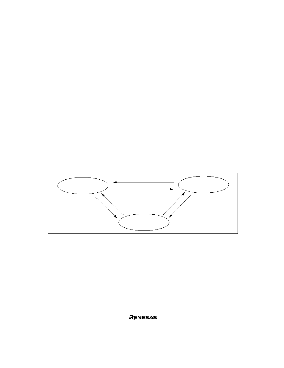
117
5.4.3
Interrupt Control Mode 1
Three-level masking is implemented for IRQ interrupts and on-chip supporting module interrupts
by means of the I and UI bits in the CPU's CCR, and ICR.
∑
Control level 0 interrupt requests are enabled when the I bit is cleared to 0, and disabled when
set to 1.
∑
Control level 1 interrupt requests are enabled when the I bit or UI bit is cleared to 0, and
disabled when both the I bit and the UI bit are set to 1.
For example, if the interrupt enable bit for an interrupt request is set to 1, and H'20, H'00, and H'00
are set in ICRA, ICRB, and ICRC, respectively, (i.e. IRQ2 and IRQ3 interrupts are set to control
level 1 and other interrupts to control level 0), the situation is as follows:
∑
When I = 0, all interrupts are enabled
(Priority order: NMI > IRQ2 > IRQ3 > IRQ0 ...)
∑
When I = 1 and UI = 0, only NMI, IRQ2, and IRQ3 interrupts are enabled
∑
When I = 1 and UI = 1, only NMI interrupts are enabled
Figure 5-6 shows the state transitions in these cases.
Only NMI interrupts enabled
All interrupts enabled
Exception handling execution
or I
1, UI
1
I
0
I
1, UI
0
I
0
UI
0
Exception handling execution
or UI
1
Only NMI, IRQ2, and
IRQ3 interrupts enabled
Figure 5-6 Example of State Transitions in Interrupt Control Mode 1
Figure 5-7 shows a flowchart of the interrupt acceptance operation in this case.

118
[1] If an interrupt source occurs when the corresponding interrupt enable bit is set to 1, an interrupt
request is sent to the interrupt controller.
[2] When interrupt requests are sent to the interrupt controller, a control level 1 interrupt,
according to the control level set in ICR, has priority for selection, and other interrupt requests
are held pending. If a number of interrupt requests with the same control level setting are
generated at the same time, the interrupt request with the highest priority according to the
priority system shown in table 5-4 is selected.
[3] The I bit is then referenced. If the I bit is cleared to 0, it is not affected by the UI bit.
An interrupt request set to interrupt control level 0 is accepted when the I bit is cleared to 0. If
the I bit is set to 1, only an NMI interrupt is accepted, and other interrupt requests are held
pending.
An interrupt request set to interrupt control level 1 has priority over an interrupt request set to
interrupt control level 0, and is accepted if the I bit is cleared to 0, or if the I bits is set to 1 and
the UI bit is cleared to 0.
When both the I bit and the UI bit are set to 1, only an NMI interrupt is accepted, and other
interrupt requests are held pending.
[4] When an interrupt request is accepted, interrupt exception handling starts after execution of the
current instruction has been completed.
[5] The PC and CCR are saved to the stack area by interrupt exception handling. The PC saved on
the stack shows the address of the first instruction to be executed after returning from the
interrupt handling routine.
[6] Next, the I and UI bits in CCR are set to 1. This masks all interrupts except NMI.
[7] A vector address is generated for the accepted interrupt, and execution of the interrupt handling
routine starts at the address indicated by the contents of that vector address.

119
Program execution status
Interrupt generated?
NMI
Control level 1
interrupt?
IRQ0
IRQ1
TEI2
IRQ0
IRQ1
TEI2
UI=0
Save PC and CCR
I
1, UI
1
Read vector address
Branch to interrupt handling routine
Yes
No
Yes
Yes
Yes
No
No
Yes
No
Yes
No
Yes
Yes
No
No
Yes
Yes
No
Hold pending
I=0
I=0
Yes
Yes
No
No
Figure 5-7 Flowchart of Procedure Up to Interrupt Acceptance
in Interrupt Control Mode 1

120
5.4.4
Interrupt Exception Handling Sequence
Figure 5-8 shows the interrupt exception handling sequence. The example shown is for the case
where interrupt control mode 0 is set in advanced mode, and the program area and stack area are
in on-chip memory.
(14)
(12)
(10)
(8)
(6)
(4)
(2)
(1)
(5)
(7)
(9)
(11)
(13)
Interrupt service
routine instruction
prefetch
Internal
operation
Vector fetch
Stack
Instruction
prefetch
Internal
operation
Interrupt
acceptance
Interrupt level determination
Wait for end of instruction
Interrupt
request signal
Internal
address bus
Internal
read signal
Internal
write signal
Internal
data bus
¯
(3)
(1)
(2) (4)
(3)
(5)
(7)
Instruction prefetch address (Not executed.
This is the contents of the saved PC, the return address.)
Instruction code (Not executed.)
Instruction prefetch address (Not executed.)
SP-2
SP-4
Saved PC and saved CCR
Vector address
Interrupt handling routine start address (vector
address contents)
Interrupt handling routine start address ((13) = (10) (12))
First instruction of interrupt handling routine
(6) (8)
(9) (11)
(10) (12)
(13)
(14)
Figure 5-8 Interrupt Exception Handling

121
5.4.5
Interrupt Response Times
The H8S/2245 Series is capable of fast word transfer instruction to on-chip memory, and the
program area is provided in on-chip ROM and the stack area in on-chip RAM, enabling high-
speed processing.
Table 5-8 shows interrupt response times - the interval between generation of an interrupt request
and execution of the first instruction in the interrupt handling routine. The execution status
symbols used in table 5-8 are explained in table 5-9.
Table 5-8
Interrupt Response Times
Normal Mode
Advanced Mode
No.
Execution Status
INTM1 = 0
INTM1 = 0
1
Interrupt priority determination
*
1
3
3
2
Number of wait states until executing
instruction ends
*
2
1 to 19+2∑S
I
1 to 19+2∑S
I
3
PC, CCR stack save
2∑S
K
2∑S
K
4
Vector fetch
S
I
2∑S
I
5
Instruction fetch
*
3
2∑S
I
2∑S
I
6
Internal processing
*
4
2
2
Total (using on-chip memory)
11 to 31
12 to 32
Notes: 1. Two states in case of internal interrupt.
2. Refers to MULXS and DIVXS instructions.
3. Prefetch after interrupt acceptance and interrupt handling routine prefetch.
4. Internal processing after interrupt acceptance and internal processing after vector fetch.
Table 5-9
Number of States in Interrupt Handling Routine Execution Statuses
Object of Access
External Device
8 Bit Bus
16 Bit Bus
Symbol
Internal
Memory
2-State
Access
3-State
Access
2-State
Access
3-State
Access
Instruction fetch
S
I
1
4
6+2m
2
3+m
Branch address read
S
J
Stack manipulation
S
K
Legend
m
: Number of wait states in an external device access.
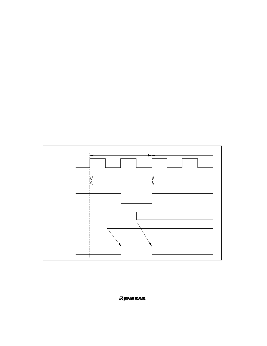
122
5.5
Usage Notes
5.5.1
Contention between Interrupt Generation and Disabling
When an interrupt enable bit is cleared to 0 to disable interrupts, the disabling becomes effective
after execution of the instruction.
In other words, when an interrupt enable bit is cleared to 0 by an instruction such as BCLR or
MOV, if an interrupt is generated during execution of the instruction, the interrupt concerned will
still be enabled on completion of the instruction, and so interrupt exception handling for that
interrupt will be executed on completion of the instruction. However, if there is an interrupt
request of higher priority than that interrupt, interrupt exception handling will be executed for the
higher-priority interrupt, and the lower-priority interrupt will be ignored.
The same also applies when an interrupt source flag is cleared.
Figure 5-9 shows and example in which the CMIEA bit in 8-bit timer TCR is cleared to 0.
Internal
address bus
Internal
write signal
¯
CMIEA
CMFA
CMIA
interrupt signal
TCR write cycle by CPU
CMIA exception handling
TCR address
Figure 5-9 Contention between Interrupt Generation and Disabling
The above contention will not occur if an enable bit or interrupt source flag is cleared to 0 while
the interrupt is masked.

123
5.5.2
Instructions that Disable Interrupts
Instructions that disable interrupts are LDC, ANDC, ORC, and XORC. After any of these
instructions is executed, all interrupts including NMI are disabled and the next instruction is
always executed. When the I bit or UI bit is set by one of these instructions, the new value
becomes valid two states after execution of the instruction ends.
5.5.3
Interrupts during Execution of EEPMOV Instruction
Interrupt operation differs between the EEPMOV.B instruction and the EEPMOV.W instruction.
With the EEPMOV.B instruction, an interrupt request (including NMI) issued during the transfer
is not accepted until the move is completed.
With the EEPMOV.W instruction, if an interrupt request is issued during the transfer, interrupt
exception handling starts at a break in the transfer cycle. The PC value saved on the stack in this
case is the address of the next instruction.
Therefore, if an interrupt is generated during execution of an EEPMOV.W instruction, the
following coding should be used.
L1: EEPMOV.W
MOV.W R4,R4
BNE L1
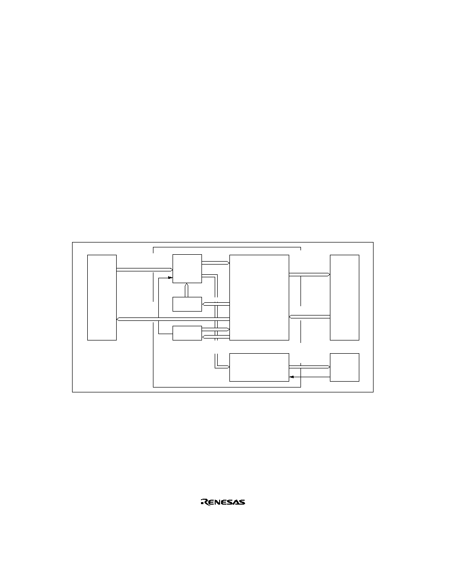
124
5.6
DTC Activation by Interrupt
5.6.1
Overview
The DTC can be activated by an interrupt. In this case, the following options are available:
∑
Interrupt request to CPU
∑
Activation request to DTC
∑
Selection of a number of the above
For details of interrupt requests that can be used with to activate the DTC, see section 7, Data
Transfer Controller.
5.6.2
Block Diagram
Figure 5-10 shows a block diagram of the DTC and interrupt controller.
Selection
circuit
DTCER
DTVECR
Control logic
CPU
DTC
DTC activation
request vector
number
Clear signal
CPU interrupt
request vector
number
Select
signal
Interrupt
request
Interrupt source
clear signal
IRQ
interrupt
On-chip
supporting
module
Clear signal
Interrupt controller
I, UI
SWDTE
clear signal
Determination of
priority
Figure 5-10 Interrupt Control for DTC

125
5.6.3
Operation
The interrupt controller has three main functions in DTC control.
(1) Selection of Interrupt Source: Interrupt sources can be specified as DTC activation requests
or CPU interrupt requests by means of the DTCE bit of DTCEA to DTCEF in the DTC.
After a DTC data transfer, the DTCE bit can be cleared to 0 and an interrupt request sent to the
CPU in accordance with the specification of the DISEL bit of MRB in the DTC.
When the DTC has performed the specified number of data transfers and the transfer counter value
is zero, the DTCE bit is cleared to 0 and an interrupt request is sent to the CPU after the DTC data
transfer.
(2) Determination of Priority: The DTC activation source is selected in accordance with the
default priority order, and is not affected by mask or priority levels. See section 7.3.3, DTC
Vector Table, for the respective priorities.
(3) Operation Order: If the same interrupt is selected as a DTC activation source and a CPU
interrupt source, the DTC data transfer is performed first, followed by CPU interrupt exception
handling.
Table 5-10 summarizes interrupt source selection and interrupt source clearance control according
to the settings of the DTCE bit of DTCEA to DTCEF in the DTC and the DISEL bit of MRB in
the DTC.
Table 5-10 Interrupt Source Selection and Clearing Control
Settings
DTC
Interrupt Source Selection/Clearing Control
DTCE
DISEL
DTC
CPU
0
*
X
1
0
X
1
Legend
: The relevant interrupt is used. Interrupt source clearing is performed.
(The CPU should clear the source flag in the interrupt handling routine.)
: The relevant interrupt is used. The interrupt source is not cleared.
X : The relevant bit cannot be used.
*
: Don't care
(4) Usage Note: SCI and A/D converter interrupt sources are cleared when the appropriate DTC
register is read or written to, and are independent of the DISEL bit.

127
Section 6 Bus Controller
6.1
Overview
The H8S/2245 Series has a built-in bus controller (BSC) that manages the external address space
divided into eight areas. The bus specifications, such as bus width and number of access states,
can be set independently for each area, enabling multiple memories to be connected easily.
The bus controller also has a bus arbitration function, and controls the operation of the internal bus
masters: the CPU, and data transfer controller (DTC).
6.1.1
Features
The features of the bus controller are listed below.
∑
Manages external address space in area units
In advanced mode, manages the external space as 8 areas of 128-kbytes/2-Mbytes
In normal mode, manages the external space as a single area
Bus specifications can be set independently for each area
Burst ROM interface can be set
∑
Basic bus interface
Chip select (
CS0 to CS3) can be output for areas 0 to 3
8-bit access or 16-bit access can be selected for each area
2-state access or 3-state access can be selected for each area
Program wait states can be inserted for each area
∑
Burst ROM interface
Burst ROM interface can be set for area 0
1-state or 2-state burst access can be selected
∑
Idle cycle insertion
An idle cycle can be inserted in case of an external read cycle between different areas
An idle cycle can be inserted in case of an external write cycle immediately after an
external read cycle
∑
Bus arbitration function
Includes a bus arbiter that arbitrates bus mastership among the CPU, and DTC
∑
Other features
External bus release function

128
6.1.2
Block Diagram
Figure 6-1 shows a block diagram of the bus controller.
Area decoder
Bus
controller
ABWCR
ASTCR
BCRH
BCRL
Internal
address bus
CS0
to
CS3
External bus control signals
BREQ
BACK
BREQO
Internal control
signals
Wait
controller
WCRH
WCRL
Bus mode signal
Bus arbiter
CPU bus request signal
DTC bus request signal
CPU bus acknowledge signal
DTC bus acknowledge signal
WAIT
Internal data bus
Figure 6-1 Block Diagram of Bus Controller

129
6.1.3
Pin Configuration
Table 6-1 summarizes the pins of the bus controller.
Table 6-1
Bus Controller Pins
Name
Symbol
I/O
Function
Address strobe
AS
Output
Strobe signal indicating that address output on
address bus is enabled.
Read
RD
Output
Strobe signal indicating that external space is
being read.
High write
HWR
Output
Strobe signal indicating that external space is
to be written, and upper half (D
15
to D
8
) of data
bus is enabled.
Low write
LWR
Output
Strobe signal indicating that external space is
to be written, and lower half (D
7
to D
0
) of data
bus is enabled.
Chip select 0
CS0
Output
Strobe signal indicating that area 0 is selected.
Chip select 1
CS1
Output
Strobe signal indicating that area 1 is selected.
Chip select 2
CS2
Output
Strobe signal indicating that area 2 is selected.
Chip select 3
CS3
Output
Strobe signal indicating that area 3 is selected.
Wait
WAIT
Input
Wait request signal when accessing external
3-state access space.
Bus request
BREQ
Input
Request signal that releases bus to external
device.
Bus request acknowledge
BACK
Output
Acknowledge signal indicating that bus has
been released.
Bus request output
BREQO
Output
External bus request signal used when internal
bus master accesses external space when
external bus is released.

130
6.1.4
Register Configuration
Table 6-2 summarizes the registers of the bus controller.
Table 6-2
Bus Controller Registers
Initial Value
Name
Abbreviation
R/W
Power-On
Reset
Manual
Reset
Address
*
1
Bus width control register
ABWCR
R/W
H'FF/H'00
*
2
Retained
H'FED0
Access state control register
ASTCR
R/W
H'FF
Retained
H'FED1
Wait control register H
WCRH
R/W
H'FF
Retained
H'FED2
Wait control register L
WCRL
R/W
H'FF
Retained
H'FED3
Bus control register H
BCRH
R/W
H'D0
Retained
H'FED4
Bus control register L
BCRL
R/W
H'3C
Retained
H'FED5
Notes: 1. Lower 16 bits of the address.
2. Determined by the MCU operating mode.

131
6.2
Register Descriptions
6.2.1
Bus Width Control Register (ABWCR)
7
ABW7
1
R/W
0
R/W
6
ABW6
1
R/W
0
R/W
5
ABW5
1
R/W
0
R/W
4
ABW4
1
R/W
0
R/W
3
ABW3
1
R/W
0
R/W
0
ABW0
1
R/W
0
R/W
2
ABW2
1
R/W
0
R/W
1
ABW1
1
R/W
0
R/W
Bit
Modes 1, 2, 3, 5, 6, 7
Initial value
R/W
Mode 4
Initial value
R/W
:
:
:
:
:
ABWCR is an 8-bit readable/writable register that designates each area for either 8-bit access or
16-bit access.
ABWCR sets the data bus width for the external memory space. The bus width for on-chip
memory and internal I/O registers is fixed regardless of the settings in ABWCR.
In normal mode, the settings of bits ABW7 to ABW1 have no effect on operation.
After a power-on reset and in hardware standby mode, ABWCR is initialized to H'FF in modes 1,
2, 3, and 5, 6, 7, and to H'00 in mode 4. It is not initialized by a manual reset or in software
standby mode.
Bits 7 to 0--Area 7 to 0 Bus Width Control (ABW7 to ABW0): These bits select whether the
corresponding area is to be designated for 8-bit access or 16-bit access. In normal mode, only part
of area 0 is enabled, and the ABW0 bit selects whether external space is to be designated for 8-bit
access or 16-bit access .
Bit n
ABWn
Description
0
Area n is designated for 16-bit access
1
Area n is designated for 8-bit access
(n = 7 to 0)

132
6.2.2
Access State Control Register (ASTCR)
7
AST7
1
R/W
6
AST6
1
R/W
5
AST5
1
R/W
4
AST4
1
R/W
3
AST3
1
R/W
0
AST0
1
R/W
2
AST2
1
R/W
1
AST1
1
R/W
Bit
Initial value
R/W
:
:
:
ASTCR is an 8-bit readable/writable register that designates each area as either a 2-state access
space or a 3-state access space.
ASTCR sets the number of access states for the external memory space. The number of access
states for on-chip memory and internal I/O registers is fixed regardless of the settings in ASTCR.
In normal mode, the settings of bits AST7 to AST1 have no effect on operation.
ASTCR is initialized to H'FF by a power-on reset and in hardware standby mode. It is not
initialized by a manual reset or in software standby mode.
Bits 7 to 0--Area 7 to 0 Access State Control (AST7 to AST0): These bits select whether the
corresponding area is to be designated as a 2-state access space or a 3-state access space. In
normal mode, only part of area 0 is enabled, and the AST0 bit selects whether external space is to
be designated for 2-state access or 3-state access.
Wait state insertion is enabled or disabled at the same time.
Bit n
ASTn
Description
0
Area n is designated for 2-state access
Wait state insertion in area n external space is disabled
1
Area n is designated for 3-state access
(Initial value)
Wait state insertion in area n external space is enabled
(n = 7 to 0)

133
6.2.3
Wait Control Registers H and L (WCRH, WCRL)
WCRH and WCRL are 8-bit readable/writable registers that select the number of program wait
states for each area.
In normal mode, only part of area is 0 is enabled, and bits W01 and W00 select the number of
program wait states for the external space . The settings of bits W71, W70 to W11, and W10 have
no effect on operation.
Program waits are not inserted in the case of on-chip memory or internal I/O registers.
WCRH and WCRL are initialized to H'FF by a power-on reset and in hardware standby mode.
They are not initialized by a manual reset or in software standby mode.
(1) WCRH
7
W71
1
R/W
6
W70
1
R/W
5
W61
1
R/W
4
W60
1
R/W
3
W51
1
R/W
0
W40
1
R/W
2
W50
1
R/W
1
W41
1
R/W
Bit
Initial value
R/W
:
:
:
Bits 7 and 6--Area 7 Wait Control 1 and 0 (W71, W70): These bits select the number of
program wait states when area 7 in external space is accessed while the AST7 bit in ASTCR is set
to 1.
Bit 7
Bit 6
W71
W70
Description
0
0
Program wait not inserted when external space area 7 is accessed
1
1 program wait state inserted when external space area 7 is accessed
1
0
2 program wait states inserted when external space area 7 is accessed
1
3 program wait states inserted when external space area 7 is accessed
(Initial value)

134
Bits 5 and 4--Area 6 Wait Control 1 and 0 (W61, W60): These bits select the number of
program wait states when area 6 in external space is accessed while the AST6 bit in ASTCR is set
to 1.
Bit 5
Bit 4
W61
W60
Description
0
0
Program wait not inserted when external space area 6 is accessed
1
1 program wait state inserted when external space area 6 is accessed
1
0
2 program wait states inserted when external space area 6 is accessed
1
3 program wait states inserted when external space area 6 is accessed
(Initial value)
Bits 3 and 2--Area 5 Wait Control 1 and 0 (W51, W50): These bits select the number of
program wait states when area 5 in external space is accessed while the AST5 bit in ASTCR is set
to 1.
Bit 3
Bit 2
W51
W50
Description
0
0
Program wait not inserted when external space area 5 is accessed
1
1 program wait state inserted when external space area 5 is accessed
1
0
2 program wait states inserted when external space area 5 is accessed
1
3 program wait states inserted when external space area 5 is accessed
(Initial value)
Bits 1 and 0--Area 4 Wait Control 1 and 0 (W41, W40): These bits select the number of
program wait states when area 4 in external space is accessed while the AST4 bit in ASTCR is set
to 1.
Bit 1
Bit 0
W41
W40
Description
0
0
Program wait not inserted when external space area 4 is accessed
1
1 program wait state inserted when external space area 4 is accessed
1
0
2 program wait states inserted when external space area 4 is accessed
1
3 program wait states inserted when external space area 4 is accessed
(Initial value)

135
(2) WCRL
7
W31
1
R/W
6
W30
1
R/W
5
W21
1
R/W
4
W20
1
R/W
3
W11
1
R/W
0
W00
1
R/W
2
W10
1
R/W
1
W01
1
R/W
Bit
Initial value
R/W
:
:
:
Bits 7 and 6--Area 3 Wait Control 1 and 0 (W31, W30): These bits select the number of
program wait states when area 3 in external space is accessed while the AST3 bit in ASTCR is set
to 1.
Bit 7
Bit 6
W31
W30
Description
0
0
Program wait not inserted when external space area 3 is accessed
1
1 program wait state inserted when external space area 3 is accessed
1
0
2 program wait states inserted when external space area 3 is accessed
1
3 program wait states inserted when external space area 3 is accessed
(Initial value)
Bits 5 and 4--Area 2 Wait Control 1 and 0 (W21, W20): These bits select the number of
program wait states when area 2 in external space is accessed while the AST2 bit in ASTCR is set
to 1.
Bit 5
Bit 4
W21
W20
Description
0
0
Program wait not inserted when external space area 2 is accessed
1
1 program wait state inserted when external space area 2 is accessed
1
0
2 program wait states inserted when external space area 2 is accessed
1
3 program wait states inserted when external space area 2 is accessed
(Initial value)

136
Bits 3 and 2--Area 1 Wait Control 1 and 0 (W11, W10): These bits select the number of
program wait states when area 1 in external space is accessed while the AST1 bit in ASTCR is set
to 1.
Bit 3
Bit 2
W11
W10
Description
0
0
Program wait not inserted when external space area 1 is accessed
1
1 program wait state inserted when external space area 1 is accessed
1
0
2 program wait states inserted when external space area 1 is accessed
1
3 program wait states inserted when external space area 1 is accessed
(Initial value)
Bits 1 and 0--Area 0 Wait Control 1 and 0 (W01, W00): These bits select the number of
program wait states when area 0 in external space is accessed while the AST0 bit in ASTCR is set
to 1.
Bit 1
Bit 0
W01
W00
Description
0
0
Program wait not inserted when external space area 0 is accessed
1
1 program wait state inserted when external space area 0 is accessed
1
0
2 program wait states inserted when external space area 0 is accessed
1
3 program wait states inserted when external space area 0 is accessed
(Initial value)

137
6.2.4
Bus Control Register H (BCRH)
7
ICIS1
1
R/W
6
ICIS0
1
R/W
5
BRSTRM
0
R/W
4
BRSTS1
1
R/W
3
BRSTS0
0
R/W
0
--
0
(R/W)
2
--
0
(R/W)
1
--
0
(R/W)
Bit
Initial value
R/W
:
:
:
BCRH is an 8-bit readable/writable register that selects enabling or disabling of idle cycle
insertion, and the memory interface for area 0.
BCRH is initialized to H'D0 by a power-on reset and in hardware standby mode. It is not
initialized by a manual reset or in software standby mode.
Bit 7--Idle Cycle Insert 1 (ICIS1): Selects whether or not one idle cycle state is to be inserted
between bus cycles when successive external read cycles are performed in different areas.
Bit 7
ICIS1
Description
0
Idle cycle not inserted in case of successive external read cycles in different areas.
1
Idle cycle inserted in case of successive external read cycles in different areas.
(Initial value)
Bit 6--Idle Cycle Insert 0 (ICIS0): Selects whether or not one idle cycle state is to be inserted
between bus cycles when successive external read and external write cycles are performed .
Bit 6
ICIS0
Description
0
Idle cycle not inserted in case of successive external read and external write cycles.
1
Idle cycle inserted in case of successive external read and external write cycles.
(Initial value)

138
Bit 5--Burst ROM Enable (BRSTRM): Selects whether area 0 is used as a burst ROM
interface. In normal mode, the selection can be made from the entire external space .
Bit 5
BRSTRM
Description
0
Area 0 is basic bus interface
(Initial value)
1
Area 0 is burst ROM interface
Bit 4--Burst Cycle Select 1 (BRSTS1): Selects the number of burst cycles for the burst ROM
interface.
Bit 4
BRSTS1
Description
0
Burst cycle comprises 1 state
1
Burst cycle comprises 2 states
(Initial value)
Bit 3--Burst Cycle Select 0 (BRSTS0): Selects the number of words that can be accessed in a
burst ROM interface burst access.
Bit 3
BRSTS0
Description
0
Max. 4 words in burst access
(Initial value)
1
Max. 8 words in burst access
Bits 2 to 0--Reserved: Only 0 should be written to these bits.

139
6.2.5
Bus Control Register L (BCRL)
7
BRLE
0
R/W
6
BREQOE
0
R/W
5
EAE
1
R/W
4
--
1
(R/W)
3
--
1
(R/W)
0
WAITE
0
R/W
2
ASS
1
R/W
1
--
0
(R/W)
Bit
Initial value
R/W
:
:
:
BCRL is an 8-bit readable/writable register that performs selection of the external bus release state
protocol, selection of the area partition unit and enabling or disabling of
WAIT pin input.
BCRL is initialized to H'3C by a power-on reset and in hardware standby mode. It is not
initialized by a manual reset or in software standby mode.
Bit 7--Bus Release Enable (BRLE): Enables or disables external bus release.
Bit 7
BRLE
Description
0
External bus release is disabled.
BREQ
,
BACK
, and
BREQO
can be used as I/O
ports.
(Initial value)
1
External bus release is enabled.
Bit 6--BREQO Pin Enable (BREQOE): Outputs a signal that requests the external bus master
to drop the bus request signal (
BREQ) in the external bus release state, when an internal bus
master performs an external space access.
Bit 6
BREQOE
Description
0
BREQO
output disabled.
BREQO
can be used as I/O port.
(Initial value)
1
BREQO
output enabled.

140
Bit 5--External Address Enable (EAE): Selects whether addresses H'010000 to H'01FFFF are
to be internal addresses or external addresses.
This setting is invalid in normal mode.
Bit 5
EAE
Description
0
Addresses H'010000 to H'01FFFF are in on-chip ROM (H8S/2246 and H8S/2245) or
a reserved area
*
(H8S/2244, H8S/2243, H8S/2242, and H8S/2241).
1
Addresses H'010000 to H'01FFFF are external addresses (external expansion mode)
or a reserved area
*
(single-chip mode).
(Initial value)
Note:
*
Reserved areas should not be accessed.
Bits 4 and 3--Reserved: Only 1 should be written to these bits.
Bit 2--Area Partition Unit Select (ASS): Selects the area partition unit.
Bit 2
ASS
Description
0
Area partition unit is 128 kbytes (1 Mbit)
1
Area partition unit is 2 Mbytes (16 Mbits)
(Initial value)
Bit 1--Reserved: Only 0 should be written to this bit.
Bit 0--WAIT Pin Enable (WAITE): Selects enabling or disabling of wait input by the
WAIT
pin.
Bit 0
WAITE
Description
0
Wait input by
WAIT
pin disabled.
WAIT
pin can be used as I/O port.
(Initial value)
1
Wait input by
WAIT
pin enabled
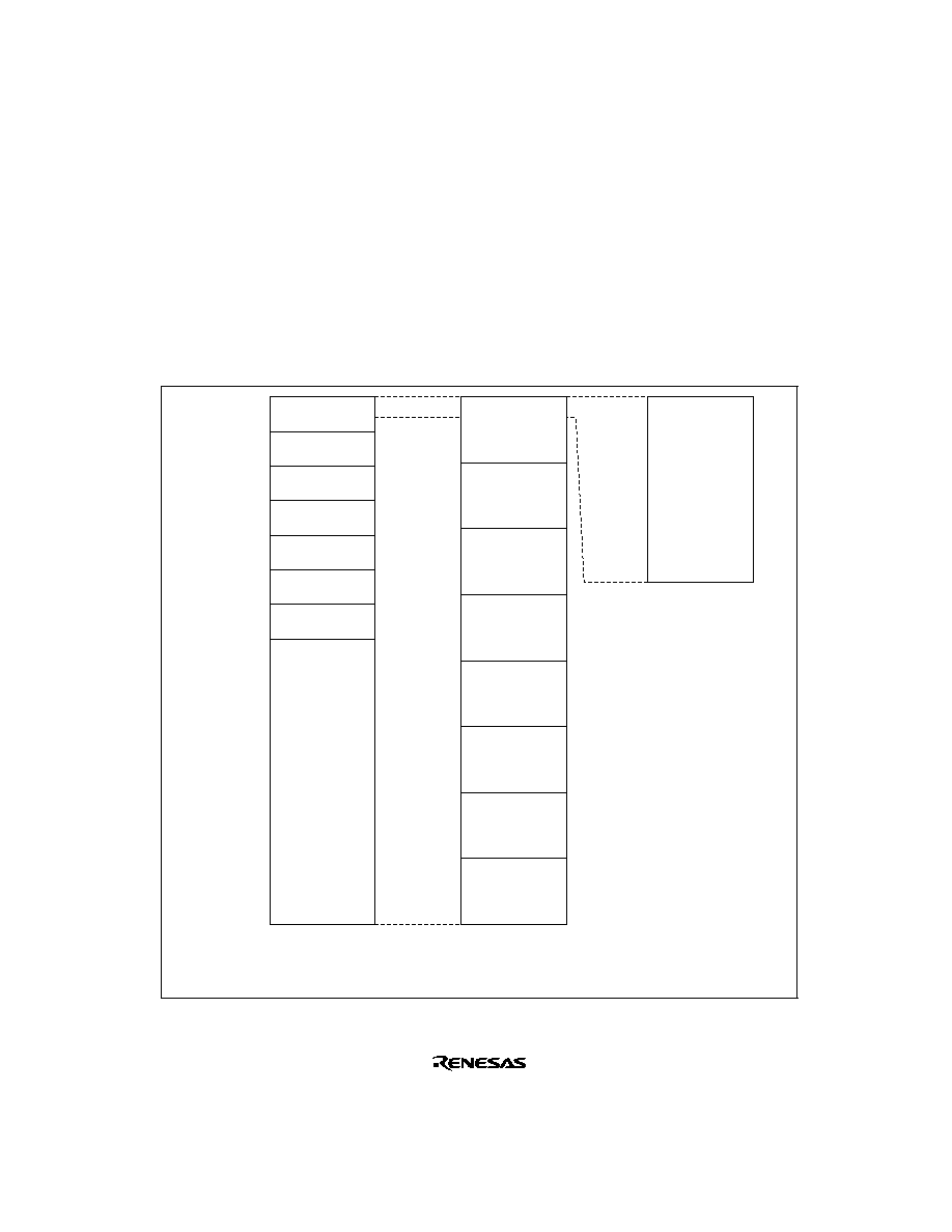
141
6.3
Overview of Bus Control
6.3.1
Area Partitioning
In advanced mode, the bus controller partitions the 16 Mbytes address space into eight areas, 0 to
7, in 128-kbyte or 2-Mbyte units, and performs bus control for external space in area units. In
normal mode, it controls a 64-kbyte address space comprising part of area 0. Figure 6-2 shows an
outline of the memory map.
Chip select signals (
CS0 to CS3) can be output for areas 0 to 3.
Area 0
(128kbytes)
H'000000
H'01FFFF
H'020000
H'03FFFF
H'040000
H'05FFFF
H'060000
H'07FFFF
H'080000
H'09FFFF
H'0A0000
H'0BFFFF
H'0C0000
H'0DFFFF
H'0E0000
Area 1
(128kbytes)
Area 2
(128kbytes)
Area 3
(128kbytes)
Area 4
(128kbytes)
Area 5
(128kbytes)
Area 6
(128kbytes)
Area 7
(15Mbytes)
H'FFFFFF
(1)
Area 0
(2Mbytes)
H'000000
H'FFFFFF
(2)
(3)
H'0000
H'1FFFFF
H'200000
Area 1
(2Mbytes)
H'3FFFFF
H'400000
Area 2
(2Mbytes)
H'5FFFFF
H'600000
Area 3
(2Mbytes)
H'7FFFFF
H'800000
Area 4
(2Mbytes)
H'9FFFFF
H'A00000
Area 5
(2Mbytes)
H'BFFFFF
H'C00000
Area 6
(2Mbytes)
H'DFFFFF
H'E00000
Area 7
(2Mbytes)
H'FFFF
Advanced mode
When ASS = 0
Advanced mode
When ASS = 1
Normal mode
Figure 6-2 Overview of Area Partitioning

142
6.3.2
Bus Specifications
The external space bus specifications consist of three elements: (1) bus width, (2) number of
access states, and (3) number of program wait states.
The bus width and number of access states for on-chip memory and internal I/O registers are
fixed, and are not affected by the bus controller.
(1) Bus Width: A bus width of 8 or 16 bits can be selected with ABWCR. An area for which an
8-bit bus is selected functions as an 8-bit access space, and an area for which a 16-bit bus is
selected functions as a16-bit access space.
If all areas are designated for 8-bit access, 8-bit bus mode is set; if any area is designated for 16-bit
access, 16-bit bus mode is set. When the burst ROM interface is designated, 16-bit bus mode is
always set.
(2) Number of Access States: Two or three access states can be selected with ASTCR. An area
for which 2-state access is selected functions as a 2-state access space, and an area for which 3-
state access is selected functions as a 3-state access space.
With the burst ROM interface, the number of states is one or two regardless of the ASTCR setting.
When 2-state access space is designated, wait insertion is disabled.
(3) Number of Program Wait States: When 3-state access space is designated by ASTCR, the
number of program wait states to be inserted automatically is selected with WCRH and WCRL.
From 0 to 3 program wait states can be selected.
Table 6-3 shows the bus specifications for each basic bus interface area.

143
Table 6-3
Bus Specifications for Each Area (Basic Bus Interface)
ABWCR
ASTCR
WCRH
WCRL
Bus Specifications (Basic Bus Interface)
ABWn
ASTn
Wn1
Wn0
Bus Width
Access States
Program Wait
States
0
0
--
--
16
2
0
1
0
0
3
0
1
1
1
0
2
1
3
1
0
--
--
8
2
0
1
0
0
3
0
1
1
1
0
2
1
3
6.3.3
Memory Interfaces
The H8S/2245 Series memory interfaces comprise a basic bus interface that allows direct
connection of ROM, SRAM, and so on; and a burst ROM interface that allows direct connection
of burst ROM.
An area for which the basic bus interface is designated functions as normal space, and an area for
which the burst ROM interface is designated functions as burst ROM space.

144
6.3.4
Advanced Mode
The initial state of each area is basic bus interface, 3-state access space. The initial bus width is
selected according to the operating mode. The bus specifications described here cover basic items
only, and the sections on each memory interface should be referred to for further details.
Area 0: Area 0 includes on-chip ROM, and in ROM-disabled expansion mode, all of area 0 is
external space. In ROM-enabled expansion mode, the space excluding on-chip ROM is external
space.
When area 0 external space is accessed, the
CS0 signal can be output.
Either basic bus interface or burst ROM interface can be selected for area 0.
The size of area 0 is switched between 128 kbytes and 2 Mbytes according to the state of the ASS
bit.
Areas 1 to 6: In external expansion mode, all of area 1 to 6 is external space.
When area 1 to 3 external space is accessed, the
CS1 and CS3 pin signals respectively can be
output.
Only the basic bus interface can be used for areas 1 and 6.
The size of areas 1 to 6 is switched between 128 kbytes and 2 Mbytes according to the state of the
ASS bit.
Area 7: Area 7 includes the on-chip RAM and internal I/O registers. In external expansion mode,
the space excluding the on-chip RAM and internal I/O registers is external space. The on-chip
RAM is enabled when the RAME bit in the system control register (SYSCR) is set to 1; when the
RAME bit is cleared to 0, the on-chip RAM is disabled and the corresponding space becomes
external space.
Only the basic bus interface can be used for the area 7.
The size of area 7 is switched between 15 Mbytes and 2 Mbytes according to the state of the ASS
bit.

145
6.3.5
Areas in Normal Mode
In normal mode, a 64-kbyte address space comprising part of area 0 is controlled. Area
partitioning is not performed in normal mode. In ROM-disabled expansion mode, the space
excluding the on-chip RAM and internal I/O registers is external space. In ROM-enabled
expansion mode the space excluding the on-chip ROM, on-chip RAM, and internal I/O registers is
external space. The on-chip RAM is enabled when the RAME bit in the system control register
(SYSCR) is set to 1; when the RAME bit is cleared to 0, the on-chip RAM is disabled and the
corresponding addresses become external space .
When external space is accessed, the
CS0 signal can be output.
In normal mode, the basic bus interface or burst ROM interface can be selected.

146
6.3.6
Chip Select Signals
The H8S/2245 Series can output chip select signals (
CS0 to CS3) to areas 0 to 3, the signal being
driven low when the corresponding external space area is accessed. In normal mode, only the
CS0
signal can be output.
Figure 6-3 shows an example of
CSn (n = 0 to 3) output timing.
Enabling or disabling of the
CSn signal is performed by setting the data direction register (DDR)
for the port corresponding to the particular
CSn pin.
In ROM-disabled expansion mode, the
CS0 pin is placed in the output state after a power-on reset.
Pins
CS1 to CS3 are placed in the input state after a power-on reset, and so the corresponding
DDR should be set to 1 when outputting signals
CS1 to CS3.
In ROM-enabled expansion mode, pins
CS0 to CS3 are all placed in the input state after a power-
on reset, and so the corresponding DDR should be set to 1 when outputting signals
CS0 to CS3.
For details, see section 8, I/O Ports.
Bus cycle
T
1
T
2
T
3
Area n external address
Address bus
¯
CSn
Figure 6-3 CSn Signal Output Timing (n = 0 to 3)
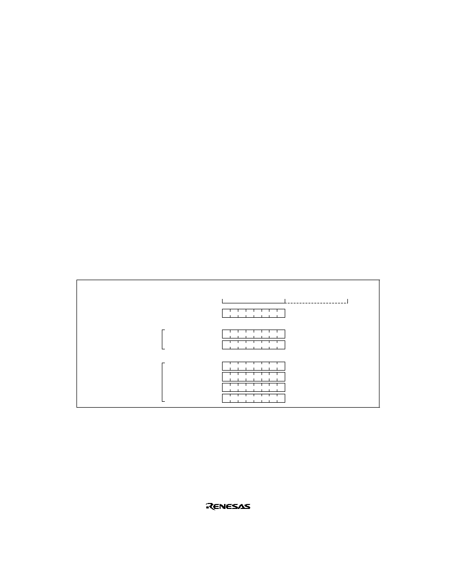
147
6.4
Basic Bus Interface
6.4.1
Overview
The basic bus interface enables direct connection of ROM, SRAM, and so on.
The bus specifications can be selected with ABWCR, ASTCR, WCRH, and WCRL (see table 6-
3).
6.4.2
Data Size and Data Alignment
Data sizes for the CPU and other internal bus masters are byte, word, and longword. The bus
controller has a data alignment function, and when accessing external space, controls whether the
upper data bus (D
15
to D
8
) or lower data bus (D
7
to D
0
) is used according to the bus specifications
for the area being accessed (8-bit access space or 16-bit access space) and the data size.
8-Bit Access Space: Figure 6-4 illustrates data alignment control for the 8-bit access space. With
the 8-bit access space, the upper data bus (D
15
to D
8
) is always used for accesses. The amount of
data that can be accessed at one time is one byte: a word transfer instruction is performed as two
byte accesses, and a longword transfer instruction, as four byte accesses.
D
15
D
8
D
7
D
0
Upper data bus
Lower data bus
Byte size
Word size
1st bus cycle
2nd bus cycle
Longword size
1st bus cycle
2nd bus cycle
3rd bus cycle
4th bus cycle
Figure 6-4 Access Sizes and Data Alignment Control (8-Bit Access Space)
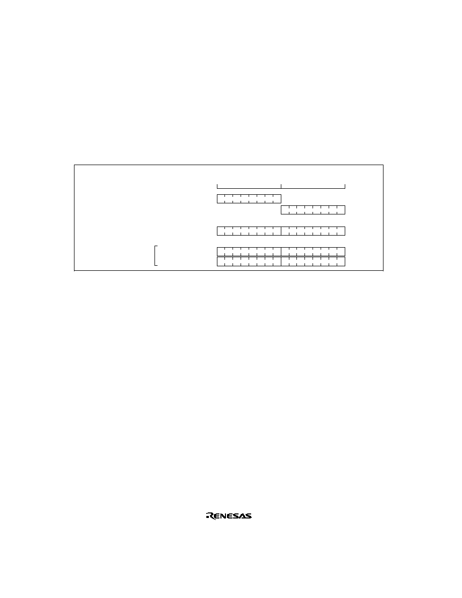
148
16-Bit Access Space: Figure 6-5 illustrates data alignment control for the 16-bit access space.
With the 16-bit access space, the upper data bus (D
15
to D
8
) and lower data bus (D
7
to D
0
) are used
for accesses. The amount of data that can be accessed at one time is one byte or one word, and a
longword transfer instruction is executed as two word transfer instructions.
In byte access, whether the upper or lower data bus is used is determined by whether the address is
even or odd. The upper data bus is used for an even address, and the lower data bus for an odd
address.
D
15
D
8
D
7
D
0
Upper data bus
Byte size
Word size
1st bus cycle
2nd bus cycle
Longword
size
∑ Even address
Byte size
∑ Odd address
Lower data bus
Figure 6-5 Access Sizes and Data Alignment Control (16-Bit Access Space)

149
6.4.3
Valid Strobes
Table 6-4 shows the data buses used and valid strobes for the access spaces.
In a read, the
RD signal is valid without discrimination between the upper and lower halves of the
data bus.
In a write, the
HWR signal is valid for the upper half of the data bus, and the LWR signal for the
lower half.
Table 6-4
Data Buses Used and Valid Strobes
Area
Access
Size
Read/
Write
Address
Valid
Strobe
Upper Data Bus
(D
15
to D
8
)
Lower data bus
(D
7
to D
0
)
8-bit access
Byte
Read
--
RD
Valid
Invalid
space
Write
--
HWR
Hi-Z
16-bit access
Byte
Read
Even
RD
Valid
Invalid
space
Odd
Invalid
Valid
Write
Even
HWR
Valid
Hi-Z
Odd
LWR
Hi-Z
Valid
Word
Read
--
RD
Valid
Valid
Write
--
HWR
,
LWR
Valid
Valid
Note:
Invalid: Input state; input value is ignored.
Hi-Z: High impedance.
150
6.4.4
Basic Timing
(1) 8-Bit 2-State Access Space: Figure 6-6 shows the bus timing for an 8-bit 2-state access space.
When an 8-bit access space is accessed , the upper half (D
15
to D
8
) of the data bus is used.
The
LWR pin is fixed high. Wait states cannot be inserted.
Bus cycle
T
1
T
2
Address bus
¯
CSn
AS
RD
D
15
to D
8
Valid
D
7
to D
0
Invalid
Read
HWR
LWR
D
15
to D
8
Valid
D
7
to D
0
High impedance
Write
Note: n = 0 to 3
High
Figure 6-6 Bus Timing for 8-Bit 2-State Access Space
151
(2) 8-Bit 3-State Access Space: Figure 6-7 shows the bus timing for an 8-bit 3-state access
space. When an 8-bit access space is accessed, the upper half (D
15
to D
8
) of the data bus is used.
The
LWR pin is fixed high. Wait states can be inserted.
Bus cycle
T
1
T
2
Address bus
¯
CSn
AS
RD
D
15
to D
8
Valid
D
7
to D
0
Invalid
Read
HWR
LWR
D
15
to D
8
Valid
D
7
to D
0
High impedance
Write
High
Note: n = 0 to 3
T
3
Figure 6-7 Bus Timing for 8-Bit 3-State Access Space

152
(3) 16-Bit 2-State Access Space: Figures 6-8 to 6-10 show bus timings for a 16-bit 2-state access
space. When a 16-bit access space is accessed, the upper half (D
15
to D
8
) of the data bus is used
for the even address, and the lower half (D
7
to D
0
) for the odd address.
Wait states cannot be inserted.
Bus cycle
T
1
T
2
Address bus
¯
CSn
AS
RD
D
15
to D
8
Valid
D
7
to D
0
Invalid
Read
HWR
LWR
D
15
to D
8
Valid
D
7
to D
0
High impedance
Write
High
Note: n = 0 to 3
Figure 6-8 Bus Timing for 16-Bit 2-State Access Space (1) (Even Address Byte Access)

153
Bus cycle
T
1
T
2
Address bus
¯
CSn
AS
RD
D
15
to D
8
Invalid
D
7
to D
0
Valid
Read
HWR
LWR
D
15
to D
8
High impedance
D
7
to D
0
Valid
Write
Note: n = 0 to 3
High
Figure 6-9 Bus Timing for 16-Bit 2-State Access Space (2) (Odd Address Byte Access)
154
Bus cycle
T
1
T
2
Address bus
¯
CSn
AS
RD
D
15
to D
8
Valid
D
7
to D
0
Valid
Read
HWR
LWR
D
15
to D
8
Valid
D
7
to D
0
Valid
Write
Note: n = 0 to 3
Figure 6-10 Bus Timing for 16-Bit 2-State Access Space (3) (Word Access)

155
(4) 16-Bit 3-State Access Space: Figures 6-11 to 6-13 show bus timings for a 16-bit 3-state
access space. When a 16-bit access space is accessed, the upper half (D
15
to D
8
) of the data bus is
used for the odd address, and the lower half (D
7
to D
0
) for the even address.
Wait states can be inserted.
Bus cycle
T
1
T
2
Address bus
¯
CSn
AS
RD
D
15
to D
8
Valid
D
7
to D
0
Invalid
Read
HWR
LWR
D
15
to D
8
Valid
D
7
to D
0
High impedance
Write
High
Note: n = 0 to 3
T
3
Figure 6-11 Bus Timing for 16-Bit 3-State Access Space (1) (Even Address Byte Access)
156
Bus cycle
T
1
T
2
Address bus
¯
CSn
AS
RD
D
15
to
D
8
Invalid
D
7
to
D
0
Valid
Read
HWR
LWR
D
15
to
D
8
High impedance
D
7
to
D
0
Valid
Write
High
Note: n = 0 to 3
T
3
Figure 6-12 Bus Timing for 16-Bit 3-State Access Space (2) (Odd Address Byte Access)

157
Bus cycle
T
1
T
2
Address bus
¯
CSn
AS
RD
D
15
to D
8
Valid
D
7
to D
0
Valid
Read
HWR
LWR
D
15
to D
8
Valid
D
7
to D
0
Valid
Write
Note: n = 0 to 3
T
3
Figure 6-13 Bus Timing for 16-Bit 3-State Access Space (3) (Word Access)

158
6.4.5
Wait Control
When accessing external space, the H8S/2245 Series can extend the bus cycle by inserting one or
more wait states (T
w
). There are two ways of inserting wait states: (1) program wait insertion and
(2) pin wait insertion using the
WAIT pin.
(1) Program Wait Insertion
From 0 to 3 wait states can be inserted automatically between the T
2
state and T
3
state on an
individual area basis in 3-state access space, according to the settings of WCRH and WCRL.
(2) Pin Wait Insertion Using
WAIT Pin
Setting the WAITE bit in BCRL to 1 enables wait insertion by means of the
WAIT pin. Program
wait insertion is first carried out according to the settings in WCRH and WCRL. Then, if the
WAIT pin is low at the falling edge of ¯ in the last T
2
or T
w
state, a T
w
state is inserted. If the
WAIT pin is held low, T
w
states are inserted until it goes high.
This is useful when inserting four or more T
w
states, or when changing the number of T
w
states for
different external devices.
The WAITE bit setting applies to all areas.
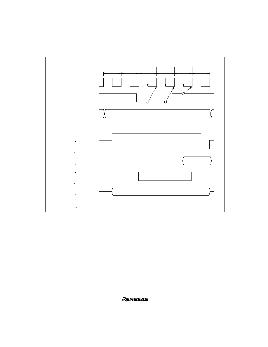
159
Figure 6-14 shows an example of wait state insertion timing.
By program wait
T
1
Address bus
¯
AS
RD
Data bus
Read data
Read
HWR
,
LWR
Write data
Write
Note: indicates the timing of
WAIT
pin sampling.
WAIT
Data bus
T
2
T
w
T
w
T
w
T
3
By
WAIT
pin
Figure 6-14 Example of Wait State Insertion Timing
The settings after a power-on reset are: 3-state access, 3 program wait state insertion, and WAIT
input disabled. When a manual reset is performed, the contents of bus controller registers are
retained, and the wait control settings remain the same as before the reset.

160
6.5
Burst ROM Interface
6.5.1
Overview
With the H8S/2245 Series, external space area 0 can be designated as burst ROM space, and burst
ROM interfacing can be performed. The burst ROM space interface enables 16-bit configuration
ROM with burst access capability to be accessed at high speed.
Area 0 can be designated as burst ROM space by means of the BRSTRM bit in BCRH.
Consecutive burst accesses of a maximum of 4 words or 8 words can be performed for CPU
instruction fetches only. One or two states can be selected for burst access.
6.5.2
Basic Timing
The number of states in the initial cycle (full access) of the burst ROM interface is in accordance
with the setting of the AST0 bit in ASTCR. Also, when the AST0 bit is set to 1, wait state
insertion is possible. One or two states can be selected for the burst cycle, according to the setting
of the BRSTS1 bit in BCRH. Wait states cannot be inserted. When area 0 is designated as burst
ROM space, it becomes 16-bit access space regardless of the setting of the ABW0 bit in ABWCR.
When the BRSTS0 bit in BCRH is cleared to 0, burst access of up to 4 words is performed; when
the BRSTS0 bit is set to 1, burst access of up to 8 words is performed.
The basic access timing for burst ROM space is shown in figure 6-15 (a) and (b). The timing
shown in figure 6-15 (a) is for the case where the AST0 and BRSTS1 bits are both set to 1, and
that in figure 6-15 (b) is for the case where both these bits are cleared to 0.
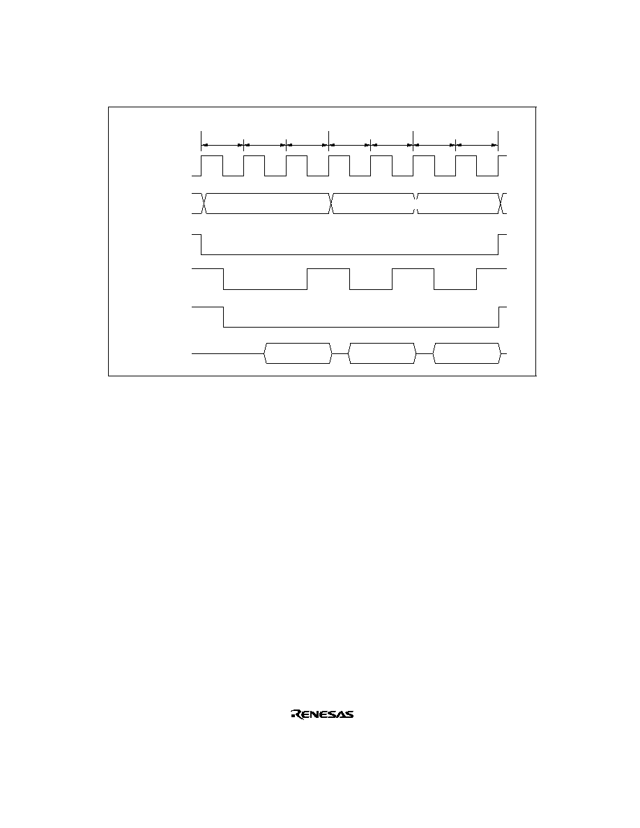
161
T
1
Address bus
¯
CS0
AS
Data bus
T
2
T
3
T
1
T
2
T
1
Full access
T
2
RD
Burst access
Only lower address changed
Read data
Read data
Read data
Figure 6-15 (a) Example of Burst ROM Access Timing (When AST0 = BRSTS1 = 1)

162
T
1
Address bus
¯
CS0
AS
Data bus
T
2
T
1
T
1
Full access
RD
Burst access
Only lower address changed
Read data
Read data Read data
Figure 6-15 (b) Example of Burst ROM Access Timing (When AST0 = BRSTS1 = 0)
6.5.3
Wait Control
As with the basic bus interface, either program wait insertion or pin wait insertion using the
WAIT
pin can be used in the initial cycle (full access) of the burst ROM interface. See section 6.4.5, Wait
Control.
Wait states cannot be inserted in a burst cycle.
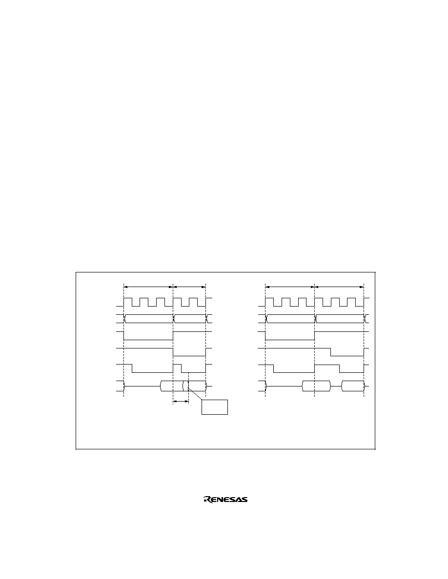
163
6.6
Idle Cycle
6.6.1
Operation
When the H8S/2245 Series accesses external space , it can insert a 1-state idle cycle (T
I
) between
bus cycles in the following two cases: (1) when read accesses between different areas occur
consecutively, and (2) when a write cycle occurs immediately after a read cycle. By inserting an
idle cycle it is possible, for example, to avoid data collisions between ROM, with a long output
floating time, and high-speed memory, I/O interfaces, and so on.
(1) Consecutive Reads between Different Areas
If consecutive reads between different areas occur while the ICIS1 bit in BCRH is set to 1, an idle
cycle is inserted at the start of the second read cycle. This is enabled in advanced mode.
Figure 6-16 shows an example of the operation in this case. In this example, bus cycle A is a read
cycle from ROM with a long output floating time, and bus cycle B is a read cycle from SRAM,
each being located in a different area. In (a), an idle cycle is not inserted, and a collision occurs in
cycle B between the read data from ROM and that from SRAM. In (b), an idle cycle is inserted,
and a data collision is prevented.
T
1
Address bus
¯
RD
Bus cycle A
,
Data bus
T
2
T
3
T
1
T
2
Bus cycle B
Bus cycle A
Bus cycle B
Long output
floating time
Data
collision
(a) Idle cycle not inserted
(ICIS1 = 0)
(b) Idle cycle inserted
(Initial value ICIS1 = 1)
T
1
Address bus
¯
RD
Data bus
T
2
T
3
T
I
T
1
T
2
CS
(area A)
CS
(area B)
CS
(area A)
CS
(area B)
Figure 6-16 Example of Idle Cycle Operation (1)
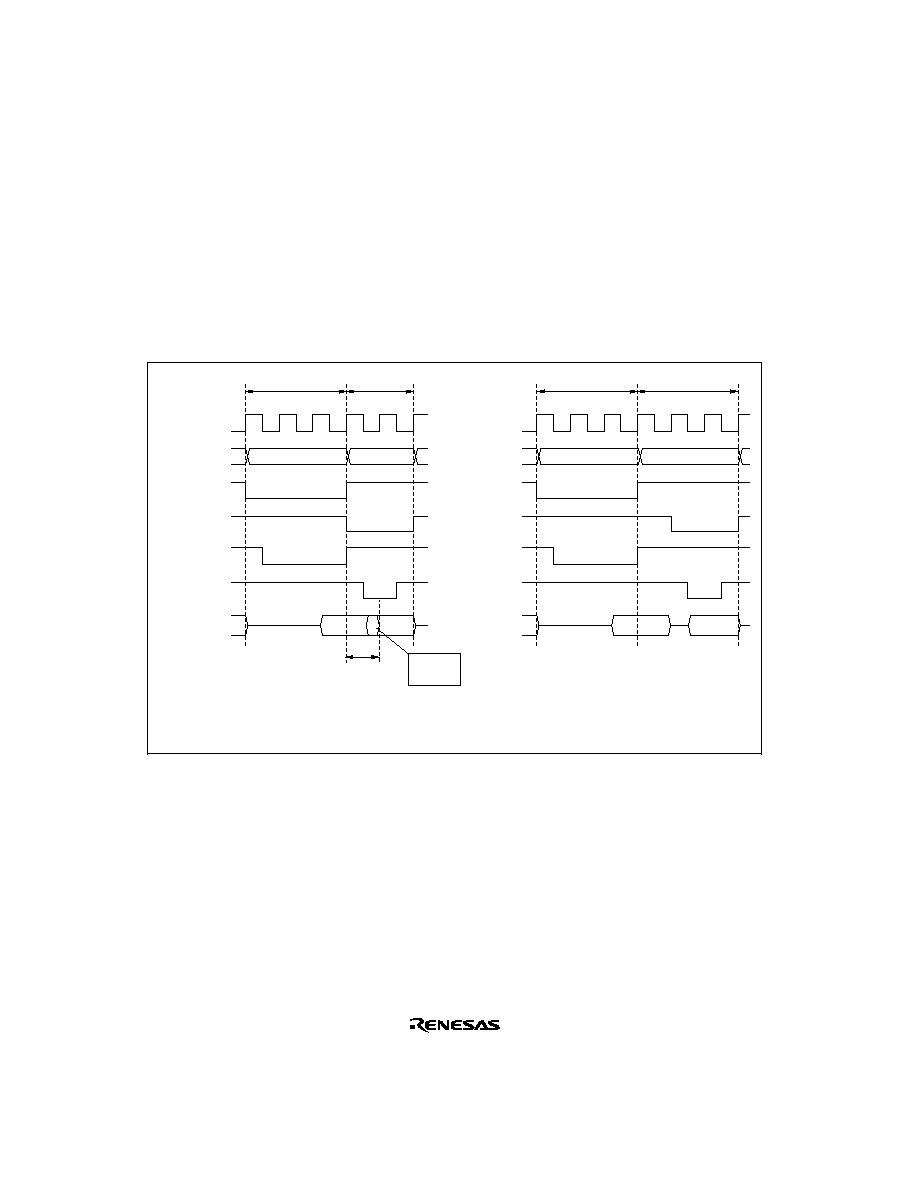
164
(2) Write after Read
If an external write occurs after an external read while the ICIS0 bit in BCRH is set to 1, an idle
cycle is inserted at the start of the write cycle. This is enabled in advanced mode and normal
mode.
Figure 6-17 shows an example of the operation in this case. In this example, bus cycle A is a read
cycle from ROM with a long output floating time, and bus cycle B is a CPU write cycle. In (a), an
idle cycle is not inserted, and a collision occurs in cycle B between the read data from ROM and
the CPU write data. In (b), an idle cycle is inserted, and a data collision is prevented.
T
1
Address bus
¯
RD
Bus cycle A
,
Data bus
T
2
T
3
T
1
T
2
Bus cycle B
Long output
floating time
Data
collision
T
1
Address bus
¯
RD
Bus cycle A
Data bus
T
2
T
3
T
I
T
1
Bus cycle B
T
2
HWR
HWR
CS
(area A)
CS
(area B)
CS
(area A)
CS
(area B)
(a) Idle cycle not inserted
(ICIS0 = 0)
(b) Idle cycle inserted
(Initial value ICIS0 = 1)
Figure 6-17 Example of Idle Cycle Operation (2)
165
(3) Relationship between Chip Select (
CS) Signal and Read (RD) Signal
Depending on the system's load conditions, the
RD signal may lag behind the CS signal. An
example is shown in figure 6.18.
In this case, with the setting for no idle cycle insertion (a), there may be a period of overlap
between the bus cycle A
RD signal and the bus cycle B CS signal.
Setting idle cycle insertion, as in (b), however, will prevent any overlap between the
RD and CS
signals.
In the initial state after reset release, idle cycle insertion (b) is set.
T
1
Address bus
¯
RD
Bus cycle A
T
2
T
3
T
1
T
2
Bus cycle B
Possibility of overlap between
CS
(area B) and
RD
T
1
Address bus
¯
Bus cycle A
T
2
T
3
T
I
T
1
Bus cycle B
T
2
CS
(area A)
CS
(area B)
RD
CS
(area A)
CS
(area B)
(a) Idle cycle not inserted
(ICIS1 = 0)
(b) Idle cycle inserted
(Initial value ICIS1 = 1)
Figure 6.18 Relationship between Chip Select (
CS) and Read (RD)

166
6.6.2
Pin States in Idle Cycle
Table 6-5 shows pin states in an idle cycle.
Table 6-5
Pin States in Idle Cycle
Pins
Pin State
A
23
to A
0
Contents of next bus cycle
D
15
to D
0
High impedance
CSn
High
AS
High
RD
High
HWR
High
LWR
High

167
6.7
Bus Release
6.7.1
Overview
The H8S/2245 Series can release the external bus in response to a bus request from an external
device. In the external bus released state, the internal bus master continues to operate as long as
there is no external access.
If an internal bus master wants to make an external access in the external bus released state, it can
issue a bus request off-chip.
6.7.2
Operation
In external expansion mode, the bus can be released to an external device by setting the BRLE bit
in BCRL to 1. Driving the
BREQ pin low issues an external bus request to the H8S/2245 Series.
When the
BREQ pin is sampled, at the prescribed timing the BACK pin is driven low, and the
address bus, data bus, and bus control signals are placed in the high-impedance state, establishing
the external bus-released state.
In the external bus released state, an internal bus master can perform accesses using the internal
bus. When an internal bus master wants to make an external access, it temporarily defers
activation of the bus cycle, and waits for the bus request from the external bus master to be
dropped.
If the BREQOE bit in BCRL is set to 1, when an internal bus master wants to make an external
access in the external bus released state, the
BREQO pin is driven low and a request can be made
off-chip to drop the bus request.
When the
BREQ pin is driven high, the BACK pin is driven high at the prescribed timing and the
external bus released state is terminated.
In the event of simultaneous external bus release request, and external access request generation,
the order of priority is as follows:
(High) External bus release > Internal bus master external access (Low)

168
6.7.3
Pin States in External Bus Released State
Table 6-6 shows pin states in the external bus released state.
Table 6-6
Pin States in Bus Released State
Pins
Pin State
A
23
to A
0
High impedance
D
15
to D
0
High impedance
CSn
High impedance
AS
High impedance
RD
High impedance
HWR
High impedance
LWR
High impedance

169
6.7.4
Transition Timing
Figure 6-19 shows the timing for transition to the bus-released state.
CPU
cycle
External bus released state
CPU cycle
Address
Minimum
1 state
T
0
T
1
T
2
¯
Address bus
Data bus
AS
HWR
,
LWR
BREQ
BACK
High impedance
[1]
[2]
[3]
[4]
[5]
[1]
Low level of
BREQ
pin is sampled at rise of T
2
state.
[2]
BACK
pin is driven low at end of CPU read cycle, releasing bus to external bus master.
[3]
BREQ
pin state is still sampled in external bus released state.
[4]
High level of
BREQ
pin is sampled.
[5]
BACK
pin is driven high, ending bus release cycle.
High impedance
High impedance
High impedance
RD
High impedance
Figure 6-19 Bus-Released State Transition Timing

170
6.7.5
Usage Note
When MSTPCR has been set to H'FFFF or H'EFFF and a transition has been made to sleep mode,
the external bus release function is stopped. If the external bus release function is to be used in
sleep mode, H'FFFF or H'EFFF should not be set in MSTPCR.
6.8
Bus Arbitration
6.8.1
Overview
The H8S/2245 Series has a bus arbiter that arbitrates bus master operations.
There are two bus masters, the CPU and DTC, which perform read/write operations when they
have possession of the bus. Each bus master requests the bus by means of a bus request signal. The
bus arbiter determines priorities at the prescribed timing, and permits use of the bus by means of a
bus request acknowledge signal. The selected bus master then takes possession of the bus and
begins its operation.
6.8.2
Operation
The bus arbiter detects the bus masters' bus request signals, and if the bus is requested, sends a bus
request acknowledge signal to the bus master making the request. If there are bus requests from
more than one bus master, the bus request acknowledge signal is sent to the one with the highest
priority. When a bus master receives the bus request acknowledge signal, it takes possession of the
bus until that signal is canceled.
The order of priority of the bus masters is as follows:
(High)
DTC
>
CPU
(Low)
An internal bus access by an internal bus master, and external bus release, can be executed in
parallel.
In the event of simultaneous external bus release request, and internal bus master external access
request generation, the order of priority is as follows:
(High) External bus release > Internal bus master external access (Low)

171
6.8.3
Bus Transfer Timing
Even if a bus request is received from a bus master with a higher priority than that of the bus
master that has acquired the bus and is currently operating, the bus is not necessarily transferred
immediately. There are specific times at which each bus master can relinquish the bus.
CPU: The CPU is the lowest-priority bus master, and if a bus request is received from the DTC,
the bus arbiter transfers the bus to the bus master that issued the request. The timing for transfer of
the bus is as follows:
∑
The bus is transferred at a break between bus cycles. However, if a bus cycle is executed in
discrete operations, as in the case of a longword-size access, the bus is not transferred between
the operations.
∑
If the CPU is in sleep mode, it transfers the bus immediately.
DTC: The DTC sends the bus arbiter a request for the bus when an activation request is generated.
The DTC can release the bus after a vector read, a register information read (3 states), a single data
transfer, or a register information write (3 states). It does not release the bus during a register
information read (3 states), a single data transfer, or a register information write (3 states).
6.8.4
External Bus Release Usage Note
External bus release can be performed on completion of an external bus cycle. The
RD signal
remains low until the end of the external bus cycle. Therefore, when external bus release is
performed, the
RD signal may change from the low level to the high-impedance state.
6.9
Resets and the Bus Controller
In a power-on reset, the H8S/2245, including the bus controller, enters the reset state at that point,
and an executing bus cycle is discontinued.
In a manual reset, the bus controller's registers and internal state are maintained, and an executing
external bus cycle is completed. In this case,
WAIT input is ignored and write data is not
guaranteed.

173
Section 7 Data Transfer Controller
7.1
Overview
The H8S/2245 Series includes a data transfer controller (DTC). The DTC can be activated by an
interrupt or software, to transfer data.
7.1.1
Features
∑
Transfer possible over any number of channels
Transfer information is stored in memory
One activation source can trigger a number of data transfers (chain transfer)
∑
Wide range of transfer modes
Normal, repeat, and block transfer modes available
Incrementing, decrementing, and fixing of source and destination addresses can be selected
∑
Direct specification of 16-Mbyte address space possible
24-bit transfer source and destination addresses can be specified
∑
Transfer can be set in byte or word units
∑
A CPU interrupt can be requested for the interrupt that activated the DTC
An interrupt request can be issued to the CPU after one data transfer ends
An interrupt request can be issued to the CPU after the specified data transfers have
completely ended
∑
Activation by software is possible
∑
Module stop mode can be set
The initial setting enables DTC registers to be accessed. DTC operation is halted by setting
module stop mode.
174
7.1.2
Block Diagram
Figure 7-1 shows a block diagram of the DTC.
The DTC's register information is stored in the on-chip RAM*. A 32-bit bus connects the DTC to
the on-chip RAM (1 kbyte), enabling 32-bit/1-state reading and writing of the DTC register
information and hence helping to increase processing speed.
Note: * When the DTC is used, the RAME bit SYSCR must be set to 1.
Interrupt
request
Interrupt controller
DTC
Internal address bus
DTC service
request
Control logic
Register information
MRA
MRB
CRA
CRB
DAR
SAR
CPU interrupt
request
On-chip
RAM
Internal data bus
Legend
MRA, MRB
CRA, CRB
SAR
DAR
DTCERA to DTCERF
DTVECR
DTCERA
to
DTCERF
DTVECR
: DTC mode registers A and B
: DTC transfer count registers A and B
: DTC source address register
: DTC destination address register
: DTC enable registers A to F
: DTC vector register
Figure 7-1 Block Diagram of DTC

175
7.1.3
Register Configuration
Table 7-1 summarizes the DTC registers.
Table 7-1
DTC Registers
Name
Abbreviation
R/W
Initial Value
Address
*
1
DTC mode register A
MRA
--
*
2
Undefined
--
*
3
DTC mode register B
MRB
--
*
2
Undefined
--
*
3
DTC source address register
SAR
--
*
2
Undefined
--
*
3
DTC destination address register
DAR
--
*
2
Undefined
--
*
3
DTC transfer count register A
CRA
--
*
2
Undefined
--
*
3
DTC transfer count register B
CRB
--
*
2
Undefined
--
*
3
DTC enable registers
DTCER
R/W
H'00
H'FF30 to H'FF35
DTC vector register
DTVECR
R/W
H'00
H'FF37
Module stop control register
MSTPCR
R/W
H'3FFF
H'FF3C
Notes: 1. Lower 16 bits of the address.
2. Registers within the DTC cannot be read or written to directly.
3. Register information is located in on-chip RAM addresses H'F800 to H'FBFF. It cannot
be located in external space. When the DTC is used, do not clear the RAME bit in
SYSCR to 0.

176
7.2
Register Descriptions
7.2.1
DTC Mode Register A (MRA)
7
SM1
6
SM0
5
DM1
4
DM0
3
MD1
0
Sz
2
MD0
1
DTS
Bit
Initial value
:
:
--
Unde-
fined
R/W
:
--
Unde-
fined
--
Unde-
fined
--
Unde-
fined
--
Unde-
fined
--
Unde-
fined
--
Unde-
fined
--
Unde-
fined
MRA is an 8-bit register that controls the DTC operating mode.
Bits 7 and 6--Source Address Mode 1 and 0 (SM1, SM0): These bits specify whether SAR is
to be incremented, decremented, or left fixed after a data transfer.
Bit 7
Bit 6
SM1
SM0
Description
0
--
SAR is fixed
1
0
SAR is incremented after a transfer
(by +1 when Sz = 0; by +2 when Sz = 1)
1
SAR is decremented after a transfer
(by ≠1 when Sz = 0; by ≠2 when Sz = 1)
Bits 5 and 4--Destination Address Mode 1 and 0 (DM1, DM0): These bits specify whether
DAR is to be incremented, decremented, or left fixed after a data transfer.
Bit 5
Bit 4
DM1
DM0
Description
0
--
DAR is fixed
1
0
DAR is incremented after a transfer
(by +1 when Sz = 0; by +2 when Sz = 1)
1
DAR is decremented after a transfer
(by ≠1 when Sz = 0; by ≠2 when Sz = 1)

177
Bits 3 and 2--DTC Mode (MD1, MD0): These bits specify the DTC transfer mode.
Bit 3
Bit 2
MD1
MD0
Description
0
0
Normal mode
1
Repeat mode
1
0
Block transfer mode
1
--
Bit 1--DTC Transfer Mode Select (DTS): Specifies whether the source side or the destination
side is set to be a repeat area or block area, in repeat mode or block transfer mode.
Bit 1
DTS
Description
0
Destination side is repeat area or block area
1
Source side is repeat area or block area
Bit 0--DTC Data Transfer Size (Sz): Specifies the size of data to be transferred.
Bit 0
Sz
Description
0
Byte-size transfer
1
Word-size transfer

178
7.2.2
DTC Mode Register B (MRB)
7
CHNE
6
DISEL
5
--
4
--
3
--
0
--
2
--
1
--
Bit
Initial value
:
:
R/W
:
--
Unde-
fined
--
Unde-
fined
--
Unde-
fined
--
Unde-
fined
--
Unde-
fined
--
Unde-
fined
--
Unde-
fined
--
Unde-
fined
MRB is an 8-bit register that controls the DTC operating mode.
Bit 7--DTC Chain Transfer Enable (CHNE): Specifies chain transfer. With chain transfer, a
number of data transfers can be performed consecutively in response to a single transfer request.
In data transfer with CHNE set to 1, determination of the end of the specified number of transfers,
clearing of the interrupt source flag, and clearing of DTCER is not performed.
Bit 7
CHNE
Description
0
End of DTC data transfer (activation waiting state is entered)
1
DTC chain transfer (new register information is read, then data is transferred)
Bit 6--DTC Interrupt Select (DISEL): Specifies whether interrupt requests to the CPU are
disabled or enabled after a data transfer.
Bit 6
DISEL
Description
0
After a data transfer ends, the CPU interrupt is disabled unless the transfer counter is
0 (the DTC clears the interrupt source flag of the activating interrupt to 0)
1
After a data transfer ends, the CPU interrupt is enabled (the DTC does not clear the
interrupt source flag of the activating interrupt to 0)
Bits 5 to 0--Reserved: These bits have no effect on DTC operation, and should always be written
with 0 in a write.
179
7.2.3
DTC Source Address Register (SAR)
23
22
21
20
19
4
3
2
1
0
Bit
Initial value
:
:
--
Unde-
fined
R/W
:
--
Unde-
fined
--
Unde-
fined
--
Unde-
fined
--
Unde-
fined
--
Unde-
fined
--
Unde-
fined
--
Unde-
fined
--
Unde-
fined
--
Unde-
fined
SAR is a 24-bit register that designates the source address of data to be transferred by the DTC.
For word-size transfer, specify an even source address.
7.2.4
DTC Destination Address Register (DAR)
23
22
21
20
19
4
3
2
1
0
Bit
Initial value
:
:
--
Unde-
fined
R/W
:
--
Unde-
fined
--
Unde-
fined
--
Unde-
fined
--
Unde-
fined
--
Unde-
fined
--
Unde-
fined
--
Unde-
fined
--
Unde-
fined
--
Unde-
fined
DAR is a 24-bit register that designates the destination address of data to be transferred by the
DTC. For word-size transfer, specify an even destination address.
7.2.5
DTC Transfer Count Register A (CRA)
15
14
13
12
11
10
9
8
7
6
5
4
3
2
1
0
CRAH
CRAL
Bit
Initial value
:
:
--
Unde-
fined
R/W
:
--
Unde-
fined
--
Unde-
fined
--
Unde-
fined
--
Unde-
fined
--
Unde-
fined
--
Unde-
fined
--
Unde-
fined
--
Unde-
fined
--
Unde-
fined
--
Unde-
fined
--
Unde-
fined
--
Unde-
fined
--
Unde-
fined
--
Unde-
fined
--
Unde-
fined
CRA is a 16-bit register that designates the number of times data is to be transferred by the DTC.
In normal mode, the entire CRA functions as a 16-bit transfer counter (1 to 65536). It is
decremented by 1 every time data is transferred, and transfer ends when the count reaches H'0000.
In repeat mode or block transfer mode, the CRA is divided into two parts: the upper 8 bits
(CRAH) and the lower 8 bits (CRAL). CRAH holds the number of transfers while CRAL
functions as an 8-bit transfer counter (1 to 256). CRAL is decremented by 1 every time data is
transferred, and the contents of CRAH are sent when the count reaches H'00. This operation is
repeated.

180
7.2.6
DTC Transfer Count Register B (CRB)
15
14
13
12
11
10
9
8
7
6
5
4
3
2
1
0
Bit
Initial value
:
:
--
--
--
--
--
--
--
--
--
--
--
--
--
--
--
--
Unde-
fined
Unde-
fined
Unde-
fined
Unde-
fined
Unde-
fined
Unde-
fined
Unde-
fined
Unde-
fined
Unde-
fined
Unde-
fined
Unde-
fined
Unde-
fined
Unde-
fined
Unde-
fined
Unde-
fined
Unde-
fined
R/W
:
CRB is a 16-bit register that designates the number of times data is to be transferred by the DTC in
block transfer mode. It functions as a 16-bit transfer counter (1 to 65536) that is decremented by 1
every time data is transferred, and transfer ends when the count reaches H'0000.
7.2.7
DTC Enable Registers (DTCER)
7
DTCE7
0
R/W
6
DTCE6
0
R/W
5
DTCE5
0
R/W
4
DTCE4
0
R/W
3
DTCE3
0
R/W
0
DTCE0
0
R/W
2
DTCE2
0
R/W
1
DTCE1
0
R/W
Bit
Initial value
R/W
:
:
:
The DTC enable registers comprise six 8-bit readable/writable registers, DTCERA to DTCERF,
with bits corresponding to the interrupt sources that can activate the DTC. These bits enable or
disable DTC service for the corresponding interrupt sources.
The DTC enable registers are initialized to H'00 by a reset and in hardware standby mode.
Bit n--DTC Activation Enable (DTCEn)
Bit n
DTCEn
Description
0
DTC activation by this interrupt is disabled
(Initial value)
[Clearing conditions]
1. When DISEL = 1 and data transfer ends
2. When the specified number of transfers end
1
DTC activation by this interrupt is enabled
[Holding condition]
When DISEL = 0 and the specified number of transfers have not ended
(n = 7 to 0)
A DTCE bit can be set for each interrupt source that can activate the DTC. The correspondence
between interrupt sources and DTCE bits is shown in table 7-3, together with the vector number
generated for each interrupt controller.

181
For DTCE bit setting, use bit manipulation instructions such as BSET and BCLR. If all interrupts
are masked, multiple activation sources can be set at one time by writing data after executing a
dummy read on the relevant register.
7.2.8
DTC Vector Register (DTVECR)
7
SWDTE
0
R/(W)
*
6
DTVEC6
0
R/W
5
DTVEC5
0
R/W
4
DTVEC4
0
R/W
3
DTVEC3
0
R/W
0
DTVEC0
0
R/W
2
DTVEC2
0
R/W
1
DTVEC1
0
R/W
A value of 1 can always be written to the SWDTE bit, but 0 can only be written after 1
is read.
Bit
Initial value
R/W
:
:
:
Note:
*
DTVECR is an 8-bit readable/writable register that enables or disables DTC activation by
software, and sets a vector number for the software activation interrupt.
DTVECR is initialized to H'00 by a reset and in hardware standby mode.
Bit 7--DTC Software Activation Enable (SWDTE): Enables or disables DTC activation by
software. The SWDTE bit is cleared by writing 0 after reading 1.
Bit 7
SWDTE
Description
0
DTC software activation is disabled
(Initial value)
[Clearing condition]
When DISEL = 0 and the specified number of transfers have not ended
1
DTC software activation is enabled
[Holding conditions]
1. When DISEL = 1 and data transfer ends
2. When the specified number of transfers end
3. During data transfer due to software activation
Bits 6 to 0--DTC Software Activation Vectors 6 to 0 (DTVEC6 to DTVEC0): These bits
specify a vector number for DTC software activation.
The vector address is expressed as H'0400 + ((vector number) << 1). <<1 indicates a one-bit left-
shift. For example, when DTVEC6 to DTVEC0 = H'10, the vector address is H'0420.

182
7.2.9
Module Stop Control Register (MSTPCR)
15
0
R/W
Bit
Initial value
R/W
:
:
:
14
0
R/W
13
1
R/W
12
1
R/W
11
1
R/W
10
1
R/W
9
1
R/W
8
1
R/W
7
1
R/W
6
1
R/W
5
1
R/W
4
1
R/W
3
1
R/W
2
1
R/W
1
1
R/W
0
1
R/W
MSTPCRH
MSTPCRL
MSTPCR is a 16-bit readable/writable register that performs module stop mode control.
When the MSTP14 bit in MSTPCR is set to 1, the DTC operation stops at the end of the bus cycle
and a transition is made to module stop mode. However, 1 cannot be written in the MSTP14 bit
while the DTC is operating. For details, see section 18.5, Module Stop Mode.
MSTPCR is initialized to H'3FFF by a reset and in hardware standby mode. It is not initialized in
software standby mode.
Bit 14--Module Stop (MSTP14): Specifies the DTC module stop mode.
Bit 14
MSTP14
Description
0
DTC module stop mode cleared
(Initial value)
1
DTC module stop mode set

183
7.3
Operation
7.3.1
Overview
When activated, the DTC reads register information that is already stored in memory and transfers
data on the basis of that register information. After the data transfer, it writes updated register
information back to memory. Pre-storage of register information in memory makes it possible to
transfer data over any required number of channels. Setting the CHNE bit to 1 makes it possible
to perform a number of transfers with a single activation.
Figure 7-2 shows a flowchart of DTC operation.
Start
Next transfer
Read DTC vector
Read register information
Data transfer
Write register information
Clear an activation flag
CHNE = 1?
Transfer counter = 0
or
DISEL = 1
No
No
Yes
Yes
Clear DTCER
Interrupt
exception handling
End
Figure 7-2 Flowchart of DTC Operation

184
The DTC transfer mode can be normal mode, repeat mode, or block transfer mode.
The 24-bit SAR designates the DTC transfer source address and the 24-bit DAR designates the
transfer destination address. After each transfer, SAR and DAR are independently incremented,
decremented, or left fixed.
Table 7-2 outlines the functions of the DTC.
Table 7-2
DTC Functions
Address Registers
Transfer Mode
Activation Source
Transfer
Source
Transfer
Destination
∑
Normal mode
One transfer request transfers one
byte or one word
Memory addresses are incremented
or decremented by 1 or 2
Up to 65,536 transfers possible
∑
Repeat mode
One transfer request transfers one
byte or one word
Memory addresses are incremented
or decremented by 1 or 2
After the specified number of transfers
(1 to 256), the initial state resumes and
operation continues
∑
Block transfer mode
One transfer request transfers a block
of the specified size
Block size is from 1 to 256 bytes or
words
Up to 65,536 transfers possible
A block area can be designated at either
the source or destination
∑
IRQ
∑
TPU TGI
∑
8-bit timer CMI
∑
SCI TXI or RXI
∑
A/D converter ADI
∑
Software
24 bits
24 bits
7.3.2
Activation Sources
The DTC operates when activated by an interrupt or by a write to DTVECR by software. An
interrupt request can be directed to the CPU or DTC, as designated by the corresponding DTCER
bit. An interrupt becomes a DTC activation source when the corresponding bit is set to 1, and a
CPU interrupt source when the bit is cleared to 0.
At the end of a data transfer (or the last consecutive transfer in the case of chain transfer), the
activation source or corresponding DTCER bit is cleared. Table 7-3 shows activation source and

185
DTCER clearance. The activation source flag, in the case of RXI0, for example, is the RDRF flag
of SCI0.
Table 7-3
Activation Source and DTCER Clearance
Activation Source
When the DISEL Bit Is 0 and
the Specified Number of
Transfers Have Not Ended
When the DISEL Bit Is 1, or when
the Specified Number of Transfers
Have Ended
Software activation
The SWDTE bit is cleared to 0
The SWDTE bit remains set to 1
An interrupt request is issued to the CPU
Interrupt activation
The corresponding DTCER bit
remains set to 1
The activation source flag is
cleared to 0
The corresponding DTCER bit is cleared
to 0
The activation source flag remains set to 1
A request is issued to the CPU for the
activation source interrupt
Figure 7-3 shows a block diagram of activation source control. For details see section 5, Interrupt
Controller.
On-chip
supporting
module
IRQ interrupt
DTVECR
Selection circuit
Interrupt controller
CPU
DTC
DTCER
Clear
controller
Select
Interrupt
request
Source flag cleared
Clear
Clear request
Interrupt mask
Figure 7-3 Block Diagram of DTC Activation Source Control
When an interrupt has been designated a DTC activation source, existing CPU mask level and
interrupt controller priorities have no effect. If there is more than one activation source at the same
time, the DTC operates in accordance with the default priorities.

186
7.3.3
DTC Vector Table
Figure 7-4 shows the correspondence between DTC vector addresses and register information.
Table 7-4 shows the correspondence between activation sources, vector addresses, and DTCER
bits. When the DTC is activated by software, the vector address is obtained from: H'0400 +
(DTVECR[6:0] << 1) (where << 1 indicates a 1-bit left shift). For example, if DTVECR is H'10,
the vector address is H'0420.
The DTC reads the start address of the register information from the vector address set for each
activation source, and then reads the register information from that start address. The register
information can be placed at predetermined addresses in the on-chip RAM. The start address of
the register information should be an integral multiple of four.
The configuration of the vector address is the same in both normal and advanced modes, a 2-byte
unit being used in both cases. These two bytes specify the lower bits of the address in the on-chip
RAM.

187
Table 7-4
Interrupt Sources, DTC Vector Addresses, and Corresponding DTCEs
Interrupt Source
Origin of
Interrupt
Source
Vector
Number
Vector
Address
DTCE
*
Priority
Write to DTVECR
Software
DTVECR
H'0400+
DTVECR
[6:0]
<<1
--
High
IRQ0
External pin
16
H'0420
DTCEA7
IRQ1
17
H'0422
DTCEA6
IRQ2
18
H'0424
DTCEA5
IRQ3
19
H'0426
DTCEA4
IRQ4
20
H'0428
DTCEA3
IRQ5
21
H'042A
DTCEA2
IRQ6
22
H'042C
DTCEA1
IRQ7
23
H'042E
DTCEA0
ADI (A/D conversion end)
A/D
28
H'0438
DTCEB6
TGI0A (GR0A compare match/
input capture)
TPU
channel 0
32
H'0440
DTCEB5
TGI0B (GR0B compare match/
input capture)
33
H'0442
DTCEB4
TGI0C (GR0C compare match/
input capture)
34
H'0444
DTCEB3
TGI0D (GR0D compare match/
input capture)
35
H'0446
DTCEB2
TGI1A (GR1A compare match/
input capture)
TPU
channel 1
40
H'0450
DTCEB1
TGI1B (GR1B compare match/
input capture)
41
H'0452
DTCEB0
TGI2A (GR2A compare match/
input capture)
TPU
channel 2
44
H'0458
DTCEC7
TGI2B (GR2B compare match/
input capture)
45
H'045A
DTCEC6
Low
Note:
*
DTCE bits with no corresponding interrupt are reserved, and should be written with 0.
188
Table 7-4
Interrupt Sources, DTC Vector Addresses, and Corresponding DTCEs (cont)
Interrupt Source
Origin of
Interrupt
Source
Vector
Number
Vector
Address
DTCE
Priority
CMIA0
8-bit timer
64
H'0480
DTCED3
High
CMIB0
channel 0
65
H'0482
DTCED2
CMIA1
8-bit timer
68
H'0488
DTCED1
CMIB1
channel 1
69
H'048A
DTCED0
RXI0 (reception complete 0)
SCI
81
H'04A2
DTCEE3
TXI0 (transmit data empty 0)
channel 0
82
H'04A4
DTCEE2
RXI1 (reception complete 1)
SCI
85
H'04AA
DTCEE1
TXI1 (transmit data empty 1)
channel 1
86
H'04AC
DTCEE0
RXI2 (reception complete 2)
SCI
89
H'04B2
DTCEF7
TXI2 (transmit data empty 2)
channel 2
90
H'04B4
DTCEF6
Low
Register information
start address
Register information
Next transfer
DTC vector
address
Figure 7-4 Correspondence between DTC Vector Address and Register Information
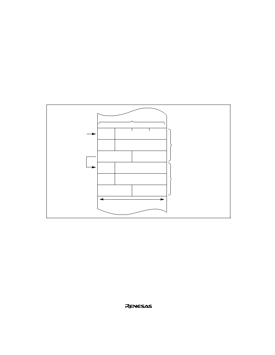
189
7.3.4
Location of Register Information in Address Space
Figure 7-5 shows how the register information should be located in the address space.
Locate the MRA, SAR, MRB, DAR, CRA, and CRB registers, in that order, from the start address
of the register information (contents of the vector address). In the case of chain transfer, register
information should be located in consecutive areas.
Locate the register information in the on-chip RAM (addresses: H'FFF800 to H'FFFBFF).
Lower address
0
1
2
3
MRA
SAR
DAR
MRB
CRA
CRB
MRA
SAR
DAR
MRB
CRA
CRB
Register information
Register information
for 2nd transfer in
chain transfer
Register
information
start address
Chain
transfer
4 bytes
Figure 7-5 Location of DTC Register Information in Address Space
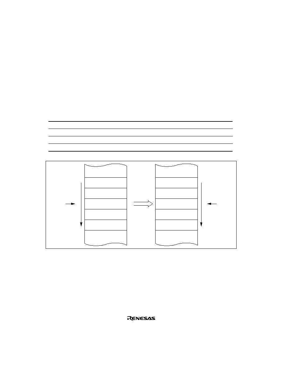
190
7.3.5
Normal Mode
In normal mode, one operation transfers one byte or one word of data.
From 1 to 65,536 transfers can be specified. Once the specified number of transfers have ended, a
CPU interrupt can be requested.
Table 7-5 lists the register information in normal mode and figure 7-6 shows memory mapping in
normal mode.
Table 7-5
Register Information in Normal Mode
Name
Abbreviation
Function
DTC source address register
SAR
Designates source address
DTC destination address register
DAR
Designates destination address
DTC transfer count register A
CRA
Designates transfer count
DTC transfer count register B
CRB
Not used
Transfer
SAR
DAR
Figure 7-6 Memory Mapping in Normal Mode

191
7.3.6
Repeat Mode
In repeat mode, one operation transfers one byte or one word of data.
From 1 to 256 transfers can be specified. Once the specified number of transfers have ended, the
initial states of the transfer counter and the address register specified as the repeat area are
restored, and transfer is repeated. In repeat mode the transfer counter value does not reach H'00,
and therefore CPU interrupts cannot be requested when DISEL = 0.
Table 7-6 lists the register information in repeat mode and figure 7-7 shows memory mapping in
repeat mode.
Table 7-6
Register Information in Repeat Mode
Name
Abbreviation
Function
DTC source address register
SAR
Designates source address
DTC destination address register
DAR
Designates destination address
DTC transfer count register AH
CRAH
Holds number of transfers
DTC transfer count register AL
CRAL
Designates transfer count
DTC transfer count register B
CRB
Not used
Transfer
SAR or
DAR
DAR or
SAR
Figure 7-7 Memory Mapping in Repeat Mode

192
7.3.7
Block Transfer Mode
In block transfer mode, one operation transfers one block of data. A block area is specified for
either the transfer source or the transfer destination.
The block size is 1 to 256. When the transfer of one block ends, the initial state of the block size
counter and the address register specified as the block area is restored. The other address register
is then incremented, decremented, or left fixed.
From 1 to 65,536 transfers can be specified. Once the specified number of transfers have ended, a
CPU interrupt is requested.
Table 7-7 lists the register information in block transfer mode and figure 7-8 shows memory
mapping in block transfer mode.
Table 7-7
Register Information in Block Transfer Mode
Name
Abbreviation
Function
DTC source address register
SAR
Designates source address
DTC destination address register
DAR
Designates destination address
DTC transfer count register AH
CRAH
Holds block size
DTC transfer count register AL
CRAL
Block size count
DTC transfer count register B
CRB
Transfer count
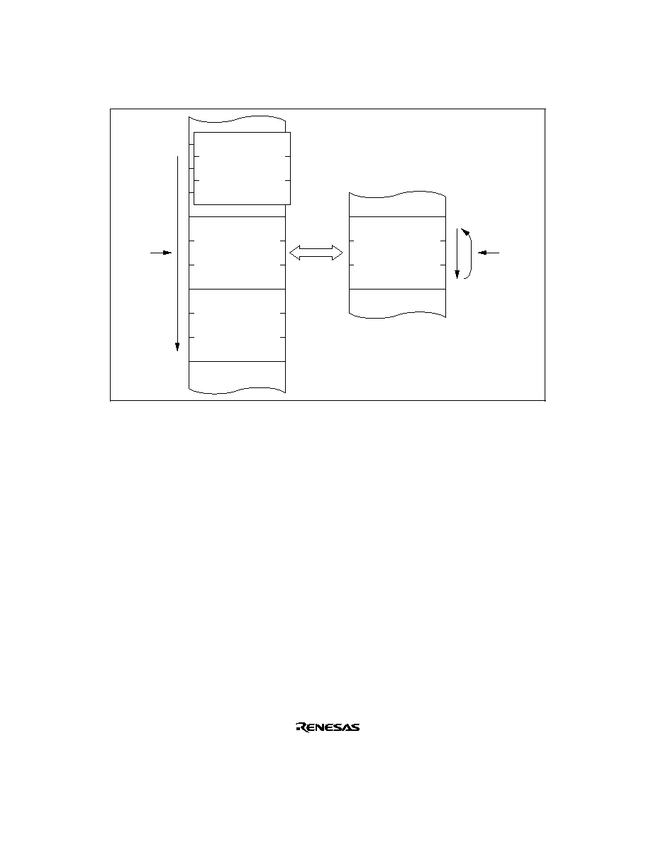
193
Transfer
SAR or
DAR
DAR or
SAR
Block area
First block
nth block
∑
∑
∑
Figure 7-8 Memory Mapping in Block Transfer Mode
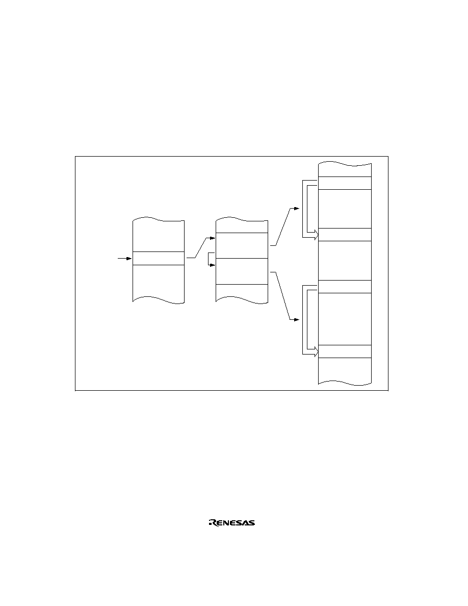
194
7.3.8
Chain Transfer
Setting the CHNE bit to 1 enables a number of data transfers to be performed consecutively in
response to a single transfer request. SAR, DAR, CRA, CRB, MRA, and MRB, which define data
transfers, can be set independently,
Figure 7-9 shows the memory map for chain transfer.
Source
Source
Destination
Destination
DTC vector
address
Register information
start address
Register information
CHNE = 1
Register information
CHNE = 0
Figure 7-9 Chain Transfer Memory Map
In the case of transfer with CHNE set to 1, an interrupt request to the CPU is not generated at the
end of the specified number of transfers or by setting of the DISEL bit to 1, and the interrupt
source flag for the activation source is not affected.
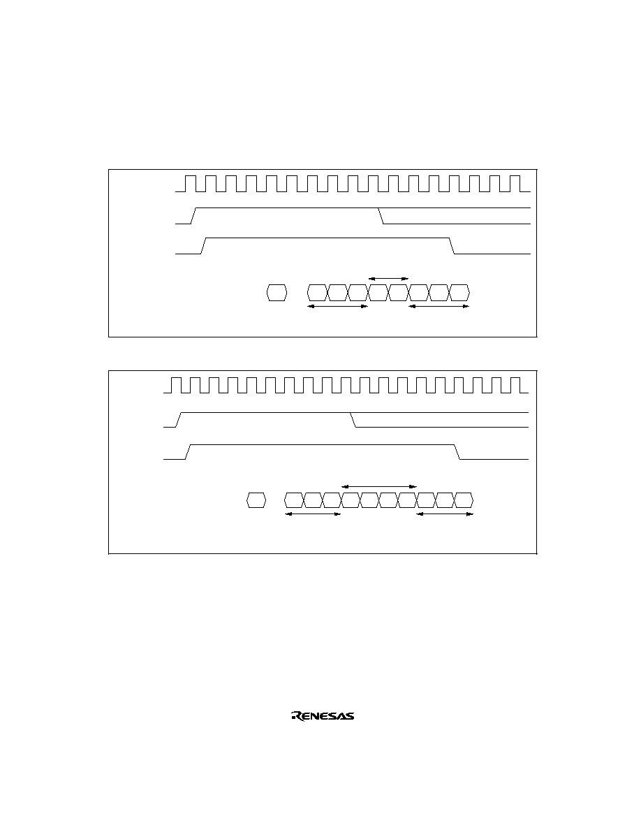
195
7.3.9
Operation Timing
Figures 7-10, 7-11, and 7-12 show examples of DTC operation timings.
DTC activation
request
DTC
request
Address
Vector read
Transfer
information read
Transfer
information write
Data transfer
¯
Read Write
Figure 7-10 DTC Operation Timing (Example in Normal Mode or Repeat Mode)
Read Write Read Write
Data transfer
Transfer
information write
Transfer
information read
Vector read
¯
DTC activation
request
DTC request
Address
Figure 7-11 DTC Operation Timing (Example of Block Transfer Mode,
with Block Size of 2)
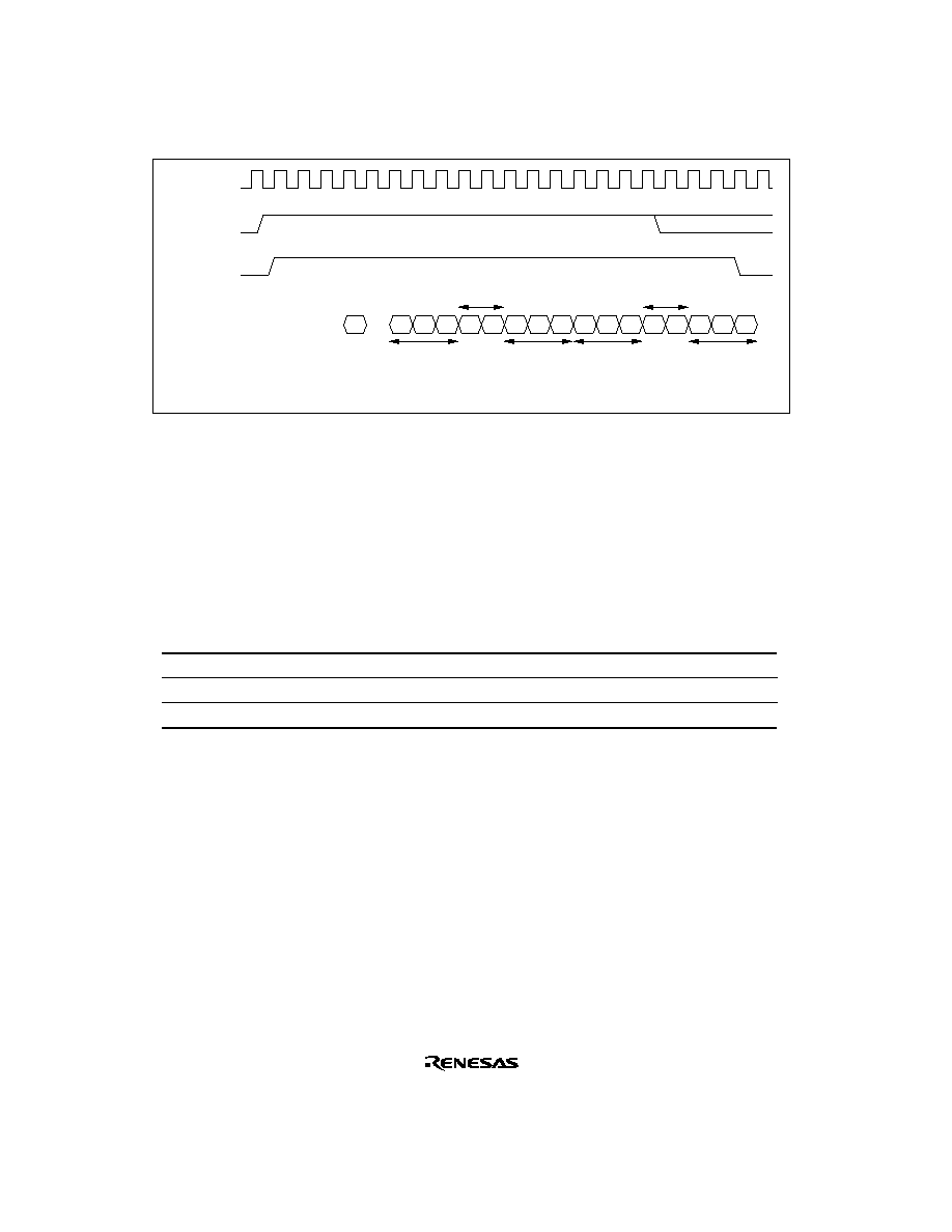
196
Read Write
Read Write
Address
¯
DTC activation
request
DTC
request
Data transfer
Data transfer
Transfer
information
write
Transfer
information
write
Transfer
information
read
Transfer
information
read
Vector read
Figure 7-12 DTC Operation Timing (Example of Chain Transfer)
7.3.10
Number of DTC Execution States
Table 7-8 lists execution statuses for a single DTC data transfer, and table 7-9 shows the number
of states required for each execution status.
Table 7-8
DTC Execution Statuses
Mode
Vector Read
I
Register Information
Read/Write
J
Data Read
K
Data Write
L
Internal
Operations
M
Normal
1
6
1
1
3
Repeat
1
6
1
1
3
Block transfer 1
6
N
N
3
N: Block size (initial setting of CRAH and CRAL)

197
Table 7-9
Number of States Required for Each Execution Status
Object to be Accessed
On-
Chip
RAM
On-
Chip
ROM
On-
Chip I/O
Registers
External Devices
Bus width
32
16
8
16
8
16
Access states
1
1
2
2
2
3
2
3
Execution Vector read
S
I
--
1
--
--
4
6+2m 2
3+m
status
Register
information
read/write
S
J
1
--
--
--
--
--
--
--
Byte data read
S
K
1
1
2
2
2
3+m
2
3+m
Word data read
S
K
1
1
4
2
4
6+2m 2
3+m
Byte data write
S
L
1
1
2
2
2
3+m
2
3+m
Word data write
S
L
1
1
4
2
4
6+2m 2
3+m
Internal operation
S
M
1
m: Number of wait states in external device access
The number of execution states is calculated from the formula below. Note that
means the sum
of all transfers activated by one activation event (the number in which the CHNE bit is set to 1,
plus 1).
Number of execution states = I ∑ S
I
+
(J ∑ S
J
+ K ∑ S
K
+ L ∑ S
L
) + M ∑ S
M
For example, when the DTC vector address table is located in on-chip ROM, normal mode is set,
and data is transferred from the on-chip ROM to an internal I/O register, the time required for the
DTC operation is 13 states. The time from activation to the end of the data write is 10 states.

198
7.3.11
Procedures for Using DTC
Activation by Interrupt: The procedure for using the DTC with interrupt activation is as follows:
[1] Set the MRA, MRB, SAR, DAR, CRA, and CRB register information in the on-chip RAM.
[2] Set the start address of the register information in the DTC vector address.
[3] Set the corresponding bit in DTCER to 1.
[4] Set the enable bits for the interrupt sources to be used as the activation sources to 1. The DTC
is activated when an interrupt used as an activation source is generated.
[5] After the end of one data transfer, or after the specified number of data transfers have ended,
the DTCE bit is cleared to 0 and a CPU interrupt is requested. If the DTC is to continue
transferring data, set the DTCE bit to 1.
Activation by Software: The procedure for using the DTC with software activation is as follows:
[1] Set the MRA, MRB, SAR, DAR, CRA, and CRB register information in the on-chip RAM.
[2] Set the start address of the register information in the DTC vector address.
[3] Check that the SWDTE bit is 0.
[4] Write 1 to SWDTE bit and the vector number to DTVECR.
[5] Check the vector number written to DTVECR.
[6] After the end of one data transfer, if the DISEL bit is 0 and a CPU interrupt is not requested,
the SWDTE bit is cleared to 0. If the DTC is to continue transferring data, set the SWDTE bit
to 1. When the DISEL bit is 1, or after the specified number of data transfers have ended, the
SWDTE bit is held at 1 and a CPU interrupt is requested.
7.3.12
Examples of Use of the DTC
(1) Normal Mode
The first example shows how the DTC can be used to receive 128 bytes of data via the SCI.
[1] Set MRA to fixed source address (SM1 = SM0 = 0), incrementing destination address (DM1 =
1, DM0 = 0), normal mode (MD1 = MD0 = 0), and byte size (Sz = 0). The DTS bit can have
any value. Set MRB for one data transfer by one interrupt (CHNE = 0, DISEL = 0). Set the
SCI RDR address in SAR, the start address of the RAM area where the data will be received in
DAR, and 128 (H'0080) in CRA. CRB can be set to any value.

199
[2] Set the start address of the register information at the DTC vector address.
[3] Set the corresponding bit in DTCER to 1.
[4] Set the SCI to the appropriate receive mode. Set the RIE bit in SCR to 1 to enable the
reception complete (RXI) interrupt. Since the generation of a receive error during the SCI
reception operation will disable subsequent reception, the CPU should be enabled to accept
receive error interrupts.
[5] Each time reception of one byte of data ends on the SCI, the RDRF flag in SSR is set to 1, an
RXI interrupt is generated, and the DTC is activated. The receive data is transferred from RDR
to RAM by the DTC, and then DAR is incremented and CRA is decremented. The RDRF flag
is automatically cleared to 0.
[6] When CRA becomes 0 after the 128 data transfers have ended, the RDRF flag is held at 1, the
DTCE bit is cleared to 0, and an RXI interrupt request is sent to the CPU. The interrupt
handling routine should perform wrap-up processing.
(2) Software Activation
The second example shows how the DTC can be used to transfer a block of 128 bytes of data by
means of software activation. The transfer source address is H'1000 and the destination address is
H'2000. The vector number is H'60, so the vector address is H'04C0.
[1] Set MRA to incrementing source address (SM1 = 1, SM0 = 0), incrementing destination
address (DM1 = 1, DM0 = 0), block transfer mode (MD1 = 1, MD0 = 0), and byte size (Sz =
0). The DTS bit can have any value. Set MRB for one block transfer by one interrupt (CHNE =
0). Set the transfer source address (H'1000) in SAR, the destination address (H'2000) in DAR,
and 128 (H'8080) in CRA. Set 1 (H'0001) in CRB.
[2] Set the start address of the register information at the DTC vector address (H'04C0).
[3] Check that the SWDTE bit in DTVECR is 0. Check that there is currently no transfer activated
by software.
[4] Write 1 to the SWDTE bit and the vector number (H'60) to DTVECR. The write data is H'E0.
[5] Read DTVECR again and check that it is set to the vector number (H'60). If it is not, this
indicates that the write failed. This is presumably because an interrupt occurred between steps
3 and 4 and led to a different software activation. To activate this transfer, go back to step 3.
[6] If the write was successful, the DTC is activated and a block of 128 bytes of data is transferred.
[7] After the transfer, an SWDTEND interrupt occurs. The interrupt handling routine should clear
the SWDTE bit to 0 and perform other wrap-up processing.

200
7.4
Interrupts
An interrupt request is issued to the CPU when the DTC finishes the specified number of data
transfers, or a data transfer for which the DISEL bit was set to 1. In the case of interrupt activation,
the interrupt set as the activation source is generated. These interrupts to the CPU are subject to
CPU mask level and interrupt controller priority level control.
In the case of activation by software, a software activated data transfer end interrupt (SWDTE
ND) is generated.
When one data transfer ends, or the specified number of data transfers end, with the DISEL bit set
to 1, after the end of the data transfer the SWDTE bit remains set to 1 and an SWDTEND interrupt
is generated.
The interrupt handling routine should clear the SWDTE bit to 0.
When the DTC is activated by software, an SWDTEND interrupt is not generated during a data
transfer wait or during data transfer even if the SWDTE bit is set to 1.
7.5
Usage Notes
Module Stop: When the MSTP14 bit in MSTPCR is set to 1, the DTC clock stops, and the DTC
enters the module stop state. However, 1 cannot be written in the MSTP14 bit while the DTC is
operating.
On-Chip RAM: The MRA, MRB, SAR, DAR, CRA, and CRB registers are all located in on-chip
RAM. When the DTC is used, the RAME bit in SYSCR must not be cleared to 0.
DTCE Bit Setting: For DTCE bit setting, use bit manipulation instructions such as BSET and
BCLR. If all interrupts are masked, multiple activation sources can be set at one time by writing
data after executing a dummy read on the relevant register.

201
Section 8 I/O Ports
8.1
Overview
The H8S/2245 Series has 11 I/O ports (ports 1, 2, 3, 5, and A to G), and one input-only port (port
4).
Table 8-1 summarizes the port functions. The pins of each port also have other functions.
Each port includes a data direction register (DDR) that controls input/output (not provided for the
input-only port), a data register (DR) that stores output data, and a port register (PORT) used to
read the pin states.
Ports A to E have a built-in MOS input pull-up function, and in addition to DR and DDR, have a
MOS input pull-up control register (PCR) to control the on/off state of MOS input pull-up.
Ports 3 and A include an open-drain control register (ODR) that controls the on/off state of the
output buffer PMOS.
Ports 1 and A to F can drive a single TTL load and 90 pF capacitive load, and ports 2, 3, 5, and G
can drive a single TTL load and 30 pF capacitive load. All the I/O ports can drive a Darlington
transistor when in output mode. Ports 1, and A to C can drive an LED (10 mA sink current).
Port 2 and the interrupt input pins (
IRQ0 to IRQ7) are Schmitt-triggered inputs.

202
Port
Description
Pins
Mode 1
Mode 2
*
Mode 3
*
Mode 4
Mode 5
Mode 6
*
Mode 7
*
Port 1
∑
8-bit I/O port
P1
7
/TIOCB2/TCLKD
8-bit I/O port also functioning as TPU I/O pins (TCLKA, TCLKB,
P1
6
/TIOCA2
TCLKC, TCLKD, TIOCA0, TIOCB0, TIOCC0, TIOCD0, TIOCA1,
P1
5
/TIOCB1/TCLKC
TIOCB1, TIOCA2, TIOCB2)
P1
4
/TIOCA1
P1
3
/TIOCD0/TCLKB/A
23
P1
2
/TIOCC0/TCLKA/A
22
P1
1
/TIOCB0/A
21
P1
0
/TIOCA0/A
20
Port 2
∑
8-bit I/O port
P2
7
/TMO1
8-bit I/O port also functioning as 8-bit timer (channels 0 and 1)
∑
Schmitt-
P2
6
/TMO0
I/O pins (TMRI0, TMCI0, TMO0, TMRI1, TMCI1, TMO1)
triggered P2
5
/TMCI1
input
P2
4
/TMRI1
P2
3
/TMCI0
P2
2
/TMRI0
P2
1
P2
0
Port 3
∑
6-bit I/O port
P3
5
/SCK1/
IRQ5
6-bit I/O port also functioning as SCI (channels 0 and 1) I/O pins
∑
Open-drain
P3
4
/SCK0/
IRQ4
(TxD0, RxD0, SCK0, TxD1, RxD1, SCK1) and interrupt input pins
output P3
3
/RxD1
(
IRQ5
,
IRQ4
)
capability
P3
2
/RxD0
∑
Schmitt-
P3
1
/TxD1
triggered input
P3
0
/TxD0
(
IRQ5
,
IRQ4
)
Port 4
∑
4-bit input
P4
3
/AN3
4-bit input port also functioning as A/D converter analog inputs (AN3
port
P4
2
/AN2
to AN0)
P4
1
/AN1
P4
0
/AN0
Port 5
∑
4-bit I/O port
P5
3
4-bit I/O port also functioning as SCI (channel 2) I/O pins (TxD2,
P5
2
/SCK2
RxD2, SCK2)
P5
1
/RxD2
P5
0
/TxD2
Table 8-1 Port Functions
When DDR=0: Input port also
functioning as TPU I/O pins
(TCLKA, TCLKB, TIOCA0,
TIOCB0, TIOCC0, TIOCD0)
When DDR= 1: Address output
Note:
*
Cannot be used in the H8S/2240.

203
Port
Description
Pins
Mode 1
Mode 3
*
Mode 2
*
Mode 4
Mode 5
Mode 6
*
Mode 7
*
Port A
∑
4-bit I/O
PA
3
/A
19
I/O ports
Address output
When DDR
I/O ports
port
to PA
0
/A
16
= 0 (after
∑
Built-in MOS
reset):
input pull-up
input ports
∑
Open-drain
When DDR
output
= 1:
capability
address
output
Table 8-1 Port Functions (cont)
Port B
∑
8-bit I/O
PB
7
/A
15
Address
When DDR
I/O port
Address output
When DDR
I/O port
port
to PB
0
/A
8
output
= 0 (after
= 0 (after
∑
Built-in MOS
reset):
reset):
input pull-up
input port
input port
When DDR
When DDR
= 1:
= 1:
address address
output
output
Port C
∑
8-bit I/O
PC
7
/A
7
Address
When DDR
I/O port
Address output
When DDR
I/O port
port
to PC
0
/A
0
output
= 0 (after
= 0 (after
∑
Built-in MOS
reset):
reset):
input pull-up
input port
input port
When DDR
When DDR
= 1:
= 1:
address address
output
output
Note:
*
Cannot be used in the H8S/2240.

204
Port
Description
Pins
Mode 1
Mode 3
*
Mode 2
*
Mode 4
Mode 5
Mode 6
*
Mode 7
*
Port D
∑
8-bit I/O
PD
7
/D
15
Data bus input/output
I/O port
Data bus input/output
I/O port
port
to PD
0
/D
8
∑
Built-in MOS
input pull-up
Port E
∑
8-bit I/O
PE
7
/D
7
In 8-bit bus mode: I/O port
I/O port
In 8-bit bus mode: I/O port
I/O port
port
to PE
0
/D
0
In 16-bit bus mode: data
In 16-bit bus mode: data bus input/
∑
Built-in MOS
bus input/output
output
input pull-up
Port F
∑
8-bit I/O
PF
7
/¯
When DDR = 0:
When DDR
When DDR = 0: input port
When DDR
port
input port
= 0 (after
When DDR = 1 (after reset): ¯ output
= 0 (after
∑
Schmitt-
When DDR = 1 (after
reset):
reset):
triggered
reset): ¯ output
input port
input port
input (
IRQ3
When DDR
When DDR
to
IRQ0
)
=
1:
= 1:
¯ output
¯ output
PF
6
/
AS
AS
,
RD
,
HWR
,
LWR
I/O
port
AS
,
RD
,
HWR
,
LWR
output
I/O port
PF
5
/
RD
output
PF
4
/
HWR
PF
3
/
LWR
/
I/O port also
I/O port also
IRQ3
functioning functioning
as interrupt
as interrupt
input pins
input pins
(
IRQ3
to
IRQ0
)(
IRQ3
to
IRQ0
)
Table 8-1 Port Functions (cont)
Note:
*
Cannot be used in the H8S/2240.
205
Port
Description
Pins
Mode 1
Mode 3
*
Mode 2
*
Mode 4
Mode 5
Mode 6
*
Mode 7
*
Port F
∑
8-bit I/O
PF
2
/
port
WAIT
/
∑
Schmitt-
BREQO
/
triggered
IRQ2
input (
IRQ3
to
IRQ0
)
PF
1
/
BACK
/
IRQ1
PF
0
/
BREQ
/
IRQ0
Table 8-1 Port Functions (cont)
When WAITE = 0 and BREQOE = 0
(after reset): I/O port also functioning
as interrupt input pin (
IRQ2
)
When WAITE = 1 and BREQOE = 0:
WAIT
input also functioning as interrupt
input pin (
IRQ2
)
When WAITE = 0 and BREQOE = 1:
BREQO
output also functioning as
interrupt input pin (
IRQ2
)
When BRLE = 0 (after reset): I/O port
also functioning as interrupt input pins
(
IRQ1
,
IRQ0
)
When BRLE = 1:
BREQ
input,
BACK
output also functioning as interrupt input
pins (
IRQ1
,
IRQ0
)
When WAITE = 0 and
BREQOE = 0 (after reset):
I/O port also functioning as
interrupt input pin (
IRQ2
)
When WAITE = 1 and
BREQOE = 0:
WAIT
input
also functioning as
interrupt input pin (
IRQ2
)
When WAITE = 0 and
BREQOE = 1:
BREQO
output also functioning as
interrupt input pin (
IRQ2
)
I/O port also
functioning
as interrupt
input pins
(
IRQ3
to
IRQ0
)
I/O port also
functioning
as interrupt
input pin
(
IRQ3
to
IRQ0
)
When BRLE = 0 (after
reset): I/O port also
functioning as interrupt
input pins (
IRQ1
,
IRQ0
)
When BRLE = 1:
BREQ
input,
BACK
output also
functioning as interrupt
input pins (
IRQ1
,
IRQ0
)
Note:
*
Cannot be used in the H8S/2240.
206
Port
Description
Pins
Mode 1
Mode 3
*
3
Mode 2
*
3
Mode 4
Mode 5
Mode 6
*
3
Mode 7
*
3
Port G
∑
5-bit I/O
PG
4
/
CS0
port
∑
Schmitt-
triggered
input
(
IRQ7
,
IRQ6
)
Notes:
1.
After a reset in mode 2 or 6.
2.
After a reset in mode 1, 4 or 5.
3.
Cannot be used in the H8S/2240.
PG
0
/
IRQ6
/
ADTRG
Table 8-1 Port Functions (cont)
PG
3
/
CS1
PG
2
/
CS2
PG
1
/
CS3
/
IRQ7
When DDR = 0 (after reset): input port
also functioning as interrupt input pin
(IRQ7)
When DDR = 1:
CS1
,
CS2
,
CS3
output
also functioning as interrupt input pin
(
IRQ7
)
When DDR = 0
*
1
: input
port
When DDR = 1
*
2
:
CS0
output
When DDR = 0
*
1
: input port
When DDR = 1
*
2
:
CS0
output
I/O port also
functioning
as interrupt
input pins
(
IRQ7
,
IRQ6
)
and A/D
converter
input pin
(
ADTRG
)
I/O port also
functioning
as interrupt
input pins
(
IRQ7
,
IRQ6
)
and A/D
converter
input pin
(
ADTRG
)
I/O port also functioning
as interrupt input pins
(
IRQ6
,
IRQ7
) and A/D
converter input pin
(
ADTRG
)
I/O port also functioning as interrupt
input pin (
IRQ6
) and A/D converter input
pin (
ADTRG
)
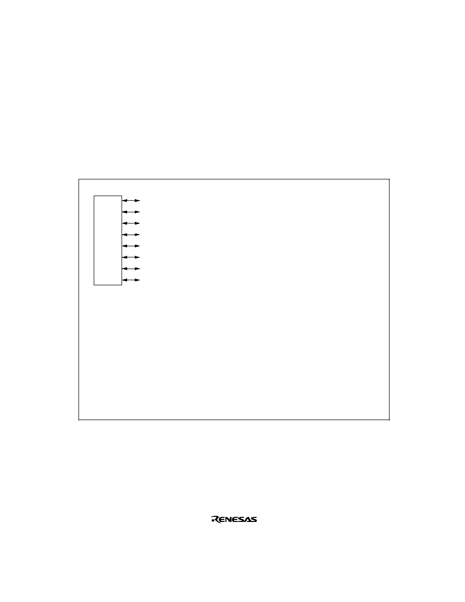
207
8.2
Port 1
8.2.1
Overview
Port 1 is an 8-bit I/O port. Port 1 pins also function as TPU I/O pins (TCLKA, TCLKB, TCLKC,
TCLKD, TIOCA0, TIOCB0, TIOCC0, TIOCD0, TIOCA1, TIOCB1, TIOCA2, and TIOCB2) and
an address bus output function. Port 1 pin functions change according to the operating mode.
Figure 8-1 shows the port 1 pin configuration.
P1
7
(I/O)/TIOCB2 (I/O)/TCLKD (input)
P1
6
(I/O)/TIOCA2 (I/O)
P1
5
(I/O)/TIOCB1 (I/O)/TCLKC (input)
P1
4
(I/O)/TIOCA1 (I/O)
P1
3
(I/O)/TIOCD0 (I/O)/TCLKB (input)/A
23
(output)
P1
2
(I/O)/TIOCC0 (I/O)/TCLKA (input)/A
22
(output)
P1
1
(I/O)/TIOCB0 (I/O)/A
21
(output)
P1
0
(I/O)/TIOCA0 (I/O)/A
20
(output)
Note:
*
Modes 2, 3, 6, and 7 cannot be used in the H8S/2240.
Port 1
Port 1 pins
P1
7
(I/O)/TIOCB2 (I/O)/TCLKD (input)
P1
6
(I/O)/TIOCA2 (I/O)
P1
5
(I/O)/TIOCB1 (I/O)/TCLKC (input)
P1
4
(I/O)/TIOCA1 (I/O)
P1
3
(I/O)/TIOCD0 (I/O)/TCLKB (input)
P1
2
(I/O)/TIOCC0 (I/O)/TCLKA (input)
P1
1
(I/O)/TIOCB0 (I/O)
P1
0
(I/O)/TIOCA0 (I/O)
Pin functions in modes 1 to 3 and 7
*
P1
7
(I/O)/TIOCB2 (I/O)/TCLKD (input)
P1
6
(I/O)/TIOCA2 (I/O)
P1
5
(I/O)/TIOCB1 (I/O)/TCLKC (input)
P1
4
(I/O)/TIOCA1 (I/O)
P1
3
(input)/TIOCD0 (I/O)/TCLKB (input)/A
23
(output)
P1
2
(input)/TIOCC0 (I/O)/TCLKA (input)/A
22
(output)
P1
1
(input)/TIOCB0 (I/O)/A
21
(output)
P1
0
(input)/TIOCA0 (I/O)/A
20
(output)
Pin functions in modes 4 to 6
*
Figure 8-1 Port 1 Pin Functions

208
8.2.2
Register Configuration
Table 8-2 shows the port 1 register configuration.
Table 8-2
Port 1 Registers
Name
Abbreviation
R/W
Initial Value
Address
*
Port 1 data direction register
P1DDR
W
H'00
H'FEB0
Port 1 data register
P1DR
R/W
H'00
H'FF60
Port 1 register
PORT1
R
Undefined
H'FF50
Note:
*
Lower 16 bits of the address.
Port 1 Data Direction Register (P1DDR)
7
P17DDR
0
W
6
P16DDR
0
W
5
P15DDR
0
W
4
P14DDR
0
W
3
P13DDR
0
W
0
P10DDR
0
W
2
P12DDR
0
W
1
P11DDR
0
W
Bit
Initial value
R/W
:
:
:
P1DDR is an 8-bit write-only register, the individual bits of which specify input or output for the
pins of port 1. P1DDR cannot be read; if it is, an undefined value will be read.
P1DDR is initialized to H'00 by a power-on reset, and in hardware standby mode. It retains its
prior state after a manual reset, and in software standby mode. As the TPU is initialized by a
manual reset, the pin states are determined by the P1DDR and P1DR specifications.
Whether the address output pins maintain their output state or go to the high-impedance state in a
transition to software standby mode is selected by the OPE bit in SBYCR.
∑
Modes 1 to 3 and 7
The corresponding port 1 pins are output ports when P1DDR is set to 1, and input ports when
cleared to 0.
Note: Modes 2, 3, and 7 cannot be used in the H8S/2240.
∑
Modes 4 to 6
The corresponding port 1 pins are address outputs when P13DDR to P10DDR are set to 1, and
input ports when cleared to 0.
The corresponding port 1 pins are output ports when P17DDR to P14DDR are set to 1, and
input ports when cleared to 0.
Note: Mode 6 cannot be used in the H8S/2240.

209
Port 1 Data Register (P1DR)
7
P17DR
0
R/W
6
P16DR
0
R/W
5
P15DR
0
R/W
4
P14DR
0
R/W
3
P13DR
0
R/W
0
P10DR
0
R/W
2
P12DR
0
R/W
1
P11DR
0
R/W
Bit
Initial value
R/W
:
:
:
P1DR is an 8-bit readable/writable register that stores output data for the port 1 pins (P1
7
to P1
0
).
P1DR is initialized to H'00 by a power-on reset, and in hardware standby mode. It retains its prior
state after a manual reset, and in software standby mode.
Port 1 Register (PORT1)
7
P17
--
*
R
6
P16
--
*
R
5
P15
--
*
R
4
P14
--
*
R
3
P13
--
*
R
0
P10
--
*
R
2
P12
--
*
R
1
P11
--
*
R
Bit
Initial value
R/W
Note:
*
Determined by state of pins P1
7
to P1
0
.
:
:
:
PORT1 is an 8-bit read-only register that shows the pin states. It cannot be written to. Writing of
output data for the port 1 pins (P1
7
to P1
0
) must always be performed on P1DR.
If a port 1 read is performed while P1DDR bits are set to 1, the P1DR values are read. If a port 1
read is performed while P1DDR bits are cleared to 0, the pin states are read.
After a power-on reset and in hardware standby mode, PORT1 contents are determined by the pin
states, as P1DDR and P1DR are initialized. PORT1 retains its prior state after a manual reset, and
in software standby mode.
210
8.2.3
Pin Functions
Port 1 pins also function as TPU I/O pins (TCLKA, TCLKB, TCLKC, TCLKD, TIOCA0,
TIOCB0, TIOCC0, TIOCD0, TIOCA1, TIOCB1, TIOCA2, and TIOCB2), and address output
pins (A
23
to A
20
). Port 1 pin functions are shown in table 8-3.
Table 8-3
Port 1 Pin Functions
Pin
Selection Method and Pin Functions
P1
7
/TIOCB2/
TCLKD
The pin function is switched as shown below according to the combination of
the TPU channel 2 setting (by bits MD3 to MD0 in TMDR2, bits IOB3 to IOB0
in TIOR2, and bits CCLR2 to CCLR0 in TCR2), bits TPSC2 to TPSC0 in
TCR0, and bit P17DDR.
TPU Channel
2 Setting
Table Below (1)
Table Below (2)
P17DDR
--
0
1
Pin function
TIOCB2 output
P1
7
input
P1
7
output
TIOCB2 input
*
1
TCLKD input
*
2
Notes: 1.
TIOCB2 input when input capture is set (IOB3 to IOB0 = B'10xx) in
normal operating mode (MD3 to MD0 = B'0000).
2. TCLKD input when the TCR0 setting is: TPSC2 to TPSC0 = B'111.
TCLKD input when channel 2 is set to phase counting mode (MD3
to MD0 = B'01xx).
TPU Channel
2 Setting
(2)
(1)
(2)
(2)
(1)
(2)
MD3 to MD0
B'0000, B'01xx
B'0010
B'0011
IOB3 to IOB0
B'0000
B'0100
B'1xxx
B'0001 to
B'0011
B'0101 to
B'0111
--
B'xx00
Other than B'xx00
CCLR2 to
CCLR0
--
--
--
--
Other
than
B'010
B'010
Output
function
--
Output
compare
output
--
--
PWM
mode 2
output
--
x: Don't care

211
Table 8-3
Port 1 Pin Functions (cont)
Pin
Selection Method and Pin Functions
P1
6
/TIOCA2
The pin function is switched as shown below according to the combination of
the TPU channel 2 setting (by bits MD3 to MD0 in TMDR2, bits IOA3 to IOA0
in TIOR2, and bits CCLR2 to CCLR0 in TCR2), and bit P16DDR.
TPU Channel
2 Setting
Table Below (1)
Table Below (2)
P16DDR
--
0
1
Pin function
TIOCA2 output
P1
6
input
P1
6
output
TIOCA2 input
*
1
Note: 1. TIOCA2 input when input capture is set (IOA3 to IOA0 = B'10xx) in
normal operating mode (MD3 to MD0 = B'0000).
TPU Channel
2 Setting
(2)
(1)
(2)
(1)
(1)
(2)
MD3 to MD0
B'0000, B'01xx
B'001x
B'0010
B'0011
IOA3 to IOA0
B'0000
B'0100
B'1xxx
B'0001 to
B'0011
B'0101 to
B'0111
B'xx00
Other than B'xx00
CCLR2 to
CCLR0
--
--
--
--
Other
than
B'001
B'001
Output
function
--
Output
compare
output
--
PWM
mode 1
output
*
2
PWM
mode 2
output
--
x: Don't care
Note: 2. TIOCB2 output is disabled.
212
Table 8-3
Port 1 Pin Functions (cont)
Pin
Selection Method and Pin Functions
P1
5
/TIOCB1/
TCLKC
The pin function is switched as shown below according to the combination of
the TPU channel 1 setting (by bits MD3 to MD0 in TMDR1, bits IOB3 to IOB0
in TIOR1, and bits CCLR2 to CCLR0 in TCR1), bits TPSC2 to TPSC0 in TCR0
and TCR2, and bit P15DDR.
TPU Channel
1 Setting
Table Below (1)
Table Below (2)
P15DDR
--
0
1
Pin function
TIOCB1 output
P1
5
input
P1
5
output
TIOCB1 input
*
1
TCLKC input
*
2
Notes: 1. TIOCB1 input when input capture is set (IOB3 to IOB0 = B'10xx) in
normal operating mode (MD3 to MD0 = B'0000).
2. TCLKC input when either the TCR0 or TCR2 setting is: TPSC2 to
TPSC0 = B'110.
TCLKC input when channel 2 is set to phase counting mode (MD3
to MD0 = B'01xx).
TPU Channel
1 Setting
(2)
(1)
(2)
(2)
(1)
(2)
MD3 to MD0
B'0000, B'01xx
B'0010
B'0011
IOB3 to IOB0
B'0000
B'0100
B'1xxx
B'0001 to
B'0011
B'0101 to
B'0111
--
B'xx00
Other than B'xx00
CCLR2 to
CCLR0
--
--
--
--
Other
than
B'010
B'010
Output
function
--
Output
compare
output
--
--
PWM
mode 2
output
--
x: Don't care
213
Table 8-3
Port 1 Pin Functions (cont)
Pin
Selection Method and Pin Functions
P1
4
/TIOCA1
The pin function is switched as shown below according to the combination of
the TPU channel 1 setting (by bits MD3 to MD0 in TMDR1, bits IOA3 to IOA0
in TIOR1, and bits CCLR2 to CCLR0 in TCR1), and bit P14DDR.
TPU Channel
1 Setting
Table Below (1)
Table Below (2)
P14DDR
--
0
1
Pin function
TIOCA1 output
P1
4
input
P1
4
output
TIOCA1 input
*
1
Note: 1. TIOCA1 input when input capture is set (IOA3 to IOA0 = B'10xx) in
normal operating mode (MD3 to MD0 = B'0000).
TPU Channel
1 Setting
(2)
(1)
(2)
(1)
(1)
(2)
MD3 to MD0
B'0000, B'01xx
B'001x
B'0010
B'0011
IOA3 to IOA0
B'0000
B'0100
B'1xxx
B'0001 to
B'0011
B'0101 to
B'0111
B'xx00
Other than B'xx00
CCLR2 to
CCLR0
--
--
--
--
Other
than
B'001
B'001
Output
function
--
Output
compare
output
--
PWM
mode 1
output
*
2
PWM
mode 2
output
--
x: Don't care
Note: 2. TIOCB1 output is disabled.
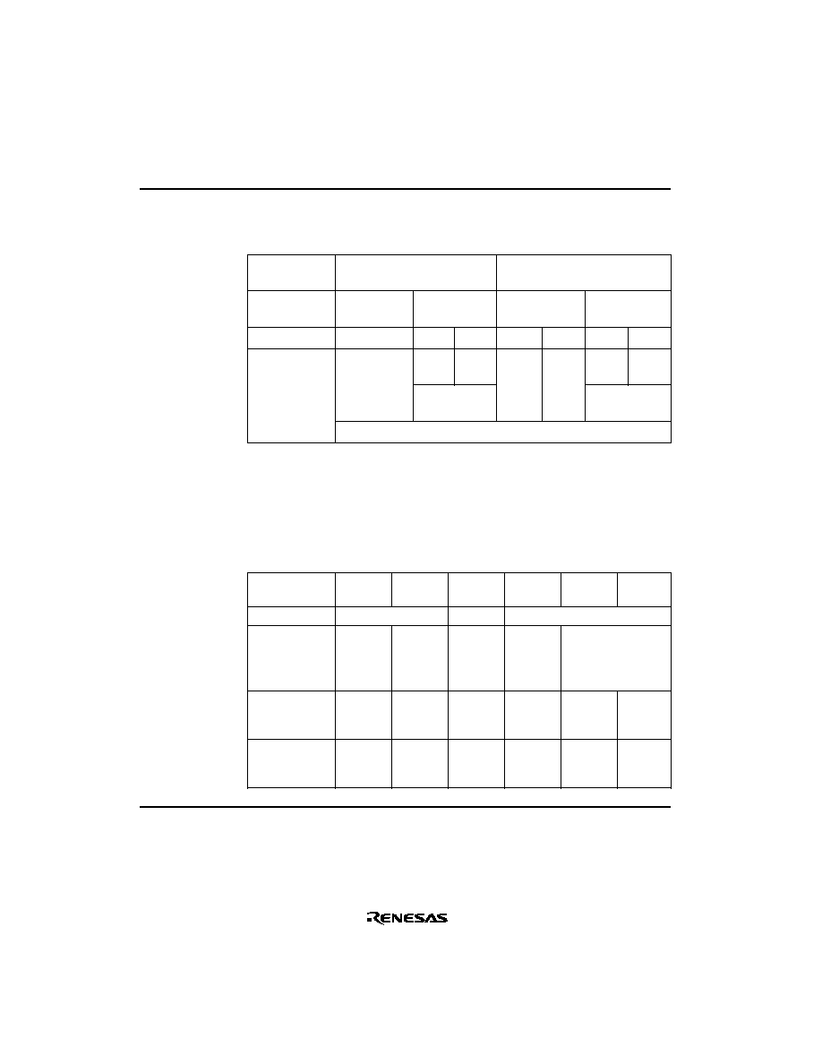
214
Table 8-3
Port 1 Pin Functions (cont)
Pin
Selection Method and Pin Functions
P1
3
/TIOCD0/
TCLKB/A
23
The pin function is switched as shown below according to the combination of
the operating mode, TPU channel 0 setting (by bits MD3 to MD0 in TMDR0,
bits IOD3 to IOD0 in TIOR0L, and bits CCLR2 to CCLR0 in TCR0), bits TPSC2
to TPSC0 in TCR0 to TCR2, and bit P13DDR.
Operating
Mode
Modes 1, 2, 3, 7
*
1
Modes 4, 5, 6
*
1
TPU Channel
0 Setting
Table
Below (1)
Table
Below (2)
Table
Below (1)
Table
Below (2)
P13DDR
--
0
1
0
1
0
1
Pin function
TIOCD0
output
P1
3
input
P1
3
output
TIOCD0
output
A
23
output
P1
3
input
A
23
output
TIOCD0
input
*
2
TIOCD0
input
*
2
TCLKB input
*
3
Notes: 1. Modes 2, 3, 6, and 7 cannot be used in the H8S/2240.
2. TIOCD0 input when input capture is set (IOD3 to IOD0 = B'10xx) in
normal operating mode (MD3 to MD0 = B'0000).
3. TCLKB input when the TCR0, TCR1, or TCR2 setting is: TPSC2 to
TPSC0 = B'101.
TCLKB input when channel 1 is set to phase counting mode (MD3
to MD0 = B'01xx).
TPU Channel
0 Setting
(2)
(1)
(2)
(2)
(1)
(2)
MD3 to MD0
B'0000
B'0010
B'0011
IOD3 to IOD0
B'0000
B'0100
B'1xxx
B'0001 to
B'0011
B'0101 to
B'0111
--
B'xx00
Other than B'xx00
CCLR2 to
CCLR0
--
--
--
--
Other
than
B'110
B'110
Output
function
--
Output
compare
output
--
--
PWM
mode 2
output
--
x: Don't care
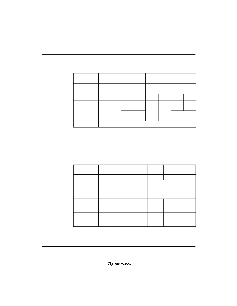
215
Table 8-3
Port 1 Pin Functions (cont)
Pin
Selection Method and Pin Functions
P1
2
/TIOCC0/
TCLKA/A
22
The pin function is switched as shown below according to the combination of
the operating mode, TPU channel 0 setting (by bits MD3 to MD0 in TMDR0,
bits IOC3 to IOC0 in TIOR0L, and bits CCLR2 to CCLR0 in TCR0), bits TPSC2
to TPSC0 in TCR0 to TCR2, and bit P12DDR.
Operating
Mode
Modes 1, 2, 3, 7
*
1
Modes 4, 5, 6
*
1
TPU Channel
0 Setting
Table
Below (1)
Table
Below (2)
Table
Below (1)
Table
Below (2)
P12DDR
--
0
1
0
1
0
1
Pin function
TIOCC0
output
P1
2
input
P1
2
output
TIOCC0
output
A
22
output
P1
2
input
A
22
output
TIOCC0
input
*
2
TIOCC0
input
*
2
TCLKA input
*
3
Notes: 1. Modes 2, 3, 6, and 7 cannot be used in the H8S/2240.
2. TIOCC0 input when input capture is set (IOC3 to IOC0 = B'10xx) in
normal operating mode (MD3 to MD0 = B'0000).
3. TCLKA input when the TCR0, TCR1, or TCR2 setting is: TPSC2 to
TPSC0 = B'100.
TCLKA input when channel 1 is set to phase counting mode (MD3
to MD0 = B'01xx).
TPU Channel
0 Setting
(2)
(1)
(2)
(1)
(1)
(2)
MD3 to MD0
B'0000
B'001x
B'0010
B'0011
IOC3 to IOC0
B'0000
B'0100
B'1xxx
B'0001 to
B'0011
B'0101 to
B'0111
B'xx00
Other than B'xx00
CCLR2 to
CCLR0
--
--
--
--
Other
than
B'101
B'101
Output
function
--
Output
compare
output
--
PWM
mode 1
output
*
4
PWM
mode 2
output
--
x: Don't care
Note: 4. TIOCD0 output is disabled.
When BFA = 1 or BFB = 1 in TMDR0, output is disabled and setting
(2) applies.
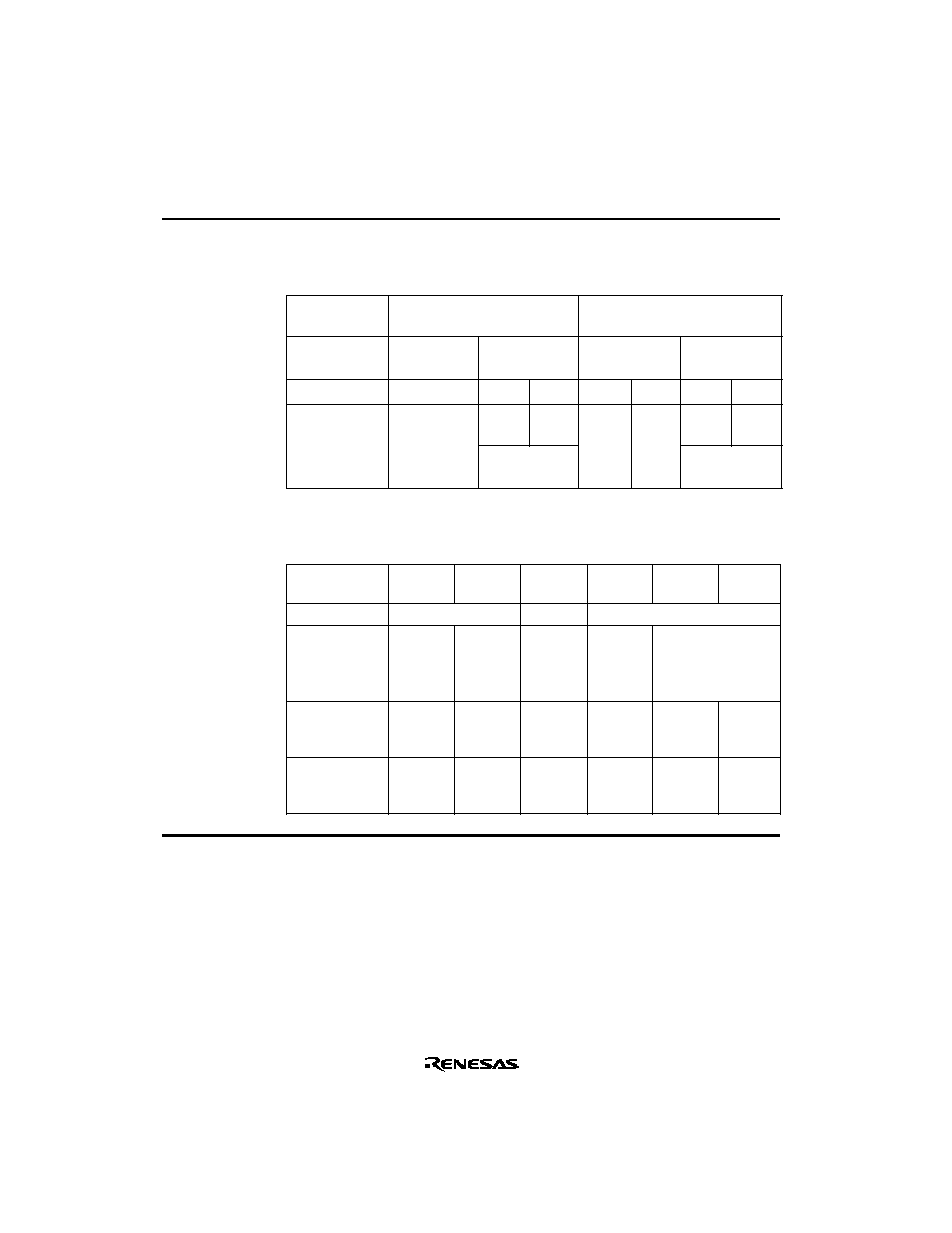
216
Table 8-3
Port 1 Pin Functions (cont)
Pin
Selection Method and Pin Functions
P1
1
/TIOCB0/
A
21
The pin function is switched as shown below according to the combination of
the operating mode, TPU channel 0 setting (by bits MD3 to MD0 in TMDR0,
bits IOB3 to IOB0 in TIOR0H, and bits CCLR2 to CCLR0 in TCR0), and bit
P11DDR.
Operating
Mode
Modes 1, 2, 3, 7
*
1
Modes 4, 5, 6
*
1
TPU Channel
0 Setting
Table
Below (1)
Table
Below (2)
Table
Below (1)
Table
Below (2)
P11DDR
--
0
1
0
1
0
1
Pin function
TIOCB0
output
P1
1
input
P1
1
output
TIOCB0
output
A
21
output
P1
1
input
A
21
output
TIOCB0
input
*
2
TIOCB0
input
*
2
Notes: 1. Modes 2, 3, 6, and 7 cannot be used in the H8S/2240.
2. TIOCB0 input when input capture is set (IOB3 to IOB0 = B'10xx) in
normal operating mode (MD3 to MD0 = B'0000).
TPU Channel
0 Setting
(2)
(1)
(2)
(2)
(1)
(2)
MD3 to MD0
B'0000
B'0010
B'0011
IOB3 to IOB0
B'0000
B'0100
B'1xxx
B'0001 to
B'0011
B'0101 to
B'0111
--
B'xx00
Other than B'xx00
CCLR2 to
CCLR0
--
--
--
--
Other
than
B'010
B'010
Output
function
--
Output
compare
output
--
--
PWM
mode 2
output
--
x: Don't care
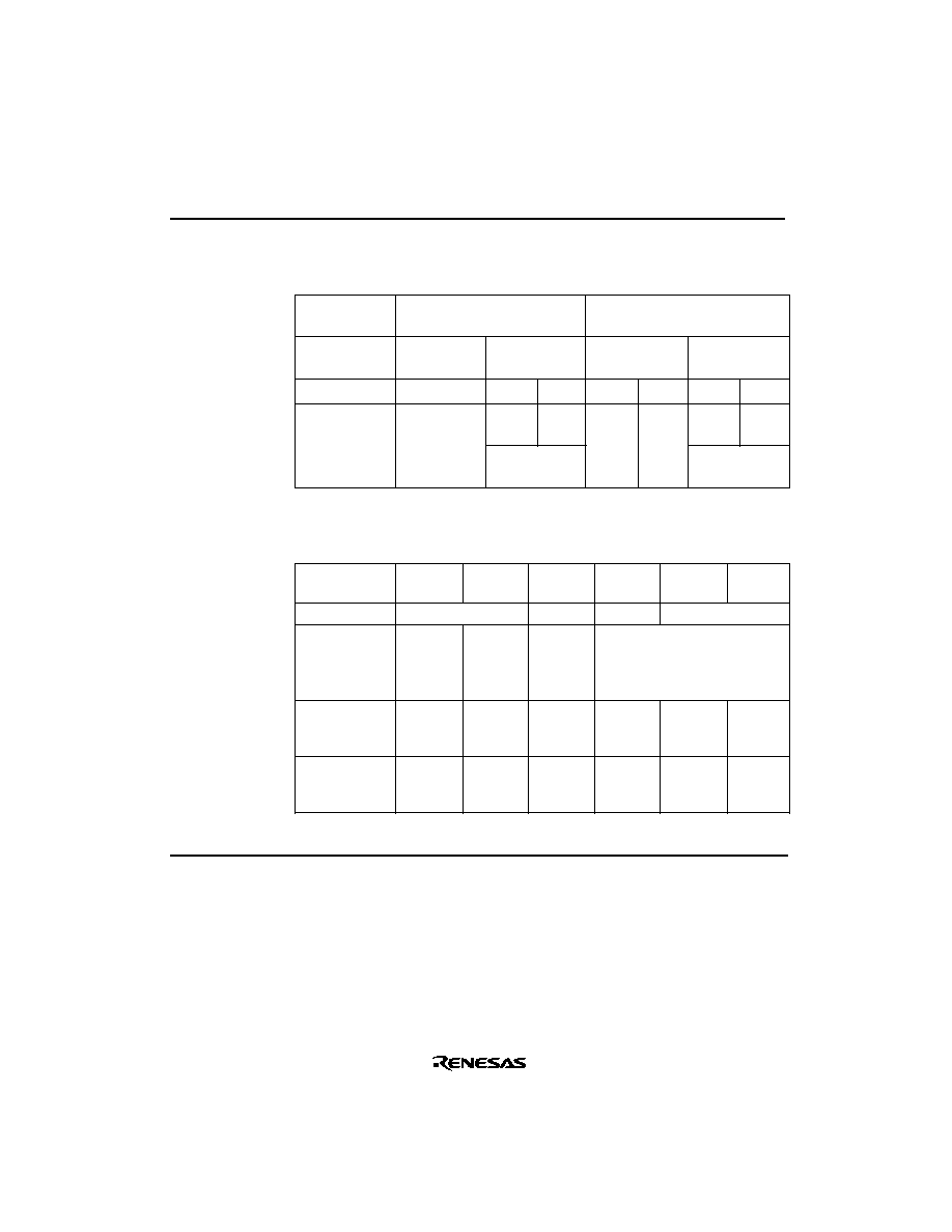
217
Table 8-3
Port 1 Pin Functions (cont)
Pin
Selection Method and Pin Functions
P1
0
/TIOCA0/
A
20
The pin function is switched as shown below according to the combination of
the operating mode, TPU channel 0 setting (by bits MD3 to MD0 in TMDR0,
bits IOA3 to IOA0 in TIOR0H, and bits CCLR2 to CCLR0 in TCR0), and bit
P10DDR.
Operating
Mode
Modes 1, 2, 3, 7
*
1
Modes 4, 5, 6
*
1
TPU Channel
0 Setting
Table
Below (1)
Table
Below (2)
Table
Below (1)
Table
Below (2)
P10DDR
--
0
1
0
1
0
1
Pin function
TIOCA0
output
P1
0
input
P1
0
output
TIOCA0
output
A
20
output
P1
0
input
A
20
output
TIOCA0
input
*
2
TIOCA0
input
*
2
Notes: 1. Modes 2, 3, 6, and 7 cannot be used in the H8S/2240.
2. TIOCA0 input when input capture is set (IOA3 to IOA0 = B'10xx) in
normal operating mode (MD3 to MD0 = B'0000).
TPU Channel
0 Setting
(2)
(1)
(2)
(1)
(1)
(2)
MD3 to MD0
B'0000
B'001x
B'0010
B'0011
IOA3 to IOA0
B'0000
B'0100
B'1xxx
B'0001 to
B'0011
B'0101 to
B'0111
B'xx00
Other than B'xx00
CCLR2 to
CCLR0
--
--
--
--
Other
than
B'001
B'001
Output
function
--
Output
compare
output
--
PWM
mode 1
output
*
3
PWM
mode 2
output
--
x: Don't care
Note: 3. TIOCB0 output is disabled.
218
8.3
Port 2
8.3.1
Overview
Port 2 is an 8-bit I/O port. Port 2 pins also function as 8-bit timer I/O pins (TMRI0, TMCI0,
TMO0, TMRI1, TMCI1, and TMO1). Port 2 pin functions are the same in all operating modes.
Port 2 uses Schmitt-triggered input.
Figure 8-2 shows the port 2 pin configuration.
P2
7
P2
6
P2
5
P2
4
P2
3
P2
2
P2
1
P2
0
Port 2
TMO1
TMO0
TMCI1
TMRI1
TMCI0
TMRI0
Port 2 pins
(I/O)/
(I/O)/
(I/O)/
(I/O)/
(I/O)/
(I/O)/
(I/O)
(I/O)
(output)
(output)
(input)
(input)
(input)
(input)
Figure 8-2 Port 2 Pin Functions
8.3.2
Register Configuration
Table 8-4 shows the port 2 register configuration.
Table 8-4
Port 2 Registers
Name
Abbreviation
R/W
Initial Value
Address
*
Port 2 data direction register
P2DDR
W
H'00
H'FEB1
Port 2 data register
P2DR
R/W
H'00
H'FF61
Port 2 register
PORT2
R
Undefined
H'FF51
Note:
*
Lower 16 bits of the address.

219
Port 2 Data Direction Register (P2DDR)
7
P27DDR
0
W
6
P26DDR
0
W
5
P25DDR
0
W
4
P24DDR
0
W
3
P23DDR
0
W
0
P20DDR
0
W
2
P22DDR
0
W
1
P21DDR
0
W
Bit
Initial value
R/W
:
:
:
P2DDR is an 8-bit write-only register, the individual bits of which specify input or output for the
pins of port 2. P2DDR cannot be read; if it is, an undefined value will be read.
Setting a P2DDR bit to 1 makes the corresponding port 2 pin an output pin, while clearing the bit
to 0 makes the pin an input pin.
P2DDR is initialized to H'00 by a power-on reset, and in hardware standby mode. It retains its
prior state after a manual reset, and in software standby mode. As the 8-bit timer is initialized by a
manual reset, the pin states are determined by the P2DDR and P2DR specifications.
Port 2 Data Register (P2DR)
7
P27DR
0
R/W
6
P26DR
0
R/W
5
P25DR
0
R/W
4
P24DR
0
R/W
3
P23DR
0
R/W
0
P20DR
0
R/W
2
P22DR
0
R/W
1
P21DR
0
R/W
Bit
Initial value
R/W
:
:
:
P2DR is an 8-bit readable/writable register that stores output data for the port 2 pins (P2
7
to P2
0
).
P2DR is initialized to H'00 by a power-on reset, and in hardware standby mode. It retains its prior
state after a manual reset, and in software standby mode.
Port 2 Register (PORT2)
7
P27
--
*
R
6
P26
--
*
R
5
P25
--
*
R
4
P24
--
*
R
3
P23
--
*
R
0
P20
--
*
R
2
P22
--
*
R
1
P21
--
*
R
Bit
Initial value
R/W
:
:
:
Note:
*
Determined by state of pins P2
7
to P2
0
.
PORT2 is an 8-bit read-only register that shows the pin states. It cannot be written to. Writing of
output data for the port 2 pins (P2
7
to P2
0
) must always be performed on P2DR.
If a port 2 read is performed while P2DDR bits are set to 1, the P2DR values are read. If a port 2
read is performed while P2DDR bits are cleared to 0, the pin states are read.

220
After a power-on reset and in hardware standby mode, PORT2 contents are determined by the pin
states, as P2DDR and P2DR are initialized. PORT2 retains its prior state after a manual reset, and
in software standby mode.
8.3.3
Pin Functions
Port 2 pins also function as 8-bit timer I/O pins (TMRI0, TMCI0, TMO0, TMRI1, TMCI1, and
TMO1). Port 2 pin functions are shown in table 8-5.
Table 8-5
Port 2 Pin Functions
Pin
Selection Method and Pin Functions
P2
7
/TMO1
The pin function is switched as shown below according to the combination of
the bits OS3 to OS0 in TCSR1 of the 8-bit timer, and bit P27DDR.
OS3 to OS0
All 0
Any 1
P27DDR
0
1
--
Pin function
P2
7
input
P2
7
output
TMO1 output
P2
6
/TMO0
The pin function is switched as shown below according to the combination of
bits OS3 to OS0 in TCSR0, and bit P26DDR.
OS3 to OS0
All 0
Any 1
P26DDR
0
1
--
Pin function
P2
6
input
P2
6
output
TMO0 output
P2
5
/TMCI1
This pin is used as the 8-bit timer external clock input pin when external clock
is selected with bits CKS2 to CKS0 in TCR1.
The pin function is switched as shown below according to the combination of
bit P25DDR.
P25DDR
0
1
Pin function
P2
5
input
P2
5
output
TMCI1 input

221
Table 8-5
Port 2 Pin Functions (cont)
Pin
Selection Method and Pin Functions
P2
4
/TMRI1
This pin is used as the 8-bit timer counter reset pin when bits CCLR1 and
CCLR0 in TCR1 are both set to 1.
The pin function is switched as shown below according to the combination of
bit P24DDR.
P24DDR
0
1
Pin function
P2
4
input
P2
4
output
TMRI1 input
P2
3
/TMCI
0
This pin is used as the 8-bit timer external clock input pin when external clock
is selected with bits CKS2 to CKS0 in TCR0.
The pin function is switched as shown below according to the combination of
bit P23DDR.
P23DDR
0
1
Pin function
P2
3
input
P2
3
output
TMCI0 input
P2
2
/TMRI0
This pin is used as the 8-bit timer counter reset pin when bits CCLR1 and
CCLR0 in TCR0 are both set to 1.
The pin function is switched as shown below according to the combination of
bit P22DDR.
P22DDR
0
1
Pin function
P2
2
input
P2
2
output
TMRI0 input
P2
1
The pin function is switched as shown below according to the combination of
bit P21DDR.
P21DDR
0
1
Pin function
P2
1
input
P2
1
output
P2
0
The pin function is switched as shown below according to the combination of
bit P20DDR.
P20DDR
0
1
Pin function
P2
0
input
P2
0
output

222
8.4
Port 3
8.4.1
Overview
Port 3 is a 6-bit I/O port. Port 3 pins also function as SCI I/O pins (TxD0, RxD0, SCK0, TxD1,
RxD1, and SCK1) and interrupt input pins (
IRQ4, IRQ5). Port 3 pin functions are the same in all
operating modes. The interrupt input pins (
IRQ4, IRQ5) are Schmitt-triggered inputs.
Figure 8-3 shows the port 3 pin configuration.
P3
5
P3
4
P3
3
P3
2
P3
1
P3
0
(I/O)/
(I/O)/
(I/O)/
(I/O)/
(I/O)/
(I/O)/
SCK1
SCK0
RxD1
RxD0
TxD1
TxD0
(I/O)/
(I/O)/
(input)
(input)
(output)
(output)
Port 3 pins
Port 3
IRQ5
(input)
IRQ4
(input)
Figure 8-3 Port 3 Pin Functions
8.4.2
Register Configuration
Table 8-6 shows the port 3 register configuration.
Table 8-6
Port 3 Registers
Name
Abbreviation
R/W
Initial Value
*
1
Address
*
2
Port 3 data direction register
P3DDR
W
H'00
H'FEB2
Port 3 data register
P3DR
R/W
H'00
H'FF62
Port 3 register
PORT3
R
Undefined
H'FF52
Port 3 open drain control register
P3ODR
R/W
H'00
H'FF76
Notes: 1. Value of bits 5 to 0.
2. Lower 16 bits of the address.

223
Port 3 Data Direction Register (P3DDR)
7
--
Undefined
--
6
--
Undefined
--
5
P35DDR
0
W
4
P34DDR
0
W
3
P33DDR
0
W
0
P30DDR
0
W
2
P32DDR
0
W
1
P31DDR
0
W
Bit
Initial value
R/W
:
:
:
P3DDR is an 8-bit write-only register, the individual bits of which specify input or output for the
pins of port 3. Bits 7 and 6 are reserved. P3DDR cannot be read; if it is, an undefined value will be
read.
Setting a P3DDR bit to 1 makes the corresponding port 3 pin an output pin, while clearing the bit
to 0 makes the pin an input pin.
P3DDR is initialized to H'00 (bits 5 to 0) by a power-on reset, and in hardware standby mode. It
retains its prior state after a manual reset, and in software standby mode. As the SCI is initialized
by a reset and in standby mode, the pin states are determined by the P3DDR and P3DR
specifications.
Port 3 Data Register (P3DR)
7
--
Undefined
--
6
--
Undefined
--
5
P35DR
0
R/W
4
P34DR
0
R/W
3
P33DR
0
R/W
0
P30DR
0
R/W
2
P32DR
0
R/W
1
P31DR
0
R/W
Bit
Initial value
R/W
:
:
:
P3DR is an 8-bit readable/writable register that stores output data for the port 3 pins (P3
5
to P3
0
).
Bits 7 and 6 are reserved; they return an undetermined value if read, and cannot be modified.
P3DR is initialized to H'00 (bits 5 to 0) by a power-on reset, and in hardware standby mode. It
retains its prior state after a manual reset, and in software standby mode.

224
Port 3 Register (PORT3)
7
--
Undefined
--
6
--
Undefined
--
5
P35
--
*
R
4
P34
--
*
R
3
P33
--
*
R
0
P30
--
*
R
2
P32
--
*
R
1
P31
--
*
R
Bit
Initial value
R/W
:
:
:
Note:
*
Determined by state of pins P3
5
to P3
0
.
PORT3 is an 8-bit read-only register that shows the pin states. Writing of output data for the port 3
pins (P3
5
to P3
0
) must always be performed on P3DR.
Bits 7 and 6 are reserved; they return an undetermined value if read, and cannot be modified.
If a port 3 read is performed while P3DDR bits are set to 1, the P3DR values are read. If a port 3
read is performed while P3DDR bits are cleared to 0, the pin states are read.
After a power-on reset and in hardware standby mode, PORT3 contents are determined by the pin
states, as P3DDR and P3DR are initialized. PORT3 retains its prior state after a manual reset, and
in software standby mode.
Port 3 Open Drain Control Register (P3ODR)
7
--
Undefined
--
6
--
Undefined
--
5
P35ODR
0
R/W
4
P34ODR
0
R/W
3
P33ODR
0
R/W
0
P30ODR
0
R/W
2
P32ODR
0
R/W
1
P31ODR
0
R/W
Bit
Initial value
R/W
:
:
:
P3ODR is an 8-bit readable/writable register that controls the PMOS on/off status for each port 3
pin (P3
5
to P3
0
).
Bits 7 and 6 are reserved; they return an undetermined value if read, and cannot be modified.
Setting a P3ODR bit to 1 makes the corresponding port 3 pin an NMOS open-drain output pin,
while clearing the bit to 0 makes the pin a CMOS output pin.
P3ODR is initialized to H'00 (bits 5 to 0) by a power-on reset, and in hardware standby mode. It
retains its prior state after a manual reset, and in software standby mode.
225
8.4.3
Pin Functions
Port 3 pins also function as SCI I/O pins (TxD0, RxD0, SCK0, TxD1, RxD1, and SCK1) and
interrupt input pins (
IRQ4, IRQ5). Port 3 pin functions are shown in table 8-7.
Table 8-7
Port 3 Pin Functions
Pin
Selection Method and Pin Functions
P3
5
/SCK1/
IRQ5
The pin function is switched as shown below according to the combination of
bit C/
A
in the SCI1 SMR, bits CKE0 and CKE1 in SCR, and bit P35DDR.
CKE1
0
1
C/
A
0
1
--
CKE0
0
1
--
--
P35DDR
0
1
--
--
--
Pin function
P3
5
input pin
P3
5
output pin
*
1
SCK1
output pin
*
1
SCK1
output pin
*
1
SCK1
input pin
IRQ5
interrupt input pin
*
2
Notes: 1. When P35ODR = 1, the pin becomes on NMOS open-drain output.
2. When this pin is used as an external interrupt input, it should not be
used as an input/output pin with other functions.
P3
4
/SCK0/
IRQ4
The pin function is switched as shown below according to the combination of
bit C/
A
in the SCI0 SMR, bits CKE0 and CKE1 in SCR, and bit P34DDR.
CKE1
0
1
C/
A
0
1
--
CKE0
0
1
--
--
P34DDR
0
1
--
--
--
Pin function
P3
4
input pin
P3
4
output pin
*
1
SCK0
output pin
*
1
SCK0
output pin
*
1
SCK0
input pin
IRQ4
interrupt input pin
*
2
Notes: 1. When P34ODR = 1, the pin becomes an NMOS open-drain output.
2. When this pin is used as an external interrupt input, it should not be
used as an input/output pin with other functions.
226
Table 8-7
Port 3 Pin Functions (cont)
Pin
Selection Method and Pin Functions
P3
3
/RxD1
The pin function is switched as shown below according to the combination of
bit RE in the SCI1 SCR, and bit P33DDR.
RE
0
1
P33DDR
0
1
--
Pin function
P3
3
input pin
P3
3
output pin
*
RxD1 input pin
Note:
*
When P33ODR = 1, the pin becomes an NMOS open drain output.
P3
2
/RxD0
The pin function is switched as shown below according to the combination of
bit RE in the SCI0 SCR, and bit P32DDR.
RE
0
1
P32DDR
0
1
--
Pin function
P3
2
input pin
P3
2
output pin
*
RxD0 input pin
Note:
*
When P32ODR = 1, the pin becomes an NMOS open drain output.
P3
1
/TxD1
The pin function is switched as shown below according to the combination of
bit TE in the SCI1 SCR, and bit P31DDR.
TE
0
1
P31DDR
0
1
--
Pin function
P3
1
input pin
P3
1
output pin
*
TxD1 output pin
*
Note:
*
When P31ODR = 1, the pin becomes an NMOS open drain output.
P3
0
/TxD0
The pin function is switched as shown below according to the combination of
bit TE in the SCI0 SCR, and bit P30DDR.
TE
0
1
P30DDR
0
1
--
Pin function
P3
0
input pin
P3
0
output pin
*
TxD0 output pin
*
Note:
*
When P30ODR = 1, the pin becomes an NMOS open drain output.

227
8.5
Port 4
8.5.1
Overview
Port 4 is an 8-bit input-only port. Port 4 pins also function as A/D converter analog input pins
(AN0 to AN3). Port 4 pin functions are the same in all operating modes. Figure 8-4 shows the port
4 pin configuration.
P4
3
P4
2
P4
1
P4
0
(input)/
(input)/
(input)/
(input)/
AN3
AN2
AN1
AN0
(input)
(input)
(input)
(input)
Port 4 pins
Port 4
Figure 8-4 Port 4 Pin Functions
8.5.2
Register Configuration
Table 8-8 shows the port 4 register configuration. Port 4 is an input-only port, and does not have a
data direction register or data register.
Table 8-8
Port 4 Registers
Name
Abbreviation
R/W
Initial Value
Address
*
Port 4 register
PORT4
R
Undefined
H'FF53
Note:
*
Lower 16 bits of the address.

228
Port 4 Register (PORT4)
7
--
Undefined
--
6
--
Undefined
--
5
--
Undefined
--
4
--
Undefined
--
3
P43
--
*
R
0
P40
--
*
R
2
P42
--
*
R
1
P41
--
*
R
Bit
Initial value
R/W
:
:
:
Note:
*
Determined by state of pins P4
3
to P4
0
.
The pin states are always read when a port 4 read is performed.
Bits 7 to 4 are reserved; they return an undetermined value if read.
8.5.3
Pin Functions
Port 4 pins also function as A/D converter analog input pins (AN0 to AN3).

229
8.6
Port 5
8.6.1
Overview
Port 5 is a 4-bit I/O port. Port 5 pins also function as SCI I/O pins (TxD2, RxD2, and SCK2). Port
5 pin functions are the same in all operating modes. Figure 8-5 shows the port 5 pin configuration.
P5
3
P5
2
P5
1
P5
0
(I/O)
(I/O)/
(I/O)/
(I/O)/
SCK2
RxD2
TxD2
(I/O)
(input)
(output)
Port 5 pins
Port 5
Figure 8-5 Port 5 Pin Functions
8.6.2
Register Configuration
Table 8-9 shows the port 5 register configuration.
Table 8-9
Port 5 Registers
Name
Abbreviation
R/W
Initial Value
*
1
Address
*
2
Port 5 data direction register
P5DDR
W
H'0
H'FEB4
Port 5 data register
P5DR
R/W
H'0
H'FF64
Port 5 register
PORT5
R
Undefined
H'FF54
Notes: 1. Value of bits 3 to 0.
2. Lower 16 bits of the address.

230
Port 5 Data Direction Register (P5DDR)
7
--
Undefined
--
6
--
Undefined
--
5
--
Undefined
--
4
--
Undefined
--
3
P53DDR
0
W
0
P50DDR
0
W
2
P52DDR
0
W
1
P51DDR
0
W
Bit
Initial value
R/W
:
:
:
P5DDR is an 8-bit write-only register, the individual bits of which specify input or output for the
pins of port 5. Bits 7 to 4 are reserved. P5DDR cannot be read; if it is, an undefined value will be
read.
Setting a P5DDR bit to 1 makes the corresponding port 5 pin an output pin, while clearing the bit
to 0 makes the pin an input pin.
P5DDR is initialized to H'0 (bits 3 to 0) by a power-on reset, and in hardware standby mode. It
retains its prior state after a manual reset, and in software standby mode. As the SCI is initialized
by a reset and in standby mode, the pin states are determined by the P5DDR and P5DR
specifications.
Port 5 Data Register (P5DR)
7
--
Undefined
--
6
--
Undefined
--
5
--
Undefined
--
4
--
Undefined
--
3
P53DR
0
R/W
0
P50DR
0
R/W
2
P52DR
0
R/W
1
P51DR
0
R/W
Bit
Initial value
R/W
:
:
:
P5DR is an 8-bit readable/writable register that stores output data for the port 5 pins (P5
3
to P5
0
).
Bits 7 to 4 are reserved; they return an undetermined value if read, and cannot be modified.
P5DR is initialized to H'0 (bits 3 to 0) by a power-on reset, and in hardware standby mode. It
retains its prior state after a manual reset, and in software standby mode.

231
Port 5 Register (PORT5)
7
--
Undefined
--
6
--
Undefined
--
5
--
Undefined
--
4
--
Undefined
--
3
P53
--
*
R
0
P50
--
*
R
2
P52
--
*
R
1
P51
--
*
R
Bit
Initial value
R/W
:
:
:
Note:
*
Determined by state of pins P5
3
to P5
0
.
PORT5 is an 8-bit read-only register that shows the pin states. It cannot be written to. Writing of
output data for the port 5 pins (P5
3
to P5
0
) must always be performed on P5DR.
Bits 7 to 4 are reserved; they return an undetermined value if read, and cannot be modified.
If a port 5 read is performed while P5DDR bits are set to 1, the P5DR values are read. If a port 5
read is performed while P5DDR bits are cleared to 0, the pin states are read.
After a power-on reset and in hardware standby mode, PORT5 contents are determined by the pin
states, as P5DDR and P5DR are initialized. PORT5 retains its prior state after a manual reset, and
in software standby mode.

232
8.6.3
Pin Functions
Port 5 pins also function as SCI I/O pins (TxD2, RxD2, and SCK2). Port 5 pin functions are
shown in table 8-10.
Table 8-10 Port 5 Pin Functions
Pin
Selection Method and Pin Functions
P5
3
The pin function is switched as shown below according to bit P53DDR.
P53DDR
0
1
Pin function
P5
3
input pin
P5
3
output pin
P5
2
/SCK2
The pin function is switched as shown below according to the combination of
bit C/
A
in the SCI2 SMR, bits CKE0 and CKE1 in SCR, and bit P52DDR.
CKE1
0
1
C/
A
0
1
--
CKE0
0
1
--
--
P52DDR
0
1
--
--
--
Pin function
P5
2
input pin
P5
2
output pin
SCK2
output pin
SCK2
output pin
SCK2
input pin
P5
1
/RxD2
The pin function is switched as shown below according to the combination of
bit RE in the SCI2 SCR, and bit P51DDR.
RE
0
1
P51DDR
0
1
--
Pin function
P5
1
input pin
P5
1
output pin
RxD2 input pin
P5
0
/TxD2
The pin function is switched as shown below according to the combination of
bit TE in the SCI2 SCR, and bit P50DDR.
TE
0
1
P50DDR
0
1
--
Pin function
P5
0
input pin
P5
0
output pin
TxD2 output pin
233
8.7
Port A
8.7.1
Overview
Port A is an 4-bit I/O port. Port A pins also function as address bus outputs. The pin functions
change according to the operating mode.
Port A has a built-in MOS input pull-up function that can be controlled by software.
Figure 8-6 shows the port A pin configuration.
PA
3
/ A
19
PA
2
/ A
18
PA
1
/ A
17
PA
0
/ A
16
A
1 9
A
1 8
A
1 7
A
1 6
(output)
(output)
(output)
(output)
Port A pins
Pin functions in modes 4 and 5
Pin functions in mode 6
*
PA
3
PA
2
PA
1
PA
0
(I/O)
(I/O)
(I/O)
(I/O)
Pin functions in modes 1, 2, 3, and 7
*
PA
3
PA
2
PA
1
PA
0
(input)/
(input)/
(input)/
(input)/
A
19
A
18
A
17
A
16
(output)
(output)
(output)
(output)
Port A
Note:
*
Modes 2, 3, 6, and 7 cannot be used in the H8S/2240.
Figure 8-6 Port A Pin Functions

234
8.7.2
Register Configuration
Table 8-11 shows the port A register configuration.
Table 8-11 Port A Registers
Name
Abbreviation
R/W
Initial Value
*
1
Address
*
2
Port A data direction register
PADDR
W
H'0
H'FEB9
Port A data register
PADR
R/W
H'0
H'FF69
Port A register
PORTA
R
Undefined
H'FF59
Port A MOS pull-up control register
PAPCR
R/W
H'0
H'FF70
Port A open-drain control register
PAODR
R/W
H'0
H'FF77
Notes: 1. Value of bits 3 to 0.
2. Lower 16 bits of the address.
Port A Data Direction Register (PADDR)
7
--
Undefined
--
6
--
Undefined
--
5
--
Undefined
--
4
--
Undefined
--
3
PA3DDR
0
W
0
PA0DDR
0
W
2
PA2DDR
0
W
1
PA1DDR
0
W
Bit
Initial value
R/W
:
:
:
PADDR is an 8-bit write-only register, the individual bits of which specify input or output for the
pins of port A. Bits 7 to 4 are reserved. PADDR cannot be read; if it is, an undefined value will be
read.
PADDR is initialized to H'0 (bits 3 to 0) by a power-on reset and in hardware standby mode. It
retains its prior state after a manual reset, and in software standby mode. The OPE bit in SBYCR
is used to select whether the address output pins retain their output state or become high-
impedance when a transition is made to software standby mode.
∑
Modes 1, 2, 3, and 7
Setting a PADDR bit to 1 makes the corresponding port A pin an output port, while clearing
the bit to 0 makes the pin an input port.
Note:
Modes 2, 3, and 7 cannot be used in the H8S/2240.
∑
Modes 4 and 5
The corresponding port A pins are address outputs irrespective of the value of bits PA3DDR to
PA0DDR.

235
∑
Mode 6
Setting a PADDR bit to 1 makes the corresponding port A pin an address output while clearing
the bit to 0 makes the pin an input port.
Note: Mode 6 cannot be used in the H8S/2240.
Port A Data Register (PADR)
7
--
Undefined
--
6
--
Undefined
--
5
--
Undefined
--
4
--
Undefined
--
3
PA3DR
0
R/W
0
PA0DR
0
R/W
2
PA2DR
0
R/W
1
PA1DR
0
R/W
Bit
Initial value
R/W
:
:
:
PADR is an 8-bit readable/writable register that stores output data for the port A pins (PA
3
to
PA
0
).
Bits 7 to 4 are reserved; they return an undetermined value if read, and cannot be modified.
PADR is initialized to H'0 (bits 3 to 0) by a power-on reset, and in hardware standby mode. It
retains its prior state after a manual reset, and in software standby mode.
Port A Register (PORTA)
7
--
Undefined
--
6
--
Undefined
--
5
--
Undefined
--
4
--
Undefined
--
3
PA3
--
*
R
0
PA0
--
*
R
2
PA2
--
*
R
1
PA1
--
*
R
Bit
Initial value
R/W
Note:
*
Determined by state of pins PA
3
to PA
0
.
:
:
:
PORTA is an 8-bit read-only register that shows the pin states. It cannot be written to. Writing of
output data for the port A pins (PA
3
to PA
0
) must always be performed on PADR.
Bits 7 to 4 are reserved; they return an undetermined value if read, and cannot be modified.
If a port A read is performed while PADDR bits are set to 1, the PADR values are read. If a port A
read is performed while PADDR bits are cleared to 0, the pin states are read.
After a power-on reset and in hardware standby mode, PORTA contents are determined by the pin
states, as PADDR and PADR are initialized. PORTA retains its prior state after a manual reset,
and in software standby mode.

236
Port A MOS Pull-Up Control Register (PAPCR)
7
--
Undefined
--
6
--
Undefined
--
5
--
Undefined
--
4
--
Undefined
--
3
PA3PCR
0
R/W
0
PA0PCR
0
R/W
2
PA2PCR
0
R/W
1
PA1PCR
0
R/W
Bit
Initial value
R/W
:
:
:
PAPCR is an 8-bit readable/writable register that controls the MOS input pull-up function
incorporated into port A on an individual bit basis.
Bits 7 to 4 are reserved; they return an undetermined value if read, and cannot be modified.
Bits 3 to 0 are valid in modes 1, 2, 3, 6, and 7, and all the bits are invalid in modes 4 and 5. When
a PADDR bit is cleared to 0 (input port setting), setting the corresponding PAPCR bit to 1 turns on
the MOS input pull-up for the corresponding pin.
PAPCR is initialized to H'0 (bits 3 to 0) by a power-on reset, and in hardware standby mode. It
retains its prior state after a manual reset, and in software standby mode.
Port A Open Drain Control Register (PAODR)
7
--
Undefined
--
6
--
Undefined
--
5
--
Undefined
--
4
--
Undefined
--
3
PA3ODR
0
R/W
0
PA0ODR
0
R/W
2
PA2ODR
0
R/W
1
PA1ODR
0
R/W
Bit
Initial value
R/W
:
:
:
PAODR is an 8-bit readable/writable register that controls whether PMOS is on or off for each
port A pin (PA
3
to PA
0
).
Bits 7 to 4 are reserved; they return an undetermined value if read, and cannot be modified.
All bits are valid in modes 1, 2, 3, and 7.
Setting a PAODR bit to 1 makes the corresponding port A pin an NMOS open-drain output, while
clearing the bit to 0 makes the pin a CMOS output.
PAODR is initialized to H'0 (bits 3 to 0) by a power-on reset, and in hardware standby mode. It
retains its prior state after a manual reset, and in software standby mode.
237
8.7.3
Pin Functions
Modes 1, 2, 3 and 7: In mode 1, 2, 3, and 7, port A pins function as I/O ports. Input or output can
be specified for each pin on an individual bit basis. Setting a PADDR bit to 1 makes the
corresponding port A pin an output port, while clearing the bit to 0 makes the pin an input port.
Note: Modes 2, 3, and 7 cannot be used in the H8S/2240.
Port A pin functions in modes 1, 2, 3, and 7 are shown in figure 8-7.
PA
3
PA
2
PA
1
PA
0
(I/O)
(I/O)
(I/O)
(I/O)
Port A
Figure 8-7 Port A Pin Functions (Modes 1, 2, 3, and 7)
Modes 4 and 5: In modes 4 and 5, the lower 4 bits of port A are designated as address outputs
automatically.
Port A pin functions in modes 4 and 5 are shown in figure 8-8.
A
19
A
18
A
17
A
16
(output)
(output)
(output)
(output)
Port A
Figure 8-8 Port A Pin Functions (Modes 4 and 5)
238
Mode 6: In mode 6, port A pins function as address outputs or input ports. Input or output can be
specified on an individual bit basis. Setting a PADDR bit to 1 makes the corresponding port A pin
an address output, while clearing the bit to 0 makes the pin an input port.
Note: Mode 6 cannot be used in the H8S/2240.
Port A pin functions in mode 6 are shown in figure 8-9.
A
19
A
18
A
17
A
16
PA
3
PA
2
PA
1
PA
0
(input)
(input)
(input)
(input)
(output)
(output)
(output)
(output)
Port A
When PADDR = 1
When PADDR = 0
Figure 8-9 Port A Pin Functions (Mode 6)
8.7.4
MOS Input Pull-Up Function
Port A has a built-in MOS input pull-up function that can be controlled by software. This MOS
input pull-up function can be used in modes 1, 2, 3, 6, and 7, and cannot be used in modes 4 and 5.
MOS input pull-up can be specified as on or off on an individual bit basis.
When a PADDR bit is cleared to 0, setting the corresponding PAPCR bit to 1 turns on the MOS
input pull-up for that pin.
The MOS input pull-up function is in the off state after a power-on reset, and in hardware standby
mode. The prior state is retained after a manual reset, and in software standby mode.
Note: Modes 2, 3, 6, and 7 cannot be used in the H8S/2240.
Table 8-12 summarizes the MOS input pull-up states.
Table 8-12 MOS Input Pull-Up States (Port A)
Modes
Power-On
Reset
Hardware
Standby Mode
Manual
Reset
Software
Standby Mode
In Other
Operations
1 to 3, 6, 7 PA
3
to PA
0
OFF
ON/OFF
4, 5
PA
3
to PA
0
OFF
Legend:
OFF
: MOS input pull-up is always off.
ON/OFF : On when PADDR = 0 and PAPCR = 1; otherwise off.
239
8.8
Port B
8.8.1
Overview
Port B is an 8-bit I/O port. Port B has an address bus output function, and the pin functions change
according to the operating mode.
Port B has a built-in MOS input pull-up function that can be controlled by software.
Figure 8-10 shows the port B pin configuration.
PB
7
/ A
15
PB
6
/ A
14
PB
5
/ A
13
PB
4
/ A
12
PB
3
/ A
11
PB
2
/ A
10
PB
1
/ A
9
PB
0
/ A
8
PB
7
PB
6
PB
5
PB
4
PB
3
PB
2
PB
1
PB
0
Note:
*
Modes 2, 3, 6, and 7 cannot be used in the H8S/2240.
(input)/
(input)/
(input)/
(input)/
(input)/
(input)/
(input)/
(input)/
A
15
A
14
A
13
A
12
A
11
A
10
A
9
A
8
(output)
(output)
(output)
(output)
(output)
(output)
(output)
(output)
Port B pins
Pin functions in modes 2 and 6
*
Pin functions in modes 3 and 7
*
A
15
A
14
A
13
A
12
A
11
A
10
A
9
A
8
(output)
(output)
(output)
(output)
(output)
(output)
(output)
(output)
Pin functions in modes 1, 4, and 5
PB
7
PB
6
PB
5
PB
4
PB
3
PB
2
PB
1
PB
0
(I/O)
(I/O)
(I/O)
(I/O)
(I/O)
(I/O)
(I/O)
(I/O)
Port B
Figure 8-10 Port B Pin Functions

240
8.8.2
Register Configuration
Table 8-13 shows the port B register configuration.
Table 8-13 Port B Registers
Name
Abbreviation
R/W
Initial Value
Address
*
Port B data direction register
PBDDR
W
H'00
H'FEBA
Port B data register
PBDR
R/W
H'00
H'FF6A
Port B register
PORTB
R
Undefined
H'FF5A
Port B MOS pull-up control register
PBPCR
R/W
H'00
H'FF71
Note:
*
Lower 16 bits of the address.
Port B Data Direction Register (PBDDR)
7
PB7DDR
0
W
6
PB6DDR
0
W
5
PB5DDR
0
W
4
PB4DDR
0
W
3
PB3DDR
0
W
0
PB0DDR
0
W
2
PB2DDR
0
W
1
PB1DDR
0
W
Bit
Initial value
R/W
:
:
:
PBDDR is an 8-bit write-only register, the individual bits of which specify input or output for the
pins of port B. PBDDR cannot be read; if it is, an undefined value will be read.
PBDDR is initialized to H'00 by a power-on reset and in hardware standby mode. It retains its
prior state after a manual reset, and in software standby mode. The OPE bit in SBYCR is used to
select whether the address output pins retain their output state or become high-impedance when a
transition is made to software standby mode.
∑
Modes 1, 4, and 5
The corresponding port B pins are address outputs irrespective of the value of the PBDDR bits.
∑
Modes 2 and 6
Setting a PBDDR bit to 1 makes the corresponding port B pin an address output, while clearing
the bit to 0 makes the pin an input port.
Note: Modes 2 and 6 cannot be used in the H8S/2240.
∑
Modes 3 and 7
Setting a PBDDR bit to 1 makes the corresponding port B pin an output port, while clearing
the bit to 0 makes the pin an input port.
Note:
Modes 3 and 7 cannot be used in the H8S/2240.

241
Port B Data Register (PBDR)
7
PB7DR
0
R/W
6
PB6DR
0
R/W
5
PB5DR
0
R/W
4
PB4DR
0
R/W
3
PB3DR
0
R/W
0
PB0DR
0
R/W
2
PB2DR
0
R/W
1
PB1DR
0
R/W
Bit
Initial value
R/W
:
:
:
PBDR is an 8-bit readable/writable register that stores output data for the port B pins (PB
7
to PB
0
).
PBDR is initialized to H'00 by a power-on reset, and in hardware standby mode. It retains its prior
state after a manual reset, and in software standby mode.
Port B Register (PORTB)
7
PB7
--
*
R
6
PB6
--
*
R
5
PB5
--
*
R
4
PB4
--
*
R
3
PB3
--
*
R
0
PB0
--
*
R
2
PB2
--
*
R
1
PB1
--
*
R
Bit
Initial value
R/W
Note:
*
Determined by state of pins PB
7
to PB
0
.
:
:
:
PORTB is an 8-bit read-only register that shows the pin states. It cannot be written to. Writing of
output data for the port B pins (PB
7
to PB
0
) must always be performed on PBDR.
If a port B read is performed while PBDDR bits are set to 1, the PBDR values are read. If a port B
read is performed while PBDDR bits are cleared to 0, the pin states are read.
After a power-on reset and in hardware standby mode, PORTB contents are determined by the pin
states, as PBDDR and PBDR are initialized. PORTB retains its prior state after a manual reset, and
in software standby mode.

242
Port B MOS Pull-Up Control Register (PBPCR)
7
PB7PCR
0
R/W
6
PB6PCR
0
R/W
5
PB5PCR
0
R/W
4
PB4PCR
0
R/W
3
PB3PCR
0
R/W
0
PB0PCR
0
R/W
2
PB2PCR
0
R/W
1
PB1PCR
0
R/W
Bit
Initial value
R/W
:
:
:
PBPCR is an 8-bit readable/writable register that controls the MOS input pull-up function
incorporated into port B on an individual bit basis.
When a PBDDR bit is cleared to 0 (input port setting) in mode 2, 3, 6, or 7, setting the
corresponding PBPCR bit to 1 turns on the MOS input pull-up for the corresponding pin.
PBPCR is initialized to H'00 by a power-on reset, and in hardware standby mode. It retains its
prior state after a manual reset, and in software standby mode.
8.8.3
Pin Functions
Modes 1, 4, and 5: In modes 1, 4, and 5, port B pins are automatically designated as address
outputs.
Port B pin functions in modes 1, 4, and 5 are shown in figure 8-11.
A
15
A
14
A
13
A
12
A
11
A
10
A
9
A
8
(output)
(output)
(output)
(output)
(output)
(output)
(output)
(output)
Port B
Figure 8-11 Port B Pin Functions (Modes 1, 4, and 5)

243
Modes 2 and 6: In modes 2 and 6, port B pins function as address outputs or input ports. Input or
output can be specified on an individual bit basis. Setting a PBDDR bit to 1 makes the
corresponding port B pin an address output, while clearing the bit to 0 makes the pin an input port.
Note: Modes 2 and 6 cannot be used in the H8S/2240.
Port B pin functions in modes 2 and 6 are shown in figure 8-12.
A
15
A
14
A
13
A
12
A
11
A
10
A
9
A
8
PB
7
PB
6
PB
5
PB
4
PB
3
PB
2
PB
1
PB
0
(input)
(input)
(input)
(input)
(input)
(input)
(input)
(input)
When PBDDR = 1
When PBDDR = 0
(output)
(output)
(output)
(output)
(output)
(output)
(output)
(output)
Port B
Figure 8-12 Port B Pin Functions (Modes 2 and 6)
Modes 3 and 7: In modes 3 and 7, port B pins function as I/O ports. Input or output can be
specified for each pin on an individual bit basis. Setting a PBDDR bit to 1 makes the
corresponding port B pin an output port, while clearing the bit to 0 makes the pin an input port.
Note: Modes 3 and 7 cannot be used in the H8S/2240.
Port B pin functions in modes 3 and 7 are shown in figure 8-13.
PB
7
PB
6
PB
5
PB
4
PB
3
PB
2
PB
1
PB
0
Port B
(I/O)
(I/O)
(I/O)
(I/O)
(I/O)
(I/O)
(I/O)
(I/O)
Figure 8-13 Port B Pin Functions (Modes 3 and 7)

244
8.8.4
MOS Input Pull-Up Function
Port B has a built-in MOS input pull-up function that can be controlled by software. This MOS
input pull-up function can be used in modes 2, 3, 6, and 7, and can be specified as on or off on an
individual bit basis.
When a PBDDR bit is cleared to 0 in mode 2, 3, 6, or 7, setting the corresponding PBPCR bit to 1
turns on the MOS input pull-up for that pin.
The MOS input pull-up function is in the off state after a power-on reset, and in hardware standby
mode. The prior state is retained after a manual reset, and in software standby mode.
Note:
Modes 2, 3, 6, and 7 cannot be used in the H8S/2240.
Table 8-14 summarizes the MOS input pull-up states.
Table 8-14 MOS Input Pull-Up States (Port B)
Modes
Power-On
Reset
Hardware
Standby Mode
Manual
Reset
Software
Standby Mode
In Other
Operations
1, 4, 5
OFF
OFF
2, 3, 6, 7
ON/OFF
Legend:
OFF
: MOS input pull-up is always off.
ON/OFF : On when PBDDR = 0 and PBPCR = 1; otherwise off.

245
8.9
Port C
8.9.1
Overview
Port C is an 8-bit I/O port. Port C has an address bus output function, and the pin functions change
according to the operating mode.
Port C has a built-in MOS input pull-up function that can be controlled by software.
Figure 8-14 shows the port C pin configuration.
PC
7
/ A
7
PC
6
/ A
6
PC
5
/ A
5
PC
4
/ A
4
PC
3
/ A
3
PC
2
/ A
2
PC
1
/ A
1
PC
0
/ A
0
Port C
PC
7
PC
6
PC
5
PC
4
PC
3
PC
2
PC
1
PC
0
Note:
*
Modes 2, 3, 6, and 7 cannot be used in the H8S/2240.
(input)/
(input)/
(input)/
(input)/
(input)/
(input)/
(input)/
(input)/
A
7
A
6
A
5
A
4
A
3
A
2
A
1
A
0
(output)
(output)
(output)
(output)
(output)
(output)
(output)
(output)
Port C pins
Pin functions in modes 2 and 6
*
Pin functions in modes 3 and 7
*
A
7
A
6
A
5
A
4
A
3
A
2
A
1
A
0
(output)
(output)
(output)
(output)
(output)
(output)
(output)
(output)
Pin functions in modes 1, 4, and 5
PC
7
PC
6
PC
5
PC
4
PC
3
PC
2
PC
1
PC
0
(I/O)
(I/O)
(I/O)
(I/O)
(I/O)
(I/O)
(I/O)
(I/O)
Figure 8-14 Port C Pin Functions

246
8.9.2
Register Configuration
Table 8-15 shows the port C register configuration.
Table 8-15 Port C Registers
Name
Abbreviation
R/W
Initial Value
Address
*
Port C data direction register
PCDDR
W
H'00
H'FEBB
Port C data register
PCDR
R/W
H'00
H'FF6B
Port C register
PORTC
R
Undefined
H'FF5B
Port C MOS pull-up control register
PCPCR
R/W
H'00
H'FF72
Note:
*
Lower 16 bits of the address.
Port C Data Direction Register (PCDDR)
7
PC7DDR
0
W
6
PC6DDR
0
W
5
PC5DDR
0
W
4
PC4DDR
0
W
3
PC3DDR
0
W
0
PC0DDR
0
W
2
PC2DDR
0
W
1
PC1DDR
0
W
Bit
Initial value
R/W
:
:
:
PCDDR is an 8-bit write-only register, the individual bits of which specify input or output for the
pins of port C. PCDDR cannot be read; if it is, an undefined value will be read.
PCDDR is initialized to H'00 by a power-on reset and in hardware standby mode. It retains its
prior state after a manual reset, and in software standby mode. The OPE bit in SBYCR is used to
select whether the address output pins retain their output state or become high-impedance when a
transition is made to software standby mode.
∑
Modes 1, 4, and 5
The corresponding port C pins are address outputs irrespective of the value of the PCDDR bits.
∑
Modes 2 and 6
Setting a PCDDR bit to 1 makes the corresponding port C pin an address output, while clearing
the bit to 0 makes the pin an input port.
Note:
Modes 2 and 6 cannot be used in the H8S/2240.
∑
Modes 3 and 7
Setting a PCDDR bit to 1 makes the corresponding port C pin an output port, while clearing
the bit to 0 makes the pin an input port.
Note:
Modes 3 and 7 cannot be used in the H8S/2240.

247
Port C Data Register (PCDR)
7
PC7DR
0
R/W
6
PC6DR
0
R/W
5
PC5DR
0
R/W
4
PC4DR
0
R/W
3
PC3DR
0
R/W
0
PC0DR
0
R/W
2
PC2DR
0
R/W
1
PC1DR
0
R/W
Bit
Initial value
R/W
:
:
:
PCDR is an 8-bit readable/writable register that stores output data for the port C pins (PC
7
to PC
0
).
PCDR is initialized to H'00 by a power-on reset, and in hardware standby mode. It retains its prior
state after a manual reset, and in software standby mode.
Port C Register (PORTC)
7
PC7
--
*
R
6
PC6
--
*
R
5
PC5
--
*
R
4
PC4
--
*
R
3
PC3
--
*
R
0
PC0
--
*
R
2
PC2
--
*
R
1
PC1
--
*
R
Bit
Initial value
R/W
Note:
*
Determined by state of pins PC
7
to PC
0
.
:
:
:
PORTC is an 8-bit read-only register that shows the pin states. It cannot be written to. Writing of
output data for the port C pins (PC
7
to PC
0
) must always be performed on PCDR.
If a port C read is performed while PCDDR bits are set to 1, the PCDR values are read. If a port C
read is performed while PCDDR bits are cleared to 0, the pin states are read.
After a power-on reset and in hardware standby mode, PORTC contents are determined by the pin
states, as PCDDR and PCDR are initialized. PORTC retains its prior state after a manual reset, and
in software standby mode.

248
Port C MOS Pull-Up Control Register (PCPCR)
7
PC7PCR
0
R/W
6
PC6PCR
0
R/W
5
PC5PCR
0
R/W
4
PC4PCR
0
R/W
3
PC3PCR
0
R/W
0
PC0PCR
0
R/W
2
PC2PCR
0
R/W
1
PC1PCR
0
R/W
Bit
Initial value
R/W
:
:
:
PCPCR is an 8-bit readable/writable register that controls the MOS input pull-up function
incorporated into port C on an individual bit basis.
When a PCDDR bit is cleared to 0 (input port setting) in mode 2, 3, 6, or 7, setting the
corresponding PCPCR bit to 1 turns on the MOS input pull-up for the corresponding pin.
PCPCR is initialized to H'00 by a power-on reset, and in hardware standby mode. It retains its
prior state after a manual reset, and in software standby mode.
8.9.3
Pin Functions
Modes 1, 4, and 5: In modes 1, 4, and 5, port C pins are automatically designated as address
outputs.
Port C pin functions in modes 1, 4, and 5 are shown in figure 8-15.
A
7
A
6
A
5
A
4
A
3
A
2
A
1
A
0
(output)
(output)
(output)
(output)
(output)
(output)
(output)
(output)
Port C
Figure 8-15 Port C Pin Functions (Modes 1, 4, and 5)

249
Modes 2 and 6: In modes 2 and 6, port C pins function as address outputs or input ports. Input or
output can be specified on an individual bit basis. Setting a PCDDR bit to 1 makes the
corresponding port C pin an address output, while clearing the bit to 0 makes the pin an input port.
Note:
Modes 2 and 6 cannot be used in the H8S/2240.
Port C pin functions in modes 2 and 6 are shown in figure 8-16.
A
7
A
6
A
5
A
4
A
3
A
2
A
1
A
0
Port C
PC
7
PC
6
PC
5
PC
4
PC
3
PC
2
PC
1
PC
0
(input)
(input)
(input)
(input)
(input)
(input)
(input)
(input)
When PCDDR = 1
When PCDDR = 0
(output)
(output)
(output)
(output)
(output)
(output)
(output)
(output)
Figure 8-16 Port C Pin Functions (Modes 2 and 6)
Modes 3 and 7: In modes 3 and 7, port C pins function as I/O ports. Input or output can be
specified for each pin on an individual bit basis. Setting a PCDDR bit to 1 makes the
corresponding port C pin an output port, while clearing the bit to 0 makes the pin an input port.
Note:
Modes 3 and 7 cannot be used in the H8S/2240.
Port C pin functions in modes 3 and 7 are shown in figure 8-17.
PC
7
PC
6
PC
5
PC
4
PC
3
PC
2
PC
1
PC
0
Port C
(I/O)
(I/O)
(I/O)
(I/O)
(I/O)
(I/O)
(I/O)
(I/O)
Figure 8-17 Port C Pin Functions (Modes 3 and 7)

250
8.9.4
MOS Input Pull-Up Function
Port C has a built-in MOS input pull-up function that can be controlled by software. This MOS
input pull-up function can be used in modes 2, 3, 6, and 7, and can be specified as on or off on an
individual bit basis.
When a PCDDR bit is cleared to 0 in mode 2, 3, 6, or 7, setting the corresponding PCPCR bit to 1
turns on the MOS input pull-up for that pin.
The MOS input pull-up function is in the off state after a power-on reset, and in hardware standby
mode. The prior state is retained after a manual reset, and in software standby mode.
Note: Modes 2, 3, 6, and 7 cannot be used in the H8S/2240.
Table 8-16 summarizes the MOS input pull-up states.
Table 8-16 MOS Input Pull-Up States (Port C)
Modes
Power-On
Reset
Hardware
Standby Mode
Manual
Reset
Software
Standby Mode
In Other
Operations
1, 4, 5
OFF
OFF
2, 3, 6, 7
ON/OFF
Legend:
OFF
: MOS input pull-up is always off.
ON/OFF : On when PCDDR = 0 and PCPCR = 1; otherwise off.
251
8.10
Port D
8.10.1
Overview
Port D is an 8-bit I/O port. Port D has a data bus I/O function, and the pin functions change
according to the operating mode.
Port D has a built-in MOS input pull-up function that can be controlled by software.
Figure 8-18 shows the port D pin configuration.
PD
7
/ D
15
PD
6
/ D
14
PD
5
/ D
13
PD
4
/ D
12
PD
3
/ D
11
PD
2
/ D
10
PD
1
/ D
9
PD
0
/ D
8
Note:
*
Modes 2, 3, 6, and 7 cannot be used in the H8S/2240.
Port D
D
15
D
14
D
13
D
12
D
11
D
10
D
9
D
8
(I/O)
(I/O)
(I/O)
(I/O)
(I/O)
(I/O)
(I/O)
(I/O)
Port D pins
Pin functions in modes 1, 2, 4, 5, and 6
*
PD
7
PD
6
PD
5
PD
4
PD
3
PD
2
PD
1
PD
0
(I/O)
(I/O)
(I/O)
(I/O)
(I/O)
(I/O)
(I/O)
(I/O)
Pin functions in modes 3 and 7
*
Figure 8-18 Port D Pin Functions

252
8.10.2
Register Configuration
Table 8-17 shows the port D register configuration.
Table 8-17 Port D Registers
Name
Abbreviation
R/W
Initial Value
Address
*
Port D data direction register
PDDDR
W
H'00
H'FEBC
Port D data register
PDDR
R/W
H'00
H'FF6C
Port D register
PORTD
R
Undefined
H'FF5C
Port D MOS pull-up control register
PDPCR
R/W
H'00
H'FF73
Note:
*
Lower 16 bits of the address.
Port D Data Direction Register (PDDDR)
7
PD7DDR
0
W
6
PD6DDR
0
W
5
PD5DDR
0
W
4
PD4DDR
0
W
3
PD3DDR
0
W
0
PD0DDR
0
W
2
PD2DDR
0
W
1
PD1DDR
0
W
Bit
Initial value
R/W
:
:
:
PDDDR is an 8-bit write-only register, the individual bits of which specify input or output for the
pins of port D. PDDDR cannot be read; if it is, an undefined value will be read..
PDDDR is initialized to H'00 by a power-on reset, and in hardware standby mode. It retains its
prior state after a manual reset, and in software standby mode.
∑
Modes 1, 2, 4, 5, and 6
The input/output direction specification by PDDDR is ignored, and port D is automatically
designated for data I/O.
Note:
Modes 2 and 6 cannot be used in the H8S/2240.
∑
Modes 3 and 7
Setting a PDDDR bit to 1 makes the corresponding port D pin an output port, while clearing
the bit to 0 makes the pin an input port.
Note:
Modes 3 and 7 cannot be used in the H8S/2240.

253
Port D Data Register (PDDR)
7
PD7DR
0
R/W
6
PD6DR
0
R/W
5
PD5DR
0
R/W
4
PD4DR
0
R/W
3
PD3DR
0
R/W
0
PD0DR
0
R/W
2
PD2DR
0
R/W
1
PD1DR
0
R/W
Bit
Initial value
R/W
:
:
:
PDDR is an 8-bit readable/writable register that stores output data for the port D pins (PD
7
to
PD
0
).
PDDR is initialized to H'00 by a power-on reset, and in hardware standby mode. It retains its prior
state after a manual reset, and in software standby mode.
Port D Register (PORTD)
7
PD7
--
*
R
6
PD6
--
*
R
5
PD5
--
*
R
4
PD4
--
*
R
3
PD3
--
*
R
0
PD0
--
*
R
2
PD2
--
*
R
1
PD1
--
*
R
Bit
Initial value
R/W
Note:
*
Determined by state of pins PD
7
to PD
0
.
:
:
:
PORTD is an 8-bit read-only register that shows the pin states. It cannot be written to. Writing of
output data for the port D pins (PD
7
to PD
0
) must always be performed on PDDR.
If a port D read is performed while PDDDR bits are set to 1, the PDDR values are read. If a port D
read is performed while PDDDR bits are cleared to 0, the pin states are read.
After a power-on reset and in hardware standby mode, PORTD contents are determined by the pin
states, as PDDDR and PDDR are initialized. PORTD retains its prior state after a manual reset,
and in software standby mode.
254
Port D MOS Pull-Up Control Register (PDPCR)
7
PD7PCR
0
R/W
6
PD6PCR
0
R/W
5
PD5PCR
0
R/W
4
PD4PCR
0
R/W
3
PD3PCR
0
R/W
0
PD0PCR
0
R/W
2
PD2PCR
0
R/W
1
PD1PCR
0
R/W
Bit
Initial value
R/W
:
:
:
PDPCR is an 8-bit readable/writable register that controls the MOS input pull-up function
incorporated into port D on an individual bit basis.
When a PDDDR bit is cleared to 0 (input port setting) in mode 3 or 7, setting the corresponding
PDPCR bit to 1 turns on the MOS input pull-up for the corresponding pin.
PDPCR is initialized to H'00 by a power-on reset, and in hardware standby mode. It retains its
prior state after a manual reset, and in software standby mode.
8.10.3
Pin Functions
Modes 1, 2, 4, 5, and 6: In modes 1, 2, 4, 5, and 6, port D pins are automatically designated as
data I/O pins.
Note:
Modes 2 and 6 cannot be used in the H8S/2240.
Port D pin functions in modes 1, 2, 4, 5, and 6 are shown in figure 8-19.
D
15
D
14
D
13
D
12
D
11
D
10
D
9
D
8
Port D
(I/O)
(I/O)
(I/O)
(I/O)
(I/O)
(I/O)
(I/O)
(I/O)
Figure 8-19 Port D Pin Functions (Modes 1, 2, 4, 5, and 6)
Modes 3 and 7: In modes 3 and 7, port D pins function as I/O ports. Input or output can be
specified for each pin on an individual bit basis. Setting a PDDDR bit to 1 makes the
corresponding port D pin an output port, while clearing the bit to 0 makes the pin an input port.
Note:
Modes 3 and 7 cannot be used in the H8S/2240.
255
Port D pin functions in modes 3 and 7 are shown in figure 8-20.
PD
7
PD
6
PD
5
PD
4
PD
3
PD
2
PD
1
PD
0
Port D
(I/O)
(I/O)
(I/O)
(I/O)
(I/O)
(I/O)
(I/O)
(I/O)
Figure 8-20 Port D Pin Functions (Modes 3 and 7)
8.10.4
MOS Input Pull-Up Function
Port D has a built-in MOS input pull-up function that can be controlled by software. This MOS
input pull-up function can be used in modes 3 and 7, and can be specified as on or off on an
individual bit basis.
When a PDDDR bit is cleared to 0 in mode 3 or 7, setting the corresponding PDPCR bit to 1 turns
on the MOS input pull-up for that pin.
The MOS input pull-up function is in the off state after a power-on reset, and in hardware standby
mode. The prior state is retained after a manual reset, and in software standby mode.
Note:
Modes 2, 3, 6, and 7 cannot be used in the H8S/2240.
Table 8-18 summarizes the MOS input pull-up states.
Table 8-18 MOS Input Pull-Up States (Port D)
Modes
Power-On
Reset
Hardware
Standby Mode
Manual
Reset
Software
Standby Mode
In Other
Operations
1, 2, 4 to 6
OFF
OFF
3, 7
ON/OFF
Legend:
OFF
: MOS input pull-up is always off.
ON/OFF : On when PDDDR = 0 and PDPCR = 1; otherwise off.
256
8.11
Port E
8.11.1
Overview
Port E is an 8-bit I/O port. Port E has a data bus I/O function, and the pin functions change
according to the operating mode and whether 8-bit or 16-bit bus mode is selected.
Port E has a built-in MOS input pull-up function that can be controlled by software.
Figure 8-21 shows the port E pin configuration.
PE
7
/ D
7
PE
6
/ D
6
PE
5
/ D
5
PE
4
/ D
4
PE
3
/ D
3
PE
2
/ D
2
PE
1
/ D
1
PE
0
/ D
0
PE
7
PE
6
PE
5
PE
4
PE
3
PE
2
PE
1
PE
0
(I/O)/
(I/O)/
(I/O)/
(I/O)/
(I/O)/
(I/O)/
(I/O)/
(I/O)/
Port E pins
Pin functions in modes 1, 2, 4, 5, and 6
*
Pin functions in modes 3 and 7
*
D
7
D
6
D
5
D
4
D
3
D
2
D
1
D
0
(I/O)
(I/O)
(I/O)
(I/O)
(I/O)
(I/O)
(I/O)
(I/O)
PE
7
PE
6
PE
5
PE
4
PE
3
PE
2
PE
1
PE
0
(I/O)
(I/O)
(I/O)
(I/O)
(I/O)
(I/O)
(I/O)
(I/O)
Port E
Note:
*
Modes 2, 3, 6, and 7 cannot be used in the H8S/2240.
Figure 8-21 Port E Pin Functions

257
8.11.2
Register Configuration
Table 8-19 shows the port E register configuration.
Table 8-19 Port E Registers
Name
Abbreviation
R/W
Initial Value
Address
*
Port E data direction register
PEDDR
W
H'00
H'FEBD
Port E data register
PEDR
R/W
H'00
H'FF6D
Port E register
PORTE
R
Undefined
H'FF5D
Port E MOS pull-up control register
PEPCR
R/W
H'00
H'FF74
Note:
*
Lower 16 bits of the address.
Port E Data Direction Register (PEDDR)
7
PE7DDR
0
W
6
PE6DDR
0
W
5
PE5DDR
0
W
4
PE4DDR
0
W
3
PE3DDR
0
W
0
PE0DDR
0
W
2
PE2DDR
0
W
1
PE1DDR
0
W
Bit
Initial value
R/W
:
:
:
PEDDR is an 8-bit write-only register, the individual bits of which specify input or output for the
pins of port E. PEDDR cannot be read; if it is, an undefined value will be read.
PEDDR is initialized to H'00 by a power-on reset, and in hardware standby mode. It retains its
prior state after a manual reset, and in software standby mode.
∑
Modes 1, 2, 4, 5, and 6
When 8-bit bus mode has been selected, port E pins function as I/O ports. Setting a PEDDR bit
to 1 makes the corresponding port E pin an output port, while clearing the bit to 0 makes the
pin an input port.
When 16-bit bus mode has been selected, the input/output direction specification by PEDDR is
ignored, and port E is designated for data I/O.
For details of 8-bit and 16-bit bus modes, see section 6, Bus Controller.
Note:
Modes 2 and 6 cannot be used in the H8S/2240.
∑
Modes 3 and 7
Setting a PEDDR bit to 1 makes the corresponding port E pin an output port, while clearing the
bit to 0 makes the pin an input port.
Note:
Modes 3 and 7 cannot be used in the H8S/2240.

258
Port E Data Register (PEDR)
7
PE7DR
0
R/W
6
PE6DR
0
R/W
5
PE5DR
0
R/W
4
PE4DR
0
R/W
3
PE3DR
0
R/W
0
PE0DR
0
R/W
2
PE2DR
0
R/W
1
PE1DR
0
R/W
Bit
Initial value
R/W
:
:
:
PEDR is an 8-bit readable/writable register that stores output data for the port E pins (PE
7
to PE
0
).
PEDR is initialized to H'00 by a power-on reset, and in hardware standby mode. It retains its prior
state after a manual reset, and in software standby mode.
Port E Register (PORTE)
7
PE7
--
*
R
6
PE6
--
*
R
5
PE5
--
*
R
4
PE4
--
*
R
3
PE3
--
*
R
0
PE0
--
*
R
2
PE2
--
*
R
1
PE1
--
*
R
Bit
Initial value
R/W
Note:
*
Determined by state of pins PE
7
to PE
0
.
:
:
:
PORTE is an 8-bit read-only register that shows the pin states. It cannot be written to. Writing of
output data for the port E pins (PE
7
to PE
0
) must always be performed on PEDR.
If a port E read is performed while PEDDR bits are set to 1, the PEDR values are read. If a port E
read is performed while PEDDR bits are cleared to 0, the pin states are read.
After a power-on reset and in hardware standby mode, PORTE contents are determined by the pin
states, as PEDDR and PEDR are initialized. PORTE retains its prior state after a manual reset, and
in software standby mode.

259
Port E MOS Pull-Up Control Register (PEPCR)
7
PE7PCR
0
R/W
6
PE6PCR
0
R/W
5
PE5PCR
0
R/W
4
PE4PCR
0
R/W
3
PE3PCR
0
R/W
0
PE0PCR
0
R/W
2
PE2PCR
0
R/W
1
PE1PCR
0
R/W
Bit
Initial value
R/W
:
:
:
PEPCR is an 8-bit readable/writable register that controls the MOS input pull-up function
incorporated into port E on an individual bit basis.
When a PEDDR bit is cleared to 0 (input port setting) when 8-bit bus mode is selected in mode 1,
2, 4, 5, or 6, or in mode 3 or 7, setting the corresponding PEPCR bit to 1 turns on the MOS input
pull-up for the corresponding pin.
PEPCR is initialized to H'00 by a power-on reset, and in hardware standby mode. It retains its
prior state after a manual reset, and in software standby mode.
8.11.3
Pin Functions
Modes 1, 2, 4, 5, and 6: In modes 1, 2, 4, 5, and 6, when 8-bit access is designated and 8-bit bus
mode is selected, port E pins are automatically designated as I/O ports. Setting a PEDDR bit to 1
makes the corresponding port E pin an output port, while clearing the bit to 0 makes the pin an
input port.
When 16-bit bus mode is selected, the input/output direction specification by PEDDR is ignored,
and port E is designated for data I/O.
Note:
Modes 2 and 6 cannot be used in the H8S/2240.
260
Port E pin functions in modes 1, 2, 4, 5, and 6 are shown in figure 8-22.
PE
7
PE
6
PE
5
PE
4
PE
3
PE
2
PE
1
PE
0
Port E
D
7
D
6
D
5
D
4
D
3
D
2
D
1
D
0
(I/O)
(I/O)
(I/O)
(I/O)
(I/O)
(I/O)
(I/O)
(I/O)
8-bit bus mode
16-bit bus mode
(I/O)
(I/O)
(I/O)
(I/O)
(I/O)
(I/O)
(I/O)
(I/O)
Figure 8-22 Port E Pin Functions (Modes 1, 2, 4, 5, and 6)
Modes 3 and 7: In modes 3 and 7, port E pins function as I/O ports. Input or output can be
specified for each pin on a bit-by-bit basis. Setting a PEDDR bit to 1 makes the corresponding port
E pin an output port, while clearing the bit to 0 makes the pin an input port.
Note:
Modes 3 and 7 cannot be used in the H8S/2240.
Port E pin functions in modes 3 and 7 are shown in figure 8-23.
PE
7
PE
6
PE
5
PE
4
PE
3
PE
2
PE
1
PE
0
Port E
(I/O)
(I/O)
(I/O)
(I/O)
(I/O)
(I/O)
(I/O)
(I/O)
Figure 8-23 Port E Pin Functions (Modes 3 and 7)

261
8.11.4
MOS Input Pull-Up Function
Port E has a built-in MOS input pull-up function that can be controlled by software. This MOS
input pull-up function can be used in modes 1, 2, 4, 5, and 6 when 8-bit bus mode is selected, or in
mode 3 or 7, and can be specified as on or off on an individual bit basis.
When a PEDDR bit is cleared to 0 in mode 1, 2, 4, 5, or 6 when 8-bit bus mode is selected, or in
mode 3 or 7, setting the corresponding PEPCR bit to 1 turns on the MOS input pull-up for that pin.
The MOS input pull-up function is in the off state after a power-on reset, and in hardware standby
mode. The prior state is retained after a manual reset, and in software standby mode.
Note:
Modes 2, 3, 6, and 7 cannot be used in the H8S/2240.
Table 8-20 summarizes the MOS input pull-up states.
Table 8-20 MOS Input Pull-Up States (Port E)
Modes
Power-On
Reset
Hardware
Standby Mode
Manual
Reset
Software
Standby Mode
In Other
Operations
3, 7
OFF
ON/OFF
1, 2, 4 to 6 8-bit bus
16-bit bus
OFF
Legend:
OFF
: MOS input pull-up is always off.
ON/OFF : On when PEDDR = 0 and PEPCR = 1; otherwise off.
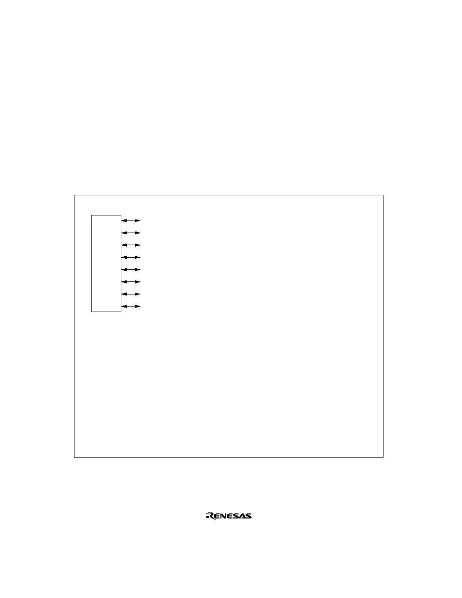
262
8.12
Port F
8.12.1
Overview
Port F is an 8-bit I/O port. Port F pins also function as bus control signal input/output pins (
AS,
RD, HWR, LWR, WAIT, BREQO, BREQ, and BACK), the system clock (¯) output pin and
interrupt input pins (
IRQ0 to IRQ3).
The interrupt input pins (
IRQ0 to IRQ3) are Schmitt-triggered inputs.
Figure 8-24 shows the port F pin configuration.
PF
7
/ ¯
PF
6
/
AS
PF
5
/
RD
PF
4
/
HWR
PF
3
/
LWR
/
IRQ3
PF
2
/
WAIT
/
BREQO
/
IRQ2
PF
1
/
BACK
/
IRQ1
PF
0
/
BREQ
/
IRQ0
Port F
Note:
*
Modes 2, 3, 6, and 7 cannot be used in the H8S/2240.
PF
7
(input)/¯(output)
AS
(output)
RD
(output)
HWR
(output)
LWR
(output)
PF
2
(I/O)/
WAIT
(input)/
BREQO
(output)/
IRQ2
(input)
PF
1
(I/O)/
BACK
(output)/
IRQ1
(input)
PF
0
(I/O)/
BREQ
(input)/
IRQ0
(input)
Port F pins
Pin functions in modes 1, 2, 4, 5, and 6
*
PF
7
(input)/¯ (output)
PF
6
(I/O)
PF
5
(I/O)
PF
4
(I/O)
PF
3
(I/O)/
IRQ3
(input)
PF
2
(I/O)/
IRQ2
(input)
PF
1
(I/O)/
IRQ1
(input)
PF
0
(I/O)/
IRQ0
(input)
Pin functions in modes 3 and 7
*
Figure 8-24 Port F Pin Functions
263
8.12.2
Register Configuration
Table 8-21 shows the port F register configuration.
Table 8-21 Port F Registers
Name
Abbreviation
R/W
Initial Value
Address
*
1
Port F data direction register
PFDDR
W
H'80/H'00
*
2
H'FEBE
Port F data register
PFDR
R/W
H'00
H'FF6E
Port F register
PORTF
R
Undefined
H'FF5E
Notes: 1. Lower 16 bits of the address.
2. Initial value depends on the mode.
Port F Data Direction Register (PFDDR)
7
PF7DDR
1
W
0
W
6
PF6DDR
0
W
0
W
5
PF5DDR
0
W
0
W
4
PF4DDR
0
W
0
W
3
PF3DDR
0
W
0
W
0
PF0DDR
0
W
0
W
2
PF2DDR
0
W
0
W
1
PF1DDR
0
W
0
W
Bit
Modes 1, 2, 4, 5, 6
Initial value
R/W
Modes 3 and 7
Initial value
R/W
:
:
:
:
:
PFDDR is an 8-bit write-only register, the individual bits of which specify input or output for the
pins of port F. PFDDR cannot be read; if it is, an undefined value will be read.
PFDDR is initialized by a power-on reset, and in hardware standby mode, to H'80 in modes 1, 2,
4, 5, and 6, and to H'00 in modes 3 and 7. It retains its prior state after a manual reset, and in
software standby mode. The OPE bit in SBYCR is used to select whether the bus control output
pins retain their output state or become high-impedance when a transition is made to software
standby mode.
∑
Modes 1, 2, 4, 5, and 6
Pin PF
7
functions as the ¯ output pin when the corresponding PFDDR bit is set to 1, and as an
input port when the bit is cleared to 0.
The input/output direction specified by PFDDR is ignored for pins PF
6
to PF
3
, which are
automatically designated as bus control outputs (
AS, RD, HWR, and LWR).

264
For pins PF
2
to PF
0
, setting a PFDDR bit to 1 makes the corresponding port F pin an output
port, while clearing the bit to 0 makes the pin an input port.
Note:
Modes 2 and 6 cannot be used in the H8S/2240.
∑
Modes 3 and 7
Setting a PFDDR bit to 1 makes the corresponding port F pin PF
6
to PF
0
an output port, or in
the case of pin PF
7
, the ¯ output pin. Clearing the bit to 0 makes the pin an input port.
Note:
Modes 3 and 7 cannot be used in the H8S/2240.
Port F Data Register (PFDR)
7
PF7DR
0
R/W
6
PF6DR
0
R/W
5
PF5DR
0
R/W
4
PF4DR
0
R/W
3
PF3DR
0
R/W
0
PF0DR
0
R/W
2
PF2DR
0
R/W
1
PF1DR
0
R/W
Bit
Initial value
R/W
:
:
:
PFDR is an 8-bit readable/writable register that stores output data for the port F pins (PF
7
to PF
0
).
PFDR is initialized to H'00 by a power-on reset, and in hardware standby mode. It retains its prior
state after a manual reset, and in software standby mode.
Port F Register (PORTF)
7
PF7
--
*
R
6
PF6
--
*
R
5
PF5
--
*
R
4
PF4
--
*
R
3
PF3
--
*
R
0
PF0
--
*
R
2
PF2
--
*
R
1
PF1
--
*
R
Bit
Initial value
R/W
Note:
*
Determined by state of pins PF
7
to PF
0
.
:
:
:
PORTF is an 8-bit read-only register that shows the pin states. Writing of output data for the port
F pins (PF
7
to PF
0
) must always be performed on PFDR.
If a port F read is performed while PFDDR bits are set to 1, the PFDR values are read. If a port F
read is performed while PFDDR bits are cleared to 0, the pin states are read.
After a power-on reset and in hardware standby mode, PORTF contents are determined by the pin
states, as PFDDR and PFDR are initialized. PORTF retains its prior state after a manual reset, and
in software standby mode.

265
8.12.3
Pin Functions
Port F pins also function as bus control signal input/output pins (
AS, RD, HWR, LWR, WAIT,
BREQO, BREQ, and BACK), the system clock (¯) output pin and interrupt input pins (IRQ0 to
IRQ
3). The pin functions differ between modes 1, 2, 4, 5, and 6, and modes 3 and 7. Port F pin
functions are shown in table 8-22.
Table 8-22 Port F Pin Functions
Pin
Selection Method and Pin Functions
PF
7
/¯
The pin function is switched as shown below according to bit PF7DDR.
PF7DDR
0
1
Pin function
PF
7
input pin
¯ output pin
PF
6
/
AS
The pin function is switched as shown below according to the operating mode
and bit PF6DDR.
Operating
Mode
Modes 1, 2, 4, 5, 6
*
Modes 3 and 7
*
PF6DDR
--
0
1
Pin function
AS
output pin
PF
6
input pin
PF
6
output pin
Note:
*
Modes 2, 3, 6, and 7 cannot be used in the H8S/2240.
PF
5
/
RD
The pin function is switched as shown below according to the operating mode
and bit PF5DDR.
Operating
Mode
Modes 1, 2, 4, 5, 6
*
Modes 3 and 7
*
PF5DDR
--
0
1
Pin function
RD
output pin
PF
5
input pin
PF
5
output pin
Note:
*
Modes 2, 3, 6, and 7 cannot be used in the H8S/2240.
PF
4
/
HWR
The pin function is switched as shown below according to the operating mode
and bit PF4DDR.
Operating
Mode
Modes 1, 2, 4, 5, 6
*
Modes 3 and 7
*
PF4DDR
--
0
1
Pin function
HWR
output pin
PF
4
input pin
PF
4
output pin
Note:
*
Modes 2, 3, 6, and 7 cannot be used in the H8S/2240.

266
Table 8-22 Port F Pin Functions (cont)
Pin
Selection Method and Pin Functions
PF
3
/
LWR
/
IRQ3
The pin function is switched as shown below according to the operating mode
and bit PF3DDR.
Operating
Mode
Modes
1, 2, 4, 5, 6
*
2
Modes
3 and 7
*
2
PF3DDR
--
0
1
Pin function
LWR
output pin
PF
3
input pin
PF
3
output pin
IRQ3
interrupt input pin
*
1
Notes: 1. When this pin is used as an external interrupt input, it should not be
used as an input/output pin with other functions.
2. Modes 2, 3, 6, and 7 cannot be used in the H8S/2240.
PF
2
/
WAIT
/
BREQO
/
IRQ2
The pin function is switched as shown below according to the operating mode,
and the BREQOE bit, WAITE bit in BCRL, and PF2DDR bit.
Operating
Mode
Modes 1, 2, 4, 5, 6
*
2
Modes 3 and 7
*
2
BREQOE
0
1
--
WAITE
0
1
--
--
PF2DDR
0
1
--
--
0
1
Pin function
PF
2
input pin
PF
2
output pin
WAIT
input pin
BREQO
output pin
PF
2
input pin
PF
2
output pin
IRQ2
interrupt input pin
*
1
Notes: 1. When this pin is used as an external interrupt input, it should not be
used as an input/output pin with other functions.
2. Modes 2, 3, 6, and 7 cannot be used in the H8S/2240.
267
Table 8-22 Port F Pin Functions (cont)
Pin
Selection Method and Pin Functions
PF
1
/
BACK
/
IRQ1
The pin function is switched as shown below according to the operating mode,
and the BRLE bit in BCRL and PF1DDR bit.
Operating
Mode
Modes 1, 2, 4, 5, 6
*
2
Modes 3 and 7
*
2
BRLE
0
1
--
PF1DDR
0
1
--
0
1
Pin function
PF
1
input pin
PF
1
output pin
BACK
output pin
PF
1
input pin
PF
1
output pin
IRQ1
interrupt input pin
*
1
Notes: 1. When this pin is used as an external interrupt input, it should not be
used as an input/output pin with other functions.
2. Modes 2, 3, 6, and 7 cannot be used in the H8S/2240.
PF
0
/
BREQ
/
IRQ0
The pin function is switched as shown below according to the operating mode,
and the BRLE bit in BCRL and PF0DDR bit.
Operating
Mode
Modes 1, 2, 4, 5, 6
*
2
Modes 3 and 7
*
2
BRLE
0
1
--
PF0DDR
0
1
--
0
1
Pin function
PF
0
input pin
PF
0
output pin
BREQ
input pin
PF
0
input pin
PF
0
output pin
IRQ0
interrupt input pin
*
1
Notes: 1. When this pin is used as an external interrupt input, it should not be
used as an input/output pin with other functions.
2. Modes 2, 3, 6, and 7 cannot be used in the H8S/2240.

268
8.13
Port G
8.13.1
Overview
Port G is a 5-bit I/O port. Port G pins also function as bus control signal output pins (
CS0 to CS3).
The A/D converter input pin (
ADTRG), and interrupt input pins (IRQ6, IRQ7). The interrupt input
pins (
IRQ6, IRQ7) are Schmitt-triggered inputs.
Figure 8-25 shows the port G pin configuration.
PG
4
/
CS0
PG
3
/
CS1
PG
2
/
CS2
PG
1
/
CS3
/
IRQ7
PG
0
/
ADTRG
/
IRQ6
PG
4
PG
3
PG
2
PG
1
PG
0
Note:
*
Modes 2, 3, 6, and 7 cannot be used in the H8S/2240.
(I/O)
(I/O)
(I/O)
(I/O)/
IRQ7
(input)
(I/O)/
Port G pins
Pin functions in modes 3 and 7
*
Pin functions in modes 4 to 6
*
PG
4
PG
3
PG
2
PG
1
PG
0
(input)/
(I/O)
(I/O)
(I/O)/
IRQ7
(input)
(I/O)/
ADTRG
(input)/
IRQ6
(input)
CS0
(output)
Pin functions in modes 1 and 2
*
PG
4
PG
3
PG
2
PG
1
PG
0
(input)/
(input)/
(input)/
(input)/
(I/O)/
CS0
CS1
CS2
CS3
(output)
(output)
(output)
(output)/
IRQ7
(input)
Port G
ADTRG
(input)/
IRQ6
(input)
ADTRG
(input)/
IRQ6
(input)
Figure 8-25 Port G Pin Functions

269
8.13.2
Register Configuration
Table 8-23 shows the port G register configuration.
Table 8-23 Port G Registers
Name
Abbreviation
R/W
Initial Value*
1
Address
*
2
Port G data direction register
PGDDR
W
H'00/H'10
*
3
H'FEBF
Port G data register
PGDR
R/W
H'00
H'FF6F
Port G register
PORTG
R
Undefined
H'FF5F
Notes: 1. Value of bits 4 to 0.
2. Lower 16 bits of the address.
3. Initial value depends on the mode.
Port G Data Direction Register (PGDDR)
7
--
Undefined
--
Undefined
--
6
--
Undefined
--
Undefined
--
5
--
Undefined
--
Undefined
--
4
PG4DDR
1
W
0
W
3
PG3DDR
0
W
0
W
0
PG0DDR
0
W
0
W
2
PG2DDR
0
W
0
W
1
PG1DDR
0
W
0
W
Bit
Modes 1, 4, 5
Initial value
R/W
Modes 2, 3, 6, 7
Initial value
R/W
:
:
:
:
:
PGDDR is an 8-bit write-only register, the individual bits of which specify input or output for the
pins of port G. PGDDR cannot be read, and bits 7 to 5 are reserved. If PGDDR is read, an
undefined value will be read.
PGDDR is initialized by a power-on reset, and in hardware standby mode, to H'10 (bits 4 to 0) in
modes 1, 4, and 5, and to H'00 (bits 4 to 0) in modes 2, 3, 6, and 7. It retains its prior state after a
manual reset, and in software standby mode. The OPE bit in SBYCR is used to select whether the
bus control output pins retain their output state or become high-impedance when a transition is
made to software standby mode.
Note:
Modes 2, 3, 6, and 7 cannot be used in the H8S/2240.

270
∑
Modes 1, 2, 4, 5, and 6
Pins PG
4
to PG
1
function as bus control output pins (
CS
0
to
CS
3
) when the corresponding
PGDDR bits are set to 1, and as input ports when the bits are cleared to 0.
Pin PG
0
is an output port when the corresponding PGDDR bit is set to 1, and an input port
when the bit is cleared to 0.
Note:
Modes 2 and 6 cannot be used in the H8S/2240.
∑
Modes 3 and 7
Setting a PGDDR bit to 1 makes the corresponding port G pin an output port, while clearing
the bit to 0 makes the pin an input port.
Note:
Modes 3 and 7 cannot be used in the H8S/2240.
Port G Data Register (PGDR)
7
--
Undefined
--
6
--
Undefined
--
5
--
Undefined
--
4
PG4DR
0
R/W
3
PG3DR
0
R/W
0
PG0DR
0
R/W
2
PG2DR
0
R/W
1
PG1DR
0
R/W
Bit
Initial value
R/W
:
:
:
PGDR is an 8-bit readable/writable register that stores output data for the port G pins (PG
4
to
PG
0
).
Bits 7 to 5 are reserved; they return an undetermined value if read, and cannot be modified.
PGDR is initialized to H'00 (bits 4 to 0) by a power-on reset, and in hardware standby mode. It
retains its prior state after a manual reset, and in software standby mode.
Port G Register (PORTG)
7
--
Undefined
--
6
--
Undefined
--
5
--
Undefined
--
4
PG4
--
*
R
3
PG3
--
*
R
0
PG0
--
*
R
2
PG2
--
*
R
1
PG1
--
*
R
Bit
Initial value
R/W
Note:
*
Determined by state of pins PG
4
to PG
0
.
:
:
:
PORTG is an 8-bit read-only register that shows the pin states. It cannot be written to. Writing of
output data for the port G pins (PG
4
to PG
0
) must always be performed on PGDR.
Bits 7 to 5 are reserved; they return an undetermined value if read, and cannot be modified.

271
If a port G read is performed while PGDDR bits are set to 1, the PGDR values are read. If a port G
read is performed while PGDDR bits are cleared to 0, the pin states are read.
After a power-on reset and in hardware standby mode, PORTG contents are determined by the pin
states, as PGDDR and PGDR are initialized. PORTG retains its prior state after a manual reset,
and in software standby mode.
8.13.3
Pin Functions
Port G pins also function as bus control signal output pins (
CS0 to CS3) the A/D converter input
pin (
ADTRG), and interrupt input pins (IRQ6, IRQ7). The pin functions are different in modes 1
and 2, modes 3 and 7, and modes 4 to 6. Port G pin functions are shown in table 8-24.
Table 8-24 Port G Pin Functions
Pin
Selection Method and Pin Functions
PG
4
/
CS0
The pin function is switched as shown below according to the operating mode
and bit PG4DDR.
Operating
Mode
Modes 1, 2, 4, 5, 6
*
Modes 3 and 7
*
PG4DDR
0
1
0
1
Pin function
PG
4
input pin
CS0
output pin PG
4
input pin PG
4
output pin
Note:
*
Modes 2, 3, 6, and 7 cannot be used in the H8S/2240.
PG
3
/
CS1
The pin function is switched as shown below according to the operating mode
and bit PG3DDR.
Operating
Mode
Modes 1, 2, 3, 7
*
Modes 4 to 6
*
PG3DDR
0
1
0
1
Pin function
PG
3
input pin PG
3
output pin PG
3
input pin
CS1
output pin
Note:
*
Modes 2, 3, 6, and 7 cannot be used in the H8S/2240.
PG
2
/
CS2
The pin function is switched as shown below according to the operating mode
and bit PG2DDR.
Operating
Mode
Modes 1, 2, 3, 7
*
Modes 4 to 6
*
PG2DDR
0
1
0
1
Pin function
PG
2
input pin PG
2
output pin PG
2
input pin
CS2
output pin
Note:
*
Modes 2, 3, 6, and 7 cannot be used in the H8S/2240.
272
Table 8-24 Port G Pin Functions (cont)
Pin
Selection Method and Pin Functions
PG
1
/
CS3
/
IRQ7
The pin function is switched as shown below according to the combination of
operating mode and bit PG1DDR.
Operating
Mode
Modes 1, 2, 3, 7
*
2
Modes 4 to 6
*
2
PG1DDR
0
1
0
1
Pin function
PG
1
input pin PG
1
output pin PG
1
input pin
CS3
output pin
IRQ7
interrupt input pin
*
1
Notes: 1.
When this pin is used as an external interrupt input, it should not be
used as an input/output pin with other functions.
2. Modes 2, 3, 6, and 7 cannot be used in the H8S/2240.
PG
0
/
ADTRG
/
IRQ6
The pin function is switched as shown below according to the combination of
bits TRGS1 and TRGS0 in the A/D ADCR and bit PG0DDR.
PG0DDR
0
1
Pin function
PG
0
input
PG
0
output
ADTRG
input pin
*
1
IRQ6
interrupt input pin
*
2
Notes: 1.
ADTRG
input when TRGS0 = TRGS1 = 1.
2. When this pin is used as an external interrupt input, it should not be
used as an input/output pin with other functions.

273
Section 9 16-Bit Timer Pulse Unit (TPU)
9.1
Overview
The H8S/2245 Series has an on-chip 16-bit timer pulse unit (TPU) that comprises three 16-bit
timer channels.
9.1.1
Features
∑
Maximum 8-pulse input/output
∑
A total of 8 timer general registers (TGRs) are provided (four for channel 0 and two each for
channels 1, and 2), each of which can be set independently as an output compare/input capture
register
TGRC and TGRD for channel 0 can also be used as buffer registers
∑
Selection of 7 or 8 counter input clocks for each channel
∑
The following operations can be set for each channel:
Waveform output at compare match: Selection of 0, 1, or toggle output
Input capture function: Selection of rising edge, falling edge, or both edge detection
Counter clear operation: Counter clearing possible by compare match or input capture
Synchronous operation: Multiple timer counters (TCNT) can be written to simultaneously
Simultaneous clearing by compare match and input capture possible
Register simultaneous input/output possible by counter synchronous operation
PWM mode: Any PWM output duty can be set
Maximum of 7-phase PWM output possible by combination with synchronous operation
∑
Buffer operation settable for channel 0
Input capture register double-buffering possible
Automatic rewriting of output compare register possible
∑
Phase counting mode settable independently for each of channels 1, and 2
Two-phase encoder pulse up/down-count possible
∑
Fast access via internal 16-bit bus
Fast access is possible via a 16-bit bus interface

274
∑
13 interrupt sources
For channel 0 four compare match/input capture dual-function interrupts and one overflow
interrupt can be requested independently
For channels 1, and 2, two compare match/input capture dual-function interrupts, one
overflow interrupt, and one underflow interrupt can be requested independently
∑
Automatic transfer of register data
Block transfer, 1-word data transfer, and 1-byte data transfer possible by data transfer
controller (DTC) activation
∑
A/D converter conversion start trigger can be generated
Channel 2 to 0 compare match A/input capture A signals can be used as A/D converter
conversion start trigger
∑
Module stop mode can be set
As the initial setting, TPU operation is halted. Register access is enabled by exiting module
stop mode.
Table 9-1 lists the functions of the TPU.

275
Table 9-1
TPU Functions (1)
Item
Channel 0
Channel 1
Channel 2
Count clock
¯/1
¯/4
¯/16
¯/64
TCLKA
TCLKB
TCLKC
TCLKD
¯/1
¯/4
¯/16
¯/64
¯/256
TCLKA
TCLKB
¯/1
¯/4
¯/16
¯/64
¯/1024
TCLKA
TCLKB
TCLKC
General registers
TGR0A
TGR0B
TGR1A
TGR1B
TGR2A
TGR2B
General registers/
buffer registers
TGR0C
TGR0D
--
--
I/O pins
TIOCA0
TIOCB0
TIOCC0
TIOCD0
TIOCA1
TIOCB1
TIOCA2
TIOCB2
Counter clear
function
TGR compare match or
input capture
TGR compare match or
input capture
TGR compare match or
input capture
Compare 0 output
match
1 output
output
Toggle
output
Input capture
function
Synchronous
operation
PWM mode
Phase counting
mode
--
Buffer operation
--
--
Legend
: Possible
-- : Not possible

276
Table 9-1
TPU Functions (2)
Item
Channel 0
Channel 1
Channel 2
DTC activation
TGR compare match or
input capture
TGR compare match or
input capture
TGR compare match or
input capture
A/D converter trigger
TGR0A compare match
or input capture
TGR1A compare match
or input capture
TGR2A compare match
or input capture
Interrupt sources
5 sources
∑
Compare match or
input capture 0A
∑
Compare match or
input capture 0B
∑
Compare match or
input capture 0C
∑
Compare match or
input capture 0D
∑
Overflow
4 sources
∑
Compare match or
input capture 1A
∑
Compare match or
input capture 1B
∑
Overflow
∑
Underflow
4 sources
∑
Compare match or
input capture 2A
∑
Compare match or
input capture 2B
∑
Overflow
∑
Underflow

277
9.1.2
Block Diagram
Figure 9-1 shows a block diagram of the TPU.
Control logic
TMDR
TSR
TCR
TIOR
TIER
TGRA
TCNT
TGRB
TGRC
Channel 1
TMDR
TSR
TCR
TIOR
TIER
TGRA
TCNT
TGRB
Channel 0
TMDR
TSR
TCR
TIORH
TIER
Control logic for channels 0 to 2
TGRA
TCNT
TGRB
TGRD
TSYR
TSTR
Clock input
¯/1
¯/4
¯/16
¯/64
¯/256
¯/1024
TCLKA
TCLKB
TCLKC
TCLKD
Input/output pins
TIOCA0
TIOCB0
TIOCC0
TIOCD0
TIOCA1
TIOCB1
TIOCA2
TIOCB2
Interrupt request signals
Channel 0:
Channel 1:
Channel 2:
Internal data bus
A/D conversion
start request signal
TIORL
Module data bus
TGI0A
TGI0B
TGI0C
TGI0D
TCI0V
TGI1A
TGI1B
TCI1V
TCI1U
TGI2A
TGI2B
TCI2V
TCI2U
Internal clock:
External clock:
Channel 0:
Channel 1:
Channel 2:
Channel 2
Common
Bus interface
Figure 9-1 Block Diagram of TPU

278
9.1.3
Pin Configuration
Table 9-2 shows the pin configuration of the TPU.
Table 9-2
TPU Pins
Channel
Name
Symbol
I/O
Function
All
Clock input A
TCLKA
Input
External clock A input pin
(Channel 1 phase counting mode A phase
input)
Clock input B
TCLKB
Input
External clock B input pin
(Channel 1 phase counting mode B phase
input)
Clock input C
TCLKC
Input
External clock C input pin
(Channel 2 phase counting mode A phase
input)
Clock input D
TCLKD
Input
External clock D input pin
(Channel 2 phase counting mode B phase
input)
0
Input capture/output
compare match A0
TIOCA0
I/O
TGR0A input capture input/output compare
output/PWM output pin
Input capture/output
compare match B0
TIOCB0
I/O
TGR0B input capture input/output compare
output/PWM output pin
Input capture/output
compare match C0
TIOCC0
I/O
TGR0C input capture input/output compare
output/PWM output pin
Input capture/output
compare match D0
TIOCD0
I/O
TGR0D input capture input/output compare
output/PWM output pin
1
Input capture/output
compare match A1
TIOCA1
I/O
TGR1A input capture input/output compare
output/PWM output pin
Input capture/output
compare match B1
TIOCB1
I/O
TGR1B input capture input/output compare
output/PWM output pin
2
Input capture/output
compare match A2
TIOCA2
I/O
TGR2A input capture input/output compare
output/PWM output pin
Input capture/output
compare match B2
TIOCB2
I/O
TGR2B input capture input/output compare
output/PWM output pin

279
9.1.4
Register Configuration
Table 9-3 summarizes the TPU registers.
Table 9-3
TPU Registers
Channel
Name
Abbreviation
R/W
Initial Value
Address
*
1
0
Timer control register 0
TCR0
R/W
H'00
H'FFD0
Timer mode register 0
TMDR0
R/W
H'C0
H'FFD1
Timer I/O control register 0H
TIOR0H
R/W
H'00
H'FFD2
Timer I/O control register 0L
TIOR0L
R/W
H'00
H'FFD3
Timer interrupt enable register 0 TIER0
R/W
H'40
H'FFD4
Timer status register 0
TSR0
R/(W)
*
2
H'C0
H'FFD5
Timer counter 0
TCNT0
R/W
H'0000
H'FFD6
Timer general register 0A
TGR0A
R/W
H'FFFF
H'FFD8
Timer general register 0B
TGR0B
R/W
H'FFFF
H'FFDA
Timer general register 0C
TGR0C
R/W
H'FFFF
H'FFDC
Timer general register 0D
TGR0D
R/W
H'FFFF
H'FFDE
1
Timer control register 1
TCR1
R/W
H'00
H'FFE0
Timer mode register 1
TMDR1
R/W
H'C0
H'FFE1
Timer I/O control register 1
TIOR1
R/W
H'00
H'FFE2
Timer interrupt enable register 1 TIER1
R/W
H'40
H'FFE4
Timer status register 1
TSR1
R/(W)
*
2
H'C0
H'FFE5
Timer counter 1
TCNT1
R/W
H'0000
H'FFE6
Timer general register 1A
TGR1A
R/W
H'FFFF
H'FFE8
Timer general register 1B
TGR1B
R/W
H'FFFF
H'FFEA
2
Timer control register 2
TCR2
R/W
H'00
H'FFF0
Timer mode register 2
TMDR2
R/W
H'C0
H'FFF1
Timer I/O control register 2
TIOR2
R/W
H'00
H'FFF2
Timer interrupt enable register 2 TIER2
R/W
H'40
H'FFF4
Timer status register 2
TSR2
R/(W)
*
2
H'C0
H'FFF5
Timer counter 2
TCNT2
R/W
H'0000
H'FFF6
Timer general register 2A
TGR2A
R/W
H'FFFF
H'FFF8
Timer general register 2B
TGR2B
R/W
H'FFFF
H'FFFA

280
Table 9-2
TPU Registers (cont)
Channel
Name
Abbreviation
R/W
Initial Value
Address
*
1
All
Timer start register
TSTR
R/W
H'00
H'FFC0
Timer synchro register
TSYR
R/W
H'00
H'FFC1
Module stop control register
MSTPCR
R/W
H'3FFF
H'FF3C
Notes: 1. Lower 16 bits of the address.
2. Can only be written with 0 for flag clearing.

281
9.2
Register Descriptions
9.2.1
Timer Control Register (TCR)
7
CCLR2
0
R/W
6
CCLR1
0
R/W
5
CCLR0
0
R/W
4
CKEG1
0
R/W
3
CKEG0
0
R/W
0
TPSC0
0
R/W
2
TPSC2
0
R/W
1
TPSC1
0
R/W
Bit
Initial value
R/W
:
:
:
Channel 0: TCR0
7
--
0
--
6
CCLR1
0
R/W
5
CCLR0
0
R/W
4
CKEG1
0
R/W
3
CKEG0
0
R/W
0
TPSC0
0
R/W
2
TPSC2
0
R/W
1
TPSC1
0
R/W
Channel 1: TCR1
Channel 2: TCR2
Bit
Initial value
R/W
:
:
:
The TCR registers are 8-bit registers that control the TCNT channels. The TPU has three TCR
registers, one for each of channels 0 to 2. The TCR registers are initialized to H'00 by a reset, and
in hardware standby mode.
TCNT operation should be stopped when making TCR settings.

282
Bits 7, 6, 5--Counter Clear 2, 1, and 0 (CCLR2, CCLR1, CCLR0): These bits select the
TCNT counter clearing source.
Bit 7
Bit 6
Bit 5
Channel
CCLR2
CCLR1
CCLR0
Description
0
0
0
0
TCNT clearing disabled
(Initial value)
1
TCNT cleared by TGRA compare match/input
capture
1
0
TCNT cleared by TGRB compare match/input
capture
1
TCNT cleared by counter clearing for another
channel performing synchronous
clearing/synchronous operation
*
1
1
0
0
TCNT clearing disabled
1
TCNT cleared by TGRC compare match/input
capture
*
2
1
0
TCNT cleared by TGRD compare match/input
capture
*
2
1
TCNT cleared by counter clearing for another
channel performing synchronous
clearing/synchronous operation
*
1
Bit 7
Bit 6
Bit 5
Channel
Reserved
*
3
CCLR1
CCLR0
Description
1, 2
0
0
0
TCNT clearing disabled
(Initial value)
1
TCNT cleared by TGRA compare match/input
capture
1
0
TCNT cleared by TGRB compare match/input
capture
1
TCNT cleared by counter clearing for another
channel performing synchronous clearing/
synchronous operation
*
1
Notes: 1. Synchronous operation setting is performed by setting the SYNC bit in TSYR to 1.
2. When TGRC or TGRD is used as a buffer register, TCNT is not cleared because the
buffer register setting has priority, and compare match/input capture does not occur.
3. Bit 7 is reserved in channels 1and 2. It is always read as 0 and cannot be modified.

283
Bits 4 and 3--Clock Edge 1 and 0 (CKEG1, CKEG0): These bits select the input clock edge.
When a both-edges count is selected, a clock divided by two from the input clock can be selected.
(e.g. ¯/4 both edges = ¯/2 rising edge). If phase counting mode is used on channels 1, and 2, this
setting is ignored and the phase counting mode setting has priority.
Bit 4
Bit 3
CKEG1
CKEG0
Description
0
0
Count at rising edge
(Initial value)
1
Count at falling edge
1
--
Count at both edges
Note:
Internal clock edge selection is valid when the input clock is ¯/4 or slower. If ¯/1 is selected
for the input clock, this setting is ignored and a rising-edge count is selected.
Bits 2, 1, and 0--Time Prescaler 2, 1, and 0 (TPSC2 to TPSC0): These bits select the TCNT
counter clock. The clock source can be selected independently for each channel. Table 9-4 shows
the clock sources that can be set for each channel.
Table 9-4
TPU Clock Sources
Internal Clock
External Clock
Channel
¯/1
¯/4
¯/16
¯/64
¯/256
¯/1024
TCLKA
TCLKB
TCLKC
TCLKD
0
1
2
Legend
: Setting
Blank : No setting

284
Bit 2
Bit 1
Bit 0
Channel
TPSC2
TPSC1
TPSC0
Description
0
0
0
0
Internal clock: counts on ¯/1
(Initial value)
1
Internal clock: counts on ¯/4
1
0
Internal clock: counts on ¯/16
1
Internal clock: counts on ¯/64
1
0
0
External clock: counts on TCLKA pin input
1
External clock: counts on TCLKB pin input
1
0
External clock: counts on TCLKC pin input
1
External clock: counts on TCLKD pin input
Bit 2
Bit 1
Bit 0
Channel
TPSC2
TPSC1
TPSC0
Description
1
0
0
0
Internal clock: counts on ¯/1
(Initial value)
1
Internal clock: counts on ¯/4
1
0
Internal clock: counts on ¯/16
1
Internal clock: counts on ¯/64
1
0
0
External clock: counts on TCLKA pin input
1
External clock: counts on TCLKB pin input
1
0
Internal clock: counts on ¯/256
1
Setting prohibited
Note:
This setting is ignored when channel 1 is in phase counting mode.
Bit 2
Bit 1
Bit 0
Channel
TPSC2
TPSC1
TPSC0
Description
2
0
0
0
Internal clock: counts on ¯/1
(Initial value)
1
Internal clock: counts on ¯/4
1
0
Internal clock: counts on ¯/16
1
Internal clock: counts on ¯/64
1
0
0
External clock: counts on TCLKA pin input
1
External clock: counts on TCLKB pin input
1
0
External clock: counts on TCLKC pin input
1
Internal clock: counts on ¯/1024
Note:
This setting is ignored when channel 2 is in phase counting mode.

285
9.2.2
Timer Mode Register (TMDR)
7
--
1
--
6
--
1
--
5
BFB
0
R/W
4
BFA
0
R/W
3
MD3
0
R/W
0
MD0
0
R/W
2
MD2
0
R/W
1
MD1
0
R/W
Bit
Initial value
R/W
:
:
:
Channel 0: TMDR0
7
--
1
--
6
--
1
--
5
--
0
--
4
--
0
--
3
MD3
0
R/W
0
MD0
0
R/W
2
MD2
0
R/W
1
MD1
0
R/W
Bit
Initial value
R/W
:
:
:
Channel 1: TMDR1
Channel 2: TMDR2
The TMDR registers are 8-bit readable/writable registers that are used to set the operating mode
for each channel. The TPU has three TMDR registers, one for each channel. The TMDR registers
are initialized to H'C0 by a reset, and in hardware standby mode.
TCNT operation should be stopped when making TMDR settings.
Bits 7 and 6--Reserved: Read-only bits, always read as 1.
Bit 5--Buffer Operation B (BFB): Specifies whether TGRB is to operate in the normal way, or
TGRB and TGRD are to be used together for buffer operation. When TGRD is used as a buffer
register, TGRD input capture/output compare is not generated.
In channels 1 and 2, which have no TGRD, bit 5 is reserved. It is always read as 0 and cannot be
modified.
Bit 5
BFB
Description
0
TGRB operates normally
(Initial value)
1
TGRB and TGRD used together for buffer operation

286
Bit 4--Buffer Operation A (BFA): Specifies whether TGRA is to operate in the normal way, or
TGRA and TGRC are to be used together for buffer operation. When TGRC is used as a buffer
register, TGRC input capture/output compare is not generated.
In channels 1, and 2, which have no TGRC, bit 4 is reserved. It is always read as 0 and cannot be
modified.
Bit 4
BFA
Description
0
TGRA operates normally
(Initial value)
1
TGRA and TGRC used together for buffer operation
Bits 3 to 0--Modes 3 to 0 (MD3 to MD0): These bits are used to set the timer operating mode.
Bit 3
Bit 2
Bit 1
Bit 0
MD3
*
1
MD2
*
2
MD1
MD0
Description
0
0
0
0
Normal operation
(Initial value)
1
Reserved
1
0
PWM mode 1
1
PWM mode 2
1
0
0
Phase counting mode 1
1
Phase counting mode 2
1
0
Phase counting mode 3
1
Phase counting mode 4
1
*
*
*
--
*
: Don't care
Notes: 1. MD3 is a reserved bit. In a write, it should always be written with 0.
2. Phase counting mode cannot be set for channel 0. In this case, 0 should always be
written to MD2.

287
9.2.3
Timer I/O Control Register (TIOR)
7
IOB3
0
R/W
6
IOB2
0
R/W
5
IOB1
0
R/W
4
IOB0
0
R/W
3
IOA3
0
R/W
0
IOA0
0
R/W
2
IOA2
0
R/W
1
IOA1
0
R/W
Bit
Initial value
R/W
:
:
:
Channel 0: TIOR0H
Channel 1: TIOR1
Channel 2: TIOR2
7
IOD3
0
R/W
6
IOD2
0
R/W
5
IOD1
0
R/W
4
IOD0
0
R/W
3
IOC3
0
R/W
0
IOC0
0
R/W
2
IOC2
0
R/W
1
IOC1
0
R/W
Channel 0: TIOR0L
Note: When TGRC or TGRD is designated for buffer operation, this setting is invalid and the
register operates as a buffer register.
Bit
Initial value
R/W
:
:
:
The TIOR registers are 8-bit registers that control the TGR registers. The TPU has four TIOR
registers, two for channel 0 and one each for channels 1, and 2. The TIOR registers are initialized
to H'00 by a reset, and in hardware standby mode.
Care is required since TIOR is affected by the TMDR setting. The initial output specified by TIOR
is valid when the counter is stopped (the CST bit in TSTR is cleared to 0). Note also that, in PWM
mode 2, the output at the point at which the counter is cleared to 0 is specified.

288
Bits 7 to 4-- I/O Control B3 to B0 (IOB3 to IOB0)
I/O Control D3 to D0 (IOD3 to IOD0):
Bits IOB3 to IOB0 specify the function of TGRB.
Bits IOD3 to IOD0 specify the function of TGRD.
TIOR0H
Bit 7
Bit 6
Bit 5
Bit 4
Channel
IOB3 IOB2 IOB1 IOB0 Description
0
0
0
0
0
TGR0B is Output disabled
(Initial value)
1
output
Initial output is 0
0 output at compare match
1
0
compare
output
1 output at compare match
1
register
Toggle output at compare
match
1
0
0
Output disabled
1
Initial output is 1
0 output at compare match
1
0
output
1 output at compare match
1
Toggle output at compare
match
1
0
0
0
TGR0B is Capture input
Input capture at rising edge
1
input
source is
Input capture at falling edge
1
*
capture
TIOCB0 pin
Input capture at both edges
1
*
*
register
Setting prohibited
*
: Don't care

289
TIOR0L
Bit 7
Bit 6
Bit 5
Bit 4
Channel
IOD3 IOD2 IOD1 IOD0 Description
0
0
0
0
0
TGR0D is Output disabled
(Initial value)
1
output
Initial output is 0
0 output at compare match
1
0
compare
output
1 output at compare match
1
register
*
1
Toggle output at compare
match
1
0
0
Output disabled
1
Initial output is 1
0 output at compare match
1
0
output
1 output at compare match
1
Toggle output at compare
match
1
0
0
0
TGR0D is Capture input
Input capture at rising edge
1
input
source is
Input capture at falling edge
1
*
capture
TIOCD0 pin
Input capture at both edges
1
*
*
register
*
1
Seetting
prohibited
Note:
1. When the BFB bit in TMDR0 is set to 1 and TGR0D is used as a buffer register, this
setting is invalid and input capture/output compare is not generated.

290
TIOR1
Bit 7
Bit 6
Bit 5
Bit 4
Channel
IOB3 IOB2 IOB1 IOB0 Description
1
0
0
0
0
TGR1B is Output disabled
(Initial value)
1
output
Initial output is 0
0 output at compare match
1
0
compare
output
1 output at compare match
1
register
Toggle output at compare
match
1
0
0
Output disabled
1
Initial output is 1
0 output at compare match
1
0
output
1 output at compare match
1
Toggle output at compare
match
1
0
0
0
TGR1B is Capture input
Input capture at rising edge
1
input
source is
Input capture at falling edge
1
*
capture
TIOCB1 pin
Input capture at both edges
1
*
*
register
Setting prohibited
*
: Don't care
TIOR2
Bit 7
Bit 6
Bit 5
Bit 4
Channel
IOB3 IOB2 IOB1 IOB0 Description
2
0
0
0
0
TGR2B is Output disabled
(Initial value)
1
output
Initial output is 0
0 output at compare match
1
0
compare
output
1 output at compare match
1
register
Toggle output at compare
match
1
0
0
Output disabled
1
Initial output is 1
0 output at compare match
1
0
output
1 output at compare match
1
Toggle output at compare
match
1
*
0
0
TGR2B is Capture input
Input capture at rising edge
1
input
source is
Input capture at falling edge
1
*
capture
register
TIOCB2 pin
Input capture at both edges
*
: Don't care

291
Bits 3 to 0-- I/O Control A3 to A0 (IOA3 to IOA0)
I/O Control C3 to C0 (IOC3 to IOC0):
IOA3 to IOA0 specify the function of TGRA.
IOC3 to IOC0 specify the function of TGRC.
TIOR0H
Bit 3
Bit 2
Bit 1
Bit 0
Channel
IOA3 IOA2 IOA1 IOA0 Description
0
0
0
0
0
TGR0A is Output disabled
(Initial value)
1
output
Initial output is 0
0 output at compare match
1
0
compare
output
1 output at compare match
1
register
Toggle output at compare
match
1
0
0
Output disabled
1
Initial output is 1
0 output at compare match
1
0
output
1 output at compare match
1
Toggle output at compare
match
1
0
0
0
TGR0A is Capture input
Input capture at rising edge
1
input
source is
Input capture at falling edge
1
*
capture
TIOCA0 pin
Input capture at both edges
1
*
*
register
Setting prohibited
*
: Don't care

292
TIOR0L
Bit 3
Bit 2
Bit 1
Bit 0
Channel
IOC3 IOC2 IOC1 IOC0 Description
0
0
0
0
0
TGR0C is Output disabled
(Initial value)
1
output
Initial output is 0
0 output at compare match
1
0
compare
output
1 output at compare match
1
register
*
1
Toggle output at compare
match
1
0
0
Output disabled
1
Initial output is 1
0 output at compare match
1
0
output
1 output at compare match
1
Toggle output at compare
match
1
0
0
0
TGR0C is Capture input
Input capture at rising edge
1
input
source is
Input capture at falling edge
1
*
capture
TIOCC0 pin
Input capture at both edges
1
*
*
register
*
1
Setting prohibited
*
: Don't care
Note:
1. When the BFA bit in TMDR0 is set to 1 and TGR0C is used as a buffer register, this
setting is invalid and input capture/output compare is not generated.

293
TIOR1
Bit 3
Bit 2
Bit 1
Bit 0
Channel
IOA3 IOA2 IOA1 IOA0 Description
1
0
0
0
0
TGR1A is Output disabled
(Initial value)
1
output
Initial output is 0
0 output at compare match
1
0
compare
output
1 output at compare match
1
register
Toggle output at compare
match
1
0
0
Output disabled
1
Initial output is 1
0 output at compare match
1
0
output
1 output at compare match
1
Toggle output at compare
match
1
0
0
0
TGR1A is Capture input
Input capture at rising edge
1
input
source is
Input capture at falling edge
1
*
capture
TIOCA1 pin
Input capture at both edges
1
*
*
register
Setting prohibited
*
: Don't care
TIOR2
Bit 3
Bit 2
Bit 1
Bit 0
Channel
IOA3 IOA2 IOA1 IOA0 Description
2
0
0
0
0
TGR2A is Output disabled
(Initial value)
1
output
Initial output is 0
0 output at compare match
1
0
compare
output
1 output at compare match
1
register
Toggle output at compare
match
1
0
0
Output disabled
1
Initial output is 1
0 output at compare match
1
0
output
1 output at compare match
1
Toggle output at compare
match
1
*
0
0
TGR2A is Capture input
Input capture at rising edge
1
input
source is
Input capture at falling edge
1
*
capture
register
TIOCA2 pin
Input capture at both edges
*
: Don't care

294
9.2.4
Timer Interrupt Enable Register (TIER)
7
TTGE
0
R/W
6
--
1
--
5
--
0
--
4
TCIEV
0
R/W
3
TGIED
0
R/W
0
TGIEA
0
R/W
2
TGIEC
0
R/W
1
TGIEB
0
R/W
Bit
Initial value
R/W
:
:
:
Channel 0: TIER0
7
TTGE
0
R/W
6
--
1
--
5
TCIEU
0
R/W
4
TCIEV
0
R/W
3
--
0
--
0
TGIEA
0
R/W
2
--
0
--
1
TGIEB
0
R/W
Channel 1: TIER1
Channel 2: TIER2
Bit
Initial value
R/W
:
:
:
The TIER registers are 8-bit registers that control enabling or disabling of interrupt requests for
each channel. The TPU has three TIER registers, one for each channel. The TIER registers are
initialized to H'40 by a reset, and in hardware standby mode.

295
Bit 7--A/D Conversion Start Request Enable (TTGE): Enables or disables generation of A/D
conversion start requests by TGRA input capture/compare match.
Bit 7
TTGE
Description
0
A/D conversion start request generation disabled
(Initial value)
1
A/D conversion start request generation enabled
Bit 6--Reserved: Read-only bit, always read as 1.
Bit 5--Underflow Interrupt Enable (TCIEU): Enables or disables interrupt requests (TCIU) by
the TCFU flag when the TCFU flag in TSR is set to 1 in channels 1 and 2.
In channel 0 bit 5 is reserved. It is always read as 0 and cannot be modified.
Bit 5
TCIEU
Description
0
Interrupt requests (TCIU) by TCFU disabled
(Initial value)
1
Interrupt requests (TCIU) by TCFU enabled
Bit 4--Overflow Interrupt Enable (TCIEV): Enables or disables interrupt requests (TCIV) by
the TCFV flag when the TCFV flag in TSR is set to 1.
Bit 4
TCIEV
Description
0
Interrupt requests (TCIV) by TCFV disabled
(Initial value)
1
Interrupt requests (TCIV) by TCFV enabled
Bit 3--TGR Interrupt Enable D (TGIED): Enables or disables interrupt requests (TGID) by the
TGFD bit when the TGFD bit in TSR is set to 1 in channel 0.
In channels 1, and 2, bit 3 is reserved. It is always read as 0 and cannot be modified.
Bit 3
TGIED
Description
0
Interrupt requests (TGID) by TGFD bit disabled
(Initial value)
1
Interrupt requests (TGID) by TGFD bit enabled

296
Bit 2--TGR Interrupt Enable C (TGIEC): Enables or disables interrupt requests (TGIC) by the
TGFC bit when the TGFC bit in TSR is set to 1 in channel 0.
In channels 1, and 2, bit 2 is reserved. It is always read as 0 and cannot be modified.
Bit 2
TGIEC
Description
0
Interrupt requests (TGIC) by TGFC bit disabled
(Initial value)
1
Interrupt requests (TGIC) by TGFC bit enabled
Bit 1--TGR Interrupt Enable B (TGIEB): Enables or disables interrupt requests (TGIB) by the
TGFB bit when the TGFB bit in TSR is set to 1.
Bit 1
TGIEB
Description
0
Interrupt requests (TGIB) by TGFB bit disabled
(Initial value)
1
Interrupt requests (TGIB) by TGFB bit enabled
Bit 0--TGR Interrupt Enable A (TGIEA): Enables or disables interrupt requests (TGIA) by the
TGFA bit when the TGFA bit in TSR is set to 1.
Bit 0
TGIEA
Description
0
Interrupt requests (TGIA) by TGFA bit disabled
(Initial value)
1
Interrupt requests (TGIA) by TGFA bit enabled

297
9.2.5
Timer Status Register (TSR)
7
--
1
--
6
--
1
--
5
--
0
--
4
TCFV
0
R/(W)
*
3
TGFD
0
R/(W)
*
0
TGFA
0
R/(W)
*
2
TGFC
0
R/(W)
*
1
TGFB
0
R/(W)
*
Bit
Initial value
R/W
Note:
*
Can only be written with 0 for flag clearing.
:
:
:
Channel 0: TSR0
7
TCFD
1
R
6
--
1
--
5
TCFU
0
R/(W)
*
4
TCFV
0
R/(W)
*
3
--
0
--
0
TGFA
0
R/(W)
*
2
--
0
--
1
TGFB
0
R/(W)
*
Channel 1: TSR1
Channel 2: TSR2
Bit
Initial value
R/W
Note:
*
Can only be written with 0 for flag clearing.
:
:
:
The TSR registers are 8-bit registers that indicate the status of each channel. The TPU has three
TSR registers, one for each channel. The TSR registers are initialized to H'C0 by a reset, and in
hardware standby mode.

298
Bit 7--Count Direction Flag (TCFD): Status flag that shows the direction in which TCNT
counts in channels 1, and 2.
In channel 0 bit 7 is reserved. It is always read as 1 and cannot be modified.
Bit 7
TCFD
Description
0
TCNT counts down
1
TCNT counts up
(Initial value)
Bit 6--Reserved: Read-only bit, always read as 1.
Bit 5--Underflow Flag (TCFU): Status flag that indicates that TCNT underflow has occurred
when channels 1 and 2 are set to phase counting mode.
In channel 0 bit 5 is reserved. It is always read as 0 and cannot be modified.
Bit 5
TCFU
Description
0
[Clearing condition]
(Initial value)
When 0 is written to TCFU after reading TCFU = 1
1
[Setting condition]
When the TCNT value underflows (changes from H'0000 to H'FFFF)
Bit 4--Overflow Flag (TCFV): Status flag that indicates that TCNT overflow has occurred.
Bit 4
TCFV
Description
0
[Clearing condition]
(Initial value)
When 0 is written to TCFV after reading TCFV = 1
1
[Setting condition]
When the TCNT value overflows (changes from H'FFFF to H'0000 )

299
Bit 3--Input Capture/Output Compare Flag D (TGFD): Status flag that indicates the
occurrence of TGRD input capture or compare match in channel 0.
In channels 1, and 2, bit 3 is reserved. It is always read as 0 and cannot be modified.
Bit 3
TGFD
Description
0
[Clearing conditions]
(Initial value)
∑
When DTC is activated by TGID interrupt while DISEL bit of MRB in DTC is 0
∑
When 0 is written to TGFD after reading TGFD = 1
1
[Setting conditions]
∑
When TCNT = TGRD while TGRD is functioning as output compare register
∑
When TCNT value is transferred to TGRD by input capture signal while TGRD is
functioning as input capture register
Bit 2--Input Capture/Output Compare Flag C (TGFC): Status flag that indicates the
occurrence of TGRC input capture or compare match in channel 0.
In channels 1, and 2, bit 2 is reserved. It is always read as 0 and cannot be modified.
Bit 2
TGFC
Description
0
[Clearing conditions]
(Initial value)
∑
When DTC is activated by TGIC interrupt while DISEL bit of MRB in DTC is 0
∑
When 0 is written to TGFC after reading TGFC = 1
1
[Setting conditions]
∑
When TCNT = TGRC while TGRC is functioning as output compare register
∑
When TCNT value is transferred to TGRC by input capture signal while TGRC is
functioning as input capture register

300
Bit 1--Input Capture/Output Compare Flag B (TGFB): Status flag that indicates the
occurrence of TGRB input capture or compare match.
Bit 1
TGFB
Description
0
[Clearing conditions]
(Initial value)
∑
When DTC is activated by TGIB interrupt while DISEL bit of MRB in DTC is 0
∑
When 0 is written to TGFB after reading TGFB = 1
1
[Setting conditions]
∑
When TCNT = TGRB while TGRB is functioning as output compare register
∑
When TCNT value is transferred to TGRB by input capture signal while TGRB is
functioning as input capture register
Bit 0--Input Capture/Output Compare Flag A (TGFA): Status flag that indicates the
occurrence of TGRA input capture or compare match.
Bit 0
TGFA
Description
0
[Clearing conditions]
(Initial value)
∑
When DTC is activated by TGIA interrupt while DISEL bit of MRB in DTC is 0
∑
When 0 is written to TGFA after reading TGFA = 1
1
[Setting conditions]
∑
When TCNT = TGRA while TGRA is functioning as output compare register
∑
When TCNT value is transferred to TGRA by input capture signal while TGRA is
functioning as input capture register

301
9.2.6
Timer Counter (TCNT)
15
0
R/W
14
0
R/W
13
0
R/W
12
0
R/W
11
0
R/W
8
0
R/W
10
0
R/W
9
0
R/W
Bit
Initial value
R/W
:
:
:
7
0
R/W
6
0
R/W
5
0
R/W
4
0
R/W
3
0
R/W
0
0
R/W
2
0
R/W
1
0
R/W
Channel 0: TCNT0 (up-counter)
Channel 1: TCNT1 (up/down-counter
*
)
Channel 2: TCNT2 (up/down-counter
*
)
Note:
*
These counters can be used as up/down-counters only in phase counting mode. In other
cases they function as up-counters.
The TCNT registers are 16-bit counters. The TPU has three TCNT counters, one for each channel.
The TCNT counters are initialized to H'0000 by a reset, and in hardware standby mode.
The TCNT counters cannot be accessed in 8-bit units; they must always be accessed as a 16-bit
unit.
9.2.7
Timer General Register (TGR)
15
1
R/W
14
1
R/W
13
1
R/W
12
1
R/W
11
1
R/W
8
1
R/W
10
1
R/W
9
1
R/W
Bit
Initial value
R/W
:
:
:
7
1
R/W
6
1
R/W
5
1
R/W
4
1
R/W
3
1
R/W
0
1
R/W
2
1
R/W
1
1
R/W
The TGR registers are 16-bit registers with a dual function as output compare and input capture
registers. The TPU has 8 TGR registers, four for channel 0 and two each for channels 1, and 2.
TGRC and TGRD for channel 0 can also be designated for operation as buffer registers*. The
TGR registers are initialized to H'FFFF by a reset, and in hardware standby mode.
The TGR registers cannot be accessed in 8-bit units; they must always be accessed as a 16-bit unit.
Note: * TGR buffer register combinations are TGRA--TGRC and TGRB--TGRD.

302
9.2.8
Timer Start Register (TSTR)
7
--
0
--
6
--
0
--
5
--
0
--
4
--
0
--
3
--
0
--
0
CST0
0
R/W
2
CST2
0
R/W
1
CST1
0
R/W
Bit
Initial value
R/W
:
:
:
TSTR is an 8-bit readable/writable register that selects operation/stoppage for channels 0 to 2.
TSTR is initialized to H'00 by a reset, and in hardware standby mode.
TCNT counter operation should be stopped when setting the operating mode in TMDR or the
TCNT count clock in TCR.
Bits 7 and 3--Reserved: Should always be written with 0.
Bits 2 to 0--Counter Start 2 to 0 (CST2 to CST0): These bits select operation or stoppage for
TCNT.
Bit n
CSTn
Description
0
TCNTn count operation is stopped
(Initial value)
1
TCNTn performs count operation
n = 2 to 0
Note:
If 0 is written to the CST bit during operation with the TIOC pin designated for output, the
counter stops but the TIOC pin output compare output level is retained. If TIOR is written to
when the CST bit is cleared to 0, the pin output level will be changed to the set initial output
value.

303
9.2.9
Timer Synchro Register (TSYR)
7
--
0
--
6
--
0
--
5
--
0
--
4
--
0
--
3
--
0
--
0
SYNC0
0
R/W
2
SYNC2
0
R/W
1
SYNC1
0
R/W
Bit
Initial value
R/W
:
:
:
TSYR is an 8-bit readable/writable register that selects independent operation or synchronous
operation for the channel 0 to 2 TCNT counters. A channel performs synchronous operation when
the corresponding bit in TSYR is set to 1.
TSYR is initialized to H'00 by a reset, and in hardware standby mode.
Bits 7 and 3--Reserved: Should always be written with 0.
Bits 2 to 0--Timer Synchro 2 to 0 (SYNC2 to SYNC0): These bits select whether operation is
independent of or synchronized with other channels.
When synchronous operation is selected, synchronous presetting of multiple channels*
1
, and
synchronous clearing through counter clearing on another channel*
2
are possible.
Bit n
SYNCn
Description
0
TCNTn operates independently (TCNT presetting/clearing is unrelated to
other channels)
(Initial value)
1
TCNTn performs synchronous operation
TCNT synchronous presetting/synchronous clearing is possible
n = 2 to 0
Notes: 1. To set synchronous operation, the SYNC bits for at least two channels must be set to 1.
2. To set synchronous clearing, in addition to the SYNC bit , the TCNT clearing source
must also be set by means of bits CCLR2 to CCLR0 in TCR.

304
9.2.10
Module Stop Control Register (MSTPCR)
15
0
R/W
Bit
Initial value
R/W
:
:
:
14
0
R/W
13
1
R/W
12
1
R/W
11
1
R/W
10
1
R/W
9
1
R/W
8
1
R/W
7
1
R/W
6
1
R/W
5
1
R/W
4
1
R/W
3
1
R/W
2
1
R/W
1
1
R/W
0
1
R/W
MSTPCRH
MSTPCRL
MSTPCR is a 16-bit readable/writable register that performs module stop mode control.
When the MSTP13 bit in MSTPCR is set to 1, TPU operation stops at the end of the bus cycle and
a transition is made to module stop mode. For details, see section 18.5, Module Stop Mode.
MSTPCR is initialized to H'3FFF by a reset and in hardware standby mode. It is not initialized in
software standby mode.
Bit 13--Module Stop (MSTP13): Specifies the TPU module stop mode.
Bit 13
MSTP13
Description
0
TPU module stop mode cleared
1
TPU module stop mode set
(Initial value)
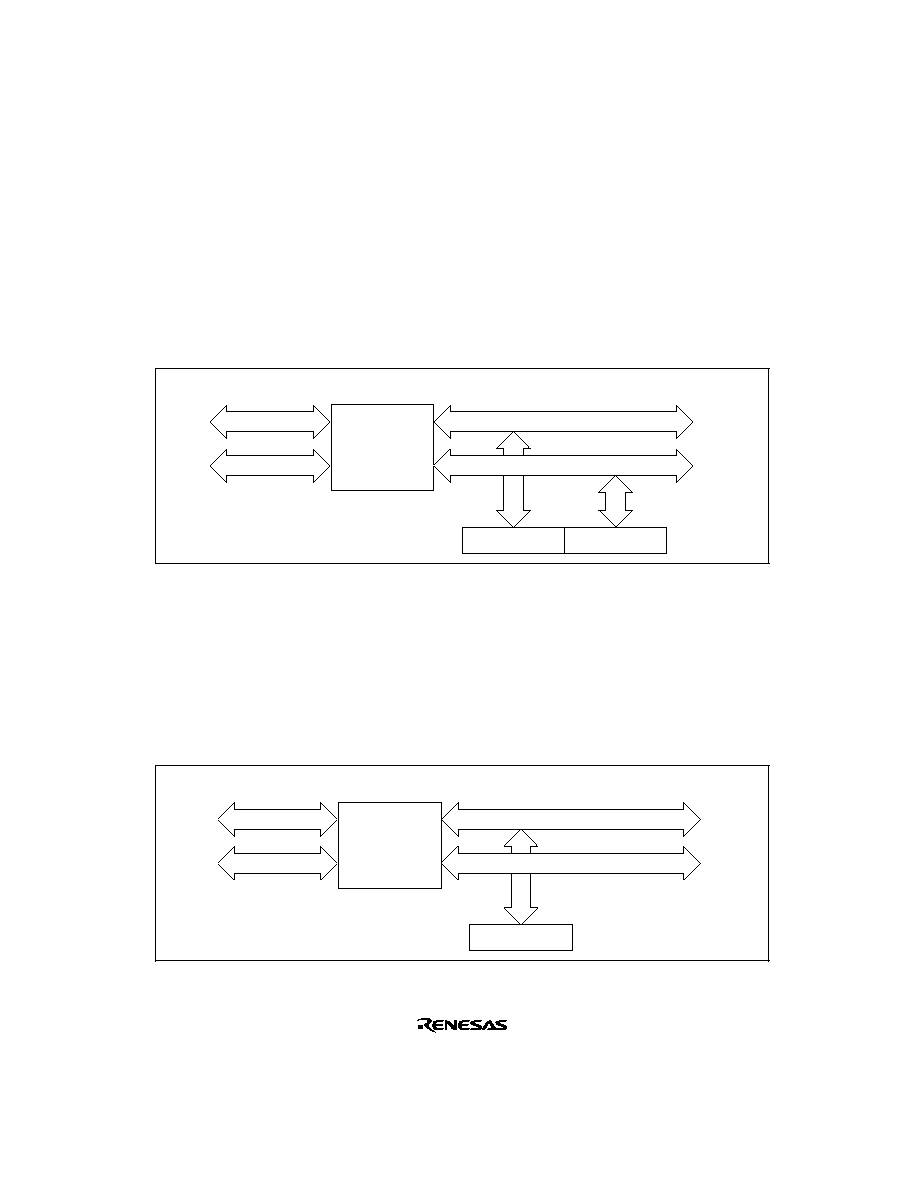
305
9.3
Interface to Bus Master
9.3.1
16-Bit Registers
TCNT and TGR are 16-bit registers. As the data bus to the bus master is 16 bits wide, these
registers can be read and written to in 16-bit units.
These registers cannot be read or written to in 8-bit units; 16-bit access must always be used.
An example of 16-bit register access operation is shown in figure 9-2.
Bus interface
H
Internal data bus
L
Bus
master
Module
data bus
TCNTH
TCNTL
Figure 9-2 16-Bit Register Access Operation [Bus Master
TCNT (16 Bits)]
9.3.2
8-Bit Registers
Registers other than TCNT and TGR are 8-bit. As the data bus to the CPU is 16 bits wide, these
registers can be read and written to in 16-bit units. They can also be read and written to in 8-bit
units.
Examples of 8-bit register access operation are shown in figures 9-3, 9-4, and 9-5.
Bus interface
H
Internal data bus
L
Module
data bus
TCR
Bus
master
Figure 9-3 8-Bit Register Access Operation [Bus Master
TCR (Upper 8 Bits)]

306
Bus interface
H
Internal data bus
L
Module
data bus
TMDR
Bus
master
Figure 9-4 8-Bit Register Access Operation [Bus Master
TMDR (Lower 8 Bits)]
Bus interface
H
Internal data bus
L
Module
data bus
TCR
TMDR
Bus
master
Figure 9-5 8-Bit Register Access Operation [Bus Master
TCR and TMDR (16 Bits)]

307
9.4
Operation
9.4.1
Overview
Operation in each mode is outlined below.
Normal Operation: Each channel has a TCNT and TGR register. TCNT performs up-counting,
and is also capable of free-running operation, synchronous counting, and external event counting.
Each TGR can be used as an input capture register or output compare register.
Synchronous Operation: When synchronous operation is designated for a channel, TCNT for
that channel performs synchronous presetting. That is, when TCNT for a channel designated for
synchronous operation is rewritten, the TCNT counters for the other channels are also rewritten at
the same time. Synchronous clearing of the TCNT counters is also possible by setting the timer
synchronization bits in TSYR for channels designated for synchronous operation.
Buffer Operation
∑
When TGR is an output compare register
When a compare match occurs, the value in the buffer register for the relevant channel is
transferred to TGR.
∑
When TGR is an input capture register
When input capture occurs, the value in TCNT is transfer to TGR and the value previously
held in TGR is transferred to the buffer register.
PWM Mode: In this mode, a PWM waveform is output. The output level can be set by means of
TIOR. A PWM waveform with a duty of between 0% and 100% can be output, according to the
setting of each TGR register.
Phase Counting Mode: In this mode, TCNT is incremented or decremented by detecting the
phases of two clocks input from the external clock input pins in channels 1, and 2. When phase
counting mode is set, the corresponding TCLK pin functions as the clock pin, and TCNT performs
up- or down-counting.
This can be used for two-phase encoder pulse input.

308
9.4.2
Basic Functions
Counter Operation: When one of bits CST0 to CST2 is set to 1 in TSTR, the TCNT counter for
the corresponding channel starts counting. TCNT can operate as a free-running counter, periodic
counter, and so on.
∑
Example of count operation setting procedure
Figure 9-6 shows an example of the count operation setting procedure.
Select counter clock
Operation selection
Select counter clearing source
Periodic counter
Set period
Start count operation
<Periodic counter>
[1]
[2]
[4]
[3]
[5]
Free-running counter
Start count operation
<Free-running counter>
[5]
[1]
[2]
[3]
[4]
[5]
Select the counter
clock with bits
TPSC2 to TPSC0 in
TCR. At the same
time, select the
input clock edge
with bits CKEG1
and CKEG0 in
TCR.
For periodic counter
operation, select
the TGR to be used
as the TCNT
clearing source with
bits CCLR2 to
CCLR0 in TCR.
Designate the TGR
selected in [2] as an
output compare
register by means
of TIOR.
Set the periodic
counter cycle in the
TGR selected in [2].
Set the CST bit in
TSTR to 1 to start
the count operation.
Select output compare register
Figure 9-6 Example of Counter Operation Setting Procedure

309
∑
Free-running count operation and periodic count operation
Immediately after a reset, the TPU's TCNT counters are all designated as free-running
counters. When the relevant bit in TSTR is set to 1 the corresponding TCNT counter starts up-
count operation as a free-running counter. When TCNT overflows (from H'FFFF to H'0000),
the TCFV bit in TSR is set to 1. If the value of the corresponding TCIEV bit in TIER is 1 at
this point, the TPU requests an interrupt. After overflow, TCNT starts counting up again from
H'0000.
Figure 9-7 illustrates free-running counter operation.
TCNT value
H'FFFF
H'0000
CST bit
TCFV
Time
Figure 9-7 Free-Running Counter Operation
When compare match is selected as the TCNT clearing source, the TCNT counter for the
relevant channel performs periodic count operation. The TGR register for setting the period is
designated as an output compare register, and counter clearing by compare match is selected
by means of bits CCLR2 to CCLR0 in TCR. After the settings have been made, TCNT starts
up-count operation as periodic counter when the corresponding bit in TSTR is set to 1. When
the count value matches the value in TGR, the TGF bit in TSR is set to 1 and TCNT is cleared
to H'0000.
If the value of the corresponding TGIE bit in TIER is 1 at this point, the TPU requests an
interrupt. After a compare match, TCNT starts counting up again from H'0000.
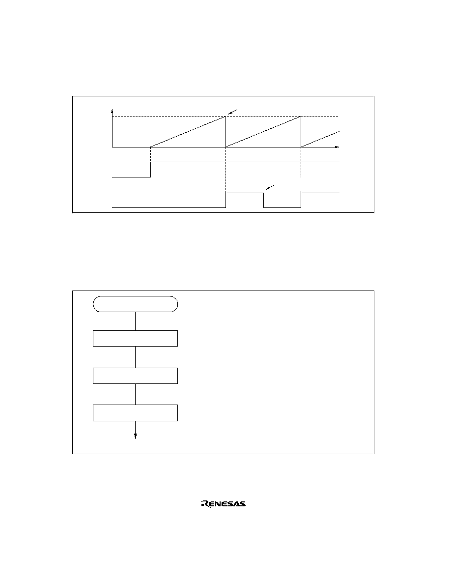
310
Figure 9-8 illustrates periodic counter operation.
TCNT value
TGR
H'0000
CST bit
TGF
Time
Counter cleared by TGR
compare match
Flag cleared by software or
DTC activation
Figure 9-8 Periodic Counter Operation
Waveform Output by Compare Match: The TPU can perform 0, 1, or toggle output from the
corresponding output pin using compare match.
∑
Example of setting procedure for waveform output by compare match
Figure 9-9 shows an example of the setting procedure for waveform output by compare match
Select waveform output mode
Output selection
Set output timing
Start count operation
<Waveform output>
[1]
[2]
[3]
[1] Select initial value 0 output or 1 output, and
compare match output value 0 output, 1
output, or toggle output, by means of TIOR.
The set initial value is output at the TIOC
pin until the first compare match occurs.
[2] Set the timing for compare match
generation in TGR.
[3] Set the CST bit in TSTR to 1 to start the
count operation.
Figure 9-9 Example Of Setting Procedure For Waveform Output By Compare Match
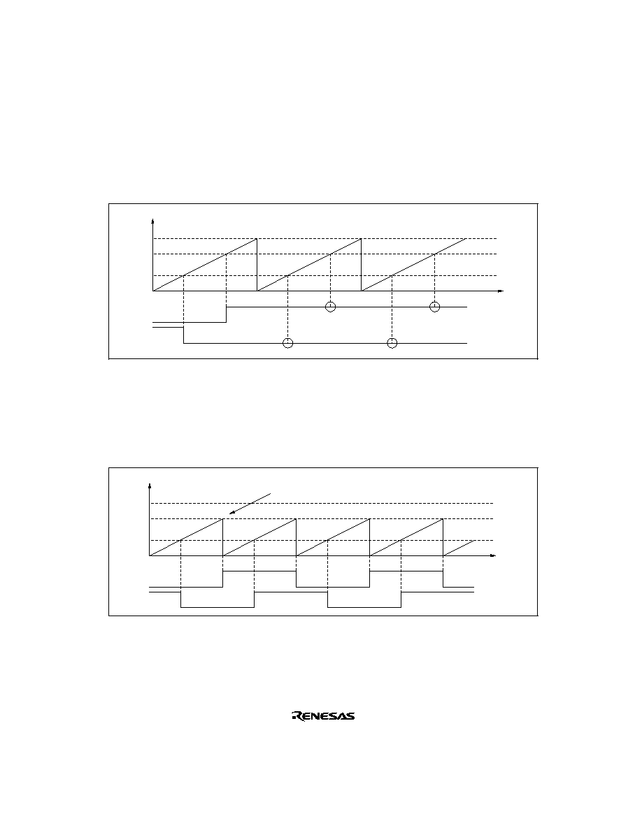
311
∑
Examples of waveform output operation
Figure 9-10 shows an example of 0 output/1 output.
In this example TCNT has been designated as a free-running counter, and settings have been
made so that 1 is output by compare match A, and 0 is output by compare match B. When the
set level and the pin level coincide, the pin level does not change.
TCNT value
H'FFFF
H'0000
TIOCA
TIOCB
Time
TGRA
TGRB
No change
No change
No change
No change
1 output
0 output
Figure 9-10 Example of 0 Output/1 Output Operation
Figure 9-11 shows an example of toggle output.
In this example TCNT has been designated as a periodic counter (with counter clearing
performed by compare match B), and settings have been made so that output is toggled by both
compare match A and compare match B.
TCNT value
H'FFFF
H'0000
TIOCB
TIOCA
Time
TGRB
TGRA
Toggle output
Toggle output
Counter cleared by TGRB compare match
Figure 9-11 Example of Toggle Output Operation
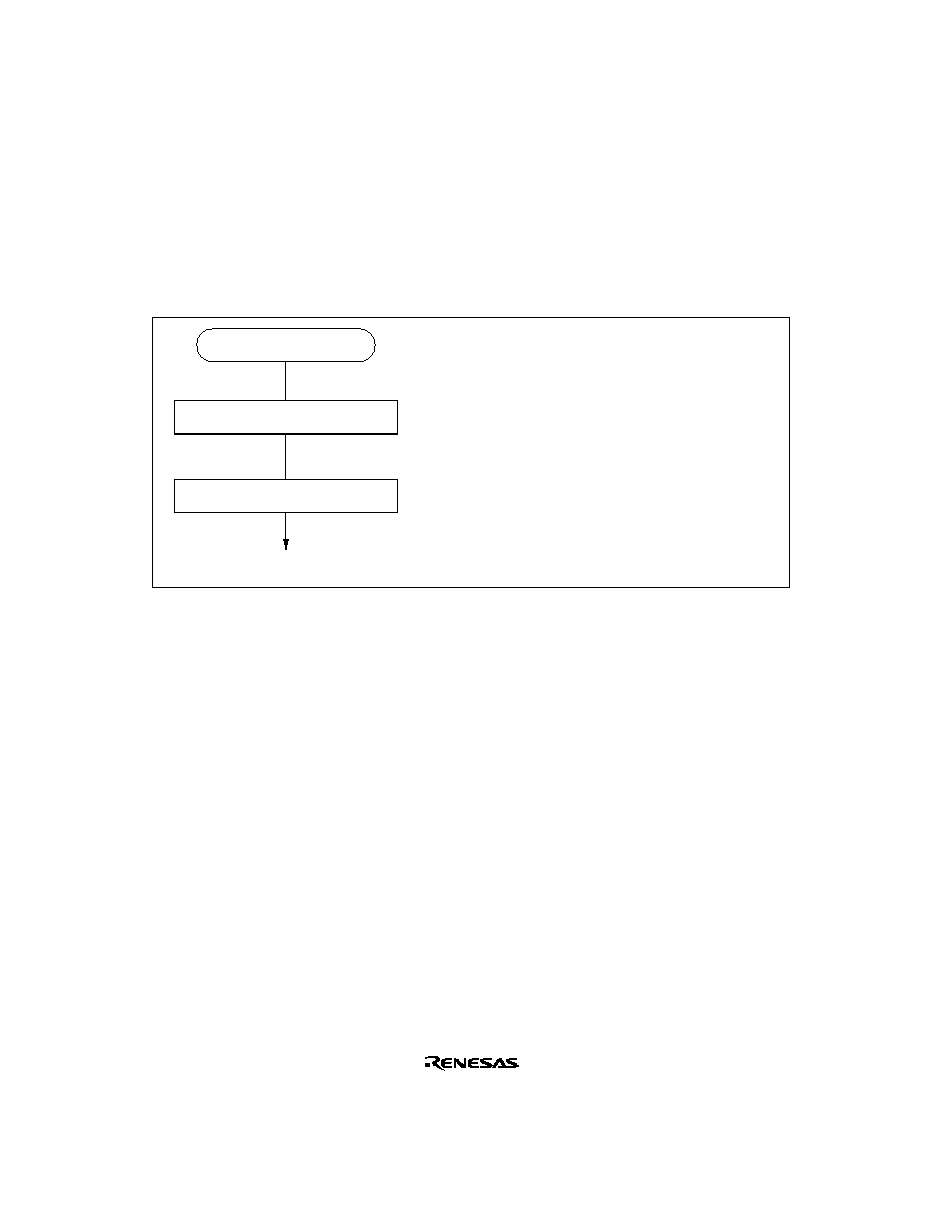
312
Input Capture Function: The TCNT value can be transferred to TGR on detection of the TIOC
pin input edge.
Rising edge, falling edge, or both edges can be selected as the detected edge.
∑
Example of input capture operation setting procedure
Figure 9-12 shows an example of the input capture operation setting procedure.
Select input capture input
Input selection
Start count
<Input capture operation>
[1]
[2]
[1] Designate TGR as an input capture register by
means of TIOR, and select rising edge, falling
edge, or both edges as the input capture
source and input signal edge.
[2] Set the CST bit in TSTR to 1 to start the count
operation.
Figure 9-12 Example of Input Capture Operation Setting Procedure
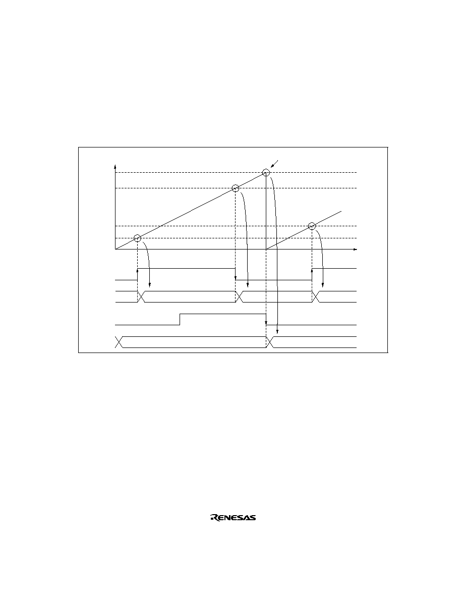
313
∑
Example of input capture operation
Figure 9-13 shows an example of input capture operation.
In this example both rising and falling edges have been selected as the TIOCA pin input
capture input edge, falling edge has been selected as the TIOCB pin input capture input edge,
and counter clearing by TGRB input capture has been designated for TCNT.
TCNT value
H'0180
H'0000
TIOCA
TGRA
Time
H'0010
H'0005
Counter cleared by TIOCB
input (falling edge)
H'0160
H'0005
H'0160
H'0010
TGRB
H'0180
TIOCB
Figure 9-13 Example of Input Capture Operation
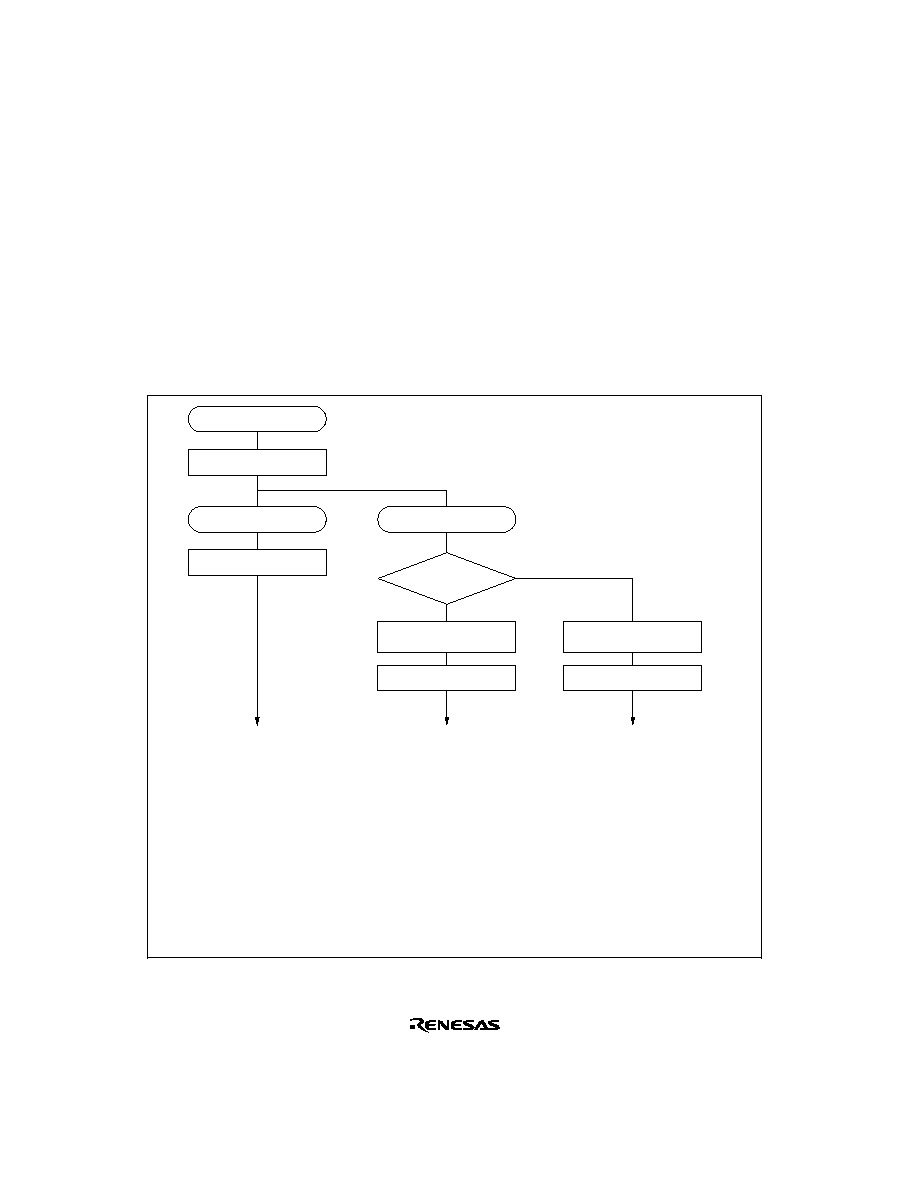
314
9.4.3
Synchronous Operation
In synchronous operation, the values in a number of TCNT counters can be rewritten
simultaneously (synchronous presetting). Also, a number of TCNT counters can be cleared
simultaneously by making the appropriate setting in TCR (synchronous clearing).
Synchronous operation enables TGR to be incremented with respect to a single time base.
Channels 0 to 2 can all be designated for synchronous operation.
Example of Synchronous Operation Setting Procedure: Figure 9-14 shows an example of the
synchronous operation setting procedure.
Set synchronous
operation
Synchronous operation
selection
Set TCNT
Synchronous presetting
<Synchronous presetting>
[1]
[2]
Synchronous clearing
Select counter
clearing source
<Counter clearing>
[3]
Start count
[5]
Set synchronous
counter clearing
<Synchronous clearing>
[4]
Start count
[5]
Clearing
sourcegeneration
channel?
No
Yes
[1]
[2]
[3]
[4]
[5]
Set to 1 the SYNC bits in TSYR corresponding to the channels to be designated for synchronous
operation.
When the TCNT counter of any of the channels designated for synchronous operation is
written to, the same value is simultaneously written to the other TCNT counters.
Use bits CCLR2 to CCLR0 in TCR to specify TCNT clearing by input capture/output compare,
etc.
Use bits CCLR2 to CCLR0 in TCR to designate synchronous clearing for the counter clearing
source.
Set to 1 the CST bits in TSTR for the relevant channels, to start the count operation.
Figure 9-14 Example of Synchronous Operation Setting Procedure
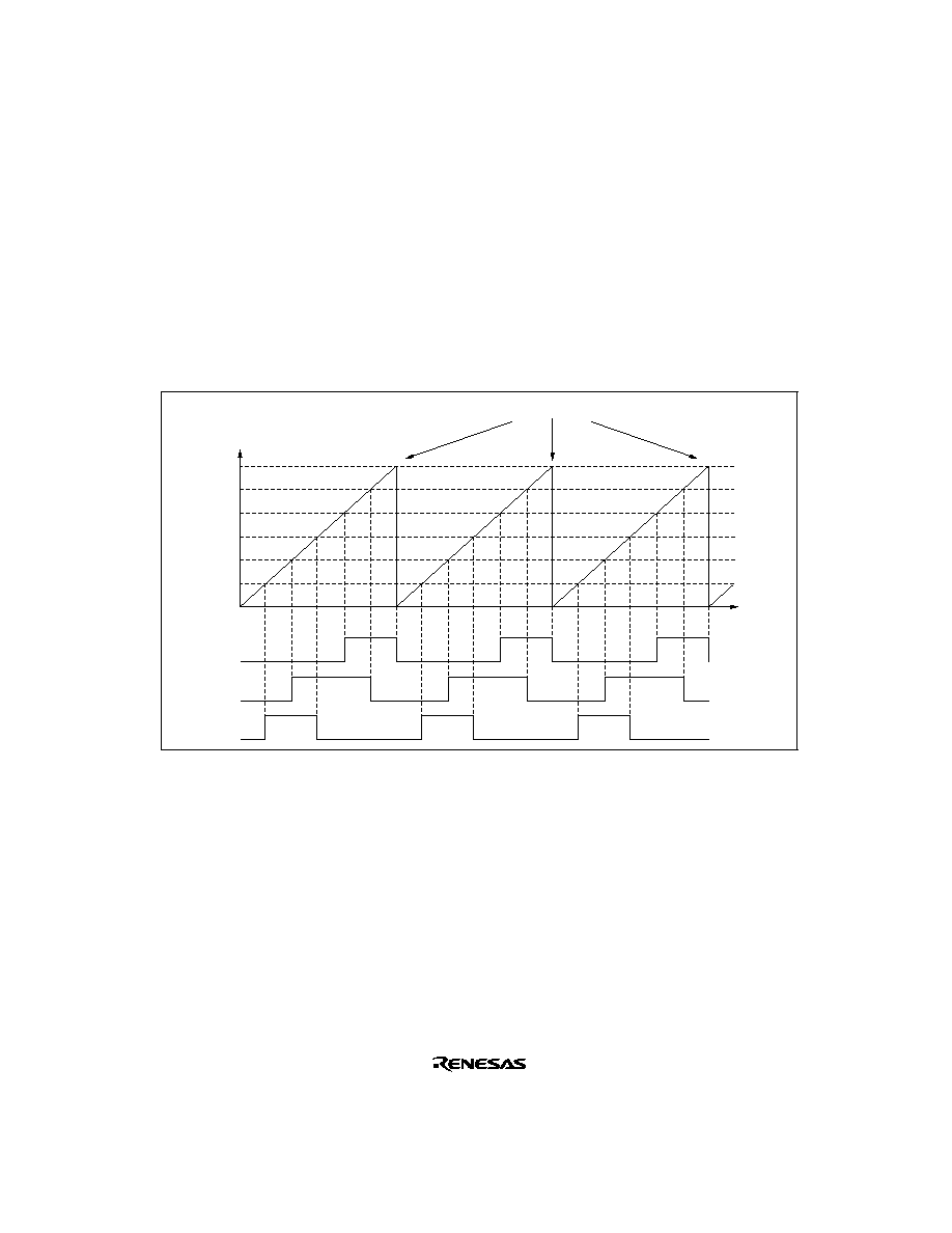
315
Example of Synchronous Operation: Figure 9-15 shows an example of synchronous operation.
In this example, synchronous operation and PWM mode 1 have been designated for channels 0 to
2, TGR0B compare match has been set as the channel 0 counter clearing source, and synchronous
clearing has been set for the channel 1 and 2 counter clearing source.
Three-phase PWM waveforms are output from pins TIOC0A, TIOC1A, and TIOC2A. At this
time, synchronous presetting, and synchronous clearing by TGR0B compare match, is performed
for channel 0 to 2 TCNT counters, and the data set in TGR0B is used as the PWM cycle.
For details of PWM modes, see section 9.4.6, PWM Modes.
TCNT0 to TCNT2 values
H'0000
TIOC0A
TIOC1A
Time
TGR0B
Synchronous clearing by TGR0B compare match
TGR2A
TGR1A
TGR2B
TGR0A
TGR1B
TIOC2A
Figure 9-15 Example of Synchronous Operation
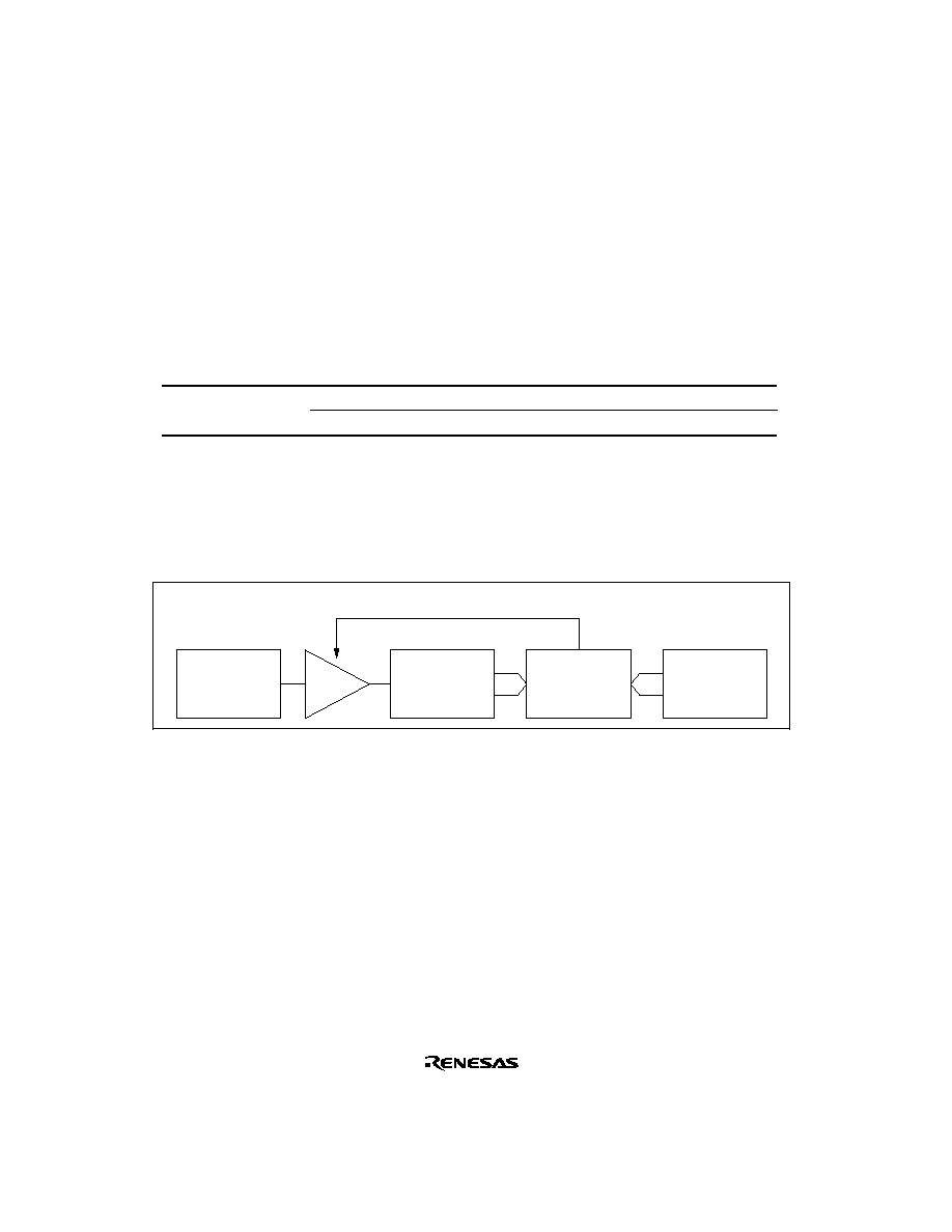
316
9.4.4
Buffer Operation
Buffer operation, provided for channel 0 enables TGRC and TGRD to be used as buffer registers.
Buffer operation differs depending on whether TGR has been designated as an input capture
register or as a compare match register.
Table 9-5 shows the register combinations used in buffer operation.
Table 9-5
Register Combinations in Buffer Operation
Channel
Timer General Register
Buffer Register
0
TGR0A
TGR0C
TGR0B
TGR0D
∑
When TGR is an output compare register
When a compare match occurs, the value in the buffer register for the corresponding channel is
transferred to the timer general register.
This operation is illustrated in figure 9-16.
Buffer register
Timer general
register
TCNT
Comparator
Compare match signal
Figure 9-16 Compare Match Buffer Operation
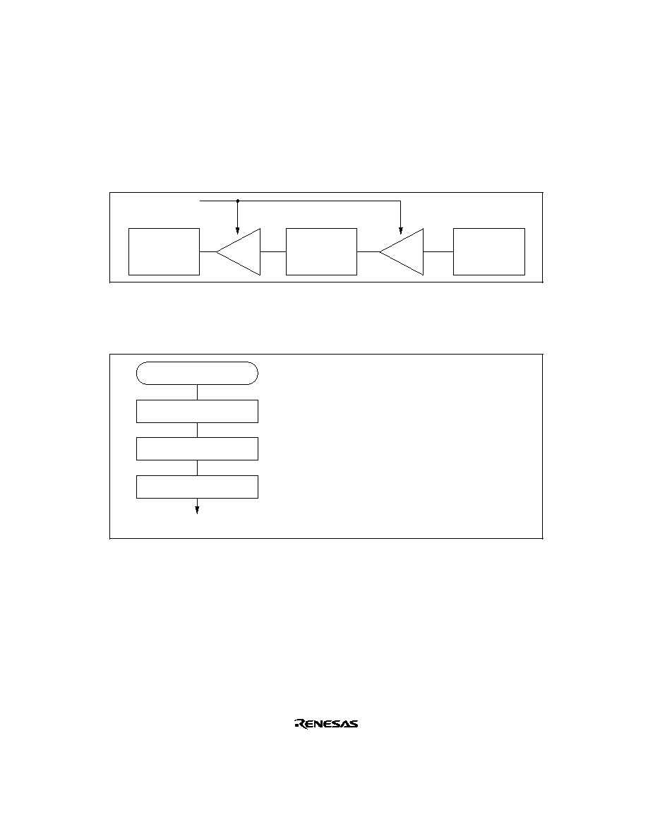
317
∑
When TGR is an input capture register
When input capture occurs, the value in TCNT is transferred to TGR and the value previously
held in the timer general register is transferred to the buffer register.
This operation is illustrated in figure 9-17.
Buffer register
Timer general
register
TCNT
Input capture
signal
Figure 9-17 Input Capture Buffer Operation
Example of Buffer Operation Setting Procedure: Figure 9-18 shows an example of the buffer
operation setting procedure.
Select TGR function
Buffer operation
Set buffer operation
Start count
<Buffer operation>
[1]
[2]
[3]
[1] Designate TGR as an input capture register or
output compare register by means of TIOR.
[2] Designate TGR for buffer operation with bits
BFA and BFB in TMDR.
[3] Set the CST bit in TSTR to 1 to start the count
operation.
Figure 9-18 Example of Buffer Operation Setting Procedure
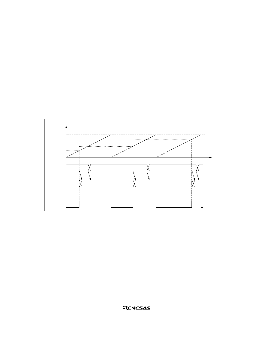
318
Examples of Buffer Operation
∑
When TGR is an output compare register
Figure 9-19 shows an operation example in which PWM mode 1 has been designated for
channel 0, and buffer operation has been designated for TGRA and TGRC. The settings used
in this example are TCNT clearing by compare match B, 1 output at compare match A, and 0
output at compare match B.
As buffer operation has been set, when compare match A occurs the output changes and the
value in buffer register TGRC is simultaneously transferred to timer general register TGRA.
This operation is repeated each time compare match A occurs.
For details of PWM modes, see section 9.4.5, PWM Modes.
TCNT value
TGR0B
H'0000
TGR0C
Time
TGR0A
H'0200
H'0520
TIOCA
H'0200
H'0450
H'0520
H'0450
TGR0A
H'0450
H'0200
Transfer
Figure 9-19 Example of Buffer Operation (1)
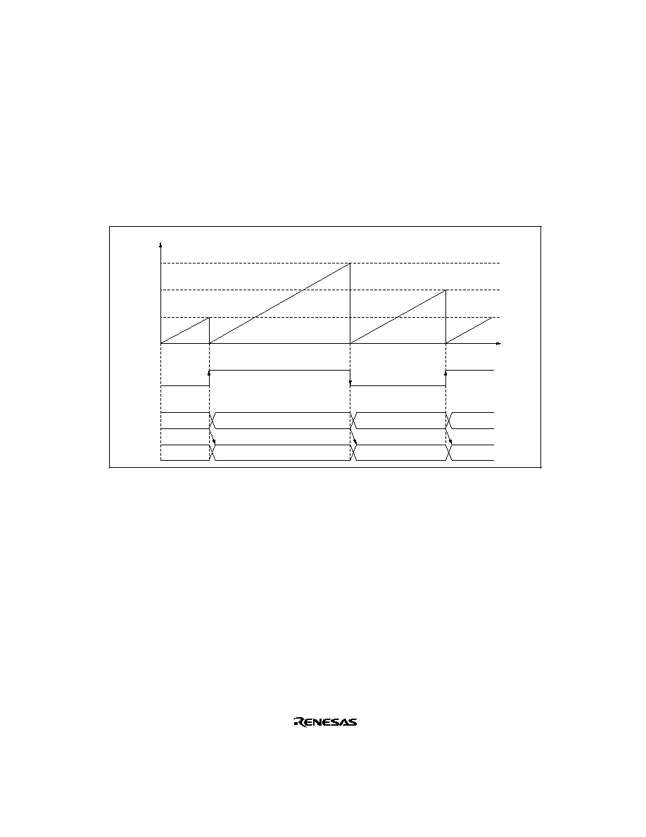
319
∑
When TGR is an input capture register
Figure 9-20 shows an operation example in which TGRA has been designated as an input
capture register, and buffer operation has been designated for TGRA and TGRC.
Counter clearing by TGRA input capture has been set for TCNT, and both rising and falling
edges have been selected as the TIOCA pin input capture input edge.
As buffer operation has been set, when the TCNT value is stored in TGRA upon occurrence of
input capture A, the value previously stored in TGRA is simultaneously transferred to TGRC.
TCNT value
H'09FB
H'0000
TGRC
Time
H'0532
TIOCA
TGRA
H'0F07
H'0532
H'0F07
H'0532
H'0F07
H'09FB
Figure 9-20 Example of Buffer Operation (2)

320
9.4.5
PWM Modes
In PWM mode, PWM waveforms are output from the output pins. 0, 1, or toggle output can be
selected as the output level in response to compare match of each TGR.
Designating TGR compare match as the counter clearing source enables the period to be set in that
register. All channels can be designated for PWM mode independently. Synchronous operation is
also possible.
There are two PWM modes, as described below.
∑
PWM mode 1
PWM output is generated from the TIOCA and TIOCC pins by pairing TGRA with TGRB and
TGRC with TGRD. The output specified by bits IOA3 to IOA0 and IOC3 to IOC0 in TIOR is
output from the TIOCA and TIOCC pins at compare matches A and C, and the output
specified by bits IOB3 to IOB0 and IOD3 to IOD0 in TIOR is output at compare matches B
and D. The initial output value is the value set in TGRA or TGRC. If the set values of paired
TGRs are identical, the output value does not change when a compare match occurs.
In PWM mode 1, a maximum 4-phase PWM output is possible.
∑
PWM mode 2
PWM output is generated using one TGR as the cycle register and the others as duty registers.
The output specified in TIOR is performed by means of compare matches. Upon counter
clearing by a synchronization register compare match, the output value of each pin is the initial
value set in TIOR. If the set values of the cycle and duty registers are identical, the output
value does not change when a compare match occurs.
In PWM mode 2, a maximum 7-phase PWM output is possible by combined use with
synchronous operation.
The correspondence between PWM output pins and registers is shown in table 9-6.

321
Table 9-6
PWM Output Registers and Output Pins
Output Pins
Channel
Registers
PWM Mode 1
PWM Mode 2
0
TGR0A
TIOCA0
TIOCA0
TGR0B
TIOCB0
TGR0C
TIOCC0
TIOCC0
TGR0D
TIOCD0
1
TGR1A
TIOCA1
TIOCA1
TGR1B
TIOCB1
2
TGR2A
TIOCA2
TIOCA2
TGR2B
TIOCB2
Note:
In PWM mode 2, PWM output is not possible for the TGR register in which the period is set.

322
Example of PWM Mode Setting Procedure: Figure 9-21 shows an example of the PWM mode
setting procedure.
Select counter clock
PWM mode
Select counter clearing source
Select waveform output level
<PWM mode>
[1]
[2]
[3]
Set TGR
[4]
Set PWM mode
[5]
Start count
[6]
[1] Select the counter clock with bits TPSC2 to
TPSC0 in TCR. At the same time, select the
input clock edge with bits CKEG1 and CKEG0
in TCR.
[2] Use bits CCLR2 to CCLR0 in TCR to select
the TGR to be used as the TCNT clearing
source.
[3] Use TIOR to designate the TGR as an output
compare register, and select the initial value
and output value.
[4] Set the cycle in the TGR selected in [2], and
set the duty in the other the TGR.
[5] Select the PWM mode with bits MD3 to MD0
in TMDR.
[6] Set the CST bit in TSTR to 1 to start the count
operation.
Figure 9-21 Example of PWM Mode Setting Procedure
Examples of PWM Mode Operation: Figure 9-22 shows an example of PWM mode 1 operation.
In this example, TGRA compare match is set as the TCNT clearing source, 0 is set for the TGRA
initial output value and output value, and 1 output is set as the TGRB output value.
In this case, the value set in TGRA is used as the period, and the values set in TGRB registers as
the duty.
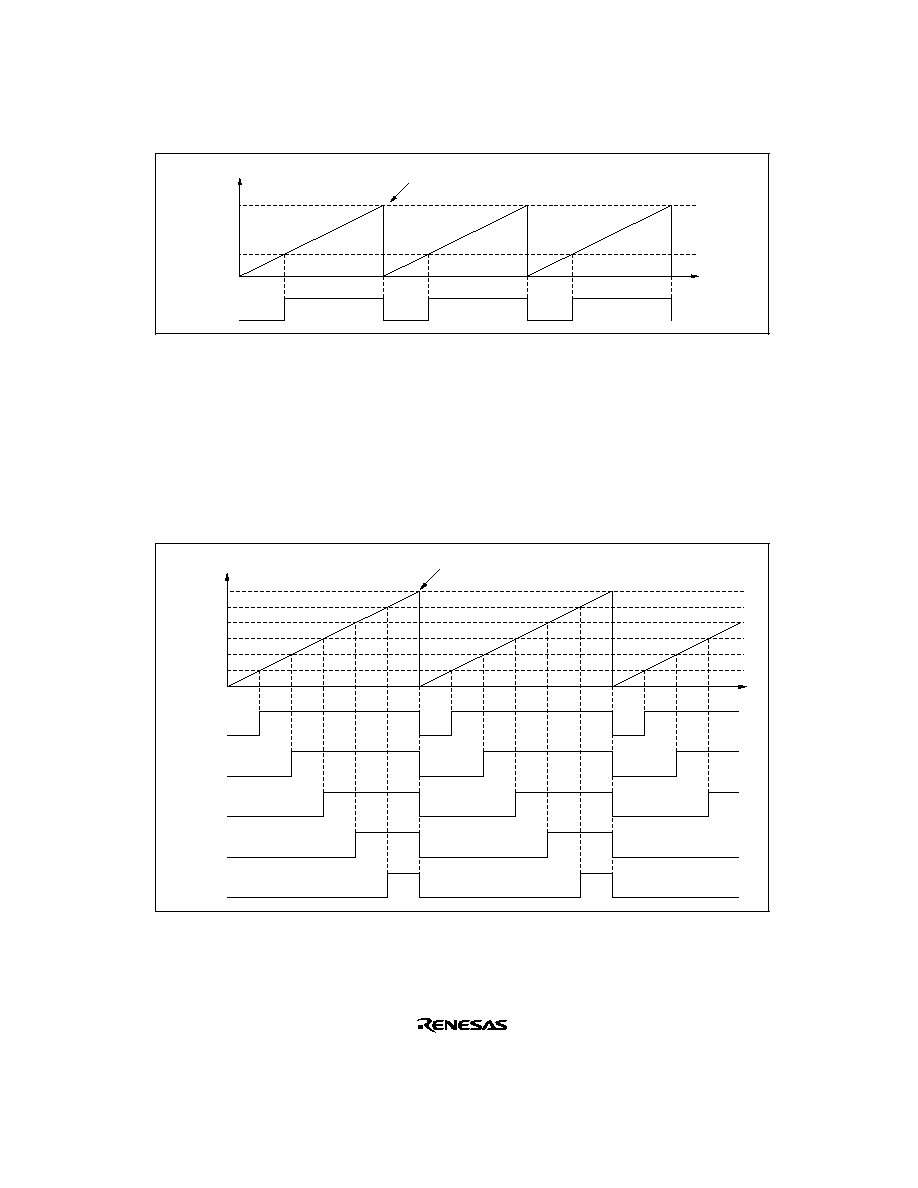
323
TCNT value
TGRA
H'0000
TIOCA
Time
TGRB
Counter cleared by
TGRA compare match
Figure 9-22 Example of PWM Mode Operation (1)
Figure 9-23 shows an example of PWM mode 2 operation.
In this example, synchronous operation is designated for channels 0 and 1, TGR1B compare match
is set as the TCNT clearing source, and 0 is set for the initial output value and 1 for the output
value of the other TGR registers, to output a 5-phase PWM waveform.
In this case, the value set in TGR1B is used as the cycle, and the values set in the other TGRs as
the duty.
TCNT value
TGR1B
H'0000
TIOCA0
Counter cleared by TGR1B
compare match
TGR1A
TGR0D
TGR0C
TGR0B
TGR0A
TIOCB0
TIOCC0
TIOCD0
TIOCA1
Figure 9-23 Example of PWM Mode Operation (2)
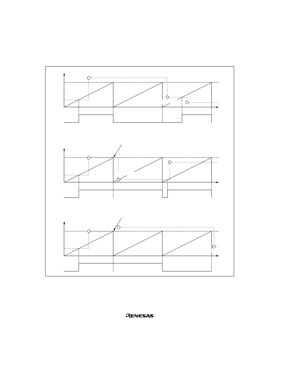
324
Figure 9-24 shows examples of PWM waveform output with 0% duty and 100% duty in PWM
mode.
TCNT value
TGRA
H'0000
TIOCA
Time
TGRB
0% duty
TGRB rewritten
TGRB
rewritten
TGRB rewritten
TCNT value
TGRA
H'0000
TIOCA
Time
TGRB
100% duty
TGRB rewritten
TGRB rewritten
TGRB rewritten
Output does not change when cycle register and duty register
compare matches occur simultaneously
TCNT value
TGRA
H'0000
TIOCA
Time
TGRB
100% duty
TGRB rewritten
TGRB rewritten
TGRB rewritten
Output does not change when cycle register and duty
register compare matches occur simultaneously
0% duty
Figure 9-24 Example of PWM Mode Operation (3)
325
9.4.6
Phase Counting Mode
In phase counting mode, the phase difference between two external clock inputs is detected and
TCNT is incremented/decremented accordingly. This mode can be set for channels 1, and 2.
When phase counting mode is set, an external clock is selected as the counter input clock and
TCNT operates as an up/down-counter regardless of the setting of bits TPSC2 to TPSC0 and bits
CKEG1 and CKEG0 in TCR. However, the functions of bits CCLR1 and CCLR0 in TCR, and of
TIOR, TIER, and TGR are valid, and input capture/compare match and interrupt functions can be
used.
When overflow occurs while TCNT is counting up, the TCFV flag in TSR is set; when underflow
occurs while TCNT is counting down, the TCFU flag is set.
The TCFD bit in TSR is the count direction flag. Reading the TCFD flag provides an indication of
whether TCNT is counting up or down.
Table 9-7 shows the correspondence between external clock pins and channels.
Table 9-7
Phase Counting Mode Clock Input Pins
External Clock Pins
Channels
A-Phase
B-Phase
When channel 1 is set to phase counting mode
TCLKA
TCLKB
When channel 2 is set to phase counting mode
TCLKC
TCLKD
Example of Phase Counting Mode Setting Procedure: Figure 9-25 shows an example of the
phase counting mode setting procedure.
Select phase counting mode
Phase counting mode
Start count
<Phase counting mode>
[1]
[2]
[1] Select phase counting mode with bits MD3
to MD0 in TMDR.
[2] Set the CST bit in TSTR to 1 to start the
count operation.
Figure 9-25 Example of Phase Counting Mode Setting Procedure
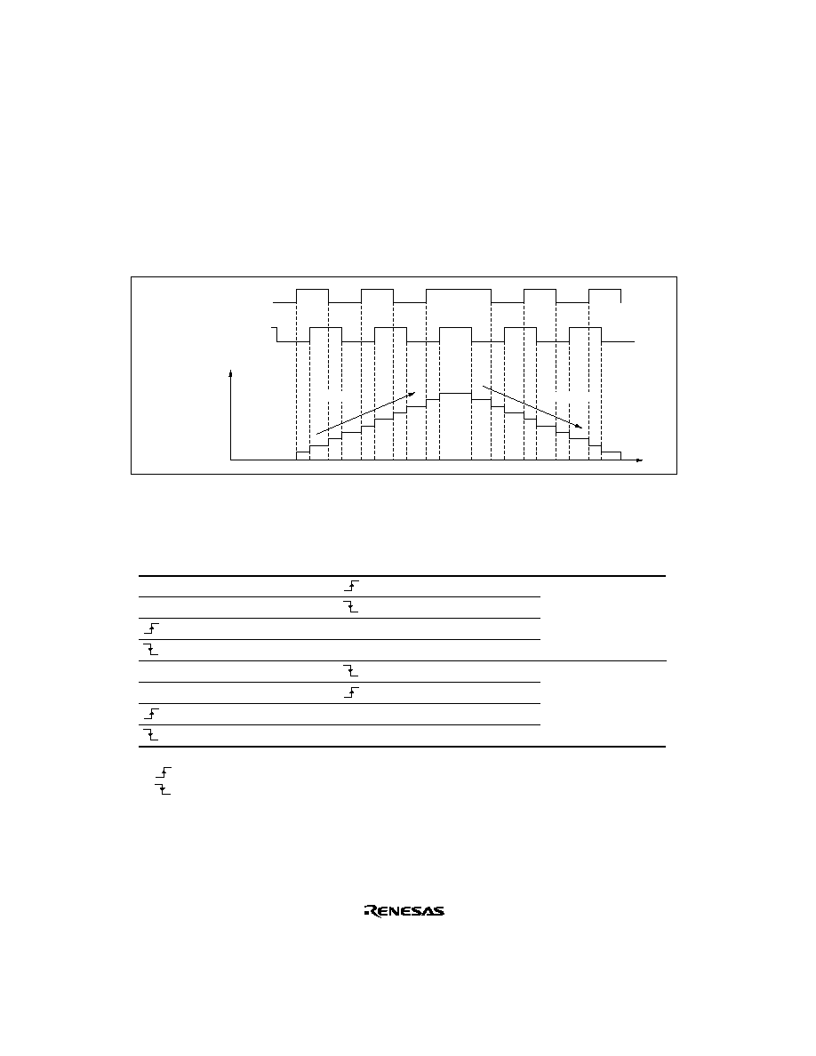
326
Examples of Phase Counting Mode Operation: In phase counting mode, TCNT counts up or
down according to the phase difference between two external clocks. There are four modes,
according to the count conditions.
∑
Phase counting mode 1
Figure 9-26 shows an example of phase counting mode 1 operation, and table 9-8 summarizes
the TCNT up/down-count conditions.
TCNT value
Time
Down-count
Up-count
TCLKA (channel 1)
TCLKC (channel 2)
TCLKB (channel 1)
TCLKD (channel 2)
Figure 9-26 Example of Phase Counting Mode 1 Operation
Table 9-8
Up/Down-Count Conditions in Phase Counting Mode 1
TCLKA (Channel 1)
TCLKC (Channel 2)
TCLKB (Channel 1)
TCLKD (Channel 2)
Operation
High level
Up-count
Low level
Low level
High level
High level
Down-count
Low level
High level
Low level
Legend
: Rising edge
: Falling edge
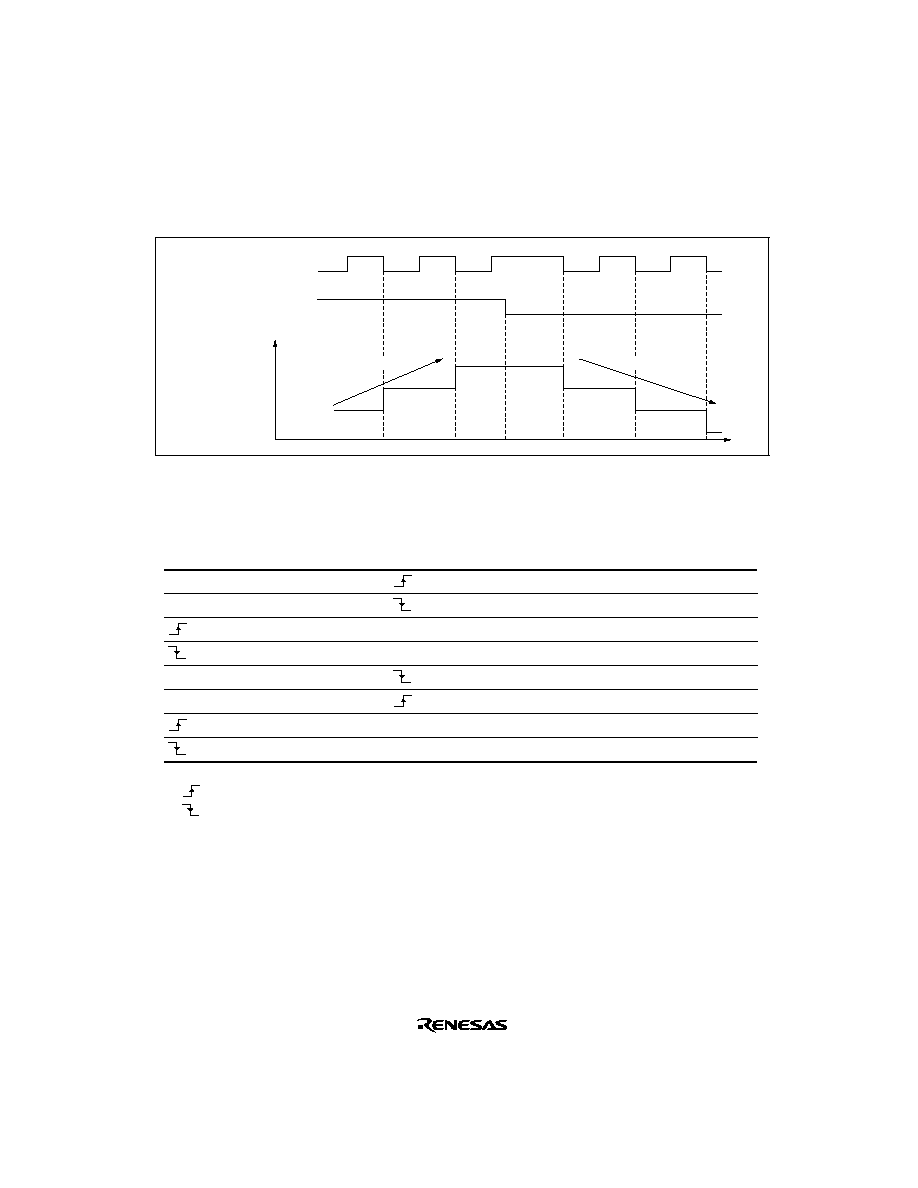
327
∑
Phase counting mode 2
Figure 9-27 shows an example of phase counting mode 2 operation, and table 9-9 summarizes
the TCNT up/down-count conditions.
TCNT value
Time
Down-count
Up-count
TCLKA (Channel 1)
TCLKC (Channel 2)
TCLKB (Channel 1)
TCLKD (Channel 2)
Figure 9-27 Example of Phase Counting Mode 2 Operation
Table 9-9
Up/Down-Count Conditions in Phase Counting Mode 2
TCLKA (Channel 1)
TCLKC (Channel 2)
TCLKB (Channel 1)
TCLKD (Channel 2)
Operation
High level
Don't care
Low level
Don't care
Low level
Don't care
High level
Up-count
High level
Don't care
Low level
Don't care
High level
Don't care
Low level
Down-count
Legend
: Rising edge
: Falling edge
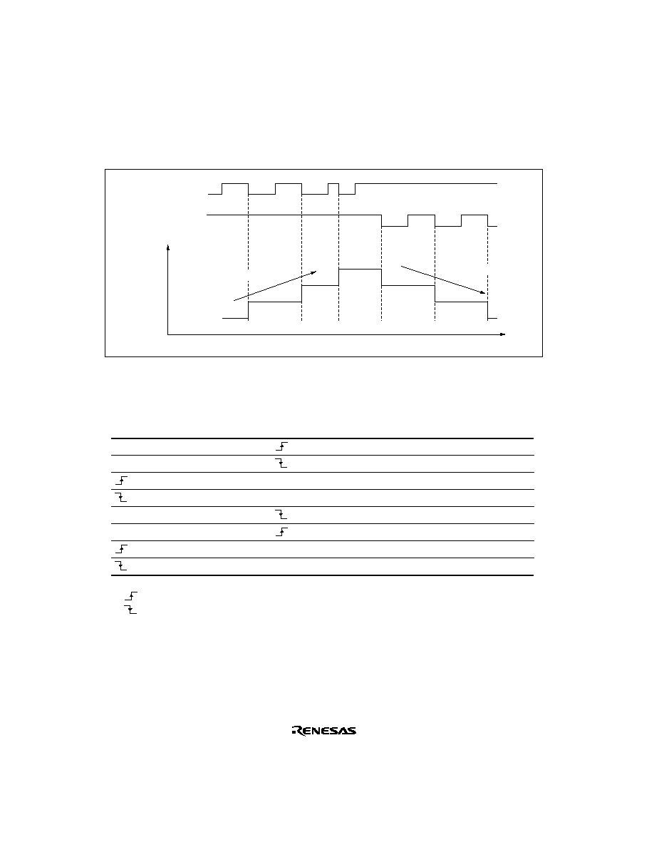
328
∑
Phase counting mode 3
Figure 9-28 shows an example of phase counting mode 3 operation, and table 9-10 summarizes
the TCNT up/down-count conditions.
TCNT value
Time
Up-count
TCLKA (channel 1)
TCLKC (channel 2)
TCLKB (channel 1)
TCLKD (channel 2)
Down-count
Figure 9-28 Example of Phase Counting Mode 3 Operation
Table 9-10 Up/Down-Count Conditions in Phase Counting Mode 3
TCLKA (Channel 1)
TCLKC (Channel 2)
TCLKB (Channel 1)
TCLKD (Channel 2)
Operation
High level
Don't care
Low level
Don't care
Low level
Don't care
High level
Up-count
High level
Down-count
Low level
Don't care
High level
Don't care
Low level
Don't care
Legend
: Rising edge
: Falling edge
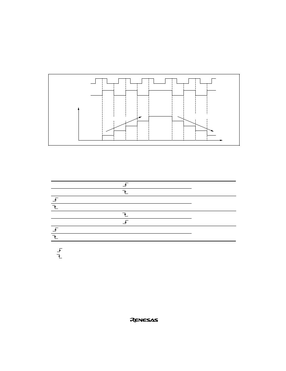
329
∑
Phase counting mode 4
Figure 9-29 shows an example of phase counting mode 4 operation, and table 9-11 summarizes
the TCNT up/down-count conditions.
Time
TCLKA (channel 1)
TCLKC (channel 2)
TCLKB (channel 1)
TCLKD (channel 2)
Up-count
Down-count
TCNT value
Figure 9-29 Example of Phase Counting Mode 4 Operation
Table 9-11 Up/Down-Count Conditions in Phase Counting Mode 4
TCLKA (Channel 1)
TCLKC (Channel 2)
TCLKB (Channel 1)
TCLKD (Channel 2)
Operation
High level
Up-count
Low level
Low level
Don't care
High level
High level
Down-count
Low level
High level
Don't care
Low level
Legend
: Rising edge
: Falling edge

330
9.5
Interrupts
9.5.1
Interrupt Sources and Priorities
There are three kinds of TPU interrupt source: TGR input capture/compare match, TCNT
overflow, and TCNT underflow. Each interrupt source has its own status flag and enable/disabled
bit, allowing generation of interrupt request signals to be enabled or disabled individually.
When an interrupt request is generated, the corresponding status flag in TSR is set to 1. If the
corresponding enable/disable bit in TIER is set to 1 at this time, an interrupt is requested. The
interrupt request is cleared by clearing the status flag to 0.
Relative channel priorities can be changed by the interrupt controller, but the priority order within
a channel is fixed. For details, see section 5, Interrupt Controller.
Table 9-12 lists the TPU interrupt sources.
Table 9-12 TPU Interrupts
Channel
Interrupt
Source
Description
DTC
Activation
Priority
0
TGI0A
TGR0A input capture/compare match
Possible
High
TGI0B
TGR0B input capture/compare match
Possible
TGI0C
TGR0C input capture/compare match
Possible
TGI0D
TGR0D input capture/compare match
Possible
TCI0V
TCNT0 overflow
Not possible
1
TGI1A
TGR1A input capture/compare match
Possible
TGI1B
TGR1B input capture/compare match
Possible
TCI1V
TCNT1 overflow
Not possible
TCI1U
TCNT1 underflow
Not possible
2
TGI2A
TGR2A input capture/compare match
Possible
TGI2B
TGR2B input capture/compare match
Possible
TCI2V
TCNT2 overflow
Not possible
TCI2U
TCNT2 underflow
Not possible
Low
Note:
This table shows the initial state immediately after a reset. The relative channel priorities
can be changed by the interrupt controller.

331
Input Capture/Compare Match Interrupt: An interrupt is requested if the TGIE bit in TIER is
set to 1 when the TGF flag in TSR is set to 1 by the occurrence of a TGR input capture/compare
match on a particular channel. The interrupt request is cleared by clearing the TGF flag to 0. The
TPU has 8 input capture/compare match interrupts, four for channel 0, and two each for channels
1, and 2.
Overflow Interrupt: An interrupt is requested if the TCIEV bit in TIER is set to 1 when the
TCFV flag in TSR is set to 1 by the occurrence of TCNT overflow on a particular channel. The
interrupt request is cleared by clearing the TCFV flag to 0. The TPU has three overflow interrupts,
one for each channel.
Underflow Interrupt: An interrupt is requested if the TCIEU bit in TIER is set to 1 when the
TCFU flag in TSR is set to 1 by the occurrence of TCNT underflow on channel. The interrupt
request is cleared by clearing the TCFU flag to 0. The TPU has two underflow interrupts, one each
for channels 1, and 2.
9.5.2
DTC Activation
DTC Activation: The DTC can be activated by the TGR input capture/compare match interrupt
for a channel. For details, see section 7, Data Transfer Controller.
A total of 8 TPU input capture/compare match interrupts can be used as DTC activation sources,
four for channels 0, and two each for channels 1, and 2.
9.5.3
A/D Converter Activation
The A/D converter can be activated by the TGRA input capture/compare match for a channel.
If the TTGE bit in TIER is set to 1 when the TFGA flag in TSR is set to 1 by the occurrence of a
TGRA input capture/compare match on a particular channel, a request to start A/D conversion is
sent to the A/D converter. If the TPU conversion start trigger has been selected on the A/D
converter side at this time, A/D conversion is started.
In the TPU, a total of three TGRA input capture/compare match interrupts can be used as A/D
converter conversion start sources, one for each channel.

332
9.6
Operation Timing
9.6.1
Input/Output Timing
TCNT Count Timing: Figure 9-30 shows TCNT count timing in internal clock operation, and
figure 9-31 shows TCNT count timing in external clock operation.
TCNT
TCNT
input clock
Internal clock
¯
N≠1
N
N+1
N+2
Falling edge
Rising edge
Figure 9-30 Count Timing in Internal Clock Operation
TCNT
TCNT
input clock
External clock
¯
N≠1
N
N+1
N+2
Rising edge
Falling edge
Falling edge
Figure 9-31 Count Timing in External Clock Operation
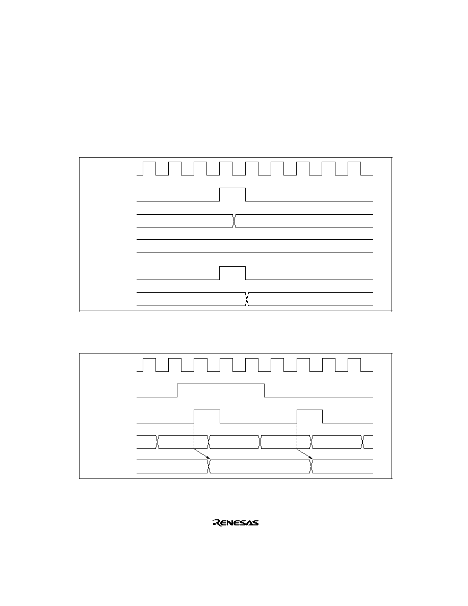
333
Output Compare Output Timing: A compare match signal is generated in the final state in
which TCNT and TGR match (the point at which the count value matched by TCNT is updated).
When a compare match signal is generated, the output value set in TIOR is output at the output
compare output pin (TIOC pin). After a match between TCNT and TGR, the compare match
signal is not generated until the TCNT input clock is generated.
Figure 9-32 shows output compare output timing.
TGR
TCNT
TCNT
input clock
¯
N
N
N+1
Compare
match signal
TIOC pin
Figure 9-32 Output Compare Output Timing
Input Capture Signal Timing: Figure 9-33 shows input capture signal timing.
TCNT
Input capture
input
¯
N
N+1
N+2
N
N+2
TGR
Input capture
signal
Figure 9-33 Input Capture Input Signal Timing
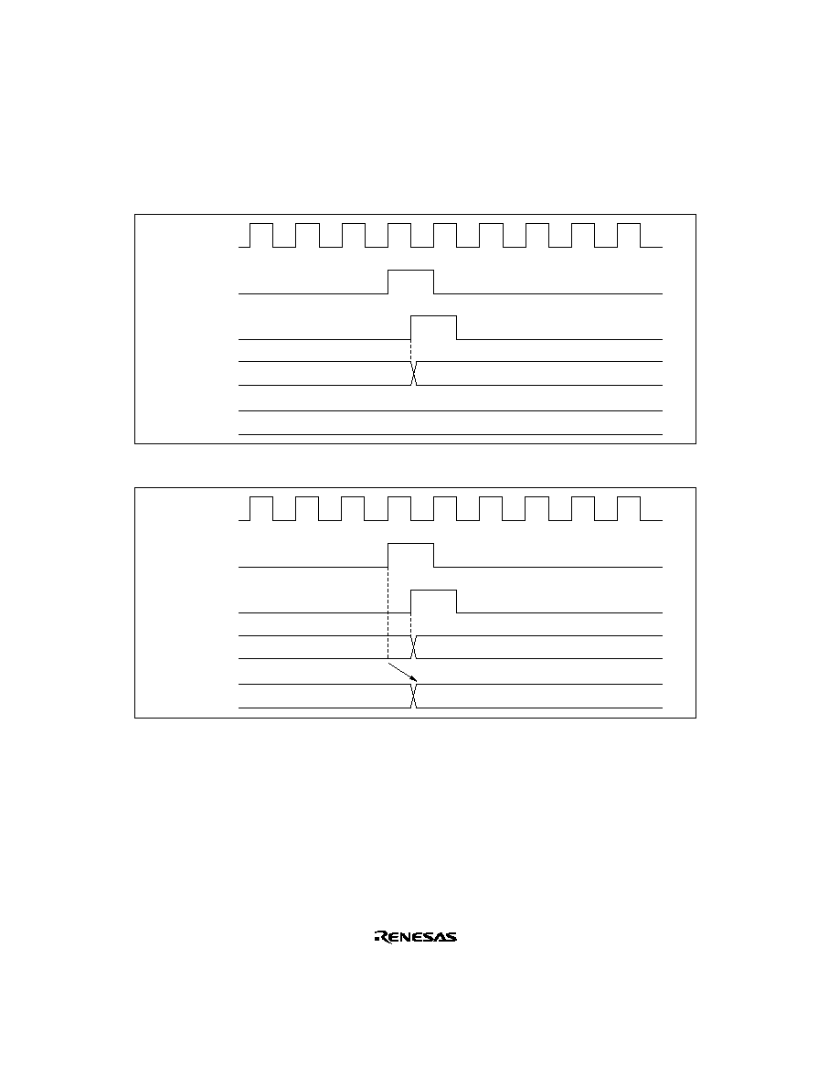
334
Timing for Counter Clearing by Compare Match/Input Capture: Figure 9-34 shows the
timing when counter clearing by compare match occurrence is specified, and figure
9-35 shows the timing when counter clearing by input capture occurrence is specified.
TCNT
Counter
clear signal
Compare
match signal
¯
TGR
N
N
H'0000
Figure 9-34 Counter Clear Timing (Compare Match)
TCNT
Counter clear
signal
Input capture
signal
¯
TGR
N
H'0000
N
Figure 9-35 Counter Clear Timing (Input Capture)

335
Buffer Operation Timing: Figures 9-36 and 9-37 show the timing in buffer operation.
TGRA,
TGRB
Compare
match signal
TCNT
¯
TGRC,
TGRD
n
N
N
n
n+1
Figure 9-36 Buffer Operation Timing (Compare Match)
TGRA,
TGRB
TCNT
Input capture
signal
¯
TGRC,
TGRD
N
n
n
N+1
N
N
N+1
Figure 9-37 Buffer Operation Timing (Input Capture)

336
9.6.2
Interrupt Signal Timing
TGF Flag Setting Timing in Case of Compare Match: Figure 9-38 shows the timing for setting
of the TGF flag in TSR by compare match occurrence, and TGI interrupt request signal timing.
TGR
TCNT
TCNT input
clock
¯
N
N
N+1
Compare
match signal
TGF flag
TGI interrupt
Figure 9-38 TGI Interrupt Timing (Compare Match)

337
TGF Flag Setting Timing in Case of Input Capture: Figure 9-39 shows the timing for setting of
the TGF flag in TSR by input capture occurrence, and TGI interrupt request signal timing.
TGR
TCNT
Input capture
signal
¯
N
N
TGF flag
TGI interrupt
Figure 9-39 TGI Interrupt Timing (Input Capture)
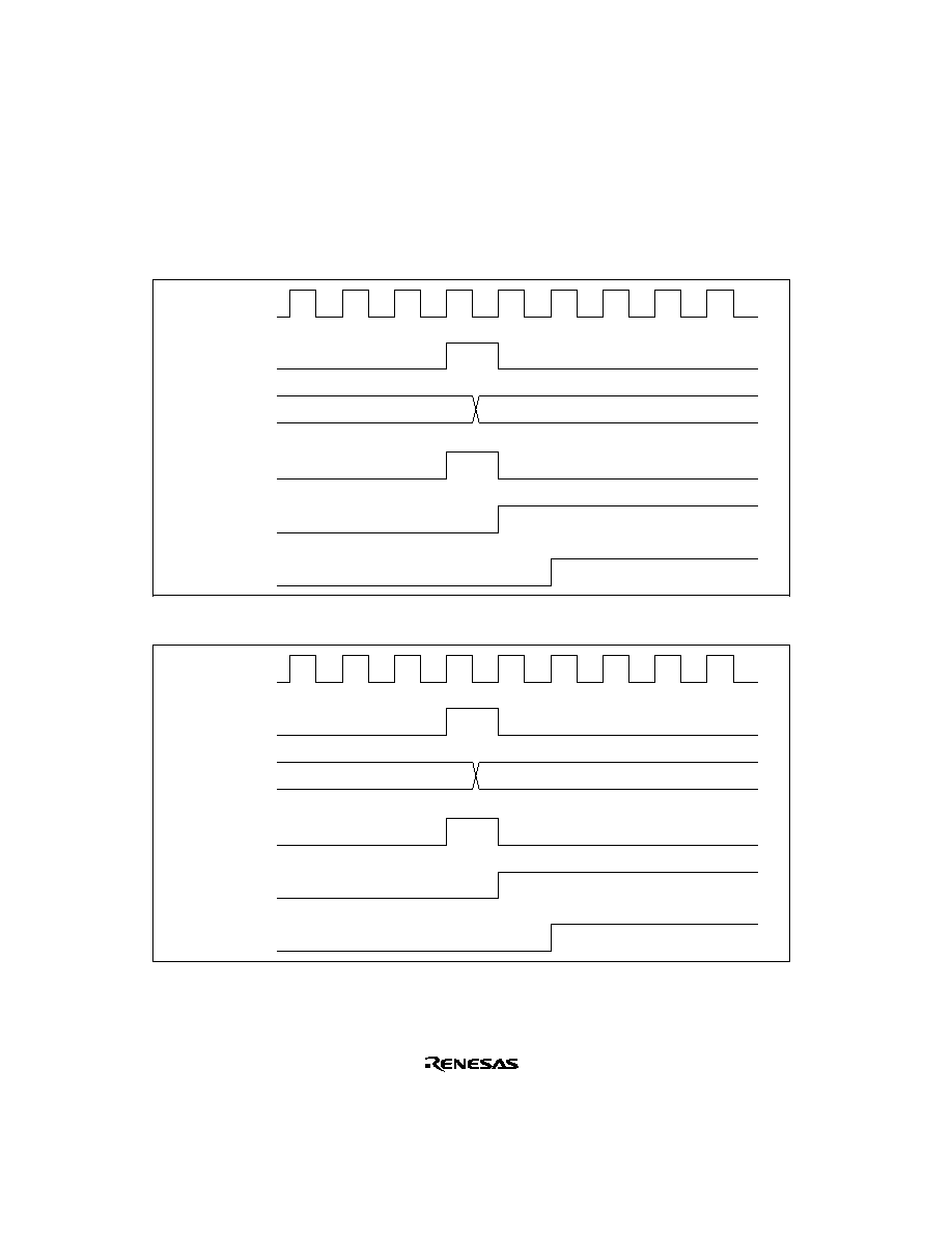
338
TCFV Flag/TCFU Flag Setting Timing: Figure 9-40 shows the timing for setting of the TCFV
flag in TSR by overflow occurrence, and TCIV interrupt request signal timing.
Figure 9-41 shows the timing for setting of the TCFU flag in TSR by underflow occurrence, and
TCIU interrupt request signal timing.
Overflow
signal
TCNT
(overflow)
TCNT input
clock
¯
H'FFFF
H'0000
TCFV flag
TCIV interrupt
Figure 9-40 TCIV Interrupt Setting Timing
Underflow signal
TCNT
(underflow)
TCNT
input clock
¯
H'0000
H'FFFF
TCFU flag
TCIU interrupt
Figure 9-41 TCIU Interrupt Setting Timing
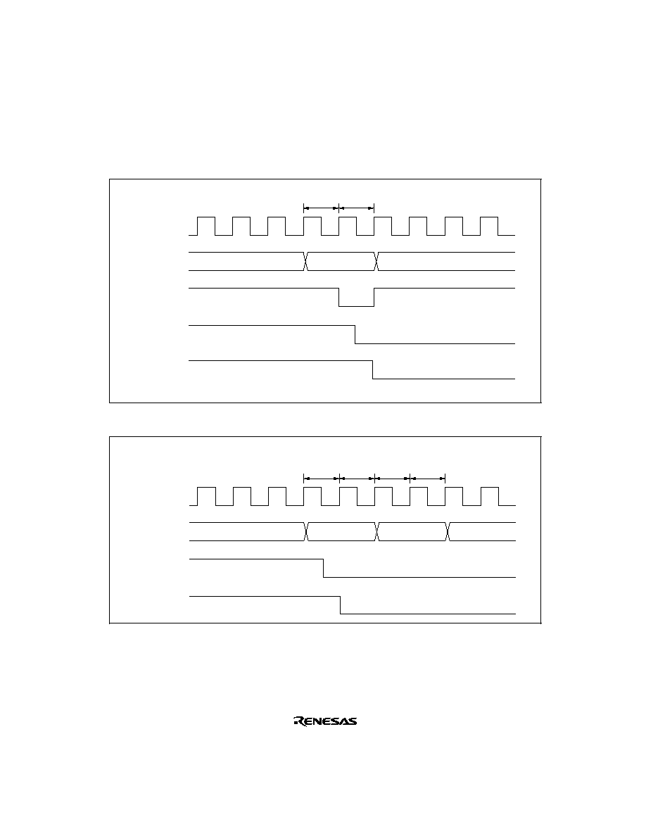
339
Status Flag Clearing Timing: After a status flag is read as 1 by the CPU, it is cleared by writing
0 to it. When the DTC is activated, the flag is cleared automatically. Figure 9-42 shows the timing
for status flag clearing by the CPU, and figure 9-43 shows the timing for status flag clearing by the
DTC.
Status flag
Write signal
Address
¯
TSR address
Interrupt
request
signal
TSR write cycle
T1
T2
Figure 9-42 Timing for Status Flag Clearing by CPU
Interrupt
request
signal
Status flag
Address
¯
Source address
DTC
read cycle
T1
T2
Destination
address
T1
T2
DTC
write cycle
Figure 9-43 Timing for Status Flag Clearing by DTC Activation

340
9.7
Usage Notes
Note that the kinds of operation and contention described below occur during TPU operation.
Input Clock Restrictions: The input clock pulse width must be at least 1.5 states in the case of
single-edge detection, and at least 2.5 states in the case of both-edge detection. The TPU will not
operate properly with a narrower pulse width.
In phase counting mode, the phase difference and overlap between the two input clocks must be at
least 1.5 states, and the pulse width must be at least 2.5 states. Figure 9-44 shows the input clock
conditions in phase counting mode.
Overlap
Phase
differ-
ence
Phase
differ-
ence
Overlap
TCLKA
(TCLKC)
TCLKB
(TCLKD)
Pulse width
Pulse width
Pulse width
Pulse width
Notes: Phase difference and overlap : 1.5 states or more
Pulse width
: 2.5 states or more
Figure 9-44 Phase Difference, Overlap, and Pulse Width in Phase Counting Mode
Caution on Period Setting: When counter clearing by compare match is set, TCNT is cleared in
the final state in which it matches the TGR value (the point at which the count value matched by
TCNT is updated). Consequently, the actual counter frequency is given by the following formula:
f =
¯
(N + 1)
Where
f
: Counter frequency
¯
: Operating frequency
N : TGR set value
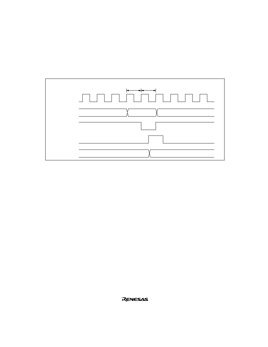
341
Contention between TCNT Write and Clear Operations: If the counter clear signal is
generated in the T2 state of a TCNT write cycle, TCNT clearing takes precedence and the TCNT
write is not performed.
Figure 9-45 shows the timing in this case.
Counter clear
signal
Write signal
Address
¯
TCNT address
TCNT
TCNT write cycle
T1
T2
N
H'0000
Figure 9-45 Contention between TCNT Write and Clear Operations

342
Contention between TCNT Write and Increment Operations: If incrementing occurs in the T2
state of a TCNT write cycle, the TCNT write takes precedence and TCNT is not incremented.
Figure 9-46 shows the timing in this case.
TCNT input
clock
Write signal
Address
¯
TCNT address
TCNT
TCNT write cycle
T1
T2
N
M
TCNT write data
Figure 9-46 Contention between TCNT Write and Increment Operations
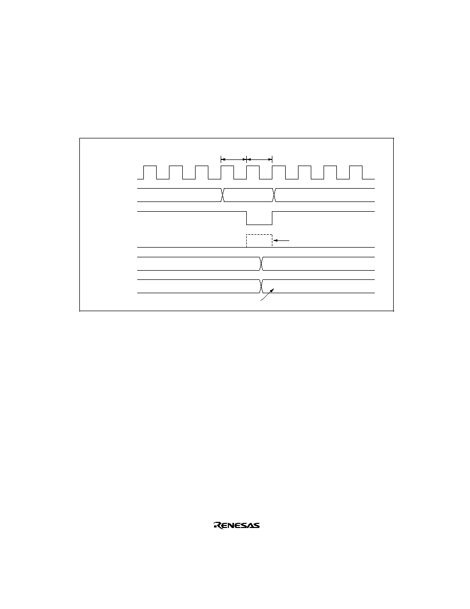
343
Contention between TGR Write and Compare Match: If a compare match occurs in the T2
state of a TGR write cycle, the TGR write takes precedence and the compare match signal is
inhibited. A compare match does not occur even if the same value as before is written.
Figure 9.47 shows the timing in this case.
Compare
match signal
Write signal
Address
¯
TGR address
TCNT
TGR write cycle
T1
T2
N
M
TGR write data
TGR
N
N+1
Inhibited
Figure 9-47 Contention between TGR Write and Compare Match

344
Contention between Buffer Register Write and Compare Match: If a compare match occurs in
the T2 state of a TGR write cycle, the data transferred to TGR by the buffer operation will be the
data prior to the write.
Figure 9-48 shows the timing in this case.
Compare
match signal
Write signal
Address
¯
Buffer register
address
Buffer
register
TGR write cycle
T1
T2
N
TGR
N
M
Buffer register write data
Figure 9-48 Contention between Buffer Register Write and Compare Match

345
Contention between TGR Read and Input Capture: If the input capture signal is generated in
the T1 state of a TGR read cycle, the data that is read will be the data after input capture transfer.
Figure 9-49 shows the timing in this case.
Input capture
signal
Read signal
Address
¯
TGR address
TGR
TGR read cycle
T1
T2
M
Internal
data bus
X
M
Figure 9-49 Contention between TGR Read and Input Capture

346
Contention between TGR Write and Input Capture: If the input capture signal is generated in
the T2 state of a TGR write cycle, the input capture operation takes precedence and the write to
TGR is not performed.
Figure 9-50 shows the timing in this case.
Input capture
signal
Write signal
Address
¯
TCNT
TGR write cycle
T1
T2
M
TGR
M
TGR address
Figure 9-50 Contention between TGR Write and Input Capture
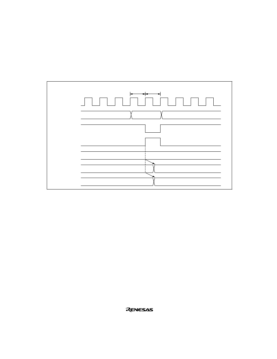
347
Contention between Buffer Register Write and Input Capture: If the input capture signal is
generated in the T2 state of a buffer write cycle, the buffer operation takes precedence and the
write to the buffer register is not performed.
Figure 9-51 shows the timing in this case.
Input capture
signal
Write signal
Address
¯
TCNT
Buffer register write cycle
T1
T2
N
TGR
N
M
M
Buffer
register
Buffer register
address
Figure 9-51 Contention between Buffer Register Write and Input Capture

348
Contention between Overflow/Underflow and Counter Clearing: If overflow/underflow and
counter clearing occur simultaneously, the TCFV/TCFU flag in TSR is not set and TCNT clearing
takes precedence.
Figure 9-52 shows the operation timing when a TGR compare match is specified as the clearing
source, and H'FFFF is set in TGR.
Counter
clear signal
TCNT input
clock
¯
TCNT
TGF
Disabled
TCFV
H'FFFF
H'0000
Figure 9-52 Contention between Overflow and Counter Clearing
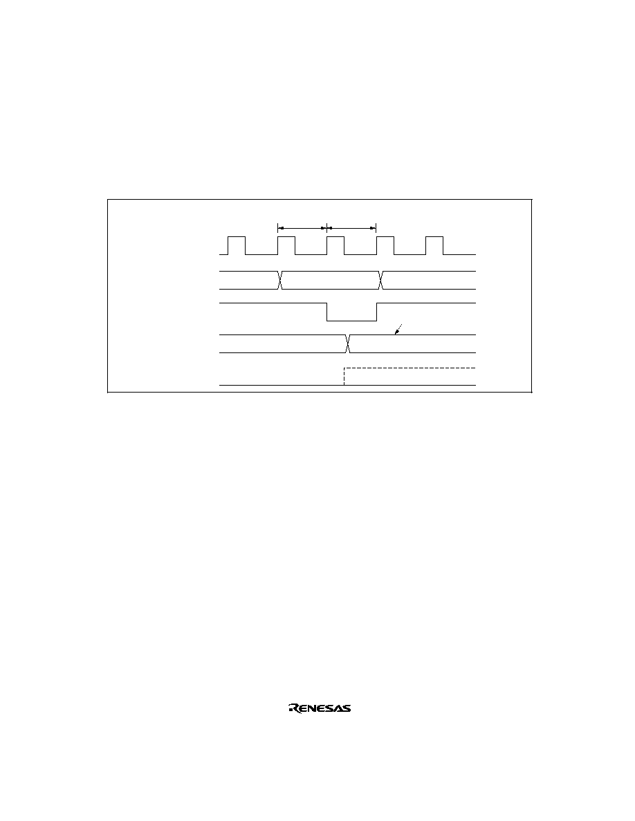
349
Contention between TCNT Write and Overflow/Underflow: If there is an up-count or down-
count in the T2 state of a TCNT write cycle, and overflow/underflow occurs, the TCNT write
takes precedence and the TCFV/TCFU flag in TSR is not set .
Figure 9-53 shows the operation timing in the case of contention between a TCNT write and
overflow.
Write signal
Address
¯
TCNT address
TCNT
TCNT write cycle
T1
T2
H'FFFF
M
TCNT write data
TCFV flag
Figure 9-53 Contention between TCNT Write and Overflow
Multiplexing of I/O Pins: In the H8S/2245 Series, the TCLKA input pin is multiplexed with the
TIOCC0 I/O pin, the TCLKB input pin with the TIOCD0 I/O pin, the TCLKC input pin with the
TIOCB1 I/O pin, and the TCLKD input pin with the TIOCB2 I/O pin. When an external clock is
input, compare match output should not be performed from a multiplexed pin.
Interrupts and Module Stop Mode: If module stop mode is entered when an interrupt has been
requested, it will not be possible to clear the CPU interrupt source or DTC activation source.
Interrupts should therefore be disabled before entering module stop mode.

351
Section 10 8-Bit Timers
10.1
Overview
The H8S/2245 Series includes an 8-bit timer module with two channels (TMR0 and TMR1). Each
channel has an 8-bit counter (TCNT) and two time constant registers (TCORA and TCORB) that
are constantly compared with the TCNT value to detect compare match events. The 8-bit timer
module can thus be used for a variety of functions, including pulse output with an arbitrary duty
cycle.
10.1.1
Features
∑
Selection of four clock sources
The counters can be driven by one of three internal clock signals (¯/8, ¯/64, or ¯/8192) or an
external clock input (enabling use as an external event counter).
∑
Selection of three ways to clear the counters
The counters can be cleared on compare match A or B, or by an external reset signal.
∑
Timer output control by a combination of two compare match signals
The timer output signal in each channel is controlled by a combination of two independent
compare match signals, enabling the timer to generate output waveforms with an arbitrary duty
cycle or PWM output.
∑
Provision for cascading of two channels
Operation as a 16-bit timer is possible, using channel 0 for the upper 8 bits and channel 1
for the lower 8 bits (16-bit count mode).
Channel 1 can be used to count channel 0 compare matches (compare match count mode).
∑
Three independent interrupts
Compare match A and B and overflow interrupts can be requested independently.
∑
Module stop mode can be set
As the initial setting, 8-bit timer operation is halted. Register access is enabled by exiting
module stop mode.
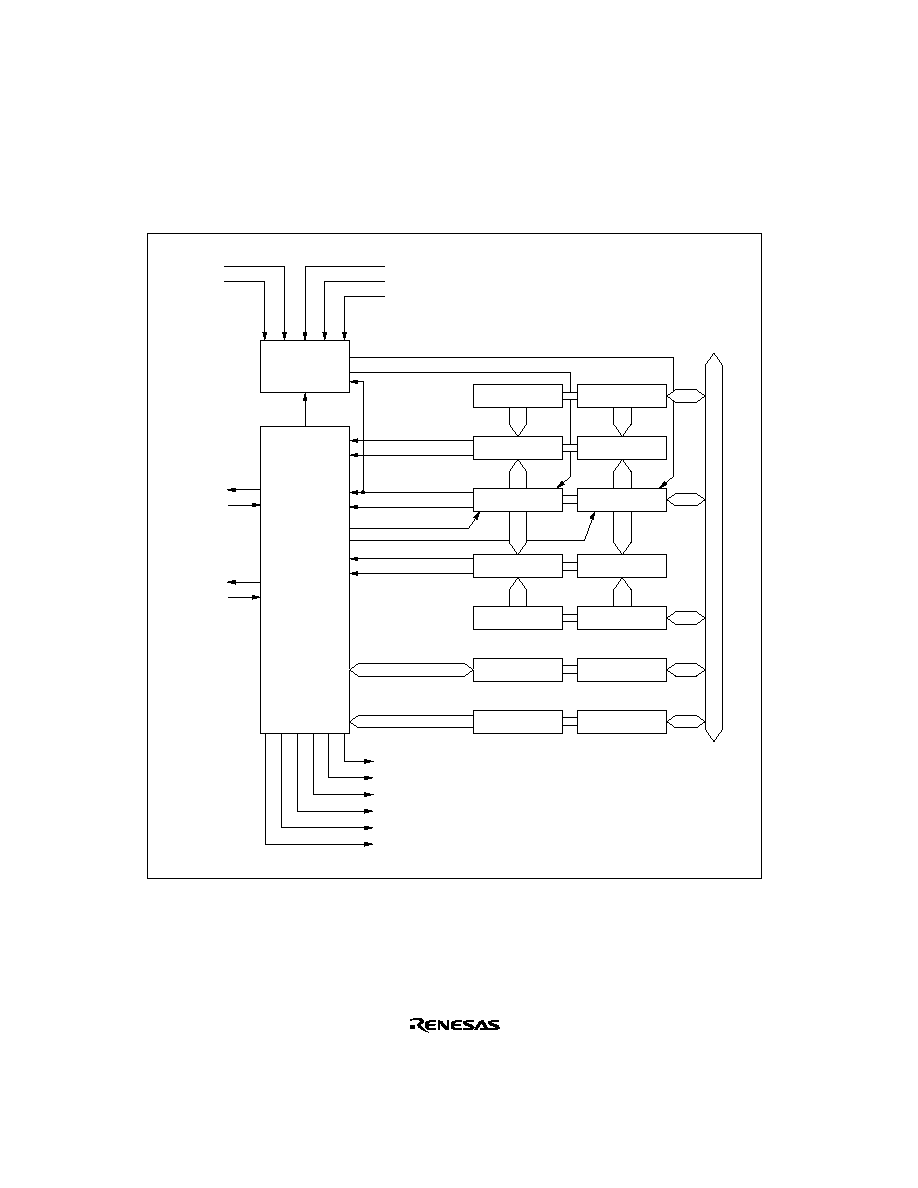
352
10.1.2
Block Diagram
Figure 10-1 shows a block diagram of the 8-bit timer module.
External clock source
Internal clock sources
¯/8
¯/64
¯/8192
Clock 1
Clock 0
Compare match A1
Compare match A0
Clear 1
CMIA0
CMIB0
OVI0
CMIA1
CMIB1
OVI1
Interrupt signals
TMO0
TMRI0
Internal bus
TCORA0
Comparator A0
Comparator B0
TCORB0
TCSR0
TCR0
TCORA1
Comparator A1
TCNT1
Comparator B1
TCORB1
TCSR1
TCR1
TMCI0
TMCI1
TCNT0
Overflow 1
Overflow 0
Compare match B1
Compare match B0
TMO1
TMRI1
Clock select
Control logic
Clear 0
Figure 10-1 Block Diagram of 8-Bit Timer

353
10.1.3
Pin Configuration
Table 10-1 summarizes the input and output pins of the 8-bit timer.
Table 10-1 Input and Output Pins of 8-Bit Timer
Channel
Name
Symbol
I/O
Function
0
Timer output pin 0
TMO0
Output
Outputs at compare match
Timer clock input pin 0
TMCI0
Input
Inputs external clock for counter
Timer reset input pin 0
TMRI0
Input
Inputs external reset to counter
1
Timer output pin 1
TMO1
Output
Outputs at compare match
Timer clock input pin 1
TMCI1
Input
Inputs external clock for counter
Timer reset input pin 1
TMRI1
Input
Inputs external reset to counter
10.1.4
Register Configuration
Table 10-2 summarizes the registers of the 8-bit timer module.
Table 10-2 8-Bit Timer Registers
Channel
Name
Abbreviation
R/W
Initial Value
Address
*
1
0
Timer control register 0
TCR0
R/W
H'00
H'FFB0
Timer control/status register 0 TCSR0
R/(W)
*
2
H'00
H'FFB2
Time constant register A0
TCORA0
R/W
H'FF
H'FFB4
Time constant register B0
TCORB0
R/W
H'FF
H'FFB6
Timer counter 0
TCNT0
R/W
H'00
H'FFB8
1
Timer control register 1
TCR1
R/W
H'00
H'FFB1
Timer control/status register 1 TCSR1
R/(W)
*
2
H'10
H'FFB3
Time constant register A1
TCORA1
R/W
H'FF
H'FFB5
Time constant register B1
TCORB1
R/W
H'FF
H'FFB7
Timer counter 1
TCNT1
R/W
H'00
H'FFB9
All
Module stop control register
MSTPCR
R/W
H'3FFF
H'FF3C
Notes: 1. Lower 16 bits of the address
2. Only 0 can be written to bits 7 to 5, to clear these flags.
Each pair of registers for channel 0 and channel 1 is a 16-bit register with the upper 8 bits for
channel 0 and the lower 8 bits for channel 1, so they can be accessed together by word transfer
instruction.
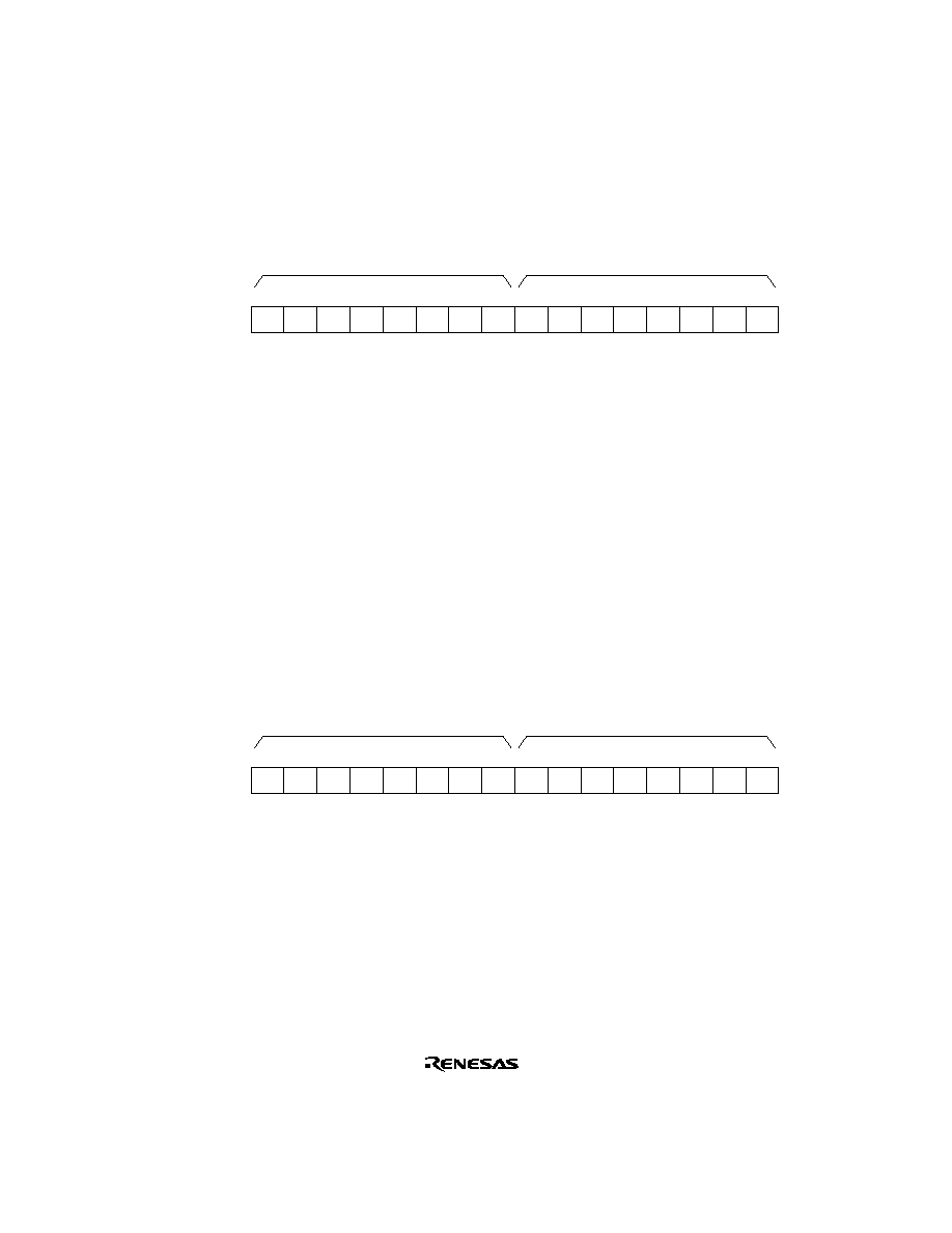
354
10.2
Register Descriptions
10.2.1
Timer Counters 0 and 1 (TCNT0, TCNT1)
15
0
R/W
14
0
R/W
13
0
R/W
12
0
R/W
11
0
R/W
10
0
R/W
9
0
R/W
8
0
R/W
7
0
R/W
6
0
R/W
5
0
R/W
4
0
R/W
3
0
R/W
2
0
R/W
1
0
R/W
0
0
R/W
TCNT0
TCNT1
Bit
Initial value
R/W
:
:
:
TCNT0 and TCNT1 are 8-bit readable/writable up-counters that increment on pulses generated
from an internal or external clock source. This clock source is selected by clock select bits CKS2
to CKS0 of TCR. The CPU can read or write to TCNT0 and TCNT1 at all times.
TCNT0 and TCNT1 comprise a single 16-bit register, so they can be accessed together by word
transfer instruction.
TCNT0 and TCNT1 can be cleared by an external reset input or by a compare match signal.
Which signal is to be used for clearing is selected by clock clear bits CCLR1 and CCLR0 of TCR.
When a timer counter overflows from H'FF to H'00, OVF in TCSR is set to 1.
TCNT0 and TCNT1 are each initialized to H'00 by a reset and in hardware standby mode.
10.2.2
Time Constant Registers A0 and A1 (TCORA0, TCORA1)
15
1
R/W
14
1
R/W
13
1
R/W
12
1
R/W
11
1
R/W
10
1
R/W
9
1
R/W
8
1
R/W
7
1
R/W
6
1
R/W
5
1
R/W
4
1
R/W
3
1
R/W
2
1
R/W
1
1
R/W
0
1
R/W
TCORA0
TCORA1
Bit
Initial value
R/W
:
:
:
TCORA0 and TCORA1 are 8-bit readable/writable registers. TCORA0 and TCORA1 comprise a
single 16-bit register so they can be accessed together by word transfer instruction.
TCORA is continually compared with the value in TCNT. When a match is detected, the
corresponding CMFA flag of TCSR is set. Note, however, that comparison is disabled during the
T2 state of a TCOR write cycle.
355
The timer output can be freely controlled by these compare match signals and the settings of
output select bits OS1 and OS0 of TCSR.
TCORA0 and TCORA1 are each initialized to H'FF by a reset and in hardware standby mode.
10.2.3
Time Constant Registers B0 and B1 (TCORB0, TCORB1)
15
1
R/W
14
1
R/W
13
1
R/W
12
1
R/W
11
1
R/W
10
1
R/W
9
1
R/W
8
1
R/W
7
1
R/W
6
1
R/W
5
1
R/W
4
1
R/W
3
1
R/W
2
1
R/W
1
1
R/W
0
1
R/W
TCORB0
TCORB1
Bit
Initial value
R/W
:
:
:
TCORB0 and TCORB1 are 8-bit readable/writable registers. TCORB0 and TCORB1 comprise a
single 16-bit register so they can be accessed together by word transfer instruction.
TCORB is continually compared with the value in TCNT. When a match is detected, the
corresponding CMFB flag of TCSR is set. Note, however, that comparison is disabled during the
T2 state of a TCOR write cycle.
The timer output can be freely controlled by these compare match signals and the settings of
output select bits OS3 and OS2 of TCSR.
TCORB0 and TCORB1 are each initialized to H'FF by a reset and in hardware standby mode.
10.2.4
Time Control Registers 0 and 1 (TCR0, TCR1)
7
CMIEB
0
R/W
6
CMIEA
0
R/W
5
OVIE
0
R/W
4
CCLR1
0
R/W
3
CCLR0
0
R/W
0
CKS0
0
R/W
2
CKS2
0
R/W
1
CKS1
0
R/W
Bit
Initial value
R/W
:
:
:
TCR0 and TCR1 are 8-bit readable/writable registers that select the clock source and the time at
which TCNT is cleared, and enable interrupts.
TCR0 and TCR1 are each initialized to H'00 by a reset and in hardware standby mode.
For details of this timing, see section 10.3, Operation.

356
Bit 7--Compare Match Interrupt Enable B (CMIEB): Selects whether CMFB interrupt
requests (CMIB) are enabled or disabled when the CMFB flag of TCSR is set to 1.
Bit 7
CMIEB
Description
0
CMFB interrupt requests (CMIB) are disabled
(Initial value)
1
CMFB interrupt requests (CMIB) are enabled
Bit 6--Compare Match Interrupt Enable A (CMIEA): Selects whether CMFA interrupt
requests (CMIA) are enabled or disabled when the CMFA flag of TCSR is set to 1.
Bit 6
CMIEA
Description
0
CMFA interrupt requests (CMIA) are disabled
(Initial value)
1
CMFA interrupt requests (CMIA) are enabled
Bit 5--Timer Overflow Interrupt Enable (OVIE): Selects whether OVF interrupt requests
(OVI) are enabled or disabled when the OVF flag of TCSR is set to 1.
Bit 5
OVIE
Description
0
OVF interrupt requests (OVI) are disabled
(Initial value)
1
OVF interrupt requests (OVI) are enabled
Bits 4 and 3--Counter Clear 1 and 0 (CCLR1 and CCLR0): These bits select the method by
which TCNT is cleared: by compare match A or B, or by an external reset input.
Bit 4
Bit 3
CCLR1
CCLR0
Description
0
0
Clear is disabled
(Initial value)
1
Clear by compare match A
1
0
Clear by compare match B
1
Clear by rising edge of external reset input

357
Bits 2 to 0--Clock Select 2 to 0 (CKS2 to CKS0): These bits select whether the clock input to
TCNT is an internal or external clock.
Three internal clocks can be selected, all divided from the system clock (¯): ¯/8, ¯/64, and ¯/8192.
The falling edge of the selected internal clock triggers the count.
When use of an external clock is selected, three types of count can be selected: at the rising edge,
the falling edge, and both rising and falling edges.
Some functions differ between channel 0 and channel 1.
Bit 2
Bit 1
Bit 0
CKS2
CKS1
CKS0
Description
0
0
0
Clock input disabled
(Initial value)
1
Internal clock, counted at falling edge of ¯/8
1
0
Internal clock, counted at falling edge of ¯/64
1
Internal clock, counted at falling edge of ¯/8192
1
0
0
For channel 0: count at TCNT1 overflow signal
*
For channel 1: count at TCNT0 compare match A
*
1
External clock, counted at rising edge
1
0
External clock, counted at falling edge
1
External clock, counted at both rising and falling edges
Note:
*
If the count input of channel 0 is the TCNT1 overflow signal and that of channel 1 is the
TCNT0 compare match signal, no incrementing clock is generated. Do not use this setting.

358
10.2.5
Timer Control/Status Registers 0 and 1 (TCSR0, TCSR1)
7
CMFB
0
R/(W)
*
6
CMFA
0
R/(W)
*
5
OVF
0
R/(W)
*
4
ADTE
0
R/W
3
OS3
0
R/W
0
OS0
0
R/W
2
OS2
0
R/W
1
OS1
0
R/W
Only 0 can be written to bits 7 to 5, to clear these flags.
Bit
Initial value
R/W
:
:
:
Note:
*
7
CMFB
0
R/(W)
*
6
CMFA
0
R/(W)
*
5
OVF
0
R/(W)
*
4
--
1
--
3
OS3
0
R/W
0
OS0
0
R/W
2
OS2
0
R/W
1
OS1
0
R/W
Bit
Initial value
R/W
:
:
:
TCSR0
TCSR1
TCSR0 and TCSR1 are 8-bit registers that display compare match and overflow statuses, and
control compare match output.
TCSR0 is initialized to H'00, and TCSR1 to H'10, by a reset and in hardware standby mode.
Bit 7--Compare Match Flag B (CMFB): Status flag indicating whether the values of TCNT and
TCORB match.
Bit 7
CMFB
Description
0
[Clearing conditions]
(Initial value)
∑
Cleared by reading CMFB when CMFB = 1, then writing 0 to CMFB
∑
When DTC is activated by CMIB interrupt while DISEL bit of MRB in DTC is 0
1
[Setting condition]
Set when TCNT matches TCORB

359
Bit 6--Compare Match Flag A (CMFA): Status flag indicating whether the values of TCNT and
TCORA match.
Bit 6
CMFA
Description
0
[Clearing conditions]
(Initial value)
∑
Cleared by reading CMFA when CMFA = 1, then writing 0 to CMFA
∑
When DTC is activated by CMIA interrupt while DISEL bit of MRB in DTC is 0
1
[Setting condition]
Set when TCNT matches TCORA
Bit 5--Timer Overflow Flag (OVF): Status flag indicating that TCNT has overflowed (changed
from H'FF to H'00).
Bit 5
OVF
Description
0
[Clearing condition]
(Initial value)
Cleared by reading OVF when OVF = 1, then writing 0 to OVF
1
[Setting condition]
Set when TCNT overflows from H'FF to H'00
Bit 4--A/D Trigger Enable (ADTE) (TCSR0 Only): Selects enabling or disabling of A/D
converter start requests by compare-match A.
In TCSR1, this bit is reserved: it is always read as 1 and cannot be modified.
Bit 4
ADTE
Description
0
A/D converter start requests by compare match A are disabled
(Initial value)
1
A/D converter start requests by compare match A are enabled

360
Bits 3 to 0--Output Select 3 to 0 (OS3 to OS0): These bits specify how the timer output level is
to be changed by a compare match of TCOR and TCNT.
Bits OS3 and OS2 select the effect of compare match B on the output level, bits OS1 and OS0
select the effect of compare match A on the output level, and both of them can be controlled
independently.
Note, however, that priorities are set such that: toggle output > 1 output > 0 output. If compare
matches occur simultaneously, the output changes according to the compare match with the higher
priority.
Timer output is disabled when bits OS3 to OS0 are all 0.
After a reset, the timer output is 0 until the first compare match event occurs.
Bit 3
Bit 2
OS3
OS2
Description
0
0
No change when compare match B occurs
(Initial value)
1
0 is output when compare match B occurs
1
0
1 is output when compare match B occurs
1
Output is inverted when compare match B occurs (toggle output)
Bit 1
Bit 0
OS1
OS0
Description
0
0
No change when compare match A occurs
(Initial value)
1
0 is output when compare match A occurs
1
0
1 is output when compare match A occurs
1
Output is inverted when compare match A occurs (toggle output)

361
10.2.6
Module Stop Control Register (MSTPCR)
15
0
R/W
Bit
Initial value
R/W
:
:
:
14
0
R/W
13
1
R/W
12
1
R/W
11
1
R/W
10
1
R/W
9
1
R/W
8
1
R/W
7
1
R/W
6
1
R/W
5
1
R/W
4
1
R/W
3
1
R/W
2
1
R/W
1
1
R/W
0
1
R/W
MSTPCRH
MSTPCRL
MSTPCR is a 16-bit readable/writable register that performs module stop mode control.
When the MSTP12 bit in MSTPCR is set to 1, the 8-bit timer operation stops at the end of the bus
cycle and a transition is made to module stop mode. Registers cannot be read or written to in
module stop mode. For details, see section 18.5, Module Stop Mode.
MSTPCR is initialized to H'3FFF by a reset and in hardware standby mode. It is not initialized in
software standby mode.
Bit 12--Module Stop (MSTP12): Specifies the 8-bit timer stop mode.
Bit 12
MSTP12
Description
0
8-bit timer module stop mode cleared
1
8-bit timer module stop mode set
(Initial value)
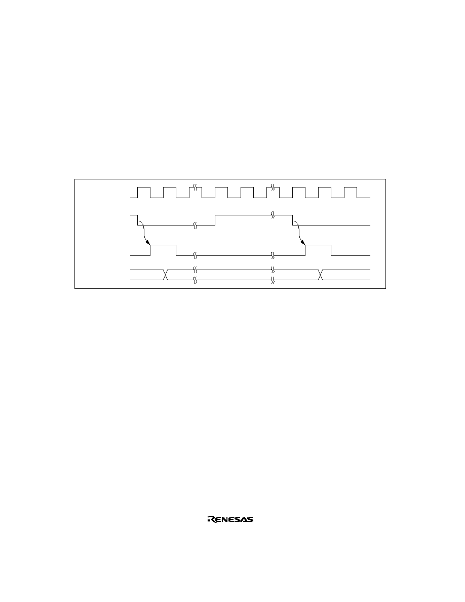
362
10.3
Operation
10.3.1
TCNT Incrementation Timing
TCNT is incremented by input clock pulses (either internal or external).
Internal Clock: Three different internal clock signals (¯/8, ¯/64, or ¯/8192) divided from the
system clock (¯) can be selected, by setting bits CKS2 to CKS0 in TCR. Figure 10-2 shows the
count timing.
¯
Internal clock
Clock input
to TCNT
TCNT
N≠1
N
N+1
Figure 10-2 Count Timing for Internal Clock Input
External Clock: Three incrementation methods can be selected by setting bits CKS2 to CKS0 in
TCR: at the rising edge, the falling edge, and both rising and falling edges.
Note that the external clock pulse width must be at least 1.5 states for incrementation at a single
edge, and at least 2.5 states for incrementation at both edges. The counter will not increment
correctly if the pulse width is less than these values.
Figure 10-3 shows the timing of incrementation at both edges of an external clock signal.
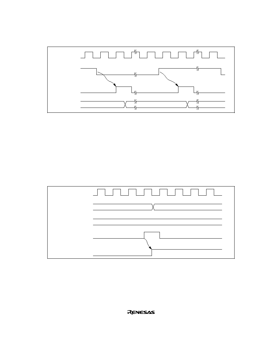
363
¯
External clock
input
Clock input
to TCNT
TCNT
N≠1
N
N+1
Figure 10-3 Count Timing for External Clock Input
10.3.2
Compare Match Timing
Setting of Compare Match Flags A and B (CMFA, CMFB): The CMFA and CMFB flags in
TCSR are set to 1 by a compare match signal generated when the TCOR and TCNT values match.
The compare match signal is generated at the last state in which the match is true, just before the
timer counter is updated.
Therefore, when TCOR and TCNT match, the compare match signal is not generated until the
next incrementation clock input. Figure 10-4 shows this timing.
¯
TCNT
N
N+1
TCOR
N
Compare match
signal
CMF
Figure 10-4 Timing of CMF Setting
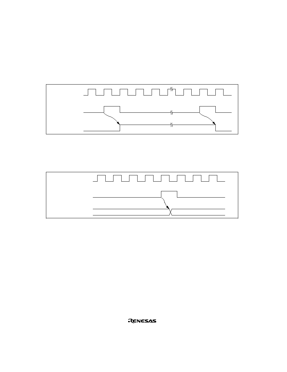
364
Timer output timing: When compare match A or B occurs, the timer output changes a specified
by bits OS3 to OS0 in TCSR. Depending on these bits, the output can remain the same, change to
0, change to 1, or toggle.
Figure 10-5 shows the timing when the output is set to toggle at compare match A.
¯
Compare match A
signal
Timer output pin
Figure 10-5 Timing of Timer Output
Timing of Compare Match Clear: The timer counter is cleared when compare match A or B
occurs, depending on the setting of the CCLR1 and CCLR0 bits in TCR. Figure 10-6 shows the
timing of this operation.
¯
N
H'00
Compare match
signal
TCNT
Figure 10-6 Timing of Compare Match Clear
365
10.3.3
Timing of External RESET on TCNT
TCNT is cleared at the rising edge of an external reset input, depending on the settings of the
CCLR1 and CCLR0 bits in TCR. The clear pulse width must be at least 1.5 states. Figure 10-7
shows the timing of this operation.
¯
Clear signal
External reset
input pin
TCNT
N
H'00
N≠1
Figure 10-7 Timing of External Reset
10.3.4
Timing of Overflow Flag (OVF) Setting
The OVF in TCSR is set to 1 when the timer count overflows (changes from H'FF to H'00). Figure
10-8 shows the timing of this operation.
¯
OVF
Overflow signal
TCNT
H'FF
H'00
Figure 10-8 Timing of OVF Setting

366
10.3.5
Operation with Cascaded Connection
If bits CKS2 to CKS0 in either TCR0 or TCR1 are set to B'100, the 8-bit timers of the two
channels are cascaded. With this configuration, a single 16-bit timer could be used (16-bit timer
mode) or compare matches of the 8-bit channel 0 could be counted by the timer of channel 1
(compare match counter mode). In this case, the timer operates as below.
16-Bit Counter Mode: When bits CKS2 to CKS0 in TCR0 are set to B'100, the timer functions
as a single 16-bit timer with channel 0 occupying the upper 8 bits and channel 1 occupying the
lower 8 bits.
∑
Setting of compare match flags
The CMF flag in TCSR0 is set to 1 when a 16-bit compare match event occurs.
The CMF flag in TCSR1 is set to 1 when a lower 8-bit compare match event occurs.
∑
Counter clear specification
If the CCLR1 and CCLR0 bits in TCR0 have been set for counter clear at compare match,
the 16-bit counter (TCNT0 and TCNT1 together) is cleared when a 16-bit compare match
event occurs. The 16-bit counter (TCNT0 and TCNT1 together) is cleared even if counter
clear by the TMRI0 pin has also been set.
The settings of the CCLR1 and CCLR0 bits in TCR1 are ignored. The lower 8 bits cannot
be cleared independently.
∑
Pin output
Control of output from the TMO0 pin by bits OS3 to OS0 in TCSR0 is in accordance with
the 16-bit compare match conditions.
Control of output from the TMO1 pin by bits OS3 to OS0 in TCSR1 is in accordance with
the lower 8-bit compare match conditions.
Compare Match Counter Mode: When bits CKS2 to CKS0 in TCR1 are B'100, TCNT1 counts
compare match A's for channel 0.
Channels 1 and 0 are controlled independently. Conditions such as setting of the CMF flag,
generation of interrupts, output from the TMO pin, and counter clear are in accordance with the
settings for each channel.
Note on Usage: If the 16-bit counter mode and compare match counter mode are set
simultaneously, the input clock pulses for TCNT0 and TCNT1 are not generated and thus the
counters will stop operating. Software should therefore avoid using both these modes.

367
10.4
Interrupt Sources
10.4.1
Interrupt Sources and DTC Activation
There are three 8-bit timer interrupt sources: CMIA, CMIB, and OVI. Their relative priorities are
shown in Table 10-3. Each interrupt source is set as enabled or disabled by the corresponding
interrupt enable bit in TCR, and independent interrupt requests are sent for each to the interrupt
controller. It is also possible to activate the DTC by means of CMIA and CMIB interrupts.
Table 10-3 8-Bit Timer Interrupt Sources
Channel
Interrupt Source
Description
DTC Activation
Priority
0
CMIA0
Interrupt by CMFA
Possible
High
CMIB0
Interrupt by CMFB
Possible
OVI0
Interrupt by OVF
Not possible
1
CMIA1
Interrupt by CMFA
Possible
CMIB1
Interrupt by CMFB
Possible
OVI1
Interrupt by OVF
Not possible
Low
Note:
This table shows the initial state immediately after a reset. The relative channel priorities
can be changed by the interrupt controller.
10.4.2
A/D Converter Activation
The A/D converter can be activated only by channel 0 compare match A.
If the ADTE bit in TCSR0 is set to 1 when the CMFA flag is set to 1 by the occurrence of channel
0 compare match A, a request to start A/D conversion is sent to the A/D converter. If the 8-bit
timer conversion start trigger has been selected on the A/D converter side at this time, A/D
conversion is started.
368
10.5
Sample Application
In the example below, the 8-bit timer is used to generate a pulse output with a selected duty cycle,
as shown in figure 10-9. The control bits are set as follows:
[1] In TCR, bit CCLR1 is cleared to 0 and bit CCLR0 is set to 1 so that the timer counter is
cleared when its value matches the constant in TCORA.
[2] In TCSR, bits OS3 to OS0 are set to B'0110, causing the output to change to 1 at a TCORA
compare match and to 0 at a TCORB compare match.
With these settings, the 8-bit timer provides output of pulses at a rate determined by TCORA with
a pulse width determined by TCORB. No software intervention is required.
TCNT
H'FF
Counter clear
TCORA
TCORB
H'00
TMO
Figure 10-9 Example of Pulse Output
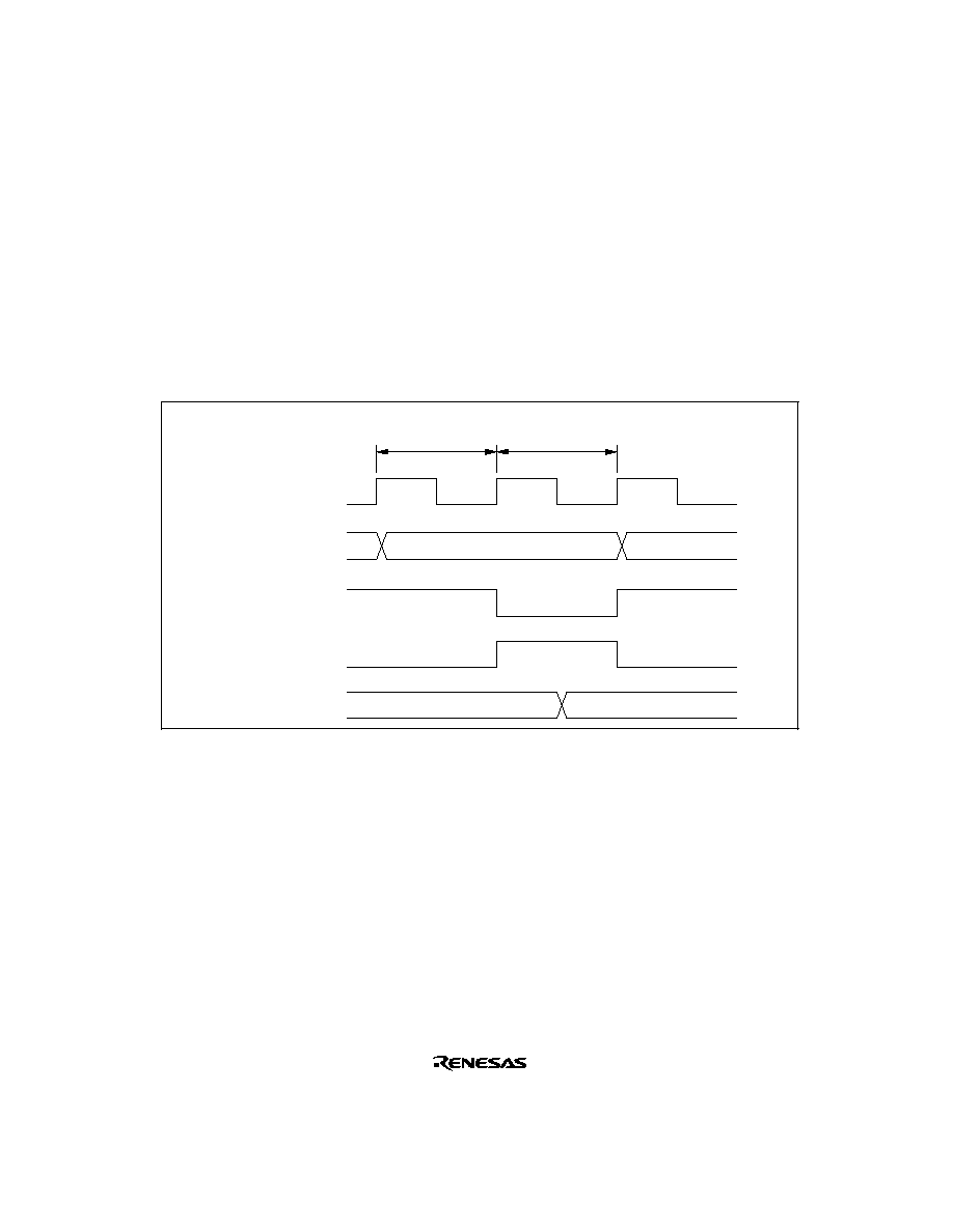
369
10.6
Usage Notes
Application programmers should note that the following kinds of contention can occur in the 8-bit
timer.
10.6.1
Contention between TCNT Write and Clear
If a timer counter clock pulse is generated during the T2 state of a TCNT write cycle, the clear
takes priority, so that the counter is cleared and the write is not performed.
Figure 10-10 shows this operation.
¯
Address
TCNT address
Internal write signal
Counter clear signal
TCNT
N
H'00
T1
T2
TCNT write cycle by CPU
Figure 10-10 Contention between TCNT Write and Clear
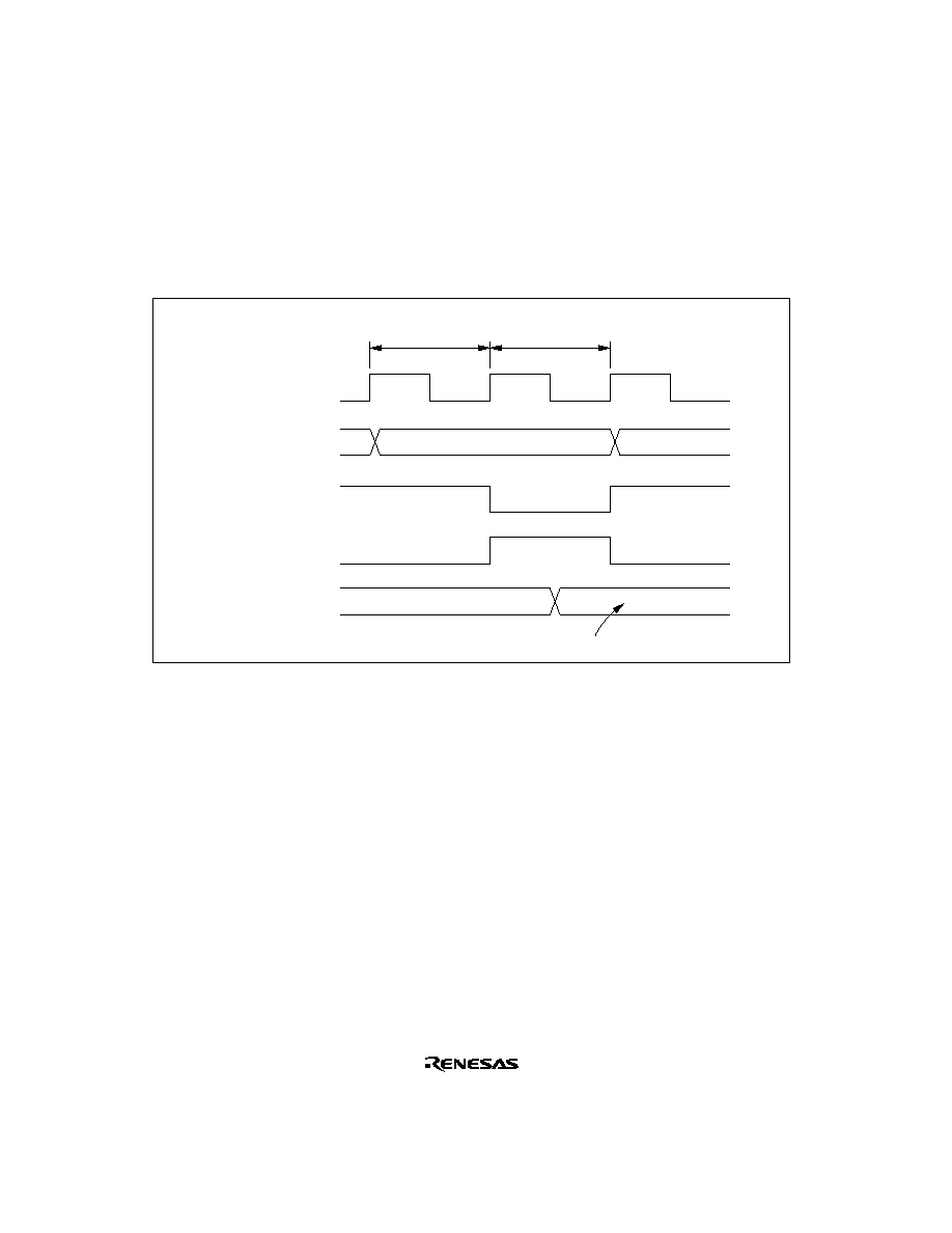
370
10.6.2
Contention between TCNT Write and Increment
If a timer counter clock pulse is generated during the T2 state of a TCNT write cycle, the write
takes priority and the counter is not incremented.
Figure 10-11 shows this operation.
¯
Address
TCNT address
Internal write signal
TCNT input clock
TCNT
N
M
T1
T2
TCNT write cycle by CPU
Counter write data
Figure 10-11 Contention between TCNT Write and Increment
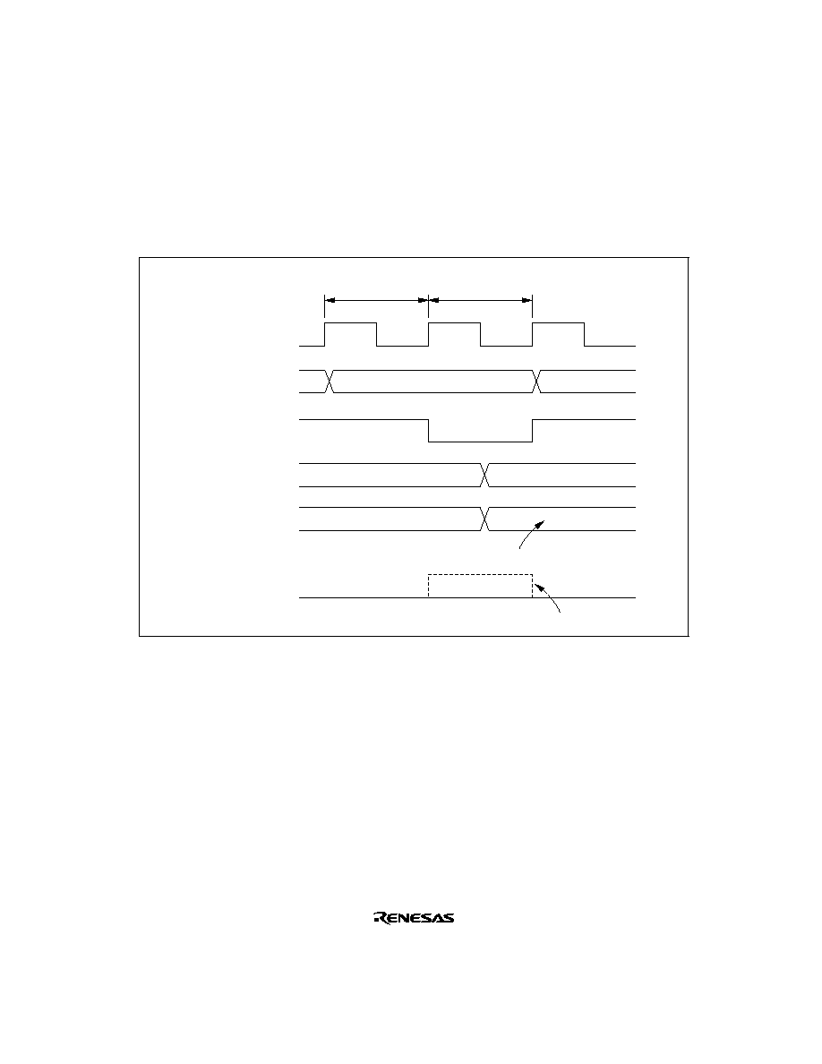
371
10.6.3
Contention between TCOR Write and Compare Match
During the T2 state of a TCOR write cycle, the TCOR write has priority even if a compare match
event occurs.
Figure 10-12 shows this operation.
¯
Address
TCOR address
Internal write signal
TCNT
TCOR
N
M
T1
T2
TCOR write cycle by CPU
TCOR write data
N
N+1
Compare match signal
Disabled
Figure 10-12 Contention between TCOR Write and Compare Match

372
10.6.4
Contention between Compare Matches A and B
If compare match events A and B occur at the same time, the 8-bit timer operates in accordance
with the priorities for the output statuses set for compare match A and compare match B, as shown
in table 10-4.
Table 10-4 Timer Output Priorities
Output Setting
Priority
Toggle output
High
1 output
0 output
No change
Low
10.6.5
Switching of Internal Clocks and TCNT Operation
TCNT may increment erroneously when the internal clock is switched over. Table 10-5 shows the
relationship between the timing at which the internal clock is switched (by writing to the CKS1
and CKS0 bits) and the TCNT operation.
When the TCNT clock is generated from an internal clock, the falling edge of the internal clock
pulse is detected. If clock switching causes a change from high to low level, as shown in case 3 in
table 10-5, a TCNT clock pulse is generated on the assumption that the switchover is a falling
edge. This increments TCNT.
The erroneous incrementation can also happen when switching between internal and external
clocks.
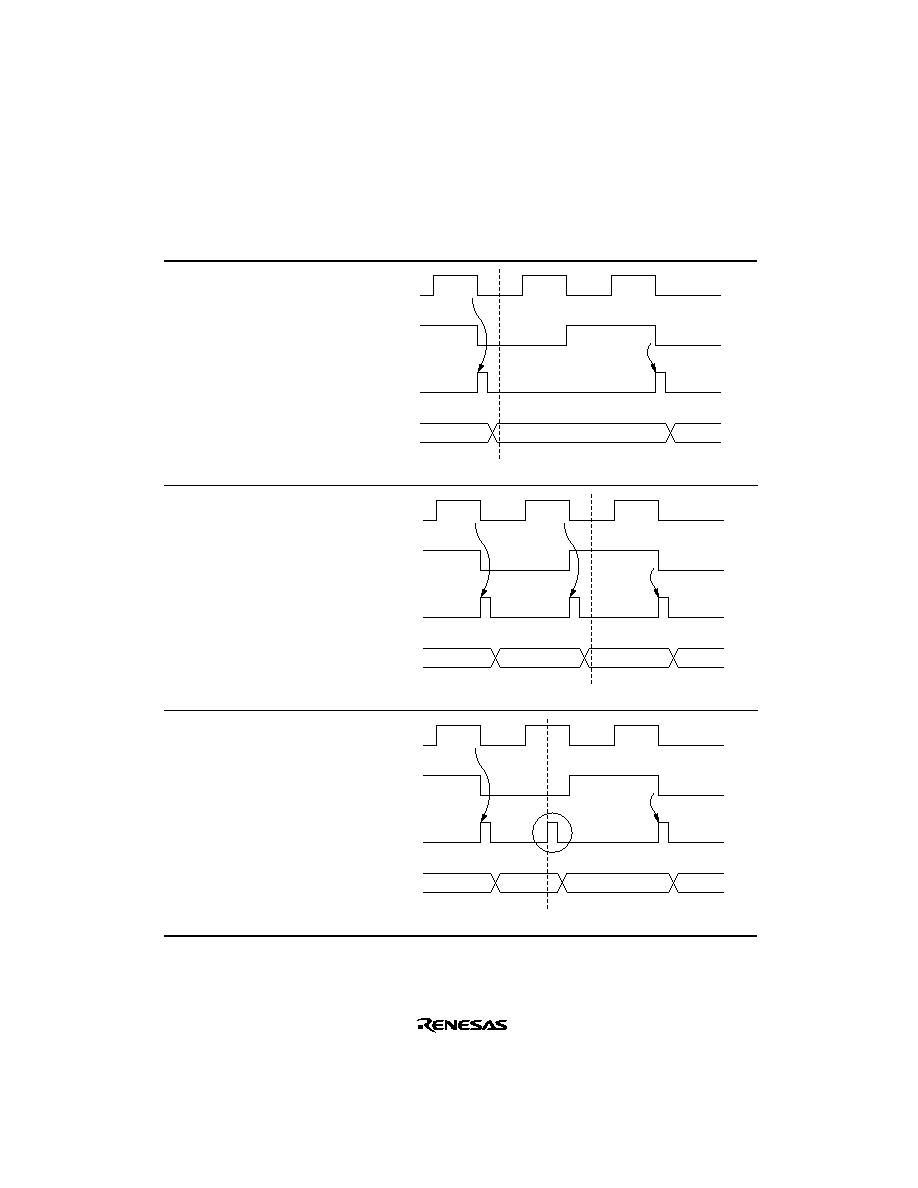
373
Table 10-5 Switching of Internal Clock and TCNT Operation
No.
Timing of
Switchover by
Means of CKS1
and CKS0 Bits
TCNT Clock Operation
1
Switching from
low to low
*
1
Clock before
switchover
Clock after
switchover
TCNT clock
TCNT
CKS bit write
N
N+1
2
Switching from
low to high
*
2
Clock before
switchover
Clock after
switchover
TCNT clock
TCNT
CKS bit write
N
N+1
N+2
3
Switching from
high to low
*
3
Clock before
switchover
Clock after
switchover
TCNT clock
TCNT
CKS bit write
N
N+1
N+2
*
4
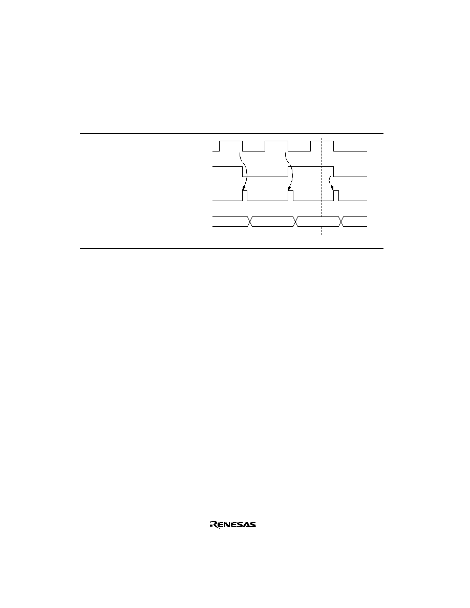
374
Table 10-5 Switching of Internal Clock and TCNT Operation (cont)
No.
Timing of
Switchover by
Means of CKS1
and CKS0 Bits
TCNT Clock Operation
4
Switching from
high to high
Clock before
switchover
Clock after
switchover
TCNT clock
TCNT
CKS bit write
N
N+1
N+2
Notes: 1. Includes switching from low to stop, and from stop to low.
2. Includes switching from stop to high.
3. Includes switching from high to stop.
4. Generated on the assumption that the switchover is a falling edge; TCNT is
incremented.
10.6.6
Interrupts and Module Stop Mode
If module stop mode is entered when an interrupt has been requested, it will not be possible to
clear the CPU interrupt source or DTC activation source. Interrupts should therefore be disabled
before entering module stop mode.

375
Section 11 Watchdog Timer
11.1
Overview
The H8S/2245 Series has a single-channel on-chip watchdog timer (WDT) for monitoring system
operation. The WDT outputs an overflow signal (
WDTOVF) if a system crash prevents the CPU
from writing to the timer counter, allowing it to overflow. At the same time, the WDT can also
generate an internal reset signal for the H8S/2245 Series.
When this watchdog function is not needed, the WDT can be used as an interval timer. In interval
timer operation, an interval timer interrupt is generated each time the counter overflows.
11.1.1
Features
WDT features are listed below.
∑
Switchable between watchdog timer mode and interval timer mode
∑
WDTOVF output when in watchdog timer mode
If the counter overflows, the WDT outputs
WDTOVF. It is possible to select whether or not
the entire H8S/2245 Series is reset at the same time. This internal reset can be a power-on reset
or a manual reset.
∑
Interrupt generation when in interval timer mode
If the counter overflows, the WDT generates an interval timer interrupt.
∑
Choice of eight counter clock sources.

376
11.1.2
Block Diagram
Figure 11-1 shows a block diagram of the WDT.
Overflow
Interrupt
control
WOVI
(interrupt request
signal)
WDTOVF
Internal reset signal
*
Reset
control
RSTCSR
TCNT
TSCR
¯/2
¯/64
¯/128
¯/512
¯/2048
¯/8192
¯/32768
¯/131072
Clock
Clock
select
Internal clock
sources
Bus
interface
Module bus
Legend
TCSR
TCNT
RSTCSR
Note:
*
: Timer control/status register
: Timer counter
: Reset control/status register
Internal bus
WDT
The type of internal reset signal depends on a register setting. Either power-on reset or manual
reset can be selected.
Figure 11-1 Block Diagram of WDT

377
11.1.3
Pin Configuration
Table 11-1 describes the WDT output pin.
Table 11-1 WDT Pin
Name
Symbol
I/O
Function
Watchdog timer overflow
WDTOVF
Output
Outputs counter overflow signal in watchdog
timer mode
11.1.4
Register Configuration
The WDT has three registers, as summarized in table 11-2. These registers control clock selection,
WDT mode switching, and the reset signal.
Table 11-2 WDT Registers
Address
*
1
Name
Abbreviation
R/W
Initial Value
Write
*
2
Read
Timer control/status register
TCSR
R/(W)
*
3
H'18
H'FFBC
H'FFBC
Timer counter
TCNT
R/W
H'00
H'FFBC
H'FFBD
Reset control/status register
RSTCSR
R/(W)
*
3
H'1F
H'FFBE
H'FFBF
Notes: 1. Lower 16 bits of the address.
2. For details of write operations, see section 11.2.4, Notes on Register Access.
3. Only a write of 0 is permitted to bit 7, to clear the flag.

378
11.2
Register Descriptions
11.2.1
Timer Counter (TCNT)
7
0
R/W
6
0
R/W
5
0
R/W
4
0
R/W
3
0
R/W
0
0
R/W
2
0
R/W
1
0
R/W
Bit
Initial value
R/W
:
:
:
TCNT is an 8-bit readable/writable* up-counter.
When the TME bit is set to 1 in TCSR, TCNT starts counting pulses generated from the internal
clock source selected by bits CKS2 to CKS0 in TCSR. When the count overflows (changes from
H'FF to H'00), either the watchdog timer overflow signal (
WDTOVF) or an interval timer
interrupt (WOVI) is generated, depending on the mode selected by the WT/
IT bit in TCSR.
TCNT is initialized to H'00 by a reset, in hardware standby mode, or when the TME bit is cleared
to 0. It is not initialized in software standby mode.
Note: * TCNT is write-protected by a password to prevent accidental overwriting. For details see
section 11.2.4, Notes on Register Access.
11.2.2
Timer Control/Status Register (TCSR)
7
OVF
0
R/(W)
*
6
WT/IT
0
R/W
5
TME
0
R/W
4
--
1
--
3
--
1
--
0
CKS0
0
R/W
2
CKS2
0
R/W
1
CKS1
0
R/W
Bit
Initial value
R/W
:
:
:
Note:
*
Can only be written with 0 for flag clearing.
TCSR is an 8-bit readable/writable* register. Its functions include selecting the clock source to be
input to TCNT, and the timer mode.
TCR is initialized to H'18 by a reset and in hardware standby mode. It is not initialized in software
standby mode.
Note: * TCSR is write-protected by a password to prevent accidental overwriting. For details see
section 11.2.4, Notes on Register Access.

379
Bit 7--Overflow Flag (OVF): Indicates that TCNT has overflowed from H'FF to H'00, when in
interval timer mode. This flag cannot be set during watchdog timer operation.
Bit 7
OVF
Description
0
[Clearing condition]
Cleared by reading TCSR when OVF = 1, then writing 0 to OVF
(Initial value)
1
[Setting condition]
Set when TCNT overflows (changes from H'FF to H'00) in interval timer mode
Bit 6--Timer Mode Select (WT/
IT): Selects whether the WDT is used as a watchdog timer or
interval timer. If used as an interval timer, the WDT generates an interval timer interrupt request
(WOVI) when TCNT overflows. If used as a watchdog timer, the WDT generates the
WDTOVF
signal when TCNT overflows.
Bit 6
WT/
IT
Description
0
Interval timer: Sends the CPU an interval timer interrupt request (WOVI)
when TCNT overflows
(Initial value)
1
Watchdog timer: Generates the
WDTOVF
signal when TCNT overflows
*
Note:
*
For details of the case where TCNT overflows in watchdog timer mode, see section 11.2.3,
Reset Control/Status Register (RSTCSR).
Bit 5--Timer Enable (TME): Selects whether TCNT runs or is halted.
Bit 5
TME
Description
0
TCNT is initialized to H'00 and halted
(Initial value)
1
TCNT counts
Bits 4 and 3--Reserved: Read-only bits, always read as 1.

380
Bits 2 to 0: Clock Select 2 to 0 (CKS2 to CKS0): These bits select one of eight internal clock
sources, obtained by dividing the system clock (¯), for input to TCNT.
Bit 2
Bit 1
Bit 0
Description
CKS2
CKS1
CKS0
Clock
Overflow period (when ¯ = 20 MHz)
*
0
0
0
¯/2 (initial value)
25.6 µs
1
¯/64
819.2 µs
1
0
¯/128
1.6 ms
1
¯/512
6.6 ms
1
0
0
¯/2048
26.2 ms
1
¯/8192
104.9 ms
1
0
¯/32768
419.4 ms
1
¯/131072
1.68 s
Note:
*
The overflow period is the time from when TCNT starts counting up from H'00 until overflow
occurs.
11.2.3
Reset Control/Status Register (RSTCSR)
7
WOVF
0
R/(W)
*
6
RSTE
0
R/W
5
RSTS
0
R/W
4
--
1
--
3
--
1
--
0
--
1
--
2
--
1
--
1
--
1
--
Note:
*
Can only be written with 0 for flag clearing.
Bit
Initial value
R/W
:
:
:
RSTCSR is an 8-bit readable/writable* register that controls the generation of the internal reset
signal when TCNT overflows, and selects the type of internal reset signal.
RSTCSR is initialized to H'1F by a reset signal from the
RES pin, but not by the WDT internal
reset signal caused by overflows.
Note: * RSTCSR is write-protected by a password to prevent accidental overwriting. For details
see section 11.2.4, Notes on Register Access.

381
Bit 7--Watchdog Overflow Flag (WOVF): Indicates that TCNT has overflowed (changed from
H'FF to H'00) during watchdog timer operation. This bit is not set in interval timer mode.
Bit 7
WOVF
Description
0
[Clearing condition]
(Initial value)
Cleared by reading TCSR when WOVF = 1, then writing 0 to WOVF
1
[Setting condition]
Set when TCNT overflows (changes from H'FF to H'00) during watchdog timer
operation
Bit 6--Reset Enable (RSTE): Specifies whether or not a reset signal is generated in the
H8S/2245 Series if TCNT overflows during watchdog timer operation.
Bit 6
RSTE
Description
0
Reset signal is not generated if TCNT overflows
*
(Initial value)
1
Reset signal is generated if TCNT overflows
Note:
*
The modules within the H8S/2245 Series are not reset, but TCNT and TCSR within the
WDT are reset.
Bit 5--Reset Select (RSTS): Selects the type of internal reset generated if TCNT overflows
during watchdog timer operation.
For details of the types of resets, see section 4, Exception Handling.
Bit 5
RSTS
Description
0
Power-on reset
(Initial value)
1
Manual reset
Bits 4 to 0--Reserved: Read-only bits, always read as 1.

382
11.2.4
Notes on Register Access
The watchdog timer's TCNT, TCSR, and RSTCSR registers differ from other registers in being
more difficult to write to. The procedures for writing to and reading these registers are given
below.
Writing to TCNT and TCSR: These registers must be written to by a word transfer instruction.
They cannot be written to with byte instructions.
Figure 11-2 shows the format of data written to TCNT and TCSR. TCNT and TCSR both have the
same write address. For a write to TCNT, the upper byte of the written word must contain H'5A
and the lower byte must contain the write data. For a write to TCSR, the upper byte of the written
word must contain H'A5 and the lower byte must contain the write data. This transfers the write
data from the lower byte to TCNT or TCSR (see figure 11-2).
TCNT write
TCSR write
Address: H'FFBC
Address: H'FFBC
H'5A
Write data
15
8 7
0
H'A5
Write data
15
8 7
0
Figure 11-2 Format of Data Written to TCNT and TCSR

383
Writing to RSTCSR: RSTCSR must be written to by word transfer instruction to address
H'FFBE. It cannot be written to with byte instructions.
Figure 11-3 shows the format of data written to RSTCSR. The method of writing 0 to the WOVF
bit differs from that for writing to the RSTE and RSTS bits.
To write 0 to the WOVF flag, the write data must have H'A5 in the upper byte and H'00 in the
lower byte. This clears the WOVF bit to 0, but has no effect on the RSTE and RSTS bits. To write
to the RSTE and RSTS bits, the upper byte must contain H'5A and the lower byte must contain the
write data. This writes the values in bits 6 and 5 of the lower byte into the RSTE and RSTS bits,
but has no effect on the WOVF flag.
H'A5
H'00
15
8 7
0
H'5A
Write data
15
8 7
0
Writing 0 to WOVF bit
Writing to RSTE and RSTS bits
Address: H'FFBE
Address: H'FFBE
Figure 11-3 Format of Data Written to RSTCSR
Reading TCNT, TCSR, and RSTCSR: These registers are read in the same way as other
registers. The read addresses are H'FFBC for TCSR, H'FFBD for TCNT, and H'FFBF for
RSTCSR.

384
11.3
Operation
11.3.1
Watchdog Timer Operation
To use the WDT as a watchdog timer, set the WT/
IT and TME bits to 1. Software must prevent
TCNT overflows by rewriting the TCNT value (normally be writing H'00) before overflows
occurs. This ensures that TCNT does not overflow while the system is operating normally. If
TCNT overflows without being rewritten because of a system crash or other error, the
WDTOVF
signal is output. This is shown in figure 11-4. This
WDTOVF signal can be used to reset the
system. The
WDTOVF signal is output for 132 states when RSTE = 1, and for 130 states when
RSTE = 0.
If TCNT overflows when 1 is set in the RSTE bit in RSTCSR, a signal that resets the H8S/2245
Series internally is generated at the same time as the
WDTOVF signal. This reset can be selected
as a power-on reset or a manual reset, depending on the setting of the RSTS bit in RSTCSR. The
internal reset signal is output for 518 states.
If a reset caused by a signal input to the
RES pin occurs at the same time as a reset caused by a
WDT overflow, the
RES pin reset has priority and the WOVF flag in RSTCSR is cleared to 0.
TCNT count
H'00
Time
H'FF
WT/IT=1
TME=1
H'00 written
to TCNT
WT/IT=1
TME=1
H'00 written
to TCNT
132 states
*
2
518 states
WDTOVF signal
Internal reset signal
*
1
WT/IT
TME
WOVF
Notes:
WDT overflow
WDTOVF and
internal reset are
generated
WOVF=1
: Timer mode select bit
: Timer enable bit
: Watchdog timer overflow
1. The internal reset signal is generated only if the RSTE bit is set to 1.
2. 130 states when the RSTE bit is cleared to 0
Legend
Figure 11-4 Watchdog Timer Operation
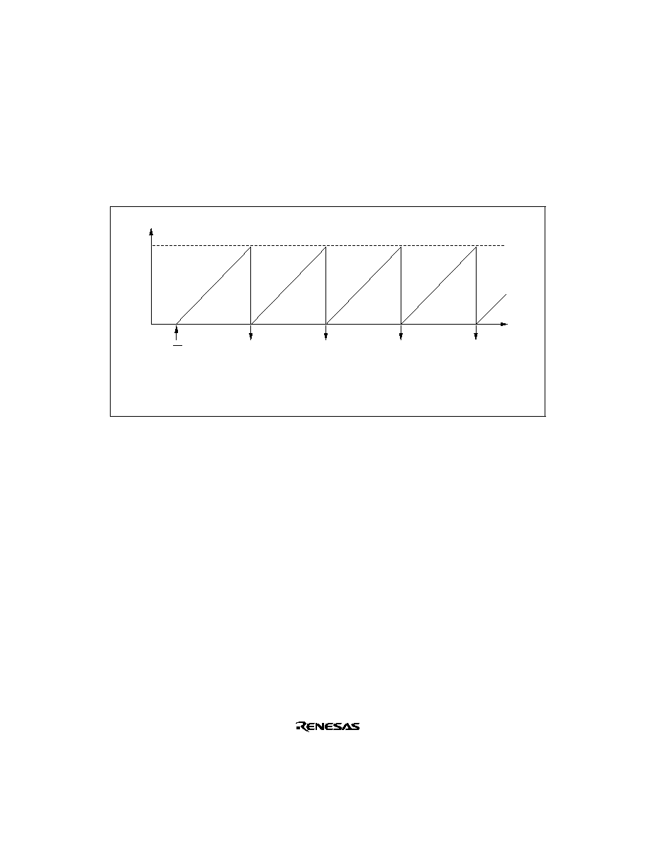
385
11.3.2
Interval Timer Operation
To use the WDT as an interval timer, clear the WT/
IT bit in TCSR to 0 and set the TME bit to 1.
An interval timer interrupt (WOVI) is generated each time TCNT overflows, provided that the
WDT is operating as an interval timer, as shown in figure 11-5. This function can be used to
generate interrupt requests at regular intervals.
TCNT count
H'00
Time
H'FF
WT/IT=0
TME=1
WOVI
Overflow
Overflow
Overflow
Overflow
Legend
WOVI: Interval timer interrupt request generation
WOVI
WOVI
WOVI
Figure 11-5 Interval Timer Operation
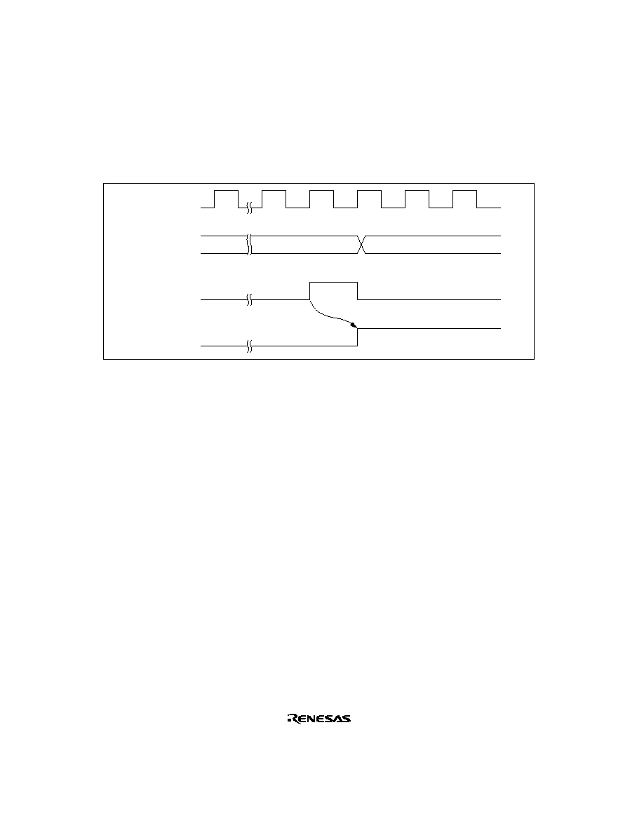
386
11.3.3
Timing of Setting Overflow Flag (OVF)
The OVF flag is set to 1 if TCNT overflows during interval timer operation. At the same time, an
interval timer interrupt (WOVI) is requested. This timing is shown in figure 11-6.
¯
TCNT
H'FF
H'00
Overflow signal
(internal signal)
OVF
Figure 11-6 Timing of Setting of OVF

387
11.3.4
Timing of Setting of Watchdog Timer Overflow Flag (WOVF)
The WOVF flag is set to 1 if TCNT overflows during watchdog timer operation. At the same time,
the
WDTOVF signal goes low. If TCNT overflows while the RSTE bit in RSTCSR is set to 1, an
internal reset signal is generated for the entire H8S/2245 Series chip. Figure 11-7 shows the timing
in this case.
¯
TCNT
H'FF
H'00
Overflow signal
(internal signal)
WOVF
WDTOVF signal
Internal reset
signal
132 states
518 states
Figure 11-7 Timing of Setting of WOVF

388
11.4
Interrupts
During interval timer mode operation, an overflow generates an interval timer interrupt (WOVI).
The interval timer interrupt is requested whenever the OVF flag is set to 1 in TCSR.
11.5 Usage
Notes
11.5.1
Contention between Timer Counter (TCNT) Write and Increment
If a timer counter clock pulse is generated during the T2 state of a TCNT write cycle, the write
takes priority and the timer counter is not incremented. Figure 11-8 shows this operation.
Address
¯
Internal write signal
TCNT input clock
pulse
TCNT
N
M
T1
T2
TCNT write cycle
Counter write data
Figure 11-8 Contention between TCNT Write and Increment
11.5.2
Changing Value of CKS2 to CKS0
If bits CKS2 to CKS0 in TCSR are written to while the WDT is operating, errors could occur in
the incrementation. Software must stop the watchdog timer (by clearing the TME bit to 0) before
changing the value of bits CKS2 to CKS0.

389
11.5.3
Switching between Watchdog Timer Mode and Interval Timer Mode
If the mode is switched from watchdog timer to interval timer, or vice versa, while the WDT is
operating, errors could occur in the incrementation. Software must stop the watchdog timer (by
clearing the TME bit to 0) before switching the mode.
11.5.4
System Reset by
WDTOVF Signal
If the
WDTOVF output signal is input to the RES pin of the H8S/2245 Series, the H8S/2245
Series will not be initialized correctly. Make sure that the
WDTOVF signal is not input logically
to the
RES pin. To reset the entire system by means of the WDTOVF signal, use the circuit shown
in figure 11-9.
Reset input
Reset signal to entire system
H8S/2245
RES
WDTOVF
Figure 11-9 Circuit for System Reset by
WDTOVF Signal (Example)
11.5.5
Internal Reset in Watchdog Timer Mode
The H8S/2245 Series is not reset internally if TCNT overflows while the RSTE bit is cleared to 0
during watchdog timer operation, but TCNT and TSCR of the WDT are reset.
TCNT, TCSR, and RSTCR cannot be written to while the
WDTOVF signal is low. Also note that
a read of the WOVF flag is not recognized during this period. To clear the WOVF falg, therefore,
read TCSR after the
WDTOVF signal goes high, then write 0 to the WOVF flag.

391
Section 12 Serial Communication Interface (SCI)
12.1
Overview
The H8S/2245 Series is equipped with a 3-channel serial communication interface (SCI). All three
channels have the same functions. The SCI can handle both asynchronous and clocked
synchronous serial communication. A function is also provided for serial communication between
processors (multiprocessor communication function).
12.1.1
Features
SCI features are listed below.
∑
Choice of asynchronous or clocked synchronous serial communication mode
Asynchronous mode
Serial data communication executed using asynchronous system in which synchronization
is achieved character by character
Serial data communication can be carried out with standard asynchronous communication
chips such as a Universal Asynchronous Receiver/Transmitter (UART) or Asynchronous
Communication Interface Adapter (ACIA)
A multiprocessor communication function is provided that enables serial data
communication with a number of processors
Choice of 12 serial data transfer formats
Data length
: 7 or 8 bits
Stop bit length
: 1 or 2 bits
Parity
: Even, odd, or none
Multiprocessor bit
: 1 or 0
Receive error detection : Parity, overrun, and framing errors
Break detection
: Break can be detected by reading the RxD pin level
directly in case of a framing error
Clocked Synchronous mode
Serial data communication synchronized with a clock
Serial data communication can be carried out with other chips that have a synchronous
communication function
One serial data transfer format
Data length
: 8 bits
Receive error detection : Overrun errors detected

392
∑
Full-duplex communication capability
The transmitter and receiver are mutually independent, enabling transmission and reception
to be executed simultaneously
Double-buffering is used in both the transmitter and the receiver, enabling continuous
transmission and continuous reception of serial data
∑
On-chip baud rate generator allows any bit rate to be selected
∑
Choice of LSB-first or MSB-first transfer (8 bits length)
Can be selected regardless of the communication mode*
Note: * Descriptions in this section refer to LSB-first transfer.
∑
Choice of serial clock source: internal clock from baud rate generator or external clock from
SCK pin
∑
Four interrupt sources
Four interrupt sources -- transmit-data-empty, transmit-end, receive-data-full, and receive
error -- that can issue requests independently
The transmit-data-empty interrupt and receive data full interrupts can activate data transfer
controller (DTC) to execute data transfer
∑
Module stop mode can be set
As the initial setting, SCI operation is halted. Register access is enabled by exiting module
stop mode.
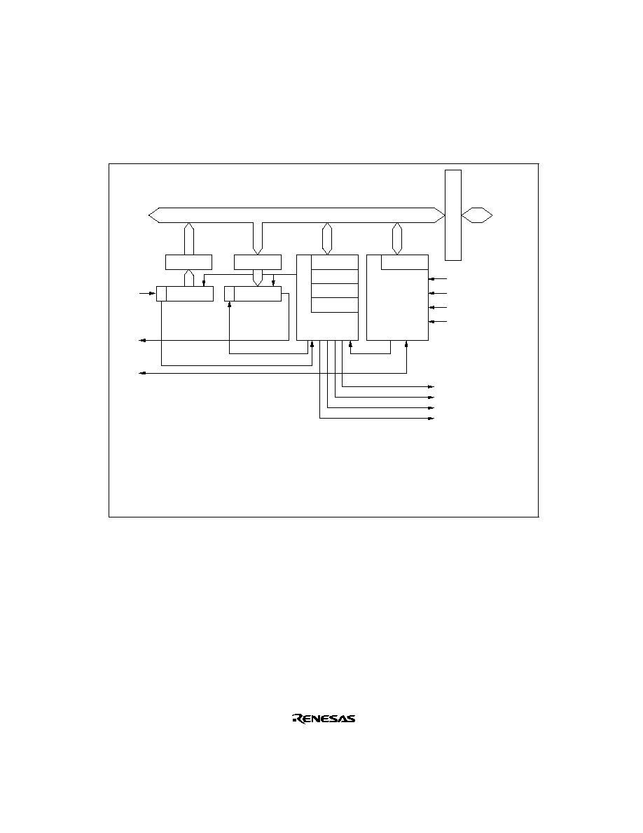
393
12.1.2
Block Diagram
Figure 12-1 shows a block diagram of the SCI.
RxD
TxD
SCK
Clock
External clock
¯
¯/4
¯/16
¯/64
TEI
TXI
RXI
ERI
SCMR
RSR
RDR
TSR
TDR
SMR
SCR
SSR
BRR
: Smart Card mode register
: Receive shift register
: Receive data register
: Transmit shift register
: Transmit data register
: Serial mode register
: Serial control register
: Serial status register
: Bit rate register
SCMR
SSR
SCR
SMR
Transmission/
reception control
Baud rate
generator
BRR
Module data bus
Bus interface
Internal
data bus
RDR
TSR
RSR
Parity generation
Parity check
Legend
TDR
Figure 12-1 Block Diagram of SCI

394
12.1.3
Pin Configuration
Table 12-1 shows the serial pins for each SCI channel.
Table 12-1 SCI Pins
Channel
Pin Name
Symbol
I/O
Function
0
Serial clock pin 0
SCK0
I/O
SCI0 clock input/output
Receive data pin 0
RxD0
Input
SCI0 receive data input
Transmit data pin 0
TxD0
Output
SCI0 transmit data output
1
Serial clock pin 1
SCK1
I/O
SCI1 clock input/output
Receive data pin 1
RxD1
Input
SCI1 receive data input
Transmit data pin 1
TxD1
Output
SCI1 transmit data output
2
Serial clock pin 2
SCK2
I/O
SCI2 clock input/output
Receive data pin 2
RxD2
Input
SCI2 receive data input
Transmit data pin 2
TxD2
Output
SCI2 transmit data output

395
12.1.4
Register Configuration
The SCI has the internal registers shown in table 12-2. These registers are used to specify
asynchronous mode or clocked synchronous mode, the data format , and the bit rate, and to control
transmitter/receiver.
Table 12-2 SCI Registers
Channel
Name
Abbreviation
R/W
Initial Value
Address
*
1
0
Serial mode register 0
SMR 0
R/W
H'00
H'FF78
Bit rate register 0
BRR 0
R/W
H'FF
H'FF79
Serial control register 0
SCR 0
R/W
H'00
H'FF7A
Transmit data register 0
TDR 0
R/W
H'FF
H'FF7B
Serial status register 0
SSR 0
R/(W)
*
2
H'84
H'FF7C
Receive data register 0
RDR 0
R
H'00
H'FF7D
Smart card mode register 0
SCMR0
R/W
H'F2
H'FF7E
1
Serial mode register 1
SMR1
R/W
H'00
H'FF80
Bit rate register 1
BRR1
R/W
H'FF
H'FF81
Serial control register 1
SCR1
R/W
H'00
H'FF82
Transmit data register 1
TDR1
R/W
H'FF
H'FF83
Serial status register 1
SSR1
R/(W)
*
2
H'84
H'FF84
Receive data register 1
RDR1
R
H'00
H'FF85
Smart card mode register 1
SCMR1
R/W
H'F2
H'FF86
2
Serial mode register 2
SMR2
R/W
H'00
H'FF88
Bit rate register 2
BRR2
R/W
H'FF
H'FF89
Serial control register 2
SCR2
R/W
H'00
H'FF8A
Transmit data register 2
TDR2
R/W
H'FF
H'FF8B
Serial status register 2
SSR2
R/(W)
*
2
H'84
H'FF8C
Receive data register 2
RDR2
R
H'00
H'FF8D
Smart card mode register 2
SCMR2
R/W
H'F2
H'FF8E
All
Module stop control register
MSTPCR
R/W
H'3FFF
H'FF3C
Notes: 1. Lower 16 bits of the address.
2. Can only be written with 0 for flag clearing.

396
12.2
Register Descriptions
12.2.1
Receive Shift Register (RSR)
7
--
6
--
5
--
4
--
3
--
0
--
2
--
1
--
Bit
R/W
:
:
RSR is a register used to receive serial data.
The SCI sets serial data input from the RxD pin in RSR in the order received, starting with the
LSB (bit 0), and converts it to parallel data. When one byte of data has been received, it is
transferred to RDR automatically.
RSR cannot be directly read or written to by the CPU.
12.2.2
Receive Data Register (RDR)
7
0
R
6
0
R
5
0
R
4
0
R
3
0
R
0
0
R
2
0
R
1
0
R
Bit
Initial value
R/W
:
:
:
RDR is a register that stores received serial data.
When the SCI has received one byte of serial data, it transfers the received serial data from RSR to
RDR where it is stored, and completes the receive operation. After this, RSR is receive-enabled.
Since RSR and RDR function as a double buffer in this way, enables continuous receive
operations to be performed.
RDR is a read-only register, and cannot be written to by the CPU.
RDR is initialized to H'00 by a reset, and in standby mode or module stop mode.

397
12.2.3
Transmit Shift Register (TSR)
7
--
6
--
5
--
4
--
3
--
0
--
2
--
1
--
Bit
R/W
:
:
TSR is a register used to transmit serial data.
To perform serial data transmission, the SCI first transfers transmit data from TDR to TSR, then
sends the data to the TxD pin starting with the LSB (bit 0).
When transmission of one byte is completed, the next transmit data is transferred from TDR to
TSR, and transmission started, automatically. However, data transfer from TDR to TSR is not
performed if the TDRE bit in SSR is set to 1.
TSR cannot be directly read or written to by the CPU.
12.2.4
Transmit Data Register (TDR)
7
1
R/W
6
1
R/W
5
1
R/W
4
1
R/W
3
1
R/W
0
1
R/W
2
1
R/W
1
1
R/W
Bit
Initial value
R/W
:
:
:
TDR is an 8-bit register that stores data for serial transmission.
When the SCI detects that TSR is empty, it transfers the transmit data written in TDR to TSR and
starts serial transmission. Continuous serial transmission can be carried out by writing the next
transmit data to TDR during serial transmission of the data in TSR.
TDR can be read or written to by the CPU at all times.
TDR is initialized to H'FF by a reset, and in standby mode or module stop mode.

398
12.2.5
Serial Mode Register (SMR)
7
C/
A
0
R/W
6
CHR
0
R/W
5
PE
0
R/W
4
O/
E
0
R/W
3
STOP
0
R/W
0
CKS0
0
R/W
2
MP
0
R/W
1
CKS1
0
R/W
Bit
Initial value
R/W
:
:
:
SMR is an 8-bit register used to set the SCI's serial transfer format and select the baud rate
generator clock source.
SMR can be read or written to by the CPU at all times.
SMR is initialized to H'00 by a reset, and in standby mode or module stop mode.
Bit 7--Communication Mode (C/
A): Selects asynchronous mode or clocked synchronous mode
as the SCI operating mode.
Bit 7
C/
A
Description
0
Asynchronous mode
(Initial value)
1
Clocked synchronous mode
Bit 6--Character Length (CHR): Selects 7 or 8 bits as the data length in asynchronous mode. In
clocked synchronous mode, a fixed data length of 8 bits is used regardless of the CHR setting.
Bit 6
CHR
Description
0
8-bit data
(Initial value)
1
7-bit data
*
Note:
*
When 7-bit data is selected, the MSB (bit 7) of TDR is not transmitted, and it is not possible
to choose between LSB-first or MSB-first transfer.

399
Bit 5--Parity Enable (PE): In asynchronous mode, selects whether or not parity bit addition is
performed in transmission, and parity bit checking in reception. In clocked synchronous mode,
parity bit addition and checking is not performed, regardless of the PE bit setting.
Bit 5
PE
Description
0
Parity bit addition and checking disabled
(Initial value)
1
Parity bit addition and checking enabled
*
Note:
*
When the PE bit is set to 1, the parity (even or odd) specified by the O/
E
bit is added to
transmit data before transmission. In reception, the parity bit is checked for the parity (even
or odd) specified by the O/
E
bit.
Bit 4--Parity Mode (O/
E): Selects either even or odd parity for use in parity addition and
checking.
The O/
E bit setting is only valid when the PE bit is set to 1, enabling parity bit addition and
checking, in asynchronous mode. The O/
E bit setting is invalid in clocked synchronous mode, and
when parity addition and checking is disabled in asynchronous mode.
Bit 4
O/
E
Description
0
Even parity
*
1
(Initial value)
1
Odd parity
*
2
Notes: 1. When even parity is set, parity bit addition is performed in transmission so that the total
number of 1 bits in the transmit character plus the parity bit is even.
In reception, a check is performed to see if the total number of 1 bits in the receive
character plus the parity bit is even.
2. When odd parity is set, parity bit addition is performed in transmission so that the total
number of 1 bits in the transmit character plus the parity bit is odd.
In reception, a check is performed to see if the total number of 1 bits in the receive
character plus the parity bit is odd.

400
Bit 3--Stop Bit Length (STOP): Selects 1 or 2 bits as the stop bit length in asynchronous mode.
The STOP bits setting is only valid in asynchronous mode. If clocked synchronous mode is set the
STOP bit setting is invalid since stop bits are not added.
Bit 3
STOP
Description
0
1 stop bit: In transmission, a single 1 bit (stop bit) is added to the end of a transmit
character before it is sent.
(Initial value)
1
2 stop bits: In transmission, two 1 bits (stop bits) are added to the end of a transmit
character before it is sent.
In reception, only the first stop bit is checked, regardless of the STOP bit setting. If the second
stop bit is 1, it is treated as a stop bit; if it is 0, it is treated as the start bit of the next transmit
character.
Bit 2--Multiprocessor Mode (MP): Selects multiprocessor format. When multiprocessor format
is selected, the PE bit and O/
E bit parity settings are invalid. The MP bit setting is only valid in
asynchronous mode; it is invalid in clocked synchronous mode.
For details of the multiprocessor communication function, see section 12.3.3, Multiprocessor
Communication Function.
Bit 2
MP
Description
0
Multiprocessor function disabled
(Initial value)
1
Multiprocessor format selected

401
Bits 1 and 0--Clock Select 1 and 0 (CKS1, CKS0): These bits select the clock source for the
baud rate generator. The clock source can be selected from ¯, ¯/4, ¯/16, and ¯/64, according to the
setting of bits CKS1 and CKS0.
For the relation between the clock source, the bit rate register setting, and the baud rate, see
section 12.2.8, Bit Rate Register.
Bit 1
Bit 0
CKS1
CKS0
Description
0
0
¯ clock
(Initial value)
1
¯/4 clock
1
0
¯/16 clock
1
¯/64 clock
12.2.6
Serial Control Register (SCR)
7
TIE
0
R/W
6
RIE
0
R/W
5
TE
0
R/W
4
RE
0
R/W
3
MPIE
0
R/W
0
CKE0
0
R/W
2
TEIE
0
R/W
1
CKE1
0
R/W
Bit
Initial value
R/W
:
:
:
SCR is a register that performs enabling or disabling of SCI transfer operations, serial clock output
in asynchronous mode, and interrupt requests, and selection of the serial clock source.
SCR can be read or written to by the CPU at all times.
SCR is initialized to H'00 by a reset, and in standby mode or module stop mode.
Bit 7--Transmit Interrupt Enable (TIE): Enables or disables transmit data empty interrupt
(TXI) request generation when serial transmit data is transferred from TDR to TSR and the TDRE
flag in SSR is set to 1.
Bit 7
TIE
Description
0
Transmit data empty interrupt (TXI) requests disabled
*
(Initial value)
1
Transmit data empty interrupt (TXI) requests enabled
Note:
*
TXI interrupt request cancellation can be performed by reading 1 from the TDRE flag, then
clearing it to 0, or clearing the TIE bit to 0.

402
Bit 6--Receive Interrupt Enable (RIE): Enables or disables receive data full interrupt (RXI)
request and receive error interrupt (ERI) request generation when serial receive data is transferred
from RSR to RDR and the RDRF flag in SSR is set to 1.
Bit 6
RIE
Description
0
Receive data full interrupt (RXI) request and receive error interrupt (ERI) request
disabled
*
(Initial value)
1
Receive data full interrupt (RXI) request and receive error interrupt (ERI) request
enabled
Note:
*
RXI and ERI interrupt request cancellation can be performed by reading 1 from the RDRF
flag, or the FER, PER, or ORER flag, then clearing the flag to 0, or clearing the RIE bit to 0.
Bit 5--Transmit Enable (TE): Enables or disables the start of serial transmission by the SCI.
Bit 5
TE
Description
0
Transmission disabled
*
1
(Initial value)
1
Transmission enabled
*
2
Notes: 1. The TDRE flag in SSR is fixed at 1.
2. In this state, serial transmission is started when transmit data is written to TDR and the
TDRE flag in SSR is cleared to 0.
SMR setting must be performed to decide the transfer format before setting the TE bit
to 1.
Bit 4--Receive Enable (RE): Enables or disables the start of serial reception by the SCI.
Bit 4
RE
Description
0
Reception disabled
*
1
(Initial value)
1
Reception enabled
*
2
Notes: 1. Clearing the RE bit to 0 does not affect the RDRF, FER, PER, and ORER flags, which
retain their states.
2. Serial reception is started in this state when a start bit is detected in asynchronous
mode or serial clock input is detected in clocked synchronous mode.
SMR setting must be performed to decide the transfer format before setting the RE bit
to 1.

403
Bit 3--Multiprocessor Interrupt Enable (MPIE): Enables or disables multiprocessor interrupts.
The MPIE bit setting is only valid in asynchronous mode when the MP bit in SMR is set to 1.
The MPIE bit setting is invalid in clocked synchronous mode or when the MP bit is cleared to 0.
Bit 3
MPIE
Description
0
Multiprocessor interrupts disabled (normal reception performed)
(Initial value)
[Clearing conditions]
∑
When the MPIE bit is cleared to 0
∑
When MPB= 1 data is received
1
Multiprocessor interrupts enabled
*
Receive interrupt (RXI) requests, receive error interrupt (ERI) requests, and setting
of the RDRF, FER, and ORER flags in SSR are disabled until data with the
multiprocessor bit set to 1 is received.
Note:
*
When receive data including MPB = 0 is received, receive data transfer from RSR to RDR,
receive error detection, and setting of the RDRF, FER, and ORER flags in SSR , is not
performed. When receive data including MPB = 1 is received, the MPB bit in SSR is set to
1, the MPIE bit is cleared to 0 automatically, and generation of RXI and ERI interrupts
(when the TIE and RIE bits in SCR are set to 1) and FER and ORER flag setting is enabled.
Bit 2--Transmit End Interrupt Enable (TEIE): Enables or disables transmit end interrupt
(TEI) request generation when there is no valid transmit data in TDR in MSB data transmission.
Bit 2
TEIE
Description
0
Transmit end interrupt (TEI) request disabled
*
(Initial value)
1
Transmit end interrupt (TEI) request enabled
Note:
*
TEI cancellation can be performed by reading 1 from the TDRE flag in SSR, then clearing it
to 0 and clearing the TEND flag to 0, or clearing the TEIE bit to 0.

404
Bits 1 and 0--Clock Enable 1 and 0 (CKE1, CKE0): These bits are used to select the SCI clock
source and enable or disable clock output from the SCK pin. The combination of the CKE1 and
CKE0 bits determines whether the SCK pin functions as an I/O port, the serial clock output pin, or
the serial clock input pin.
The setting of the CKE0 bit, however, is only valid for internal clock operation (CKE1 = 0) in
asynchronous mode. The CKE0 bit setting is invalid in clocked synchronous mode, and in the case
of external clock operation (CKE1 = 1). Note that the SCI's operating mode must be decided using
SMR before setting the CKE1 and CKE0 bits.
For details of clock source selection, see table 12.9 in section 12.3, Operation.
Bit 1
Bit 0
CKE1
CKE0
Description
0
0
Asynchronous mode
Internal clock/SCK pin functions as I/O port
*
1
Clocked synchronous
mode
Internal clock/SCK pin functions as serial clock
output
1
Asynchronous mode
Internal clock/SCK pin functions as clock output
*
2
Clocked synchronous
mode
Internal clock/SCK pin functions as serial clock
output
1
0
Asynchronous mode
External clock/SCK pin functions as clock input
*
3
Clocked synchronous
mode
External clock/SCK pin functions as serial clock
input
1
Asynchronous mode
External clock/SCK pin functions as clock input
*
3
Clocked synchronous
mode
External clock/SCK pin functions as serial clock
input
Notes: 1. Initial value
2. Outputs a clock of the same frequency as the bit rate.
3. Inputs a clock with a frequency 16 times the bit rate.
12.2.7
Serial Status Register (SSR)
7
TDRE
1
R/(W)
*
6
RDRF
0
R/(W)
*
5
ORER
0
R/(W)
*
4
FER
0
R/(W)
*
3
PER
0
R/(W)
*
0
MPBT
0
R/W
2
TEND
1
R
1
MPB
0
R
Bit
Initial value
R/W
:
:
:
Note:
Only 0 can be written, to clear the flag.

405
SSR is an 8-bit register containing status flags that indicate the operating status of the SCI, and
multiprocessor bits.
SSR can be read or written to by the CPU at all times. However, 1 cannot be written to flags
TDRE, RDRF, ORER, PER, and FER. Also note that in order to clear these flags they must be
read as 1 beforehand. The TEND flag and MPB flag are read-only flags and cannot be modified.
SSR is initialized to H'84 by a reset, and in standby mode or module stop mode.
Bit 7--Transmit Data Register Empty (TDRE): Indicates that data has been transferred from
TDR to TSR and the next serial data can be written to TDR.
Bit 7
TDRE
Description
0
[Clearing conditions]
∑
When 0 is written to TDRE after reading TDRE = 1
∑
When the DTC is activated by a TXI interrupt and write data to TDR
1
[Setting conditions]
(Initial value)
∑
When the TE bit in SCR is 0
∑
When data is transferred from TDR to TSR and data can be written to TDR
Bit 6--Receive Data Register Full (RDRF): Indicates that the received data is stored in RDR.
Bit 6
RDRF
Description
0
[Clearing conditions]
(Initial value)
∑
When 0 is written to RDRF after reading RDRF = 1
∑
When the DTC is activated by an RXI interrupt and read data from RDR
1
[Setting condition]
When serial reception ends normally and receive data is transferred from RSR to RDR
Note:
RDR and the RDRF flag are not affected and retain their previous values when an error is
detected during reception or when the RE bit in SCR is cleared to 0.
If reception of the next data is completed while the RDRF flag is still set to 1, an overrun
error will occur and the receive data will be lost.

406
Bit 5--Overrun Error (ORER): Indicates that an overrun error occurred during reception,
causing abnormal termination.
Bit 5
ORER
Description
0
[Clearing condition]
(Initial value)
*
1
When 0 is written to ORER after reading ORER = 1
1
[Setting condition]
When the next serial reception is completed while RDRF = 1
*
2
Notes: 1. The ORER flag is not affected and retains its previous state when the RE bit in SCR is
cleared to 0.
2. The receive data prior to the overrun error is retained in RDR, and the data received
subsequently is lost. Also, subsequent serial reception cannot be continued while the
ORER flag is set to 1. In clocked synchronous mode, serial transmission cannot be
continued, either.
Bit 4--Framing Error (FER): Indicates that a framing error occurred during reception in
asynchronous mode, causing abnormal termination.
Bit 4
FER
Description
0
[Clearing condition]
(Initial value)
*
1
When 0 is written to FER after reading FER = 1
1
[Setting condition]
When the SCI checks the stop bit at the end of the receive data when reception ends,
and the stop bit is 0
*
2
Notes: 1. The FER flag is not affected and retains its previous state when the RE bit in SCR is
cleared to 0.
2. In 2-stop-bit mode, only the first stop bit is checked for a value of 0; the second stop bit
is not checked. If a framing error occurs, the receive data is transferred to RDR but the
RDRF flag is not set. Also, subsequent serial reception cannot be continued while the
FER flag is set to 1. In clocked synchronous mode, serial transmission cannot be
continued, either.

407
Bit 3--Parity Error (PER): Indicates that a parity error occurred during reception using parity
addition in asynchronous mode, causing abnormal termination.
Bit 3
PER
Description
0
[Clearing condition]
(Initial value)
*
1
When 0 is written to PER after reading PER = 1
1
[Setting condition]
When, in reception, the number of 1 bits in the receive data plus the parity bit does not
match the parity setting (even or odd) specified by the O/
E
bit in SMR
*
2
Notes: 1. The PER flag is not affected and retains its previous state when the RE bit in SCR is
cleared to 0.
2. If a parity error occurs, the receive data is transferred to RDR but the RDRF flag is not
set. Also, subsequent serial reception cannot be continued while the PER flag is set to
1. In clocked synchronous mode, serial transmission cannot be continued, either.
Bit 2--Transmit End (TEND): Indicates that there is no valid data in TDR when the last bit of
the transmit character is sent, and transmission has been ended.
The TEND flag is read-only and cannot be modified.
Bit 2
TEND
Description
0
[Clearing conditions]
∑
When 0 is written to TDRE after reading TDRE = 1
∑
When the DTC is activated by a TXI interrupt and write data to TDR
1
[Setting conditions]
(Initial value)
∑
When the TE bit in SCR is 0
∑
When TDRE = 1 at transmission of the last bit of a 1-byte serial transmit character
Bit 1--Multiprocessor bit (MPB): When reception is performed using multiprocessor format in
asynchronous mode, MPB stores the multiprocessor bit in the receive data.
MPB is a read-only bit, and cannot be modified.
Bit 1
MPB
Description
0
[Clearing condition]
(Initial value)
*
When data with a 0 multiprocessor bit is received
1
[Setting condition]
When data with a 1 multiprocessor bit is received
Note:
*
Retains its previous state when the RE bit in SCR is cleared to 0 with multiprocessor
format.

408
Bit 0--Multiprocessor Bit Transfer (MPBT): When transmission is performed using
multiprocessor format in asynchronous mode, MPBT stores the multiprocessor bit to be added to
the transmit data.
The MPBT bit setting is invalid in clocked synchronous mode, when multiprocessor format is not
used, and when the operation is not transmission.
Bit 0
MPBT
Description
0
Data with a 0 multiprocessor bit is transmitted
(Initial value)
1
Data with a 1 multiprocessor bit is transmitted
12.2.8
Bit Rate Register (BRR)
7
1
R/W
6
1
R/W
5
1
R/W
4
1
R/W
3
1
R/W
0
1
R/W
2
1
R/W
1
1
R/W
Bit
Initial value
R/W
:
:
:
BRR is an 8-bit register that sets the serial transfer bit rate in accordance with the baud rate
generator operating clock selected by bits CKS1 and CKS0 in SMR.
BRR can be read or written to by the CPU at all times.
BRR is initialized to H'FF by a reset, and in standby mode or module stop mode.
As baud rate generator control is performed independently for each channel, different values can
be set for each channel.
Table 12-3 shows sample BRR settings in asynchronous mode, and table 12-4 shows sample BRR
settings in clocked synchronous mode.

409
Table 12-3 BRR Settings for Various Bit Rates (Asynchronous Mode)
¯ (MHz)
2
2.097152
2.4576
3
Bit Rate
(bit/s)
n
N
Error
(%)
n
N
Error
(%)
n
N
Error
(%)
n
N
Error
(%)
110
1
141
0.03
1
148
≠0.04
1
174
≠0.26
1
212
0.03
150
1
103
0.16
1
108
0.21
1
127
0.00
1
155
0.16
300
0
207
0.16
0
217
0.21
0
255
0.00
1
77
0.16
600
0
103
0.16
0
108
0.21
0
127
0.00
0
155
0.16
1200
0
51
0.16
0
54
≠0.70
0
63
0.00
0
77
0.16
2400
0
25
0.16
0
26
1.14
0
31
0.00
0
38
0.16
4800
0
12
0.16
0
13
≠2.48
0
15
0.00
0
19
≠2.34
9600
--
--
--
0
6
≠2.48
0
7
0.00
0
9
≠2.34
19200
--
--
--
--
--
--
0
3
0.00
0
4
≠2.34
31250
0
1
0.00
--
--
--
--
--
--
0
2
0.00
38400
--
--
--
--
--
--
0
1
0.00
--
--
--
¯ (MHz)
3.6864
4
4.9152
5
Bit Rate
(bit/s)
n
N
Error
(%)
n
N
Error
(%)
n
N
Error
(%)
n
N
Error
(%)
110
2
64
0.70
2
70
0.03
2
86
0.31
2
88
≠0.25
150
1
191
0.00
1
207
0.16
1
255
0.00
2
64
0.16
300
1
95
0.00
1
103
0.16
1
127
0.00
1
129
0.16
600
0
191
0.00
0
207
0.16
0
255
0.00
1
64
0.16
1200
0
95
0.00
0
103
0.16
0
127
0.00
0
129
0.16
2400
0
47
0.00
0
51
0.16
0
63
0.00
0
64
0.16
4800
0
23
0.00
0
25
0.16
0
31
0.00
0
32
≠1.36
9600
0
11
0.00
0
12
0.16
0
15
0.00
0
15
1.73
19200
0
5
0.00
--
--
--
0
7
0.00
0
7
1.73
31250
--
--
--
0
3
0.00
0
4
≠1.70
0
4
0.00
38400
0
2
0.00
0
2
8.51
0
3
0.00
0
3
1.73

410
Table 12-3 BRR Settings for Various Bit Rates (Asynchronous Mode) (cont)
¯ (MHz)
6
6.144
7.3728
8
Bit Rate
(bit/s)
n
N
Error
(%)
n
N
Error
(%)
n
N
Error
(%)
n
N
Error
(%)
110
2
106
≠0.44
2
108
0.08
2
130
≠0.07
2
141
0.03
150
2
77
0.16
2
79
0.00
2
95
0.00
2
103
0.16
300
1
155
0.16
1
159
0.00
1
191
0.00
1
207
0.16
600
1
77
0.16
1
79
0.00
1
95
0.00
1
103
0.16
1200
0
155
0.16
0
159
0.00
0
191
0.00
0
207
0.16
2400
0
77
0.16
0
79
0.00
0
95
0.00
0
103
0.16
4800
0
38
0.16
0
39
0.00
0
47
0.00
0
51
0.16
9600
0
19
≠2.34
0
19
0.00
0
23
0.00
0
25
0.16
19200
0
9
≠2.34
0
9
0.00
0
11
0.00
0
12
0.16
31250
0
5
0.00
0
5
2.40
--
--
--
0
7
0.00
38400
0
4
≠2.34
0
4
0.00
0
5
0.00
0
6
≠6.99
¯ (MHz)
9.8304
10
12
12.288
Bit Rate
(bit/s)
n
N
Error
(%)
n
N
Error
(%)
n
N
Error
(%)
n
N
Error
(%)
110
2
174
≠0.26
2
177
≠0.25
2
212
0.03
2
217
0.08
150
2
127
0.00
2
129
0.16
2
155
0.16
2
159
0.00
300
1
255
0.00
2
64
0.16
2
77
0.16
2
79
0.00
600
1
127
0.00
1
129
0.16
1
155
0.16
1
159
0.00
1200
0
255
0.00
1
64
0.16
1
77
0.16
1
79
0.00
2400
0
127
0.00
0
129
0.16
0
155
0.16
0
159
0.00
4800
0
63
0.00
0
64
0.16
0
77
0.16
0
79
0.00
9600
0
31
0.00
0
32
≠1.36
0
38
0.16
0
39
0.00
19200
0
15
0.00
0
15
1.73
0
19
≠2.34
0
19
0.00
31250
0
9
≠1.70
0
9
0.00
0
11
0.00
0
11
2.40
38400
0
7
0.00
0
7
1.73
0
9
≠2.34
0
9
0.00

411
Table 12-3 BRR Settings for Various Bit Rates (Asynchronous Mode) (cont)
¯ (MHz)
14
14.7456
16
17.2032
Bit Rate
(bit/s)
n
N
Error
(%)
n
N
Error
(%)
n
N
Error
(%)
n
N
Error
(%)
110
2
248
≠0.17
3
64
0.70
3
70
0.03
3
75
0.48
150
2
181
0.16
2
191
0.00
2
207
0.16
2
223
0.00
300
2
90
0.16
2
95
0.00
2
103
0.16
2
111
0.00
600
1
181
0.16
1
191
0.00
1
207
0.16
1
223
0.00
1200
1
90
0.16
1
95
0.00
1
103
0.16
1
111
0.00
2400
0
181
0.16
0
191
0.00
0
207
0.16
0
223
0.00
4800
0
90
0.16
0
95
0.00
0
103
0.16
0
111
0.00
9600
0
45
≠0.93
0
47
0.00
0
51
0.16
0
55
0.00
19200
0
22
≠0.93
0
23
0.00
0
25
0.16
0
27
0.00
31250
0
13
0.00
0
14
≠1.70
0
15
0.00
0
16
1.20
38400
--
--
--
0
11
0.00
0
12
0.16
0
13
0.00
¯ (MHz)
18
19.6608
20
Bit Rate
(bit/s)
n
N
Error
(%)
n
N
Error
(%)
n
N
Error
(%)
110
3
79
≠0.12
3
86
0.31
3
88
≠0.25
150
2
233
0.16
2
255
0.00
3
64
0.16
300
2
116
0.16
2
127
0.00
2
129
0.16
600
1
233
0.16
1
255
0.00
2
64
0.16
1200
1
116
0.16
1
127
0.00
1
129
0.16
2400
0
233
0.16
0
255
0.00
1
64
0.16
4800
0
116
0.16
0
127
0.00
0
129
0.16
9600
0
58
≠0.69
0
63
0.00
0
64
0.16
19200
0
28
1.02
0
31
0.00
0
32
≠1.36
31250
0
17
0.00
0
19
≠1.70
0
19
0.00
38400
0
14
≠2.34
0
15
0.00
0
15
1.73
Note:
As far as possible, the setting should be made so that the error is no more than 1%.
Legend
--: Can be set, but there will be a degree of error.

412
Table 12-4 BRR Settings for Various Bit Rates (Clocked Synchronous Mode)
¯ (MHz)
2
4
8
10
16
20
Bit Rate
(bit/s)
n
N
n
N
n
N
n
N
n
N
n
N
110
3
70
--
--
--
--
--
--
--
--
--
--
250
2
124
2
249
3
124
--
--
3
249
--
--
500
1
249
2
124
2
249
--
--
3
124
--
--
1 k
1
124
1
249
2
124
--
--
2
249
--
--
2.5 k
0
199
1
99
1
199
1
249
2
99
2
124
5 k
0
99
0
199
1
99
1
124
1
199
1
249
10 k
0
49
0
99
0
199
0
249
1
99
1
124
25 k
0
19
0
39
0
79
0
99
0
159
0
199
50 k
0
9
0
19
0
39
0
49
0
79
0
99
100 k
0
4
0
9
0
19
0
24
0
39
0
49
250 k
0
1
0
3
0
7
0
9
0
15
0
19
500 k
0
0
*
0
1
0
3
0
4
0
7
0
9
1 M
0
0
*
0
1
--
--
0
3
0
4
2.5 M
--
--
0
0
*
--
--
0
1
5 M
--
--
0
0
*
Note:
As far as possible, the setting should be made so that the error is no more than 1%.
Legend
Blank : Cannot be set.
-- : Can be set, but there will be a degree of error.
*
: Continuous transmission/reception is not possible.

413
The BRR setting is found from the following formulas.
Asynchronous mode:
N =
¯
◊
10
6
≠ 1
64
◊
2
2n≠1
◊
B
Clocked synchronous mode:
N =
¯
◊
10
6
≠ 1
8
◊
2
2n≠1
◊
B
Where B: Bit rate (bit/s)
N: BRR setting for baud rate generator (0
N
255)
¯: Operating frequency (MHz)
n: Baud rate generator input clock (n = 0 to 3)
(See the table below for the relation between n and the clock.)
SMR Setting
n
Clock
CKS1
CKS0
0
¯
0
0
1
¯/4
0
1
2
¯/16
1
0
3
¯/64
1
1
The bit rate error in asynchronous mode is found from the following formula:
Error (%) = {
¯
◊
10
6
≠ 1
} ◊
100
(N + 1)
◊
B
◊
64
◊
2
2n≠1

414
Table 12-5 shows the maximum bit rate for each frequency in asynchronous mode. Tables 12-6
and 12-7 show the maximum bit rates with external clock input.
Table 12-5 Maximum Bit Rate for Each Frequency (Asynchronous Mode)
¯ (MHz)
Maximum Bit Rate (bit/s)
n
N
2
62500
0
0
2.097152
65536
0
0
2.4576
76800
0
0
3
93750
0
0
3.6864
115200
0
0
4
125000
0
0
4.9152
153600
0
0
5
156250
0
0
6
187500
0
0
6.144
192000
0
0
7.3728
230400
0
0
8
250000
0
0
9.8304
307200
0
0
10
312500
0
0
12
375000
0
0
12.288
384000
0
0
14
437500
0
0
14.7456
460800
0
0
16
500000
0
0
17.2032
537600
0
0
18
562500
0
0
19.6608
614400
0
0
20
625000
0
0

415
Table 12-6 Maximum Bit Rate with External Clock Input (Asynchronous Mode)
¯ (MHz)
External Input Clock (MHz)
Maximum Bit Rate (bit/s)
2
0.5000
31250
2.097152
0.5243
32768
2.4576
0.6144
38400
3
0.7500
46875
3.6864
0.9216
57600
4
1.0000
62500
4.9152
1.2288
76800
5
1.2500
78125
6
1.5000
93750
6.144
1.5360
96000
7.3728
1.8432
115200
8
2.0000
125000
9.8304
2.4576
153600
10
2.5000
156250
12
3.0000
187500
12.288
3.0720
192000
14
3.5000
218750
14.7456
3.6864
230400
16
4.0000
250000
17.2032
4.3008
268800
18
4.5000
281250
19.6608
4.9152
307200
20
5.0000
312500

416
Table 12-7 Maximum Bit Rate with External Clock Input (Clocked Synchronous Mode)
¯ (MHz)
External Input Clock (MHz)
Maximum Bit Rate (bit/s)
2
0.3333
333333.3
4
0.6667
666666.7
6
1.0000
1000000.0
8
1.3333
1333333.3
10
1.6667
1666666.7
12
2.0000
2000000.0
14
2.3333
2333333.3
16
2.6667
2666666.7
18
3.0000
3000000.0
20
3.3333
3333333.3

417
12.2.9
Smart Card Mode Register (SCMR)
7
--
1
--
6
--
1
--
5
--
1
--
4
--
1
--
3
SDIR
0
R/W
0
SMIF
0
R/W
2
SINV
0
R/W
1
--
1
--
Bit
Initial value
R/W
:
:
:
SCMR selects LSB-first or MSB-first by means of bit SDIR. With an 8-bit length, LSB-first or
MSB-first transfer can be selected regardless of the serial communication mode. The descriptions
in this chapter refer to LSB-first transfer.
For details of the other bits in SCMR, see 13.2.1, Smart Card Mode Register (SCMR).
SCMR is initialized to H'F2 by a reset, and in standby mode or module stop mode.
Bits 7 to 4--Reserved: Read-only bits, always read as 1.
Bit 3--Smart Card Data Transfer Direction (SDIR): Selects the serial/parallel conversion
format.
The transfer format is valid for 8-bit data.
Bit 3
SDIR
Description
0
TDR contents are transmitted LSB-first
(Initial value)
Receive data is stored in RDR LSB-first
1
TDR contents are transmitted MSB-first
Receive data is stored in RDR MSB-first
Bit 2--Smart Card Data Invert (SINV): When the smart card interface operates as a normal
SCI, 0 should be written in this bit.
Bit 1--Reserved: Read-only bit, always read as 1.
Bit 0--Smart Card Interface Mode Select (SMIF): When the smart card interface operates as a
normal SCI, 0 should be written in this bit.

418
12.2.10
Module Stop Control Register (MSTPCR)
15
0
R/W
Bit
Initial value
R/W
:
:
:
14
0
R/W
13
1
R/W
12
1
R/W
11
1
R/W
10
1
R/W
9
1
R/W
8
1
R/W
7
1
R/W
6
1
R/W
5
1
R/W
4
1
R/W
3
1
R/W
2
1
R/W
1
1
R/W
0
1
R/W
MSTPCRH
MSTPCRL
MSTPCR is a 16-bit readable/writable register that performs module stop mode control.
When the corresponding bit of bits MSTP7 to MSTP5 is set to 1, SCI operation stops at the end of
the bus cycle and a transition is made to module stop mode. For details, see section 18.5, Module
Stop Mode.
MSTPCR is initialized to H'3FFF by a reset and in hardware standby mode. It is not initialized in
software standby mode.
Bit 7--Module Stop (MSTP7): Specifies the SCI channel 2 module stop mode.
Bit 7
MSTP7
Description
0
SCI channel 2 module stop mode cleared
1
SCI channel 2 module stop mode set
(Initial value)
Bit 6--Module Stop (MSTP6): Specifies the SCI channel 1 module stop mode.
Bit 6
MSTP6
Description
0
SCI channel 1 module stop mode cleared
1
SCI channel 1 module stop mode set
(Initial value)
Bit 5--Module Stop (MSTP5): Specifies the SCI channel 0 module stop mode.
Bit 5
MSTP5
Description
0
SCI channel 0 module stop mode cleared
1
SCI channel 0 module stop mode set
(Initial value)

419
12.3
Operation
12.3.1
Overview
The SCI can carry out serial communication in two modes: asynchronous mode in which
synchronization is achieved character by character, and clocked synchronous mode in which
synchronization is achieved with clock pulses.
Selection of asynchronous or clocked synchronous mode and the transmission format is made
using SMR as shown in table 12-8. The SCI clock is determined by a combination of the C/
A bit
in SMR and the CKE1 and CKE0 bits in SCR, as shown in table 12-9.
Asynchronous mode
∑
Data length: Choice of 7 or 8 bits
∑
Choice of parity addition, multiprocessor bit addition, and addition of 1 or 2 stop bits (the
combination of these parameters determines the transfer format and character length)
∑
Detection of framing, parity, and overrun errors, and breaks, during reception
∑
Choice of internal or external clock as SCI clock source
When internal clock is selected:
The SCI operates on the baud rate generator clock and a clock with the same frequency as
the bit rate can be output
When external clock is selected:
A clock with a frequency of 16 times the bit rate must be input (the on-chip baud rate
generator is not used)
Clocked synchronous mode
∑
Transfer format: Fixed 8-bit data
∑
Detection of overrun errors during reception
∑
Choice of internal or external clock as SCI clock source
When internal clock is selected:
The SCI operates on the baud rate generator clock and a serial clock is output off-chip
When external clock is selected:
The on-chip baud rate generator is not used, and the SCI operates on the input serial clock

420
Table 12-8 SMR Settings and Serial Transfer Format Selection
SMR Settings
SCI Transfer Format
Bit 7
Bit 6
Bit 2
Bit 5
Bit 3
Data
Multi-
processor
Parity
Stop Bit
C/
A
CHR
MP
PE
STOP
Mode
Length
Bit
Bit
Length
0
0
0
0
0
Asynchronous
8-bit data
No
No
1 bit
1
mode
2 bits
1
0
Yes
1 bit
1
2 bits
1
0
0
7-bit data
No
1 bit
1
2 bits
1
0
Yes
1 bit
1
2 bits
0
1
--
0
Asynchronous
8-bit data
Yes
No
1 bit
--
1
mode (multi-
2 bits
1
--
0
processor
7-bit data
1 bit
--
1
format)
2 bits
1
--
--
--
--
Clocked
synchronous mode
8-bit data
No
None
Table 12-9 SMR and SCR Settings and SCI Clock Source Selection
SMR
SCR Setting
SCI Transmit/Receive clock
Bit 7
Bit 1
Bit 0
Clock
C/
A
CKE1
CKE0
Mode
Source
SCK Pin Function
0
0
0
Asynchronous
Internal
SCI does not use SCK pin
1
mode
Outputs clock with same frequency as bit
rate
1
0
External
Inputs clock with frequency of 16 times
1
the bit rate
1
0
0
Clocked
Internal
Outputs the serial clock
1
synchronous
1
0
mode
External
Inputs the serial clock
1
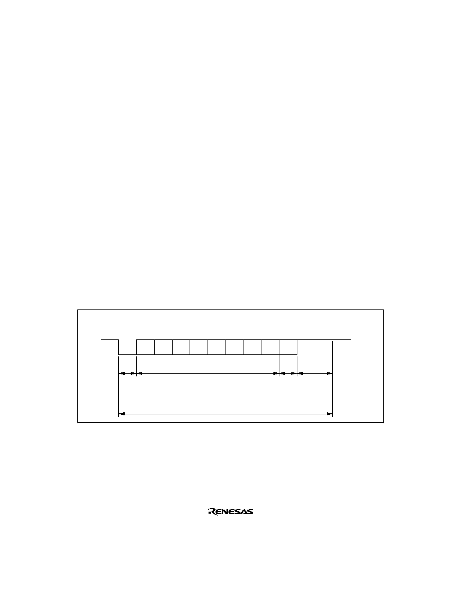
421
12.3.2
Operation in Asynchronous Mode
In asynchronous mode, characters are sent or received, each preceded by a start bit indicating the
start of communication and one or two stop bits indicating the end of communication. Serial
communication is thus carried out with synchronization established on a character-by-character
basis.
Inside the SCI, the transmitter and receiver are independent units, enabling full-duplex
communication. Both the transmitter and the receiver also have a double-buffered structure, so
that data can be read or written during transmission or reception, enabling continuous data
transfer.
Figure 12-2 shows the general format for asynchronous serial communication.
In asynchronous serial communication, the transmission line is usually held in the mark state (high
level). The SCI monitors the transmission line, and when it goes to the space state (low level),
recognizes a start bit and starts serial communication.
One serial communication character consists of a start bit (low level), followed by data (in LSB-
first order), a parity bit (high or low level), and finally one or two stop bits (high level).
In asynchronous mode, the SCI performs synchronization at the falling edge of the start bit in
reception. The SCI samples the data on the 8th pulse of a clock with a frequency of 16 times the
length of one bit, so that the transfer data is latched at the center of each bit.
LSB
Start
bit
MSB
Idle state
(mark state)
Stop bit
0
Transmit/receive data
D0
D1
D2
D3
D4
D5
D6
D7
0/1
1
1
1
1
Serial
data
Parity
bit
1 bit
1 or
2 bits
7 or 8 bits
1 bit,
or none
One unit of transfer data (character or frame)
Figure 12-2 Data Format in Asynchronous Communication
(Example with 8-Bit Data, Parity, Two Stop Bits)
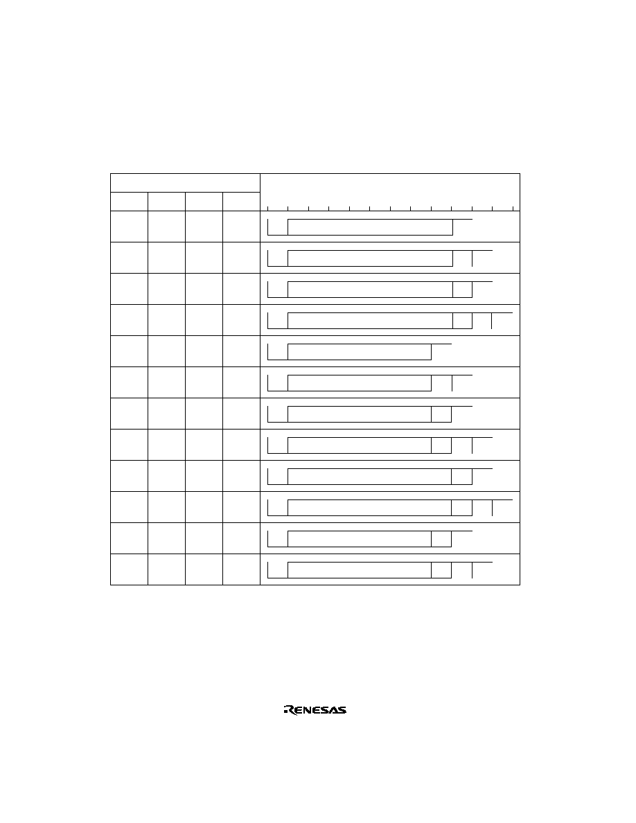
422
Data Transfer Format: Table 12-10 shows the data transfer formats that can be used in
asynchronous mode. Any of 12 transfer formats can be selected according to the SMR setting.
Table 12-10 Serial Transfer Formats (Asynchronous Mode)
PE
0
0
1
1
0
0
1
1
--
--
--
--
S
8-bit data
STOP
S
7-bit data
STOP
S
8-bit data
STOP STOP
S
8-bit data
P STOP
S
7-bit data
STOP
P
S
8-bit data
MPB STOP
S
8-bit data
MPB STOP STOP
S
7-bit data
STOP
MPB
S
7-bit data
STOP
MPB
STOP
S
7-bit data
STOP
STOP
CHR
0
0
0
0
1
1
1
1
0
0
1
1
MP
0
0
0
0
0
0
0
0
1
1
1
1
STOP
0
1
0
1
0
1
0
1
0
1
0
1
SMR Settings
1
2
3
4
5
6
7
8
9
10
11
12
Serial Transfer Format and Frame Length
STOP
S
8-bit data
P STOP
S
7-bit data
STOP
P
STOP
Legend
S
: Start bit
STOP : Stop bit
P
: Parity bit
MPB
: Multiprocessor bit
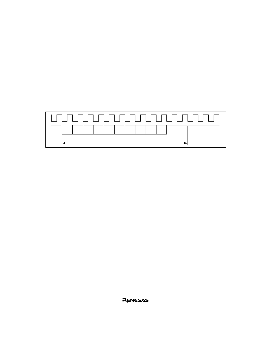
423
Clock: Either an internal clock generated by the on-chip baud rate generator or an external clock
input at the SCK pin can be selected as the SCI's serial clock, according to the setting of the C/
A
bit in SMR and the CKE1 and CKE0 bits in SCR. For details of SCI clock source selection, see
table 12-9.
When an external clock is input at the SCK pin, the clock frequency should be 16 times the bit rate
used.
When the SCI is operated on an internal clock, the clock can be output from the SCK pin. The
frequency of the clock output in this case is equal to the bit rate, and the phase is such that the
rising edge of the clock is in the middle of the transmit data, as shown in figure 12-3.
0
1 frame
D0
D1
D2
D3
D4
D5
D6
D7
0/1
1
1
Figure 12-3 Relation between Output Clock and Transfer Data Phase
(Asynchronous Mode)
Data Transfer Operations:
∑
SCI initialization (asynchronous mode)
Before transmitting and receiving data, you should first clear the TE and RE bits in SCR to 0,
then initialize the SCI as described below.
When the operating mode, transfer format, etc., is changed, the TE and RE bits must be cleared
to 0 before making the change using the following procedure. When the TE bit is cleared to 0,
the TDRE flag is set to 1 and TSR is initialized. Note that clearing the RE bit to 0 does not
change the contents of the RDRF, PER, FER, and ORER flags, or the contents of RDR.
When an external clock is used the clock should not be stopped during operation, including
initialization, since operation is uncertain.
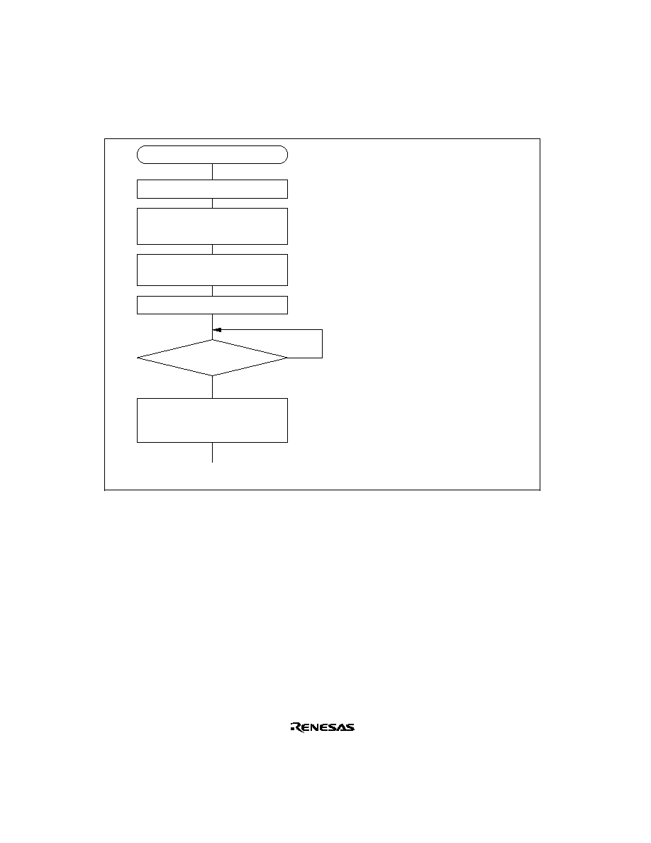
424
Figure 12-4 shows a sample SCI initialization flowchart.
Wait
<Transfer completion>
Start initialization
Set data transfer format in
SMR and SCMR
[1]
Set CKE1 and CKE0 bits in SCR
(TE, RE bits 0)
No
Yes
Set value in BRR
Clear TE and RE bits in SCR to 0
[2]
[3]
Set TE and RE bits in
SCR to 1, and set RIE, TIE, TEIE,
and MPIE bits
[4]
1-bit interval elapsed?
[1] Set the clock selection in SCR.
Be sure to clear bits RIE, TIE,
TEIE, and MPIE, and bits TE and
RE, to 0.
When the clock is selected in
asynchronous mode, it is output
immediately after SCR settings are
made.
[2] Set the data transfer format in SMR
and SCMR.
[3] Write a value corresponding to the
bit rate to BRR. Not necessary if an
external clock is used.
[4] Wait at least one bit interval, then
set the TE bit or RE bit in SCR to 1.
Also set the RIE, TIE, TEIE, and
MPIE bits.
Setting the TE and RE bits enables
the TxD and RxD pins to be used.
Figure 12-4 Sample SCI Initialization Flowchart

425
∑
Serial data transmission (asynchronous mode)
Figure 12-5 shows a sample flowchart for serial transmission.
The following procedure should be used for serial data transmission.
No
<End>
[1]
Yes
Initialization
Start transmission
Read TDRE flag in SSR
[2]
Write transmit data to TDR
and clear TDRE flag in SSR to 0
No
Yes
No
Yes
Read TEND flag in SSR
[3]
No
Yes
[4]
Clear DR to 0 and
set DDR to 1
Clear TE bit in SCR to 0
TDRE=1
All data transmitted?
TEND= 1
Break output?
[1] SCI initialization:
The TxD pin is automatically
designated as the transmit data
output pin.
After the TE bit is set to 1, a frame
of 1s is output, and transmission is
enabled.
[2] SCI status check and transmit data
write:
Read SSR and check that the
TDRE flag is set to 1, then write
transmit data to TDR and clear the
TDRE flag to 0.
[3] Serial transmission continuation
procedure:
To continue serial transmission,
read 1 from the TDRE flag to
confirm that writing is possible,
then write data to TDR, and then
clear the TDRE flag to 0. Checking
and clearing of the TDRE flag is
automatic when the DTC is
activated by a transmit data
empty interrupt (TXI) request, and
data is written to TDR.
[4] Break output at the end of serial
transmission:
To output a break in serial
transmission, set DDR for the port
corresponding to the TxD pin to 1,
clear DR to 0, then clear the TE bit
in SCR to 0.
Figure 12-5 Sample Serial Transmission Flowchart

426
In serial transmission, the SCI operates as described below.
[1] The SCI monitors the TDRE flag in SSR, and if is 0, recognizes that data has been written to
TDR, and transfers the data from TDR to TSR.
[2] After transferring data from TDR to TSR, the SCI sets the TDRE flag to 1 and starts
transmission.
If the TIE bit is set to 1 at this time, a transmit data empty interrupt (TXI) is generated.
The serial transmit data is sent from the TxD pin in the following order.
[a] Start bit:
One 0-bit is output.
[b] Transmit data:
8-bit or 7-bit data is output in LSB-first order.
[c] Parity bit or multiprocessor bit:
One parity bit (even or odd parity), or one multiprocessor bit is output.
A format in which neither a parity bit nor a multiprocessor bit is output can also be
selected.
[d] Stop bit(s):
One or two 1-bits (stop bits) are output.
[e] Mark state:
1 is output continuously until the start bit that starts the next transmission is sent.
[3] The SCI checks the TDRE flag at the timing for sending the stop bit.
If the TDRE flag is cleared to 0, the data is transferred from TDR to TSR, the stop bit is sent,
and then serial transmission of the next frame is started.
If the TDRE flag is set to 1, the TEND flag in SSR is set to 1, the stop bit is sent, and then the
"mark state" is entered in which 1 is output continuously. If the TEIE bit in SCR is set to 1 at
this time, a TEI interrupt request is generated.

427
Figure 12-6 shows an example of the operation for transmission in asynchronous mode.
TDRE
TEND
0
1 frame
D0
D1
D7
0/1
1
0
D0
D1
D7
0/1
1
1
1
Data
Start
bit
Parity
bit
Stop
bit
Start
bit
Data Parity
bit
Stop
bit
TXI interrupt
request generated
Data written to TDR and
TDRE flag cleared to 0 in
TXI interrupt service routine
TEI interrupt
request generated
Idle state
(mark state)
TXI interrupt
request generated
Figure 12-6 Example of Operation in Transmission in Asynchronous Mode
(Example with 8-Bit Data, Parity, One Stop Bit)

428
∑
Serial data reception (asynchronous mode)
Figure 12-7 shows a sample flowchart for serial reception.
The following procedure should be used for serial data reception.
Yes
<End>
[1]
No
Initialization
Start reception
[2]
No
Yes
Read RDRF flag in SSR
[4]
[5]
Clear RE bit in SCR to 0
Read ORER, PER, and
FER flags in SSR
Error processing
(Continued on next page)
[3]
Read receive data in RDR, and
clear RDRF flag in SSR to 0
No
Yes
PER
FER
ORER= 1
RDRF= 1
All data received?
SCI initialization:
The RxD pin is automatically
designated as the receive data
input pin.
Receive error processing and
break detection:
If a receive error occurs, read the
ORER, PER, and FER flags in
SSR to identify the error. After
performing the appropriate error
processing, ensure that the
ORER, PER, and FER flags are
all cleared to 0. Reception cannot
be resumed if any of these flags
are set to 1. In the case of a
framing error, a break can be
detected by reading the value of
the input port corresponding to
the RxD pin.
SCI status check and receive
data read :
Read SSR and check that RDRF
= 1, then read the receive data in
RDR and clear the RDRF flag to
0. Transition of the RDRF flag
from 0 to 1 can also be identified
by an RXI interrupt.
Serial reception continuation
procedure:
To continue serial reception,
before the stop bit for the current
frame is received, read the
RDRF flag, read RDR, and clear
the RDRF flag to 0. The RDRF
flag is cleared automatically
when the DTC is activated by an
RXI interrupt and the RDR value
is read.
[1]
[2] [3]
[4]
[5]
Figure 12-7 Sample Serial Reception Data Flowchart
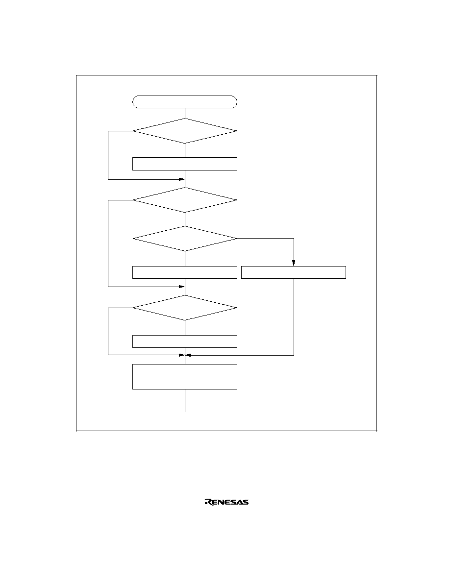
429
<End>
[3]
Error processing
Parity error processing
No
Yes
Clear ORER, PER, and
FER flags in SSR to 0
No
Yes
No
Yes
Framing error processing
No
Yes
Overrun error processing
ORER= 1
FER= 1
Break?
PER= 1
Clear RE bit in SCR to 0
Figure 12-7 Sample Serial Reception Data Flowchart (cont)

430
In serial reception, the SCI operates as described below.
[1] The SCI monitors the transmission line, and if a 0 stop bit is detected, performs internal
synchronization and starts reception.
[2] The received data is stored in RSR in LSB-to-MSB order.
[3] The parity bit and stop bit are received.
After receiving these bits, the SCI carries out the following checks.
[a] Parity check:
The SCI checks whether the number of 1 bits in the receive data agrees with the parity
(even or odd) set in the O/
E bit in SMR.
[b] Stop bit check:
The SCI checks whether the stop bit is 1.
If there are two stop bits, only the first is checked.
[c] Status check:
The SCI checks whether the RDRF flag is 0, indicating that the receive data can be
transferred from RSR to RDR.
If all the above checks are passed, the RDRF flag is set to 1, and the receive data is stored in
RDR.
If a receive error* is detected in the error check, the operation is as shown in table 12-11.
Note: * Subsequent receive operations cannot be performed when a receive error has occurred.
Also note that the RDRF flag is not set to 1 in reception, and so the error flags must be
cleared to 0.
[4] If the RIE bit in SCR is set to 1 when the RDRF flag changes to 1, a receive data full interrupt
(RXI) request is generated.
Also, if the RIE bit in SCR is set to 1 when the ORER, PER, or FER flag changes to 1, a
receive error interrupt (ERI) request is generated.
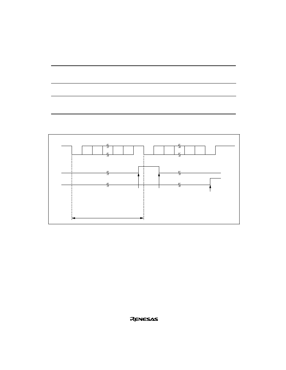
431
Table 12-11 Receive Errors and Conditions for Occurrence
Receive Error
Abbreviation
Occurrence Condition
Data Transfer
Overrun error
ORER
When the next data reception is
completed while the RDRF flag
in SSR is set to 1
Receive data is not
transferred from RSR to
RDR.
Framing error
FER
When the stop bit is 0
Receive data is transferred
from RSR to RDR.
Parity error
PER
When the received data differs
from the parity (even or odd) set
in SMR
Receive data is transferred
from RSR to RDR.
Figure 12-8 shows an example of the operation for reception in asynchronous mode.
RDRF
FER
0
1 frame
D0
D1
D7
0/1
1
0
D0
D1
D7
0/1
0
1
1
Data
Start
bit
Parity
bit
Stop
bit
Start
bit
Data Parity
bit
Stop
bit
RXI interrupt
request generated
ERI interrupt request
generated by framing
error
Idle state
(mark state)
RDR data read and RDRF
flag cleared to 0 in RXI
interrupt service routine
Figure 12-8 Example of SCI Operation in Reception
(Example with 8-Bit Data, Parity, One Stop Bit)

432
12.3.3
Multiprocessor Communication Function
The multiprocessor communication function performs serial communication using the
multiprocessor format, in which a multiprocessor bit is added to the transfer data, in asynchronous
mode. Use of this function enables data transfer to be performed among a number of processors
sharing transmission lines.
When multiprocessor communication is carried out, each receiving station is addressed by a
unique ID code.
The serial communication cycle consists of two component cycles: an ID transmission cycle
which specifies the receiving station , and a data transmission cycle. The multiprocessor bit is used
to differentiate between the ID transmission cycle and the data transmission cycle.
The transmitting station first sends the ID of the receiving station with which it wants to perform
serial communication as data with a 1 multiprocessor bit added. It then sends transmit data as data
with a 0 multiprocessor bit added.
The receiving station skips the data until data with a 1 multiprocessor bit is sent.
When data with a 1 multiprocessor bit is received, the receiving station compares that data with its
own ID. The station whose ID matches then receives the data sent next. Stations whose ID does
not match continue to skip the data until data with a 1 multiprocessor bit is again received. In this
way, data communication is carried out among a number of processors.
Figure 12-9 shows an example of inter-processor communication using the multiprocessor format.
Data Transfer Format: There are four data transfer formats.
When the multiprocessor format is specified, the parity bit specification is invalid.
For details, see table 12-10.
Clock: See the section on asynchronous mode.
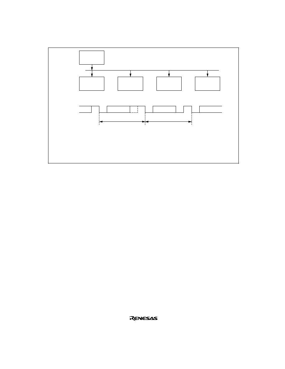
433
Transmitting
station
Receiving
station A
(ID= 01)
Receiving
station B
(ID= 02)
Receiving
station C
(ID= 03)
Receiving
station D
(ID= 04)
Serial transmission line
Serial
data
ID transmission cycle=
receiving station
specification
Data transmission cycle=
Data transmission to
receiving station specified by ID
(MPB= 1)
(MPB= 0)
H'01
H'AA
Legend
MPB: Multiprocessor bit
Figure 12-9 Example of Inter-Processor Communication Using Multiprocessor Format
(Transmission of Data H'AA to Receiving Station A)
Data Transfer Operations:
∑
Multiprocessor serial data transmission
Figure 12-10 shows a sample flowchart for multiprocessor serial data transmission.
The following procedure should be used for multiprocessor serial data transmission.

434
No
<End>
[1]
Yes
Initialization
Start transmission
Read TDRE flag in SSR
[2]
Write transmit data to TDR and
set MPBT bit in SSR
No
Yes
No
Yes
Read TEND flag in SSR
[3]
No
Yes
[4]
Clear DR to 0 and set DDR to 1
Clear TE bit in SCR to 0
TDRE= 1
All data transmitted?
TEND= 1
Break output?
Clear TDRE flag to 0
SCI initialization:
The TxD pin is automatically
designated as the transmit data
output pin.
After the TE bit is set to 1, a
frame of 1s is output, and
transmission is enabled.
SCI status check and transmit
data write:
Read SSR and check that the
TDRE flag is set to 1, then write
transmit data to TDR. Set the
MPBT bit in SSR to 0 or 1.
Finally, clear the TDRE flag to 0.
Serial transmission continuation
procedure:
To continue serial transmission,
be sure to read 1 from the TDRE
flag to confirm that writing is
possible, then write data to TDR,
and then clear the TDRE flag to
0. Checking and clearing of the
TDRE flag is automatic when the
DTC is activated by a transmit
data empty interrupt (TXI)
request, and data is written to
TDR.
Break output at the end of serial
transmission:
To output a break in serial
transmission, set the port DDR to
1, clear DR to 0, then clear the
TE bit in SCR to 0.
[1]
[2]
[3]
[4]
Figure 12-10 Sample Multiprocessor Serial Transmission Flowchart

435
In serial transmission, the SCI operates as described below.
[1] The SCI monitors the TDRE flag in SSR, and if is 0, recognizes that data has been written to
TDR, and transfers the data from TDR to TSR.
[2] After transferring data from TDR to TSR, the SCI sets the TDRE flag to 1 and starts
transmission.
If the TIE bit is set to 1 at this time, a transmit data empty interrupt (TXI) request is generated.
The serial transmit data is sent from the TxD pin in the following order.
[a] Start bit:
One 0-bit is output.
[b] Transmit data:
8-bit or 7-bit data is output in LSB-first order.
[c] Multiprocessor bit
One multiprocessor bit (MPBT value) is output.
[d] Stop bit(s):
One or two 1-bits (stop bits) are output.
[e] Mark state:
1 is output continuously until the start bit that starts the next transmission is sent.
[3] The SCI checks the TDRE flag at the timing for sending the stop bit.
If the TDRE flag is cleared to 0, data is transferred from TDR to TSR, the stop bit is sent, and
then serial transmission of the next frame is started.
If the TDRE flag is set to 1, the TEND flag in SSR is set to 1, the stop bit is sent, and then the
mark state is entered in which 1 is output continuously. If the TEIE bit in SCR is set to 1 at this
time, a transmission end interrupt (TEI) request is generated.
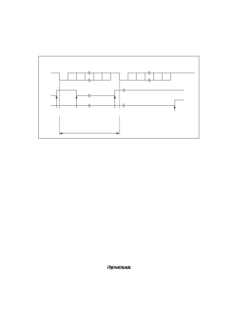
436
Figure 12-11 shows an example of SCI operation for transmission using the multiprocessor
format.
TDRE
TEND
0
1 frame
D0
D1
D7
0/1
1
0
D0
D1
D7
0/1
1
1
1
Data
Start
bit
Multi-
proce-
ssor
bit
Stop
bit
Start
bit
Data
Multi-
proces-
sor bit
Stop
bit
TXI interrupt
request generated
Data written to TDR
and TDRE flag cleared to
0 in TXI interrupt service
routine
TEI interrupt
request generated
Idle state
(mark state)
TXI interrupt
request generated
Figure 12-11 Example of SCI Operation in Transmission
(Example with 8-Bit Data, Multiprocessor Bit, One Stop Bit)
∑
Multiprocessor serial data reception
Figure 12-12 shows a sample flowchart for multiprocessor serial reception.
The following procedure should be used for multiprocessor serial data reception.
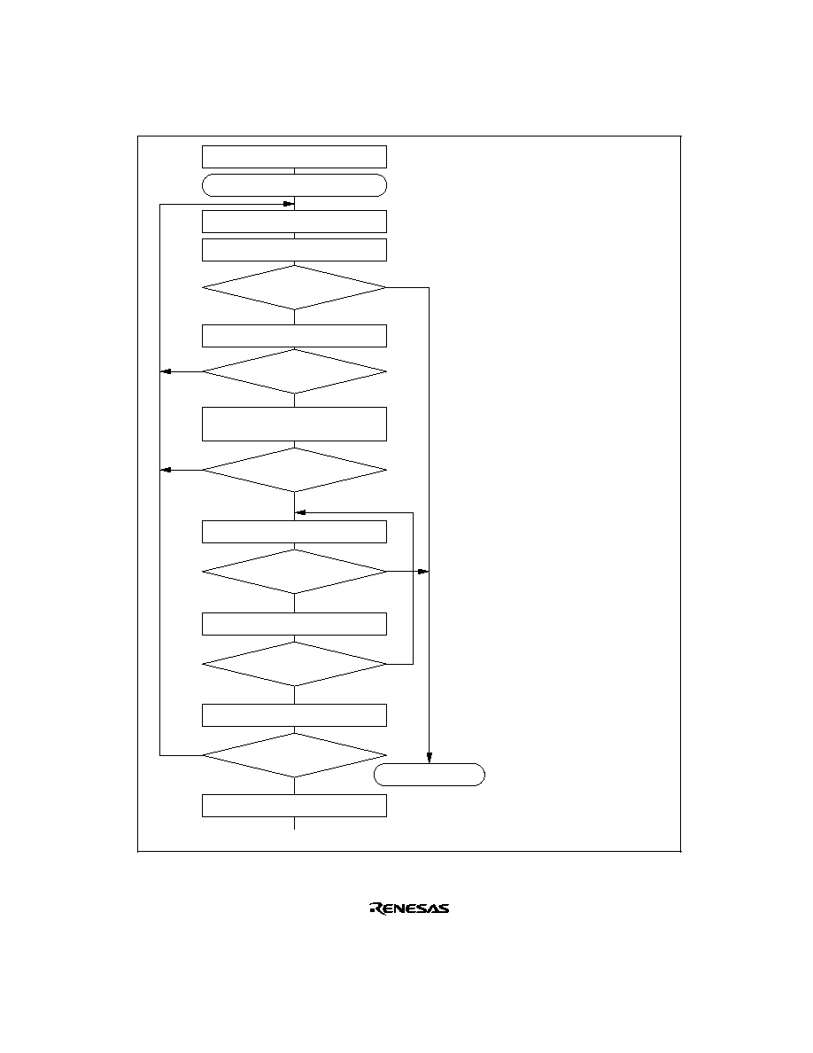
437
Yes
<End>
[1]
No
Initialization
Start reception
No
Yes
[4]
Clear RE bit in SCR to 0
Error processing
(Continued on
next page)
[5]
No
Yes
FER
ORER= 1
RDRF= 1
All data received?
Read MPIE bit in SCR
[2]
Read ORER and FER flags in SSR
Read RDRF flag in SSR
[3]
Read receive data in RDR
No
Yes
This station's ID?
Read ORER and FER flags in SSR
Yes
No
Read RDRF flag in SSR
No
Yes
FER
ORER= 1
Read receive data in RDR
RDRF= 1
SCI initialization:
The RxD pin is automatically
designated as the receive data
input pin.
ID reception cycle:
Set the MPIE bit in SCR to 1.
SCI status check, ID reception
and comparison:
Read SSR and check that the
RDRF flag is set to 1, then read
the receive data in RDR and
compare it with this station's ID.
If the data is not this station's ID,
set the MPIE bit to 1 again, and
clear the RDRF flag to 0.
If the data is this station's ID,
clear the RDRF flag to 0.
SCI status check and data
reception:
Read SSR and check that the
RDRF flag is set to 1, then read
the data in RDR.
Receive error processing and
break detection:
If a receive error occurs, read the
ORER and FER flags in SSR to
identify the error. After
performing the appropriate error
processing, ensure that the
ORER and FER flags are all
cleared to 0.
Reception cannot be resumed if
either of these flags is set to 1.
In the case of a framing error, a
break can be detected by reading
the RxD pin value.
[1]
[2]
[3]
[4]
[5]
Figure 12-12 Sample Multiprocessor Serial Reception Flowchart
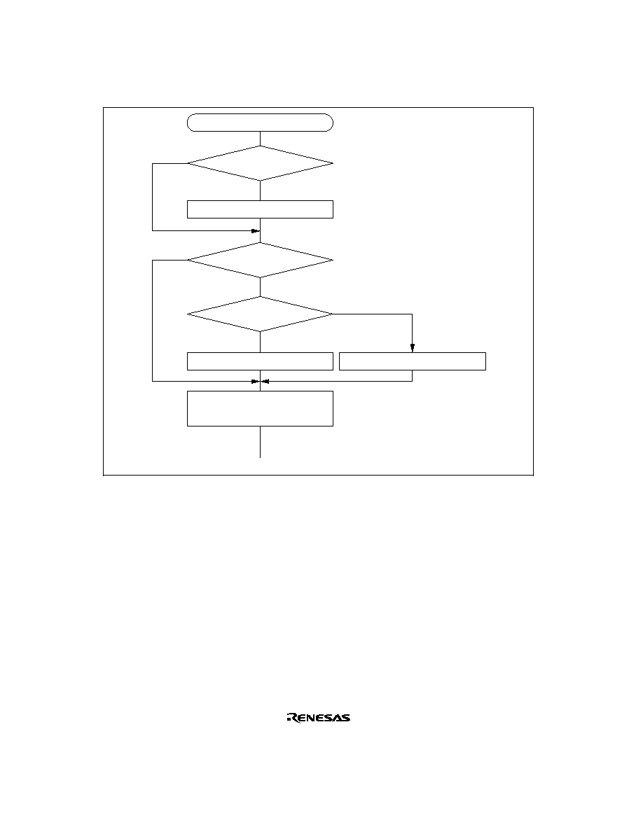
438
<End>
Error processing
Yes
No
Clear ORER, PER, and
FER flags in SSR to 0
No
Yes
No
Yes
Framing error processing
Overrun error processing
ORER= 1
FER= 1
Break?
Clear RE bit in SCR to 0
[5]
Figure 12-12 Sample Multiprocessor Serial Reception Flowchart (cont)
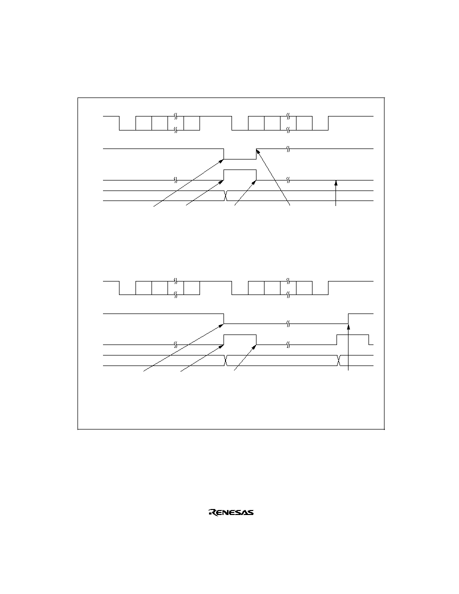
439
Figure 12-13 shows an example of SCI operation for multiprocessor format reception.
MPIE
RDR
value
0
D0
D1
D7
1
1
0
D0
D1
D7
0
1
1
1
Data (ID1)
Start
bit
MPB
Stop
bit
Start
bit
Data (Data1)
MPB
Stop
bit
RXI interrupt
request
(multiprocessor
interrupt)
generated
MPIE = 0
Idle state
(mark state)
RDRF
RDR data read
and RDRF flag
cleared to 0 in
RXI interrupt
service routine
If not this station's ID,
MPIE bit is set to 1
again
RXI interrupt request is
not generated, and RDR
retains its state
ID1
(a) Data does not match station's ID
MPIE
RDR
value
0
D0
D1
D7
1
1
0
D0
D1
D7
0
1
1
1
Data (ID2)
Start
bit
MPB
Stop
bit
Start
bit
Data (Data2)
MPB
Stop
bit
RXI interrupt
request
(multiprocessor
interrupt)
generated
MPIE = 0
Idle state
(mark state)
RDRF
RDR data read and
RDRF flag cleared
to 0 in RXI interrupt
service routine
Matches this station's ID,
so reception continues, and
data is received in RXI
interrupt service routine
MPIE bit set to 1
again
ID2
(b) Data matches station's ID
Data2
ID1
Figure 12-13 Example of SCI Operation in Reception
(Example with 8-Bit Data, Multiprocessor Bit, One Stop Bit)

440
12.3.4
Operation in Clocked Synchronous Mode
In clocked synchronous mode, data is transmitted or received in synchronization with clock
pulses, making it suitable for high-speed serial communication.
Inside the SCI, the transmitter and receiver are independent units, enabling full-duplex
communication by use of a common clock. Both the transmitter and the receiver also have a
double-buffered structure, so that data can be read or written during transmission or reception,
enabling continuous data transfer.
Figure 12-14 shows the general format for clocked synchronous serial communication.
Don't care
Don't care
One unit of transfer data (character or frame)
Bit 0
Serial
data
Serial
clock
Bit 1
Bit 3
Bit 4
Bit 5
LSB
MSB
Bit 2
Bit 6
Bit 7
*
Note:
*
High except in continuous transfer
*
Figure 12-14 Data Format in Synchronous Communication
In clocked synchronous serial communication, data on the transmission line is output from one
falling edge of the serial clock to the next. Data confirmation is guaranteed at the rising edge of
the serial clock.
In clocked serial communication, one character consists of data output starting with the LSB and
ending with the MSB. After the MSB is output, the transmission line holds the MSB state.
In clocked synchronous mode, the SCI receives data in synchronization with the rising edge of the
serial clock.

441
Data Transfer Format: A fixed 8-bit data format is used.
No parity or multiprocessor bits are added.
Clock: Either an internal clock generated by the on-chip baud rate generator or an external serial
clock input at the SCK pin can be selected, according to the setting of the C/
A bit in SMR and the
CKE1 and CKE0 bits in SCR. For details of SCI clock source selection, see table 12-9.
When the SCI is operated on an internal clock, the serial clock is output from the SCK pin.
Eight serial clock pulses are output in the transfer of one character, and when no transfer is
performed the clock is fixed high. When only receive operations are performed, however, the
serial clock is output until an overrun error occurs or the RE bit is cleared to 0. If you want to
perform receive operations in units of one character, you should select an external clock as the
clock source.
Data Transfer Operations:
∑
SCI initialization (clocked synchronous mode)
Before transmitting and receiving data, you should first clear the TE and RE bits in SCR to 0,
then initialize the SCI as described below.
When the operating mode, transfer format, etc., is changed, the TE and RE bits must be cleared
to 0 before making the change using the following procedure. When the TE bit is cleared to 0,
the TDRE flag is set to 1 and TSR is initialized. Note that clearing the RE bit to 0 does not
change the contents of the RDRF, PER, FER, and ORER flags, or the contents of RDR.
Figure 12-15 shows a sample SCI initialization flowchart.
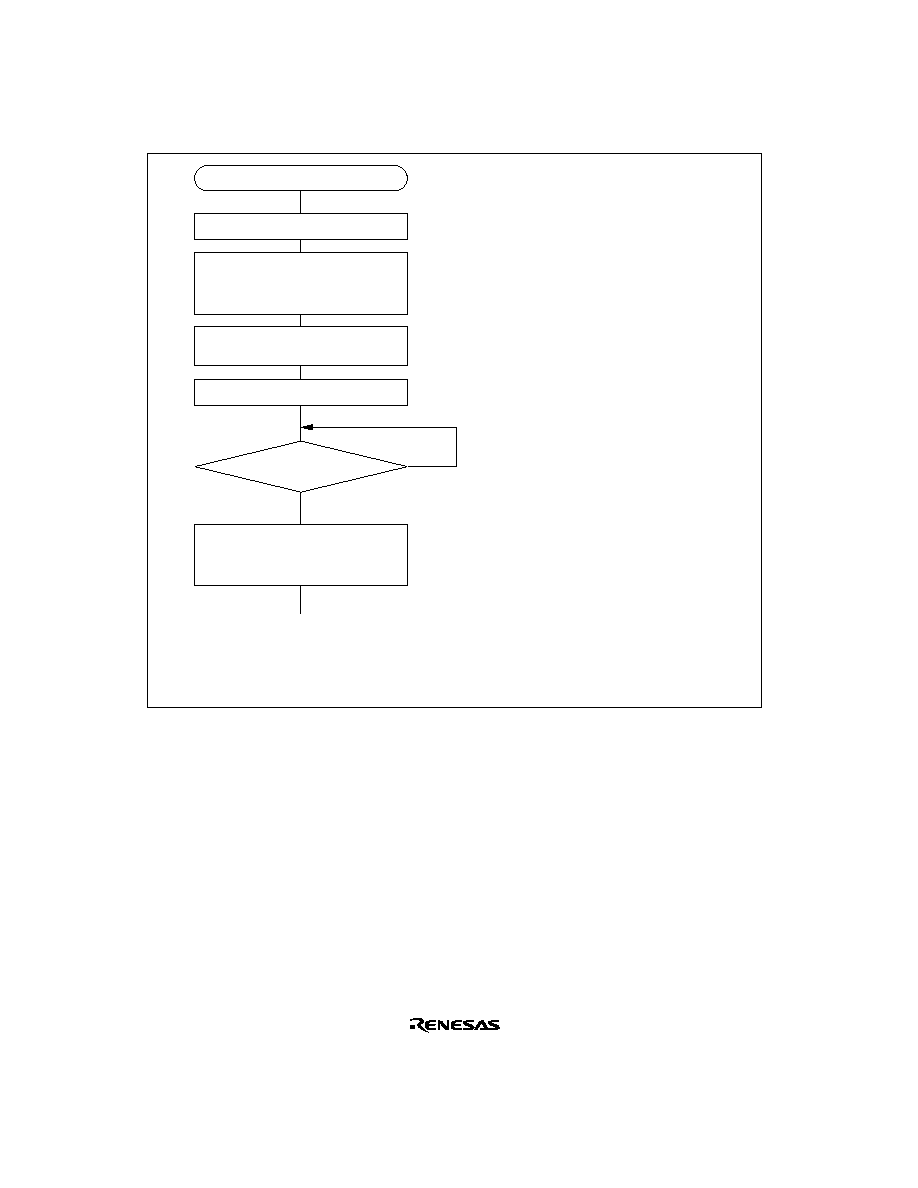
442
Wait
<Transfer start>
Start initialization
Set data transfer format in
SMR and SCMR
No
Yes
Set value in BRR
Clear TE and RE bits in SCR to 0
[2]
[3]
Set TE and RE bits in SCR to 1, and
set RIE, TIE, TEIE, and MPIE bits
[4]
1-bit interval elapsed?
Set CKE1 and CKE0 bits in SCR
(TE, RE bits 0)
[1]
[1] Set the clock selection in SCR. Be sure
to clear bits RIE, TIE, TEIE, and MPIE,
TE and RE, to 0.
[2] Set the data transfer format in SMR
and SCMR.
[3] Write a value corresponding to the bit
rate to BRR. Not necessary if an
external clock is used.
[4] Wait at least one bit interval, then set
the TE bit or RE bit in SCR to 1.
Also set the RIE, TIE, TEIE, and MPIE
bits.
Setting the TE and RE bits enables the
TxD and RxD pins to be used.
Note: In simultaneous transmit and receive operations, the TE and RE bits should both
be cleared to 0 or set to 1 simultaneously.
Figure 12-15 Sample SCI Initialization Flowchart
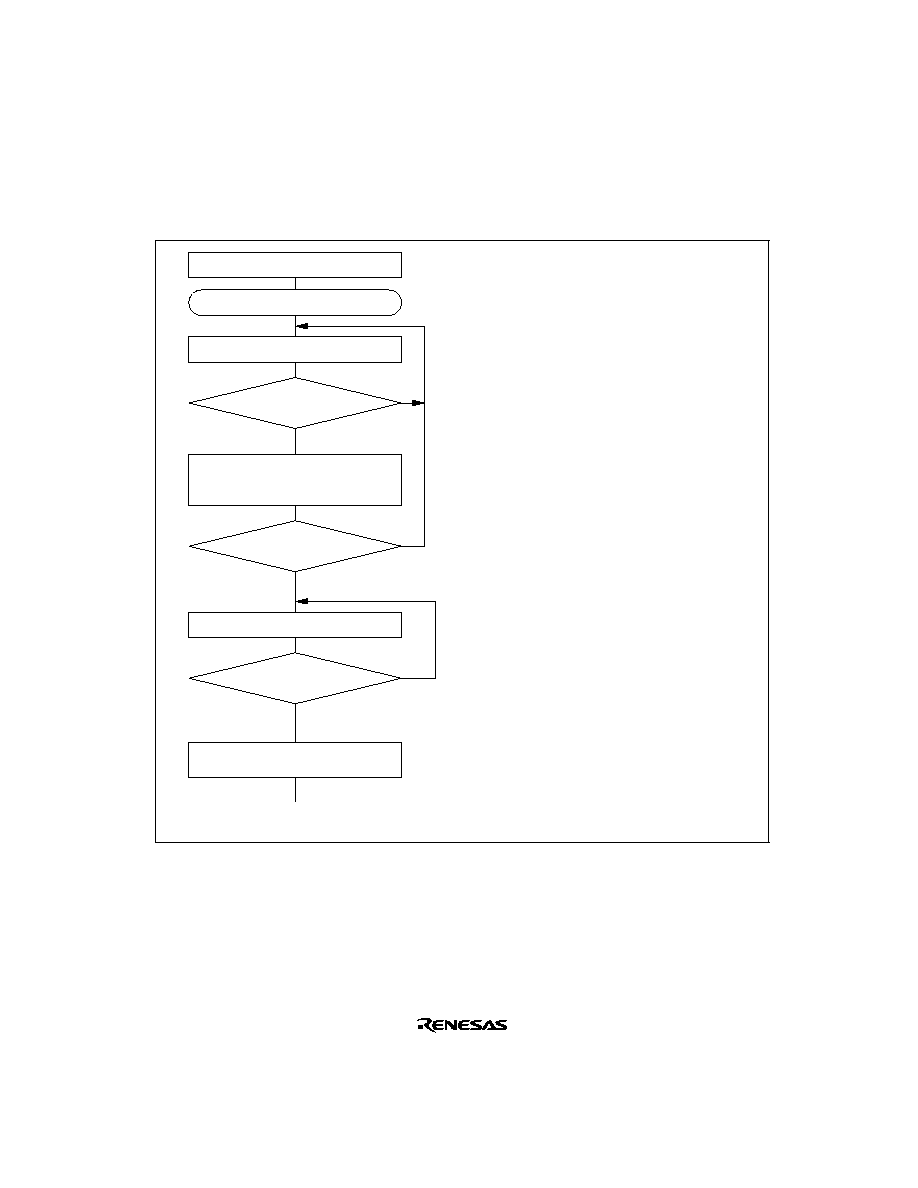
443
∑
Serial data transmission (clocked synchronous mode)
Figure 12-16 shows a sample flowchart for serial transmission.
The following procedure should be used for serial data transmission.
No
<End>
[1]
Yes
Initialization
Start transmission
Read TDRE flag in SSR
[2]
Write transmit data to TDR and
clear TDRE flag in SSR to 0
No
Yes
No
Yes
Read TEND flag in SSR
[3]
Clear TE bit in SCR to 0
TDRE= 1
All data transmitted?
TEND= 1
[1] SCI initialization:
The TxD pin is automatically
designated as the transmit data output
pin.
[2] SCI status check and transmit data
write:
Read SSR and check that the TDRE
flag is set to 1, then write transmit data
to TDR and clear the TDRE flag to 0.
[3] Serial transmission continuation
procedure:
To continue serial transmission, be
sure to read 1 from the TDRE flag to
confirm that writing is possible, then
write data to TDR, and then clear the
TDRE flag to 0.
Checking and clearing of the TDRE
flag is automatic when the DTC is
activated by a transmit data empty
interrupt (TXI) request, and data is
written to TDR.
Figure 12-16 Sample Serial Transmission Flowchart

444
In serial transmission, the SCI operates as described below.
[1] The SCI monitors the TDRE flag in SSR, and if is 0, recognizes that data has been written to
TDR, and transfers the data from TDR to TSR.
[2] After transferring data from TDR to TSR, the SCI sets the TDRE flag to 1 and starts
transmission. If the TIE bit is set to 1 at this time, a transmit data empty interrupt (TXI) is
generated.
When clock output mode has been set, the SCI outputs 8 serial clock pulses. When use of an
external clock has been specified, data is output synchronized with the input clock.
The serial transmit data is sent from the TxD pin starting with the LSB (bit 0) and ending with
the MSB (bit 7).
[3] The SCI checks the TDRE flag at the timing for sending the MSB (bit 7).
If the TDRE flag is cleared to 0, data is transferred from TDR to TSR, and serial transmission
of the next frame is started.
If the TDRE flag is set to 1, the TEND flag in SSR is set to 1, the MSB (bit 7) is sent, and the
TxD pin maintains its state.
If the TEIE bit in SCR is set to 1 at this time, a TEI interrupt request is generated.
[4] After completion of serial transmission, the SCK pin is fixed.
Figure 12-17 shows an example of SCI operation in transmission.

445
Transfer direction
Bit 0
Serial data
Serial clock
1 frame
TDRE
TEND
Bit 1
Bit 7
Bit 0
Bit 1
Bit 7
Bit 6
Data written to TDR
and TDRE flag
cleared to 0 in TXI
interrupt service routine
TEI interrupt
request generated
TXI interrupt
request generated
TXI interrupt
request generated
Figure 12-17 Example of SCI Operation in Transmission
∑
Serial data reception (clocked synchronous mode)
Figure 12-18 shows a sample flowchart for serial reception.
The following procedure should be used for serial data reception.
When changing the operating mode from asynchronous to clocked synchronous, be sure to
check that the ORER, PER, and FER flags are all cleared to 0.
The RDRF flag will not be set if the FER or PER flag is set to 1, and neither transmit nor
receive operations will be possible.

446
Yes
<End>
[1]
No
Initialization
Start reception
[2]
No
Yes
Read RDRF flag in SSR
[4]
[5]
Clear RE bit in SCR to 0
Error processing
(Continued below)
[3]
Read receive data in RDR, and
clear RDRF flag in SSR to 0
No
Yes
ORER= 1
RDRF= 1
All data received?
Read ORER flag in SSR
[1]
[2] [3]
[4]
[5]
SCI initialization:
The RxD pin is automatically
designated as the receive data
input pin.
Receive error processing:
If a receive error occurs, read the
ORER flag in SSR , and after
performing the appropriate error
processing, clear the ORER flag
to 0. Transfer cannot be resumed
if the ORER flag is set to 1.
SCI status check and receive
data read:
Read SSR and check that the
RDRF flag is set to 1, then read
the receive data in RDR and
clear the RDRF flag to 0.
Transition of the RDRF flag from
0 to 1 can also be identified by
an RXI interrupt.
Serial reception continuation
procedure:
To continue serial reception,
before the MSB (bit 7) of the
current frame is received, finish
reading the RDRF flag, reading
RDR, and clearing the RDRF flag
to 0. The RDRF flag is cleared
automatically when the DTC is
activated by a receive data full
interrupt (RXI) request and the
RDR value is read.
<End>
Error processing
Overrun error processing
[3]
Clear ORER flag in SSR to 0
Figure 12-18 Sample Serial Reception Flowchart

447
In serial reception, the SCI operates as described below.
[1] The SCI performs internal initialization in synchronization with serial clock input or output.
[2] The received data is stored in RSR in LSB-to-MSB order.
After reception, the SCI checks whether the RDRF flag is 0 and the receive data can be
transferred from RSR to RDR.
If this check is passed, the RDRF flag is set to 1, and the receive data is stored in RDR. If a
receive error is detected in the error check, the operation is as shown in table 12-11.
Neither transmit nor receive operations can be performed subsequently when a receive error
has been found in the error check.
[3] If the RIE bit in SCR is set to 1 when the RDRF flag changes to 1, a receive data full interrupt
(RXI) request is generated.
Also, if the RIE bit in SCR is set to 1 when the ORER flag changes to 1, a receive error
interrupt (ERI) request is generated.
Figure 12-19 shows an example of SCI operation in reception.
Bit 7
Serial
data
Serial
clock
1 frame
RDRF
ORER
Bit 0
Bit 7
Bit 0
Bit 1
Bit 6
Bit 7
RXI interrupt request
generated
RDR data read and
RDRF flag cleared to 0
in RXI interrupt service
routine
RXI interrupt request
generated
ERI interrupt request
generated by overrun
error
Figure 12-19 Example of SCI Operation in Reception
∑
Simultaneous serial data transmission and reception (clocked synchronous mode)
Figure 12-20 shows a sample flowchart for simultaneous serial transmit and receive operations.
The following procedure should be used for simultaneous serial data transmit and receive
operations.
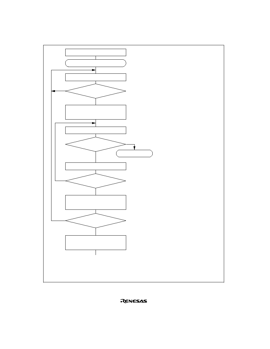
448
Yes
<End>
[1]
No
Initialization
Start transmission/reception
[5]
Error processing
[3]
Read receive data in RDR, and
clear RDRF flag in SSR to 0
No
Yes
ORER= 1
All data received?
[2]
Read TDRE flag in SSR
No
Yes
TDRE= 1
Write transmit data to TDR and
clear TDRE flag in SSR to 0
No
Yes
RDRF= 1
Read ORER flag in SSR
[4]
Read RDRF flag in SSR
Clear TE and RE bits in SCR to 0
Note: When switching from transmit or receive operation to simultaneous
transmit and receive operations, first clear the TE bit and RE bit to
0, then set both these bits to 1 simultaneously.
[1]
[2]
[3]
[4]
[5]
SCI initialization:
The TxD pin is designated as the
transmit data output pin, and the
RxD pin is designated as the
receive data input pin, enabling
simultaneous transmit and receive
operations.
SCI status check and transmit data
write:
Read SSR and check that the
TDRE flag is set to 1, then write
transmit data to TDR and clear the
TDRE flag to 0.
Transition of the TDRE flag from 0
to 1 can also be identified by a TXI
interrupt.
Receive error processing:
If a receive error occurs, read the
ORER flag in SSR , and after
performing the appropriate error
processing, clear the ORER flag to
0. Transmission/reception cannot be
resumed if the ORER flag is set to 1.
SCI status check and receive data
read:
Read SSR and check that the
RDRF flag is set to 1, then read the
receive data in RDR and clear the
RDRF flag to 0. Transition of the
RDRF flag from 0 to 1 can also be
identified by an RXI interrupt.
Serial transmission/reception
continuation procedure:
To continue serial transmission/
reception, before the MSB (bit 7) of
the current frame is transmitted,
read 1 from the TDRE flag to
confirm that writing is possible.
Then write data to TDR and clear
the TDRE flag to 0. Also, before the
MSB (bit 7) of the current frame is
received, finish reading the RDRF
flag, reading RDR, and clearing the
RDRF flag to 0.
Checking and clearing of the TDRE
flag is automatic when the DTC is
activated by a transmit data empty
interrupt (TXI) request and data is
written to TDR. Also, the RDRF flag
is cleared automatically when the
DTC is activated by a receive data
full interrupt (RXI) request and the
RDR value is read.
Figure 12-20 Sample Flowchart of Simultaneous Serial Transmit and Receive Operations

449
12.4
SCI Interrupts
The SCI has four interrupt sources: the transmit-end interrupt (TEI) request, receive-error interrupt
(ERI) request, receive-data-full interrupt (RXI) request, and transmit-data-empty interrupt (TXI)
request. Table 12-12 shows the interrupt sources and their relative priorities. Individual interrupt
sources can be enabled or disabled with the TIE, RIE, and TEIE bits in the SCR. Each kind of
interrupt request is sent to the interrupt controller independently.
When the TDRE flag in SSR is set to 1, a TXI interrupt request is generated. When the TEND flag
in SSR is set to 1, a TEI interrupt request is generated. A TXI interrupt can activate the DTC to
perform data transfer. The TDRE flag is cleared to 0 automatically when data transfer is
performed by the DTC. The DTC cannot be activated by a TEI interrupt request.
When the RDRF flag in SSR is set to 1, an RXI interrupt request is generated. When the ORER,
PER, or FER flag in SSR is set to 1, an ERI interrupt request is generated. An RXI interrupt can
activate the DTC to perform data transfer. The RDRF flag is cleared to 0 automatically when data
transfer is performed by the DTC. The DTC cannot be activated by an ERI interrupt request.

450
Table 12-12 SCI Interrupt Sources
Channel
Interrupt
Source
Description
DTC
Activation
Priority
*
0
ERI
Interrupt due to receive error
(ORER, FER, or PER)
Not
possible
High
RXI
Interrupt due to receive data full
state (RDRF)
Possible
TXI
Interrupt due to transmit data empty state
(TDRE)
Possible
TEI
Interrupt due to transmission end (TEND)
Not
possible
1
ERI
Interrupt due to receive error
(ORER, FER, or PER)
Not
possible
RXI
Interrupt due to receive data full
state (RDRF)
Possible
TXI
Interrupt due to transmit data empty
state (TDRE)
Possible
TEI
Interrupt due to transmission end
(TEND)
Not
possible
2
ERI
Interrupt due to receive error
(ORER, FER, or PER)
Not
possible
RXI
Interrupt due to receive data full
state (RDRF)
Possible
TXI
Interrupt due to transmit data empty
state (TDRE)
Possible
TEI
Interrupt due to transmission end
(TEND)
Not
possible
Low
Note:
*
This table shows the initial state immediately after a reset. Relative priorities among
channels can be changed by means of ICR.
A TEI interrupt is requested when the TEND flag is set to 1 while the TEIE bit is set to 1. The
TEND flag is cleared at the same time as the TDRE flag. Consequently, if a TEI interrupt and a
TXI interrupt are requested simultaneously, the TXI interrupt may be accepted first, with the result
that the TDRE and TEND flags are cleared. Note that the TEI interrupt will not be accepted in
this case.

451
12.5
Usage Notes
The following points should be noted when using the SCI.
Relation between Writes to TDR and the TDRE Flag
The TDRE flag in SSR is a status flag that indicates that transmit data has been transferred from
TDR to TSR. When the SCI transfers data from TDR to TSR, the TDRE flag is set to 1.
Data can be written to TDR regardless of the state of the TDRE flag. However, if new data is
written to TDR when the TDRE flag is cleared to 0, the data stored in TDR will be lost since it has
not yet been transferred to TSR. It is therefore essential to check that the TDRE flag is set to 1
before writing transmit data to TDR.
Operation when Multiple Receive Errors Occur Simultaneously
If a number of receive errors occur at the same time, the state of the status flags in SSR is as
shown in table 12-13. If there is an overrun error, data is not transferred from RSR to RDR, and
the receive data is lost.
Table 12-13
State of SSR Status Flags and Transfer of Receive Data
SSR Status Flags
Receive Data Transfer
RDRF
ORER
FER
PER
RSR to RDR
Receive Error Status
1
1
0
0
X
Overrun error
0
0
1
0
Framing error
0
0
0
1
Parity error
1
1
1
0
X
Overrun error + framing error
1
1
0
1
X
Overrun error + parity error
0
0
1
1
Framing error + parity error
1
1
1
1
X
Overrun error + framing error +
parity error
Notes:
: Receive data is transferred from RSR to RDR.
X: Receive data is not transferred from RSR to RDR.

452
Break Detection and Processing (Asynchronous Mode Only): When framing error (FER)
detection is performed, a break can be detected by reading the RxD pin value directly. In a break,
the input from the RxD pin becomes all 0s, and so the FER flag is set, and the parity error flag
(PER) may also be set.
Note that, since the SCI continues the receive operation after receiving a break, even if the FER
flag is cleared to 0, it will be set to 1 again.
Sending a Break (Asynchronous Mode Only): The TxD pin has a dual function as an I/O port
whose direction (input or output) is determined by DR and DDR. This can be used to send a break.
Between serial transmission initialization and setting of the TE bit to 1, the mark state is replaced
by the value of DR (the pin does not function as the TxD pin until the TE bit is set to 1).
Consequently, DDR and DR for the port corresponding to the TxD pin are first set to 1.
To send a break during serial transmission, first clear DR to 0, then clear the TE bit to 0.
When the TE bit is cleared to 0, the transmitter is initialized regardless of the current transmission
state, the TxD pin becomes an I/O port, and 0 is output from the TxD pin.
Receive Error Flags and Transmit Operations (Clocked Synchronous Mode Only):
Transmission cannot be started when a receive error flag (ORER, PER, or FER) is set to 1, even if
the TDRE flag is cleared to 0. Be sure to clear the receive error flags to 0 before starting
transmission.
Note also that receive error flags cannot be cleared to 0 even if the RE bit is cleared to 0.
Receive Data Sampling Timing and Reception Margin in Asynchronous Mode:
In asynchronous mode, the SCI operates on a basic clock with a frequency of 16 times the transfer
rate.
In reception, the SCI samples the falling edge of the start bit using the basic clock, and performs
internal synchronization. Receive data is latched internally at the rising edge of the 8th pulse of the
basic clock. This is illustrated in figure 12-21.

453
Internal basic
clock
16 clocks
8 clocks
Receive data
(RxD)
Synchronization
sampling timing
Start bit
D0
D1
Data sampling
timing
15 0
7
15 0
0
7
Figure 12-21 Receive Data Sampling Timing in Asynchronous Mode
Thus the reception margin in asynchronous mode is given by formula (1) below.
M = | (0.5 ≠
1
) ≠ (L ≠ 0.5) F ≠
| D ≠ 0.5 |
(1 + F) |
◊
100%
2N
N
... Formula (1)
Where M : Reception margin (%)
N : Ratio of bit rate to clock (N = 16)
D : Clock duty (D = 0 to 1.0)
L : Frame length (L = 9 to 12)
F
: Absolute value of clock rate deviation
Assuming values of F = 0 and D = 0.5 in formula (1), a reception margin of 46.875% is given by
formula (2) below.
When D = 0.5 and F = 0,
M = (0.5 ≠
1
)
◊
100%
2
◊
16
= 46.875%
... Formula (2)
However, this is only the computed value, and a margin of 20% to 30% should be allowed in
system design.

454
Restrictions Concerning TDR Updating
∑
When an external clock source is used as the serial clock, the transmit clock should not be
input until at least 5 ¯ clock cycles after TDR is updated by the CPU and DTC. Misoperation
may occur if the transmit clock is input within 4 ¯ clocks after TDR is updated. (Figure 12-22)
∑
When RDR is read by the DTC, be sure to set the activation source to the relevant SCI
reception end interrupt (RXI).
t
D0
LSB
Serial data
SCK
D1
D3
D4
D5
D2
D6
D7
Note: When operating on an external clock, set t >4 clocks.
TDRE
Figure 12-22 Example of Clocked Synchronous Transmission by DTC

455
Section 13 Smart Card Interface
13.1
Overview
SCI supports an IC card (Smart Card) interface conforming to ISO/IEC 7816-3 (Identification
Card) as a serial communication interface extension function.
Switching between the normal serial communication interface and the Smart Card interface is
carried out by means of a register setting.
13.1.1
Features
Features of the Smart Card interface supported by the H8S/2245 are as follows.
∑
Asynchronous mode
Data length: 8 bits
Parity bit generation and checking
Transmission of error signal (parity error) in receive mode
Error signal detection and automatic data retransmission in transmit mode
Direct convention and inverse convention both supported
∑
On-chip baud rate generator allows any bit rate to be selected
∑
Three interrupt sources
Three interrupt sources (transmit data empty, receive data full, and transmit/receive error)
that can issue requests independently
The transmit data empty interrupt and receive data full interrupt can activate the data
transfer controller (DTC) to execute data transfer
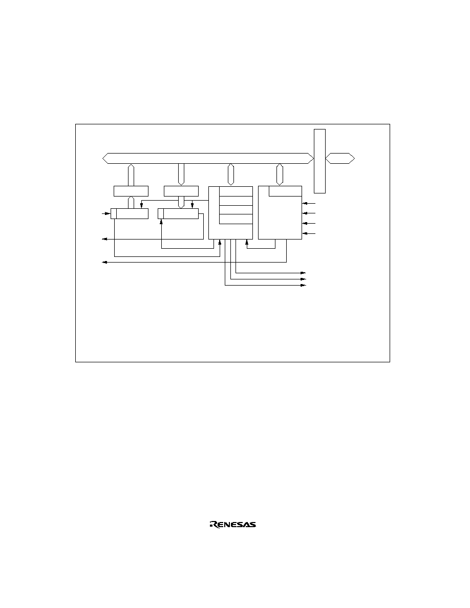
456
13.1.2
Block Diagram
Figure 13-1 shows a block diagram of the Smart Card interface.
Bus interface
TDR
RSR
RDR
Module data bus
TSR
SCMR
SSR
SCR
Transmission/
reception control
BRR
Baud rate
generator
Internal
data bus
RxD
TxD
SCK
Parity generation
Parity check
Clock
¯
¯/4
¯/16
¯/64
TXI
RXI
ERI
SMR
Legend
SCMR
RSR
RDR
TSR
TDR
SMR
SCR
SSR
BRR
: Smart Card mode register
: Receive shift register
: Receive data register
: Transmit shift register
: Transmit data register
: Serial mode register
: Serial control register
: Serial status register
: Bit rate register
Figure 13-1 Block Diagram of Smart Card Interface

457
13.1.3
Pin Configuration
Table 13-1 shows the Smart Card interface pin configuration.
Table 13-1 Smart Card Interface Pins
Channel
Pin Name
Symbol
I/O
Function
0
Serial clock pin 0
SCK0
I/O
SCI0 clock input/output
Receive data pin 0
RxD0
Input
SCI0 receive data input
Transmit data pin 0
TxD0
Output
SCI0 transmit data output
1
Serial clock pin 1
SCK1
I/O
SCI1 clock input/output
Receive data pin 1
RxD1
Input
SCI1 receive data input
Transmit data pin 1
TxD1
Output
SCI1 transmit data output
2
Serial clock pin 2
SCK2
I/O
SCI2 clock input/output
Receive data pin 2
RxD2
Input
SCI2 receive data input
Transmit data pin 2
TxD2
Output
SCI2 transmit data output

458
13.1.4
Register Configuration
Table 13-2 shows the registers used by the Smart Card interface. Details of SMR, BRR, SCR,
TDR, RDR, and MSTPCR are the same as for the normal SCI function: see the register
descriptions in section 12, Serial Communication Interface.
Table 13-2 Smart Card Interface Registers
Channel
Name
Abbreviation
R/W
Initial Value
Address
*
1
0
Serial mode register 0
SMR0
R/W
H'00
H'FF78
Bit rate register 0
BRR0
R/W
H'FF
H'FF79
Serial control register 0
SCR0
R/W
H'00
H'FF7A
Transmit data register 0
TDR0
R/W
H'FF
H'FF7B
Serial status register 0
SSR0
R/(W)
*
2
H'84
H'FF7C
Receive data register 0
RDR0
R
H'00
H'FF7D
Smart card mode
register 0
SCMR0
R/W
H'F2
H'FF7E
1
Serial mode register 1
SMR1
R/W
H'00
H'FF80
Bit rate register 1
BRR1
R/W
H'FF
H'FF81
Serial control register 1
SCR1
R/W
H'00
H'FF82
Transmit data register 1
TDR1
R/W
H'FF
H'FF83
Serial status register 1
SSR1
R/(W)
*
2
H'84
H'FF84
Receive data register 1
RDR1
R
H'00
H'FF85
Smart card mode
register 1
SCMR1
R/W
H'F2
H'FF86
2
Serial mode register 2
SMR2
R/W
H'00
H'FF88
Bit rate register 2
BRR2
R/W
H'FF
H'FF89
Serial control register 2
SCR2
R/W
H'00
H'FF8A
Transmit data register 2
TDR2
R/W
H'FF
H'FF8B
Serial status register 2
SSR2
R/(W)
*
2
H'84
H'FF8C
Receive data register 2
RDR2
R
H'00
H'FF8D
Smart card mode
register 2
SCMR2
R/W
H'F2
H'FF8E
All
Module stop control
register
MSTPCR
R/W
H'3FFF
H'FF3C
Notes: 1. Lower 16 bits of the address.
2. Can only be written with 0 for flag clearing.

459
13.2
Register Descriptions
Registers added with the Smart Card interface and bits for which the function changes are
described here.
13.2.1
Smart Card Mode Register (SCMR)
Bit
:
7
6
5
4
3
2
1
0
--
--
--
--
SDIR
SINV
--
SMIF
Initial value :
1
1
1
1
0
0
1
0
R/W
:
--
--
--
--
R/W
R/W
--
R/W
SCMR is an 8-bit readable/writable register that selects the Smart Card interface function.
SCMR is initialized to H'F2 by a reset, and in standby mode or module stop mode.
Bits 7 to 4--Reserved: Read-only bits, always read as 1.
Bit 3--Smart Card Data Transfer Direction (SDIR): Selects the serial/parallel conversion
format.
Bit 3
SDIR
Description
0
TDR contents are transmitted LSB-first
(Initial value)
Receive data is stored in RDR LSB-first
1
TDR contents are transmitted MSB-first
Receive data is stored in RDR MSB-first
Bit 2--Smart Card Data Invert (SINV): Specifies inversion of the data logic level. This
function is used together with the SDIR bit for communication with an inverse convention card.
The SINV bit does not affect the logic level of the parity bit. For parity-related setting procedures,
see section 13.3.4, Register Settings.
Bit 2
SINV
Description
0
TDR contents are transmitted as they are
(Initial value)
Receive data is stored as it is in RDR
1
TDR contents are inverted before being transmitted
Receive data is stored in inverted form in RDR

460
Bit 1--Reserved: Read-only bit, always read as 1.
Bit 0--Smart Card Interface Mode Select (SMIF): Enables or disables the Smart Card interface
function.
Bit 0
SMIF
Description
0
Smart Card interface function is disabled
(Initial value)
1
Smart Card interface function is enabled
13.2.2
Serial Status Register (SSR)
Bit
:
7
6
5
4
3
2
1
0
TDRE
RDRF
ORER
ERS
PER
TEND
MPB
MPBT
Initial value :
1
0
0
0
0
1
0
0
R/W
:
R/(W)
*
R/(W)
*
R/(W)
*
R/(W)
*
R/(W)
*
R
R
R/W
Note:
*
Only 0 can be written to bits 7 to 3, to clear these flags.
Bit 4 of SSR has a different function in Smart Card interface mode. Coupled with this, the setting
conditions for bit 2, TEND, are also different.
Bits 7 to 5--Operate in the same way as for the normal SCI. For details, see section 12.2.7, Serial
Status Register (SSR).
Bit 4--Error Signal Status (ERS): In Smart Card interface mode, bit 4 indicates the status of the
error signal sent back from the receiving end in transmission. Framing errors are not detected in
Smart Card interface mode.
Bit 4
ERS
Description
0
[Clearing condition]
(Initial value)
∑
Upon reset, and in standby mode or module stop mode
∑
When 0 is written to ERS after reading ERS = 1
1
[Setting condition]
When the low level of the error signal is sampled
Note:
Clearing the TE bit in SCR to 0 does not affect the ERS flag, which retains its previous
state.

461
Bits 3 to 0--Operate in the same way as for the normal SCI. For details, see section 12.2.7, Serial
Status Register (SSR).
However, the setting conditions for the TEND bit, are as shown below.
Bit 2
TEND
Description
0
[Clearing conditions]
(Initial value)
∑
When 0 is written to TDRE after reading TDRE = 1
∑
When the DTC is activated by a TXI interrupt and write data to TDR
1
[Setting conditions]
∑
Upon reset, and in standby mode or module stop mode
∑
When the TE bit in SCR is 0 and the ERS bit is also 0
∑
When TDRE = 1 and ERS = 0 (normal transmission) 2.5 etu after transmission of a
1-byte serial character when GM = 0
∑
When TDRE = 1 and ERS = 0 (normal transmission) 1.0 etu after transmission of a
1-byte serial character when GM = 1
Note:
etu: Elementary Time Unit (time for transfer of 1 bit)
13.2.3
Serial Mode Register (SMR)
Bit
:
7
6
5
4
3
2
1
0
GM
CHR
PE
O/
E
STOP
MP
CKS1
CKS0
Initial value :
0
0
0
0
0
0
0
0
Set value
*
:
GM
0
1
O/
E
1
0
CKS1
CKS0
R/W
:
R/W
R/W
R/W
R/W
R/W
R/W
R/W
R/W
Note:
*
When the smart card interface is used, be sure to make the 0 or 1 setting shown for bits 6,
5, 3, and 2.
The function of bit 7 of SMR changes in smart card interface mode.
Bit 7--GSM Mode (GM): Sets the smart card interface function to GSM mode.
This bit is cleared to 0 when the normal smart card interface is used. In GSM mode, this bit is set
to 1, the timing of setting of the TEND flag that indicates transmission completion is advanced
and clock output control mode addition is performed. The contents of the clock output control
mode addition are specified by bits 1 and 0 of the serial control register (SCR).

462
Bit 7
GM
Description
0
Normal smart card interface mode operation
(Initial value)
∑
TEND flag generation 12.5 etu after beginning of start bit
∑
Clock output ON/OFF control only
1
GSM mode smart card interface mode operation
∑
TEND flag generation 11.0 etu after beginning of start bit
∑
High/low fixing control possible in addition to clock output ON/OFF control (set by
SCR)
Note:
etu: Elementary time unit (time for transfer of 1 bit)
Bits 6 to 0--Operate in the same way as for the normal SCI.
For details, see section 12.2.5, Serial Mode Register (SMR).
13.2.4
Serial Control Register (SCR)
Bit
:
7
6
5
4
3
2
1
0
TIE
RIE
TE
RE
MPIE
TEIE
CKE1
CKE0
Initial value :
0
0
0
0
0
0
0
0
R/W
:
R/W
R/W
R/W
R/W
R/W
R/W
R/W
R/W
In smart card interface mode, the function of bits 1 and 0 of SCR changes when bit 7 of the serial
mode register (SMR) is set to 1.
Bits 7 to 2--Operate in the same way as for the normal SCI.
For details, see section 12.2.6, Serial Control Register (SCR).
Bits 1 and 0--Clock Enable 1 and 0 (CKE1, CKE0): These bits are used to select the SCI clock
source and enable or disable clock output from the SCK pin.
In smart card interface mode, in addition to the normal switching between clock output enabling
and disabling, the clock output can be specified as to be fixed high or low.

463
SCMR
SMR
SCR Setting
SMIF
C/
A
, GM
CKE1
CKE0
SCK Pin Function
0
See the SCI
1
0
0
0
Operates as port I/O pin
1
0
0
1
Outputs clock as SCK output pin
1
1
0
0
Operates as SCK output pin, with output fixed
low
1
1
0
1
Outputs clock as SCK output pin
1
1
1
0
Operates as SCK output pin, with output fixed
high
1
1
1
1
Outputs clock as SCK output pin
13.3
Operation
13.3.1
Overview
The main functions of the Smart Card interface are as follows.
∑
One frame consists of 8-bit data plus a parity bit.
∑
In transmission, a guard time of at least 2 etu (Elementary Time Unit: the time for transfer of
one bit) is left between the end of the parity bit and the start of the next frame.
∑
If a parity error is detected during reception, a low error signal level is output for one etu
period, 10.5 etu after the start bit.
∑
If the error signal is sampled during transmission, the same data is transmitted automatically
after the elapse of 2 etu or longer.
∑
Only asynchronous communication is supported; there is no clocked synchronous
communication function.
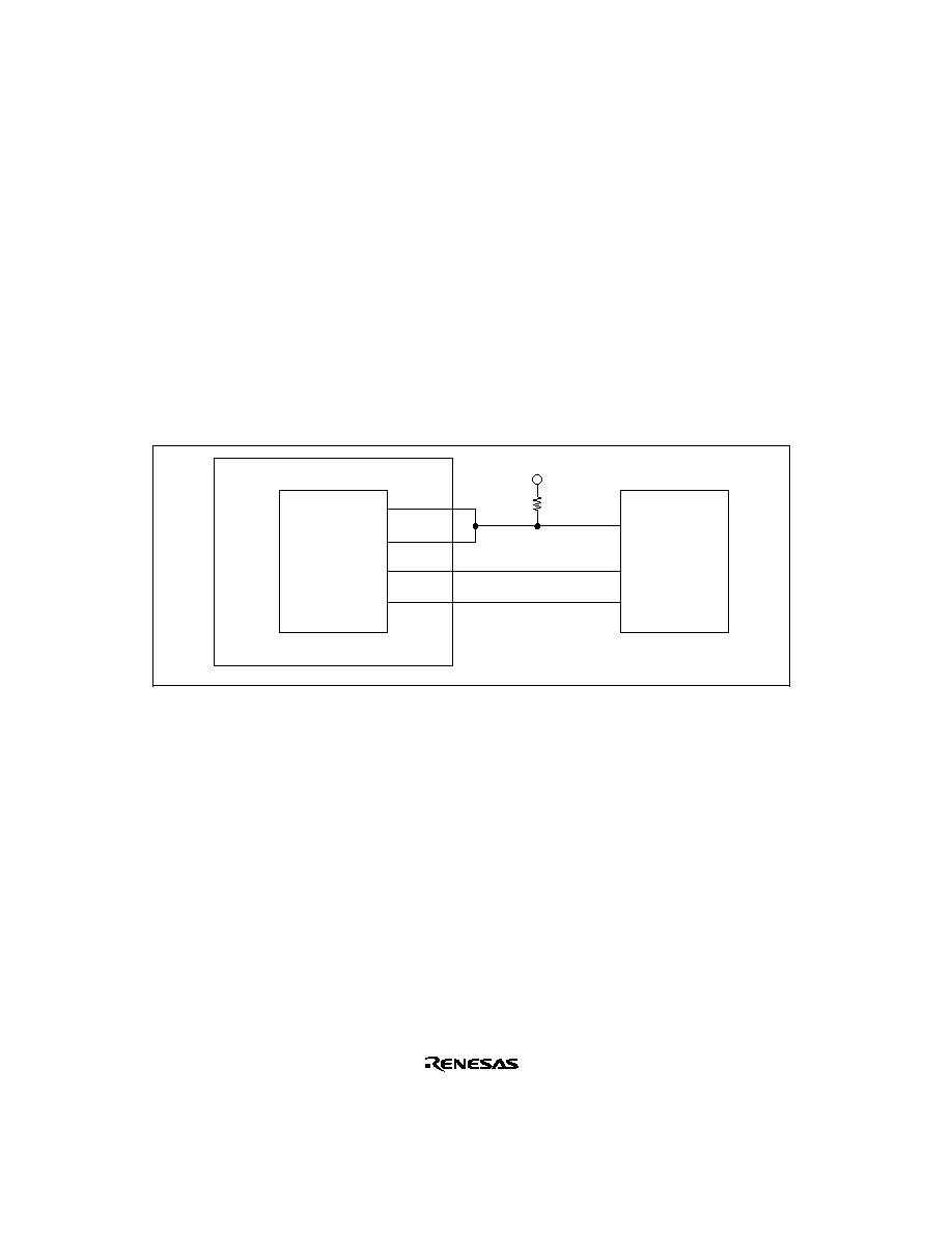
464
13.3.2
Pin Connections
Figure 13-2 shows a schematic diagram of Smart Card interface related pin connections.
In communication with an IC card, since both transmission and reception are carried out on a
single data transmission line, the TxD pin and RxD pin should be connected with the LSI pin. The
data transmission line should be pulled up to the V
CC
power supply with a resistor.
When the clock generated on the Smart Card interface is used by an IC card, the SCK pin output is
input to the CLK pin of the IC card. No connection is needed if the IC card uses an internal clock.
LSI port output is used as the reset signal.
Other pins must normally be connected to the power supply or ground.
TxD
RxD
SCK
Rx (port)
H8S/2245
I/O
CLK
RST
V
CC
Connected equipment
IC card
Data line
Clock line
Reset line
Figure 13-2 Schematic Diagram of Smart Card Interface Pin Connections
Note:
If an IC card is not connected, and the TE and RE bits are both set to 1, closed
transmission/reception is possible, enabling self-diagnosis to be carried out.

465
13.3.3
Data Format
Figure 13-3 shows the Smart Card interface data format. In reception in this mode, a parity check
is carried out on each frame, and if an error is detected an error signal is sent back to the
transmitting end, and retransmission of the data is requested. If an error signal is sampled during
transmission, the same data is retransmitted.
Ds
D0
D1
D2
D3
D4
D5
D6
D7
Dp
When there is no parity error
Transmitting station output
Ds
D0
D1
D2
D3
D4
D5
D6
D7
Dp
When a parity error occurs
Transmitting station output
DE
Receiving station
output
: Start bit
: Data bits
: Parity bit
: Error signal
Legend
Ds
D0 to D7
Dp
DE
Figure 13-3 Smart Card Interface Data Format

466
The operation sequence is as follows.
[1] When the data line is not in use it is in the high-impedance state, and is fixed high with a pull-
up resistor.
[2] The transmitting station starts transfer of one frame of data. The data frame starts with a start
bit (Ds, low-level), followed by 8 data bits (D0 to D7) and a parity bit (Dp).
[3] With the Smart Card interface, the data line then returns to the high-impedance state. The data
line is pulled high with a pull-up resistor.
[4] The receiving station carries out a parity check.
If there is no parity error and the data is received normally, the receiving station waits for
reception of the next data.
If a parity error occurs, however, the receiving station outputs an error signal (DE, low-level)
to request retransmission of the data. After outputting the error signal for the prescribed length
of time, the receiving station places the signal line in the high-impedance state again. The
signal line is pulled high again by a pull-up resistor.
[5] If the transmitting station does not receive an error signal, it proceeds to transmit the next data
frame.
If it does receive an error signal, however, it returns to step [2] and retransmits the erroneous
data.

467
13.3.4
Register Settings
Table 13-3 shows a bit map of the registers used by the smart card interface.
Bits indicated as 0 or 1 must be set to the value shown. The setting of other bits is described
below.
Table 13-3 Smart Card Interface Register Settings
Bit
Register
Bit 7
Bit 6
Bit 5
Bit 4
Bit 3
Bit 2
Bit 1
Bit 0
SMR
GM
0
1
O/
E
1
0
CKS1
CKS0
BRR
BRR7
BRR6
BRR5
BRR4
BRR3
BRR2
BRR1
BRR0
SCR
TIE
RIE
TE
RE
0
0
CKE1
*
CKE0
TDR
TDR7
TDR6
TDR5
TDR4
TDR3
TDR2
TDR1
TDR0
SSR
TDRE
RDRF
ORER
ERS
PER
TEND
0
0
RDR
RDR7
RDR6
RDR5
RDR4
RDR3
RDR2
RDR1
RDR0
SCMR
--
--
--
--
SDIR
SINV
--
SMIF
Notes: -- : Unused bit.
*
: The CKE1 bit must be cleared to 0 when the GM bit in SMR is cleared to 0.
SMR Setting: The GM bit is cleared to 0 in normal smart card interface mode, and set to 1 in
GSM mode. The O/
E bit is cleared to 0 if the IC card is of the direct convention type, and set to 1
if of the inverse convention type.
Bits CKS1 and CKS0 select the clock source of the on-chip baud rate generator. See section
13.3.5, Clock.
BRR Setting: BRR is used to set the bit rate. See section 13.3.5, Clock, for the method of
calculating the value to be set.
SCR Setting: The function of the TIE, RIE, TE, and RE bits is the same as for the normal SCI.
For details, see section 12, Serial Communication Interface.
Bits CKE1 and CKE0 specify the clock output. When the GM bit in SMR is cleared to 0, set these
bits to H'00 if a clock is not to be output, or to H'01 if a clock is to be output. When the GM bit in
SMR is set to 1, clock output is performed. The clock output can also be fixed high or low.

468
Smart Card Mode Register (SCMR) Setting:
The SDIR bit is cleared to 0 if the IC card is of the direct convention type, and set to 1 if of the
inverse convention type.
The SINV bit is cleared to 0 if the IC card is of the direct convention type, and set to 1 if of the
inverse convention type.
The SMIF bit is set to 1 in the case of the Smart Card interface.
Examples of register settings and the waveform of the start character are shown below for the two
types of IC card (direct convention and inverse convention).
∑
Direct convention (SDIR = SINV = O/
E = 0)
Ds
D0
D1
D2
D3
D4
D5
D6
D7
Dp
A
Z
Z
A
Z
Z
Z
A
A
Z
(Z)
(Z)
State
With the direct convention type, the logic 1 level corresponds to state Z and the logic 0 level to
state A, and transfer is performed in LSB-first order. The start character data above is H'3B.
The parity bit is 1 since even parity is stipulated for the Smart Card.
∑
Inverse convention (SDIR = SINV = O/
E = 1)
Ds
D7
D6
D5
D4
D3
D2
D1
D0
Dp
A
Z
Z
A
A
A
A
A
A
Z
(Z)
(Z)
State
With the inverse convention type, the logic 1 level corresponds to state A and the logic 0 level
to state Z, and transfer is performed in MSB-first order. The start character data above is H'3F.
The parity bit is 0, corresponding to state Z, since even parity is stipulated for the Smart Card.
With the H8S/2245 Series, inversion specified by the SINV bit applies only to the data bits, D7
to D0. For parity bit inversion, the O/
E bit in SMR is set to odd parity mode (the same applies
to both transmission and reception).

469
13.3.5
Clock
Only an internal clock generated by the on-chip baud rate generator can be used as the
transmit/receive clock for the smart card interface. The bit rate is set with BRR and the CKS1 and
CKS0 bits in SMR. The formula for calculating the bit rate is as shown below. Table 13-5 shows
some sample bit rates.
If clock output is selected by setting CKE0 to 1, a clock with a frequency of 372 times the bit rate
is output from the SCK pin.
B =
¯
1488
◊
2
2n≠1
◊
(N + 1)
◊
10
6
Where: N = Value set in BRR (0
N
255)
B = Bit rate (bit/s)
¯ = Operating frequency (MHz)
n = See table 13-4
Table 13-4 Correspondence between n and CKS1, CKS0
n
CKS1
CKS0
0
0
0
1
1
2
1
0
3
1
Table 13-5 Examples of Bit Rate B (bit/s) for Various BRR Settings (When n = 0)
¯ (MHz)
N
10.00
10.714
13.00
14.285
16.00
18.00
20.00
0
13441
14400
17473
19200
21505
24194
26882
1
6720
7200
8737
9600
10753
12097
13441
2
4480
4800
5824
6400
7168
8065
8961
Note:
Bit rates are rounded to the nearest whole number.

470
The method of calculating the value to be set in the bit rate register (BRR) from the operating
frequency and bit rate, on the other hand, is shown below. N is an integer, 0
N
255, and the
smaller error is specified.
N =
¯
1488
◊
2
2n≠1
◊
B
◊
10
6
≠ 1
Table 13-6 Examples of BRR Settings for Bit Rate B (bit/s) (When n = 0)
¯ (MHz)
7.1424
10.00
10.7136
13.00
14.2848
16.00
18.00
20.00
bit/s
N
Error
N
Error
N
Error
N
Error
N
Error
N
Error
N
Error
N
Error
9600
0
0.00
1
30
1
25
1
8.99
1
0.00
1
12.01
2
15.99
2
6.60
Table 13-7 Maximum Bit Rate at Various Frequencies (Smart Card Interface Mode)
¯ (MHz)
Maximum Bit Rate (bit/s)
N
n
7.1424
9600
0
0
10.00
13441
0
0
10.7136
14400
0
0
13.00
17473
0
0
14.2848
19200
0
0
16.00
21505
0
0
18.00
24194
0
0
20.00
26882
0
0
The bit rate error is given by the following formula:
Error (%) = (
¯
1488
◊
2
2n≠1
◊
B
◊
(N + 1)
◊
10
6
≠ 1)
◊
100

471
13.3.6
Data Transfer Operations
Initialization: Before transmitting and receiving data, initialize the SCI as described below.
Initialization is also necessary when switching from transmit mode to receive mode, or vice versa.
[1] Clear the TE and RE bits in SCR to 0.
[2] Clear the error flags ERS, PER, and ORER in SSR to 0.
[3] Set the O/
E bit and CKS1 and CKS0 bits in SMR. Clear the C/A, CHR, and MP bits to 0, and
set the STOP and PE bits to 1.
[4] Set the SMIF, SDIR, and SINV bits in SCMR.
When the SMIF bit is set to 1, the TxD and RxD pins are both switched from ports to SCI pins,
and are placed in the high-impedance state.
[5] Set the value corresponding to the bit rate in BRR.
[6] Set the CKE0 bit in SCR. Clear the TIE, RIE, TE, RE, MPIE, TEIE and CKE1 bits to 0.
If the CKE0 bit is set to 1, the clock is output from the SCK pin.
[7] Wait at least one bit interval, then set the TIE, RIE, TE, and RE bits in SCR. Do not set the TE
bit and RE bit at the same time, except for self-diagnosis.

472
Serial Data Transmission: As data transmission in smart card mode involves error signal
sampling and retransmission processing, the processing procedure is different from that for the
normal SCI. Figure 13-4 shows a flowchart for transmitting, and figure 13-5 shows the relation
between a transmit operation and the internal registers.
[1] Perform Smart Card interface mode initialization as described above in Initialization.
[2] Check that the ERS error flag in SSR is cleared to 0.
[3] Repeat steps [2] and [3] until it can be confirmed that the TEND flag in SSR is set to 1.
[4] Write the transmit data to TDR, clear the TDRE flag to 0, and perform the transmit operation.
The TEND flag is cleared to 0.
[5] When transmitting data continuously, go back to step [2].
[6] To end transmission, clear the TE bit to 0.
With the above processing, interrupt servicing or data transfer by the DTC is possible.
If transmission ends and the TEND flag is set to 1 while the TIE bit is set to 1 and interrupt
requests are enabled, a transmit data empty interrupt (TXI) request will be generated. If an error
occurs in transmission and the ERS flag is set to 1 while the RIE bit is set to 1 and interrupt
requests are enabled, a transfer error interrupt (ERI) request will be generated.
The timing for setting the TEND flag depends on the value of the GM bit in SMR. The TEND
flag set timing is shown in figure 13-6.
If the DTC is activated by a TXI request, the number of bytes set in the DTC can be transmitted
automatically, including automatic retransmission.
For details, see Interrupt Operations and Data Transfer Operation by DTC below.
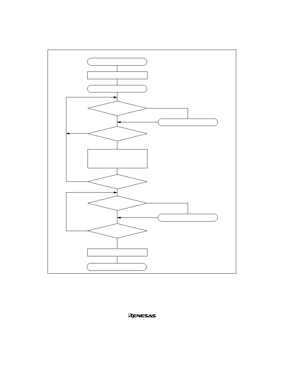
473
Initialization
No
Yes
Clear TE bit to 0
Start transmission
Start
No
No
No
Yes
Yes
Yes
Yes
No
End
Write data to TDR,
and clear TDRE flag
in SSR to 0
Error processing
Error processing
TEND=1?
All data transmitted?
TEND=1?
ERS=0?
ERS=0?
Figure 13-4 Example of Transmission Processing Flow

474
(1) Data write
TDR
TSR
(shift register)
Data 1
(2) Transfer from
TDR to TSR
Data 1
Data 1
; Data remains in TDR
(3) Serial data output
Note: When the ERS flag is set, it should be cleared until transfer of the last bit (D7 in LSB-first
transmission, D0 in MSB-first transmission) of the next transfer data to be transmitted has
been completed.
In case of normal transmission: TEND flag is set
In case of transmit error:
ERS flag is set
Steps (2) and (3) above are repeated until the TEND flag is set
I/O signal line output
Data 1
Data 1
Figure 13-5 Relation Between Transmit Operation and Internal Registers
Ds
D0
D1
D2
D3
D4
D5
D6
D7
Dp
I/O data
12.5etu
TXI
(TEND interrupt)
11.0etu
DE
Guard
time
When GM = 1
Legend
Ds
: Start bit
D0 to D7 : Data bits
Dp
: Parity bit
DE
: Error signal
When GM = 0
Figure 13-6 TEND Flag Generation Timing in Transmission Operation
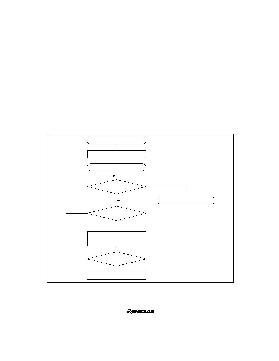
475
Serial Data Reception: Data reception in Smart Card mode uses the same processing procedure
as for the normal SCI. Figure 13-7 shows an example of the transmission processing flow.
[1] Perform Smart Card interface mode initialization as described above in Initialization.
[2] Check that the ORER flag and PER flag in SSR are cleared to 0. If either is set, perform the
appropriate receive error processing, then clear both the ORER and the PER flag to 0.
[3] Repeat steps [2] and [3] until it can be confirmed that the RDRF flag is set to 1.
[4] Read the receive data from RDR.
[5] When receiving data continuously, clear the RDRF flag to 0 and go back to step [2].
[6] To end reception, clear the RE bit to 0.
Initialization
Read RDR and clear
RDRF flag in SSR to 0
Clear RE bit to 0
Start reception
Start
Error processing
No
No
No
Yes
Yes
ORER = 0 and
PER = 0
RDRF=1?
All data received?
Yes
Figure 13-7 Example of Reception Processing Flow

476
With the above processing, interrupt servicing or data transfer by the or DTC is possible.
If reception ends and the RDRF flag is set to 1 while the RIE bit is set to 1 and interrupt requests
are enabled, a receive data full interrupt (RXI) request will be generated. If an error occurs in
reception and either the ORER flag or the PER flag is set to 1, a transfer error interrupt (ERI)
request will be generated.
If the DTC is activated by an RXI request, the receive data in which the error occurred is skipped,
and only the number of bytes of receive data set in the DTC are transferred.
For details, see Interrupt Operation and Data Transfer Operation by DTC below.
If a parity error occurs during reception and the PER is set to 1, the received data is still
transferred to RDR, and therefore this data can be read.
Mode Switching Operation: When switching from receive mode to transmit mode, first confirm
that the receive operation has been completed, then start from initialization, clearing RE bit to 0
and setting TE bit to 1. The RDRF flag or the PER and ORER flags can be used to check that the
receive operation has been completed.
When switching from transmit mode to receive mode, first confirm that the transmit operation has
been completed, then start from initialization, clearing TE bit to 0 and setting RE bit to 1. The
TEND flag can be used to check that the transmit operation has been completed.
Fixing Clock Output Level: When the GSM bit in SMR is set to 1, the clock output level can be
fixed with bits CKE1 and CKE0 in SCR. At this time, the minimum clock pulse width can be
made the specified width.
Figure 13-8 shows the timing for fixing the clock output level. In this example, GSM is set to 1,
CKE1 is cleared to 0, and the CKE0 bit is controlled.
SCK
Specified pulse width
SCR write
(CKE0 = 0)
SCR write
(CKE0 = 1)
Specified pulse width
Figure 13-8 Timing for Fixing Clock Output Level
Interrupt Operation: There are three interrupt sources in smart card interface mode: transmit
data empty interrupt (TXI) requests, transfer error interrupt (ERI) requests, and receive data full
interrupt (RXI) requests. The transmit end interrupt (TEI) request is not used in this mode.

477
When the TEND flag in SSR is set to 1, a TXI interrupt request is generated.
When the RDRF flag in SSR is set to 1, an RXI interrupt request is generated.
When any of flags ORER, PER, and ERS in SSR is set to 1, an ERI interrupt request is generated.
The relationship between the operating states and interrupt sources is shown in table 13-8.
Table 13-8 Smart Card Mode Operating States and Interrupt Sources
Operating State
Flag
Enable Bit
Interrupt
Source
DTC
Activation
Transmit Mode
Normal
operation
TEND
TIE
TXI
Possible
Error
ERS
RIE
ERI
Not possible
Receive Mode
Normal
operation
RDRF
RIE
RXI
Possible
Error
PER, ORER
RIE
ERI
Not possible
Data Transfer Operation by DTC: In smart card mode, as with the normal SCI, transfer can be
carried out using the DTC. In a transmit operation, the TDRE flag is also set to 1 at the same time
as the TEND flag in SSR, and a TXI interrupt is generated. If the TXI request is designated
beforehand as a DTC activation source, the DTC will be activated by the TXI request, and transfer
of the transmit data will be carried out. The TDRE and TEND flags are automatically cleared to 0
when data transfer is performed by the DTC. In the event of an error, the SCI retransmits the same
data automatically. However, the ERS flag is not cleared automatically when an error occurs, and
so the RIE bit should be set to 1 beforehand so that an ERI request will be generated in the event
of an error, and the ERS flag will be cleared.
When performing transfer using the DTC, it is essential to set and enable the DTC before carrying
out SCI setting. For details of the DTC setting procedures, see section 7, Data Transfer Controller
(DTC).
In a receive operation, an RXI interrupt request is generated when the RDRF flag in SSR is set to
1. If the RXI request is designated beforehand as a DTC activation source, the DTC will be
activated by the RXI request, and transfer of the receive data will be carried out. The RDRF flag is
cleared to 0 automatically when data transfer is performed by the DTC. If an error occurs, an error
flag is set but the RDRF flag is not. Consequently, the DTC is not activated, but instead, an ERI
interrupt request is sent to the CPU. Therefore, the error flag should be cleared.
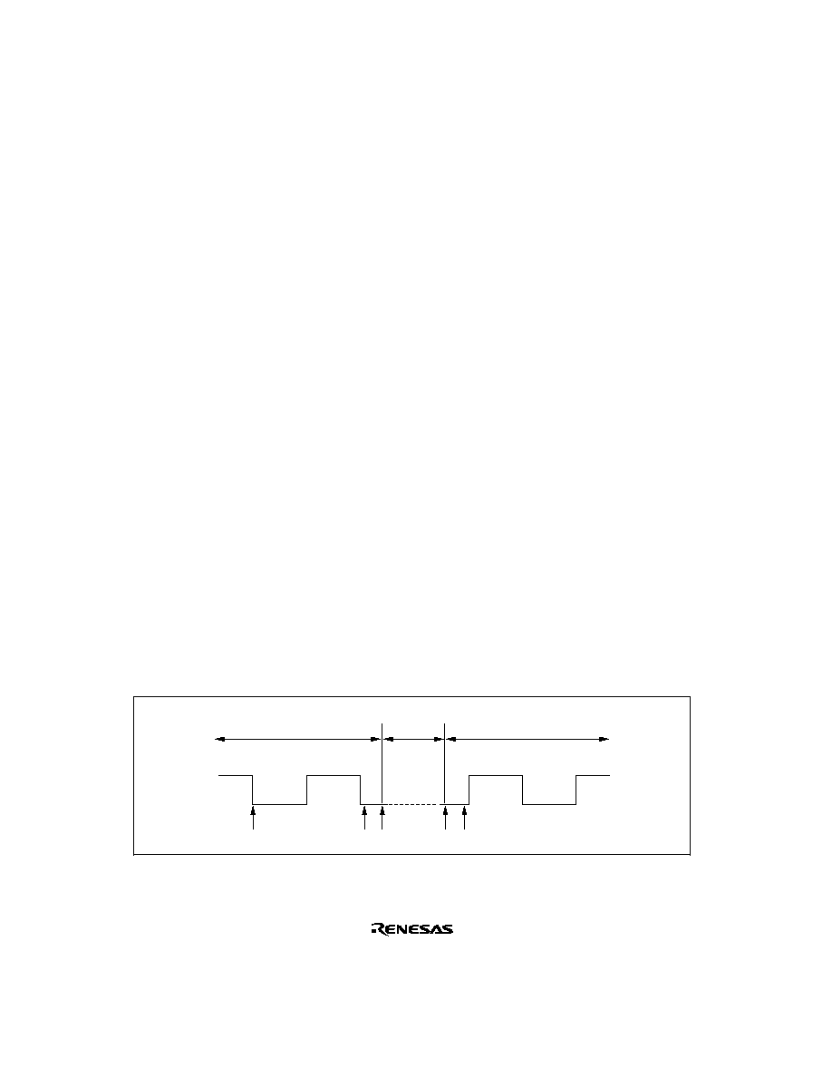
478
13.3.7
Operation in GSM Mode
Switching the Mode: When switching between smart card interface mode and software standby
mode, the following switching procedure should be followed in order to maintain the clock duty.
∑
When changing from smart card interface mode to software standby mode
[1] Set the data register (DR) and data direction register (DDR) corresponding to the SCK pin to
the value for the fixed output state in software standby mode.
[2] Write 0 to the TE bit and RE bit in the serial control register (SCR) to halt transmit/receive
operation. At the same time, set the CKE1 bit to the value for the fixed output state in software
standby mode.
[3] Write 0 to the CKE0 bit in SCR to halt the clock.
[4] Wait for one serial clock period.
During this interval, clock output is fixed at the specified level, with the duty preserved.
[5] Write H'00 to SMR and SCMR.
[6] Make the transition to the software standby state.
∑
When returning to smart card interface mode from software standby mode
[7] Exit the software standby state.
[8] Set the CKE1 bit in SCR to the value for the fixed output state (current SCK pin state) when
software standby mode is initiated.
[9] Set smart card interface mode and output the clock. Signal generation is started with the
normal duty.
[1] [2] [3]
[4] [5] [6]
[7] [8] [9]
Software
standby
Normal operation
Normal operation
Figure 13-9 Clock Halt and Restart Procedure

479
Powering On: To secure the clock duty from power-on, the following switching procedure should
be followed.
[1] The initial state is port input and high impedance. Use a pull-up resistor or pull-down resistor
to fix the potential.
[2] Fix the SCK pin to the specified output level with the CKE1 bit in SCR.
[3] Set SMR and SCMR, and switch to smart card mode operation.
[4] Set the CKE0 bit in SCR to 1 to start clock output.
13.4
Usage Notes
The following points should be noted when using the SCI as a Smart Card interface.
Receive Data Sampling Timing and Reception Margin in Smart Card Interface Mode: In
Smart Card Interface mode, the SCI operates on a basic clock with a frequency of 372 times the
transfer rate.
In reception, the SCI samples the falling edge of the start bit using the basic clock, and performs
internal synchronization. Receive data is latched internally at the rising edge of the 186th pulse of
the basic clock. This is illustrated in figure 13-10.
Internal
basic
clock
372 clocks
186 clocks
Receive
data (RxD)
Synchro-
nization
sampling
timing
D0
D1
Data
sampling
timing
185
371 0
371
185
0
0
Start bit
Figure 13-10 Receive Data Sampling Timing in Smart Card Mode

480
Thus the reception margin in asynchronous mode is given by the following formula.
M =
(0.5 ≠
1
2N
) ≠ (L ≠ 0.5) F ≠
D ≠ 0.5
N
(1 + F
) ◊
100%
Where M: Reception margin (%)
N: Ratio of bit rate to clock (N = 372)
D: Clock duty (D = 0 to 1.0)
L: Frame length (L = 10)
F: Absolute value of clock frequency deviation
Assuming values of F = 0 and D = 0.5 in the above formula, the reception margin formula is as
follows.
When D = 0.5 and F = 0,
M = (0.5 ≠ 1/2
◊
372)
◊
100%
= 49.866%
Retransfer Operations: Retransfer operations are performed by the SCI in receive mode and
transmit mode as described below.
∑
Retransfer operation when SCI is in receive mode
Figure 13-11 illustrates the retransfer operation when the SCI is in receive mode.
[1] If an error is found when the received parity bit is checked, the PER bit in SSR is automatically
set to 1. If the RIE bit in SCR is enabled at this time, an ERI interrupt request is generated. The
PER bit in SSR should be kept cleared to 0 until the next parity bit is sampled.
[2] The RDRF bit in SSR is not set for a frame in which an error has occurred.
[3] If no error is found when the received parity bit is checked, the PER bit in SSR is not set to 1.
[4] If no error is found when the received parity bit is checked, the receive operation is judged to
have been completed normally, and the RDRF flag in SSR is automatically set to 1. If the RIE
bit in SCR is enabled at this time, an RXI interrupt request is generated.
If DTC data transfer by an RXI source is enabled, the contents of RDR can be read
automatically. When the RDR data is read by the DTC, the RDRF flag is automatically cleared
to 0.
[5] When a normal frame is received, the pin retains the high-impedance state at the timing for
error signal transmission.
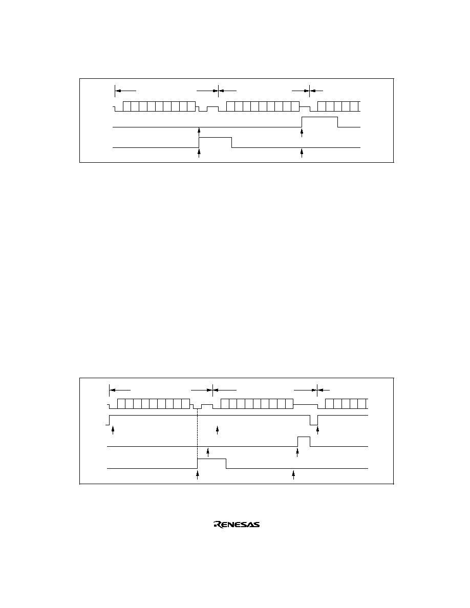
481
D0 D1 D2 D3 D4 D5 D6 D7 Dp DE
Ds D0 D1 D2 D3 D4 D5 D6 D7 Dp
(DE)
Ds D0 D1 D2 D3 D4
Ds
Transfer
frame n+1
Retransferred frame
nth transfer frame
RDRF
[1]
PER
[2]
[3]
[4]
Figure 13-11 Retransfer Operation in SCI Receive Mode
∑
Retransfer operation when SCI is in transmit mode
Figure 13-12 illustrates the retransfer operation when the SCI is in transmit mode.
[6] If an error signal is sent back from the receiving end after transmission of one frame is
completed, the ERS bit in SSR is set to 1. If the RIE bit in SCR is enabled at this time, an ERI
interrupt request is generated. The ERS bit in SSR should be kept cleared to 0 until the next
parity bit is sampled.
[7] The TEND bit in SSR is not set for a frame for which an error signal indicating an abnormality
is received.
[8] If an error signal is not sent back from the receiving end, the ERS bit in SSR is not set.
[9] If an error signal is not sent back from the receiving end, transmission of one frame, including
a retransfer, is judged to have been completed, and the TEND bit in SSR is set to 1. If the TIE
bit in SCR is enabled at this time, a TXI interrupt request is generated.
If data transfer by the DTC by means of the TXI source is enabled, the next data can be written
to TDR automatically. When data is written to TDR by the DTC, the TDRE bit is
automatically cleared to 0.
D0 D1 D2 D3 D4 D5 D6 D7 Dp DE
Ds D0 D1 D2 D3 D4 D5 D6 D7 Dp
(DE)
Ds D0 D1 D2 D3 D4
Ds
Transfer
frame n+1
Retransferred frame
nth transfer frame
TDRE
TEND
[6]
FER/ERS
Transfer to TSR from TDR
[7]
[9]
[8]
Transfer to TSR from TDR
Transfer to TSR
from TDR
Figure 13-12 Retransfer Operation in SCI Transmit Mode

483
Section 14 A/D Converter
14.1
Overview
The H8/2245 Series incorporates a successive approximation type 10-bit A/D converter that
allows up to four analog input channels to be selected.
14.1.1
Features
A/D converter features are listed below
∑
10-bit resolution
∑
Four input channels
∑
Settable analog conversion voltage range
Conversion of analog voltages with the reference voltage pin (V
ref
) as the analog reference
voltage
∑
High-speed conversion
Minimum conversion time: 6.7 µs per channel (at 20 MHz operation)
∑
Choice of single mode or scan mode
Single mode: Single-channel A/D conversion
Scan mode:
Continuous A/D conversion on 1 to 4 channels
∑
Four data registers
Conversion results are held in a 16-bit data register for each channel
∑
Sample and hold function
∑
Three kinds of conversion start
Choice of software or timer conversion start trigger (TPU or 8-bit timer), or
ADTRG pin
∑
A/D conversion end interrupt generation
A/D conversion end interrupt (ADI) request can be generated at the end of A/D conversion
∑
Module stop mode can be set
As the initial setting, A/D converter operation is halted. Register access is enabled by
exiting module stop mode.
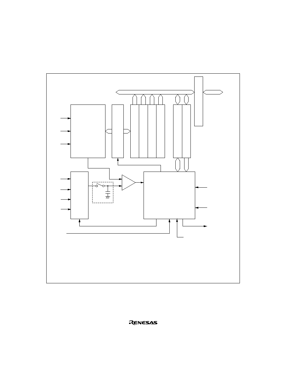
484
14.1.2
Block Diagram
Figure 14-1 shows a block diagram of the A/D converter.
Module data bus
Control circuit
Internal data bus
10-bit D/A
Comparator
+
≠
Sample-and-
hold circuit
¯/8
¯/16
ADI
interrupt
Bus interface
A
D
C
S
R
A
D
C
R
A
D
D
R
D
A
D
D
R
C
A
D
D
R
B
A
D
D
R
A
AV
CC
V
ref
AV
SS
AN0
AN1
AN2
AN3
ADTRG
Conversion start
trigger from 8-bit
timer or TPU
Successive approximations
register
Multiplexer
ADCR
ADCSR
ADDRA
ADDRB
ADDRC
ADDRD
: A/D control register
: A/D control/status register
: A/D data register A
: A/D data register B
: A/D data register C
: A/D data register D
Figure 14-1 Block Diagram of A/D Converter

485
14.1.3
Pin Configuration
Table 14-1 summarizes the input pins used by the A/D converter.
The AV
CC
and AV
SS
pins are the power supply pins for the analog block in the A/D converter. The
V
ref
pin is the A/D conversion reference voltage pin.
Table 14-1 A/D Converter Pins
Pin Name
Symbol
I/O
Function
Analog power supply pin
AV
CC
Input
Analog block power supply
Analog ground pin
AV
SS
Input
Analog block ground and A/D conversion
reference voltage
Reference voltage pin
V
ref
Input
A/D conversion reference voltage
Analog input pin 0
AN0
Input
Analog input channel 0
Analog input pin 1
AN1
Input
Analog input channel 1
Analog input pin 2
AN2
Input
Analog input channel 2
Analog input pin 3
AN3
Input
Analog input channel 3
A/D external trigger input pin
ADTRG
Input
External trigger input for starting A/D
conversion

486
14.1.4
Register Configuration
Table 14-2 summarizes the registers of the A/D converter.
Table 14-2 A/D Converter Registers
Name
Abbreviation
R/W
Initial Value
Address
*
1
A/D data register AH
ADDRAH
R
H'00
H'FF90
A/D data register AL
ADDRAL
R
H'00
H'FF91
A/D data register BH
ADDRBH
R
H'00
H'FF92
A/D data register BL
ADDRBL
R
H'00
H'FF93
A/D data register CH
ADDRCH
R
H'00
H'FF94
A/D data register CL
ADDRCL
R
H'00
H'FF95
A/D data register DH
ADDRDH
R
H'00
H'FF96
A/D data register DL
ADDRDL
R
H'00
H'FF97
A/D control/status register
ADCSR
R/(W)
*
2
H'00
H'FF98
A/D control register
ADCR
R/W
H'3F
H'FF99
Module stop control register
MSTPCR
R/W
H'3FFF
H'FF3C
Notes: 1. Lower 16 bits of the address.
2. Bit 7 can only be written with 0 for flag clearing.

487
14.2
Register Descriptions
14.2.1
A/D Data Registers A to D (ADDRA to ADDRD)
15
AD9
0
R
Bit
Initial value
R/W
:
:
:
14
AD8
0
R
13
AD7
0
R
12
AD6
0
R
11
AD5
0
R
10
AD4
0
R
9
AD3
0
R
8
AD2
0
R
7
AD1
0
R
6
AD0
0
R
5
--
0
R
4
--
0
R
3
--
0
R
2
--
0
R
1
--
0
R
0
--
0
R
There are four 16-bit read-only ADDR registers, ADDRA to ADDRD, used to store the results of
A/D conversion.
The 10-bit data resulting from A/D conversion is transferred to the ADDR register for the selected
channel and stored there. The upper 8 bits of the converted data are transferred to the upper byte
(bits 15 to 8) of ADDR, and the lower 2 bits are transferred to the lower byte (bits 7 and 6) and
stored. Bits 5 to 0 are always read as 0.
The correspondence between the analog input channels and ADDR registers is shown in table 14-
3.
ADDR can always be read by the CPU. The upper byte can be read directly, but for the lower
byte, data transfer is performed via a temporary register (TEMP). For details, see section 14.3,
Interface to Bus Master.
The ADDR registers are initialized to H'0000 by a reset, and in standby mode or module stop
mode.
Table 14-3 Analog Input Channels and Corresponding ADDR Registers
Analog Input Channel
A/D Data Register
AN0
ADDRA
AN1
ADDRB
AN2
ADDRC
AN3
ADDRD

488
14.2.2
A/D Control/Status Register (ADCSR)
7
ADF
0
R/(W)
*
6
ADIE
0
R/W
5
ADST
0
R/W
4
SCAN
0
R/W
3
CKS
0
R/W
0
CH0
0
R/W
2
--
0
R/W
1
CH1
0
R/W
Bit
Initial value
R/W
:
:
:
Note:
*
Only 0 can be written to bit 7, to clear this flag.
ADCSR is an 8-bit readable/writable register that controls A/D conversion operations and shows
the status of the operation.
ADCSR is initialized to H'00 by a reset, and in hardware standby mode or module stop mode.
Bit 7--A/D End Flag (ADF): Status flag that indicates the end of A/D conversion.
Bit 7
ADF
Description
0
[Clearing conditions]
(Initial value)
∑
When 0 is written to the ADF flag after reading ADF = 1
∑
When the DTC is activated by an ADI interrupt and ADDR is read
1
[Setting conditions]
∑
Single mode: When A/D conversion ends
∑
Scan mode: When A/D conversion ends on all specified channels
Bit 6--A/D Interrupt Enable (ADIE): Selects enabling or disabling of interrupt (ADI) requests
at the end of A/D conversion.
Bit 6
ADIE
Description
0
A/D conversion end interrupt (ADI) request disabled
(Initial value)
1
A/D conversion end interrupt (ADI) request enabled

489
Bit 5--A/D Start (ADST): Selects starting or stopping on A/D conversion. Holds a value of 1
during A/D conversion.
The ADST bit can be set to 1 by software, a timer conversion start trigger, or the A/D external
trigger input pin (
ADTRG).
Bit 5
ADST
Description
0
∑
A/D conversion stopped
(Initial value)
1
∑
Single mode: A/D conversion is started. Cleared to 0 automatically when
conversion on the specified channel ends
∑
Scan mode: A/D conversion is started. Conversion continues sequentially on the
selected channels until ADST is cleared to 0 by software, a reset, or
a transition to standby mode or module stop mode.
Bit 4--Scan Mode (SCAN): Selects single mode or scan mode as the A/D conversion operating
mode. See section 14.4, Operation, for single mode and scan mode operation. Only set the SCAN
bit while conversion is stopped (ADST = 0).
Bit 4
SCAN
Description
0
Single mode
(Initial value)
1
Scan mode
Bit 3--Clock Select (CKS): Sets the A/D conversion time. Only change the conversion time
while conversion is stopped (ADST = 0).
Bit 3
CKS
Description
0
Conversion time = 266 states (max.)
(Initial value)
1
Conversion time = 134 states (max.)
Bit 2--Reserved: This bit can be read or written, but should only be written with 0.

490
Bits 1 to 0--Channel Select 1 and 0 (CH1, CH0): Together with the SCAN bit, these bits select
the analog input channel(s).
Only set the input channel while conversion is stopped.
Bit 1
Bit 0
Description
CH1
CH0
Single Mode (SCAN = 0)
Scan Mode (SCAN = 1)
0
0
AN0
(Initial value)
AN0
1
AN1
AN0, AN1
1
0
AN2
AN0 to AN2
1
AN3
AN0 to AN3
14.2.3
A/D Control Register (ADCR)
7
TRGS1
0
R/W
6
TRGS0
0
R/W
5
--
1
--
4
--
1
--
3
--
1
--
0
--
1
--
2
--
1
--
1
--
1
--
Bit
Initial value
R/W
:
:
:
ADCR is an 8-bit readable/writable register that enables or disables external triggering of A/D
conversion operations.
ADCR is initialized to H'3F by a reset, and in hardware standby mode or module stop mode.
Bits 7 and 6--Timer Trigger Select 1 and 0 (TRGS1, TRGS0): Select enabling or disabling of
the start of A/D conversion by a trigger signal. Only set bits TRGS1 and TRGS0 while conversion
is stopped.
Bit 7
Bit 6
TRGS1
TRGS0
Description
0
0
Start of A/D conversion by external trigger is disabled
(Initial value)
1
Start of A/D conversion by external trigger (TPU) is enabled
1
0
Start of A/D conversion by external trigger (8-bit timer) is enabled
1
Start of A/D conversion by external trigger pin is enabled
Bits 5 to 0--Reserved: These bits are reserved; they are always read as 1 and cannot be
modified.

491
14.2.4
Module Stop Control Register (MSTPCR)
15
0
R/W
Bit
Initial value
R/W
:
:
:
14
0
R/W
13
1
R/W
12
1
R/W
11
1
R/W
10
1
R/W
9
1
R/W
8
1
R/W
7
1
R/W
6
1
R/W
5
1
R/W
4
1
R/W
3
1
R/W
2
1
R/W
1
1
R/W
0
1
R/W
MSTPCRH
MSTPCRL
MSTPCR is a 16-bit readable/writable register that performs module stop mode control.
When the MSTP9 bit in MSTPCR is set to 1, A/D converter operation stops at the end of the bus
cycle and a transition is made to module stop mode. Registers cannot be read or written to in
module stop mode. For details, see section 18.5, Module Stop Mode.
MSTPCR is initialized to H'3FFF by a reset and in hardware standby mode. It is not initialized in
software standby mode.
Bit 9--Module Stop (MSTP9): Specifies the A/D converter module stop mode.
Bit 9
MSTP9
Description
0
A/D converter module stop mode cleared
1
A/D converter module stop mode set
(Initial value)

492
14.3
Interface to Bus Master
ADDRA to ADDRD are 16-bit registers, and the data bus to the bus master is 8 bits wide.
Therefore, in accesses by the bus master, the upper byte is accessed directly, but the lower byte is
accessed via a temporary register (TEMP).
A data read from ADDR is performed as follows. When the upper byte is read, the upper byte
value is transferred to the CPU and the lower byte value is transferred to TEMP. Next, when the
lower byte is read, the TEMP contents are transferred to the CPU.
When reading ADDR. always read the upper byte before the lower byte. It is possible to read only
the upper byte, but if only the lower byte is read, incorrect data may be obtained.
Figure 14-2 shows the data flow for ADDR access.
Bus master
(H'AA)
ADDRnH
(H'AA)
ADDRnL
(H'40)
Lower byte read
ADDRnH
(H'AA)
ADDRnL
(H'40)
TEMP
(H'40)
TEMP
(H'40)
(n = A to D)
(n = A to D)
Module data bus
Module data bus
Bus interface
Upper byte read
Bus master
(H'40)
Bus interface
Figure 14-2 ADDR Access Operation (Reading H'AA40)

493
14.4
Operation
The A/D converter operates by successive approximation with 10-bit resolution. It has two
operating modes: single mode and scan mode.
14.4.1
Single Mode (SCAN = 0)
Single mode is selected when A/D conversion is to be performed on a single channel only. A/D
conversion is started when the ADST bit is set to 1, according to the software or external trigger
input. The ADST bit remains set to 1 during A/D conversion, and is automatically cleared to 0
when conversion ends.
On completion of conversion, the ADF flag is set to 1. If the ADIE bit is set to 1 at this time, an
ADI interrupt request is generated. The ADF flag is cleared by writing 0 after reading ADCSR.
When the operating mode or analog input channel must be changed during analog conversion, to
prevent incorrect operation, first clear the ADST bit to 0 in ADCSR to halt A/D conversion. After
making the necessary changes, set the ADST bit to 1 to start A/D conversion again. The ADST bit
can be set at the same time as the operating mode or input channel is changed.
Typical operations when channel 1 (AN1) is selected in single mode are described next. Figure
14-3 shows a timing diagram for this example.
[1] Single mode is selected (SCAN = 0), input channel AN1 is selected (CH1 = 0, CH0 = 1), the
A/D interrupt is enabled (ADIE = 1), and A/D conversion is started (ADST = 1).
[2] When A/D conversion is completed, the result is transferred to ADDRB. At the same time the
ADF flag is set to 1, the ADST bit is cleared to 0, and the A/D converter becomes idle.
[3] Since ADF = 1 and ADIE = 1, an ADI interrupt is requested.
[4] The A/D interrupt handling routine starts.
[5] The routine reads ADCSR, then writes 0 to the ADF flag.
[6] The routine reads and processes the connection result (ADDRB).
[7] Execution of the A/D interrupt handling routine ends. After that, if the ADST bit is set to 1,
A/D conversion starts again and steps [2] to [7] are repeated.

494
ADIE
ADST
ADF
State of channel 0 (AN0)
A/D
conversion
starts
2
1
ADDRA
ADDRB
ADDRC
ADDRD
State of channel 1 (AN1)
State of channel 2 (AN2)
State of channel 3 (AN3)
Note:
*
Vertical arrows ( ) indicate instructions executed by software.
Set
*
Set
*
Clear
*
Clear
*
A/D conversion result 1
A/D conversion
A/D conversion result 2
Read conversion result
Read conversion result
Idle
Idle
Idle
Idle
Idle
Idle
A/D conversion
Set
*
Figure 14-3 Example of A/D Converter Operation (Single Mode, Channel 1 Selected)

495
14.4.2
Scan Mode (SCAN = 1)
Scan mode is useful for monitoring analog inputs in a group of one or more channels. When the
ADST bit is set to 1 by a software, timer or external trigger input, A/D conversion starts on the
first channel in the group (AN0). When two or more channels are selected, after conversion of the
first channel ends, conversion of the second channel (AN1) starts immediately. A/D conversion
continues cyclically on the selected channels until the ADST bit is cleared to 0. The conversion
results are transferred for storage into the ADDR registers corresponding to the channels.
When the operating mode or analog input channel must be changed during analog conversion, to
prevent incorrect operation, first clear the ADST bit to 0 in ADCSR to halt A/D conversion. After
making the necessary changes, set the ADST bit to 1 to start A/D conversion again. The ADST bit
can be set at the same time as the operating mode or input channel is changed.
Typical operations when three channels (AN0 to AN2) are selected in scan mode are described
next. Figure 14-4 shows a timing diagram for this example.
[1] Scan mode is selected (SCAN = 1), analog input channels AN0 to AN2 are selected (CH1 = 1,
CH0 = 0), and A/D conversion is started (ADST = 1)
[2] When A/D conversion of the first channel (AN0) is completed, the result is transferred to
ADDRA. Next, conversion of the second channel (AN1) starts automatically.
[3] Conversion proceeds in the same way through the third channel (AN2).
[4] When conversion of all the selected channels (AN0 to AN2) is completed, the ADF flag is set
to 1 and conversion of the first channel (AN0) starts again. If the ADIE bit is set to 1 at this
time, an ADI interrupt is requested after A/D conversion ends.
[5] Steps [2] to [4] are repeated as long as the ADST bit remains set to 1. When the ADST bit is
cleared to 0, A/D conversion stops. After that, if the ADST bit is set to 1, A/D conversion
starts again from the first channel (AN0).
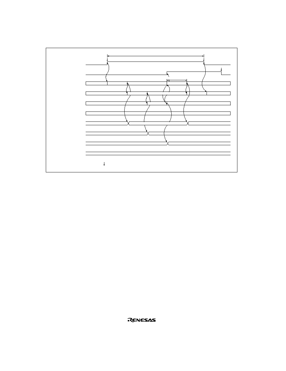
496
ADST
ADF
ADDRA
ADDRB
ADDRC
ADDRD
State of channel 0 (AN0)
State of channel 1 (AN1)
State of channel 2 (AN2)
State of channel 3 (AN3)
Set
*
1
Clear
*
1
Idle
Notes: 1. Vertical arrows ( ) indicate instructions executed by software.
2. Data currently being converted is ignored.
Clear
*
1
Idle
Idle
A/D conversion time
Idle
Continuous A/D conversion execution
A/D conversion 1
Idle
Idle
Idle
Idle
Idle
Transfer
*
2
A/D conversion 3
A/D conversion 2
A/D conversion 5
A/D conversion 4
A/D conversion result 1
A/D conversion result 2
A/D conversion result 3
A/D conversion result 4
Figure 14-4 Example of A/D Converter Operation
(Scan Mode, Channels AN0 to AN2 Selected)
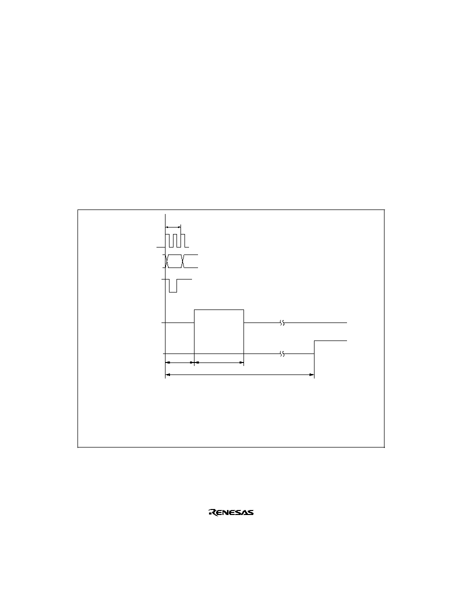
497
14.4.3
Input Sampling and A/D Conversion Time
The A/D converter has a built-in sample-and-hold circuit. The A/D converter samples the analog
input at a time t
D
after the ADST bit is set to 1, then starts conversion. Figure 14-5 shows the A/D
conversion timing. Table 14-4 indicates the A/D conversion time.
As indicated in figure 14-5, the A/D conversion time includes t
D
and the input sampling time. The
length of t
D
varies depending on the timing of the write access to ADCSR. The total conversion
time therefore varies within the ranges indicated in table 14-4.
In scan mode, the values given in table 14-4 apply to the first conversion time. In the second and
subsequent conversions the conversion time is fixed at 256 states when CKS = 0 or 128 states
when CKS = 1.
(1)
(2)
t
D
t
SPL
t
CONV
¯
Input sampling
timing
ADF
Address bus
Write signal
Legend
(1)
: ADCSR write cycle
(2)
: ADCSR address
t
D
: A/D conversion start delay
t
SPL
: Input sampling time
t
CONV
: A/D conversion time
Figure 14-5 A/D Conversion Timing

498
Table 14-4 A/D Conversion Time (Single Mode)
CKS = 0
CKS = 1
Item
Symbol
Min
Typ
Max
Min
Typ
Max
A/D conversion start delay
t
D
10
--
17
6
--
9
Input sampling time
t
SPL
--
63
--
--
31
--
A/D conversion time
t
CONV
259
--
266
131
--
134
Note:
Values in the table are the number of states.
14.4.4
External Trigger Input Timing
A/D conversion can be externally triggered. When the TRGS1 and TRGS0 bits are set to 11 in
ADCR, external trigger input is enabled at the
ADTRG pin. A falling edge at the ADTRG pin sets
the ADST bit to 1 in ADCSR, starting A/D conversion. Other operations, in both single and scan
modes, are the same as if the ADST bit has been set to 1 by software. Figure 14-6 shows the
timing.
¯
ADTRG
Internal trigger signal
ADST
A/D conversion
Figure 14-6 External Trigger Input Timing

499
14.5
Interrupts
The A/D converter generates an interrupt (ADI) at the end of A/D conversion. The ADI interrupt
request can be enabled or disabled by the ADIE bit in ADCSR.
The DTC can be activated by an ADI interrupt. Having the converted data read by the DTC in
response to an ADI interrupt enables continuous conversion to be achieved without imposing a
load on software.
The A/D converter interrupt source is shown in table 14-5.
Table 14-5 A/D Converter Interrupt Source
Interrupt Source
Description
DTC Activation
ADI
Interrupt due to end of conversion
Possible
14.6
Usage Notes
The following points should be noted when using the A/D converter.
Setting Range of Analog Power Supply and Other Pins:
(1) Analog input voltage range
The voltage applied to analog input pins AN0 to AN3 during A/D conversion should be in the
range AV
SS
ANn
AV
ref
.
(2) Relation between AV
CC
, AV
SS
and V
CC
, V
SS
As the relationship between AV
CC
, AV
SS
and V
CC
, V
SS
, set AV
SS
= V
SS
. If the A/D converter is
not used, the AV
CC
and AV
SS
pins must on no account be left open.
(3) V
ref
input range
The analog reference voltage input at the V
ref
pin set in the range V
ref
AV
CC
.
Note:
If conditions (1), (2), and (3) above are not met, the reliability of the device may be
adversely affected.
Notes on Board Design: In board design, digital circuitry and analog circuitry should be as
mutually isolated as possible, and layout in which digital circuit signal lines and analog circuit
signal lines cross or are in close proximity should be avoided as far as possible. Failure to do so
may result in incorrect operation of the analog circuitry due to inductance, adversely affecting A/D
conversion values.
Also, digital circuitry must be isolated from the analog input signals (AN0 to AN3), analog
reference power supply (V
ref
), and analog power supply (AV
CC
) by the analog ground (AV
SS
).

500
Also, the analog ground (AV
SS
) should be connected at one point to a stable digital ground (V
SS
)
on the board.
Notes on Noise Countermeasures: A protection circuit connected to prevent damage due to an
abnormal voltage such as an excessive surge at the analog input pins (AN0 to AN3) and analog
reference power supply (V
ref
) should be connected between AV
CC
and AV
SS
as shown in figure
14-7.
Also, the bypass capacitors connected to AV
CC
and V
ref
and the filter capacitor connected to AN0
to AN3 must be connected to AV
SS
.
If a filter capacitor is connected as shown in figure 14-7, the input currents at the analog input pins
(AN0 to AN3) are averaged, and so an error may arise. Also, when A/D conversion is performed
frequently, as in scan mode, if the current charged and discharged by the capacitance of the
sample-and-hold circuit in the A/D converter exceeds the current input via the input impedance
(R
in
), an error will arise in the analog input pin voltage. Careful consideration is therefore required
when deciding the circuit constants.
AV
CC
*
1
*
1
V
ref
AN0 to AN3
AV
SS
Notes:
Values are reference values.
1.
2. R
in
: Input impedance
R
in
*
2
100
0.1
µ
F
0.01
µ
F
10
µ
F
Figure 14-7 Example of Analog Input Protection Circuit

501
Table 14-6 Analog Pin Specifications
Item
Min
Max
Unit
Analog input capacitance
--
20
pF
Permissible signal source impedance
--
10
*
k
Note:
*
When V
CC
= 4.0 V to 5.5 V and ¯
12 MHz
20 pF
To A/D
converter
AN0 to
AN3
10 k
Note: Values are reference values.
Figure 14-8 Analog Input Pin Equivalent Circuit
A/D Conversion Precision Definitions: H8S/2245 Series A/D conversion precision definitions
are given below.
∑
Resolution
The number of A/D converter digital output codes
∑
Offset error
The deviation of the analog input voltage value from the ideal A/D conversion characteristic
when the digital output changes from the minimum voltage value B'0000000000 (H'000) to
B'0000000001 (H'001) (see figure 14-10).
∑
Full-scale error
The deviation of the analog input voltage value from the ideal A/D conversion characteristic
when the digital output changes from B'1111111110 (H'3FE) to B'1111111111 (H'3FF) (see
figure 14-10).
∑
Quantization error
The deviation inherent in the A/D converter, given by 1/2 LSB (see figure 14-9).
∑
Nonlinearity error
The error with respect to the ideal A/D conversion characteristic between the zero voltage and
the full-scale voltage. Does not include the offset error, full-scale error, or quantization error.
∑
Absolute precision
The deviation between the digital value and the analog input value. Includes the offset error,
full-scale error, quantization error, and nonlinearity error.
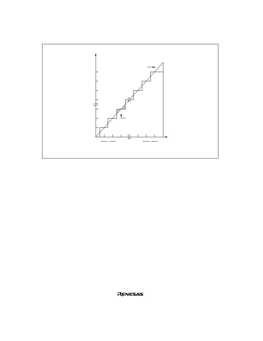
502
H'3FF
H'3FE
H'001
H'000
FS
Quantization error
Digital output
Ideal A/D conversion
characteristic
Analog
input voltage
1
1024
2
1024
1022
1024
1023
1024
Figure 14-9 A/D Conversion Precision Definitions (1)

503
FS
Offset error
Nonlinearity
error
Actual A/D conversion
characteristic
Analog
input voltage
Digital output
Ideal A/D conversion
characteristic
Full-scale error
Figure 14-10 A/D Conversion Precision Definitions (2)
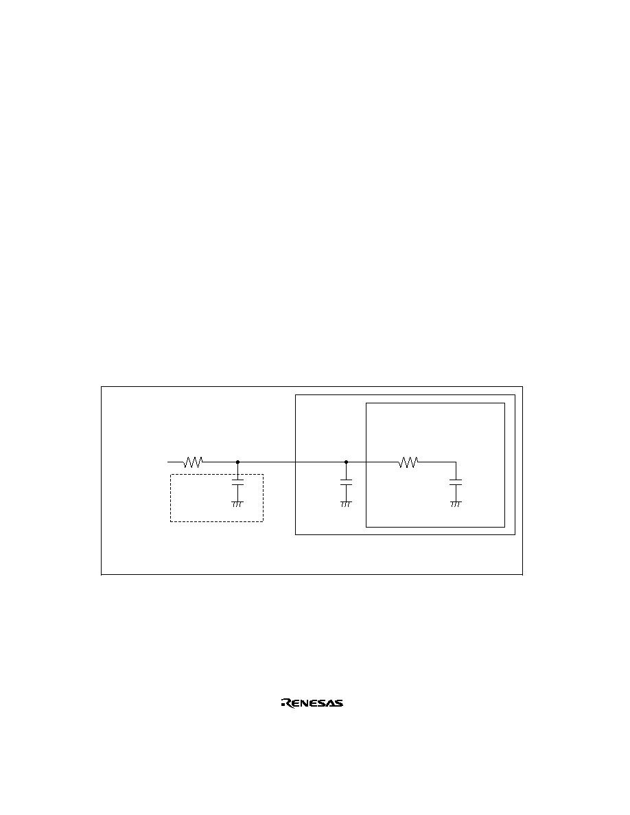
504
Permissible Signal Source Impedance: H8S/2245 Series analog input is designed so that
conversion precision is guaranteed for an input signal for which the signal source impedance is 10
k
or less. This specification is provided to enable the A/D converter's sample-and-hold circuit
input capacitance to be charged within the sampling time; if the sensor output impedance exceeds
10 k
, charging may be insufficient and it may not be possible to guarantee the A/D conversion
precision.
However, if a large capacitance is provided externally, the input load will essentially comprise
only the internal input resistance of 10 k
, and the signal source impedance is ignored.
However, since a low-pass filter effect is obtained in this case, it may not be possible to follow an
analog signal with a large differential coefficient (e.g., 5 mV/µsec or greater).
When converting a high-speed analog signal, a low-impedance buffer should be inserted.
Influences on Absolute Precision: Adding capacitance results in coupling with GND, and
therefore noise in GND may adversely affect absolute precision. Be sure to make the connection
to an electrically stable GND such as AV
SS
.
Care is also required to insure that filter circuits do not communicate with digital signals on the
mounting board, so acting as antennas.
A/D converter
equivalent circuit
H8/2245 Series
20 pF
C
in
=
15 pF
10 k
to 10 k
Low-pass
filter
C to 0.1
µ
F
Sensor output
impedance
Sensor input
Note: Values are reference values.
Figure 14-11 Example of Analog Input Circuit

505
Section 15 RAM
15.1
Overview
The H8S/2246, H8S/2244, and H8S/2242 have 8 kbytes of on-chip high-speed static RAM, and
the H8S/2245, H8S/2243, H8S/2241, and H8S/2240 have 4 kbytes. The on-chip RAM is
connected to the CPU by a 16-bit data bus, enabling both byte data and word data to be accessed
in one state. This makes it possible to perform fast word data transfer.
The on-chip RAM on the H8S/2246, H8S/2244, and H8S/2242 is located in addresses H'E400 to
H'FBFF (6 kbytes) in normal mode (modes 1 to 3), and in addresses H'FFDC00 to H'FFFBFF (8
kbytes) in advanced mode (modes 4 to 7).
The on-chip RAM on the H8S/2245, H8S/2243, H8S/2241, and H8S/2240 is located in addresses
H'EC00 to H'FBFF (4 kbytes) in normal mode (modes 1 to 3), and in addresses H'FFEC00 to
H'FFFBFF (4 kbytes) in advanced mode (modes 4 to 7).
The on-chip RAM can be enabled or disabled by means of the RAM enable bit (RAME) in the
system control register (SYSCR).

506
15.1.1
Block Diagram
Figure 15-1 shows a block diagram of the on-chip RAM.
Internal data bus (upper 8 bits)
Internal data bus (lower 8 bits)
H'FFDC00
H'FFDC02
H'FFDC04
H'FFFBFE
H'FFDC01
H'FFDC03
H'FFDC05
H'FFFBFF
Figure 15-1 Block Diagram of RAM (Example with H8S/2246 in Advanced Mode)
15.1.2
Register Configuration
The on-chip RAM is controlled by SYSCR. Table 15-1 shows the register configuration.
Table 15-1 Register Configuration
Name
Abbreviation
R/W
Initial Value
Address
*
System control register
SYSCR
R/W
H'01
H'FF39
Note:
*
Lower 16 bits of the address.

507
15.2
Register Descriptions
15.2.1
System Control Register (SYSCR)
7
--
0
--
6
--
0
--
5
INTM1
0
R/W
4
INTM0
0
R/W
3
NMIEG
0
R/W
0
RAME
1
R/W
2
--
0
--
1
--
0
--
Bit
Initial value
R/W
:
:
:
The on-chip RAM is enabled or disabled by the RAME bit in SYSCR. For details of other bits in
SYSCR, see section 3.2.2, System Control Register (SYSCR).
Bit 0--RAM Enable (RAME): Enables or disables the on-chip RAM. The RAME bit is
initialized when the reset state is released. It is not initialized in software standby mode.
Bit 0
RAME
Description
0
On-chip RAM is disabled
1
On-chip RAM is enabled
(Initial value)
Note:
Do not clear the RAME bit to 0 when the DTC is used.
15.3
Operation
When the RAME bit is set to 1, accesses to H8S/2246, H8S/2244, and H8S/2242 addresses
H'FFDC00 to H'FFFBFF, and H8S/2245, H8S/2243, H8S/2241, and H8S/2240 addresses
H'FFEC00 to H'FFFBFF, are directed to the on-chip RAM. When the RAME bit is cleared to 0,
the off-chip address space is accessed.
Since the on-chip RAM is connected to the CPU by an internal 16-bit data bus, it can be written to
and read in byte or word units. Each type of access can be performed in one state.
Even addresses use the upper 8 bits, and odd addresses use the lower 8 bits. Word data must start
at an even address.

509
Section 16 ROM
16.1
Overview
The H8S/2246 and H8S/2245 have 128 kbytes of on-chip ROM (PROM or mask ROM). The
H8S/2244 and H8S/2243 have 64 kbytes of on-chip ROM (mask ROM). The H8S/2242 and
H8S/2241 have 32 kbytes of on-chip ROM (mask ROM). The ROM is connected to the CPU by a
16-bit data bus. The CPU accesses both byte data and word data in one state, making possible
rapid instruction fetches and high-speed processing.
The on-chip ROM is enabled or disabled by setting the mode pins (MD
2
, MD
1
, and MD
0
) and bit
EAE in BCRL.
The PROM version of the H8S/2245 Series (H8S/2246) can be programmed with a general-
purpose PROM programmer, by setting PROM mode.

510
16.1.1
Block Diagram
Figure 16-1 shows a block diagram of the on-chip ROM.
Internal data bus (upper 8 bits)
Internal data bus (lower 8 bits)
H'000000
H'000002
H'01FFFE
H'000001
H'000003
H'01FFFF
H'00FFFE
H'010000
H'010002
H'00FFFF
H'010001
H'010003
When EAE= 0
Figure 16-1 Block Diagram of ROM (Example with H8S/2246 in Modes 6, 7)
16.1.2
Register Configuration
The on-chip ROM is controlled by BCRL. The register configuration is shown in table 16-1.
Table 16-1 Register Configuration
Initial Value
Name
Abbreviation
R/W
Power-On Reset
Manual Reset
Address
*
Bus control register L
BCRL
R/W
H'3C
Retained
H'FED5
Note:
*
Lower 16 bits of the address.

511
16.2
Register Descriptions
16.2.1
Bus Control Register L (BCRL)
7
BRLE
0
R/W
6
BREQOE
0
R/W
5
EAE
1
R/W
4
--
1
R/W
3
--
1
R/W
0
WAITE
0
R/W
2
ASS
1
R/W
1
--
0
R/W
Bit
Initial value
R/W
:
:
:
BCRL is an 8-bit readable/writable register that performs selection of the external bus release state
protocol, selection of the area partition unit, and enabling or disabling of
WAIT pin input.
BCRL is initialized to H'3C by a power-on reset and in hardware standby mode. It is not
initialized by a manual reset or in software standby mode.
Enabling or disabling of part of the on-chip ROM area can be selected by means of the EAE bit in
BCRL. For details of the other bits in BCRL, see 6.2.5, Bus Control Register L.
Bit 5--External Address Enable (EAE): Selects whether addresses H'010000 to H'01FFFF are
to be internal addresses or external addresses.
This setting is invalid in normal mode.
Bit 5
EAE
Description
0
Addresses H'010000 to H'01FFFF are in on-chip ROM (in the H8S/2246 and
H8S/2245) or a reserved area (in the H8S/2244, H8S/2243, H8S/2242, and
H8S/2241).
1
Addresses H'010000 to H'01FFFF are external addresses (external expansion mode)
or a reserved area
*
(single-chip mode).
(Initial value)
Note:
*
Reserved areas should not be accessed.

512
16.3
Operation
The on-chip ROM is connected to the CPU by a 16-bit data bus, and both byte and word data can
be accessed in one state. Even addresses are connected to the upper 8 bits, and odd addresses to
the lower 8 bits. Word data must start at an even address.
The on-chip ROM is enabled and disabled by setting the mode pins (MD
2
, MD
1
, and MD
0
) and bit
EAE in BCRL. These settings are shown in table 16-2.
In the H8S/2246, H8S/2245, H8S/2244, and H8S/2243 normal mode, a maximum of 56 kbytes of
ROM can be used.
Table 16-2 Operating Modes and ROM Area
Mode Pin Setting BCRL
On-Chip ROM
Operating Mode
MD
2
MD
1
MD
0
EAE
H8S/2246
and
H8S/2245
H8S/2244
and
H8S/2243
H8S/2242
and
H8S/2241
Mode 1 Normal expanded
mode with on-chip
ROM disabled
0
0
1
--
Disabled
Disabled
Disabled
Mode 2 Normal expanded
mode with on-chip
ROM enabled
1
0
--
Enabled
(56 kbytes)
Enabled
(56 kbytes)
Enabled
(32 kbytes)
Mode 3 Normal single-chip
mode
1
Mode 4 Advanced expanded
mode with on-chip
ROM disabled
1
0
0
--
Disabled
Disabled
Disabled
Mode 5 Advanced expanded
mode with on-chip
ROM disabled
1
Mode 6 Advanced expanded
mode with on-chip
1
0
0
Enabled
(128 kbytes)
Enabled
(64 kbytes)
Enabled
(32 kbytes)
ROM enabled
1
Enabled
(64 kbytes)
Mode 7 Advanced single-chip
mode
1
0
Enabled
(128 kbytes)
1
Enabled
(64 kbytes)
In H8S/2246 and H8S/2245 modes 6 and 7, the on-chip ROM available after a power-on reset is
the 64-kbyte area comprising addresses H'000000 to H'00FFFF.

513
16.4
PROM Mode
16.4.1
PROM Mode Setting
The PROM version of the H8S/2245 Series suspends its microcontroller functions when placed in
PROM mode, enabling the on-chip PROM to be programmed. This programming can be done
with a PROM programmer set up in the same way as for the HN27C101 EPROM (V
PP
= 12.5 V).
Use of a 100-pin/32-pin socket adapter enables programming with a commercial PROM
programmer.
Note that the PROM programmer should not be set to page mode as the H8S/2245 Series does not
support page programming.
Table 16-3 shows how PROM mode is selected.
Table 16-3 Selecting PROM Mode
Pin Names
Setting
MD
2
, MD
1
, MD
0
Low
STBY
PA
2
, PA
1
High
16.4.2
Socket Adapter and Memory Map
Programs can be written and verified by attaching a 100-pin/32-pin socket adapter to the PROM
programmer. Table 16-4 gives ordering information for the socket adapter, and figure 16-2 shows
the wiring of the socket adapter. Figure 16-3 shows the memory map in PROM mode.
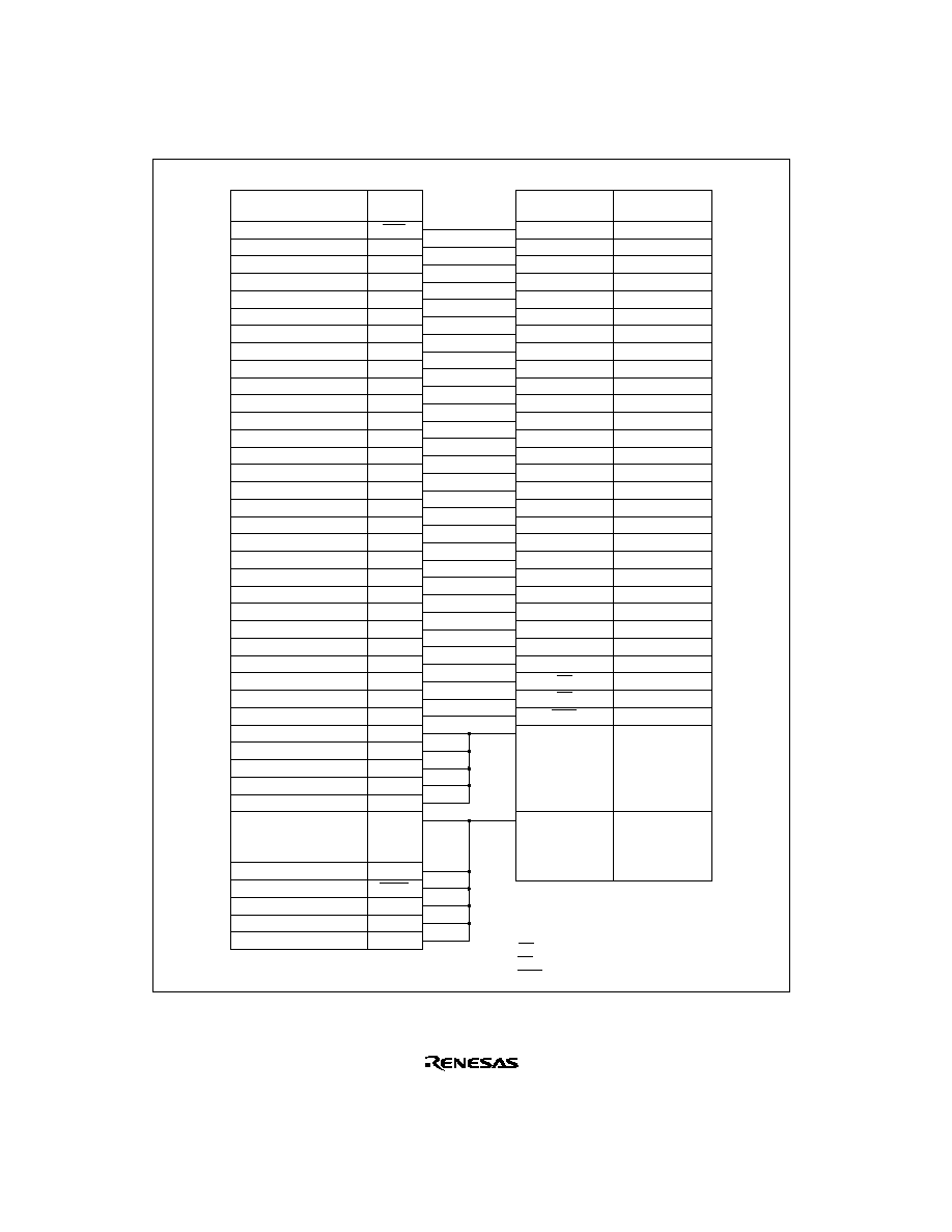
514
FP-100B, TFP-100B
62
23
24
25
26
27
28
29
30
32
33
34
35
36
37
38
39
41
63
43
44
45
46
47
48
50
74
42
75
40, 65, 98
77
78
51
52
7, 18, 31
49, 68, 84
83
64
57
58
61
Pin
RES
PD
0
PD
1
PD
2
PD
3
PD
4
PD
5
PD
6
PD
7
PC
0
PC
1
PC
2
PC
3
PC
4
PC
5
PC
6
PC
7
PB
0
NMI
PB
2
PB
3
PB
4
PB
5
PB
6
PB
7
PA
0
PF
2
PB
1
PF
1
V
CC
AV
CC
V
ref
PA
1
PA
2
V
SS
AV
SS
STBY
MD
0
MD
1
MD
2
1
13
14
15
17
18
19
20
21
12
11
10
9
8
7
6
5
27
26
23
25
4
28
29
3
2
22
24
31
32
16
Pin
V
PP
EO
0
EO
1
EO
2
EO
3
EO
4
EO
5
EO
6
EO
7
EA
0
EA
1
EA
2
EA
3
EA
4
EA
5
EA
6
EA
7
EA
8
EA
9
EA
10
EA
11
EA
12
EA
13
EA
14
EA
15
EA
16
CE
OE
PGM
V
CC
V
SS
H8S/2245 Series
EPROM socket
Note: Pins not shown in this figure should be left open.
V
PP
EO
7
to EO
0
EA
16
to EA
0
OE
CE
PGM
: Programming power
supply (12.5 V)
: Data input/output
: Address input
: Output enable
: Chip enable
: Program
HN27C101
(32 Pins)
Figure 16-2 Wiring of 100-Pin/32-Pin Socket Adapter

515
Table 16-4 Socket Adapter
Microcontroller
Package
Socket Adapter
H8S/2246
100 pin QFP (FP-100B)
HS2245ESHS1H
100 pin TQFP (TFP-100B)
HS2245ESNS1H
On-chip PROM
Addresses in
MCU mode
Addresses in
PROM mode
H'000000
H'01FFFF
H'00000
H'1FFFF
Figure 16-3 Memory Map in PROM Mode

516
16.5
Programming
16.5.1
Overview
Table 16-5 shows how to select the program, verify, and program-inhibit modes in PROM mode.
Table 16-5 Mode Selection in PROM Mode
Pins
Mode
CE
OE
PGM
V
PP
V
CC
EO
7
to EO
0
EA
16
to EA
0
Program
L
H
L
V
PP
V
CC
Data input
Address input
Verify
L
L
H
V
PP
V
CC
Data output
Address input
Program-inhibit
L
L
L
V
PP
V
CC
High impedance
Address input
L
H
H
H
L
L
H
H
H
Legend
L : Low voltage level
H : High voltage level
V
PP
: V
PP
voltage level
V
CC
: V
CC
voltage level
Programming and verification should be carried out using the same specifications as for the
standard HN27C101 EPROM.
However, do not set the PROM programmer to page mode does not support page programming. A
PROM programmer that only supports page programming cannot be used. When choosing a
PROM programmer, check that it supports high-speed programming in byte units. Always set
addresses within the range H'00000 to H'1FFFF.
16.5.2
Programming and Verification
An efficient, high-speed programming procedure can be used to program and verify PROM data.
This procedure writes data quickly without subjecting the chip to voltage stress or sacrificing data
reliability. It leaves the data H'FF in unused addresses. Figure 16-4 shows the basic high-speed
programming flowchart. Tables 16-6 and 16-7 list the electrical characteristics of the chip during
programming. Figure 16-5 shows a timing chart.

517
Start
Set programming/
verification mode
V
CC
= 6.0V
±
0.25V,
V
PP
= 12.5V
±
0.3V
Address = 0
Verification OK?
Yes
No
n = 0
n + 1
n
Program with t
PW
= 0.2 ms
±
5%
Program with t
OPW
= 0.2n ms
Last address?
Set read mode
V
CC
= 5.0 V
±
0.25 V
V
PP
= V
CC
All addresses read?
Yes
No
No
Yes
Go
Address + 1
address
n<25
End
Fail
No go
Figure 16-4 High-Speed Programming Flowchart

518
Table 16-6 DC Characteristics in PROM Mode
(Preliminary)
(When V
CC
= 6.0 V ± 0.25 V, V
PP
= 12.5 V ± 0.3 V, V
SS
= 0 V, T
a
= 25∞C ± 5∞C)
Item
Symbol Min
Typ
Max
Unit
Test
Conditions
Input high voltage
EO
7
to EO
0
, EA
16
to EA
0
,
OE
,
CE
,
PGM
V
IH
2.4
--
V
CC
+ 0.3
V
Input low voltage
EO
7
to EO
0
, EA
16
to EA
0
,
OE
,
CE
,
PGM
V
IL
≠0.3
--
0.8
V
Output high voltage EO
7
to EO
0
V
OH
2.4
--
--
V
I
OH
= ≠200 µA
Output low voltage
EO
7
to EO
0
V
OL
--
--
0.45
V
I
OL
= 1.6 mA
Input leakage
current
EO
7
to EO
0
, EA
16
to EA
0
,
OE
,
CE
,
PGM
| I
IL
|
--
--
2
µA
V
in
=
5.25 V/0.5 V
V
CC
current
I
CC
--
--
40
mA
V
PP
current
I
PP
--
--
40
mA

519
Table 16-7 AC Characteristics in PROM Mode
(Preliminary)
(When V
CC
= 6.0 V ± 0.25 V, V
PP
= 12.5 V ± 0.3 V, T
a
= 25∞C ± 5∞C)
Item
Symbol
Min
Typ
Max
Unit
Test
Conditions
Address setup time
t
AS
2
--
--
µs
Figure 16-5
*
1
OE
setup time
t
OES
2
--
--
µs
Data setup time
t
DS
2
--
--
µs
Address hold time
t
AH
0
--
--
µs
Data hold time
t
DH
2
--
--
µs
Data output disable time
t
DF
*
2
--
--
130
ns
V
PP
setup time
t
VPS
2
--
--
µs
Programming pulse width
t
PW
0.19
0.20
0.21
ms
PGM
pulse width for overwrite programming t
OPW
*
3
0.19
--
5.25
ms
V
CC
setup time
t
VCS
2
--
--
µs
CE
setup time
t
CES
2
--
--
µs
Data output delay time
t
OE
0
--
150
ns
Notes: 1. Input pulse level: 0.8 V to 2.2 V
Input rise time and fall time
20 ns
Timing reference levels; Input: 1.0 V, 2.0 V;
Output: 0.8 V, 2.0 V
2. t
DF
is defined to be when output has reached the open state, and the output level can no
longer be referenced.
3. t
OPW
is defined by the value shown in the flowchart.
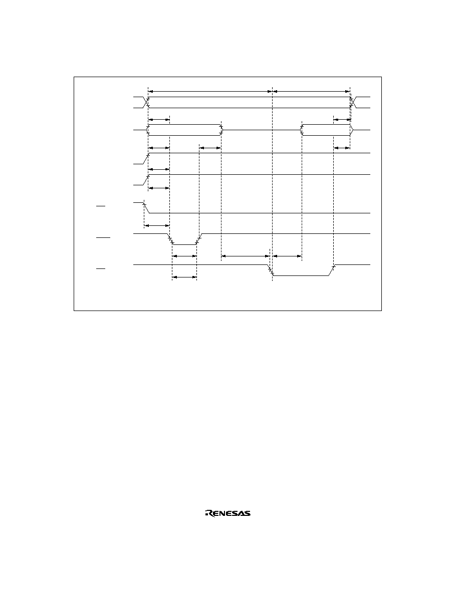
520
Program
Verify
Input data
Output data
t
AS
t
AH
t
DF
t
DH
t
DS
t
VPS
t
VCS
t
CES
t
PW
t
OPW
*
t
OES
t
OE
Address
Data
V
PP
V
CC
CE
PGM
OE
V
PP
V
CC
V
CC
+1
V
CC
Note:
*
t
OPW
is defined by the value shown in the flowchart.
Figure 16-5 PROM Programming/Verification Timing

521
16.5.3
Programming Precautions
∑
Program using the specified voltages and timing.
The programming voltage (V
PP
) in PROM mode is 12.5 V.
If the PROM programmer is set to Hitachi HN27C101 specifications, V
PP
will be 12.5 V.
Applied voltages in excess of the specified values can permanently destroy the MCU. Be
particularly careful about the PROM programmer's overshoot characteristics.
∑
Before programming, check that the MCU is correctly mounted in the PROM programmer.
Overcurrent damage to the MCU can result if the index marks on the PROM programmer,
socket adapter, and MCU are not correctly aligned.
∑
Do not touch the socket adapter or MCU while programming. Touching either of these can
cause contact faults and programming errors.
∑
The MCU cannot be programmed in page programming mode. Select the programming mode
carefully.
∑
The size of the H8S/2246 PROM is 128 kbytes. Always set addresses within the range
H'00000 to H'1FFFF. During programming, write H'FF to unused addresses to avoid
verification errors.
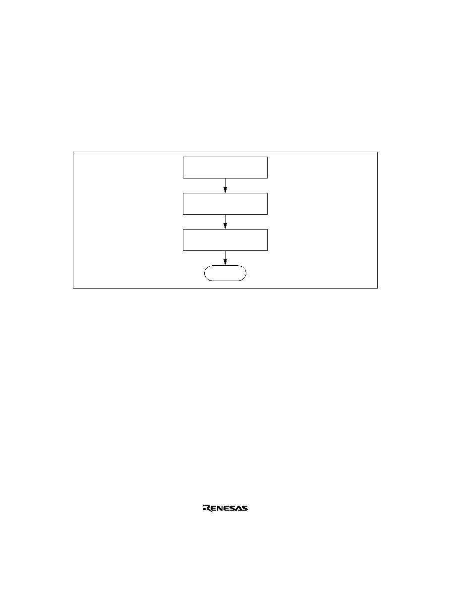
522
16.5.4
Reliability of Programmed Data
An effective way to assure the data retention characteristics of the programmed chips is to bake
them at 150∞C, then screen them for data errors. This procedure quickly eliminates chips with
PROM memory cells prone to early failure.
Figure 16-6 shows the recommended screening procedure.
Mount
Program chip and verify data
Bake chip for 24 to 48 hours at
125
∞
C to 150
∞
C with power off
Read and check program
Figure 16-6 Recommended Screening Procedure
If a series of programming errors occurs while the same PROM programmer is being used, stop
programming and check the PROM programmer and socket adapter for defects.
Please inform Hitachi of any abnormal conditions noted during or after programming or in
screening of program data after high-temperature baking.

523
Section 17 Clock Pulse Generator
17.1
Overview
The H8S/2245 Series has a built-in clock pulse generator (CPG) that generates the system clock
(¯), the bus master clock, and internal clocks.
The clock pulse generator consists of an oscillator circuit, a duty adjustment circuit, a medium-
speed clock divider, and a bus master clock selection circuit.
17.1.1
Block Diagram
Figure 17-1 shows a block diagram of the clock pulse generator.
EXTAL
XTAL
Duty
adjustment
circuit
Oscillator
circuit
Medium-
speed
divider
System clock to ¯ pin
Internal clock
to supporting modules
Bus master clock
to CPU and DTC
¯/2 to ¯/32
SCK2 to SCK0
SCKCR
Bus master
clock
selection
circuit
Figure 17-1 Block Diagram of Clock Pulse Generator

524
17.1.2
Register Configuration
The clock pulse generator is controlled by SCKCR and LPWCR. Table 17-1 shows the register
configuration.
Table 17-1 Clock Pulse Generator Register
Name
Abbreviation
R/W
Initial Value
Address
*
System clock control register
SCKCR
R/W
H'00
H'FF3A
Low power control register
LPWCR
R/W
H'00
H'FF44
Note:
*
Lower 16 bits of the address.

525
17.2
Register Descriptions
17.2.1
System Clock Control Register (SCKCR)
7
PSTOP
0
R/W
6
--
0
R/W
5
--
0
--
4
--
0
--
3
--
0
--
0
SCK0
0
R/W
2
SCK2
0
R/W
1
SCK1
0
R/W
Bit
Initial value
R/W
:
:
:
SCKCR is an 8-bit readable/writable register that performs ¯ clock output control and medium-
speed mode control.
SCKCR is initialized to H'00 by a reset and in hardware standby mode. It is not initialized in
software standby mode.
Bit 7--¯ Clock Output Disable (PSTOP): Controls ¯ output.
Description
Bit 7
Software
Hardware
PSTOP
Normal Operation
Sleep Mode
Standby Mode
Standby Mode
0
¯ output
(initial value)
¯ output
Fixed high
High impedance
1
Fixed high
Fixed high
Fixed high
High impedance
Bit 6--Reserved: This bit can be read or written to, but only 0 should be written.
Bits 5 to 3--Reserved: Read-only bits, always read as 0.
Bits 2 to 0--System Clock Select 2 to 0 (SCK2 to SCK0): These bits select the clock for the bus
master.
Bit 2
Bit 1
Bit 0
SCK2
SCK1
SCK0
Description
0
0
0
Bus master is in high-speed mode
(Initial value)
1
Medium-speed clock is ¯/2
1
0
Medium-speed clock is ¯/4
1
Medium-speed clock is ¯/8
1
0
0
Medium-speed clock is ¯/16
1
Medium-speed clock is ¯/32
1
--
--

526
17.2.2
Low Power Control Register (LPWCR)
7
--
0
R/W
6
--
0
R/W
5
RFCUT
0
R/W
4
--
0
R/W
3
--
0
R/W
0
--
0
R/W
2
--
0
R/W
1
--
0
R/W
Bit
Initial value
R/W
:
:
:
LPWCR is an 8-bit readable/writable register that controls the oscillator's built-in feedback
resistor when using external clock input.
LPWCR is initialized to H'00 by a reset and in hardware standby mode. It is not initialized in
software standby mode.
Bits 6 and 7--Reserved: These bits can be read or written to, but do not affect operation.
Bit 5--Built-in Feedback Resistor Control (RFCUT): Selects whether the oscillator's built-in
feedback resistor and duty adjustment circuit are used with external clock input. Do not access this
bit when a crystal oscillator is used.
When an external clock is input, a temporary transition should be made to software standby mode
after setting this bit. When software standby mode is entered, it is possible to select use or non-use
of the oscillator's built-in feedback resistor and duty adjustment circuit. Software standby mode
should then be exited by means of an external interrupt.
Bit 5
RFCUT
Description
0
Oscillator's built-in feedback resistor and duty adjustment circuit are used
(Initial value)
1
Oscillator's built-in feedback resistor and duty adjustment circuit are not used
Bits 4 to 0--Reserved: These bits can be read or written to, but do not affect operation.

527
17.3
Oscillator
Clock pulses can be supplied by connecting a crystal resonator, or by input of an external clock.
17.3.1
Connecting a Crystal Resonator
Circuit Configuration: A crystal resonator can be connected as shown in the example in figure
17-2. Select the damping resistance R
d
according to table 17-2. An AT-cut parallel-resonance
crystal should be used.
EXTAL
XTAL
R
d
C
L2
C
L1
C
L1
= C
L2
= 10 to 22pF
Figure 17-2 Connection of Crystal Resonator (Example)
Table 17-2 Damping Resistance Value
Frequency (MHz)
2
4
8
12
16
20
R
d
(
)
1k
500
200
0
0
0
Crystal resonator: Figure 17-3 shows the equivalent circuit of the crystal resonator. Use a crystal
resonator that has the characteristics shown in table 17-3 and the same resonance frequency as the
system clock (¯).
XTAL
C
L
AT-cut parallel-resonance type
EXTAL
C
0
L
R
s
Figure 17-3 Crystal Resonator Equivalent Circuit
Table 17-3 Crystal Resonator Parameters
Frequency (MHz)
2
4
8
12
16
20
R
s
max (
)
500
120
80
60
50
40
C
0
max (pF)
7
7
7
7
7
7

528
Note on Board Design: When a crystal resonator is connected, the following points should be
noted:
Other signal lines should be routed away from the oscillator circuit to prevent induction from
interfering with correct oscillation. See figure 17-4.
When designing the board, place the crystal resonator and its load capacitors as close as possible
to the XTAL and EXTAL pins.
C
L2
Signal A Signal B
C
L1
H8S/2245
XTAL
EXTAL
Avoid
Figure 17-4 Example of Incorrect Board Design

529
17.3.2
External Clock Input
Circuit Configuration: An external clock signal can be input as shown in the examples in figure
17-5. If the XTAL pin is left open, make sure that stray capacitance is no more than 10 pF.
In example (b), make sure that the external clock is held high in standby mode.
EXTAL
XTAL
External clock input
Open
(a) XTAL pin left open
EXTAL
XTAL
External clock input
(b) Complementary clock input at XTAL pin
Figure 17-5 External Clock Input (Examples)

530
External Clock: The external clock signal should have the same frequency as the system clock
(¯).
Table 17-4 and figure 17-6 show the input conditions for the external clock.
Table 17-4 External Clock Input Conditions
V
CC
= 2.7 V
to 5.5 V
V
CC
= 2.7 V
to 5.5 V
*
V
CC
= 5.0 V
± 10%
Item
Symbol
Min
Max
Min
Max
Min
Max
Unit
Test Conditions
External clock
input pulse
width low level
t
EXL
40
--
30
--
20
--
ns
Figure 17-6
External clock
input pulse
width high level
t
EXH
40
--
30
--
20
--
ns
External clock
rise time
t
EXr
--
10
--
7.5
--
5
ns
External clock
fall time
t
EXf
--
10
--
7.5
--
5
ns
Clock pulse
t
CL
0.4
0.6
0.4
0.6
0.4
0.6
t
cyc
¯
5 MHz
Figure
width low level
80
--
80
--
80
--
ns
¯ < 5 MHz 19-4
Clock pulse
t
CH
0.4
0.6
0.4
0.6
0.4
0.6
t
cyc
¯
5 MHz
width high level
80
--
80
--
80
--
ns
¯ < 5 MHz
Note:
*
Does not apply to the HD6472246.
Table 17-5 and figure 17-6 show the external clock input conditions when the duty adjustment
circuit is not used. When the duty adjustment circuit is not used, the ¯ output waveform depends
on the external clock input waveform, and therefore no specifications are provided.
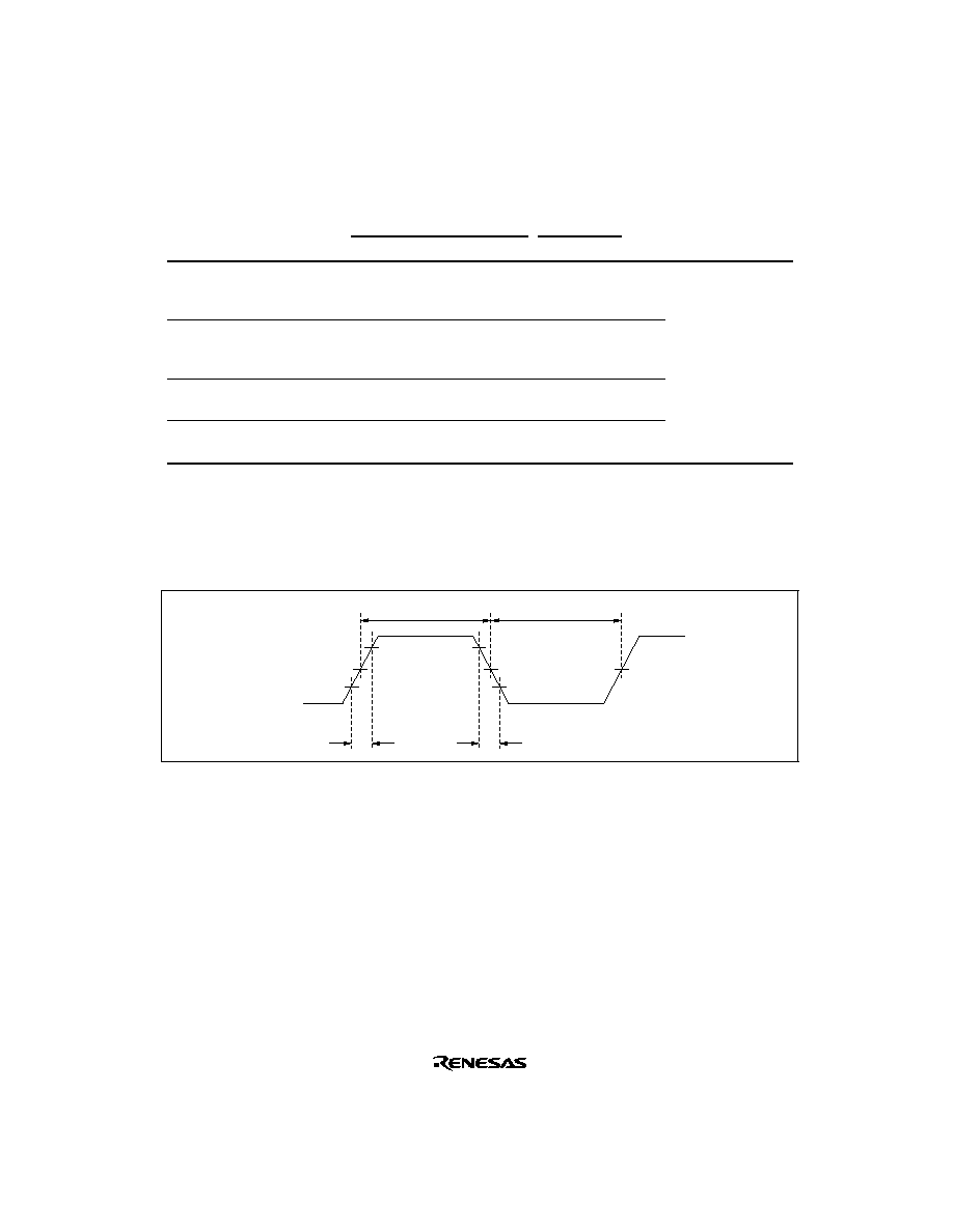
531
Table 17-5 External Clock Input Conditions when Duty Adjustment Circuit Is Not Used
V
CC
= 2.7 V
to 5.5 V
V
CC
= 2.7 V
to 5.5 V
*
V
CC
= 5.0 V
± 10%
Item
Symbol
Min
Max
Min
Max
Min
Max
Unit
Test Conditions
External clock
input pulse
width low level
t
EXL
50
--
37.5
--
25
--
ns
Figure 17-6
External clock
input pulse
width high level
t
EXH
50
--
37.5
--
25
--
ns
External clock
rise time
t
EXr
--
10
--
7.5
--
5
ns
External clock
fall time
t
EXf
--
10
--
7.5
--
5
ns
Notes: When the duty adjustment circuit is not used, the maximum operating frequency falls
according to the input waveform.
(Example: When t
EXL
= t
EXH
= 25 ns and t
EXr
= t
EXf
= 5 ns, the clock cycle time = 60 ns, and
therefore the maximum operating frequency = 16.7 MHz.)
*
Does not apply to the HD6472246.
t
EXH
t
EXL
t
EXr
t
EXf
V
CC
◊
0.5
EXTAL
Figure 17-6 External Clock Input Timing

532
Note on External Clock Switchover: When using two or more external clocks (e.g. 10 MHz and
32 kHz), input clock switchover should be carried out in software standby mode.
A sample external clock switching circuit is shown in figure 17-7, and sample external clock
switchover timing in figure 17-8.
H8S/2245
EXTAL
External clock 1
External clock 2
Control
circuit
External clock switchover request
External interrupt signal
External clock switchover signal
Selector
Port output
External interrupt
Figure 17-7 Sample External Clock Switching Circuit
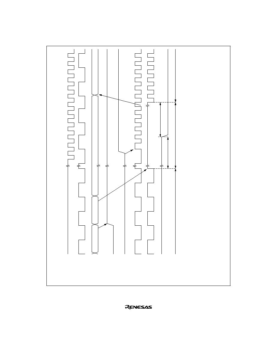
533
200 ns or more (4)
(2)
(1)
Port setting (clock switchover)
(2)
Software standby mode transition
(3)
External clock switchover
(4)
External interrupt generation
(Input interrupt 200 ns or more after transition to software standby mode.)
(5)
Interrupt exception handling
(5)
Sleep instruction
execution
Interrupt exception handling
Operation
External clock 1
External clock 2
(1)
Port setting
(3)
External clock
switchover signal
EXTAL
Internal clock ¯
Standby time
External interrupt
Active (external clock 1)
Active (external clock 2)
Software standby mode
Clock switchover
request
Figure 17-8 Sample External Clock Switchover Timing

534
17.4
Duty Adjustment Circuit
When the oscillator frequency is 5 MHz or higher, the duty adjustment circuit adjusts the duty
cycle of the clock signal from the oscillator to generate the system clock (¯).
17.5
Medium-Speed Clock Divider
The medium-speed clock divider divides the system clock to generate ¯/2, ¯/4, ¯/8, ¯/16, and ¯/32.
17.6
Bus Master Clock Selection Circuit
The bus master clock selection circuit selects the system clock (¯) or one of the medium-speed
clocks (¯/2, ¯/4, or ¯/8, ¯/16, and ¯/32) to be supplied to the bus master, according to the settings
of the SCK2 to SCK0 bits in SCKCR.

535
Section 18 Power-Down Modes
18.1
Overview
In addition to the normal program execution state, the H8S/2245 Series has power-down modes in
which operation of the CPU and oscillator is halted and power dissipation is reduced. Low-power
operation can be achieved by individually controlling the CPU, on-chip supporting modules, and
so on.
The H8S/2245 Series operating modes are as follows:
(1) High-speed mode
(2) Medium-speed mode
(3) Sleep mode
(4) Module stop mode
(5) Software standby mode
(6) Hardware standby mode
Of these, (2) to (6) are power-down modes. Sleep mode is a CPU mode, medium-speed mode is a
CPU and bus master mode, and module stop mode is an on-chip supporting module mode
(including bus masters other than the CPU). A combination of these modes can be set.
After a reset, the H8S/2245 Series is in high-speed mode.
Table 18-1 shows the conditions for transition to the various modes, the status of the CPU, on-chip
supporting modules, etc., and the method of clearing each mode.

536
Table 18-1 Operating Modes
Operating
Transition
Clearing
CPU
Modules
Mode
Condition
Condition
Oscillator
Registers
Registers
I/O Ports
High speed
mode
Control register
Functions
High
speed
Functions
High
speed
Functions
High speed
Medium-
speed mode
Control register
Functions
Medium
speed
Functions
High/
medium
speed
*
1
Functions
High speed
Sleep mode Instruction
Interrupt
Functions
Halted
Retained
High
speed
Functions
High speed
Module stop
mode
Control register
Functions
High/
medium
speed
Functions
Halted
Retained/
reset
*
2
Retained
Software
standby
mode
Instruction
External
interrupt
Halted
Halted
Retained
Halted
Retained/
reset
*
2
Retained
Hardware
standby
mode
Pin
Halted
Halted
Undefined
Halted
Reset
High
impedance
Notes: 1. The bus master operates on the medium-speed clock, and other on-chip supporting
modules on the high-speed clock.
2. The SCI and A/D are reset, and other on-chip supporting modules retain their state.
18.1.1
Register Configuration
Power-down modes are controlled by the SBYCR, SCKCR, and MSTPCR registers. Table 18-2
summarizes these registers.
Table 18-2 Power-Down Mode Registers
Name
Abbreviation
R/W
Initial Value
Address
*
Standby control register
SBYCR
R/W
H'08
H'FF38
System clock control register
SCKCR
R/W
H'00
H'FF3A
Module stop control register H
MSTPCRH
R/W
H'3F
H'FF3C
Module stop control register L
MSTPCRL
R/W
H'FF
H'FF3D
Note:
*
Lower 16 bits of the address.

537
18.2
Register Descriptions
18.2.1
Standby Control Register (SBYCR)
7
SSBY
0
R/W
6
STS2
0
R/W
5
STS1
0
R/W
4
STS0
0
R/W
3
OPE
1
R/W
0
--
0
--
2
--
0
--
1
--
0
--
Bit
Initial value
R/W
:
:
:
SBYCR is an 8-bit readable/writable register that performs software standby mode control.
SBYCR is initialized to H'08 by a reset and in hardware standby mode. It is not initialized in
software standby mode.
Bit 7--Software Standby (SSBY): Specifies a transition to software standby mode. Remains set
to 1 when software standby mode is released by an external interrupt, and a transition is made to
normal operation. The SSBY bit should be cleared by writing 0 to it.
Bit 7
SSBY
Description
0
Transition to sleep mode after execution of SLEEP instruction
(Initial value)
1
Transition to software standby mode after execution of SLEEP instruction
Bits 6 to 4--Standby Timer Select 2 to 0 (STS2 to STS0): These bits select the time the MCU
waits for the clock to stabilize when software standby mode is cleared by an external interrupt.
With crystal oscillation, refer to table 18-4 and make a selection according to the operating
frequency so that the standby time is at least 8 ms (the oscillation stabilization time). With an
external clock, any selection can be made.
Bit 6
Bit 5
Bit 4
STS2
STS1
STS0
Description
0
0
0
Standby time = 8192 states
(Initial value)
1
Standby time = 16384 states
1
0
Standby time = 32768 states
1
Standby time = 65536 states
1
0
0
Standby time = 131072 states
1
Standby time = 262144 states
1
0
Reserved
1
Standby time = 16 states

538
Bit 3--Output Port Enable (OPE): Specifies whether the output of the address bus and bus
control signals (
CS0 to CS3, AS, RD, HWR, LWR) is retained or set to the high-impedance state
in software standby mode.
Bit 3
OPE
Description
0
In software standby mode, address bus and bus control signals are high-impedance
1
In software standby mode, address bus and bus control signals retain output state
(Initial value)
Bits 2 to 0--Reserved: Read-only bits, always read as 0.
18.2.2
System Clock Control Register (SCKCR)
7
PSTOP
0
R/W
6
--
0
R/W
5
--
0
--
4
--
0
--
3
--
0
--
0
SCK0
0
R/W
2
SCK2
0
R/W
1
SCK1
0
R/W
Bit
Initial value
R/W
:
:
:
SCKCR is an 8-bit readable/writable register that performs ¯ clock output control and medium-
speed mode control.
SCKCR is initialized to H'00 by a reset and in hardware standby mode. It is not initialized in
software standby mode.
Bit 7--¯ Clock Output Disable (PSTOP): Controls ¯ output.
Description
Bit 7
Normal Operating
Software Standby
Hardware Standby
PSTOP
Mode
Sleep Mode
Mode
Mode
0
¯ output (initial value)
¯ output
Fixed high
High impedance
1
Fixed high
Fixed high
Fixed high
High impedance
Bits 6--Reserved: This bit can be read or written to, but only 0 should be written.
Bits 5 to 3--Reserved: Read-only bits, always read as 0.

539
Bits 2 to 0--System Clock Select (SCK2 to SCK0): These bits select the clock for the bus
master.
Bit 2
Bit 1
Bit 0
SCK2
SCK1
SCK0
Description
0
0
0
Bus master in high-speed mode
(Initial value)
1
Medium-speed clock is ¯/2
1
0
Medium-speed clock is ¯/4
1
Medium-speed clock is ¯/8
1
0
0
Medium-speed clock is ¯/16
1
Medium-speed clock is ¯/32
1
--
--
18.2.3
Module Stop Control Register (MSTPCR)
15
0
R/W
Bit
Initial value
R/W
:
:
:
14
0
R/W
13
1
R/W
12
1
R/W
11
1
R/W
10
1
R/W
9
1
R/W
8
1
R/W
7
1
R/W
6
1
R/W
5
1
R/W
4
1
R/W
3
1
R/W
2
1
R/W
1
1
R/W
0
1
R/W
MSTPCRH
MSTPCRL
MSTPCR is a 16-bit readable/writable register that performs module stop mode control.
MSTPCR is initialized to H'3FFF by a reset and in hardware standby mode. It is not initialized in
software standby mode.
Bits 15 to 0--Module Stop (MSTP 15 to MSTP 0): These bits specify module stop mode. See
table 18-3 for the method of selecting on-chip supporting modules.
Bits 15 to 0
MSTP15 to MSTP0
Description
0
Module stop mode cleared
1
Module stop mode set

540
18.3
Medium-Speed Mode
When the SCK2 to SCK0 bits in SCKCR are set to 1, the operating mode changes to medium-
speed mode at the end of the bus cycle. In medium-speed mode, the CPU operates on the
operating clock (¯/2, ¯/4, ¯/8, ¯/16, or ¯/32) specified by the SCK2 to SCK0 bits. The bus masters
other than the CPU (DTC) also operate in medium-speed mode. On-chip supporting modules other
than the bus masters always operate on the high-speed clock (¯).
In medium-speed mode, a bus access is executed in the specified number of states with respect to
the bus master operating clock. For example, if ¯/4 is selected as the operating clock, on-chip
memory is accessed in 4 states, and internal I/O registers in 8 states.
Medium-speed mode is cleared by clearing all of bits SCK2 to SCK0 to 0. A transition is made to
high-speed mode and medium-speed mode is cleared at the end of the current bus cycle.
If a SLEEP instruction is executed when the SSBY bit in SBYCR is cleared to 0, a transition is
made to sleep mode. When sleep mode is cleared by an interrupt, medium-speed mode is restored.
If a SLEEP instruction is executed when the SSBY bit in SBYCR is set to 1, a transition is made
to software standby mode. When software standby mode is cleared by an external interrupt,
medium-speed mode is restored.
When the
RES pin is driven low, a transition is made to the reset state, and medium-speed mode is
cleared. The same applies in the case of a reset caused by overflow of the watchdog timer.
When the
STBY pin is driven low, a transition is made to hardware standby mode.
541
Figure 18-1 shows the timing for transition to and clearance of medium-speed mode.
Bus master clock
¯,
supporting module
clock
Internal address
bus
Internal write signal
Medium-speed mode
SCKCR
SCKCR
Figure 18-1 Medium-Speed Mode Transition and Clearance Timing
18.4
Sleep Mode
If a SLEEP instruction is executed when the SSBY bit in SBYCR is cleared to 0, the CPU enters
sleep mode. In sleep mode, CPU operation stops but the contents of the CPU's internal registers
are retained. Other supporting modules do not stop.
Sleep mode is cleared by a reset or any interrupt, and the CPU returns to the normal program
execution state via the exception handling state. Sleep mode is not cleared if interrupts are
disabled, or if interrupts other than NMI are masked by the CPU.
When the
STBY pin is driven low, a transition is made to hardware standby mode.

542
18.5
Module Stop Mode
18.5.1
Module Stop Mode
Module stop mode can be set for individual on-chip supporting modules.
When the corresponding MSTP bit in MSTPCR is set to 1, module operation stops at the end of
the bus cycle and a transition is made to module stop mode. The CPU continues operating
independently.
Table 18-3 shows MSTP bits and the corresponding on-chip supporting modules.
When the corresponding MSTP bit is cleared to 0, module stop mode is cleared and the module
starts operating again at the end of the bus cycle. In module stop mode, the internal states of
modules other than the SCI and A/D are retained.
After reset clearance, all modules other than DTC are in module stop mode.
When an on-chip supporting module is in module stop mode, read/write access to its registers is
disabled.
If a transition is made to sleep mode when all modules are stopped (MSTPCR = H'FFFF) or
modules other than the 8-bit timers are stopped (MSTPCR = H'EFFF), operation of the bus
controller and I/O ports is also halted, enabling current dissipation to be further reduced.

543
Table 18-3 MSTP Bits and Corresponding On-Chip Supporting Modules
Register
Bit
Module
MSTPCRH
MSTP15
--
MSTP14
Data transfer controller (DTC)
MSTP13
16-bit timer pulse unit (TPU)
MSTP12
8-bit timer
MSTP11
--
MSTP10
--
MSTP9
A/D converter
MSTP8
--
MSTPCRL
MSTP7
Serial communication interface (SCI) channel 2
MSTP6
Serial communication interface (SCI) channel 1
MSTP5
Serial communication interface (SCI) channel 0
MSTP4
--
MSTP3
--
MSTP2
--
MSTP1
--
MSTP0
--
Note: Bits 15, 11, 10, 8 and bits 4 to 0 can be read or written to, but do not affect operation.
18.5.2
Usage Notes
DTC Module Stop Mode: Depending on the operating status of the DTC, the MSTP14 bit may
not be set to 1. Setting of the DTC module stop mode should be carried out only when the DTC is
not activated.
For details, refer to section 7, Data Transfer Controller (DTC).
On-Chip Supporting Module Interrupts: Relevant interrupt operations cannot be performed in
module stop mode. Consequently, if module stop mode is entered when an interrupt has been
requested, it will not be possible to clear the CPU interrupt source or DTC activation source.
Interrupts should therefore be disabled before entering module stop mode.
Writing to MSTPCR: MSTPCR should only be written to by the CPU.

544
18.6
Software Standby Mode
18.6.1
Software Standby Mode
If a SLEEP instruction is executed when the SSBY bit in SBYCR is set to 1, software standby
mode is entered. In this mode, the CPU, on-chip supporting modules, and oscillator all stop.
However, the contents of the CPU's internal registers, RAM data, and the states of on-chip
supporting modules other than the SCI and A/D, and I/O ports, are retained. Whether the address
bus and bus control signals are placed in the high-impedance state or retain the output state can be
specified by the OPE bit in SBYCR.
In this mode the oscillator stops, and therefore power dissipation is significantly reduced.
18.6.2
Clearing Software Standby Mode
Software standby mode is cleared by an external interrupt (NMI pin, or pins
IRQ0 to IRQ2), or by
means of the
RES pin or STBY pin.
Clearing with an Interrupt: When an NMI or IRQ0 to IRQ2 interrupt request signal is input,
clock oscillation starts, and after the elapse of the time set in bits STS2 to STS0 in SYSCR, stable
clocks are supplied to the entire H8S/2245 Series chip, software standby mode is cleared, and
interrupt exception handling is started.
When clearing software standby mode with an IRQ0 to IRQ2 interrupt, set the corresponding
enable bit to 1 and ensure that no interrupt with a higher priority than interrupts IRQ0 to IRQ2 is
generated. Software standby mode cannot be cleared if the interrupt has been masked on the CPU
side or has been designated as a DTC activation source.
Clearing with the
RES Pin: When the RES pin is driven low, clock oscillation is started. At the
same time as clock oscillation starts, clocks are supplied to the entire H8S/2245 Series chip. Note
that the
RES pin must be held low until clock oscillation stabilizes. When the RES pin goes high,
the CPU begins reset exception handling.
Clearing with the
STBY Pin: When the STBY pin is driven low, a transition is made to hardware
standby mode.
545
18.6.3
Setting Oscillation Stabilization Time after Clearing Software Standby Mode
Bits STS2 to STS0 in SBYCR should be set as described below.
Using a Crystal Oscillator: Set bits STS2 to STS0 so that the standby time is at least 8 ms (the
oscillation stabilization time).
Table 18-4 shows the standby times for different operating frequencies and settings of bits STS2
to STS0.
Table 18-4 Oscillation Stabilization Time Settings
STS2 STS1 STS0 Standby Time
20
MHz
16
MHz
12
MHz
10
MHz
8
MHz
6
MHz
4
MHz
2
MHz Unit
0
0
0
8192 states
0.41
0.51
0.68
0.8
1.0
1.3
2.0
4.1
ms
1
16384 states
0.82
1.0
1.3
1.6
2.0
2.7
4.1
8.2
1
0
32768 states
1.6
2.0
2.7
3.3
4.1
5.5
8.2
16.4
1
65536 states
3.3
4.1
5.5
6.6
8.2
10.9 16.4
32.8
1
0
0
131072 states
6.6
8.2
10.9
13.1 16.4
21.8
32.8
65.5
1
262144 states
13.1
16.4
21.8
26.2
32.8
43.6
65.6
131.2
1
0
Reserved
--
--
--
--
--
--
--
--
--
1
16 states
0.8
1.0
1.3
1.6
2.0
2.7
4.0
8.0
µs
: Recommended time setting
Using an External Clock: Any value can be set. Normally, use of the minimum time is
recommended.
18.6.4
Software Standby Mode Application Example
Figure 18-2 shows an example in which a transition is made to software standby mode at the
falling edge on the NMI pin, and software standby mode is cleared at the rising edge on the NMI
pin.
In this example, an NMI interrupt is accepted with the NMIEG bit in SYSCR cleared to 0 (falling
edge specification), then the NMIEG bit is set to 1 (rising edge specification), the SSBY bit is set
to 1, and a SLEEP instruction is executed, causing a transition to software standby mode.
Software standby mode is then cleared at the rising edge on the NMI pin.

546
Oscillator
¯
NMI
NMIEG
SSBY
NMI exception
handling
NMIEG=1
SSBY=1
SLEEP instruction
Software standby mode
(power-down mode)
Oscillation
stabilization
time
t
OSC2
NMI exception
handling
Figure 18-2 Software Standby Mode Application Example
18.6.5
Usage Notes
I/O Port Status: In software standby mode, I/O port states are retained. If the OPE bit is set to 1,
the address bus and bus control signal output is also retained. Therefore, there is no reduction in
current dissipation for the output current when a high-level signal is output.
Current Dissipation during Oscillation Stabilization Wait Period: Current dissipation
increases during the oscillation stabilization wait period.

547
18.7
Hardware Standby Mode
18.7.1
Hardware Standby Mode
When the
STBY pin is driven low, a transition is made to hardware standby mode from any mode.
In hardware standby mode, all functions enter the reset state and stop operation, resulting in a
significant reduction in power dissipation. As long as the prescribed voltage is supplied, on-chip
RAM data is retained. I/O ports are set to the high-impedance state.
In order to retain on-chip RAM data, the RAME bit in SYSCR should be cleared to 0 before
driving the
STBY pin low.
Do not change the state of the mode pins (MD
2
to MD
0
) while the H8S/2245 Series is in hardware
standby mode.
Hardware standby mode is cleared by means of the
STBY pin and the RES pin. When the STBY
pin is driven high while the
RES pin is low, the reset state is set and clock oscillation is started.
Ensure that the
RES pin is held low until the clock oscillation stabilizes (at least 8 ms--the
oscillation stabilization time--when using a crystal oscillator). When the
RES pin is subsequently
driven high, a transition is made to the program execution state via the reset exception handling
state.
18.7.2
Hardware Standby Mode Timing
Figure 18-3 shows an example of hardware standby mode timing.
When the
STBY pin is driven low after the RES pin has been driven low, a transition is made to
hardware standby mode. Hardware standby mode is cleared by driving the
STBY pin high,
waiting for the oscillation stabilization time, then changing the
RES pin from low to high.

548
Oscillator
RES
STBY
Oscillation
stabilization
time
Reset
exception
handling
Figure 18-3 Hardware Standby Mode Timing (Example)
18.8
¯ Clock Output Disabling Function
Output of the ¯ clock can be controlled by means of the PSTOP bit in SCKCR and DDR for the
corresponding port. When the PSTOP bit is set to 1, the ¯ clock stops at the end of the bus cycle,
and ¯ output goes high. ¯ clock output is enabled when the PSTOP bit is cleared to 0. When DDR
for the corresponding port is cleared to 0, ¯ clock output is disabled and input port mode is set.
Table 18-5 shows the state of the ¯ pin in each processing mode.
Table 18-5 ¯ Pin State in Each Processing Mode
DDR
0
1
PSTOP
--
0
1
Hardware standby mode
High impedance
Software standby mode
High impedance
Fixed high
Sleep mode
High impedance
¯ output
Fixed high
Normal operating mode
High impedance
¯ output
Fixed high

549
Section 19 Electrical Characteristics
19.1
Absolute Maximum Ratings
Table 19-1 lists the absolute maximum ratings.
Table 19-1 Absolute Maximum Ratings
Item
Symbol
Value
Unit
Power supply voltage
V
CC
≠0.3 to +7.0
V
Programming voltage
V
PP
≠0.3 to +13.5
V
Input voltage (except port 4)
V
in
≠0.3 to V
CC
+0.3
V
Input voltage (port 4)
V
in
≠0.3 to AV
CC
+0.3
V
Reference voltage
V
ref
≠0.3 to AV
CC
+0.3
V
Analog power supply voltage
AV
CC
≠0.3 to +7.0
V
Analog input voltage
V
AN
≠0.3 to AV
CC
+0.3
V
Operating temperature
T
opr
Regular specifications: ≠20 to +75
∞C
Wide-range specifications: ≠40 to +85
∞C
Storage temperature
T
stg
≠55 to +125
∞C
Caution: Permanent damage to the chip may result if absolute maximum ratings are exceeded.

550
19.2
Power Supply Voltage and Operating Frequency Ranges
Power supply voltage and operating frequency ranges (shaded areas) are shown in table 19-2.
Table 19-2 Power Supply Voltage and Operating Frequency Ranges
Condition A: All H8S/2245 Series products
V
CC
= 2.7 V to 5.5 V, AV
CC
= 2.7 V to 5.5 V, V
ref
= 2.7 V to AV
CC
, V
SS
= AV
SS
=
0 V, ¯ = 32 kHz to 10 MHz, T
a
= ≠20∞C to +75∞C (regular specifications),
T
a
= ≠40∞C to +85∞C (wide-range specifications)
Condition B: HD6432246, HD6432245, HD6432244, HD6432243, HD6432242, HD6432241R,
HD6412240
V
CC
= 2.7 V to 5.5 V, AV
CC
= 2.7 V to 5.5 V, V
ref
= 2.7 V to AV
CC
, V
SS
= AV
SS
=
0 V, ¯ = 32 kHz to 13 MHz, T
a
= ≠20∞C to +75∞C (regular specifications),
T
a
= ≠40∞C to +85∞C (wide-range specifications)
Condition C: All H8S/2245 Series products
V
CC
= 5.0 V ±10%, AV
CC
= 5.0 V ±10%, V
ref
= 4.5 V to AV
CC
, V
SS
= AV
SS
= 0 V,
¯ = 2 MHz to 20 MHz, T
a
= ≠20∞C to +75∞C (regular specifications),
T
a
= ≠40∞C to +85∞C (wide-range specifications)

551
Clock Supply
Method
Crystal Resonator
Connection
External Clock Input
Operating
Modules
All Modules
DTC
TPU
SCI
A/D Converter
CPU
Bus controller
Interrupt Controller
I/O Ports
8-Bit Timers
WDT
Condition A
5.5
20 M
10 M
2 M
32 k
0
2.7
4.5
V
CC
(V)
f (Hz)
20 M
10 M
2 M
32 k
0
2.7
4.5
5.5
V
CC
(V)
f (Hz)
Condition B
20 M
10 M
13 M
2 M
32 k
0
2.7
4.5
5.5
V
CC
(V)
f (Hz)
20 M
10 M
13 M
2 M
32 k
0
2.7
4.5
5.5
V
CC
(V)
f (Hz)
Condition C
20 M
10 M
2 M
32 k
0
2.7
4.5
5.5
V
CC
(V)
f (Hz)
13 M

552
19.3
DC Characteristics
Table 19-3 lists the DC characteristics. Table 19-4 lists the permissible output currents.
Table 19-3 DC Characteristics
Conditions: V
CC
= 5.0 V ± 10%, AV
CC
= 5.0 V ± 10%, V
ref
= 4.5 V to AV
CC
, V
SS
= AV
SS
= 0 V*
1
,
T
a
= ≠20 to +75∞C (regular specifications), T
a
= ≠40 to +85∞C (wide-range
specifications)
Item
Symbol
Min
Typ
Max
Unit
Test Conditions
Schmitt
Port 2,
V
T
≠
1.0
--
--
V
trigger input
IRQ0
to
IRQ7
V
T
+
--
--
V
CC
◊
0.7
V
voltage
V
T
+
≠V
T
≠
0.4
--
--
V
Input high
voltage
RES
,
STBY
,
NMI, MD
2
to MD
0
V
IH
V
CC
≠ 0.7
--
V
CC
+0.3
V
EXTAL
V
CC
◊
0.7
--
V
CC
+0.3
V
Port 1, 3, 5,
A to G
2.0
--
V
CC
+0.3
V
Port 4
2.0
--
AV
CC
+0.3 V
Input low
voltage
RES
,
STBY
,
MD
2
to MD
0
V
IL
≠0.3
--
0.5
V
NMI, EXTAL,
Port 1, 3 to 5,
A to G
≠0.3
--
0.8
V
Output high
All output pins V
OH
V
CC
≠0.5
--
--
V
I
OH
= ≠200 µA
voltage
3.5
--
--
V
I
OH
= ≠1 mA
Output low
All output pins V
OL
--
--
0.4
V
I
OL
= 1.6 mA
voltage
Port 1, A to C
--
--
1.0
V
I
OL
= 10 mA
Input
RES
| I
in
|
--
--
10.0
µA
V
in
=
leakage
current
STBY
, NMI,
MD
2
to MD
0
--
--
1.0
0.5 to V
CC
≠0.5 V
Port 4
--
--
1.0
µA
V
in
=
0.5 to AV
CC
≠0.5 V
Note:
1. If the A/D converter is not used, do not leave the AV
CC
, AV
SS
, and V
ref
pins open.
Connect AV
CC
and V
ref
to V
CC
, and connect AV
SS
to V
SS
.

553
Table 19-3 DC Characteristics (cont)
Conditions: V
CC
= 5.0 V ± 10%, AV
CC
= 5.0 V ± 10%, V
ref
= 4.5 V to AV
CC
, V
SS
= AV
SS
= 0 V*
1
,
T
a
= ≠20 to +75∞C (regular specifications), T
a
= ≠40 to +85∞C (wide-range
specifications)
Item
Symbol
Min
Typ
Max
Unit
Test Conditions
Three-state
leakage
current
(off state)
Port 1 to 3,
5, A to G
I
TSI
--
--
1.0
µA
V
in
=
0.5 to V
CC
≠0.5 V
Input pull-up
MOS current
Port A to E
≠I
P
50
--
300
µA
V
in
= 0 V
Input
RES
C
in
--
--
80
pF
V
in
= 0 V
capacitance
NMI
--
--
50
pF
f = 1 MHz
All input pins
except
RES
and NMI
--
--
15
pF
T
a
= 25∞C
Current
dissipation
*
2
Normal
operation
I
CC
*
4
--
50
(5.0 V)
75
(5.5 V)
mA
f = 20 MHz
Sleep mode
--
35
(5.0 V)
55
(5.5 V)
mA
f = 20 MHz
All module
stop mode
--
35
(5.0 V)
--
mA
Reference value
f = 20 MHz
Medium speed
(¯/32) mode
--
25
(5.0 V)
--
mA
Reference value
f = 20 MHz
Sleep, all
module stop
and medium
speed (¯/32)
mode
--
5.0
(5.0 V)
10
(5.5 V)
mA
f = 20 MHz
Standby
--
0.01
5.0
µA
T
a
50∞C
mode
*
3
--
--
20.0
50∞C < T
a
Analog power
supply current
During A/D
conversion
Al
CC
--
1.2
2.0
mA
Idle
--
0.01
5.0
µA
Reference
current
During A/D
conversion
Al
CC
--
0.5
0.8
mA
V
ref
= 5.0 V
Idle
--
0.01
5.0
µA
RAM standby voltage
V
RAM
2.0
--
--
V

554
Notes: 1. If the A/D converter is not used, do not leave the AV
CC
, AV
SS
, and V
ref
pins open.
Connect AV
CC
and V
ref
to V
CC
, and connect AV
SS
to V
SS
.
2. Current dissipation values are for V
IH
min = V
CC
≠0.5 V and V
IL
max = 0.5V with all
output pins unloaded and the on-chip pull-up transistors in the off state.
3. The values are for V
RAM
V
CC
< 4.5V, V
IH
min = V
CC
◊
0.9, and V
IL
max = 0.3 V.
4. I
CC
depends on V
CC
and f as follows:
I
CC
max = 2.0 (mA) + 0.67 (mA/(MHz
◊
V))
◊
V
CC
◊
f [normal mode]
I
CC
max = 2.0 (mA) + 0.48 (mA/(MHz
◊
V))
◊
V
CC
◊
f [sleep mode]
I
CC
max = 2.0 (mA) + 0.07 (mA/(MHz
◊
V))
◊
V
CC
◊
f [sleep, all module stop and medium
speed (¯/32) mode]

555
Table 19-3 DC Characteristics (cont)
Conditions: V
CC
= 2.7 V to 5.5 V, AV
CC
= 2.7 V to 5.5 V, V
ref
= 2.7 V to AV
CC
,
V
SS
= AV
SS
= 0 V*
1
, T
a
= ≠20 to +75∞C (regular specifications),
T
a
= ≠40 to +85∞C (wide-range specifications)
Item
Symbol
Min
Typ
Max
Unit
Test Conditions
Schmitt
Port 2,
V
T
≠
V
CC
◊
0.2
--
--
V
trigger input
IRQ0
to
IRQ7
V
T
+
--
--
V
CC
◊
0.7
V
voltage
V
T
+
≠ V
T
≠
V
CC
◊
0.07 --
--
V
Input high
voltage
RES
,
STBY
,
NMI, MD
2
to MD
0
V
IH
V
CC
◊
0.9
--
V
CC
+0.3
V
EXTAL
V
CC
◊
0.7
--
V
CC
+0.3
V
Port 1, 3, 5,
A to G
V
CC
◊
0.7
--
V
CC
+0.3
V
Port4
V
CC
◊
0.7
--
AV
CC
+0.3 V
Input low
voltage
RES
,
STBY
,
MD
2
to MD
0
V
IL
≠0.3
--
V
CC
◊
0.1
V
NMI, EXTAL,
Port 1, 3 to 5,
A to G
≠0.3
--
V
CC
◊
0.2
0.8
V
V
CC
< 4.0 V
V
CC
= 4.0 to 5.5 V
Output high
All output pins V
OH
V
CC
≠0.5
--
--
V
I
OH
= ≠200 µA
voltage
V
CC
≠1.0
--
--
V
I
OH
= ≠1 mA
Output low
All output pins V
OL
--
--
0.4
V
I
OL
= 1.6 mA
voltage
Port 1, A to C
--
--
1.0
V
V
CC
4 V
I
OL
= 5 mA
4 V < V
CC
5 V
I
OL
= 10 mA
Input
RES
I
in
--
--
10.0
µA
V
in
=
leakage
current
STBY
, NMI,
MD
2
to MD
0
--
--
1.0
0.5 to V
CC
≠0.5V
Port 4
--
--
1.0
µA
V
in
=
0.5 to AV
CC
≠0.5V
Note:
1. If the A/D converter is not used, do not leave the AV
CC
, AV
SS
, and V
ref
pins open.
Connect AV
CC
and V
ref
to V
CC
, and connect AV
SS
to V
SS
.

556
Table 19-3 DC Characteristics (cont)
Conditions: V
CC
= 2.7 V to 5.5 V, AV
CC
= 2.7 V to 5.5 V, V
ref
= 2.7 V to AV
CC
,
V
SS
= AV
SS
= 0 V*
1
, T
a
= ≠20 to +75∞C (regular specifications),
T
a
= ≠40 to +85∞C (wide-range specifications)
Item
Symbol
Min
Typ
Max
Unit
Test Conditions
Three-state
leakage
current
(off state)
Port 1 to 3,
5, A to G
I
TSI
--
--
1.0
µA
V
in
=
0.5 to V
CC
≠0.5 V
Input pull-
up current
Port A to E
≠I
P
10
--
300
µA
V
CC
= 2.7 V to
5.5 V, V
in
= 0 V
Input
RES
C
in
--
--
80
pF
V
in
= 0 V
capacitance
NMI
--
--
50
pF
f = 1 MHz
All input pins
except
RES
and NMI
--
--
15
pF
Ta = 25∞C
Current
dissipation
*
2
Normal
operation
I
CC
*
4
--
13
(3.0 V)
40
(5.5 V)
mA
f = 10 MHz
--
18
(3.0 V)
52
(5.5 V)
f = 13 MHz
--
60
120
µA
f = 32 kHz,
V
CC
= 3.0 V
*
5
Sleep mode
--
9
(3.0 V)
28
(5.5 V)
mA
f = 10 MHz
--
12
(3.0 V)
37
(5.5 V)
f = 13 MHz
All module
stop mode
--
9
(3.0 V)
--
mA
Reference value
f = 10 MHz
--
12
(3.0 V)
--
Reference value
f = 13 MHz
Medium speed
(¯/32) mode
--
6
(3.0 V)
--
mA
Reference value
f = 10 MHz
--
8
(3.0 V)
--
Reference value
f = 13 MHz

557
Table 19-3 DC Characteristics (cont)
Conditions: V
CC
= 2.7 V to 5.5 V, AV
CC
= 2.7 V to 5.5 V, V
ref
= 2.7 V to AV
CC
,
V
SS
= AV
SS
= 0 V*
1
, T
a
= ≠20 to +75∞C (regular specifications),
T
a
= ≠40 to +85∞C (wide-range specifications)
Item
Symbol
Min
Typ
Max
Unit
Test Conditions
Current
dissipation
*
2
Sleep, all
module stop
I
CC
*
4
--
1.5
(3.0 V)
6.0
(5.5 V)
mA
f = 10 MHz
and medium
speed (¯/32)
--
2.5
(3.0 V)
7.5
(5.5 V)
f = 13 MHz
mode
--
30
60
µA
f = 32 kHz,
V
CC
= 3.0 V
*
5
Standby
--
0.01
5.0
µA
T
a
50∞C
mode
*
3
--
--
20.0
50∞C < T
a
Analog power
During A/D
Al
CC
--
0.4
1.0
mA
AV
CC
= 3.0 V
supply current conversion
--
1.2
--
mA
AV
CC
= 5.0 V
Idle
--
0.01
5.0
µA
Reference
During A/D
Al
CC
--
0.3
0.6
mA
V
ref
= 3.0 V
power supply
conversion
--
0.5
--
mA
V
ref
= 5.0 V
current
Idle
--
0.01
5.0
µA
RAM standby voltage
V
RAM
2.0
--
--
V
Notes: 1. If the A/D converter is not used, do not leave the AV
CC
, AV
SS
, and V
ref
pins open.
Connect AV
CC
and V
ref
to V
CC
, and connect AV
SS
to V
SS
.
2. Current dissipation values are for V
IH
min = V
CC
≠0.5 V and V
IL
max = 0.5V with all
output pins unloaded and the on-chip pull-up transistors in the off state.
3. The values are for V
RAM
V
CC
< 2.7 V, V
IH
min = V
CC
◊
0.9, and V
IL
max = 0.3V.
4. I
CC
depends on V
CC
and f as follows:
I
CC
max = 2.0 (mA) + 0.67 (mA/(MHz
◊
V))
◊
V
CC
◊
f [normal mode]
I
CC
max = 2.0 (mA) + 0.48 (mA/(MHz
◊
V))
◊
V
CC
◊
f [sleep mode]
I
CC
max = 2.0 (mA) + 0.07 (mA/(MHz
◊
V))
◊
V
CC
◊
f [sleep, all module stop and medium
speed (¯/32) mode]
5. The current dissipation for 32 kHz operation is the value when the duty adjustment
circuit is stopped.
558
Table 19-4 Permissible Output Currents
Conditions: V
CC
= 2.7 V to 5.5 V, AV
CC
= 2.7 to 5.5 V, V
ref
= 2.7 V to AV
CC
, V
SS
= AV
SS
= 0 V,
T
a
= ≠20 to +75∞C (regular specifications), Ta = ≠40 to +85∞C (wide-range
specifications)
Item
Symbol
Min
Typ
Max
Unit
Permissible output
Port1, A to C
I
OL
--
--
10
mA
low current (per pin)
Other output pins
--
--
2.0
mA
Permissible output
low current (total)
Total of 28 pins
including port 1
and A to C
I
OL
--
--
80
mA
Total of all output
pins, including the
above
--
--
120
mA
Permissible output
high current (per pin)
All output pins
≠I
OH
--
--
2.0
mA
Permissible output
high current (total)
Total of all output
pins
≠I
OH
--
--
40
mA
Notes: 1. To protect chip reliability, do not exceed the output current values in table 19-4.
2. When driving a darlington pair or LED, always insert a current-limiting resister in the
output line, as show in figures 19-1 and 19-2.
2k
H8S/2245 Series
Port
Darlington Pair
Figure 19-1 Darlington Pair Drive Circuit (Example)
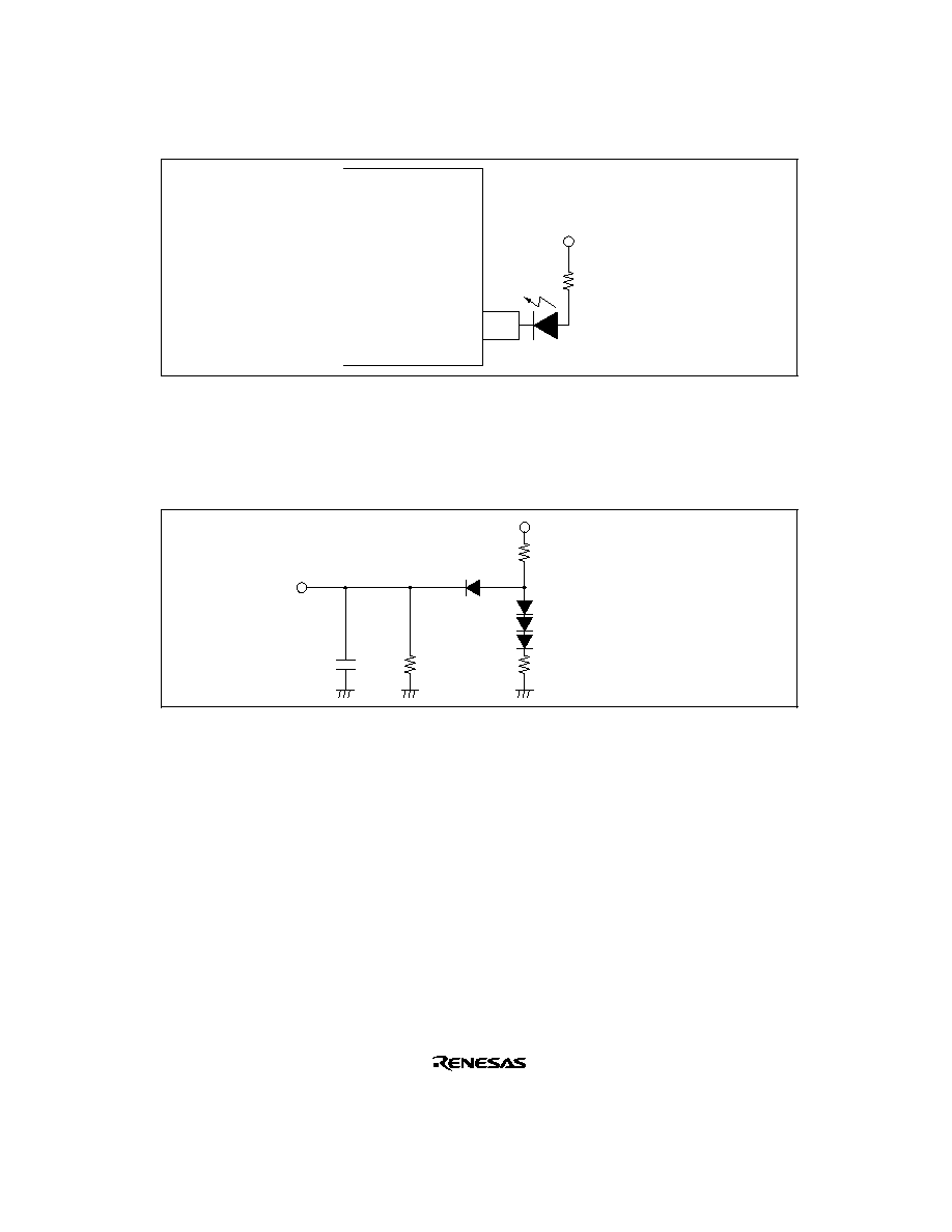
559
600
H8S/2245 Series
Port 1, A to C
LED
Figure 19-2 LED Drive Circuit (Example)
19.4
AC Characteristics
Figure 19-3 show, the test conditions for the AC characteristics.
C
LSI output pin
R
H
R
L
C = 90 pF: Port 1, A to F
C = 30 pF: Port 2, 3, 5, G
R
L
= 2.4 k
R
H
= 12 k
I/O timing test levels
∑ Low level: 0.8 V
∑ High level: 2.0 V
5 V
Figure 19-3 Output Load Circuit

560
19.4.1
Clock Timing
Table 19-5 lists the clock timing
Table 19-5 Clock Timing
Condition A: V
CC
= 2.7 V to 5.5 V, AV
CC
= 2.7 V to 5.5 V, V
ref
= 2.7 V to AV
CC
,
V
SS
= AV
SS
= 0 V, ¯ = 32 kHz to 10 MHz, T
a
= ≠20 to +75∞C (regular
specifications), T
a
= ≠40 to +85∞C (wide-range specifications)
Condition B: V
CC
= 2.7 to 5.5 V, AV
CC
= 2.7 to 5.5 V, V
ref
= 2.7 V to AV
CC
,
V
SS
= AV
SS
= 0 V, ¯ = 32 kHz to 13 MHz, T
a
= ≠20 to +75∞C (regular
specifications), T
a
= ≠40 to +85∞C (wide-range specifications)
Condition C: V
CC
= 5.0 V ± 10%, AV
CC
= 5.0 V ± 10%, V
ref
= 4.5 V to AV
CC
,
V
SS
= AV
SS
= 0 V, ¯ = 2 to 20 MHz, T
a
= ≠20 to +75∞C (regular specifications),
T
a
= ≠40 to +85∞C (wide-range specifications)
Condition A
Condition B
Condition C
Test
Item
Symbol
Min
Max
Min
Max
Min
Max
Unit
Conditions
Clock cycle time
t
cyc
100
31250
75
31250
50
500
ns
Figure 19-4
Clock high pulse
width
t
CH
35
--
25
--
20
--
ns
Clock low pulse
width
t
CL
35
--
25
--
20
--
ns
Clock rise time
t
Cr
--
15
--
10
--
5
ns
Clock fall time
t
Cf
--
15
--
10
--
5
ns
Clock oscillator
setting time at
reset (crystal)
t
OSC1
20
--
20
--
10
--
ms
Figure 19-5
Clock oscillator
setting time in
software standby
(crystal)
t
OSC2
8
--
8
--
8
--
ms
Figure 18-2
External clock
output stabilization
delay time
t
DEXT
500
--
500
--
500
--
µs
Figure 19-5
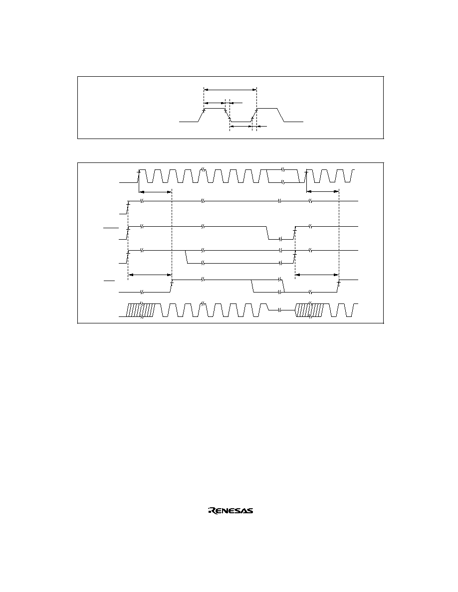
561
t
CH
t
cyc
t
Cf
t
CL
t
Cr
¯
Figure 19-4 System Clock Timing
t
OSC1
t
OSC1
EXTAL
V
CC
NMI
STBY
RES
¯
t
DEXT
t
DEXT
Figure 19-5 Oscillator Settling Timing

562
19.4.2
Control Signal Timing
Table 19-6 lists the control signal timing.
Table 19-6 Control Signal Timing
Condition A: V
CC
= 2.7 V to 5.5 V, AV
CC
= 2.7 V to 5.5 V, V
ref
= 2.7 V to AV
CC
,
V
SS
= AV
SS
= 0 V, ¯ = 32 kHz to 10 MHz, T
a
= ≠20 to +75∞C (regular
specifications), T
a
= ≠40 to +85∞C (wide-range specifications)
Condition B: V
CC
= 2.7 V to 5.5 V, AV
CC
= 2.7 V to 5.5 V, V
ref
= 2.7 V to AV
CC
,
V
SS
= AV
SS
= 0 V, ¯ = 32 kHz to 13 MHz, T
a
= ≠20 to +75∞C (regular
specifications), T
a
= ≠40 to +85∞c (wide-range specifications)
Condition C: V
CC
= 5.0 V ± 10%, AV
CC
= 5.0 V ± 10%, V
ref
= 4.5 V to AV
CC
,
V
SS
= AV
SS
= 0 V, ¯ = 2 to 20 MHz, T
a
= ≠20 to +75∞C (regular specifications),
T
a
= ≠40 to +85∞C (wide-range specifications)
Condition A
Condition B
Condition C
Test
Item
Symbol
Min
Max
Min
Max
Min
Max
Unit
Conditions
RES
setup time
t
RESS
200
--
200
--
200
--
ns
Figure 19-6
RES
pulse width
t
RESW
20
--
20
--
20
--
t
cyc
NMI reset setup
time
t
NMIRS
200
--
200
--
200
--
ns
NMI reset hold
time
t
NMIRH
200
--
200
--
200
--
NMI setup time
t
NMIS
200
--
200
--
150
--
ns
Figure 19-7
NMI hold time
t
NMIH
10
--
10
--
10
--
NMI pulse width
(exiting software
standby mode)
t
NMIW
200
--
200
--
200
--
ns
IRQ
setup time
t
IRQS
200
--
200
--
150
--
ns
IRQ
hold time
t
IRQH
10
--
10
--
10
--
ns
IRQ
pulse width
(exiting software
standby mode)
t
IRQW
200
--
200
--
200
--
ns

563
t
RESS
¯
t
RESW
t
NMIRH
t
NMIRS
t
RESS
RES
NMI
Figure 19-6 Reset Input Timing
t
IRQS
¯
t
NMIS
t
NMIH
IRQ
Edge input
NMI
t
IRQS
t
IRQH
IRQi
(i= 0 to 2)
IRQ
Level input
t
NMIW
t
IRQW
Figure 19-7 Interrupt Input Timing

564
19.4.3
Bus Timing
Table 19-7 lists the bus timing.
Table 19-7 Bus Timing
Condition A: V
CC
= 2.7 V to 5.5 V, AV
CC
= 2.7 V to 5.5 V, V
ref
= 2.7 V to AV
CC
,
V
SS
= AV
SS
= 0 V, ¯ = 32 kHz to 10 MHz, T
a
= ≠20 to +75∞C (regular
specifications), T
a
= ≠40 to +85∞C (wide-range specifications)
Condition B: V
CC
= 2.7 V to 5.5 V, AV
CC
= 2.7 V to 5.5 V, V
ref
= 2.7 V to AV
CC
,
V
SS
= AV
SS
= 0 V, ¯ = 32 kHz to 13 MHz, T
a
= ≠20 to +75∞C (regular
specifications), T
a
= ≠40 to +85∞C (wide-range specifications)
Condition C: V
CC
= 5.0 V ± 10%, AV
CC
= 5.0 V ± 10%, V
ref
= 4.5 V to AV
CC
,
V
SS
= AV
SS
= 0 V, ¯ = 2 to 20 MHz, T
a
= ≠20 to +75∞C (regular specifications),
T
a
= ≠40 to +85∞C (wide-range specifications)
Condition A
Condition B
Condition C
Test
Item
Symbol Min
Max
Min
Max
Min
Max
Unit
Conditions
Address
delay time
t
AD
--
40
--
35
--
20
ns
Figure 19-8
to
Address
setup time
t
AS
0.5
◊
t
cyc
≠ 30
--
0.5
◊
t
cyc
≠ 20
--
0.5
◊
t
cyc
≠ 15
--
ns
Figure 19-12
Address
hold time
t
AH
0.5
◊
t
cyc
≠ 20
--
0.5
◊
t
cyc
≠ 15
--
0.5
◊
t
cyc
≠ 10
--
ns
CS
delay
time
t
CSD
--
40
--
35
--
20
ns
AS
delay
time
t
ASD
--
60
--
50
--
30
ns
RD
delay
time 1
t
RSD1
--
60
--
45
--
30
ns
RD
delay
time 2
t
RSD2
--
60
--
45
--
30
ns
Read data
setup time
t
RDS
30
--
30
--
15
--
ns
Read data
hold time
t
RDH
0
--
0
--
0
--
ns

565
Table 19-7 Bus Timing (cont)
Condition A: V
CC
= 2.7 V to 5.5 V, AV
CC
= 2.7 V to 5.5 V, V
ref
= 2.7 V to AV
CC
,
V
SS
= AV
SS
= 0 V, ¯ = 32 kHz to 10 MHz, T
a
= ≠20 to +75∞C (regular
specifications), T
a
= ≠40 to +85∞C (wide-range specifications)
Condition B: V
CC
= 2.7 V to 5.5 V, AV
CC
= 2.7 V to 5.5 V, V
ref
= 2.7 V to AV
CC
,
V
SS
= AV
SS
= 0 V, ¯ = 32 kHz to 13 MHz, T
a
= ≠20 to +75∞C (regular
specifications), T
a
= ≠40 to +85∞C (wide-range specifications)
Condition C: V
CC
= 5.0 V ± 10%, AV
CC
= 5.0 V ± 10%, V
ref
= 4.5 V to AV
CC
,
V
SS
= AV
SS
= 0 V, ¯ = 2 to 20 MHz, T
a
= ≠20 to +75∞C (regular specifications),
T
a
= ≠40 to +85∞C (wide-range specifications)
Condition A
Condition B
Condition C
Test
Item
Symbol Min
Max
Min
Max
Min
Max
Unit
Conditions
Read data
access
time 1
t
ACC1
--
1.0
◊
t
cyc
≠ 50
--
1.0
◊
t
cyc
≠ 55
--
1.0
◊
t
cyc
≠ 25
ns
Figure 19-8
to
Figure 19-12
Read data
access
time 2
t
ACC2
--
1.5
◊
t
cyc
≠ 50
--
1.5
◊
t
cyc
≠ 55
--
1.5
◊
t
cyc
≠ 25
ns
Read data
access
time 3
t
ACC3
--
2.0
◊
t
cyc
≠ 50
--
2.0
◊
t
cyc
≠ 55
--
2.0
◊
t
cyc
≠ 25
ns
Read data
access
time 4
t
ACC4
--
2.5
◊
t
cyc
≠ 50
--
2.5
◊
t
cyc
≠ 55
--
2.5
◊
t
cyc
≠ 25
ns
Read data
access
time 5
t
ACC5
--
3.0
◊
t
cyc
≠ 50
--
3.0
◊
t
cyc
≠ 55
--
3.0
◊
t
cyc
≠ 25
ns
WR
delay
time 1
t
WRD1
--
60
--
45
--
30
ns
WR
delay
time 2
t
WRD2
--
60
--
50
--
30
ns
WR
pulse
width 1
t
WSW1
1.0
◊
t
cyc
≠ 40
--
1.0
◊
t
cyc
≠ 30
--
1.0
◊
t
cyc
≠ 20
--
ns
WR
pulse
width 2
t
WSW2
1.5
◊
t
cyc
≠ 40
--
1.5
◊
t
cyc
≠ 30
--
1.5
◊
t
cyc
≠ 20
--
ns

566
Table 19-7 Bus Timing (cont)
Condition A: V
CC
= 2.7 V to 5.5 V, AV
CC
= 2.7 V to 5.5 V, V
ref
= 2.7 V to AV
CC
,
V
SS
= AV
SS
= 0 V, ¯ = 32 kHz to 10 MHz, T
a
= ≠20 to +75∞C (regular
specifications), T
a
= ≠40 to +85∞C (wide-range specifications)
Condition B: V
CC
= 2.7 V to 5.5 V, AV
CC
= 2.7 V to 5.5 V, V
ref
= 2.7 V to AV
CC
,
V
SS
= AV
SS
= 0 V, ¯ = 32 kHz to 13 MHz, T
a
= ≠20 to +75∞C (regular
specifications), T
a
= ≠40 to +85∞C (wide-range specifications)
Condition C: V
CC
= 5.0 V ± 10%, AV
CC
= 5.0 V ± 10%, V
ref
= 4.5 V to AV
CC
,
V
SS
= AV
SS
= 0 V, ¯ = 2 to 20 MHz, T
a
= ≠20 to +75∞C (regular specifications),
T
a
= ≠40 to +85∞C (wide-range specifications)
Condition A
Condition B
Condition C
Test
Item
Symbol Min
Max
Min
Max
Min
Max
Unit
Conditions
Write data
delay time
t
WDD
--
60
--
60
--
30
ns
Figure 19-8
to
Write data
setup time
t
WDS
0
--
0
--
0
--
ns
Figure 19-12
Write data
hold time
t
WDH
20
--
20
--
10
--
ns
WAIT
setup time
t
WTS
60
--
50
--
30
--
ns
Figure 19-10
WAIT
hold
time
t
WTH
10
--
10
--
5
--
ns
BREQ
setup time
t
BRQS
60
--
50
--
30
--
ns
Figure 19-13
BACK
delay time
t
BACD
--
60
--
50
--
30
ns
Bus-floating
time
t
BZD
--
100
--
80
--
50
ns
BREQO
delay time
t
BRQOD
--
60
--
50
--
30
ns
Figure 19-14

567
t
RSD2
¯
T
1
t
AD
AS
A
23
to A
0
t
ASD
RD
(read)
T
2
t
CSD
t
AS
t
AS
t
AS
t
ASD
t
ACC2
t
RSD1
t
ACC3
t
RDS
t
RDH
t
WRD2
t
WRD2
t
WDD
t
WSW1
t
WDH
CS3
to
CS0
D
15
to D
0
(read)
HWR
,
LWR
(write)
D
15
to D
0
(write)
t
AH
t
AH
Figure 19-8 Basic Bus Timing (Two-State Access)

568
t
RSD2
¯
T
2
AS
A
23
to A
0
t
ASD
RD
(read)
T
3
t
AS
t
AS
t
AH
t
AH
t
ASD
t
ACC4
t
RSD1
t
ACC5
t
RDS
t
RDH
t
WRD1
t
WRD2
t
WDS
t
WSW2
t
WDH
CS3
to
CS0
D
15
to D
0
(read)
HWR
,
LWR
(write)
D
15
to D
0
(write)
T
1
t
CSD
t
WDD
t
AD
Figure 19-9 Basic Bus Timing (Three-State Access)

569
¯
T
W
AS
A
23
to A
0
RD
(read)
T
3
CS3
to
CS0
D
15
to D
0
(read)
HWR
,
LWR
(write)
D
15
to D
0
(write)
T
2
t
WTS
T
1
t
WTH
t
WTS
t
WTH
WAIT
Figure 19-10 Basic Bus Timing (Three-State Access with One Wait State)

570
t
RSD2
¯
T
1
AS
A
23
to A
0
T
2
t
AH
t
ACC3
t
RDS
CS3
to
CS0
D
15
to D
0
(read)
T
2
or T
3
t
AS
T
1
t
ASD
t
ASD
t
RDH
t
AD
RD
(read)
Figure 19-11 Burst ROM Access Timing (Two-State Access)

571
t
RSD2
¯
T
1
AS
A
23
to A
0
T
1
t
ACC1
CS3
to
CS0
D
15
to D
0
(read)
T
2
or T
3
t
RDH
t
AD
RD
(read)
t
RDS
Figure 19-12 Burst ROM Access Timing (One-State Access)

572
¯
BREQ
A
23
to A
0
,
CS3
to
CS0
,
t
BRQS
t
BACD
t
BZD
t
BACD
t
BZD
t
BRQS
BACK
AS
,
RD
,
HWR
,
LWR
Figure 19-13 External Bus Release Timing
¯
BREQO
t
BRQOD
t
BRQOD
Figure 19-14 External Bus Request Output Timing

573
19.4.4
Timing of On-Chip Supporting Modules
Table 19-8 lists the timing of on-chip supporting modules.
Table 19-8 Timing of On-Chip Supporting Modules
Condition A: V
CC
= 2.7 V to 5.5 V, AV
CC
= 2.7 V to 5.5 V, V
ref
= 2.7 V to AV
CC
,
V
SS
= AV
SS
= 0 V, ¯ = 32 kHz to 10 MHz (I/O port, TMR, WDT),
¯ = 2 to 10 MHz (TPU, SCI, A/D converter), T
a
= ≠20 to +75∞C (regular
specifications), T
a
= ≠40 to +85∞C (wide-range specifications)
Condition B: V
CC
= 2.7 V to 5.5 V, AV
CC
= 2.7 V to 5.5 V, V
ref
= 2.7 V to AV
CC
,
V
SS
= AV
SS
= 0 V, ¯ = 32 kHz to 13 MHz (I/O port, TMR, WDT),
¯ = 2 to 13 MHz (TPU, SCI, A/D converter), T
a
= ≠20 to +75∞C (regular
specifications), T
a
= ≠40 to +85∞C (wide-range specifications)
Condition C: V
CC
= 5.0 V ± 10%, AV
CC
= 5.0 V ± 10%, V
ref
= 4.5 V to AV
CC
,
V
SS
= AV
SS
= 0 V, ¯ = 2 to 20 MHz, T
a
= ≠20 to +75∞C (regular specifications),
T
a
= ≠40 to +85∞C (wide-range specifications)
Condition A Condition B Condition C
Test
Item
Symbol Min
Max
Min
Max
Min
Max
Unit Conditions
I/O
port
Output data delay
time
t
PWD
--
100
--
75
--
50
ns
Figure
19-15
Input data setup
time
t
PRS
50
--
50
--
30
--
Input data hold
time
t
PRH
50
--
50
--
30
--
TPU
Timer output
delay time
t
TOCD
--
100
--
75
--
50
ns
Figure
19-16
Timer input setup
time
t
TICS
50
--
40
--
30
--
Timer clock input
setup time
t
TCKS
50
--
40
--
30
--
ns
Figure
19-17
Timer
clock
Single
edge
t
TCKWH
1.5
--
1.5
--
1.5
--
t
cyc
pulse
width
Both
edges
t
TCKWL
2.5
--
2.5
--
2.5
--

574
Table 19-8 Timing of On-Chip Supporting Modules (cont)
Condition A: V
CC
= 2.7 V to 5.5 V, AV
CC
= 2.7 V to 5.5 V, V
ref
= 2.7 V to AV
CC
,
V
SS
= AV
SS
= 0 V, ¯ = 32 kHz to 10 MHz (I/O port, TMR, WDT),
¯ = 2 to 10 MHz (TPU, SCI, A/D converter), T
a
= ≠20 to +75∞C (regular
specifications), T
a
= ≠40 to +85∞C (wide-range specifications)
Condition B: V
CC
= 2.7 V to 5.5 V, AV
CC
= 2.7 V to 5.5 V, V
ref
= 2.7 V to AV
CC
,
V
SS
= AV
SS
= 0 V, ¯ = 32 kHz to 13 MHz (I/O port, TMR, WDT),
¯ = 2 to 13 MHz (TPU, SCI, A/D converter), T
a
= ≠20 to +75∞C (regular
specifications), T
a
= ≠40 to +85∞C (wide-range specifications)
Condition C: V
CC
= 5.0 V ± 10%, AV
CC
= 5.0 V ± 10%, V
ref
= 4.5 V to AV
CC
,
V
SS
= AV
SS
= 0 V, ¯ = 2 to 20 MHz, T
a
= ≠20 to +75∞C (regular specifications),
T
a
= ≠40 to +85∞C (wide-range specifications)
Condition A Condition B Condition C
Test
Item
Symbol Min
Max
Min
Max
Min
Max
Unit Conditions
8-bit
timer
Timer output
delay time
t
TMOD
--
100
--
75
--
50
ns
Figure
19-18
Timer reset input
setup time
t
TMRS
50
--
50
--
30
--
ns
Figure
19-20
Timer clock input
setup time
t
TMCS
50
--
50
--
30
--
ns
Figure
19-19
Timer
clock
Single
edge
t
TMCWH
1.5
--
1.5
--
1.5
--
t
cyc
pulse
width
Both
edges
t
TMCWL
2.5
--
2.5
--
2.5
--
WDT
Overflow output
delay time
t
WOVD
--
100
--
75
--
50
ns
Figure
19-21
SCI
Input
clock
Asynchro-
nous
t
Scyc
4
--
4
--
4
--
t
cyc
Figure
19-22
cycle
Synchro-
nous
6
--
6
--
6
--
Input clock pulse
width
t
SCKW
0.4
0.6
0.4
0.6
0.4
0.6
t
Scyc
Input clock rise
time
t
SCKr
--
1.5
--
1.5
--
1.5
t
cyc
Input clock fall
time
t
SCKf
--
1.5
--
1.5
--
1.5

575
Table 19-8 Timing of On-Chip Supporting Modules (cont)
Condition A: V
CC
= 2.7 V to 5.5 V, AV
CC
= 2.7 V to 5.5 V, V
ref
= 2.7 V to AV
CC
,
V
SS
= AV
SS
= 0 V, ¯ = 32 kHz to 10 MHz (I/O port, TMR, WDT),
¯ = 2 to 10 MHz (TPU, SCI, A/D converter), T
a
= ≠20 to +75∞C (regular
specifications), T
a
= ≠40 to +85∞C (wide-range specifications)
Condition B: V
CC
= 2.7 V to 5.5 V, AV
CC
= 2.7 V to 5.5 V, V
ref
= 2.7 V to AV
CC
,
V
SS
= AV
SS
= 0 V, ¯ = 32 kHz to 13 MHz (I/O port, TMR, WDT),
¯ = 2 to 13 MHz (TPU, SCI, A/D converter), T
a
= ≠20 to +75∞C (regular
specifications), T
a
= ≠40 to +85∞C (wide-range specifications)
Condition C: V
CC
= 5.0 V ± 10%, AV
CC
= 5.0 V ± 10%, V
ref
= 4.5 V to AV
CC
,
V
SS
= AV
SS
= 0 V, ¯ = 2 to 20 MHz, T
a
= ≠20 to +75∞C (regular specifications),
T
a
= ≠40 to +85∞C (wide-range specifications)
Condition A Condition B Condition C
Test
Item
Symbol Min
Max
Min
Max
Min
Max
Unit Conditions
SCI
Transmit data
delay time
t
TXD
--
100
--
75
--
50
ns
Figure
19-23
Receive data
setup time
(synchronous)
t
RXS
100
--
75
--
50
--
ns
Receive data
hold time
(synchronous)
t
RXH
100
--
75
--
50
--
ns
A/D
con-
verter
Trigger input
setup time
t
TRGS
50
--
40
--
30
--
ns
Figure
19-24
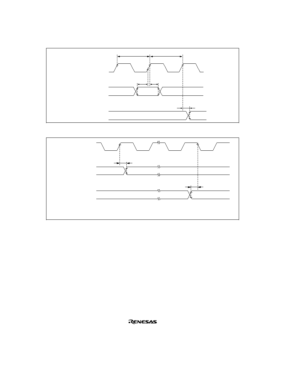
576
¯
Port 1 to 5,
A to G (read)
T2
T1
t
PWD
t
PRH
t
PRS
Port 1 to 3, 5,
A to G (write)
Figure 19-15 I/O Port Input/Output Timing
¯
t
TICS
t
TOCD
Output compare
output
*
Input capture
input
*
Note:
*
TIOCA0 to TIOCA2, TIOCB0 to TIOCB2, TIOCC0, TIOCD0
Figure 19-16 TPU Input/Output Timing
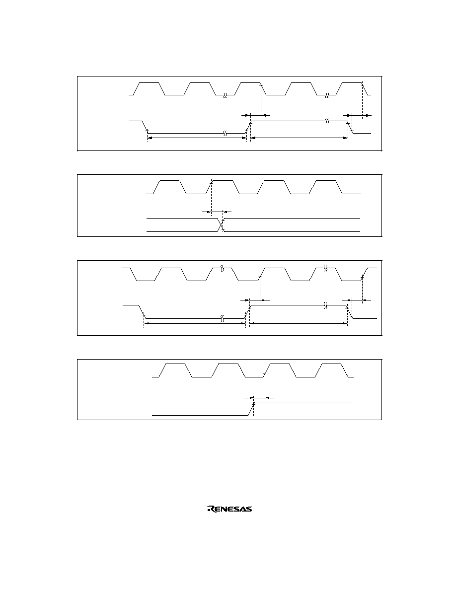
577
t
TCKS
¯
t
TCKS
TCLKA to TCLKD
t
TCKWH
t
TCKWL
Figure 19-17 TPU Clock Input Timing
¯
TMO0, TMO1
t
TMOD
Figure 19-18 8-Bit Timer Output Timing
¯
TMCI0, TMCI1
t
TMCS
t
TMCS
t
TMCWH
t
TMCWL
Figure 19-19 8-Bit Timer Clock Input Timing
¯
TMRI0, TMRI1
t
TMRS
Figure 19-20 8-Bit Timer Reset Input Timing
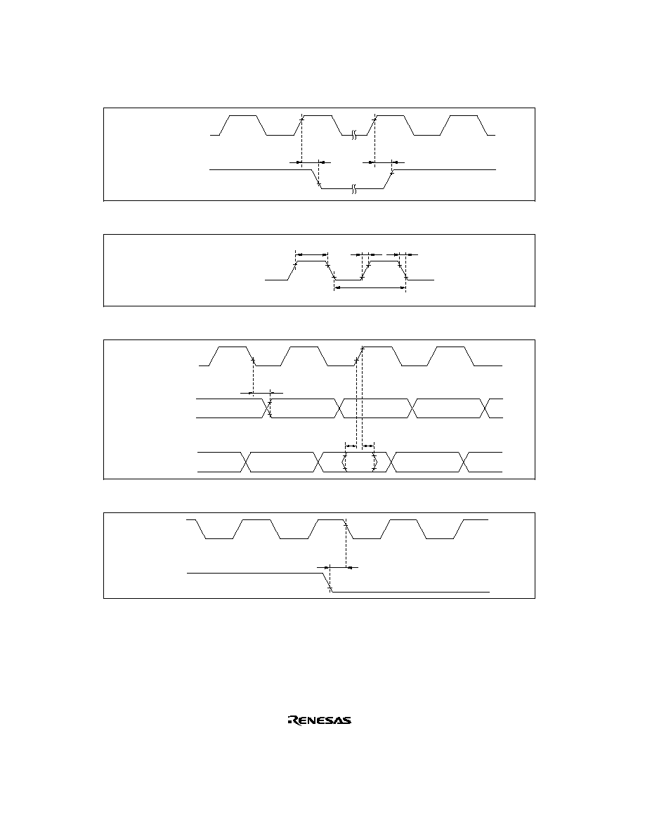
578
¯
WDTOVF
t
WOVD
t
WOVD
Figure 19-21 WDT Output Timing
SCK0 to SCK2
t
SCKW
t
SCKr
t
SCKf
t
Scyc
Figure 19-22 SCK Clock Input Timing
TxD0 to TxD2
Transmit data
RxD0 to RxD2
Receive data
SCK0 to SCK2
t
RXS
t
RXH
t
TXD
Figure 19-23 SCI Input/Output Timing Synchronous Mode
¯
ADTRG
t
TRGS
Figure 19-24 A/D Converter External Trigger Input Timing

579
19.5
A/D Conversion Characteristics
Table 19-9 lists the A/D conversion characteristics.
Table 19.9
A/D Conversion Characteristics
Condition A: V
CC
= 2.7 V to 5.5 V, AV
CC
= 2.7 V to 5.5 V, V
ref
= 2.7 V to AV
CC
,
V
SS
= AV
SS
= 0 V, ¯ = 2 to 10 MHz, T
a
= ≠20 to +75∞C (regular specifications),
T
a
= ≠40 to +85∞C (wide-range specifications)
Condition B: V
CC
= 2.7 V to 5.5 V, AV
CC
= 2.7 V to 5.5 V, V
ref
= 2.7 V to AV
CC
,
V
SS
= AV
SS
= 0 V, ¯ = 2 to 13 MHz, T
a
= ≠20 to +75∞C (regular specifications),
T
a
= ≠40 to +85∞C (wide-range specifications)
Condition C: V
CC
= 5.0 V ± 10%, AV
CC
= 5.0 V ± 10%, V
ref
= 4.5 V to AV
CC
,
V
SS
= AV
SS
= 0 V, ¯ = 2 to 20 MHz, T
a
= ≠20 to +75∞C (regular specifications),
T
a
= ≠40 to +85∞C (wide-range specifications)
Condition A
Condition B
Condition C
Item
Min
Typ
Max
Min
Typ
Max
Min
Typ
Max
Unit
Resolution
10
10
10
10
10
10
10
10
10
bits
Conversion time
--
--
13.4
--
--
10.1
--
--
6.7
µs
Analog input
capacitance
--
--
20
--
--
20
--
--
20
pF
Permissible signal-
--
--
10
*
1
--
--
10
*
1
--
--
10
*
3
k
source impedance
--
--
5
*
2
--
--
5
*
2
--
--
5
*
4
Nonlinearity error
--
--
±6.0
--
--
±6.0
--
--
±3.0
LSB
Offset error
--
--
±4.0
--
--
±4.0
--
--
±2.0
LSB
Full-scale error
--
--
±4.0
--
--
±4.0
--
--
±2.0
LSB
Quantization error
--
--
±0.5
--
--
±0.5
--
--
±0.5
LSB
Absolute accuracy
--
--
±8.0
--
--
±8.0
--
--
±4.0
LSB
Notes: 1. 4.0
AV
CC
5.5 V
2. 2.7 V
AV
CC
< 4.0 V
3. ¯
12 MHz
4. ¯ > 12 MHz

580
19.6
Usage Notes
Although both the ZTAT and mask ROM versions fully meet the electrical specifications listed in
this manual, due to differences in the fabrication process, the on-chip ROM, and the layout
patterns, there will be differences in the actual values of the electrical characteristics, the operating
margins, the noise margins, and other aspects.
Therefore, if a system is evaluated using the ZTAT version, a similar evaluation should also be
performed using the mask ROM version.

581
Appendix A Instruction Set
A.1
Instruction List
Operand Notation
Rd
General register (destination)
*
Rs
General register (source)
*
Rn
General register
*
ERn
General register (32-bit register)
(EAd)
Destination operand
(EAs)
Source operand
EXR
Extended control register
CCR
Condition-code register
N
N (negative) flag in CCR
Z
Z (zero) flag in CCR
V
V (overflow) flag in CCR
C
C (carry) flag in CCR
PC
Program counter
SP
Stack pointer
#IMM
Immediate data
disp
Displacement
+
Add
≠
Subtract
◊
Multiply
˜
Divide
Logical AND
Logical OR
Logical exclusive OR
Move
¨
Logical NOT (logical complement)
( ) < >
Contents of effective address of the operand
:8/:16/:24/:32
8-, 16-, 24-, or 32-bit length
Note:
*
General registers include 8-bit registers (R0H to R7H, R0L to R7L), 16-bit registers (R0 to
R7, E0 to E7), and 32-bit registers (ER0 to ER7).

582
Condition Code Notation
Symbol
Changes according to the result of instruction
*
Undetermined (no guaranteed value)
0
Always cleared to 0
1
Always set to 1
--
Not affected by execution of the instruction
583
Table A-1 Instruction Set
(1) Data Transfer Instructions
Addressing Mode/
Instruction Length (Bytes)
Operand Size
#xx
Rn
@ERn
@(d,ERn)
@≠ERn/@ERn+
@aa
@(d,PC)
@@aa
--
Mnemonic
MOV
MOV.B #xx:8,Rd
B
2
MOV.B Rs,Rd
B
2
MOV.B @ERs,Rd
B
2
MOV.B @(d:16,ERs),Rd
B
4
MOV.B @(d:32,ERs),Rd
B
8
MOV.B @ERs+,Rd
B
2
MOV.B @aa:8,Rd
B
2
MOV.B @aa:16,Rd
B
4
MOV.B @aa:32,Rd
B
6
MOV.B Rs,@ERd
B
2
MOV.B Rs,@(d:16,ERd)
B
4
MOV.B Rs,@(d:32,ERd)
B
8
MOV.B Rs,@-ERd
B
2
MOV.B Rs,@aa:8
B
2
MOV.B Rs,@aa:16
B
4
MOV.B Rs,@aa:32
B
6
MOV.W #xx:16,Rd
W
4
MOV.W Rs,Rd
W
2
MOV.W @ERs,Rd
W
2
#xx:8
Rd8
--
--
0
--
1
Rs8
Rd8
--
--
0
--
1
@ERs
Rd8
--
--
0
--
2
@(d:16,ERs)
Rd8
--
--
0
--
3
@(d:32,ERs)
Rd8
--
--
0
--
5
@ERs
Rd8,ERs32+1
ERs32
--
--
0
--
3
@aa:8
Rd8
--
--
0
--
2
@aa:16
Rd8
--
--
0
--
3
@aa:32
Rd8
--
--
0
--
4
Rs8
@ERd
--
--
0
--
2
Rs8
@(d:16,ERd)
--
--
0
--
3
Rs8
@(d:32,ERd)
--
--
0
--
5
ERd32-1
ERd32,Rs8
@ERd
--
--
0
--
3
Rs8
@aa:8
--
--
0
--
2
Rs8
@aa:16
--
--
0
--
3
Rs8
@aa:32
--
--
0
--
4
#xx:16
Rd16
--
--
0
--
2
Rs16
Rd16
--
--
0
--
1
@ERs
Rd16
--
--
0
--
2
Operation
Condition Code
Normal
IH
N
Z
V
C
Advanced
No. of States
*
1

584
Table A-1 Instruction Set (cont)
(1) Data Transfer Instructions (cont)
Addressing Mode/
Instruction Length (Bytes)
Operand Size
#xx
Rn
@ERn
@(d,ERn)
@≠ERn/@ERn+
@aa
@(d,PC)
@@aa
--
Mnemonic
MOV
MOV.W @(d:16,ERs),Rd
W
4
MOV.W @(d:32,ERs),Rd
W
8
MOV.W @ERs+,Rd
W
2
MOV.W @aa:16,Rd
W
4
MOV.W @aa:32,Rd
W
6
MOV.W Rs,@ERd
W
2
MOV.W Rs,@(d:16,ERd)
W
4
MOV.W Rs,@(d:32,ERd)
W
8
MOV.W Rs,@-ERd
W
2
MOV.W Rs,@aa:16
W
4
MOV.W Rs,@aa:32
W
6
MOV.L #xx:32,ERd
L
6
MOV.L ERs,ERd
L
2
MOV.L @ERs,ERd
L
4
MOV.L @(d:16,ERs),ERd
L
6
MOV.L @(d:32,ERs),ERd
L
1
0
MOV.L @ERs+,ERd
L
4
MOV.L @aa:16,ERd
L
6
MOV.L @aa:32,ERd
L
8
@(d:16,ERs)
Rd16
--
--
0
--
3
@(d:32,ERs)
Rd16
--
--
0
--
5
@ERs
Rd16,ERs32+2
ERs32
----
0
--
3
@aa:16
Rd16
--
--
0
--
3
@aa:32
Rd16
--
--
0
--
4
Rs16
@ERd
--
--
0
--
2
Rs16
@(d:16,ERd)
--
--
0
--
3
Rs16
@(d:32,ERd)
--
--
0
--
5
ERd32-2
ERd32,Rs16
@ERd
--
--
0
--
3
Rs16
@aa:16
--
--
0
--
3
Rs16
@aa:32
--
--
0
--
4
#xx:32
ERd32
--
--
0
--
3
ERs32
ERd32
--
--
0
--
1
@ERs
ERd32
--
--
0
--
4
@(d:16,ERs)
ERd32
--
--
0
--
5
@(d:32,ERs)
ERd32
--
--
0
--
7
@ERs
ERd32,ERs32+4
ERs32
----
0
--
5
@aa:16
ERd32
--
--
0
--
5
@aa:32
ERd32
--
--
0
--
6
Operation
Condition Code
Normal
IH
N
Z
V
C
Advanced
No. of States
*
1

585
Table A-1 Instruction Set (cont)
(1) Data Transfer Instructions (cont)
Addressing Mode/
Instruction Length (Bytes)
Operand Size
#xx
Rn
@ERn
@(d,ERn)
@≠ERn/@ERn+
@aa
@(d,PC)
@@aa
--
Mnemonic
MOV
POP
PUSH
LDM
STM
MOVFPE
MOVTPE
MOV.L ERs,@ERd
L
4
MOV.L ERs,@(d:16,ERd)
L
6
MOV.L ERs,@(d:32,ERd)
L
1
0
MOV.L ERs,@-ERd
L
4
MOV.L ERs,@aa:16
L
6
MOV.L ERs,@aa:32
L
8
POP.W Rn
W
2
POP.L ERn
L
4
PUSH.W Rn
W
2
PUSH.L ERn
L
4
LDM @SP+,(ERm-ERn)
L
4
STM (ERm-ERn),@-SP
L
4
MOVFPE @aa:16,Rd
MOVTPE Rs,@aa:16
ERs32
@ERd
--
--
0
--
4
ERs32
@(d:16,ERd)
--
--
0
--
5
ERs32
@(d:32,ERd)
--
--
0
--
7
ERd32-4
ERd32,ERs32
@
ERd
----
0
--
5
ERs32
@aa:16
--
--
0
--
5
ERs32
@aa:32
--
--
0
--
6
@SP
Rn16,SP+2
SP
--
--
0
--
3
@SP
ERn32,SP+4
SP
--
--
0
--
5
SP-2
SP,Rn16
@SP
--
--
0
--
3
SP-4
SP,ERn32
@SP
--
--
0
--
5
(@SP
ERn32,SP+4
SP)
--
--
--
--
--
--
7/9/11 [1]
Repeated for each register restored
(SP-4
SP,ERn32
@SP)
--
--
--
--
--
--
7/9/11 [1]
Repeated for each register saved
[2]
[2]
Operation
Condition Code
Normal
IH
N
Z
V
C
Advanced
No. of States
*
1
Cannot be used in the H8S/2245 Series
Cannot be used in the H8S/2245 Series

586
Table A-1 Instruction Set
(2) Arithmetic Instructions
Addressing Mode/
Instruction Length (Bytes)
Operand Size
#xx
Rn
@ERn
@(d,ERn)
@≠ERn/@ERn+
@aa
@(d,PC)
@@aa
--
Mnemonic
ADD
ADDX
ADDS
INC
DAA
ADD.B #xx:8,Rd
B
2
ADD.B Rs,Rd
B
2
ADD.W #xx:16,Rd
W
4
ADD.W Rs,Rd
W
2
ADD.L #xx:32,ERd
L
6
ADD.L ERs,ERd
L
2
ADDX #xx:8,Rd
B
2
ADDX Rs,Rd
B
2
ADDS #1,ERd
L
2
ADDS #2,ERd
L
2
ADDS #4,ERd
L
2
INC.B Rd
B
2
INC.W #1,Rd
W
2
INC.W #2,Rd
W
2
INC.L #1,ERd
L
2
INC.L #2,ERd
L
2
DAA Rd
B
2
Rd8+#xx:8
Rd8
--
1
Rd8+Rs8
Rd8
--
1
Rd16+#xx:16
Rd16
--
[3]
2
Rd16+Rs16
Rd16
--
[3]
1
ERd32+#xx:32
ERd32
--
[4]
3
ERd32+ERs32
ERd32
--
[4]
1
Rd8+#xx:8+C
Rd8
--
[5]
1
Rd8+Rs8+C
Rd8
--
[5]
1
ERd32+1
ERd32
------------
1
ERd32+2
ERd32
------------
1
ERd32+4
ERd32
------------
1
Rd8+1
Rd8
--
--
--
1
Rd16+1
Rd16
--
--
--
1
Rd16+2
Rd16
--
--
--
1
ERd32+1
ERd32
--
--
--
1
ERd32+2
ERd32
--
--
--
1
Rd8 decimal adjust
Rd8
--
*
*
1
Operation
Condition Code
Normal
IH
N
Z
V
C
Advanced
No. of States
*
1

587
Table A-1 Instruction Set (cont)
(2) Arithmetic Instructions (cont)
Addressing Mode/
Instruction Length (Bytes)
Operand Size
#xx
Rn
@ERn
@(d,ERn)
@≠ERn/@ERn+
@aa
@(d,PC)
@@aa
--
Mnemonic
SUBX
SUBS
DEC
DAS
MULXU
SUB.W Rs,Rd
W
2
SUB.L #xx:32,ERd
L
6
SUB.L ERs,ERd
L
2
SUBX #xx:8,Rd
B
2
SUBX Rs,Rd
B
2
SUBS #1,ERd
L
2
SUBS #2,ERd
L
2
SUBS #4,ERd
L
2
DEC.B Rd
B
2
DEC.W #1,Rd
W
2
DEC.W #2,Rd
W
2
DEC.L #1,ERd
L
2
DEC.L #2,ERd
L
2
DAS Rd
B
2
MULXU.B Rs,Rd
B
2
MULXU.W Rs,ERd
W
2
Rd16-Rs16
Rd16
--
[3]
1
ERd32-#xx:32
ERd32
--
[4]
3
ERd32-ERs32
ERd32
--
[4]
1
Rd8-#xx:8-C
Rd8
--
[5]
1
Rd8-Rs8-C
Rd8
--
[5]
1
ERd32-1
ERd32
----------
--
1
ERd32-2
ERd32
----------
--
1
ERd32-4
ERd32
----------
--
1
Rd8-1
Rd8
--
--
--
1
Rd16-1
Rd16
--
--
--
1
Rd16-2
Rd16
--
--
--
1
ERd32-1
ERd32
--
--
--
1
ERd32-2
ERd32
--
--
--
1
Rd8 decimal adjust
Rd8
--
*
*
--1
Rd8
◊
Rs8
Rd16
----------
--
1
2
(unsigned multiplication)
Rd16
◊
Rs16
ERd32
----------
--
2
0
(unsigned multiplication)
Operation
Condition Code
Normal
IH
N
Z
V
C
Advanced
No. of States
*
1
SUB.B Rs,Rd
B
2
SUB.W #xx:16,Rd
SUB
Rd8-Rs8
Rd8
--
1
Rd16-#xx:16
Rd16
--
[3]
2
W 4
588
Table A-1 Instruction Set (cont)
(2) Arithmetic Instructions (cont)
Addressing Mode/
Instruction Length (Bytes)
Operand Size
#xx
Rn
@ERn
@(d,ERn)
@≠ERn/@ERn+
@aa
@(d,PC)
@@aa
--
Mnemonic
DIVXU
DIVXS
CMP
NEG
MULXS.B Rs,Rd
B
4
MULXS.W Rs,ERd
W
4
DIVXU.B Rs,Rd
B
2
DIVXU.W Rs,ERd
W
2
DIVXS.B Rs,Rd
B
4
DIVXS.W Rs,ERd
W
4
CMP.B #xx:8,Rd
B
2
CMP.B Rs,Rd
B
2
CMP.W #xx:16,Rd
W
4
CMP.W Rs,Rd
W
2
CMP.L #xx:32,ERd
L
6
CMP.L ERs,ERd
L
2
NEG.B Rd
B
2
NEG.W Rd
W
2
NEG.L ERd
L
2
Rd8
◊
Rs8
Rd16 --
--
--
--
13
(signed multiplication)
Rd16
◊
Rs16
ERd32 --
--
--
--
21
(signed multiplication)
Rd16
˜
Rs8
Rd16 (RdH: remainder,
--
--
[6]
[7]
--
--
12
RdL: quotient) (unsigned division)
ERd32
˜
Rs16
ERd32 (Ed: remainder,
--
--
[6]
[7]
--
--
20
Rd: quotient) (unsigned division)
Rd16
˜
Rs8
Rd16 (RdH: remainder,
--
--
[8]
[7]
--
--
13
RdL: quotient) (signed division)
ERd32
˜
Rs16
ERd32 (Ed: remainder,
--
--
[8]
[7]
--
--
21
Rd: quotient) (signed division)
Rd8-#xx:8
--
1
Rd8-Rs8
--
1
Rd16-#xx:16
--
[3]
2
Rd16-Rs16
--
[3]
1
ERd32-#xx:32
--
[4]
3
ERd32-ERs32
--
[4]
1
0-Rd8
Rd8
--
1
0-Rd16
Rd16
--
1
0-ERd32
ERd32
--
1
Operation
Condition Code
Normal
IH
N
Z
V
C
Advanced
No. of States
*
1
MULXS
589
Table A-1 Instruction Set (cont)
(2) Arithmetic Instructions (cont)
Addressing Mode/
Instruction Length (Bytes)
Operand Size
#xx
Rn
@ERn
@(d,ERn)
@≠ERn/@ERn+
@aa
@(d,PC)
@@aa
--
Mnemonic
EXTS
TAS
EXTU.W Rd
W
2
EXTU.L ERd
L
2
EXTS.W Rd
W
2
EXTS.L ERd
L
2
TAS @ERd
B
4
0
(<bit 15 to 8
>
of Rd16)
--
--
0
0
--
1
0
(<bit 31 to 16
>
of ERd32)
--
--
0
0
--
1
(<bit 7
>
of Rd16)
----
0
--
1
(<bit 15 to 8
>
of Rd16)
(<bit 15
>
of ERd32)
----
0
--
1
(<bit 31 to 16> of ERd32)
@ERd-0
CCR set, (1)
----
0
--
4
(
<
bit 7
>
of @ERd)
Operation
Condition Code
Normal
IH
N
Z
V
C
Advanced
No. of States
*
1
EXTU

590
Table A-1 Instruction Set
(3) Logical Instructions
Addressing Mode/
Instruction Length (Bytes)
Operand Size
#xx
Rn
@ERn
@(d,ERn)
@≠ERn/@ERn+
@aa
@(d,PC)
@@aa
--
Mnemonic
OR
XOR
NOT
AND.B #xx:8,Rd
B
2
AND.B Rs,Rd
B
2
AND.W #xx:16,Rd
W
4
AND.W Rs,Rd
W
2
AND.L #xx:32,ERd
L
6
AND.L ERs,ERd
L
4
OR.B #xx:8,Rd
B
2
OR.B Rs,Rd
B
2
OR.W #xx:16,Rd
W
4
OR.W Rs,Rd
W
2
OR.L #xx:32,ERd
L
6
OR.L ERs,ERd
L
4
XOR.B #xx:8,Rd
B
2
XOR.B Rs,Rd
B
2
XOR.W #xx:16,Rd
W
4
XOR.W Rs,Rd
W
2
XOR.L #xx:32,ERd
L
6
XOR.L ERs,ERd
L
4
NOT.B Rd
B
2
NOT.W Rd
W
2
NOT.L ERd
L
2
Rd8
#xx:8
Rd8
--
--
0
--
1
Rd8
Rs8
Rd8
--
--
0
--
1
Rd16
#xx:16
Rd16
--
--
0
--
2
Rd16
Rs16
Rd16
--
--
0
--
1
ERd32
#xx:32
ERd32
--
--
0
--
3
ERd32
ERs32
ERd32
--
--
0
--
2
Rd8
#xx:8
Rd8
--
--
0
--
1
Rd8
Rs8
Rd8
--
--
0
--
1
Rd16
#xx:16
Rd16
--
--
0
--
2
Rd16
Rs16
Rd16
--
--
0
--
1
ERd32
#xx:32
ERd32
--
--
0
--
3
ERd32
ERs32
ERd32
--
--
0
--
2
Rd8
#xx:8
Rd8
--
--
0
--
1
Rd8
Rs8
Rd8
--
--
0
--
1
Rd16
#xx:16
Rd16
--
--
0
--
2
Rd16
Rs16
Rd16
--
--
0
--
1
ERd32
#xx:32
ERd32
--
--
0
--
3
ERd32
ERs32
ERd32
--
--
0
--
2
¨ Rd8
Rd8
--
--
0
--
1
¨ Rd16
Rd16
--
--
0
--
1
¨ ERd32
ERd32
--
--
0
--
1
Operation
Condition Code
Normal
IH
N
Z
V
C
Advanced
No. of States
*
1
AND

591
Table A-1 Instruction Set
(4) Shift Instructions
Addressing Mode/
Instruction Length (Bytes)
Operand Size
#xx
Rn
@ERn
@(d,ERn)
@≠ERn/@ERn+
@aa
@(d,PC)
@@aa
--
Mnemonic
SHAL
SHAR
SHLL
SHAL.B Rd
B
2
SHAL.B #2,Rd
B
2
SHAL.W Rd
W
2
SHAL.W #2,Rd
W
2
SHAL.L ERd
L
2
SHAL.L #2,ERd
L
2
SHAR.B Rd
B
2
SHAR.B #2,Rd
B
2
SHAR.W Rd
W
2
SHAR.W #2,Rd
W
2
SHAR.L ERd
L
2
SHAR.L #2,ERd
L
2
SHLL.B Rd
B
2
SHLL.B #2,Rd
B
2
SHLL.W Rd
W
2
SHLL.W #2,Rd
W
2
SHLL.L ERd
L
2
SHLL.L #2,ERd
L
2
----
1
----
1
----
1
----
1
----
1
----
1
----
0
1
----
0
1
----
0
1
----
0
1
----
0
1
----
0
1
----
0
1
----
0
1
----
0
1
----
0
1
----
0
1
----
0
1
Operation
Condition Code
Normal
IH
N
Z
V
C
Advanced
No. of States
*
1
C
MSB
LSB
0
C
MSB
LSB
MSB
LSB
C
0
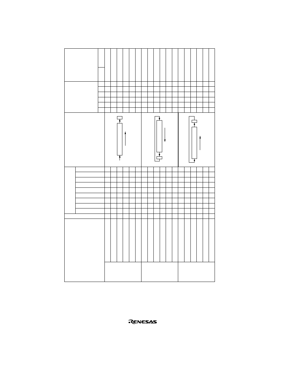
592
Table A-1 Instruction Set (cont)
(4) Shift Instructions (cont)
Addressing Mode/
Instruction Length (Bytes)
Operand Size
#xx
Rn
@ERn
@(d,ERn)
@≠ERn/@ERn+
@aa
@(d,PC)
@@aa
--
Mnemonic
SHLR
ROTXL
ROTXR
SHLR.B Rd
B
2
SHLR.B #2,Rd
B
2
SHLR.W Rd
W
2
SHLR.W #2,Rd
W
2
SHLR.L ERd
L
2
SHLR.L #2,ERd
L
2
ROTXL.B Rd
B
2
ROTXL.B #2,Rd
B
2
ROTXL.W Rd
W
2
ROTXL.W #2,Rd
W
2
ROTXL.L ERd
L
2
ROTXL.L #2,ERd
L
2
ROTXR.B Rd
B
2
ROTXR.B #2,Rd
B
2
ROTXR.W Rd
W
2
ROTXR.W #2,Rd
W
2
ROTXR.L ERd
L
2
ROTXR.L #2,ERd
L
2
----
0
0
1
----
0
0
1
----
0
0
1
----
0
0
1
----
0
0
1
----
0
0
1
----
0
1
----
0
1
----
0
1
----
0
1
----
0
1
----
0
1
----
0
1
----
0
1
----
0
1
----
0
1
----
0
1
----
0
1
Operation
Condition Code
Normal
IH
N
Z
V
C
Advanced
No. of States
*
1
C
MSB
LSB
0
C
MSB
LSB
C
MSB
LSB

593
----
0
1
----
0
1
----
0
1
----
0
1
----
0
1
----
0
1
----
0
1
----
0
1
----
0
1
----
0
1
----
0
1
----
0
1
Table A-1 Instruction Set (cont)
(4) Shift Instructions (cont)
Addressing Mode/
Instruction Length (Bytes)
Operand Size
#xx
Rn
@ERn
@(d,ERn)
@≠ERn/@ERn+
@aa
@(d,PC)
@@aa
--
Mnemonic
ROTL
ROTR
ROTL.B Rd
B
2
ROTL.B #2,Rd
B
2
ROTL.W Rd
W
2
ROTL.W #2,Rd
W
2
ROTL.L ERd
L
2
ROTL.L #2,ERd
L
2
ROTR.B Rd
B
2
ROTR.B #2,Rd
B
2
ROTR.W Rd
W
2
ROTR.W #2,Rd
W
2
ROTR.L ERd
L
2
ROTR.L #2,ERd
L
2
Operation
Condition Code
Normal
IH
N
Z
V
C
Advanced
No. of States
*
1
C
MSB
LSB
C
MSB
LSB

594
Table A-1 Instruction Set
(5) Bit-Manipulation Instructions
Addressing Mode/
Instruction Length (Bytes)
Operand Size
#xx
Rn
@ERn
@(d,ERn)
@≠ERn/@ERn+
@aa
@(d,PC)
@@aa
--
Mnemonic
BSET
BCLR
BSET #xx:3,Rd
B
2
BSET #xx:3,@ERd
B
4
BSET #xx:3,@aa:8
B
4
BSET #xx:3,@aa:16
B
6
BSET #xx:3,@aa:32
B
8
BSET Rn,Rd
B
2
BSET Rn,@ERd
B
4
BSET Rn,@aa:8
B
4
BSET Rn,@aa:16
B
6
BSET Rn,@aa:32
B
8
BCLR #xx:3,Rd
B
2
BCLR #xx:3,@ERd
B
4
BCLR #xx:3,@aa:8
B
4
BCLR #xx:3,@aa:16
B
6
BCLR #xx:3,@aa:32
B
8
BCLR Rn,Rd
B
2
BCLR Rn,@ERd
B
4
BCLR Rn,@aa:8
B
4
BCLR Rn,@aa:16
B
6
(#xx:3 of Rd8)
1
--
--
--------
1
(#xx:3 of @ERd)
1
--
--
--------
4
(#xx:3 of @aa:8)
1
--
--
--------
4
(#xx:3 of @aa:16)
1
--
--
--------
5
(#xx:3 of @aa:32)
1
--
--
--------
6
(Rn8 of Rd8)
1
--
--
--------
1
(Rn8 of @ERd)
1
--
--
--------
4
(Rn8 of @aa:8)
1
--
--
--------
4
(Rn8 of @aa:16)
1
--
--
--------
5
(Rn8 of @aa:32)
1
--
--
--------
6
(#xx:3 of Rd8)
0
--
--
--------
1
(#xx:3 of @ERd)
0
--
--
--------
4
(#xx:3 of @aa:8)
0
--
--
--------
4
(#xx:3 of @aa:16)
0
--
--
--------
5
(#xx:3 of @aa:32)
0
--
--
--------
6
(Rn8 of Rd8)
0
--
--
--------
1
(Rn8 of @ERd)
0
--
--
--------
4
(Rn8 of @aa:8)
0
--
--
--------
4
(Rn8 of @aa:16)
0
--
--
--------
5
Operation
Condition Code
Normal
IH
N
Z
V
C
Advanced
No. of States
*
1
595
Table A-1 Instruction Set (cont)
(5) Bit-Manipulation Instructions (cont)
Addressing Mode/
Instruction Length (Bytes)
Operand Size
#xx
Rn
@ERn
@(d,ERn)
@≠ERn/@ERn+
@aa
@(d,PC)
@@aa
--
Mnemonic
BCLR
BNOT
BTST
BCLR Rn,@aa:32
B
8
BNOT #xx:3,Rd
B
2
BNOT #xx:3,@ERd
B
4
BNOT #xx:3,@aa:8
B
4
BNOT #xx:3,@aa:16
B
6
BNOT #xx:3,@aa:32
B
8
BNOT Rn,Rd
B
2
BNOT Rn,@ERd
B
4
BNOT Rn,@aa:8
B
4
BNOT Rn,@aa:16
B
6
BNOT Rn,@aa:32
B
8
BTST #xx:3,Rd
B
2
BTST #xx:3,@ERd
B
4
BTST #xx:3,@aa:8
B
4
BTST #xx:3,@aa:16
B
6
(Rn8 of @aa:32)
0
------------
6
(#xx:3 of Rd8)
[¨ (#xx:3 of Rd8)]
------------
1
(#xx:3 of @ERd)
------------
4
[¨ (#xx:3 of @ERd)]
(#xx:3 of @aa:8)
------------
4
[¨ (#xx:3 of @aa:8)]
(#xx:3 of @aa:16)
------------
5
[¨ (#xx:3 of @aa:16)]
(#xx:3 of @aa:32)
------------
6
[¨ (#xx:3 of @aa:32)]
(Rn8 of Rd8)
[¨ (Rn8 of Rd8)]
------------
1
(Rn8 of @ERd)
[¨ (Rn8 of @ERd)]
------------
4
(Rn8 of @aa:8)
[¨ (Rn8 of @aa:8)]
------------
4
(Rn8 of @aa:16)
------------
5
[¨ (Rn8 of @aa:16)]
(Rn8 of @aa:32)
------------
6
[¨ (Rn8 of @aa:32)]
¨ (#xx:3 of Rd8)
Z
------
----
1
¨ (#xx:3 of @ERd)
Z
------
----
3
¨ (#xx:3 of @aa:8)
Z
------
----
3
¨ (#xx:3 of @aa:16)
Z
------
----
4
Operation
Condition Code
Normal
IH
N
Z
V
C
Advanced
No. of States
*
1

596
Table A-1 Instruction Set (cont)
(5) Bit-Manipulation Instructions (cont)
Addressing Mode/
Instruction Length (Bytes)
Operand Size
#xx
Rn
@ERn
@(d,ERn)
@≠ERn/@ERn+
@aa
@(d,PC)
@@aa
--
Mnemonic
BTST
BLD
BILD
BST
BTST #xx:3,@aa:32
B
8
BTST Rn,Rd
B
2
BTST Rn,@ERd
B
4
BTST Rn,@aa:8
B
4
BTST Rn,@aa:16
B
6
BTST Rn,@aa:32
B
8
BLD #xx:3,Rd
B
2
BLD #xx:3,@ERd
B
4
BLD #xx:3,@aa:8
B
4
BLD #xx:3,@aa:16
B
6
BLD #xx:3,@aa:32
B
8
BILD #xx:3,Rd
B
2
BILD #xx:3,@ERd
B
4
BILD #xx:3,@aa:8
B
4
BILD #xx:3,@aa:16
B
6
BILD #xx:3,@aa:32
B
8
BST #xx:3,Rd
B
2
BST #xx:3,@ERd
B
4
BST #xx:3,@aa:8
B
4
¨ (#xx:3 of @aa:32)
Z
------
----
5
¨ (Rn8 of Rd8)
Z
------
----
1
¨ (Rn8 of @ERd)
Z
------
----
3
¨ (Rn8 of @aa:8)
Z
------
----
3
¨ (Rn8 of @aa:16)
Z
------
----
4
¨ (Rn8 of @aa:32)
Z
------
----
5
(#xx:3 of Rd8)
C
----------
1
(#xx:3 of @ERd)
C
----------
3
(#xx:3 of @aa:8)
C
----------
3
(#xx:3 of @aa:16)
C
----------
4
(#xx:3 of @aa:32)
C
----------
5
¨ (#xx:3 of Rd8)
C
----------
1
¨ (#xx:3 of @ERd)
C
----------
3
¨ (#xx:3 of @aa:8)
C
----------
3
¨ (#xx:3 of @aa:16)
C
----------
4
¨ (#xx:3 of @aa:32)
C
----------
5
C
(#xx:3 of Rd8)
------------
1
C
(#xx:3 of @ERd)
------------
4
C
(#xx:3 of @aa:8)
------------
4
Operation
Condition Code
Normal
IH
N
Z
V
C
Advanced
No. of States
*
1
597
Table A-1 Instruction Set (cont)
(5) Bit-Manipulation Instructions (cont)
Addressing Mode/
Instruction Length (Bytes)
Operand Size
#xx
Rn
@ERn
@(d,ERn)
@≠ERn/@ERn+
@aa
@(d,PC)
@@aa
--
Mnemonic
BST
BIST
BAND
BIAND
BOR
BST #xx:3,@aa:16
B
6
BST #xx:3,@aa:32
B
8
BIST #xx:3,Rd
B
2
BIST #xx:3,@ERd
B
4
BIST #xx:3,@aa:8
B
4
BIST #xx:3,@aa:16
B
6
BIST #xx:3,@aa:32
B
8
BAND #xx:3,Rd
B
2
BAND #xx:3,@ERd
B
4
BAND #xx:3,@aa:8
B
4
BAND #xx:3,@aa:16
B
6
BAND #xx:3,@aa:32
B
8
BIAND #xx:3,Rd
B
2
BIAND #xx:3,@ERd
B
4
BIAND #xx:3,@aa:8
B
4
BIAND #xx:3,@aa:16
B
6
BIAND #xx:3,@aa:32
B
8
BOR #xx:3,Rd
B
2
BOR #xx:3,@ERd
B
4
C
(#xx:3 of @aa:16)
------------
5
C
(#xx:3 of @aa:32)
------------
6
¨ C
(#xx:3 of Rd8)
------------
1
¨ C
(#xx:3 of @ERd)
------------
4
¨ C
(#xx:3 of @aa:8)
------------
4
¨ C
(#xx:3 of @aa:16)
------------
5
¨ C
(#xx:3 of @aa:32)
------------
6
C
(#xx:3 of Rd8)
C
----------
1
C
(#xx:3 of @ERd)
C
----------
3
C
(#xx:3 of @aa:8)
C
----------
3
C
(#xx:3 of @aa:16)
C
----------
4
C
(#xx:3 of @aa:32)
C
----------
5
C
[¨ (#xx:3 of Rd8)]
C
----------
1
C
[¨ (#xx:3 of @ERd)]
C
----------
3
C
[¨ (#xx:3 of @aa:8)]
C
----------
3
C
[¨ (#xx:3 of @aa:16)]
C
----------
4
C
[¨ (#xx:3 of @aa:32)]
C
----------
5
C
(#xx:3 of Rd8)
C
----------
1
C
(#xx:3 of @ERd)
C
----------
3
Operation
Condition Code
Normal
IH
N
Z
V
C
Advanced
No. of States
*
1
598
Table A-1 Instruction Set (cont)
(5) Bit-Manipulation Instructions (cont)
Addressing Mode/
Instruction Length (Bytes)
Operand Size
#xx
Rn
@ERn
@(d,ERn)
@≠ERn/@ERn+
@aa
@(d,PC)
@@aa
--
Mnemonic
BOR
BIOR
BXOR
BIXOR
BOR #xx:3,@aa:8
B
4
BOR #xx:3,@aa:16
B
6
BOR #xx:3,@aa:32
B
8
BIOR #xx:3,Rd
B
2
BIOR #xx:3,@ERd
B
4
BIOR #xx:3,@aa:8
B
4
BIOR #xx:3,@aa:16
B
6
BIOR #xx:3,@aa:32
B
8
BXOR #xx:3,Rd
B
2
BXOR #xx:3,@ERd
B
4
BXOR #xx:3,@aa:8
B
4
BXOR #xx:3,@aa:16
B
6
BXOR #xx:3,@aa:32
B
8
BIXOR #xx:3,Rd
B
2
BIXOR #xx:3,@ERd
B
4
BIXOR #xx:3,@aa:8
B
4
BIXOR #xx:3,@aa:16
B
6
BIXOR #xx:3,@aa:32
B
8
C
(#xx:3 of @aa:8)
C
----------
3
C
(#xx:3 of @aa:16)
C
----------
4
C
(#xx:3 of @aa:32)
C
----------
5
C
[¨ (#xx:3 of Rd8)]
C
----------
1
C
[¨ (#xx:3 of @ERd)]
C
----------
3
C
[¨ (#xx:3 of @aa:8)]
C
----------
3
C
[¨ (#xx:3 of @aa:16)]
C
----------
4
C
[¨ (#xx:3 of @aa:32)]
C
----------
5
C
(#xx:3 of Rd8)
C
----------
1
C
(#xx:3 of @ERd)
C
----------
3
C
(#xx:3 of @aa:8)
C
----------
3
C
(#xx:3 of @aa:16)
C
----------
4
C
(#xx:3 of @aa:32)
C
----------
5
C
[¨ (#xx:3 of Rd8)]
C
----------
1
C
[¨ (#xx:3 of @ERd)]
C
----------
3
C
[¨ (#xx:3 of @aa:8)]
C
----------
3
C
[¨ (#xx:3 of @aa:16)]
C
----------
4
C
[¨ (#xx:3 of @aa:32)]
C
----------
5
Operation
Condition Code
Normal
IH
N
Z
V
C
Advanced
No. of States
*
1
599
Table A-1 Instruction Set
(6) Branch Instructions
Addressing Mode/
Instruction Length (Bytes)
Operand Size
#xx
Rn
@ERn
@(d,ERn)
@≠ERn/@ERn+
@aa
@(d,PC)
@@aa
--
Mnemonic
Bcc
Always
--------
--
--
2
--------
--
--
3
Never
--------
--
--
2
--------
--
--
3
C
Z
=
0
--------
--
--
2
--------
--
--
3
C
Z
=
1
--------
--
--
2
--------
--
--
3
C
=
0
--------
--
--
2
--------
--
--
3
C
=
1
--------
--
--
2
--------
--
--
3
Z
=
0
--------
--
--
2
--------
--
--
3
Z
=
1
--------
--
--
2
--------
--
--
3
V
=
0
--------
--
--
2
--------
--
--
3
Operation
Condition Code
Branching
Condition
Normal
IH
N
Z
V
C
Advanced
No. of States
*
1
BRA d:8(BT d:8)
--
2
if condition is true then
BRA d:16(BT d:16)
--
4
PC
PC+d
BRN d:8(BF d:8)
--
2
else next;
BRN d:16(BF d:16)
--
4
BHI d:8
--
2
BHI d:16
--
4
BLS d:8
--
2
BLS d:16
--
4
BCC d:8(BHS d:8)
--
2
BCC d:16(BHS d:16)
--
4
BCS d:8(BLO d:8)
--
2
BCS d:16(BLO d:16)
--
4
BNE d:8
--
2
BNE d:16
--
4
BEQ d:8
--
2
BEQ d:16
--
4
BVC d:8
--
2
BVC d:16
--
4
600
Table A-1 Instruction Set (cont)
(6) Branch Instructions (cont)
Addressing Mode/
Instruction Length (Bytes)
Operand Size
#xx
Rn
@ERn
@(d,ERn)
@≠ERn/@ERn+
@aa
@(d,PC)
@@aa
--
Mnemonic
Bcc
V
=
1
----------
--
2
----------
--
3
N
=
0
----------
--
2
----------
--
3
N
=
1
----------
--
2
----------
--
3
N
V
=
0
----------
--
2
----------
--
3
N
V
=
1
----------
--
2
----------
--
3
Z
(N
V)=0
----------
--
2
----------
--
3
Z
(N
V)=1
----------
--
2
----------
--
3
Operation
Condition Code
Branching
Condition
Normal
IH
N
Z
V
C
Advanced
No. of States
*
1
BVS d:8
--
2
BVS d:16
--
4
BPL d:8
--
2
BPL d:16
--
4
BMI d:8
--
2
BMI d:16
--
4
BGE d:8
--
2
BGE d:16
--
4
BLT d:8
--
2
BLT d:16
--
4
BGT d:8
--
2
BGT d:16
--
4
BLE d:8
--
2
BLE d:16
--
4
If condition is true
then PC
PC + d
else next;

601
Table A-1 Instruction Set (cont)
(6) Branch Instructions (cont)
Addressing Mode/
Instruction Length (Bytes)
Operand Size
#xx
Rn
@ERn
@(d,ERn)
@≠ERn/@ERn+
@aa
@(d,PC)
@@aa
--
Mnemonic
JMP
BSR
JSR
RTS
MP @ERn
--
2
JMP @aa:24
--
4
JMP @@aa:8
--
2
BSR d:8
--
2
BSR d:16
--
4
JSR @ERn
--
2
JSR @aa:24
--
4
JSR @@aa:8
--
2
RTS
--
2
PC
E
R
n
------------
2
PC
aa:24
------------
3
PC
@aa:8
------------
4
5
PC
@-SP,PC
PC+d:8
------------
3
4
PC
@-SP,PC
PC+d:16
------------
4
5
PC
@-SP,PC
E
R
n
------------
3
4
PC
@-SP,PC
aa:24
------------
4
5
PC
@-SP,PC
@aa:8
------------
4
6
PC
@SP+
------------
4
5
Operation
Condition Code
Normal
IH
N
Z
V
C
Advanced
No. of States
*
1

602
Table A-1 Instruction Set
(7) System Control Instructions
Addressing Mode/
Instruction Length (Bytes)
Operand Size
#xx
Rn
@ERn
@(d,ERn)
@≠ERn/@ERn+
@aa
@(d,PC)
@@aa
--
Mnemonic
TRAPA
RTE
SLEEP
LDC
TRAPA #xx:2
--
RTE
--
SLEEP
--
LDC #xx:8,CCR
B
2
LDC #xx:8,EXR
B
4
LDC Rs,CCR
B
2
LDC Rs,EXR
B
2
LDC @ERs,CCR
W
4
LDC @ERs,EXR
W
4
LDC @(d:16,ERs),CCR
W
6
LDC @(d:16,ERs),EXR
W
6
LDC @(d:32,ERs),CCR
W
1
0
LDC @(d:32,ERs),EXR
W
1
0
LDC @ERs+,CCR
W
4
LDC @ERs+,EXR
W
4
LDC @aa:16,CCR
W
6
LDC @aa:16,EXR
W
6
LDC @aa:32,CCR
W
8
LDC @aa:32,EXR
W
8
PC
@-SP,CCR
@-SP, 1
--------
--
7
[
9
]
8
[
9
]
EXR
@-SP,<vector>
PC
EXR
@SP+,CCR
@SP+,
5 [9]
PC
@SP+
Transition to power-down state
----------
--
2
#xx:8
CCR
1
#xx:8
E
X
R
----------
--
2
Rs8
CCR
1
Rs8
E
X
R
----------
--
1
@ERs
CCR
3
@ERs
E
X
R
----------
--
3
@(d:16,ERs)
CCR
4
@(d:16,ERs)
E
X
R
----------
--
4
@(d:32,ERs)
CCR
6
@(d:32,ERs)
E
X
R
----------
--
6
@ERs
CCR,ERs32+2
ERs32
4
@ERs
EXR,ERs32+2
ERs32
----------
--
4
@aa:16
CCR
4
@aa:16
E
X
R
----------
--
4
@aa:32
CCR
5
@aa:32
E
X
R
----------
--
5
Operation
Condition Code
Normal
IH
N
Z
V
C
Advanced
No. of States
*
1
603
Table A-1 Instruction Set (cont)
(7) System Control Instructions (cont)
Addressing Mode/
Instruction Length (Bytes)
Operand Size
#xx
Rn
@ERn
@(d,ERn)
@≠ERn/@ERn+
@aa
@(d,PC)
@@aa
--
Mnemonic
STC
ANDC
ORC
XORC
NOP
STC CCR,Rd
B
2
STC EXR,Rd
B
2
STC CCR,@ERd
W
4
STC EXR,@ERd
W
4
STC CCR,@(d:16,ERd)
W
6
STC EXR,@(d:16,ERd)
W
6
STC CCR,@(d:32,ERd)
W
1
0
STC EXR,@(d:32,ERd)
W
1
0
STC CCR,@-ERd
W
4
STC EXR,@-ERd
W
4
STC CCR,@aa:16
W
6
STC EXR,@aa:16
W
6
STC CCR,@aa:32
W
8
STC EXR,@aa:32
W
8
ANDC #xx:8,CCR
B
2
ANDC #xx:8,EXR
B
4
ORC #xx:8,CCR
B
2
ORC #xx:8,EXR
B
4
XORC #xx:8,CCR
B
2
XORC #xx:8,EXR
B
4
NOP
--
2
CCR
R
d
8
------------
1
EXR
R
d
8
------------
1
CCR
@ERd
------------
3
EXR
@ERd
------------
3
CCR
@(d:16,ERd)
------------
4
EXR
@(d:16,ERd)
------------
4
CCR
@(d:32,ERd)
------------
6
EXR
@(d:32,ERd)
------------
6
ERd32-2
ERd32,CCR
@ERd
------------
4
ERd32-2
ERd32,EXR
@ERd
------------
4
CCR
@aa:16
------------
4
EXR
@aa:16
------------
4
CCR
@aa:32
------------
5
EXR
@aa:32
------------
5
CCR
#xx:8
CCR
1
EXR
#xx:8
E
X
R
------------
2
CCR
#xx:8
CCR
1
EXR
#xx:8
E
X
R
------------
2
CCR
#xx:8
CCR
1
EXR
#xx:8
E
X
R
------------
2
PC
PC+2
------------
1
Operation
Condition Code
Normal
IH
N
Z
V
C
Advanced
No. of States
*
1
604
Table A-1 Instruction Set
(8) Program Transfer Instructions
Addressing Mode/
Instruction Length (Bytes)
Operand Size
#xx
Rn
@ERn
@(d,ERn)
@≠ERn/@ERn+
@aa
@(d,PC)
@@aa
--
Mnemonic
EEPMOV
Notes:
1.
The number of states is the number of states required for execution when the instruction and its operands are located i
n on-chip memory.
2.
n is the initial value of R4L or R4.
[1]
Seven states for saving or restoring two registers, nine states for three registers, or eleven states for four registers.
[2]
Cannot be used in the H8S/2245 Series.
[3]
Set to 1 when a carry or borrow occurs at bit 11; otherwise cleared to 0.
[4]
Set to 1 when a carry or borrow occurs at bit 27; otherwise cleared to 0.
[5]
Retains its previous value when the result is zero; otherwise cleared to 0.
[6]
Set to 1 when the divisor is negative; otherwise cleared to 0.
[7]
Set to 1 when the divisor is zero; otherwise cleared to 0.
[8]
Set to 1 when the quotient is negative; otherwise cleared to 0.
[9]
One additional state is required for execution when EXR is valid.
EEPMOV.B
--
4
EEPMOV.W
--
4
if R4L
0
--
--
--
--
--
--
4+2n
*
2
Repeat @ER5
@ER6
ER5+1
ER5
ER6+1
ER6
R4L-1
R4L
Until R4L=0
else next;
if R4
0
--
--
--
--
--
--
4+2n
*
2
Repeat @ER5
@ER6
ER5+1
ER5
ER6+1
ER6
R4-1
R4
Until R4=0
else next;
Operation
Condition Code
Normal
IH
N
Z
V
C
Advanced
No. of States
*
1

605
A.2
Operation Code Map
Table A-2 shows the operation code map.
Instruction code
1st byte
2nd byte
AH
AL
BH
BL
Instruction when most significant bit of BH is 0.
Instruction when most significant bit of BH is 1.
0
NOP
BRA
MULXU
BSET
AH
AL
0
1
2
3
4
5
6
7
8
9
A
B
C
D
E
F
1
BRN
DIVXU
BNOT
2
BHI
MULXU
BCLR
3
BLS
DIVXU
BTST
STC
LDC
4
ORC
OR
BCC
RTS
OR
BOR
BIOR
6
ANDC
AND
BNE
RTE
AND
5
XORC
XOR
BCS
BSR
XOR
BXOR
BIXOR
BAND
BIAND
7
LDC
BEQ
TRAPA
BST
BIST
BLD
BILD
8
BVC
MOV
9
BVS
A
BPL
JMP
B
BMI
EEPMOV
C
BGE
BSR
D
BLT
MOV
E
ADDX
SUBX
BGT
JSR
F
BLE
MOV.B
ADD
ADDX
CMP
SUBX
OR
XOR
AND
MOV
ADD
SUB
MOV
MOV
CMP
Table
A.2(2)
Table
A.2(2)
Table
A.2(2)
Table
A.2(2)
Table
A.2(2)
Table
A.2(2)
Table
A.2(2)
Table
A.2(2)
Table
A.2(2)
Table
A.2(2)
Table
A.2(2)
Table
A.2(2)
Table
A.2(2)
Table
A.2(2)
Table
A.2(2)
Table
A.2(2)
Table A.2(3)
Table A-2 Operation Code Map (1)

606
Instruction code
1st byte
2nd byte
AH
AL
BH
BL
01
0A
0B
0F
10
11
12
13
17
1A
1B
1F
58
6A
79
7A
0
MOV
INC
ADDS
DAA
DEC
SUBS
DAS
BRA
MOV
MOV
MOV
SHLL
SHLR
ROTXL
ROTXR
NOT
1
LDM
BRN
ADD
ADD
2
BHI
MOV
CMP
CMP
3
STM
NOT
BLS
SUB
SUB
4
SHLL
SHLR
ROTXL
ROTXR
BCC
MOVFPE
OR
OR
5
INC
EXTU
DEC
BCS
XOR
XOR
6
BNE
AND
AND
7
INC
SHLL
SHLR
ROTXL
ROTXR
EXTU
DEC
BEQ
LDC
STC
8
SLEEP
BVC
MOV
ADDS
SHAL
SHAR
ROTL
ROTR
NEG
SUBS
9
BVS
A
BPL
MOV
B
NEG
BMI
ADD
MOV
SUB
CMP
C
SHAL
SHAR
ROTL
ROTR
BGE
MOVTPE
D
INC
EXTS
DEC
BLT
E
TAS
BGT
F
INC
SHAL
SHAR
ROTL
ROTR
EXTS
DEC
BLE
BH
AH AL
Table
A.2(3)
Table
A.2(3)
Table
A.2(3)
Table
A.2(4)
Table
A.2(4)
T
able A-2 Operation Code Map (2)

607
Instruction code
1st byte
2nd byte
AH
AL
BH
BL
3rd byte
4th byte
CH
CL
DH
DL
r is the register specification field.
aa is the absolute address specification.
Instruction when most significant bit of DH is 0.
Instruction when most significant bit of DH is 1.
Notes:
AH AL BH BL CH
CL
01C05
01D05
01F06
7Cr06
*
1
7Cr07
*
1
7Dr06
*
1
7Dr07
*
1
7Eaa6
*
2
7Eaa7
*
2
7Faa6
*
2
7Faa7
*
2
0
MULXS
BSET
BSET
BSET
BSET
1
DIVXS
BNOT
BNOT
BNOT
BNOT
2
MULXS
BCLR
BCLR
BCLR
BCLR
3
DIVXS
BTST
BTST
BTST
BTST
4
OR
5
XOR
6
AND
789
A
B
C
D
E
F
1.
2.
BOR
BIOR
BXOR
BIXOR
BAND
BIAND
BLD
BILD
BST
BIST
BOR
BIOR
BXOR
BIXOR
BAND
BIAND
BLD
BILD
BST
BIST
Table A-2 Operation Code Map (3)

608
Instruction code
1st byte
2nd byte
AH
AL
BH
BL
3rd byte
4th byte
CH
CL
DH
DL
Instruction when most significant bit of FH is 0.
Instruction when most significant bit of FH is 1.
5th byte
6th byte
EH
EL
FH
FL
Instruction code
1st byte
2nd byte
AH
AL
BH
BL
3rd byte
4th byte
CH
CL
DH
DL
Instruction when most significant bit of HH is 0.
Instruction when most significant bit of HH is 1.
Note:
*
aa is the absolute address specification
5th byte
6th byte
EH
EL
FH
FL
7th byte
8th byte
GH
GL
HH
HL
6A10aaaa6
*
6A10aaaa7
*
6A18aaaa6
*
6A18aaaa7
*
AHALBHBLCHCLDHDLEH
EL
0
BSET
1
BNOT
2
BCLR
3
BTST
BOR
BIOR
BXOR
BIXOR
BAND
BIAND
BLD
BILD
BST
BIST
456789
A
B
C
D
E
F
6A30aaaaaaaa6
*
6A30aaaaaaaa7
*
6A38aaaaaaaa6
*
6A38aaaaaaaa7
*
AHALBHBL ... FHFLGH
GL
0
BSET
1
BNOT
2
BCLR
3
BTST
BOR
BIOR
BXOR
BIXOR
BAND
BIAND
BLD
BILD
BST
BIST
456789
A
B
C
D
E
F
Table A-2 Operation Code Map (4)

609
A.3
Number of States Required for Instruction Execution
The tables in this section can be used to calculate the number of states required for instruction
execution by the H8S/2000 CPU. Table A-4 indicates the number of instruction fetch, data
read/write, and other cycles occurring in each instruction. Table A-3 indicates the number of states
required for each cycle, depending on its size. The number of states required for execution of an
instruction can be calculated from these two tables as follows:
Execution states = I
◊
S
I
+ J
◊
S
J
+ K
◊
S
K
+ L
◊
S
L
+ M
◊
S
M
+ N
◊
S
N
Examples: Advanced mode, program code and stack located in external memory, on-chip
supporting modules accessed in two states with 8-bit bus width, external devices accessed in three
states with one wait state and 16-bit bus width.
1. BSET #0, @FFFFC7:8
From table A-4:
I = L = 2, J = K = M = N = 0
From table A-3:
S
I
= 4, S
L
= 2
Number of states required for execution = 2
◊
4 + 2
◊
2 = 12
2. JSR @@30
From table A-4:
I = J = K = 2, L = M = N = 0
From table A-3:
S
I
= S
J
= S
K
= 4
Number of states required for execution = 2
◊
4 + 2
◊
4 + 2
◊
4 = 24

610
Table A-3
Number of States per Cycle
Access Conditions
On-Chip Supporting
External Device
Module
8-Bit Bus
16-Bit Bus
On-Chip
Memory
8-Bit
Bus
16-Bit
Bus
2-State
Access
3-State
Access
2-State
Access
3-State
Access
Instruction fetch
SI
1
4
2
4
6 + 2m
2
3 + m
Branch address read
SJ
Stack operation
SK
Byte data access
SL
2
2
3 + m
Word data access
SM
4
4
6 + 2m
Internal operation
SN
1
1
1
1
1
1
1
Legend
m: Number of wait states inserted into external device access

611
Table A-4
Number of Cycles in Instruction Execution
Instruction
Fetch
Branch
Address
Read
Stack
Operation
Byte Data
Access
Word Data
Access
Internal
Operation
Instruction
Mnemonic
I
J
K
L
M
N
ADD
ADD.B #xx:8,Rd
ADD.B Rs,Rd
ADD.W #xx:16,Rd
ADD.W Rs,Rd
ADD.L #xx:32,ERd
ADD.L ERs,ERd
1
1
2
1
3
1
ADDS
ADDS #1/2/4,ERd
1
ADDX
ADDX #xx:8,Rd
ADDX Rs,Rd
1
1
AND
AND.B #xx:8,Rd
AND.B Rs,Rd
AND.W #xx:16,Rd
AND.W Rs,Rd
AND.L #xx:32,ERd
AND.L ERs,ERd
1
1
2
1
3
2
ANDC
AND.B #xx:8,CCR
ANDC #xx:8,EXR
1
2
BAND
BAND #xx:3,Rd
BAND #xx:3,@ERd
BAND #xx:3,@aa:8
BAND #xx:3,@aa:16
BAND #xx:3,@aa:32
1
2
2
3
4
1
1
1
1
Bcc
BRA d:8 (BT d:8)
BRN d:8 (BF d:8)
BHI d:8
BLS d:8
BCC d:8 (BHS d:8)
BCS d:8 (BLO d:8)
BNE d:8
BEQ d:8
BVC d:8
BVS d:8
BPL d:8
BMI d:8
BGE d:8
BLT d:8
BGT d:8
BLE d:8
BRA d:16 (BT d:16)
BRN d:16 (BF d:16)
2
2
2
2
2
2
2
2
2
2
2
2
2
2
2
2
2
2
1
1

612
Table A-4
Number of Cycles in Instruction Execution (cont)
Instruction
Fetch
Branch
Address
Read
Stack
Operation
Byte Data
Access
Word Data
Access
Internal
Operation
Instruction
Mnemonic
I
J
K
L
M
N
Bcc
BHI d:16
BLS d:16
BCC d:16 (BHS d:16)
BCS d:16 (BLO d:16)
BNE d:16
BEQ d:16
BVC d:16
BVS d:16
BPL d:16
BMI d:16
BGE d:16
BLT d:16
BGT d:16
BLE d:16
2
2
2
2
2
2
2
2
2
2
2
2
2
2
1
1
1
1
1
1
1
1
1
1
1
1
1
1
BCLR
BCLR #xx:3,Rd
BCLR #xx:3,@ERd
BCLR #xx:3,@aa:8
BCLR #xx:3,@aa:16
BCLR #xx:3,@aa:32
BCLR Rn,Rd
BCLR Rn,@ERd
BCLR Rn,@aa:8
BCLR Rn,@aa:16
BCLR Rn,@aa:32
1
2
2
3
4
1
2
2
3
4
2
2
2
2
2
2
2
2
BIAND
BIAND #xx:3,Rd
BIAND #xx:3,@ERd
BIAND #xx:3,@aa:8
BIAND #xx:3,@aa:16
BIAND #xx:3,@aa:32
1
2
2
3
4
1
1
1
1
BILD
BILD #xx:3,Rd
BILD #xx:3,@ERd
BILD #xx:3,@aa:8
BILD #xx:3,@aa:16
BILD #xx:3,@aa:32
1
2
2
3
4
1
1
1
1
BIOR
BIOR #xx:8,Rd
BIOR #xx:8,@ERd
BIOR #xx:8,@aa:8
BIOR #xx:8,@aa:16
BIOR #xx:8,@aa:32
1
2
2
3
4
1
1
1
1

613
Table A-4
Number of Cycles in Instruction Execution (cont)
Instruction
Fetch
Branch
Address
Read
Stack
Operation
Byte Data
Access
Word Data
Access
Internal
Operation
Instruction
Mnemonic
I
J
K
L
M
N
BIST
BIST #xx:3,Rd
BIST #xx:3,@ERd
BIST #xx:3,@aa:8
BIST #xx:3,@aa:16
BIST #xx:3,@aa:32
1
2
2
3
4
2
2
2
2
BIXOR
BIXOR #xx:3,Rd
BIXOR #xx:3,@ERd
BIXOR #xx:3,@aa:8
BIXOR #xx:3,@aa:16
BIXOR #xx:3,@aa:32
1
2
2
3
4
1
1
1
1
BLD
BLD #xx:3,Rd
BLD #xx:3,@ERd
BLD #xx:3,@aa:8
BLD #xx:3,@aa:16
BLD #xx:3,@aa:32
1
2
2
3
4
1
1
1
1
BNOT
BNOT #xx:3,Rd
BNOT #xx:3,@ERd
BNOT #xx:3,@aa:8
BNOT #xx:3,@aa:16
BNOT #xx:3,@aa:32
BNOT Rn,Rd
BNOT Rn,@ERd
BNOT Rn,@aa:8
BNOT Rn,@aa:16
BNOT Rn,@aa:32
1
2
2
3
4
1
2
2
3
4
2
2
2
2
2
2
2
2
BOR
BOR #xx:3,Rd
BOR #xx:3,@ERd
BOR #xx:3,@aa:8
BOR #xx:3,@aa:16
BOR #xx:3,@aa:32
1
2
2
3
4
1
1
1
1
BSET
BSET #xx:3,Rd
BSET #xx:3,@ERd
BSET #xx:3,@aa:8
BSET #xx:3,@aa:16
BSET #xx:3,@aa:32
BSET Rn,Rd
BSET Rn,@ERd
BSET Rn,@aa:8
BSET Rn,@aa:16
BSET Rn,@aa:32
1
2
2
3
4
1
2
2
3
4
2
2
2
2
2
2
2
2

614
Table A-4
Number of Cycles in Instruction Execution (cont)
Instruction
Fetch
Branch
Address
Read
Stack
Operation
Byte Data
Access
Word Data
Access
Internal
Operation
Instruction
Mnemonic
I
J
K
L
M
N
BSR
BSR d:8
Normal
2
1
Advanced
2
2
BSR d:16
Normal
2
1
1
Advanced
2
2
1
BST
BST #xx:3,Rd
BST #xx:3,@ERd
BST #xx:3,@aa:8
BST #xx:3,@aa:16
BST #xx:3,@aa:32
1
2
2
3
4
2
2
2
2
BTST
BTST #xx:3,Rd
BTST #xx:3,@ERd
BTST #xx:3,@aa:8
BTST #xx:3,@aa:16
BTST #xx:3,@aa:32
BTST Rn,Rd
BTST Rn,@ERd
BTST Rn,@aa:8
BTST Rn,@aa:16
BTST Rn,@aa:32
1
2
2
3
4
1
2
2
3
4
1
1
1
1
1
1
1
1
BXOR
BXOR #xx:3,Rd
BXOR #xx:3,@ERd
BXOR #xx:3,@aa:8
BXOR #xx:3,@aa:16
BXOR #xx:3,@aa:32
1
2
2
3
4
1
1
1
1
CMP
CMP.B #xx:8,Rd
CMP.B Rs,Rd
CMP.W #xx:16,Rd
CMP.W Rs,Rd
CMP.L #xx:32,ERd
CMP.L ERs,ERd
1
1
2
1
3
1
DAA
DAA Rd
1
DAS
DAS Rd
1
DEC
DEC.B Rd
DEC.W #1/2,Rd
DEC.L #1/2,ERd
1
1
1
DIVXS
DIVXS.B Rs,Rd
DIVXS.W Rs,ERd
2
2
11
19
DIVXU
DIVXU.B Rs,Rd
DIVXU.W Rs,ERd
1
1
11
19

615
Table A-4
Number of Cycles in Instruction Execution (cont)
Instruction
Fetch
Branch
Address
Read
Stack
Operation
Byte Data
Access
Word Data
Access
Internal
Operation
Instruction
Mnemonic
I
J
K
L
M
N
EEPMOV
EEPMOV.B
EEPMOV.W
2
2
2n + 2
*
2
2n + 2
*
2
EXTS
EXTS.W Rd
EXTS.L ERd
1
1
EXTU
EXTU.W Rd
EXTU.L ERd
1
1
INC
INC.B Rd
INC.W #1/2,Rd
INC.L #1/2,ERd
1
1
1
JMP
JMP @ERn
JMP @aa:24
2
2
1
JMP @@aa:8
Normal
2
1
1
Advanced
2
2
1
JSR
JSR @ERn
Normal
2
1
Advanced
2
2
JSR @aa:24
Normal
2
1
1
Advanced
2
2
1
JSR @@aa:8
Normal
2
1
1
Advanced
2
2
2
LDC
LDC #xx:8,CCR
LDC #xx:8,EXR
LDC Rs,CCR
LDC Rs,EXR
LDC @ERs,CCR
LDC @ERs,EXR
LDC @(d:16,ERs),CCR
LDC @(d:16,ERs),EXR
LDC @(d:32,ERs),CCR
LDC @(d:32,ERs),EXR
LDC @ERs+,CCR
LDC @ERs+,EXR
LDC @aa:16,CCR
LDC @aa:16,EXR
LDC @aa:32,CCR
LDC @aa:32,EXR
1
2
1
1
2
2
3
3
5
5
2
2
3
3
4
4
1
1
1
1
1
1
1
1
1
1
1
1
1
1
LDM
LDM.L @SP+,(ERn≠ERn+1)
LDM.L @SP+,(ERn≠ERn+2)
LDM.L @SP+,(ERn≠ERn+3)
2
2
2
4
6
8
1
1
1

616
Table A-4
Number of Cycles in Instruction Execution (cont)
Instruction
Fetch
Branch
Address
Read
Stack
Operation
Byte Data
Access
Word Data
Access
Internal
Operation
Instruction
Mnemonic
I
J
K
L
M
N
MOV
MOV.B #xx:8,Rd
MOV.B Rs,Rd
MOV.B @ERs,Rd
MOV.B @(d:16,ERs),Rd
MOV.B @(d:32,ERs),Rd
MOV.B @ERs+,Rd
MOV.B @aa:8,Rd
MOV.B @aa:16,Rd
MOV.B @aa:32,Rd
MOV.B Rs,@ERd
MOV.B Rs,@(d:16,ERd)
MOV.B Rs,@(d:32,ERd)
MOV.B Rs,@≠ERd
MOV.B Rs,@aa:8
MOV.B Rs,@aa:16
MOV.B Rs,@aa:32
MOV.W #xx:16,Rd
MOV.W Rs,Rd
MOV.W @ERs,Rd
MOV.W @(d:16,ERs),Rd
MOV.W @(d:32,ERs),Rd
MOV.W @ERs+,Rd
MOV.W @aa:16,Rd
MOV.W @aa:32,Rd
MOV.W Rs,@ERd
MOV.W Rs,@(d:16,ERd)
MOV.W Rs,@(d:32,ERd)
MOV.W Rs,@≠ERd
MOV.W Rs,@aa:16
MOV.W Rs,@aa:32
MOV.L #xx:32,ERd
MOV.L ERs,ERd
MOV.L @ERs,ERd
MOV.L @(d:16,ERs),ERd
MOV.L @(d:32,ERs),ERd
MOV.L @ERs+,ERd
MOV.L @aa:16,ERd
MOV.L @aa:32,ERd
MOV.L ERs,@ERd
MOV.L ERs,@(d:16,ERd)
MOV.L ERs,@(d:32,ERd)
1
1
1
2
4
1
1
2
3
1
2
4
1
1
2
3
2
1
1
2
4
1
2
3
1
2
4
1
2
3
3
1
2
3
5
2
3
4
2
3
5
1
1
1
1
1
1
1
1
1
1
1
1
1
1
1
1
1
1
1
1
1
1
1
1
1
1
2
2
2
2
2
2
2
2
2
1
1
1
1
1

617
Table A-4
Number of Cycles in Instruction Execution (cont)
Instruction
Fetch
Branch
Address
Read
Stack
Operation
Byte Data
Access
Word Data
Access
Internal
Operation
Instruction
Mnemonic
I
J
K
L
M
N
MOV
MOV.L ERs,@≠ERd
MOV.L ERs,@aa:16
MOV.L ERs,@aa:32
2
3
4
2
2
2
1
MOVFPE
MOVFPE @:aa:16,Rd
Cannot be used in the H8S/2245 Series
MOVTPE
MOVTPE Rs,@:aa:16
Cannot be used in the H8S/2245 Series
MULXS
MULXS.B Rs,Rd
2
11
MULXS.W Rs,ERd
2
19
MULXU
MULXU.B Rs,Rd
1
11
MULXU.W Rs,ERd
1
19
NEG
NEG.B Rd
NEG.W Rd
NEG.L ERd
1
1
1
NOP
NOP
1
NOT
NOT.B Rd
NOT.W Rd
NOT.L ERd
1
1
1
OR
OR.B #xx:8,Rd
OR.B Rs,Rd
OR.W #xx:16,Rd
OR.W Rs,Rd
OR.L #xx:32,ERd
OR.L ERs,ERd
1
1
2
1
3
2
ORC
ORC #xx:8,CCR
ORC #xx:8,EXR
1
2
POP
POP.W Rn
POP.L ERn
1
2
1
2
1
1
PUSH
PUSH.W Rn
PUSH.L ERn
1
2
1
2
1
1
ROTL
ROTL.B Rd
ROTL.B #2,Rd
ROTL.W Rd
ROTL.W #2,Rd
ROTL.L ERd
ROTL.L #2,ERd
1
1
1
1
1
1
ROTR
ROTR.B Rd
ROTR.B #2,Rd
ROTR.W Rd
ROTR.W #2,Rd
ROTR.L ERd
ROTR.L #2,ERd
1
1
1
1
1
1

618
Table A-4
Number of Cycles in Instruction Execution (cont)
Instruction
Fetch
Branch
Address
Read
Stack
Operation
Byte Data
Access
Word Data
Access
Internal
Operation
Instruction
Mnemonic
I
J
K
L
M
N
ROTXL
ROTXL.B Rd
ROTXL.B #2,Rd
ROTXL.W Rd
ROTXL.W #2,Rd
ROTXL.L ERd
ROTXL.L #2,ERd
1
1
1
1
1
1
ROTXR
ROTXR.B Rd
ROTXR.B #2,Rd
ROTXR.W Rd
ROTXR.W #2,Rd
ROTXR.L ERd
ROTXR.L #2,ERd
1
1
1
1
1
1
RTE
RTE
2
2/3
*
1
1
RTS
RTS
Normal
2
1
1
Advanced
2
2
1
SHAL
SHAL.B Rd
SHAL.B #2,Rd
SHAL.W Rd
SHAL.W #2,Rd
SHAL.L ERd
SHAL.L #2,ERd
1
1
1
1
1
1
SHAR
SHAR.B Rd
SHAR.B #2,Rd
SHAR.W Rd
SHAR.W #2,Rd
SHAR.L ERd
SHAR.L #2,ERd
1
1
1
1
1
1
SHLL
SHLL.B Rd
SHLL.B #2,Rd
SHLL.W Rd
SHLL.W #2,Rd
SHLL.L ERd
SHLL.L #2,ERd
1
1
1
1
1
1
SHLR
SHLR.B Rd
SHLR.B #2,Rd
SHLR.W Rd
SHLR.W #2,Rd
SHLR.L ERd
SHLR.L #2,ERd
1
1
1
1
1
1
SLEEP
SLEEP
1
1

619
Table A-4
Number of Cycles in Instruction Execution (cont)
Instruction
Fetch
Branch
Address
Read
Stack
Operation
Byte Data
Access
Word Data
Access
Internal
Operation
Instruction
Mnemonic
I
J
K
L
M
N
STC
STC.B CCR,Rd
STC.B EXR,Rd
STC.W CCR,@ERd
STC.W EXR,@ERd
STC.W CCR,@(d:16,ERd)
STC.W EXR,@(d:16,ERd)
STC.W CCR,@(d:32,ERd)
STC.W EXR,@(d:32,ERd)
STC.W CCR,@≠ERd
STC.W EXR,@≠ERd
STC.W CCR,@aa:16
STC.W EXR,@aa:16
STC.W CCR,@aa:32
STC.W EXR,@aa:32
1
1
2
2
3
3
5
5
2
2
3
3
4
4
1
1
1
1
1
1
1
1
1
1
1
1
1
1
STM
STM.L (ERn≠ERn+1),@≠SP
STM.L (ERn≠ERn+2),@≠SP
STM.L (ERn≠ERn+3),@≠SP
2
2
2
4
6
8
1
1
1
SUB
SUB.B Rs,Rd
SUB.W #xx:16,Rd
SUB.W Rs,Rd
SUB.L #xx:32,ERd
SUB.L ERs,ERd
1
2
1
3
1
SUBS
SUBS #1/2/4,ERd
1
SUBX
SUBX #xx:8,Rd
SUBX Rs,Rd
1
1
TAS
TAS @ERd
2
2
TRAPA
TRAPA #xx:2
Normal
2
1
2/3
*
1
2
Advanced
2
2
2/3
*
1
2
XOR
XOR.B #xx:8,Rd
XOR.B Rs,Rd
XOR.W #xx:16,Rd
XOR.W Rs,Rd
XOR.L #xx:32,ERd
XOR.L ERs,ERd
1
1
2
1
3
2
XORC
XORC #xx:8,CCR
XORC #xx:8,EXR
1
2
Notes: 1. 2 when EXR is invalid, 3 when EXR is valid.
2. When n bytes of data are transferred.

620
Appendix B Register Field
B.1
Register Addresses
Address
(Low)
Register
Name
Bit 7
Bit 6
Bit 5
Bit 4
Bit 3
Bit 2
Bit 1
Bit 0
Module
Name
Bus Width
(Bit)
H'F800
MRA
SM1
SM0
DM1
DM0
MD1
MD0
DTS
Sz
DTC
16/32
*
to
MRB
CHNE
DISEL
--
--
--
--
--
--
H'FBFF
SAR
DAR
CRA
CRB
H'FEB0
P1DDR
P17DDR P16DDR P15DDR P14DDR P13DDR P12DDR P11DDR P10DDR Port 1
8
H'FEB1
P2DDR
P27DDR P26DDR P25DDR P24DDR P23DDR P22DDR P21DDR P20DDR Port 2
H'FEB2
P3DDR
--
--
P35DDR P34DDR P33DDR P32DDR P31DDR P30DDR Port 3
H'FEB4
P5DDR
--
--
--
--
P53DDR P52DDR P51DDR P50DDR Port 5
H'FEB9
PADDR
--
--
--
--
PA3DDR PA2DDR PA1DDR PA0DDR Port A
H'FEBA
PBDDR
PB7DDR PB6DDR PB5DDR PB4DDR PB3DDR PB2DDR PB1DDR PB0DDR Port B
H'FEBB
PCDDR
PC7DDR PC6DDR PC5DDR PC4DDR PC3DDR PC2DDR PC1DDR PC0DDR Port C
H'FEBC
PDDDR
PD7DDR PD6DDR PD5DDR PD4DDR PD3DDR PD2DDR PD1DDR PD0DDR Port D
H'FEBD
PEDDR
PE7DDR PE6DDR PE5DDR PE4DDR PE3DDR PE2DDR PE1DDR PE0DDR Port E
H'FEBE
PFDDR
PF7DDR PF6DDR PF5DDR PF4DDR PF3DDR PF2DDR PF1DDR PF0DDR Port F
H'FEBF
PGDDR
--
--
--
PG4DDR PG3DDR PG2DDR PG1DDR PG0DDR Port G
H'FEC0
ICRA
ICRA7
ICRA6
ICRA5
ICRA4
ICRA3
ICRA2
ICRA1
--
Interrupt
controller
8
H'FEC1
ICRB
--
ICRB6
ICRB5
ICRB4
ICRB 3
--
--
--
H'FEC2
ICRC
ICRC7
ICRC6
--
ICRC4
ICRC3
ICRC2
ICRC1
ICRC0
H'FED0
ABWCR
ABW7
ABW6
ABW5
ABW4
ABW3
ABW2
ABW1
ABW0
Bus
controller
8
H'FED1
ASTCR
AST7
AST6
AST5
AST4
AST3
AST2
AST1
AST0
H'FED2
WCRH
W71
W70
W61
W60
W51
W50
W41
W40
H'FED3
WCRL
W31
W30
W21
W20
W11
W10
W01
W00
H'FED4
BCRH
ICIS1
ICIS0
BRSTRM BRSTS1 BRSTS0 --
--
--
H'FED5
BCRL
BRLE
BREQOE EAE
--
--
ASS
--
WAITE
H'FF2C
ISCRH
IRQ7SCB IRQ7SCA IRQ6SCB IRQ6SCA IRQ5SCB IRQ5SCA IRQ4SCB IRQ4SCA Interrupt
controller
8
H'FF2D
ISCRL
IRQ3SCB IRQ3SCA IRQ2SCB IRQ2SCA IRQ1SCB IRQ1SCA IRQ0SCB IRQ0SCA
H'FF2E
IER
IRQ7E
IRQ6E
IRQ5E
IRQ4E
IRQ3E
IRQ2E
IRQ1E
IRQ0E
H'FF2F
ISR
IRQ7F
IRQ6F
IRQ5F
IRQ4F
IRQ3F
IRQ2F
IRQ1F
IRQ0F
Note:
*
Located in on-chip RAM. The bus width is 32 bits when the DTC accesses this area as
register information, and 16 bits otherwise.

621
Address
(Low)
Register
Name
Bit 7
Bit 6
Bit 5
Bit 4
Bit 3
Bit 2
Bit 1
Bit 0
Module
Name
Bus Width
(Bit)
H'FF30
DTCEA
DTCEA7 DTCEA6 DTCEA5 DTCEA4 DTCEA3 DTCEA2 DTCEA1 DTCEA0 DTC
8
H'FF31
DTCEB
DTCEB7 DTCEB6 DTCEB5 DTCEB4 DTCEB3 DTCEB2 DTCEB1 DTCEB0
H'FF32
DTCEC
DTCEC7 DTCEC6 DTCEC5 DTCEC4 DTCEC3 DTCEC2 DTCEC1 DTCEC0
H'FF33
DTCED
DTCED7 DTCED6 DTCED5 DTCED4 DTCED3 DTCED2 DTCED1 DTCED0
H'FF34
DTCEE
DTCEE7 DTCEE6 DTCEE5 DTCEE4 DTCEE3 DTCEE2 DTCEE1 DTCEE0
H'FF35
DTCEF
DTCEF7 DTCEF6 DTCEF5 DTCEF4 DTCEF3 DTCEF2 DTCEF1 DTCEF0
H'FF37
DTVECR
SWDTE
DTVEC6 DTVEC5 DTVEC4 DTVEC3 DTVEC2 DTVEC1 DTVEC0
H'FF38
SBYCR
SSBY
STS2
STS1
STS0
OPE
--
--
--
Power-
down state
8
H'FF39
SYSCR
--
--
INTM1
INTM0
NMIEG
--
--
RAME
MCU
8
H'FF3A
SCKCR
PSTOP
--
--
--
--
SCK2
SCK1
SCK0
Clock
pulse
generator
8
H'FF3B
MDCR
--
--
--
--
--
MDS2
MDS1
MDS0
MCU
8
H'FF3C
MSTPCRH MSTP15 MSTP14 MSTP13 MSTP12 MSTP11 MSTP10 MSTP9
MSTP8
Power-
down state
8
H'FF3D
MSTPCRL MSTP7
MSTP6
MSTP5
MSTP4
MSTP3
MSTP2
MSTP1
MSTP0
H'FF44
LPWCR
--
--
RFCUT
--
--
--
--
--
Clock
pulse
generator
8
H'FF50
PORT1
P17
P16
P15
P14
P13
P12
P11
P10
Port 1
8
H'FF51
PORT2
P27
P26
P25
P24
P23
P22
P21
P20
Port 2
H'FF52
PORT3
--
--
P35
P34
P33
P32
P31
P30
Port 3
H'FF53
PORT4
--
--
--
--
P43
P42
P41
P40
Port 4
H'FF54
PORT5
--
--
--
--
P53
P52
P51
P50
Port 5
H'FF59
PORTA
--
--
--
--
PA3
PA2
PA1
PA0
Port A
H'FF5A
PORTB
PB7
PB6
PB5
PB4
PB3
PB2
PB1
PB0
Port B
H'FF5B
PORTC
PC7
PC6
PC5
PC4
PC3
PC2
PC1
PC0
Port C
H'FF5C
PORTD
PD7
PD6
PD5
PD4
PD3
PD2
PD1
PD0
Port D
H'FF5D
PORTE
PE7
PE6
PE5
PE4
PE3
PE2
PE1
PE0
Port E
H'FF5E
PORTF
PF7
PF6
PF5
PF4
PF3
PF2
PF1
PF0
Port F
H'FF5F
PORTG
--
--
--
PG4
PG3
PG2
PG1
PG0
Port G
H'FF60
P1DR
P17DR
P16DR
P15DR
P14DR
P13DR
P12DR
P11DR
P10DR
Port 1
H'FF61
P2DR
P27DR
P26DR
P25DR
P24DR
P23DR
P22DR
P21DR
P20DR
Port 2

622
Address
(Low)
Register
Name
Bit 7
Bit 6
Bit 5
Bit 4
Bit 3
Bit 2
Bit 1
Bit 0
Module
Name
Bus Width
(Bit)
H'FF62
P3DR
--
--
P35DR
P34DR
P33DR
P32DR
P31DR
P30DR
Port 3
8
H'FF64
P5DR
--
--
--
--
P53DR
P52DR
P51DR
P50DR
Port 5
H'FF69
PADR
--
--
--
--
PA3DR
PA2DR
PA1DR
PA0DR
Port A
H'FF6A
PBDR
PB7DR
PB6DR
PB5DR
PB4DR
PB3DR
PB2DR
PB1DR
PB0DR
Port B
H'FF6B
PCDR
PC7DR
PC6DR
PC5DR
PC4DR
PC3DR
PC2DR
PC1DR
PC0DR
Port C
H'FF6C
PDDR
PD7DR
PD6DR
PD5DR
PD4DR
PD3DR
PD2DR
PD1DR
PD0DR
Port D
H'FF6D
PEDR
PE7DR
PE6DR
PE5DR
PE4DR
PE3DR
PE2DR
PE1DR
PE0DR
Port E
H'FF6E
PFDR
PF7DR
PF6DR
PF5DR
PF4DR
PF3DR
PF2DR
PF1DR
PF0DR
Port F
H'FF6F
PGDR
--
--
--
PG4DR
PG3DR
PG2DR
PG1DR
PG0DR
Port G
H'FF70
PAPCR
--
--
--
--
PA3PCR PA2PCR PA1PCR PA0PCR Port A
H'FF71
PBPCR
PB7PCR PB6PCR PB5PCR PB4PCR PB3PCR PB2PCR PB1PCR PB0PCR Port B
H'FF72
PCPCR
PC7PCR PC6PCR PC5PCR PC4PCR PC3PCR PC2PCR PC1PCR PC0PCR Port C
H'FF73
PDPCR
PD7PCR PD6PCR PD5PCR PD4PCR PD3PCR PD2PCR PD1PCR PD0PCR Port D
H'FF74
PEPCR
PE7PCR PE6PCR PE5PCR PE4PCR PE3PCR PE2PCR PE1PCR PE0PCR Port E
H'FF76
P3ODR
--
--
P35ODR P34ODR P33ODR P32ODR P31ODR P30ODR Port 3
H'FF77
PAODR
--
--
--
--
PA3ODR PA2ODR PA1ODR PA0ODR Port A
H'FF78
SMR0
C/
A
CHR
PE
O/
E
STOP
MP
CKS1
CKS0
SCI0
8
SMR0
GM
CHR
PE
O/
E
STOP
MP
CKS1
CKS0
Smart card
interface 0
H'FF79
BRR0
SCI0,
Smart card
interface 0
H'FF7A
SCR0
TIE
RIE
TE
RE
MPIE
TEIE
CKE1
CKE0
SCI0,
SCR0
TIE
RIE
TE
RE
MPIE
TEIE
CKE1
CKE0
Smart card
interface 0
H'FF7B
TDR0
H'FF7C
SSR0
TDRE
RDRF
ORER
FER
PER
TEND
MPB
MPBT
SCI0
SSR0
TDRE
RDRF
ORER
ERS
PER
TEND
MPB
MPBT
Smart card
interface 0
H'FF7D
RDR0
SCI0,
H'FF7E
SCMR0
--
--
--
--
SDIR
SINV
--
SMIF
Smart card
interface 0

623
Address
(Low)
Register
Name
Bit 7
Bit 6
Bit 5
Bit 4
Bit 3
Bit 2
Bit 1
Bit 0
Module
Name
Bus Width
(Bit)
H'FF80
SMR1
C/
A
CHR
PE
O/
E
STOP
MP
CKS1
CKS0
SCI1
8
SMR1
GM
CHR
PE
O/
E
STOP
MP
CKS1
CKS0
Smart card
interface 1
H'FF81
BRR1
SCI1,
Smart card
interface 1
H'FF82
SCR1
TIE
RIE
TE
RE
MPIE
TEIE
CKE1
CKE0
SCI1,
SCR1
TIE
RIE
TE
RE
MPIE
TEIE
CKE1
CKE0
Smart card
interface 1
H'FF83
TDR1
H'FF84
SSR1
TDRE
RDRF
ORER
FER
PER
TEND
MPB
MPBT
SCI1
SSR1
TDRE
RDRF
ORER
ERS
PER
TEND
MPB
MPBT
Smart card
interface 1
H'FF85
RDR1
SCI1,
H'FF86
SCMR1
--
--
--
--
SDIR
SINV
--
SMIF
Smart card
interface 1
H'FF88
SMR2
C/
A
CHR
PE
O/
E
STOP
MP
CKS1
CKS0
SCI2
SMR2
GM
CHR
PE
O/
E
STOP
MP
CKS1
CKS0
Smart card
interface 2
H'FF89
BRR2
SCI2,
Smart card
interface 2
H'FF8A
SCR2
TIE
RIE
TE
RE
MPIE
TEIE
CKE1
CKE0
SCI2,
SCR2
TIE
RIE
TE
RE
MPIE
TEIE
CKE1
CKE0
Smart card
interface 2
H'FF8B
TDR2
H'FF8C
SSR2
TDRE
RDRF
ORER
FER
PER
TEND
MPB
MPBT
SCI2
SSR2
TDRE
RDRF
ORER
ERS
PER
TEND
MPB
MPBT
Smart card
interface 2
H'FF8D
RDR2
SCI2,
H'FF8E
SCMR2
--
--
--
--
SDIR
SINV
--
SMIF
Smart card
interface 2

624
Address
(Low)
Register
Name
Bit 7
Bit 6
Bit 5
Bit 4
Bit 3
Bit 2
Bit 1
Bit 0
Module
Name
Bus Width
(Bit)
H'FF90
ADDRAH
AD9
AD8
AD7
AD6
AD5
AD4
AD3
AD2
A/D
converter
8
H'FF91
ADDRAL
AD1
AD0
--
--
--
--
--
--
H'FF92
ADDRBH
AD9
AD8
AD7
AD6
AD5
AD4
AD3
AD2
H'FF93
ADDRBL
AD1
AD0
--
--
--
--
--
--
H'FF94
ADDRCH
AD9
AD8
AD7
AD6
AD5
AD4
AD3
AD2
H'FF95
ADDRCL
AD1
AD0
--
--
--
--
--
--
H'FF96
ADDRDH
AD9
AD8
AD7
AD6
AD5
AD4
AD3
AD2
H'FF97
ADDRDL
AD1
AD0
--
--
--
--
--
--
H'FF98
ADCSR
ADF
ADIE
ADST
SCAN
CKS
--
CH1
CH0
H'FF99
ADCR
TRGS1
TRGS0
--
--
--
--
--
--
H'FFB0
TCR0
CMIEB
CMIEA
OVIE
CCLR1
CCLR0
CKS2
CKS1
CKS0
8-bit timer
channel 0
16
H'FFB1
TCR1
CMIEB
CMIEA
OVIE
CCLR1
CCLR0
CKS2
CKS1
CKS0
8-bit timer
channel 1
H'FFB2
TCSR0
CMFB
CMFA
OVF
ADTE
OS3
OS2
OS1
OS0
8-bit timer
channel 0
H'FFB3
TCSR1
CMFB
CMFA
OVF
--
OS3
OS2
OS1
OS0
8-bit timer
channel 1
H'FFB4
TCORA0
8-bit timer
channel 0
H'FFB5
TCORA1
8-bit timer
channel 1
H'FFB6
TCORB0
8-bit timer
channel 0
H'FFB7
TCORB1
8-bit timer
channel 1
H'FFB8
TCNT0
8-bit timer
channel 0
H'FFB9
TCNT1
8-bit timer
channel 1
H'FFBC
(write)
H'FFBC
(read)
TCSR
OVF
WT/
IT
TME
--
--
CKS2
CKS1
CKS0
WDT
16
H'FFBC
(write)
H'FFBD
(read)
TCNT
WDT
H'FFBE
(write)
H'FFBF
(read)
RSTCSR
WOVF
RSTE
RSTS
--
--
--
--
--
WDT

625
Address
(Low)
Register
Name
Bit 7
Bit 6
Bit 5
Bit 4
Bit 3
Bit 2
Bit 1
Bit 0
Module
Name
Bus Width
(Bit)
H'FFC0
TSTR
--
--
--
--
--
CST2
CST1
CST0
TPU
16
H'FFC1
TSYR
--
--
--
--
--
SYNC2
SYNC1
SYNC0
H'FFD0
TCR0
CCLR2
CCLR1
CCLR0
CKEG1
CKEG0
TPSC2
TPSC1
TPSC0
TPU0
16
H'FFD1
TMDR0
--
--
BFB
BFA
MD3
MD2
MD1
MD0
H'FFD2
TIOR0H
IOB3
IOB2
IOB1
IOB0
IOA3
IOA2
IOA1
IOA0
H'FFD3
TIOR0L
IOD3
IOD2
IOD1
IOD0
IOC3
IOC2
IOC1
IOC0
H'FFD4
TIER0
TTGE
--
--
TCIEV
TGIED
TGIEC
TGIEB
TGIEA
H'FFD5
TSR0
--
--
--
TCFV
TGFD
TGFC
TGFB
TGFA
H'FFD6
TCNT0
H'FFD8
TGR0A
H'FFDA
TGR0B
H'FFDC
TGR0C
H'FFDE
TGR0D
H'FFE0
TCR1
--
CCLR1
CCLR0
CKEG1
CKEG0
TPSC2
TPSC1
TPSC0
TPU1
16
H'FFE1
TMDR1
--
--
--
--
MD3
MD2
MD1
MD0
H'FFE2
TIOR1
IOB3
IOB2
IOB1
IOB0
IOA3
IOA2
IOA1
IOA0
H'FFE4
TIER1
TTGE
--
TCIEU
TCIEV
--
--
TGIEB
TGIEA
H'FFE5
TSR1
TCFD
--
TCFU
TCFV
--
--
TGFB
TGFA
H'FFE6
TCNT1
H'FFE8
TGR1A
H'FFEA
TGR1B
H'FFF0
TCR2
--
CCLR1
CCLR0
CKEG1
CKEG0
TPSC2
TPSC1
TPSC0
TPU2
16
H'FFF1
TMDR2
--
--
--
--
MD3
MD2
MD1
MD0
H'FFF2
TIOR2
IOB3
IOB2
IOB1
IOB0
IOA3
IOA2
IOA1
IOA0
H'FFF4
TIER2
TTGE
--
TCIEU
TCIEV
--
--
TGIEB
TGIEA
H'FFF5
TSR2
TCFD
--
TCFU
TCFV
--
--
TGFB
TGFA
H'FFF6
TCNT2
H'FFF8
TGR2A
H'FFFA
TGR2B

626
B.2
Register Descriptions
MRA--DTC Mode Register A
H'F800--H'FBFF
DTC
7
SM1
Undefined
--
6
SM0
Undefined
--
5
DM1
Undefined
--
4
DM0
Undefined
--
3
MD1
Undefined
--
0
Sz
Undefined
--
2
MD0
Undefined
--
1
DTS
Undefined
--
Bit
Initial value
Read/Write
:
:
:
0
1
Source Address Mode
--
0
1
0
1
Destination Address Mode
--
0
1
DTC Mode
0
1
Normal mode
Repeat mode
Block transfer mode
--
0
1
0
1
DTC Data
Transfer Size
0
1
Byte-size
transfer
DTC Transfer Mode Select
0
1
Word-size
transfer
Destination side is repeat
area or block area
Source side is repeat area
or block area
DAR is incremented after a transfer
(by +1 when Sz = 0; by +2 when Sz = 1)
DAR is decremented after a transfer
(by -1 when Sz = 0; by -2 when Sz = 1)
DAR is fixed
SAR is incremented after a transfer
(by +1 when Sz = 0; by +2 when Sz = 1)
SAR is decremented after a transfer
(by -1 when Sz = 0; by -2 when Sz = 1)
SAR is fixed
627
MRB--DTC Mode Register B
H'F800--H'FBFF
DTC
7
CHNE
Undefined
--
6
DISEL
Undefined
--
5
--
Undefined
--
4
--
Undefined
--
3
--
Undefined
--
0
--
Undefined
--
2
--
Undefined
--
1
--
Undefined
--
Bit
Initial value
Read/Write
:
:
:
DTC Chain Transfer Enable
0
1
End of DTC data transfer
DTC chain transfer
DTC Interrupt Select
0
1
After a data transfer ends, the CPU interrupt is
disabled unless the transfer counter is 0
After a data transfer ends, the CPU interrupt is enabled
SAR--DTC Source Address Register
H'F800--H'FBFF
DTC
23
Bit
Initial value
Read/Write
:
:
:
22
21
20
19
4
3
2
1
0
- - -
- - -
- - -
- - -
Specifies transfer data source address
Unde-
fined
--
Unde-
fined
--
Unde-
fined
--
Unde-
fined
--
Unde-
fined
--
Unde-
fined
Unde-
fined
Unde-
fined
Unde-
fined
Unde-
fined
--
--
--
--
--
DAR--DTC Destination Address Register
H'F800--H'FBFF
DTC
23
Bit
Initial value
Read/Write
:
:
:
22
21
20
19
4
3
2
1
0
- - -
- - -
- - -
- - -
Specifies transfer data destination address
Unde-
fined
--
Unde-
fined
--
Unde-
fined
--
Unde-
fined
--
Unde-
fined
--
Unde-
fined
--
Unde-
fined
--
Unde-
fined
--
Unde-
fined
--
Unde-
fined
--

628
CRA--DTC Transfer Count Register A
H'F800--H'FBFF
DTC
15
Bit
Initial value
Read/Write
:
:
:
14
13
12
11
10
9
8
7
6
5
4
3
2
1
0
CRAH
CRAL
Specifies the number of DTC data transfers
Unde-
fined
--
Unde-
fined
--
Unde-
fined
--
Unde-
fined
--
Unde-
fined
--
Unde-
fined
Unde-
fined
Unde-
fined
Unde-
fined
Unde-
fined
--
--
--
--
--
Unde-
fined
Unde-
fined
Unde-
fined
Unde-
fined
Unde-
fined
--
--
--
--
--
Unde-
fined
--
CRB--DTC Transfer Count Register B
H'F800--H'FBFF
DTC
15
14
13
12
11
10
9
8
7
6
5
4
3
2
1
0
Specifies the number of DTC block data transfers
Bit
Initial value
Read/Write
:
:
:
Unde-
fined
--
Unde-
fined
--
Unde-
fined
--
Unde-
fined
--
Unde-
fined
--
Unde-
fined
Unde-
fined
Unde-
fined
Unde-
fined
Unde-
fined
--
--
--
--
--
Unde-
fined
Unde-
fined
Unde-
fined
Unde-
fined
Unde-
fined
--
--
--
--
--
Unde-
fined
--
629
P1DDR--Port 1 Data Direction Register
H'FEB0
Port 1
7
P17DDR
0
W
6
P16DDR
0
W
5
P15DDR
0
W
4
P14DDR
0
W
3
P13DDR
0
W
0
P10DDR
0
W
2
P12DDR
0
W
1
P11DDR
0
W
Bit
Initial value
Read/Write
:
:
:
Specify input or output for individual port 1 pins
P2DDR--Port 2 Data Direction Register
H'FEB1
Port 2
7
P27DDR
0
W
6
P26DDR
0
W
5
P25DDR
0
W
4
P24DDR
0
W
3
P23DDR
0
W
0
P20DDR
0
W
2
P22DDR
0
W
1
P21DDR
0
W
Specify input or output for individual port 2 pins
Bit
Initial value
Read/Write
:
:
:
P3DDR--Port 3 Data Direction Register
H'FEB2
Port 3
7
--
Undefined
--
6
--
Undefined
--
5
P35DDR
0
W
4
P34DDR
0
W
3
P33DDR
0
W
0
P30DDR
0
W
2
P32DDR
0
W
1
P31DDR
0
W
Specify input or output for individual port 3 pins
Bit
Initial value
Read/Write
:
:
:

630
P5DDR--Port 5 Data Direction Register
H'FEB4
Port 5
7
--
Undefined
--
6
--
Undefined
--
5
--
Undefined
--
4
--
Undefined
--
3
P53DDR
0
W
0
P50DDR
0
W
2
P52DDR
0
W
1
P51DDR
0
W
Specify input or output for individual port 5 pins
Bit
Initial value
Read/Write
:
:
:
PADDR--Port A Data Direction Register
H'FEB9
Port A
7
--
Undefined
--
6
--
Undefined
--
5
--
Undefined
--
4
--
Undefined
--
3
PA3DDR
0
W
0
PA0DDR
0
W
2
PA2DDR
0
W
1
PA1DDR
0
W
Specify input or output for individual port A pins
Bit
Initial value
Read/Write
:
:
:
PBDDR--Port B Data Direction Register
H'FEBA
Port B
7
PB7DDR
0
W
6
PB6DDR
0
W
5
PB5DDR
0
W
4
PB4DDR
0
W
3
PB3DDR
0
W
0
PB0DDR
0
W
2
PB2DDR
0
W
1
PB1DDR
0
W
Specify input or output for individual port B pins
Bit
Initial value
Read/Write
:
:
:

631
PCDDR--Port C Data Direction Register
H'FEBB
Port C
7
PC7DDR
0
W
6
PC6DDR
0
W
5
PC5DDR
0
W
4
PC4DDR
0
W
3
PC3DDR
0
W
0
PC0DDR
0
W
2
PC2DDR
0
W
1
PC1DDR
0
W
Specify input or output for individual port C pins
Bit
Initial value
Read/Write
:
:
:
PDDDR--Port D Data Direction Register
H'FEBC
Port D
7
PD7DDR
0
W
6
PD6DDR
0
W
5
PD5DDR
0
W
4
PD4DDR
0
W
3
PD3DDR
0
W
0
PD0DDR
0
W
2
PD2DDR
0
W
1
PD1DDR
0
W
Bit
Initial value
Read/Write
:
:
:
Specify input or output for individual port D pins
PEDDR--Port E Data Direction Register
H'FEBD
Port E
7
PE7DDR
0
W
6
PE6DDR
0
W
5
PE5DDR
0
W
4
PE4DDR
0
W
3
PE3DDR
0
W
0
PE0DDR
0
W
2
PE2DDR
0
W
1
PE1DDR
0
W
Specify input or output for individual port E pins
Bit
Initial value
Read/Write
:
:
:

632
PFDDR--Port F Data Direction Register
H'FEBE
Port F
7
PF7DDR
1
W
0
W
6
PF6DDR
0
W
0
W
5
PF5DDR
0
W
0
W
4
PF4DDR
0
W
0
W
3
PF3DDR
0
W
0
W
0
PF0DDR
0
W
0
W
2
PF2DDR
0
W
0
W
1
PF1DDR
0
W
0
W
Specify input or output for individual port F pins
Bit
Modes 1, 2, 4, 5, 6
Initial value
Read/Write
Modes 3, 7
Initial value
Read/Write
:
:
:
:
:
PGDDR--Port G Data Direction Register
H'FEBF
Port G
7
--
Undefined
--
Undefined
--
6
--
Undefined
--
Undefined
--
5
--
Undefined
--
Undefined
--
4
PG4DDR
1
W
0
W
3
PG3DDR
0
W
0
W
0
PG0DDR
0
W
0
W
2
PG2DDR
0
W
0
W
1
PG1DDR
0
W
0
W
Specify input or output for individual port G pins
Bit
Modes 1, 4, 5
Initial value
Read/Write
Modes 2, 3, 6, 7
Initial value
Read/Write
:
:
:
:
:

633
ICRA--Interrupt Control Register A
H'FEC0
Interrupt Controller
ICRB--Interrupt Control Register B
H'FEC1
Interrupt Controller
ICRC--Interrupt Control Register C
H'FEC2
Interrupt Controller
7
ICR7
0
R/W
6
ICR6
0
R/W
5
ICR5
0
R/W
4
ICR4
0
R/W
3
ICR3
0
R/W
0
ICR0
0
R/W
2
ICR2
0
R/W
1
ICR1
0
R/W
Bit
Initial value
Read/Write
:
:
:
Sets the interrupt control level for interrupts
ICRA
ICRB
ICRC
Register
7
IRQ0
--
6
IRQ1
A/D
converter
5
IRQ2
IRQ3
TPU
channel 0
--
4
IRQ4
IRQ5
TPU
channel 1
SCI
channel 0
3
2
1
0
IRQ6
IRQ7
TPU
channel 2
SCI
channel 1
DTC
--
SCI
channel 2
--
--
--
--
Bits
Correspondence between Interrupt Sources and ICR Settings
Watchdog
timer
--
8-bit
timer
channel 0
8-bit
timer
channel 1

634
ABWCR--Bus Width Control Register
H'FED0
Bus Controller
7
ABW7
1
R/W
0
R/W
6
ABW6
1
R/W
0
R/W
5
ABW5
1
R/W
0
R/W
4
ABW4
1
R/W
0
R/W
3
ABW3
1
R/W
0
R/W
0
ABW0
1
R/W
0
R/W
2
ABW2
1
R/W
0
R/W
1
ABW1
1
R/W
0
R/W
Bit
Modes 1, 2, 3, 5, 6, 7
Initial value
Read/Write
Mode 4
Initial value
Read/Write
:
:
:
:
:
Area 7 to 0 Bus Width Control
0
1
Area n is designated for 16-bit access
Area n is designated for 8-bit access
(n = 7 to 0)
ASTCR--Access State Control Register
H'FED1
Bus Controller
7
AST7
1
R/W
6
AST6
1
R/W
5
AST5
1
R/W
4
AST4
1
R/W
3
AST3
1
R/W
0
AST0
1
R/W
2
AST2
1
R/W
1
AST1
1
R/W
Bit
Initial value
Read/Write
:
:
:
Area 7 to 0 Access State Control
0
1
Area n is designated for 2-state access
Wait state insertion in area n external space is disabled.
Area n is designated for 3-state access
Wait state insertion in area n external space is enabled
(n = 7 to 0)
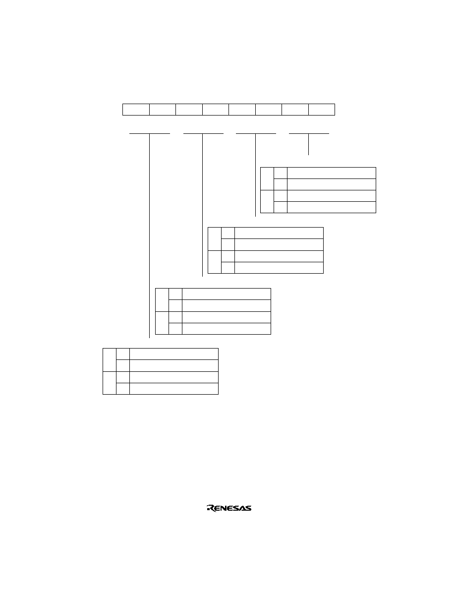
635
WCRH--Wait Control Register H
H'FED2
Bus Controller
7
W71
1
R/W
6
W70
1
R/W
5
W61
1
R/W
4
W60
1
R/W
3
W51
1
R/W
0
W40
1
R/W
2
W50
1
R/W
1
W41
1
R/W
Bit
Initial value
Read/Write
:
:
:
Area 7 Wait Control
Area 6 Wait Control
Area 5 Wait Control
Area 4 Wait Control
0
1
0
1
0
1
Program wait not inserted
1 program wait state inserted
2 program wait states inserted
3 program wait states inserted
0
1
0
1
0
1
Program wait not inserted
1 program wait state inserted
2 program wait states inserted
3 program wait states inserted
0
1
0
1
0
1
Program wait not inserted
1 program wait state inserted
2 program wait states inserted
3 program wait states inserted
0
1
0
1
0
1
Program wait not inserted
1 program wait state inserted
2 program wait states inserted
3 program wait states inserted
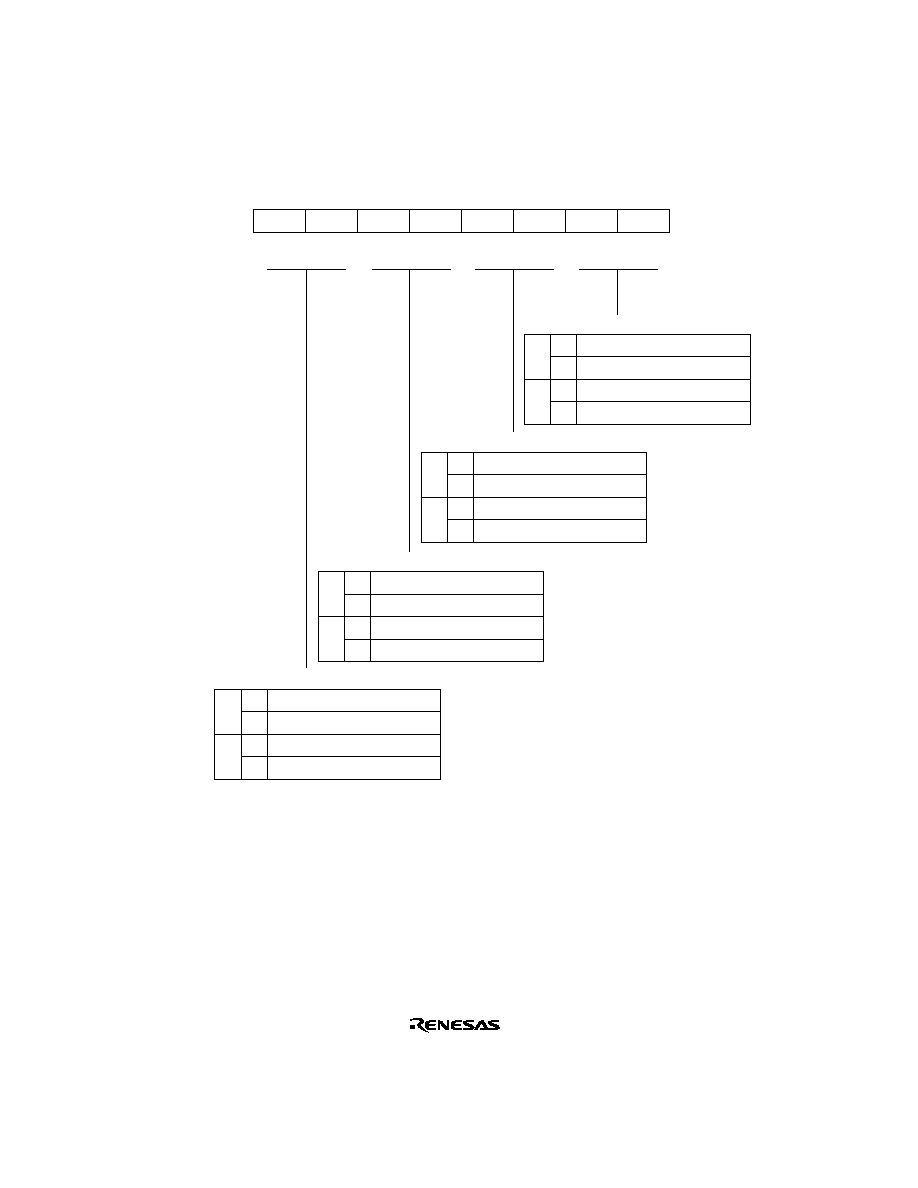
636
WCRL--Wait Control Register L
H'FED3
Bus Controller
7
W31
1
R/W
6
W30
1
R/W
5
W21
1
R/W
4
W20
1
R/W
3
W11
1
R/W
0
W00
1
R/W
2
W10
1
R/W
1
W01
1
R/W
Bit
Initial value
Read/Write
:
:
:
Area 3 Wait Control
Area 2 Wait Control
Area 1 Wait Control
Area 0 Wait Control
0
1
0
1
0
1
Program wait not inserted
1 program wait state inserted
2 program wait states inserted
3 program wait states inserted
0
1
0
1
0
1
Program wait not inserted
1 program wait state inserted
2 program wait states inserted
3 program wait states inserted
0
1
0
1
0
1
Program wait not inserted
1 program wait state inserted
2 program wait states inserted
3 program wait states inserted
0
1
0
1
0
1
Program wait not inserted
1 program wait state inserted
2 program wait states inserted
3 program wait states inserted
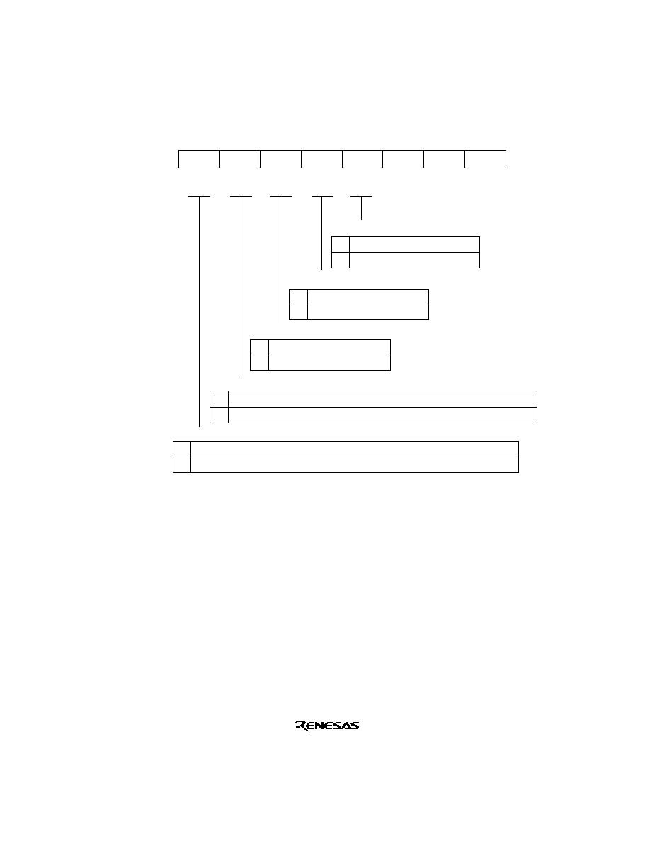
637
BCRH--Bus Control Register H
H'FED4
Bus Controller
7
ICIS1
1
R/W
6
ICIS0
1
R/W
5
BRSTRM
0
R/W
4
BRSTS1
1
R/W
3
BRSTS0
0
R/W
0
--
0
R/W
2
--
0
R/W
1
--
0
R/W
Bit
Initial value
Read/Write
:
:
:
Idle Cycle Insert 1
0
1
Idle cycle not inserted in case of successive external read cycles in different areas
Idle cycle inserted in case of successive external read cycles in different areas
Idle Cycle Insert 0
0
1
Idle cycle not inserted in case of successive external read and external write cycles
Idle cycle inserted in case of successive external read and external write cycles
Area 0 Burst ROM Enable
0
1
Area 0 is basic bus interface
Area 0 is burst ROM interface
Burst Cycle Select 1
0
1
Burst cycle comprises 1 state
Burst cycle comprises 2 states
Burst Cycle Select 0
0
1
Max. 4 words in burst access
Max. 8 words in burst access
638
BCRL--Bus Control Register L
H'FED5
Bus Controller
7
BRLE
0
R/W
6
BREQOE
0
R/W
5
EAE
1
R/W
4
--
1
R/W
3
--
1
R/W
0
WAITE
0
R/W
2
ASS
1
R/W
1
--
0
R/W
Bit
Initial value
Read/Write
:
:
:
Bus Release Enable
0
1
External bus release is disabled
External bus release is enabled
BREQO Pin Enable
0
1
BREQO
output disabled
BREQO
output enabled
External Addresses H'010000 to H'01FFFF Enable
0
1
Area Partition Unit Select
0
1
Area partition unit is 128 kbytes (1 Mbit)
Area partition unit is 2 Mbytes (16 Mbits)
WAIT Pin Enable
0
1
Wait input by
WAIT
pin disabled
Notes:
*
Do not access a reserved area.
Wait input by
WAIT
pin enabled
On-chip ROM (H8S/2246 and H8S/2245) or a reserved
area (H8S/2244, H8S/2243, H8S/2242, and H8S/2241)
External addresses (in external expansion mode) or
reserved area
*
(in single-chip mode)
639
ISCRH -- IRQ Sense Control Register H
H'FF2C
Interrupt Controller
ISCRL -- IRQ Sense Control Register L
H'FF2D
Interrupt Controller
15
IRQ7SCB
0
R/W
14
IRQ7SCA
0
R/W
13
IRQ6SCB
0
R/W
12
IRQ6SCA
0
R/W
11
IRQ5SCB
0
R/W
8
IRQ4SCA
0
R/W
10
IRQ5SCA
0
R/W
9
IRQ4SCB
0
R/W
Bit
Initial value
Read/Write
:
:
:
ISCRH
7
IRQ3SCB
0
R/W
6
IRQ3SCA
0
R/W
5
IRQ2SCB
0
R/W
4
IRQ2SCA
0
R/W
3
IRQ1SCB
0
R/W
0
IRQ0SCA
0
R/W
2
IRQ1SCA
0
R/W
1
IRQ0SCB
0
R/W
IRQ7 to IRQ4 Sense Control
IRQ
3
to IRQ
0
Sense Control
0
1
0
1
0
1
IRQ
n
input low level
Falling edge of
IRQ
n
input
Rising edge of
IRQ
n
input
Both falling and rising edges of
IRQ
n
input
IRQ
n
SCB IRQ
n
SCA
Interrupt Request Generation
(n = 7 to 0)
Bit
Initial value
Read/Write
:
:
:
ISCRL
640
IER--IRQ Enable Register
H'FF2E
Interrupt Controller
7
IRQ7E
0
R/W
6
IRQ6E
0
R/W
5
IRQ5E
0
R/W
4
IRQ4E
0
R/W
3
IRQ3E
0
R/W
0
IRQ0E
0
R/W
2
IRQ2E
0
R/W
1
IRQ1E
0
R/W
IRQn Enable
0
1
IRQn interrupt disabled
IRQn interrupt enabled
(n = 7 to 0)
Bit
Initial value
Read/Write
:
:
:
ISR--IRQ Status Register
H'FF2F
Interrupt Controller
7
IRQ7F
0
R/(W)
*
6
IRQ6F
0
R/(W)
*
5
IRQ5F
0
R/(W)
*
4
IRQ4F
0
R/(W)
*
3
IRQ3F
0
R/(W)
*
0
IRQ0F
0
R/(W)
*
2
IRQ2F
0
R/(W)
*
1
IRQ1F
0
R/(W)
*
Bit
Initial value
Read/Write
Note:
*
Can only be written with 0 for flag clearing.
:
:
:
Indicate the status of IRQ7 to IRQ0 interrupt requests

641
DTCER--DTC Enable Registers
H'FF30 to H'FF35
DTC
7
DTCE7
0
R/W
6
DTCE6
0
R/W
5
DTCE5
0
R/W
4
DTCE4
0
R/W
3
DTCE3
0
R/W
0
DTCE0
0
R/W
2
DTCE2
0
R/W
1
DTCE1
0
R/W
0
1
DTC activation by this interrupt is disabled
[Clearing conditions]
∑ When the DISEL bit is 1 and data transfer has ended
∑ When the specified number of transfers have ended
DTC activation by this interrupt is enabled
[Holding condition]
∑ When the DISEL bit is 0 and the specified number of transfers have not
ended
DTC Activation Enable
Bit
Initial value
Read/Write
:
:
:
Correspondence between interrupt sources and DTCER bits
Register
Bit
7
IRQ0
--
TGI2A
--
--
RXI2
DTCERA
DTCERB
DTCERC
DTCERD
DTCERE
DTCERF
6
IRQ1
ADI
TGI2B
--
--
TXI2
5
IRQ2
TGI0A
--
--
--
--
4
IRQ3
TGI0B
--
--
--
--
3
IRQ4
TGI0C
--
CMIA0
RXI0
--
2
IRQ5
TGI0D
--
CMIB0
TXI0
--
1
IRQ6
TGI1A
--
CMIA1
RXI1
--
0
IRQ7
TGI1B
--
CMIB1
TXI1
--
642
DTVECR--DTC Vector Register
H'FF37
DTC
7
SWDTE
0
R/(W)
*
6
DTVEC6
0
R/W
5
DTVEC5
0
R/W
4
DTVEC4
0
R/W
3
DTVEC3
0
R/W
0
DTVEC0
0
R/W
2
DTVEC2
0
R/W
1
DTVEC1
0
R/W
A value of 1 can always be written to the SWDTE bit, but 0 can only be written after 1
is read.
Note:
*
DTC Software Activation Enable
Sets vector number for DTC software activation
Bit
Initial value
Read/Write
:
:
:
0
1
DTC software activation is disabled
[Clearing condition]
When the DISEL bit is 0 and the specified number of transfers have not ended
DTC software activation is enabled
[Holding conditions]
∑ When the DISEL bit is 1 and data transfer has ended
∑ When the specified number of transfers have ended
∑ During data transfer activated by software
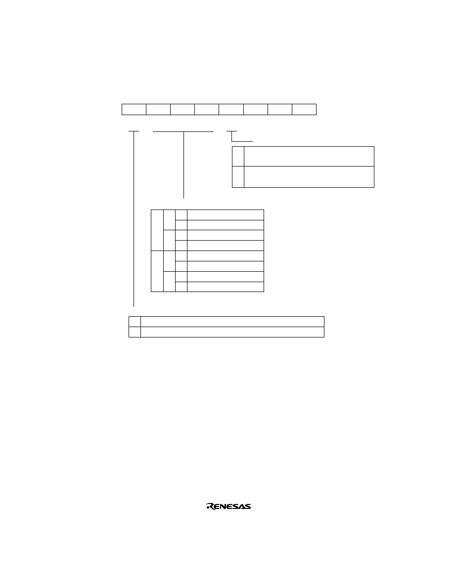
643
SBYCR--Standby Control Register
H'FF38
Power-Down State
7
SSBY
0
R/W
6
STS2
0
R/W
5
STS1
0
R/W
4
STS0
0
R/W
3
OPE
1
R/W
0
--
0
--
2
--
0
--
1
--
0
--
Software Standby
0
1
Transition to sleep mode after execution of SLEEP instruction
Transition to software standby mode after execution of SLEEP instruction
Standby Timer Select
0
1
0
1
0
1
0
1
0
1
0
1
0
1
Standby time = 8192 states
Standby time = 16384 states
Standby time = 32768 states
Standby time = 65536 states
Standby time = 131072 states
Standby time = 262144 states
Reserved
Standby time = 16 states
Output Port Enable
0
1
In software standby mode, address bus and bus
control signals are high-impedance
Bit
Initial value
Read/Write
:
:
:
In software standby mode, address bus and bus
control signals retain output state
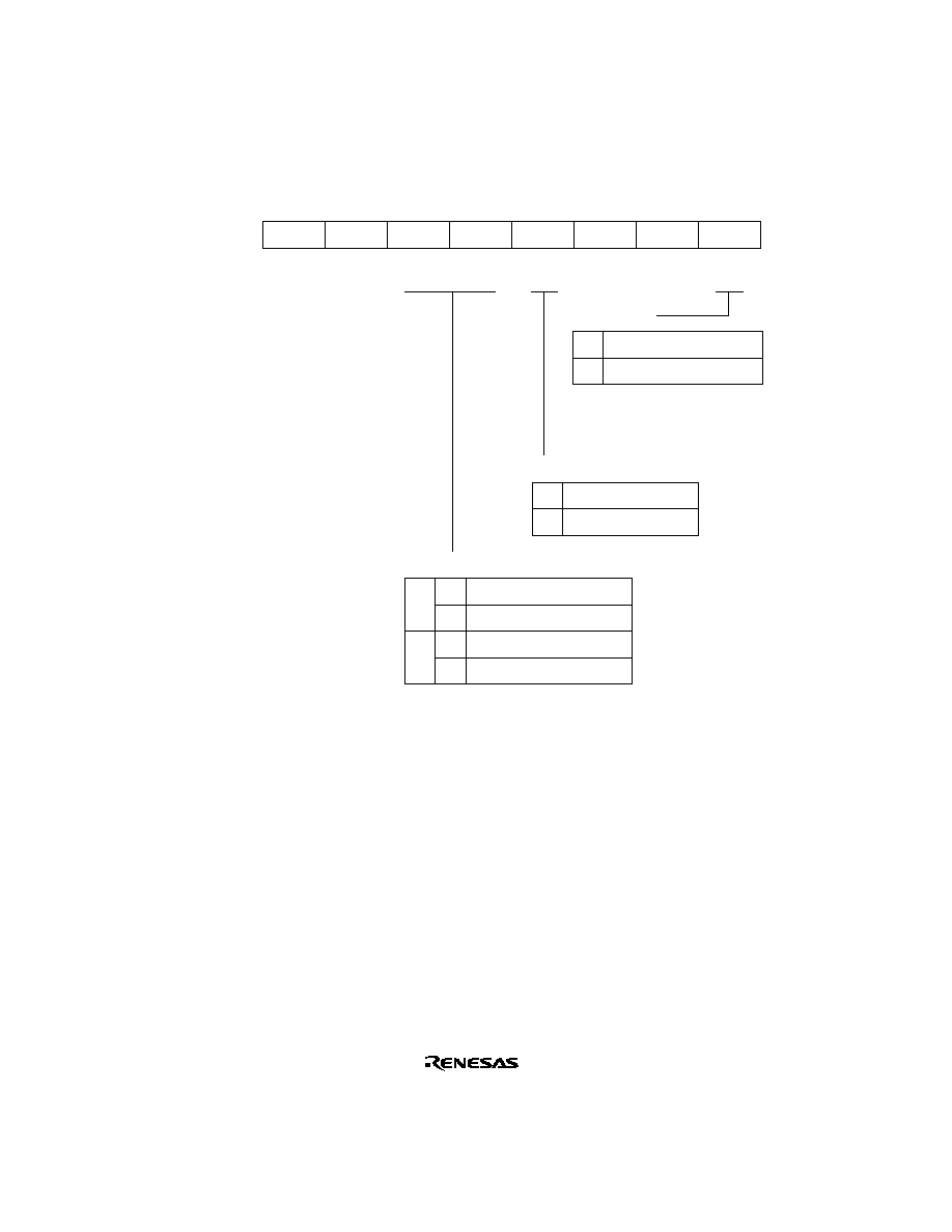
644
SYSCR--System Control Register
H'FF39
MCU
7
--
0
R/W
6
--
0
--
5
INTM1
0
R/W
4
INTM0
0
R/W
3
NMIEG
0
R/W
0
RAME
1
R/W
2
--
0
--
1
--
0
--
Bit
Initial value
Read/Write
:
:
:
Interrupt Control Mode Selection
0
1
0
1
0
1
Interrupt control mode 0
Interrupt control mode 1
Setting prohibited
Setting prohibited
NMI Input Edge Select
0
1
Falling edge
Rising edge
RAM Enable
*
0
1
On-chip RAM disabled
On-chip RAM enabled
Note:
*
When the DTC is used,
the RAME bit should
not be cleared to 0.

645
SCKCR--System Clock Control Register
H'FF3A
Clock Pulse Generator
7
PSTOP
0
R/W
6
--
0
--
5
--
0
--
4
--
0
--
3
--
0
--
0
SCK0
0
R/W
2
SCK2
0
R/W
1
SCK1
0
R/W
0
1
PSTOP
Normal Operation
¯ output
Fixed high
High impedance
High impedance
Fixed high
Fixed high
¯ Clock Output Control
Bus Master Clock Select
0
1
0
1
0
1
0
1
0
1
0
1
--
Bus master is in high-speed mode
Medium-speed clock is ¯/2
Medium-speed clock is ¯/4
Medium-speed clock is ¯/8
Medium-speed clock is ¯/16
Medium-speed clock is ¯/32
--
¯ output
Fixed high
Sleep Mode
Bit
Initial value
Read/Write
:
:
:
Software
Standby Mode
Hardware
Standby Mode
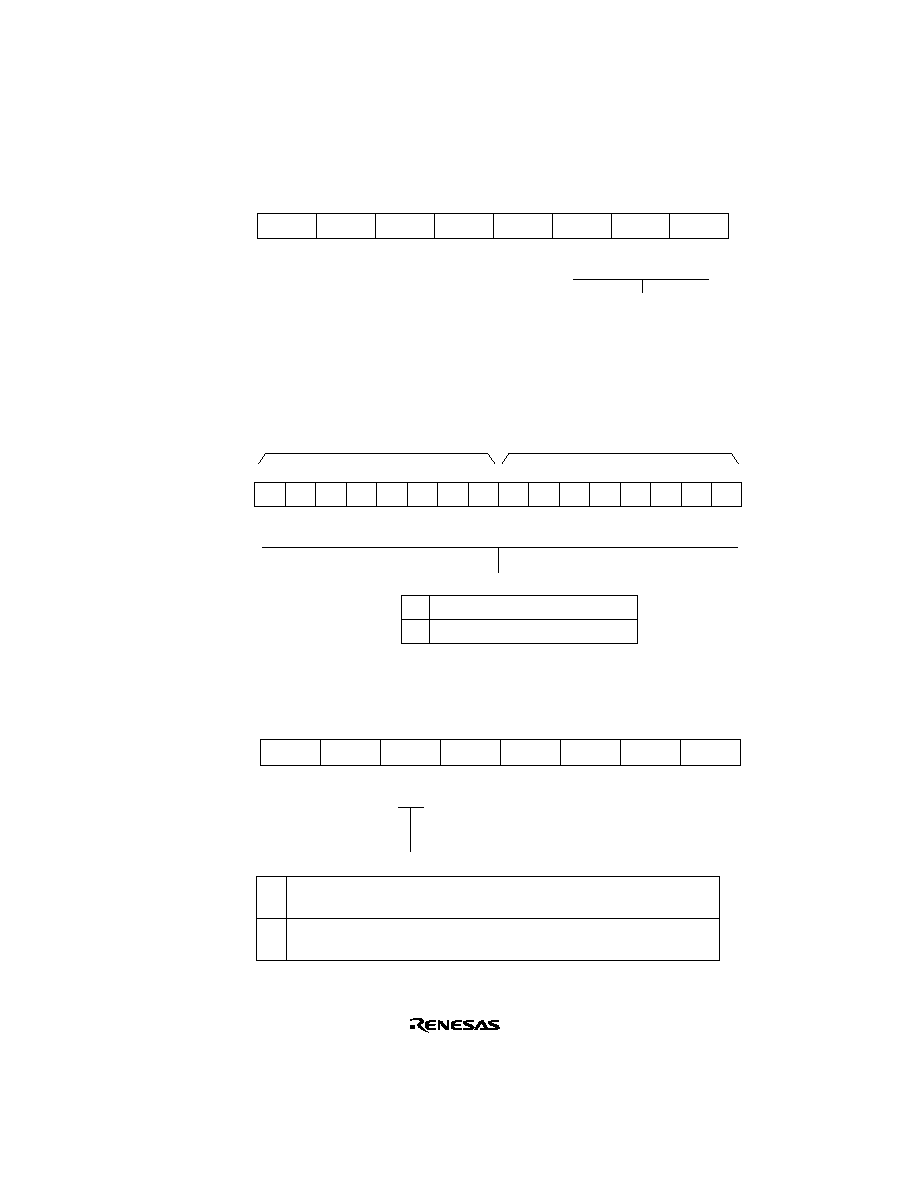
646
MDCR--Mode Control Register
H'FF3B
MCU
7
--
1
--
6
--
0
--
5
--
0
--
4
--
0
--
3
--
0
--
0
MDS0
--
*
R
2
MDS2
--
*
R
1
MDS1
--
*
R
Current mode pin operating mode
Bit
Initial value
Read/Write
:
:
:
Note:
*
Determined by pins MD
2
to MD
0
MSTPCRH -- Module Stop Control Register H
H'FF3C
Power-Down State
MSTPCRL -- Module Stop Control Register L
H'FF3D
Power-Down State
15
0
R/W
14
0
R/W
13
1
R/W
12
1
R/W
11
1
R/W
10
1
R/W
9
1
R/W
8
1
R/W
7
1
R/W
6
1
R/W
5
1
R/W
4
1
R/W
3
1
R/W
2
1
R/W
1
1
R/W
0
1
R/W
MSTPCRH
MSTPCRL
Specifies module stop mode
0
1
Module stop mode cleared
Module stop mode set
Bit
Initial value
Read/Write
:
:
:
LPWCR--Low Power Control Register
H'FF44
Clock Oscillator
7
--
0
R/W
6
--
0
R/W
5
RFCUT
0
R/W
4
--
0
R/W
3
--
0
R/W
0
--
0
R/W
2
--
0
R/W
1
--
0
R/W
Bit
Initial value
Read/Write
:
:
:
Control of Oscillator's Built-In Feedback Resistor in External Clock Input
0
1
Oscillator's built-in feedback resistor and duty adjustment circuit are
used
Oscillator's built-in feedback resistor and duty adjustment circuit are
not used

647
PORT1--Port 1 Register
H'FF50
Port 1
7
P17
--
*
R
6
P16
--
*
R
5
P15
--
*
R
4
P14
--
*
R
3
P13
--
*
R
0
P10
--
*
R
2
P12
--
*
R
1
P11
--
*
R
Note:
*
Determined by the state of pins P1
7
to P1
0
.
State of port 1 pins
Bit
Initial value
Read/Write
:
:
:
PORT2--Port 2 Register
H'FF51
Port 2
7
P27
--
*
R
6
P26
--
*
R
5
P25
--
*
R
4
P24
--
*
R
3
P23
--
*
R
0
P20
--
*
R
2
P22
--
*
R
1
P21
--
*
R
State of port 2 pins
Note:
*
Determined by the state of pins P2
7
to P2
0
.
Bit
Initial value
Read/Write
:
:
:
PORT3--Port 3 Register
H'FF52
Port 3
7
--
Undefined
--
6
--
Undefined
--
5
P35
--
*
R
4
P34
--
*
R
3
P33
--
*
R
0
P30
--
*
R
2
P32
--
*
R
1
P31
--
*
R
State of port 3 pins
Note:
*
Determined by the state of pins P3
5
to P3
0
.
Bit
Initial value
Read/Write
:
:
:

648
PORT4--Port 4 Register
H'FF53
Port 4
7
--
Undefined
--
6
--
Undefined
--
5
--
Undefined
--
4
--
Undefined
--
3
P43
--
*
R
0
P40
--
*
R
2
P42
--
*
R
1
P41
--
*
R
State of port 4 pins
Note:
*
Determined by the state of pins P4
3
to P4
0
.
Bit
Initial value
Read/Write
:
:
:
PORT5--Port 5 Register
H'FF54
Port 5
7
--
Undefined
--
6
--
Undefined
--
5
--
Undefined
--
4
--
Undefined
--
3
P53
--
*
R
0
P50
--
*
R
2
P52
--
*
R
1
P51
--
*
R
State of port 5 pins
Note:
*
Determined by the state of pins P5
3
to P5
0
.
Bit
Initial value
Read/Write
:
:
:
PORTA--Port A Register
H'FF59
Port A
7
--
Undefined
--
6
--
Undefined
--
5
--
Undefined
--
4
--
Undefined
--
3
PA3
--
*
R
0
PA0
--
*
R
2
PA2
--
*
R
1
PA1
--
*
R
State of port A pins
Note:
*
Determined by the state of pins PA
3
to PA
0
.
Bit
Initial value
Read/Write
:
:
:
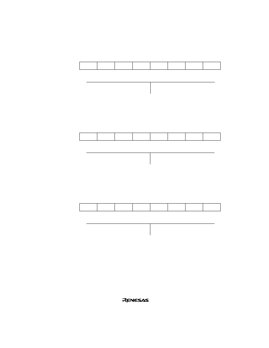
649
PORTB--Port B Register
H'FF5A
Port B
7
PB7
--
*
R
6
PB6
--
*
R
5
PB5
--
*
R
4
PB4
--
*
R
3
PB3
--
*
R
0
PB0
--
*
R
2
PB2
--
*
R
1
PB1
--
*
R
State of port B pins
Note:
*
Determined by the state of pins PB
7
to PB
0
.
Bit
Initial value
Read/Write
:
:
:
PORTC--Port C Register
H'FF5B
Port C
7
PC7
--
*
R
6
PC6
--
*
R
5
PC5
--
*
R
4
PC4
--
*
R
3
PC3
--
*
R
0
PC0
--
*
R
2
PC2
--
*
R
1
PC1
--
*
R
State of port C pins
Note:
*
Determined by the state of pins PC
7
to PC
0
.
Bit
Initial value
Read/Write
:
:
:
PORTD--Port D Register
H'FF5C
Port D
7
PD7
--
*
R
6
PD6
--
*
R
5
PD5
--
*
R
4
PD4
--
*
R
3
PD3
--
*
R
0
PD0
--
*
R
2
PD2
--
*
R
1
PD1
--
*
R
State of port D pins
Note:
*
Determined by the state of pins PD
7
to PD
0
.
Bit
Initial value
Read/Write
:
:
:

650
PORTE--Port E Register
H'FF5D
Port E
7
PE7
--
*
R
6
PE6
--
*
R
5
PE5
--
*
R
4
PE4
--
*
R
3
PE3
--
*
R
0
PE0
--
*
R
2
PE2
--
*
R
1
PE1
--
*
R
State of port E pins
Note:
*
Determined by the state of pins PE
7
to PE
0
.
Bit
Initial value
Read/Write
:
:
:
PORTF--Port F Register
H'FF5E
Port F
7
PF7
--
*
R
6
PF6
--
*
R
5
PF5
--
*
R
4
PF4
--
*
R
3
PF3
--
*
R
0
PF0
--
*
R
2
PF2
--
*
R
1
PF1
--
*
R
State of port F pins
Note:
*
Determined by the state of pins PF
7
to PF
0
.
Bit
Initial value
Read/Write
:
:
:
PORTG--Port G Register
H'FF5F
Port G
7
--
Undefined
--
6
--
Undefined
--
5
--
Undefined
--
4
PG4
--
*
R
3
PG3
--
*
R
0
PG0
--
*
R
2
PG2
--
*
R
1
PG1
--
*
R
State of port G pins
Note:
*
Determined by the state of pins PG
4
to PG
0
.
Bit
Initial value
Read/Write
:
:
:

651
P1DR--Port 1 Data Register
H'FF60
Port 1
7
P17DR
0
R/W
6
P16DR
0
R/W
5
P15DR
0
R/W
4
P14DR
0
R/W
3
P13DR
0
R/W
0
P10DR
0
R/W
2
P12DR
0
R/W
1
P11DR
0
R/W
Stores output data for port 1 pins (P1
7
to P1
0
)
Bit
Initial value
Read/Write
:
:
:
P2DR--Port 2 Data Register
H'FF61
Port 2
7
P27DR
0
R/W
6
P26DR
0
R/W
5
P25DR
0
R/W
4
P24DR
0
R/W
3
P23DR
0
R/W
0
P20DR
0
R/W
2
P22DR
0
R/W
1
P21DR
0
R/W
Stores output data for port 2 pins (P2
7
to P2
0
)
Bit
Initial value
Read/Write
:
:
:
P3DR--Port 3 Data Register
H'FF62
Port 3
7
--
Undefined
--
6
--
Undefined
--
5
P35DR
0
R/W
4
P34DR
0
R/W
3
P33DR
0
R/W
0
P30DR
0
R/W
2
P32DR
0
R/W
1
P31DR
0
R/W
Stores output data for port 3 pins (P3
5
to P3
0
)
Bit
Initial value
Read/Write
:
:
:

652
P5DR--Port 5 Data Register
H'FF64
Port 5
7
--
Undefined
--
6
--
Undefined
--
5
--
Undefined
--
4
--
Undefined
--
3
P53DR
0
R/W
0
P50DR
0
R/W
2
P52DR
0
R/W
1
P51DR
0
R/W
Stores output data for port 5 pins (P5
3
to P5
0
)
Bit
Initial value
Read/Write
:
:
:
PADR--Port A Data Register
H'FF69
Port A
7
--
Undefined
--
6
--
Undefined
--
5
--
Undefined
--
4
--
Undefined
--
3
PA3DR
0
R/W
0
PA0DR
0
R/W
2
PA2DR
0
R/W
1
PA1DR
0
R/W
Stores output data for port A pins (PA
3
to
PA
0
)
Bit
Initial value
Read/Write
:
:
:
PBDR--Port B Data Register
H'FF6A
Port B
7
PB7DR
0
R/W
6
PB6DR
0
R/W
5
PB5DR
0
R/W
4
PB4DR
0
R/W
3
PB3DR
0
R/W
0
PB0DR
0
R/W
2
PB2DR
0
R/W
1
PB1DR
0
R/W
Stores output data for port B pins (PB
7
to PB
0
)
Bit
Initial value
Read/Write
:
:
:
653
PCDR--Port C Data Register
H'FF6B
Port C
7
PC7DR
0
R/W
6
PC6DR
0
R/W
5
PC5DR
0
R/W
4
PC4DR
0
R/W
3
PC3DR
0
R/W
0
PC0DR
0
R/W
2
PC2DR
0
R/W
1
PC1DR
0
R/W
Stores output data for port C pins (PC
7
to PC
0
)
Bit
Initial value
Read/Write
:
:
:
PDDR--Port D Data Register
H'FF6C
Port D
7
PD7DR
0
R/W
6
PD6DR
0
R/W
5
PD5DR
0
R/W
4
PD4DR
0
R/W
3
PD3DR
0
R/W
0
PD0DR
0
R/W
2
PD2DR
0
R/W
1
PD1DR
0
R/W
Stores output data for port D pins (PD
7
to PD
0
)
Bit
Initial value
Read/Write
:
:
:
PEDR--Port E Data Register
H'FF6D
Port E
7
PE7DR
0
R/W
6
PE6DR
0
R/W
5
PE5DR
0
R/W
4
PE4DR
0
R/W
3
PE3DR
0
R/W
0
PE0DR
0
R/W
2
PE2DR
0
R/W
1
PE1DR
0
R/W
Stores output data for port E pins (PE
7
to PE
0
)
Bit
Initial value
Read/Write
:
:
:
654
PFDR--Port F Data Register
H'FF6E
Port F
7
PF7DR
0
R/W
6
PF6DR
0
R/W
5
PF5DR
0
R/W
4
PF4DR
0
R/W
3
PF3DR
0
R/W
0
PF0DR
0
R/W
2
PF2DR
0
R/W
1
PF1DR
0
R/W
Stores output data for port F pins (PF
7
to PF
0
)
Bit
Initial value
Read/Write
:
:
:
PGDR--Port G Data Register
H'FF6F
Port G
7
--
Undefined
--
6
--
Undefined
--
5
--
Undefined
--
4
PG4DR
0
R/W
3
PG3DR
0
R/W
0
PG0DR
0
R/W
2
PG2DR
0
R/W
1
PG1DR
0
R/W
Stores output data for port G pins (PG
4
to PG
0
)
Bit
Initial value
Read/Write
:
:
:
PAPCR--Port A MOS Pull-Up Control Register
H'FF70
Port A
7
--
Undefined
--
6
--
Undefined
--
5
--
Undefined
--
4
--
Undefined
--
3
PA3PCR
0
R/W
0
PA0PCR
0
R/W
2
PA2PCR
0
R/W
1
PA1PCR
0
R/W
Controls the MOS input pull-up function
incorporated into port A on a bit-by-bit
basis
Bit
Initial value
Read/Write
:
:
:

655
PBPCR--Port B MOS Pull-Up Control Register
H'FF71
Port B
7
PB7PCR
0
R/W
6
PB6PCR
0
R/W
5
PB5PCR
0
R/W
4
PB4PCR
0
R/W
3
PB3PCR
0
R/W
0
PB0PCR
0
R/W
2
PB2PCR
0
R/W
1
PB1PCR
0
R/W
Controls the MOS input pull-up function incorporated into port B on a bit-by-bit basis
Bit
Initial value
Read/Write
:
:
:
PCPCR--Port C MOS Pull-Up Control Register
H'FF72
Port C
7
PC7PCR
0
R/W
6
PC6PCR
0
R/W
5
PC5PCR
0
R/W
4
PC4PCR
0
R/W
3
PC3PCR
0
R/W
0
PC0PCR
0
R/W
2
PC2PCR
0
R/W
1
PC1PCR
0
R/W
Controls the MOS input pull-up function incorporated into port C on a bit-by-bit basis
Bit
Initial value
Read/Write
:
:
:
PDPCR--Port D MOS Pull-Up Control Register
H'FF73
Port D
7
PD7PCR
0
R/W
6
PD6PCR
0
R/W
5
PD5PCR
0
R/W
4
PD4PCR
0
R/W
3
PD3PCR
0
R/W
0
PD0PCR
0
R/W
2
PD2PCR
0
R/W
1
PD1PCR
0
R/W
Controls the MOS input pull-up function incorporated into port D on a bit-by-bit basis
Bit
Initial value
Read/Write
:
:
:
656
PEPCR--Port E MOS Pull-Up Control Register
H'FF74
Port E
7
PE7PCR
0
R/W
6
PE6PCR
0
R/W
5
PE5PCR
0
R/W
4
PE4PCR
0
R/W
3
PE3PCR
0
R/W
0
PE0PCR
0
R/W
2
PE2PCR
0
R/W
1
PE1PCR
0
R/W
Controls the MOS input pull-up function incorporated into port E on a bit-by-bit basis
Bit
Initial value
Read/Write
:
:
:
P3ODR--Port 3 Open Drain Control Register
H'FF76
Port 3
7
--
Undefined
--
6
--
Undefined
--
5
P35ODR
0
R/W
4
P34ODR
0
R/W
3
P33ODR
0
R/W
0
P30ODR
0
R/W
2
P32ODR
0
R/W
1
P31ODR
0
R/W
Controls the PMOS on/off status for each port 3 pin (P3
5
to P3
0
)
Bit
Initial value
Read/Write
:
:
:
PAODR--Port A Open Drain Control Register
H'FF77
Port A
7
--
Undefined
--
6
--
Undefined
--
5
--
Undefined
--
4
--
Undefined
--
3
PA3ODR
0
R/W
0
PA0ODR
0
R/W
2
PA2ODR
0
R/W
1
PA1ODR
0
R/W
Controls the PMOS on/off status for
each port A pin (PA
3
to PA
0
)
Bit
Initial value
Read/Write
:
:
:
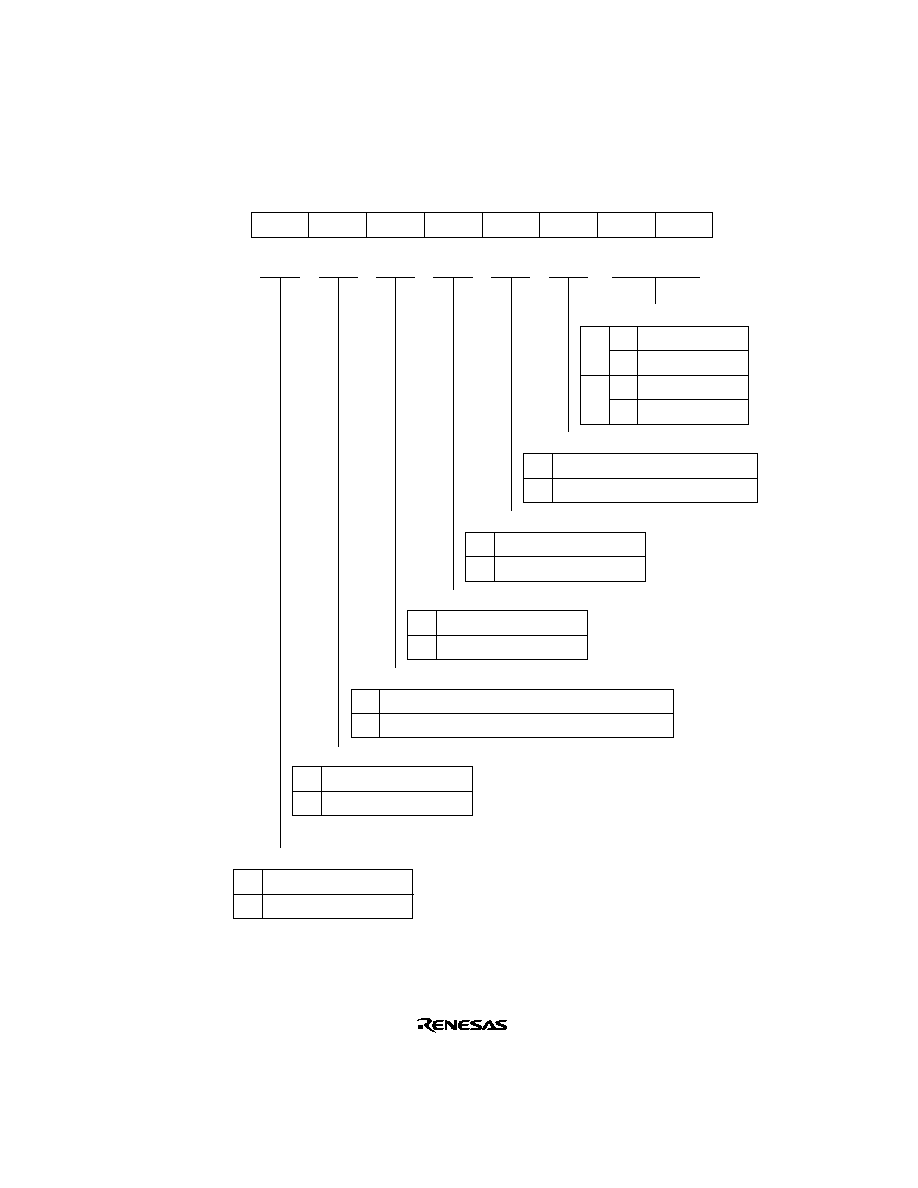
657
SMR0--Serial Mode Register 0
H'FF78
SCI0
7
C/
A
0
R/W
6
CHR
0
R/W
5
PE
0
R/W
4
O/
E
0
R/W
3
STOP
0
R/W
0
CKS0
0
R/W
2
MP
0
R/W
1
CKS1
0
R/W
0
1
Asynchronous mode
Synchronous mode
Asynchronous Mode/Synchronous Mode Select
0
1
Parity bit addition and checking disabled
Parity bit addition and checking enabled
Parity Enable
0
1
Even parity
Odd parity
Parity Mode
0
1
0
1
0
1
¯ clock
¯/4 clock
¯/16 clock
¯/64 clock
Clock Select
0
1
Multiprocessor function disabled
Multiprocessor format selected
Multiprocessor Mode
0
1
1 stop bit
2 stop bits
Stop Bit Length
0
1
8-bit data
7-bit data
*
Character Length
Note:
*
When 7-bit data is selected, the MSB (bit 7) of TDR is not transmitted.
Bit
Initial value
Read/Write
:
:
:

658
SMR0--Serial Mode Register 0
H'FF78
Smart Card Interface 0
7
GM
0
R/W
6
CHR
0
R/W
5
PE
0
R/W
4
O/
E
0
R/W
3
STOP
0
R/W
0
CKS0
0
R/W
2
MP
0
R/W
1
CKS1
0
R/W
0
1
Normal smart card interface mode operation
∑ TEND flag generated 12.5 etu after beginning of start bit
∑ Clock output on/off control only
GSM mode smart card interface mode operation
∑ TEND flag generated 11.0 etu after beginning of start bit
∑ Fixed high/low-level control possible (set in SCR) in addition to clock output on/off control
GSM Mode
0
1
Setting prohibited
Parity bit addition and checking enabled
Parity Enable
0
1
Even parity
Odd parity
Parity Mode
0
1
0
1
0
1
¯ clock
¯/4 clock
¯/16 clock
¯/64 clock
Clock Select
0
1
Multiprocessor function disabled
Setting prohibited
Multiprocessor Mode
0
1
Setting prohibited
2 stop bits
Stop Bit Length
0
1
8-bit data
Setting prohibited
Character Length
Bit
Initial value
Read/Write
:
:
:
Note: etu (Elementary Time Unit): Interval for transfer of one bit

659
BRR0--Bit Rate Register 0
H'FF79
SCI0, Smart Card Interface 0
7
1
R/W
6
1
R/W
5
1
R/W
4
1
R/W
3
1
R/W
0
1
R/W
2
1
R/W
1
1
R/W
Sets the serial transfer bit rate
Note: See section 12.2.8, Bit Rate Register (BRR), for details.
Bit
Initial value
Read/Write
:
:
:

660
SCR0--Serial Control Register 0
H'FF7A
SCI0
7
TIE
0
R/W
6
RIE
0
R/W
5
TE
0
R/W
4
RE
0
R/W
3
MPIE
0
R/W
0
CKE0
0
R/W
2
TEIE
0
R/W
1
CKE1
0
R/W
0
0
Asynchronous
mode
Internal clock/SCK pin functions
as I/O port
Clock Enable
0
1
Transmit end interrupt (TEI) request disabled
Transmit end interrupt (TEI) request enabled
Transmit End Interrupt Enable
0
Multiprocessor interrupts disabled
[Clearing conditions]
∑ When the MPIE bit is cleared to 0
∑ When MPB= 1 data is received
Multiprocessor Interrupt Enable
0
1
Reception disabled
Reception enabled
Receive Enable
0
1
Transmission disabled
Transmission enabled
Transmit Enable
0
Receive data full interrupt (RXI) request and
receive error interrupt (ERI) request disabled
Receive Interrupt Enable
0
1
Transmit data empty interrupt (TXI) requests disabled
Transmit data empty interrupt (TXI) requests enabled
Transmit Interrupt Enable
Notes:
Bit
Initial value
Read/Write
:
:
:
Synchronous
mode
Internal clock/SCK pin functions
as serial clock output
Asynchronous
mode
Internal clock/SCK pin functions
as clock output
*
1
Synchronous
mode
Internal clock/SCK pin functions
as serial clock output
Asynchronous
mode
External clock/SCK pin functions
as clock input
*
2
Synchronous
mode
External clock/SCK pin functions
as serial clock input
Asynchronous
mode
External clock/SCK pin functions
as clock input
*
2
Synchronous
mode
External clock/SCK pin functions
as serial clock input
1. Outputs a clock of the same frequency as the bit rate.
2. Inputs a clock with a frequency 16 times the bit rate.
Multiprocessor interrupts enabled
Receive interrupt (RXI) requests, receive error interrupt (ERI)
requests, and setting of the RDRF, FER, and ORER flags in
SSR are disabled until data with the multiprocessor bit set to 1
is received
1
0
1
1
1
1
Receive data full interrupt (RXI) request and
receive error interrupt (ERI) request enabled
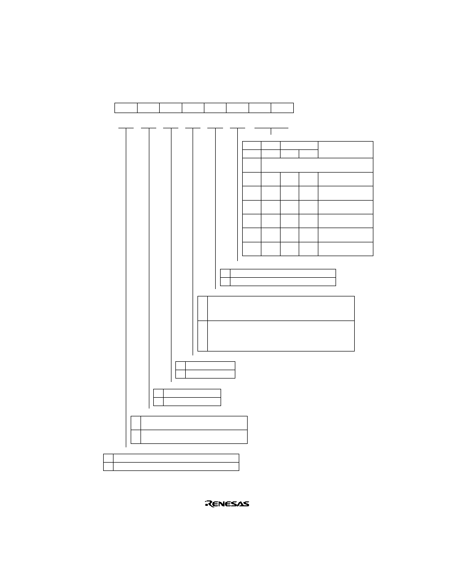
661
SCR0--Serial Control Register 0
H'FF7A
Smart Card Interface 0
7
TIE
0
R/W
6
RIE
0
R/W
5
TE
0
R/W
4
RE
0
R/W
3
MPIE
0
R/W
0
CKE0
0
R/W
2
TEIE
0
R/W
1
CKE1
0
R/W
SMCR
SMIF
0
1
1
1
1
1
1
0
0
1
1
1
1
0
0
0
0
1
1
0
1
0
1
0
1
SMR
C/
A
,GM CKE1
CKE0
See SCI specification
SCK pin function
Clock Enable
SCR setting
0
1
Transmit end interrupt (TEI) request disabled
Transmit end interrupt (TEI) request enabled
Transmit End Interrupt Enable
0
Multiprocessor interrupts disabled
[Clearing conditions]
∑ When the MPIE bit is cleared to 0
∑ When MPB= 1 data is received
Multiprocessor Interrupt Enable
0
1
Reception disabled
Reception enabled
Receive Enable
0
1
Transmission disabled
Transmission enabled
Transmit Enable
0
Receive data full interrupt (RXI) request and
receive error interrupt (ERI) request disabled
Receive Interrupt Enable
0
1
Transmit data empty interrupt (TXI) requests disabled
Transmit data empty interrupt (TXI) requests enabled
Transmit Interrupt Enable
Bit
Initial value
Read/Write
:
:
:
Multiprocessor interrupts enabled
Receive interrupt (RXI) requests, receive error interrupt (ERI)
requests, and setting of the RDRF, FER, and ORER flags in
SSR are disabled until data with the multiprocessor bit set to 1
is received
1
1
Receive data full interrupt (RXI) request and
receive error interrupt (ERI) request enabled
Operates as port input
pin
Clock output as SCK
output pin
Fixed-low output as
SCK output pin
Clock output as SCK
output pin
Fixed-high output as
SCK output pin
Clock output as SCK
output pin

662
TDR0--Transmit Data Register 0
H'FF7B
SCI0, Smart Card Interface 0
7
1
R/W
6
1
R/W
5
1
R/W
4
1
R/W
3
1
R/W
0
1
R/W
2
1
R/W
1
1
R/W
Stores data for serial transmission
Bit
Initial value
Read/Write
:
:
:
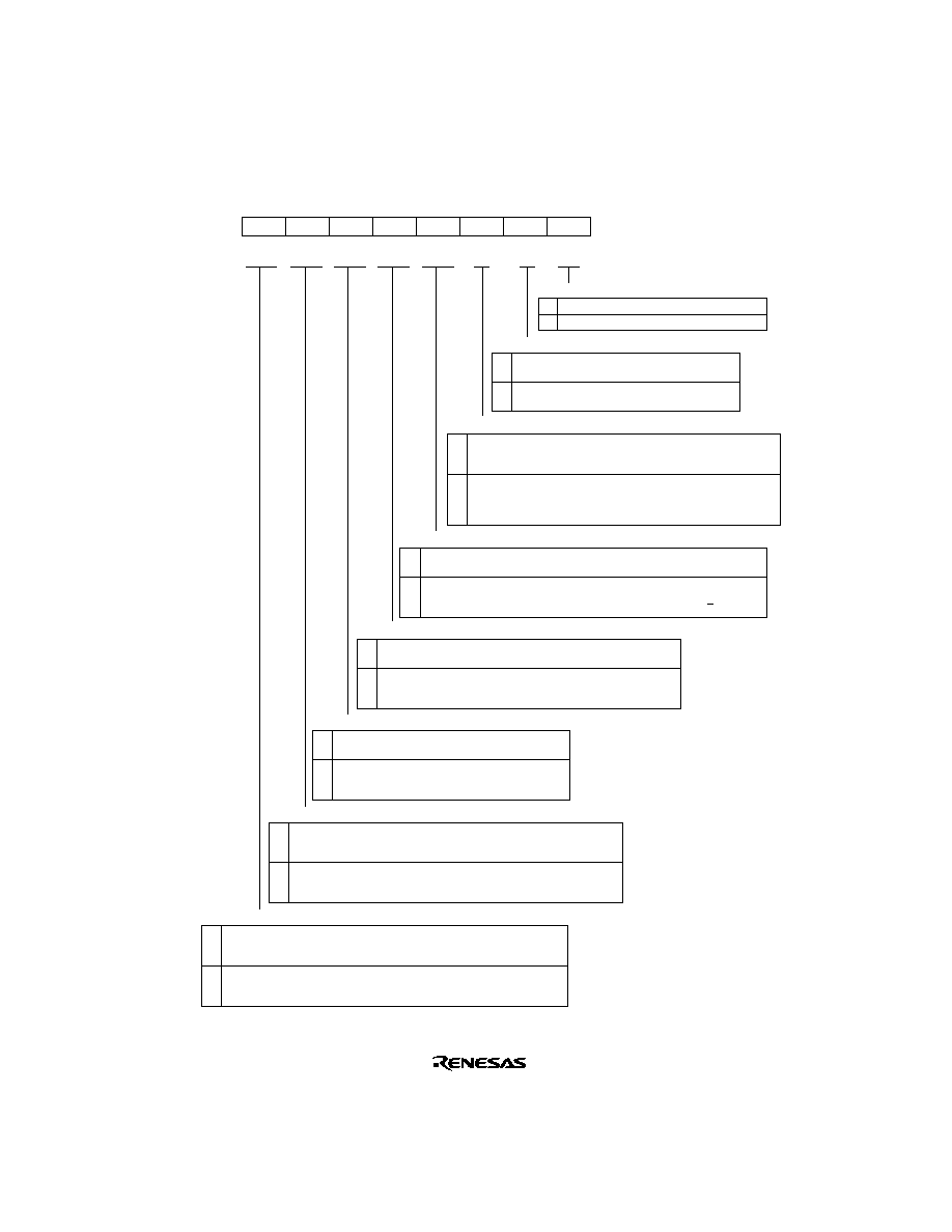
663
SSR0--Serial Status Register 0
H'FF7C
SCI0
[Setting condition]
When serial reception ends normally and receive data is transferred
from RSR to RDR
7
TDRE
1
R/(W)
*
6
RDRF
0
R/(W)
*
5
ORER
0
R/(W)
*
4
FER
0
R/(W)
*
3
PER
0
R/(W)
*
0
MPBT
0
R/W
2
TEND
1
R
1
MPB
0
R
Note:
*
Can only be written with 0 for flag clearing.
0
Transmit Data Register Empty
0
Receive Data Register Full
0
Overrun Error
0
Framing Error
0
Parity Error
0
Transmit End
[Clearing condition]
∑ When 0 is written to TDRE after reading TDRE = 1
∑ When the DTC is activated by a TXI interrupt and write data to TDR
0
Multiprocessor Bit
[Clearing condition]
When data with a 0 multiprocessor bit is received
[Setting condition]
When data with a 1 multiprocessor bit is received
Multiprocessor Bit Transfer
0
1
Data with a 0 multiprocessor bit is transmitted
Data with a 1 multiprocessor bit is transmitted
Bit
Initial value
Read/Write
:
:
:
[Setting conditions]
∑ When the TE bit in SCR is 0
∑ When TDRE = 1 at transmission of the last bit of a 1-byte
serial transmit character
[Clearing condition]
When 0 is written to PER after reading PER = 1
[Setting condition]
When, in reception, the number of 1 bits in the receive data plus the parity bit
does not match the parity setting (even or odd) specified by the O/E bit in SMR
[Clearing condition]
When 0 is written to FER after reading FER = 1
[Setting condition]
When the SCI checks whether the stop bit at the end of the receive
data is 1 when reception ends, and the stop bit is 0
[Clearing condition]
When 0 is written to ORER after reading ORER = 1
[Setting condition]
When the next serial reception is completed while
RDRF = 1
[Clearing condition]
∑ When 0 is written to RDRF after reading RDRF = 1
∑ When the DTC is activated by an RXI interrupt and read data from RDR
[Clearing condition]
∑ When 0 is written to TDRE after reading TDRE = 1
∑ When the DTC is activated by a TXI interrupt and write data to TDR
[Setting condition]
∑ When the TE bit in SCR is 0
∑ When data is transferred from TDR to TSR and data can be written to TDR
1
1
1
1
1
1
1
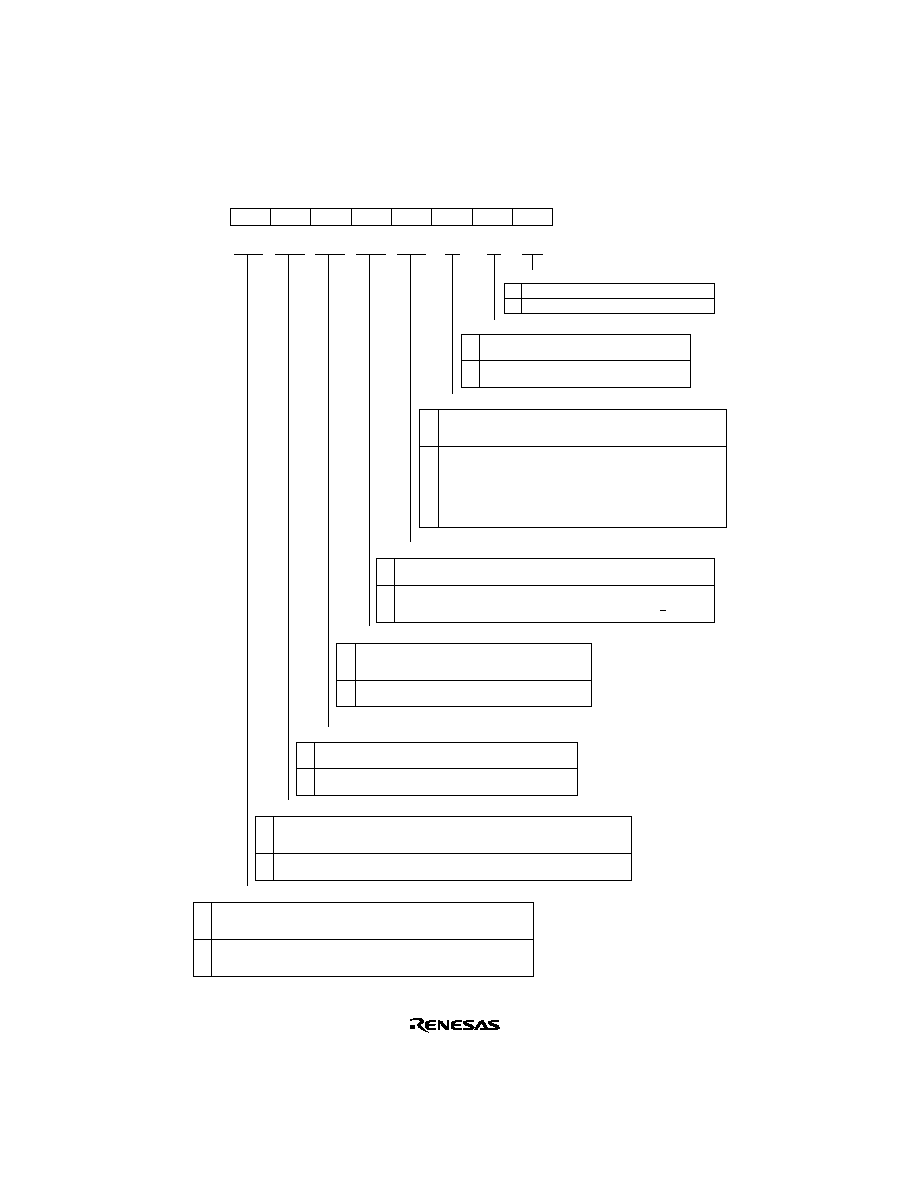
664
SSR0--Serial Status Register 0
H'FF7C
Smart Card Interface 0
7
TDRE
1
R/(W)
*
6
RDRF
0
R/(W)
*
5
ORER
0
R/(W)
*
4
ERS
0
R/(W)
*
3
PER
0
R/(W)
*
0
MPBT
0
R/W
2
TEND
1
R
1
MPB
0
R
Note:
*
Can only be written with 0 for flag clearing.
0
Transmit Data Register Empty
0
Receive Data Register Full
0
Overrun Error
0
Error Signal Status
0
Parity Error
0
Transmit End
[Clearing condition]
∑ When 0 is written to TDRE after reading TDRE = 1
∑ When the DTC is activated by a TXI interrupt and write data to TDR
0
Multiprocessor Bit
[Clearing condition]
When data with a 0 multiprocessor bit is received
[Setting condition]
When data with a 1 multiprocessor bit is received
Multiprocessor Bit Transfer
0
1
Data with a 0 multiprocessor bit is transmitted
Data with a 1 multiprocessor bit is transmitted
Bit
Initial value
Read/Write
:
:
:
[Setting conditions]
∑ On reset, or in standby mode or module stop mode
∑ When the TE bit in SCR is 0 and the ERS bit is 0
∑ When TDRE = 1 and ERS = 0 (normal transmission) 2.5 etu
after a 1-byte serial character is sent when GM = 0
∑ When TDRE = 1 and ERS = 0 (normal transmission) 1.0 etu
after a 1-byte serial character is sent when GM = 1
[Clearing condition]
When 0 is written to PER after reading PER = 1
[Setting condition]
When, in reception, the number of 1 bits in the receive data plus the parity bit
does not match the parity setting (even or odd) specified by the O/E bit in SMR
[Clearing condition]
∑ On reset, or in standby mode or module stop mode
∑ When 0 is written to ERS after reading ERS = 1
[Setting condition]
When the error signal is sampled at the low level
[Clearing condition]
When 0 is written to ORER after reading ORER = 1
[Setting condition]
When the next serial reception is completed while RDRF = 1
[Clearing condition]
∑ When 0 is written to RDRF after reading RDRF = 1
∑ When the DTC is activated by an RXI interrupt and read data from RDR
[Setting condition]
When serial reception ends normally and receive data is transferred from RSR to RDR
[Clearing condition]
∑ When 0 is written to TDRE after reading TDRE = 1
∑ When the DTC is activated by a TXI interrupt and write data to TDR
[Setting condition]
∑ When the TE bit in SCR is 0
∑ When data is transferred from TDR to TSR and data can be written to TDR
Note: etu: Elementary Time Unit (the time taken to transmit one bit)
Note: Clearing the TE bit in SCR to 0 does not affect the ERS flag, which retains its prior state.
1
1
1
1
1
1
1

665
RDR0--Receive Data Register 0
H'FF7D
SCI0, Smart Card Interface 0
7
0
R
6
0
R
5
0
R
4
0
R
3
0
R
0
0
R
2
0
R
1
0
R
Bit
Initial value
Read/Write
:
:
:
Stores received serial data
SCMR0--Smart Card Mode Register 0
H'FF7E
SCI0, Smart Card Interface 0
7
--
1
--
6
--
1
--
5
--
1
--
4
--
1
--
3
SDIR
0
R/W
0
SMIF
0
R/W
2
SINV
0
R/W
1
--
1
--
0
1
TDR contents are transmitted LSB-first
Receive data is stored in RDR LSB-first
Smart Card Data Direction
0
1
TDR contents are transmitted as they are
Receive data is stored in RDR as it is
Smart Card Data Invert
0
1
Smart Card interface
function is disabled
Smart Card
Interface Mode Select
Bit
Initial value
Read/Write
:
:
:
Smart Card interface
function is enabled
TDR contents are inverted before
being transmitted
Receive data is stored in RDR
in inverted form
TDR contents are transmitted MSB-first
Receive data is stored in RDR MSB-first
666
SMR1--Serial Mode Register 1
H'FF80
SCI1
7
C/
A
0
R/W
6
CHR
0
R/W
5
PE
0
R/W
4
O/
E
0
R/W
3
STOP
0
R/W
0
CKS0
0
R/W
2
MP
0
R/W
1
CKS1
0
R/W
0
1
Asynchronous mode
Synchronous mode
Asynchronous Mode/Synchronous Mode Select
0
1
Parity bit addition and checking disabled
Parity bit addition and checking enabled
Parity Enable
0
1
Even parity
Odd parity
Parity Mode
0
1
0
1
0
1
¯ clock
¯/4 clock
¯/16 clock
¯/64 clock
Clock Select
0
1
Multiprocessor function disabled
Multiprocessor format selected
Multiprocessor Mode
0
1
1 stop bit
2 stop bits
Stop Bit Length
0
1
8-bit data
7-bit data
*
Character Length
Note:
*
When 7-bit data is selected, the MSB (bit 7) of TDR is not transmitted.
Bit
Initial value
Read/Write
:
:
:
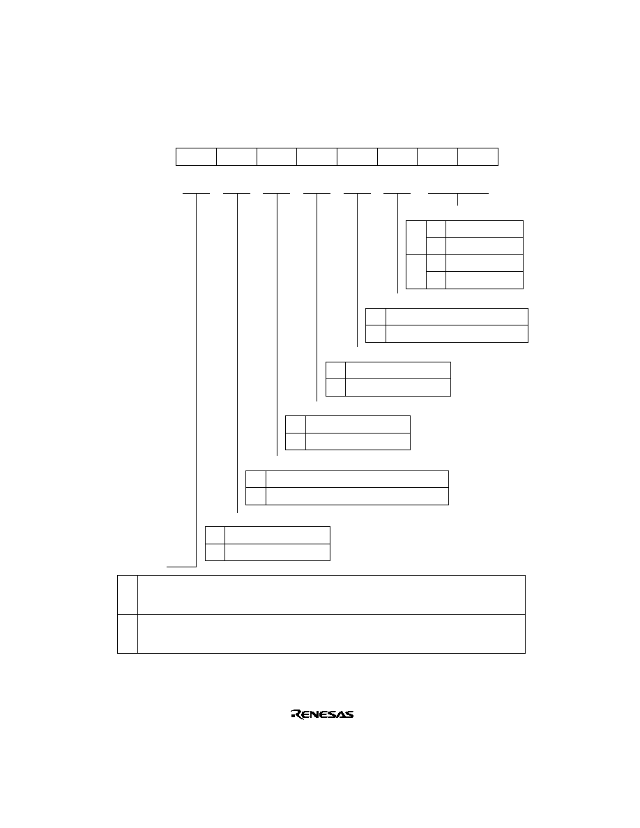
667
SMR1--Serial Mode Register 1
H'FF80
Smart Card Interface 1
7
GM
0
R/W
6
CHR
0
R/W
5
PE
0
R/W
4
O/
E
0
R/W
3
STOP
0
R/W
0
CKS0
0
R/W
2
MP
0
R/W
1
CKS1
0
R/W
0
1
Normal smart card interface mode operation
∑ TEND flag generated 12.5 etu after beginning of start bit
∑ Clock output on/off control only
GSM mode smart card interface mode operation
∑ TEND flag generated 11.0 etu after beginning of start bit
∑ Fixed high/low-level control possible (set in SCR) in addition to clock output on/off control
GSM Mode
0
1
Setting prohibited
Parity bit addition and checking enabled
Parity Enable
0
1
Even parity
Odd parity
Parity Mode
0
1
0
1
0
1
¯ clock
¯/4 clock
¯/16 clock
¯/64 clock
Clock Select
0
1
Multiprocessor function disabled
Setting prohibited
Multiprocessor Mode
0
1
Setting prohibited
2 stop bits
Stop Bit Length
0
1
8-bit data
Setting prohibited
Character Length
Bit
Initial value
Read/Write
:
:
:
Note: etu (Elementary Time Unit): Interval for transfer of one bit

668
BRR1--Bit Rate Register 1
H'FF81
SCI1, Smart Card Interface 1
7
1
R/W
6
1
R/W
5
1
R/W
4
1
R/W
3
1
R/W
0
1
R/W
2
1
R/W
1
1
R/W
Note: See section 12.2.8, Bit Rate Register (BRR), for details.
Sets the serial transfer bit rate
Bit
Initial value
Read/Write
:
:
:

669
SCR1--Serial Control Register 1
H'FF82
SCI1
7
TIE
0
R/W
6
RIE
0
R/W
5
TE
0
R/W
4
RE
0
R/W
3
MPIE
0
R/W
0
CKE0
0
R/W
2
TEIE
0
R/W
1
CKE1
0
R/W
1
0
Asynchronous
mode
Internal clock/SCK pin functions
as I/O port
Clock Enable
0
1
Transmit end interrupt (TEI) request disabled
Transmit end interrupt (TEI) request enabled
Transmit End Interrupt Enable
0
Multiprocessor interrupts disabled
[Clearing conditions]
∑ When the MPIE bit is cleared to 0
∑ When MPB= 1 data is received
Multiprocessor Interrupt Enable
0
1
Reception disabled
Reception enabled
Receive Enable
0
1
Transmission disabled
Transmission enabled
Transmit Enable
0
Receive data full interrupt (RXI) request and
receive error interrupt (ERI) request disabled
Receive Interrupt Enable
0
1
Transmit data empty interrupt (TXI) requests disabled
Transmit data empty interrupt (TXI) requests enabled
Transmit Interrupt Enable
Notes:
Bit
Initial value
Read/Write
:
:
:
Synchronous
mode
Internal clock/SCK pin functions
as serial clock output
Asynchronous
mode
Internal clock/SCK pin functions
as clock output
*
1
Synchronous
mode
Internal clock/SCK pin functions
as serial clock output
Asynchronous
mode
External clock/SCK pin functions
as clock input
*
2
Synchronous
mode
External clock/SCK pin functions
as serial clock input
Asynchronous
mode
External clock/SCK pin functions
as clock input
*
2
Synchronous
mode
External clock/SCK pin functions
as serial clock input
1. Outputs a clock of the same frequency as the bit rate.
2. Inputs a clock with a frequency 16 times the bit rate.
Multiprocessor interrupts enabled
Receive interrupt (RXI) requests, receive error interrupt (ERI)
requests, and setting of the RDRF, FER, and ORER flags in
SSR are disabled until data with the multiprocessor bit set to 1
is received
1
1
Receive data full interrupt (RXI) request and
receive error interrupt (ERI) request enabled
1
0
1
0
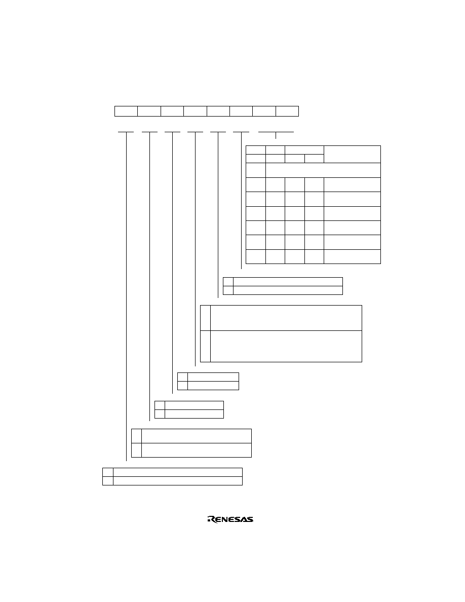
670
SCR1--Serial Control Register 1
H'FF82
Smart Card Interface 1
7
TIE
0
R/W
6
RIE
0
R/W
5
TE
0
R/W
4
RE
0
R/W
3
MPIE
0
R/W
0
CKE0
0
R/W
2
TEIE
0
R/W
1
CKE1
0
R/W
SMCR
SMIF
0
1
1
1
1
1
1
0
0
1
1
1
1
0
0
0
0
1
1
0
1
0
1
0
1
SMR
C/
A
,GM CKE1
CKE0
See SCI specification
SCK pin function
Clock Enable
SCR setting
0
1
Transmit end interrupt (TEI) request disabled
Transmit end interrupt (TEI) request enabled
Transmit End Interrupt Enable
0
Multiprocessor interrupts disabled
[Clearing conditions]
∑ When the MPIE bit is cleared to 0
∑ When MPB= 1 data is received
Multiprocessor Interrupt Enable
0
1
Reception disabled
Reception enabled
Receive Enable
0
1
Transmission disabled
Transmission enabled
Transmit Enable
0
Receive data full interrupt (RXI) request and
receive error interrupt (ERI) request disabled
Receive Interrupt Enable
0
1
Transmit data empty interrupt (TXI) requests disabled
Transmit data empty interrupt (TXI) requests enabled
Transmit Interrupt Enable
Bit
Initial value
Read/Write
:
:
:
Multiprocessor interrupts enabled
Receive interrupt (RXI) requests, receive error interrupt (ERI)
requests, and setting of the RDRF, FER, and ORER flags in
SSR are disabled until data with the multiprocessor bit set to 1
is received
1
1
Receive data full interrupt (RXI) request and
receive error interrupt (ERI) request enabled
Operates as port input
pin
Clock output as SCK
output pin
Fixed-low output as
SCK output pin
Clock output as SCK
output pin
Fixed-high output as
SCK output pin
Clock output as SCK
output pin

671
TDR1--Transmit Data Register 1
H'FF83
SCI1, Smart Card Interface 1
7
1
R/W
6
1
R/W
5
1
R/W
4
1
R/W
3
1
R/W
0
1
R/W
2
1
R/W
1
1
R/W
Stores data for serial transmission
Bit
Initial value
Read/Write
:
:
:

672
SSR1--Serial Status Register 1
H'FF84
SCI1
7
TDRE
1
R/(W)
*
6
RDRF
0
R/(W)
*
5
ORER
0
R/(W)
*
4
FER
0
R/(W)
*
3
PER
0
R/(W)
*
0
MPBT
0
R/W
2
TEND
1
R
1
MPB
0
R
Note:
*
Can only be written with 0 for flag clearing.
0
Transmit Data Register Empty
0
Receive Data Register Full
0
Overrun Error
0
Framing Error
0
Parity Error
0
Transmit End
0
Multiprocessor Bit
[Clearing condition]
When data with a 0 multiprocessor bit is received
Multiprocessor Bit Transfer
0
1
Data with a 0 multiprocessor bit is transmitted
Data with a 1 multiprocessor bit is transmitted
Bit
Initial value
Read/Write
:
:
:
[Setting condition]
When data with a 1 multiprocessor bit is received
[Clearing condition]
∑ When 0 is written to TDRE after reading TDRE = 1
∑ When the DTC is activated by a TXI interrupt and write data to TDR
[Setting condition]
∑ When the TE bit in SCR is 0
∑ When TDRE = 1 at transmission of the last bit of a 1-byte
serial transmit character
1
[Clearing condition]
When 0 is written to PER after reading PER = 1
[Setting condition]
When, in reception, the number of 1 bits in the receive data plus the parity bit
does not match the parity setting (even or odd) specified by the O/E bit in SMR
1
[Clearing condition]
When 0 is written to FER after reading FER = 1
[Setting condition]
When the SCI checks whether the stop bit at the end of the receive
data is 1 when reception ends, and the stop bit is 0
[Clearing condition]
When 0 is written to ORER after reading ORER = 1
[Setting condition]
When the next serial reception is completed while RDRF = 1
[Clearing condition]
∑ When 0 is written to RDRF after reading RDRF = 1
∑ When the DTC is activated by an RXI interrupt and read data from RDR
[Setting condition]
When serial reception ends normally and receive data is transferred
from RSR to RDR
[Clearing condition]
∑ When 0 is written to TDRE after reading TDRE = 1
∑ When the DTC is activated by a TXI interrupt and write data to TDR
[Setting condition]
∑ When the TE bit in SCR is 0
∑ When data is transferred from TDR to TSR and data can be written to TDR
1
1
1
1
1
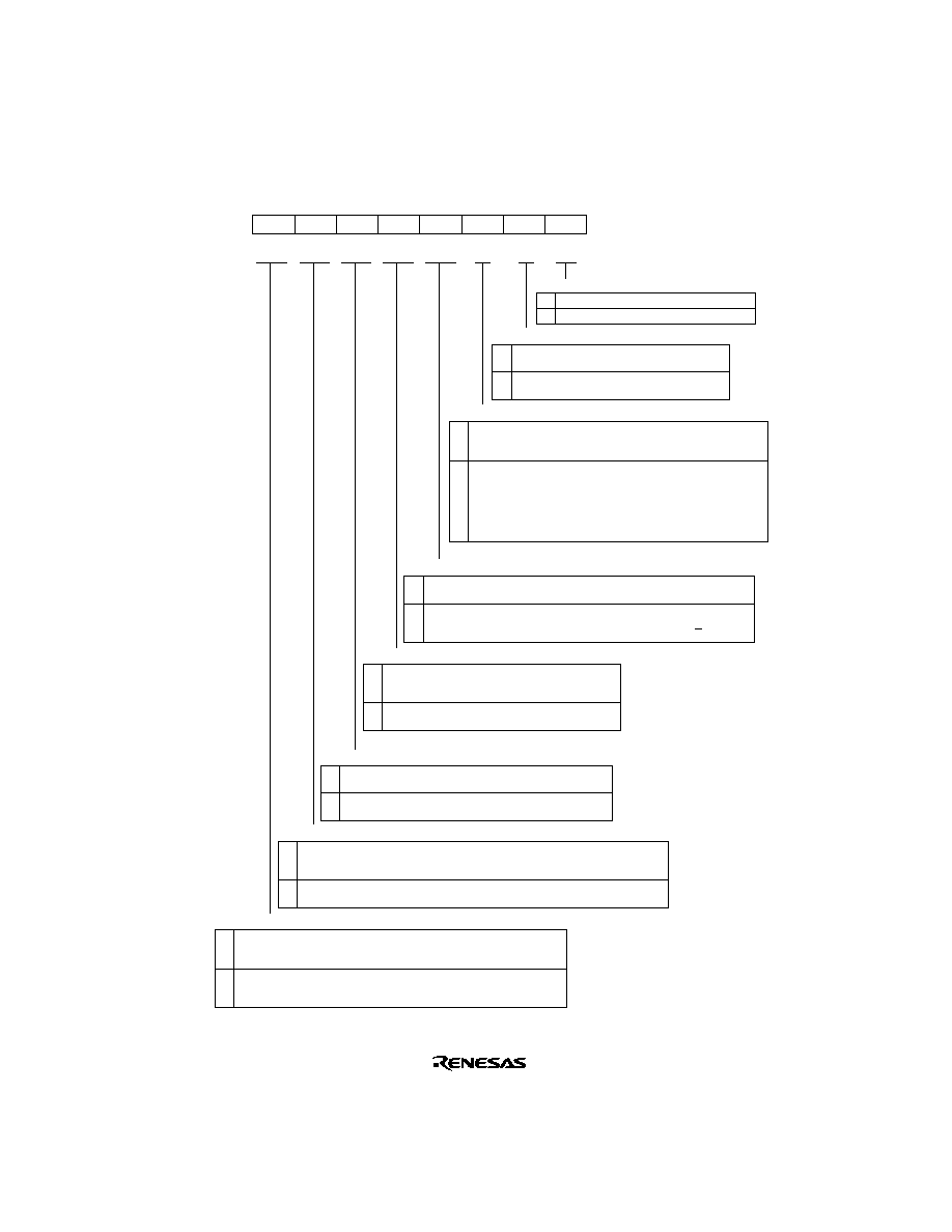
673
SSR1--Serial Status Register 1
H'FF84
Smart Card Interface 1
7
TDRE
1
R/(W)
*
6
RDRF
0
R/(W)
*
5
ORER
0
R/(W)
*
4
ERS
0
R/(W)
*
3
PER
0
R/(W)
*
0
MPBT
0
R/W
2
TEND
1
R
1
MPB
0
R
Note:
*
Can only be written with 0 for flag clearing.
Transmit Data Register Empty
0
Receive Data Register Full
0
Overrun Error
0
Error Signal Status
0
Parity Error
0
Transmit End
0
Multiprocessor Bit
[Clearing condition]
When data with a 0 multiprocessor bit is received
Multiprocessor Bit Transfer
0
1
Data with a 0 multiprocessor bit is transmitted
Data with a 1 multiprocessor bit is transmitted
Bit
Initial value
Read/Write
:
:
:
[Setting conditions]
When data with a 1 multiprocessor bit is received
[Clearing condition]
∑ When 0 is written to TDRE after reading TDRE = 1
∑ When the DTC is activated by a TXI interrupt and write data to TDR
[Setting conditions]
∑ On reset, or in standby mode or module stop mode
∑ When the TE bit in SCR is 0 and the ERS bit is 0
∑ When TDRE = 1 and ERS = 0 (normal transmission) 2.5 etu
after a 1-byte serial character is sent when GM = 0
∑ When TDRE = 1 and ERS = 0 (normal transmission) 1.0 etu
after a 1-byte serial character is sent when GM = 1
1
[Clearing condition]
When 0 is written to PER after reading PER = 1
[Setting condition]
When, in reception, the number of 1 bits in the receive data plus the parity bit
does not match the parity setting (even or odd) specified by the O/E bit in SMR
1
[Clearing condition]
∑ On reset, or in standby mode or module stop mode
∑ When 0 is written to ERS after reading ERS =1
[Setting conditions]
When the error signal is sampled at the low level
[Clearing condition]
When 0 is written to ORER after reading ORER = 1
[Setting condition]
When the next serial reception is completed while RDRF = 1
[Clearing condition]
∑ When 0 is written to RDRF after reading RDRF = 1
∑ When the DTC is activated by an RXI interrupt and read data from RDR
[Setting condition]
When serial reception ends normally and receive data is transferred from RSR to RDR
[Clearing condition]
∑ When 0 is written to TDRE after reading TDRE = 1
∑ When the DTC is activated by a TXI interrupt and write data to TDR
[Setting condition]
∑ When the TE bit in SCR is 0
∑ When data is transferred from TDR to TSR and data can be written to TDR
Note: etu: Elementary Time Unit (the time taken to transmit one bit)
1
Note: Clearing the TE bit in SCR to 0 does not affect the ERS flag, which retains its prior state.
1
1
1
0
1
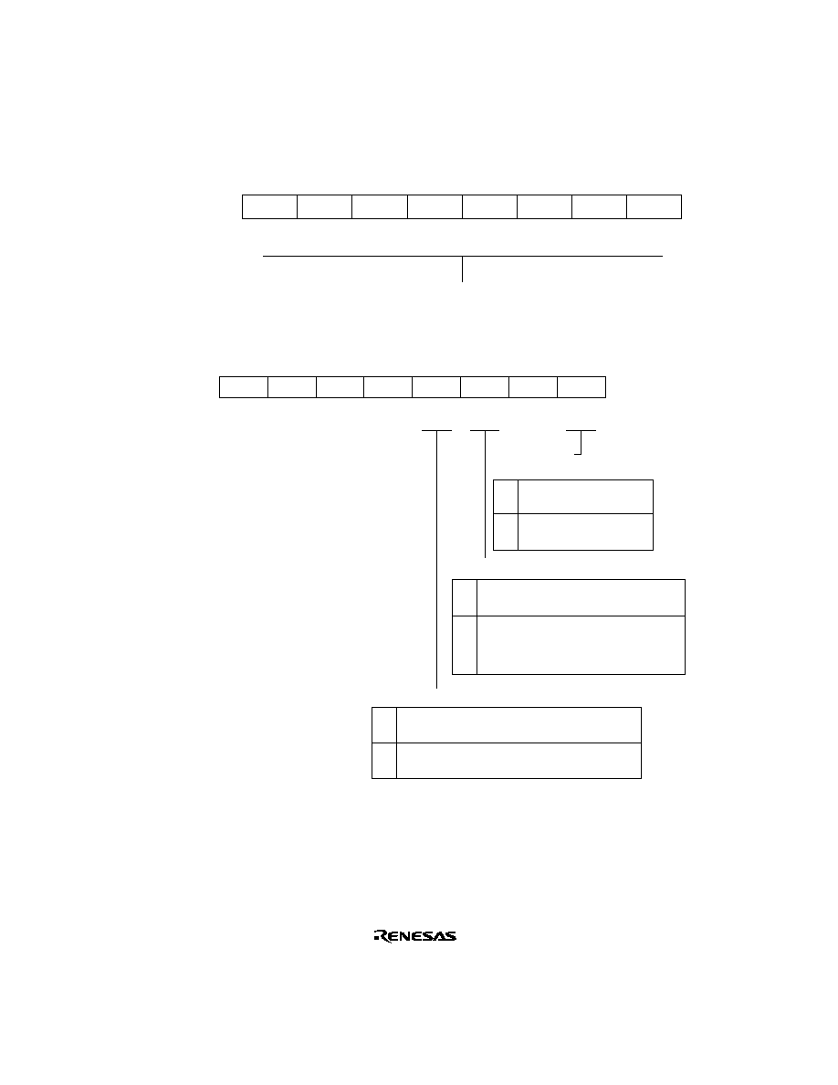
674
RDR1--Receive Data Register 1
H'FF85
SCI1, Smart Card Interface 1
7
0
R
6
0
R
5
0
R
4
0
R
3
0
R
0
0
R
2
0
R
1
0
R
Stores received serial data
Bit
Initial value
Read/Write
:
:
:
SCMR1--Smart Card Mode Register 1
H'FF86
SCI1, Smart Card Interface 1
7
--
1
--
6
--
1
--
5
--
1
--
4
--
1
--
3
SDIR
0
R/W
0
SMIF
0
R/W
2
SINV
0
R/W
1
--
1
--
0
1
TDR contents are transmitted LSB-first
Receive data is stored in RDR LSB-first
Smart Card Data Direction
0
TDR contents are transmitted as they are
Receive data is stored in RDR as it is
Smart Card Data Invert
0
1
Smart Card interface
function is disabled
Smart Card
Interface Mode Select
Bit
Initial value
Read/Write
:
:
:
Smart Card interface
function is enabled
TDR contents are inverted before
being transmitted
Receive data is stored in RDR
in inverted form
1
TDR contents are transmitted MSB-first
Receive data is stored in RDR MSB-first

675
SMR2--Serial Mode Register 2
H'FF88
SCI2
7
C/
A
0
R/W
6
CHR
0
R/W
5
PE
0
R/W
4
O/
E
0
R/W
3
STOP
0
R/W
0
CKS0
0
R/W
2
MP
0
R/W
1
CKS1
0
R/W
0
1
Asynchronous mode
Synchronous mode
Asynchronous Mode/Synchronous Mode Select
0
1
Parity bit addition and checking disabled
Parity bit addition and checking enabled
Parity Enable
0
1
Even parity
Odd parity
Parity Mode
0
1
0
1
0
1
¯ clock
¯/4 clock
¯/16 clock
¯/64 clock
Clock Select
0
1
Multiprocessor function disabled
Multiprocessor format selected
Multiprocessor Mode
0
1
1 stop bit
2 stop bits
Stop Bit Length
0
1
8-bit data
7-bit data
*
Character Length
Note:
*
When 7-bit data is selected, the MSB (bit 7) of TDR is not transmitted.
Bit
Initial value
Read/Write
:
:
:

676
SMR2--Serial Mode Register 2
H'FF88
Smart Card Interface 2
7
GM
0
R/W
6
CHR
0
R/W
5
PE
0
R/W
4
O/
E
0
R/W
3
STOP
0
R/W
0
CKS0
0
R/W
2
MP
0
R/W
1
CKS1
0
R/W
0
1
Normal smart card interface mode operation
∑ TEND flag generated 12.5 etu after beginning of start bit
∑ Clock output on/off control only
GSM mode smart card interface mode operation
∑ TEND flag generated 11.0 etu after beginning of start bit
∑ Fixed high/low-level control possible (set in SCR) in addition to clock output on/off control
GSM Mode
0
1
Setting prohibited
Parity bit addition and checking enabled
Parity Enable
0
1
Even parity
Odd parity
Parity Mode
0
1
0
1
0
1
¯ clock
¯/4 clock
¯/16 clock
¯/64 clock
Clock Select
0
1
Multiprocessor function disabled
Setting prohibited
Multiprocessor Mode
0
1
Setting prohibited
2 stop bits
Stop Bit Length
0
1
8-bit data
Setting prohibited
Character Length
Bit
Initial value
Read/Write
:
:
:
Note: etu (Elementary Time Unit): Interval for transfer of one bit

677
BRR2--Bit Rate Register 2
H'FF89
SCI2, Smart Card Interface 2
7
1
R/W
6
1
R/W
5
1
R/W
4
1
R/W
3
1
R/W
0
1
R/W
2
1
R/W
1
1
R/W
Sets the serial transfer bit rate
Note: See section 12.2.8, Bit Rate Register (BRR), for details.
Bit
Initial value
Read/Write
:
:
:
678
SCR2--Serial Control Register 2
H'FF8A
SCI2
7
TIE
0
R/W
6
RIE
0
R/W
5
TE
0
R/W
4
RE
0
R/W
3
MPIE
0
R/W
0
CKE0
0
R/W
2
TEIE
0
R/W
1
CKE1
0
R/W
Asynchronous
mode
Internal clock/SCK pin functions
as I/O port
Clock Enable
0
1
Transmit end interrupt (TEI) request disabled
Transmit end interrupt (TEI) request enabled
Transmit End Interrupt Enable
Multiprocessor interrupts disabled
[Clearing conditions]
∑ When the MPIE bit is cleared to 0
∑ When MPB= 1 data is received
Multiprocessor Interrupt Enable
0
1
Reception disabled
Reception enabled
Receive Enable
0
1
Transmission disabled
Transmission enabled
Transmit Enable
Receive data full interrupt (RXI) request and
receive error interrupt (ERI) request disabled
Receive Interrupt Enable
0
1
Transmit data empty interrupt (TXI) requests disabled
Transmit data empty interrupt (TXI) requests enabled
Transmit Interrupt Enable
Notes:
Bit
Initial value
Read/Write
:
:
:
Synchronous
mode
Internal clock/SCK pin functions
as serial clock output
Asynchronous
mode
Internal clock/SCK pin functions
as clock output
*
1
Synchronous
mode
Internal clock/SCK pin functions
as serial clock output
Asynchronous
mode
External clock/SCK pin functions
as clock input
*
2
Synchronous
mode
External clock/SCK pin functions
as serial clock input
Asynchronous
mode
External clock/SCK pin functions
as clock input
*
2
Synchronous
mode
External clock/SCK pin functions
as serial clock input
1. Outputs a clock of the same frequency as the bit rate.
2. Inputs a clock with a frequency 16 times the bit rate.
Multiprocessor interrupts enabled
Receive interrupt (RXI) requests, receive error interrupt (ERI)
requests, and setting of the RDRF, FER, and ORER flags in
SSR are disabled until data with the multiprocessor bit set to 1
is received
0
0
1
0
1
1
0
1
0
1
Receive data full interrupt (RXI) request and
receive error interrupt (ERI) request enabled

679
SCR2--Serial Control Register 2
H'FF8A
Smart Card Interface 2
7
TIE
0
R/W
6
RIE
0
R/W
5
TE
0
R/W
4
RE
0
R/W
3
MPIE
0
R/W
0
CKE0
0
R/W
2
TEIE
0
R/W
1
CKE1
0
R/W
SMCR
SMIF
0
1
1
1
1
1
1
0
0
1
1
1
1
0
0
0
0
1
1
0
1
0
1
0
1
SMR
C/
A
,GM CKE1
CKE0
See SCI specification
SCK pin function
Clock Enable
SCR setting
0
1
Transmit end interrupt (TEI) request disabled
Transmit end interrupt (TEI) request enabled
Transmit End Interrupt Enable
0
Multiprocessor interrupts disabled
[Clearing conditions]
∑ When the MPIE bit is cleared to 0
∑ When MPB= 1 data is received
Multiprocessor Interrupt Enable
0
1
Reception disabled
Reception enabled
Receive Enable
0
1
Transmission disabled
Transmission enabled
Transmit Enable
0
Receive data full interrupt (RXI) request and
receive error interrupt (ERI) request disabled
Receive Interrupt Enable
0
1
Transmit data empty interrupt (TXI) requests disabled
Transmit data empty interrupt (TXI) requests enabled
Transmit Interrupt Enable
Bit
Initial value
Read/Write
:
:
:
Multiprocessor interrupts enabled
Receive interrupt (RXI) requests, receive error interrupt (ERI)
requests, and setting of the RDRF, FER, and ORER flags in
SSR are disabled until data with the multiprocessor bit set to 1
is received
1
1
Receive data full interrupt (RXI) request and
receive error interrupt (ERI) request enabled
Operates as port input
pin
Clock output as SCK
output pin
Fixed-low output as
SCK output pin
Clock output as SCK
output pin
Fixed-high output as
SCK output pin
Clock output as SCK
output pin

680
TDR2--Transmit Data Register 2
H'FF8B
SCI2, Smart Card Interface 2
7
1
R/W
6
1
R/W
5
1
R/W
4
1
R/W
3
1
R/W
0
1
R/W
2
1
R/W
1
1
R/W
Stores data for serial transmission
Bit
Initial value
Read/Write
:
:
:

681
SSR2--Serial Status Register 2
H'FF8C
SCI2
7
TDRE
1
R/(W)
*
6
RDRF
0
R/(W)
*
5
ORER
0
R/(W)
*
4
FER
0
R/(W)
*
3
PER
0
R/(W)
*
0
MPBT
0
R/W
2
TEND
1
R
1
MPB
0
R
Note:
*
Can only be written with 0 for flag clearing.
Transmit Data Register Empty
Receive Data Register Full
Overrun Error
Framing Error
Parity Error
Transmit End
Multiprocessor Bit
[Clearing condition]
When data with a 0 multiprocessor bit is received
Multiprocessor Bit Transfer
0
1
Data with a 0 multiprocessor bit is transmitted
Data with a 1 multiprocessor bit is transmitted
Bit
Initial value
Read/Write
:
:
:
[Setting condition]
When data with a 1 multiprocessor bit is received
[Clearing condition]
∑ When 0 is written to TDRE after reading TDRE = 1
∑ When the DTC is activated by a TXI interrupt and write data to TDR
[Setting condition]
∑ When the TE bit in SCR is 0
∑ When TDRE = 1 at transmission of the last bit of a 1-byte
serial transmit character
[Clearing condition]
When 0 is written to FER after reading FER = 1
[Setting condition]
When, in reception, the number of 1 bits in the receive data plus the parity bit
does not match the parity setting (even or odd) specified by the O/E bit in SMR
[Clearing condition]
When 0 is written to FER after reading FER = 1
[Setting condition]
When the SCI checks whether the stop bit at the end of the receive
data is 1 when reception ends, and the stop bit is 0
[Clearing condition]
When 0 is written to ORER after reading ORER = 1
[Setting condition]
When the next serial reception is completed while
RDRF = 1
[Clearing condition]
∑ When 0 is written to RDRF after reading RDRF = 1
∑ When the DTC is activated by an RXI interrupt and read data from RDR
[Setting condition]
When serial reception ends normally and receive data is transferred
from RSR to RDR
[Clearing condition]
∑ When 0 is written to TDRE after reading TDRE = 1
∑ When the DTC is activated by a TXI interrupt and write data to TDR
[Setting condition]
∑ When the TE bit in SCR is 0
∑ When data is transferred from TDR to TSR and data can be written to TDR
0
1
0
1
0
1
0
1
0
1
0
1
0
1
682
SSR2--Serial Status Register 2
H'FF8C
Smart Card Interface 2
7
TDRE
1
R/(W)
*
6
RDRF
0
R/(W)
*
5
ORER
0
R/(W)
*
4
ERS
0
R/(W)
*
3
PER
0
R/(W)
*
0
MPBT
0
R/W
2
TEND
1
R
1
MPB
0
R
Note:
*
Can only be written with 0 for flag clearing.
Transmit Data Register Empty
Receive Data Register Full
Overrun Error
Parity Error
Multiprocessor Bit
[Clearing condition]
When data with a 0 multiprocessor bit is received
Multiprocessor Bit Transfer
0
1
Data with a 0 multiprocessor bit is transmitted
Data with a 1 multiprocessor bit is transmitted
Bit
Initial value
Read/Write
:
:
:
[Setting condition]
When data with a 1 multiprocessor bit is received
[Clearing condition]
When 0 is written to PER after reading PER = 1
[Setting condition]
When, in reception, the number of 1 bits in the receive data plus the parity bit
does not match the parity setting (even or odd) specified by the O/E bit in SMR
[Clearing condition]
When 0 is written to ORER after reading ORER = 1
[Setting condition]
On of the next serial reception when RDRF= 1 completion
[Clearing condition]
∑ When 0 is written to RDRF after reading RDRF = 1
∑ When the DTC is activated by an RXI interrupt and read data from RDR
[Setting condition]
When serial reception ends normally and receive data is transferred from RSR to RDR
[Clearing condition]
∑ When 0 is written to TDRE after reading TDRE = 1
∑ When the DTC is activated by a TXI interrupt and write data to TDR
[Setting condition]
∑ When the TE bit in SCR is 0
∑ When data is transferred from TDR to TSR and data can be written to TDR
Transmit End
[Clearing condition]
∑ When 0 is written to TDRE after reading TDRE = 1
∑ When the DTC is activated by a TXI interrupt and write data to TDR
[Setting conditions]
∑ On reset, or in standby mode or module stop mode
∑ When the TE bit in SCR is 0
∑ When TDRE = 1 and ERS = 0 (normal transmission) 2.5 etu
after a 1-byte serial character is sent when GM = 0
∑ When TDRE = 1 and ERS = 0 (normal transmission) 1.0 etu
after a 1-byte serial character is sent when GM = 1
Note: etu: Elementary Time Unit (the time taken to transmit one bit)
0
Error Signal Status
[Clearing condition]
∑ On reset, or in standby mode or module stop mode
∑ When 0 is written to ERS after reading ERS =1
[Setting conditions]
When the error signal is sampled at the low level
1
Note: Clearing the TE bit in SCR to 0 does not affect the ERS flag, which retains its prior state.
0
1
0
1
0
1
0
1
0
1
0
1
683
RDR2--Receive Data Register 2
H'FF8D
SCI2, Smart Card Interface 2
7
0
R
6
0
R
5
0
R
4
0
R
3
0
R
0
0
R
2
0
R
1
0
R
Stores received serial data
Bit
Initial value
Read/Write
:
:
:
SCMR2--Smart Card Mode Register 2
H'FF8E
SCI2, Smart Card Interface 2
7
--
1
--
6
--
1
--
5
--
1
--
4
--
1
--
3
SDIR
0
R/W
0
SMIF
0
R/W
2
SINV
0
R/W
1
--
1
--
0
1
TDR contents are transmitted LSB-first
Receive data is stored in RDR LSB-first
Smart Card Data Direction
0
1
TDR contents are transmitted as they are
Receive data is stored in RDR as it is
Smart Card Data Invert
0
1
Smart Card interface
function is disabled
Smart Card
Interface Mode Select
Bit
Initial value
Read/Write
:
:
:
Smart Card interface
function is enabled
TDR contents are inverted before being
transmitted
Receive data is stored in RDR in
inverted form
TDR contents are transmitted MSB-first
Receive data is stored in RDR MSB-first
684
ADDRAH --
A/D Data Register AH
H'FF90
A/D Converter
ADDRAL --
A/D Data Register AL
H'FF91
A/D Converter
ADDRBH --
A/D Data Register BH
H'FF92
A/D Converter
ADDRBL --
A/D Data Register BL
H'FF93
A/D Converter
ADDRCH --
A/D Data Register CH
H'FF94
A/D Converter
ADDRCL --
A/D Data Register CL
H'FF95
A/D Converter
ADDRDH --
A/D Data Register DH
H'FF96
A/D Converter
ADDRDL --
A/D Data Register DL
H'FF97
A/D Converter
15
AD9
0
R
14
AD8
0
R
13
AD7
0
R
12
AD6
0
R
11
AD5
0
R
10
AD4
0
R
9
AD3
0
R
8
AD2
0
R
7
AD1
0
R
6
AD0
0
R
5
--
0
R
4
--
0
R
3
--
0
R
2
--
0
R
1
--
0
R
0
--
0
R
Stores the results of A/D conversion
Analog Input Channel
AN0
AN1
AN2
AN3
A/D Data Register
ADDRA
ADDRB
ADDRC
ADDRD
Bit
Initial value
Read/Write
:
:
:

685
ADCSR--A/D Control/Status Register
H'FF98
A/D Converter
[Clearing conditions]
∑ When 0 is written to the ADF flag after reading ADF = 1
∑ When the DTC is activated by an ADI interrupt, and ADDR is read
7
ADF
0
R/(W)
*
6
ADIE
0
R/W
5
ADST
0
R/W
4
SCAN
0
R/W
3
CKS
0
R/W
0
CH0
0
R/W
2
--
0
R/W
1
CH1
0
R/W
Note:
*
Can only be written with 0 for flag clearing.
0
1
Conversion time= 266 states (max.)
Conversion time= 134 states (max.)
Group Select
0
1
A/D conversion end interrupt (ADI) request disabled
A/D conversion end interrupt (ADI) request enabled
A/D Interrupt Enable
0
1
Single mode
Scan mode
Scan Mode
0
1
A/D conversion stopped
A/D Start
0
A/D End Flag
0
1
0
1
0
1
Single Mode
(SCAN = 0)
AN0
AN1
AN2
AN3
Scan Mode
(SCAN = 1)
AN0
AN0 to AN1
AN0 to AN2
AN0 to AN3
Channel Select
CH1 CH0
Bit
Initial value
Read/Write
:
:
:
∑ Single mode: A/D conversion is started. Cleared to 0 automatically when
conversion ends
∑ Scan mode: A/D conversion is started. Conversion continues sequentially
on the selected channels until ADST is cleared to 0 by software, a reset,
or transition to standby mode or module stop mode
[Setting conditions]
∑ Single mode: When A/D conversion ends
∑ Scan mode:
When one round of conversion has been performed on all specified channels
1

686
ADCR--A/D Control Register
H'FF99
A/D
7
TRGS1
0
R/W
6
TRGS0
0
R/W
5
--
1
--
4
--
1
--
3
--
1
--
0
--
1
--
2
--
1
--
1
--
1
--
0
0
Description
Timer Trigger Select
Bit
Initial value
Read/Write
:
:
:
Start of A/D conversion by external trigger
is disabled
Start of A/D conversion by external trigger (TPU)
is enabled
Start of A/D conversion by external trigger
(8-bit timer) is enabled
Start of A/D conversion by external trigger pin is
enabled
0
1
1
1
TRGS1
TRGS1
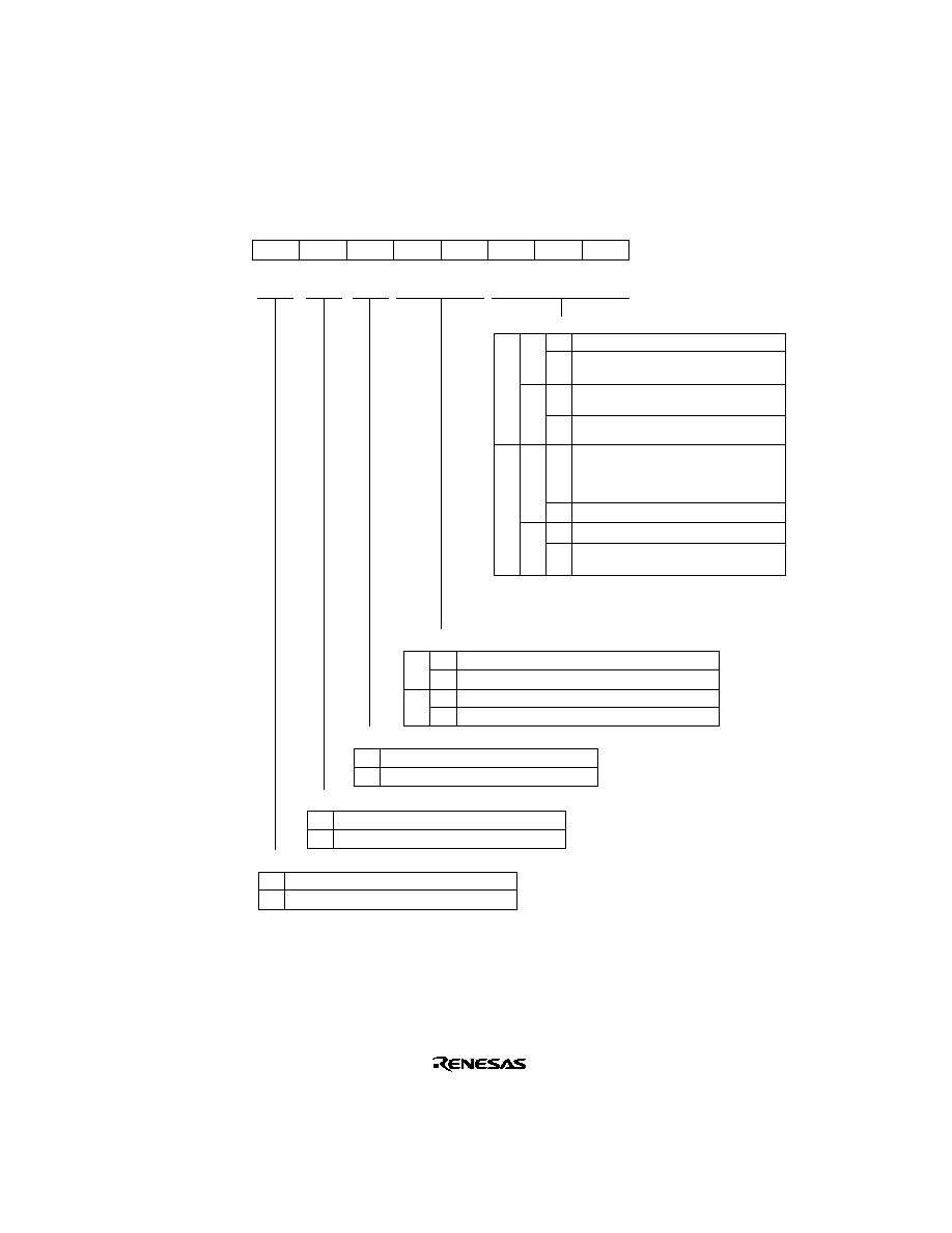
687
TCR0--Time Control Register 0
H'FFB0
8-Bit Timer Channel 0
TCR1--Time Control Register 1
H'FFB1
8-Bit Timer Channel 1
7
CMIEB
0
R/W
6
CMIEA
0
R/W
5
OVIE
0
R/W
4
CCLR1
0
R/W
3
CCLR0
0
R/W
0
CKS0
0
R/W
2
CKS2
0
R/W
1
CKS1
0
R/W
Note:
*
0
0
0
1
Clock input disabled
Internal clock: counted at falling edge
of ¯/8
Internal clock: counted at falling edge
of ¯/64
1
0
Internal clock: counted at falling edge
of ¯/8192
1
1
0
0
For channel 0:
Count at TCNT1 overflow signal
*
For channel 1:
Count at TCNT0 compare match A
*
External clock: counted at rising edge
External clock: counted at falling edge
1
0
1
External clock: counted at both rising and
falling edges
1
Clock Select
0
1
CMFB interrupt requests (CMIB) are disabled
CMFB interrupt requests (CMIB) are enabled
Compare Match Interrupt Enable B
0
1
CMFA interrupt requests (CMIA) are disabled
CMFA interrupt requests (CMIA) are enabled
Compare Match Interrupt Enable A
0
1
OVF interrupt requests (OVI) are disabled
OVF interrupt requests (OVI) are enabled
Timer Overflow Interrupt Enable
0
1
Clear is disabled
Clear by compare match A
Clear by compare match B
Clear by rising edge of external reset input
0
1
0
1
Counter Clear
Bit
Initial value
Read/Write
If the count input of channel 0 is the TCNT1 overflow
signal and that of channel 1 is the TCNT0 compare
match signal, no incrementing clock is generated.
Do not use this setting.
:
:
:

688
TCSR0--Timer Control/Status Register 0
H'FFB2
8-Bit Timer Channel 0
TCSR1--Timer Control/Status Register 1
H'FFB3
8-Bit Timer Channel 1
7
CMFB
0
R/(W)
*
6
CMFA
0
R/(W)
*
5
OVF
0
R/(W)
*
4
--
1
--
3
OS3
0
R/W
0
OS0
0
R/W
2
OS2
0
R/W
1
OS1
0
R/W
TCSR1
7
CMFB
0
R/(W)
*
6
CMFA
0
R/(W)
*
5
OVF
0
R/(W)
*
4
ADTE
0
R/W
3
OS3
0
R/W
0
OS0
0
R/W
2
OS2
0
R/W
1
OS1
0
R/W
TCSR0
Note:
*
Only 0 can be written to bits 7 to 5, to clear these flags.
0
1
Compare Match Flag B
0
1
Compare Match Flag A
0
[Clearing condition]
Cleared by reading OVF when OVF = 1, then writing 0 to OVF
1
Timer Overflow Flag
0
1
A/D converter start requests by compare match A are disabled
A/D converter start requests by compare match A are enabled
A/D Trigger Enable (TCSR0 only)
0
1
No change when compare match B occurs
0 is output when compare match B occurs
1 is output when compare match B occurs
0
1
0
1
Output Select
0
No change when compare match A
occurs
0
Output Select
Output is inverted when compare
match A occurs (toggle output)
Bit
Initial value
Read/Write
:
:
:
Bit
Initial value
Read/Write
:
:
:
[Setting condition]
Set when TCNT overflows (changes from H'FF to H'00)
[Clearing condition]
∑ Cleared by reading CMFA when CMFA = 1, then writing 0 to CMFA
∑ When the DTC is activated by a CMIA interrupt, while DISEL bit of MRB in DTC is 0.
[Setting condition]
Set when TCNT matches TCORA
[Clearing condition]
∑ Cleared by reading CMFB when CMFB = 1, then writing 0 to CMFB
∑ When the DTC is activated by a CMIB interrupt, while DISEL bit of MRB in DTC is 0.
[Setting condition]
Set when TCNT matches TCORB
Output is inverted when compare match B occurs
(toggle output)
1 is output when compare match A
occurs
0 is output when compare match A
occurs
1
1
0
1
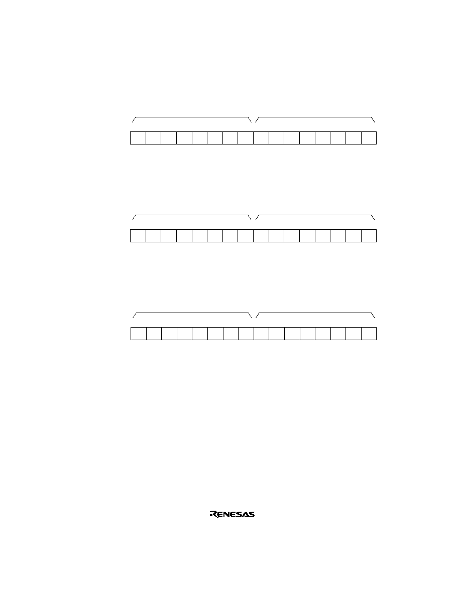
689
TCORA0--Time Constant Register A0
H'FFB4
8-Bit Timer Channel 0
TCORA1--Time Constant Register A1
H'FFB5
8-Bit Timer Channel 1
15
1
R/W
14
1
R/W
13
1
R/W
12
1
R/W
11
1
R/W
10
1
R/W
9
1
R/W
8
1
R/W
7
1
R/W
6
1
R/W
5
1
R/W
4
1
R/W
3
1
R/W
2
1
R/W
1
1
R/W
0
1
R/W
TCORA0
TCORA1
Bit
Initial value
Read/Write
:
:
:
TCORB0--Time Constant Register B0
H'FFB6
8-Bit Timer Channel 0
TCORB1--Time Constant Register B1
H'FFB7
8-Bit Timer Channel 1
15
1
R/W
14
1
R/W
13
1
R/W
12
1
R/W
11
1
R/W
10
1
R/W
9
1
R/W
8
1
R/W
7
1
R/W
6
1
R/W
5
1
R/W
4
1
R/W
3
1
R/W
2
1
R/W
1
1
R/W
0
1
R/W
TCORB0
TCORB1
Bit
Initial value
Read/Write
:
:
:
TCNT0--Timer Counter 0
H'FFB8
8-Bit Timer Channel 0
TCNT1--Timer Counter 1
H'FFB9
8-Bit Timer Channel 1
15
0
R/W
14
0
R/W
13
0
R/W
12
0
R/W
11
0
R/W
10
0
R/W
9
0
R/W
8
0
R/W
7
0
R/W
6
0
R/W
5
0
R/W
4
0
R/W
3
0
R/W
2
0
R/W
1
0
R/W
0
0
R/W
TCNT0
TCNT1
Bit
Initial value
Read/Write
:
:
:
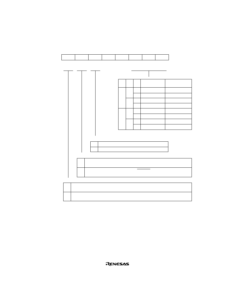
690
TCSR--Timer Control/Status Register
H'FFBC (W) H'FFBC (R)
WDT
7
OVF
0
R/(W)
*
6
WT/
IT
0
R/W
5
TME
0
R/W
4
--
1
--
3
--
1
--
0
CKS0
0
R/W
2
CKS2
0
R/W
1
CKS1
0
R/W
The method for writing to TCSR is different from that for general registers to prevent accidental overwriting.
For details see section 11.2.4, Notes on Register Access.
0
[Clearing condition]
Cleared by reading TCSR when OVF = 1, then writing 0 to OVF
1
Overflow Flag
0
Interval timer mode: Sends the CPU an interval timer interrupt request
(WOVI) when TCNT overflows
Watchdog timer mode: Generates the WDTOVF signal when
TCNT overflows
1
Timer Mode Select
0
1
TCNT is initialized to H'00 and halted
TCNT counts
Timer Enable
Clock Select
CKS2 CKS1 CKS0
Clock
Overflow period
*
(when ¯ = 20 MHz)
0
1
0
1
0
1
0
1
0
1
0
1
0
1
¯/2 (initial value)
¯/64
¯/128
¯/512
¯/2048
¯/8192
¯/32768
¯/131072
25.6
µ
s
819.2
µ
s
1.6ms
6.6ms
26.2ms
104.9ms
419.4ms
1.68s
Note:
*
Can only be written with 0 for flag clearing.
Note:
*
Bit
Initial value
Read/Write
:
:
:
The overflow period is the time from when TCNT
starts counting up from H'00 until overflow occurs.
[Setting condition]
Set when TCNT overflows from H'FF to H'00 in interval timer mode
691
TCNT--Timer Counter
H'FFBC (W) H'FFBD (R)
WDT
7
0
R/W
6
0
R/W
5
0
R/W
4
0
R/W
3
0
R/W
0
0
R/W
2
0
R/W
1
0
R/W
Bit
Initial value
Read/Write
Note: The method for writing to TCNT is different from that for general registers to prevent
accidental overwriting. For details see section 11.2.4, Notes on Register Access.
:
:
:
RSTCSR--Reset Control/Status Register
H'FFBE (W) H'FFBF (R)
WDT
7
WOVF
0
R/(W)
*
6
RSTE
0
R/W
5
RSTS
0
R/W
4
--
1
--
3
--
1
--
0
--
1
--
2
--
1
--
1
--
1
--
0
1
[Clearing condition]
Cleared by reading TCSR when WOVF = 1, then writing 0 to WOVF
Watchdog Timer Overflow Flag
Note:
*
Can only be written with 0 for flag clearing.
The method for writing to RSTCSR is different from that for general registers to prevent
accidental overwriting. For details see section 11.2.4, Notes on Register Access.
0
1
Reset Enable
Reset signal is not generated if TCNT overflows
*
Reset signal is generated if TCNT overflows
0
1
Reset Select
Power-on reset
Manual reset
Bit
Initial value
Read/Write
:
:
:
[Setting condition]
Set when TCNT overflows (changed from H'FF to H'00) during
watchdog timer operation
Note:
*
The modules H8S/2245 Series are not reset, but TCNT
and TCSR in WDT are reset.

692
TSTR--Timer Start Register
H'FFC0
TPU
7
--
0
--
6
--
0
--
5
--
0
--
4
--
0
--
3
--
0
--
0
CST0
0
R/W
2
CST2
0
R/W
1
CST1
0
R/W
Counter Start
0
1
TCNT
n
count operation is stopped
TCNT
n
performs count operation
Note:
(n = 2 to 0)
If 0 is written to the CST bit during operation with the TIOC pin designated for output,
the counter stops but the TIOC pin output compare output level is retained. If TIOR
is written to when the CST bit is cleared to 0, the pin output level will be changed to
the set initial output value.
Bit
Initial value
Read/Write
:
:
:
TSYR--Timer Synchro Register
H'FFC1
TPU
7
--
0
--
6
--
0
--
5
--
0
--
4
--
0
--
3
--
0
--
0
SYNC0
0
R/W
2
SYNC2
0
R/W
1
SYNC1
0
R/W
Timer Synchronization
0
1
TCNTn operates independently (TCNT presetting/
clearing is unrelated to other channels)
(n = 2 to 0)
Notes:
To set synchronous operation, the SYNC bits for at least two channels must
be set to 1.
To set synchronous clearing, in addition to the SYNC bit , the TCNT clearing
source must also be set by means of bits CCLR2 to CCLR0 in TCR.
1.
2.
Bit
Initial value
Read/Write
:
:
:
TCNTn performs synchronous operation
TCNT synchronous presetting/synchronous clearing
is possible
693
TCR0--Timer Control Register 0
H'FFD0
TPU0
7
CCLR2
0
R/W
6
CCLR1
0
R/W
5
CCLR0
0
R/W
4
CKEG1
0
R/W
3
CKEG0
0
R/W
0
TPSC0
0
R/W
2
TPSC2
0
R/W
1
TPSC1
0
R/W
TCNT clearing disabled
TCNT cleared by TGRA compare match/input capture
TCNT cleared by TGRB compare match/input capture
Counter Clear
0
0
1
0
1
0
1
0
1
Clock Edge
0
1
--
Count at rising edge
Count at falling edge
Count at both edges
Internal clock: counts on ¯/1
Internal clock: counts on ¯/4
Internal clock: counts on ¯/16
Internal clock: counts on ¯/64
External clock: counts on TCLKA pin input
External clock: counts on TCLKB pin input
External clock: counts on TCLKC pin input
External clock: counts on TCLKD pin input
Time Prescaler
0
1
0
1
0
1
0
1
0
1
0
1
0
1
Bit
Initial value
Read/Write
:
:
:
TCNT cleared by counter clearing for another channel
performing synchronous clearing/synchronous operation
TCNT cleared by counter clearing for another channel
performing synchronous clearing/synchronous operation
1
0
1
0
1
0
1
TCNT clearing disabled
TCNT cleared by TGRC compare match/input capture
TCNT cleared by TGRD compare match/input capture
694
TMDR0--Timer Mode Register 0
H'FFD1
TPU0
7
--
1
--
6
--
1
--
5
BFB
0
R/W
4
BFA
0
R/W
3
MD3
0
R/W
0
MD0
0
R/W
2
MD2
0
R/W
1
MD1
0
R/W
0
1
Buffer Operation Setting B
TGRB operates normally
0
1
Buffer Operation Setting A
TGRA operates normally
0
1
Normal operation
Reserved
PWM mode 1
PWM mode 2
Phase counting mode 1
Phase counting mode 2
Phase counting mode 3
Phase counting mode 4
--
Mode
0
1
*
0
1
0
1
*
0
1
0
1
0
1
0
1
*
Notes: 1.
2.
MD3 is a reserved bit. In a write, it
should always be written with 0.
Phase counting mode cannot be set
for channels 0 and 3. In this case,
0 should always be written to MD2.
*
: Don't care
Bit
Initial value
Read/Write
:
:
:
TGRA and TGRC used together
for buffer operation
TGRB and TGRD used together
for buffer operation

695
TIOR0H--Timer I/O Control Register 0H
H'FFD2
TPU0
7
IOB3
0
R/W
6
IOB2
0
R/W
5
IOB1
0
R/W
4
IOB0
0
R/W
3
IOA3
0
R/W
0
IOA0
0
R/W
2
IOA2
0
R/W
1
IOA1
0
R/W
0
1
TGR0B I/O Control
0
1
0
1
0
1
0
1
0
1
*
0
1
0
1
0
1
0
1
0
1
*
*
0
1
TGR0A
is output
compare
register
TGR0A I/O Control
0
1
0
1
0
1
0
1
0
1
*
0
1
0
1
0
1
0
1
0
1
*
*
Output disabled
0 output at compare match
1 output at compare match
Toggle output at compare match
0 output at compare match
1 output at compare match
Toggle output at compare match
Input capture at rising edge
Input capture at falling edge
Input capture at both edges
*
: Don't care
*
: Don't care
Bit
Initial value
Read/Write
:
:
:
Initial output is
0 output
TGR0A
is input
capture
register
Output disabled
Initial output is
1 output
Capture input
source is
TIOCA0 pin
Setting prohibited
TGR0B
is output
compare
register
Output disabled
0 output at compare match
1 output at compare match
Toggle output at compare match
0 output at compare match
1 output at compare match
Toggle output at compare match
Input capture at rising edge
Input capture at falling edge
Input capture at both edges
Initial output is
0 output
TGR0B
is input
capture
register
Output disabled
Initial output is
1 output
Capture input
source is
TIOCB0 pin
Setting prohibited
696
TIOR0L--Timer I/O Control Register 0L
H'FFD3
TPU0
0
1
TGR0D I/O Control
0
1
0
1
0
1
0
1
0
1
*
0
1
0
1
0
1
0
1
0
1
*
*
0
1
TGR0C I/O Control
0
1
0
1
0
1
0
1
0
1
*
0
1
0
1
0
1
0
1
0
1
*
*
*
: Don't care
*
: Don't care
Note: 1. When the BFB bit in TMDR0 is set to 1 and TGR0D is used as a buffer
register, this setting is invalid and input capture/output compare is not
generated.
Note: 1. When the BFA bit in TMDR0 is set to 1 and TGR0C is used as a buffer
register, this setting is invalid and input capture/output compare is not
generated.
7
IOD3
0
R/W
6
IOD2
0
R/W
5
IOD1
0
R/W
4
IOD0
0
R/W
3
IOC3
0
R/W
0
IOC0
0
R/W
2
IOC2
0
R/W
1
IOC1
0
R/W
Note: When TGRC or TGRD is designated for buffer operation, this setting is invalid and the register operates as
a buffer register.
Bit
Initial value
Read/Write
:
:
:
:
TGR0C
is output
compare
register
Output disabled
0 output at compare match
1 output at compare match
Toggle output at compare match
0 output at compare match
1 output at compare match
Toggle output at compare match
Input capture at rising edge
Input capture at falling edge
Input capture at both edges
Initial output is
0 output
TGR0C
is input
capture
register
*
1
Output disabled
Initial output is
1 output
Capture input
source is
TIOCC0 pin
Setting prohibited
TGR0D
is output
compare
register
Output disabled
0 output at compare match
1 output at compare match
Toggle output at compare match
0 output at compare match
1 output at compare match
Toggle output at compare match
Input capture at rising edge
Input capture at falling edge
Input capture at both edges
Initial output is
0 output
TGR0D
is input
capture
register
*
1
Output disabled
Initial output is
1 output
Capture input
source is
TIOCD0 pin
Setting prohibited

697
TIER0--Timer Interrupt Enable Register 0
H'FFD4
TPU0
7
TTGE
0
R/W
6
--
1
--
5
--
0
--
4
TCIEV
0
R/W
3
TGIED
0
R/W
0
TGIEA
0
R/W
2
TGIEC
0
R/W
1
TGIEB
0
R/W
0
1
A/D conversion start request generation disabled
A/D conversion start request generation enabled
A/D Conversion Start Request Enable
0
1
Interrupt requests (TCIV) by TCFV disabled
Interrupt requests (TCIV) by TCFV enabled
Overflow Interrupt Enable
TGR Interrupt Enable D
TGR Interrupt Enable C
TGR Interrupt Enable B
0
1
Interrupt requests (TGIA)
by TGFA bit disabled
TGR Interrupt Enable A
0
1
Interrupt requests (TGIB)
by TGFB bit disabled
0
1
Interrupt requests (TGIC) by
TGFC bit disabled
0
1
Interrupt requests (TGID) by TGFD
bit disabled
Bit
Initial value
Read/Write
:
:
:
Interrupt requests (TGIA)
by TGFA bit enabled
Interrupt requests (TGIB)
by TGFB bit enabled
Interrupt requests (TGIC) by
TGFC bit enabled
Interrupt requests (TGID) by TGFD
bit enabled

698
TSR0--Timer Status Register 0
H'FFD5
TPU0
7
--
1
--
6
--
1
--
5
--
0
--
4
TCFV
0
R/(W)*
3
TGFD
0
R/(W)*
0
TGFA
0
R/(W)*
2
TGFC
0
R/(W)*
1
TGFB
0
R/(W)*
Note:
*
Can only be written with 0 for flag clearing.
0
Overflow Flag
1
0
TGRD∑Input Capture/Output Compare Flag
1
0
TGRC∑Input Capture/Output Compare Flag
1
0
TGRB∑Input Capture/Output Compare Flag
1
0
[Clearing condition]
∑ When DTC is activated by TGIA interrupt
while DISEL bit of MRB in DTC is 0.
∑ When 0 is written to TGFA after reading
TGFA = 1
TGRA∑Input Capture/Output Compare Flag
1
Bit
Initial value
Read/Write
:
:
:
[Setting conditions]
∑ When TCNT = TGRA while TGRA is function-
ing as output compare register
∑ When TCNT value is transferred to TGRA by
input capture signal while TGRA is functioning
as input capture register
[Clearing condition]
∑ When DTC is activated by TGIB interrupt while DISEL
bit of MRB in DTC is 0.
∑ When 0 is written to TGFB after reading TGFB = 1
[Setting conditions]
∑ When TCNT = TGRB while TGRB is functioning as
output compare register
∑ When TCNT value is transferred to TGRB by input
capture signal while TGRB is functioning as input
capture register
[Clearing condition]
∑ When DTC is activated by TGIC interrupt while DISEL bit of MRB in
DTC is 0
∑ When 0 is written to TGFC after reading TGFC = 1
[Setting conditions]
∑ When TCNT = TGRC while TGRC is functioning as output compare
register
∑ When TCNT value is transferred to TGRC by input capture signal
while TGRC is functioning as input capture register
[Clearing condition]
∑ When DTC is activated by TGID interrupt while DISEL bit of MRB in DTC
is 0
∑ When 0 is written to TGFD after reading TGFD = 1
[Setting conditions]
∑ When TCNT = TGRD while TGRD is functioning as output compare register
∑ When TCNT value is transferred to TGRD by input capture signal while
TGRD is functioning as input capture register
[Clearing condition]
When 0 is written to TCFV after reading TCFV = 1
[Setting conditions]
When the TCNT value overflows (changes from H'FFFF to H'0000 )
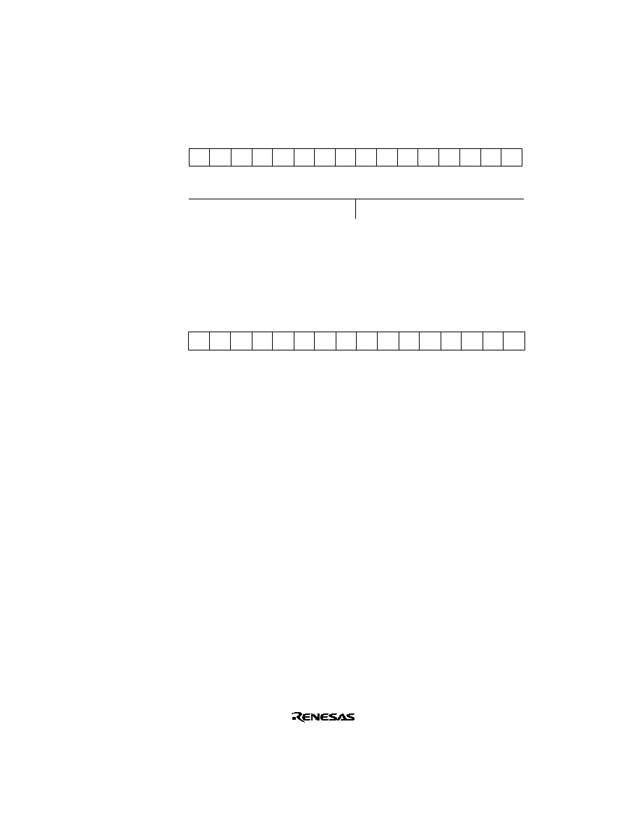
699
TCNT0--Timer Counter 0
H'FFD6
TPU0
15
0
R/W
14
0
R/W
13
0
R/W
12
0
R/W
11
0
R/W
8
0
R/W
10
0
R/W
9
0
R/W
Bit
Initial value
Read/Write
:
:
:
7
0
R/W
6
0
R/W
5
0
R/W
4
0
R/W
3
0
R/W
0
0
R/W
2
0
R/W
1
0
R/W
Up-counter
TGR0A--Timer General Register 0A
H'FFD8
TPU0
TGR0B--Timer General Register 0B
H'FFDA
TPU0
TGR0C--Timer General Register 0C
H'FFDC
TPU0
TGR0D--Timer General Register 0D
H'FFDE
TPU0
15
1
R/W
14
1
R/W
13
1
R/W
12
1
R/W
11
1
R/W
8
1
R/W
10
1
R/W
9
1
R/W
7
1
R/W
6
1
R/W
5
1
R/W
4
1
R/W
3
1
R/W
0
1
R/W
2
1
R/W
1
1
R/W
Bit
Initial value
Read/Write
:
:
:
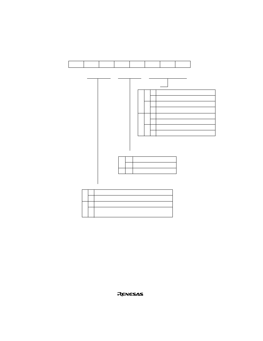
700
TCR1--Timer Control Register 1
H'FFE0
TPU1
TCNT clearing disabled
TCNT cleared by TGRA compare match/input capture
TCNT cleared by TGRB compare match/input capture
Counter Clear
0
1
0
1
0
1
0
1
Clock Edge
0
1
--
Count at rising edge
Count at falling edge
Count at both edges
Internal clock: counts on ¯/1
Internal clock: counts on ¯/4
Internal clock: counts on ¯/16
Internal clock: counts on ¯/64
External clock: counts on TCLKA pin input
External clock: counts on TCLKB pin input
Internal clock: counts on ¯/256
Setting prohibited
Time Prescaler
0
1
0
1
0
1
0
1
0
1
0
1
0
1
7
--
0
--
6
CCLR1
0
R/W
5
CCLR0
0
R/W
4
CKEG1
0
R/W
3
CKEG0
0
R/W
0
TPSC0
0
R/W
2
TPSC2
0
R/W
1
TPSC1
0
R/W
Note: This setting is ignored when channel 1 is in phase
counting mode.
Bit
Initial value
Read/Write
:
:
:
Note: This setting is ignored when channel 1
is in phase counting mode.
TCNT cleared by counter clearing for another channel
performing synchronous clearing/synchronous operation
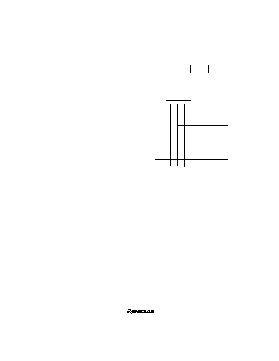
701
TMDR1--Timer Mode Register 1
H'FFE1
TPU1
0
1
Normal operation
Reserved
PWM mode 1
PWM mode 2
Phase counting mode 1
Phase counting mode 2
Phase counting mode 3
Phase counting mode 4
--
Mode
0
1
*
0
1
0
1
*
0
1
0
1
0
1
0
1
*
Notes: MD3 is a reserved bit. In a write, it
should always be written with 0.
*
: Don't care
7
--
1
--
6
--
1
--
5
--
0
--
4
--
0
--
3
MD3
0
R/W
0
MD0
0
R/W
2
MD2
0
R/W
1
MD1
0
R/W
Bit
Initial value
Read/Write
:
:
:
702
TIOR1--Timer I/O Control Register 1
H'FFE2
TPU1
7
IOB3
0
R/W
6
IOB2
0
R/W
5
IOB1
0
R/W
4
IOB0
0
R/W
3
IOA3
0
R/W
0
IOA0
0
R/W
2
IOA2
0
R/W
1
IOA1
0
R/W
0
1
TGR1B I/O Control
0
1
0
1
0
1
0
1
0
1
*
0
1
0
1
0
1
0
1
0
1
*
*
TGR1A I/O Control
*
: Don't care
0
1
0
1
0
1
0
1
0
1
0
1
*
0
1
0
1
0
1
0
1
0
1
*
*
*
: Don't care
Bit
Initial value
Read/Write
:
:
:
TGR1A
is output
compare
register
Output disabled
0 output at compare match
1 output at compare match
Toggle output at compare match
0 output at compare match
1 output at compare match
Toggle output at compare match
Input capture at rising edge
Input capture at falling edge
Input capture at both edges
Initial output is
0 output
TGR1A
is input
capture
register
Output disabled
Initial output is
1 output
Capture input
source is
TIOCA1 pin
Setting prohibited
TGR1B
is output
compare
register
Output disabled
0 output at compare match
1 output at compare match
Toggle output at compare match
0 output at compare match
1 output at compare match
Toggle output at compare match
Input capture at rising edge
Input capture at falling edge
Input capture at both edges
Initial output is
0 output
TGR1B
is input
capture
register
Output disabled
Initial output is
1 output
Capture input
source is
TIOCB1 pin
Setting prohibited

703
TIER1--Timer Interrupt Enable Register 1
H'FFE4
TPU1
7
TTGE
0
R/W
6
--
1
--
5
TCIEU
0
R/W
4
TCIEV
0
R/W
3
--
0
--
0
TGIEA
0
R/W
2
--
0
--
1
TGIEB
0
R/W
0
1
A/D conversion start request generation disabled
A/D conversion start request generation enabled
A/D Conversion Start Request Enable
0
1
Interrupt requests (TCIU) by TCFU disabled
Interrupt requests (TCIU) by TCFU enabled
Underflow Interrupt Enable
TGR Interrupt Enable B
0
1
Interrupt requests (TGIA)
by TGFA bit disabled
TGR Interrupt Enable A
0
1
Interrupt requests (TGIB)
by TGFB bit disabled
0
1
Interrupt requests (TCIV) by TCFV disabled
Interrupt requests (TCIV) by TCFV enabled
Overflow Interrupt Enable
Bit
Initial value
Read/Write
:
:
:
Interrupt requests (TGIA)
by TGFA bit enabled
Interrupt requests (TGIB)
by TGFB bit enabled

704
TSR1--Timer Status Register 1
H'FFE5
TPU1
7
TCFD
1
R
6
--
1
--
5
TCFU
0
R/(W)
*
4
TCFV
0
R/(W)
*
3
--
0
--
0
TGFA
0
R/(W)
*
2
--
0
--
1
TGFB
0
R/(W)
*
0
1
TCNT counts down
TCNT counts up
Count Direction Flag
0
Underflow Flag
1
0
Overflow Flag
1
0
TGRB Capture/Output Compare Flag
1
0
[Clearing condition]
∑ When DTC is activated by TGIA interrupt while
DISEL bit of MRB in DTC is 0.
∑ When 0 is written to TGFA after reading
TGFA = 1
TGRA Input Capture/Output Compare Flag
1
Note:
*
Can only be written with 0 for flag clearing.
Bit
Initial value
Read/Write
:
:
:
[Setting conditions]
∑ When TCNT = TGRA while TGRA is function-
ing as output compare register
∑ When TCNT value is transferred to TGRA by
input capture signal while TGRA is functioning
as input capture register
[Clearing condition]
∑ When DTC is activated by TGIB interrupt while DISEL
bit of MRB in DTC is 0.
∑ When 0 is written to TGFB after reading TGFB = 1
[Setting conditions]
∑ When TCNT = TGRB while TGRB is functioning as
output compare register
∑ When TCNT value is transferred to TGRB by input
capture signal while TGRB is functioning as input
capture register
[Clearing condition]
When 0 is written to TCFV after reading TCFV = 1
[Setting conditions]
When the TCNT value overflows (changes from H'FFFF to H'0000 )
[Clearing condition]
When 0 is written to TCFU after reading TCFU = 1
[Setting conditions]
When the TCNT value underflows (changes from H'0000 to H'FFFF)

705
TCNT1--Timer Counter 1
H'FFE6
TPU1
15
0
R/W
14
0
R/W
13
0
R/W
12
0
R/W
11
0
R/W
8
0
R/W
10
0
R/W
9
0
R/W
7
0
R/W
6
0
R/W
5
0
R/W
4
0
R/W
3
0
R/W
0
0
R/W
2
0
R/W
1
0
R/W
Note:
*
Up/down-counter
*
Bit
Initial value
Read/Write
:
:
:
This timer counter can be used as an up/down-counter only in phase counting
mode or when performing overflow/underflow counting on another channel. In
other cases it functions as an up-counter.
TGR1A--Timer General Register 1A
H'FFE8
TPU1
TGR1B--Timer General Register 1B
H'FFEA
TPU1
15
1
R/W
14
1
R/W
13
1
R/W
12
1
R/W
11
1
R/W
8
1
R/W
10
1
R/W
9
1
R/W
7
1
R/W
6
1
R/W
5
1
R/W
4
1
R/W
3
1
R/W
0
1
R/W
2
1
R/W
1
1
R/W
Bit
Initial value
Read/Write
:
:
:

706
TCR2--Timer Control Register 2
H'FFF0
TPU2
TCNT clearing disabled
TCNT cleared by TGRA compare match/input capture
TCNT cleared by TGRB compare match/input capture
Counter Clear
0
1
0
1
0
1
0
1
Clock Edge
0
1
--
Count at rising edge
Count at falling edge
Count at both edges
Internal clock: counts on ¯/1
Internal clock: counts on ¯/4
Internal clock: counts on ¯/16
Internal clock: counts on ¯/64
External clock: counts on TCLKA pin input
External clock: counts on TCLKB pin input
External clock: counts on TCLKC pin input
Internal clock: counts on ¯/1024
Time Prescaler
0
1
0
1
0
1
0
1
0
1
0
1
0
1
7
--
0
--
6
CCLR1
0
R/W
5
CCLR0
0
R/W
4
CKEG1
0
R/W
3
CKEG0
0
R/W
0
TPSC0
0
R/W
2
TPSC2
0
R/W
1
TPSC1
0
R/W
Note: This setting is ignored when channel 2 is in phase
counting mode.
Bit
Initial value
Read/Write
:
:
:
Note: This setting is ignored when channel 2
is in phase counting mode.
TCNT cleared by counter clearing for another channel
performing synchronous clearing/synchronous operation

707
TMDR2--Timer Mode Register 2
H'FFF1
TPU2
0
1
Normal operation
Reserved
PWM mode 1
PWM mode 2
Phase counting mode 1
Phase counting mode 2
Phase counting mode 3
Phase counting mode 4
--
Mode
0
1
*
0
1
0
1
*
0
1
0
1
0
1
0
1
*
Notes: MD3 is a reserved bit. In a write, it
should always be written with 0.
*
: Don't care
7
--
1
--
6
--
1
--
5
--
0
--
4
--
0
--
3
MD3
0
R/W
0
MD0
0
R/W
2
MD2
0
R/W
1
MD1
0
R/W
Bit
Initial value
Read/Write
:
:
:
708
TIOR2--Timer I/O Control Register 2
H'FFF2
TPU2
7
IOB3
0
R/W
6
IOB2
0
R/W
5
IOB1
0
R/W
4
IOB0
0
R/W
3
IOA3
0
R/W
0
IOA0
0
R/W
2
IOA2
0
R/W
1
IOA1
0
R/W
0
1
TGR2B I/O Control
0
1
*
0
1
0
1
0
1
0
1
0
1
0
1
0
1
0
1
*
*
: Don't care
0
1
TGR2A
is output
compare
register
TGR2A I/O Control
0
1
*
0
1
0
1
0
1
0
1
0
1
0
1
0
1
0
1
*
0 output at compare match
1 output at compare match
Toggle output at compare match
0 output at compare match
1 output at compare match
Toggle output at compare match
Input capture at rising edge
Input capture at falling edge
Input capture at both edges
*
: Don't care
Bit
Initial value
Read/Write
:
:
:
Output disabled
Initial output is
0 output
Output disabled
Initial output is
1 output
TGR2A
is input
capture
register
Capture input
source is
TIOCA2 pin
TGR2B
is output
compare
register
0 output at compare match
1 output at compare match
Toggle output at compare match
0 output at compare match
1 output at compare match
Toggle output at compare match
Input capture at rising edge
Input capture at falling edge
Input capture at both edges
Output disabled
Initial output is
0 output
Output disabled
Initial output is
1 output
TGR2B
is input
capture
register
Capture input
source is
TIOCB2 pin

709
TIER2--Timer Interrupt Enable Register 2
H'FFF4
TPU2
7
TTGE
0
R/W
6
--
1
--
5
TCIEU
0
R/W
4
TCIEV
0
R/W
3
--
0
--
0
TGIEA
0
R/W
2
--
0
--
1
TGIEB
0
R/W
0
1
A/D conversion start request generation disabled
A/D conversion start request generation enabled
A/D Conversion Start Request Enable
0
1
Interrupt requests (TCIU) by TCFU disabled
Interrupt requests (TCIU) by TCFU enabled
Underflow Interrupt Enable
TGR Interrupt Enable B
0
1
Interrupt requests (TGIA)
by TGFA bit disabled
TGR Interrupt Enable A
0
1
Interrupt requests (TGIB)
by TGFB bit disabled
0
1
Interrupt requests (TCIV) by TCFV disabled
Interrupt requests (TCIV) by TCFV enabled
Overflow Interrupt Enable
Bit
Initial value
Read/Write
:
:
:
Interrupt requests (TGIA)
by TGFA bit enabled
Interrupt requests (TGIB)
by TGFB bit enabled

710
TSR2--Timer Status Register 2
H'FFF5
TPU2
7
TCFD
1
R
6
--
1
--
5
TCFU
0
R/(W)
*
4
TCFV
0
R/(W)
*
3
--
0
--
0
TGFA
0
R/(W)
*
2
--
0
--
1
TGFB
0
R/(W)
*
0
1
TCNT counts down
TCNT counts up
Count Direction Flag
0
Underflow Flag
1
0
Overflow Flag
1
0
TGRB Capture/Output Compare Flag
1
0
[Clearing condition]
∑ When DTC is activated by TGIA interrupt while
DISEL bit of MRB in DTC is 0.
∑ When 0 is written to TGFA after reading
TGFA = 1
TGRA Input Capture/Output Compare Flag
1
Note:
*
Can only be written with 0 for flag clearing.
Bit
Initial value
Read/Write
:
:
:
[Setting conditions]
∑ When TCNT = TGRA while TGRA is function-
ing as output compare register
∑ When TCNT value is transferred to TGRA by
input capture signal while TGRA is functioning
as input capture register
[Clearing condition]
∑ When DTC is activated by TGIB interrupt while DISEL
bit of MRB in DTC is 0.
∑ When 0 is written to TGFB after reading TGFB = 1
[Setting conditions]
∑ When TCNT = TGRB while TGRB is functioning as
output compare register
∑ When TCNT value is transferred to TGRB by input
capture signal while TGRB is functioning as input
capture register
[Clearing condition]
When 0 is written to TCFV after reading TCFV = 1
[Setting conditions]
When the TCNT value overflows (changes from H'FFFF to H'0000 )
[Clearing condition]
When 0 is written to TCFU after reading TCFU = 1
[Setting conditions]
When the TCNT value underflows (changes from H'0000 to H'FFFF)

711
TCNT2--Timer Counter 2
H'FFF6
TPU2
15
0
R/W
14
0
R/W
13
0
R/W
12
0
R/W
11
0
R/W
8
0
R/W
10
0
R/W
9
0
R/W
7
0
R/W
6
0
R/W
5
0
R/W
4
0
R/W
3
0
R/W
0
0
R/W
2
0
R/W
1
0
R/W
Note:
*
This timer counter can be used as an up/down-counter only in phase counting
mode or when performing overflow/underflow counting on another channel. In
other cases it functions as an up-counter.
Up/down-counter
*
Bit
Initial value
Read/Write
:
:
:
TGR2A--Timer General Register 2A
H'FFF8
TPU2
TGR2B--Timer General Register 2B
H'FFFA
TPU2
15
1
R/W
14
1
R/W
13
1
R/W
12
1
R/W
11
1
R/W
8
1
R/W
10
1
R/W
9
1
R/W
7
1
R/W
6
1
R/W
5
1
R/W
4
1
R/W
3
1
R/W
0
1
R/W
2
1
R/W
1
1
R/W
Bit
Initial value
Read/Write
:
:
:
712
Appendix C I/O Port Block Diagrams
C.1
Port 1 Block Diagram
R
P1nDDR
C
Q
D
Reset
WDDR1
Mode 1/2/3/7
Mode
4/5/6
Reset
WDR1
R
P1nDR
C
Q
D
P1
n
RDR1
RPOR1
Internal data bus
Internal address bus
TPU module
Output compare
output/PWM
output enable
Output compare
output/PWM
output
Input capture
input
Legend
WDDR1
WDR1
RDR1
RPOR1
n = 0 or 1
: Write to P1DDR
: Write to P1DR
: Read P1DR
: Read port 1
Figure C-1 (a) Port 1 Block Diagram (Pins P1
0
and P1
1
)

713
R
P1nDDR
C
Q
D
Reset
WDDR1
Reset
Mode 1/2/3/7
Mode
4/5/6
WDR1
R
P1nDR
C
Q
D
P1
n
RDR1
RPOR1
Internal data bus
Internal address bus
TPU module
Output compare
output/PWM
output enable
Output compare
output/PWM
output
External clock
input
Input capture
input
Legend
WDDR1
WDR1
RDR1
RPOR1
n = 2 or 3
: Write to P1DDR
: Write to P1DR
: Read P1DR
: Read port 1
Figure C-1 (b) Port 1 Block Diagram (Pins P1
2
and P1
3
)

714
R
P1nDDR
C
Q
D
Reset
WDDR1
Reset
WDR1
R
P1nDR
C
Q
D
P1
n
RDR1
RPOR1
Internal data bus
TPU module
Output compare output/
PWM output enable
Output compare output/
PWM output
Input capture input
Legend
WDDR1
WDR1
RDR1
RPOR1
n = 4 or 6
: Write to P1DDR
: Write to P1DR
: Read P1DR
: Read port 1
Figure C-1 (c) Port 1 Block Diagram (Pins P1
4
and P1
6
)

715
R
P1nDDR
C
Q
D
Reset
WDDR1
Reset
WDR1
R
P1nDR
C
Q
D
P1
n
RDR1
RPOR1
Internal data bus
TPU module
Output compare output/
PWM output enable
Output compare output/
PWM output
External clock input
Input capture input
Legend
WDDR1
WDR1
RDR1
RPOR1
n = 5 or 7
: Write to P1DDR
: Write to P1DR
: Read P1DR
: Read port 1
Figure C-1 (d) Port 1 Block Diagram (Pins P1
5
and P1
7
)

716
C.2
Port 2 Block Diagram
R
P2nDDR
C
Q
D
Reset
WDDR2
Reset
WDR2
R
P2nDR
C
Q
D
P2
n
RDR2
RPOR2
Internal data bus
Legend
WDDR2
WDR2
RDR2
RPOR2
n = 0 or 1
: Write to P2DDR
: Write to P2DR
: Read P2DR
: Read port 2
Figure C-2 (a) Port 2 Block Diagram (Pins P2
0
and P2
1
)

717
R
P2nDDR
C
Q
D
Reset
WDDR2
Reset
WDR2
R
P2nDR
C
Q
D
P2
n
RDR2
RPOR2
Internal data bus
Counter external reset
input
8-bit timer module
Legend
WDDR2
WDR2
RDR2
RPOR2
n = 2 or 4
: Write to P2DDR
: Write to P2DR
: Read P2DR
: Read port 2
Figure C-2 (b) Port 2 Block Diagram (Pins P2
2
and P2
4
)
718
R
P2nDDR
C
Q
D
Reset
WDDR2
Reset
WDR2
R
P2nDR
C
Q
D
P2
n
RDR2
RPOR2
Internal data bus
Counter external
clock input
8-bit timer module
Legend
WDDR2
WDR2
RDR2
RPOR2
n = 3 or 5
: Write to P2DDR
: Write to P2DR
: Read P2DR
: Read port 2
Figure C-2 (c) Port 2 Block Diagram (Pins P2
3
and P2
5
)

719
R
P2nDDR
C
Q
D
Reset
WDDR2
Reset
WDR2
R
P2nDR
C
Q
D
P2
n
RDR2
RPOR2
Internal data bus
8-bit timer
Compare-match
output enable
Compare-match output
Legend
WDDR2
WDR2
RDR2
RPOR2
n = 6 or 7
: Write to P2DDR
: Write to P2DR
: Read P2DR
: Read port 2
Figure C-2 (d) Port 2 Block Diagram (Pins P2
6
and P2
7
)
720
C.3
Port 3 Block Diagram
R
P3nDDR
C
Q
D
Reset
WDDR3
Reset
WDR3
R
C
Q
D
P3
n
RDR3
RODR3
RPOR3
Internal data bus
SCI module
Serial transmit enable
Serial transmit data
Legend
WDDR3
WDR3
WODR3
RDR3
RPOR3
RODR3
n = 0 or 1
Notes: 1. Output enable signal
2. Open drain control signal
: Write to P3DDR
: Write to P3DR
: Write to P3ODR
: Read P3DR
: Read port 3
: Read P3ODR
P3nDR
Reset
WODR3
R
C
Q
D
P3nODR
*
1
*
2
Figure C-3 (a) Port 3 Block Diagram (Pins P3
0
and P3
1
)
721
R
P3nDDR
C
Q
D
Reset
WDDR3
Reset
WDR3
R
C
Q
D
P3
n
RDR3
RODR3
RPOR3
Internal data bus
SCI module
Serial receive data
enable
Serial receive data
Legend
WDDR3
WDR3
WODR3
RDR3
RPOR3
RODR3
n = 2 or 3
Notes: 1. Output enable signal
2. Open drain control signal
: Write to P3DDR
: Write to P3DR
: Write to P3ODR
: Read P3DR
: Read port 3
: Read P3ODR
P3nDR
Reset
WODR3
R
C
Q
D
P3nODR
*
1
*
2
Figure C-3 (b) Port 3 Block Diagram (Pins P3
2
and P3
3
)
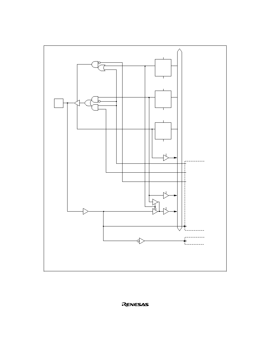
722
R
P3nDDR
C
Q
D
Reset
WDDR3
Reset
WDR3
R
C
Q
D
P3
n
RDR3
RODR3
RPOR3
Internal data bus
SCI module
Serial clock output
enable
Serial clock output
Interrupt controller
IRQ interrupt input
Serial clock input
enable
Serial clock input
Legend
WDDR3
WDR3
WODR3
RDR3
RPOR3
RODR3
n = 4 or 5
Notes: 1. Priority order: Serial clock input > serial clock output > DR output
2. Output enable signal
3. Open drain control signal
: Write to P3DDR
: Write to P3DR
: Write to P3ODR
: Read P3DR
: Read port 3
: Read P3ODR
P3nDR
Reset
WODR3
R
C
Q
D
P3nODR
*
2
*
3
*
1
Figure C-3 (c) Port 3 Block Diagram (Pins P3
4
and P3
5
)
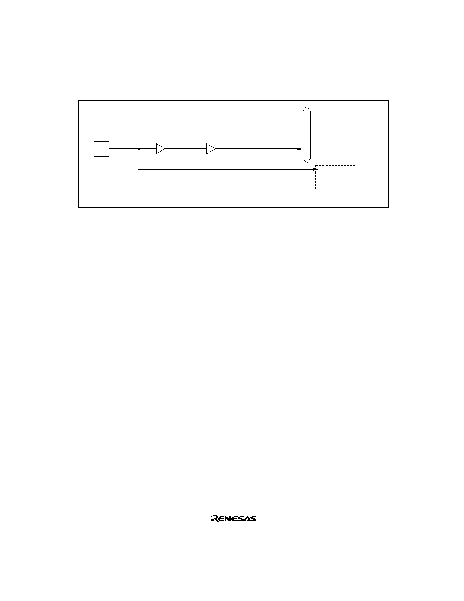
723
C.4
Port 4 Block Diagram
P4
n
RPOR4
Internal data bus
A/D converter module
Analog input
Legend
RPOR4
n = 0 to 3
: Read port 4
Figure C-4 Port 4 Block Diagram (Pins P4
0
to P4
3
)
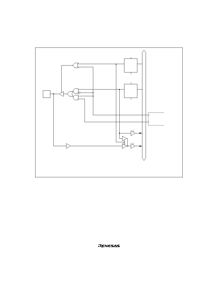
724
C.5
Port 5 Block Diagram
R
P50DDR
C
Q
D
Reset
WDDR0
Reset
WDR5
R
C
Q
D
P5
0
RDR5
RPOR5
Internal data bus
SCI module
Serial transmit data
output enable
Serial transmit data
Legend
WDDR5
WDR5
RDR5
RPOR5
: Write to P5DDR
: Write to P5DR
: Read P5DR
: Read port 5
P50DR
Figure C-5 (a) Port 5 Block Diagram (Pin P5
0
)
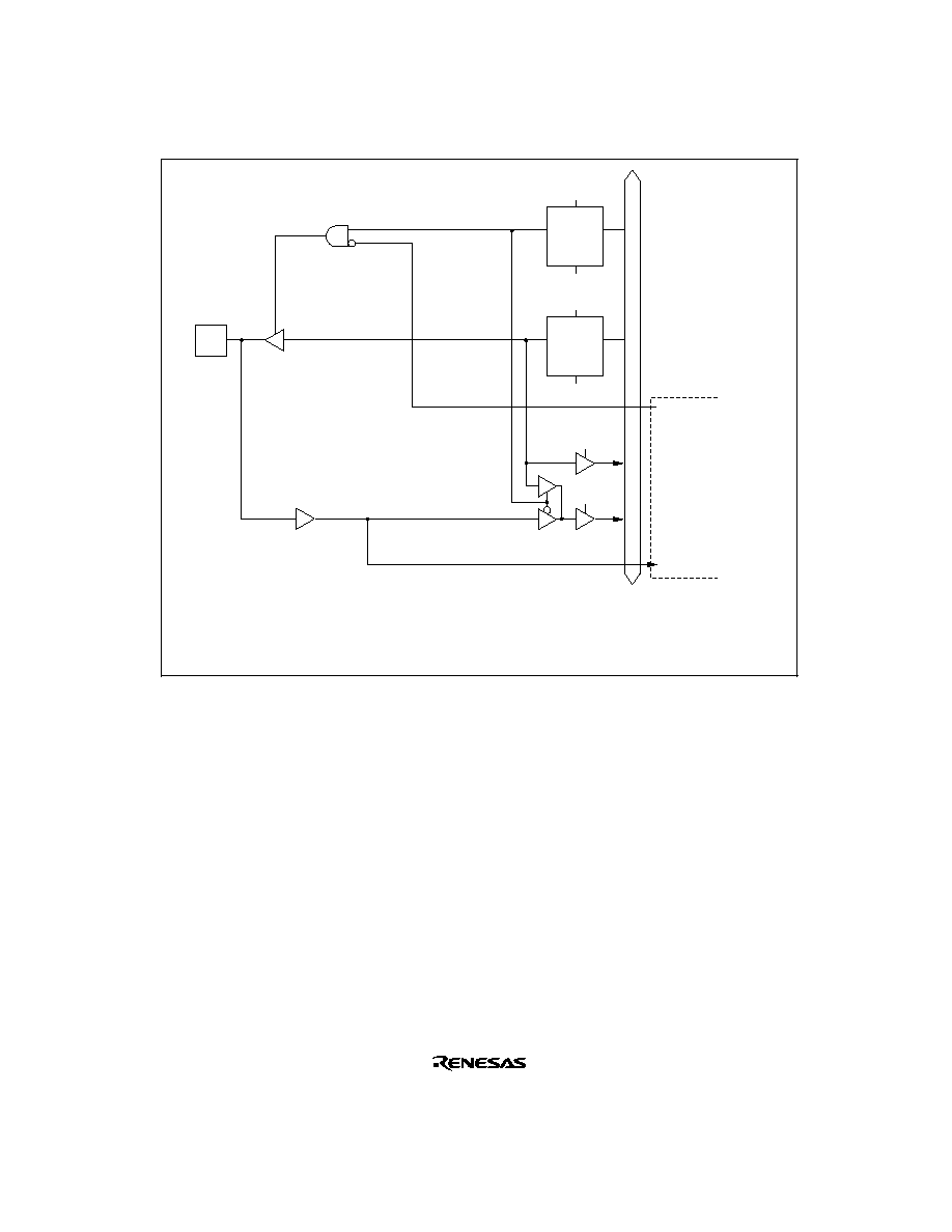
725
R
P51DDR
C
Q
D
Reset
WDDR5
Reset
WDR5
R
C
Q
D
P5
1
RDR5
RPOR5
Internal data bus
SCI module
Serial receive data
enable
Serial receive data
Legend
WDDR5
WDR5
RDR5
RPOR5
: Write to P5DDR
: Write to P5DR
: Read P5DR
: Read port 5
P51DR
Figure C-5 (b) Port 5 Block Diagram (Pin P5
1
)

726
R
P52DDR
C
Q
D
Reset
WDDR5
Reset
WDR5
R
C
Q
D
P5
2
Internal data bus
SCI module
Serial clock output
enable
Serial clock input
enable
Serial clock output
Serial clock input
Legend
WDDR5
WDR5
RDR5
RPOR5
Note:
*
Priority order: Serial clock input > serial clock output > DR output
: Write to P5DDR
: Write to P5DR
: Read P5DR
: Read port 5
P52DR
RDR5
RPOR5
*
Figure C-5 (c) Port 5 Block Diagram (Pin P5
2
)

727
R
P53DDR
C
Q
D
Reset
WDDR5
Reset
WDR5
R
C
Q
D
P5
3
RDR5
RPOR5
Internal data bus
Legend
WDDR5
WDR5
RDR5
RPOR5
: Write to P5DDR
: Write to P5DR
: Read P5DR
: Read port 5
P53DR
Figure C-5 (d) Port 5 Block Diagram (Pin P5
3
)
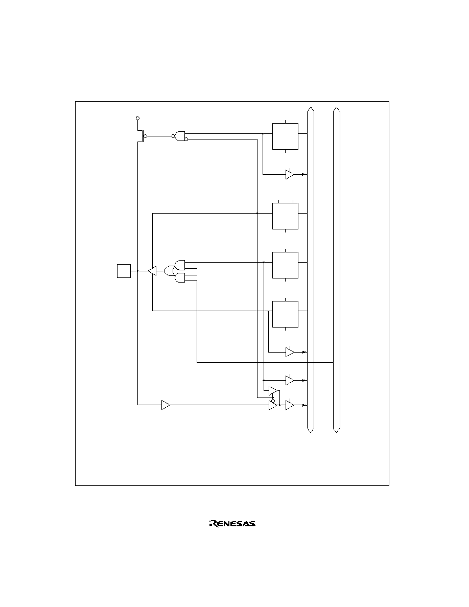
728
C.6
Port A Block Diagram
R
PAnPCR
C
Q
D
Reset
WPCRA
Reset
WDRA
R
C
Q
D
PA
n
RDRA
RODRA
RPORA
Internal data bus
Internal address bus
Legend
WDDRA
WDRA
WODRA
WPCRA
RDRA
RPORA
RODRA
RPCRA
n = 0 to 3
: Write to PADDR
: Write to PADR
: Write to PAODR
: Write to PAPCR
: Read PADR
: Read port A
: Read PAODR
: Read PAPCR
PAnDR
Reset
WDDRA
R
Mode
4/5
*
3
S
C
Q
D
PAnDDR
Reset
WODRA
RPCRA
R
C
Q
D
PAnODR
*
1
*
2
Mode 1/2/3/7
Mode 4/5/6
Notes: 1. Output enable signal
2. Open drain control signal
3. Set priority
Figure C-6 Port A Block Diagram (Pins PA
0
to PA
3
)
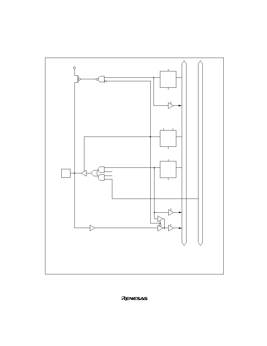
729
C.7
Port B Block Diagram
R
PBnPCR
C
Q
D
Reset
WPCRB
Reset
WDRB
R
C
Q
D
PB
n
RDRB
RPORB
Internal data bus
Internal address bus
Legend
WDDRB
WDRB
WPCRB
RDRB
RPORB
RPCRB
n = 0 to 7
Note:
*
Set priority
: Write to PBDDR
: Write to PBDR
: Write to PBPCR
: Read PBDR
: Read port B
: Read PBPCR
PBnDR
Reset
WDDRB
R
Mode
1/4/5
*
S
C
Q
D
PBnDDR
RPCRB
Mode 3/7
Mode 1/2/4/5/6
Figure C-7 Port B Block Diagram (Pin PB
n
)

730
C.8
Port C Block Diagram
R
PCnPCR
C
Q
D
Reset
WPCRC
Reset
WDRC
R
C
Q
D
PC
n
RDRC
RPORC
PCnDR
Reset
WDDRC
R
Mode
1/4/5
*
S
C
Q
D
PCnDDR
RPCRC
Mode 3/7
Mode 1/2/4/5/6
Internal data bus
Internal address bus
Legend
WDDRC
WDRC
WPCRC
RDRC
RPORC
RPCRC
n = 0 to 7
Note:
*
Set priority
: Write to PCDDR
: Write to PCDR
: Write to PCPCR
: Read PCDR
: Read port C
: Read PCPCR
Figure C-8 Port C Block Diagram (Pin PC
n
)

731
C.9
Port D Block Diagram
R
PDnPCR
C
Q
D
Reset
WPCRD
Reset
WDRD
R
C
Q
D
PD
n
RDRD
RPORD
Internal upper data bus
Internal lower data bus
External address
upper write
Legend
WDDRD
WDRD
WPCRD
RDRD
RPORD
RPCRD
n = 0 to 7
: Write to PDDDR
: Write to PDDR
: Write to PDPCR
: Read PDDR
: Read port D
: Read PDPCR
PDnDR
WDDRD
C
Q
D
PDnDDR
RPCRD
Mode 3/7
Mode 1/2/4/5/6
External address
write
Reset
R
External address upper read
External address lower read
External address
lower write
Figure C-9 Port D Block Diagram (Pin PD
n
)
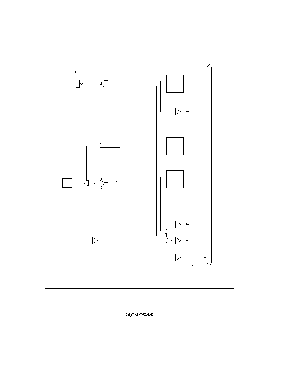
732
C.10
Port E Block Diagram
R
PEnPCR
C
Q
D
Reset
WPCRE
Reset
WDRE
R
C
Q
D
PE
n
RDRE
RPORE
PEnDR
WDDRE
C
Q
D
PEnDDR
RPCRE
Reset
R
Internal upper data bus
Internal lower data bus
Mode 3/7
Mode 1/2/4/5/6
External address
write
External address lower read
Legend
WDDRE
WDRE
WPCRE
RDRE
RPORE
RPCRE
n = 0 to 7
: Write to PEDDR
: Write to PEDR
: Write to PEPCR
: Read PEDR
: Read port E
: Read PEPCR
Figure C-10 Port E Block Diagram (Pin PE
n
)

733
C.11
Port F Block Diagram
R
PF0DDR
C
Q
D
Reset
WDDRF
Reset
WDRF
R
C
Q
D
PF0
RDRF
RPORF
Internal data bus
Bus request input
Legend
WDDRF
WDRF
RDRF
RPORF
: Write to PFDDR
: Write to PFDR
: Read PFDR
: Read port F
PF0DR
Bus controller
BRLE bit
Interrupt controller
IRQ interrupt input
Mode 1/2/4/5/6
Figure C-11 (a) Port F Block Diagram (Pin PF
0
)
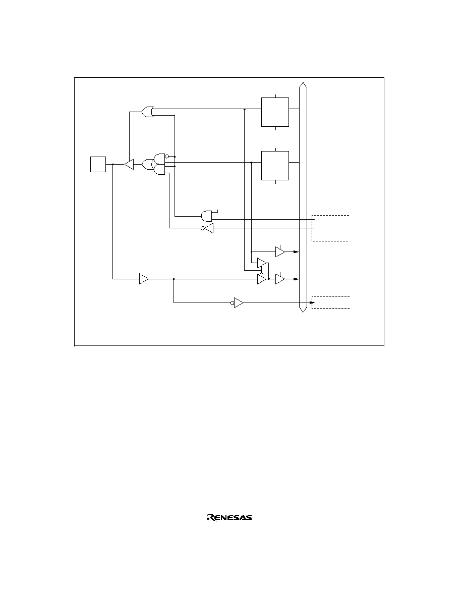
734
R
PF1DDR
C
Q
D
Reset
WDDRF
Mode 1/2/4/5/6
Reset
WDRF
R
PF1DR
C
Q
D
PF
1
RDRF
RPORF
Internal data bus
Bus controller
BRLE bit
Bus request
acknowledge output
Legend
WDDRF
WDRF
RDRF
RPORF
: Write to PFDDR
: Write to PFDR
: Read PFDR
: Read port F
Interrupt controller
IRQ interrupt input
Figure C-11 (b) Port F Block Diagram (Pin PF
1
)
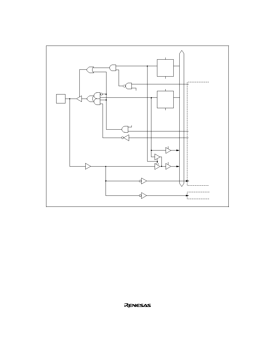
735
R
PF2DDR
C
Q
D
Reset
WDDRF
Mode 1/2/4/5/6
Reset
WDRF
R
PF2DR
C
Q
D
PF
2
RDRF
RPORF
Internal data bus
Bus request output
enable
Bus request output
Wait input
Legend
WDDRF
WDRF
RDRF
RPORF
: Write to PFDDR
: Write to PFDR
: Read PFDR
: Read port F
Bus controller
Wait enable
Mode 1/2/4/5/6
Interrupt controller
IRQ interrupt input
Figure C-11 (c) Port F Block Diagram (Pin PF
2
)
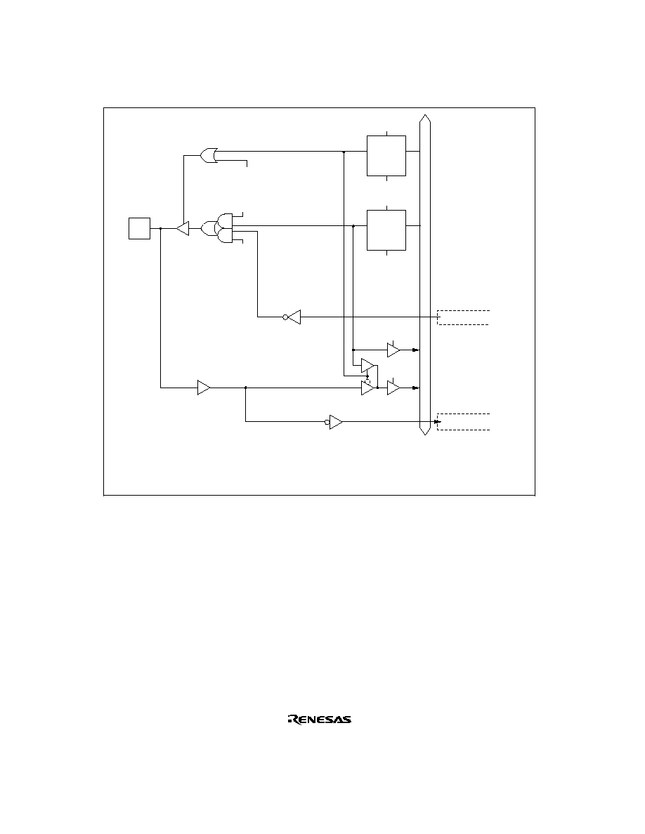
736
R
PF3DDR
C
Q
D
Reset
WDDRF
Mode 1/2/4/5/6
Reset
WDRF
R
PF3DR
C
Q
D
PF
3
RDRF
RPORF
Internal data bus
Bus controller
LWR output
Legend
WDDRF
WDRF
RDRF
RPORF
: Write to PFDDR
: Write to PFDR
: Read PFDR
: Read port F
Mode 3/7
Mode 1/2/4/5/6
Interrupt controller
IRQ interrupt input
Figure C-11 (d) Port F Block Diagram (Pin PF
3
)

737
R
PF4DDR
C
Q
D
Reset
WDDRF
Mode 1/2/4/5/6
Reset
WDRF
R
PF4DR
C
Q
D
PF
4
RDRF
RPORF
Internal data bus
Bus controller
HWR output
Legend
WDDRF
WDRF
RDRF
RPORF
: Write to PFDDR
: Write to PFDR
: Read PFDR
: Read port F
Mode 3/7
Mode 1/2/4/5/6
Figure C-11 (e) Port F Block Diagram (Pin PF
4
)
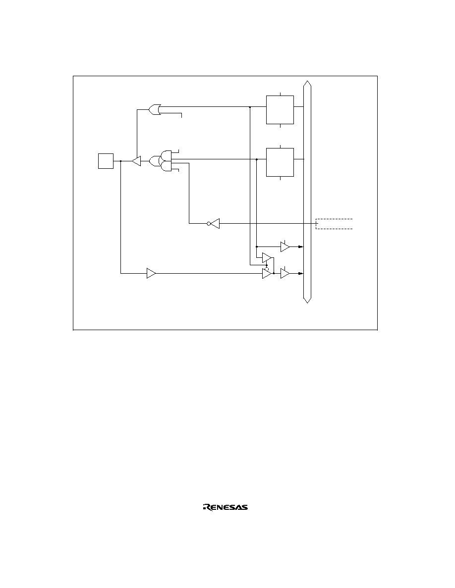
738
R
PF5DDR
C
Q
D
Reset
WDDRF
Mode 1/2/4/5/6
Reset
WDRF
R
PF5DR
C
Q
D
PF
5
RDRF
RPORF
Internal data bus
Bus controller
RD output
Legend
WDDRF
WDRF
RDRF
RPORF
: Write to PFDDR
: Write to PFDR
: Read PFDR
: Read port F
Mode 3/7
Mode 1/2/4/5/6
Figure C-11 (f) Port F Block Diagram (Pin PF
5
)
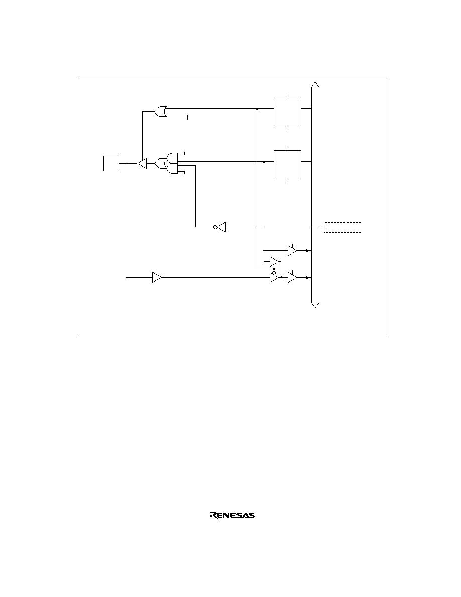
739
R
PF6DDR
C
Q
D
Reset
WDDRF
Mode 1/2/4/5/6
Reset
WDRF
R
PF6DR
C
Q
D
PF
6
RDRF
RPORF
Internal data bus
Bus controller
AS output
Legend
WDDRF
WDRF
RDRF
RPORF
: Write to PFDDR
: Write to PFDR
: Read PFDR
: Read port F
Mode 3/7
Mode 1/2/4/5/6
Figure C-11 (g) Port F Block Diagram (Pin PF
6
)
740
WDDRF
Reset
WDRF
R
PF7DR
C
Q
D
PF
7
RDRF
RPORF
Internal data bus
¯
Legend
WDDRF
WDRF
RDRF
RPORF
Note:
*
Set priority
Reset
R
Mode
1/2/4/5/6
*
S
C
Q
PF7DDR
: Write to PFDDR
: Write to PFDR
: Read PFDR
: Read port F
D
Figure C-11 (h) Port F Block Diagram (Pin PF
7
)
741
C.12
Port G Block Diagram
R
PG0DDR
C
Q
D
Reset
WDDRG
Reset
WDRG
R
PG0DR
C
Q
D
PG
0
RDRG
RPORG
Internal data bus
Legend
WDDRG
WDRG
RDRG
RPORG
: Write to PGDDR
: Write to PGDR
: Read PGDR
: Read port G
A/D converter external
trigger input
Interrupt controller
A/D converter
IRQ interrupt input
Figure C-12 (a) Port G Block Diagram (Pin PG
0
)

742
R
PG1DDR
C
Q
D
Reset
WDDRG
Reset
WDRG
R
PG1DR
C
Q
D
PG
1
RDRG
RPORG
Internal data bus
Bus controller
Chip select
Legend
WDDRG
WDRG
RDRG
RPORG
: Write to PGDDR
: Write to PGDR
: Read PGDR
: Read port G
Mode 1/2/3/7
Mode 4/5/6
Interrupt controller
IRQ interrupt input
Figure C-12 (b) Port G Block Diagram (Pin PG
1
)
743
R
PGnDDR
C
Q
D
Reset
WDDRG
Reset
WDRG
R
PGnDR
C
Q
D
PG
n
RDRG
RPORG
Internal data bus
Bus controller
Chip select
Legend
WDDRG
WDRG
RDRG
RPORG
n = 2 or 3
: Write to PGDDR
: Write to PGDR
: Read PGDR
: Read port G
Mode 1/2/3/7
Mode 4/5/6
Figure C-12 (c) Port G Block Diagram (Pins PG
2
and PG
3
)
744
WDDRG
Reset
WDRG
R
PG4DR
C
Q
D
PG
4
RDRG
RPORG
Internal data bus
Bus controller
Chip select
Legend
WDDRG
WDRG
RDRG
RPORG
: Write to PGDDR
: Write to PGDR
: Read PGDR
: Read port G
Mode 3/7
Mode 1/2/4/5/6
Reset
R
Mode
2/3/6/7
Mode
1/4/5
S
C
PG4DDR
Q
D
Figure C-12 (d) Port G Block Diagram (Pin PG
4
)

745
Appendix D Pin States
D.1
Port States in Each Mode
Table D-1
I/O Port States in Each Processing State
Port Name
Pin Name
MCU
Operating
Mode
Power-On
Reset
Manual
Reset
Hardware
Standby
Mode
Software
Standby
Mode
Bus
Release
State
Program
Execution
State
Sleep Mode
P1
7
/TIOCB2/
TCLKD
P1
6
/TIOCA2
P1
5
/TIOCB1/
TCLKC
P1
4
/TIOCA1
1 to 7
T
kept
T
kept
kept
I/O port
P1
3
/TIOCD0/
TCLKB/A
23
P1
2
/TIOCC0/
TCLKA/A
22
P1
1
/TIOCB0/
A
21
P1
0
/TIOCA0/
A
20
1 to 3, 7
4 to 6
T
T
kept
kept
T
T
kept
[DDR ∑ OPE = 0]
T
[DDR ∑ OPE = 1]
kept
kept
T
I/O port
[DDR = 0]
Input port
[DDR = 1]
Address
output
Port 2
1 to 7
T
kept
T
kept
kept
I/O port
Port 3
1 to 7
T
kept
T
kept
kept
I/O port
Port 4
1 to 7
T
T
T
T
T
Input port
Port 5
1 to 7
T
kept
T
kept
kept
I/O port
Port A
1 to 3, 7
T
kept
T
kept
kept
I/O port
4, 5
L
kept
T
[OPE = 0]
T
[OPE = 1]
kept
T
Address
output
6
T
kept
T
[DDR ∑ OPE = 0]
T
[DDR ∑ OPE = 1]
kept
T
[DDR = 0]
Input port
[DDR = 1]
Address
output

746
Table D-1
I/O Port States in Each Processing State (cont)
Port Name
Pin Name
MCU
Operating
Mode
Power-On
Reset
Manual
Reset
Hardware
Standby
Mode
Software
Standby
Mode
Bus
Release
State
Program
Execution
State
Sleep Mode
Port B
1, 4, 5
L
kept
T
[OPE = 0]
T
[OPE = 1]
kept
T
Address
output
2, 6
T
kept
T
[DDR ∑ OPE = 0]
T
[DDR ∑ OPE = 1]
kept
T
[DDR = 0}
Input port
[DDR = 1]
Address
output
3, 7
T
kept
T
kept
kept
I/O port
Port C
1, 4, 5
L
kept
T
[OPE = 0]
T
[OPE = 1]
kept
T
Address
output
2, 6
T
kept
T
[DDR ∑ OPE = 0]
T
[DDR ∑ OPE = 1]
kept
T
[DDR = 0]
Input port
[DDR = 1]
Address
output
3, 7
T
kept
T
kept
kept
I/O port
Port D
1, 2, 4 to 6
T
T
T
T
T
Data bus
3, 7
T
kept
T
kept
kept
I/O port
Port E
1, 2,
4 to 6
8 bit
bus
T
kept
T
kept
kept
I/O port
16 bit
bus
T
T
T
T
T
Data bus
3, 7
T
kept
T
kept
kept
I/O port

747
Table D-1
I/O Port States in Each Processing State (cont)
Port Name
Pin Name
MCU
Operating
Mode
Power-On
Reset
Manual
Reset
Hardware
Standby
Mode
Software
Standby
Mode
Bus
Release
State
Program
Execution
State
Sleep Mode
PF
7
/¯
1, 2, 4 to 6
Clock
output
[DDR = 0]
Input port
[DDR = 1]
Clock
output
T
[DDR = 0]
Input port
[DDR = 1]
H
[DDR = 0]
Input port
[DDR = 1]
Clock output
[DDR = 0]
Input port
[DDR = 1]
Clock output
3, 7
T
kept
T
[DDR = 0]
Input port
[DDR = 1]
H
[DDR = 0]
Input port
[DDR = 1]
Clock output
[DDR = 0]
Input port
[DDR = 1]
Clock output
PF
6
/
AS
PF
5
/
RD
PF
4
/
HWR
PF
3
/
LWR
/
IRQ3
1, 2, 4 to 6
H
H
T
[OPE= 0]
T
[OPE = 1]
H
T
AS
,
RD
,
HWR
,
LWR
3, 7
T
kept
T
kept
kept
I/O port
PF
2
/
WAIT
/
BREQO
/
IRQ2
1, 2, 4 to 6
T
kept
T
[BREQOE +
WAITE = 0]
kept
[BREQOE = 1,
WAITE = 0]
kept
[BREQOE = 0,
WAITE = 1]
T
[BREQOE +
WAITE = 0]
kept
[BREQOE = 1,
WAITE = 0]
BREQO
[BREQOE = 0,
WAITE = 1]
T
[BREQOE +
WAITE = 0]
I/O port
[BREQOE = 1,
WAITE = 0]
BREQO
[BREQOE= 0,
WAITE = 1]
WAIT
3, 7
T
kept
T
kept
kept
I/O port
PF
1
/
BACK
/
IRQ1
1, 2, 4 to 6
T
kept
T
[BRLE = 0]
kept
[BRLE = 1]
H
L
[BRLE = 0]
I/O port
[BRLE = 1]
BACK
3, 7
T
kept
T
kept
kept
I/O port
PF
0
/
BREQ
/
IRQ0
1, 2, 4 to 6
T
kept
T
[BRLE = 0]
kept
[BRLE = 1]
T
T
[BRLE = 0]
I/O port
[BRLE = 1]
BREQ
3, 7
T
kept
T
kept
kept
I/O port

748
Table D-1
I/O Port States in Each Processing State (cont)
Port Name
Pin Name
MCU
Operating
Mode
Power-On
Reset
Manual
Reset
Hardware
Standby
Mode
Software
Standby
Mode
Bus
Release
State
Program
Execution
State
Sleep Mode
PG
4
/
CS0
1, 4, 5
H
kept
T
[DDR ∑ OPE = 0]
T
T
[DDR = 0]
Input port
2, 6
T
[DDR ∑ OPE = 1]
H
[DDR = 1]
CS0
(in sleep
mode, H)
3, 7
T
kept
T
kept
kept
I/O port
PG
3
/
CS1
PG
2
/
CS2
PG
1
/
CS3
/
IRQ0
1 to 3, 7
4 to 6
T
T
kept
kept
T
T
kept
[DDR ∑ OPE = 0]
T
[DDR ∑ OPE = 1]
H
kept
T
I/O port
[DDR = 0]
Input port
[DDR = 1]
CS1
to
CS3
PG
0
/
ADTRG
/
IRQ6
1 to 7
T
kept
T
kept
kept
I/O port
Legend:
H
: High level
L
: Low level
T
: High impedance
kept
: Input port becomes high-impedance, output port retains state
DDR
: Data direction register
OPE
: Output port enable
WAITE
: Wait input enable
BRLE
: Bus release enable
BREQOE : BREQO pin enable
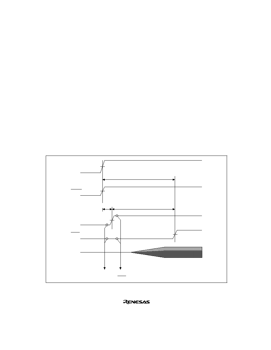
749
Appendix E Pin States at Power-On
Note that pin states at power-on depend on the state of the
STBY pin and NMI pin. The case in
which pins settle* from an indeterminate state at power-on, and the case in which pins settle* from
the high-impedance state, are described below.
After reset release, power-on reset exception handling is started.
Note: * "Settle" refers to the pin states in a power-on reset in each MCU operating mode.
E.1
When Pins Settle from an Indeterminate State at Power-On
When the NMI pin level changes from low to high after powering on, the chip goes to the power-
on reset state after a high level is detected at the NMI pin. While the chip detects a low level at the
NMI pin, the manual reset state is established. The pin states are indeterminate during this interval.
(Ports may output an internally determined value after powering on.)
The NMI setup time (t
NMIS
) is necessary for the chip to detect a high level at the NMI pin.
V
CC
STBY
NMI
RES
Power-on reset
t
OSC1
NMI = Low
NMI = High
RES = Low
Manual reset
Figure E-1 When Pins Settle from an Indeterminate State at Power-On
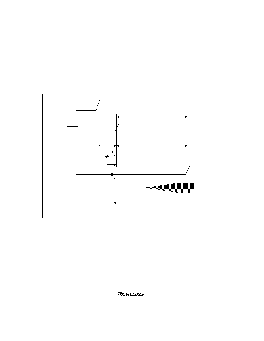
750
E.2
When Pins Settle from the High-Impedance State at Power-On
When the
STBY pin level changes from low to high after powering on, the chip goes to the power-
on reset state after a high level is detected at the
STBY pin. While the chip detects a low level at
the
STBY pin, it is in the hardware standby mode. During this interval, the pins are in the high-
impedance state.
After detecting a high level at the
STBY pin, the chip starts oscillation.
V
CC
NMI
Power-on reset
t
OSC1
NMI = High
RES = Low
T1
Confirm t1min and t
NMIS
.
Hardware
standby mode
STBY
RES
Figure E-2 When Pins Settle from the High-Impedance State at Power-On

751
Appendix F Timing of Transition to and Recovery from
Hardware Standby Mode
Timing of Transition to Hardware Standby Mode
(1) To retain RAM contents with the RAME bit set to 1 in SYSCR, drive the
RES signal low at
least 10 states before the
STBY signal goes low, as shown figure E-1. RES must remain low
until
STBY goes low (delay from STBY fall to RES rise: minimum 0 ns).
STBY
RES
t
1
10t
cyc
t
2
0 ns
Figure F-1 Timing of Transition to Hardware Standby Mode
(2) To retain RAM contents with the RAME bit cleared to 0 in SYSCR, or when RAM contents do
not need to be retained,
RES does not have to be driven low as in (1).
Timing of Recovery from Hardware Standby Mode
Drive the
RES signal low and the NMI signal high approximately 100 ns or more before STBY
goes high, and execute a power-on reset.
t
NMIRH
t
OSC
t
100 ns
STBY
RES
NMI
Figure F-2 Timing of Recovery from Hardware Standby Mode

752
Appendix G Product Code Lineup
Product Type
Product Code
Mark Code
Package
(Hitachi Package Code)
H8S/2246
Mask ROM version
HD6432246
HD6432246FA
100 pin QFP (FP-100B)
HD6432246TE
100-pin TQFP (TFP-100B)
ZTATTM version
HD6472246
HD6472246FA
100-pin QFP (FP-100B)
HD6472246TE
100-pin TQFP (TFP-100B)
H8S/2245
Mask ROM version
HD6432245
HD6432245FA
100-pin QFP (FP-100B)
HD6432245TE
100-pin TQFP (TFP-100B)
H8S/2244
HD6432244
HD6432244FA
100-pin QFP (FP-100B)
HD6432244TE
100-pin TQFP (TFP-100B)
H8S/2243
HD6432243
HD6432243FA
100-pin QFP (FP-100B)
HD6432243TE
100-pin TQFP (TFP-100B)
H8S/2242
HD6432242
HD6432242FA
100-pin QFP (FP-100B)
HD6432242TE
100-pin TQFP (TFP-100B)
H8S/2241
HD6432241R
HD6432241RFA 100-pin QFP (FP-100B)
HD6432241RTE 100-pin TQFP (TFP-100B)
H8S/2240
ROMless version
HD6412240
HD6412240FA
100-pin QFP (FP-100B)
HD6412240TE
100-pin TQFP (TFP-100B)
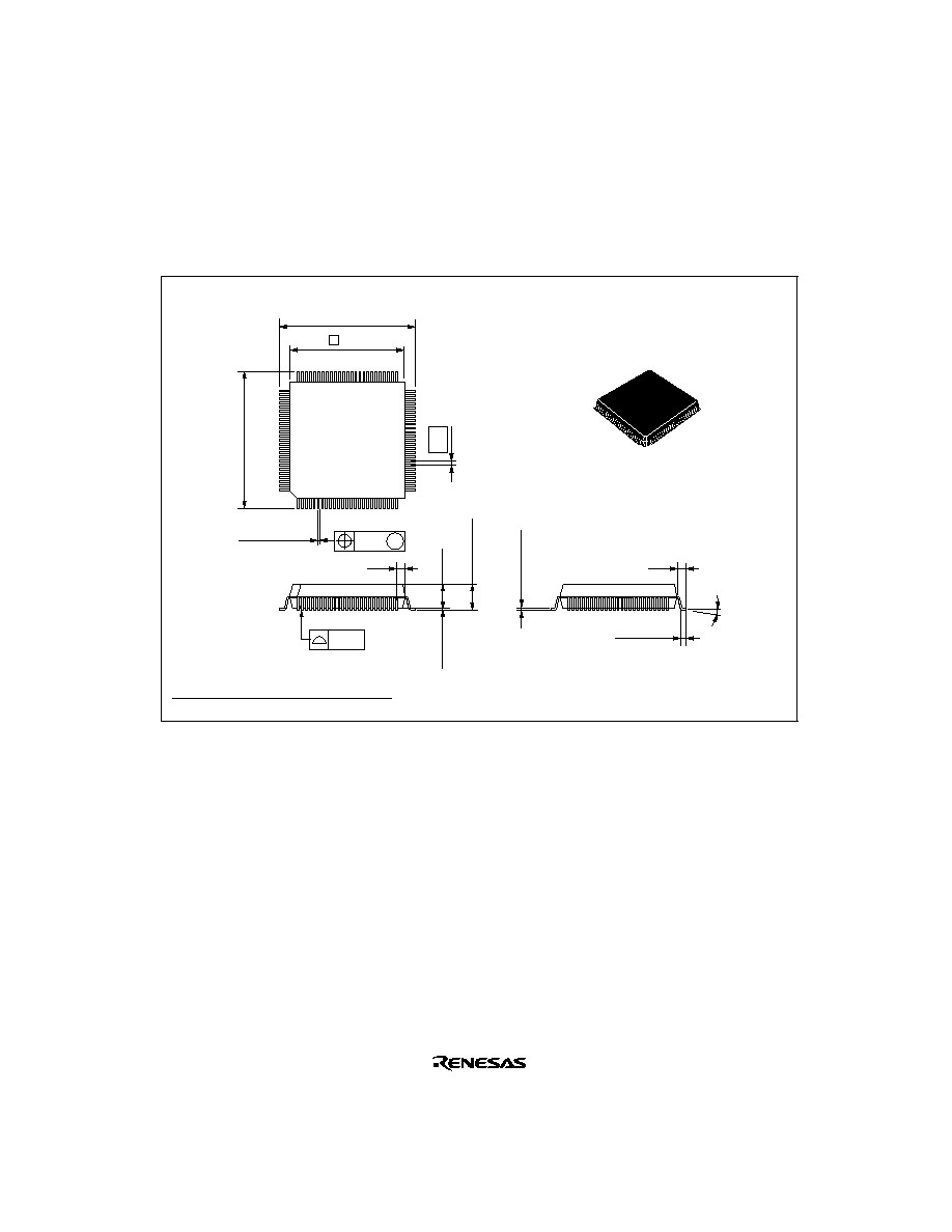
753
Appendix H Package Dimensions
Figures H-1 and H-2 show the FP-100B and TFP-100B package dimensions of the H8/2245
Series.
0.10
16.0
±
0.3
1.0
0.5
±
0.2
16.0
±
0.3
3.05 Max
75
51
50
26
1
25
76
100
14
0
∞
≠ 8
∞
0.5
0.08 M
0.22
±
0.05
2.70
0.17
±
0.05
0.12
+0.13 ≠0.12
1.0
0.20
±
0.04
0.15
±
0.04
Unit: mm
Dimension including the plating thickness
Base material dimension
Figure H-1 FP-100B Package Dimensions
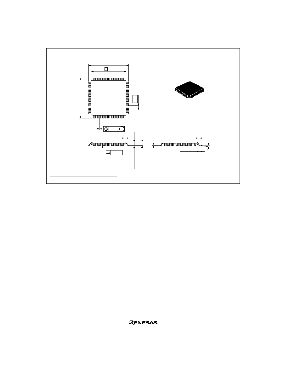
754
16.0
±
0.2
14
0.08
0.10
0.5
±
0.1
16.0
±
0.2
0.5
0.10
±
0.10
1.20 Max
0.17
±
0.05
0
∞
≠ 8
∞
75
51
1
25
76
100
26
50
M
0.22
±
0.05
1.0
1.00
1.0
0.20
±
0.04
0.15
±
0.04
Unit: mm
Dimension including the plating thickness
Base material dimension
Figure H-2 TFP-100B Package Dimensions

H8S/2245 Series Hardware Manual
Publication Date: 1st Edition, December 1996
2nd Edition, March 1998
Published by:
Electronic Devices Business Group
Hitachi, Ltd.
Edited by:
Technical Documentation Center
Hitachi Microcomputer System Ltd.
Copyright © Hitachi, Ltd., 1996. All rights reserved. Printed in Japan.
HITACHI MICROCOMPUTER TECHNICAL UPDATE
DATE
REFERENCE
DOCUMENTS
No.
THEME
CLASSIFICATION
Supplement of Documents
Limitation on Use
Effective Date
From
TN-H8*-190A/E
PRODUCT NAME
1/2
Lot No.etc.
Spec change
Rev.
Correction of Documents of H8S/2200 Series and H8S/2345 Series
Hardware Manual
All Lots
Now
Shown Below
We would like to inform you about the flag clearing condition of the register of the on-chip watchdog
timer (WDT0), watch timer (WDT1), and PC break controller (PBC) that we have added note.
1. Watchdog Timer (WDT)
[Product Name: H8S/2214 Series]
(Addition of Note)
Shown Below
Bit 7
OVF
Description
[Clearing condition] (Initial value)
Read TCSR when OVF = 1, then write 0 in OVFA *
[Setting condition]
When TCNT overflows (changes from H'FF to H'00)
When internal reset request generation is selected in watchdog timer mode, OVF is
cleared automatically by the internal reset.
0
1
Note: * When OVF is polled and the interval timer interrupt is disabled, OVF = 1 must be read
at least twice.
Bit 7
Overflow Flag (OVF): A status flag that indicates that TCNT has overflowed from H'FF to H'00.
2. Watchdog Timer (WDT)
[Product Name: H8S/2245 Series, H8S/2345 Series]
(Addition of Note)
Bit 7
OVF
Description
[Clearing condition]
Cleared by reading TCSR when OVF = 1, then writing 0 in OVF * (Initial value)
[Setting condition]
Set when TCNT overflows (changes from H'FF to H'00) in interval timer mode
0
1
Note: * When OVF is polled and the interval timer interrupt is disabled, OVF = 1 must be read
at least twice.
Bit 7
Overflow Flag (OVF): Indicates that TCNT has overflowed from H'FF to H'00, when in interval timer
mode. This flag cannot be set during watchdog timer operation.
11 October 2000

2/E
4. PC Break Controller (PBC)
[Product Name: H8S/2227 Series, H8S/2237 Series, H8S/2238 Series]
(Addition of Note)
< Product Name >
H8S/2214 Series(WDT0), H8S/2227 Series(WDT0, WDT1, PBC),
H8S/2237 Series(WDT0, WDT1, PBC), H8S/2238 Series(WDT0, WDT1, PBC),
H8S/2245 Series(WDT0), H8S/2345 Series(WDT0)
< Reference Documents >
H8S/2214 Series Hardware Manual (4/3/00 Rev. 1.0 ADE-602-213)
H8S/2245 Series Hardware Manual (3/10/98 Rev. 2.0 ADE-602-100A)
H8S/2237 Series, H8S/2227 Series Hardware Manual (12/15/98 Rev. 2.0 ADE-602-154A)
H8S/2238 Series Hardware Manual (3/19/00 Rev. 2.0 ADE-602-176A)
H8S/2345 Series Hardware Manual (9/17/99 Rev. 3.0 ADE-602-129B)
Bit 7 Condition Match Flag A (CMFA): Set to 1 when a break condition set for channel A is
satisfied. This flag is not cleared to 0.
Bit 7
CMFA
Description
[Clearing condition]
When 0 is written to CMFA after reading CMFA = 1 * (Initial value)
[Setting condition]
When a condition set for channel A is satisfied
0
1
Note: * When CMFA is polled and the PC break interrupt is disabled, CMFA = 1 must be read
at least twice.
3. Watchdog Timer (WDT0) and Watch Timer (WDT1)
[Product Name: H8S/2227 Series, H8S/2237 Series, H8S/2238 Series]
(Addition of Note)
Bit 7
OVF
Description
[Clearing conditions] (Initial value)
∑ Write 0 in the TME bit (Only applies to WDT1)
∑ Read TCSR when OVF = 1, then write 0 in OVFA *
[Setting condition]
When TCNT overflows (changes from H'FF to H'00)
When internal reset request generation is selected in watchdog timer mode, OVF is
cleared automatically by the internal reset.
0
1
Note: * When OVF is polled and the interval timer interrupt is disabled, OVF = 1 must be read
at least twice.
Bit 7 Overflow Flag (OVF): A status flag that indicates that TCNT has overflowed from H'FF
to H'00.