
Regarding the change of names mentioned in the document, such as Hitachi
Electric and Hitachi XX, to Renesas Technology Corp.
The semiconductor operations of Mitsubishi Electric and Hitachi were transferred to Renesas
Technology Corporation on April 1st 2003. These operations include microcomputer, logic, analog
and discrete devices, and memory chips other than DRAMs (flash memory, SRAMs etc.)
Accordingly, although Hitachi, Hitachi, Ltd., Hitachi Semiconductors, and other Hitachi brand
names are mentioned in the document, these names have in fact all been changed to Renesas
Technology Corp. Thank you for your understanding. Except for our corporate trademark, logo and
corporate statement, no changes whatsoever have been made to the contents of the document, and
these changes do not constitute any alteration to the contents of the document itself.
Renesas Technology Home Page: http://www.renesas.com
Renesas Technology Corp.
Customer Support Dept.
April 1, 2003
To all our customers

Cautions
Keep safety first in your circuit designs!
1. Renesas Technology Corporation puts the maximum effort into making semiconductor products better
and more reliable, but there is always the possibility that trouble may occur with them. Trouble with
semiconductors may lead to personal injury, fire or property damage.
Remember to give due consideration to safety when making your circuit designs, with appropriate
measures such as (i) placement of substitutive, auxiliary circuits, (ii) use of nonflammable material or
(iii) prevention against any malfunction or mishap.
Notes regarding these materials
1. These materials are intended as a reference to assist our customers in the selection of the Renesas
Technology Corporation product best suited to the customer's application; they do not convey any
license under any intellectual property rights, or any other rights, belonging to Renesas Technology
Corporation or a third party.
2. Renesas Technology Corporation assumes no responsibility for any damage, or infringement of any
third-party's rights, originating in the use of any product data, diagrams, charts, programs, algorithms, or
circuit application examples contained in these materials.
3. All information contained in these materials, including product data, diagrams, charts, programs and
algorithms represents information on products at the time of publication of these materials, and are
subject to change by Renesas Technology Corporation without notice due to product improvements or
other reasons. It is therefore recommended that customers contact Renesas Technology Corporation
or an authorized Renesas Technology Corporation product distributor for the latest product information
before purchasing a product listed herein.
The information described here may contain technical inaccuracies or typographical errors.
Renesas Technology Corporation assumes no responsibility for any damage, liability, or other loss
rising from these inaccuracies or errors.
Please also pay attention to information published by Renesas Technology Corporation by various
means, including the Renesas Technology Corporation Semiconductor home page
(http://www.renesas.com).
4. When using any or all of the information contained in these materials, including product data, diagrams,
charts, programs, and algorithms, please be sure to evaluate all information as a total system before
making a final decision on the applicability of the information and products. Renesas Technology
Corporation assumes no responsibility for any damage, liability or other loss resulting from the
information contained herein.
5. Renesas Technology Corporation semiconductors are not designed or manufactured for use in a device
or system that is used under circumstances in which human life is potentially at stake. Please contact
Renesas Technology Corporation or an authorized Renesas Technology Corporation product distributor
when considering the use of a product contained herein for any specific purposes, such as apparatus or
systems for transportation, vehicular, medical, aerospace, nuclear, or undersea repeater use.
6. The prior written approval of Renesas Technology Corporation is necessary to reprint or reproduce in
whole or in part these materials.
7. If these products or technologies are subject to the Japanese export control restrictions, they must be
exported under a license from the Japanese government and cannot be imported into a country other
than the approved destination.
Any diversion or reexport contrary to the export control laws and regulations of Japan and/or the
country of destination is prohibited.
8. Please contact Renesas Technology Corporation for further details on these materials or the products
contained therein.

Hitachi 16-Bit Single-Chip Microcomputer
H8S/2268 Series,
H8S/2264 Series
H8S/2268
HD6432268, HD6432268W, HD64F2268
H8S/2266
HD6432266, HD6432266W, HD64F2266
H8S/2265
HD6432265, HD6432265W, HD64F2265
H8S/2264
HD6432264, HD6432264W, HD64F2264
H8S/2264R
HD6432264R, HD6432264RW, HD64F2264R
H8S/2262
HD6432262, HD6432262W,
H8S/2262R
HD6432262R, HD6432262RW
Hardware Manual
ADE-602-240A
Rev 2.0
09/17/02
Hitachi, Ltd.

Rev. 2.0, 09/02, page
ii
of xl
Cautions
1. Hitachi neither warrants nor grants licenses of any rights of Hitachi's or any third party's
patent, copyright, trademark, or other intellectual property rights for information contained in
this document. Hitachi bears no responsibility for problems that may arise with third party's
rights, including intellectual property rights, in connection with use of the information
contained in this document.
2. Products and product specifications may be subject to change without notice. Confirm that you
have received the latest product standards or specifications before final design, purchase or
use.
3. Hitachi makes every attempt to ensure that its products are of high quality and reliability.
However, contact Hitachi's sales office before using the product in an application that
demands especially high quality and reliability or where its failure or malfunction may directly
threaten human life or cause risk of bodily injury, such as aerospace, aeronautics, nuclear
power, combustion control, transportation, traffic, safety equipment or medical equipment for
life support.
4. Design your application so that the product is used within the ranges guaranteed by Hitachi
particularly for maximum rating, operating supply voltage range, heat radiation characteristics,
installation conditions and other characteristics. Hitachi bears no responsibility for failure or
damage when used beyond the guaranteed ranges. Even within the guaranteed ranges,
consider normally foreseeable failure rates or failure modes in semiconductor devices and
employ systemic measures such as fail-safes, so that the equipment incorporating Hitachi
product does not cause bodily injury, fire or other consequential damage due to operation of
the Hitachi product.
5. This product is not designed to be radiation resistant.
6. No one is permitted to reproduce or duplicate, in any form, the whole or part of this document
without written approval from Hitachi.
7. Contact Hitachi's sales office for any questions regarding this document or Hitachi
semiconductor products.

Rev. 2.0, 09/02, page
iii
of xl
General Precautions on Handling of Product
1. Treatment of NC Pins
Note:
Do not connect anything to the NC pins.
The NC (not connected) pins are either not connected to any of the internal circuitry or are
used as test pins or to reduce noise. If something is connected to the NC pins, the
operation of the LSI is not guaranteed.
2. Treatment of Unused Input Pins
Note:
Fix all unused input pins to high or low level.
Generally, the input pins of CMOS products are high-impedance input pins. If unused pins
are in their open states, intermediate levels are induced by noise in the vicinity, a pass-
through current flows internally, and a malfunction may occur.
3. Processing before Initialization
Note:
When power is first supplied, the product's state is undefined.
The states of internal circuits are undefined until full power is supplied throughout the
chip and a low level is input on the reset pin. During the period where the states are
undefined, the register settings and the output state of each pin are also undefined. Design
your system so that it does not malfunction because of processing while it is in this
undefined state. For those products which have a reset function, reset the LSI immediately
after the power supply has been turned on.
4. Prohibition of Access to Undefined or Reserved Addresses
Note:
Access to undefined or reserved addresses is prohibited.
The undefined or reserved addresses may be used to expand functions, or test registers
may have been be allocated to these addresses. Do not access these registers; the system's
operation is not guaranteed if they are accessed.

Rev. 2.0, 09/02, page
iv
of xl
Configuration of This Manual
This manual comprises the following items:
1. General Precautions on Handling of Product
2. Configuration of This Manual
3. Preface
4. Contents
5. Overview
6. Description of Functional Modules
∑
CPU and System-Control Modules
∑
On-Chip Peripheral Modules
The configuration of the functional description of each module differs according to the
module. However, the generic style includes the following items:
i) Feature
ii) Input/Output Pin
iii) Register Description
iv) Operation
v) Usage Note
When designing an application system that includes this LSI, take notes into account. Each section
includes notes in relation to the descriptions given, and usage notes are given, as required, as the
final part of each section.
7. List of Registers
8. Electrical Characteristics
9. Appendix
10. Main Revisions and Additions in this Edition (only for revised versions)
The list of revisions is a summary of points that have been revised or added to earlier versions.
This does not include all of the revised contents. For details, see the actual locations in this
manual.
11. Index

Rev. 2.0, 09/02, page
v
of xl
Preface
This LSI is a high-performance microcontroller (MCU) made up of the H8S/2000 CPU with an
internal 32-bit configuration as its core, and the peripheral functions required to configure a
system.
A single-power flash memory (F-ZTAT
TM
)* version and a masked-ROM version are available for
this LSI's ROM. The F-ZTAT version provides flexibility as it can be reprogrammed in no time to
cope with all situations from the early stages of mass production to full-scale mass production.
This is particularly applicable to application devices with specifications that will most probably
change.
List of on-chip peripheral functions:
Series Name
H8S/2268 Series
H8S/2264 Series
Product Name
H8S/2268, 2266, 2265
H8S/2264, 2264R, 2262,
2262R
PC break controller (PBC)
X 2
Data transfer controller (DTC)
X 1
16-bit timer pulse unit (TPU)
X 3
X 2
8-bit timer (TMR_0 to TMR_3)
X 4
X 2
8-bit reload timer (TMR_4)
X 4
Watch dog timer (WDT)
X 2
X 2
Serial communication interface (SCI)
X 3
X 3
I
2
C bus interface (IIC)
X 2 (option)
X 1 (option)
A/D converter
X 10
X 10
D/A converter
X 2
LCD controller/driver
40 SEG/4 COM
40 SEG/4 COM
DTMF generation circuit
X 1
Power-on reset circuit
X 1
Ports
1, 3, 4, 7, 9, F, H, J to N
1, 3, 4, 7, 9, F, H, J to L
External interrupts
14
13
Interrupt priorities
8 levels
Notes: *
F-ZTAT
TM
is a trademark of Hitachi, Ltd.

Rev. 2.0, 09/02, page
vi
of xl
Target Users:
This manual was written for users who will be using the H8S/2268 Series and
H8S/2264 Series in the design of application systems. Target users are expected to
understand the fundamentals of electrical circuits, logical circuits, and
microcomputers.
Objective:
This manual was written to explain the hardware functions and electrical
characteristics of the H8S/2268 Series and H8S/2264 Series to the target users.
Refer to the H8S/2600 Series, H8S/2000 Series Programming Manual for a
detailed description of the instruction set.
Notes on reading this manual:
∑
In order to understand the overall functions of the chip
Read the manual according to the contents. This manual can be roughly categorized into parts
on the CPU, system control functions, peripheral functions and electrical characteristics.
∑
In order to understand the details of the CPU's functions
Read the H8S/2600 Series, H8S/2000 Series Programming Manual.
∑
In order to understand the details of a register when its name is known
Read the index that is the final part of the manual to find the page number of the entry on the
register. The addresses, bits, and initial values of the registers are summarized in section 25,
List of Registers.
Examples:
Register name:
The following notation is used for cases when the same or a
similar function, e.g. 16-bit timer pulse unit or serial
communication, is implemented on more than one channel:
XXX_N (XXX is the register name and N is the channel
number)
Bit order:
The MSB is on the left and the LSB is on the right.
Notes: 1. When using the on-chip emulator (E10T) for the H8S/2264 Series program
development and debugging, the following restrictions must be noted.
∑
The WDT timer stops counting while the on-chip emulation is in break mode.
Accordingly, after resuming from the break mode, the counter value may be
invalid.
∑
The FWE (BRK) pin is reserved for the E10T, and cannot be used.
∑
Pins P77, P76, and P75 cannot be used. In order to use these pins, additional
parts are required on the user board.
∑
When the E10T is used, the FWE (BRK) pin is an input/output pin (open-drain
in output mode), P75 and P76 are input pins, and P77 is an output pin.
2.
The emulator (E6000) does not support the following functions. They are only
supported by the on-chip emulator (E10T).
∑
Power-on reset (H8S/2264 Series)
∑
Oscillation stabilization time shortened (H8S/2264R, 2262R)

Rev. 2.0, 09/02, page
vii
of xl
∑
PH4/
, PH5 pin function (H8S/2264 Series)
∑
Selection of the input subclock source WDT_1,
SUB
/4, or
SUB
/60 (H8S/2264
Series)
∑
Selection of the segment driver in four bit units (H8S/2264 Series)
Related Manuals: The latest versions of all related manuals are available from our web site. Please
ensure you have the latest versions of all documents you require.
http://www.hitachisemiconductor.com/
H8S/2268 Series, H8S/2264 Series manuals:
Manual Title
ADE No.
H8S/2268 Series, H8S/2264 Series Hardware Manual
This manual
H8S/2600 Series, H8S/2000 Series Programming Manual
ADE-602-083
User's manuals for development tools:
Manual Title
ADE No.
H8S, H8/300 Series C/C++ Compiler, Assembler, Optimized Linkage Editor
User's Manual
ADE-702-247
H8S, H8/300 Series Simulator/Debugger User's Manual
ADE-702-282
H8S, H8/300 Series Hitachi Embedded Workshop, Hitachi Debugging
Interface Tutorial
ADE-702-231
Hitachi Embedded Workshop User's Manual
ADE-702-201
Application Notes:
Manual Title
ADE No.
C/C++ Compiler Guide
ADE-702-189
F-ZTAT Technical Q & A
ADE-502-046

Rev. 2.0, 09/02, page
viii
of xl

Rev. 2.0, 09/02, page
ix
of xl
Contents
Section 1 Overview........................................................................................ 1
1.1
Features ....................................................................................................................... 1
1.2
Internal Block Diagram ................................................................................................ 3
1.3
Pin Arrangement .......................................................................................................... 5
1.4
Pin Functions ............................................................................................................... 7
Section 2 CPU................................................................................................ 13
2.1
Features ....................................................................................................................... 13
2.1.1
Differences between H8S/2600 CPU and H8S/2000 CPU................................. 14
2.1.2
Differences from H8/300 CPU ......................................................................... 15
2.1.3
Differences from H8/300H CPU ...................................................................... 15
2.2
CPU Operating Modes ................................................................................................. 16
2.2.1
Normal Mode .................................................................................................. 16
2.2.2
Advanced Mode .............................................................................................. 17
2.3
Address Space.............................................................................................................. 20
2.4
Register Configuration ................................................................................................. 21
2.4.1
General Registers............................................................................................. 22
2.4.2
Program Counter (PC) ..................................................................................... 23
2.4.3
Extended Control Register (EXR) (H8S/2268 Series Only)............................... 23
2.4.4
Condition-Code Register (CCR)....................................................................... 24
2.4.5
Initial Values of CPU Registers........................................................................ 25
2.5
Data Formats................................................................................................................26
2.5.1
General Register Data Formats......................................................................... 26
2.5.2
Memory Data Formats ..................................................................................... 28
2.6
Instruction Set............................................................................................................. . 29
2.6.1
Table of Instructions Classified by Function..................................................... 30
2.6.2
Basic Instruction Formats ................................................................................ 39
2.7
Addressing Modes and Effective Address Calculation .................................................. 40
2.7.1
Register Direct
Rn ........................................................................................ 41
2.7.2
Register Indirect
@ERn ................................................................................ 41
2.7.3
Register Indirect with Displacement
@(d:16, ERn) or @(d:32, ERn) ............. 41
2.7.4
Register Indirect with Post-Increment or Pre-Decrement
@ERn+ or @-ERn.. 41
2.7.5
Absolute Address
@aa:8, @aa:16, @aa:24, or @aa:32 .................................. 41
2.7.6
Immediate
#xx:8, #xx:16, or #xx:32 .............................................................. 42
2.7.7
Program-Counter Relative
@(d:8, PC) or @(d:16, PC) .................................. 42
2.7.8
Memory Indirect
@@aa:8............................................................................. 42
2.7.9
Effective Address Calculation .......................................................................... 43
2.8
Processing States.......................................................................................................... 46
2.9
Usage Notes.................................................................................................................48

Rev. 2.0, 09/02, page
x
of xl
2.9.1
TAS Instruction............................................................................................... 48
2.9.2
STM/LDM Instruction..................................................................................... 48
2.9.3
Bit Manipulation Instructions........................................................................... 48
Section 3 MCU Operating Modes .................................................................. 49
3.1
Operating Mode Selection............................................................................................ 49
3.2
Register Description..................................................................................................... 49
3.2.1
Mode Control Register (MDCR)...................................................................... 50
3.3
Operating Mode ........................................................................................................... 50
3.4
Pin Functions in Each Operating Mode......................................................................... 50
3.5
Address Map................................................................................................................ 51
Section 4 Exception Handling........................................................................ 53
4.1
Exception Handling Types and Priority ........................................................................ 53
4.2
Exception Sources and Exception Vector Table ............................................................ 54
4.3
Reset ........................................................................................................................... 55
4.3.1
Reset Exception Handling................................................................................ 55
4.3.2
Interrupts after Reset ....................................................................................... 56
4.3.3
State of On-Chip Peripheral Modules after Reset Release................................. 56
4.4
Traces (Supported only by the H8S/2268 Series) .......................................................... 57
4.5
Interrupts ..................................................................................................................... 57
4.6
Trap Instruction ........................................................................................................... 58
4.7
Stack Status after Exception Handling .......................................................................... 59
4.8
Usage Note .................................................................................................................. 59
Section 5 Interrupt Controller ........................................................................ 61
5.1
Features ....................................................................................................................... 61
5.2
Input/Output Pins......................................................................................................... 64
5.3
Register Descriptions ................................................................................................... 64
5.3.1
System Control Register (SYSCR)................................................................... 65
5.3.2
Interrupt Priority Registers A to G, I to M, and O
(IPRA to IPRG, IPRI to IPRM, IPRO) (H8S/2268 Series Only) ....................... 67
5.3.3
IRQ Enable Register (IER) .............................................................................. 68
5.3.4
IRQ Sense Control Registers H and L (ISCRH and ISCRL) ............................. 69
5.3.5
IRQ Status Register (ISR)................................................................................ 71
5.3.6
Wakeup Interrupt Request Register (IWPR) ..................................................... 73
5.3.7
Interrupt Enable Register 1 (IENR1) ................................................................ 73
5.4
Interrupt Sources.......................................................................................................... 7 4
5.4.1
External Interrupts........................................................................................... 74
5.4.2
Internal Interrupts............................................................................................ 77
5.4.3
Interrupt Exception Handling Vector Table ...................................................... 77
5.5
Operation..................................................................................................................... 82
5.5.1
Interrupt Control Modes and Interrupt Operation.............................................. 82

Rev. 2.0, 09/02, page
xi
of xl
5.5.2
Interrupt Control Mode 0 ................................................................................. 85
5.5.3
Interrupt Control Mode 2 (H8S/2268 Series Only)............................................ 87
5.5.4
Interrupt Exception Handling Sequence ........................................................... 88
5.5.5
Interrupt Response Times ................................................................................ 90
5.5.6
DTC Activation by Interrupt (H8S/2268 Series Only)....................................... 91
5.6
Usage Notes.................................................................................................................91
5.6.1
Contention between Interrupt Generation and Disabling ................................... 91
5.6.2
Instructions that Disable Interrupts................................................................... 92
5.6.3
When Interrupts Are Disabled.......................................................................... 92
5.6.4
Interrupts during Execution of EEPMOV Instruction........................................ 92
Section 6 PC Break Controller (PBC).............................................................93
6.1
Features ....................................................................................................................... 93
6.2
Register Descriptions ................................................................................................... 94
6.2.1
Break Address Register A (BARA) .................................................................. 94
6.2.2
Break Address Register B (BARB) .................................................................. 94
6.2.3
Break Control Register A (BCRA) ................................................................... 95
6.2.4
Break Control Register B (BCRB) ................................................................... 96
6.3
Operation..................................................................................................................... 96
6.3.1
PC Break Interrupt Due to Instruction Fetch..................................................... 96
6.3.2
PC Break Interrupt Due to Data Access............................................................ 96
6.3.3
Notes on PC Break Interrupt Handling ............................................................. 97
6.3.4
Operation in Transitions to Power-Down Modes .............................................. 97
6.3.5
When Instruction Execution Is Delayed by One State ....................................... 98
6.4
Usage Notes.................................................................................................................99
6.4.1
Module Stop Mode Setting .............................................................................. 99
6.4.2
PC Break Interrupts ......................................................................................... 99
6.4.3
CMFA and CMFB ........................................................................................... 99
6.4.4
PC Break Interrupt when DTC Is Bus Master ................................................... 99
6.4.5
PC Break Set for Instruction Fetch at Address Following
BSR, JSR, JMP, TRAPA, RTE, or RTS Instruction.......................................... 99
6.4.6
I Bit Set by LDC, ANDC, ORC, or XORC Instruction ..................................... 99
6.4.7
PC Break Set for Instruction Fetch at Address Following Bcc Instruction ......... 100
6.4.8
PC Break Set for Instruction Fetch at Branch Destination Address of Bcc
Instruction....................................................................................................... 100
Section 7 Bus Controller ................................................................................ 101
7.1
Basic Timing ............................................................................................................... 101
7.1.1
On-Chip Memory Access Timing (ROM, RAM) .............................................. 101
7.1.2
On-Chip Peripheral Module Access Timing (H'FFFDAC to H'FFFFBF)........... 102
7.1.3
On-Chip Peripheral Module Access Timing (H'FFFC30 to H'FFFCA3) ............ 102
7.2
Bus Arbitration (H8S/2268 Series Only)....................................................................... 103
7.2.1
Order of Priority of the Bus Masters................................................................. 103

Rev. 2.0, 09/02, page
xii
of xl
7.2.2
Bus Transfer Timing........................................................................................ 104
7.2.3
Resets and the Bus Controller .......................................................................... 104
Section 8 Data Transfer Controller (DTC) ..................................................... 105
8.1
Features ....................................................................................................................... 105
8.2
Register Descriptions ................................................................................................... 107
8.2.1
DTC Mode Register A (MRA)......................................................................... 107
8.2.2
DTC Mode Register B (MRB) ......................................................................... 109
8.2.3
DTC Source Address Register (SAR)............................................................... 109
8.2.4
DTC Destination Address Register (DAR) ....................................................... 109
8.2.5
DTC Transfer Count Register A (CRA) ........................................................... 110
8.2.6
DTC Transfer Count Register B (CRB)............................................................ 110
8.2.7
DTC Enable Register (DTCER) ....................................................................... 110
8.2.8
DTC Vector Register (DTVECR) .................................................................... 111
8.3
Activation Sources....................................................................................................... 111
8.4
Location of Register Information and DTC Vector Table .............................................. 112
8.5
Operation..................................................................................................................... 115
8.5.1
Normal Mode .................................................................................................. 116
8.5.2
Repeat Mode ................................................................................................... 117
8.5.3
Block Transfer Mode....................................................................................... 118
8.5.4
Chain Transfer................................................................................................. 119
8.5.5
Interrupts......................................................................................................... 120
8.5.6
Operation Timing ............................................................................................ 121
8.5.7
Number of DTC Execution States .................................................................... 122
8.6
Procedures for Using DTC ........................................................................................... 123
8.6.1
Activation by Interrupt .................................................................................... 123
8.6.2
Activation by Software .................................................................................... 124
8.7
Examples of Use of the DTC........................................................................................ 124
8.7.1
Normal Mode .................................................................................................. 124
8.7.2
Software Activation......................................................................................... 125
8.8
Usage Notes................................................................................................................. 125
8.8.1
Module Stop Mode Setting .............................................................................. 125
8.8.2
On-Chip RAM................................................................................................. 126
8.8.3
DTCE Bit Setting ............................................................................................ 126
Section 9 I/O Ports......................................................................................... 127
9.1
Port 1........................................................................................................................... 133
9.1.1
Port 1 Data Direction Register (P1DDR).......................................................... 133
9.1.2
Port 1 Data Register (P1DR)............................................................................ 134
9.1.3
Port 1 Register (PORT1).................................................................................. 134
9.1.4
Pin Functions .................................................................................................. 135
9.2
Port 3........................................................................................................................... 138
9.2.1
Port 3 Data Direction Register (P3DDR).......................................................... 139

Rev. 2.0, 09/02, page
xiii
of xl
9.2.2
Port 3 Data Register (P3DR) ............................................................................ 139
9.2.3
Port 3 Register (PORT3).................................................................................. 140
9.2.4
Port 3 Open Drain Control Register (P3ODR) .................................................. 140
9.2.5
Pin Functions................................................................................................... 141
9.3
Port 4........................................................................................................................... 144
9.3.1
Port 4 Register (PORT4).................................................................................. 144
9.3.2
Pin Functions................................................................................................... 144
9.4
Port 7........................................................................................................................... 145
9.4.1
Port 7 Data Direction Register (P7DDR) .......................................................... 145
9.4.2
Port 7 Data Register (P7DR) ............................................................................ 145
9.4.3
Port 7 Register (PORT7).................................................................................. 146
9.4.4
Pin Functions................................................................................................... 146
9.5
Port 9........................................................................................................................... 148
9.5.1
Port 9 Register (PORT9).................................................................................. 148
9.5.2
Pin Functions................................................................................................... 148
9.6
Port F........................................................................................................................... 149
9.6.1
Port F Data Direction Register (PFDDR).......................................................... 149
9.6.2
Port F Data Register (PFDR)............................................................................ 149
9.6.3
Port F Register (PORTF) ................................................................................. 150
9.6.4
Pin Functions................................................................................................... 150
9.7
Port H .......................................................................................................................... 150
9.7.1
Port H Data Direction Register (PHDDR) ........................................................ 151
9.7.2
Port H Data Register (PHDR) .......................................................................... 152
9.7.3
Port H Register (PORTH) ................................................................................ 153
9.7.4
Pin Functions................................................................................................... 153
9.8
Port J ........................................................................................................................... 156
9.8.1
Port J Data Direction Register (PJDDR) ........................................................... 157
9.8.2
Port J Data Register (PJDR)............................................................................. 157
9.8.3
Port J Register (PORTJ)................................................................................... 158
9.8.4
Port J Pull-Up MOS Control Register (PJPCR) ................................................ 158
9.8.5
Wakeup Control Register (WPCR)................................................................... 159
9.8.6
Pin Functions................................................................................................... 159
9.8.7
Input Pull-Up MOS Function ........................................................................... 160
9.9
Port K .......................................................................................................................... 161
9.9.1
Port K Data Direction Register (PKDDR) ........................................................ 161
9.9.2
Port K Data Register (PKDR) .......................................................................... 161
9.9.3
Port K Register (PORTK) ................................................................................ 162
9.9.4
Pin Functions................................................................................................... 162
9.10
Port L .......................................................................................................................... 163
9.10.1 Port L Data Direction Register (PLDDR) ......................................................... 163
9.10.2 Port L Data Register (PLDR) ........................................................................... 164
9.10.3 Port L Register (PORTL) ................................................................................. 164
9.10.4 Pin Functions................................................................................................... 165

Rev. 2.0, 09/02, page
xiv
of xl
9.11
Port M (H8S/2268 Series Only).................................................................................... 166
9.11.1 Port M Data Direction Register (PMDDR) ....................................................... 166
9.11.2 Port M Data Register (PMDR) ......................................................................... 166
9.11.3 Port M Register (PORTM)............................................................................... 167
9.11.4 Pin Functions .................................................................................................. 167
9.12
Port N (H8S/2268 Series Only) .................................................................................... 168
9.12.1 Port N Data Direction Register (PNDDR) ........................................................ 168
9.12.2 Port N Data Register (PNDR) .......................................................................... 168
9.12.3 Port N Register (PORTN) ................................................................................ 169
9.12.4 Pin Functions .................................................................................................. 169
Section 10 16-Bit Timer Pulse Unit (TPU)..................................................... 171
10.1
Features ....................................................................................................................... 171
10.2
Input/Output Pins......................................................................................................... 176
10.3
Register Descriptions ................................................................................................... 177
10.3.1 Timer Control Register (TCR) ......................................................................... 178
10.3.2 Timer Mode Register (TMDR) ........................................................................ 182
10.3.3 Timer I/O Control Register (TIOR).................................................................. 184
10.3.4 Timer Interrupt Enable Register (TIER) ........................................................... 192
10.3.5 Timer Status Register (TSR) ............................................................................ 194
10.3.6 Timer Counter (TCNT).................................................................................... 199
10.3.7 Timer General Register (TGR)......................................................................... 199
10.3.8 Timer Start Register (TSTR)............................................................................ 199
10.3.9 Timer Synchro Register (TSYR)...................................................................... 201
10.4
Interface to Bus Master ................................................................................................ 202
10.4.1 16-Bit Registers............................................................................................... 202
10.4.2 8-Bit Registers................................................................................................. 202
10.5
Operation..................................................................................................................... 203
10.5.1 Basic Functions ............................................................................................... 203
10.5.2 Synchronous Operation ................................................................................... 208
10.5.3 Buffer Operation (H8S/2268 Series Only)........................................................ 210
10.5.4 Operation with Cascaded Connection (H8S/2264 Series Only) ......................... 213
10.5.5 PWM Modes ................................................................................................... 215
10.5.6 Phase Counting Mode (H8S/2268 Series Only) ................................................ 220
10.6
Interrupt Sources.......................................................................................................... 225
10.7
DTC Activation (H8S/2268 Series Only)...................................................................... 226
10.8
A/D Converter Activation ............................................................................................ 226
10.9
Operation Timing......................................................................................................... 227
10.9.1 Input/Output Timing........................................................................................ 227
10.9.2 Interrupt Signal Timing ................................................................................... 231
10.10 Usage Notes................................................................................................................. 234
10.10.1 Module Stop Mode Setting .............................................................................. 234
10.10.2 Input Clock Restrictions .................................................................................. 234

Rev. 2.0, 09/02, page
xv
of xl
10.10.3 Caution on Period Setting ................................................................................ 235
10.10.4 Contention between TCNT Write and Clear Operations ................................... 235
10.10.5 Contention between TCNT Write and Increment Operations ............................ 236
10.10.6 Contention between TGR Write and Compare Match ....................................... 236
10.10.7 Contention between Buffer Register Write and Compare Match
(H8S/2268 Series Only) .................................................................................. 237
10.10.8 Contention between TGR Read and Input Capture............................................ 238
10.10.9 Contention between TGR Write and Input Capture........................................... 238
10.10.10 Contention between Buffer Register Write and Input Capture
(H8S/2268 Series Only) ............................................................................... 239
10.10.11 Contention between Overflow/Underflow and Counter Clearing................... 240
10.10.12 Contention between TCNT Write and Overflow/Underflow.......................... 241
10.10.13 Multiplexing of I/O Pins .............................................................................. 241
10.10.14 Interrupts in Module Stop Mode................................................................... 241
Section 11 8-Bit Timers ................................................................................. 243
11.1
8-Bit Timer Module (TMR_0, TMR_1, TMR_2 and TMR_3)....................................... 243
11.1.1 Features........................................................................................................... 243
11.2
Input/Output Pins ......................................................................................................... 245
11.3
Register Descriptions ................................................................................................... 245
11.3.1 Timer Counter (TCNT).................................................................................... 246
11.3.2 Time Constant Register A (TCORA)................................................................ 246
11.3.3 Time Constant Register B (TCORB) ................................................................ 246
11.3.4 Timer Control Register (TCR) ......................................................................... 247
11.3.5 Timer Control/Status Register (TCSR) ............................................................. 249
11.4
Operation..................................................................................................................... 254
11.4.1 Pulse Output .................................................................................................... 254
11.5
Operation Timing......................................................................................................... 255
11.5.1 TCNT Incrementation Timing.......................................................................... 255
11.5.2 Timing of CMFA and CMFB Setting When a Compare-Match Occurs ............. 255
11.5.3 Timing of Timer Output When a Compare-Match Occurs................................. 256
11.5.4 Timing of Compare-Match Clear When a Compare-Match Occurs ................... 256
11.5.5 TCNT External Reset Timing .......................................................................... 257
11.5.6 Timing of Overflow Flag (OVF) Setting .......................................................... 257
11.6
Operation with Cascaded Connection ........................................................................... 258
11.6.1 16-Bit Count Mode .......................................................................................... 258
11.6.2 Compare-Match Count Mode........................................................................... 258
11.7
Interrupt Sources..........................................................................................................259
11.7.1 Interrupt Sources and DTC Activation ............................................................. 259
11.7.2 A/D Converter Activation ................................................................................ 259
11.8
Usage Notes................................................................................................................ . 260
11.8.1 Contention between TCNT Write and Clear ..................................................... 260
11.8.2 Contention between TCNT Write and Increment .............................................. 261

Rev. 2.0, 09/02, page
xvi
of xl
11.8.3 Contention between TCOR Write and Compare-Match .................................... 262
11.8.4 Contention between Compare-Matches A and B .............................................. 262
11.8.5 Switching of Internal Clocks and TCNT Operation .......................................... 263
11.8.6 Contention between Interrupts and Module Stop Mode .................................... 264
11.9
8-Bit Reload Timer (TMR_4) (H8S/2268 Series Only) ................................................. 265
11.9.1 Features........................................................................................................... 265
11.9.2 Input/Output Pins ............................................................................................ 266
11.10 Register Descriptions ................................................................................................... 267
11.10.1 Timer Control Registers 4 to 7 (TCR_4 to TCR_7) .......................................... 267
11.10.2 Timer Counters 4 to 7 (TCNT4 to TCNT7) ...................................................... 268
11.10.3 Time Reload Registers 4 to 7 (TLR_4 to TLR_7) ............................................. 268
11.11 Operation..................................................................................................................... 269
11.11.1 Interval Timer Operation ................................................................................. 269
11.11.2 Automatic Reload Timer Operation ................................................................. 270
11.11.3 Cascaded Connection ...................................................................................... 270
11.12 Usage Notes................................................................................................................. 272
11.12.1 Conflict between Write to TLR and Count up/Automatic Reload...................... 272
11.12.2 Switchover of the Internal Clock and TCNT Operation .................................... 272
11.12.3 Interrupt during Module Stop........................................................................... 272
Section 12 Watchdog Timer .......................................................................... 273
12.1
Features ....................................................................................................................... 273
12.2
Register Descriptions ................................................................................................... 275
12.2.1 Timer Counter (TCNT).................................................................................... 275
12.2.2 Timer Control/Status Register (TCSR)............................................................. 276
12.2.3 Reset Control/Status Register (RSTCSR) (only WDT_0) ................................. 280
12.3
Operation..................................................................................................................... 281
12.3.1 Watchdog Timer Mode.................................................................................... 281
12.3.2 Interval Timer Mode........................................................................................ 282
12.3.3 Timing of Setting Overflow Flag (OVF) .......................................................... 283
12.3.4 Timing of Setting Watchdog Timer Overflow Flag (WOVF) ............................ 284
12.4
Interrupt Sources.......................................................................................................... 284
12.5
Usage Notes................................................................................................................. 285
12.5.1 Notes on Register Access................................................................................. 285
12.5.2 Contention between Timer Counter (TCNT) Write and Increment .................... 286
12.5.3 Changing Value of CKS2 to CKS0 .................................................................. 286
12.5.4 Switching between Watchdog Timer Mode and Interval Timer Mode............... 286
12.5.5 Internal Reset in Watchdog Timer Mode.......................................................... 286
12.5.6 OVF Flag Clearing in Interval Timer Mode...................................................... 287
Section 13 Serial Communication Interface (SCI).......................................... 289
13.1
Features ....................................................................................................................... 289
13.2
Input/Output Pins......................................................................................................... 293

Rev. 2.0, 09/02, page
xvii
of xl
13.3
Register Descriptions ................................................................................................... 293
13.3.1 Receive Shift Register (RSR)........................................................................... 294
13.3.2 Receive Data Register (RDR) .......................................................................... 294
13.3.3 Transmit Data Register (TDR) ......................................................................... 294
13.3.4 Transmit Shift Register (TSR).......................................................................... 294
13.3.5 Serial Mode Register (SMR) ............................................................................ 295
13.3.6 Serial Control Register (SCR) .......................................................................... 298
13.3.7 Serial Status Register (SSR)............................................................................. 303
13.3.8 Smart Card Mode Register (SCMR)................................................................. 310
13.3.9 Bit Rate Register (BRR) .................................................................................. 311
13.3.10 Serial Expansion Mode Register (SEMR_0)..................................................... 319
13.4
Operation in Asynchronous Mode ................................................................................ 323
13.4.1 Data Transfer Format....................................................................................... 323
13.4.2 Receive Data Sampling Timing and Reception Margin
in Asynchronous Mode .................................................................................... 325
13.4.3 Clock .............................................................................................................. 326
13.4.4 SCI Initialization (Asynchronous Mode) .......................................................... 326
13.4.5 Serial Data Transmission (Asynchronous Mode) .............................................. 327
13.4.6 Serial Data Reception (Asynchronous Mode) ................................................... 330
13.5
Multiprocessor Communication Function ..................................................................... 334
13.5.1 Multiprocessor Serial Data Transmission ......................................................... 335
13.5.2 Multiprocessor Serial Data Reception .............................................................. 337
13.6
Operation in Clocked Synchronous Mode ..................................................................... 340
13.6.1 Clock .............................................................................................................. 340
13.6.2 SCI Initialization (Clocked Synchronous Mode)............................................... 340
13.6.3 Serial Data Transmission (Clocked Synchronous Mode)................................... 342
13.6.4 Serial Data Reception (Clocked Synchronous Mode)........................................ 344
13.6.5 Simultaneous Serial Data Transmission and Reception
(Clocked Synchronous Mode).......................................................................... 346
13.7
Operation in Smart Card Interface ................................................................................ 348
13.7.1 Pin Connection Example.................................................................................. 348
13.7.2 Data Format (Except for Block Transfer Mode)................................................ 348
13.7.3 Block Transfer Mode ....................................................................................... 350
13.7.4 Receive Data Sampling Timing and Reception Margin ..................................... 350
13.7.5 Initialization .................................................................................................... 351
13.7.6 Serial Data Transmission (Except for Block Transfer Mode) ............................ 352
13.7.7 Serial Data Reception (Except for Block Transfer Mode) ................................. 355
13.7.8 Clock Output Control....................................................................................... 356
13.8
Interrupt Sources..........................................................................................................358
13.8.1 Interrupts in Normal Serial Communication Interface Mode ............................. 358
13.8.2 Interrupts in Smart Card Interface Mode .......................................................... 360
13.9
Usage Notes................................................................................................................ . 360
13.9.1 Module Stop Mode Setting .............................................................................. 360

Rev. 2.0, 09/02, page
xviii
of xl
13.9.2 Break Detection and Processing (Asynchronous mode only) ............................ 360
13.9.3 Mark State and Break Detection (Asynchronous mode only) ............................ 361
13.9.4 Receive Error Flags and Transmit Operations
(Clocked Synchronous Mode Only) ................................................................. 361
13.9.5 Restrictions on Use of DTC (H8S/2268 Series Only)........................................ 361
13.9.6 Operation in Case of Mode Transition.............................................................. 362
13.9.7 Switching from SCK Pin Function to Port Pin Function: .................................. 365
13.9.8 Assignment and Selection of Registers............................................................. 366
Section 14 I
2
C Bus Interface (IIC) (Option) ................................................... 367
14.1
Features ....................................................................................................................... 367
14.2
Input/Output Pins......................................................................................................... 370
14.3
Register Descriptions ................................................................................................... 370
14.3.1 I
2
C Bus Data Register (ICDR).......................................................................... 371
14.3.2 Slave Address Register (SAR) ......................................................................... 373
14.3.3 Second Slave Address Register (SARX) .......................................................... 373
14.3.4 I
2
C Bus Mode Register (ICMR) ....................................................................... 374
14.3.5 Serial Control Register (SCRX) ....................................................................... 377
14.3.6 I
2
C Bus Control Register (ICCR) ..................................................................... 378
14.3.7 I
2
C Bus Status Register (ICSR) ........................................................................ 382
14.3.8 DDC Switch Register (DDCSWR)................................................................... 385
14.4
Operation..................................................................................................................... 385
14.4.1 I
2
C Bus Data Format........................................................................................ 385
14.4.2 Master Transmit Operation .............................................................................. 387
14.4.3 Master Receive Operation................................................................................ 388
14.4.4 Slave Receive Operation.................................................................................. 391
14.4.5 Slave Transmit Operation ................................................................................ 393
14.4.6 IRIC Setting Timing and SCL Control ............................................................. 396
14.4.7 Operation Using the DTC (H8S/2268 Series Only)........................................... 397
14.4.8 Noise Chancellor ............................................................................................. 398
14.4.9 Sample Flowcharts .......................................................................................... 398
14.5
Usage Notes................................................................................................................. 403
Section 15 A/D Converter.............................................................................. 411
15.1
Features ....................................................................................................................... 411
15.2
Input/Output Pins......................................................................................................... 413
15.3
Register Descriptions ................................................................................................... 414
15.3.1 A/D Data Registers A to D (ADDRA to ADDRD) ........................................... 414
15.3.2 A/D Control/Status Register (ADCSR) ............................................................ 415
15.3.3 A/D Control Register (ADCR)......................................................................... 417
15.4
Operation..................................................................................................................... 418
15.4.1 Single Mode .................................................................................................... 418
15.4.2 Scan Mode ...................................................................................................... 419

Rev. 2.0, 09/02, page
xix
of xl
15.4.3 Input Sampling and A/D Conversion Time....................................................... 420
15.4.4 External Trigger Input Timing ......................................................................... 422
15.5
Interrupt Source ...........................................................................................................422
15.6
A/D Conversion Accuracy Definitions.......................................................................... 423
15.7
Usage Notes................................................................................................................. 425
15.7.1 Module Stop Mode Setting .............................................................................. 425
15.7.2 Permissible Signal Source Impedance .............................................................. 425
15.7.3 Influences on Absolute Accuracy ..................................................................... 425
15.7.4 Range of Analog Power Supply and Other Pin Settings .................................... 426
15.7.5 Notes on Board Design .................................................................................... 426
15.7.6 Notes on Noise Countermeasures ..................................................................... 426
Section 16 D/A Converter .............................................................................. 429
16.1
Features ....................................................................................................................... 429
16.2
Input/Output Pins ......................................................................................................... 430
16.3
Register Description..................................................................................................... 430
16.3.1 D/A Data Registers 0 and 1 (DADR0 and DADR1).......................................... 430
16.3.2 D/A Control Register (DACR) ......................................................................... 431
16.4
Operation..................................................................................................................... 432
16.5
Usage notes.................................................................................................................. 433
16.5.1 Analog Power Supply Current in Software Standby Mode ................................ 433
16.5.2 Setting for Module Stop Mode ......................................................................... 433
Section 17 LCD Controller/Driver.................................................................. 435
17.1
Overview ..................................................................................................................... 435
17.2
Input/Output Pins ......................................................................................................... 437
17.3
Register Descriptions ................................................................................................... 437
17.3.1 LCD Port Control Register (LPCR).................................................................. 438
17.3.2 LCD Control Register (LCR) ........................................................................... 441
17.3.3 LCD Control Register 2 (LCR2) ...................................................................... 442
17.4
Operation..................................................................................................................... 446
17.4.1 Settings up to LCD Display ............................................................................. 446
17.4.2 Relationship between LCD RAM and Display.................................................. 447
17.4.3 Triple Step-Up Voltage Circuit (Supported Only by the H8S/2268 Series) ........ 452
17.4.4 Operation in Power-Down Modes .................................................................... 453
17.4.5 Low-Power LCD Drive.................................................................................... 454
17.4.6 Boosting the LCD Drive Power Supply ............................................................ 455
Section 18 DTMF Generation Circuit............................................................. 457
18.1
Features ....................................................................................................................... 457
18.2
Input/Output Pins ......................................................................................................... 458
18.3
Register Descriptions ................................................................................................... 458
18.3.1 DTMF Control Register (DTCR) ..................................................................... 459

Rev. 2.0, 09/02, page
xx
of xl
18.3.2 DTMF Load Register (DTLR) ......................................................................... 460
18.4
Operation..................................................................................................................... 462
18.4.1 Output Waveform............................................................................................ 462
18.4.2 Operation Flow ............................................................................................... 463
18.5
Application Circuit Example ........................................................................................ 464
18.6
Usage Notes................................................................................................................. 464
Section 19 RAM ............................................................................................ 465
Section 20 ROM ............................................................................................ 467
20.1
Features ....................................................................................................................... 467
20.2
Mode Transitions ......................................................................................................... 468
20.3
Block Configuration..................................................................................................... 472
20.4
Input/Output Pins......................................................................................................... 476
20.5
Register Descriptions ................................................................................................... 476
20.5.1 Flash Memory Control Register 1 (FLMCR1) .................................................. 477
20.5.2 Flash Memory Control Register 2 (FLMCR2) .................................................. 478
20.5.3 Erase Block Register 1 (EBR1)........................................................................ 478
20.5.4 Erase Block Register 2 (EBR2)........................................................................ 480
20.5.5 RAM Emulation Register (RAMER)................................................................ 480
20.5.6 Flash Memory Power Control Register (FLPWCR).......................................... 482
20.5.7 Serial Control Register X (SCRX) ................................................................... 483
20.6
On-Board Programming Modes.................................................................................... 484
20.6.1 Boot Mode ...................................................................................................... 484
20.6.2 Programming/Erasing in User Program Mode .................................................. 487
20.7
Flash Memory Emulation in RAM ............................................................................... 488
20.8
Flash Memory Programming/Erasing ........................................................................... 492
20.8.1 Program/Program-Verify ................................................................................. 492
20.8.2 Erase/Erase-Verify .......................................................................................... 494
20.8.3 Interrupt Handling when Programming/Erasing Flash Memory ........................ 494
20.9
Program/Erase Protection............................................................................................. 496
20.9.1 Hardware Protection ........................................................................................ 496
20.9.2 Software Protection ......................................................................................... 496
20.9.3 Error Protection............................................................................................... 496
20.10 Interrupt Handling when Programming/Erasing Flash Memory..................................... 497
20.11 Programmer Mode ....................................................................................................... 497
20.12 Power-Down States for Flash Memory ......................................................................... 499
20.13 Flash Memory Programming and Erasing Precautions .................................................. 500
20.14 Note on Switching from F-ZTAT Version to Masked ROM Version............................. 505
Section 21 Clock Pulse Generator.................................................................. 507
21.1
Register Descriptions ................................................................................................... 509
21.1.1 System Clock Control Register (SCKCR) ........................................................ 509

Rev. 2.0, 09/02, page
xxi
of xl
21.1.2 System Clock Control Register 2 (SCKCR2)
(Supported only by the H8S/2264 Series) ......................................................... 509
21.1.3 Low-Power Control Register (LPWRCR)......................................................... 512
21.2
System Clock Oscillator ............................................................................................... 514
21.2.1 Connecting a Crystal Resonator ....................................................................... 514
21.2.2 Connecting a Ceramic Resonator ..................................................................... 515
21.2.3 External Clock Input........................................................................................ 516
21.2.4 Notes on Switching External Clock .................................................................. 517
21.3
Duty Adjustment Circuit .............................................................................................. 519
21.4
Medium-Speed Clock Divider ...................................................................................... 519
21.5
Bus Master Clock Selection Circuit .............................................................................. 519
21.6
Subclock Oscillator ...................................................................................................... 519
21.6.1 Connecting 32.768kHz Crystal Resonator ........................................................ 519
21.6.2 Handling Pins When Subclock Not Required ................................................... 520
21.7
Subclock Waveform Generation Circuit........................................................................ 521
21.8
Usage Notes................................................................................................................. 521
21.8.1 Note on Crystal Resonator ............................................................................... 521
21.8.2 Note on Board Design...................................................................................... 521
21.8.3 Note on Using a Crystal Resonator (Except for a Ceramic Resonator)............... 521
Section 22 Power-Down Modes ..................................................................... 523
22.1
Register Description..................................................................................................... 526
22.1.1 Standby Control Register (SBYCR) ................................................................. 527
22.1.2 Module Stop Control Registers A to D (MSTPCRA to MSTPCRD) ................. 529
22.2
Medium-Speed Mode ................................................................................................... 531
22.3
Sleep Mode.................................................................................................................. 532
22.3.1 Sleep Mode ..................................................................................................... 532
22.3.2 Exiting Sleep Mode ......................................................................................... 532
22.4
Software Standby Mode ............................................................................................... 533
22.4.1 Software Standby Mode................................................................................... 533
22.4.2 Clearing Software Standby Mode..................................................................... 533
22.4.3 Oscillation Settling Time after Clearing Software Standby Mode...................... 534
22.4.4 Software Standby Mode Application Example ................................................. 535
22.5
Hardware Standby Mode .............................................................................................. 536
22.5.1 Hardware Standby Mode ................................................................................. 536
22.5.2 Clearing Hardware Standby Mode ................................................................... 536
22.5.3 Hardware Standby Mode Timing ..................................................................... 537
22.6
Module Stop Mode....................................................................................................... 537
22.7
Watch Mode ................................................................................................................ 538
22.7.1 Transition to Watch Mode ............................................................................... 538
22.7.2 Exiting Watch Mode........................................................................................ 538
22.8
Sub-Sleep Mode........................................................................................................... 539
22.8.1 Transition to Sub-Sleep Mode.......................................................................... 539

Rev. 2.0, 09/02, page
xxii
of xl
22.8.2 Exiting Sub-Sleep Mode .................................................................................. 539
22.9
Sub-Active Mode......................................................................................................... 540
22.9.1 Transition to Sub-Active Mode ........................................................................ 540
22.9.2 Exiting Sub-Active Mode ................................................................................ 540
22.10 Direct Transitions ........................................................................................................ 541
22.10.1 Direct Transitions from High-Speed Mode to Sub-Active Mode ....................... 541
22.10.2 Direct Transitions from Sub-Active Mode to High-Speed Mode ....................... 541
22.11 Usage Notes................................................................................................................. 541
22.11.1 I/O Port Status................................................................................................. 541
22.11.2 Current Dissipation during Oscillation Settling Wait Period ............................. 541
22.11.3 DTC Module Stop (Supported only by the H8S/2268 Series)............................ 541
22.11.4 On-Chip Peripheral Module Interrupt............................................................... 542
22.11.5 Writing to MSTPCR........................................................................................ 542
22.11.6 Entering Subactive / Watch mode and DTC Module Stop
(Supported only by the H8S/2268 Series)......................................................... 542
Section 23 Power-On Reset Circuit................................................................ 543
23.1
Features ....................................................................................................................... 543
23.2
Operation..................................................................................................................... 543
23.2.1 Power-On Reset Circuit ................................................................................... 543
Section 24 Power Supply Circuit ................................................................... 545
24.1
When the internal power step-down circuit is used........................................................ 545
Section 25 List of Registers ........................................................................... 547
25.1
Register Addresses (by function module, in address order) ........................................... 547
25.2
Register Bits ................................................................................................................ 555
25.3
Register States in Each Operating Mode ....................................................................... 563
Section 26 Electrical Characteristics .............................................................. 571
26.1
Power Supply Voltage and Operating Frequency Range ............................................... 571
26.2
Electrical Characteristics of the H8S/2268 Series.......................................................... 573
26.2.1 Absolute Maximum Ratings ............................................................................ 573
26.2.2 DC Characteristics........................................................................................... 574
26.2.3 AC Characteristics........................................................................................... 589
26.2.4 A/D Conversion Characteristics ....................................................................... 594
26.2.5 D/A Conversion Characteristics ....................................................................... 595
26.2.6 LCD Characteristics ........................................................................................ 596
26.2.7 DTMF Characteristics ..................................................................................... 598
26.2.8 Flash Memory Characteristics.......................................................................... 599
26.3
Electrical Characteristics of the H8S/2264 Series.......................................................... 600
26.3.1 Absolute Maximum Ratings ............................................................................ 600
26.3.2 DC Characteristics........................................................................................... 601

Rev. 2.0, 09/02, page
xxiii
of xl
26.3.3 AC Characteristics........................................................................................... 615
26.3.4 A/D Conversion Characteristics ....................................................................... 620
26.3.5 LCD Characteristics......................................................................................... 621
26.3.6 Flash Memory Characteristics.......................................................................... 622
26.4
Operation Timing......................................................................................................... 624
26.4.1 Clock Timing .................................................................................................. 624
26.4.2 Control Signal Timings.................................................................................... 625
26.4.3 Timing of On-Chip Peripheral Modules ........................................................... 625
26.5
Usage Note .................................................................................................................. 627
Appendix A I/O Port States in Each Pin State................................................. 629
A.1
I/O Port State in Each Pin State of the H8S/2268 Series ................................................ 629
A.2
I/O Port State in Each Pin State of the H8S/2264 Series ................................................ 630
Appendix B Product Codes ............................................................................ 632
Appendix C Package Dimensions................................................................... 642
Main Revisions and Additions in this Edition................................................... 645
Index
..................................................................................................... 655

Rev. 2.0, 09/02, page
xxiv
of xl

Rev. 2.0, 09/02, page xxv of xl
Figures
Section 1 Overview
Figure 1.1 Internal Block Diagram of H8S/2268 Series ..............................................................3
Figure 1.2 Internal Block Diagram of H8S/2264 Series ..............................................................4
Figure 1.3 Pin Arrangement of H8S/2268 Series ........................................................................5
Figure 1.4 Pin Arrangement of H8S/2264 Series ........................................................................6
Section 2 CPU
Figure 2.1 Exception Vector Table (Normal Mode) ..................................................................17
Figure 2.2 Stack Structure in Normal Mode .............................................................................17
Figure 2.3 Exception Vector Table (Advanced Mode) ..............................................................18
Figure 2.4 Stack Structure in Advanced Mode..........................................................................19
Figure 2.5 Memory Map ........................................................................................................ ..20
Figure 2.6 CPU Registers ..................................................................................................... ...21
Figure 2.7 Usage of General Registers .....................................................................................22
Figure 2.8 Stack Status ...................................................................................................... ......23
Figure 2.9 General Register Data Formats (1) ..........................................................................26
Figure 2.9 General Register Data Formats (2) ..........................................................................27
Figure 2.10 Memory Data Formats ..........................................................................................28
Figure 2.11 Instruction Formats (Examples).............................................................................40
Figure 2.12 Branch Address Specification in Memory Indirect Mode .......................................43
Figure 2.13 State Transitions ...................................................................................................47
Section 3 MCU Operating Modes
Figure 3.1 Address Map (1) .....................................................................................................51
Figure 3.2 Address Map (2) .....................................................................................................52
Section 4 Exception Handling
Figure 4.1 Reset Sequence (Advanced Mode with On-chip ROM Enabled) ..............................56
Figure 4.2 Stack Status after Exception Handling (Advanced Mode) ........................................59
Figure 4.3 Operation when SP Value Is Odd ............................................................................60
Section 5 Interrupt Controller
Figure 5.1 Block Diagram of Interrupt Controller for H8S/2268 Series.....................................62
Figure 5.2 Block Diagram of Interrupt Controller for H8S/2264 Series.....................................63
Figure 5.3 Block Diagram of IRQn Interrupts ..........................................................................74
Figure 5.4 Set Timing for IRQnF .............................................................................................75
Figure 5.5 Block Diagram of Interrupts WKP7 to WKP0 .........................................................76
Figure 5.6 IWPFn Setting Timing ............................................................................................76
Figure 5.7 Block Diagram of Interrupt Control Operation for H8S/2268 Series.........................83
Figure 5.8 Block Diagram of Interrupt Control Operation for H8S/2264 Series.........................83
Figure 5.9 Flowchart of Procedure up to Interrupt Acceptance in Interrupt Control Mode 0 .....86
Figure 5.10 Flowchart of Procedure Up to Interrupt Acceptance in Control Mode 2..................88

Rev. 2.0, 09/02, page xxvi of xl
Figure 5.11 Interrupt Exception Handling ................................................................................ 89
Figure 5.12 Contention between Interrupt Generation and Disabling ........................................ 91
Section 6 PC Break Controller (PBC)
Figure 6.1 Block Diagram of PC Break Controller ................................................................... 94
Figure 6.2 Operation in Power-Down Mode Transitions........................................................... 98
Section 7 Bus Controller
Figure 7.1 On-Chip Memory Access Cycle ............................................................................ 101
Figure 7.2 On-Chip Peripheral Module Access Cycle (H'FFFDAC to H'FFFFBF) .................. 102
Figure 7.3 On-Chip Peripheral Module Access Cycle (H'FFFC30 to H'FFFCA3).................... 103
Section 8 Data Transfer Controller (DTC)
Figure 8.1 Block Diagram of DTC......................................................................................... 106
Figure 8.2 Block Diagram of DTC Activation Source Control ................................................ 112
Figure 8.3 The Location of the DTC Register Information in the Address Space..................... 113
Figure 8.4 Correspondence between DTC Vector Address and Register Information .............. 113
Figure 8.5 Flowchart of DTC Operation................................................................................. 116
Figure 8.6 Memory Mapping in Normal Mode....................................................................... 117
Figure 8.7 Memory Mapping in Repeat Mode ........................................................................ 118
Figure 8.8 Memory Mapping in Block Transfer Mode............................................................ 119
Figure 8.9 Chain Transfer Operation...................................................................................... 120
Figure 8.10 DTC Operation Timing (Example in Normal Mode or Repeat Mode)................... 121
Figure 8.11 DTC Operation Timing
(Example of Block Transfer Mode, with Block Size of 2) .................................... 121
Figure 8.12 DTC Operation Timing (Example of Chain Transfer) .......................................... 122
Section 9 I/O Ports
Figure 9.1 Types of Open Drain Outputs................................................................................ 141
Section 10 16-Bit Timer Pulse Unit (TPU)
Figure 10.1 Block Diagram of TPU for H8S/2268 Series........................................................ 174
Figure 10.2 Block Diagram of TPU for H8S/2264 Series........................................................ 175
Figure 10.3 16-Bit Register Access Operation [ Bus Master
∑
TCNT (16 Bits)
]
.................... 202
Figure 10.4 8-Bit Register Access Operation [ Bus Master
∑
TCR (Upper 8 Bits)
]
................ 202
Figure 10.5 8-Bit Register Access Operation [ Bus Master
∑
TMDR (Lower 8 Bits)
]
............ 203
Figure 10.6 8-Bit Register Access Operation [ Bus Master
∑
TCR and TMDR (16 Bits)
]
...... 203
Figure 10.7 Example of Counter Operation Setting Procedure ................................................ 204
Figure 10.8 Free-Running Counter Operation......................................................................... 205
Figure 10.9 Periodic Counter Operation ................................................................................. 205
Figure 10.10 Example of Setting Procedure for Waveform Output by Compare Match ........... 206
Figure 10.11 Example of 0 Output/1 Output Operation........................................................... 206
Figure 10.12 Example of Toggle Output Operation ................................................................ 207
Figure 10.13 Example of Input Capture Operation Setting Procedure ..................................... 207
Figure 10.14 Example of Input Capture Operation ................................................................. 208
Figure 10.15 Example of Synchronous Operation Setting Procedure....................................... 209

Rev. 2.0, 09/02, page xxvii of xl
Figure 10.16 Example of Synchronous Operation................................................................... 210
Figure 10.17 Compare Match Buffer Operation...................................................................... 211
Figure 10.18 Input Capture Buffer Operation ......................................................................... 211
Figure 10.19 Example of Buffer Operation Setting Procedure................................................. 211
Figure 10.20 Example of Buffer Operation (1) ....................................................................... 212
Figure 10.21 Example of Buffer Operation (2) ....................................................................... 213
Figure 10.22 Setting Procedure for Operation with Cascaded Operation ................................. 214
Figure 10.23 Example of Operation with Cascaded Connection .............................................. 214
Figure 10.24 Example of PWM Mode Setting Procedure........................................................ 216
Figure 10.25 Example of PWM Mode Operation (1) .............................................................. 217
Figure 10.26 Example of PWM Mode Operation (2) .............................................................. 218
Figure 10.27 Example of PWM Mode Operation (3) .............................................................. 219
Figure 10.28 Example of Phase Counting Mode Setting Procedure......................................... 220
Figure 10.29 Example of Phase Counting Mode 1 Operation .................................................. 221
Figure 10.30 Example of Phase Counting Mode 2 Operation .................................................. 222
Figure 10.31 Example of Phase Counting Mode 3 Operation .................................................. 223
Figure 10.32 Example of Phase Counting Mode 4 Operation .................................................. 224
Figure 10.33 Count Timing in Internal Clock Operation ......................................................... 227
Figure 10.34 Count Timing in External Clock Operation ........................................................ 227
Figure 10.35 Output Compare Output Timing ........................................................................ 228
Figure 10.36 Input Capture Input Signal Timing .................................................................... 228
Figure 10.37 Counter Clear Timing (Compare Match)............................................................ 229
Figure 10.38 Counter Clear Timing (Input Capture) ............................................................... 229
Figure 10.39 Buffer Operation Timing (Compare Match) ....................................................... 230
Figure 10.40 Buffer Operation Timing (Input Capture)........................................................... 230
Figure 10.41 TGI Interrupt Timing (Compare Match) ............................................................ 231
Figure 10.42 TGI Interrupt Timing (Input Capture) ................................................................ 231
Figure 10.43 TCIV Interrupt Setting Timing .......................................................................... 232
Figure 10.44 TCIU Interrupt Setting Timing (H8S/2268 Series Only)..................................... 232
Figure 10.45 Timing for Status Flag Clearing by CPU............................................................ 233
Figure 10.46 Timing for Status Flag Clearing by DTC Activation (H8S/2268 Series Only) ..... 233
Figure 10.47 Phase Difference, Overlap, and Pulse Width in Phase Counting Mode
(H8S/2268 Series Only) .................................................................................... 234
Figure 10.48 Contention between TCNT Write and Clear Operations ..................................... 235
Figure 10.49 Contention between TCNT Write and Increment Operations.............................. 236
Figure 10.50 Contention between TGR Write and Compare Match......................................... 237
Figure 10.51 Contention between Buffer Register Write and Compare Match......................... 237
Figure 10.52 Contention between TGR Read and Input Capture ............................................. 238
Figure 10.53 Contention between TGR Write and Input Capture ............................................ 239
Figure 10.54 Contention between Buffer Register Write and Input Capture ............................ 239
Figure 10.55 Contention between Overflow and Counter Clearing.......................................... 240
Figure 10.56 Contention between TCNT Write and Overflow................................................. 241

Rev. 2.0, 09/02, page xxviii of xl
Section 11 8-Bit Timers
Figure 11.1 Block Diagram of 8-Bit Timer Module................................................................ 244
Figure 11.2 Example of Pulse Output..................................................................................... 254
Figure 11.3 Count Timing for Internal Clock Input ................................................................ 255
Figure 11.4 Count Timing for External Clock Input ............................................................... 255
Figure 11.5 Timing of CMF Setting ....................................................................................... 256
Figure 11.6 Timing of Timer Output ...................................................................................... 256
Figure 11.7 Timing of Compare-Match Clear......................................................................... 256
Figure 11.8 Timing of Clearing by External Reset Input......................................................... 257
Figure 11.9 Timing of OVF Setting ....................................................................................... 257
Figure 11.10 Contention between TCNT Write and Clear....................................................... 260
Figure 11.11 Contention between TCNT Write and Increment ............................................... 261
Figure 11.12 Contention between TCOR Write and Compare-Match...................................... 262
Figure 11.13 Block Diagram of 8-Bit Reload Timer ............................................................... 266
Figure 11.14 Operation in Interval Timer Mode ..................................................................... 269
Figure 11.15 Operation in Automatic Reload Timer Mode ..................................................... 270
Figure 11.16 Channel Relationship of Cascaded Connection .................................................. 271
Section 12 Watchdog Timer
Figure 12.1 Block Diagram of WDT_0 .................................................................................. 274
Figure 12.2 Block Diagram of WDT_1 for H8S/2268 Series .................................................. 274
Figure 12.3 Block Diagram of WDT_1 for H8S/2264 Series .................................................. 275
Figure 12.4 Watchdog Timer Mode Operation ....................................................................... 282
Figure 12.5 Interval Timer Mode Operation ........................................................................... 283
Figure 12.6 Timing of OVF Setting ....................................................................................... 283
Figure 12.7 Timing of WOVF Setting.................................................................................... 284
Figure 12.8 Writing to TCNT and TCSR (example for WDT_0) ............................................ 285
Figure 12.9 Contention between TCNT Write and Increment ................................................. 286
Section 13 Serial Communication Interface (SCI)
Figure 13.1 Block Diagram of SCI_0 ..................................................................................... 291
Figure 13.2 Block Diagram of SCI_1 or SCI_2 ...................................................................... 292
Figure 13.3 Example of the Internal Base Clock When the Average Transfer Rate is Selected (1)
........................................................................................................................... 321
Figure 13.4 Example of the Internal Base Clock When the Average Transfer Rate is Selected (2)
........................................................................................................................... 322
Figure 13.5 Data Format in Asynchronous Communication
(Example with 8-Bit Data, Parity, Two Stop Bits) ................................................ 323
Figure 13.6 Receive Data Sampling Timing in Asynchronous Mode....................................... 325
Figure 13.7 Relationship between Output Clock and Transfer Data Phase
(Asynchronous Mode) ......................................................................................... 326
Figure 13.8 Sample SCI Initialization Flowchart .................................................................... 327
Figure 13.9 Example of Operation in Transmission in Asynchronous Mode
(Example with 8-Bit Data, Parity, One Stop Bit).................................................. 328

Rev. 2.0, 09/02, page xxix of xl
Figure 13.10 Sample Serial Transmission Flowchart .............................................................. 329
Figure 13.11 Example of SCI Operation in Reception
(Example with 8-Bit Data, Parity, One Stop Bit)................................................ 330
Figure 13.12 Sample Serial Reception Data Flowchart (1)...................................................... 332
Figure 13.12 Sample Serial Reception Data Flowchart (2)...................................................... 333
Figure 13.13 Example of Communication Using Multiprocessor Format
(Transmission of Data H'AA to Receiving Station A) ........................................ 335
Figure 13.14 Sample Multiprocessor Serial Transmission Flowchart ...................................... 336
Figure 13.15 Example of SCI Operation in Reception
(Example with 8-Bit Data, Multiprocessor Bit, One Stop Bit) ............................ 337
Figure 13.16 Sample Multiprocessor Serial Reception Flowchart (1) ...................................... 338
Figure 13.16 Sample Multiprocessor Serial Reception Flowchart (2) ...................................... 339
Figure 13.17 Data Format in Synchronous Communication (For LSB-First) ........................... 340
Figure 13.18 Sample SCI Initialization Flowchart .................................................................. 341
Figure 13.19 Sample SCI Transmission Operation in Clocked Synchronous Mode.................. 342
Figure 13.20 Sample Serial Transmission Flowchart .............................................................. 343
Figure 13.21 Example of SCI Operation in Reception ............................................................ 344
Figure 13.22 Sample Serial Reception Flowchart ................................................................... 345
Figure 13.23 Sample Flowchart of Simultaneous Serial Transmit and Receive Operations ...... 347
Figure 13.24 Schematic Diagram of Smart Card Interface Pin Connections ............................ 348
Figure 13.25 Normal Smart Card Interface Data Format......................................................... 349
Figure 13.26 Direct Convention (SDIR = SINV = O/
= 0)....................................................349
Figure 13.27 Inverse Convention (SDIR = SINV = O/
= 1) ..................................................349
Figure 13.28 Receive Data Sampling Timing in Smart Card Mode
(Using Clock of 372 Times the Transfer Rate) ................................................... 351
Figure 13.29 Retransfer Operation in SCI Transmit Mode ...................................................... 353
Figure 13.30 TEND Flag Generation Timing in Transmission Operation ................................ 353
Figure 13.31 Example of Transmission Processing Flow ........................................................ 354
Figure 13.32 Retransfer Operation in SCI Receive Mode........................................................ 355
Figure 13.33 Example of Reception Processing Flow ............................................................. 356
Figure 13.34 Timing for Fixing Clock Output Level............................................................... 356
Figure 13.35 Clock Halt and Restart Procedure ...................................................................... 357
Figure 13.36 Example of Clocked Synchronous Transmission by DTC................................... 361
Figure 13.37 Sample Flowchart for Mode Transition during Transmission ............................. 363
Figure 13.38 Asynchronous Transmission Using Internal Clock ............................................. 363
Figure 13.39 Synchronous Transmission Using Internal Clock ............................................... 364
Figure 13.40 Sample Flowchart for Mode Transition during Reception................................... 364
Figure 13.41 Operation when Switching from SCK Pin Function to Port Pin Function ............ 365
Figure 13.42 Operation when Switching from SCK Pin Function to Port Pin Function
(Example of Preventing Low-Level Output) ...................................................... 366
Section 14 I
2
C Bus Interface (IIC) (Option)
Figure 14.1 Block Diagram of I
2
C Bus Interface .................................................................... 369

Rev. 2.0, 09/02, page xxx of xl
Figure 14.2 I
2
C Bus Interface Connections (Example: This LSI as Master)............................. 370
Figure 14.3 I
2
C Bus Data Formats (I
2
C Bus Formats)............................................................. 386
Figure 14.4 I
2
C Bus Data Format (Serial Format)................................................................... 386
Figure 14.5 I
2
C Bus Timing................................................................................................... 386
Figure 14.6 Master Transmit Mode Operation Timing Example (MLS = WAIT = 0) .............. 388
Figure 14.7 (1) Master Receive Mode Operation Timing Example
(MLS = ACKB = 0, WAIT = 1) ..................................................................... 390
Figure 14.7 (2) Master Receive Mode Operation Timing Example
(MLS = ACKB = 0, WAIT = 1) ..................................................................... 390
Figure 14.8 Example of Slave Receive Mode Operation Timing (1) (MLS = ACKB = 0)........ 392
Figure 14.9 Example of Slave Receive Mode Operation Timing (2) (MLS = ACKB = 0)........ 393
Figure 14.10 Example of Slave Transmit Mode Operation Timing (MLS = 0) ........................ 395
Figure 14.11 IRIC Setting Timing and SCL Control............................................................... 396
Figure 14.12 Block Diagram of Noise Chancellor .................................................................. 398
Figure 14.13 Sample Flowchart for Master Transmit Mode .................................................... 399
Figure 14.14 Sample Flowchart for Master Receive Mode...................................................... 400
Figure 14.15 Sample Flowchart for Slave Receive Mode........................................................ 401
Figure 14.16 Sample Flowchart for Slave Transmit Mode ...................................................... 402
Figure 14.17 Points for Attention Concerning Reading of Master Receive Data...................... 406
Figure 14.18 Flowchart and Timing of Start Condition Instruction Issuance
for Retransmission ............................................................................................ 408
Figure 14.19 Timing of Stop Condition Issuance.................................................................... 409
Section 15 A/D Converter
Figure 15.1 Block Diagram of A/D Converter ........................................................................ 412
Figure 15.2 Example of A/D converter Operation (Single Mode, Channel 1 Selected) ............ 419
Figure 15.3 Example of A/D Converter Operation
(Scan Mode, Channels AN0 to AN2 Selected) ..................................................... 420
Figure 15.4 A/D Conversion Timing...................................................................................... 421
Figure 15.5 External Trigger Input Timing............................................................................. 422
Figure 15.6 A/D Conversion Accuracy Definitions (1) ........................................................... 424
Figure 15.7 A/D Conversion Accuracy Definitions (2) ........................................................... 424
Figure 15.8 Example of Analog Input Circuit......................................................................... 425
Figure 15.9 Example of Analog Input Protection Circuit ........................................................ 427
Figure 15.10 Analog Input Pin Equivalent Circuit .................................................................. 427

Rev. 2.0, 09/02, page xxxi of xl
Section 16 D/A Converter
Figure 16.1 Block Diagram of D/A Converter ........................................................................ 429
Figure 16.2 D/A Converter Operation Example...................................................................... 433
Section 17 LCD Controller/Driver
Figure 17.1 Block Diagram of LCD Controller/Driver............................................................ 436
Figure 17.2 A waveform 1/2 duty 1/2 vias.............................................................................. 444
Figure 17.3 Handling of LCD Drive Power Supply when Using 1/2 Duty............................... 446
Figure 17.4 LCD RAM Map (1/4 Duty) ................................................................................. 447
Figure 17.5 LCD RAM Map (1/3 Duty) ................................................................................. 448
Figure 17.6 LCD RAM Map (1/2 Duty) ................................................................................. 448
Figure 17.7 LCD RAM Map (Static Mode) ............................................................................ 449
Figure 17.8 Output Waveforms for Each Duty Cycle (A Waveform) ...................................... 450
Figure 17.9 Output Waveforms for Each Duty Cycle (B Waveform) ...................................... 451
Figure 17.10 Connection when Triple Step-Up Voltage Circuit Used
(Supported Only by the H8S/2268 Series) ......................................................... 453
Figure 17.11 Example of Low-Power-Consumption LCD Drive Operation............................. 455
Figure 17.12 Connection of External Split-Resistance ............................................................ 456
Section 18 DTMF Generation Circuit
Figure 18.1 DTMF Frequencies ............................................................................................. 457
Figure 18.2 DTMF Generation Circuit Diagram ..................................................................... 458
Figure 18.3 TONED Pin Output Equivalent Circuit................................................................ 462
Figure 18.4 TONED Pin Output Waveform (Row or Column Group Alone)........................... 462
Figure 18.5 Example of HA16808ANT Connection ............................................................... 464
Section 20 ROM
Figure 20.1 Block Diagram of Flash Memory......................................................................... 468
Figure 20.2 Flash Memory State Transitions .......................................................................... 469
Figure 20.3 Boot Mode.......................................................................................................... 470
Figure 20.4 User Program Mode (Example) ........................................................................... 471
Figure 20.5 Flash Memory Block Configuration (H8S/2268).................................................. 473
Figure 20.6 Flash Memory Block Configuration (H8S/2266 and H8S/2265) ........................... 474
Figure 20.7 Flash Memory Block Configuration (H8S/2264 and H8S/2264R) ........................ 475
Figure 20.8 Programming/Erasing Flowchart Example in User Program Mode ....................... 487
Figure 20.9 Flowchart for Flash Memory Emulation in RAM................................................. 488
Figure 20.10 Example of RAM Overlap Operation (H8S/2268 Series).................................... 490
Figure 20.11 Example of RAM Overlap Operation (H8S/2264 Series).................................... 491
Figure 20.12 Program/Program-Verify Flowchart .................................................................. 493
Figure 20.13 Erase/Erase-Verify Flowchart............................................................................ 495
Figure 20.14 Socket Adapter Pin Correspondence Diagram.................................................... 498
Figure 20.15 Power-On/Off Timing (Boot Mode)................................................................... 502
Figure 20.16 Power-On/Off Timing (User Program Mode)..................................................... 503

Rev. 2.0, 09/02, page xxxii of xl
Figure 20.17 Mode Transition Timing
(Example: Boot Mode
User Mode
User Program Mode) .......................... 504
Section 21 Clock Pulse Generator
Figure 21.1 Block Diagram of Clock Pulse Generator (H8S/2268 Series) ............................... 507
Figure 21.2 Block Diagram of Clock Pulse Generator (H8S/2264 Series) ............................... 508
Figure 21.3 Connection of Crystal Resonator (Example) ........................................................ 514
Figure 21.4 Crystal Resonator Equivalent Circuit................................................................... 515
Figure 21.5 Connection of Ceramic Resonator (Example) ...................................................... 515
Figure 21.6 External Clock Input (Examples)......................................................................... 516
Figure 21.7 External Clock Input Timing ............................................................................... 517
Figure 21.8 External Clock Switching Circuit (Examples)...................................................... 518
Figure 21.9 External Clock Switching Timing (Examples) ..................................................... 518
Figure 21.10 Example Connection of 32.768kHz Quartz Oscillator ........................................ 519
Figure 21.11 Equivalence Circuit for 32.768kHz Oscillator.................................................... 520
Figure 21.12 Pin Handling When Subclock Not Required ...................................................... 520
Figure 21.13 Note on Board Design of Oscillator Circuit ....................................................... 521
Section 22 Power-Down Modes
Figure 22.1 Mode Transition Diagram ................................................................................... 525
Figure 22.2 Medium-Speed Mode Transition and Clearance Timing....................................... 532
Figure 22.3 Software Standby Mode Application Example..................................................... 536
Figure 22.4 Hardware Standby Mode Timing......................................................................... 537
Section 23 Power-On Reset Circuit
Figure 23.1 Power-On Reset Circuit ...................................................................................... 543
Figure 23.2 Power-On Reset Circuit Operation Timing .......................................................... 544
Section 24 Power Supply Circuit
Figure 24.1 Power Supply Connections when an Internal Power Supply Step-Down Circuit is
Used ................................................................................................................... 545
Section 26 Electrical Characteristics
Figure 26.1 Power Supply Voltage and Operating Ranges (1)................................................. 571
Figure 26.1 Power Supply Voltage and Operating Ranges (2)................................................. 572
Figure 26.2 Output Load Circuit ............................................................................................ 589
Figure 26.3 Output Load Circuit ............................................................................................ 615
Figure 26.4 Output Clock Timing .......................................................................................... 624
Figure 26.5 Oscillator Settling Timing ................................................................................... 624
Figure 26.6 Reset Input Timing ............................................................................................. 625
Figure 26.7 Interrupt Input Timing ........................................................................................ 625
Figure 26.8 TPU Clock Input Timing..................................................................................... 625
Figure 26.9 8-Bit Timer Clock Input Timing.......................................................................... 626
Figure 26.10 SCK Clock Input Timing .................................................................................. 626
Figure 26.11 SCI Input/Output Timing (Clock Synchronous Mode) ....................................... 626
Figure 26.12 I
2
C Bus Interface Input/Output Timing (Option) ................................................ 627

Rev. 2.0, 09/02, page xxxiii of xl
Figure 26.13 TONED Load Circuit (Supported only by the H8S/2268 Series) ........................ 627
Appendix C Package Dimensions
Figure C.1 TFP-100B Package Dimensions............................................................................ 642
Figure C.2 TFP-100G Package Dimensions ........................................................................... 643
Figure C.3 FP-100B Package Dimensions.............................................................................. 644

Rev. 2.0, 09/02, page xxxiv of xl

Rev. 2.0, 09/02, page xxxv of xl
Tables
Section 1 Overview
Table 1.1
Pin Functions ...........................................................................................................7
Section 2 CPU
Table 2.1
Instruction Classification ........................................................................................29
Table 2.2
Operation Notation .................................................................................................30
Table 2.3
Data Transfer Instructions.......................................................................................31
Table 2.4
Arithmetic Operations Instructions (1) ....................................................................32
Table 2.4
Arithmetic Operations Instructions (2) ....................................................................33
Table 2.5
Logic Operations Instructions .................................................................................34
Table 2.6
Shift Instructions ....................................................................................................34
Table 2.7
Bit Manipulation Instructions (1) ............................................................................35
Table 2.7
Bit Manipulation Instructions (2) ............................................................................36
Table 2.8
Branch Instructions.................................................................................................37
Table 2.9
System Control Instructions....................................................................................38
Table 2.10
Block Data Transfer Instructions.........................................................................39
Table 2.11
Addressing Modes ..............................................................................................40
Table 2.12
Absolute Address Access Ranges........................................................................42
Table 2.13
Effective Address Calculation (1) .......................................................................44
Table 2.13
Effective Address Calculation (2) .......................................................................45
Section 3 MCU Operating Modes
Table 3.1
MCU Operating Mode Selection .............................................................................49
Section 4 Exception Handling
Table 4.1
Exception Types and Priority..................................................................................53
Table 4.2
Exception Handling Vector Table ...........................................................................54
Table 4.3
Status of CCR and EXR after Trace Exception Handling.........................................57
Table 4.4
Status of CCR and EXR* after Trap Instruction Exception Handling .......................58
Section 5 Interrupt Controller
Table 5.1
Pin Configuration ...................................................................................................64
Table 5.2
Interrupt Sources, Vector Addresses, and Interrupt Priorities ...................................78
Table 5.3
Interrupt Control Modes .........................................................................................82
Table 5.4
Interrupts Selected in Each Interrupt Control Mode (1)............................................84
Table 5.5
Interrupts Selected in Each Interrupt Control Mode (2)............................................84
Table 5.6
Operations and Control Signal Functions in Each Interrupt Control Mode ...............85
Table 5.7
Interrupt Response Times (States)...........................................................................90
Table 5.8
Number of States in Interrupt Handling Routine Execution Status ...........................90

Rev. 2.0, 09/02, page xxxvi of xl
Section 8 Data Transfer Controller (DTC)
Table 8.1
Interrupt Sources, DTC Vector Addresses, and Corresponding DTCEs.................. 114
Table 8.2
Register Information in Normal Mode .................................................................. 117
Table 8.3
Register Information in Repeat Mode.................................................................... 118
Table 8.4
Register Information in Block Transfer Mode ....................................................... 119
Table 8.5
DTC Execution Status .......................................................................................... 122
Table 8.6
Number of States Required for Each Execution Status .......................................... 123
Section 9 I/O Ports
Table 9.1
H8S/2268 Series Port Functions (1) ...................................................................... 128
Table 9.1
H8S/2264 Series Port Functions (2) ...................................................................... 131
Table 9.2
Input Pull-Up MOS States (Port J) ........................................................................ 160
Section 10 16-Bit Timer Pulse Unit (TPU)
Table 10.1
TPU Functions ................................................................................................. 172
Table 10.2
TPU Pins.......................................................................................................... 176
Table 10.3
CCLR0 to CCLR2 (channel 0) (H8S/2268 Series Only) .................................... 179
Table 10.4
CCLR0 to CCLR2 (channels 1 and 2) ............................................................... 179
Table 10.5
TPSC0 to TPSC2 (channel 0) (H8S/2268 Series Only) ...................................... 180
Table 10.6
TPSC0 to TPSC2 (channel 1)............................................................................ 180
Table 10.7
TPSC0 to TPSC2 (channels 2) .......................................................................... 181
Table 10.8
MD0 to MD3.................................................................................................... 183
Table 10.9
TIORH_0 (Channel 0) (H8S/2268 Series Only)................................................. 185
Table 10.10
TIORL_0 (Channel 0) (H8S/2268 Series Only) ................................................. 186
Table 10.11
TIOR_1 (Channel 1)......................................................................................... 187
Table 10.12
TIOR_2 (Channel 2)......................................................................................... 188
Table 10.13
TIORH_0 (Channel 0) (H8S/2268 Series Only)................................................. 189
Table 10.14
TIORL_0 (Channel 0) (H8S/2268 Series Only) ................................................. 190
Table 10.15
TIOR_1 (Channel 1)......................................................................................... 191
Table 10.16
TIOR_2 (Channel 2)......................................................................................... 192
Table 10.17
Register Combinations in Buffer Operation....................................................... 210
Table 10.18
Counter Combination in Operation with Cascaded Connection .......................... 213
Table 10.19
PWM Output Registers and Output Pins ........................................................... 216
Table 10.20
Phase Counting Mode Clock Input Pins ............................................................ 220
Table 10.21
Up/Down-Count Conditions in Phase Counting Mode 1 .................................... 221
Table 10.22
Up/Down-Count Conditions in Phase Counting Mode 2 .................................... 222
Table 10.23
Up/Down-Count Conditions in Phase Counting Mode 3 .................................... 223
Table 10.24
Up/Down-Count Conditions in Phase Counting Mode 4 .................................... 224
Table 10.25
TPU Interrupts.................................................................................................. 225
Section 11 8-Bit Timers
Table 11.1
Pin Configuration ............................................................................................. 245
Table 11.2
8-Bit Timer Interrupt Sources ........................................................................... 259

Rev. 2.0, 09/02, page xxxvii of xl
Table 11.3
Timer Output Priorities ..................................................................................... 262
Table 11.4
Switching of Internal Clock and TCNT Operation ............................................. 263
Section 12 Watchdog Timer
Table 12.1
Clock Selection When PSS = 1. ........................................................................ 279
Table 12.2
WDT Interrupt Source ...................................................................................... 284
Section 13 Serial Communication Interface (SCI)
Table 13.1
Pin Configuration ............................................................................................. 293
Table 13.2
The Relationships between The N Setting in BRR and Bit Rate B...................... 311
Table 13.3
BRR Settings for Various Bit Rates (Asynchronous Mode) (1) .......................... 312
Table 13.3
BRR Settings for Various Bit Rates (Asynchronous Mode) (2) .......................... 313
Table 13.3
BRR Settings for Various Bit Rates (Asynchronous Mode) (3) .......................... 314
Table 13.3
BRR Settings for Various Bit Rates (Asynchronous Mode) (4) .......................... 315
Table 13.4
Maximum Bit Rate for Each Frequency (Asynchronous Mode) ......................... 315
Table 13.5
Maximum Bit Rate with External Clock Input (Asynchronous Mode)................ 316
Table 13.6
BRR Settings for Various Bit Rates (Clocked Synchronous Mode) .................... 317
Table 13.7
Maximum Bit Rate with External Clock Input (Clocked Synchronous Mode) .... 317
Table 13.8
Examples of Bit Rate for Various BRR Settings
(Smart Card Interface Mode) (When n = 0 and S = 372).................................... 318
Table 13.9
Maximum Bit Rate at Various Frequencies
(Smart Card Interface Mode) (when S = 372) .................................................... 318
Table 13.10
Serial Transfer Formats (Asynchronous Mode) ................................................. 324
Table 13.11
SSR Status Flags and Receive Data Handling.................................................... 331
Table 13.12
Interrupt Sources of Serial Communication Interface Mode ............................... 359
Table 13.13
Interrupt Sources in Smart Card Interface Mode ................................................ 360
Section 14 I
2
C Bus Interface (IIC) (Option)
Table 14.1
Pin Configuration ............................................................................................. 370
Table 14.2
Transfer Format................................................................................................ 374
Table 14.3
I
2
C Transfer Rate.............................................................................................. 376
Table 14.4
Flags and Transfer States .................................................................................. 382
Table 14.5
Flags and Transfer States .................................................................................. 397
Table 14.6
I
2
C Bus Timing (SCL and SDA Output)............................................................ 403
Table 14.7
Permissible SCL Rise Time (t
sr
) Values............................................................. 404
Table 14.8
I
2
C Bus Timing (with Maximum Influence of t
Sr
/t
Sf
).......................................... 405
Section 15 A/D Converter
Table 15.1
Pin Configuration ............................................................................................. 413
Table 15.2
Analog Input Channels and Corresponding ADDR Registers............................. 414
Table 15.3
A/D Conversion Time (Single Mode)................................................................ 421
Table 15.4
A/D Conversion Time (Scan Mode) .................................................................. 421
Table 15.5
A/D Converter Interrupt Source ........................................................................ 422

Rev. 2.0, 09/02, page xxxviii of xl
Table 15.6
Analog Pin Specifications................................................................................. 427
Section 16 D/A Converter
Table 16.1
Pin Configuration ............................................................................................. 430
Table 16.2
D/A Conversion Control ................................................................................... 432
Section 17 LCD Controller/Driver
Table 17.1
Pin Configuration ............................................................................................. 437
Table 17.2
Duty Cycle and Common Function Selection .................................................... 439
Table 17.3
Segment Driver Selection (1) (H8S/2268 Series) ............................................... 439
Table 17.4
Segment Driver Selection (2) (H8S/2264 Series) ............................................... 440
Table 17.5
Frame Frequency Selection ............................................................................... 442
Table 17.6
Output Levels ................................................................................................... 452
Table 17.7
Power-Down Modes and Display Operation...................................................... 454
Section 18 DTMF Generation Circuit
Table 18.1
Pin Configuration ............................................................................................. 458
Table 18.2
Frequency Deviation Between DTMF Output Signals And Typical Signals ....... 463
Section 20 ROM
Table 20.1
Differences between Boot Mode and User Program Mode................................. 469
Table 20.2
Pin Configuration ............................................................................................. 476
Table 20.3
Setting On-Board Programming Modes............................................................. 484
Table 20.4
Boot Mode Operation ....................................................................................... 486
Table 20.5
System Clock Frequencies for which Automatic Adjustment of LSI Bit Rate is
Possible............................................................................................................ 486
Table 20.6
Flash Memory Operating States ........................................................................ 499
Table 20.7
Registers Present in F-ZTAT Version but Absent in Masked ROM Version....... 505
Section 21 Clock Pulse Generator
Table 21.1
Clock Output Control .................................................................................... 510
Table 21.2
Clock Selection ............................................................................................. 511
Table 21.3
Damping Resistance Value ............................................................................... 515
Table 21.4
Crystal Resonator Characteristics...................................................................... 515
Table 21.5
External Clock Input Conditions ....................................................................... 516
Table 21.6
External Clock Input Conditions (Duty Adjustment Circuit not used) ................ 517
Section 22 Power-Down Modes
Table 22.1
LSI Internal States in Each Mode...................................................................... 523
Table 22.2
Low Power Dissipation Mode Transition Conditions......................................... 526
Table 22.3
Oscillation Settling Time Settings (Normal Oscillation) .................................... 534
Table 22.4
Oscillation Settling Time Settings
(Oscillation Settling Time Shortened: Crystal Oscillator)................................... 535

Rev. 2.0, 09/02, page xxxix of xl
Table 22.5
Oscillation Settling Time Settings
(Oscillation Settling Time Shortened: Ceramic Oscillator)................................. 535
Section 26 Electrical Characteristics
Table 26.1
Absolute Maximum Ratings.............................................................................. 573
Table 26.2
DC Characteristics (1) ...................................................................................... 574
Table 26.2
DC Characteristics (2) ...................................................................................... 576
Table 26.2
DC Characteristics (3) ...................................................................................... 578
Table 26.2
DC Characteristics (4) ...................................................................................... 580
Table 26.2
DC Characteristics (5) ...................................................................................... 582
Table 26.2
DC Characteristics (6) -- Preliminary -- ......................................................... 584
Table 26.3
Permissible Output Currents ............................................................................. 586
Table 26.4
Bus Drive Characteristics (1) ............................................................................ 587
Table 26.4
Bus Drive Characteristics (2) ............................................................................ 588
Table 26.5
Clock Timing ................................................................................................... 590
Table 26.6
Control Signal Timing ...................................................................................... 591
Table 26.7
Timing of On-Chip Peripheral Modules ............................................................ 592
Table 26.8
I
2
C Bus Timing ................................................................................................ 593
Table 26.9
A/D Conversion Characteristics ........................................................................ 594
Table 26.10
D/A Conversion Characteristics ........................................................................ 595
Table 26.11
LCD Characteristics ......................................................................................... 596
Table 26.12
DTMF Characteristics....................................................................................... 598
Table 26.13
Flash Memory Characteristics........................................................................... 599
Table 26.14
Absolute Maximum Ratings.............................................................................. 600
Table 26.15
DC Characteristics (1) -- Preliminary -- .......................................................... 601
Table 26.15
DC Characteristics (2) -- Preliminary -- .......................................................... 603
Table 26.15
DC Characteristics (3) -- Preliminary -- .......................................................... 605
Table 26.15
DC Characteristics (4) -- Preliminary -- .......................................................... 607
Table 26.15
DC Characteristics (5) -- Preliminary -- .......................................................... 609
Table 26.15
DC Characteristics (6) -- Preliminary -- .......................................................... 611
Table 26.16
Permissible Output Currents ............................................................................. 613
Table 26.17
Bus Drive Characteristics (1) ............................................................................ 614
Table 26.17
Bus Drive Characteristics (2) ............................................................................ 615
Table 26.18
Clock Timing -- Preliminary -- ....................................................................... 616
Table 26.19
Control Signal Timing ...................................................................................... 617
Table 26.20
Timing of On-Chip Peripheral Modules ............................................................ 618
Table 26.21
I
2
C Bus Timing ................................................................................................ 619
Table 26.22
A/D Conversion Characteristics -- Preliminary --............................................ 620
Table 26.23
LCD Characteristics ......................................................................................... 621
Table 26.24
Flash Memory Characteristics
Preliminary
............................................... 622

Rev. 2.0, 09/02, page xl of xl

Rev. 2.0, 09/02, page 1 of 658
Section 1 Overview
1.1
Features
∑
High-speed H8S/2000 central processing unit with an internal 16-bit architecture
Upward-compatible with H8/300 and H8/300H CPUs on an object level
Sixteen 16-bit general registers
65 basic instructions
∑
Various peripheral functions
Interrupt controller
PC break controller (supported only by the H8S/2268 Series)
Data transfer controller (DTC) (supported only by the H8S/2268 Series)
16-bit timer-pulse unit (TPU)
8-bit timer (TMR)
Watchdog timer (WDT)
Serial communication interface (SCI)
I
2
C bus interface (option)
A/D converter
D/A converter (supported only by the H8S/2268 Series)
LCD controller/driver
DTMF generation circuit (supported only by the H8S/2268 Series)
∑
On-chip memory
H8S/2268 Series:
ROM
Model
ROM
RAM
Remarks
HD64F2268
256 kbytes
16 kbytes
HD64F2266
128 kbytes
8 kbytes
Flash memory
version
HD64F2265
128 kbytes
4 kbytes
HD6432268
256 kbytes
16 kbytes
HD6432268W
256 kbytes
16 kbytes
HD6432266
128 kbytes
8 kbytes
HD6432266W
128 kbytes
8 kbytes
HD6432265
128 kbytes
4 kbytes
Masked ROM
version
HD6432265W
128 kbytes
4 kbytes

Rev. 2.0, 09/02, page 2 of 658
H8S/2264 Series:
ROM
Model
ROM
RAM
Remarks
HD64F2264
128 kbytes
4 kbytes
Flash memory
version
HD64F2264R
128 kbytes
4 kbytes
HD6432264
128 kbytes
4 kbytes
HD6432264W
128 kbytes
4 kbytes
HD6432264R
128 kbytes
4 kbytes
HD6432264RW
128 kbytes
4 kbytes
HD6432262
64 kbytes
2 kbytes
HD6432262W
64 kbytes
2 kbytes
HD6432262R
64 kbytes
2 kbytes
Masked ROM
version
HD6432262RW
64 kbytes
2 kbytes
∑
General I/O ports
I/O pins: 67 (supported only by the H8S/2268 Series)
53 (supported only by the H8S/2264 Series)
Input-only pins: 11
∑
Supports various power-down states
∑
Compact package
Package
(Code)
Body Size
Pin Pitch
TQFP-100
TFP-100B
14.0
◊
14.0 mm
0.5 mm
TQFP-100
TFP-100G
12.0
◊
12.0 mm
0.4 mm
QFP-100
FP-100B
14.0
◊
14.0 mm
0.5 mm

Rev. 2.0, 09/02, page 3 of 658
1.2
Internal Block Diagram
Figure 1.1 shows the internal block diagram of the H8S/2268 Series and figure 1.2 shows that of
the H8S/2264 Series.
Internal data bus
CVcc
Vcc
Vss
Vss
V1
V2
V3
C1
C2
Vref
AVcc
AVss
ROM
PC break controller
(2 channels)
RAM
TPU (3 channels)
MD2
MD1
EXTAL
XTAL
OSC1
OSC2
NMI
FWE
H8S/2000 CPU
DTC
Interrupt controller
PN7
/
SEG40
PN6
/
SEG39
PN5
/
SEG38
PN4
/
SEG37
PN3
/
SEG36
PN2
/
SEG35
PN1
/
SEG34
PN0
/
SEG33
Port N
P47
/
AN7
P46
/
AN6
P45
/
AN5
P44
/
AN4
P43
/
AN3
P42
/
AN2
P41
/
AN1
P40
/
AN0
Port 4
P10
/
TIOCA0
P11
/
TIOCB0
P12
/
TIOCC0
/
TCLKA
P13
/
TIOCD0
/
TCLKB
P14
/
TIOCA1/
P15
/
TIOCB1
/
TCLKC
P16
/
TIOCA2/
P17
/
TIOCB2/
TCLKD
Port 1
P96/AN8/DA0
P97/AN9/DA1
Port 9
Internal address bus
PL7 / SEG24
PL6 / SEG23
PL5 / SEG22
PL4 /SEG21
PL3 / SEG20
PL2 / SEG19
PL1 / SEG18
PL0 / SEG17
PK7 / SEG16
PK6 / SEG15
PK5 / SEG14
PK4 /SEG13
PK3 / SEG12
PK2 / SEG11
PK1 / SEG10
PK0 / SEG9
PJ7 /
/SEG8
PJ6 /
/SEG7
PJ5 /
/SEG6
PJ4 /
/SEG5
PJ3 /
/SEG4
PJ2 /
/SEG3
PJ1 /
/SEG2
PJ0 /
/SEG1
PM7 / SEG32
PM6 / SEG31
PM5 / SEG30
PM4 /SEG29
PM3 / SEG28
PM2 / SEG27
PM1 / SEG26
PM0 / SEG25
PH7/TONED/TMCI4
PH3/COM4
PH2/COM3
PH1/COM2
PH0/COM1
PF3/
/
P35/SCK1/SCL0/
P34/RxD1/SDA0
P33/TxD1/SCL1
P32/SCK0/SDA1/
P31/RxD0
P30/TxD0
P7 0 / T M R I 0 1 / T M C I 0 1
P7 1 / T M R I 2 3 / T M C I 2 3
P72/ T M O 0
P73/ T M O 1
P74/ T M O 2
P75/ T M O 3 / S C K 2
P76/RxD2
P77/TxD2
Port 7
Port 3
Port F
LCD (40SEG/4COM)
IIC (2 channels)
(option)
SCI (3 channels)
A/D converter(10 channels)
8 bit timer
(4 channels+4 channels)
D/A converter(2 channels)
WDT0
WDT1
(sub clock)
Sub
Clock pulse
generator
System
clock pulse
generator
DTMF
Peripheral data bus
Peripheral address bus
Port H
Port J
Port K
Port L
Port M
Bus controller
Figure 1.1 Internal Block Diagram of H8S/2268 Series

Rev. 2.0, 09/02, page 4 of 658
Internal data bus
CVcc
Vcc
Vss
Vss
V1
V2
V3
Vref
AVcc
AVss
ROM
RAM
TPU (2 channels)
MD2
MD1
EXTAL
XTAL
OSC1
OSC2
NMI
FWE
H8S/2000 CPU
Interrupt controller
SEG40
SEG39
SEG38
SEG37
SEG36
SEG35
SEG34
SEG33
P47
/
AN7
P46
/
AN6
P45
/
AN5
P44
/
AN4
P43
/
AN3
P42
/
AN2
P41
/
AN1
P40
/
AN0
Port 4
P10
P11
P12
/
TCLKA
P13
/
TCLKB
P14
/
TIOCA1/
P15
/
TIOCB1
/
TCLKC
P16
/
TIOCA2/
P17
/
TIOCB2
Port 1
P96/AN8
P97/AN9
Port 9
Internal address bus
PL7 / SEG24
PL6 / SEG23
PL5 / SEG22
PL4 /SEG21
PL3 / SEG20
PL2 / SEG19
PL1 / SEG18
PL0 / SEG17
PK7 / SEG16
PK6 / SEG15
PK5 / SEG14
PK4 /SEG13
PK3 / SEG12
PK2 / SEG11
PK1 / SEG10
PK0 / SEG9
PJ7 /
/SEG8
PJ6 /
/SEG7
PJ5 /
/SEG6
PJ4 /
/SEG5
PJ3 /
/SEG4
PJ2 /
/SEG3
PJ1 /
/SEG2
PJ0 /
/SEG1
SEG32
SEG31
SEG30
SEG29
SEG28
SEG27
SEG26
SEG25
PH7
PH5
PH4/
PH3/COM4
PH2/COM3
PH1/COM2
PH0/COM1
PF3/
/
P35/SCK1/SCL0
P34/RxD1/SDA0
P33/TxD1
P32/SCK0/
P31/RxD0
P30/TxD0
P7 0 / T M R I 0 1 / T M C I 0 1
P7 1
P72/ T M O 0
P73/ T M O 1
P74
P75/ S C K 2
P76/RxD2
P77/TxD2
Port 7
Port 3
Port F
LCD (40SEG/4COM)
IIC (1 channel)
(option)
SCI (3 channels)
A/D converter(10 channels)
8 bit timer
(2 channels)
WDT0
WDT1
(sub clock)
Sub
Clock pulse
generator
System
clock pulse
generator
Peripheral data bus
Peripheral address bus
Port H
Port J
Port K
Port L
Bus controller
Figure 1.2 Internal Block Diagram of H8S/2264 Series
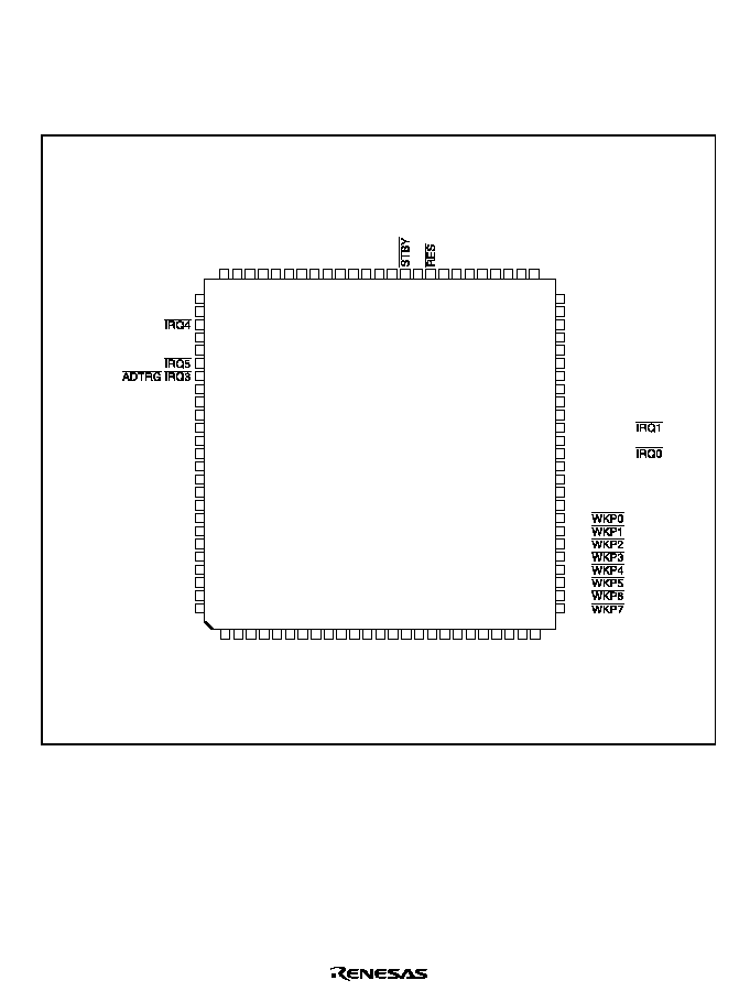
Rev. 2.0, 09/02, page 5 of 658
1.3
Pin Arrangement
Figure 1.3 shows the pin arrangement of the H8S/2268 Series and figure 1.4 shows that of the
H8S/2264 Series.
P30/TxD0
P31/RxD0
P32/SCK0/SDA1/
P33/TxD1/SCL1
P34/RxD1/SDA0
P35/SCK1/SCL0/
PF3/
/
C2
C1
V3
V2
V1
PH3/COM4
PH2/COM3
PH1/COM2
PH0/COM1
PN7/SEG40
PN6/SEG39
PN5/SEG38
PN4/SEG37
PN3/SEG36
PN2/SEG35
PN1/SEG34
PN0/SEG33
PM7/SEG32
76
77
78
79
80
81
82
83
84
85
86
87
88
89
90
91
92
93
94
95
96
97
98
99
100
50
49
48
47
46
45
44
43
42
41
40
39
38
37
36
35
34
33
32
31
30
29
28
27
26
P70/TMRI01/TMCI01
P71/TMRI23/TMCI23
P72/TMO0
P73/TMO1
P74/TMO2
P75/TMO3/SCK2
P76/RxD2
P77/TxD2
MD2
FWE
EXTAL
Vss
XTAL
Vcc
NMI
OSC1
OSC2
MD1
PH7/TONED/TMCI4
AVcc
Vref
P40/AN0
P41/AN1
75
74
73
72
71
70
69
68
67
66
65
64
63
62
61
60
59
58
57
56
55
54
53
52
51
P42/AN2
P43/AN3
P44/AN4
P45/AN5
P46/AN6
P47/AN7
P96/AN8/DA0
P97/AN9/DA1
P17/TIOCB2/TCLKD
P16/TIOCA2/
P14/TIOCA1/
P13/TIOCD0/TCLKB
P12/TIOCC0/TCLKA
P11/TIOCB0
P10/TIOCA0
PJ0/
/SEG1
PJ1/
/SEG2
PJ2/
/SEG3
PJ3/
/SEG4
PJ4/
/SEG5
PJ5/
/SEG6
PJ6/
/SEG7
PJ7/
/SEG8
AVss
P15/TIOCB1/TCLKC
1
2
3
4
5
6
7
8
9
10
11
12
13
14
15
16
17
18
19
20
21
22
23
24
25
PM6/SEG31
PM5/SEG30
PM4/SEG29
PM3/SEG28
PM2/SEG27
PM1/SEG26
PM0/SEG25
PL7/SEG24
PL6/SEG23
PL5/SEG22
PL4/SEG21
PL2/SEG19
PL1/SEG18
PL0/SEG17
PK7/SEG16
PK6/SEG15
PK5/SEG14
PK4/SEG13
PK3/SEG12
PK1/SEG10
PK0/SEG9
CVcc
PL3/SEG20
Vss
PK2/SEG11
FP-100B
TFP-100B
TFP-100G
(TOP VIEW)
Figure 1.3 Pin Arrangement of H8S/2268 Series

Rev. 2.0, 09/02, page 6 of 658
P30/TxD0
P31/RxD0
P32/SCK0/
P33/TxD1
P34/RxD1/SDA0
P35/SCK1/SCL0
PF3/
/
PH5
PH4/
V3
V2
V1
PH3/COM4
PH2/COM3
PH1/COM2
PH0/COM1
SEG40
SEG39
SEG38
SEG37
SEG36
SEG35
SEG34
SEG33
SEG32
76
77
78
79
80
81
82
83
84
85
86
87
88
89
90
91
92
93
94
95
96
97
98
99
100
50
49
48
47
46
45
44
43
42
41
40
39
38
37
36
35
34
33
32
31
30
29
28
27
26
P70/TMRI01/TMCI01
P71
P72/TMO0
P73/TMO1
P74
P75/SCK2
P76/RxD2
P77/TxD2
MD2
FWE
EXTAL
Vss
XTAL
Vcc
NMI
OSC1
OSC2
MD1
PH7
AVcc
Vref
P40/AN0
P41/AN1
75
74
73
72
71
70
69
68
67
66
65
64
63
62
61
60
59
58
57
56
55
54
53
52
51
P42/AN2
P43/AN3
P44/AN4
P45/AN5
P46/AN6
P47/AN7
P96/AN8
P97/AN9
P17/TIOCB2
P16/TIOCA2/
P14/TIOCA1/
P13/TCLKB
P12/TCLKA
P11
P10
PJ0/
/SEG1
PJ1/
/SEG2
PJ2/
/SEG3
PJ3/
/SEG4
PJ4/
/SEG5
PJ5/
/SEG6
PJ6/
/SEG7
PJ7/
/SEG8
AVss
P15/TIOCB1/TCLKC
1
2
3
4
5
6
7
8
9
10
11
12
13
14
15
16
17
18
19
20
21
22
23
24
25
SEG31
SEG30
SEG29
SEG28
SEG27
SEG26
SEG25
PL7/SEG24
PL6/SEG23
PL5/SEG22
PL4/SEG21
PL2/SEG19
PL1/SEG18
PL0/SEG17
PK7/SEG16
PK6/SEG15
PK5/SEG14
PK4/SEG13
PK3/SEG12
PK1/SEG10
PK0/SEG9
CVcc
PL3/SEG20
Vss
PK2/SEG11
FP-100B
TFP-100B
TFP-100G
(TOP VIEW)
Figure 1.4 Pin Arrangement of H8S/2264 Series

Rev. 2.0, 09/02, page 7 of 658
1.4
Pin Functions
Table 1.1 lists the pins functions.
Table 1.1
Pin Functions
Type
Symbol
Pin NO.
I/O
Function
Power
supply
VCC
62
Input
Power supply pin. Connect this pin to the system
power supply.
CVCC
12
Input
Connect this pin to VSS via a 0.1-µF capacitor for
voltage stabilization. Note that applying a voltage
exceeding 4.3 V, the absolute maximum rating, to
the CVCC pin may cause fatal damages on this
LSI. Do not connect the power supply to the
CVCC pin. See section 24, Power Supply Circuit,
for connecting examples.
V3
V2
V1
85
86
87
Input
Power supply pins for the LCD controller/driver.
With an internal power supply division resistor,
these pins are normally left open. Power supply
should be within the range of Vcc
V1
V2
V3
Vss. When the triple step-up voltage circuit
*
2
is
used, the V3 pin is used for the LCD input
reference power supply.
VSS
14
64
Input
Ground pins. Connect this pin to the system power
supply (0V).
Clock
XTAL
63
Input
For connection to a crystal resonator or a ceramic
resonator
*
3
. For examples of crystal or ceramic
*
3
resonator connection and external clock input, see
section 21, Clock Pulse Generator.
EXTAL
65
Input
For connection to a crystal resonator or a ceramic
resonator
*
3
. This pin can be also used for external
clock input. For examples of crystal or ceramic
*
3
resonator connection and external clock input, see
section 21, Clock Pulse Generator.
OSC1
58
Input
Connects to a 32.768 kHz crystal resonator. See
section 21, Clock Pulse Generator, for typical
connection diagrams for a crystal resonator.
OSC2
57
Input
Connects to a 32.768 kHz crystal resonator. See
section 21, Clock Pulse Generator, for typical
connection diagrams for a crystal resonator.
*
1
84
Output
Supplies clock pulses to external devices.

Rev. 2.0, 09/02, page 8 of 658
Type
Symbol
Pin NO.
I/O
Function
Operating
mode
control
MD2,
MD1
67
56
Input
Sets the operating mode. Inputs at these pins
should not be changed during operation. Be sure
to fix the levels of the mode pins (MD2, MD1) by
pull-down or pull-up, except for mode changing.
System
control
5(6
59
Input
Reset input pin. When this pin is low, the chip
enters in the power-on reset state.
67%<
61
Input
When this pin is low, a transition is made to
hardware standby mode.
FWE
66
Input
Enables/disables programming the flash memory.
Interrupts
NMI
60
Input
Nonmaskable interrupt pin. If this pin is not used,
it should be fixed-high.
,54
*
2
,54
,54
,54
,54
81
78
82
40
38
Input
These pins request a maskable interrupt.
:.3
to
:.3
26 to 33
Input
These pins request a wakeup interrupt. This
interrupt is maskable.
16-bit
timer-
pulse unit
(TPU)
TCLKD
*
2
TCLKC
TCLKB
TCLKA
41
39
37
36
Input
These pins input an external clock.
TIOCA0
*
2
TIOCB0
*
2
TIOCC0
*
2
TIOCD0
*
2
34
35
36
37
Input/
Output
Pins for the TGRA_0 to TGRD_0 input capture
input or output compare output, or PWM output.
TIOCA1
TIOCB1
38
39
Input/
Output
Pins for the TGRA
_
1 and TGRB
_
1 input capture
input or output compare output, or PWM output.
TIOCA2
TIOCB2
40
41
Input/
Output
Pins for the TGRA
_
2 and TGRB
_
2 input capture
input or output compare output, or PWM output.
8-bit timer
TMO3
*
2
TMO2
*
2
TMO1
TMO0
70
71
72
73
Output
Compare-match output pins
TMCI23
*
2
TMCI01
TMCI4
*
2
74
75
55
Input
Pins for external clock input to the counter
TMRI23
*
2
TMRI01
74
75
Input
Counter reset input pins.

Rev. 2.0, 09/02, page 9 of 658
Type
Symbol
Pin NO.
I/O
Function
Serial
communi-
cation
TxD2
TxD1
TxD0
68
79
76
Output
Data output pins
Interface
(SCI)/
smart
card
RxD2
RxD1
RxD0
69
80
77
Input
Data input pins
interface
SCK2
SCK1
SCK0
70
81
78
Input/
Output
Clock input/output pins
SCL1
*
2
SCL0
79
81
Input/
Output
I
2
C clock input/output pins.
I
2
C bus
interface
(optional)
SDA1
*
2
SDA0
78
80
Input/
Output
I
2
C data input/output pins.
A/D
converter
AN9 to
AN0
43 to 52
Input
Analog input pins
$'75*
82
Input
Pin for input of an external trigger to start A/D
conversion
D/A
converter
*
2
DA1
DA0
43
44
Output
Analog output pins for the D/A converter
*
2
.
A/D
converter,
D/A
converter
*
2
AVCC
54
Input
Power supply pin for the A/D converter, D/A
converter
*
2
and DTMF generation circuit
*
2
. If
none of the A/D converter, D/A converter
*
2
and
DTMF generation circuit
*
2
is used, connect this
pin to the system power supply (+5 V).
AVSS
42
Input
Ground pin for the A/D converter, D/A
converter
*
2
, and DTMF generator
*
2
. Connect this
pin to the system power supply (0 V).
Vref
53
Input
Reference voltage input pin for the A/D converter
and D/A converter
*
2
. If neither the A/D converter
nor D/A converter
*
2
is used, connect this pin to
the system power supply (+5 V).
LCD
controller/
driver
SEG40
to
SEG 1
92 to
100,
1 to 11,
13, 15 to
33
Output
LCD segment output pins
COM4 to
COM1
88 to 91
Output
LCD common output pins
C2
*
2
C1
*
2
83
84
--
Pins for the step-up voltage capacitor of the LCD
drive power supply.

Rev. 2.0, 09/02, page 10 of 658
Type
Symbol
Pin NO.
I/O
Function
DTMF
generatio
n circuit
*
2
TONED
55
Output
DTMF signal output pin.
I/O ports
P17 to
P10
41 to 34
Input/
Output
8-bit I/O pins
P35 to
P30
81 to 76
Input/
Output
6-bit I/O pins
P47 to
P40
45 to 52
Input
8-bit input pins
P77 to
P70
68 to 75
Input/
Output
8-bit I/O pins
P97
P96
43
44
Input
2-bit input pins
PF3
82
Input/
Output
1-bit I/O pin
PH7
55
Input
1-bit input pin
PH5
*
1
PH4
*
1
83
84
Input/
Output
2-bit I/O pins
PH3 to
PH0
88 to 91
Input/
Output
4-bit I/O pins
PJ7 to
PJ0
26 to 33
Input/
Output
8-bit I/O pins
PK7 to
PK0
18 to 25
Input/
Output
8-bit I/O pins
PL7
PL6
PL5
PL4
PL3
PL2
PL1
PL0
8
9
10
11
13
15
16
17
Input/
Output
8-bit I/O pins
PM7
*
2
PM6
*
2
PM5
*
2
PM4
*
2
PM3
*
2
PM2
*
2
PM1
*
2
PM0
*
2
100
1
2
3
4
5
6
7
Input/
Output
8-bit I/O pins

Rev. 2.0, 09/02, page 11 of 658
Type
Symbol
Pin NO.
I/O
Function
I/O ports
PN7 to
PN0
*
2
92 to 99
Input/
Output
8-bit I/O pins
Notes: 1. Supported only by the H8S/2264 Series.
2. Supported only by the H8S/2268 Series.
3. Supported only by the H8S/2264R and H8S/2262R.

Rev. 2.0, 09/02, page 12 of 658

Rev. 2.0, 09/02, page 13 of 658
Section 2 CPU
The H8S/2000 CPU is a high-speed central processing unit with an internal 32-bit architecture that
is upward-compatible with the H8/300 and H8/300H CPUs. The H8S/2000 CPU has sixteen 16-bit
general registers, can address a 16-Mbyte linear address space, and is ideal for realtime control.
This section describes the H8S/2000 CPU. The usable modes and address spaces differ depending
on the product. For details on each product, refer to section 3, MCU Operating Modes.
2.1
Features
∑
Upward-compatible with H8/300 and H8/300H CPU
Can execute H8/300 and H8/300H CPU object programs
∑
General-register architecture
Sixteen 16-bit general registers also usable as sixteen 8-bit registers or eight 32-bit registers
∑
Sixty-five basic instructions
8/16/32-bit arithmetic and logic instructions
Multiply and divide instructions
Powerful bit-manipulation instructions
∑
Eight addressing modes
Register direct [Rn]
Register indirect [@ERn]
Register indirect with displacement [@(d:16,ERn) or @(d:32,ERn)]
Register indirect with post-increment or pre-decrement [@ERn+ or @≠ERn]
Absolute address [@aa:8, @aa:16, @aa:24, or @aa:32]
Immediate [#xx:8, #xx:16, or #xx:32]
Program-counter relative [@(d:8,PC) or @(d:16,PC)]
Memory indirect [@@aa:8]
∑
16-Mbyte address space
Program: 16 Mbytes
Data:
16 Mbytes
∑
High-speed operation
All frequently-used instructions execute in one or two states
8/16/32-bit register-register add/subtract
: 1 state
8
◊
8-bit register-register multiply
: 12 states
16 ˜ 8-bit register-register divide
: 12 states
16
◊
16-bit register-register multiply : 20 states
32 ˜ 16-bit register-register divide
: 20 states

Rev. 2.0, 09/02, page 14 of 658
∑
Two CPU operating modes
Normal mode*
Advanced mode
∑
Power-down state
Transition to power-down state by a SLEEP instruction
CPU clock speed selection
Note: *
Normal mode is not available in this LSI.
2.1.1
Differences between H8S/2600 CPU and H8S/2000 CPU
The differences between the H8S/2600 CPU and the H8S/2000 CPU are shown below.
∑
Register configuration
The MAC register is supported by the H8S/2600 CPU only.
∑
Basic instructions
The four instructions MAC, CLRMAC, LDMAC, and STMAC are supported by the
H8S/2600 CPU only.
∑
The number of execution states of the MULXU and MULXS instructions;
Execution States
Instruction
Mnemonic
H8S/2600
H8S/2000
MULXU
MULXU.B Rs, Rd
3
12
MULXU.W Rs, ERd
4
20
MULXS
MULXS.B Rs, Rd
4
13
MULXS.W Rs, ERd
5
21
In addition, there are differences in address space, CCR and EXR* register functions, and power-
down modes, etc., depending on the model.
Note: *
Supported only by the H8S/2268 Series.

Rev. 2.0, 09/02, page 15 of 658
2.1.2
Differences from H8/300 CPU
In comparison to the H8/300 CPU, the H8S/2000 CPU has the following enhancements:
∑
More general registers and control registers
Eight 16-bit expanded registers, and one 8-bit and two 32-bit control registers, have been
added.
∑
Expanded address space
Normal mode supports the same 64-kbyte address space as the H8/300 CPU.
Advanced mode supports a maximum 16-Mbyte address space.
∑
Enhanced addressing
The addressing modes have been enhanced to make effective use of the 16-Mbyte address
space.
∑
Enhanced instructions
Addressing modes of bit-manipulation instructions have been enhanced.
Signed multiply and divide instructions have been added.
Two-bit shift instructions have been added.
Instructions for saving and restoring multiple registers have been added.
A test and set instruction has been added.
∑
Higher speed
Basic instructions execute twice as fast.
2.1.3
Differences from H8/300H CPU
In comparison to the H8/300H CPU, the H8S/2000 CPU has the following enhancements:
∑
Additional control register
One 8-bit control registers have been added.
∑
Enhanced instructions
Addressing modes of bit-manipulation instructions have been enhanced.
Two-bit shift instructions have been added.
Instructions for saving and restoring multiple registers have been added.
A test and set instruction has been added.
∑
Higher speed
Basic instructions execute twice as fast.

Rev. 2.0, 09/02, page 16 of 658
2.2
CPU Operating Modes
The H8S/2000 CPU has two operating modes: normal and advanced. Normal mode supports a
maximum 64-kbyte address space. Advanced mode supports a maximum 16-Mbyte total address
space. The mode is selected by the mode pins.
2.2.1
Normal Mode
The exception vector table and stack have the same structure as in the H8/300 CPU.
∑
Address Space
Linear access is provided to a maximum address space of 64 kbytes.
∑
Extended Registers (En)
The extended registers (E0 to E7) can be used as 16-bit registers, or as the upper 16-bit
segments of 32-bit registers. When En is used as a 16-bit register it can contain any value, even
when the corresponding general register (Rn) is used as an address register. If the general
register is referenced in the register indirect addressing mode with pre-decrement (@≠Rn) or
post-increment (@Rn+) and a carry or borrow occurs, however, the value in the corresponding
extended register (En) will be affected.
∑
Instruction Set
All instructions and addressing modes can be used. Only the lower 16 bits of effective
addresses (EA) are valid.
∑
Exception Vector Table and Memory Indirect Branch Addresses
In normal mode the top area starting at H'0000 is allocated to the exception vector table. One
branch address is stored per 16 bits. Figure 2.1 shows the structure of the exception vector
table in normal mode. For details of the exception vector table, see section 4, Exception
Handling.
The memory indirect addressing mode (@@aa:8) employed in the JMP and JSR instructions
uses an 8-bit absolute address included in the instruction code to specify a memory operand
that contains a branch address. In normal mode the operand is a 16-bit word operand,
providing a 16-bit branch address. Branch addresses can be stored in the top area from H'0000
to H'00FF. Note that this area is also used for the exception vector table.
∑
Stack Structure
When the program counter (PC) is pushed onto the stack in a subroutine call, and the PC,
condition-code register (CCR) and extended control register (EXR) are pushed onto the stack
in exception handling, they are stored as shown in figure 2.2. EXR is not pushed onto the stack
in interrupt control mode 0. For details, see section 4, Exception Handling.
Note: *
Normal mode is not available in this LSI.

Rev. 2.0, 09/02, page 17 of 658
H'0000
H'0001
H'0002
H'0003
H'0004
H'0005
H'0006
H'0007
H'0008
H'0009
H'000A
H'000B
Reset exception vector
(Reserved for system use)
Exception vector 1
Exception vector 2
Exception
vector table
Figure 2.1 Exception Vector Table (Normal Mode)
PC
(16 bits)
EXR
*
1
Reserved
*
1
,
*
3
CCR
CCR
*
3
PC
(16 bits)
SP
SP
(SP
*
2
1. When EXR is not used it is not stored on the stack.
2. SP when EXR is not used.
3. lgnored when returning.
Notes:
(b) Exception Handling
(a) Subroutine Branch
)
Figure 2.2 Stack Structure in Normal Mode
2.2.2
Advanced Mode
∑
Address Space
Linear access is provided to a maximum 16-Mbyte address space.
∑
Extended Registers (En)
The extended registers (E0 to E7) can be used as 16-bit registers, or as the upper 16-bit
segments of 32-bit registers or address registers.
∑
Instruction Set
All instructions and addressing modes can be used.

Rev. 2.0, 09/02, page 18 of 658
∑
Exception Vector Table and Memory Indirect Branch Addresses
In advanced mode, the top area starting at H'00000000 is allocated to the exception vector
table in units of 32 bits. In each 32 bits, the upper 8 bits are ignored and a branch address is
stored in the lower 24 bits (figure 2.3). For details of the exception vector table, see section 4,
Exception Handling.
H'00000000
H'00000003
H'00000004
H'0000000B
H'0000000C
H'00000010
H'00000008
H'00000007
Reserved
Reserved
Reset exception vector
Exception vector 3
Exception vector table
Exception vector 1
Figure 2.3 Exception Vector Table (Advanced Mode)
The memory indirect addressing mode (@@aa:8) employed in the JMP and JSR instructions
uses an 8-bit absolute address included in the instruction code to specify a memory operand
that contains a branch address. In advanced mode, the operand is a 32-bit longword operand,
providing a 32-bit branch address. The upper 8 bits of these 32 bits is a reserved area that is
regarded as H'00. Branch addresses can be stored in the area from H'00000000 to H'000000FF.
Note that the first part of this range is also the exception vector table.
∑
Stack Structure
In advanced mode, when the program counter (PC) is pushed onto the stack in a subroutine
call, and the PC, condition-code register (CCR), and extended control register (EXR*) are
pushed onto the stack in exception handling, they are stored as shown in figure 2.4. When
EXR* is invalid, it is not pushed onto the stack. For details, see section 4, Exception Handling.
Note: *
Supported only by the H8S/2268 Series.

Rev. 2.0, 09/02, page 19 of 658
PC
(24 bits)
EXR
*
1
,
*
4
Reserved
*
1
,
*
3
,
*
4
CCR
PC
(24 bits)
SP
SP
(SP
*
2
Reserved
(a) Subroutine Branch
(b) Exception Handling
Notes: 1. When EXR is not used it is not stored on the stack.
2. SP when EXR is not used (The H8S/2264 Series SP always points here).
3. Ignored when returning.
4. Supported only by the H8S/2268 Series.
)
Figure 2.4 Stack Structure in Advanced Mode

Rev. 2.0, 09/02, page 20 of 658
2.3
Address Space
Figure 2.5 shows a memory map of the H8S/2000 CPU. The H8S/2000 CPU provides linear
access to a maximum 64-kbyte address space in normal mode, and a maximum 16-Mbyte
(architecturally 4-Gbyte) address space in advanced mode. The usable modes and address spaces
differ depending on the product. For details on each product, refer to section 3, MCU Operating
Modes.
H'0000
H'FFFF
H'00000000
H'FFFFFFFF
H'00FFFFFF
64-kbyte
16-Mbyte
Program area
Data area
(b) Advanced Mode
(a) Normal Mode
Note: Normal mode is not available in this LSI
Figure 2.5 Memory Map

Rev. 2.0, 09/02, page 21 of 658
2.4
Register Configuration
The H8S/2000 CPU has the internal registers shown in figure 2.6. There are two types of registers:
general registers and control registers. Control registers are a 24-bit program counter (PC), an 8-bit
extended control register (EXR*), and an 8-bit condition code register (CCR).
Note: *
Supported only by the H8S/2268 Series.
T
I2 I1 I0
EXR
*
1
7 6 5 4 3 2 1 0
PC
23
0
15
0 7
0 7
0
E0
E1
E2
E3
E4
E5
E6
E7
R0H
R1H
R2H
R3H
R4H
R5H
R6H
R7H
R0L
R1L
R2L
R3L
R4L
R5L
R6L
R7L
SP
PC
EXR
T
I2 to I0
CCR
I
UI
:Stack pointer
:Program counter
:Extended control register
*
1
:Trace bit
*
1
:Interrupt mask bits
*
1
:Condition-code register
*
1
:Interrupt mask bit
:User bit or interrupt mask bit
*
2
:Half-carry flag
:User bit
:Negative flag
:Zero flag
:Overflow flag
:Carry flag
ER0
ER1
ER2
ER3
ER4
ER5
ER6
ER7 (SP)
I UI H U N Z V C
CCR
7 6 5 4 3 2 1 0
H
U
N
Z
V
C
General Registers (Rn) and Extended Registers (En)
Control Registers (CR)
Legend
- - - -
Notes: 1. Supported only by the H8S/2268 Series.
2. The interrupt mask bit is not available in this LSI.
Figure 2.6 CPU Registers

Rev. 2.0, 09/02, page 22 of 658
2.4.1
General Registers
The H8S/2000 CPU has eight 32-bit general registers. These general registers are all functionally
alike and can be used as both address registers and data registers. When a general register is used
as a data register, it can be accessed as a 32-bit, 16-bit, or 8-bit register. Figure 2.7 illustrates the
usage of the general registers.
When the general registers are used as 32-bit registers or address registers, they are designated by
the letters ER (ER0 to ER7).
The ER registers divide into 16-bit general registers designated by the letters E (E0 to E7) and R
(R0 to R7). These registers are functionally equivalent, providing a maximum sixteen 16-bit
registers. The E registers (E0 to E7) are also referred to as extended registers.
The R registers divide into 8-bit general registers designated by the letters RH (R0H to R7H) and
RL (R0L to R7L). These registers are functionally equivalent, providing a maximum sixteen 8-bit
2egisters.
The usage of each register can be selected independently.
General register ER7 has the function of stack pointer (SP) in addition to its general-register
function, and is used implicitly in exception handling and subroutine calls. Figure 2.8 shows the
stack.
∑ Address registers
∑ 32-bit registers
∑ 16-bit registers
∑ 8-bit registers
ER registers
(ER0 to ER7)
E registers (extended registers)
(E0 to E7)
R registers
(R0 to R7)
RH registers
(R0H to R7H)
RL registers
(R0L to R7L)
Figure 2.7 Usage of General Registers

Rev. 2.0, 09/02, page 23 of 658
SP (ER7)
Free area
Stack area
Figure 2.8 Stack Status
2.4.2
Program Counter (PC)
This 24-bit counter indicates the address of the next instruction the CPU will execute. The length
of all CPU instructions is 2 bytes (one word), so the least significant PC bit is ignored. (When an
instruction is fetched, the least significant PC bit is regarded as 0.)
2.4.3
Extended Control Register (EXR) (H8S/2268 Series Only)
EXR is an 8-bit register that manipulates the LDC, STC, ANDC, ORC, and XORC instructions.
When these instructions except for the STC instruction is executed, all interrupts including NMI
will be masked for three states after execution is completed.
Bit
Bit Name
Initial Value
R/W
Description
7
T
0
R/W
Trace Bit
When this bit is set to 1, a trace exception is
generated each time an instruction is executed.
When this bit is cleared to 0, instructions are
executed in sequence.
6 to 3
1
Reserved
These bits are always read as 1.
2
1
0
I2
I1
I0
1
1
1
R/W
R/W
R/W
These bits designate the interrupt mask level (0 to
7). For details, refer to section 5, Interrupt
Controller.

Rev. 2.0, 09/02, page 24 of 658
2.4.4
Condition-Code Register (CCR)
This 8-bit register contains internal CPU status information, including an interrupt mask bit (I) and
half-carry (H), negative (N), zero (Z), overflow (V), and carry (C) flags.
Operations can be performed on the CCR bits by the LDC, STC, ANDC, ORC, and XORC
instructions. The N, Z, V, and C flags are used as branching conditions for conditional branch
(Bcc) instructions.
Bit
Bit Name
Initial Value
R/W
Description
7
I
1
R/W
Interrupt Mask Bit
Masks interrupts other than NMI when set to 1.
NMI is accepted regardless of the I bit setting.
The I bit is set to 1 by hardware at the start of an
exception-handling sequence. For details, refer to
section 5, Interrupt Controller.
6
UI
undefined
R/W
User Bit or Interrupt Mask Bit
Can be written and read by software using the
LDC, STC, ANDC, ORC, and XORC instructions.
This bit cannot be used as an interrupt mask bit in
this LSI.
5
H
undefined
R/W
Half-Carry Flag
When the ADD.B, ADDX.B, SUB.B, SUBX.B,
CMP.B, or NEG.B instruction is executed, this
flag is set to 1 if there is a carry or borrow at bit 3,
and cleared to 0 otherwise. When the ADD.W,
SUB.W, CMP.W, or NEG.W instruction is
executed, the H flag is set to 1 if there is a carry
or borrow at bit 11, and cleared to 0 otherwise.
When the ADD.L, SUB.L, CMP.L, or NEG.L
instruction is executed, the H flag is set to 1 if
there is a carry or borrow at bit 27, and cleared to
0 otherwise.
4
U
undefined
R/W
User Bit
Can be written and read by software using the
LDC, STC, ANDC, ORC, and XORC instructions.
3
N
undefined
R/W
Negative Flag
Stores the value of the most significant bit of data
as a sign bit.

Rev. 2.0, 09/02, page 25 of 658
Bit
Bit Name
Initial Value
R/W
Description
2
Z
undefined
R/W
Zero Flag
Set to 1 to indicate zero data, and cleared to 0 to
indicate non-zero data.
1
V
undefined
R/W
Overflow Flag
Set to 1 when an arithmetic overflow occurs, and
cleared to 0 at other times.
0
C
undefined
R/W
Carry Flag
Set to 1 when a carry occurs, and cleared to 0
otherwise. Used by:
∑
Add instructions, to indicate a carry
∑
Subtract instructions, to indicate a borrow
∑
Shift and rotate instructions, to indicate a
carry
The carry flag is also used as a bit accumulator
by bit manipulation instructions.
2.4.5
Initial Values of CPU Registers
Reset exception handling loads the CPU's program counter (PC) from the vector table, clears the
trace bit in EXR* to 0, and sets the interrupt mask bits in CCR and EXR* to 1. The other CCR bits
and the general registers are not initialized. In particular, the stack pointer (ER7) is not initialized.
The stack pointer should therefore be initialized by an MOV.L instruction executed immediately
after a reset.
Note: *
Supported only by the H8S/2268 Series.
Rev. 2.0, 09/02, page 26 of 658
2.5
Data Formats
The H8S/2000 CPU can process 1-bit, 4-bit (BCD), 8-bit (byte), 16-bit (word), and 32-bit
(longword) data. Bit-manipulation instructions operate on 1-bit data by accessing bit n (n = 0, 1, 2,
..., 7) of byte operand data. The DAA and DAS decimal-adjust instructions treat byte data as two
digits of 4-bit BCD data.
2.5.1
General Register Data Formats
Figure 2.9 shows the data formats in general registers.
7
0
7
0
MSB
LSB
MSB
LSB
7
0
4 3
Don't care
Don't care
Don't care
7
0
4 3
7
0
Don't care
6 5 4 3 2
7
1 0
7
0
Don't care
6 5 4 3 2
7
1 0
Don't care
RnH
RnL
RnH
RnL
RnH
RnL
Data Type
Register Number
Data Format
Byte data
Byte data
4-bit BCD data
4-bit BCD data
1-bit data
1-bit data
Upper
Lower
Upper
Lower
Figure 2.9 General Register Data Formats (1)

Rev. 2.0, 09/02, page 27 of 658
15
0
MSB
LSB
15
0
MSB
LSB
31
16
MSB
15
0
LSB
En
Rn
ERn
En
Rn
RnH
RnL
MSB
LSB
: General register ER
: General register E
: General register R
: General register RH
: General register RL
: Most significant bit
: Least significant bit
Data Type
Data Format
Register Number
Word data
Word data
Rn
En
Longword data
Legend
ERn
Figure 2.9 General Register Data Formats (2)
Rev. 2.0, 09/02, page 28 of 658
2.5.2
Memory Data Formats
Figure 2.10 shows the data formats in memory. The H8S/2000 CPU can access word data and
longword data in memory, but word or longword data must begin at an even address. If an attempt
is made to access word or longword data at an odd address, no address error occurs but the least
significant bit of the address is regarded as 0, so the access starts at the preceding address. This
also applies to instruction fetches.
When ER7 is used as an address register to access the stack, the operand size should be word or
longword.
7
0
7
6
5
4
3
2
1
0
MSB
LSB
MSB
MSB
LSB
LSB
Data Type
Address
1-bit data
Byte data
Word data
Address L
Address L
Address 2M
Address 2M+1
Longword data
Address 2N
Address 2N+1
Address 2N+2
Address 2N+3
Data Format
Figure 2.10 Memory Data Formats

Rev. 2.0, 09/02, page 29 of 658
2.6
Instruction Set
The H8S/2000 CPU has 65 types of instructions. The instructions are classified by function in
table 2.1.
Table 2.1
Instruction Classification
Function
Instructions
Size
Types
Data transfer
MOV
B/W/L
5
POP
*
1
, PUSH
*
1
W/L
LDM, STM
L
MOVFPE
*
3
, MOVTPE
*
3
B
Arithmetic
ADD, SUB, CMP, NEG
B/W/L
19
operations
ADDX, SUBX, DAA, DAS
B
INC, DEC
B/W/L
ADDS, SUBS
L
MULXU, DIVXU, MULXS, DIVXS
B/W
EXTU, EXTS
W/L
TAS
*
4
B
Logic operations
AND, OR, XOR, NOT
B/W/L
4
Shift
SHAL, SHAR, SHLL, SHLR, ROTL, ROTR, ROTXL, ROTXR
B/W/L
8
Bit manipulation
BSET, BCLR, BNOT, BTST, BLD, BILD, BST, BIST, BAND,
BIAND, BOR, BIOR, BXOR, BIXOR
B
14
Branch
Bcc
*
2
, JMP, BSR, JSR, RTS
5
System control
TRAPA, RTE, SLEEP, LDC, STC, ANDC, ORC, XORC, NOP
9
Block data transfer EEPMOV
1
Total: 65
Notes: B-byte; W-word; L-longword.
1. POP.W Rn and PUSH.W Rn are identical to MOV.W @SP+, Rn and MOV.W Rn,
@-SP. POP.L ERn and PUSH.L ERn are identical to MOV.L @SP+, ERn and MOV.L
ERn, @-SP.
2. Bcc is the general name for conditional branch instructions.
3. Cannot be used in this LSI.
4. Only register ER0, ER1, ER4, or ER5 should be used when using the TAS instruction.

Rev. 2.0, 09/02, page 30 of 658
2.6.1
Table of Instructions Classified by Function
Tables 2.3 to 2.10 summarize the instructions in each functional category. The notation used in
tables 2.3 to 2.10 is defined below.
Table 2.2
Operation Notation
Symbol
Description
Rd
General register (destination)
*
1
Rs
General register (source)
*
1
Rn
General register
*
1
ERn
General register (32-bit register)
(EAd)
Destination operand
(EAs)
Source operand
EXR
Extended control register
*
2
CCR
Condition-code register
N
N (negative) flag in CCR
Z
Z (zero) flag in CCR
V
V (overflow) flag in CCR
C
C (carry) flag in CCR
PC
Program counter
SP
Stack pointer
#IMM
Immediate data
disp
Displacement
+
Addition
≠
Subtraction
◊
Multiplication
˜
Division
Logical AND
Logical OR
Logical XOR
Move
¨
NOT (logical complement)
:8/:16/:24/:32
8-, 16-, 24-, or 32-bit length
Notes: 1. General registers include 8-bit registers (R0H to R7H, R0L to R7L), 16-bit registers (R0
to R7, E0 to E7), and 32-bit registers (ER0 to ER7).
2. Supported only by the H8S/2268 Series.

Rev. 2.0, 09/02, page 31 of 658
Table 2.3
Data Transfer Instructions
Instruction
Size
*
Function
MOV
B/W/L
(EAs)
Rd, Rs
(EAd)
Moves data between two general registers or between a general register
and memory, or moves immediate data to a general register.
MOVFPE
B
Cannot be used in this LSI.
MOVTPE
B
Cannot be used in this LSI.
POP
W/L
@SP+
Rn
Pops a general register from the stack. POP.W Rn is identical to MOV.W
@SP+, Rn. POP.L ERn is identical to MOV.L @SP+, ERn.
PUSH
W/L
Rn
@≠SP
Pushes a general register onto the stack. PUSH.W Rn is identical to
MOV.W Rn, @≠SP. PUSH.L ERn is identical to MOV.L ERn, @≠SP.
LDM
L
@SP+
Rn (register list)
Pops two or more general registers from the stack.
STM
L
Rn (register list)
@≠SP
Pushes two or more general registers onto the stack.
Note:
*
Refers to the operand size.
B: Byte
W: Word
L: Longword

Rev. 2.0, 09/02, page 32 of 658
Table 2.4
Arithmetic Operations Instructions (1)
Instruction
Size
*
Function
ADD
SUB
B/W/L
Rd ± Rs
Rd, Rd ± #IMM
Rd
Performs addition or subtraction on data in two general registers, or on
immediate data and data in a general register (immediate byte data
cannot be subtracted from byte data in a general register. Use the SUBX
or ADD instruction.)
ADDX
SUBX
B
Rd ± Rs ± C
Rd, Rd ± #IMM ± C
Rd
Performs addition or subtraction with carry on byte data in two general
registers, or on immediate data and data in a general register.
INC
DEC
B/W/L
Rd ± 1
Rd, Rd ± 2
Rd
Increments or decrements a general register by 1 or 2. (Byte operands
can be incremented or decremented by 1 only.)
ADDS
SUBS
L
Rd ± 1
Rd, Rd ± 2
Rd, Rd ± 4
Rd
Adds or subtracts the value 1, 2, or 4 to or from data in a 32-bit register.
DAA
DAS
B
Rd decimal adjust
Rd
Decimal-adjusts an addition or subtraction result in a general register by
referring to the CCR to produce 4-bit BCD data.
MULXU
B/W
Rd
◊
Rs
Rd
Performs unsigned multiplication on data in two general registers: either
8 bits
◊
8 bits
16 bits or 16 bits
◊
16 bits
32 bits.
MULXS
B/W
Rd
◊
Rs
Rd
Performs signed multiplication on data in two general registers: either 8
bits
◊
8 bits
16 bits or 16 bits
◊
16 bits
32 bits.
DIVXU
B/W
Rd ˜ Rs
Rd
Performs unsigned division on data in two general registers: either 16
bits ˜ 8 bits
8-bit quotient and 8-bit remainder or 32 bits ˜ 16 bits
16-bit quotient and 16-bit remainder.
Note:
*
Refers to the operand size.
B: Byte
W: Word
L: Longword

Rev. 2.0, 09/02, page 33 of 658
Table 2.4
Arithmetic Operations Instructions (2)
Instruction
Size
*
1
Function
DIVXS
B/W
Rd ˜ Rs
Rd
Performs signed division on data in two general registers: either 16 bits ˜
8 bits
8-bit quotient and 8-bit remainder or 32 bits ˜ 16 bits
16-bit
quotient and 16-bit remainder.
CMP
B/W/L
Rd ≠ Rs, Rd ≠ #IMM
Compares data in a general register with data in another general register
or with immediate data, and sets CCR bits according to the result.
NEG
B/W/L
0 ≠ Rd
Rd
Takes the two's complement (arithmetic complement) of data in a
general register.
EXTU
W/L
Rd (zero extension)
Rd
Extends the lower 8 bits of a 16-bit register to word size, or the lower 16
bits of a 32-bit register to longword size, by padding with zeros on the
left.
EXTS
W/L
Rd (sign extension)
Rd
Extends the lower 8 bits of a 16-bit register to word size, or the lower 16
bits of a 32-bit register to longword size, by extending the sign bit.
TAS
*
2
B
@ERd ≠ 0, 1
(<bit 7> of @ERd)
Tests memory contents, and sets the most significant bit (bit 7) to 1.
Notes: 1. Refers to the operand size.
B: Byte
W: Word
L: Longword
2. Only register ER0, ER1, ER4, or ER5 should be used when using the TAS instruction.

Rev. 2.0, 09/02, page 34 of 658
Table 2.5
Logic Operations Instructions
Instruction
Size
*
Function
AND
B/W/L
Rd
Rs
Rd, Rd
#IMM
Rd
Performs a logical AND operation on a general register and another
general register or immediate data.
OR
B/W/L
Rd
Rs
Rd, Rd
#IMM
Rd
Performs a logical OR operation on a general register and another
general register or immediate data.
XOR
B/W/L
Rd
Rs
Rd, Rd
#IMM
Rd
Performs a logical exclusive OR operation on a general register and
another general register or immediate data.
NOT
B/W/L
¨ (Rd)
(Rd)
Takes the one's complement of general register contents.
Note:
*
Refers to the operand size.
B: Byte
W: Word
L: Longword
Table 2.6
Shift Instructions
Instruction
Size
*
Function
SHAL
SHAR
B/W/L
Rd (shift)
Rd
Performs an arithmetic shift on general register contents.
1-bit or 2-bit shifts are possible.
SHLL
SHLR
B/W/L
Rd (shift)
Rd
Performs a logical shift on general register contents.
1-bit or 2-bit shifts are possible.
ROTL
ROTR
B/W/L
Rd (rotate)
Rd
Rotates general register contents.
1-bit or 2-bit rotations are possible.
ROTXL
ROTXR
B/W/L
Rd (rotate)
Rd
Rotates general register contents through the carry flag.
1-bit or 2-bit rotations are possible.
Note:
*
Refers to the operand size.
B: Byte
W: Word
L: Longword

Rev. 2.0, 09/02, page 35 of 658
Table 2.7
Bit Manipulation Instructions (1)
Instruction
Size
*
Function
BSET
B
1
(<bit-No.> of <EAd>)
Sets a specified bit in a general register or memory operand to 1. The bit
number is specified by 3-bit immediate data or the lower three bits of a
general register.
BCLR
B
0
(<bit-No.> of <EAd>)
Clears a specified bit in a general register or memory operand to 0. The
bit number is specified by 3-bit immediate data or the lower three bits of a
general register.
BNOT
B
¨ (<bit-No.> of <EAd>)
(<bit-No.> of <EAd>)
Inverts a specified bit in a general register or memory operand. The bit
number is specified by 3-bit immediate data or the lower three bits of a
general register.
BTST
B
¨ (<bit-No.> of <EAd>)
Z
Tests a specified bit in a general register or memory operand and sets or
clears the Z flag accordingly. The bit number is specified by 3-bit
immediate data or the lower three bits of a general register.
BAND
BIAND
B
B
C
(<bit-No.> of <EAd>)
C
ANDs the carry flag with a specified bit in a general register or memory
operand and stores the result in the carry flag.
C
¨ (<bit-No.> of <EAd>)
C
ANDs the carry flag with the inverse of a specified bit in a general
register or memory operand and stores the result in the carry flag.
The bit number is specified by 3-bit immediate data.
BOR
BIOR
B
B
C
(<bit-No.> of <EAd>)
C
ORs the carry flag with a specified bit in a general register or memory
operand and stores the result in the carry flag.
C
¨ (<bit-No.> of <EAd>)
C
ORs the carry flag with the inverse of a specified bit in a general register
or memory operand and stores the result in the carry flag.
The bit number is specified by 3-bit immediate data.
Note:
*
Refers to the operand size.
B: Byte

Rev. 2.0, 09/02, page 36 of 658
Table 2.7
Bit Manipulation Instructions (2)
Instruction
Size
*
Function
BXOR
BIXOR
B
B
C
(<bit-No.> of <EAd>)
C
XORs the carry flag with a specified bit in a general register or memory
operand and stores the result in the carry flag.
C
¨ (<bit-No.> of <EAd>)
C
XORs the carry flag with the inverse of a specified bit in a general
register or memory operand and stores the result in the carry flag.
The bit number is specified by 3-bit immediate data.
BLD
BILD
B
B
(<bit-No.> of <EAd>)
C
Transfers a specified bit in a general register or memory operand to the
carry flag.
¨ (<bit-No.> of <EAd>)
C
Transfers the inverse of a specified bit in a general register or memory
operand to the carry flag.
The bit number is specified by 3-bit immediate data.
BST
BIST
B
B
C
(<bit-No.> of <EAd>)
Transfers the carry flag value to a specified bit in a general register or
memory operand.
¨ C
(<bit-No.> of <EAd>)
Transfers the inverse of the carry flag value to a specified bit in a general
register or memory operand.
The bit number is specified by 3-bit immediate data.
Note:
*
Refers to the operand size.
B: Byte

Rev. 2.0, 09/02, page 37 of 658
Table 2.8
Branch Instructions
Instruction
Size
Function
Bcc
Branches to a specified address if a specified condition is true. The
branching conditions are listed below.
Mnemonic
Description
Condition
BRA(BT)
Always (true)
Always
BRN(BF)
Never (false)
Never
BHI
High
C
Z = 0
BLS
Low or same
C
Z = 1
BCC(BHS)
Carry clear
(high or same)
C = 0
BCS(BLO)
Carry set (low)
C = 1
BNE
Not equal
Z = 0
BEQ
Equal
Z = 1
BVC
Overflow clear
V = 0
BVS
Overflow set
V = 1
BPL
Plus
N = 0
BMI
Minus
N = 1
BGE
Greater or equal
N
V = 0
BLT
Less than
N
V = 1
BGT
Greater than
Z
(N
V) = 0
BLE
Less or equal
Z
(N
V) = 1
JMP
Branches unconditionally to a specified address.
BSR
Branches to a subroutine at a specified address.
JSR
Branches to a subroutine at a specified address.
RTS
Returns from a subroutine

Rev. 2.0, 09/02, page 38 of 658
Table 2.9
System Control Instructions
Instruction
Size
*
1
Function
TRAPA
Starts trap-instruction exception handling.
RTE
Returns from an exception-handling routine.
SLEEP
Causes a transition to a power-down state.
LDC
B/W
(EAs)
CCR, (EAs)
EXR
*
2
Moves the source operand contents or immediate data to CCR or EXR
*
2
.
Although CCR and EXR
*
2
are 8-bit registers, word-size transfers are
performed between them and memory. The upper 8 bits are valid.
STC
B/W
CCR
(EAd), EXR
*
2
(EAd)
Transfers CCR or EXR
*
2
contents to a general register or memory.
Although CCR and EXR
*
2
are 8-bit registers, word-size transfers are
performed between them and memory. The upper 8 bits are valid.
ANDC
B
CCR
#IMM
CCR, EXR
#IMM
EXR
*
2
Logically ANDs the CCR or EXR
*
2
contents with immediate data.
ORC
B
CCR
#IMM
CCR, EXR
#IMM
EXR
*
2
Logically ORs the CCR or EXR
*
2
contents with immediate data.
XORC
B
CCR
#IMM
CCR, EXR
#IMM
EXR
*
2
Logically XORs the CCR or EXR
*
2
contents with immediate data.
NOP
PC + 2
PC
Only increments the program counter.
Notes: 1. Refers to the operand size.
B: Byte
W: Word
2. Supported only by the H8S/2268 Series.

Rev. 2.0, 09/02, page 39 of 658
Table 2.10
Block Data Transfer Instructions
Instruction
Size
Function
EEPMOV.B
if R4L
0 then
Repeat @ER5+
@ER6+
R4L≠1
R4L
Until R4L = 0
else next;
EEPMOV.W
if R4
0 then
Repeat @ER5+ ∑ @ER6+
R4≠1 ∑ R4
Until R4 = 0
else next;
Transfers a data block. Starting from the address set in ER5, transfers
data for the number of bytes set in R4L or R4 to the address location set
in ER6.
Execution of the next instruction begins as soon as the transfer is
completed.
2.6.2
Basic Instruction Formats
This LSI instructions consist of 2-byte (1-word) units. An instruction consists of an operation field
(op field), a register field (r field), an effective address extension (EA field), and a condition field
(cc).
Figure 2.11 shows examples of instruction formats.
∑
Operation Field
Indicates the function of the instruction, the addressing mode, and the operation to be carried
out on the operand. The operation field always includes the first four bits of the instruction.
Some instructions have two operation fields.
∑
Register Field
Specifies a general register. Address registers are specified by 3 bits, and data registers by 3
bits or 4 bits. Some instructions have two register fields. Some have no register field.
∑
Effective Address Extension
8, 16, or 32 bits specifying immediate data, an absolute address, or a displacement.
∑
Condition Field
Specifies the branching condition of Bcc instructions.
Rev. 2.0, 09/02, page 40 of 658
op
op
r n
r m
NOP, RTS, etc.
ADD.B Rn, Rm, etc.
MOV.B @(d:16, Rn), Rm, etc.
r n
r m
op
EA(disp)
op
cc
EA(disp)
BRA d:16, etc.
(1) Operation field only
(2) Operation field and register fields
(3) Operation field, register fields, and effective address extension
(4) Operation field, effective address extension, and condition field
Figure 2.11 Instruction Formats (Examples)
2.7
Addressing Modes and Effective Address Calculation
The H8S/2000 CPU supports the eight addressing modes listed in table 2.11. Each instruction uses
a subset of these addressing modes. Arithmetic and logic instructions can use the register direct
and immediate modes. Data transfer instructions can use all addressing modes except program-
counter relative and memory indirect. Bit manipulation instructions use register direct, register
indirect, or the absolute addressing mode to specify an operand, and register direct (BSET, BCLR,
BNOT, and BTST instructions) or immediate (3-bit) addressing mode to specify a bit number in
the operand.
Table 2.11
Addressing Modes
No.
Addressing Mode
Symbol
1
Register direct
Rn
2
Register indirect
@ERn
3
Register indirect with displacement
@(d:16,ERn)/@(d:32,ERn)
4
Register indirect with post-increment
Register indirect with pre-decrement
@ERn+
@≠ERn
5
Absolute address
@aa:8/@aa:16/@aa:24/@aa:32
6
Immediate
#xx:8/#xx:16/#xx:32
7
Program-counter relative
@(d:8,PC)/@(d:16,PC)
8
Memory indirect
@@aa:8

Rev. 2.0, 09/02, page 41 of 658
2.7.1
Register Direct
Rn
The register field of the instruction specifies an 8-, 16-, or 32-bit general register containing the
operand. R0H to R7H and R0L to R7L can be specified as 8-bit registers. R0 to R7 and E0 to E7
can be specified as 16-bit registers. ER0 to ER7 can be specified as 32-bit registers.
2.7.2
Register Indirect
@ERn
The register field of the instruction code specifies an address register (ERn) which contains the
address of the operand on memory. If the address is a program instruction address, the lower 24
bits are valid and the upper 8 bits are all assumed to be 0 (H'00).
2.7.3
Register Indirect with Displacement
@(d:16, ERn) or @(d:32, ERn)
A 16-bit or 32-bit displacement contained in the instruction is added to an address register (ERn)
specified by the register field of the instruction, and the sum gives the address of a memory
operand. A 16-bit displacement is sign-extended when added.
2.7.4
Register Indirect with Post-Increment or Pre-Decrement
@ERn+ or @-ERn
Register indirect with post-increment
@ERn+: The register field of the instruction code
specifies an address register (ERn) which contains the address of a memory operand. After the
operand is accessed, 1, 2, or 4 is added to the address register contents and the sum is stored in the
address register. The value added is 1 for byte access, 2 for word transfer instruction, or 4 for
longword transfer instruction. For the word or longword transfer instructions, the register value
should be even.
Register indirect with pre-decrement
@-ERn: The value 1, 2, or 4 is subtracted from an
address register (ERn) specified by the register field in the instruction code, and the result is the
address of a memory operand. The result is also stored in the address register. The value
subtracted is 1 for byte access, 2 for word transfer instruction, or 4 for longword transfer
instruction. For the word or longword transfer instructions, the register value should be even.
2.7.5
Absolute Address
@aa:8, @aa:16, @aa:24, or @aa:32
The instruction code contains the absolute address of a memory operand. The absolute address
may be 8 bits long (@aa:8), 16 bits long (@aa:16), 24 bits long (@aa:24), or 32 bits long
(@aa:32). Table 2.12 indicates the accessible absolute address ranges.
To access data, the absolute address should be 8 bits (@aa:8), 16 bits (@aa:16), or 32 bits
(@aa:32) long. For an 8-bit absolute address, the upper 24 bits are all assumed to be 1 (H'FFFF).
For a 16-bit absolute address the upper 16 bits are a sign extension. A 32-bit absolute address can
access the entire address space.

Rev. 2.0, 09/02, page 42 of 658
A 24-bit absolute address (@aa:24) indicates the address of a program instruction. The upper 8
bits are all assumed to be 0 (H'00).
Table 2.12
Absolute Address Access Ranges
Absolute Address
Normal Mode
*
Advanced Mode
Data address
8 bits (@aa:8)
H'FF00 to H'FFFF
H'FFFF00 to H'FFFFFF
16 bits (@aa:16)
H'0000 to H'FFFF
H'000000 to H'007FFF,
H'FF8000 to H'FFFFFF
32 bits (@aa:32)
H'000000 to H'FFFFFF
Program instruction
address
24 bits (@aa:24)
Note:
*
Normal mode is not available in this LSI.
2.7.6
Immediate
#xx:8, #xx:16, or #xx:32
The instruction contains 8-bit (#xx:8), 16-bit (#xx:16), or 32-bit (#xx:32) immediate data as an
operand.
The ADDS, SUBS, INC and DEC instructions contain immediate data implicitly. Some bit
manipulation instructions contain 3-bit immediate data in the instruction code, specifying a bit
number. The TRAPA instruction contains 2-bit immediate data in its instruction code, specifying a
vector address.
2.7.7
Program-Counter Relative
@(d:8, PC) or @(d:16, PC)
This mode is used in the Bcc and BSR instructions. An 8-bit or 16-bit displacement contained in
the instruction is sign-extended and added to the 24-bit PC contents to generate a branch address.
Only the lower 24 bits of this branch address are valid; the upper 8 bits are all assumed to be 0
(H'00). The PC value to which the displacement is added is the address of the first byte of the next
instruction, so the possible branching range is ≠126 to +128 bytes (≠63 to +64 words) or ≠32766 to
+32768 bytes (≠16383 to +16384 words) from the branch instruction. The resulting value should
be an even number.
2.7.8
Memory Indirect
@@aa:8
This mode can be used by the JMP and JSR instructions. The instruction code contains an 8-bit
absolute address specifying a memory operand. This memory operand contains a branch address.
The upper bits of the absolute address are all assumed to be 0, so the address range is 0 to 255
(H'0000 to H'00FF in normal mode*, H'000000 to H'0000FF in advanced mode). In normal mode,
the memory operand is a word operand and the branch address is 16 bits long. In advanced mode,
the memory operand is a longword operand, the first byte of which is assumed to be 0 (H'00).

Rev. 2.0, 09/02, page 43 of 658
Note that the first part of the address range is also the exception vector area. For further details,
refer to section 4, Exception Handling.
If an odd address is specified in word or longword memory access, or as a branch address, the
least significant bit is regarded as 0, causing data to be accessed or instruction code to be fetched
at the address preceding the specified address. (For further information, see section 2.5.2, Memory
Data Formats.)
Note: *
Normal mode is not available in this LSI.
Specified
by @aa:8
Specified
by @aa:8
Branch address
Branch address
Reserved
(a) Normal Mode
*
(a) Advanced Mode
Note:
*
Normal mode is not available in this LSI.
Figure 2.12 Branch Address Specification in Memory Indirect Mode
2.7.9
Effective Address Calculation
Table 2.13 indicates how effective addresses are calculated in each addressing mode. In normal
mode the upper 8 bits of the effective address are ignored in order to generate a 16-bit address.

Rev. 2.0, 09/02, page 44 of 658
Table 2.13
Effective Address Calculation (1)
No
1
Offset
1
2
4
r
op
31
0
31
23
2
3
Register indirect with displacement
@(d:16,ERn) or @(d:32,ERn)
4
r
op
disp
r
op
rm
op
rn
31
0
31
0
r
op
Don't care
31
23
31
0
Don't care
31
0
disp
31
0
31
0
31
23
31
0
Don't care
31
23
31
0
Don't care
24
24
24
24
Addressing Mode and Instruction Format
Effective Address Calculation
Effective Address (EA)
Register direct(Rn)
General register contents
General register contents
General register contents
General register contents
Sign extension
Register indirect(@ERn)
Register indirect with post-increment or
pre-decrement
∑Register indirect with post-increment @ERn+
∑Register indirect with pre-decrement @-ERn
1, 2, or 4
1, 2, or 4
Operand Size
Byte
Word
Longword
Operand is general register contents.

Rev. 2.0, 09/02, page 45 of 658
Table 2.13
Effective Address Calculation (2)
No
5
op
31
23
31
0
Don't care
abs
@aa:8
7
H'FFFF
op
31
23
31
0
Don't care
@aa:16
op
@aa:24
@aa:32
abs
15
16
31
23
31
0
Don't care
31
23
31
0
Don't care
abs
op
abs
6
op
IMM
#xx:8/#xx:16/#xx:32
8
24
24
24
24
Addressing Mode and Instruction Format
Absolute address
Immediate
Effective Address Calculation
Effective Address (EA)
Sign extension
Operand is immediate data.
31
23
7
Program-counter relative
@(d:8,PC) @(d:16,PC)
Memory indirect @@aa:8
∑ Normal mode*
∑ Advanced mode
31
0
Don't care
23
0
disp
0
31
23
31
0
Don't care
disp
op
23
op
8
abs
31
0
abs
H'000000
7
8
0
15
31
23
31
0
Don't care
15
H'00
16
op
abs
31
0
abs
H'000000
7
8
0
31
24
24
24
Note:
*
Normal mode is not available in this LSI.
PC contents
Sign
extension
Memory contents
Memory contents

Rev. 2.0, 09/02, page 46 of 658
2.8
Processing States
The H8S/2000 CPU has five main processing states: the reset state, exception handling state,
program execution state, bus-released state, and power-down state. Figure 2.13 indicates the state
transitions.
∑
Reset State
In this state, the CPU and all on-chip peripheral modules are initialized and not operating.
When the
#$ input goes low, all current processing stops and the CPU enters the reset state.
All interrupts are masked in the reset state. Reset exception handling starts when the
#$
signal changes from low to high. For details, refer to section 4, Exception Handling and section
23, Power-On Reset Circuit*.
The reset state can also be entered by a watchdog timer overflow.
Note: *
Supported only by the H8S/2264 Series.
∑
Exception-Handling State
The exception-handling state is a transient state that occurs when the CPU alters the normal
processing flow due to an exception source, such as a reset, trace, interrupt, or trap instruction.
The CPU fetches a start address (vector) from the exception vector table and branches to that
address. For further details, refer to section 4, Exception Handling.
∑
Program Execution State
In this state, the CPU executes program instructions in sequence.
∑
Bus-Released State (H8S/2268 Series only)
In a product which has a bus master other than the CPU, such as a data transfer controller
(DTC), the bus-released state occurs when the bus has been released in response to a bus
request from a bus master other than the CPU.
While the bus is released, the CPU halts operations.
∑
Power-down State
This is a power-down state in which the CPU stops operating. The program stop state occurs
when a SLEEP instruction is executed or the CPU enters hardware standby mode. For further
details, refer to section 22, Power-Down Modes.

Rev. 2.0, 09/02, page 47 of 658
Exception handling state
Bus-released state
*
4
Hardware standby mode
*
2
Software standby mode
Reset state
*
1
Sleep mode
Power-down state
*
3
Program execution state
End of bus request
*
4
Bus request
*
4
Interrupt request
External interrupt request
= High
Request for exception handling
= High,
= Low
End of bus
request
*
4
Bus request
*
4
SLEEP instruction,
SSBY = 0
SLEEP instruction,
SSBY = 1
Notes: 1.
2.
3.
4.
From any state except hardware standby mode, a transition to the reset state occurs whenever
goes low. A transition can also be made to the reset state when the
watchdog timer overflows.
From any state, a transition to hardware standby mode occurs when
goes low.
Apart from these states, there are also the watch mode, subactive mode, and the subsleep mode.
See section 22, Power-Down Modes.
Supported only by the H8S/2268 Series.
End of exception
handling
Figure 2.13 State Transitions

Rev. 2.0, 09/02, page 48 of 658
2.9
Usage Notes
2.9.1
TAS Instruction
Only register ER0, ER1, ER4, or ER5 should be used when using the TAS instruction. The TAS
instruction is not generated by the Hitachi H8S and H8/300 Series C/C++ compilers. If the TAS
instruction is used as a user-defined intrinsic function, ensure that only register ER0, ER1, ER4, or
ER5 is used.
2.9.2
STM/LDM Instruction
With the STM or LDM instruction, the ER7 register is used as the stack pointer, and thus cannot
be used as a register that allows save (STM) or restore (LDM) operation.
With a single STM or LDM instruction, two to four registers can be saved or restored. The
available registers are as follows:
For two registers: ER0 and ER1, ER2 and ER3, or ER4 and ER5
For three registers: ER0 to ER2, or ER4 to ER6
For four registers: ER0 to ER3
For the Hitachi H8S or H8/300 Series C/C++ Compiler, the STM/LDM instruction including ER7
is not created.
2.9.3
Bit Manipulation Instructions
The BSET, BCLR, BNOT, BST, and BIST instructions are used to read data in byte-wise, operate
the data in bit-wise, and write the result of the bit-wise operation in bit-wise again. Therefore,
special care is necessary to use these instructions for the registers and the ports that include write-
only bit.
The BCLR instruction can be used to clear to 0 the flags in the internal I/O registers. In this time,
if it is obvious that the flag has been set to 1 in the interrupt handler, there is no need to read the
flag beforehand.

Rev. 2.0, 09/02, page 49 of 658
Section 3 MCU Operating Modes
3.1
Operating Mode Selection
This LSI supports only operating mode 7, that is, the advanced single-chip mode. The operating
mode is determined by the setting of the mode pins (MD2 and MD1). Only mode 7 can be used in
this LSI. The H8S/2268 Series does not include power-on reset circuit. Therefore, all mode pins
must be fixed high. While the H8S/2264 Series includes a power-on reset circuit.. The power-on
reset circuit can be enabled/disabled by mode pin settings.
Do not change the mode pin settings during operation.
Table 3.1
MCU Operating Mode Selection
External Data Bus
MCU
Operating
Mode
MD2 MD1
CPU
Operating
Mode
Description
On-Chip
ROM
Initial
Width
Max.
Width
Power-on reset
circuit
7
1
1
Advanced
mode
Single-chip
mode
Enabled
Disabled
7
0
1
Advanced
mode
Single-chip
mode
Enabled
Enabled
*
Note:
*
Supported only by the H8S/2264 series.
3.2
Register Description
The following registers are related to the operating mode.
∑
Mode control register (MDCR)

Rev. 2.0, 09/02, page 50 of 658
3.2.1
Mode Control Register (MDCR)
MDCR monitors the current operating mode.
Bit
Bit
Name
Initial Value
R/W
Descriptions
7
1
R/W
Reserved
This bit is always read as 1 and cannot be modified.
6 to 3
All 0
Reserved
These bits are always read as 0 and cannot be
modified.
2
1
MDS2
MDS1
R
R
Mode Select 2 and 1
These bits indicate the input levels at pins MD2 and
MD1 (the current operating mode). Bits MDS2 and
MDS1 correspond to MD2 and MD1, respectively.
MDS2 and MDS1 are read-only bits and they cannot
be written to. The mode pin (MD2 and MD1) input
levels are latched into these bits when MDCR is
read. These latches are canceled by a reset. These
latches are canceled by a reset.
0
1
Reserved
This bit is always read as 1 and cannot be modified.
3.3
Operating Mode
The CPU can access a 16-Mbyte address space in advanced mode. On-chip ROM is valid and the
external address cannot be used.
3.4
Pin Functions in Each Operating Mode
For details on pin functions in each operating mode, refer to section 1, Overview.
Rev. 2.0, 09/02, page 51 of 658
3.5
Address Map
Figures 3.1 and 3.2 show the address map in each operating mode.
H'000000
H'FFB000
H'03FFFF
H'000000
H'01FFFF
H'FFD000
H'FFEFBF
H'FFEFBF
H'FFF800
H'FFF800
H'FFFF3F
H'FFFF3F
H'FFFF60
H'FFFF60
H'FFFFC0
H'FFFFC0
H'FFFFFF
H'FFFFFF
H8S/2268
H8S/2266
ROM: 128 kbytes,
RAM: 8 kbytes
Mode 7
Advanced single-chip mode
On-chip RAM
On-chip RAM
On-chip RAM
Internal I/O registers
Internal I/O registers
ROM: 256 kbytes,
RAM: 16 kbytes
Mode 7
Advanced single-chip mode
On-chip RAM
On-chip RAM
On-chip RAM
Internal I/O registers
Internal I/O registers
Figure 3.1 Address Map (1)

Rev. 2.0, 09/02, page 52 of 658
H'00FFFF
H'000000
H'FFE800
H'FFEFBF
H'FFF800
H'FFFF3F
H'FFFF60
H'FFFFC0
H'FFFFFF
H8S/2262 and H8S/2262R
ROM: 64 kbytes,
RAM: 2 kbytes
Mode 7
Advanced single-chip mode
On-chip RAM
On-chip RAM
On-chip RAM
Internal I/O registers
Internal I/O registers
H'01FFFF
H'000000
H'FFE000
H'FFEFBF
H'FFF800
H'FFFF3F
H'FFFF60
H'FFFFC0
H'FFFFFF
H8S/2265, H8S/2264, and H8S/2264R
ROM: 128 kbytes,
RAM: 4 kbytes
Mode 7
Advanced single-chip mode
On-chip RAM
On-chip RAM
On-chip RAM
Internal I/O registers
Internal I/O registers
Figure 3.2 Address Map (2)

Rev. 2.0, 09/02, page 53 of 658
Section 4 Exception Handling
4.1
Exception Handling Types and Priority
As table 4.1 indicates, exception handling may be caused by a reset, trace*, trap instruction, or
interrupt. Exception handling is prioritized as shown in table 4.1. If two or more exceptions occur
simultaneously, they are accepted and processed in order of priority. Trap instruction exception
handling requests are accepted at all times in program execution state.
Exception sources, the stack structure, and operation of the CPU vary depending on the interrupt
control mode set by the INTM0 and INTM1 bits in SYSCR.
Table 4.1
Exception Types and Priority
Priority
Exception Type
Start of Exception Handling
High
Reset
Starts immediately after a low-to-high transition at the
#$
pin, or when the watchdog timer overflows. The CPU enters
the reset state when the
#$
pin is low.
Trace
*
Starts when execution of the current instruction or exception
handling ends, if the trace (T) bit in the EXR is set to 1.
Traces are enabled only in interrupt control mode 2. Trace
exception handling is not executed after execution of an
RTE instruction.
Interrupt
Starts when execution of the current instruction or exception
handling ends, if an interrupt request has been issued.
Interrupt detection is not performed on completion of ANDC,
ORC, XORC, or LDC instruction execution, or on
completion of reset exception handling.
Low
Trap instruction
Started by execution of a trap instruction (TRAPA). Trap
instruction exception handling requests are accepted at all
times in program execution state.
Note:
*
Supported only by the H8S/2268 Series.

Rev. 2.0, 09/02, page 54 of 658
4.2
Exception Sources and Exception Vector Table
Different vector addresses are assigned to different exception sources. Table 4.2 lists the exception
sources and their vector addresses.
Table 4.2
Exception Handling Vector Table
Exception Source
Vector Number
Vector Address Advanced Mode
*
1
Reset
0
H'0000 to H'0003
Reserved for system use
1
H'0004 to H'0007
2
H'0008 to H'000B
3
H'000C to H'000F
4
H'0010 to H'0013
Trace
*
4
5
H'0014 to H'0017
Direct transitions
*
3
6
H'0018 to H'001B
External interrupt (NMI)
7
H'001C to H'001F
Trap instruction (four sources)
8
H'0020 to H'0023
9
H'0024 to H'0027
10
H'0028 to H'002B
11
H'002C to H'002F
Reserved for system use
12
H'0030 to H'0033
13
H'0034 to H'0037
14
H'0038 to H'003B
15
H'003C to H'003F
External interrupt
IRQ0
16
H'0040 to H'0043
IRQ1
17
H'0044 to H'0047
Reserved for system use
18
H'0048 to H'004B
External interrupt
IRQ3
19
H'004C to H'004F
IRQ4
20
H'0050 to H'0053
IRQ5
*
4
21
H'0054 to H'0057

Rev. 2.0, 09/02, page 55 of 658
Exception Source
Vector Number
Vector Address Advanced Mode
*
1
Reserved for system use
22
H'0058 to H'005B
23
H'005C to H'005F
Internal interrupt
*
2
24
107
H'0060 to H'0063
H'01AC to H'01AF
External interrupt
WKP0 to WKP7
108
H'01B0 to H'01B3
Internal interrupt
120
123
H'01E0 to H'01E3
H'01EC to H'01EF
Notes: 1. Lower 16 bits of the address.
2. For details of internal interrupt vectors, see section 5.4.3, Interrupt Exception Handling
Vector Table.
3. For details on direct transitions, see section 22.10, Direct Transitions.
4. Supported only by the H8S/2268 Series.
4.3
Reset
A reset has the highest exception priority.
When the
#$ pin goes low, all processing halts and this LSI enters the reset. A reset initializes
the internal state of the CPU and the registers of on-chip peripheral modules. The interrupt control
mode is 0 immediately after reset.
When the
#$ pin goes high from the low state, this LSI starts reset exception handling.
The chip can also be reset by overflow of the watchdog timer. For details see section 12,
Watchdog Timer.
4.3.1
Reset Exception Handling
When the
#$ pin goes low, this LSI enters the reset. To ensure that this LSI is reset, hold the
#$ pin low for at least 20 ms at power-up. To reset the chip during operation, hold the #$ pin
low for at least 20 states. When the
#$ pin goes high after being held low for the necessary
time, this LSI starts reset exception handling as follows. See section 23, Power-On Reset Circuit
for the reset sequence when the power-on reset circuit is enabled in the H8S/2264 Series.
1.
The internal state of the CPU and the registers of the on-chip peripheral modules are
initialized, the T bit in EXR* is cleared to 0, and the I bits in EXR* and CCR is set to 1.
2.
The reset exception handling vector address is read and transferred to the PC, and program
execution starts from the address indicated by the PC.

Rev. 2.0, 09/02, page 56 of 658
Note:
Supported only by the H8S/2268 Series.
Figures 4.1 shows an example of the reset sequence.
High
Vector fetch
Internal
processing
Prefetch of first
program instruction
(1)(3) Reset exception handling vector address(when reset, (1)=H'000000, (3)=H'000002)
(2)(4) Start address (contents of reset exception handling vector address)
(5) Start address ((5)=(2)(4))
(6) First program instruction
Internal
address bus
Internal read
signal
Internal write
signal
Internal data
bus
(1)
(2)
(4)
(6)
(3)
(5)
Figure 4.1 Reset Sequence (Advanced Mode with On-chip ROM Enabled)
4.3.2
Interrupts after Reset
If an interrupt is accepted after a reset and before the stack pointer (SP) is initialized, the PC and
CCR will not be saved correctly, leading to a program crash. To prevent this, all interrupt requests,
including NMI, are disabled immediately after a reset. Since the first instruction of a program is
always executed immediately after the reset state ends, make sure that this instruction initializes
the stack pointer (example: MOV.L #xx: SP).
4.3.3
State of On-Chip Peripheral Modules after Reset Release
After reset release, MSTPCRA is initialized to H'3F, MSTPCRB to MSTPCRD are initialized to
H'FF, and all modules except the DTC (only for the H8S/2268 Series) enter module stop mode.
Consequently, on-chip peripheral module registers cannot be read or written to. Register reading
and writing is enabled when the module stop mode is exited.

Rev. 2.0, 09/02, page 57 of 658
4.4
Traces (Supported only by the H8S/2268 Series)
Traces are enabled in interrupt control mode 2. Trace mode is not activated in interrupt control
mode 0, irrespective of the state of the T bit. For details of interrupt control modes, see section 5,
Interrupt Controller.
If the T bit in EXR is set to 1, trace mode is activated. In trace mode, a trace exception occurs on
completion of each instruction. Trace mode is not affected by interrupt masking. Table 4.3 shows
the state of CCR and EXR after execution of trace exception handling. Trace mode is canceled by
clearing the T bit in EXR to 0. Interrupts are accepted even within the trace exception handling
routine.
The T bit saved on the stack retains its value of 1, and when control is returned from the trace
exception handling routine by the RTE instruction, trace mode resumes. Trace exception handling
is not carried out after execution of the RTE instruction.
Table 4.3
Status of CCR and EXR after Trace Exception Handling
CCR
EXR
Interrupt Control Mode
I
UI
I2 to I0
T
0
Trace exception handling cannot be used.
2
1
--
--
0
Legend:
1: Set to 1
0: Cleared to 0
--: Retains value prior to execution
4.5
Interrupts
Interrupts are controlled by the interrupt controller. The interrupt controller of the H8S/2268
Series has two interrupt control modes and can assign interrupts other than NMI to eight
priority/mask levels to enable multiplexed interrupt control. For details, refer to section 5,
Interrupt Controller.
Interrupt exception handling is conducted as follows:
1.
The values in the program counter (PC), condition code register (CCR), and extended control
register (EXR)* are saved to the stack.
2.
The interrupt mask bit is updated and the T bit* is cleared to 0.
3.
A vector address corresponding to the interrupt source is generated, the start address is loaded
from the vector table to the PC, and program execution begins from that address.
Note: *
Supported only by the H8S/2268 Series.

Rev. 2.0, 09/02, page 58 of 658
4.6
Trap Instruction
Trap instruction exception handling starts when a TRAPA instruction is executed. Trap instruction
exception handling can be executed at all times in the program execution state.
Trap instruction exception handling is conducted as follows:
1.
The values in the program counter (PC), condition code register (CCR), and extended control
register (EXR)* are saved to the stack.
2.
The interrupt mask bit is updated and the T bit* is cleared.
3.
A vector address corresponding to the interrupt source is generated, the start address is loaded
from the vector table to the PC, and program execution starts from that address.
The TRAPA instruction fetches a start address from a vector table entry corresponding to a vector
number from 0 to 3, as specified in the instruction code.
Table 4.4 shows the status of CCR and EXR* after execution of trap instruction exception
handling.
Table 4.4
Status of CCR and EXR* after Trap Instruction Exception Handling
CCR
EXR
*
Interrupt Control Mode
I
UI
I2 to I0
T
0
1
--
--
--
2
*
1
--
--
0
Legend:
1: Set to 1
0: Cleared to 0
--: Retains value prior to execution
Note:
*
Supported only by the H8S/2268 series.

Rev. 2.0, 09/02, page 59 of 658
4.7
Stack Status after Exception Handling
Figures 4.2 shows the stack after completion of trap instruction exception handling and interrupt
exception handling.
CCR
PC
(24 bit)
SP
Note: 1. Ignored on return
2. Supported only by the H8S/2268 Series.
EXR
RESERVED
*
1
PC
(24 bit)
SP
Interrupt control mode 0
Interrupt control mode
*
2
Figure 4.2 Stack Status after Exception Handling (Advanced Mode)
4.8
Usage Note
When accessing word data or longword data, this LSI assumes that the lowest address bit is 0. The
stack should always be accessed by word transfer instruction or longword transfer instruction, and
the value of the stack pointer (SP, ER7) should always be kept even. Use the following
instructions to save registers:
PUSH.W Rn (or MOV.W Rn, @-SP)
PUSH.L ERn (or MOV.L ERn, @-SP)
Use the following instructions to restore registers:
POP.W Rn (or MOV.W @SP+, Rn)
POP.L ERn (or MOV.L @SP+, ERn)
Setting SP to an odd value may lead to a malfunction. Figure 4.3 shows an example of what
happens when the SP value is odd.
Rev. 2.0, 09/02, page 60 of 658
SP
H'FFFEFA
H'FFFEFB
H'FFFEFC
H'FFFEFD
H'FFFEFF
R1L
PC
SP
CCR
PC
SP
CCR :
PC :
R1L :
SP :
Condition code register
Program counter
General register R1L
Stack pointer
TRAP instruction executed
SP set to H'FFFEFF
Data saved above SP
MOV.B R1L, @-ER7 executed
Contents of CCR lost
Legend
Note: This diagram illustrates an example in which the interrupt control mode is 0, in advanced mode.
Figure 4.3 Operation when SP Value Is Odd

Rev. 2.0, 09/02, page 61 of 658
Section 5 Interrupt Controller
5.1
Features
This LSI controls interrupts with the interrupt controller. The interrupt controller has the following
features:
∑
Two interrupt control modes (H8S/2268 Series only)
Any of two interrupt control modes can be set by means of the INTM1 and INTM0 bits in
the system control register (SYSCR).
∑
Priorities settable with IPR (H8S/2268 Series only)
An interrupt priority register (IPR) is provided for setting interrupt priorities. Eight priority
levels can be set for each module for all interrupts except NMI. NMI is assigned the
highest priority level of 8, and can be accepted at all times.
∑
Independent vector addresses
All interrupt sources except WKP7 to WKP0 are assigned independent vector addresses,
making it unnecessary for the source to be identified in the interrupt handling routine.
∑
External interrupts
H8S/2268 Series: 14 (NMI, IRQ5 to IRQ3, IRQ1, IRQ0, and WKP7 to WKP0)
H8S/2264 Series: 13 (NMI, IRQ4, IRQ3, IRQ1, IRQ0, and WKP7 to WKP0)
NMI is the highest-priority interrupt, and is accepted at all times. Rising edge or falling
edge can be selected for NMI. Falling edge, rising edge, or both edge detection, or level
sensing, can be independently selected for IRQ5 to IRQ3, IRQ1, and IRQ0.
WKP7 to WKP0 are accepted at a falling edge
∑
DTC control (H8S/2268 Series only)
The DTC can be activated by an interrupt request.
A block diagram of the interrupt controller for the H8S/2268 Series is shown in figure 5.1, and
that for the H8S/2264 Series is shown in figure 5.2
Rev. 2.0, 09/02, page 62 of 658
SYSCR
NMI input
IRQ input
Internal interrupt
request
SWDTEND to TEI2
NMIEG
INTM1, INTM0
NMI input unit
IRQ input unit
ISR
ISCR
IER
IPR
Interrupt controller
Priority
determination
Interrupt
request
Vector number
I
I2 to I0
CCR
EXR
CPU
ISCR
IER
ISR
IENR1
IWPR
IPR
SYSCR
: IRQ sense control register
: IRQ enable register
: IRQ status register
: Interrupt enable register1
: Wakeup interrupt request register
: Interrupt priority register
: System control register
Legend
IENR1
WKP input
WKP input unit
IWPR
Figure 5.1 Block Diagram of Interrupt Controller for H8S/2268 Series
Rev. 2.0, 09/02, page 63 of 658
SYSCR
NMI input
IRQ input
Internal interrupt
request
WOVI0 to TEI2
NMIEG
INTM1, INTM0
NMI input unit
IRQ input unit
ISR
ISCR
IER
Interrupt controller
Priority
determination
Interrupt
request
Vector number
I
CCR
CPU
ISCR
IER
ISR
IENR1
IWPR
SYSCR
: IRQ sense control register
: IRQ enable register
: IRQ status register
: Interrupt enable register1
: Wakeup interrupt request register
: System control register
Legend
IENR1
WKP input
WKP input unit
IWPR
Figure 5.2 Block Diagram of Interrupt Controller for H8S/2264 Series

Rev. 2.0, 09/02, page 64 of 658
5.2
Input/Output Pins
Table 5.1 summarizes the pins of the interrupt controller.
Table 5.1
Pin Configuration
Name
I/O
Function
NMI
Input
Nonmaskable external interrupt
Rising or falling edge can be selected
,54*
,54
,54
,54
,54
,54
Input
Input
Input
Input
Input
Input
Maskable external interrupts
Rising, falling, or both edges, or level sensing, can be selected
:.3
:.3
:.3
:.3
:.3
:.3
:.3
:.3
Input
Input
Input
Input
Input
Input
Input
Input
Maskable external interrupts
Accepted at a falling edge
Note:
*
Supported only by the H8S/2268 Series.
5.3
Register Descriptions
The interrupt controller has the following registers.
∑
System control register (SYSCR)
∑
IRQ sense control register H (ISCRH)
∑
IRQ sense control register L (ISCRL)
∑
IRQ enable register (IER)
∑
IRQ status register (ISR)
∑
Interrupt priority register A (IPRA)*
∑
Interrupt priority register B (IPRB)*
∑
Interrupt priority register C (IPRC)*
∑
Interrupt priority register D (IPRD)*
∑
Interrupt priority register E (IPRE)*

Rev. 2.0, 09/02, page 65 of 658
∑
Interrupt priority register F (IPRF)*
∑
Interrupt priority register G (IPRG)*
∑
Interrupt priority register I (IPRI)*
∑
Interrupt priority register J (IPRJ)*
∑
Interrupt priority register K (IPRK)*
∑
Interrupt priority register L (IPRL)*
∑
Interrupt priority register M (IPRM)*
∑
Interrupt priority register O (IPRO)*
∑
Wakeup interrupt request register (IWPR)
∑
Interrupt enable register 1 (IENR1)
Note:* Supported only by the H8S/2268 Series.
5.3.1
System Control Register (SYSCR)
SYSCR selects the interrupt control mode and the detected edge for NMI.

Rev. 2.0, 09/02, page 66 of 658
Bit
Bit Name
Initial
Value
R/W
Descriptions
7
0
R/W
Reserved
The write value should always be 0.
6
0
Reserved
This bit is always read as 0, and cannot be modified.
5
4
INTM1
INTM0
0
0
R/W
R/W
Interrupt Control Mode 1 and 0
H8S/2268 Series:
These bits select the control mode of the interrupt
controller.
00: Interrupt control mode 0 (interrupts are controlled
by the I bit.)
01: Setting prohibited
10: Interrupt control mode 2 (Interrupts are controlled
by the I2 to I0 bits and IPR.)
11: Setting prohibited
H8S/2264 Series:
The write value should always be 0.
00: Interrupt control mode 0 (interrupts are controlled
by the I bit.)
01: Setting prohibited
10: Setting prohibited
11: Setting prohibited
3
NMIEG
0
R/W
NMI Edge Select
Selects the valid edge of the NMI interrupt input.
0: An interrupt is requested at the falling edge of NMI
input
1: An interrupt is requested at the rising edge of NMI
input
2
0
R/W
Reserved
The write value should always be 0.
1
0
Reserved
This bit is always read as 0, and cannot be modified.
0
1
R/W
Reserved
The write value should always be 0.

Rev. 2.0, 09/02, page 67 of 658
5.3.2
Interrupt Priority Registers A to G, I to M, and O (IPRA to IPRG, IPRI to IPRM,
IPRO) (H8S/2268 Series Only)
The IPR registers are thirteen 8-bit readable/writable registers that set priorities (levels 7 to 0) for
interrupts other than NMI. The correspondence between interrupt sources and IPR settings is
shown in table 5.2. Setting a value in the range from H'0 to H'7 in the 3-bit groups of bits 0 to 2
and 4 to 6 sets the priority of the corresponding interrupt.
Bit
Bit Name
Initial
Value
R/W
Description
7
0
Reserved
This bit is always read as 0, and cannot be modified.
6
5
4
IPR6
IPR5
IPR4
1
1
1
R/W
R/W
R/W
Sets the priority of the corresponding interrupt source
000: Priority level 0 (Lowest)
001: Priority level 1
010: Priority level 2
011: Priority level 3
100: Priority level 4
101: Priority level 5
110: Priority level 6
111: Priority level 7 (Highest)
3
0
Reserved
This bit is always read as 0, and cannot be modified.
2
1
0
IPR2
IPR1
IPR0
1
1
1
R/W
R/W
R/W
Sets the priority of the corresponding interrupt
source.
000: Priority level 0 (Lowest)
001: Priority level 1
010: Priority level 2
011: Priority level 3
100: Priority level 4
101: Priority level 5
110: Priority level 6
111: Priority level 7 (Highest)

Rev. 2.0, 09/02, page 68 of 658
5.3.3
IRQ Enable Register (IER)
IER controls the enabling and disabling of interrupt requests
,54Q (H8S/2268 Series:
n = 5 to 3, 1, 0; H8S/2264 Series: n = 4, 3, 1, 0).
Bit
Bit Name
Initial
Value
R/W
Description
7, 6
All 0
R/W
Reserved
The write value should always be 0.
5
IRQ5E
0
R/W
H8S/2268 Series:
IRQ5 Enable
The IRQ5 interrupt request is enabled when this bit is
1.
H8S/2264 Series:
Reserved
The write value should always be 0.
4
IRQ4E
0
R/W
IRQ4 Enable
The IRQ4 interrupt request is enabled when this bit is
1.
3
IRQ3E
0
R/W
IRQ3 Enable
The IRQ3 interrupt request is enabled when this bit is
1.
2
0
R/W
Reserved
The write value should always be 0.
1
IRQ1E
0
R/W
IRQ1 Enable
The IRQ1 interrupt request is enabled when this bit is
1.
0
IRQ0E
0
R/W
IRQ0 Enable
The IRQ0 interrupt request is enabled when this bit is
1.

Rev. 2.0, 09/02, page 69 of 658
5.3.4
IRQ Sense Control Registers H and L (ISCRH and ISCRL)
The ISCR registers select the source that generates an interrupt request at pins
,54Q (H8S/2268
Series: n = 5 to 3, 1, 0; H8S/2264 Series: n = 4, 3, 1, 0). Specifiable sources are the falling edge,
rising edge, or both edge detection, and level sensing.
Bit
Bit Name
Initial
Value
R/W
Description
15 to
12
All 0
R/W
Reserved
The write value should always be 0.
11
10
IRQ5SCB
IRQ5SCA
0
0
R/W
R/W
H8S/2268 Series:
IRQ5 Sense Control B
IRQ5 Sense Control A
00: Interrupt request generated at
,54
input level
low
01: Interrupt request generated at falling edge of
,54
input
10: Interrupt request generated at rising edge of
,54
input
11: Interrupt request generated at both falling and
rising edges of
,54
input
H8S/2264 Series:
Reserved
The write value should always be 0.
9
8
IRQ4SCB
IRQ4SCA
0
0
R/W
R/W
IRQ4 Sense Control B
IRQ4 Sense Control A
00: Interrupt request generated at
,54
input level
low
01: Interrupt request generated at falling edge of
,54
input
10: Interrupt request generated at rising edge of
,54
input
11: Interrupt request generated at both falling and
rising edges of
,54
input

Rev. 2.0, 09/02, page 70 of 658
Bit
Bit Name
Initial
Value
R/W
Description
7
6
IRQ3SCB
IRQ3SCA
0
0
R/W
R/W
IRQ3 Sense Control B
IRQ3 Sense Control A
00: Interrupt request generated at
,54
input level
low
01: Interrupt request generated at falling edge of
,54
input
10: Interrupt request generated at rising edge of
,54
input
11: Interrupt request generated at both falling and
rising edges of
,54
input
5, 4
All 0
R/W
Reserved
The write value should always be 0.
3
2
IRQ1SCB
IRQ1SCA
0
0
R/W
R/W
IRQ1 Sense Control B
IRQ1 Sense Control A
00: Interrupt request generated at
,54
input level
low
01: Interrupt request generated at falling edge of
,54
input
10: Interrupt request generated at rising edge of
,54
input
11: Interrupt request generated at both falling and
rising edges of
,54
input
1
0
IRQ0SCB
IRQ0SCA
0
0
R/W
R/W
IRQ0 Sense Control B
IRQ0 Sense Control A
00: Interrupt request generated at
,54
input level
low
01: Interrupt request generated at falling edge of
,54
input
10: Interrupt request generated at rising edge of
,54
input
11: Interrupt request generated at both falling and
rising edges of
,54
input

Rev. 2.0, 09/02, page 71 of 658
5.3.5
IRQ Status Register (ISR)
ISR indicates the status of
,54Q (H8S/2268 Series: n = 5 to 3, 1, 0; H8S/2264 Series:
n = 4, 3, 1, 0) interrupt requests.
Bit
Bit Name
Initial
Value
R/W
Description
7, 6
All 0
R/W
Reserved
The write value should always be 0.
5
IRQ5F
0
R/(W)
*
1
H8S/2268 Series:
IRQ5 Flag
Indicates the status of an IRQ5 interrupt request.
[Setting condition]
When the interrupt source selected by the ISCR
registers occurs
[Clearing conditions]
Cleared by reading IRQ5F flag when IRQ5F = 1,
then writing 0 to IRQ5F flag
When interrupt exception handling is executed
when low-level detection is set and
,54
input is
high level
When IRQ5 interrupt exception handling is
executed when falling, rising, or both-edge
detection is set
When the DTC is activated by an IRQ5 interrupt,
and the DISEL bit in MRB of the DTC is cleared to
0
H8S/2264 Series:
Reserved
The write value should always be 0.

Rev. 2.0, 09/02, page 72 of 658
Bit
Bit Name
Initial
Value
R/W
Description
4
3
IRQ4F
IRQ3F
0
0
R/(W)
*
2
R/(W)
*
2
IRQ4 and IRQ3 Flags
Indicate the status of IRQ4 and IRQ3 interrupt
requests.
[Setting condition]
When the interrupt source selected by the ISCR
registers occurs
[Clearing conditions]
Cleared by reading IRQnF flag when IRQnF = 1,
then writing 0 to IRQnF flag
When interrupt exception handling is executed
when low-level detection is set and
,54Q
input is
high
When IRQn interrupt exception handling is
executed when falling, rising, or both-edge
detection is set
When the DTC is activated by an IRQn interrupt,
and the DISEL bit in MRB of the DTC is cleared to
0 (H8S/2268 Series only)
2
0
R/W
Reserved
The write value should always be 0.
1
0
IRQ1F
IRQ0F
0
0
R/(W)
*
2
R/(W)
*
2
IRQ1 and IRQ0 Flags
Indicate the status of IRQ1 and IRQ0 interrupt
requests.
[Setting condition]
When the interrupt source selected by the ISCR
registers occurs
[Clearing conditions]
Cleared by reading IRQnF flag when IRQnF = 1,
then writing 0 to IRQnF flag
When interrupt exception handling is executed
when low-level detection is set and
,54Q
input is
high
When IRQn interrupt exception handling is
executed when falling, rising, or both-edge
detection is set
When the DTC is activated by an IRQn interrupt,
and the DISEL bit in MRB of the DTC is cleared to
0 (H8S/2268 Series only)
Notes: 1. In the H8S/2268 Series, only 0 can be written to this bit to clear the flag. In the
H8S/2264 Series, this bit is readable/writable.
2. Only 0 can be written to this bit to clear the flag.

Rev. 2.0, 09/02, page 73 of 658
5.3.6
Wakeup Interrupt Request Register (IWPR)
IWPR indicates the status of WKP7 to WKP0 interrupt requests.
Bit
Bit Name
Initial
Value
R/W
Description
7
6
5
4
3
2
1
0
IWPF7
IWPF6
IWPF5
IWPF4
IWPF3
IWPF2
IWPF1
IWPF0
0
0
0
0
0
0
0
0
R/(W)
*
R/(W)
*
R/(W)
*
R/(W)
*
R/(W)
*
R/(W)
*
R/(W)
*
R/(W)
*
Wakeup Interrupt Request Flags
Indicate the status of WKP7 to WKP0 interrupt
requests.
[Setting condition]
When
:.3
to
:.3
pins are set as wakeup
inputs and these pins have a falling edge.
[Clearing condition]
When this bit reads 1 and then write 0.
Note: Only 0 can be written to this bit to clear the flag.
5.3.7
Interrupt Enable Register 1 (IENR1)
IENR1 enables/disables wakeup interrupt requests.
Bit
Bit Name
Initial
Value
R/W
Description
7
IENWP
0
R/W
Wakeup Interrupt Enable
Enables/disables WKP7 to WKP0 interrupt
requests
0:
:.3
to
:.3
pin interrupt requests are
disabled.
1:
:.3
to
:.3
pin interrupt requests are
enabled.
6 to 1
All 0
Reserved
These bits are always read as 0 and cannot be
modified.
0
0
R/W
Reserved
This bit should always be 0 when it is read.
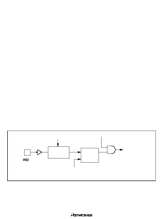
Rev. 2.0, 09/02, page 74 of 658
5.4
Interrupt Sources
5.4.1
External Interrupts
There are 14 external interrupts for the H8S/2268 Series: NMI, IRQ5 to IRQ3, IRQ1, IRQ0, and
WKP7 to WKP0, and 13 external interrupts for the H8S/2264 Series: NMI, IRQ4, IRQ3, IRQ1,
IRQ0, and WKP7 to WKP0. These interrupts can be used to restore this LSI from software
standby mode.
NMI Interrupt: NMI is the highest-priority interrupt, and is always accepted by the CPU
regardless of the interrupt control mode or the status of the CPU interrupt mask bits. The NMIEG
bit in SYSCR can be used to select whether an interrupt is requested at a rising edge or a falling
edge on the NMI pin.
IRQn Interrupts (H8S/2268 Series: n = 5 to 3, 1 and 0; H8S/2264 Series: n = 4, 3, 1 and 0):
IRQn interrupts are requested by an input signal at
,54Q pins. IRQn interrupts have the following
features:
∑
Using ISCR, it is possible to select whether an interrupt is generated by a low level, falling
edge, rising edge, or both edges, at
,54Q pins.
∑
Enabling or disabling of IRQn interrupt requests can be selected with IER.
∑
The interrupt priority level can be set with IPR. (H8S/2268 Series only)
∑
The status of IRQn interrupt requests is indicated in ISR. ISR flags can be cleared to 0 by
software.
A block diagram of IRQn interrupts is shown in figure 5.3.
IRQn interrupt
request
IRQnE
IRQnF
S
R
Q
Clear signal
Edge / level
detection circuit
IRQnSCA, IRQnSCB
input
Note: H8S/2268 Series: n = 5 to 3, 1, 0
H8S/2264 Series: n = 4, 3, 1, 0
Figure 5.3 Block Diagram of IRQn Interrupts

Rev. 2.0, 09/02, page 75 of 658
The set timing for IRQnF is shown in figure 5.4.
Input Pin
IRQnF
Note: H8S/2268 Series: n = 5 to 3, 1, 0
H8S/2264 Series: n = 4, 3, 1, 0
Figure 5.4 Set Timing for IRQnF
The detection of IRQn interrupts does not depend on whether the relevant pin has been set for
input or output. However, when a pin is used as an external interrupt input pin, do not clear the
corresponding DDR to 0; and use the pin as an I/O pin for another function. IRQnF interrupt
request flag is set to 1 when the setting condition is satisfied, regardless of IER settings.
Accordingly, refer to only necessary flags.
WKP7 to WKP0 Interrupts:WKP7 to WKP0 interrupts are requested by falling edge input
signal at
:.3 to :.3 pins. WKP7 to WKP0 interrupts have the following features:
∑
WPCR selects whether the PJn/
:.3Q/SEGn+1 pin is used as the PJn pin or :.3Q pin when
the PJn/
:.3Q/SEGn+1 pin is not used as the SEGn+1 pin. (n=7 to 0)
For pin switching, see 9.8.5 Wakeup Control Register (WPCR).
∑
IENR1 can be used to select enabling or disabling of WKP7 to WKP0 interrupt requests.
∑
IPR sets the interrupt priority level. (H8S/2268 Series only)
∑
IWPR indicates the status of WKP7 to WKP0 interrupt requests. IWPR flag can be cleared to 0
by software.
The block diagram of interrupts WKP7 to WKP0 is shown in figure 5.5.

Rev. 2.0, 09/02, page 76 of 658
WKP7 to WKP0
IWPF7
IENWP
S
R
Q
IWPF6
S
R
Q
IWPF0
S
R
Q
Input
- - - - -
- - - - -
- - - - -
- - - - -
Clear signal
Falling edge
detection circuit
Falling edge
detection circuit
Falling edge
detection circuit
Interrupt request
Input
Input
Figure 5.5 Block Diagram of Interrupts WKP7 to WKP0
Figure 5.6 shows the IWPFn setting timing.
input
IWPFn
(n = 7 to 0)
Figure 5.6 IWPFn Setting Timing
The vector number for the WKP7 to WKP0 interrupt exception handling is 108. Eight interrupt
pins are assigned to one vector number. Accordingly, determine the source using an exception
handling routine.

Rev. 2.0, 09/02, page 77 of 658
The detection of interrupts WKP7 to WKP0 does not depend on whether the relevant pin has been
set for input or output. However, when a pin is used as an external interrupt input pin, do not clear
the corresponding DDR to 0; and use the pin as an I/O pin for another function. IRQnF interrupt
request flag is set to 1 when the setting condition is satisfied, regardless of IER settings.
Accordingly, refer to only necessary flags.
5.4.2
Internal Interrupts
For each on-chip peripheral module, there are flags that indicate the interrupt request status, and
enable bits that select enabling or disabling of these interrupts. If both of these are set to 1 for a
particular interrupt source, an interrupt request is issued to the interrupt controller.
5.4.3
Interrupt Exception Handling Vector Table
Table 5.2 shows interrupt exception handling sources, vector addresses, and interrupt priorities.
For default priorities, the lower the vector number, the higher the priority.
Priorities among modules can be set by means of the IPR. (H8S/2268 Series only)
Modules set at the same priority will conform to their default priorities. Priorities within a module
are fixed.

Rev. 2.0, 09/02, page 78 of 658
Table 5.2
Interrupt Sources, Vector Addresses, and Interrupt Priorities
Vector
Address
*
1
Interrupt
Source
Origin of
Interrupt Source
Vector
Number
Advanced
Mode
IPR
*
2
*
3
Priority
NMI
7
H'001C
High
External
Pin
IRQ0
16
H'0040
IPRA6 to IPRA4
IRQ1
17
H'0044
IPRA2 to IPRA0
Reserved
18
H'0048
IPRB6 to IPRB4
IRQ3
19
H'004C
IRQ4
20
H'0050
IPRB2 to IPRB0
IRQ5
*
3
21
H'0054
Reserved
22
23
H'0058
H'005C
IPRC6 to IPRC4
DTC
*
3
SWDTEND
(completion of
software initiation data
transfer)
24
H'0060
IPRC2 to IPRC0
Watchdog
timer 0
WOVI0
(interval timer 0)
25
H'0064
IPRD6 to IPRD4
PC break
*
3
PC break
27
H'006C
IPRE6 to IPRE4
A/D
ADI (completion of A/D
conversion)
28
H'0070
IPRE2 to IPRE0
Watchdog
timer 1
WOVI1
(interval timer 1)
29
H'0074
Reserved
30
31
H'0078
H'007C
TPU channel
0
*
3
TGI0A (TGR0A input
capture/compare-
match)
32
H'0080
IPRF6 to IPRF4
TGI0B (TGR0B input
capture/compare-
match)
33
H'0084
TGI0C (TGR0C input
capture/compare-
match)
34
H'0088
TGI0D(TGR0D input
capture/compare-
match)
35
H'008C
Low

Rev. 2.0, 09/02, page 79 of 658
Vector
Address
*
1
Interrupt
Source
Origin of
Interrupt Source
Vector
Number
Advanced
Mode
IPR
*
2
*
3
Priority
TCI0V (overflow 0)
36
H'0090
High
Reserved
37
38
39
H'0094
H'0098
H'009C
TPU channel
1
TGI1A (TGR1A input
capture/compare-
match)
40
H'00A0
IPRF2 to IPRF0
TGI1B (TGR1B input
capture/compare-
match)
41
H'00A4
TCI1V (overflow 1)
42
H'00A8
TCI1U (underflow 1)
*
3
43
H'00AC
TPU channel
2
TGI2A (TGR2A input
capture/compare-
match)
44
H'00B0
IPRG6 to IPRG4
TGI2B (TGR2B input
capture/compare-
match)
45
H'00B4
TCI2V (overflow 2)
46
H'00B8
TCI2U (underflow 2)
*
3
47
H'00BC
8-bit timer
channel 0
CMIA0 (compare-
match A0)
64
H'0100
IPRI6 to IPRI4
CMIB0 (compare-
match B0)
65
H'0104
OVI0 (overflow 0)
66
H'0108
Reserved
67
H'010C
Low

Rev. 2.0, 09/02, page 80 of 658
Vector
Address
*
1
Interrupt
Source
Origin of
Interrupt Source
Vector
Number
Advanced
Mode
IPR
*
2
*
3
Priority
8-bit timer
channel 1
CMIA1 (compare-
match A1)
68
H'0110
IPRI2 to IPRI0
High
CMIB1 (compare-
match B1)
69
H'0114
OVI1 (overflow 1)
70
H'0118
Reserved
71
H'011C
ERI0 (receive error 0) 80
H'0140
IPRJ2 to IPRJ0
RXI0 (receive
completion 0)
81
H'0144
TXI0 (transmit data
empty 0)
82
H'0148
SCI
channel 0
TEI0 (transmit end 0)
83
H'014C
ERI1 (receive error 1) 84
H'0150
IPRK6 to IPRK4
SCI
channel 1
RXI1 (receive
completion 1)
85
H'0154
TXI1 (transmit data
empty 1)
86
H'0158
TEI1 (transmit end 1)
87
H'015C
8-bit timer
channel 2
*
3
CMIA2 (compare-
match A2)
92
H'0170
IPRL6 to IPRL4
CMIB2 (compare-
match B2)
93
H'0174
OVI2 (overflow 2)
94
H'0178
Reserved
95
H'017C
Low
Rev. 2.0, 09/02, page 81 of 658
Vector
Address
*
1
Interrupt
Source
Origin of
Interrupt Source
Vector
Number
Advanced
Mode
IPR
*
2
*
3
Priority
8-bit timer
channel 3
*
3
CMIA3 (compare-
match A3)
96
H'0180
High
CMIB3 (compare-
match B3)
97
H'0184
OVI3 (overflow 3)
98
H'0188
Reserved
99
H'018C
IIC channel 0
(option)
IICI0 (1-byte
transmission/
reception completion)
100
H'0190
Reserved
101
H'0194
IPRL2 to IPRL0
IICI1 (1-byte
transmission/
reception completion)
102
H'0198
IIC channel
1
*
3
(option)
Reserved
103
H'019C
OVI4 (overflow 4)
104
H'01A0
OVI5 (overflow 5)
105
H'01A4
OVI6 (overflow 6)
106
H'01A8
8-bit reload
timer
channels 4 to
7
*
3
OVI7 (overflow 7)
107
H'01AC
IPRM6 to IPRM4
External pins WKP7 to WKP0
108
H'01B0
IPRM2 to IPRM0
ERI2 (receive error 2) 120
H'01E0
IPRO6 to IPRO4
RXI2 (receive
completion 2)
121
H'01E4
TXI2 (transmit data
empty 2)
122
H'01E8
SCI
channel 2
TEI2 (transmit end 2)
123
H'01EC
Low
Notes: 1. Lower 16 bits of the start address.
2. IPR6 to IPR4, and IPR2 to IPR0 bits are reserved, because these bits have no
corresponding interruption. These bits are always read as 0 and cannot be modified.
3. Supported only by the H8S/2268 Series.

Rev. 2.0, 09/02, page 82 of 658
5.5
Operation
5.5.1
Interrupt Control Modes and Interrupt Operation
Interrupt operations in the H8S/2268 differ depending on the interrupt control mode.
NMI interrupts are accepted at all times except in the reset state and the hardware standby state. In
the case of IRQ interrupts, WKP interrupts and on-chip peripheral module interrupts, an enable bit
is provided for each interrupt. Clearing an enable bit to 0 disables the corresponding interrupt
request. Interrupt sources for which the enable bits are set to 1 are controlled by the interrupt
controller.
Table 5.3 shows the interrupt control modes.
The interrupt controller performs interrupt control according to the interrupt control mode set by
the INTM1 and INTM0 bits in SYSCR, the priorities set in IPR*, and the masking state indicated
by the I bit in the CPU's CCR, and bits I2 to I0 in EXR*.
Table 5.3
Interrupt Control Modes
Interrupt
SYSCR
Priority Setting
Interrupt
Control Mode INTM1 INTM0 Registers
*
Mask Bits Description
0
0
0
I
Interrupt mask control is
performed by the I bit.
1
Setting prohibited
2
*
1
0
IPR
I2 to I0
8-level interrupt mask control
is performed by bits I2 to I0.
8 priority levels can be set with
IPR.
1
Setting prohibited
Note:
*
Supported only by the H8S/2268 Series.

Rev. 2.0, 09/02, page 83 of 658
Figures 5.7 and 5.8 show block diagrams of the priority decision circuits for the H8S/2268 Series
and H8S/2264 Series, respectively.
Interrupt
acceptance
control
8-level
mask control
Default priority
determination
Vector number
Interrupt control mode 2
IPR
Interrupt source
I2 to I0
Interrupt
control
mode 0
I
Figure 5.7 Block Diagram of Interrupt Control Operation for H8S/2268 Series
Interrupt
acceptance
control
Default priority
determination
Vector number
Interrupt source
Interrupt
control
mode 0
I
Figure 5.8 Block Diagram of Interrupt Control Operation for H8S/2264 Series

Rev. 2.0, 09/02, page 84 of 658
Interrupt Acceptance Control: In interrupt control mode 0, interrupt acceptance is controlled by
the I bit in CCR.
Table 5.4 shows the interrupts selected in each interrupt control mode.
Table 5.4
Interrupts Selected in Each Interrupt Control Mode (1)
Interrupt Mask Bits
Interrupt Control Mode
I
Selected Interrupts
0
0
All interrupts
1
NMI interrupts
2
*
X
All interrupts
Legend:
X: Don't care
Note:
*
Supported only by the H8S/2268 Series.
8-Level Control (H8S/2268 Series Only): In interrupt control mode 2, 8-level mask level
determination is performed for the selected interrupts in interrupt acceptance control according to
the interrupt priority level (IPR).
The interrupt source selected is the interrupt with the highest priority level, and whose priority
level set in IPR is higher than the mask level.
Table 5.5
Interrupts Selected in Each Interrupt Control Mode (2)
Interrupt Control Mode
Selected Interrupts
0
All interrupts
2
Highest-priority-level (IPR) interrupt whose priority level is greater
than the mask level (IPR > I2 to I0).
Default Priority Determination: When an interrupt is selected by 8-level control, its priority is
determined and a vector number is generated.
If the same value is set for IPR, acceptance of multiple interrupts is enabled, and so only the
interrupt source with the highest priority according to the preset default priorities is selected and
has a vector number generated (H8S/2268 Series only).
Interrupt sources with a lower priority than the accepted interrupt source are held pending.
Table 5.6 shows operations and control signal functions in each interrupt control mode.

Rev. 2.0, 09/02, page 85 of 658
Table 5.6
Operations and Control Signal Functions in Each Interrupt Control Mode
Interrupt
Control Setting
Interrupt
Acceptance
Control
8-Level Control
*
3
Default Priority
T
Mode
INTM1 INTM0
I
I2 to I0
*
3
IPR
*
3
Determination
(Trace)
0
0
0
O
IM
X
*
2
O
2
*
3
1
0
X
*
1
O IM
PR
O
T
Legend
O : Interrupt operation control performed
X : No operation. (All interrupts enabled)
IM : Used as interrupt mask bit
PR : Sets priority.
: Not used.
Notes: 1. Set to 1 when interrupt is accepted.
2. Keep the initial setting.
3. Supported only by the H8S/2268 Series.
5.5.2
Interrupt Control Mode 0
Enabling and disabling of IRQ interrupts, WKP interrupts and on-chip peripheral module
interrupts can be set by means of the I bit in the CPU's CCR. Interrupts are enabled when the I bit
is cleared to 0, and disabled when set to 1.
Figure 5.9 shows a flowchart of the interrupt acceptance operation in this case.
1. If an interrupt source occurs when the corresponding interrupt enable bit is set to 1, an
interrupt request is sent to the interrupt controller.
2. If the I bit is set to 1, only an NMI interrupt is accepted, and other interrupt requests are held
pending. If the I bit is cleared, an interrupt request is accepted.
3. Interrupt requests are sent to the interrupt controller, the highest-ranked interrupt according to
the priority system is accepted, and other interrupt requests are held pending.
4. When the CPU accepts an interrupt request, it starts interrupt exception handling after
execution of the current instruction has been completed.
5. The PC and CCR are saved to the stack area by interrupt exception handling. The PC saved on
the stack shows the address of the first instruction to be executed after returning from the
interrupt handling routine.
6. Next, the I bit in CCR is set to 1. This masks all interrupts except NMI.
7. The CPU generates a vector address for the accepted interrupt and starts execution of the
interrupt handling routine at the address indicated by the contents of the vector address in the
vector table.
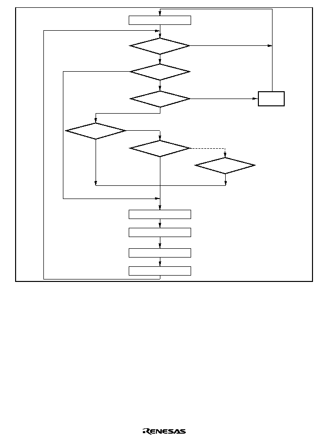
Rev. 2.0, 09/02, page 86 of 658
Yes
Program execution status
Interrupt generated
NMI
IRQ1
IRQ0
Save PC and CCR
I=1
Read vector address
Branch to interrupt handling routine
Hold
pending
TEI2
Yes
Yes
No
Yes
Yes
Yes
No
No
No
I=0
No
Figure 5.9 Flowchart of Procedure up to Interrupt Acceptance
in Interrupt Control Mode 0

Rev. 2.0, 09/02, page 87 of 658
5.5.3
Interrupt Control Mode 2 (H8S/2268 Series Only)
Eight-level masking is implemented for IRQ interrupts, WKP interrupts and on-chip peripheral
module interrupts by comparing the interrupt mask level set by bits I2 to I0 of EXR in the CPU
with IPR.
Figure 5.10 shows a flowchart of the interrupt acceptance operation in this case.
1. If an interrupt source occurs when the corresponding interrupt enable bit is set to 1, an interrupt
request is sent to the interrupt controller.
2. When interrupt requests are sent to the interrupt controller, the interrupt with the highest
priority according to the interrupt priority levels set in IPR is selected, and lower-priority
interrupt requests are held pending. If a number of interrupt requests with the same priority are
generated at the same time, the interrupt request with the highest priority according to the
priority system shown in table 5.2 is selected.
3. Next, the priority of the selected interrupt request is compared with the interrupt mask level set
in EXR. An interrupt request with a priority no higher than the mask level set at that time is
held pending, and only an interrupt request with a priority higher than the interrupt mask level
is accepted.
4. When the CPU accepts an interrupt request, it starts interrupt exception handling after
execution of the current instruction has been completed.
5. The PC, CCR, and EXR are saved to the stack area by interrupt exception handling. The PC
saved on the stack shows the address of the first instruction to be executed after returning from
the interrupt handling routine.
6. The T bit in EXR is cleared to 0. The interrupt mask level is rewritten with the priority level of
the accepted interrupt.
If the accepted interrupt is NMI, the interrupt mask level is set to H'7.
7. The CPU generates a vector address for the accepted interrupt and starts execution of the
interrupt handling routine at the address indicated by the contents of the vector address in the
vector table.

Rev. 2.0, 09/02, page 88 of 658
Yes
Program execution status
Interrupt generated?
NMI
Level 6 interrupt?
Mask level 5
or below?
Level 7 interrupt?
Mask level 6
or below?
Save PC, CCR, and EXR
Clear T bit to 0
Update mask level
Read vector address
Branch to interrupt handling routine
Hold
pending
Level 1 interrupt?
Mask level 0?
Yes
Yes
No
Yes
Yes
Yes
No
Yes
Yes
No
No
No
No
No
No
Figure 5.10 Flowchart of Procedure Up to Interrupt Acceptance in Control Mode 2
5.5.4
Interrupt Exception Handling Sequence
Figure 5.11 shows the interrupt exception handling sequence. The example shown is for the case
where interrupt control mode 0 is set in advanced mode, and the program area and stack area are
in on-chip memory.

Rev. 2.0, 09/02, page 89 of 658
(14)
(12)
(10)
(6)
(4)
(2)
(1)
(5)
(7)
(9)
(11)
(13)
Interrupt service
routine instruction
prefetch
Internal
operation
Vector fetch
stack
Instruction
prefetch
Internal
operation
Interrupt
acceptance
Interrupt level determination
Wait for end of instruction
Interrupt
request signal
Internal
address bus
Internal
read signal
Internal
write signal
Internal
data bus
(3)
(1)
(2) (4)
(3)
(5)
(7)
Instruction prefetch address (Not executed.
This is the contents of the saved PC, the return address.)
Instruction code (Not executed.)
Instruction prefetch address (Not executed.)
SP-2
SP-4
Saved PC and saved CCR
Vector address
Interrupt handling routine start address (Vector address contents)
Interrupt handling routine start address ((13) = (10)(12))
First instruction of interrupt handling routine
(6) (8)
(9) (11)
(10) (12)
(13)
(14)
(8)
Figure 5.11 Interrupt Exception Handling

Rev. 2.0, 09/02, page 90 of 658
5.5.5
Interrupt Response Times
This LSI is capable of fast word transfer to on-chip memory, has the program area in on-chip
ROM and the stack area in on-chip RAM, enabling high-speed processing.
Table 5.7 shows interrupt response times - the interval between generation of an interrupt request
and execution of the first instruction in the interrupt handling routine. The execution status
symbols used in table 5.7 are explained in table 5.8.
Table 5.7
Interrupt Response Times (States)
Normal Mode
*
5
Advanced Mode
No.
Execution Status
INTM1 = 0
INTM1 = 1
INTM1 = 0
INTM1 = 1
1
Interrupt priority determination
*
1
3
3
3
3
2
Number of wait states until executing
instruction ends
*
2
1 to 19 + 2∑S
I
1 to 19 + 2∑S
I
1 to 19 + 2∑S
I
1 to 19 + 2∑S
I
3
PC, CCR, EXR stack save
2∑S
K
3∑S
K
2∑S
K
3∑S
K
4
Vector fetch
S
I
S
I
2∑S
I
2∑S
I
5
Instruction fetch
*
3
2∑S
I
2∑S
I
2∑S
I
2∑S
I
6
Internal processing
*
4
2
2
2
2
Total (using on-chip memory)
11 to 31
12 to 32
12 to 32
13 to 33
Notes: 1. Two states in case of internal interrupt.
2. Refers to MULXS and DIVXS instructions.
3. Prefetch after interrupt acceptance and interrupt handling routine prefetch.
4. Internal processing after interrupt acceptance and internal processing after vector fetch.
5. Not available in this LSI.
Table 5.8
Number of States in Interrupt Handling Routine Execution Status
Object of Access
External Device
*
8 Bit Bus
16 Bit Bus
Symbol
Internal
Memory
2-State
Access
3-State
Access
2-State
Access
3-State
Access
Instruction fetch
S
I
1
4
6 + 2m
2
3 + m
Branch address read
S
J
Stack manipulation
S
K
Legend
m
: Number of wait states in an external device access.
Note:
*
Cannot be used in this LSI.
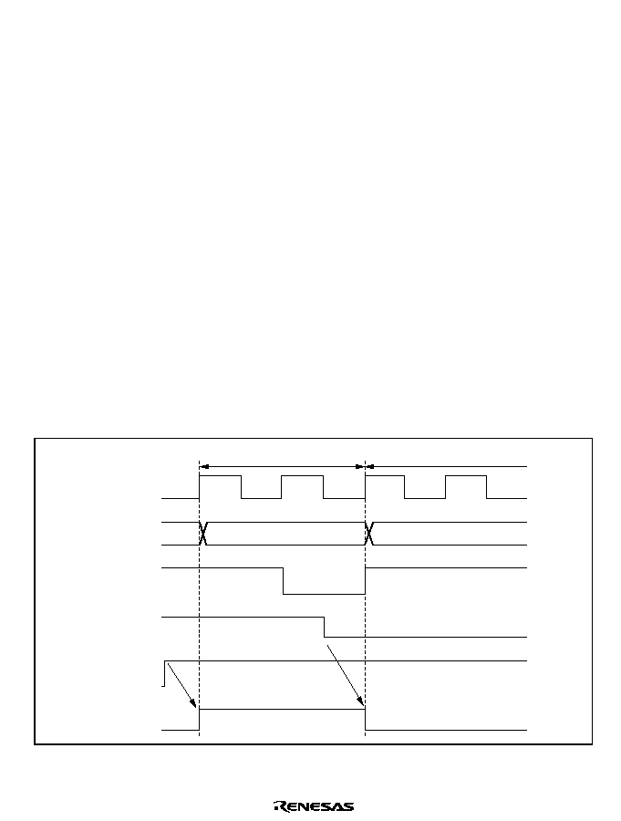
Rev. 2.0, 09/02, page 91 of 658
5.5.6
DTC Activation by Interrupt (H8S/2268 Series Only)
The DTC can be activated by an interrupt. For details, see section 8, Data Transfer Controller
(DTC).
5.6
Usage Notes
5.6.1
Contention between Interrupt Generation and Disabling
When an interrupt enable bit is cleared to 0 to disable interrupts, the disabling becomes effective
after execution of the instruction.
When an interrupt enable bit is cleared to 0 by an instruction such as BCLR or MOV, and if an
interrupt is generated during execution of the instruction, the interrupt concerned will still be
enabled on completion of the instruction, and so interrupt exception handling for that interrupt will
be executed on completion of the instruction. However, if there is an interrupt request of higher
priority than that interrupt, interrupt exception handling will be executed for the higher-priority
interrupt, and the lower-priority interrupt will be ignored.
The same also applies when an interrupt source flag is cleared to 0.
Figure 5.12 shows an example in which the CMIEA bit in the TCR register of the 8-bit timer is
cleared to 0.
Internal
address bus
Internal
write signal
CMIEA
CMFA
CMIA
interrupt signal
TCR write cycle by CPU
CMIA exception handling
TCR address
Figure 5.12 Contention between Interrupt Generation and Disabling

Rev. 2.0, 09/02, page 92 of 658
The above contention will not occur if an enable bit or interrupt source flag is cleared to 0 while
the interrupt is masked.
5.6.2
Instructions that Disable Interrupts
The instructions that disable interrupts are LDC, ANDC, ORC, and XORC. After any of these
instructions are executed, all interrupts including NMI are disabled and the next instruction is
always executed. When the I bit is set by one of these instructions, the new value becomes valid
two states after execution of the instruction ends.
5.6.3
When Interrupts Are Disabled
There are times when interrupt acceptance is disabled by the interrupt controller.
The interrupt controller disables interrupt acceptance for a 3-state period after the CPU has
updated the mask level with an LDC, ANDC, ORC, or XORC instruction.
5.6.4
Interrupts during Execution of EEPMOV Instruction
Interrupt operation differs between the EEPMOV.B instruction and the EEPMOV.W instruction.
With the EEPMOV.B instruction, an interrupt request (including NMI) issued during the transfer
is not accepted until the move is completed.
With the EEPMOV.W instruction, if an interrupt request is issued during the transfer, interrupt
exception handling starts at a break in the transfer cycle. The PC value saved on the stack in this
case is the address of the next instruction.
Therefore, if an interrupt is generated during execution of an EEPMOV.W instruction, the
following coding should be used.
L1: EEPMOV.W
MOV.W R4,R4
BNE L1

Rev. 2.0, 09/02, page 93 of 658
Section 6 PC Break Controller (PBC)
The H8S/2268 Series includes a PC break controller (PBC), while the H8S/2264 Series does not.
The PC break controller (PBC) provides functions that simplify program debugging. Using these
functions, it is easy to create a self-monitoring debugger, enabling programs to be debugged with
the chip alone, without using an in-circuit emulator. A block diagram of the PC break controller is
shown in figure 6.1.
6.1
Features
∑
Two break channels (A and B)
∑
24-bit break address
Bit masking possible
∑
Four types of break compare conditions
Instruction fetch
Data read
Data write
Data read/write
∑
Bus master
Either CPU or CPU/DTC can be selected
∑
The timing of PC break exception handling after the occurrence of a break condition is as
follows:
Immediately before execution of the instruction fetched at the set address (instruction
fetch)
Immediately after execution of the instruction that accesses data at the set address (data
access)
∑
Module stop mode can be set
PBC0000B_000020020700

Rev. 2.0, 09/02, page 94 of 658
Output control
Output control
Mask control
PC break
interrupt
Match signal
Mask control
BARA
BCRA
BARB
BCRB
Comparator
Control
logic
Comparator
Control
logic
Internal address
Access
status
Match signal
Figure 6.1 Block Diagram of PC Break Controller
6.2
Register Descriptions
The PC break controller has the following registers.
∑
Break address register A (BARA)
∑
Break address register B (BARB)
∑
Break control register A (BCRA)
∑
Break control register B (BCRB)
6.2.1
Break Address Register A (BARA)
BARA is a 32-bit readable/writable register that specifies the channel A break address.
Bit
Bit Name
Initial Value
R/W
Description
31 to 24
Undefined
Reserved
These bits are read as an undefined value
and cannot be modified.
23 to 0
BAA23 to BAA0
H'000000
R/W
These bits set the channel A PC break
address.
6.2.2
Break Address Register B (BARB)
BARB is the channel B break address register. The bit configuration is the same as for BARA.

Rev. 2.0, 09/02, page 95 of 658
6.2.3
Break Control Register A (BCRA)
BCRA controls channel A PC breaks.
Bit
Bit Name
Initial
Value
R/W
Description
7
CMFA
0
R/(W)
*
1
Condition Match Flag A
[Setting condition]
When a condition set for channel A is satisfied
[Clearing condition]
When 0 is written to CMFA after reading
*
2
CMFA = 1
6
CDA
0
R/W
CPU Cycle/DTC Cycle Select A
Selects the channel A break condition bus master.
0: CPU
1: CPU or DTC
5
4
3
BAMRA2
BAMRA1
BAMRA0
0
0
0
R/W
R/W
R/W
Break Address Mask Register A2 to A0
These bits specify which bits of the break address set
in BARA are to be masked.
000: BAA23≠0 (All bits are unmasked)
001: BAA23≠1 (Lowest bit is masked)
010: BAA23≠2 (Lower 2 bits are masked)
011: BAA23≠3 (Lower 3 bits are masked)
100: BAA23≠4 (Lower 4 bits are masked)
101: BAA23≠8 (Lower 8 bits are masked)
110: BAA23≠12 (Lower 12 bits are masked)
111: BAA23≠16 (Lower 16 bits are masked)
2
1
CSELA1
CSELA0
0
0
R/W
R/W
Break Condition Select
Selects break condition of channel A.
00: Instruction fetch is used as break condition
01: Data read cycle is used as break condition
10: Data write cycle is used as break condition
11: Data read/write cycle is used as break condition
0
BIEA
0
R/W
Break Interrupt Enable
When this bit is 1, the PC break interrupt request of
channel A is enabled.
Notes: 1. Only a 0 can be written to this bit to clear the flag.
2. Read the state wherein CMFA = 1 twice or more, when the CMFA is polled after
inhibiting the PC break interruption.

Rev. 2.0, 09/02, page 96 of 658
6.2.4
Break Control Register B (BCRB)
BCRB is the channel B break control register. The bit configuration is the same as for BCRA.
6.3
Operation
The operation flow from break condition setting to PC break interrupt exception handling is
shown in section 6.3.1, PC Break Interrupt Due to Instruction Fetch, and 6.3.2, PC Break Interrupt
Due to Data Access, taking the example of channel A.
6.3.1
PC Break Interrupt Due to Instruction Fetch
1. Set the break address in BARA.
For a PC break caused by an instruction fetch, set the address of the first instruction byte as the
break address.
2. Set the break conditions in BCR.
Set bit 6 (CDA) to 0 to select the CPU because the bus master must be the CPU for a PC break
caused by an instruction fetch. Set the address bits to be masked to bits 3 to 5 (BAMA2 to 0).
Set bits 1 and 2 (CSELA1 to 0) to 00 to specify an instruction fetch as the break condition. Set
bit 0 (BIEA) to 1 to enable break interrupts.
3. When the instruction at the set address is fetched, a PC break request is generated immediately
before execution of the fetched instruction, and the condition match flag (CMFA) is set.
4. After priority determination by the interrupt controller, PC break interrupt exception handling
is started.
6.3.2
PC Break Interrupt Due to Data Access
1. Set the break address in BARA.
For a PC break caused by a data access, set the target ROM, RAM, I/O, or external address
space address as the break address. Stack operations and branch address reads are included in
data accesses.
2. Set the break conditions in BCRA.
Select the bus master with bit 6 (CDA). Set the address bits to be masked to bits 3 to 5
(BAMA2 to 0). Set bits 1 and 2 (CSELA1 to 0) to 01, 10, or 11 to specify data access as the
break condition. Set bit 0 (BIEA) to 1 to enable break interrupts.
3. After execution of the instruction that performs a data access on the set address, a PC break
request is generated and the condition match flag (CMFA) is set.
4. After priority determination by the interrupt controller, PC break interrupt exception handling
is started.

Rev. 2.0, 09/02, page 97 of 658
6.3.3
Notes on PC Break Interrupt Handling
∑
When a PC break interrupt is generated at the transfer address of an EEPMOV.B instruction
PC break exception handling is executed after all data transfers have been completed and the
EEPMOV.B instruction has ended.
∑
When a PC break interrupt is generated at a DTC transfer address
PC break exception handling is executed after the DTC has completed the specified number of
data transfers, or after data for which the DISEL bit is set to 1 has been transferred.
6.3.4
Operation in Transitions to Power-Down Modes
The operation when a PC break interrupt is set for an instruction fetch at the address after a
SLEEP instruction is shown below.
∑
When the SLEEP instruction causes a transition from high-speed (medium-speed) mode to
sleep mode:
After execution of the SLEEP instruction, a transition is not made to sleep mode, and PC break
interrupt handling is executed. After execution of PC break interrupt handling, the instruction
at the address after the SLEEP instruction is executed (figure 6.2 (A)).
∑
When the SLEEP instruction causes a transition from high speed (medium speed) mode to
subactive mode (figure 6.2 (B)).
∑
When the SLEEP instruction causes a transition from subactive mode to high speed (medium
speed) mode (figure 6.2 (C)).
∑
When the SLEEP instruction causes a transition to software standby mode:
After execution of the SLEEP instruction, a transition is made to the respective mode, and PC
break interrupt handling is not executed. However, the CMFA or CMFB flag is set (figure 6.2
(D)).

Rev. 2.0, 09/02, page 98 of 658
SLEEP instruction
execution
High-speed
(medium-speed)
mode
SLEEP instruction
execution
Subactive
mode
System clock
subclock
Direct transition
exception handling
PC break exception
handling
Execution of instruction
after sleep instruction
Subclock
system clock,
oscillation settling time
SLEEP instruction
execution
Transition to
respective mode
Direct transition
exception handling
PC break exception
handling
Execution of instruction
after sleep instruction
PC break exception
handling
Execution of instruction
after sleep instruction
(A)
(B)
(C)
(D)
SLEEP instruction
execution
Figure 6.2 Operation in Power-Down Mode Transitions
6.3.5
When Instruction Execution Is Delayed by One State
While the break interrupt enable bit is set to 1, instruction execution is one state later than usual.
∑
For 1-word branch instructions (Bcc d:8, BSR, JSR, JMP, TRAPA, RTE, and RTS) in on-chip
ROM or RAM.
∑
When break interruption by instruction fetch is set, the set address indicates on-chip ROM or
RAM space, and that address is used for data access, the instruction that executes the data
access is one state later than in normal operation.
∑
When break interruption by instruction fetch is set and a break interrupt is generated, if the
executing instruction immediately preceding the set instruction has one of the addressing
modes shown below, and that address indicates on-chip ROM or RAM, the instruction will be
one state later than in normal operation.
Addressing modes: @ERn, @(d:16,ERn), @(d:32,ERn), @-ERn/ERn+, @aa:8, @aa:24,
@aa:32, @(d:8,PC), @(d:16,PC), @@aa:8
∑
When break interruption by instruction fetch is set and a break interrupt is generated, if the
executing instruction immediately preceding the set instruction is NOP or SLEEP, or has #xx,
Rn as its addressing mode, and that instruction is located in on-chip ROM or RAM, the
instruction will be one state later than in normal operation.

Rev. 2.0, 09/02, page 99 of 658
6.4
Usage Notes
6.4.1
Module Stop Mode Setting
PBC operation can be disabled or enabled using the module stop control register. The initial
setting is for PBC operation to be halted. Register access is enabled by clearing module stop
mode. For details, refer to section 22, Power-Down Modes.
6.4.2
PC Break Interrupts
The PC break interrupt is shared by channels A and B. The channel from which the request was
issued must be determined by the interrupt handler.
6.4.3
CMFA and CMFB
The CMFA and CMFB flags are not automatically cleared to 0, so 0 must be written to CMFA or
CMFB after first reading the flag while it is set to 1. If the flag is left set to 1, another interrupt
will be requested after interrupt handling ends.
6.4.4
PC Break Interrupt when DTC Is Bus Master
A PC break interrupt generated when the DTC is the bus master is accepted after the bus has been
transferred to the CPU by the bus controller.
6.4.5
PC Break Set for Instruction Fetch at Address Following BSR, JSR, JMP, TRAPA,
RTE, or RTS Instruction
When a PC break is set for an instruction fetch at an address following a BSR, JSR, JMP, TRAPA,
RTE, or RTS instruction:
Even if the instruction at the address following a BSR, JSR, JMP, TRAPA, RTE, or RTS
instruction is fetched, it is not executed, and so a PC break interrupt is not generated by the
instruction fetch at the next address.
6.4.6
I Bit Set by LDC, ANDC, ORC, or XORC Instruction
When the I bit is set by an LDC, ANDC, ORC, or XORC instruction, a PC break interrupt
becomes valid two states after the end of the executing instruction. If a PC break interrupt is set
for the instruction following one of these instructions, since interrupts, including NMI, are
disabled for a 3-state period in the case of LDC, ANDC, ORC, and XOR, the next instruction is
always executed. For details, see section 5, Interrupt Controller.

Rev. 2.0, 09/02, page 100 of 658
6.4.7
PC Break Set for Instruction Fetch at Address Following Bcc Instruction
When a PC break is set for an instruction fetch at an address following a Bcc instruction:
A PC break interrupt is generated if the instruction at the next address is executed in accordance
with the branch condition, and is not generated if the instruction at the next address is not
executed.
6.4.8
PC Break Set for Instruction Fetch at Branch Destination Address of Bcc
Instruction
When a PC break is set for an instruction fetch at the branch destination address of a Bcc
instruction:
A PC break interrupt is generated if the instruction at the branch destination is executed in
accordance with the branch condition, and is not generated if the instruction at the branch
destination is not executed.
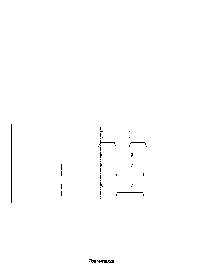
Rev. 2.0, 09/02, page 101 of 658
Section 7 Bus Controller
The H8S/2000 CPU is driven by a system clock, denoted by the symbol
.
The bus controller controls a memory cycle and a bus cycle. Different methods are used to access
on-chip memory and on-chip peripheral modules. In the H8S/2268 Series, the bus controller also
has a bus arbitration function, and controls the operation of the internal bus masters: the CPU and
data transfer controller (DTC).
7.1
Basic Timing
The period from one rising edge of
to the next is referred to as a "state." The memory cycle or
bus cycle consists of one, two, or four states. Different methods are used to access on-chip
memory, on-chip peripheral modules, and the external address space.
7.1.1
On-Chip Memory Access Timing (ROM, RAM)
On-chip memory is accessed in one state. The data bus is 16 bits wide, permitting both byte and
word transfer instruction. Figure 7.1 shows the on-chip memory access cycle.
T1
Internal address bus
Bus cycle
Address
Read data
Write data
Internal read signal
Internal data bus
Internal write signal
Internal data bus
Read
access
Write
access
Figure 7.1 On-Chip Memory Access Cycle

Rev. 2.0, 09/02, page 102 of 658
7.1.2
On-Chip Peripheral Module Access Timing (H'FFFDAC to H'FFFFBF)
Addresses H'FFFDAC to H'FFFFBF in the on-chip peripheral modules are accessed in two states.
The data bus is either 8 bits or 16 bits wide, depending on the particular internal I/O register being
accessed. For details, refer to section 25, List of Registers. Figure 7.2 shows access timing for the
on-chip peripheral modules (H'FFFDAC to H'FFFFBF).
T1
T2
Internal address bus
Bus cycle
Address
Read data
Write data
Internal read signal
Internal data bus
Internal write signal
Internal data bus
Read
access
Write
access
Figure 7.2 On-Chip Peripheral Module Access Cycle (H'FFFDAC to H'FFFFBF)
7.1.3
On-Chip Peripheral Module Access Timing (H'FFFC30 to H'FFFCA3)
Addresses H'FFFC30 to H'FFFCA3 on the on-chip peripheral modules and registers are accessed
in four states. The data bus is either 8 bits or 16 bits wide, depending on the particular internal I/O
register being accessed. For details, refer to section 25, List of Registers. Figure 7.3 shows access
timing for the on-chip peripheral modules (H'FFFC30 to H'FFFCA3).
The on-chip module of which address is between H'FFFC30 to H'FFFCA3 includes LCD,
DTMF*
1
, TMR4*
1
, port H to L and ports M*
1
and N*
1
. The registers are WKP register, module
stop control register D and system clock control register 2*
2
.
Notes: 1. Supported only by the H8S/2268 Series.
2. Supported only by the H8S/2264 Series.

Rev. 2.0, 09/02, page 103 of 658
Internal address bus
Internal read signal
Internal data bus
Internal write signal
Internal data bus
Bus cycle
T1
Address
Read
access
Write
access
T3
T2
T4
Read data
Write data
Figure 7.3 On-Chip Peripheral Module Access Cycle (H'FFFC30 to H'FFFCA3)
7.2
Bus Arbitration (H8S/2268 Series Only)
The Bus Controller has a bus arbiter that arbitrates bus master operations.
There are two bus masters, the CPU and DTC, which perform read/write operations when they
control the bus.
7.2.1
Order of Priority of the Bus Masters
Each bus master requests the bus by means of a bus request signal. The bus arbiter detects the bus
masters' bus request signals, and if the bus is requested, sends a bus request acknowledge signal to
the bus master making the request. If there are bus requests from more than one bus master, the
bus request acknowledge signal is sent to the one with the highest priority. When a bus master
receives the bus request acknowledge signal, it takes possession of the bus until that signal is
canceled.
The order of priority of the bus masters is as follows:
(High) DTC > CPU (Low)

Rev. 2.0, 09/02, page 104 of 658
7.2.2
Bus Transfer Timing
Even if a bus request is received from a bus master with a higher priority than that of the bus
master that has acquired the bus and is currently operating, the bus is not necessarily transferred
immediately. The CPU is the lowest-priority bus master, and if a bus request is received from the
DTC, the bus arbiter transfers the bus to the bus master that issued the request. The timing for
transfer of the bus is as follows:
∑
The bus is transferred at a break between bus cycles. However, if a bus cycle is executed in
discrete operations, as in the case of a longword-size access, the bus is not transferred between
such operations. For details, refer to section 2.7, Bus States During Instruction Execution, in
the H8S/2600 Series, H8S/2000 Series Programming Manual.
∑
If the CPU is in sleep mode, it transfers the bus immediately.
The DTC sends the bus arbiter a request for the bus when an activation request is generated.
7.2.3
Resets and the Bus Controller
In a reset, the H8S/2268, including the bus controller, enters the reset state at that point, and an
executing bus cycle is discontinued.

Rev. 2.0, 09/02, page 105 of 658
Section 8 Data Transfer Controller (DTC)
The H8S/2268 Series includes a data transfer controller (DTC), while the H8S/2264 Series does
not. The DTC can be activated by an interrupt or software, to transfer data.
Figure 8.1 shows a block diagram of the DTC.
The DTC's register information is stored in the on-chip RAM. When the DTC is used, the RAME
bit in SYSCR must be set to 1. A 32-bit bus connects the DTC to the on-chip RAM (1 kbyte),
enabling 32-bit/1-state reading and writing of the DTC register information.
8.1
Features
∑
Transfer is possible over any number of channels
∑
Three transfer modes
Normal, repeat, and block transfer modes are available
∑
One activation source can trigger a number of data transfers (chain transfer)
∑
The direct specification of 16-Mbyte address space is possible
∑
Activation by software is possible
∑
Transfer can be set in byte or word units
∑
A CPU interrupt can be requested for the interrupt that activated the DTC
∑
Module stop mode can be set
DTCH808B_000020020700
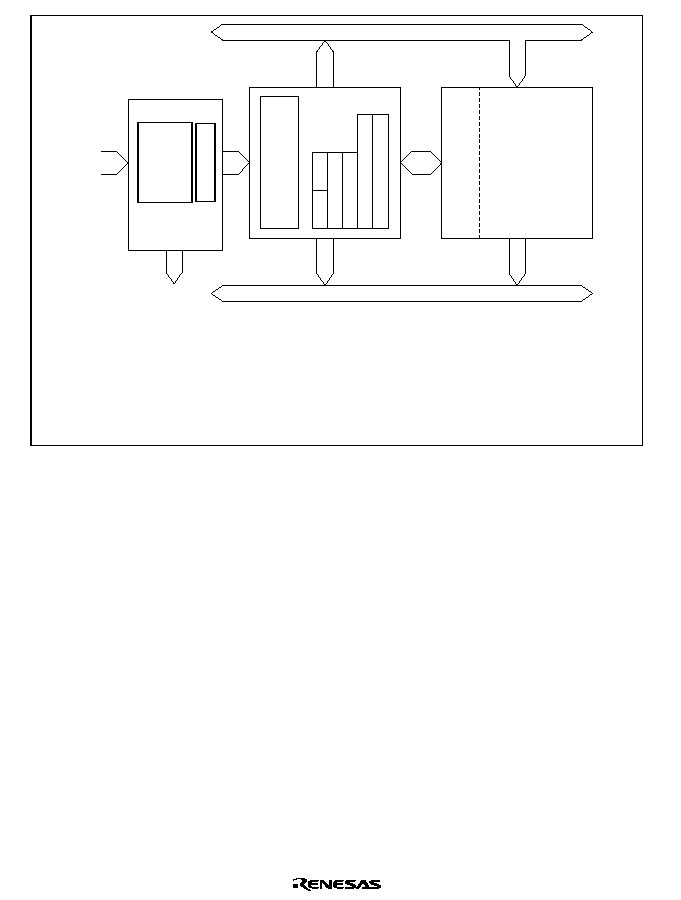
Rev. 2.0, 09/02, page 106 of 658
Internal address bus
DTCER
A
to
DTCERF
and DTCERI
Interrupt controller
Interrupt
request
DTC
On-chip
RAM
Internal data bus
CPU interrupt
request
MRA
MRB
CRA
CRB
DAR
SAR
MRA, MRB
CRA, CRB
SAR
DAR
DTCERA to DTCERF
and DTCERI
DTVECR
: DTC mode registers A and B
: DTC transfer count registers A and B
: DTC source address register
: DTC destination address register
: DTC enable registers A to F and I
: DTC vector register
Legend
DTC service
request
Control logic
Register information
DTVECR
Figure 8.1 Block Diagram of DTC

Rev. 2.0, 09/02, page 107 of 658
8.2
Register Descriptions
The DTC has the following registers.
∑
DTC mode register A (MRA)
∑
DTC mode register B (MRB)
∑
DTC source address register (SAR)
∑
DTC destination address register (DAR)
∑
DTC transfer count register A (CRA)
∑
DTC transfer count register B (CRB)
These six registers cannot be directly accessed from the CPU.
When activated, the DTC reads a set of register information that is stored in on-chip RAM to the
corresponding DTC registers and transfers data. After the data transfer, it writes a set of updated
register information back to the RAM.
∑
DTC enable registers (DTCER)
∑
DTC vector register (DTVECR)
8.2.1
DTC Mode Register A (MRA)
MRA selects the DTC operating mode.

Rev. 2.0, 09/02, page 108 of 658
Bit
Bit Name
Initial
Value
R/W
Description
7
6
SM1
SM0
Undefined
Undefined
Source Address Mode 1 and 0
These bits specify an SAR operation after a data
transfer.
0X: SAR is fixed
10: SAR is incremented after a transfer
(by +1 when Sz = 0; by +2 when Sz = 1)
11: SAR is decremented after a transfer
(by ≠1 when Sz = 0; by ≠2 when Sz = 1)
5
4
DM1
DM0
Undefined
Undefined
Destination Address Mode 1 and 0
These bits specify a DAR operation after a data
transfer.
0X: DAR is fixed
10: DAR is incremented after a transfer
(by +1 when Sz = 0; by +2 when Sz = 1)
11: DAR is decremented after a transfer
(by ≠1 when Sz = 0; by ≠2 when Sz = 1)
3
2
MD1
MD0
Undefined
Undefined
DTC Mode 1 and 0
These bits specify the DTC transfer mode.
00: Normal mode
01: Repeat mode
10: Block transfer mode
11: Setting prohibited
1
DTS
Undefined
DTC Transfer Mode Select
Specifies whether the source side or the destination
side is set to be a repeat area or block area, in repeat
mode or block transfer mode.
0: Destination side is repeat area or block area
1: Source side is repeat area or block area
0
Sz
Undefined
DTC Data Transfer Size
Specifies the size of data to be transferred.
0: Byte-size transfer
1: Word-size transfer
Legend
X: Don't care

Rev. 2.0, 09/02, page 109 of 658
8.2.2
DTC Mode Register B (MRB)
MRB is an 8-bit register that selects the DTC operating mode.
Bit
Bit Name
Initial
Value
R/W
Description
7
CHNE
Undefined
DTC Chain Transfer Enable
This bit specifies a chain transfer. For details, refer to
8.5.4, Chain Transfer.
In data transfer with CHNE set to 1, determination of
the end of the specified number of transfers, clearing
of the interrupt source flag, and clearing of DTCER,
are not performed.
0: DTC data transfer completed (waiting for start)
1: DTC data transfer (reads new register information
and transfers data)
6
DISEL
Undefined
DTC Interrupt Select
This bit specifies whether CPU interrupt is disabled
or enabled after a data transfer.
0: Interrupt request is issued to the CPU when the
specified data transfer is completed.
1: DTC issues interrupt request to the CPU in every
data transfer (DTC does not clear the interrupt
request flag that is a cause of the activation).
5 to 0
Undefined
Reserved
These bits have no effect on DTC operation. The
write value should always be 0.
8.2.3
DTC Source Address Register (SAR)
SAR is a 24-bit register that designates the source address of data to be transferred by the DTC.
For word-size transfer, specify an even source address.
8.2.4
DTC Destination Address Register (DAR)
DAR is a 24-bit register that designates the destination address of data to be transferred by the
DTC. For word-size transfer, specify an even destination address.

Rev. 2.0, 09/02, page 110 of 658
8.2.5
DTC Transfer Count Register A (CRA)
CRA is a 16-bit register that designates the number of times data is to be transferred by the DTC.
In normal mode, the entire CRA functions as a 16-bit transfer counter (1 to 65536). It is
decremented by 1 every time data is transferred, and transfer ends when the count reaches H'0000.
In repeat mode or block transfer mode, the CRA is divided into two parts; the upper 8 bits
(CRAH) and the lower 8 bits (CRAL). CRAH holds the number of transfers while CRAL
functions as an 8-bit transfer counter (1 to 256). CRAL is decremented by 1 every time data is
transferred, and the contents of CRAH are sent when the count reaches H'00.
8.2.6
DTC Transfer Count Register B (CRB)
CRB is a 16-bit register that designates the number of times data is to be transferred by the DTC in
block transfer mode. It functions as a 16-bit transfer counter (1 to 65536) that is decremented by 1
every time data is transferred, and transfer ends when the count reaches H'0000.
8.2.7
DTC Enable Register (DTCER)
DTCER is comprised of seven registers; DTCERA to DTCERF and DTCERI, and is a register
that specifies DTC activation interrupt sources. The correspondence between interrupt sources and
DTCE bits is shown in table 8.1. For DTCE bit setting, use bit manipulation instructions such as
BSET and BCLR for reading and writing. If all interrupts are masked, multiple activation sources
can be set at one time (only at the initial setting) by writing data after executing a dummy read on
the relevant register.
Bit
Bit Name
Initial
Value
R/W
Description
7
6
5
4
3
2
1
0
DTCE7
DTCE6
DTCE5
DTCE4
DTCE3
DTCE2
DTCE1
DTCE0
0
0
0
0
0
0
0
0
R/W
R/W
R/W
R/W
R/W
R/W
R/W
R/W
DTC Activation Enable
Setting this bit to 1 specifies a relevant interrupt
source as a DTC activation source.
[Clearing conditions]
When the DISEL bit is 1 and the data transfer has
ended
When the specified number of transfers have ended
These bits are not cleared when the DISEL bit is 0
and the specified number of transfers have not been
completed

Rev. 2.0, 09/02, page 111 of 658
8.2.8
DTC Vector Register (DTVECR)
DTVECR is an 8-bit readable/writable register that enables or disables DTC activation by
software, and sets a vector number for the software activation interrupt.
Bit
Bit Name
Initial
Value
R/W
Description
7
SWDTE
0
R/W
DTC Software Activation Enable
Setting this bit to 1 activates DTC. Only a 1 can be
written to this bit.
[Clearing conditions]
When the DISEL bit is 0 and the specified number of
transfers have not ended
When 0 s written to the DISEL bit after a software-
activated data transfer end interrupt (SWDTEND)
request has been sent to the CPU.
When the DISEL bit is 1 and data transfer has ended,
the specified number of transfers have ended, or
software-activated data transfer is in process, this bit
will not be cleared.
6
5
4
3
2
1
0
DTVEC6
DTVEC5
DTVEC4
DTVEC3
DTVEC2
DTVEC1
DTVEC0
0
0
0
0
0
0
0
R/W
R/W
R/W
R/W
R/W
R/W
R/W
DTC Software Activation Vectors 0 to 6
These bits specify a vector number for DTC software
activation.
The vector address is expressed as H'0400 + (vector
number
◊
2). For example, when DTVEC6 to
DTVEC0 = H'10, the vector address is H'0420.
These bits are writable when SWDTE=0.
8.3
Activation Sources
The DTC operates when activated by an interrupt or by a write to DTVECR by software. An
interrupt request can be directed to the CPU or DTC, as designated by the corresponding DTCER
bit. At the end of a data transfer (or the last consecutive transfer in the case of chain transfer), the
activation source or corresponding DTCER bit is cleared. The activation source flag, in the case of
RXI0, for example, is the RDRF flag of SCI_0.
When an interrupt has been designated a DTC activation source, the existing CPU mask level and
interrupt controller priorities have no effect. If there is more than one activation source at the same
time, the DTC operates in accordance with the default priorities.
Figure 8.2 shows a block diagram of activation source control. For details, see section 5, Interrupt
Controller.

Rev. 2.0, 09/02, page 112 of 658
CPU
DTC
DTCER
Source flag cleared
On-chip
peripheral
module
IRQ interrupt
Interrupt
request
Clear
Clear
controller
Clear request
Interrupt controller
Selection circuit
Interrupt mask
Select
DTVECR
Figure 8.2 Block Diagram of DTC Activation Source Control
8.4
Location of Register Information and DTC Vector Table
Locate the register information in the on-chip RAM (addresses: H'FFEBC0 to H'FFEFBF).
Register information should be located at an address that is a multiple of four within the range.
Locating the register information in address space is shown in figure 8.3. Locate the MRA, SAR,
MRB, DAR, CRA, and CRB registers, in that order, from the start address of the register
information.
In the case of chain transfer, register information should be located in consecutive areas as shown
in figure 8.3, and the register information start address should be located at the vector address
corresponding to the interrupt source. Figure 8.4 shows the correspondence between DTC vector
address and register information. The DTC reads the start address of the register information from
the vector address set for each activation source, and then reads the register information from that
start address.
When the DTC is activated by software, the vector address is obtained from: H'0400 +
(DTVECR[6:0]
◊
2). For example, if DTVECR is H'10, the vector address is H'0420.
The configuration of the vector address is the same in both normal* and advanced modes, a 2-byte
unit being used in both cases. These two bytes specify the lower bits of the register information
start address.
Note:
Normal mode cannot be used in this LSI.

Rev. 2.0, 09/02, page 113 of 658
MRA
0
1
2
3
SAR
MRB
DAR
CRA
CRB
MRA
SAR
MRB
DAR
CRA
CRB
Lower address
4 bytes
Register information
Register information
for 2nd transfer in
chain transfer
Register
information
start address
Chain
transfer
Figure 8.3 The Location of the DTC Register Information in the Address Space
Register information
start address
Register information
Chain transfer
DTC vector
address
Figure 8.4 Correspondence between DTC Vector Address and Register Information

Rev. 2.0, 09/02, page 114 of 658
Table 8.1
Interrupt Sources, DTC Vector Addresses, and Corresponding DTCEs
Interrupt
Source
Origin of
Interrupt Source
Vector Number
DTC
Vector Address
DTCE
*
Priority
Software
Write to DTVECR
DTVECR
H'0400 +
vector number
◊
2
High
External pin
IRQ0
16
H'0420
DTCEA7
IRQ1
17
H'0422
DTCEA6
IRQ3
19
H'0426
DTCEA4
IRQ4
20
H'0428
DTCEA3
IRQ5
21
H'042A
DTCEA2
A/D
ADI (A/D conversion
end)
28
H'0438
DTCEB6
TGI0A
32
H'0440
DTCEB5
TPU
Channel 0
TGI0B
33
H'0442
DTCEB4
TGI0C
34
H'0444
DTCEB3
TGI0D
35
H'0446
DTCEB2
TGI1A
40
H'0450
DTCEB1
TPU
Channel 1
TGI1B
41
H'0452
DTCEB0
TGI2A
44
H'0458
DTCEC7
TPU
Channel 2
TGI2B
45
H'045A
DTCEC6
CMIA0
64
H'0480
DTCED3
8-bit timer
channel 0
CMIB0
65
H'0482
DTCED2
CMIA1
68
H'0488
DTCED1
8-bot timer
channel 1
CMIB1
69
H'048A
DTCED0
RXI0
81
H'04A2
DTCEE3
SCI
channel 0
TXI0
82
H'04A4
DTCEE2
RXI1
85
H'04AA
DTCEE1
SCI
channel 1
TXI1
86
H'04AC
DTCEE0
CMIA2
92
H'04B8
DTCEF5
8-bit timer
channel 2
CMIB2
93
H'04BA
DTCEF4
CMIA3
96
H'04C0
DTCEF3
8-bit timer
channel 3
CMIB3
97
H'04C2
DTCEF2
Low

Rev. 2.0, 09/02, page 115 of 658
Interrupt
Source
Origin of
Interrupt Source
Vector Number
DTC
Vector Address
DTCE
*
Priority
IIC channel 0
(optional)
IICI0
100
H'04C8
DTCEF1
High
IIC channel 1
(optional)
IICI1
102
H'04CC
DTCEF0
RXI2
121
H'04F2
DTCEI7
SCI
channel 2
TXI2
122
H'04F4
DTCEI6
Low
Note:
*
DTCE bits with no corresponding interrupt are reserved, and should be written with 0.
8.5
Operation
Register information is stored in on-chip RAM. When activated, the DTC reads register
information in on-chip RAM and transfers data. After the data transfer, the DTC writes updated
register information back to the memory.
The pre-storage of register information in memory makes it possible to transfer data over any
required number of channels. The transfer mode can be specified as normal, repeat, and block
transfer mode. Setting the CHNE bit in MRB to 1 makes it possible to perform a number of
transfers with a single activation source (chain transfer).
The 24-bit SAR designates the DTC transfer source address, and the 24-bit DAR designates the
transfer destination address. After each transfer, SAR and DAR are independently incremented,
decremented, or left fixed depending on its register information.
Figure 8.5 shows the flowchart of DTC operation.

Rev. 2.0, 09/02, page 116 of 658
Start
End
Read DTC vector
Read register infomation
Data transfer
Write register information
Interupt exception
handling
Clear DTCER
Clear an activeation flag
CHNE 1
Next transfer
Yes
Yes
No
Transfer Counter=0
or DISEL 1
No
Figure 8.5 Flowchart of DTC Operation
8.5.1
Normal Mode
In normal mode, one operation transfers one byte or one word of data.
From 1 to 65,536 transfers can be specified. Once the specified number of transfers have been
completed, a CPU interrupt can be requested.
Table 8.2 lists the register information in normal mode. Figure 8.6 shows the memory mapping in
normal mode.

Rev. 2.0, 09/02, page 117 of 658
Table 8.2
Register Information in Normal Mode
Name
Abbreviation
Function
DTC source address register
SAR
Designates source address
DTC destination address register
DAR
Designates destination address
DTC transfer count register A
CRA
Designates transfer count
DTC transfer count register B
CRB
Not used
SAR
DAR
Transfer
Figure 8.6 Memory Mapping in Normal Mode
8.5.2
Repeat Mode
In repeat mode, one operation transfers one byte or one word of data.
From 1 to 256 transfers can be specified. Once the specified number of transfers have ended, the
initial state of the transfer counter and the address register specified as the repeat area is restored,
and transfer is repeated. In repeat mode the transfer counter value does not reach H'00, and
therefore CPU interrupts cannot be requested when DISEL = 0.
Table 8.3 lists the register information in repeat mode. Figure 8.7 shows the memory mapping in
repeat mode.

Rev. 2.0, 09/02, page 118 of 658
Table 8.3
Register Information in Repeat Mode
Name
Abbreviation
Function
DTC source address register
SAR
Designates source address
DTC destination address register
DAR
Designates destination address
DTC transfer count register AH
CRAH
Holds number of transfers
DTC transfer count register AL
CRAL
Designates transfer count
DTC transfer count register B
CRB
Not used
SAR
or
DAR
DAR
or
SAR
Repeat area
Transfer
Figure 8.7 Memory Mapping in Repeat Mode
8.5.3
Block Transfer Mode
In block transfer mode, one operation transfers one block of data. Either the transfer source or the
transfer destination is designated as a block area.
The block size can be between 1 to 256. When the transfer of one block ends, the initial state of
the block size counter and the address register specified as the block area is restored. The other
address register is then incremented, decremented, or left fixed.
From 1 to 65,536 transfers can be specified. Once the specified number of transfers have been
completed, a CPU interrupt is requested.
Table 8.4 lists the register information in block transfer mode. Figure 8.8 shows the memory
mapping in block transfer mode.

Rev. 2.0, 09/02, page 119 of 658
Table 8.4
Register Information in Block Transfer Mode
Name
Abbreviation
Function
DTC source address register
SAR
Designates source address
DTC destination address register
DAR
Designates destination address
DTC transfer count register AH
CRAH
Holds block size
DTC transfer count register AL
CRAL
Designates block size count
DTC transfer count register B
CRB
Transfer count
First block
Transfer
Block area
Nth block
DAR
or
SAR
SAR
or
DAR
Figure 8.8 Memory Mapping in Block Transfer Mode
8.5.4
Chain Transfer
Setting the CHNE bit in MRB to 1 enables a number of data transfers to be performed
consecutively in response to a single transfer request. SAR, DAR, CRA, CRB, MRA, and MRB,
which define data transfers, can be set independently.
Figure 8.9 shows the memory map for chain transfer.
When activated, the DTC reads the register information start address stored at the vector address,
and then reads the first register information at that start address. After the data transfer, the CHNE
bit will be tested. When it has been set to 1, DTC reads the next register information located in a

Rev. 2.0, 09/02, page 120 of 658
consecutive area and performs the data transfer. These sequences are repeated until the CHNE bit
is cleared to 0.
In the case of transfer with CHNE set to 1, an interrupt request to the CPU is not generated at the
end of the specified number of transfers or by setting of the DISEL bit to 1, and the interrupt
source flag for the activation source is not affected.
DTC vector
address
Register information
CHNE=1
Register information
CHNE=0
Register information
start address
Source
Destination
Source
Destination
Figure 8.9 Chain Transfer Operation
8.5.5
Interrupts
An interrupt request is issued to the CPU when the DTC has completed the specified number of
data transfers, or a data transfer for which the DISEL bit was set to 1. In the case of interrupt
activation, the interrupt set as the activation source is generated. These interrupts to the CPU are
subject to CPU mask level and interrupt controller priority level control.
In the case of software activation, a software-activated data transfer end interrupt (SWDTEND) is
generated.

Rev. 2.0, 09/02, page 121 of 658
When the DISEL bit is 1 and one data transfer has been completed, or the specified number of
transfers have been completed, after data transfer ends the SWDTE bit is held at 1 and an
SWDTEND interrupt is generated. The interrupt handling routine will then clear the SWDTE bit
to 0.
When the DTC is activated by software, an SWDTEND interrupt is not generated during a data
transfer wait or during data transfer even if the SWDTE bit is set to 1.
8.5.6
Operation Timing
Figure 8.10 to 8.12 show the DTC operation timings.
DTC activation
request
DTC
request
Address
Vector read
Read Write
Data transfer
Transfer
information write
Transfer
information read
Figure 8.10 DTC Operation Timing (Example in Normal Mode or Repeat Mode)
DTC activation
request
DTC
request
Address
Vector read
Read Write Read Write
Data transfer
Transfer
information write
Transfer
information read
Figure 8.11 DTC Operation Timing (Example of Block Transfer Mode,
with Block Size of 2)
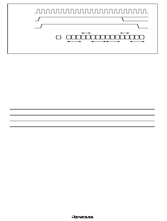
Rev. 2.0, 09/02, page 122 of 658
DTC activation
request
DTC
request
Address
Vector read
Read Write
Read Write
Data transfer
Data transfer
Transfer
information
write
Transfer
information write
Transfer
information read
Transfer
information
read
Figure 8.12 DTC Operation Timing (Example of Chain Transfer)
8.5.7
Number of DTC Execution States
Table 8.5 lists execution status for a single DTC data transfer, and table 8.6 shows the number of
states required for each execution status.
Table 8.5
DTC Execution Status
Mode
Vector Read
I
Register Information
Read/Write
J
Data Read
K
Data Write
L
Internal
Operations
M
Normal
1
6
1
1
3
Repeat
1
6
1
1
3
Block transfer
1
6
N
N
3
Legend:
N: Block size (initial setting of CRAH and CRAL)

Rev. 2.0, 09/02, page 123 of 658
Table 8.6
Number of States Required for Each Execution Status
Object to be Accessed
On-
Chip
RAM
On-
Chip
ROM
Internal I/O
Registers
External Devices
*
Bus width
32
16
8
16
8
16
Access states
1
1
2
2
2
3
2
3
Vector read S
I
1
4
6 + 2m 2
3 + m
Execution
Status
Register information
read/write S
J
1
Byte data read S
K
1
1
2
2
2
3 + m 2
3 + m
Word data read S
K
1
1
4
2
4
6 + 2m 2
3 + m
Byte data write S
L
1
1
2
2
2
3 + m 2
3 + m
Word data write S
L
1
1
4
2
4
6 + 2m 2
3 + m
Internal operation S
M
1
Legend:
m: The number of wait states for accessing external devices.
Note:
*
Cannot be used in this LSI.
The number of execution states is calculated from using the formula below. Note that
is the sum
of all transfers activated by one activation event (the number in which the CHNE bit is set to 1,
plus 1).
Number of execution states = I ∑ S
I
+
(J ∑ S
J
+ K ∑ S
K
+ L ∑ S
L
) + M ∑ S
M
For example, when the DTC vector address table is located in the on-chip ROM, normal mode is
set, and data is transferred from on-chip ROM to an internal I/O register, then the time required for
the DTC operation is 13 states. The time from activation to the end of the data write is 10 states.
8.6
Procedures for Using DTC
8.6.1
Activation by Interrupt
The procedure for using the DTC with interrupt activation is as follows:
1.
Set the MRA, MRB, SAR, DAR, CRA, and CRB register information in on-chip RAM.
2.
Set the start address of the register information in the DTC vector address.
3.
Set the corresponding bit in DTCER to 1.
4.
Set the enable bits for the interrupt sources to be used as the activation sources to 1. The DTC
is activated when an interrupt used as an activation source is generated.

Rev. 2.0, 09/02, page 124 of 658
5.
After one data transfer has been completed, or after the specified number of data transfers
have been completed, the DTCE bit is cleared to 0 and a CPU interrupt is requested. If the
DTC is to continue transferring data, set the DTCE bit to 1.
8.6.2
Activation by Software
The procedure for using the DTC with software activation is as follows:
1.
Set the MRA, MRB, SAR, DAR, CRA, and CRB register information in on-chip RAM.
2.
Set the start address of the register information in the DTC vector address.
3.
Check that the SWDTE bit is 0.
4.
Write 1 to SWDTE bit and the vector number to DTVECR.
5.
Check the vector number written to DTVECR.
6.
After one data transfer has been completed, if the DISEL bit is 0 and a CPU interrupt is not
requested, the SWDTE bit is cleared to 0. If the DTC is to continue transferring data, set the
SWDTE bit to 1. When the DISEL bit is 1, or after the specified number of data transfers
have been completed, the SWDTE bit is held at 1 and a CPU interrupt is requested.
8.7
Examples of Use of the DTC
8.7.1
Normal Mode
An example is shown in which the DTC is used to receive 128 bytes of data via the SCI.
1.
Set MRA to a fixed source address (SM1 = SM0 = 0), incrementing destination address
(DM1 = 1, DM0 = 0), normal mode (MD1 = MD0 = 0), and byte size (Sz = 0). The DTS bit
can have any value. Set MRB for one data transfer by one interrupt (CHNE = 0, DISEL = 0).
Set the SCI RDR address in SAR, the start address of the RAM area where the data will be
received in DAR, and 128 (H'0080) in CRA. CRB can be set to any value.
2.
Set the start address of the register information at the DTC vector address.
3.
Set the corresponding bit in DTCER to 1.
4.
Set the SCI to the appropriate receive mode. Set the RIE bit in SCR to 1 to enable the
reception complete (RXI) interrupt. Since the generation of a receive error during the SCI
reception operation will disable subsequent reception, the CPU should be enabled to accept
receive error interrupts.
5.
Each time the reception of one byte of data has been completed on the SCI, the RDRF flag
in SSR is set to 1, an RXI interrupt is generated, and the DTC is activated. The receive data is
transferred from RDR to RAM by the DTC. DAR is incremented and CRA is decremented.
The RDRF flag is automatically cleared to 0.

Rev. 2.0, 09/02, page 125 of 658
6.
When CRA becomes 0 after the 128 data transfers have been completed, the RDRF flag is
held at 1, the DTCE bit is cleared to 0, and an RXI interrupt request is sent to the CPU. The
interrupt handling routine will perform wrap-up processing.
8.7.2
Software Activation
An example is shown in which the DTC is used to transfer a block of 128 bytes of data by means
of software activation. The transfer source address is H'1000 and the destination address is
H'2000. The vector number is H'60, so the vector address is H'04C0.
1.
Set MRA to incrementing source address (SM1 = 1, SM0 = 0), incrementing destination
address (DM1 = 1, DM0 = 0), block transfer mode (MD1 = 1, MD0 = 0), and byte size (Sz =
0). The DTS bit can have any value. Set MRB for one block transfer by one interrupt (CHNE
= 0). Set the transfer source address (H'1000) in SAR, the destination address (H'2000) in
DAR, and 128 (H'8080) in CRA. Set 1 (H'0001) in CRB.
2.
Set the start address of the register information at the DTC vector address (H'04C0).
3.
Check that the SWDTE bit in DTVECR is 0. Check that there is currently no transfer
activated by software.
4.
Write 1 to the SWDTE bit and the vector number (H'60) to DTVECR. The write data is
H'E0.
5.
Read DTVECR again and check that it is set to the vector number (H'60). If it is not, this
indicates that the write failed. This is presumably because an interrupt occurred between steps
3 and 4 and led to a different software activation. To activate this transfer, go back to step 3.
6.
If the write was successful, the DTC is activated and a block of 128 bytes of data is
transferred.
7.
After the transfer, an SWDTEND interrupt occurs. The interrupt handling routine should
clear the SWDTE bit to 0 and perform other wrap-up processing.
8.8
Usage Notes
8.8.1
Module Stop Mode Setting
DTC operation can be disabled or enabled using the module stop control register. The initial
setting is for DTC operation to be enabled. Register access is disabled by setting module stop
mode. Module stop mode cannot be set during DTC operation. For details, refer to section 22,
Power-Down Modes.

Rev. 2.0, 09/02, page 126 of 658
8.8.2
On-Chip RAM
The MRA, MRB, SAR, DAR, CRA, and CRB registers are all located in on-chip RAM.
8.8.3
DTCE Bit Setting
For DTCE bit setting, use bit manipulation instructions such as BSET and BCLR. If all interrupts
are masked, multiple activation sources can be set at one time (only at the initial setting) by
writing data after executing a dummy read on the relevant register.

Rev. 2.0, 09/02, page 127 of 658
Section 9 I/O Ports
The H8S/2268 Series has ten I/O ports (ports 1, 3, 7, F, H, and J to N), and two input-only port
(ports 4 and 9). The H8S/2264 Series has eight I/O ports (ports 1, 3, 7, F, H, and J to L), and two
input-only port (ports 4 and 9).
Table 9.1 summarizes the port functions. The pins of each port also have other functions such as
input/output or interrupt input pins of on-chip peripheral modules.
Each I/O port includes a data direction register (DDR) that controls input/output, a data register
(DR) that stores output data, and a port register (PORT) used to read the pin states. The input-only
ports do not have DDR and DR registers.
Port J has a built-in input pull-up MOS function and an input pull-up MOS control register (PCR)
to control the on/off state of input pull-up MOS.
Port 3 includes an open-drain control register (ODR) that controls the on/off state of the output
buffer PMOS.
All the I/O ports can drive a single TTL load and a 30 pF capacitive load.
The P34 and P35 pins on port 3 are NMOS push pull outputs.
Pins
,54 and :.3 are Schmitt-trigger inputs. Pins PH0 to PH3 and ports J to N in the H8S/2268
Series and pins PH0 to PH3 and ports J to L in the H8S/2264 Series are shared as LCD segment
pins and common pins. They can be selected on an 8-bit basis in the H8S/2268 Series and on a 4-
bit basis in the H8S/2264 Series.

Rev. 2.0, 09/02, page 128 of 658
Table 9.1
H8S/2268 Series Port Functions (1)
Port
Description
Port and
Other Functions Name
Input/Output and
Output Type
Port 1
P17/TIOCB2/TCLKD
P16/TIOCA2/
,54
P15/TIOCB1/TCLKC
P14/TIOCA1/
,54
P13/TIOCD0/TCLKB
P12/TIOCC0/TCLKA
P11/TIOCB0
General I/O port also
functioning as TPU I/O
pins and interrupt input
pins
P10/TIOCA0
Port 3
P35/SCK1/SCL0/
,54
P34/RxD1/SDA0
P33/TxD1/SDA0
P32/SCK0/SDA1/
,54
P31/RxD0
General I/O port also
functioning as SCI_0
and SCI_1 I/O pins, I
2
C
bus interface I/O pins,
and interrupt input pins
P30/TxD0
Specifiable of open drain
output
Port 4
P47/AN7
P46/AN6
P45/AN5
P44/AN4
P43/AN3
P42/AN2
P41/AN1
General input port also
functioning as A/D
converter analog input
pins
P40/AN0
Port 7
P77/TxD2
P76/RxD2
P75/TMO3/SCK2
P74/TMO2
P73/TMO1
P72/TMO0
P71/TMRI23/TMCI23
General I/O port also
functioning as SCI_2
I/O pins and 8-bit timer
I/O pins
P70/TMRI01/TMCI01

Rev. 2.0, 09/02, page 129 of 658
Port
Description
Port and
Other Functions Name
Input/Output and
Output Type
Port 9
P97/AN9/DA1
General input port also
functioning as A/D
converter analog input
and D/A converter
analog output pins
P96/AN8/DA0
Port F
General I/O port also
functioning as interrupt
input pins and an A/D
converter input pins
PF3/
$'75*
/
,54
Port H
PH7/TONED/TMCI4
PH3/COM4
PH2/COM3
PH1/COM2
General input port also
functioning as DTMF
generation circuit pins,
8-bit reload timer input
pins
General I/O port also
functioning as LCD
common output pins
PH0/COM1
Port J
PJ7/
:.3
/SEG8
Built-in input pull-up MOS
PJ6/
:.3
/SEG7
PJ5/
:.3
/SEG6
PJ4/
:.3
/SEG5
PJ3/
:.3
/SEG4
PJ2/
:.3
/SEG3
PJ1/
:.3
/SEG2
General I/O port also
functioning as wakeup
input pins and LCD
segment output pins
PJ0/
:.3
/SEG1
Port K
PK7/SEG16
PK6/SEG15
PK5/SEG14
PK4/SEG13
PK3/SEG12
PK2/SEG11
PK1/SEG10
General I/O port also
functioning as LCD
segment output pins
PK0/SEG9

Rev. 2.0, 09/02, page 130 of 658
Port
Description
Port and
Other Functions Name
Input/Output and
Output Type
Port L
PL7/SEG24
PL6/SEG23
PL5/SEG22
PL4/SEG21
PL3/SEG20
PL2/SEG19
PL1/SEG18
General I/O port also
functioning as LCD
segment output pins
PL0/SEG17
Port M
PM7/SEG32
PM6/SEG31
PM5/SEG30
PM4/SEG29
PM3/SEG28
PM2/SEG27
PM1/SEG26
General I/O port also
functioning as LCD
segment output pins
PM0/SEG25
Port N
PN7/SEG40
PN6/SEG39
PN5/SEG38
PN4/SEG37
PN3/SEG36
PN2/SEG35
PN1/SEG34
General I/O port also
functioning as LCD
segment output pins
PN0/SEG33

Rev. 2.0, 09/02, page 131 of 658
Table 9.1
H8S/2264 Series Port Functions (2)
Port
Description
Port and
Other Functions Name
Input/Output and
Output Type
Port 1
P17/TIOCB2
P16/TIOCA2/
,54
P15/TIOCB1/TCLKC
P14/TIOCA1/
,54
P13/TCLKB
P12/TCLKA
P11
General I/O port also
functioning as TPU I/O
pins and interrupt input
pins
P10
Port 3
P35/SCK1/SCL0
P34/RxD1/SDA0
P33/TxD1
P32/SCK0/
,54
P31/RxD0
General I/O port also
functioning as SCI_0
and SCI_1 I/O pins, I
2
C
bus interface I/O pins,
and interrupt input pins
P30/TxD0
Specifiable of open drain
output
Port 4
P47/AN7
P46/AN6
P45/AN5
P44/AN4
P43/AN3
P42/AN2
P41/AN1
General input port also
functioning as A/D
converter analog input
pins
P40/AN0
Port 7
P77/TxD2
P76/RxD2
P75/SCK2
P74
P73/TMO1
P72/TMO0
P71
General I/O port also
functioning as SCI_2
I/O pins and 8-bit timer
I/O pins
P70/TMRI01/TMCI01

Rev. 2.0, 09/02, page 132 of 658
Port
Description
Port and
Other Functions Name
Input/Output and
Output Type
Port 9
P97/AN9
General input port also
functioning as A/D
converter analog inputs
P96/AN8
Port F
PF3/
$'75*
/
,54
General I/O port also
functioning as interrupt
input pins and an A/D
converter input pins
Port H
General input port
PH7
PH5
PH4/
PH3/COM4
PH2/COM3
PH1/COM2
General I/O port also
functioning as
output
pin and LCD common
output pins
PH0/COM1
Port J
PJ7/
:.3
/SEG8
Built-in input pull-up MOS
PJ6/
:.3
/SEG7
PJ5/
:.3
/SEG6
PJ4/
:.3
/SEG5
PJ3/
:.3
/SEG4
PJ2/
:.3
/SEG3
PJ1/
:.3
/SEG2
General I/O port also
functioning as wakeup
input pins and LCD
segment output pins
PJ0/
:.3
/SEG1
Port K
PK7/SEG16
PK6/SEG15
PK5/SEG14
PK4/SEG13
PK3/SEG12
PK2/SEG11
PK1/SEG10
General I/O port also
functioning as LCD
segment output pins
PK0/SEG9

Rev. 2.0, 09/02, page 133 of 658
Port
Description
Port and
Other Functions Name
Input/Output and
Output Type
Port L
PL7/SEG24
PL6/SEG23
PL5/SEG22
PL4/SEG21
PL3/SEG20
PL2/SEG19
PL1/SEG18
General I/O port also
functioning as LCD
segment output pins
PL0/SEG17
9.1
Port 1
Port 1 is an 8-bit I/O port and has the following registers.
∑
Port 1 data direction register (P1DDR)
∑
Port 1 data register (P1DR)
∑
Port 1 register (PORT1)
9.1.1
Port 1 Data Direction Register (P1DDR)
P1DDR specifies input or output of the port 1 pins using the individual bits. P1DDR cannot be
read; if it is, an undefined value will be read.
Bit
Bit Name
Initial
Value
R/W
Description
7
P17DDR
0
W
6
P16DDR
0
W
5
P15DDR
0
W
4
P14DDR
0
W
3
P13DDR
0
W
2
P12DDR
0
W
1
P11DDR
0
W
0
P10DDR
0
W
When a pin is specified as a general purpose I/O port,
setting this bit to 1 makes the corresponding port 1
pin an output pin. Clearing this bit to 0 makes the pin
an input pin.

Rev. 2.0, 09/02, page 134 of 658
9.1.2
Port 1 Data Register (P1DR)
P1DR stores output data for port 1 pins.
Bit
Bit Name
Initial
Value
R/W
Description
7
P17DR
0
R/W
6
P16DR
0
R/W
5
P15DR
0
R/W
4
P14DR
0
R/W
3
P13DR
0
R/W
2
P12DR
0
R/W
1
P11DR
0
R/W
0
P10DR
0
R/W
Output data for a pin is stored when the pin is
specified as a general purpose output port.
9.1.3
Port 1 Register (PORT1)
PORT1 shows the pin states. This register cannot be modified.
Bit
Bit Name
Initial
Value
R/W
Description
7
P17
*
R
6
P16
*
R
5
P15
*
R
4
P14
*
R
3
P13
*
R
2
P12
*
R
1
P11
*
R
0
P10
*
R
If a port 1 read is performed while P1DDR bits are set
to 1, the P1DR values are read. If a port 1 read is
performed while P1DDR bits are cleared to 0, the pin
states are read.
Note:
*
Determined by the states of pins P17 to P10.

Rev. 2.0, 09/02, page 135 of 658
9.1.4
Pin Functions
Port 1 pins also function as TPU I/O pins (TCLKA, TCLKB, TCLKC, TCLKD*, TIOCA0*,
TIOCB0*, TIOCC0*, TIOCD0*, TIOCA1, TIOCB1, TIOCA2, and TIOCB2) and external
interrupt input pins (
,54 and ,54). Port 1 pin functions are shown below.
Note: *
Supported only by the H8S/2268 Series.
∑
P17/TIOCB2/TCLKD*
3
The pin function is switched as shown below according to the combination of the TPU channel
2 setting, TPSC2 to TPS0 bits in TCR0*, and the P17DDR bit.
TPU Channel 2 Setting
**
Output
Input or Initial Value
P17DDR
0
1
P17 input
P17 output
TIOCB2 output
TIOCB2 input
*
1
Pin function
TCLKD input
*
2
*
3
Notes 1. This pin functions as TIOCB2 input when TPU channel 2 timer operating mode is set to
normal operation or phase counting mode
*
3
and IOB3 in TIOR_2 is set to 1.
2. In the H8S/2268 Series, this pin functions as TCLKD input when TPSC2 to TPSC0 in
TCR0 are set to 111 or when channel 2 is set to phase counting mode
*
3
.
3. Supported only by the H8S/2268 Series.
∑
P16/TIOCA2/
,54
The pin function is switched as shown below according to the combination of the TPU channel
2 setting and the P16DDR bit.
TPU Channel 2 Setting
**
Output
Input or Initial Value
P16DDR
0
1
P16 input
P16 output
TIOCA2 output
TIOCA2 input
*
1
Pin function
,54
input
*
2
Notes 1. This pin functions as TIOCA2 input when TPU channel 2 timer operating mode is set to
normal operation or phase counting mode
*
3
and IOA3 in TIOR_2 is 1.
2. When this pin is used as an external interrupt pin, do not specify other functions.
3. Supported only by the H8S/2268 Series.

Rev. 2.0, 09/02, page 136 of 658
∑
P15/TIOCB1/TCLKC
The pin function is switched as shown below according to the combination of the TPU channel
1 setting, TPSC2 to TPSC0 bits in TCR0*
3
and TCR2, and the P15DDR bit.
TPU Channel 1 Setting
**
Output
Input or Initial Value
P15DDR
0
1
P15 input
P15 output
TIOCB1 output
TIOCB1 input
*
1
Pin function
TCLKC input
*
2
Notes 1. This pin functions as TIOCB1 input when TPU channel 1 timer operating mode is set to
normal operation or phase counting mode*
3
and IOB3 to IOB0 in TIOR_1 are set
to10xx.
2. This pin functions as TCLKC inputs when TPSC2 to TPSC0 in TCR0*
3
or TCR2 are set
to 110 or TCLKC input when channel 2 is set to phase counting mode*
3
.
3. Supported only by the H8S/2268 Series.
∑
P14/TIOCA1/
,54
The pin function is switched as shown below according to the combination of the TPU channel
1 setting and the P14DDR bit.
TPU Channel 1 Setting
**
Output
Input or Initial Value
P14DDR
0
1
P14 input
P14 output
TIOCA1 output
TIOCA1 input
*
1
Pin function
,54
input
*
2
Notes: 1. This pin functions as TIOCA1 input when TPU channel 1 timer operating mode is set to
normal operation or phase counting mode
*
3
and IOA3 to IOA0 in TIOR_1 are set to
10xx.
2. When this pin is used as an external interrupt pin, do not specify other functions.
3. Supported only by the H8S/2268 Series.
Rev. 2.0, 09/02, page 137 of 658
∑
P13/TIOCD0*
3
/TCLKB
The pin function is switched as shown below according to the combination of the TPU channel
0*
3
setting, TPSC2 to TPSC0 bits in TCR0*
3
, TCR1 and TCR2, and the P13DDR bit.
TPU Channel 0 Setting
** *
3
Output
Input or Initial Value
P13DDR
0
1
P13 input
P13 output
TIOCD0 output
*
3
TIOCD0 input
*
1
*
3
Pin function
TCLKB input
*
2
Notes: 1. In the H8S/2268 Series, this pin functions as TIOCD0 input when TPU channel 0 timer
operating mode is set to normal operation and IOD3 to IOD0 in TIORL_0 are set to
10xx.
2. This pin functions as TCLKB input when TPSC2 to TPSC0 are set to 101 in any of
TCR0
*
3
, TCR1 and TCR2. TCLKB input, or when channel 1 is set to phase counting
mode
*
3
.
3. Supported only by the H8S/2268 Series.
∑
P12/TIOCC0*
3
/TCLKA
The pin function is switched as shown below according to the combination of the TPU channel
0*
3
setting, TPSC2 to TPSC0 bits in TCR2, TCR1 and TCR0*
3
, and the P12DDR bit.
TPU Channel 0 Setting
** *
3
Output
Input or Initial Value
P12DDR
0
1
P12 input
P12 output
TIOCC0 output
*
3
TIOCC0 input
*
1
*
3
Pin function
TCLKA input
*
2
Notes: 1. In the H8S/2268 Series, TIOCC0 input when TPU channel 0 timer operating mode is
set to normal operation and IOC3 to IOC0 in TIORL_0 are set to 10xx.
2. This functions as TCLKA input when TPSC2 to TPSC0 are set to 100 in any of TCR2,
TCR1 and TCR0
*
3
or when channel 1 is set to phase counting mode
*
3
.
3. Supported only by the H8S/2268 Series.
Rev. 2.0, 09/02, page 138 of 658
∑
P11/TIOCB0*
2
The pin function is switched as shown below according to the combination of the TPU channel
0*
2
setting and the P11DDR bit.
TPU Channel 0
Setting
** *
2
Output
Input or Initial Value
P11DDR
0
1
P11 input
P11 output
Pin function
TIOCB0 output
*
2
TIOCB0 input
*
1
*
2
Notes: 1. In the H8S/2268 Series, this pin functions as TIOCB0 input when TPU channel 0 timer
operating mode is set to normal operation and IOB3 to IOB0 in TIORH_0 are set to
10xx.
2. Supported only by the H8S/2268 Series.
∑
P10/TIOCA0*
2
The pin function is switched as shown below according to the combination of the TPU channel
0*
2
setting and the P10DDR bit.
TPU Channel 0 Setting
** *
2
Output
Input or Initial Value
P10DDR
0
1
P10 input
P10 output
Pin function
TIOCA0 output
*
2
TIOCA0 input
*
1
*
2
Notes: 1. In the H8S/2268 Series, this pin functions as TIOCA0 input when TPU channel 0 timer
operating mode is set to normal operation and IOA3 to IOA0 in TIORH_0 are set to
10xx.
2. Supported only by the H8S/2268 Series.
**:
For the setting of the TPU channel, see section 10, 16-Bit Timer Pulse Unit (TPU).
9.2
Port 3
Port 3 is a 6-bit I/O port and has the following registers.
∑
Port 3 data direction register (P3DDR)
∑
Port 3 data register (P3DR)
∑
Port 3 register (PORT3)
∑
Port 3 open drain control register (P3ODR)

Rev. 2.0, 09/02, page 139 of 658
9.2.1
Port 3 Data Direction Register (P3DDR)
P3DDR specifies input or output of the port 3 pins using the individual bits.
P3DDR cannot be read; if it is, an undefined value will be read.
Bit
Bit Name
Initial
Value
R/W
Description
7, 6
Undefined
Reserved
These bits are always read as undefined value and
cannot be modified.
5
P35DDR
0
W
4
P34DDR
0
W
3
P33DDR
0
W
2
P32DDR
0
W
1
P31DDR
0
W
0
P30DDR
0
W
When a pin is specified as a general purpose I/O port,
setting this bit to 1 makes the corresponding port 3
pin an output port. Clearing this bit to 0 makes the pin
an input port.
9.2.2
Port 3 Data Register (P3DR)
P3DR stores output data for port 3 pins.
Bit
Bit Name
Initial
Value
R/W
Description
7, 6
Undefined
Reserved
These bits are always read as undefined value and
cannot be modified.
5
P35DR
0
R/W
4
P34DR
0
R/W
3
P33DR
0
R/W
2
P32DR
0
R/W
1
P31DR
0
R/W
0
P30DR
0
R/W
Output data for a pin is stored when the pin is
specified as a general purpose output port.

Rev. 2.0, 09/02, page 140 of 658
9.2.3
Port 3 Register (PORT3)
PORT3 shows the pin states. This register cannot be modified.
Bit
Bit Name
Initial
Value
R/W
Description
7, 6
Undefined
Reserved
These bits are always read as undefined value and
cannot be modified.
5
P35
*
R
4
P34
*
R
3
P33
*
R
2
P32
*
R
1
P31
*
R
0
P30
*
R
If a port 3 read is performed while P3DDR bits are set
to 1, the P3DR values are read. If a port 3 read is
performed while P3DDR bits are cleared to 0, the pin
states are read.
Note:
*
Determined by the states of pins P35 to P30.
9.2.4
Port 3 Open Drain Control Register (P3ODR)
P3ODR controls on/off state of the PMOS for port 3 pins.
Bit
Bit Name
Initial
Value
R/W
Description
7, 6
Undefined
Reserved
These bits are always read as undefined value and
cannot be modified.
5
P35ODR
0
R/W
4
P34ODR
0
R/W
3
P33ODR
0
R/W
2
P32ODR
0
R/W
1
P31ODR
0
R/W
0
P30ODR
0
R/W
When each of P33ODR to P30ODR bits is set to 1,
the corresponding pins P33 to P30 function as NMOS
open drain outputs. When cleared to 0, the
corresponding pins function as CMOS outputs. When
each of P35ODR and P34ODR bits is set to 1, the
corresponding pins P35 and P34 function as NMOS
open drain outputs. When they are cleared to 0, the
corresponding pins function as NMOS push pull
outputs.

Rev. 2.0, 09/02, page 141 of 658
9.2.5
Pin Functions
The port 3 pins also function as SCI I/O input pins (TxD0, RxD0, SCK0, TxD1, RxD1, and
SCK1), I2C bus interface I/O pins (SCL0, SDA0, SCL1*, and SDA1*), and as external interrupt
input pins (
,54 and ,54*).
As shown in figure 9.1, when the pins P34, P35, SCL0 or SDA0 type open drain output is used, a
bus line is not affected even if the power supply for this LSI fails. Use (a) type open drain output
when using a bus line having a state in which the power is not supplied to this LSI.
Output
0
(a) Open drain output type for
P34, P35, SCLO and SDA0 pins
Note:
*
Supported only by the H8S/2268 Series.
NMOS Off
Output
(b) Open drain output type for
P33 to P30, SCL1
*
and SDA1
*
pins
PMOS Off
Input
1
Input
Figure 9.1 Types of Open Drain Outputs
Note: *
Supported only by the H8S/2268 Series.
The functions of port 3 pins are shown below.

Rev. 2.0, 09/02, page 142 of 658
∑
P35/SCK1/SCL0/
,54*
2
The pin function is switched as shown below according to the combination of the ICE bit in
ICCR_0 of IIC_0, C/
$ bit in SMR of SCI_1, CKE0 and CKE1 bits in SCR and the P35DDR
bit.
ICE
0
1
CKE1
0
1
0
C/
$
0
1
0
CKE0
0
1
0
P35DDR
0
1
P35 input
pin
P35 output
pin
SCK1 output
pin
SCK1 output
pin
SCK1 input
pin
SCL0 I/O pin
Pin functions
,54
Input
*
1
*
2
Notes: 1. When this pin is used as an external interrupt pin, do not specify other functions.
2. Supported only by the H8S/2268 Series.
∑
P34/RxD1/SDA0
The pin function is switched as shown below according to the combination of the ICE bit in
ICCR_0 of IIC_0, RXD1S bit in SCKCR2*, RE bit in SCR of SCI_1 and the P34DDR bit.
ICE
0
1
RXD1S
*
0
1
RE
0
1
P34DDR
0
1
0
1
Pin functions
P34 input
pin
P34 output
pin
RxD1 input
pin
P34 input
pin
P34 output
pin
SDAO I/O
pin
Note:
*
Supported only by the H8S/2264 Series.
∑
P33/TxD1/SCL1*
The pin function is switched as shown below according to the combination of the ICE bit* in
ICCR_1 of IIC_1, TE bit in SCR of SCI_1 and the P33DDR bit.
ICE
*
0
1
TE
0
1
P33DDR
0
1
Pin functions
P33 input pin
P33 output pin
TxD1 output pin
SCL1 I/O pin
*
Note:
*
Supported only by the H8S/2268 Series.

Rev. 2.0, 09/02, page 143 of 658
∑
P32/SCK0/SDA1*
2
/
,54
The pin function is switched as shown below according to the combination of the ICE bit*
2
in
ICCR_1 of IIC_1, C/
$ bit in SMR of SCI_0, CKE0 and CKE1 bits in SCR and the P32DDR
bit.
ICE
*
2
0
1
CKE1
0
1
0
C/
$
0
1
0
CKE0
0
1
0
P32DDR
0
1
P32 input
pin
P32 output
pin
SCK0 output
pin
SCK0 output
pin
SCK0 input
pin
SDA1 I/O
pin
*
2
Pin functions
,54
Input
*
1
Notes: 1. When this pin is used as an external interrupt pin, do not specify other functions.
2. Supported only by the H8S/2268 Series.
∑
P31/RxD0
The pin function is switched as shown below according to the combination of the RE bit in
SCR of SCI_0 and the P31DDR bit.
RE
0
1
P31DDR
0
1
Pin functions
P31 input pin
P31 output pin
RxD0 input pin
∑
P30/TxD0
The pin function is switched as shown below according to the combination of the TE bit in
SCR of SCI_0 and the P30DDR bit.
TE
0
1
P30DDR
0
1
Pin functions
P30 input pin
P30 output pin
TxD0 output pin

Rev. 2.0, 09/02, page 144 of 658
9.3
Port 4
Port 4 is an 8-bit input-only port and has the following register.
∑
Port 4 register (PORT4)
9.3.1
Port 4 Register (PORT4)
PORT4 shows port 4 pin states. This register cannot be modified.
Bit
Bit Name
Initial
Value
R/W
Description
7
P47
*
R
6
P46
*
R
5
P45
*
R
4
P44
*
R
3
P43
*
R
2
P42
*
R
1
P41
*
R
0
P40
*
R
The pin states are always read when a port 4 read is
performed.
Note:
*
Determined by the states of pins P47 to P40.
9.3.2
Pin Functions
Port 4 pins also function as A/D converter analog input pins (AN0 to AN7).

Rev. 2.0, 09/02, page 145 of 658
9.4
Port 7
Port 7 is an 8-bit I/O port and has the following registers.
∑
Port 7 data direction register (P7DDR)
∑
Port 7 data register (P7DR)
∑
Port 7 register (PORT7)
9.4.1
Port 7 Data Direction Register (P7DDR)
P7DDR specifies input or output of the port 7 pins using the individual bits. P7DDR cannot be
read; if it is, an undefined value will be read.
Bit
Bit Name
Initial
Value
R/W
Description
7
P77DDR
0
W
6
P76DDR
0
W
5
P75DDR
0
W
4
P74DDR
0
W
3
P73DDR
0
W
2
P72DDR
0
W
1
P71DDR
0
W
0
P70DDR
0
W
When a pin is specified as a general purpose I/O port,
setting this bit to 1 makes the corresponding port 7
pin an output pin. Clearing this bit to 0 makes the pin
an input pin.
9.4.2
Port 7 Data Register (P7DR)
P7DR stores output data for port 7 pins.
Bit
Bit Name
Initial
Value
R/W
Description
7
P77DR
0
R/W
6
P76DR
0
R/W
5
P75DR
0
R/W
4
P74DR
0
R/W
3
P73DR
0
R/W
2
P72DR
0
R/W
1
P71DR
0
R/W
0
P70DR
0
R/W
Output data for a pin is stored when the pin is
specified as a general purpose output port.

Rev. 2.0, 09/02, page 146 of 658
9.4.3
Port 7 Register (PORT7)
PORT7 shows the pin states. This register cannot be modified.
Bit
Bit Name
Initial
Value
R/W
Description
7
P77
*
R
6
P76
*
R
5
P75
*
R
4
P74
*
R
3
P73
*
R
2
P72
*
R
1
P71
*
R
0
P70
*
R
If a port 1 read is performed while P7DDR bits are set
to 1, the P7DR values are read. If a port 1 read is
performed while P7DDR bits are cleared to 0, the pin
states are read.
Note:
*
Determined by the states of pins P77 to P70.
9.4.4
Pin Functions
Port 7 pins also function as the 8-bit timer I/O pins (TMRI01, TMCI01, TMRI23*, TMCI23*,
TMO0, TMO1, TMO2*, and TMO3*) and SCI I/O pins (SCK2, RxD2 and TxD2). Port 7 pin
functions are shown below.
Note: *
Supported only by the H8S/2268 Series.
∑
P77/TxD2
The pin function is switched as shown below according to the combination of the TE bit in
SCR of SCI_2 and the P77DDR bit.
TE
0
1
P77DDR
0
1
Pin functions
P77 input pin
P77 output pin
TxD2 output pin
∑
P76/RxD2
The pin function is switched as shown below according to the combination of the RE bit in
SCR of SCI_2 and the P76DDR bit.
RE
0
1
P76DDR
0
1
Pin functions
P76 input pin
P76 output pin
RxD2 Input pin

Rev. 2.0, 09/02, page 147 of 658
∑
P75/TMO3*/SCK2
The pin function is switched as shown below according to the combination of the OS3 to OS0
bits in TCSR_3* of the 8-bit timer, the C/A bit in SMR of SCI_2, the CKE0 and CKE1 bits in
SCR and the P75DDR bit.
OS3 to OS0
*
All bits are 0
Any bit is 1
CKE1
0
1
C/
$
0
1
CKE0
0
1
P75DDR
0
1
Pin functions
P75 input
pin
P75 output
pin
SCK2 output
pin
SCK2 output
pin
SCK2 input
pin
TMO3
output pin
*
Note:
*
Supported only by the H8S/2268 Series.
∑
P74/TMO2*
The pin function is switched as shown below according to the combination of the OS3 to OS0
bits in TCSR_2* of the 8-bit timer and the P74DDR bit.
OS3 to OS0
*
All bits are 0
Any bit is 1
P74DDR
0
1
Pin functions
P74 input pin
P74 output pin
TMO2 output pin
*
Note:
*
Supported only by the H8S/2268 Series.
∑
P73/TMO1
The pin function is switched as shown below according to the combination of the OS3 to OS0
bits in TCSR_1 of the 8-bit timer and the P73DDR bit.
OS3 to OS0
All bits are 0
Any bit is 1
P73DDR
0
1
Pin functions
P73 input pin
P73 output pin
TMO1 output pin
∑
P72/TMO0
The pin function is switched as shown below according to the combination of the OS3 to OS0
bits in TCSR_0 of the 8-bit timer and the P72DDR bit.
OS3 to OS0
All bits are 0
Any bit is 1
P72DDR
0
1
Pin functions
P72 input pin
P72 output pin
TMO0 output pin

Rev. 2.0, 09/02, page 148 of 658
∑
P71/TMRI23*/TMCI23*
The pin function is switched as shown below according to the P71DDR bit.
P71DDR
0
1
Pin functions
P71 input pin
P71 output pin
TMRI23/TMCI23 input pin
*
Note:
*
Supported only by the H8S/2268 Series.
∑
P70/TMRI01/TMCI01
The pin function is switched as shown below according to the P70DDR bit.
P70DDR
0
1
Pin functions
P70 input pin
P70 output pin
TMRI01/TMCI01 input pin
9.5
Port 9
Port 9 is a 2-bit input-only port and has the following register.
∑
Port 9 register (PORT9)
9.5.1
Port 9 Register (PORT9)
PORT9 shows port 9 pin states. This register cannot be modified.
Bit
Bit Name
Initial
Value
R/W
Description
7
P97
*
R
6
P96
*
R
The pin states are always read when these bits are
read.
5 to 0
Undefined
R
Reserved
These bits are always read as undefined value and
cannot be modified.
Note:
*
Determined by the states of pins P97 and P96.
9.5.2
Pin Functions
Port 9 pins also function as A/D converter analog input pins (AN8 and AN9) and D/A converter
analog output pins (DA0 and DA1)*.
Note: *
Supported only by the H8S/2268 Series.

Rev. 2.0, 09/02, page 149 of 658
9.6
Port F
Port F is a 1-bit I/O port and has the following register.
∑
Port F data direction register (PFDDR)
∑
Port F data register (PFDR)
∑
Port F register (PORTF)
9.6.1
Port F Data Direction Register (PFDDR)
PFDDR specifies input or output the port F pins using the individual bits. PFDDR cannot be read;
if it is, an undefined value will be read.
Bit
Bit Name
Initial
Value
R/W
Description
7 to 4
Undefined
Reserved
These bits are always read as undefined value and
cannot be modified.
3
PF3DDR
0
W
When a pin is specified as a general purpose I/O port,
setting this bit to 1 makes the corresponding port F
pin an output pin. Clearing this bit to 0 makes the pin
an input pin.
2 to 0
Undefined
Reserved
These bits are always read as undefined value and
cannot be modified.
9.6.2
Port F Data Register (PFDR)
PFDR stores output data for port F pins.
Bit
Bit Name
Initial
Value
R/W
Description
7 to 4
Undefined
Reserved
These bits are always read as undefined value and
cannot be modified.
3
PF3DR
0
R/W
Output data for a pin is stored when the pin is
specified as a general purpose output port.
2 to 0
Undefined
Reserved
These bits are always read as undefined value and
cannot be modified.

Rev. 2.0, 09/02, page 150 of 658
9.6.3
Port F Register (PORTF)
PORTF shows the pin states. This register cannot be modified.
Bit
Bit Name
Initial
Value
R/W
Description
7 to 4
Undefined
Reserved
These bits are always read as undefined value and
cannot be modified.
3
PF3
*
R
If this bit is read while PFDDR is set to 1, the PFDR
value is read. If this bit is read while PFDDR is
cleared, the PF3 pin states are read.
2 to 0
Undefined
Reserved
These bits are always read as undefined value and
cannot be modified.
Note:
*
Determined by the states of PF3 pin.
9.6.4
Pin Functions
Port F pins also function as an external interrupt input pin (
,54) and A/D trigger output pin
(
$'75*). Port F pin functions are shown below.
∑
PF3/
$'75*/,54
The pin function is switched as shown below according to the combination of the TRGS1 and
TRGS0 bits of ADCR of the A/D converter and the PF3DDR bit.
PF3DDR
0
1
PF3 input pin
PF3 output pin
$'75*
Input pin
*
1
Pin functions
,54
input pin
*
2
Notes: 1. When TRGS0 = TRGS1 = 1, port F is used as the
$'75*
input pin.
2. When this port is used as an external interrupt pin, do not specify other functions.
9.7
Port H
Port H for the H8S/2268 Series is a 1-bit input and 4-bit I/O port, and that for the H8S/2264 Series
is a 1-bit input and 6-bit I/O port. Port H has the following registers.
∑
Port H data direction register (PHDDR)
∑
Port H data register (PHDR)
∑
Port H register (PORTH)

Rev. 2.0, 09/02, page 151 of 658
9.7.1
Port H Data Direction Register (PHDDR)
PHDDR specifies input or output the port H pins using the individual bits. PHDDR cannot be
read; if it is, an undefined value will be read.
Bit
Bit Name
Initial
Value
R/W
Description
7, 6
Undefined
Reserved
These bits are always read as undefined value and
cannot be modified.
5
4
PH5DDR
PH4DDR
0
*
1
0
*
1
W
*
2
W
*
2
H8S/2268 Series:
Reserved
These bits are always read as undefined value and
cannot be modified.
H8S/2264 Series:
When a pin is specified as a general purpose I/O port,
setting the bit to 1 makes the corresponding port H
pin an output pin. Clearing the bit to 0 makes the pin
an input pin.
3
PH3DDR
0
W
2
PH2DDR
0
W
1
PH1DDR
0
W
0
PH0DDR
0
W
When a pin is specified as a general purpose I/O port,
setting these bits to 1 makes the corresponding port H
pin an output pin. Clearing this bit to 0 makes the pin
an input pin.
Notes: 1. Undefined in the H8S/2268 Series.
2. This bit cannot be modified in the H8S/2268 Series.

Rev. 2.0, 09/02, page 152 of 658
9.7.2
Port H Data Register (PHDR)
PHDR stores output data for port H pins (H8S/2268 Series: PH3 to PH0; H8S/2264 Series: PH5 to
PH0).
Bit
Bit Name
Initial
Value
R/W
Description
7, 6
Undefined
Reserved
These bits are always read as undefined value and
cannot be modified.
5
4
PH5DR
PH4DR
0
*
1
0
*
1
R/W
*
2
R/W
*
2
H8S/2268 Series:
Reserved
These bits are always read as undefined value and
cannot be modified.
H8S/2264 Series:
Output data for a pin is stored when the pin is
specified as a general purpose output port.
3
PH3DR
0
R/W
2
PH2DR
0
R/W
1
PH1DR
0
R/W
0
PH0DR
0
R/W
Output data for a pin is stored when the pin is
specified as a general purpose output port.
Notes: 1. Undefined in the H8S/2268 Series.
2. This bit cannot be modified in the H8S/2268 Series.

Rev. 2.0, 09/02, page 153 of 658
9.7.3
Port H Register (PORTH)
PORTH shows the pin states and cannot be modified.
Bit
Bit Name
Initial
Value
R/W
Description
7
PH7
*
1
R
When this bit is read, PH7 pin status is always read.
6
Undefined
Reserved
This bit is always read as undefined value and cannot
be modified.
5
4
PH5
PH4
*
1
*
2
*
1
*
2
R
R
H8S/2268 Series:
Reserved
These bits are always read as undefined value and
cannot be modified.
H8S/2264 Series:
If these bits are read while the corresponding PHDDR
bits are set to 1, the PHDR value is read. If these bits
are read while PHDDR bits are cleared to 0, the pin
states are read.
3
PH3
*
1
R
2
PH2
*
1
R
1
PH1
*
1
R
0
PH0
*
1
R
If these bits are read while the corresponding PHDDR
bits are set to 1, the PHDR value is read. If these bits
are read while PHDDR bits are cleared to 0, the pin
states are read.
Notes: 1. In the H8S/2268 Series, determined by the states of pins PH7 and PH3 to PH0. In the
H8S/2264 Series, determined by the states of pins PH7 and PH5 to PH0
2. Undefined in the H8S/2268 Series only.
9.7.4
Pin Functions
Port H pins also function as a DTMF generation circuit analog output pin (TONED)*
1
, 8-bit reload
timer input pin (TMCI4)*
1
, SCI input pin (RxD1)*
2
, clock (
) output pin*
2
and LCD driver
common output pins (COM4 to COM1). Port H pin functions are shown below.
Notes: 1. Supported only by the H8S/2268 Series.
2. Supported only by the H8S/2264 Series.
Rev. 2.0, 09/02, page 154 of 658
∑
PH7/TONED*
3
/TMCI4*
3
The pin function is switched as shown below according to the combination of the CLOE and
RWOE bits in DTCR of the DTMF generation circuit*
3
.
CLOE, RWOE
*
3
All bits are 0
Any bit is 1
Pin functions
PH7 input pin
*
1
TMCI4 input pin
*
1
*
2
*
3
TONED output pin
*
3
Notes: 1. Voltage applied to PH7 and TMCI4
*
3
shoud be within the range of Avss
(PH7,TMCI4)
Avss.
2. When this port is used as TMCI4 input pin
*
3
, do not specify other functions.
3. Supported only by the H8S/2268 Series.
∑
PH5/RxD1 (H8S/2264 Series Only)
The pin function is switched as shown below according to the combination of the RXD1S bit
in SCKCR2 and the RE bit in SCI_1, and the PH5DDR bit.
RXD1S, RE
Other than B'11
B'11
PH5DDR
0
1
Pin functions
PH5 input pin
PH5 output pin
RxD1 input pin
∑
PH4/
(H8S/2264 Series Only)
The pin function is switched as shown below according to the combination of the PHOE bit in
SCKCR2 and the PH4DDR bit.
PHOE
0
1
PH4DDR
0
1
Pin functions
PH4 input pin
PH4 output pin
output pin

Rev. 2.0, 09/02, page 155 of 658
∑
PH3/COM4
The pin function is switched as shown below according to the combination of the DTS1,
DTS0, CMX, and SGS3 to SGS0 bits of LPCR, the SUPS* bit of LCR2 of the LCD
controller/driver and the PH3DDR bit.
SGS3 to
SGS0
B'0000
H8S/2268 Series: B'0001, B'001X, or B'010X
H8S/2264 Series: B'X01X, B'010X, or B'1100
DTS1, DTS0
B'XX
B'0X
B'10
B'11
CMX
0
1
0
1
SUPS
*
0
1
PH3DDR
0
1
0
1
0
1
Pin
functions
PH3
input
pin
PH3
outpu
t pin
PH3
input
pin
PH3
outpu
t pin
COM4
output
pin
PH3
input
pin
PH3
outpu
t pin
Settin
g pro-
hibited
COM4
output
pin
COM4
output
pin
Legend
X: Don't care
Note:
*
Supported only by the H8S/2268 Series.
∑
PH2/COM3
The pin function is switched as shown below according to the combination of the DTS1,
DTS0, CMX, SGS3 to SGS0 bits of LPCR of the LCD controller/driver, and PH2DDR bit.
SGS3 to
SGS0
B'0000
H8S/2268 Series: B'0001, B'001X or B'010X
H8S/2264 Series: B'X01X, B'010X, or B'1100
DTS1, DTS0
B'XX
B'0X
B'1X
CMX
0
1
PH2DDR
0
1
0
1
Pin functions
PH2 input pin
PH2 output
pin
PH2 input pin
PH2 output
pin
COM3 output
pin
Legend
X: Don't care

Rev. 2.0, 09/02, page 156 of 658
∑
PH1/COM2
The pin function is switched as shown below according to the combination of the DTS1,
DTS0, CMX, SGS3 to SGS0 bits of LPCR of the LCD controller/driver, and PH2DDR bit.
SGS3 to
SGS0
B'0000
H8S/2268 Series: B'0001, B'001X or B'010X
H8S/2264 Series: B'X01X, B'010X, or B'1100
DTS1, DTS0
B'XX
B'00
Other than
B'00X
CMX
0
1
PH1DDR
0
1
0
1
Pin functions
PH1 input
pin
PH1 output
pin
PH1 input
pin
PH1 output
pin
COM2 output pin
Legend
X: Don't care
∑
PH0/COM1
The pin function is switched as shown below according to the combination of the SGS3 to
SGS0 bits in LPCR of the LCD controller/driver and the PH0DDR bit.
SGS3 to
SGS0
B'0000
H8S/2268 Series: B'0001, B'001X or B'010X
H8S/2264 Series: B'X01X, B'010X, or B'1100
PH0DDR
0
1
Pin functions
PH0 input pin
PH0 output pin
COM1 output pin
Legend
X: Don't care
9.8
Port J
Port J is an 8-bit I/O port and has the following registers.
∑
Port J data direction register (PJDDR)
∑
Port J data register (PJDR)
∑
Port J register (PORTJ)
∑
Port J pull-up MOS control register (PJPCR)
∑
Wakeup control register (WPCR)

Rev. 2.0, 09/02, page 157 of 658
9.8.1
Port J Data Direction Register (PJDDR)
PJDDR specifies input or output the port J pins using the individual bits. PJDDR cannot be read; if
it is, an undefined value will be read.
Bit
Bit Name
Initial
Value
R/W
Description
7
PJ7DDR
0
W
6
PJ6DDR
0
W
5
PJ5DDR
0
W
4
PJ4DDR
0
W
3
PJ3DDR
0
W
2
PJ2DDR
0
W
1
PJ1DDR
0
W
0
PJ0DDR
0
W
When a pin is specified as a general purpose I/O port,
setting this bit to 1 makes the corresponding port J pin
an output pin. Clearing this bit to 0 makes the pin an
input pin.
9.8.2
Port J Data Register (PJDR)
PJDR stores output data for port J pins.
Bit
Bit Name
Initial
Value
R/W
Description
7
PJ7DR
0
R/W
6
PJ6DR
0
R/W
5
PJ5DR
0
R/W
4
PJ4DR
0
R/W
3
PJ3DR
0
R/W
2
PJ2DR
0
R/W
1
PJ1DR
0
R/W
0
PJ0DR
0
R/W
Output data for a pin is stored when the pin is
specified as a general purpose output port.

Rev. 2.0, 09/02, page 158 of 658
9.8.3
Port J Register (PORTJ)
PORTJ shows port J pin states. This register cannot be modified.
Bit
Bit Name
Initial
Value
R/W
Description
7
PJ7
*
R
6
PJ6
*
R
5
PJ5
*
R
4
PJ4
*
R
3
PJ3
*
R
2
PJ2
*
R
1
PJ1
*
R
0
PJ0
*
R
If a port J read is performed while PJDDR bits are set
to 1, the PJDR values are read. If a port J read is
performed while PADDR bits are cleared to 0, the pin
states are read.
Note:
*
Determined by the states of pins PJ7 to PJ0.
9.8.4
Port J Pull-Up MOS Control Register (PJPCR)
PJPCR controls the input pull-up MOS function for each bit.
Bit
Bit Name
Initial
Value
R/W
Description
7
PJ7PCR
0
R/W
6
PJ6PCR
0
R/W
5
PJ5PCR
0
R/W
4
PJ4PCR
0
R/W
3
PJ3PCR
0
R/W
2
PJ2PCR
0
R/W
1
PJ1PCR
0
R/W
0
PJ0PCR
0
R/W
When a pin is specified as an input port, setting the
corresponding bit to 1 turns on the input pull-up MOS
for that pin.
Rev. 2.0, 09/02, page 159 of 658
9.8.5
Wakeup Control Register (WPCR)
WPCR controls switching of port J pin functions. For details on interrupt request flags, refer to
5.3.6, Wakeup Interrupt Request Register (IWPR).
Bit
Bit Name
Initial
Value
R/W
Description
7
WPC7
0
R/W
6
WPC6
0
R/W
5
WPC5
0
R/W
4
WPC4
0
R/W
3
WPC3
0
R/W
2
WPC2
0
R/W
1
WPC1
0
R/W
0
WPC0
0
R/W
When these bits are set to 1, the corresponding
PJn/
:.3Q
pin becomes the
:.3Q
input pin. When
cleared, they become the PJn input/output pin.
(n = 7 to 0)
9.8.6
Pin Functions
Port J pins also function as wakeup input pins (
:.3 to :.3) and LCD driver segment output
pins (SEG8 to SEG1). Port J pin functions are shown below.
∑
PJn/
:.3Q/SEGn+1
The pin function is switched as shown below according to the combination of the SGS3 to
SGS0 bits in LPCR of the LCD driver/controller, WKP7 to WKP0 bits in WPCR, and
PJnDDR bit.
H8S/2268 Series:
SGS3 to SGS0
B'00XX or B'0100
B'0101
WPCn
0
1
PJnDDR
0
1
Pin functions
PJn input pin
PJn output pin
:.3Q
input pin
SEGn+1 output
pin
Legend
X: Don't care
Note:
n = 7 to 0
Rev. 2.0, 09/02, page 160 of 658
H8S/2264 Series:
SGS3 to SGS0
B'0000, B'X01X or B'0100
B'0101
WPCn
0
1
PJnDDR
0
1
Pin functions
PJn input pin
PJn output pin
:.3Q
input pin
SEGn + 1
output pin
SGS3 to SGS0
B'0000, B'X01X or B'0100
B'0101
WPCm
0
1
PJmDDR
0
1
Pin functions
PJm input pin
PJm output pin
:.3P
input pin
SEGm + 1
output pin
Legend
X: Don't care
Note:
n = 7 to 4, m = 3 to 0
9.8.7
Input Pull-Up MOS Function
Port J has a built-in input pull-up MOS function that can be controlled by software. Input pull-up
MOS can be specified as on or off on an individual bit basis.
When port J is set to port input and wakeup input, PJDDR is cleared to 0, and then PJPCR is set to
1, the input pull-up MOS is turned on.
The input pull-up MOS function is in the off state after a reset, and in hardware standby mode.
The prior state is retained in software standby mode.
Table 9.2 summarizes the input pull-up MOS states in port J.
Table 9.2
Input Pull-Up MOS States (Port J)
Pin States
Reset
Hardware
Standby Mode
Software
Standby Mode
In Other
Operations
Segment output and port
output
OFF
OFF
OFF
OFF
Port input and wakeup
input
ON/OFF
ON/OFF
Legend:
OFF
: Input pull-up MOS is always off.
ON/OFF : On when PJDDR = 0 and PJPCR = 1; otherwise off.

Rev. 2.0, 09/02, page 161 of 658
9.9
Port K
Port K is an 8-bit I/O port and has the following registers.
∑
Port K data direction register (PKDDR)
∑
Port K data register (PKDR)
∑
Port K register (PORTK)
9.9.1
Port K Data Direction Register (PKDDR)
PKDDR specifies input or output the port K pins using the individual bits. PKDDR cannot be
read; if it is, an undefined value will be read.
Bit
Bit Name
Initial
Value
R/W
Description
7
PK7DDR
0
W
6
PK6DDR
0
W
5
PK5DDR
0
W
4
PK4DDR
0
W
3
PK3DDR
0
W
2
PK2DDR
0
W
1
PK1DDR
0
W
0
PK0DDR
0
W
When a pin is specified as a general purpose I/O port,
setting this bit to 1 makes the corresponding port K
pin an output port. Clearing this bit to 0 makes the pin
an input port.
9.9.2
Port K Data Register (PKDR)
PKDR stores output data for port K pins.
Bit
Bit Name
Initial
Value
R/W
Description
7
PK7DR
0
R/W
6
PK6DR
0
R/W
5
PK5DR
0
R/W
4
PK4DR
0
R/W
3
PK3DR
0
R/W
2
PK2DR
0
R/W
1
PK1DR
0
R/W
0
PK0DR
0
R/W
Output data for a pin is stored when the pin is
specified as a general purpose output port.

Rev. 2.0, 09/02, page 162 of 658
9.9.3
Port K Register (PORTK)
PORTK shows port K pin states. This register cannot be modified.
Bit
Bit Name
Initial
Value
R/W
Description
7
PK7
*
R
6
PK6
*
R
5
PK5
*
R
4
PK4
*
R
3
PK3
*
R
2
PK2
*
R
1
PK1
*
R
0
PK0
*
R
If a port K read is performed while PKDDR bits are set
to 1, the PKDR values are read. If a port K read is
performed while PKDDR bits are cleared to 0, the pin
states are read.
Note:
*
Determined by the states of pins PK7 to PK0.
9.9.4
Pin Functions
Port K pins also function as LCD driver segment output pins (SEG16 to SEG9). Port K pin
functions are shown below.
∑
PKn/SEGn+9
The pin function is switched as shown below according to the combination of the SGS3 to
SGS0 bits in LPCR of the LCD driver/controller and PKnDDR bit.
H8S/2268 Series:
SGS3 to SGS0
B'00XX
B'010X
PKnDDR
0
1
Pin functions
PKn input pin
PKn output pin
SEGn+9 output pin
Legend
X: Don't care
Note:
n = 7 to 0
H8S/2264 Series:
SGS3 to SGS0
B'0000, B'X010 or B'0011
B'0101, B'X010 or B'1011
PKnDDR
0
1
Pin functions
PKn input pin
PKn output pin
SEGn+9 output pin

Rev. 2.0, 09/02, page 163 of 658
SGS3 to SGS0
B'0000 or B'X01X
B'0101 or B'X100
PKmDDR
0
1
Pin functions
PKm input pin
PKm output pin
SEGm+9 output pin
Legend
X: Don't care
Note: n = 7 to 4, m = 3 to 0
9.10
Port L
Port L is an 8-bit I/O port and has the following registers.
∑
Port L data direction register (PLDDR)
∑
Port L data register (PLDR)
∑
Port L register (PORTL)
9.10.1
Port L Data Direction Register (PLDDR)
PLDDR specifies input or output of the port L pins using the individual bits. PLDDR cannot be
read; if it is, an undefined value will be read.
Bit
Bit Name
Initial
Value
R/W
Description
7
PL7DDR
0
W
6
PL6DDR
0
W
5
PL5DDR
0
W
4
PL4DDR
0
W
3
PL3DDR
0
W
2
PL2DDR
0
W
1
PL1DDR
0
W
0
PL0DDR
0
W
When a pin is specified as a general purpose I/O port,
setting this bit to 1 makes the corresponding port L
pin an output port. Clearing this bit to 0 makes the pin
an input port.

Rev. 2.0, 09/02, page 164 of 658
9.10.2
Port L Data Register (PLDR)
PLDR stores output data for port L pins.
Bit
Bit Name
Initial
Value
R/W
Description
7
PL7DR
0
R/W
6
PL6DR
0
R/W
5
PL5DR
0
R/W
4
PL4DR
0
R/W
3
PL3DR
0
R/W
2
PL2DR
0
R/W
1
PL1DR
0
R/W
0
PL0DR
0
R/W
Output data for a pin is stored when the pin is
specified as a general purpose output port.
9.10.3
Port L Register (PORTL)
PORTL shows port L pin states. This register cannot be modified.
Bit
Bit Name
Initial
Value
R/W
Description
7
PL7
*
R
6
PL6
*
R
5
PL5
*
R
4
PL4
*
R
3
PL3
*
R
2
PL2
*
R
1
PL1
*
R
0
PL0
*
R
If a port L read is performed while PLDDR bits are set
to 1, the PLDR values are read. If a port L read is
performed while PLDDR bits are cleared to 0, the pin
states are read.
Note:
*
Determined by the states of pins PL7 to PL0.

Rev. 2.0, 09/02, page 165 of 658
9.10.4
Pin Functions
Port L pins also function as LCD driver segment output pins (SEG24 to SEG17). Port L pin
functions are shown below.
∑
PLn/SEGn+17
The pin function is switched as shown below according to the combination of the SGS3 to
SGS0 bits in LPCR of the LCD driver/controller and PLnDDR bit.
H8S/2268 Series:
SGS3 to SGS0
B'000X or B'0010
B'0011, or B'010X
PLnDDR
0
1
Pin functions
PLn input pin
PLn output pin
SEGn+17 output pin
Legend
X: Don't care
Note: n = 7 to 0
H8S/2264 Series:
SGS3 to SGS0
B'00X0
B'0101, B'X100, B'X011 or B'1010
PLnDDR
0
1
Pin functions
PLn input pin
PLn output pin
SEGn+17 output pin
SGS3 to SGS0
B'0000 or B'X010
B'0101, B'X100 or B'X011
PLmDDR
0
1
Pin functions
PLm input pin
PLm output pin
SEGm+17 output pin
Legend
X: Don't care
Note: n = 7 to 4, m = 3 to 0

Rev. 2.0, 09/02, page 166 of 658
9.11
Port M (H8S/2268 Series Only)
Port M is an 8-bit I/O port and has the following registers.
∑
Port M data direction register (PMDDR)
∑
Port M data register (PMDR)
∑
Port M register (PORTM)
9.11.1
Port M Data Direction Register (PMDDR)
PMDDR specifies input or output of the port M pins using the individual bits. PMDDR cannot be
read; if it is, an undefined value will be read.
Bit
Bit Name
Initial
Value
R/W
Description
7
PM7DDR
0
W
6
PM6DDR
0
W
5
PM5DDR
0
W
4
PM4DDR
0
W
3
PM3DDR
0
W
2
PM2DDR
0
W
1
PM1DDR
0
W
0
PM0DDR
0
W
When a pin is specified as a general purpose I/O port,
setting this bit to 1 makes the corresponding port M
pin an output port. Clearing this bit to 0 makes the pin
an input port.
9.11.2
Port M Data Register (PMDR)
PMDR stores output data for port M pins.
Bit
Bit Name
Initial
Value
R/W
Description
7
PM7DR
0
R/W
6
PM6DR
0
R/W
5
PM5DR
0
R/W
4
PM4DR
0
R/W
3
PM3DR
0
R/W
2
PM2DR
0
R/W
1
PM1DR
0
R/W
0
PM0DR
0
R/W
Output data for a pin is stored when the pin is
specified as a general purpose output port.

Rev. 2.0, 09/02, page 167 of 658
9.11.3
Port M Register (PORTM)
PORTM shows port M pin states.
Bit
Bit Name
Initial
Value
R/W
Description
7
PM7
*
R
6
PM6
*
R
5
PM5
*
R
4
PM4
*
R
3
PM3
*
R
2
PM2
*
R
1
PM1
*
R
0
PM0
*
R
If a port M read is performed while PMDDR bits are
set to 1, the PMDR values are read. If a port M read is
performed while PMDDR bits are cleared to 0, the pin
states are read.
Note:
*
Determined by the states of pins PM7 to PM0.
9.11.4
Pin Functions
Port M pins also function as LCD driver segment output pins (SEG32 to SEG25). Port M pin
functions are shown below.
∑
PMn/SEGn+25
The pin function is switched as shown below according to the combination of the SGS3 to
SGS0 bits in LPCR of the LCD driver/controller and PMnDDR bit.
SGS3 to SGS0
B'000X
B'001X, or B'010X
PMnDDR
0
1
Pin functions
PMn input pin
PMn output pin
SEGn+25 output pin
Legend
X: Don't care
Note: n = 7 to 0

Rev. 2.0, 09/02, page 168 of 658
9.12
Port N (H8S/2268 Series Only)
Port N is an 8-bit I/O port and has the following registers.
∑
Port N data direction register (PNDDR)
∑
Port N data register (PNDR)
∑
Port N register (PORTN)
9.12.1
Port N Data Direction Register (PNDDR)
PNDDR specifies input or output of the port N pins using the individual bits. PNDDR cannot be
read; if it is, an undefined value will be read.
Bit
Bit Name
Initial
Value
R/W
Description
7
PN7DDR
0
W
6
PN6DDR
0
W
5
PN5DDR
0
W
4
PN4DDR
0
W
3
PN3DDR
0
W
2
PN2DDR
0
W
1
PN1DDR
0
W
0
PN0DDR
0
W
When a pin is specified as a general purpose I/O port,
setting this bit to 1 makes the corresponding port N
pin an output port. Clearing this bit to 0 makes the pin
an input port.
9.12.2
Port N Data Register (PNDR)
PNDR stores output data for port N pins.
Bit
Bit Name
Initial
Value
R/W
Description
7
PN7DR
0
R/W
6
PN6DR
0
R/W
5
PN5DR
0
R/W
4
PN4DR
0
R/W
3
PN3DR
0
R/W
2
PN2DR
0
R/W
1
PN1DR
0
R/W
0
PN0DR
0
R/W
Output data for a pin is stored when the pin is
specified as a general purpose output port.

Rev. 2.0, 09/02, page 169 of 658
9.12.3
Port N Register (PORTN)
PORTN shows port N pin states.
Bit
Bit Name
Initial
Value
R/W
Description
7
PN7
*
R
6
PN6
*
R
5
PN5
*
R
4
PN4
*
R
3
PN3
*
R
2
PN2
*
R
1
PN1
*
R
0
PN0
*
R
If a port N read is performed while PNDDR bits are
set to 1, the PNDR values are read. If a port N read is
performed while PNDDR bits are cleared to 0, the pin
states are read.
Note:
*
Determined by the states of pins PN7 to PN0.
9.12.4
Pin Functions
Port N pins also function as LCD driver segment output pins (SEG40 to SEG33). Port N pin
functions are shown below.
∑
PNn/SEGn+33
The pin function is switched as shown below according to the combination of the SGS3 to
SGS0 bits in LPCR of the LCD driver/contoller and PNnDDR bit.
SGS3 to SGS0
B'0000
B'0001, B'001X, or B'010X
PNnDDR
0
1
Pin functions
PNn input pin
PNn output pin
SEGn+33 output pin
Legend
X: Don't care
Note: n = 7 to 0

Rev. 2.0, 09/02, page 170 of 658

Rev. 2.0, 09/02, page 171 of 658
Section 10 16-Bit Timer Pulse Unit (TPU)
The H8S/2268 Series has an on-chip 16-bit timer pulse unit (TPU) comprised of three 16-bit timer
channels, and the H8S/2264 Series has the TPU comprised of two 16-bit timer channels. The
function list of the TPU is shown in table 10.1. A block diagram of the TPU for the H8S/2268
Series and that for the H8S/2264 Series are shown figures 10.1 and 10.2, respectively.
10.1
Features
∑
Maximum 8-pulse input/output (H8S/2268 Series)
∑
Maximum 4-pulse input/output (H8S/2264 Series)
∑
Selection of 7 or 8 counter input clocks for each channel
∑
The following operations can be set for each channel:
Waveform output at compare match
Input capture function
Counter clear operation
Synchronous operation:
Multiple timer counters (TCNT) can be written to simultaneously
Simultaneous clearing by compare match and input capture is possible
Register simultaneous input/output is possible by synchronous counter operation
PWM output with any duty level is possible
A maximum 7-phase (H8S/2268 Series)/3-phase (H8S/2264 Series) PWM output is
possible in combination with synchronous operation
∑
Buffer operation settable for channel 0 (H8S/2268 Series only)
∑
Phase counting mode settable independently for each of channels 1 and 2 (H8S/2268 Series
only)
∑
Operation with Cascaded Connection (H8S/2264 Series only)
∑
Fast access via internal 16-bit bus
∑
13-type interrupt sources (H8S/2268 Series)
∑
6-type interrupt sources (H8S/2264 Series)
∑
Register data can be transmitted automatically
∑
A/D converter conversion start trigger can be generated
∑
Module stop mode can be set
TIMTPU3B_000020020700
Rev. 2.0, 09/02, page 172 of 658
Table 10.1
TPU Functions
Item
Channel 0
*
1
Channel 1
Channel 2
Count clock
/1
/4
/16
/64
TCLKA
TCLKB
TCLKC
TCLKD
/1
/4
/16
/64
/256
TCLKA
TCLKB
/1
/4
/16
/64
/1024
TCLKA
TCLKB
TCLKC
General registers
(TGR)
TGRA_0
TGRB_0
TGRA_1
TGRB_1
TGRA_2
TGRB_2
General registers/
buffer registers
*
1
TGRC_0
TGRD_0
--
--
I/O pins
TIOCA0
TIOCB0
TIOCC0
TIOCD0
TIOCA1
TIOCB1
TIOCA2
TIOCB2
Counter clear
function
TGR compare match or
input capture
TGR compare match
or input capture
TGR compare match or
input capture
0 output
1 output
Compare
match
output
Toggle
output
Input capture function
Synchronous operation
PWM mode
Phase counting mode
*
1
--
Buffer operation
*
1
--
--

Rev. 2.0, 09/02, page 173 of 658
Item
Channel 0
*
1
Channel 1
Channel 2
DTC activation
*
1
TGR compare match or
input capture
TGR compare match or
input capture
TGR compare match or
input capture
A/D converter trigger TGRA_0 compare
match or input capture
TGRA_1 compare match
or input capture
TGRA_2 compare match
or input capture
Interrupt sources
5 sources
∑
Compare match or
input capture 0A
∑
Compare match or
input capture 0B
∑
Compare match or
input capture 0C
∑
Compare match or
input capture 0D
∑
Overflow
4 sources
*
1
3 sources
*
2
∑
Compare match or
input capture 1A
∑
Compare match or
input capture 1B
∑
Overflow
∑
Underflow
*
1
4 sources
*
1
3 sources
*
2
∑
Compare match or
input capture 2A
∑
Compare match or
input capture 2B
∑
Overflow
∑
Underflow
*
1
Legend
: Possible
-- : Not possible
Notes: 1. Supported only by the H8S/2268 Series.
2. Supported only by the H8S/2264 Series.
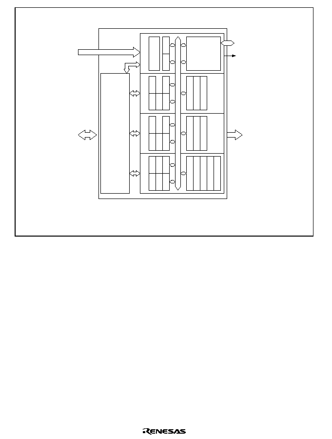
Rev. 2.0, 09/02, page 174 of 658
Channel 2
TMDR
TSR
TCR
TIOR
TIER
TGRA
TCNT
TGRB
TGRC
Channel 1
TMDR
TSR
TCR
TIOR
TIER
TGRA
TCNT
TGRB
Channel 0
Control logic for channel 0 to 2
TGRA
TCNT
TGRB
TGRD
Bus
interface
Common
TSYR
Control logic
TSTR
/1
/4
/16
/64
/256
/1024
TCLKA
TCLKB
TCLKC
TCLKD
Legend
TSTR:
TSYR:
TCR:
TMDR:
Timer start register
Timer synchro register
Timer control register
Timer mode register
Timer I/O control registers (H, L)
Timer interrupt enable register
Timer status register
TImer general registers (A, B, C, D)
TIOCA0
TIOCB0
TIOCC0
TIOCD0
TIOCA1
TIOCB1
TIOCA2
TIOCB2
Interrupt request signals
Channel 0:
Channel 1:
Channel 2:
Internal data bus
A/D convertion start request signal
Module data bus
TGI0A
TGI0B
TGI0C
TGI0D
TCI0V
TGI1A
TGI1B
TCI1V
TCI1U
TGI2A
TGI2B
TCI2V
TCI2U
TMDR
TSR
TCR
TIORH
TIER
TIORL
Input/output pins
Channel 0:
Channel 1:
Channel 2:
Clock input
Internal clock:
External clock:
TIOR(H, L)
TIER:
TSR:
TGR(A, B, C, D):
Figure 10.1 Block Diagram of TPU for H8S/2268 Series
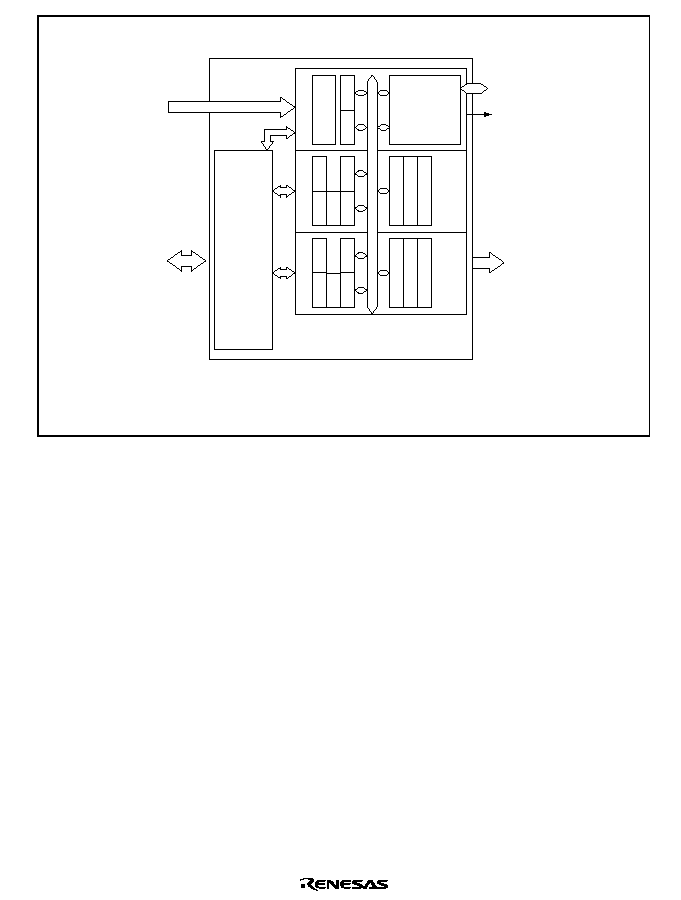
Rev. 2.0, 09/02, page 175 of 658
Channel 2
TMDR
TSR
TCR
TIOR
TIER
Channel 1
TMDR
TSR
TCR
TIOR
TIER
TGRA
TCNT
TGRB
Control logic for channel 1 to 2
TGRA
TCNT
TGRB
Bus
interface
Common
TSYR
Control logic
TSTR
/1
/4
/16
/64
/256
/1024
TCLKA
TCLKB
TCLKC
Legend
TSTR:
TSYR:
TCR:
TMDR:
Timer start register
Timer synchro register
Timer control register
Timer mode register
Timer I/O control registers
Timer interrupt enable register
Timer status register
TImer general registers (A, B)
TIOCA1
TIOCB1
TIOCA2
TIOCB2
Interrupt request signals
Channel 1:
Channel 2:
Internal data bus
A/D convertion start request signal
Module data bus
TGI1A
TGI1B
TCI1V
TCI1U
TGI2A
TGI2B
TCI2V
TCI2U
Input/output pins
Channel 1:
Channel 2:
Clock input
Internal clock:
External clock:
TIOR
TIER:
TSR:
TGR(A, B):
Figure 10.2 Block Diagram of TPU for H8S/2264 Series

Rev. 2.0, 09/02, page 176 of 658
10.2
Input/Output Pins
Table 10.2
TPU Pins
Channel
Symbol
I/O
Function
All
TCLKA
Input
External clock A input pin
(Channel 1 phase counting mode A phase input
*
)
TCLKB
Input
External clock B input pin
(Channel 1 phase counting mode B phase input
*
)
TCLKC
Input
External clock C input pin
(Channel 2 phase counting mode A phase input
*
)
TCLKD
*
Input
External clock D input pin
(Channel 2 phase counting mode B phase input
*
)
0
*
TIOCA0
I/O
TGRA_0 input capture input/output compare output/PWM output pin
TIOCB0
I/O
TGRB_0 input capture input/output compare output/PWM output pin
TIOCC0
I/O
TGRC_0 input capture input/output compare output/PWM output pin
TIOCD0
I/O
TGRD_0 input capture input/output compare output/PWM output pin
1
TIOCA1
I/O
TGRA_1 input capture input/output compare output/PWM output pin
TIOCB1
I/O
TGRB_1 input capture input/output compare output/PWM output pin
2
TIOCA2
I/O
TGRA_2 input capture input/output compare output/PWM output pin
TIOCB2
I/O
TGRB_2 input capture input/output compare output/PWM output pin
Note:
*
Supported only by the H8S/2268 Series.

Rev. 2.0, 09/02, page 177 of 658
10.3
Register Descriptions
The TPU has the following registers. To distinguish registers in each channel, an underscore and
the channel number are added as a suffix to the register name; TCR for channel 0 is expressed as
TCR_0.
∑
Timer control register_0 (TCR_0)*
∑
Timer mode register_0 (TMDR_0)*
∑
Timer I/O control register H_0 (TIORH_0)*
∑
Timer I/O control register L_0 (TIORL_0)*
∑
Timer interrupt enable register_0 (TIER_0)*
∑
Timer status register_0 (TSR_0)*
∑
Timer counter_0 (TCNT_0)*
∑
Timer general register A_0 (TGRA_0)*
∑
Timer general register B_0 (TGRB_0)*
∑
Timer general register C_0 (TGRC_0)*
∑
Timer general register D_0 (TGRD_0)*
∑
Timer control register_1 (TCR_1)
∑
Timer mode register_1 (TMDR_1)
∑
Timer I/O control register _1 (TIOR_1)
∑
Timer interrupt enable register_1 (TIER_1)
∑
Timer status register_1 (TSR_1)
∑
Timer counter_1 (TCNT_1)
∑
Timer general register A_1 (TGRA_1)
∑
Timer general register B_1 (TGRB_1)
∑
Timer control register_2 (TCR_2)
∑
Timer mode register_2 (TMDR_2)
∑
Timer I/O control register_2 (TIOR_2)
∑
Timer interrupt enable register_2 (TIER_2)
∑
Timer status register_2 (TSR_2)
∑
Timer counter_2 (TCNT_2)
∑
Timer general register A_2 (TGRA_2)
∑
Timer general register B_2 (TGRB_2)
Common Registers
∑
Timer start register (TSTR)
∑
Timer synchro register (TSYR)

Rev. 2.0, 09/02, page 178 of 658
Note: *
Supported only by the H8S/2268 Series.
10.3.1
Timer Control Register (TCR)
The TCR registers control the TCNT operation for each channel. The H8S/2268 Series TPU has a
total of three TCR registers and the H8S/2264 Series TPU has a total of two TCR registers, one for
each channel (channels 0 to 2, or 1 and 2). TCR register settings should be conducted only when
TCNT operation is stopped.
Bit
Bit Name
Initial
value
R/W
Description
7
6
5
CCLR2
CCLR1
CCLR0
0
0
0
R/W
R/W
R/W
Counter Clear 0 to 2
These bits select the TCNT counter clearing source.
See tables 10.3 and 10.4 for details.
4
3
CKEG1
CKEG0
0
0
R/W
R/W
Clock Edge 0 and 1
These bits select the input clock edge. When the input
clock is counted using both edges, the input clock
period is halved (e.g.
/4 both edges =
/2 rising
edge). Internal clock edge selection is valid when the
input clock is
/4 or slower. If the input clock is
1, this
setting is ignored and count at rising edge is selected.
In the H8S/2268 Series, if phase counting mode is
used on channels 1 and 2, this setting is ignored and
the phase counting mode setting has priority.
00: Count at rising edge
01: Count at falling edge
1X: Count at both edges
Legend X: Don't care
2
1
0
TPSC2
TPSC1
TPSC0
0
0
0
R/W
R/W
R/W
Time Prescaler 0 to 2
These bits select the TCNT counter clock. The clock
source can be selected independently for each
channel. See tables10.5 to10.7 for details.

Rev. 2.0, 09/02, page 179 of 658
Table 10.3
CCLR0 to CCLR2 (channel 0) (H8S/2268 Series Only)
Channel
Bit 7
CCLR2
Bit 6
CCLR1
Bit 5
CCLR0
Description
0
0
0
0
TCNT clearing disabled
1
TCNT cleared by TGRA compare match/input
capture
1
0
TCNT cleared by TGRB compare match/input
capture
1
TCNT cleared by counter clearing for another
channel performing synchronous clearing/
synchronous operation
*
1
1
0
0
TCNT clearing disabled
1
TCNT cleared by TGRC compare match/input
capture
*
2
1
0
TCNT cleared by TGRD compare match/input
capture
*
2
1
TCNT cleared by counter clearing for another
channel performing synchronous clearing/
synchronous operation
*
1
Notes: 1. Synchronous operation is set by setting the SYNC bit in TSYR to 1.
2. When TGRC or TGRD is used as a buffer register, TCNT is not cleared because the
buffer register setting has priority, and compare match/input capture does not occur.
Table 10.4
CCLR0 to CCLR2 (channels 1 and 2)
Channel
Bit 7
Reserved
*
2
Bit 6
CCLR1
Bit 5
CCLR0
Description
1, 2
0
0
0
TCNT clearing disabled
1
TCNT cleared by TGRA compare match/input
capture
1
0
TCNT cleared by TGRB compare match/input
capture
1
TCNT cleared by counter clearing for another
channel performing synchronous clearing/
synchronous operation
*
1
Notes: 1. Synchronous operation is selected by setting the SYNC bit in TSYR to 1.
2. Bit 7 is reserved in channels 1 and 2. It is always read as 0 and cannot be modified.

Rev. 2.0, 09/02, page 180 of 658
Table 10.5
TPSC0 to TPSC2 (channel 0) (H8S/2268 Series Only)
Channel
Bit 2
TPSC2
Bit 1
TPSC1
Bit 0
TPSC0
Description
0
0
0
0
Internal clock: counts on
/1
1
Internal clock: counts on
/4
1
0
Internal clock: counts on
/16
1
Internal clock: counts on
/64
1
0
0
External clock: counts on TCLKA pin input
1
External clock: counts on TCLKB pin input
1
0
External clock: counts on TCLKC pin input
1
External clock: counts on TCLKD pin input
Table 10.6
TPSC0 to TPSC2 (channel 1)
Channel
Bit 2
TPSC2
Bit 1
TPSC1
Bit 0
TPSC0
Description
1
0
0
0
Internal clock: counts on
/1
1
Internal clock: counts on
/4
1
0
Internal clock: counts on
/16
1
Internal clock: counts on
/64
1
0
0
External clock: counts on TCLKA pin input
1
External clock: counts on TCLKB pin input
1
0
Internal clock: counts on
/256
1
Counts on TCNT_2 overflow.
(H8S/2268 Series: Setting disabled)
Note:
*
This setting is ignored when channel 1 is in phase counting mode (H8S/2268 Series
only).

Rev. 2.0, 09/02, page 181 of 658
Table 10.7
TPSC0 to TPSC2 (channels 2)
Channel
Bit 2
TPSC2
Bit 1
TPSC1
Bit 0
TPSC0
Description
2
0
0
0
Internal clock: counts on
/1
1
Internal clock: counts on
/4
1
0
Internal clock: counts on
/16
1
Internal clock: counts on
/64
1
0
0
External clock: counts on TCLKA pin input
1
External clock: counts on TCLKB pin input
1
0
External clock: counts on TCLKC pin input
1
Internal clock: counts on
/1024
Note:
*
This setting is ignored when channel 2 is in phase counting mode (H8S/2268 Series
only).

Rev. 2.0, 09/02, page 182 of 658
10.3.2
Timer Mode Register (TMDR)
The TMDR registers are used to set the operating mode of each channel. The H8S/2268 Series
TPU has three TMDR registers and the H8S/2264 Series TPU has two TMDR registers, one for
each channel (channels 0 to 2, or 1 and 2). TMDR register settings should be changed only when
TCNT operation is stopped.
Bit
Bit Name
Initial
value
R/W
Description
7, 6
All 1
Reserved
These bits are always read as 1 and cannot be
modified.
5
BFB
0
R/W
H8S/2268 Series:
Buffer Operation B
Specifies whether TGRB is to operate in the normal
way, or TGRB and TGRD are to be used together for
buffer operation. When TGRD is used as a buffer
register, TGRD input capture/output compare is not
generated.
In channels 1 and 2, which have no TGRD, bit 5 is
reserved. It is always read as 0 and cannot be
modified.
0: TGRB operates normally
1: TGRB and TGRD used together for buffer
operation
H8S/2264 Series:
Reserved
These bits are always read as 0 and cannot be
modified.

Rev. 2.0, 09/02, page 183 of 658
Bit
Bit Name
Initial
value
R/W
Description
4
BFA
0
R/W
H8S/2268 Series:
Buffer Operation A
Specifies whether TGRA is to operate in the normal
way, or TGRA and TGRC are to be used together for
buffer operation. When TGRC is used as a buffer
register, TGRC input capture/output compare is not
generated.
In channels 1 and 2, which have no TGRC, bit 4 is
reserved. It is always read as 0 and cannot be
modified.
0: TGRA operates normally
1:TGRA and TGRC used together for buffer operation
H8S/2264 Series:
Reserved
These bits are always read as 0 and cannot be
modified.
3
2
1
0
MD3
MD2
MD1
MD0
0
0
0
0
R/W
R/W
R/W
R/W
Modes 0 to 3
These bits are used to set the timer operating mode.
MD3 is a reserved bit. In a write, it should always be
written with 0. See table 10.8 for details.
Table 10.8
MD0 to MD3
Bit 3
MD3
*
1
Bit 2
MD2
*
2
Bit 1
MD1
Bit 0
MD0
Description
0
0
0
0
Normal operation
1
Reserved
1
0
PWM mode 1
1
PWM mode 2
1
0
0
Phase counting mode 1
1
Phase counting mode 2
1
0
Phase counting mode 3
1
Phase counting mode 4
1
X
X
X
Legend
X: Don't care
Notes: 1. MD3 is a reserved bit. In a write, it should always be written with 0.
2. Phase counting mode cannot be set in the H8S/2264 Series or for channels 0 in the
H8S/2268 Series. In this case, 0 should always be written to MD2.

Rev. 2.0, 09/02, page 184 of 658
10.3.3
Timer I/O Control Register (TIOR)
The TIOR registers control the TGR registers. The H8S/2268 Series TPU has four TIOR registers
and the H8S/2264 Series TPU has two TIOR registers, two for channel 0, and one each for
channels 1 and 2.
Care is required as TIOR is affected by the TMDR setting. The initial output specified by TIOR is
valid when the counter is stopped (the CST bit in TSTR is cleared to 0). Note also that, in PWM
mode 2, the output at the point at which the counter is cleared to 0 is specified.
In the H8S/2268 Series, when TGRC or TGRD is designated for buffer operation, this setting is
invalid and the register operates as a buffer register.
∑
TIORH_0 (H8S/2268 Series only), TIOR_1, TIOR_2
Bit
Bit Name
Initial
value
R/W
Description
7
6
5
4
IOB3
IOB2
IOB1
IOB0
All 0
R/W
I/O Control B0 to B3
Specify the function of TGRB.
For details, refer to table 10.9, 10.11, and 10.12.
3
2
1
0
IOA3
IOA2
IOA1
IOA0
All 0
R/W
I/O Control A0 to A3
Specify the function of TGRA.
For details, refer to table 10.13, 10.15, and 10.16.
∑
TIORL_0 (H8S/2268 Series only)
Bit
Bit Name
Initial
value
R/W
Description
7
6
5
4
IOD3
IOD2
IOD1
IOD0
All 0
R/W
I/O Control D0 to D3
Specify the function of TGRD.
For details, refer to table 10.10.
3
2
1
0
IOC3
IOC2
IOC1
IOC0
All 0
R/W
I/O Control C0 to C3
Specify the function of TGRC.
For details, refer to table 10.14.

Rev. 2.0, 09/02, page 185 of 658
Table 10.9
TIORH_0 (Channel 0) (H8S/2268 Series Only)
Description
Bit 7
IOB3
Bit 6
IOB2
Bit 5
IOB1
Bit 4
IOB0
TGRB_0
Function
TIOCB0 Pin Function
0
0
0
0
Output disabled
1
Output
compare
register
Initial output is 0
0 output at compare match
1
0
Initial output is 0
1 output at compare match
1
Initial output is 0
Toggle output at compare match
1
0
0
Output disabled
1
Initial output is 1
0 output at compare match
1
0
Initial output is 1
1 output at compare match
1
Initial output is 1
Toggle output at compare match
1
0
0
0
Capture input source is TIOCB0 pin
Input capture at rising edge
1
Capture input source is TIOCB0 pin
Input capture at falling edge
1
X
Capture input source is TIOCB0 pin
Input capture at both edges
1
X
X
Input
capture
register
Setting disabled
Legend
X: Don't care

Rev. 2.0, 09/02, page 186 of 658
Table 10.10 TIORL_0 (Channel 0) (H8S/2268 Series Only)
Description
Bit 7
IOD3
Bit 6
IOD2
Bit 5
IOD1
Bit 4
IOD0
TGRD_0
Function
TIOCD0 Pin Function
0
0
0
0
Output disabled
1
Output
compare
register
*
Initial output is 0
0 output at compare match
1
0
Initial output is 0
1 output at compare match
1
Initial output is 0
Toggle output at compare match
1
0
0
Output disabled
1
Initial output is 1
0 output at compare match
1
0
Initial output is 1
1 output at compare match
1
Initial output is 1
Toggle output at compare match
1
0
0
0
Capture input source is TIOCD0 pin
Input capture at rising edge
1
Capture input source is TIOCD0 pin
Input capture at falling edge
1
X
Input
capture
register
*
Capture input source is TIOCD0 pin
Input capture at both edges
1
X
X
Setting disabled
Legend
X: Don't care
Note:
*
When the BFB bit in TMDR_0 is set to 1 and TGRD_0 is used as a buffer register, this
setting is invalid and input capture/output compare is not generated.

Rev. 2.0, 09/02, page 187 of 658
Table 10.11 TIOR_1 (Channel 1)
Description
Bit 7
IOB3
Bit 6
IOB2
Bit 5
IOB1
Bit 4
IOB0
TGRB_1
Function
TIOCB1 Pin Function
0
0
0
0
Output disabled
1
Output
compare
register
Initial output is 0
0 output at compare match
1
0
Initial output is 0
1 output at compare match
1
Initial output is 0
Toggle output at compare match
1
0
0
Output disabled
1
Initial output is 1
0 output at compare match
1
0
Initial output is 1
1 output at compare match
1
Initial output is 1
Toggle output at compare match
1
0
0
0
Capture input source is TIOCB1 pin
Input capture at rising edge
1
Capture input source is TIOCB1 pin
Input capture at falling edge
1
X
Input
capture
register
Capture input source is TIOCB1 pin
Input capture at both edges
1
X
X
Setting disabled
Legend
X: Don't care

Rev. 2.0, 09/02, page 188 of 658
Table 10.12 TIOR_2 (Channel 2)
Description
Bit 7
IOB3
Bit 6
IOB2
Bit 5
IOB1
Bit 4
IOB0
TGRB_2
Function
TIOCB2 Pin Function
0
0
0
0
Output disabled
1
Output
compare
register
Initial output is 0
0 output at compare match
1
0
Initial output is 0
1 output at compare match
1
Initial output is 0
Toggle output at compare match
1
0
0
Output disabled
1
Initial output is 1
0 output at compare match
1
0
Initial output is 1
1 output at compare match
1
Initial output is 1
Toggle output at compare match
1
X
0
0
Capture input source is TIOCB2 pin
Input capture at rising edge
1
Capture input source is TIOCB2 pin
Input capture at falling edge
1
X
Input
capture
register
Capture input source is TIOCB2 pin
Input capture at both edges
Legend
X: Don't care

Rev. 2.0, 09/02, page 189 of 658
Table 10.13 TIORH_0 (Channel 0) (H8S/2268 Series Only)
Description
Bit 3
IOA3
Bit 2
IOA2
Bit 1
IOA1
Bit 0
IOA0
TGRA_0
Function
TIOCA0 Pin Function
0
0
0
0
Output disabled
1
Output
compare
register
Initial output is 0
0 output at compare match
1
0
Initial output is 0
1 output at compare match
1
Initial output is 0
Toggle output at compare match
1
0
0
Output disabled
1
Initial output is 1
0 output at compare match
1
0
Initial output is 1
1 output at compare match
1
Initial output is 1
Toggle output at compare match
1
0
0
0
Capture input source is TIOCA0 pin
Input capture at rising edge
1
Capture input source is TIOCA0 pin
Input capture at falling edge
1
X
Input
capture
register
Capture input source is TIOCA0 pin
Input capture at both edges
1
X
X
Setting disabled
Legend
X: Don't care

Rev. 2.0, 09/02, page 190 of 658
Table 10.14 TIORL_0 (Channel 0) (H8S/2268 Series Only)
Description
Bit 3
IOC3
Bit 2
IOC2
Bit 1
IOC1
Bit 0
IOC0
TGRC_0
Function
TIOCC0 Pin Function
0
0
0
0
Output disabled
1
Output
compare
register
*
Initial output is 0
0 output at compare match
1
0
Initial output is 0
1 output at compare match
1
Initial output is 0
Toggle output at compare match
1
0
0
Output disabled
1
Initial output is 1
0 output at compare match
1
0
Initial output is 1
1 output at compare match
1
Initial output is 1
Toggle output at compare match
1
0
0
0
Capture input source is TIOCC0 pin
Input capture at rising edge
1
Capture input source is TIOCC0 pin
Input capture at falling edge
1
X
Capture input source is TIOCC0 pin
Input capture at both edges
1
X
X
Input
capture
register
*
Setting disabled
Legend
X: Don't care
Note:
*
When the BFA bit in TMDR_0 is set to 1 and TGRC_0 is used as a buffer register, this
setting is invalid and input capture/output compare is not generated.

Rev. 2.0, 09/02, page 191 of 658
Table 10.15 TIOR_1 (Channel 1)
Description
Bit 3
IOA3
Bit 2
IOA2
Bit 1
IOA1
Bit 0
IOA0
TGRA_1
Function
TIOCA1 Pin Function
0
0
0
0
Output disabled
1
Output
compare
register
Initial output is 0
0 output at compare match
1
0
Initial output is 0
1 output at compare match
1
Initial output is 0
Toggle output at compare match
1
0
0
Output disabled
1
Initial output is 1
0 output at compare match
1
0
Initial output is 1
1 output at compare match
1
Initial output is 1
Toggle output at compare match
1
0
0
0
Capture input source is TIOCA1 pin
Input capture at rising edge
1
Capture input source is TIOCA1 pin
Input capture at falling edge
1
X
Input
capture
register
Capture input source is TIOCA1 pin
Input capture at both edges
1
X
X
Setting disabled
Legend
X: Don't care

Rev. 2.0, 09/02, page 192 of 658
Table 10.16 TIOR_2 (Channel 2)
Description
Bit 3
IOA3
Bit 2
IOA2
Bit 1
IOA1
Bit 0
IOA0
TGRA_2
Function
TIOCA2 Pin Function
0
0
0
0
Output disabled
1
Output
compare
register
Initial output is 0
0 output at compare match
1
0
Initial output is 0
1 output at compare match
1
Initial output is 0
Toggle output at compare match
1
0
0
Output disabled
1
Initial output is 1
0 output at compare match
1
0
Initial output is 1
1 output at compare match
1
Initial output is 1
Toggle output at compare match
1
X
0
0
Capture input source is TIOCA2 pin
Input capture at rising edge
1
Capture input source is TIOCA2 pin
Input capture at falling edge
1
X
Input
capture
register
Capture input source is TIOCA2 pin
Input capture at both edges
Legend
X: Don't care
10.3.4
Timer Interrupt Enable Register (TIER)
The TIER registers control enabling or disabling of interrupt requests for each channel. The
H8S/2268 Series TPU has three TIER registers and the H8S/2264 Series TPU has two TIER
registers, one for each channel (channels 0 to 2, or 1 and 2).

Rev. 2.0, 09/02, page 193 of 658
Bit
Bit Name
Initial
value
R/W
Description
7
TTGE
0
R/W
A/D Conversion Start Request Enable
Enables or disables generation of A/D conversion
start requests by TGRA input capture/compare match.
0: A/D conversion start request generation disabled
1: A/D conversion start request generation enabled
6
1
Reserved
This bit is always read as 1 and cannot be modified.
5
TCIEU
0
R/W
H8S/2268 Series:
Underflow Interrupt Enable
Enables or disables interrupt requests (TCIU) by the
TCFU flag when the TCFU flag in TSR is set to 1 in
channels 1 and 2.
In channel 0, bit 5 is reserved. It is always read as 0
and cannot be modified.
0: Interrupt requests (TCIU) by TCFU disabled
1: Interrupt requests (TCIU) by TCFU enabled
H8S/2264 Series:
The write value should always be 0.
4
TCIEV
0
R/W
Overflow Interrupt Enable
Enables or disables interrupt requests (TCIV) by the
TCFV flag when the TCFV flag in TSR is set to 1.
0: Interrupt requests (TCIV) by TCFV disabled
1: Interrupt requests (TCIV) by TCFV enabled
3
TGIED
0
R/W
TGR Interrupt Enable D
Enables or disables interrupt requests (TGID) by the
TGFD bit when the TGFD bit in TSR is set to 1 in
channel 0.
In channels 1 and 2, bit 3 is reserved. It is always
read as 0 and cannot be modified.
0: Interrupt requests (TGID) by TGFD bit disabled
1: Interrupt requests (TGID) by TGFD bit enabled
2
TGIEC
0
R/W
TGR Interrupt Enable C
Enables or disables interrupt requests (TGIC) by the
TGFC bit when the TGFC bit in TSR is set to 1 in
channel 0.
In channels 1 and 2, bit 2 is reserved. It is always
read as 0 and cannot be modified.
0: Interrupt requests (TGIC) by TGFC bit disabled
1: Interrupt requests (TGIC) by TGFC bit enabled

Rev. 2.0, 09/02, page 194 of 658
Bit
Bit Name
Initial
value
R/W
Description
1
TGIEB
0
R/W
TGR Interrupt Enable B
Enables or disables interrupt requests (TGIB) by the
TGFB bit when the TGFB bit in TSR is set to 1.
0: Interrupt requests (TGIB) by TGFB bit disabled
1: Interrupt requests (TGIB) by TGFB bit enabled
0
TGIEA
0
R/W
TGR Interrupt Enable A
Enables or disables interrupt requests (TGIA) by the
TGFA bit when the TGFA bit in TSR is set to 1.
0: Interrupt requests (TGIA) by TGFA bit disabled
1: Interrupt requests (TGIA) by TGFA bit enabled
10.3.5
Timer Status Register (TSR)
The TSR registers indicate the status of each channel. The H8S/2268 Series TPU has three TSR
registers and the H8S/2264 Series TPU has two TSR registers, one for each channel (channels 0 to
2, or 1 and 2).
Bit
Bit Name
Initial
value
R/W
Description
7
TCFD
1
R
H8S/2268 Series:
Count Direction Flag
Status flag that shows the direction in which TCNT
counts in channels 1 and 2.
In channel 0, bit 7 is reserved. It is always read as 1
and cannot be modified.
0: TCNT counts down
1: TCNT counts up
H8S/2264 Series:
Reserved
This bit is always read as 1 and cannot be modified.
6
1
Reserved
This bit is always read as 1 and cannot be modified.

Rev. 2.0, 09/02, page 195 of 658
Bit
Bit Name
Initial
value
R/W
Description
5
TCFU
0
R/(W)
*
1
H8S/2268 Series:
Underflow Flag
Status flag that indicates that TCNT underflow has
occurred when channels 1 and 2 are set to phase
counting mode. Only 0 can be written, for flag
clearing.
In channel 0, bit 5 is reserved. It is always read as 0
and cannot be modified.
[Setting condition]
When the TCNT value underflows (changes from
H'0000 to H'FFFF)
[Clearing condition]
When 0 is written to TCFU after reading TCFU = 1
H8S/2264 Series:
Reserved
This bit is always read as 0 and cannot be modified.
4
TCFV
0
R/(W)
*
1
Overflow Flag
Status flag that indicates that TCNT overflow has
occurred. Only 0 can be written, for flag clearing.
[Setting condition]
When the TCNT value overflows (changes from
H'FFFF to H'0000 )
[Clearing condition]
When 0 is written to TCFV after reading TCFV = 1

Rev. 2.0, 09/02, page 196 of 658
Bit
Bit Name
Initial
value
R/W
Description
3
TGFD
0
R/(W)
*
1
H8S/2268 Series:
Input Capture/Output Compare Flag D
Status flag that indicates the occurrence of TGRD
input capture or compare match in channel 0. Only 0
can be written, for flag clearing. In channels 1 and 2,
bit 3 is reserved. It is always read as 0 and cannot be
modified.
[Setting conditions]
∑
When TCNT = TGRD and TGRD is functioning as
output compare register
∑
When TCNT value is transferred to TGRD by input
capture signal and TGRD is functioning as input
capture register
[Clearing conditions]
∑
When DTC is activated by TGID interrupt and the
DISEL bit of MRB in DTC is 0
∑
When 0 is written to TGFD after reading TGFD = 1
H8S/2264 Series:
Reserved
This bit is always read as 0 and cannot be modified.

Rev. 2.0, 09/02, page 197 of 658
Bit
Bit Name
Initial
value
R/W
Description
2
TGFC
0
R/(W)
*
1
H8S/2268 Series:
Input Capture/Output Compare Flag C
Status flag that indicates the occurrence of TGRC
input capture or compare match in channel 0. Only 0
can be written, for flag clearing. In channels 1 and 2,
bit 2 is reserved. It is always read as 0 and cannot be
modified.
[Setting conditions]
∑
When TCNT = TGRC and TGRC is functioning as
output compare register
∑
When TCNT value is transferred to TGRC by input
capture signal and TGRC is functioning as input
capture register
[Clearing conditions]
∑
When DTC is activated by TGIC interrupt and the
DISEL bit of MRB in DTC is 0
∑
When 0 is written to TGFC after reading TGFC = 1
H8S/2264 Series:
Reserved
This bit is always read as 0 and cannot be modified.

Rev. 2.0, 09/02, page 198 of 658
Bit
Bit Name
Initial
value
R/W
Description
1
TGFB
0
R/(W)
*
1
Input Capture/Output Compare Flag B
Status flag that indicates the occurrence of TGRB
input capture or compare match. Only 0 can be
written, for flag clearing.
[Setting conditions]
∑
When TCNT = TGRB and TGRB is functioning as
output compare register
∑
When TCNT value is transferred to TGRB by input
capture signal and TGRB is functioning as input
capture register
[Clearing conditions]
∑
When DTC*2 is activated by TGIB interrupt and
the DISEL bit of MRB in DTC*2 is 0
∑
When 0 is written to TGFB after reading TGFB = 1
0
TGFA
0
R/(W)
*
1
Input Capture/Output Compare Flag A
Status flag that indicates the occurrence of TGRA
input capture or compare match. Only 0 can be
written, for flag clearing.
[Setting conditions]
∑
When TCNT = TGRA and TGRA is functioning as
output compare register
∑
When TCNT value is transferred to TGRA by input
capture signal and TGRA is functioning as input
capture register
[Clearing conditions]
∑
When DTC
*
2
is activated by TGIA interrupt and
the DISEL bit of MRB in DTC
*
2
is 0
∑
When 0 is written to TGFA after reading TGFA = 1
Notes: 1. Only 0 can be written to this bit to clear the flag.
2. Supported only by the H8S/2268 Series.

Rev. 2.0, 09/02, page 199 of 658
10.3.6
Timer Counter (TCNT)
The TCNT registers are 16-bit readable/writable counters. The H8S/2268 Series TPU has three
TCNT counters and the H8S/2264 Series TPU has two TCNT counters, one for each channel
(channels 0 to 2, or 1 and 2).
The TCNT counters are initialized to H'0000 by a reset, or in hardware standby mode.
The TCNT counters cannot be accessed in 8-bit units; they must always be accessed as a 16-bit
unit.
10.3.7
Timer General Register (TGR)
The TGR registers are dual function 16-bit readable/writable registers, functioning as either output
compare or input capture registers. The H8S/2268 Series TPU has eight TGR registers and the
H8S/2264 Series TPU has four TGR registers, four for channel 0 and two each for channels 1 and
2. TGR is initialized to H'FFFF at reset or in hardware standby mode. The TGR registers cannot
be accessed in 8-bit units; they must always be accessed as a 16-bit unit. In the H8S/2268 Series,
TGRC and TGRD for channel 0 can also be designated for operation as buffer registers. TGR
buffer register combinations are TGRA--TGRC and TGRB--TGRD.
10.3.8
Timer Start Register (TSTR)
TSTR selects operation/stoppage for channels 0 to 2 in the H8S/2268 Series and for channels 1
and 2 in the H8S/2264 Series. When setting the operating mode in TMDR or setting the count
clock in TCR, first stop the TCNT counter.

Rev. 2.0, 09/02, page 200 of 658
Bit
Bit Name
Initial
value
R/W
Description
7 to 3
All 0
Reserved
The write value should always be 0.
2
1
0
CST2
CST1
CST0
*
0
0
0
R/W
R/W
R/W
Counter Start 0 to 2 (CST0 to CST2)
These bits select operation or stoppage for TCNT.
If 0 is written to the CST bit during operation with the
TIOC pin designated for output, the counter stops but
the TIOC pin output compare output level is retained.
If TIOR is written to when the CST bit is cleared to 0,
the pin output level will be changed to the set initial
output value.
0: TCNT_n count operation is stopped
1: TCNT_n performs count operation
(n = 0 to 2)
Note:
*
In the H8S/2264 Series, this bit is reserved. The write value should always be 0.

Rev. 2.0, 09/02, page 201 of 658
10.3.9
Timer Synchro Register (TSYR)
TSYR selects independent operation or synchronous operation of the TCNT counters for channels
0 to 2 in the H8S/2268 Series and for channels 1 and 2 in the H8S/2264 Series. A channel
performs synchronous operation when the corresponding bit in TSYR is set to 1.
Bit
Bit Name
Initial
value
R/W
Description
7 to 3
0
Reserved
The write value should always be 0.
2
1
0
SYNC2
SYNC1
SYNC0
*
0
0
0
R/W
R/W
R/W
Timer Synchro 0 to 2
These bits are used to select whether operation is
independent of or synchronized with other channels.
When synchronous operation is selected, the TCNT
synchronous presetting of multiple channels, and
synchronous clearing by counter clearing on another
channel, are possible.
To set synchronous operation, the SYNC bits for at
least two channels must be set to 1. To set
synchronous clearing, in addition to the SYNC bit , the
TCNT clearing source must also be set by means of
bits CCLR0 to CCLR2 in TCR.
0: TCNT_n operates independently (TCNT
presetting /clearing is unrelated to other channels)
1: TCNT_n performs synchronous operation
TCNT synchronous presetting/synchronous
clearing is possible
(n = 0 to 2)
Note:
*
In the H8S/2264 Series, this bit is reserved. The write value should always be 0.

Rev. 2.0, 09/02, page 202 of 658
10.4
Interface to Bus Master
10.4.1
16-Bit Registers
TCNT and TGR are 16-bit registers. As the data bus to the master is 16 bits wide, these registers
can be read or written to in 8-bit units; 16-bit access must always be used.
An example of 16-bit register access operation is shown in figure 10.3.
H
L
Bus master
TCNTH
TCNTL
Module data bus
Bus interface
Internal data bus
Figure 10.3 16-Bit Register Access Operation [ Bus Master
TCNT (16 Bits)
]
10.4.2
8-Bit Registers
Registers other than TCNT and TGR are 8-bit. As the data bus to the CPU is 16 bits wide, these
registers can be read and written to in 16-bit units. They can also be read and written to in 8-bit
units.
Examples of 8-bit register access operation are shown in figure 10.4, 10.5, and 10.6.
Bus interface
H
Internal data bus
L
Bus master
Module data bus
TCR
Figure 10.4 8-Bit Register Access Operation [ Bus Master
TCR (Upper 8 Bits)
]
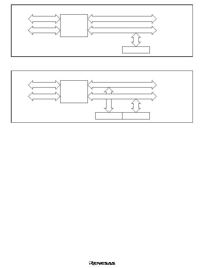
Rev. 2.0, 09/02, page 203 of 658
Bus interface
H
Internal data bus
L
Bus master
Module data bus
TMDR
Figure 10.5 8-Bit Register Access Operation [ Bus Master
TMDR (Lower 8 Bits)
]
Bus interface
H
Internal data bus
L
Bus master
Module data bus
TCR
TMDR
Figure 10.6 8-Bit Register Access Operation [ Bus Master
TCR and TMDR (16 Bits)
]
10.5
Operation
10.5.1
Basic Functions
Each channel has a TCNT and TGR register. TCNT performs up-counting, and is also capable of
free-running operation, synchronous counting, and external event counting.
Each TGR can be used as an input capture register or output compare register.
Counter Operation: When one of bits CST0 to CST2 in the H8S/2268 Series or one of bits CST1
and CST2 in the H8S/2264 Series is set to 1 in TSTR, the TCNT counter for the corresponding
channel begins counting. TCNT can operate as a free-running counter, periodic counter, for
example.
1. Example of count operation setting procedure
Figure 10.7 shows an example of the count operation setting procedure.

Rev. 2.0, 09/02, page 204 of 658
Operation selection
Select counter clock
Periodic counter
Select counter clearing source
Select output compare register
Set period
Free-running counter
Start count operation
<Free-running counter>
Note:
*
In the H8S/2264 Series, bits
CCLR1 and CCLR0 in TCR.
<Periodic counter>
Start count operation
Select the counter
clock with bits
TPSC2 to TPSC0 in
TCR. At the same
time, select the
input clock edge
with bits CKEG1
and CKEG0 in TCR.
For periodic counter
operation, select the
TGR to be used as
the TCNT clearing
source with bits
CCLR2 to CCLR0
*
in
TCR.
Designate the TGR
selected in [2] as an
output compare
register by means of
TIOR.
Set the periodic
counter cycle in the
TGR selected in [2].
Set the CST bit in
TSTR to 1 to start
the counter
operation.
[1]
[1]
[2]
[2]
[3]
[3]
[4]
[4]
[5]
[5]
Figure 10.7 Example of Counter Operation Setting Procedure
2. Free-running count operation and periodic count operation
Immediately after a reset, the TPU's TCNT counters are all designated as free-running
counters. When the relevant bit in TSTR is set to 1 the corresponding TCNT counter starts up-
count operation as a free-running counter. When TCNT overflows (from H'FFFF to H'0000),
the TCFV bit in TSR is set to 1. If the value of the corresponding TCIEV bit in TIER is 1 at
this point, the TPU requests an interrupt. After overflow, TCNT starts counting up again from
H'0000.
Figure 10.8 illustrates free-running counter operation.

Rev. 2.0, 09/02, page 205 of 658
TCNT value
H'FFFF
H'0000
CST bit
TCFV
Time
Figure 10.8 Free-Running Counter Operation
When compare match is selected as the TCNT clearing source, the TCNT counter for the relevant
channel performs periodic count operation. The TGR register for setting the period is designated
as an output compare register, and counter clearing by compare match is selected by means of bits
CCLR0 to CCLR2 in the H8S/2268 Series TCR or bits CCLR0 and CCLR1 in the H8S/2264
Series TCR. After the settings have been made, TCNT starts up-count operation as a periodic
counter when the corresponding bit in TSTR is set to 1. When the count value matches the value
in TGR, the TGF bit in TSR is set to 1 and TCNT is cleared to H'0000.
If the value of the corresponding TGIE bit in TIER is 1 at this point, the TPU requests an interrupt.
After a compare match, TCNT starts counting up again from H'0000.
Figure 10.9 illustrates periodic counter operation.
TCNT value
TGR
H'0000
CST bit
TGF
Note:
*
Supported only by the H8S/2268 Series.
Time
Counter cleared by TGR
compare match
Flag cleared by software or
DTC
*
activation
Figure 10.9 Periodic Counter Operation

Rev. 2.0, 09/02, page 206 of 658
Waveform Output by Compare Match: The TPU can perform 0, 1, or toggle output from the
corresponding output pin using compare match.
1. Example of setting procedure for waveform output by compare match
Figure 10.10 shows an example of the setting procedure for waveform output by compare
match.
Input selection
Select waveform output mode
Start count operation
< Waveform output >
Select initial value 0 output or 1 output, and
compare match output value 0 output, 1 output,
or toggle output, by means of TIOR. The set
initial value is output at the TIOC pin unit the
first compare match occurs.
Set the timing for compare match generation in
TGR.
Set the CST bit in TSTR to 1 to start the count
operation.
[1]
[2]
[1]
[2]
Set output timing
[3]
[3]
Figure 10.10 Example of Setting Procedure for Waveform Output by Compare Match
2. Examples of waveform output operation
Figure 10.11 shows an example of 0 output/1 output.
In this example TCNT has been designated as a free-running counter, and settings have been
made such that 1 is output by compare match A, and 0 is output by compare match B. When
the set level and the pin level coincide, the pin level does not change.
TCNT value
H'FFFF
H'0000
TIOCA
TIOCB
Time
TGRA
TGRB
No change
No change
No change
No change
1 output
0 output
Figure 10.11 Example of 0 Output/1 Output Operation
Figure 10.12 shows an example of toggle output.

Rev. 2.0, 09/02, page 207 of 658
In this example, TCNT has been designated as a periodic counter (with counter clearing on
compare match B), and settings have been made such that the output is toggled by both compare
match A and compare match B.
TCNT value
H'FFFF
H'0000
TIOCB
TIOCA
Time
TGRB
TGRA
Toggle output
Toggle output
Counter cleared by TGRB compare match
Figure 10.12 Example of Toggle Output Operation
Input Capture Function: The TCNT value can be transferred to TGR on detection of the TIOC
pin input edge.
Rising edge, falling edge, or both edges can be selected as the detected edge.
1. Example of input capture operation setting procedure
Figure 10.13 shows an example of the input capture operation setting procedure.
Input selection
Select input capture input
Start count
<Input capture operation>
Designate TGR as an input capture register by
means of TIOR, and select rising edge, falling
edge, or both edges as the input capture source
and input signal edge.
Set the CST bit in TSTR to 1 to start the count
operation.
[1]
[2]
[1]
[2]
Figure 10.13 Example of Input Capture Operation Setting Procedure

Rev. 2.0, 09/02, page 208 of 658
2. Example of input capture operation
Figure 10.14 shows an example of input capture operation.
In this example both rising and falling edges have been selected as the TIOCA pin input
capture input edge, the falling edge has been selected as the TIOCB pin input capture input
edge, and counter clearing by TGRB input capture has been designated for TCNT.
TCNT value
H'0180
H'0000
TIOCA
TGRA
H'0010
H'0005
Counter cleared by TIOCB
input (falling edge)
H'0160
H'0005
H'0160
H'0010
TGRB
H'0180
TIOCB
Time
Figure 10.14 Example of Input Capture Operation
10.5.2
Synchronous Operation
In synchronous operation, the values in a number of TCNT counters can be rewritten
simultaneously (synchronous presetting). Also, a number of TCNT counters can be cleared
simultaneously by making the appropriate setting in TCR (synchronous clearing).
Synchronous operation enables TGR to be incremented with respect to a single time base.
Channels 0 to 2 in the H8S/2268 Series or channels 1 and 2 in the H8S/2264 Series can all be
designated for synchronous operation.
Example of Synchronous Operation Setting Procedure: Figure 10.15 shows an example of the
synchronous operation setting procedure.
Rev. 2.0, 09/02, page 209 of 658
No
Yes
Synchronous operation
selection
Set synchronous
operation
Synchronous presetting
Set TCNT
<Synchronous presetting>
<Counter clearing>
<Synchronous clearing>
Synchronous clearing
Clearing
source generation
channel?
Select counter
clearing source
Start count
Set synchronous
counter clearing
Start count
Set to 1 the SYNC bits in TSYR corresponding to the channels to be designated for synchronous
operation.
When the TCNT counter of any of the channels designated for synchronous operation is
written to, the same value is simultaneously written to the other TCNT counters.
Use bits CCLR2 to CCLR0
*
in TCR to specify TCNT clearing by input capture/output compare,
etc.
Use bits CCLR2 to CCLR0
*
in TCR to designate synchronous clearing for the counter clearing
source.
Set to 1 the CST bits in TSTR for the relevant channels, to start the count operation.
[1]
[2]
[3]
[4]
[5]
Note:
*
In the H8S/2264 Series, bits CCRL1 and CCLR0 in TCR.
[1]
[3]
[5]
[4]
[5]
[2]
Figure 10.15 Example of Synchronous Operation Setting Procedure
Example of Synchronous Operation: Figure 10.16 shows an example of synchronous operation.
In this example, synchronous operation and PWM mode 1 have been designated for channels 0 to
2 in the H8S/2268 Series, TGRB_0 compare match has been set as the channel 0 counter clearing
source, and synchronous clearing has been set for the channel 1 and 2 counter clearing source.
Three-phase PWM waveforms are output from pins TIOC0A, TIOC1A, and TIOC2A. At this
time, synchronous presetting, and synchronous clearing by TGRB_0 compare match, are
performed for channel 0 to 2 TCNT counters, and the data set in TGRB_0 is used as the PWM
cycle.
For details of PWM modes, see section 10.5.5, PWM Modes.

Rev. 2.0, 09/02, page 210 of 658
TCNT0 to TCNT2 values
H'0000
TIOCA0
TIOCA1
TGRB_0
Synchronous clearing by TGRB_0 compare match
TGRA_2
TGRA_1
TGRB_2
TGRA_0
TGRB_1
TIOCA2
Time
Figure 10.16 Example of Synchronous Operation
10.5.3
Buffer Operation (H8S/2268 Series Only)
Buffer operation, provided for channel 0, enables TGRC and TGRD to be used as buffer registers.
Buffer operation differs depending on whether TGR has been designated as an input capture
register or as a compare match register.
Table 10.17 shows the register combinations used in buffer operation.
Table 10.17 Register Combinations in Buffer Operation
Channel
Timer General Register
Buffer Register
0
TGRA_0
TGRC_0
TGRB_0
TGRD_0
∑
When TGR is an output compare register
When a compare match occurs, the value in the buffer register for the corresponding channel is
transferred to the timer general register.
This operation is illustrated in figure 10.17.
Rev. 2.0, 09/02, page 211 of 658
Buffer register
Timer general
register
TCNT
Comparator
Compare match signal
Figure 10.17 Compare Match Buffer Operation
∑
When TGR is an input capture register
When input capture occurs, the value in TCNT is transferred to TGR and the value previously
held in the timer general register is transferred to the buffer register.
This operation is illustrated in figure 10.18.
Buffer register
Timer general
register
TCNT
Input capture
signal
Figure 10.18 Input Capture Buffer Operation
Example of Buffer Operation Setting Procedure: Figure 10.19 shows an example of the buffer
operation setting procedure.
Buffer operation
Select TGR function
Set buffer operation
Start count
<Buffer operation>
[1]
[2]
[3]
[1]
[2]
[3]
Designate TGR as an input capture register or
output compare register by means of TIOR.
Designate TGR for buffer operation with bits
BFA and BFB in TMDR.
Set the CST bit in TSTR to 1 start the count
operation.
Figure 10.19 Example of Buffer Operation Setting Procedure

Rev. 2.0, 09/02, page 212 of 658
Examples of Buffer Operation:
1. When TGR is an output compare register
Figure 10.20 shows an operation example in which PWM mode 1 has been designated for
channel 0, and buffer operation has been designated for TGRA and TGRC. The settings used
in this example are TCNT clearing by compare match B, 1 output at compare match A, and 0
output at compare match B.
As buffer operation has been set, when compare match A occurs the output changes and the
value in buffer register TGRC is simultaneously transferred to timer general register TGRA.
This operation is repeated each time that compare match A occurs.
For details of PWM modes, see section 10.5.5, PWM Modes.
TCNT value
TGRB_0
H'0000
TGRC_0
TGRA_0
H'0200
H'0520
TIOCA
H'0200
H'0450
H'0520
H'0450
TGRA_0
H'0450
H'0200
Transfer
Time
Figure 10.20 Example of Buffer Operation (1)
2. When TGR is an input capture register
Figure 10.21 shows an operation example in which TGRA has been designated as an input
capture register, and buffer operation has been designated for TGRA and TGRC.
Counter clearing by TGRA input capture has been set for TCNT, and both rising and falling
edges have been selected as the TIOCA pin input capture input edge.
As buffer operation has been set, when the TCNT value is stored in TGRA upon the
occurrence of input capture A, the value previously stored in TGRA is simultaneously
transferred to TGRC.

Rev. 2.0, 09/02, page 213 of 658
TCNT value
H'09FB
H'0000
TGRC
Time
H'0532
TIOCA
TGRA
H'0F07
H'0532
H'0F07
H'0532
H'0F07
H'09FB
Figure 10.21 Example of Buffer Operation (2)
10.5.4
Operation with Cascaded Connection (H8S/2264 Series Only)
Operation as a 32-bit timer can be performed by cascading two 16-bit counter channels.
This function is enabled when the TPSC2 to TPSC0 bits in TCR are set to count on TCNT2
overflow for the channel 1 counter clock. Table 10.18 shows the counter combination used in
operation with the cascaded connection.
Table 10.18 Counter Combination in Operation with Cascaded Connection
Combination
Upper 16 bits
Lower 16 bits
Channel 1 and channel 2
TCNT1
TCNT2
Setting Procedure for Operation with Cascaded Connection: Figure 10.22 shows the cascaded
connection operation setting procedure.

Rev. 2.0, 09/02, page 214 of 658
Operation with cascaded
connection
[1]
[1] Set bits TPSC2 to TPSC0 in TCR in
channel 1 to B'111 to select to count
on TCNT2 overflow.
[2] Set the CST bit in TSTR corresponding
the upper and lower channels to start
counting.
[2]
<Operation with cascaded connection>
Set operation with cascaded
connection
Start operation with cascaded
connection
Figure 10.22 Setting Procedure for Operation with Cascaded Operation
Example of Operation with Cascaded Connection: Figure 10.23 shows an example of operation
with cascaded connection, where TCNT1 is set to count TCNT2 overflow, TCRA_1 and TCRA_2
are set to be input capture registers, and the TIOC pin rising edge is selected.
If rising edges are input simultaneously to the TIOCA1 and TIOCA2 pins, the upper 16 bits of 32-
bit data are transferred to TGRA_1 and the lower 16 bits are transferred to TGRA_2.
TIOCA1
TIOCA2
TCNT2
TCNT1
TCNT1
clock
TCNT2
clock
H'03A2
H'03A1
H'FFFF
H'0000
H'0001
TGRA_1
H'03A2
H'0000
TGRA_2
Figure 10.23 Example of Operation with Cascaded Connection

Rev. 2.0, 09/02, page 215 of 658
10.5.5
PWM Modes
In PWM mode, PWM waveforms are output from the output pins. The output level can be selected
as 0, 1, or toggle output in response to a compare match of each TGR.
Designating TGR compare match as the counter clearing source enables the period to be set in that
register. All channels can be designated for PWM mode independently. Synchronous operation is
also possible.
There are two PWM modes, as described below.
∑
PWM mode 1
H8S/2268 Series:
PWM output is generated from the TIOCA and TIOCC pins by pairing TGRA with TGRB and
TGRC with TGRD. The output specified by bits IOA0 to IOA3 and IOC0 to IOC3 in TIOR is
output from the TIOCA and TIOCC pins at compare matches A and C, and the output
specified by bits IOB0 to IOB3 and IOD0 to IOD3 in TIOR is output at compare matches B
and D. The initial output value is the value set in TGRA or TGRC. If the set values of paired
TGRs are identical, the output value does not change when a compare match occurs.
In PWM mode 1, PWM output is enable up to 4 phases.
H8S/2264 Series:
PWM output is generated from the TIOCA pin by pairing TGRA with TGRB. The output
specified by bits IOA0 to IOA3 in TIOR is output from the TIOCA pin at compare match A,
and the output specified by bits IOB0 to IOB3 in TIOR is output at compare match B. The
initial output value is the value set in TGRA. If the set values of paired TGRs are identical, the
output value does not change when a compare match occurs.
In PWM mode 1, PWM output is enable up to 2 phases.
∑
PWM mode 2
PWM output is generated using one TGR as the cycle register and the others as duty registers.
The output specified in TIOR is performed by means of compare matches. Upon counter
clearing by a synchronization register compare match, the output value of each pin is the initial
value set in TIOR. If the set values of the cycle and duty registers are identical, the output
value does not change when a compare match occurs.
In PWM mode 2, PWM output is enabled up to 7 phases in the H8S/2268 Series or 3 phases in
the H8S/2264 Series by using also synchronous operation.
The correspondence between PWM output pins and registers is shown in table 10.19.
Rev. 2.0, 09/02, page 216 of 658
Table 10.19 PWM Output Registers and Output Pins
Output Pins
Channel
Registers
PWM Mode 1
PWM Mode 2
*
2
0
*
1
TGRA_0
TIOCA0
TIOCA0
TGRB_0
TIOCB0
TGRC_0
TIOCC0
TIOCC0
TGRD_0
TIOCD0
1
TGRA_1
TIOCA1
TIOCA1
TGRB_1
TIOCB1
2
TGRA_2
TIOCA2
TIOCA2
TGRB_2
TIOCB2
Notes: 1. Supported only by the H8S/2268 Series.
2. In PWM mode 2, PWM output is not possible for the TGR register in which the period is
set.
Example of PWM Mode Setting Procedure: Figure 10.24 shows an example of the PWM mode
setting procedure.
PWM mode
Select counter clock
Select counter clearing source
Select waveform output level
Set TGR
Set PWM mode
Start count
<PWM mode>
Select the counter clock with bits TPSC2 to
TPSC0 in TCR. At the same time, select the
input clock edge with bits CKEG1 and CKEG0
in TCR.
Use bits CCLR2 to CCLR0
*
in TCR to select the
TGR to be used as the TCNT clearing source.
Use TIOR to designate the TGR as an output
compare register, and select the initial value and
output value.
Set the cycle in the TGR selected in [2], and set
the duty in the other the TGR.
Select the PWM mode with bits MD3 to MD0 in
TMDR.
Set the CST bit in TSTR to 1 start the count
operation.
[1]
[2]
[3]
[4]
[5]
[6]
[1]
Note:
*
In the H8S/2264 Series, bits CCLR1 and
CCLR0 in TCR.
[2]
[3]
[4]
[5]
[6]
Figure 10.24 Example of PWM Mode Setting Procedure

Rev. 2.0, 09/02, page 217 of 658
Examples of PWM Mode Operation: Figure 10.25 shows an example of PWM mode 1
operation.
In this example, TGRA compare match is set as the TCNT clearing source, 0 is set for the TGRA
initial output value and output value, and 1 is set as the TGRB output value.
In this case, the value set in TGRA is used as the period, and the values set in the TGRB registers
are used as the duty levels.
TCNT value
TGRA
H'0000
TIOCA
Time
TGRB
Counter cleared by
TGRA compare match
Figure 10.25 Example of PWM Mode Operation (1)
Figure 10.26 shows an example of PWM mode 2 operation.
In this example, synchronous operation is designated for channels 0 and 1, TGRB_1 compare
match is set as the TCNT clearing source, and 0 is set for the initial output value and 1 for the
output value of the other TGR registers (TGRA_0 to TGRD_0, TGRA_1), outputting a 5-phase
PWM waveform, in the H8S/2268 Series.
In this case, the value set in TGRB_1 is used as the cycle, and the values set in the other TGRs are
used as the duty levels.

Rev. 2.0, 09/02, page 218 of 658
TCNT value
TGRB_1
H'0000
TIOCA0
Counter cleared by
TGRB_1 compare match
Time
TGRA_1
TGRD_0
TGRC_0
TGRB_0
TGRA_0
TIOCB0
TIOCC0
TIOCD0
TIOCA1
Figure 10.26 Example of PWM Mode Operation (2)
Figure 10.27 shows examples of PWM waveform output with 0% duty and 100% duty in PWM
mode.
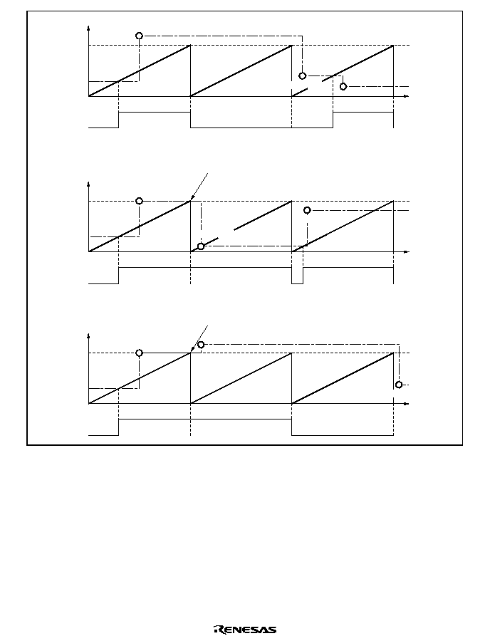
Rev. 2.0, 09/02, page 219 of 658
TCNT value
TGRA
H'0000
TIOCA
Time
TGRB
0% duty
TGRB rewritten
TGRB
rewritten
TGRB rewritten
TCNT value
TGRA
H'0000
TIOCA
Time
TGRB
100% duty
TGRB rewritten
TGRB rewritten
TGRB rewritten
Output does not change when cycle register and duty register
compare matches occur simultaneously
TCNT value
TGRA
H'0000
TIOCA
Time
TGRB
100% duty
TGRB rewritten
TGRB rewritten
TGRB rewritten
Output does not change when cycle register and duty
register compare matches occur simultaneously
0% duty
Figure 10.27 Example of PWM Mode Operation (3)

Rev. 2.0, 09/02, page 220 of 658
10.5.6
Phase Counting Mode (H8S/2268 Series Only)
In phase counting mode, the phase difference between two external clock inputs is detected and
TCNT is incremented/decremented accordingly. This mode can be set for channels 1 and 2.
When phase counting mode is set, an external clock is selected as the counter input clock and
TCNT operates as an up/down-counter regardless of the setting of bits TPSC0 to TPSC2 and bits
CKEG0 and CKEG1 in TCR. However, the functions of bits CCLR0 and CCLR1 in TCR, and of
TIOR, TIER, and TGR, are valid, and input capture/compare match and interrupt functions can be
used.
If overflow occurs when TCNT is counting up, the TCFV flag in TSR is set; if underflow occurs
when TCNT is counting down, the TCFU flag is set.
The TCFD bit in TSR is the count direction flag. Reading the TCFD flag reveals whether TCNT is
counting up or down.
Table 10.20 shows the correspondence between external clock pins and channels.
Table 10.20 Phase Counting Mode Clock Input Pins
External Clock Pins
Channels
A-Phase
B-Phase
When channel 1 is set to phase counting mode
TCLKA
TCLKB
When channel 2 is set to phase counting mode
TCLKC
TCLKD
Example of Phase Counting Mode Setting Procedure: Figure 10.28 shows an example of the
phase counting mode setting procedure.
Phase counting mode
Select phase counting mode
Start count
<Phase counting mode>
Select phase counting mode with bits MD3 to
MD0 in TMDR.
Set the CST bit in TSTR to 1 to start the count
operation.
[1]
[2]
[1]
[2]
Figure 10.28 Example of Phase Counting Mode Setting Procedure

Rev. 2.0, 09/02, page 221 of 658
Examples of Phase Counting Mode Operation: In phase counting mode, TCNT counts up or
down according to the phase difference between two external clocks. There are four modes,
according to the count conditions.
1. Phase counting mode 1
Figure 10.29 shows an example of phase counting mode 1 operation, and table 10.21
summarizes the TCNT up/down-count conditions.
TCNT value
Time
Down-count
Up-count
TCLKA(channel 1)
TCLKC(channel 2)
TCLKB(channel 1)
TCLKD(channel 2)
Figure 10.29 Example of Phase Counting Mode 1 Operation
Table 10.21 Up/Down-Count Conditions in Phase Counting Mode 1
TCLKA (Channel 1)
TCLKC (Channel 2)
TCLKB (Channel 1)
TCLKD (Channel 2)
Operation
High level
Up-count
Low level
Low level
High level
High level
Down-count
Low level
High level
Low level
Legend
: Rising edge
: Falling edge

Rev. 2.0, 09/02, page 222 of 658
2. Phase counting mode 2
Figure 10.30 shows an example of phase counting mode 2 operation, and table 10.22
summarizes the TCNT up/down-count conditions.
Time
Down-count
Up-count
TCNT value
TCLKA(channel 1)
TCLKC(channel 2)
TCLKB(channel 1)
TCLKD(channel 2)
Figure 10.30 Example of Phase Counting Mode 2 Operation
Table 10.22 Up/Down-Count Conditions in Phase Counting Mode 2
TCLKA (Channel 1)
TCLKC (Channel 2)
TCLKB (Channel 1)
TCLKD (Channel 2)
Operation
High level
Don't care
Low level
Don't care
Low level
Don't care
High level
Up-count
High level
Don't care
Low level
Don't care
High level
Don't care
Low level
Down-count
Legend
: Rising edge
: Falling edge

Rev. 2.0, 09/02, page 223 of 658
3. Phase counting mode 3
Figure 10.31 shows an example of phase counting mode 3 operation, and table 10.23
summarizes the TCNT up/down-count conditions.
Time
Up-count
Down-count
TCNT value
TCLKA(channel 1)
TCLKC(channel 2)
TCLKB(channel 1)
TCLKD(channel 2)
Figure 10.31 Example of Phase Counting Mode 3 Operation
Table 10.23 Up/Down-Count Conditions in Phase Counting Mode 3
TCLKA (Channel 1)
TCLKC (Channel 2)
TCLKB (Channel 1)
TCLKD (Channel 2)
Operation
High level
Don't care
Low level
Don't care
Low level
Don't care
High level
Up-count
High level
Down-count
Low level
Don't care
High level
Don't care
Low level
Don't care
Legend
: Rising edge
: Falling edge

Rev. 2.0, 09/02, page 224 of 658
4. Phase counting mode 4
Figure 10.32 shows an example of phase counting mode 4 operation, and table 10.24
summarizes the TCNT up/down-count conditions.
Time
Up-count
Down-count
TCNT value
TCLKA(channels 1)
TCLKC(channels 2)
TCLKB(channels 1)
TCLKD(channels 2)
Figure 10.32 Example of Phase Counting Mode 4 Operation
Table 10.24 Up/Down-Count Conditions in Phase Counting Mode 4
TCLKA (Channel 1)
TCLKC (Channel 2)
TCLKB (Channel 1)
TCLKD (Channel 2)
Operation
High level
Up-count
Low level
Low level
Don't care
High level
High level
Down-count
Low level
High level
Don't care
Low level
Legend
: Rising edge
: Falling edge

Rev. 2.0, 09/02, page 225 of 658
10.6
Interrupt Sources
There are three kinds of TPU interrupt source for the H8S/2268 Series; TGR input
capture/compare match, TCNT overflow, and TCNT underflow. There are two kinds of TPU
interrupt source for the H8S/2264 Series; TGR input capture/compare match and TCNT overflow.
Each interrupt source has its own status flag and enable/disabled bit, allowing the generation of
interrupt request signals to be enabled or disabled individually.
When an interrupt request is generated, the corresponding status flag in TSR is set to 1. If the
corresponding enable/disable bit in TIER is set to 1 at this time, an interrupt is requested. The
interrupt request is cleared by clearing the status flag to 0.
In the H8S/2268 Series, relative channel priorities can be changed by the interrupt controller,
however the priority order within a channel is fixed. For details, see section 5, Interrupt Controller.
Table 10.25 lists the TPU interrupt sources.
Table 10.25 TPU Interrupts
Channel Name
Interrupt Source
Interrupt Flag
DTC
Activation
*
Priority Level
0
*
TGI0A
TGRA_0 input capture/compare match
TGFA_0
Possible
High
TGI0B
TGRB_0 input capture/compare match
TGFB_0
Possible
TGI0C
TGRC_0 input capture/compare match
TGFC_0
Possible
TGI0D
TGRD_0 input capture/compare match
TGFD_0
Possible
TCI0V
TCNT_0 overflow
TCFV_0
Not possible
1
TGI1A
TGRA_1 input capture/compare match
TGFA_1
Possible
TGI1B
TGRB_1 input capture/compare match
TGFB_1
Possible
TCI1V
TCNT_1 overflow
TCFV_1
Not possible
TCI1U
*
TCNT_1 underflow
TCFU_1
Not possible
2
TGI2A
TGRA_2 input capture/compare match
TGFA_2
Possible
TGI2B
TGRB_2 input capture/compare match
TGFB_2
Possible
TCI2V
TCNT_2 overflow
TCFV_2
Not possible
TCI2U
*
TCNT_2 underflow
TCFU_2
Not possible
Low
Note:
*
Supported only by the H8S/2268 Series.

Rev. 2.0, 09/02, page 226 of 658
Input Capture/Compare Match Interrupt: An interrupt is requested if the TGIE bit in TIER is
set to 1 when the TGF flag in TSR is set to 1 by the occurrence of a TGR input capture/compare
match on a particular channel. The interrupt request is cleared by clearing the TGF flag to 0. The
H8S/2268 Series TPU has eight input capture/compare match interrupts and the H8S/2264 Series
TPU has four input capture/compare match interrupts, four for channel 0, and two each for
channels 1 and 2.
Overflow Interrupt: An interrupt is requested if the TCIEV bit in TIER is set to 1 when the
TCFV flag in TSR is set to 1 by the occurrence of TCNT overflow on a channel. The interrupt
request is cleared by clearing the TCFV flag to 0. The H8S/2268 Series TPU has three overflow
interrupts and the H8S/2264 Series TPU has two overflow interrupts, one for each channel
(channels 0 to 2, or 1 and 2).
Underflow Interrupt (H8S/2268 Series Only): An interrupt is requested if the TCIEU bit in
TIER is set to 1 when the TCFU flag in TSR is set to 1 by the occurrence of TCNT underflow on a
channel. The interrupt request is cleared by clearing the TCFU flag to 0. The TPU has two
underflow interrupts, one each for channels 1 and 2.
10.7
DTC Activation (H8S/2268 Series Only)
The DTC can be activated by the TGR input capture/compare match interrupt for a channel. For
details, see section 8, Data Transfer Controller (DTC).
A total of eight TPU input capture/compare match interrupts can be used as DTC activation
sources, four for channel 0, and two each for channels 1 and 2.
10.8
A/D Converter Activation
The A/D converter can be activated by the TGRA input capture/compare match for a channel.
If the TTGE bit in TIER is set to 1 when the TGFA flag in TSR is set to 1 by the occurrence of a
TGRA input capture/compare match on a particular channel, a request to begin A/D conversion is
sent to the A/D converter. If the TPU conversion start trigger has been selected on the A/D
converter side at this time, A/D conversion is begun.
In the H8S/2268 Series TPU, a total of three TGRA input capture/compare match interrupts can be
used as A/D converter conversion start sources, one for each channel (channels 0 to 2). While in
the H8S/2264 Series TPU, a total of two TGRA input capture/compare match interrupts can be
used, one for each channel (channels 1 and 2).
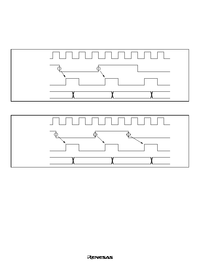
Rev. 2.0, 09/02, page 227 of 658
10.9
Operation Timing
10.9.1
Input/Output Timing
TCNT Count Timing: Figure 10.33 shows TCNT count timing in internal clock operation, and
figure 10.34 shows TCNT count timing in external clock operation.
TCNT
TCNT
input clock
Internal clock
N-1
N
N+1
N+2
Falling edge
Rising edge
Figure 10.33 Count Timing in Internal Clock Operation
TCNT
TCNT
input clock
External clock
N-1
N
N+1
N+2
Falling edge
Rising edge
Falling edge
Figure 10.34 Count Timing in External Clock Operation
Output Compare Output Timing: A compare match signal is generated in the final state in
which TCNT and TGR match (the point at which the count value matched by TCNT is updated).
When a compare match signal is generated, the output value set in TIOR is output at the output
compare output pin. After a match between TCNT and TGR, the compare match signal is not
generated until the TCNT input clock is generated.
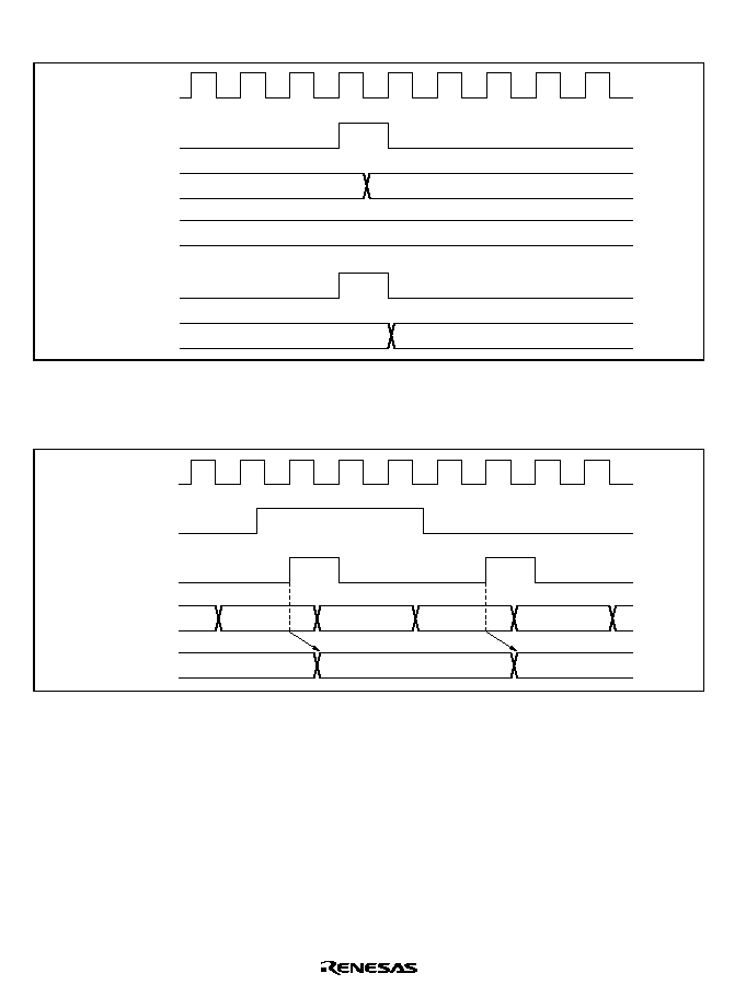
Rev. 2.0, 09/02, page 228 of 658
Figure 10.35 shows output compare output timing.
TGR
TCNT
TCNT
input clock
N
N
N+1
Compare
match signal
TIOC pin
Figure 10.35 Output Compare Output Timing
Input Capture Signal Timing: Figure 10.36 shows input capture signal timing.
TCNT
Input capture
input
N
N+1
N+2
N
N+2
TGR
Input capture
signal
Figure 10.36 Input Capture Input Signal Timing
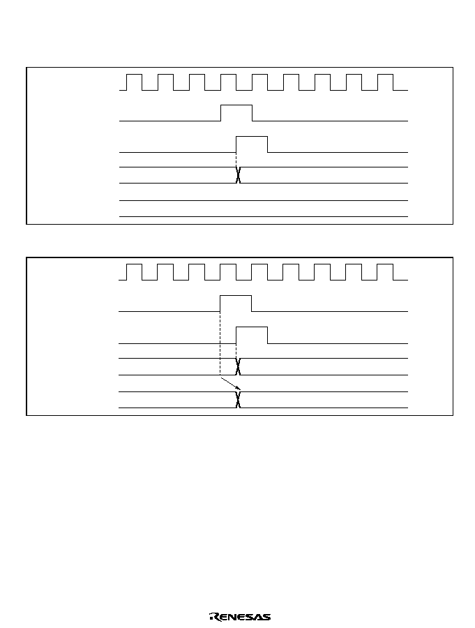
Rev. 2.0, 09/02, page 229 of 658
Timing for Counter Clearing by Compare Match/Input Capture: Figure 10.37 shows the
timing when counter clearing on compare match is specified, and figure 10.38 shows the timing
when counter clearing on input capture is specified.
TCNT
Counter
clear signal
Compare
match signal
TGR
N
N
H'0000
Figure 10.37 Counter Clear Timing (Compare Match)
TCNT
Counter clear
signal
Input capture
signal
TGR
N
H'0000
N
Figure 10.38 Counter Clear Timing (Input Capture)
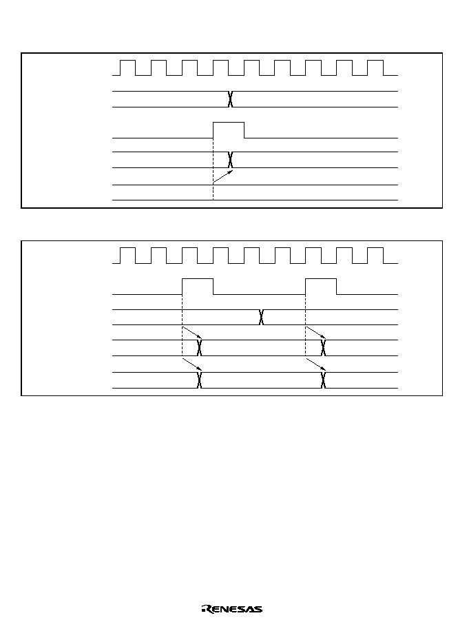
Rev. 2.0, 09/02, page 230 of 658
Buffer Operation Timing (H8S/2268 Series Only): Figures 10.39 and 10.40 show the timing in
buffer operation.
TGRA,
TGRB
Compare
match signal
TCNT
TGRC,
TGRD
n
N
N
n
n+1
Figure 10.39 Buffer Operation Timing (Compare Match)
TGRA,
TGRB
TCNT
Input capture
signal
TGRC,
TGRD
N
n
n
N+1
N
N
N+1
Figure 10.40 Buffer Operation Timing (Input Capture)
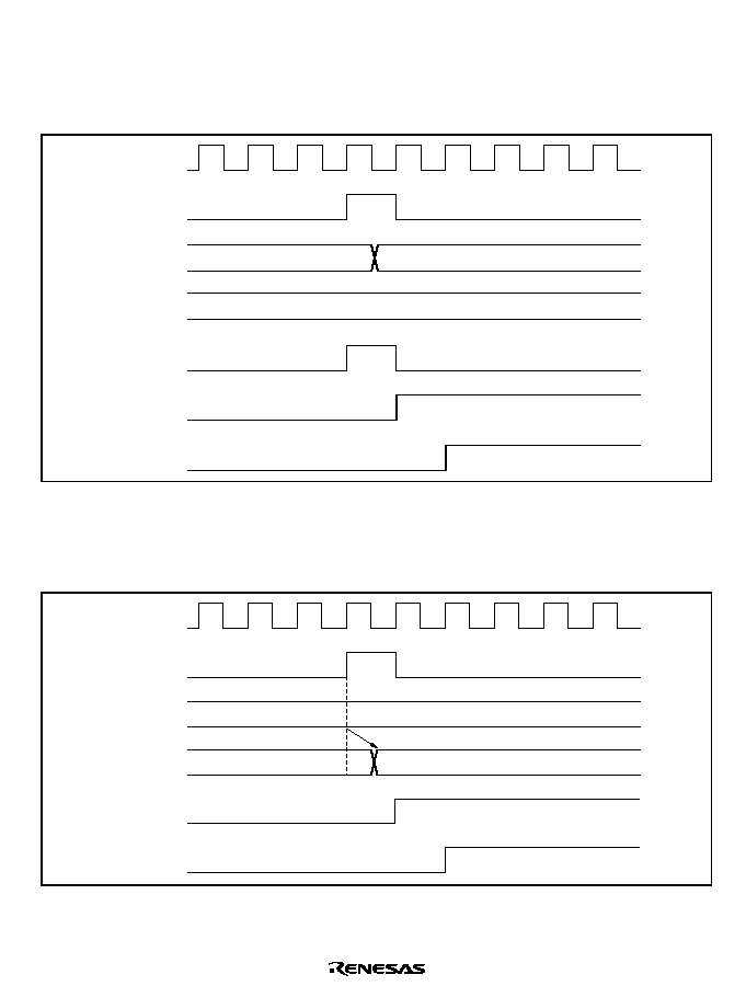
Rev. 2.0, 09/02, page 231 of 658
10.9.2
Interrupt Signal Timing
TGF Flag Setting Timing in Case of Compare Match: Figure 10.41 shows the timing for
setting of the TGF flag in TSR on compare match, and TGI interrupt request signal timing.
TGR
TCNT
TCNT input
clock
N
N
N+1
Compare
match signal
TGF flag
TGI interrupt
Figure 10.41 TGI Interrupt Timing (Compare Match)
TGF Flag Setting Timing in Case of Input Capture: Figure 10.42 shows the timing for setting
of the TGF flag in TSR on input capture, and TGI interrupt request signal timing.
TGR
TCNT
Input capture
signal
N
N
TGF flag
TGI interrupt
Figure 10.42 TGI Interrupt Timing (Input Capture)

Rev. 2.0, 09/02, page 232 of 658
TCFV Flag/TCFU Flag Setting Timing: Figure 10.43 shows the timing for setting of the TCFV
flag in TSR on overflow, and TCIV interrupt request signal timing.
Figure 10.44 shows the timing for setting of the TCFU flag in TSR on underflow, and TCIU
interrupt request signal timing in the H8S/2268 Series.
Overflow
signal
TCNT
(overflow)
TCNT input
clock
H'FFFF
H'0000
TCFV flag
TCIV interrupt
Figure 10.43 TCIV Interrupt Setting Timing
Underflow
signal
TCNT
(underflow)
TCNT
input clock
H'0000
H'FFFF
TCFU flag
TCIU interrupt
Figure 10.44 TCIU Interrupt Setting Timing (H8S/2268 Series Only)

Rev. 2.0, 09/02, page 233 of 658
Status Flag Clearing Timing: After a status flag is read as 1 by the CPU, it is cleared by writing
0 to it. When the DTC is activated in the H8S/2268 Series, the flag is cleared automatically.
Figure 10.45 shows the timing for status flag clearing by the CPU, and figure 10.46 shows the
timing for status flag clearing by the DTC.
Status flag
Write signal
Address
TSR address
Interrupt
request
signal
TSR write cycle
T1
T2
Figure 10.45 Timing for Status Flag Clearing by CPU
Interrupt
request
signal
Status flag
Address
Source address
DTC
read cycle
T1
T2
Destination
address
T1
T2
DTC
write cycle
Figure 10.46 Timing for Status Flag Clearing by DTC Activation (H8S/2268 Series Only)

Rev. 2.0, 09/02, page 234 of 658
10.10 Usage Notes
10.10.1
Module Stop Mode Setting
TPU operation can be disabled or enabled using the module stop control register. The initial
setting is for TPU operation to be halted. Register access is enabled by clearing module stop
mode. For details, refer to section 22, Power-Down Modes.
10.10.2
Input Clock Restrictions
The input clock pulse width must be at least 1.5 states in the case of single-edge detection, and at
least 2.5 states in the case of both-edge detection. The TPU will not operate properly at narrower
pulse widths.
In the H8S/2268 Series phase counting mode, the phase difference and overlap between the two
input clocks must be at least 1.5 states, and the pulse width must be at least 2.5 states. Figure
10.47 shows the input clock conditions in phase counting mode.
Overlap
Phase
differ-
ence
Phase
differ-
ence
Overlap
TCLKA
(TCLKC)
TCLKB
(TCLKD)
Pulse width
Pulse width
Pulse width
Pulse width
Notes: Phase difference and overlap
Pulse width
: 1.5 states or more
: 2.5 states or more
Figure 10.47 Phase Difference, Overlap, and Pulse Width in Phase Counting Mode
(H8S/2268 Series Only)

Rev. 2.0, 09/02, page 235 of 658
10.10.3
Caution on Period Setting
When counter clearing on compare match is set, TCNT is cleared in the final state in which it
matches the TGR value (the point at which the count value matched by TCNT is updated).
Consequently, the actual counter frequency is given by the following formula:
f =
(N + 1)
Where
f
: Counter frequency
: Operating frequency
N : TGR set value
10.10.4
Contention between TCNT Write and Clear Operations
If the counter clear signal is generated in the T2 state of a TCNT write cycle, TCNT clearing takes
precedence and the TCNT write is not performed.
Figure 10.48 shows the timing in this case.
Counter clear
signal
Write signal
Address
TCNT address
TCNT
TCNT write cycle
T1
T2
N
H'0000
Figure 10.48 Contention between TCNT Write and Clear Operations
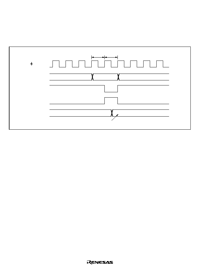
Rev. 2.0, 09/02, page 236 of 658
10.10.5
Contention between TCNT Write and Increment Operations
If incrementing occurs in the T2 state of a TCNT write cycle, the TCNT write takes precedence
and TCNT is not incremented.
Figure 10.49 shows the timing in this case.
TCNT input
clock
Write signal
Address
TCNT address
TCNT
TCNT write cycle
T1
T2
N
M
TCNT write data
Figure 10.49 Contention between TCNT Write and Increment Operations
10.10.6
Contention between TGR Write and Compare Match
If a compare match occurs in the T2 state of a TGR write cycle, the TGR write takes precedence
and the compare match signal is inhibited. A compare match does not occur even if the previous
value is written.
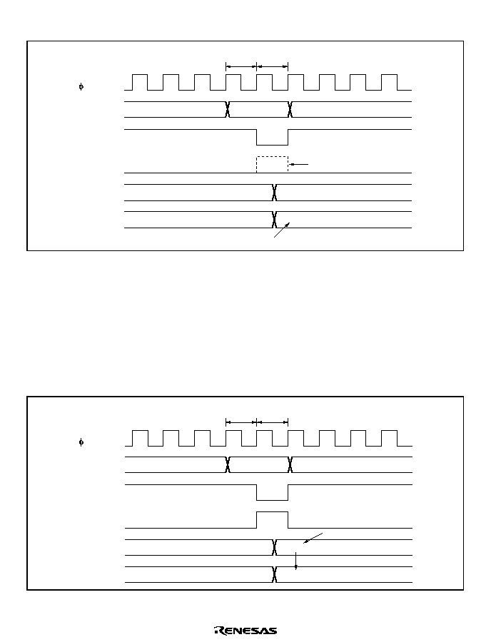
Rev. 2.0, 09/02, page 237 of 658
Figure 10.50 shows the timing in this case.
Compare
match signal
Write signal
Address
TGR address
TCNT
TGR write cycle
T1
T2
N
M
TGR write data
TGR
N
N+1
Inhibited
Figure 10.50 Contention between TGR Write and Compare Match
10.10.7
Contention between Buffer Register Write and Compare Match (H8S/2268 Series
Only)
If a compare match occurs in the T2 state of a TGR write cycle, the data that is transferred to TGR
by the buffer operation will be that in the buffer prior to the write.
Figure 10.51 shows the timing in this case.
Compare
match signal
Write signal
Address
Buffer register
address
Buffer
register
TGR write cycle
T1
T2
N
TGR
N
M
Buffer register write data
Figure 10.51 Contention between Buffer Register Write and Compare Match

Rev. 2.0, 09/02, page 238 of 658
10.10.8
Contention between TGR Read and Input Capture
If an input capture signal is generated in the T1 state of a TGR read cycle, the data that is read will
be that in the buffer after input capture transfer.
Figure 10.52 shows the timing in this case.
Input capture
signal
Read signal
Address
TGR address
TGR
TGR read cycle
T1
T2
M
Internal
data bus
X
M
Figure 10.52 Contention between TGR Read and Input Capture
10.10.9
Contention between TGR Write and Input Capture
If an input capture signal is generated in the T2 state of a TGR write cycle, the input capture
operation takes precedence and the write to TGR is not performed.
Figure 10.53 shows the timing in this case.

Rev. 2.0, 09/02, page 239 of 658
Input capture
signal
Write signal
Address
TCNT
TGR write cycle
T1
T2
M
TGR
M
TGR address
Figure 10.53 Contention between TGR Write and Input Capture
10.10.10 Contention between Buffer Register Write and Input Capture (H8S/2268 Series
Only)
If an input capture signal is generated in the T2 state of a buffer register write cycle, the buffer
operation takes precedence and the write to the buffer register is not performed.
Figure 10.54 shows the timing in this case.
Input capture
signal
Write signal
Address
TCNT
Buffer register write cycle
T1
T2
N
TGR
N
M
M
Buffer
register
Buffer register
address
Figure 10.54 Contention between Buffer Register Write and Input Capture

Rev. 2.0, 09/02, page 240 of 658
10.10.11 Contention between Overflow/Underflow and Counter Clearing
In the H8S/2268 Series, if overflow/underflow and counter clearing occur simultaneously, the
TCFV/TCFU flag in TSR is not set and TCNT clearing takes precedence.
In the H8S/2264 Series, if overflow and counter clearing occur simultaneously, the TCFV flag in
TSR is not set and TCNT clearing takes precedence.
Figure 10.55 shows the operation timing when a TGR compare match is specified as the clearing
source, and when H'FFFF is set in TGR.
Counter
clear signal
TCNT input
clock
TCNT
TGF
Disabled
TCFV
H'FFFF
H'0000
Figure 10.55 Contention between Overflow and Counter Clearing

Rev. 2.0, 09/02, page 241 of 658
10.10.12 Contention between TCNT Write and Overflow/Underflow
In the H8S/2268 Series, if there is an up-count or down-count in the T2 state of a TCNT write
cycle and overflow/underflow occurs, the TCNT write takes precedence and the TCFV/TCFU flag
in TSR is not set.
In the H8S/2264 Series, if there is an up-count in the T2 state of a TCNT write cycle and overflow
occurs, the TCNT write takes precedence and the TCFV flag in TSR is not set.
Figure 10.56 shows the operation timing when there is contention between TCNT write and
overflow.
Write signal
Address
TCNT address
TCNT
TCNT write cycle
T1
T2
H'FFFF
M
TCNT write data
TCFV flag
Figure 10.56 Contention between TCNT Write and Overflow
10.10.13 Multiplexing of I/O Pins
In the H8S/2268 Series, the TCLKA input pin is multiplexed with the TIOCC0 I/O pin, the
TCLKB input pin with the TIOCD0 I/O pin, the TCLKC input pin with the TIOCB1 I/O pin, and
the TCLKD input pin with the TIOCB2 I/O pin. In the H8S/2264 Series, the TCLKC input pin is
multiplexed with the TIOCB1 I/O pin. When an external clock is input, compare match output
should not be performed from a multiplexed pin.
10.10.14 Interrupts in Module Stop Mode
If module stop mode is entered when an interrupt has been requested, it will not be possible to
clear the CPU interrupt source, or the DTC activation source (the H8S/2268 Series only).
Interrupts should therefore be disabled before entering module stop mode.

Rev. 2.0, 09/02, page 242 of 658

Rev. 2.0, 09/02, page 243 of 658
Section 11 8-Bit Timers
The H8S/2268 Series has an on-chip 8-bit timer module with four channels (TMR_0, TMR_1,
TMR_2 and TMR_3) operating on the basis of an 8-bit counter and an 8-bit reload timer with four
channels (TMR_4). The H8S/2264 Series has an on-chip 8-bit timer module with two channels
(TMR_0 and TMR_1) operating on the basis of an 8-bit counter.
11.1
8-Bit Timer Module (TMR_0, TMR_1, TMR_2 and TMR_3)
The 8-bit timer module can be used to count external events and be used as a multifunction timer
in a variety of applications, such as generation of counter reset, interrupt requests, and pulse output
with an arbitrary duty cycle using a compare-match signal with two registers.
11.1.1
Features
∑
Selection of clock sources
Selected from three internal clocks (
/8,
/64, and
/8192) and an external clock.
∑
Selection of three ways to clear the counters
The counters can be cleared on compare-match A or B, or by an external reset signal.
∑
Timer output controlled by two compare-match signals
The timer output signal in each channel is controlled by two independent compare-match
signals, enabling the timer to be used for various applications, such as the generation of pulse
output or PWM output with an arbitrary duty cycle.
∑
Cascading of the two channels
The module can operate as a 16-bit timer using channel 0 (channel 2*) as the upper half and
channel 1 (channel 3*) as the lower half (16-bit count mode).
Channel 1 (channel 3*) can be used to count channel 0 (channel 2*) compare-match
occurrences (compare-match count mode).
∑
Multiple interrupt sources for each channel
Two compare-match interrupts and one overflow interrupt can be requested independently.
∑
Generation of A/D conversion start trigger
Channel 0 compare-match signal can be used as the A/D conversion start trigger.
∑
Module stop mode can be set
At initialization, the 8-bit timer operation is halted. Register access is enabled by canceling the
module stop mode.
Note: *
Supported only by the H8S/2268 Series.
TIMH220B_000020020700
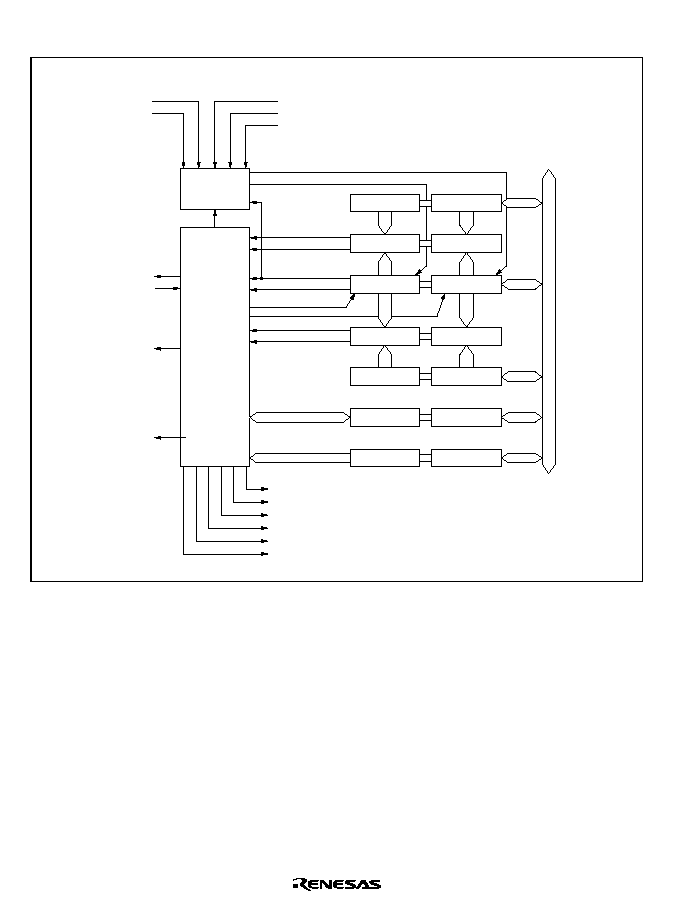
Rev. 2.0, 09/02, page 244 of 658
Figure 11.1 shows a block diagram of the 8-bit timer module (TMR_0 and TMR_1).
External clock
sources
Internal clock
sources
TMR
0
/8
/64
/8192
Clock 1
Clock 0
Compare-match A1
Compare-match A0
Clear 1
CMIA0
CMIB0
OVI0
CMIA1
CMIB1
OVI1
Interrupt signals
TMO
TMRI01
Internal bus
TCORA_0
Comparator A_0
Comparator B_0
TCORB_0
TCSR_0
TCR_0
TCORA_1
Comparator A_1
TCNT_1
Comparator B_1
TCORB_1
TCSR_1
TCR_1
TMCI01
TCNT_0
Overflow 1
Overflow 0
Compare-match B1
Compare-match B0
TMO1
A/D
Clock select
Control logic
Clear 0
Figure 11.1 Block Diagram of 8-Bit Timer Module
Legend
TCORA_0: Time constant register A_0
TCORB_0: Time constant register B_0
TCNT_0: Timer counter_0
TCSR_0: Timer control/status register_0
TCR_0: Timer control register_0
TCORA_1: Time constant register A_1
TCORB_1: Time constant register B_1
TCNT_1: Timer counter_1
TCSR_1: Timer control/status register_1
TCR_1: Timer control register_1

Rev. 2.0, 09/02, page 245 of 658
11.2
Input/Output Pins
Table 11.1 summarizes the input and output pins of the 8-bit timer module.
Table 11.1
Pin Configuration
Channel
Name
Symbol
I/O
Function
0
Timer output
TMO0
Output
Output controlled by compare-match
1
Timer output
TMO1
Output
Output controlled by compare-match
Timer clock input
TMCI01
Input
External clock input for the counter
Common to
0 and 1
Timer reset input
TMRI01
Input
External reset input for the counter
2
*
Timer output
TMO2
Output
Output controlled by compare-match
3
*
Timer output
TMO3
Output
Output controlled by compare-match
Timer clock input
TMCI23
Input
External clock input for the counter
Common to
2 and 3
*
Timer reset input
TMRI23
Input
External reset input for the counter
Note:
*
Supported only by the H8S/2268 Series.
11.3
Register Descriptions
The 8-bit timer has the following registers. For details on the module stop register, refer to section
22.1.2, Module Stop Registers A to D (MSTPCRA to MSTPCRD).
∑
Timer counter_0 (TCNT_0)
∑
Time constant register A_0 (TCORA_0)
∑
Time constant register B_0 (TCORB_0)
∑
Timer control register_0 (TCR_0)
∑
Timer control/status register_0 (TCSR_0)
∑
Timer counter_1 (TCNT_1)
∑
Time constant register A_1 (TCORA_1)
∑
Time constant register B_1 (TCORB_1)
∑
Timer control register_1 (TCR_1)
∑
Timer control/status register_1 (TCSR_1)
∑
Timer counter_2 (TCNT_2)*
∑
Time constant register A_2 (TCORA_2)*
∑
Time constant register B_2 (TCORB_2)*
∑
Timer control register_2 (TCR_2)*
∑
Timer control/status register_2 (TCSR_2)*
∑
Timer counter_3 (TCNT_3)*
∑
Time constant register A_3 (TCORA_3)*

Rev. 2.0, 09/02, page 246 of 658
∑
Time constant register B_3 (TCORB_3)*
∑
Timer control register_3 (TCR_3)*
∑
Timer control/status register_3 (TCSR_3)*
Note: *
Supported only by the H8S/2268 Series.
11.3.1
Timer Counter (TCNT)
Each TCNT is an 8-bit up-counter. TCNT_0 and TCNT_1 (TCNT_2 and TCNT_3) comprise a
single 16-bit register, so they can be accessed together by word access.
TCNT increments on pulses generated from an internal or external clock source. This clock source
is selected by clock select bits CKS2 to CKS0 in TCR. TCNT can be cleared by an external reset
input signal or compare-match signals A and B. Counter clear bits CCLR1 and CCLR0 in TCR
select the method of clearing.
When TCNT overflows from H'FF to H'00, the overflow flag (OVF) in TCSR is set to 1.
11.3.2
Time Constant Register A (TCORA)
TCORA is an 8-bit readable/writable register. TCORA_0 and TCORA_1 (TCORA_2 and
TCORA_3) comprise a single 16-bit register, so they can be accessed together by word access.
TCORA is continually compared with the value in TCNT. When a match is detected, the
corresponding compare-match flag A (CMFA) in TCSR is set. Note, however, that comparison is
disabled during the T2 state of a TCORA write cycle.
The timer output from the TMO pin can be freely controlled by the compare-match signal A and
the settings of output select bits OS1 and OS0 in TCSR.
The initial value of TCORA is H'FF.
11.3.3
Time Constant Register B (TCORB)
TCORB is an 8-bit readable/writable register. TCORB_0 and TCORB_1 (TCORB_2 and
TCORB_3) comprise a single 16-bit register, so they can be accessed together by word access.
TCORB is continually compared with the value in TCNT. When a match is detected, the
corresponding compare-match flag B (CMFB) in TCSR is set. Note, however, that comparison is
disabled during the T2 state of a TCORB write cycle.
The timer output from the TMO pin can be freely controlled by the compare-match signal B and
the settings of output select bits OS1 and OS0 in TCSR.

Rev. 2.0, 09/02, page 247 of 658
The initial value of TCORB is H'FF.
11.3.4
Timer Control Register (TCR)
TCR selects the TCNT clock source and the time at which TCNT is cleared, and controls interrupt
requests.
Bit
Bit Name
Initial
Value
R/W
Description
7
CMIEB
0
R/W
Compare-Match Interrupt Enable B
Selects whether the CMFB interrupt request (CMIB) is
enabled or disabled when the CMFB flag in TCSR is
set to 1.
0: CMFB interrupt request (CMIB) is disabled
1: CMFB interrupt request (CMIB) is enabled
6
CMIEA
0
R/W
Compare-Match Interrupt Enable A
Selects whether the CMFA interrupt request (CMIA) is
enabled or disabled when the CMFA flag in TCSR is
set to 1.
0: CMFA interrupt request (CMIA) is disabled
1: CMFA interrupt request (CMIA) is enabled
5
OVIE
0
R/W
Timer Overflow Interrupt Enable
Selects whether the OVF interrupt request (OVI) is
enabled or disabled when the OVF flag in TCSR is set
to 1.
0: OVF interrupt request (OVI) is disabled
1: OVF interrupt request (OVI) is enabled
4
3
CCLR1
CCLR0
0
0
R/W
R/W
Counter Clear 1 and 0
These bits select the method by which TCNT is
cleared
00: Clearing is disabled
01: Cleared on compare-match A
10: Cleared on compare-match B
11: Cleared on rising edge of external reset input

Rev. 2.0, 09/02, page 248 of 658
Bit
Bit Name
Initial
Value
R/W
Description
2 to 0
CKS2
CKS1
CKS0
0
0
0
R/W
R/W
R/W
Clock Select 2 to 0
The input clock can be selected from three clocks
divided from the system clock (
). When use of an
external clock is selected, three types of count can be
selected: at the rising edge, the falling edge, and both
rising and falling edges.
000: Clock input disabled
001:
/8 internal clock source, counted on the falling
edge
010:
/64 internal clock source, counted on the falling
edge
011:
/8192 internal clock source, counted on the
falling edge
100: For channel 0: Counted on TCNT1 overflow
signal
*
For channel 1: Counted on TCNT0 compare-matchA
signal
*
For channel 2: Counted on TCNT3 overflow signal
*
For channel 3: Counted on TCNT2 compare-matchA
signal
*
101: External clock source, counted at rising edge
110: External clock source, counted at falling edge
111: External clock source, counted at both rising and
falling edges
Note:
*
If the count input of channel 0 (channel 2) is the TCNT1 (TCNT3) overflow signal and
that of channel 1 (channel 3) is the TCNT0 (TCNT2) compare-match signal, no
incrementing clock will be generated. Do not use this setting.

Rev. 2.0, 09/02, page 249 of 658
11.3.5
Timer Control/Status Register (TCSR)
TCSR indicates status flags and controls compare-match output.
∑
TCSR_0
Bit
Bit Name
Initial
Value
R/W
Description
7
CMFB
0
R/(W)
*
1
Compare-Match Flag B
[Setting condition]
When TCNT = TCORB
[Clearing condition]
Read CMFB when CMFB = 1, then write 0 in CMFB.
The DTC
*
2
is activated by the CMIB interrupt and the
DISEL bit = 0 in MRB of the DTC
*
2
.
6
CMFA
0
R/(W)
*
1
Compare-match Flag A
[Setting condition]
When TCNT = TCORA
[Clearing condition]
Read CMFA when CMFA = 1, then write 0 in CMFA.
The DTC
*
2
is activated by the CMIA interrupt and
DISEL bit = 0 in MRB of the DTC
*
2
.
5
OVF
0
R/(W)
*
1
Timer Overflow Flag
[Setting condition]
When TCNT overflows from H'FF to H'00
[Clearing condition]
Read OVF when OVF = 1, then write 0 in OVF
4
ADTE
0
R/W
A/D Trigger Enable
Enables or disables A/D converter start requests by
compare-match A.
0: A/D converter start requests by compare-match A
are disabled
1: A/D converter start requests by compare-match A
are enabled

Rev. 2.0, 09/02, page 250 of 658
Bit
Bit Name
Initial
Value
R/W
Description
3
2
OS3
OS2
0
0
R/W
R/W
Output Select 3 and 2
These bits specify how the timer output level is to be
changed by a compare-match B of TCORB and
TCNT.
00: No change when compare-match B occurs
01: 0 is output when compare-match B occurs
10: 1 is output when compare-match B occurs
11: Output is inverted when compare-match B occurs
(toggle output)
1
0
OS1
OS0
0
0
R/W
R/W
Output Select 1 and 0
These bits specify how the timer output level is to be
changed by a compare-match A of TCORA and
TCNT.
00: No change when compare-match A occurs
01: 0 is output when compare-match A occurs
10: 1 is output when compare-match A occurs
11: Output is inverted when compare-match A occurs
(toggle output)
Notes: 1. Only 0 can be written to this bit, to clear the flag.
2. Supported only by the H8S/2268 Series.

Rev. 2.0, 09/02, page 251 of 658
∑
TCSR_1 and TCSR_3
Bit
Bit Name
Initial
Value
R/W
Description
7
CMFB
0
R/(W)
*
1
Compare-Match Flag B
[Setting condition]
When TCNT = TCORB
[Clearing condition]
Read CMFB when CMFB = 1, then write 0 in CMFB
The DTC
*
2
is activated by the CMIB interrupt and the
DISEL Bit = 0 in MRB of the DTC
*
2
.
6
CMFA
0
R/(W)
*
1
Compare-match Flag A
[Setting condition]
When TCNT = TCORA
[Clearing condition]
Read CMFA when CMFA = 1, then write 0 in CMFA
The DTC
*
2
is activated by the CMIA interrupt and the
DISEL Bit = 0 in MRB of the DTC
*
2
.
5
OVF
0
R/(W)
*
1
Timer Overflow Flag
[Setting condition]
When TCNT overflows from H'FF to H'00
[Clearing condition]
Read OVF when OVF = 1, then write 0 in OVF
4
1
Reserved
This bit is always read as 1 and cannot be modified.
3
2
OS3
OS2
0
0
R/W
R/W
Output Select 3 and 2
These bits specify how the timer output level is to be
changed by a compare-match B of TCORB and
TCNT.
00: No change when compare-match B occurs
01: 0 is output when compare-match B occurs
10: 1 is output when compare-match B occurs
11: Output is inverted when compare-match B occurs
(toggle output)

Rev. 2.0, 09/02, page 252 of 658
Bit
Bit Name
Initial
Value
R/W
Description
1
0
OS1
OS0
0
0
R/W
R/W
Output Select 1 and 0
These bits specify how the timer output level is to be
changed by a compare-match A of TCORA and
TCNT.
00: No change when compare-match A occurs
01: 0 is output when compare-match A occurs
10: 1 is output when compare-match A occurs
11: Output is inverted when compare-match A occurs
(toggle output)
Notes: 1. Only 0 can be written to this bit, to clear the flag.
2. Supported only by the H8S/2268 Series.
∑
TCSR_2
Bit
Bit Name
Initial
Value
R/W
Description
7
CMFB
0
R/(W)
*
1
Compare-Match Flag B
[Setting condition]
When TCNT = TCORB
[Clearing condition]
Read CMFB when CMFB = 1, then write 0 in CMFB
The DTC
*
2
is activated by the CMIB interrupt and the
DISEL Bit = 0 in MRB of the DTC
*
2
.
6
CMFA
0
R/(W)
*
1
Compare-match Flag A
[Setting condition]
When TCNT = TCORA
[Clearing condition]
Read CMFA when CMFA = 1, then write 0 in CMFA
The DTC
*
2
is activated by the CMIA interrupt and the
DISEL Bit = 0 in MRB of the DTC
*
2
.
5
OVF
0
R/(W)
*
1
Timer Overflow Flag
[Setting condition]
When TCNT overflows from H'FF to H'00
[Clearing condition]
Read OVF when OVF = 1, then write 0 in OVF

Rev. 2.0, 09/02, page 253 of 658
Bit
Bit Name
Initial
Value
R/W
Description
4
0
R/W
Reserved
This bit is a readable/writable bit, but the write value
should always be 0.
3
2
OS3
OS2
0
0
R/W
R/W
Output Select 3 and 2
These bits specify how the timer output level is to be
changed by a compare-match B of TCORB and
TCNT.
00: No change when compare-match B occurs
01: 0 is output when compare-match B occurs
10: 1 is output when compare-match B occurs
11: Output is inverted when compare-match B occurs
(toggle output)
1
0
OS1
OS0
0
0
R/W
R/W
Output Select 1 and 0
These bits specify how the timer output level is to be
changed by a compare-match A of TCORA and
TCNT.
00: No change when compare-match A occurs
01: 0 is output when compare-match A occurs
10: 1 is output when compare-match A occurs
11: Output is inverted when compare-match A occurs
(toggle output)
Notes: 1. Only 0 can be written to this bit, to clear the flag.
2. Supported only by the H8S/2268 Series.

Rev. 2.0, 09/02, page 254 of 658
11.4
Operation
11.4.1
Pulse Output
Figure 11.2 shows an example of arbitrary duty pulse output.
1. Set TCR in CCR1 to 0 and CCLR0 to 1 to clear TCNT by a TCORA compare-match.
2. Set OS3 to OS0 bits in TCSR to B'0110 to output 1 by a TCORA compare-match and 0 by a
TCORB compare-match.
By the above settings, waveforms with the cycle of TCORA and the pulse width of TCORB can
be output without software intervention.
TCNT
H'FF
Counter clear
TCORA
TCORB
H'00
TMO
Figure 11.2 Example of Pulse Output
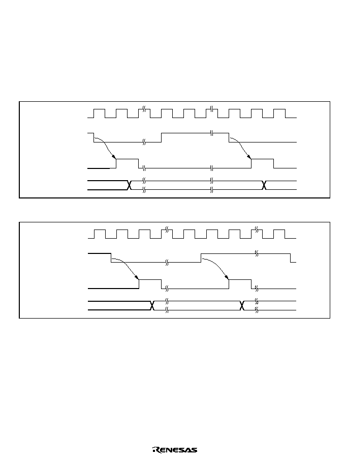
Rev. 2.0, 09/02, page 255 of 658
11.5
Operation Timing
11.5.1
TCNT Incrementation Timing
Figure 11.3 shows the TCNT count timing with internal clock source. Figure 11.4 shows the
TCNT incrementation timing with external clock source. The pulse width of the external clock for
incrementation at single edge must be at least 1.5 status, and at least 2.5 states for incrementation
at both edges. The counter will not increment correctly if the pulse width is less than these values.
Internal clock
TCNT input
clock
TCNT
N ≠ 1
N
N + 1
Figure 11.3 Count Timing for Internal Clock Input
External clock
input pin
TCNT input
clock
TCNT
N ≠ 1
N
N + 1
Figure 11.4 Count Timing for External Clock Input
11.5.2
Timing of CMFA and CMFB Setting When a Compare-Match Occurs
The CMFA and CMFB flags in TCSR are set to 1 by a compare-match signal generated when the
TCOR and TCNT values match. The compare-match signal is generated at the last state in which
the match is true, just before the timer counter is updated. Therefore, when TCOR and TCNT
match, the compare-match signal is not generated until the next incrementation clock input. Figure
11.5 shows the timing of CMF flag setting.

Rev. 2.0, 09/02, page 256 of 658
TCNT
N
N + 1
TCOR
N
Compare-match
signal
CMF
Figure 11.5 Timing of CMF Setting
11.5.3
Timing of Timer Output When a Compare-Match Occurs
When a compare-match occurs, the timer output changes as specified by the output select bits
(OS3 to OS0) in TCSR. Figure 11.6 shows the timing when the output is set to toggle at compare-
match A.
Compare-match A
signal
Timer output
pin
Figure 11.6 Timing of Timer Output
11.5.4
Timing of Compare-Match Clear When a Compare-Match Occurs
TCNT is cleared when compare-match A or B occurs, depending on the setting of the CCLR1 and
CCLR0 bits in TCR. Figure 11.7 shows the timing of this operation.
N
H'00
Compare-match
signal
TCNT
Figure 11.7 Timing of Compare-Match Clear

Rev. 2.0, 09/02, page 257 of 658
11.5.5
TCNT External Reset Timing
TCNT is cleared at the rising edge of an external reset input, depending on the settings of the
CCLR1 and CCLR0 bits in TCR. The width of the clearing pulse must be at least 1.5 states. Figure
11.8 shows the timing of this operation.
Clear signal
External reset
input pin
TCNT
N
H'00
N ≠ 1
Figure 11.8 Timing of Clearing by External Reset Input
11.5.6
Timing of Overflow Flag (OVF) Setting
OVF in TCSR is set to 1 when the timer count overflows (changes from H'FF to H'00). Figure
11.9 shows the timing of this operation.
OVF
Overflow signal
TCNT
H'FF
H'00
Figure 11.9 Timing of OVF Setting

Rev. 2.0, 09/02, page 258 of 658
11.6
Operation with Cascaded Connection
If bits CKS2 to CKS0 in one of TCR_0 and TCR_1 (TCR_2 and TCR_3) are set to B'100, the 8-
bit timers of the two channels are cascaded. With this configuration, a single 16-bit timer can be
used (16-bit timer mode) or compare-matches of 8-bit channel 0 (channel 2) can be counted by the
timer of channel 1 (channel 3) (compare-match count mode). In the case that channel 0 is
connected to channel 1 in cascade, the timer operates as described below.
11.6.1
16-Bit Count Mode
When bits CKS2 to CKS0 in TCR_0 are set to B'100, the timer functions as a single 16-bit timer
with channel 0 occupying the upper 8 bits and channel 1 occupying the lower 8 bits.
∑
Setting of compare-match flags
The CMF flag in TCSR_0 is set to 1 when a 16-bit compare-match occurs.
The CMF flag in TCSR_1 is set to 1 when a lower 8-bit compare-match occurs.
∑
Counter clear specification
If the CCLR1 and CCLR0 bits in TCR_0 have been set for counter clear at compare-match,
the 16-bit counter (TCNT_0 and TCNT_1 together) is cleared when a 16-bit compare-
match occurs. The 16-bit counter (TCNT_0 and TCNT_1 together) is cleared even if
counter clear by the TMRI01 pin has also been set.
The settings of the CCLR1 and CCLR0 bits in TCR_1 are ignored. The lower 8 bits cannot
be cleared independently.
∑
Pin output
Control of output from the TMO0 pin by bits OS3 to OS0 in TCSR_0 is in accordance with
the 16-bit compare-match conditions.
Control of output from the TMO1 pin by bits OS3 to OS0 in TCSR_1 is in accordance with
the lower 8-bit compare-match conditions.
11.6.2
Compare-Match Count Mode
When bits CKS2 to CKS0 in TCR_1 are B'100, TCNT_1 counts compare-match A for channel 0.
Channels 0 and 1 are controlled independently. Conditions such as setting of the CMF flag,
generation of interrupts, output from the TMO pin, and counter clearing are in accordance with the
settings for each channel.

Rev. 2.0, 09/02, page 259 of 658
11.7
Interrupt Sources
11.7.1
Interrupt Sources and DTC Activation
The 8-bit timer can generate three types of interrupt: CMIA, CMIB, and OVI. Table 11.2 shows
the interrupt sources and priority. Each interrupt source can be enabled or disabled independently
by interrupt enable bits in TCR. Independent signals are sent to the interrupt controller for each
interrupt. In the H8S/2268 Series, it is also possible to activate the DTC by means of CMIA and
CMIB interrupts.
Table 11.2
8-Bit Timer Interrupt Sources
Interrupt source Description
Flag
DTC
Activation
*
Interrupt
Priority
CMIA0
TCORA_0 compare-match
CMFA
Possible
High
CMIB0
TCORB_0 compare-match
CMFB
Possible
OVI0
TCNT_0 overflow
OVF
Not possible
Low
CMIA1
TCORA_1 compare-match
CMFA
Possible
High
CMIB1
TCORB_1 compare-match
CMFB
Possible
OVI1
TCNT_1 overflow
OVF
Not possible
Low
CMIA2
*
TCORA_2 compare-match
CMFA
Possible
High
CMIB2
*
TCORB_2 compare-match
CMFB
Possible
OVI2
*
TCNT_2 overflow
OVF
Not possible
Low
CMIA3
*
TCORA_3 compare-match
CMFA
Possible
High
CMIB3
*
TCORB_3 compare-match
CMFB
Possible
OVI3
*
TCNT_3 overflow
OVF
Not possible
Low
Note:
*
Supported only by the H8S/2268 Series.
11.7.2
A/D Converter Activation
The A/D converter can be activated only by channel 0 compare match A.
If the ADTE bit in TCSR0 is set to 1 when the CMFA flag is set to 1 by the occurrence of channel
0 compare match A, a request to start A/D conversion is sent to the A/D converter. If the 8-bit
timer conversion start trigger has been selected on the A/D converter side at this time, A/D
conversion is started.

Rev. 2.0, 09/02, page 260 of 658
11.8
Usage Notes
11.8.1
Contention between TCNT Write and Clear
If a timer counter clock pulse is generated during the T2 state of a TCNT write cycle, the clear
takes priority, so that the counter is cleared and the write is not performed. Figure 11.10 shows
this operation.
Address
TCNT address
Internal write signal
Counter clear signal
TCNT
N
H'00
T
1
T
2
TCNT write cycle by CPU
Figure 11.10 Contention between TCNT Write and Clear

Rev. 2.0, 09/02, page 261 of 658
11.8.2
Contention between TCNT Write and Increment
If a timer counter clock pulse is generated during the T2 state of a TCNT write cycle, the write
takes priority and the counter is not incremented. Figure 11.11 shows this operation.
Address
TCNT address
Internal write signal
TCNT input clock
TCNT
N
M
T
1
T
2
TCNT write cycle by CPU
Counter write data
Figure 11.11 Contention between TCNT Write and Increment

Rev. 2.0, 09/02, page 262 of 658
11.8.3
Contention between TCOR Write and Compare-Match
During the T2 state of a TCOR write cycle, the TCOR write has priority even if a compare-match
occurs and the compare-match signal is disabled. Figure 11.12 shows this operation.
Address
TCOR address
Internal write signal
TCNT
TCOR
N
M
T
1
T
2
TCOR write cycle by CPU
TCOR write data
N
N + 1
Compare-match signal
Inhibited
Figure 11.12 Contention between TCOR Write and Compare-Match
11.8.4
Contention between Compare-Matches A and B
If compare-matches A and B occur at the same time, the 8-bit timer operates in accordance with
the priorities for the output states set for compare-match A and compare-match B, as shown in
table 11.3.
Table 11.3
Timer Output Priorities
Output Setting
Priority
Toggle output
High
1 output
0 output
No change
Low
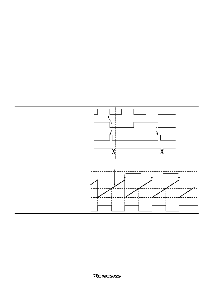
Rev. 2.0, 09/02, page 263 of 658
11.8.5
Switching of Internal Clocks and TCNT Operation
TCNT may increment erroneously when the internal clock is switched over. Table 11.4 shows the
relationship between the timing at which the internal clock is switched (by writing to the CKS1
and CKS0 bits) and the TCNT operation
When the TCNT clock is generated from an internal clock, the falling edge of the internal clock
pulse is detected. If clock switching causes a change from high to low level, as shown in no. 3 in
table 11.4, a TCNT clock pulse is generated on the assumption that the switchover is a falling
edge. This increments TCNT.
Erroneous incrementation can also happen when switching between internal and external clocks.
Table 11.4
Switching of Internal Clock and TCNT Operation
No.
Timing of Switchover
by Means of CKS1 and
CKS0 Bits
TCNT Clock Operation
1
Switching from low to
low
*
1
Clock before
switchover
Clock after
switchover
TCNT clock
TCNT
CKS bit rewrite
N
N + 1
2
Switching from low to
high
*
2
TCNT
H'FF
Counter clear
TCORA
TCORB
H'00
TMO
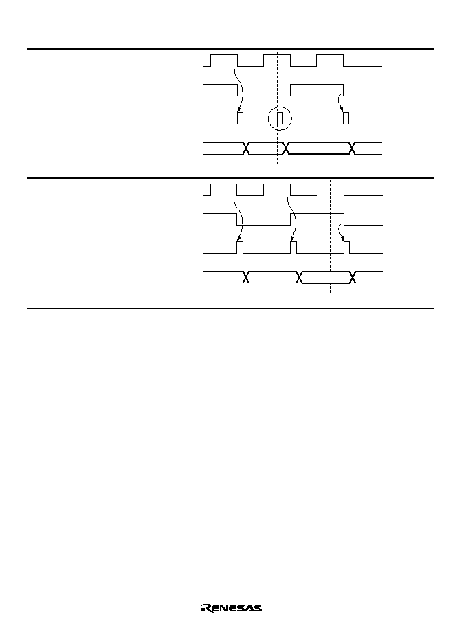
Rev. 2.0, 09/02, page 264 of 658
No.
Timing of Switchover
by Means of CKS1 and
CKS0 Bits
TCNT Clock Operation
3
Switching from high to
low
*
3
Clock before
switchover
Clock after
switchover
TCNT clock
TCNT
CKS bit rewrite
N
N + 1
N + 2
*
4
4
Switching from high to
high
Clock before
switchover
Clock after
switchover
TCNT clock
TCNT
CKS bit rewrite
N
N + 1
N + 2
Notes: 1. Includes switching from low to stop, and from stop to low.
2. Includes switching from stop to high.
3. Includes switching from high to stop.
4. Generated on the assumption that the switchover is a falling edge; TCNT is
incremented.
11.8.6
Contention between Interrupts and Module Stop Mode
If module stop mode is entered when an interrupt has been requested, it will not be possible to
clear the CPU interrupt source or the DTC activation source. Interrupts should therefore be
disabled before entering module stop mode.

Rev. 2.0, 09/02, page 265 of 658
11.9
8-Bit Reload Timer (TMR_4) (H8S/2268 Series Only)
The 8-bit reload timer comprises an 8-bit up-counter with four channels, and has two functions,
the interval function and automatic reload function.
11.9.1
Features
∑
Selection of clock sources
Selected from 14 internal clocks (
/32768,
/8192,
/2048,
/512,
/128,
/32,
/8,
/2,
SUB
/256,
SUB
/128,
SUB
/64,
SUB
/32,
SUB
/8 and
SUB
/2) and an external clock.
∑
Interrupts requested by counter overflow
∑
Operation with cascaded connection (the lower the channel number, the higher the bit in the
connected timer)
Connecting two timers (channels 4 and 5, channels 5 and 6, or channels 6 and 7): The
module operates as a 16-bit timer
Connecting three timers (channels 4 to 6 or channels 5 to 7): The module operates as a 24-
bit timer
Connecting four timers (channels 4 to 7): The module operates as a 32-bit timer
∑
Module stop mode can be set
At initialization, the 8-bit reload timer is halted. Register access is enabled by canceling the
module stop mode.

Rev. 2.0, 09/02, page 266 of 658
Figure 11.13 shows a block diagram of the 8-bit reload timer.
TCR_4
Clock select
TCNT_4
TLR_4
OVI4
OVI5
OVI6
OVI7
TCR_5
Clock select
TCNT_5
TLR_5
TCR_6
Clock select
TCNT_6
TLR_6
TCR_7
Clock select
TCNT_7
TLR_7
Interrupt contorol
Bus
interface
Internal clock
/2
/8
/32
/128
/512
/2048
/8192
/32768
SUB
/2
SUB
/8
SUB
/32
SUB
/64
SUB
/128
SUB
/256
Inter
nal b
u
s
External clock TMCI4
reload
TCR_4 : Timer control register 4
TCNT_4 : Timer counter 4
TLR_4 : Timer reload register 4
TCR_5 : Timer control register 5
TCNT_5 : Timer counter 5
TLR_5
: Timer reload register 5
TCR_6 : Timer control register 6
TCNT_6 : Timer counter 6
TLR_6 : Timer reload register 6
TCR_7 : Timer control register 7
TCNT_7 : Timer counter 7
TLR_7
: Timer reload register 7
Module b
u
s
Figure 11.13 Block Diagram of 8-Bit Reload Timer
11.9.2
Input/Output Pins
The following table shows the pin configuration for the 8-bit timer module.
Name
Symbol
I/O
Function
Timer clock input pin
TMCI4
Input
External clock input for the counter
Note: Voltage applied to the TMCI4 input pin should be within the range, AVss
TMCI4
AVcc.

Rev. 2.0, 09/02, page 267 of 658
11.10
Register Descriptions
The 8-bit reload timer has the following registers. For details on the module stop control register,
refer to section 22.1.2, Module Stop Control Registers A to D (MSTPCRA to MSTPCRD).
∑
Timer control register (TCR)
∑
Timer Counter (TCNT)
∑
Timer reload register (TLR)
TCNT or TLR can operate as a 16-bit timer using TCNT_4 or TLR_4 (TCNT_6 or TLR_6) as the
upper half and TCNT_5 or TLR_5 (TCNT_7 or TLR_7) as the lower half.
11.10.1
Timer Control Registers 4 to 7 (TCR_4 to TCR_7)
TCR selects the automatic reload function and TCNT clock source, and controls interrupt requests.
Bit
Bit Name
Initial
Value
R/W
Description
7
ARSL
0
R/W
Automatic Reload Function Select
Selects the automatic reload function
0: The interval function is selected
1: The automatic reload function is selected
6
OVF
0
R/(W)
*
Timer Overflow Flag
Indicates that TCNT overflows from H'FF to H'00.
0: [Clearing condition]
Read OVF when OVF = 1, then write 0 in OVF
1: [Setting condition]
When TCNT overflows from H'FF to H'00
5
OVIE
0
R/W
Timer Overflow Interrupt Enable
Selects whether the OVF interrupt request (OVI) is
enabled or disabled when the OVF flag in TCSR is set
to 1.
0: OVF interrupt request (OVI) is disabled
1: OVF interrupt request (OVI) is enabled
4, 3
All 1
Reserved
These bits are always read as 1 and cannot be
modified.

Rev. 2.0, 09/02, page 268 of 658
Bit
Bit Name
Initial
Value
R/W
Description
Clock Select 2 to 0
The input clock can be selected from internal clocks
and an external clock, which are divided from the
system clock (
) or subclock (
SUB
).
Channel4
Channel5
Channel6
Channel7
000:
/32768
/8192
/32768
/8192
001:
/2048
/512
/2048
/512
010:
/128
/32
/128
/32
011:
/8
/2
/8
/2
100:
SUB
/256
SUB
/128
SUB
/256
SUB
/128
101:
SUB
/64
SUB
/32
SUB
/64
SUB
/32
110:
SUB
/8
SUB
/2
SUB
/8
SUB
/2
2 to 0
CKS2
CKS1
CKS0
0
0
0
R/W
R/W
R/W
111:
TCNT_5
overflow
TCNT_6
overflow
TCNT_7
overflow
Count of the
rising clock of
the external
clock.
Note:
*
Only a 0 can be written to this bit, to clear the flag.
11.10.2
Timer Counters 4 to 7 (TCNT4 to TCNT7)
Each TCNT is an 8-bit readable up-counter and increments on clock pulses generated from an
internal or external clock source. This clock source is selected by clock select bits CKS2 to CKS0
in TCR
TCNT_4 and TCNT_5, or TCNT_6 and TCNT_7 comprise a single 16-bit register, and can be
accessed simultaneously by word access.
When TCNT overflows from H'FF to H'00, the overflow flag (OVF) in TCR is set to 1.
TCNT is initialized to H'00 by a reset or in hardware standby mode.
11.10.3
Time Reload Registers 4 to 7 (TLR_4 to TLR_7)
Each TLR is an 8-bit writable register and sets a reload value for TCNT. When a reload value is
set to TLR, the value is simultaneously load to TCNT and incrementation starts from the value.
When TCNT overflows during automatic reload operation, the TLR value is written to TCNT.
Therefore, the overflow cycle can be set within the range from 1 to 256 input clock cycles.
TLR_4 and TLR_5, or TLR_6 and TLR_7 comprise a single 16-bit register, and can be accessed
simultaneously by word access.
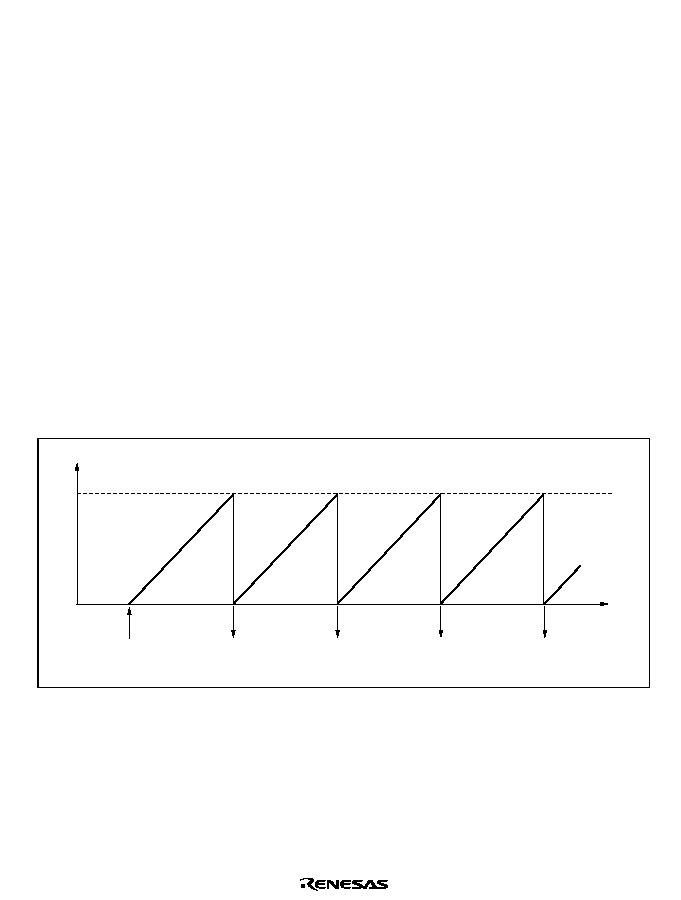
Rev. 2.0, 09/02, page 269 of 658
TLR is initialized to H'00 by a reset or in hardware standby mode.
11.11
Operation
11.11.1
Interval Timer Operation
When the ARSL bit in TCR is set to 0, the timer operates as an interval timer.
After a module stop mode is canceled, the timer continues incrementation as an interval timer
without stopping because TCNT is initialized to H'00 and TLR is cleared to 0 by a reset. The input
clock source can be selected from 14 internal clocks output from the prescaler unit and an external
clock from the TMCI4 input pin, using the CKS2 to CKS0 bits in TCR.
When a clock is input after the TCNT value has been H'FF, the timer overflows and OVF in TCR
is set to 1. At this time, if OVIE in TCR is 1, an interrupt is generated.
When an overflow occurs, the TCNT count value is cleared to H'00 and TCNT restarts
incrementation. If a value is set to TLR during interval timer operation, the value is also written to
TCNT.
This operation timing is shown in figure 11.14.
H'FF
H'00
Time
Overflow
Overflow
Overflow
Overflow
MSTPD5=0
ARSL=0
OVF
OVF
OVF
OVF
TCNT value
OVF: Timer overflow interrupt request generation
Figure 11.14 Operation in Interval Timer Mode

Rev. 2.0, 09/02, page 270 of 658
11.11.2
Automatic Reload Timer Operation
When the ARSL bit in TCR is set to 1, the timer operates as an automatic reload timer.
When a reload value is set to TLR, the value is also loaded to TCNT simultaneously, and TCNT
starts incrementation from the value.
If a clock is input after the TCNT count value reaches H'FF, the timer overflows, the TLR value is
written to TCNT, and incrementation is continued from the value. Therefore, the overflow cycle
can be set within the range from 1 to 256, using a TLR value.
Clock sources and interrupts in automatic reload operation are the same as those in interval
operation. If TLR is re-set during automatic reload operation, the value is also set to TCNT.
This operation timing is shown in figure 11.15.
H'FF
H'80
H'40
H'00
TCNT value
MSTPD5=0
ARSL=0
ARSL=1
TLR setting
(H'80))
TLR setting
(H'40)
OVF
OVF
OVF
OVF
OVF
OVF: Timer overflow interrupt request generation
OVF
Time
Overflow
Overflow
Overflow
Overflow
Overflow
Overflow
Figure 11.15 Operation in Automatic Reload Timer Mode
11.11.3
Cascaded Connection
∑
Read of TCNT
The channel relationship for cascaded connection is shown in figure 11.16.
When accessing beyond the word area, for example, when a cascaded connection including
channels 5 and 6 is created as shown in (3), and (6) to (8) in the figure, the counter value of the
lower channel is read when TCNT5 is read, and the data is stored in the TCNT register.
For case (7) where channels 5 to 7 are cascaded, the counter values of channels 6 and 7 are
read when TCNT5 is read, and the data is stored in TCNT6/7 registers. Accordingly, when
reading cascaded TCNT, read from the upper channel.
For a word connection, access in word units.
Rev. 2.0, 09/02, page 271 of 658
Cascaded connection
Upper
Lower
1
2
3
4
5
6
7
8
Channel 4
Channel 4
Channel 4
Channel 4
Channel 4
Channel 4
Channel 4
Channel 4
Channel 5 Channel 6 Channel 7
Channel 5 Channel 6 Channel 7
Channel 5 Channel 6 Channel 7
Channel 5 Channel 6 Channel 7
Channel 5 Channel 6 Channel 7
Channel 5 Channel 6 Channel 7
Channel 5 Channel 6 Channel 7
Channel 5 Channel 6 Channel 7
Figure 11.16 Channel Relationship of Cascaded Connection
∑
Write to TLR
When writing to the cascaded TLR, even if a single channel of TLR is written, the system
regards that the entire channels of the cascaded TLR are rewritten. At this point in time, the
value in the entire cascaded TLR is loaded into the corresponding TCNT. The timer operation
starts at the TLR value that is most-recently written in TLR access cycles.
∑
Operation Clock
Although each channel usually operates on an individual clock, a cascaded channel operates on
the same clock. The operation clock for the lowest cascaded channel is used as a common
clock of each channel.
In this case, the setting for the clocks of the channels other than the lowest channel is disabled.

Rev. 2.0, 09/02, page 272 of 658
∑
Automatic Reload Function Select and Operation Timing
Although the automatic reload function is usually set and implemented in individual channel, a
cascaded channel operates according to the setting for the automatic reload function of the
highest channel.
In this case, the automatic reload function settings for the channels other than the highest
channel are disabled. When the automatic reload function is enabled for cascaded channel, the
TLR setting value of each channel is automatically reloaded simultaneously in the reload
timing of the highest channel.
∑
Timer Overflow Flag (OVF)
Although an OVF is usually set to an individual channel independently, an OVF is set to the
highest channel of a cascaded channel. In this case, OVFs of the channels other than that of the
highest channel is disabled.
11.12
Usage Notes
11.12.1
Conflict between Write to TLR and Count up/Automatic Reload
Even if a count up occurs in the T2 state during TLR write cycles, the counter is not incremented
and TLR write (load to TCNT) is carried out instead (as in Figure 11.11).
Likewise, if an automatic reload occurs during write cycles, TLR write (load to TCNT) is carried
out instead.
11.12.2
Switchover of the Internal Clock and TCNT Operation
Depending on the timing which the internal clock is switched, TCNT may be incremented (see
table 11.4). Likewise, when the clock pulse is changed (
and
SUB
), TCNT may be incremented,
and may not in some cases. Therefore, when the internal clock is changed, resume timer operation
by resetting TLR (Write H'00 to TLR when the interval timer is in operation).
11.12.3 Interrupt during Module Stop
When module stop mode is entered with an interrupt being requested, the cause of an interrupt to
the CPU cannot be cleared. Enter module stop mode after, for example, disabling an interrupt
request.

Rev. 2.0, 09/02, page 273 of 658
Section 12 Watchdog Timer
The watchdog timer (WDT) is an 8-bit timer that can generate an internal reset signal for this LSI
if a system crash prevents the CPU from writing to the timer counter, thus allowing it to overflow.
When this watchdog function is not needed, the WDT can be used as an interval timer. In interval
timer operation, an interval timer interrupt is generated each time the counter overflows.
The block diagram of the WDT is shown in figures 12.1 to 12.3.
12.1
Features
∑
Selectable from eight counter input clocks for WDT_0
Selectable from 16 counter input clocks for WDT_1 in the H8S/2268 Series
Selectable from 26 counter input clocks for WDT_1 in the H8S/2264 Series
∑
Switchable between watchdog timer mode and interval timer mode
In watchdog timer mode
∑
If the counter in WDT_0 overflows, it is possible to select whether this LSI is internally reset
or not.
∑
If the counter in WDT_1 overflows, it is possible to select whether this LSI is internally reset
or the internal NMI interrupt is generated.
In interval timer mode
∑
If the counter overflows, the WDT generates an interval timer interrupt (WOVI).
WDT0105B_000020020700

Rev. 2.0, 09/02, page 274 of 658
Overflow
Interrupt
control
WOVI
(interrupt request
signal)
Internal reset signal
*
Reset
control
RSTCSR
TCNT_0
TSCR_0
/2
/64
/128
/512
/2048
/8192
/32768
/131072
Clock
Clock
select
Internal clock
sources
Bus
interface
Module bus
TCSR_0
TCNT_0
RSTCSR
Note:
*
The type of internal reset signal depends on a register setting.
: Timer control/status register0
: Timer counter0
: Reset control/status register
WDT
Legend
Internal bus
Figure 12.1 Block Diagram of WDT_0
Overflow
Interrupt
control
WOVI
(interrupt request
signal)
Internal NMI
(interrupt request signal)
Internal reset signal
*
Reset
control
TCNT_1
TSCR_1
/2
/64
/128
/512
/2048
/8192
/32768
/131072
SUB/2
SUB/4
SUB/8
SUB/16
SUB/32
SUB/64
SUB/128
SUB/256
Clock
Clock
select
Internal clock
sources
Bus
interface
Module bus
Internal bus
WDT
TCSR_1
TCNT_1
Note:
*
The type of internal reset signal depends on a register setting.
: Timer control/status register1
: Timer counter1
Legend
Figure 12.2 Block Diagram of WDT_1 for H8S/2268 Series

Rev. 2.0, 09/02, page 275 of 658
TCNT_1
Module bus
Internal bus
Internal clock
/2
/64
/128
/512
/2048
/8192
/32768
/131072
SUB
/120
SUB
/240
SUB
/480
SUB
/960
SUB
/1920
SUB
/3840
SUB
/7680
SUB
/15360
SUB
/2
SUB
/4
SUB
/8
SUB
/16
SUB
/32
SUB
/64
SUB
/128
SUB
/256
SUB
/512
SUB
/1024
Overflow
Clock
Interrupt
control
Clock
selection
Reset
control
WOVI1
(interrupt request signal)
Internal NMI
(interrupt request signal)
Internal reset signal
*
Legend
TCSR_1: Timer control/status register 1
TCNT_1: Timer counter 1
Note:
*
An internal reset signal is generated by the register setting.
TSCR_1
Bus
interface
WDT
Figure 12.3 Block Diagram of WDT_1 for H8S/2264 Series
12.2
Register Descriptions
The WDT has the following three registers. To prevent accidental overwriting, TCSR, TCNT, and
RSTCSR have to be written to by a different method to normal registers. For details, refer to
section 12.5.1, Notes on Register Access. For detained description on the system control register,
refer to section 5.3.1, System Control Register (SYSCR).
∑
Timer counter (TCNT)
∑
Timer control/status register (TCSR)
∑
Reset control/status register (RSTCSR)
12.2.1
Timer Counter (TCNT)
TCNT is an 8-bit readable/writable up-counter. TCNT is initialized to H'00 when the TME bit in
TCSR is cleared to 0.

Rev. 2.0, 09/02, page 276 of 658
12.2.2
Timer Control/Status Register (TCSR)
TCSR functions include selecting the clock source to be input to TCNT and the timer mode.
∑
TCSR_0
Bit
Bit Name
Initial
Value
R/W
Description
7
OVF
0
R/(W)
*
1
Overflow Flag
Indicates that TCNT has overflowed. Only a 0 can
be written to this bit, to clear the flag.
[Setting condition]
When TCNT overflows (changes from H'FF to
H'00)
When internal reset request generation is selected
in watchdog timer mode, OVF is cleared
automatically by the internal reset.
[Clearing conditions]
Cleared by reading TCSR
*
2
when OVF = 1, then
writing 0 to OVF
6
WT/
,7
0
R/W
Timer Mode Select
Selects whether the WDT is used as a watchdog
timer or interval timer.
0: Interval timer mode
1: Watchdog timer mode
5
TME
0
R/W
Timer Enable
When this bit is set to 1, TCNT starts counting.
When this bit is cleared, TCNT stops counting and
is initialized to H'00.
4, 3
All 1
Reserved
These bits are always read as 1 and cannot be
modified.

Rev. 2.0, 09/02, page 277 of 658
Bit
Bit Name
Initial
Value
R/W
Description
2
1
0
CKS2
CKS1
CKS0
0
0
0
R/W
R/W
R/W
Clock Select 0 to 2
Selects the clock source to be input to TCNT. The
overflow frequency
*
3
for
= 20 MHz is enclosed in
parentheses.
000: Clock
/2 (frequency: 25.6
µ
s)
001: Clock
/64 (frequency: 819.2
µ
s)
010: Clock
/128 (frequency: 1.6 ms)
011: Clock
/512 (frequency: 6.6 ms)
100: Clock
/2048 (frequency: 26.2 ms)
101: Clock
/8192 (frequency: 104.9 ms)
110: Clock
/32768 (frequency: 419.4 ms)
111: Clock
/131072 (frequency: 1.68 s)
Notes: 1. Only 0 can be written, for flag clearing.
2. When the OVF flag is polled with the interval timer interrupt disabled, read the OVF bit
while it is 1 at least twice.
3. The overflow period is the time from when TCNT starts counting up from H'00 until
overflow occurs.
∑
TCSR_1
Bit
Bit Name
Initial
Value
R/W
Description
7
OVF
0
R/(W)
*
1
Overflow Flag
Indicates that TCNT has overflowed. Only a 0 can
be written to this bit, to clear the flag.
[Setting condition]
When TCNT overflows (changes from H'FF to
H'00)
When internal reset request generation is selected
in watchdog timer mode, OVF is cleared
automatically by the internal reset.
[Clearing conditions]
Cleared by reading TCSR
*
2
when OVF = 1, then
writing 0 to OVF
6
WT/
,7
0
R/W
Timer Mode Select
Selects whether the WDT is used as a watchdog
timer or interval timer.
0: Interval timer mode
1: Watchdog timer mode

Rev. 2.0, 09/02, page 278 of 658
Bit
Bit Name
Initial
Value
R/W
Description
5
TME
0
R/W
Timer Enable
When this bit is set to 1, TCNT starts counting.
When this bit is cleared, TCNT stops counting and
is initialized to H'00.
4
PSS
0
R/W
Prescaler Select
Selects the clock source input to TCNT of WDT_1
0: TCNT counts divided clock of
-base prescaler
(PSM).
1: TCNT counts divided clock of
SUB
-base
prescaler (PSS)
3
RST
10,
0
R/W
Reset or NMI (REST/
10,
)
0: An NMI interrupt is requested.
1: reset is requested.
2
1
0
CKS2
CKS1
CKS0
0
0
0
R/W
R/W
R/W
Clock Select 0 to 2
Selects the clock source to be input to TCNT. The
overflow frequency
*
3
for
= 20 MHz is enclosed in
parentheses.
When PSS = 0:
000: Clock
/2 (frequency: 25.6
µ
s)
001: Clock
/64 (frequency: 819.2
µ
s)
010: Clock
/128 (frequency: 1.6 ms)
011: Clock
/512 (frequency: 6.6 ms)
100: Clock
/2048 (frequency: 26.2 ms)
101: Clock
/8192 (frequency: 104.9 ms)
110: Clock
/32768 (frequency: 419.4 ms)
111: Clock
/131072 (frequency: 1.68 s)
When PSS = 1:
See table 12.1, Clock Selection When PSS = 1.
Notes: 1. Only 0 can be written, for flag clearing.
2. When the OVF flag is polled with the interval timer interrupt disabled, read the OVF bit
while it is 1 at least twice
3. The overflow period is the time from when TCNT starts counting up from H'00 until
overflow occurs.

Rev. 2.0, 09/02, page 279 of 658
Table 12.1
Clock Selection When PSS = 1.
H8S/2268 Series
H8S/2264 Series
When PSS = 1:
000: Clock
SUB
/2 (frequency: 15.6 ms)
001: Clock
SUB
/4 (frequency: 31.3 ms)
010: Clock
SUB
/8 (frequency: 62.5 ms)
011: Clock
SUB
/16 (frequency: 125 ms)
100: Clock
SUB
/32 (frequency: 250 ms)
101: Clock
SUB
/64 (frequency: 500 ms)
110: Clock
SUB
/128 (frequency: 1 s)
111: Clock
SUB
/256 (frequency: 2 s)
Clock selection differs according to the
combination of the SUBCKS1 and SUBCKS0
bits in SCKCR2 and the PSS bit.
When PSS = 1, SUBCKS1=0, SUBCKS0=0,
000: Clock
SUB
/2 (frequency: 15.6 ms)
001: Clock
SUB
/4 (frequency: 31.3 ms)
010: Clock
SUB
/8 (frequency: 62.5 ms)
011: Clock
SUB
/16 (frequency: 125 ms)
100: Clock
SUB
/32 (frequency: 250 ms)
101: Clock
SUB
/64 (frequency: 500 ms)
110: Clock
SUB
/128 (frequency: 1 s)
111: Clock
SUB
/256 (frequency: 2 s)
When PSS = 1, SUBCKS1=0, SUBCKS0=1,
000: Clock
SUB
/8 (frequency: 62.5 ms)
001: Clock
SUB
/16 (frequency: 125 ms)
010: Clock
SUB
/32 (frequency: 250 ms)
011: Clock
SUB
/64 (frequency: 500 ms)
100: Clock
SUB
/128 (frequency: 1 s)
101: Clock
SUB
/256 (frequency: 2 s)
110: Clock
SUB
/512 (frequency: 4 s)
111: Clock
SUB
/1024 (frequency: 8 s)
When PSS = 1, SUBCKS1=1, SUBCKS0=0,
000: Clock
SUB
/120 (frequency: 938 ms)
001: Clock
SUB
/240 (frequency: 1.9 s)
010: Clock
SUB
/480 (frequency: 3.8 s)
011: Clock
SUB
/960 (frequency: 7.5 s)
100: Clock
SUB
/1920 (frequency: 15 s)
101: Clock
SUB
/3840 (frequency: 30 s)
110: Clock
SUB
/7680 (frequency: 1 min)
111: Clock
SUB
/15360 (frequency: 2 min)
Note:
*
A value in parentheses represents an overflow period when
SUB
= 32.768 kHz. The
overflow period is the time from when TCNT starts connoting up from H'00 until
overflow occurs.

Rev. 2.0, 09/02, page 280 of 658
12.2.3
Reset Control/Status Register (RSTCSR) (only WDT_0)
RSTCSR controls the generation of the internal reset signal when TCNT overflows, and selects
the type of internal reset signal. RSTCSR is initialized to H'1F by a reset signal from the
5(6 pin,
and not by the WDT internal reset signal caused by overflows.
Bit
Bit Name
Initial
Value
R/W
Description
7
WOVF
0
R/(W)
*
Watchdog Overflow Flag
This bit is set when TCNT overflows in watchdog
timer mode. This bit cannot be set in interval timer
mode, and only 0 can be written, to clear the flag.
[Setting condition]
Set when TCNT overflows (changed from H'FF to
H'00) in watchdog timer mode
[Clearing condition]
Cleared by reading RSTCSR when WOVF = 1,
and then writing 0 to WOVF
6
RSTE
0
R/W
Reset Enable
Specifies whether or not a reset signal is
generated in the chip if TCNT overflows during
watchdog timer operation.
0: Reset signal is not generated even if TCNT
overflows (Though this LSI is not reset, TCNT
and TCSR in WDT are reset)
1: Reset signal is generated if TCNT overflows
5
0
R/W
Reserved
This bit can be read from and written to. However,
the write value should always be 0.
4 to 0
1
Reserved
These bits are always read as 1 and cannot be
modified.
Note:
*
Only 0 can be written, to clear the flag.

Rev. 2.0, 09/02, page 281 of 658
12.3
Operation
12.3.1
Watchdog Timer Mode
To use the WDT as a watchdog timer, set the WT/
,7 bit in TCSR and the TME bit to 1.
Software must prevent TCNT overflows by rewriting the TCNT value (normally be writing H'00)
before overflows occurs. Thus, TCNT does not overflow while the system is operating normally.
When the WDT is used as a watchdog timer and the RSTE bit in RSTCSR of WDT_0 is set to 1,
and if TCNT overflows without being rewritten because of a system malfunction or other error, an
internal reset signal for this LSI is output for 518 system clocks.
When the RST/
10, bit in TCSR of WDT_1 is set to 1, and if TCNT overflows, the internal reset
signal is output for 516 system clock periods. When the RST/
10, bit is cleared to 0, an NMI
interrupt request is generated (for 515 or 516 system clock periods when the clock source is set to
SUB
(PSS = 1)).
An internal reset request from the watchdog timer and a reset input from the
5(6 pin are both
treated as having the same vector. If a WDT internal reset request and the
5(6 pin reset occur at
the same time, the
5(6 pin reset has priority and the WOVF bit in RSTCSR is cleared to 0.
An NMI request from the watchdog timer and an interrupt request from the NMI pin are both
treated as having the same vector. So, avoid handling an NMI request from the watchdog timer
and an interrupt request from the NMI pin at the same time.

Rev. 2.0, 09/02, page 282 of 658
TCNT value
H'00
Time
H'FF
WT/ =1
TME=1
Write H'00'
to TCNT
WT/ =1
TME=1
Write H'00'
to TCNT
518 system clock (WDT0)
515/516 system clock (WDT1)
Internal reset signal
*
WT/
TME
Note:
*
In the case of WDT_0, the internal reset signal is generated only when the RSTE bit is set to 1.
In the case of WDT_1,either the internal reset or the NMI interrupt is generated.
Overflow
internal reset is
generated
WOVF=1
: Timer mode select bit
: Timer enable bit
Legend
Figure 12.4 Watchdog Timer Mode Operation
12.3.2
Interval Timer Mode
To use the WDT as an internal timer, set the WT/
,7 and TME bits in TCSR to 0.
When the WDT is used as an interval timer, an interval timer interrupt (WOVI) is generated each
time the TCNT overflows. Therefore, an interrupt can be generated at intervals.
When the TCNT overflows in interval timer mode, an interval timer interrupt (WOVI) is requested
at the time the OVF bit of the TCSR is set to 1.
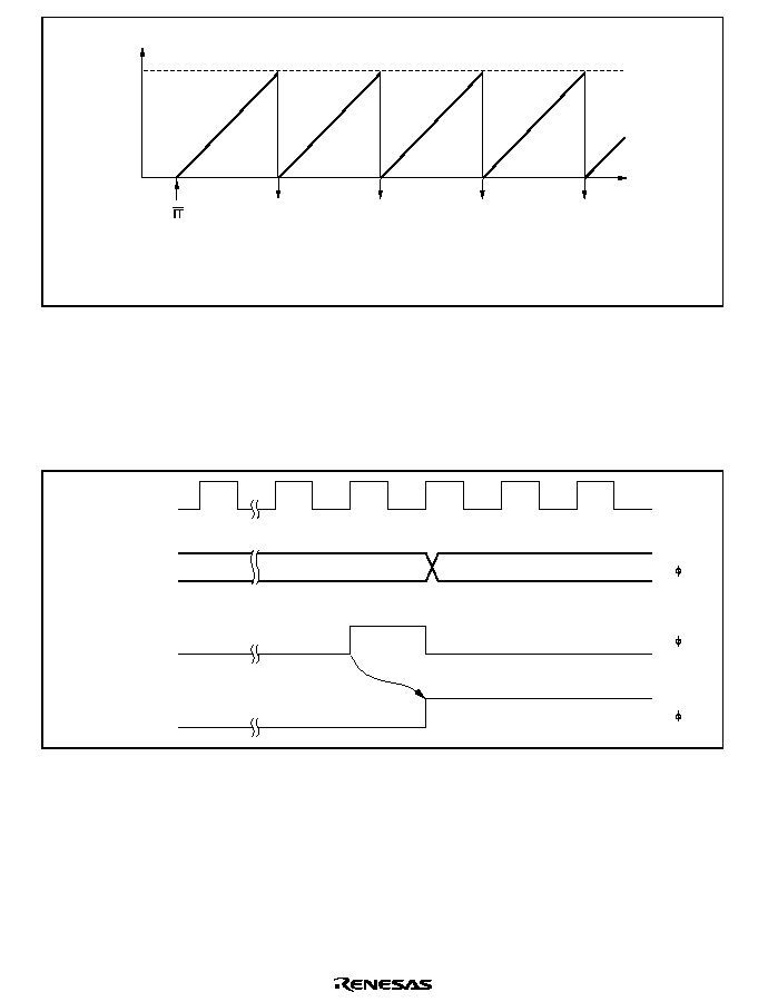
Rev. 2.0, 09/02, page 283 of 658
TCNT value
H'00
Time
H'FF
WT/ =0
TME=1
WOVI
Overflow
Overflow
Overflow
Overflow
Legend
WOVI: Interval timer interrupt request generation
WOVI
WOVI
WOVI
Figure 12.5 Interval Timer Mode Operation
12.3.3
Timing of Setting Overflow Flag (OVF)
The OVF flag is set to 1 if TCNT overflows during interval timer operation. At the same time, an
interval timer interrupt (WOVI) is requested. This timing is shown in figure 12.6.
TCNT
H'FF
H'00
OVF
1
1
1
Overflow signal
(internal signal)
Figure 12.6 Timing of OVF Setting
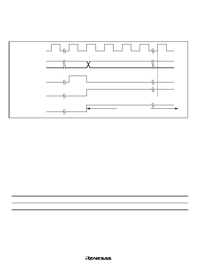
Rev. 2.0, 09/02, page 284 of 658
12.3.4
Timing of Setting Watchdog Timer Overflow Flag (WOVF)
With WDT_0 the WOVF bit in RSTCSR is set to 1 if TCNT overflows in watchdog timer mode.
If TCNT overflows while the RSTE bit in RSTCSR is set to 1, an internal is generated for the
entire chip. this timing is illustrated in figure 12.7.
TCNT
H'FF
H'00
Overflow signal
(internal signal)
WOVF
Internal reset
signal
518 states (WDT_0)
515/516 states (WDT_1)
Figure 12.7 Timing of WOVF Setting
12.4
Interrupt Sources
During interval timer mode operation, an overflow generates an interval timer interrupt (WOVI).
The interval timer interrupt is requested whenever the OVF flag is set to 1 in TCSR. OVF must be
cleared to 0 in the interrupt handling routine.
If an NMI request has been chosen in the watchdog timer mode, an NMI request is generated
when a TCNT overflow occurs.
Table 12.2
WDT Interrupt Source
Name
Interrupt Source
Interrupt Flag
WOVI
TCNT overflow (interval timer mode)
OVF
NMI
TCNT overflow (watchdog timer mode)
OVF

Rev. 2.0, 09/02, page 285 of 658
12.5
Usage Notes
12.5.1
Notes on Register Access
The watchdog timer's TCNT and TCSR registers differ from other registers in being more difficult
to write to. The procedures for writing to and reading these registers are given below.
Writing to TCNT, TCSR, and RSTCSR
These registers must be written to by a word transfer instruction. They cannot be written to by a
byte transfer instruction.
TCNT and TCSR both have the same write address. Therefore, the relative condition shown in
figure 12.8 needs to be satisfied in order to write to TCNT or TCSR. The transfer instruction
writes the lower byte data to TCNT or TCSR. The upper byte must be H'5A for writing to TCNT,
and H'A5 for writing to TCSR.
To write to RSTCSR, execute a word transfer instruction for address H'FF76. A byte transfer
instruction cannot write to RSTCSR.
The method of writing 0 to the OVF bit differs from that of writing to the RSTE bit. To write 0 to
the WOVF bit, satisfy the condition shown in figure 12.8. If satisfied, the transfer instruction
clears the WOVF bit to 0, but has no effect on the RSTE bit. To write to the RSTE and RSTS bits,
satisfy the condition shown in figure 12.8. If satisfied, the transfer instruction writes the values in
bit 6 of the lower byte into the RSTE bit, but has no effect on the WOVF bit.
TCNT write
Writing to RSTE and RSTS bits
TCSR write
Writing 0 to WOVF bit
Address:
Address:
15
8
7
0
H'5A
H'FF74
H'FF76
Write data
15
8
7
0
H'A5
H'FF74
H'FF76
Write data or H'00
Figure 12.8 Writing to TCNT and TCSR (example for WDT_0)
Reading TCNT, TCSR and RSTCSR (WDT
_
0)
These registers are read in the same way as other registers. The read addresses are H'FF74 for
TCSR and H'FF77 for RSTCSR.
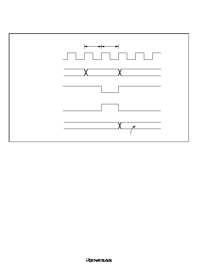
Rev. 2.0, 09/02, page 286 of 658
12.5.2
Contention between Timer Counter (TCNT) Write and Increment
If a timer counter clock pulse is generated during the T2 state of a TCNT write cycle, the write
takes priority and the timer counter is not incremented. Figure 12.9 shows this operation.
Address
Internal write signal
TCNT input clock
TCNT
N
M
T1
T2
TCNT write cycle
Counter write data
Figure 12.9 Contention between TCNT Write and Increment
12.5.3
Changing Value of CKS2 to CKS0
If bits CKS0 to CKS2 in TCSR are written to while the WDT is operating, errors could occur in
the incrementation. Software must be used to stop the watchdog timer (by clearing the TME bit to
0) before changing the value of bits CKS0 to CKS2.
12.5.4
Switching between Watchdog Timer Mode and Interval Timer Mode
If the mode is switched from watchdog timer to interval timer while the WDT is operating, errors
could occur in the incrementation. Software must be used to stop the watchdog timer (by clearing
the TME bit to 0) before switching the mode.
12.5.5
Internal Reset in Watchdog Timer Mode
This LSI is not reset internally if TCNT overflows while the RSTE bit is cleared to 0 during
watchdog timer operation, however TCNT_0 and TCSR_0 of the WDT_0 are reset.

Rev. 2.0, 09/02, page 287 of 658
TCNT, TCSR, or RSTCR cannot be written to for 132 states following an overflow. During this
period, any attempt to read the WOVF flag is not acknowledged. Accordingly, wait 132 states
after overflow to write 0 to the WOVF flag for clearing.
12.5.6
OVF Flag Clearing in Interval Timer Mode
When the OVF flag setting conflicts with the OVF flag reading in interval timer mode, writing 0
to the OVF bit may not clear the flag even though the OVF bit has been read while it is 1. If there
is a possibility that the OVF flag setting and reading will conflict, such as when the OVF flag is
polled with the interval timer interrupt disabled, read the OVF bit while it is 1 at least twice before
writing 0 to the OVF bit to clear the flag.

Rev. 2.0, 09/02, page 288 of 658

Rev. 2.0, 09/02 page 289 of 658
Section 13 Serial Communication Interface (SCI)
This LSI has three independent serial communication interface (SCI) channels. The SCI can
handle both asynchronous and clocked synchronous serial communication. Serial data
communication can be carried out using standard asynchronous communication chips such as a
Universal Asynchronous Receiver/Transmitter (UART) or an Asynchronous Communication
Interface Adapter (ACIA). A function is also provided for serial communication between
processors (multiprocessor communication function). The SCI also supports an IC card (Smart
Card) interface conforming to ISO/IEC 7816-3 (Identification Card) as a serial communication
interface extension function.
13.1
Features
∑
Choice of asynchronous or clocked synchronous serial communication mode
∑
Full-duplex communication capability
The transmitter and receiver are mutually independent, enabling transmission and reception to
be executed simultaneously.
Double-buffering is used in both the transmitter and the receiver, enabling continuous
transmission and continuous reception of serial data.
∑
On-chip baud rate generator allows any bit rate to be selected
External clock can be selected as a transfer clock source (except for in Smart Card interface
mode).
∑
Choice of LSB-first or MSB-first transfer (except in the case of asynchronous mode 7-bit data)
∑
Four interrupt sources
Transmit-end, transmit-data-empty, receive-data-full, and receive error -- that can issue
requests.
The transmit-data-empty interrupt and receive data full interrupts can be used to activate the
data transfer controller (DTC) (H8S/2268 Series only).
∑
Module stop mode can be set
Asynchronous mode
∑
Data length: 7 or 8 bits
∑
Stop bit length: 1 or 2 bits
∑
Parity: Even, odd, or none
∑
Receive error detection: Parity, overrun, and framing errors
∑
Break detection: Break can be detected by reading the RxD pin level directly in the case of a
framing error
SCI0025B_000020020700

Rev. 2.0, 09/02, page 290 of 658
∑
Average transfer rate generator (SCI_0): 720 kbps, 460.784 kbps, or 115.196 kbps can be
selected at 16 MHz operation.
∑
Transfer rate clock can be input from the TPU (SCI_0).
∑
Communications between multi-processors are possible.
Clocked Synchronous mode
∑
Data length: 8 bits
∑
Receive error detection: Overrun errors detected
Smart Card Interface
∑
Automatic transmission of error signal (parity error) in receive mode
∑
Error signal detection and automatic data retransmission in transmit mode
∑
Direct convention and inverse convention both supported

Rev. 2.0, 09/02 page 291 of 658
Figure 13.1 shows a block diagram of the SCI_0, and figure 13.2 shows that of the SCI1 and
SCI_2.
RxD0
TxD0
SCK0
TEI
TXI
RXI
ERI
SCMR
SSR
SCR
SMR
SEMR
BRR
RDR
TSR
RSR
TDR
TIOCA1
TCLKA
TIOCA2
TPU
External clock
Transmission/
reception control
Baud rate
generator
Module data bus
Bus interface
Parity generation
Internal
data bus
Clock
/4
/16
/64
RSR
RDR
TSR
TDR
SMR
: Receive shift register
: Receive data register
: Transmit shift register
: Transmit data register
: Serial mode register
SCR
SSR
SCMR
BRR
SEMR
: Serial control register
: Serial status register
: Smart card mode register
: Bit rate register
: Serial expansion mode register
Legend
Parity check
10.667MHz operation
115.152kbps
460.606kbps
16MHz operation
115.196kbps
460.784kbps
720kbps
Average
transfer rate
generator
Figure 13.1 Block Diagram of SCI_0

Rev. 2.0, 09/02, page 292 of 658
RxD
TxD
SCK
Clock
External clock
/4
/16
/64
TEI
TXI
RXI
ERI
RSR
RDR
TSR
TDR
SMR
SCR
SSR
SCMR
BRR
: Receive shift register
: Receive data register
: Transmit shift register
: Transmit data register
: Serial mode register
: Serial control register
: Serial status register
: Smart card mode register
: Bit rate register
SCMR
SSR
SCR
SMR
Transmission/
reception control
Baud rate
generator
BRR
Module data bus
Bus interface
RDR
TSR
RSR
Parity generation
Parity check
Legend
TDR
Internal
data bus
Figure 13.2 Block Diagram of SCI_1 or SCI_2

Rev. 2.0, 09/02 page 293 of 658
13.2
Input/Output Pins
Table 13.1 shows the pin configuration for each SCI channel.
Table 13.1
Pin Configuration
Channel
Pin Name
*
I/O
Function
SCK0
I/O
SCI0 clock input/output
RxD0
Input
SCI0 receive data input
0
TxD0
Output
SCI0 transmit data output
SCK1
I/O
SCI1 clock input/output
RxD1
Input
SCI1 receive data input
1
TxD1
Output
SCI1 transmit data output
SCK2
I/O
SCI2 clock input/output
RxD2
Input
SCI2 receive data input
2
TxD2
Output
SCI2 transmit data output
Note:
*
Pin names SCK, RxD, and TxD are used in the text for all channels, omitting the
channel designation.
13.3
Register Descriptions
The SCI has the following registers for each channel. For details on register addresses and register
states during each process, refer to appendix A, Internal I/O Register. The serial mode register
(SMR), serial status register (SSR), and serial control register (SCR) are described separately for
normal serial communication interface mode and Smart Card interface mode because their bit
functions differ in part.
∑
Receive Shift Register (RSR)
∑
Receive Data Register (RDR)
∑
Transmit Data Register (TDR)
∑
Transmit Shift Register (TSR)
∑
Serial Mode Register (SMR)
∑
Serial Control Register (SCR)
∑
Serial Status Register (SSR)
∑
Smart Card Mode Register (SCMR)
∑
Bit Rate Register (BRR)
Other than the above registers, SCI_0 has the following register.
∑
Serial Expansion Mode Register (SEMR0)

Rev. 2.0, 09/02, page 294 of 658
13.3.1
Receive Shift Register (RSR)
RSR is a shift register that is used to receive serial data input to the RxD pin and convert it into
parallel data. When one byte of data has been received, it is transferred to RDR automatically.
RSR cannot be directly accessed by the CPU.
13.3.2
Receive Data Register (RDR)
RDR is an 8-bit register that stores received data. When the SCI has received one byte of serial
data, it transfers the received serial data from RSR to RDR, where it is stored. After this, RSR is
receive-enabled. As RSR and RDR function as a double buffer in this way, continuous receive
operations are possible. After confirming that the RDRF bit in SSR is set to 1, read RDR only
once.
RDR cannot be written to by the CPU.
RDR is initialized to H'00 by a reset, in standby mode, watch mode,subactive mode, subsleep
mode or module stop mode.
13.3.3
Transmit Data Register (TDR)
TDR is an 8-bit register that stores data for transmission. When the SCI detects that TSR is empty,
it transfers the transmit data written in TDR to TSR and starts transmission. The double-buffered
structure of TDR and TSR enables continuous serial transmission. If the next transmit data has
already been written to TDR during serial transmission, the SCI transfers the written data to TSR
to continue transmission. Although TDR can be read or written to by the CPU at all times, to
achieve reliable serial transmission, write transmit data to TDR only once after confirming that the
TDRE bit in SSR is set to 1.
TDR is initialized to H'FF by a reset, in standby mode, watch mode, subactive mode, subsleep
mode or module stop mode.
13.3.4
Transmit Shift Register (TSR)
TSR is a shift register that transmits serial data. To perform serial data transmission, the SCI first
transfers transmit data from TDR to TSR, then sends the data to the TxD pin. TSR cannot be
directly accessed by the CPU.

Rev. 2.0, 09/02 page 295 of 658
13.3.5
Serial Mode Register (SMR)
SMR is used to set the SCI's serial transfer format and select the baud rate generator clock source.
Some bit functions of SMR differ between normal serial communication interface mode and Smart
Card interface mode.
Normal Serial Communication Interface Mode (When SMIF in SCMR is 0)
Bit
Bit Name
Initial
Value
R/W
Description
7
C/
0
R/W
Communication Mode
0: Asynchronous mode
1: Clocked synchronous mode
6
CHR
0
R/W
Character Length (enabled only in asynchronous
mode)
0: Selects 8 bits as the data length.
1: Selects 7 bits as the data length. LSB-first is
fixed and the MSB (bit 7) of TDR is not
transmitted in transmission.
In clocked synchronous mode, a fixed data length
of 8 bits is used.
5
PE
0
R/W
Parity Enable (enabled only in asynchronous
mode)
When this bit is set to 1, the parity bit is added to
transmit data before transmission, and the parity
bit is checked in reception. For a multiprocessor
format, parity bit addition and checking are not
performed regardless of the PE bit setting.
4
O/
0
R/W
Parity Mode (enabled only when the PE bit is 1 in
asynchronous mode)
0: Selects even parity.
When even parity is set, parity bit addition is
performed in transmission so that the total
number of 1 bits in the transmit character plus
the parity bit is even. In reception, a check is
performed to see if the total number of 1 bits in
the receive character plus parity bit is even.
1: Selects odd parity.
When odd parity is set, parity bit addition is
performed in transmission so that the total
number of 1 bits in the transmit character plus
the parity bit is odd. In reception, a check is
performed to see if the total number of 1 bits in
the receive character plus the parity bit is odd.

Rev. 2.0, 09/02, page 296 of 658
Bit
Bit Name
Initial
Value
R/W
Description
3
STOP
0
R/W
Stop Bit Length (enabled only in asynchronous
mode)
Selects the stop bit length in transmission.
0: 1 stop bit
1: 2 stop bits
In reception, only the first stop bit is checked. If the
second stop bit is 0, it is treated as the start bit of
the next transmit character.
2
MP
0
R/W
Multiprocessor Mode (enabled only in
asynchronous mode)
When this bit is set to 1, the multiprocessor
communication function is enabled. The PE bit and
O/
bit settings are invalid in multiprocessor mode.
For details, see 13.5, Multiprocessor
Communication Function.
1
0
CKS1
CKS0
0
0
R/W
R/W
Clock Select 0 and 1
These bits select the clock source for the baud rate
generator.
00:
clock (n = 0)
01:
/4 clock (n = 1)
10:
/16 clock (n = 2)
11:
/64 clock (n = 3)
For the relationship between the bit rate register
setting and the baud rate, see section 13.3.9, Bit
Rate Register (BRR). n is the decimal
representation of the value of n in BRR (see
section 13.3.9, Bit Rate Register (BRR)).

Rev. 2.0, 09/02 page 297 of 658
Smart Card Interface Mode (When SMIF in SCMR is 1)
Bit
Bit Name
Initial
Value
R/W
Description
7
GM
0
R/W
GSM Mode
When this bit is set to 1, the SCI operates in GSM
mode. In GSM mode, the timing of the TEND
setting is advanced by 11.0 etu (Elementary Time
Unit: the time for transfer of one bit), and clock
output control mode addition is performed. For
details, refer to section 13.7.8, Clock Output
Control.
6
BLK
0
R/W
When this bit is set to 1, the SCI operates in block
transfer mode. For details on block transfer mode,
refer to section 13.7.3, Block Transfer Mode.
5
PE
0
R/W
Parity Enable (enabled only in asynchronous
mode)
When this bit is set to 1, the parity bit is added to
transmit data in transmission, and the parity bit is
checked in reception. In Smart Card interface
mode, this bit must be set to 1.
4
O/
0
R/W
Parity Mode (enabled only when the PE bit is 1 in
asynchronous mode)
0: Selects even parity.
1: Selects odd parity.
For details on setting this bit in Smart Card
interface mode, refer to section 13.7.2, Data
Format (Except for Block Transfer Mode).
3
2
BCP1
BCP0
0
0
R/W
R/W
Basic Clock Pulse 0 and 1
These bits specify the number of basic clock
periods in a 1-bit transfer interval on the Smart
Card interface.
00: 32 clock (S = 32)
01: 64 clock (S = 64)
10: 372 clock (S = 372)
11: 256 clock (S = 256)
For details, refer to section 13.7.4, Receive Data
Sampling Timing and Reception Margin in Smart
Card Interface Mode. S stands for the value of S in
BRR (see section 13.3.9, Bit Rate Register (BRR)).

Rev. 2.0, 09/02, page 298 of 658
Bit
Bit Name
Initial
Value
R/W
Description
1
0
CKS1
CKS0
0
0
R/W
R/W
Clock Select 0 and 1
These bits select the clock source for the baud rate
generator.
00:
clock (n = 0)
01:
/4 clock (n = 1)
10:
/16 clock (n = 2)
11:
/64 clock (n = 3)
For the relationship between the bit rate register
setting and the baud rate, see section 13.3.9, Bit
Rate Register (BRR). n is the decimal
representation of the value of n in BRR (see
section 13.3.9, Bit Rate Register (BRR)).
Note: etu (Elementary Time Unit): Abbreviation for the transfer period for one bit.
13.3.6
Serial Control Register (SCR)
SCR is a register that enables or disables SCI transfer operations and interrupt requests, and is also
used to selection of the transfer clock source. For details on interrupt requests, refer to section
13.8, Interrupts. Some bit functions of SCR differ between normal serial communication interface
mode and Smart Card interface mode.
Normal Serial Communication Interface Mode (When SMIF in SCMR is 0)
Bit
Bit Name
Initial
Value
R/W
Description
7
TIE
0
R/W
Transmit Interrupt Enable
When this bit is set to 1, the TXI interrupt request is
enabled.
TXI interrupt request cancellation can be
performed by reading 1 from the TDRE flag in
SSR, then clearing it to 0, or clearing the TIE bit to
0.
6
RIE
0
R/W
Receive Interrupt Enable
When this bit is set to 1, RXI and ERI interrupt
requests are enabled.
RXI and ERI interrupt request cancellation can be
performed by reading 1 from the RDRF, FER,
PER, or ORER flag in SSR, then clearing the flag
to 0, or clearing the RIE bit to 0.

Rev. 2.0, 09/02 page 299 of 658
Bit
Bit Name
Initial
Value
R/W
Description
5
TE
0
R/W
Transmit Enable
When this bit s set to 1, transmission is enabled.
In this state, serial transmission is started when
transmit data is written to TDR and the TDRE flag
in SSR is cleared to 0.
SMR setting must be performed to decide the
transfer format before setting the TE bit to 1. When
this bit is cleared to 0, the transmission operation is
disabled, and the TDRE flag is fixed at 1.
4
RE
0
R/W
Receive Enable
When this bit is set to 1, reception is enabled.
Serial reception is started in this state when a start
bit is detected in asynchronous mode or serial
clock input is detected in clocked synchronous
mode.
SMR setting must be performed to decide the
reception format before setting the RE bit to 1.
Clearing the RE bit to 0 does not affect the RDRF,
FER,PER, and ORER flags, which retain their
states.
3
MPIE
0
R/W
Multiprocessor Interrupt Enable (enabled only
when the MP bit in SMR is 1 in asynchronous
mode)
When this bit is set to 1, receive data in which the
multiprocessor bit is 0 is skipped, and setting of the
RDRF, FER, and ORER status flags in SSR is
prohibited. On receiving data in which the
multiprocessor bit is 1, this bit is automatically
cleared and normal reception is resumed. For
details, refer to section 13.5, Multiprocessor
Communication Function.
When receive data including MPB = 0 is received,
receive data transfer from RSR to RDR, receive
error detection, and setting of the RERF, FER, and
ORER flags in SSR, are not performed.
When receive data including MPB = 1 is received,
the MPB bit in SSR is set to 1, the MPIE bit is
cleared to 0 automatically, and generation of RXI
and ERI interrupts (when the TIE and RIE bits in
SCR are set to 1) and FER and ORER flag setting
are enabled.

Rev. 2.0, 09/02, page 300 of 658
Bit
Bit Name
Initial
Value
R/W
Description
2
TEIE
0
R/W
Transmit End Interrupt Enable
This bit is set to 1, TEI interrupt request is enabled.
TEI cancellation can be performed by reading 1
from the TDRE flag in SSR, then clearing it to 0
and clearing the TEND flag to 0, or clearing the
TEIE bit to 0.
1
0
CKE1
CKE0
0
0
R/W
R/W
Clock Enable 0 and 1
Selects the clock source and SCK pin function.
Asynchronous mode
00: On-chip baud rate generator
SCK pin functions as I/O port
01: On-chip baud rate generator
Outputs a clock of the same frequency as the
bit rate from the SCK pin.
1X: External clock
Inputs a clock with a frequency 16 times the bit
rate from the SCK pin.
Clocked synchronous mode
0X: Internal clock (SCK pin functions as clock
output)
1X: External clock (SCK pin functions as clock
input)
Legend
X: Don't care

Rev. 2.0, 09/02 page 301 of 658
Smart Card Interface Mode (When SMIF in SCMR is 1)
Bit
Bit Name
Initial
Value
R/W
Description
7
TIE
0
R/W
Transmit Interrupt Enable
When this bit is set to 1, TXI interrupt request is
enabled.
TXI interrupt request cancellation can be
performed by reading 1 from the TDRE flag in
SSR, then clearing it to 0, or clearing the TIE bit to
0.
6
RIE
0
R/W
Receive Interrupt Enable
When this bit is set to 1, RXI and ERI interrupt
requests are enabled.
RXI and ERI interrupt request cancellation can be
performed by reading 1 from the RDRF, FER,
PER, or ORER flag in SSR, then clearing the flag
to 0, or clearing the RIE bit to 0.
5
TE
0
R/W
Transmit Enable
When this bit s set to 1, transmission is enabled.
In this state, serial transmission is started when
transmit data is written to TDR and the TDRE flag
in SSR is cleared to 0.
SMR setting must be performed to decide the
transfer format before setting the TE bit to 1. When
this bit is cleared to 0, the transmission operation is
disabled, and the TDRE flag is fixed at 1.
4
RE
0
R/W
Receive Enable
When this bit is set to 1, reception is enabled.
Serial reception is started in this state when a start
bit is detected in asynchronous mode or serial
clock input is detected in clocked synchronous
mode.
SMR setting must be performed to decide the
reception format before setting the RE bit to 1.
Clearing the RE bit to 0 does not affect the RDRF,
FER,PER, and ORER flags, which retain their
states.

Rev. 2.0, 09/02, page 302 of 658
Bit
Bit Name
Initial
Value
R/W
Description
3
MPIE
0
R/W
Multiprocessor Interrupt Enable (enabled only
when the MP bit in SMR is 1 in asynchronous
mode)
Write 0 to this bit in Smart Card interface mode.
When receive data including MPB = 0 is received,
receive data transfer from RSR to RDR, receive
error detection, and setting of the RERF, FER, and
ORER flags in SSR, are not performed.
When receive data including MPB = 1 is received,
the MPB bit in SSR is set to 1, the MPIE bit is
cleared to 0 automatically, and generation of RXI
and ERI interrupts (when the TIE and RIE bits in
SCR are set to 1) and FER and ORER flag setting
are enabled.
2
TEIE
0
R/W
Transmit End Interrupt Enable
Write 0 to this bit in Smart Card interface mode.
TEI cancellation can be performed by reading 1
from the TDRE flag in SSR, then clearing it to 0
and clearing the TEND flag to 0, or clearing the
TEIE bit to 0.
1
0
CKE1
CKE0
0
0
R/W
Clock Enable 0 and 1
Enables or disables clock output from the SCK pin.
The clock output can be dynamically switched in
GSM mode. For details, refer to section 13.7.8,
Clock Output Control.
When the GM bit in SMR is 0:
00: Output disabled (SCK pin can be used as an
I/O port pin)
01: Clock output
1X: Reserved
When the GM bit in SMR is 1:
00: Output fixed low
01: Clock output
10: Output fixed high
11: Clock output
Legend
X: Don't care

Rev. 2.0, 09/02 page 303 of 658
13.3.7
Serial Status Register (SSR)
SSR is a register containing status flags of the SCI and multiprocessor bits for transfer. 1 cannot
be written to flags TDRE, RDRF, ORER, PER, and FER; they can only be cleared. Some bit
functions of SSR differ between normal serial communication interface mode and Smart Card
interface mode.
Normal Serial Communication Interface Mode (When SMIF in SCMR is 0)
Bit
Bit Name
Initial
Value
R/W
Description
7
TDRE
1
R/(W)
*
Transmit Data Register Empty
Displays whether TDR contains transmit data.
[Setting conditions]
∑
When the TE bit in SCR is 0
∑
When data is transferred from TDR to TSR and
data can be written to TDR
[Clearing conditions]
∑
When 0 is written to TDRE after reading TDRE
= 1
∑
When the DTC is activated by a TXI interrupt
request and writes data to TDR (H8S/2268
Series only)
6
RDRF
0
R/(W)
*
Receive Data Register Full
Indicates that the received data is stored in RDR.
[Setting condition]
∑
When serial reception ends normally and
receive data is transferred from RSR to RDR
[Clearing conditions]
∑
When 0 is written to RDRF after reading RDRF
= 1
∑
When the DTC is activated by an RXI interrupt
and transferred data from RDR (H8S/2268
Series only)
The RDRF flag is not affected and retains their
previous values when the RE bit in SCR is cleared
to 0.
If reception of the next data is completed while the
RDRF flag is still set to 1, an overrun error will
occur and the receive data will be lost.

Rev. 2.0, 09/02, page 304 of 658
Bit
Bit Name
Initial
Value
R/W
Description
5
ORER
0
R/(W)
*
Overrun Error
Indicates that an overrun error occurred during
reception, causing abnormal termination.
[Setting condition]
∑
When the next serial reception is completed
while RDRF = 1
The receive data prior to the overrun error is
retained in RDR, and the data received
subsequently is lost. Also, subsequent serial
reception cannot be continued while the ORER flag
is set to 1. In clocked synchronous mode, serial
transmission cannot be continued either.
[Clearing condition]
∑
When 0 is written to ORER after reading ORER
= 1
The ORER flag is not affected and retains its
previous state when the RE bit in SCR is cleared to
0.
4
FER
0
R/(W)
*
Framing Error
Indicates that a framing error occurred during
reception in asynchronous mode, causing
abnormal termination.
[Setting condition]
∑
When the stop bit is 0
In 2 stop bit mode, only the first stop bit is checked
for a value to 1; the second stop bit is not checked.
If a framing error occurs, the receive data is
transferred to RDR but the RDRF flag is not set.
Also, subsequent serial reception cannot be
continued while the FER flag is set to 1. In clocked
synchronous mode, serial transmission cannot be
continued, either.
[Clearing condition]
∑
When 0 is written to FER after reading FER = 1
In 2-stop-bit mode, only the first stop bit is
checked.
The FER flag is not affected and retains its
previous state when the RE bit in SCR is cleared to
0.

Rev. 2.0, 09/02 page 305 of 658
Bit
Bit Name
Initial
Value
R/W
Description
3
PER
0
R/(W)
*
Parity Error
Indicates that a parity error occurred during
reception using parity addition in asynchronous
mode, causing abnormal termination.
[Setting condition.]
∑
When a parity error is detected during
reception
If a parity error occurs, the receive data is
transferred to RDR but the RDRF flag is not set.
Also, subsequent serial reception cannot be
continued while the PER flag is set to 1. In clocked
synchronous mode, serial transmission cannot be
continued, either.
[Clearing condition]
∑
When 0 is written to PER after reading PER = 1
The PER flag is not affected and retains its previous
state when the RE bit in SCR is cleared to 0.
2
TEND
1
R
Transmit End
Indicates that transmission has been ended.
[Setting conditions]
∑
When the TE bit in SCR is 0
∑
When TDRE = 1 at transmission of the last bit
of a 1-byte serial transmit character
[Clearing conditions]
∑
When 0 is written to TDRE after reading TDRE
= 1
∑
When the DTC is activated by a TXI interrupt
request and transfer transmission data to TDR
(H8S/2268 Series only)
1
MPB
0
R
Multiprocessor Bit
MPB stores the multiprocessor bit in the receive
data. When the RE bit in SCR is cleared to 0 its
previous state is retained.
0
MPBT
0
R/W
Multiprocessor Bit Transfer
MPBT stores the multiprocessor bit to be added to
the transmit data.
Note:
*
Only a 0 can be written to this bit, to clear the flag.

Rev. 2.0, 09/02, page 306 of 658
Smart Card Interface Mode (When SMIF in SCMR is 1)
Bit
Bit Name
Initial
Value
R/W
Description
7
TDRE
1
R/(W)
*
Transmit Data Register Empty
Indicates whether TDR contains transmit data.
[Setting conditions]
∑
When the TE bit in SCR is 0
∑
When data is transferred from TDR to TSR and
data can be written to TDR
[Clearing conditions]
∑
When 0 is written to TDRE after reading TDRE
= 1
∑
When the DTC is activated by a TXI interrupt
request and writes data to TDR (H8S/2268
Series only)
6
RDRF
0
R/(W)
*
Receive Data Register Full
Indicates that the received data is stored in RDR.
[Setting condition]
∑
When serial reception ends normally and
receive data is transferred from RSR to RDR
[Clearing conditions]
∑
When 0 is written to RDRF after reading RDRF
= 1
∑
When the DTC is activated by an RXI interrupt
and transferred data from RDR (H8S/2268
Series only)
The RDRF flag is not affected and retains their
previous values when the RE bit in SCR is cleared
to 0.
If reception of the next data is completed while the
RDRF flag is still set to 1, an overrun error will
occur and the receive data will be lost.

Rev. 2.0, 09/02 page 307 of 658
Bit
Bit Name
Initial
Value
R/W
Description
5
ORER
0
R/(W)
*
Overrun Error
Indicates that an overrun error occurred during
reception, causing abnormal termination.
[Setting condition]
∑
When the next serial reception is completed
while RDRF = 1
The receive data prior to the overrun error is
retained in RDR, and the data received
subsequently is lost. Also, subsequent serial
cannot be continued while the ORER flag is set to
1. In clocked synchronous mode, serial
transmission cannot be continued, either.
[Clearing condition]
∑
When 0 is written to ORER after reading ORER
= 1
The ORER flag is not affected and retains its
previous state when the RE bit in SCR is cleared to
0.
4
ERS
0
R/(W)
*
Error Signal Status
Indicates that the status of an error, signal 1
returned from the reception side at reception
[Setting condition]
∑
When the low level of the error signal is
sampled
[Clearing conditions]
∑
When 0 is written to ERS after reading ERS = 1
The ERS flag is not affected and retains its
previous state when the RE bit in SCR is cleared to
0.

Rev. 2.0, 09/02, page 308 of 658
Bit
Bit Name
Initial
Value
R/W
Description
3
PER
0
R/(W)
*
Parity Error
Indicates that a parity error occurred during
reception using parity addition in asynchronous
mode, causing abnormal termination.
[Setting condition]
∑
When a parity error is detected during
reception
If a parity error occurs, the receive data is
transferred to RDR but the RDRF flag is not set.
Also, subsequent serial reception cannot be
continued while the PER flag is set to 1. In clocked
synchronous mode, serial transmission cannot be
continued, either.
[Clearing condition]
∑
When 0 is written to PER after reading PER = 1
The PER flag is not affected and retains its
previous state when the RE bit in SCR is cleared to
0.

Rev. 2.0, 09/02 page 309 of 658
Bit
Bit Name
Initial
Value
R/W
Description
2
TEND
1
R
Transmit End
This bit is set to 1 when no error signal has been
sent back from the receiving end and the next
transmit data is ready to be transferred to TDR.
[Setting conditions]
∑
When the TE bit in SCR is 0 and the ERS bit is
also 0
When the ESR bit is 0 and the TDRE bit is 1 after
the specified interval following transmission of 1-
byte data.
The timing of bit setting differs according to the
register setting as follows:
When GM = 0 and BLK = 0, 2.5 etu after
transmission starts
When GM = 0 and BLK = 1, 1.0 etu after
transmission starts
When GM = 1 and BLK = 0, 1.5 etu after
transmission starts
When GM = 1 and BLK = 1, 1.0 etu after
transmission starts
[Clearing conditions]
∑
When 0 is written to TDRE after reading TDRE
= 1
∑
When the DTC is activated by a TXI interrupt
and transfers transmission data to TDR
(H8S/2268 Series only)
1
MPB
0
R
Multiprocessor Bit
This bit is not used in Smart Card interface mode.
0
MPBT
0
R/W
Multiprocessor Bit Transfer
Write 0 to this bit in Smart Card interface mode.
Note: Only 0 can be written to this bit, to clear the flag.

Rev. 2.0, 09/02, page 310 of 658
13.3.8
Smart Card Mode Register (SCMR)
SCMR is a register that selects Smart Card interface mode and its format.
Bit
Bit Name
Initial
Value
R/W
Description
7 to 4
--
All 1
--
Reserved
These bits are always read as 1, and cannot be
modified.
3
SDIR
0
R/W
Smart Card Data Transfer Direction
Selects the serial/parallel conversion format.
0: LSB-first in transfer
1: MSB-first in transfer
The bit setting is valid only when the transfer data
format is 8 bits. For 7-bit data, LSB-first is fixed.
2
SINV
0
R/W
Smart Card Data Invert
Specifies inversion of the data logic level. The
SINV bit does not affect the logic level of the parity
bit. To invert the parity bit, invert the O/
bit in
SMR.
0: TDR contents are transmitted as they are.
Receive data is stored as it is in RDR
1: TDR contents are inverted before being
transmitted. Receive data is stored in inverted
form in RDR
1
--
1
--
Reserved
This bit is always read as 1, and cannot be
modified.
0
SMIF
0
R/W
Smart Card Interface Mode Select
This bit is set to 1 to make the SCI operate in
Smart Card interface mode.
0: Normal asynchronous mode or clocked
synchronous mode
1: Smart card interface mode

Rev. 2.0, 09/02 page 311 of 658
13.3.9
Bit Rate Register (BRR)
BRR is an 8-bit register that adjusts the bit rate. As the SCI performs baud rate generator control
independently for each channel, different bit rates can be set for each channel. Table 13.2 shows
the relationships between the N setting in BRR and bit rate B for normal asynchronous mode,
clocked synchronous mode, and Smart Card interface mode. The initial value of BRR is H'FF, and
it can be read or written to by the CPU at all times.
Table 13.2
The Relationships between The N Setting in BRR and Bit Rate B
Communication
Mode
ABCS bit
Bit Rate
Error
0
B =
64 2
2n-1
(N + 1)
10
6
Error (%) = {
B 64 2
2n-1
(N + 1)
-1 } 100
10
6
Asynchronous
Mode
1
B =
32 2
2n-1
(N + 1)
10
6
Error (%) = {
B 32 2
2n-1
(N + 1)
-1 } 100
10
6
Clocked
Synchronous
Mode
B =
8 2
2n-1
(N + 1)
10
6
Smart Card
Interface Mode
B =
S 2
2n+1
(N + 1)
10
6
Error (%) = {
B S 2
2n+1
(N + 1)
-1 } 100
10
6
Note: B: Bit rate (bit/s)
N: BRR setting for baud rate generator (0
N
255)
: Operating frequency (MHz)
n and S: Determined by the SMR settings shown in the following tables.
SMR Setting
SMR Setting
CKS1
CKS0
Clock
Source
n
BCP1
BCP0
S
0
0
0
0
0
32
0
1
/4
1
0
1
64
1
0
/16
2
1
0
372
1
1
/64
3
1
1
256

Rev. 2.0, 09/02, page 312 of 658
Table 13.3 shows sample N settings in BRR in normal asynchronous mode. Table 13.4 shows the
maximum bit rate for each frequency in normal asynchronous mode. Table 13.6 shows sample N
settings in BRR in clocked synchronous mode. Table 13.8 shows sample N settings in BRR in
Smart Card interface mode. In Smart Card interface mode, S (the number of basic clock periods in
a 1-bit transfer interval) can be selected. For details, refer to section 13.7.4, Receive Data
Sampling Timing and Reception Margin. Tables 13.5 and 13.7 show the maximum bit rates with
external clock input.
When the ABCS bit in SEMR_0 of SCI_0 is set to 1 in asynchronous mode, the maximum bit rate
is twice the value shown in tables 13.4 and 13.5.
Table 13.3
BRR Settings for Various Bit Rates (Asynchronous Mode) (1)
Operating Frequency
(MHz)
2
2.097152
2.4576
3
Bit Rate
(bps)
n
N
Error
(%)
n
N
Error
(%)
n
N
Error
(%)
n
N
Error (%)
110
1
141 0.03
1
148 ≠0.04
1
174
≠0.26
1
212
0.33
150
1
103 0.16
1
108 0.21
1
127
0.00
1
155
0.16
300
0
207 0.16
0
217 0.21
0
255
0.00
1
77
0.16
600
0
103 0.16
0
108 0.21
0
127
0.00
0
155
0.16
1200
0
51
0.16
0
54
≠0.70
0
63
0.00
0
77
0.16
2400
0
25
0.16
0
26
1.14
0
31
0.00
0
38
0.16
4800
0
12
0.16
0
13
≠2.48
0
15
0.00
0
19
≠2.34
9600
--
--
--
0
6
≠2.48
0
7
0.00
0
9
≠2.34
19200
--
--
--
--
--
--
0
3
0.00
0
4
≠2.34
31250
0
1
0.00
--
--
--
--
--
--
0
2
0.00
38400
--
--
--
--
--
--
0
1
0.00
--
--
--

Rev. 2.0, 09/02 page 313 of 658
Table 13.3
BRR Settings for Various Bit Rates (Asynchronous Mode) (2)
Operating Frequency
(MHz)
3.6864
4
4.9152
5
Bit Rate
(bps)
n
N
Error
(%)
n
N
Error
(%)
n
N
Error
(%)
n
N
Error
(%)
110
2
64
0.70
2
70
0.33
2
86
0.31
2
88
≠0.25
150
1
191
0.00
1
207 0.16
2
255
0.00
2
64
0.16
300
1
95
0.00
1
103 0.16
1
127
0.00
1
129
0.16
600
0
191
0.00
0
207 0.16
1
255
0.00
1
64
0.16
1200
0
95
0.00
0
103 0.16
0
127
0.00
0
129
0.16
2400
0
47
0.00
0
51
0.16
0
63
0.00
0
64
0.16
4800
0
23
0.00
0
25
0.16
0
31
0.00
0
32
≠1.36
9600
0
11
0.00
0
12
0.16
0
15
0.00
0
15
1.73
19200
0
5
0.00
--
--
--
0
7
0.00
0
7
1.73
31250
--
--
--
0
3
0.00
0
4
≠1.70
0
4
0.00
38400
0
2
0.00
--
--
--
0
3
0.00
0
3
1.73
Operating Frequency
(MHz)
6
6.144
7.3728
8
Bit Rate
(bps)
N
N
Error
(%)
n
N
Error
(%)
n
N
Error
(%)
n
N
Error
(%)
110
2
106
≠0.44
2
108 0.08
2
130
≠0.07
2
141
0.03
150
2
77
0.16
2
79
0.00
2
95
0.00
2
103
0.16
300
1
155
0.16
1
159 0.00
1
191
0.00
1
207
0.16
600
1
77
0.16
1
79
0.00
1
95
0.00
1
103
0.16
1200
0
155
0.16
0
159 0.00
0
191
0.00
0
207
0.16
2400
0
77
0.16
0
79
0.00
0
95
0.00
0
103
0.16
4800
0
38
0.16
0
39
0.00
0
47
0.00
0
51
0.16
9600
0
19
≠2.34
0
19
0.00
0
23
0.00
0
25
0.16
19200
0
9
≠2.34
0
9
0.00
0
11
0.00
0
12
0.16
31250
0
5
0.00
0
5
2.40
--
--
--
0
7
0.00
38400
0
4
≠2.34
0
4
0.00
0
5
0.00
--
--
--

Rev. 2.0, 09/02, page 314 of 658
Table 13.3
BRR Settings for Various Bit Rates (Asynchronous Mode) (3)
Operating Frequency
(MHz)
9.8304
10
12
12.288
Bit Rate
(bps)
n
N
Error
(%)
n
N
Error
(%)
n
N
Error
(%)
n
N
Error
(%)
110
2
174
≠0.26
2
177
≠0.25
2
212
0.03
2
217
0.08
150
2
127
0.00
2
129
0.16
2
155
0.16
2
159
0.00
300
1
255
0.00
2
64
0.16
2
77
0.16
2
79
0.00
600
1
127
0.00
1
129
0.16
1
155
0.16
1
159
0.00
1200
0
255
0.00
1
64
0.16
1
77
0.16
1
79
0.00
2400
0
127
0.00
0
129
0.16
0
155
0.16
0
159
0.00
4800
0
63
0.00
0
64
0.16
0
77
0.16
0
79
0.00
9600
0
31
0.00
0
32
≠1.36
0
38
0.16
0
39
0.00
19200
0
15
0.00
0
15
1.73
0
19
≠2.34
0
19
0.00
31250
0
9
≠1.70
0
9
0.00
0
11
0.00
0
11
2.40
38400
0
7
0.00
0
7
1.73
0
9
≠2.34
0
9
0.00
Operating Frequency
(MHz)
14
14.7456
16
17.2032
Bit Rate
(bps)
n
N
Error
(%)
n
N
Error
(%)
n
N
Error
(%)
n
N
Error
(%)
110
2
248
≠0.17
3
64
0.70
3
70
0.03
3
75
0.48
150
2
181
0.16
2
191
0.00
2
207
0.16
2
223
0.00
300
2
90
0.16
2
95
0.00
2
103
0.16
2
111
0.00
600
1
181
0.16
1
191
0.00
1
207
0.16
1
223
0.00
1200
1
90
0.16
1
95
0.00
1
103
0.16
1
111
0.00
2400
0
181
0.16
0
191
0.00
0
207
0.16
0
223
0.00
4800
0
90
0.16
0
95
0.00
0
103
0.16
0
111
0.00
9600
0
45
≠0.93
0
47
0.00
0
51
0.16
0
55
0.00
19200
0
22
≠0.93
0
23
0.00
0
25
0.16
0
27
0.00
31250
0
13
0.00
0
14
≠1.70
0
15
0.00
0
16
1.20
38400
--
--
--
--
11
0.00
0
12
0.16
0
13
0.00

Rev. 2.0, 09/02 page 315 of 658
Table 13.3
BRR Settings for Various Bit Rates (Asynchronous Mode) (4)
Operating Frequency
(MHz)
18
19.6608
20
Bit Rate
(bps)
n
N
Error
(%)
n
N
Error
(%)
n
N
Error
(%)
110
3
79
≠0.12
3
86
0.31
3
88
≠0.25
150
2
233 0.16
2
255 0.00
2
64
0.16
300
2
116 0.16
2
127 0.00
2
129 0.16
600
1
233 0.16
1
255 0.00
1
64
0.16
1200
1
116 0.16
1
127 0.00
1
129 0.16
2400
0
233 0.16
0
255 0.00
0
64
0.16
4800
0
116 0.16
0
127 0.00
0
129 0.16
9600
0
58
≠0.69
0
63
0.00
0
64
0.16
19200
0
28
1.02
0
31
0.00
0
32
≠1.36
31250
0
17
0.00
0
19
≠1.70
0
19
0.00
38400
0
14
≠2.34
0
15
0.00
0
15
1.73
Table 13.4
Maximum Bit Rate for Each Frequency (Asynchronous Mode)
(MHz)
Maximum Bit
Rate (kbps)
n
N
(MHz)
Maximum Bit
Rate (kbps)
n
N
2
62.5
0
0
9.8304
307.2
0
0
2.097152 65.536
0
0
10
312.5
0
0
2.4576
76.8
0
0
12
375.0
0
0
3
93.75
0
0
12.288
384.0
0
0
3.6864
115.2
0
0
14
437.5
0
0
4
125.0
0
0
14.7456
460.8
0
0
4.9152
153.6
0
0
16
500.0
0
0
5
156.25
0
0
17.2032
537.6
0
0
6
187.5
0
0
18
562.5
0
0
6.144
192.0
0
0
19.6608
614.4
0
0
7.3728
230.4
0
0
20
625.0
0
0
8
250.0
0
0

Rev. 2.0, 09/02, page 316 of 658
Table 13.5
Maximum Bit Rate with External Clock Input (Asynchronous Mode)
(MHz)
External Input
Clock (MHz)
Maximum Bit
Rate (kbps)
(MHz)
External Input
Clock (MHz)
Maximum Bit
Rate (kbps)
2
0.5000
31.25
9.8304
2.4576
153.6
2.097152 0.5243
327.68
10
2.5000
156.25
2.4576
0.6144
38.4
12
3.0000
187.5
3
0.7500
46.875
12.288
3.0720
192.0
3.6864
0.9216
57.6
14
3.5000
218.75
4
1.0000
62.5
14.7456
3.6864
230.4
4.9152
1.2288
76.8
16
4.0000
250.0
5
1.2500
78.125
17.2032
4.3008
268.8
6
1.5000
93.75
18
4.5000
281.25
6.144
1.5360
96.0
19.6608
4.9152
307.2
7.3728
1.8432
115.2
20
5.0000
312.5
8
2.0000
125.0

Rev. 2.0, 09/02 page 317 of 658
Table 13.6
BRR Settings for Various Bit Rates (Clocked Synchronous Mode)
Operating Frequency
(MHz)
2
4
8
10
16
20
Bit Rate
(bps)
n
N
n
N
n
N
n
N
n
N
n
N
110
3
70
--
--
250
2
124
2
249
3
124
--
--
3
249
500
1
249
2
124
2
249
--
--
3
124
--
--
1k
1
124
1
249
2
124
--
--
2
249
--
--
2.5k
0
199
1
99
1
199
1
249
2
99
2
124
5k
0
99
0
199
1
99
1
124
1
199
1
249
10k
0
49
0
99
0
199
0
249
1
99
1
124
25k
0
19
0
39
0
79
0
99
0
159
0
199
50k
0
9
0
19
0
39
0
49
0
79
0
99
100k
0
4
0
9
0
19
0
24
0
39
0
49
250k
0
1
0
3
0
7
0
9
0
15
0
19
500k
0
0
*
0
1
0
3
0
4
0
7
0
9
1M
0
0
*
0
1
0
3
0
4
2.5M
0
0
*
0
1
5M
0
0
*
Legend
Blank : Cannot be set.
--
: Can be set, but there will be a degree of error.
*
: Continuous transfer is not possible.
Table 13.7
Maximum Bit Rate with External Clock Input (Clocked Synchronous Mode)
(MHz)
External Input
Clock (MHz)
Maximum Bit Rate
(bps)
(MHz)
External Input
Clock (MHz)
Maximum Bit Rate
(bps)
2
0.3333
0.333
12
2.0000
2.000
4
0.6667
0.667
14
2.6667
2.667
6
1.0000
1.000
16
3.0000
3.000
8
1.3333
1.333
20
3.3333
3.333
10
1.6667
1.667

Rev. 2.0, 09/02, page 318 of 658
Table 13.8
Examples of Bit Rate for Various BRR Settings (Smart Card Interface Mode)
(When n = 0 and S = 372)
Operating Frequency
(MHz)
5.00
7.00
7.1424
10.00
10.7136
Bit Rate
(bps)
N
Error (%)
N
Error (%)
N
Error (%)
N
Error (%)
N
Error (%)
6720
0
0.00
1
30
1
28.75
1
0.01
1
7.14
9600
0.00
1
30
1
25
Operating Frequency
(MHz)
13.00
14.2848
16.00
18.00
20.00
Bit Rate
(bps)
N
Error (%)
N
Error (%)
N
Error (%)
N
Error (%)
N
Error (%)
6720
2
13.33
2
4.76
2
6.67
2
20.01
2
33.34
9600
1
8.99
1
0.00
1
12.01
2
15.99
2
6.66
Table 13.9
Maximum Bit Rate at Various Frequencies (Smart Card Interface Mode)
(when S = 372)
(MHz)
Maximum Bit Rate (bps)
n
N
5.00
6720
0
0
7.00
9409
0
0
7.1424
9600
0
0
10.00
13441
0
0
10.7136
14400
0
0
13.00
17473
0
0
14.2848
19200
0
0
16.00
21505
0
0
18.00
24194
0
0
20.00
26882
0
0

Rev. 2.0, 09/02 page 319 of 658
13.3.10
Serial Expansion Mode Register (SEMR_0)
SEMR_0 is an 8-bit register that expands SCI_0 functions; such as setting of the basic clock,
selecting of the clock source, and automatic setting of the transfer rate.
Bit
Bit Name
Initial
Value
R/W
Description
7
--
0
R/W
Reserved
This is a readable/writable bit, but the write value
should always be 0.
6 to 4
--
All 0
--
Reserved
The write value should always be 0.
3
ABCS
0
R/W
Asynchronous Basic Clock Select
Selects the 1-bit-interval base clock in
asynchronous mode.
The ABCS setting is valid in asynchronous mode
(C/
in SMR = 0).
0: Operates on a basic clock with a frequency of
16-times the transfer rate.
1: Operates on a basic clock with a frequency of 8-
times the transfer rate.

Rev. 2.0, 09/02, page 320 of 658
Bit
Bit Name
Initial
Value
R/W
Description
2
1
0
ACS2
ACS1
ACS0
0
0
0
R/W
R/W
R/W
Asynchronous Clock Source Select
When an average transfer rate is selected, the
base clock is set automatically regardless of the
ABCS value. Note that average transfer rates are
not supported for operating frequencies other than
10.667 MHz and 16 MHz.
The ACS0 to ACS0 settings are valid when the
external clock input is selected (CKE1 in SCR = 1)
in asynchronous mode (C/
in SMR = 0).
000: External clock input
001: Selects the average transfer rate 115.152
kbps only for
= 10.667MHz (operates on a
basic clock with a frequency of 16-times the
transfer rate).
001: Selects the average transfer rate 460.606
kbps only for
= 10.667MHz (operates on a
basic clock with a frequency of 8-times the
transfer rate).
011: Reserved
100: TPU clock input (logical ANDs TIOCA1 and
TIOCA2)
101: 115.196 kbps average transfer rate (for
= 6
MHz only) is selected (SCI0 operates on base
clock with frequency of 16 times transfer rate)
110: 460.784 kbps average transfer rate (for
= 6
MHz only) is selected (SCI0 operates on base
clock with frequency of 16 times transfer rate)
111: 720 kbps average transfer rate (for
= 6
MHz only) is selected (SCI0 operates on base
clock with frequency of 8 times transfer rate)
Figure 13.3 and 13.4 shows an example of the internal base clock when the average transfer rate is
selected.

Rev. 2.0, 09/02 page 321 of 658
123456789
1
0
1
1
123
45
67
8
12
13
14
15
16
17
18
19
20
21
23
22
24
25
26
27
30
31
32
33
34
35
36
37
38
39
40
41
42
43
44
45
46
47
48
49
50
51
52
53
54
55
1
2
3
4
28
29
5.333 MHz
3.6848 MHz
123
123
456789
1
0
1
1
1
2
1
3
1
4
1
5
1
6
1
7
1
8
1
9
2
0
2
1
2
3
22
4
5
6
7
8
9
10
11
12
13
14
15
16
24
25
26
27
30
31
32
33
34
35
36
37
38
39
40
41
42
43
44
45
46
47
48
49
50
51
52
53
54
55
1
2
3
4
28
29
2.667 MHz
1.8424 MHz
1 bit
= Base clock x 16
*
Base clock
10.667 MHz/4 =
2.667 MHz
2.667 MHz x (38/55) =
1.8424 MHz (Average)
Average transfer rate when
=
10.667 MHz
Average transfer rate = 1.8424 MHz/16 = 115.152 kbps
Average error with 115.2kbps = - 0.043%
1 bit
= Base clock x 16
*
Base clock
10.667 MHz/2 =
5.333 MHz
5.333 MHz x (38/55) =
3.6848 MHz (Average)
Average transfer rate when
=
460.606 MHz
Average transfer rate = 3.6848 MHz/8 = 460.606 kbps
Average error with 460.6kbps = - 0.043%
Note: The 1-bit length changes according to the base clock synchronization.
Figure 13.3 Example of the Internal Base Clock When the Average Transfer Rate is
Selected (1)

Rev. 2.0, 09/02, page 322 of 658
123456789
1
0
123
45
678
11
12
13
14
15
16
17
18
19
20
21
23
2
2
2
4
2
5
12
5
6789
1
0
1
1
1
2
1
3
1
4
1
5
1
6
1
7
1
8
1
9
2
0
2
1
2
2
2
3
2
4
2
5
34
8 MHz
7.3725 MHz
123456789
1
0
1
1
1
2
1
3
1
4
1
5
1
6
1
7
123456789
1
0
1
1
1
2
1
3
1
4
1
5
1
6
18
19
20
21
23
22
24
25
26
27
30
31
32
33
34
35
36
37
38
39
40
41
42
43
44
45
46
47
48
49
50
51
52
53
54
55
56
57
58
59
28
29
8 MHz
5.76 MHz
123
2 MHz
1.8431 MHz
456789
1
0
1
1
1
2
1
3
1
4
1
5
1
6
1
7
123456789
1
0
1
1
1
2
1
3
1
4
1
5
1
6
18
19
20
21
23
22
24
25
26
27
30
31
32
33
34
35
36
37
38
39
40
41
42
43
44
45
46
47
48
49
50
51
1
2
3
4
5
6
7
8
28
29
1 bit
= Base clock x 16*
Base clock
16 MHz/8 = 2 MHz
2 MHz x (47/51) =
1.8431 MHz (Average)
Average transfer rate when
f =
115.196 kbps
Average transfer rate = 1.8431 MHz/16 = 115.196 kbps
Average error with 115.2kbps = - 0.004%
1 bit
= Base clock x 16
*
Base clock
16 MHz/2 = 8 MHz
8 MHz x (47/51) =
7.3725 MHz (Average)
Average transfer rate when
=
460.784 kbps
Average transfer rate = 7.3725 MHz/16 = 460.784 kbps
Average error with 460.8kbps = - 0.004%
1 bit
= Base clock x 16
*
Base clock
16 MHz/2 = 8 MHz
8 MHz x (18/5) =
5.76 MHz (Average)
Average transfer rate when
=
720 kbps
Average transfer rate = 5.76 MHz/8 = 720 kbps
Average error with 720kbps = - 0%
Note: The 1-bit length changes according to the base clock synchronization.
Figure 13.4 Example of the Internal Base Clock When the Average Transfer Rate is
Selected (2)

Rev. 2.0, 09/02 page 323 of 658
13.4
Operation in Asynchronous Mode
Figure 13.5 shows the general format for asynchronous serial communication. One frame consists
of a start bit (low level), followed by data, a parity bit, and finally stop bits (high level). In
asynchronous serial communication, the transmission line is usually held in the mark state (high
level). The SCI monitors the transmission line, and when it goes to the space state (low level),
recognizes a start bit and starts serial communication. Inside the SCI, the transmitter and receiver
are independent units, enabling full-duplex communication. Both the transmitter and the receiver
also have a double-buffered structure, so that data can be read or written during transmission or
reception, enabling continuous data transfer. In asynchronous mode, the SCI performs
synchronization at the falling edge of the start bit in reception. The SCI samples the data on the
8th pulse of a clock with a frequency of 16 times the length of one bit, so that the transfer data is
latched at the center of each bit.
The SCI_0 samples the data on the 4th pulse of a clock with a frequency of 8 times the length of
one bit when the ABCS bit in SEMR_0 is 1.
LSB
Start
bit
MSB
Idle state
(mark state)
Stop bit
0
Transmit/receive data
D0
D1
D2
D3
D4
D5
D6
D7
0/1
1
1
1
1
Serial
data
Parity
bit
1 bit
1 or
2 bits
7 or 8 bits
1 bit,
or none
One unit of transfer data (character or frame)
Figure 13.5 Data Format in Asynchronous Communication
(Example with 8-Bit Data, Parity, Two Stop Bits)
13.4.1
Data Transfer Format
Table 13.10 shows the data transfer formats that can be used in asynchronous mode. Any of 12
transfer formats can be selected according to the SMR setting. For details on the multiprocessor
bit, refer to section 13.5, Multiprocessor Communication Function.

Rev. 2.0, 09/02, page 324 of 658
Table 13.10 Serial Transfer Formats (Asynchronous Mode)
PE
0
0
1
1
0
0
1
1
--
--
--
--
S
8-bit data
STOP
S
7-bit data
STOP
S
8-bit data
STOPSTOP
S
8-bit data
P STOP
S
7-bit data
STOP
P
S
8-bit data
MPB STOP
S
8-bit data
MPB STOPSTOP
S
7-bit data
STOP
MPB
S
7-bit data
STOP
MPB
STOP
S
7-bit data
STOP
STOP
CHR
0
0
0
0
1
1
1
1
0
0
1
1
MP
0
0
0
0
0
0
0
0
1
1
1
1
STOP
0
1
0
1
0
1
0
1
0
1
0
1
SMR Settings
1
2
3
4
5
6
7
8
9
10
11
12
Serial Transfer Format and Frame Length
STOP
S
8-bit data
P STOP
S
7-bit data
STOP
P
STOP
Legend
S
: Start bit
STOP : Stop bit
P
: Parity bit
MPB
: Multiprocessor bit
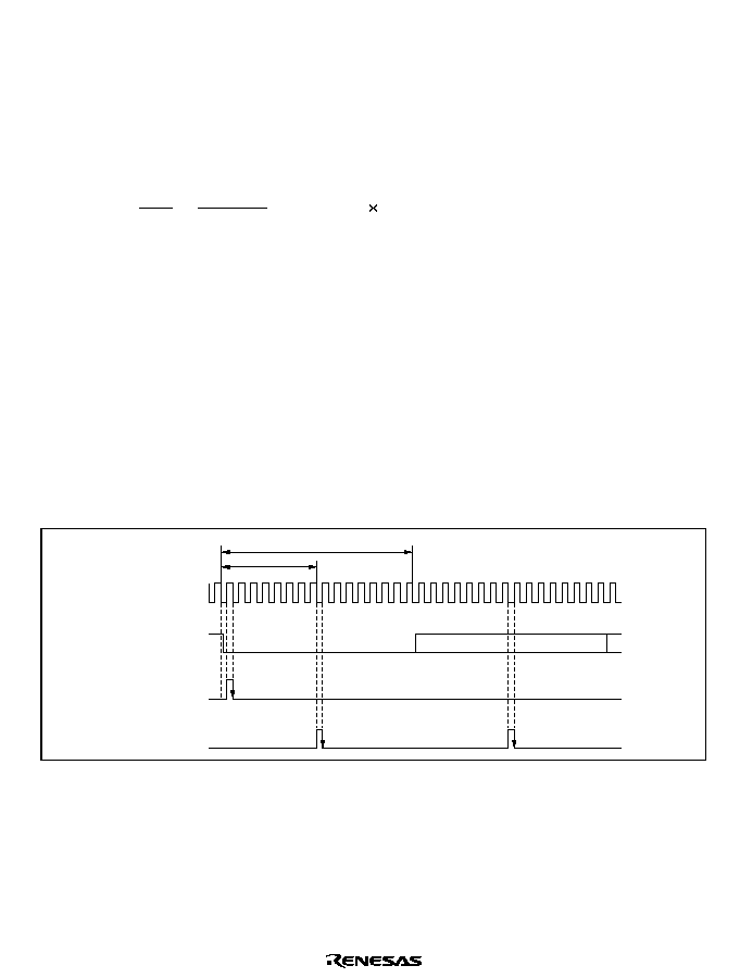
Rev. 2.0, 09/02 page 325 of 658
13.4.2
Receive Data Sampling Timing and Reception Margin in Asynchronous Mode
In asynchronous mode, the SCI operates on a basic clock with a frequency of 16 times the transfer
rate. In reception, the SCI samples the falling edge of the start bit using the basic clock, and
performs internal synchronization. Receive data is latched internally at the rising edge of the 8th
pulse of the basic clock as shown in figure 13.6. Thus, the reception margin in asynchronous mode
is given by formula (1) below.
M = { (0.5 ≠
) ≠
≠ (L ≠ 0.5) F} 100 [%]
1
2N
D ≠ 0.5
N
... Formula (1)
Where
N : Ratio of bit rate to clock (N = 16)
D : Clock duty (D = 0.5 to 1.0)
L : Frame length (L = 9 to 12)
F : Absolute value of clock rate deviation
Assuming values of F (absolute value of clock rate deviation) = 0, D (clock duty) = 0.5, and N
(ratio of bit rate to clock) = 16 in formula (1), the reception margin can be given by the formula.
M = {0.5 ≠ 1/(2
◊
16)}
◊
100 [%] = 46.875%
However, this is only the computed value, and a margin of 20% to 30% should be allowed for in
system design.
Internal basic
clock
16 clocks
8 clocks
Receive data
(RxD)
Synchronization
sampling timing
Start bit
D0
D1
Data sampling
timing
15 0
7
15 0
0
7
Figure 13.6 Receive Data Sampling Timing in Asynchronous Mode
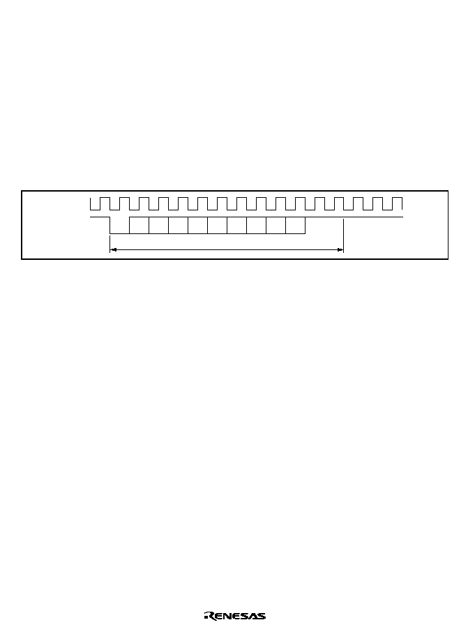
Rev. 2.0, 09/02, page 326 of 658
13.4.3
Clock
Either an internal clock generated by the on-chip baud rate generator or an external clock input at
the SCK pin can be selected as the SCI's serial clock, according to the setting of the C/
bit in
SMR and the CKE0 and CKE1 bits in SCR. When an external clock is input at the SCK pin, the
clock frequency should be 16 times the bit rate used. When an external clock is selected, a base
clock with an average transfer rate can be selected by setting bits ACS2 to ACS0 in SEMR_0.
When the SCI is operated on an internal clock, the clock can be output from the SCK pin when
setting CKE1 = 0 and CKE0 = 1. The frequency of the clock output in this case is equal to the bit
rate, and the phase is such that the rising edge of the clock is in the middle of the transmit data, as
shown in figure 13.7.
0
1 frame
D0
D1
D2
D3
D4
D5
D6
D7
0/1
1
1
SCK
TxD
Figure 13.7 Relationship between Output Clock and Transfer Data Phase
(Asynchronous Mode)
13.4.4
SCI Initialization (Asynchronous Mode)
Before transmitting and receiving data, you should first clear the TE and RE bits in SCR to 0, then
initialize the SCI as described below. When the operating mode, or transfer format, is changed for
example, the TE and RE bits must be cleared to 0 before making the change using the following
procedure. When the TE bit is cleared to 0, the TDRE flag is set to 1. Note that clearing the RE bit
to 0 does not initialize the contents of the RDRF, PER, FER, and ORER flags, or the contents of
RDR. When the external clock is used in asynchronous mode, the clock must be supplied even
during initialization.

Rev. 2.0, 09/02 page 327 of 658
Wait
<Initialization completion>
Start initialization
Set data transfer format in
SMR, SCMR, and SEMR_0
[1]
Set CKE1 and CKE0 bits in SCR
(TE, RE bits 0)
No
Yes
Set value in BRR
Clear TE and RE bits in SCR to 0
[2]
[3]
Set TE and RE bits in
SCR to 1, and set RIE, TIE, TEIE,
and MPIE bits
[4]
1-bit interval elapsed?
[1] Set the clock selection in SCR.
Be sure to clear bits RIE, TIE,
TEIE, and MPIE, and bits TE and
RE, to 0.
When the clock is selected in
asynchronous mode, it is output
immediately after SCR settings are
made.
[2] Set the data transfer format in
SMR, SCMR and SEMR_0.
[3] Write a value corresponding to the
bit rate to BRR. Not necessary if
an external clock or an average
transfer rate clock by bits AC2 to
ACS0 in SEMR_0 is used.
[4] Wait at least one bit interval, then
set the TE bit or RE bit in SCR to 1.
Also set the RIE, TIE, TEIE, and
MPIE bits.
Figure 13.8 Sample SCI Initialization Flowchart
13.4.5
Serial Data Transmission (Asynchronous Mode)
Figure 13.9 shows an example of operation for transmission in asynchronous mode. In
transmission, the SCI operates as described below.
1. The SCI monitors the TDRE flag in SSR. If the flag is cleared to 0, the SCI recognizes that
data has been written to TDR, and transfers the data from TDR to TSR.
2. After transferring data from TDR to TSR, the SCI sets the TDRE flag to 1 and starts
transmission. If the TIE bit is set to 1 at this time, a transmit data empty interrupt request (TXI)
is generated. Continuous transmission is possible because the TXI interrupt routine writes next
transmit data to TDR before transmission of the current transmit data has been completed.
3. Data is sent from the TxD pin in the following order: start bit, transmit data, parity bit or
multiprocessor bit (may be omitted depending on the format), and stop bit.
4. The SCI checks the TDRE flag at the timing for sending the stop bit.
5. If the TDRE flag is 0, the data is transferred from TDR to TSR, the stop bit is sent, and then
serial transmission of the next frame is started.
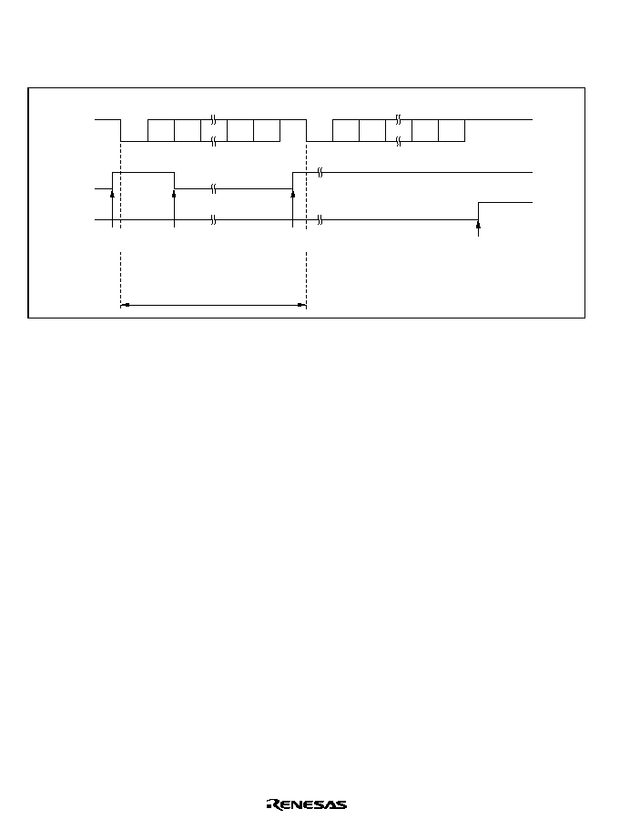
Rev. 2.0, 09/02, page 328 of 658
6. If the TDRE flag is 1, the TEND flag in SSR is set to 1, the stop bit is sent, and then the "mark
state" is entered, in which 1 is output. If the TEIE bit in SCR is set to 1 at this time, a TEI
interrupt request is generated.
TDRE
TEND
0
1 frame
D0
D1
D7
0/1
1
0
D0
D1
D7
0/1
1
1
1
Data
Start
bit
Parity
bit
Stop
bit
Start
bit
Data
Parity
bit
Stop
bit
TXI interrupt
request generated
Data written to TDR and
TDRE flag cleared to 0 in
TXI interrupt service routine
TEI interrupt
request generated
Idle state
(mark state)
TXI interrupt
request generated
Figure 13.9 Example of Operation in Transmission in Asynchronous Mode
(Example with 8-Bit Data, Parity, One Stop Bit)

Rev. 2.0, 09/02 page 329 of 658
Figure 13.10 shows a sample flowchart for data transmission.
No
<End>
[1]
Yes
Initialization
Start transmission
Read TDRE flag in SSR
[2]
Write transmit data to TDR
and clear TDRE flag in SSR to 0
No
Yes
No
Yes
Read TEND flag in SSR
[3]
No
Yes
[4]
Clear DR to 0 and
set DDR to 1
Clear TE bit in SCR to 0
TDRE = 1
All data transmitted?
TEND = 1
Break output?
[1] SCI initialization:
The TxD pin is automatically
designated as the transmit data
output pin.
After the TE bit is set to 1, a frame
of 1s is output, and transmission is
enabled.
[2] SCI status check and transmit data
write:
Read SSR and check that the
TDRE flag is set to 1, then write
transmit data to TDR and clear the
TDRE flag to 0.
[3] Serial transmission continuation
procedure:
To continue serial transmission,
read 1 from the TDRE flag to
confirm that writing is possible,
then write data to TDR, and then
clear the TDRE flag to 0. Checking
and clearing of the TDRE flag is
automatic when the DTC is
activated by a transmit data empty
interrupt (TXI) request, and data is
written to TDR. (H8S/2268 Series
only)
[4] Break output at the end of serial
transmission:
To output a break in serial
transmission, set DR for the port
corresponding to the TxD pin to 0,
clear DDR to 1, then clear the TE
Figure 13.10 Sample Serial Transmission Flowchart
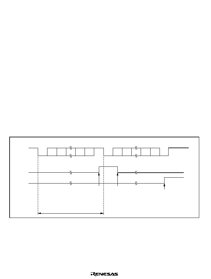
Rev. 2.0, 09/02, page 330 of 658
13.4.6
Serial Data Reception (Asynchronous Mode)
Figure 13.11 shows an example of operation for reception in asynchronous mode. In serial
reception, the SCI operates as described below.
1. The SCI monitors the communication line. If a start bit is detected, the SCI performs internal
synchronization, receives receive data in RSR, and checks the parity bit and stop bit.
2. If an overrun error occurs (when reception of the next data is completed while the RDRF flag
is still set to 1), the ORER bit in SSR is set to 1. If the RIE bit in SCR is set to 1 at this time, an
ERI interrupt request is generated. Receive data is not transferred to RDR. The RDRF flag
remains to be set to 1.
3. If a parity error is detected, the PER bit in SSR is set to 1 and receive data is transferred to
RDR. If the RIE bit in SCR is set to 1 at this time, an ERI interrupt request is generated.
4. If a framing error is detected (when the stop bit is 0), the FER bit in SSR is set to 1 and receive
data is transferred to RDR. If the RIE bit in SCR is set to 1 at this time, an ERI interrupt
request is generated.
5. If reception is completed successfully, the RDRF bit in SSR is set to 1, and receive data is
transferred to RDR. If the RIE bit in SCR is set to 1 at this time, an RXI interrupt request is
generated. Continuous reception is possible because the RXI interrupt routine reads the receive
data transferred to RDR before reception of the next receive data has been completed.
RDRF
FER
0
1 frame
D0
D1
D7
0/1
1
0
D0
D1
D7
0/1
0
1
1
Data
Start
bit
Parity
bit
Stop
bit
Start
bit
Data
Parity
bit
Stop
bit
ERI interrupt request
generated by framing
error
Idle state
(mark state)
RDR data read and RDRF
flag cleared to 0 in RXI
interrupt service routine
RXI interrupt
request
generated
Figure 13.11 Example of SCI Operation in Reception
(Example with 8-Bit Data, Parity, One Stop Bit)

Rev. 2.0, 09/02 page 331 of 658
Table 13.11 shows the states of the SSR status flags and receive data handling when a receive
error is detected. If a receive error is detected, the RDRF flag retains its state before receiving
data. Reception cannot be resumed while a receive error flag is set to 1. Accordingly, clear the
ORER, FER, PER, and RDRF bits to 0 before resuming reception. Figure 13.12 shows a sample
flow chart for serial data reception.
Table 13.11 SSR Status Flags and Receive Data Handling
SSR Status Flag
RDRF
*
ORER
FER
PER
Receive Data
Receive Error Type
1
1
0
0
Lost
Overrun error
0
0
1
0
Transferred to RDR
Framing error
0
0
0
1
Transferred to RDR
Parity error
1
1
1
0
Lost
Overrun error + framing error
1
1
0
1
Lost
Overrun error + parity error
0
0
1
1
Transferred to RDR
Framing error + parity error
1
1
1
1
Lost
Overrun error + framing error +
parity error
Note:
*
The RDRF flag retains the state it had before data reception.

Rev. 2.0, 09/02, page 332 of 658
Yes
<End>
[1]
No
Initialization
Start reception
[2]
No
Yes
Read RDRF flag in SSR
[4]
[5]
Clear RE bit in SCR to 0
Read ORER, PER, and
FER flags in SSR
Error processing
(Continued on next page)
[3]
Read receive data in RDR, and
clear RDRF flag in SSR to 0
No
Yes
PER FER ORER = 1
RDRF = 1
All data received?
[1] SCI initialization:
The RxD pin is automatically
designated as the receive data input
pin.
[2] [3] Receive error processing and break
detection:
If a receive error occurs, read the
ORER, PER, and FER flags in SSR to
identify the error. After performing the
appropriate error processing, ensure
that the ORER, PER, and FER flags are
all cleared to 0. Reception cannot be
resumed if any of these flags are set to
1. In the case of a framing error, a
break can be detected by reading the
value of the input port corresponding to
the RxD pin.
[4] SCI status check and receive data read:
Read SSR and check that RDRF = 1,
then read the receive data in RDR and
clear the RDRF flag to 0. Transition of
the RDRF flag from 0 to 1 can also be
identified by an RXI interrupt.
[5] Serial reception continuation procedure:
To continue serial reception, before the
stop bit for the current frame is
received, read the RDRF flag, read
RDR, and clear the RDRF flag to 0.
The RDRF flag is cleared automatically
when DTC is activated by an RXI
interrupt and the RDR value is read.
(H8S/2268 Series only)
Figure 13.12 Sample Serial Reception Data Flowchart (1)
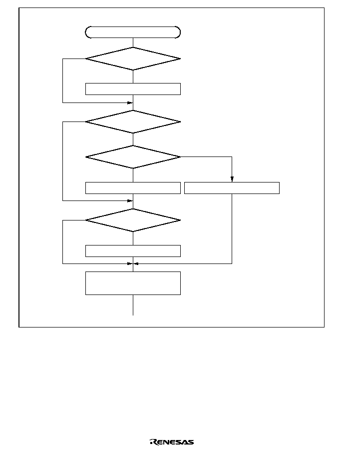
Rev. 2.0, 09/02 page 333 of 658
<End>
[3]
Error processing
Parity error processing
Yes
No
Clear ORER, PER, and
FER flags in SSR to 0
No
Yes
No
Yes
Framing error processing
No
Yes
Overrun error processing
ORER = 1
FER = 1
Break?
PER = 1
Clear RE bit in SCR to 0
Figure 13.12 Sample Serial Reception Data Flowchart (2)

Rev. 2.0, 09/02, page 334 of 658
13.5
Multiprocessor Communication Function
Use of the multiprocessor communication function enables data transfer between a number of
processors sharing communication lines by asynchronous serial communication using the
multiprocessor format, in which a multiprocessor bit is added to the transfer data. When
multiprocessor communication is performed, each receiving station is addressed by a unique ID
code. The serial communication cycle consists of two component cycles; an ID transmission cycle
that specifies the receiving station, and a data transmission cycle. The multiprocessor bit is used to
differentiate between the ID transmission cycle and the data transmission cycle. If the
multiprocessor bit is 1, the cycle is an ID transmission cycle; if the multiprocessor bit is 0, the
cycle is a data transmission cycle. Figure 13.13 shows an example of inter-processor
communication using the multiprocessor format. The transmitting station first sends the ID code
of the receiving station with which it wants to perform serial communication as data with a 1
multiprocessor bit added. It then sends transmit data as data with a 0 multiprocessor bit added.
When data with a 1 multiprocessor bit is received, the receiving station compares that data with its
own ID. The station whose ID matches then receives the data sent next. Stations whose IDs do not
match continue to skip data until data with a 1 multiprocessor bit is again received.
The SCI uses the MPIE bit in SCR to implement this function. When the MPIE bit is set to 1,
transfer of receive data from RSR to RDR, error flag detection, and setting the SSR status flags,
RDRF, FER, and ORER to 1, are inhibited until data with a 1 multiprocessor bit is received. On
reception of a receive character with a 1 multiprocessor bit, the MPB bit in SSR is set to 1 and the
MPIE bit is automatically cleared, thus normal reception is resumed. If the RIE bit in SCR is set to
1 at this time, an RXI interrupt is generated.
When the multiprocessor format is selected, the parity bit setting is rendered invalid. All other bit
settings are the same as those in normal asynchronous mode. The clock used for multiprocessor
communication is the same as that in normal asynchronous mode.

Rev. 2.0, 09/02 page 335 of 658
Transmitting
station
Receiving
station A
Receiving
station B
Receiving
station C
Receiving
station D
(ID = 01)
(ID = 02)
(ID = 03)
(ID = 04)
Serial transmission line
Serial
data
ID transmission cycle =
receiving station
specification
Data transmission cycle =
Data transmission to
receiving station specified by ID
(MPB = 1)
(MPB = 0)
H'01
H'AA
Legend
MPB: Multiprocessor bit
Figure 13.13 Example of Communication Using Multiprocessor Format
(Transmission of Data H'AA to Receiving Station A)
13.5.1
Multiprocessor Serial Data Transmission
Figure 13.14 shows a sample flowchart for multiprocessor serial data transmission. For an ID
transmission cycle, set the MPBT bit in SSR to 1 before transmission. For a data transmission
cycle, clear the MPBT bit in SSR to 0 before transmission. All other SCI operations are the same
as those in asynchronous mode.
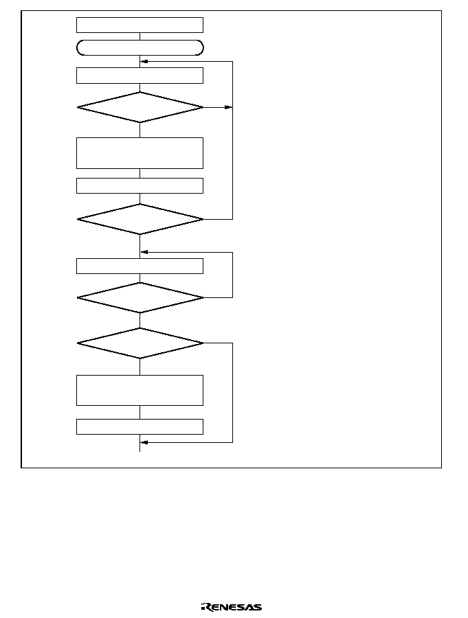
Rev. 2.0, 09/02, page 336 of 658
No
<End>
[1]
Yes
Initialization
Start transmission
Read TDRE flag in SSR
[2]
Write transmit data to TDR and
set MPBT bit in SSR
No
Yes
No
Yes
Read TEND flag in SSR
[3]
No
Yes
[4]
Clear DR to 0 and set DDR to 1
Clear TE bit in SCR to 0
TDRE = 1
All data transmitted?
TEND = 1
Break output?
Clear TDRE flag to 0
[1] SCI initialization:
The TxD pin is automatically
designated as the transmit data
output pin.
After the TE bit is set to 1, a
frame of 1s is output, and
transmission is enabled.
[2] SCI status check and transmit
data write:
Read SSR and check that the
TDRE flag is set to 1, then write
transmit data to TDR. Set the
MPBT bit in SSR to 0 or 1.
Finally, clear the TDRE flag to 0.
[3] Serial transmission continuation
procedure:
To continue serial transmission,
be sure to read 1 from the TDRE
flag to confirm that writing is
possible, then write data to TDR,
and then clear the TDRE flag to
0. Checking and clearing of the
TDRE flag is automatic when the
DTC is activated by a transmit
data empty interrupt (TXI)
request, and data is written to
TDR. (H8S/2268 Series only)
[4] Break output at the end of serial
transmission:
To output a break in serial
transmission, set the port DR to
0, clear DDR to 1, then clear the
TE bit in SCR to 0.
Figure 13.14 Sample Multiprocessor Serial Transmission Flowchart

Rev. 2.0, 09/02 page 337 of 658
13.5.2
Multiprocessor Serial Data Reception
Figure 13.16 shows a sample flowchart for multiprocessor serial data reception. If the MPIE bit in
SCR is set to 1, data is skipped until data with a 1 multiprocessor bit is sent. On receiving data
with a 1 multiprocessor bit, the receive data is transferred to RDR. An RXI interrupt request is
generated at this time. All other SCI operations are the same as in asynchronous mode. Figure
13.15 shows an example of SCI operation for multiprocessor format reception.
MPIE
RDR
value
0
D0
D1
D7
1
1
0
D0
D1
D7
0
1
1
1
Data (ID1)
Start
bit
MPB
Stop
bit
Start
bit
Data (Data1)
MPB
Stop
bit
Data (ID2)
Start
bit
Stop
bit
Start
bit
Data (Data2)
Stop
bit
RXI interrupt
request
(multiprocessor
interrupt)
generated
Mark state
(idle state)
RDRF
RDR data read
and RDRF flag
cleared to 0 in
RXI interrupt
service routine
If not this station's ID,
MPIE bit is set to 1
again
RXI interrupt request is
not generated, and RDR
retains its state
ID1
(a) Data does not match station's ID
MPIE
RDR
value
0
D0
D1
D7
1
1
0
D0
D1
D7
0
1
1
1
MPB
MPB
RXI interrupt
request
(multiprocessor
interrupt)
generated
Mark state
(idle state)
RDRF
RDR data read and
RDRF flag cleared
to 0 in RXI interrupt
service routine
Matches this station's ID,
so reception continues, and
data is received in RXI
interrupt service routine
MPIE bit set to 1
again
ID2
(b) Data matches station's ID
Data2
ID1
MPIE = 0
MPIE = 0
Figure 13.15 Example of SCI Operation in Reception
(Example with 8-Bit Data, Multiprocessor Bit, One Stop Bit)
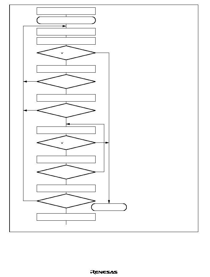
Rev. 2.0, 09/02, page 338 of 658
Yes
<End>
[1]
No
Initialization
Start reception
No
Yes
[4]
Clear RE bit in SCR to 0
Error processing
(Continued on
next page)
[5]
No
Yes
FER ORER = 1
RDRF = 1
All data received?
Read MPIE bit in SCR
[2]
Read ORER and FER flags in SSR
Read RDRF flag in SSR
[3]
Read receive data in RDR
No
Yes
This station's ID?
Read ORER and FER flags in SSR
Yes
No
Read RDRF flag in SSR
No
Yes
FER ORER = 1
Read receive data in RDR
RDRF = 1
[1] SCI initialization:
The RxD pin is automatically designated
as the receive data input pin.
[2] ID reception cycle:
Set the MPIE bit in SCR to 1.
[3] SCI status check, ID reception and
comparison:
Read SSR and check that the RDRF
flag is set to 1, then read the receive
data in RDR and compare it with this
station's ID.
If the data is not this station's ID, set the
MPIE bit to 1 again, and clear the RDRF
flag to 0.
If the data is this station's ID, clear the
RDRF flag to 0.
[4] SCI status check and data reception:
Read SSR and check that the RDRF
flag is set to 1, then read the data in
RDR.
[5] Receive error processing and break
detection:
If a receive error occurs, read the ORER
and FER flags in SSR to identify the
error. After performing the appropriate
error processing, ensure that the ORER
and FER flags are all cleared to 0.
Reception cannot be resumed if either
of these flags is set to 1.
In the case of a framing error, a break
can be detected by reading the RxD pin
value.
Figure 13.16 Sample Multiprocessor Serial Reception Flowchart (1)
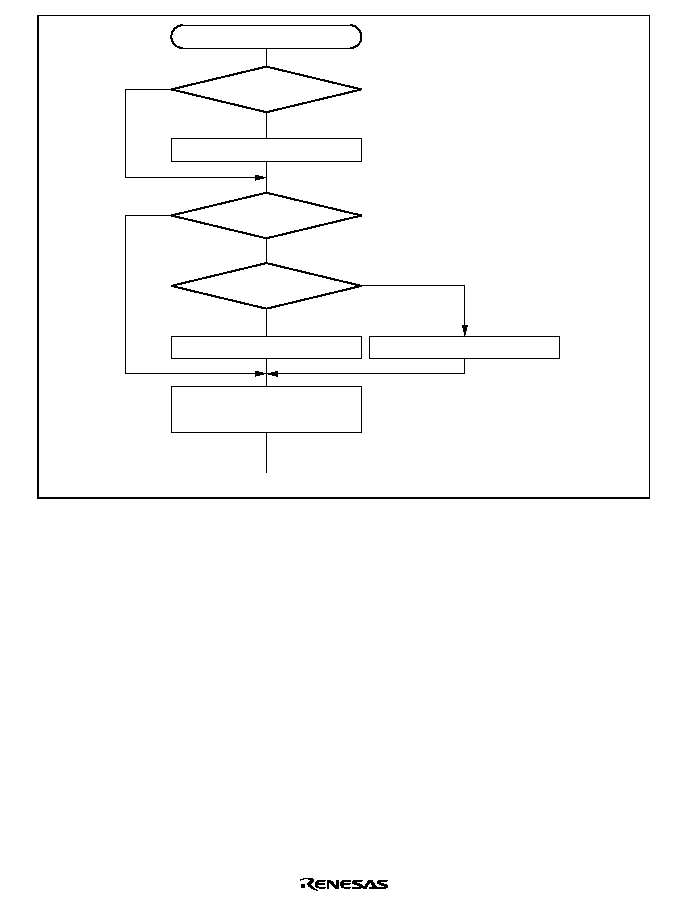
Rev. 2.0, 09/02 page 339 of 658
<End>
Error processing
Yes
No
Clear ORER, PER, and
FER flags in SSR to 0
No
Yes
No
Yes
Framing error processing
Overrun error processing
ORER = 1
FER = 1
Break?
Clear RE bit in SCR to 0
[5]
Figure 13.16 Sample Multiprocessor Serial Reception Flowchart (2)

Rev. 2.0, 09/02, page 340 of 658
13.6
Operation in Clocked Synchronous Mode
Figure 13.17 shows the general format for clocked synchronous communication. In clocked
synchronous mode, data is transmitted or received synchronous with clock pulses. In clocked
synchronous serial communication, data on the transmission line is output from one falling edge of
the serial clock to the next. In clocked synchronous mode, the SCI receives data in synchronous
with the rising edge of the serial clock. After 8-bit data is output, the transmission line holds the
MSB state. In clocked synchronous mode, no parity or multiprocessor bit is added. Inside the SCI,
the transmitter and receiver are independent units, enabling full-duplex communication through
the use of a common clock. Both the transmitter and the receiver also have a double-buffered
structure, so data can be read or written during transmission or reception, enabling continuous data
transfer.
Don't care
Don't care
One unit of transfer data (character or frame)
Bit 0
Serial data
Synchronization
clock
Bit 1
Bit 3
Bit 4
Bit 5
LSB
MSB
Bit 2
Bit 6
Bit 7
*
*
Note:
*
High except in continuous transfer
Figure 13.17 Data Format in Synchronous Communication (For LSB-First)
13.6.1
Clock
Either an internal clock generated by the on-chip baud rate generator or an external
synchronization clock input at the SCK pin can be selected, according to the setting of CKE0 and
CKE1 bits in SCR. When the SCI is operated on an internal clock, the serial clock is output from
the SCK pin. Eight serial clock pulses are output in the transfer of one character, and when no
transfer is performed the clock is fixed high.
13.6.2
SCI Initialization (Clocked Synchronous Mode)
Before transmitting and receiving data, the TE and RE bits in SCR should be cleared to 0, then the
SCI should be initialized as described in a sample flowchart in figure 13.18. When the operating
mode, or transfer format, is changed for example, the TE and RE bits must be cleared to 0 before
making the change using the following procedure. When the TE bit is cleared to 0, the TDRE flag
is set to 1. Note that clearing the RE bit to 0 does not change the contents of the RDRF, PER,
FER, and ORER flags, or the contents of RDR.

Rev. 2.0, 09/02 page 341 of 658
Wait
<Transfer start>
Start initialization
Set data transfer format in
SMR and SCMR
No
Yes
Set value in BRR
Clear TE and RE bits in SCR to 0
[2]
[3]
Set TE and RE bits in SCR to 1, and
set RIE, TIE, TEIE, and MPIE bits
[4]
1-bit interval elapsed?
Set CKE1 and CKE0 bits in SCR
(TE, RE bits 0)
[1]
[1] Set the clock selection in SCR. Be sure
to clear bits RIE, TIE, TEIE, and MPIE,
TE and RE, to 0.
[2] Set the data transfer format in SMR and
SCMR.
[3] Write a value corresponding to the bit
rate to BRR. Not necessary if an
external clock is used.
[4] Wait at least one bit interval, then set
the TE bit or RE bit in SCR to 1.
Also set the RIE, TIE TEIE, and MPIE
bits.
Setting the TE and RE bits enables the
TxD and RxD pins to be used.
Note: In simultaneous transmit and receive operations, the TE and RE bits should both be cleared
to 0 or set to 1 simultaneously.
Figure 13.18 Sample SCI Initialization Flowchart
Rev. 2.0, 09/02, page 342 of 658
13.6.3
Serial Data Transmission (Clocked Synchronous Mode)
Figure 13.19 shows an example of SCI operation for transmission in clocked synchronous mode.
In serial transmission, the SCI operates as described below.
1. The SCI monitors the TDRE flag in SSR, and if the flag is 0, the SCI recognizes that data has
been written to TDR, and transfers the data from TDR to TSR.
2. After transferring data from TDR to TSR, the SCI sets the TDRE flag to 1 and starts
transmission. If the TIE bit in SCR is set to 1 at this time, a transmit data empty interrupt
(TXI) is generated. Continuous transmission is possible because the TXI interrupt routine
writes the next transmit data to TDR before transmission of the current transmit data has been
completed.
3. 8-bit data is sent from the TxD pin synchronized with the output clock when output clock
mode has been specified, and synchronized with the input clock when use of an external clock
has been specified.
4. The SCI checks the TDRE flag at the timing for sending the MSB (bit 7).
5. If the TDRE flag is cleared to 0, data is transferred from TDR to TSR, and serial transmission
of the next frame is started.
6. If the TDRE flag is set to 1, the TEND flag in SSR is set to 1, and the TDRE flag maintains the
output state of the last bit. If the TEIE bit in SCR is set to 1 at this time, a TEI interrupt request
is generated. The SCK pin is fixed high.
Figure 13.20 shows a sample flow chart for serial data transmission. Even if the TDRE flag is
cleared to 0, transmission will not start while a receive error flag (ORER, FER, or PER) is set to 1.
Make sure that the receive error flags are cleared to 0 before starting transmission. Note that
clearing the RE bit to 0 does not clear the receive error flags.
Transfer direction
Bit 0
Serial data
Synchronization
clock
1 frame
TDRE
TEND
Data written to TDR
and TDRE flag cleared
to 0 in TXI interrupt
service routine
TXI interrupt
request generated
Bit 1
Bit 7
Bit 0
Bit 1
Bit 6
Bit 7
TXI interrupt
request generated
TEI interrupt request
generated
Figure 13.19 Sample SCI Transmission Operation in Clocked Synchronous Mode
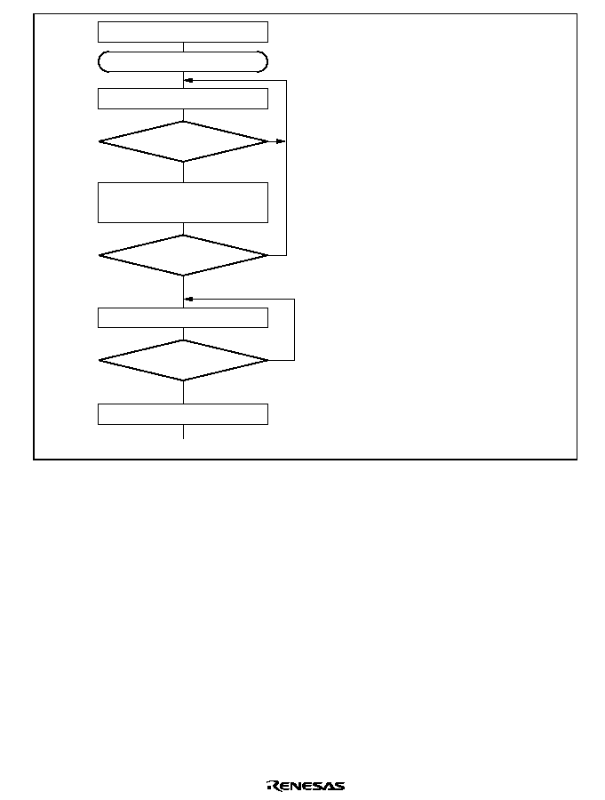
Rev. 2.0, 09/02 page 343 of 658
No
<End>
[1]
Yes
Initialization
Start transmission
Read TDRE flag in SSR
[2]
Write transmit data to TDR and
clear TDRE flag in SSR to 0
No
Yes
No
Yes
Read TEND flag in SSR
[3]
Clear TE bit in SCR to 0
TDRE = 1
All data transmitted?
TEND = 1
[1] SCI initialization:
The TxD pin is automatically
designated as the transmit data output
pin.
[2] SCI status check and transmit data
write:
Read SSR and check that the TDRE
flag is set to 1, then write transmit data
to TDR and clear the TDRE flag to 0.
[3] Serial transmission continuation
procedure:
To continue serial transmission, be
sure to read 1 from the TDRE flag to
confirm that writing is possible, then
write data to TDR, and then clear the
TDRE flag to 0.
Checking and clearing of the TDRE
flag is automatic when the DTC is
activated by a transmit data empty
interrupt (TXI) request and data is
written to TDR. (H8S/2268 Series
only)
Figure 13.20 Sample Serial Transmission Flowchart

Rev. 2.0, 09/02, page 344 of 658
13.6.4
Serial Data Reception (Clocked Synchronous Mode)
Figure 13.21 shows an example of SCI operation for reception in clocked synchronous mode. In
serial reception, the SCI operates as described below.
1. The SCI performs internal initialization synchronous with a synchronous clock input or output,
starts receiving data, and stores the received data in RSR.
2. If an overrun error occurs (when reception of the next data is completed while the RDRF flag
in SSR is still set to 1), the ORER bit in SSR is set to 1. If the RIE bit in SCR is set to 1 at this
time, an ERI interrupt request is generated, receive data is not transferred to RDR, and the
RDRF flag remains to be set to 1.
3. If reception is completed successfully, the RDRF bit in SSR is set to 1, and receive data is
transferred to RDR. If the RIE bit in SCR is set to 1 at this time, an RXI interrupt request is
generated. Continuous reception is possible because the RXI interrupt routine reads the receive
data transferred to RDR before reception of the next receive data has finished.
Bit 7
Serial data
Synchronization
clock
1 frame
RDRF
ORER
ERI interrupt request
generated by overrun
error
RXI interrupt
request generated
RDR data read and
RDRF flag cleared
to 0 in RXI interrupt
RXI interrupt
request
generated
Bit 0
Bit 7
Bit 0
Bit 1
Bit 6
Bit 7
Figure 13.21 Example of SCI Operation in Reception
Reception cannot be resumed while a receive error flag is set to 1. Accordingly, clear the ORER,
FER, PER, and RDRF bits to 0 before resuming reception. Figure 13.22 shows a sample flow
chart for serial data reception.
An overrun error occurs or synchronous clocks are output until the RE bit is cleared to 0 when an
internal clock is selected and only receive operation is possible. When a transmission and
reception will be carried out in a unit of one frame, be sure to carry out a dummy transmission
with only one frame by the simultaneous transmit and receive operations at the same time.

Rev. 2.0, 09/02 page 345 of 658
Yes
<End>
[1]
No
Initialization
Start reception
[2]
No
Yes
Read RDRF flag in SSR
[4]
[5]
Clear RE bit in SCR to 0
Error processing
(Continued below)
[3]
Read receive data in RDR, and
clear RDRF flag in SSR to 0
No
Yes
ORER = 1
RDRF = 1
All data received?
Read ORER flag in SSR
<End>
Error processing
Overrun error processing
Clear ORER flag in SSR to 0
[3]
[1] SCI initialization:
The RxD pin is automatically
designated as the receive data input
pin.
[2] [3] Receive error processing:
If a receive error occurs, read the
ORER flag in SSR, and after
performing the appropriate error
processing, clear the ORER flag to 0.
Transfer cannot be resumed if the
ORER flag is set to 1.
[4] SCI status check and receive data
read:
Read SSR and check that the RDRF
flag is set to 1, then read the receive
data in RDR and clear the RDRF flag
to 0.
Transition of the RDRF flag from 0 to 1
can also be identified by an RXI
interrupt.
[5] Serial reception continuation
procedure:
To continue serial reception, before
the final bit of the current frame is
received, reading the RDRF flag,
reading RDR, and clearing the RDRF
flag to 0 should be finished. The
RDRF flag is cleared automatically
when the DTC is activated by a
receive data full interrupt (RXI) request
and the RDR value is read. (H8S/2268
Series only)
Figure 13.22 Sample Serial Reception Flowchart

Rev. 2.0, 09/02, page 346 of 658
13.6.5
Simultaneous Serial Data Transmission and Reception (Clocked Synchronous
Mode)
Figure 13.23 shows a sample flowchart for simultaneous serial transmit and receive operations.
The following procedure should be used for simultaneous serial data transmit and receive
operations. To switch from transmit mode to simultaneous transmit and receive mode, after
checking that the SCI has finished transmission and the TDRE and TEND flags are set to 1, clear
TE to 0. Then simultaneously set TE and RE to 1 with a single instruction. To switch from receive
mode to simultaneous transmit and receive mode, after checking that the SCI has finished
reception, clear RE to 0. Then after checking that the RDRF and receive error flags (ORER, FER,
and PER) are cleared to 0, simultaneously set TE and RE to 1 with a single instruction.
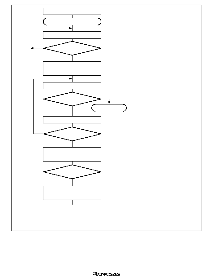
Rev. 2.0, 09/02 page 347 of 658
Yes
<End>
[1]
No
Initialization
Start transmission/reception
[5]
Error processing
[3]
Read receive data in RDR, and
clear RDRF flag in SSR to 0
No
Yes
ORER = 1
All data received?
[2]
Read TDRE flag in SSR
No
Yes
TDRE = 1
Write transmit data to TDR and
clear TDRE flag in SSR to 0
No
Yes
RDRF = 1
Read ORER flag in SSR
[4]
Read RDRF flag in SSR
Clear TE and RE bits in SCR to 0
[1]
SCI initialization:
The TxD pin is designated as the
transmit data output pin, and the RxD
pin is designated as the receive data
input pin, enabling simultaneous
transmit and receive operations.
[2]
SCI status check and transmit data
write:
Read SSR and check that the TDRE
flag is set to 1, then write transmit
data to TDR and clear the TDRE flag
to 0.
Transition of the TDRE flag from 0 to
1 can also be identified by a TXI
interrupt.
[3]
Receive error processing:
If a receive error occurs, read the
ORER flag in SSR, and after
performing the appropriate error
processing, clear the ORER flag to 0.
Transmission/reception cannot be
resumed if the ORER flag is set to 1.
[4]
SCI status check and receive data
read:
Read SSR and check that the RDRF
flag is set to 1, then read the receive
data in RDR and clear the RDRF flag
to 0. Transition of the RDRF flag from
0 to 1 can also be identified by an RXI
interrupt.
[5]
Serial transmission/reception
continuation procedure:
To continue serial transmission/
reception, before the final bitof the
current frame is received, finish
reading the RDRF flag, reading RDR,
and clearing the RDRF flag to 0.
Also, before the final bit of the current
frame is transmitted, read 1 from the
TDRE flag to confirm that writing is
possible. Then write data to TDR and
clear the TDRE flag to 0.
Checking and clearing of the TDRE
flag is automatic when the DTC is
activated by a transmit data empty
interrupt (TXI) request and data is
written to TDR. Also, the RDRF flag
is cleared automatically when the
DTC is activated by a receive data full
interrupt (RXI) request and the RDR
value is read.
(H8S/2268 Series
only)
Note: When switching from transmit or receive operation to simultaneous
transmit and receive operations, first clear the TE bit and RE bit to 0,
then set both these bits to 1 by one instruction simultaneously.
Figure 13.23 Sample Flowchart of Simultaneous Serial Transmit and Receive Operations
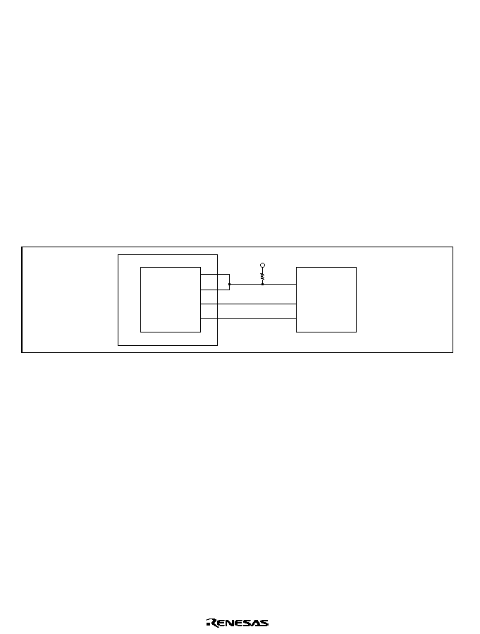
Rev. 2.0, 09/02, page 348 of 658
13.7
Operation in Smart Card Interface
The SCI supports an IC card (Smart Card) interface that conforms to ISO/IEC 7816-3
(Identification Card) as a serial communication interface extension function. Switching between
the normal serial communication interface and the Smart Card interface mode is carried out by
means of a register setting.
13.7.1
Pin Connection Example
Figure 13.24 shows an example of connection with the Smart Card. In communication with an IC
card, as both transmission and reception are carried out on a single data transmission line, the TxD
pin and RxD pin should be connected to the LSI pin. The data transmission line should be pulled
up to the V
CC
power supply with a resistor. If an IC card is not connected, and the TE and RE bits
are both set to 1, closed transmission/reception is possible, enabling self-diagnosis to be carried
out. When the clock generated on the Smart Card interface is used by an IC card, the SCK pin
output is input to the CLK pin of the IC card. This LSI port output is used as the reset signal.
TxD
RxD
This LSI
V
CC
I/O
Connected equipment
IC card
Data line
Clock line
Reset line
CLK
RST
SCK
Rx (port)
Figure 13.24 Schematic Diagram of Smart Card Interface Pin Connections
13.7.2
Data Format (Except for Block Transfer Mode)
Figure 13.25 shows the transfer data format in Smart Card interface mode.
∑
One frame consists of 8-bit data plus a parity bit in asynchronous mode.
∑
In transmission, a guard time of at least 2 etu (Elementary Time Unit: the time for transfer of
one bit) is left between the end of the parity bit and the start of the next frame.
∑
If a parity error is detected during reception, a low error signal level is output for one etu
period, 10.5 etu after the start bit.
∑
If an error signal is sampled during transmission, the same data is retransmitted automatically
after a delay of 2 etu or longer.

Rev. 2.0, 09/02 page 349 of 658
Ds
D0
D1
D2
D3
D4
D5
D6
D7
Dp
When there is no parity error
Transmitting station output
Ds
D0
D1
D2
D3
D4
D5
D6
D7
Dp
When a parity error occurs
Transmitting station output
DE
Receiving station
output
: Start bit
: Data bits
: Parity bit
: Error signal
Legend
DS
D0 to D7
Dp
DE
Figure 13.25 Normal Smart Card Interface Data Format
Data transfer with other types of IC cards (direct convention and inverse convention) are
performed as described in the following.
Ds
A
Z
Z
A
Z
Z
Z
Z
A
A
(Z)
(Z)
State
D0
D1
D2
D3
D4
D5
D6
D7
Dp
Figure 13.26 Direct Convention (SDIR = SINV = O/
= 0)
With the direction convention type IC and the above sample start character, the logic 1 level
corresponds to state Z and the logic 0 level to state A, and transfer is performed in LSB-first order.
The start character data above is H'3B. For the direct convention type, clear the SDIR and SINV
bits in SCMR to 0. According to Smart Card regulations, clear the O/
bit in SMR to 0 to select
even parity mode.
Ds
A
Z
Z
A
A
A
Z
A
A
A
(Z)
(Z)
State
D7
D6
D5
D4
D3
D2
D1
D0
Dp
Figure 13.27 Inverse Convention (SDIR = SINV = O/
= 1)
With the inverse convention type, the logic 1 level corresponds to state A and the logic 0 level to
state Z, and transfer is performed in MSB-first order. The start character data for the above is
H'3F. For the inverse convention type, set the SDIR and SINV bits in SCMR to 1. According to
Smart Card regulations, even parity mode is the logic 0 level of the parity bit, and corresponds to
state Z. In this LSI, the SINV bit inverts only data bits D0 to D7. Therefore, set the O/
bit in
SMR to 1 to invert the parity bit for both transmission and reception.

Rev. 2.0, 09/02, page 350 of 658
13.7.3
Block Transfer Mode
Operation in block transfer mode is the same as that in the normal Smart Card interface mode,
except for the following points.
∑
In reception, though the parity check is performed, no error signal is output even if an error is
detected. However, the PER bit in SSR is set to 1 and must be cleared before receiving the
parity bit of the next frame.
∑
In transmission, a guard time of at least 1 etu is left between the end of the parity bit and the
start of the next frame.
∑
In transmission, because retransmission is not performed, the TEND flag is set to 1, 11.5 etu
after transmission start.
∑
As with the normal Smart Card interface, the ERS flag indicates the error signal status, but
since error signal transfer is not performed, this flag is always cleared to 0.
13.7.4
Receive Data Sampling Timing and Reception Margin
In Smart Card interface mode an internal clock generated by the on-chip baud rate generator can
only be used as a transmission/reception clock. In this mode, the SCI operates on a basic clock
with a frequency of 32, 64, 372, or 256 times the transfer rate (fixed to 16 times in normal
asynchronous mode) as determined by bits BCP1 and BCP0. In reception, the SCI samples the
falling edge of the start bit using the basic clock, and performs internal synchronization. As shown
in figure 13.28, by sampling receive data at the rising-edge of the 16th, 32nd, 186th, or 128th
pulse of the basic clock, data can be latched at the middle of the bit. The reception margin is given
by the following formula.
M = | (0.5 ≠
) ≠ (L ≠ 0.5) F ≠
(1 + F) | 100%
1
2N
| D ≠ 0.5 |
N
Where
M: Reception margin (%)
N: Ratio of bit rate to clock (N = 32, 64, 372, and 256)
D: Clock duty (D = 0 to 1.0)
L: Frame length (L = 10)
F: Absolute value of clock frequency deviation
Assuming values of F = 0, D = 0.5 and N = 372 in the above formula, the reception margin
formula is as follows.
M = (0.5 ≠ 1/2
◊
372)
◊
100%
= 49.866%

Rev. 2.0, 09/02 page 351 of 658
Internal
basic clock
372 clocks
186 clocks
Receive data
(RxD)
Synchronization
sampling timing
D0
D1
Data sampling
timing
185
371 0
371
185
0
0
Start bit
Figure 13.28 Receive Data Sampling Timing in Smart Card Mode
(Using Clock of 372 Times the Transfer Rate)
13.7.5
Initialization
Before transmitting and receiving data, initialize the SCI as described below. Initialization is also
necessary when switching from transmit mode to receive mode, or vice versa.
1. Clear the TE and RE bits in SCR to 0.
2. Clear the error flags ERS, PER, and ORER in SSR to 0.
3. Set the GM, BLK, O/
, BCP0, BCP1, CKS0, CKS1 bits in SMR. Set the PE bit to 1.
4. Set the SMIF, SDIR, and SINV bits in SCMR.
When the SMIF bit is set to 1, the TxD and RxD pins are both switched from ports to SCI pins,
and are placed in the high-impedance state.
5. Set the value corresponding to the bit rate in BRR.
6. Set the CKE0 and CKE1 bits in SCR. Clear the TIE, RIE, TE, RE, MPIE, and TEIE bits to 0.
If the CKE0 bit is set to 1, the clock is output from the SCK pin.
7. Wait at least one bit interval, then set the TIE, RIE, TE, and RE bits in SCR. Do not set the TE
bit and RE bit at the same time, except for self-diagnosis.
To switch from receive mode to transmit mode, after checking that the SCI has finished reception,
initialize the SCI, and set RE to 0 and TE to 1. Whether SCI has finished reception or not can be
checked with the RDRF, PER, or ORER flags. To switch from transmit mode to receive mode,
after checking that the SCI has finished transmission, initialize the SCI, and set TE to 0 and RE to
1. Whether SCI has finished transmission or not can be checked with the TEND flag.

Rev. 2.0, 09/02, page 352 of 658
13.7.6
Serial Data Transmission (Except for Block Transfer Mode)
As data transmission in Smart Card interface mode involves error signal sampling and
retransmission processing, the operations are different from those in normal serial communication
interface mode (except for block transfer mode). Figure 13.29 illustrates the retransfer operation
when the SCI is in transmit mode.
1. If an error signal is sent back from the receiving end after transmission of one frame is
complete, the ERS bit in SSR is set to 1. If the RIE bit in SCR is enabled at this time, an ERI
interrupt request is generated. The ERS bit in SSR should be cleared to 0 by the time the next
parity bit is sampled.
2. The TEND bit in SSR is not set for a frame in which an error signal indicating an abnormality
is received. Data is retransferred from TDR to TSR, and retransmitted automatically.
3. If an error signal is not sent back from the receiving end, the ERS bit in SSR is not set.
Transmission of one frame, including a retransfer, is judged to have been completed, and the
TEND bit in SSR is set to 1. If the TIE bit in SCR is enabled at this time, a TXI interrupt
request is generated. Writing transmit data to TDR transfers the next transmit data.
Figure 13.31 shows a flowchart for transmission. In the H8S/2268 Series, a sequence of transmit
operations can be performed automatically by specifying the DTC to be activated with a TXI
interrupt source. In a transmit operation, the TDRE flag is set to 1 at the same time as the TEND
flag in SSR is set, and a TXI interrupt will be generated if the TIE bit in SCR has been set to 1. If
the TXI request is designated beforehand as a DTC activation source, the DTC will be activated
by the TXI request, and transfer of the transmit data will be carried out. The TDRE and TEND
flags are automatically cleared to 0 when data is transferred by the DTC. In the event of an error,
the SCI retransmits the same data automatically. During this period, the TEND flag remains
cleared to 0 and the DTC is not activated. Therefore, the SCI and DTC will automatically transmit
the specified number of bytes in the event of an error, including retransmission. However, the ERS
flag is not cleared automatically when an error occurs, and so the RIE bit should be set to 1
beforehand so that an ERI request will be generated in the event of an error, and the ERS flag will
be cleared.
When performing transfer using the DTC, it is essential to set and enable the DTC before carrying
out SCI setting. For details of the DTC setting procedures, refer to section 8, Data Transfer
Controller (DTC).

Rev. 2.0, 09/02 page 353 of 658
D0 D1 D2 D3 D4 D5 D6 D7 Dp
DE
Ds D0 D1 D2 D3 D4 D5 D6 D7 Dp
(DE)
Ds D0 D1 D2 D3 D4
Ds
Transfer
frame n+1
Retransferred frame
nth transfer frame
TDRE
TEND
FER/ERS
Transfer to TSR from TDR
Transfer to TSR from TDR
Transfer to TSR
from TDR
Figure 13.29 Retransfer Operation in SCI Transmit Mode
The timing for setting the TEND flag depends on the value of the GM bit in SMR. The TEND flag
set timing is shown in figure 13.30.
Ds
D0
D1
D2
D3
D4
D5
D6
D7
Dp
I/O data
12.5etu
TXI
(TEND interrupt)
11.0etu
DE
Guard
time
When GM = 0
When GM = 1
: Start bit
: Data bits
: Parity bit
: Error signal
Legend
Ds
D0 to D7
Dp
DE
Figure 13.30 TEND Flag Generation Timing in Transmission Operation

Rev. 2.0, 09/02, page 354 of 658
Initialization
No
Yes
Clear TE bit to 0
Start transmission
Start
No
No
No
Yes
Yes
Yes
Yes
No
End
Write data to TDR,
and clear TDRE flag
in SSR to 0
Error processing
Error processing
TEND = 1?
All data transmitted ?
TEND = 1?
ERS = 0?
ERS = 0?
Figure 13.31 Example of Transmission Processing Flow
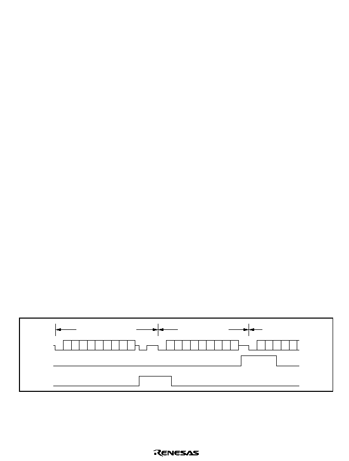
Rev. 2.0, 09/02 page 355 of 658
13.7.7
Serial Data Reception (Except for Block Transfer Mode)
Data reception in Smart Card interface mode uses the same operation procedure as for normal
serial communication interface mode. Figure 13.32 illustrates the retransfer operation when the
SCI is in receive mode.
1. If an error is found when the received parity bit is checked, the PER bit in SSR is
automatically set to 1. If the RIE bit in SCR is set at this time, an ERI interrupt request is
generated. The PER bit in SSR should be kept cleared to 0 until the next parity bit is sampled.
2. The RDRF bit in SSR is not set for a frame in which an error has occurred.
3. If no error is found when the received parity bit is checked, the PER bit in SSR is not set to 1,
the receive operation is judged to have been completed normally, and the RDRF flag in SSR is
automatically set to 1. If the RIE bit in SCR is enabled at this time, an RXI interrupt request is
generated.
Figure 13.33 shows a flowchart for reception. In the H8S/2268 Series, a sequence of receive
operations can be performed automatically by specifying the DTC to be activated using an RXI
interrupt source. In a receive operation, an RXI interrupt request is generated when the RDRF flag
in SSR is set to 1. If the RXI request is designated beforehand as a DTC activation source, the
DTC will be activated by the RXI request, and the receive data will be transferred. The RDRF flag
is cleared to 0 automatically when data is transferred by the DTC. If an error occurs in receive
mode and the ORER or PER flag is set to 1, a transfer error interrupt (ERI) request will be
generated. Hence, so the error flag must be cleared to 0. In the event of an error, the DTC is not
activated and receive data is skipped. Therefore, receive data is transferred for only the specified
number of bytes in the event of an error. Even when a parity error occurs in receive mode and the
PER flag is set to 1, the data that has been received is transferred to RDR and can be read from
there.
Note:
For details on receive operations in block transfer mode, refer to section 13.4, Operation in
Asynchronous Mode.
D0 D1 D2 D3 D4 D5 D6 D7 Dp DE
Ds D0 D1 D2 D3 D4 D5 D6 D7 Dp
(DE)
Ds D0 D1 D2 D3 D4
Ds
Transfer
frame n+1
Retransferred frame
nth transfer frame
RDRF
PER
Figure 13.32 Retransfer Operation in SCI Receive Mode

Rev. 2.0, 09/02, page 356 of 658
Initialization
Read RDR and clear
RDRF flag in SSR to 0
Clear RE bit to 0
Start reception
Start
Error processing
No
No
No
Yes
Yes
ORER = 0 and
PER = 0
RDRF = 1?
All data received?
Yes
Figure 13.33 Example of Reception Processing Flow
13.7.8
Clock Output Control
When the GM bit in SMR is set to 1, the clock output level can be fixed with bits CKE0 and
CKE1 in SCR. At this time, the minimum clock pulse width can be made the specified width.
Figure 13.34 shows the timing for fixing the clock output level. In this example, GM is set to 1,
CKE1 is cleared to 0, and the CKE0 bit is controlled.
Specified pulse width
SCK
CKE0
Specified pulse width
Figure 13.34 Timing for Fixing Clock Output Level
When turning on the power or switching between Smart Card interface mode and software standby
mode, the following procedures should be followed in order to maintain the clock duty.

Rev. 2.0, 09/02 page 357 of 658
Powering On: To secure clock duty from power-on, the following switching procedure should be
followed.
1. The initial state is port input and high impedance. Use a pull-up resistor or pull-down
resistor to fix the potential.
2. Fix the SCK pin to the specified output level with the CKE1 bit in SCR.
3. Set SMR and SCMR, and switch to smart card mode operation.
4. Set the CKE0 bit in SCR to 1 to start clock output.
When changing from smart card interface mode to software standby mode:
1. Set the data register (DR) and data direction register (DDR) corresponding to the SCK pin
to the value for the fixed output state in software standby mode.
2. Write 0 to the TE bit and RE bit in the serial control register (SCR) to halt transmit/receive
operation. At the same time, set the CKE1 bit to the value for the fixed output state in
software standby mode.
3. Write 0 to the CKE0 bit in SCR to halt the clock.
4. Wait for one serial clock period.
During this interval, clock output is fixed at the specified level, with the duty preserved.
5. Make the transition to the software standby state.
When returning to smart card interface mode from software standby mode:
1. Exit the software standby state.
2. Write 1 to the CKE0 bit in SCR and output the clock. Signal generation is started with the
normal duty.
Software
standby
Normal operation
Normal operation
Figure 13.35 Clock Halt and Restart Procedure

Rev. 2.0, 09/02, page 358 of 658
13.8
Interrupt Sources
13.8.1
Interrupts in Normal Serial Communication Interface Mode
Table 13.12 shows the interrupt sources in normal serial communication interface mode. A
different interrupt vector is assigned to each interrupt source, and individual interrupt sources can
be enabled or disabled using the enable bits in SCR.
When the TDRE flag in SSR is set to 1, a TXI interrupt request is generated. When the TEND flag
in SSR is set to 1, a TEI interrupt request is generated.
A TXI interrupt can activate the DTC to perform data transfer. The TDRE flag is cleared to 0
automatically when data is transferred by the DTC. (H8S/2268 Series only)
When the RDRF flag in SSR is set to 1, an RXI interrupt request is generated. When the ORER,
PER, or FER flag in SSR is set to 1, an ERI interrupt request is generated.
An RXI interrupt request can activate the DTC to transfer data. The RDRF flag is cleared to 0
automatically when data is transferred by the DTC. (H8S/2268 Series only)
A TEI interrupt is requested when the TEND flag is set to 1 and the TEIE bit is set to 1. If a TEI
interrupt and a TXI interrupt are requested simultaneously, the TXI interrupt has priority for
acceptance. However, if the TDRE and TEND flags are cleared simultaneously by the TXI
interrupt routine, the SCI cannot branch to the TEI interrupt routine later.

Rev. 2.0, 09/02 page 359 of 658
Table 13.12 Interrupt Sources of Serial Communication Interface Mode
Channel
Name
Interrupt Source
Interrupt Flag
DTC Activation
*
2
Priority
*
1
ERI0
Receive Error
ORER, FER, PER
Not possible
High
RXI0
Receive Data Full
RDRF
Possible
TXI0
Transmit Data Empty
TDRE
Possible
0
TEI0
Transmission End
TEND
Not possible
ERI1
Receive Error
ORER, FER, PER
Not possible
RXI1
Receive Data Full
RDRF
Possible
TXI1
Transmit Data Empty
TDRE
Possible
1
TEI1
Transmission End
TEND
Not possible
ERI2
Receive Error
ORER, FER, PER
Not possible
RXI2
Receive Data Full
RDRF
Possible
TXI2
Transmit Data Empty
TDRE
Possible
2
TEI2
Transmission End
TEND
Not possible
Low
Notes: 1. Indicates the initial state immediately after a reset.
Priorities in channels can be changed by the interrupt controller. (H8S/2268 Series only)
2. Supported only by the H8S/2268 Series.

Rev. 2.0, 09/02, page 360 of 658
13.8.2
Interrupts in Smart Card Interface Mode
Table 13.13 shows the interrupt sources in Smart Card interface mode. The transmit end interrupt
(TEI) request cannot be used in this mode.
Note: In case of block transfer mode, see 13.8.1, Interrupts in Nomal Serial Communication
Interface Mode.
Table 13.13 Interrupt Sources in Smart Card Interface Mode
Channel
Name
Interrupt Source
Interrupt Flag
DTC
Activation
*
2
Priority
*
1
ERI0
Receive Error, detection
ORER, PER, ERS
Not possible
High
RXI0
Receive Data Full
RDRF
Possible
0
TXI0
Transmit Data Empty
TEND
Possible
ERI1
Receive Error, detection
ORER, PER, ERS
Not possible
RXI1
Receive Data Full
RDRF
Possible
1
TXI1
Transmit Data Empty
TEND
Possible
ERI2
Receive Error, detection
ORER, PER, ERS
Not possible
RXI2
Receive Data Full
RDRF
Possible
2
TXI2
Transmit Data Empty
TEND
Possible
Low
Notes: 1. Indicates the initial state immediately after a reset.
Priorities in channels can be changed by the interrupt controller. (H8S/2268 Series only)
2. Supported only by the H8S/2268 Series.
13.9
Usage Notes
13.9.1
Module Stop Mode Setting
SCI operation can be disabled or enabled using the module stop control register. The initial setting
is for SCI operation to be halted. Register access is enabled by clearing module stop mode. For
details, refer to section 22, Power-Down Modes.
13.9.2
Break Detection and Processing (Asynchronous mode only)
When framing error (FER) detection is performed, a break can be detected by reading the RxD pin
value directly. In a break, the input from the RxD pin becomes all 0s, setting the FER flag, and
possibly the PER flag. Note that as the SCI continues the receive operation after receiving a break,
even if the FER flag is cleared to 0, it will be set to 1 again.

Rev. 2.0, 09/02 page 361 of 658
13.9.3
Mark State and Break Detection (Asynchronous mode only)
When TE is 0, the TxD pin is used as an I/O port whose direction (input or output) and level are
determined by DDR. This can be used to set the TxD pin to mark state (high level) or send a break
during serial data transmission. To maintain the communication line at mark state until TE is set to
1, set both DDR and DR to 1. As TE is cleared to 0 at this point, the TxD pin becomes an I/O port,
and 1 is output from the TxD pin. To send a break during serial transmission, first set PDR to 1
and DR to 0, and then clear TE to 0. When TE is cleared to 0, the transmitter is initialized
regardless of the current transmission state, the TxD pin becomes an I/O port, and 0 is output from
the TxD pin.
13.9.4
Receive Error Flags and Transmit Operations (Clocked Synchronous Mode Only)
Transmission cannot be started when a receive error flag (ORER, PER, or FER) is set to 1, even if
the TDRE flag is cleared to 0. Be sure to clear the receive error flags to 0 before starting
transmission. Note also that receive error flags cannot be cleared to 0 even if the RE bit is cleared
to 0.
13.9.5
Restrictions on Use of DTC (H8S/2268 Series Only)
∑
When an external clock source is used as the serial clock, the transmit clock should not be
input until at least 5
clock cycles after TDR is updated by the DTC. Misoperation may occur
if the transmit clock is input within 4
clocks after TDR is updated. (Figure 13.36)
∑
When RDR is read by the DTC, be sure to set the activation source to the relevant SCI
reception data full interrupt (RXI).
t
D0
LSB
Serial data
SCK
D1
D3
D4
D5
D2
D6
D7
Note: When operating on an external clock, set t >4 clocks.
TDRE
Figure 13.36 Example of Clocked Synchronous Transmission by DTC

Rev. 2.0, 09/02, page 362 of 658
13.9.6
Operation in Case of Mode Transition
∑
Transmission
Operation should be stopped (by clearing TE, TIE, and TEIE to 0) before making a module
stop mode, software standby mode, watch mode, subactive mode, or subsleep mode transition.
TSR, TDR, and SSR are reset. The output pin states in module stop mode, software standby
mode, watch mode, subactive mode, or subsleep mode depend on the port settings, and
becomes high-level output after the relevant mode is cleared. If a transition is made during
transmission, the data being transmitted will be undefined. When transmitting without
changing the transmit mode after the relevant mode is cleared, transmission can be started by
setting TE to 1 again, and performing the following sequence: SSR read -> TDR write ->
TDRE clearance. To transmit with a different transmit mode after clearing the relevant mode,
the procedure must be started again from initialization. Figure 13.37 shows a sample flowchart
for mode transition during transmission. Port pin states are shown in figures 13.38 and 13.39.
Operation should also be stopped (by clearing TE, TIE, and TEIE to 0) before making a
transition from transmission by DTC transfer to module stop mode, software standby mode,
watch mode, subactive mode, or subsleep mode transition. To perform transmission with the
DTC after the relevant mode is cleared, setting TE and TIE to 1 will set the TXI flag and start
DTC transmission. (H8S/2268 Series only)
∑
Reception
Receive operation should be stopped (by clearing RE to 0) before making a module stop mode,
software standby mode, watch mode, subactive mode, or subsleep mode transition. RSR, RDR,
and SSR are reset. If a transition is made without stopping operation, the data being received
will be invalid.
To continue receiving without changing the reception mode after the relevant mode is cleared,
set RE to 1 before starting reception. To receive with a different receive mode, the procedure
must be started again from initialization.
Figure 13.40 shows a sample flowchart for mode transition during reception.
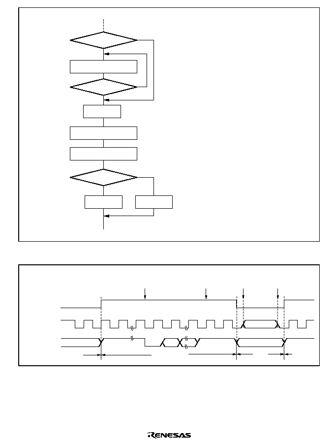
Rev. 2.0, 09/02 page 363 of 658
Read TEND flag in SSR
TE = 0
Transition to software
standby mode, etc.
Exit from software
standby mode, etc.
Change
operating mode?
No
All data
transmitted?
TEND = 1
Yes
Yes
Yes
<Transmission>
No
No
[1]
[3]
[2]
TE = 1
Initialization
<Start of transmission>
[1]
Data being transmitted is interrupted.
After exiting software standby mode,
etc., normal CPU transmission is
possible by setting TE to 1, reading
SSR, writing TDR, and clearing
TDRE to 0, but note that if the DTC
has been activated, the remaining
data in DTCRAM will be transmitted
when TE and TIE are set to 1.
(H8S/2268 Series only)
[2]
If TIE and TEIE are set to 1, clear
them to 0 in the same way.
[3]
Includes module stop mode, watch
mode, subactive mode, and subsleep
mode.
Figure 13.37 Sample Flowchart for Mode Transition during Transmission
SCK output pin
TE bit
TxD output pin
Port input/output
High output
Port input/output
High output
Start
Stop
Start of transmission
End of
transmission
Port input/output
SCI TxD output
Port
SCI TxD
output
Port
Transition
to software
standby
Exit from
software
standby
Figure 13.38 Asynchronous Transmission Using Internal Clock
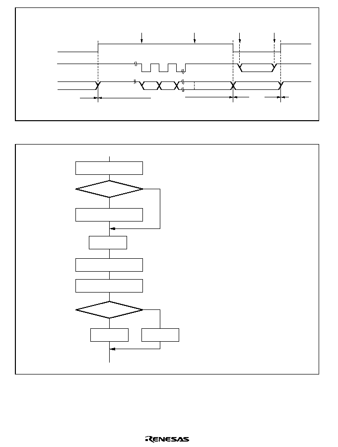
Rev. 2.0, 09/02, page 364 of 658
Port input/output
Last TxD bit held
High output
*
Port input/output
Marking output
Port input/output
SCI TxD output
Port
Port
Note:
*
Initialized by software standby.
SCK output pin
TE bit
TxD output pin
SCI TxD
output
Start of transmission
End of
transmission
Transition
to software
standby
Exit from
software
standby
Figure 13.39 Synchronous Transmission Using Internal Clock
RE = 0
Transition to software
standby mode, etc.
Read receive data in RDR
Read RDRF flag in SSR
Exit from software
standby mode, etc.
Change
operating mode?
No
RDRF = 1
Yes
Yes
<Reception>
No
[1]
[2]
RE = 1
Initialization
<Start of reception>
[1]
Receive data being received
becomes invalid.
[2]
Includes module stop mode,
watch mode, subactive mode,
and subsleep mode.
Figure 13.40 Sample Flowchart for Mode Transition during Reception

Rev. 2.0, 09/02 page 365 of 658
13.9.7
Switching from SCK Pin Function to Port Pin Function:
∑
Problem in Operation: When switching the SCK pin function to the output port function (high-
level output) by making the following settings while DDR = 1, DR = 1, C/
= 1, CKE1 = 0,
CKE0 = 0, and TE = 1 (synchronous mode), low-level output occurs for one half-cycle.
1. End of serial data transmission
2. TE bit = 0
3. C/
bit = 0 ... switchover to port output
4. Occurrence of low-level output (see figure 13.41)
SCK/port
Data
TE
C/A
CKE1
CKE0
Bit 7
Bit 6
1. End of transmission
4. Low-level output
3. C/ = 0
2. TE = 0
Half-cycle low-level output
Figure 13.41 Operation when Switching from SCK Pin Function to Port Pin Function
∑
Sample Procedure for Avoiding Low-Level Output: As this sample procedure temporarily
places the SCK pin in the input state, the SCK/port pin should be pulled up beforehand with an
external circuit.
With DDR = 1, DR = 1, C/
= 1, CKE1 = 0, CKE0 = 0, and TE = 1, make the following
settings in the order shown.
1. End of serial data transmission
2. TE bit = 0
3. CKE1 bit = 1
4. C/
bit = 0 ... switchover to port output
5. CKE1 bit = 0

Rev. 2.0, 09/02, page 366 of 658
SCK/port
Data
TE
C/A
CKE1
CKE0
Bit 7
Bit 6
1. End of transmission
3. CKE1 = 1
5. CKE1 = 0
4. C/ = 0
2. TE = 0
High-level output
Figure 13.42 Operation when Switching from SCK Pin Function to Port Pin Function
(Example of Preventing Low-Level Output)
13.9.8
Assignment and Selection of Registers
Some serial communication interface registers are assigned to the same address as other registers.
Register selection is performed by means of the IICE bit in the serial control register (SCRX). For
details on register addresses, see section 25, List of Registers.

Rev. 2.0, 09/02, page 367 of 658
Section 14 I
2
C Bus Interface (IIC) (Option)
An I
2
C bus interface is available as an option. Observe the following notes when using this option.
1. For mask-ROM versions, a W is added to the part number in products in which this optional
function is used.
Examples: HD6432268WTE
2. The product number is identical for F-ZTAT versions. However, be sure to inform your
Hitachi sales representative if you will be using this option.
The H8S/2268 Series has an internal I
2
C bus interface of two channels, while the H8S/2264
Series has that of one channel.
The I
2
C bus interface conforms to and provides a subset of the Philips I
2
C bus (inter-IC bus)
interface functions. The register configuration that controls the I
2
C bus differs partly from the
Philips configuration, however.
The I
2
C bus interface data transfer is performed using a data line (SDA) and a clock line (SCL) for
each channel, which allows efficient use of connectors and the area of the PCB.
14.1
Features
∑
Selection of I
2
C format or clocked synchronous serial format
I
2
C bus format: addressing format with acknowledge bit, for master/slave operation
Clocked synchronous serial format: non-addressing format without acknowledge bit, for
master operation only
I
2
C bus format
∑
Two ways of setting slave address
∑
Start and stop conditions generated automatically in master mode
∑
Selection of acknowledge output levels when receiving
∑
Automatic loading of acknowledge bit when transmitting
∑
Wait function in master mode
A wait can be inserted by driving the SCL pin low after data transfer, excluding
acknowledgement. The wait can be cleared by clearing the interrupt flag.
∑
Wait function in slave mode
A wait request can be generated by driving the SCL pin low after data transfer, excluding
acknowledgement. The wait request is cleared when the next transfer becomes possible.
IICIC05B_000020020700

Rev. 2.0, 09/02, page 368 of 658
∑
Three interrupt sources
Data transfer end (including transmission mode transition with I2C bus format and address
reception after loss of master arbitration)
Address match: when any slave address matches or the general call address is received in
slave receive mode
Stop condition detection
∑
Selection of 16 internal clocks (in master mode)
∑
Direct bus drive
Two pins, P35/SCL0 and P34/SDA0, function as NMOS open-drain outputs when the bus
drive function is selected.
Two pins ≠ P33/SCL1 and P32/SDA1 ≠ function as NMOS-only outputs when the bus
drive function is selected. (H8S/2268 Series only)
Figure 14.1 shows a block diagram of the I
2
C bus interface. Figure 14.2 shows an example of I/O
pin connections to external circuits. Channel I/O pins are NMOS open drains, and it is possible to
apply voltages in excess of the power supply (Vcc) voltage for this LSI. Set the upper limit of
voltage applied to the power supply (Vcc) power supply range +0.3V, i.e.5.8.V. Channel 1
(H8S/2268 Series only) I/O pins are driven solely by NMOS, so in terms of appearance they carry
out the same operations as an NMOS open drain. However, the voltage which can be applied to
the I/O pins depends on the voltage of the power supply (Vcc) of this LSI.
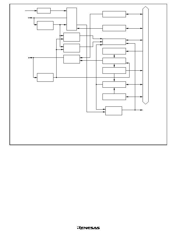
Rev. 2.0, 09/02, page 369 of 658
PS
Noise
canceler
Noise
canceler
Clock
control
Bus state
decision
circuit
Arbitration
decision
circuit
Output data
control
circuit
Address
comparator
SAR, SARX
Interrupt
generator
ICDRS
ICDRR
ICDRT
ICSR
ICMR
ICCR
Internal data bus
Interrupt
request
SCL
SDA
Legend:
ICCR:
ICMR:
ICSR:
ICDR:
SAR:
SARX:
PS:
I
2
C bus control register
I
2
C bus mode register
I
2
C bus status register
I
2
C bus data register
Slave address register
Slave address register X
Prescaler
Figure 14.1 Block Diagram of I
2
C Bus Interface

Rev. 2.0, 09/02, page 370 of 658
SCL
in
out
SDA
in
out
(Slave 1)
SCL
SDA
SCL
in
out
SDA
in
out
(Slave 2)
SCL
SDA
SCL
in
out
SDA
in
out
(Master)
This LSI
SCL
SDA
V
DD
V
CC
SCL
SDA
Figure 14.2 I
2
C Bus Interface Connections (Example: This LSI as Master)
14.2
Input/Output Pins
Table 14.1 shows the pin configuration for the I
2
C bus interface.
Table 14.1
Pin Configuration
Name
Abbreviation
*
1
I/O
Function
Serial clock
SCL0
I/O
IIC_0 serial clock input/output
Serial data
SDA0
I/O
IIC_0 serial data input/output
Serial clock
*
2
SCL1
I/O
IIC_1 serial clock input/output
Serial data
*
2
SDA1
I/O
IIC_1 serial data input/output
Notes: 1. In the text, the channel subscript is omitted, and only SCL and SDA are used.
2. Supported only by the H8S/2268 Series.
14.3
Register Descriptions
The I
2
C bus interface has the following registers. Registers ICDR and SARX and registers ICMR
and SAR are allocated to the same addresses. Accessible addresses differ depending on the ICE bit
in ICCR. SAR and SARX are accessed when ICE is 0, and ICMR and ICDR are accessed when
ICE is 1. For details on the module stop control register, refer to section 22.1.2, Module Stop
Control Registers A to D (MSTPCRA to MSTPCRD).

Rev. 2.0, 09/02, page 371 of 658
∑
I
2
C bus data register_0 (ICDR_0)
∑
Slave address register_0 (SAR_0)
∑
Second slave address register_0 (SARX_0)
∑
I
2
C bus mode register_0 (ICMR_0)
∑
I
2
C bus control register_0 (ICCR_0)
∑
I
2
C bus status register_0 (ICSR_0)
∑
I
2
C bus data register_1 (ICDR_1)*
∑
Slave address register_1 (SAR_1)*
∑
Second slave address register_1 (SARX_1)*
∑
I
2
C bus mode register_1 (ICMR_1)*
∑
I
2
C bus control register_1 (ICCR_1)*
∑
I
2
C bus status register_1 (ICSR_1)*
∑
DDC switch register (DDCSWR)
∑
Serial control register (SCRX)
Note: *
Supported only by the H8S/2268 Series.
14.3.1
I
2
C Bus Data Register (ICDR)
ICDR is an 8-bit readable/writable register that is used as a transmit data register when
transmitting and a receive data register when receiving. ICDR is divided internally into a shift
register (ICDRS), receive buffer (ICDRR), and transmit buffer (ICDRT). Data transfers among the
three registers are performed automatically in coordination with changes in the bus state, and
affect the status of internal flags such as TDRE and RDRF. When TDRE is 1 and the transmit
buffer is empty, TDRE shows that the next transmit data can be written from the CPU. When
RDRF is 1, it shows that the valid receive data is stored in the receive buffer.
If I
2
C is in transmit mode and the next data is in ICDRT (the TDRE flag is 0) following
transmission/reception of one frame of data using ICDRS, data is transferred automatically from
ICDRT to ICDRS. If I
2
C is in receive mode and no previous data remains in ICDRR (the RDRF
flag is 0) following transmission/reception of one frame of data using ICDRS, data is transferred
automatically from ICDRS to ICDRR.
If the number of bits in a frame, excluding the acknowledge bit, is less than 8, transmit data and
receive data are stored differently. Transmit data should be written justified toward the MSB side
when MLS = 0, and toward the LSB side when MLS = 1. Receive data bits read from the LSB
side should be treated as valid when MLS = 0, and bits read from the MSB side when MLS = 1.
ICDR can be written and read only when the ICE bit is set to 1 in ICCR. The value of ICDR is
undefined after a reset.

Rev. 2.0, 09/02, page 372 of 658
The TDRE and RDRF flags are set and cleared under the conditions shown below. Setting the
TDRE and RDRF flags affects the status of the interrupt flags.
Bit
Bit Name
Initial
Value
R/W
Description
TDRE
Transmit Data Register Empty
[Setting conditions]
∑
In transmit mode, when a start condition is detected in
the bus line state after a start condition is issued in
master mode with the I
2
C bus format or serial format
selected
∑
When data is transferred from ICDRT to ICDRS
∑
When a switch is made from receive mode to transmit
mode after detection of a start condition
[Clearing conditions]
∑
When transmit data is written in ICDR in transmit mode
∑
When a stop condition is detected in the bus line state
after a stop condition is issued with the I
2
C bus format
or serial format selected
∑
When a stop condition is detected with the I
2
C bus
format selected
∑
In receive mode
RDRF
Receive Data Register Full
[Setting condition]
When data is transferred from ICDRS to ICDRR
[Clearing condition]
When ICDR (ICDRR) receive data is read in receive mode

Rev. 2.0, 09/02, page 373 of 658
14.3.2
Slave Address Register (SAR)
SAR selects the slave address and selects the transfer format. SAR can be written and read only
when the ICE bit is cleared to 0 in ICCR.
Bit
Bit Name
Initial
Value
R/W
Description
7
6
5
4
3
2
1
SVA6
SVA5
SVA4
SVA3
SVA2
SVA1
SVA0
0
0
0
0
0
0
0
R/W
R/W
R/W
R/W
R/W
R/W
R/W
Slave Address 6 to 0
Sets a slave address
0
FS
0
R/W
Selects the transfer format together with the FSX bit in
SARX. Refer to table 14.2.
14.3.3
Second Slave Address Register (SARX)
SARX stores the second slave address and selects the transfer format. SARX can be written and
read only when the ICE bit is cleared to 0 in ICCR.
Bit
Bit Name
Initial
Value
R/W
Description
7
6
5
4
3
2
1
SVAX6
SVAX5
SVAX4
SVAX3
SVAX2
SVAX1
SVAX0
0
0
0
0
0
0
0
R/W
R/W
R/W
R/W
R/W
R/W
R/W
Slave Address 6 to 0
Sets the second slave address
0
FSX
1
R/W
Selects the transfer format together with the FS bit in SAR.
Refer to table 14.2.

Rev. 2.0, 09/02, page 374 of 658
Table 14.2
Transfer Format
SAR
SARX
FS
FSX
I
2
C Transfer Format
0
0
SAR and SARX are used as the slave addresses with
the I
2
C bus format.
0
1
Only SAR is used as the slave address with the I
2
C bus
format.
1
0
Only SARX is used as the slave address with the I
2
C
bus format.
1
1
Clock synchronous serial format (SAR and SARX are
invalid)
14.3.4
I
2
C Bus Mode Register (ICMR)
ICMR sets the transfer format and transfer rate. It can only be accessed when the ICE bit in ICCR
is 1.
Bit
Bit Name
Initial
Value
R/W
Description
7
MLS
0
R/W
MSB-First/LSB-First Select
0: MSB-first
1: LSB-first
Set this bit to 0 when the I
2
C bus format is used.
6
WAIT
0
R/W
Wait Insertion Bit
This bit is valid only in master mode with the I
2
C bus
format.
When WAIT is set to 1, after the fall of the clock for the final
data bit, the IRIC flag is set to 1 in ICCR, and a wait state
begins (with SCL at the low level). When the IRIC flag is
cleared to 0 in ICCR, the wait ends and the acknowledge
bit is transferred.
If WAIT is cleared to 0, data and acknowledge bits are
transferred consecutively with no wait inserted.
The IRIC flag in ICCR is set to 1 on completion of the
acknowledge bit transfer, regardless of the WAIT setting.
5
4
3
CKS2
CKS1
CKS0
0
0
0
R/W
R/W
R/W
Serial Clock Select 2 to 0
This bit is valid only in master mode.
These bits select the required transfer rate, together with
the IICX 1 and IICX0 bit in SCRX. Refer table 14.3.

Rev. 2.0, 09/02, page 375 of 658
Bit
Bit Name
Initial
Value
R/W
Description
2
1
0
BC2
BC1
BC0
0
0
0
R/W
R/W
R/W
Bit Counter 2 to 0
These bits specify the number of bits to be transferred next.
With the I
2
C bus format, the data is transferred with one
addition acknowledge bit. Bit BC2 to BC0 settings should
be made during an interval between transfer frames. If bits
BC2 to BC0 are set to a value other than 000, the setting
should be made while the SCL line is low. The value
returns to 000 at the end of a data transfer, including the
acknowledge bit.
I
2
C Bus Format Clocked Synchronous Mode
000: 9 bit 000: 8 bit
001: 2 bit 001: 1 bit
010: 3 bit 010: 2 bit
011: 4 bit 011: 3 bit
100: 5 bit 100: 4 bit
101: 6 bit 101: 5 bit
110: 7 bit 110: 6 bit
111: 8 bit 111: 7 bit

Rev. 2.0, 09/02, page 376 of 658
Table 14.3
I
2
C Transfer Rate
SCRX
ICMR
Bit 5 or 6 Bit 5
Bit 4
Bit 3
Transfer Rate
IICX
CKS2 CKS1 CKS0 Clock
=
5 MHz
=
8 MHz
=
10 MHz
=
16 MHz
=
20 MHz
0
0
0
0
/28
179MHz 286kHz
357kHz
571kHz
*
714kHz
*
0
0
0
1
/40
125kHz
200kHz
250kHz
400kHz
500kHz
*
0
0
1
0
/48
104kHz
167kHz
208kHz
333kHz
417kHz
0
0
1
1
/64
78.1kHz
125kHz
156kHz
250kHz
313kHz
0
1
0
0
/80
62.5kHz
100kHz
125kHz
200kHz
250kHz
0
1
0
1
/100
50.0kHz
80.0kHz
100kHz
160kHz
200kHz
0
1
1
0
/112
44.6kHz
71.4kHz
89.3kHz
143kHz
179kHz
0
1
1
1
/128
39.1kHz
62.5kHz
78.1kHz
125kHz
156kHz
1
0
0
0
/56
89.3kHz
143kHz
179kHz
286kHz
357kHz
1
0
0
1
/80
62.5kHz
100kHz
125kHz
200kHz
250kHz
1
0
1
0
/96
52.1kHz
83.3kHz
104kHz
167kHz
208kHz
1
0
1
1
/128
39.1kHz
62.5kHz
78.1kHz
125kHz
156kHz
1
1
0
0
/160
31.3kHz
50.0kHz
62.5kHz
100kHz
125kHz
1
1
0
1
/200
25.0kHz
40.0kHz
50.0kHz
80.0kHz
100kHz
1
1
1
0
/224
22.3kHz
35.7kHz
44.6kHz
71.4kHz
89.3kHz
1
1
1
1
/256
19.5kHz
31.3kHz
39.1kHz
62.5kHz
78.1kHz
Note:
*
Out of the range of the I2C bus interface specification (normal mode: 100kHz in max.
and high-speed mode: 400kHz in max)

Rev. 2.0, 09/02, page 377 of 658
14.3.5
Serial Control Register (SCRX)
SCRX controls the IIC operating modes.
Bit
Bit Name
Initial
Value
R/W
Description
7
0
R/W
Reserved
The initial value should not be changed.
6
5
IICX1
*
IICX0
0
0
R/W
R/W
I
2
C Transfer Rate Select 1 and 0
Selects the transfer rate in master mode, together with bits
CKS2 to CKS0 in ICMR. Refer to table 14.3.
Note:
*
In the H8S/2264 Series, this bit is reserved.
4
IICE
0
R/W
I
2
C Master Enable
Controls CPU access to the IIC data register and control
registers (ICCR, ICSR, ICDR/SARX, and ICMR/SAR).
0: CPU access to the IIC data register and control registers
is disabled.
1: CPU access to the IIC data register and control registers
is enabled.
3
FLSHE
0
R/W
For details on this bit, refer to section 20.5.7, Serial Control
Register X (SCRX).
2 to 0
All 0
R/W
Reserved
The initial value should not be changed.

Rev. 2.0, 09/02, page 378 of 658
14.3.6
I
2
C Bus Control Register (ICCR)
I
2
C bus control register (ICCR) consists of the control bits and interrupt request flags of I
2
C bus
interface.
Bit
Bit Name
Initial
Value
R/W
Description
7
ICE
0
R/W
I
2
C Bus Interface Enable
When this bit is set to 1, the I
2
C bus interface module is
enabled to send/receive data and drive the bus since it is
connected to the SCL and SDA pins. ICMR and ICDR can
be accessed.
When this bit is cleared, the module is halted and
separated from the SCL and SDA pins. SAR and SARX
can be accessed.
6
IEIC
0
R/W
I
2
C Bus Interface Interrupt Enable
When this bit is 1, interrupts are enabled by IRIC.
5
4
MST
TRS
0
0
R/W
Master/Slave Select
Transmit/Receive Select
00: Slave receive mode
01: Slave transmit mode
10: Master receive mode
11: Master transmit mode
Both these bits will be cleared by hardware when they lose
in a bus contention in master mode of the I
2
C bus format. In
slave receive mode, the R/
:
bit in the first frame
immediately after the start automatically sets these bits in
receive mode or transmit mode by using hardware. The
settings can be made again for the bits that were
set/cleared by hardware, by reading these bits. When the
TRS bit is intended to change during a transfer, the bit will
not be switched until the frame transfer is completed,
including acknowledgement.

Rev. 2.0, 09/02, page 379 of 658
Bit
Bit Name
Initial
Value
R/W
Description
3
ACKE
0
R/W
Acknowledge Bit Judgement Selection
0: The value of the acknowledge bit is ignored, and
continuous transfer is performed. The value of the
received acknowledge bit is not indicated by the ACKB
bit, which is always 0.
1: If the acknowledge bit is 1, continuous transfer is
interrupted.
In the H8S/2268 Series, the DTC
*
can be used to perform
continuous transfer. The DTC
*
is activated when the IRTR
interrupt flag is set to 1 (IRTR us one of two interrupt flags,
the other being IRIC). When the ACKE bit is 0, the TDRE,
IRIC, and IRTR flags are set on completion of data
transmission, regardless of the acknowledge bit. When the
ACKE bit is 1, the TDRE, IRIC, and IRTR flags are set on
completion of data transmission when the acknowledge bit
is 0, and the IRIC flag alone is set on completion of data
transmission when the acknowledge bit is 1.
When the DTC
*
is activated, the TDRE, IRIC, and IRTR
flags are cleared to 0 after the specified number of data
transfers have been executed. Consequently, interrupts are
not generated during continuos data transfer, but if data
transmission is completed with a 1 acknowledge bit when
the ACKE bit is set to 1, the DTC
*
is not activated and an
interrupt is generated, if enabled.
Depending on the receiving device, the acknowledge bit
may be significant, in indicating completion of processing of
the received data, for instance, or may be fixed at 1 and
have no significance.
Note:
*
Supported only by the H8S/2268 Series.
2
BBSY
0
R/W
Bus Busy
In slave mode, reading the BBSY flag enables to confirm
whether the I
2
C bus is occupied or released. The BBSY flag
is set to 0 when the SDA level changes from high to low
under the condition of SCl = high, assuming that the start
condition has been issued. The BBSY flag is cleared to 0
when the SDA level changes from low to high under the
condition of SCl = high, assuming that the start condition
has been issued. Writing to the BBSY flag in slave mode is
disabled.
In master mode, the BBSY flag is used to issue start and
stop conditions. Write 1 to BBSY and 0 to SCP to issue a
start condition. Follow this procedure when also re-
transmitting a start condition. To issue a start/stop
condition, use the MOV instruction. The I
2
C bus interface
must be set in master transmit mode before the issue of a
start condition.

Rev. 2.0, 09/02, page 380 of 658
Bit
Bit Name
Initial
Value
R/W
Description
1
IRIC
0
R/W
I
2
C Bus Interface Interrupt Request Flag
Also see table 14.4.
[Setting conditions]
In I
2
C bus format master mode
∑
When a start condition is detected in the bus line state after a
start condition is issued (when the TDRE flag is set to 1
because of first frame transmission)
∑
When a wait is inserted between the data and acknowledge bit
when WAIT = 1
∑
At the end of data transfer (when the TDRE or RDRF flag is
set to 1)
∑
When a slave address is received after bus arbitration is lost
(when the AL flag is set to1)
∑
When 1 is received as the acknowledge bit when the ACKE bit
is 1(when the ACKB bit is set to 1)
In I
2
C bus format slave mode
∑
When the slave address (SVA, SVAX) matches (when the
AAS and AASX flags are set to 1) and at the end of data
transfer up to the subsequent retransmission start condition or
stop condition detection (when the TDRE or RDRF flag is set
to 1)
∑
When the general call address is detected (when the ADZ flag
is set to 1) and at the end of data transfer up to the
subsequent retransmission start condition or stop condition
detection(when the TDRE or RDRF flag is set to 1)
∑
When 1 is received as the acknowledge bit when the ACKE bit
is 1(when the ACKB bit is set to 1)
∑
When a stop condition is detected(when the STOP or ESTP
flag is set to 1)
With clocked synchronous serial format
∑
At the end of data transfer (when the TDRE or RDRF flag is
set to 1)
∑
When a start condition is detected with serial format selected
When a condition occurs in which internal flag of TDRE and RDFR
is set to 1 except for the above
[Clearing condition]
When 0 is written in IRIC after reading IRIC = 1
∑
When ICDR is read/written by DTC (H8S/2268 Series only)
(When TDRE or RDRF flag is cleared to 0)
(AS it might not be a condition to clear, for details, see description
of DTC operation below)

Rev. 2.0, 09/02, page 381 of 658
Bit
Bit Name
Initial
Value
R/W
Description
0
SCP
1
R/W
Start Condition/Stop Condition Prohibit bit
The SCP bit controls the issue of start/stop conditions in
master mode.
To issue a start condition, write 1 in BBSY and 0 in SCP. A
retransmit start condition is issued in the same way. To
issue a stop condition, write 0 in BBSY and 0 in SCP. This
bit is always read as 1. If 1 is written, the data is not stored.
When, with the I
2
C bus format selected, IRIC is set to 1 and an interrupt is generated, other flags
must be checked in order to identify the source that set IRIC to 1. Although each source has a
corresponding flag, caution is needed at the end of a transfer.
When the TDRE or RDRF internal flag is set, the readable IRTR flag may or may not be set. In
the H8S/2268 Series, even when data transfer is complete, the DTC activation request flag, IRTR,
is not set until a retransmission start condition or stop condition is detected after a slave address
(SVA) or general call address matched in the I
2
C bus format slave mode.
Even when the IRIC flag and IRTR flag are set, the TDRE or RDRF internal flag may not be set.
For a continuous transfer using the DTC in the H8S/2268 Series, the IRIC or IRTR flag is not
cleared at the completion of the specified number of times of transfers. On the other hand, the
TDRE and RDRF flags are cleared because the specified number of times of read/write operations
have been complete.
Table 14.4 shows the relationship between the flags and the transfer states.

Rev. 2.0, 09/02, page 382 of 658
Table 14.4
Flags and Transfer States
MST TRS BBSY ESTP STOP IRTR
AASX AL
AAS ADZ ACKB
State
1/0
1/0
0
0
0
0
0
0
0
0
0
Idle state (flag clearing required)
1
1
0
0
0
0
0
0
0
0
0
Start condition issuance
1
1
1
0
0
1
0
0
0
0
0
Start condition established
1
1/0
1
0
0
0
0
0
0
0
0/1
Master mode wait
1
1/0
1
0
0
1
0
0
0
0
0/1
Master mode transmit/receive end
0
0
1
0
0
0
1/0
1
1/0
1/0
0
Arbitration lost
0
0
1
0
0
0
0
0
1
0
0
SAR match by first frame in slave mode
0
0
1
0
0
0
0
0
1
1
0
General call address match
0
0
1
0
0
0
1
0
0
0
0
SARX match
0
1/0
1
0
0
0
0
0
0
0
0/1
Slave mode transmit/receive end(except
after SARX match)
0
0
1/0
1
1
1
0
0
0
0
1
0
1
1
0
0
0
0
0
0
0
1
Slave mode transmit/receive end(after SARX
match)
0
1/0
0
1/0
1/0
0
0
0
0
0
0/1
Stop condition detected
14.3.7
I
2
C Bus Status Register (ICSR)
ICSR consists of status flags.
Bit
Bit Name
Initial
Value
R/W
Description
7
ESTP
0
R/(W)
*
Error Stop Condition Detection Flag
This bit is valid in I
2
C bus format slave mode.
[Setting condition]
When a stop condition is detected during frame transfer.
[Clearing condition]
∑
When 0 is written in ESTP after reading the state of 1
∑
When the IRIC flag is cleared to 0
6
STOP
0
R/(W)
*
Normal Stop Condition Detection Flag
This bit is valid in I
2
C bus format slave mode.
[Setting condition]
When a stop condition is detected during frame transfer.
[Clearing condition]
∑
When 0 is written in STOP after reading STOP = 1
∑
When the IRIC flag is cleared to 0

Rev. 2.0, 09/02, page 383 of 658
Bit
Bit Name
Initial
Value
R/W
Description
5
IRTR
0
R/(W)
*
I
2
C Bus Interface Continuous Transmission/Reception
Interrupt Request Flag
[Setting conditions]
In I
2
C bus interface slave mode
∑
When the TDRE or RDRF flag is set to 1 when AASX =
1
In I
2
C bus interface other modes
∑
When the TDRE or RDRF flag is set to 1
[Clearing conditions]
∑
When 0 is written in IRTR after reading IRTR = 1
∑
When the IRIC flag is cleared to 0
4
AASX
0
R/(W)
*
Second Slave Address Recognition Flag
[Setting condition]
When the second slave address is detected in slave
receive mode and FSX = 0
[Clearing conditions]
∑
When 0 is written in AASX after reading AASX = 1
∑
When a start condition is detected
∑
In master mode
3
AL
0
R/(W)
*
Arbitration Lost Flag
Indicates that bus arbitration was lost in master mode.
[Setting condition]
∑
When the internal SDA and SDA pin do not match at
the rise of SCL.
∑
When the internal SCL is high at the fall of SCL.
[Clearing conditions]
∑
When 0 is written in AL after reading AL = 1
∑
When ICDR data is written (transmit mode) or read
(receive mode)

Rev. 2.0, 09/02, page 384 of 658
Bit
Bit Name
Initial
Value
R/W
Description
2
AAS
0
R/(W)
*
Slave Address Recognition Flag
[Setting condition]
When the slave address or general call address is detected
in slave receive mode and FS = 0.
[Clearing conditions]
∑
When ICDR data is written (transmit mode) or read
(receive mode)
∑
When 0 is written in AAS after reading AAS = 1
∑
In master mode
1
ADZ
0
R/(W)
*
General Call Address Recognition Flag
This bit is valid in I
2
C bus format slave receive mode.
[Setting condition]
When the general call address is detected in slave receive
mode and FSX = 0 or FS = 0.
[Clearing conditions]
∑
When ICDR data is written (transmit mode) or read
(receive mode)
∑
When 0 is written in ADZ after reading ADZ = 1
∑
In master mode
0
ACKB
0
R/(W)
*
Acknowledge Bit
Stores acknowledge bit.
0: At reception, outputs 0 in the acknowledge output timing.
At transmission, indicates that acknowledge was sent (0)
from the receive device.
1: At reception, outputs 1 in the acknowledge output timing.
At transmission, indicates that acknowledge was not
sent (1) from the receive device.
Note: Only a 0 can be written to this bit, to clear the flag.

Rev. 2.0, 09/02, page 385 of 658
14.3.8
DDC Switch Register (DDCSWR)
DDCSWR controls the I
2
C bus interface format automatic switching function and internal latch
clear.
Bit
Bit Name
Initial
Value
R/W
Description
7 to 4
All 0
R/(W)
*
1
Reserved
The write value should always be 0.
3
2
1
0
CLR3
CLR2
CLR1
CLR0
1
1
1
1
W
W
W
W
I
2
C Bus Interface Clear 3 to 0:
When bits CLR3 to CLR0 are set, a clear signal is
generated for the I
2
C bus interface internal latch circuit, and
the internal state is initialized. The write data for these bits
is not retained. To perform I
2
C clearance, bits CLR3 to
CLR0 must be written to simultaneously using an MOV
instruction. Do not use a bit manipulation instruction such
as BCLR.
00XX: Setting prohibited
0100: Setting prohibited
0101: IIC_0 Internal latch cleared
0110: IIC_1
*
2
Internal Iatch cleared
0111: IIC_0, IIC_1
*
2
Internal Iatch cleared
1XXX: Invalid setting
Legend
X: Don't care
Notes: 1. Only 0 can be written to these bits, to clear the flag.
2. Supported only by the H8S/2268 Series.
14.4
Operation
The I
2
C bus interface has serial and I
2
C bus formats.
14.4.1
I
2
C Bus Data Format
The I
2
C bus formats are addressing formats and an acknowledge bit is inserted. The first frame
following a start condition always consists of 8 bits. The I
2
C bus format is shown in figure 14.3.
The serial format is a non-addressing format with no acknowledge bit. This is shown in figure
14.4. Figure 14.5 shows the I
2
C bus timing.
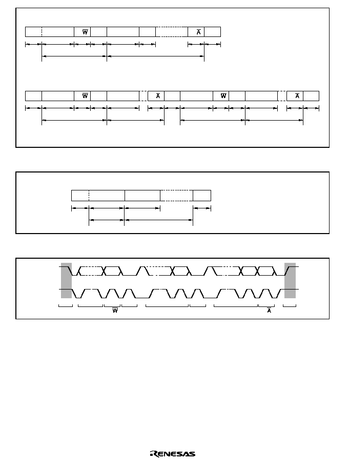
Rev. 2.0, 09/02, page 386 of 658
S
SLA
R/
A
DATA
A
A/
P
1
1
1
1
n
7
1
m
(a) I
2
C bus format (FS = 0 or FSX = 0)
(b) I
2
C bus format (start condition retransmission, FS = 0 or FSX = 0)
n: transfer bit count
(n = 1 to 8)
m: transfer frame count
(m
1)
S
SLA
R/
A
DATA
1
1
1
n1
7
1
m1
S
SLA
R/
A
DATA
A/
P
1
1
1
n2
7
1
m2
1
1
1
A/
n1 and n2: transfer bit count (n1 and n2 = 1 to 8)
m1 and m2: transfer frame count (m1 and m2
1)
1
1
Figure 14.3 I
2
C Bus Data Formats (I
2
C Bus Formats)
S
DATA
DATA
P
1
1
n
8
1
m
FS = 1 and FSX = 1
n: transfer bit count
(n = 1 to 8)
m: transfer frame count
(m
1)
Figure 14.4 I
2
C Bus Data Format (Serial Format)
SDA
SCL
S
1-7
SLA
8
R/
9
A
1-7
DATA
8
9
1-7
8
9
A
DATA
P
A/
Figure 14.5 I
2
C Bus Timing
Legend
S:
Start condition. The master device drives SDA from high to low while SCL is high
SLA: Slave
address
R/
:: Indicates the direction of data transfer: from the slave device to the master device when
R/
: is 1, or from the master device to the slave device when R/: is 0
A:
Acknowledge. The receiving device drives SDA
DATA:Transferred data
P:
Stop condition. The master device drives SDA from low to high while SCL is high

Rev. 2.0, 09/02, page 387 of 658
14.4.2
Master Transmit Operation
In I
2
C bus format master transmit mode, the master device outputs the transmit clock and transmit
data, and the slave device returns an acknowledge signal. The transmission procedure and
operations synchronized with the ICDR writing are described below.
1.
Set the ICE bit in ICCR to 1. Set bits MLS, WAIT, and CKS2 to CKS0 in ICMR, and bit
IICX in SCRX, according to the operating mode.
2.
Read the BBSY flag in ICCR to confirm that the bus is free.
3.
Set bits MST and TRS to 1 in ICCR to select master transmit mode.
4.
Write 1 to BBSY and 0 to SCP. This changes SDA from high to low when SCL is high, and
generates the start condition.
5.
Then IRIC and IRTR flags are set to 1. If the IEIC bit in ICCR has been set to 1, an interrupt
request is sent to the CPU.
6.
Write the data (slave address + R/
:) to ICDR. With the I
2
C bus format (when the FS bit in
SAR or the FSX bit in SARX is 0), the first frame data following the start condition indicates
the 7-bit slave address and transmit/receive direction. As indicating the end of the transfer,
and so the IRIC flag is cleared to 0. After writing ICDR, clear IRIC continuously not to
execute other interrupt handling routine. If one frame of data has been transmitted before the
IRIC clearing, it can not be determine the end of transmission. The master device sequentially
sends the transmission clock and the data written to ICDR using the timing shown in figure
14.6. The selected slave device (i.e. the slave device with the matching slave address) drives
SDA low at the 9th transmit clock pulse and returns an acknowledge signal.
7.
When one frame of data has been transmitted, the IRIC flag is set to 1 at the rise of the 9th
transmit clock pulse. After one frame has been transmitted SCL is automatically fixed low in
synchronization with the internal clock until the next transmit data is written.
8.
Read the ACKB bit in ICSR to confirm that ACKB is cleared to 0. When the slave device has
not acknowledged (ACKB bit is 1), operate the step [12] to end transmission, and retry the
transmit operation.
9.
Write the transmit data to ICDR. As indicating the end of the transfer, and so the IRIC flag is
cleared to 0. Perform the ICDR write and the IRIC flag clearing sequentially, just as in point 6
in this flowchart. Transmission of the next frame is performed in synchronization with the
internal clock.
10.
When one frame of data has been transmitted, the IRIC flag is set to 1 at the rise of the 9th
transmit clock pulse. After one frame has been transmitted SCL is automatically fixed low in
synchronization with the internal clock until the next transmit data is written.
11.
Read the ACKB bit in ICSR. Confirm that the slave device has been acknowledged (ACKB
bit is 0). When there is data to be transmitted, go to the step [9] to continue next transmission.
When the slave device has not acknowledged (ACKB bit is set to 1), operate the step [12] to
end transmission.
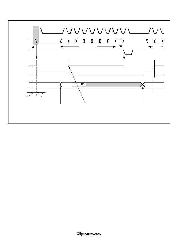
Rev. 2.0, 09/02, page 388 of 658
12.
Clear the IRIC flag to 0. And write 0 to BBSY and SCP in ICCR. This changes SDA from
low to high when SCL is high, and generates the stop condition.
SDA
(master output)
SDA
(slave output)
2
1
2
1
4
3
6
5
8
7
9
Bit 7
Slave address
Bit 6
Bit 7
Bit 6
Bit 5
Bit 4
Bit 3
Bit 2
Bit 1
Bit 0
IRIC
IRTR
ICDR
SCL
(master output)
Start condition generation
Data 1
Address + R/
[4] Write BBSY = 1
and SCP = 0
(start condition
issuance)
[9] IRIC clearance
[9] ICDR write
[6] IRIC clearance
User processing
Slave address
Data 1
R/
[7]
[5]
A
[6] ICDR write
Normal
operation
ICDR writing
prohibited
Note:
*
Data write timing in ICDR
*
Figure 14.6 Master Transmit Mode Operation Timing Example (MLS = WAIT = 0)
14.4.3
Master Receive Operation
In master receive mode, the master device outputs the receive clock, receives data, and returns an
acknowledge signal. The slave device transmits data. The reception procedure and operations with
the wait function synchronized with the ICDR read operation to receive data in sequence are
shown below.
1. Clear the TRS bit in ICCR to 0 to switch from transmit mode to receive mode, and set the
WAIT bit in ICMR to 1. Also clear the bit in ICSR to ACKB 0 (acknowledge data setting).
2. When ICDR is read (dummy data read), reception is started, and the receive clock is output,
and data received, in synchronization with the internal clock. In order to detect wait operation,
set the IRIC flag in ICCR must be cleared to 0. After reading ICDR, clear IRIC continuously
not to execute other interrupt handling routine. If one frame of data has been received before
the IRIC clearing, it cannot be determine the end of reception.

Rev. 2.0, 09/02, page 389 of 658
3. The IRIC flag is set to 1 at the fall of the 8th receive clock pulse. If the IEIC bit in ICCR has
been set to 1, an interrupt request is sent to the CPU. SCL is automatically fixed low in
synchronization with the internal clock until the IRIC flag clearing. If the first frame is the last
receive data, execute step [10] to halt reception.
4. Clear the IRIC flag to release from the Wait State. The master device outputs the 9th clock and
drives SDA at the 9th receive clock pulse to return an acknowledge signal.
5. When one frame of data has been received, the IRIC flag in ICCR and the IRTR flag in ICSR
are set to 1 at the rise of the 9th receive clock pulse. The master device outputs SCL clock to
receive next data.
6. Read ICDR.
7. Clear the IRIC flag to detect next wait operation. Data reception process from [5] to [7] should
be executed during one byte reception period after IRIC flag clearing in [4] or [9] to release
wait status.
8. The IRIC flags set to 1 at the fall of 8th receive clock pulse. SCL is automatically fixed low in
synchronization with the internal clock until the IRIC flag clearing. If this frame is the last
receive data, execute step [10] to halt reception.
9. Clear the IRIC flag in ICCR to cancel wait operation. The master device drives SDA low at the
9th receive clock pulse and returns an acknowledge signal.
10. Data can be received continuously by repeating step [5] to [9].
11. Set the ACKB bit in ICSR to 1 so as to return "No acknowledge" data. Also set the TRS bit in
ICCR to 1 to switch from receive mode to transmit mode.
12. Clear IRIC flag to 0 to release from the Wait State.
13. When one frame of data has been received, the IRIC flag is set to 1 at the rise of the 9th
receive clock pulse.
14. Clear the WAIT bit to 0 to switch from wait mode to no wait mode. Read ICDR and clear the
IRIC flag to 0. Clearing of the IRIC flag should be after the WAIT = 0. If the WAIT bit is
cleared to 0 after clearing the IRIC flag and then an instruction to issue a stop condition is
executed, the stop condition cannot be issued because the output level of the SDA line is fixed
as low.
15. Clear the BBSY bit and SCP bit to 0. This changes SDA from low to high when SCL is high,
and generates the stop condition.

Rev. 2.0, 09/02, page 390 of 658
SDA
(master output)
SDA
(slave output)
2
1
2
1
4
3
6
5
8
7
9
Bit 7
Bit 6
Bit 7
Bit 6
Bit 5
Bit 4
Bit 3
Bit 2
Bit 1
Bit 0
IRIC
IRTR
ICDR
SCL
(master output)
Data 1
[1] TRS cleared to 0
WAIT set to 1
ACKB cleared to 0
[7] IRIC clearance
[6] ICDR read
(Data 1)
[4] IRIC clearance
[2] IRIC clearance
User processing
Bit 5
Bit 4
Bit 3
5
4
3
9
Data 1
Data 2
[3]
[5]
A
[2] ICDR read
(dummy read)
Master tansmit mode
Master receive mode
A
Figure 14.7 (1) Master Receive Mode Operation Timing Example
(MLS = ACKB = 0, WAIT = 1)
SDA
(master output)
SDA
(slave output)
2
1
2
1
4
3
6
5
8
7
9
Bit 7
Bit 6
Bit 7
Bit 6
Bit 5
Bit 4
Bit 3
Bit 2
Bit 1
Bit 0
IRIC
IRTR
ICDR
SCL
(master output)
Data 3
[9] IRIC clearance
[7] IRIC clearance
[9] IRIC clearance
[6] ICDR read
(Data 3)
[7] IRIC clearance
User processing
9
8
Data 3
Data 4
[8]
[5]
[8]
[5]
A
A
[6] ICDR read
(Data 2)
Bit 0
Data 2
Data 2
Data 1
Figure 14.7 (2) Master Receive Mode Operation Timing Example
(MLS = ACKB = 0, WAIT = 1)

Rev. 2.0, 09/02, page 391 of 658
14.4.4
Slave Receive Operation
In slave receive mode, the master device outputs the transmit clock and transmit data, and the
slave device returns an acknowledge signal. The reception procedure and operations in slave
receive mode are described below.
1. Set the ICE bit in ICCR to 1. Set the MLS bit in ICMR and the MST and TRS bits in ICCR
according to the operating mode.
2. When the start condition output by the master device is detected, the BBSY flag in ICCR is set
to 1.
3. When the slave address matches in the first frame following the start condition, the device
operates as the slave device specified by the master device. If the 8th data bit (R/
:) is 0, the
TRS bit in ICCR remains cleared to 0, and slave receive operation is performed.
4. At the 9th clock pulse of the receive frame, the slave device drives SDA low and returns an
acknowledge signal. At the same time, the IRIC flag in ICCR is set to 1. If the IEIC bit in
ICCR has been set to 1, an interrupt request is sent to the CPU. If the RDRF internal flag has
been cleared to 0, it is set to 1, and the receive operation continues. If the RDRF internal flag
has been set to 1, the slave device drives SCL low from the fall of the receive clock until data
is read into ICDR.
5. Read ICDR and clear the IRIC flag in ICCR to 0. The RDRF flag is cleared to 0.
Receive operations can be performed continuously by repeating steps [4] and [5]. When SDA is
changed from low to high when SCL is high, and the stop condition is detected, the BBSY flag in
ICCR is cleared to 0.
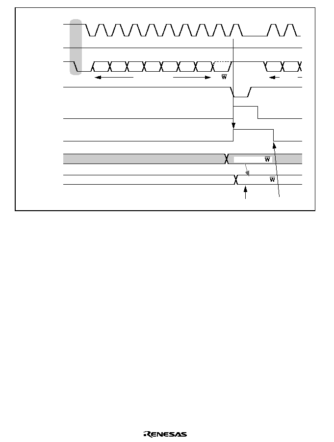
Rev. 2.0, 09/02, page 392 of 658
SDA
(master output)
SDA
(slave output)
2
1
2
1
4
3
6
5
8
7
9
Bit 7
Bit 6
Bit 7
Bit 6
Bit 5
Bit 4
Bit 3
Bit 2
Bit 1
Bit 0
IRIC
ICDRS
ICDRR
RDRF
SCL
(master output)
Start condition issuance
SCL
(slave output)
Interrupt
request
generation
Address + R/
Address + R/
[5] ICDR read
[5] IRIC clearance
User processing
Slave address
Data 1
[4]
A
R/
Figure 14.8 Example of Slave Receive Mode Operation Timing (1)
(MLS = ACKB = 0)

Rev. 2.0, 09/02, page 393 of 658
SDA
(master output)
SDA
(slave output)
2
1
4
3
6
5
8
7
9
8
7
9
Bit 7
Bit 6
Bit 5
Bit 4
Bit 3
Bit 2
Bit 1
Bit 0
Bit 1
Bit 0
IRIC
ICDRS
ICDRR
RDRF
SCL
(master output)
SCL
(slave output)
Interrupt
request
generation
Interrupt
request
generation
Data 2
Data 2
Data 1
Data 1
[5] ICDR read
[5] IRIC clearance
User processing
Data 2
Data 1
[4]
[4]
A
A
Figure 14.9 Example of Slave Receive Mode Operation Timing (2)
(MLS = ACKB = 0)
14.4.5
Slave Transmit Operation
In slave transmit mode, the slave device outputs the transmit data, while the master device outputs
the receive clock and returns an acknowledge signal. The transmission procedure and operations in
slave transmit mode are described below.
1.
Set the ICE bit in ICCR to 1. Set the MLS bit in ICMR and the MST and TRS bits in ICCR
according to the operating mode.
2. When the slave address matches in the first frame following detection of the start condition,
the slave device drives SDA low at the 9th clock pulse and returns an acknowledge signal. At
the same time, the IRIC flag in ICCR is set to 1. If the IEIC bit in ICCR has been set to 1, an
interrupt request is sent to the CPU. If the 8th data bit (R/
:) is 1, the TRS bit in ICCR is set to
1, and the mode changes to slave transmit mode automatically. The TDRE internal flag is set
to 1. The slave device drives SCL low from the fall of the transmit clock until ICDR data is
written.

Rev. 2.0, 09/02, page 394 of 658
3. After clearing the IRIC flag to 0, write data to ICDR. The TDRE internal flag is cleared to 0.
The written data is transferred to ICDRS, and the TDRE internal flag and the IRIC and IRTR
flags are set to 1 again. After clearing the IRIC flag to 0, write the next data to ICDR. The
slave device sequentially sends the data written into ICDR in accordance with the clock output
by the master device at the timing shown in figure 14.10.
4. When one frame of data has been transmitted, the IRIC flag in ICCR is set to 1 at the rise of
the 9th transmit clock pulse. If the TDRE internal flag has been set to 1, this slave device
drives SCL low from the fall of the transmit clock until data is written to ICDR. The master
device drives SDA low at the 9th clock pulse, and returns an acknowledge signal. As this
acknowledge signal is stored in the ACKB bit in ICSR, this bit can be used to determine
whether the transfer operation was performed normally. When the TDRE internal flag is 0, the
data written into ICDR is transferred to ICDRS, transmission is started, and the TDRE internal
flag and the IRIC and IRTR flags are set to 1 again.
5. To continue transmission, clear the IRIC flag to 0, then write the next data to be transmitted
into ICDR. The TDRE flag is cleared to 0.
Transmit operations can be performed continuously by repeating steps [4] and [5]. To end
transmission, write H'FF to ICDR. When SDA is changed from low to high when SCL is high, and
the stop condition is detected, the BBSY flag in ICCR is cleared to 0.

Rev. 2.0, 09/02, page 395 of 658
SDA
(slave output)
SDA
(master output)
SCL
(slave output)
2
1
2
1
4
3
6
5
8
7
9
9
8
Bit
7
Bit
6
Bit
5
Bit
7
Bit
6
Bit
4
Bit
3
Bit
2
Bit
1
Bit
0
IRIC
ICDRS
ICDRT
TDRE
SCL
(master output)
Interrupt
request
generation
Interrupt
request
generation
Interrupt
request
generation
Slave receive mode
Slave transmit mode
Data 1
Data 2
[3] IRIC
clearance
[5] IRIC
clearance
[3] ICDR
write
[3] ICDR
write
[5] ICDR
write
User processing
Data 1
Data 1
Data 2
Data 2
A
R/
A
[3]
[2]
Figure 14.10 Example of Slave Transmit Mode Operation Timing (MLS = 0)

Rev. 2.0, 09/02, page 396 of 658
14.4.6
IRIC Setting Timing and SCL Control
The interrupt request flag (IRIC) is set at different times depending on the WAIT bit in ICMR, the
FS bit in SAR, and the FSX bit in SARX. If the TDRE or RDRF internal flag is set to 1, SCL is
automatically held low after one frame has been transferred; this timing is synchronized with the
internal clock. Figure 14.11 shows the IRIC set timing and SCL control.
(a) When WAIT = 0, and FS = 0 or FSX = 0 (I
2
C bus format, no wait)
SCL
SDA
IRIC
User processing
Clear IRIC
Write to ICDR (transmit)
or read ICDR (receive)
1
A
8
1
1
A
7
1
8
9
7
(b) When WAIT = 1, and FS = 0 or FSX = 0 (I
2
C bus format, wait inserted)
SCL
SDA
IRIC
User processing
Clear
IRIC
Clear
IRIC
Write to ICDR (transmit)
or read ICDR (receive)
SCL
SDA
IRIC
User processing
(c) When FS = 1 and FSX = 1 (synchronous serial format)
Clear IRIC
Write to ICDR (transmit)
or read ICDR (receive)
8
8
9
8
7
1
8
7
1
Figure 14.11 IRIC Setting Timing and SCL Control

Rev. 2.0, 09/02, page 397 of 658
14.4.7
Operation Using the DTC (H8S/2268 Series Only)
The I
2
C bus format provides for selection of the slave device and transfer direction by means of
the slave address and the R/
: bit, confirmation of reception with acknowledge bit, indication of
the last frame, and so on. Therefore, continuous data transfer using the DTC must be carried out in
conjunction CPU processing by means of interrupts.
Table 14.5 shows some example of processing using the DTC. These examples assume that the
number of transfer data bytes is know in slave mode.
Table 14.5
Flags and Transfer States
Item
Master Transmit
Mode
Master Receive
Mode
Slave Transmit
Mode
Slave Receive
Mode
Slave address +
R/W bit
Transmission/
reception
Transmission by
DTC (ICDR rite)
Transmission by
DTC (ICDR rite)
Reception by CPU
(ICDR read)
Reception by CPU
(ICDR read)
Dummy data
read
Processing by
DTC (ICDR read)
Actual data
transmission/rec
eption
Transmission by
DTC (ICDR write)
Reception by CPU
(ICDR read)
Transmission by
DTC (ICDR write)
Reception by CPU
(ICDR read)
Dummy data
(H
FF) write
Processing by DTC
(ICDR write)
Last frame
processing
Not necessary
Reception by CPU
(ICDR read)
Not necessary
Reception by CPU
(ICDR read)
Transfer request
processing after
last frame
processing
1st time: Clearing
by CPU
2nd time: End
condition issuance
by CPU
Not necessary
Automatic clearing
on detection of end
condition during
transmission of
dummy data (H
FF)
Not necessary
Setting of
number of DTC
transfer data
frames
Transmission:
Actual data count
+ 1 (+ 1 equivalent
to slave address +
R/
:
bits)
Reception: Actual
data count
Transmission: Actual
data count + 1 (+ 1
equivalent to dummy
data (H
FF))
Reception: Actual
data count
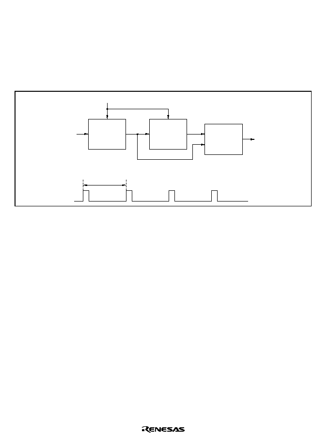
Rev. 2.0, 09/02, page 398 of 658
14.4.8
Noise Chancellor
The logic levels at the SCL and SDA pins are routed through noise chancellors before being
latched internally. Figure 14.12 shows a block diagram of the noise cancelled circuit.
The noise chancellor consists of two cascaded latches and a match detector. The SCL (or SDA)
input signal is sampled on the system clock, but is not passed forward to the next circuit unless the
outputs of both latches agree. If they do not agree, the previous value is held.
System clock
period
Sampling clock
C
D
Q
Latch
C
D
Q
Latch
SCL or
SDA input
signal
Match
detector
Internal
SCL or
SDA
signal
Sampling
clock
Figure 14.12 Block Diagram of Noise Chancellor
14.4.9
Sample Flowcharts
Figures 14.13 to 14.16 show sample flowcharts for using the I
2
C bus interface in each mode.

Rev. 2.0, 09/02, page 399 of 658
Start
Initialize
Set MST = 1 and
TRS = 1 in ICCR
Write BBSY =1 and
SCP = 0 in ICCR
Write transmit data in ICDR
Clear IRIC in ICCR
No
No
Yes
Yes
Yes
Yes
No
No
[1] Initialization
[3] Select master transmit mode.
[4] Start condition issuance
[6] Set transmit data for the first byte
(slave address + R/
).
(After writing ICDR, clear IRIC
continuously)
[9] Set transmit data for the second and
subsequent bytes.
(After writing ICDR, clear IRIC
immediately)
[2] Test the status of the SCL and SDA lines.
[7] Wait for 1 byte to be transmitted.
[10] Wait for 1 byte to be transmitted.
[11] Test for end of tranfer
[12] Stop condition issuance
[8] Test the acknowledge bit,
transferred from slave device.
[5] Wait for a start condition
Read IRIC in ICCR
Read ACKB in ICSR
IRIC = 1?
ACKB = 0?
Transmit mode?
Write transmit data in ICDR
Clear IRIC in ICCR
Read IRIC in ICCR
Read ACKB in ICSR
Clear IRIC in ICCR
End of transmission?
or ACKB = 1?
Write BBSY = 0 and
SCP = 0 in ICCR
End
Read BBSY in ICCR
BBSY = 0?
Yes
No
Read IRIC in ICCR
IRIC = 1?
Yes
No
Yes
No
IRIC = 1?
Master receive mode
Figure 14.13 Sample Flowchart for Master Transmit Mode
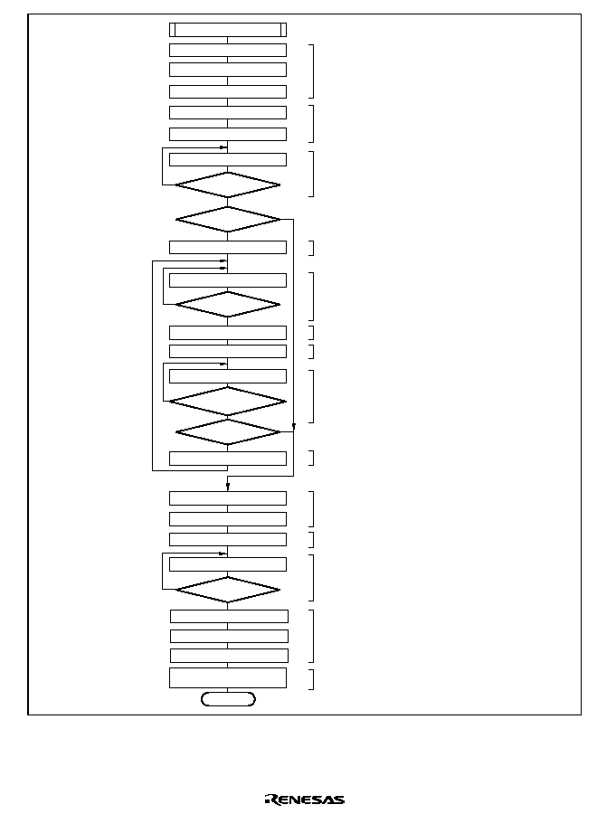
Rev. 2.0, 09/02, page 400 of 658
Master receive operation
Clear IRIC in ICCR
Yes
No
Yes
Yes
No
Yes
No
[1] Select receive mode.
[3] Wait for 1 byte to be received.
[4] Clear IRIC.
(to end the wait insertion)
[6] Read the receive data.
[9] Clear IRIC.
(to end the wait insertion)
[2] Start receiving. The first read
is a dummy read. After reading
ICDR, please clear IRIC immediately.
[7] Clear IRIC.
[10] Set acknowledge data for
the last reception.
[11] Clear IRIC.
(to end the wait insertion)
[12] Wait for 1 byte to be received.
[13] ---------
Clear IRIC.
(Note: After setting WAIT = 0,
IRIC should be cleared to 0.)
[14] Stop condition issuance.
[8] Wait for the next data to be
received.
[5] Wait for 1 byte to be received.
Read IRIC in ICCR
Read ICDR
Clear IRIC in ICCR
IRIC = 1?
IRIC = 1?
Yes
Last receive?
Last receive?
Set ACKB = 1 in ICSR
Set TRS = 1 in ICCR
Clear IRIC = 1 in ICCR
Read IRIC in ICCR
Set Wait = 0 in ICMR
Read ICDR
Clear IRIC in ICCR
Write BBSY = 0 and
SCP = 0 in ICCR
End
Set TRS = 0 in ICCR
Set ACKB = 0 in ICSR
Read IRIC in ICCR
IRIC = 1?
Yes
No
No
Read IRIC in ICCR
Clear IRIC in ICCR
No
IRIC = 1?
Set WAIT = 1 in ICMR
Clear IRIC in ICCR
Read ICDR
Figure 14.14 Sample Flowchart for Master Receive Mode
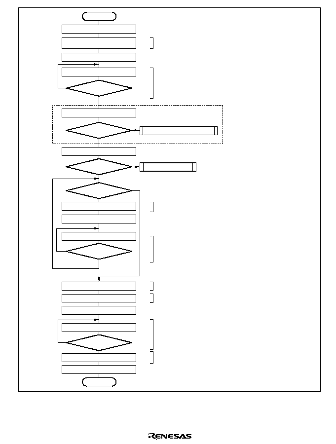
Rev. 2.0, 09/02, page 401 of 658
Start
Initialize
Set MST = 0
and TRS = 0 in ICCR
Set ACKB = 0 in ICSR
Read IRIC in ICCR
IRIC = 1?
Yes
No
Clear IRIC in ICCR
Read AAS and ADZ in ICSR
AAS = 1
and ADZ = 0?
Read TRS in ICCR
TRS = 0?
No
Yes
No
Yes
Yes
No
Yes
Yes
No
No
[1]
[2]
[3]
[4]
[5]
[6]
[7]
[8]
Last receive?
Read ICDR
Read IRIC in ICCR
IRIC = 1?
Clear IRIC in ICCR
Set ACKB = 1 in ICSR
Read ICDR
Read IRIC in ICCR
Read ICDR
IRIC = 1?
Clear IRIC in ICCR
End
General call address processing
*
Description omitted
Slave transmit mode
[1] Select slave receive mode.
[2] Wait for the first byte to be received (slave
address).
[3] Start receiving. The first read is a dummy read.
[4] Wait for the transfer to end.
[5] Set acknowledge data for the last reception.
[6] Start the last reception.
[7] Wait for the transfer to end.
[8] Read the last receive data.
Figure 14.15 Sample Flowchart for Slave Receive Mode

Rev. 2.0, 09/02, page 402 of 658
Slave transmit mode
Write transmit data in ICDR
Read IRIC in ICCR
IRIC = 1?
Clear IRIC in ICCR
Clear IRIC in ICCR
Clear IRIC in ICCR
Read ACKB in ICSR
Set TRS = 0 in ICCR
End
of transmission
(ACKB = 1)?
Yes
No
No
Yes
End
[1]
[2]
[3]
Read ICDR
[5]
[4]
[1] Set transmit data for the second and
subsequent bytes.
[2] Wait for 1 byte to be transmitted.
[3] Test for end of transfer.
[4] Set slave receive mode.
[5] Dummy read (to release the SCL line).
Figure 14.16 Sample Flowchart for Slave Transmit Mode

Rev. 2.0, 09/02, page 403 of 658
14.5
Usage Notes
1. In master mode, if an instruction to generate a start condition is immediately followed by an
instruction to generate a stop condition, neither condition will be output correctly. To output
consecutive start and stop conditions, after issuing the instruction that generates the start
condition, read the relevant ports, check that SCL and SDA are both low, then issue the
instruction that generates the stop condition. Note that SCL may not yet have gone low when
BBSY is cleared to 0.
2. Either of the following two conditions will start the next transfer. Pay attention to these
conditions when reading or writing to ICDR.
Write access to ICDR when ICE = 1 and TRS = 1 (including automatic transfer from
ICDRT to ICDRS)
Read access to ICDR when ICE = 1 and TRS = 0 (including automatic transfer from
ICDRS to ICDRR)
3. Table 14.6 shows the timing of SCL and SDA output in synchronization with the internal
clock. Timings on the bus are determined by the rise and fall times of signals affected by the
bus load capacitance, Series resistance, and parallel resistance.
Table 14.6
I
2
C Bus Timing (SCL and SDA Output)
Item
Symbol
Output Timing
Unit
Notes
SCL output cycle time
t
SCLO
28t
cyc
to 256t
cyc
ns
SCL output high pulse width
t
SCLHO
0.5t
SCLO
ns
SCL output low pulse width
t
SCLLO
0.5t
SCLO
ns
SDA output bus free time
t
BUFO
0.5t
SCLO
≠ 1t
cyc
ns
Start condition output hold time
t
STAHO
0.5t
SCLO
≠ 1t
cyc
ns
Retransmission start condition output
setup time
t
STASO
1t
SCLO
ns
Stop condition output setup time
t
STOSO
0.5t
SCLO
+ 2t
cyc
ns
Data output setup time (master)
t
SDASO
1t
SCLLO
≠ 3t
cyc
ns
Data output setup time (slave)
1t
SCLL
≠ 3t
cyc
ns
Data output hold time
t
SDAHO
3t
cyc
ns
4. SCL and SDA inputs are sampled in synchronization with the internal clock. The AC timing
therefore depends on the system clock cycle t
cyc
, as shown in table 26.8 in section 26, Electrical
Characteristics. Note that the I
2
C bus interface AC timing specifications will not be met with a
system clock frequency of less than 5 MHz.

Rev. 2.0, 09/02, page 404 of 658
5. The I
2
C bus interface specification for the SCL rise time t
sr
is under 1000 ns (300 ns for high-
speed mode). In master mode, the I
2
C bus interface monitors the SCL line and synchronizes
one bit at a time during communication. If t
sr
(the time for SCL to go from low to V
IH
) exceeds
the time determined by the input clock of the I
2
C bus interface, the high period of SCL is
extended. The SCL rise time is determined by the pull-up resistance and load capacitance of
the SCL line. To insure proper operation at the set transfer rate, adjust the pull-up resistance
and load capacitance so that the SCL rise time does not exceed the values given in the table in
table 14.7.
Table 14.7
Permissible SCL Rise Time (t
sr
) Values
Time Indication
IICX
t
cyc
Indication
I
2
C Bus
Specification
(Max.)
=
5 MHz
=
8 MHz
=
10 MHz
=
16 MHz
=
20 MHz
0
7.5t
cyc
Normal mode
1000 ns
1000 ns
937 ns
750 ns
468 ns
375 ns
High-speed
mode
300 ns
300 ns
300 ns
300 ns
300 ns
300 ns
1
17.5t
cyc
Normal mode
1000 ns
1000 ns
1000 ns
1000 ns
1000 ns
875 ns
High-speed
mode
300 ns
300 ns
300 ns
300 ns
300 ns
300 ns
6. The I
2
C bus interface specifications for the SCL and SDA rise and fall times are under 1000 ns
and 300 ns. The I
2
C bus interface SCL and SDA output timing is prescribed by t
Scyc
and t
cyc
, as
shown in table 14.6. However, because of the rise and fall times, the I
2
C bus interface
specifications may not be satisfied at the maximum transfer rate. Table 14.8 shows output
timing calculations for different operating frequencies, including the worst-case influence of
rise and fall times. The values in the above table will vary depending on the settings of the
IICX bit and bits CKS0 to CKS2. Depending on the frequency it may not be possible to
achieve the maximum transfer rate; therefore, whether or not the I
2
C bus interface
specifications are met must be determined in accordance with the actual setting conditions.
t
BUFO
fails to meet the I
2
C bus interface specifications at any frequency. The solution is either (a)
to provide coding to secure the necessary interval (approximately 1 µs) between issuance of a
stop condition and issuance of a start condition, or (b) to select devices whose input timing
permits this output timing for use as slave devices connected to the I
2
C bus.
t
SCLLO
in high-speed mode and t
STASO
in standard mode fail to satisfy the I
2
C bus interface
specifications for worst-case calculations of t
Sr
/t
Sf
. Possible solutions that should be investigated
include (a) adjusting the rise and fall times by means of a pull-up resistor and capacitive load,
(b) reducing the transfer rate to meet the specifications, or (c) selecting devices whose input
timing permits this output timing for use as slave devices connected to the I
2
C bus.

Rev. 2.0, 09/02, page 405 of 658
Table 14.8
I
2
C Bus Timing (with Maximum Influence of t
Sr
/t
Sf
)
Time Indication (at Maximum Transfer Rate) [ns]
Item
t
cyc
Indication
t
Sr
/t
Sf
Influence
(Max.)
I
2
C Bus
Specifi-
cation
(Min.)
=
5 MHz
=
8 MHz
=
10 MHz
=
16 MHz
=
20 MHz
t
SCLHO
0.5t
SCLO
(≠t
Sr
)
Standard mode
≠1000
4000
4000
4000
4000
4000
4000
High-speed mode ≠300
600
950
950
950
950
950
t
SCLLO
0.5t
SCLO
(≠t
Sf
)
Standard mode
≠250
4700
4750
4750
4750
4750
4750
High-speed mode ≠250
1300
1000
*
1
1000
*
1
1000
*
1
1000
*
1
1000
*
1
t
BUFO
0.5t
SCLO
≠1t
cyc
Standard mode
≠1000
4700
3800
*
1
3875
*
1
3900
*
1
3938
*
1
3950
*
1
( ≠t
Sr
)
High-speed mode ≠300
1300
750
*
1
825
*
1
850
*
1
888
*
1
900
*
1
t
STAHO
0.5t
SCLO
≠1t
cyc
Standard mode
≠250
4000
4550
4625
4650
4688
4700
(≠t
Sf
)
High-speed mode ≠250
600
800
875
900
938
950
t
STASO
1t
SCLO
(≠t
Sr
)
Standard mode
≠1000
4700
9000
9000
9000
9000
9000
High-speed mode ≠300
600
2200
2200
2200
2200
2200
t
STOSO
0.5t
SCLO
+ 2t
cyc
Standard mode
≠1000
4000
4400
4250
4200
4125
4100
(≠t
Sr
)
High-speed mode ≠300
600
1350
1200
1150
1075
1050
t
SDASO
1t
SCLLO
*
2
≠3t
cyc
Standard mode
≠1000
250
3100
3325
3400
3513
3550
(master)
(≠t
Sr
)
High-speed mode ≠300
100
400
625
700
813
850
t
SDASO
1t
SCLL
*
2
≠3t
cyc
*
2
Standard mode
≠1000
250
3100
3325
3400
3513
3550
(slave)
(≠t
Sr
)
High-speed mode ≠300
100
400
625
700
813
850
t
SDAHO
3t
cyc
Standard mode
0
0
600
375
300
188
150
High-speed mode 0
0
600
375
300
188
150
Notes: 1. Does not meet the I
2
C bus interface specification. Remedial action such as the following
is necessary: (a) secure a start/stop condition issuance interval; (b)adjust the rise and
fall times by means of a pull-up resistor and capacitive load; (c) reduce the transfer rate;
(d) select slave devices whose input timing permits this output timing.
The values in the above table will vary depending on the settings of the IICX bit and bits
CKS0 to CKS2.Depending on the frequency it may not be possible to achieve the
maximum transfer rate; therefore, whether or not the I
2
C bus interface specifications are
met must be determined in accordance with the actual setting conditions.
2. Calculated using the I
2
C bus specification values (standard mode: 4700 ns min.; high-
speed mode: 1300 ns min.).

Rev. 2.0, 09/02, page 406 of 658
7. Note on ICDR Read at End of Master Reception
To halt reception after completion of a receive operation in master receive mode, set the TRS
bit to 1 and write 0 to BBSY and SCP in ICCR. This changes the SDA pin from low to high
when the SCL pin is high, and generates the stop condition. After this, receive data can be read
by means of an ICDR read, but if data remains in the buffer the ICDRS receive data will not be
transferred to ICDR, and so it will not be possible to read the second byte of data. If it is
necessary to read the second byte of data, issue the stop condition in master receive mode (i.e.
with the TRS bit cleared to 0). When reading the receive data, first confirm that the BBSY bit
in ICCR is cleared to 0, the stop condition has been generated, and the bus has been released,
then read ICDR with TRS cleared to 0. Note that if the receive data (ICDR data) is read in the
interval between execution of the instruction for issuance of the stop condition (writing of 0 to
BBSY and SCP in ICCR) and the actual generation of the stop condition, the clock may not be
output correctly in subsequent master transmission.
Clearing of the MST bit after completion of master transmission/reception, or other
modifications of IIC control bits to change the transmit/receive operating mode or settings,
must be carried out during interval (a) in figure 14.17 (after confirming that the BBSY bit has
been cleared to 0 in the ICCR register).
SDA
SCL
Internal clock
BBSY bit
Master receive mode
ICDR reading
prohibited
Bit 0
A
8
9
Stop condition
(a)
Start condition
Execution of stop
condition issuance
instruction
(0 written to BBSY
and SCP)
Confirmation of stop
condition generation
(0 read from BBSY)
Start condition
issuance
Figure 14.17 Points for Attention Concerning Reading of Master Receive Data

Rev. 2.0, 09/02, page 407 of 658
8. Notes on Start Condition Issuance for Retransmission
Depending on the timing combination with the start condition issuance and the subsequently
writing data to ICDR, it may not be possible to issue the retransmission and the data
transmission after retransmission condition issuance.
After start condition issuance is done and determined the start condition, write the transmit
data to ICDR, as shown below. Figure 14.18 shows the timing of start condition issuance for
retransmission, and the timing for subsequently writing data to ICDR, together with the
corresponding flowchart.

Rev. 2.0, 09/02, page 408 of 658
SDA
IRIC
SCL
ACK
Bit 7
Data output
[3] (Restart) Start condition instruction issuance
[4] IRIC determination
[5] ICDR write (next transmit data)
[2] Detemination of SCL = Low
[1] IRIC determination
Start condition
(retransmission)
IRIC = 1?
Yes
Clear IRIC in ICSR
Read SCL pin
Write transmit data to ICDR
Write BBSY = 1,
SCP = 0 (ICSR)
[1]
[1] Wait for end of 1-byte transfer
[2] Determine whether SCL0 is low
[3] Issue restart condition instruction for transmission
[4] Determine whether start condition is generated or not
[5] Set transmit data (slave address + R/
)
[2]
[3]
[4]
[5]
Yes
Yes
No
No
IRIC = 1?
Yes
SCL = Low?
Start condition
issuance?
No
No
Other processing
Note: Program so that processing from [3] to [5]
is executed continuously.
9
Figure 14.18 Flowchart and Timing of Start Condition Instruction Issuance for
Retransmission

Rev. 2.0, 09/02, page 409 of 658
9. Notes on I
2
C Bus Interface Stop Condition Instruction Issuance
If the rise time of the 9th SCL clock exceeds the specification because the bus load capacitance
is large, or if there is a slave device of the type that drives SCL low to effect a wait, after rising
of the 9th SCL clock, issue the stop condition after reading SCL and determining it to be low,
as shown below.
Stop condition
SCL
IRIC
[1] Determination of SCL = Low
9th clock
VIH
High period secured
[2] Stop condition instruction isuuance
SDA
As waveform rise is late,
SCL is detected as low
Figure 14.19 Timing of Stop Condition Issuance
10. Notes on Initialization of Internal State
The I
2
C has a function for forcible initialization of its internal state if a deadlock occurs during
communication.
Initialization is executed by (1) setting bits CLR3 to CLR0 in the DDCSWR register. For
details see section 14.3.8 DDC Switch Register (DDCSWR).
∑
Scope of Initialization: The initialization executed by function covers the following items:
TDRE and RDRF internal flags
Transmit/receive sequencer and internal operating clock counter
Internal latches for retaining the output state of the SCL and SDA pins (wait, clock, data
output, etc.)
∑
The following items are not initialized:
Actual register values (ICDR, SAR, SARX, ICMR, ICCR, ICSR, DDCSWR, STCR)
Internal latches used t retain register read information setting/clearing flags in the
ICMR,.ICCR, ICSR, and DDCSWR registers
The value of the ICMR register bit counter (BC2 to BC0)
Generated interrupt sources (interrupt sources transferred to the interrupt controller)

Rev. 2.0, 09/02, page 410 of 658
∑
Notes on Initialization:
Interrupt flags and interrupt sources are not cleared, and so flag clearing measures must be
taken as necessary. Basically, other register flags are not cleared either, and so flag clearing
measures must be taken as necessary.
When initialization is executed by the DDCSWR register, the write data for bits CLR3 to
CLR0 is not retained. To perform IIC clearance, bits CLR3 to CLR0 must be written to
simultaneously using an MOV instruction. Do not use a bit manipulation instruction such as
BCLR. Similarly, when clearing is required again, all the bits must be written to
simultaneously in accordance with the setting.
If a flag clearing setting is made during transmission/reception, the IIC module will stop
transmitting/receiving at that point and the SCL and SDA pins will be released. When
transmission/reception is started again, register initialization, etc., must be carried out as
necessary to enable correct communication as a system.
The value of the BBSY bit cannot be modified directly by this module clear function, but since
the stop condition pin waveform is generated according to the state and release timing of the
SCL and SDA pins, the BBSY bit may be cleared as a result. Similarly, state switching of
other bits and flags may also have an effect.
To prevent problems caused by these factors, the following procedure should be used when
initializing the IIC state.
Execute initialization of the internal state according to the setting of bits CLR3 to CLR0.
Execute a stop condition issuance instruction (write 0 to BBSY and SCP) to clear the BBSY
bit to 0, and wait for two transfer rate clock cycles.
Re-execute initialization of the internal state according to the setting of bits CLR3 to CLR0.
Initialize (re-set) the IIC registers.
11. Interrupt during Module Stop Mode
When the module is stopped in the state that an interrupt is requested, the interrupt source of
the CPU or activation source of the DTC* is not cleared. Be sure to enter module stop mode by
disabling the interrupt beforehand.
Note: *
Supported only by the H8S/2268 Series.
12. Assignment and Selection of Register Addresses
Some I
2
C bus interface registers are assigned to the same address as other registers. Register
selection is performed by means of the IICE bit in the serial control register X (SCRX). For
details on register addresses, see section 25, List of Registers.

Rev. 2.0, 09/02, page 411 of 658
Section 15 A/D Converter
This LSI includes a successive approximation type 10-bit A/D converter that allows up to ten
analog input channels to be selected. A block diagram of the A/D converter is shown in figure
15.1.
15.1
Features
∑
10-bit resolution
∑
Ten input channels
∑
Conversion time: 6.3 µs per channel (at 20.5 MHz operation)
∑
Two operating modes
Single mode: Single-channel A/D conversion
Scan mode: Continuous A/D conversion on 1 to 4 channels
∑
Four data registers
Conversion results are held in a 16-bit data register for each channel
∑
Sample and hold function
∑
Three methods conversion start
Software
16-bit timer pulse unit (TPU or TMR) conversion start trigger
External trigger signal
∑
Interrupt request
An A/D conversion end interrupt request (ADI) can be generated
∑
Module stop mode can be set
ADCMS35B_000020020700

Rev. 2.0, 09/02, page 412 of 658
Module data bus
Control circuit
Internal data bus
10-bit D/A
Comparator
+
Sample-and-
hold circuit
ADI
interrupt
Bus interface
Successive approximations
register
Multiplexer
A
D
C
S
R
A
D
C
R
A
D
D
R
D
A
D
D
R
C
A
D
D
R
B
A
D
D
R
A
AN0
AN1
AN2
AN3
AN4
AN5
AN6
AN7
Legend
ADCR
: A/D control register
ADCSR : A/D control/status register
ADDRA : A/D data register A
ADDRB : A/D data register B
ADDRC : A/D data register C
ADDRD : A/D data register D
Conversion start
trigger from TPU or TMR
AN8
AN9
AN10
AN11
/2
/4
/8
/16
AV
CC
AV
SS
Vref
Figure 15.1 Block Diagram of A/D Converter

Rev. 2.0, 09/02, page 413 of 658
15.2
Input/Output Pins
Table 15.1 summarizes the input pins used by the A/D converter. The eight analog input pins are
divided into two groups each of which consists of four channels; analog input pins 0 to 3 (AN0 to
AN3) comprising group 0 and analog input pins 4 to 7 (AN4 to AN7) comprising group 1. The
AVcc and AVss pins are the power supply pins for the analog block in the A/D converter. The
Vref pin is the A/D conversion reference voltage pin.
Table 15.1
Pin Configuration
Pin Name
Symbol
I/O
Function
Analog power supply pin
AV
CC
Input
Analog block power supply and reference
voltage
Analog ground pin
AV
SS
Input
Analog block ground and reference voltage
Reference voltage pin
Vref
Input
Reference voltage for A/D conversion
Analog input pin 0
AN0
Input
Analog input pin 1
AN1
Input
Analog input pin 2
AN2
Input
Analog input pin 3
AN3
Input
Group 0 analog input pins
Analog input pin 4
AN4
Input
Analog input pin 5
AN5
Input
Analog input pin 6
AN6
Input
Analog input pin 7
AN7
Input
Group 1 analog input pins
Analog input pin 8
AN8
Input
Analog input pin 9
AN9
Input
Analog input pins
A/D external trigger input
pin
$'75*
Input
External trigger input pin for starting A/D
conversion

Rev. 2.0, 09/02, page 414 of 658
15.3
Register Descriptions
The A/D converter has the following registers. For details on the module stop control register,
refer to section 22.1.2, Module Stop Control Registers A to D (MSTPCRA to MSTPCRD).
∑
A/D data register A (ADDRA)
∑
A/D data register B (ADDRB)
∑
A/D data register C (ADDRC)
∑
A/D data register D (ADDRD)
∑
A/D control/status register (ADCSR)
∑
A/D control register (ADCR)
15.3.1
A/D Data Registers A to D (ADDRA to ADDRD)
There are four 16-bit read-only ADDR registers; ADDRA to ADDRD, used to store the results of
A/D conversion. The ADDR registers, which store a conversion result for each channel, are shown
in table 15.2.
The converted 10-bit data is stored in bits 6 to 15. The lower 6 bits are always read as 0.
The data bus between the CPU and the A/D converter is 8 bits wide. The upper byte can be read
directly from the CPU, however the lower byte should be read via a temporary register. Therefore,
when reading the ADDR, read only the upper byte, or read in word unit.
Table 15.2
Analog Input Channels and Corresponding ADDR Registers
Analog Input Channel
CH3 = 0
CH3 = 1
Group 0
(CH2 = 0)
Group 1
(CH2 = 1)
--
(CH2 = 0)
--
(CH2 = 1)
A/D Data Register to
Be Stored the Results
of A/D Conversion
AN0
AN4
Setting
prohibited
Setting
prohibited
ADDRA
AN1
AN5
Setting
prohibited
Setting
prohibited
ADDRB
AN2
AN6
Setting
prohibited
AN8
ADDRC
AN3
AN7
Setting
prohibited
AN9
ADDRD

Rev. 2.0, 09/02, page 415 of 658
15.3.2
A/D Control/Status Register (ADCSR)
ADCSR controls A/D conversion operations.
Bit
Bit Name
Initial
Value
R/W
Description
7
ADF
0
R/(W)
*
1
A/D End Flag
A status flag that indicates the end of A/D
conversion.
[Setting conditions]
∑
When A/D conversion ends in single mode
∑
When A/D conversion ends on all specified
channels in scan mode
[Clearing conditions]
∑
When 0 is written after reading ADF = 1
∑
When the DTC is activated by an ADI interrupt
and ADDR is read
*
2
6
ADIE
0
R/W
A/D Interrupt Enable
A/D conversion end interrupt (ADI) request enabled
when 1 is set
5
ADST
0
R/W
A/D Start
Clearing this bit to 0 stops A/D conversion, and the
A/D converter enters the wait state.
Setting this bit to 1 starts A/D conversion. In single
mode, this bit is cleared to 0 automatically when
conversion on the specified channel is complete. In
scan mode, conversion continues sequentially on
the specified channels until this bit is cleared to 0 by
software, a reset, or a transition to power-down
mode in which the A/D converter is halted, shown in
table 22.1.
The ADST bit can be set to 1 by software, a timer
conversion start trigger, or the A/D external trigger
input pin (
$'75*
).

Rev. 2.0, 09/02, page 416 of 658
Bit
Bit Name
Initial
Value
R/W
Description
4
SCAN
0
R/W
Scan Mode
Selects single mode or scan mode as the A/D
conversion operating mode.
Only set the SCAN bit while conversion is stopped
(ADST = 0).
0: Single mode
1: Scan mode
3
2
1
0
CH3
CH2
CH1
CH0
0
0
0
0
R/W
R/W
R/W
R/W
Channel Select 0 to 3
Select analog input channels.
When SCAN = 0
When SCAN = 1
0000: AN0
0000: AN0
0001: AN1
0001: AN0 to AN1
0010: AN2
0010: AN0 to AN2
0011: AN3
0011: AN0 to AN3
0100: AN4
0100: AN4
0101: AN5
0101: AN4 to AN5
0110: AN6
0110: AN4 to AN6
0111: AN7
0111: AN4 to AN7
1000: Setting prohibited
1000: Setting prohibited
1001: Setting prohibited
1001: Setting prohibited
1010: Setting prohibited
1010: Setting prohibited
1011: Setting prohibited
1011: Setting prohibited
1100: Setting prohibited
1100: Setting prohibited
1101: Setting prohibited
1101: Setting prohibited
1110: AN8
1110: Setting prohibited
1111: AN9
1111: Setting prohibited
Notes: 1. Only 0 can be written to bit 7, to clear this bit.
2. Supported only by the H8S/2268 Series.

Rev. 2.0, 09/02, page 417 of 658
15.3.3
A/D Control Register (ADCR)
The ADCR enables A/D conversion started by an external trigger signal.
Bit
Bit Name
Initial
Value
R/W
Description
7
6
TRGS1
TRGS0
0
0
R/W
R/W
Timer Trigger Select 0 and 1
Enables the start of A/D conversion by a trigger
signal. Only set bits TRGS0 and TRGS1 while
conversion is stopped (ADST = 0).
00: A/D conversion start by software is enabled
01: A/D conversion start by TPU conversion start
trigger is enabled
10: A/D conversion start by 8-bit timer conversion
start trigger is enabled
11: A/D conversion start by external trigger pin
(
$'75*
) is enabled
5
4
--
--
1
1
--
--
Reserved
These bits are always read as 1 and cannot be
modified.
3
2
CKS1
CKS0
0
0
R/W
R/W
Clock Select 0 and 1
These bits specify the A/D conversion time. The
conversion time should be changed only when
ADST = 0. Specify a setting that gives a value
within the range shown in table 26.9 or 26.22 in
section 26, Electrical Characteristics.
00: Conversion time = 530 states (max.)
01: Conversion time = 266 states (max.)
10: Conversion time = 134 states (max.)
11: Conversion time = 68 states (max.)
1, 0
All 1
Reserved
These bits are always read as 1 and cannot be
modified.

Rev. 2.0, 09/02, page 418 of 658
15.4
Operation
The A/D converter operates by successive approximation with 10-bit resolution. It has two
operating modes; single mode and scan mode. When changing the operating mode or analog input
channel, in order to prevent incorrect operation, first clear the bit ADST to 0 in ADCSR. The
ADST bit can be set at the same time as the operating mode or analog input channel is changed.
15.4.1
Single Mode
In single mode, A/D conversion is to be performed only once on the specified single channel. The
operations are as follows.
1. A/D conversion is started when the ADST bit is set to 1, according to software, timer
conversion start trigger, or external trigger input.
2. When A/D conversion is completed, the result is transferred to the corresponding A/D data
register to the channel.
3. On completion of conversion, the ADF bit in ADCSR is set to 1. If the ADIE bit is set to 1 at
this time, an ADI interrupt request is generated.
4. The ADST bit remains set to 1 during A/D conversion. When A/D conversion ends, the ADST
bit is automatically cleared to 0 and the A/D converter enters the wait state.

Rev. 2.0, 09/02, page 419 of 658
ADIE
ADST
ADF
State of channel 0 (AN0)
A/D conversion result 2
A/D
conversion start
A/D conversion result 1
ADDRA
ADDRB
ADDRC
ADDRD
State of channel 1 (AN1)
State of channel 2 (AN2)
State of channel 3 (AN3)
Note:
A/D conversion 1
Set
*
Set
*
Set
*
Clear
*
Clear
*
Idle
Idle
Idle
Idle
A/D conversion 2
Idle
Read conversion result
*
Read conversion result
*
Vertical arrows indicate instructions executed by software.
Figure 15.2 Example of A/D converter Operation (Single Mode, Channel 1 Selected)
15.4.2
Scan Mode
In scan mode, A/D conversion is to be performed sequentially on the specified channels (four
channels maximum). The operations are as follows.
1. When the ADST bit is set to 1 by software, TPU, timer conversion start trigger, or external
trigger, input, A/D conversion starts on the first channel in the group (AN0 when CH3 and
CH2 = 00, AN4 when CH3 and CH2 = 01, or AN8 when CH3 and CH2 = 10).
2. When A/D conversion for each channel is completed, the result is sequentially transferred to
the A/D data register corresponding to each channel.
3. When conversion of all the selected channels is completed, the ADF flag is set to 1. If the
ADIE bit is set to 1 at this time, an ADI interrupt is requested after A/D conversion ends.
Conversion of the first channel in the group starts again.
4. Steps [2] to [3] are repeated as long as the ADST bit remains set to 1. When the ADST bit is
cleared to 0, A/D conversion stops and the A/D converter enters the wait state.

Rev. 2.0, 09/02, page 420 of 658
ADST
ADF
ADDRA
ADDRB
ADDRC
ADDRD
State of channel 0
(AN0)
Note:
Contimuous A/D conversion
*
2
State of channel 1
(AN1)
State of channel 3
(AN3)
State of channel 2
(AN2)
Clear
*
1
Clear
*
1
Set
*
1
Idle
Idle
Idle
Idle
Idle
Idle
Idle
Idle
Idle
A/D conversion time
A/D conversion 1
A/D conversion 2
A/D conversion 4
A/D conversion 3
A/D conversion 5
A/D conversion result 1
A/D conversion result 2
A/D conversion result 2
A/D conversion result 3
1. Vertical arrows indicate instructions executed by software.
2. Data currently being converted is ignored.
Figure 15.3 Example of A/D Converter Operation (Scan Mode, Channels AN0 to AN2
Selected)
15.4.3
Input Sampling and A/D Conversion Time
The A/D converter has a built-in sample-and-hold circuit. The A/D converter samples the analog
input when the A/D conversion start delay time (t
D
) has passed after the ADST bit is set to 1, then
starts conversion. Figure 15.2 shows the A/D conversion timing. Table 15.3 shows the A/D
conversion time.
As indicated in figure 15.4, the A/D conversion time (t
CONV
) includes t
D
and the input sampling time
(t
SPL
). The length of t
D
varies depending on the timing of the write access to ADCSR. The total
conversion time therefore varies within the ranges indicated in table 15.3.
In scan mode, the values given in table 15.3 apply to the first conversion time. The values given in
table 15.4 apply to the second and subsequent conversions.

Rev. 2.0, 09/02, page 421 of 658
(1)
(2)
t
D
t
SPL
t
CONV
Address
Write signal
Input sampling
timing
ADF
Legend
(1)
: ADCSR write cycle
(2)
: ADCSR address
t
D
: A/D conversion start delay
t
SPL
: Input sampling time
t
CONV
: A/D conversion time
Figure 15.4 A/D Conversion Timing
Table 15.3
A/D Conversion Time (Single Mode)
CKS1 = 0
CKS1 = 1
CKS0 = 0
CKS0 = 1
CKS0 = 0
CKS0 = 1
Item
Symbol Min Typ Max
Min Typ Max
Min Typ Max
Min Typ Max
A/D conversion
start delay
t
D
18
--
33
10
--
17
6
--
9
4
--
5
Input sampling
time
t
SPL
--
127 --
--
63
--
--
31
--
--
15
--
A/D conversion
time
t
CONV
515 --
530
259 --
266
131 --
134
67
--
68
Note:
*
All values represent the number of states.
Table 15.4
A/D Conversion Time (Scan Mode)
CKS1
CKS0
Conversion Time (State)
0
512 (Fixed)
0
1
256 (Fixed)
0
128 (Fixed)
1
1
64 (Fixed)
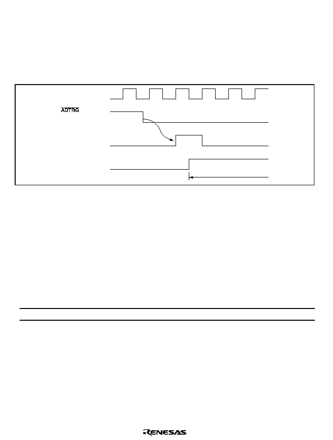
Rev. 2.0, 09/02, page 422 of 658
15.4.4
External Trigger Input Timing
A/D conversion can be externally triggered. When the TRGS0 and TRGS1 bits are set to 11 in
ADCR, external trigger input is enabled at the
$'75* pin. A falling edge at the $'75* pin sets
the ADST bit to 1 in ADCSR, starting A/D conversion. Other operations, in both single and scan
modes, are the same as when the bit ADST has been set to 1 by software. Figure 15.5 shows the
timing.
Internal trigger signal
ADST
A/D conversion
Figure 15.5 External Trigger Input Timing
15.5
Interrupt Source
The A/D converter generates an A/D conversion end interrupt (ADI) at the end of A/D conversion.
Setting the ADIE bit to 1 enables ADI interrupt requests while the bit ADF in ADCSR is set to 1
after A/D conversion is completed. In the H8S/2268 Series, the DTC* can be activated by an ADI
interrupt. Having the converted data read by the DTC* in response to an ADI interrupt enables
continuous conversion without imposing a load on software.
Table 15.5
A/D Converter Interrupt Source
Name
Interrupt Source
Interrupt Source Flag
DTC Activation
*
ADI
A/D conversion completed
ADF
Possible
Note:
*
Supported only by the H8S/2268 Series.

Rev. 2.0, 09/02, page 423 of 658
15.6
A/D Conversion Accuracy Definitions
This LSI's A/D conversion accuracy definitions are given below.
∑
Resolution
The number of A/D converter digital output codes
∑
Quantization error
The deviation inherent in the A/D converter, given by 1/2 LSB (see figure 15.6).
∑
Offset error
The deviation of the analog input voltage value from the ideal A/D conversion characteristic
when the digital output changes from the minimum voltage value B'0000000000 (H'000) to
B'0000000001 (H'001) (see figure 15.7).
∑
Full-scale error
The deviation of the analog input voltage value from the ideal A/D conversion characteristic
when the digital output changes from B'1111111110 (H'3FE) to B'1111111111 (H'3FF) (see
figure 15.7).
∑
Nonlinearity error
The error with respect to the ideal A/D conversion characteristic between zero voltage and full-
scale voltage. Does not include offset error, full-scale error, or quantization error (see figure 15.7).
∑
Absolute accuracy
The deviation between the digital value and the analog input value. Includes offset error, full-
scale error, quantization error, and nonlinearity error.

Rev. 2.0, 09/02, page 424 of 658
111
110
101
100
011
010
001
000
1
1024
2
1024
1022
1024
1023
1024
FS
Quantization error
Digital output
Ideal A/D conversion
characteristic
Analog
input voltage
Figure 15.6 A/D Conversion Accuracy Definitions (1)
FS
Digital output
Ideal A/D conversion
characteristic
Nonlinearity
error
Analog
input voltage
Offset error
Actual A/D conversion
characteristic
Full-scale error
Figure 15.7 A/D Conversion Accuracy Definitions (2)

Rev. 2.0, 09/02, page 425 of 658
15.7
Usage Notes
15.7.1
Module Stop Mode Setting
Operation of the A/D converter can be disabled or enabled using the module stop control register.
The initial setting is for operation of the A/D converter to be halted. Register access is enabled by
clearing module stop mode. For details, refer to section 22, Power-Down Modes.
15.7.2
Permissible Signal Source Impedance
This LSI's analog input is designed such that conversion accuracy is guaranteed for an input signal
for which the signal source impedance is 5 k
or less. This specification is provided to enable the
A/D converter's sample-and-hold circuit input capacitance to be charged within the sampling time;
if the sensor output impedance exceeds 5 k
, charging may be insufficient and it may not be
possible to guarantee A/D conversion accuracy. However, for A/D conversion in single mode with
a large capacitance provided externally, the input load will essentially comprise only the internal
input resistance of 10 k
, and the signal source impedance is ignored. However, as a low-pass
filter effect is obtained in this case, it may not be possible to follow an analog signal with a large
differential coefficient (e.g., 5 mV/
µ
s or greater) (see figure 15.8). When converting a high-speed
analog signal, a low-impedance buffer should be inserted.
15.7.3
Influences on Absolute Accuracy
Adding capacitance results in coupling with GND, and therefore noise in GND may adversely
affect absolute accuracy. Be sure to make the connection to an electrically stable GND such as
AVss.
Care is also required to insure that filter circuits do not communicate with digital signals on the
mounting board (i.e., acting as antennas).
A/D converter
equivalent circuit
This LSI
20 pF
C
in
=
15 pF
10 k
Low-pass
filter
C to 0.1mF
Sensor output
impedance
to 5 k
Sensor input
Figure 15.8 Example of Analog Input Circuit

Rev. 2.0, 09/02, page 426 of 658
15.7.4
Range of Analog Power Supply and Other Pin Settings
If the conditions below are not met, the reliability of the device may be adversely affected.
∑
Analog input voltage range
The voltage applied to analog input pin ANn during A/D conversion should be in the range
AVss
ANn
AVcc.
∑
Relationship between AVcc, AVss and Vcc, Vss
Set AVss = Vss as the relationship between AVcc, AVss and Vcc, Vss. If the A/D converter is
not used, the AVcc and AVss pins must not be left open.
∑
Vref range
The reference voltage input from the Vref pin should be set to AVcc or less.
15.7.5
Notes on Board Design
In board design, digital circuitry and analog circuitry should be as mutually isolated as possible,
and layout in which digital circuit signal lines and analog circuit signal lines cross or are in close
proximity should be avoided as far as possible. Failure to do so may result in incorrect operation
of the analog circuitry due to inductance, adversely affecting A/D conversion values. Also, digital
circuitry must be isolated from the analog input signals (AN0 to AN9), and analog power supply
(AVcc) by the analog ground (AVss). Also, the analog ground (AVss) should be connected at one
point to a stable digital ground (Vss) on the board.
15.7.6
Notes on Noise Countermeasures
A protection circuit should be connected in order to prevent damage due to abnormal voltage, such
as an excessive surge at the analog input pins (AN0 to AN9), between AVcc and AVss, as shown
in figure 15.9. Also, the bypass capacitors connected to AVcc and the filter capacitor connected to
AN0 to AN9 must be connected to AVss.
If a filter capacitor is connected, the input currents at the analog input pins (AN0 to AN9) are
averaged, and so an error may arise. Also, when A/D conversion is performed frequently, as in
scan mode, if the current charged and discharged by the capacitance of the sample-and-hold circuit
in the A/D converter exceeds the current input via the input impedance (R
in
), an error will arise in
the analog input pin voltage. Careful consideration is therefore required when deciding circuit
constants.

Rev. 2.0, 09/02, page 427 of 658
AVCC
*
1
AN0 to AN9
AVSS
R
in
*
2
100
0.1 F
0.01 F
10 F
Notes: Values are reference values.
1.
2. R
in
: Input impedance
Vref
*
1
Figure 15.9 Example of Analog Input Protection Circuit
Table 15.6
Analog Pin Specifications
Item
Min
Max
Unit
Analog input capacitance
--
20
pF
Permissible signal source impedance
--
5
k
20 pF
AN0 to AN9
Note: Values are reference values.
10 k
To A/D converter
Figure 15.10 Analog Input Pin Equivalent Circuit

Rev. 2.0, 09/02, page 428 of 658

Rev. 2.0, 09/02, page 429 of 658
Section 16 D/A Converter
The H8S/2268 Series includes a D/A converter, while the H8S/2264 Series does not.
16.1
Features
∑
8-bit resolution
∑
Two output channels
∑
Conversion time: 10 µs, maximum (when load capacitance is 20 pF)
∑
Output voltage: 0 V to Vref
∑
D/A output retaining function in software standby mode
∑
Module stop mode can be set
Module data bus
Bus interface
Internal data bus
Vref
AVCC
DA1
DA0
AVSS
8-bit D/A
Control circuit
D
A
D
R
0
D
A
D
R
1
D
A
C
R
Legend
DACR : D/A control register
DADR0: D/A data register 0
DADR1: D/A data register 1
Figure 16.1 Block Diagram of D/A Converter
DAC0004B_000020020700

Rev. 2.0, 09/02, page 430 of 658
16.2
Input/Output Pins
Table 16.1 shows the pin configuration for the D/A converter.
Table 16.1
Pin Configuration
Pin Name
Symbol
I/O
Function
Analog power supply pin
AV
CC
Input
Analog block power supply
Analog ground pin
AV
SS
Input
Analog block ground and reference voltage
Analog output pin 0
DA0
Output
Channel 0 analog output pin
Analog output pin 1
DA1
Output
Channel 1 analog output pin
Reference voltage pin
Vref
Input
Reference voltage for analog block
16.3
Register Description
The D/A converter has the following registers. For details on the module stop control register,
refer to section 22.1.2, Module Stop Control Registers A to D (MSTPCRA to MSTPCRD).
∑
D/A data register 0 (DADR0)
∑
D/A data register 1 (DADR1)
∑
D/A control register (DACR)
16.3.1
D/A Data Registers 0 and 1 (DADR0 and DADR1)
DADR0 and DADR1 are 8-bit readable/writable registers that store data for D/A conversion.
When analog output is permitted, D/A data register contents are converted and output to analog
output pins.

Rev. 2.0, 09/02, page 431 of 658
16.3.2
D/A Control Register (DACR)
DACR controls D/A converter operation.
Bit
Bit Name
Initial
Value
R/W
Description
7
DAOE1
0
R/W
D/A Output Enable 1
Controls D/A conversion and analog output
0: Analog output DA1 is disabled
1: D/A conversion for channel 1 and analog output
DA1 are enabled
6
DAOE0
0
R/W
D/A Output Enable 0
Controls D/A conversion and analog output
0: Analog output DA0 is disabled
1: D/A conversion for channel 0 and analog output
DA0 are enabled
5
DAE
0
R/W
D/A Enable
Controls D/A conversion in conjunction with the
DAOE0 and DAOE1 bits. When the DAE bit is
cleared to 0, D/A conversion for channels 0 and 1
are controlled individually. When DAE is set to 1,
D/A conversion for channels 0 and 1 are controlled
as one. Conversion result output is controlled by the
DAOE0 and DAOE1 bits. For details, see table
16.2.
4 to 0
All 1
Reserved
These bits are always read as 1 and cannot be
modified.

Rev. 2.0, 09/02, page 432 of 658
Table 16.2
D/A Conversion Control
Bit 5
Bit 7
Bit 6
DAE
DAOE1
DAOE0
Description
0
0
0
Disables D/A Conversion
1
Enables D/A Conversion for channel 0
1
0
Enables D/A Conversion for channel 1
1
Enables D/A Conversion for channels 0 and 1
1
0
0
Disables D/A Conversion
1
Enables D/A Conversion for channels 0 and 1
1
0
1
16.4
Operation
Two channels of the D/A converter can perform conversion individually.
When the DAOE bit in DACR is set to 1, D/A conversion is enabled and the conversion results are
output.
An example of D/A conversion of channel 0 is shown below. The operation timing is shown in
figure 16.2.
1.
Write conversion data to DADR0.
2.
When the DAOE0 bit in DACR is set to 1, D/A conversion starts. After the interval of t
DCONV
,
the conversion results are output from the analog output pin DA0. The conversion results are
output continuously until DADR0 is modified or DAOE0 bit is cleared to 0. The output value
is calculated by the following formula:
(DADR contents)/256
x
Vref
3.
Conversion starts immediately after DADR0 is modified. After the interval of t
DCONV
,
conversion results are output.
4.
When the DAOE bit is cleared to 0, analog output is disabled.

Rev. 2.0, 09/02, page 433 of 658
DADR0
write cycle
DACR
write cycle
DADR0
write cycle
DACR
write cycle
ADRES
DADR0
DAOE0
DA0
Conversion data (1)
Conversion data (2)
High impedance state
Conversion result (1)
Conversion result (2)
tDCONV
tDCONV
Legend
tDCONV: D/A conversion time
Figure 16.2 D/A Converter Operation Example
16.5
Usage notes
16.5.1
Analog Power Supply Current in Software Standby Mode
If this LSI enters software standby mode while D/A conversion is enabled, D/A output is retained
and the analog power supply current is equivalent to that during D/A conversion. To reduce analog
power supply current in software standby mode, clear the DAOE0, DAOE1 and DAE bits to 0 to
disable D/A output.
16.5.2
Setting for Module Stop Mode
It is possible to enable/disable the D/A converter operation using the module stop control register,
the D/A converter does not operate by the initial value of the register. The register can be accessed
by releasing the module stop mode. For more details, see section 22, Power-Down Modes.

Rev. 2.0, 09/02, page 434 of 658

Rev. 2.0, 09/02, page 435 of 658
Section 17 LCD Controller/Driver
The H8S/2268 has an on-chip segment type LCD control circuit, LCD driver, and power supply
circuit, enabling it to directly drive an LCD panel.
17.1
Overview
Features of the LCD controller/driver are given below.
∑
Display capacity
Duty Cycle
Internal Driver
Static
40 SEG
1/2
40 SEG
1/3
40 SEG
1/4
40 SEG
∑
LCD RAM capacity
8 bits
◊
20 bytes (160 bits)
Byte or word access to LCD RAM
∑
The segment output pins can be used as ports.
H8S/2268 series: SEG40 to SEG1 pins can be used as ports in groups of eight.
H8S/2264 series: SEG24 to SEG1 pins can be used as ports in groups of four.
∑
Common output pins not used because of the duty cycle can be used for common double-
buffering (parallel connection).
With 1/2 duty, parallel connection of COM1 to COM2, and of COM3 to COM4, can be used
In static mode, parallel connection of COM1 to COM2, COM3, and COM4 can be used
∑
Choice of 11 frame frequencies
∑
A or B waveform selectable by software
∑
Built-in power supply split-resistance
∑
Display possible in operating modes other than standby mode and module stop mode
∑
Display possible during low-voltage operation by built-in triple step-up voltage circuit
(supported only by the H8S/2268 Series)
∑
Module stop mode
As the initial setting, LCD operation is halted. Access to registers and LCD RAM is enabled
by clearing module stop mode.
LCDSG00B_000020020700

Rev. 2.0, 09/02, page 436 of 658
Figure 17.1 shows a block diagram of the LCD controller/driver.
/16 to
/2048
SUB
CL2
CL1
SEGn, DO
LPCR
LCR
LCR2
Display timing generator
LCD RAM
20 bytes
Internal data bus
40-bit
shift
register
LCD drive
power supply
(Built-in step-up
voltage circuit
*
)
Segment
driver
Common
data latch
Common
driver
M
V1
V2
V3
V
SS
COM1
COM4
SEG40
SEG39
SEG38
SEG37
SEG36
SEG1
Legend:
LPCR: LCD port control register
LCR:
LCD control register
LCR2: LCD control register 2
Note:
*
Supported only by the H8S/2268 Series.
LPV
CC
Figure 17.1 Block Diagram of LCD Controller/Driver

Rev. 2.0, 09/02, page 437 of 658
17.2
Input/Output Pins
Table 17.1 shows the LCD controller/driver pin configuration.
Table 17.1
Pin Configuration
Name
Abbreviation
I/O
Function
Segment output
pins
SEG40 to SEG1
Output
LCD segment drive pins
(H8S/2268 Series)
All pins are multiplexed as port pins (setting
programmable)
(H8S/2264 Series)
SEG24 to SEG1 pins are multiplexed as port
pins (setting programmable)
Common output
pins
COM4 to COM1
Output
LCD common drive pins
Pins can be used in parallel with static or
1/2 duty
LCD power supply
pins
V1, V2, V3
--
Used when a bypass capacitor is connected
externally, and when an external power
supply circuit is used
V3 pin is LCD input reference power supply
when triple step-up voltage circuit is used
*
.
Capacitance pins
for LCD step-up
voltage
*
C1, C2
--
Capacitance pins for step-up voltage LCD
drive power supply
Note:
*
Supported only by the H8S/2268 Series.
17.3
Register Descriptions
The LCD controller/driver has the following registers.
∑
LCD port control register (LPCR)
∑
LCD control register (LCR)
∑
LCD control register 2 (LCR2)
∑
LCDRAM

Rev. 2.0, 09/02, page 438 of 658
17.3.1
LCD Port Control Register (LPCR)
LPCR selects the duty cycle, LCD driver, and pin functions.
Bit
Bit Name
Initial Value
R/W
Description
7
6
5
DTS1
DTS0
CMX
0
0
0
R/W
R/W
R/W
Duty Cycle Select 1 and 0
Common Function Select
The combination of DTS1 and DTS0 selects static,
1/2, 1/3, or 1/4 duty.
CMX specifies whether or not the same waveform
is to be output from multiple pins to increase the
common drive power when not all common pins
are used because of the duty setting.
4
--
0
--
Reserved
This bit is always read as 0 and should only be
written with 0.
3
2
1
0
SGS3
SGS2
SGS1
SGS0
0
0
0
0
R/W
R/W
R/W
R/W
Segment Driver Select 3 to 0
Bits 3 to 0 select the segment drivers to be used.
For details, see tables 17.3 and 17.4.

Rev. 2.0, 09/02, page 439 of 658
Table 17.2
Duty Cycle and Common Function Selection
Bit 7:
DTS1
Bit 6:
DTS0
Bit 5:
CMX
Duty Cycle
Common Drivers
Notes
0
0
0
Static
COM1
COM4, COM3, and COM2 can
be used as ports (Initial value)
1
COM4 to COM1
COM4, COM3, and COM2 output
the same waveform as COM1
1
0
1/2 duty
COM2 to COM1
COM4 and COM3 can be used
as ports
1
COM4 to COM1
COM4 outputs the same
waveform as COM3, and COM2
outputs the same waveform as
COM1
1
0
0
1/3 duty
COM3 to COM1
COM4 can be used as a port
*
1
COM4 to COM1
Do not use COM4
1
X
1/4 duty
COM4 to COM1
--
Legend
X:
Don't care
Note:
COM4 to COM1 function as ports when the setting of SGS3 to SGS0 is 0000.
*
Cannot be used as a port when the SUPS bit in LCR2 is 1 in the H8S/2268 Series. Set
the SUPS bit to 0 when using as a port.
Table 17.3
Segment Driver Selection (1) (H8S/2268 Series)
Function of Pins SEG40 to SEG1
Bit 3:
SGS3
Bit 2:
SGS2
Bit 1:
SGS1
Bit 0:
SGS0
SEG40
to
SEG33
SEG32
to
SEG25
SEG24
to
SEG17
SEG16
to
SEG9
SEG8
to
SEG1
0
0
0
0
Port
Port
Port
Port
Port
1
SEG
Port
Port
Port
Port
1
0
SEG
SEG
Port
Port
Port
1
SEG
SEG
SEG
Port
Port
1
0
0
SEG
SEG
SEG
SEG
Port
1
SEG
SEG
SEG
SEG
SEG
1
X
Setting
prohibited
Setting
prohibited
Setting
prohibited
Setting
prohibited
Setting
prohibited
1
X
X
X
Setting
prohibited
Setting
prohibited
Setting
prohibited
Setting
prohibited
Setting
prohibited
Legend
X:
Don't care
Note:
*
COM4 to COM1 also function as ports when the setting of SGS3 to SGS0 is 0000.

Rev. 2.0, 09/02, page 440 of 658
Table 17.4
Segment Driver Selection (2) (H8S/2264 Series)
Function of Pins SEG40 to SEG1
Bit 3:
SGS3
Bit 2:
SGS2
Bit 1:
SGS1
Bit 0:
SGS0
SEG40
to
SEG25
SEG24
to
SEG21
SEG20
to
SEG17
SEG16
to
SEG13
SEG12
to
SEG9
SEG8
to
SEG5
SEG4
to
SEG1
0
0
0
0
--
Port
Port
Port
Port
Port
Port
1
Setting
prohibited
Setting
prohibited
Setting
prohibited
Setting
prohibited
Setting
prohibited
Setting
prohibited
Setting
prohibited
1
0
SEG
Port
Port
Port
Port
Port
Port
1
SEG
SEG
SEG
Port
Port
Port
Port
1
0
0
SEG
SEG
SEG
SEG
SEG
Port
Port
1
SEG
SEG
SEG
SEG
SEG
SEG
SEG
1
X
Setting
prohibited
Setting
prohibited
Setting
prohibited
Setting
prohibited
Setting
prohibited
Setting
prohibited
Setting
prohibited
1
0
0
X
Setting
prohibited
Setting
prohibited
Setting
prohibited
Setting
prohibited
Setting
prohibited
Setting
prohibited
Setting
prohibited
1
0
SEG
SEG
Port
Port
Port
Port
Port
1
SEG
SEG
SEG
SEG
Port
Port
Port
1
0
0
SEG
SEG
SEG
SEG
SEG
SEG
Port
1
Setting
prohibited
Setting
prohibited
Setting
prohibited
Setting
prohibited
Setting
prohibited
Setting
prohibited
Setting
prohibited
1
X
Setting
prohibited
Setting
prohibited
Setting
prohibited
Setting
prohibited
Setting
prohibited
Setting
prohibited
Setting
prohibited
Legend
X:
Don't care
Note:
*
COM4 to COM1 also function as ports when the setting of SGS3 to SGS0 is 0000.

Rev. 2.0, 09/02, page 441 of 658
17.3.2
LCD Control Register (LCR)
LCR performs LCD power supply split-resistance connection control and display data control, and
selects the frame frequency.
Bit
Bit Name
Initial Value
R/W
Description
7
--
1
R/W
LCD Disable Bit
This bit is always read as 1. The write value should
always be 0.
6
PSW
0
R/W
LCD Power Supply Split-Resistance Connection
Control
Bit 6 can be used to disconnect the LCD power
supply split-resistance from V
CC
when LCD display
is not required in a power-down mode, or when an
external power supply is used. When the ACT bit is
cleared to 0, and also in standby mode, the LCD
power supply split-resistance is disconnected from
V
CC
regardless of the setting of this bit.
0: LCD power supply split-resistance is
disconnected from V
CC
1: LCD power supply split-resistance is connected
to V
CC
5
ACT
0
R/W
Display Function Activate
Bit 5 specifies whether or not the LCD
controller/driver is used. Clearing this bit to 0 halts
operation of the LCD controller/driver. The LCD
drive power supply ladder resistance is also turned
off, regardless of the setting of the PSW bit.
However, register contents are retained.
0: LCD controller/driver operation halted
1: LCD controller/driver operation enabled
4
DISP
0
R/W
Display Data Control
Bit 4 specifies whether the LCD RAM contents are
displayed or blank data is displayed regardless of
the LCD RAM contents.
0: Blank data is displayed
1: LCD RAM data is displayed

Rev. 2.0, 09/02, page 442 of 658
Bit
Bit Name
Initial Value
R/W
Description
3
2
1
0
CKS3
CKS2
CKS1
CKS0
0
0
0
0
R/W
R/W
R/W
R/W
Frame Frequency Select 3 to 0
Bits 3 to 0 select the operating clock and the frame
frequency. In subactive mode, watch mode, and
subsleep mode, the system clock (
) is halted, and
therefore display operations are not performed if
one of the clocks from
/16 to
/2048 is selected. If
LCD display is required in these modes,
SUB
,
SUB
/2,
or
SUB
/4 must be selected as the operating clock.
For details, see table 17.5.
Note:
*
0 should be written to bit 7 after the other bits have been set.
Table 17.5
Frame Frequency Selection
Bit 3:
Bit 2:
Bit 1:
Bit 0:
Frame Frequency
*
1
CKS3
CKS2
CKS1
CKS0
Operating Clock
= 20 MHz
= 2 MHz
0
X
0
0
SUB
128 Hz*
2
128 Hz
*
2
1
SUB
/2
64 Hz*
2
64 Hz
*
2
1
X
SUB
/4
32 Hz*
2
32 Hz
*
2
1
0
0
0
/16
--
488 Hz
1
/32
--
244 Hz
1
0
/64
--
122 Hz
1
/128
610 Hz
61 Hz
1
0
0
/256
305 Hz
30.5 Hz
1
/512
152.6 Hz
--
1
0
/1024
76.3 Hz
--
1
/2048
38.1 Hz
--
Legend
X:
Don't care
Notes: 1. When 1/3 duty is selected, the frame frequency is 4/3 times the value shown.
2. This is the frame frequency when
SUB
= 32.768 kHz.
17.3.3
LCD Control Register 2 (LCR2)
LCR2 controls switching between the A waveform and B waveform, selects clock for step-up
voltage circuit, selects power supply, and selects the duty ratio for charge/discharge pulse that
controls to separate power supply divider resistance from power supply circuit.

Rev. 2.0, 09/02, page 443 of 658
Bit
Bit
Name
Initial Value
R/W
Description
7
LCDAB
0
R/W
A Waveform/B Waveform Switching Control
Bit 7 specifies whether the A waveform or B waveform is
used as the LCD drive waveform.
0: Drive using A waveform
1: Drive using B waveform
6
--
1
--
Reserved
These bits are always read as 1 and cannot be modified.
5
HCKS
0
R/W
(H8S/2268 Series)
Triple Step-Up Voltage Circuit Clock Select
This bit selects a clock used for triple step-up voltage
circuit. This bit selects a clock which divides a clock
specified by the LCD operating control register (LCR) by
4 or 8 as step-up voltage circuit clock.
0: A clock, which divides a LCD operating clock by 4, is
selected as step-up voltage circuit clock
1: A clock, which divides a LCD operating clock by 8, is
selected as step-up voltage circuit clock
(H8S/2264 Series)
Reserved
0 should be written to this bit.
4
SUPS
0
R/W
(H8S/2268 Series)
Drive Power Select
Triple Step-up Voltage Circuit Control
The triple step-up voltage circuit stops operation when
Vcc is selected as drive power. The triple step-up voltage
circuit starts operation when LCD input reference voltage
(V
LCD3
) is selected as drive power.
0: Drive power is Vcc, triple step-up voltage circuit halts
1: Drive power is triple step-up voltage of the LCD input
reference voltage (V
LCD3
), triple step-up voltage circuit
operates
(H8S/2264 Series)
Reserved
0 should be written to this bit.
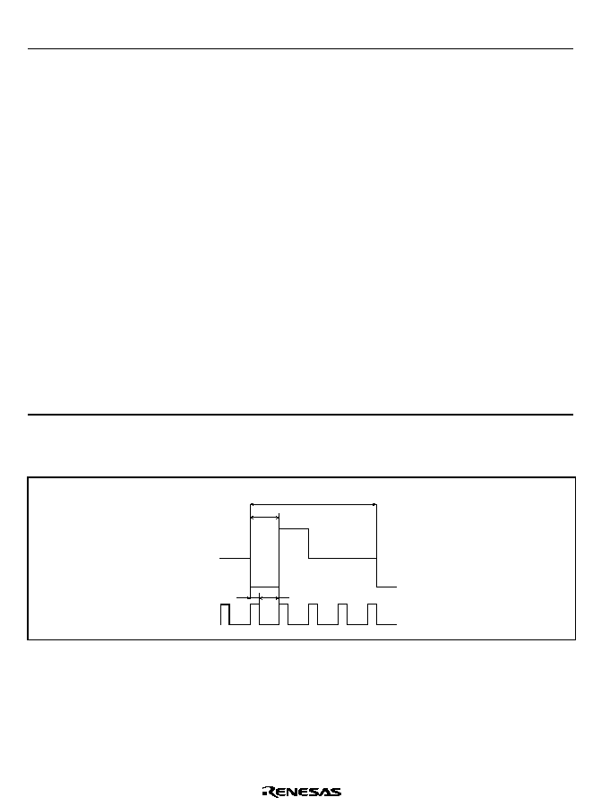
Rev. 2.0, 09/02, page 444 of 658
Bit
Bit
Name
Initial Value
R/W
Description
3
2
1
0
CDS3
CDS2
CDS1
CDS0
0
0
0
0
R/W
R/W
R/W
R/W
Selection of Duty Ratio for Charge/Discharge Pulse
Duty ratio is selected during the power supply divider
resistance is connected to power supply circuit. When
the duty ratio of 0 is selected, the power supply divider
resistance is fixed to the state that the resistance is
separated from the power supply circuit. Therefore,
supply the power to pins V
1
, V
2
, and V
3
from the external
circuit.
The charge/discharge pulses have the waveform shown
in figure 17.2. The duty ratio is represented by T
C
/T
W
.
0000: duty ratio = 1 (stack at high)
0001: duty ratio = 1/8
0010: duty ratio = 2/8
0011: duty ratio = 3/8
0100: duty ratio = 4/8
0101: duty ratio = 5/8
0110: duty ratio = 6/8
0111: duty ratio = 0 (stack at low)
10XX: duty ratio = 1/16
11XX: duty ratio = 1/32
Legend
X:
Don't care
COM1
Tc
Tdc
T
W
1
Tc
Tdc
Figure 17.2 A waveform 1/2 duty 1/2 vias

Rev. 2.0, 09/02, page 445 of 658
The relationships between the LCD operating clock and step-up voltage clock, and between bits
CKS3 to CKS0 in LCD control register (LCR) and bit HCKS in LCD control register 2 (LCR2)
are shown below.
LCR
Bit 3
Bit 2
Bit 1
Bit 0
Frame frequency
Step-Up Voltage
Circuit clock
frequency
*
CKS3
CKS2
CKS1
CKS0
LCR2
Bit 5
HCKS
*
LCD
clock
Step-up
Voltage
Circuit
clock
*
= 20
MHz
= 2
MHz
= 20
MHz
= 2
MHz
0
SUB
/4
8192 Hz
0
X
0
0
1
SUB
128 Hz
0
SUB
/8
4096 Hz
0
X
0
1
1
SUB
/2
64 Hz
0
SUB
/16
2048 Hz
0
X
1
X
1
SUB
/4
SUB
/32
32 Hz
1024 Hz
0
64
--
31.3 kHz
1
0
0
0
1
/16
--
488 Hz
0
128
--
15.6 kHz
1
0
0
1
1
/32
--
244 Hz
0
256
--
7.81 kHz
1
0
1
0
1
/64
--
122 Hz
--
0
512
39.1 kHz
3.91 kHz
1
0
1
1
1
/128
610 Hz
61 Hz
0
1024
19.5 kHz
1.95 kHz
1
1
0
0
1
/256
305 Hz
30.5 Hz
977 kHz
0
2048
9.77 kHz
--
1
1
0
1
1
/512
152.6 Hz
--
0
4096
4.88 kHz
--
1
1
1
0
1
/1024
76.3 Hz
--
0
8192
2.44 kHz
--
1
1
1
1
1
/2048
16384
38.1 Hz
--
1.22 kHz
--
Legend
X:
Don't care
Note:
*
Supported only by the H8S/2268 Series.

Rev. 2.0, 09/02, page 446 of 658
17.4
Operation
17.4.1
Settings up to LCD Display
To perform LCD display, the hardware and software related items described below must first be
determined.
1. Hardware Settings
A. Using 1/2 duty
When 1/2 duty is used, interconnect pins V
2
and V
3
as shown in figure 17.3.
V1
V2
V3
V
CC
V
SS
Figure 17.3 Handling of LCD Drive Power Supply when Using 1/2 Duty
B. Large-panel display
As the impedance of the built-in power supply split-resistance is large, it may not be
suitable for driving a large panel. If the display lacks sharpness when using a large panel,
refer to section 17.4.6, Boosting the LCD Drive Power Supply. When static or 1/2 duty is
selected, the common output drive capability can be increased. Set CMX to 1 when
selecting the duty cycle. In this mode, with a static duty cycle pins COM4 to COM1 output
the same waveform, and with 1/2 duty the COM1 waveform is output from pins COM2 and
COM1, and the COM2 waveform is output from pins COM4 and COM3.
C. LCD drive power supply setting
With the H8S/2268 and 2264, there are two ways of providing LCD power: by using the
on-chip power supply circuit, or by using an external power supply circuit.
When an external power supply circuit is used for the LCD drive power supply, connect the
external power supply to the V1 pin.
2. Software Settings
A. Duty selection
Any of four duty cycles--static, 1/2 duty, 1/3 duty, or 1/4 duty--can be selected with bits
DTS1 and DTS0.

Rev. 2.0, 09/02, page 447 of 658
B. Segment selection
The segment drivers to be used can be selected with bits SGS3 to SGS0.
3.
Frame frequency selection
The frame frequency can be selected by setting bits CKS3 to CKS0. The frame frequency
should be selected in accordance with the LCD panel specification. For the clock selection
method in watch mode, subactive mode, and subsleep mode, see section 17.4.4, Operation in
Power-Down Modes.
A. A or B waveform selection
Either the A or B waveform can be selected as the LCD waveform to be used by means of
LCDAB.
B. LCD drive power supply selection
When an external power supply circuit is used, turn the LCD drive power supply off with
the PSW bit.
17.4.2
Relationship between LCD RAM and Display
The relationship between the LCD RAM and the display segments differs according to the duty
cycle. LCD RAM maps for the different duty cycles are shown in figures 17.4 to 17.7.
After setting the registers required for display, data is written to the part corresponding to the duty
using the same kind of instruction as for ordinary RAM, and display is started automatically when
turned on. Word- or byte-access instructions can be used for RAM setting.
Bit 7
Bit 6
Bit 5
Bit 4
Bit 3
Bit 2
Bit 1
Bit 0
SEG40
H'FC53
H'FC40
SEG40
SEG40
SEG40
SEG39
SEG39
SEG39
SEG39
SEG2
SEG2
SEG2
SEG2
SEG1
SEG1
SEG1
SEG1
COM4
COM3
COM2
COM1
COM4
COM3
COM2
COM1
Figure 17.4 LCD RAM Map (1/4 Duty)

Rev. 2.0, 09/02, page 448 of 658
H'FC53
H'FC40
SEG40
SEG40
SEG40
SEG39
SEG39
SEG39
SEG2
SEG2
SEG2
SEG1
SEG1
SEG1
COM3
Space not used for display
COM2
COM1
COM3
COM2
COM1
Bit 7
Bit 6
Bit 5
Bit 4
Bit 3
Bit 2
Bit 1
Bit 0
Figure 17.5 LCD RAM Map (1/3 Duty)
H'FC53
H'FC40
H'FC49
SEG40
SEG40
SEG39
SEG39
SEG38
SEG38
SEG37
SEG37
SEG4
SEG4
SEG3
SEG3
SEG2
SEG2
SEG1
SEG1
Display space
Space not used
for display
COM2
COM1
COM2
COM1
COM2
COM1
COM2
COM1
Bit 7
Bit 6
Bit 5
Bit 4
Bit 3
Bit 2
Bit 1
Bit 0
Figure 17.6 LCD RAM Map (1/2 Duty)

Rev. 2.0, 09/02, page 449 of 658
H'FC53
H'FC40
H'FC44
SEG40
SEG39
SEG38
SEG37
SEG36
SEG35
SEG34
SEG33
Display space
Space not used
for display
SEG8
SEG7
SEG6
SEG5
SEG4
SEG3
SEG2
SEG1
COM1
COM1
COM1
COM1
COM1
COM1
COM1
COM1
Bit 7
Bit 6
Bit 5
Bit 4
Bit 3
Bit 2
Bit 1
Bit 0
Figure 17.7 LCD RAM Map (Static Mode)

Rev. 2.0, 09/02, page 450 of 658
M
Data
(a) Waveform with 1/4 duty
(c) Waveform with 1/2 duty
(d) Waveform with static output
(b) Waveform with 1/3 duty
COM1
COM2
COM3
COM4
SEGn
M
Data
COM1
COM2
SEGn
M
Data
COM1
SEGn
M
Data
1 frame
1 frame
1 frame
1 frame
COM1
V1
V2
V3
VSS
V1
V2
V3
VSS
V1
V2
V3
VSS
V1
V2
V3
VSS
V1
V2
V3
VSS
V1
V2,V3
VSS
V1
VSS
V1
VSS
V1
V2,V3
VSS
V1
V2,V3
VSS
V1
V2
V3
VSS
V1
V2
V3
VSS
V1
V1
V2
V3
VSS
V2
V3
VSS
COM2
COM3
SEGn
Figure 17.8 Output Waveforms for Each Duty Cycle (A Waveform)

Rev. 2.0, 09/02, page 451 of 658
M
Data
(a) Waveform with 1/4 duty
(c) Waveform with 1/2 duty
(d) Waveform with static output
(b) Waveform with 1/3 duty
COM1
COM2
COM3
COM4
SEGn
M
Data
COM1
COM2
SEGn
M
Data
COM1
SEGn
M
Data
1 frame
1 frame
1 frame
1 frame
1 frame
1 frame
1 frame
1 frame
1 frame
1 frame
1 frame
1 frame
1 frame
1 frame
1 frame
1 frame
COM1
V1
V2
V3
VSS
V1
V2
V3
VSS
V1
V2
V3
VSS
V1
V2
V3
VSS
V1
V2
V3
VSS
V1
V2,V3
VSS
V1
VSS
V1
VSS
V1
V2,V3
VSS
V1
V2,V3
VSS
V1
V2
V3
VSS
V1
V2
V3
VSS
V1
V1
V2
V3
VSS
V2
V3
VSS
COM2
COM3
SEGn
Figure 17.9 Output Waveforms for Each Duty Cycle (B Waveform)

Rev. 2.0, 09/02, page 452 of 658
Table 17.6
Output Levels
Data
0
0
1
1
M
0
1
0
1
Static
Common output
V1
V
SS
V1
V
SS
Segment output
V1
V
SS
V
SS
V1
1/2 duty
Common output
V2, V3
V2, V3
V1
V
SS
Segment output
V1
V
SS
V
SS
V1
1/3 duty
Common output
V3
V2
V1
V
SS
Segment output
V2
V3
V
SS
V1
1/4 duty
Common output
V3
V2
V1
V
SS
Segment output
V2
V3
V
SS
V1
17.4.3
Triple Step-Up Voltage Circuit (Supported Only by the H8S/2268 Series)
The H8S/2268 Series incorporates a triple step-up voltage circuit. Triple voltage of liquid crystal
input reference voltage (V
LCD3
) input from V3 pin can be used for the LCD driver.
Before enabling the step-up voltage circuit, duty cycle (1/3 duty or 1/4 duty), LCD driver or I/O
pin function, and display data and frame frequency should be selected. Around 0.1-µF capacitor
should be connected between C1 and C2, and voltage specified in section 26.2.6, LCD
Characteristics should be applied to V3 pin.
After above settings, by selecting the step-up voltage circuit clock in LCD control register 2
(LCR2) and setting SUPS to 1, the triple step-up voltage circuit operates, voltage double of V
LCD3
is generated for V2 pin, and voltage triple of V
LCD3
is generated for V1pin.
Notes: 1. The triple step-up voltage circuit should only be used as LCD drive power of the
H8S/2268 Series. To drive large panel, power supply capacitance may be insufficient.
In this case, Vcc should be used as power supply or external power supply circuit
should be used.
2. When the triple step-up voltage circuit is used, do not specify static or 1/2 duty as duty
cycle.
3. Do not use capacitance with polarity such as electrolytic capacitor as capacitance to be
connected between C1 and C2.

Rev. 2.0, 09/02, page 453 of 658
C1
C
C
C
C
Note: C: 0.1 F (typ.) (0.05 to 0.2 F)
C2
V1
V2
V3
Figure 17.10 Connection when Triple Step-Up Voltage Circuit Used
(Supported Only by the H8S/2268 Series)
17.4.4
Operation in Power-Down Modes
In the H8S/2268 and 2264, the LCD controller/driver can be operated even in the power-down
modes. The operating state of the LCD controller/driver in the power-down modes is summarized
in table 17.7.
In subactive mode, watch mode, and subsleep mode, the system clock oscillator stops, and
therefore, unless
SUB
,
SUB
/2, or
SUB
/4 has been selected by bits CKS3 to CKS0, the clock will not
be supplied and display will halt. Since there is a possibility that a direct current will be applied to
the LCD panel in this case, it is essential to ensure that
SUB
,
SUB
/2, or
SUB
/4 is selected.
In the software standby mode the segment output and common output pins switch to I/O port
status. In this case if a port's DDR or PCR bit is set to 1, a DC voltage could be applied to the
LCD panel. Therefore, DDR and PCR must never be set to 1 for ports being used for segment
output or common output.

Rev. 2.0, 09/02, page 454 of 658
Table 17.7
Power-Down Modes and Display Operation
Mode
Reset Active
Sleep
Watch
Subactive Subsleep
Software
Standby
Hardware
standby
Module Stop
Clock
Runs
Runs
Runs
Stops
Stops
Stops
Stops
Stops
Stops
*
4
w
Runs
Runs
Runs
Runs
Runs
Runs
Stops
*
1
Stops
Stops
*
4
Display
ACT = 0 Stops Stops
Stops
Stops
Stops
Stops
Stops
*
2
Stops
*
2
Stops
operation
ACT = 1 Stops Functions Functions Functions
*
3
Functions
*
3
Functions
*
3
Stops
*
2
Stops
*
2
Stops
Notes: 1. The subclock oscillator does not stop, but clock supply is halted.
2. The LCD drive power supply is turned off regardless of the setting of the PSW bit.
3. Display operation is performed only if
SUB
,
SUB
/2, or
SUB
/4 is selected as the operating
clock.
4. The clock supplied to the LCD stops.
17.4.5
Low-Power LCD Drive
The simplest way to achieve low-power operation for an LCD power supply circuit is to use an
internal division resistor. However, since the values of the internal resistors are fixed, a constant
current continually flows from Vcc to Vss of the internal resistor. Since the quantity of the current
is independent of the dissipation current of an LCD panel, power is wasted in using a low-power
LCD. This LSI incorporates a function that eliminates wastage of power. By using this function, a
power supply circuit that is most suitable for the power of a given LCD panel can be obtained.
∑
Principle
As shown in figure 17.11, external capacitors are connected to V1, V2, and V3 of the LCD
power supply terminals.
The capacitors connected to V1, V2, and V3 are repeatedly charged and discharged to
retain required voltage levels in the cycles shown in figure 17.11.
In this case, the charged voltages are equivalent to V1, V2, and V3, respectively. (In 1/3
bias operation, for example, the V2 voltage is two thirds of the V1 voltage and the V3
voltage is one third of the V1 voltage.)
Power is supplied to the LCD panel by the electric charges that are accumulated in these
capacitors.
The capacitances of the capacitors and the charge-discharge period are determined by the
quantity of power which the LCD panel requires.
The charge-discharge period can be determined by software.
∑
Example of Operation (1/3 bias operation)

Rev. 2.0, 09/02, page 455 of 658
During charging period Tc in figure 17.11, the voltages that are divided by the internal
division resistors are applied to the V1, V2, and V3 terminals (the V2 voltage is two thirds
of the V1 voltage and the V3 voltage is one third of the V1 voltage), and these voltages
charge external capacitors C1, C2, and C3. Even during this period, the LCD panel is
being driven.
In the subsequent discharge period Tdc, the charge operation stops. The LCD panel is now
driven by discharge of the charges accumulated in the respective capacitors.
At this point in time, the respective voltages fall slightly as the capacitors are discharged.
Attention must be paid so that the operation of the LCD panel is not affected, by selecting
the proper charging period and the capacitance of the capacitors.
The capacitors connected to the V1, V2, and V3 terminals are repeatedly charged and
discharged in the cycles shown in figure 17.11 and retain required voltages, keeping the
LCD panel in operation.
The capacitance of the capacitors and a charge-discharge period is determined by the
quantity of power in which the LCD panel requires. In addition, the charge-discharge
period can be selected by CDS3 to 0.
In actuality, the capacitance of the capacitors and the charge-discharge period must be
determined through experiment, on the basis of the power dissipation specifications of the
LCD panel. This method, however, permits the most proper current value to be selected,
compared with a case in which a DC current continually flows in the internal resistors.
V1
V2
V3
C3
C2
C1
V1 potential
V2 potential
V3 potential
Charging
period Tc
Discharging
period Tdc
Vd1
Vd2
Vd3
Voltage drop
associated with
discharging due
to LCD panel
driving
V1x2/3
V1x1/3
Power supply voltage fluctuation in 1/3 bias system
Figure 17.11 Example of Low-Power-Consumption LCD Drive Operation
17.4.6
Boosting the LCD Drive Power Supply
When a large panel is driven, the on-chip power supply capacity may be insufficient. In this case,
the power supply impedance must be reduced. This can be done by connecting bypass capacitors
of around 0.1 to 0.3 µF to pins V1 to V3, as shown in figure 17.12, or by adding a split-resistance
externally.

Rev. 2.0, 09/02, page 456 of 658
This LSI
V
CC
V
SS
V1
V2
V3
VR
R
R
R
R =
C = 0.1 to 0.3
µ
F
several k
to
several M
Figure 17.12 Connection of External Split-Resistance

Rev. 2.0, 09/02, page 457 of 658
Section 18 DTMF Generation Circuit
The H8S/2268 Series contains a Dual-Tone Multi-Frequency generation circuit to generate DTMF
signals. It is not contained in the H8S/2264 Series.
The DTMF signal consists of two types of sine waveforms and is used to access a switch device.
The function of the DTMF signal is shown in the frequency matrix in figure 18.1. The DTMF
generation circuit produces the frequencies corresponding to the numbers and symbols in the
figure.
1
2
3
A
R1(697Hz)
R2(770Hz)
R3(852Hz)
R4(941Hz)
C1(1,209Hz)
C2(1,336Hz)
C3(1,477Hz)
C4(1,633Hz)
4
5
6
B
7
8
9
C
*
0
#
D
Figure 18.1 DTMF Frequencies
18.1
Features
∑
Generating DTMF frequency sine waveform from the system clock (
)
The system clock (2.0 to 20.4 MHz, with 400 kHz stops) is divided to produce a 400-kHz
clock signal. This clock signal is then supplied to the feedback loop, comprised of a variant
program divider and sine waveform counter to generate a DTMF frequency sine waveform.
∑
Producing low distortion, stable sine waveforms
Sine waveforms signals are output from the high-precision resistor rudder-type D/A converter.
In addition, one cycle is divided into 32, resulting in low-distortion stable signal waveforms.
∑
Synthesis or single waveform output selectable
Synthesized row and column output, row output, or column output are selectable.
∑
Module stop mode can be set.
Figure 18.2 shows the block diagram for the DTMF generation circuit.
DTMF000B_000020020700

Rev. 2.0, 09/02, page 458 of 658
Clock
counter
(2.0 to 20.4MHz,
with 400kHz steps)
400kHz
DTLR
Sine waveform
counterD/A
TONED
AV
CC
Variant program
divider
Sine waveform
counter D/A
Variant progam
divider
Feed back
Feedback
Symbol explanationl
DTLR : DTMF Load Register
DTCR : DTMF Control Register
Inter
nal data b
u
s
DTCR
Column
Row
Figure 18.2 DTMF Generation Circuit Diagram
18.2
Input/Output Pins
Table 18.1 shows the pin configuration of the DTMF generation circuit.
Table 18.1
Pin Configuration
Name
Abbreviation
Input/Output
Function
Analog power supply pin
AVcc
Input
Power supply of analog
section
DTMF signal output
TONED
Output
DTMF signal output pin
18.3
Register Descriptions
The DTMF generation circuit contains the following resisters:
∑
DTMF control register (DTCR)
∑
DTMF load register (DTLR)

Rev. 2.0, 09/02, page 459 of 658
18.3.1
DTMF Control Register (DTCR)
The DTCR controls the DTMF generation circuit operation, column and row outputs, and selects
the output frequency.
Bit
Bit Name
Initial Value
R/W
Description
7
DTEN
0
R/W
This bit controls DTMF generation
0: Halts the DTMF generation circuit.
1: Operates DTMF generation circuit.
6
-
1
-
Reserved
This bit is always read as 1 and cannot be modified.
5
CLOE
0
R/W
This bit controls Column section outputs
0: Inhibits DTMF signal output on Column section
(hi-impedance)
1: Enables DTMF signal output on Column section.
4
RWOE
0
R/W
This bit controls Column section outputs
0: Inhibits DTMF signal output on Row section (hi-
impedance)
1: Enables DTMF signal output on Row section.
3
2
CLF1
CLF0
0
0
R/W
R/W
DTMF signal output frequency on Column section 1
and 0
Selects Column DTMF signal frequency from C1 to C4.
00: Column DTMF signal output frequency: 1209 Hz
(C1)
01: Column DTMF signal output frequency: 1336 Hz
(C2)
10: Column DTMF signal output frequency: 1447 Hz
(C3)
11: Column DTMF signal output frequency: 1633 Hz
(C4)

Rev. 2.0, 09/02, page 460 of 658
Bit
Bit Name
Initial Value
R/W
Description
1
0
RWF1
RWF0
0
0
R/W
R/W
DTMF signal output frequency on Row section: 1, 0
Selects Column DTMF signal frequency from R1 to R4.
00: Row DTMF signal output frequency: 697 Hz
(R1)
01: Row DTMF signal output frequency: 770 Hz
(R2)
10: Row DTMF signal output frequen#y: 852 Hz
(R3)
11: Row DTMF signal output frequency: 941 Hz
(R4)
18.3.2
DTMF Load Register (DTLR)
The DTLR sets the system clock division ratio for the DTMF generation circuit.

Rev. 2.0, 09/02, page 461 of 658
Bit
Bit Name
Initial Value
R/W
Description
7 to
6
-
1
-
Reserved
This bit is always read as 1 and cannot be modified.
5
4
3
2
1
0
DTL5
DTL4
DTL3
DTL2
DTL1
DTL0
0
0
0
0
0
0
R/W
R/W
R/W
R/W
R/W
R/W
Main clock division ratio 5 to 0
These bits set the system clock division ratio to
produce 400-kHz clock signals to be supplied to the
DTMF generation circuit. The division ratio
determines the counter value of 6b'000101 to
6b'110011(D'5 to D'51) according to the range 2.0 to
20.4 MHz.
000000: Setting prohibited
000001: Setting prohibited
000010: Setting prohibited
000011: Setting prohibited
000100: Setting prohibited
000101: Division ratio (5) main clock frequency (2.0
MHz)
000110: Division ratio (6) main clock frequency (2.4
MHz)
000111: Division ratio (7) main clock frequency (2.8
MHz)
: :
110001: Division ratio (49) main clock frequency
(19.6 MHz)
110010: Division ratio (50) main clock frequency
(20.0 MHz)
110011: Division ratio (51) main clock frequency
(20.4 MHz)
110100: Setting prohibited
: :
111111: Setting prohibited
Note: The correct values should be set in DTL0 to DTL5. If these bit settings do not match the
system clock, correct DTMF signal output frequency cannot be obtained. Additionally,
correct operation is not guaranteed if the DTL0 to DTL5 settings are other than 5 to 51
(division ratio 5 to 51).

Rev. 2.0, 09/02, page 462 of 658
18.4
Operation
18.4.1
Output Waveform
The DTMF generation circuit provides synthesized row and column groups output waveforms or
sine waveforms (DTCR signal) of row or column group from TONED pin. These signals are
produced in the high-precision resistor rudder-type D/A converter. The output frequency is set in
DTCR.
Figure 18.3 shows the TONED pin output equivalent circuit. Figure 18.4 shows a single output
waveform of column or row group alone. One cycle of the output waveform is divided into 32,
resulting in low-distortion stable signal waveforms.
control
Output control
Row
Column
AV
CC
AV
SS
TONED
Figure 18.3 TONED Pin Output Equivalent Circuit
Time slot
AV
CC
AV
SS
1 2 3 4 5 6 7 8 9 10111213141516171819202122232425
3031 32
26272829
Figure 18.4 TONED Pin Output Waveform (Row or Column Group Alone)
Table 18.2 shows DTMF generation circuit output signal and typical signal frequencies, and
frequency deviation between the two.

Rev. 2.0, 09/02, page 463 of 658
Table 18.2
Frequency Deviation Between DTMF Output Signals And Typical Signals
Symbol
Typical Signal (Hz)
DTMF Signal Output (Hz)
Frequency Deviation (%)
R1
697
694.44
-
0.37
R2
770
769.23
-
0.10
R3
852
851.06
-
0.11
R4
941
938.97
-
0.22
C1
1209
1212.12
0.26
C2
1336
1333.33
-
0.20
C3
1477
1481.48
0.30
C4
1633
1639.34
0.39
18.4.2
Operation Flow
The operating procedure for the DTMF generation circuit is as follows:
1. Set the system clock division ratio for the DTLR based on the frequency of the connected
system clock. (2.0 to 20.4 MHz, with 400 kHz stops)
2. Set the frequencies of the Row (R1 to R4) and Column (C1 to C4) sections based on CLF0,
CLF1, RWF0 and RWF1 of the DTCR.
3. Select the outputs of the Row and Column based on CLOE and RWOE of the DTCR, and set
DTEN to 1 to operate the DTMF generation circuit.
With the above setting, the set DTMF signal is output from the TONED pin.

Rev. 2.0, 09/02, page 464 of 658
18.5
Application Circuit Example
An application example of the DTMF generation circuit is shown in figure 18.5.
TONED
AV
CC
LSI
Pxx
DTMF
V
ref
1
HA16808ANT
MUTE
2SC458
19
2k
24k
100k
360k
+0.47
20
11
Note: The numeriic values on the right end of the signal lines indicate the HA16808ANT pin numbers.
Figure 18.5 Example of HA16808ANT Connection
18.6
Usage Notes
1. Setting the module stop mode
It is possible to enable/disable the DTMF operation using the module stop control register. The
DTMF does not operate by the initial value of the register. The register can be accessed by
releasing the module stop mode. For more details, see section 22, Power-Down Modes.
2. DTLR setting and system clock
When using the DTMF generation circuit, note the following: The DTLR must be set so as to
accommodate the system clock. If the DTLR setting does not match the system clock, correct
DTMF signal output frequency cannot be obtained.
3. Relationship between AVcc, AVss and Vcc, Vss
Set AVss = Vss as the relationship between AVcc, AVss and Vcc, Vss. If the DTMF
generation circuit is not used, the AVcc and AVss pins must not be left open.
Note:
If the conditions above are not met, the reliability of the device may be adversely affected.

Rev. 2.0, 09/02, page 465 of 658
Section 19 RAM
In the H8S/2268 Series, the H8S/2268 has 16 kbytes of on-chip high-speed static RAM, the
H8S/2266 has 8 kbytes of on-chip high-speed static RAM, and the H8S/2265 has 4 kbytes of on-
chip high-speed static RAM. In the H8S/2264 Series, the H8S/2264 and H8S/2264R have 4 kbytes
of on-chip high-speed static RAM, and the H8S/2262 and H8S/2262R have 2 kbytes of on-chip
high-speed static RAM. The RAM is connected to the CPU by a 16-bit data bus, enabling one-
state access by the CPU to both byte data and word data.

Rev. 2.0, 09/02, page 466 of 658

Rev. 2.0, 09/02, page 467 of 658
Section 20 ROM
The features of the flash memory are summarized below.
The block diagram of the flash memory is shown in figure 20.1.
20.1
Features
∑
Capacity
H8S/2268 Series: 256 kbytes (H8S/2268)
128 kbytes (H8S/2266, H8S/2265)
H8S/2264 Series: 128 kbytes (H8S/2264, H8S/2264R)
∑
Programming/erase methods
The flash memory is programmed 128 bytes at a time. Erase is performed in single-block
units. The flash memory of the H8S/2268 is configured as follows: 64 kbytes
◊
3 blocks, 32
kbytes
◊
1 block, and 4 kbytes
◊
8 blocks. The flash memory of the H8S/2266 and H8S/2265
is configured as follows: 64 kbytes
◊
1 block, 32 kbytes
◊
1 block, and 4 kbytes
◊
8 blocks.
The flash memory of the H8S/2264 and H8S/2264R is configured as follows: 32 kbytes
◊
2
blocks, 28 kbytes
◊
1 block, 16 kbytes
◊
1 block, 8 kbytes
◊
2 blocks, and 1 kbyte
◊
4 blocks.
To erase the entire flash memory, each block must be erased in turn.
∑
Reprogramming capability
The flash memory can be reprogrammed for 100 times.
∑
Two programming modes
Boot mode
User program mode
On-board programming/erasing can be done in boot mode, in which the boot program built
into the chip is started to erase or program of the entire flash memory. In normal user program
mode, individual blocks can be erased or programmed.
∑
Automatic bit rate adjustment
For data transfer in boot mode, this LSI's bit rate can be automatically adjusted to match the
transfer bit rate of the host.
∑
Programming/erasing protection
There are three protect modes, hardware, software, and error protect, which allow protected
status to be designated for flash memory program/erase operations.
∑
Programmer mode
Flash memory can be programmed/erased in programmer mode using a PROM programmer,
as well as in on-board programming mode.
∑
Emulation function for flash memory in RAM
ROMF253B_000020020700

Rev. 2.0, 09/02, page 468 of 658
The real-time emulation for programming of flash memory is possible by overlapping the flash
memory to a part of RAM.
Module bus
Bus interface/controller
Flash memory
(256 kbytes
*
)
Operating
mode
FLMCR2
Internal address bus
Internal data bus (16 bits)
FWE pin
Mode pin
EBR1
EBR2
RAMER
FLMCR1
Flash memory control register 1
Flash memory control register 2
Erase block register 1
Erase block register 2
RAM emulation register
Legend
FLMCR1:
FLMCR2:
EBR1:
EBR2:
RAMER:
FLPWCR: Flash memory power control register
Note:
*
The flash memory of the H8S/2266, H8S/2265, H8S/2264, and H8S/2264R is 128 kbytes.
FLPWCR
Figure 20.1 Block Diagram of Flash Memory
20.2
Mode Transitions
When the mode pins and the FWE pin are set in the reset state and a reset-start is executed, this
LSI enters an operating mode as shown in figure 20.2. In user mode, flash memory can be read but
not programmed or erased.
The boot, user program and programmer modes are provided as modes to write and erase the flash
memory.
The differences between boot mode and user program mode are shown in table 20.1.
Figure 20.3 shows the operation flow for boot mode and figure 20.4 shows that for user program
mode.

Rev. 2.0, 09/02, page 469 of 658
Boot mode
On-board programming mode
User
program mode
User mode
Reset state
Programmer
mode
= 0
FWE = 1
FWE = 0
*
1
*
1
*
2
Notes: Only make a transition between user mode and user program mode when the CPU is
not accessing the flash memory.
1. RAM emulation possible
2. MD1 = 0, MD2 = 0, P14 = 0, P16 = 0, P70 = 1
3. In the H8S/2264 Series, reset state should be cancelled when the P76 pin is driven
high by pulling the pin up on the board.
= 0
MD1 = 0
MD2 = 1,
FWE = 1
= 0
= 0
MD1 = 1,
MD2 = 1,
FWE = 0
MD1 = 1,
MD2 = 1,
FWE = 1
*
3
Figure 20.2 Flash Memory State Transitions
Table 20.1
Differences between Boot Mode and User Program Mode
Boot Mode
User Program Mode
Total erase
Yes
Yes
Block erase
No
Yes
Programming control program
*
Program/program-verify Program/program-verify/erase/
erase-verify/emulation
Note:
*
To be provided by the user, in accordance with the recommended algorithm.

Rev. 2.0, 09/02, page 470 of 658
Flash memory
This LSI
RAM
Host
Programming control
program
SCI
Application program
(old version)
�
New application
program
Flash memory
This LSI
RAM
Host
SCI
Application program
(old version)
Boot program area
New application
program
Flash memory
This LSI
RAM
Host
SCI
Flash memory
preprogramming
erase
Boot program
New application
program
Flash memory
This LSI
Program execution state
RAM
Host
SCI
New application
program
Boot program
Programming control
program
,
!
"
1. Initial state
The old program version or data remains written
in the flash memory. The user should prepare the
programming control program and new
application program beforehand in the host.
2. Programming control program transfer
When boot mode is entered, the boot program in
this LSI (originally incorporated in the chip) is
started and the programming control program in
the host is transferred to RAM via SCI
communication. The boot program required for
flash memory erasing is automatically transferred
to the RAM boot program area.
3. Flash memory initialization
The erase program in the boot program area (in
RAM) is executed, and the flash memory is
initialized (to H'FF). In boot mode, total flash
memory erasure is performed, without regard to
blocks.
4. Writing new application program
The programming control program transferred
from the host to RAM is executed, and the new
application program in the host is written into the
flash memory.
Programming control
program
Boot program
Boot program
Boot program area
Boot program area
Programming control
program
Figure 20.3 Boot Mode

Rev. 2.0, 09/02, page 471 of 658
Flash memory
This LSI
RAM
Host
Programming/
erase control program
SCI
Boot program
New application
program
Flash memory
This LSI
RAM
Host
SCI
New application
program
Flash memory
This LSI
RAM
Host
SCI
Flash memory
erase
Boot program
New application
program
Flash memory
This LSI
Program execution state
RAM
Host
SCI
Boot program
!
,
Boot program
FWE assessment
program
Application program
(old version)
,
New application
program
1. Initial state
The FWE assessment program that confirms that
user program mode has been entered, and the
program that will transfer the programming/erase
control program from flash memory to on-chip
RAM should be written into the flash memory by
the user beforehand. The programming/erase
control program should be prepared in the host
or in the flash memory.
2. Programming/erase control program transfer
When user program mode is entered, user
software confirms this fact, executes transfer
program in the flash memory, and transfers the
programming/erase control program to RAM.
3. Flash memory initialization
The programming/erase program in RAM is
executed, and the flash memory is initialized (to
H'FF). Erasing can be performed in block units,
but not in byte units.
4. Writing new application program
Next, the new application program in the host is
written into the erased flash memory blocks. Do
not write to unerased blocks.
Programming/
erase control program
Programming/
erase control program
Programming/
erase control program
Transfer program
Application program
(old version)
Transfer program
FWE assessment
program
FWE assessment
program
Transfer program
FWE assessment
program
Transfer program
Figure 20.4 User Program Mode (Example)

Rev. 2.0, 09/02, page 472 of 658
20.3
Block Configuration
Figure 20.5 shows the block configuration of 256-kbyte flash memory of the H8S/2268. Figure
20.6 shows the block configuration of 128-kbyte flash memory of the H8S/2266 and H8S/2265.
Figure 20.7 shows the block configuration of 128-kbyte flash memory of the H8S/2264 and
H8S/2264R. The thick lines indicate erasing units, the narrow lines indicate programming units,
and the values are addresses. The flash memory of the H8S/2268 is divided into 4 kbytes (8
blocks), 32 kbytes (1 block), and 64 kbytes (3 blocks). The flash memory of the H8S/2266 and
H8S/2265 is divided into 4 kbytes (8 blocks), 32 kbytes (1 block), and 64 kbytes (1 block). The
flash memory of the H8S/2264 and H8S/2264R is divided into 1 kbyte (4 blocks), 28 kbytes (1
block), 16 kbytes (1 block), 8 kbytes (2 blocks), and 32 kbytes (2 blocks). Erasing is performed in
these units. Programming is performed in 128-byte units starting from an address with lower eight
bits H'00 or H'80.

Rev. 2.0, 09/02, page 473 of 658
EB0
Erase unit
4 kbytes
EB1
Erase unit
4 kbytes
EB2
Erase unit
4 kbytes
EB3
Erase unit
4 kbytes
EB4
Erase unit
4 kbytes
EB5
Erase unit
4 kbytes
EB6
Erase unit
4 kbytes
EB7
Erase unit
4 kbytes
EB8
Erase unit
32 kbytes
EB9
Erase unit
64 kbytes
H'000000
H'000001
H'000002
H'00007F
H'000FFF
H'00107F
H'00207F
H'00307F
H'00407F
H'004FFF
H'00507F
H'005FFF
H'001FFF
H'002FFF
H'003FFF
H'01FFFF
H'00607F
H'006FFF
H'00707F
H'007FFF
H'00807F
H'00FFFF
H'01007F
H'001000
H'001001
H'001002
H'002000
H'002001
H'002002
H'003000
H'003001
H'003002
H'004000
H'004001
H'004002
H'005000
H'005001
H'005002
H'006000
H'006001
H'006002
H'007000
H'007001
H'007002
H'008000
H'008001
H'008002
H'010000
H'010001
H'010002
Programming unit: 128 bytes
Programming unit: 128 bytes
EB10
Erase unit
64 kbytes
H'02007F
H'02FFFF
H'020000
H'020001
H'020002
Programming unit: 128 bytes
EB11
Erase unit
64 kbytes
H'03007F
H'03FFFF
H'030000
H'030001
H'030002
Programming unit: 128 bytes
Programming unit: 128 bytes
Programming unit: 128 bytes
Programming unit: 128 bytes
Programming unit: 128 bytes
Programming unit: 128 bytes
Programming unit: 128 bytes
Programming unit: 128 bytes
Programming unit: 128 bytes
Figure 20.5 Flash Memory Block Configuration (H8S/2268)
Rev. 2.0, 09/02, page 474 of 658
EB0
Erase unit
4 kbytes
EB1
Erase unit
4 kbytes
EB2
Erase unit
4 kbytes
EB3
Erase unit
4 kbytes
EB4
Erase unit
4 kbytes
EB5
Erase unit
4 kbytes
EB6
Erase unit
4 kbytes
EB7
Erase unit
4 kbytes
EB8
Erase unit
32 kbytes
EB9
Erase unit
64 kbytes
H'000000
H'000001
H'000002
H'00007F
H'000FFF
H'00107F
H'00207F
H'00307F
H'00407F
H'004FFF
H'00507F
H'005FFF
H'001FFF
H'002FFF
H'003FFF
H'01FFFF
H'00607F
H'006FFF
H'00707F
H'007FFF
H'00807F
H'00FFFF
H'01007F
H'001000
H'001001
H'001002
H'002000
H'002001
H'002002
H'003000
H'003001
H'003002
H'004000
H'004001
H'004002
H'005000
H'005001
H'005002
H'006000
H'006001
H'006002
H'007000
H'007001
H'007002
H'008000
H'008001
H'008002
H'010000
H'010001
H'010002
Programming unit: 128 bytes
Programming unit: 128 bytes
Programming unit: 128 bytes
Programming unit: 128 bytes
Programming unit: 128 bytes
Programming unit: 128 bytes
Programming unit: 128 bytes
Programming unit: 128 bytes
Programming unit: 128 bytes
Programming unit: 128 bytes
Figure 20.6 Flash Memory Block Configuration (H8S/2266 and H8S/2265)
Rev. 2.0, 09/02, page 475 of 658
EB0
Erase unit
1 kbyte
EB1
Erase unit
1 kbyte
EB2
Erase unit
1 kbyte
EB3
Erase unit
1 kbyte
EB4
Erase unit
28 kbytes
EB5
Erase unit
16 kbytes
EB6
Erase unit
8 kbytes
EB7
Erase unit
8 kbytes
EB8
Erase unit
32 kbytes
EB9
Erase unit
32 kbytes
H'000000
H'000001
H'000002
H'000380
H'000381
H'000382
H'000780
H'000781
H'000782
H'00007F
H'0003FF
H'00047F
H'00087F
H'000C7F
H'00107F
H'007FFF
H'00807F
H'00BFFF
H'0007FF
H'000BFF
H'000FFF
H'01FFFF
H'00C07F
H'00DFFF
H'00E07F
H'00FFFF
H'01007F
H'017FFF
H'01807F
H'000400
H'000401
H'000402
H'000800
H'000801
H'000802
H'000B80
H'000B81
H'000B82
H'000C00
H'000C01
H'000C02
H'000F80
H'000F81
H'000F82
H'001000
H'001001
H'001002
H'007F80
H'007F81
H'007F82
H'008000
H'008001
H'008002
H'00BF80
H'00BF81
H'00BF82
H'00C000
H'00C001
H'00C002
H'00DF80
H'00DF81
H'00DF82
H'00E000
H'00E001
H'00E002
H'00FF80
H'00FF81
H'00FF82
H'01FF80
H'01FF81
H'01FF82
H'017F80
H'017F81
H'017F82
H'010000
H'010001
H'010002
H'018000
H'018001
H'018002
Programming unit: 128 bytes
Programming unit: 128 bytes
Programming unit: 128 bytes
Programming unit: 128 bytes
Programming unit: 128 bytes
Programming unit: 128 bytes
Programming unit: 128 bytes
Programming unit: 128 bytes
Programming unit: 128 bytes
Programming unit: 128 bytes
Figure 20.7 Flash Memory Block Configuration (H8S/2264 and H8S/2264R)

Rev. 2.0, 09/02, page 476 of 658
20.4
Input/Output Pins
The flash memory is controlled by means of the pins shown in table 20.2.
Table 20.2
Pin Configuration
Pin Name
I/O
Function
#$
Input
Reset
FWE
Input
Flash program/erase protection by hardware
MD2
Input
Sets this LSI's operating mode
MD1
Input
Sets this LSI's operating mode
P70
Input
Sets MCU operating mode in programmer mode
P16
Input
Sets MCU operating mode in programmer mode
P14
Input
Sets MCU operating mode in programmer mode
TxD0
Output
Serial transmit data output
RxD0
Input
Serial receive data input
20.5
Register Descriptions
The flash memory has the following registers.
∑
Flash memory control register 1 (FLMCR1)
∑
Flash memory control register 2 (FLMCR2)
∑
Erase block register 1 (EBR1)
∑
Erase block register 2 (EBR2)
∑
RAM emulation register (RAMER)
∑
Flash memory power control register (FLPWCR)
∑
Serial control register X (SCRX)
The registers described above are not present in the masked ROM version. If a register described
above is read in the masked ROM version, an undefined value will be returned.

Rev. 2.0, 09/02, page 477 of 658
20.5.1
Flash Memory Control Register 1 (FLMCR1)
FLMCR1 is a register that makes the flash memory change to program mode, program-verify
mode, erase mode, or erase-verify mode. For details on register setting, refer to section 20.8,
Flash Memory Programming/Erasing.
Bit
Bit Name
Initial Value
R/W
Description
7
FWE
--
R
Flash Write Enable Bit
Reflects the input level at the FWE pin. It is set to
1 when a low level is input to the FWE pin, and
cleared to 0 when a high level is input. When this
bit is cleared to 0, the flash memory changes to
hardware protect mode.
6
SWE1
0
R/W
Software Write Enable Bit
When this bit is set to 1, flash memory
programming/erasing is enabled. When this bit is
cleared to 0, bits 5 to 0 in FLMCR1 register and all
EBR1 and EBR2 bits cannot be set.
[Setting condition]
When FWE = 1.
5
ESU1
0
R/W
Erase Setup Bit
When this bit is set to 1, the flash memory
changes to the erase setup state. When it is
cleared to 0, the erase setup state is cancelled.
Set this bit to 1 before setting the E1 bit in
FLMCR1.
[Setting condition]
When FWE = 1 and SWE1 = 1
4
PSU1
0
R/W
Program Setup Bit
When this bit is set to 1, the flash memory
changes to the program setup state. When it is
cleared to 0, the program setup state is cancelled.
Set this bit to 1 before setting the P1 bit in
FLMCR1.
[Setting condition]
When FWE = 1 and SWE1 = 1
3
EV1
0
R/W
Erase-Verify
When this bit is set to 1, the flash memory
changes to erase-verify mode. When it is cleared
to 0, erase-verify mode is cancelled.
[Setting condition]
When FWE = 1 and SWE1 = 1

Rev. 2.0, 09/02, page 478 of 658
Bit
Bit Name
Initial Value
R/W
Description
2
PV1
0
R/W
Program-Verify
When this bit is set to 1, the flash memory changes
to program-verify mode. When it is cleared to 0,
program-verify mode is cancelled.
[Setting condition]
When FWE = 1 and SWE1 = 1
1
E1
0
R/W
Erase
When this bit is set to 1, and while the SWE1 and
ESU1 bits are 1, the flash memory changes to
erase mode. When it is cleared to 0, erase mode is
cancelled.
[Setting condition]
When FWE = 1, SWE1 = 1, and ESU1 = 1
0
P1
0
R/W
Program
When this bit is set to 1, and while the SWE1 and
PSU1 bits are 1, the flash memory changes to
program mode. When it is cleared to 0, program
mode is cancelled.
When FWE = 1, SWE1 = 1, and PSU1 = 1
20.5.2
Flash Memory Control Register 2 (FLMCR2)
FLMCR2 is a register that displays the state of flash memory programming/erasing. FLMCR2 is a
read-only register, and should not be written to.
Bit
Bit Name
Initial Value
R/W
Description
7
FLER
0
R
Indicates that an error has occurred during an
operation on flash memory (programming or
erasing). When FLER is set to 1, flash memory
goes to the error-protection state.
See section 20.9.3, Error Protection, for details.
6 to 0
--
All 0
R
Reserved
These bits are always read as 0.
20.5.3
Erase Block Register 1 (EBR1)
EBR1 specifies the flash memory erase area block. EBR1 is initialized to H'00 when the SWE1
bit in FLMCR1 is 0. Do not set more than one bit at a time, as this will cause all the bits in EBR1
and EBR2 to be automatically cleared to 0.

Rev. 2.0, 09/02, page 479 of 658
∑
H8S/2268 Series
Bit
Bit Name
Initial Value
R/W
Description
7
EB7
0
R/W
When this bit is set to 1, 4 kbytes of EB7 (H'007000
to H'007FFF) will be erased.
6
EB6
0
R/W
When this bit is set to 1, 4 kbytes of EB6 (H'006000
to H'006FFF) will be erased.
5
EB5
0
R/W
When this bit is set to 1, 4 kbytes of EB5 (H'005000
to H'005FFF) will be erased.
4
EB4
0
R/W
When this bit is set to 1, 4 kbytes of EB4 (H'004000
to H'004FFF) will be erased.
3
EB3
0
R/W
When this bit is set to 1, 4 kbytes of EB3 (H'003000
to H'003FFF) will be erased.
2
EB2
0
R/W
When this bit is set to 1, 4 kbytes of EB2 (H'002000
to H'002FFF) will be erased.
1
EB1
0
R/W
When this bit is set to 1, 4 kbytes of EB1 (H'001000
to H'001FFF) will be erased.
0
EB0
0
R/W
When this bit is set to 1, 4 kbytes of EB0 (H'000000
to H'000FFF) will be erased.
∑
H8S/2264 Series
Bit
Bit Name
Initial Value
R/W
Description
7
EB7
0
R/W
When this bit is set to 1, 8 kbytes of EB7
(H'00E000 to H'00FFFF) will be erased.
6
EB6
0
R/W
When this bit is set to 1, 8 kbytes of EB6
(H'00C000 to H'00DFFF) will be erased.
5
EB5
0
R/W
When this bit is set to 1, 16 kbytes of EB5
(H'008000 to H'00BFFF) will be erased.
4
EB4
0
R/W
When this bit is set to 1, 28 kbytes of EB4
(H'001000 to H'007FFF) will be erased.
3
EB3
0
R/W
When this bit is set to 1, 1 kbyte of EB3 (H'000C00
to H'000FFF) will be erased.
2
EB2
0
R/W
When this bit is set to 1, 1 kbyte of EB2 (H'000800
to H'000BFF) will be erased.
1
EB1
0
R/W
When this bit is set to 1, 1 kbyte of EB1 (H'000400
to H'0007FF) will be erased.
0
EB0
0
R/W
When this bit is set to 1, 1 kbyte of EB0 (H'000000
to H'0003FF) will be erased.

Rev. 2.0, 09/02, page 480 of 658
20.5.4
Erase Block Register 2 (EBR2)
EBR2 specifies the flash memory erase area block. EBR2 is initialized to H'00 when the SWE1
bit in FLMCR1 is 0. Do not set more than one bit at a time, as this will cause all the bits in EBR1
and EBR2 to be automatically cleared to 0.
∑
H8S/2268 Series
Bit
Bit Name
Initial Value
R/W
Description
7 to 4
--
All 0
R/W
Reserved
These bits are always read as 0. Only 0 should be
written to these bits.
3
EB11
*
0
R/W
When this bit is set to 1, 64 kbytes of EB11
(H'030000 to H'03FFFF) will be erased.
2
EB10
*
0
R/W
When this bit is set to 1, 64 kbytes of EB10
(H'020000 to H'02FFFF) will be erased.
1
EB9
0
R/W
When this bit is set to 1, 64 kbytes of EB9
(H'010000 to H'01FFFF) will be erased.
0
EB8
0
R/W
When this bit is set to 1, 32 kbytes of EB8
(H'008000 to H'00FFFF) will be erased.
Note:
*
These bits are reserved bits in the H8S/2266 and H8S/2265. Only 0 should be written to
these bits.
∑
H8S/2264 Series
Bit
Bit Name
Initial Value
R/W
Description
7 to 2
--
All 0
R/W
Reserved
These bits are always read as 0. Only 0 should be
written to these bits.
1
EB9
0
R/W
When this bit is set to 1, 32 kbytes of EB9
(H'018000 to H'01FFFF) will be erased.
0
EB8
0
R/W
When this bit is set to 1, 32 kbytes of EB8
(H'010000 to H'017FFF) will be erased.
20.5.5
RAM Emulation Register (RAMER)
RAMER specifies the area of flash memory to be overlapped with part of RAM when emulating
real-time flash memory programming. RAMER settings should be made in user mode or user
program mode. To ensure correct operation of the emulation function, the ROM for which RAM
emulation is performed should not be accessed immediately after this register has been modified.
Normal execution of an access immediately after register modification is not guaranteed.

Rev. 2.0, 09/02, page 481 of 658
∑
H8S/2268 Series
Bit
Bit Name
Initial Value
R/W
Description
7 to 5
--
All 0
R
Reserved
These bits are always read as 0.
4
--
0
R/W
Reserved
Only 0 should be written to this bit.
3
RAMS
0
R/W
RAM Select
Specifies selection or non-selection of flash
memory emulation in RAM. When RAMS = 1, the
flash memory is overlapped with part of RAM, and
all flash memory block are program/erase-
protected.
2
1
0
RAM2
RAM1
RAM0
0
0
0
R/W
R/W
R/W
Flash Memory Area Selection
When the RAMS bit is set to 1, one of the following
flash memory areas is selected to overlap the RAM
area. The areas correspond with 4-kbyte erase
blocks.
000: H'000000 to H'000FFF (EB0)
001: H'001000 to H'001FFF (EB1)
010: H'002000 to H'002FFF (EB2)
011: H'003000 to H'003FFF (EB3)
100: H'004000 to H'004FFF (EB4)
101: H'005000 to H'005FFF (EB5)
110: H'006000 to H'006FFF (EB6)
111: H'007000 to H'007FFF (EB7)
∑
H8S/2264 Series
Bit
Bit Name
Initial Value
R/W
Description
7 to 5
--
All 0
R
Reserved
These bits are always read as 0.
4
--
0
R/W
Reserved
Only 0 should be written to this bit.
3
RAMS
0
R/W
RAM Select
Specifies selection or non-selection of flash
memory emulation in RAM. When RAMS = 1, the
flash memory is overlapped with part of RAM, and
all flash memory block are program/erase-
protected.

Rev. 2.0, 09/02, page 482 of 658
Bit
Bit Name
Initial Value
R/W
Description
2
--
0
R/W
Reserved
Only 0 should be written to this bit.
1
0
RAM1
RAM0
0
0
R/W
R/W
Flash Memory Area Selection
When the RAMS bit is set to 1, one of the following
flash memory areas is selected to overlap the RAM
area. The areas correspond with 1-kbyte erase
block.
00: H'000000 to H'0003FF (EB0)
01: H'000400 to H'0007FF (EB1)
10: H'000800 to H'00BFFF (EB2)
11: H'000C00 to H'000FFF (EB3)
20.5.6
Flash Memory Power Control Register (FLPWCR)
FLPWCR enables/disables transition to power-down modes for the flash memory when this LSI
enters sub-active mode.
Bit
Bit Name
Initial Value
R/W
Description
7
PDWND
0
R/W
Power Down Disable
Enables/disables transition to power-down modes
for the flash memory when this LSI enters sub-
active mode.
0: Transition to power-down modes for the flash
memory enabled.
1: Transition to power-down modes for the flash
memory disabled.
6 to 0
--
All 0
R
Reserved
These bits are always read as 0.

Rev. 2.0, 09/02, page 483 of 658
20.5.7
Serial Control Register X (SCRX)
SCRX performs register access control.
Bit
Bit Name
Initial Value
R/W
Description
7
--
0
R/W
Reserved
Only 0 should be written to this bit.
6
5
IICX1
IICX0
0
0
R/W
R/W
I
2
C Transfer Select 1, 0
For details, see section 14.3.5, Serial Control
Register X (SCRX).
4
IICE
0
R/W
I
2
C Master Enable
For details, see section 14.3.5, Serial Control
Register X (SCRX).
3
FLSHE
0
R/W
Flash Memory Control Register Enable
Controls for the CPU accessing to the control
registers (FLMCR1, FLMCR2, EBR1, EBR2) of the
flash memory. When this bit is set to 1, the flash
memory control registers can be read/written to.
When this bit is cleared to 0, the flash memory
control registers are not selected. At this time, the
contents of the flash memory control registers are
retained.
0: Area at H'FFFFA8 to H'FFFFAC not selected for
the flash memory control registers.
1: Area at H'FFFFA8 to H'FFFFAC selected for the
flash memory control registers.
2 to 0
--
All 0
R/W
Reserved
Only 0 should be written to these bits.

Rev. 2.0, 09/02, page 484 of 658
20.6
On-Board Programming Modes
When pins are set to on-board programming mode, program/erase/verify operations can be
performed on the on-chip flash memory. There are two on-board programming modes: boot mode
and user program mode. The pin settings for transition to each of these modes are shown in table
20.3. For a diagram of the transitions to the various flash memory modes, see figure 20.2.
Table 20.3
Setting On-Board Programming Modes
FWE
MD2
MD1
Mode Setting
1
1
0
Boot Mode
1
1
1
User program mode
*
0
1
1
User mode
Note:
*
To set user program mode in the H8S/2264 Series, reset state should be cancelled
when the P76 pin is driven high by pulling the pin up on the board.
20.6.1
Boot Mode
Table 20.4 shows the boot mode operations between reset end and branching to the programming
control program.
1. When boot mode is used, the flash memory programming control program must be prepared in
the host beforehand. Prepare a programming control program in accordance with the
description in section 20.8, Flash Memory Programming/Erasing.
In boot mode, if any data has been programmed into the flash memory (if all data is not 1), all
flash memory blocks are erased. Boot mode is for use when user program mode is unavailable,
such as the first time on-board programming is performed, or if the program activated in user
program mode is accidentally erased.
2. SCI_0 should be set to asynchronous mode, and the transfer format as follows: 8-bit data, 1
stop bit, and no parity.
3. When the boot program is initiated, the chip measures the low-level period of asynchronous
SCI communication data (H'00) transmitted continuously from the host. The chip then
calculates the bit rate of transmission from the host, and adjusts the SCI_0 bit rate to match
that of the host. The reset should end with the RxD pin high. The RxD and TxD pins should
be pulled up on the board if necessary. After the reset is complete, it takes approximately 100
states before the chip is ready to measure the low-level period.
4. After matching the bit rates, the chip transmits one H'00 byte to the host to indicate the
completion of bit rate adjustment. The host should confirm that this adjustment end indication
(H'00) has been received normally, and transmit one H'55 byte to the chip. If reception could
not be performed normally, initiate boot mode again by a reset. Depending on the host's
transfer bit rate and system clock frequency of this LSI, there will be a discrepancy between

Rev. 2.0, 09/02, page 485 of 658
the bit rates of the host and the chip. To operate the SCI properly, set the host's transfer bit
rate and system clock frequency of this LSI within the ranges listed in table 20.5.
5. In boot mode, a part of the on-chip RAM area is used by the boot program. The area
H'FFC000 to H'FFDFFF is the area to which the programming control program is transferred
from the host in the H8S/2268 Series. In the H8S/2266 and H8S/2265, the RAM in this area is
enabled only in boot mode. The area H'FFE000 to H'FFE7FF is the area to which the
programming control program is transferred from the host in the H8S/2264 Series. The boot
program area cannot be used until the execution state in boot mode switches to the
programming control program.
6. Before branching to the programming control program, the chip terminates transfer operations
by SCI_0 (by clearing the RE and TE bits in SCR to 0), however the adjusted bit rate value
remains set in BRR. Therefore, the programming control program can still use it for transfer
of write data or verify data with the host. The TxD pin is high. The contents of the CPU
general registers are undefined immediately after branching to the programming control
program. These registers must be initialized at the beginning of the programming control
program, as the stack pointer (SP), in particular, is used implicitly in subroutine calls, etc.
7. Boot mode can be cleared by driving the reset pin low, waiting at least 20 states, then setting
the FWE pin and mode pins, and executing reset release*. Boot mode is also cleared when a
WDT overflow occurs.
8. All interrupts are disabled during programming or erasing of the flash memory.
Note:
The input signals on the FWE and mode pins must satisfy the mode programming setup
time (t
MDS
= 200 ns) at the reset release timing. In the H8S/2264 Series, reset state should
be cancelled when the P76 pin is driven high by pulling the pin up.

Rev. 2.0, 09/02, page 486 of 658
Table 20.4
Boot Mode Operation
Item
Host Operation
Communications Contents
LSI Operation
Boot mode
start
Branches to boot program at reset-start.
Processing Contents
Processing Contents
Bit rate
adjustment
Continuously transmits data H'00 at
specified bit rate.
H'00, H'00 ...... H'00
H'00
H'55
∑ Measures low-level period of receive data
H'00.
∑ Calculates bit rate and sets it in BRR of
SCI_0.
∑ Transmits data H'00 to host as adjustment
end indication.
Transmits data H'AA to host when data
H'55 is received.
Transmits data H'55 when data H'00
is received error-free.
Transmits number of bytes (N) of
programming control program to be
transferred as 2-byte data (low-order
byte following high-order byte)
Receives data H'AA.
Transmits 1-byte of programming
control program (repeated for
N times)
Receives data H'AA.
Transfer of
programming
control
program
Flash memory
erase
Boot program initiation
Echobacks the 2-byte data received.
Branches to programming control program
transferred to on-chip RAM and starts
execution.
Echobacks received data to host and also
transfers it to RAM (repeated for N times)
Checks flash memory data, erases all
flash memory blocks in case of written
data existing, and transmits data H'AA to
host. (If erase could not be done,
transmits data H'FF to host and aborts
operation.)
High-order byte and
low-order byte
H'XX
H'AA
Echoback
Echoback
H'FF
H'AA
Boot program
erase error
Table 20.5
System Clock Frequencies for which Automatic Adjustment of LSI Bit Rate is
Possible
Host Bit Rate
System Clock Frequency Range of this LSI
19,200 bps
8 to 20.5 MHz
9,600 bps
4 to 20.5 MHz
4,800 bps
2 to 20.5 MHz

Rev. 2.0, 09/02, page 487 of 658
20.6.2
Programming/Erasing in User Program Mode
On-board programming/erasing of an individual flash memory block can also be performed in user
program mode by branching to a user program/erase control program. The user must prepare on-
board means for controlling FWE, on-board means of supplying programming data, and branching
conditions. The flash memory must contain the user program/erase control program or a program
that provides the user program/erase control program from external memory. As the flash memory
itself cannot be read during programming/erasing, transfer the user program/erase control program
to on-chip RAM, as in boot mode. Figure 20.8 shows a sample procedure for
programming/erasing in user program mode. Prepare a user program/erase control program in
accordance with the description in section 20.8, Flash Memory Programming/Erasing.
Yes
No
Program/erase?
Transfer user program/erase control
program to RAM
Reset-start
Branch to user program/erase control
program in RAM
Execute user program/erase control
program (flash memory rewrite)
Branch to flash memory application
program
Branch to flash memory application
program
Figure 20.8 Programming/Erasing Flowchart Example in User Program Mode

Rev. 2.0, 09/02, page 488 of 658
20.7
Flash Memory Emulation in RAM
A setting in the RAM emulation register (RAMER) enables part of RAM to be overlapped onto
the flash memory area so that data to be written to flash memory can be emulated in RAM in real
time. Emulation can be performed in user mode or user program mode. Figure 20.9 shows an
example of emulation of real-time flash memory programming.
1. Set RAMER to overlap part of RAM onto the area for which real-time programming is
required.
2. Emulation is performed using the overlapping RAM.
3. After the program data has been confirmed, the RAMS bit is cleared, thus releasing the RAM
overlap.
4. The data written in the overlapping RAM is written into the flash memory space.
Start of emulation program
Set RAMER
Write tuning data to overlap
RAM
Execute application program
Tuning OK?
Clear RAMER
Write to flash memory
emulation block
End of emulation program
No
Yes
Figure 20.9 Flowchart for Flash Memory Emulation in RAM

Rev. 2.0, 09/02, page 489 of 658
An example in which flash memory block area EB0 is overlapped is shown in figures 20.10 and
20.11.
1. The RAM area to be overlapped is fixed at a 4-kbyte area in the range H'FFD000 to H'FFDFFF
in the H8S/2268 Series. In the H8S/2265, the RAM in this area is enabled only in RAM
emulation mode. The RAM area to be overlapped is fixed at a 1-kbyte area in the range
H'FFE000 to H'FFE3FF in the H8S/2264 Series.
2. The flash memory area to be overlapped is selected by RAMER from a 4-kbyte area of the
EB0 to EB7 blocks in the H8S/2268 Series. The flash memory area to be overlapped is
selected by RAMER from a 1-kbyte area of the EB0 to EB3 blocks in the H8S/2264 Series.
3. The overlapped RAM area can be accessed from both the flash memory addresses and RAM
addresses.
4. When the RAMS bit in RAMER is set to 1, program/erase protection is enabled for all flash
memory blocks (emulation protection). In this state, setting the P1 or E1 bit in FLMCR1 to 1
does not cause a transition to program mode or erase mode.
5. A RAM area cannot be erased by execution of software in accordance with the erase
algorithm.
6. Block area EB0 contains the vector table. When performing RAM emulation, the vector table
is needed in the overlap RAM.

Rev. 2.0, 09/02, page 490 of 658
H'000000
H'001000
H'002000
H'003000
H'FFD000
H'FFDFFF
Flash memory
(EB0)
Flash memory
(EB0)
(EB1)
(EB2)
(EB3)
On-chip RAM
(4 kbytes)
On-chip RAM
(Shadow of
H'FFD000 to
H'FFDFFF)
Flash memory
(EB2)
On-chip RAM
(4 kbytes)
(EB3)
Normal memory map
RAM overlap memory map
Figure 20.10 Example of RAM Overlap Operation (H8S/2268 Series)
Rev. 2.0, 09/02, page 491 of 658
H'000000
H'0003FF
H'0007FF
H'000BFF
H'000FFF
H'000400
H'000800
H'000C00
H'FFE000
H'FFE3FF
Flash memory
(EB0)
Flash memory
(EB0)
(EB1)
(EB2)
(EB3)
On-chip RAM
(1 kbyte)
On-chip RAM
(Shadow of
H'FFE000 to
H'FFE3FF)
Flash memory
(EB2)
On-chip RAM
(1 kbyte)
(EB3)
Normal memory map
RAM overlap memory map
Figure 20.11 Example of RAM Overlap Operation (H8S/2264 Series)

Rev. 2.0, 09/02, page 492 of 658
20.8
Flash Memory Programming/Erasing
A software method using the CPU is employed to program and erase flash memory in the on-
board programming modes. Depending on the FLMCR1 setting, the flash memory operates in one
of the following four modes: Program mode, program-verify mode, erase mode, and erase-verify
mode. The programming control program in boot mode and the user program/erase control
program in user program mode use these operating modes in combination to perform
programming/erasing. Flash memory programming and erasing should be performed in
accordance with the descriptions in section 20.8.1, Program/Program-Verify and section 20.8.2,
Erase/Erase-Verify, respectively.
20.8.1
Program/Program-Verify
When writing data or programs to the flash memory, the program/program-verify flowchart shown
in figure 20.12 should be followed. Performing programming operations according to this
flowchart will enable data or programs to be written to the flash memory without subjecting the
chip to voltage stress or sacrificing program data reliability.
1. Programming must be done to an empty address. Do not reprogram an address to which
programming has already been performed.
2. Programming should be carried out 128 bytes at a time. A 128-byte data transfer must be
performed even if writing fewer than 128 bytes. In this case, H'FF data must be written to the
extra addresses.
3. Prepare the following data storage areas in RAM: A 128-byte programming data area, a 128-
byte reprogramming data area, and a 128-byte additional-programming data area. Perform
reprogramming data computation and additional programming data computation according to
Figure 20.12.
4. Consecutively transfer 128 bytes of data in byte units from the reprogramming data area or
additional-programming data area to the flash memory. The program address and 128-byte
data are latched in the flash memory. The lower 8 bits of the start address in the flash memory
destination area must be H'00 or H'80.
5. The time during which the P1 bit is set to 1 is the programming time. Figure 20.12 shows the
allowable programming times.
6. The watchdog timer (WDT) is set to prevent overprogramming due to program runaway, etc.
Set a value greater than (tspsu + tsp200 + tcp + tcpsu) µs as the WDT overflow period.
7. For a dummy write to a verify address, write 1-byte data H'FF to an address whose lower 2 bits
are b'00. Verify data can be read in words from the address to which a dummy write was
performed.
8. The maximum number of repetitions of the program/program-verify sequence of the same bit
is (N).

Rev. 2.0, 09/02, page 493 of 658
START
End of programming
Set SWE1 bit in FLMCR1
Start of programming
Write pulse application subroutine
Wait (tsswe) 1
µ
s
Sub-Routine Write Pulse
End Sub
Set PSU1 bit in FLMCR1
WDT enable
Disable WDT
Number of Writes n
1
2
3
4
5
6
7
8
9
10
11
12
13
998
999
1000
Note 6: Write Pulse Width
Write Time
(tsp30/tsp200)
µ
s
30
30
30
30
30
30
200
200
200
200
200
200
200
200
200
200
Wait (tspsu) 50
µ
s
Set P1 bit in FLMCR1
Wait tsp10 or 30 or 200
Clear P1 bit in FLMCR1
Wait (tcp) 5
µ
s
Clear PSU1 bit in FLMCR1
Wait (tcpsu) 5
µ
s
n= 1
m= 0
No
No
No
No
Yes
Yes
Yes
Wait (tspv) 4
µ
s
tspvr = Wait 2
µ
s
*
2
*
4
Start of programming
End of programming
*
5
*
1
Wait (tcpv)
µ
s
Apply Write pulse tsp30 or 200
Sub-Routine-Call
Set PV1 bit in FLMCR1
H'FF dummy write to verify address
Read verify data
Write data =
verify data?
*
4
*
3
*
1
Transfer reprogram data to reprogram data area
Reprogram data computation
*
4
Transfer additional-programming data to
additional-programming data area
Additional-programming data computation
Clear PV1 bit in FLMCR1
Clear SWE1 bit in FLMCR1
m = 1
Reprogram
See Note 6 for pulse width
m= 0 ?
Increment address
Programming failure
Yes
Clear SWE1 bit in FLMCR1
Wait (tcswe) 100
µ
s
No
Yes
6
n?
No
Yes
6
n ?
Wait (tcswe) 100
µ
s
n
1000?
n
n + 1
Original Data
(D)
Verify Data
(V)
Reprogram Data
(X)
Comments
Programming completed
Still in erased state; no action
Programming incomplete;
reprogram
Note:
*
Use a 10
µ
s write pulse for additional programming.
Write 128-byte data in RAM reprogram
data area consecutively to flash memory
RAM
Program data storage
area (128 bytes)
Reprogram data storage
area (128 bytes)
Additional-programming
data storage area
(128 bytes)
Store 128-byte program data in program
data area and reprogram data area
Apply Write Pulse (Additional programming)
Sub-Routine-Call
128-byte
data verification completed?
Successively write 128-byte data from additional-
programming data area in RAM to flash memory
Reprogram Data Computation Table
Reprogram Data
(X')
Verify Data
(V)
Additional-
Programming Data (Y)
1
1
1
1
0
1
0
0
0
0
1
1
Comments
Additional programming
to be executed
Additional programming
not to be executed
Additional programming
not to be executed
Additional programming
not to be executed
0
1
1
1
0
1
0
1
0
0
1
1
Additional-Programming Data Computation Table
Perform programming in the erased state.
Do not perform additional programming
on previously programmed addresses.
Notes: 1. Data transfer is performed by byte transfer. The lower 8 bits of the first address written to must be H'00 or H'80.
A 128-byte data transfer must be performed even if writing fewer than 128 bytes; in this case, H'FF data must be written to the extra addresses.
2. Verify data is read in 16-bit (word) units.
3. Reprogram data is determined by the operation shown in the table below (comparison between the data stored in the program data area and the verify data). Bits for
which the reprogram data is 0 are programmed in the next reprogramming loop. Therefore, even bits for which programming has been completed will be subjected to
programming once again if the result of the subsequent verify operation is NG.
4. A 128-byte area for storing program data, a 128-byte area for storing reprogram data, and a 128-byte area for storing additional data must be provided in RAM.
The contents of the reprogram data area and additional data area are modified as programming proceeds.
5. A write pulse of 30
µ
s or 200
µ
s is applied according to the progress of the programming operation. See Note 6 for details of the pulse widths. When writing of
additional-programming data is executed, a 10
µ
s write pulse should be applied. Reprogram data X' means reprogram data when the write pulse is applied.
*
*
*
*
*
*
Figure 20.12 Program/Program-Verify Flowchart

Rev. 2.0, 09/02, page 494 of 658
20.8.2
Erase/Erase-Verify
When erasing flash memory, the erase/erase-verify flowchart shown in figure 20.13 should be
followed.
1. Prewriting (setting erase block data to all 0) is not necessary.
2. Erasing is performed in block units. Make only a single-bit specification in the erase block
register 1 and 2 (EBR1 and EBR2). To erase multiple blocks, each block must be erased in
turn.
3. The time during which the E1 bit is set to 1 is the flash memory erase time.
4. The watchdog timer (WDT) is set to prevent overprogramming due to program runaway, etc.
Set a value greater than (t
sesu
+ t
se
+ t
ce
+ t
cesu
) ms as the WDT overflow period.
5. For a dummy write to a verify address, write 1-byte data H'FF to an address whose lower two
bits are b'00. Verify data can be read in words from the address to which a dummy write was
performed.
6. If the read data is not erased successfully, set erase mode again, and repeat the erase/erase-
verify sequence as before. The maximum number of repetitions of the erase/erase-verify
sequence is (N).
20.8.3
Interrupt Handling when Programming/Erasing Flash Memory
All interrupts, including the
10, interrupt, are disabled while flash memory is being programmed
or erased, or while the boot program is executing, for the following three reasons:
1. Interrupt during programming/erasing may cause a violation of the programming or erasing
algorithm, with the result that normal operation cannot be assured.
2. If interrupt exception handling starts before the vector address is written or during
programming/erasing, a correct vector cannot be fetched and the CPU malfunctions.
3. If an interrupt occurs during boot program execution, normal boot mode sequence cannot be
carried out.

Rev. 2.0, 09/02, page 495 of 658
Erase start
Set EBR1 (2)
Enable WDT
Disable WDT
Read verify data
Increment address
Verify data = all 1?
Last address of block?
All erase block erased?
Set block start address as verify address
H'FF dummy write to verify address
SWE1 bit in FLMCR1
1
n
=
1
ESU1 bit in FLMCR1
1
E1 bit in FLMCR1
1
start erasing
stop erasing
tsswe: Wait 1
µ
s
tsesu: Wait 100
µ
s
E1 bit in FLMCR1
0
EV1 bit in FLMCR1
1
tse: Wait 10 ms
ESU1 bit in FLMCR1
0
tce: Wait 10
µ
s
tcesu: Wait 10
µ
s
tsev: Wait 20
µ
s
EV1 bit in FLMCR1
0
n
n + 1
tcev: Wait 4
µ
s
SWE1 bit in FLMCR1
0
tcswe: Wait 100
µ
s
EV1 bit in FLMCR1
0
n
100?
tcev: Wait 4
µ
s
SWE1 bit in FLMCR1
0
tcswe: Wait 100
µ
s
Erase failure
End of erasing
tsevr: Wait 2
µ
s
No
Yes
Yes
No
No
No
Yes
Yes
*
1
*
3
*
2
*
4
Erasing should be
done to a block
1. Pre-writing (all erase block data are cleared to 0) is not necessary.
2. Verify data is read out in 16 bit size (word access).
3. Erasing block register (EBR) can be set about 1 bit at a time.
Do not specify 2 bits or more.
4. Erasing is performed block by block. when multiple blocks must be erased,
erase each lock one by one.
Notes:
Figure 20.13 Erase/Erase-Verify Flowchart

Rev. 2.0, 09/02, page 496 of 658
20.9
Program/Erase Protection
There are three kinds of flash memory program/erase protection; hardware protection, software
protection, and error protection.
20.9.1
Hardware Protection
Hardware protection refers to a state in which programming/erasing of flash memory is forcibly
disabled or aborted because of a transition to reset or standby mode. Flash memory control
register 1 (FLMCR1), flash memory control register 2 (FLMCR2), erase block register 1 (EBR1),
and erase block register 2 (EBR2) are initialized. In a reset via the
5(6 pin, the reset state is not
entered unless the
5(6 pin is held low until oscillation stabilizes after powering on. In the case of
a reset during operation, hold the
5(6 pin low for the 5(6 pulse width specified in the AC
Characteristics section.
20.9.2
Software Protection
Software protection can be implemented against programming/erasing of all flash memory blocks
by clearing the SWE1 bit in FLMCR1. When software protection is in effect, setting the P1 or E1
bit in FLMCR1 does not cause a transition to program mode or erase mode. By setting the erase
block register 1 and 2 (EBR1 and EBR2), erase protection can be set for individual blocks. When
EBR1 and EBR2 are set to H'00, erase protection is set for all blocks. By setting bit RAMS in
RAMER, programming/erase protection is set for all blocks.
20.9.3
Error Protection
In error protection, an error is detected when CPU runaway occurs during flash memory
programming/erasing, or operation is not performed in accordance with the program/erase
algorithm, and the program/erase operation is aborted. Aborting the program/erase operation
prevents damage to the flash memory due to overprogramming or overerasing.
When the following errors are detected during programming/erasing of flash memory, the FLER
bit in FLMCR2 is set to 1, and the error protection state is entered.
∑
When the flash memory of the relevant address area is read during programming/erasing
(including vector read and instruction fetch)
∑
Immediately after exception handling (excluding a reset) during programming/erasing
∑
When a SLEEP instruction is executed during programming/erasing
∑
When the CPU loses the bus during programming/erasing (supported only by the H8S/2268
Series)
The FLMCR1, FLMCR2, EBR1, and EBR2 settings are retained, however program mode or erase
mode is aborted at the point at which the error occurred. Program mode or erase mode cannot be

Rev. 2.0, 09/02, page 497 of 658
re-entered by re-setting the P1 or E1 bit. However, PV1 and EV1 bit setting is enabled, and a
transition can be made to verify mode. Error protection can be cleared only by a reset or in
hardware standby.
20.10
Interrupt Handling when Programming/Erasing Flash Memory
All interrupts, including NMI input, are disabled when flash memory is being programmed or
erased (when the P1 or E1 bit is set in FLMCR1), and while the boot program is executing in boot
mode*
1
, to give priority to the program or erase operation. There are three reasons for this:
1. Interrupt during programming or erasing might cause a violation of the programming or
erasing algorithm, with the result that normal operation could not be assured.
2. In the interrupt exception handling sequence during programming or erasing, the vector would
not be read correctly*
2
, possibly resulting in CPU runaway.
3. If an interrupt occurred during boot program execution, it would not be possible to execute the
normal boot mode sequence.
Notes: 1. Interrupt requests must be disabled inside and outside the CPU until the programming
control program has completed programming.
2. The vector may not be read correctly in this case for the following two reasons:
∑ If flash memory is read while being programmed or erased (while the P1 or E1 bit is
set in FLMCR1), correct read data will not be obtained (undetermined values will be
returned).
∑ If the interrupt entry in the vector table has not been programmed yet, interrupt
exception handling will not be executed correctly.
20.11
Programmer Mode
In programmer mode, a PROM programmer can be used to perform programming/erasing via a
socket adapter, just as for a discrete flash memory. Use a PROM programmer which supports the
Hitachi 256-kbyte flash memory on-chip microcomputer device type (FZTAT256V3A) and the
Hitachi 128-kbyte flash memory on-chip microcomputer device type (FZTAT128V3A).
The socket adapter pin correspondence diagram is shown in figure 20.14.

Rev. 2.0, 09/02, page 498 of 658
This LSI
Socket Adapter
(Conversion to
40-Pin
Arrangement)
FP-100B,TFP-100B,
TFP-100G
Pin No.
Pin Name
A0
A1
A2
A3
A4
A5
A6
A7
A8
A9
A10
A11
A12
A13
A14
A15
A16
A17
A18
D0
D1
D2
D3
D4
D5
D6
D7
FWE
HN27C4096HG (40-Pin)
Pin No.
Pin Name
21
22
23
24
25
26
27
28
29
31
32
33
34
35
36
37
38
39
10
19
18
17
16
15
14
13
12
2
20
3
4
1, 40
11, 30
5, 6, 7
8
9
A0
A1
A2
A3
A4
A5
A6
A7
A8
A9
A10
A11
A12
A13
A14
A15
A16
A17
A18
I/O0
I/O1
I/O2
I/O3
I/O4
I/O5
I/O6
I/O7
FWE
V
CC
V
SS
NC
A20
A19
XTAL
EXTAL
N.C.(OPEN)
17
16
15
13
11
10
9
8
7
6
5
4
3
2
1
100
99
98
97
25
24
23
22
21
20
19
18
26
28
27
66
59
63
65
Other than the above
12, 30, 53, 54, 58,
60, 61, 62, 75
14, 29, 38, 40,42,
56, 64, 67
V
CC
V
SS
Oscillator
circuit
Legend
FWE:
I/O0 to 7:
A20 to 0:
:
:
:
Flash write enable
Data input/output
Address input
Output enable
Chip enable
Write enable
Power-on
reset circuit
Note: This drawing indicates pin correspondences and does not show the entire circuitry of the socket adapter.
Figure 20.14 Socket Adapter Pin Correspondence Diagram

Rev. 2.0, 09/02, page 499 of 658
20.12
Power-Down States for Flash Memory
In user mode, the flash memory will operate in either of the following states:
∑
Normal operating mode
The flash memory can be read and written to at high speed.
∑
Power-down state
The flash memory can be read when part of the power circuit is halted and the LSI operates by
subclocks.
∑
Standby mode
All flash memory circuits are halted.
Table 20.6 shows the correspondence between the operating modes of the H8S/2268 series and the
flash memory. When the flash memory returns to its normal operating state from standby mode, a
period to stabilize the power supply circuits that were stopped is needed. When the flash memory
returns to its normal operating state, bits STS2 to STS0 in SBYCR must be set to provide a wait
time of at least 100 µs (at least TBD µs for the H8S/2264R), even when the external clock is being
used.
Table 20.6
Flash Memory Operating States
LSI Operating State
Flash Memory Operating State
Active mode
Normal operating mode
Sleep mode
Normal operating mode
Watch mode
Standby mode
Standby mode
Sub-active mode
Sub-sleep mode
PDWND = 0: Power-down mode (read only)
PDWND = 1: Normal operating mode (read
only)

Rev. 2.0, 09/02, page 500 of 658
20.13
Flash Memory Programming and Erasing Precautions
Precautions concerning the use of on-board programming mode, the RAM emulation function, and
programmer mode are summarized below.
Use the specified voltages and timing for programming and erasing: Applied voltages in
excess of the rating can permanently damage the device. Use a PROM programmer that supports
the Hitachi 256-kbyte flash memory on-chip microcomputer device type (FZTAT256V3A and the
Hitachi 128-kbyte flash memory on-chip microcomputer device type (FZTAT128V3A).
Do not select the HN27C4096, HN27C101, and HN28F101 setting for the PROM programmer,
and only use the specified socket adapter. Failure to observe these points may result in damage to
the device.
Powering on and off (see figures 20.15 to 20.17): Do not apply a high level to the FWE pin until
VCC has stabilized. Also, drive the FWE pin low before turning off VCC.
When applying or disconnecting VCC power, fix the FWE pin low and place the flash memory in
the hardware protection state.
The power-on and power-off timing requirements should also be satisfied in the event of a power
failure and subsequent recovery.
FWE application/disconnection (see figures 20.15 to 20.17): FWE application should be carried
out when MCU operation is in a stable condition. If MCU operation is not stable, fix the FWE pin
low and set the protection state.
The following points must be observed concerning FWE application and disconnection to prevent
unintentional programming or erasing of flash memory:
∑
Apply FWE when the VCC voltage has stabilized within its rated voltage range.
∑
In boot mode, apply and disconnect FWE during a reset.
∑
In user program mode, FWE can be switched between high and low level regardless of the
reset state. FWE input can also be switched during execution of a program in flash memory.
∑
Do not apply FWE if program runaway has occurred.
∑
Disconnect FWE only when the SWE1, ESU1, PSU1, EV1, PV1, P1, and E1 bits in FLMCR1
are cleared.
Make sure that the SWE1, ESU1, PSU1, EV1, PV1, P1, and E1 bits are not set by mistake
when applying or disconnecting FWE.

Rev. 2.0, 09/02, page 501 of 658
Do not apply a constant high level to the FWE pin: Apply a high level to the FWE pin only
when programming or erasing flash memory. A system configuration in which a high level is
constantly applied to the FWE pin should be avoided. Also, while a high level is applied to the
FWE pin, the watchdog timer should be activated to prevent overprogramming or overerasing due
to program runaway, etc.
Use the recommended algorithm when programming and erasing flash memory: The
recommended algorithm enables programming and erasing to be carried out without subjecting the
device to voltage stress or sacrificing program data reliability. When setting the P1 or E1 bit in
FLMCR1, the watchdog timer should be set beforehand as a precaution against program runaway,
etc.
Do not set or clear the SWE1 bit during execution of a program in flash memory: Wait for at
least 100 µs after clearing the SWE1 bit before executing a program or reading data in flash
memory.
When the SWE1 bit is set, data in flash memory can be rewritten. Access flash memory only for
verify operations (verification during programming/erasing). Also, do not clear the SWE1 bit
during programming, erasing, or verifying. Similarly, when using the RAM emulation function
while a high level is being input to the FWE pin, the SWE1 bit must be cleared before executing a
program or reading data in flash memory.
However, the RAM area overlapping flash memory space can be read and written to regardless of
whether the SWE1 bit is set or cleared.
Do not use interrupts while flash memory is being programmed or erased: All interrupt
requests, including NMI, should be disabled during FWE application to give priority to
program/erase operations.
Do not perform additional programming. Erase the memory before reprogramming: In on-
board programming, perform only one programming operation on a 128-byte programming unit
block. In programmer mode, too, perform only one programming operation on a 128-byte
programming unit block. Programming should be carried out with the entire programming unit
block erased.
Before programming, check that the chip is correctly mounted in the PROM programmer:
Overcurrent damage to the device can result if the index marks on the PROM programmer socket,
socket adapter, and chip are not correctly aligned.
Do not touch the socket adapter or chip during programming: Touching either of these can
cause contact faults and write errors.
Reset the flash memory before turning on the power: To reset the flash memory during
oscillation stabilization period, the reset signal must be input for at least 100 µs (at least TBD µs
for the H8S/2264R).

Rev. 2.0, 09/02, page 502 of 658
Apply the reset signal while SWE1 is low to reset the flash memory during its operation: The
reset signal is applied at least 100 µs after the SWE1 bit has been cleared.
1
2
3
Except when switching modes, the level of the mode pins (MD2, MD1) must be fixed until
power-off by pulling the pins up or down. In the H8S/2264 Series, the level of the P76 pin
must be fixed by pulling the pin up.
See sections 26.2.8 and 26.3.6, Flash Memory Characteristics.
Mode programming setup time t
MDS
(min) = 200ns.
Period during which flash memory access is prohibited
(t
sswe
: Wait time after setting SWE1 bit)
*
2
Period during which flash memory can be programmed
(Execution of program in flash memory prohibited, and data reads other than verify operations
prohibited)
Notes:
V
CC
FWE
t
OSC1
min 0 s
min 0 s
t
MDS
*
3
t
MDS
*
3
MD2, MD1
*
1
SWE1bit
SWE1 set
SWE1 cleared
t
sswe
100 s
Programming/
erasing
possible
Wait time:
Wait time:
Figure 20.15 Power-On/Off Timing (Boot Mode)

Rev. 2.0, 09/02, page 503 of 658
SWE1 set
SWE1 cleared
V
CC
FWE
t
OSC1
min 0 s
MD2,MD1
*
1
SWE1 bit
t
sswe
t
MDS
*
3
s
1
2
3
Except when switching modes, the level of the mode pins (MD2, MD1) must be fixed until
power-off by pulling the pins up or down. In the H8S/2264 Series, the level of the P76 pin
must be fixed by pulling the pin up.
See sections 26.2.8 and 26.3.6, Flash Memory Characteristics.
Mode programming setup time t
MDS
(min) = 200ns.
Period during which flash memory access is prohibited
(t
sswe
: Wait time after setting SWE1 bit)
*
2
Period during which flash memory can be programmed
(Execution of program in flash memory prohibited, and data reads other than verify operations
prohibited)
Notes:
Programming/
erasing
possible
Wait time:
Wait time:
Figure 20.16 Power-On/Off Timing (User Program Mode)

Rev. 2.0, 09/02, page 504 of 658
V
CC
FWE
t
OSC1
min 0 s
t
MDS
t
MDS
t
MDS
t
RESW
MD2,MD1
SWE1 bit
Mode
change
Boot
mode
Mode
change
User
mode
User program mode
User
mode
User program
mode
SWE1 set
SWE1
cleared
t
sswe
*
4
*
4
*
4
*
2
1
2
3
4
When entering boot mode or making a transition from boot mode to another mode, mode switching must be
carried out by means of
input. In the H8S/2264 Series, the level of the P76 pin must be fixed by pulling
the pin up when mode switching is carried out by means of
input.
When making a transition from boot mode to another mode, a mode programming setup time t
MDS
(min) of 200
ns is necessary with respect to
clearance timing.
See sections 26.2.8 and 26.3.6, Flash Memory Characteristics.
Wait time: 100 s.
Period during which flash memory access is prohibited
(t
sswe
: Wait time after setting SWE1 bit)
*
3
Period during which flash memory can be programmed
(Execution of program in flash memory prohibited, and data reads other than verify operations prohibited)
Notes:
*
1
*
1
Wait time:
Programming/
erasing possible
t
sswe
Wait time:
Programming/
erasing possible
t
sswe
Wait time:
Programming/
erasing possible
t
sswe
Wait time:
Programming/
erasing possible
Figure 20.17 Mode Transition Timing
(Example: Boot Mode
User Mode
User Program Mode)

Rev. 2.0, 09/02, page 505 of 658
20.14
Note on Switching from F-ZTAT Version to Masked ROM Version
The masked ROM version does not have the internal registers for flash memory control that are
provided in the F-ZTAT version. Table 20.7 lists the registers that are present in the F-ZTAT
version but not in the masked ROM version. If a register listed in table 20.7 is read in the masked
ROM version, an undefined value will be returned. Therefore, if application software developed
on the F-ZTAT version is switched to a masked ROM version product, it must be modified to
ensure that the registers in table 20.7 have no effect.
Table 20.7
Registers Present in F-ZTAT Version but Absent in Masked ROM Version
Register
Abbreviation
Address
Flash memory control register 1
FLMCR1
H'FFA8
Flash memory control register 2
FLMCR2
H'FFA9
Erase block register 1
EBR1
H'FFAA
Erase block register 2
EBR2
H'FFAB
RAM emulation register
RAMER
H'FEDB
Flash memory power control
register
FLPWCR
H'FFAC
Serial control register X (Only bit 3)
SCRX
H'FDB4

Rev. 2.0, 09/02, page 506 of 658
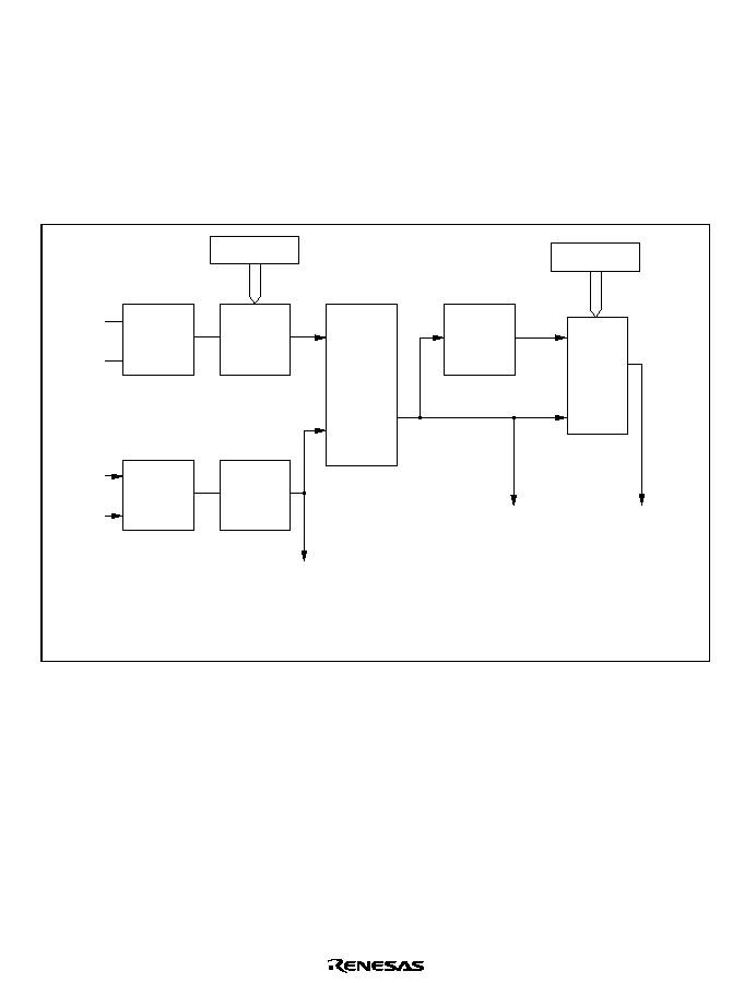
Rev. 2.0, 09/02, page 507 of 658
Section 21 Clock Pulse Generator
This LSI has an on-chip clock pulse generator that generates the system clock (
), the bus master
clock, and internal clocks. The clock pulse generator consists of an oscillator, duty adjustment
circuit, clock selection circuit, medium-speed clock divider, bus master clock selection circuit,
subclock oscillator, and wave formation circuit. A block diagram of the clock pulse generator of
the H8S/2268 Series is shown in figure 21.1. A block diagram of the clock pulse generator of the
H8S/2264 Series is shown in figure 21.2.
Legend:
LPWRCR:
SCKCR:
Low-power control register
System clock control register
EXTAL
XTAL
Duty
adjustment
circuit
Medium-
speed
clock divider
System
clock
oscillator
Clock
selection
circuit
SUB
WDT_1, TMR4, LCD count clock
Internal clock to
peripheral modules
Bus master clock
to CPU and DTC
/2 to
/32
Internal
clock
SCK2 to SCK0
SCKCR
RFCUT
OSC1
OSC2
Waveform
Generation
Circuit
Subclock
oscillator
LPWRCR
Bus
master
clock
selection
circuit
Figure 21.1 Block Diagram of Clock Pulse Generator (H8S/2268 Series)
CPG0501B_000020020700

Rev. 2.0, 09/02, page 508 of 658
Legend:
LPWRCR:
SCKCR:
SCKCR2:
Low-power control register
System clock control register
System clock control register 2
EXTAL
XTAL
Duty
adjustment
circuit
Medium-
speed
clock divider
System
clock
oscillator
Clock
selection
circuit
SUB
LCD
count clock
WDT_1
count clock
Internal clock to
peripheral modules
Output clock
to
pin
Bus master clock
to CPU
/2 to
/32
to
/131072,
SUB
/2 to
SUB
/256
SUB
/4
SUB
/60
Internal
clock
SCK2 to SCK0
SCKCR
Selector
Selector
SCKCR2
PHOE
PHCK3 to
PHCK0
SUBCKS1,
SUBCKS0
Divided
by 4
Divided
by 60
RFCUT
OSC1
OSC2
Waveform
generation
circuit
Subclock
oscillator
LPWRCR
Bus
master
clock
selection
circuit
Figure 21.2 Block Diagram of Clock Pulse Generator (H8S/2264 Series)
Frequency changes are performed by software by settings in the low-power control register
(LPWRCR) and system clock control register (SCKCR).

Rev. 2.0, 09/02, page 509 of 658
21.1
Register Descriptions
The on-chip clock pulse generator has the following registers.
∑
System clock control register (SCKCR)
∑
System clock control register 2 (SCKCR2) (supported only by the H8S/2264 Series)
∑
Low-power control register (LPWRCR)
21.1.1
System Clock Control Register (SCKCR)
SCKCR performs medium-speed mode control.
Bit
Bit Name
Initial Value
R/W
Description
7
6
--
--
0
0
R/W
R/W
Reserved
These are readable/writable bits, but the write
value should always be 0.
5
4
--
--
0
0
--
--
Reserved
These bits are always read as 0.Writing is invalid.
3
--
0
R/W
Reserved
This is a readable/writable bit, but the write value
should always be 0.
2
1
0
SCK2
SCK1
SCK0
0
0
0
R/W
R/W
R/W
System Clock Select 2 to 0
These bits select the bus master clock.
000: High-speed mode
001: Medium-speed clock is
/2
010: Medium-speed clock is
/4
011: Medium-speed clock is
/8
100: Medium-speed clock is
/16
101: Medium-speed clock is
/32
11X: Setting prohibited
Legend
X: Don't care
21.1.2 System Clock Control Register 2 (SCKCR2) (Supported only by the H8S/2264 Series)
SCKCR2 controls output clock
, selects RxD1 input pin, and TCNT_1 input subclock of
WDT_1.

Rev. 2.0, 09/02, page 510 of 658
Bit
Bit Name
Initial Value
R/W
Description
7
PHOE
0
R/W
Clock Output Enable
Controls
clock output from the PH4 selected by
the bits PHCK3 to PHCK0. For details, see table
21.1.
6
RXD1S
0
R/W
RxD1 Select
Selects the RxD1 input pin.
0: The RxD1 signal is input from the P34.
1: The RxD1 signal is input from the PH5.
5
4
SUBCKS1
SUBCKS0
0
0
R/W
R/W
Prescaler Subclock Select 1, 0
These bits select the TCNT_1 input subclock
source of WDT_1.
00: Clock
SUB
01: Clock
SUB
/4
10: Clock
SUB
/60
11: Setting prohibited
3
2
1
0
PHCK3
PHCK2
PHCK1
PHCK0
0
0
0
0
R/W
R/W
R/W
R/W
Clock Select 3 to 0
These bits select the
clock output from the PH4.
For details, see table 21.2.
Note:
*
To change the
clock output selection, bits PHCK3 to PHCK0 must be set after clock
output is halted by wiring 0 to the PHOE bit.
Table 21.1
Clock Output Control
PHOE
0
1
PHCK3
--
0
1
Subactive mode,
subsleep mode,
watch mode
PH4 I/O
Fixed to high
output
High-speed mode,
medium-speed mode,
sleep mode
PH4 I/O
output
Software standby
mode, direct
transition
PH4 I/O
Fixed to high
Hardware standby
mode
High impedance
High impedance

Rev. 2.0, 09/02, page 511 of 658
Table 21.2
Clock Selection
TCSR_1
SCKCR2
Bit 4
Bit 3
Bit 2
Bit 1
Bit 0
Main Clock
Frequency
Subclock Frequency
32.768 kHz
PSS
PHCK
3
PHCK
2
PHCK
1
PHCK
0
PH4
Output
Clock
2 MHz
20 MHz
SUB
*
2
SUB
/4
*
2
SUB
/60
*
2
0
/1
2 MHz
20 MHz
--
--
--
0
1
/2
1 MHz
10 MHz
--
--
--
0
/8
250 kHz
2.5 MHz
--
--
--
0
1
1
/64
31 kHz
313 kHz
--
--
--
0
/512
3.9 Hz
39 kHz
--
--
--
0
1
/2048
1.0 kHz
10 kHz
--
--
--
0
/8192
244 Hz
2.4 kHz
--
--
--
X
0
1
1
1
/131072
15 Hz
153 Hz
--
--
--
0
SUB
/2
--
16.38
kHz
4.096
kHz
273 Hz
0
1
SUB
/4
--
8.192
kHz
2.048
kHz
137 Hz
0
SUB
/8
--
4.096
kHz
1.024
kHz
68 Hz
0
1
1
SUB
/16
--
2.048
kHz
512 Hz
34 Hz
0
SUB
/32
--
1.024
kHz
256 Hz
17 Hz
0
1
SUB
/64
--
512
Hz
128 Hz
8.5 Hz
0
SUB
/128
--
256
Hz
64 Hz
4.3 Hz
1
*
1
1
1
1
1
SUB
/256
--
128
Hz
32 Hz
2.1 Hz
Legend
X: Don't care
Notes:
1.
To output
SUB
/2 to
SUB
/256, the PSS bit in TCSR_1 of WDT_1 must be set to 1.
2.
The subclock frequencies of
SUB
,
SUB
/4, and
SUB
/60 are set by the SUBCKS1 and SUBCKS0
bits in SCKCR2.

Rev. 2.0, 09/02, page 512 of 658
21.1.3
Low-Power Control Register (LPWRCR)
LPWRCR performs down-mode control, selects sampling frequency for eliminating noise,
performs subclock generation control, and specifies multiplication factor.
Bit
Bit Name
Initial Value
R/W
Description
7
DTON
0
R/W
Direct Transition ON Flag
0: When the SLEEP instruction is executed in high-
speed mode or medium-speed mode, operation
shifts to sleep mode, software standby mode, or
watch mode.
When the SLEEP instruction is executed in sub-
active mode, operation shifts to sub-sleep mode or
watch mode.
1: When the SLEEP instruction is executed in high-
speed mode or medium-speed mode, operation
shifts directly to sub-active mode, or shifts to sleep
mode or software standby mode.
When the SLEEP instruction is executed in sub-
active mode, operation shifts directly to high-speed
mode, or shifts to sub-sleep mode.
6
LSON
0
R/W
Low Speed ON Fag
0: When the SLEEP instruction is executed in high-
speed mode or medium-speed mode, operation
shifts to sleep mode, software standby mode, or
watch mode
*.
When the SLEEP instruction is executed in sub-
active mode, operation shifts to watch mode
*
or
shifts directly to high-speed mode.
Operation shifts to high-speed mode when watch
mode is cancelled.
1: When the SLEEP instruction is executed in high-
speed mode, operation shifts to watch mode or
sub-active mode.
When the SLEEP instruction is executed in sub-
active mode, operation shifts to sub-sleep mode or
watch mode.
Operation shifts to sub-active mode when watch
mode is cancelled.

Rev. 2.0, 09/02, page 513 of 658
Bit
Bit Name
Initial Value
R/W
Description
5
NESEL
0
R/W
Noise Elimination Sampling Frequency Select
This bit selects the sampling frequency of the
subclock (
SUB
) generated by the subclock oscillator is
sampled by the clock (
) generated by the system
clock oscillator
Set 0 when
is 5 MHz or higher. Set 1 when
is 2.1
MHz or lower. Any value can be set when
is 2.1 to
5 MHz.
0: Sampling using 1/32 x
1: Sampling using 1/4 x
4
SUBSTP
0
R/W
Subclock Enable
This bit enables/disables subclock generation. This
bit should be set to 1 when subclock is not used.
0: Enables subclock generation.
1: Disables subclock generation.
3
RFCUT
0
R/W
(H8S/2268, H8S/2266, H8S/2265, H8S/2264, and
H8S/2262)
Oscillation Circuit Feedback Resistance Control Bit
Selects whether or not built-in feedback resistance
and duty adjustment circuit of the system clock
generator are used when an external clock is input.
Do not access when the crystal resonator is used.
After setting this bit in the external clock input state,
enter software standby mode, watch mode, or
subactive mode. When software standby mode,
watch mode, or subactive mode is entered, switch
whether or not built-in feedback resistance and duty
adjustment circuit are used.
0: Built-in feedback resistance and duty adjustment
circuit of the system clock generator used.
1: Built-in feedback resistance and duty adjustment
circuit of the system clock generator not used.
(H8S/2264R and H8S/2262R)
Reserved
This is a readable/writable bit, but the write value
should always be 0.
2
--
0
R/W
Reserved
This is a readable/writable bit, but the write value
should always be 0.

Rev. 2.0, 09/02, page 514 of 658
Bit
Bit Name
Initial Value
R/W
Description
1
0
STC1
STC0
0
0
R/W
R/W
Multiplication factor setting
Specifies multiplication factor of the PLL circuit built
in the evaluation chip. The specified multiplication
factor becomes valid software standby mode, watch
mode, or subactive mode is entered.
These bits should be set to 11 in this LSI. Since the
value becomes STC1 = STC0 = 0 after a reset, set
STC1 = STC0 = 1.
00: x 1
01: x 2 (setting prohibited)
10: x 4 (setting prohibited)
11: PLL is bypass
Note:
*
When watch mode or subactive mode is entered, set high-speed mode.
21.2
System Clock Oscillator
System clock pulses can be supplied by connecting a crystal resonator, or by input of an external
clock.
21.2.1
Connecting a Crystal Resonator
A crystal resonator can be connected as shown in the example in figure 21.3. Select the damping
resistance R
d
according to table 21.3. An AT-cut parallel-resonance crystal should be used.
EXTAL
XTAL
R
d
C
L2
C
L1
C
L1
= C
L2
= 10 to 22pF
Note:
C
L1
and C
L2
are reference values including the floating capacitance of the board.
Figure 21.3 Connection of Crystal Resonator (Example)
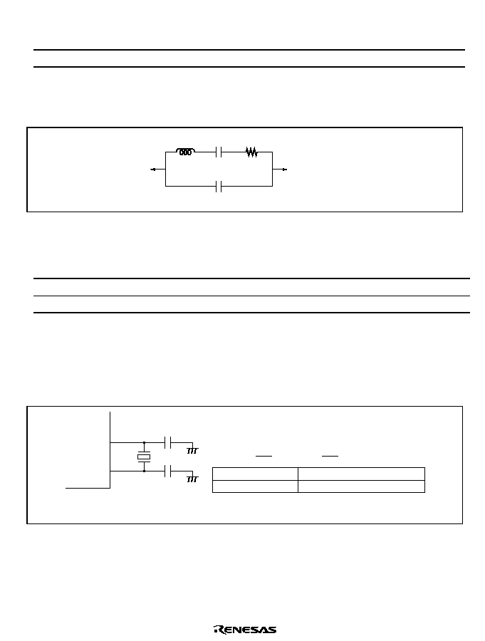
Rev. 2.0, 09/02, page 515 of 658
Table 21.3
Damping Resistance Value
Frequency (MHz)
2
4
6
8
10
12
16
20
R
d
(
)
1 k
500
300
200
100
0
0
0
Figure 21.4 shows the equivalent circuit of the crystal resonator. Use a crystal resonator that has
the characteristics shown in table 21.4.
XTAL
C
L
AT-cut parallel-resonance type
EXTAL
C
0
L
R
s
Figure 21.4 Crystal Resonator Equivalent Circuit
Table 21.4
Crystal Resonator Characteristics
Frequency (MHz)
2
4
6
8
10
12
16
20
R
S
max (
)
500
120
100
80
60
60
50
40
C
0
max (pF)
7
7
7
7
7
7
7
7
21.2.2
Connecting a Ceramic Resonator
A ceramic resonator can be connected in the H8S/2264R and H8S/2262R as shown in the example
in figure 21.5.
EXTAL
XTAL
C
L2
C
L1
Oscillation frequency
Preliminary
Note:
*
CL1 and CL2 are recommended values including the floating capacitance of the board.
CL1, CL2 recommended values
T.B.D
T.B.D
Figure 21.5 Connection of Ceramic Resonator (Example)

Rev. 2.0, 09/02, page 516 of 658
21.2.3
External Clock Input
External clock input is supported by the H8S/2268, H8S/2266, H8S/2265, H8S/2264, and
H8S/2262. An external clock signal can be input as shown in the examples in figure 21.6. If the
XTAL pin is left open, ensure that stray capacitance does not exceed 10 pF. When
complementary clock is input to the XTAL pin, the external clock input should be fixed high in
standby mode, subactive mode, subsleep mode, or watch mode.
EXTAL
XTAL
EXTAL
XTAL
External clock input
Open
External clock input
(a) XTAL pin left open
(b) Complementary clock input at XTAL pin
Figure 21.6 External Clock Input (Examples)
Table 21.5 shows the input conditions for the external clock. Table 21.6 shows the input
conditions for the external clock when duty adjustment circuit is not used.
Table 21.5
External Clock Input Conditions
V
CC
= 2.7 V to 5.0 V
V
CC
= 4.0 V to 5.5 V
Item
Symbol
Min
Max
Min
Max
Unit
Test
Conditions
External clock input low
pulse width
t
EXL
30
--
20
--
ns
External clock input high
pulse width
t
EXH
30
--
20
--
ns
External clock rise time t
EXr
--
7
--
5
ns
External clock fall time
t
EXf
--
7
--
5
ns
Figure 21.7

Rev. 2.0, 09/02, page 517 of 658
Table 21.6
External Clock Input Conditions (Duty Adjustment Circuit not used)
V
CC
= 2.7 V to 5.0 V
V
CC
= 4.0 V to 5.5 V
Item
Symbol
Min
Max
Min
Max
Unit
Test
Conditions
External clock input low
pulse width
t
EXL
37
--
25
--
ns
External clock input high
pulse width
t
EXH
37
--
25
--
ns
External clock rise time t
EXr
--
7
--
5
ns
External clock fall time
t
EXf
--
7
--
5
ns
Figure 21.7
Note: When duty adjustment circuit is not used, maximum operating frequency is lowered
according to the input waveform.
(Example: When t
EXL
= t
EXH
= 50 ns, t
EXr
= t
EXf
= 10 ns, clock cycle time = 120 ns, and
maximum operating frequency = 8.3 MHz)
t
EXH
t
EXL
t
EXr
t
EXf
V
CC
0.5
EXTAL
Figure 21.7 External Clock Input Timing
21.2.4
Notes on Switching External Clock
When two or more external clocks (e.g.: 10 MHz and 2 MHz) are used as the system clock, input
clock should be switched in software standby mode.
An example of external clock switching circuit is shown in figure 21.8. An example of external
clock switching timing is shown in figure 21.9.
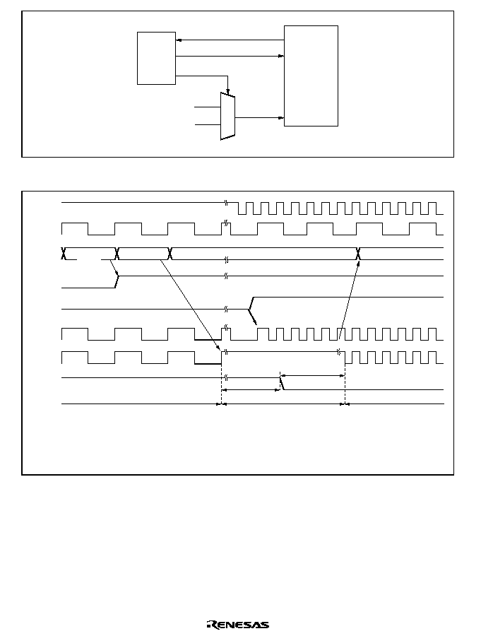
Rev. 2.0, 09/02, page 518 of 658
This LSI
Port output
External
interrupt
EXTAL
External clock 1
External clock 2
Selector
Control
circuit
External clock switch request
External interrupt signal
External clock switch signal
Figure 21.8 External Clock Switching Circuit (Examples)
200ns or more
(2)
(1) Port output (clock switching)
(2) Transition to software standby mode
(3) External clock switchover
(4) External interrupt generation
(An interrupt should be input 200 ns or more after transition to software standby mode.)
(5) Interrupt exception handling
(5)
SLEEP instruction
execution
Interrupt exception handling
Operation
External
clock 1
External
clock 2
(1)
Port output
(3)
External
clock
switching
circuit
EXTAL
Internal
clock
¯
(4)
standby mode
External
interrupt
Active (external clock1)
Active (external clock2)
Software standby mode
Clock switching
request
Figure 21.9 External Clock Switching Timing (Examples)
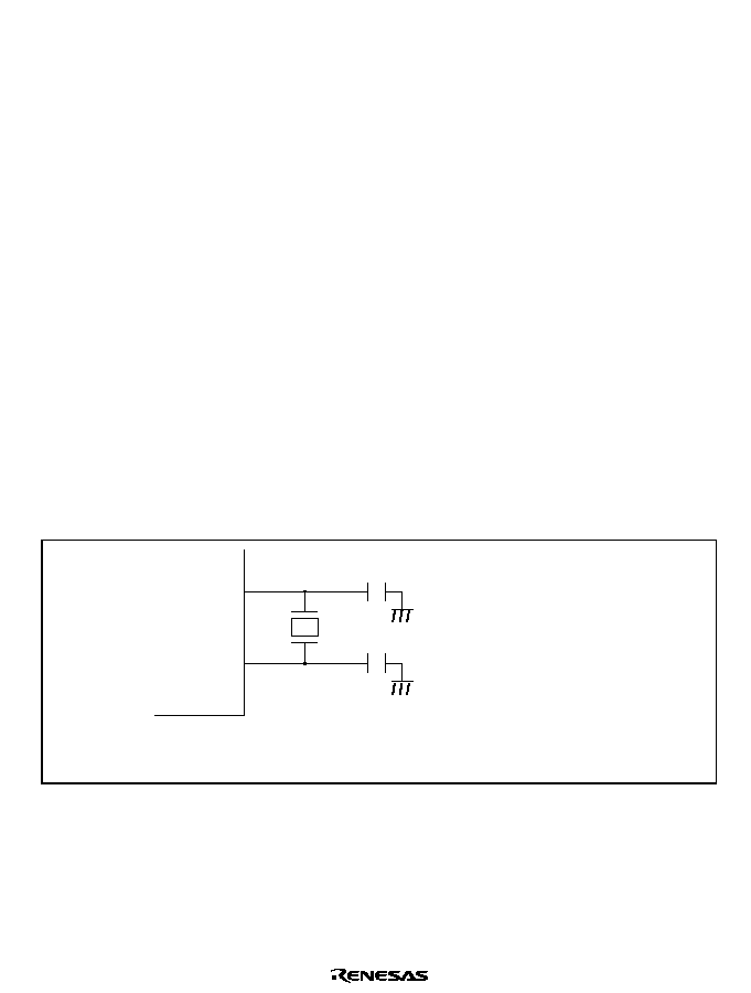
Rev. 2.0, 09/02, page 519 of 658
21.3
Duty Adjustment Circuit
The duty adjustment circuit is valid when oscillation frequency is more than 5 MHz. The duty
adjustment circuit adjusts clock output fr/m the system clock oscillator to generate the system
clock (
).
21.4
Medium-Speed Clock Divider
The medium-speed clock divider divides the system clock to generate
/2,
/4,
/8,
/16, and
/32.
21.5
Bus Master Clock Selection Circuit
The bus master clock selection circuit selects the clock supplied to the bus master by setting the
bits SCK2 to SCK0 in SCKCR. The bus master clock can be selected from system clock (
), or
medium-speed clocks (
/2,
/4,
/8,
/16,
/32).
21.6
Subclock Oscillator
21.6.1
Connecting 32.768kHz Crystal Resonator
To supply a clock to the subclock divider, connect a 32.768kHz crystal resonator, as shown in
Figure 21.10. Figure 21.11 shows the equivalence circuit for a 32.768kHz oscillator.
OSC1
OSC2
C
1
C
2
C
1
= C
2
= 15pF (typ)
Note: C1 and C2 are reference values including the floating
capacitance of the boad.
Figure 21.10 Example Connection of 32.768kHz Quartz Oscillator

Rev. 2.0, 09/02, page 520 of 658
OSC1
OSC2
C
s
L
s
R
s
C
o
Co = 1.5pF (typ.)
Rs = 14k (typ.)
fw = 32.768kHz
Type name = C001R (SEIKO EPSON)
Figure 21.11 Equivalence Circuit for 32.768kHz Oscillator
21.6.2
Handling Pins When Subclock Not Required
If no subclock is required, connect the OSC1 pin to Vss and leave OSC2 open, as shown in figure
21.12. Set the SUBSTP bit of LPWRCR to 1.
OSC1
OSC2
Open
Note: Set the SUBSTP
bit in LPWRCR to 1.
Figure 21.12 Pin Handling When Subclock Not Required

Rev. 2.0, 09/02, page 521 of 658
21.7
Subclock Waveform Generation Circuit
To eliminate noise from the subclock input to OSCI, the subclock is sampled using the dividing
clock
. The sampling frequency is set using the NESEL bit of LPWRCR. For details, see Section
21.1.3, Low Power Control Register (LPWRCR).
No sampling is performed in sub-active mode, sub-sleep mode, or watch mode.
21.8
Usage Notes
21.8.1
Note on Crystal Resonator
As various characteristics related to the crystal resonator are closely linked to the user's board
design, thorough evaluation is necessary on the user's part, using the resonator connection
examples shown in this section as a guide. As the resonator circuit ratings will depend on the
floating capacitance of the resonator and the mounting circuit, the ratings should be determined in
consultation with the resonator manufacturer. The design must ensure that a voltage exceeding the
maximum rating is not applied to the oscillator pin.
21.8.2
Note on Board Design
When designing the board, place the crystal resonator (ceramic resonator) and its load capacitors
as close as possible to the XTAL and EXTAL pins. Make wires as short as possible. Other signal
lines should be routed away from the oscillator circuit, as shown in figure 21.13. This is to prevent
induction from interfering with correct oscillation.
C2
Avoid
Signal A Signal B
C1
This LSI
XTAL, OSC2
EXTAL, OSC1
Figure 21.13 Note on Board Design of Oscillator Circuit
21.8.3
Note on Using a Crystal Resonator (Except for a Ceramic Resonator)
When a microcomputer runs, internal power supply potential will fluctuate synchronized with the
system clock. In addition, according to the individual characteristics of crystal resonator, there is a
case where the amplitude of the oscillation waveform will not be grown sufficiently immediately
after oscillation stabilization period, thus the oscillation waveform is easily affected by the

Rev. 2.0, 09/02, page 522 of 658
fluctuation of the power supply voltage. In this condition, oscillation waveform will be unstable,
resulting in the system clock instability and malfunction of the microcomputer.
If a malfunction occurs, the setting of the standby timer select 2 to 0 (STS2 to STS0) bits in the
standby control register (SBYCR) must be set so as for the standby time to be longer.
For example, if a malfunction occurs when the standby time is set to 8192 states, the operation
should be confirmed by setting the standby time to 16384 states or longer.
In addition, if a malfunction similar to at state transition occurs at reset, the
#$ pin hold time
must be set longer.

Rev. 2.0, 09/02, page 523 of 658
Section 22 Power-Down Modes
In addition to the normal program execution state, the H8S/2268 series and the H8S/2264 series
have nine power-down modes in which operation of the CPU and oscillator is halted and power
dissipation is reduced. Low-power operation can be achieved by individually controlling the CPU,
on-chip peripheral modules, and so on.
The H8S/2268 series and the H8S/2264 series operating modes are as follows:
1.
High-speed mode
2.
Medium-speed mode
3.
Subactive mode
4.
Sleep mode
5.
Subsleep mode
6.
Watch mode
7.
Module stop mode
8.
Software standby mode
9.
Hardware standby mode
2. to 9. are low power dissipation states. Sleep mode and sub-sleep mode are CPU states, medium-
speed mode is a CPU and bus master state, sub-active mode is a CPU and bus master and internal
peripheral function state, and module stop mode is an internal peripheral function (including bus
masters other than the CPU) state. Some of these states can be combined.
After a reset, the LSI is in high-speed mode with modules other than the DTC in module stop
mode.
Table 22.1 shows the internal state of the LSI in the respective modes. Table 22.2 shows the
conditions for shifting between the low power dissipation modes.
Figure 22.1 is a mode transition diagram.
Table 22.1
LSI Internal States in Each Mode
Function
High-
Speed
Medium-
Speed
Sleep
Module
Stop
Watch
Sub-
active
Subsleep
Software
Standby
Hardware
Standby
System clock pulse
generator
Function-
ing
Function-
ing
Function-
ing
Function-
ing
Halted
Halted
Halted
Halted
Halted
Subclock pulse
generator
Function-
ing/halted
Function-
ing/halted
Function-
ing/halted
Function-
ing/halted
Function-
ing
Function-
ing
Function-
ing
Function-
ing/halted
Halted

Rev. 2.0, 09/02, page 524 of 658
Function
High-
Speed
Medium-
Speed
Sleep
Module
Stop
Watch
Sub-
active
Subsleep
Software
Standby
Hardware
Standby
CPU
Instructions Function-
ing
Medium-
speed
operation
Halted
Function-
ing
Halted
Subclock
operation
Halted
Halted
Halted
Registers
Retained
Retained
Retained
Retained
Undefined
RAM
Function-
ing
Function-
ing
Function-
ing (DTC)
*
2
Function-
ing
Retained
Function-
ing
Retained
Retained
Retained
I/O
Function-
ing
Function-
ing
Function-
ing
Function-
ing
Retained
Function-
ing
Function-
ing
Halted
High
impedance
External
interrupts
NMI
IRQn
WKPn
Function-
ing
Function-
ing
Function-
ing
Function-
ing
Function-
ing
Function-
ing
Function-
ing
Function-
ing
Halted
Peripheral
functions
PBC
*
2
Function-
ing
Medium-
speed
operation
Function-
ing
Function-
ing/halted
(retained)
Halted
(retained)
Subclock
operation
Halted
(retained)
Halted
(retained)
Halted
(reset)
DTC
*
2
Function-
ing
Medium-
speed
operation
Function-
ing
Function-
ing/halted
(retained)
Halted
(retained)
Halted
(retained)
Halted
(retained)
Halted
(retained)
Halted
(reset)
TMR_4
*
2
LCD
Function-
ing
Function-
ing
Function-
ing
Function-
ing/halted
(retained)
Subclock
operation
*
1
Subclock
operation
*
1
Subclock
operation
*
1
Halted
(retained)
Halted
(reset)
WDT_1
Function-
ing
Function-
ing
Function-
ing
Function-
ing
Subclock
operation
*
1
Subclock
operation
*
1
Subclock
operation
*
1
Halted
(retained)
Halted
(reset)
WDT_0
Function-
ing
Function-
ing
Function-
ing
Function-
ing
Halted
(retained)
Subclock
operation
Subclock
operation
Halted
(retained)
Halted
(reset)
TMR_0
TMR_1
TMR_2
*
2
TMR_3
*
2
Function-
ing
Function-
ing
Function-
ing
Function-
ing/halted
(retained)
Halted
(retained)
Subclock
operation
Subclock
operation
Halted
(retained)
Halted
(reset)
TPU
SCI
IIC
DTMF
*
2
D/A
*
2
Function-
ing
Function-
ing
Function-
ing
Function-
ing/halted
(retained)
Halted
(retained)
Halted
(retained)
Halted
(retained)
Halted
(retained)
Halted
(reset)
A/D
Function-
ing
Function-
ing
Function-
ing
Function-
ing/halted
(reset)
Halted
(reset)
Halted
(reset)
Halted
(reset)
Halted
(reset)
Halted
(reset)
Notes:
"Halted (retained)" means that internal register values are retained. The internal state is
"operation suspended."
"Halted (reset)" means that internal register values and internal states are initialized.
In module stop mode, only modules for which a stop setting has been made are halted
(reset or retained).
1. When the TMR_4
*
2
, WDT_1, or LCD is operated in watch, subactive, or subsleep
mode, select the subclock as the clock to be used.
2. Supported only by the H8S/2268 Series.
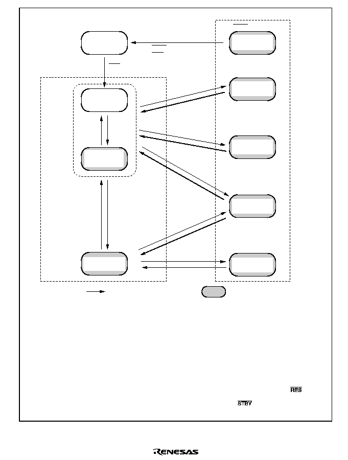
Rev. 2.0, 09/02, page 525 of 658
Program-halted state
Program execution state
SCK2 to
SCK0= 0
SCK2 to
SCK0 0
SLEEP instruction
SSBY = 1, PSS = 1
DTON = 1, LSON = 1
Clock switching
exception processing
SLEEP instruction
SSBY = 1, PSS = 1
DTON = 1, LSON = 0
After the oscillation
settling time
(STS2 to 0), clock
switching exception
processing
SLEEP instruction
SLEEP
instruction
External
interrupt
*
4
Any interrupt
*
3
SLEEP
instruction
SLEEP
instruction
SLEEP instruction
Interrupt
*
1
LSON bit = 0
Interrupt
*
2
Interrupt
*
1
LSON bit = 1
STBY pin = High
RES pin = Low
STBY pin = Low
SSBY= 0, LSON= 0
SSBY= 1,
PSS= 0, LSON= 0
SSBY= 0,
PSS= 1, LSON= 1
SSBY= 1,
PSS= 1, DTON= 0
RES pin = High
: Transition after exception processing
: Low power dissipation mode
Reset state
High-speed mode
(main clock)
Medium-speed
mode
(main clock)
Sub-active mode
(subclock)
Sub-sleep mode
(subclock)
Hardware
standby mode
Software
standby mode
Sleep mode
(main clock)
Watch mode
(subclock)
Notes: 1.
2.
3.
4.
H8S/2268 Series: NMI, IRQ0, IRQ1, IRQ3 to IRQ5, WKP0 to WKP7, WDT1 interrupt, and TMR4
interrupt
H8S/2264 Series: NMI, IRQ0, IRQ1, IRQ3, IRQ4, WKP0 to WKP7, and WDT1 interrupt
H8S/2268 Series: NMI, IRQ0, IRQ1, IRQ3 to IRQ5, WKP0 to WKP7, WDT0 interrupt, WDT1 interrupt,
and TMR0 to TMR4 interrupts
H8S/2264 Series: NMI, IRQ0, IRQ1, IRQ3, IRQ4, WKP0 to WKP7, WDT0 interrupt, WDT1 interrupt,
TMR0 interrupt, and TMR1 interrupt
All interrupts
H8S/2268 series: NMI, IRQ0, IRQ1, IRQ3 to IRQ5, WKP0 to WKP7
H8S/2264 series: NMI, IRQ0, IRQ1, IRQ3, IRQ4, WKP0 to WKP7
∑ When a transition is made between modes by means of an interrupt, the transition cannot be made
on interrupt source generation alone. Ensure that interrupt handling is performed after accepting the
interrupt request.
∑ From any state except hardware standby mode, a transition to the reset state occurs when
is
driven Low.
∑ From any state, a transition to hardware standby mode occurs when
is driven low.
∑ Always select high-speed mode before making a transition to watch mode or sub-active mode.
Figure 22.1 Mode Transition Diagram

Rev. 2.0, 09/02, page 526 of 658
Table 22.2
Low Power Dissipation Mode Transition Conditions
Status of Control Bit at
Transition
Pre-Transition
State
SSBY PSS
LSON DTON
State After Transition
Invoked by SLEEP
Instruction
State After Transition
Back from Low Power
Mode Invoked by
Interrupt
0
X
0
X
Sleep
High-speed/Medium-speed
High-speed/
Medium-speed
0
X
1
X
--
--
1
0
0
X
Software standby
High-speed/Medium-speed
1
0
1
X
--
--
1
1
0
0
Watch
High-speed
1
1
1
0
Watch
Sub-active
1
1
0
1
--
--
1
1
1
1
Sub-active
--
Sub-active
0
0
X
X
--
--
0
1
0
X
--
--
0
1
1
X
Sub-sleep
Sub-active
1
0
X
X
--
--
1
1
0
0
Watch
High-speed
1
1
1
0
Watch
Sub-active
1
1
0
1
High-speed
--
1
1
1
1
--
--
Legend
X :
Don't care
--:
Do not set.
22.1
Register Description
The following registers relates to the power-down modes. For details on system clock control
register (SCKCR), refer to section 21.1.1, System Clock Control Register (SCKCR). For details
on low power control register (LPWRCR), refer to section 21.1.3, Low Power Control Register
(LPWRCR). For details on timer control status register (TCSR), refer to section 12.2.2, Timer
Control Status Register (TCSR).
∑
Standby control register (SBYCR)
∑
Module stop control register A (MSTPCRA)
∑
Module stop control register B (MSTPCRB)
∑
Module stop control register C (MSTPCRC)
∑
Module stop control register D (MSTPCRD)

Rev. 2.0, 09/02, page 527 of 658
∑
Low power control register (LPWRCR)
∑
System clock control register (SCKCR)
∑
Timer control status register (TCSR)
22.1.1
Standby Control Register (SBYCR)
SBYCR performs power-down mode control.
Bit
Bit Name
Initial Value
R/W
Description
7
SSBY
0
R/W
Software Standby
Specifies transition destination when the SLEEP
instruction is executed.
0: Shifts to sleep mode when the SLEEP
instruction is executed in high-speed mode or
medium-speed mode.
Shifts to sub-sleep mode when the SLEEP
instruction is executed in sub-active mode.
1: Shifts to software standby mode, sub-active
mode, and watch mode when the SLEEP
instruction is executed in high-speed mode or
medium-speed mode.
Shifts to watch mode or high-speed mode when
the SLEEP instruction is executed in sub-active
mode.
Note that the value of the SSBY bit does not
change even when software standby mode is
canceled and making normal operation mode
transition by executing an external interrupt. To
clear this bit, 0 should be written to.

Rev. 2.0, 09/02, page 528 of 658
Bit
Bit Name
Initial Value
R/W
Description
6
5
4
STS2
STS1
STS0
0
0
0
R/W
R/W
R/W
Standby Timer Select 2 to 0
These bits select the MCU wait time for clock
settling to cancel software standby mode, watch
mode, or sub-active mode.
(Normal oscillation: H8S/2268, H8S/2266,
H8S/2265, H8S/2264, and H8S/2262)
With a crystal resonator (Table 22.3), select a wait
time of 8 ms (oscillation settling time) or more,
depending on the operating frequency. With an
external clock, there are no specific wait
requirements.
000: Standby time = 8192 states
001: Standby time = 16384 states
010: Standby time = 32768 states
011: Standby time = 65536 states
100: Standby time = 131072 states
101: Standby time = 262144 states
110: Standby time = 2048 states
111: Standby time = 16 states
*
(Oscillation settling time shortened: H8S/2264R
and H8S/2262R)
With a crystal resonator or ceramic resonator, refer
to tables 22.4 and 22.5 and select a wait time of
TBD µs (oscillation settling time) or more,
depending on the operating frequency. An external
clock cannot be used.
000: Standby time = 8192 states
001: Standby time = 16384 states
010: Standby time = 256 states
011: Standby time = 512 states
100: Standby time = 1024 states
101: Standby time = 4096 states
110: Standby time = 2048 states
111: Reserved
3
--
1
R/W
Reserved
This is a readable/writable bit, but the write value
should always be 1.

Rev. 2.0, 09/02, page 529 of 658
Bit
Bit Name
Initial Value
R/W
Description
2 to 0
--
All 0
--
Reserved
These bits are always read as 0 and cannot be
modified.
Note:
*
Do not set 16 states for standby time in the version with built-in flash memory. 2048 states
or more should be set.
22.1.2
Module Stop Control Registers A to D (MSTPCRA to MSTPCRD)
MSTPCR performs module stop mode control. When bits in MSTPCR registers are set to 1,
module stop mode is set. When cleared to 0, module stop mode is cleared.
MSTPCRA
Bit
Bit Name
Initial Value
R/W
Target Module
7
MSTPA7
*
1
0
R/W
6
MSTPA6
*
2
0
R/W
Data transfer controller (DTC)
5
MSTPA5
1
R/W
16-bit timer pulse unit (TPU)
4
MSTPA4
1
R/W
8-bit timer (TMR_0, TMR_1)
3
MSTPA3
*
1
1
R/W
2
MSTPA2
*
1
1
R/W
1
MSTPA1
1
R/W
A/D converter
0
MSTPA0
*
2
1
R/W
8-bit timer (TMR_2, TMR_3)
MSTPCRB
Bit
Bit Name
Initial Value
R/W
Target Module
7
MSTPB7
1
R/W
Serial communication interface 0 (SCI_0)
6
MSTPB6
1
R/W
Serial communication interface 1 (SCI_1)
5
MSTPB5
*
1
1
R/W
4
MSTPB4
1
R/W
I
2
C bus interface 0 (I
2
C_0) (optional)
3
MSTPB3
*
2
1
R/W
I
2
C bus interface 1 (I
2
C_1) (optional)
2
MSTPB2
*
1
1
R/W
1
MSTPB1
*
1
1
R/W
0
MSTPB0
*
1
1
R/W

Rev. 2.0, 09/02, page 530 of 658
MSTPCRC
Bit
Bit Name
Initial Value
R/W
Target Module
7
MSTPC7
1
R/W
Serial communication interface 2 (SCI_2)
6
MSTPC6
*
1
1
R/W
5
MSTPC5
*
2
1
R/W
D/A converter
4
MSTPC4
*
2
1
R/W
PC break controller (PBC)
3
MSTPC3
*
1
1
R/W
2
MSTPC2
*
2
1
R/W
DTMF generation circuit
1
MSTPC1
*
1
1
R/W
0
MSTPC0
*
1
1
R/W
MSTPCRD
Bit
Bit Name
Initial Value
R/W
Target Module
7
MSTPD7
*
1
1
R/W
6
MSTPD6
1
R/W
LCD controller/driver
5
MSTPD5
*
2
1
R/W
8-bit reload timer (TMR_4)
4
MSTPD4
*
1
1
R/W
3
MSTPD3
*
1
1
R/W
2
MSTPD2
*
1
1
R/W
1
MSTPD1
*
1
1
R/W
0
MSTPD0
*
1
1
R/W
Notes: 1. Bit MSTPA7 can be read/written to. This bit is initialized to 0. Only 1 should be written
to. Bits MSTPA3, MSTPA2, MSTPB5, MSTPB2 to MSTPB0, MSTPC6, MSTPC3,
MSTPC1, MSTPC0, MSTPD7, MSTPD4 to MSTPD0 can be read/written to. These bits
are initialized to 1. Only 1 should be written to.
2. With the H8S/2264 Series, only 1 should be written to.

Rev. 2.0, 09/02, page 531 of 658
22.2
Medium-Speed Mode
In high-speed mode, when the SCK2 to SCK0 bits in SCKCR are set to 1, the operating mode
changes to medium-speed mode as soon as the current bus cycle ends. In medium-speed mode, the
CPU operates on the operating clock (
/2,
/4,
/8,
/16, or
/32) specified by the SCK2 to SCK0
bits. The bus masters other than the CPU (DTC*) also operate in medium-speed mode.
On-chip peripheral modules other than the bus masters always operate on the high-speed clock (
).
In medium-speed mode, a bus access is executed in the specified number of states with respect to
the bus master operating clock. For example, if
/4 is selected as the operating clock, on-chip
memory is accessed in 4 states, and internal I/O registers in 8 states.
Medium-speed mode is cleared by clearing all of bits SCK2 to SCK0 to 0. A transition is made to
high-speed mode and medium-speed mode is cleared at the end of the current bus cycle.
If a SLEEP instruction is executed when the SSBY bit in SBYCR is cleared to 0, and LSON bit in
LPWRCR is cleared to 0, a transition is made to sleep mode. When sleep mode is cleared by an
interrupt, medium-speed mode is restored.
When the SLEEP instruction is executed with the SSBY bit = 1, LPWRCR LSON bit = 0, and
TCSR (WDT_1) PSS bit = 0, operation shifts to the software standby mode. When software
standby mode is cleared by an external interrupt, medium-speed mode is restored.
When the
5(6 pin is set low and medium-speed mode is cancelled, operation shifts to the reset
state. The same applies in the case of a reset caused by overflow of the watchdog timer.
When the
67%< pin is driven low, a transition is made to hardware standby mode.
Figure 22.2 shows the timing for transition to and clearance of medium-speed mode.
Note:
Supported only by the H8S/2268 Series.

Rev. 2.0, 09/02, page 532 of 658
Internal clock ,
Bus master clock
peripheral module clock
Internal address bus
Internal write signal
Medium-speed mode
SBYCR
SBYCR
Figure 22.2 Medium-Speed Mode Transition and Clearance Timing
22.3
Sleep Mode
22.3.1
Sleep Mode
When the SLEEP instruction is executed while the SBYCR SSBY bit = 0 and the LPWRCR
LSON bit = 0, the CPU enters the sleep mode. In sleep mode, CPU operation stops but the
contents of the CPU's internal registers are retained. Other peripheral modules do not stop.
22.3.2
Exiting Sleep Mode
Sleep mode is exited by any interrupt, or signals at the
5(6, or 67%< pins.
∑
Exiting Sleep Mode by Interrupts
When an interrupt occurs, sleep mode is exited and interrupt exception processing starts. Sleep
mode is not exited if the interrupt is disabled, or interrupts other than NMI are masked by the
CPU.
∑
Exiting Sleep Mode by
5(6 pin
Setting the
5(6 pin level low selects the reset state. After the stipulated reset input duration,
driving the
5(6 pin high starts the CPU performing reset exception processing.
∑
Exiting Sleep Mode by
67%< Pin
When the
67%< pin level is driven low, a transition is made to hardware standby mode.

Rev. 2.0, 09/02, page 533 of 658
22.4
Software Standby Mode
22.4.1
Software Standby Mode
A transition is made to software standby mode when the SLEEP instruction is executed while the
SBYCR SSBY bit = 1 and the LPWRCR LSON bit = 0, and the TCSR (WDT_1) PSS bit = 0. In
this mode, the CPU, on-chip peripheral modules, and oscillator all stop. However, the contents of
the CPU's internal registers, RAM data, and the states of on-chip peripheral modules other than
the A/D converter, and the states of I/O ports are retained. In this mode the oscillator stops, and
therefore power dissipation is significantly reduced.
22.4.2
Clearing Software Standby Mode
Software standby mode is cleared by an external interrupt (NMI pin, or pins
,54, ,54, ,54,
,54 , ,54*, :.3 to :.3), or by means of the 5(6 pin or 67%< pin.
∑
Clearing with an interrupt
When an NMI, or IRQ0, IRQ1, IRQ3, IRQ4, IRQ5*, or WKP0 to WKP7 interrupt request
signal is input, clock oscillation starts, and after the elapse of the time set in bits STS2 to STS0
in SYSCR, stable clocks are supplied to the entire chip, software standby mode is cleared, and
interrupt exception handling is started.
When clearing software standby mode with an IRQ0, IRQ1, IRQ3, IRQ4, IRQ5*, or WKP0 to
WKP7 interrupt, set the corresponding enable bit/pin function switching bit to 1 and ensure
that no interrupt with a higher priority than interrupts IRQ0, IRQ1, IRQ3, IRQ4, IRQ5*, or
WKP0 to WKP7 is generated. Software standby mode cannot be cleared if the interrupt has
been masked on the CPU side or has been designated as a DTC activation source.
∑
Clearing with the
5(6 pin
When the
5(6 pin is driven low, clock oscillation is started. At the same time as clock
oscillation starts, clocks are supplied to the entire chip. Note that the
5(6 pin must be held low
until clock oscillation settles. When the
5(6 pin goes high, the CPU begins reset exception
handling.
∑
Clearing with the
67%< pin
When the
67%< pin is driven low, a transition is made to hardware standby mode.
Note:
Supported only by the H8S/2268 Series.

Rev. 2.0, 09/02, page 534 of 658
22.4.3
Oscillation Settling Time after Clearing Software Standby Mode
Bits STS2 to STS0 in SBYCR should be set as described below.
Normal Oscillation (H8S/2268, H8S/2266, H8S/2265, H8S/2264, and H8S/2262):
∑
Using a Crystal Oscillator
Set bits STS2 to STS0 so that the standby time is at least 8 ms (the oscillation settling time).
Table 22.3 shows the standby times for different operating frequencies and settings of bits
STS2 to STS0.
∑
Using an External Clock
Any value can be set. Normally, minimum time is recommended.
Note:
Do not set 16 states for standby time in the version with built-in flash memory. 2048 states
or more should be set.
Table 22.3
Oscillation Settling Time Settings (Normal Oscillation)
STS2
STS1
STS0
Standby Time
20 MHz 16 MHz 13 MHz 10 MHz 8 MHz
6 MHz
4 MHz
2 MHz
Unit
0
0
0
8192 states
0.41
0.51
0.63
0.82
1.0
1.4
2.0
4.1
ms
1
16384 states
0.82
1.0
1.3
1.6
2.0
2.7
4.1
8.2
1
0
32768 states
1.6
2.0
2.5
3.3
4.1
5.5
8.2
16.4
1
65536 states
3.3
4.1
5.0
6.6
8.2
10.9
16.4
32.8
1
0
0
131072 states
6.6
8.2
10.1
13.1
16.4
21.8
32.8
65.5
1
262144 states
13.1
16.4
20.2
26.2
32.8
43.7
65.5
131.1
1
0
2048 states
0.10
0.13
0.16
0.20
0.26
0.34
0.51
1.0
1
16 states
0.8
1.0
1.2
1.6
2.0
2.7
4.0
8.0
µs
Shading: Recommended time setting
Oscillation Settling Time Shortened (H8S/2264R and H8S/2262R)
Preliminary
:
∑
Using a Crystal Oscillator
Set bits STS2 to STS0 so that the standby time is at least TBD µs (the oscillation settling time).
Table 22.4 shows the standby times for different operating frequencies and settings of bits
STS2 to STS0.
∑
Using a Ceramic Oscillator
Table 22.5 shows the standby times for different operating frequencies and settings of bits
STS2 to STS0.
Note:
An external clock cannot be used in the H8S/2264R and H8S/2262R.

Rev. 2.0, 09/02, page 535 of 658
Table 22.4
Oscillation Settling Time Settings (Oscillation Settling Time Shortened: Crystal
Oscillator)
STS2
STS1
STS0
Standby Time
20 MHz 16 MHz 13 MHz 10 MHz 8 MHz
6 MHz
4 MHz
2 MHz
Unit
0
1
0
256 states
12.8
16.0
19.7
25.6
32.0
42.7
64.0
128
µs
0
1
1
512 states
25.6
32.0
39.4
51.2
64.0
85.3
128
256
1
0
0
1024 states
51.2
64.0
78.8
102
128
171
256
512
1
1
0
2048 states
102
128
158
205
256
341
512
1024
1
0
1
4096 states
205
256
315
410
512
683
1024
2048
0
0
0
8192 states
410
512
630
819
1024
1365
2048
4096
0
0
1
16384 states
819
1024
1260
1638
2048
2731
4096
8192
1
1
1
Reserved
--
--
--
--
--
--
--
--
--
Table 22.5
Oscillation Settling Time Settings (Oscillation Settling Time Shortened:
Ceramic Oscillator)
STS2
STS1
STS0
Standby Time
20 MHz 16 MHz 13 MHz 10 MHz 8 MHz
6 MHz
4 MHz
2 MHz
Unit
0
1
0
256 states
12.8
16.0
19.7
25.6
32.0
42.7
64.0
128
µs
0
1
1
512 states
25.6
32.0
39.4
51.2
64.0
85.3
128
256
1
0
0
1024 states
51.2
64.0
78.8
102
128
171
256
512
1
1
0
2048 states
102
128
158
205
256
341
512
1024
1
0
1
4096 states
205
256
315
410
512
683
1024
2048
0
0
0
8192 states
410
512
630
819
1024
1365
2048
4096
0
0
1
16384 states
819
1024
1260
1638
2048
2731
4096
8192
1
1
1
Reserved
--
--
--
--
--
--
--
--
--
Shading: Recommended time setting
22.4.4
Software Standby Mode Application Example
Figure 22.3 shows an example in which a transition is made to software standby mode at the
falling edge on the NMI pin, and software standby mode is cleared at the rising edge on the NMI
pin.
In this example, an NMI interrupt is accepted with the NMIEG bit in SYSCR cleared to 0 (falling
edge specification), then the NMIEG bit is set to 1 (rising edge specification), the SSBY bit is set
to 1, and a SLEEP instruction is executed, causing a transition to software standby mode.
Software standby mode is then cleared at the rising edge on the NMI pin.

Rev. 2.0, 09/02, page 536 of 658
Oscillator
Internal clock
NMI
NMIEG
SSBY
NMI exception
handling
NMIEG=1
SSBY=1
SLEEP instruction
Software standby mode
(power-down mode)
Oscillation
settling
time t
OSC2
NMI exception
handling
Figure 22.3 Software Standby Mode Application Example
22.5
Hardware Standby Mode
22.5.1
Hardware Standby Mode
When the
67%< pin is driven low, a transition is made to hardware standby mode from any mode.
In hardware standby mode, all functions enter the reset state and stop operation, resulting in a
significant reduction in power dissipation. As long as the prescribed voltage is supplied, on-chip
RAM data is retained. I/O ports are set to the high-impedance state.
Do not change the state of the mode pins (MD2,MD1) during hardware standby mode.
22.5.2
Clearing Hardware Standby Mode
Hardware standby mode is cleared by means of the
67%< pin and the 5(6 pin. When the 67%<
pin is driven high while the
5(6 pin is low, the reset state is set and clock oscillation is started.
Ensure that the
5(6 pin is held low until the clock oscillator settles (at least t
osc1
ms--the
oscillation settling time--when using a crystal/ceramic oscillator). When the
5(6 pin is
subsequently driven high, a transition is made to the program execution state via the reset
exception handling state.
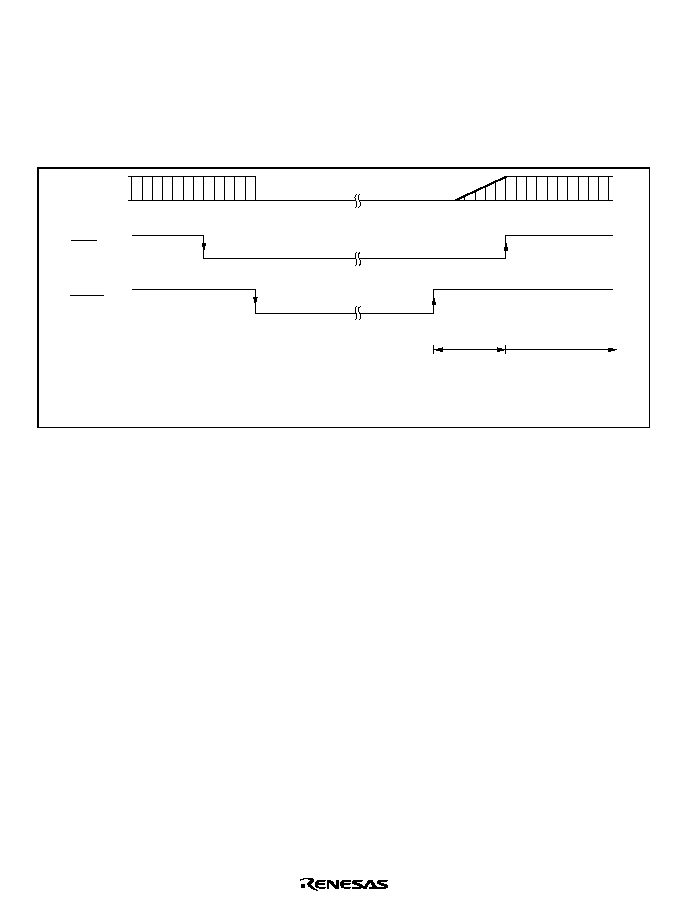
Rev. 2.0, 09/02, page 537 of 658
22.5.3
Hardware Standby Mode Timing
Figure 22.4 shows an example of hardware standby mode timing.
When the
67%< pin is driven low after the 5(6 pin has been driven low, a transition is made to
hardware standby mode. Hardware standby mode is cleared by driving the
67%< pin high, waiting
for the oscillation settling time, then changing the
5(6 pin from low to high.
Oscillator
RES
STBY
Oscillation
settling
time t
osc1
Reset
exception
handling
Figure 22.4 Hardware Standby Mode Timing
22.6
Module Stop Mode
Module stop mode can be set for individual on-chip peripheral modules.
When the corresponding MSTP bit in MSTPCR is set to 1, module operation stops at the end of
the bus cycle and a transition is made to module stop mode. The CPU continues operating
independently.
When the corresponding MSTP bit is cleared to 0, module stop mode is cleared and the module
starts operating at the end of the bus cycle. In module stop mode, the internal states of modules
other than the A/D converter are retained.
After reset clearance, all modules other than DTC* are in module stop mode.
When an on-chip peripheral module is in module stop mode, read/write access to its registers is
disabled.
Since the operations of the bus controller and I/O port are stopped when sleep mode is entered at
the all-module stop state (MSTPCR=H'FFFFFFFF), power consumption can further be reduced.
Note:
Supported only by the H8S/2268 Series.

Rev. 2.0, 09/02, page 538 of 658
22.7
Watch Mode
22.7.1
Transition to Watch Mode
CPU operation makes a transition to watch mode when the SLEEP instruction is executed in high-
speed mode or sub-active mode with SBYCR SSBY=1, LPWRCR DTON = 0, and TCSR
(WDT_1) PSS = 1.
In watch mode, the CPU is stopped and peripheral modules other than WDT_1, TMR_4*, and
LCD are also stopped. The contents of the CPU's internal registers, the data in internal RAM, and
the statuses of the internal peripheral modules (excluding the A/D converter) and I/O ports are
retained. To make a transition to watch mode, bits SCK2 to SCK0 in SCKCR must be set to 0.
Note:
Supported only by the H8S/2268 Series.
22.7.2
Exiting Watch Mode
Watch mode is exited by any interrupt (WOVI1 interrupt, OVI4 to OVI7 interrupts*, NMI pin, or
,54, ,54, ,54, ,54, ,54*, or :.3 to :.3), or signals at the 5(6, or 67%< pins.
∑
Exiting Watch Mode by Interrupts
When an interrupt occurs, watch mode is exited and a transition is made to high-speed mode or
medium-speed mode when the LPWRCR LSON bit = 0 or to sub-active mode when the LSON
bit = 1. When a transition is made to high-speed mode, a stable clock is supplied to all LSI
circuits and interrupt exception processing starts after the time set in SBYCR STS2 to STS0
has elapsed. In the case of IRQ0, IRQ1, IRQ3, IRQ4, IRQ5*, and WKP0 to WKP7 interrupts,
no transition is made from watch mode if the corresponding enable bit/pin function switching
bit has been cleared to 0, and, in the case of interrupts from the internal peripheral modules, the
interrupt enable register has been set to disable the reception of that interrupt, or is masked by
the CPU.
See section 22.4.3, Oscillation Settling Time after Clearing Software Standby Mode, for how
to set the oscillation settling time when making a transition from watch mode to high-speed
mode.
∑
Exiting Watch Mode by
5(6 pins
For exiting watch mode by the
5(6 pins, see section 22.4.2, Clearing Software Standby Mode.
∑
Exiting Watch Mode by
67%< pin
When the
67%< pin level is driven low, a transition is made to hardware standby mode.
Note:
Supported only by the H8S/2268 Series.

Rev. 2.0, 09/02, page 539 of 658
22.8
Sub-Sleep Mode
22.8.1
Transition to Sub-Sleep Mode
When the SLEEP instruction is executed with the SBYCR SSBY bit = 0, LPWRCR LSON bit = 1,
and TCSR (WDT_1) PSS bit = 1, CPU operation shifts to sub-sleep mode.
In sub-sleep mode, the CPU is stopped. Peripheral modules other than TMR_0, TMR1, TMR2 to
TMR_4*, WDT_0, WDT_1, and LCD are also stopped. The contents of the CPU's internal
registers, the data in internal RAM, and the statuses of the internal peripheral modules (excluding
the A/D converter) and I/O ports are retained.
Note:
Supported only by the H8S/2268 Series.
22.8.2
Exiting Sub-Sleep Mode
Sub-sleep mode is exited by an interrupt (interrupts from internal peripheral modules, NMI pin, or
,54, ,54, ,54, ,54, ,54*, or :.3 to :.3), or signals at the 5(6 or 67%< pins.
∑
Exiting Sub-Sleep Mode by Interrupts
When an interrupt occurs, sub-sleep mode is exited and interrupt exception processing starts.
In the case of
,54, ,54, ,54, ,54, ,54*, and :.3 to :.3 interrupts, sub-sleep
mode is not cancelled if the corresponding enable bit/pin function switching bit has been
cleared to 0, and, in the case of interrupts from the internal peripheral modules, the interrupt
enable register has been set to disable the reception of that interrupt, or is masked by the CPU.
∑
Exiting Sub-Sleep Mode by
5(6
For exiting sub-sleep mode by the
5(6 pins, see section 22.4.2, Clearing Software Standby
Mode.
∑
Exiting Sub-Sleep Mode by
67%< Pin
When the
67%< pin level is driven low, a transition is made to hardware standby mode.
Note:
Supported only by the H8S/2268 Series.

Rev. 2.0, 09/02, page 540 of 658
22.9
Sub-Active Mode
22.9.1
Transition to Sub-Active Mode
When the SLEEP instruction is executed in high-speed mode with the SBYCR SSBY bit = 1,
LPWRCR DTON bit = 1, LSON bit = 1, and TCSR (WDT_1) PSS bit = 1, CPU operation shifts to
sub-active mode. When an interrupt occurs in watch mode, and if the LSON bit of LPWRCR is 1,
a transition is made to sub-active mode. And if an interrupt occurs in sub-sleep mode, a transition
is made to sub-active mode.
In sub-active mode, the CPU operates at low speed on the subclock, and the program is executed
step by step. Peripheral modules other than PBC*, TMR_0, TMR_1, TMR_2 to TMR_4*,
WDT_0, WDT_1, and LCD are also stopped.
When operating the CPU in sub-active mode, the SCKCR SCK2 to SCK0 bits must be set to 0.
Note:
Supported only by the H8S/2268 Series.
22.9.2
Exiting Sub-Active Mode
Sub-active mode is exited by the SLEEP instruction or the
5(6 or 67%< pins.
∑
Exiting Sub-Active Mode by SLEEP Instruction
When the SLEEP instruction is executed with the SBYCR SSBY bit = 1, LPWRCR DTON bit
= 0, and TCSR (WDT_1) PSS bit = 1, the CPU exits sub-active mode and a transition is made
to watch mode. When the SLEEP instruction is executed with the SBYCR SSBY bit = 0,
LPWRCR LSON bit = 1, and TCSR (WDT_1) PSS bit = 1, a transition is made to sub-sleep
mode. Finally, when the SLEEP instruction is executed with the SBYCR SSBY bit = 1,
LPWRCR DTON bit = 1, LSON bit = 0, and TCSR (WDT_1) PSS bit = 1, a direct transition is
made to high-speed mode (SCK0 to SCK2 all 0).
∑
Exiting Sub-Active Mode by
5(6 Pins
For exiting sub-active mode by the
5(6 pins, see section 22.4.2, Clearing Software Standby
Mode.
∑
Exiting Sub-Active Mode by
67%< Pin
When the
67%< pin level is driven low, a transition is made to hardware standby mode.

Rev. 2.0, 09/02, page 541 of 658
22.10
Direct Transitions
There are three modes, high-speed, medium-speed, and sub-active, in which the CPU executes
programs. When a direct transition is made, there is no interruption of program execution when
shifting between high-speed and sub-active modes. Direct transitions are enabled by setting the
LPWRCR DTON bit to 1, then executing the SLEEP instruction. After a transition, direct
transition interrupt exception processing starts.
22.10.1
Direct Transitions from High-Speed Mode to Sub-Active Mode
Execute the SLEEP instruction in high-speed mode when the SBYCR SSBY bit = 1, LPWRCR
LSON bit = 1, and DTON bit = 1, and TSCR (WDT_1) PSS bit = 1 to make a transition to sub-
active mode.
22.10.2
Direct Transitions from Sub-Active Mode to High-Speed Mode
Execute the SLEEP instruction in sub-active mode when the SBYCR SSBY bit = 1, LPWRCR
LSON bit = 0, and DTON bit = 1, and TSCR (WDT_1) PSS bit = 1 to make a direct transition to
high-speed mode after the time set in SBYCR STS2 to STS0 has elapsed.
22.11
Usage Notes
22.11.1
I/O Port Status
In software standby mode and watch mode, I/O port states are retained. Therefore, there is no
reduction in current dissipation for the output current when a high-level signal is output.
22.11.2
Current Dissipation during Oscillation Settling Wait Period
Current dissipation increases during the oscillation settling wait period.
22.11.3
DTC Module Stop (Supported only by the H8S/2268 Series)
Depending on the operating status of the DTC, the MSTPA6 bit may not be set to 1. Setting of the
DTC module stop mode should be carried out only when the respective module is not activated.
For details, refer to section 8, Data Transfer Controller (DTC).

Rev. 2.0, 09/02, page 542 of 658
22.11.4
On-Chip Peripheral Module Interrupt
∑
Module stop mode
Relevant interrupt operations cannot be performed in module stop mode. Consequently, if
module stop mode is entered when an interrupt has been requested, it will not be possible to
clear the CPU interrupt source or the DTC* activation source. Interrupts should therefore be
disabled before entering module stop mode.
Note:
Supported only by the H8S/2268 Series.
∑
Subactive mode / Watch mode
On-chip peripheral modules (DTC*, TPU, IIC) that stop operation in subactive mode cannot
clear interrupts in subactive mode. Therefore, if subactive mode is entered when an interrupt is
requested, CPU interrupt factors cannot be cleared.
Interrupts should therefore before executing the SLEEP instruction and entering subactive or
watch mode.
Note:
Supported only by the H8S/2268 Series.
22.11.5
Writing to MSTPCR
MSTPCR should only be written to by the CPU.
22.11.6
Entering Subactive / Watch mode and DTC Module Stop (Supported only by the
H8S/2268 Series)
To enter subactive or watch mode, set DTC to module stop (write 1 to the MSTPA6 bit) and
reading the MSTPA6 bit as 1 before transiting mode. After transiting from subactive mode to
active mode, clear module stop.
When DTC activation factor occurs in subactive mode, DTC is activated when module stop is
cleared after active mode is entered.

Rev. 2.0, 09/02, page 543 of 658
Section 23 Power-On Reset Circuit
The H8S/2264 Series has a power-on reset circuit. The H8S/2268 Series does not have a power-on
reset circuit.
Block diagram of the power-on reset circuit is shown in figure 23.1.
23.1
Features
∑
Power-on reset circuit
The power-on reset circuit can be enabled or disabled according to the mode pin settings
(enabled when MD2 = 0 and MD1 = 1).
An internal reset signal is generated at turning the power on by externally connecting a
capacitor.
CK
MD2
MD1
Legend:
PS: Prescaler
R
PS
OVF
R
S
Q
Figure 23.1 Power-On Reset Circuit
23.2
Operation
23.2.1
Power-On Reset Circuit
The power-on reset circuit is enabled by setting the mode pins MD2 and MD1 to B'01. The
operation timing of the power-on reset circuit is shown in figure 23.2. As the power supply
voltage rises, the capacitor is gradually charged through the pull-up resistor, which is connected to
the
#$ pin. The low level of the #$ pin is sent to the chip and resets the prescaler and the
whole chip. When the level of the
#$ pin reaches to the predetermined level, reset state of the
prescaler is cancelled and count-up operation starts. When the prescaler counts
for 131,072
times, an OVF signal is generated and an internal reset signal is cancelled.
PSCKT10A_000020020700

Rev. 2.0, 09/02, page 544 of 658
Note that the power-supply circuit must be designed so that the power supply voltage reaches an
appropriate level within the stipulated time. In addition, when the capacitance of the capacitor
which is externally connected is determined, the rising time of the power supply voltage level
must be taken into consideration.
Vcc
Vss
Vss
t
PORESW
*
PS
reset signal
Internal
reset signal
OVF
131,072 states
PS counter starts
Reset cancelled
VIH
Figure 23.2 Power-On Reset Circuit Operation Timing
Note: *
In case of t
OSC1
131,072 states
t
PORESW
t
RESW
In case of t
OSC1
>
131,072 states
t
PORESW
t
RESW
+ t
OCS1
≠ 131,072 states
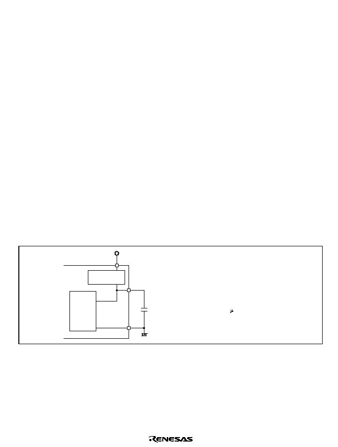
Rev. 2.0, 09/02, page 545 of 658
Section 24 Power Supply Circuit
This LSI has an internal power step-down circuit built into it. Using this circuit allows the internal
power supply to be fixed at approximately 3.0 V without relaying on the power supply voltage
connected to the external Vcc terminal. This means that, when used at an external power supply
higher than 3.0 V, the current consumption value can be suppressed to largely the same value as
that when used at approximately 3.0 V. If the external voltage is 3.0 V or less, the internal voltage
will be largely consistent with the external voltage.
24.1
When the internal power step-down circuit is used
As shown in figure 24.1, an external power supply should be connected to the Vcc terminal, using
the shortest possible wiring, with a capacitance of approximately 0.1
µ
F between CVcc and Vss.
Adding this external circuit makes the internal step-down circuit valid. Applying a power supply
exceeding the absolute maximum rated value of 4.3 V to the CVcc terminal can permanently
damage the LSI, so the power supply should not be connected to the CVcc terminal. The external
power supply voltage connected to Vcc and the GND potential connected to Vss serve as the
references for the input/output levels of the external circuit. For example, a "High" port
input/output level will be the Vcc reference, and a "Low" level will be the Vss reference. The
analog power supplies of the A/D converter, D/A converter*, and DTMF generation circuit* do
not affect the internal step-down circuit.
Note: * Supported only by the H8S/2268 Series.
Vss
CVcc
Vcc
Internal
power
supply
Internal
logic
Vcc 2.7 to 5.5V
(Vcc = 3.0 to 5.5V for the F-ZTAT version)
Setup-down
voltage circuit
Stabilized capacitance (approx. 0.1 F)
Figure 24.1 Power Supply Connections when an Internal Power Supply
Step-Down Circuit is Used

Rev. 2.0, 09/02, page 546 of 658

Rev. 2.0, 09/02, page 547 of 658
Section 25 List of Registers
This section gives information on the on-chip I/O registers and is configured as described below.
1. Register Addresses (by functional module, in address order)
∑
Descriptions by functional module, in ascending order of addresses
∑
When registers consist of 16 bits, the addresses of the MSBs are given.
∑
Data bus width is given.
∑
The number of access states are given.
2. Register Bits
∑
Bit configurations of the registers are described in the same order as the Register Addresses
(by functional module, in ascending order of addresses).
∑
Reserved bits are indicated by
in the bit name.
∑
When registers consist of 16 or 32 bits, bits are described from the MSB side.
3. Register States in Each Operating Mode
∑
Register states are described in the same order as the Register Addresses (by functional
module, in ascending order of addresses).
∑
The register states described are for the basic operating modes. If there is a specific reset for an
on-chip module, refer to the section on that on-chip module.
25.1
Register Addresses (by function module, in address order)
The data bus width indicates the numbers of bits by which the register is accessed.
The number of access states indicates the number of states based on the specified reference clock.

Rev. 2.0, 09/02, page 548 of 658
Register Name
Abbrevia-
tion
Bit No.
Address
*
1
Module
Data
Width
Access
State
DTC mode register A
*
4
MRA
8
H'EBC0 to DTC
16/32
*
2
1
DTC source address register
*
4
SAR
24
H'EFBF
DTC
16/32
*
2
1
DTC mode register B
*
4
MRB
8
DTC
16/32
*
2
1
DTC destination address register
*
4
DAR
24
DTC
16/32
*
2
1
DTC transfer count register A
*
4
CRA
16
DTC
16/32
*
2
1
DTC transfer count register B
*
4
CRB
16
DTC
16/32
*
2
1
LCD port control register
LPCR
8
H'FC30
LCD
8/16
4
LCD control register
LCR
8
H'FC31
LCD
8/16
4
LCD control register 2
LCR2
8
H'FC32
LCD
8/16
4
LCD RAM
8
H'FC40 to
H'FC53
LCD
8/16
4
Module stop control register D
MSTPCRD 8
H'FC60
SYSTEM 8
4
System clock control register 2
*
5
SCKCR2
8
H'FC61
SYSTEM 8
4
DTMF control register
*
4
DTCR
8
H'FC68
DTMF
8
4
DTMF load register
*
4
DTLR
8
H'FC69
DTMF
8
4
Timer control register_4
*
4
TCR_4
8
H'FC70
TMR_4
8/16
4
Timer control register_5
*
4
TCR_5
8
H'FC71
TMR_4
8/16
4
Timer control register_6
*
4
TCR_6
8
H'FC72
TMR_4
8/16
4
Timer control register_7
*
4
TCR_7
8
H'FC73
TMR_4
8/16
4
Timer counter 4/Timer reload
register 4
*
4
TCNT_4(R)/
TLR_4(W)
8
H'FC74
TMR_4
8/16
4
Timer counter 5/Timer reload
register 5
*
4
TCNT_5(R)/
TLR_5(W)
8
H'FC75
TMR_4
8/16
4
Timer counter 6/Timer reload
register 6
*
4
TCNT_6(R)/
TLR_6(W)
8
H'FC76
TMR_4
8/16
4
Timer counter 7/Timer reload
register 7
*
4
TCNT_7(R)/
TLR_7(W)
8
H'FC77
TMR_4
8/16
4
Port H data direction register
PHDDR
8
H'FC80
PORT
8
4

Rev. 2.0, 09/02, page 549 of 658
Register Name
Abbrevia-
tion
Bit No.
Address
*
1
Module
Data
Width
Access
State
Port J data direction register
PJDDR
8
H'FC81
PORT
8
4
Port K data direction register
PKDDR
8
H'FC82
PORT
8
4
Port L data direction register
PLDDR
8
H'FC83
PORT
8
4
Port M data direction register
*
4
PMDDR
8
H'FC84
PORT
8
4
Port N data direction register
*
4
PNDDR
8
H'FC85
PORT
8
4
Port H data register
PHDR
8
H'FC88
PORT
8
4
Port J data register
PJDR
8
H'FC89
PORT
8
4
Port K data register
PKDR
8
H'FC8A
PORT
8
4
Port L data register
PLDR
8
H'FC8B
PORT
8
4
Port M data register
*
4
PMDR
8
H'FC8C
PORT
8
4
Port N data register
*
4
PNDR
8
H'FC8D
PORT
8
4
Port H register
PORTH
8
H'FC90
PORT
8
4
Port J register
PORTJ
8
H'FC91
PORT
8
4
Port K register
PORTK
8
H'FC92
PORT
8
4
Port L register
PORTL
8
H'FC93
PORT
8
4
Port M register
*
4
PORTM
8
H'FC94
PORT
8
4
Port N register
*
4
PORTN
8
H'FC95
PORT
8
4
Port J pull-up MOS control register PJPCR
8
H'FC99
PORT
8
4
Wakeup control register
WPCR
8
H'FC9F
PORT
8
4
Wakeup interrupt request register
IWPR
8
H'FCA0
INT
8
4
Interrupt enable register
IENR1
8
H'FCA1
INT
8
4
D/A data register_0
*
4
DADR_0
8
H'FDAC
D/A
8
2
D/A data register_1
*
4
DADR_1
8
H'FDAD
D/A
8
2
D/A control register
*
4
DACR
8
H'FDAE
D/A
8
2
Serial control register X
SCRX
8
H'FDB4
IIC,
FLASH
8
2
DDC switch register
DDCSWR
8
H'FDB5
IIC
8
2
Timer control register_2
*
4
TCR_2
8
H'FDC0
TMR_2
8
2
Timer control register_3
*
4
TCR_3
8
H'FDC1
TMR_3
8
2
Timer control/status register_2
*
4
TCSR_2
8
H'FDC2
TMR_2
8
2
Timer control/status register_3
*
4
TCSR_3
8
H'FDC3
TMR_3
8
2
Time constant register A_2
*
4
TCORA_2
8
H'FDC4
TMR_2
8/16
2
Time constant register A_3
*
4
TCORA_3
8
H'FDC5
TMR_3
8/16
2

Rev. 2.0, 09/02, page 550 of 658
Register Name
Abbrevia-
tion
Bit No.
Address
*
1
Module
Data
Width
Access
State
Time constant register B_2
*
4
TCORB_2
8
H'FDC6
TMR_2
8/16
2
Time constant register B_3
*
4
TCORB_3
8
H'FDC7
TMR_3
8/16
2
Timer counter_2
*
4
TCNT_2
8
H'FDC8
TMR_2
8/16
2
Timer counter_3
*
4
TCNT_3
8
H'FDC9
TMR_3
8/16
2
Serial mode register_2
SMR_2
8
H'FDD0
SCI_2
8
2
Bit rate register_2
BRR_2
8
H'FDD1
SCI_2
8
2
Serial control register_2
SCR_2
8
H'FDD2
SCI_2
8
2
Transmit data register_2
TDR_2
8
H'FDD3
SCI_2
8
2
Serial status register_2
SSR_2
8
H'FDD4
SCI_2
8
2
Receive data register_2
RDR_2
8
H'FDD5
SCI_2
8
2
Smart card mode register_2
SCMR_2
8
H'FDD6
SCI_2
8
2
Standby control register
SBYCR
8
H'FDE4
SYSTEM 8
2
System control register
SYSCR
8
H'FDE5
SYSTEM 8
2
System clock control register
SCKCR
8
H'FDE6
SYSTEM 8
2
Mode control register
MDCR
8
H'FDE7
SYSTEM 8
2
Module stop control register A
MSTPCRA 8
H'FDE8
SYSTEM 8
2
Module stop control register B
MSTPCRB 8
H'FDE9
SYSTEM 8
2
Module stop control register C
MSTPCRC 8
H'FDEA
SYSTEM 8
2
Low power control register
LPWRCR
8
H'FDEC
SYSTEM 8
2
Serial expansion mode register_0
SEMR_0
8
H'FDF8
SCI_0
8
2
Break address register A
*
4
BARA
32
H'FE00
PBC
8/16
2
Break address register B
*
4
BARB
32
H'FE04
PBC
8/16
2
Break control register A
*
4
BCRA
8
H'FE08
PBC
8/16
2
Break control register B
*
4
BCRB
8
H'FE09
PBC
8/16
2
IRQ sense control register H
ISCRH
8
H'FE12
INT
8
2
IRQ sense control register L
ISCRL
8
H'FE13
INT
8
2
IRQ enable register
IER
8
H'FE14
INT
8
2
IRQ status register
ISR
8
H'FE15
INT
8
2
DTC enable register
*
4
DTCER
8
H'FE16 to
H'FE1B,
H'FE1E
DTC
8
2
DTC vector register
*
4
DTVECR
8
H'FE1F
DTC
8
2
Port 1 data direction register
P1DDR
8
H'FE30
PORT
8
2
Port 3 data direction register
P3DDR
8
H'FE32
PORT
8
2

Rev. 2.0, 09/02, page 551 of 658
Register Name
Abbrevia-
tion
Bit No.
Address
*
1
Module
Data
Width
Access
State
Port 7 data direction register
P7DDR
8
H'FE36
PORT
8
2
Port F data direction register
PFDDR
8
H'FE3E
PORT
8
2
Port 3 open drain control register
P3ODR
8
H'FE46
PORT
8
2
Timer start register
TSTR
8
H'FEB0
TPU
8
2
Timer synchro register
TSYR
8
H'FEB1
TPU
8
2
Interrupt priority register A
*
4
IPRA
8
H'FEC0
INT
8
2
Interrupt priority register B
*
4
IPRB
8
H'FEC1
INT
8
2
Interrupt priority register C
*
4
IPRC
8
H'FEC2
INT
8
2
Interrupt priority register D
*
4
IPRD
8
H'FEC3
INT
8
2
Interrupt priority register E
*
4
IPRE
8
H'FEC4
INT
8
2
Interrupt priority register F
*
4
IPRF
8
H'FEC5
INT
8
2
Interrupt priority register G
*
4
IPRG
8
H'FEC6
INT
8
2
Interrupt priority register I
*
4
IPRI
8
H'FEC8
INT
8
2
Interrupt priority register J
*
4
IPRJ
8
H'FEC9
INT
8
2
Interrupt priority register K
*
4
IPRK
8
H'FECA
INT
8
2
Interrupt priority register L
*
4
IPRL
8
H'FECB
INT
8
2
Interrupt priority register M
*
4
IPRM
8
H'FECC
INT
8
2
Interrupt priority register O
*
4
IPRO
8
H'FECE
INT
8
2
RAM emulation register
RAMER
8
H'FEDB
FLASH
8
2
Port 1 data register
P1DR
8
H'FF00
PORT
8
2
Port 3 data register
P3DR
8
H'FF02
PORT
8
2
Port 7 data register
P7DR
8
H'FF06
PORT
8
2
Port F data register
PFDR
8
H'FF0E
PORT
8
2
Timer control register_0
*
4
TCR_0
8
H'FF10
TPU_0
8
2
Timer mode register_0
*
4
TMDR_0
8
H'FF11
TPU_0
8
2
Timer I/O control register H_0
*
4
TIORH_0
8
H'FF12
TPU_0
8
2
Timer I/O control register L_0
*
4
TIORL_0
8
H'FF13
TPU_0
8
2
Timer interrupt enable register_0
*
4
TIER_0
8
H'FF14
TPU_0
8
2
Timer status register_0
*
4
TSR_0
8
H'FF15
TPU_0
8
2
Timer counter_0
*
4
TCNT_0
16
H'FF16
TPU_0
16
2
Timer general register A_0
*
4
TGRA_0
16
H'FF18
TPU_0
16
2
Timer general register B_0
*
4
TGRB_0
16
H'FF1A
TPU_0
16
2
Timer general register C_0
*
4
TGRC_0
16
H'FF1C
TPU_0
16
2

Rev. 2.0, 09/02, page 552 of 658
Register Name
Abbrevia-
tion
Bit No. Address
*
1
Module
Data
Width
Access
State
Timer general register D_0
*
4
TGRD_0
16
H'FF1E
TPU_0
16
2
Timer control register_1
TCR_1
8
H'FF20
TPU_1
8
2
Timer mode register_1
TMDR_1
8
H'FF21
TPU_1
8
2
Timer I/O control register_1
TIOR_1
8
H'FF22
TPU_1
8
2
Timer interrupt enable register_1
TIER_1
8
H'FF24
TPU_1
8
2
Timer status register_1
TSR_1
8
H'FF25
TPU_1
8
2
Timer counter_1
TCNT_1
16
H'FF26
TPU_1
16
2
Timer general register A_1
TGRA_1
16
H'FF28
TPU_1
16
2
Timer general register B_1
TGRB_1
16
H'FF2A
TPU_1
16
2
Timer control register_2
TCR_2
8
H'FF30
TPU_2
8
2
Timer mode register_2
TMDR_2
8
H'FF31
TPU_2
8
2
Timer I/O control register_2
TIOR_2
8
H'FF32
TPU_2
8
2
Timer interrupt enable register_2
TIER_2
8
H'FF34
TPU_2
8
2
Timer status register_2
TSR_2
8
H'FF35
TPU_2
8
2
Timer counter_2
TCNT_2
16
H'FF36
TPU_2
16
2
Timer general register A_2
TGRA_2
16
H'FF38
TPU_2
16
2
Timer general register B_2
TGRB_2
16
H'FF3A
TPU_2
16
2
Timer control register_0
TCR_0
8
H'FF68
TMR_0
8
2
Timer control register_1
TCR_1
8
H'FF69
TMR_1
8
2
Timer control/status register_0
TCSR_0
8
H'FF6A
TMR_0
8
2
Timer control/status register_1
TCSR_1
8
H'FF6B
TMR_1
8
2
Time constant register A_0
TCORA_0 8
H'FF6C
TMR_0
8/16
2
Time constant register A_1
TCORA_1 8
H'FF6D
TMR_1
8/16
2
Time constant register B_0
TCORB_0 8
H'FF6E
TMR_0
8/16
2
Time constant register B_1
TCORB_1 8
H'FF6F
TMR_1
8/16
2
Timer counter_0
TCNT_0
8
H'FF70
TMR_0
8/16
2
Timer counter_1
TCNT_1
8
H'FF71
TMR_1
8/16
2
Timer control/status register_0
TCSR_0
8
H'FF74(W)
H'FF74(R)
WDT_0 16
2
Timer counter_0
TCNT_0
8
H'FF74(W)
H'FF75(R)
WDT_0 16
2

Rev. 2.0, 09/02, page 553 of 658
Register Name
Abbrevia-
tion
Bit No. Address
*
1
Module
Data
Width
Access
State
Reset control/status register
RSTCSR
8
H'FF76(W)
H'FF77(R)
WDT_0
16
2
Serial mode register_0
SMR_0
8
H'FF78
*
3
SCI_0
8
2
I
2
C bus control register_0
ICCR_0
8
H'FF78
*
3
IIC_0
8
2
Bit rate register_0
BRR_0
8
H'FF79
*
3
SCI_0
8
2
I
2
C bus status register_0
ICSR_0
8
H'FF79
*
3
IIC_0
8
2
Serial control register_0
SCR_0
8
H'FF7A
SCI_0
8
2
Transmit data register_0
TDR_0
8
H'FF7B
SCI_0
8
2
Serial status register_0
SSR_0
8
H'FF7C
SCI_0
8
2
Receive data register_0
RDR_0
8
H'FF7D
SCI_0
8
2
Smart card mode register_0
SCMR_0
8
H'FF7E
*
3
SCI_0
8
2
I
2
C bus data register_0/Second
slave address register_0
ICDR_0
/SARX_0
8
H'FF7E
*
3
IIC_0
8
2
I
2
C bus mode register_0/Slave
address register_0
ICMR_0
/SAR_0
8
H'FF7F
IIC_0
8
2
Serial mode register_1
SMR_1
8
H'FF80
*
3
SCI_1
8
2
I
2
C bus control register_1
*
4
ICCR_1
8
H'FF80
*
3
IIC_1
8
2
Bit rate register_1
BRR_1
8
H'FF81
*
3
SCI_1
8
2
I
2
C bus status register_1
*
4
ICSR_1
8
H'FF81
*
3
IIC_1
8
2
Serial control register_1
SCR_1
8
H'FF82
SCI_1
8
2
Transmit data register_1
TDR_1
8
H'FF83
SCI_1
8
2
Serial status register_1
SSR_1
8
H'FF84
SCI_1
8
2
Receive data register_1
RDR_1
8
H'FF85
SCI_1
8
2
Smart card mode register_1
SCMR_1
8
H'FF86
*
3
SCI_1
8
2
I
2
C bus data register_1/Second
slave address register_1
*
4
ICDR_1
/SARX_1
8
H'FF86
*
3
IIC_1
8
2
I
2
C bus mode register_1/Slave
address register_1
*
4
ICMR_1
/SAR_1
8
H'FF87
IIC_1
8
2
A/D data register AH
ADDRAH
8
H'FF90
A/D
8
2
A/D data register AL
ADDRAL
8
H'FF91
A/D
8
2
A/D data register BH
ADDRBH
8
H'FF92
A/D
8
2
A/D data register BL
ADDRBL
8
H'FF93
A/D
8
2
A/D data register CH
ADDRCH
8
H'FF94
A/D
8
2
A/D data register CL
ADDRCL
8
H'FF95
A/D
8
2

Rev. 2.0, 09/02, page 554 of 658
Register Name
Abbrevia-
tion
Bit No. Address
*
1
Module
Data
Width
Access
State
A/D data register DH
ADDRDH
8
H'FF96
A/D
8
2
A/D data register DL
ADDRDL
8
H'FF97
A/D
8
2
A/D control/status register
ADCSR
8
H'FF98
A/D
8
2
A/D control register
ADCR
8
H'FF99
A/D
8
2
Timer control/status register_1
TCSR_1
8
H'FFA2(W)
H'FFA2(R)
WDT_1
16
2
Timer counter_1
TCNT_1
8
H'FFA2(W)
H'FFA3(R)
WDT_1
16
2
Flash memory control register 1
FLMCR1
8
H'FFA8
FLASH
8
2
Flash memory control register 2
FLMCR2
8
H'FFA9
FLASH
8
2
Erase block register 1
EBR1
8
H'FFAA
FLASH
8
2
Erase block register 2
EBR2
8
H'FFAB
FLASH
8
2
Flash memory power control
register
FLPWCR
8
H'FFAC
FLASH
8
2
Port 1 register
PORT1
8
H'FFB0
PORT
8
2
Port 3 register
PORT3
8
H'FFB2
PORT
8
2
Port 4 register
PORT4
8
H'FFB3
PORT
8
2
Port 7 register
PORT7
8
H'FFB6
PORT
8
2
Port 9 register
PORT9
8
H'FFB8
PORT
8
2
Port F register
PORTF
8
H'FFBE
PORT
8
2
Notes: 1. Lower 16 bits of the address.
2. Allocated on the on-chip RAM. 32-bit bus when DTC accesses as register information,
and 16-bit in other cases.
3. Part of registers SCI_0 and SCI_1 and part of registers IIC_0 and IIC_1
*
4
are allocated
to the same address. Use the IICE bit of the serial control register X (SCRX) to select
the register.
4. Supported only by the H8S/2268 Series.
5. Supported only by the H8S/2264 Series.

Rev. 2.0, 09/02, page 555 of 658
25.2
Register Bits
Register
Name
Bit 7
Bit 6
Bit 5
Bit 4
Bit 3
Bit 2
Bit 1
Bit 0
Module
MRA
*
1
SM1
SM0
DM1
DM0
MD1
MD0
DTS
Sz
DTC
SAR
*
1
MRB
*
1
CHNE
DISEL
-
-
-
-
-
-
DAR
*
1
CRA
*
1
CRB
*
1
LPCR
DTS1
DTS0
CMX
-
SGS3
SGS2
SGS1
SGS0
LCD
LCR
-
PSW
ACT
DISP
CKS3
CKS2
CKS1
CKS0
LCR2
LCDAB
-
HCKS
*
4
SUPS
*
4
CDS3
CDS2
CDS1
CDS0
LCD RAM
Bit7
Bit6
Bit5
Bit4
Bit3
Bit2
Bit1
Bit0
MSTPCRD
MSTPD7
MSTPD6
MSTPD5
MSTPD4
MSTPD3
MSTPD2
MSTPD1
MSTPD0
SYSTEM
SCKCR2
*
2
PHOE
RXD1S
SUBCKS1
SUBCKS0
PHCK3
PHCK2
PHCK1
PHCK0
DTCR
*
1
DTEN
-
CLOE
RWOE
CLF1
CLF0
RWF1
RWF0
DTMF
DTLR
*
1
-
-
DTL5
DTL4
DTL3
DTL2
DTL1
DTL0
TCR_4
*
1
ARSL
OVF
OVIE
-
-
CKS2
CKS1
CKS0
TMR_4
TCR_5
*
1
ARSL
OVF
OVIE
-
-
CKS2
CKS1
CKS0
TCR_6
*
1
ARSL
OVF
OVIE
-
-
CKS2
CKS1
CKS0
TCR_7
*
1
ARSL
OVF
OVIE
-
-
CKS2
CKS1
CKS0
TCNT_4(R)
/TLR_4(W)
*
1
Bit7
Bit6
Bit5
Bit4
Bit3
Bit2
Bit1
Bit0
TCNT_5(R)
/TLR_5(W)
*
1
Bit7
Bit6
Bit5
Bit4
Bit3
Bit2
Bit1
Bit0
TCNT_6(R)
/TLR_6(W)
*
1
Bit7
Bit6
Bit5
Bit4
Bit3
Bit2
Bit1
Bit0
TCNT_7(R)
/TLR_7(W)
*
1
Bit7
Bit6
Bit5
Bit4
Bit3
Bit2
Bit1
Bit0

Rev. 2.0, 09/02, page 556 of 658
Register
Name
Bit 7
Bit 6
Bit 5
Bit 4
Bit 3
Bit 2
Bit 1
Bit 0
Module
PHDDR
-
-
PH5DDR
*
3
PH4DDR
*
3
PH3DDR
PH2DDR
PH1DDR
PH0DDR
PORT
PJDDR
PJ7DDR
PJ6DDR
PJ5DDR
PJ4DDR
PJ3DDR
PJ2DDR
PJ1DDR
PJ0DDR
PKDDR
PK7DDR
PK6DDR
PK5DDR
PK4DDR
PK3DDR
PK2DDR
PK1DDR
PK0DDR
PLDDR
PL7DDR
PL6DDR
PL5DDR
PL4DDR
PL3DDR
PL2DDR
PL1DDR
PL0DDR
PMDDR
*
1
PM7DDR
PM6DDR
PM5DDR
PM4DDR
PM3DDR
PM2DDR
PM1DDR
PM0DDR
PNDDR
*
1
PN7DDR
PN6DDR
PN5DDR
PN4DDR
PN3DDR
PN2DDR
PN1DDR
PN0DDR
PHDR
-
-
PHD5R
*
3
PH4DR
*
3
PH3DR
PH2DR
PH1DR
PH0DR
PJDR
PJ7DR
PJ6DR
PJ5DR
PJ4DR
PJ3DR
PJ2DR
PJ1DR
PJ0DR
PKDR
PK7DR
PK6DR
PK5DR
PK4DR
PK3DR
PK2DR
PK1DR
PK0DR
PLDR
PL7DR
PL6DR
PL5DR
PL4DR
PL3DR
PL2DR
PL1DR
PL0DR
PMDR
*
1
PM7DR
PM6DR
PM5DR
PM4DR
PM3DR
PM2DR
PM1DR
PM0DR
PNDR
*
1
PN7DR
PN6DR
PN5DR
PN4DR
PN3DR
PN2DR
PN1DR
PN0DR
PORTH
PH7
-
PH5
*
3
PH4
*
3
PH3
PH2
PH1
PH0
PORTJ
PJ7
PJ6
PJ5
PJ4
PJ3
PJ2
PJ1
PJ0
PORTK
PK7
PK6
PK5
PK4
PK3
PK2
PK1
PK0
PORTL
PL7
PL6
PL5
PL4
PL3
PL2
PL1
PL0
PORTM
*
1
PM7
PM6
PM5
PM4
PM3
PM2
PM1
PM0
PORTN
*
1
PN7
PN6
PN5
PN4
PN3
PN2
PN1
PN0
PJPCR
PJ7PCR
PJ6PCR
PJ5PCR
PJ4PCR
PJ3PCR
PJ2PCR
PJ1PCR
PJ0PCR
WPCR
WPC7
WPC6
WPC5
WPC4
WPC3
WPC2
WPC1
WPC0
IWPR
IWPF7
IWPF6
IWPF5
IWPF4
IWPF3
IWPF2
IWPF1
IWPF0
INT
IENR1
IENWP
-
-
-
-
-
-
-
DADR_0
*
1
Bit7
Bit6
Bit5
Bit4
Bit3
Bit2
Bit1
Bit0
D/A
DADR_1
*
1
Bit7
Bit6
Bit5
Bit4
Bit3
Bit2
Bit1
Bit0
DACR
*
1
DAOE1
DAOE0
DAE
-
-
-
-
-
SCRX
-
IICX1
*
4
IICX0
IICE
FLSHE
-
-
-
IIC, FLASH
DDCSWR
-
-
-
-
CLR3
CLR2
CLR1
CLR0
IIC
TCR_2
*
1
CMIEB
CMIEA
OVIE
CCLR1
CCLR0
CKS2
CKS1
CKS0
TMR_2
TCR_3
*
1
CMIEB
CMIEA
OVIE
CCLR1
CCLR0
CKS2
CKS1
CKS0
TMR_3
TCSR_2
*
1
CMFB
CMFA
OVF
-
OS3
OS2
OS1
OS0
TMR_2
TCSR_3
*
1
CMFB
CMFA
OVF
-
OS3
OS2
OS1
OS0
TMR_3
TCORA_2
*
1
Bit7
Bit6
Bit5
Bit4
Bit3
Bit2
Bit1
Bit0
TMR_2
TCORA_3
*
1
Bit7
Bit6
Bit5
Bit4
Bit3
Bit2
Bit1
Bit0
TMR_3

Rev. 2.0, 09/02, page 557 of 658
Register
Name
Bit 7
Bit 6
Bit 5
Bit 4
Bit 3
Bit 2
Bit 1
Bit 0
Module
TCORB_2
*
1
Bit7
Bit6
Bit5
Bit4
Bit3
Bit2
Bit1
Bit0
TMR_2
TCORB_3
*
1
Bit7
Bit6
Bit5
Bit4
Bit3
Bit2
Bit1
Bit0
TMR_3
TCNT_2
*
1
Bit7
Bit6
Bit5
Bit4
Bit3
Bit2
Bit1
Bit0
TMR_2
TCNT_3
*
1
Bit7
Bit6
Bit5
Bit4
Bit3
Bit2
Bit1
Bit0
TMR_3
SMR_2
C /
$
CHR
PE
O /
(
STOP
MP
CKS1
CKS0
SCI_2
SMR_2
GM
BLK
PE
O /
(
BCP1
BCP0
CKS1
CKS0
BRR_2
Bit7
Bit6
Bit5
Bit4
Bit3
Bit2
Bit1
Bit0
SCR_2
TIE
RIE
TE
RE
MPIE
TEIE
CKE1
CKE0
TDR_2
Bit7
Bit6
Bit5
Bit4
Bit3
Bit2
Bit1
Bit0
SSR_2
TDRE
RDRF
ORER
FER
PER
TEND
MPB
MPBT
SSR_2
TDRE
RDRF
ORER
ERS
PER
TEND
MPB
MPBT
RDR_2
Bit7
Bit6
Bit5
Bit4
Bit3
Bit2
Bit1
Bit0
SCMR_2
-
-
-
-
SDIR
SINV
-
SMIF
SBYCR
SSBY
STS2
STS1
STS0
-
-
-
-
SYSTEM
SYSCR
-
-
INTM1
INTM0
NMIEG
-
-
-
SCKCR
-
-
-
-
-
SCK2
SCK1
SCK0
MDCR
-
-
-
-
-
MDS2
MDS1
-
MSTPCRA
MSTPA7
MSTPA6
MSTPA5
MSTPA4
MSTPA3
MSTPA2
MSTPA1
MSTPA0
MSTPCRB
MSTPB7
MSTPB6
MSTPB5
MSTPB4
MSTPB3
MSTPB2
MSTPB1
MSTPB0
MSTPCRC
MSTPC7
MSTPC6
MSTPC5
MSTPC4
MSTPC3
MSTPC2
MSTPC1
MSTPC0
LPWRCR
DTON
LSON
NESEL
SUBSTP
RFCUT
-
STC1
STC0
SEMR0
-
-
-
-
ABCS
ACS2
ACS1
ACS0
SCI_0
BARA
*
1
-
-
-
-
-
-
-
-
PBC
BAA23
BAA22
BAA21
BAA20
BAA19
BAA18
BAA17
BAA16
BAA15
BAA14
BAA13
BAA12
BAA11
BAA10
BAA9
BAA8
BAA7
BAA6
BAA5
BAA4
BAA3
BAA2
BAA1
BAA0
BARB
*
1
-
-
-
-
-
-
-
-
BAB23
BAB22
BAB21
BAB20
BAB19
BAB18
BAB17
BAB16
BAB15
BAB14
BAB13
BAB12
BAB11
BAB10
BAB9
BAB8
BAB7
BAB6
BAB5
BAB4
BAB3
BAB2
BAB1
BAB0
BCRA
*
1
CMFA
CDA
BAMRA2
BAMRA1
BAMRA0
CSELA1
CSELA0
BIEA
BCRB
*
1
CMFB
CDB
BAMRB2
BAMRB1
BAMRB0
CSELB1
CSELB0
BIEB

Rev. 2.0, 09/02, page 558 of 658
Register
Name
Bit 7
Bit 6
Bit 5
Bit 4
Bit 3
Bit 2
Bit 1
Bit 0
Module
ISCRH
-
-
-
-
IRQ5SCB
*
4
IRQ5SCA
*
4
IRQ4SCB
IRQ4SCA
INT
ISCRL
IRQ3SCB
IRQ3SCA
-
-
IRQ1SCB
IRQ1SCA
IRQ0SCB
IRQ0SCA
IER
-
-
IRQ5E
*
4
IRQ4E
IRQ3E
-
IRQ1E
IRQ0E
ISR
-
-
IRQ5F
*
4
IRQ4F
IRQ3F
-
IRQ1F
IRQ0F
DTCER
*
1
DTCE7
DTCE6
DTCE5
DTCE4
DTCE3
DTCE2
DTCE1
DTCE0
DTC
DTVECR
*
1
SWDTE
DTVEC6
DTVEC5
DTVEC4
DTVEC3
DTVEC2
DTVEC1
DTVEC0
P1DDR
P17DDR
P16DDR
P15DDR
P14DDR
P13DDR
P12DDR
P11DDR
P10DDR
PORT
P3DDR
-
-
P35DDR
P34DDR
P33DDR
P32DDR
P31DDR
P30DDR
P7DDR
P77DDR
P76DDR
P75DDR
P74DDR
P73DDR
P72DDR
P71DDR
P70DDR
PFDDR
-
-
-
-
PF3DDR
-
-
-
P3ODR
-
-
P35ODR
P34ODR
P33ODR
P32ODR
P31ODR
P30ODR
TSTR
-
-
-
-
-
CST2
CST1
CST0
*
4
TPU
TSYR
-
-
-
-
-
SYNC2
SYNC1
SYNC0
*
4
IPRA
*
1
-
IPR6
IPR5
IPR4
-
IPR2
IPR1
IPR0
INT
IPRB
*
1
-
IPR6
IPR5
IPR4
-
IPR2
IPR1
IPR0
IPRC
*
1
-
-
-
-
-
IPR2
IPR1
IPR0
IPRD
*
1
-
IPR6
IPR5
IPR4
-
-
-
-
IPRE
*
1
-
IPR6
IPR5
IPR4
-
IPR2
IPR1
IPR0
IPRF
*
1
-
IPR6
IPR5
IPR4
-
IPR2
IPR1
IPR0
IPRG
*
1
-
IPR6
IPR5
IPR4
-
-
-
-
IPRI
*
1
-
IPR6
IPR5
IPR4
-
IPR2
IPR1
IPR0
IPRJ
*
1
-
-
-
-
-
IPR2
IPR1
IPR0
IPRK
*
1
-
IPR6
IPR5
IPR4
-
IPR2
IPR1
IPR0
IPRL
*
1
-
IPR6
IPR5
IPR4
-
IPR2
IPR1
IPR0
IPRM
*
1
-
IPR6
IPR5
IPR4
-
IPR2
IPR1
IPR0
IPRO
*
1
-
IPR6
IPR5
IPR4
-
-
-
-
RAMER
-
-
-
-
RAMS
RAM2
*
4
RAM1
RAM0
FLASH
P1DR
P17DR
P16DR
P15DR
P14DR
P13DR
P12DR
P11DR
P10DR
PORT
P3DR
-
-
P35DR
P34DR
P33DR
P32DR
P31DR
P30DR
P7DR
P77DR
P76DR
P75DR
P74DR
P73DR
P72DR
P71DR
P70DR
PFDR
-
-
-
-
PF3DR
-
-
-

Rev. 2.0, 09/02, page 559 of 658
Register
Name
Bit 7
Bit 6
Bit 5
Bit 4
Bit 3
Bit 2
Bit 1
Bit 0
Module
TCR_0
*
1
CCLR2
CCLR1
CCLR0
CKEG1
CKEG0
TPSC2
TPSC1
TPSC0
TPU_0
TMDR_0
*
1
-
-
BFB
BFA
MD3
MD2
MD1
MD0
TIORH_0
*
1
IOB3
IOB2
IOB1
IOB0
IOA3
IOA2
IOA1
IOA0
TIORL_0
*
1
IOD3
IOD2
IOD1
IOD0
IOC3
IOC2
IOC1
IOC0
TIER_0
*
1
TTGE
-
-
TCIEV
TGIED
TGIEC
TGIEB
TGIEA
TSR_0
*
1
-
-
-
TCFV
TGFD
TGFC
TGFB
TGFA
TCNT_0
*
1
Bit15
Bit14
Bit13
Bit12
Bit11
Bit10
Bit9
Bit8
Bit7
Bit6
Bit5
Bit4
Bit3
Bit2
Bit1
Bit0
TGRA_0
*
1
Bit15
Bit14
Bit13
Bit12
Bit11
Bit10
Bit9
Bit8
Bit7
Bit6
Bit5
Bit4
Bit3
Bit2
Bit1
Bit0
TGRB_0
*
1
Bit15
Bit14
Bit13
Bit12
Bit11
Bit10
Bit9
Bit8
Bit7
Bit6
Bit5
Bit4
Bit3
Bit2
Bit1
Bit0
TGRC_0
*
1
Bit15
Bit14
Bit13
Bit12
Bit11
Bit10
Bit9
Bit8
Bit7
Bit6
Bit5
Bit4
Bit3
Bit2
Bit1
Bit0
TGRD_0
*
1
Bit15
Bit14
Bit13
Bit12
Bit11
Bit10
Bit9
Bit8
Bit7
Bit6
Bit5
Bit4
Bit3
Bit2
Bit1
Bit0
TCR_1
-
CCLR1
CCLR0
CKEG1
CKEG0
TPSC2
TPSC1
TPSC0
TPU_1
TMDR_1
-
-
-
-
MD3
MD2
MD1
MD0
TIOR_1
IOB3
IOB2
IOB1
IOB0
IOA3
IOA2
IOA1
IOA0
TIER_1
TTGE
-
TCIEU
*
4
TCIEV
-
-
TGIEB
TGIEA
TSR_1
TCFD
*
4
-
TCFU
*
4
TCFV
-
-
TGFB
TGFA
TCNT_1
Bit15
Bit14
Bit13
Bit12
Bit11
Bit10
Bit9
Bit8
Bit7
Bit6
Bit5
Bit4
Bit3
Bit2
Bit1
Bit0
TGRA_1
Bit15
Bit14
Bit13
Bit12
Bit11
Bit10
Bit9
Bit8
Bit7
Bit6
Bit5
Bit4
Bit3
Bit2
Bit1
Bit0
TGRB_1
Bit15
Bit14
Bit13
Bit12
Bit11
Bit10
Bit9
Bit8
Bit7
Bit6
Bit5
Bit4
Bit3
Bit2
Bit1
Bit0
TCR_2
-
CCLR1
CCLR0
CKEG1
CKEG0
TPSC2
TPSC1
TPSC0
TPU_2
TMDR_2
-
-
-
-
MD3
MD2
MD1
MD0
TIOR_2
IOB3
IOB2
IOB1
IOB0
IOA3
IOA2
IOA1
IOA0
TIER_2
TTGE
-
TCIEU
*
4
TCIEV
-
-
TGIEB
TGIEA
TSR_2
TCFD
*
4
-
TCFU
*
4
TCFV
-
-
TGFB
TGFA

Rev. 2.0, 09/02, page 560 of 658
Register
Name
Bit 7
Bit 6
Bit 5
Bit 4
Bit 3
Bit 2
Bit 1
Bit 0
Module
TCNT_2
Bit15
Bit14
Bit13
Bit12
Bit11
Bit10
Bit9
Bit8
TPU_2
Bit7
Bit6
Bit5
Bit4
Bit3
Bit2
Bit1
Bit0
TGRA_2
Bit15
Bit14
Bit13
Bit12
Bit11
Bit10
Bit9
Bit8
Bit7
Bit6
Bit5
Bit4
Bit3
Bit2
Bit1
Bit0
TGRB_2
Bit15
Bit14
Bit13
Bit12
Bit11
Bit10
Bit9
Bit8
Bit7
Bit6
Bit5
Bit4
Bit3
Bit2
Bit1
Bit0
TCR_0
CMIEB
CMIEA
OVIE
CCLR1
CCLR0
CKS2
CKS1
CKS0
TMR_0
TCR_1
CMIEB
CMIEA
OVIE
CCLR1
CCLR0
CKS2
CKS1
CKS0
TMR_1
TCSR_0
CMFB
CMFA
OVF
ADTE
OS3
OS2
OS1
OS0
TMR_0
TCSR_1
CMFB
CMFA
OVF
-
OS3
OS2
OS1
OS0
TMR_1
TCORA_0
Bit7
Bit6
Bit5
Bit4
Bit3
Bit2
Bit1
Bit0
TMR_0
TCORA_1
Bit7
Bit6
Bit5
Bit4
Bit3
Bit2
Bit1
Bit0
TMR_1
TCORB_0
Bit7
Bit6
Bit5
Bit4
Bit3
Bit2
Bit1
Bit0
TMR_0
TCORB_1
Bit7
Bit6
Bit5
Bit4
Bit3
Bit2
Bit1
Bit0
TMR_1
TCNT_0
Bit7
Bit6
Bit5
Bit4
Bit3
Bit2
Bit1
Bit0
TMR_0
TCNT_1
Bit7
Bit6
Bit5
Bit4
Bit3
Bit2
Bit1
Bit0
TMR_1
TCSR_0
OVF
WT /
,7
TME
-
-
CKS2
CKS1
CKS0
WDT_0
TCNT_0
Bit7
Bit6
Bit5
Bit4
Bit3
Bit2
Bit1
Bit0
RSTCSR
WOVF
RSTE
-
-
-
-
-
-
SMR_0
C /
$
CHR
PE
O /
(
STOP
MP
CKS1
CKS0
SCI_0
SMR_0
GM
BLK
PE
O /
(
BCP1
BCP0
CKS1
CKS0
ICCR_0
ICE
IEIC
MST
TRS
ACKE
BBSY
IRIC
SCP
IIC_0
BRR_0
Bit7
Bit6
Bit5
Bit4
Bit3
Bit2
Bit1
Bit0
SCI_0
ICSR_0
ESTP
STOP
IRTR
AASX
AL
AAS
ADZ
ACKB
IIC_0
SCR_0
TIE
RIE
TE
RE
MPIE
TEIE
CKE1
CKE0
SCI_0
TDR_0
Bit7
Bit6
Bit5
Bit4
Bit3
Bit2
Bit1
Bit0
SSR_0
TDRE
RDRF
ORER
FER
PER
TEND
MPB
MPBT
SSR_0
TDRE
RDRF
ORER
ERS
PER
TEND
MPB
MPBT
RDR_0
Bit7
Bit6
Bit5
Bit4
Bit3
Bit2
Bit1
Bit0
SCMR_0
-
-
-
-
SDIR
SINV
-
SMIF
ICDR_0
/ SARX_0
ICDR7
/ SVAX6
ICDR6
/ SVAX5
ICDR5
/ SVAX4
ICDR4
/ SVAX3
ICDR3
/ SVAX2
ICDR2
/ SVAX1
ICDR1
/ SVAX0
ICDR0
/ FSX
IIC_0
ICMR_0
/ SAR_0
MLS
/ SVA6
WAIT
/ SVA5
CKS2
/ SVA4
CKS1
/ SVA3
CKS0
/ SVA2
BC2
/ SVA1
BC1
/ SVA0
BC0
/ FS

Rev. 2.0, 09/02, page 561 of 658
Register
Name
Bit 7
Bit 6
Bit 5
Bit 4
Bit 3
Bit 2
Bit 1
Bit 0
Module
SMR_1
C /
$
CHR
PE
O /
(
STOP
MP
CKS1
CKS0
SCI_1
SMR_1
GM
BLK
PE
O /
(
BCP1
BCP0
CKS1
CKS0
ICCR_1
*
1
ICE
IEIC
MST
TRS
ACKE
BBSY
IRIC
SCP
IIC_1
BRR_1
Bit7
Bit6
Bit5
Bit4
Bit3
Bit2
Bit1
Bit0
SCI_1
ICSR_1
*
1
ESTP
STOP
IRTR
AASX
AL
AAS
ADZ
ACKB
IIC_1
SCR_1
TIE
RIE
TE
RE
MPIE
TEIE
CKE1
CKE0
SCI_1
TDR_1
Bit7
Bit6
Bit5
Bit4
Bit3
Bit2
Bit1
Bit0
SSR_1
TDRE
RDRF
ORER
FER
PER
TEND
MPB
MPBT
SSR_1
TDRE
RDRF
ORER
ERS
PER
TEND
MPB
MPBT
RDR_1
Bit7
Bit6
Bit5
Bit4
Bit3
Bit2
Bit1
Bit0
SCMR_1
-
-
-
-
SDIR
SINV
-
SMIF
ICDR_1
/ SARX_1
*
1
ICDR7
/ SVAX6
ICDR6
/ SVAX5
ICDR5
/ SVAX4
ICDR4
/ SVAX3
ICDR3
/ SVAX2
ICDR2
/ SVAX1
ICDR1
/ SVAX0
ICDR0
/ FSX
IIC_1
ICMR_1
/ SAR_1
*
1
MLS
/ SVA6
WAIT
/ SVA5
CKS2
/ SVA4
CKS1
/ SVA3
CKS0
/ SVA2
BC2
/ SVA1
BC1
/ SVA0
BC0
/ FS
ADDRAH
AD9
AD8
AD7
AD6
AD5
AD4
AD3
AD2
A/D
ADDRAL
AD1
AD0
-
-
-
-
-
-
ADDRBH
AD9
AD8
AD7
AD6
AD5
AD4
AD3
AD2
ADDRBL
AD1
AD0
-
-
-
-
-
-
ADDRCH
AD9
AD8
AD7
AD6
AD5
AD4
AD3
AD2
ADDRCL
AD1
AD0
-
-
-
-
-
-
ADDRDH
AD9
AD8
AD7
AD6
AD5
AD4
AD3
AD2
ADDRDL
AD1
AD0
-
-
-
-
-
-
ADCSR
ADF
ADIE
ADST
SCAN
CH3
CH2
CH1
CH0
ADCR
TRGS1
TRGS0
-
-
CKS1
CKS0
-
-
TCSR_1
OVF
WT /
,7
TME
PSS
RST /
10,
CKS2
CKS1
CKS0
WDT_1
TCNT_1
Bit7
Bit6
Bit5
Bit4
Bit3
Bit2
Bit1
Bit0
FLMCR1
FWE
SWE1
ESU1
PSU1
EV1
PV1
E1
P1
FLASH
FLMCR2
FLER
-
-
-
-
-
-
-
EBR1
EB7
EB6
EB5
EB4
EB3
EB2
EB1
EB0
EBR2
-
-
-
-
EB11
*
4
EB10
*
4
EB9
EB8
FLPWCR
PDWND
-
-
-
-
-
-
-

Rev. 2.0, 09/02, page 562 of 658
Register
Name
Bit 7
Bit 6
Bit 5
Bit 4
Bit 3
Bit 2
Bit 1
Bit 0
Module
PORT1
P17
P16
P15
P14
P13
P12
P11
P10
PORT
PORT3
-
-
P35
P34
P33
P32
P31
P30
PORT4
P47
P46
P45
P44
P43
P42
P41
P40
PORT7
P77
P76
P75
P74
P73
P72
P71
P70
PORT9
P97
P96
-
-
-
-
-
-
PORTF
-
-
-
-
PF3
-
-
-
Notes: 1. Supported only by the H8S/2268 Series.
2. Supported only by the H8S/2264 Series.
3. Reserved in the H8S/2268 Series.
4. Reserved in the H8S/2264 Series.

Rev. 2.0, 09/02, page 563 of 658
25.3
Register States in Each Operating Mode
Register Name
Reset
High
-speed
Medium-
speed
Sleep
Module
Stop
Watch
Subactive
Subsleep
Software
Standby
Hardware
Standby
Module
MRA
*
1
-
-
-
-
-
-
-
-
-
-
DTC
SAR
*
1
-
-
-
-
-
-
-
-
-
-
MRB
*
1
-
-
-
-
-
-
-
-
-
-
DAR
*
1
-
-
-
-
-
-
-
-
-
-
CRA
*
1
-
-
-
-
-
-
-
-
-
-
CRB
*
1
-
-
-
-
-
-
-
-
-
-
LPCR
Initialized
-
-
-
-
-
-
-
-
Initialized
LCD
LCR
Initialized
-
-
-
-
-
-
-
-
Initialized
LCR2
Initialized
-
-
-
-
-
-
-
-
Initialized
LCD RAM
-
-
-
-
-
-
-
-
-
-
MSTPCRD
Initialized
-
-
-
-
-
-
-
-
Initialized
SYSTEM
SCKCR2
*
2
Initialized
-
-
-
-
-
-
-
-
Initialized
DTCR
*
1
Initialized
-
-
-
-
-
-
-
-
Initialized
DTMF
DTLR
*
1
Initialized
-
-
-
-
-
-
-
-
Initialized
TCR_4
*
1
Initialized
-
-
-
-
-
-
-
-
Initialized
TMR_4
TCR_5
*
1
Initialized
-
-
-
-
-
-
-
-
Initialized
TCR_6
*
1
Initialized
-
-
-
-
-
-
-
-
Initialized
TCR_7
*
1
Initialized
-
-
-
-
-
-
-
-
Initialized
TCNT_4/
TLR_4
*
1
Initialized
-
-
-
-
-
-
-
-
Initialized
TCNT_5/
TLR_5
*
1
Initialized
-
-
-
-
-
-
-
-
Initialized
TCNT_6/
TLR_6
*
1
Initialized
-
-
-
-
-
-
-
-
Initialized
TCNT_7/
TLR_7
*
1
Initialized
-
-
-
-
-
-
-
-
Initialized
PHDDR
Initialized
-
-
-
-
-
-
-
-
Initialized
PORT
PJDDR
Initialized
-
-
-
-
-
-
-
-
Initialized
PKDDR
Initialized
-
-
-
-
-
-
-
-
Initialized
PLDDR
Initialized
-
-
-
-
-
-
-
-
Initialized
PMDDR
*
1
Initialized
-
-
-
-
-
-
-
-
Initialized
PNDDR
*
1
Initialized
-
-
-
-
-
-
-
-
Initialized
PHDR
Initialized
-
-
-
-
-
-
-
-
Initialized

Rev. 2.0, 09/02, page 564 of 658
Register Name
Reset
High
-speed
Medium-
speed
Sleep
Module
Stop
Watch
Subactive
Subsleep
Software
Standby
Hardware
Standby
Module
PJDR
Initialized
-
-
-
-
-
-
-
-
Initialized
PORT
PKDR
Initialized
-
-
-
-
-
-
-
-
Initialized
PLDR
Initialized
-
-
-
-
-
-
-
-
Initialized
PMDR
*
1
Initialized
-
-
-
-
-
-
-
-
Initialized
PNDR
*
1
Initialized
-
-
-
-
-
-
-
-
Initialized
PORTH
Initialized
-
-
-
-
-
-
-
-
Initialized
PORTJ
Initialized
-
-
-
-
-
-
-
-
Initialized
PORTK
Initialized
-
-
-
-
-
-
-
-
Initialized
PORTL
Initialized
-
-
-
-
-
-
-
-
Initialized
PORTM
*
1
Initialized
-
-
-
-
-
-
-
-
Initialized
PORTN
*
1
Initialized
-
-
-
-
-
-
-
-
Initialized
PJPCR
Initialized
-
-
-
-
-
-
-
-
Initialized
WPCR
Initialized
-
-
-
-
-
-
-
-
Initialized
IWPR
Initialized
-
-
-
-
-
-
-
-
Initialized
INT
IENR1
Initialized
-
-
-
-
-
-
-
-
Initialized
DADR_0
*
1
Initialized
-
-
-
-
-
-
-
-
Initialized
D/A
DADR_1
*
1
Initialized
-
-
-
-
-
-
-
-
Initialized
DACR
Initialized
-
-
-
-
-
-
-
-
Initialized
SCRX
Initialized
-
-
-
-
-
-
-
-
Initialized
IIC,
FLASH
DDCSWR
Initialized
-
-
-
-
-
-
-
-
Initialized
IIC
TCR_2
*
1
Initialized
-
-
-
-
-
-
-
-
Initialized
TMR_2
TCR_3
*
1
Initialized
-
-
-
-
-
-
-
-
Initialized
TMR_3
TCSR_2
*
1
Initialized
-
-
-
-
-
-
-
-
Initialized
TMR_2
TCSR_3
*
1
Initialized
-
-
-
-
-
-
-
-
Initialized
TMR_3
TCORA_2
*
1
Initialized
-
-
-
-
-
-
-
-
Initialized
TMR_2
TCORA_3
*
1
Initialized
-
-
-
-
-
-
-
-
Initialized
TMR_3
TCORB_2
*
1
Initialized
-
-
-
-
-
-
-
-
Initialized
TMR_2
TCORB_3
*
1
Initialized
-
-
-
-
-
-
-
-
Initialized
TMR_3
TCNT_2
*
1
Initialized
-
-
-
-
-
-
-
-
Initialized
TMR_2
TCNT_3
*
1
Initialized
-
-
-
-
-
-
-
-
Initialized
TMR_3
SMR_2
Initialized
-
-
-
-
-
-
-
-
Initialized
SCI_2
BRR_2
Initialized
-
-
-
-
-
-
-
-
Initialized
SCR_2
Initialized
-
-
-
-
-
-
-
-
Initialized

Rev. 2.0, 09/02, page 565 of 658
Register Name
Reset
High
-speed
Medium-
speed
Sleep
Module
Stop
Watch
Subactive
Subsleep
Software
Standby
Hardware
Standby
Module
TDR_2
Initialized
-
-
-
Initialized
Initialized Initialized
Initialized
Initialized
Initialized
SCI_2
SSR_2
Initialized
-
-
-
Initialized
Initialized Initialized
Initialized
Initialized
Initialized
RDR_2
Initialized
-
-
-
Initialized
Initialized Initialized
Initialized
Initialized
Initialized
SCMR_2
Initialized
-
-
-
-
-
-
-
-
Initialized
SBYCR
Initialized
-
-
-
-
-
-
-
-
Initialized
SYSTEM
SYSCR
Initialized
-
-
-
-
-
-
-
-
Initialized
SCKCR
Initialized
-
-
-
-
-
-
-
-
Initialized
MDCR
Initialized
-
-
-
-
-
-
-
-
Initialized
MSTPCRA
Initialized
-
-
-
-
-
-
-
-
Initialized
MSTPCRB
Initialized
-
-
-
-
-
-
-
-
Initialized
MSTPCRC
Initialized
-
-
-
-
-
-
-
-
Initialized
LPWRCR
Initialized
-
-
-
-
-
-
-
-
Initialized
SEMR_0
Initialized
-
-
-
-
-
-
-
-
Initialized
SCI_0
BARA
*
1
Initialized
-
-
-
-
-
-
-
-
Initialized
PBC
BARB
*
1
Initialized
-
-
-
-
-
-
-
-
Initialized
BCRA
*
1
Initialized
-
-
-
-
-
-
-
-
Initialized
BCRB
*
1
Initialized
-
-
-
-
-
-
-
-
Initialized
ISCRH
Initialized
-
-
-
-
-
-
-
-
Initialized
INT
ISCRL
Initialized
-
-
-
-
-
-
-
-
Initialized
IER
Initialized
-
-
-
-
-
-
-
-
Initialized
ISR
Initialized
-
-
-
-
-
-
-
-
Initialized
DTCER
*
1
Initialized
-
-
-
-
-
-
-
-
Initialized
DTC
DTVECR
*
1
Initialized
-
-
-
-
-
-
-
-
Initialized
P1DDR
Initialized
-
-
-
-
-
-
-
-
Initialized
PORT
P3DDR
Initialized
-
-
-
-
-
-
-
-
Initialized
P7DDR
Initialized
-
-
-
-
-
-
-
-
Initialized
PFDDR
Initialized
-
-
-
-
-
-
-
-
Initialized
P3ODR
Initialized
-
-
-
-
-
-
-
-
Initialized
TSTR
Initialized
-
-
-
-
-
-
-
-
Initialized
TPU
TSYR
Initialized
-
-
-
-
-
-
-
-
Initialized
IPRA
*
1
Initialized
-
-
-
-
-
-
-
-
Initialized
INT
IPRB
*
1
Initialized
-
-
-
-
-
-
-
-
Initialized
IPRC
*
1
Initialized
-
-
-
-
-
-
-
-
Initialized
IPRD
*
1
Initialized
-
-
-
-
-
-
-
-
Initialized

Rev. 2.0, 09/02, page 566 of 658
Register Name
Reset
High
-speed
Medium-
speed
Sleep
Module
Stop
Watch
Subactive
Subsleep
Software
Standby
Hardware
Standby
Module
IPRE
*
1
Initialized
-
-
-
-
-
-
-
-
Initialized
INT
IPRF
*
1
Initialized
-
-
-
-
-
-
-
-
Initialized
IPRG
*
1
Initialized
-
-
-
-
-
-
-
-
Initialized
IPRI
*
1
Initialized
-
-
-
-
-
-
-
-
Initialized
IPRJ
*
1
Initialized
-
-
-
-
-
-
-
-
Initialized
IPRK
*
1
Initialized
-
-
-
-
-
-
-
-
Initialized
IPRL
*
1
Initialized
-
-
-
-
-
-
-
-
Initialized
IPRM
*
1
Initialized
-
-
-
-
-
-
-
-
Initialized
IPRO
*
1
Initialized
-
-
-
-
-
-
-
-
Initialized
RAMER
Initialized
-
-
-
-
-
-
-
-
Initialized
FLASH
P1DR
Initialized
-
-
-
-
-
-
-
-
Initialized
PORT
P3DR
Initialized
-
-
-
-
-
-
-
-
Initialized
P7DR
Initialized
-
-
-
-
-
-
-
-
Initialized
PFDR
Initialized
-
-
-
-
-
-
-
-
Initialized
TCR_0
*
1
Initialized
-
-
-
-
-
-
-
-
Initialized
TPU_0
TMDR_0
*
1
Initialized
-
-
-
-
-
-
-
-
Initialized
TIORH_0
*
1
Initialized
-
-
-
-
-
-
-
-
Initialized
TIORL_0
*
1
Initialized
-
-
-
-
-
-
-
-
Initialized
TIER_0
*
1
Initialized
-
-
-
-
-
-
-
-
Initialized
TSR_0
*
1
Initialized
-
-
-
-
-
-
-
-
Initialized
TCNT_0
*
1
Initialized
-
-
-
-
-
-
-
-
Initialized
TGRA_0
*
1
Initialized
-
-
-
-
-
-
-
-
Initialized
TGRB_0
*
1
Initialized
-
-
-
-
-
-
-
-
Initialized
TGRC_0
*
1
Initialized
-
-
-
-
-
-
-
-
Initialized
TGRD_0
*
1
Initialized
-
-
-
-
-
-
-
-
Initialized
TCR_1
Initialized
-
-
-
-
-
-
-
-
Initialized
TPU_1
TMDR_1
Initialized
-
-
-
-
-
-
-
-
Initialized
TIOR_1
Initialized
-
-
-
-
-
-
-
-
Initialized
TIER_1
Initialized
-
-
-
-
-
-
-
-
Initialized
TSR_1
Initialized
-
-
-
-
-
-
-
-
Initialized
TCNT_1
Initialized
-
-
-
-
-
-
-
-
Initialized
TGRA_1
Initialized
-
-
-
-
-
-
-
-
Initialized
TGRB_1
Initialized
-
-
-
-
-
-
-
-
Initialized
TCR_2
Initialized
-
-
-
-
-
-
-
-
Initialized
TPU_2

Rev. 2.0, 09/02, page 567 of 658
Register Name
Reset
High
-speed
Medium-
speed
Sleep
Module
Stop
Watch
Subactive
Subsleep
Software
Standby
Hardware
Standby
Module
TMDR_2
Initialized
-
-
-
-
-
-
-
-
Initialized
TPU_2
TIOR_2
Initialized
-
-
-
-
-
-
-
-
Initialized
TIER_2
Initialized
-
-
-
-
-
-
-
-
Initialized
TSR_2
Initialized
-
-
-
-
-
-
-
-
Initialized
TCNT_2
Initialized
-
-
-
-
-
-
-
-
Initialized
TGRA_2
Initialized
-
-
-
-
-
-
-
-
Initialized
TGRB_2
Initialized
-
-
-
-
-
-
-
-
Initialized
TCR_0
Initialized
-
-
-
-
-
-
-
-
Initialized
TMR_0
TCR_1
Initialized
-
-
-
-
-
-
-
-
Initialized
TMR_1
TCSR_0
Initialized
-
-
-
-
-
-
-
-
Initialized
TMR_0
TCSR_1
Initialized
-
-
-
-
-
-
-
-
Initialized
TMR_1
TCORA_0
Initialized
-
-
-
-
-
-
-
-
Initialized
TMR_0
TCORA_1
Initialized
-
-
-
-
-
-
-
-
Initialized
TMR_1
TCORB_0
Initialized
-
-
-
-
-
-
-
-
Initialized
TMR_0
TCORB_1
Initialized
-
-
-
-
-
-
-
-
Initialized
TMR_1
TCNT_0
Initialized
-
-
-
-
-
-
-
-
Initialized
TMR_0
TCNT_1
Initialized
-
-
-
-
-
-
-
-
Initialized
TMR_1
TCSR_0
Initialized
-
-
-
-
-
-
-
-
Initialized
WDT_0
TCNT_0
Initialized
-
-
-
-
-
-
-
-
Initialized
RSTCSR
Initialized
-
-
-
-
-
-
-
-
Initialized
SMR_0
Initialized
-
-
-
-
-
-
-
-
Initialized
SCI_0
ICCR_0
Initialized
-
-
-
-
-
-
-
-
Initialized
IIC_0
BRR_0
Initialized
-
-
-
-
-
-
-
-
Initialized
SCI_0
ICSR_0
Initialized
-
-
-
-
-
-
-
-
Initialized
IIC_0
SCR_0
Initialized
-
-
-
-
-
-
-
-
Initialized
SCI_0
TDR_0
Initialized
-
-
-
Initialized
Initialized Initialized
Initialized
Initialized
Initialized
SSR_0
Initialized
-
-
-
Initialized
Initialized Initialized
Initialized
Initialized
Initialized
RDR_0
Initialized
-
-
-
Initialized
Initialized Initialized
Initialized
Initialized
Initialized
SCMR_0
Initialized
-
-
-
-
-
-
-
-
Initialized
ICDR_0/
SARX_0
Initialized
-
-
-
-
-
-
-
-
Initialized
IIC_0
ICMR_0/
SAR_0
Initialized
-
-
-
-
-
-
-
-
Initialized

Rev. 2.0, 09/02, page 568 of 658
Register Name
Reset
High
-speed
Medium-
speed
Sleep
Module
Stop
Watch
Subactive Subsleep
Software
Standby
Hardware
Standby
Module
SMR_1
Initialized
-
-
-
-
-
-
-
-
Initialized
SCI_1
ICCR_1
*
1
Initialized
-
-
-
-
-
-
-
-
Initialized
IIC_1
BRR_1
Initialized
-
-
-
-
-
-
-
-
Initialized
SCI_1
ICSR_1
*
1
Initialized
-
-
-
-
-
-
-
-
Initialized
IIC_1
SCR_1
Initialized
-
-
-
-
-
-
-
-
Initialized
SCI_1
TDR_1
Initialized
-
-
-
Initialized
Initialized
Initialized
Initialized
Initialized
Initialized
SSR_1
Initialized
-
-
-
Initialized
Initialized
Initialized
Initialized
Initialized
Initialized
RDR_1
Initialized
-
-
-
Initialized
Initialized
Initialized
Initialized
Initialized
Initialized
SCMR_1
Initialized
-
-
-
-
-
-
-
-
Initialized
ICDR_1/
SARX_1
*
1
Initialized
-
-
-
-
-
-
-
-
Initialized
IIC_1
ICMR_1/
SAR_1
*
1
Initialized
-
-
-
-
-
-
-
-
Initialized
ADDRAH
Initialized
-
-
-
Initialized
Initialized
Initialized
Initialized
Initialized
Initialized
A/D
ADDRAL
Initialized
-
-
-
Initialized
Initialized
Initialized
Initialized
Initialized
Initialized
ADDRBH
Initialized
-
-
-
Initialized
Initialized
Initialized
Initialized
Initialized
Initialized
ADDRBL
Initialized
-
-
-
Initialized
Initialized
Initialized
Initialized
Initialized
Initialized
ADDRCH
Initialized
-
-
-
Initialized
Initialized
Initialized
Initialized
Initialized
Initialized
ADDRCL
Initialized
-
-
-
Initialized
Initialized
Initialized
Initialized
Initialized
Initialized
ADDRDH
Initialized
-
-
-
Initialized
Initialized
Initialized
Initialized
Initialized
Initialized
ADDRDL
Initialized
-
-
-
Initialized
Initialized
Initialized
Initialized
Initialized
Initialized
ADCSR
Initialized
-
-
-
Initialized
Initialized
Initialized
Initialized
Initialized
Initialized
ADCR
Initialized
-
-
-
Initialized
Initialized
Initialized
Initialized
Initialized
Initialized
TCSR_1
Initialized
-
-
-
-
-
-
-
-
Initialized
WDT_1
TCNT_1
Initialized
-
-
-
-
-
-
-
-
Initialized
FLMCR1
Initialized
-
-
-
-
-
-
-
Initialized
Initialized
FLASH
FLMCR2
Initialized
-
-
-
-
-
-
-
Initialized
Initialized
EBR1
Initialized
-
-
-
-
-
-
-
Initialized
Initialized
EBR2
Initialized
-
-
-
-
-
-
-
Initialized
Initialized
FLPWCR
Initialized
-
-
-
-
-
-
-
Initialized
Initialized
PORT1
Initialized
-
-
-
-
-
-
-
-
Initialized
PORT
PORT3
Initialized
-
-
-
-
-
-
-
-
Initialized
PORT4
Initialized
-
-
-
-
-
-
-
-
Initialized

Rev. 2.0, 09/02, page 569 of 658
Register Name
Reset
High
-speed
Medium-
speed
Sleep
Module
Stop
Watch
Subactive Subsleep
Software
Standby
Hardware
Standby
Module
PORT7
Initialized
-
-
-
-
-
-
-
-
Initialized
PORT
PORT9
Initialized
-
-
-
-
-
-
-
-
Initialized
PORTF
Initialized
-
-
-
-
-
-
-
-
Initialized
Notes:
-
is not initialized.
1. Supported only by the H8S/2268 Series.
2. Supported only by the H8S/2264 Series.

Rev. 2.0, 09/02, page 570 of 658
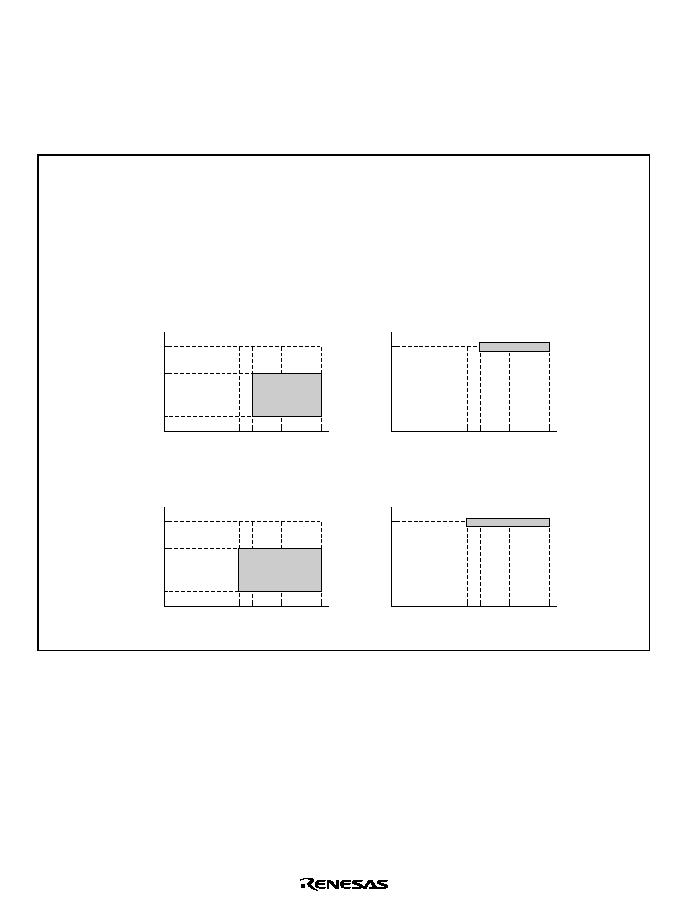
Rev. 2.0, 09/02, page 571 of 658
Section 26 Electrical Characteristics
26.1
Power Supply Voltage and Operating Frequency Range
Power supply voltage and operating frequency ranges (shaded areas) are shown in figure 26.1.
System clock
(1) Power supply voltage and range of oscillation frequency (condition A)
Condition A (F-ZTAT version) : Vcc = 3.0 to 5.5V, AVcc = 2.7 to 5.5V, Vref = 2.7V to AVcc, Vss = AVss = 0V,
= 32.768kHz, 2 to 13.5MHz, Ta = -20 to +75 (regular specification),
Ta = -40 to + 85 (wide range specification)
Condition B (mask ROM version) : Vcc = 2.7 to 5.5V, AVcc = 2.7 to 5.5V, Vref = 2.7V to AVcc, Vss = AVss = 0V,
= 32.768kHz, 2 to 13.5MHz, Ta = -20 to +75 (regular specification),
Ta = -40 to + 85 (wide range specification)
Condition C (F-ZTAT version) : Vcc = 4.0 to 5.5V, AVcc = 4.0 to 5.5V, Vref = 4.0V to AVcc, Vss = AVss = 0V,
= 32.768kHz, 10 to 20.5MHz, Ta = -20 to +75 (regular specification),
Ta = -40 to + 85 (wide range specification)
Condition D (mask ROM version) : Vcc = 4.0 to 5.5V, AVcc = 4.0 to 5.5V, Vref = 4.0V to AVcc, Vss = AVss = 0V,
= 32.768kHz, 10 to 20.5MHz, Ta = -20 to +75 (regular specification),
Ta = -40 to + 85 (wide range specification)
Active (high-speed/medium-speed) mode
Sleep mode
f (MHz)
20.5
13.5
2.0
0
2.7 3.0
4.0
5.5 Vcc (V)
Sub clock
Sub clock
AII operating modes
System clock
(2) Power supply voltage and range of oscillation frequency (condition B)
Active (high-speed/medium-speed) mode
Sleep mode
AII operating modes
f (kHz)
32.768
0
2.7 3.0
4.0
5.5 Vcc (V)
f (MHz)
20.5
13.5
2.0
0
2.7 3.0
4.0
5.5 Vcc (V)
f (kHz)
32.768
0
2.7 3.0
4.0
5.5 Vcc (V)
Figure 26.1 Power Supply Voltage and Operating Ranges (1)

Rev. 2.0, 09/02, page 572 of 658
48.8
74
500
0
2.7 3.0
4.0
5.5
30.5
0
2.7 3.0
4.0
5.5
48.8
74
500
0
2.7 3.0
4.0
5.5
30.5
0
2.7 3.0
4.0
5.5
48.8
74
100
500
0
2.7 3.0
4.0
5.5
30.5
0
2.7 3.0
4.0
5.5
20.5
13.5
10.0
2.0
0
2.7 3.0
4.0
5.5
32.768
0
2.7 3.0
4.0
5.5
System clock
(3) Power supply voltage and range of oscillation frequency (condition C and D)
Active (high-speed/medium-speed) mode
Sleep mode
f (MHz)
t (ns)
Vcc (V)
Sub clock
AII operating modes
f (kHz)
System clock
(4) Power supply voltage and range of instruction execution (condition A)
Active (high-speed/medium-speed) mode
Sub clock
Subactive mode
t ( s)
t (ns)
System clock
(5) Power supply voltage and range of instruction execution (condition B)
Active (high-speed/medium-speed) mode
Sub clock
Subactive mode
t ( s)
Vcc (V)
Vcc (V)
Vcc (V)
Vcc (V)
Vcc (V)
t (ns)
System clock
(6) Power supply voltage and range of instruction execution (condition C and D)
Active (high-speed/medium-speed) mode
Sub clock
Subactive mode
t ( s)
Vcc (V)
Vcc (V)
Figure 26.1 Power Supply Voltage and Operating Ranges (2)

Rev. 2.0, 09/02, page 573 of 658
26.2
Electrical Characteristics of the H8S/2268 Series
26.2.1
Absolute Maximum Ratings
Table 26.1 lists the absolute maximum ratings.
Table 26.1
Absolute Maximum Ratings
Item
Symbol
Value
Unit
Power supply voltage
V
CC
≠0.3 to +7.0
V
CV
CC
≠0.3 to +4.3
V
Input voltage (except port 4, 9, PH7)
V
in
≠0.3 to V
CC
+0.3
V
Input voltage (port 4, 9, PH7)
V
in
≠0.3 to AV
CC
+0.3
V
Reference voltage
V
ref
≠0.3 to AV
CC
+0.3
V
Analog power supply voltage
AV
CC
≠0.3 to +7.0
V
Analog input voltage
V
AN
≠0.3 to AV
CC
+0.3
V
Operating temperature
T
opr
Regular specifications: ≠20 to +75
*
∞C
Wide-range specifications: ≠40 to +85
*
∞C
Storage temperature
T
stg
≠55 to +125
∞C
Caution:
Permanent damage to the chip may result if absolute maximum rating are exceeded.
Note:
*
Operating temperature range for flash memory programming/erasing is T
a
= -20 to
+75∞C.

Rev. 2.0, 09/02, page 574 of 658
26.2.2
DC Characteristics
Table 26.2 lists the DC characteristics. Table 26.3 lists the permissible output currents. Table 26.4
lists the bus drive characteristics.
Table 26.2
DC Characteristics (1)
Condition A (F-ZTAT version): V
CC
= 3.0 V to 5.5 V, AV
CC
= 2.7 V to 5.5 V, V
ref
= 2.7 V to AV
CC
,
V
SS
= AV
SS
= 0 V, T
a
= ≠20∞C to +75∞C (regular specifications), T
a
= ≠40∞C to
+85∞C (wide-range specifications)*
1
Condition B (Masked-ROM version): V
CC
= 2.7 V to 5.5 V, AV
CC
= 2.7 V to 5.5 V, V
ref
= 2.7 V to
AV
CC
, V
SS
= AV
SS
= 0 V, T
a
= ≠20∞C to +75∞C (regular specifications), T
a
= ≠40∞C to
+85∞C (wide-range specifications)*
1
Item
Symbol
Min.
Typ.
Max.
Unit
Test Conditions
VT
-
V
CC
x 0.2
≠
≠
V
VT
+
≠
≠
V
CC
x 0.8
V
VT
+
- VT
-
V
CC
x 0.05
≠
≠
V
Vcc = 4.0 to 5.5 V
Schmitt trigger
input voltage
,54
,
,54
,
,54
to
,54
,
:.3
to
:.3
V
CC
x 0.04
≠
≠
V
Vcc = 2.7 to 4.0 V
Input high
voltage
5(6
,
67%<
,
NMI, FWE,
MD2, MD1
V
IH
V
CC
x 0.9
≠
V
CC
+ 0.3
V
EXTAL, Port 1,
3, 7, F, J to N,
PH0 to PH3
V
CC
x 0.8
≠
V
CC
+ 0.3
V
Port 4, 9, PH7
V
CC
x 0.8
≠
AV
CC
+ 0.3
V
Input low
voltage
5(6
,
67%<
,
FWE, MD2,
MD1
V
IL
- 0.3
≠
V
CC
x 0.1
V
NMI, EXTAL,
Port 1, 3, 4, 7, 9,
F, H, J to N
- 0.3
≠
V
CC
x 0.2
V

Rev. 2.0, 09/02, page 575 of 658
Item
Symbol
Min.
Typ.
Max.
Unit
Test Conditions
V
OH
V
CC
- 0.5
≠
≠
V
I
OH
= - 200
µ
A
All output pins
except P34 and
P35, PH0 to
PH3, and Port J
to N
V
CC
- 1.0
≠
≠
V
I
OH
= - 1 mA
P34 and P35
*
2
V
CC
- 2.7
≠
≠
V
I
OH
= - 100
µ
A
V
CC
= 4.0 to 5.5 V
V
CC
- 0.5
≠
≠
V
I
OH
= - 200
µ
A
Output high
voltage
PH0 to PH3,
Port J to N
V
CC
- 1.0
≠
≠
V
I
OH
= - 1 mA
V
CC
= 4.0 to 5.5 V
All output
pins
*
3
V
OL
≠
≠
0.4
V
I
OL
= - 0.8 mA
I
OL
= 5 mA
Output low
voltage
Port 7
≠
≠
1.0
V
I
OL
= 10 mA,
V
CC
= 4.0 to 5.5 V
5(6
≠
≠
1.0
µ
A
67%<
, NMI,
FWE, MD2, MD1
≠
≠
1.0
µ
A
V
in
= 0.5 to V
CC
- 0.5
V
Port 4, 9
≠
≠
1.0
µ
A
V
in
= 0.5 to AV
CC
-
0.5 V
Input leakage
current
PH7
|
l
in
|
≠
≠
1.0
µ
A
V
in
= 0.5 to AV
CC
-
0.5 V
Three-state
leakage
current
(off state)
Port 1, 3, 7,
Port F, J to N,
PH0 to PH3
|
l
TSI
|
≠
≠
1.0
µ
A
V
in
= 0.5 to AV
CC
-
0.5 V
Input pull-up
MOS current
Port J
≠l
P
10
≠
300
µ
A
V
in
= 0 V
Notes: 1. If the A/D and D/A converters and DTMF generation circuit are not used, do not leave
the AV
CC
, V
ref
, and AV
SS
pins open. Apply a voltage 2.0 V to 5.5 V to the AV
CC
and V
ref
pins by connecting them to V
CC
, for instance. Set V
ref
AV
CC
.
2. P35/SCK1/SCL0 and P34/SDA0 are NMOS push/pull outputs.
To output high level signal from SCL0 and SDA0 (ICE = 1), pull-up resistance must be
connected externally.
P35/SCK1 and P34 (ICE = 0) are driven high by NMOS. To output high when V
CC
=
4.0V or less, pull-up resistance should be connected externally.
3. When ICE = 0. To output low when bus drive function is selected is determined in table
26.4, Bus Drive Characteristics.

Rev. 2.0, 09/02, page 576 of 658
Table 26.2
DC Characteristics (2)
Condition C (F-ZTAT version): V
CC
= 4.0V to 5.5 V, AV
CC
= 4.0V to 5.5V, V
ref
= 4.0V to AV
CC
,
V
SS
= AV
SS
= 0 V, T
a
= ≠20∞C to +75∞C (regular specifications), T
a
= ≠40∞C to
+85∞C (wide-range specifications)*
1
Condition D (Masked-ROM version): V
CC
= 4.0V to 5.5 V, AV
CC
= 4.0V to 5.5V, V
ref
= 4.0 V to
AV
CC
, V
SS
= AV
SS
= 0 V, T
a
= ≠20∞C to +75∞C (regular specifications), T
a
= ≠40∞C to
+85∞C (wide-range specifications)*
1
Item
Symbol
Min.
Typ.
Max.
Unit
Test Conditions
VT
-
V
CC
x 0.2
≠
≠
V
VT
+
≠
≠
V
CC
x 0.8
V
Schmitt trigger
input voltage
,54
,
,54
,
,54
to
,54
,
:.3
to
:.3
VT
+
- VT
-
V
CC
x 0.05
≠
≠
V
Input high
voltage
5(6
,
67%<
,
NMI, FWE,
MD2, MD1
V
IH
V
CC
x 0.9
≠
V
CC
+ 0.3
V
EXTAL, Port 1,
3, 7, F, J to N,
PH0 to PH3
V
CC
x 0.8
≠
V
CC
+ 0.3
V
Port 4, 9, PH7
V
CC
x 0.8
≠
V
CC
+ 0.3
V
Input low
voltage
5(6
,
67%<
,
FWE, MD2,
MD1
V
IL
- 0.3
≠
V
CC
x 0.1
V
NMI, EXTAL,
Port 1, 3, 4, 7, 9,
F, H, J to N
- 0.3
≠
V
CC
x 0.2
V
Output high
voltage
V
OH
V
CC
- 0.5
≠
≠
V
I
OH
= - 200
µ
A
All output pins
except P34 and
P35, PH0 to
PH3, and Port J
to N
V
CC
- 1.0
≠
≠
V
I
OH
= - 1 mA
P34 and P35
*
2
V
CC
- 2.7
≠
≠
V
I
OH
= - 100
µ
A
V
CC
- 0.5
≠
≠
V
I
OH
= - 200
µ
A
PH0 to PH3,
Port J to N
V
CC
- 1.0
≠
≠
V
I
OH
= - 1 mA

Rev. 2.0, 09/02, page 577 of 658
Item
Symbol
Min.
Typ.
Max.
Unit
Test Conditions
All output
pins
*
3
V
OL
≠
≠
0.4
V
I
OL
= 0.8 mA
Output low
voltage
Port 7
≠
≠
1.0
V
I
OL
= 10 mA
5(6
≠
≠
1.0
µ
A
67%<
, NMI,
FWE, MD2, MD1
≠
≠
1.0
µ
A
V
in
= 0.5 to V
CC
- 0.5
V
Port 4, 9
≠
≠
1.0
µ
A
V
in
= 0.5 to AV
CC
-
0.5 V
Input leakage
current
PH7
|
l
in
|
≠
≠
1.0
µ
A
V
in
= 0.5 to AV
CC
-
0.5 V
Three-state
leakage
current
(off state)
Port 1, 3, 7,
Port F, J to N,
PH0 to PH3
|
l
TSI
|
≠
≠
1.0
µ
A
V
in
= 0.5 to AV
CC
-
0.5 V
Input pull-up
MOS current
Port J
≠l
P
50
≠
300
µ
A
V
in
= 0 V
Notes: 1. If the A/D and D/A converters and DTMF generation circuit are not used, do not leave
the AV
CC
, V
ref
, and AV
SS
pins open. Apply a voltage 4.0 V to 5.5 V to the AV
CC
and V
ref
pins by connecting them to V
CC
, for instance. Set V
ref
AV
CC
.
2. P35/SCK1/SCL0 and P34/SDA0 are NMOS push/pull outputs.
To output high level signal from SCL0 and SDA0 (ICE = 1), pull-up resistance must be
connected externally.
P35/SCK1 and P34 (ICE = 0) are driven high by NMOS.
3. When ICE = 0. To output low when bus drive function is selected is determined in table
26.4, Bus Drive Characteristics.

Rev. 2.0, 09/02, page 578 of 658
Table 26.2
DC Characteristics (3)
Condition A (F-ZTAT version): V
CC
= 3.0 V to 5.5 V, AV
CC
= 2.7 V to 5.5 V, V
ref
= 2.7 V to AV
CC
,
V
SS
= AV
SS
= 0 V, T
a
= ≠20∞C to +75∞C (regular specifications), T
a
= ≠40∞C to
+85∞C (wide-range specifications)*
1
Item
Symbol
Min.
Typ.
Max.
Unit
Test Conditions
5(6
C
in
≠
≠
30
pF
NMI
≠
≠
30
pF
P32 to P35
≠
≠
20
pF
Input
capacitance
All input pins
except
5(6
,
NMi, P32 to
P35
≠
≠
15
pF
V
in
= 0 V
f = 1 MHz
Ta = 25∞C
Current
consumption
*
2
Normal
operation
I
CC
*
4
≠
18
V
CC
= 3.0 V
30
V
CC
= 5.5 V
mA
f = 13.5 MHz
Sleep mode
≠
13
V
CC
= 3.0 V
22
V
CC
= 5.5 V
mA
f = 13.5 MHz
All modules
stopped
≠
10
≠
mA
f = 13.5 MHz,
V
CC
= 3.0 V
(reference values)
Medium-speed
mode (
/32)
≠
12
≠
mA
f = 13.5 MHz,
V
CC
= 3.0 V
(reference values)
Subactive
mode
≠
60
110
µ
A
Using 32.768 kHz
crystal resonator
Vcc = 3.0 V
(LCD lighting)
Subsleep
mode
≠
50
90
µ
A
Using 32.768 kHz
crystal resonator
Vcc = 3.0 V
(LCD lighting)
Watch mode
≠
4
25
µ
A
Using 32.768 kHz
crystal resonator
Vcc = 3.0 V
(LCD and TMR4 not
used, WDT_1
operates)

Rev. 2.0, 09/02, page 579 of 658
Item
Symbol
Min.
Typ.
Max.
Unit
Test Conditions
≠
0.5
Vcc = 3.0 V
10
Vcc = 5.5 V
µ
A
T
a
50∞C
32.768 kHz not used
Current
consumption
*
2
Standby
mode
*
3
I
CC
*
4
≠
≠
50
Vcc = 5.5 V
50∞C < T
a
32.768 kHz not used
Analog
power supply
current
During A/D
conversion,
D/A
conversion,
DTMF output
Al
CC
≠
1.0
2.4
mA
Waiting for A/D
conversion,
D/A
conversion,
DTMF stopped
≠
0.01
5.0
µ
A
Reference
current
During A/D
conversion,
D/A
conversion
Al
CC
≠
1.0
2.2
mA
Waiting for A/D
conversion,
D/A
conversion
≠
0.01
5.0
µ
A
RAM standby voltage
V
RAM
2.0
≠
≠
V
Notes: 1. If the A/D and D/A converters and DTMF generation circuit are not used, do not leave
the AVCC, Vref , and AVSS pins open. Apply a voltage 2.0 to 5.5 V to the AVCC and
Vref pins by connecting them to V
CC
, for instance. Set V
ref
AV
CC
.
2. Current consumption values are for V
IH
min. = V
CC
≠ 0.2 V, V
IL
max. = 0.2 V with all
output pins unloaded and the on-chip pull-up resistors in the off state.
3. The values are for V
RAM
V
CC
< 3.0 V, V
IH
min. = V
CC
≠ 0.2, and V
IL
max. = 0.2 V.
4. I
CC
depends on V
CC
and f as follows (reference):
I
CC
max. = 4.0 (mA) + 0.64 (mA/V) x Vcc + 0.75 (mA/MHz) x f + 0.15 (mA/(MHz
∑
V)) x
V
CC
x f (normal operation)
I
CC
max. = 3.0 (mA) + 0.60 (mA/V) x Vcc + 0.60 (mA/MHz) x f + 0.10 (mA/(MHz
∑
V))
V
CC
x f (sleep mode)

Rev. 2.0, 09/02, page 580 of 658
Table 26.2
DC Characteristics (4)
Condition B (Masked-ROM version): V
CC
= 2.7 V to 5.5 V, AV
CC
= 2.7 V to 5.5 V, V
ref
= 2.7 V to
AV
CC
, V
SS
= AV
SS
= 0 V, T
a
= ≠20∞C to +75∞C (regular specifications), T
a
= ≠40∞C to
+85∞C (wide-range specifications)*
1
Item
Symbol
Min.
Typ.
Max.
Unit
Test Conditions
5(6
C
in
≠
≠
30
pF
NMI
≠
≠
30
pF
P32 to P35
≠
≠
20
pF
Input
capacitance
All input pins
except
5(6
,
NMi, P32 to
P35
≠
≠
15
pF
V
in
= 0 V
f = 1 MHz
Ta = 25∞C
Current
consumption
*
2
Normal
operation
I
CC
*4
≠
TBD
V
CC
= 3.0V
TBD
V
CC
= 5.5V
mA
f = 13.5 MHz
Sleep mode
≠
TBD
V
CC
= 3.0V
TBD
V
CC
= 5.5V
mA
f = 13.5 MHz
All modules
stopped
≠
TBD
≠
mA
f = 13.5 MHz,
V
CC
= 3.0 V
(reference values)
Medium-speed
mode (
/32)
≠
TBD
≠
mA
f = 13.5 MHz,
V
CC
= 3.0 V
(reference values)
Subactive
mode
≠
TBD
TBD
µ
A
Using 32.768 kHz
crystal resonator
Vcc = 3.0 V
(LCD lighting)
Subsleep
mode
≠
TBD
TBD
µ
A
Using 32.768 kHz
crystal resonator
Vcc = 3.0 V
(LCD lighting)
Watch mode
≠
TBD
TBD
µ
A
Using 32.768 kHz
crystal resonator
Vcc = 3.0 V
(LCD and TMR4 not
used, WDT_1
operates)

Rev. 2.0, 09/02, page 581 of 658
Item
Symbol
Min.
Typ.
Max.
Unit
Test Conditions
Current
consumption
*
2
I
CC
*4
≠
TBD
Vcc = 3.0 V
TBD
Vcc = 5.5 V
µ
A
T
a
50∞C
32.768 kHz not used
Standby
mode
*
3
≠
≠
TBD
Vcc = 5.5 V
50∞C < T
a
32.768 kHz not used
Analog
power supply
current
During A/D
conversion,
D/A
conversion,
DTMF output
Al
CC
≠
TBD
TBD
mA
Waiting for A/D
conversion,
D/A
conversion,
DTMF stopped
≠
TBD
TBD
µ
A
Reference
current
During A/D
conversion,
D/A conversion
Al
CC
≠
TBD
TBD
mA
Waiting for A/D
conversion,
D/A conversion
≠
TBD
TBD
µ
A
RAM standby voltage
V
RAM
2.0
≠
≠
V
Notes: 1. If the A/D and D/A converters and DTMF generation circuit are not used, do not leave
the AVCC, Vref , and AVSS pins open. Apply a voltage 2.0 to 5.5 V to the AVCC and
Vref pins by connecting them to V
CC
, for instance. Set V
ref
AV
CC
.
2. Current consumption values are for V
IH
min. = V
CC
≠ 0.2 V, V
IL
max. = 0.2 V with all
output pins unloaded and the on-chip pull-up resistors in the off state.
3. The values are for V
RAM
V
CC
< 2.7 V, V
IH
min. = V
CC
≠ 0.2, and V
IL
max. = 0.2 V.
4. I
CC
depends on V
CC
and f as follows (reference):
I
CC
max. = TBD (mA) + TBD (mA/V) x Vcc + TBD (mA/MHz) x f + TBD (mA/(MHz
∑
V)) x
V
CC
x f (normal operation)
I
CC
max. = TBD (mA) + TBD (mA/V) x Vcc + TBD (mA/MHz) x f + TBD (mA/(MHz
∑
V))
V
CC
x f (sleep mode)

Rev. 2.0, 09/02, page 582 of 658
Table 26.2
DC Characteristics (5)
Condition C (F-ZTAT version): V
CC
= 4.0V to 5.5 V, AV
CC
= 4.0V to 5.5V, V
ref
= 4.0V to AV
CC
,
V
SS
= AV
SS
= 0 V, T
a
= ≠20∞C to +75∞C (regular specifications), T
a
= ≠40∞C to +85∞C
(wide-range specifications)*
1
Item
Symbol
Min.
Typ.
Max.
Unit
Test Conditions
5(6
C
in
≠
≠
30
pF
NMI
≠
≠
30
pF
P32 to P35
≠
≠
20
pF
Input
capacitance
All input pins
except
5(6
,
NMi, P32 to
P35
≠
≠
15
pF
V
in
= 0 V
f = 1 MHz
Ta = 25∞C
Current
consumption
*
2
Normal
operation
I
CC
*4
≠
30
V
CC
= 5.0 V
40
V
CC
= 5.5 V
mA
f = 20.5 MHz
Sleep mode
≠
22
V
CC
= 5.0 V
30
V
CC
= 5.5 V
mA
f = 20.5 MHz
All modules
stopped
≠
15
≠
mA
f = 20.5 MHz,
V
CC
= 5.0 V
(reference values)
Medium-speed
mode (
/32)
≠
19
≠
mA
f = 20.5 MHz,
V
CC
= 5.0 V
(reference values)
Subactive
mode
≠
70
120
µ
A
Using 32.768 kHz
crystal resonator
Vcc = 5.0 V
(LCD lighting)
Subsleep
mode
≠
60
100
µ
A
Using 32.768 kHz
crystal resonator
Vcc = 5.0 V
(LCD lighting)
Watch mode
≠
5
30
µ
A
Using 32.768 kHz
crystal resonator
Vcc = 5.0 V
(LCD and TMR4 not
used, WDT_1
operates)

Rev. 2.0, 09/02, page 583 of 658
Item
Symbol
Min.
Typ.
Max.
Unit
Test Conditions
Current
consumption
*
2
I
CC
*4
≠
1.0
Vcc = 5.0 V
10
Vcc = 5.5 V
µ
A
T
a
50∞C
32.768 kHz not used
Standby mode
*
3
≠
≠
50
Vcc = 5.5 V
50∞C < T
a
32.768 kHz not used
Analog
power supply
current
During A/D
conversion,
D/A
conversion,
DTMF output
Al
CC
≠
1.5
2.5
mA
Waiting for A/D
conversion,
D/A
conversion,
DTMF stopped
≠
0.01
5.0
µ
A
Reference
current
During A/D
conversion,
D/A conversion
Al
CC
≠
1.5
2.2
mA
Waiting for A/D
conversion,
D/A conversion
≠
0.01
5.0
µ
A
RAM standby voltage
V
RAM
2.0
≠
≠
V
Notes: 1. If the A/D and D/A converters and DTMF generation circuit are not used, do not leave
the AVCC, Vref , and AVSS pins open. Apply a voltage 4.0 to 5.5 V to the AVCC and
Vref pins by connecting them to V
CC
, for instance. Set V
ref
AV
CC
.
2. Current consumption values are for V
IH
min. = V
CC
≠ 0.2 V, V
IL
max. = 0.2 V with all
output pins unloaded and the on-chip pull-up resistors in the off state.
3. The values are for V
RAM
V
CC
< 4.0 V, V
IH
min. = V
CC
≠ 0.2, and V
IL
max. = 0.2 V.
4. I
CC
depends on V
CC
and f as follows (reference):
I
CC
max. = 4.0 (mA) + 0.64 (mA/V) x Vcc+ 0.75 (mA/MHz) x f + 0.15 (mA/(MHz
∑
V)) x
V
CC
x f (normal operation)
I
CC
max. = 3.0 (mA) + 0.60 (mA/V) x Vcc+ 0.60 (mA/MHz) x f + 0.10 (mA/(MHz
∑
V)) V
CC
x f (sleep mode)

Rev. 2.0, 09/02, page 584 of 658
Table 26.2
DC Characteristics (6)
-- Preliminary --
Condition D (Masked-ROM version): V
CC
= 4.0V to 5.5 V, AV
CC
= 4.0V to 5.5V, V
ref
= 4.0 V to
AV
CC
, V
SS
= AV
SS
= 0 V, T
a
= ≠20∞C to +75∞C (regular specifications), T
a
= ≠40∞C to
+85∞C (wide-range specifications)*
1
Item
Symbol
Min.
Typ.
Max.
Unit
Test Conditions
5(6
C
in
≠
≠
30
pF
NMI
≠
≠
30
pF
P32 to P35
≠
≠
20
pF
Input
capacitance
All input pins
except
5(6
,
NMi, P32 to
P35
≠
≠
15
pF
V
in
= 0 V
f = 1 MHz
Ta = 25∞C
Current
consumption
*
2
Normal
operation
I
CC
*
4
≠
TBD
V
CC
= 5.0 V
TBD
V
CC
= 5.5 V
mA
f = 20.5 MHz
Sleep mode
≠
TBD
V
CC
= 5.0 V
TBD
V
CC
= 5.5 V
mA
f = 20.5 MHz
All modules
stopped
≠
TBD
≠
mA
f = 20.5 MHz,
V
CC
= 5.0 V
(reference values)
Medium-speed
mode (
/32)
≠
TBD
≠
mA
f = 20.5 MHz,
V
CC
= 5.0 V
(reference values)
Subactive
mode
≠
TBD
TBD
µ
A
Using 32.768 kHz
crystal resonator
Vcc = 5.0 V
(LCD lighting)
Subsleep
mode
≠
TBD
TBD
µ
A
Using 32.768 kHz
crystal resonator
Vcc = 5.0 V
(LCD lighting)
Watch mode
≠
TBD
TBD
µ
A
Using 32.768 kHz
crystal resonator
Vcc = 5.0 V
(LCD and TMR4 not
used, WDT_1
operates)

Rev. 2.0, 09/02, page 585 of 658
Item
Symbol
Min.
Typ.
Max.
Unit
Test Conditions
Current
consumption
*
2
I
CC
*
4
≠
TBD
Vcc = 5.0 V
TBD
Vcc = 5.5 V
µ
A
T
a
50∞C
32.768 kHz not used
Standby
mode
*
3
≠
≠
TBD
Vcc = 5.5 V
50∞C < T
a
32.768 kHz not used
Analog
power supply
current
During A/D
conversion,
D/A
conversion,
DTMF output
Al
CC
≠
TBD
TBD
mA
Waiting for
A/D
conversion,
D/A
conversion,
DTMF
stopped
≠
TBD
TBD
µ
A
Reference
current
During A/D
conversion,
D/A
conversion
Al
CC
≠
TBD
TBD
mA
Waiting for
A/D
conversion,
D/A
conversion
≠
TBD
TBD
µ
A
RAM standby voltage
V
RAM
2.0
≠
≠
V
Notes: 1. If the A/D and D/A converters and DTMF generation circuit are not used, do not leave
the AVCC, Vref , and AVSS pins open. Apply a voltage 4.0 to 5.5 V to the AVCC and
Vref pins by connecting them to V
CC
, for instance. Set V
ref
AV
CC
.
2. Current consumption values are for V
IH
min. = VCC ≠ 0.2 V, V
IL
max. = 0.2 V with all
output pins unloaded and the on-chip pull-up resistors in the off state.
3. The values are for V
RAM
V
CC
< 4.0 V, V
IH
min. = V
CC
≠ 0.2, and V
IL
max. = 0.2 V.
4. I
CC
depends on V
CC
and f as follows (reference):
I
CC
max. = TBD (mA) + TBD (mA/V) x Vcc + TBD (mA/MHz) x f + TBD (mA/(MHz
∑
V)) x
V
CC
x f (normal operation)
I
CC
max. = TBD (mA) + TBD (mA/V) x Vcc + TBD (mA/MHz) x f + TBD (mA/(MHz
∑
V))
V
CC
x f (sleep mode)

Rev. 2.0, 09/02, page 586 of 658
Table 26.3
Permissible Output Currents
Condition A (F-ZTAT version): V
CC
= 3.0 V to 5.5 V, AV
CC
= 2.7 V to 5.5 V, V
ref
= 2.7 V to AV
CC
,
V
SS
= AV
SS
= 0 V, T
a
= ≠20∞C to +75∞C (regular specifications), T
a
= ≠40∞C to
+85∞C (wide-range specifications)
Condition B (Masked-ROM version): V
CC
= 2.7 V to 5.5 V, AV
CC
= 2.7 V to 5.5 V, V
ref
= 2.7 V to
AV
CC
, V
SS
= AV
SS
= 0 V, T
a
= ≠20∞C to +75∞C (regular specifications), T
a
= ≠40∞C to
+85∞C (wide-range specifications)
Condition C (F-ZTAT version): V
CC
= 4.0V to 5.5 V, AV
CC
= 4.0V to 5.5V, V
ref
= 4.0V to AV
CC
,
V
SS
= AV
SS
= 0 V, T
a
= ≠20∞C to +75∞C (regular specifications), T
a
= ≠40∞C to
+85∞C (wide-range specifications)
Condition D (Masked-ROM version): V
CC
= 4.0V to 5.5 V, AV
CC
= 4.0V to 5.5V, V
ref
= 4.0V to
AV
CC
, V
SS
= AV
SS
= 0 V, T
a
= ≠20∞C to +75∞C (regular specifications), T
a
= ≠40∞C
to +85∞C (wide-range specifications)
Item
Symbol
Min.
Typ.
Max.
Unit
Permissible output low
current (per pin)
Port 7
I
OL
--
--
10
mA
SCL1, SCL0, SDA1, SDA0
--
--
10
mA
Output pins except port 7,
SCL1, SCL0, SDA1, SDA0
--
--
1.0
mA
Permissible output low
current (total)
Total of port 7
I
OL
--
--
30
mA
Total of all output pins
including port 7
--
--
60
mA
Permissible output high
current (per pin)
All output pins
≠I
OH
--
--
1.0
mA
Permissible output high
current (total)
Total of all output pins
≠
I
OH
--
--
30
mA
Note: To protect chip reliability, do not exceed the output current values in table 26.3.

Rev. 2.0, 09/02, page 587 of 658
Table 26.4
Bus Drive Characteristics (1)
Condition A (F-ZTAT version): V
CC
= 3.0 V to 5.5 V, AV
CC
= 2.7 V to 5.5 V, V
ref
= 2.7 V to AV
CC
,
V
SS
= AV
SS
= 0 V, T
a
= ≠20∞C to +75∞C (regular specifications), T
a
= ≠40∞C to
+85∞C (wide-range specifications)*
1
, Target pins: SCL1, SCL
0
, SDA1, SDA
0
Condition B (Masked-ROM version): V
CC
= 2.7 V to 5.5 V, AV
CC
= 2.7 V to 5.5 V, V
ref
= 2.7 V to
AV
CC
, V
SS
= AV
SS
= 0 V, T
a
= ≠20∞C to +75∞C (regular specifications), T
a
= ≠40∞C to
+85∞C (wide-range specifications)*
1
, Target pins: SCL1, SCL
0
, SDA1, SDA
0
Item
Symbol
Min.
Typ.
Max.
Unit
Test Conditions
Schmitt trigger input voltage
VT
-
V
CC
◊
0.3
--
--
V
VT
+
--
--
V
CC
◊
0.7
0.4
--
--
V
CC
= 4.0 to 5.5 V
VT
+
- VT
-
V
CC
◊
0.05
--
--
V
CC
=2.7 to 4.0 V
Input high voltage
V
IH
V
CC
◊
0.7
--
V
CC
+
0.5
V
Input low voltage
V
IL
-0.5
--
V
CC
◊
0.3
V
--
--
0.5
V
I
OL
=8 mA,
V
CC
=4.0 to 5.5 V
Output low voltage
V
OL
--
--
0.4
I
OL
=3mA
Input capacitance
C
IN
--
--
20
pF
VIN=0 V, f=1 MHz,
T
a
=25∞C
Three-state leakage current
(off state)
|
l
STI
|
--
--
1.0
µ
A
V
IN
=0.5 to V
CC
-0.5
SDL, SDA output fall time
t
Of
20
+
0.1Cb
--
250
ns
Note: If the A/D and D/A converters and DTMF generation circuit are not used, do not leave the
AV
CC
, V
ref
, and AV
SS
pins open. Apply a voltage 2.0 V to 5.5 V to the AV
CC
and V
ref
pins by
connecting them to V
CC
, for instance. Set V
ref
AV
CC

Rev. 2.0, 09/02, page 588 of 658
Table 26.4
Bus Drive Characteristics (2)
Condition C (F-ZTAT version): V
CC
= 4.0V to 5.5 V, AV
CC
= 4.0V to 5.5V, V
ref
= 4.0V to AV
CC
,
V
SS
= AV
SS
= 0 V, T
a
= ≠20∞C to +75∞C (regular specifications), T
a
= ≠40∞C to +85∞C
(wide-range specifications)*
1
, Target pins: SCL1, SCL
0
, SDA1, SDA
0
Condition D (Masked-ROM version): V
CC
= 4.0V to 5.5 V, AV
CC
= 4.0V to 5.5V, V
ref
= 4.0V to
AV
CC
, V
SS
= AV
SS
= 0 V, T
a
= ≠20∞C to +75∞C (regular specifications), T
a
= ≠40∞C to
+85∞C (wide-range specifications)*
1
, Target pins: SCL1, SCL
0
, SDA1, SDA
0
Item
Symbol
Min.
Typ.
Max.
Unit
Test Conditions
Schmitt trigger input voltage
VT
-
V
CC
◊
0.3
--
--
V
VT
+
--
--
V
CC
◊
0.7
VT
+
- VT
-
0.4
--
--
Input high voltage
V
IH
V
CC
◊
0.7
--
V
CC
+
0.5
V
Input low voltage
V
IL
-0.5
--
V
CC
◊
0.3
V
--
--
0.5
V
I
OL
=8 mA
Output low voltage
V
OL
--
--
0.4
I
OL
=3 mA
Input capacitance
C
in
--
--
20
pF
V
IN
=0 V, f=1 MHz,
T
a
=25∞C
Three-state leakage current
(off state)
|
l
STI
|
--
--
1.0
µ
A
V
IN
=0.5 to V
CC
-0.5
SDL, SDA output fall time
t
Of
20
+
0.1Cb
--
250
ns
Note: If the A/D and D/A converters and DTMF generation circuit are not used, do not leave the
AV
CC
, V
ref
, and AV
SS
pins open. Apply a voltage 4.0 V to 5.5 V to the AV
CC
and V
ref
pins by
connecting them to V
CC
, for instance. Set V
ref
AV
CC

Rev. 2.0, 09/02, page 589 of 658
26.2.3
AC Characteristics
Figure 26.2 show, the test conditions for the AC characteristics.
5V
R
L
R
H
C
LSI output pin
C=30pF:
R
L
= 2.4k
R
H
=12
Input/output timing measurement levels
∑ Low level : 0.8V
∑ High level : 2.0V
Figure 26.2 Output Load Circuit

Rev. 2.0, 09/02, page 590 of 658
Clock Timing: Table 26.5 lists the clock timing.
Table 26.5
Clock Timing
Condition A (F-ZTAT version): V
CC
= 3.0 V to 5.5 V, AV
CC
= 2.7 V to 5.5 V, V
ref
= 2.7 V to AV
CC
,
V
SS
= AV
SS
= 0 V,
= 32.768kHz, 2 to 13.5MHz, T
a
= ≠20∞C to +75∞C (regular
specifications), T
a
= ≠40∞C to +85∞C (wide-range specifications)
Condition B (Masked-ROM version): V
CC
= 2.7 V to 5.5 V, AV
CC
= 2.7 V to 5.5 V, V
ref
= 2.7 V to
AV
CC
, V
SS
= AV
SS
= 0 V,
= 32.768kHz, 2 to 13.5MHz,T
a
= ≠20∞C to +75∞C (regular
specifications), T
a
= ≠40∞C to +85∞C (wide-range specifications)
Condition C (F-ZTAT version): V
CC
= 4.0V to 5.5 V, AV
CC
= 4.0V to 5.5V, V
ref
= 4.0V to AV
CC
,
V
SS
= AV
SS
= 0 V,
= 32.768kHz, 10 to 20.5 MHz, T
a
= ≠20∞C to +75∞C (regular
specifications), T
a
= ≠40∞C to +85∞C (wide-range specifications)
Condition D (Masked-ROM version): V
CC
= 4.0V to 5.5 V, AV
CC
= 4.0V to 5.5V, V
ref
= 4.0V to
AV
CC
, V
SS
= AV
SS
= 0 V,
= 32.768kHz, 10 to 20.5 MHz, T
a
= ≠20∞C to +75∞C
(regular specifications), T
a
= ≠40∞C to +85∞C (wide-range specifications)
Condition A and B
Condition C and D
13.5MHz
20.5 MHz
Item
Symbol Min.
Typ.
Max.
Min.
Typ.
Max.
Unit
Test Conditions
Clock cycle time
t
cyc
74
--
500
48.8
--
100
ns
Clock oscillator settling time at reset
(crystal)
t
OSC1
20
--
--
10
--
--
ms
Figure 26.5
Clock oscillator settling time in software
standby (crystal)
t
OSC2
8
--
--
8
--
--
ms
Figure 26.3
External clock settling delay time
t
DEXT
500
--
--
500
--
--
µ
s
Figure 26.5
Sub clock oscillator settling time
t
OSC3
--
--
2
--
--
2
s
Sub clock oscillator frequency
f
SUB
--
32.768 --
--
32.768 --
kHz
Sub clock (
SUB
) cycle time
t
SUB
--
30.5
--
--
30.5
--
µ
s

Rev. 2.0, 09/02, page 591 of 658
Control Signal Timing: Table 26.6 lists the control signal timing.
Table 26.6
Control Signal Timing
Condition A (F-ZTAT version): V
CC
= 3.0 V to 5.5 V, AV
CC
= 2.7 V to 5.5 V, V
ref
= 2.7 V to AV
CC
,
V
SS
= AV
SS
= 0 V,
= 32.768 kHz, 2 to 13.5 MHz, T
a
= ≠20∞C to +75∞C (regular
specifications), T
a
= ≠40∞C to +85∞C (wide-range specifications)
Condition B (Masked-ROM version): V
CC
= 2.7 V to 5.5 V, AV
CC
= 2.7 V to 5.5 V, V
ref
= 2.7 V to
AV
CC
, V
SS
= AV
SS
= 0 V,
= 32.768 kHz, 2 to 13.5 MHz, T
a
= ≠20∞C to +75∞C
(regular specifications), T
a
= ≠40∞C to +85∞C (wide-range specifications)
Condition C (F-ZTAT version): V
CC
= 4.0V to 5.5 V, AV
CC
= 4.0V to 5.5V, V
ref
= 4.0V to AV
CC
,
V
SS
= AV
SS
= 0 V,
= 32.768 kHz, 10 to 20.5 MHz, T
a
= ≠20∞C to +75∞C (regular
specifications), T
a
= ≠40∞C to +85∞C (wide-range specifications)
Condition D (Masked-ROM version): V
CC
= 4.0V to 5.5 V, AV
CC
= 4.0V to 5.5V, V
ref
= 4.0V to
AV
CC
, V
SS
= AV
SS
= 0 V,
= 32.768 kHz, 10 to 20.5 MHz, T
a
= ≠20∞C to +75∞C
(regular specifications), T
a
= ≠40∞C to +85∞C (wide-range specifications)
Item
Symbol Min.
Max.
Unit
Test Conditions
5(6
pulse width
t
RESW
20
--
t
cyc
Figure 26.6
NMI pulse width (exiting
software standby mode)
t
NMIW
200
--
ns
Figure 26.7
,54
pulse width (exiting
software standby mode)
t
IRQW
200
--
ns

Rev. 2.0, 09/02, page 592 of 658
Timing of On-Chip Peripheral Modules: Table 26.7 lists the timing of on-chip peripheral
modules. Table 26.8 lists the I
2
C bus timing.
Table 26.7
Timing of On-Chip Peripheral Modules
Condition A (F-ZTAT version): V
CC
= 3.0 V to 5.5 V, AV
CC
= 2.7 V to 5.5 V, V
ref
= 2.7 V to AV
CC
,
V
SS
= AV
SS
= 0 V,
= 32.768 kHz, 2 to 13.5 MHz, T
a
= ≠20∞C to +75∞C (regular
specifications), T
a
= ≠40∞C to +85∞C (wide-range specifications)
Condition B (Masked-ROM version): V
CC
= 2.7 V to 5.5 V, AV
CC
= 2.7 V to 5.5 V, V
ref
= 2.7 V to
AV
CC
, V
SS
= AV
SS
= 0 V,
= 32.768 kHz, 2 to 13.5 MHz, T
a
= ≠20∞C to +75∞C
(regular specifications), T
a
= ≠40∞C to +85∞C (wide-range specifications)
Condition C (F-ZTAT version): V
CC
= 4.0V to 5.5 V, AV
CC
= 4.0V to 5.5V, V
ref
= 4.0V to AV
CC
,
V
SS
= AV
SS
= 0 V,
= 32.768 kHz, 10 to 20.5 MHz, T
a
= ≠20∞C to +75∞C (regular
specifications), T
a
= ≠40∞C to +85∞C (wide-range specifications)
Condition D (Masked-ROM version): V
CC
= 4.0V to 5.5 V, AV
CC
= 4.0V to 5.5V, V
ref
= 4.0V to
AV
CC
, V
SS
= AV
SS
= 0 V,
= 32.768 kHz, 10 to 20.5 MHz, T
a
= ≠20∞C to +75∞C
(regular specifications), T
a
= ≠40∞C to +85∞C (wide-range specifications)
Condition A, B Condition C, D
Item
Symbol Min.
Max.
Min.
Max.
Unit
Test Conditions
TPU
Single edge
t
TCKWH
1.5
≠
1.5
≠
t
CyC
Figure 26.8
Timer clock
pulse width
Both edges
t
TCKWL
2.5
≠
2.5
≠
Single edge
1.5
≠
1.5
≠
TMR_0 to
TMR_3
Timer clock
pulse width
Both edges
t
TMCWH
t
TMCWL
2.5
≠
2.5
≠
t
CyC
Figure 26.9
TMR_4
Timer clock pulse width
t
TMCWH
t
TMCWL
1.5
≠
1.5
≠
t
CyC
SCI
Input clock
cycle
Asynchronous
t
SCyC
≠
4
≠
t
CyC
Figure 26.10
Synchronous
≠
6
≠
Input clock pulse width
t
SCKW
0.4
0.6
0.4
0.6
t
ScyC
Input clock rise time
t
SCKf
≠
1.5
≠
1.5
t
CyC
Input clock fall time
t
SCKf
≠
1.5
≠
1.5
Transmit data delay time
t
TXD
≠
75
≠
50
ns
Figure 26.11
Receive data setup time
(synchronous)
t
RXS
75
≠
50
≠
ns
Receive data hold time (synchronous) t
RXH
75
≠
50
≠
ns

Rev. 2.0, 09/02, page 593 of 658
Table 26.8
I
2
C Bus Timing
Conditions: V
CC
= 2.7 V to 5.5 V, V
SS
= 0 V,
= 5 MHz to maximum operating frequency
T
a
= ≠20∞C to +75∞C (regular specifications), T
a
= ≠40∞C to +80∞C (wide-range
specifications)
Item
Symbol Min.
Typ.
Max.
Unit
Test
Conditions
Remarks
SCL input cycle time
t
SCL
12t
cyc
≠
≠
ns
SCL input high pulse width
t
SCLH
3t
cyc
≠
≠
ns
SCL input low pulse width
t
SCLL
5t
cyc
≠
≠
ns
SCL, SDA input rise time
t
Sr
≠
≠
7.5t
cyc
*
ns
SCL, SDA input fall time
t
Sf
≠
≠
300
ns
SCL, SDA input spike pulse
elimination time
t
SP
≠
≠
1t
cyc
ns
SDA input bus free time
t
BUF
5t
cyc
≠
≠
ns
Start condition input hold time
t
STAH
3t
cyc
≠
≠
ns
Retransmission start condition
input setup time
t
STAS
3t
cyc
≠
≠
ns
Stop condition input setup time
t
STOS
3t
cyc
≠
≠
ns
Data input setup time
t
SDAS
0.5t
cyc
≠
≠
ns
Data input hold time
t
SDAH
0
≠
≠
ns
SCL, SDA load capacitance
C
b
≠
≠
400
pF
Figure 26.12
Note:
*
t
Sr
can be set to 7.5 t
cyc
or 17.5 t
cyc
according to the clock used for the I
2
C module. For
details, see section 14.5 Usage Notes.

Rev. 2.0, 09/02, page 594 of 658
26.2.4
A/D Conversion Characteristics
Table 26.9 lists the A/D conversion characteristics.
Table 26.9
A/D Conversion Characteristics
Condition A (F-ZTAT version): V
CC
= 3.0 V to 5.5 V, AV
CC
= 2.7 V to 5.5 V, V
ref
= 2.7 V to AV
CC
,
V
SS
= AV
SS
= 0 V,
= 2 to 13.5 MHz, T
a
= ≠20∞C to +75∞C (regular specifications),
T
a
= ≠40∞C to +85∞C (wide-range specifications)
Condition B (Masked-ROM version): V
CC
= 2.7 V to 5.5 V, AV
CC
= 2.7 V to 5.5 V, V
ref
= 2.7 V to
AV
CC
, V
SS
= AV
SS
= 0 V,
= 2 to 13.5 MHz, T
a
= ≠20∞C to +75∞C (regular
specifications), T
a
= ≠40∞C to +85∞C (wide-range specifications)
Condition C (F-ZTAT version): V
CC
= 4.0V to 5.5 V, AV
CC
= 4.0V to 5.5V, V
ref
= 4.0V to AV
CC
,
V
SS
= AV
SS
= 0 V,
= 10 to 20.5 MHz, T
a
= ≠20∞C to +75∞C (regular specifications),
T
a
= ≠40∞C to +85∞C (wide-range specifications)
Condition D (Masked-ROM version): V
CC
= 4.0V to 5.5 V, AV
CC
= 4.0V to 5.5V, V
ref
= 4.0V to
AV
CC
, V
SS
= AV
SS
= 0 V,
= 10 to 20.5 MHz, T
a
= ≠20∞C to +75∞C (regular
specifications), T
a
= ≠40∞C to +85∞C (wide-range specifications)
Condition A, B
Condition C, D
13.5MHz
20.5 MHz
Item
Min.
Typ.
Max.
Min.
Typ.
Max.
Unit
Resolution
10
10
10
10
10
10
bits
Conversion time
9.6
--
--
6.3
--
--
µs
Analog input capacitance
--
--
20
--
--
20
pF
Permissible signal-source impedance
--
--
5
--
--
5
k
Nonlinearity error
--
--
±6.0
--
--
±3.0
LSB
Offset error
--
--
±4.0
--
--
±2.0
LSB
Full-scale error
--
--
±4.0
--
--
±2.0
LSB
Quantization error
--
--
±0.5
--
--
±0.5
LSB
Absolute accuracy
--
--
±8.0
--
--
±4.0
LSB

Rev. 2.0, 09/02, page 595 of 658
26.2.5
D/A Conversion Characteristics
Table 26.10 lists the D/A conversion characteristics.
Table 26.10 D/A Conversion Characteristics
Condition A (F-ZTAT version): V
CC
= 3.0 V to 5.5 V, AV
CC
= 2.7 V to 5.5 V, V
ref
= 2.7 V to AV
CC
,
V
SS
= AV
SS
= 0 V,
= 2 to 13.5 MHz, T
a
= ≠20∞C to +75∞C (regular specifications),
T
a
= ≠40∞C to +85∞C (wide-range specifications)
Condition B (Masked-ROM version): V
CC
= 2.7 V to 5.5 V, AV
CC
= 2.7 V to 5.5 V, V
ref
= 2.7 V to
AV
CC
, V
SS
= AV
SS
= 0 V,
= 2 to 13.5 MHz, T
a
= ≠20∞C to +75∞C (regular
specifications), T
a
= ≠40∞C to +85∞C (wide-range specifications)
Condition C (F-ZTAT version): V
CC
= 4.0V to 5.5 V, AV
CC
= 4.0V to 5.5V, V
ref
= 4.0V to AV
CC
,
V
SS
= AV
SS
= 0 V,
= 10 to 20.5 MHz, T
a
= ≠20∞C to +75∞C (regular specifications),
T
a
= ≠40∞C to +85∞C (wide-range specifications)
Condition D (Masked-ROM version): V
CC
= 4.0V to 5.5 V, AV
CC
= 4.0V to 5.5V, V
ref
= 4.0V to
AV
CC
, V
SS
= AV
SS
= 0 V,
= 10 to 20.5 MHz, T
a
= ≠20∞C to +75∞C (regular
specifications), T
a
= ≠40∞C to +85∞C (wide-range specifications)
Condition A, B, C, D
Item
Min.
Typ.
Max.
Unit
Test Conditions
Resolution
8
8
8
bits
Conversion time
--
--
10
µs
Load capacitance: 20 pF
Absolute accuracy
--
±2.0
±3.0
LSB
Load resistance: 2 M
--
--
±2.0
LSB
Load resistance: 4 M

Rev. 2.0, 09/02, page 596 of 658
26.2.6
LCD Characteristics
Table 26.11 lists the LCD characteristics.
Table 26.11 LCD Characteristics
Condition A (F-ZTAT version): V
CC
= 3.0 V to 5.5 V, AV
CC
= 2.7 V to 5.5 V, V
ref
= 2.7 V to AV
CC
,
V
SS
= AV
SS
= 0 V,
= 32.768 kHz, 2 to 13.5 MHz, T
a
= ≠20∞C to +75∞C (regular
specifications), T
a
= ≠40∞C to +85∞C (wide-range specifications)
Condition B (Masked-ROM version): V
CC
= 2.7 V to 5.5 V, AV
CC
= 2.7 V to 5.5 V, V
ref
= 2.7 V to
AV
CC
, V
SS
= AV
SS
= 0 V,
= 32.768 kHz, 2 to 13.5 MHz, T
a
= ≠20∞C to +75∞C
(regular specifications), T
a
= ≠40∞C to +85∞C (wide-range specifications)
Condition C (F-ZTAT version): V
CC
= 4.0V to 5.5 V, AV
CC
= 4.0V to 5.5V, V
ref
= 4.0V to AV
CC
,
V
SS
= AV
SS
= 0 V,
= 32.768 kHz, 10 to 20.5 MHz, T
a
= ≠20∞C to +75∞C (regular
specifications), T
a
= ≠40∞C to +85∞C (wide-range specifications)
Condition D (Masked-ROM version): V
CC
= 4.0V to 5.5 V, AV
CC
= 4.0V to 5.5V, V
ref
= 4.0V to
AV
CC
, V
SS
= AV
SS
= 0 V,
= 32.768 kHz, 10 to 20.5 MHz, T
a
= ≠20∞C to +75∞C
(regular specifications), T
a
= ≠40∞C to +85∞C (wide-range specifications)
Condition A, B
Condition C, D
Standard Value
Standard Value
Item
Symbol
Applicable
Pins
Test
Conditions Min.
Typ.
Max.
Min.
Typ.
Max.
Unit
Notes
Segment driver step-
down voltage
V
DS
SEG1 to
SEG40
ID = 2
µ
A
--
--
0.6
--
--
0.6
V
*
1
Common driver step-
down voltage
V
DC
COM1 to
COM4
ID = 2
µ
A
--
--
0.3
--
--
0.3
V
*
1
LCD power supply
division resistor
R
LCD
Between V1
and V
SS
40
360
1000
40
360
1000
k
LCD voltage (step-up
voltage circuit not used)
V
LCD
V1
3.0
*
4
--
V
CC
4.0
--
V
CC
V
*
2
LCD input reference
voltage (using step-up
voltage circuit)
*
3
V
LCD3
V3
1.0
1.67
1.83
--
--
--
V
V
LCD2
V2
--
2
◊
V
LCD3
--
--
--
--
LCD voltage (using
step-up voltage circuit)
*
3
V
LCD1
V1
No load
--
3
◊
V
LCD3
--
--
--
--
V
Reference
value

Rev. 2.0, 09/02, page 597 of 658
Condition A, B
Condition C, D
Standard Value
Standard Value
Item
Symbol
Applicable
Pins
Test
Conditions Min.
Typ.
Max.
Min.
Typ.
Max.
Unit
Notes
LCD input reference
power supply current
(using step-up voltage
circuit)
*
3
I
LCD3
V3
No load,
frame
frequency:
64 Hz, V
LCD3
= 1.67 V
--
2.0
--
--
--
--
µ
A
Reference
value
Notes: 1. Voltage step-down between power supply pins V1, V2, V3, and V
SS
and segment pins.
2. If the LCD voltage is provided by an external power supply, the following relationship
must be maintained: V
CC
V1
V2
V3
V
SS
.
3. The step-up voltage circuit should be used with 1/3 duty or 1/4 duty.
4. When the step-up voltage circuit is not used, the lowest value of V
CC
is VCC = V1 =
3.0V. Use the step-up voltage circuit when VCC < 3.0V.

Rev. 2.0, 09/02, page 598 of 658
26.2.7
DTMF Characteristics
Table 26.12 lists the DTMF characteristics.
Table 26.12 DTMF Characteristics
Condition A (F-ZTAT version): V
CC
= 3.0 V to 5.5 V, AV
CC
= 2.7 V to 5.5 V, V
ref
= 2.7 V to AV
CC
,
V
SS
= AV
SS
= 0 V,
= 2 to 13.2 MHz, T
a
= ≠20∞C to +75∞C (regular specifications),
T
a
= ≠40∞C to +85∞C (wide-range specifications)
Condition B (Masked-ROM version): V
CC
= 2.7 V to 5.5 V, AV
CC
= 2.7 V to 5.5 V, V
ref
= 2.7 V to
AV
CC
, V
SS
= AV
SS
= 0 V,
= 2 to 13.2 MHz, T
a
= ≠20∞C to +75∞C (regular
specifications), T
a
= ≠40∞C to +85∞C (wide-range specifications)
Condition C (F-ZTAT version): V
CC
= 4.0V to 5.5 V, AV
CC
= 2.7 V*
1
to 5.5V, V
ref
= 2.7 V*
1
to
AV
CC
, V
SS
= AV
SS
= 0 V,
= 10 to 20.4 MHz, T
a
= ≠20∞C to +75∞C (regular
specifications), T
a
= ≠40∞C to +85∞C (wide-range specifications)
Condition D (Masked-ROM version): V
CC
= 4.0V to 5.5 V, AV
CC
= 2.7 V*
1
to 5.5V, V
ref
= 2.7 V*
1
to AV
CC
, V
SS
= AV
SS
= 0 V,
= 10 to 20.4 MHz, T
a
= ≠20∞C to +75∞C (regular
specifications), T
a
= ≠40∞C to +85∞C (wide-range specifications)
Standard Value
Item
Symbol
Applicable
Pins
Test
Conditions
Min.
Typ.
Max.
Unit
Notes
DTMF output voltage
(Row side)
V
OR
TONED
AV
cc
-
GND=2.7V
R
L
=100k
750
924
≠
mVrms Figure
26.13
*
2
DTMF output voltage
(Column side)
V
OC
TONED
AV
cc
-
GND=2.7V
R
L
=100k
770
945
≠
mVrms Figure
26.13
*
2
DTMF output distortion
%
DISDT
TONED
AV
cc
-
GND=2.7V
R
L
=100k
≠
3
7
%
Figure
26.13
DTMF output ratio
dB
CR
TONED
AV
cc
-
GND=2.7V
R
L
=100k
≠
2.5
≠
dB
Figure
26.13
Notes: 1. When AV
cc
= 2.7 to 4.0 V, and V
ref
= 2.7 to 4.0 V, DTMF is only available.
2. V
OR
and V
cc
are output voltages when a single waveform is output.

Rev. 2.0, 09/02, page 599 of 658
26.2.8
Flash Memory Characteristics
Table 26.13 shows the flash memory characteristics.
Table 26.13 Flash Memory Characteristics
Conditions:V
CC
= 3.0 V to 5.5 V, AV
CC
= 2.7 V to 5.5 V, V
ref
= 2.7 V to AV
CC
, V
SS
= AV
SS
= 0 V,
T
a
= ≠25∞C to +75∞C (Programming/erasing operating temperature range: regular
specification)
Item
Symbol
Min.
Typ.
Max. Unit
Test
Condition
Programming time
*
1
*
2
*
4
t
p
≠
30
200
ms/
128 bytes
Erase time
*
1
*
3
*
5
t
E
≠
100
1200 ms/block
Count of rewriting
N
WEC
100
*
6
10000
*
7
≠
Times
Data retention time
T
DRP
*
8
10
≠
≠
Year
Programming Wait time after SWE1 bit setting
*
1
t
sswe
1
1
≠
µ
s
Wait time after PSU1 bit setting
*
1
t
spsu
50
50
≠
µ
s
Wait time after P1 bit setting
*
1,
*
4
t
sp10
8
10
12
µ
s
t
sp30
28
30
32
µ
s
6
n
1
t
sp200
198
200
202
µ
s
1000
n
7
Wait time after P1 bit clear
*
1
t
cp
5
5
≠
µ
s
Wait time after PSU1 bit clear
*
1
t
cpsu
4
4
≠
µ
s
Wait time after PV1 bit setting
*
1
t
spv
2
2
≠
µ
s
Wait time after H'FF dummy
write
*
1
t
spvr
2
2
≠
µ
s
Wait time after PV1 bit clear
*
1
t
cpv
100
100
≠
µ
s
Wait time after SWE1 bit clear
t
cswe
≠
≠
≠
µ
s
N1
≠
≠
6
*
4
Times
Maximum programming count
*
1
*
4
N2
≠
≠
994
*
4
Times
Erase
Wait time after SWE1 bit setting
*
1
t
sswe
1
1
≠
µ
s
Wait time after ESU1 bit setting
*
1
t
sesu
100
100
≠
µ
s
Wait time after E1 bit setting
*
1
*
5
t
se
10
10
100
ms
Wait time after E1 bit clear
*
1
t
ce
10
10
≠
µ
s
Wait time after ESU1 bit clear
*
1
t
cesu
10
10
≠
µ
s
Wait time after EV1 bit setting
*
1
t
sev
20
20
≠
µ
s
Wait time after H'FF dummy
write
*
1
t
sevr
2
2
≠
µ
s
Wait time after EV1 bit clear
*
1
t
cev
4
4
≠
µ
s
Wait time after SWE1 bit clear
t
cswe
100
100
≠
µ
s
Maximum erase count
*
1
*
5
N
≠
≠
100
Times

Rev. 2.0, 09/02, page 600 of 658
Notes: 1. Make each time setting in accordance with the program or erase algorithm.
2. Programming time per 128 bytes (Shows the total period for which the P1 bit in the
flash memory control register (FLMCR1) is set. It does not include the programming
verification time.)
3. Block erase time (Shows the total period for which the E1 bit in FLMCR1 is set. It does
not include the erase verification time.)
4. The maximum programming time value (tp(max.)):
t
P
(max.) = Wait time after P1 bit setting (t
sp
) x maximum programming count (N)
(t
sp30
+ t
sp10
) x 6 + (t
sp200
) x 994
5. For the maximum erase time (t
E
(max.)), the following relationship applies between the
wait time after E1 bit setting (t
se
) and the maximum erase count (N):
t
E
(max.) = Wait time after E1 bit setting (t
se
) x maximum erase count (N)
6. The minimum times that all characteristics after rewriting are guaranteed. (A range
between 1 and minimum value is guaranteed.)
7. The reference value at 25∞C. (Normally, it is a reference that rewriting is enabled up to
this value.)
8. Data hold characteristics when rewriting is performed within the range of specifications
including minimum value.
26.3
Electrical Characteristics of the H8S/2264 Series
26.3.1
Absolute Maximum Ratings
Table 26.14 lists the absolute maximum ratings.
Table 26.14 Absolute Maximum Ratings
Item
Symbol
Value
Unit
Power supply voltage
V
CC
≠0.3 to +7.0
V
CV
CC
≠0.3 to +4.3
V
Input voltage (except port 4, 9, PH7)
V
in
≠0.3 to V
CC
+0.3
V
Input voltage (port 4, 9, PH7)
V
in
≠0.3 to AV
CC
+0.3
V
Reference voltage
V
ref
≠0.3 to AV
CC
+0.3
V
Analog power supply voltage
AV
CC
≠0.3 to +7.0
V
Analog input voltage
V
AN
≠0.3 to AV
CC
+0.3
V
Operating temperature
T
opr
Regular specifications: ≠20 to +75
*
∞C
Wide-range specifications: ≠40 to +85
*
∞C
Storage temperature
T
stg
≠55 to +125
∞C
Caution:
Permanent damage to the chip may result if absolute maximum rating are exceeded.
Note:
*
Operating temperature range for flash memory programming/erasing is T
a
= -20 to
+75∞C.

Rev. 2.0, 09/02, page 601 of 658
26.3.2
DC Characteristics
Table 26.15 lists the DC characteristics. Table 26.16 lists the permissible output currents. Table
26.17 lists the bus drive characteristics.
Table 26.15 DC Characteristics (1)
-- Preliminary --
Condition A (F-ZTAT version): V
CC
= 3.0 V to 5.5 V, AV
CC
= 2.7 V to 5.5 V, V
ref
= 2.7 V to AV
CC
,
V
SS
= AV
SS
= 0 V, T
a
= ≠20∞C to +75∞C (regular specifications), T
a
= ≠40∞C to +85∞C
(wide-range specifications)*
1
Condition B (Masked-ROM version): V
CC
= 2.7 V to 5.5 V, AV
CC
= 2.7 V to 5.5 V, V
ref
= 2.7 V to
AV
CC
, V
SS
= AV
SS
= 0 V, T
a
= ≠20∞C to +75∞C (regular specifications), T
a
= ≠40∞C to
+85∞C (wide-range specifications)*
1
Item
Symbol
Min.
Typ.
Max.
Unit
Test Conditions
VT
-
V
CC
x 0.2
≠
≠
V
VT
+
≠
≠
V
CC
x 0.8
V
VT
+
- VT
-
V
CC
x 0.05
≠
≠
V
Vcc = 4.0 to 5.5 V
Schmitt trigger
input voltage
,54
,
,54
,
,54
,
,54
,
:.3
to
:.3
V
CC
x 0.04
≠
≠
V
Vcc = 2.7 to 4.0 V
Input high
voltage
5(6
,
67%<
,
NMI, FWE,
MD2, MD1
V
IH
V
CC
x 0.9
≠
V
CC
+ 0.3
V
EXTAL
*
4
, Port
1, 3, 7, F, J to L,
PH0 to PH5
V
CC
x 0.8
≠
V
CC
+ 0.3
V
Port 4, 9, PH7
V
CC
x 0.8
≠
AV
CC
+ 0.3 V
Input low
voltage
5(6
,
67%<
,
FWE, MD2,
MD1
V
IL
- 0.3
≠
V
CC
x 0.1
V
NMI, EXTAL
*
4
,
Port 1, 3, 4, 7, 9,
F, H, J to L
- 0.3
≠
V
CC
x 0.2
V
Output high
voltage
V
OH
V
CC
- 0.5
≠
≠
V
I
OH
= - 200
µ
A
All output pins
except P34 and
P35
V
CC
- 1.0
≠
≠
V
I
OH
= - 1 mA
P34 and P35
*
2
V
CC
- 2.7
≠
≠
V
I
OH
= - 100
µ
A
V
CC
= 4.0 to 5.5 V
All output
pins
*
3
V
OL
≠
≠
0.4
V
I
OL
= - 0.8 mA
I
OL
= 5 mA
Output low
voltage
Port 7
≠
≠
1.0
V
I
OL
= 10 mA,
V
CC
= 4.0 to 5.5 V

Rev. 2.0, 09/02, page 602 of 658
Item
Symbol
Min.
Typ.
Max.
Unit
Test Conditions
5(6
≠
≠
1.0
µ
A
67%<
, NMI,
FWE, MD2,
MD1
≠
≠
1.0
µ
A
V
in
= 0.5 to V
CC
- 0.5 V
Port 4, 9
≠
≠
1.0
µ
A
V
in
= 0.5 to AV
CC
- 0.5
V
Input leakage
current
PH7
|
l
in
|
≠
≠
1.0
µ
A
V
in
= 0.5 to AV
CC
- 0.5
V
Three-state
leakage
current
(off state)
Port 1, 3, 7,
Port F, J to N,
PH0 to PH5
|
l
TSI
|
≠
≠
1.0
µ
A
V
in
= 0.5 to AV
CC
- 0.5
V
Input pull-up
MOS current
Port J
≠l
P
10
≠
300
µ
A
V
in
= 0 V
Notes: 1. If the A/D converter is not used, do not leave the AV
CC
, V
ref
, and AV
SS
pins open. Apply
a voltage 2.0 V to 5.5 V to the AV
CC
and V
ref
pins by connecting them to V
CC
, for
instance. Set V
ref
AV
CC
.
2. P35/SCK1/SCL0 and P34/SDA0 are NMOS push/pull outputs.
To output high level signal from SCL0 and SDA0 (ICE = 1), pull-up resistors must be
connected externally.
P35/SCK1 and P34 (ICE = 0) are driven high by NMOS. To output high when V
CC
=
4.0V or less, pull-up resistors should be connected externally.
3. When ICE = 0. The output low level when bus drive function is selected is indicated in
table 26.17, Bus Drive Characteristics.
4. Supported only by the H8S/2264 and H8S/2262. In the H8S/2264R and H8S/2262R,
an external clock is disabled.

Rev. 2.0, 09/02, page 603 of 658
Table 26.15 DC Characteristics (2)
-- Preliminary --
Condition C (F-ZTAT version): V
CC
= 4.0V to 5.5 V, AV
CC
= 4.0V to 5.5V, V
ref
= 4.0V to AV
CC
,
V
SS
= AV
SS
= 0 V, T
a
= ≠20∞C to +75∞C (regular specifications), T
a
= ≠40∞C to +85∞C
(wide-range specifications)*
1
Condition D (Masked-ROM version): V
CC
= 4.0V to 5.5 V, AV
CC
= 4.0V to 5.5V, V
ref
= 4.0 V to
AV
CC
, V
SS
= AV
SS
= 0 V, T
a
= ≠20∞C to +75∞C (regular specifications), T
a
= ≠40∞C to
+85∞C (wide-range specifications)*
1
Item
Symbol
Min.
Typ.
Max.
Unit
Test Conditions
VT
-
V
CC
x 0.2
≠
≠
V
VT
+
≠
≠
V
CC
x 0.8
V
Schmitt trigger
input voltage
,54
,
,54
,
,54
,
,54
,
:.3
to
:.3
VT
+
- VT
-
V
CC
x 0.05
≠
≠
V
Input high
voltage
5(6
,
67%<
,
NMI, FWE, MD2,
MD1
V
IH
V
CC
x 0.9
≠
V
CC
+ 0.3
V
EXTAL
*
4
, Port 1,
3, 7, F, J to L,
PH0 to PH5
V
CC
x 0.8
≠
V
CC
+ 0.3
V
Port 4, 9, PH7
V
CC
x 0.8
≠
AV
CC
+ 0.3 V
Input low
voltage
5(6
,
67%<
,
FWE, MD2, MD1
V
IL
- 0.3
≠
V
CC
x 0.1
V
NMI, EXTAL
*
4
,
Port 1, 3, 4, 7, 9,
F, H, J to L
- 0.3
≠
V
CC
x 0.2
V
Output high
voltage
V
OH
V
CC
- 0.5
≠
≠
V
I
OH
= - 200
µ
A
All output pins
except P34 and
P35
V
CC
- 1.0
≠
≠
V
I
OH
= - 1 mA
P34 and P35
*
2
V
CC
- 2.7
≠
≠
V
I
OH
= - 100
µ
A
All output
pins
*
3
V
OL
≠
≠
0.4
V
I
OL
= 0.8 mA
Output low
voltage
Port 7
≠
≠
1.0
V
I
OL
= 10 mA
5(6
≠
≠
1.0
µ
A
67%<
, NMI,
FWE, MD2, MD1
≠
≠
1.0
µ
A
V
in
= 0.5 to V
CC
- 0.5 V
Port 4, 9
≠
≠
1.0
µ
A
V
in
= 0.5 to AV
CC
- 0.5 V
Input leakage
current
PH7
|
l
in
|
≠
≠
1.0
µ
A
V
in
= 0.5 to AV
CC
- 0.5 V

Rev. 2.0, 09/02, page 604 of 658
Item
Symbol
Min.
Typ.
Max.
Unit
Test Conditions
Three-state
leakage
current
(off state)
Port 1, 3, 7,
Port F, J to L,
PH0 to PH5
|
l
TSI
|
≠
≠
1.0
µ
A
V
in
= 0.5 to AV
CC
- 0.5 V
Input pull-up
MOS current
Port J
≠l
P
50
≠
300
µ
A
V
in
= 0 V
Notes: 1. If the A/D converter is not used, do not leave the AV
CC
, V
ref
, and AV
SS
pins open. Apply
a voltage 4.0 V to 5.5 V to the AV
CC
and V
ref
pins by connecting them to V
CC
, for
instance. Set V
ref
AV
CC
.
2. P35/SCK1/SCL0 and P34/SDA0 are NMOS push/pull outputs.
To output high level signal from SCL0 and SDA0 (ICE = 1), pull-up resistors must be
connected externally.
P35/SCK1 and P34 (ICE = 0) are driven high by NMOS.
3. When ICE = 0. The output low level when bus drive function is selected is indicated in
table 26.17, Bus Drive Characteristics.
4. Supported only by the H8S/2264 and H8S/2262. In the H8S/2264R and H8S/2262R,
an external clock is disabled.

Rev. 2.0, 09/02, page 605 of 658
Table 26.15 DC Characteristics (3)
-- Preliminary --
Condition A (F-ZTAT version): V
CC
= 3.0 V to 5.5 V, AV
CC
= 2.7 V to 5.5 V, V
ref
= 2.7 V to AV
CC
,
V
SS
= AV
SS
= 0 V, T
a
= ≠20∞C to +75∞C (regular specifications), T
a
= ≠40∞C to +85∞C
(wide-range specifications)*
1
Item
Symbol
Min.
Typ.
Max.
Unit
Test Conditions
5(6
C
in
≠
≠
30
pF
NMI
≠
≠
30
pF
P34 and P35
≠
≠
20
pF
Input
capacitance
All input pins
except
5(6
,
NMi, P34, and
P35
≠
≠
15
pF
V
in
= 0 V
f = 1 MHz
Ta = 25∞C
Current
consumption
*
2
Normal
operation
I
CC
*4
≠
TBD
V
CC
= 3.0 V
TBD
V
CC
= 5.5 V
mA
f = 13.5 MHz
Sleep mode
≠
TBD
V
CC
= 3.0 V
TBD
V
CC
= 5.5 V
mA
f = 13.5 MHz
All modules
stopped
≠
TBD
≠
mA
f = 13.5 MHz,
V
CC
= 3.0 V
(reference values)
Medium-speed
mode (
/32)
≠
TBD
≠
mA
f = 13.5 MHz,
V
CC
= 3.0 V
(reference values)
Subactive
mode
≠
TBD
TBD
µ
A
Using 32.768 kHz
crystal resonator
Vcc = 3.0 V
(LCD lighting)
Subsleep
mode
≠
TBD
TBD
µ
A
Using 32.768 kHz
crystal resonator
Vcc = 3.0 V
(LCD lighting)
Current
consumption
*
2
Watch mode
≠
TBD
TBD
µ
A
Using 32.768 kHz
crystal resonator
Vcc = 3.0 V
(LCD not used,
WDT_1 operates)

Rev. 2.0, 09/02, page 606 of 658
Item
Symbol
Min.
Typ.
Max.
Unit
Test Conditions
Current
consumption
*
2
Watch mode
I
CC
*4
≠
TBD
≠
µ
A
Using 32.768 kHz
crystal resonator
Vcc = 3.0 V
(LCD not used,
WDT_1 operates)
WDT_1 overflow
cycle 2 min selected
(reference value)
≠
TBD
Vcc = 3.0 V
TBD
Vcc = 5.5 V
µ
A
T
a
50∞C
32.768 kHz not used
Standby
mode
*
3
≠
≠
TBD
Vcc = 5.5 V
50∞C < T
a,
32.768 kHz not used
Analog
power supply
current
During A/D
conversion
Al
CC
≠
TBD
TBD
mA
Waiting for A/D
conversion
≠
TBD
TBD
µ
A
Reference
current
During A/D
conversion
Al
CC
≠
TBD
TBD
mA
Waiting for A/D
conversion
≠
TBD
TBD
µ
A
RAM standby voltage
V
RAM
2.0
≠
≠
V
Notes: 1. If the A/D converter is not used, do not leave the AVCC, Vref , and AVSS pins open.
Apply a voltage 2.0 to 5.5 V to the AVCC and Vref pins by connecting them to V
CC
, for
instance. Set V
ref
AV
CC
.
2. Current consumption values are for V
IH
min. = V
CC
≠ 0.2 V, V
IL
max. = 0.2 V with all
output pins unloaded and the on-chip pull-up resistors in the off state.
3. The values are for V
RAM
V
CC
< 3.0 V, V
IH
min. = V
CC
≠ 0.2, and V
IL
max. = 0.2 V.
4. I
CC
depends on V
CC
and f as follows (reference):
I
CC
max. = TBD (mA) + TBD (mA/V) x Vcc + TBD (mA/MHz) x f + TBD (mA/(MHz
∑
V)) x
V
CC
x f (normal operation)
I
CC
max. = TBD (mA) + TBD (mA/V) x Vcc + TBD (mA/MHz) x f + TBD (mA/(MHz
∑
V))
V
CC
x f (sleep mode)

Rev. 2.0, 09/02, page 607 of 658
Table 26.15 DC Characteristics (4)
-- Preliminary --
Condition B (Masked-ROM version): V
CC
= 2.7 V to 5.5 V, AV
CC
= 2.7 V to 5.5 V, V
ref
= 2.7 V to
AV
CC
, V
SS
= AV
SS
= 0 V, T
a
= ≠20∞C to +75∞C (regular specifications), T
a
= ≠40∞C to
+85∞C (wide-range specifications)*
1
Item
Symbol
Min.
Typ.
Max.
Unit
Test Conditions
5(6
C
in
≠
≠
30
pF
NMI
≠
≠
30
pF
P34 and P35
≠
≠
20
pF
Input
capacitance
All input pins
except
5(6
,
NMi, P34, and
P35
≠
≠
15
pF
V
in
= 0 V
f = 1 MHz
Ta = 25∞C
Current
consumption
*
2
Normal
operation
I
CC
*
4
≠
TBD
V
CC
= 3.0 V
TBD
V
CC
= 5.5 V
mA
f = 13.5 MHz
Sleep mode
≠
TBD
V
CC
= 3.0 V
TBD
V
CC
= 5.5 V
mA
f = 13.5 MHz
All modules
stopped
≠
TBD
≠
mA
f = 13.5 MHz,
V
CC
= 3.0 V
(reference values)
Medium-speed
mode (
/32)
≠
TBD
≠
mA
f = 13.5 MHz,
V
CC
= 3.0 V
(reference values)
Subactive
mode
≠
TBD
TBD
µ
A
Using 32.768 kHz
crystal resonator
Vcc = 2.7 V
(LCD lighting)
Subsleep
mode
≠
TBD
TBD
µ
A
Using 32.768 kHz
crystal resonator
Vcc = 2.7 V
(LCD lighting)

Rev. 2.0, 09/02, page 608 of 658
Item
Symbol
Min.
Typ.
Max.
Unit
Test Conditions
Current
consumption
*
2
Watch mode
I
CC
*
4
≠
TBD
TBD
µ
A
Using 32.768 kHz
crystal resonator
Vcc = 2.7 V
(LCD not used,
WDT_1 operates)
≠
TBD
≠
µ
A
Using 32.768 kHz
crystal resonator
Vcc = 2.7 V
(LCD not used,
WDT_1 operates)
WDT_1 overflow
cycle 2 min selected
(reference value)
≠
TBD
Vcc = 3.0 V
TBD
Vcc = 5.5 V
µ
A
T
a
50∞C
32.768 kHz not used
Standby
mode
*
3
≠
≠
TBD
Vcc = 5.5 V
50∞C < T
a
32.768 kHz not used
Analog
power supply
current
During A/D
conversion
Al
CC
≠
TBD
TBD
mA
Waiting for A/D
conversion
≠
TBD
TBD
µ
A
Reference
current
During A/D
conversion
Al
CC
≠
TBD
TBD
mA
Waiting for A/D
conversion
≠
TBD
TBD
µ
A
RAM standby voltage
V
RAM
2.0
≠
≠
V
Notes: 1. If the A/D converter is not used, do not leave the AVCC, Vref , and AVSS pins open.
Apply a voltage 2.0 to 5.5 V to the AVCC and Vref pins by connecting them to V
CC
, for
instance. Set V
ref
AV
CC
.
2. Current consumption values are for V
IH
min. = V
CC
≠ 0.2 V, V
IL
max. = 0.2 V with all
output pins unloaded and the on-chip pull-up resistors in the off state.
3. The values are for V
RAM
V
CC
< 2.7 V, V
IH
min. = V
CC
≠ 0.2, and V
IL
max. = 0.2 V.
4. I
CC
depends on V
CC
and f as follows (reference):
I
CC
max. = TBD (mA) + TBD (mA/V) x Vcc + TBD (mA/MHz) x f + TBD (mA/(MHz
∑
V)) x
V
CC
x f (normal operation)
I
CC
max. = TBD (mA) + TBD (mA/V) x Vcc + TBD (mA/MHz) x f + TBD (mA/(MHz
∑
V))
V
CC
x f (sleep mode)

Rev. 2.0, 09/02, page 609 of 658
Table 26.15 DC Characteristics (5)
-- Preliminary --
Condition C (F-ZTAT version): V
CC
= 4.0V to 5.5 V, AV
CC
= 4.0V to 5.5V, V
ref
= 4.0V to AV
CC
,
V
SS
= AV
SS
= 0 V, T
a
= ≠20∞C to +75∞C (regular specifications), T
a
= ≠40∞C to +85∞C
(wide-range specifications)*
1
Item
Symbol
Min.
Typ.
Max.
Unit
Test Conditions
5(6
C
in
≠
≠
30
pF
NMI
≠
≠
30
pF
P34 and P35
≠
≠
20
pF
Input
capacitance
All input pins
except
5(6
,
NMi, P34, and
P35
≠
≠
15
pF
V
in
= 0 V
f = 1 MHz
Ta = 25∞C
Current
consumption
*
2
Normal
operation
I
CC
*
4
≠
TBD
V
CC
= 5.0V
TBD
V
CC
= 5.5V
mA
f = 20.5 MHz
Sleep mode
≠
TBD
V
CC
= 5.0V
TBD
V
CC
= 5.5V
mA
f = 20.5 MHz
All modules
stopped
≠
TBD
≠
mA
f = 20.5 MHz,
V
CC
= 5.0V
(reference values)
Medium-speed
mode (
/32)
≠
TBD
≠
mA
f = 20.5 MHz,
V
CC
= 5.0V
(reference values)
Subactive
mode
≠
TBD
TBD
µ
A
Using 32.768 kHz
crystal resonator
Vcc = 5.0 V
(LCD lighting)
Subsleep
mode
≠
TBD
TBD
µ
A
Using 32.768 kHz
crystal resonator
Vcc = 5.0 V
(LCD lighting)

Rev. 2.0, 09/02, page 610 of 658
Item
Symbol
Min.
Typ.
Max.
Unit
Test Conditions
Current
consumption
*
2
Watch mode
I
CC
*
4
≠
TBD
TBD
µ
A
Using 32.768 kHz
crystal resonator
Vcc = 5.0 V
(LCD not used,
WDT_1 operates)
≠
TBD
≠
µ
A
Using 32.768 kHz
crystal resonator
Vcc = 5.0 V
(LCD not used,
WDT_1 operates),
WDT_1 overflow
cycle 2 min selected
(reference value)
I
CC
*
4
≠
TBD
Vcc = 5.0 V
TBD
Vcc = 5.5 V
µ
A
T
a
50∞C
32.768 kHz not used
Standby
mode
*
3
≠
≠
TBD
Vcc = 5.5 V
50∞C < T
a
32.768 kHz not used
Analog
power supply
current
During A/D
conversion
Al
CC
≠
TBD
TBD
mA
Waiting for A/D
conversion
≠
TBD
TBD
µ
A
Reference
current
During A/D
conversion
Al
CC
≠
TBD
TBD
mA
Waiting for A/D
conversion
≠
TBD
TBD
µ
A
RAM standby voltage
V
RAM
2.0
≠
≠
V
Notes: 1. If the A/D converter is not used, do not leave the AVCC, Vref , and AVSS pins open.
Apply a voltage 4.0 to 5.5 V to the AVCC and Vref pins by connecting them to V
CC
, for
instance. Set V
ref
AV
CC
.
2. Current consumption values are for V
IH
min. = V
CC
≠ 0.2 V, V
IL
max. = 0.2 V with all
output pins unloaded and the on-chip pull-up resistors in the off state.
3. The values are for V
RAM
V
CC
< 4.0 V, V
IH
min. = V
CC
≠ 0.2, and V
IL
max. = 0.2 V.
4. I
CC
depends on V
CC
and f as follows (reference):
I
CC
max. = TBD (mA) + TBD (mA/V) x Vcc+ TBD (mA/MHz) x f + TBD (mA/(MHz
∑
V)) x
V
CC
x f (normal operation)
I
CC
max. = TBD (mA) + TBD (mA/V) x Vcc+ TBD (mA/MHz) x f + TBD (mA/(MHz
∑
V))
V
CC
x f (sleep mode)

Rev. 2.0, 09/02, page 611 of 658
Table 26.15 DC Characteristics (6)
-- Preliminary --
Condition D (Masked-ROM version): V
CC
= 4.0V to 5.5 V, AV
CC
= 4.0V to 5.5V, V
ref
= 4.0 V to
AV
CC
, V
SS
= AV
SS
= 0 V, T
a
= ≠20∞C to +75∞C (regular specifications), T
a
= ≠40∞C to
+85∞C (wide-range specifications)*
1
Item
Symbol
Min.
Typ.
Max.
Unit
Test Conditions
5(6
C
in
≠
≠
30
pF
NMI
≠
≠
30
pF
P34 and P35
≠
≠
20
pF
Input
capacitance
All input pins
except
5(6
,
NMi, P34, and
P35
≠
≠
15
pF
V
in
= 0 V
f = 1 MHz
Ta = 25∞C
Current
consumption
*
2
Normal
operation
I
CC
*
4
≠
TBD
V
CC
= 5.0 V
TBD
V
CC
= 5.5 V
mA
f = 20.5 MHz
Sleep mode
≠
TBD
V
CC
= 5.0 V
TBD
V
CC
= 5.5 V
mA
f = 20.5 MHz
All modules
stopped
≠
TBD
≠
mA
f = 20.5 MHz,
V
CC
= 5.0V
(reference values)
Medium-speed
mode (
/32)
≠
TBD
≠
mA
f = 20.5 MHz,
V
CC
= 5.0V
(reference values)
Subactive
mode
≠
TBD
TBD
µ
A
Using 32.768 kHz
crystal resonator
Vcc = 5.0 V
(LCD lighting)
Subsleep
mode
≠
TBD
TBD
µ
A
Using 32.768 kHz
crystal resonator
Vcc = 5.0 V
(LCD lighting)

Rev. 2.0, 09/02, page 612 of 658
Item
Symbol
Min.
Typ.
Max.
Unit
Test Conditions
Current
consumption
*
2
Watch mode
I
CC
*
4
≠
TBD
TBD
µ
A
Using 32.768 kHz
crystal resonator
Vcc = 5.0 V
(LCD not used,
WDT_1 operates)
≠
TBD
≠
µ
A
Using 32.768 kHz
crystal resonator
Vcc = 5.0 V
(LCD not used,
WDT_1 operates),
WDT_1 overflow
cycle 2 min selected
(reference value)
2
≠
TBD
Vcc = 5.0 V
TBD
Vcc = 5.5 V
µ
A
T
a
50∞C
32.768 kHz not used
Standby
mode
*
3
≠
≠
TBD
Vcc = 5.5 V
50∞C < T
a
32.768 kHz not used
Analog
power supply
current
During A/D
conversion
Al
CC
≠
TBD
TBD
mA
Waiting for A/D
conversion
≠
TBD
TBD
µ
A
Reference
current
During A/D
conversion
Al
CC
≠
TBD
TBD
mA
Waiting for A/D
conversion
≠
TBD
TBD
µ
A
RAM standby voltage
V
RAM
2.0
≠
≠
V
Notes: 1. If the A/D converter is not used, do not leave the AVCC, Vref , and AVSS pins open.
Apply a voltage 4.0 to 5.5 V to the AVCC and Vref pins by connecting them to V
CC
, for
instance. Set V
ref
AV
CC
.
2. Current consumption values are for V
IH
min. = VCC ≠ 0.2 V, V
IL
max. = 0.2 V with all
output pins unloaded and the on-chip pull-up resistors in the off state.
3. The values are for V
RAM
V
CC
< 4.0 V, V
IH
min. = V
CC
≠ 0.2, and V
IL
max. = 0.2 V.
4. I
CC
depends on V
CC
and f as follows (reference):
I
CC
max. = TBD (mA) + TBD (mA/V) x Vcc + TBD (mA/MHz) x f + TBD (mA/(MHz
∑
V)) x
V
CC
x f (normal operation)
I
CC
max. = TBD (mA) + TBD (mA/V) x Vcc + TBD (mA/MHz) x f + TBD (mA/(MHz
∑
V))
V
CC
x f (sleep mode)

Rev. 2.0, 09/02, page 613 of 658
Table 26.16 Permissible Output Currents
Condition A (F-ZTAT version): V
CC
= 3.0 V to 5.5 V, AV
CC
= 2.7 V to 5.5 V, V
ref
= 2.7 V to AV
CC
,
V
SS
= AV
SS
= 0 V, T
a
= ≠20∞C to +75∞C (regular specifications), T
a
= ≠40∞C to +85∞C
(wide-range specifications)
Condition B (Masked-ROM version): V
CC
= 2.7 V to 5.5 V, AV
CC
= 2.7 V to 5.5 V, V
ref
= 2.7 V to
AV
CC
, V
SS
= AV
SS
= 0 V, T
a
= ≠20∞C to +75∞C (regular specifications), T
a
= ≠40∞C to
+85∞C (wide-range specifications)
Condition C (F-ZTAT version): V
CC
= 4.0V to 5.5 V, AV
CC
= 4.0V to 5.5V, V
ref
= 4.0V to AV
CC
,
V
SS
= AV
SS
= 0 V, T
a
= ≠20∞C to +75∞C (regular specifications), T
a
= ≠40∞C to +85∞C
(wide-range specifications)
Condition D (Masked-ROM version): V
CC
= 4.0V to 5.5 V, AV
CC
= 4.0V to 5.5V, V
ref
= 4.0V to
AV
CC
, V
SS
= AV
SS
= 0 V, T
a
= ≠20∞C to +75∞C (regular specifications), T
a
= ≠40∞C
to +85∞C (wide-range specifications)
Item
Symbol
Min.
Typ.
Max.
Unit
Permissible output low
current (per pin)
Port 7
I
OL
--
--
10
mA
SCL0, SDA0
--
--
10
mA
Output pins except port 7,
SCL0, SDA0
--
--
1.0
mA
Permissible output low
current (total)
Total of port 7
I
OL
--
--
30
mA
Total of all output pins
including port 7
--
--
60
mA
Permissible output high
current (per pin)
All output pins
≠I
OH
--
--
1.0
mA
Permissible output high
current (total)
Total of all output pins
≠
I
OH
--
--
30
mA
Note: To protect chip reliability, do not exceed the output current values in table 26.16.

Rev. 2.0, 09/02, page 614 of 658
Table 26.17 Bus Drive Characteristics (1)
Condition A (F-ZTAT version): V
CC
= 3.0 V to 5.5 V, AV
CC
= 2.7 V to 5.5 V, V
ref
= 2.7 V to AV
CC
,
V
SS
= AV
SS
= 0 V, T
a
= ≠20∞C to +75∞C (regular specifications), T
a
= ≠40∞C to +85∞C
(wide-range specifications)*
1
, Target pins: SCL
0
, SDA
0
Condition B (Masked-ROM version): V
CC
= 2.7 V to 5.5 V, AV
CC
= 2.7 V to 5.5 V, V
ref
= 2.7 V to
AV
CC
, V
SS
= AV
SS
= 0 V, T
a
= ≠20∞C to +75∞C (regular specifications), T
a
= ≠40∞C to
+85∞C (wide-range specifications)*
1
, Target pins: SCL
0
, SDA
0
Item
Symbol
Min.
Typ.
Max.
Unit
Test Conditions
Schmitt trigger input voltage
VT
-
V
CC
◊
0.3
--
--
V
VT
+
--
--
V
CC
◊
0.7
0.4
--
--
V
CC
= 4.0 to 5.5 V
VT
+
- VT
-
V
CC
◊
0.05
--
--
V
CC
=2.7 to 4.0 V
Input high voltage
V
IH
V
CC
◊
0.7
--
V
CC
+
0.5
V
Input low voltage
V
IL
-0.5
--
V
CC
◊
0.3
V
--
--
0.5
V
I
OL
=8 mA,
V
CC
=4.0 to 5.5 V
Output low voltage
V
OL
--
--
0.4
I
OL
=3 mA
Input capacitance
C
IN
--
--
20
pF
VIN=0 V, f=1 MHz,
T
a
=25∞C
Three-state leakage current
(off state)
|
l
STI
|
--
--
1.0
µ
A
V
IN
=0.5 to V
CC
-0.5
SDL, SDA output fall time
t
Of
20
+
0.1Cb
--
250
ns
Note: If the A/D converter is not used, do not leave the AV
CC
, V
ref
, and AV
SS
pins open. Apply a
voltage 4.0 V to 5.5 V to the AV
CC
and V
ref
pins by connecting them to V
CC
, for instance. Set
V
ref
AV
CC
.
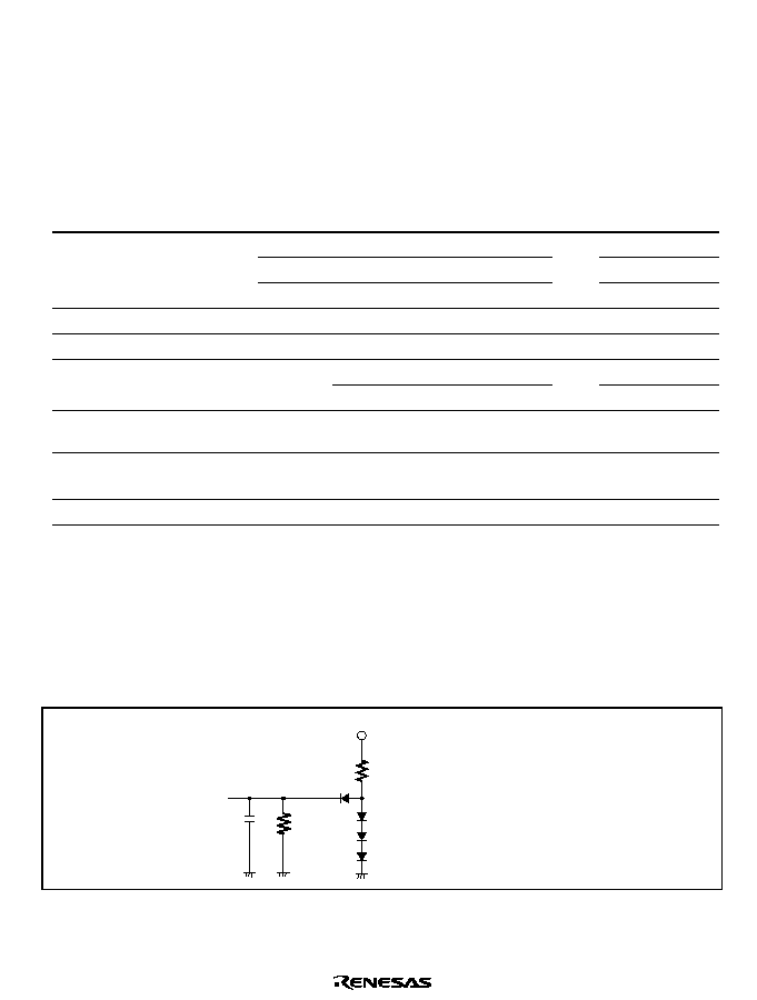
Rev. 2.0, 09/02, page 615 of 658
Table 26.17 Bus Drive Characteristics (2)
Condition C (F-ZTAT version): V
CC
= 4.0V to 5.5 V, AV
CC
= 4.0V to 5.5V, V
ref
= 4.0V to AV
CC
,
V
SS
= AV
SS
= 0 V, T
a
= ≠20∞C to +75∞C (regular specifications), T
a
= ≠40∞C to +85∞C
(wide-range specifications)*
1
,
Target pins: SCL
0
, SDA
0
Condition D (Masked-ROM version): V
CC
= 4.0V to 5.5 V, AV
CC
= 4.0V to 5.5V, V
ref
= 4.0V to
AV
CC
, V
SS
= AV
SS
= 0 V, T
a
= ≠20∞C to +75∞C (regular specifications), T
a
= ≠40∞C
to +85∞C (wide-range specifications)*
1
,
Target pins: SCL
0
, SDA
0
Item
Symbol
Min.
Typ.
Max.
Unit
Test Conditions
Schmitt trigger input voltage
VT
-
V
CC
◊
0.3
--
--
V
VT
+
--
--
V
CC
◊
0.7
VT
+
- VT
-
0.4
--
--
Input high voltage
V
IH
V
CC
◊
0.7
--
V
CC
+
0.5
V
Input low voltage
V
IL
-0.5
--
V
CC
◊
0.3
V
--
--
0.5
V
I
OL
=8mA
Output low voltage
V
OL
--
--
0.4
I
OL
=3mA
Input capacitance
C
in
--
--
20
pF
VIN=0 V, f=1 MHz,
T
a
=25∞C
Three-state leakage current
(off state)
|
l
STI
|
--
--
1.0
µ
A
V
IN
=0.5 to V
CC
-0.5
SDL, SDA output fall time
t
Of
20
+
0.1Cb
--
250
ns
Note: If the A/D converter is not used, do not leave the AV
CC
, V
ref
, and AV
SS
pins open. Apply a
voltage 4.0 V to 5.5 V to the AV
CC
and V
ref
pins by connecting them to V
CC
, for instance. Set
V
ref
AV
CC
.
26.3.3
AC Characteristics
Figure 26.3 shows the test conditions for the AC characteristics.
5V
R
L
R
H
C
LSI output pin
C=30pF:
R
L
= 2.4k
R
H
=12
Input/output timing measurement levels
∑ Low level : 0.8V
∑ High level : 2.0V
Figure 26.3 Output Load Circuit

Rev. 2.0, 09/02, page 616 of 658
Clock Timing: Table 26.18 lists the clock timing.
Table 26.18 Clock Timing
-- Preliminary --
Condition A (F-ZTAT version): V
CC
= 3.0 V to 5.5 V, AV
CC
= 2.7 V to 5.5 V, V
ref
= 2.7 V to AV
CC
,
V
SS
= AV
SS
= 0 V,
= 32.768kHz, 2 to 13.5MHz, T
a
= ≠20∞C to +75∞C (regular
specifications), T
a
= ≠40∞C to +85∞C (wide-range specifications)
Condition B (Mask-ROM version): V
CC
= 2.7 V to 5.5 V, AV
CC
= 2.7 V to 5.5 V, V
ref
= 2.7 V to
AV
CC
, V
SS
= AV
SS
= 0 V,
= 32.768kHz, 2 to 13.5MHz,T
a
= ≠20∞C to +75∞C (regular
specifications), T
a
= ≠40∞C to +85∞C (wide-range specifications)
Condition C (F-ZTAT version): V
CC
= 4.0V to 5.5 V, AV
CC
= 4.0V to 5.5V, V
ref
= 4.0V to AV
CC
,
V
SS
= AV
SS
= 0 V,
= 32.768kHz, 10 to 20.5 MHz, T
a
= ≠20∞C to +75∞C (regular
specifications), T
a
= ≠40∞C to +85∞C (wide-range specifications)
Condition D (Mask-ROM version): V
CC
= 4.0V to 5.5 V, AV
CC
= 4.0V to 5.5V, V
ref
= 4.0V to
AV
CC
, V
SS
= AV
SS
= 0 V,
= 32.768kHz, 10 to 20.5 MHz, T
a
= ≠20∞C to +75∞C
(regular specifications), T
a
= ≠40∞C to +85∞C (wide-range specifications)
Condition A and B
Condition C and D
13.5MHz
20.5 MHz
Item
Symbol Min.
Typ.
Max.
Min.
Typ.
Max.
Unit
Test Conditions
Clock cycle time
t
cyc
74
--
500
48.8
--
100
ns
Output clock high width
t
OCH
25
--
--
16
--
--
ns
Figure 26.4
Output clock low width
t
OCL
25
--
--
16
--
--
Output clock rising time
t
OCr
--
--
10
--
--
8
Output clock falling time
t
OCf
--
--
10
--
--
8
Clock oscillator settling time at reset
(crystal)
t
OSC1
20
--
--
10
--
--
ms
Figure 26.5
H8S/2264,
H8S/2262
Clock oscillator settling time in software
standby (crystal)
t
OSC2
8
--
--
8
--
--
ms
Figure 22.3
H8S/2264,
H8S/2262
Clock oscillator settling time at reset or
in software standby (ceramic)
t
OSC1
--
TBD
TBD
--
TBD
TBD
µ
s
Figure 26.5
H8S/2264R,
H8S/2262R
TBD
(
= 2 to
4 MHz)
TBD
(
= 2
to 4
MHz)
Clock oscillator settling time at reset or
in software standby (crystal)
t
OSC1
--
TBD
TBD
--
TBD
TBD
µ
s
Figure 26.5
H8S/2264R,
H8S/2262R

Rev. 2.0, 09/02, page 617 of 658
Condition A and B
Condition C and D
13.5MHz
20.5 MHz
Item
Symbol Min.
Typ.
Max.
Min.
Typ.
Max.
Unit
Test Conditions
External clock settling time
*
t
DEXT
500
--
--
500
--
--
µ
s
Figure 26.5
Sub clock oscillator settling time
t
OSC3
--
--
2
--
--
2
s
Sub clock oscillator frequency
f
SUB
--
32.768 --
--
32.768 --
kHz
Sub clock (
SUB
) cycle time
t
SUB
--
30.5
--
--
30.5
--
µ
s
Note:
*
Supported only by the H8S/2264 and H8S/2262. In the H8S/2264R and H8S/2262R,
an external clock input is disabled.
Control Signal Timing: Table 26.19 lists the control signal timing.
Table 26.19 Control Signal Timing
Condition A (F-ZTAT version): V
CC
= 3.0 V to 5.5 V, AV
CC
= 2.7 V to 5.5 V, V
ref
= 2.7 V to AV
CC
,
V
SS
= AV
SS
= 0 V,
= 32.768 kHz, 2 to 13.5 MHz, T
a
= ≠20∞C to +75∞C (regular
specifications), T
a
= ≠40∞C to +85∞C (wide-range specifications)
Condition B (Masked-ROM version): V
CC
= 2.7 V to 5.5 V, AV
CC
= 2.7 V to 5.5 V, V
ref
= 2.7 V to
AV
CC
, V
SS
= AV
SS
= 0 V,
= 32.768 kHz, 2 to 13.5 MHz, T
a
= ≠20∞C to +75∞C
(regular specifications), T
a
= ≠40∞C to +85∞C (wide-range specifications)
Condition C (F-ZTAT version): V
CC
= 4.0V to 5.5 V, AV
CC
= 4.0V to 5.5V, V
ref
= 4.0V to AV
CC
,
V
SS
= AV
SS
= 0 V,
= 32.768 kHz, 10 to 20.5 MHz, T
a
= ≠20∞C to +75∞C (regular
specifications), T
a
= ≠40∞C to +85∞C (wide-range specifications)
Condition D (Masked-ROM version): V
CC
= 4.0V to 5.5 V, AV
CC
= 4.0V to 5.5V, V
ref
= 4.0V to
AV
CC
, V
SS
= AV
SS
= 0 V,
= 32.768 kHz, 10 to 20.5 MHz, T
a
= ≠20∞C to +75∞C
(regular specifications), T
a
= ≠40∞C to +85∞C (wide-range specifications)
Item
Symbol Min.
Max.
Unit
Test Conditions
5(6
pulse width
t
RESW
20
--
t
cyc
Figure 26.6
NMI pulse width (exiting
software standby mode)
t
NMIW
200
--
ns
Figure 26.7
,54
pulse width (exiting
software standby mode)
t
IRQW
200
--
ns

Rev. 2.0, 09/02, page 618 of 658
Timing of On-Chip Peripheral Modules: Table 26.20 lists the timing of on-chip peripheral
modules. Table 26.21 lists the I
2
C bus timing.
Table 26.20 Timing of On-Chip Peripheral Modules
Condition A (F-ZTAT version): V
CC
= 3.0 V to 5.5 V, AV
CC
= 2.7 V to 5.5 V, V
ref
= 2.7 V to AV
CC
,
V
SS
= AV
SS
= 0 V,
= 32.768 kHz, 2 to 13.5 MHz, T
a
= ≠20∞C to +75∞C (regular
specifications), T
a
= ≠40∞C to +85∞C (wide-range specifications)
Condition B (Masked-ROM version): V
CC
= 2.7 V to 5.5 V, AV
CC
= 2.7 V to 5.5 V, V
ref
= 2.7 V to
AV
CC
, V
SS
= AV
SS
= 0 V,
= 32.768 kHz, 2 to 13.5 MHz, T
a
= ≠20∞C to +75∞C
(regular specifications), T
a
= ≠40∞C to +85∞C (wide-range specifications)
Condition C (F-ZTAT version): V
CC
= 4.0V to 5.5 V, AV
CC
= 4.0V to 5.5V, V
ref
= 4.0V to AV
CC
,
V
SS
= AV
SS
= 0 V,
= 32.768 kHz, 10 to 20.5 MHz, T
a
= ≠20∞C to +75∞C (regular
specifications), T
a
= ≠40∞C to +85∞C (wide-range specifications)
Condition D (Masked-ROM version): V
CC
= 4.0V to 5.5 V, AV
CC
= 4.0V to 5.5V, V
ref
= 4.0V to
AV
CC
, V
SS
= AV
SS
= 0 V,
= 32.768 kHz, 10 to 20.5 MHz, T
a
= ≠20∞C to +75∞C
(regular specifications), T
a
= ≠40∞C to +85∞C (wide-range specifications)
Condition A, B Condition C, D
Item
Symbol Min.
Max.
Min.
Max.
Unit
Test Conditions
TPU
Single edge
t
TCKWH
1.5
≠
1.5
≠
t
CyC
Figure 26.8
Timer clock
pulse width
Both edges
t
TCKWL
2.5
≠
2.5
≠
Single edge
1.5
≠
1.5
≠
TMR_0,
TMR_1
Timer clock
pulse width
Both edges
t
TMCWH
t
TMCWL
2.5
≠
2.5
≠
t
CyC
Figure 26.9
SCI
Input clock
cycle
Asynchronous
t
SCyC
4
≠
4
≠
t
CyC
Figure 26.10
Synchronous
6
≠
6
≠
Input clock pulse width
t
SCKW
0.4
0.6
0.4
0.6
t
ScyC
Input clock rise time
t
SCKf
≠
1.5
≠
1.5
t
CyC
Input clock fall time
t
SCKf
≠
1.5
≠
1.5
Transmit data delay time
t
TXD
≠
75
≠
50
ns
Figure 26.11
Receive data setup time
(synchronous)
t
RXS
75
≠
50
≠
ns
Receive data hold time (synchronous) t
RXH
75
≠
50
≠
ns

Rev. 2.0, 09/02, page 619 of 658
Table 26.21 I
2
C Bus Timing
Conditions: V
CC
= 2.7 V to 5.5 V, V
SS
= 0 V,
= 5 MHz to maximum operating frequency,
T
a
= ≠20∞C to +75∞C (regular specifications), T
a
= ≠40∞C to +80∞C (wide-range
specifications)
Item
Symbol Min.
Typ.
Max.
Unit
Test
Conditions
Remarks
SCL input cycle time
t
SCL
12t
cyc
≠
≠
ns
SCL input high pulse width
t
SCLH
3t
cyc
≠
≠
ns
SCL input low pulse width
t
SCLL
5t
cyc
≠
≠
ns
SCL, SDA input rise time
t
Sr
≠
≠
7.5t
cyc
*
ns
SCL, SDA input fall time
t
Sf
≠
≠
300
ns
SCL, SDA input spike pulse
elimination time
t
SP
≠
≠
1t
cyc
ns
SDA input bus free time
t
BUF
5t
cyc
≠
≠
ns
Start condition input hold time
t
STAH
3t
cyc
≠
≠
ns
Retransmission start condition
input setup time
t
STAS
3t
cyc
≠
≠
ns
Stop condition input setup time
t
STOS
3t
cyc
≠
≠
ns
Data input setup time
t
SDAS
0.5t
cyc
≠
≠
ns
Data input hold time
t
SDAH
0
≠
≠
ns
SCL, SDA load capacitance
C
b
≠
≠
400
pF
Figure 26.12
Note:
*
t
Sr
can be set to 7.5 t
cyc
or 17.5 t
cyc
according to the clock used for the I
2
C module. For
details, see section 14.5 Usage Notes.

Rev. 2.0, 09/02, page 620 of 658
26.3.4
A/D Conversion Characteristics
Table 26.22 lists the A/D conversion characteristics.
Table 26.22 A/D Conversion Characteristics
-- Preliminary --
Condition A (F-ZTAT version): V
CC
= 3.0 V to 5.5 V, AV
CC
= 2.7 V to 5.5 V, V
ref
= 2.7 V to AV
CC
,
V
SS
= AV
SS
= 0 V,
= 2 to 13.5 MHz, T
a
= ≠20∞C to +75∞C (regular specifications),
T
a
= ≠40∞C to +85∞C (wide-range specifications)
Condition B (Masked-ROM version): V
CC
= 2.7 V to 5.5 V, AV
CC
= 2.7 V to 5.5 V, V
ref
= 2.7 V to
AV
CC
, V
SS
= AV
SS
= 0 V,
= 2 to 13.5 MHz, T
a
= ≠20∞C to +75∞C (regular
specifications), T
a
= ≠40∞C to +85∞C (wide-range specifications)
Condition C (F-ZTAT version): V
CC
= 4.0V to 5.5 V, AV
CC
= 4.0V to 5.5V, V
ref
= 4.0V to AV
CC
,
V
SS
= AV
SS
= 0 V,
= 10 to 20.5 MHz, T
a
= ≠20∞C to +75∞C (regular specifications),
T
a
= ≠40∞C to +85∞C (wide-range specifications)
Condition D (Masked-ROM version): V
CC
= 4.0V to 5.5 V, AV
CC
= 4.0V to 5.5V, V
ref
= 4.0V to
AV
CC
, V
SS
= AV
SS
= 0 V,
= 10 to 20.5 MHz, T
a
= ≠20∞C to +75∞C (regular
specifications), T
a
= ≠40∞C to +85∞C (wide-range specifications)
Condition A, B
Condition C, D
13.5MHz
20.5 MHz
Item
Min.
Typ.
Max.
Min.
Typ.
Max.
Unit
Resolution
10
10
10
10
10
10
bits
Conversion time
9.6
--
--
6.3
--
--
µs
Analog input capacitance
--
--
20
--
--
20
pF
Permissible signal-source impedance
--
--
5
--
--
5
k
Nonlinearity error
--
--
±6.0
--
--
±3.0
LSB
Offset error
--
--
±4.0
--
--
±2.0
LSB
Full-scale error
--
--
±4.0
--
--
±2.0
LSB
Quantization error
--
--
±0.5
--
--
±0.5
LSB
Absolute accuracy
--
--
±8.0
--
--
±4.0
LSB

Rev. 2.0, 09/02, page 621 of 658
26.3.5
LCD Characteristics
Table 26.23 lists the LCD characteristics.
Table 26.23 LCD Characteristics
Condition A (F-ZTAT version): V
CC
= 3.0 V to 5.5 V, AV
CC
= 2.7 V to 5.5 V, V
ref
= 2.7 V to AV
CC
,
V
SS
= AV
SS
= 0 V,
= 32.768 kHz, 2 to 13.5 MHz, T
a
= ≠20∞C to +75∞C (regular
specifications), T
a
= ≠40∞C to +85∞C (wide-range specifications)
Condition B (Masked-ROM version): V
CC
= 2.7 V to 5.5 V, AV
CC
= 2.7 V to 5.5 V, V
ref
= 2.7 V to
AV
CC
, V
SS
= AV
SS
= 0 V,
= 32.768 kHz, 2 to 13.5 MHz, T
a
= ≠20∞C to +75∞C
(regular specifications), T
a
= ≠40∞C to +85∞C (wide-range specifications)
Condition C (F-ZTAT version): V
CC
= 4.0V to 5.5 V, AV
CC
= 4.0V to 5.5V, V
ref
= 4.0V to AV
CC
,
V
SS
= AV
SS
= 0 V,
= 32.768 kHz, 10 to 20.5 MHz, T
a
= ≠20∞C to +75∞C (regular
specifications), T
a
= ≠40∞C to +85∞C (wide-range specifications)
Condition D (Masked-ROM version): V
CC
= 4.0V to 5.5 V, AV
CC
= 4.0V to 5.5V, V
ref
= 4.0V to
AV
CC
, V
SS
= AV
SS
= 0 V,
= 32.768 kHz, 10 to 20.5 MHz, T
a
= ≠20∞C to +75∞C
(regular specifications), T
a
= ≠40∞C to +85∞C (wide-range specifications)
Condition A, B
Condition C, D
Standard Value
Standard Value
Item
Symbol
Applicable
Pins
Test
Conditions Min.
Typ.
Max.
Min.
Typ.
Max.
Unit
Notes
Segment driver step-
down voltage
V
DS
SEG1 to
SEG40
ID = 2
µ
A
--
--
0.6
--
--
0.6
V
*
1
Common driver step-
down voltage
V
DC
COM1 to
COM4
ID = 2
µ
A
--
--
0.3
--
--
0.3
V
*
1
LCD power supply
division resistor
R
LCD
Between
V1 and V
SS
40
360
1000
40
360
1000
k
LCD voltage
V
LCD
V1
3.0
--
V
CC
4.0
--
V
CC
V
*
2
Notes: 1. Voltage step-down between power supply pins V1, V2, V3, and V
SS
and segment pins.
2. If the LCD voltage is provided by an external power supply, the following relationship
must be maintained: V
CC
V1
V2
V3
V
SS
.

Rev. 2.0, 09/02, page 622 of 658
26.3.6
Flash Memory Characteristics
Table 26.24 shows the flash memory characteristics.
Table 26.24 Flash Memory Characteristics
Preliminary
Conditions:V
CC
= 3.0 V to 5.5 V, AV
CC
= 2.7 V to 5.5 V, V
ref
= 2.7 V to AV
CC
, V
SS
= AV
SS
= 0 V,
T
a
= ≠25∞C to +75∞C (Programming/erasing operating temperature range: regular
specification)
Item
Symbol
Min.
Typ.
Max. Unit
Test
Condition
Programming time
*
1
*
2
*
4
t
p
≠
10
200
ms/
128 bytes
Erase time
*
1,
*
3,
*
5
t
E
≠
100
1200 ms/block
Count of rewriting
N
WEC
100
*
6
10000
*
7
≠
Times
Data retention time
t
DRP
*
8
10
≠
≠
Year
Programming Wait time after SWE1 bit setting
*
1
t
sswe
1
1
≠
µ
s
Wait time after PSU1 bit setting
*
1
t
spsu
50
50
≠
µ
s
Wait time after P1 bit setting
*
1
*
4
t
sp10
8
10
12
µ
s
t
sp30
28
30
32
µ
s
6
n
1
t
sp200
198
200
202
µ
s
1000
n
7
Wait time after P1 bit clear
*
1
t
cp
5
5
≠
µ
s
Wait time after PSU1 bit clear
*
1
t
cpsu
4
4
≠
µ
s
Wait time after PV1 bit setting
*
1
t
spv
2
2
≠
µ
s
Wait time after H'FF dummy
write
*
1
t
spvr
2
2
≠
µ
s
Wait time after PV1 bit clear
*
1
t
cpv
100
100
≠
µ
s
Wait time after SWE1 bit clear
t
cswe
≠
≠
≠
µ
s
N1
≠
≠
6
*
4
Times
Maximum programming count
*
1
*
4
N2
≠
≠
994
*
4
Times
Erase
Wait time after SWE1 bit setting
*
1
t
sswe
1
1
≠
µ
s
Wait time after ESU1 bit setting
*
1
t
sesu
100
100
≠
µ
s
Wait time after E1 bit setting
*
1
*
5
t
se
10
10
100
ms
Wait time after E1 bit clear
*
1
t
ce
10
10
≠
µ
s
Wait time after ESU1 bit clear
*
1
t
cesu
10
10
≠
µ
s
Wait time after EV1 bit setting
*
1
t
sev
20
20
≠
µ
s

Rev. 2.0, 09/02, page 623 of 658
Item
Symbol
Min.
Typ.
Max. Unit
Test
Condition
Erase
Wait time after H'FF dummy
write
*
1
t
sevr
2
2
≠
µ
s
Wait time after EV1 bit clear
*
1
t
cev
4
4
≠
µ
s
Wait time after SWE1 bit clear
t
cswe
100
100
≠
µ
s
Maximum erase count
*
1,
*
5
N
≠
≠
100
Times
Notes: 1. Make each time setting in accordance with the program or erase algorithm.
2. Programming time per 128 bytes (Shows the total period for which the P1 bit in the
flash memory control register (FLMCR1) is set. It does not include the programming
verification time.)
3. Block erase time (Shows the total period for which the E1 bit in FLMCR1 is set. It does
not include the erase verification time.)
4. The maximum programming time value (tp(max.)):
t
P
(max.) = Wait time after P1 bit setting (t
sp
) x maximum programming count (N)
(t
sp30
+ t
sp10
) x 6 + (t
sp200
) x 994
5. For the maximum erase time (t
E
(max.)), the following relationship applies between the
wait time after E1 bit setting (t
se
) and the maximum erase count (N):
t
E
(max.) = Wait time after E1 bit setting (t
se
) x maximum erase count (N)
6. The minimum times that all characteristics after rewriting are guaranteed. (A range
between 1 and minimum value is guaranteed.)
7. The reference value at 25∞C. (Normally, it is a reference that rewriting is enabled up to
this value.)
8. Data retention characteristics when rewriting is performed within the range of
specifications including minimum value.

Rev. 2.0, 09/02, page 624 of 658
26.4
Operation Timing
Operation timings are shown below.
26.4.1
Clock Timing
Clock timing is shown below.
Output Clock Timing (Supported only by the H8S/2264 Series): Figure 26.4 shows the output
clock timing.
pin
t
OCH
t
OCL
t
OCr
t
OCf
Figure 26.4 Output Clock Timing
Oscillator Settling Timing: Figure 26.5 shows the oscillator settling timing.
t
OSC1
t
DEXT
EXTAL
Vcc
Internal
clock
t
DEXT
t
OSC1
Figure 26.5 Oscillator Settling Timing

Rev. 2.0, 09/02, page 625 of 658
26.4.2
Control Signal Timings
Control signal timings are shown below.
∑
Reset Input Timing
Figure 26.6 shows the reset input timing.
∑
Interrupt Input Timing
Figure 26.7 shows the NMI,
,54 interrupt reset input timing.
t
RESW
RES
Figure 26.6 Reset Input Timing
NMI
IRQ
t
NMIW
t
IRQW
Figure 26.7 Interrupt Input Timing
26.4.3
Timing of On-Chip Peripheral Modules
Figures 26.8 to 26.12 show timing of on-chip peripheral modules.
TCLKA to TCLKC, TCLKD
*
Note:
*
Supported only by the H8S/2268 Series.
t
TCKWH
t
TCKWL
Figure 26.8 TPU Clock Input Timing
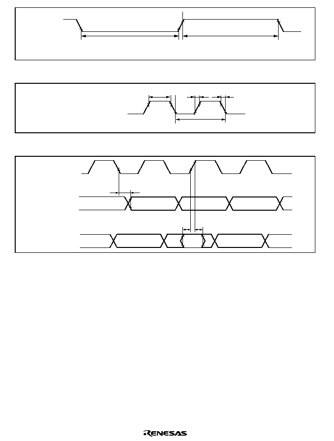
Rev. 2.0, 09/02, page 626 of 658
TMCI01,
TMCI23
*
,
TMCI4
*
t
TCKWH
t
TCKWL
Note:
*
Supported only by the H8S/2268 Series.
Figure 26.9 8-Bit Timer Clock Input Timing
SCK0 to SCK2
t
SCKW
t
SCKr
t
SCKf
t
Scyc
Figure 26.10 SCK Clock Input Timing
TxD0 to TxD2
(transmit data)
RxD0 to RxD2
(receive data)
SCK0 to SCK2
t
RXS
t
RXH
t
TXD
Figure 26.11 SCI Input/Output Timing (Clock Synchronous Mode)
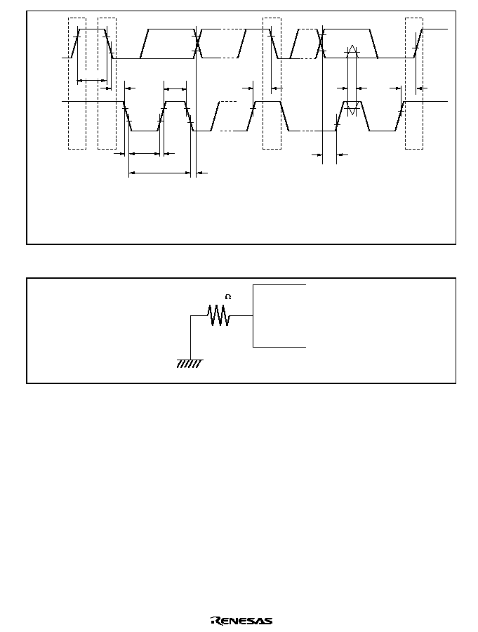
Rev. 2.0, 09/02, page 627 of 658
t
BUF
t
STAH
t
STAS
t
SP
t
STOS
t
SCLH
t
SCLL
t
sf
t
Sr
t
SCL
t
SDAH
t
SDAS
P
*
1
S
*
1
S
r
*
1
V
IH
V
IL
SDA0
to
SDA1
*
2
SCL0
to
SCL1
*
2
S, P, and Sr indicate the following conditions.
S : Start condition
P : Stop condition
Sr : Retransmission start condition
Supported only by the H8S/2268 Series.
*
1.
*
2.
Note:
Figure 26.12 I
2
C Bus Interface Input/Output Timing (Option)
TONED
GND
R
L
100k
Figure 26.13 TONED Load Circuit (Supported only by the H8S/2268 Series)
26.5
Usage Note
The F-ZTAT and masked ROM versions both satisfy the electrical characteristics shown in this
manual, but actual electrical characteristic values, operating margins, noise margins, and other
properties may vary due to differences in manufacturing process, on-chip ROM, layout patterns,
and so on.
When system evaluation testing is carried out using the F-ZTAT version, the same evaluation
testing should also be conducted for the masked ROM version when changing over to that version.

Rev. 2.0, 09/02, page 628 of 658

Rev. 2.0, 09/02, page 629 of 658
Appendix A I/O Port States in Each Pin State
A.1
I/O Port State in Each Pin State of the H8S/2268 Series
Port Name Reset
Hardware
Standby
Mode
Software
Standby Mode
Watch Mode
Program Execution
State Sleep Mode
Subsleep Mode
Port 1
T
T
Keep
Keep
I/O port
Port 3
T
T
Keep
Keep
I/O port
Port 4
T
T
T
T
I/O port
Port 7
T
T
Keep
Keep
I/O port
P97/DA1
P96/DA0
T
T
[DAOEn = 1]
Keep
[DAOEn = 0]
T
[DAOEn = 1]
Keep
[DAOEn = 0]
T
Input port
Port F
T
T
Keep
Keep
I/O port
PH7
T
T
T
T
Input port
PH3 to PH0 T
T
[Common output]
Port
[Otherwise]
Keep
[Common output]
COM4 to COM1
[Otherwise]
Keep
[Common output]
COM4 to COM1
[Otherwise]
I/O port
Port J
T
T
[Segment output]
Port
[Otherwise]
Keep
[Segment output]
SEG8 to SEG1
[Otherwise]
Keep
[Segment output]
SEG8 to SEG1
[Otherwise]
I/O port
Port K
T
T
[Segment output]
Port
[Otherwise]
Keep
[Segment output]
SEG16 to SEG9
[Otherwise]
Keep
[Segment output]
SEG16 to SEG9
[Otherwise]
I/O port
Port L
T
T
[Segment output]
Port
[Otherwise]
Keep
[Segment output]
SEG24 to SEG17
[Otherwise]
Keep
[Segment output]
SEG24 to SEG17
[Otherwise]
I/O port
Port M
T
T
[Segment output]
Port
[Otherwise]
Keep
[Segment output]
SEG32 to SEG25
[Otherwise]
Keep
[Segment output]
SEG32 to SEG25
[Otherwise]
I/O port

Rev. 2.0, 09/02, page 630 of 658
Port Name Reset
Hardware
Standby
Mode
Software
Standby Mode
Watch Mode
Program Execution
State Sleep Mode
Port N
T
T
[Segment output]
Port
[Otherwise]
Keep
[Segment output]
SEG40 to SEG33
[Otherwise]
Keep
[Segment output]
SEG40 to SEG33
[Otherwise]
I/O port
A.2
I/O Port State in Each Pin State of the H8S/2264 Series
Port Name Reset
Hardware
Standby
Mode
Software
Standby Mode
Watch Mode
Program Execution
State Sleep Mode
Subsleep Mode
Port 1
T
T
Keep
Keep
I/O port
Port 3
T
T
Keep
Keep
I/O port
Port 4
T
T
T
T
Input port
Port 7
T
T
Keep
Keep
I/O port
Port 9
T
T
T
T
Input port
Port F
T
T
Keep
Keep
I/O port
PH7
T
T
T
T
Input port
PH5
T
T
Keep
Keep
I/O port
PH4
T
T
[Clock output]
H
[Otherwise]
Keep
[Clock output]
[Otherwise]
Keep
[Clock output]
*
[Otherwise]
I/O port
PH3 to PH0 T
T
[Common output]
Port
[Otherwise]
Keep
[Common output]
COM4 to COM1
[Otherwise]
Keep
[Common output]
COM4 to COM1
[Otherwise]
I/O port
Port J
T
T
[Segment output]
Port
[Otherwise]
Keep
[Segment output]
SEG8 to SEG1
[Otherwise]
Keep
[Segment output]
SEG8 to SEG1
[Otherwise]
I/O port
Port K
T
T
[Segment output]
Port
[Otherwise]
Keep
[Segment output]
SEG16 to SEG9
[Otherwise]
Keep
[Segment output]
SEG16 to SEG9
[Otherwise]
I/O port

Rev. 2.0, 09/02, page 631 of 658
Port Name Reset
Hardware
Standby
Mode
Software
Standby Mode
Watch Mode
Program Execution
State Sleep Mode
Subsleep Mode
Port L
T
T
[Segment output]
Port
[Otherwise]
Keep
[Segment output]
SEG24 to SEG17
[Otherwise]
Keep
[Segment output]
SEG24 to SEG17
[Otherwise]
I/O port
SEG40 to
SEG25
T
T
T
[Segment output]
SEG40 to SEG25
[Otherwise]
T
[Segment output]
SEG40 to SEG25
[Otherwise]
T
Legend
H:
High level
T:
High-impedance
Keep: Input port becomes high-impedance, output port retains state
Port:
Determined by port setting (input is high-impedance)
Note:
*
The I/O port state at the clock output is high, if the operation shifts to sleep mode while
all modules are sopped (MSTPCR = H"FFFFFFFF).

Rev. 2.0, 09/02, page 632 of 658
Appendix B Product Codes
∑
H8S/2268 Series
Product Type
Product
Code
Mark Code
Package
(Hitachi
Package
Code)
Operating
Voltage
HD6432268(A
**
)TE
100-pin
TQFP
(TFP-100B)
HD6432268(A
**
)TF
100-pin
TQFP
(TFP-100G)
HD6432268(A
**
)FA
100-pin QFP
(FP-100B)
2.7 V to 5.5
V
HD6432268(F
**
)TE
100-pin
TQFP
(TFP-100B)
HD6432268(F
**
)TF
100-pin
TQFP
(TFP-100G)
Standard
product
HD6432268
HD6432268(F
**
)FA
100-pin QFP
(FP-100B)
4.0 V to 5.5
V
HD6432268W(A
**
)TE
100-pin
TQFP
(TFP-100B)
HD6432268W(A
**
)TF
100-pin
TQFP
(TFP-100G)
HD6432268W(A
**
)FA
100-pin QFP
(FP-100B)
2.7 V to 5.5
V
HD6432268W(F
**
)TE
100-pin
TQFP
(TFP-100B)
HD6432268W(F
**
)TF
100-pin
TQFP
(TFP-100G)
H8S/2268
(regular
oscillation)
Masked-
ROM
version
Version
with
on-chip I
2
C
bus
interface
HD6432268
W
HD6432268W(F
**
)FA
100-pin QFP
(FP-100B)
4.0 V to 5.5
V

Rev. 2.0, 09/02, page 633 of 658
Product Type
Product
Code
Mark Code
Package
(Hitachi
Package
Code)
Operating
Voltage
HD64F2268TE13
100-pin
TQFP
(TFP-100B)
HD64F2268TF13
100-pin
TQFP
(TFP-100G)
HD64F2268FA13
100-pin QFP
(FP-100B)
3.0 V to 5.5
V
HD64F2268TE20
100-pin
TQFP
(TFP-100B)
HD64F2268TF20
100-pin
TQFP
(TFP-100G)
H8S/2268
(regular
oscillation)
F-ZTAT
version
Standard
product
HD64F2268
HD64F2268FA20
100-pin QFP
(FP-100B)
4.0 V to 5.5
V
HD6432266(A
**
)TE
100-pin
TQFP
(TFP-100B)
HD6432266(A
**
)TF
100-pin
TQFP
(TFP-100G)
HD6432266(A
**
)FA
100-pin QFP
(FP-100B)
2.7 V to 5.5
V
HD6432266(F
**
)TE
100-pin
TQFP
(TFP-100B)
HD6432266(F
**
)TF
100-pin
TQFP
(TFP-100G)
H8S/2266
(regular
oscillation)
Masked-
ROM
version
Standard
product
HD6432266
HD6432266(F
**
)FA
100-pin QFP
(FP-100B)
4.0 V to 5.5
V

Rev. 2.0, 09/02, page 634 of 658
Product Type
Product
Code
Mark Code
Package
(Hitachi
Package
Code)
Operating
Voltage
HD6432266W(A
**
)TE
100-pin
TQFP
(TFP-100B)
HD6432266W(A
**
)TF
100-pin
TQFP
(TFP-100G)
HD6432266W(A
**
)FA
100-pin QFP
(FP-100B)
2.7 V to 5.5
V
HD6432266W(F
**
)TE
100-pin
TQFP
(TFP-100B)
HD6432266W(F
**
)TF
100-pin
TQFP
(TFP-100G)
Masked-
ROM
version
Version
with
on-chip I
2
C
bus
interface
HD6432266
W
HD6432266W(F
**
)FA
100-pin QFP
(FP-100B)
4.0 V to 5.5
V
HD64F2266TE13
100-pin
TQFP
(TFP-100B)
HD64F2266TF13
100-pin
TQFP
(TFP-100G)
HD64F2266FA13
100-pin QFP
(FP-100B)
3.0 V to 5.5
V
HD64F2266TE20
100-pin
TQFP
(TFP-100B)
HD64F2266TF20
100-pin
TQFP
(TFP-100G)
H8S/2266
(regular
oscillation)
F-ZTAT
version
Standard
product
HD64F2266
HD64F2266FA20
100-pin QFP
(FP-100B)
4.0 V to 5.5
V

Rev. 2.0, 09/02, page 635 of 658
Product Type
Product
Code
Mark Code
Package
(Hitachi
Package
Code)
Operating
Voltage
HD6432265(A
**
)TE
100-pin
TQFP
(TFP-100B)
HD6432265(A
**
)TF
100-pin
TQFP
(TFP-100G)
HD6432265(A
**
)FA
100-pin QFP
(FP-100B)
2.7 V to 5.5
V
HD6432265(F
**
)TE
100-pin
TQFP
(TFP-100B)
HD6432265(F
**
)TF
100-pin
TQFP
(TFP-100G)
Standard
product
HD6432265
HD6432265(F
**
)FA
100-pin QFP
(FP-100B)
4.0 V to 5.5
V
HD6432265W(A
**
)TE
100-pin
TQFP
(TFP-100B)
HD6432265W(A
**
)TF
100-pin
TQFP
(TFP-100G)
HD6432265W(A
**
)FA
100-pin QFP
(FP-100B)
2.7 V to 5.5
V
HD6432265W(F
**
)TE
100-pin
TQFP
(TFP-100B)
HD6432265W(F
**
)TF
100-pin
TQFP
(TFP-100G)
H8S/2265
(regular
oscillation)
Masked-
ROM
version
Version
with
on-chip I
2
C
bus
interface
HD6432265
W
HD6432265W(F
**
)FA
100-pin QFP
(FP-100B)
4.0 V to 5.5
V

Rev. 2.0, 09/02, page 636 of 658
Product Type
Product
Code
Mark Code
Package
(Hitachi
Package
Code)
Operating
Voltage
HD64F2265TE13
100-pin
TQFP
(TFP-100B)
HD64F2265TF13
100-pin
TQFP
(TFP-100G)
HD64F2265FA13
100-pin QFP
(FP-100B)
3.0 V to 5.5
V
HD64F2265TE20
100-pin
TQFP
(TFP-100B)
HD64F2265TF20
100-pin
TQFP
(TFP-100G)
H8S/2265
(regular
oscillation)
F-ZTAT
version
Standard
product
HD64F2265
HD64F2265FA20
100-pin QFP
(FP-100B)
4.0 V to 5.5
V
Legend
(A
**
), (F
**
): ROM code
Note: Some products above are in the developing or planning stage. Please contact Hitachi
agency to conform the present state of each product.

Rev. 2.0, 09/02, page 637 of 658
∑
H8S/2264 Series
Product Type
Product
Code
Mark Code
Package
(Hitachi
Package
Code)
Operating
Voltage
HD6432264(A
**
)TE
100-pin
TQFP
(TFP-100B)
HD6432264(A
**
)TF
100-pin
TQFP
(TFP-100G)
HD6432264(A
**
)FA
100-pin QFP
(FP-100B)
2.7 V to 5.5
V
HD6432264(F
**
)TE
100-pin
TQFP
(TFP-100B)
HD6432264(F
**
)TF
100-pin
TQFP
(TFP-100G)
Standard
product
HD6432264
HD6432264(F
**
)FA
100-pin QFP
(FP-100B)
4.0 V to 5.5
V
HD6432264W(A
**
)TE
100-pin
TQFP
(TFP-100B)
HD6432264W(A
**
)TF
100-pin
TQFP
(TFP-100G)
HD6432264W(A
**
)FA
100-pin QFP
(FP-100B)
2.7 V to 5.5
V
HD6432264W(F
**
)TE
100-pin
TQFP
(TFP-100B)
HD6432264W(F
**
)TF
100-pin
TQFP
(TFP-100G)
H8S/2264
(regular
oscillation)
Masked-
ROM
version
Version
with
on-chip I
2
C
bus
interface
HD6432264
W
HD6432264W(F
**
)FA
100-pin QFP
(FP-100B)
4.0 V to 5.5
V

Rev. 2.0, 09/02, page 638 of 658
Product Type
Product
Code
Mark Code
Package
(Hitachi
Package
Code)
Operating
Voltage
HD64F2264TE13
100-pin
TQFP
(TFP-100B)
HD64F2264TF13
100-pin
TQFP
(TFP-100G)
HD64F2264FA13
100-pin QFP
(FP-100B)
3.0 V to 5.5
V
HD64F2264TE20
100-pin
TQFP
(TFP-100B)
HD64F2264TF20
100-pin
TQFP
(TFP-100G)
H8S/2264
(regular
oscillation)
F-ZTAT
version
Standard
product
HD64F2264
HD64F2264FA20
100-pin QFP
(FP-100B)
4.0 V to 5.5
V
HD6432264R(A
**
)TE
100-pin
TQFP
(TFP-100B)
HD6432264R(A
**
)TF
100-pin
TQFP
(TFP-100G)
HD6432264R(A
**
)FA
100-pin QFP
(FP-100B)
2.7 V to 5.5
V
HD6432264R(F
**
)TE
100-pin
TQFP
(TFP-100B)
HD6432264R(F
**
)TF
100-pin
TQFP
(TFP-100G)
H8S/2264R
(oscillation
stabilization
time
shortened)
Masked-
ROM
version
Standard
product
HD6432264
R
HD6432264R(F
**
)FA
100-pin QFP
(FP-100B)
4.0 V to 5.5
V

Rev. 2.0, 09/02, page 639 of 658
Product Type
Product
Code
Mark Code
Package
(Hitachi
Package
Code)
Operating
Voltage
HD6432264RW(A
**
)T
E
100-pin
TQFP
(TFP-100B)
HD6432264RW(A
**
)T
F
100-pin
TQFP
(TFP-100G)
HD6432264RW(A
**
)F
A
100-pin QFP
(FP-100B)
2.7 V to 5.5
V
HD6432264RW(F
**
)T
E
100-pin
TQFP
(TFP-100B)
HD6432264RW(F
**
)T
F
100-pin
TQFP
(TFP-100G)
Masked-
ROM
version
Version
with
on-chip
I
2
C bus
interface
HD6432264
RW
HD6432264RW(F
**
)F
A
100-pin QFP
(FP-100B)
4.0 V to 5.5
V
HD64F2264RTE13
100-pin
TQFP
(TFP-100B)
HD64F2264RTF13
100-pin
TQFP
(TFP-100G)
HD64F2264RFA13
100-pin QFP
(FP-100B)
3.0 V to 5.5
V
HD64F2264RTE20
100-pin
TQFP
(TFP-100B)
HD64F2264RTF20
100-pin
TQFP
(TFP-100G)
H8S/2264R
(oscillation
stabilization
time
shortened)
F-ZTAT
version
Standard
product
HD64F2264
R
HD64F2264RFA20
100-pin QFP
(FP-100B)
4.0 V to 5.5
V

Rev. 2.0, 09/02, page 640 of 658
Product Type
Product
Code
Mark Code
Package
(Hitachi
Package
Code)
Operating
Voltage
HD6432262W(A
**
)TE
100-pin
TQFP
(TFP-100B)
HD6432262W(A
**
)TF
100-pin
TQFP
(TFP-100G)
HD6432262W(A
**
)FA
100-pin QFP
(FP-100B)
2.7 V to 5.5
V
HD6432262W(F
**
)TE
100-pin
TQFP
(TFP-100B)
HD6432262W(F
**
)TF
100-pin
TQFP
(TFP-100G)
H8S/2264R
(regular
oscillation)
Masked-
ROM
version
Version
with
on-chip
I
2
C bus
interface
HD6432262
W
HD6432262W(F
**
)FA
100-pin QFP
(FP-100B)
4.0 V to 5.5
V
HD6432262R(A
**
)TE
100-pin
TQFP
(TFP-100B)
HD6432262R(A
**
)TF
100-pin
TQFP
(TFP-100G)
HD6432262R(A
**
)FA
100-pin QFP
(FP-100B)
2.7 V to 5.5
V
HD6432262R(F
**
)TE
100-pin
TQFP
(TFP-100B)
HD6432262R(F
**
)TF
100-pin
TQFP
(TFP-100G)
H8S/2262R
(oscillation
stabilization
time
shortened)
Masked-
ROM
version
Standard
product
HD6432262
R
HD6432262R(F
**
)FA
100-pin QFP
(FP-100B)
4.0 V to 5.5
V

Rev. 2.0, 09/02, page 641 of 658
Product Type
Product
Code
Mark Code
Package
(Hitachi
Package
Code)
Operating
Voltage
HD6432262RW(A
**
)T
E
100-pin
TQFP
(TFP-100B)
HD6432262RW(A
**
)T
F
100-pin
TQFP
(TFP-100G)
HD6432262RW(A
**
)F
A
100-pin QFP
(FP-100B)
2.7 V to 5.5
V
HD6432262RW(F
**
)T
E
100-pin
TQFP
(TFP-100B)
HD6432262RW(F
**
)T
F
100-pin
TQFP
(TFP-100G)
H8S/2262R
(oscillation
stabilization
time
shortened)
Masked-
ROM
version
Version
with
on-chip
I
2
C bus
interface
HD6432262
RW
HD6432262RW(F
**
)F
A
100-pin QFP
(FP-100B)
4.0 V to 5.5
V
Legend
(A
**
), (F
**
): ROM code
Note: Some products above are in the developing or planning stage. Please contact Hitachi
agency to conform the present state of each product.

Rev. 2.0, 09/02, page 642 of 658
Appendix C Package Dimensions
Figures C.1, C.2, and C.3 show the package dimensions of the H8S/2268 Series and H8S/2264
Series.
Hitachi Code
JEDEC
JEITA
Mass (reference value)
TFP-100B
--
Conforms
0.5 g
*
Dimension including the plating thickness
Base material dimension
16.0 ± 0.2
14
0.08
0.10
0.5 ± 0.1
16.0 ± 0.2
0.5
0.10 ± 0.10
1.20 Max
*
0.17 ± 0.05
0∞ ≠ 8∞
75
51
1
25
76
100
26
50
M
*
0.22 ± 0.05
1.0
1.00
1.0
0.20 ± 0.04
0.15 ± 0.04
As of January,2002
Unit: mm
Figure C.1 TFP-100B Package Dimensions
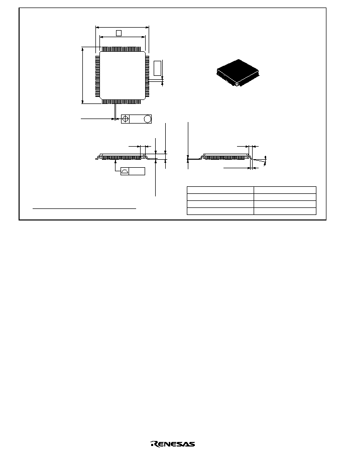
Rev. 2.0, 09/02, page 643 of 658
Hitachi Code
JEDEC
JEITA
Mass (reference value)
TFP-100G
--
Conforms
0.4 g
*
Dimension including the plating thickness
Base material dimension
14.0 ± 0.2
12
0.07
0.10
0.5 ± 0.1
14.0 ± 0.2
0.4
1.20 Max
*
0.17 ± 0.05
0∞ ≠ 8∞
75
51
1
25
76
100
26
50
M
*
0.18 ± 0.05
1.0
1.2
0.16 ± 0.04
0.15 ± 0.04
1.00
0.10 ± 0.10
As of January,2002
Unit: mm
Figure C.2 TFP-100G Package Dimensions
Rev. 2.0, 09/02, page 644 of 658
Hitachi Code
JEDEC
JEITA
Mass (reference value)
FP-100B
--
Conforms
1.2 g
*
Dimension including the plating thickness
Base material dimension
0.10
16.0 ± 0.3
1.0
0.5 ± 0.2
16.0 ± 0.3
3.05 Max
75
51
50
26
1
25
76
100
14
0∞ ≠ 8∞
0.5
0.08 M
*
0.22 ± 0.05
2.70
*
0.17 ± 0.05
0.12
+0.13 ≠0.12
1.0
0.20 ± 0.04
0.15 ± 0.04
As of January,2002
Unit: mm
Figure C.3 FP-100B Package Dimensions

Rev. 2.0, 09/02, page 645 of 658
Main Revisions and Additions in this Edition
Item
Page
Revisions (See Manual for Details)
All
In this version, descriptions of the H8S/2264 Series are
added. Therefore, notes indicating the series name are added
if there are differences in the specifications between the
H8S/2268 Series and H8S/2264 Series. The added notes are
as follows: (H8S/2268), (H8S/2268 Series), (H8S/2268 Series
only), supported only by the H8S/2268 Series, (H8S/2264),
(H8S/2264 Series), (H8S/2264 Series only), or supported only
by the H8S/2264 Series.
(Error) (Correction)
H8S/2268 Series:
Model
ROM
RAM
Model
ROM
RAM
HD64F2268
256 kbytes 16 kbytes
HD64F2268
256 kbytes
16 kbytes
HD6432268
256 kbytes 16 kbytes
HD64F2266
128 kbytes
8 kbytes
HD6432268W 256 kbytes 16 kbytes
HD64F2265
128 kbytes
8 kbytes
HD6432268D 256 kbytes 16 kbytes
HD6432268
256 kbytes
16 kbytes
HD6432266
128 kbytes 8 kbytes
HD6432268W 256 kbytes
16 kbytes
HD6432266W 128 kbytes 8 kbytes
HD6432266
128 kbytes
8 kbytes
HD6432266D 128 kbytes 8 kbytes
HD6432266W 128 kbytes
8 kbytes
HD6432265
128 kbytes 4 kbytes
HD6432265
128 kbytes
4 kbytes
HD6432265W 128 kbytes 4 kbytes
HD6432265W 128 kbytes
4 kbytes
HD6432265D 128 kbytes 4 kbytes
Section 1 Overview
1.1 Overview
∑
On-chip memory
Figure 1.1 Internal Block
Diagram of H8S/2268
Amended.
Description of (option) in DTMF deleted.
Bus line of port 9 amended.
Port 4
Port 9
A/D converter(10 channels)
D/A converter(2 channels)
DTMF
Peripheral data bus
Peripheral address bus
Port H
Port J
Rev. 2.0, 09/02, page 646 of 658
Item
Page
Revisions (See Manual for Details)
9.1.4 Pin Functions
P15/TIOCB1/TCLKC
Amended.
(Error)
Notes: 2. This pin functions as TCLKD inputs when TPSC2 to
TPSC0 in TCR0 or TCR2 are set to 110.
(Correction)
Notes: 2. This pin functions as TCLKC inputs when TPSC2 to
TPSC0 in TCR0 or TCR2 are set to 110.
9.2.4 Port 3 Open Drain
Control Register (P3ODR)
Description of bits 5 to 0 amended.
(Error)
When each of P35DDR and P34DDR bits is set to 1, the
corresponding pins P35 and P34 function as open drain
outputs.
(Correction)
When each of P35ODR and P34ODR bits is set to 1, the
corresponding pins P35 and P34 function as open drain
outputs.
Amended.
PH3/COM4
X is amended to
in table.
1 is amended to 0 in table.
CMX
0
1
0
1
SUPS
*
0
1
PH3DDR
0
1
0
1
0
1
PH2/COM3 and PH1/COM2
X is amended to
in table.
CMX
0
1
PH2DDR
0
1
0
1
9.7.4 Pin Functions
Amended.
1
1
1
Counts on TCNT_2 overflow.
(H8S/2268 Series: Setting disabled)
Table 10.6 TPSC0 to
TPSC2 (channel 1)

Rev. 2.0, 09/02, page 647 of 658
Item
Page
Revisions (See Manual for Details)
Amended.
Capture input source is TIOCA0 pin
Input capture at rising edge
Input
caputure
register
Capture input source is TIOCA0 pin
Input capture at falling edge
Table 10.13 TIORH_0
(channel 0) (H8S/2268
Series only)
10.3.6 Timer Counter
(TCNT)
Amended.
The TCNT counters are initialized to H'0000 by a reset, or in
hardware standby mode.
11.9.2 Input/Output Pins
Name in table amended.
(Error) Timer clock input pin 4
(Correction) Timer clock input pin
Description of bits 6 to 4 amended.
(Error) These bits are always read as 0 and cannot be
modified.
(Correction) The write value should always be 0.
13.3.10 Serial Expansion
Mode Register (SEMR_0)
Description of bits 2 to 0 amended.
The ACS0 to ACS0 settings are valid when the external clock
input is selected (CKE1 in SCR = 1) in asynchronous mode
(C/
in SMR = 0).
000: External clock input
:
111: 720 kbps average transfer rate (for
= 6 MHz only) is
selected (SCI0 operates on base clock with frequency of
8 times transfer rate)
15.1 Features
Amended.
∑
Conversion time: 6.3
µ
s per channel (at 20.5 MHz
operation)
15.3.2 A/D Control/Status
Register (ADCSR)
Description of bit 5 amended.
A/D Start
In scan mode, conversion continues sequentially on the
specified channels until this bit is cleared to 0 by software, a
reset, or a transition to power-down mode in which the A/D
converter is halted, shown in table 22.1.
Figure 17.1 Block
Diagram of LCD
Controller/Driver
Amended.
Description of
/8 to
/1024 is amended to
/16 to
/2048.

Rev. 2.0, 09/02, page 648 of 658
Item
Page
Revisions (See Manual for Details)
Description of bits 7 and 3 amended.
Bit 7
R/W
LCD Disable Bit
This bit is always read as 1. The write value should
always be 0.
Bit 3
R/W
R/W
R/W
R/W
Frame Frequency Select 3 to 0
In subactive mode, watch mode, and subsleep
mode, the system clock (
) is halted, and therefore
display operations are not performed if one of the
clocks from
/16 to
/2048 is selected.
17.3.2 LCD Control
Register (LCR)
Table 17.5 Frame
Frequency Selection
Values of Operating Clock and Frame Frequency amended.
17.3.3 LCD Control
Register 2 (LCR2)
Description of bit 5 amended.
(H8S/2268 Series)
Triple Step-Up Voltage Circuit Clock Select
This bit selects a clock used for triple step-up voltage circuit.
This bit selects a clock which divides a clock specified by the
LCD operating control register (LCR) by 4 or 8 as step-up
voltage circuit clock.
0: A clock, which divides a LCD operating clock by 4, is
selected as step-up voltage circuit clock
1: A clock, which divides a LCD operating clock by 8, is
selected as step-up voltage circuit clock
Relationships between LCD operating clock and step-up
voltage clock, and between bits CKS3 to CKS0 and bit HCKS
Values of LCD clock, step-up voltage circuit clock, frame
frequency, and step-up voltage circuit clock frequency
amended.
Symbol of
*
is amended to X.
18.1 Features
Amended.
∑
Generating DTMF frequency sine waveform from the
system clock (
)
The system clock (2.0 to 20.4 MHz, with 400 kHz stops)
Figure 18.2 DTMF
Generation Circuit
Diagram
Amended.
Description of 2.0 to 20.0 MHz is amended to 2.0 to 20.4 MHz.

Rev. 2.0, 09/02, page 649 of 658
Item
Page
Revisions (See Manual for Details)
Description of bits 5 to 0 amended.
Main clock division ratio 5 to 0
These bits set the system clock division ratio to produce 400-
kHz clock signals to be supplied to the DTMF generation
circuit. The division ratio determines the counter value of
6b'000101 to 6b'110011(D'5 to D'51) according to the range
2.0 to 20.4 MHz.
000000: Setting prohibited
: :
110010: Division ratio (50) main clock frequency (20.0 MHz)
110011: Division ratio (51) main clock frequency (20.4 MHz)
110100: Setting prohibited
: :
18.3.2 DTMF Load
Register (DTLR)
Note amended.
Additionally, correct operation is not guaranteed if the DTL0 to
DTL5 settings are other than 5 to 51 (division ratio 5 to 51).
18.4.2 Operation Flow
Amended.
1. Set the system clock division ratio for the DTLR based on
the frequency of the connected system clock. (2.0 to 20.4
MHz, with 400 kHz stops)
Amended.
8 to 20.5 MHz
4 to 20.5 MHz
2 to 20.5 MHz
Table 20.5 System Clock
Frequencies for which
Automatic Adjustment of
LSI Bit Rate is Possible
20.11 Programmer Mode
Description amended.
20.13 Flash Memory
Programming and Erasing
Precautions
Description of Use the specified voltages and timing for
programming and erasing amended.
22.1.1 Standby Control
Register (SBYCR)
Description of bits 6 to 4 amended.
000: Standby time = 8192 states
: :
101: Standby time = 262144 states
110: Standby time = 2048 states
111: Standby time = 16 states
*

Rev. 2.0, 09/02, page 650 of 658
Item
Page
Revisions (See Manual for Details)
Figure 22.2 Medium-
Speed Mode Transition
and Clearance Timing
Amended.
Description of
is amended to internal clock
.
Amended.
Number of access states is amended from 2 to 1 in MRA,
SAR, MRB, DAR, CRA, and CRB.
25.1 Register Addresses
(In Address Order)
Added.
System clock control register 2 added.
25.3 Register States in
Each Operating Mode
Amended.
States of MRA, SAR, MRB, DAR, CRA, and CRB are
amended from initialized to
.
Figure 26.1 Power Supply
Voltage and Operating
Ranges (1)
Amended.
Description of 2 to 20 MHz in conditions C and D is amended
to 10 to 20.5 MHz.
Values of f (MHz) in graphs (1) and (2) are amended from
20.0 to 20.5.
Figure 26.1 Power Supply
Voltage and Operating
Ranges (2)
Amended.
Value of f (MHz) in graph (3) is amended from 20.0 to 20.5
and value of 10.0 is added.
Values of t (ns) in graphs (4) and (5) are amended from 50 to
48.8.
Value of t (ns) in graph (6) is amended from 50 to 48.8 and
value of 100 is added.
Amended.
Description of
-
Preliminary
-
deleted.
Table 26.2 DC
Characteristics (1)
Values of output high voltage, output low voltage, and input
leakage current amended.
Amended.
Description of
-
Preliminary
-
deleted.
Table 26.2 DC
Characteristics (2)
Values of output high voltage, output low voltage, and input
leakage current amended.
Amended.
Description of
-
Preliminary
-
deleted.
Values of current dissipation and analog power supply current
amended.
Table 26.2 DC
Characteristics (3)
Values of reference current amended.
Notes 3 and 4 amended.

Rev. 2.0, 09/02, page 651 of 658
Item
Page
Revisions (See Manual for Details)
Table 26.2 DC
Characteristics (4)
-
Preliminary
-
Amended.
Notes 3 and 4 amended.
Amended.
Description of
-
Preliminary
-
deleted.
Values of current dissipation, analog power supply current,
and reference current amended.
Table 26.2 DC
Characteristics (5)
Notes 3 and 4 amended.
Amended.
Test condition of current dissipation is amended from f = 20
MHz to f = 20.5 MHz.
Table 26.2 DC
Characteristics (6)
-
Preliminary
-
Notes 3 and 4 amended.
Table 26.3 Permissible
Output Currents
Amended.
Value of total of port 7, 8 is amended from TBD to 30.
Amended.
Description of 2 to 20 MHz in conditions C and D is amended
to 10 to 20.5 MHz.
Description of 20 MHz in condition C and D in table is
amended to 20.5 MHz.
Table 26.5 Clock Timing
Values of condition C and D in clock cycle time are amended
from min. 50 and max. 500 to min. 48.8 and max. 100.
Table 26.6 Control Signal
Timing
Amended.
Description of 2 to 20 MHz in conditions C and D is amended
to 10 to 20.5 MHz.
Amended.
Description of 2 to 20 MHz in conditions C and D is amended
to 10 to 20.5 MHz.
Table 26.7 Timing of On-
Chip Peripheral Modules
Item of transmit data delay time t
TXD
is added to SCI.
Table 26.8 I
2
C Bus Timing
Added.
Conditions of (regular specifications), Ta =
-
40
∞
C to
+
80
∞
C
(wide-range specifications) added.

Rev. 2.0, 09/02, page 652 of 658
Item
Page
Revisions (See Manual for Details)
Amended.
Description of 2 to 20 MHz in conditions C and D is amended
to 10 to 20.5 MHz.
Description of 20 MHz in condition C and D in table is
amended to 20.5 MHz.
Table 26.9 A/D
Conversion
Characteristics
In table:
Value of condition C and D in conversion time is amended
from min. 6.5 to min. 6.3.
Value of condition C and D in nonlinearity error is amended
from max.
±
6.0 to max.
±
3.0.
Value of condition C and D in offset error is amended from
max.
±
4.0 to max.
±
2.0.
Value of condition C and D in full-scale error is amended from
max.
±
4.0 to max.
±
2.0.
Value of condition C and D in absolute accuracy is amended
from max.
±
8.0 to max.
±
4.0.
Table 26.10 D/A
Conversion
Characteristics
Amended.
Description of 2 to 20 MHz in conditions C and D is amended
to 10 to 20.5 MHz.
Amended.
Description of 2 to 20 MHz in conditions C and D is amended
to 10 to 20.5 MHz.
Table 26.11 LCD
Characteristics
Values of LCD power supply division resistor, LCD input
reference voltage, LCD voltage, and LCD input reference
power supply current amended.
Amended.
Conditions C and D
Description of AV
cc
= 4.0 V to 5.5 V, V
ref
= 4.0 V to AV
cc
, V
ss
=
AV
ss
= 0 V,
= 2 to 20 MHz is amended to AV
cc
= 2.7 V to 5.5
V, V
ref
= 2.7 V to AV
cc
, V
ss
= AV
ss
= 0 V,
= 10 to 20.4 MHz.
Table 26.12 DTMF
Characteristics
Values of DTMF output voltage (row side) and DTMF output
voltage (column side) amended.
Note amended.

Rev. 2.0, 09/02, page 653 of 658
Item
Page
Revisions (See Manual for Details)
Table 26.13 Flash
Memory Characteristics
Amended.
Values of programming time, erase time, and count of
rewriting amended.
Item of data hold time added.
Figure 26.5 Oscillator
Settling Timing
Amended.
Description of
is amended to internal clock
.
Figure 26.10 SCK Clock
Input Timing
Amended.
Arrow which indicates range of t
SCKW
amended.

Rev. 2.0, 09/02, page 654 of 658

Rev. 2.0, 09/02, page 655 of 658
Index
16-Bit Timer Pulse Unit (TPU) .............. 171
Buffer Operation ............................... 210
Buffer Operation Timing ................... 230
Counter Operation ............................. 203
Free-running count operation ............. 204
Input Capture Function ...................... 207
Input Capture Signal Timing.............. 228
Output Compare Output Timing ........ 227
periodic count operation .................... 204
Phase Counting Mode........................ 220
PWM Modes ..................................... 215
Synchronous Operation ..................... 208
TCNT Count Timing ......................... 227
toggle output ..................................... 206
Waveform Output by Compare Match 206
8-Bit Reload Timer................................ 265
Automatic Reload Timer Operation ... 270
Interval Timer Operation ................... 269
8-Bit Timers.......................................... 243
16-Bit Count Mode............................ 258
Cascaded Connection ........................ 258
Compare-Match Count Mode............. 258
Pulse Output...................................... 254
TCNT Incrementation Timing............ 255
Toggle output .................................... 262
A/D Converter....................................... 411
A/D Converter Activation .................. 226
Analog Input Channel........................ 414
conversion time ................................. 420
external trigger .................................. 422
Scan Mode ........................................ 419
single mode ....................................... 418
Address Map ........................................... 51
Address Space......................................... 20
Addressing Modes................................... 40
Absolute Address ................................ 41
Immediate ........................................... 42
Memory Indirect.................................. 42
Program-Counter Relative....................42
Register Direct.....................................41
Register Indirect ..................................41
Register Indirect with Displacement.....41
Register indirect with post-increment ...41
Register indirect with pre-decrement ....41
Bcc..........................................................37
break address...........................................93
Break Condition ......................................95
Bus Arbitration...................................... 103
bus cycle ............................................... 101
Bus Masters........................................... 103
Clock Pulse Generator ........................... 507
Condition Field .......................................39
Condition-Code Register .........................24
D/A Converter....................................... 429
data direction register (DDR) ................. 127
data register (DR) .................................. 127
Data Transfer Controller ........................ 105
activated by software ......................... 121
block transfer mode ........................... 118
chain transfer ..................................... 119
DTC Vector Table ............................. 112
normal mode...................................... 116
register information ........................... 112
repeat mode ....................................... 117
software activation..................... 120, 125
vector number for the software activation
interrupt......................................... 111
DTMF Generation Circuit...................... 457
Effective Address .............................. 40, 43
Effective Address Extension ....................39
Exception Handling .................................53
Interrupts.............................................57
Reset Exception Handling....................55

Rev. 2.0, 09/02, page 656
of 658
Stack Status......................................... 59
Traces ................................................. 57
Trap Instruction................................... 58
Exception Vector Table ........................... 54
Extended Control Register....................... 23
flash memory ........................................ 467
boot mode ......................................... 484
emulation .......................................... 488
erase/erase-verify............................... 494
erasing units ...................................... 472
error protection.................................. 496
Hardware protection .......................... 496
program/program-verify .................... 492
Software protection ........................... 496
user program mode............................ 487
General Register...................................... 26
I
2
C Bus Interface................................... 367
I
2
C bus format ................................... 385
noise cancelers .................................. 398
serial format ...................................... 385
input pull-up MOS function................... 127
Instruction Set ......................................... 29
Arithmetic Operations Instructions ...... 32
Bit Manipulation Instructions .............. 35
Block Data Transfer Instructions.......... 39
Branch Instructions.............................. 37
Data Transfer Instructions.................... 31
Logic Operations Instructions .............. 34
Shift Instructions ................................. 34
System Control Instructions................. 38
Interrupt
ADI................................................... 422
CMIA ............................................... 259
CMIB................................................ 259
ERI ................................................... 359
NMI .................................................. 284
OVI................................................... 259
RXI ................................................... 359
SWDTEND....................................... 120
TCI ................................................... 225
TEI.................................................... 359
TGI ................................................... 225
TXI ................................................... 359
WOVI ............................................... 284
Interrupt Control Modes .......................... 82
Interrupt Controller.................................. 61
Interrupt Exception Handling Vector Table
............................................................ 77
Interrupt Mask Bit ................................... 24
LCD Controller/Driver .......................... 435
Common Drivers ............................... 439
Duty Cycle ........................................ 435
LCD Display ..................................... 446
LCD RAM ........................................ 447
Segment Driver ................................. 440
memory cycle........................................ 101
On-Board Programming ........................ 484
Operating Mode Selection ....................... 49
Operation Field ....................................... 39
PC Break Controller ................................ 93
Power-Down Modes .............................. 523
Direct Transitions .............................. 541
Hardware Standby Mode.................... 536
medium-speed mode.......................... 531
Module Stop Mode ............................ 537
Sleep Mode ....................................... 532
Software Standby Mode..................... 533
Sub-Active Mode............................... 540
Sub-Sleep Mode ................................ 539
Watch Mode...................................... 538
Power-on Reset Circuit
power-on reset circuit ........................ 543
Program Counter ..................................... 23
Program/Erase Protection ...................... 496
Programmer Mode................................. 497
Register
ADCR ........................ 417, 554, 561, 568
ADCSR ...................... 415, 554, 561, 568

Rev. 2.0, 09/02, page 657 of 658
ADDR........................ 414, 553, 561, 568
BARA .......................... 94, 550, 557, 565
BARB .......................... 94, 550, 557, 565
BCRA .......................... 95, 550, 557, 565
BCRB .......................... 96, 550, 557, 565
BRR ........................... 311, 553, 560, 567
CRA........................... 110, 548, 555, 563
CRB ........................... 110, 548, 555, 563
DACR ........................ 431, 549, 556, 564
DADR........................ 430, 549, 556, 564
DAR........................... 109, 548, 555, 563
DDCSWR .................. 385, 549, 556, 564
DTCER ...................... 110, 550, 558, 565
DTCR ........................ 459, 548, 555, 563
DTLR......................... 460, 548, 555, 563
DTVECR ................... 111, 550, 558, 565
EBR1 ......................... 478, 554, 561, 568
EBR2 ......................... 480, 554, 561, 568
FLMCR1.................... 477, 554, 561, 568
FLMCR2.................... 478, 554, 561, 568
FLPWCR ................... 482, 554, 561, 568
ICCR.......................... 378, 553, 560, 567
ICDR ......................... 371, 553, 560, 567
ICMR......................... 374, 553, 560, 567
ICSR .......................... 382, 553, 560, 567
IENR1.......................... 73, 549, 556, 564
IER .............................. 68, 550, 558, 565
IPR............................... 67, 551, 558, 565
ISCR ............................ 69, 550, 558, 565
ISR............................... 71, 550, 558, 565
IWPR ........................... 73, 549, 556, 564
LCD RAM ................. 447, 548, 555, 563
LCR ........................... 441, 548, 555, 563
LCR2 ......................... 442, 548, 555, 563
LPCR ......................... 438, 548, 555, 563
LPWRCR ................... 512, 550, 557, 565
MDCR ......................... 50, 550, 557, 565
MRA.......................... 107, 548, 555, 563
MRB .......................... 109, 548, 555, 563
MSTPCR.................... 529, 557, 563, 565
P1DDR....................... 133, 550, 558, 565
P1DR ......................... 134, 551, 558, 566
P3DDR....................... 139, 550, 558, 565
P3DR ......................... 139, 551, 558, 566
P3ODR....................... 140, 551, 558, 565
P7DDR....................... 145, 551, 558, 565
P7DR ......................... 145, 551, 558, 566
PFDDR....................... 149, 551, 558, 565
PFDR ......................... 149, 551, 558, 566
PHDDR...................... 151, 548, 556, 563
PHDR......................... 152, 549, 556, 563
PJDDR ....................... 157, 549, 556, 563
PJDR.......................... 157, 549, 556, 564
PJPCR ........................ 158, 549, 556, 564
PKDDR...................... 161, 549, 556, 563
PKDR......................... 161, 549, 556, 564
PLDDR ...................... 163, 549, 556, 563
PLDR ......................... 164, 549, 556, 564
PMDDR ..................... 166, 549, 556, 563
PMDR ........................ 166, 549, 556, 564
PNDDR...................... 168, 549, 556, 563
PNDR......................... 168, 549, 556, 564
PORT1 ....................... 134, 554, 562, 568
PORT3 ....................... 140, 554, 562, 568
PORT4 ....................... 144, 554, 562, 568
PORT7 ....................... 146, 554, 562, 569
PORT9 ....................... 148, 554, 562, 569
PORTF....................... 150, 554, 562, 569
PORTH ...................... 153, 549, 556, 564
PORTJ........................ 158, 549, 556, 564
PORTK ...................... 162, 549, 556, 564
PORTL....................... 164, 549, 556, 564
PORTM...................... 167, 549, 556, 564
PORTN ...................... 169, 549, 556, 564
RAMER ..................... 480, 551, 558, 566
RDR........................... 294, 553, 560, 567
RSR................................................... 294
RSTCSR..................... 280, 553, 560, 567
SAR ........................... 109, 548, 555, 563
SARX......................... 373, 553, 560, 567
SBYCR ...................... 527, 550, 557, 565
SCKCR ...................... 509, 550, 557, 565
SCMR ........................ 310, 553, 560, 567
SCR............................ 298, 553, 560, 567
SCRX......................... 377, 549, 556, 564
SEMR ........................ 319, 550, 557, 565

Rev. 2.0, 09/02, page 658
of 658
SMR .......................... 295, 553, 560, 567
SSR............................ 303, 553, 560, 567
SYSCR ........................ 65, 550, 557, 565
TCNT ................ 199, 246, 268, 275, 551,
552, 559, 560, 566, 567
TCORA...................... 246, 552, 560, 567
TCORB...................... 246, 552, 560, 567
TCR .......................... 178, 247, 551, 552,
559, 560, 566, 567
TCSR..................249, 276, 552, 560, 567
TDR........................... 294, 553, 560, 567
TGR........................... 199, 551, 559, 566
TIER.......................... 192, 551, 559, 566
TIOR.......................... 184, 551, 559, 566
TMDR ....................... 182, 551, 559, 566
TSR ........................... 194, 551, 559, 566
TSTR ......................... 199, 551, 558, 565
TSYR......................... 201, 551, 558, 565
WPCR........................ 159, 549, 556, 564
Register Field.......................................... 39
Reset....................................................... 55
Serial Communication Interface (SCI) ... 289
Asynchronous Mode.......................... 323
Bit Rate ............................................. 311
Break ................................................ 361
Clocked Synchronous Mode .............. 340
framing error ..................................... 330
Mark State......................................... 361
Multiprocessor Communication Function
...................................................... 334
overrun error ..................................... 330
parity error ........................................ 330
Smart Card ............................................ 289
Smart Card Interface.............................. 348
stack pointer ............................................ 22
the internal power step-down circuit ...... 545
Watchdog Timer.................................... 273
Interval Timer Mode.......................... 282
Overflow ........................................... 283
Watchdog Timer Mode ...................... 281

H8S/2268 Series, H8S/2264 Series
Hardware Manual
Publication Date: 1st Edition, April 2001
2nd Edition, September 2002
Published by:
Business Operation Division
Semiconductor & Integrated Circuits
Hitachi, Ltd.
Edited by:
Technical Documentation Group
Hitachi Kodaira Semiconductor Co., Ltd.
Copyright © Hitachi, Ltd., 2001. All rights reserved. Printed in Japan.